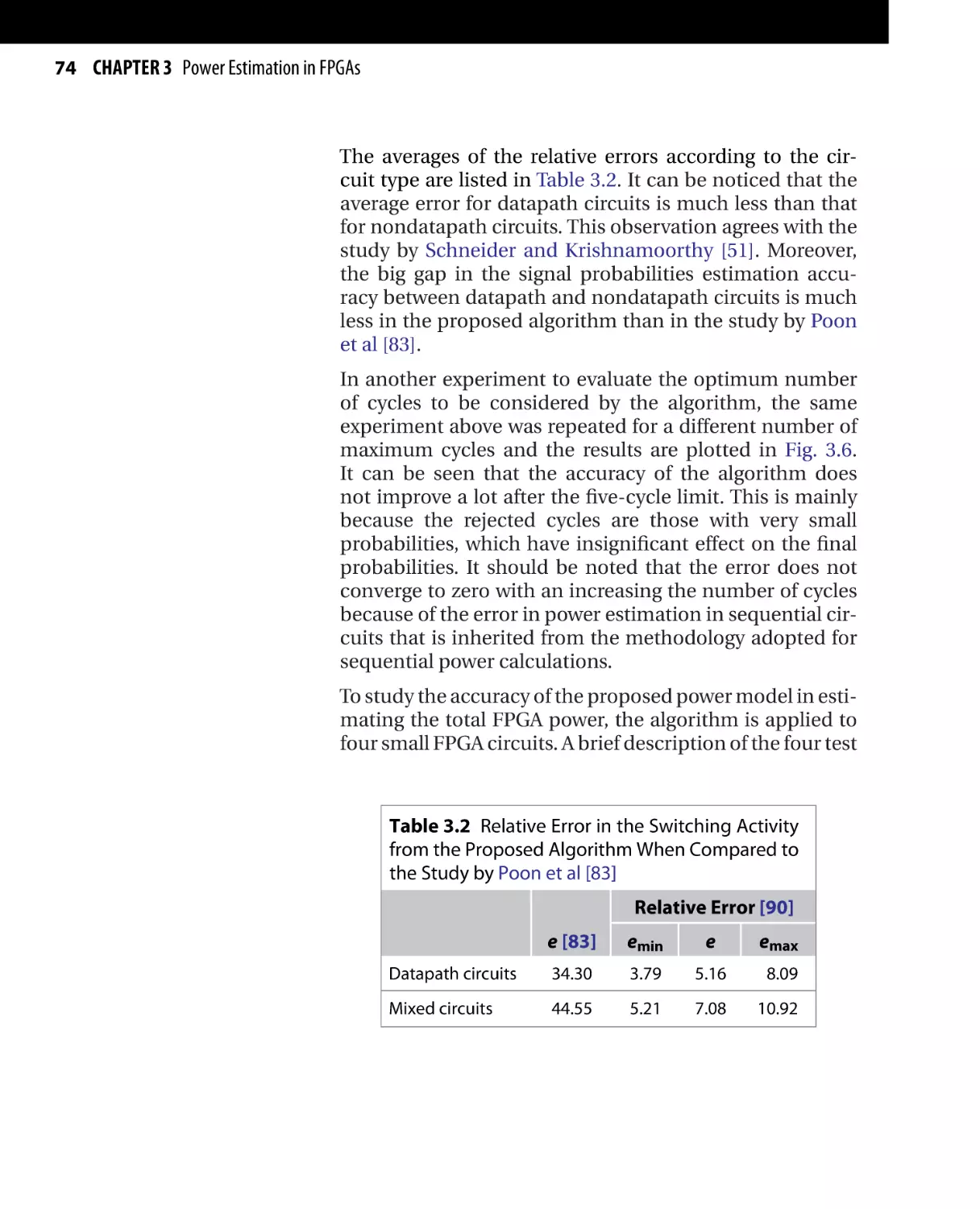
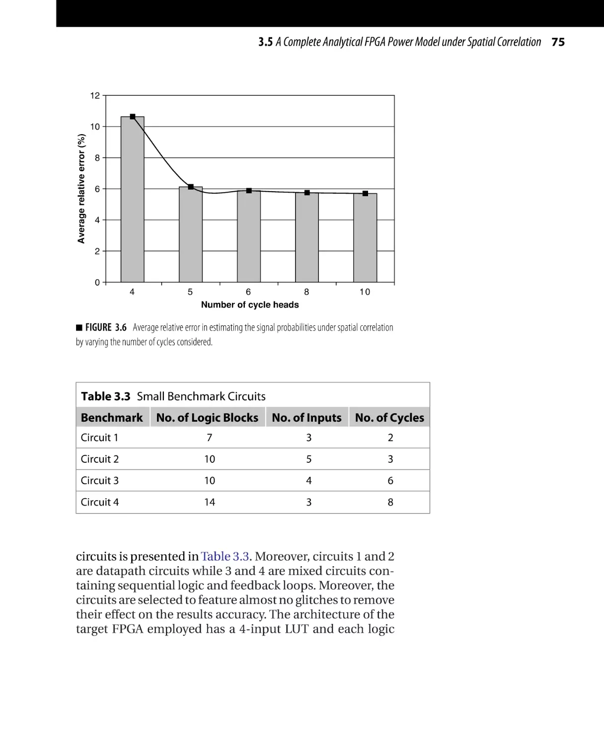
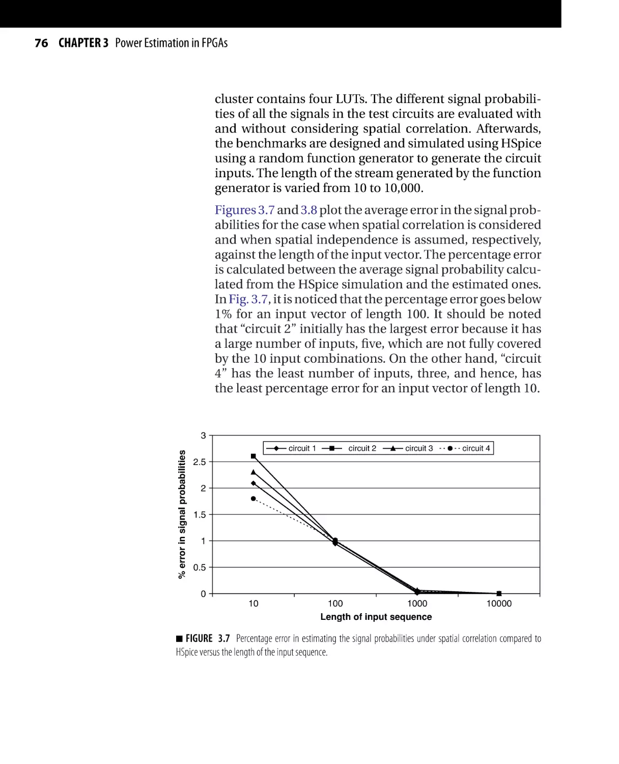
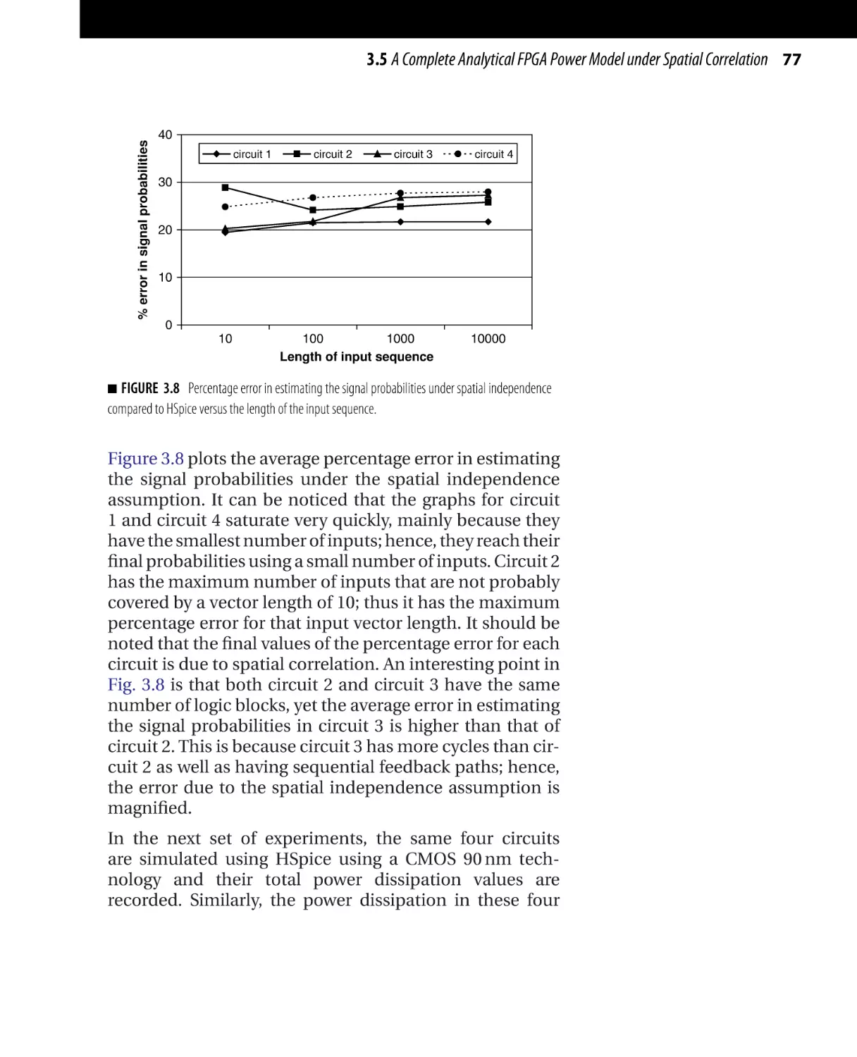
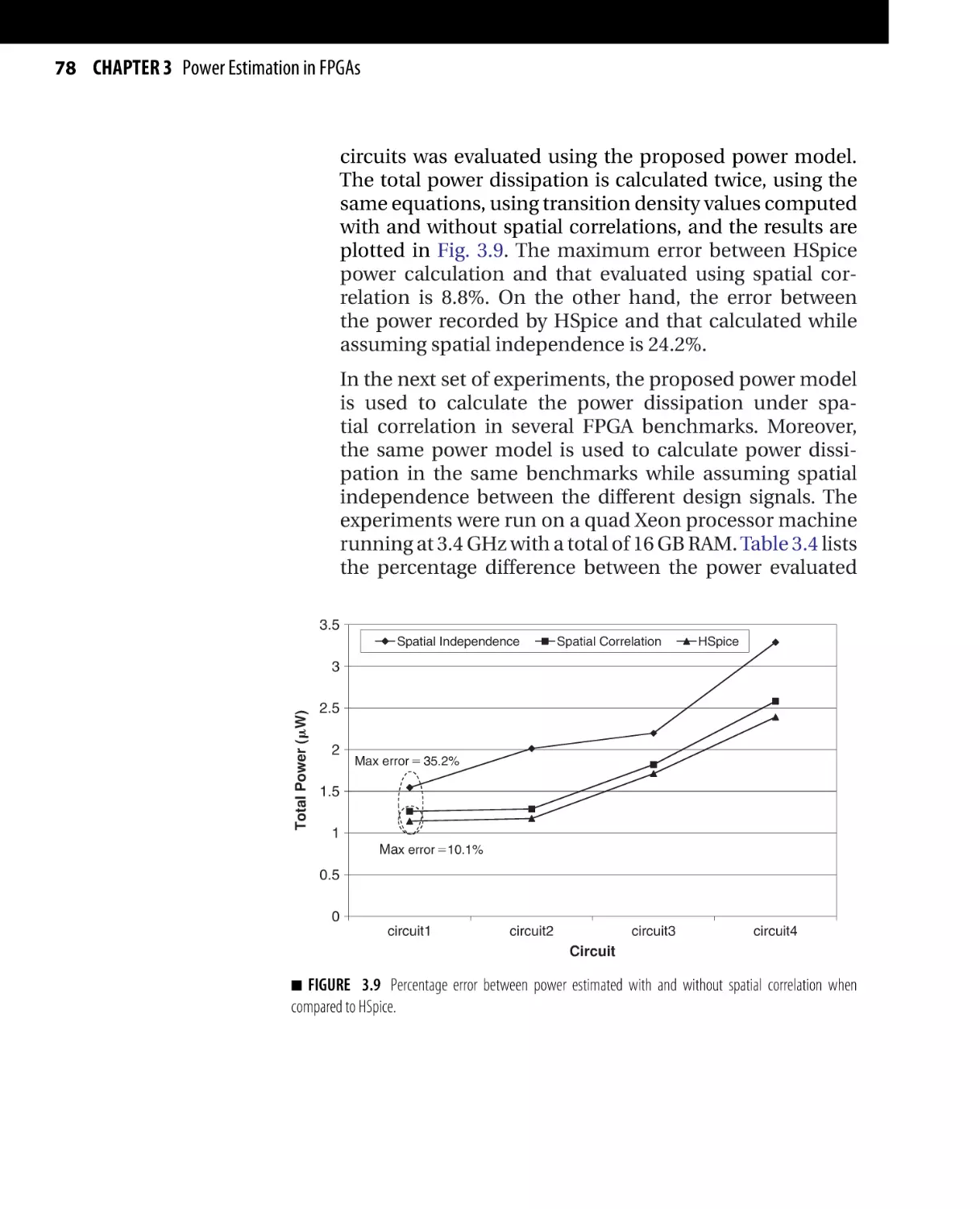
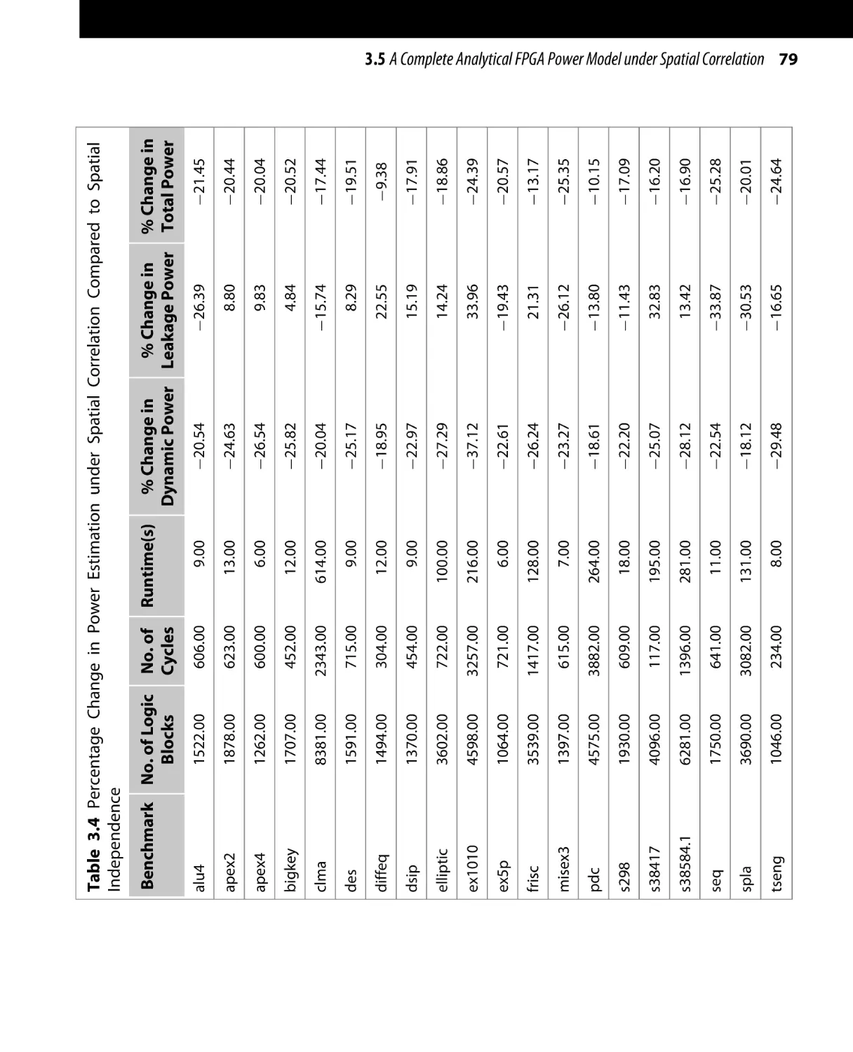
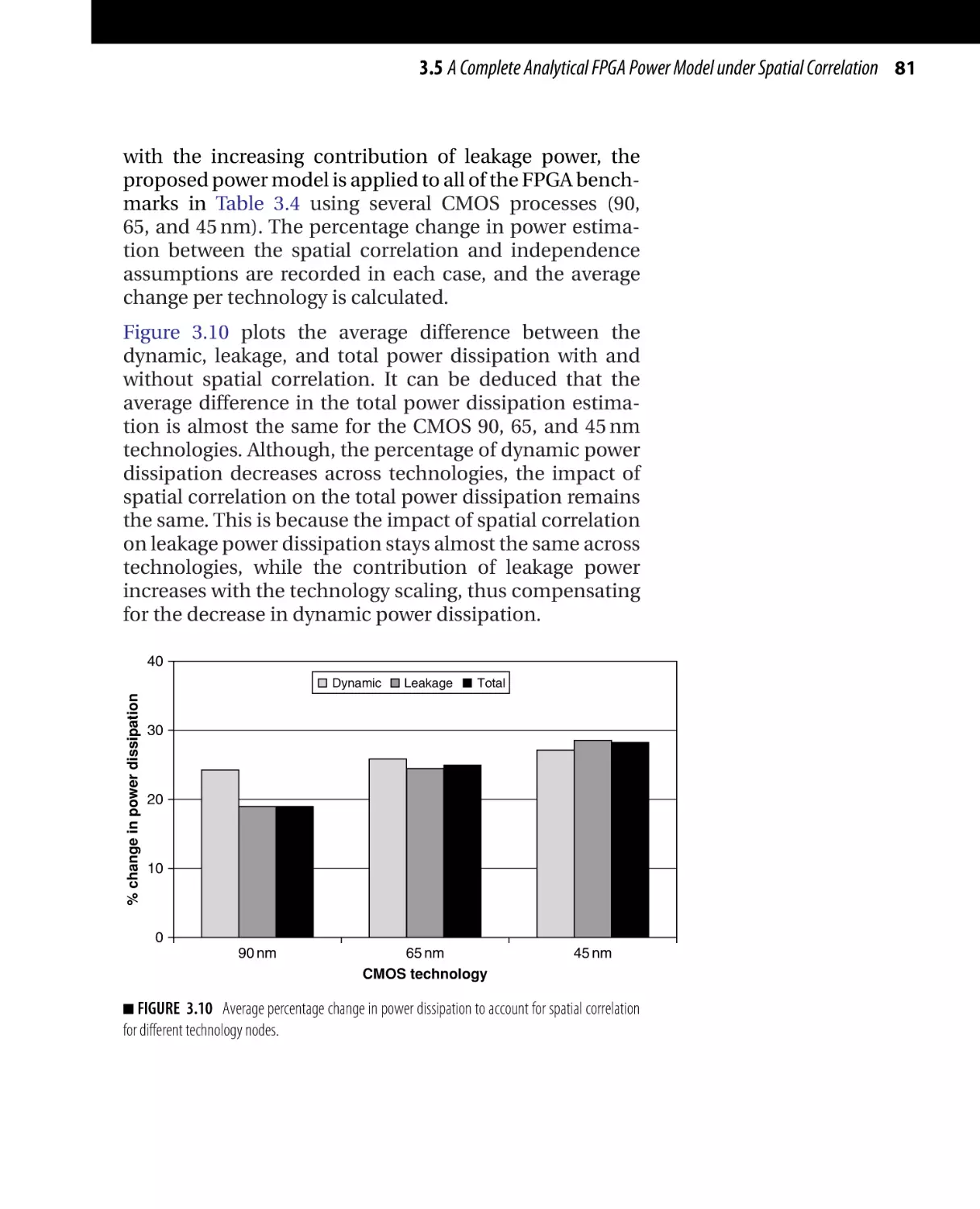
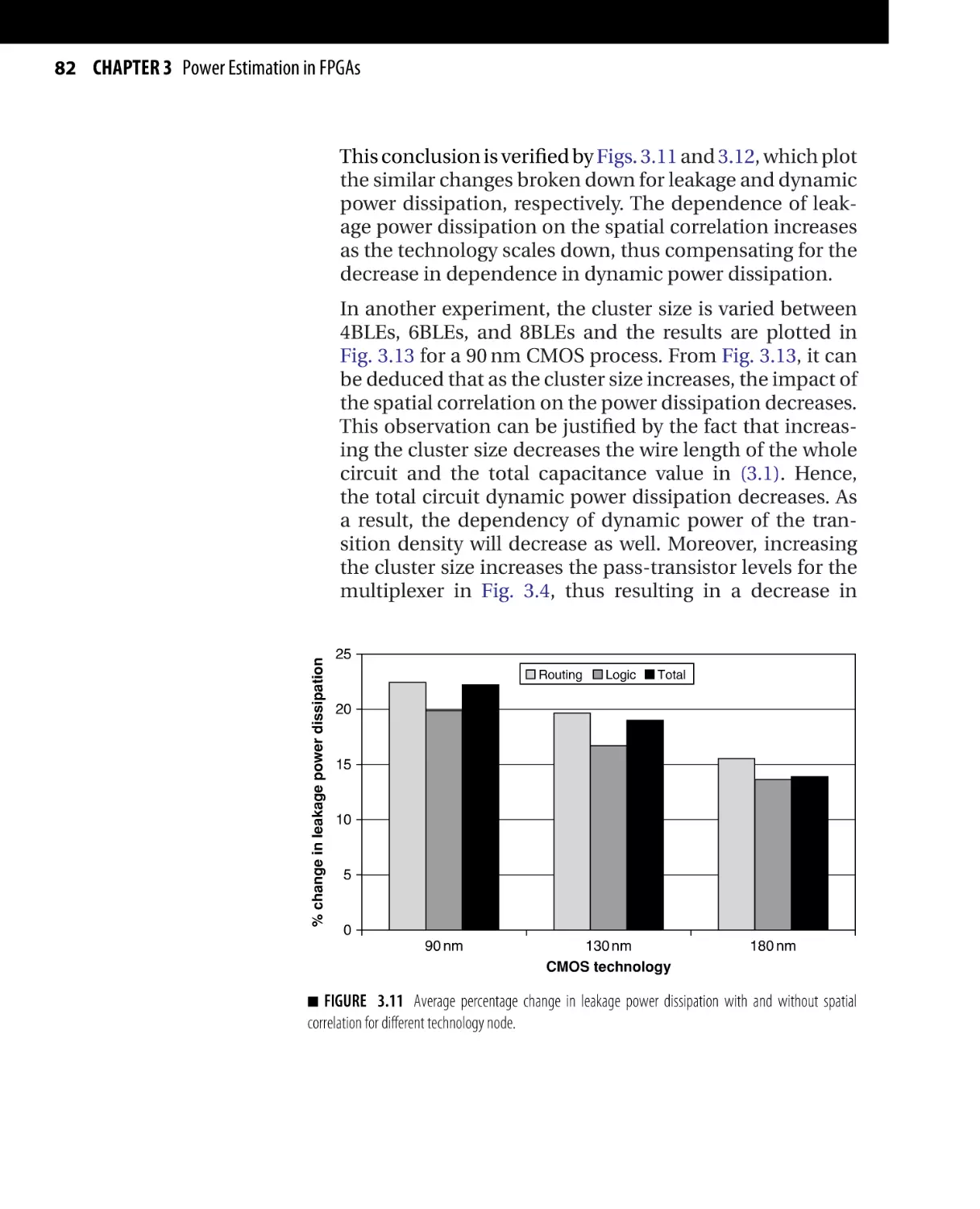
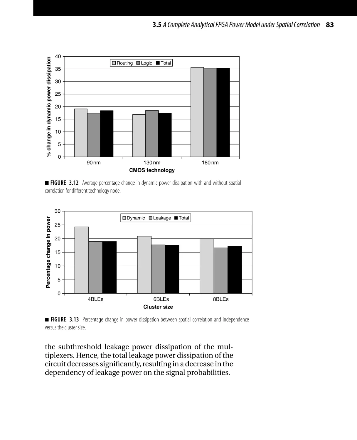
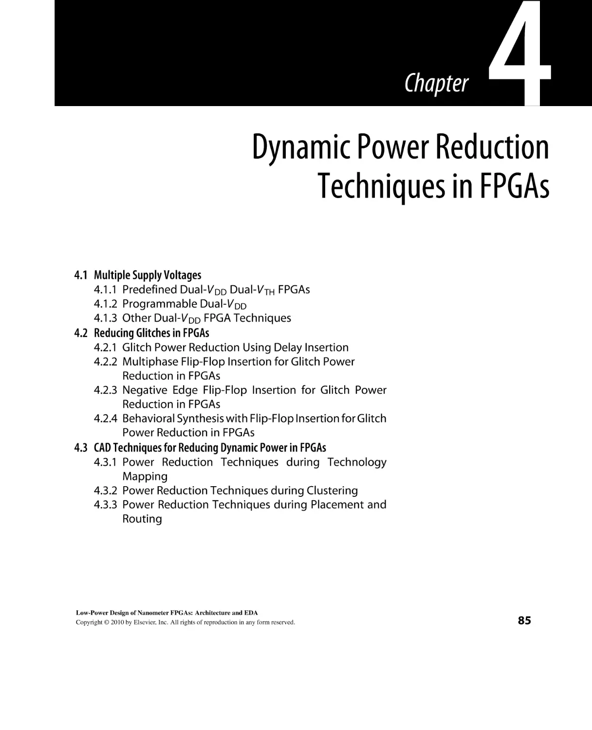
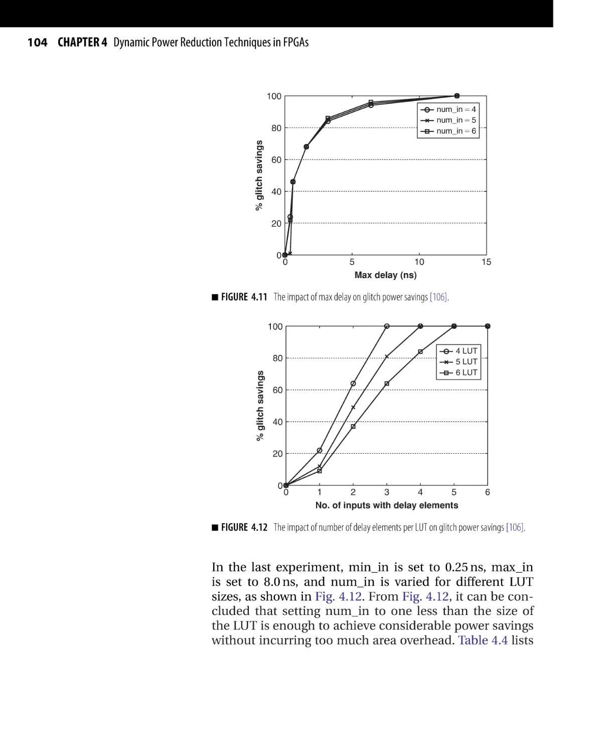
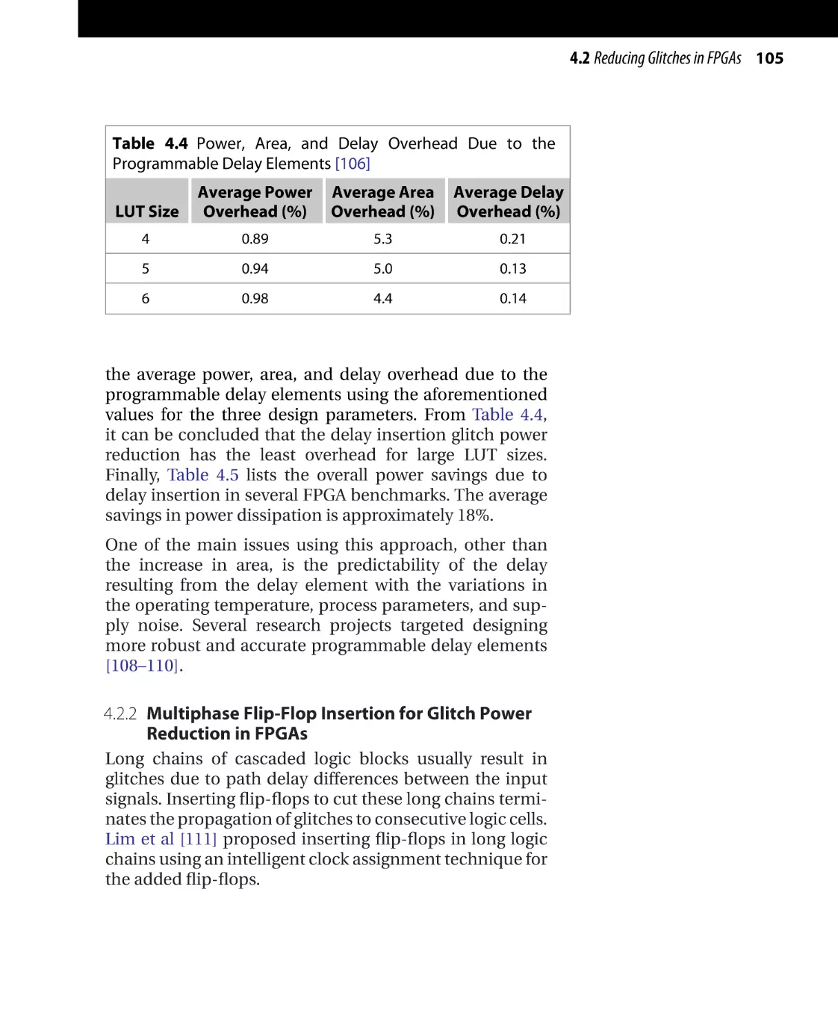
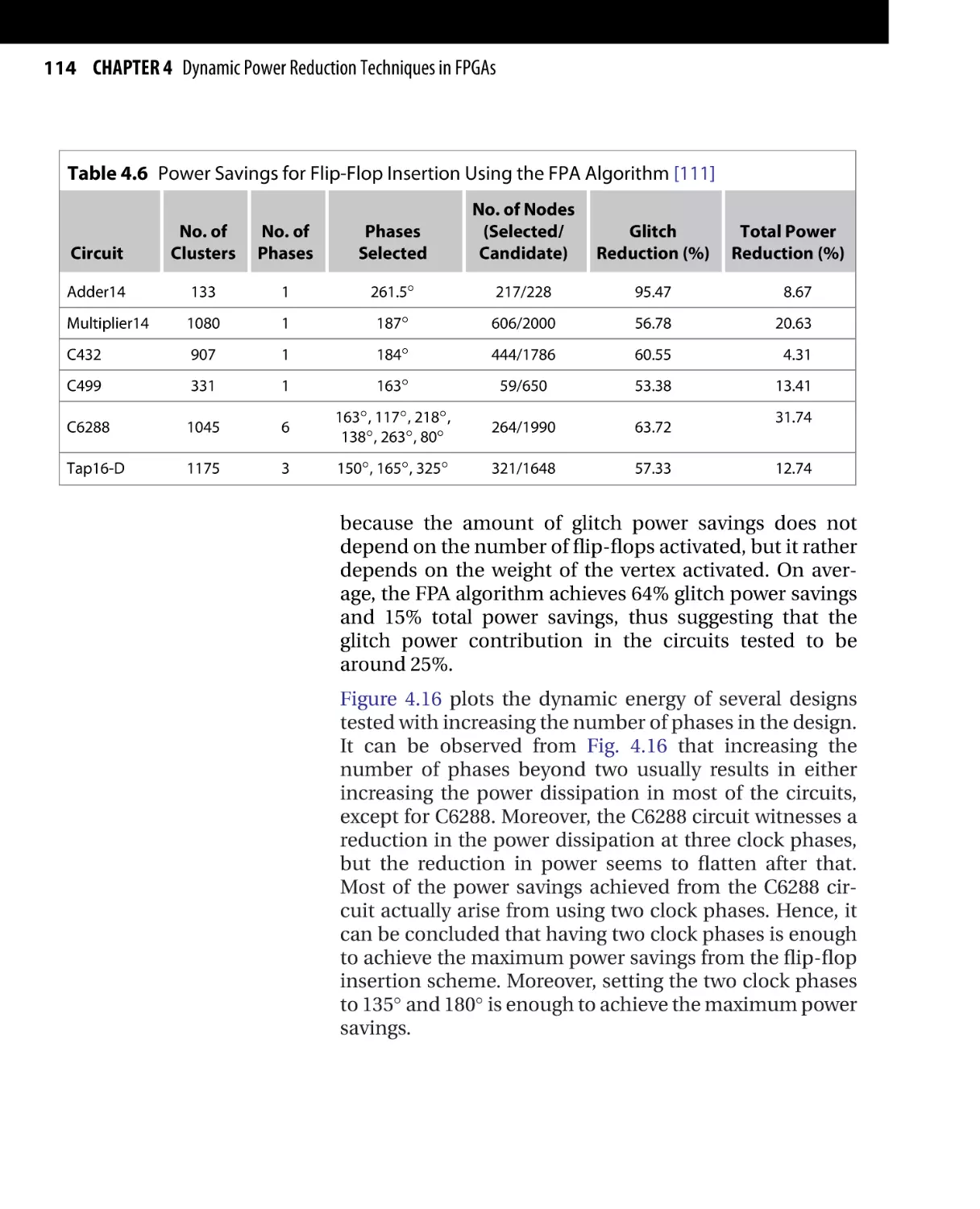
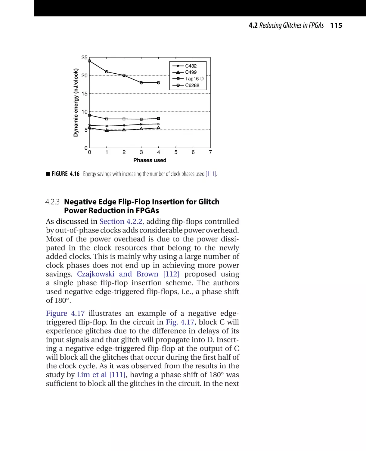
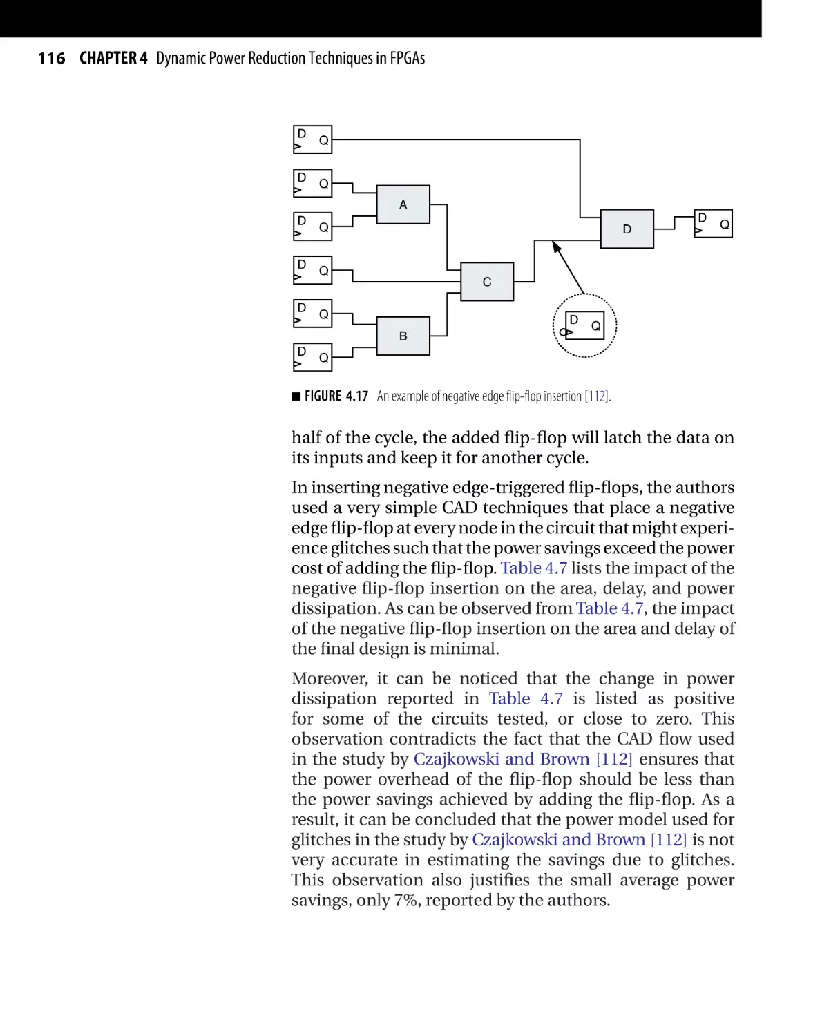
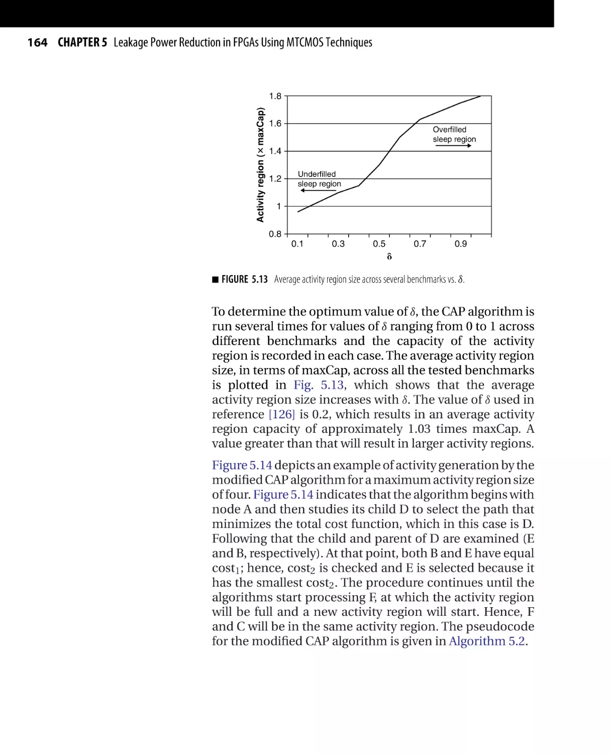
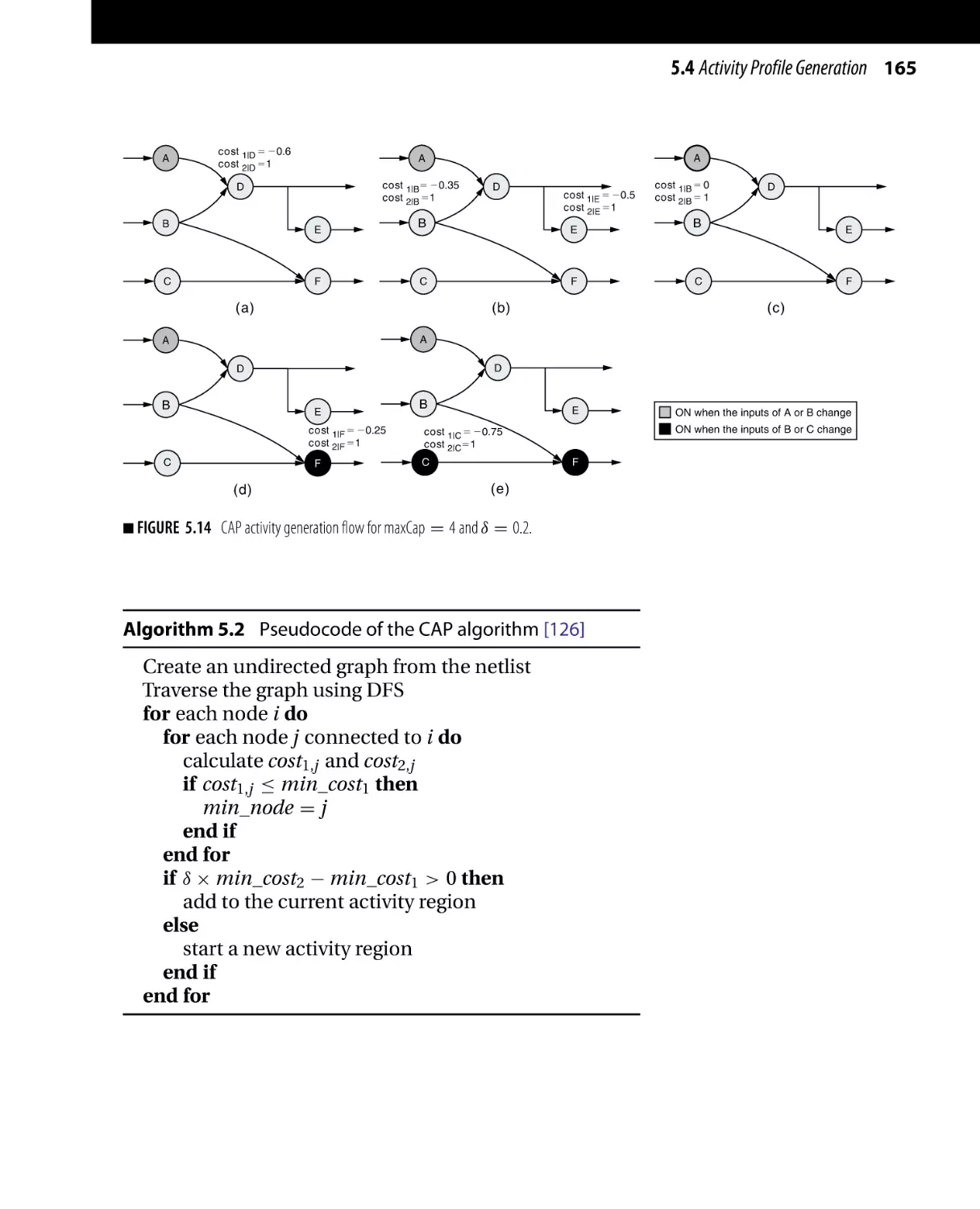
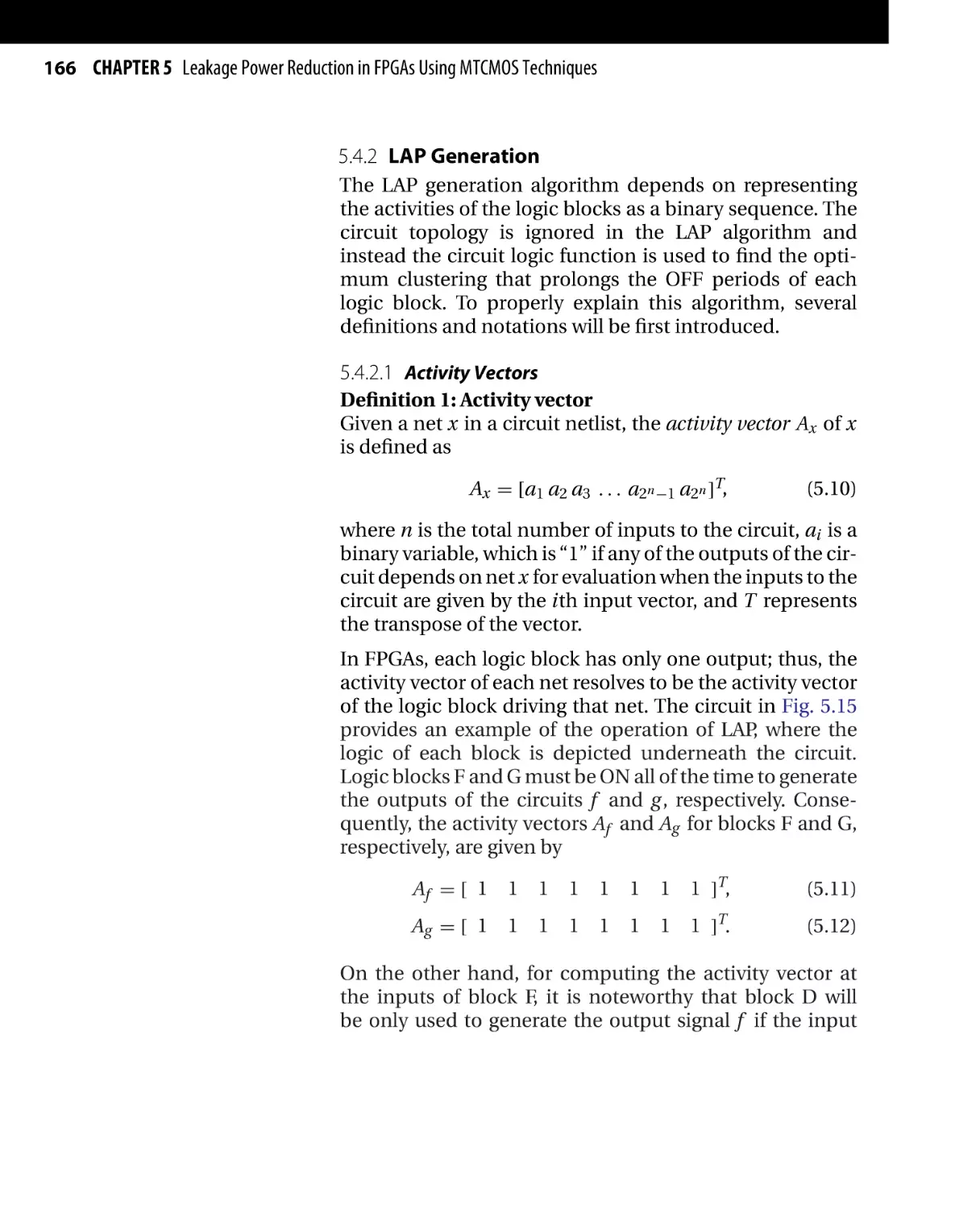
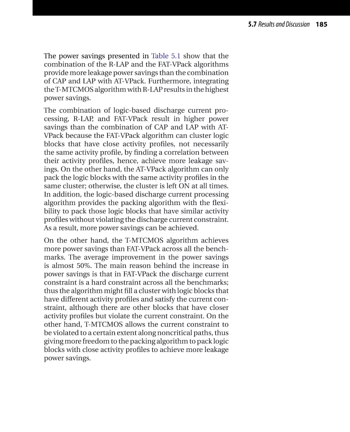
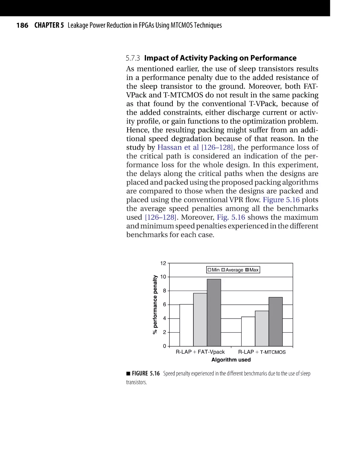
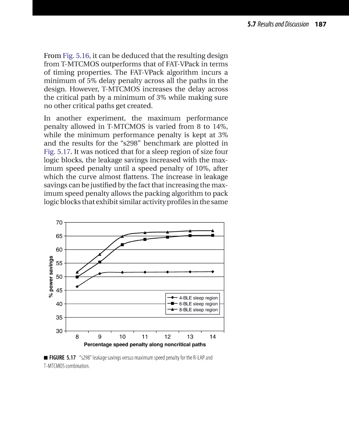
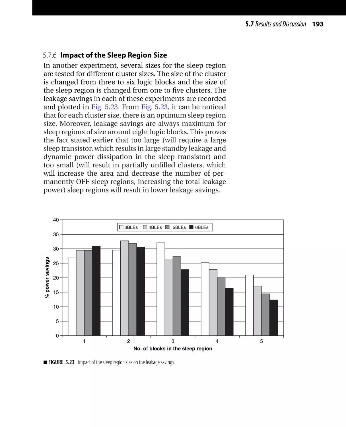
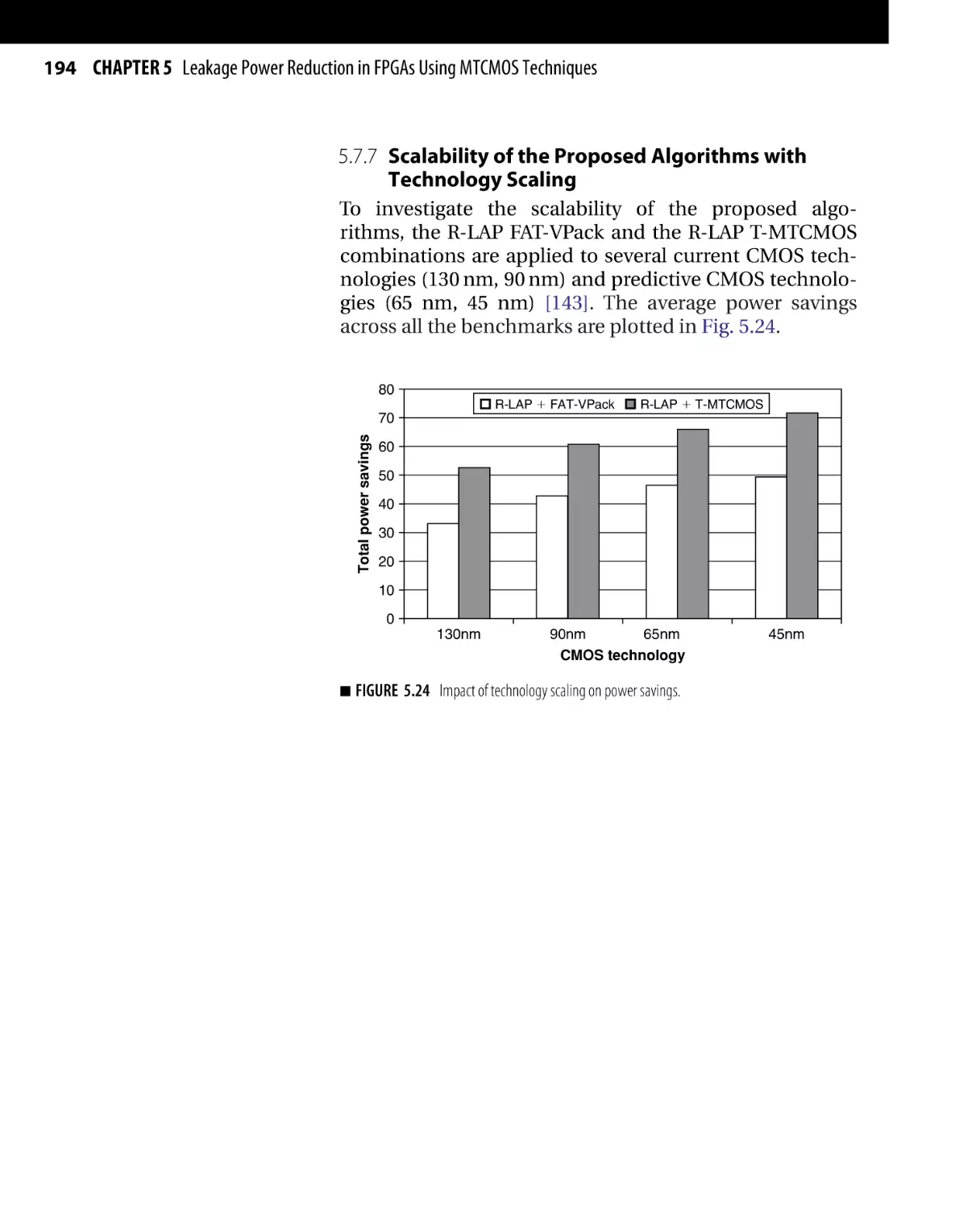
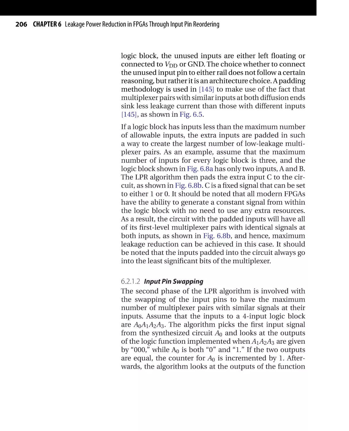
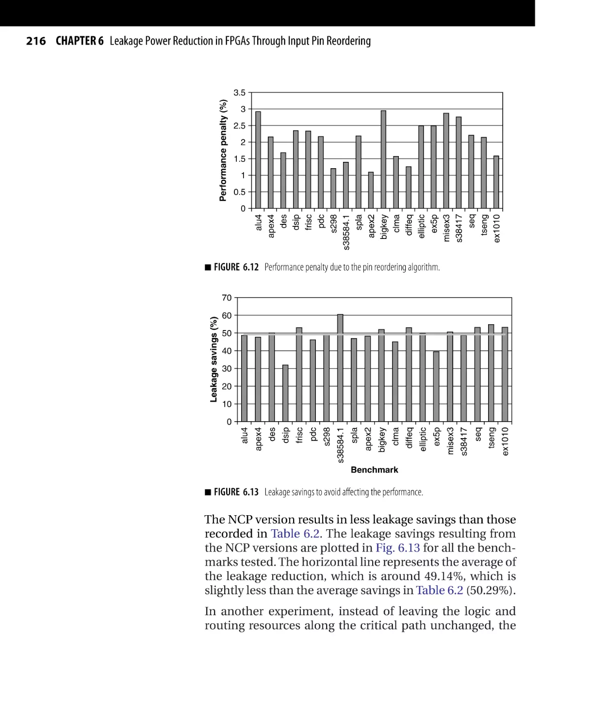
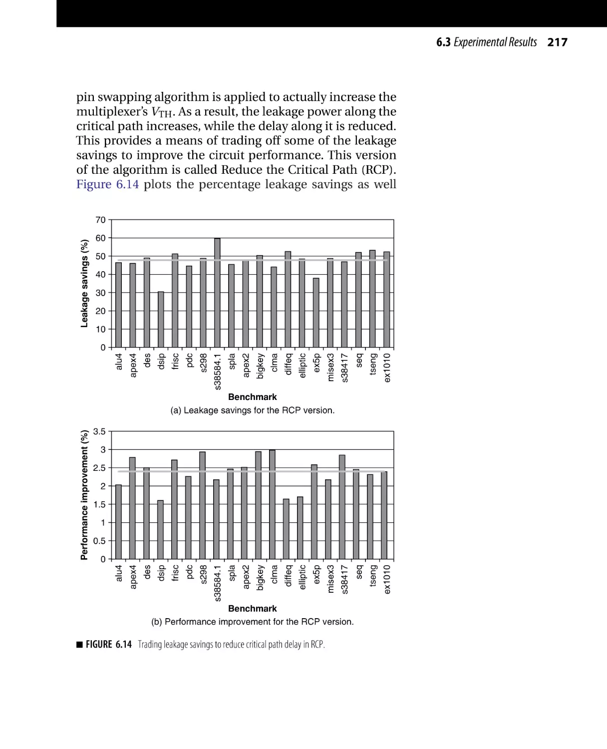
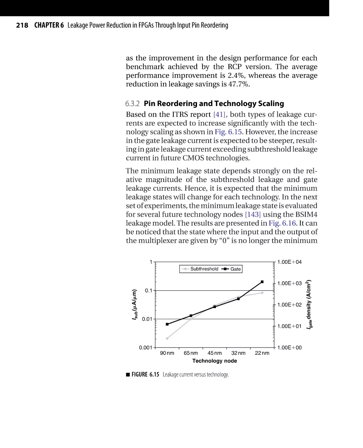
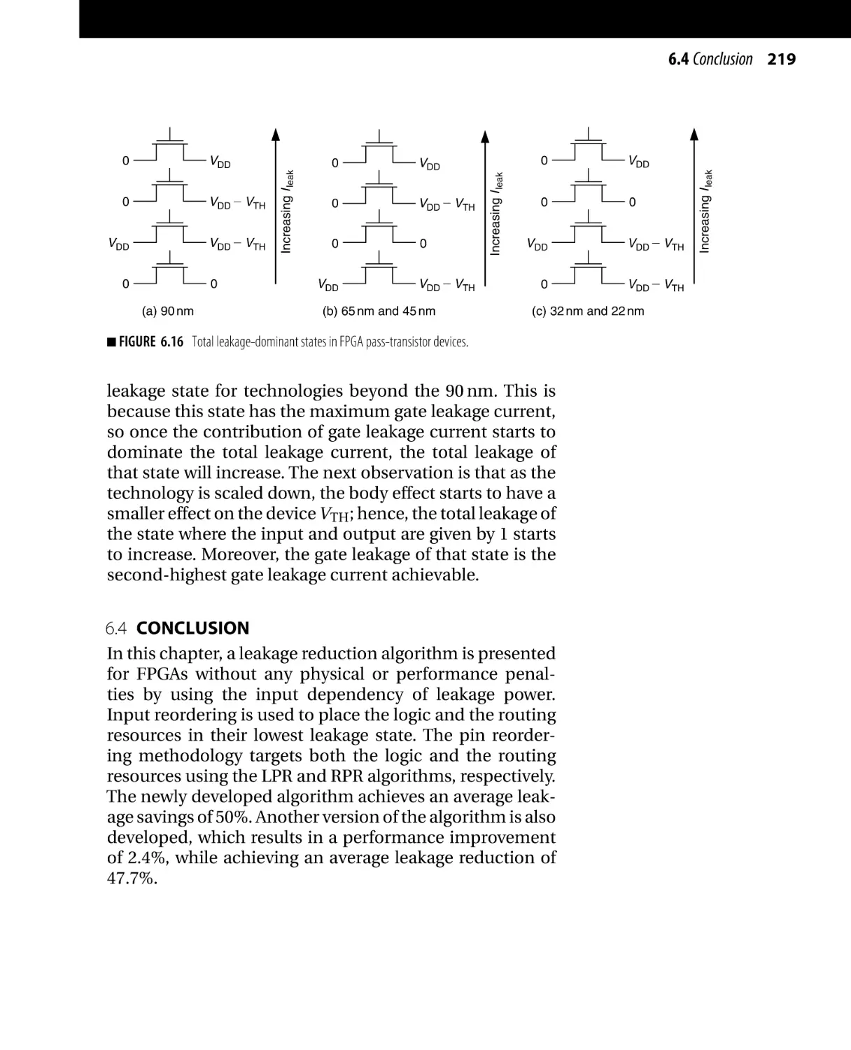
/


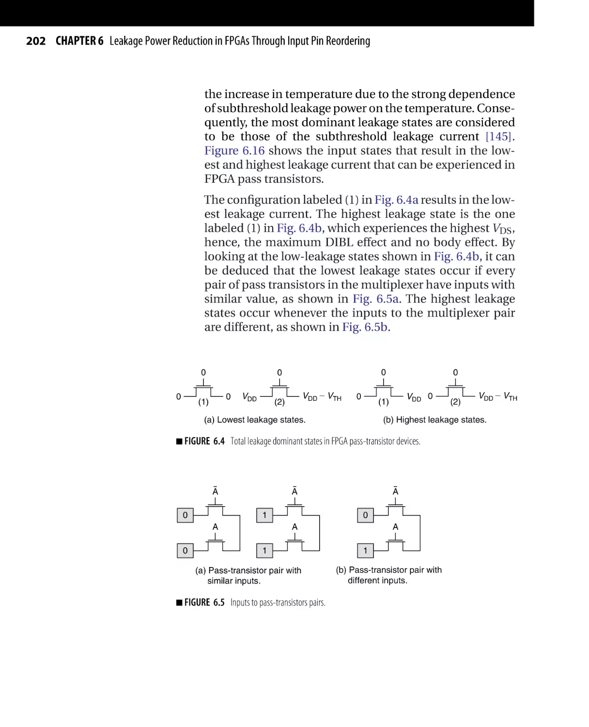
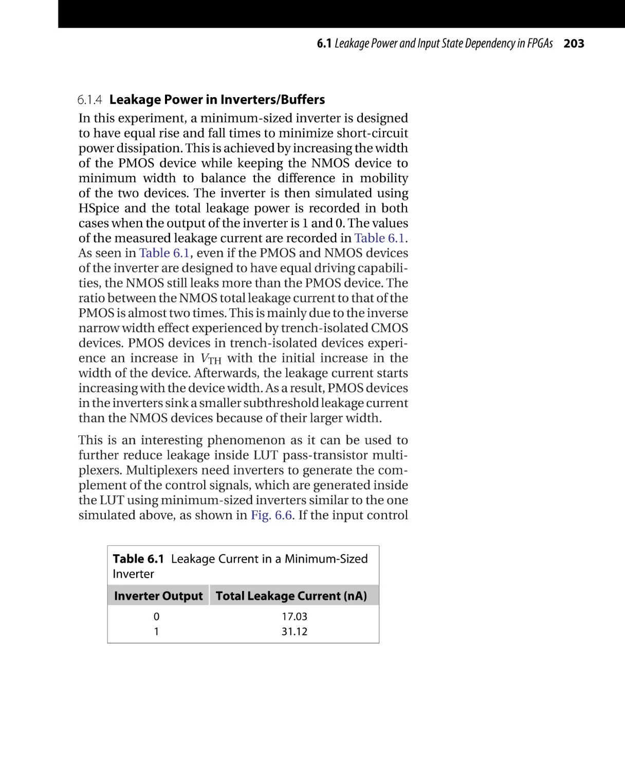


Text
Morgan Kaufmann Publishers is an imprint of Elsevier.
30 Corporate Drive, Suite 400, Burlington, MA 01803, USA
This book is printed on acid-free paper.
Copyright © 2010, Elsevier Inc. All rights reserved.
No part of this publication may be reproduced or transmitted in any form or by any means, electronic or
mechanical, including photocopying, recording, or any information storage and retrieval system, without
permission in writing from the publisher. Details on how to seek permission, further information about the
Publisher’s permissions policies, and our arrangements with organizations such as the Copyright Clearance
Center and the Copyright Licensing Agency can be found at our website: www.elsevier.com/permissions.
This book and the individual contributions contained in it are protected under copyright by the Publisher
(other than as may be noted herein).
Notices
Knowledge and best practice in this field are constantly changing. As new research and experience broaden
our understanding, changes in research methods, professional practices, or medical treatment may
become necessary.
Practitioners and researchers must always rely on their own experience and knowledge in evaluating and using
any information, methods, compounds, or experiments described herein. In using such information or methods
they should be mindful of their own safety and the safety of others, including parties for whom they have a
professional responsibility.
To the fullest extent of the law, neither the Publisher nor the authors, contributors, or editors assume any liability
for any injury and/or damage to persons or property as a matter of product liability, negligence, or otherwise, or
from any use or operation of any methods, products, instructions, or ideas contained in the material herein.
Library of Congress Cataloging-in-Publication Data
Application Submitted
British Library Cataloguing-in-Publication Data
A catalogue record for this book is available from the British Library.
ISBN: 978-0-12-374438-8
For information on all Morgan Kaufmann publications,
visit our Web site at www.mkp.com or www.elsevierdirect.com
Typeset by: diacriTech, India
Printed in the United States of America
10 11 12 13 5 4 3 2 1
To my wife, Allaa, and my supportive parents, Abdel Rahman and Nabila
– Hassan Hassan
To my wonderful family, Heba, Selim, and Adham
– Mohab Anis
Author Bios
Hassan Hassan received the B.Sc. degree (with honors) in
electronics and communication engineering from Cairo
University, Cairo, Egypt, in 2001 and the M.A.Sc. and
Ph.D. degrees in electrical engineering from the University of Waterloo, Waterloo, ON, Canada, in 2004 and 2008,
respectively.
Dr. Hassan is currently a staff engineer in the timing
and power group at Actel Corporation. He has authored/
coauthored more than 20 papers in international journals
and conferences. His research interests include integrated
circuit design and design automation for deep submicron VLSI systems. He is also a member of the program
committee for several IEEE conferences.
Mohab Anis received the B.Sc. degree (with honors) in
electronics and communication engineering from Cairo
University, Cairo, Egypt, in 1997 and the M.A.Sc. and
Ph.D. degrees in electrical engineering from the University of Waterloo, Waterloo, ON, Canada, in 1999 and 2003,
respectively.
Dr. Anis is currently a tenured Associate Professor at
the Department of Electrical and Computer Engineering, University of Waterloo. During 2009, he was with
the Electronics Engineering Department at the American University in Cairo. He has authored/coauthored over
80 papers in international journals and conferences and
is the author of the book Multi-Threshold CMOS Digital Circuits—Managing Leakage Power (Kluwer, 2003).
His research interests include integrated circuit design
and design automation for VLSI systems in the deep
submicrometer regime.
Dr. Anis is an Associate Editor of the IEEE Transactions
on Circuits and Systems—II, Microelectronics Journal, Journal of Circuits, Systems and Computers, ASP Journal of Low
xiii
xiv Author Bios
Power Electronics, and VLSI Design. He is also a member
of the program committee for several IEEE conferences.
He was awarded the 2009 Early Research Award, the
2004 Douglas R. Colton Medal for Research Excellence
in recognition of excellence in research leading to new
understanding and novel developments in microsystems
in Canada and the 2002 International Low-Power Design
Contest.
Dr. Anis also holds two business degrees: an M.B.A. with
concentration in Innovation and Entrepreneurship from
Wilfrid Laurier University, and an M.M.S. from the University of Waterloo. He is the co-founder of Spry Design
Automation Inc. and has published a number of papers on
technology transfer.
Chapter
1
FPGA Overview:
Architecture and CAD
1.1 Introduction
1.2 FPGA Logic Resources Architecture
1.2.1
1.2.2
1.2.3
1.2.4
Altera Stratix IV Logic Resources
Xilinx Virtex-5 Logic Resources
Actel ProASIC3/IGLOO Logic Resources
Actel Axcelerator Logic Resources
1.3 FPGA Routing Resources Architecture
1.4 CAD for FPGAs
1.4.1
1.4.2
1.4.3
1.4.4
1.4.5
Logic Synthesis
Packing
Placement
Timing Analysis
Routing
1.5 Versatile Place and Route (VPR) CAD Tool
1.5.1
1.5.2
1.5.3
1.5.4
1.5.5
VPR Architectural Assumptions
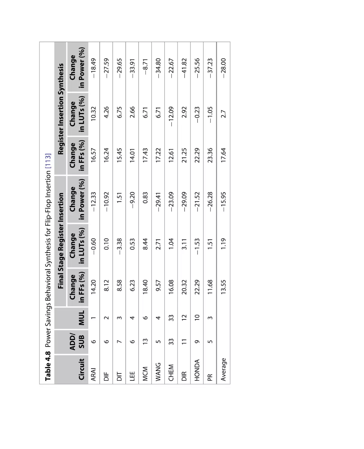
Basic Logic Packing Algorithm: VPack
Timing-Driven Logic Block Packing: T-VPack
Placement: VPR
Routing: VPR
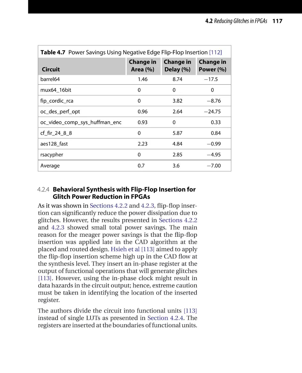
Low-Power Design of Nanometer FPGAs: Architecture and EDA
Copyright © 2010 by Elsevier, Inc. All rights of reproduction in any form reserved.
1
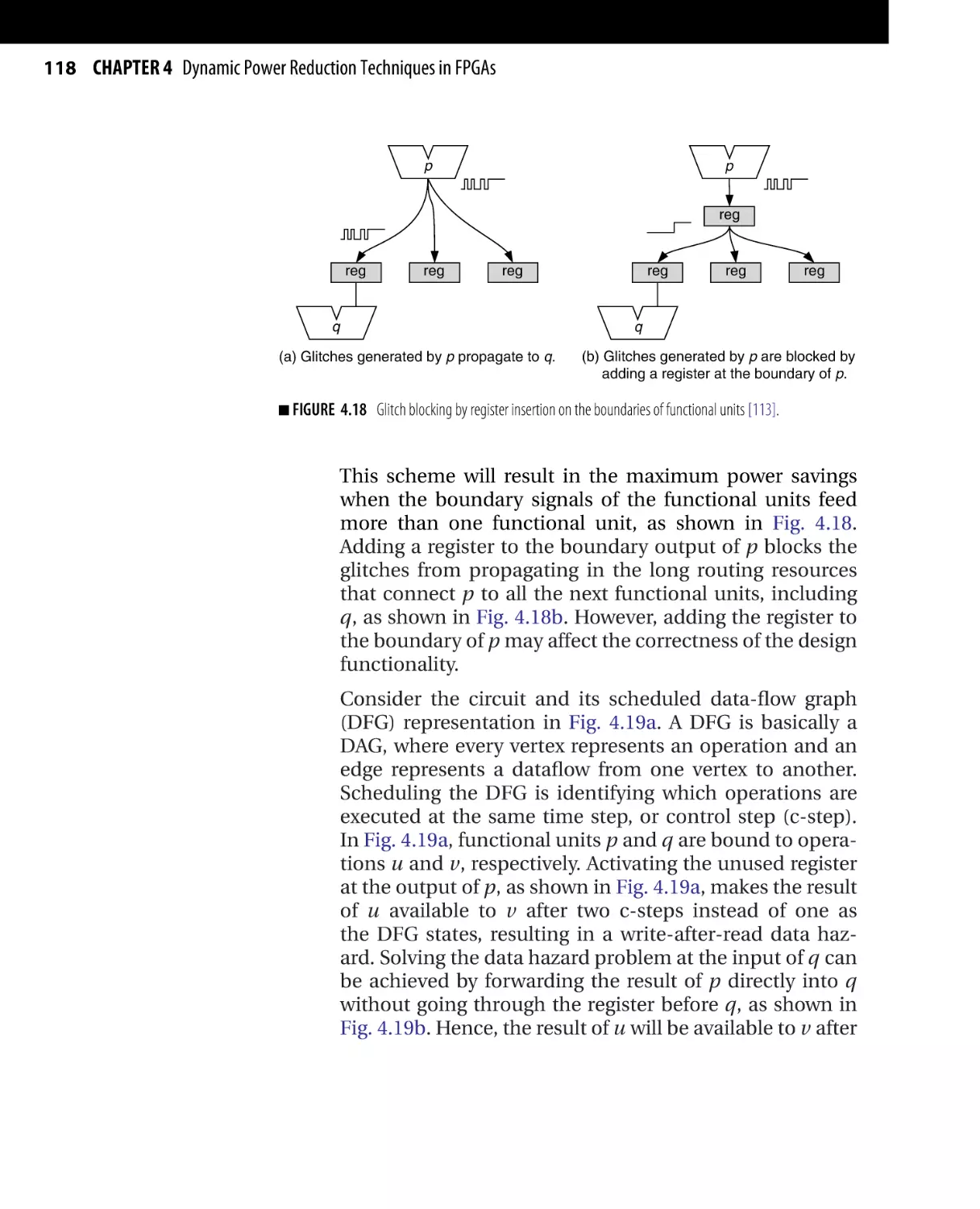
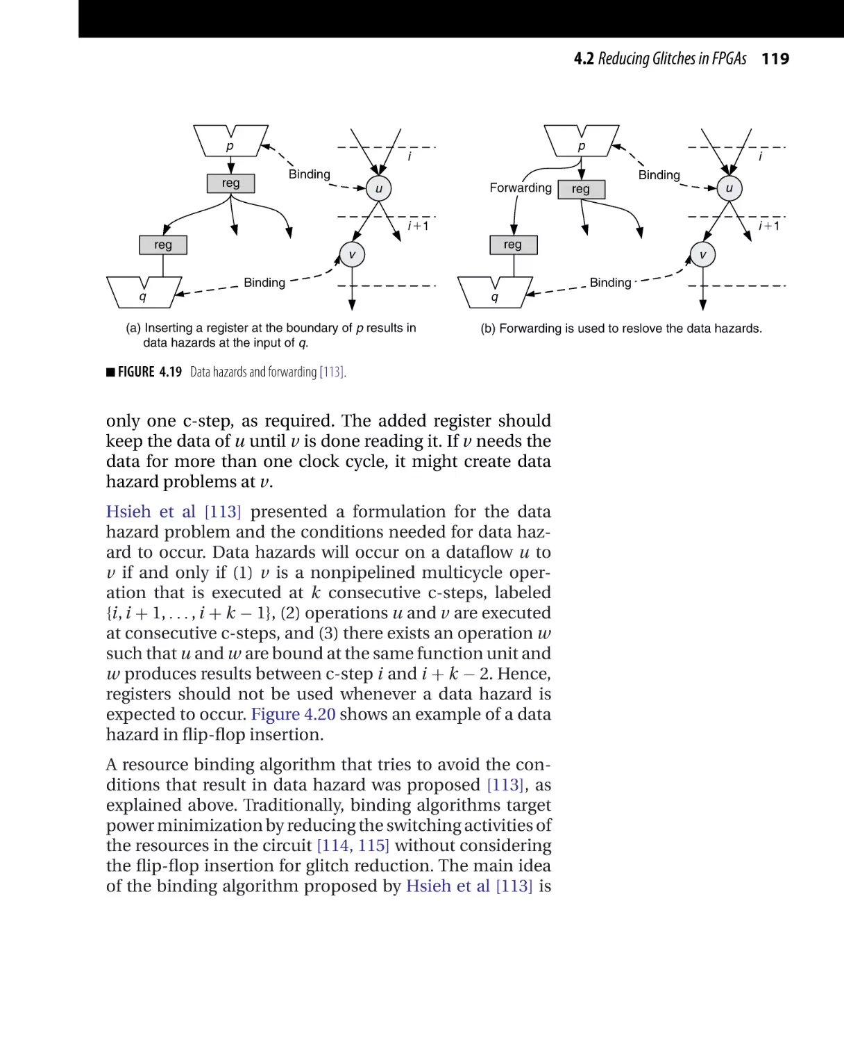
2 CHAPTER 1 FPGA Overview: Architecture and CAD
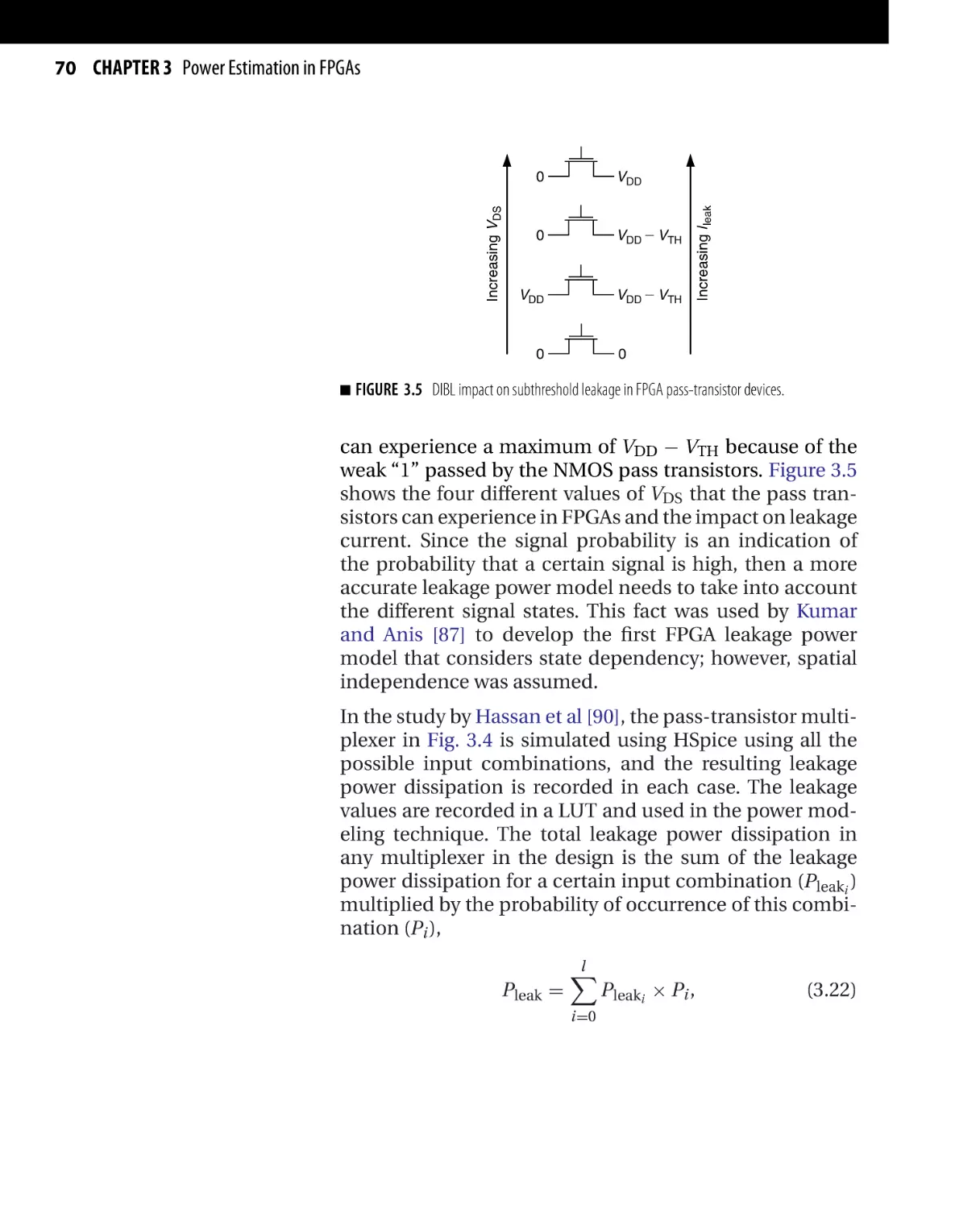
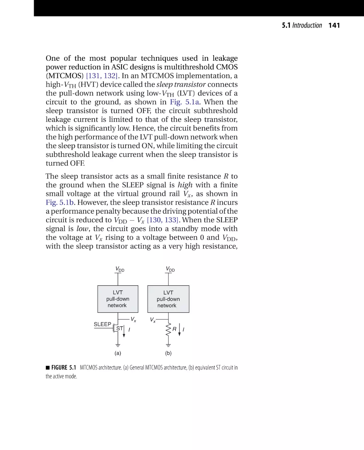
1.1 INTRODUCTION
Field programmable gate arrays (FPGAs) were first introduced to the very-large-scale integration (VLSI) market in
the 1980s [1]. Initially, FPGAs were designed to complement application-specific integrated circuit (ASIC) designs
by providing reprogrammability on the expense of power
dissipation, chip area, and performance. The main advantages of FPGAs compared to ASIC designs can be summarized as follows:
■
FPGAs’ time-to-market is minimal when compared
to ASIC designs. Once a fully tested design is available, the design can be burned into the FPGA and
verified, hence initiating the production phase. As a
result, FPGAs eliminate the fabrication wait time.
■
FPGAs are excellent candidates for low-volume productions since they eliminate the mask generation
cost.
■
FPGAs are ideal for prototyping purposes. Hardware
testing and verification can be quickly performed on
the chip. Moreover, design errors can be easily fixed
without incurring any additional hardware costs.
■
FPGAs are versatile and reprogrammable, thus allowing them to be used in several designs at no additional
costs.
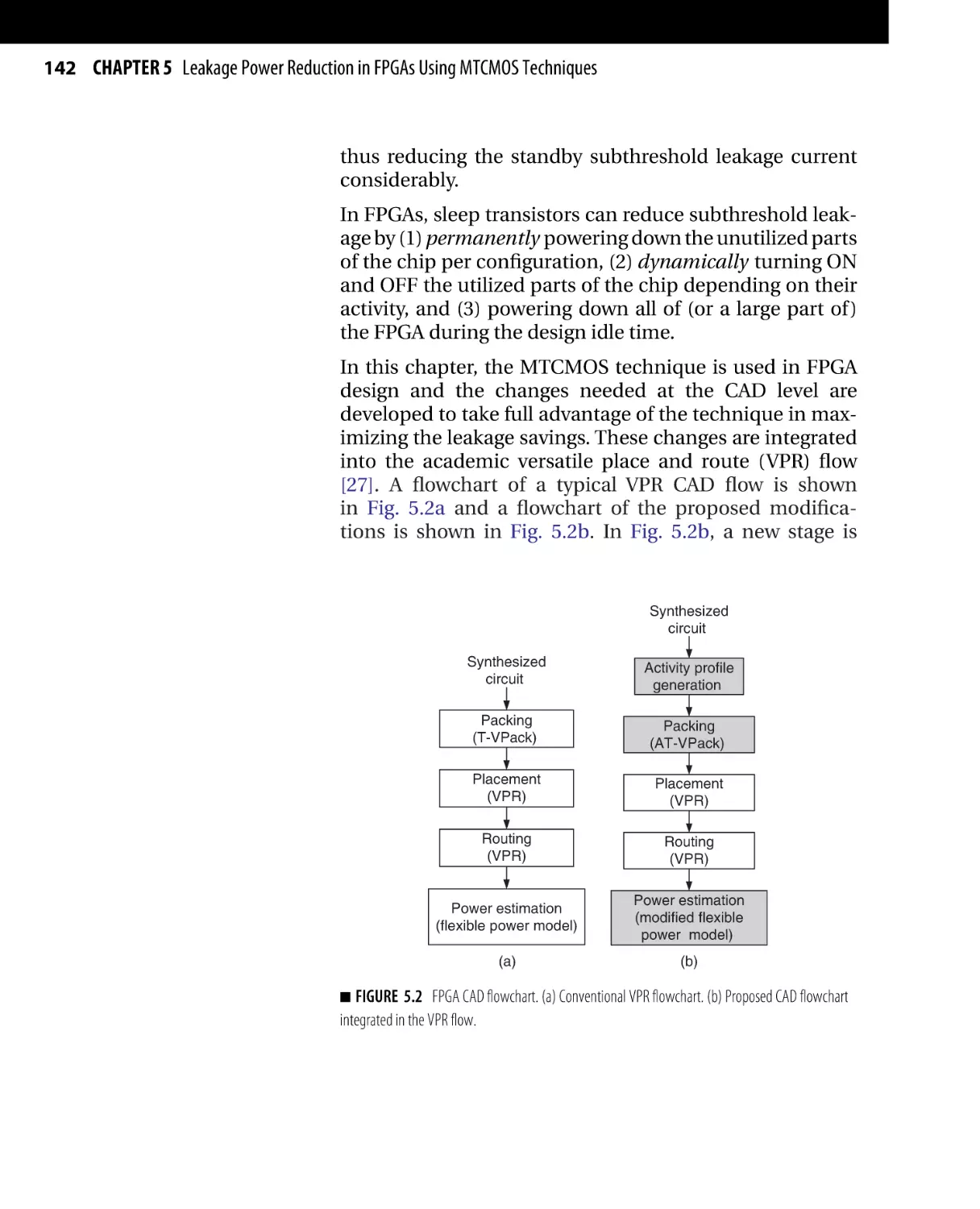
Fueled by the increase in the time-to-market pressures, the
rise in ASIC mask and development costs, and increase in
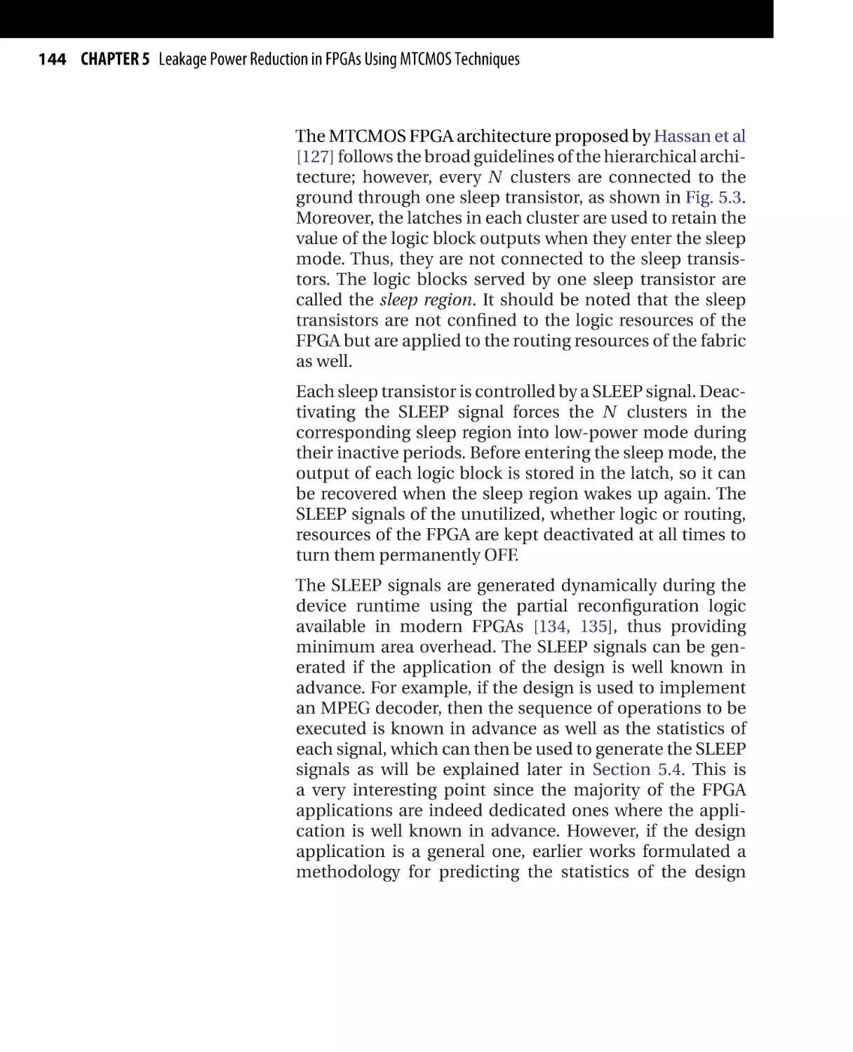
the FPGAs’ performance and system-level features, more
and more traditionally ASIC designers are migrating their
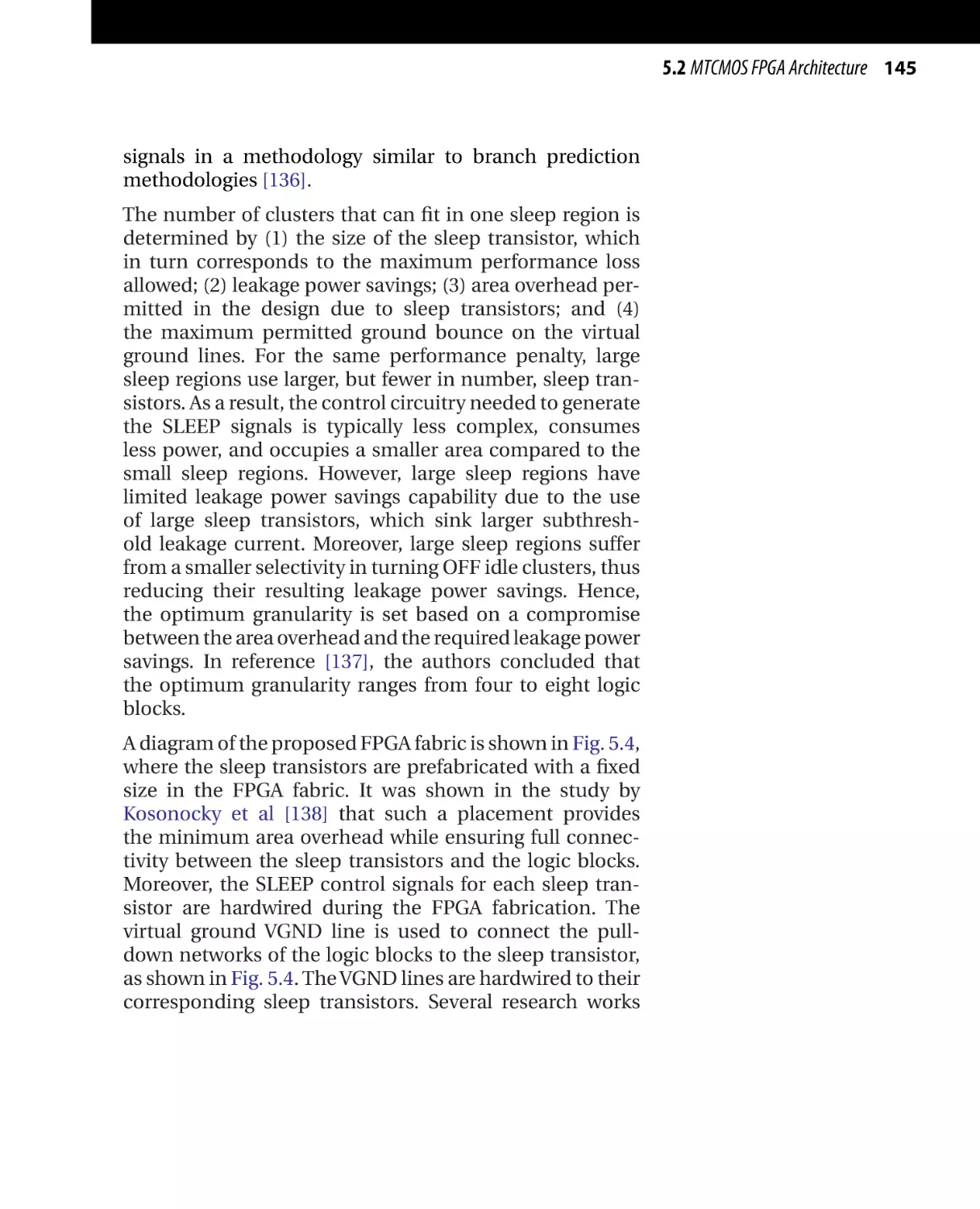
designs to programmable logic devices (PLDs). Moreover,
PLDs progressed both in terms of resources and performance. The latest FPGAs have come to provide platform
solutions that are easily customizable for system connectivity, digital signal processing (DSP), and/or data processing applications. These platform building tools accelerate
the time-to-market by automating the system definition
1.1 Introduction 3
and integration phases of the system on programmable
chip (SoPC) development.
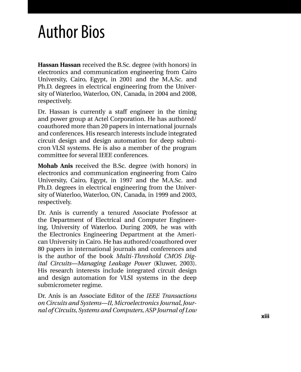
FPGAs belong to a type of VLSI circuits called PLDs. The
first PLD devices developed are the programmable array
logic (PAL) devices designed by Monolithic Memories Inc.
in 1978. PALs adopt a simple PLD (SPLD) architecture,
where functionality is provided by a matrix of AND gates
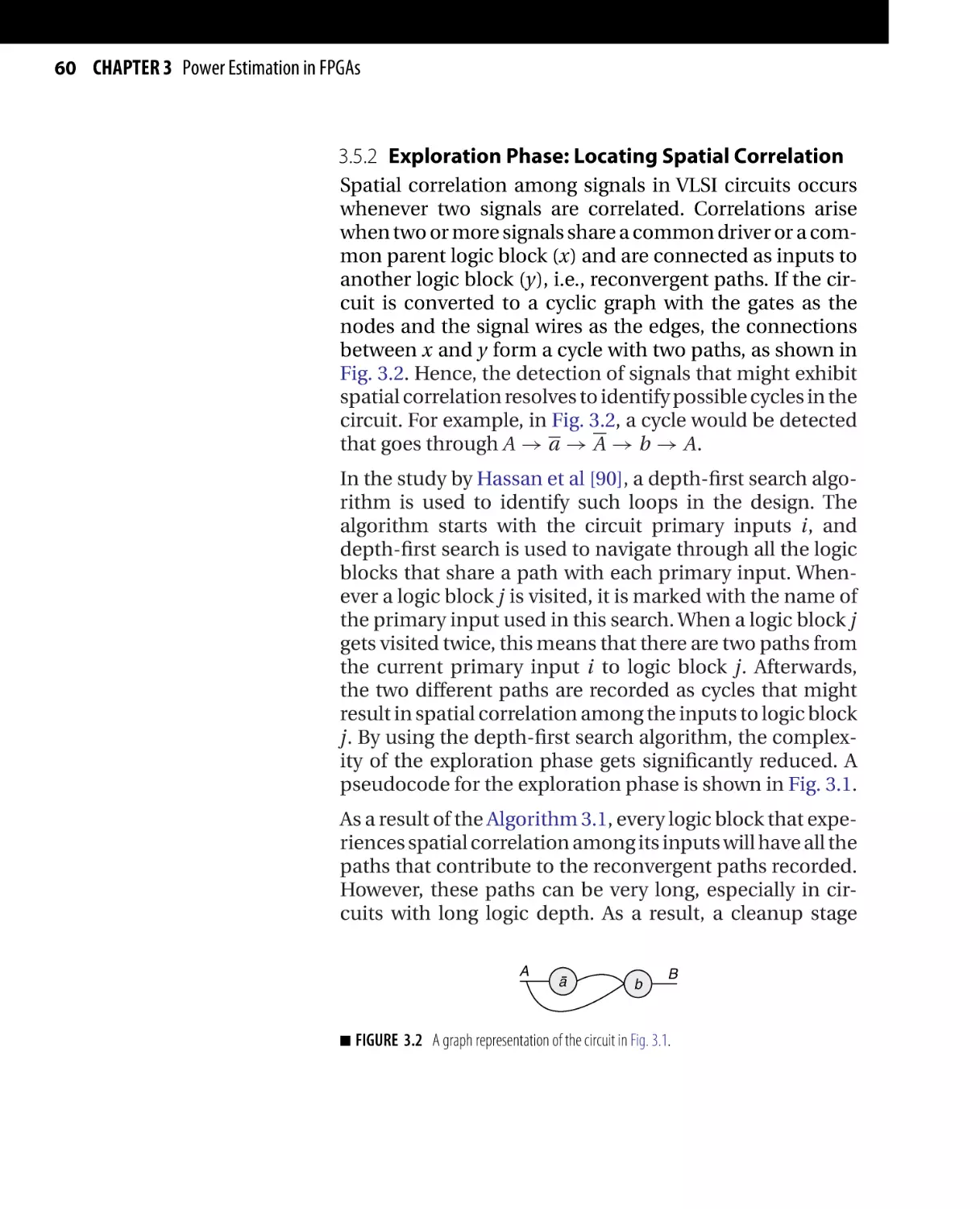
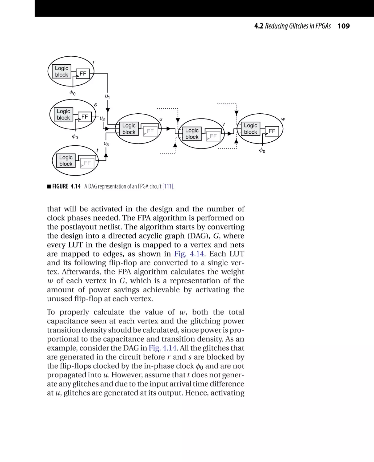
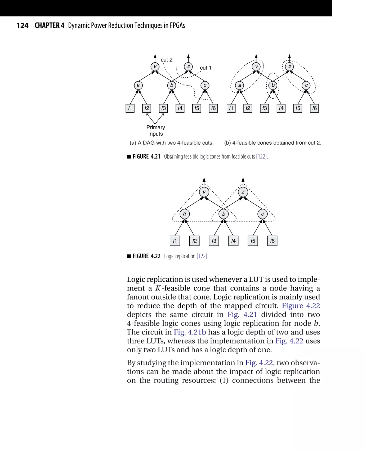
followed by a matrix of OR gates to implement sum-ofproducts function representation, as shown in Fig. 1.1.
It should be noted that PAL devices are limited to only
two-level logic functionality. Complex PLDs (CPLDs) succeeded PALs in the PLD market to offer higher-order
logic functionality. CPLDs consist of SLPD-like devices
that are interconnected using a programmable switch
A
B
F0
■
FIGURE 1.1 PAL architecture.
F1
F2
F3
4 CHAPTER 1 FPGA Overview: Architecture and CAD
matrix. Despite the increase in the complexity of the
functionality of CPLDs, their use remained limited to glue
logic in large designs. Finally, FPGAs were introduced to
offer more complex functionality by employing a look-up
table (LUT) approach to implement logic functions and
channel-based routing strategy. The first commercial PLD
that adopts the FPGA architecture was developed by Xilinx
in 1984.
Recently, FPGA vendors provided a comprehensive alternative to FPGAs for large-volume demands called structured ASICs [2, 3]. Structured ASICs offer a complete
solution from prototype to high-volume production and
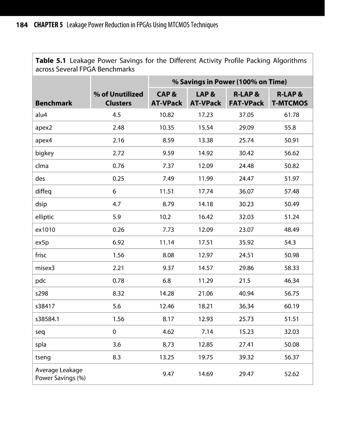
maintain the powerful features and high-performance
architecture of their equivalent FPGAs with the programmability removed. Structured ASIC solutions not only
provide performance improvement, but also result in
significant high-volume cost reduction than FPGAs.
FPGAs consist of programmable logic resources embedded in a sea of programmable interconnects. The programmable logic resources can be configured to implement
any logic function, while the interconnects provide the
flexibility to connect any signal in the design to any
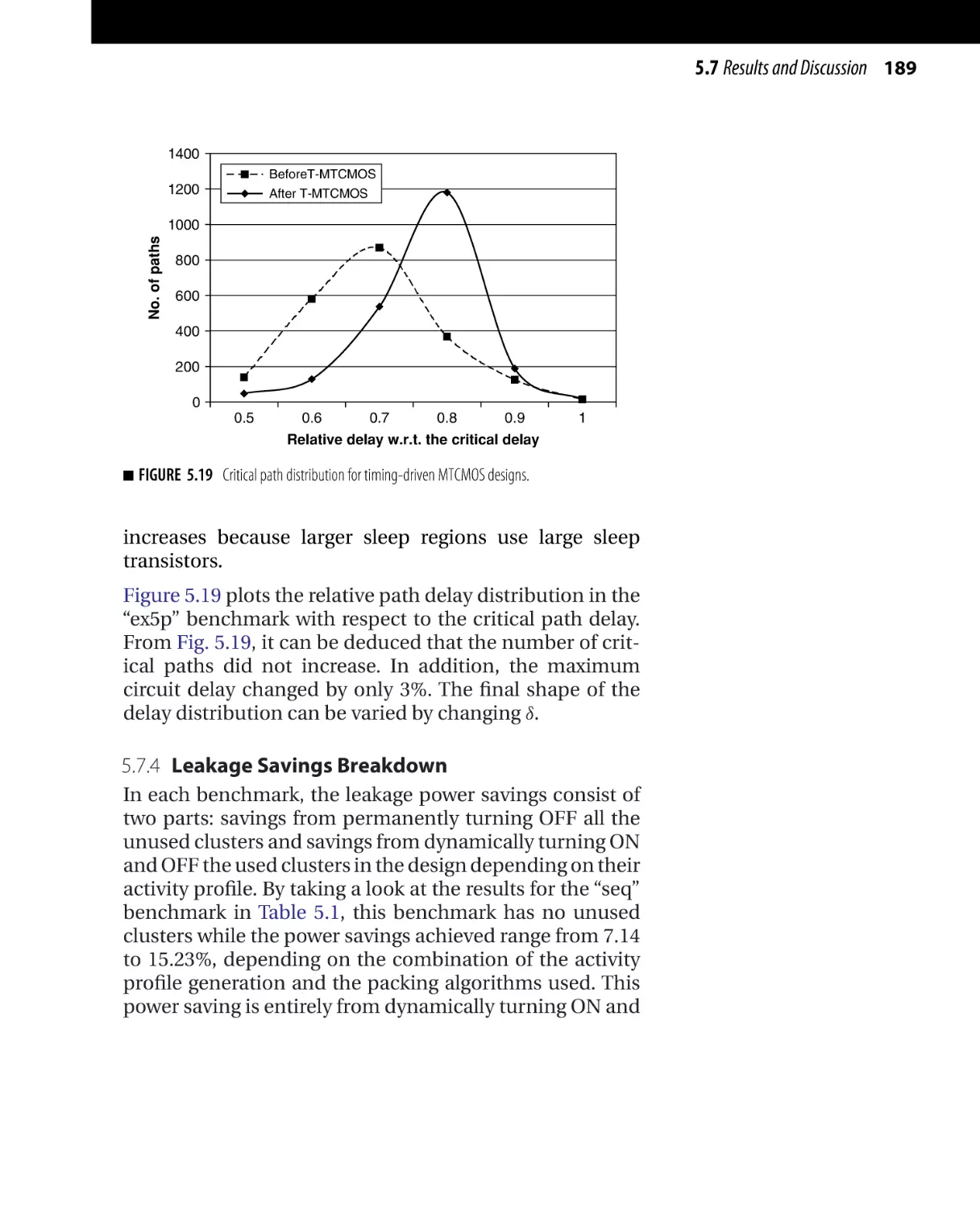
logic resource. The programming technology for the logic
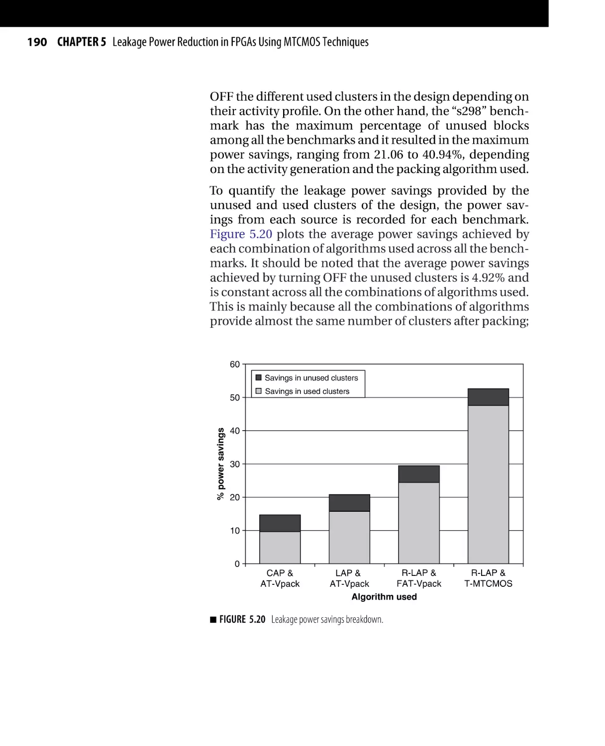
and interconnect resources can be static random access
memory (SRAM), flash memory [4], or antifuse [5, 6].
SRAM-based FPGAs offer in-circuit reconfigurability at
the expense of being volatile, while antifuse are writeonce devices. Flash-based FPGAs provide an intermediate
alternative by providing reconfigurability as well as nonvolatility. The most popular programming technology in
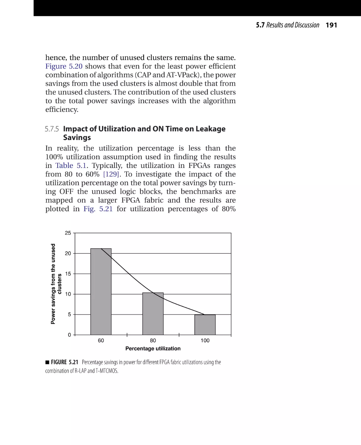
state-of-the-art FPGAs is SRAM.
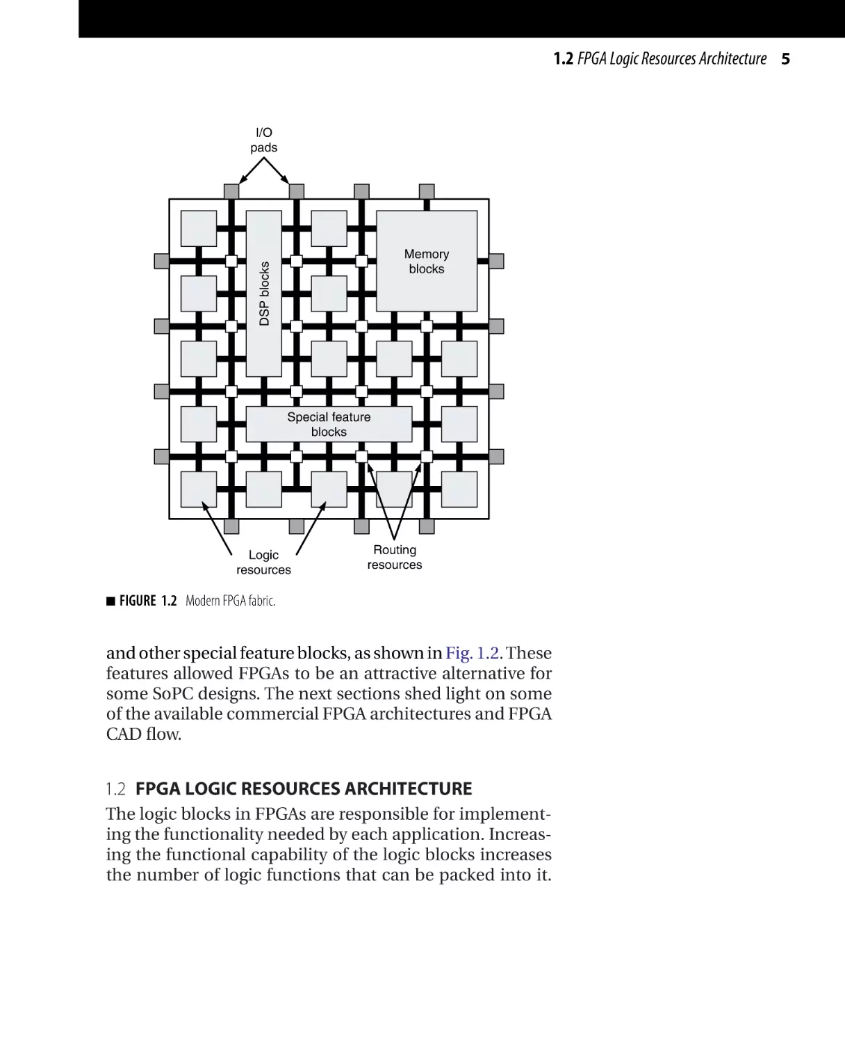
Traditionally, FPGAs consist of input/output (IO) pads,
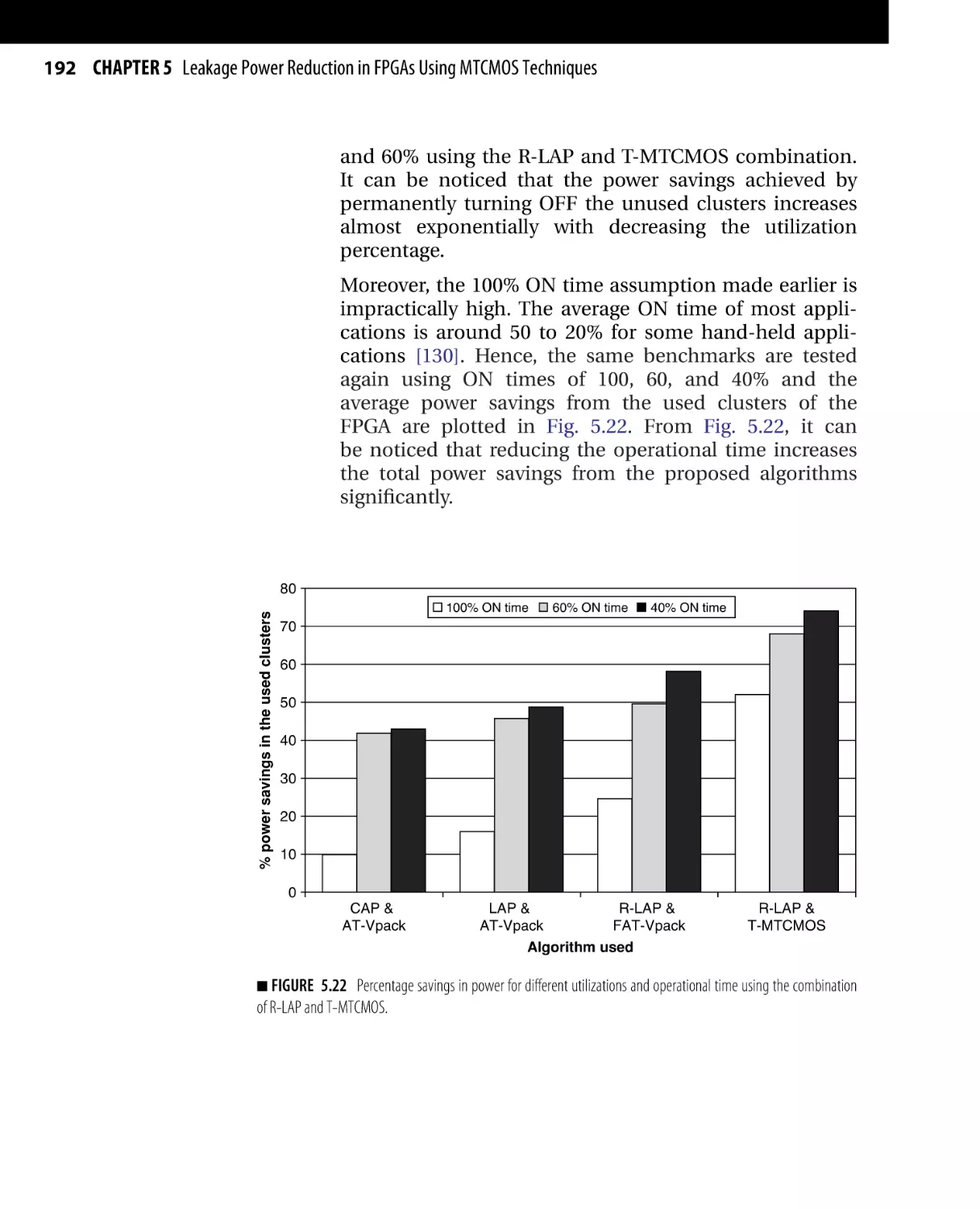
logic resources, and routing resources. However, state-ofthe-art FPGAs usually include embedded memory, DSP
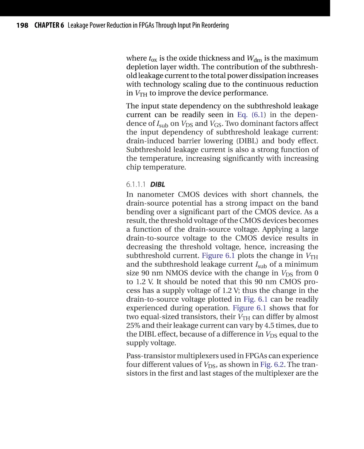
blocks, phase-locked loops (PLLs), embedded processors,
analog functionality (e.g., analog-to-digital converters),
1.2 FPGA Logic Resources Architecture 5
I/O
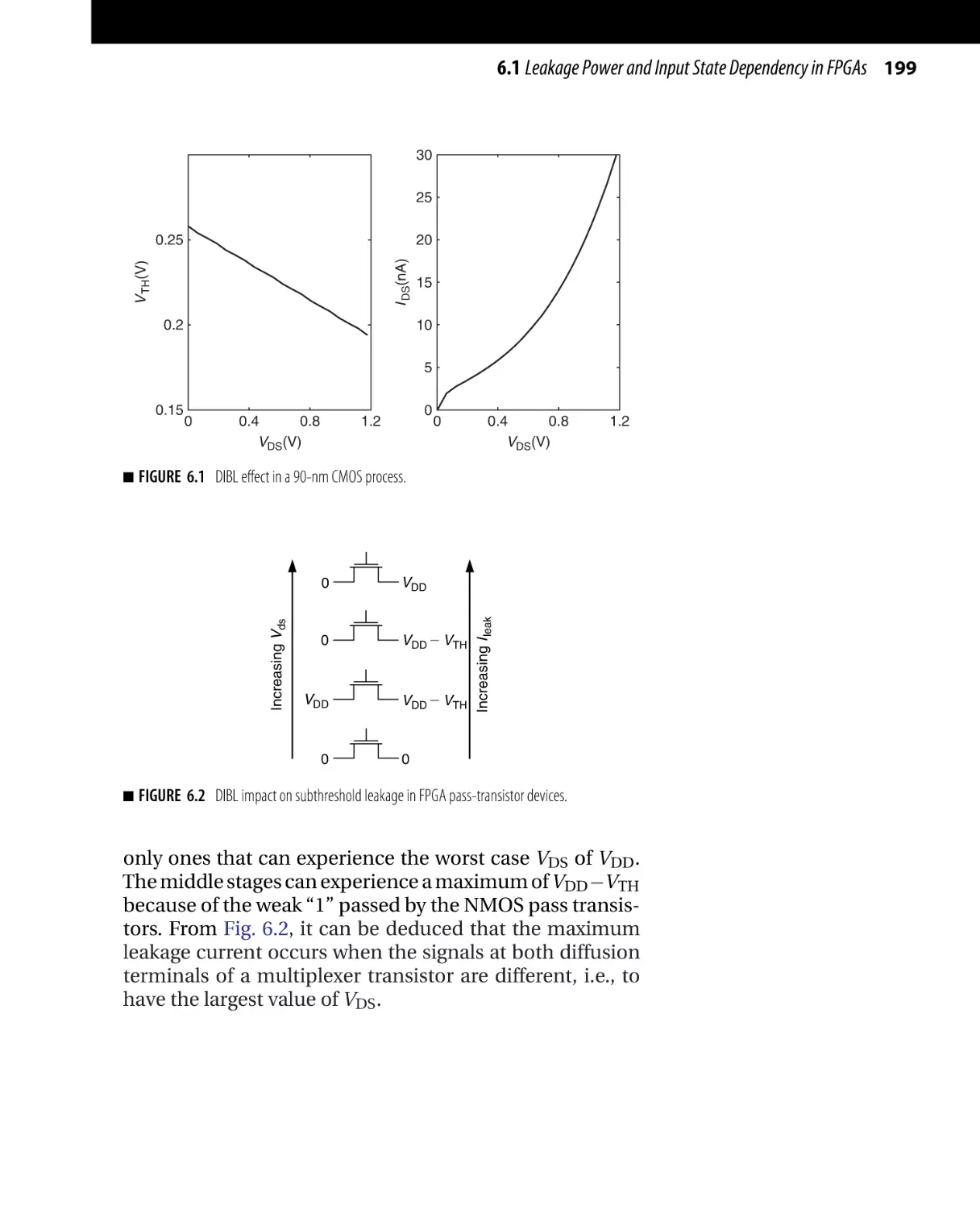
pads
DSP blocks
Memory
blocks
Special feature
blocks
Logic
resources
■
Routing
resources
FIGURE 1.2 Modern FPGA fabric.
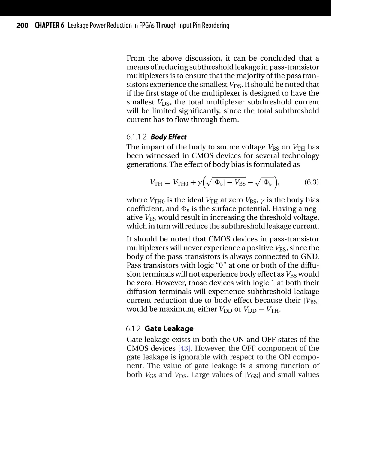
and other special feature blocks, as shown in Fig. 1.2. These
features allowed FPGAs to be an attractive alternative for
some SoPC designs. The next sections shed light on some
of the available commercial FPGA architectures and FPGA
CAD flow.
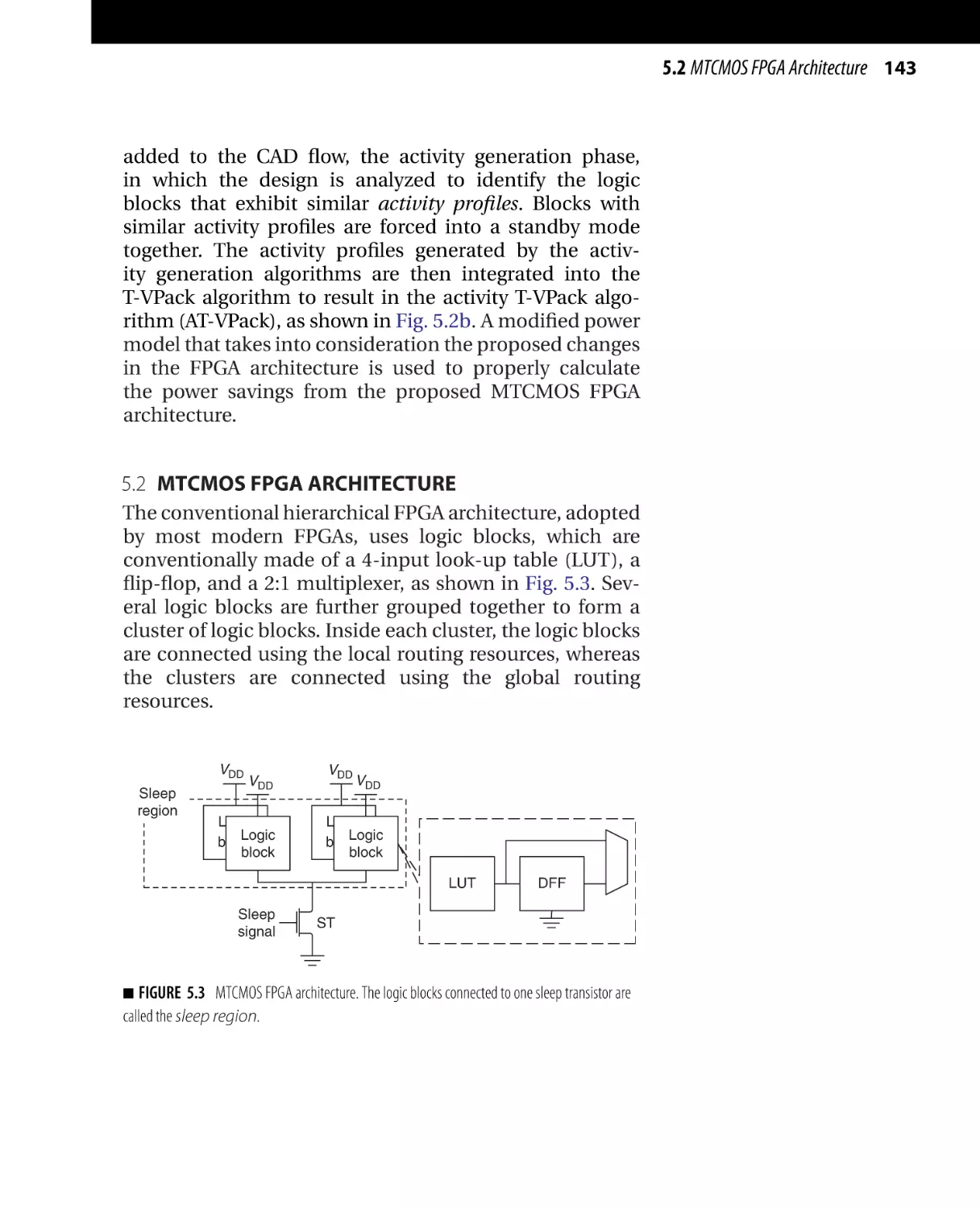
1.2 FPGA LOGIC RESOURCES ARCHITECTURE
The logic blocks in FPGAs are responsible for implementing the functionality needed by each application. Increasing the functional capability of the logic blocks increases
the number of logic functions that can be packed into it.
6 CHAPTER 1 FPGA Overview: Architecture and CAD
Moreover, increasing the size of logic blocks, i.e., increasing
the number of inputs to each logic block, increases the
number of logic functions performed by each logic block as
well as improving the area/delay performance of the logic
block [7]. However, this comes at the expense of wasted
resources because not all of the blocks will have all of their
inputs fully utilized.
Most commercial FPGAs employ LUTs to implement the
logic blocks. A k-input LUT consists of 2k configuration
bits in which the required truth table is programmed during the configuration stage. The almost standard number
of inputs for LUTs is four, which was proven optimum
for area and delay objectives [8]. However, this number
can vary depending on the targeted application by the
vendor. Moreover, modern FPGAs utilize a hierarchical
architecture, where every group of basic logic blocks are
grouped together into a bigger logic structure, logic cluster.
The remaining of this section describes the programmable
logic resources in three of the most popular commercial
FPGAs.
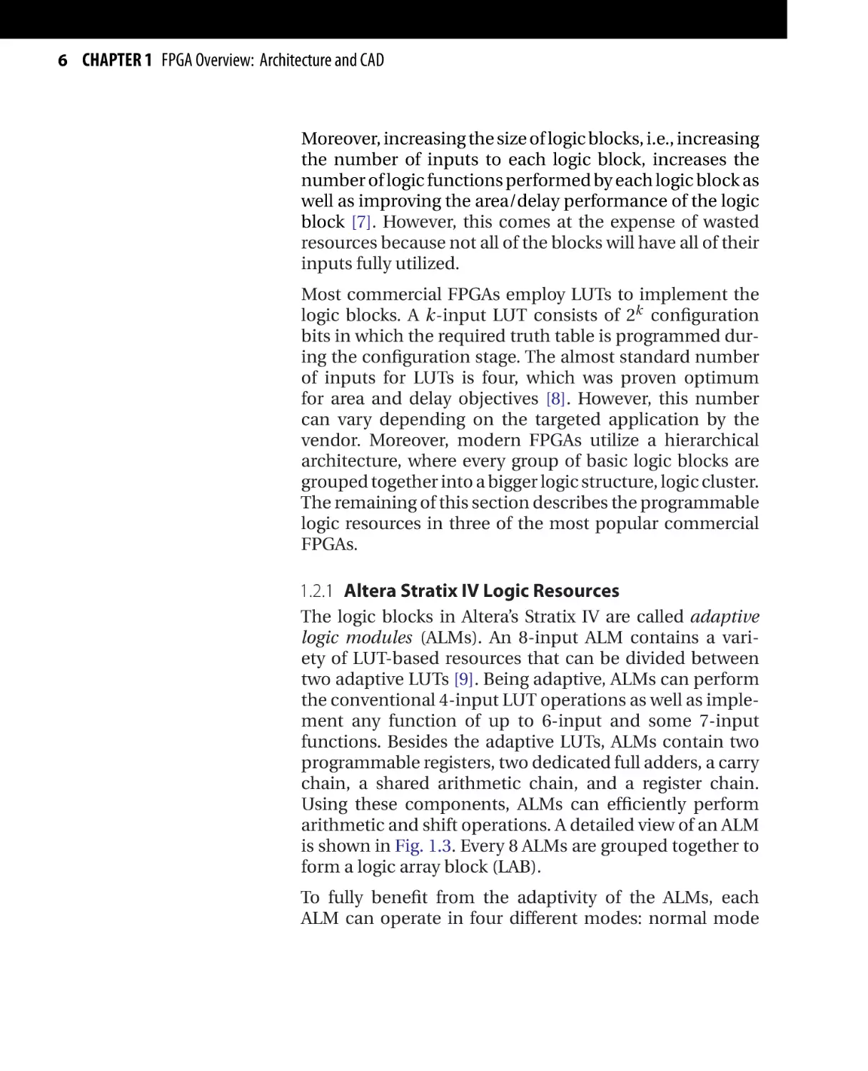
1.2.1 Altera Stratix IV Logic Resources
The logic blocks in Altera’s Stratix IV are called adaptive
logic modules (ALMs). An 8-input ALM contains a variety of LUT-based resources that can be divided between
two adaptive LUTs [9]. Being adaptive, ALMs can perform
the conventional 4-input LUT operations as well as implement any function of up to 6-input and some 7-input
functions. Besides the adaptive LUTs, ALMs contain two
programmable registers, two dedicated full adders, a carry
chain, a shared arithmetic chain, and a register chain.
Using these components, ALMs can efficiently perform
arithmetic and shift operations. A detailed view of an ALM
is shown in Fig. 1.3. Every 8 ALMs are grouped together to
form a logic array block (LAB).
To fully benefit from the adaptivity of the ALMs, each
ALM can operate in four different modes: normal mode
1.2 FPGA Logic Resources Architecture 7
shared_arith_in
carry_in
reg_chain_in
labclk
Combinational ALUT0
dataf0
datae0
dataa
datab
6-input LUT
adder0
CLR
D Q
datac
datad
datae
dataf1
6-input LUT
adder1
CLR
D Q
Combinational ALUT1
shared_arith_out
■ FIGURE
carry_out
reg_chain_out
1.3 Altera’s Stratix IV ALM architecture [9].
(for general logic applications and combinational functions), extended LUT mode (for implementing some
7-input functions), arithmetic mode (for implementing
adders, counters, accumulators, wide parity functions, and
comparators), and shared arithmetic mode (for 3-input
addition).
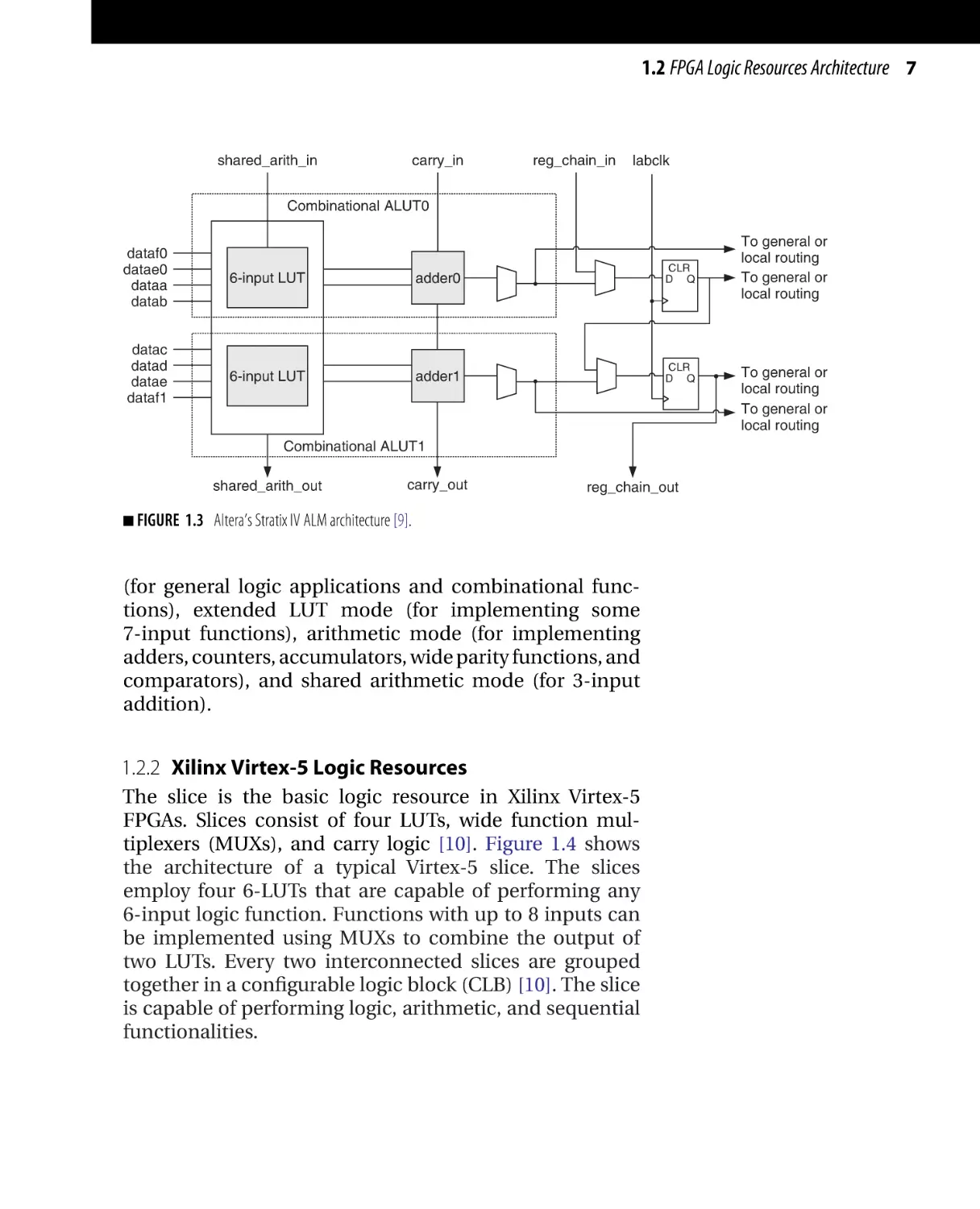
1.2.2 Xilinx Virtex-5 Logic Resources
The slice is the basic logic resource in Xilinx Virtex-5
FPGAs. Slices consist of four LUTs, wide function multiplexers (MUXs), and carry logic [10]. Figure 1.4 shows
the architecture of a typical Virtex-5 slice. The slices
employ four 6-LUTs that are capable of performing any
6-input logic function. Functions with up to 8 inputs can
be implemented using MUXs to combine the output of
two LUTs. Every two interconnected slices are grouped
together in a configurable logic block (CLB) [10]. The slice
is capable of performing logic, arithmetic, and sequential
functionalities.
To general or
local routing
To general or
local routing
To general or
local routing
To general or
local routing
8 CHAPTER 1 FPGA Overview: Architecture and CAD
COUT
A6
A5
A4
A3
A2
A1
O6
O5
carry/
control
logic
FF
A6
A5
A4
A3
A2
A1
O6
O5
carry/
control
logic
FF
A6
A5
A4
A3
A2
A1
O6
O5
carry/
control
logic
FF
A6
A5
A4
A3
A2
A1
O6
O5
carry/
control
logic
FF
DX
CX
BX
AX
CLK
■
CIN
FIGURE 1.4 Xilinx’s Vertex-5 slice architecture [10].
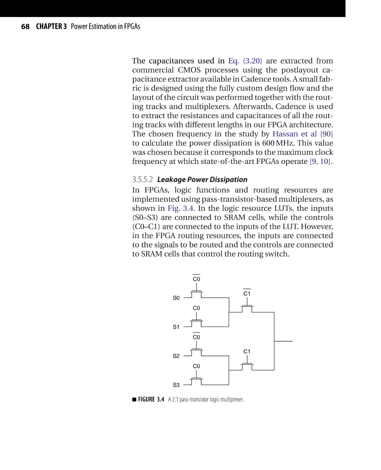
1.2.3 Actel ProASIC3/IGLOO Logic Resources
Actel ProASIC3/IGLOO FPGAs employ a flash-based architecture, instead of the conventional SRAM-based FPGAs
used by both Altera and Xilinx, to store the configuration
bits. The flash architecture provides the FPGAs with both
reconfigurability and nonvolatility. The ProASIC3/IGLOO
FPGAs employ the VersaTile 3-input logic block that can
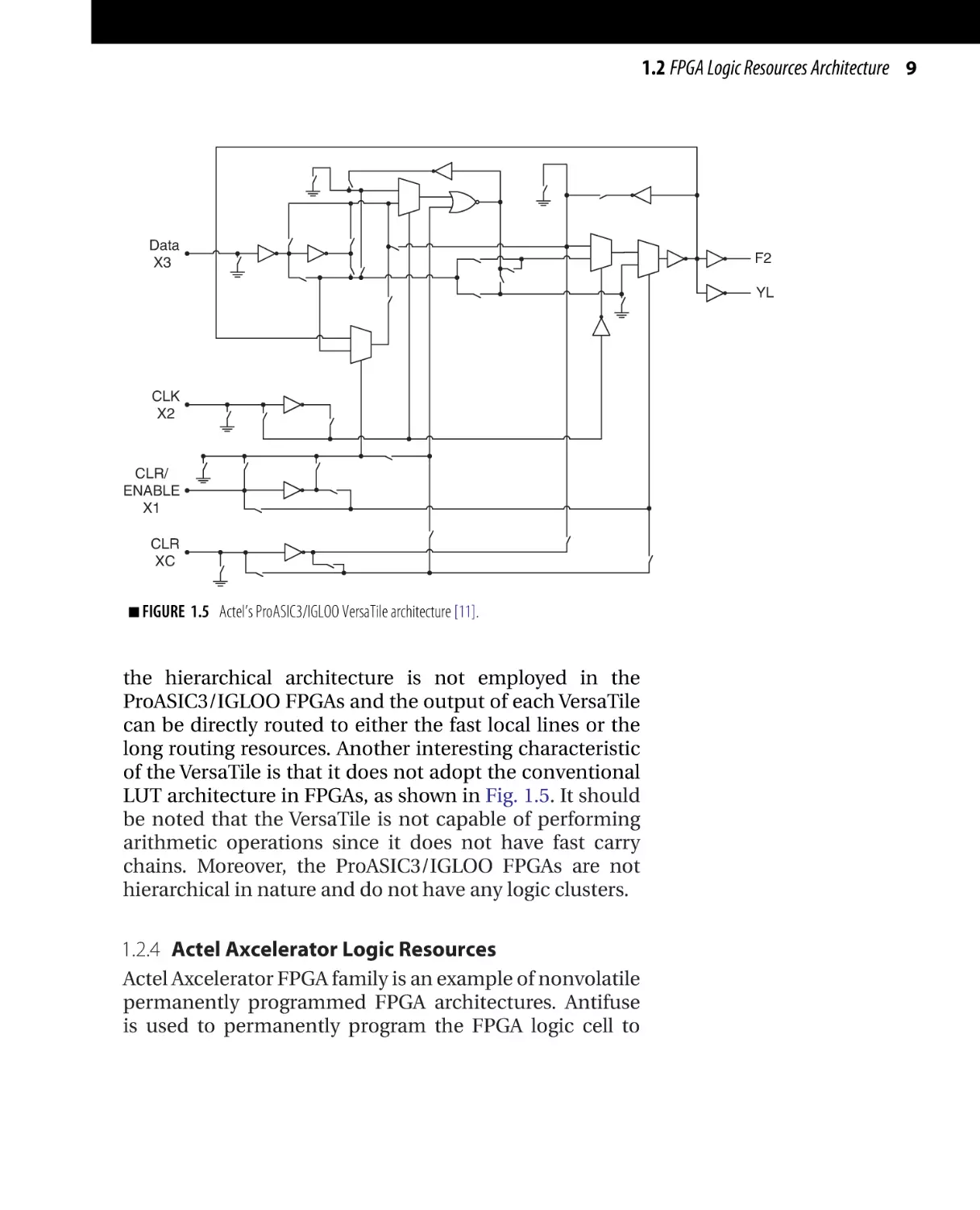
implement any 3-input logic function as well as sequential functionality, as shown in Fig. 1.5 [11]. Furthermore,
1.2 FPGA Logic Resources Architecture 9
Data
X3
F2
YL
CLK
X2
CLR/
ENABLE
X1
CLR
XC
■ FIGURE
1.5 Actel’s ProASIC3/IGLOO VersaTile architecture [11].
the hierarchical architecture is not employed in the
ProASIC3/IGLOO FPGAs and the output of each VersaTile
can be directly routed to either the fast local lines or the
long routing resources. Another interesting characteristic
of the VersaTile is that it does not adopt the conventional
LUT architecture in FPGAs, as shown in Fig. 1.5. It should
be noted that the VersaTile is not capable of performing
arithmetic operations since it does not have fast carry
chains. Moreover, the ProASIC3/IGLOO FPGAs are not
hierarchical in nature and do not have any logic clusters.
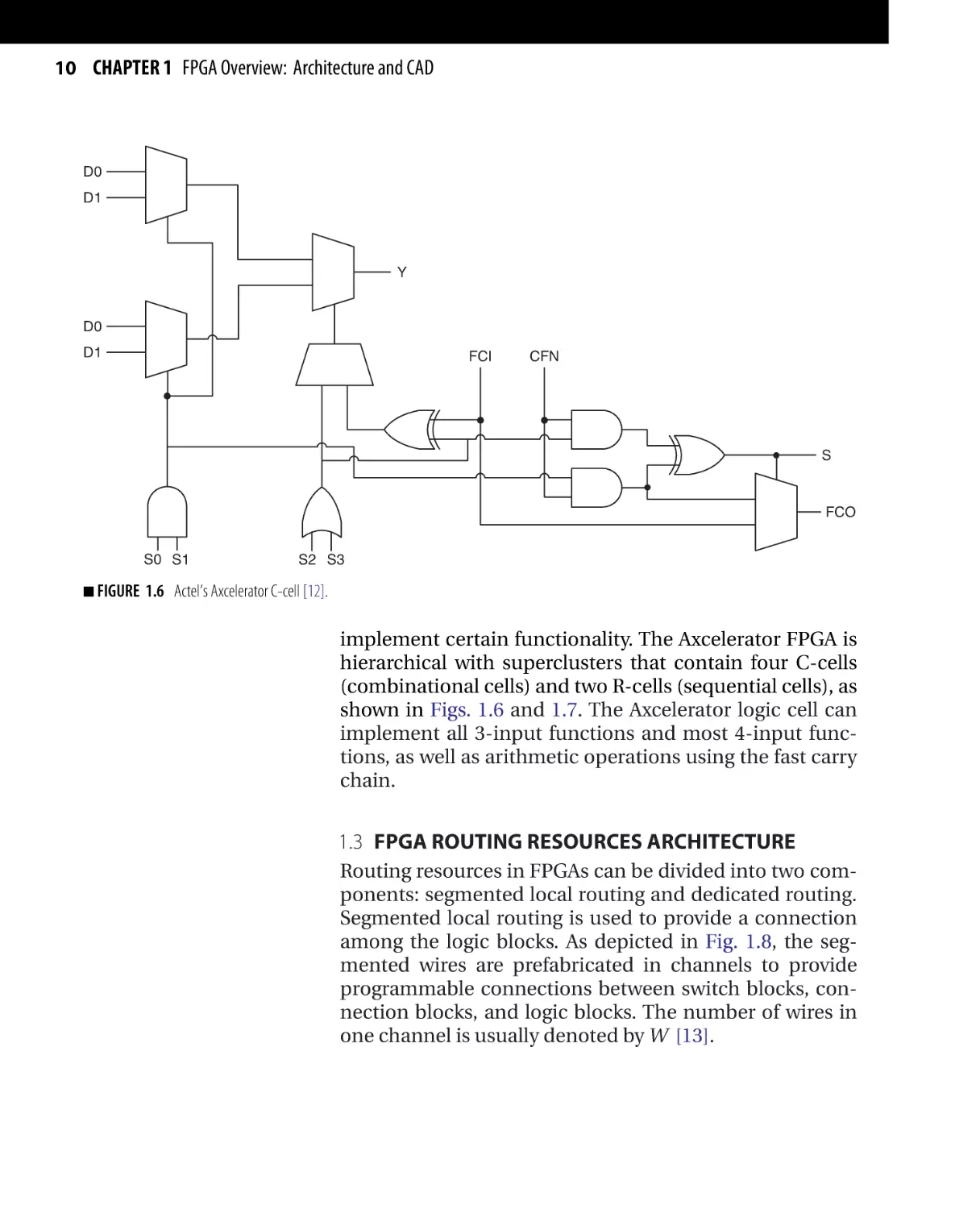
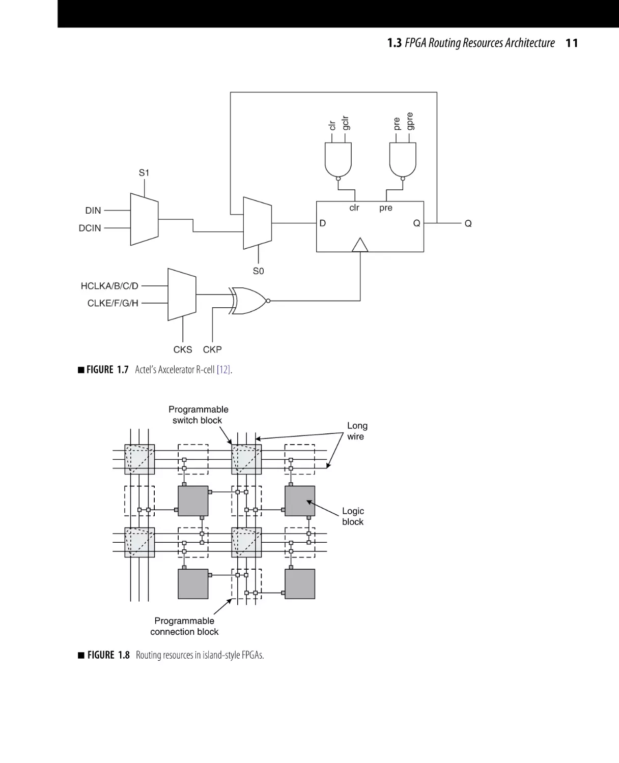
1.2.4 Actel Axcelerator Logic Resources
Actel Axcelerator FPGA family is an example of nonvolatile
permanently programmed FPGA architectures. Antifuse
is used to permanently program the FPGA logic cell to
10 CHAPTER 1 FPGA Overview: Architecture and CAD
D0
D1
Y
D0
D1
FCI
CFN
S
FCO
S0 S1
■ FIGURE
S2 S3
1.6 Actel’s Axcelerator C-cell [12].
implement certain functionality. The Axcelerator FPGA is
hierarchical with superclusters that contain four C-cells
(combinational cells) and two R-cells (sequential cells), as
shown in Figs. 1.6 and 1.7. The Axcelerator logic cell can
implement all 3-input functions and most 4-input functions, as well as arithmetic operations using the fast carry
chain.
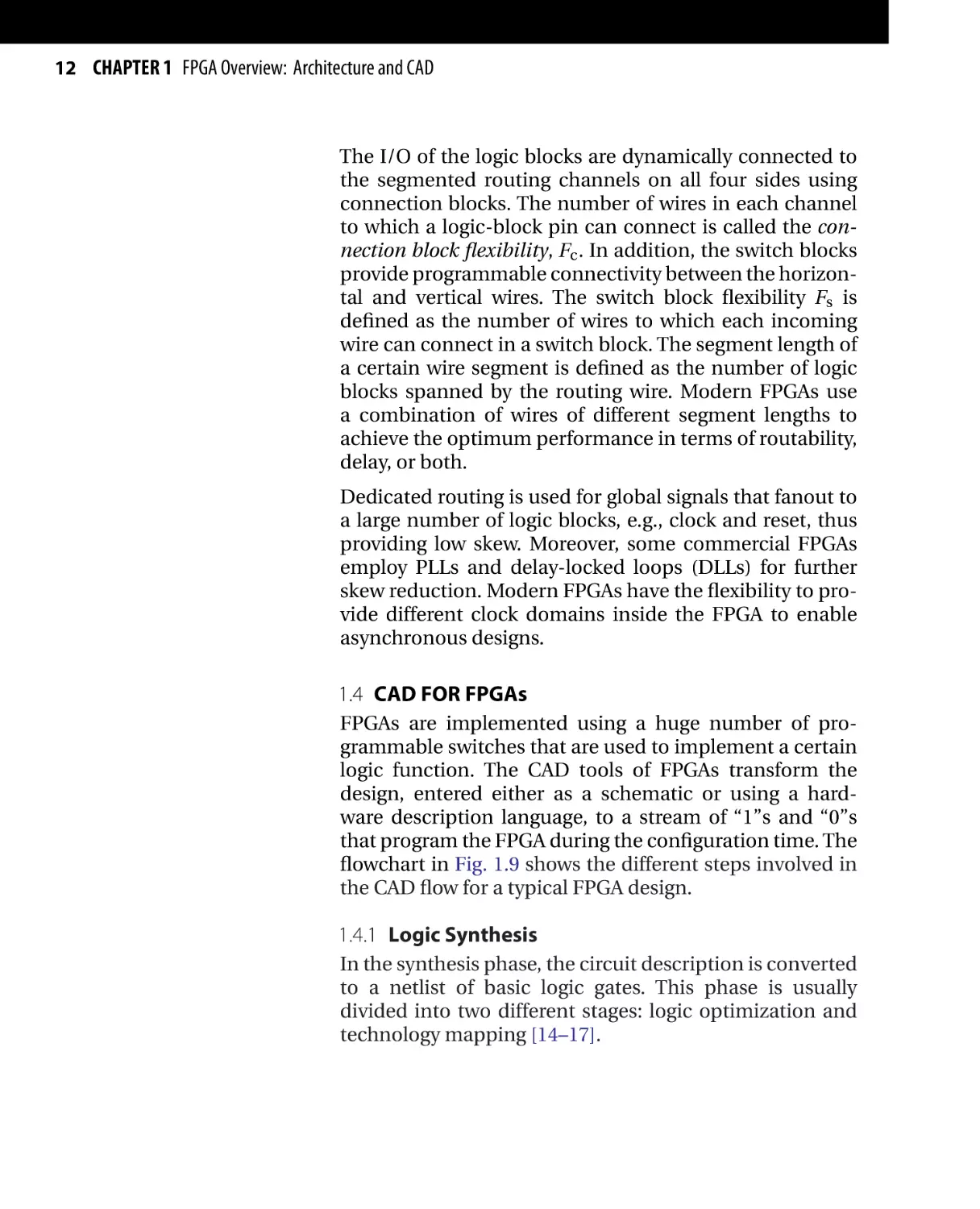
1.3 FPGA ROUTING RESOURCES ARCHITECTURE
Routing resources in FPGAs can be divided into two components: segmented local routing and dedicated routing.
Segmented local routing is used to provide a connection
among the logic blocks. As depicted in Fig. 1.8, the segmented wires are prefabricated in channels to provide
programmable connections between switch blocks, connection blocks, and logic blocks. The number of wires in
one channel is usually denoted by W [13].
clr
gclr
pre
gpre
1.3 FPGA Routing Resources Architecture 11
S1
clr
DIN
D
DCIN
Q
S0
HCLKA/B/C/D
CLKE/F/G/H
CKS
■ FIGURE
CKP
1.7 Actel’s Axcelerator R-cell [12].
Programmable
switch block
Long
wire
Logic
block
Programmable
connection block
■
FIGURE 1.8 Routing resources in island-style FPGAs.
pre
Q
12 CHAPTER 1 FPGA Overview: Architecture and CAD
The I/O of the logic blocks are dynamically connected to
the segmented routing channels on all four sides using
connection blocks. The number of wires in each channel
to which a logic-block pin can connect is called the connection block flexibility, Fc . In addition, the switch blocks
provide programmable connectivity between the horizontal and vertical wires. The switch block flexibility Fs is
defined as the number of wires to which each incoming
wire can connect in a switch block. The segment length of
a certain wire segment is defined as the number of logic
blocks spanned by the routing wire. Modern FPGAs use
a combination of wires of different segment lengths to
achieve the optimum performance in terms of routability,
delay, or both.
Dedicated routing is used for global signals that fanout to
a large number of logic blocks, e.g., clock and reset, thus
providing low skew. Moreover, some commercial FPGAs
employ PLLs and delay-locked loops (DLLs) for further
skew reduction. Modern FPGAs have the flexibility to provide different clock domains inside the FPGA to enable
asynchronous designs.
1.4 CAD FOR FPGAs
FPGAs are implemented using a huge number of programmable switches that are used to implement a certain
logic function. The CAD tools of FPGAs transform the
design, entered either as a schematic or using a hardware description language, to a stream of “1”s and “0”s
that program the FPGA during the configuration time. The
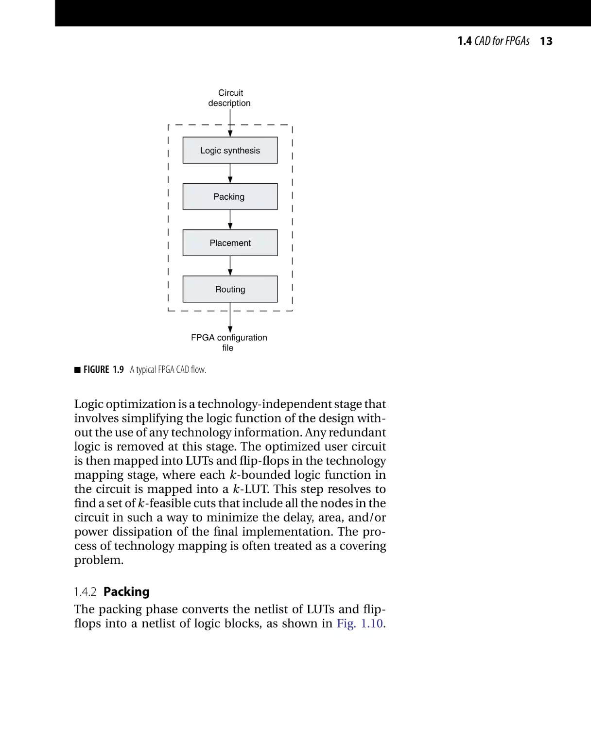
flowchart in Fig. 1.9 shows the different steps involved in
the CAD flow for a typical FPGA design.
1.4.1 Logic Synthesis
In the synthesis phase, the circuit description is converted
to a netlist of basic logic gates. This phase is usually
divided into two different stages: logic optimization and
technology mapping [14–17].
1.4 CAD for FPGAs 13
Circuit
description
Logic synthesis
Packing
Placement
Routing
FPGA configuration
file
■
FIGURE 1.9 A typical FPGA CAD flow.
Logic optimization is a technology-independent stage that
involves simplifying the logic function of the design without the use of any technology information. Any redundant
logic is removed at this stage. The optimized user circuit
is then mapped into LUTs and flip-flops in the technology
mapping stage, where each k-bounded logic function in
the circuit is mapped into a k-LUT. This step resolves to
find a set of k-feasible cuts that include all the nodes in the
circuit in such a way to minimize the delay, area, and/or
power dissipation of the final implementation. The process of technology mapping is often treated as a covering
problem.
1.4.2 Packing
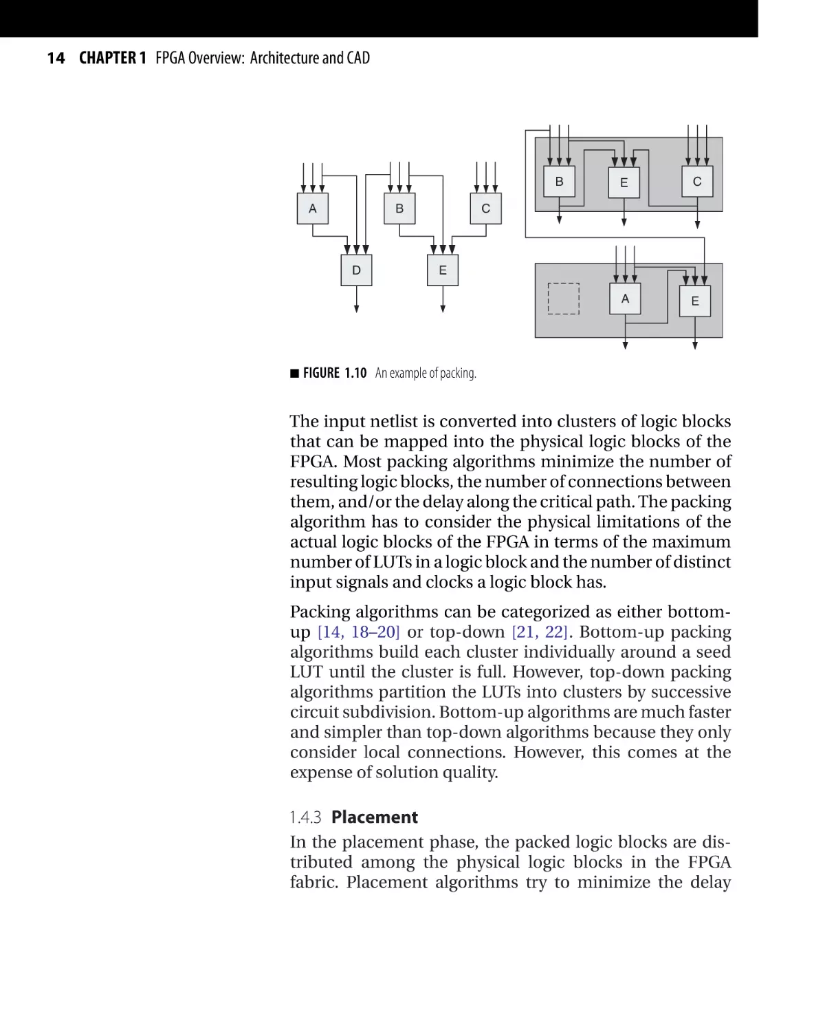
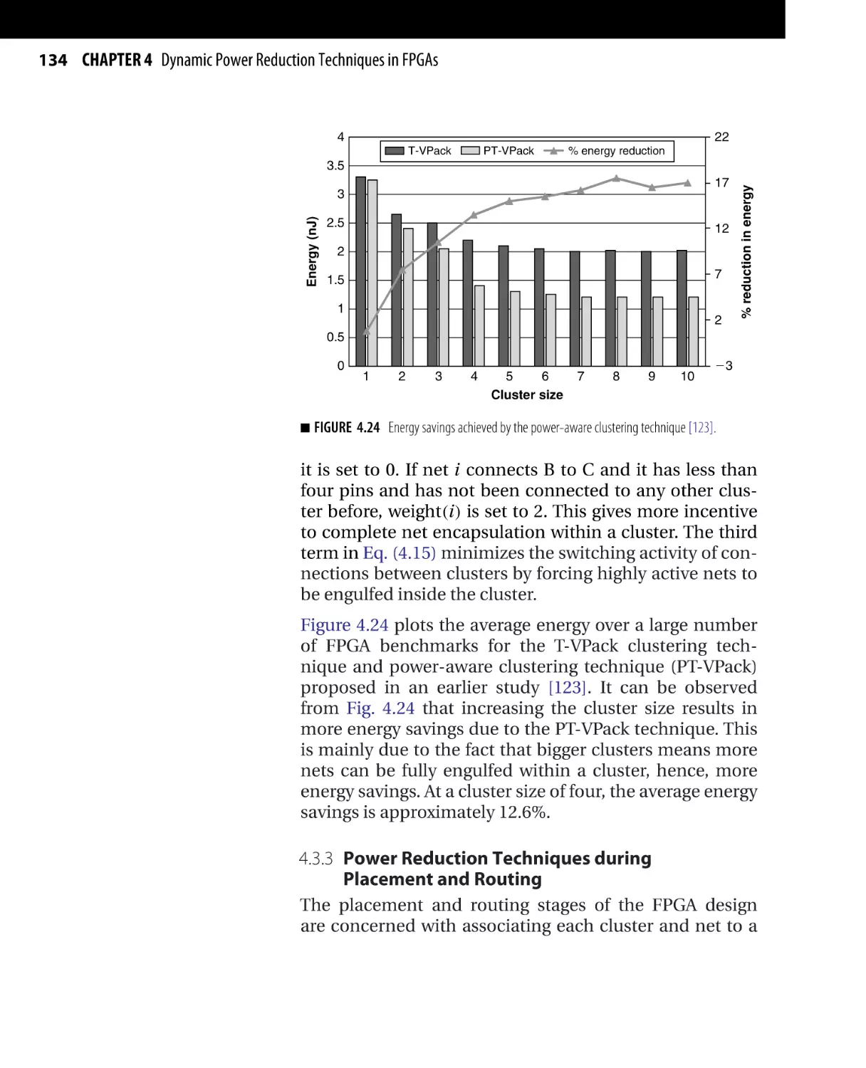
The packing phase converts the netlist of LUTs and flipflops into a netlist of logic blocks, as shown in Fig. 1.10.
14 CHAPTER 1 FPGA Overview: Architecture and CAD
B
A
B
D
■
E
C
A
E
C
E
FIGURE 1.10 An example of packing.
The input netlist is converted into clusters of logic blocks
that can be mapped into the physical logic blocks of the
FPGA. Most packing algorithms minimize the number of
resulting logic blocks, the number of connections between
them, and/or the delay along the critical path. The packing
algorithm has to consider the physical limitations of the
actual logic blocks of the FPGA in terms of the maximum
number of LUTs in a logic block and the number of distinct
input signals and clocks a logic block has.
Packing algorithms can be categorized as either bottomup [14, 18–20] or top-down [21, 22]. Bottom-up packing
algorithms build each cluster individually around a seed
LUT until the cluster is full. However, top-down packing
algorithms partition the LUTs into clusters by successive
circuit subdivision. Bottom-up algorithms are much faster
and simpler than top-down algorithms because they only
consider local connections. However, this comes at the
expense of solution quality.
1.4.3 Placement
In the placement phase, the packed logic blocks are distributed among the physical logic blocks in the FPGA
fabric. Placement algorithms try to minimize the delay
1.4 CAD for FPGAs 15
along the critical path and enhance the resulting circuit
routability. Available placement algorithms can be classified into three categories: min-cut algorithms [23, 24],
analytic algorithms [25, 26], and algorithms based on simulated annealing (SA) [27–29]. Most of the commercial
placement tools for FPGAs employ SA-based algorithms
due to their flexibility to adapt to a wide variety of
optimization goals.
SA placement tools depend on the SA algorithm, which is
derived from the annealing process used to cool molten
metals [30]. Initially, a random initial placement for all
the logic blocks is generated. Afterwards, pairs of logic
blocks are selected at random as candidates for swapping to improve the cost function. If the swap results in
a decrease in the cost function, it is directly allowed; otherwise, it is only allowed with a probability that decreases
as the algorithm progresses, thus allowing less worsening
swaps after every iteration. A pseudocode for the SA placer
is listed in Algorithm 1.1.
Algorithm 1.1 SA generic placer pseudocode
S = RandomPlacement()
T = InitialTemperature()
while ExitCriterion() == False do
/* Outer loop */
while InnerLoopCriterion () == False do
/* Inner loop */
Snew = GenerateViaMove(S)
C = Cost(Snew ) - Cost(S)
r = random(0,1)
if r < e−C/T then
S = Snew
end if
end while
T = UpdateTemp()
end while
16 CHAPTER 1 FPGA Overview: Architecture and CAD
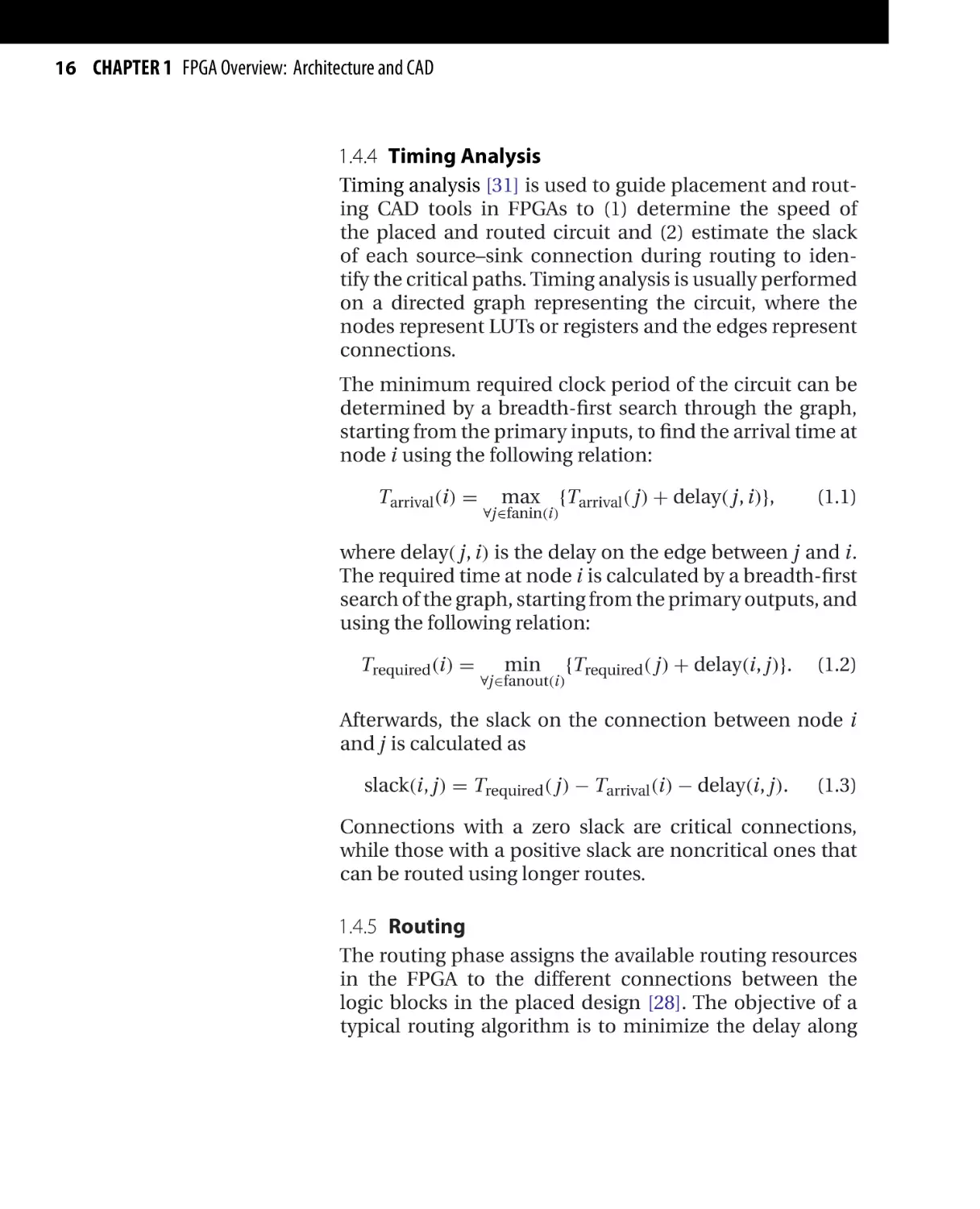
1.4.4 Timing Analysis
Timing analysis [31] is used to guide placement and routing CAD tools in FPGAs to (1) determine the speed of
the placed and routed circuit and (2) estimate the slack
of each source–sink connection during routing to identify the critical paths. Timing analysis is usually performed
on a directed graph representing the circuit, where the
nodes represent LUTs or registers and the edges represent
connections.
The minimum required clock period of the circuit can be
determined by a breadth-first search through the graph,
starting from the primary inputs, to find the arrival time at
node i using the following relation:
Tarrival (i) =
max {Tarrival ( j) + delay( j, i)},
∀j∈fanin(i)
(1.1)
where delay( j, i) is the delay on the edge between j and i.
The required time at node i is calculated by a breadth-first
search of the graph, starting from the primary outputs, and
using the following relation:
Trequired (i) =
min
{Trequired ( j) + delay(i, j)}.
∀j∈fanout(i)
(1.2)
Afterwards, the slack on the connection between node i
and j is calculated as
slack(i, j) = Trequired ( j) − Tarrival (i) − delay(i, j).
(1.3)
Connections with a zero slack are critical connections,
while those with a positive slack are noncritical ones that
can be routed using longer routes.
1.4.5 Routing
The routing phase assigns the available routing resources
in the FPGA to the different connections between the
logic blocks in the placed design [28]. The objective of a
typical routing algorithm is to minimize the delay along
1.5 Versatile Place and Route (VPR) CAD Tool 17
the critical path and avoid congestions in the FPGA
routing resources. Generally, routing algorithms can be
classified into global routers and detailed routers. Global
routers consider only the circuit architecture without paying attention to the numbers and types of wires available,
whereas detailed routers assign the connections to specific
wires in the FPGA.
1.5 VERSATILE PLACE AND ROUTE (VPR) CAD TOOL
VPR is a popular academic placement and routing tool for
FPGAs [28]. Almost all the academic works performed on
FPGAs is based on the VPR flow. Moreover, VPR is the core
for Altera’s CAD tool [32, 33]. VPR is usually used in conjunction with T-VPack [18, 27], a timing-driven logic block
packing algorithm.VPR consists of two main parts: a placer
and router and an area and delay model. These two components interact together to find out the optimum placement
and routing that satisfies a set of conditions. This section
describes the FPGA architecture supported by VPR as well
as gives a quick overview about the tool flow.
1.5.1 VPR Architectural Assumptions
VPR assumes an SRAM-based architecture, where SRAM
cells hold the configuration bits for all the pass-transistor
MUXs and tristate buffers in the FPGA in both logic and
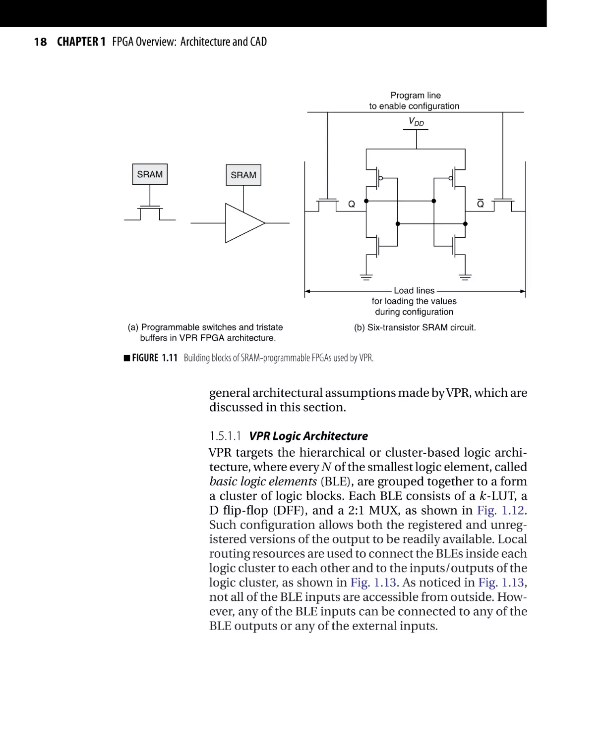
routing resources, as shown in Fig. 1.11a. The SRAMs used
are the six-transistor SRAM cells made of minimum size
transistors, as shown in Fig. 1.11b. Moreover, an islandstyle FPGA is assumed by VPR, where the logic clusters
are surrounded by routing tracks from all sides. VPR uses
an architecture file to describe the underlying FPGA architecture used. The architecture file contains information
about the logic block size, wire segment length, connection topologies, and other information used by VPR. The
use of the architecture file allows VPR to work on a wide
range of FPGA architectures. However, there are some
18 CHAPTER 1 FPGA Overview: Architecture and CAD
Program line
to enable configuration
VDD
SRAM
SRAM
Q
Q
Load lines
for loading the values
during configuration
(a) Programmable switches and tristate
buffers in VPR FPGA architecture.
■ FIGURE
(b) Six-transistor SRAM circuit.
1.11 Building blocks of SRAM-programmable FPGAs used by VPR.
general architectural assumptions made by VPR, which are
discussed in this section.
1.5.1.1 VPR Logic Architecture
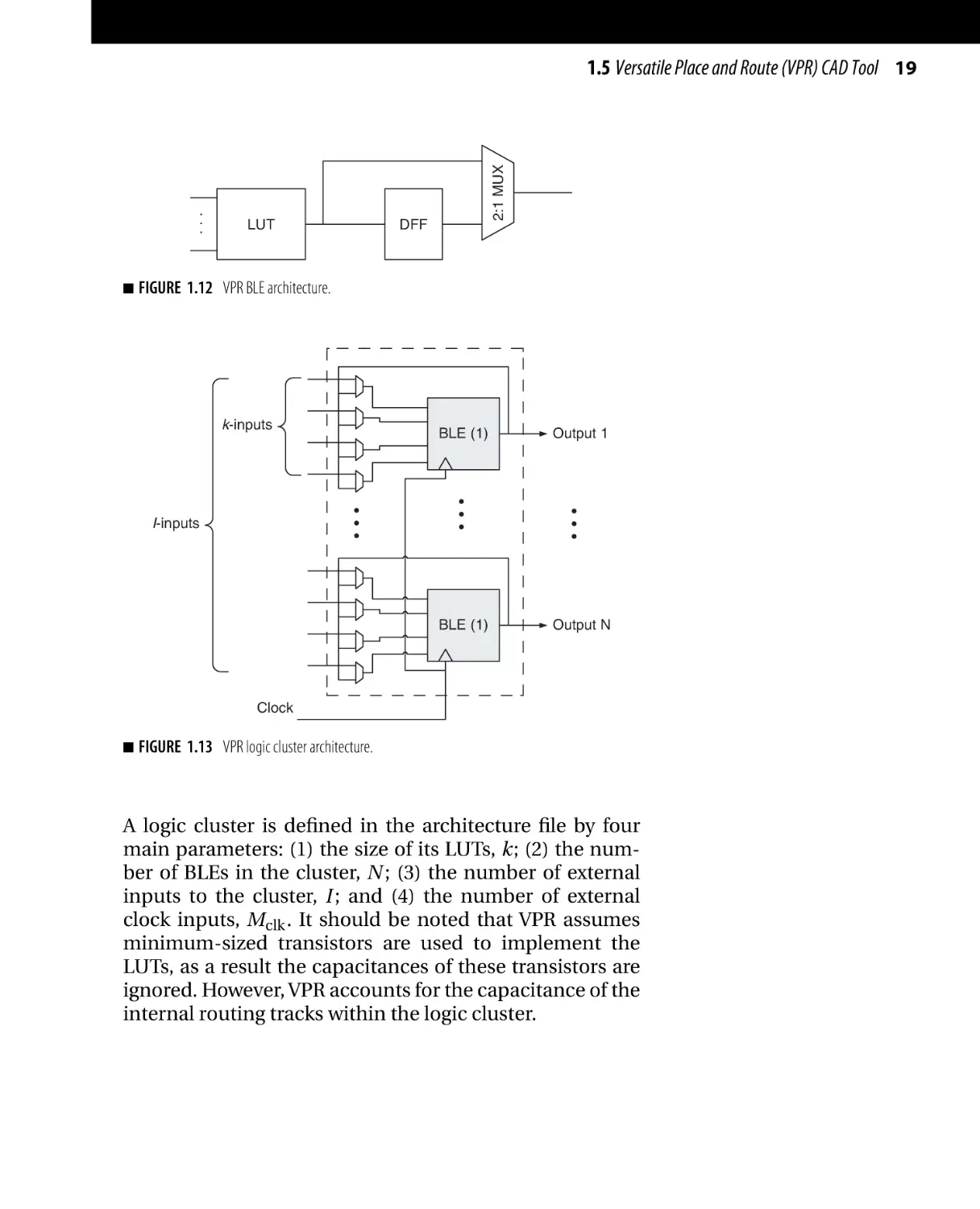
VPR targets the hierarchical or cluster-based logic architecture, where every N of the smallest logic element, called
basic logic elements (BLE), are grouped together to a form
a cluster of logic blocks. Each BLE consists of a k-LUT, a
D flip-flop (DFF), and a 2:1 MUX, as shown in Fig. 1.12.
Such configuration allows both the registered and unregistered versions of the output to be readily available. Local
routing resources are used to connect the BLEs inside each
logic cluster to each other and to the inputs/outputs of the
logic cluster, as shown in Fig. 1.13. As noticed in Fig. 1.13,
not all of the BLE inputs are accessible from outside. However, any of the BLE inputs can be connected to any of the
BLE outputs or any of the external inputs.
.
.
.
■
LUT
2:1 MUX
1.5 Versatile Place and Route (VPR) CAD Tool 19
DFF
FIGURE 1.12 VPR BLE architecture.
k-inputs
BLE (1)
Output 1
BLE (1)
Output N
I-inputs
Clock
■
FIGURE 1.13 VPR logic cluster architecture.
A logic cluster is defined in the architecture file by four
main parameters: (1) the size of its LUTs, k; (2) the number of BLEs in the cluster, N ; (3) the number of external
inputs to the cluster, I ; and (4) the number of external
clock inputs, Mclk . It should be noted that VPR assumes
minimum-sized transistors are used to implement the
LUTs, as a result the capacitances of these transistors are
ignored. However, VPR accounts for the capacitance of the
internal routing tracks within the logic cluster.
20 CHAPTER 1 FPGA Overview: Architecture and CAD
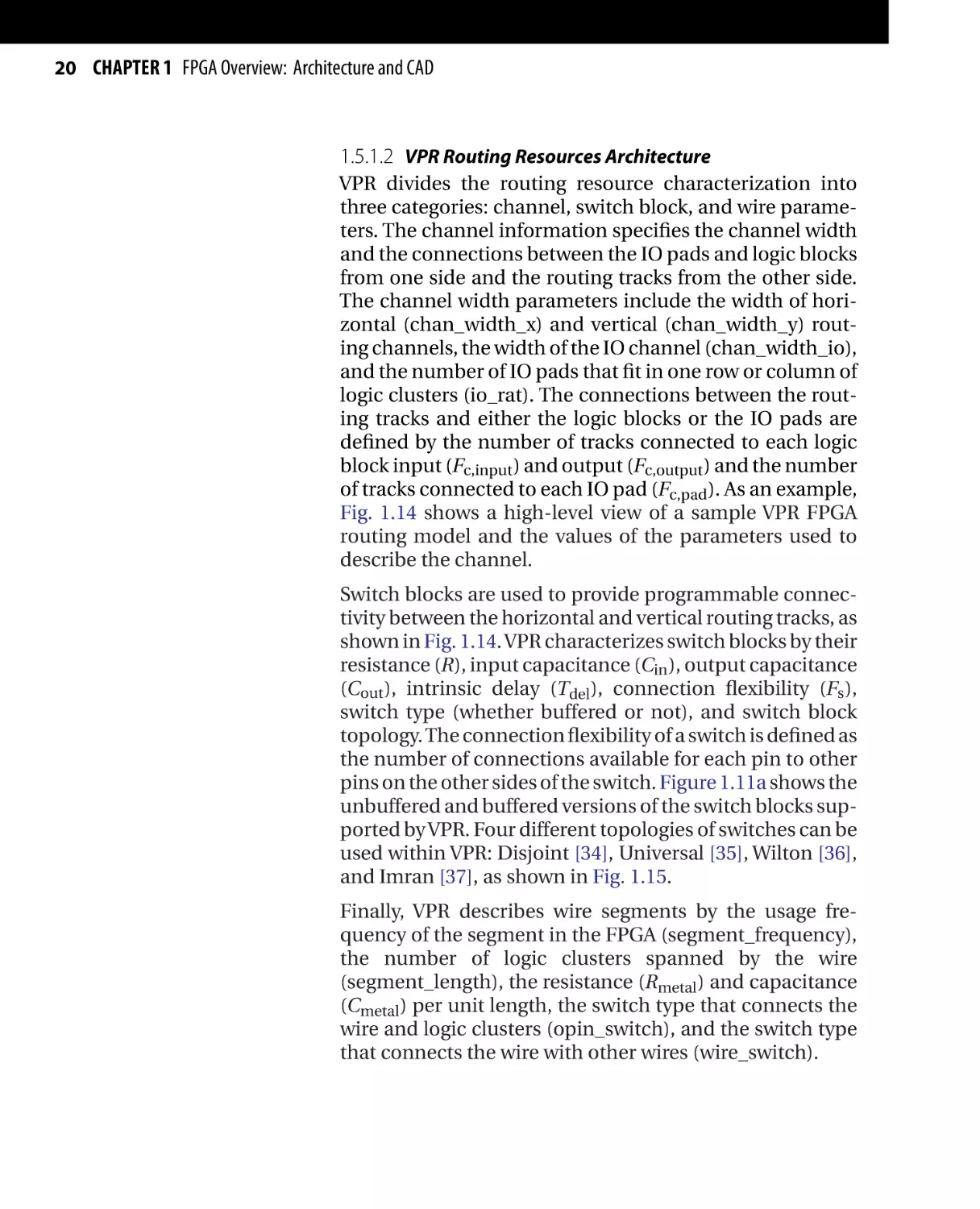
1.5.1.2 VPR Routing Resources Architecture
VPR divides the routing resource characterization into
three categories: channel, switch block, and wire parameters. The channel information specifies the channel width
and the connections between the IO pads and logic blocks
from one side and the routing tracks from the other side.
The channel width parameters include the width of horizontal (chan_width_x) and vertical (chan_width_y) routing channels, the width of the IO channel (chan_width_io),
and the number of IO pads that fit in one row or column of
logic clusters (io_rat). The connections between the routing tracks and either the logic blocks or the IO pads are
defined by the number of tracks connected to each logic
block input (Fc,input ) and output (Fc,output ) and the number
of tracks connected to each IO pad (Fc,pad ). As an example,
Fig. 1.14 shows a high-level view of a sample VPR FPGA
routing model and the values of the parameters used to
describe the channel.
Switch blocks are used to provide programmable connectivity between the horizontal and vertical routing tracks, as
shown in Fig. 1.14. VPR characterizes switch blocks by their
resistance (R), input capacitance (Cin ), output capacitance
(Cout ), intrinsic delay (Tdel ), connection flexibility (Fs ),
switch type (whether buffered or not), and switch block
topology. The connection flexibility of a switch is defined as
the number of connections available for each pin to other
pins on the other sides of the switch. Figure 1.11a shows the
unbuffered and buffered versions of the switch blocks supported by VPR. Four different topologies of switches can be
used within VPR: Disjoint [34], Universal [35], Wilton [36],
and Imran [37], as shown in Fig. 1.15.
Finally, VPR describes wire segments by the usage frequency of the segment in the FPGA (segment_frequency),
the number of logic clusters spanned by the wire
(segment_length), the resistance (Rmetal ) and capacitance
(Cmetal ) per unit length, the switch type that connects the
wire and logic clusters (opin_switch), and the switch type
that connects the wire with other wires (wire_switch).
1.5 Versatile Place and Route (VPR) CAD Tool 21
Connections
between the IO
pads and the
tracks
Switch
block
Connections
between the
tracks and logic
block input pin
Logic
cluster
I/O
pads
Logic
clusters
IO
channel
Horizontal
channel
Connections
between the
tracks and logic
block ouput pin
Connections
between tracks
inside a switch
block
Routing
tracks
Vertical
channel
■
FIGURE 1.14 VPR FPGA routing architecture. chan_width_x = 1, chan_width_y = 1, chan_width_io = 0.5,
io_rat = 2, Fc,input = 3, Fc,output = 1, and Fc,pad = 2.
0 1 2 3
0 1 2 3
0 1 2 3
0 1 2 3
3
3
3
3
3
3
3
3
2
2
2
2
2
2
2
2
1
1
1
1
1
1
1
1
0
0
0
0
0
0
0
0
0 1 2 3
0 1 2 3
(a) Disjoint switch block. (b) Universal switch block.
■ FIGURE
1.15 Switch topologies supported by VPR.
0 1 2 3
(c) Wilton switch block.
0 1 2 3
(d) Imran switch block.
22 CHAPTER 1 FPGA Overview: Architecture and CAD
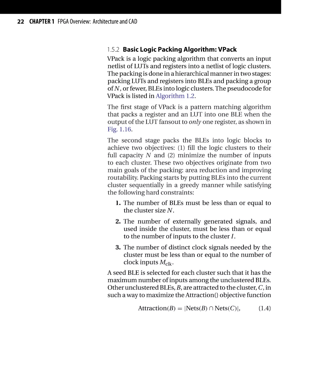
1.5.2 Basic Logic Packing Algorithm: VPack
VPack is a logic packing algorithm that converts an input
netlist of LUTs and registers into a netlist of logic clusters.
The packing is done in a hierarchical manner in two stages:
packing LUTs and registers into BLEs and packing a group
of N , or fewer, BLEs into logic clusters. The pseudocode for
VPack is listed in Algorithm 1.2.
The first stage of VPack is a pattern matching algorithm
that packs a register and an LUT into one BLE when the
output of the LUT fansout to only one register, as shown in
Fig. 1.16.
The second stage packs the BLEs into logic blocks to
achieve two objectives: (1) fill the logic clusters to their
full capacity N and (2) minimize the number of inputs
to each cluster. These two objectives originate from two
main goals of the packing: area reduction and improving
routability. Packing starts by putting BLEs into the current
cluster sequentially in a greedy manner while satisfying
the following hard constraints:
1. The number of BLEs must be less than or equal to
the cluster size N .
2. The number of externally generated signals, and
used inside the cluster, must be less than or equal
to the number of inputs to the cluster I .
3. The number of distinct clock signals needed by the
cluster must be less than or equal to the number of
clock inputs Mclk .
A seed BLE is selected for each cluster such that it has the
maximum number of inputs among the unclustered BLEs.
Other unclustered BLEs, B, are attracted to the cluster, C, in
such a way to maximize the Attraction() objective function
Attraction(B) = |Nets(B) ∩ Nets(C)|,
(1.4)
1.5 Versatile Place and Route (VPR) CAD Tool 23
Algorithm 1.2 VPack pseudocode [28]
Let: UnclusteredBLEs be the set of BLEs not contained in any cluster
- C be the set of BLEs in the current cluster
- LogicClusters be the set of clusters (where each cluster is a set of BLEs)
UnclusteredBLEs = PatternMatchToBLEs (LUTs, Registers)
LogicClusters = NULL
while UnclusteredBLEs != NULL do
/* More BLEs to cluster */
C = GetBLEwithMostUsedInputs (UnclusteredBLEs)
while |C| < N do
/* Cluster is not full */
BestBLE = MaxAttractionLegalBLE (C, UnclusteredBLEs)
if BestBLE == NULL then
/* No BLE can be added to cluster */
break
end if
UnclusteredBLEs = UnclusteredBLEs - BestBLE
C = C ∪ BestBLE
end while
if |C| < N then
/* Cluster not full | try hill-climbing */
while |C| < N do
BestBLE = MINClusterInputIncreaseBLE (C, UnclusteredBLEs)
C = C ∪ BestBLE
UnclusteredBLEs = UnclusteredBLEs - BestBLE
end while
if ClusterIsIllegal (C) then
RestoreToLastLegalState (C, UnclusteredBLEs)
end if
end if
LogicClusters = LogicClusters ∪ C
end while
24 CHAPTER 1 FPGA Overview: Architecture and CAD
LUT
Reg.
Reg.
LUT
LUT
(a) LUT and register packing into one BLE.
■ FIGURE
(b) LUT and register packing into two BLEs.
1.16 Packing LUTs and registers into BLEs [28].
where Nets(x) are the nets connected to BLE (or cluster)
x. This process continues until the cluster is filled to its
maximum capacity N .
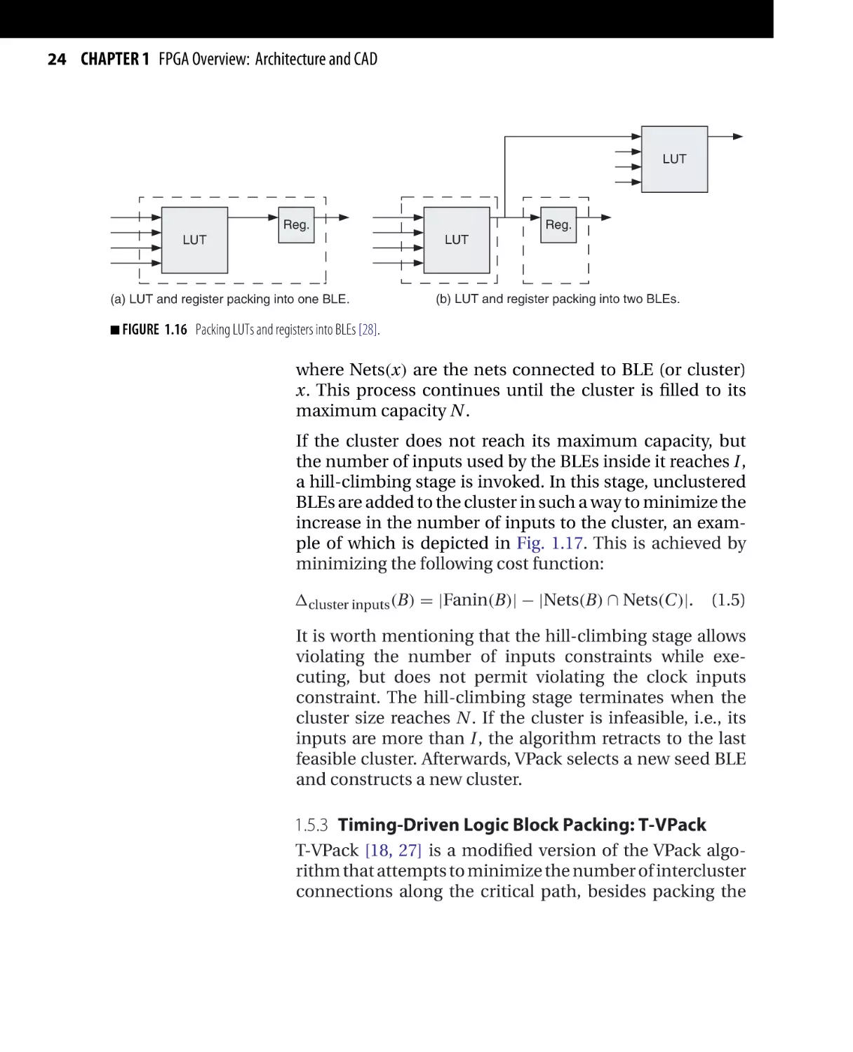
If the cluster does not reach its maximum capacity, but
the number of inputs used by the BLEs inside it reaches I ,
a hill-climbing stage is invoked. In this stage, unclustered
BLEs are added to the cluster in such a way to minimize the
increase in the number of inputs to the cluster, an example of which is depicted in Fig. 1.17. This is achieved by
minimizing the following cost function:
cluster inputs (B) = |Fanin(B)| − |Nets(B) ∩ Nets(C)|.
(1.5)
It is worth mentioning that the hill-climbing stage allows
violating the number of inputs constraints while executing, but does not permit violating the clock inputs
constraint. The hill-climbing stage terminates when the
cluster size reaches N . If the cluster is infeasible, i.e., its
inputs are more than I , the algorithm retracts to the last
feasible cluster. Afterwards, VPack selects a new seed BLE
and constructs a new cluster.
1.5.3 Timing-Driven Logic Block Packing: T-VPack
T-VPack [18, 27] is a modified version of the VPack algorithm that attempts to minimize the number of intercluster
connections along the critical path, besides packing the
1.5 Versatile Place and Route (VPR) CAD Tool 25
Add another BLE
a
c
b
a
a
BLE
BLE
b
b
BLE
b
BLE
BLE
BLE
d
e
c
c
d
e
■ FIGURE
1.17 Adding a BLE to a cluster can decrease the number of used cluster inputs [28].
clusters to their maximum capacity. This achieves speed
up along the critical path as local interconnects (intracluster connections) are faster than intercluster interconnects.
T-VPack employs a timing analyzer to calculate the slack
along the connections in the design and identify the critical path(s). The criticality measure of a connection is
calculated as
ConnectionCriticality(i) = 1 −
slack(i)
,
MaxSlack
(1.6)
where MaxSlack is the largest slack in the circuit.
In T-VPack, the BLE with the highest criticality, i.e.,
the BLE connected to the nets with the highest
ConnectionCriticality, is selected as the seed BLE for the
cluster. Afterwards, BLEs are attracted to the cluster to
maximize a modified version of the Attraction() function
in Eq. (1.4), given by
Attraction(B) = λ × Criticality(B) + (1 − λ)
×
Nets(B) ∩ Nets(C)
,
MaxNets
(1.7)
26 CHAPTER 1 FPGA Overview: Architecture and CAD
where MaxNets is the maximum number of nets that can
connect to any BLE and λ a parameter that controls the
trade-off between net sharing and delay minimization.
A small value of λ forces T-VPack to focus more on minimizing the number of used inputs to the cluster, and vice
versa.
The Criticality(B) of a BLE is given by
Criticality(B) = BaseBLECrit(B) + ε
× TotalPathsAffected(B) + ε2
× Dsource (B),
(1.8)
where ε is a parameter, Dsource (B) is the BLE distance or
level from the source of the path, TotalPathsAffected(B)
is the total number of critical paths connecting primary
inputs/outputs or registers inputs/outputs and B, and
BaseBLECrit(B) is the base criticality of BLE B and is evaluated as: (i) the maximum ConnectionCriticality(i) of all the
connection to/from B while selecting a seed BLE, or (ii) the
maximum ConnectionCriticality(i) of all the connections
joining BLE B to the other BLEs in the cluster currently
being packed.
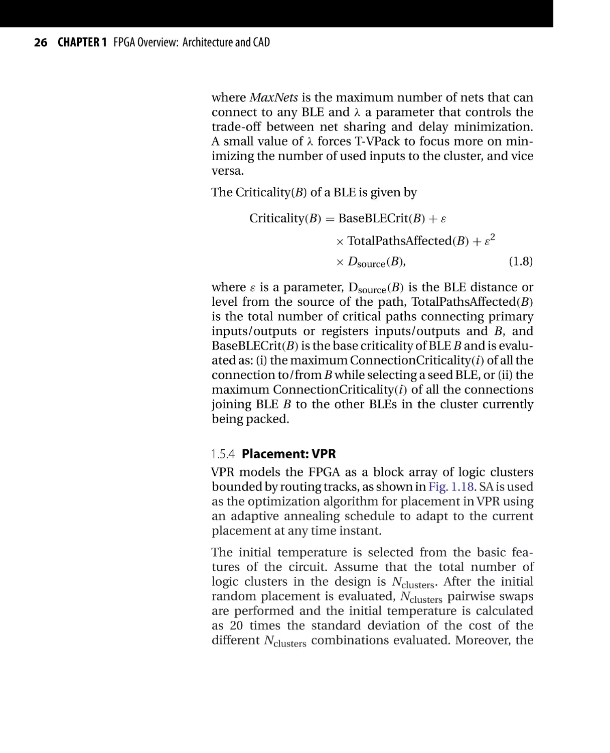
1.5.4 Placement: VPR
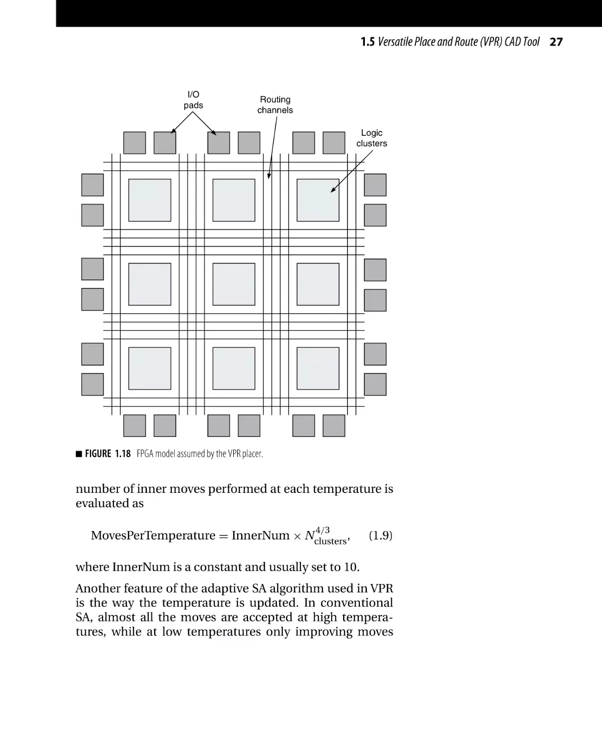
VPR models the FPGA as a block array of logic clusters
bounded by routing tracks, as shown in Fig. 1.18. SA is used
as the optimization algorithm for placement in VPR using
an adaptive annealing schedule to adapt to the current
placement at any time instant.
The initial temperature is selected from the basic features of the circuit. Assume that the total number of
logic clusters in the design is Nclusters . After the initial
random placement is evaluated, Nclusters pairwise swaps
are performed and the initial temperature is calculated
as 20 times the standard deviation of the cost of the
different Nclusters combinations evaluated. Moreover, the
1.5 Versatile Place and Route (VPR) CAD Tool 27
I/O
pads
Routing
channels
Logic
clusters
■
FIGURE 1.18 FPGA model assumed by the VPR placer.
number of inner moves performed at each temperature is
evaluated as
4/3
MovesPerTemperature = InnerNum × Nclusters ,
(1.9)
where InnerNum is a constant and usually set to 10.
Another feature of the adaptive SA algorithm used in VPR
is the way the temperature is updated. In conventional
SA, almost all the moves are accepted at high temperatures, while at low temperatures only improving moves
28 CHAPTER 1 FPGA Overview: Architecture and CAD
Table 1.1 VPR Temperature
Update Schedule [28]
α
γ
0.96 < α
0.5
0.8 < α ≤ 0.96
0.9
0.15 < α ≤ 0.8
0.95
α ≤ 0.15
0.8
are accepted. In the adaptive SA [28], the cooling scheme
tries to prolong the time spent in these cost-improving
temperatures (medium and low temperatures) at the
expense of possibly cost-worsening temperatures (high
temperatures) using the following temperature update
relationship
Tnew = γ × Told ,
(1.10)
where γ is evaluated with respect to the percentage of
moves accepted (α), according to Table 1.1.
1.5.5 Routing: VPR
VPR incorporates two different routing algorithms: a
routability-driven router and a timing-driven router.
1.5.5.1 Routability-Driven Router
The VPR routability-driven router is based on the
Pathfinder algorithm [38]. The Pathfinder algorithm
repeatedly rips up and reroutes every net in the circuit
during each routing iteration until all congestions are
removed. Initially, all nets are routed to minimize the
delay, even if this results in congestion. Afterwards, routing iterations are applied to overused routing resources to
resolve such congestions. InVPR, the cost of using a routing
resource n when it is reached by connecting it to routing
1.5 Versatile Place and Route (VPR) CAD Tool 29
resource m is given by
Cost(n) = b(n) × h(n) × p(n) + BendCost(n, m), (1.11)
where b(n), h(n), and p(n) are the base cost, historical congestion, and present congestion, respectively. b(n) is set to
the delay of n, delay(n). h(n) is incremented after each
routing iteration in which n is overused. p(n) is set to “1”
if routing the current net through n will not result in congestion and increases with the amount of overuse of n. The
BendCost(n, m) is used to penalize bends in global routing
to improve the detailed routability.
Timing-Driven Router
The timing-driven router inVPR is based on the Pathfinder,
but timing information is considered during every routing
iteration. Elmore delay models are used to calculate the
delays, and hence, timing information in the circuit. To
include timing information, the cost of including a node n
in a net’s routing is given by
Cost(n) = Crit(i, j) × delay(n, topology)
+ [1 − Crit(i, j)] × b(n) × h(n) × p(n),
where a connection criticality Crit(i, j) is given by
slack(i, j) η
Crit(i, j) = max MaxCrit −
,0 ,
Dmax
(1.12)
(1.13)
where Dmax is the critical path delay and η and MaxCrit are
parameters that control how a connection’s slack impacts
the congestion-delay trade-off in the cost function.
Chapter
2
Power Dissipation in
Modern FPGAs
2.1 CMOS Technology Scaling Trends and Power Dissipation in VLSI
Circuits
2.2 Dynamic Power in FPGAs
2.3 Leakage Power in FPGAs
2.3.1 CMOS Device Leakage Mechanisms
2.3.2 Current Situation of Leakage Power in Nanometer
FPGAs
The tremendous growth of the semiconductor industry in
the past few decades is fueled by the aggressive scaling of
the semiconductor technology following Moore’s law. As a
result, the industry witnessed an exponential increase in
the chip speed and functional density with a significant
decrease in power dissipation and cost per function [39].
However, as complementary metal oxide semiconductor
(CMOS) devices enter the nanometer regime, leakage current is becoming one of the main hurdles to Moore’s
law. According to Moore, the key challenge for continuing process scaling in the nanometer era is leakage power
reduction [40]. Thus, circuit designers and CAD engineers have to work hand in hand with device designers
to deliver high-performance and low-power systems for
Low-Power Design of Nanometer FPGAs: Architecture and EDA
Copyright © 2010 by Elsevier, Inc. All rights of reproduction in any form reserved.
31
32 CHAPTER 2 Power Dissipation in Modern FPGAs
future CMOS devices. In this chapter, the power dissipation problem is discussed in the VLSI industry in general
and in FPGAs in particular.
2.1 CMOS TECHNOLOGY SCALING TRENDS AND
POWER DISSIPATION IN VLSI CIRCUITS
The main driving forces that govern the CMOS technology scaling trend are the overall circuit requirements: the
maximum power dissipation, the required chip speed, and
the needed functional density. The overall device requirements such as the maximum MOSFET leakage current,
minimum MOSFET drive current, and desired transistor
size are determined to meet the overall circuit requirements. Similarly, the choices for MOSFET scaling and
design, including the choice of physical gate length Lg and
equivalent oxide thickness of the gate dielectric tox , and so
forth, are made to meet the overall device requirements.
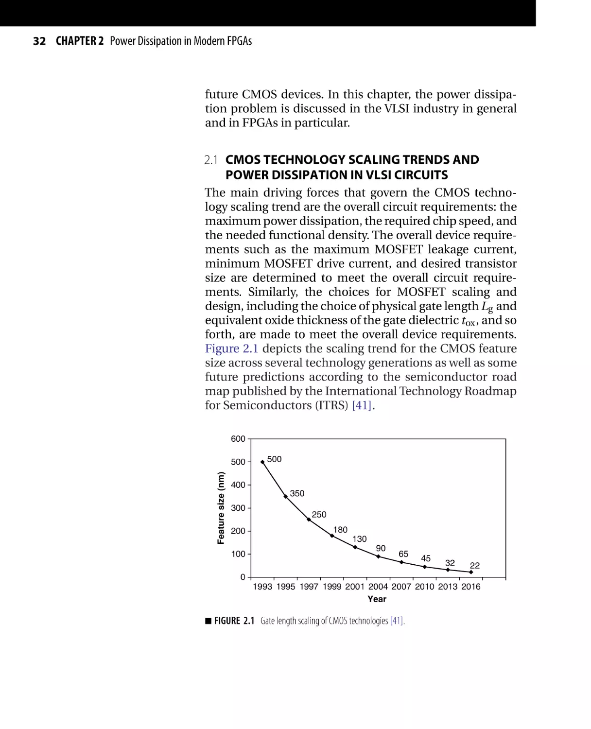
Figure 2.1 depicts the scaling trend for the CMOS feature
size across several technology generations as well as some
future predictions according to the semiconductor road
map published by the International Technology Roadmap
for Semiconductors (ITRS) [41].
600
Feature size (nm)
500
500
400
350
300
200
250
180
130
100
90
65
45
32
22
0
1993 1995 1997 1999 2001 2004 2007 2010 2013 2016
Year
■
FIGURE 2.1 Gate length scaling of CMOS technologies [41].
2.1 CMOS Technology Scaling Trends and Power Dissipation in VLSI Circuits 33
There are two common types of scaling trends in the
CMOS process: constant field scaling and constant voltage
scaling. Constant field scaling yields the largest reduction in the power-delay product of a single transistor.
However, it requires a reduction in the power supply voltage as the minimum feature size is decreased. Constant
voltage scaling does not suffer from this problem, therefore, it provides voltage compatibility with older circuit
technologies. The disadvantage of constant voltage scaling is the electric field increases as the minimum feature
length is reduced, resulting in velocity saturation, mobility
degradation, increased leakage currents, and lower breakdown voltages. Hence, the constant field scaling is the
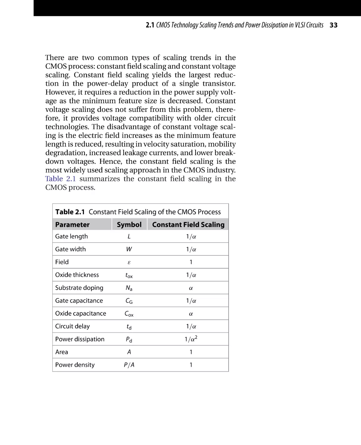
most widely used scaling approach in the CMOS industry.
Table 2.1 summarizes the constant field scaling in the
CMOS process.
Table 2.1 Constant Field Scaling of the CMOS Process
Parameter
Symbol
Gate length
L
1/α
Gate width
W
1/α
Field
ε
1
Oxide thickness
tox
1/α
Substrate doping
Na
α
Gate capacitance
CG
1/α
Oxide capacitance
Cox
α
Circuit delay
td
1/α
Power dissipation
Pd
1/α2
Area
A
1
P/A
1
Power density
Constant Field Scaling
34 CHAPTER 2 Power Dissipation in Modern FPGAs
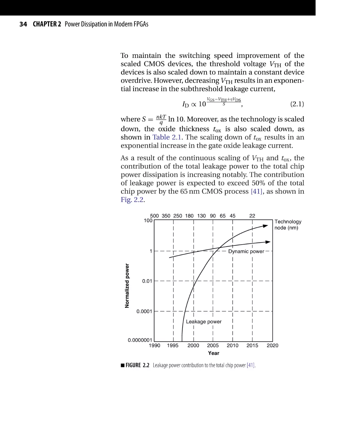
To maintain the switching speed improvement of the
scaled CMOS devices, the threshold voltage VTH of the
devices is also scaled down to maintain a constant device
overdrive. However, decreasing VTH results in an exponential increase in the subthreshold leakage current,
ID ∝ 10
VGS −VTH +ηVDS
S
,
(2.1)
where S = nkT
q ln 10. Moreover, as the technology is scaled
down, the oxide thickness tox is also scaled down, as
shown in Table 2.1. The scaling down of tox results in an
exponential increase in the gate oxide leakage current.
As a result of the continuous scaling of VTH and tox , the
contribution of the total leakage power to the total chip
power dissipation is increasing notably. The contribution
of leakage power is expected to exceed 50% of the total
chip power by the 65 nm CMOS process [41], as shown in
Fig. 2.2.
500 350 250 180 130 90 65 45
100
Normalized power
1
22
Technology
node (nm)
Dynamic power
0.01
0.0001
Leakage power
0.0000001
1990
1995
2000
2005
2010
2015
Year
■ FIGURE
2.2 Leakage power contribution to the total chip power [41].
2020
2.3 Leakage Power in FPGAs 35
2.2 DYNAMIC POWER IN FPGAs
FPGAs provide reconfigurability by using redundant logic
and switches inside the chip. As a result, FPGA design
dynamic power dissipation is much larger than their
application-specific integrated circuit (ASIC) counterparts. In a study by Kuan and Rose [42], the authors
performed a quantitative study to compare the dynamic
power dissipation in FPGAs to that of ASICs, and the results
are listed in Table 2.2.
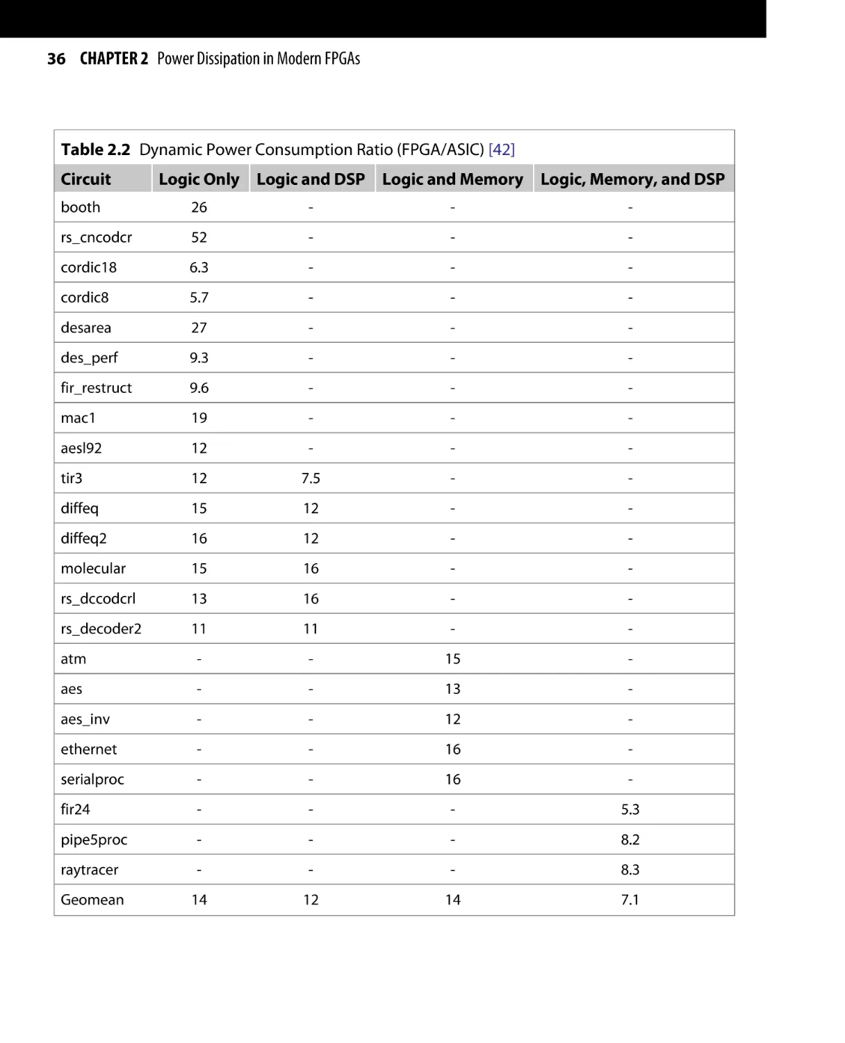
The results in Table 2.2 suggest that, on average, FPGAs
consume 14× more dynamic power than ASICs when the
circuits contain only logic. However, when the design uses
some of the hard blocks inside the FPGA, e.g., memory
blocks and multipliers, the dynamic power gap is reduced
between FPGAs and ASICs, with multipliers being the main
factor in reducing FPGA power dissipation. The main reason for this reduction in the power gap is due to the fact
that using the hard macros inside the FPGAs means fewer
logic resources are used, hence, less power is being dissipated. As a result, it can be concluded that FPGAs are less
efficient in terms of power dissipation when compared to
ASICs. In order for FPGAs to be able to compete with ASICs,
extensive work is still needed to reduce FPGA dynamic
power dissipation.
2.3 LEAKAGE POWER IN FPGAs
2.3.1 CMOS Device Leakage Mechanisms
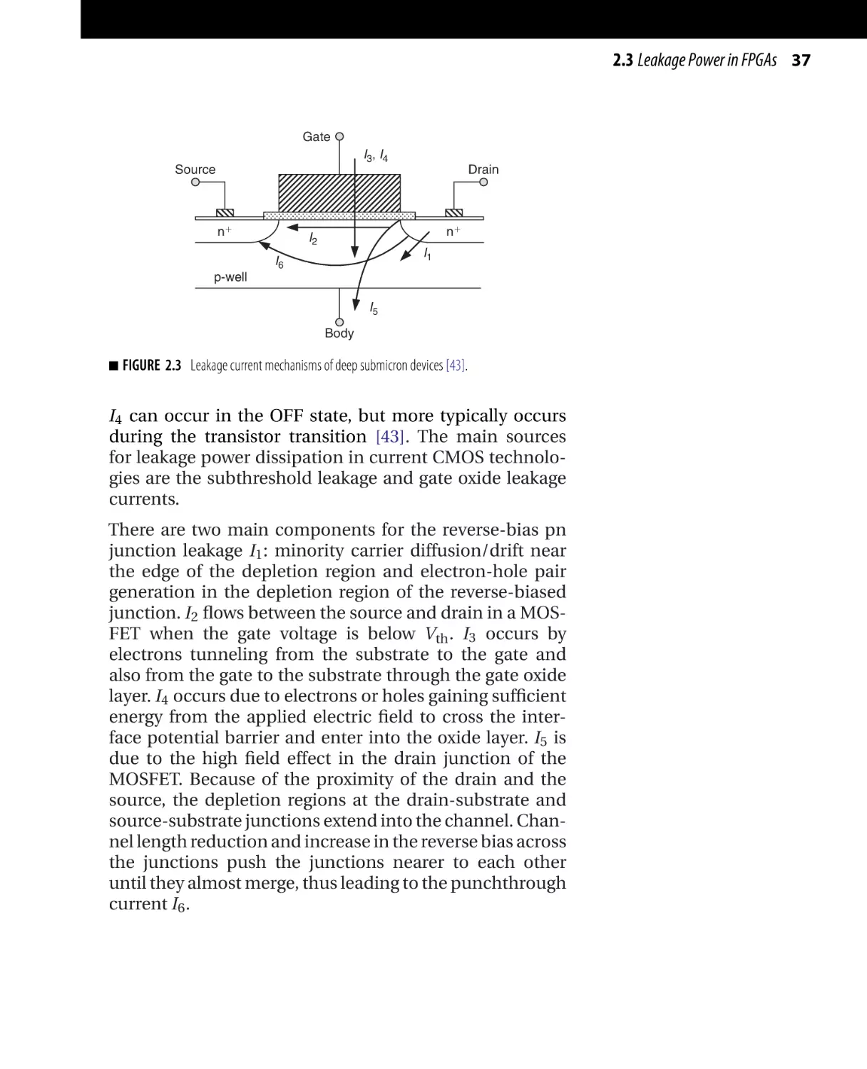
There are six short-channel leakage current mechanisms
in CMOS devices. Figure 2.3 summarizes the leakage current types that affect state-of-the-art CMOS devices [43].
I1 is the reverse-bias pn junction leakage; I2 is the subthreshold leakage; I3 is the oxide tunneling current; I4 is
the gate current due to hot-carrier injection; I5 is the gateinduced drain leakage; and I6 is the channel punchthrough
current. Currents I2 , I5 , and I6 are OFF-state leakage currents, while I1 and I3 occur in both ON and OFF states.
36 CHAPTER 2 Power Dissipation in Modern FPGAs
Table 2.2 Dynamic Power Consumption Ratio (FPGA/ASIC) [42]
Circuit
Logic Only
Logic and DSP Logic and Memory Logic, Memory, and DSP
booth
26
-
-
-
rs_cncodcr
52
-
-
-
cordic18
6.3
-
-
-
cordic8
5.7
-
-
-
desarea
27
-
-
-
des_perf
9.3
-
-
-
fir_restruct
9.6
-
-
-
mac1
19
-
-
-
aesl92
12
-
-
-
tir3
12
7.5
-
-
diffeq
15
12
-
-
diffeq2
16
12
-
-
molecular
15
16
-
-
rs_dccodcrl
13
16
-
-
rs_decoder2
11
11
-
-
atm
-
-
15
-
aes
-
-
13
-
aes_inv
-
-
12
-
ethernet
-
-
16
-
serialproc
-
-
16
-
fir24
-
-
-
5.3
pipe5proc
-
-
-
8.2
raytracer
-
-
-
8.3
Geomean
14
12
14
7.1
2.3 Leakage Power in FPGAs 37
Gate
I3 , I4
Source
Drain
n1
n1
I2
I1
I6
p-well
I5
Body
■
FIGURE 2.3 Leakage current mechanisms of deep submicron devices [43].
I4 can occur in the OFF state, but more typically occurs
during the transistor transition [43]. The main sources
for leakage power dissipation in current CMOS technologies are the subthreshold leakage and gate oxide leakage
currents.
There are two main components for the reverse-bias pn
junction leakage I1 : minority carrier diffusion/drift near
the edge of the depletion region and electron-hole pair
generation in the depletion region of the reverse-biased
junction. I2 flows between the source and drain in a MOSFET when the gate voltage is below Vth . I3 occurs by
electrons tunneling from the substrate to the gate and
also from the gate to the substrate through the gate oxide
layer. I4 occurs due to electrons or holes gaining sufficient
energy from the applied electric field to cross the interface potential barrier and enter into the oxide layer. I5 is
due to the high field effect in the drain junction of the
MOSFET. Because of the proximity of the drain and the
source, the depletion regions at the drain-substrate and
source-substrate junctions extend into the channel. Channel length reduction and increase in the reverse bias across
the junctions push the junctions nearer to each other
until they almost merge, thus leading to the punchthrough
current I6 .
38 CHAPTER 2 Power Dissipation in Modern FPGAs
Of these six different leakage current mechanisms experienced by current CMOS devices, subthreshold and gate
leakage currents are the most dominant leakage currents.
Furthermore, the contribution of subthreshold leakage
current to the total leakage power is much higher than that
of gate leakage current, especially at above room temperature operating conditions. The contribution of gate leakage
current to the leakage power dissipation is expected to
increase significantly with the technology scaling, unless
high-k materials are introduced in the CMOS fabrication
industry [41].
2.3.2 Current Situation of Leakage Power in
Nanometer FPGAs
For FPGAs to support reconfigurability, more transistors
are used than those used in an ASIC design that performs
the same functionality. Consequently, leakage power dissipation in FPGAs is higher than that in their ASIC counterpart. It was reported in a study by Kuon and Rose [42] that
on average, the leakage power dissipation in FPGA designs
is almost 5.4 times that of their ASIC counterparts under
worst-case operating conditions. The excess leakage power
dissipated in FPGAs is mainly due to the programming
logic that is not present in ASIC designs.
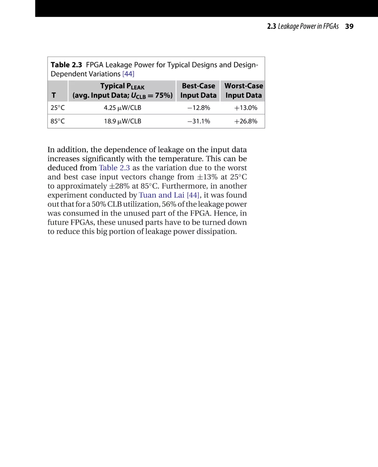
A study of the leakage power dissipation in a 90-nm CMOS
FPGA was performed by Tuan and Lai [44], the results of
which are summarized in Table 2.3. By comparing the average leakage power dissipation of a typical 90-nm CMOS
FPGA at 25◦ C and 85◦ C, it can be seen that the average leakage power increases by four times. Moreover, the results in
the first column are for a utilization of 75%; hence, the
leakage power dissipation for a 1000-CLB FPGA would be
in the range of 4.2 mW. If these FPGAs are to be used in
a wireless mobile application, which has a typical leakage
current of 300 A, then the maximum number of CLBs that
can be used would be 86 CLBs for the 25◦ C and 20 CLBs for
the 85◦ C.
2.3 Leakage Power in FPGAs 39
Table 2.3 FPGA Leakage Power for Typical Designs and DesignDependent Variations [44]
Typical PLEAK
(avg. Input Data; UCLB = 75%)
Best-Case
Input Data
Worst-Case
Input Data
25◦ C
4.25 W/CLB
−12.8%
+13.0%
85◦ C
18.9 W/CLB
−31.1%
+26.8%
T
In addition, the dependence of leakage on the input data
increases significantly with the temperature. This can be
deduced from Table 2.3 as the variation due to the worst
and best case input vectors change from ±13% at 25◦ C
to approximately ±28% at 85◦ C. Furthermore, in another
experiment conducted by Tuan and Lai [44], it was found
out that for a 50% CLB utilization, 56% of the leakage power
was consumed in the unused part of the FPGA. Hence, in
future FPGAs, these unused parts have to be turned down
to reduce this big portion of leakage power dissipation.
Chapter
3
Power Estimation in FPGAs
3.1 Introduction
3.2 Power Estimation in VLSI: An Overview
3.2.1 Simulation-Based Power Estimation Techniques
3.2.2 Probabilistic-Based Power Estimation Techniques
3.3 Commercial FPGA Power Estimation Techniques
3.3.1 Spreadsheet Power Estimation Tools
3.3.2 CAD Power Estimation Tools
3.4 A Survey of FPGA Power Estimation Techniques
3.4.1 Linear Regression-Based Power Modeling
3.4.2 Probabilistic FPGA Power Models
3.4.3 Look-up Table–Based FPGA Power Models
3.5 A Complete Analytical FPGA Power Model under Spatial Correlation
3.5.1 Spatial Correlation and Signal Probability Calculations
3.5.2 Exploration Phase: Locating Spatial Correlation
3.5.3 Signal Probabilities Calculation Algorithm
under Spatial Correlation
3.5.4 Power Calculations Due to Glitches
3.5.5 Signal Probabilities and Power Dissipation
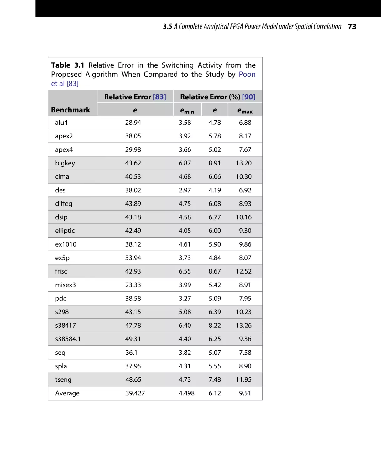
3.5.6 Results and Discussion
Low-Power Design of Nanometer FPGAs: Architecture and EDA
Copyright © 2010 by Elsevier, Inc. All rights of reproduction in any form reserved.
41
42 CHAPTER 3 Power Estimation in FPGAs
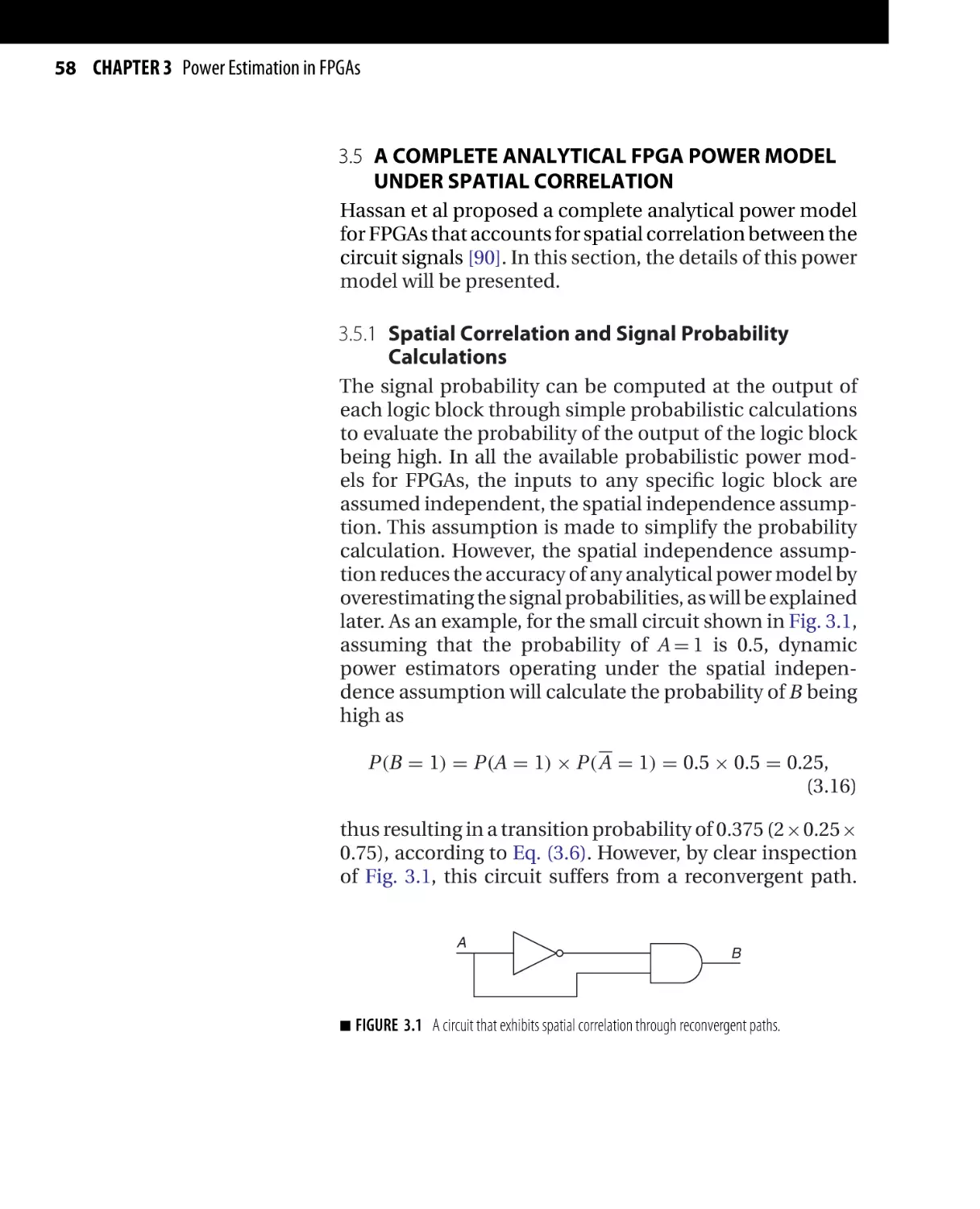
With power dissipation posing as an important factor in
the design phase of FPGAs, power estimation and analysis techniques have turned out to be huge challenges for
both FPGA vendors and designers. Power characterization
is an important step in designing power efficient FPGA
architectures and FPGA applications. FPGA designers need
a method to quantify the power advantage of the architectural design decisions without having to go through
fabrication. Moreover, FPGA users need to check the power
efficiency of the several possible implementations without
actually going through the lengthy design phase.
Power models for FPGAs need to consider both components of power dissipation: dynamic power and leakage
power. To further improve the accuracy of the power
model, all the subcomponents of both dynamic power
(switching, short circuit, and glitch power) and leakage
power (subthreshold and gate leakage power) need to
be accounted for. In addition, other factors that affect
power dissipation, including spatial correlation and input
dependency of leakage power, should be considered, especially in the subnanometer regime since their impact is
highlighted as the CMOS minimum feature size is scaled
down.
3.1 INTRODUCTION
Modern CMOS processes suffer from two dominant
sources of power dissipation: dynamic and leakage power.
Dynamic power dissipation can be divided into switching, glitch, and short-circuit power dissipation, whereas
leakage power dissipation can be further divided into
subthreshold leakage and gate leakage power dissipation.
Historically, CMOS circuits were dominated by dynamic
power dissipation; however, by the 65 nm CMOS process,
leakage power is expected to dominate the total power
dissipation, as explained in Chapter 2. In addition, as the
3.1 Introduction 43
CMOS process is further scaled down, gate leakage power
is expected to surpass the subthreshold power dissipation,
especially at lower operating temperatures, as predicted
by the semiconductor road map issued by the ITRS [41],
unless high-k materials are used to implement the device
gates.
All sources of power dissipation in CMOS circuits exhibit
significant state dependency. To develop an accurate
power model, accurate information about signal probabilities should be made available. Several studies in the
literature have addressed this problem and a complete
survey was presented in the study by Najm [45].
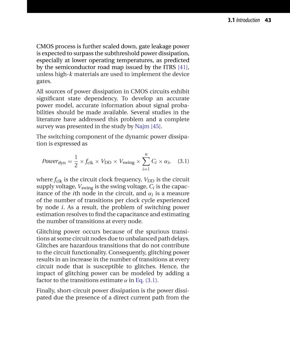
The switching component of the dynamic power dissipation is expressed as
1
× fclk × VDD × Vswing ×
Ci × αi,
2
n
Powerdyn =
(3.1)
i=1
where fclk is the circuit clock frequency, VDD is the circuit
supply voltage, Vswing is the swing voltage, Ci is the capacitance of the ith node in the circuit, and αi is a measure
of the number of transitions per clock cycle experienced
by node i. As a result, the problem of switching power
estimation resolves to find the capacitance and estimating
the number of transitions at every node.
Glitching power occurs because of the spurious transitions at some circuit nodes due to unbalanced path delays.
Glitches are hazardous transitions that do not contribute
to the circuit functionality. Consequently, glitching power
results in an increase in the number of transitions at every
circuit node that is susceptible to glitches. Hence, the
impact of glitching power can be modeled by adding a
factor to the transitions estimate α in Eq. (3.1).
Finally, short-circuit power dissipation is the power dissipated due the presence of a direct current path from the
44 CHAPTER 3 Power Estimation in FPGAs
power supply to the ground during the rise and fall times
of each transition. Hence, short-circuit power is a function
of the rise and fall times and the load capacitance. Several
research projects have been directed to provide an accurate estimate of short-circuit power dissipation [46–49].
However, the simplest method to account for short-circuit
power dissipation is to set it as a percentage of the dynamic
power dissipation, usually 10% [50].
In most of the power estimation techniques in the literature, spatial independence among the signals was
assumed. Under the spatial independence assumption, all
the signals are assumed independent even though they
might share a common parent gate; hence, the effect of
reconvergent paths is ignored. This assumption is used to
significantly reduce the power calculation runtime; however, it results in significant inaccuracies in the power
estimation. It was reported in the study by Schneider
and Krishnamoorthy [51] that the relative error in switching activities estimation under the spatial independence
assumption in VLSI designs can reach 50%.
3.2 POWER ESTIMATION IN VLSI: AN OVERVIEW
The power estimation is defined as the problem of evaluating the average power dissipation in a digital circuit [45].
Power estimation techniques fall into two main categories:
simulation-based or probabilistic-based approaches. In
this section, a brief overview of the two power estimation
techniques is presented.
3.2.1 Simulation-Based Power Estimation Techniques
In simulation-based techniques, a random sequence of
input vectors is generated and used to simulate the circuit
to estimate the power dissipation. The first approaches
developed were based on the use of SPICE simulations
to simulate the whole circuit using a long sequence of
3.2 Power Estimation in VLSI: An Overview 45
input vectors [52, 53]. However, the use of such methods
in today’s VLSI industry is impractical, especially with the
huge levels of integration achieved, that it might take days
if not weeks to simulate a complete chip using SPICE.
Moreover, these methods are significantly pattern dependent due to the use of a random sequence of input
vectors. If an intelligent method is used to select the input
sequence, these methods would provide the most accurate
power estimation.
Several simplifications of these methodologies were proposed to reduce the computational complexity of power
estimation [54–57]. The methods still rely on simulations,
but instead of using SPICE simulations, other levels of circuit simulations were performed including switch-level
and logic-based simulations. These methodologies trade
accuracy for faster runtime. To perform these simulations,
the power supply and ground are assumed constant. However, these methods still suffer from pattern dependency
since there is a need to generate a long sequence of input
vectors to achieve the required accuracy. Although these
simulations are more efficient than SPICE simulations,
they are somewhat impractical to use for large circuits,
especially if a long input sequence is used to increase the
method accuracy.
To solve the pattern dependency problem of simulationbased power estimation methods, several statistical methods had been proposed [58–63]. These statistical methods
aim to quantify two parameters: the length of the input
sequence and the stopping criteria for simulation, required
to achieve a predefined power estimate accuracy.
The earliest of these studies focused on the use of Monte
Carlo simulations to estimate the total average power [58].
A random sequence of N input vectors was independently
generated and used to simulate the circuit. Let p and s be
the average and standard deviation of the power measured
over a time period T and Pav is the average power. Hence,
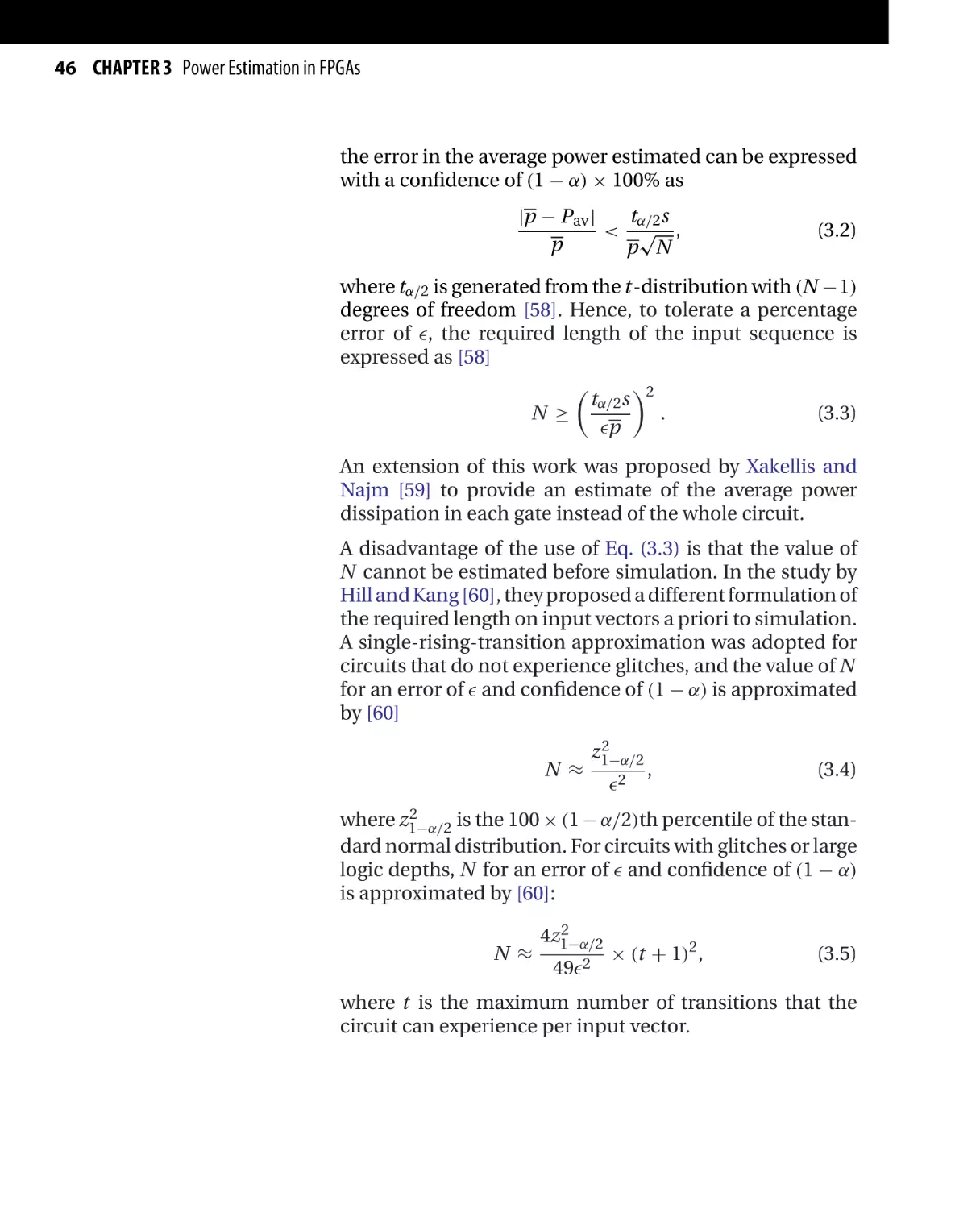
46 CHAPTER 3 Power Estimation in FPGAs
the error in the average power estimated can be expressed
with a confidence of (1 − α) × 100% as
tα/2 s
|p − Pav |
< √ ,
p
p N
(3.2)
where tα/2 is generated from the t-distribution with (N −1)
degrees of freedom [58]. Hence, to tolerate a percentage
error of , the required length of the input sequence is
expressed as [58]
tα/2 s 2
N≥
.
(3.3)
p
An extension of this work was proposed by Xakellis and
Najm [59] to provide an estimate of the average power
dissipation in each gate instead of the whole circuit.
A disadvantage of the use of Eq. (3.3) is that the value of
N cannot be estimated before simulation. In the study by
Hill and Kang [60], they proposed a different formulation of
the required length on input vectors a priori to simulation.
A single-rising-transition approximation was adopted for
circuits that do not experience glitches, and the value of N
for an error of and confidence of (1 − α) is approximated
by [60]
N≈
2
z1−α/2
2
,
(3.4)
2
where z1−α/2
is the 100 × (1 − α/2)th percentile of the standard normal distribution. For circuits with glitches or large
logic depths, N for an error of and confidence of (1 − α)
is approximated by [60]:
N≈
2
4z1−α/2
492
× (t + 1)2 ,
(3.5)
where t is the maximum number of transitions that the
circuit can experience per input vector.
3.2 Power Estimation in VLSI: An Overview 47
Another disadvantage with Eq. (3.3) is the large number of input vectors needed to achieve the required
accuracy, since it depends on the square of the sample
variance. Moreover, as the resulting power estimate deviates from the normal distribution, the simulation might
terminate early, thus compromising the accuracy of the
results. In the studies by Marculescu et al [61] and Liu
and Papaefthymiou [63], solutions to these two issues
were proposed using a Markov chain to generate the
input sequence. The resulting sequences are more compact than the ones used in the study by Burch et al [58]
and provide a reduction in the simulation time by orders
of magnitude while keeping the estimated average power
within 5%.
Another statistical method proposed in the literature to
provide the needed length for the input sequence is based
on the least square estimation methods [62]. The authors
viewed the estimation problem of the input sequence as an
approximation problem and explored the use of sequential least square and recursive least square to solve the
problem of finding the input sequence that has minimum
variance and without making any probabilistic assumptions about the data. It was reported by Murugavel et al [62]
that least square algorithms need a much smaller number
of iterations, i.e., smaller input sequence, to provide a close
estimate of the average power dissipation to that reported
in the study by Burch et al [58].
3.2.2 Probabilistic-Based Power Estimation
Techniques
Probabilistic power estimation techniques have been
proposed to solve the problem of pattern dependency of
simulation-based approaches. In these techniques, signal
probabilities are propagated through the circuit starting
from the primary inputs until the outputs are reached.
These estimation techniques require circuit models for
probability propagation for every gate in the library.
48 CHAPTER 3 Power Estimation in FPGAs
The first ever probabilistic propagation model was proposed in the study by Cirit [64]. In this model, a zero-delay
assumption was considered, under which the delay of all
logic gates and routing resources was assumed zero. The
switching activity of node x was defined as the probability
that a transition occurs at x. The transition probability of
x, Pt (x) is calculated according to
Pt (x) = 2 × Ps (x) × Ps (x ) = 2 × Ps (x) × 1 − Ps (x) ,
(3.6)
where Ps (x) and Ps (x ) are the probabilities x = 1 and
x = 0, respectively. In adopting Eq. (3.6), the authors
assume that the values of the same signal in two consecutive clock cycles are independent, which is referred to as
temporal independence. Moreover, the signal probabilities
at the primary inputs are propagated into the circuit while
assuming that all internal signals are independent. This
assumption is referred to as spatial independence. Furthermore, Cirit [64] ignores glitching power since a zero delay
model was adopted.
Najm [65], proposed the use of the transition density to
represent the signal probabilities more accurately than the
simple transition probability in Eq. (3.6). The transition
density is defined as the average number of transitions per
second at a node in the circuit. The transition density at
node x, D(x), is given by
nx (T )
,
T →∞
T
D(x) = lim
(3.7)
where nx (T ) is the number of transitions within time T .
Najm [65] formulated the relationship between the transition density and the transition probability by
D(x) ≥
Pt (x)
,
Tc
(3.8)
where Tc is the clock cycle. Hence, the transition probability will always be less than the transition density,
3.2 Power Estimation in VLSI: An Overview 49
thus underestimating the power dissipation. The transition density at node y with a set of inputs x0 , x1 , . . . , xn is
given by the following set of relationships:
D(y) =
n
i=1
P
∂y
∂xi
D(xi ),
∂y
y|xi =1 ⊕ y|xi =0 ,
∂xi
(3.9)
(3.10)
∂y
where ∂xi is the Boolean difference of y with respect to its
ith input and ⊕ denotes exclusive OR operation. To evaluate the Boolean difference at each node, the probabilities
at each node need to be propagated through the whole
circuit. It should be noted that the use of (3.9) only provides a better estimate for the number of transitions than
the transition density given in Eq. (3.6) and this model
still suffers from both spatial and temporal independence
assumptions.
In the study by Ghosh et al [66], the authors proposed
the use of binary decision diagrams (BDDs) to account
for spatial and temporal correlations. The regular Boolean
function of any logic gate stores the steady-state value of
the output given the inputs. However, BDDs are used to
store the final value as well as the intermediate states,
provided that circuit delays are available beforehand. As
a result, such a probabilistic model can predict the signal probabilities at each circuit node under spatial and
temporal correlations. However, this technique is computationally expensive and only practical for moderate-sized
circuits. In addition, a BDD is required for every logic gate.
If some gates have a large number of intermediate states,
then this technique might become impractical even for
medium-sized circuits.
Several other research projects have been proposed in
the literature to handle spatial and temporal correlations
[67–72].
50 CHAPTER 3 Power Estimation in FPGAs
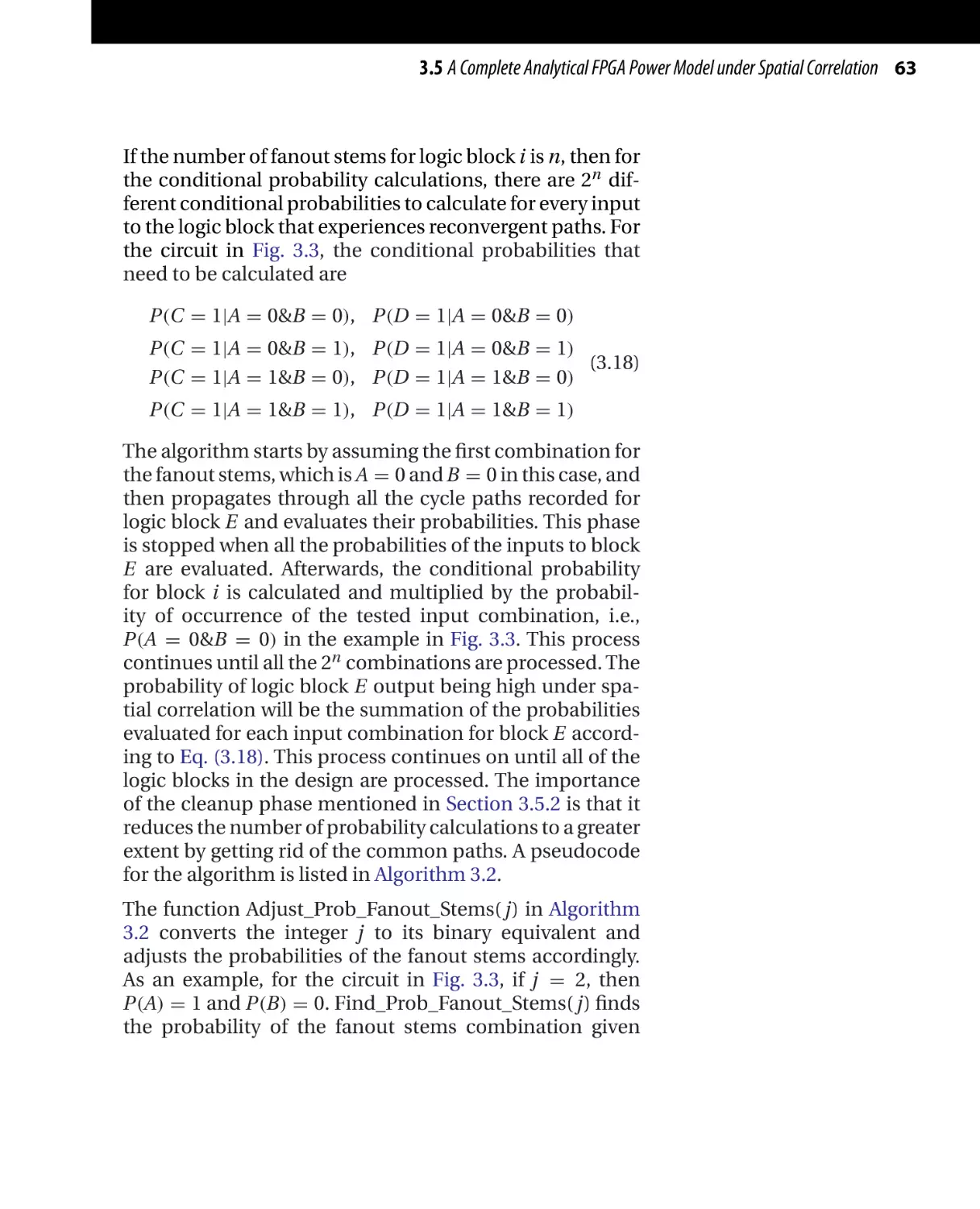
3.3 COMMERCIAL FPGA POWER ESTIMATION
TECHNIQUES
Commercial FPGA vendors offer a variety of power estimation techniques for customers. There are two categories of
commercial FPGA power estimation techniques: devicespecific spreadsheets [73–75] and CAD-based power estimation techniques [74, 76, 77].
3.3.1 Spreadsheet Power Estimation Tools
FPGA power spreadsheets analyze both the leakage and
dynamic power dissipation components in the FPGA.
This method of power estimation is usually used in the
early stages of the design process to give a quick estimate of the power dissipation of the design [73–75]. In
spreadsheet-based power estimators, the users must provide the clock frequency of the design and the toggle
percentage for the logic blocks. Consequently, this method
gives a rough approximation of power and requires designers to thoroughly understand the switching activity inside
their circuits.
For dynamic power computation, designers provide the
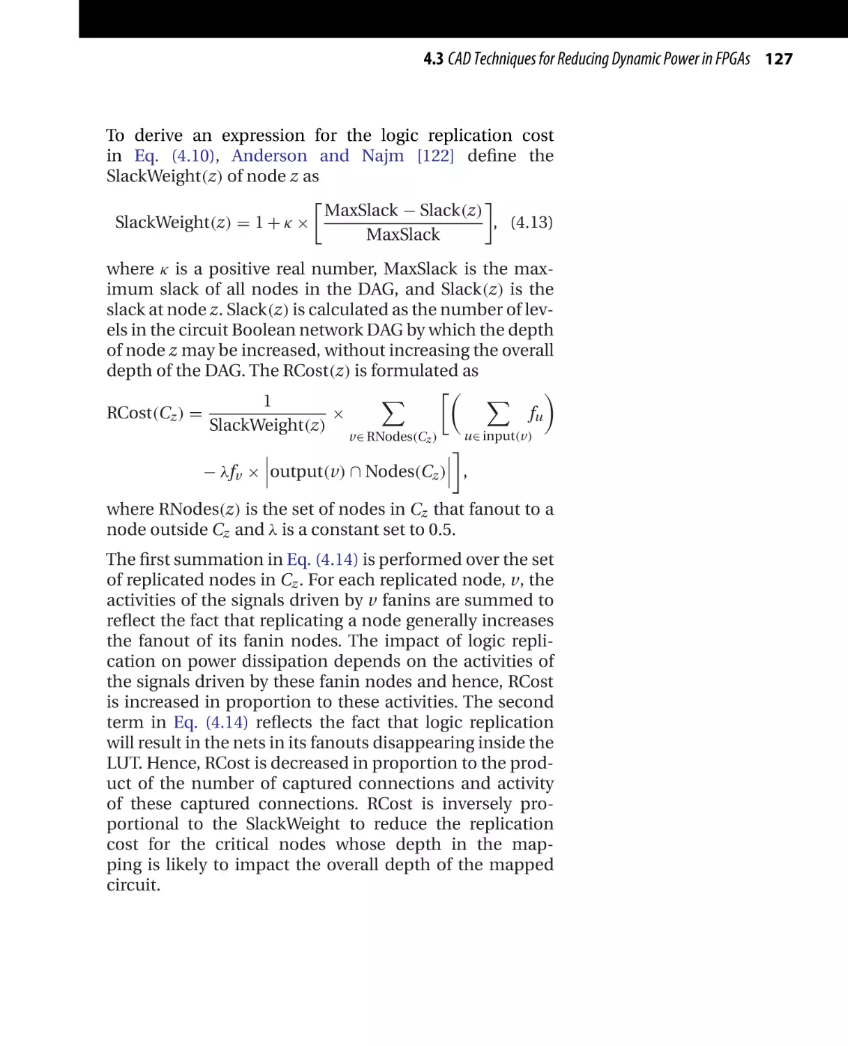
average switching frequency α for all the logic blocks, or for
each module in the design. Coefficients for adjusting the
dynamic power calculation are provided in the device data
sheet. The total dynamic power is calculated according to
Pdyn = K × fclk × VDD ×
αi Ci Vswing,i ,
all_components
(3.11)
where K is the coefficient used in adjusting the power
estimate for each device family. The value of K is measured through empirical experiments performed by the
FPGA vendor to encompass the impact of both glitching
and short-circuit power components. The values of both
K and the node capacitance are usually provided as an
3.3 Commercial FPGA Power Estimation Techniques 51
average value for the combination of family/die/package
being used. The only variables that are design specific are
the clock frequency and the average switching probability
of the design. As a result, the average dynamic power estimated using this approach is very crude and should only
be used as a guideline on which family/die/package to be
used for a certain design.
In modeling leakage power dissipation, power spreadsheets list the leakage power of each FPGA component
Pleak_per_component . For example, the spreadsheet lists the
average leakage power per logic block, sequential flip-flop
or latch, and IO cell. The total leakage is calculated by summing the leakage power for each component used in the
design according to
Pleak =
Pleak_per_component × Ncomponent .
all_components
(3.12)
Similarly, the value of Pleak_per_component is provided for
each combination of FPGA family/die/package. It should
be noted that the leakage power estimated using this
approach is device specific rather than design specific.
The total estimated power is the summation of the
dynamic and leakage power evaluated using Eqs. (3.11)
and (3.12), respectively.
3.3.2 CAD Power Estimation Tools
Commercial CAD power estimation tools provide different variants of power estimators with different accuracies.
The most accurate power estimation tool provided relies
on cycle accurate simulations to capture the switching
at each node in the design [74, 76, 77]. The user specifies a simulation test bench, and the design is simulated
using logic simulators. The logic simulator records all
the transitions that occur on every net in the design.
52 CHAPTER 3 Power Estimation in FPGAs
Afterwards, these transitions are read using the power
estimator, and using the value of the capacitance at each
node, the total dynamic power of the design can be easily estimated using Eq. (3.1). The accuracy of the power
estimation can be further improved by using postlayout
capacitance for power calculation. Although this power
estimation technique provides a better estimate for power
dissipation than spreadsheets, the runtime of this technique is very long and the power estimate accuracy is
dependent on the length of the test vector used, similar to
simulation-based power estimation techniques discussed
above.
Another method of power estimation used by commercial FPGA power estimators is vectorless power estimation.
This approach is mainly a probabilistic power estimation methodology, where the probabilities at every net
are propagated through the circuit to estimate the total
dynamic power estimation. Again, postlayout node capacitances can be used to improve the power estimation
accuracy. Commercial vectorless power estimation tools
do not take into account glitching power or spatial correlation between signals, thus suffering from reduced accuracy
compared to the simulation-based approach.
FPGA vendors provide another simulation-based power
estimation methodology that does not depend on cycle
accurate simulation. A random input vector is used to simulate the circuit while counting the transitions that occur at
every node. Hence, glitching power is ignored in that case,
while spatial correlation between the different signals is
taken into consideration. Since cycle accurate simulation
is not used in that case, simple logic simulators can be
used, thus reducing the runtime of that approach, while
keeping the accuracy of the power estimated somewhere
between the first two approaches mentioned above.
Finally, for leakage power estimation, most commercial
FPGA CAD power estimators use an approach similar to
3.4 A Survey of FPGA Power Estimation Techniques 53
that used in power spreadsheets. An extra parameter that
is used to increase the accuracy of leakage power estimation is accounting for the power dissipated in the unused
resources of the FPGA. This is achieved by multiplying
the number of the unused resources on the die by the
average leakage power of the unused resources. Hence, it
should be noted that none of the commercial FPGA CAD
tools accounts for the state dependency of leakage power
dissipation.
3.4 A SURVEY OF FPGA POWER ESTIMATION
TECHNIQUES
Power modeling in FPGAs did not receive wide attention
in the literature, especially for generic FPGA architectures.
Several works targeted specific FPGA architectures [44, 78–
82]. These works are only applicable to one architecture
because they depend on the specific architecture details
to extract the power dissipation. Moreover, all these works
targeted only dynamic power estimation in FPGAs, except
for the study by Tuan and Lai [44] that provided an insight
into leakage power dissipation in a 90 nm CMOS commercial FPGA. On the other hand, power dissipation in
general architecture FPGA has been targeted in a limited
number of research projects [83–87]. However, all these
research projects did not provide an analytical methodology for estimating the effect of spatial correlation on the
total power dissipation.
In the study by Kusse and Rabaey [78], a Xilinx XC4003ATM
FPGA was used to study the power breakdown inside the
FPGA. The power reported was the actual power measure recorded from the physical FPGA itself. Weiß et al
[79] introduced a technology-dependent empirical correction factor for dynamic power estimation in the Xilinx
VirtexTM FPGA. The factor introduced was used to adjust
the switching activity estimated through regular probabilistic analysis similar to the study by Najm [65]. The
54 CHAPTER 3 Power Estimation in FPGAs
power dissipation in the FPGA under consideration was
physically measured for different benchmarks, and the
power dissipation was calculated in a similar manner
to that of the study by Najm [65] for the same benchmarks. The ratio between the measured and estimated
power values was calculated as the correction factor for
power estimation. The main reason for using that correction factor is to account for the factors that affect power
dissipation, including temporal and spatial correlations,
which are not captured in the probabilistic calculations
presented in the study by Najm [65]. It should be noted that
this power estimation methodology is strongly dependent
on the benchmarks used to compute the value of the correction factor as different types of benchmarks will result
in different values of the factor. It should be noted that
both the studies by Kusse and Rabaey [78] and Weiß et
al [79] do not account for leakage power dissipation in the
FPGA under consideration.
A model for dynamic power dissipation in Xilinx VirtexIITM FPGAs was described in the study by Shang et al [80].
The switching activity was estimated using logic simulation of some practical input vectors obtained from the
users. The different node capacitances were evaluated
from post–silicon capacitance extraction techniques. An
extension of this work was presented by Degalahal and
Tuan [81], where the node capacitances were evaluated
using simple RC models for the Xilinx Spartan-3TM FPGA.
The methodology is still simulation-based since it relies on
logic-level simulation to find the node activities.
3.4.1 Linear Regression-Based Power Modeling
Anderson and Najm [82] proposed a power model for
FPGAs that predicts accurate switching activities in Xilinx
FPGAs using curve fitting theories and empirical formulae. The main goal of this work is to account for glitches
in the transitions activity used in dynamic power calculations. A prediction function was proposed to calculate the
3.4 A Survey of FPGA Power Estimation Techniques 55
change in transitions activity to account for glitching in the
form of
PRi = α × GENi + β × GEN2i + γ × PROPi + υ × PROP2i
+ ν × Di + ξ × Di2 + η × PROPi × GENi
+ ι × GENi × Di + ρ × PROPi × Di + φ,
(3.13)
where α, β, γ, υ, ν, ξ, η, ι, ρ, φ are scalar constants, GENi
is a parameter used to quantify the number of glitches
generated at node i, PROPi represents the amount of glitch
propagation at node i, and Di is a parameter to represent
the depth of node i. GENi is formulated as
GENi =
|PLy | − |PLxi | ,
min
xi ∈inputs(y)
(3.14)
where PLy is the set of different paths from the primary
inputs to node y and is given by
p + 1|p ∈ PLxi .
PLy =
(3.15)
xi ∈inputs(y)
The authors used a commercial Xilinx Virtex-IITM PRO
FPGA, and using a predefined input sequence and a commercial simulation tool, they generated the number of
transitions experienced by every gate per clock cycle in
several FPGA benchmarks. Afterwards, using curve fitting
theories, the constants in Eq. (3.13) were evaluated.
Although the method proposed in their study [82] tries
to formulate the impact of glitches on dynamic power
estimation in FPGAs, it has several drawbacks. First, the
method is architecture dependent and cannot be readily used to estimate dynamic power dissipation in other
FPGA architectures than the one used. Moreover, to apply
this method on a new architecture, the linear regression
model needs to be trained; hence, there is a need for a reference power estimator to train the linear regression model.
56 CHAPTER 3 Power Estimation in FPGAs
In addition, the model accuracy is strongly dependent
on the types of circuits used to evaluate the curve fitting
parameters, which makes it very susceptible to errors for
the different circuit types.
3.4.2 Probabilistic FPGA Power Models
The power models that target general architectures consider dynamic, leakage, and short-circuit power dissipation in FPGAs. The first power model for generic FPGA
architectures was proposed by Poon et al [83]. This power
model is analytic in nature, making it very easy to implement with fast runtime. However, for this model to have
such fast runtime, several approximations were assumed
by the authors. First, for dynamic power estimation, they
[83] assume spatial and temporal independencies among
the internal design signals, as well as ignore the impact of
glitching power. Second, the leakage power was calculated
across all the transistors in the circuit while considering the
VGS to be half the threshold voltage VTH , thus, significantly
reducing the accuracy of the leakage power estimation.
Moreover, the state dependency of leakage power was not
considered in that model, which has a significant impact
on FPGAs built using current nanometer CMOS technologies, as explained in the study by Tuan and Lai [44].
However, the power model proposed by Poon et al [83]
had several advantages, including fast runtime and ability
to be integrated within VPR. As a result, the power model
became the de facto for power estimation for academic
research.
3.4.3 Look-up Table–Based FPGA Power Models
A study of the leakage power dissipation in the CMOS
90 nm Xilinx Virtex-IITM FPGA was presented by Tuan and
Lai [44]. The leakage power modeling was performed using
look-up tables (LUTs) of HSpice simulations. The leakage
power for every input vector measured, obtained using
3.4 A Survey of FPGA Power Estimation Techniques 57
HSpice simulations, was recorded and used to study the
impact of the state dependency and utilization on FPGA
leakage power dissipation. The study showed that the
input state dependency can vary leakage power in modern
FPGAs by approximately 60%. Moreover, a breakdown of
leakage power dissipation in the different parts of the FPGA
was provided. It should be noted that this study ignored
the effect of signal correlations on leakage power. Moreover, Tuan and Lai [44] did not evaluate the total leakage
power dissipation in the whole FPGA, only evaluated the
leakage power per logic block.
Another FPGA power model was presented for generic
FPGAs [84–86]. Leakage power dissipation was calculated
through the use of LUTs, which do not consider the state
dependency of leakage power. Moreover, the power model
depended on logic simulation to estimate the switching activities of the different circuit nodes. Although this
method can achieve high accuracy, its computational cost
is quite high. The authors tried to limit the execution
time by limiting the number of input vectors to 2000,
irrespective of the circuit size and its number of inputs.
However, this approach sacrifices the accuracy of the algorithm significantly as explained in the study by Chou and
Roy [88].
The input dependency of leakage power dissipation in
generic FPGAs was first addressed by Kumar and Anis [87].
The authors proposed a leakage power model based on the
BSIM4 models while accounting for the state dependencies. However, spatial correlation among internal signals
was not addressed. Moreover, the authors used some
empirical constants in the power formulation obtained
using curve fitting, thus, rendering the power model technology dependent. Finally, the temperature dependence
of power dissipation in FPGAs was studied by Lui et al [89].
The authors tried to estimate a factor that captures the
dependence of total power dissipation on the temperature
using empirical experimentation.
58 CHAPTER 3 Power Estimation in FPGAs
3.5 A COMPLETE ANALYTICAL FPGA POWER MODEL
UNDER SPATIAL CORRELATION
Hassan et al proposed a complete analytical power model
for FPGAs that accounts for spatial correlation between the
circuit signals [90]. In this section, the details of this power
model will be presented.
3.5.1 Spatial Correlation and Signal Probability
Calculations
The signal probability can be computed at the output of
each logic block through simple probabilistic calculations
to evaluate the probability of the output of the logic block
being high. In all the available probabilistic power models for FPGAs, the inputs to any specific logic block are
assumed independent, the spatial independence assumption. This assumption is made to simplify the probability
calculation. However, the spatial independence assumption reduces the accuracy of any analytical power model by
overestimating the signal probabilities, as will be explained
later. As an example, for the small circuit shown in Fig. 3.1,
assuming that the probability of A = 1 is 0.5, dynamic
power estimators operating under the spatial independence assumption will calculate the probability of B being
high as
P(B = 1) = P(A = 1) × P(A = 1) = 0.5 × 0.5 = 0.25,
(3.16)
thus resulting in a transition probability of 0.375 (2×0.25×
0.75), according to Eq. (3.6). However, by clear inspection
of Fig. 3.1, this circuit suffers from a reconvergent path.
A
■
B
FIGURE 3.1 A circuit that exhibits spatial correlation through reconvergent paths.
3.5 A Complete Analytical FPGA Power Model under Spatial Correlation 59
Both A and A can never be “1” simultaneously; hence, the
probability of B being high should be zero, assuming the
zero delay model. It should be noted that such a structure
is common in FPGA circuits, which will be depicted later
in Table 3.4.
As noticed from the previous example, the spatial independence assumption can significantly affect the dynamic
power calculations. If spatial correlation is to be taken into
consideration, conditional probability should be used to
evaluate the probability of all signals. As an example, considering the circuit in Fig. 3.1, the probability of B being
high is formulated as
P(B = 1) = P(A = 1|A = 1) × P(A = 1|A = 1) × P(A = 1)
+ P(A = 1|A = 0) × P(A = 1|A = 0) × P(A = 0),
(3.17)
which resolves to zero. From the above example, it can
be deduced that the spatial independence assumption
can significantly affect the accuracy of power estimation in VLSI circuits in general. Moreover, by inspecting Eq. (3.17), it can be noticed that spatial correlation
will cancel one or more of the conditional probabilities
listed. Hence, the impact of spatial independence will
always be toward overestimating the power dissipation by
overestimating the signal probabilities. Thus, the spatial
independence assumption costs the designers in terms
of overdesign to account for the overestimated power
dissipation.
Hassan et al proposed a methodology to calculate the signal probabilities under spatial correlation [90]. To consider
spatial correlation for power calculations, such reconvergent paths as the one shown in Fig. 3.1 need to be
identified, as discussed in Section 3.5.2, and their signal probabilities corrected accordingly, as explained in
Section 3.5.3. The proposed methodology is explained in
the following two sections.
60 CHAPTER 3 Power Estimation in FPGAs
3.5.2 Exploration Phase: Locating Spatial Correlation
Spatial correlation among signals in VLSI circuits occurs
whenever two signals are correlated. Correlations arise
when two or more signals share a common driver or a common parent logic block (x) and are connected as inputs to
another logic block (y), i.e., reconvergent paths. If the circuit is converted to a cyclic graph with the gates as the
nodes and the signal wires as the edges, the connections
between x and y form a cycle with two paths, as shown in
Fig. 3.2. Hence, the detection of signals that might exhibit
spatial correlation resolves to identify possible cycles in the
circuit. For example, in Fig. 3.2, a cycle would be detected
that goes through A → a → A → b → A.
In the study by Hassan et al [90], a depth-first search algorithm is used to identify such loops in the design. The
algorithm starts with the circuit primary inputs i, and
depth-first search is used to navigate through all the logic
blocks that share a path with each primary input. Whenever a logic block j is visited, it is marked with the name of
the primary input used in this search. When a logic block j
gets visited twice, this means that there are two paths from
the current primary input i to logic block j. Afterwards,
the two different paths are recorded as cycles that might
result in spatial correlation among the inputs to logic block
j. By using the depth-first search algorithm, the complexity of the exploration phase gets significantly reduced. A
pseudocode for the exploration phase is shown in Fig. 3.1.
As a result of the Algorithm 3.1, every logic block that experiences spatial correlation among its inputs will have all the
paths that contribute to the reconvergent paths recorded.
However, these paths can be very long, especially in circuits with long logic depth. As a result, a cleanup stage
A
■
a
b
B
FIGURE 3.2 A graph representation of the circuit in Fig. 3.1.
3.5 A Complete Analytical FPGA Power Model under Spatial Correlation 61
Algorithm 3.1 The exploration phase pseudocode used to
identify reconvergent paths in a circuit [90]
Function: explore
for all primary inputs i do
for all blocks j connected to i do
depth_first(j,i)
end for
end for
return
Function: depth_first(j,i)
if j has been visited before by i then
a cycle is found
record the path i → j
else
label j as visited by i
end if
for each block k connected to j do
depth_first(k,i)
end for
return
is performed on these paths to remove the redundancy
in these paths. For example, in Fig. 3.2, the two paths
recorded for B would be A → A and A. If A is not a primary
input, then the two paths will also include logic blocks
that generate the inputs to A in the circuit and so on until
the primary inputs. Hence, the cleanup stage deletes all
the nodes in the path that are common and only keeps the
fanout stem of the reconvergent path, which is A in this
example.
3.5.3 Signal Probabilities Calculation Algorithm
under Spatial Correlation
Once all the cycles in the circuit that contribute to spatial correlation are identified and recorded, the algorithm
starts correcting the signal probabilities for all the logic
62 CHAPTER 3 Power Estimation in FPGAs
blocks that have correlated inputs. As a first step, all the
logic blocks are sorted in a topological order according
to their connections. In this ordering, the primary inputs
come in first, followed by those logic blocks that only have
primary inputs as their inputs, and so on. This ordering is
essential because it is the same order at which the signal
probabilities and hence transition densities are calculated
according to Eq. (3.9).
In the second step, all the signal probabilities in the
design are calculated based on the spatial independence
assumption among the circuit signals. Processing the logic
blocks according to the topological ordering performed
earlier ensures that whenever a logic block is processed,
all its inputs have already been processed and signal
probabilities have been calculated for them.
In the third step, the logic blocks that have cycles are examined. For each logic block that has cycles, the number of
different fanout stems for the cycles are recorded. As an
example, in Fig. 3.3, logic block E will have two cycles with
A and B being the fanout stem of the two cycles. The first
cycle has A as the first path and A → C as the second path.
The second cycle has B → C as the first path and B → D as
the second path. It should be noted that these two cycles
are not independent, they both share C, thus making the
calculation of the signal probabilities more complex.
A
B
C
E
D
■
FIGURE 3.3 A circuit that exhibits spatial correlation.
3.5 A Complete Analytical FPGA Power Model under Spatial Correlation 63
If the number of fanout stems for logic block i is n, then for
the conditional probability calculations, there are 2n different conditional probabilities to calculate for every input
to the logic block that experiences reconvergent paths. For
the circuit in Fig. 3.3, the conditional probabilities that
need to be calculated are
P(C = 1|A = 0&B = 0), P(D = 1|A = 0&B = 0)
P(C = 1|A = 0&B = 1), P(D = 1|A = 0&B = 1)
(3.18)
P(C = 1|A = 1&B = 0), P(D = 1|A = 1&B = 0)
P(C = 1|A = 1&B = 1), P(D = 1|A = 1&B = 1)
The algorithm starts by assuming the first combination for
the fanout stems, which is A = 0 and B = 0 in this case, and
then propagates through all the cycle paths recorded for
logic block E and evaluates their probabilities. This phase
is stopped when all the probabilities of the inputs to block
E are evaluated. Afterwards, the conditional probability
for block i is calculated and multiplied by the probability of occurrence of the tested input combination, i.e.,
P(A = 0&B = 0) in the example in Fig. 3.3. This process
continues until all the 2n combinations are processed. The
probability of logic block E output being high under spatial correlation will be the summation of the probabilities
evaluated for each input combination for block E according to Eq. (3.18). This process continues on until all of the
logic blocks in the design are processed. The importance
of the cleanup phase mentioned in Section 3.5.2 is that it
reduces the number of probability calculations to a greater
extent by getting rid of the common paths. A pseudocode
for the algorithm is listed in Algorithm 3.2.
The function Adjust_Prob_Fanout_Stems( j) in Algorithm
3.2 converts the integer j to its binary equivalent and
adjusts the probabilities of the fanout stems accordingly.
As an example, for the circuit in Fig. 3.3, if j = 2, then
P(A) = 1 and P(B) = 0. Find_Prob_Fanout_Stems( j) finds
the probability of the fanout stems combination given
64 CHAPTER 3 Power Estimation in FPGAs
Algorithm 3.2 Probabilities calculation under spatial correlation algorithm [90]
Order_Logic_Blocks()
Calc_Prob_Under_Independence()
for each block i with cycles do
n = Find_Num_Fanout_Stems(i)
probi = 0
for j=0 : j = 2n do
Adjust_Prob_Fanout_Stems( j)
prob_fanout_stems = Find_Prob_Fanout_Stems( j)
probi = probi + Find_Prob(i) × prob_fanout_stems
end for
end for
by j, e.g., when j = 2, prob_fanout_stems = P(A = 1) ×
P(B = 0), assuming that A and B are independent. If A
and B are not dependent, then the probability of P(A) = 1
and P(B) = 0 was calculated by the algorithm when it processed A and B. Find_Prob(i) evaluates the probability of
block i for the current input combination of the fanout
stems. This is performed by evaluating the probabilities of
all the logic blocks in the paths contributing to the cycles
connected to block i. It should be noted that similar algorithms had been used in the literature for fault detection
in VLSI circuits [91–94].
By inspecting Algorithm 3.2, it can be deduced that the
complexity of the algorithm is O(m × 2n × k), where m
is the number of logic blocks with cycles, n is the number of fanout stems that any logic block can have, and k
is the maximum number of cycles that any logic has. Signal probabilities under spatial correlation depend on the
maximum number of cycles handled. If all the cycles at
the input of any logic block are handled, then the algorithm would have the highest accuracy at the expense of
the increased complexity and execution time. Hence, having a maximum for the number of cycles to be considered
3.5 A Complete Analytical FPGA Power Model under Spatial Correlation 65
by the algorithm would result in slightly less accurate value
for the probabilities but with a faster runtime.
The proposed algorithm was executed first for all the FPGA
benchmarks listed in Table 3.4 while considering all the
cycles present in the design. Afterwards, a maximum limit
on the number of fanout stems for each node to be considered was set and the algorithm was executed several times
for different maximum values. The paths that are rejected
are the paths in which their children have the lowest probabilities. For example, in Fig. 3.3, if one of the paths is to
be rejected, if the P(C = 1) < P(B = 1) < P(A = 1),
then the paths that have C in them are rejected. This decision is taken because they will have the least impact on
the final probability [59]. It was found that when the number of fanout stems handled by the algorithm was limited
to five, the accuracy of the signal probabilities calculated,
when compared to the first case, had an error below 4%,
while the algorithm execution time got reduced significantly when compared to the case with all the cycles.
Hence, in the study by Hassan et al [90], the number
of fanout stems handled is limited to five to reduce the
algorithm complexity while achieving the best accuracy.
The results of this experiment are presented later on in
Section 3.5.6.
3.5.4 Power Calculations Due to Glitches
Glitches occur in VLSI circuits due to the difference in
the arrival times of the inputs to any logic block, e.g.,
both A and C have different arrival times as inputs of E
in Fig. 3.3. To identify the logic blocks that might generate glitches, the postlayout arrival times of all the design
signals are extracted using VPR [28]. VPR takes as input
the capacitances and resistances of the different wire segments in the FPGA fabric under consideration. Using this
information, VPR calculates the arrival times for every
signal at every circuit node using simple Elmore delay
calculations. There are two conditions needed for glitch
66 CHAPTER 3 Power Estimation in FPGAs
generation: (1) the differences in the arrival times should
be larger than the intrinsic delay of the logic cell and (2) the
logic implemented results in a glitch. Moreover, it should
be noted that glitches are filtered out of the circuit through
retiming elements such as latches and buffers.
The proposed algorithm for glitch probability calculations
consists of three phases: glitch generation, glitch propagation, and glitch termination. Starting with the logic cells
connected to the primary inputs, and parsing the circuit
in a depth-first strategy, when conditions (1) and (2) are
satisfied, glitches are generated at the output of the logic
cell. For instance, in Fig. 3.3, if a glitch at E occurs when A
switches to “1” and C to “0”, then the probability that such
a glitch occurs is
Pg (E) = P(C = 0|A = 1) × P(A = 1).
(3.19)
It should be noted that the algorithm for calculating the
signal probabilities under spatial correlation calculates the
conditional probability in Eq. (3.19) if they are correlated;
otherwise, Eq. (3.19) resolves to P(C = 0) × P(A = 1).
When a glitch from the output of one cell is fed to the input
of the next cell, that glitch propagates only if the logic function of the second cell allows it to. The probability of that
a certain glitch will propagate is equal to the probability
of the glitch multiplied by the conditional probabilities of
the inputs needed to propagate the glitch. The proposed
glitch propagation algorithm keeps on parsing the circuit
by the depth-first search until the probability of glitch
propagation is less than 0.01, at which point the glitch is
dropped, glitch termination. It should be noted that no
new probabilities are calculated by the glitch processing
algorithm.
3.5.5 Signal Probabilities and Power Dissipation
In this section, the effect of signal probabilities on the components of power dissipation is discussed. Moreover, the
3.5 A Complete Analytical FPGA Power Model under Spatial Correlation 67
method used in the study by Hassan et al [90] to model
both dynamic and static power dissipation is presented.
3.5.5.1 Dynamic Power Dissipation
Using the transition density in calculating the dynamic
power dissipation using Eq. (3.1) results in [65]
1
2
Ci Di ,
× fclk × VDD
2
n
Pdyn =
(3.20)
i=1
where Di is the transition density of node i. The transition density is calculated from the signal probabilities
using Eqs. (3.9) and (3.10) [65]. From the above equations,
it is shown that the calculation of the transition density
depends strongly on the proper calculation of the signal probabilities. Consequently, spatial correlation directly
affects the accuracy of the transition density calculation.
The transition density at each node is calculated efficiently
by simple propagation algorithms that depend on the
signal probabilities at each node [65].
The above discussion is valid for combinational logic;
however, for sequential circuits, some approximations are
made. In the study by Tsui et al [95], iterations were used
to calculate the output probability of sequential feedback
loops. Initially, the input and output probabilities are set
to the same value. Then, by performing several probability
calculation iterations, the output probability is adjusted.
Tsui et al [95] also demonstrated that the transition probability of the feedback loop is within 5% compared to the
exact transition probability value, provided that a sufficient number of iterations are performed. In the study by
Hassan et al [90], the same methodology proposed by Tsui
et al [95] and used in the study by Poon et al [50] is used to
calculate the transition density at the output of sequential
feedback loops. It should be noted that this methodology
has been selected due its ease of implementation, rather
than the quality of its results.
68 CHAPTER 3 Power Estimation in FPGAs
The capacitances used in Eq. (3.20) are extracted from
commercial CMOS processes using the postlayout capacitance extractor available in Cadence tools. A small fabric is designed using the fully custom design flow and the
layout of the circuit was performed together with the routing tracks and multiplexers. Afterwards, Cadence is used
to extract the resistances and capacitances of all the routing tracks with different lengths in our FPGA architecture.
The chosen frequency in the study by Hassan et al [90]
to calculate the power dissipation is 600 MHz. This value
was chosen because it corresponds to the maximum clock
frequency at which state-of-the-art FPGAs operate [9, 10].
3.5.5.2 Leakage Power Dissipation
In FPGAs, logic functions and routing resources are
implemented using pass-transistor-based multiplexers, as
shown in Fig. 3.4. In the logic resource LUTs, the inputs
(S0–S3) are connected to SRAM cells, while the controls
(C0–C1) are connected to the inputs of the LUT. However,
in the FPGA routing resources, the inputs are connected
to the signals to be routed and the controls are connected
to SRAM cells that control the routing switch.
C0
C1
S0
C0
S1
C0
C1
S2
C0
S3
■
FIGURE 3.4 A 2:1 pass-transistor logic multiplexer.
3.5 A Complete Analytical FPGA Power Model under Spatial Correlation 69
Anderson et al [96] demonstrated the dependence of
leakage power dissipation in the pass-transistor-based
multiplexers on the input vector. For a 90 nm CMOS process, the leakage power dissipation in the pass-transistor
multiplexer in Fig. 3.4 can vary by 14 times depending on
the input combination [96]. Two main factors affect the
threshold voltage of the pass transistors and, hence, leakage power dissipation in these multiplexers: body effect
and drain-induced barrier lowering (DIBL). The effect of
body bias on VTH is formulated as
VTH = VTH0 + γ
s − VBS −
s ,
(3.21)
where VTH0 is the ideal VTH at zero VBS , γ is the body
bias coefficient, and s is the surface potential. Having
a negative VBS would result in increasing the subthreshold
voltage, which in turn will reduce the subthreshold leakage
current. It should be noted that CMOS devices in passtransistor multiplexers will never experience a positive
VBS . Pass transistors with logic 0 or opposite signal polarity
at both terminals will not experience body effect because
their VBS would be zero. However, those devices with logic 1
at both the terminals will experience subthreshold leakage
current reduction due to body effect because their |VBS |
would be maximum (either VDD or VDD − VTH ).
In nanometer CMOS devices, the DIBL effect causes the
threshold voltage to be a function of the drain-source voltage. Applying a large drain-source voltage to the CMOS
device results in decreasing the subthreshold voltage,
hence increasing the subthreshold current. For minimumsized 90 nm NMOS devices, VTH can vary by almost 25%
and leakage current by 4.5 times due to a difference in VDS
equal to the supply voltage.
Pass-transistor multiplexers used in FPGAs can experience
four different values of VDS . The transistors in the first and
last stages of the multiplexer are the only ones that can
experience the worst-case VDS of VDD . The middle stages
0
VDD
0
VDD 2 VTH
VDD
VDD 2 VTH
0
■
Increasing l leak
Increasing VDS
70 CHAPTER 3 Power Estimation in FPGAs
0
FIGURE 3.5 DIBL impact on subthreshold leakage in FPGA pass-transistor devices.
can experience a maximum of VDD − VTH because of the
weak “1” passed by the NMOS pass transistors. Figure 3.5
shows the four different values of VDS that the pass transistors can experience in FPGAs and the impact on leakage
current. Since the signal probability is an indication of
the probability that a certain signal is high, then a more
accurate leakage power model needs to take into account
the different signal states. This fact was used by Kumar
and Anis [87] to develop the first FPGA leakage power
model that considers state dependency; however, spatial
independence was assumed.
In the study by Hassan et al [90], the pass-transistor multiplexer in Fig. 3.4 is simulated using HSpice using all the
possible input combinations, and the resulting leakage
power dissipation is recorded in each case. The leakage
values are recorded in a LUT and used in the power modeling technique. The total leakage power dissipation in
any multiplexer in the design is the sum of the leakage
power dissipation for a certain input combination (Pleaki )
multiplied by the probability of occurrence of this combination (Pi ),
Pleak =
l
i=0
Pleaki × Pi ,
(3.22)
3.5 A Complete Analytical FPGA Power Model under Spatial Correlation 71
where l is the total number of input combinations. Using
Eq. (3.22), the proposed power model will take into consideration the state dependency of subthreshold leakage
power under spatial correlation if the probabilities are
computed under spatial correlation using the algorithm
presented in Section 3.5.3.
3.5.5.3 Gate Leakage Power Dissipation
Under the predictions of ITRS [41], the contribution of gate
leakage is expected to increase significantly compared to
subthreshold leakage power in future technology nodes.
Unlike subthreshold leakage, gate leakage is available in
both the ON and OFF states of the CMOS devices. The
value of gate leakage is again a strong function of both
VGS and VDS . Large values of VGS and small values of VDS
result in a larger gate leakage current. Hence, an accurate
power model for future FPGAs should consider the state
dependency, including spatial correlation, of gate leakage
power dissipation.
In the study by Hassan et al [90], the values of the gate leakage of all the basic circuit elements that are used in FPGAs
are evaluated using HSpice simulations. The values of the
gate leakage current under all the input combinations are
recorded in a LUT and used to evaluate the gate leakage
power in a similar manner to Eq. (3.22).
3.5.6 Results and Discussion
The proposed power estimation methodology under spatial correlation is implemented and integrated into the
VPR CAD tool [28]. To evaluate the performance of the
proposed algorithm for signal probability estimations
under spatial correlation, several experiments were performed. First, to test the accuracy of the algorithm in
evaluating the signal probabilities for the different signals in the design, several FPGA benchmarks are simulated
using a logic simulator under the zero-delay assumption.
72 CHAPTER 3 Power Estimation in FPGAs
A pseudorandom input vector is applied to the inputs of
each benchmark and the signal probabilities of the circuit internal nodes are recorded. The length of the input
vector used is 105 , which is proven to result in small inaccuracies [88]. To quantify the accuracy of the proposed
algorithm, the following metrics are used. The average relative error of the signal switching activity is used as a metric
of the algorithm accuracy in estimating the switching
activity [51]
e=
1
# signals
αi,alg − αi,sim
signal i
αi,sim
,
(3.23)
where αi,alg and αi,sim are the switching activities estimated
by the proposed algorithm and the input vector simulation
method, respectively. We also define the maximum and
minimum relative errors of the signal switching activity as
follows:
emin = min
signal i
emax = max
signal i
αi,alg − αi,sim
αi,sim
αi,alg − αi,sim
αi,sim
,
(3.24)
.
(3.25)
The switching activities evaluated from the input simulations are then compared to those evaluated from the
proposed algorithm and the study by Poon et al [83].
The resulting relative errors are reported in Table 3.1. The
benchmarks marked with a gray background are those
with a combinational section while the others are datapath circuits. It can be noticed from Table 3.1 that the
proposed algorithm manages to capture the correlation
between the internal signals of the design even though
only five cycles were included in the switching activity
estimation. The average emax resulting from the proposed
algorithm is almost four times smaller than the average e
evaluated by Poon et al [83].
3.5 A Complete Analytical FPGA Power Model under Spatial Correlation 73
Table 3.1 Relative Error in the Switching Activity from the
Proposed Algorithm When Compared to the Study by Poon
et al [83]
Relative Error [83]
Benchmark
e
Relative Error (%) [90]
emin
e
emax
alu4
28.94
3.58
4.78
6.88
apex2
38.05
3.92
5.78
8.17
apex4
29.98
3.66
5.02
7.67
bigkey
43.62
6.87
8.91
13.20
clma
40.53
4.68
6.06
10.30
des
38.02
2.97
4.19
6.92
diffeq
43.89
4.75
6.08
8.93
dsip
43.18
4.58
6.77
10.16
elliptic
42.49
4.05
6.00
9.30
ex1010
38.12
4.61
5.90
9.86
ex5p
33.94
3.73
4.84
8.07
frisc
42.93
6.55
8.67
12.52
misex3
23.33
3.99
5.42
8.91
pdc
38.58
3.27
5.09
7.95
s298
43.15
5.08
6.39
10.23
s38417
47.78
6.40
8.22
13.26
s38584.1
49.31
4.40
6.25
9.36
seq
36.1
3.82
5.07
7.58
spla
37.95
4.31
5.55
8.90
tseng
48.65
4.73
7.48
11.95
Average
39.427
4.498
6.12
9.51
74 CHAPTER 3 Power Estimation in FPGAs
The averages of the relative errors according to the circuit type are listed in Table 3.2. It can be noticed that the
average error for datapath circuits is much less than that
for nondatapath circuits. This observation agrees with the
study by Schneider and Krishnamoorthy [51]. Moreover,
the big gap in the signal probabilities estimation accuracy between datapath and nondatapath circuits is much
less in the proposed algorithm than in the study by Poon
et al [83].
In another experiment to evaluate the optimum number
of cycles to be considered by the algorithm, the same
experiment above was repeated for a different number of
maximum cycles and the results are plotted in Fig. 3.6.
It can be seen that the accuracy of the algorithm does
not improve a lot after the five-cycle limit. This is mainly
because the rejected cycles are those with very small
probabilities, which have insignificant effect on the final
probabilities. It should be noted that the error does not
converge to zero with an increasing the number of cycles
because of the error in power estimation in sequential circuits that is inherited from the methodology adopted for
sequential power calculations.
To study the accuracy of the proposed power model in estimating the total FPGA power, the algorithm is applied to
four small FPGA circuits. A brief description of the four test
Table 3.2 Relative Error in the Switching Activity
from the Proposed Algorithm When Compared to
the Study by Poon et al [83]
Relative Error [90]
e [83]
emin
e
emax
Datapath circuits
34.30
3.79
5.16
8.09
Mixed circuits
44.55
5.21
7.08
10.92
3.5 A Complete Analytical FPGA Power Model under Spatial Correlation 75
12
Average relative error (%)
10
8
6
4
2
0
4
5
6
8
Number of cycle heads
10
■
FIGURE 3.6 Average relative error in estimating the signal probabilities under spatial correlation
by varying the number of cycles considered.
Table 3.3 Small Benchmark Circuits
Benchmark
No. of Logic Blocks
No. of Inputs
No. of Cycles
Circuit 1
7
3
2
Circuit 2
10
5
3
Circuit 3
10
4
6
Circuit 4
14
3
8
circuits is presented in Table 3.3. Moreover, circuits 1 and 2
are datapath circuits while 3 and 4 are mixed circuits containing sequential logic and feedback loops. Moreover, the
circuits are selected to feature almost no glitches to remove
their effect on the results accuracy. The architecture of the
target FPGA employed has a 4-input LUT and each logic
76 CHAPTER 3 Power Estimation in FPGAs
cluster contains four LUTs. The different signal probabilities of all the signals in the test circuits are evaluated with
and without considering spatial correlation. Afterwards,
the benchmarks are designed and simulated using HSpice
using a random function generator to generate the circuit
inputs. The length of the stream generated by the function
generator is varied from 10 to 10,000.
Figures 3.7 and 3.8 plot the average error in the signal probabilities for the case when spatial correlation is considered
and when spatial independence is assumed, respectively,
against the length of the input vector. The percentage error
is calculated between the average signal probability calculated from the HSpice simulation and the estimated ones.
In Fig. 3.7, it is noticed that the percentage error goes below
1% for an input vector of length 100. It should be noted
that “circuit 2” initially has the largest error because it has
a large number of inputs, five, which are not fully covered
by the 10 input combinations. On the other hand, “circuit
4” has the least number of inputs, three, and hence, has
the least percentage error for an input vector of length 10.
% error in signal probabilities
3
circuit 1
circuit 2
circuit 3
circuit 4
2.5
2
1.5
1
0.5
0
10
■
100
1000
Length of input sequence
10000
FIGURE 3.7 Percentage error in estimating the signal probabilities under spatial correlation compared to
HSpice versus the length of the input sequence.
% error in signal probabilities
3.5 A Complete Analytical FPGA Power Model under Spatial Correlation 77
40
circuit 1
circuit 2
circuit 3
circuit 4
30
20
10
0
10
100
1000
Length of input sequence
10000
■
FIGURE 3.8 Percentage error in estimating the signal probabilities under spatial independence
compared to HSpice versus the length of the input sequence.
Figure 3.8 plots the average percentage error in estimating
the signal probabilities under the spatial independence
assumption. It can be noticed that the graphs for circuit
1 and circuit 4 saturate very quickly, mainly because they
have the smallest number of inputs; hence, they reach their
final probabilities using a small number of inputs. Circuit 2
has the maximum number of inputs that are not probably
covered by a vector length of 10; thus it has the maximum
percentage error for that input vector length. It should be
noted that the final values of the percentage error for each
circuit is due to spatial correlation. An interesting point in
Fig. 3.8 is that both circuit 2 and circuit 3 have the same
number of logic blocks, yet the average error in estimating
the signal probabilities in circuit 3 is higher than that of
circuit 2. This is because circuit 3 has more cycles than circuit 2 as well as having sequential feedback paths; hence,
the error due to the spatial independence assumption is
magnified.
In the next set of experiments, the same four circuits
are simulated using HSpice using a CMOS 90 nm technology and their total power dissipation values are
recorded. Similarly, the power dissipation in these four
78 CHAPTER 3 Power Estimation in FPGAs
circuits was evaluated using the proposed power model.
The total power dissipation is calculated twice, using the
same equations, using transition density values computed
with and without spatial correlations, and the results are
plotted in Fig. 3.9. The maximum error between HSpice
power calculation and that evaluated using spatial correlation is 8.8%. On the other hand, the error between
the power recorded by HSpice and that calculated while
assuming spatial independence is 24.2%.
In the next set of experiments, the proposed power model
is used to calculate the power dissipation under spatial correlation in several FPGA benchmarks. Moreover,
the same power model is used to calculate power dissipation in the same benchmarks while assuming spatial
independence between the different design signals. The
experiments were run on a quad Xeon processor machine
running at 3.4 GHz with a total of 16 GB RAM. Table 3.4 lists
the percentage difference between the power evaluated
3.5
Spatial Independence
Spatial Correlation
HSpice
Total Power (mW)
3
2.5
2
Max error 5 35.2%
1.5
1
Max error 510.1%
0.5
0
circuit1
circuit2
circuit3
circuit4
Circuit
■
FIGURE 3.9 Percentage error between power estimated with and without spatial correlation when
compared to HSpice.
1522.00
1878.00
1262.00
1707.00
8381.00
1591.00
1494.00
1370.00
3602.00
4598.00
1064.00
3539.00
1397.00
4575.00
1930.00
4096.00
6281.00
1750.00
3690.00
1046.00
apex2
apex4
bigkey
clma
des
diffeq
dsip
elliptic
ex1010
ex5p
frisc
misex3
pdc
s298
s38417
s38584.1
seq
spla
tseng
No. of Logic
Blocks
alu4
Benchmark
234.00
3082.00
641.00
1396.00
117.00
609.00
3882.00
615.00
1417.00
721.00
3257.00
722.00
454.00
304.00
715.00
2343.00
452.00
600.00
623.00
606.00
No. of
Cycles
8.00
131.00
11.00
281.00
195.00
18.00
264.00
7.00
128.00
6.00
216.00
100.00
9.00
12.00
9.00
614.00
12.00
6.00
13.00
9.00
Runtime(s)
−26.39
8.80
9.83
4.84
−15.74
8.29
22.55
15.19
14.24
33.96
−19.43
21.31
−26.12
−13.80
−11.43
32.83
13.42
−33.87
−30.53
−16.65
−20.54
−24.63
−26.54
−25.82
−20.04
−25.17
−18.95
−22.97
−27.29
−37.12
−22.61
−26.24
−23.27
−18.61
−22.20
−25.07
−28.12
−22.54
−18.12
−29.48
−24.64
−20.01
−25.28
−16.90
−16.20
−17.09
−10.15
−25.35
−13.17
−20.57
−24.39
−18.86
−17.91
−9.38
−19.51
−17.44
−20.52
−20.04
−20.44
−21.45
% Change in
% Change in
% Change in
Dynamic Power Leakage Power Total Power
Table 3.4 Percentage Change in Power Estimation under Spatial Correlation Compared to Spatial
Independence
3.5 A Complete Analytical FPGA Power Model under Spatial Correlation 79
80 CHAPTER 3 Power Estimation in FPGAs
when considering spatial correlations and while assuming
spatial independence. It should be noted that the runtimes reported in Table 3.4 correspond to the proposed
power modeling technique with spatial correlation. Moreover, Table 3.4 lists the number of cycles found in each
benchmark, which suggests that cycles are frequent in
VLSI circuits; hence, spatial correlation among the different signals in a design is common. An interesting point
in Table 3.4 is that the runtime is almost proportional to
the number of cycles, except for two benchmarks, “clma”
and “s38584.1.” This is mainly because these two are the
largest benchmarks and it takes a long time to process
them, even without considering spatial correlation. For
small benchmarks, regular probability propagation consumes considerable runtime, which covers for the increase
in runtime to account for signal correlations. However, for
bigger benchmarks, the runtime gets dominated by the
correlation processing algorithm.
By examining the results in Table 3.4, it can be noticed
that after considering spatial correlation, the dynamic
power estimated for all the designs decreased because
of the overestimation nature of the spatial independence
assumption. On the other hand, there is no clear trend on
the impact of spatial correlation among the design signals
on leakage power dissipation. This is because considering spatial correlation will only change the probabilities
of some of the leakage states. The state that experiences a
change in its probability might be the one with the highest
or lowest leakage current. Hence, there is no limitation
on the change in the leakage power estimation due to
spatial correlation. The average change in the total power
dissipation is almost 19%.
As the CMOS process is scaled down, the contribution
of leakage power dissipation to the total power dissipation is expected to increase notably until it surpasses the
dynamic power by the 65 nm process [41]. To evaluate
the scalability of the proposed power modeling technique
3.5 A Complete Analytical FPGA Power Model under Spatial Correlation 81
with the increasing contribution of leakage power, the
proposed power model is applied to all of the FPGA benchmarks in Table 3.4 using several CMOS processes (90,
65, and 45 nm). The percentage change in power estimation between the spatial correlation and independence
assumptions are recorded in each case, and the average
change per technology is calculated.
Figure 3.10 plots the average difference between the
dynamic, leakage, and total power dissipation with and
without spatial correlation. It can be deduced that the
average difference in the total power dissipation estimation is almost the same for the CMOS 90, 65, and 45 nm
technologies. Although, the percentage of dynamic power
dissipation decreases across technologies, the impact of
spatial correlation on the total power dissipation remains
the same. This is because the impact of spatial correlation
on leakage power dissipation stays almost the same across
technologies, while the contribution of leakage power
increases with the technology scaling, thus compensating
for the decrease in dynamic power dissipation.
40
% change in power dissipation
Dynamic
Leakage
Total
30
20
10
0
90 nm
■ FIGURE
65 nm
CMOS technology
45 nm
3.10 Average percentage change in power dissipation to account for spatial correlation
for different technology nodes.
82 CHAPTER 3 Power Estimation in FPGAs
This conclusion is verified by Figs. 3.11 and 3.12, which plot
the similar changes broken down for leakage and dynamic
power dissipation, respectively. The dependence of leakage power dissipation on the spatial correlation increases
as the technology scales down, thus compensating for the
decrease in dependence in dynamic power dissipation.
% change in leakage power dissipation
In another experiment, the cluster size is varied between
4BLEs, 6BLEs, and 8BLEs and the results are plotted in
Fig. 3.13 for a 90 nm CMOS process. From Fig. 3.13, it can
be deduced that as the cluster size increases, the impact of
the spatial correlation on the power dissipation decreases.
This observation can be justified by the fact that increasing the cluster size decreases the wire length of the whole
circuit and the total capacitance value in (3.1). Hence,
the total circuit dynamic power dissipation decreases. As
a result, the dependency of dynamic power of the transition density will decrease as well. Moreover, increasing
the cluster size increases the pass-transistor levels for the
multiplexer in Fig. 3.4, thus resulting in a decrease in
25
Routing
Logic
Total
20
15
10
5
0
90 nm
130 nm
CMOS technology
180 nm
■ FIGURE 3.11 Average percentage change in leakage power dissipation with and without spatial
correlation for different technology node.
% change in dynamic power dissipation
3.5 A Complete Analytical FPGA Power Model under Spatial Correlation 83
40
Routing
Logic
Total
35
30
25
20
15
10
5
0
90 nm
130 nm
CMOS technology
180 nm
■
FIGURE 3.12 Average percentage change in dynamic power dissipation with and without spatial
correlation for different technology node.
Percentage change in power
30
Dynamic
Leakage
Total
25
20
15
10
5
0
4BLEs
6BLEs
Cluster size
8BLEs
■ FIGURE 3.13 Percentage change in power dissipation between spatial correlation and independence
versus the cluster size.
the subthreshold leakage power dissipation of the multiplexers. Hence, the total leakage power dissipation of the
circuit decreases significantly, resulting in a decrease in the
dependency of leakage power on the signal probabilities.
Chapter
4
Dynamic Power Reduction
Techniques in FPGAs
4.1 Multiple Supply Voltages
4.1.1 Predefined Dual-V DD Dual-V TH FPGAs
4.1.2 Programmable Dual-V DD
4.1.3 Other Dual-V DD FPGA Techniques
4.2 Reducing Glitches in FPGAs
4.2.1 Glitch Power Reduction Using Delay Insertion
4.2.2 Multiphase Flip-Flop Insertion for Glitch Power
Reduction in FPGAs
4.2.3 Negative Edge Flip-Flop Insertion for Glitch Power
Reduction in FPGAs
4.2.4 Behavioral Synthesis with Flip-Flop Insertion for Glitch
Power Reduction in FPGAs
4.3 CAD Techniques for Reducing Dynamic Power in FPGAs
4.3.1 Power Reduction Techniques during Technology
Mapping
4.3.2 Power Reduction Techniques during Clustering
4.3.3 Power Reduction Techniques during Placement and
Routing
Low-Power Design of Nanometer FPGAs: Architecture and EDA
Copyright © 2010 by Elsevier, Inc. All rights of reproduction in any form reserved.
85
86 CHAPTER 4 Dynamic Power Reduction Techniques in FPGAs
Due to historical reasons, most power reduction techniques in FPGAs developed either in academic research or
in the industry focused in dynamic power reduction. The
dynamic power reduction techniques can be categorized
as circuit, architecture, or CAD techniques.
The first work to develop a low-energy FPGA was presented by Kurse and Rabaey [78], George et al [97], and
George and Rabaey [98]. A power-optimized version of
the Xilinx XC4000 FPGA was proposed, which has significant changes in the logic and routing fabrics to enable
power reduction. First, larger, 5-input LUTs were used
rather than 4-input LUTs to encompass more connections within LUTs instead of being routed through the
FPGA interconnects. Second, an energy-efficient routing
architecture was used that uses two-dimensional mesh
networks, nearest-neighbor interconnects, and an inverse
clustering scheme. Third, low-swing voltage interconnects
were used. Last, the frequency inside the logic blocks
was reduced by half by using double-edge-triggered flipflops. In this chapter, the main techniques proposed in
the literature for dynamic power reduction in FPGAs are
discussed.
4.1 MULTIPLE SUPPLY VOLTAGES
The idea of dual-VDD in an FPGA has been studied in various research papers [84, 86, 99–104]. The idea relies on
having dual-VDD supply lines in the FPGA fabric (VDDH
and VDDL ) and the CAD tool can select which one to use
based on the performance and power requirements. The
granularity of the selection can vary from the whole chip to
a single logic module or a routing buffer. The power reduction arises from the ability to use the lower voltage VDD ,
whenever possible, to reduce the dynamic power. Dynamic
power is quadratically proportional to VDD .
Commercially, FPGAs use a multiple VDD line; however,
there is no possible method to select which supply lines
4.1 Multiple Supply Voltages 87
to use. The FPGA IOs are always connected to the VDD line
that is higher than the chip core supply line to meet certain
output standards. Moreover, the SRAM cells are usually
connected to a VDD that is lower than the chip supply voltage for dynamic power reduction. The problems arising
from the selectivity of the VDD lines can be summarized
as follows: (1) the need for a level converter to convert
the logic output of low-VDD to high-VDD regions, (2) the
extra hardware needed to select which supply line to use,
(3) generation of the extra supply voltage, whether it will
be generated internally by the chip or supplied externally
from a specific pin, and (4) the need to lower the transistors, VTH , to fully benefit from the lower VDD without
incurring too many performance penalties.
4.1.1 Predefined Dual-V DD Dual-V TH FPGAs
The first work that considered dual-VDD for FPGAs was the
study by Li et al [101]. In this work, the authors proposed a
dual-VDD dual-VTH FPGA fabric where each logic cluster or
routing resource can use either VDDH or VDDL . Each cluster or routing resource does not have the programmability
to use any of the available supply voltages; rather the connection to the supply lines is hardwired. However, inside
every logic cluster or routing resource, the configuration
SRAM cells are always designed using high-VTH devices for
leakage power minimization.
While designing dual-VDD circuits, special attention must
be given to the direction of all the routed signals. When
a VDDH region is deriving a VDDL region, the transistors in
the VDDL will be overdriven by a high supply voltage. As
a result, these transistors will have shorter delays. However, when a VDDL region is deriving a VDDH region, the
delays in the VDDH regions will turn out to be asymmetric,
since the input voltage never reaches the supply voltage
VDDH. Moreover, if the VDDL is below, or close to, the inversion point of the VDDH inverters, then the VDDH inverters
might suffer from signal integrity problems, and in the
88 CHAPTER 4 Dynamic Power Reduction Techniques in FPGAs
VDDH
■
VDDH
IN
OUT
VDDL
VDDH
FIGURE 4.1 A voltage level converter circuit [101].
worst case, might never output a logic zero. In addition, a
low input voltage will also increase the short-circuit power
dissipation in the VDDH region inverters.
To avoid the problems associated with multiple supply
voltages, level converters are needed to raise the level of
VDDL to that of VDDH. Figure 4.1 shows the level converter
used in the study by Li et al [101]. Level converters are
used only when a VDDL region is deriving a VDDH region.
Hence, they are only available to VDDL logic resources.
However, adding the level converters adds both area
and delay overhead to the FPGA as well as consumes
power.
In the predefined dual-VDD dual-VTH architecture proposed by Li et al [101], the authors proposed two FPGA
fabric architectures for the dual-VDD dual-VTH FPGA: rowbased and interleaved architectures, as shown in Fig. 4.2.
The main parameter in these two architectures is the ratio
between the VDDL and VDDH logic blocks. In all the experiments performed by Li et al [101], the ratio is set to
2:1. Hence, for every VDDH logic block, the fabric has two
VDDL blocks. Moreover, the authors experimented with the
two architectures shown in Fig. 4.2; however, they give similar results. Hence, it is recommended to use the row-based
4.1 Multiple Supply Voltages 89
VDDH output
w/level
convertor
VDDH input
wo/level
convertor
VDDL Logic
VDDL Logic
VDDH IO
pins
VDDL output
w/level
convertor
VDDH Logic
VDDH Logic
(a) Row-based dual-VDD FPGA fabric.
■ FIGURE
(b) Interleaved dual-VDD FPGA fabric.
4.2 Predefined dual-VDD dual-VTH FPGA fabric [101].
architecture rather than the interleaved one since it is more
uniform. It should be noted that in both the architectures,
all the routing is done by VDDH routing resources. As a
result, all the output pins of VDDL logic blocks have level
converters connected to them. All the input pins do not
have any level converters.
One of the problems faced in dual-VDD architectures is
the performance reduction experienced due to using
VDDL . Li et al [101] investigated the impact of different
VDD scaling techniques on the delay of a 100 nm CMOS
4-LUT. Figure 4.3 plots the results of these experiments.
Only scaling VDD results in almost a three times increase
in the LUT delay when VDD is scaled down from 1.3 to
0.8 V. Scaling down VTH with VDD alleviates the delay
90 CHAPTER 4 Dynamic Power Reduction Techniques in FPGAs
Constant VTH
0.6
Constant VDD /VTH
Delay (ns)
Constant leakage
0.5
0.4
0.3
0.2
0.1
0.8
0.9
1
1.3
V DD (V)
■
FIGURE 4.3 Change in 4-input LUT delay due to reduction in VDD for different VDD scaling
techniques [101].
increase problem, as shown in Fig. 4.3. Keeping a constant
ratio between VDD and VTH achieves the lowest delay
increase by scaling VDD , only 40% delay increase when
VDD is scaled down by 38%. However, reducing VTH by
38% results in a significant increase in the leakage power
since leakage current is exponentially proportional to the
decrease in VTH .
Li et al [101] proposed the use of a constant leakage
VDD scaling. Basically, the value of VTH is reduced at every
value of VDDL such that the leakage current of a 4-LUT
operating at VDDL is the same as that operating at VDDH.
This VTH scaling technique maintains a constant leakage power of the FPGA with the reduction in VDD . Using
the VDD scaling approach results in an increase in delay
of approximately 50% with a 38% decrease in VDD . The
constant leakage current scaling approach provides a
reasonable compromise between the constant VTH and
constant VDD/VTH supply voltage scaling techniques.
The CAD flow for the predefined dual-VDD dual-VTH FPGA
implementation is divided into two steps. Initially, a
4.1 Multiple Supply Voltages 91
VDD assignment phase is applied to identify which blocks
will be assigned to the VDDL regions. Afterwards, a supplyaware placement algorithm is applied. Finally, the resulting placed design is routed.
The VDD assignment relies on a greedy algorithm that
applies VDDL to selected logic blocks. The algorithm starts
with a VDDH netlist and estimates the slacks and critical
paths based on a unit delay model. A block is selected
from the path with the highest slack that has the maximum power dissipation and assigned to VDDL . Afterwards,
the affected paths are checked to make sure that no new
critical paths got created. If a new critical path gets created, or the delay on the critical path increases, that
assignment is rejected; otherwise, it is accepted. The
algorithm continues until it visits all the design logic
blocks once.
Algorithm 4.1 VDD assignment algorithm pseudocode [101]
Input: single-VDD netlist N
Output: dual-VDD netlist N
Constraint: crit_path_delay(N )−crit_path_delay(N ) < delay_increase_bound
N = N
while N has logic blocks not visited do
Find path p with largest slack
Select logic block B on p and not the critical path: PowB = max Pow(p)
Assign B to VDDL
if delay constraint not met then
Assign B to VDDH
end if
Mark B as visited
end while
The placement algorithm used in this study relies on the
VPR CAD tool explained earlier in Chapter 1 with a slight
change in the cost function. An extra term Cost is added
92 CHAPTER 4 Dynamic Power Reduction Techniques in FPGAs
to the cost and expressed as
Cost = α × matched( j) + γ × 1 − matched( j) ,
(4.1)
where matched(j) is a Boolean function that is set to 1 if
block j is placed in a location with its preassigned VDD ,
and 0 otherwise, and α and γ are weight parameters used
to fine-tune the power-delay trade-off.
Li et al [101] used the VDD assignment algorithm and the
modified placement algorithm on several FPGA benchmarks using a VDDH of 1.3 V and VDDL of 0.8 V. Two architectures were tested, a single-VDD dual-VTH (SVDT) that
only uses transistors with higher VTH for the configuration
SRAMs, and a dual-VDD dual-VTH architecture. The results
of these experiments are listed in Table 4.1, where the logic
resource power savings are calculated with respect to the
single-VDD single-VTH (SVST) architecture. From Table 4.1,
it can be noticed that the average power savings using the
DVDT architecture is almost equal to that achieved by the
SVDT. The average power savings from the SVDT architecture is 13.1%, whereas that achieved by DVDT is only
13.8%. Hence, it can be concluded that the DVDT architecture does not offer the expected power savings because
the extra hardware added (level converters) consumes
most of the power savings, thus rendering it impractical
to use.
4.1.2 Programmable Dual-V DD
In the study by Li et al [100], the dual-VDD FPGA power
reduction approach is extended by offering programmable VDD blocks. The authors offered three different logic
blocks: high-VDD block (H-block) (Fig. 4.4a), low-VDD
block (L-Block) (Fig. 4.4b), and programmable VDD block
(P-block) (Fig. 4.4c). Two configuration bits are used in
P-blocks to select either VDDH, VDDL, or power gating by
4.1 Multiple Supply Voltages 93
Table 4.1 Power Savings in the Logic Resources Achieved
by the Dual-VDD Dual-VTH Architecture [101]
SVST Power (W)
SVDT Power
Savings (%)
DVDT Power
Savings (%)
alu4
0.0798
8.50
14.90
apex2
0.108
9.30
7.70
apex4
0.0536
12.30
16.80
bigkey
0.148
12.30
22.10
clma
0.632
14.80
18.70
des
0.234
10.70
13.60
diffeq
0.0391
19.70
13.80
dsip
0.134
14.50
22.20
elliptic
0.14
16.30
12.00
ex1010
0.179
17.30
12.30
ex5p
0.059
11.60
16.10
frisc
0.19
19.20
18.00
misex3
0.0753
9.40
13.10
pdc
0.256
14.70
15.00
s298
0.0736
13.40
9.30
s38417
0.307
11.70
6.90
s38584
0.261
10.20
5.60
seq
0.0927
9.40
4.30
spla
0.18
12.40
22.20
tseng
0.0351
14.00
11.80
Circuit
94 CHAPTER 4 Dynamic Power Reduction Techniques in FPGAs
High-VDD
Low-VDD
■
Config
bit
Config
bit
High-VDD
Low-VDD
Logic
block
Logic
block
Logic
block
(a) H-block
(b) L-block
(c) P-block
FIGURE 4.4 VDD programmable low-power FPGA resources [100].
turning off the two PMOS power switches if the logic block
is left unused. The P-blocks in the FPGA fabric have the
flexibility to either connect to VDDH or VDDL depending
on the criticality of the net. It should be noted that in
this architecture, the logic blocks still use high-VTH SRAM
configuration cells.
Similar to the predefined dual-VDD FPGA architecture, the
programmable dual-VDD architecture still uses level converters, as shown in Fig. 4.1, to increase the output voltage
of logic blocks operating at low-VDD , either L-blocks or Hblocks. The authors also used an interleaved architecture
that has for each H-block, one L-block, and three P-blocks,
as shown in Fig. 4.5. It should be noted that all the routing
in the fabric is still performed at VDDH. The same CAD algorithm in Section 4.1.1 is used with only one slight change
to the cost function in Eq. (4.1):
Cost = α × matched( j) + γ × (1 − matched( j))
+ β × prog( j) + θ × prog( j),
(4.2)
where prog( j) is a function to penalize a block moving from a matched VDD region to a P-block, prog( j)
is a Boolean function to represent whether the current
location is a P-block or not, and β and θ are parameters
used to steer the trade-off between the power and delay.
4.1 Multiple Supply Voltages 95
■
Lblock
Hblock
Pblock
Hblock
Pblock
Lblock
FIGURE 4.5 Interleaved architecture with H-, L-, and P-blocks [100].
The power savings achieved by having programmable
VDD supply lines in FPGAs are listed in Table 4.2. The
results are presented for having an interleaved architecture
as shown in Fig. 4.5 and having another architecture with
all the blocks as P-blocks. From Table 4.2, it can be concluded that although the programmable VDD architecture
achieves considerable power savings in the logic blocks,
the savings in the total power dissipation is still not that
high, only 14%. This is mainly due to the fact that most
of the power dissipated in FPGAs is in the routing and
IO resources. Moreover, another observation that can be
made is that having configurable VDD adds more power
savings, thus offsetting the power dissipated in the level
converters.
To increase the power savings, the authors extend the programmable dual-VDD architecture to the routing resources
[99]. A VDD -programmable routing switch is used to select
the supply voltage of the routing buffer as well as to activate the level converters, as shown in Fig. 4.6. By using
programmable VDD routing tracks, the total average power
savings increased from 14% to approximately 50% for an
FPGA with 100% P-block architectures. Table 4.3 lists the
average power savings in the routing resources as well
as the total power savings achieved by adopting the programmable VDD FPGA architecture. One interesting point
that can be deduced from Table 4.3 is that the reduction in
leakage power in the routing resources is quite significant,
96 CHAPTER 4 Dynamic Power Reduction Techniques in FPGAs
Table 4.2 Power Savings in the Logic Resources Achieved by the Programmable Dual-VDD Architecture [100]
DVDT (H/L/P = 1/1/3) Power Savings
DVDT (100% P)
Logic Power
Savings (%)
Total Power
Savings (%)
Logic Power
Savings (%)
Total Power
Savings (%)
alu4
27.06
12.66
34.20
15.83
apex4
24.33
4.18
22.18
7.58
bigkey
39.79
19.16
53.39
24.89
clma
24.78
3.07
30.07
8.82
des
46.12
10.36
56.26
19.07
diffeq
20.47
7.02
25.39
11.01
dsip
49.20
22.27
66.46
24.17
elliptic
26.49
7.89
35.10
11.62
ex5p
27.51
10.51
22.94
8.50
frisc
23.55
4.51
33.36
9.57
misex3
21.67
2.17
22.06
8.12
pdc
20.26
4.41
28.56
8.32
s298
23.36
6.21
26.32
12.87
s38417
23.01
4.45
31.27
17.45
s38584
36.34
15.47
49.88
24.99
seq
25.35
3.38
27.11
8.54
spla
28.46
15.25
32.32
14.64
tseng
27.39
9.81
41.47
21.20
Average
28.62
9.04
35.46
14.29
Circuit
4.1 Multiple Supply Voltages 97
VDDH
VDDL
Level
converter
■
FIGURE 4.6 VDD -programmable routing switch [99].
approximately 80%, which arises mostly by turning off all
the unused routing buffers. Most modern FPGAs suffer
from a high percentage of unused routing resources.
4.1.3 Other Dual-V DD FPGA Techniques
Several other modifications have been proposed in the
literature to either increase the power savings or handle
certain conditions. Lin et al [86, 102] experimented with
a dual-VDD FPGA architecture that contains no level converters. The FPGA fabric has duplicated routing resources,
one with VDDH and another with VDDL . As a result, the
power consumed by the level converters is saved while still
benefiting from dual-VDD architecture in both the logic
and routing resources. However, since the locations of
the VDDL routing resources are predefined, the CAD tool
does not have the same flexibility to achieve the maximum
power savings. The average power savings from using that
architecture is approximately 45%, which is slightly less
than that of the programmable VDD architecture. However, the main attractive part of this architecture is saving
the level converters, which reduces the area of the FPGA
considerably.
Another research topic for dual-VDD FPGAs is performed
to estimate the timing slacks on the paths accurately
during the VDD assignment phase of the CAD algorithm.
98 CHAPTER 4 Dynamic Power Reduction Techniques in FPGAs
Table 4.3 Routing and Total Power Savings in the Programmable
Dual-VDD Architecture [99]
Routing Power Savings (%)
Circuit
Dynamic
Leakage
Total
Total Power Savings (%)
alu4
27.51
78.35
41.52
39.12
apex4
22.63
79.04
47.43
41.31
bigkey
38.85
80.61
52.51
49.12
clma
46.07
82.83
66.97
60.57
des
42.50
82.54
51.54
49.60
diffeq
39.69
77.09
64.46
52.10
dsip
40.89
84.07
57.12
57.03
elliptic
54.46
80.71
69.73
60.98
ex5p
21.24
79.87
47.15
38.45
frisc
48.12
82.65
73.06
64.42
misex3
21.83
78.40
38.07
33.43
pdc
36.15
82.02
61.78
56.37
s298
37.03
77.80
51.92
44.43
s38417
38.46
79.89
56.30
48.84
s38584
59.94
79.61
68.02
62.97
seq
26.36
79.73
43.77
38.76
spla
39.0
81.11
58.65
53.50
tseng
57.89
76.26
67.21
58.91
Average
38.81
80.14
56.51
50.55
4.2 Reducing Glitches in FPGAs 99
Hu et al [103] used mixed integer and linear programming
to solve that problem, whereas in the study by Lin et al
[104], network flow techniques are used. Finally, Lin and
He [105] used the dual-VDD assignment technique under
process variations to increase the yield of the resulting
design.
4.2 REDUCING GLITCHES IN FPGAs
Glitching power constitutes power lost while performing
unnecessary transitions. The contribution of glitches to
the dynamic power dissipation can vary greatly depending
on the type of the design. In arithmetic circuits, glitches
contribute almost half the dynamic power dissipated.
Pipelined circuits, however, have a lower contribution of
glitching power since flip-flops retime the circuits to wait
for slow signals. In the study by Lamoureux et al [106], the
authors found out that, on average, the contribution of
glitching power can reach 30% of the total dynamic power
dissipated.
Several research projects have addressed glitch power
reduction in ASIC circuits. Kim and Choi [107] used loop
folding techniques to reduce glitching power in circuits
dominated by combinational loops. The algorithm works
in the synthesis phase of the CAD flow and can reduce
glitching power by up to 50%.
4.2.1 Glitch Power Reduction Using Delay Insertion
Glitches occur due to unbalanced paths of inputs to combinational circuits. The most straightforward method of
reducing glitches is to delay the fast input signals such
that they have the same arrival times as slow input signals.
Figure 4.7a shows how a delay difference between the two
input signals to the XOR gate results in a glitch transition at
the output. Adding an extra delay element before the fast
input, which is equivalent to the difference in arrival times
100 CHAPTER 4 Dynamic Power Reduction Techniques in FPGAs
1
0
0
1
1
1
0
1
0
1
0
0
D
D
D
(a) Unbalanced input paths result in glitches.
■ FIGURE
(b) Delaying fast signals eliminates glitches.
4.7 Removing glitches by delay insertion.
2n21R
2R
R
SRAM
IN
OUT
C
2n21R
■
2R
R
FIGURE 4.8 Programmable delay elements [106].
of the two input signals, eliminates the glitch at the output, as shown in Fig. 4.7b. Lamoureux et al [106] propose
adding programmable delay elements to the inputs of the
logic blocks to slow down fast input signals.
Figure 4.8 illustrates the programmable delay elements
used in the study by Lamoureux et al [106]. The delay
element is composed of two-stage inverters, where the
first one has programmable pull-up and pull-down resistors that are controlled by configuration SRAM bits. If
the bypass transistor in the pull-up/pull-down network is
active, the corresponding resistor is bypassed. Using the
control bits, the circuit can be programmed to have any
delay ∈ {k, τ + k, 2τ + k, . . . , (2n − 1)τ + k}, where τ is
the delay taken by the resistance R to charge/discharge the
capacitor C, and k is the delay due to the bypass resistances
and the inverters.
4.2 Reducing Glitches in FPGAs 101
Adding such programmable delay elements to an FPGA
architecture results in increasing the area as well as power
dissipation of the FPGA. Hence, designers should be aware
of the trade-offs involved in adding such programmable
delays, or else the power savings will end up being consumed by the added delay elements. Lamoureux et al
[106] investigated several architectures for the delay elements to find the one that resulted in the maximum power
savings with minimum area, power, and delay overhead.
The authors experimented with adding the programmable
delay elements at the inputs of the logic blocks, outputs of the logic blocks, and/or inputs of the cluster. The
architecture that resulted in the maximum power savings and minimum overhead is shown in Fig. 4.9, where
the delay elements are placed at the inputs of the logic
blocks.
Based on the architecture shown in Fig. 4.9, there are
three different parameters that need to be fine-tuned to
achieve the maximum power savings with minimum overhead. The first parameter is the value of the delay step that
the delay element can produce (min_in). This parameter
Logic
block
Logic
block
Logic
block
■
FIGURE 4.9 Programmable delay FPGA architecture [106].
102 CHAPTER 4 Dynamic Power Reduction Techniques in FPGAs
dictates the resolution of the delays inserted. Delay elements with a large step can balance the paths with large
delay differences, but will face problems in fine-tuning
small delay differences. The second parameter is the value
of the maximum delay achievable by the programmable
delay elements (max_in). Similarly, the maximum achievable delay affects the delay matching capabilities of the
delay element. The third parameter is the number of delay
elements used per LUT (num_in).
Lamoureux et al [106] proposed a delay assignment CAD
flow to determine the configuration of each delay element in the architecture. For each fanin f to every logic
block n in the design, the needed_delay is calculated
according to
needed_delay = arrival_time(n) − arrival_time( f )
− fanin_delay(n, f ) .
(4.3)
Afterwards, the added_delay for each fanin to every
logic block is calculated using the delay assignment
Algorithm 4.2.
Algorithm 4.2 Delay assignment algorithm for delay insertion glitch reduction [106]
for each LUT n ∈ circuit do
count = 0
for each fanin f ∈ n do
if ((needed_delay(n, f ) > min_in) && (needed_delay(n, f ) ≤ max_in)
&& (count < num_in)) then
added_delay(n, f ) = min_in × needed_delay(n, f )/min_in
needed_delay(n, f ) = needed_delay(n, f ) − added_delay(n, f )
count + +
end if
end for
end for
4.2 Reducing Glitches in FPGAs 103
100
num_in 5 4
num_in 5 5
num_in 5 6
% glitch savings
80
60
40
20
0
■
0
1
2
3
Min delay step (ns)
4
FIGURE 4.10 The impact of the delay step on glitch power savings [106].
To find out the optimum values of the three design parameters (min_in, max_in, num_in), several experiments were
performed in the study by Lamoureux et al [106]. In the first
experiment performed, max_in is set to ∞, num_in is set
to the number of inputs to the LUT, and min_in is varied,
as shown in Fig. 4.10. From Fig. 4.10, it can be noticed that
having a very small value for min_in increases the ability
to match any delay differences, especially with max_in of
∞, thus increasing the glitching power savings. However,
this comes at the expense of significant area and power
overhead. Moreover, a min_in of 0.25 ns is sufficient to get
rid of most of the glitching power, as shown in Fig. 4.10. It
should be noted that glitches that propagate through the
fabric are usually wider than the delay of the logic block.
Hence, there is no point in min_in smaller than the delay
of one logic block.
In the next experiment, min_in is set to 0.25 ns, num_in
is set to the number of inputs to the LUT, and max_in
is varied, as shown in Fig. 4.11. It can be observed that
increasing max_in increases the glitching power savings;
however, the savings reach a plateau beyond 12 ns.
104 CHAPTER 4 Dynamic Power Reduction Techniques in FPGAs
100
num_in 5 4
num_in 5 5
num_in 5 6
% glitch savings
80
60
40
20
0
■
0
5
10
Max delay (ns)
15
FIGURE 4.11 The impact of max delay on glitch power savings [106].
100
4 LUT
5 LUT
6 LUT
% glitch savings
80
60
40
20
0
■
0
1
2
3
4
5
No. of inputs with delay elements
6
FIGURE 4.12 The impact of number of delay elements per LUT on glitch power savings [106].
In the last experiment, min_in is set to 0.25 ns, max_in
is set to 8.0 ns, and num_in is varied for different LUT
sizes, as shown in Fig. 4.12. From Fig. 4.12, it can be concluded that setting num_in to one less than the size of
the LUT is enough to achieve considerable power savings
without incurring too much area overhead. Table 4.4 lists
4.2 Reducing Glitches in FPGAs 105
Table 4.4 Power, Area, and Delay Overhead Due to the
Programmable Delay Elements [106]
LUT Size
Average Power
Overhead (%)
Average Area
Overhead (%)
Average Delay
Overhead (%)
4
0.89
5.3
0.21
5
0.94
5.0
0.13
6
0.98
4.4
0.14
the average power, area, and delay overhead due to the
programmable delay elements using the aforementioned
values for the three design parameters. From Table 4.4,
it can be concluded that the delay insertion glitch power
reduction has the least overhead for large LUT sizes.
Finally, Table 4.5 lists the overall power savings due to
delay insertion in several FPGA benchmarks. The average
savings in power dissipation is approximately 18%.
One of the main issues using this approach, other than
the increase in area, is the predictability of the delay
resulting from the delay element with the variations in
the operating temperature, process parameters, and supply noise. Several research projects targeted designing
more robust and accurate programmable delay elements
[108–110].
4.2.2 Multiphase Flip-Flop Insertion for Glitch Power
Reduction in FPGAs
Long chains of cascaded logic blocks usually result in
glitches due to path delay differences between the input
signals. Inserting flip-flops to cut these long chains terminates the propagation of glitches to consecutive logic cells.
Lim et al [111] proposed inserting flip-flops in long logic
chains using an intelligent clock assignment technique for
the added flip-flops.
106 CHAPTER 4 Dynamic Power Reduction Techniques in FPGAs
Table 4.5 Overall Power Savings Due to
the Programmable Delay Elements [106]
Circuit
Power Savings (%)
C135
25.4
C1908
18.1
C2670
11.6
C3540
27.5
C432
13.0
C499
31.8
C5315
18.2
C6288
52.1
C7552
22.6
C880
7.2
alu4
2.5
apex2
3.6
apex4
9.5
des
15.1
ex1010
16.8
ex5p
23.8
misex3
7.6
pdc
11.1
seq
5.3
spla
20.3
Average
18.2
4.2 Reducing Glitches in FPGAs 107
The methodology proposed in the study by Lim et al [111]
uses the unused flip-flops inside the basic logic cell to
cut long combinational chains. Since this methodology
uses the unused flip-flops, the area of the design does not
increase. To avoid any change in the design, the flip-flops
have to be clocked using phase-shifted clocks instead of
the original design clock.
An example of glitch filtering using the unused flip-flops is
shown in Fig. 4.13, where the gray wires represent disabled
paths. FF1 in Fig. 4.13a blocks all the glitches generated by
L1 or any other logic block in its fanin. In Fig. 4.13b, FF1
is disabled; hence, glitches generated by L1 or any of its
FF
FF
Basic logic cell
Basic logic cell
Basic logic cell
FF
0
Logic
block
FF
L1
FF1
FF
0
FF
0
Logic
block
FF
L1
FF1
L2
FF2
FF0
(a) Glitches generated at/before L1 are blocked
by FF1.
(b) Glitches generated at/before L1 are blocked by FF2.
FF
Basic logic cell
Basic logic cell
FF
Logic
block
FF
L1
0
Logic
block
FF
L2
FF2
FF1
x
FF
FF0
(c) Blocking glitches at FF1 and FF2.
■ FIGURE
FF
0
FF
FF0
Logic
block
4.13 Glitch blocking by flip-flop insertion [111].
0
108 CHAPTER 4 Dynamic Power Reduction Techniques in FPGAs
fanin blocks propagate to the output of L2, where they are
blocked by FF2. As a result, the configuration in Fig. 4.13b
consumes more power than the one in Fig. 4.13a. In
Fig. 4.13a, the unused FF1 is used for blocking the glitches
at the output of L1, thus preventing them from propagating
to L2. However, if FF1 runs at the same clock φ0 as FF2, the
result of this path will be available after two clock cycles.
If FF1 runs at a clock with a different phase but same frequency as φ0 , the result of this path can be evaluated at one
clock cycle. Determining the phase difference between φ0
and φx depends on the slack and delays of the path.
The glitch blocking technique comes at the expense of
power overhead in other parts of the design. The added
flip-flop adds capacitance to the signal path, thus consuming dynamic power. Moreover, the phase-shifted clock
generated also consumes dynamic power through the
clock network. Hence, the power savings achieved from
blocking the glitches are slightly reduced by the power
overhead. However, the most interesting aspect of this
technique is that it does not require any architecture modifications; hence, the designer can only use when reducing
the glitches is pivotal to reducing the total power dissipated
in the design.
There are some limitations to applying this methodology
for glitch blocking. First, the design needs to have some
unused flip-flops in the used logic resources. Moreover,
these unused flip-flops should not lie on the critical path
and have sufficient slack to use for the phase-shifted clock.
Second, the design should have available clock routing
resources for the added clock. Moreover, the phase shift
needed should be within the resolution of the FPGA phaselocked loop (PLL) or delay-locked loop (DLL). In addition,
the number of clocks used should be as small as possible to
minimize the power overhead. As a result, an optimization
algorithm is needed to solve this problem.
Lim et al [111] proposed the flip-flop and phase-shifted
clock assignment (FPA) algorithm to identify the flip-flops
4.2 Reducing Glitches in FPGAs 109
r
Logic
block
FF
0
u1
s
Logic
block
FF
u2
u
Logic
block
0
FF
v
Logic
block
FF
w
Logic
block
u3
t
Logic
block
■ FIGURE
FF
4.14 A DAG representation of an FPGA circuit [111].
that will be activated in the design and the number of
clock phases needed. The FPA algorithm is performed on
the postlayout netlist. The algorithm starts by converting
the design into a directed acyclic graph (DAG), G, where
every LUT in the design is mapped to a vertex and nets
are mapped to edges, as shown in Fig. 4.14. Each LUT
and its following flip-flop are converted to a single vertex. Afterwards, the FPA algorithm calculates the weight
w of each vertex in G, which is a representation of the
amount of power savings achievable by activating the
unused flip-flop at each vertex.
To properly calculate the value of w, both the total
capacitance seen at each vertex and the glitching power
transition density should be calculated, since power is proportional to the capacitance and transition density. As an
example, consider the DAG in Fig. 4.14. All the glitches that
are generated in the circuit before r and s are blocked by
the flip-flops clocked by the in-phase clock φ0 and are not
propagated into u. However, assume that t does not generate any glitches and due to the input arrival time difference
at u, glitches are generated at its output. Hence, activating
FF
0
110 CHAPTER 4 Dynamic Power Reduction Techniques in FPGAs
the unused flip-flop in u results in saving glitching power
that will charge/discharge the output capacitance of u
(Ceff (u)). Furthermore, the glitch generated in u will propagate into its fanouts, i.e., v, resulting in more glitching
power. This trend will continue until the path is terminated
by an in-phase flip-flop, as in w. Consequently, in calculating the power saved by activating the unused capacitance
at u, the capacitance of all its fanouts should be accounted
for in a depth-first approach until a flip-flop is reached.
Hence, the total capacitance at u is given in the study by
Lim et al [111]:
∂y
Ctotal (u) = Ceff (u) +
Ctotal (v) × P −
→ , (4.4)
∂
uv
v∈fanout(u)
−
→
where uv is the edge that goes from u to v, y is the out∂y
put of v, and P −
→ is the Boolean difference between
∂uv
−
→
y and uv and calculated using Eq. (3.10). The Boolean
difference is used in Eq. (4.4) to account for only the
amount of glitching generated at the output of u that will
propagate to the output of v based on the logic function
implemented by v.
In Chapter 3, the transition density at any vertex is defined
using Eq. (3.9). Lim et al [111] propose another formulation
for the transition density at y with n inputs x1 , . . . , xn to
account for the circuit delays
D ( y) = min
n
i=1
P
∂y
∂xi
D (xi ), τ/μ
,
(4.5)
where τ is the circuit clock period and μ is the delay due
to one LUT. The minimum of both quantities is used in
Eq. (4.5) to reject all transitions that are narrower than
the LUT delay. It should be noted that the formulation
presented in Eq. (4.5) is a crude approximation of the
actual transition density due to LUT delays. Afterwards,
4.2 Reducing Glitches in FPGAs 111
the authors [111] estimate the transition density due to
glitches as
Gtrans ( y) = D ( y) − D( y) .
(4.6)
Using Eqs. (4.4) and (4.6), weight at u is calculated as [111]
w(v) = Gtrans (u) × Ctotal (u).
(4.7)
The next step in the FPA algorithm is to calculate the slack
available for each vertex in the DAG to get an estimate of
the freedom available for adding the new clock domains.
The slack in the study by Lim et al [111] for vertex v is calculated based on the assumption that all the fanin signals
of v arrive as early as possible and all the fanouts of v arrive
as late as possible. Consequently, if the cumulative delay
after v is τf and the cumulative delay before v is τb , then
the allowable phase range available for v is given by
ξ=
2πτf 2πτb
,
τ
τ
⇐⇒ τ > τf + τb,
(4.8)
where τ is the clock period. Figure 4.15 shows an example
of the slack distribution of a DAG with the weights on every
edge. The different clock phases available are denoted by
a, b, c, d, e, and f, with the difference between their phases
given by p, which corresponds to the FPGA PLL/DLL resolution. The weight, or power savings, of each clock phase is
p
w (v1)
w (v4)
w (v2)
w (v6)
w (v3)
w (v5)
a
■
b
c
FIGURE 4.15 Weighted slack intervals [111].
d
e
f
112 CHAPTER 4 Dynamic Power Reduction Techniques in FPGAs
calculated by summing up the weight on each clock phase.
As an example, the phase weight, pw, of phase e is given by
pw(e) = w(v3 ) + w(v4 ) + w(v5 ) + w(v6 ).
(4.9)
The clock phase that maximizes the power savings is the
one that has the maximum pw (mpw). However, getting the
phase that maximizes the power savings is not as simple
as getting the one with the maximum pw because some of
the vertices might have a direct connection. Hence, their ξ
will have a strong correlation between them. It was proven
by Lim et al [111] that finding the maximum pw is an
Non-deterministic Polynomial (NP) problem because of
the correlation between the different vertices in the DAG.
To identify the phase that will result in the maximum power
savings, Lim et al [111] used a greedy algorithm to solve
that problem. For every phase p, the algorithm sorts all the
set of weights Vp descendingly. All the vertices in Vp that are
connected to the vertex with the maximum weight are then
deleted from Vp to remove the correlation between the vertices that belong to a certain phase. The same procedures
are repeated for the next vertex/weight in Vp until all the Vp
is processed. The pw is then calculated using the weights
remaining in Vp . The algorithm then considers the phase
with the maximum weight and calculates the power overhead resulting from activating the flip-flop(s) associated
with it. If the power savings are enough to offset the power
overhead, the flip-flop(s) are activated; otherwise, not. The
pseudocode of the FPA algorithm is listed in Algorithm 4.3.
The FPA algorithm was applied on several benchmarks
to calculate the amount of power savings that can be
achieved from flip-flop insertion in FPGAs. Table 4.6 lists
some of the results reported in the study by Lim et al [111]
for the FPA algorithm. The second column in Table 4.6
lists the number of clusters for each design, while the
third column lists the number of phases that are evaluated by the FPA algorithm for each benchmark. It can
be observed that most of the benchmarks needed only
4.2 Reducing Glitches in FPGAs 113
Algorithm 4.3 FPA algorithm pseudocode [111]
Input: FPGA design D, c = (c1 , . . . , cnc ), p = (p1 , . . . , prp )
Output: power minimized FPGA design Dnew
get graph G from design D
for each new clock ci do
for each v ∈ G do
get weight w and interval ξ
end for
for each phase pj do
get maximum phase weight mpw(pj )
end for
select pmax with maximum mpw(pj )
if mpw(pj ) ≤ overhead then
break
end if
assign pmax to ci
modify G with ci
end for
get Dnew from G
one clock phase to achieve the maximum power savings,
except for two benchmarks. The other observation that
can be made based on the clock phases selected by the
FPA algorithm is that most of them are multiples of 45◦
with the majority of them close to 135◦ and 180◦.
The fifth column in Table 4.6 lists the total number of
candidate flip-flops, or unused flip-flops, available in the
circuit and the number of unused flip-flops that ended
up being activated by the FPA algorithm. The interesting observation that can be made from this column is
that the ratio of selected to candidate flip-flops is not
always proportional to the glitch savings achieved; the
same glitch savings was achieved by activating only 9%
of the candidate flip-flops in C499, while approximately
30% were needed in the Multiplier14 circuit. This is mainly
114 CHAPTER 4 Dynamic Power Reduction Techniques in FPGAs
Table 4.6 Power Savings for Flip-Flop Insertion Using the FPA Algorithm [111]
Circuit
No. of
Clusters
No. of
Phases
Phases
Selected
No. of Nodes
(Selected/
Candidate)
Glitch
Reduction (%)
Adder14
133
1
261.5◦
217/228
95.47
8.67
Multiplier14
1080
1
187◦
606/2000
56.78
20.63
444/1786
60.55
4.31
13.41
C432
907
1
184◦
C499
331
1
163◦
59/650
53.38
C6288
1045
6
163◦ , 117◦ , 218◦ ,
138◦ , 263◦ , 80◦
264/1990
63.72
Tap16-D
1175
3
150◦ , 165◦ , 325◦
321/1648
57.33
Total Power
Reduction (%)
31.74
12.74
because the amount of glitch power savings does not
depend on the number of flip-flops activated, but it rather
depends on the weight of the vertex activated. On average, the FPA algorithm achieves 64% glitch power savings
and 15% total power savings, thus suggesting that the
glitch power contribution in the circuits tested to be
around 25%.
Figure 4.16 plots the dynamic energy of several designs
tested with increasing the number of phases in the design.
It can be observed from Fig. 4.16 that increasing the
number of phases beyond two usually results in either
increasing the power dissipation in most of the circuits,
except for C6288. Moreover, the C6288 circuit witnesses a
reduction in the power dissipation at three clock phases,
but the reduction in power seems to flatten after that.
Most of the power savings achieved from the C6288 circuit actually arise from using two clock phases. Hence, it
can be concluded that having two clock phases is enough
to achieve the maximum power savings from the flip-flop
insertion scheme. Moreover, setting the two clock phases
to 135◦ and 180◦ is enough to achieve the maximum power
savings.
4.2 Reducing Glitches in FPGAs 115
Dynamic energy (nJ/clock)
25
20
15
10
5
0
■
C432
C499
Tap16-D
C6288
0
1
2
3
4
Phases used
5
6
7
FIGURE 4.16 Energy savings with increasing the number of clock phases used [111].
4.2.3 Negative Edge Flip-Flop Insertion for Glitch
Power Reduction in FPGAs
As discussed in Section 4.2.2, adding flip-flops controlled
by out-of-phase clocks adds considerable power overhead.
Most of the power overhead is due to the power dissipated in the clock resources that belong to the newly
added clocks. This is mainly why using a large number of
clock phases does not end up in achieving more power
savings. Czajkowski and Brown [112] proposed using
a single phase flip-flop insertion scheme. The authors
used negative edge-triggered flip-flops, i.e., a phase shift
of 180◦ .
Figure 4.17 illustrates an example of a negative edgetriggered flip-flop. In the circuit in Fig. 4.17, block C will
experience glitches due to the difference in delays of its
input signals and that glitch will propagate into D. Inserting a negative edge-triggered flip-flop at the output of C
will block all the glitches that occur during the first half of
the clock cycle. As it was observed from the results in the
study by Lim et al [111], having a phase shift of 180◦ was
sufficient to block all the glitches in the circuit. In the next
116 CHAPTER 4 Dynamic Power Reduction Techniques in FPGAs
D
D
Q
Q
A
D
D
D
D
Q
D
Q
C
Q
D
B
D
■
Q
Q
Q
FIGURE 4.17 An example of negative edge flip-flop insertion [112].
half of the cycle, the added flip-flop will latch the data on
its inputs and keep it for another cycle.
In inserting negative edge-triggered flip-flops, the authors
used a very simple CAD techniques that place a negative
edge flip-flop at every node in the circuit that might experience glitches such that the power savings exceed the power
cost of adding the flip-flop. Table 4.7 lists the impact of the
negative flip-flop insertion on the area, delay, and power
dissipation. As can be observed from Table 4.7, the impact
of the negative flip-flop insertion on the area and delay of
the final design is minimal.
Moreover, it can be noticed that the change in power
dissipation reported in Table 4.7 is listed as positive
for some of the circuits tested, or close to zero. This
observation contradicts the fact that the CAD flow used
in the study by Czajkowski and Brown [112] ensures that
the power overhead of the flip-flop should be less than
the power savings achieved by adding the flip-flop. As a
result, it can be concluded that the power model used for
glitches in the study by Czajkowski and Brown [112] is not
very accurate in estimating the savings due to glitches.
This observation also justifies the small average power
savings, only 7%, reported by the authors.
4.2 Reducing Glitches in FPGAs 117
Table 4.7 Power Savings Using Negative Edge Flip-Flop Insertion [112]
Circuit
Change in
Area (%)
Change in
Delay (%)
barrel64
1.46
8.74
mux64_16bit
0
0
fip_cordic_rca
0
3.82
−8.76
oc_des_perf_opt
0.96
2.64
−24.75
oc_video_comp_sys_huffman_enc
0.93
0
0.33
cf_fir_24_8_8
0
5.87
0.84
aes128_fast
2.23
4.84
−0.99
rsacypher
0
2.85
−4.95
Average
0.7
3.6
−7.00
4.2.4 Behavioral Synthesis with Flip-Flop Insertion for
Glitch Power Reduction in FPGAs
As it was shown in Sections 4.2.2 and 4.2.3, flip-flop insertion can significantly reduce the power dissipation due to
glitches. However, the results presented in Sections 4.2.2
and 4.2.3 showed small total power savings. The main
reason for the meager power savings is that the flip-flop
insertion was applied late in the CAD algorithm at the
placed and routed design. Hsieh et al [113] aimed to apply
the flip-flop insertion scheme high up in the CAD flow at
the synthesis level. They insert an in-phase register at the
output of functional operations that will generate glitches
[113]. However, using the in-phase clock might result in
data hazards in the circuit output; hence, extreme caution
must be taken in identifying the location of the inserted
register.
The authors divide the circuit into functional units [113]
instead of single LUTs as presented in Section 4.2.4. The
registers are inserted at the boundaries of functional units.
Change in
Power (%)
−17.5
0
118 CHAPTER 4 Dynamic Power Reduction Techniques in FPGAs
p
p
reg
reg
reg
reg
q
reg
reg
q
(a) Glitches generated by p propagate to q.
■ FIGURE
reg
(b) Glitches generated by p are blocked by
adding a register at the boundary of p.
4.18 Glitch blocking by register insertion on the boundaries of functional units [113].
This scheme will result in the maximum power savings
when the boundary signals of the functional units feed
more than one functional unit, as shown in Fig. 4.18.
Adding a register to the boundary output of p blocks the
glitches from propagating in the long routing resources
that connect p to all the next functional units, including
q, as shown in Fig. 4.18b. However, adding the register to
the boundary of p may affect the correctness of the design
functionality.
Consider the circuit and its scheduled data-flow graph
(DFG) representation in Fig. 4.19a. A DFG is basically a
DAG, where every vertex represents an operation and an
edge represents a dataflow from one vertex to another.
Scheduling the DFG is identifying which operations are
executed at the same time step, or control step (c-step).
In Fig. 4.19a, functional units p and q are bound to operations u and v, respectively. Activating the unused register
at the output of p, as shown in Fig. 4.19a, makes the result
of u available to v after two c-steps instead of one as
the DFG states, resulting in a write-after-read data hazard. Solving the data hazard problem at the input of q can
be achieved by forwarding the result of p directly into q
without going through the register before q, as shown in
Fig. 4.19b. Hence, the result of u will be available to v after
4.2 Reducing Glitches in FPGAs 119
p
p
i
i
Binding
reg
Binding
Forwarding
u
u
reg
i ⫹1
reg
i ⫹1
reg
v
Binding
q
Binding
q
(a) Inserting a register at the boundary of p results in
data hazards at the input of q.
■ FIGURE
v
(b) Forwarding is used to reslove the data hazards.
4.19 Data hazards and forwarding [113].
only one c-step, as required. The added register should
keep the data of u until v is done reading it. If v needs the
data for more than one clock cycle, it might create data
hazard problems at v.
Hsieh et al [113] presented a formulation for the data
hazard problem and the conditions needed for data hazard to occur. Data hazards will occur on a dataflow u to
v if and only if (1) v is a nonpipelined multicycle operation that is executed at k consecutive c-steps, labeled
{i, i + 1, . . . , i + k − 1}, (2) operations u and v are executed
at consecutive c-steps, and (3) there exists an operation w
such that u and w are bound at the same function unit and
w produces results between c-step i and i + k − 2. Hence,
registers should not be used whenever a data hazard is
expected to occur. Figure 4.20 shows an example of a data
hazard in flip-flop insertion.
A resource binding algorithm that tries to avoid the conditions that result in data hazard was proposed [113], as
explained above. Traditionally, binding algorithms target
power minimization by reducing the switching activities of
the resources in the circuit [114, 115] without considering
the flip-flop insertion for glitch reduction. The main idea
of the binding algorithm proposed by Hsieh et al [113] is
120 CHAPTER 4 Dynamic Power Reduction Techniques in FPGAs
p
i
Binding
Forwarding
u
reg
i ⫹1
reg
w
v
q
i⫹2
Binding
■
FIGURE 4.20 An example of a DFG that creates data hazard [113].
to bind any two operations that depend on each other into
two nonconsecutive c-steps. As an example, in Fig. 4.20,
the flip-flop insertion binding algorithm will try to move
operation v such that it is not executed in nonconsecutive
c-steps to u.
To move an operation that takes more than one c-step
to later c-steps, the slack of each dataflow involved is
used. The slack of a dataflow edge (u, v) is defined as the
number of c-steps between operations u and v. Positive
slacks indicate that the two operations can be executed
at nonconsecutive c-steps, whereas a zero slack indicates
consecutive operations. Hence, to fully use from the flipflop insertion at the synthesis stage, whenever a data
hazard is expected to occur, the slacks of the consecutive
operations can be used to move the conflicting operations into nonconsecutive c-steps. The authors [113] use a
network flow model to solve that problem optimally.
Table 4.8 lists the power savings achieved from the behavioral synthesis flip-flop insertion technique. The results
6
7
6
13
5
33
11
9
5
DIF
DIT
LEE
MCM
WANG
CHEM
DIR
HONDA
PR
Average
6
ARAI
Circuit
ADD/
SUB
3
10
12
33
4
6
4
3
2
1
MUL
13.55
11.68
22.29
20.32
16.08
9.57
18.40
6.23
8.58
8.12
14.20
Change
in FFs (%)
16.24
15.45
14.01
−10.92
1.51
−9.20
0.10
−3.38
17.22
12.61
21.25
22.29
23.36
17.64
−29.41
−23.09
−29.09
−21.52
−26.28
−15.95
3.11
−1.53
1.19
1.51
1.04
2.71
17.43
0.83
8.44
0.53
16.57
−12.33
−0.60
Change
in FFs (%)
Change
in Power (%)
2.7
−1.05
−0.23
2.92
−12.09
6.71
6.71
2.66
6.75
4.26
10.32
Change
in LUTs (%)
−28.00
−37.23
−25.56
−41.82
−22.67
−34.80
−8.71
−33.91
−29.65
−27.59
−18.49
Change
in Power (%)
Register Insertion Synthesis
Change
in LUTs (%)
Final Stage Register Insertion
Table 4.8 Power Savings Behavioral Synthesis for Flip-Flop Insertion [113]
122 CHAPTER 4 Dynamic Power Reduction Techniques in FPGAs
are listed for two different schemes. In the first scheme,
flip-flops are only inserted at the final stage of the synthesis phase when data hazards are not expected to occur.
Slacks are not used in that scheme to add further flipflops. In the second scheme, slacks are used to move
operations between c-steps to add more flip-flops without causing data hazards. The results in Table 4.8 show
an average power savings of 16% by inserting flip-flops
when data hazards will not occur. This average power
savings is very close to the previously discussed glitch
power reduction techniques. Using slacks during synthesis to add more flip-flops to the circuit resulted in
approximately 28% power reduction. As a result, it can
be concluded that addressing the flip-flop insertion problem at a higher design level can achieve more power
savings.
However, behavioral synthesis for flip-flop insertion
results in an area increase of approximately 4%. The main
reason for this increase in area is that at the synthesis stage,
adding an extra flip-flop to the circuit does not guarantee that it will go to an unused flip-flop location in the
FPGA fabric. The packing and placement stages, which
come after synthesis, are responsible for that. The synthesis phase does not have any control of the location of the
inserted flip-flop.
4.3 CAD TECHNIQUES FOR REDUCING DYNAMIC
POWER IN FPGAs
4.3.1 Power Reduction Techniques during
Technology Mapping
During the technology mapping phase in FPGAs, the circuit is transformed into a group of LUTs and flip-flops. Traditionally, FPGA mapping techniques aim to optimize the
circuit area [116–118] and/or the resulting design depth
[119–121]. Several works in the literature addressed power
minimization during technology mapping, in addition to
minimizing area and/or depth [122, 123].
4.3 CAD Techniques for Reducing Dynamic Power in FPGAs 123
4.3.1.1 Power-Aware Technology Mapping
In the study by Anderson and Najm [122], a mapping
algorithm is proposed that tries to minimize the number of highly active nets that are passed to the routing
resources. Moreover, the authors offer a power-aware logic
replication technique.
During mapping, the circuit is converted into a DAG where
each node represents a single-output logic function and
edges between nodes are the input/output dependencies
between the different logic functions. Before explaining the power-aware technology mapping technique
developed by Anderson and Najm [122], the terminology
used in the study will be introduced. For a subgraph H ,
input(H ) is a set of all the fanins of nodes in H . Similarly,
output(H ) contains all the nodes that do not belong to H
and are fanouts of the nodes in H . A subgraph is said to
be rooted at a node z if the subgraph contains z and all
of its predecessor nodes, i.e., all the fanin nodes of z. A K feasible cone at z (Fz ) is defined as a subgraph that contains
z and some of its predecessors such that |input(Fz )| < K .
Hence, a K -feasible logic cone can be implemented by a
single K -LUT.
The goal of technology mapping is to cover a design with
K -feasible logic cones. Any node in the design would
usually have a large number of K -feasible logic cones.
Technology mapping selects the logic cone that maximizes
the objective function of the mapping.
The K -feasible logic cones are obtained by finding the
K -feasible cuts of the graph. A K -feasible cut (X , X ) for
a node z is defined as a partition of the nodes in the subgraph rooted at z such that z ∈ X and the number of nodes
in X that fanout to nodes in X is ≤ K . Figure 4.21a shows
a DAG with two 4-feasible cuts for the subgraph rooted
at z. Using cut 2, the 4-feasible logic cones in Fig. 4.21b
are obtained from the DAG in Fig. 4.21a. It can be noticed
from Fig. 4.21b that the logic cones are obtained without
duplicating any of the nodes among any of the logic cones.
124 CHAPTER 4 Dynamic Power Reduction Techniques in FPGAs
cut 2
v
z
a
I1
b
I2
I3
v
cut 1
a
c
I4
I5
z
b
I1
I6
I2
I3
c
I4
I5
I6
Primary
inputs
(a) A DAG with two 4-feasible cuts.
■
(b) 4-feasible cones obtained from cut 2.
FIGURE 4.21 Obtaining feasible logic cones from feasible cuts [122].
v
z
a
I1
■
c
b
I2
I3
I4
I5
I6
FIGURE 4.22 Logic replication [122].
Logic replication is used whenever a LUT is used to implement a K -feasible cone that contains a node having a
fanout outside that cone. Logic replication is mainly used
to reduce the depth of the mapped circuit. Figure 4.22
depicts the same circuit in Fig. 4.21 divided into two
4-feasible logic cones using logic replication for node b.
The circuit in Fig. 4.21b has a logic depth of two and uses
three LUTs, whereas the implementation in Fig. 4.22 uses
only two LUTs and has a logic depth of one.
By studying the implementation in Fig. 4.22, two observations can be made about the impact of logic replication
on the routing resources: (1) connections between the
4.3 CAD Techniques for Reducing Dynamic Power in FPGAs 125
replicated node and its fanouts may be covered by the
LUTs, edges b → v and b → z, thus reducing the use of
the FPGA routing resources, and (2) the fanout of the
nodes that fanin to the replicated node increases, edges
I 3 → b and I 4 → b. Hence, it can be concluded that replication can either end up increasing or decreasing the total
wire length. However, in terms of power dissipation, it all
depends on the switching activities of the connections
that got covered and those which got created. If the
net switching activities decreased, then the total power
dissipation will decrease, and vice versa.
Anderson and Najm [122] developed a mapping algorithm
for FPGAs that tries to minimize the total switching activities of the nets through logic replication. The algorithm
is divided into three different phases. First, a set of K feasible cuts is generated for each node in the network.
Second, the algorithm calculates the cost of each cut and
selects the one that results in the maximum power savings.
Third, the algorithm evaluates the K -feasible logic cones
that correspond to the optimum cut.
To find all the K -feasible cuts, the DAG is traversed starting
from the primary inputs to primary outputs. As an example, consider node z in Fig. 4.22. Since the DAG is traversed
from inputs to outputs, nodes b and c have already been
traversed. Assume that b has two feasible K -feasible cuts
Cb1 and Cb2 , whereas c has only one K -feasible cut Cc .
Cb1 and Cc can be merged to include node z, thus creating a new cut Cz , if: (1) Nodes(Cz ) = z ∪ Nodes(Cb1 ) ∪
Nodes(Cc ), (2) support(Cz ) = support(Cb1 ) ∪ support(Cc ),
and (3) |support(Cz )| ≤ K , where support(Cz ) denotes the
nodes that fanin to nodes in Cz . Traversing the DAG in a
breadth-first approach using the same procedures would
generate all the cuts of the DAG.
The authors [122] used a cost function that takes into
consideration the depth DCost(Cz ), power PCost(Cz ), and
logic replication RCost(Cz ) of cut Cz rooted at z. The
126 CHAPTER 4 Dynamic Power Reduction Techniques in FPGAs
total cost is given by
Cost(Cz ) = α × DCost(Cz )
+ β × PCost(Cz ) + γ × DCost(Cz ),
(4.10)
where α, β, and γ are weights for each cost parameter. The
depth cost DCost(Cz ) is given by [122]
DCost(Cz ) = 1 +
{DCost(BestCut(v))}, (4.11)
max
v∈ support(Cz )
where BestCut(v) is the cut that results in the maximum
cost for the subgraph rooted at v.
The power cost function in Eq. (4.10) is expressed as
PCost(Cz ) =
[ fv + PCost(BestCut(v))]
v∈ support(Cz )
−
[ fw × |output(w) ∩ Nodes(Cz )|],
w∈ support(Cz )
(4.12)
where fx is the switching activity of the net driven by
node x. The first summation in Eq. (4.12) represents
the activities of the connections in the mapping of the
subgraph rooted at z. The first term of that summation
models the switching activities of nodes that fanout to a
node in Nodes(Cz ), which will need to be routed through
the interconnect if Nodes(Cz ) is implemented as a LUT in
the final mapping. The second term in the first summation
reflects the power cost of the mapping solutions rooted
at each of the support nodes. The second summation
term represents the sum of the fanout-weighted switching
activity on the connections that have been captured
inside a LUT if Nodes(Cz ) is implemented as a LUT. For
each node w in Nodes(Cz ), this term counts the number
of fanouts of w that are in Nodes(Cz ) and multiplies this
count by the activity of the signal driven by w.
4.3 CAD Techniques for Reducing Dynamic Power in FPGAs 127
To derive an expression for the logic replication cost
in Eq. (4.10), Anderson and Najm [122] define the
SlackWeight(z) of node z as
SlackWeight(z) = 1 + κ ×
MaxSlack − Slack(z)
, (4.13)
MaxSlack
where κ is a positive real number, MaxSlack is the maximum slack of all nodes in the DAG, and Slack(z) is the
slack at node z. Slack(z) is calculated as the number of levels in the circuit Boolean network DAG by which the depth
of node z may be increased, without increasing the overall
depth of the DAG. The RCost(z) is formulated as
1
RCost(Cz ) =
×
fu
SlackWeight(z)
v∈ RNodes(Cz )
u∈ input(v)
− λfv × output(v) ∩ Nodes(Cz ) ,
where RNodes(z) is the set of nodes in Cz that fanout to a
node outside Cz and λ is a constant set to 0.5.
The first summation in Eq. (4.14) is performed over the set
of replicated nodes in Cz . For each replicated node, v, the
activities of the signals driven by v fanins are summed to
reflect the fact that replicating a node generally increases
the fanout of its fanin nodes. The impact of logic replication on power dissipation depends on the activities of
the signals driven by these fanin nodes and hence, RCost
is increased in proportion to these activities. The second
term in Eq. (4.14) reflects the fact that logic replication
will result in the nets in its fanouts disappearing inside the
LUT. Hence, RCost is decreased in proportion to the product of the number of captured connections and activity
of these captured connections. RCost is inversely proportional to the SlackWeight to reduce the replication
cost for the critical nodes whose depth in the mapping is likely to impact the overall depth of the mapped
circuit.
128 CHAPTER 4 Dynamic Power Reduction Techniques in FPGAs
Table 4.9 Power, Area, and Number of Connections Results for the PowerAware Technology Mapping Technique [122]
Depth
Power
Savings (%)
Area
Reduction (%)
No. of Connections
Reduction (%)
C3540
15
11
9
5
C5315
11
2
3
4
alu4
7
20
11
11
apex1
7
14
0
0
apex2
8
15
8
7
apex3
6
19
10
9
ex5p
7
26
−3
−3
apex5
5
5
5
3
cordic
9
8
4
6
cps
5
16
6
5
dalu
6
16
3
7
des
7
6
1
2
Average for
these circuits
13
5
5
Average across
29 circuits
14
5
6
Circuit
In the study by Anderson and Najm [122], the mapping
cost formulation in Eq. (4.10) is used to drive the FlowMap
algorithm proposed by Cong and Ding [119]. Table 4.9
lists a comparison between the power, area, number of
connections used in FlowMap, and the power-aware technology mapping techniques proposed by Anderson and
Najm [122]. The results in Table 4.9 suggest that the poweraware technology mapping algorithm always results in
4.3 CAD Techniques for Reducing Dynamic Power in FPGAs 129
Power-aware map (4-LUTs)
FlowMap (4-LUTs)
Power-aware map (5-LUTs)
FlowMap (5-LUTs)
Normalized power
1.4
1.3
1.2
1.1
1.0
0.9
0.8
Optimal depth
Optimal depth 11
Depth
■
FIGURE 4.23 Power savings with the logic depth and LUT size [122].
power savings over the conventional FlowMap algorithm
without adding any penalties on the total area of or
the number of connections in the design. The average
power savings achieved by the power-aware technology
mapping algorithm is almost 16%. The only design that
experimented an increase in the area and number of
connections is the ex5p benchmark.
Figure 4.23 plots the power savings achieved by the poweraware technology mapping algorithm as the depth of the
circuit is increased by 1 from the optimal depth. From
Fig. 4.23, it can be shown that increasing the depth of
the circuit by only 1 from the optimal depth would result
in almost 8–10% power savings using the power-aware
technology mapping. Moreover, for the FlowMap results,
increasing the depth by 1 would result in a significant
reduction in the power dissipation, yet the power dissipated is still higher than that dissipated by a design
implemented using the power-aware technology mapping
algorithm at optimal depth. These results show the significance of the power savings achieved by the power-aware
technology mapping algorithm. Moreover, mapping to
130 CHAPTER 4 Dynamic Power Reduction Techniques in FPGAs
5-LUT architectures results in slight power savings while
using the power-aware technology mapper, while FlowMap results in an increase in the power dissipation.
4.3.1.2 Energy-Aware Technology Mapping (EMap)
Lamoureux andWilton [123] proposed a new energy-aware
technology mapper (EMap) that tries to minimize the total
wire length during mapping rather than to minimize the
wire length of the highly active nets as in the study by
Anderson and Najm [122]. As a result, EMap tries to minimize the number of replicated nodes in the circuit. The
EMap algorithm is composed of three phases as shown in
Algorithm 4.4. The first phase generates all the K -feasible
cuts for each node in the circuit adopting the same techniques used in the study by Cong et al [16] by processing all
the circuit nodes in a topological order. While processing
each node, a label is added to every node to represent its
optimal depth.
In the second phase of the EMap algorithm, the cuts generated for each node in the first phase are processed in
reverse topological order. If the node has zero slack, the
cut that results in the optimal depth is selected; otherwise,
the cut that has the minimum cost is selected. The cost of
the cut (Xv , Xv ) is evaluated as
Cost(Xv , Xv ) =
1 + |rooted(Xv )|
1 + |Xv | − |rooted(Xv )|
×
u∈input(Xv )
weight(u) × 1 + λ × act(u)
,
|output(u)|
(4.14)
where Xv is the set of nodes inside the LUT that correspond to the cut (Xv , Xv ), rooted(Xv ) is the set of nodes
in Xv that have been labeled as root nodes, weight(u) is
a binary variable that is set to zero if node u is labeled
as a root node of a LUT and one, otherwise, act(u) is an
4.3 CAD Techniques for Reducing Dynamic Power in FPGAs 131
Algorithm 4.4 EMap algorithm pseudocode [123]
Phase 1:
for each node v ∈ N do
enumerate_K_feasible_cuts(v, K )
end for
for each node v ∈ N do
label(v)
= compute_label(v)
if v ∈ primary_input(N ) || v ∈ primary_output(N ) then
rooted(v) = TRUE
else
rooted(v) = FALSE
end if
end for
Dopt = max label(v)|v ∈ N
for each node v ∈ N do
latest(v) = Dopt
slack(v) = latest(v) − label(v)
end for
Phase 2:
for each node v ∈ N do
if rooted(v) == TRUE then
if slack(v) > 0 then
(Xv , Xv ) = choose_cut(K -feasible_cut(v));
else
(Xv , Xv ) = choose_cut(min_height_K -feasible_cut(v));
end if
for each node u ∈ input(Xv , Xv ) do
rooted(u) = TRUE
latest(u) = min latest(u), latest(v) − 1
slack(u) = latest(u) − label(u)
end for
end if
end for
Phase 3:
for_LUT_network(N )
132 CHAPTER 4 Dynamic Power Reduction Techniques in FPGAs
Table 4.10 Energy, Area, and Number of Connections Results for EMap [123]
Compared to FlowMap
LUT Size
Energy Savings (%)
Area Reduction (%)
No. of Connections
Reduction (%)
4
15.9
15.83
16.16
5
18.18
18.6
19.46
6
18.15
16.03
18.16
estimation of the switching activity of the net driven by u,
λ is a parameter used to control the relative importance of
the activity factor, and output(u) is the set of nodes that
are fanouts of node u. The first part of the cost function in
Eq. (4.20) minimizes node duplications by increasing the
cost of cuts with root nodes. The second part in Eq. (4.20)
favors cuts that have fewer inputs, since they would have
lower connection activities.
Table 4.10 lists the results for the energy, area, and number
of connections savings achieved by EMap [123] compared to that of the study by Cong et al [16]. The average
energy savings achieved by EMap ranges from 15 to 18%.
Comparing the results of EMap [123] with those of the
power-aware technology mapping proposed by Anderson
and Najm [122] is a bit difficult since both works used
different power models to estimate the power savings
achieved.
4.3.2 Power Reduction Techniques during Clustering
In modern clustered FPGA architectures, several LUTs and
flip-flops are grouped together to form one cluster. Interconnects within the cluster are faster and dissipate less
energy than connections between clusters. Traditionally,
clustering algorithms use area minimization, delay minimization, and/or routability maximization as objective
functions. Hence, clustering algorithms aim to (1) pack
4.3 CAD Techniques for Reducing Dynamic Power in FPGAs 133
clusters to their maximum capacity, (2) cluster LUTs on
the critical path together, and/or (3) minimize the number
of inputs per cluster.
Intuitively, we would expect clustering to be more effective than technology mapping at reducing power, since
clusters are typically larger (commercial parts contain
as many as 10 LUTs per cluster). On the other hand,
encapsulating high activity nodes into clusters does not
eliminate these nodes entirely, as it does in technology
mapping. An interconnection between LUTs within a cluster still requires a connection; however, the capacitance
of this intracluster connection is much smaller than the
capacitance of the intercluster connections.
Lamoureux and Wilton [123] proposed a clustering algorithm that targets power minimization, in addition to
the area, delay, and routability objectives. The technique
is based on the T-VPack tool [18, 27], explained earlier in Chapter 1. The power-aware clustering techniques
achieve power reductions by modifying the Attraction(B)
function between each logic block and the cluster, which
is given in Eq. (1.7). The Attraction(B) function is modified
according to
Attraction(B) = λ × Criticality(B)
weight(i)|i ∈ Nets(B) ∩ Nets(C)
+ (1 − λ) × (1 − β) ×
MaxNets
Activity(i)|i ∈ Nets(B) ∩ Nets(C)
+β×
,
(4.15)
MaxNets × Activityavg
where Activity(i) is the switching activity of net i,
Activity avg is the average switching activity of all the nets in
the circuit, β is a constant used to give more importance for
one part of the relationship over the other, and weight(i)
is a function used to model complete net encapsulation
inside a cluster. If net i connects block B to another block
in cluster c, then weight(i) can be either 1 or 2; otherwise,
134 CHAPTER 4 Dynamic Power Reduction Techniques in FPGAs
4
22
T-VPack
PT-VPack
% energy reduction
17
Energy (nJ)
3
2.5
12
2
7
1.5
1
2
% reduction in energy
3.5
0.5
0
■
1
2
3
4
5
6
Cluster size
7
8
9
10
23
FIGURE 4.24 Energy savings achieved by the power-aware clustering technique [123].
it is set to 0. If net i connects B to C and it has less than
four pins and has not been connected to any other cluster before, weight(i) is set to 2. This gives more incentive
to complete net encapsulation within a cluster. The third
term in Eq. (4.15) minimizes the switching activity of connections between clusters by forcing highly active nets to
be engulfed inside the cluster.
Figure 4.24 plots the average energy over a large number
of FPGA benchmarks for the T-VPack clustering technique and power-aware clustering technique (PT-VPack)
proposed in an earlier study [123]. It can be observed
from Fig. 4.24 that increasing the cluster size results in
more energy savings due to the PT-VPack technique. This
is mainly due to the fact that bigger clusters means more
nets can be fully engulfed within a cluster, hence, more
energy savings. At a cluster size of four, the average energy
savings is approximately 12.6%.
4.3.3 Power Reduction Techniques during
Placement and Routing
The placement and routing stages of the FPGA design
are concerned with associating each cluster and net to a
4.3 CAD Techniques for Reducing Dynamic Power in FPGAs 135
physical location on the FPGA. Most power efficient FPGA
placement tools try to place clusters that are connected
by highly active nets close to each to reduce the total
capacitance of their connections [123–125].
4.3.3.1 Power-Aware Placement Technique
Lamoureux and Wilton [123] proposed a power-aware
placement technique based on the VPR placement
algorithm [28]. The technique adds a power cost function
to the cost function used by VPR. VPR uses a cost function
that consists of two parts: a wire-length cost (WiringCost)
and a timing cost (TimingCost). The wire-length cost function is based on bounding box wire-length calculations
and is given by
WiringCost =
N
nets
q(i) × [bbx (i) + bby (i)] ,
(4.16)
i=1
where Nnets is the total number of nets, bbx (i) and bby (i)
are the x and y bounding box dimensions of net i, and
q(i) is a scaling factor to increase the accuracy of the wirelength estimation.
The TimingCost is given by
TimingCost =
Delay(i, j) × Criticality(i, j)CE ,
∀i,j∈circuit
(4.17)
where Delay(i, j) is the delay of the net connecting i and j,
Criticality(i, j) is a measure of how critical the net is, and
CE is a constant. Hence, the cost function used by VPR is
given by
C = λ ×
×
TimingCost
+ (1 − λ)
PreviousTimingCost
WiringCost
,
PreviousWiringCost
(4.18)
136 CHAPTER 4 Dynamic Power Reduction Techniques in FPGAs
where PreviousTimingCost and PreviousWiringCost are
the cost functions evaluated in the previous simulated
annealing temperature iteration and λ is a constant used
to give importance of one cost function over the other.
The PowerCost introduced in the study by Lamoureux and
Wilton [123] is given by
PowerCost =
N
nets
q(i) × [bbx (i) + bby (i)] × Activity(i) ,
i=1
(4.19)
where Activity(i) is a measure of the switching activity of
net i. Hence, the cost function used [123] is given by
C = (1 − γ) × λ ×
×
TimingCost
+ (1 − λ)
PreviousTimingCost
WiringCost
PowerCost
+γ ×
,
PreviousWiringCost
PreviousPowerCost
(4.20)
where γ is a parameter used to give importance to
the PowerCost over the other cost functions. Applying
the power-aware placement algorithm in reference [123]
results in an average energy savings of only 3%; however, the delay of the critical path increases by approximately 4%.
4.3.3.2 Power-Aware Routing Technique
To reduce dynamic power dissipation during routing, the
routing algorithm needs to make sure that the nets with
high switching activities be kept as short as possible. Lamoureux and Wilton [123] achieve this goal by adding a
term to the routing cost function that depends on the
4.3 CAD Techniques for Reducing Dynamic Power in FPGAs 137
net switching activity. The power-aware routing algorithm
[123] uses the following formulation instead of the one in
Eq. (1.11):
Cost(n) = Crit(i, j) × delay(n, topology)
+ 1 − Crit(i, j) × ActCrit(i) × Cap(n)
+ 1 − ActCrit(i) × b(n) × h(n) × p(n) ,
(4.21)
where Cap(n) is the capacitance of net n and ActCrit(i) is
the activity criticality and is given by
Activity(i)
ActCrit(i) = min
, MaxActCrit ,
MaxActivity
where Activity(i) is the switching activity in net i,
MaxActivity is the maximum switching activity of all the
nets, and MaxActCrit is the maximum activity criticality
that any net can have. Applying the power-aware routing
algorithm in reference [123] results in an average energy
savings of only 2.6%; however, the delay of the critical path
increases by approximately 3.8%.
4.3.3.3 Power-Aware Placement and Routing Techniques in
Commercial FPGAs
Gupta et al [124] and Vorwerk et al [125] present a
low-power placer and router for Xilinx and Actel FPGAs,
respectively. The placement and routing techniques try
to minimize the length of the nets with high switching
activities but without adding any performance penalties
to critical nets. Critical nets are routed in a timingdriven approach rather than a power-driven approach.
The authors recorded an average power savings of 8.6%,
whereas the performance degradation was in the range of
3–4% [124]. The average power savings was 13%, whereas
138 CHAPTER 4 Dynamic Power Reduction Techniques in FPGAs
the performance loss was limited to 1% [125]. The main
reason for the difference in the results between the techniques proposed in the above studies [124, 125] is the
difference between the FPGA architecture the algorithms
were applied to.
Chapter
5
Leakage Power Reduction
in FPGAs Using MTCMOS
Techniques
5.1 Introduction
5.2 MTCMOS FPGA Architecture
5.3 Sleep Transistor Design and Discharge Current Processing
5.3.1
5.3.2
5.3.3
5.3.4
Sleep Transistor Sizing
Mutually Exclusive Discharge Current Processing
Logic-Based Discharge Current Processing
Topological Sorting and Discharge Current Addition
5.4 Activity Profile Generation
5.4.1 Connection-Based Activity Profile Generation
Algorithm (CAP)
5.4.2 LAP Generation
5.5 Activity Packing Algorithms
5.5.1 AT-VPack
5.5.2 Force-Based Activity T-VPack (FAT-VPack)
5.5.3 Timing-Driven MTCMOS (T-MTCMOS) AT-VPack
5.6 Power Estimation
5.7 Results and Discussion
5.7.1 Experimental Setup
5.7.2 Algorithm Comparison
5.7.3 Impact of Activity Packing on Performance
Low-Power Design of Nanometer FPGAs: Architecture and EDA
Copyright © 2010 by Elsevier, Inc. All rights of reproduction in any form reserved.
139
140 CHAPTER 5 Leakage Power Reduction in FPGAs Using MTCMOS Techniques
5.7.4 Leakage Savings Breakdown
5.7.5 Impact of Utilization and ON Time on Leakage
Savings
5.7.6 Impact of the Sleep Region Size
5.7.7 Scalability of the Proposed Algorithms with
Technology Scaling
This chapter presents supply gating techniques in FPGAs
through the use of multithreshold CMOS (MTCMOS)
approaches for subthreshold leakage power reduction
[126–128]. A modified FPGA architecture with sleep transistors is discussed and the CAD algorithms needed to
benefit from the architecture changes are introduced.
Specifically, a new activity profiling phase is introduced
in the CAD flow to identify the blocks that exhibit similar idleness to collectively turn them OFF during their idle
times. Moreover, new packing techniques are presented to
pack those blocks with similar activity profiles together to
easily turn them OFF.
5.1 INTRODUCTION
In FPGA designs, leakage power reduction has been overshadowed by performance improvements and dynamic
power minimization techniques. However, recently, leakage power started to gain increased attention by both FPGA
circuits and CAD designers. The leakage power dissipation
problem is more crucial in FPGAs compared to custom
ASIC designs because of the unutilized resources in FPGAs.
On average, the percentage utilization of resources in
FPGAs is approximately 60% [129]. Thus, almost 40% of the
FPGA consumes standby leakage power without delivering
useful output. Moreover, FPGAs used in wireless applications can go into idle mode for long periods of time [130]. In
such designs, even the utilized resources need to be forced
into a low-power (standby) mode during their idle periods
to save leakage power.
5.1 Introduction 141
One of the most popular techniques used in leakage
power reduction in ASIC designs is multithreshold CMOS
(MTCMOS) [131, 132]. In an MTCMOS implementation, a
high-VTH (HVT) device called the sleep transistor connects
the pull-down network using low-VTH (LVT) devices of a
circuit to the ground, as shown in Fig. 5.1a. When the
sleep transistor is turned OFF, the circuit subthreshold
leakage current is limited to that of the sleep transistor,
which is significantly low. Hence, the circuit benefits from
the high performance of the LVT pull-down network when
the sleep transistor is turned ON, while limiting the circuit
subthreshold leakage current when the sleep transistor is
turned OFF.
The sleep transistor acts as a small finite resistance R to
the ground when the SLEEP signal is high with a finite
small voltage at the virtual ground rail Vx , as shown in
Fig. 5.1b. However, the sleep transistor resistance R incurs
a performance penalty because the driving potential of the
circuit is reduced to VDD − Vx [130, 133]. When the SLEEP
signal is low, the circuit goes into a standby mode with
the voltage at Vx rising to a voltage between 0 and VDD ,
with the sleep transistor acting as a very high resistance,
VDD
VDD
LVT
pull-down
network
SLEEP
LVT
pull-down
network
Vx
Vx
ST I
(a)
R
I
(b)
■ FIGURE 5.1 MTCMOS architecture. (a) General MTCMOS architecture, (b) equivalent ST circuit in
the active mode.
142 CHAPTER 5 Leakage Power Reduction in FPGAs Using MTCMOS Techniques
thus reducing the standby subthreshold leakage current
considerably.
In FPGAs, sleep transistors can reduce subthreshold leakage by (1) permanently powering down the unutilized parts
of the chip per configuration, (2) dynamically turning ON
and OFF the utilized parts of the chip depending on their
activity, and (3) powering down all of (or a large part of)
the FPGA during the design idle time.
In this chapter, the MTCMOS technique is used in FPGA
design and the changes needed at the CAD level are
developed to take full advantage of the technique in maximizing the leakage savings. These changes are integrated
into the academic versatile place and route (VPR) flow
[27]. A flowchart of a typical VPR CAD flow is shown
in Fig. 5.2a and a flowchart of the proposed modifications is shown in Fig. 5.2b. In Fig. 5.2b, a new stage is
Synthesized
circuit
■
Synthesized
circuit
Activity profile
generation
Packing
(T-VPack)
Packing
(AT-VPack)
Placement
(VPR)
Placement
(VPR)
Routing
(VPR)
Routing
(VPR)
Power estimation
(flexible power model)
Power estimation
(modified flexible
power model)
(a)
(b)
FIGURE 5.2 FPGA CAD flowchart. (a) Conventional VPR flowchart. (b) Proposed CAD flowchart
integrated in the VPR flow.
5.2 MTCMOS FPGA Architecture 143
added to the CAD flow, the activity generation phase,
in which the design is analyzed to identify the logic
blocks that exhibit similar activity profiles. Blocks with
similar activity profiles are forced into a standby mode
together. The activity profiles generated by the activity generation algorithms are then integrated into the
T-VPack algorithm to result in the activity T-VPack algorithm (AT-VPack), as shown in Fig. 5.2b. A modified power
model that takes into consideration the proposed changes
in the FPGA architecture is used to properly calculate
the power savings from the proposed MTCMOS FPGA
architecture.
5.2 MTCMOS FPGA ARCHITECTURE
The conventional hierarchical FPGA architecture, adopted
by most modern FPGAs, uses logic blocks, which are
conventionally made of a 4-input look-up table (LUT), a
flip-flop, and a 2:1 multiplexer, as shown in Fig. 5.3. Several logic blocks are further grouped together to form a
cluster of logic blocks. Inside each cluster, the logic blocks
are connected using the local routing resources, whereas
the clusters are connected using the global routing
resources.
VDD
Sleep
region
VDD
Logic
Logic
block
block
VDD
VDD
Logic
Logic
block
block
LUT
Sleep
signal
DFF
ST
■ FIGURE 5.3 MTCMOS FPGA architecture. The logic blocks connected to one sleep transistor are
called the sleep region.
144 CHAPTER 5 Leakage Power Reduction in FPGAs Using MTCMOS Techniques
The MTCMOS FPGA architecture proposed by Hassan et al
[127] follows the broad guidelines of the hierarchical architecture; however, every N clusters are connected to the
ground through one sleep transistor, as shown in Fig. 5.3.
Moreover, the latches in each cluster are used to retain the
value of the logic block outputs when they enter the sleep
mode. Thus, they are not connected to the sleep transistors. The logic blocks served by one sleep transistor are
called the sleep region. It should be noted that the sleep
transistors are not confined to the logic resources of the
FPGA but are applied to the routing resources of the fabric
as well.
Each sleep transistor is controlled by a SLEEP signal. Deactivating the SLEEP signal forces the N clusters in the
corresponding sleep region into low-power mode during
their inactive periods. Before entering the sleep mode, the
output of each logic block is stored in the latch, so it can
be recovered when the sleep region wakes up again. The
SLEEP signals of the unutilized, whether logic or routing,
resources of the FPGA are kept deactivated at all times to
turn them permanently OFF.
The SLEEP signals are generated dynamically during the
device runtime using the partial reconfiguration logic
available in modern FPGAs [134, 135], thus providing
minimum area overhead. The SLEEP signals can be generated if the application of the design is well known in
advance. For example, if the design is used to implement
an MPEG decoder, then the sequence of operations to be
executed is known in advance as well as the statistics of
each signal, which can then be used to generate the SLEEP
signals as will be explained later in Section 5.4. This is
a very interesting point since the majority of the FPGA
applications are indeed dedicated ones where the application is well known in advance. However, if the design
application is a general one, earlier works formulated a
methodology for predicting the statistics of the design
5.2 MTCMOS FPGA Architecture 145
signals in a methodology similar to branch prediction
methodologies [136].
The number of clusters that can fit in one sleep region is
determined by (1) the size of the sleep transistor, which
in turn corresponds to the maximum performance loss
allowed; (2) leakage power savings; (3) area overhead permitted in the design due to sleep transistors; and (4)
the maximum permitted ground bounce on the virtual
ground lines. For the same performance penalty, large
sleep regions use larger, but fewer in number, sleep transistors. As a result, the control circuitry needed to generate
the SLEEP signals is typically less complex, consumes
less power, and occupies a smaller area compared to the
small sleep regions. However, large sleep regions have
limited leakage power savings capability due to the use
of large sleep transistors, which sink larger subthreshold leakage current. Moreover, large sleep regions suffer
from a smaller selectivity in turning OFF idle clusters, thus
reducing their resulting leakage power savings. Hence,
the optimum granularity is set based on a compromise
between the area overhead and the required leakage power
savings. In reference [137], the authors concluded that
the optimum granularity ranges from four to eight logic
blocks.
A diagram of the proposed FPGA fabric is shown in Fig. 5.4,
where the sleep transistors are prefabricated with a fixed
size in the FPGA fabric. It was shown in the study by
Kosonocky et al [138] that such a placement provides
the minimum area overhead while ensuring full connectivity between the sleep transistors and the logic blocks.
Moreover, the SLEEP control signals for each sleep transistor are hardwired during the FPGA fabrication. The
virtual ground VGND line is used to connect the pulldown networks of the logic blocks to the sleep transistor,
as shown in Fig. 5.4. The VGND lines are hardwired to their
corresponding sleep transistors. Several research works
146 CHAPTER 5 Leakage Power Reduction in FPGAs Using MTCMOS Techniques
VDD
Sleep region
VGND
Sleep region
VGND
Sleep region
VGND
GND
VDD
Sleep region
Sleep region
Sleep region
Sleep region
Sleep region
Sleep region
GND
VDD
GND
■
FIGURE 5.4 MTCMOS-based FPGA fabric with sleep transistors.
proposed optimum layouts for the sleep transistors to provide the minimum area overhead [139], and the average
area overhead of MTCMOS architectures with fine granularity (from four to eight logic blocks) in FPGAs is reported
to be approximately 5% [140, 141].
It should be noted that there are two approaches for sleep
transistor implementations: header or footer devices.
Header devices use a PMOS sleep transistor to block
the path from the supply rail, whereas the footer approach
uses an NMOS to block the path to the ground, as shown
in Fig. 5.5. The PMOS header approach has the disadvantage of incurring a large-area penalty compared to the
5.2 MTCMOS FPGA Architecture 147
VDD
VDD
Logic
block
Logic
block
(a)
■
(b)
FIGURE 5.5 Sleep transistor implementations. (a) NMOS footer. (b) PMOS header.
NMOS footer approach. This is mainly because of the
lower drive current of PMOS devices due to the lower
mobility of holes compared to electrons. As a result, to
have the same performance penalty due to sleep transistors, PMOS headers with larger areas are needed.
Consequently, only footer NMOS sleep transistors are
used [127].
Typically, there are two sleep transistor architectures: local
and global sleep transistors. Local, or distributed, sleep
transistors are placed at the local block level, where the
local block is defined as a part of the circuit that can be
independently idle. On the other hand, a global sleep transistor architecture uses a single sleep transistor for a large
circuit block that includes several local blocks. In reference
[127], a local sleep transistor architecture is adopted for the
following reasons: (1) the VGND lines are short enough to
be treated as local connections, and hence, there is no need
to fabricate them using wide metal lines like VDD and GND
rails; (2) the routing complexity of theVGND lines is significantly easy in local sleep transistor architectures compared
to the global architecture; and (3) local sleep transistors
provide less routing overhead in terms of the criticality of
the sleep signals, better noise margins, and higher turn
OFF flexibility, thus higher power savings. However, the
control systems for local sleep transistor architecture are
more complicated.
148 CHAPTER 5 Leakage Power Reduction in FPGAs Using MTCMOS Techniques
5.3 SLEEP TRANSISTOR DESIGN AND DISCHARGE
CURRENT PROCESSING
In this section, several issues related to the sleep region
are discussed. First, the design problem of the sleep transistor is introduced and a formulation for the transistor
size is presented in terms of the total discharge current
of the sleep region. Second, two methods for total sleep
region discharge current calculations are proposed. The
first one is a modified version of the mutually exclusive
discharge current algorithm proposed by Anis et al [133].
The second method is a newly proposed algorithm that
considers the logic function implemented by the logic
blocks.
5.3.1 Sleep Transistor Sizing
The proper sizing of the sleep transistor is crucial to
achieve the maximum subthreshold leakage power savings
without incurring large performance and area penalties,
as explained in Section 5.2. While the delay penalty is
inversely proportional to the width of the sleep transistor, a large sleep transistor results in a large subthreshold
leakage current and higher parasitic capacitances, which
results in high dynamic power dissipation during the
switching of the sleep transistor. Moreover, a large sleep
transistor consumes a larger part of the total chip area. The
first step in sizing the sleep transistor is to formulate the
delay penalty experienced by the FPGA circuitry due to the
sleep transistors.
The delay of a CMOS gate without any sleep transistors td
is expressed as [131, 142]
td ∝
CL VDD
,
(VDD − VTHl )α
(5.1)
where CL is the gate load capacitance, VTHl is the threshold
voltage of the circuit LVT, and α is the velocity saturation
5.3 Sleep Transistor Design and Discharge Current Processing 149
index. The delay of the same gate in the presence of a sleep
transistor td,sleep is expressed as [133]
td,sleep ∝
CL VDD
,
(VDD − Vx − VTHl )α
(5.2)
where Vx is virtual ground rail voltage, as shown in
Fig. 5.1a.
To balance between the performance penalty and power
savings, the maximum allowable performance loss should
be limited to a predefined value. Let the ratio between td
and td,sleep be given by
td,sleep − td
= x,
td,sleep
(5.3)
where x is the performance loss due to sleep transistors.
For simplicity, assume that α can be approximated to be
equal to 1 [133]. Therefore, substituting with Eqs. (5.1) and
(5.2) into (5.3) yields
Vx = x × (VDD − VTHl ).
(5.4)
When the sleep transistor is turned ON, it will operate in
the linear mode of operation, as explained earlier. Using
the square law for the MOS device current, the drain to
source current flowing through the sleep transistor Isleep ,
i.e., discharge current, can be approximated by
Isleep = μn Cox
W
L
sleep
Vx2
, (5.5)
(VDD − VTHh ) × Vx −
2
where μn is the device mobility, Cox is the oxide thickness,
W and L are the device width and length, respectively, and
VTHh is the threshold voltage of the sleep transistor, which
is an HVT device. Substituting with the expression of Vx
given in Eq. (5.4) into the value of Isleep in Eq. (5.5) and
150 CHAPTER 5 Leakage Power Reduction in FPGAs Using MTCMOS Techniques
rearranging the relationship results in [133]
Isleep
W
=
.
L sleep xμn Cox (VDD − VTHl )(VDD − VTHh )
(5.6)
The parameters in Eq. (5.6) are all technology parameters
except for the speed penalty x and the maximum discharge
current allowed through the sleep transistor Isleep . In most
earlier works, x has been set to a constant value, usually
5% [133]. As a result, all the circuit paths will experience a
fixed speed degradation. However, in the study by Hassan
et al [127], two possibilities are explored: setting x to a
fixed value as well as using variable speed penalties to
improve the final design performance, as will be explained
in Section 5.5.
The next step in finding the proper size of the sleep transistor is to compute the sleep region maximum discharge
current Isleep . It should be noted that reference [127] uses
footer devices, i.e., NMOS devices, as sleep transistors.
Hence, the main criterion that controls the sizing of footer
devices is the discharge current of the pull-down network.
The charging current flows through the pull-up circuit
and the sleep transistor is not involved in this process,
hence, the charging time is not affected.
The worst-case maximum value for Isleep is the sum of
discharge currents of all the logic blocks inside the sleep
region. Since all the logic blocks in FPGAs are identical,
then the values of their discharge currents would be equal.
As a result, the value of Isleep would be expressed as
Isleep = Idischarge × N,
(5.7)
where Idischarge is the discharge current of one logic block
and N is the granularity of the sleep region, i.e., the number
of logic blocks in one sleep region.
However, this is more of an upper bound on the value of
Isleep due to two factors: (1) the delays of the logic blocks
5.3 Sleep Transistor Design and Discharge Current Processing 151
are finite and (2) not all the logic blocks inside the sleep
region will discharge simultaneously. The choice and computation of the discharge current Isleep inside the sleep
region are explained in the following subsections. Selecting a value for Isleep depends on the allowable number
of logic blocks in each sleep region. To find the optimum value of Isleep to be used, the discharge current of
each cluster placed using the conventional VPR tool is calculated for several FPGA benchmarks. It was found that
the value of the discharge current of all the clusters is
usually less than 75% of the worst-case discharge current, which is therefore used in reference [127]. However,
it should be noted that the sum of discharge currents of
all the logic blocks inside the cluster must not exceed
the value of Isleep , or else the sleep region will experience
W a bigger speed penalty than that used to evaluate
L sleep in Eq. (5.6).
5.3.2 Mutually Exclusive Discharge Current
Processing
The mutually exclusive discharge current processing technique was first proposed by Anis et al [133] for standard cell
MTCMOS design. This technique makes use of the finite
delays of each gate to provide a sequence of discharge
current patterns inside each sleep region. The discharge
current of any logic gate is represented using a symmetric triangular approximation, as shown in Fig. 5.6b. Due
to the finite delay of A in Fig. 5.6a and the dependence of
B on the inputs to A, B will not start discharging before
the discharge current of A reaches its peak [133]. In this
case, A and B are said to be mutually exclusive in their
discharge current, since they are not going to discharge
simultaneously.
In Fig. 5.6a, two parameters characterize the discharge current of each gate: the maximum value the discharge current can reach Ii and the time it takes for the
discharge current to reach its peak Ti , as shown in Fig. 5.6b.
152 CHAPTER 5 Leakage Power Reduction in FPGAs Using MTCMOS Techniques
I1
0 T1 2T1
A
B
I2
T1
(a) A circuit example for the timing diagram.
■ FIGURE
T1 1T2
T1 1 2T2
(b) Timing diagram for mutually exclusive
logic gates.
5.6 Mutually exclusive discharge current processing.
The values of these two parameters depend on the type of
the gate, since every gate would have a different delay and
maximum discharge current, and the fanout, increasing
the gate fanout slows down the discharge by decreasing the
value of Ii and increasing Ti . Hence, to use this technique,
all gates in the design library are characterized initially
by simulating their discharge currents under all possible
loading scenarios using HSpice.
Applying this technique for discharge current processing
in FPGAs is much simpler than the standard cell case due
to the regularity of FPGAs. First, all FPGA logic blocks
are identical, since a k-input logic block can implement
any k-input logic function. As a result, only one circuit is
characterized using HSpice. Second, the loading effect in
FPGAs is very uniform due to the use of routing switches.
Hence, there is a very limited number of loading scenarios that can be experienced. These two facts decrease the
number of HSpice simulations needed to characterize the
logic gates significantly. As an approximation, Hassan et al
[127] assumes that the discharge current patterns, in terms
of peak value and duration, are the same for all the logic
blocks in the design.
If the small circuit example in Fig. 5.6a is implemented in
an FPGA, the discharge current of these two logic blocks
will be represented as shown in Fig. 5.7a. It can be noticed
5.3 Sleep Transistor Design and Discharge Current Processing 153
I
0
tmax 2tmax
I
I
tmax 2tmax 3tmax
(a) FPGA timing diagram of the circuit in Fig.
5.6a.
■ FIGURE
0
t max 2t max 3t max
(b) Summation of discharge currents.
5.7 Mutually exclusive discharge current processing.
in Fig. 5.7a that the discharge currents of both A and B
are identical to reflect the fact that FPGA logic blocks are
identical. These two discharge currents can be summed in
a vector manner to result in the total discharge current for
these two logic blocks, as shown in Fig. 5.7b. Hence, if these
two logic blocks are placed in one sleep region, then the
maximum discharge current that this sleep region will ever
experience is only equal to Idischarge of one logic block. This
proves the worst-case value of Isleep given in Eq. (5.7) is not
always needed for the logic blocks inside the sleep region.
5.3.3 Logic-Based Discharge Current Processing
Earlier MTCMOS works adopted a worst-case discharge
current processing algorithm by assuming that whenever a logic block A discharges, all of its outputs will
start discharging after the discharge current of A reaches
its maximum [133], as shown in Fig. 5.8b. However, the
discharge of the fanout logic blocks of A will depend on
the logic they implement. Therefore, a more efficient current processing algorithm has to include the probability of
the circuit actually discharging based on the logic function
implemented by the circuit.
For example, considering the small circuit in Fig. 5.8a,
assume that B implements the following logic function:
b = a + az. Hence, whenever the output of A goes low,
the output of B will always go high. Consequently, A and B
154 CHAPTER 5 Leakage Power Reduction in FPGAs Using MTCMOS Techniques
I
Imax
I
Imax
0
A
0
........ t max ........
2t max
0
t
B
0
y
A
z
B
b
(a) Small circuit example.
■ FIGURE
0
........ t max ........
2t max
t
0
........ t max ........
2t max
t
0 ........ t max ........ 2t max ........ 3t max
B
0
0
........ t max ........
2t max
t
I
Imax
I
Imax
a
0
I
Imax
I
Imax
x
A
t
(b) Logic-based discharge current processing for nonmutually exclusive
logic blocks.
0
0 ........ t max ........ 2t max ........ 3t max
t
(c) Logic-based discharge current processing for mutually exclusive logic
blocks.
5.8 Linear vector approximation of discharge current and logic-based current vectors summation.
are mutually exclusive in their discharge. As a result, the
total discharge current of these two logic blocks would only
be equivalent to one of them, as shown in Fig. 5.8c. As a
result, adding block B to the sleep region that contains A
comes at no expense in terms of the discharge current of
the sleep region—hence, speed penalty. This property will
give the packing algorithms, which will be introduced later
on in Section 5.5, more flexibility in packing logic blocks
in the same sleep region without violating the maximum
discharge current constraint of the sleep region. This new
technique used in calculating the total discharge current
inside a sleep region is called logic-based discharge current
processing.
5.3.4 Topological Sorting and Discharge Current
Addition
Topological sorting is used to properly align the current
vectors in the sleep region to find the total discharge current [127]. The topological sorting algorithm encounters
three different types of sleep regions: a combinational
5.3 Sleep Transistor Design and Discharge Current Processing 155
B
B
A
A
A
C
D
Sleep region
(a) Combinational connected.
■ FIGURE
B
C
D
Sleep region
(b) Combinational with unconnected
blocks.
5.9 Different types of sleep regions.
sleep region where each logic block shares at least one net
with any other logic block in the sleep region (Fig. 5.9a),
a combinational sleep region with at least one logic block
not sharing any net with any other logic block in the sleep
region (Fig. 5.9b), or a sequential sleep region that contains
one or more loops (Fig. 5.9c).
For a combinational connected sleep region, as shown in
Fig. 5.9a, the algorithm starts by converting the logic blocks
inside the sleep region into an undirected graph. The graph
in Fig. 5.10a is equivalent to the sleep region in Fig. 5.9a.
Afterwards, a topological sorting of the resulting graph is
used to find the relationship between all the logic blocks
in the sleep region by converting the graph to a hierarchical data structure. An example of the topological sorting
procedure is shown in Fig. 5.10, where A is found as the
parent node, B and C are ordered in the same level, and
D is in the last level. The linear approximation for the discharge current for the logic blocks in the sleep region is
shown in Fig. 5.10e as well as the resulting sum of the
discharge current vectors. It should be noted that the summation in Fig. 5.10e assumes that the logic blocks will have
nonmutually exclusive discharge.
For a combinational graph with unconnected nodes, as
shown in Fig. 5.11, instead of using the triangular approximation as discussed before, the discharge current is
C
D
Sleep region
(c) Sequential with loops.
156 CHAPTER 5 Leakage Power Reduction in FPGAs Using MTCMOS Techniques
B
D
B
A
A
A
C
C
B
C
D
D
B
C
D
A
(a)
(b)
(c)
(d)
Imax
A
0
0 ........... t max ........... 2t max
I max
0
B
0 ........... t max ........... 2t max
Imax
C
0
0 ........... t max ........... 2t max
Imax
0
D
0 ........... t max ........... 2t max
2Imax
Imax
0
0 ........ t max ........ 2t max ........ 3t max ........ 4t max
(e)
■ FIGURE
5.10 Steps of the current feasibility check for a combinational connected sleep region. (a) A is selected to be deleted, (b)
A is ordered in the first position and B and C are selected for deletion, (c) B and C are ordered in the same position, (d) Final ordering,
(e) Current vectors summation.
assumed to be constant and equal to the peak value for
the unconnected logic blocks because it is difficult to
predict when the unconnected node is expected to discharge. The unconnected node is identified only during
5.3 Sleep Transistor Design and Discharge Current Processing 157
D
B
A
B
C
D
A
A
B
C
C
D
C
B
A
(a)
(b)
D
(c)
(d)
Imax
0
A
0 ........... t max ........... 2t max
Imax
B
0
0 ........... t max ........... 2t max ........ 3t max ........... 4t max
Imax
0
C
0 ........... t max ........... 2t max
Imax
D
0
0 ........... t max ........... 2t max
2Imax
Imax
0
0 ........... t max ........... 2t max ........ 3t max ........... 4t max
(e)
■ FIGURE
5.11 Steps of the current feasibility check for a sequential connected sleep region. (a) Both A and B are selected for
deletion, (b) A and B are ordered on the same position, with B an unconnected node and C is marked for deletion, (c) C is ordered in
the next position, (d) Final ordering, (e) Current vectors summation.
the first iteration of the algorithm. Figure 5.11a represents the graphical representation of the sleep region in
Fig. 5.9b. Node B is identified as an unconnected node.
The algorithm then continues as the previous case to sort
the rest of the graph. Afterwards, the current vector of the
158 CHAPTER 5 Leakage Power Reduction in FPGAs Using MTCMOS Techniques
unconnected node B is represented as a rectangle with
width equal to the sum of the widths of the other vectors
and added to the rest of the currents, as shown in Fig. 5.11e.
The last case is when the graph contains one or more loops.
Having a loop in the graph makes the topological ordering
infeasible; hence, a loop has to be detected before starting
the topological sorting algorithm. Thus, before the topological sorting phase, loop detection is used on the sleep
region graph; if a loop is found, then a loop-resolving
algorithm is used. It was found out that the presence of
loops does not change the value of the peak current of the
sleep region; it only affects the shape of the discharge current pattern. Whenever a loop is detected, it is broken at
any point, and a virtual edge to represent the broken edge
is kept. Afterwards, the algorithm continues in the same
manner as earlier.
A pseudocode for the discharge current processing algorithm with topological sorting is listed in Algorithm 5.1.
In the first step in Algorithm 5.1, the logic block under
consideration is added to the cluster under consideration.
Following topological sorting (Top_Sort), the logic blocks
are checked according to their order in the sorting. If a
block is found to be unconnected, then its current vector is
treated as a rectangle with a maximum of Imax and starting
time of 0 (rect(Imax , 0)), as shown in Fig. 5.11e. If two blocks
are sorted in the same level, as blocks B and C in Fig. 5.10d,
then either their triangular discharge currents start at the
same time or only one of them is considered, depending on
whether they are mutually exclusive from the block on the
upper level or not. Similarly for blocks from different levels, their triangular discharge current depends on whether
their discharge current is mutually exclusive or not.
5.4 ACTIVITY PROFILE GENERATION
To properly explain this phase of the CAD flow, a few
definitions will first be presented. An activity profile is a
5.4 Activity Profile Generation 159
Algorithm 5.1 Pseudocode of the logic-based discharge
current processing algorithm [127]
for each block B to be added to activity region C do
C =C +B
Sort_C = Top_Sort(C)
currC = 0
for i = 0 : size(Sort_C) − 1 do
if blocki is unconnected then
curri = rect(Imax , 0)
else
if leveli == leveli−1 then
if !(blocki ⊕ blocki−2 ) then
curri = trig (Imax , (i − 1) × tmax )
end if
else
if (blocki ⊕ blocki−1 ) then
curri = trig (Imax , i × tmax )
end if
currC = currc + curri
end if
end if
end for
if max currC > Isleep then
C =C −B
else
break
end if
end for
representation of the periods that a logic block is active
(switching). If a group of logic blocks is expected to switch
in the same time periods, then it is said that they have
similar activity profiles. To maximize the power savings
from the use of sleep transistors, logic blocks with similar
activity profiles should be packed together and connected
to one sleep transistor. The main goal of the activity
160 CHAPTER 5 Leakage Power Reduction in FPGAs Using MTCMOS Techniques
generation is to identify the logic blocks that have similar
activity profiles so that the packing algorithm can cluster them together. By the end of this phase, all the logic
blocks in the design are given labels to divide them into
several activity regions according to their activity profile.
Logic blocks with similar activity labels have similar activity profiles. In references [126, 127], two activity profile
generation algorithms are proposed: connection-based
activity profile (CAP) generation and logic-based activity
profile (LAP) generation, as well as a modification for the
LAP algorithm reverse-LAP (R-LAP).
5.4.1 Connection-Based Activity Profile Generation
Algorithm (CAP)
The main criterion used by CAP to identify the activity profiles is connectivity. Logic blocks that are connected to each
other are expected to have similar activity profiles. The
main reasoning behind this assumption is that whenever
the inputs to a logic block change, its output is expected
to change as well, which in turn will cause the logic blocks
connected to its output to switch too. This is a pessimistic
approximation of the real case as the change in the output
depends on the logic implemented by the logic block.
The algorithm begins with the circuit primary inputs and
greedily allocates activity regions as it traverses the circuit netlist by means of a simple depth-first graph search
algorithm, resulting in a fast and computationally efficient
algorithm. While traversing the circuit netlist, whenever a
new logic block is reached, it is necessary to determine
whether to add this logic block to the current activity
region or to place it in a new activity region. There are
two principal driving costs that need to be considered at
each node: the size of the activity region and the attraction
of a certain logic block to that activity region.
Reducing the size of the activity region provides the clustering algorithm with more flexibility to pack only those
5.4 Activity Profile Generation 161
logic blocks that manifest the same activity, not those that
have close activity profiles. Although this leads to a greater
leakage savings, increasing the number of activity regions
results in increasing the number of sleep signals used, thus
causing a power-inefficient implementation, as well as
complicating the control circuitry for generating these signals. Furthermore, the algorithm must be expansive while
each logic block is processed. The addition of any logic
block to the current activity region implies the addition of
all of its fanin and fanout logic blocks, because the algorithm is connection based. Consequently, the number of
fanins and fanouts of any logic block should be considered
during the process, and the cost of adding the current
logic block to the current activity region is expressed as
cost1 =
currCap + α × Neighbors − maxCap
,
maxCap
(5.8)
where maxCap is the predefined maximum capacity for
the activity region, currCap is the current capacity of the
activity region, Neighbors is the number of logic blocks
directly connected to B and not yet placed in any activity
region, and α is a weighting constant to control the quality of the final solution. The use of Neighbors provides the
cost function with the capability to look around the current logic block to examine which other logic blocks are
expected to be attracted to the current activity region, if
the logic block under investigation is placed in it. It should
be noted that the value of Neighbors can be easily evaluated during the file parsing stage without the need for a
special preprocessing phase. The parameters that need to
be tuned in (5.8) are maxCap and α.
The value of maxCap should be a function of the circuit size
to ensure its scalability with the different circuits. In the
study by Hassan et al [126], maxCap is selected as a function of the number of logic blocks on the longest path in
the circuit. Reducing maxCap enables the activity generation algorithm to pack only those logic blocks that manifest
162 CHAPTER 5 Leakage Power Reduction in FPGAs Using MTCMOS Techniques
the same activity, i.e., closely connected to each other, not
those that have close activity profiles, thus resulting in a
large number of activity regions, as well as sleep regions.
Although this leads to more leakage savings, yet increasing the number of activity regions results in increasing the
number of sleep signals used, thus complicating the control circuitry needed for generating these signals. On the
other hand, a large value for maxCap will result in a large
activity region with a short sleep time, thus reducing the
leakage power savings resulting from the algorithm.
By running the algorithm on several benchmarks for a wide
variety of values for maxCap, it was found that a value
for maxCap of 1.5 times the longest path from input to
output in the circuit provides the best results in terms of
power savings. The average leakage power savings across
the tested benchmarks is plotted in Fig. 5.12. Increasing maxCap more than 1.5 times the longest path in the
circuit results in excessively large activity regions that
have limited leakage power saving capability. On the other
hand, decreasing maxCap increases the number of activity
regions in the final design, thus resulting in a complex and
power-hungry sleep-signal generation circuitry.
Average power savings (%)
30
25
Large sleep regions
with short sleep
20
15
10
Large number of sleep
regions with complex
sleep–signal generation
5
0
0.4
■
1
0.6 0.8
1.2 1.4 1.6 1.8
maxCap (3 longest path length)
2
FIGURE 5.12 Leakage power savings versus the maximum activity region capacity.
5.4 Activity Profile Generation 163
On the other hand, α controls the expansive ability of the
algorithm. The value of α should range between 0 and 1,
where a 0 value means that the algorithm considers that
adding the current logic block to the cluster will not attract
other logic blocks to it. A value of 1 for α means that adding
the current logic block to the cluster will result in adding
all the logic blocks connected to it as well. The value of α
is updated adaptively according to currCap based on the
following relation [126]:
⎧
⎪
⎨0.3 currCap < 0.5 × maxCap
α = 0.6 0.5 × maxCap ≤ currCap < 0.7 × maxCap
⎪
⎩
1
0.7 × maxCap ≤ currCap
The second cost function is the attraction between the
logic block B and the current activity region C, which is
expressed as
cost2 = Nets(B) ∩ Nets(C),
(5.9)
where ∩ denotes the number of nets shared between B
and C. The decision of whether or not a certain logic block
should be added to the current activity region resolves to
a comparison between cost1 and cost2
δ × cost2 − cost1 ≥ 0 ⇒ add to the current activity region
δ × cost2 − cost1 < 0 ⇒ start a new activity region
where δ is a normalization factor. It should be noted that
cost1 is always negative, ranging from −1 to 0, unless
the activity region capacity exceeds that of the maximum
capacity. On the other hand, cost2 is a positive integer.
When δ is close to 0, the activity region maximum capacity
maxCap is the main limiting factor to assign activity
labels, AND all activity regions will have capacity equal
to maxCap. When δ is close to 1, the attraction to the
activity region is the driving factor for activity labeling.
Thus the activity region capacity might exceed maxCap.
164 CHAPTER 5 Leakage Power Reduction in FPGAs Using MTCMOS Techniques
Activity region (3 maxCap)
1.8
1.6
Overfilled
sleep region
1.4
1.2
Underfilled
sleep region
1
0.8
0.1
0.3
0.5
0.7
0.9
d
■
FIGURE 5.13 Average activity region size across several benchmarks vs. δ.
To determine the optimum value of δ, the CAP algorithm is
run several times for values of δ ranging from 0 to 1 across
different benchmarks and the capacity of the activity
region is recorded in each case. The average activity region
size, in terms of maxCap, across all the tested benchmarks
is plotted in Fig. 5.13, which shows that the average
activity region size increases with δ. The value of δ used in
reference [126] is 0.2, which results in an average activity
region capacity of approximately 1.03 times maxCap. A
value greater than that will result in larger activity regions.
Figure 5.14 depicts an example of activity generation by the
modified CAP algorithm for a maximum activity region size
of four. Figure 5.14 indicates that the algorithm begins with
node A and then studies its child D to select the path that
minimizes the total cost function, which in this case is D.
Following that the child and parent of D are examined (E
and B, respectively). At that point, both B and E have equal
cost1 ; hence, cost2 is checked and E is selected because it
has the smallest cost2 . The procedure continues until the
algorithms start processing F, at which the activity region
will be full and a new activity region will start. Hence, F
and C will be in the same activity region. The pseudocode
for the modified CAP algorithm is given in Algorithm 5.2.
5.4 Activity Profile Generation 165
A
cost 1|D ⫽ ⫺0.6
cost 2|D ⫽1
D
B
E
C
F
D
B
cost 1|E ⫽ ⫺0.5
cost 2|E ⫽1
E
F
C
(a)
(b)
cost 1|B ⫽ 0
cost 2|B ⫽ 1
D
B
E
C
F
(c)
A
A
D
D
B
E
cost 1|F ⫽ ⫺0.25
cost 2|F ⫽1
C
F
(d)
■ FIGURE
A
A
cost 1|B⫽ ⫺0.35
cost 2|B ⫽1
B
E
C
F
(e)
5.14 CAP activity generation flow for maxCap = 4 and δ = 0.2.
Algorithm 5.2 Pseudocode of the CAP algorithm [126]
Create an undirected graph from the netlist
Traverse the graph using DFS
for each node i do
for each node j connected to i do
calculate cost1,j and cost2,j
if cost1,j ≤ min_cost1 then
min_node = j
end if
end for
if δ × min_cost2 − min_cost1 > 0 then
add to the current activity region
else
start a new activity region
end if
end for
ON when the inputs of A or B change
ON when the inputs of B or C change
cost 1|C ⫽ ⫺0.75
cost 2|C⫽1
166 CHAPTER 5 Leakage Power Reduction in FPGAs Using MTCMOS Techniques
5.4.2 LAP Generation
The LAP generation algorithm depends on representing
the activities of the logic blocks as a binary sequence. The
circuit topology is ignored in the LAP algorithm and
instead the circuit logic function is used to find the optimum clustering that prolongs the OFF periods of each
logic block. To properly explain this algorithm, several
definitions and notations will be first introduced.
5.4.2.1 Activity Vectors
Definition 1: Activity vector
Given a net x in a circuit netlist, the activity vector Ax of x
is defined as
Ax = [a1 a2 a3 . . . a2n −1 a2n ]T,
(5.10)
where n is the total number of inputs to the circuit, ai is a
binary variable, which is “1” if any of the outputs of the circuit depends on net x for evaluation when the inputs to the
circuit are given by the ith input vector, and T represents
the transpose of the vector.
In FPGAs, each logic block has only one output; thus, the
activity vector of each net resolves to be the activity vector
of the logic block driving that net. The circuit in Fig. 5.15
provides an example of the operation of LAP, where the
logic of each block is depicted underneath the circuit.
Logic blocks F and G must be ON all of the time to generate
the outputs of the circuits f and g , respectively. Consequently, the activity vectors Af and Ag for blocks F and G,
respectively, are given by
Af = [ 1 1 1 1 1 1 1 1 ]T,
(5.11)
Ag = [ 1 1 1 1 1 1 1 1 ]T.
(5.12)
On the other hand, for computing the activity vector at
the inputs of block F, it is noteworthy that block D will
be only used to generate the output signal f if the input
5.4 Activity Profile Generation 167
a
d
D
b
f
F
e
E
c
i
I
d ⫽ a.b
e ⫽ a.b’ ⫹ a’.b
g
H
h
f ⫽ c.d ⫹ c’.e
i ⫽ a.c
■
G
g⫽a⫹f
h⫽e⫹i
FIGURE 5.15 A circuit example.
c is 1. Similarly, block E is only used when c is 0. Hence,
the activity vectors for D and E, when f is evaluated, are
represented by
Ad = [ 0 1 0 1 0 1 0
1 ]T,
(5.13)
Ae |f = [ 1 0 1 0 1 0 1
0 ]T.
(5.14)
However, to evaluate h, E will have the following activity
vector:
Ae |h = [ 1
1 1 1 1 1 1
0 ]T.
(5.15)
Hence, the resulting Ae is given by
Ae = Ae |f + Ae |h = [ 1
1 1 1 1
1
1
0 ]T. (5.16)
168 CHAPTER 5 Leakage Power Reduction in FPGAs Using MTCMOS Techniques
Finally, the activity vector for i is given by
Ai = [ 1
1
0
0
0
0
1
1 ]T.
(5.17)
From this discussion, it can be deduced that if F, G, and
H are active for all the input combinations, packing them
together will result in improved results. Moreover, E will
be active for almost all of the input combinations except
for only one; thus it can also be packed with F, G, and H
in the same cluster. Therefore, the cluster containing E, F,
G, and H will always be ON. On the other hand, D and I
have similar activity profiles for half of the input combinations; thus it will be a good strategy to group them together
and turn OFF this cluster for half of the circuit operational
time.
From the above discussion, it can be deduced that the
complexity of the original LAP algorithm is proportional to
2n , where n is the total number of circuit inputs. In large circuits with hundreds of inputs, this complexity renders the
LAP algorithm impractical. In the next subsections, several modifications are proposed to reduce its complexity
significantly.
5.4.2.2 Hamming Distance: A Measure of the Correlation
between Activity Profiles
The relation between the activity profiles of the different logic blocks is evaluated by means of the Hamming
distance between their activity vectors.
Definition 2: Hamming distance
Given two binary sequences of length n, An , and Bn , the
Hamming distance d(a,b) between these two sequences is
defined as
n−1
d(a,b) =
|ak − bk |,
(5.18)
k=0
where ak and bk are the kth elements of An and Bn ,
respectively.
5.4 Activity Profile Generation 169
Hence, the Hamming distances between the activity
vectors of the signals in Fig. 5.15 are evaluated as
d(f ,g ) = 0 d(f ,d) = 4 d(f ,e) = 1 d(f ,i) = 4
d(g ,d) = 4 d(g ,e) = 1 d(g ,i) = 4 d(e,d) = 5
d(e,i) = 5 d(e,h) = 1 d(d,i) = 4 d(d,h) = 4
d(i,h) = 4
It can be noticed that the Hamming distance between the
activity vectors of any two logic blocks is a measure of the
correlation between their activity profiles. A Hamming distance close to the absolute minimum of zero indicates that
the two blocks will exhibit the same activity profile, and
thus, when positioned together in the same cluster, will
result in maximum power savings and vice versa. This is
verified by examining the values of the above Hamming
distances and the results stated in the previous subsection. However, the Hamming distance between the activity
vectors of two logic blocks does not take into consideration the probability of occurrence of the different input
combinations, which can notably affect the quality of the
results. The weighted Hamming distance is used to efficiently incorporate the various probabilities of the circuit
input combinations.
Definition 3: Weighted Hamming distance
Given two binary sequences of length n, An , and Bn , and
a weighting vector Wn , the weighted Hamming distance
dw(a,b) between these two sequences is defined as
n−1
dw(a,b) =
wk × |ak − bk |,
(5.19)
k=0
where ak , bk , and wk are the kth elements of An , Bn , and
Wn , respectively.
The use of the weighted Hamming distance is not a sufficient measure for the difference in activity between the
different logic blocks. For example, if there are two logic
blocks with a weighted Hamming distance of 1 between
170 CHAPTER 5 Leakage Power Reduction in FPGAs Using MTCMOS Techniques
them and the net and at which they differ is an active
net that continuously toggles, then the Sleep Transistor
(ST) connected to them will switch frequently, increasing the dynamic power dissipation to the extent that it
might override any savings in leakage power dissipation.
To avoid such a condition, the transition density [65] of the
net needs to be considered while calculating the Hamming
distance. The transition density D is defined as the average
number of transitions per unit time.
Definition 4: Transition weighted Hamming distance
Given the weighted Hamming distance dw(a,b) between
two activity vectors, A and B, and Di the transition density of signal i, the transition weighted Hamming distance
dw (a,b) between these two activity vectors is defined as
dw (a,b) = dw(a,b) × max{DA , DB }.
(5.20)
5.4.2.3 The LAP Algorithm Operation
The LAP algorithm consists of two main phases: activity
vector generation and activity labeling. The activity vector
generation phase exhaustively simulates the circuit by iterating all the input vectors and finding the values of all the
circuit nets resulting from that input vector. Afterwards,
for each input vector iteration, each signal (or block) is
tested to investigate whether or not it affects the evaluation
of the circuit outputs. This is performed by complementing the value of the signal under consideration and then
proceeding from that point toward the circuit outputs. If
the output of the logic blocks that have this net as an
input will change, then this change is taken to the next
circuit level. Otherwise, 0 is placed in the corresponding
row of the input vector. If a loop is found, then this net is
given 1 in its activity vector for that input combination. It
should be noted that the number of levels checked from
the net under consideration increases the computational
time significantly. To limit this computational complexity,
the number of levels to be checked is limited to three. After
5.4 Activity Profile Generation 171
exhaustively generating all the activity vectors for all the
circuit nets, the static probability of each net is calculated.
The next step is the calculation of the Hamming distance between each two logic blocks in the design. This
is performed recursively through all the design elements.
The transition weighted Hamming distance dw between
every two logic blocks is then calculated. At this point, the
activity labels can be assigned according to the weighted
Hamming distance. However, this approach can result in
performance deterioration as the connections between
the different logic blocks is not considered. Since those
logic blocks that will have a similar activity label are
expected to be placed in the same sleep region, i.e., will
be placed close to each other, hence, it seems that the
wire length should be included in the activity labeling
as well. Since at this stage the algorithm does not have
any information about where each block will be placed,
an approximation for the wire length is adopted. If any
two logic blocks share one net, then the distance between
them, l, is considered zero, e.g., E and F in Fig. 5.15. If there
is one level of logic blocks in between any two logic blocks,
then the distance is considered 1, and so on.
To combine the transition weighted Hamming distance
and the distance between logic blocks, logic blocks are
assigned activity labels by minimizing the cost function
given below:
min{dw + δ × l},
(5.21)
where δ is a normalization constant selected to be 0.5. To
avoid having activity regions with a large number of logic
blocks, which will decrease the leakage savings, the size of
the activity region is limited to 1.5 times the longest path
from input to output in the circuit. This value was obtained
by running the algorithm on several benchmarks. Assigning a constant value for activity region size, irrespective of
the circuit size, results in impractical results. Increasing the
activity region size more than 1.5 times the longest path
172 CHAPTER 5 Leakage Power Reduction in FPGAs Using MTCMOS Techniques
in the circuit results in excessively large activity regions
that are usually not fully filled up by the algorithm. On the
other hand, reducing the activity region size increases the
number of activity regions in the final design.
Hence, the algorithm starts to greedily assign activity labels
to the logic blocks according to Eq. (5.21) until the maximum activity region size is reached. Afterwards, a new
logic block is selected as a seed cell for a new activity
region and the procedure is repeated. The pseudocode of
the algorithm is listed in Algorithm 5.3.
5.4.2.4 Reverse Logic-Based Activity Profile (R-LAP)
Generation Algorithm
In this section, the R-LAP generation algorithm is presented. The R-LAP algorithm is a modification of the
Algorithm 5.3 Pseudocode of the LAP algorithm [127]
for all the input combinations do
for all the nets in the circuit do
find the value of the net
end for
for each net in the circuit do
toggle the value of the net
Activity[input_vector][net] = 0
proceed with the new value of the net
if the value of any output changes then
Activity[input_vector][net] = 1
end if
end for
end for
for each net in the circuit do
find the static probability
find the transition density
find the distance to each net in the circuit
end for
5.4 Activity Profile Generation 173
LAP algorithm that offers a significant execution time
improvement as well as more leakage power savings.
R-LAP represents the logic block activity profiles using an
activity vector, similar to the LAP algorithm.
R-LAP Algorithm Operation
To reduce the complexity of the LAP algorithm, Hassan et
al [127] propose the R-LAP generation algorithm. In the
R-LAP algorithm, instead of generating the activity vectors
for the outputs of each logic block, R-LAP generates the
activity vectors of the inputs to each logic block. This is performed by checking each logic block whether its ith input
will contribute to the output when the other inputs are
given by a certain combination. If the ith input is needed
for evaluating the output, then “1” is placed in the input
signal activity vector that corresponds to this input combination; otherwise, “0” is entered. Hence, the complexity
of the algorithm is O(2(m−1) × m), where m is the number of inputs to the logic block, which is usually around
four [28].
As an example, for the circuit shown in Fig. 5.15, when b is
“0,” a is not needed to evaluate d. On the other hand, a is
always needed to evaluate e. By taking a look at logic block
F, e is not needed to evaluate f when c is 1. Similarly, d is
only needed when c is 1. Furthermore, f is needed to evaluate g when c is 0. Hence, the R-LAP algorithm will evaluate
the activity vectors of the different signals in Fig. 5.15 as
Ad |c = [0 1]
Ae |c = [1 0]
Af |c = [1 0]
Hence, it can be deduced that placing F and E in the same
sleep region will result in maximum power leakage savings
as they both can be turned OFF when c is 1.
For each logic block, the different activity vectors for all of
its inputs are generated as mentioned above. As a result,
each net will have p different activity vectors associated
with it, where p is the number of the net fanout. To find
174 CHAPTER 5 Leakage Power Reduction in FPGAs Using MTCMOS Techniques
the Hamming distance between the logic blocks inside
any sleep region, a large activity vector is generated using
the smaller activity vectors of each logic block inside it,
and then the Hamming distance is evaluated from the
sleep region activity vector. It should be noted that the
R-LAP algorithm generates the activity vectors for each
logic block with respect to all the other logic blocks it is
connected to. Furthermore, sleep regions are usually filled
by logic blocks that share connections to reduce the total
wire length and enhance the final design performance.
Hence, there is no need to generate the activity vectors
for each logic block with respect to all the other logic
blocks in the circuit that they do not share a connection
with. The pseudocode of the R-LAP algorithm is listed in
Algorithm 5.4.
Algorithm 5.4 Pseudocode of the R-LAP algorithm
for each logic block i do
for each input j of i do
for each of the other input combinations k do
Evaluate the output of block i when input j is ‘0’
Evaluate the output of block i when input j is ‘1’
if i|j=0 == i|j=1 then
Aj |i [k] = 0
else
Aj |i [k] = 1
end if
end for
end for
end for
5.5 ACTIVITY PACKING ALGORITHMS
Modern island-style FPGAs have a hierarchical architecture, where several logic blocks are packed together to form
clusters. The packing process takes a netlist of LUTs and
5.5 Activity Packing Algorithms 175
registers and outputs a netlist of logic clusters. The main
aim of the available packing algorithms is to minimize
the total area (by packing clusters to their full capacity),
minimize the delay (by packing LUTs on a certain critical path together [18]), and/or maximize routability (by
minimizing the number of inputs to each cluster). However, the goal of minimizing power dissipation, either
dynamic or leakage power dissipation, has been rarely
addressed. In references [126, 127], the activity profiles
obtained earlier are incorporated into the T-VPack [18]
algorithm to pack logic blocks to minimize leakage power
dissipation.
5.5.1 AT-VPack
In reference [127], the T-VPack algorithm is modified to
include activity profiles; thus the modified T-VPack is
called AT-VPack. In AT-VPack, a set of logic blocks are
selected as candidates to be added to the cluster under
investigation. The selection criteria for these candidate
logic blocks are (1) the combined discharge current of the
logic blocks inside the cluster plus the logic block to be
added does not exceed Isleep and (2) the activity label of
the logic block to be added is the same as that of the logic
blocks inside the cluster. From the pool of candidate logic
blocks, the one that maximizes Attraction and satisfies the
three hard constraints of VPack is selected to be added to
the cluster. If AT-VPack fails to fill out all of the spaces in
the cluster, the hill-climbing approach used in the original
T-VPack is invoked to start filling the vacant places while
satisfying both (1) and (2).
Unlike T-VPack, AT-VPack might still be unable to fill the
cluster to its maximum capacity due to the additional two
constraints (1) and (2). Hence, a second hill-climbing stage
is used that uses simulated annealing to swap the logic
blocks in the cluster with other candidate logic blocks that
have not been clustered yet and then try to fill the cluster.
If the set of logic blocks currently in the cluster is given by
176 CHAPTER 5 Leakage Power Reduction in FPGAs Using MTCMOS Techniques
A and the set of logic blocks that had not been clustered is
called B, the algorithm swaps block i from set A with block
j from set B while satisfying constraints (1) and (2) using
the following cost function:
min α κ Attraction(Ai ) − Attraction(Bj )
number of vacant places
+ (1 − κ)
total number of places
,
(5.22)
where α is a variable that represents the transition
weighted Hamming distance between A and Bj (α =
1 + dw) and κ is a weighting constant (0 ≤ κ ≤ 1) that
is used to give importance to either filling up the cluster with any blocks or to consider the attraction force. A
small value of κ would result in a faster filling for the cluster, while a decrease in the Attraction() can be tolerated,
while a large value will keep the decrease in Attraction() to
a minimum and accepting partially filled clusters. By performing several experiments using AT-VPack for different
FPGA benchmarks, it is found that the best value for κ is 0.5.
The value chosen for α forces the algorithm to start looking at first for blocks with the same activity as the cluster
before looking for blocks with other activities. Even when it
does look for logic blocks with different activities, it always
searches for those with close activity profiles. This ensures
maximum leakage savings (clusters with blocks that have
different activity profiles will be on for a longer period).
Moreover, the cost function in Eq. (5.22) minimizes the
loss in the quality of the solution, in terms of the attraction
force, by minimizing the difference between Attraction(Ai )
and Attraction(Bj ). Similarly, the current constraint is kept
as a hard constraint throughout this hill-climbing stage.
By the end of this hill-climbing stage, the cluster is full to
its maximum capacity. A pseudocode for AT-VPack algorithm is listed in Algorithm 5.5. In addition, the starting
temperature parameter of the simulated annealing and
5.5 Activity Packing Algorithms 177
Algorithm 5.5 Pseudocode for the AT-VPack algorithm
Perform T-VPack with 2 extra constraints:
- Icluster ≤ Isleep
- activityblocks in cluster is constant
while there are empty spaces in the cluster do
for all unclustered blocks do
find blocks i and j with min cost (Eq. (5.22))
add i to the cluster
if max Icluster > Isleep then
remove i
end if
end for
end while
the number of inner iterations to be performed are chosen not to be large to speed up the packing process and
avoid decreasing the quality of the original solution.
The ability of AT-VPack in minimizing the number of logic
blocks used in the design can be verified by finding the
maximum number of unfilled clusters in each benchmark.
Among all the benchmarks tested, the maximum number
of unfilled clusters is four, which is less than 1% of the total
number of clusters in the design.
5.5.2 Force-Based Activity T-VPack (FAT-VPack)
The AT-VPack algorithm suffers from long execution time
because it added two hard constraints to the conventional
T-VPack algorithm: (1) the combined discharge current of
the logic blocks inside the cluster plus the logic block to be
added does not exceed Isleep and (2) the activity profile of
the logic block to be added is the same as that of the logic
blocks inside the cluster. As a result, this algorithm suffers from a long runtime. In reference [127], the FAT-VPack
algorithm is proposed to reduce the complexity of the ATVPack algorithm by getting rid of one of the added hard
178 CHAPTER 5 Leakage Power Reduction in FPGAs Using MTCMOS Techniques
constraints used in AT-VPack. The activity profiles of the
different logic blocks are added to the Attraction() function in Eq. (1.7) by including a new activity gain function.
It should be noted that the constraint on the maximum
discharge current of the activity region is still adopted in
the FAT-VPack algorithm.
The ActivityGain is a representation of how close is the
activity vector of block B to that of cluster C. In the
R-LAP algorithm, the ActivityGain(B,C) of adding block B
to cluster C is calculated as
ActivityGain(B) =
2n − dw (b,c)
,
2n
(5.23)
where n is the number of cluster inputs.
The total FAT-VPack gain function used in the study by
Hassan et al [127] is given by
Attraction(B) = (1 − α) × λ × Criticality(B) + (1 − λ)
× SharingGain(B, C) + α × ActivityGain(B, C) (5.24)
where α is weighting constant (0 ≤ α ≤ 1). Setting a large
value for α will force the packing algorithm to pack the
blocks that have the shortest Hamming distance in the
same cluster—hence, same sleep region, without giving
much weight to the timing information and wire length.
In the following experiments, α will be set to 0.5 and the
impact of its value on both the leakage savings and speed
penalty will be discussed later.
5.5.3 Timing-Driven MTCMOS (T-MTCMOS) AT-VPack
In both the AT-VPack and the FAT-VPack algorithms, the
total discharge current constraint was kept as a hard constraint for all the clusters. In the T-MTCMOS algorithm,
the maximum discharge current is varied from one cluster
to the other. From Eq. (5.6), it can be noticed that for the
5.5 Activity Packing Algorithms 179
same W
L sleep of the sleep transistor, the performance loss
depends on Isleep . A sleep region with a large Isleep will have
a larger performance loss than another one with smaller
Isleep , if they use equal-sized sleep transistors.
Hassan et al [128] make use of this observation to avoid
incurring a large performance penalty on the critical path.
Hence, the maximum performance loss along the critical
path can be limited to a value smaller than that along noncritical ones, i.e., timing-driven MTCMOS (T-MTCMOS).
The timing information of the logic blocks is used to vary
Isleep of each cluster according to its criticality using the
proposed T-MTCMOS technique.
The maximum discharge current inside any cluster should
not exceed the value used in Eq. (5.6) for a speed penalty of
x%. The value of the discharge current can vary from one
cluster to the other depending on the criticality of each
cluster—hence, the speed penalty imposed on the cluster.
To account for the different criticalities along the signal
paths, Isleep (C) is formulated as
Criticality(C)
Isleep (C) = 1 + δ 1 −
Max_Criticality
×
Isleep , (5.25)
where
Isleep is the maximum discharge current calculated
for the minimum performance penalty, i.e., 3%, δ is a
weighting constant, Criticality(C) is the criticality of cluster
C, and Max_Criticality is the criticality of the critical path(s)
of the circuit. From Eq. (5.25), it can be noticed that if the
criticality of the cluster is equal to the maximum criticality of the circuit, i.e., the cluster lies on the critical path,
the value of Isleep will be equal to that for the minimum
performance penalty, i.e., 3%; otherwise, a larger value
for Isleep will be used and, hence, a larger performance
penalty.
The weighting factor δ is used to make sure that after
adding block B to cluster C, the path does not become
180 CHAPTER 5 Leakage Power Reduction in FPGAs Using MTCMOS Techniques
a critical path itself. If δ is set to a value close to 0, then all
the sleep regions will have an Isleep very close to that for
a 3% performance penalty. On the other hand, if δ is set
to 1.6, the sleep regions will have a wide variety of Isleep
values, hence speed penalties, with a maximum penalty
of 8%. However, a large value for δ increases the possibility that the added performance penalty might cause
some uncritical paths to become critical. By conducting
several experiments on the value of Isleep , it was discovered that by adopting an adaptive update technique
for δ, shown below, depending on the criticality ratio
(Criticality(C)/Max_Criticality), resulted in no new critical
paths while having a wide variety for Isleep values.
0 < Criticality(C)/Max_Criticality ≤ 0.5 δ = 1.6
0.5 < Criticality(C)/Max_Criticality ≤ 0.8 δ = 0.8
0.8 < Criticality(C)/Max_Criticality ≤ 1 δ = 0
5.6 POWER ESTIMATION
To evaluate the performance of the proposed algorithms,
the power dissipation in the placed and routed design
is compared to that of the same benchmark without
sleep transistors. The power model proposed in Chapter 3, which calculates dynamic, short-circuit, and leakage
power, is used to estimate the power dissipation in the
design without sleep transistors. To measure the power
dissipation in the design with sleep transistors, several
modifications are added to the power model.
There are two standby modes for any circuit: full standby
and partial standby. In the full standby state, the whole circuit is in the idle state and all the sleep transistors in the
circuit should be turned off. During that period, the circuit only consumes standby leakage power. During partial
standby, some parts of the circuit are in the active state
and other parts are in the idle state. Hence, some of the
sleep transistors are turned ON and others are OFF. Thus,
5.7 Results and Discussion 181
the circuit will consume a combination of dynamic power
and active and standby leakage power.
The total power dissipation Pt is expressed as
Pt = ton × Pon + toff × Pidle ,
(5.26)
where ton and toff are the percentages of ON and OFF times
of the FPGA, respectively, and Pon and Pidle are the power
dissipation during the active and idle modes of operation
of the FPGA, respectively. Pon is expressed as
Pon = [Pdyn + Psckt + Pleak ]utilized + Pleak |unutilized , (5.27)
where Pdyn , Psckt , and Pleak are the dynamic, short-circuit,
and active leakage power dissipations, respectively, in the
utilized logic blocks, while Pleak |unutilized is the standby
leakage in the unutilized logic blocks.
Three different modifications were done to the power
model presented in Chapter 3. (1) Leakage current is
calculated only due to the sleep transistor rather than calculating the leakage through all the devices in the circuit
because the sleep transistors act as a bottleneck for the
subthreshold leakage current. (2) Short-circuit power dissipation is approximated as 15% of the dynamic power
dissipation rather than the 10% used in the original model
to account for the increased rise/fall times of the logic
blocks with sleep transistors. The 15% approximation was
evaluated by simulating logic blocks with and without a
sleep transistor using HSpice. (3) The dynamic power consumed in the sleep transistor during switching between
the ON and OFF states is calculated and added to the total
power dissipation.
5.7 RESULTS AND DISCUSSION
In this section, the capability of the proposed activity profile generation algorithms presented in Section 5.4 and
the packing algorithms discussed in Section 5.5 to reduce
182 CHAPTER 5 Leakage Power Reduction in FPGAs Using MTCMOS Techniques
leakage power dissipation will be tested. The CAP, LAP,
and R-LAP algorithms are integrated into the VPR tool
together with the AT-VPack, FAT-VPack, and T-MTCMOS.
In addition, the power model presented in Chapter 3
with the modifications discussed in Section 5.6 is used
to estimate the power savings achieved by each combination of activity profile generation algorithm and activity
packing algorithm in the final design. It should be noted
that the proposed logic-based discharge current processing algorithm is used to calculate the discharge currents
of the sleep regions. The proposed algorithms are tested
on several FPGA benchmarks to assess their capability
in minimizing both standby and active leakage power
dissipation.
The decision whether to keep a utilized sleep region ON
always or dynamically switching between ON and OFF
depending on its activity profile is based on a balance
between the leakage power savings resulting from turning it OFF during its idle periods and the dynamic power
dissipated in the sleep transistor during the transition.
Whenever the dynamic power dissipated in the sleep transistor during waking up or putting the cluster into sleep
exceeds the leakage savings from any cluster, the cluster is
kept always ON. Leakage power savings can be achieved
when the cluster stays OFF for a certain period of time,
Tbreak even . In the studies by Hassan et al [126–128], the
transition density [65], the average number of transitions
per cycle, is used as a measure of how long a signal stays in a
certain state. Based on the transition density of each sleep
signal, if the signal experiences a large number of transitions such that Tbreak even is never or rarely reached, the
sleep region is kept always ON; otherwise, it is dynamically
turned ON and OFF depending on the activity profile.
5.7.1 Experimental Setup
In the first set of experiments, the sleep region size is
set to one cluster and each cluster has four logic blocks.
5.7 Results and Discussion 183
This is only a starting point for the experiments and
later on the optimum size of the sleep region will be
evaluated. Moreover, the selected size is close to the
optimum sleep region size reported in the study by
Rahman et al [137].
It should be noted that the maximum allowable performance loss due to the sleep transistors in all the benchmarks is kept fixed at 5% in the AT-VPack and FAT-VPack
algorithm, i.e., x in Eq. (5.6) is set to 0.05. However, in the
case of the T-MTCMOS algorithm, the value of x is varied
depending on the criticality of the logic blocks in the sleep
region.
All the circuits tested are mapped onto the smallest
square FPGA array that can accommodate them, i.e., maximum utilization percentage. The case where the design
is mapped onto the minimum FPGA array is called 100%
utilization. Moreover, the design is assumed to be operating without standby periods for the whole benchmark.
This case is referred to as 100% ON time. Initially, the
results reported are for a 90 nm CMOS process; however,
toward the end of this section, the proposed leakage reduction algorithms are applied to 130, 65, and 45 nm CMOS
technologies.
5.7.2 Algorithm Comparison
Table 5.1 lists the results of applying the different activity generation algorithms with a variety of the proposed
activity packing algorithms on several FPGA benchmarks
under the above-mentioned conditions. The power dissipated by each design is calculated using the modified
power model discussed in Chapter 3 and the percentage
savings in the total power are listed in Table 5.1. It should
be noted that Table 5.1 does not iterate the results from
all the possible combinations of the proposed algorithms.
Only the combinations that achieve large leakage power
savings are reported.
184 CHAPTER 5 Leakage Power Reduction in FPGAs Using MTCMOS Techniques
Table 5.1 Leakage Power Savings for the Different Activity Profile Packing Algorithms
across Several FPGA Benchmarks
% Savings in Power (100% on Time)
% of Unutilized
Clusters
CAP &
AT-VPack
LAP &
AT-VPack
R-LAP &
FAT-VPack
R-LAP &
T-MTCMOS
alu4
4.5
10.82
17.23
37.05
61.78
apex2
2.48
10.35
15.54
29.09
55.8
apex4
2.16
8.59
13.38
25.74
50.91
bigkey
2.72
9.59
14.92
30.42
56.62
clma
0.76
7.37
12.09
24.48
50.82
des
0.25
7.49
11.99
24.47
51.97
diffeq
6
11.51
17.74
36.07
57.48
dsip
4.7
8.79
14.18
30.23
50.49
elliptic
5.9
16.42
32.03
51.24
ex1010
0.26
7.73
12.09
23.07
48.49
ex5p
6.92
11.14
17.51
35.92
54.3
frisc
1.56
8.08
12.97
24.51
50.98
misex3
2.21
9.37
14.57
29.86
58.33
pdc
0.78
6.8
11.29
21.5
46.34
s298
8.32
14.28
21.06
40.94
56.75
s38417
5.6
12.46
18.21
36.34
60.19
s38584.1
1.56
8.17
12.93
25.73
51.51
seq
0
4.62
7.14
15.23
32.03
spla
3.6
8.73
12.85
27.41
50.08
tseng
8.3
13.25
19.75
39.32
56.37
9.47
14.69
29.47
52.62
Benchmark
Average Leakage
Power Savings (%)
10.2
5.7 Results and Discussion 185
The power savings presented in Table 5.1 show that the
combination of the R-LAP and the FAT-VPack algorithms
provide more leakage power savings than the combination
of CAP and LAP with AT-VPack. Furthermore, integrating
the T-MTCMOS algorithm with R-LAP results in the highest
power savings.
The combination of logic-based discharge current processing, R-LAP, and FAT-VPack result in higher power
savings than the combination of CAP and LAP with ATVPack because the FAT-VPack algorithm can cluster logic
blocks that have close activity profiles, not necessarily
the same activity profile, by finding a correlation between
their activity profiles, hence, achieve more leakage savings. On the other hand, the AT-VPack algorithm can only
pack the logic blocks with the same activity profiles in the
same cluster; otherwise, the cluster is left ON at all times.
In addition, the logic-based discharge current processing
algorithm provides the packing algorithm with the flexibility to pack those logic blocks that have similar activity
profiles without violating the discharge current constraint.
As a result, more power savings can be achieved.
On the other hand, the T-MTCMOS algorithm achieves
more power savings than FAT-VPack across all the benchmarks. The average improvement in the power savings
is almost 50%. The main reason behind the increase in
power savings is that in FAT-VPack the discharge current
constraint is a hard constraint across all the benchmarks;
thus the algorithm might fill a cluster with logic blocks that
have different activity profiles and satisfy the current constraint, although there are other blocks that have closer
activity profiles but violate the current constraint. On the
other hand, T-MTCMOS allows the current constraint to
be violated to a certain extent along noncritical paths, thus
giving more freedom to the packing algorithm to pack logic
blocks with close activity profiles to achieve more leakage
power savings.
186 CHAPTER 5 Leakage Power Reduction in FPGAs Using MTCMOS Techniques
5.7.3 Impact of Activity Packing on Performance
As mentioned earlier, the use of sleep transistors results
in a performance penalty due to the added resistance of
the sleep transistor to the ground. Moreover, both FATVPack and T-MTCMOS do not result in the same packing
as that found by the conventional T-VPack, because of
the added constraints, either discharge current or activity profile, or gain functions to the optimization problem.
Hence, the resulting packing might suffer from an additional speed degradation because of that reason. In the
study by Hassan et al [126–128], the performance loss of
the critical path is considered an indication of the performance loss for the whole design. In this experiment,
the delays along the critical paths when the designs are
placed and packed using the proposed packing algorithms
are compared to those when the designs are packed and
placed using the conventional VPR flow. Figure 5.16 plots
the average speed penalties among all the benchmarks
used [126–128]. Moreover, Fig. 5.16 shows the maximum
and minimum speed penalties experienced in the different
benchmarks for each case.
12
% performance penalty
Min
Average
Max
10
8
6
4
2
0
R-LAP 1 FAT-Vpack
R-LAP 1 T-MTCMOS
Algorithm used
■
FIGURE 5.16 Speed penalty experienced in the different benchmarks due to the use of sleep
transistors.
5.7 Results and Discussion 187
From Fig. 5.16, it can be deduced that the resulting design
from T-MTCMOS outperforms that of FAT-VPack in terms
of timing properties. The FAT-VPack algorithm incurs a
minimum of 5% delay penalty across all the paths in the
design. However, T-MTCMOS increases the delay across
the critical path by a minimum of 3% while making sure
no other critical paths get created.
In another experiment, the maximum performance
penalty allowed in T-MTCMOS is varied from 8 to 14%,
while the minimum performance penalty is kept at 3%
and the results for the “s298” benchmark are plotted in
Fig. 5.17. It was noticed that for a sleep region of size four
logic blocks, the leakage savings increased with the maximum speed penalty until a speed penalty of 10%, after
which the curve almost flattens. The increase in leakage
savings can be justified by the fact that increasing the maximum speed penalty allows the packing algorithm to pack
logic blocks that exhibit similar activity profiles in the same
70
65
% power savings
60
55
50
45
4-BLE sleep region
6-BLE sleep region
8-BLE sleep region
40
35
30
8
9
10
11
12
13
14
Percentage speed penalty along noncritical paths
■ FIGURE 5.17 “s298” leakage savings versus maximum speed penalty for the R-LAP and
T-MTCMOS combination.
188 CHAPTER 5 Leakage Power Reduction in FPGAs Using MTCMOS Techniques
cluster regardless of their discharge current. On the other
hand, as the speed penalty is increased beyond a certain
limit, the packing algorithm cannot achieve more leakage
savings because the sleep regions are now packed to their
maximum (four logic blocks). However, as the number of
logic blocks per sleep region is increased, more leakage
savings can be experienced, as shown in Fig. 5.17. It should
be noted that increasing the size of the sleep region beyond
eight logic blocks results in an increase in the leakage savings; however, the dynamic power dissipation in the sleep
transistors, which are significantly upsized, increases to
cancel out most of the leakage savings.
In another experiment, the maximum speed penalty is set
to 12 for the “s298” benchmark while varying the minimum
speed penalty (Fig. 5.18). As the minimum performance
penalty increases (by upsizing the sleep transistor), the
leakage savings increases, until a certain limit after which
the savings decrease because of the increase in dynamic
power of the sleep transistors. It can be noticed that the
breakpoint gets smaller as the size of the sleep region
250
4-BLE
6-BLE
8-BLE
% leakage savings
200
150
100
50
0
3
■
5
7
8
9
6
4
Percentage delay along the critical path
FIGURE 5.18 “s298” leakage savings versus minimum speed penalty for the R-LAP and
T-MTCMOS combination.
10
5.7 Results and Discussion 189
1400
BeforeT-MTCMOS
1200
After T-MTCMOS
No. of paths
1000
800
600
400
200
0
0.5
■
0.6
0.7
0.8
0.9
Relative delay w.r.t. the critical delay
1
FIGURE 5.19 Critical path distribution for timing-driven MTCMOS designs.
increases because larger sleep regions use large sleep
transistors.
Figure 5.19 plots the relative path delay distribution in the
“ex5p” benchmark with respect to the critical path delay.
From Fig. 5.19, it can be deduced that the number of critical paths did not increase. In addition, the maximum
circuit delay changed by only 3%. The final shape of the
delay distribution can be varied by changing δ.
5.7.4 Leakage Savings Breakdown
In each benchmark, the leakage power savings consist of
two parts: savings from permanently turning OFF all the
unused clusters and savings from dynamically turning ON
and OFF the used clusters in the design depending on their
activity profile. By taking a look at the results for the “seq”
benchmark in Table 5.1, this benchmark has no unused
clusters while the power savings achieved range from 7.14
to 15.23%, depending on the combination of the activity
profile generation and the packing algorithms used. This
power saving is entirely from dynamically turning ON and
190 CHAPTER 5 Leakage Power Reduction in FPGAs Using MTCMOS Techniques
OFF the different used clusters in the design depending on
their activity profile. On the other hand, the “s298” benchmark has the maximum percentage of unused blocks
among all the benchmarks and it resulted in the maximum
power savings, ranging from 21.06 to 40.94%, depending
on the activity generation and the packing algorithm used.
To quantify the leakage power savings provided by the
unused and used clusters of the design, the power savings from each source is recorded for each benchmark.
Figure 5.20 plots the average power savings achieved by
each combination of algorithms used across all the benchmarks. It should be noted that the average power savings
achieved by turning OFF the unused clusters is 4.92% and
is constant across all the combinations of algorithms used.
This is mainly because all the combinations of algorithms
provide almost the same number of clusters after packing;
60
Savings in unused clusters
% power savings
50
Savings in used clusters
40
30
20
10
0
CAP &
AT-Vpack
■
R-LAP &
LAP &
FAT-Vpack
AT-Vpack
Algorithm used
FIGURE 5.20 Leakage power savings breakdown.
R-LAP &
T-MTCMOS
5.7 Results and Discussion 191
hence, the number of unused clusters remains the same.
Figure 5.20 shows that even for the least power efficient
combination of algorithms (CAP and AT-VPack), the power
savings from the used clusters is almost double that from
the unused clusters. The contribution of the used clusters
to the total power savings increases with the algorithm
efficiency.
5.7.5 Impact of Utilization and ON Time on Leakage
Savings
In reality, the utilization percentage is less than the
100% utilization assumption used in finding the results
in Table 5.1. Typically, the utilization in FPGAs ranges
from 80 to 60% [129]. To investigate the impact of the
utilization percentage on the total power savings by turning OFF the unused logic blocks, the benchmarks are
mapped on a larger FPGA fabric and the results are
plotted in Fig. 5.21 for utilization percentages of 80%
Power savings from the unused
clusters
25
20
15
10
5
0
60
80
100
Percentage utilization
■ FIGURE 5.21 Percentage savings in power for different FPGA fabric utilizations using the
combination of R-LAP and T-MTCMOS.
192 CHAPTER 5 Leakage Power Reduction in FPGAs Using MTCMOS Techniques
and 60% using the R-LAP and T-MTCMOS combination.
It can be noticed that the power savings achieved by
permanently turning OFF the unused clusters increases
almost exponentially with decreasing the utilization
percentage.
Moreover, the 100% ON time assumption made earlier is
impractically high. The average ON time of most applications is around 50 to 20% for some hand-held applications [130]. Hence, the same benchmarks are tested
again using ON times of 100, 60, and 40% and the
average power savings from the used clusters of the
FPGA are plotted in Fig. 5.22. From Fig. 5.22, it can
be noticed that reducing the operational time increases
the total power savings from the proposed algorithms
significantly.
% power savings in the used clusters
80
100% ON time
60% ON time
40% ON time
70
60
50
40
30
20
10
0
CAP &
AT-Vpack
LAP &
R-LAP &
AT-Vpack
FAT-Vpack
Algorithm used
R-LAP &
T-MTCMOS
■ FIGURE 5.22 Percentage savings in power for different utilizations and operational time using the combination
of R-LAP and T-MTCMOS.
5.7 Results and Discussion 193
5.7.6 Impact of the Sleep Region Size
In another experiment, several sizes for the sleep region
are tested for different cluster sizes. The size of the cluster
is changed from three to six logic blocks and the size of
the sleep region is changed from one to five clusters. The
leakage savings in each of these experiments are recorded
and plotted in Fig. 5.23. From Fig. 5.23, it can be noticed
that for each cluster size, there is an optimum sleep region
size. Moreover, leakage savings are always maximum for
sleep regions of size around eight logic blocks. This proves
the fact stated earlier that too large (will require a large
sleep transistor, which results in large standby leakage and
dynamic power dissipation in the sleep transistor) and
too small (will result in partially unfilled clusters, which
will increase the area and decrease the number of permanently OFF sleep regions, increasing the total leakage
power) sleep regions will result in lower leakage savings.
40
3BLEs
4BLEs
5BLEs
6BLEs
35
% power savings
30
25
20
15
10
5
0
1
■ FIGURE
2
3
4
No. of blocks in the sleep region
5.23 Impact of the sleep region size on the leakage savings.
5
194 CHAPTER 5 Leakage Power Reduction in FPGAs Using MTCMOS Techniques
5.7.7 Scalability of the Proposed Algorithms with
Technology Scaling
To investigate the scalability of the proposed algorithms, the R-LAP FAT-VPack and the R-LAP T-MTCMOS
combinations are applied to several current CMOS technologies (130 nm, 90 nm) and predictive CMOS technologies (65 nm, 45 nm) [143]. The average power savings
across all the benchmarks are plotted in Fig. 5.24.
80
R-LAP 1 FAT-VPack
R-LAP 1 T-MTCMOS
Total power savings
70
60
50
40
30
20
10
0
130nm
■
90nm
65nm
CMOS technology
FIGURE 5.24 Impact of technology scaling on power savings.
45nm
Chapter
6
Leakage Power Reduction
in FPGAs Through Input Pin
Reordering
6.1 Leakage Power and Input State Dependency in FPGAs
6.1.1
6.1.2
6.1.3
6.1.4
Subthreshold Leakage Current
Gate Leakage
Low-Leakage States in Pass-Transistor Multiplexers
Leakage Power in Inverters/Buffers
6.2 The Input Pin Reordering Algorithm
6.2.1 LPR Algorithm
6.2.2 Routing Switch Pin Reordering (RPR) Algorithm
6.3 Experimental Results
6.3.1 Pin Reordering and Performance
6.3.2 Pin Reordering and Technology Scaling
6.4 Conclusion
Input dependency of leakage power has been witnessed in
VLSI circuits in general [144] and in FPGAs in particular
[44], where it was reported that four times variations in
leakage power can be experienced in commercial 90 nm
FPGAs.
Low-Power Design of Nanometer FPGAs: Architecture and EDA
Copyright © 2010 by Elsevier, Inc. All rights of reproduction in any form reserved.
195
196 CHAPTER 6 Leakage Power Reduction in FPGAs Through Input Pin Reordering
Input signal forcing techniques have been used in the
study by Anderson et al [96] to reduce the active leakage
power dissipation in FPGAs. Since leakage current is heavily state dependent, by manipulating the inputs of some
logic blocks, the unused parts of the FPGA can be placed
in a low-leakage state. Moreover, by using the complements of the signals, the authors have managed to reduce
the total leakage power of the utilized parts of the FPGA.
However, the methodology [96] is based on the assumption that only one output state can result in the minimum
leakage power dissipation. This is basically due to the fact
that the authors only studied the power dissipation in
the inverters, without trying to find a low-leakage state in
the pass-transistor multiplexers. It was demonstrated that
there is more than one low-leakage state that can be further
exploited to achieve a bigger reduction in leakage power
dissipation [145]. The technique proposed by Anderson
et al [96] focuses on leakage power minimization only in
the inverters and the buffers of the FPGA without considering leakage power minimization in the other parts of the
FPGA, including the pass-transistor multiplexers.
In FPGAs, input signal forcing is a substantial leakage
power reduction technique since FPGAs depend on passtransistor logic in their design, where power dissipation is
strongly state dependent. In this chapter, a complete new
methodology, based on input pin reordering, is developed
to reduce the total leakage power dissipation in all components of FPGAs, unlike the study by Anderson et al [96] that
focuses only on the inverter, without incurring any area or
performance penalties in the final design. In the methodology proposed in [145], the logic and routing resources are
handled differently to achieve maximum leakage savings.
Moreover, a modified version is implemented to improve
the performance along the critical path and still achieves
significant leakage power savings in the design. Moreover,
the impact of technology scaling on the lowest leakage
states was investigated in the study by Hassan et al [145].
6.1 Leakage Power and Input State Dependency in FPGAs 197
This chapter is organized as follows: the state dependency
of leakage power in FPGAs is discussed in Section 6.1. The
input pin reordering algorithm is introduced in Section 6.2.
Finally, the results of applying the pin reordering algorithm on the generic FPGA architecture are discussed in
Section 6.3.
6.1 LEAKAGE POWER AND INPUT STATE
DEPENDENCY IN FPGAs
Leakage current in nanometer CMOS technologies has two
main components: subthreshold and gate leakage currents. Subthreshold leakage current flows from the drain
to the source of an OFF CMOS device. On the other hand,
gate leakage current flows through the gate of the device
to or from one or both the diffusion terminals. Gate leakage has both ON and OFF components, with its OFF
component almost ignorable relative to the ON part [43].
Both components of leakage power exhibit strong dependency on the state of the input signals as discussed in this
section.
6.1.1 Subthreshold Leakage Current
The subthreshold leakage current Isub is defined as the current that flows between the drain and the source of an MOS
device when VGS is less than VTH . Isub is formulated as
Isub = μo Cox
W
(m−1)×vT2 ×e (VGS −VTH )/mv T ×(1−e −VDS /v T ),
L
(6.1)
where μo is the device mobility, Cox is the oxide capacitance, W and L are the device dimensions, v T is the
thermal voltage (kT /q), and m is the subthreshold swing
coefficient, which is given by
m =1+
3tox
,
Wdm
(6.2)
198 CHAPTER 6 Leakage Power Reduction in FPGAs Through Input Pin Reordering
where tox is the oxide thickness and Wdm is the maximum
depletion layer width. The contribution of the subthreshold leakage current to the total power dissipation increases
with technology scaling due to the continuous reduction
in VTH to improve the device performance.
The input state dependency on the subthreshold leakage
current can be readily seen in Eq. (6.1) in the dependence of Isub on VDS and VGS . Two dominant factors affect
the input dependency of subthreshold leakage current:
drain-induced barrier lowering (DIBL) and body effect.
Subthreshold leakage current is also a strong function of
the temperature, increasing significantly with increasing
chip temperature.
6.1.1.1 DIBL
In nanometer CMOS devices with short channels, the
drain-source potential has a strong impact on the band
bending over a significant part of the CMOS device. As a
result, the threshold voltage of the CMOS devices becomes
a function of the drain-source voltage. Applying a large
drain-to-source voltage to the CMOS device results in
decreasing the threshold voltage, hence, increasing the
subthreshold current. Figure 6.1 plots the change in VTH
and the subthreshold leakage current Isub of a minimum
size 90 nm NMOS device with the change in VDS from 0
to 1.2 V. It should be noted that this 90 nm CMOS process has a supply voltage of 1.2 V; thus the change in the
drain-to-source voltage plotted in Fig. 6.1 can be readily
experienced during operation. Figure 6.1 shows that for
two equal-sized transistors, their VTH can differ by almost
25% and their leakage current can vary by 4.5 times, due to
the DIBL effect, because of a difference in VDS equal to the
supply voltage.
Pass-transistor multiplexers used in FPGAs can experience
four different values of VDS , as shown in Fig. 6.2. The transistors in the first and last stages of the multiplexer are the
6.1 Leakage Power and Input State Dependency in FPGAs 199
30
25
0.25
V TH(V)
I DS(nA)
20
0.2
15
10
5
0.15
0.4
0.8
VDS(V)
0
0.4
0.8
VDS(V)
1.2
VDD
0
VDD 2 VTH
VDD
VDD 2 VTH
Increasing I leak
0
0
■
0
1.2
FIGURE 6.1 DIBL effect in a 90-nm CMOS process.
Increasing Vds
■
0
0
FIGURE 6.2 DIBL impact on subthreshold leakage in FPGA pass-transistor devices.
only ones that can experience the worst case VDS of VDD .
The middle stages can experience a maximum of VDD −VTH
because of the weak “1” passed by the NMOS pass transistors. From Fig. 6.2, it can be deduced that the maximum
leakage current occurs when the signals at both diffusion
terminals of a multiplexer transistor are different, i.e., to
have the largest value of VDS .
200 CHAPTER 6 Leakage Power Reduction in FPGAs Through Input Pin Reordering
From the above discussion, it can be concluded that a
means of reducing subthreshold leakage in pass-transistor
multiplexers is to ensure that the majority of the pass transistors experience the smallest VDS . It should be noted that
if the first stage of the multiplexer is designed to have the
smallest VDS , the total multiplexer subthreshold current
will be limited significantly, since the total subthreshold
current has to flow through them.
6.1.1.2 Body Effect
The impact of the body to source voltage VBS on VTH has
been witnessed in CMOS devices for several technology
generations. The effect of body bias is formulated as
VTH = VTH0 + γ |s | − VBS − |s | ,
(6.3)
where VTH0 is the ideal VTH at zero VBS , γ is the body bias
coefficient, and s is the surface potential. Having a negative VBS would result in increasing the threshold voltage,
which in turn will reduce the subthreshold leakage current.
It should be noted that CMOS devices in pass-transistor
multiplexers will never experience a positive VBS , since the
body of the pass-transistors is always connected to GND.
Pass transistors with logic “0” at one or both of the diffusion terminals will not experience body effect as VBS would
be zero. However, those devices with logic 1 at both their
diffusion terminals will experience subthreshold leakage
current reduction due to body effect because their |VBS |
would be maximum, either VDD or VDD − VTH .
6.1.2 Gate Leakage
Gate leakage exists in both the ON and OFF states of the
CMOS devices [43]. However, the OFF component of the
gate leakage is ignorable with respect to the ON component. The value of gate leakage is a strong function of
both VGS and VDS . Large values of |VGS | and small values
6.1 Leakage Power and Input State Dependency in FPGAs 201
0
0
0
VDD
■
Increasing Igate
VDD
VDD 2 VTH
FIGURE 6.3 Gate leakage dominant states in FPGA pass-transistor devices.
of VDS generate a large gate leakage current. Figure 6.3
shows the two dominant gate leakage current configurations and how they depend on the input state. The gate
leakage resulting from the other input configurations is
much smaller than these two configurations and can be
safely assumed zero, at least for the 90 nm CMOS process
used in the study by Hassan et al [145]. It should be noted
that the gate leakage current is not a function of the temperature and thus stays constant with the change in the
chip temperature.
6.1.3 Low-Leakage States in Pass-Transistor
Multiplexers
From the above discussion, it can be concluded that there
is one or more input states where the leakage power will
be minimum in pass-transistor multiplexers. The input
state depends on the relative magnitude of the subthreshold leakage current to that of the gate leakage current.
In the study by Kumar and Anis [87], it was reported
that the gate leakage power dissipation is less than 1/20
of the subthreshold leakage power dissipation in 90 nm
FPGAs at room temperature. In the experiments done by
Hassan et al [145], the maximum gate leakage current in
a 90 nm minimum-sized device is on the order of 300 pA,
which is much less than the smallest subthreshold leakage
current measured, which is on the order of 1 nA. Moreover,
the contribution of the gate leakage power decreases with
202 CHAPTER 6 Leakage Power Reduction in FPGAs Through Input Pin Reordering
the increase in temperature due to the strong dependence
of subthreshold leakage power on the temperature. Consequently, the most dominant leakage states are considered
to be those of the subthreshold leakage current [145].
Figure 6.16 shows the input states that result in the lowest and highest leakage current that can be experienced in
FPGA pass transistors.
The configuration labeled (1) in Fig. 6.4a results in the lowest leakage current. The highest leakage state is the one
labeled (1) in Fig. 6.4b, which experiences the highest VDS ,
hence, the maximum DIBL effect and no body effect. By
looking at the low-leakage states shown in Fig. 6.4b, it can
be deduced that the lowest leakage states occur if every
pair of pass transistors in the multiplexer have inputs with
similar value, as shown in Fig. 6.5a. The highest leakage
states occur whenever the inputs to the multiplexer pair
are different, as shown in Fig. 6.5b.
0
0
0
0
0
(1)
VDD
VDD 2 VTH
(2)
0
0
A
1
A
0
(a) Pass-transistor pair with
similar inputs.
■ FIGURE
A
A
1
6.5 Inputs to pass-transistors pairs.
(2)
VDD 2 VTH
(b) Highest leakage states.
6.4 Total leakage dominant states in FPGA pass-transistor devices.
A
0
VDD 0
(1)
(a) Lowest leakage states.
■ FIGURE
0
A
1
(b) Pass-transistor pair with
different inputs.
6.1 Leakage Power and Input State Dependency in FPGAs 203
6.1.4 Leakage Power in Inverters/Buffers
In this experiment, a minimum-sized inverter is designed
to have equal rise and fall times to minimize short-circuit
power dissipation. This is achieved by increasing the width
of the PMOS device while keeping the NMOS device to
minimum width to balance the difference in mobility
of the two devices. The inverter is then simulated using
HSpice and the total leakage power is recorded in both
cases when the output of the inverter is 1 and 0. The values
of the measured leakage current are recorded in Table 6.1.
As seen in Table 6.1, even if the PMOS and NMOS devices
of the inverter are designed to have equal driving capabilities, the NMOS still leaks more than the PMOS device. The
ratio between the NMOS total leakage current to that of the
PMOS is almost two times. This is mainly due to the inverse
narrow width effect experienced by trench-isolated CMOS
devices. PMOS devices in trench-isolated devices experience an increase in VTH with the initial increase in the
width of the device. Afterwards, the leakage current starts
increasing with the device width. As a result, PMOS devices
in the inverters sink a smaller subthreshold leakage current
than the NMOS devices because of their larger width.
This is an interesting phenomenon as it can be used to
further reduce leakage inside LUT pass-transistor multiplexers. Multiplexers need inverters to generate the complement of the control signals, which are generated inside
the LUT using minimum-sized inverters similar to the one
simulated above, as shown in Fig. 6.6. If the input control
Table 6.1 Leakage Current in a Minimum-Sized
Inverter
Inverter Output Total Leakage Current (nA)
0
1
17.03
31.12
204 CHAPTER 6 Leakage Power Reduction in FPGAs Through Input Pin Reordering
B
A
A
■
B
FIGURE 6.6 Gate leakage dominant states in FPGA pass-transistor devices.
signal are all zeros, A and B in Fig. 6.6, then all the inverters
would have a high output, thus sinking the largest leakage
current. Hence, it is more leakage efficient to avoid having
the most probable input state being all zeros, where all the
inverters would generate the highest leakage current.
6.2 THE INPUT PIN REORDERING ALGORITHM
The pin reordering algorithm for leakage power reduction proposed in [145] uses the conclusions developed
in Section 6.1 to reduce total leakage power in the passtransistor multiplexers. The algorithm consists of two
phases: the first one targets leakage reduction in the FPGA
logic blocks, logic pin reordering (LPR), and the second
phase targets the routing switches, routing switch pin
reordering (RPR). The LPR stage is performed right after
the synthesis and before the packing stage, whereas RPR
is performed after the routing stage, as shown in Fig. 6.7.
Again, the CAD flow used in the study by Hassan et al [145]
6.2 The Input Pin Reordering Algorithm 205
Synthesis
LPR
Packing
Placement
& routing
RPR
■
FIGURE 6.7 VPR CAD flow with the pin reordering algorithm [145].
is based on the VPR CAD flow [28], where the packing is
performed using T-VPack and placement and routing are
performed using the VPR CAD tool.
6.2.1 LPR Algorithm
The LPR algorithm reorders the input pins in such a way to
have the maximum number of signals with similar polarities at the inputs of any multiplexer pair, as shown in
Fig. 6.5a. The algorithm also avoids having the input configuration with the highest probability to be the one with
all zeros to further minimize the leakage power in the LUT,
as explained in Section 6.2. Furthermore, the LPR algorithm handles logic blocks differently according to the
number of inputs of each logic block. The LPR algorithm is
divided into four separate phases as discussed in the next
subsections.
6.2.1.1 Input Pin Padding
In most FPGA CAD tools, whenever a logic block has inputs
less than the maximum number of allowable inputs to a
206 CHAPTER 6 Leakage Power Reduction in FPGAs Through Input Pin Reordering
logic block, the unused inputs are either left floating or
connected to VDD or GND. The choice whether to connect
the unused input pin to either rail does not follow a certain
reasoning, but rather it is an architecture choice. A padding
methodology is used in [145] to make use of the fact that
multiplexer pairs with similar inputs at both diffusion ends
sink less leakage current than those with different inputs
[145], as shown in Fig. 6.5.
If a logic block has inputs less than the maximum number
of allowable inputs, the extra inputs are padded in such
a way to create the largest number of low-leakage multiplexer pairs. As an example, assume that the maximum
number of inputs for every logic block is three, and the
logic block shown in Fig. 6.8a has only two inputs, A and B.
The LPR algorithm then pads the extra input C to the circuit, as shown in Fig. 6.8b. C is a fixed signal that can be set
to either 1 or 0. It should be noted that all modern FPGAs
have the ability to generate a constant signal from within
the logic block with no need to use any extra resources.
As a result, the circuit with the padded inputs will have all
of its first-level multiplexer pairs with identical signals at
both inputs, as shown in Fig. 6.8b, and hence, maximum
leakage reduction can be achieved in this case. It should
be noted that the inputs padded into the circuit always go
into the least significant bits of the multiplexer.
6.2.1.2 Input Pin Swapping
The second phase of the LPR algorithm is involved with
the swapping of the input pins to have the maximum
number of multiplexer pairs with similar signals at their
inputs. Assume that the inputs to a 4-input logic block
are A0 A1 A2 A3 . The algorithm picks the first input signal
from the synthesized circuit A0 and looks at the outputs
of the logic function implemented when A1 A2 A3 are given
by “000,” while A0 is both “0” and “1.” If the two outputs
are equal, the counter for A0 is incremented by 1. Afterwards, the algorithm looks at the outputs of the function
6.2 The Input Pin Reordering Algorithm 207
C
A
A
1
C
1
C
0
C
0
C
0
C
0
C
1
C
B
B
1
A
A
0
A
B
0
A
A
B
1
A
1
(a) Logic block with inputs
less than the maximum.
■
(b) Resulting circuit after input
padding.
FIGURE 6.8 Input padding for logic blocks with inputs less than the maximum.
when A1 A2 A3 are given by “001,” and so on until all the 23
different combinations are considered. The same procedure is repeated for the other three inputs A1 , A2 , and
A3 . The input with the highest count of equal signals is
selected as the least significant input pin. The computational complexity of this phase is O(m × 2m−1 ), where m
is the maximum number of inputs to the logic block. A
conventional value of m is four [28].
As an example of the algorithm operation, consider the
2-input logic block shown in Fig. 6.9a. The count of signals with similar input multiplexers would be zero for A
and two for B. Hence, the algorithm would move B to
be the least significant bit of the multiplexer instead of
A. The resulting logic block with configuration SRAM bits
is shown in Fig. 6.9b, where it can be seen that now the
first-stage multiplexers have signals with similar polarity
at their inputs.
208 CHAPTER 6 Leakage Power Reduction in FPGAs Through Input Pin Reordering
B
A
B
1
B
A
1
0
out
A
B
1
out
B
A
0
A
B
0
0
(a) Logic block before input
pin swapping.
■
A
1
(b) Resulting circuit after input
swapping.
FIGURE 6.9 Input pin swapping for logic blocks to minimize leakage power dissipation.
After identifying the least significant input, the algorithm
tries to find the order of the remaining inputs using the
same methodology. However, in finding the least significant input pin, the inputs to the multiplexer are known
since they are the contents of the configuration SRAM
cells. In the following multiplexer stages, static probability is used to find the most probable value expected at
their inputs. If the static probability of the control input
to the least significant multiplexer is higher than 0.5, the
algorithm assumes that all the values connected to the
transistor controlled by the least significant pin will pass to
the second stage. On the other hand, if the static probability is less than 0.5, the inputs controlled by the complement
of the least significant input pin are assumed to go through.
The same procedure used to select the least significant pin
is used to order the remaining input pins.
It should be noted that most of the leakage savings are
achieved from the selection of the least significant input
pin. This is mainly because the leakage current in the multiplexer will be limited to the smallest leakage current on
the path. However, rearranging the pins of the latter stages
6.2 The Input Pin Reordering Algorithm 209
adds an extra amount of leakage savings by adding more
resistance in the leakage current path. It is worth mentioning that this phase of LPR does not add any physical
overhead to the design since it merely rearranges the input
pins and the configuration SRAM contents.
6.2.1.3 Most Probable States
As presented in Section 6.1.4, CMOS inverters dissipate
almost two times more leakage power when their output is
1. Since the multiplexers use several inverters to generate
the needed input signals to control the multiplexer, then
it might be wise to avoid having the most probable input
being given by all zeros. Such an input will generate the
highest leakage power dissipation in the inverters inside
the multiplexer. As a matter of fact, it is more desirable to
have the most probable input being all ones.
To make use of this property, the LPR algorithm looks at the
static probabilities of the different input combinations to
each multiplexer. If the highest one contains a large number of zeros, i.e., more than half the maximum number of
inputs, the algorithm tries to avoid that by inverting one or
more of the input signals. This can be easily done in FPGAs
as it only implies changing the contents of the SRAM cells
in the logic blocks that are connected to this signal.
The LPR algorithm looks at the set of inputs that need to be
inverted and tries to invert only a small number of them
that is needed to counterbalance the effect of the large
number of zero inputs. As an example, consider a 4-input
logic block that has the most probable input being “1000.”
Then the algorithm would need to toggle two of the three
least significant inputs to counterbalance the effect of the
majority of zeros in the most probable inputs. The toggling
is performed by toggling the contents of the configuration
SRAM cells in the logic block that generates these signals.
The choice of which signals to toggle is based on the probabilities of the next most probable inputs. If a certain signal
appears 0 more than once in the first five most probable
210 CHAPTER 6 Leakage Power Reduction in FPGAs Through Input Pin Reordering
inputs states, it has a higher probability of being selected
by LPR to be toggled. If the five most probable input states
have static probabilities given by P1,2,3,4,5, , the value of the
input j in input state i is given by Ij,i . The inputs selected
for toggling are those that maximize
max
∀j
5
Ij,i × Pi .
(6.4)
i=0
6.2.1.4 Unutilized Logic Resources
The unutilized logic resources should always be placed in
a low-leakage state to avoid wasting leakage current. From
the discussion presented in Section 6.1 and summarized
in Fig. 6.4b and Table 6.1, the lowest leakage state occurs
when all the SRAM cells store 0. In addition, the input to the
inverters that generate the control signals inside the logic
blocks should be connected to VDD . Since FPGAs have the
flexibility to connect any input inside the logic blocks to
either of the supply rails, then this phase of LPR guarantees placing the unutilized logic resources in a low-leakage
mode without incurring any physical costs.
6.2.2 Routing Switch Pin Reordering (RPR) Algorithm
The routing architecture assumed by Hassan et al [145] is
the disjoint architecture with a flexibility of three. The RPR
algorithm is composed of three phases.
6.2.2.1 Input Pin Padding
The input padding phase of the RPR algorithm is similar to
that of the LPR algorithm. If one of the routing multiplexers
has one of its inputs left floating, that input is connected
to a constant signal in such a way to reduce the leakage power in that multiplexer, according to the guidelines
in Section 6.1. Similar to the logic phase, these multiplexers have the flexibility to generate constant signals
from within, thus reducing the need for extra hardware.
6.2 The Input Pin Reordering Algorithm 211
However, the inputs to the drains of the pass transistors
of the routing switches are not known beforehand, unlike
the logic blocks which are dictated by the contents of the
configuration SRAM cells. The work by Hassan et al [145]
depends on the static input probabilities of the routed signals to estimate the most probable value of the signal and
based on that pad the vacant input signals accordingly to
minimize the leakage power dissipation.
6.2.2.2 Most Probable States
Some of the routing resources used in FPGAs are buffered
routing switches, where the output of the multiplexer is
connected to a buffer to transmit the signal for a long
distance across the FPGA fabric. However, these buffered
switches are prone to the input dependency of the leakage
power dissipation in the buffers, especially since they are
designed with large dimensions. This observation is the
core of the earlier work [96].
The leakage power dissipation in the buffers can be minimized by avoiding the state with the highest leakage.
Inside the buffer, both inverters dissipate leakage power
dissipation; however, the second inverter dissipates more
leakage power because it is designed with a larger size.
Consequently, the desired low-leakage state is that of the
second inverter. According to that, the low-leakage state
is when the input to the buffer is 1. Since the input to the
buffer is not previously known, static probability is used
to estimate the most probable input to all the buffered
routing switches. If the most probable input is not 1, then
the input is inverted simply by inverting the values of the
logic blocks connected to that net. It is noteworthy that
this phase of the RPR algorithm is applied first since it
might affect the actions taken by input padding phase.
The algorithm used in the study by Hassan et al [145] is
similar to the one presented in the study by Anderson
et al [96].
212 CHAPTER 6 Leakage Power Reduction in FPGAs Through Input Pin Reordering
6.2.2.3 Unutilized Routing Resources
Similar to the LPR algorithm, the RPR is applied to place
all the unutilized routing resources in a low-leakage state.
This is performed by generating constant signals within
the unused routing multiplexers to manipulate them into
the lowest leakage state.
6.3 EXPERIMENTAL RESULTS
The leakage power reduction pin reordering algorithm
proposed in [145] is tested on a 90 nm CMOS process
using several FPGA benchmarks [28]. The algorithm takes
as an input a readily synthesized circuit and then rearranges the inputs to each LUT to result in the minimum
leakage power dissipation. The benchmark circuits are
synthesized using the SIS sequential circuit synthesis tool
[146]. Both the LPR and RPR algorithms are integrated
into the VPR CAD flow [28] according to the flowchart
shown in Fig. 6.7. The leakage power modeling is performed using the power modeling approach proposed in
[90] to take the state dependency of leakage power into
consideration.
The pin reordering algorithm is applied to several FPGA
benchmarks and the percentage leakage savings are listed
in Table 6.2 for a 4-input LUT compared to the control
case. Moreover, Table 6.2 also lists the total leakage savings
achieved [96]. The total average leakage savings is around
50% across all the benchmarks tested, while that achieved
by Anderson et al [96] is around 24.72%. It can be easily
shown that the pin reordering algorithm outperforms that
of the reference [96] in terms of leakage savings. In addition, Table 6.2 shows how the leakage savings due to the
LPR algorithm vary with the number of inputs to the logic
blocks. The larger the number of logic blocks with inputs
less than four, the higher the leakage savings due to LPR
due to its padding phase.
0.07
0.01
0.05
0
0.07
0.01
0.08
0.25
0.01
0.06
0.2
0.06
0.09
0.12
0.04
0.04
0.04
0.07
0.12
0.04
alu4
apex4
des
dsip
frisc
pdc
s298
s38584.1
spla
apex2
bigkey
clma
diffeq
elliptic
ex5p
misex3
s38417
seq
tseng
ex1010
0.42
0.27
0.33
0.41
0.35
0.21
0.28
0.29
0.24
0
0.31
0.24
0.18
0.22
0.21
0.27
0
20
0.42
0.29
69.84
58.98
Average
70.58
68.44
57.10
66.08
40.80
60.01
67.87
49.91
64.08
56.68
53.78
79.48
58.84
52.07
68.34
20.13
57.28
57.34
60.92
Logic (%)
Savings in
53
0.6
0.59
0.52
0.59
0.74
0.59
0.61
0.69
0.79
0.62
0.74
0.53
0.68
0.76
0.64
0.98
0.74
0.55
0.62
Benchmark Two Inputs Three Inputs Four Inputs
Percentage of Logic Blocks with
42.38
41.09
43.47
41.72
43.74
39.29
41.27
44.07
41.32
42.6
43.43
41.51
42.8
43.79
42.27
42.28
42.18
45.72
45.74
41.35
40.76
Routing (%)
Savings in
Avg. Leakage Avg. Leakage
50.29
54.09
56.05
54.2
50.27
52.2
41.04
51.27
53.8
46
53.28
48.78
48.02
61.49
50.12
47.18
54.61
33.16
50.96
48.9
50.3
Savings (%)
Tot. Leakage
Table 6.2 Leakage Savings by the Pin Reordering Algorithm across Several FPGA Benchmarks [145]
24.72
31.9
19.18
24.7
18.83
18.7
36.7
27.19
27.02
17.79
28.69
30.36
21.2
16.48
26.85
24.5
26.16
20.86
29.99
26.5
20.7
Savings (%) [96]
Avg. Leakage
214 CHAPTER 6 Leakage Power Reduction in FPGAs Through Input Pin Reordering
Unutilized
4%
Input
padding
26%
Input
swapping
42%
Inverters
28%
■
FIGURE 6.10 Leakage savings breakdown in logic blocks.
Figure 6.10 shows a breakdown of the leakage savings due
to the LPR phase. It can be shown that the maximum
savings are generated by the input swapping phase.
Figure 6.10 shows that very small leakage savings originate from placing the unutilized logic into a low-leakage
state because the benchmarks tested were mapped into
the smallest FPGA square array that can hold them,
thus resulting in the absolute minimum unutilized logic
resources. It should be noted that if the benchmarks were
mapped into more practical FPGA sizes, the percentage
leakage savings in the unutilized resources would increase
notably.
The leakage power savings achieved using RPR breakdown
is shown in Fig. 6.11. It can be noticed that the average
savings in the unutilized routing resources is larger than
that resulting for the logic resource. This is mainly because
the percentage of unutilized routing resources is usually
larger than that of the logic resources. Another observation
is that the percentage leakage savings in the inverters is
larger in the routing resources, which can be justified by
the fact that the inverters used in the routing resources are
of larger sizes than those used in the logic resources; thus,
they consume larger leakage.
6.3 Experimental Results 215
Input
padding
18%
Inverters
46%
■
Unutilized
36%
FIGURE 6.11 Leakage savings breakdown in the routing resources.
6.3.1 Pin Reordering and Performance
The pin swapping algorithm results in changing the VTH of
the transistors in the pass-transistor multiplexers due to
the DIBL and body effects previously explained. Its main
aim is to have a net increase in VTH to result in subthreshold leakage savings. As a result, the delay through these
multiplexers ends up increasing. To investigate the impact
of changing the input ordering on the design performance,
several SPICE simulations were performed to calculate the
average delay through the pass-transistor multiplexer for
all the possible input combinations. A LUT is then structured for all the possible delays. To quantify the increase in
delay due to the pin reordering algorithms, the delay across
the critical path of the resulting designs are compared to
those designed using the regular VPR and the performance
penalty is plotted in Fig. 6.12. It can be seen that the performance penalty is always less 3% across all benchmarks
tested.
In another experiment, the algorithm was applied in such
a way to avoid changing the logic blocks and routing
resources along the benchmark critical path. The critical
path is identified using the state-dependent delay LUT
explained above. Logic blocks and routing resources along
the critical path are marked as “Do not touch” for the LPR
and RPR algorithms not to change them. This version of the
algorithm is called No-change for the Critical Path (NCP).
216 CHAPTER 6 Leakage Power Reduction in FPGAs Through Input Pin Reordering
Performance penalty (%)
3.5
3
2.5
2
1.5
1
0.5
alu4
apex4
des
dsip
frisc
pdc
s298
s38584.1
spla
apex2
bigkey
clma
diffeq
elliptic
ex5p
misex3
s38417
seq
tseng
ex1010
0
■
FIGURE 6.12 Performance penalty due to the pin reordering algorithm.
Leakage savings (%)
70
60
50
40
30
20
10
tseng
ex1010
seq
s38417
ex5p
misex3
elliptic
clma
diffeq
bigkey
spla
apex2
s38584.1
pdc
s298
frisc
dsip
des
alu4
apex4
0
Benchmark
■
FIGURE 6.13 Leakage savings to avoid affecting the performance.
The NCP version results in less leakage savings than those
recorded in Table 6.2. The leakage savings resulting from
the NCP versions are plotted in Fig. 6.13 for all the benchmarks tested. The horizontal line represents the average of
the leakage reduction, which is around 49.14%, which is
slightly less than the average savings in Table 6.2 (50.29%).
In another experiment, instead of leaving the logic and
routing resources along the critical path unchanged, the
6.3 Experimental Results 217
pin swapping algorithm is applied to actually increase the
multiplexer’s VTH . As a result, the leakage power along the
critical path increases, while the delay along it is reduced.
This provides a means of trading off some of the leakage
savings to improve the circuit performance. This version
of the algorithm is called Reduce the Critical Path (RCP).
Figure 6.14 plots the percentage leakage savings as well
Leakage savings (%)
70
60
50
40
30
20
10
seq
tseng
ex1010
tseng
ex1010
s38417
seq
s38417
ex5p
misex3
elliptic
clma
diffeq
bigkey
spla
apex2
s38584.1
pdc
s298
frisc
des
dsip
alu4
apex4
0
3.5
3
2.5
2
1.5
1
0.5
ex5p
misex3
elliptic
diffeq
clma
bigkey
apex2
spla
s38584.1
s298
pdc
frisc
des
dsip
alu4
0
apex4
Performance improvement (%)
Benchmark
(a) Leakage savings for the RCP version.
Benchmark
(b) Performance improvement for the RCP version.
■
FIGURE 6.14 Trading leakage savings to reduce critical path delay in RCP.
218 CHAPTER 6 Leakage Power Reduction in FPGAs Through Input Pin Reordering
as the improvement in the design performance for each
benchmark achieved by the RCP version. The average
performance improvement is 2.4%, whereas the average
reduction in leakage savings is 47.7%.
6.3.2 Pin Reordering and Technology Scaling
Based on the ITRS report [41], both types of leakage currents are expected to increase significantly with the technology scaling as shown in Fig. 6.15. However, the increase
in the gate leakage current is expected to be steeper, resulting in gate leakage current exceeding subthreshold leakage
current in future CMOS technologies.
The minimum leakage state depends strongly on the relative magnitude of the subthreshold leakage and gate
leakage currents. Hence, it is expected that the minimum
leakage states will change for each technology. In the next
set of experiments, the minimum leakage state is evaluated
for several future technology nodes [143] using the BSIM4
leakage model. The results are presented in Fig. 6.16. It can
be noticed that the state where the input and the output of
the multiplexer are given by “0” is no longer the minimum
1.00E104
1
Gate
Isub (mA/mm)
1.00E103
0.1
1.00E102
0.01
1.00E101
0.001
1.00E100
90 nm
■
65 nm
45 nm
32 nm
Technology node
FIGURE 6.15 Leakage current versus technology.
22 nm
Igate density (A/cm2)
Subthreshold
0
VDD ⫺ VTH
VDD
VDD ⫺ VTH
0
0
(a) 90 nm
■ FIGURE
0
VDD
0
VDD ⫺ VTH
0
0
VDD
VDD ⫺ VTH
(b) 65 nm and 45 nm
0
VDD
0
0
VDD
VDD ⫺ VTH
0
VDD ⫺ VTH
(c) 32 nm and 22 nm
6.16 Total leakage-dominant states in FPGA pass-transistor devices.
leakage state for technologies beyond the 90 nm. This is
because this state has the maximum gate leakage current,
so once the contribution of gate leakage current starts to
dominate the total leakage current, the total leakage of
that state will increase. The next observation is that as the
technology is scaled down, the body effect starts to have a
smaller effect on the device VTH ; hence, the total leakage of
the state where the input and output are given by 1 starts
to increase. Moreover, the gate leakage of that state is the
second-highest gate leakage current achievable.
6.4 CONCLUSION
In this chapter, a leakage reduction algorithm is presented
for FPGAs without any physical or performance penalties by using the input dependency of leakage power.
Input reordering is used to place the logic and the routing
resources in their lowest leakage state. The pin reordering methodology targets both the logic and the routing
resources using the LPR and RPR algorithms, respectively.
The newly developed algorithm achieves an average leakage savings of 50%. Another version of the algorithm is also
developed, which results in a performance improvement
of 2.4%, while achieving an average leakage reduction of
47.7%.
Increasing I leak
VDD
Increasing I leak
0
Increasing I leak
6.4 Conclusion 219
References
[1] Freeman RH. Configurable electrical circuit having configurable logic elements and configurable interconnects.
U.S. Patent 4,870,302, Sept. 26, 1989.
[2] Zahiri B. Structured ASICs: opportunities and challenges.
In: Proceedings of the International Conference on Computer Design. 2003:404–409.
[3] Taylor RR, Schmit H. Creating a power-aware structured
ASIC. In: Proceedings of the International Symposium on
Low Power Electronics and Design. 2004:74–77.
[4] Han KJ, Chan N, Kim S, et al. Flash-based field programmable gate array technology with deep trench isolation. In: Proceedings of the IEEE Custom Integrated Circuits
Conference. 2007:89–91.
[5] Brown SD. An overview of technology, architecture and
CAD tools for programmable logic devices. In: Proceedings of the IEEE Custom Integrated Circuits Conference.
1994:69–76.
[6] Greene J, Hamdy E, Beal S. Antifuse field programmable
gate arrays. Proc IEEE. 1993;81(7):1042–1056.
[7] Ahmed E, Rose J. The effect of LUT and cluster size on
deep-submicron FPGA performance and density. In: Proceedings of the ACM International Symposium on Field
Programmable Gate Arrays. 2000:3–12.
[8] Rose J, Francis RJ, Lewis D, Chow P. Architecture of
field-programmable gate arrays: the effect of logic block
functionality on area efficiency. IEEE J Solid-State Circuits.
1990;25(5):1217–1225.
[9] Altera Corp. Stratix IV Device Handbook. [Online].
Available: http://www.altera.com/literature/hb/stratixiv/
stratix4_handbook.pdf
221
222 References
[10] Xilinx Inc. Vertix-5 FPGA User Guide. [Online]. Available:
http://www.xilinx.com/support/documentation/user_
guides/ug190.pdf
[11] Actel Corp. ProASIC3 Handbook. [Online]. Available:
http://www.actel.com/documents/PA3_HB.pdf
[12] Actel Corp. Axcelerator Family FPGAs Datasheet. [Online].
Available: http://www.actel.com/documents/AX_DS.pdf
[13] Rose J, Brown S. Flexibility of interconnection structures
for field-programmable gate arrays. IEEE J Solid-State
Circuits. 1991;26(3):277–282.
[14] Cong J, Ding Y. On area/depth trade-off in LUT-based
FPGA technology mapping. In: Proceedings of the
IEEE/ACM Design Automation Conference. 1993:213–218.
[15] Cong J, Peck J, Ding Y. Rasp: a general logic synthesis system for SRAM-based FPGAs. In: Proceedings of the IEEE/
ACM Design Automation Conference. 1996:137–143.
[16] Cong J, Wu C, Ding Y. Cut ranking and pruning: enabling
a general and efficient FPGA mapping solution. In: Proceedings of the ACM International Symposium on Field
Programmable Gate Arrays. 1999:29–35.
[17] Ling A, Singh DP, Brown SD. FPGA technology mapping: a
study of optimality. In: Proceedings of the IEEE/ACM Design
Automation Conference. 2005:427–432.
[18] Marquardt A, Betz V, Rose J. Using cluster-based logic
blocks and timing-driven packing to improve FPGA speed
and density. In: Proceedings of the ACM International
Symposium on Field Programmable Gate Arrays. 1999:
37–46.
[19] Cong J, Hargen L, Kahng AB. Random walks for circuit
clustering. In: Proceedings of the IEEE International Conference on Application Specific Integrated Circuits. 1991:
14–21.
[20] Cong J, Lim SK. Edge separability based circuit clustering with application to circuit partitioning. In: Proceedings
of the IEEE/ACM Asia South Pacific Design Automation
Conference. 2000:429–434.
References 223
[21] Hagen LW, Kahng AB. Combining problem reduction
and adaptive multi-start: a new technique for superior iterative partitioning. IEEE Trans Comput Aided Des.
1997;16(7):709–717.
[22] Huang DJ-H, Kahng AB. When clusters meet partitions:
new density-based methods for circuit decomposition. In:
Proceedings of the European Design and Test Conference.
1995:60–64.
[23] Dunlop AE, Kernighan BW. A procedure for placement of
standard cell VLSI circuits. IEEE Trans Comput Aided Des.
1985;4(1):92–98.
[24] Huang DJ-H, Kahng AB. Partitioning-based standard-cell
global placement with an exact objective. In: Proceedings
of the ACM International Symposium on Physical Design.
1997:18–25.
[25] Kleinhans JM, Sigl G, Johannes FM, Antreich KJ. GORDIAN: VLSI placement by quadratic programming and
slicing optimization. IEEE Trans Comput Aided Des.
1991;10(3):356–365.
[26] Srinivasan A, Chaudhary K, Kuh ES. Ritual: a performance
driven placement algorithm for small cell ICs. In: Proceedings of the International Conference on Computer Aided
Design. 1991:48–51.
[27] Marquardt A, Betz V, Rose J. Timing-driven placement
for FPGAs. In: Proceedings of the ACM International
Symposium on Field Programmable Gate Arrays. 2000:
203–213.
[28] Betz V, Rose J, Marquardt A. Architecture and CAD for
deep-submicron FPGAs. Norwell, MA: Kluwer Academic
Publishers; 1999.
[29] Sechen C, Sangiovanni-Vincentelli A. The TimberWolf
placement and routing package. IEEE J Solid-State
Circuits. 1985;20(4):510–522.
[30] Kirpatrick S, Gelatt CD, Vecchi MP. Optimization by simulated annealing. Science. Vol. 220, No. 4598, pp. 671–680,
1983.
224 References
[31] Hitchcock RB. Timing verification and the timing analysis
program. In: Proceedings of the IEEE/ACM Design Automation Conference. 1982:594–604.
[32] Lewis D, Ahmed E, Baeckler G, et al. The Stratix II logic
and routing architecture. In: Proceedings of the ACM International Symposium on Field Programmable Gate Arrays.
2005:14–20.
[33] Lewis D, Betz V, Jefferson D, et al. The StratixTM routing
and logic architecture. In: Proceedings of the ACM International Symposium on Field Programmable Gate Arrays.
2003:12–20.
[34] Lemieux GG, Brown SD. A detailed routing algorithm
for allocating wire segments in field-programmable gate
arrays. In: Proceedings of the ACM Physical Design Workshop. 1993:215–226.
[35] Chang Y-W, Wong DF, Wong CK. Universal switch modules for FPGA design. ACM Trans Des Autom Electron Syst.
1996;1(1):80–101.
[36] Wilton SJ. Architectures and algorithms for field-programmable gate arrays with embedded memory. Ph.D. dissertation, Univ. of Toronto, Toronto, 1997. [Online]. Available:
http://www.eecg.toronto.edu/jayar/pubs/theses/Wilton/
StevenWilton.pdf
[37] Masud MI, Wilton SJ. A new switch block for segmented
FPGAs. In: Proceedings of the International Workshop
on Field Programmable Logic and Applications. 1999:
274–281.
[38] Ebeling C, McMurchie L, Hauck SA, Burns S. Placement
and routing tools for the triptych FPGA. IEEE Trans VLSI
Syst. 1995;3(4):473–482.
[39] Moore GE. Lithography and the future of Moore’s law.
In: Proceedings of the Optical/Laser Microlithography VIII.
Vol. 2440, 1995:2–17.
[40] Moore GE. No exponential is forever: but “forever” can be
delayed. In: Digest of Technical Papers IEEE International
Solid-State Circuits Conference. 2003:2–17.
References 225
[41] The International Technology Roadmap for Semiconductors website. [Online]. Available: http://public.itrs.net
[42] Kuon I, Rose J. Measuring the gap between FPGAs
and ASICs. IEEE Trans Comput Aided Des. 2007;26(2):
203–215.
[43] Roy K, Mukhopadhyay S, Mahmoodi-Meimand H. Leakage current mechanisms and leakage reduction techniques in deep-submicrometer CMOS circuits. Proc IEEE.
2003;91(2):305–327.
[44] Tuan T, Lai B. Leakage power analysis of a 90nm FPGA.
In: Proceedings of the IEEE Custom Integrated Circuits
Conference. 2003:57–60.
[45] Najm FN. A survey of power estimation techniques in
VLSI circuits. IEEE Trans VLSI Syst. 1994;2(4):446–455.
[46] Vemuru SR, Scheinberg N. Short-circuit power dissipation
estimation for CMOS logic gates. IEEE Trans Circuits Syst
I. 1994;41(11):762–765.
[47] Wang Q, Vrudhula SB. On short circuit power estimation
of CMOS inverters. In: Proceedings of the International
Conference on Computer Design. 1998:70–75.
[48] Acar E, Arunachalam R, Nassif SR. Predicting short
circuit power from timing models. In: Proceedings of the
IEEE/ACM Asia South Pacific Design Automation Conference. 2003:277–282.
[49] Fatemi H, Nazarian S, Pedram M. A current-based method
for short circuit power calculation under noisy input
waveforms. In: Proceedings of the IEEE/ACM Asia South
Pacific Design Automation Conference. 2007:774–779.
[50] Poon K, Wilton S, Yan A. A detailed power model for
field-programmable gate arrays. ACM Trans Des Autom
Electron Syst. 2005;10(2):279–302.
[51] Schneider P, Krishnamoorthy S. Effects of correlations
on accuracy of power analysis - an experimental study.
In: Proceedings of the International Symposium on Low
Power Electronics and Design. 1996:113–116.
226 References
[52] Kang SM. Accurate simulation of power dissipation in
VLSI circuits. IEEE J Solid-State Circuits. 1986;21:889–891.
[53] Yacoub GY, Ku WH. An accurate simulation technique for
short-circuit power dissipation based on current component isolation. In: Proceedings of the International
Symposium on Circuits and Systems. 1989:1157–1161.
[54] Krodel TH. PowerPlay-fast dynamic power estimation
based on logic simulation. In: Proceedings of the International Conference on Computer Design. 1991:96–100.
[55] Rouatbi F, Haroun B, Al-Khalili AJ. Power estimation tool
for sub-micron CMOS VLSI circuits. In: Proceedings of
the International Conference on Computer Aided Design.
1992:204–209.
[56] Givargis TD, Vahid F, Henkel J. Trace-driven system-level
power evaluation of system-on-a-chip peripheral cores.
In: Proceedings of the IEEE/ACM Asia South Pacific Design
Automation Conference. 2001:306–312.
[57] Murugavel AK, Ranganathan N. Petri net modeling of gate
and interconnect delays for power estimation. In: Proceedings of the IEEE/ACM Design Automation Conference.
2002:455–460.
[58] Burch R, Najm FN, Yang P, Trick TN. A Monte Carlo
approach for power estimation. IEEE Trans VLSI Syst.
1993;1(1):63–71.
[59] Xakellis MG, Najm FN. Statistical estimation of the switching activity in digital circuits. In: Proceedings of the
IEEE/ACM Design Automation Conference. 1994:728–733.
[60] Hill AM, Kang S-MS. Determining accuracy bounds
for simulation-based switching activity estimation. IEEE
Trans Comput Aided Des. 1996;15(6):611–618.
[61] Marculescu R, Marculescu D, Pedram M. Sequence compaction for power estimation: theory and practice. IEEE
Trans Comput Aided Des. 1999;18(7):973–993.
[62] Murugavel A, Ranganathan N, Chandramouli R, Chavali S.
Least-square estimation of average power in digital
CMOS circuits. IEEE Trans VLSI Syst. 2002;10(1):55–58.
References 227
[63] Liu X, Papaefthymiou MC. A Markov chain sequence
generator for power macromodeling. IEEE Trans Comput
Aided Des. 2004;23(7):1048–1062.
[64] Cirit MA. Estimating dynamic power consumption of
CMOS circuits. In: Proceedings of the International
Conference on Computer Aided Design. 1987:534–537.
[65] Najm FN. Transition density: a new measure of activity in digital circuits. IEEE Trans Comput Aided Des.
1993;12(2):310–323.
[66] Ghosh A, Devadas S, Keutzer K, White J. Estimation of
average switching activity in combinational and sequential circuits. In: Proceedings of the IEEE/ACM Design
Automation Conference. 1992:253–259.
[67] Marculescu R, Marculescu D, Pedram M. Efficient power
estimation for highly correlated input streams. In: Proceedings of the IEEE/ACM Design Automation Conference.
1995:628–634.
[68] Marculescu R, Marculescu D, Pedram M. Probabilistic modeling of dependencies during switching activity analysis. IEEE Trans Comput Aided Des. 1998;17(2):
73–83.
[69] Tsui C-Y, Pedram M, Despain AM. Efficient estimation of
dynamic power consumption under a real delay model.
In: Proceedings of the International Conference on Computer Aided Design. 1993:224–228.
[70] Marculescu R, Marculescu D, Pedram M. Switching
activity analysis considering spatiotemporal correlations.
In: Proceedings of the International Conference on Computer Aided Design. 1994:294–299.
[71] Costa JC, Monteiro JC, Devadas S. Switching activity estimation using limited depth reconvergent path analysis.
In: Proceedings of the International Symposium on Low
Power Electronics and Design. 1997:184–189.
[72] Bhanja S, Ranganathan N. Switching activity estimation
of VLSI circuits using bayesian networks. IEEE Trans VLSI
Syst. 2003;11(4):558–567.
228 References
[73] Altera Corp. PowerPlay Early Power Estimator. [Online].
Available: http://www.altera.com/literature/ug/ug_stx3_
epe.pdf
[74] Xilinx Inc. Xilinx Power Estimator User Guide. [Online].
Available:
http://www.xilinx.com/products/design_
resources/power_central/ug440.pdf
[75] Actel Corp. IGLOO Power Calculator. [Online]. Available:
http://www.actel.com/documents/IGLOOpowercalculator
.zip
[76] Altera Corp. PowerPlay Power Analysis. [Online]. Available:
http://www.altera.com/literature/hb/qts/qts_qii53013.pdf
[77] Actel Corp. SmartPower v8.2 User’s Guide. [Online]. Available: http://www.actel.com/documents/smartpower_ug
.pdf
[78] Kusse E, Rabaey J. Low-energy embedded FPGA structures. In: Proceedings of the International Symposium on
Low Power Electronics and Design. 1998:155–160.
[79] Weiß K, Oetker C, Katchan I, Steckstor T, Rosenstiel W.
Power estimation approach for SRAM-based FPGAs. In:
Proceedings of the ACM International Symposium on Field
Programmable Gate Arrays. 2000:195–202.
[80] Shang L, Kaviani AS, Bathala K. Dynamic power consumption in VirtexTM -II FPGA family. In: Proceedings of the ACM
International Symposium on Field Programmable Gate
Arrays. 2002:157–164.
[81] Degalahal V, Tuan T. Methodology for high level estimation of FPGA power consumption. In: Proceedings
of the IEEE/ACM Asia South Pacific Design Automation
Conference. 2005:657–660.
[82] Anderson JH, Najm FN. Power estimation techniques in
FPGAs. IEEE Trans VLSI Syst. 2004;12(10):1015–1027.
[83] Poon K, Yan A, Wilton S. A flexible power model for FPGAs.
In: Proceedings of the ACM International Symposium on
Field Programmable Gate Arrays. 2002:312–321.
References 229
[84] Li F, Chen D, He L, Cong J. Architecture evaluation for
power-efficient FPGAs. In: Proceedings of the ACM International Symposium on Field Programmable Gate Arrays.
2003:175–184.
[85] Li F, Lin Y, Lei H, Chen D, Cong J. Power modeling and
characteristics of field programmable gate arrays. IEEE
Trans VLSI Syst. 2005;24(11):1712–1724.
[86] Lin Y, Li F, He L. Power modeling and architecture evaluation for FPGAs with novel circuits for Vdd programmability. In: Proceedings of the ACM International Symposium
on Field Programmable Gate Arrays. 2005:199–207.
[87] Kumar A, Anis M. An analytical state dependent leakage
power model for FPGAs. In: Proceedings of the Design,
Automation, and Test in Europe. 2006:612–617.
[88] Chou T-L, Roy K. Statistical estimation of sequential
circuit activity. In: Proceedings of the International Conference on Computer Aided Design. 1995:34–37.
[89] Lui HY, Lee CH, Patel RH. Power estimation and thermal budgeting methodology for FPGAs. In: Proceedings
of the IEEE Custom Integrated Circuits Conference. 2004:
711–714.
[90] Hassan H, Anis M, Elmasry M. Total power modeling in
FPGAs under spatial correlation. IEEE Trans VLSI Syst.
2009;17(4):578–582.
[91] Wunderlich H-J. PROTEST: a tool for probabilistic testability analysis. In: Proceedings of the IEEE/ACM Design
Automation Conference. 1985:204–211.
[92] Seth SC, Pan L, Agrawal VD. PREDICT - probabilistic estimation of digital circuit testability. In: Digest of Technical
Papers IEEE International Symposium on Fault-Tolerant
Comp. 1985:220–225.
[93] Maamari F, Rajski J. A reconvergent fanout analysis for
efficient exact fault simulation of combinational circuits. In: Digest of Technical Papers IEEE International
Symposium on Fault-Tolerant Comp. 1988:122–127.
230 References
[94] Chakravarty S, Hunt HB. On computing signal probability
and detection probability of stuck-at faults. IEEE Trans
Comput. 1990;39(11):1369–1377.
[95] Tsui C-Y, Pedram M, Despain AM. Exact and approximate
methods for calculating signal and transition probabilities in FSMs. In: Proceedings of the IEEE/ACM Design
Automation Conference. 1994:18–23.
[96] Anderson J, Najm FN, Tuan T. Active leakage power
optimization for FPGAs. In: Proceedings of the ACM International Symposium on Field Programmable Gate Arrays.
2004:33–41.
[97] George V, Zhang H, Rabaey J. The design of a low energy
FPGA. In: Proceedings of the International Symposium on
Low Power Electronics and Design. 1999:188–193.
[98] George V, Rabaey J. Low-Energy FPGAs: Architecture and
Design. Boston, MA: Kluwer Academic Publishers, 2001.
[99] Li F, Lin Y, He L. Vdd programmability to reduce
FPGA interconnect power. In: Proceedings of the International Conference on Computer Aided Design. 2004:
760–765.
[100] Li F, Lin Y, He L, Cong J. FPGA power reduction using
configurable dual-Vdd. In: Proceedings of the IEEE/ACM
Design Automation Conference. 2004:735–740.
[101] Li F, Lin Y, He L, Cong J. Low-power FPGA using predefined dual-Vdd/dual-Vt fabrics, In: Proceedings of the
ACM International Symposium on Field Programmable
Gate Arrays. 2004:42–50.
[102] Lin Y, Li F, He L. Routing track duplication with finegrained power gating for FPGA interconnect power reduction. In: Proceedings of the IEEE/ACM Asia South Pacific
Design Automation Conference. 2005:645–650.
[103] Hu Y, Lin Y, He L, Tuan T. Simultaneous time slack budgeting and retiming for dual-Vdd FPGA power reduction. In:
Proceedings of the IEEE/ACM Design Automation Conference. 2006:478–483.
References 231
[104] Lin Y, Hu Y, He L, Raghunat V. An efficient chip-level
time slack allocation algorithm for dual-Vdd FPGA power
reduction. In: Proceedings of the International Symposium
on Low Power Electronics and Design. 2006:168–173.
[105] LinY, He L. Statistical dual-Vdd assignment for FPGA interconnect power reduction. In: Proceedings of the Design,
Automation, and Test in Europe. 2007:636–641.
[106] Lamoureux J, Lemieux GG, Wilton SJE. Glitchless: An
Active Glitch Minimization Technique for FPGAs. In: Proceedings of the ACM International Symposium on Field
Programmable Gate Arrays. 2007:156–165.
[107] Kim D, Choi K. Power-conscious high level synthesis
using loop folding. In: Proceedings of the IEEE/ACM Design
Automation Conference. 1997:441–445.
[108] Maymandi-Nejad M, Sachdev M. A digitally programmable delay element: design and analysis. IEEE Trans VLSI
Syst. 2003;11(5):871–878.
[109] Maymandi-Nejad M, Sachdev M. A monotonic digitally
controlled delay element. IEEE J Solid-State Circuits.
2005;40(11):2212–2219.
[110] Schell B, Tsividis Y. A low power tunable delay element
suitable for asynchronous delays of burst information.
IEEE J Solid-State Circuits. 2008;43(5):1227–1234.
[111] Lim H, Lee K, Cho Y, Chang N. Flip-flop insertion with
shifted-phase clocks for FPGA power reduction. In: Proceedings of the International Conference on Computer
Aided Design. 2005:335–342.
[112] Czajkowski TS, Brown SD. Using negative edge triggered
FFs to reduce glitching power in FPGA circuits. In: Proceedings of the IEEE/ACM Design Automation Conference.
2007:324–329.
[113] Hsieh C-T, Cong J, Zhang Z, Chang S-C. Behavioral
synthesis with activating unused flip-flops for reducing
glitch power in FPGA. In: Proceedings of the IEEE/ACM
Asia South Pacific Design Automation Conference. 2008:
10–15.
232 References
[114] Pedram M, Chang J. Module assignment for low power.
In: Proceedings of the Conference on European Design
Automation. 1996:376–381.
[115] Lyuh C-G, Kim T. High-level synthesis for low power
based on network flow method. IEEE Trans VLSI Syst.
2003;11(3):364–375.
[116] Francis R, Rose J, Vranesic Z. Chortle-crf: fast technology
mapping for lookup table-based FPGAs. In: Proceedings
of the IEEE/ACM Design Automation Conference. 1991:
227–233.
[117] Cong J, Hwang Y-Y. Simultaneous depth and area minimization in LUT-based FPGA mapping. In: Proceedings of
the ACM International Symposium on Field Programmable
Gate Arrays. 1995:68–74.
[118] Kao C-C, Lai Y-T. An efficient algorithm for finding the
minimal-area FPGA technology mapping. ACM Trans Des
Autom Electron Syst. 2005;10(1):168–186.
[119] Cong J, Ding Y. FlowMap: an optimal technology mapping algorithm for delay optimization in lookup-table
based FPGA designs. IEEE Trans Comput Aided Des.
1994;13(1):1–12.
[120] Cong J, Ding Y. On area/depth trade-off in LUTbased FPGA technology mapping. IEEE Trans VLSI Syst.
1994;2(2):137–148.
[121] Teslenko M, Dubrova E. Hermes: LUT FPGA technology
mapping algorithm for area minimization with optimum
depth. In: Proceedings of the International Conference on
Computer Aided Design. 2004:748–751.
[122] Anderson J, Najm FN. Power-aware technology mapping
for LUT-based FPGAs. In: Proceedings of the IEEE International Conference on Field-Programmable Technology.
2002:211–218.
[123] Lamoureux J, Wilton S. On the interaction between
power-aware FPGA CAD algorithms. In: Proceedings of
the International Conference on Computer Aided Design.
2003:701–708.
References 233
[124] Gupta S, Anderson J, Farragher L, Wang Q. CAD techniques for power optimization in Virex-5 FPGAs. In: Proceedings of the IEEE Custom Integrated Circuits Conference.
2007:85–88.
[125] Vorwerk K, Raman M, Dunoyer J, Chung Hsu Y, Kundu A,
Kennings A. A technique for minimizing power during
FPGA placement. In: Proceedings of the International Conference on Field Programmable Logic and Applications.
2008:233–238.
[126] Hassan H, El-Daher A, Anis M, Elmasry M. Activity
packing in FPGAs for leakage power reduction. In: Proceedings of the Design, Automation, and Test in Europe.
2005:212–217.
[127] Hassan H, Anis M, Elmasry M. LAP: a logic activity packing
methodology for leakage power-tolerant FPGAs. In: Proceedings of the International Symposium on Low Power
Electronics and Design. 2005:257–262.
[128] Hassan H, Anis M, Elmasry M. A timing driven algorithm
for leakage reduction in MTCMOS FPGAs. In: Proceedings
of the IEEE/ACM Asia South Pacific Design Automation
Conference. 2007:678–683.
[129] Gayasen A, Tsai Y, Vijaykrishnan N, Kandemir M, Irwin
MJ, Tuan T. Reducing leakage energy in FPGAs using
region-constrained placement. In: Proceedings of the ACM
International Symposium on Field Programmable Gate
Arrays. 2004:51–58.
[130] Kao J, Chandrakasan A. Dual-threshold voltage techniques for low-power digital circuits. IEEE J Solid-State
Circuits. 2000;35(7):1009–1018.
[131] Mutoh S, Douseki T, Matsuya Y, Aoki T, Shigematsu S,
Yamada J. 1-V power supply high-speed digital circuit
technology with multithreshold-voltage CMOS. IEEE J
Solid-State Circuits. 1995;30(8):847–854.
[132] Shigematsu S, Mutoh S, Tanabe YMY, Yamada J. A 1-V
high-speed MTCMOS circuit scheme for power-down
application circuits. IEEE J Solid-State Circuits. 1997;32(6):
861–869.
234 References
[133] Anis M, Areibi S, Elmasry M. Design and optimization
of multithreshold CMOS (MTCMOS) circuits. IEEE Trans
Comput Aided Des. 2003;22(10):1324–1342.
[134] Altera. Stratix Device Handbook, Volume 1. [Online]. Available: http://www.altera.com/literature/hb/stx/stratix_
handbook.pdf
[135] Xilinx. Two flows for partial reconfiguration: module
based or difference based. [Online]. Available: http://
direct.xilinx.com/bvdocs/publications/xapp290.pdf
[136] Hu Z, Buyuktosunoglu A, Srinivasan V, Zyuban V,
Jacobson H, Bose P. Microarchitectural techniques for
power gating of execution units. In: Proceedings of the
International Symposium on Low Power Electronics and
Design. 2004:32–37.
[137] Rahman A, Das S, Tuan T, Trimberger S. Determination of
power gating granularity for FPGA fabric. In: Proceedings
of the IEEE Custom Integrated Circuits Conference. 2006:
9–12.
[138] Kosonocky SV, Immediato M, Cottrell P, Hook T, Mann R,
Brown J. Enchanced multi-threshold (MTCMOS) circuits
using variable well bias. In: Proceedings of the International Symposium on Low Power Electronics and Design.
2001:165–169.
[139] Kim H-O, Shin Y, Kim H, Eo I. Physical design
methodology of power gating circuits for standard-cellbased design. In: Proceedings of the IEEE/ACM Design
Automation Conference. 2006:109–112.
[140] Calhoun B, Honoré F, Chandrakasan A. A leakage reduction methodology for distributed MTCMOS. IEEE J SolidState Circuits. 2004;39(5):818–826.
[141] Tuan T, Kao S, Rahman A, Das S, Trimberger S. A 90nm
low-power FPGA for battery-powered applications. In:
Proceedings of the ACM International Symposium on Field
Programmable Gate Arrays. 2006:3–11.
References 235
[142] James Kao DA, Chandrakasan A. Transistor sizing issues
and tool for multi-threshold CMOS technology. In: Proceedings of the IEEE/ACM Design Automation Conference.
1997:409–414.
[143] The Berkeley Predictive Technology Model website. 2008
[Online]. Available: http://www-device.eecs.berkeley
.edu/∼ptm/
[144] Guindi RS, Najm FN. Design techniques for gate-leakage
reduction in CMOS circuits. In: Proceedings of the IEEE
International Symposium on Quality of Electronic Design.
2003:61–65.
[145] Hassan H, Anis M, Elmasry M. Input vector reordering for
leakage power reduction in FPGAs. IEEE Trans Comput
Aided Design. 2008;27(9):1555–1564.
[146] Sentovich EM, Singh KJ, Lavagno L, et al. SIS: A system for sequential circuit synthesis. Department of Electrical Engineering and Computer Science, University
of California, Berkeley, CA, Technical Report UCB/ERL
M92/41, May 1992.
Index
A
B
Actel Axcelerator, logic resources
architecture, 9–11
Actel ProASIC3/IGLOO, logic
resources architecture, 8–9
Activity profile
activity packing
AT-VPACK, 175–177
effects on performance,
186–189
FAT-VPACK, 177–178
overview, 174–175
T-MTCMOS AT-VPACK,
178–180
activity regions, 160
comparison of algorithms,
181–185
connection-based activity profile
generation algorithm,
160–165
logic-based activity profile
generation algorithm
activity vectors, 166–168
Hamming distance measure of
correlation between activity
profiles, 168–169
operation, 170–172
pseudocode, 172
transition weighted Hamming
distance, 170
weighted Hamming distance,
169–170
power estimation, 180–181
reverse logic-based activity profile
generation algorithm
operation, 173–174
overview, 172–173
scalability of algorithms, 194
Altera Stratix IV
logic resources architecture, 5–6
AT-VPACK
activity packing, 175–177
T-MTCMOS AT-VPACK,
178–180
BDD, see Binary decision diagram
Behavioral synthesis, flip-flop
insertion for glitch power
reduction, 117–122
Binary decision diagram (BDD),
probabilistic-based power
estimation, 49
C
CAD, see Computer-aided design
CAP, see Connection-based activity
profile
CMOS, see Complementary metal
oxide semiconductor
Complementary metal oxide
semiconductor (CMOS)
leakage power
mechanisms, 35, 37–38
nanometer FPGAs, 38–39
overview, 34
reduction, see Multithreshold
complementary metal oxide
semiconductor
scaling trends, 32–34
Complex programmable logical
device (CPLD), 3–4
Computer-aided design (CAD),
FPGAs
dynamic power reduction
techniques
clustering algorithms, 132–134
placement technique, 135–136
power-aware placement and
routing techniques, 137–138
routing technique, 136–137
technology mapping
energy-aware technology
mapping, 130–132
power-aware technology
mapping, 123–130
flowchart, 12–13
logic synthesis, 12–13
packing, 13–14
placement, 14–15
power estimation, 52–53
routing, 16–17
timing analysis, 16
versatile place and route tool, see
Versatile place and route tool
Connection criticality, T-VPack, 25
Connection-based activity profile
(CAP), generation algorithm,
160–165
CPLD, see Complex programmable
logical device
D
DAG, see Directed acyclic graph
Data-flow graph (DFG), behavioral
synthesis with flip-flop
insertion for glitch power
reduction, 118–120
Delay
complementary metal oxide
semiconductors, 148
sleep transistor effects, 149
Depth cost, power-aware technology
mapping, 126
DFG, see Data-flow graph
DIBL, see Drain-induced barrier
lowering
Directed acyclic graph (DAG), FPGA
circuit representation, 109,
112
Drain-induced barrier lowering
(DIBL), leakage power and
input state dependency,
198–200
Dual-VDD
miscellaneous dynamic power
reduction techniques, 97, 99
predefined dual-VDD dual-Vth
architecture, 87–93
programmable dual-VDD , 92,
94–98
Dynamic power, FPGAs
dissipation
equation, 43
237
238 Index
Dynamic power (continued)
modeling under spatial
correlation, 67–68
overview, 35–36
Dynamic power reduction, FPGAs
computer-aided design techniques
clustering algorithms, 132–134
placement technique, 135–136
power-aware placement and
routing techniques, 137–138
routing technique, 136–137
technology mapping
energy-aware technology
mapping, 130–132
power-aware technology
mapping, 123–130
glitch power reduction
behavioral synthesis with
flip-flop insertion, 117–122
delay insertion, 99–106
multiphase flip-flop insertion,
105, 107–114
negative edge flip-flop
insertion, 115–117
historical perspective, 86
multiple supply voltages
miscellaneous techniques, 97,
99
overview, 86–87
predefined dual-VDD dual-Vth
architecture, 87–93
programmable dual-VDD , 92,
94–98
E
EMap, see Energy-aware technology
mapping
Energy-aware technology mapping
(EMap), dynamic power
reduction, 130–132
F
FAT-VPACK, activity packing, 177–178
Field programmable gated array
(FPGA)
advantages, 2
logic resources architecture
Actel Axcelerator, 9–11
Actel ProASIC3/IGLOO, 8–9
Altera Stratix IV, 5–6
overview, 5–6
Xilnx Virtex-5, 7–8
power reduction, see Dynamic
power reduction; Leakage
power reduction
routing resources architecture,
10–12
power estimation, see Power
estimation
computer-aided design, see
Computer-aided design
power dissipation, see Power
dissipation
Flip-flop insertion
behavioral synthesis with flip-flop
insertion, 117–122
multiphase flip-flop insertion, 105,
107–114
negative edge flip-flop insertion,
115–117
FlowMap, power-aware technology
mapping, 128–129
Footer device, sleep transistor
implementation, 147
FPA, see Phase-shifted clock
assignment
FPGA, see Field programmable gated
array
G
Gate leakage
leakage power and input state
dependency, 200–201
power dissipation, 71
Glitch
power estimation, 65–66
power reduction
behavioral synthesis with
flip-flop insertion, 117–122
delay insertion, 99–106
multiphase flip-flop insertion,
105, 107–114
negative edge flip-flop
insertion, 115–117
H
Hamming distance
measure of correlation between
activity profiles, 168–169
transition weighted Hamming
distance, 170
weighted Hamming distance,
169–170
Header device, sleep transistor
implementation, 146
I
Input pin reordering
algorithm
evaluation, 212–218
logic pin reordering
input pins padding, 205–206
input pins swapping,
206–209
most probable states,
209–210
unutilized logic resources,
210
overview, 204–205
routing pin reordering
input pins padding, 210–211
most probable states, 211
unutilized logic resources,
212
scaling, 218–219
leakage power and input state
dependency
body effect, 200
drain-induced barrier lowering,
198–200
gate leakage, 200–201
inverters, 203–204
pass-transistor multiplexers,
201–202
subthreshold leakage current,
197–198
overview of input signal forcing,
196–197
Inverter, leakage power, 203–204
L
LAP, see Logic-based activity profile
Leakage power
Index 239
dissipation
mechanisms, 35, 37–38
modeling under spatial
correlation, 68–71
nanometer FPGAs, 38–39
input state dependency
body effect, 200
drain-induced barrier lowering,
198–200
gate leakage, 200–201
inverters, 203–204
pass-transistor multiplexers,
201–202
subthreshold leakage current,
197–198
overview, 34
Leakage power reduction, see
Multithreshold
complementary metal oxide
semiconductor; Input in
reordering
Logic pin reordering (LPR)
input pins padding, 205–206
input pins swapping, 206–209
most probable states, 209–210
unutilized logic resources, 210
Logic synthesis, computer-aided
design of FPGAs, 12–13
Logic-based activity profile (LAP),
generation algorithm
activity vectors, 166–168
Hamming distance measure of
correlation between activity
profiles, 168–169
operation, 170–172
pseudocode, 172
transition weighted Hamming
distance, 170
weighted Hamming distance,
169–170
Logic-based discharge current
processing, sleep transistors,
153–154
LPR, see Logic pin reordering
M
MTCMOS, see Multithreshold
complementary metal oxide
semiconductor
Multiphase flip-flop insertion, glitch
power reduction, 105,
107–114
Multithreshold complementary metal
oxide semiconductor
(MTCMOS)
activity profile
activity packing
AT-VPACK, 175–177
effects on performance,
186–189
FAT-VPACK, 177–178
overview, 174–175
T-MTCMOS AT-VPACK,
178–180
activity regions, 160
comparison of algorithms,
181–185
connection-based activity
profile generation algorithm,
160–165
logic-based activity profile
generation algorithm
activity vectors, 166–168
Hamming distance measure
of correlation between
activity profiles, 168–169
operation, 170–172
pseudocode, 172
transition weighted
Hamming distance, 170
weighted Hamming distance,
169–170
power estimation, 180–181
reverse logic-based activity
profile generation algorithm
operation, 173–174
overview, 172–173
scalability of algorithms, 194
architecture, 141, 143–147
leakage power reduction
overview, 140–141
quantification, 189–191
sleep region size effects, 193
utilization and ON time effects,
191–192
sleep transistor
discharge current processing,
155, 158–160
function, 141–142
implementation devices,
146–147
local versus global, 147
logic-based discharge current
processing, 153–154
mutually exclusive discharge
current processing, 151–153
sizing, 148–151
SLEEP signal control and
generation, 144–145
sleep regions, 144, 146, 155–157
subthreshold leakage reduction
mechanisms, 142
topological sorting, 154–158
versatile place and route tool
flowchart, 142
Mutually exclusive discharge current
processing, sleep transistors,
151–153
N
Negative edge flip-flop insertion,
glitch power reduction,
115–117
P
Packing, computer-aided design of
FPGAs, 13–14
PAL device, see Programmable array
logic device
Pass-transistor multiplexers,
low-leakage states, 201–202
Pathfinder algorithm, 28
Phase-shifted clock assignment
(FPA), glitch power
reduction, 108–114
Pin reordering, see Input pin
reordering
Placement
computer-aided design of FPGAs,
14–15
power-aware placement
technique, 135–136
versatile place and route tool,
26–27
versatile place and route tool,
26–27
PLD, see Programmable logical device
240 Index
Power cost
power-aware placement
technique, 136
power-aware technology mapping,
126
Power dissipation, FPGAs
complementary metal oxide
semiconductor scaling
trends, 32–34
dynamic power
dissipation equation, 43
overview, 35–36
leakage power
mechanisms, 35, 37–38
nanometer FPGAs, 38–39
overview, 34
modeling under spatial correlation
dynamic power dissipation,
67–68
gate leakage power dissipation,
71
leakage power dissipation,
68–71
multithreshold complementary
metal oxide semiconductors,
181
Power estimation, FPGAs
commercial techniques
computer-aided design tools,
51–53
spreadsheet tools, 50–51
modeling
complete model under spatial
correlation
dynamic power dissipation,
67–68
evaluation of model, 71–83
exploration phase, 60–61
gate leakage power
dissipation, 71
glitch power calculation,
65–66
leakage power dissipation,
68–71
signal probability calculation
algorithm under spatial
correlation, 61–65
spatial correlation and signal
probability calculations,
58–59
linear regression, 54–56
look-up table models, 56–57
overview, 53–54
probabilistic models, 56
multithreshold complementary
metal oxide semiconductors,
180–181
overview, 42–44
probabilistic-based techniques,
47–49
simulation-based techniques,
44–47
Programmable array logic (PAL)
device, architecture, 3
Programmable logical device (PLD)
complex devices, 3–4
overview, 2–3
PT-VPACK, dynamic power reduction,
134
R
RCP, see Reduce the critical path
algorithm
Reduce the critical path algorithm
(RCP), 217–218
Replication cost, power-aware
technology mapping, 127
Reverse logic-based activity profile
(R-LAP), generation
algorithm
operation, 173–174
overview, 172–173
R-LAP, see Reverse logic-based
activity profile
Routing
computer-aided design of FPGAs,
16–17
power-aware routing technique,
136–137
versatile place and route tool, 28
Routing pin reordering (RPR)
input pins padding, 210–211
most probable states, 211
unutilized logic resources, 212
RPR, see Routing pin reordering
S
SA, see Simulated annealing
Simulated annealing (SA)
computer-aided design of FPGAs,
15
versatile place and route tool, 27
Single-VDD single-Vth (SVST), 92
SlackWeight, power-aware
technology mapping, 127
Sleep transistor
discharge current processing,
158–160
function, 141–142
implementation devices, 146–147
local versus global, 147
logic-based discharge current
processing, 153–154
mutually exclusive discharge
current processing, 151–153
sizing, 148–151
SLEEP signal control and
generation, 144–145
sleep regions, 144, 146, 155–157
subthreshold leakage reduction
mechanisms, 142
topological sorting, 154–158
SPICE
HSpice, 76
simulation-based power
estimation, 44–45
Structured application specific
integrated circuit, field
programmable gated array, 4
Subthreshold leakage
input state dependency, 197–198
sleep transistors and reduction
mechanisms, 142
SVST, see Single-VDD single-Vth
T
Technology mapping
energy-aware technology
mapping, 130–132
power-aware technology mapping,
123–130
Timing analysis, computer-aided
design of FPGAs, 16
T-MTCMOS AT-VPACK
activity packing, 178–180
Index 241
T-VPack, versatile place and route
tool, 24–25, 134
V
VDD , see Dual-VDD ; Single-VDD
single-Vth
Versatile place and route tool (VPR)
architecture
assumptions, 17–18
logic architecture, 18–19
routing resources architecture,
20–21
logic packing algorithms
VPack, 22–24
T-VPack, 24–25
multithreshold complementary
metal oxide semiconductor
flowchart, 142
pin reordering algorithms,
204–205
placement, 26–27
routing, 28
VPack, versatile place and route tool,
22–24, 134
VPR, see Versatile place and route tool
X
Xilnx Virtex-5, logic resources
architecture, 7–8