/


Text
TeAM
YYePG
Digitally signed by TeAM
YYePG
DN: cn=TeAM YYePG,
c=US, o=TeAM YYePG,
ou=TeAM YYePG,
email=yyepg@msn.com
Reason: I attest to the
accuracy and integrity of
this document
Date: 2005.02.03 22:12:53
+08'00'
prelims.fm6 Page 1 Monday, October 18, 2004 4:43 PM
The Circuit Designer’s Companion
prelims.fm6 Page 2 Monday, October 18, 2004 4:43 PM
prelims.fm6 Page 3 Monday, October 18, 2004 4:43 PM
The Circuit Designer’s Companion
Second edition
Tim Williams
AMSTERDAM • BOSTON • HEIDELBERG • LONDON • NEW YORK • OXFORD
PARIS • SAN DIEGO • SAN FRANCISCO • SINGAPORE • SYDNEY • TOKYO
Newnes is an imprint of Elsevier
prelims.fm6 Page 4 Monday, October 18, 2004 4:43 PM
Newnes
An imprint of Elsevier
Linacre House, Jordan Hill, Oxford OX2 8DP
30 Corporate Drive, Burlington, MA 01803
First published 1991
Second edition 2005
Copyright 2005, Tim Williams. All rights reserved
The right of Tim Williams to be identified as the author of this work has
been asserted in accordance with Copyright, Designs and Patent Act 1988
No part of this publication may be reproduced in any material form (including
photocopying or storing in any medium by electronic means and whether
or not transiently or incidentally to some other use of this publication) without
the written permission of the copyright holder except in accordance with the
provisions of the Copyright, Designs and Patents Act 1988 or under the terms of
a licence issued by the Copyright Licensing Agency Ltd, 90 Tottenham Court Road,
London, England W1T 4LP. Applications for the copyright holder's written
permission to reproduce any part of this publication should be addressed
to the publisher
Permissions may be sought directly from Elsevier’s Science & Technology Rights
Department in Oxford, UK: phone: (+44) 1865 843830, fax: (+44) 1865 853333,
e-mail: permissions@elsevier.co.uk. You may also complete your request on-line via
the Elsevier homepage (http://www.elsevier.com), by selecting ‘Customer Support’
and then ‘Obtaining Permissions’
British Library Cataloguing in Publication Data
A catalogue record for this book is available from the British Library
Library of Congress Cataloguing in Publication Data
A catalogue record for this book is available from the Library of Congress
ISBN
0 7506 6370 7
For information on all Newnes publications visit our website
at www.newnespress.com
Printed and bound in Great Britain
TOC.FM6 Page v Monday, October 18, 2004 9:47 AM
Contents v
Contents
Introduction
1
Introduction to the second edition
2
Chapter 1
Grounding and wiring
1.1
1.2
1.3
3
Grounding
3
1.1.1
1.1.2
1.1.3
1.1.4
1.1.5
1.1.6
1.1.7
1.1.8
1.1.9
1.1.10
1.1.11
1.1.12
4
4
6
7
8
11
13
14
16
16
18
20
Grounding within one unit
Chassis ground
The conductivity of aluminium
Ground loops
Power supply returns
Input signal ground
Output signal ground
Inter-board interface signals
Star-point grounding
Ground connections between units
Shielding
The safety earth
Wiring and cables
21
1.2.1
1.2.2
1.2.3
1.2.4
1.2.5
1.2.6
1.2.7
21
23
23
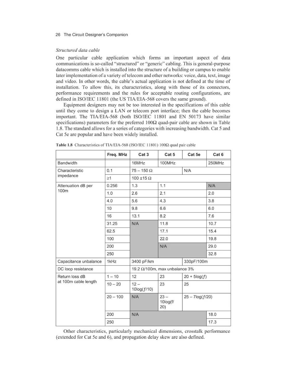
24
27
28
29
Wire types
Cable types
Power cables
Data and multicore cables
RF cables
Twisted pair
Crosstalk
Transmission lines
32
1.3.1
1.3.2
1.3.3
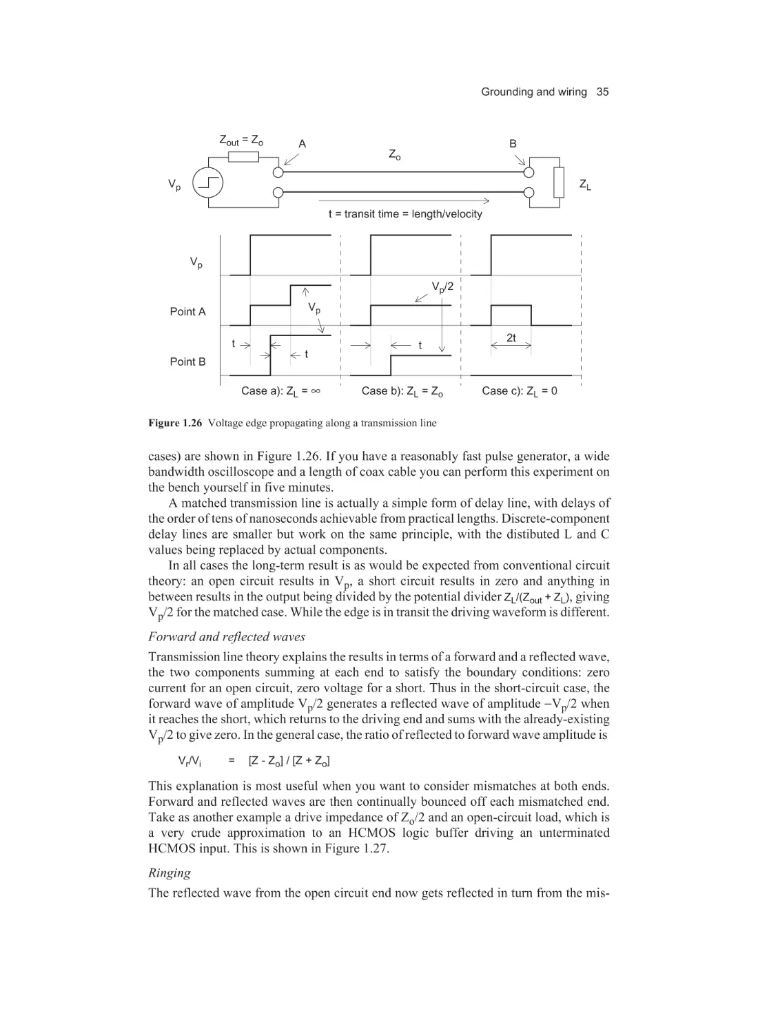
34
34
37
Characteristic impedance
Time domain
Frequency domain
Chapter 2
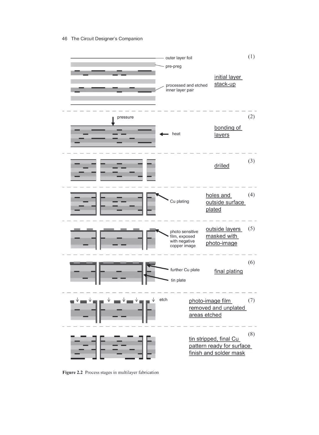
Printed circuits
2.1
40
Board types
40
2.1.1
2.1.2
2.1.3
2.1.4
2.1.5
40
41
42
44
45
Materials
Type of construction
Choice of type
Choice of size
How a multilayer board is made
TOC.FM6 Page vi Monday, October 18, 2004 9:47 AM
vi Contents
2.2
2.3
2.4
2.5
Design rules
45
2.2.1
2.2.2
2.2.3
2.2.4
2.2.5
2.2.6
2.2.7
47
50
51
52
55
55
56
Track width and spacing
Hole and pad size
Track routing
Ground and power distribution
Copper plating and finishing
Solder resist
Terminations and connections
Board assembly: surface mount and through hole
58
2.3.1
2.3.2
2.3.3
60
62
63
Surface mount design rules
Package placement
Component identification
Surface protection
63
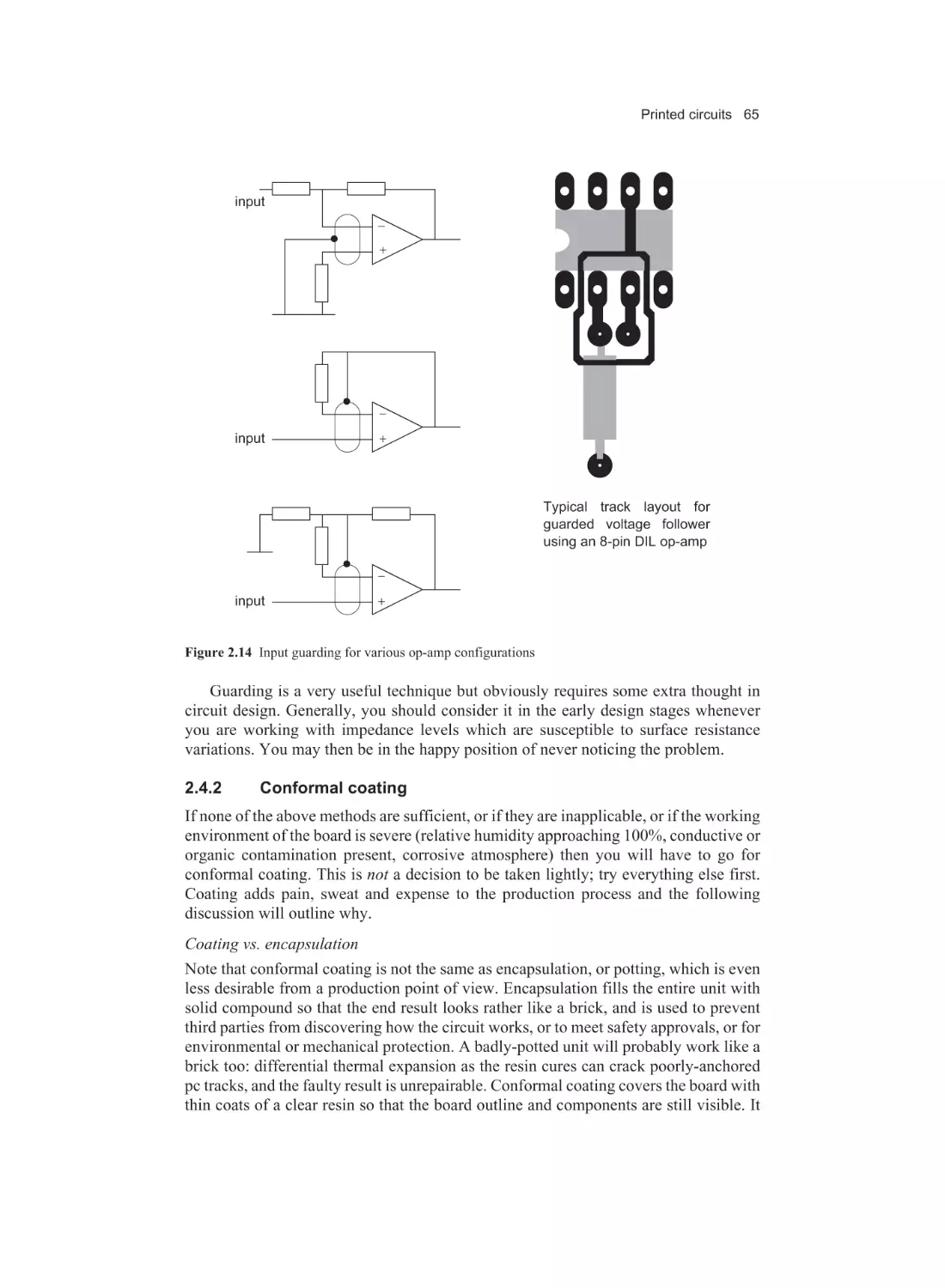
2.4.1
2.4.2
64
65
Guarding
Conformal coating
Sourcing boards and artwork
67
2.5.1
2.5.2
67
68
Artwork
Boards
Chapter 3
Passive components
3.1
3.2
3.3
3.4
70
Resistors
70
3.1.1
3.1.2
3.1.3
3.1.4
3.1.5
3.1.6
3.1.7
3.1.8
3.1.9
70
73
74
75
76
76
77
79
79
Resistor types
Tolerancing
Temperature coefficient
Power
Inductance
Pulse handling
Extreme values
Fusible and safety resistors
Resistor networks
Potentiometers
80
3.2.1
3.2.2
3.2.3
81
82
82
Trimmer types
Panel types
Pot applications
Capacitors
85
3.3.1
3.3.2
3.3.3
3.3.4
3.3.5
3.3.6
3.3.7
3.3.8
3.3.9
85
89
90
91
93
94
96
97
97
Metallised film & paper
Multilayer ceramics
Single-layer ceramics
Electrolytics
Solid tantalum
Capacitor applications
Series capacitors and dc leakage
Dielectric absorption
Self resonance
Inductors
99
3.4.1
3.4.2
99
101
Permeability
Self-capacitance
TOC.FM6 Page vii Monday, October 18, 2004 9:47 AM
Contents vii
3.4.3
3.4.4
3.5
Inductor applications
The danger of inductive transients
101
103
Crystals and resonators
105
3.5.1
3.5.2
3.5.3
3.5.4
106
107
108
108
Resonance
Oscillator circuits
Temperature
Ceramic resonators
Chapter 4
Active components
4.1
Diodes
4.1.1
4.1.2
4.1.3
4.1.4
4.1.5
4.1.6
4.1.7
4.1.8
4.2
4.3
4.4
4.5
4.6
110
110
Forward bias
Reverse bias
Leakage
High-frequency performance
Switching times
Schottky diodes
Zener diodes
The Zener as a clamp
110
113
113
114
115
116
117
120
Thyristors and triacs
121
4.2.1
4.2.2
4.2.3
4.2.4
4.2.5
4.2.6
122
122
123
124
124
125
Thyristor versus triac
Triggering characteristics
False triggering
Conduction
Switching
Snubbing
Bipolar transistors
127
4.3.1
4.3.2
4.3.3
4.3.4
4.3.5
4.3.6
4.3.7
127
128
129
129
130
132
133
Leakage
Saturation
The Darlington
Safe operating area
Gain
Switching and high frequency performance
Grading
Junction Field Effect transistors
134
4.4.1
4.4.2
4.4.3
135
136
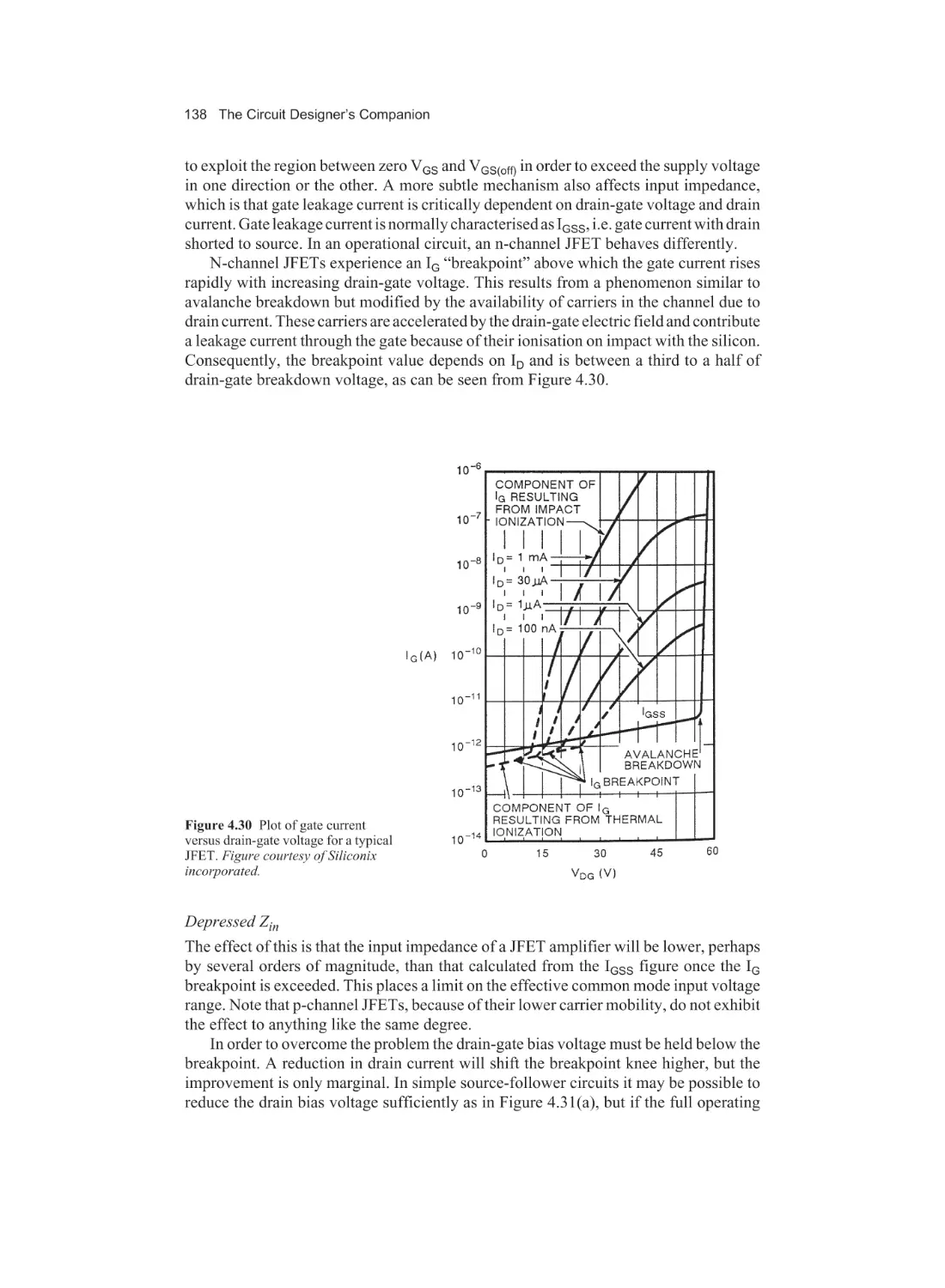
137
Pinch-off
Applications
High impedance circuits
MOSFETs
139
4.5.1
4.5.2
4.5.3
4.5.4
4.5.5
139
140
141
144
144
Low-power MOSFETs
VMOS Power FETs
Gate drive impedance
Switching speed
On-state resistance
IGBTs
4.6.1
4.6.2
4.6.3
145
IGBT structure
Advantages over MOSFETs and bipolars
Disadvantages
145
146
147
TOC.FM6 Page viii Monday, October 18, 2004 9:47 AM
viii Contents
Chapter 5
Analogue integrated circuits
5.1
5.2
5.3
5.4
5.5
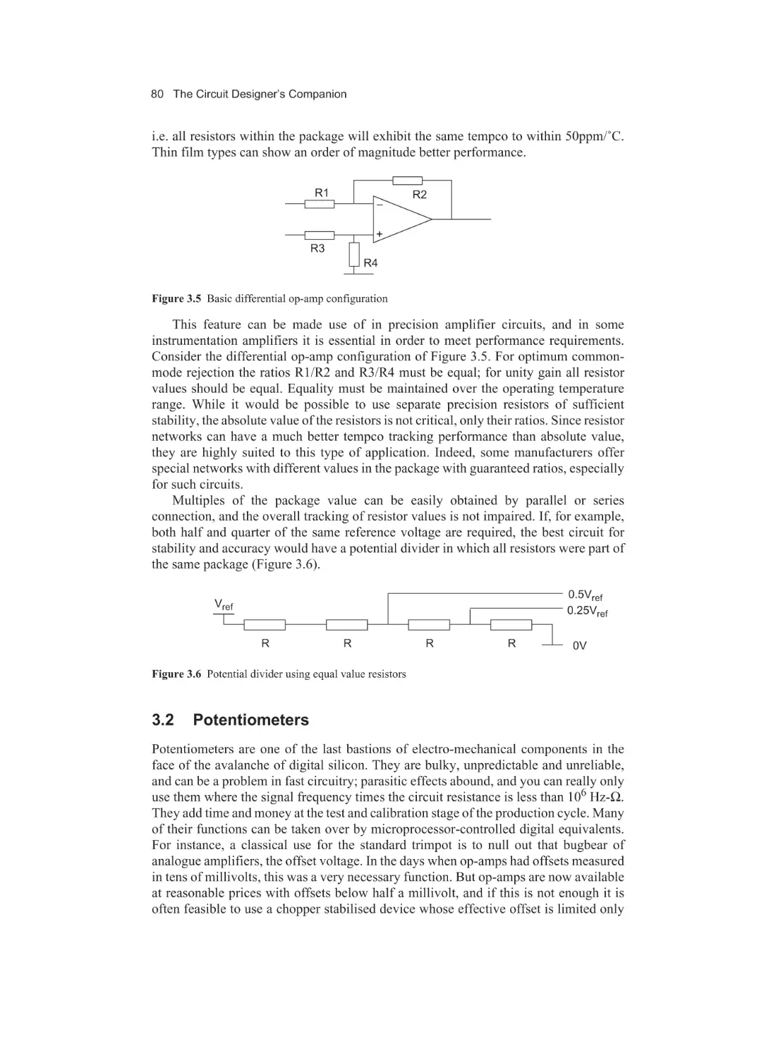
148
The ideal op-amp
148
5.1.1
149
Applications categories
The practical op-amp
149
5.2.1
5.2.2
5.2.3
5.2.4
5.2.5
5.2.6
5.2.7
5.2.8
5.2.9
5.2.10
5.2.11
5.2.12
5.2.13
5.2.14
5.2.15
5.2.16
149
152
153
154
155
156
157
158
159
159
162
163
166
167
168
169
Offset voltage
Bias and offset currents
Common mode effects
Input voltage range
Output parameters
AC parameters
Slew rate and large signal bandwidth
Small-signal bandwidth
Settling time
The oscillating amplifier
Open-loop gain
Noise
Supply current and voltage
Temperature ratings
Cost and availability
Current feedback op-amps
Comparators
170
5.3.1
5.3.2
5.3.3
5.3.4
5.3.5
5.3.6
171
171
173
174
176
177
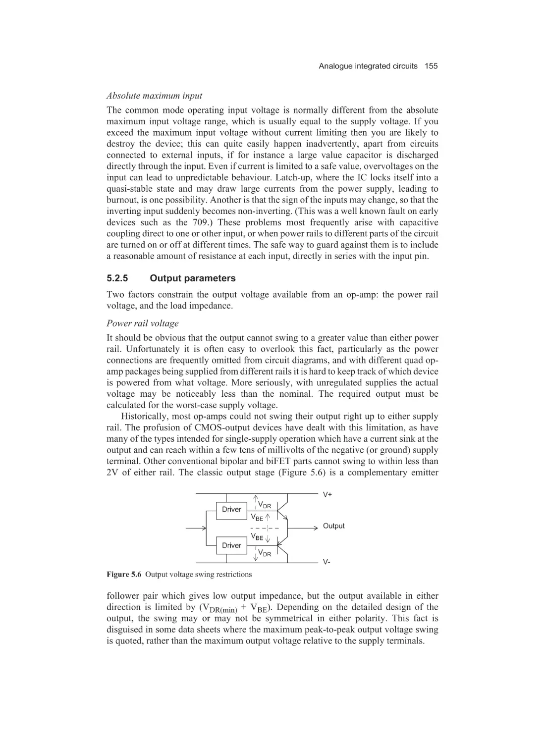
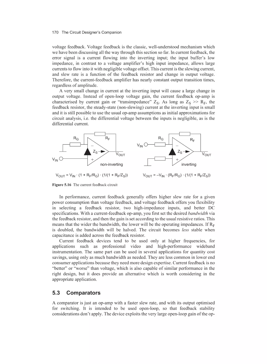
Output parameters
AC parameters
Op-amps as comparators (and vice versa)
Hysteresis and oscillations
Input voltage limits
Comparator sourcing
Voltage references
177
5.4.1
5.4.2
5.4.3
178
178
180
Zener references
Band-gap references
Reference specifications
Circuit modelling
181
Chapter 6
Digital circuits
6.1
6.2
183
Logic ICs
183
6.1.1
6.1.2
6.1.3
6.1.4
6.1.5
183
186
188
189
192
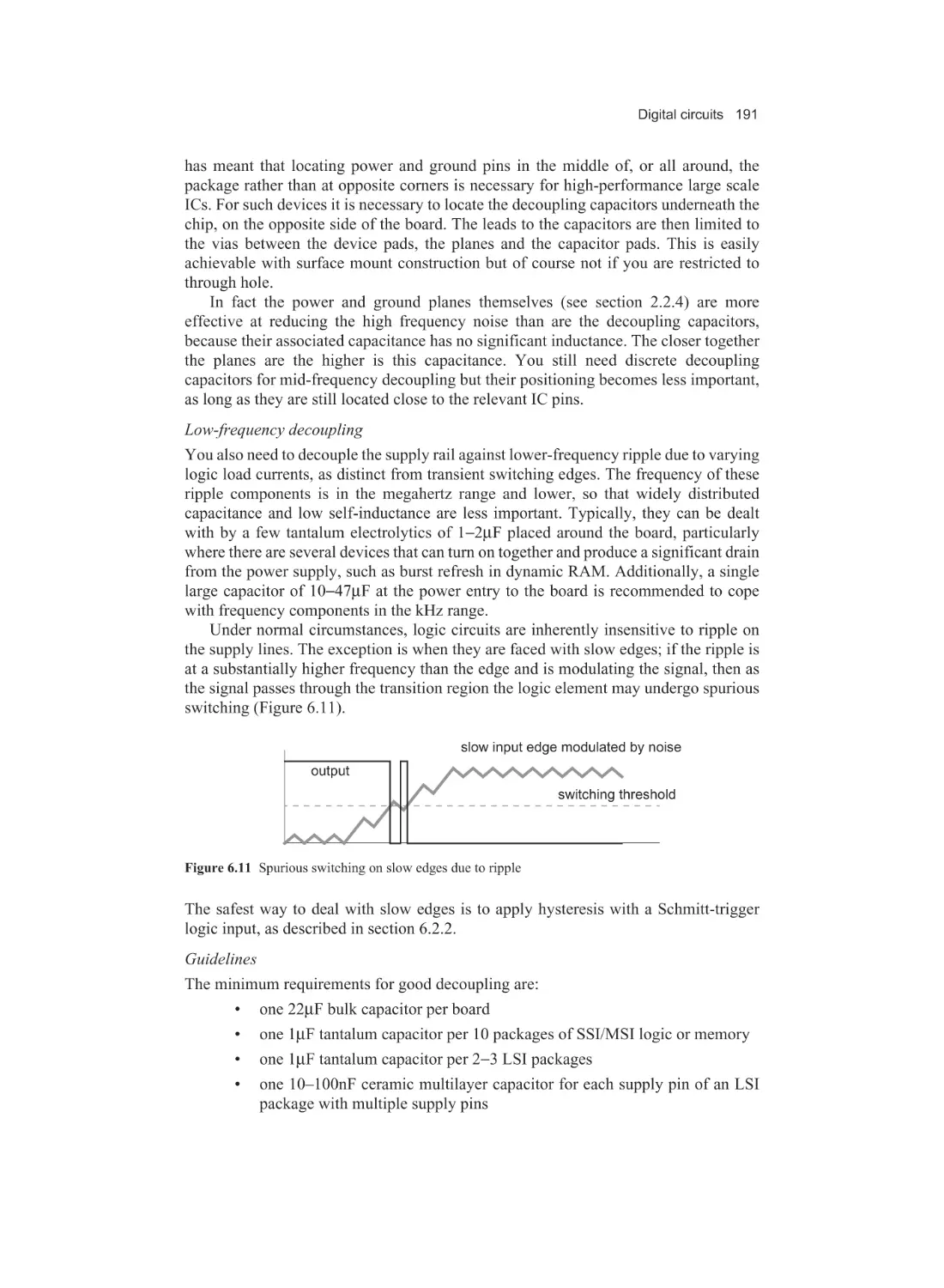
Noise immunity and thresholds
Fan-out and loading
Induced switching noise
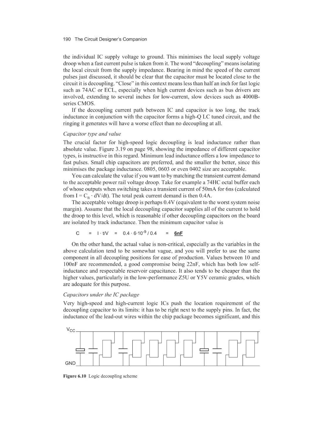
Decoupling
Unused gate inputs
Interfacing
192
6.2.1
6.2.2
6.2.3
6.2.4
6.2.5
192
195
196
197
200
Mixing analogue and digital
Generating digital levels from analogue inputs
Protection against externally-applied overvoltages
Isolation
Classic data interface standards
TOC.FM6 Page ix Monday, October 18, 2004 9:47 AM
Contents ix
6.2.6
6.3
6.4
6.5
High performance data interface standards
203
Using microcontrollers
207
6.3.1
6.3.2
6.3.3
208
210
214
How a microcontroller does your job
Timing and quantisation constraints
Programming constraints
Microprocessor watchdogs and supervision
214
6.4.1
6.4.2
6.4.3
214
215
219
The threat of corruption
Watchdog design
Supervisor design
Software protection techniques
222
6.5.1
6.5.2
6.5.3
222
223
224
Input data validation and averaging
Data and memory protection
Re-initialisation
Chapter 7
Power supplies
7.1
7.2
7.3
7.4
7.5
225
General
225
7.1.1
7.1.2
7.1.3
7.1.4
225
225
226
227
The linear supply
The switch-mode supply
Specifications
Off the shelf versus roll your own
Input and output parameters
227
7.2.1
7.2.2
7.2.3
7.2.4
7.2.5
7.2.6
7.2.7
7.2.8
7.2.9
7.2.10
7.2.11
7.2.12
7.2.13
227
228
229
230
232
234
235
235
237
238
239
241
242
Voltage
Current
Fuses
Switch-on surge, or inrush current
Waveform distortion and interference
Frequency
Efficiency
Deriving the input voltage from the output
Low-load condition
Rectifier and capacitor selection
Load and line regulation
Ripple and noise
Transient response
Abnormal conditions
243
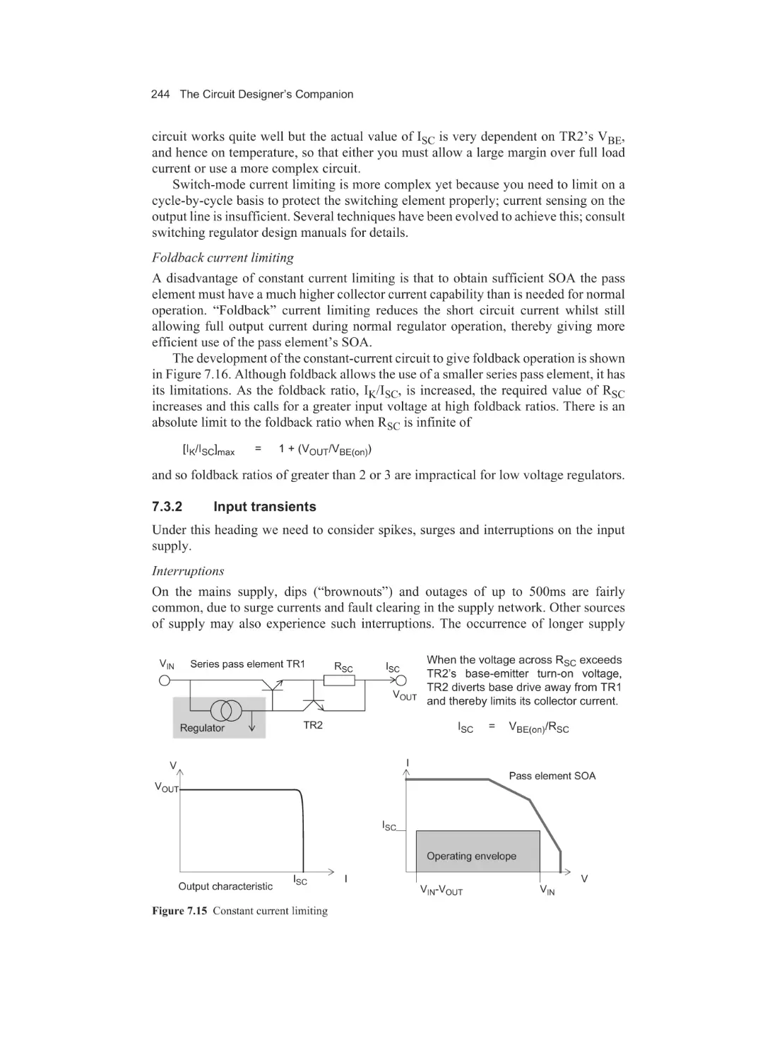
7.3.1
7.3.2
7.3.3
7.3.4
7.3.5
243
244
246
247
248
Output overload
Input transients
Transient suppressors
Overvoltage protection
Turn-on and turn-off
Mechanical requirements
249
7.4.1
7.4.2
7.4.3
249
251
251
Case size and construction
Heatsinking
Safety approvals
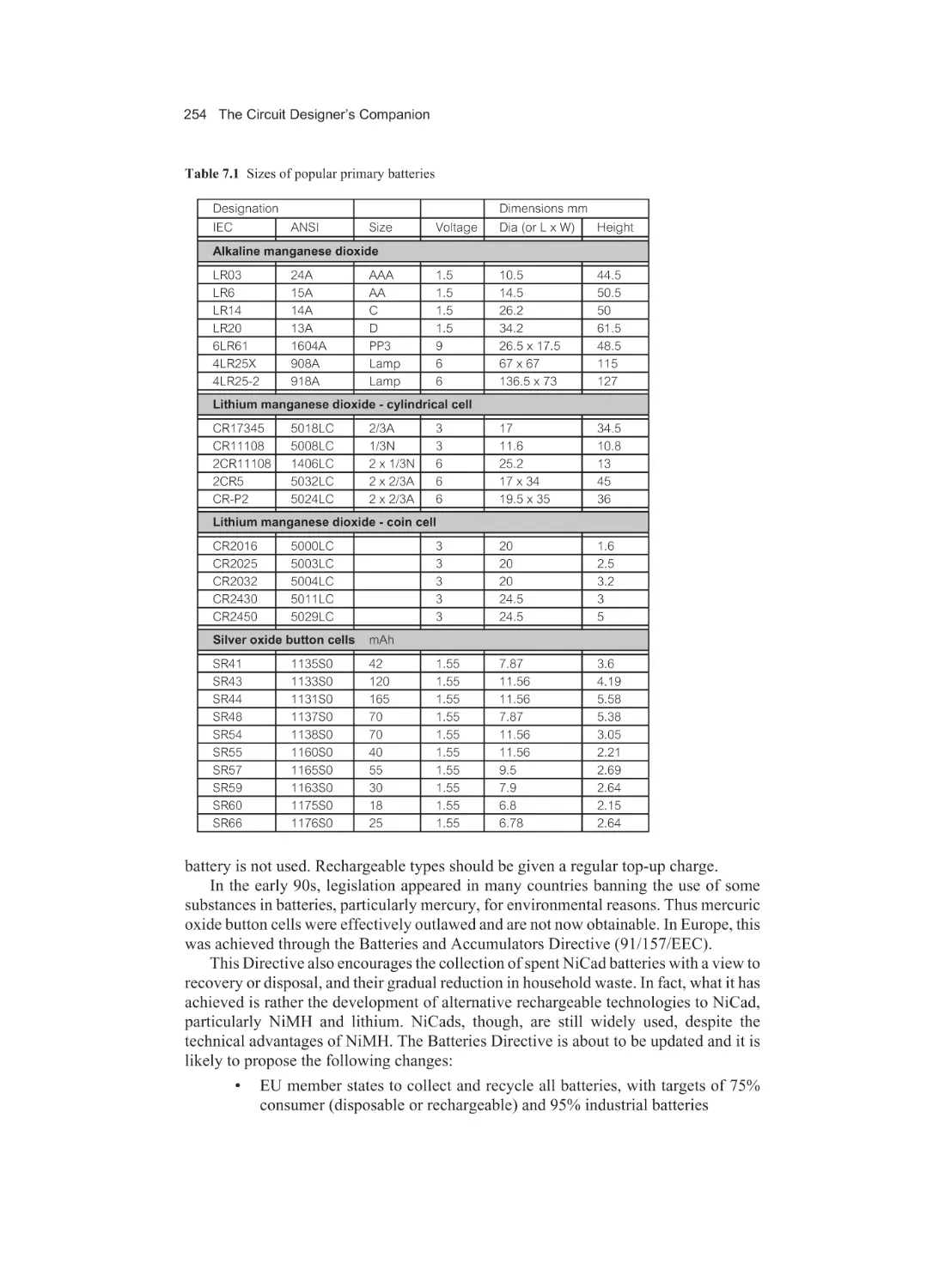
Batteries
252
7.5.1
7.5.2
252
255
Initial considerations
Primary cells
TOC.FM6 Page x Monday, October 18, 2004 9:47 AM
x Contents
7.5.3
7.5.4
Secondary cells
Charging
256
260
Chapter 8
Electromagnetic compatibility
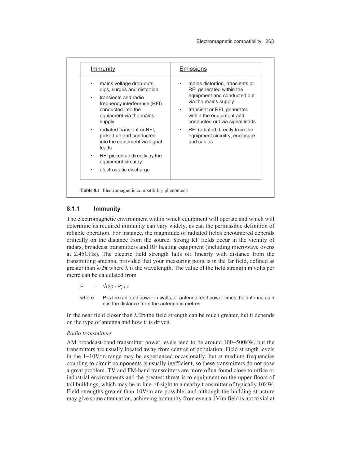
8.1
8.2
8.3
8.4
8.5
8.6
262
The need for EMC
262
8.1.1
8.1.2
263
267
Immunity
Emissions
EMC legislation and standards
267
8.2.1
8.2.2
268
269
The EMC Directive
Existing standards
Interference coupling mechanisms
272
8.3.1
8.3.2
272
273
Conducted
Radiated
Circuit design and layout
275
8.4.1
8.4.2
8.4.3
275
276
277
Choice of logic
Analogue circuits
Software
Shielding
277
8.5.1
8.5.2
279
281
Apertures
Seams
Filtering
282
8.6.1
8.6.2
8.6.3
8.6.4
282
285
286
287
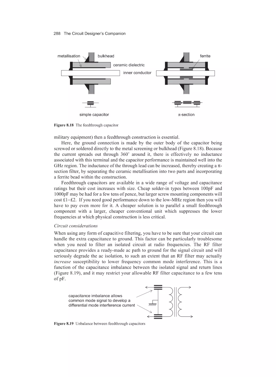
The low-pass filter
Mains filters
I/O filters
Feedthrough and 3-terminal capacitors
8.7
Cables and connectors
289
8.8
EMC design checklist
291
Chapter 9
General product design
9.1
Safety
9.1.1
9.1.2
9.1.3
9.1.4
9.2
9.3
9.4
292
292
Safety classes
Insulation types
Design considerations for safety protection
Fire hazard
293
294
294
296
Design for production
296
9.2.1
9.2.2
297
298
Checklist
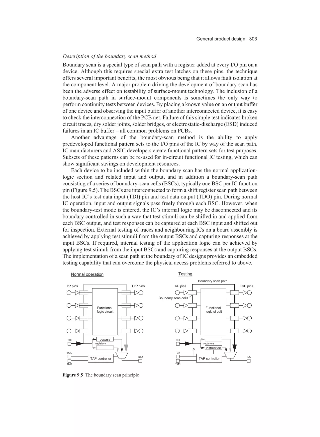
The dangers of ESD
Testability
300
9.3.1
9.3.2
9.3.3
9.3.4
300
301
302
305
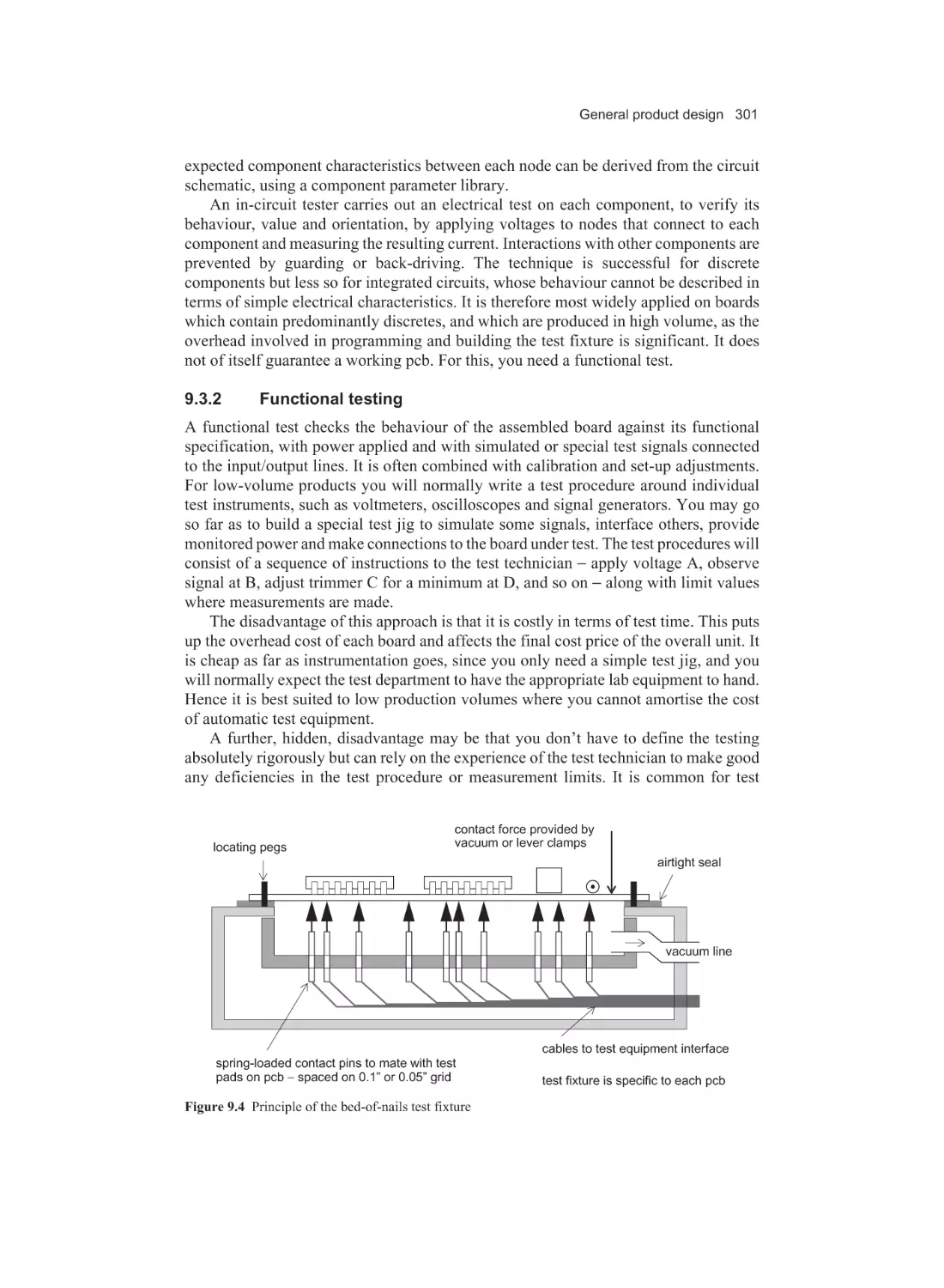
In-circuit testing
Functional testing
Boundary scan and JTAG
Design techniques
Reliability
307
TOC.FM6 Page xi Monday, October 18, 2004 9:47 AM
Contents xi
9.4.1
9.4.2
9.4.3
9.4.4
9.4.5
9.5
Definitions
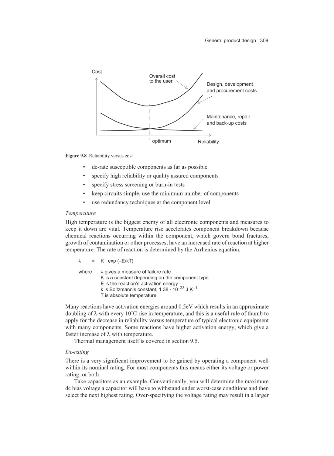
The cost of reliability
Design for reliability
The value of MTBF figures
Design faults
Thermal management
313
9.5.1
9.5.2
9.5.3
9.5.4
314
317
321
324
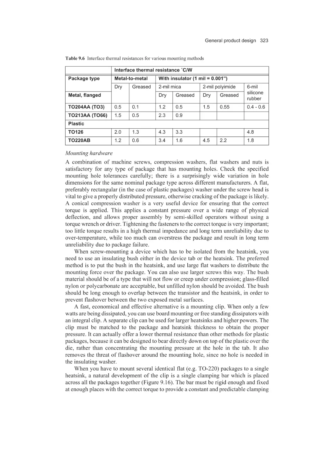
Using thermal resistance
Heatsinks
Power semiconductor mounting
Placement and layout
Appendix
Standards
326
Bibliography
Index
307
308
308
312
313
333
329
TOC.FM6 Page xii Monday, October 18, 2004 9:47 AM
xii Contents
Intro.fm6 Page 1 Monday, October 18, 2004 3:36 PM
Introduction 1
Introduction
Electronic circuit design can be divided into two areas: the first consists in designing a
circuit that will fulfil its specified function, sometimes, under laboratory conditions; the
second consists in designing the same circuit so that every production model of it will
fulfil its specified function, and no other undesired and unspecified function, always, in
the field, reliably over its lifetime. When related to circuit design skills, these two areas
coincide remarkably well with what engineers are taught at college − basic circuit
theory, Ohm’s Law, Thévenin, Kirchhoff, Norton, Maxwell and so on − and what they
learn on the job − that there is no such thing as the ideal component, that printed circuits
are more than just a collection of tracks, and that electrons have an unfortunate habit of
never doing exactly what they’re told.
This book has been written with the intention of bringing together and tying up
some of the loose ends of analogue and digital circuit design, those parts that are never
mentioned in the textbooks and rarely admitted elsewhere. In other words, it relates to
the second of the above areas.
Its genesis came with the growing frustration experienced as a senior design
engineer, attempting to recruit people for junior engineer positions in companies whose
foundations rested on analogue design excellence. Increasingly, it became clear that the
people I and my colleagues were interviewing had only the sketchiest of training in
electronic circuit design, despite offering apparently sound degree-level academic
qualifications. Many of them were more than capable of hooking together a
microprocessor and a few large-scale functional block peripherals, but were floored by
simple questions such as the nature of the p-n junction or how to go about resistor
tolerancing. It seems that this experience is by no means uncommon in other parts of
the industry.
The colleges and universities can hardly be blamed for putting the emphasis in their
courses on the skills needed to cope with digital electronics, which is after all becoming
more and more pervasive. If they are failing industry, then surely it is industry’s job to
tell them and to help put matters right. Unfortunately it is not so easy. A 1989 report
from Imperial College, London, found that few students were attracted to analogue
design, citing inadequate teaching and textbooks as well as the subject being found
"more difficult". Also, teaching institutions are under continuous pressure to broaden
their curriculum, to produce more "well-rounded" engineers, and this has to be at the
expense of greater in-depth coverage of the fundamental disciplines.
Nevertheless, the real world is obstinately analogue and will remain so. There is a
disturbing tendency to treat analogue and digital design as two entirely separate
disciplines, which does not result in good training for either. Digital circuits are in
reality only over-driven analogue ones, and anybody who has a good understanding of
analogue principles is well placed to analyse the more obscure behaviour of logic
devices. Even apparently simple digital circuits need some grasp of their analogue
interactions to be designed properly, as chapter 6 of this book shows. But also, any
Intro.fm6 Page 2 Monday, October 18, 2004 3:36 PM
2 The Circuit Designer’s Companion
product which interacts with the outside world via typical transducers must contain at
least some analogue circuits for signal conditioning and the supply of power. Indeed,
some products are still best realised as all-analogue circuits. Jim Williams, a wellknown American linear circuit designer (who bears no relation to this author), put it
succinctly when he said “wonderful things are going on in the forgotten land between
ONE and ZERO. This is Real Electronics”.
Because analogue design appears to be getting less popular, those people who do
have such skills will become more sought-after in the years ahead. This book is meant
to be a tool for any aspiring designer who wishes to develop these skills. It assumes at
least a background in electronics design; you will not find in here more than a minimum
of basic circuit theory. Neither will you find recipes for standard circuits, as there are
many other excellent books which cover those areas. Instead, there is a serious
treatment of those topics which are “more difficult” than building-block electronics:
grounding, temperature effects, EMC, component sourcing and characteristics, the
imperfections of devices, and how to design so that someone else can make the product.
I hope the book will be as useful to the experienced designer who wishes to broaden
his or her background as it will to the neophyte fresh from college who faces a first job
in industry with trepidation and excitement. The traditional way of gaining experience
is to learn on-the-job through peer contact, and this book is meant to enhance rather than
supplant that route. It is offered to those who want their circuits to stand a greater
chance of working first time every time, and a lesser chance of being completely redesigned after six months. It does not claim to be conclusive or complete. Electronic
design, analogue or digital, remains a personal art, and all designers have their own
favourite tricks and their own dislikes. Rather, it aims to stimulate and encourage the
quest for excellence in circuit design.
I must here acknowledge a debt to the many colleagues over the years who have
helped me towards an understanding of circuit design, and who have contributed
towards this book, some without knowing it: in particular Tim Price, Bruce Piggott and
Trevor Forrest. Also to Joyce, who has patiently endured the many brainstorms that the
writing of it produced in her partner.
Introduction to the second edition
The first edition was written in 1990 and eventually, after a good long run, went out of
print. But the demand for it has remained. There followed a period of false starts and
much pestering, and finally the author was persuaded to pass through the book once
more to produce this second edition. The aim remains the same but technology has
progressed in the intervening fourteen years, and so a number of anachronisms have
been corrected and some sections have been expanded. I am grateful to those who have
made suggestions for this updating, especially John Knapp and Martin O’Hara, and I
hope it continues to give the same level of help that the first edition evidently achieved.
Tim Williams
July 2004
Chap-01.fm6 Page 3 Monday, October 18, 2004 9:29 AM
Grounding and wiring 3
Chapter 1
Grounding and wiring
1.1
Grounding
A fundamental property of any electronic or electrical circuit is that the voltages present
within it are referenced to a common point, conventionally called the ground. (This
term is derived from electrical engineering practice, when the reference point is often
taken to a copper spike literally driven into the ground.) This point may also be a
connection point for the power to the circuit, and it is then called the 0V (nought-volt)
rail, and ground and 0V are frequently (and confusingly) synonymous. Then, when we
talk about a five-volt supply or a minus-twelve-volt supply or a two-and-a-half-volt
reference, each of these is referred to the 0V rail.
At the same time, ground is not the same as 0V. A ground wire connects equipment
to earth for safety reasons, and does not carry a current in normal operation. However,
in this chapter the word “grounding” will be used in its usual sense, to include both
safety earths and signal and power return paths.
Perhaps the greatest single cause of problems in electronic circuits is that 0V and
ground are taken for granted. The fact is that in a working circuit there can only ever be
one point which is truly at 0V; the concept of a “0V rail” is in fact a contradiction in
terms. This is because any practical conductor has a finite non-zero resistance and
inductance, and Ohm’s Law tells us that a current flowing through anything other than
a zero impedance will develop a voltage across it. A working circuit will have current
flowing through those conductors that are designated as the 0V rail and therefore, if any
one point of the rail is actually at 0V (say, the power supply connection) the rest of the
rail will not be at 0V. This is illustrated in Figure 1.1.
I1 (20mA)
I2 (10mA)
power supply
connection
I3 (10mA)
0V rail
A
B
C
ΣI
D
Assume the 0V conductor has a resistance of 10mΩ/inch and that points A, B, C and
D are each one inch apart. The voltages at points A, B and C referred to D are
VC
=
(I1 + I2 + I3) · 10mΩ
= 400µV
VB
=
VC + (I1 + I2) · 10mΩ
= 700µV
VA
=
VB + (I1) · 10mΩ
= 900µV
Figure 1.1 Voltages along the 0V rail
Chap-01.fm6 Page 4 Monday, October 18, 2004 9:29 AM
4 The Circuit Designer’s Companion
Now, after such a trenchant introduction, you might be tempted to say well, there
are millions of electronic circuits in existence, they must all have 0V rails, they seem to
work well enough, so what’s the problem? Most of the time there is no problem. The
impedance of the 0V conductor is in the region of milliohms, the current levels are
milliamps, and the resulting few hundred microvolts drop doesn’t offend the circuit at
all. 0V plus 500µV is close enough to 0V for nobody to worry.
The difficulty with this answer is that it is then easy to forget about the 0V rail and
assume that it is 0V under all conditions, and subsequently be surprised when a circuit
oscillates or otherwise doesn’t work. Those conditions where trouble is likely to arise
are
• where current flows are measured in amps rather than milli- or microamps
• where the 0V conductor impedance is measured in ohms rather than
milliohms
• where the resultant voltage drop, whatever its value, is of a magnitude or in
such a configuration as to affect the circuit operation.
When to consider grounding
One of the attributes of a good circuit designer is to know when these conditions need
to be carefully considered and when they may be safely ignored. A frequent
complication is that you as circuit designer may not be responsible for the circuit’s
layout, which is handed over to a layout draughtsman (who may in turn delegate many
routing decisions to the software package). Grounding is always sensitive to layout,
whether of discrete wiring or of printed circuits, and the designer must have some
knowledge of and control over this if the design is not to be compromised.
The trick is always to be sure that you know where ground return currents are
flowing, and what their consequences will be; or, if this is too complicated, to make sure
that wherever they flow, the consequences will be minimal. Although the above
comments are aimed at 0V and ground connections, because they are the ones most
taken for granted, the nature of the problem is universal and applies to any conductor
through which current flows. The power supply rail (or rails) is another special case
where conductor impedance can create difficulties.
1.1.1
Grounding within one unit
In this context, “unit” can refer to a single circuit board or a group of boards and other
wiring connected together within an enclosure such that you can identify a “local”
ground point, for instance the point of entry of the mains earth. An example might be
as shown in Figure 1.2. Let us say that printed circuit board (PCB) 1 contains input
signal conditioning circuitry, PCB2 contains a microprocessor for signal processing
and PCB3 contains high-current output drivers, such as for relays and for lamps. You
may not place all these functions on separate boards, but the principles are easier to
outline and understand if they are considered separately. The power supply unit (PSU)
provides a low-voltage supply for the first two boards, and a higher-power supply for
the output board. This is a fairly common system layout and Figure 1.2 will serve as a
starting point to illustrate good and bad practice.
1.1.2
Chassis ground
First of all, note that connections are only made to the metal chassis or enclosure at one
point. All wires that need to come to the chassis are brought to this point, which should
Chap-01.fm6 Page 5 Monday, October 18, 2004 9:29 AM
Grounding and wiring 5
PCB3
L
N
E
Outputs
VB+
PSB
0V(B)
PSU
PCB2
VA+
PSA
0V(A)
PCB1
Inputs
Chassis ground
Figure 1.2 Typical intra-unit wiring scheme
be a metal stud dedicated to the purpose. Such connections are the mains safety earth
(about which more later), the 0V power rail, and any possible screening and filtering
connections that may be required in the power supply itself, such as an electrostatic
screen in the transformer. (The topic of power supply design is itself dealt with in much
greater detail in Chapter 7).
The purpose of a single-point chassis ground is to prevent circulating currents in the
chassis.† If multiple ground points are used, even if there is another return path for the
current to take, a proportion of it will flow in the chassis (Figure 1.3); the proportion is
determined by the ratio of impedances which depends on frequency. Such currents are
very hard to predict and may be affected by changes in construction, so that they can
give quite unexpected and annoying effects: it is not unknown for hours to be devoted
to tracking down an oscillation or interference problem, only to find that it disappears
when an inoffensive-looking screw is tightened against the chassis plate. Joints in the
chassis are affected by corrosion, so that the unit performance may degrade with time,
and they are affected by surface oxidation of the chassis material. If you use multi-point
chassis grounding then it is necessary to be much more careful about the electrical
construction of the chassis.
chassis ground point
expected return current
undesired chassis return current
Figure 1.3 Return current paths with multiple ground points
† But, when RF shielding and/or a low-inductance ground is required, multiple ground points
may be essential. This is covered in Chapter 8.
Chap-01.fm6 Page 6 Monday, October 18, 2004 9:29 AM
6 The Circuit Designer’s Companion
1.1.3
The conductivity of aluminium
Aluminium is used throughout the electronics industry as a light, strong and highly
conductive chassis material − only silver, copper and gold have a higher conductivity.
You would expect an aluminium chassis to exhibit a decently low bulk resistance, and
so it does, and is very suitable as a conductive ground as a result. Unfortunately, another
property of aluminium (which is useful in other contexts) is that it oxidises very readily
on its surface, to the extent that all real-life samples of aluminium are covered by a thin
surface film of aluminium oxide (Al2O3). Aluminium oxide is an insulator. In fact, it is
such a good insulator that anodised aluminium, on which a thick coating of oxide is
deliberately grown by chemical treatment, is used for insulating washers on heatsinks.
The practical consequence of this quality of aluminium oxide is that the contact
resistance of two sheets of aluminium joined together is unpredictably high. Actual
electrical contact will only be made where the oxide film is breached. Therefore,
whenever you want to maintain continuity through a chassis made of separate pieces of
aluminium, you must ensure that the plates are tightly bonded together, preferably with
welding or by fixings which incorporate shakeproof serrated washers to dig actively
into the surface. The same applies to ground connection points. The best connection
(since aluminium cannot easily be soldered) is a force-fit or welded stud (Figure 1.4),
but if this is not available then a shakeproof serrated washer should be used underneath
the nut which is in contact with the aluminium.
Al2O3 film
Al metal
The insulating aluminium joint
serrated shakeproof washers
contact made
solder tag
through nut
serrated
shakeproof washer
force-fit stud
nut and bolt
Figure 1.4 Electrical connections to aluminium
Other materials
Another common chassis material is cadmium- or tin-plated steel, which does not suffer
from the oxidation problem. Mild steel has about three times the bulk resistance of
aluminium so does not make such a good conductor, but it has better magnetic shielding
properties and it is cheaper. Die-cast zinc is popular for its light weight and strength,
and ease of creating complex shapes through the casting process; zinc’s conductivity is
28% of copper. Other metals, particularly silver-plated copper, can be used where the
ultimate in conductivity is needed and cost is secondary, as in RF circuits. The
advantage of silver oxide (which forms on the silver-plated surface) is that it is
conductive and can be soldered through easily. Table 1.1 shows the conductivities and
temperature coefficients of several metals.
Chap-01.fm6 Page 7 Monday, October 18, 2004 9:29 AM
Grounding and wiring 7
Table 1.1 Conductivity of metals
Metal
Relative Conductivity
(Cu = 1, at 20ºC)
Temperature coefficient of
resistance (/ºC at 20ºC)
Aluminium (pure)
0.59
Aluminium alloy:
Soft-annealed
Heat-treated
0.45-0.50
0.30-0.45
Brass
0.28
0.002-0.007
Cadmium
0.19
0.0038
0.895
1.0
0.00382
0.00393
0.65
0.0034
0.177
0.02-0.12
0.005
Lead
0.7
0.0039
Nichrome
0.0145
0.0004
Nickel
0.12-0.16
0.006
Silver
1.06
0.0038
Steel
0.03-0.15
0.004-0.005
Tin
0.13
0.0042
Tungsten
0.289
0.0045
Zinc
0.282
0.0037
Copper:
Hard drawn
Annealed
Gold
Iron:
Pure
Cast
1.1.4
0.0039
Ground loops
Another reason for single-point chassis connection is that circulating chassis currents,
when combined with other ground wiring, produce the so-called “ground loop”, which
is a fruitful source of low-frequency magnetically-induced interference. A magnetic
field can only induce a current to flow within a closed loop circuit. Magnetic fields are
common around power transformers − not only the conventional 50Hz mains type
(60Hz in the US), but also high-frequency switching transformers and inductors in
switched-mode power supplies − and also other electromagnetic devices: contactors,
solenoids and fans. Extraneous magnetic fields may also be present. The mechanism of
ground-loop induction is shown in Figure 1.5.
Lenz’s law tells us that the e.m.f. induced in the loop is
V
=
where
−10-8 · A · n · dB/dt
A is the area of the loop in cm2
B is the flux density normal to it, in microTesla, assuming a uniform field
n is the number of turns (n = 1 for a single-turn loop)
As an example, take a 10µT 50Hz field as might be found near a reasonable-sized
mains transformer, contactor or motor, acting at right angles through the plane of a
10cm2 loop that would be created by running a conductor 1cm above a chassis for 10cm
and grounding it at both ends. The induced emf is given by
V
=
−10-8 · 10 · d/dt(10 · sin 2π · 50 · t)
Chap-01.fm6 Page 8 Monday, October 18, 2004 9:29 AM
8 The Circuit Designer’s Companion
ground conductor
connected to chassis
at two points
magnetic flux
induced series voltage
two-point
grounding
flux linkage normal to loop
induced current
no induced series voltage
single-point
grounding
flux linkage but no loop
Figure 1.5 The ground loop
=
−10-8 · 10 · 1000π · cos ωt
=
314µV peak
Magnetic field induction is usually a low-frequency phenomenon (unless you
happen to be very close to a high-power radio transmitter) and you can see from this
example that in most circumstances the induced voltages are low. But in low-level
applications, particularly audio and precision instrumentation, they are far from
insignificant. If the input circuit includes a ground loop, the interference voltage is
injected directly in series with the wanted signal and cannot then be separated from it.
The cures are:
• open the loop by grounding only at one point
• reduce the area of the loop (A in the equation above) by routing the
offending wire(s) right next to the ground plane or chassis, or shortening it
• reduce the flux normal to the loop by repositioning or reorienting the loop
or the interfering source
• reduce the interfering source, for instance by using a toroidal transformer.
1.1.5
Power supply returns
You will note from Figure 1.2 that the output power supply 0V connection (0V(B)) has
been shown separately from 0V(A), and linked only at the power supply itself. What
happens if, say for reasons of economy in wiring, you don’t follow this practice but
Chap-01.fm6 Page 9 Monday, October 18, 2004 9:29 AM
Grounding and wiring 9
PCB3
VB+
PSB
0V(B)
I0V(3)
PSU
VA+
PSA
0V(A)
I0V(2) + I0V(3)
PCB2
I0V(2)
VS
shared wire, resistance RS
Figure 1.6 Common power supply return
instead link the 0V rails together at PCB3 and PCB2, as shown in Figure 1.6?
The supply return currents I0V from both PSB/PCB3 and PSA/PCB2 now share the
same length of wire (or track, in a single-pcb system). This wire has a certain non-zero
impedance, say for dc purposes it is RS. In the original circuit this was only carrying
I0V(2) and so the voltage developed across it was
VS
=
RS · I0V(2)
but, in the economy circuit,
VS
=
RS · (I0V(2) + I0V(3))
This voltage is in series with the supply voltages to both boards and hence effectively
subtracts from them.
Putting some typical numbers into the equations,
I0V(3)
= 1.2A
with a VB+ of 24V because it is a high-power output board,
I0V(2)
= 50mA
with a VA+ of 3.3V because it is a microprocessor board with some
CMOS logic on it.
Now assume that, for various reasons, the power supply is some distance remote from
the boards and you have without thinking connected it with 2m of 7/0.2mm equipment
wire, which will have a room temperature resistance of about 0.2Ω. The voltage VS will
be
VS
=
0.2 · (1.2 + 0.05)
=
0.25V
which will drop the supply voltage at PCB2 to 3.05V, less than the lower limit of
operation for 3.3V logic, before allowing for supply voltage tolerances and other
voltage drops. One wrong wiring connection can make your circuit operation
borderline! Of course, the 0.25V is also subtracted from the 24V supply, but a reduction
of about 1% on this supply is unlikely to affect operation.
Varying loads
If the 1.2A load on PCB3 is varying – say several high-current relays may be switched
at different times, ranging from all off to all on – then the VS drop at PCB2 would also
vary. This is very often worse than a static voltage drop because it introduces noise on
Chap-01.fm6 Page 10 Monday, October 18, 2004 9:29 AM
10 The Circuit Designer’s Companion
the 0V line. The effects of this include unreliable processor operation, variable set
threshold voltage levels and odd feedback effects such as chattering relays or, in audio
circuits, low-frequency “motor-boating” oscillation.
For comparison, look at the same figures but applied to Figure 1.2, with separate
0V return wires. Now there are two voltage drops to consider: VS(A) for the 3.3V supply
and VS(B) for the 24V supply. VS(B) is 1.2A times 0.2Ω, substantially the same (0.24V)
as before, but it is only subtracted from the 24V supply. VS(A) is now 50mA times 0.2Ω
or 10mV, which is the only 0V drop on the 3.3V supply to PCB2 and is negligible.
The rule is: always separate power supply returns so that load currents for each
supply flow in separate conductors (Figure 1.7).
PSU
wrong
PSU
right
Figure 1.7 Ways to connect power supply return
Note that this rule is easiest to apply if different power supplies have different 0V
connections (as in Figure 1.2) but should also be applied if a common 0V is used, as
shown above. The extra investment in wiring is just about always worth it for peace of
mind!
Power rail feed
The rule also applies to the power rail feed as well as to its return, and in fact to any
connection where current is being shared between several circuits. Say the high-power
load on PCB3 was also being fed from the +5V supply VA+, then the preferred method
of connection is two separate feeds (Figure 1.8).
+5V
+5V
0V
PCB3
PSU
0V
+5V
0V
PCB2
Figure 1.8 Separate power supply rail feeds
The reasons are the same as for the 0V return: with a single feed wire, a common
voltage drop appears in series with the supply voltage, injected this time in the supply
rail rather than the 0V rail. Fault symptoms are similar. Of course, the example above
is somewhat artificial in that you would normally use a rather more suitable size of wire
for the current expected. High currents flowing through long wires demand a lowresistance and hence thick conductor. If you are expecting a significant voltage drop
then you will take the trouble to calculate it for a given wire diameter, length and
current. See Table 1.3 for a guide to the current-carrying abilities of common wires. The
Chap-01.fm6 Page 11 Monday, October 18, 2004 9:29 AM
Grounding and wiring 11
point of the previous examples is that voltage drops have a habit of cropping up when
you are not expecting them.
Conductor impedance
Note that the previous examples, and those on the next few pages, tacitly assume for
simplicity that the wire impedance is resistive only. In fact, real wire has inductance as
well as resistance and this comes into effect as soon as the wire is carrying ac,
increasing in significance as the frequency is raised. A one-metre length of 16/0.2
equipment wire has a resistance of 38mΩ and a self-inductance of 1.5µH. At 4A dc the
voltage drop across it will be 152mV. An ac current with a rate of change of 4A/µs will
generate 6V across it. Note the difference! The later discussion of wire types includes
a closer look at inductance.
1.1.6
Input signal ground
Figure 1.2 shows the input signal connections being taken directly to PCB1 and not
grounded outside of the pcb. To expand on this, the preferred scheme for two-wire
single-ended input connections is to take the ground return directly to the reference
point of the input amplifier: see Figure 1.9(a).
The reference point on a single-ended input is not always easy to find: look for the
point from which the input voltage must be developed in order for the amplifier gain to
act on it alone. In this way, no extra signals are introduced in series with the wanted
signal by means of a common impedance. In each of the examples in Figure 1.9 of bad
input wiring, getting progressively worse from (b) to (d), the impedance X-X acts as a
source of unwanted input signal due to the other currents flowing in it as well as the
input current.
Connection to 0V elsewhere on the pcb
Insufficient control over pc layout is the most usual cause of arrangement (b), especially
if auto-routing layout software is used. Most CAD layout software assumes that the 0V
rail is a single node and feels itself free to make connections to it at any point along the
track. To overcome this, either specify the input return point as a separate node and
connect it later, or edit the final layout as required. Manual layout is capable of exactly
the same mistake, although in this case it is due to lack of communication between
designer and layout draughtsman.
Connection to 0V within the unit
Arrangement (c) is quite often encountered if one pole of the input connector naturally
makes contact with the metal case, such as happens with the standard BNC coaxial
connector, or if for reasons of connector economy a common ground conductor is
shared between multiple input, output or control signals that are distributed among
different boards. With sensitive input signals, the latter is false economy; and if you
have to use a BNC-type connector, you can get versions with insulating washers, or
mount it on an insulating sub-panel in a hole in the metal enclosure. Incidentally, taking
a coax lead internally from an uninsulated BNC socket to the pcb, with the coax outer
connected both to the BNC shell and the pcb 0V, will introduce a ground loop (see
section 1.1.4) unless it is the only path for ground currents to take. But at radio
frequencies, this effect is countered by the ability of coax cable to concentrate the signal
and return currents within the cable, so that the ground loop is only a problem at low
frequencies.
Chap-01.fm6 Page 12 Monday, October 18, 2004 9:29 AM
12 The Circuit Designer’s Companion
PCB1
RIN
V
0V (typically)
a)
PCB1
RIN
V
b)
X 0V rail
X
(other connections)
PCB1
RIN
V
0V rail
c)
PSU
X
(other connections)
X
(other connections)
PCB1
RIN
V
d)
earth
X
assumed
common ground
connection
0V rail
X
PSU
(other connections)
(other connections)
PCB1
differential
amplifier
V
e)
0V
Figure 1.9 Input signal grounding
External ground connection
Despite being the most horrific input grounding scheme imaginable, arrangement (d) is
unfortunately not rare. Now, not only are noise signals internal to the unit coupled into
the signal path, but also all manner of external ground noise is included. Local earth
differences of up to 50V at mains frequency can exist at particularly bad locations such
as power stations, and differences of several volts are more common. The only
conceivable reason to use this layout is if the input signal is already firmly tied to a
remote ground outside the unit, and if this is the case it is far better to use a differential
amplifier as in Figure 1.9(e), which is often the only workable solution for low-level
signals and is in any case only a logical development of the correct approach for singleended signals (a). If for some reason you are unable to take a ground return connection
from the input signal, you will be stuck with ground-injected noise.
Chap-01.fm6 Page 13 Monday, October 18, 2004 9:29 AM
Grounding and wiring 13
All of the schemes of Figure 1.9(b) to (d) will work perfectly happily if the desired
input signal is several orders of magnitude greater than the ground-injected
interference, and this is frequently the case, which is how they came to be common
practice in the first place. If there are good practical reasons for adopting them (for
instance, connector or wiring cost restrictions) and you can be sure that interference
levels will not be a problem, then do so. But you will need to have control over all
possible connection paths before you can be sure that problems won’t arise in the field.
1.1.7
Output signal ground
Similar precautions need to be taken with output signals, for the reverse reason. Inputs
respond unfavourably to external interference, whereas outputs are the cause of
interference. Usually in an electronic circuit there is some form of power amplification
involved between input and output, so that an output will operate at a higher current
level than an input, and there is therefore the possibility of unwanted feedback.
The classical problem of output-to-input ground coupling is where both input and
output share a common impedance, in the same way as the power rail common
impedances discussed earlier. In this case the output current is made to circulate
through the same conductor as connects the input signal return (Figure 1.10(a)).
Iout
A
Vin’
Vout
RL
Vin
RS
a)
Iout
A
Iout
Vin
Vin’
Vout
RL
b)
Figure 1.10 Output to input coupling
Iout
RS
A tailor-made feedback mechanism has been inserted into this circuit, by means of
RS. The input voltage at the amplifier terminals is supposed to be Vin, but actually it is
Vin’
=
Vin − (Iout · RS)
Redrawing the circuit to reference everything to the amplifier ground terminals
(Figure 1.10(b)) shows this more clearly. When we work out the gain of this circuit, it
turns out to be
Vout/Vin
=
A/(1 + [A · RS/(RL + RS)])
which describes a circuit that will oscillate if the term [A · RS/(RL + RS)] is more negative
than −1. In other words, for an inverting amplifier, the ratio of load impedance to
common impedance must be less than the gain, to avoid instability. Even if the circuit
Chap-01.fm6 Page 14 Monday, October 18, 2004 9:29 AM
14 The Circuit Designer’s Companion
remains stable, the extra coupling due to RS upsets the expected response. Remember
also that all the above terms vary with frequency, usually in a complex fashion, so that
at high frequencies the response can be unpredictable. Note that although this has been
presented in terms of an analogue system (such as an audio amplifier), any system in
which there is input-output gain will be similarly affected. This can apply equally to a
digital system with an analogue input and digital outputs which are controlled by it.
Avoiding the common impedance
The preferable solution is to avoid the common impedance altogether by careful layout
of input and output grounds. We have already looked at input grounds, and the
grounding scheme for outputs is essentially similar: take the output ground return
directly to the point from which output current is sourced, with no other connection (or
at least, no other susceptible connection) in between. Normally, the output current
comes from the power supply so the best solution is to take the return directly back to
the supply. Thus the layout of PCB3 in Figure 1.2 should have a separate ground track
for the high-current output as in Figure 1.11(a), or the high-current output terminal
could be returned directly to the power supply, bypassing PCB3 (b).
0V to other circuits
PCB3
PSU
RS
a)
0V to other circuits
PCB3
PSU
b)
Figure 1.11 Output signal returns
If PCB3 contains only circuits which will not be susceptible to the voltage
developed across RS, then the first solution is acceptable. The important point is to
decide in advance where your return currents will flow and ensure that they do not
affect the operation of the rest of the circuits. This entails knowing the ac and dc
impedance of any common connections, the magnitude and bandwidth of the output
currents and the susceptibility of the potentially affected circuits.
1.1.8
Inter-board interface signals
There is one class of signals we have not yet covered, and that is those signals which
pass within the unit from one board to another. Typically these are digital control
signals or analogue levels which have already been processed, so are not low-level
enough to be susceptible to ground noise and are not high-current enough to generate
significant quantities of it. To be thorough in your consideration of ground return paths,
these signals should not be left out: the question is, what to do about them?
Often the answer is nothing. If no ground return is included specifically for interboard signals then signal return current must flow around the power supply connections
Chap-01.fm6 Page 15 Monday, October 18, 2004 9:29 AM
Grounding and wiring 15
and therefore the interface will suffer all the ground-injected noise Vn that is present
along these lines (Figure 1.12). But, if your grounding scheme is well thought out, this
may well not be enough to affect the operation of the interface. For instance, 100mV of
noise injected in series with a CMOS logic interface which has a noise margin of 1V
will have no direct effect. Or, ac noise injection onto a dc analogue signal which is wellfiltered at the interface input will be tolerable.
Vn
Figure 1.12 Inter-board ground noise
Partitioning the signal return
There will be occasions when taking the long-distance ground return route is not good
enough for your interface. Typically these are
• where high-speed digital signals are communicated, and the ground return
path has too much inductance, resulting in ringing on the signal transitions;
• when interfacing precision analogue signals which cannot stand the injected
noise or low-voltage dc differentials.
If you solve these headaches by taking a local inter-board ground connection for the
signal of interest, you run the risk of providing an alternative path for power supply
return currents, which nullifies the purpose of the local ground connection. A fraction
of the power return current will flow in the local link (Figure 1.13), the proportion
depending on the relative impedances, and you will be back where you started.
local inter-board
ground link
Expected P.S. return
unwanted P.S. return current
Figure 1.13 Power supply return currents through inter-board links
If you really need the local signal return, but are in trouble with ground return
currents, there are two options to pursue:
• separate the ground return (Figure 1.14) for the input side of the interface
from the rest of the ground on that pcb. This has the effect of moving the
ground noise injection point inboard, after the input buffer, which may be
all that you need. A development of this scheme is to include a “stopper”
resistor of a few ohms in the gap X-X. This prevents dc ground current flow
because its impedance is high relative to that of the correct ground path, but
Chap-01.fm6 Page 16 Monday, October 18, 2004 9:29 AM
16 The Circuit Designer’s Companion
it effectively ties the input buffer to its parent ground at high frequencies and
prevents it from floating if the inter-board link is disconnected.
X
X
ground noise injection here
Figure 1.14 Separating the ground returns
•
1.1.9
use differential connections at the interface. The signal currents are now
balanced and do not require a ground return; any ground noise is injected in
common mode and is cancelled out by the input buffer. This technique is
common where high-speed or low-level signals have to be communicated
some distance, but it is applicable at the inter-board level as well. It is of
course more expensive than typical single-ended interfaces since it needs
dedicated buffer drivers and receivers.
Star-point grounding
One technique that can be used as a circuit discipline is to choose one point in the circuit
and to take all ground returns to this point. This is then known as the “star point”. Figure
1.2 shows a limited use of this technique in connecting together chassis, mains earth,
power supply ground and 0V returns to one point. It can also be used as a local subground point on printed circuit layouts.
When comparatively few connections need to be made this is a useful and elegant
trick, especially as it offers a common reference point for circuit measurements. It can
be used as a reference for power supply voltage sensing, in conjunction with a similar
star point for the output voltage (Figure 1.2 again). It becomes progressively messier as
more connections are brought to it, and should not substitute for a thorough analysis of
the anticipated ground current return paths.
1.1.10
Ground connections between units
Much of the theory about grounding techniques tends to break down when confronted
with the prospect of several interconnected units. This is because the designer often has
either no control over the way in which units are installed, or is forced by safety-related
or other installation practices to cope with a situation which is hostile to good grounding
practice.
The classic situation is where two mains powered units are connected by one (or
more) signal cable (Figure 1.15). This is the easiest situation to explain and visualise;
actual set-ups may be complicated by having several units to contend with, or different
and contradictory ground regimes, or by extra mechanical bonding arrangements.
This configuration is exactly analogous to that of Figure 1.12. Ground noise,
represented by Vn, is coupled through the mains earth conductors and is unpredictable
and uncontrollable. If the two units are plugged in to the same mains outlet, it may be
very small, though never zero, as some noise is induced simply by the proximity of the
Chap-01.fm6 Page 17 Monday, October 18, 2004 9:29 AM
Grounding and wiring 17
Unit A
Unit B
Earth
0V
0V
Earth
Vn
mains wiring
Figure 1.15 Inter-unit ground connection via the mains
live and neutral conductors in the equipment mains cable. But this configuration cannot
be prescribed: it will be possible to use outlets some distance apart, or even on different
distribution rings, in which case the ground connection path could be lengthy and could
include several noise injection sources. Absolute values of injected noise can vary from
less than a millivolt rms in very quiet locations to the several volts, or even tens of volts,
mentioned in section 1.1.6. This noise effectively appears in series with the signal
connection.
In order to tie the signal grounds in each unit together you would normally run a
ground return line along with the signal in the same cable, but then
• noise currents can now flow in the signal ground, so it is essential that the
impedance of the ground return (Rs) is much less than the noise source
impedance (Rn) − usually but not invariably the case − otherwise the
ground-injected noise will not be reduced;
• you have created a ground loop (Figure 1.16, and compare this with section
1.1.4) which by its nature is likely to be both large and variable in area, and
to intersect various magnetic field sources, so that induced ground currents
become a real hazard.
Vg = Vn · (Rs/[Rn + Rs])
Unit A
Unit B
Earth
0V
0V
ground loop
Vn
mains wiring
Figure 1.16 Ground loop via signal and mains earths
Earth
Chap-01.fm6 Page 18 Monday, October 18, 2004 9:29 AM
18 The Circuit Designer’s Companion
Breaking the ground link
If the susceptibility of the signal circuit is such that the expected environmental noise
could affect it, then you have a number of possible design options.
• float one or other unit (disconnect its mains ground connection), which
breaks the ground loop at the mains lead. This is already done for you if it
is battery-powered and in fact this is one good reason for using batterypowered instruments. On safety-class I (earthed) mains powered equipment,
doing this is not an option because it violates the safety protection.
• transmit your signal information via a differential link, as recommended for
inter-board signals earlier. Although a ground return is not necessary for the
signal, it is advisable to include one to guard against too large a voltage
differential between the units. Noise signals are now injected in commonmode relative to the wanted signal and so will be attenuated by the input
circuit’s common mode rejection, up to the operating limit of the circuit,
which is usually several volts.
• electrically isolate the interface. This entails breaking the direct electrical
connection altogether and transmitting the signal by other means, for
instance a transformer, opto-coupler or fibre optic link. This allows the units
to communicate in the presence of several hundred volts or more of noise,
depending on the voltage rating of the isolation; alternatively it is useful for
communicating low-level ac signals in the presence of relatively moderate
amounts of noise that cannot be eliminated by other means.
1.1.11
Shielding
Some mention must be made here of the techniques of shielding inter-unit cables, even
though this is more properly the subject of Chapter 8. Shielded cable is used to protect
signal wires from noise pickup, or to prevent power or signal wires from radiating
noise. This apparently simple function is not so simple to apply in practice. The
characteristics of shielded cable are discussed later (see section 1.2.4); here we shall
look at how to apply it.
At which end of a cable do you connect the shield, and to what? There is no one
correct answer, because it depends on the application. If the cable is used to connect
two units which are both contained within screened enclosures to keep out or keep in
RF energy, then the cable shield has to be regarded as an extension of the enclosures
and it must be connected to the screening at both ends via a low-inductance connection,
preferably the connector screen itself (Figure 1.17). This is a classic application of
EMC principles and is discussed more fully in sections 8.5 and 8.7. Note that if both of
the unit enclosures are themselves separately grounded then you have formed a ground
loop (again). Because ground loops are a magnetic coupling hazard, and because
magnetic coupling diminishes in importance at higher frequencies, this is often not a
problem when the purpose of the screen is to reduce hf noise. The difficulty arises if
you are screening both against high and low frequencies, because at low frequencies
you should ground the shield at one end only, and in these cases you may have to take
the expensive option of using double-shielded cable.
The shield should not be used to carry signal return currents unless it is at RF and
you are using coaxial cable. Noise currents induced in it will add to the signal,
nullifying the effect of the shield. Typically, you will use a shielded pair to carry highimpedance low-level input signals which would be susceptible to capacitive pickup. (A
Chap-01.fm6 Page 19 Monday, October 18, 2004 9:29 AM
Grounding and wiring 19
screened enclosures
cable shield
connected to enclosures at both ends
Figure 1.17 RF cable shield connections
cable shield will not be effective against magnetic pickup, for which the best solution
is twisted pair.)
Which end to ground for LF shielding
If the input source is floating, then the shield can be grounded at the amplifier input. A
Cc
Cc
note: no direct connection to ground
no connection, or
low-value resistor/choke
Figure 1.18 Cable shield connection options
source with a floating screen around it can have this screen connected to the cable
shield. But, if the source screen is itself grounded, you will create a ground loop with
the cable shield, which is undesirable: ground loop current induced in the shield will
couple into the signal conductors. One or other of the cable shield ends should be left
floating, depending on the relative amount of unavoidable capacitive coupling to
ground (Cc) that exists at either end. If you have the choice, usually it is the source end
(which may be a transducer or sensor) that has the lower coupling capacitance so this
end should be floated.
If the source is single-ended and grounded, then the cable shield should be grounded
at the source and either left floating at the (differential) input end or connected through
a choke or low value resistor to the amplifier ground. This will preserve dc and low-
Chap-01.fm6 Page 20 Monday, October 18, 2004 9:29 AM
20 The Circuit Designer’s Companion
frequency continuity while blocking the flow of large induced high-frequency currents
along the shield. The shield should not be grounded at the opposite end to the signal.
Figure 1.18 shows the options.
Electrostatic screening
When you are using shielded cable to prevent electrostatic radiation from output or
inter-unit lines, ground loop induction is usually not a problem because the signals are
not susceptible, and the cable shield is best connected to ground at both ends. The
important point is that each conductor has a distributed (and measurable) capacitance
to the shield, so that currents on the shield will flow as long as there are ac signals
propagating within it. These shield currents must be provided with a low-impedance
ground return path so that the shield voltages do not become substantial. The same
applies in reverse when you consider coupling of noise induced on the shield into the
conductors.
Figure 1.19 Conductor-to-shield coupling capacitance
Surface transfer impedance
At high frequencies, the notion of surface transfer impedance becomes useful as a
measure of shielding effectiveness. This is the ratio of voltage developed between the
inner and outer conductors of shielded cable due to interference current flowing in the
shield, expressed in milliohms per unit length. It should not be confused with
characteristic impedance, with which it has no connection. A typical single braid screen
will be ten milliohms/m or so below 1MHz, rising at a rate of 20dB/decade with
increasing frequency. The common aluminium/mylar foil screens are around 20dB
worse. Unhappily, surface transfer impedance is rarely specified by cable
manufacturers.
1.1.12
The safety earth
A brief word is in order about the need to ensure a mains earth connection, since it is
obvious from the preceding discussion that this requirement is frequently at odds with
anti-interference grounding practice. Most countries now have electrical standards
which require that equipment powered from dangerous voltages should have a means
of protecting the user from the consequences of component failure. The main hazard is
deemed to be inadvertent connection of the live mains voltage to parts of the equipment
with which the user could come into contact directly, such as a metal case or a ground
terminal.
Imagine that the fault is such that it makes a short circuit between live and case, as
shown in Figure 1.20. These are normally isolated and if no earth connection is made
the equipment will continue to function normally − but the user will be threatened with
a lethal shock hazard without knowing it. If the safety earth conductor is connected then
the protective mains fuse will blow when the fault occurs, preventing the hazard and
alerting the user to the fault.
For this reason a safety earth conductor is mandatory for all equipment that is
designed to use this type of protection, and does not rely on extra levels of insulation.
Chap-01.fm6 Page 21 Monday, October 18, 2004 9:29 AM
Grounding and wiring 21
internal fault can connect live to case
L
N
exposed terminals
E
conductive case
Figure 1.20 The need for a safety earth
The conductor must have an adequate cross-section to carry any prospective fault
current, and all accessible conductive parts must be electrically bonded to it. The
general requirements for earth continuity are
• the earth path should remain intact until the circuit protection has operated;
• its impedance should not significantly or unnecessarily restrict the fault
current.
As an example, EN 60065 requires a resistance of less than 0.5Ω at 10A for a
minute. Design for safety is covered in greater detail in section 9.1.
1.2
Wiring and cables
This section will look briefly at the major types of wire and cable that can be found
within typical electronic equipment. There are so many varieties that it comes as
something of a surprise to find that most applications can be satisfied from a small part
of the range. First, a couple of definitions: wires are single-circuit conductors, insulated
or not; cables are groups of individual conductors, separately insulated and
mechanically contained within an overall sheath.
1.2.1
Wire types
The simplest form of wire is tinned copper wire, available in various gauges depending
on required current carrying capacity. Component leads are almost invariably tinned
copper, but the wire on its own is not used to a great extent in the electronics industry.
Its main application was for links on printed circuit boards, but the increasing use of
double-sided and multilayer plated-through-hole boards makes them redundant. Tinned
copper wire can also be used in re-wirable fuselinks. Insulated copper wire is used
principally in wound components such as inductors and transformers. The insulating
coating is a polyurethane compound which has self-fluxing properties when heated,
which makes for ease of soldered connection, especially to thin wires.
Table 1.2 compares dimensions, current capacity and other properties for various
sizes of copper wire. In the UK the wires are specified under BS EN 13602 for tinned
copper and BS EN 60182 (IEC 60182-1) for enamel insulated, and are sold in metric
sizes. Two grades of insulation are available, Grade 1 being thinner; Grade 2 has
roughly twice the breakdown voltage capability.
Wire inductance
We mentioned earlier that any length of wire has inductance as well as resistance. The
Chap-01.fm6 Page 22 Monday, October 18, 2004 9:29 AM
22 The Circuit Designer’s Companion
Wire size (mm dia)
1.6
1.25
0.71
0.56
0.315
0.2
Approx. standard wire gauge (SWG)
16
18
22
24
30
35
Approx. American Wire Gauge (AWG)
14
16
21
23
28
32
Current rating (Amps)
22
12.2
3.5
2.5
0.9
0.33
Fusing current (Amps)
70
45
25
17
9
5
Resistance/metre @ 20˚C (W)
0.0085 0.014
0.043
0.069
0.22
0.54
Inductance of 1 metre length (µH)
1.36
1.53
1.57
1.69
1.78
1.41
Table 1.2 Characteristics of copper wire
Wire size (no. of strands/mm dia)
1/0.6
7/0.2
16/0.2
24/0.2
32/0.2
63/0.2
Resistance (Ω/1000m at 20˚C)
64
88
38
25.5
19.1
9.7
Current rating at 70˚C (A)
1.8
1.4
3.0
4.5
6.0
11.0
Current rating at 25˚C (A)
3.0
2.0
4.0
6.0
10.0
18.0
Voltage drop/metre at 25˚C current
192mV 176mV 152mV 153mV 191mV 175mV
Voltage rating
1KV
1KV
1KV
1.5KV
1.5KV
1.5KV
Overall diameter (mm)
1.2
1.2
1.55
2.4
2.6
3.0
Near equivalent American Wire
Gauge (not direct equivalent)
23
24
20
18
17
15
Table 1.3 Characteristics of BS4808 equipment wire
Kynar: 30AWG 26AWG
Tefzel: 30AWG 26AWG
Conductor dia (mm)
0.25
0.4
0.25
0.4
Maximum service temperature ˚C
105
105
155
155
Resistance/m @ 20˚C (W)
0.345
0.136
0.345
0.136
Voltage rating (V)
-
-
375
375
Current rating @ 50˚C (A)
-
-
2.6
4.5
Table 1.4 Characteristics of wire-wrap wire
approximate formula for the inductance of a straight length of round section wire at
high frequencies is
L
=
where
K · l · (2.3 log10(4l/d) − 1) microhenries
l and d are length and diameter respectively, l >> d and K is 0.0051 for
dimensions in inches or 0.002 for dimensions in cm.
This equation is used to derive the inductance of a 1m length (note that this is not quite
Chap-01.fm6 Page 23 Monday, October 18, 2004 9:29 AM
Grounding and wiring 23
the same as inductance per metre) in Table 1.2 and you can see that inductance is only
marginally affected by wire diameter. Low values of inductance are not easily obtained
by adding cross-section and the reactive component of impedance dominates above a
few kiloHertz whatever the size of the conductor. A useful rule of thumb is that the
inductance of a one inch length of ordinary equipment wire is around 20nH and that of
a one centimetre length is around 7nH. This factor becomes important in high speed
digital and RF circuits where performance is limited by physical separation, and also in
circuits where the rate-of-change of current (di/dt) is high.
Equipment wire
Equipment wire is classified mainly according to its insulation. This determines the
voltage rating and the environmental properties of the wire, particularly its operating
temperature range and its resistance to chemical and solvent attack. The standard type
of wire, and the most widely available, is PVC insulated to BS4808 which has a
maximum temperature rating of 85˚C. As well as current ratings at 25˚C you will find
specifications at 70˚C; these allow for a 15˚C temperature rise, to the maximum rated
temperature, at the specified current. Temperature ratings of 70˚C for large conductor
switchgear applications and 105˚C to American and Canadian UL and CSA standards
are also available in PVC. PTFE is used for wider temperature ranges, up to 200˚C, but
is harder to work with. Other more specialised insulations include extra-flexible PVC
for test leads and silicone rubber for high temperature (150˚C) and harsh environments.
Many wires carry military, telecom and safety authority approval and have to be
specified on projects that are carried out for these customers.
Table 1.3 is included here as a guide to the electrical characteristics of various
commonly-available PVC equipment wires. Note that the published current ratings of
each wire are related to permitted temperature rise. Copper has a positive temperature
coefficient of resistivity of 0.00393 per ˚C, so that resistance rises with increasing
current; using the room temperature resistance may be optimistic by several per cent if
the actual ambient temperature is high or if significant self-heating occurs.
Wire-wrap wire
A further specialised type of wire is that used for wire-wrap construction. This is
available primarily in two sizes, with two types of insulation: Kynar, trademark of
Pennwalt, and Tefzel®, trademark of Du Pont. Tefzel is the more expensive but has a
higher temperature rating and is easier to strip. Table 1.4 lists the properties of the four
types.
1.2.2
Cable types
Ignoring the more specialised types, cables can be divided loosely into three categories:
• power
• data and multicore
• RF
1.2.3
Power cables
Because mains power cables are inherently meant to carry dangerous voltages they are
subject to strict standards: in the UK the principal one is BS6500. International ones
are IEC 60227 for PVC insulated or IEC 60245 for rubber insulated. These standards
have been harmonised throughout the CENELEC countries in Europe so that any
Chap-01.fm6 Page 24 Monday, October 18, 2004 9:29 AM
24 The Circuit Designer’s Companion
Cross-sectional area (mm2)
0.5
0.75
1.0
1.25
1.5
2.5
Current-carrying capacity (A)
3
6
10
13
16
25
Voltage drop per amp per metre (mV)
93
62
46
37
32
19
Maximum supportable mass (kg)
2
3
5
5
5
5
40˚C
0.82
45˚C
0.71
50˚C
0.58
55˚C
0.41
35-50˚C 55˚C
1.0
0.96
60˚C
0.83
65˚C
0.67
70˚C
0.47
Correction factor for ambient temperature
60˚C rubber and pvc cables:
Temp. 35˚C
CF
0.92
85˚C HOFR rubber cables:
Temp.
CF
Table 1.5 Characteristics of BS6500 mains cables
Source: IEE Wiring Regulations 15th Edition
equipment which uses a cable with a harmonised code number will be acceptable
throughout Europe. BS6500 specifies a range of current ratings and allows a variety of
sheath materials depending on application. The principal ones are rubber and PVC;
rubber is about twice the price of PVC but is somewhat more flexible and therefore
suitable for portable equipment, and can be obtained in a high-temperature HOFR (heat
and oil resisting, flame retardant) grade. The current-carrying capacities and voltage
drops for dc and single-phase ac, and supportable mass are shown in Table 1.6.
Unfortunately, American and Canadian mains cables also need to be approved, but
the approvals authorities are different (UL and CSA). Cables manufactured to the
European harmonised standards do not meet UL/CSA standards and vice versa. So, if
you intend to export your mains-powered equipment both to Europe and North America
you will need to supply it with two different cables. The easy way to do this is to use a
CEE-22 6 Amp connector on the equipment and supply a different cable set depending
on the market. This practice has been adopted by virtually all of the large-volume multinational equipment suppliers with the result that the CEE-22 mains inlet is universally
accepted. There are also several suppliers of ready-made cable sets for the different
countries!
The alternative, widely used for information technology and telecoms equipment,
is to use a “wall-wart” plug top power supply and provide different ones for each
market, so that the cable carries low voltage dc and no approved mains cable is needed.
1.2.4
Data and multicore cables
Multicore cables are used when you need to transport several signals between the same
source and destination. They should never be used for mains power because of the
hazards that could be created by a cable failure, nor should high-power and signal wires
be run within the same cable because of the risks of interference. Conventional
multicore is available with various numbers of conductors in 7/0.1mm, 7/0.2mm and
16/0.2mm, with or without an overall braided screen. As well as the usual
characteristics of current and voltage ratings, which are less than the ratings for
individual wires because the conductors are bunched together, inter-conductor
capacitance is an important consideration, especially for calculating crosstalk (to which
we return shortly). It is not normally specified for standard multicore, although nominal
conductor-to-screen capacitances of 150–200pF/m are sometimes quoted. For a more
complete specification you need to use data cable.
Chap-01.fm6 Page 25 Monday, October 18, 2004 9:29 AM
Grounding and wiring 25
Cable type
Ribbon: straight
twisted pair Round: Type A
Type B
Inter-conductor capacitance pF/m
50
72
40-115
41-98
Conductor-screen capacitance pF/m
-
-
66-213
72-180
Characteristic impedance Ω
105
105
-
50
Voltage rating V
300
300
300
30
Type A: multi-pair/multicore overall foil screened cable
Type B: multi-pair individually foil screened cable
Table 1.6 Characteristics of data transmission cables
Cable type
URM43
URM67
RG58C/U
RG174A/U RG178B/U
Overall diameter mm
5
10.3
5
2.6
Conductor material
Sol 1/0.9 Str 7/0.77 Str 19/0.18 Str 7/0.16 Str 7/0.1
Dielectric material
Solid polythene/polyethylene
1.8
PTFE
Voltage rating *
2.6kV pk
6.5kV pk
3.5kV pk
1.5kV rms 1kV rms
Attenuation dB/10m @ 100MHz
1.3
0.68
1.6
2.9
4.4
4.5
2.5
6.6
10
14
@ 1GHz
Temperature range ˚C
Cost per 100m £ †
-40 to +85
18.9
70.0
-55/+200
22.5
26.3
81.9
* voltage ratings may be specified differently between manufacturers
† prices are average 1990 costs
Table 1.7 Characteristics of 50Ω coax cables
Data communication cables
Data cables are really a special case of multicore, but with the explosion in data
communications they now deserve a special category of their own. Transmitting digital
data presents special problems, notably
• the need to communicate several parallel channels at once, usually over
short distances, which has given rise to ribbon cable;
• the need to communicate a few channels of high-speed serial data over long
distances with a high data integrity, which has given rise to cables with
multiple individually-screened conductor pairs in an overall sheath which
may or may not be screened.
Inter-conductor capacitances and characteristic impedances (which we will discuss
when we come to transmission lines) are important for digital data transmission and are
quoted for most of these types. Table 1.6 summarises the characteristics of the most
common of them.
Chap-01.fm6 Page 26 Monday, October 18, 2004 9:29 AM
26 The Circuit Designer’s Companion
Structured data cable
One particular cable application which forms an important aspect of data
communications is so-called “structured” or “generic” cabling. This is general-purpose
datacomms cable which is installed into the structure of a building or campus to enable
later implementation of a variety of telecom and other networks: voice, data, text, image
and video. In other words, the cable’s actual application is not defined at the time of
installation. To allow this, its characteristics, along with those of its connectors,
performance requirements and the rules for acceptable routing configurations, are
defined in ISO/IEC 11801 (the US TIA/EIA-568 covers the same ground).
Equipment designers may not be too interested in the specifications of this cable
until they come to design a LAN or telecom port interface; then the cable becomes
important. The TIA/EIA-568 (both ISO/IEC 11801 and EN 50173 have similar
specifications) parameters for the preferred 100Ω quad-pair cable are shown in Table
1.8. The standard allows for a series of categories with increasing bandwidth. Cat 5 and
Cat 5e are popular and have been widely installed.
Table 1.8 Characteristics of TIA/EIA-568 (ISO/IEC 11801) 100Ω quad pair cable
Freq. MHz
Bandwidth
Characteristic
impedance
Attenuation dB per
100m
Cat 3
16MHz
Cat 5
Cat 5e
100MHz
250MHz
0.1
75 – 150 Ω
≥1
100 ±15 Ω
0.256
1.3
1.1
N/A
1.0
2.6
2.1
2.0
4.0
5.6
4.3
3.8
10
9.8
6.6
6.0
16
13.1
8.2
7.6
31.25
N/A
11.8
10.7
62.5
17.1
15.4
100
22.0
19.8
200
N/A
29.0
N/A
250
Capacitance unbalance
1kHz
32.8
3400 pF/km
330pF/100m
19.2 Ω/100m, max unbalance 3%
DC loop resistance
Return loss dB
at 100m cable length
Cat 6
1 – 10
12
23
20 + 5log(ƒ)
10 – 20
12 –
10log(ƒ/10)
23
25
20 – 100
N/A
23 –
10log(f/
20)
25 – 7log(ƒ/20)
200
N/A
250
18.0
17.3
Other characteristics, particularly mechanical dimensions, crosstalk performance
(extended for Cat 5e and 6), and propagation delay skew are also defined.
Chap-01.fm6 Page 27 Monday, October 18, 2004 9:29 AM
Grounding and wiring 27
Shielding and microphony
Shielding of data and multicore falls into three categories:
• copper braid. This offers a good general-purpose electrical shield but cannot
give 100% shield coverage (80–95% is typical) and it increases the size and
weight of the cable.
• tape or foil. The most common of these is aluminised mylar. A drain wire is
run in contact with the metallisation to provide a terminating contact and to
reduce the inductance of the shield when it is helically-wound. This
provides a fairly mediocre degree of shielding but hardly affects the size,
weight and flexibility of the cable at all.
• composite foil and braid. These provide excellent electrostatic shielding for
demanding environments but are more expensive – about twice the price of
foil types.
For small-signal applications, particularly low-noise audio work, another cable
property is important − microphony due to triboelectric induction. Any insulator
generates a static voltage when it is rubbed against a dissimilar material, and this effect
results in a noise voltage between conductor and screen when the cable is moved or
vibrated. Special low-noise cable is available which minimises this noise mechanism
by including a layer of low resistance dielectric material between braid and insulator to
dissipate the static charge. When you are terminating this type of cable, make sure the
low resistance layer is stripped back to the braid, otherwise you run the risk of a near
short circuit between inner and outer.
1.2.5
RF cables
Cables for the transport of radio frequency signals are almost invariably coaxial, apart
from a few specialised applications such as hf aerial feeder which may use balanced
lines. Coax’s outstanding property is that the field due to the signal propagating along
it is confined to the inside of the cable (Figure 1.21), so that interaction with its external
environment is kept to a minimum. A further useful property is that the characteristic
impedance of coax is easily defined and maintained. This is important for RF
applications as in these cases cable lengths frequently exceed the operating wavelength.
sheath
screen or
outer conductor
dielectric
field is confined within
outer conductor
inner conductor
Figure 1.21 Coax cable
The generic properties of transmission lines − of which coax is a particular type −
will be discussed in section 1.3. The parameters that you will normally find in coax
specifications are as follows:
• characteristic impedance (Zo): the universal standard is 50Ω, since this
results in a good balance between mechanical properties and ease of circuit
application. 75Ω and 93Ω are other standards which find application in
Chap-01.fm6 Page 28 Monday, October 18, 2004 9:29 AM
28 The Circuit Designer’s Companion
video and data systems. Any other impedance must be regarded as a special.
• dielectric material. This affects just about every property of the cable,
including Zo, attenuation, voltage handling, physical properties and
temperature range. Solid polythene or polyethylene are the standard
materials; cellular polyethylene, in which part of the dielectric insulation is
provided by air gaps, offers lower weight and lower attenuation losses but
is more prone to physical distortion than solid. These two have a
temperature rating of 85˚C. PTFE is available for higher temperature
(200˚C) and lower loss applications but is much more expensive.
• conductor material. Copper is universal. Silver plating is sometimes used to
enhance high-frequency conductivity through the skin effect, or copper can
be plated onto steel strands for strength. Inner conductors can be single or
stranded; stranded is preferred when the cable will be subject to flexing. The
outer conductor is normally copper braid, again for flexibility. The degree
of braid coverage affects high-frequency attenuation and also the shielding
effectiveness. Solid outer conductor is available for extreme applications
that don’t require flexing.
• voltage rating. A thicker cable can be expected to have a higher voltage
rating and a lower attenuation. You cannot easily relate the voltage rating to
power handling ability unless the cable is matched to its characteristic
impedance. If the cable isn’t matched, voltage standing waves will exist
which will produce peaks at distinct locations along the cable higher than
would be expected from the power/impedance relationship.
• attenuation. Losses in the dielectric and conductors result in increasing
attenuation with frequency and distance, so attenuation is quoted per 10
metres at discrete frequencies and you can interpolate to find the attenuation
at your operating frequency. Cable losses can easily catch you out,
especially if you are operating long cables over a wide bandwidth and forget
to allow for several extra dB of loss at the top end.
Readily-available coax cables are specified to two standards, the US MIL-C-17 for
the RG/U (Radio Government, Universal) series and the UK BS2316 for the UR-M
(Uniradio) series. The international standard is IEC 60096. Table 1.7 gives comparative
data for a few common 50Ω types.
One word of warning: never confuse screened audio cable with RF coax. The braids
and dielectric materials are quite different, and audio cable’s Zo is undefined and its
attenuation at high frequencies is large. If you try to feed RF down it you won’t get
much at the other end! On the other hand, RF coax can be used to carry audio signals.
1.2.6
Twisted pair
Special mention should be given to twisted pair because it is a particularly effective and
simple way of reducing both magnetic and capacitive interference pickup. Twisting the
wires tends to ensure a homogeneous distribution of capacitances. Both capacitance to
ground and to extraneous sources are balanced. This means that common mode
capacitive coupling is also balanced, allowing high common mode rejection. Figure
1.22 compares twisted and un-twisted pairs. But note that if your problem is already
common mode capacitive coupling, twisting the wires won’t help. For that, you need
shielding.
Twisting is most useful in reducing low-frequency magnetic pickup because it
Chap-01.fm6 Page 29 Monday, October 18, 2004 9:29 AM
Grounding and wiring 29
successive half-twists cancel field induction
balanced capacitances to ground
twisted pair
field induction not cancelled
unbalanced capacitances to ground
straight pair
Figure 1.22 The advantage of twisted pair wires
reduces the magnetic loop area to almost zero. Each half-twist reverses the direction of
induction so, assuming a uniform external field, two successive half-twists cancel the
wires’ interaction with the field. Effective loop pickup is now reduced to the small areas
at each end of the pair, plus some residual interaction due to non-uniformity of the field
and irregularity in the twisting. Assuming that the termination area is included in the
field, the number of twists per unit length is unimportant: around 8−16 turns per foot
(26−50 turns per metre) is usual. Figure 1.23 shows measured magnetic field
attenuation versus frequency for twisted 22AWG wires compared to parallel 22AWG
wires spaced at 0.032".
Attenuation dB
40
20
0
100Hz
1kHz
10kHz
100kHz
1MHz
10MHz
Figure 1.23 Magnetic field attenuation of twisted pair
Source:
“Unscrambling the mysteries about twisted wire”, R.B.Cowdell, IEEE EMC Symposium 1979, p.183
A further advantage of twisting pairs together is that it allows a fairly reproducible
characteristic impedance. When combined with an overall shield to reduce commonmode capacitive pickup, the resulting cable is very suitable for high-speed data
communication as it reduces both radiated noise and induced interference to a
minimum.
1.2.7
Crosstalk
When more than one signal is run within the same cable bundle for any distance, the
mutual coupling between the wires allows a portion of one signal to be fed into another,
Chap-01.fm6 Page 30 Monday, October 18, 2004 9:29 AM
30 The Circuit Designer’s Companion
and vice versa. The phenomenon is known as crosstalk. Strictly speaking, crosstalk is
not only a cable phenomenon but refers to any unwanted interaction between nominally
un-coupled channels. The coupling can be predominantly either capacitive, inductive,
or due to transmission-line phenomena.
The equivalent circuit for capacitive coupling at low-to-medium frequencies where
the cable can be considered as a lumped component (in contrast to high frequencies
where it must be considered as a transmission line) is as shown in Figure 1.24.
VS1
length D
RS1
RL1
cable capacitance CC (pF/m)
VS2
RS2
RL2
C = CC · D
RS1//RL1
RS2//RL2
VS1
Crosstalk voltage VX
VX
for the case where circuit 1
is coupling into circuit 2
= VS1 · {(RS2//RL2) / [(RS2//RL2) + (RS1//RL1) + (1/ωC)]}
Figure 1.24 Crosstalk equivalent circuit
In the worst case where the capacitive coupling impedance is much lower than the
circuit impedance, the crosstalk voltage is determined only by the ratio of circuit
impedances.
Digital crosstalk
Crosstalk is well known in the telecomms and audio worlds, for example where
separate speech channels are transmitted together and one breaks through onto another,
or where stereo channel separation at high frequencies is compromised. Although
digital data might seem at first sight immune from crosstalk, in fact it is a serious threat
to data integrity as well. The capacitive coupling is all but transparent to fast edges with
Signal A
Crosstalk coupling
Clock B
Corrupted clock B
*
*
*
*
*
*
*
*
* − potential false clocking
Figure 1.25 Digital crosstalk effects
the result that clocked data can be especially corrupted, as Figure 1.25 shows. If the
logic noise immunity is poor, severe false clocking can result. A couple of worked
examples will demonstrate the nature of the problem.
Chap-01.fm6 Page 31 Monday, October 18, 2004 9:29 AM
Grounding and wiring 31
(a) Two audio circuits with 10kΩ source and load impedances are run in 2 metres of
multicore cable with interconductor capacitances of 150pF/m. What is the crosstalk ratio at
10kHz?
The coupling capacitance CC is 2 metres of 150pF/m = 300pF. At 10kHz this has an
impedance of 53kΩ.
The source and load impedances in the crosstalk circuit in each case are 10K//10K = 5kΩ.
So the crosstalk will be
5K / (5K + 5K + 53K)
=
22dB: unacceptable in just about any situation!
If the output drive impedance is reduced from 10kΩ to 50Ω then the crosstalk becomes
49 / (49 + 49 + 53K)
=
60dB
which is acceptable for many purposes, though probably not for hi-fi.
(b) Two EIA-232 (RS-232) serial data lines are run in 16m of data cable (not individual
twisted pair) which has a core/core capacitance of 108pF/m. The transmitters and receivers
conform to the EIA-232 spec of 300Ω output impedance, 5kΩ input impedance, ±10V swing
and 30V/µsec rise time. What is the expected magnitude of interference spikes on one
circuit due to the other?
Coupling capacitance here is 16 x 108pF
=
1728pF.
The current that will be flowing after t seconds in an RC circuit fed from a ramping voltage
with a constant dV/dt is
I
= C dV/dt (1 − exp[−t/RC])
which for our case with dV/dt = 30V/µsec for 0.66 µsec and a circuit resistance of 567Ω is
25mA. This translates to a peak voltage across the load resistance of (300//5K//5K) of
25. 10-3 x 267
=
6.8V
This is one reason why EIA-232 isn’t suitable for long distances and high data rates!
Crosstalk can be combated with a number of strategies, which follow from the above
examples. These are
• reduce the circuit source and/or load impedances. Ideally, the offending
circuit’s source impedance should be high and the victim’s should be low.
Low impedances require more capacitance for a given amount of coupling.
• reduce the mutual coupling capacitance. Use a shorter cable, or select a
cable with lower core-to-core capacitance per unit length. Note that for fast
or high-frequency signals this won’t solve anything, because the impedance
of the coupling capacitance is lower than the circuit impedances. If you use
ribbon cable, sacrifice some space and tie a conductor to ground between
each signal conductor; another alternative is ribbon cable with an integral
ground plane. Best of all, use an individual screen for each circuit. The
screen must be grounded or you gain nothing at all from this tactic!
• reduce the signal circuit bandwidth to the minimum required for the data
rate or frequency response of the system. As can be seen from (b) above, the
coupling depends directly on the rise time of the offending signal. Slower
Chap-01.fm6 Page 32 Monday, October 18, 2004 9:29 AM
32 The Circuit Designer’s Companion
•
1.3
rise times mean less crosstalk. If you do this by adding a capacitance in
parallel with the input load resistor (across RL2 in Figure 1.24) this will act
as a potential divider with the core-to-core capacitance, as well as reducing
the input impedance for high-frequency noise.
use differential transmission. The bogey of crosstalk is a major reason for
the popularity of differential data standards such as EIA-422 (RS-422), and
other more recent ones, at high data rates. Coupling capacitance is not
necessarily reduced by using paired lines, but the crosstalk is now injected
in common mode and so benefits from the common-mode rejection of the
input buffer. The limiting factor to the degree of rejection that can be
obtained is the unbalance in coupling capacitance of each half of the pair.
This is why twisted pair cable is advised for differential data transmission.
Transmission lines
Electronics is not a homogeneous discipline. It tends to divide into set areas: analogue,
digital, power, RF and microwave. This is a pragmatic division because different
mathematical tools are used for these different areas and it is rare for any one designer
to be proficient in all or even most of them. Unhappily for the designer, nature knows
nothing of these civilised distinctions; all electrons follow the same physical laws
regardless of who observes them and regardless of their speed.
When signal frequencies are low, it is possible to imagine that circuit operation is
constrained by the laws of circuit theory: Thévenin, Kirchhoff et al. This is not actually
true. Electrons do not read circuit diagrams, and they operate according to the rather
grander and more universal laws of Electromagnetic Field Theory, but the difference at
low frequencies is so slight that circuit-theoretical predictions are indistinguishable
from the real thing. Circuit theory serves electronic engineers well.
As the speed of circuit operation rises, though, it breaks down. It is not that electrons
change their behaviour at higher frequencies; there is no cut-off point beyond which
everything is different. It is simply that the predictions of circuit theory diverge from
those of Electromagnetic Field theory, and the latter, having the backing of nature,
wins. One of the consequences of this victory is that perfectly ordinary lengths of wire
and cable magically turn into transmission lines.
Transmission line effects
There is no straightforward answer to the question “when do I have to start considering
transmission line properties?” The best response is, when the effects become important
to you. One of the simplest electrical laws is that which relates frequency, wavelength
and the speed of light:
λ
=
3 · 108 / f
which is modified because of the reduction in velocity of propagation when a (lossless)
dielectric medium is involved by the relative permittivity or dielectric constant of the
medium,
λd
=
λ / √εr
One rule of thumb is that a cable should be considered as a transmission line when the
wavelength of the highest frequency carried is less than ten times its length. You may
be embarrassed by transmission line effects at lengths of one fortieth the wavelength or
Chap-01.fm6 Page 33 Monday, October 18, 2004 9:29 AM
Grounding and wiring 33
1. Side-by-side parallel strip
h
Zo
=
120/√εr · ln {h/w + √[(h/w)2 - 1]}
w
2. Face-to-face parallel strip
Zo
=
t
377/√εr · h/w if h > 3t, w >> h
120/√εr · ln 4h/w if h >> w
w
h
3. Parallel wire
Zo
=
h
120/√εr · ln {h/d + √[(h/d)2 - 1]}
120/√εr · ln 2h/d if d << h
d
(Zo of typical pvc-insulated pairs and twisted pairs is around 100Ω)
4. Wire parallel to infinite plate
Zo
=
d
60/√εr · ln {2h/d + √[(2h/d)2 - 1]}
60/√εr · ln 4h/d if d << h
h
5. Strip parallel to infinite plate
Zo
=
w
377/√εr · h/w if w > 3h
60/√εr · ln 8h/w if h > 3w
h
6. Coaxial
Zo
=
D
60/√εr · ln (D/d)
Dielectric constants of various materials
εr
Air
Polythene/Polyethylene
PTFE
Silicone Rubber
FR4 Fibreglass PCB
PVC
1.0
2.3
2.1
3.1
4.5 (typ)
5.0
Table 1.9 Characteristic impedance, geometry and dielectric constants
d
Velocity factor (1/√εr)
1.0
0.66
0.69
0.57
0.47
0.45
Chap-01.fm6 Page 34 Monday, October 18, 2004 9:29 AM
34 The Circuit Designer’s Companion
less if you are working with precision high-speed signals, or you may not care until the
length reaches a quarter wavelength − though by then you will certainly be getting some
odd results.
Critical lengths for pulses
If as a digital engineer you work in terms of rise times rather than frequency, then a
roughly equivalent rule of thumb is that if the shortest rise time is less than three times
the travelling time along the length of the cable you should be thinking in terms of
transmission lines. Thus for a rise time of 10ns in coax with a velocity factor (1/√εr) of
0.66 the critical length will be two thirds of a metre.
1.3.1
Characteristic impedance
Characteristic impedance (Zo) is the most important parameter for any transmission
line. It is a function of geometry as well as materials and it is a dynamic value
independent of line length; you can’t measure it with a multimeter. It is related to the
conventional distributed circuit parameters of the cable or conductors by
Zo
=
where
√[(R + jωL) / (G + jωC)]
R is the series resistance per unit length (Ω/m)
L is the series inductance (H/m)
G is the shunt conductance (mho/m)
C is the shunt capacitance (F/m)
L and C are related to the velocity factor by
velocity of propagation
=
1/√LC
=
3 · 108 / √εr
For an ideal, lossless line R = G = 0 and Zo reduces to √(L/C). Practical lines have some
losses which attenuate the signal, and these are quantified as an attenuation factor for a
specified length and frequency (Table 1.7 shows these for coaxial cables). Table 1.7
summarises the approximate characteristic impedances for various geometries, along
with velocity factors of some common dielectric materials. The value 377 (120π) crops
up several times: it is a significant number in electromagnetism, being the impedance
of free space (in ohms), which relates electric and magnetic fields in free-field
conditions.
Driving a signal down a transmission line provides an important exception to the
general rule of circuit theory (for voltage drives) that the driving source impedance
should be low while the receiving load impedance should be high. When sent down a
transmission line, the signal is only received undistorted if both source and load
impedances are the same as the line’s characteristic impedance. This is said to be the
matched condition. It is easiest to consider the effects of matching and mismatching in
two parts: in the time domain for digital applications and in the frequency domain for
analogue radio frequency applications.
1.3.2
Time domain
Imagine a step waveform being launched into a transmission line from a generator
which is matched to the line’s characteristic impedance Zo. We can view the waveform
at each end of the line and, because of the finite velocity of propagation down the line,
the two waveforms will be different. The results for three different cases of open,
matched and short line terminating impedance (these are the easily-visualised special
Chap-01.fm6 Page 35 Monday, October 18, 2004 9:29 AM
Grounding and wiring 35
Zout = Zo
A
B
Zo
Vp
ZL
t = transit time = length/velocity
Vp
Vp/2
Vp
Point A
t
t
Point B
Case a): ZL = ∞
t
Case b): ZL = Zo
2t
Case c): ZL = 0
Figure 1.26 Voltage edge propagating along a transmission line
cases) are shown in Figure 1.26. If you have a reasonably fast pulse generator, a wide
bandwidth oscilloscope and a length of coax cable you can perform this experiment on
the bench yourself in five minutes.
A matched transmission line is actually a simple form of delay line, with delays of
the order of tens of nanoseconds achievable from practical lengths. Discrete-component
delay lines are smaller but work on the same principle, with the distibuted L and C
values being replaced by actual components.
In all cases the long-term result is as would be expected from conventional circuit
theory: an open circuit results in Vp, a short circuit results in zero and anything in
between results in the output being divided by the potential divider ZL/(Zout + ZL), giving
Vp/2 for the matched case. While the edge is in transit the driving waveform is different.
Forward and reflected waves
Transmission line theory explains the results in terms of a forward and a reflected wave,
the two components summing at each end to satisfy the boundary conditions: zero
current for an open circuit, zero voltage for a short. Thus in the short-circuit case, the
forward wave of amplitude Vp/2 generates a reflected wave of amplitude −Vp/2 when
it reaches the short, which returns to the driving end and sums with the already-existing
Vp/2 to give zero. In the general case, the ratio of reflected to forward wave amplitude is
Vr/Vi
=
[Z - Zo] / [Z + Zo]
This explanation is most useful when you want to consider mismatches at both ends.
Forward and reflected waves are then continually bounced off each mismatched end.
Take as another example a drive impedance of Zo/2 and an open-circuit load, which is
a very crude approximation to an HCMOS logic buffer driving an unterminated
HCMOS input. This is shown in Figure 1.27.
Ringing
The reflected wave from the open circuit end now gets reflected in turn from the mis-
Chap-01.fm6 Page 36 Monday, October 18, 2004 9:29 AM
36 The Circuit Designer’s Companion
Zout = Zo/2
A
B
Zo
Vp
Zo
open
Vp
4/9·Vp
Vp
2/3·Vp
Point A
4/3·Vp
4/9·Vp
t
Forward wave
2/3·Vp
Vp
t
Point B
Forward wave
Reflected wave
−2/9·Vp
2/3·Vp
Reflected wave
−2/9·Vp
Figure 1.27 A mismatched transmission line
matched driver end with a lower amplitude, which is reflected back by the open circuit
which gets reflected again from the driver with a lower amplitude... Eventually the
reflections die away and equilibrium is reached. The waveforms at both ends show
considerable “ringing”. If you work with digital circuits you will be familiar with
ringing if you have ever observed your signals over a few inches of pc track with a fast
oscilloscope. The amplitude of the ringing depends entirely on the degree of mismatch
between the various impedances, which are complex and for practical purposes
essentially unknowable, and the period of the ringing depends on the transit time from
driver to termination and hence on line length. A typical ringing frequency for a 0.6mm
wide track over a ground plane on 1.6mm epoxy-glass pcb is 35MHz divided by the line
length in metres.
The Bergeron diagram
An accurate determination of the amplitude of the reflections at both ends of a
transmission line can be made using a Bergeron diagram. This shows the characteristic
impedance of a transmission line as a series of load lines on the input and output
characteristics of the line driver and receiver. Each load line originates from the point
at which the previous load line intersects the appropriate input/output characteristic. To
properly use the Bergeron diagram, you need to know the device characteristics both
within and outside the supply rail voltage levels, since ringing carries the signal line
voltage outside these points. Many manufacturers of high-speed logic ICs detail its use
in their application notes.
Ringing in digital circuits is always undesirable since it leads to spurious switching,
but it can be tolerated if the amplitudes involved are within the logic family’s noise
immunity band, or if the transit times are faster than its response speed. In fact the
idealised example in Figure 1.27 shows a step edge which is unrealistic, as practical rise
Chap-01.fm6 Page 37 Monday, October 18, 2004 9:29 AM
Grounding and wiring 37
times will damp the response. The only way to avoid it completely is to consider every
interconnection as a transmission line, and to terminate each end with its correct
characteristic impedance. Very fast circuits are designed in exactly this way; designers
of slower circuits will only meet the problem in severe form when driving long cables.
The uses of mismatching
Mismatching is not always bad. For instance, a very fast, stable pulse generator can be
built by feeding a fast risetime edge into a length of transmission line shorted at the far
end (Figure 1.28), and taking the output from the input to the line. A 1m length of coax
with velocity factor 0.66 will give a 10ns pulse.
Zo
Zo
D
t = [2 · D · √εr / 3.108]
Figure 1.28 Pulse generation with a shorted transmission line
1.3.3
Frequency domain
If you are more interested in radio frequency signals than in digital edges you want to
know what a transmission line does in the frequency domain. Consider the transmission
line of Figure 1.26 being fed from a continuous sine-wave generator of frequency f and
matched to the line’s Zo. Again, the energy can be thought of as a wave propagating
along the line until it reaches the load; if the load impedance is matched to Zo then there
is no reflection and all the power is transferred to the load.
If the load is mismatched then a portion of the incident power is reflected back
down the line, exactly like an applied pulse edge. A short or open circuit reflects all the
power back. But the signal that is reflected is a continuous wave, not a pulse; so the
voltage and current at any point along the line is the vector sum of the voltages and
currents of the forward and reflected waves, and depends on their relative amplitudes
and phases. The voltage and current distribution down the length of the line forms a socalled “standing wave”. The standing wave patterns for four conditions of line
termination are shown in Figure 1.29. You can verify this experimentally with a length
of fairly leaky coax and a “sniffer” probe, connected to an RF voltmeter, held close to
and moved along the coax.
Standing wave distribution vs. frequency
Note that the standing wave distribution depends on the wavelength of the applied
signal and hence on its frequency. Standing waves at one frequency along a given
length of line will differ from those at another. The standing wave pattern repeats itself
at multiples of λ/2 along the line. The amplitude of the standing wave depends on the
degree of mismatch, which is represented by the reflection coefficient Γ, the ratio of
reflected current or voltage to incident current or voltage. Standing wave ratio (s.w.r.)
is the ratio of maximum to minimum values of the standing wave and is given by
s.w.r.
=
(1 + |Γ|)/(1 - |Γ|)
=
RL/Zo for a purely resistive termination
Thus an s.w.r. of 1:1 describes a perfectly matched line; infinite s.w.r. describes a line
Chap-01.fm6 Page 38 Monday, October 18, 2004 9:29 AM
38 The Circuit Designer’s Companion
Zo
Zo
f
λ/4
λ/4
λ/4
λ/4
Zo
I
ZL=∞
V
ZL=0
ZL<Zo
Figure 1.29 Standing waves along a transmission line
terminated in a short or open circuit. The generator source impedance has no effect on
the s.w.r. It depends only on the nature of the load at the far end.
Impedance transformation
The variation of voltage and current along a mismatched transmission line is of great
interest to the designers and operators of radio transmitters because it affects the
efficiency of power transfer from the transmitter, through the feeder line to the antenna.
It is also useful to high-frequency circuit designers as a means of making impedance
transformations. Remembering that impedance is voltage divided by current, you can
see from Figure 1.29 that the impedance at any given point along the line varies
considerably depending on the distance from the termination. For each quarter
wavelength, the impedance varies from minimum to maximum. In fact, for a quarterwave transmission line transformer, the impedance transformation is given by
Zin
=
Zo 2 / Z L
Zo
Zin
ZL
λ/4
Figure 1.30 Quarter-wave transformer
This useful property is of course frequency dependent; it only occurs at λ/4 and
multiples thereof. If the frequency is changed then the line length departs from λ/4 and
Zin becomes reactive. A related property is that at even multiples of λ/4 (equivalent to
saying any multiple of λ/2) the original load impedance is regained, whatever the value
Chap-01.fm6 Page 39 Monday, October 18, 2004 9:29 AM
Grounding and wiring 39
of Zo. Thus a shorted line will have a virtually zero impedance λ/2 away from the short,
which property can be used to create a distributed tuned circuit.
Lossy lines
The preceding discussion assumes zero-loss lines, which in practice are unrealisable.
For short line lengths the losses are usually insignificant − see Table 1.7 for typical coax
losses. Note that these are quoted for the matched condition. If the line is operated with
standing waves, the loss is greater than if it is matched because increased voltages and
currents are present and the average heat loss is greater for the same power output. The
effect of attenuation in long lines is to cause an improvement in s.w.r. towards the
generator, since the effect of a mismatch is attenuated in both directions. In the limit, a
long cable can make a very good power attenuator!
Chap-02.fm6 Page 40 Monday, October 18, 2004 9:31 AM
40 The Circuit Designer’s Companion
Chapter 2
Printed circuits
Virtually every electronic circuit built nowadays uses a printed circuit board (pcb) as
both its interconnecting medium and mechanical mounting substrate. The pcb is
custom-designed for the circuit it carries and its selection is an important part of the
circuit designer’s task, though this is frequently delegated to the (perceived) inferior
function of pc layout draughtsman. The design of the pcb has a strong effect on the
mechanical and electrical performance of the final product. This chapter looks at the
main factors that you should consider when working with your new pcb design.
2.1
Board types
An unprocessed board is a laminate of a conductive material and an insulating dielectric
substrate. The different materials that are used, and the different ways of laminating and
interconnecting between conductive layers, decide the type.
2.1.1
Materials
The conductive layer is almost invariably copper foil, adhesive bonded under heat and
pressure to the substrate. The copper cladding thickness is usually specified (for
historical reasons) by its weight per square foot, the most common being one- or twoounce, other thicknesses being 0.25, 0.5, 3 and 4-oz. Thickness of 1-oz copper is
typically 0.035mm ±0.002mm, other weights being thicker or thinner pro rata. The
main deciding factor in choosing copper weight is its resistivity. Figure 2.3 gives
resistance versus track width for the different weights.
The most common laminates are epoxy glass and phenolic paper. Phenolic paper (or
synthetic resin bonded paper, s.r.b.p.) is cheaper and can be punched readily, so its
major application is in high-volume domestic and other non-critical sectors. It is
electrically inferior to epoxy glass, is mechanically brittle, has a poor temperature
range, absorbs moisture readily and is unsuitable for plated-through-hole construction.
You will only find it used for very cost-sensitive, low performance applications.
Otherwise, epoxy glass is universal except for specialist applications like RF circuits.
Epoxy-glass
Epoxy resin with woven glass cloth reinforcement is used for plated-through-hole
(PTH) and multilayer boards. It can also be used for simpler constructions if its better
mechanical and electrical properties are needed. It offers much better dimensional
stability and is stronger than phenolic paper but this does mean that high-volume boards
cost more, because it must be drilled rather than punched. For even denser and more
dimensionally-critical boards, epoxy-aramid is another suitable material. Table 2.1
gives a selection of material specifications for some frequently-used types of board
Chap-02.fm6 Page 41 Monday, October 18, 2004 9:31 AM
Printed circuits 41
material. The common designation of “FR4” refers to the American NEMA
specification for flame-retardant epoxy-woven glass board, which is offered by most
laminate manufacturers; there are many flavours of FR4, having better or worse
specifications but all of them meeting the NEMA requirements. Flame retardant grades
are available for all common materials, and are shown by the manufacturers’ ID being
marked in red.
For flexible boards the base films are polyester or polyimide. Polyester is cheap but
cannot easily be soldered because of its low softening temperature, so is used primarily
for flexible “tails”. Polyimide is more expensive but components can be mounted on it.
Table 2.1 PCB laminate material properties
Material
Surface
resistance
Ω
MΩ
Dielectric
εr
Dielectric
tan δ
Dielectric
strength
kV/mil
Tempco
x-y ppm/
˚C
Max.
temp ˚C
Standard FR4
Min 1.104
Max 5.4,
typ 4.6–4.9
Max 0.035
1.0 min
13–16
110–150
FR408
(high quality)
1.106
3.8
0.01
1.4
13
180
Epoxy-aramid
(close tolerance)
5.106
3.8
0.022
1.6
10
180
Polyimide (Kapton)
3.4
0.01
3.8
20
300
Polyester (Mylar)
3.0
0.018
3.4
27
105
2.1.2
Type of construction
Most circuit requirements can be accommodated on one of the following board types,
which are listed roughly by increasing cost.
1.
Single-sided
Cheap and cheerful, for simple, low-performance and/or high-volume
circuits
2.
Double-sided
As above but different track pattern on each side of the board, through
connections made on assembly; e.g. low density applications
3.
Flexible
Base material thin and flexible, may be covered with further layers to
protect track pattern. May be through-hole plated. Replacement for
wiring harnesses
Chap-02.fm6 Page 42 Monday, October 18, 2004 9:31 AM
42 The Circuit Designer’s Companion
4.
Double-sided, plated-through-hole (PTH)
Similar to ordinary double sided but hole barrels are metal plated to
interconnect both sides, so different production technique. Medium
density general industrial etc. applications
5.
Rigidised Flexible
As flexible, but part-stiffened by rigid plate for component mounting.
Used where application requires few components with flexibility
6.
Multilayer
Several layers of base material laminated into single unit. Variants may
have holes passing through all layers or only internal layers (buried
vias). Internal layer pairs may be power and ground planes. Expensive,
but very high densities achievable with many layers. See section 2.1.5
7.
Flexi-rigid
Multilayer board with some rigid layers replaced by flexible (usually
polyimide) which extend away from the rigid section to form tails or
hinges. Several rigid areas may be interconnected by flexible to allow
folded shapes for dense packing.
Many variants of the basic multilayer and flexi-rigid principles are possible, for
instance up to 24 layers can be fabricated in the multilayer construction (see section
2.1.5). Other techniques and materials are available for specialised functions such as
switch contacts, motor assemblies or microwave systems. If you have these kinds of
applications you will be talking to pcb manufacturers at the concept stage. But, if your
application is more typical, how do you select the best approach?
2.1.3
Choice of type
As in any design problem, many factors need to be balanced to achieve the best final
result. The most important are cost, packing density and electrical performance, with
other factors appearing to a lesser extent.
• cost. The above list gives an idea of ranking in terms of bare-board cost,
though there will be a degree of overlap. The actual cost formula involves
board quantity ordered, number of processes, number and variety of drill
holes and the raw material cost as its main parameters. But as well as bare-
Chap-02.fm6 Page 43 Monday, October 18, 2004 9:31 AM
Printed circuits 43
•
•
•
•
•
•
board cost you should also consider the possible effect on overall unit costs:
the choice of board type can affect assembly, test, repair and rework. For
instance, if you expect to rework a significant number of units this would
rule out phenolic paper because of its poorer copper-laminate adhesion. At
the other extreme, it could work against multilayer boards because of the
danger of destroying an otherwise good board by damaging one through
hole.
space limitations. If your board size is fixed and so is your circuit package
count, then you have automatically determined packing density and to a
great extent the optimum board type for lowest cost. Non-PTH boards give
the lowest packing density. Double-sided PTH can offer between 4 and
7 cm2 per 16-pin dual-in-line (DIL) through hole package depending on
track spacing and dimensions, while multilayers can approach the practical
limit of 2 cm2 per pack. Multilayers are also the only way to fully realise the
space advantages of flat-pack or surface mount components. Large, discrete
leaded components (resistors, capacitors, transformers etc.) reduce the
advantage of multilayers because they effectively offer more area for
tracking on the surface. If there is no limitation on board size, then using a
larger, cheaper, low-density board must be balanced against the cost of its
larger housing.
electrical characteristics. Phenolic paper may not have sufficiently high
bulk resistance, voltage breakdown or low dielectric loss; or the laminate
thickness may be determined by required track characteristics, although
usually it’s easier to work the other way round; or thicker copper may be
required for low resistivity. If surface leakage is likely to be a problem,
conformal coating is one solution (see section 2.4.2). For proper power/
ground plane distribution, a minimum four-layer multilayer construction is
normal; for lower densities the ground plane can be put on one side of a
double-sided board.
mechanical characteristics. Weight, stiffness and strength may all be
important. If you need good resistance to vibration or bowing, either a
thicker laminate or stiffening bars may be required. Usually, strength is not
critical unless the board carries very heavy components such as a large
transformer, in which case epoxy-glass is essential. Coefficient of thermal
expansion and maximum temperature rating may need checking if you have
a wide-temperature range application.
availability. Just about any pcb manufacturer should be able to cope with
ordinary single sided and double sided and PTH boards, though prices can
vary widely. As you progress towards the more exotic flexible and
multilayer constructions your options will diminish and you could become
locked in to a single source or face unacceptable delivery times. Also,
designing complex multilayer boards requires an advanced level of skill,
even with improving CAD systems, and your design resources may not
cover this when faced with short timescales.
reliability and maintainability. These factors normally favour
uncomplicated construction with high-quality materials, for which doublesided PTH on epoxy-glass wins out easily.
rigid versus flexi. The flexi-rigid construction may offer lower assembly
Chap-02.fm6 Page 44 Monday, October 18, 2004 9:31 AM
44 The Circuit Designer’s Companion
costs and better packing density and reliability by eliminating inter-board
wiring and connectors. Against this it is more expensive and more prone to
difficulties in supply, and may run counter to a repair philosophy based on
modular replacement.
2.1.4
Choice of size
If you have a free hand in selecting the size of the board or boards in your system then
another set of factors need to be considered. It may be best to go for a standard size such
as Eurocard (100 x 160mm) or double-Eurocard (233.4 x 160mm) especially if the
boards will be fitted into a modular rack system. Modularising the total system like this
may not be optimum, though; for smaller systems a single large board will do away with
the cost of interconnecting components, and will be cheaper to produce than several
smaller boards of equivalent area. On the other hand, board material costs depend to
some extent on wastage in cutting from the stock laminate, and larger boards are likely
to waste more unless their dimensions are matched to the stock. Also, there is a practical
limit to the size of very large boards, fixed by considerations of stiffness, dimensional
tolerancing and handling, not to mention the capability of the board manufacturer,
photoplotter and layout generation. Your own assembly department will also have
limits on the board size they can handle. Optimum size for large boards is generally
around 30–50cm on the longer edge.
Sub-division boundaries
If you are going to split the system into several smaller boards, then position the splits
to minimise the number of interconnections. Often this corresponds with splitting it into
functional sub-assemblies, and this helps because it is easiest to test each assembled
board as a fully functioning sub-unit. Test cost per overall system will decrease as the
board size increases, but the expense of the required automatic test equipment will rise.
Allow a safety factor in your calculations of the board area needed for each subsystem:
subsequent circuit modifications nearly always increase component count, and very
rarely reduce it.
Panelisation
It is unusual for smaller boards to be built one per stock laminate. In a production run,
the main cost is in the processing stages, and if, say, half a dozen boards can be made
at a time in one piece the processing and handling applies simultaneously to all of them
as if they were one board. The artwork for one board is simply repeated in steps across
the whole panel (Figure 2.1). At the end of the processing – quite probably even after
delivery, population and assembly of components – they can be separated. They don’t
even have to be the same design, as long as they have identical layer stack-ups. You
may, for instance, want to put all the boards for one project into one panel, since the
numbers required for each will be identical.
The size of the board can then be matched to a multiple of a given stock size,
allowing for routing and/or score lines to give separation. It can also be cost-effective
if you have a board with a large waste area, for instance a thin L-shape, to put other
boards into the waste region and make use of it. Although panelisation reduces your
options in some respects, because all the boards on a given panel must have the same
layer count and thickness, it is worth accepting these limitations for the sake of greater
cost-effectiveness.
Chap-02.fm6 Page 45 Monday, October 18, 2004 9:31 AM
Printed circuits 45
Board A
Board A
Board A
breakout bars
routing
B
Figure 2.1 Panelisation of PCBs
2.1.5
B
B
carrier board using
stock laminate
example of two different boards,
same layer stack-up
How a multilayer board is made
The stages of processing for a multilayer board are well established (Figure 2.2 shows
a six-layer board as an example). The finished board consists of a sandwich (1) of
double-sided copper inner layer pairs – each one processed and etched separately with
its track patterns – which are separated by layers of “pre-preg”, plain epoxy-glass
material without copper laminate. The outer copper layers are applied as foil, initially
unprocessed. Because of this method of assembly, multilayer boards always consist of
an even number of copper layers – four, six, eight and so on.
The individual sets of inner layers, pre-pregs and outer foil are bonded together (2)
under heat and pressure. The alignment tolerances between the layers have to be
established at this step. The assembly is then drilled according to the required pattern
(3). The holes may be used for vias, in which case they will only interconnect different
layers, or for component lead wires, or for other purposes such as mounting the final
assembly. After this, the whole assembly is put through a copper plating process (4)
which adds copper to all exposed surfaces: through the barrel of each hole (hence the
designation “plated-through-hole”) and also on the surface of the copper foil on each
side. The vias are created at this step by the contact of the hole plating with the edges
of the appropriate pads on the inner layers.
The two outside layers are then processed by applying a photosensitive film, and
then exposing and developing this (5) to leave a negative image of the required outer
track and pad pattern. Further plating (6) adds more copper and a protective tin coat to
the exposed areas; the photosensitive film is removed and the board is etched (7) to take
off the copper that was underneath it. The tin is then stripped away leaving the complete
three dimensional copper pattern outside and within the board (8), ready for the
application of solder mask and surface finishing. The thickness of the outer copper
layers is the sum of the total plating thickness and the initial foil thickness.
2.2
Design rules
Most firms that use pcbs have evolved a set of design rules for layout that have two
aims:
• ease of manufacture of the bare board, which translates into lower cost and
better reliability;
• ease of assembly, test, inspection and repair of the finished unit, which
translates as above.
These rules are necessary to ensure that layout designers know the limits within
Chap-02.fm6 Page 46 Monday, October 18, 2004 9:31 AM
46 The Circuit Designer’s Companion
(1)
outer layer foil
pre-preg
processed and etched
inner layer pair
initial layer
stack-up
(2)
pressure
bonding of
layers
heat
drilled
Cu plating
photo sensitive
film, exposed
with negative
copper image
(3)
(4)
holes and
outside surface
plated
outside layers
masked with
photo-image
(5)
(6)
further Cu plate
final plating
tin plate
etch
(7)
photo-image film
removed and unplated
areas etched
(8)
tin stripped, final Cu
pattern ready for surface
finish and solder mask
Figure 2.2 Process stages in multilayer fabrication
Chap-02.fm6 Page 47 Monday, October 18, 2004 9:31 AM
Printed circuits 47
which they can work, and so that some uniformity of purchasing policy is possible. It
has the advantage that the production and servicing departments are faced with a
reasonably consistent series of designs emanating from the design department, so that
investment in production equipment and training is efficiently used. At the same time,
the rules should be reviewed regularly to make sure that they don’t unnecessarily
restrict design freedom in the light of board production technology advances. Any
company, for instance, whose design rules still specify minimum track widths of
0.3mm is not going to achieve the best available packing densities. The design rules
should not be enforced so rigorously that they actually prevent the optimum design of
a new product.
BS6221 Part 3, “Guide for the design and use of printed wiring boards”, presents a
good overview of recommended design practices in pc layout and can be used to form
the basis of in-house design rules.
Factors in board design which should be considered in the design rules are
• track width and spacing
• hole and pad diameter
• track routing
• ground distribution
• solder mask, component identification and surface finish
• terminations and connections.
Typical capabilities for PCB producers at the time of writing are shown in Table
2.2. Having decided on a particular supplier, the first thing you should be clear about is
their capabilities in these key areas.
Table 2.2 Typical best capabilities of PCB manufacturers
Board thickness range
0.35–3.5mm
Maximum number of layers
14–24
Minimum track and gap width (1-oz copper)
0.1mm possible, 0.15mm preferred
Minimum PTH hole diameter
0.2mm possible, 0.3mm preferred
Maximum PTH hole aspect ratio
12:1 possible, 6:1 preferred
Registration: drill to pad
0.03mm
Registration: layer to layer, incl. solder mask
0.075mm
2.2.1
Track width and spacing
The minimum width and spacing determine to a large extent the achievable packing
density of a board layout. Minimum width for tracks that do not carry large currents is
set by the controllability of the etching process and layer registration for multilayers,
which may vary between board manufacturers and will also, at the margins, affect the
cost of the board. You will need to check with your board supplier what minimum width
he is capable of processing. Table 2.2 above suggests typical capabilities in this respect
at the time of writing, for 1-oz thick copper; thicker copper will demand greater widths
because of undercutting in the etching. The narrowest widths may be acceptable in
isolated instances, such as between IC pads, but are harder to maintain over long
distances. Figure 2.5 shows the trade-off in track width and spacing versus number of
tracks that can be squeezed between IC pads.
Chap-02.fm6 Page 48 Monday, October 18, 2004 9:31 AM
48 The Circuit Designer’s Companion
Conductor resistance
Track width also, rather more obviously, affects resistance and hence voltage drop for
a given current. Figure 2.3 shows the theoretical resistance for various thicknesses of
copper track per centimetre. It is derived from the equation
R
=
where
ρl/A
ρ is the conductor resistivity
l is the length
A is the track cross-sectional area
These figures should only be taken as a guide because the actual manufactured
tolerances, including base copper, plating and tin-lead thickness will be very wide,
amounting to a two-to-one variation in final value. The temperature coefficient of
copper means that resistance will vary by several per cent over typical ambient
temperature ranges, and with self-heating. Plated-through-holes of greater than 0.8mm
diameter present less than a milliohm resistance.
Maximum current-carrying ability is determined by self-heating of the tracks.
Figure 2.4 shows the safe current versus track width for a given temperature rise.
Voltage breakdown and crosstalk
Track spacing is also determined by production capability and electrical considerations.
Minimum spacings similar to track widths as shown in Table 2.2 are achievable by most
pcb manufacturers. Crosstalk and voltage breakdown are the electrical characteristics
which affect spacing. For a benign environment – dry and free from conductive
particles – a spacing of 1mm per 200V, allowing for manufacturing tolerances, is
adequate for preventing breakdown. BS6221 part 3 gives greater detail. When mains
voltages are present, wider spacing is normally set by safety approval requirements.
Spacings less than 0.5mm risk solder bridging during wave soldering, depending on the
transport direction, if solder resist is not used.
Resistance mohm/cm
@ copper resistivity of 1.8 · 10-8 ohm m
100
Copper weight
0.5oz 1oz 2oz 3oz
10
1.0
20˚C
70˚C
0.1
0.1
Conductor width mm
Figure 2.3 Resistance of copper tracks
1.0
10
Chap-02.fm6 Page 49 Monday, October 18, 2004 9:31 AM
Printed circuits 49
8
2oz Cu, 20˚C rise
2oz Cu, 10˚C rise
1oz Cu, 10˚C rise
Current A
6
4
2
0
0
0.25
0.5
0.75
1.0
1.25
1.5
1.75
2.0
2.25
Track width mm
Figure 2.4 Safe currents in pcb tracks
Source: Abstracted from BS6221 : Part 3 : 1984
Crosstalk (see section 1.2.7) is likely to be the limiting factor on low-voltage digital
or high-speed analogue boards. The mechanism is similar to that for cables; calculating
track-to-track capacitance is best performed by electromagnetic field solvers for
individual tracks working on the actual board layout. The simplest rule of thumb is that
a track spacing greater than 1mm will result in crosstalk voltages less than 10% of
signal voltages for most board configurations. Electrically short connections can be
spaced much closer than this without undue concern. Crosstalk can be reduced by
routing ground conductors between pairs of signal lines considered susceptible.
Constant impedance
For high frequency, longer tracks, including those which carry fast digital signals, it is
necessary to design the conductors as a transmission line. The basic idea behind
transmission line propagation is covered in section 1.3; the important principle is that a
signal conductor and its return path are considered as a whole, and designed for a
specific characteristic impedance (Z0). Z0 is a function of the geometry of the line and
the relative permittivity of the material which encloses it. Clearly these two factors are
specific to each PCB design and construction. This means that, if you are going to have
to rely on transmission lines in the circuit, you will have to designate certain layers as
“constant impedance” layers.
It is usual, though not universal, to use microstrip construction (Table 1.9 fig. 5) in
which a signal track is routed against a ground plane which is the return path, or (on the
inner layers) stripline construction in which the track is sandwiched between two
ground planes. The principal geometrical factors in determining Z0 are then the track
width and its separation distance from the ground plane. Track width tolerance is
controlled by the etching process, and so a wider track (which means a lower Z0) gives
a closer tolerance. The layer separation depends on the pressure applied during layer
bonding and on the thickness tolerance of the pre-preg or laminate materials. A thinner
separation again gives a lower Z0.
For transmission lines on the inner layers, Z0 also depends on the square root of the
relative permittivity εr of the epoxy-glass material. If the line is carried on the surface
layer the dependence is more complicated because part of the dielectric (above the line)
is air, while below the line it is epoxy-glass. How tightly εr is controlled depends on the
quality (and cost) of the base material. General-purpose FR4 does not have a tight
specification on this parameter, although more premium materials are available
specifically for the purpose of building constant impedance boards. Table 2.1 on page
Chap-02.fm6 Page 50 Monday, October 18, 2004 9:31 AM
50 The Circuit Designer’s Companion
41 gives some details of typical materials.
2.2.2
Hole and pad size
The diameter for component mounting holes should be reasonably closely matched to
the component lead diameter for good soldering, an allowance of 0.15 to 0.3mm greater
than the lead diameter giving the best results. Automatic insertion machines may
require larger allowances. There is a trade-off between the number of differently-sized
holes and board cost, so it is not advisable to specify different hole diameters for each
different lead diameter. Typically you will use 0.8mm diameter for DIL package leads
and most small components, 1.0mm for larger components and other sizes as required.
Remember to specify hole diameters after plating on PTH boards. Also, remember to
double-check component lead diameters against individual holes, when you’re writing
up the board specification – or, if your CAD system marks up hole diameters for you,
make sure its component library is up-to-date. Some capacitors and power rectifier
diodes in particular have larger leads than you may think! It is embarrassing to have to
tell your production department to drill out holes on a double-sided PTH board, and
then solder both sides, because you got a lead diameter wrong. It is even more
embarrassing if it’s a multilayer board, because you cannot drill out holes that connect
to internal layers.
Vias
Via holes − plated-through-holes which join tracks on different layers − can be any
reasonable diameter, subject to current rating. The smallest useable diameter is linked
to board thickness, and generally a ratio of thickness to diameter (aspect ratio) of up to
6:1 will not present too many problems in plating. But, unless you are forced into small
diameter vias by constraints of packing density, you should keep them either equivalent
to the smallest component hole diameter so that drill sizes are kept to a minimum, or
make them one size smaller (e.g. 0.6mm) so that the likelihood of false insertion of
component leads is low.
Through hole pads
Pads can be oval or round. Oval pads for dual-in-line packages on a 0.1" pitch are a
hangover from early days in pcb technology when a large pad area was needed to assure
a good soldered joint and good adhesion of the pad to the board. This is still advisable
for non-PTH boards, and a typical round pad for a 0.8mm diameter hole would be
around 2mm diameter, which leaves no room for tracking between pins. An oval allows
one track between each pad. Some care is needed with oval pads as the hole-to-pad
tolerance in the width dimension can be tight.
PTH technology reinforces the pad-to-board bond on both sides by the plating in the
barrel of the hole, and the solder flows into the annulus between lead and hole plating,
so that large or oval pads are unnecessary on PTH boards. The pad need only contain
the drilled hole before plating, with allowance for all manufacturing tolerances. For a
0.8mm diameter hole the pad diameter can be between 1.3 and 1.5mm (Figure 2.5).
Pads for larger holes on non-PTH boards should exceed the hole diameter by at least
1mm in order to obtain good adhesion. The ratio of pad-to-hole diameter should be
around 2 for epoxy-glass and 2.5−3 for phenolic paper boards.
Surface mount pads
Pad sizes for SM components are determined by the individual component terminals
Chap-02.fm6 Page 51 Monday, October 18, 2004 9:31 AM
Printed circuits 51
Through-hole (DIL)
0.1"/2.54mm
Pad size
1.5 x 2.5mm
Pad size
2mm
Pad size
1.5mm
Pad size
1.3mm
Pad size
1.28mm
Width and gap
0.35mm
Width and gap
0.5mm
Width and gap
0.35mm
Width and gap
0.25mm
Width and gap
0.18mm
Surface mount
1206
0805
0603
2.4mm
1.1mm
0.8mm
Width and gap
0.25mm
Width and gap
0.22mm
Width and gap
0.25mm
Figure 2.5 Spacing and dimensions for tracks between pads
SO-8
4mm
Width and gap
0.3mm
and by the soldering technology used: wave or reflow (see section 2.3.1). You have
virtually no choice over these dimensions once you have chosen the assembly method
and the component. CAD systems will all have libraries of the component and
associated pad dimensions and will automatically layout the artwork for the correct
sizes – provided, of course, that their libraries are correct. You may need to check this
on occasion, and when you introduce a new component to the library you will need to
be sure that you have incorporated the proper pad layout; component suppliers will
normally include recommended pad dimensions in their datasheets.
2.2.3
Track routing
The first rule of good routing is to minimise track length. Short tracks are less
susceptible to interference and crosstalk, have lower parasitic reactances and radiate
less. Routing should proceed interactively with package placement to achieve this. It is
often possible to improve routing prospects when using multi-function packages
(typically gates or op-amps) by swapping pins, so unless there are overriding circuit
considerations you shouldn’t fix pin-outs on these packages until the layout has been
finalised. A good CAD package with an extensive and intelligent component library
will do this automatically. Similarly, you may have decided on grounds of package
economy to use up all the functions in a package, but this could be at the expense of
forcing long tracks to one or other function. An optimum board layout may require a
few more packages than the minimum.
Many CAD auto-routing software packages will lay all tracks of one orientation on
one layer of the board and all of the other orientation on another layer (X-Y routing).
This works and is fast, especially for low-performance digital boards, but hardly ever
produces an optimum layout in terms of minimum track length and number of via holes,
and can be disastrous on analogue boards. Normally you should anticipate expending
Chap-02.fm6 Page 52 Monday, October 18, 2004 9:31 AM
52 The Circuit Designer’s Companion
some skilled design effort at the layout stage in cleaning up the CAD output to produce
a cheaper board with better electrical performance.
45˚ angled bends are preferable to right-angles, as they allow a slight increase in
tracking density. Right angles and acute angles in tracks are best avoided as they
provide opportunities for etchant traps and the subsequent risk of track corrosion. When
two tracks meet at an acute angle the join should be filleted to prevent this. Tracks
should not be run closer than 0.5mm from the edge of the board.
From a mechanical point of view, the aim should be to balance the total coverage
of copper on both sides of a double-sided board, or on all layers of a multilayer. This
guards against the risk of board warping due to differential strains, either because of
thermal expansion in use or because of stress relief when the board is etched, and also
assists plating.
2.2.4
Ground and power distribution
Much of what could be said here has already been said in Chapter 1. Layout of ground
interconnections is as important on pcbs as it is between them. Common impedances
should be avoided in critical parts of the circuit, but usually the best compromise is a
ground “bus” for much of the circuit. This is perfectly acceptable at low frequencies,
low gains, low currents and high signal levels, where the magnitude of voltages
developed along the ground rail are well below circuit operating voltages.
Figure 2.3 shows resistance versus track width and this can be used to calculate dc
voltage drops where necessary. The inductance of ground and power connections
becomes important when high-frequency currents are being carried; the voltage drops
now depend on rate of change of current.
Ground rail inductance
PC track inductance is primarily a function of length rather than width. The formula
given in section 1.2.1 shows that for wires, inductance depends directly on length but
only logarithmically on width. PCB tracks in isolation follow the same law, but the
inductance of a track on its own is often misleading as it will be modified by proximity
to other tracks carrying return current. Figure 2.6 shows the principle of magnetic field
cancellation of two close tracks carrying equal but opposite currents.
magnetic fields don’t cancel:
high inductance
magnetic fields nearly cancel:
low inductance
Figure 2.6 Signal and return currents
This shows that the most effective way of reducing total power and ground
inductance is to run the signal and return paths very close together. This maximises
their mutual inductance and since the currents now oppose each other, the total
inductance is reduced by the mutual inductance rather than increased. One way to
achieve this is to run power and ground rails with identical geometry on opposite sides
Chap-02.fm6 Page 53 Monday, October 18, 2004 9:31 AM
Printed circuits 53
of the board. But, if a compromise is necessary it is better to use the board space to
produce the best ground system possible and control power rail noise by decoupling
(see section 6.1.4).
Gridded ground layout
Good low-inductance power and ground rails can be assured on double-sided and
multilayer boards by either of two techniques: grid layout, or an overall or partial
ground plane. The former is really an approximation of the latter. For many purposes,
particularly when the layout is a regular pattern of ICs, and if the power and ground
lines are well decoupled, a grid can approach the performance of a ground plane.
Certainly a well-designed grid will be more effective than a poorly designed ground
plane. A grid allows you to minimise sections of common impedance and ensures that
lengthy ground separations are interconnected by several current paths. It is not
advisable for sensitive analogue layouts when you need control of ground return current
paths. In any case, an ideal grid will be too restricting for the signal paths and some
compromise will be needed.
The ground plane
A ground plane scores when, as in analogue circuits or digital circuits with a mixture of
package sizes, ground connections are made in a random rather than regular fashion
across the layout. A ground plane is not necessarily, or even usually, created simply by
filling all empty space with copper and connecting it to ground. Because its principal
purpose is to allow the flow of return current (Figure 2.7), there should be a minimum
of interruptions to it, and for this reason ground planes are more successful on a
multilayer board where an entire layer can be devoted, one to the power plane and one
to the ground. This has the additional advantage of offering a low impedance between
power and ground at high frequencies because of the distributed inter-plane
capacitance.
minimum separation distance for signal and return currents
no breaks in the plane to disrupt return current path
Figure 2.7 The purpose of the ground plane
Individual holes make no difference to the ground plane, but large slots (Figure
2.8(a)) do. When the ground plane is interrupted by other tracks or holes the normal
low-inductance current flow is diverted round the obstacle and the inductance is
effectively increased. Interruptions should only be tolerated if they don’t cut across
lines of high di/dt flow: that is, underneath tracks carrying high switching currents or
fast logic edges. Even a very narrow track interconnecting two segments of ground
plane is better than none. At high frequencies, and this includes digital logic edge
transitions, current tends to follow the path that encloses the least magnetic flux, and
this means that the ground plane return current will prefer to concentrate under its
corresponding signal track.
Some board manufacturers do not recommend leaving large areas of copper
because it may lead to board warping or crazing of the solder resist. If this is likely to
Chap-02.fm6 Page 54 Monday, October 18, 2004 9:31 AM
54 The Circuit Designer’s Companion
(i)
(ii)
A
(iii)
B
(a) When current flows from A to B, (i) is equivalent to (ii). (iii) is preferable
(b) Connecting pads to the ground plane
Figure 2.8 Ground plane connections
be a problem, you can replace solid ground plane by a cross-hatched pattern without
seriously degrading its effectiveness. To make a soldered connection to the ground
plane − or any other large area of copper − on the surface of the board, you should
“break out” the pad from the area and connect via one or more short lengths of narrow
track (Figure 2.8(b)). This prevents the plane acting as a heatsink during soldering and
makes for more reliable joints. This is not an issue for internal ground planes since the
plated-through hole increases the thermal resistance to the plane.
Inside or outside layers
A common question is whether the power and ground planes should be put on the outer
layers of a four layer board, or the inner layers. The situation is illustrated in Figure 2.9.
From the point of view of control of the current return path, the two approaches are
largely equivalent: the return current in the plane is one layer away from its adjacent
signal current whichever choice is made.
inner layer planes
outer layer planes
Figure 2.9 Inner layer vs. outer layer planes
Putting the planes on the outside layers has the merit of providing an electric field
screen for the tracks within. This might seem to be advantageous, but in fact as soon as
you put components on the board then the screening is compromised; and the denser
the component packing then the less use the screen is going to be, since there will be
more area (the components, their leadouts and their pads) outside the screen.
If two planes on the inner layers provide power and ground distribution, then
putting them close together has the great advantage of giving a distributed, low
inductance capacitance between them, which helps greatly with high frequency
Chap-02.fm6 Page 55 Monday, October 18, 2004 9:31 AM
Printed circuits 55
decoupling. It needs to be augmented with standard decoupling capacitor techniques,
but the closer the planes are the better is the board’s high frequency performance.
Putting planes on the outside throws away this advantage entirely.
So a general rule would be: if your board has few components but a lot of high
frequency tracks, for instance a system backplane, then by all means screen them with
planes on the outside. But if the board has densely packed components which need good
HF decoupling − which is probably 90% of designs − then the planes should go on the
inside.
Multiple ground planes
There is no objection to, and a great deal of advantage from, having several layers
devoted to notionally identical ground planes in a multilayer (say 8 or above)
contruction. This allows each set of track layers to be placed next to a ground plane
layer and minimises the separation distance for each track layer through the board. It is
necessary though either to be rigorous about preventing tracks from jumping layers
from one ground plane to another, or more realistically, to “stitch” the planes together
at frequent and short intervals with vias.
Separating ground planes in the x-y direction by providing “moats” around different
segments of ground is much more problematical. Essentially, the problem is that as
soon as you assign different ground segments, there will be some signals that have to
cross the moat to get from one segment to another. These signals are then exposed to
the full hostility of a compromised local return path. You should never do this if the
signals are in any way critical (high frequency or low level) and, if they are not and you
must, then treat each such signal with extreme care.
2.2.5
Copper plating and finishing
The surface of the conductors on the outside layers of a PCB needs to be finished, to
allow component soldering, or connections, or protection against oxidation. The most
common finishing for surface mount boards is hot air solder levelling (HASL) which
applies a thin layer of solder and then blasts it with a hot air knife to make sure the
surface will be flat enough to take the solder paste application for the chip components.
But for other applications, it is also possible to specify gold, silver or nickel plating, or
carbon ink. Silver may be used for RF circuits to reduce the circuit losses; gold and
nickel would typically be used for connector contacts. Carbon ink is a cheap and simple
finish for keypad contacts, where the resistivity of the contact is unimportant, and it can
also be used for low-specification resistors.
Each plating process is a separate operation and naturally increases the cost of the
bare board, even before you add the cost of the plating material itself. The thickness of
the plating can be varied from fractions of a µm to more than 10µm, and will depend
on the performance required of the surface, for instance whether there will be many reconnection operations or just a few. It is possible to mask areas of the board to prevent
plating of that area, and it is also possible to add “peelable” masks over particular areas
of plating to prevent their contamination by a wave soldering operation. For instance,
gold plated connector areas would end up coated with solder if they were passed
unprotected through a solder bath, so the mask remains in place and is removed once
the whole assembly process has been completed.
2.2.6
Solder resist
Also known as solder mask, the solder resist is a thin, tough coating of insulating
Chap-02.fm6 Page 56 Monday, October 18, 2004 9:31 AM
56 The Circuit Designer’s Companion
material applied to the board after all copper processing has been completed. Holes are
left in the resist where pads are to be soldered. It serves to prevent the risk of short
circuits between tracks and pads during soldering and subsequently, and is also
sometimes used as an anti-corrosion coating and to provide a dark, uniform background
for the component identification legend. It can be a screen printed and oven cured
epoxy resin, a photographically exposed and developed dry film or a photo-cured liquid
film.
Screen printed resists
Screen printed epoxy resin is a well-established method and is inexpensive, but
achievable accuracies are poor compared to modern etching accuracies. The
consequence of this is that there has to be an allowance for mis-registration and resist
bleeding of about 0.3–0.4mm between the edges of pads and the edge of the solder
resist pattern. It is easy to generate the artwork for this – simply repeat the pad pattern
with oversize pads, and generate a negative photographic image – but it cuts into the
spacing between pads and if fine tracks are run between pads they may not be
completely covered by the resist. Figure 2.10 shows this effect. This nullifies the
supposed purpose of the resist, to prevent bridges between pads and adjacent tracks!
Also, screen printed resists over large areas of copper that has been finished with tinlead plating may crack when the board is wave soldered, as the plating melts and
reflows. This is unsightly but not normally dangerous, as long as you do not rely upon
the resist as the only corrosion barrier.
track exposed by poor registration
Figure 2.10 Mis-registration of the solder resist
Photo-imaged film
Photo film resists are capable of much higher registration accuracy and resolution
(typically better than 0.1mm) and are therefore preferred for high-density boards. They
have their own problems, apart from expense, the main one being that dry films suffer
lack of adhesion to poorly-prepared board surfaces; liquid films have become the usual
method as a result.
A solder resist should not always be regarded as essential (although for dense, wave
soldered surface mount boards, it is). It can be useful in reducing the risk of board
failure through surface contamination or solder bridges, but is not infallible. There is a
danger that it is specified without thought, or used as a crutch to overcome bad
soldering practices. A well-designed board in a good production environment may be
able to do without it.
2.2.7
Terminations and connections
Any pcb that is part of a system must have connections to it. In the simplest case this is
a wire soldered to a pad. If the board is plated-through then this approach is acceptable,
as the combined strength of solder in the plated hole plus the pad lands on both sides
will be enough to cope with any normal wire flexing. Wires should not be soldered
straight to non-PTH boards because the wire strains will be taken by the pad-to-board
Chap-02.fm6 Page 57 Monday, October 18, 2004 9:31 AM
Printed circuits 57
bond, which will quickly fail. Greater mechanical strength is needed.
This can be offered by feeding the wire back through a second hole in the board to
give a measure of strain relief. Alternatively, use staked pins or “fish-beads”. A pin
press-fitted into a hole transmits all mechanical strains directly into the board laminate,
so the reliability of the pad-to-track transition is unaffected. Wire dressing to the pin is
slightly more labour-intensive but this is not usually a disadvantage. Fish-beads are
easier to use but more expensive than pins, and because they are not staked to the board
they can transmit some strain to the pad. Both types are eminently suitable for
individual test points. Figure 2.11 shows the options.
wire to hole
staked pin
fish-bead
Figure 2.11 Wire-to-board connections
Direct wire connections should not be dismissed out of hand because they are, after
all, cheap. But as soon as several connections must be taken to the board, or repetitive
disconnection is required, you will automatically expect to use a multi-way pcb
connector. This can take one of two forms, a two-part moulded male/female system, or
an “edge” connector.
Two-part connectors
There are many standard pcb connectors available and it is impossible to do justice to
all of them. Popular ones are the DIN-41612 range for Eurocard-sized module boards,
the many variants of square-pin stacked connectors pioneered by Molex and available
from several sources in pin pitches from 0.05" to 0.2", the insulation displacement
(IDC) types with pc-mounting headers and free sockets, and the subminiature “D”
range to MIL-C-24308 for external data links. All you can do is to compare data sheets
from several manufacturers to find the best overall fit for your particular requirement.
In connectors it is especially true that you get what you pay for in terms of quality.
Contact resistance will be important if the connector carries appreciable current, as
will be the case for power supply rails. Even more important is whether a low contact
resistance will be maintained over time in the face of corrosion and repeated mating
cycles. This depends mainly on the thickness of gold plating on the mating surfaces. A
wise precaution is to dedicate several ways of a multi-way connector in parallel for each
power and ground rail, to guard against the effects of increasing contact resistance and
faulty pins.
Insertion and withdrawal force specifications tend to be overlooked, but serious
damage to a board can result if too much force has to be used to plug it in. Conversely,
if the withdrawal force is low and/or the plug-socket pair is not latched, there is the risk
of the connectors falling apart or vibrating loose. As with single wires, it is better to
provide a separate route for diverting the mechanical strain of the interconnection into
the board laminate rather than relying on the solder joints to individual pins. Connector
mouldings which allow for nut-and-bolt fixing are best in this respect. Incidentally,
remember to specify on the production drawing that fixings should be tightened before
Chap-02.fm6 Page 58 Monday, October 18, 2004 9:31 AM
58 The Circuit Designer’s Companion
the pins are soldered – otherwise strain will be put on all the soldered joints as soon as
the nuts are torqued up, resulting in unreliable connections later.
Edge connectors
Edge connector systems are popular with many designers because they are relatively
cheap. In this case, the connector “finger” pattern is part of the pcb layout at the board
edge, and the board itself plugs into a single-piece female receptacle on the mating part.
The board should have a machined or punched slot at some point in the pattern which
mates with a blanking key in the receptacle, to ensure that the assembly is plugged in
the right way round and to align the individual connectors. The ends of the receptacle
can then be left open. This is safer than aligning the board edge with the end of a closed
receptacle, as it is more accurate and less susceptible to damage.
The fingers on the board must be protected from corrosion by gold plating. The
plating should cover the sides as well as the tops of the fingers, otherwise long-term
corrosion from the edges will be a problem. Pay attention to dimensional tolerancing of
the pcb, both on board thickness to ensure correct contact pressure and on machining to
ensure accurate mating. A useful trick if you have spare edge connector contacts is to
run them to a dummy pad in some unused space inboard. They will prove invaluable
when you discover a need for more connections during prototype testing!
One final point on pcb connectors: make sure that your chosen connector type and
board technology are compatible. Very high-density connectors are available which
have multiple rows of pins at less than 0.1" spacing. These require very fine tracking to
get between the outer rows to the inner ones. Also, they are a nightmare to assemble to
the board, and you may find that your production department want larger holes than you
bargained for, which makes the tracks even finer. Don’t go for high-density connectors
unless you really have to: stick with the chunky ones.
2.3
Board assembly: surface mount and through hole
There are two ways of mounting components to the board:
• surface mount, in which the surface mount devices (SMDs) have
termination areas rather than leads and are held in place only by solder
between pads on the board and their terminations
• through hole, in which the components have lead wires which are taken
through holes in the board. Such components are larger and the net result is
a considerably lower component density per unit area.
These are compared in Figure 2.12. Because of its advantages, surface mount
technology (SMT) makes up around 90% of board assemblies, but through hole still
accounts for the remainder and is unlikely to disappear completely.
Surface mount components
Equivalent through hole components
Figure 2.12 The difference between surface mount and through hole
The advantages and disadvantages of SM construction versus through hole can be
summarised as follows:
Chap-02.fm6 Page 59 Monday, October 18, 2004 9:31 AM
Printed circuits 59
Advantages
•
•
•
size. Very much higher packing densities can be achieved. Components can
be mounted on both sides if necessary. Enables applications that would be
impossible with through hole.
automation. SM component placement and processing lends itself to fullyautomated assembly and so it is well suited to high-volume production. Unit
assembly costs can be lowered.
electrical performance. Reduced size leads to higher circuit speeds and/or
lower interference susceptibility. Higher performance circuits can be built
in smaller packages − a prime marketing requirement.
Disadvantages
•
investment. To properly realise the potential of automated production, a
sizeable capital investment in machinery is needed. This is normally
measured in hundreds of thousands of pounds.
• experience. A company cannot jump into SM production overnight. At
every stage in the design and production process, special skills and
techniques have to be learnt.
• components. Most component types are available as SMDs, but still there
are specialised types which are only obtainable as through-hole mounting.
Higher-power and large components can never be surface mounted.
• criticality of mechanical parameters. Traditionally, any electrically
equivalent component would do if it fitted the footprint. With SM,
mechanical equivalence is as critical as electrical equivalence, because the
placement and soldering processes are that much less forgiving. This leads
either to unreliability or to difficulties with component sourcing. Also,
solderability and component shelf life become dominant issues.
• test, repair and rework. It is possible to test and rework faulty SM boards,
with tweezers, a hot-air gun and a magnifying glass. It is a lot easier to test
and rework through hole boards. Be prepared for extra expense and training
at the back end of the production line.
The investment that is needed for a company that is contemplating doing its own
SM production extends beyond simply acquiring the production equipment. There is
probably an equivalent investment in CAD design tools, storage and procurement
systems (to cut down component shelf life), test equipment and rework stations, plus a
hefty amount of time for retraining. Many companies will therefore prefer to use the
services of a sub-contract assembly house, despite a loss in their own profit margin, if
their product volume cannot justify this investment. An important benefit of this
approach is that it allows a firm to experiment with SMT, and gain some market and
product experience with it, before full commitment. The other side of the coin is that
the production staff do not gain any significant experience.
The stages of design, assembly and test are very much more tightly coupled in SM
than they need to be in conventional manufacture. The successful production and
testing of an assembly is critically related to the pcb layout and design rules employed.
Chap-02.fm6 Page 60 Monday, October 18, 2004 9:31 AM
60 The Circuit Designer’s Companion
2.3.1
Surface mount design rules
Pad dimensions and spacing are relative to the component body and leadouts and
depend on the soldering method that will be used with the board. Components can
either be placed over a dot of adhesive to hold them in place and then run through a
wave-soldering operation, or they can be placed on a board which has had solder paste
screen printed onto the pads, in which case the tackiness of the solder paste holds them
lightly in position until it is reflowed, either by an infra-red oven or a hot vapour bath.
Figure 2.13 shows the different stages for each type of production.
Solder process
If the board will be wave-soldered, then the IC packages should be oriented along the
direction of board travel, across the wave, and a minimum spacing should be observed.
This optimises solder pick-up and joint quality. Pad dimensions need to be fairly large
in order to take up placement tolerances, since the absolute position of the package
cannot be altered once the adhesive is cured. The advantage of wave soldering is that it
can simultaneously process surface mount and conventional components, if they are
mounted on opposite sides. The maximum height of the SM components will be
determined by the risk of being detached from the board when passing through the
wave.
Vapour phase or infra-red soldering allows tighter packing and smaller pads, and
the orientation is not critical. When the solder paste reflows, surface tension will draw
misaligned components into line with their pads, so that placement tolerance is less
critical. Shadowing can be a problem with components of varying height placed close
together, as can variable heat absorption if there are large and small packages with
different heat reflection coefficients. Board layout must start from the knowledge of
which soldering method will be used, and also what tolerances will be encountered in
the placement process and in the components themselves. If wave-soldering pad
dimensions are used for reflow soldering, solder joint quality will suffer. Most layout
designers use different pad dimensions for the two systems.
Printed circuit board quality
PCB finish is more important than it is with through hole components. The overriding
requirement is flatness of the surface, since component sizes are that much smaller and
since good soldered joints depend on close contact of the leadouts with the pads. A
solder resist is essential to control the soldering process. Photo-imageable film resists
are to be preferred to screen printed (see section 2.2.6) since their thickness is well
controlled; also because the tolerances on solder mask windows are that much tighter.
There must be no bleeding of the resist onto the pads. Hot air levelling of the tin/lead
finish on the solder pads is usual to prevent the bumps that form on the surface of
ordinary reflowed tin/lead.
Thermal stresses
Differential thermal expansion is a potential reliability threat for some SM components.
Chip resistors and capacitors, and leadless chip carriers (LCCs), are made with a
ceramic base material whose coefficient of thermal expansion is not well matched to
epoxy fibreglass. Originally these components were developed for hybrid circuits
which use ceramic substrates, and for which good thermal matching is possible. At the
same time, leadouts for these components are deposited directly on the ceramic so that
there is no compliance between the leadout (at the soldered joint) and the case. As a
Chap-02.fm6 Page 61 Monday, October 18, 2004 9:31 AM
Printed circuits 61
Single sided assembly SMDs only
Reflow method
Apply
solder
cream
Place
SMDs
Preheat and
dry solder
cream
Wave method
Deposit
adhesive
Place
SMDs
Cure
adhesive
Reflow
solder
Clean
Flux then
wave
solder
Clean
Double sided assembly SMDs only
Reflow method
(vapour phase only)
Apply solder
cream to
first side
Deposit
adhesive
Place
SMDs
(infra-red only)
Apply solder
cream to
second side
Preheat and
dry solder
cream
Reflow
solder
first side
Cure adhesive
Deposit
adhesive
Place
SMDs
Preheat and
dry solder
cream
Reflow
solder
Clean
Cure adhesive
Wave method
Deposit
adhesive
on first side
Place
SMDs
Cure
adhesive
Flux then
wave solder
first side
Deposit
adhesive on
second side
Place
SMDs
Cure
adhesive
Flux then
wave solder
second side
Clean
Mixed technologies - SMDs on
one side of the board only
Wave method
Deposit
adhesive
Place
SMDs
Cure
adhesive
Invert board and
insert leaded
components
Flux then
wave
solder
Figure 2.13 Surface mount assembly process stages
Clean
Chap-02.fm6 Page 62 Monday, October 18, 2004 9:31 AM
62 The Circuit Designer’s Companion
result, strains set up under thermal cycling can crack the component itself or the track
to which it is soldered.
You should not therefore use the larger ceramic or LCC components directly on
epoxy fibreglass board. Leaded SM components such as small outline or flat-pack ICs
do not suffer from this problem because there is a section of compliant lead between the
soldered joint and the package. Plastic leaded chip carriers (PLCCs) with J-lead
construction are useable for the same reason, and small chip ceramic components are
also useable, because of their small size.
Cleaning and testing
Cleaning an SM board is trickier than for a through hole assembly because there is less
of a gap underneath the packages. Flux contamination can get into the gaps but it is
harder to flush out with conventional cleaning processes. There is considerable effort
being put into developing solder fluxes that do not need to be cleaned off afterwards.
Testability is an important consideration. It is bad practice to position test probes
directly over component leadouts. Apart from the risk of component damage, the
pressure of the probe could cause a faulty joint to appear sound. All test nodes should
be brought out to separate test pads which have no component connections to them, and
which should be on the opposite side of the board to the components. There is an extra
board space overhead for these pads, but they need be no more than 1mm in diameter.
Testing a double-sided densely packed SM assembly is a nightmare (see the section on
JTAG/boundary scan testing, section 9.3.3 on page 302).
2.3.2
Package placement
There is a mix of electrical and mechanical factors to consider when placing
components and ICs. Normally the foremost is to ensure short, direct tracks between
components and it is always worth interactively optimising the placement and track
routing to achieve this. You may also face thermal constraints, for instance precision
components should not be next to ones which dissipate power, or you may have to
worry about heat removal.
Over and above individual requirements there is also the general requirement of
producibility. There should be continuous feedback between you as circuit designer and
the production and service departments to make sure that products are easy, and
therefore cheap, to produce and repair. Component and package placement rules should
evolve with the capabilities of the production department. Some examples of
producibility requirements follow:
• pick-and-place and auto-insertion machines work best when components
and packages are all facing the same way and are positioned on a welldefined grid
• small tubular components (resistors, capacitors and diodes) should conform
to a single lead pitch to minimise the required tooling heads. It doesn’t
matter what it is (0.4" and 0.5" are popular) as long as it’s constant
• inspection is easier if all ICs are placed in the same orientation, i.e. with
each pin 1 facing the same corner of the board, and similarly all polarised
components are facing the same way
• spacing between components should take into account the need to get test
probes and auto-insertion guides around each component
• spacing of components from the board edges depends on handling and wave
Chap-02.fm6 Page 63 Monday, October 18, 2004 9:31 AM
Printed circuits 63
•
2.3.3
soldering machinery which may require a clear area (sometimes called the
“stacking edge”) on one or two edges
if the board is to be wave soldered, rows of adjacent pins are best oriented
across the direction of flow, parallel to the wave, to reduce the risk of solder
bridges between pins or pads.
Component identification
Most pcbs will have a legend, usually yellow or white, screen-printed on the component
side to describe the position of the components. This can be useful if assembly of the
finished unit relies on manual insertion, but its major purpose is for the test and service
departments to assist them in seeing how the board relates to its circuit diagram. With
low-to-medium density boards you can normally find space beside each component to
indicate its number, but as boards become more densely packed this becomes
increasingly difficult. Printing a component’s ID underneath it is of no use to the
service engineer, and if component placement is automatic it’s no use to the production
department either. Particularly if the board consists almost entirely of small-outline or
DIL ICs, these can be identified by a grid reference system with the grid co-ordinates
included on the component side track artwork. Therefore you should consider whether
the extra expense of printing the legend onto a high-density board is justified.
Assuming it is, there are a few points to bear in mind when creating the legend
master. If possible, print onto flat surfaces, not over edges of tracks or pads; the uneven
surface tends to blur the print quality. Never print ink over or near a hole (allowing for
tolerances). Even if it’s not a solderable hole, the unprinted ink will build up on the
screen and after several passes will leave a blot, ruining the readability. If there are large
numbers of vias, these should be filled in or “tented” to prevent the holes remaining and
rendering areas of the board useless for legend printing.
Polarity indication
There are several ways of indicating component polarity on the legend. Really the only
criterion for these should be legibility with the component in place, so that they are as
useful to inspectors and test engineers as they are to the assembly operators. Once a
particular method has gained acceptance, it should be adhered to; using different
polarity indicators on different boards (or even on the same board) is a sure way of
confusing production staff and gaining faulty boards.
2.4
Surface protection
The insulation resistance between adjacent conductors on a bare pcb surface depends
on the conductor configuration, the surface resistance of the base material, processing
of the board and environmental conditions, particularly temperature, humidity and
contamination. For a new board with no surface contamination the expected insulation
resistance between two parallel conductors can be derived from
Ri
=
where
160 · Rm · (w/l)
Rm is the material’s surface resistance specification at a given temperature
(see Table 2.1 on page 41)
w is the track spacing
l is the length of the parallel conductors
Chap-02.fm6 Page 64 Monday, October 18, 2004 9:31 AM
64 The Circuit Designer’s Companion
Variations in surface resistance
Generally this value is of the order of thousands of megohms and could be safely
ignored for most circuits. Unfortunately it is not likely to be the actual value you would
measure. This is because plating and soldering processes, dust and other surface
contamination, moisture absorption and temperature variation will all have the effect of
lowering the insulation resistance. Variations between 10 and 1000 times less can be
observed under normal operating conditions, and a severe environment can reduce it
much more.
When you are working with high impedance or precision circuits you may not be
able to ignore the change in surface resistance. Until you realise what the problem is,
its effects can be mysterious and hard to pin down: they include variability of circuit
parameters with time of day, handling of the board, weather (relative humidity),
location and orientation of the assembly, and other such factors that normally you
would expect to be irrelevant. Typical variations are change of bias point on high input
impedance amplifiers and unreliable timing on long time constant integrators.
Circuit design vs. surface resistance
There are a number of strategies you can use to combat the effects of surface resistance.
The first and most obvious is to keep all circuit operating impedances as low as
possible, so that the influence of an unstable parallel resistance in the megohm region
is minimal. In some cases − micropower circuits and transducer inputs for example −
you don’t have the option. In other cases a change in circuit philosophy could be
beneficial; a long time constant analogue integrator or sample-and-hold might be
replaced by its digital equivalent, with an improvement in accuracy and repeatability.
If there is a particular circuit node which must be maintained at a high impedance,
the wiring to this can be kept off the board by taking it to a PTFE stand-off insulator.
PTFE has excellent surface resistance properties even in the presence of contamination.
Alternatively, reducing the length of high impedance PC tracks and increasing their
distance from other tracks may offer enough improvement, at the expense of packing
density. Simply re-routing an offending track might help: if a power rail is run past a
high impedance node which is biased near 0V, you have an unwanted potential divider
which will pull the bias voltage up by an unpredictable amount. Put the power rail track
elsewhere.
2.4.1
Guarding
The next level of defence is guarding. This technique accepts that there will be some
degree of leakage to the high impedance node, but minimises the current flow to it by
surrounding it with a conductive trace that is connected to a low impedance point at the
same potential. Like the similar circuit technique of bootstrapping, if the voltage
difference between two nodes is forced to be very low, the apparent resistance between
them is magnified. The electrical connections and pc layouts for the guards for the basic
op-amp input configurations are shown in Figure 2.14. The guard effectively absorbs
the leakage from other tracks, reducing that reaching the high impedance point.
There should be a guard on both sides of a double-sided board. Although the guard
virtually eliminates surface leakage, it has less effect on bulk leakage through the board;
fortunately this is orders of magnitude higher than leakage due to surface
contamination. The width of the guard track is unimportant as far as surface resistance
goes, but a wider guard will improve the effect on bulk resistance.
Chap-02.fm6 Page 65 Monday, October 18, 2004 9:31 AM
Printed circuits 65
input
−
+
−
input
+
Typical track layout for
guarded voltage follower
using an 8-pin DIL op-amp
−
input
+
Figure 2.14 Input guarding for various op-amp configurations
Guarding is a very useful technique but obviously requires some extra thought in
circuit design. Generally, you should consider it in the early design stages whenever
you are working with impedance levels which are susceptible to surface resistance
variations. You may then be in the happy position of never noticing the problem.
2.4.2
Conformal coating
If none of the above methods are sufficient, or if they are inapplicable, or if the working
environment of the board is severe (relative humidity approaching 100%, conductive or
organic contamination present, corrosive atmosphere) then you will have to go for
conformal coating. This is not a decision to be taken lightly; try everything else first.
Coating adds pain, sweat and expense to the production process and the following
discussion will outline why.
Coating vs. encapsulation
Note that conformal coating is not the same as encapsulation, or potting, which is even
less desirable from a production point of view. Encapsulation fills the entire unit with
solid compound so that the end result looks rather like a brick, and is used to prevent
third parties from discovering how the circuit works, or to meet safety approvals, or for
environmental or mechanical protection. A badly-potted unit will probably work like a
brick too: differential thermal expansion as the resin cures can crack poorly-anchored
pc tracks, and the faulty result is unrepairable. Conformal coating covers the board with
thin coats of a clear resin so that the board outline and components are still visible. It
Chap-02.fm6 Page 66 Monday, October 18, 2004 9:31 AM
66 The Circuit Designer’s Companion
provides environmental protection only. Occasionally it may help in meeting safety
approval clearances but this is rare.
The main environmental hazard against which conformal coating protects is
humidity. The popular coating types, acrylics, polyurethanes, epoxy resins and
silicones are all moisture-proof. Most offer protection against the common chemical
contaminants: fluxes, release agents, solvents, metal particles, finger grease, food and
cosmetics, salt spray, dust, fuels and acids. Acrylics are rather less resistant to chemical
attack than the others. A conformal coating will not allow closer track spacing when
this is determined by the surface insulation properties of the board, but it does eliminate
degradation of these properties by environmental factors: if it is used properly.
Steps to take before coating
The first point to remember is that a conformal coating seals in as well as out. The
cleanliness of the board and its low moisture content are paramount. If residual
contaminants are left under the film, corrosion and degradation will continue and will
eventually render the coating useless. A minimum of three steps must be followed
immediately prior to coating:
• vapour degrease in a solvent bath (note that with increasing concern about
environmental pollution and ozone depletion, traditional cleaning fluids,
particularly CFCs, are being phased out)
• rinse in deionised water or ethyl/isopropyl alcohol to dissolve inorganic
salts
• oven bake for 2 hours at 65–70˚C (higher if the components will allow it) to
remove any residual solvent and moisture.
After cleaning and baking, the assembly should only be handled with rubber or lintfree gloves. If the cleaned boards are left for any appreciable time before coating, they
will start to re-absorb atmospheric moisture, so they should be packed in sealed bags
with dessiccant.
Application
The coating can be applied by dipping or spraying. The application process must be
carefully controlled to produce a uniform, complete coat. Viscosity and rate of
application are both critical. At least two and preferably three coats should be applied,
air- or oven-drying between each, to guard against pinholes in each coat. Pot-life of the
coating material − the length of time it is useable before curing sets in − is a critical
parameter since it determines the economics of the application process. Singlecomponent solvent based systems are preferable to two-part resins in this respect and
also because they do not need metering and mixing, a frequent source of operator error.
On the other hand, solvent based systems require greater precautions against operator
health hazards and flammability.
Nearly all boards will require breaks in the coating, for connectors or for access to
trimming components and controls. Aside from the question of the environmental
vulnerability of these unprotected areas, such openings require masking before the
board is coated, and removal of the mask afterwards. Manual application of masking
tape, or semi-automatic application of thixotropic latex-based masking compound, are
two ways to achieve this.
Test and rework
Finally, once the board is coated, there is the difficult problem of test, rework and
Chap-02.fm6 Page 67 Monday, October 18, 2004 9:31 AM
Printed circuits 67
repair. By its nature the coating denies access to test probes, so all production testing
must be done before the coating stage. Acrylics and polyurethanes can be soldered
through or dissolved away to achieve a limited degree of rework, but other types cannot.
After rework, the damaged area must be cleaned, dried and re-coated to achieve a
proper seal. Ease of rework and ease of application are often the most important
considerations in choosing a particular type of coating material.
You might now appreciate why conformal coating is never welcome in the
production department. Because it is labour-intensive it can easily double the overall
production cost of a given assembly. Specify it only after long and careful consideration
of the alternatives.
2.5
Sourcing boards and artwork
Before we leave the subject of PCBs, a short discussion of board procurement is in
order. There are two stages involved: generation of the artwork and associated
documents, and production of the boards. The two are traditionally separated because
different firms specialise in each, so that having generated the artwork from one source
you would take it to another to have the boards made. Some larger pcb firms have both
stages in-house, or have associated operations for each.
2.5.1
Artwork
The artwork includes the track and solder resist patterns, the hole drilling diagram, the
component legend and a dimensional drawing for the board. The patterns are generated
photographically, generally direct from CAD output. To create the artwork you can
either do it yourself in-house using your CAD system, or you can take the work to a
bureau that specialises in PC artwork and has its own CAD system. There are
advantages and trade-offs both ways.
Using a bureau
So you may be faced with the choice of going to an outside bureau. Reasons for doing
this are if
• your own company doesn’t have any artwork facilities at all;
• you do have the facilities but they are insufficient for or inappropriate to
your design;
• you have all the facilities you need but they aren’t available in the timescale
required.
There are less tangible advantages of a bureau. Its staff must by nature all be highly
skilled and practised layout draughtsmen, and they should be using reasonably up-todate and reliable CAD systems, so the probability of getting a well-designed board out
in a short time may be higher than if you did it in-house. They will also be able to give
you guidance in the more esoteric aspects of pcb design that you may not be familiar
with. This can be particularly important for new surface mount designs, or those with
severe performance requirements such as high-speed critical track routes. A bureau that
is interested in keeping its customers will be flexible with its timescales. Even the cost
should be no more than you would have to pay in-house, since the bureau is using its
resources more efficiently. Finally, a bureau that works closely with a board
manufacturer will be able to generate artwork that is well matched to his requirements,
thereby freeing you of an extra and possibly unfamiliar specification burden.
Chap-02.fm6 Page 68 Monday, October 18, 2004 9:31 AM
68 The Circuit Designer’s Companion
Disadvantages of a bureau
There are three possible disadvantages. One is confidentiality: if your designs go
outside, there is always the possibility that they will be compromised, whatever
assurances the bureau may give. Another is that you are then locked in to that bureau
for future design changes, unless you happen to have the same CAD system
(remembering that even different software versions of the same system can be
incompatible) in-house. The risk is that the bureau might not be as responsive to
requests for changes in the future as it would be to the first job. You have to balance
this against what you know of the bureau’s past history.
Finally, you may feel that you have less control over the eventual layout. This is not
such a threat as it may seem. You always have the option to go and look over the layout
designer’s shoulder while they are doing the work; select a bureau nearby to avoid too
much travel. Or, use e-mail to review the design as it continues, at defined stages in the
process. Even if you don’t have the same CAD system in house, the artwork can be
viewed in standard Gerber format using the freely available GCPrevue software.
But more importantly, giving your design to an outsider imposes the very beneficial
discipline that you need to specify your requirements carefully and in detail. Thus you
are forced to do more rigorous design work in the early stages, which in the long run
can only help the project.
2.5.2
Boards
PCB suppliers are not thin on the ground. It should be possible to select one who can
offer an acceptable mix of quality, turn-round and price. There is, though, a lot of work
involved in doing this and once you have established a working relationship with a
particular supplier it is best to stay with him, unless he lets you down badly. Any board
manufacturer should be happy to show you round his facilities, and should be able to
be specific about the manufacturing limits to which he can work. You may also derive
some assurance from going to a quality-assessed supplier, or it may be company policy
to do so. While market competition prevails, using a quality-assessed supplier should
be no more expensive than not.
The major difference lies between sourcing prototype and production quantity
boards. In the prototype stage, you will want a small quantity of boards, usually no more
than half a dozen, and you will want them fast. A couple of weeks later you will have
found the errors and you will want another half a dozen even faster, because the
deadline is looming. The fastest turn-round offered on normal double-sided PTH
boards is four or five days, and the cost for such a “prototype service” is between two
and five times that for production quantities with several weeks’ lead time.
Sometimes you can find a manufacturer who can offer both reasonable production
and prototype services. Usually though, those who specialise in prototype service don’t
offer a good price on production runs, and vice versa. If you manage to extract a fast
prototype service on the promise of production orders, you then have to explain to the
purchasing department why they can’t shop around for the lowest price later. This can
be embarrassing; on the other hand they may be operating under other constraints, such
as incoming quality. There are several tradeoffs that the purchasing department has to
make which may not be obvious to you, and it pays to involve them throughout the
design process.
The board supplier will want a package of information which is more than just the
board artwork. A typical list would include:
Chap-02.fm6 Page 69 Monday, October 18, 2004 9:31 AM
Printed circuits 69
•
•
•
•
•
•
Artwork for all copper layers
Artwork for soldermask layers
Ident layers, peelable layers, carbon layers – where applicable
Drilling data
Drawings for a single PCB or PCB panel if applicable
Details of material specifications to be used – usually you will refer to the
board manufacturer’s own standard materials
• Metallic finish required
• Soldermask and ident – type and colour
• Layer build details
• Testing requirements.
It would be typical to have a “boilerplate” specification which applies to all boards
used in-house and which covers all these points in a standard way, so that only the
differences need to be considered in depth for a particular board design.
Chap-03.fm6 Page 70 Monday, October 18, 2004 9:32 AM
70 The Circuit Designer’s Companion
Chapter 3
Passive components
3.1
Resistors
Resistors are ubiquitous. Because of this their performance is taken for granted;
provided they are operated within their power, voltage and environmental ratings this
is reasonable, since after millions of accumulated resistor-years experience there is
little left for their manufacturers to discover. But there are still applications where
specifying and applying resistors needs to be handled with some care.
Let us start with an appreciation of the different varieties of resistor that are
available. Table 3.1 (opposite) is a guide to the common types that will be encountered
in general circuit design. There are more esoteric types which are not covered.
3.1.1
Resistor types
Surface mount chip
The most common general purpose resistor is the thick film surface mount chip type.
Available in huge quantities and very low prices, it is the workhorse of the resistor
world. The construction is very simple (Figure 3.1) and hardly varies from
manufacturer to manufacturer. An alumina (aluminium oxide ceramic) substrate with
nickel plated terminations has a resistive ink film printed or otherwise deposited on its
top surface. The terminations are coated with a solder dip to ensure ease of wetting
when the part is soldered into place, and the top of the part is coated with an epoxy or
glass layer to protect the resistive element.
Size
Dimensions mm L x W x H
0201
0.6 x 0.3 x 0.25
0402
1.0 x 0.5 x 0.25
0603
1.6 x 0.8 x 0.45
0805
2.0 x 1.25 x 0.5
1206
3.2 x 1.6 x 0.6
1210
3.2 x 2.6 x 0.6
2010
5.1 x 2.5 x 0.6
2512
6.5 x 3.2 x 0.6
over-coating
resistive element
alumina substrate
terminals – solder over nickel
Figure 3.1 Chip resistor construction and sizes
Different manufacturers make various claims for the ruggedness and performance
of their parts but the basic features are similar. Power dissipation is largely controlled
by the thermal properties of the PCB pads to which the chip is soldered, and if you are
Power range
Tolerance
Tempco range
Manufacturers
Applications
Cost
Carbon film
2.2 - 10M
0.25 - 2W
5%
-150 > -1000ppm/˚C
Neohm, Rohm,
Piher
General purpose/
commercial
< 1p
Carbon composition
2.2 -10M
0.25 - 1.0W
10%
+400 > -900ppm/˚C
Neohm, VTM, Welwyn
Pulse, low inductance
Metal film (standard)
1 - 10M
0.125 - 2.5W
1%, 2%, 5%
+/-50 > 200ppm/˚C
BC, Neohm, Vishay,
Piher, Rohm, Welwyn
General purpose
industrial & military
1 - 3p
Metal film (high ohm)
1M - 100M
0.5 - 1W
5%
+/-200 > 300ppm/˚C
BC, Neohm
High voltage & special
5 - 20p
Metal glaze
1 - 100M
0.25W
2%, 5%
+/-100 > 300 ppm/˚C
Neohm
Small size
5p
Wirewound
0.1 -33K
2 - 20W
5%, 10%
(0.01 . . . . . . . . . . 10W - 100W aluminium)
+/-75 > 400ppm/˚C
BC, Welwyn, CGS,
VTM, Erg
High Power
15 - 50p
50p - £1 (al)
Metal film (precision)
5 - 1M
0.125 - 0.4W
0.05 > 1%
+/-15 > 50ppm/˚C
BC, Welwyn,
Beyschlag
Precision
10p - 50p
Wirewound (precision)
1 - 1M
0.1W - 0.5W
0.01 > 0.1%
+/-3 > 10ppm/˚C
Rhopoint,
Vishay
Extra-precision
£2 - £20
Bulk metal (precision)
1 - 200K
0.33 - 1W
0.005 > 1%
+/-1 > 5ppm/˚C
Vishay,
Welwyn
Extra-precision
Resistor networks
& arrays
10 - 1M
0.125 - 0.3W
per element
2%
+/-100 > 300ppm/˚C
+/-50ppm/˚C tracking
Bourns, Dale, CTS,
Beckman
Multi-resistor
10 - 35p
SM chip film resistors
0 - 10M
0.1 - 0.5W
1%, 2%, 5%
+/-100 > 200ppm/˚C
BC, Welwyn, Rohm,
Murata, Neohm, Vishay
Surface mount, hybrids
0.2p - 2p
Notes:
1) This survey does not consider special types 2) Manufacturers quoted are thosed widely sourced in the UK at time of writing 3) Quoted ranges are for guidance only
4) Costs are typical for medium quantities
Passive components 71
Ohmic Range
Chap-03.fm6 Page 71 Monday, October 18, 2004 9:32 AM
Table 3.1 Survey of resistor types
Type
Chap-03.fm6 Page 72 Monday, October 18, 2004 9:32 AM
72 The Circuit Designer’s Companion
running close to the rated power of the part it will be necessary to confirm that your pad
design agrees with the manufacturer’s recommendations.
Common, standardised chip sizes are shown in the table in Figure 3.1. You can also
get metal film chip resistors for higher performance applications, but these are more
expensive than the common thick film.
The resistive ink technique used for chips can also produce standard axial-lead
resistors (metal glaze) of small size, and can be used directly onto a substrate to
generate printed resistors. This technique is frequently used in hybrid circuits and is
very cost-effective especially when large numbers of similar values are required. It is
possible to print resistors directly onto fibreglass printed circuit board, though the result
is of very poor quality and cannot be used where a stable, predictable value (compared
with conventional types) is required.
Metal film
The next most common type is the metal film, in its various guises. This is the standard
part for industrial and military purposes. The most popular varieties of leaded metal
film are hardly any more expensive than carbon film and, given their superior
characteristics, particularly temperature coefficient, noise and power handling ability,
many equipment manufacturers do not find it worthwhile to bother with carbon film.
Variants of the standard metal film cater for high or low resistance needs. The
“metal” in a metal film is a nickel-chromium alloy of varying composition for different
resistance ranges. A film of this alloy is plated onto an alumina substrate. For leaded
parts, the end caps and leads are force-fitted to the tubular assembly and the resistance
element is trimmed to value by cutting a helical groove of controlled dimensions in it,
which allows the same film composition to be used over quite a wide range of nominal
values. The whole part is then coated in epoxy and marked. The disadvantage of the
helical trimming process is that it inherently increases the resistor’s stray inductance,
and also limits its pulse handling capability (see sections 3.1.5 and 3.1.6).
Chip metal film resistors use the same film-on-alumina technique but the trimming,
if necessary, is done by cutting small, controlled segments out of the film element to
increase its resistance slightly.
Carbon
The most common leaded resistor for commercial applications is the carbon film. It is
certainly cheap − less than a penny in quantity. It also has the least impressive
performance in terms of tolerance and temperature coefficient, but it is normally
adequate for general purpose use. The other type which uses pure carbon as the resistive
element is carbon composition, which was the earliest type of resistor but nowadays
finds a use in certain applications which involve an assured pulse withstand capability.
Wirewound
For medium and high power (>2W) applications the wirewound resistor is almost
universally used. It is fairly cheap and readily available. Its disadvantages are its bulk,
though this allows a lower surface temperature for a given power dissipation; and that
because of its construction it is noticeably inductive, which limits its use in highfrequency or pulse applications. Wirewound types are available either with a vitreous
enamel or cement coating, or in an aluminium housing which can be mounted to a
heatsink. Aluminium housings can offer power dissipations exceeding 100W per unit.
Chap-03.fm6 Page 73 Monday, October 18, 2004 9:32 AM
Passive components 73
Precision resistors
Once circuit requirements start to call for accuracy and drift specifications exceeding
the usual metal film abilities, the cost increases substantially. It is still possible to get
metal film resistors of “precision” performance up to an order of magnitude better than
the standard, though at prices an order of magnitude or more higher. Drift requirements
of less than 10 parts-per-million per ˚C (ppm/˚C) introduce many more significant
factors into the performance equation, such as thermal emf, mechanical and thermal
stress, and terminating resistance. These can be dealt with, and the resistive and
substrate materials can be optimised, but the unit costs are now measured in pounds,
and delivery times stretch to months.
Resistor networks
Thick film resistor networks are manufactured like chips. A resistive ink is screenprinted onto a ceramic substrate to form many resistors at once, which is then
encapsulated to form a multi-resistor single package. The resulting resistors have the
same performance as a single thick film chip, though with reduced breakdown voltage
and power handling ability. However, it is also possible to manufacture metal film
networks with very good accuracy and stability, and more importantly the property of
closely tracking values over temperature (see section 3.1.9).
3.1.2
Tolerancing
Perhaps the most fundamental application question is that of accuracy and tolerancing.
Process variations apply to all standard resistor manufacturers; for example, a single
68K resistor will not have an absolute value of 68,000 ohms. If it is a 5% part its value
when supplied should lie between 64.6K and 71.4K (and occasionally outside, if the
manufacturer’s quality assurance isn’t up to scratch). What are the consequences of
this, for example, for the humble potential divider?
10V
R1 68K 5%
R2 68K 5%
Vo
The unloaded value of VO is not 5V. In the real circuit there are two worst-case values to
take into account: when R1 is at the upper limit of its tolerance and R2 is at the lower limit,
and vice versa. These two cases yield
V = 10 x 64.6 / (64.6 + 71.4) = 4.75V or −5%, and
V = 10 x 71.4 / (71.4 + 64.6) = 5.25V or +5%
The general case is
V’/V = 1 − (2K·R1 / [R2·(1 − K) + R1·(1 + K)])
where V is the output voltage with both resistors nominal, and V’ is the output voltage when
R1 is at its high tolerance K and R2 is at its low tolerance K (for 5% resistors, K = 0.05). If
the resistors are equal, the voltage variation is the same as the resistor tolerance.
You have to check that neither of these cases lead to out-of-limits circuit operation;
Chap-03.fm6 Page 74 Monday, October 18, 2004 9:32 AM
74 The Circuit Designer’s Companion
and to be thorough, this must be done for all critical resistor combinations in the whole
circuit. The trick, of course, is to know which combinations are critical. In a complex
resistor network it is not always easy to see which permutations produce worst-case
results. In such cases a circuit simulator can quickly prove its worth.
Tolerance variations
It is sometimes tempting to hope that tolerance variations will cancel out over a
medium-to-large sample, so that if a circuit parameter depends on several resistor
values a sort of “average” tolerance which is less than the specified tolerance can be
used. This is dangerously bad practice. Process similarities (the flip side of process
variations) can often mean that a single batch of 5% resistors all have the same value to
within, say, 1%, yet be 4% off their nominal value. This is quite a frequent occurrence,
because the manufacturer may select parts for close tolerance purposes out of a batch
of wider tolerance. What is left in the wide tolerance batch then has “holes” in the
middle of the tolerance range. The manufacturer is perfectly entitled to ship them, but
your test department will find a whole batch of assemblies built with perfectly good
components and all showing the same fault.
If the standard 5% thick film tolerance is not good enough, there is the option of the
(slightly) more expensive 2% or 1% metal film types. Indeed, the price differential
between these is now so small as a proportion of the overall cost of an assembly that it
is common to standardise on the 2% or 1% ranges for all applications, regardless of the
actual requirement. One point to note is that extreme low or high values may not be
available in the tighter tolerances. Below 1% tolerance the field is taken over by
precision resistors which are often specified to have a particular required value, rather
than being only available in the standard values. The standard value range specified by
IEC 60063 is given in Table 3.2.
3.1.3
Temperature coefficient
Where precision resistors are needed, usually in measurement applications, another
parameter becomes important: their resistive temperature coefficient (tempco),
expressed in parts per million per ˚C (ppm/˚C).
E6 ±20%
E12 ±10%
E24 ±5%
E48 ±2%
Additional E96 ±1%
1.0
1.0
1.0, 1.1
1.00, 1.05, 1.1, 1.15
1.02, 1.07, 1.13, 1.18
1.2
1.2, 1.3
1.21, 1.27, 1.33, 1.40, 1.47
1.24, 1.30, 1.37, 1.43
1.5
1.5, 1.6
1.54, 1.62, 1.69, 1.78
1.50, 1.58, 1.65, 1.74
1.8
1.8, 2.0
1.87, 1.96, 2.05, 2.15
1.82, 1.91, 2.00, 2.10
2.2
2.2, 2.4
2.26, 2.37, 2.49, 2.61
2.21, 2.32, 2.43, 2.55, 2.67
2.7
2.7, 3.0
2.74, 2.87, 3.01, 3.16
2.80, 2.94, 3.09, 3.24
3.3
3.3, 3.6
3.32, 3.48, 3.65, 3.83
3.40, 3.57, 3.74
3.9
3.9, 4.3
4.02, 4.22, 4.42, 4.64
3.92, 4.12, 4.32, 4.53
4.7
4.7, 5.1
4.87, 5.11, 5.36
4.75, 4.99, 5.23, 5.49
5.6
5.6, 6.2
5.62, 5.90, 6.19, 6.49
5.76, 6.04, 6.34, 6.65
6.8
6.8, 7.5
6.81, 7.15, 7.50, 7.87
6.98, 7.32, 7.68, 8.06
8.2
8.2, 9.1
8.25, 8.66, 9.09, 9.53
8.45, 8.87, 9.31, 9.76
1.5
2.2
3.3
4.7
6.8
Table 3.2 IEC 60063 standard component values
Chap-03.fm6 Page 75 Monday, October 18, 2004 9:32 AM
Passive components 75
Standard metal film and chip resistors have tempcos of the order of ±50 to
±200ppm/˚C. The value of a 200ppm/˚C part could change by up to 1% over a
temperature range of 50˚C. This does not mean that every resistor quoted at 200ppm/
˚C will change by this much, only that this is the maximum that you can expect. The
actual temperature coefficient depends on the manufacturing process and also on the
value. For instance, carbon film tempco varies from −150 to −1000ppm/˚C depending
on value. Precision wirewound, metal film and bulk metal resistors can achieve orders
of magnitude better than this − 1ppm/˚C is achievable − but are correspondingly
expensive.
A typical use for precision resistors is in dividing down a stable voltage reference - for
example, there is no point selecting a voltage reference with a tempco of 30ppm/˚C and
then dividing it down with 200ppm/˚C resistors. The type used for R1 in this circuit is not
R1
R2
Vref
Vin
R3
Vout
critical as input voltage regulation will usually be far more significant than value changes.
On the other hand, if Vout is to be used as a reference derived from Vref, then R2 and R3
must be of comparable stability to the reference voltage. Suppose that Vout is required to
be 1.00V ±1.5% and to show 30ppm/˚C temperature stability. The reference is an
LM385B–1.2 which has a specified voltage of 1.235V ±1% and an average temperature
coefficient of 20ppm/˚C.
To get 1.00V with nominal values and assuming R3 = 10K with no load current, then R2 will
need to be 2.35K (not a standard value, though the closest in the E96 series is 2.37K).
Taking worst-case tolerances for the LM385 and both resistors (Vref high, R2 low, R3 high;
Vref low, R2 high, R3 low) and assuming both resistors have the same tolerance, then some
calculation shows that the specified resistor tolerance should be better than 1.4%. Similarly
the tempcos should be better than 26ppm/˚C. These requirements would point to the use
of 1% 25ppm metal film types.
Temperature changes can come either from ambient variations (including other
nearby components) or from self-heating due to dissipated power. Any application
which requires good resistance value stability should aim for minimum, or at least
constant, power dissipation in the component. Manufacturers’ data normally shows a
graph of temperature rise versus power dissipation for a given resistor type and this
should be checked if value stability has to be maintained through changes in dissipation.
3.1.4
Power
Power dissipation is, of course, one of the most important specifications a designer has
to check for each component. Power dissipation results in temperature rise, which is
determined by how fast the heat is conducted away from the body. The maximum body
temperature usually occurs in the middle of the resistor, and this is known as the hotspot temperature. Prolonged high temperatures (remembering that the quoted hot-spot
temperature must be added to the maximum ambient) cause two things: a reduction in
Chap-03.fm6 Page 76 Monday, October 18, 2004 9:32 AM
76 The Circuit Designer’s Companion
reliability, not only of the resistor but of components near it, and a resistance shift.
A good rule-of-thumb for a reliable circuit is never to allow a dissipation of more
than half the rated power in each component; many companies have their own in-house
rules based on experience or customer’s specifications.
Power should be calculated under worst-case operating conditions: for example a
resistor may be placed across a nominally 12V supply rail which under extreme
conditions could reach 17V. The difference in power dissipation is nearly double.
3.1.5
Inductance
In some applications, other performance factors must be taken into account. The
construction of carbon and metal film leaded resistors is basically a helix cut into a
resistive film on a tubular ceramic substrate (Figure 3.2). The dimensions of the helix,
together with the bulk resistance of the film, determine the actual resistance element
value. Such a form effectively provides a low-Q inductor. When the frequency of
circuit operation extends into the RF region, the reactance can become a significant part
of the total impedance, and non-inductive resistors must be used.
element
substrate
Figure 3.2 Helical construction of film resistors
The easiest way to obtain this is to choose a carbon composition type, where the
resistive element is a homogeneous block of carbon, so that component inductance is
primarily that due to the leads. Early carbon compositions have now mostly been
superseded by ceramic-carbon types which, rather than a hot-moulded solid carbon
block, use a carbon conductor mixed with a ceramic filler; different values are obtained
by altering the ratio of filler to conductor. For more demanding requirements you need
to use special non-inductive metal film or foil resistors. Chip resistors exhibit inherently
low inductance because of their small size and are usually adequate for RF applications
if their handling requirements and power ratings are suitable.
3.1.6
Pulse handling
Another application where conventional helical-cut film resistors, and indeed ordinary
small chip resistors, are unsuitable is in pulse applications, where a high voltage must
be withstood for short durations, so that the average power dissipation is small though
the peak power is many times larger. A common application of this sort is in thyristor,
triac or power transistor snubbers for high-voltage switching. The standard snubber
circuit is shown in Figure 3.3.
The RC combination restricts the rate-of-rise of voltage across the device during
inductive switch-off, but in so doing the resistor is faced with a momentary fast voltage
spike, which approaches the power supply voltage. This can cause arcing between
adjacent turns of the helix of a film resistor, and swift breakdown of the whole unit. Use
of a wirewound high-power component in this application is ill-advised because the
high self-inductance of the resistor creates a tuned circuit which, although it has a low
Q, can actually increase the transient voltage seen by the device. Again, a carbon
composition type suffers less from both the breakdown mode and the inductance. Other
chip and metal glaze resistors are available with specifically characterised pulse
Chap-03.fm6 Page 77 Monday, October 18, 2004 9:32 AM
Passive components 77
VR during switching
VR
Vth
Vth
Figure 3.3 The snubber circuit
response. Applications such as telecoms protection, where a series resistor is used to
protect an input circuit from applied high voltage surges which may occur only very
occasionally, also call for such pulse characterisation.
Limiting element voltage (LEV)
The LEV is the maximum continuous voltage that can be applied to a resistor. For lower
values the power rating is exceeded before the LEV is reached, but with higher values
the LEV imposes limits on the applied power. For instance, a 470k 0.33 watt 1206-size
resistor requires 394 volts to dissipate its rated power; but a commercially available
such part has an LEV of 200V, so this can in fact only dissipate (continuously) 85mW.
The LEV limit becomes more significant with pulsed applications of lower-valued
resistors where the average power dissipated may be very low, but the peak applied
voltage can exceed the LEV.
Pulse applications may stress the power rating of the resistor as well as the voltage;
the average power dissipated is equal to the peak power times the duty cycle of the
pulses, but for pulse duration longer than a millisecond or duty cycles in excess of 10
or 20, the average power permissible has to be derated from the theoretical. Different
types of resistor construction suffer in different ways. For instance wirewound or film
types must dissipate all the applied power in the conductor itself, rather than letting the
heat out through the body of the resistor, since it takes a finite time for the heat to pass
from the conductor into the body. As the mass of the wire or film is low, the energy
handling capability is also low and the de-rating is significant. Some manufacturers
publish curves to allow this de-rating to be calculated.
For repetitive pulses you need to relate the average power in the pulse to the rated
power of the resistor. This can be done for rectangular or exponentially decaying
impulses as follows:
For a rectangular pulse: Pavge
=
(V2/R) · (τ/T)
≤ Prated
For an exponential pulse: Pavge
=
(V2/R) · (τ0/2T) ≤ Prated
where V is the peak pulse voltage, R is the nominal resistance, T is the pulse period (so
1/T is the pulse repetition rate), τ is the impulse duration of a rectangular pulse and τ0 is
the time constant to 0.37·V of an exponential pulse.
3.1.7
Extreme values
Very low values
A typical application for low value resistors is in current sensing. You often need to
control or monitor a power supply current of a few amps with the minimum possible
Chap-03.fm6 Page 78 Monday, October 18, 2004 9:32 AM
78 The Circuit Designer’s Companion
voltage drop, for power efficiency reasons; a low value resistor of, say 10mΩ will
develop 50mV when 5A is passed through it and this can be amplified by a precision
differential amplifier and used for monitoring. Bulk metal resistors are available in flat
chip form or as solder-in wire with values down to 3mΩ and power ratings of 1–10W.
There are some precautions to take with such low values. To achieve an acceptable
accuracy it is normally necessary to make a four-terminal or “Kelvin” connection, so that
the current carrying tracks and the voltage sense tracks go separately to the pads (Figure
3.4). An easy way to do this for through-hole components is to use opposite sides or
different layers of the PCB for the two purposes, or at least to connect to opposite sides
of the pad. Even when this is done, there is still some pad area and solder in series with
the actual resistor element, which could compromise accuracy and/or tempco. To get
around this, specify a component actually designed to have four terminals.
V
I
R
Figure 3.4 The Kelvin connection
The low impedance, low level voltage sense is susceptible to magnetic field
interference, and to control this you should minimise the loop area between the sense
resistor and the sense circuit input. When you are monitoring ac signals with a few mΩ
of resistance, the self-inductance of the resistor itself may become significant. For
instance at, say, 400Hz (a common aerospace ac power frequency) the impedance of a
stray inductance of 100nH is 0.25mΩ, which could give a 5% error on a voltage
measured across a 5mΩ sense resistor. This makes wirewound types unattractive and
bulk metal or chip resistors are to be preferred.
Finally, a metallic element with a high dissipation and a low sense voltage may give
rise to thermoelectric errors. The junction between the element and its termination is a
thermocouple, generating a voltage across it proportional to temperature. So a sense
resistor in fact includes two thermocouples back-to-back, one at each terminal. As long
as the temperatures at each termination are the same, their errors cancel out. This means
that you should aim for thermal symmetry in the layout, by offering similar heatsinking
to each terminal (via the PCB tracks, usually) and by keeping other heat sources distant.
Very high values
Different considerations apply to multi-megohm resistors. Here, the main problem is
leakage due to contamination across the terminals. The highest values (up to 1014
ohms) are encapsulated in glass envelopes and it is necessary to avoid handling the
glass, and to touch only the leads, to prevent finger grease from affecting the resistance
across the terminals. Electrically, it is helpful to have a “guard” electrode around the
resistor to act as an electrostatic shield and to reduce or null out the effects of leakage
current into the terminals. High value resistors have long time constants, and even a
small amount of self-capacitance can have a significant effect: for instance a 100GΩ
resistor with a self capacitance of only 1pF has a time constant of 0.1 seconds.
Chap-03.fm6 Page 79 Monday, October 18, 2004 9:32 AM
Passive components 79
3.1.8
Fusible and safety resistors
There are some applications where a resistor is used in series with a power circuit to
provide both a circuit function and a safety function. For instance, it may provide an
inrush current limiter in a power supply input, so that a short duration surge current at
switch on is limited in value; and it may also provide a sacrificial component that fuses
in the presence of a prolonged fault current, for instance if the input diode bridge or
electrolytic capacitor fails. Under these circumstances a resistor should be specified
principally for a predictable fusing characteristic, i.e. the time it takes to go open circuit
for a given energy duration (see also section 7.2.3). It is often necessary to be sure that
the component will be flameproof when it fuses so that there is no fire hazard. Metal
oxide and metal film components are available with these parameters fully
characterised.
3.1.9
Resistor networks
A section on resistors would be incomplete without a mention of the resistor network.
There are two main advantages to resistor networks: production efficiency, and value
matching/temperature tracking.
Production efficiency
Design for production is a subject in itself, more fully covered in Chapter 9. For leaded
components, handling and insertion costs can be a significant fraction of the total cost
of a pcb assembly. A single resistor whose purchase cost is less than 1p may cost as
much as 5−10p once it has been inserted, depending on how production costs are
calculated. If several resistors can be combined in one package then the overall cost of
the package plus one insertion can easily be less than the cost of several resistors plus
several insertions. To properly evaluate this trade-off you need to have an accurate
knowledge of your particular production costs. Chip components in surface mount
assemblies have a quite different arithmetic, since handling and placement on the board
are usually automatic and the cost per part may well be negligible.
Usually resistor networks combine several resistors of one value in a package, dualin-line or single-in-line, either all separate or with one terminal commoned. An obvious
application for the latter type is for digital bus or I/O pull-ups. Linear circuits can
benefit as well, especially if they can be designed to use several resistors of one value
rather than a mixture of similar values.
One point to be wary of is the occasional temptation to use resistor networks too
widely, so that they “gather up” what would otherwise be widely separated individual
components. This is attractive for production, but often disastrous for the board layout,
since undesirably long tracks might be needed to get the signal to and from the network.
There will often be a trade-off to make between this aspect and the demand to minimise
insertion costs.
Value tracking: thick film versus thin film
Resistor networks are available using two technologies, the universal thick-film type
and the less-widely-available thin film. Thick film networks have no better tolerance
and drift specifications than conventional resistors, and so cannot be used in demanding
applications. However, because all resistors in a package are constructed by
simultaneously screen-printing a resistive ink onto a substrate, manufacturers can
guarantee a better tempco tracking between resistors than an absolute tempco for each
resistor. A typical performance is 250ppm/˚C individually, but a tracking of 50ppm/˚C,
Chap-03.fm6 Page 80 Monday, October 18, 2004 9:32 AM
80 The Circuit Designer’s Companion
i.e. all resistors within the package will exhibit the same tempco to within 50ppm/˚C.
Thin film types can show an order of magnitude better performance.
R1
−
R2
+
R3
R4
Figure 3.5 Basic differential op-amp configuration
This feature can be made use of in precision amplifier circuits, and in some
instrumentation amplifiers it is essential in order to meet performance requirements.
Consider the differential op-amp configuration of Figure 3.5. For optimum commonmode rejection the ratios R1/R2 and R3/R4 must be equal; for unity gain all resistor
values should be equal. Equality must be maintained over the operating temperature
range. While it would be possible to use separate precision resistors of sufficient
stability, the absolute value of the resistors is not critical, only their ratios. Since resistor
networks can have a much better tempco tracking performance than absolute value,
they are highly suited to this type of application. Indeed, some manufacturers offer
special networks with different values in the package with guaranteed ratios, especially
for such circuits.
Multiples of the package value can be easily obtained by parallel or series
connection, and the overall tracking of resistor values is not impaired. If, for example,
both half and quarter of the same reference voltage are required, the best circuit for
stability and accuracy would have a potential divider in which all resistors were part of
the same package (Figure 3.6).
0.5Vref
0.25Vref
Vref
R
R
R
R
0V
Figure 3.6 Potential divider using equal value resistors
3.2
Potentiometers
Potentiometers are one of the last bastions of electro-mechanical components in the
face of the avalanche of digital silicon. They are bulky, unpredictable and unreliable,
and can be a problem in fast circuitry; parasitic effects abound, and you can really only
use them where the signal frequency times the circuit resistance is less than 106 Hz-Ω.
They add time and money at the test and calibration stage of the production cycle. Many
of their functions can be taken over by microprocessor-controlled digital equivalents.
For instance, a classical use for the standard trimpot is to null out that bugbear of
analogue amplifiers, the offset voltage. In the days when op-amps had offsets measured
in tens of millivolts, this was a very necessary function. But op-amps are now available
at reasonable prices with offsets below half a millivolt, and if this is not enough it is
often feasible to use a chopper stabilised device whose effective offset is limited only
Chap-03.fm6 Page 81 Monday, October 18, 2004 9:32 AM
Passive components 81
by thermal effects to a few microvolts. Alternatively, the intelligence of a
microprocessor can be used to dynamically calibrate out the offset of a cheap op-amp
by frequently auto zeroing the entire A-D subsystem. Equally, the gain of a network can
be trimmed using a resistive D-A converter rather than a trimpot.
Nevertheless, there will remain applications where a pot is overall the best solution
to a given circuit problem: digital implementations have been eschewed for other
reasons, or the inherent linearity and lack of distortion of a passive resistor element are
essential, or assured non-volatility of a setting is required. For these purposes, you need
to consider the different types available.
3.2.1
Trimmer types
Potentiometers can be divided into two classes. Those types which are mounted on the
circuit board and are only intended for adjustment on test and calibration, or possibly
by maintenance technicians, are known as trimmers and are distinguished by their small
size: quarter-inch diameter units are commonplace and 3mm square surface-mount
types are now on the market.
Carbon
The cheapest and lowest-performance types have a moulded carbon film track and are
of open construction (sometimes known as “skeleton” construction). They are prone to
mechanical and environmental degradation and are therefore not suitable for
professional applications, but their low cost (approaching 5p in quantity) makes them
popular in non-critical areas.
Slightly more expensive (about 20% more) are the enclosed carbon versions which
protect the track from direct contamination but are otherwise similar to the skeleton
type. Value tolerance for all carbon film trimmers is normally ±20%.
Cermet
The most popular type for commercial and professional purposes is the cermet. Several
mounting versions and sizes, all multiple-sourced, are available, with costs ranging
from 20p to 80p for single-turn variants. The term “cermet” refers to the resistive
element, which is a METal film deposited on a CERamic substrate.
The cermet offers a wide range of resistance, from 10Ω to 2MΩ, with tolerances
usually of ±10%, though cheaper parts offer ±20% and tighter tolerances can be
ordered. Because it can be obtained in small sizes with low self-capacitance, it is useful
at higher frequencies than other types.
Wirewound
The main advantages of wirewound trimmers are their low temperature coefficient,
higher power dissipation, lower noise, and tighter resistance tolerance. When used as a
variable resistor, their lower contact resistance improves the current-carrying capability
through the wiper (cf section 3.2.3). Their resistance stability with time and temperature
is slightly better than cermet, but the high-resistance extreme is comparatively low
(50kΩ) and the type is not suitable for high frequency. Their resolution is poor and they
are also somewhat more expensive and less widely sourced than cermet.
Multi-turn
Both cermet and wirewound trimmers are available in multi-turn configuration. This
means that more than 360˚ mechanical adjustment is needed to cause the wiper to
traverse the total resistance element. (Note that a single-turn trimmer normally offers
Chap-03.fm6 Page 82 Monday, October 18, 2004 9:32 AM
82 The Circuit Designer’s Companion
less than 270˚ adjustment angle.) You will commonly find 4, 10, 12, 15, 20 and 25 turn
units. These are used when better adjustability is required than can be offered by a
single-turn, but at somewhat greater cost and size, typically twice as much.
3.2.2
Panel types
The other potentiometer classification applies to those which are to be adjusted by the
user, and therefore have a spindle which protrudes through the equipment panel. These
can be mounted on the panel using an integral bush, or directly to the pcb. The latter
tends to put extra strain on the pot’s terminals, and requires careful consideration of
mechanical tolerances, but is popular because it dispenses with a wiring loom and
therefore speeds up production time. The spindle can be insulated or of metal, with or
without a locating flat for the knob; insulated types offer a potential safety and EMC
advantage, but are also less mechanically rigid.
Carbon, cermet and wirewound
The electrical characteristics of these types are similar to those of single-turn trimmers
of the same construction. Because the size of panel pots is necessarily larger to allow
for mechanical strength and easy mounting, they can have higher power ratings than
trimmers. 0.4W is typical for carbon types, while cermets and wirewounds offer 1−5W.
Conductive plastic
When you need a very high-quality track construction, then the conductive plastic type
is suitable. These offer very long life and low torque and are also suitable for position
transducers. High-accuracy components are very expensive, but general purpose ones
can be competitive with good-quality cermet types.
3.2.3
Pot applications
Firstly, remember that the wiper contact is the weakest point. Enormous advances have
been made in potentiometer reliability over the years, and the cermet construction has
proved itself in many applications. But the wiper is still essentially an electromechanical component and as such is the source of virtually all pot problems.
The golden rule is: draw as little dc through the wiper as you possibly can. If you
have to draw significant current use a wirewound device. If the pot is used as a variable
potential divider to set a circuit voltage, ensure that it is operating into a high
impedance. If it is used in a signal path to vary signal amplitude, incorporate a dc
blocking capacitor to prevent any dc flow through the wiper. The wiper/element contact
has an unpredictable resistance of its own (Figure 3.7) which is affected by oxidation
and electrochemical corrosion, and the effect of this resistance on the circuit (usually
manifested as noise) must be minimised. The less current that is drawn through the
wiper/element contact resistance
Figure 3.7 Potentiometer contact resistance
Chap-03.fm6 Page 83 Monday, October 18, 2004 9:32 AM
Passive components 83
wiper, the less it will contribute to any noise voltage. Unfortunately, for some types a
minimum current (such as 25µA) should be drawn through the wiper, in order to “wet”
the contact. This should be kept low.
Use as a rheostat
Secondly, if the pot is being used as a variable series resistor (historically called a
“rheostat”), connect the wiper to one end of the track. This is a very simple precaution
– one short length of pc track. The reason is that under conditions of age, dirt or extreme
vibration the wiper can become temporarily (or even permanently) disconnected from
the element track. If it is connected as in Figure 3.8(a), the maximum circuit resistance
is limited to the end-to-end resistance of the pot. If you connect it as in (b), then the
device can become open-circuit. In some circuit configurations this is merely a
nuisance, but in others it could be catastrophic.
a)
not
b)
Figure 3.8 Rheostat connection
In this mode, the current passes almost entirely through the wiper and this can be a
limiting factor in the circuit. Make sure the wiper current is limited to that given in the
pot’s specification. If this isn’t available, you can safely assume that it is the current that
would produce maximum power dissipation, if applied through the wiper only, with as
a rule of thumb an absolute maximum of 100mA for small trimmers. Also, remember
that pots exhibit an “end resistance” which prevents wiper access to the ends of the
resistance element. This restricts the minimum and maximum range that can be
obtained: it is impossible to get a potentiometric division ratio (at “minimum volume”)
of zero.
Adjustability
Do not expect infinite adjustability from your pot. A cermet element is theoretically
capable of infinite adjustment, but test and calibration technicians will find a centrezero reading elusive, and the test and calibration labour costs will multiply, if you try
to obtain more resolution from the pot than is realistically achievable. A multi-turn
trimmer offers a better solution in this respect (Figure 3.9). Resolution is also
compromised by shock- and vibration-induced jumps. If you use a wirewound element,
don’t even think about high resolution, think of it more like a 100-way resistance
switch.
As is emphasised in the section on design for production, one of the major aims for
any designer must be to make their design cheap to produce. Any trimming adjustment
is a production cost and the time taken to do it must be minimised. The fewer trim
adjustments there are, the better the design. But, when you are selecting a trimmer and
determining its placement on the board, keep in mind the people who will have to use
it and ensure that the adjustment screw is accessible. Place side-adjustment pots on the
edge of the board and top-adjustment ones in the middle.
For best performance, use a series fixed resistance with a trimmer to provide only
the range of adjustment required by the application – don’t use the trimmer to give you
all the necessary resistance just to avoid one extra fixed resistor.
Chap-03.fm6 Page 84 Monday, October 18, 2004 9:32 AM
84 The Circuit Designer’s Companion
Figure 3.9 Settability of single- and multi-turn trimmers
Source: Bourns
Law accuracy
The two common potentiometer laws are linear and logarithmic. These refer to the law
which relates angular displacement to proportion of total track resistance at the slider. For
linear pots, the law accuracy is specified as linearity and is closely related to cost; a lowcost panel component will probably not specify linearity at all and it is likely to be no
better than 10%. Logarithmic pots are generally only intended for use as audio volume
controls and the adherence to a log law will be even less accurate. If you need high law
accuracy, for instance because you are using the pot as a position transducer, you will
need to specify and pay for it. Linearities better than 1% are possible, but a typical highquality component will offer no better than 5%. Note that the specification tolerance is a
different parameter, as it refers only to the tolerance on the end-to-end resistance of the
track.
Manufacturing processes
Another factor which works against potentiometers is their dislike of board soldering and
cleaning processes. This of course applies to any electro-mechanical component: relays
and switches are equally susceptible. When a board is being soldered, it and the
components it carries are exposed to extreme temperature shocks; once it has been
soldered it carries flux residues which must be removed by washing in water or solvent.
Electro-mechanical components can be sealed or open. If they are sealed, there is the
danger of a damaged seal allowing ingress of washing fluid which then remains and
causes an early failure of the component. If open, the danger is that the washing fluid will
directly affect the component’s operation. Either case is unsatisfactory, and many
manufacturers prefer to add electromechanical components by hand, for reliability
reasons, after the rest of the board has been populated, soldered and cleaned − which is
clearly an added production cost.
Chap-03.fm6 Page 85 Monday, October 18, 2004 9:32 AM
Passive components 85
3.3
Capacitors
Like resistors, capacitors can tend to be taken for granted. There is as much a profusion
of capacitor types and sub-variants as there is of resistors, and it is often hard to select
the optimum part for the application. Table 3.3 shows the characteristics and
applications of the more common types.
Capacitors can be subdivided into a number of major types and subheadings within
those types. The divisions are best made by dielectric:
Film
Paper
Ceramic:
Electrolytic:
Polyester, Polycarbonate, Polypropylene, Polystyrene
Single layer: barrier layer, high-K, low-K
Multilayer: COG, X5R, X7R, Z5U
Non-solid and solid aluminium, solid tantalum
This list covers all of the common types likely to be used in general-purpose circuit
design. There are certain special or obsolete types − porcelain, trimmer, air dielectric,
silver mica − which are not included because their applications are too specialised. The
divisions listed above are further subdivided depending on their construction − chip,
radial lead, axial lead, disc, or whatever − but this does not affect their fundamental
circuit characteristics, although it becomes important when pcb layout and production
processes are considered.
3.3.1
Metallised film & paper
For a survey of the applications, let us start with the film types. These all have the same
general construction, a sandwich of dielectric and conductive films wound into a roll
and encapsulated along with their connecting wires, as shown in Figure 3.10. There are
metal foil electrodes
metallised electrodes
dielectric layer
terminal wire
Film & foil
Metallised film
Figure 3.10 Film capacitor construction
two common methods of providing the electrode; one has a separate metal foil wound
with the film dielectric, the other has a conductive film metallised onto the dielectric
directly. The film and foil construction requires a thicker dielectric film to reduce the
risk of pinholes, and therefore is more suitable to lower capacitance values and larger
case sizes. Metallised foil has self-healing properties − arcing through a pinhole will
vaporise the metallisation away from the pinhole area − and can therefore utilise thinner
dielectric films, which leads to higher capacitance values and smaller size. The thinnest
dielectric in current use is of the order of 1.5µm.
WV range
Tolerance
Tempco range
Manufacturers
Applications
Unit Cost
Metallised film:
Polyester
1nF - 15µF
50 - 1500V
5%, 10%, 20%
Non-linear
+/-5% over -55>100˚C
EPCOS, Wima,
BC Components,
General purpose
coupling & decoupling
5p - 50p
Polycarbonate
100pF - 15µF
63 - 1000V
5%, 10%, 20%
< -1% over -55>100˚C
Arcotronics, Evox-RIFA,
Low tc, timing & filtering
10p - £3
Polypropylene
100pF - 10µF
63 - 2000V
1%, 5%, 10%
+/-2% over -55>100˚C
ICW, LCR, Roederstein
High power, high freq.
10p - £1.50
Polystyrene
10pF - 47nF
30V - 630V
1% - 10%
-125ppm/˚C
LCR
Close tolerance, low-loss 7p - 50p
Metallised paper
1nF - 0.47µF
250VAC
+/-20%
-
Wima, Evox-RIFA
Mains RFI Suppression
Ceramic:
Single layer
10nF - 220nF
1pF - 47nF
12V - 50V
50V - 6KV
-20% +80%
2% > 20/80%
(Barrier layer type)
Dependent on dielectric
Beck, Taiyo Yuden, Panasonic, Murata,
Dubilier, BC Components General purpose & HV
Multilayer:
COG/NPO
1pF - 27nF
50 - 200V
2%, 5%, 10%
0 +/- 30ppm/˚C
Syfer, Sprague, Kemet,
Low tc, frequency
sensitive & timing
30p - £2
moulded
X7R
1nF - 680nF
50 - 200V
5%, 10%, 20%
Non-linear
+/-15% over -55>125˚C
BC Components,
Murata,
General purpose
coupling & decoupling
10p - £1.50
dipped
Y5V, Z5U
1nF - 10µF
10V, 16V,
50V, 100V
20%,
-20%+80%
Non-linear: +22%,-56%
over +10>85˚C
AVX, Vitramon, EPCOS
Electrolytics:
Aluminium Oxide
1µF - 4700µF
(0.1 - 68000µF)
6.3 - 100V
(up to 450V)
+/- 20%
(-10% +30%)
-
Solid Aluminium
0.1µF - 68µF
6.3 - 40V
+/-20%
-
Tantalum bead
and chip
0.1µF - 150µF
6.3 - 35V
+/-20%
-
Notes:
BC Components, Dubilier, Elna, BHC
Rubycon, NCC, Panasonic, EPCOS
20p - £1.00
3p - £1.50
3p - 60p
chip
General purpose
reservoir & decoupling
4p - £3
(10p - £10)
BC Components
High-performance
20p - £2
Sprague, Dubilier,
AVX, Kemet
General purpose
small size
6p - £1
1) This survey does not consider special types 2) Manufacturers quoted are those widely sourced in the UK at time of writing 3) Quoted ranges are for guidance only
4) Costs are typical for medium quantities
Chap-03.fm6 Page 86 Monday, October 18, 2004 9:32 AM
Cap. Range
86 The Circuit Designer’s Companion
Table 3.3 Survey of capacitor types
Type
Chap-03.fm6 Page 87 Monday, October 18, 2004 9:32 AM
Passive components 87
Rd
L
Cd
ESR
Rac
Rdc
C
C is the “ideal” capacitance of the device
Rac is the equivalent resistance due to ac dielectric losses, and may vary nonlinearly with frequency and temperature; it is usually combined with ESR for
electrolytic capacitors
Rdc is the leakage or isolation resistance of the dielectric, and may vary with
temperature
ESR is the equivalent series resistance due to the electrode, lead and terminating
resistances
L is the equivalent series inductance (E.S.L.) due to the electrodes and leads
Rd, Cd are equivalent components to represent dielectric absorption properties
Capacitor Specifications
Temperature coefficient is the change in capacitance C with temperature and
may be quoted in parts per million (ppm)/˚C or as a percentage change of C over
the operating temperature range
tan δ is a measure of the lossiness of the component and is the ratio of the resistive
and reactive parts of the impedance, R/X, where X = ωC
Insulation resistance or time constant is a measure of the dc leakage and may
be quoted as the product Rdc·C in seconds or as Rdc in MΩ. Leakage current
describes the same characteristic, more usually quoted for electrolytics
Dielectric absorption is a measure of the "voltage memory" characteristic, which
occurs because dielectric material does not polarise instantly, but needs time to
recover the full charge; it is defined as a percentage change in stored voltage a
given time after the sample is taken.
Figure 3.11 The capacitor equivalent circuit
Polyester
Of the film dielectrics listed the most common is polyester. This has the highest
dielectric constant and so is capable of the highest capacitance per unit volume. It
approaches multilayer ceramic capacitors for volumetric efficiency and in fact can be
used in most of the same applications: decoupling, coupling and by-pass, where the
stability and loss factor of the capacitor are not too important.
Polyester has a non-linear and comparatively high temperature coefficient. Its
dissipation factor tan δ (see Figure 3.11) is also high, of the order of 8 x 10⁻³ at 1kHz
and 20˚C, and varies markedly with temperature and operating frequency. These factors
make it less useful for critical circuits where a stable, low-loss component is needed.
Polycarbonate
For these cases polycarbonate is best suited. This has a near flat temperature −
Chap-03.fm6 Page 88 Monday, October 18, 2004 9:32 AM
88 The Circuit Designer’s Companion
capacitance characteristic at room temperature, with a decrease of about 1% at the
operating extremes. It also has a lower tan δ, typically less than 2 x 10⁻³ at 20˚C, 1kHz.
Polycarbonate would normally be specified for frequency-sensitive circuits such as
filters and timing functions. It is also a good general-purpose dielectric for higherpower use, but in these applications polypropylene comes into its own.
Polypropylene and polystyrene
Polypropylene has a lower dielectric constant than the others and does not metallise so
easily, and so gives a larger component for a given CV product. Also it exhibits a fairly
constant negative temperature coefficient of −200ppm/˚C which restricts its use in
frequency-critical circuits, although a defined tempco can be useful for temperature
compensation in some instances. Its main advantage is its very low dissipation factor of
around 3 x 10⁻⁴ at 20˚C and 1kHz, almost constant with temperature. This allows it to
handle much higher powers at higher frequencies than the other types, so it is suitable
for switch-mode power supplies, TV line deflection circuits and other high-power pulse
applications.
Polypropylene capacitors can also be made to close tolerances and this makes them
competitors to polystyrene in many tuned circuit and timing applications. Additionally,
both polypropylene and polystyrene have similar temperature coefficients and loss
factors (polystyrene tempco −125ppm/˚C, tan δ typically 5 x 10⁻⁴). They also both show
a better dielectric absorption performance (0.02% to 0.03% − see Figure 3.11) than the
other film types, which makes them best suited to sample-and-hold circuits. Both types
suffer from a reduced high temperature rating, generally limited to 85˚C, though some
polystyrene types are restricted to 70˚C and some polypropylene types are extended to
100˚C. Suppliers of polystyrene types are scarce and it is rarely used.
Metallised paper
A further capacitor type which is often bracketed with film dielectrics is the metallised
paper component. Paper was historically a very widely-used dielectric, particularly in
power applications, before the technical developments in plastic films superseded it.
The great advantage of plastic films is that they absorb moisture very much less readily
than paper, which has to be impregnated to prevent moisture ingress from destroying
its dielectric properties. Paper is now mostly reserved for use in special applications,
particularly for across-the-line mains interference suppressors. When a capacitor is
used directly with a continuous connection across the mains, a fault in the dielectric or
a transient overvoltage stress can lead to localised self-heating and eventually the
component will catch fire, without ever blowing the protective mains fuse. This has
been found to be the cause of many electrical equipment fires and much investigation
has been carried out (prompted by insurance claims) into the question of capacitor
flammability. Paper has excellent regenerative characteristics under fault conditions;
very much less carbon is deposited by a transient dielectric breakdown than is the case
for any of the plastic film dielectrics, so that self-heating is minimal and the component
does not ignite. Metallised paper is therefore the preferred construction for this
application, although polyester, polypropylene and ceramic suppressor types are
available.
Chap-03.fm6 Page 89 Monday, October 18, 2004 9:32 AM
Passive components 89
3.3.2
Multilayer ceramics
Electrodes
Dielectric
Terminations
Single-layer
Multilayer
Figure 3.12 Ceramic capacitor construction
Multilayer ceramics have a superficially similar construction to film capacitors, but
instead of being wound, layers of dielectric and electrode material are built up
individually and then fired to produce a solid block with terminations at each end
(Figure 3.12). For this reason they are often called “monolithic” capacitors. They can
be supplied either in chip form or encapsulated with leads; the encapsulant can be a
moulded body or a dip coating.
Of the many manufacturers of monolithic multilayer ceramics, virtually all offer
products in three grades of dielectric: COG, X7R and Y5V. Two other less common
varieties are Z5U and X5R. COG is also known as NP0, referring to its temperature
coefficient. These classifications are standardised internationally by the IEC (Europe)
and EIA (America), so allowing direct comparison of different manufacturers’
offerings. The three grades are quite different.
COG
COG is the highest quality of the three but has a lower permittivity, which means that
its capacitance range is more restricted. It exhibits a near-zero temperature coefficient,
negligible capacitance and dissipation factor change with voltage or frequency, and its
tan δ is around 0.001. These features make it the leading contender for high-stability
applications, though polycarbonate can be used in some cases.
X5R and X7R
X7R is a reasonably stable high-permittivity (Hi-K) dielectric, which allows
capacitance values up to 1µF to be achieved within a reasonable package size. It can be
used over the same temperature range as COG but it exhibits a non-linear and quite
marked change of both capacitance and tan δ over this range. X5R has a lower high
temperature limit than X7R (see Table 3.4). Tan δ at 20˚C and 1kHz is 0.025.
Capacitance and tan δ also change with applied voltage and frequency by up to 10%,
which rules out many applications, really leaving only the general-purpose coupling
and decoupling area.
Y5V and Z5U
In comparison with the previous two, the Y5V/Z5U dielectrics show a very much worse
performance. Capacitance changes by over 50% with changes in temperature and
applied voltage; the Z5U rated temperature range is only +10˚C to +85˚C, though it can
be used at lower temperatures. The Y5V dielectric extends this down to −30˚C. Tan δ
is similar to X7R. The initial tolerance can be as wide as −20%, +80%. Working
voltages are restricted to 100V. Virtually the only redeeming feature of these ceramics
is their high permittivity which allows high capacitance values, up to 2.2µF, to be
Chap-03.fm6 Page 90 Monday, October 18, 2004 9:32 AM
90 The Circuit Designer’s Companion
achieved. Their performance limitations mean that the only real application is for IC
decoupling; however, this market alone guarantees sales of millions of units, so they
remain widely available.
Table 3.4 Temperature characteristics of capacitance for class 2 ceramics
To EIA 198-1; -2; -3
Lower temperature limit
Upper temperature limit
X = –55˚C
Y = –30˚C
4 = +65˚C
5 = +85˚C
6 = +105˚C
7 = +125˚C
Z = +10˚C
8 = +150˚C
3.3.3
Max deviation of
capacitance, % ref 25˚C
P = ±10%
R = ±15%
S = ±22%
T = +22/–33%
U = +22/–56%
V = +22/–82%
Single-layer ceramics
By contrast with multilayers, single-layer ceramic capacitors are mostly of European or
Japanese origin. There is a wide range of thicknesses and types of dielectric material,
and so the varieties of capacitor under this heading are correspondingly wide.
Barrier layer
Barrier layer ceramics use a semiconducting dielectric with a surface layer of oxide,
which results in two very thin dielectric layers, effectively connected in series. The
thickness of the formed layers determines the capacitance and working voltage, so that
for a given disc size C and V are inversely proportional. Breakdown voltage is low, tan
δ is high, and capacitance change with temperature, voltage and frequency are all high.
Their only practical advantage over Y5V multilayers (see above) is cost.
Low-K and High-K dielectrics
Other single-layer ceramics use low-K (permittivity) or high-K dielectric materials, and
are generally distinguished as Type 1 or Type 2 (or Class 1/Class 2).
Type 1 dielectrics have a temperature coefficient ranging from +100 to −1500ppm/
˚C or greater, depending on the ceramic composition. The tempco is reasonably linear,
and the capacitance value is stable against voltage and frequency. Low tan δ at high
frequencies (typically 1.5 x 10⁻³ at 1MHz) allows their use extensively in RF
applications. Because of their low permittivity the capacitance range extends from less
than 1pF to around 500pF.
Type 2 dielectrics use ferro-electric materials, usually barium titanate, to allow
much higher permittivities to be obtained, at the cost of variability in capacitance and
tan δ with voltage, frequency, temperature and age. The X7R and Z5U dielectrics used
in multilayer components are also available among the very many type 2 materials used
for single-layers. Each manufacturer offers their own particular brew of ceramic and if
your application requires critical knowledge of C and/or tan δ then inspect the
published curves closely. Capacitance ranges from 100pF up to 47nF are common.
Working voltages can be extended into the kV region by simply increasing the
dielectric thickness, with a corresponding increase in electrode plate area.
Chap-03.fm6 Page 91 Monday, October 18, 2004 9:32 AM
Passive components 91
3.3.4
Electrolytics
Electrolytic capacitors represent the last major subdivision of types. Within this
subdivision the most popular type is the non-solid aluminium electrolytic. These are
available from numerous suppliers and are used for many applications. There are two
major characteristics common to all electrolytics: they achieve very high capacitance
for a given volume, and they are polarised. General-purpose aluminium electrolytics
span the capacitance range from 1µF to 4700µF. Large power-supply versions can
reach tens of thousands of µF; sub-miniature versions can be had down to 0.1µF, where
they compete with film and ceramic types on both size and price.
Construction
The non-solid aluminium electrolytic is constructed from a long strip of treated
aluminium foil wound into a cylindrical body and encased (Figure 3.13). The dielectric
is aluminium oxide (Al2O3) formed by electrochemically oxidising the aluminium. It is
contacted on one side by the base metal (the anode) and on the other by an ionic
conducting electrolyte contained within a spacer of porous paper. The electrolyte is
itself contacted by another electrode of aluminium which forms the cathode contact.
etched surface
Etched aluminium anode
Al2O3 dielectric layer
paper + electrolyte
Etched aluminium cathode
Figure 3.13 Electrolytic capacitor construction
The electrodes are normally etched to increase their effective surface area and so
increase the capacitance per unit volume, hence modern electrolytics are sometimes
known as “etched aluminium”. Because the electrolyte is an ionic conductor the
polarity of the applied voltage must not be reversed, or hydrogen will be dissociated at
the anode and create a destructive overpressure. The thickness of the Al2O3 dielectric
is determined by the applied voltage during the electrochemical forming process, and
to avoid further thickening of the dielectric during use (again with destructive results)
the operating voltage must be kept below this voltage by a suitable safety factor, which
determines the rated voltage of the component. Some manufacturers may specify a
“surge” voltage rating, which is effectively the forming voltage without a safety factor.
Solid aluminium electrolytics are a variant in which the cathode is formed from a
manganese dioxide semiconductor layer, contacted by an etched aluminium electrode.
Although in principle some reverse polarisation is possible with this system, it is not
recommended because some ionic reactions due to trapped moisture can still occur.
Leakage
The important electrolytic characteristics tend to be dependent on application, and two
broad areas can be discussed: for general purpose coupling and decoupling, and for
power supply reservoir purposes. In the first field, the most important factor is usually
leakage current, which becomes especially critical in timing circuits where it will
determine the maximum achievable time constant. Leakage currents for generalpurpose components are usually between 0.01CV and 0.03CV µA where C and V are
Chap-03.fm6 Page 92 Monday, October 18, 2004 9:32 AM
92 The Circuit Designer’s Companion
the rated capacitance and working voltage. Many manufacturers offer low leakage
versions which are usually specified at 0.002CV µA. Alternatively, leakage current is
a fairly well-defined function of applied voltage and usually drops to around a tenth of
its rated value at about 40% of rated voltage, so that a low-leakage characteristic can be
obtained by under-running the component. Leakage is also temperature-dependent and
can be ten times its rated value at 25˚C when run at maximum operating temperature.
It is also a function of history (see later under “lifetime”): when voltage is first applied
to a new component its leakage is higher.
Ripple current and ESR
For power supply reservoir applications, leakage current is unimportant and instead two
other factors must be considered, ripple current (IR) and equivalent series resistance
(ESR). The ripple current is the ac current flowing through the capacitor as the reservoir
charges and discharges, usually at 100/120Hz for ac mains supplies or at the switching
frequency for switch-mode supplies. It develops a power dissipation across the resistive
part of the capacitor impedance (ESR) which results in a temperature rise within the
capacitor, and it is this dissipation which limits the capacitor’s IR rating. Published data
for all electrolytics include an IR rating which must be observed. The rating increases
to some extent with increasing frequency and reducing temperature. But note that the
rating is normally published as an RMS value, and actual ripple waveforms are often
far from sinusoidal, so a correction factor must be derived for this difference.
Such thermal considerations imply that, particularly for reservoir applications, you
may need to select a capacitor with a higher voltage or capacitance rating than would
be expected from the circuit parameters.
The ESR value (Figure 3.14) is important both because it contributes to the IR rating
and because it limits the effective high-frequency impedance of the capacitor. This
Z
min = ESR
ESR
f
Figure 3.14 Capacitor equivalent series resistance
point has become of increasing importance with the advent of high-frequency switching
power supplies where the output ripple voltage is determined by the output capacitor’s
ESR rather than its absolute capacitance value. Some manufacturers now offer special
low-ESR versions specifically for these applications. ESR of non-solid electrolytics
increases dramatically as the operating temperature is reduced below 0˚C, which can be
a problem in circuits where actual dissipation is low. The better-quality ranges of
electrolytics include this factor in their specification of “impedance ratio”, the ratio of
ESR at some sub-zero temperature to that at 20˚C, which is usually around 3 or 4 but
may be much worse. Solid electrolytics do not exhibit this behaviour to the same extent.
Temperature and lifetime
The capacitor characteristics as discussed for ceramic and film types are generally
worse for electrolytics. Capacitance/temperature curves are rarely published but nonsolid types can vary non-linearly by around ±20% over the operating temperature
range, capacitance reducing with lower temperatures; solid types are better by a factor
Chap-03.fm6 Page 93 Monday, October 18, 2004 9:32 AM
Passive components 93
of two. Tan δ is around 0.1−0.3 at 100Hz and 20˚C but worsens dramatically with
lower temperature and increasing frequency, higher voltage ratings having lower tan δ.
Temperature ranges are typically −40˚C to 85˚C, with some types being rated for
extended temperature of –55˚C to 105˚C or 125˚C. Lifetime is an issue with
electrolytics, in two respects. Non-solid electrolytics suffer from eventual drying-out of
the electrolyte, which is a function of operating temperature and the integrity of the
component seal. In general, the life of these types can be doubled for each 10˚C drop
in operating temperature. Solid electrolytic types do not show this failure mechanism.
The second problem is that of shelf life. Non-solid aluminium electrolytics are one
of the few types of electronic component that degrade when not in use. The dielectric
Al2O3 film can deteriorate, leading to increased leakage, if the component is maintained
for long periods without a polarising voltage. The effect is dependent on temperature
and shelf life is usually measured in years at 25˚C. Capacitors that have suffered this
type of degradation can be “re-formed” by applying the forming voltage across them
through a current limiting resistor, if this is found to be necessary. At the same time, it
is inadvisable to run this type of electrolytic in circuit configurations where it is not
normally exposed to a polarising voltage. Products which are likely to have been stored
for more than one or two years before being switched on should be designed to tolerate
high leakage currents in the first few minutes of their life.
Size and weight
One disadvantage of aluminium electrolytics is that they are often the largest and
heaviest components in the circuit, with a few exceptions such as transfomers. This
means that they are a weak point when the assembly is vibrated. Some care should be
taken in choosing the right part not only for its electrical characteristics but also for the
mechanical strength of its terminals, if these are the only means of attachment; or in
providing alternative means of mounting.
3.3.5
Solid tantalum
Solid tantalum electrolytics are generally used when the various performance,
construction and reliability limitations of aluminium electrolytics cannot be tolerated.
The construction is similar to the solid aluminium type, with a manganese dioxide
electrolyte and sintered tantalum powder for the anode. They can be supplied with a
temperature range of −55˚C to 85˚C or up to +125˚C, and have a very much greater
reliability than aluminium, and so are favoured for military use.
Leakage current is around 0.01 CV µA which is comparable to the better aluminium
types, and tan δ is between 0.04 and 0.1, about twice as good as aluminium.
Capacitance change with temperature can vary from ±15% to as good as ±3% across
the working temperature range. Some proportion of the working voltage can be
tolerated in the reverse direction, which relaxes the application constraints. The resindipped bead tantalum construction offers usually the best trade-off between price,
performance and size in a given application, and tantalum beads are available from a
wide range of manufacturers.
Tantalum chip capacitors
A major advantage of tantalum capacitors is that they can be packaged in much smaller
sizes than aluminium electrolytics. This means that they are better suited to surface
mount production and indeed the majority of small SM electrolytics are tantalum types.
Capacitance values from 0.1µF to 470µF are available.
Chap-03.fm6 Page 94 Monday, October 18, 2004 9:32 AM
94 The Circuit Designer’s Companion
One unusual problem does affect these components: tantalum is a rare material and
there have been supply problems, compounded by their popularity, resulting in quoted
lead times being pushed out to half a year or more. For this reason some designers look
on tantalum capacitors unfavourably and try to minimise their use, or at least make sure
they have multiple sources available for the chosen types. A newer material, niobium
oxide, is offering itself as an alternative to tantalum and does not suffer from these
supply problems, though its electrical characteristics are slightly less attractive.
3.3.6
Capacitor applications
As with resistors, the actual capacitance that a component can exhibit is only mildly
related to its marked value. The art of circuit design lies in knowing which components
must be carefully specified and which can have wide tolerances.
Value shifts
The actual capacitance will vary with initial tolerance, temperature, applied voltage,
frequency and time.
Cactual = Cmarked x [±tolerance] · [±∆T x temp coeff] ·
[±∆V x voltage coeff] · [±∆f x freq coeff] · [t x ageing coeff]
Take a nominally 0.1µF Z5U multilayer ceramic capacitor, rated at 50V. It has an initial
tolerance of −20%,+80%; a temperature coefficient of +22%, −56% max. over the
temperature range +10 to +85˚C; a capacitance voltage coefficient that reduces by 35%
of its value at 60% of rated voltage; a frequency characteristic that reduces capacitance by
3% of its value at 10kHz and 6% at 100kHz; and an ageing characteristic that reduces its
value by 6% after 1000hr. It is run in a circuit with an operating frequency between 10kHz
and 100kHz, over its full temperature range, and with an applied voltage that varies from
5V to 30V. The worst case limits of its actual value will be:
a)
0.1µF x 1.8 [max tolerance] x 1.22 [max pos temp coeff] x 1.0 [max voltage
coeff] x 1.0 [freq coeff, dc]
= 0.219µF
b)
0.1µF x 0.8 [min tolerance] x 0.44 [max neg temp coeff] x 0.65 [min voltage
coeff] x 0.94 [min freq coeff] x 0.94 [1000hr ageing]
= 0.0202µF
In other words, an 11:1 variation. Where is the 0.1µF capacitor now? At the very
least, you can see that it is most unlikely to be 0.1µF!
Now repeat the calculation for a 10% polycarbonate component of the same value
and 63V rating, which will be larger; and a 20% tantalum bead electrolytic rated at 35V,
which will be roughly the same size but polarised. All three types are roughly the same
price.
Polycarbonate:
a)
0.1µF x 1.1 [max tolerance] x 1 [max pos temp coeff] x 1 [max voltage coeff]
x 1 [max freq coeff]
= 0.11µF
Chap-03.fm6 Page 95 Monday, October 18, 2004 9:32 AM
Passive components 95
b)
0.1µF x 0.9 [min tolerance] x 0.994 [max neg temp coeff] x 1 [min voltage
coeff] x 1 [min freq coeff] x 1 [ageing]
= 0.089µF
Tantalum bead:
a)
0.1µF x 1.2 [max tolerance] x 1.05 [max pos temp coeff] x 1 [max voltage
coeff] x 1 [max freq coeff]
= 0.125µF
b)
0.1µF x 0.8 [min tolerance] x 0.99 [max neg temp coeff] x 1 [min voltage
coeff] x 0.5 [min freq coeff] x 0.95 [ageing]
= 0.038µF
The polycarbonate performance is dominated by its initial tolerance; the tantalum
bead shows a worse performance at the higher frequency. Clearly some 0.1µF types are
better than others!
The circuit conditions quoted above are fairly extreme, particularly the wide
voltage range and the frequency excursions. But there are some applications where the
subtleties of capacitor behaviour have a serious effect on circuit operation. Consider the
simple op-amp integrator.
C
R
Vin
Vout
0V
The output voltage follows the law
Vout =
− Vin x t/CR
Usually you will assume that C and R are constant and so if Vin is also constant the output
ramp is linear with time. But if the integrator output swings over a wide range, say the 5–
30V considered in the last example, C may not be constant but will change as the voltage
across it changes. This effect is most marked in accurate timing circuits or in circuits where
a linear ramp is used to measure another voltage, such as in some A-D converters. A Z5U
ceramic will introduce an enormous non-linearity; even X7R will have a poor showing.
The effect is best combated by choosing the proper dielectric type and/or under-running it,
i.e. using a 100V rated capacitor with no more than a 1V ramp. Plastic film would be a better
choice, polycarbonate being the preferred type for tempco and frequency stability, and
would introduce negligible non-linearity.
NPO/COG ceramic, polycarbonate, polystyrene and polypropylene in roughly that
order are most suitable for any circuit which relies on the stability of a capacitor,
especially timing, tuning and oscillator circuits, as their capacitance values are least
subject to temperature and ageing. Of course, these types are restricted to the lower
capacitance ranges (pF or nF − only polycarbonate stretches up to the µF range, and
here size is usually a problem) and so are more suitable for higher frequencies. If long,
Chap-03.fm6 Page 96 Monday, October 18, 2004 9:32 AM
96 The Circuit Designer’s Companion
stable time periods are needed it is normally better to divide down a high frequency
using a digital divider chain than it is to use large value capacitors, or to expect stability
from an electrolytic.
3.3.7
Series capacitors and dc leakage
Capacitor voltage ratings can hide pitfalls. As discussed earlier, it is always better to
under-run the working voltage of a capacitor for reasons of reliability. If a particular
working voltage is just too high for the wanted capacitor type, it may seem reasonable
to simply put two or more capacitors in series and add up the overall voltage rating
accordingly, always taking into account the reduced total capacitance.
This is certainly possible but more is required than just multiple capacitors. The
capacitor equivalent circuit (Figure 3.11) also includes the dc leakage resistance Rdc of
each capacitor, as shown in Figure 3.15. The dc working voltage impressed across the
Rdc
C
Rdc
C
Figure 3.15 DC leakage resistance
terminals is divided between the capacitors not by the ratio of capacitance, but by the
ratio of the two values of Rdc. These are undefined (except for a minimum) and can vary
greatly even between two nominally identical components. Because Rdc is usually high,
of the order of tens to thousands of megohms, other leakage resistance factors −
particularly pc board leakage (see section 2.4) − will also have an effect. The result is
that the actual voltage across each capacitor is unpredictable and could be greater than
the rated voltage. The problem is at its worst with electrolytics whose leakage current
is large and varies with temperature and time.
The situation is to a certain extent self correcting because an overvoltage will in
most cases result in increased leakage which will in turn reduce the overvoltage. The
major consequence is that the actual capacitor working voltage will be unpredictable
and therefore reliability of the combination will suffer. Once one component goes
short-circuit the other (or others) will be immediately over-stressed and rapid failure of
all will follow.
Adding bleed resistors
The solution is simple and consists of placing resistors across each capacitor to swamp
out the dc leakage resistance (Figure 3.16). The resistors are sized to be comfortably
below the minimum specified leakage resistance so that variations in working voltage
are kept below the rated maximum for each capacitor. Naturally this increases the
leakage current of the combination but this is often an acceptable price, particularly if
the application is for a high-voltage reservoir where some extra drain current is
available.
Indeed, it is often necessary for safety reasons to have a defined “bleed” resistance
across a high-voltage reservoir capacitor. If the load resistance is very high, it can take
seconds or even minutes for the capacitor voltage to discharge to a safe level after power
is removed, with a consequent risk of shock to repair or test technicians. A bleed resistor
Chap-03.fm6 Page 97 Monday, October 18, 2004 9:32 AM
Passive components 97
R
R << Rdc
R
Rdc1
Rdc1 ≠ Rdc2
Rdc2
C1
C2
Figure 3.16 Swamping leakage resistance
(or resistors, if the voltage rating of a single unit is inadequate) is a simple way of
defining a maximum discharge time to reach a safe voltage.
3.3.8
Dielectric absorption
Another effect mentioned earlier is the phenomenon of dielectric absorption. If a
capacitor is charged to a given voltage, discharged by shorting it, and then opencircuited again, its voltage will begin to creep up from zero towards the original voltage.
The capacitor exhibits a “voltage memory” because the dielectric molecular dipoles
need time to align themselves in an electric field.
This effect is of most concern to designers of sample-and-hold circuits. If a
capacitor has been holding a voltage VA, and then samples another voltage VB at the
other end of its range, when returned to hold mode (effectively open-circuit) its voltage
will drift exponentially towards the old voltage VA (Figure 3.17).
VA
drift
∆V
VB
ts
t
Figure 3.17 Dielectric absorption drift characteristic
The effect can be modelled by an extra circuit in parallel with the main capacitor,
RdCd in the equivalent circuit (Figure 3.11). RdCd has a long time constant and transfers
charge slowly to C when the capacitor is open-circuit. The dielectric absorption figure,
quoted for t >> ts, is ∆V/VA − VB. The error due to dielectric absorption in a typical
circuit will be reduced if the hold time of the old voltage (VA) is short, or if the
measurement is made just after the sample is taken rather than many multiples of ts
later. At the same time, selection of capacitor type plays a part, and of the readily
available dielectrics polystyrene and polypropylene are the best, exhibiting dielectric
absorption factors of 0.01%−0.02%.
3.3.9
Self resonance
When capacitors are used at high frequencies another factor comes into play, and this
is their self-resonant frequency (s.r.f.). The capacitor equivalent circuit includes the
Chap-03.fm6 Page 98 Monday, October 18, 2004 9:32 AM
98 The Circuit Designer’s Companion
ideal capacitance C, the equivalent series resistance and the equivalent series
inductance (ESL). These three components form a low-Q series tuned circuit whose
impedance versus frequency curve has the characteristic shape of Figure 3.18, showing
a minimum impedance at self-resonance.
self-resonant frequency
Z
capacitive reactance
XC = 1/ωC
Z = √[ESR2 + (XL - XC)2]
inductive reactance
XL = ωL
f
Figure 3.18 Capacitor self-resonance
The term “high frequency” here is relative. All capacitors exhibit the same basic
curve, but the minimum for say a 47µF tantalum electrolytic could be at 500kHz and the
null could be very flat, or for a 100pF COG chip ceramic the null could be at 100MHz
and very well-defined.
The ESL is determined by the lead length and the body size. (Lead length includes
the lengths of connecting pc track to the adjoining circuit nodes.) Therefore small,
leadless chip capacitors show the lowest inductance and highest self-resonant frequency
while large, leaded capacitors have high inductance and low s.r.f. Many manufacturers
publish impedance/frequency curves if they expect their components to be used at high
frequencies. A typical comparison, comparing small polyester film, tantalum electrolytic
and multilayer ceramic of the same value, is shown in Figure 3.19.
Consequences of self-resonance
A capacitor used above its self-resonant frequency is effectively a low-Q inductor and so
RF circuits using inappropriate components can show somewhat unpredictable
behaviour. The problem also appears more frequently as the speed of digital circuits
Impedance of 0.1 µF capacitors
100.00
10.00
Ohms
1.00
0603 X7R chip ceramic
0.10
1206 X7R chip ceramic
Polyester leaded 2.5 m
Tantalum chip
0.01
0.1
1.0
MHz
10.0
100.0
Figure 3.19 Impedance-frequency characteristics for plastic, ceramic and tantalum 0.1µF capacitors
Chap-03.fm6 Page 99 Monday, October 18, 2004 9:32 AM
Passive components 99
increases, and the clock frequencies approach or exceed the s.r.f. of the capacitors that are
used for supply rail decoupling (cf section 6.1.4). Clearly a tantalum electrolytic with an
s.r.f. of 1MHz is not much use for decoupling clock transients of 10−20MHz, but you
can parallel large-value electrolytics with small-value, e.g. 10nF, ceramic or film
capacitors whose s.r.f. is in the 10−100MHz region. The combination is then effective
over a much wider range of frequencies, and the technique is common practice in
wideband amplifier circuits, although you need to beware of inter-component
resonances, where for instance the high value component’s self inductance resonates
with the low value capacitance.
3.4
Inductors
Hardly surprisingly, the inductor equivalent circuit (Figure 3.20) is very similar to the
capacitor’s. All practical components contain the three passive circuit elements, R, C
and L, in their makeup. Both capacitors and inductors are fundamentally energy storage
devices, but the practical inductor departs further from the ideal than does the practical
capacitor, and so is less universally used. Also, off-the-shelf inductors are less common
than capacitors, and the prospects for multiple sourcing are slight.
For this reason a tabular survey like those already given for resistors and capacitors
is not really feasible. Inductors are generally made by winding wire around a
magnetically permeable material and it is the performance of the material, along with
the dc resistance of the wire, which determines the performance of the finished
component.
3.4.1
Permeability
Permeability is the measure of a material’s ability to concentrate lines of magnetic flux.
Air (and other non-magnetic materials) has a relative permeability, µr, of 1. Inductors
wound on a non-magnetic core are inherently low-loss, the only losses being due to the
wire resistance. Unfortunately they are also inherently low inductance, which generally
limits their use to the hf and vhf region. Achieving an inductance greater than 100µH
Rl
L
Rw
Cp
L is the “ideal” inductance of the device
Rw is the series resistance due to the winding wire and terminations, increasing
with temperature
Rl is an equivalent parallel resistance due to the magnetic core losses, and is
variable with frequency, temperature and current
Cp is the self-capacitance of the winding, determined by the method of
construction of the component
Rw and Rl may be lumped together into an equivalent series resistance Req, in
which case the overall lossiness of the component is quoted as its Q, which is
given by ωL/Req. The reciprocal of Q is tan δ, which is analogous to the capacitor
tan δ.
Figure 3.20 The inductor equivalent circuit
Chap-03.fm6 Page 100 Monday, October 18, 2004 9:32 AM
100 The Circuit Designer’s Companion
without a magnetic core requires a large number of turns, so that either the component
becomes unmanageably large or the wire becomes unmanageably thin. At low
frequencies the winding resistance approaches the inductive reactance, making the coil
practically useless. Large air cored coils do have applications where a stable, low-loss
inductance is needed in the presence of high dc currents.
Most inductors for low- and mid-frequency use call for higher values, and must use
permeable cores to achieve this. Relative permeabilities of several thousand are
possible, allowing small inductors of several henries to be wound fairly easily.
However, there are disadvantages, as you might expect:
• high-µ materials introduce losses of their own, reducing achievable Q
factors;
• the materials reduce in permeability as the magnetic field increases. This is
known as “saturation”, and means that the inductance drops off at high
power levels or bias currents;
• a slight change in the material’s molecular structure on magnetisation
results in “hysteresis”, which shows itself as a remanent magnetic flux when
the magnetic field reduces to zero, depending on the level of previous
magnetisation;
• the absolute magnetic and physical properties of the core are hard to control
closely, so that the tolerance on the inductance value of the finished
component is wide, though this can be controlled by an air gap in the
magnetic circuit;
• the permeability and loss vary with temperature; above the “Curie point” the
magnetic properties vanish almost completely.
Figure 3.21 shows a typical curve of magnetic flux versus applied magnetic field
(the “B-H” curve) for a ferrite material, illustrating the effects of saturation and
hysteresis. You will use such published curves in inductor design, primarily to
determine the power-handling capability of the component.
Flux Density B (Gauss)
4000
saturation
3000
2000
1000
hysteresis
0
0
Figure 3.21 Typical B-H curve for ferrite
5
10
Magnetic field H (Oersteds)
Ferrites
The properties of permeable cores are reminiscent of the dielectric characteristics −
variability with voltage, temperature and frequency − of the hi-K ceramics that we
looked at earlier, and indeed there is much in common. The most common core
Chap-03.fm6 Page 101 Monday, October 18, 2004 9:32 AM
Passive components 101
material, ferrite, is in fact a type of ceramic, and is produced in at least as many varieties
as are the capacitor ceramic materials. Ferrites are a metal-oxide ceramic made of a
mixture of Fe2O3 and either manganese-zinc or nickel-zinc oxides pressed or extruded
into a range of core shapes. Every manufacturer offers a wide variety of shapes and will
usually also offer a custom service for large volumes, but for most uses a selection from
a relatively small range of standard types is adequate, and offers the benefit of sourcing
from different suppliers. Two of the most popular core types are the RM series to
IEC 60431 and the E, EP and EC series for medium-power high frequency
transformers.
Manganese-zinc ferrites have a high permeability but also their losses increase
rapidly with frequency, making them more suitable to low-frequency applications.
Nickel-zinc ferrites are of lower permeability, but their lower high-frequency losses
make them useable up to about 200MHz. Their resistivity is higher by several orders of
magnitude, and their Curie point temperature is higher. The ratio of manganese to zinc
or nickel to zinc in either case determines the grade of material.
Iron powder
The other core material in wide use is iron powder. Such cores are pressed from a very
fine carbonyl iron powder mixed with a bonding material. Eddy current losses in the
core are minimised by creating an insulating layer on the surface of each particle before
pressing, but this introduces minute gaps in the magnetic circuit, which restricts the
permeability of the material to a maximum of around 30. The same effect makes iron
powder cores very hard to saturate. The main uses for iron powder are for high
frequency tuned circuit cores, and suppressor chokes where low saturability is more
important than high inductance.
3.4.2
Self-capacitance
Generally, don’t wind directly onto the core. Apart from mechanical instability, the
very high dielectric constant of the ferrite will increase the self-capacitance Cp of the
winding several times if the two are in close contact. The bobbin serves to keep the
winding well spaced from the core and minimises self-capacitance. The way the
winding is built up also influences self-capacitance; a single layer has the lowest
capacitance, but if multiple layers are necessary then two possibilities exist to reduce it:
• “scramble” or “wave” wind rather than build up in discrete layers. This can
reduce Cp by around 20% over a layer winding, but uses more winding
space;
• use a multi-section former for a single winding. Again this uses more space,
but for example a two-section former can reduce Cp by a factor of 3.
3.4.3
Inductor applications
There are three major applications for inductors: as frequency determining components
in tuned (resonant) circuits, as energy storage components, usually in power supplies,
and as filter components in suppression circuits. Each application emphasises different
inductor characteristics and calls for a different approach to inductor design.
Tuned circuits
Signal tuned circuits demand predictable inductance values and high Q (low losses).
They do not normally see high bias currents, so core saturation and hysteresis loss is not
a problem. For low frequencies, ferrite pot cores are the most popular, but for RF use
Chap-03.fm6 Page 102 Monday, October 18, 2004 9:32 AM
102 The Circuit Designer’s Companion
(above 1MHz or so) other types of ferrite core, or iron dust cores, are better. For the best
stability and initial tolerance, a lower permeability material is preferable.
As well as the intrinsic stability of the material, for these applications it is important
to consider mechanical stability. Any movement or distortion of the core, or movement
of the winding relative to the core, will affect the magnetic path and hence the
inductance. Also, any mechanical, magnetic or thermal shock to the core causes an
immediate change in permeability followed by a long, slow relaxation towards the
original value. This is known as “disaccommodation”. These effects mean that the core
characteristics have to be very carefully considered when a stable inductance is required
in a high-shock or high-vibration environment. It is common for the winding, bobbin
and core to be encapsulated in varnish to enhance mechanical stability. Hard
encapsulating compound should not be used as the high shrinkage could mechanically
damage the brittle core.
Power circuits
Energy storage chokes and power transformers, as used for example in switching power
supplies, have a quite different set of important parameters. In these, inductance
stability is not required but high volumetric efficiency is. Energy stored in the choke is
given by L·I2 and so a material which shows a high saturation flux density, allowing a
higher magnetising current, is to be preferred. At higher operating frequencies
hysteresis becomes the dominant loss mechanism, and limits the power handling
capacity of the core. A small gap in the magnetic circuit, usually obtained by grinding
away a part of the core, allows higher saturation at the expense of lower effective
permeability. These considerations point to the use of gapped manganese-zinc ferrites
or iron dust cores in which the air gap is inherent in the material.
Suppression
In contrast to the previous applications in which low core losses were required for high
Q or high power handling, suppression chokes work best if they have high losses. A
suppression circuit has to reflect or absorb high-frequency interference energy and
prevent it from being propagated beyond the suppressor. The more energy is absorbed
within the choke the better will be its circuit performance. Clearly, high-loss ferrites are
the best type for these applications; all ferrites when used well above their intended
frequency range exhibit high losses, but materials specifically designed and
characterised for this purpose are available. The ferrite bead (Figure 3.22) is an extreme
example, in which a straight piece of wire is transformed into a high-frequency choke
merely by stringing a bead onto it. The losses induced in the ferrite at high frequencies
give the assembly a complex impedance (resistance + reactance) of several tens of
ohms. The same principle is applied to monolithic ferrite chip components, in which the
conductor is passed between layers of ferrite to create a surface mount part.
|Z|
R
(typical)
L
=
5MHz
Figure 3.22 The ferrite bead
50MHz
500MHz
f
Chap-03.fm6 Page 103 Monday, October 18, 2004 9:32 AM
Passive components 103
3.4.4
The danger of inductive transients
One of the fundamental circuit laws pertaining to inductors is the relationship
V
=
− L · di/dt
This says, in effect, that the voltage across an inductor is proportional to the rate of
change of current through it, and it is the basis for an enormous number of unreliable
circuit designs.
Consider a simple circuit: an inductor in series with a resistor and a switch,
connected to a dc voltage source, as in Figure 3.23.
R
V
L
Figure 3.23 Series inductor-switch circuit
When the switch is closed, the current through the inductor will build up according
to the above equation until it is limited by R to the steady-state value of V/R. So far so
good. But what happens when the switch opens?
The current through the inductor is cut off instantaneously with nowhere to go. But
this means that di/dt is infinite. So, according to the equation, should be the voltage
across it. And this is indeed what happens; at the instant of switch-off, a large voltage
transient is induced across the inductor. In practice, its amplitude is not infinite but is
determined by the Q and the self-capacitance of the inductor, which forms the only path
(apart from leakage) for diversion of the stored current. Or, if the self-capacitance is
small and the transient is large enough, its amplitude is limited by breakdown across the
switch. This is the source of the unreliability of any circuit design which uses this
configuration, of which there are many. (It is also the principle of operation of the car
ignition circuit, of which there are millions.) As an example, consider the relay coil.
Relay coils
A typical relay drive circuit has the coil driven by a transistor switch (Figure 3.24). The
V+
V
V+
A
t
Figure 3.24 Relay driver and turn-off waveform
waveform seen at A on switch off is a damped sinusoid that has a high initial value but
dies away rapidly. The equivalent circuit of the relay coil is an RLC tuned circuit where
the R, L and C values are the winding resistance, inductance and self-capacitance
Chap-03.fm6 Page 104 Monday, October 18, 2004 9:32 AM
104 The Circuit Designer’s Companion
respectively. The period of the damped oscillation is determined by the L-C resonant
frequency, and the amplitude and decay time constant of the waveform are determined
by the Q of the circuit, i.e. by R , L and C. The resistance of a relay coil is always
specified by its manufacturer; the inductance is sometimes specified, the selfcapacitance never. So the only way to determine the peak value of the transient is to
measure it in circuit.
Transient amplitudes of several times the supply voltage are common. It is quite
possible to get transients of hundreds of volts from a 12-volt supply, as automotive
electronics designers know only too well (cf Figure 8.2). If the transistor switch has a
collector-emitter breakdown voltage less than the transient peak, the transistor will
suffer avalanche breakdown and the transient will be limited. Transistors can withstand
repeated low-energy avalanche breakdowns before failure and so, if the circuit is not
fully investigated, it will appear to work quite satisfactorily on the bench; it will only
be after some time in the field that a high incidence of transistor failures will be noticed.
By that time, the product’s reputation for unreliability has been established.
This problem is not limited to transistor drive circuits. There are many applications
where a small switching contact is driving a larger switching coil, for example a reed
relay driving a larger relay, or a large relay driving a contactor. The same inductive
spike phenomenon will lead to spark erosion of the low-power switching contacts, and
early failure, if it is not prevented.
Transient protection
Unfortunately, all protection methods involve extra components. Each method seeks to
divert away the energy-storage current from the inductor without creating a large
transient voltage. The diode method of Figure 3.25(a) is the simplest and often the best.
It clamps the positive-going spike to the supply rail, and for all practical purposes limits
the positive voltage seen by the switch to that of the supply. The diode need only be
sized to withstand the surge of flyback current limited by the coil resistance, and its
voltage rating need be no more than the supply. This circuit does, though, lengthen the
turn-off time of the coil, since the stored inductive current continues to flow through the
diode for a short time after the switch is opened, and this may limit its applicability.
C
R
a) diode
b) zener
c) snubber
Figure 3.25 Inductive transient protection
Protection against negative transients
The single diode clamp does not protect against a negative-going transient that drives
the switch voltage below the 0V rail. This can be prevented by including another diode
in series with the switch, or by the zener circuit shown in Figure 3.25(b). The zener
clamps both negative and positive transients, but its positive clamping action is
somewhat less effective than the single diode. This is because its specified breakdown
Chap-03.fm6 Page 105 Monday, October 18, 2004 9:32 AM
Passive components 105
voltage must ensure that worst-case tolerances on supply voltage and zener voltage do
not result in continuous conduction, and so the actual clamping voltage is inevitably
higher than optimum (cf section 4.1.8). This is not usually a problem unless the
breakdown voltage of the switch is already close to the supply voltage, which is bad
practice anyway. The zener has the additional advantage of protecting the switch
against transients on the supply rail. It can also be sized to achieve a compromise with
respect to the turn-off time of the coil.
AC circuits
Both the diode and zener methods are only applicable when the supply is a polarised dc
voltage. An ac coil requires a different protection method, and for this the snubber
circuit Figure 3.25(c) is used. This essentially places an RC network in the path of the
inductive current − the network can equally well be across the switch or the coil,
provided the supply impedance is low − so that the current is absorbed by the action of
charging C. The C is effectively in parallel with the self-capacitance of the coil which
it swamps. The resistor limits the switch current when C is discharged at turn-on.
In this circuit, C should be sized carefully to ensure it is no greater than required to
reduce the transient to a manageable level, since it slows down the response of the
switch and also allows some current into the load when the switch is open. Similarly R
should be kept as high as possible consistent with the snubbing action since power is
lost both in it and in the switch, as C is discharged. The snubber is a popular network
both for ac inductive clamping and in many other circuits as a dV/dt limiter. Calculation
of snubber values is outlined in section 4.2.6.
3.5
Crystals and resonators
The quartz crystal has been widely used as a frequency-determining component for
many years. It is small, robust, accurate and stable. Also, like other components, it has
its vices. This section will look briefly at crystal theory before reviewing some
application pitfalls, and also cover its cheaper but more popular cousin the ceramic
resonator.
Quartz (silica, SiO2) exhibits a piezoelectric effect whereby mechanical stress
generates a directionally related electric field, and conversely an applied electric field
causes a directionally related force across the crystal. An alternating voltage applied to
the crystal will cause it to vibrate, and if its frequency is close to the mechanical
resonance the generated electric field will be amplified and can be used to stabilise the
applied frequency.
Angle of cut
The crystals used in electronic circuits are in the form of plates or elements cut from a
synthetic crystal. The resonant properties vary depending on the angle of cut referred
to the base crystal’s major axis. X- and Y-cut units, where the direction of cut is
perpendicular to the major axis, show subsidiary responses which can reduce the Qfactor of the element and impose a fairly low upper limit on the achievable frequency
range. Also, the temperature coefficient of these cuts is large.
Happily, a particular angle of cut of 35˚ 21´ from the major axis known as the ATcut, shows very small coupling between the principal and other modes of vibration,
therefore lacks subsidiary resonances and is capable of very high-frequency operation.
Its resonant frequency is governed directly by a fraction of the element thickness, and
Chap-03.fm6 Page 106 Monday, October 18, 2004 9:32 AM
106 The Circuit Designer’s Companion
its temperature coefficient follows a cubic-plus-linear law whose actual slope varies
according to the deviation of angle of cut (see Figure 3.29). The AT-cut crystal is the
most widely available crystal unit for general purpose use. Other cuts are available for
specialised applications.
3.5.1
Resonance
The crystal equivalent circuit is a series LCR tuned circuit together with a parallel
R
C
L
Co
Figure 3.26 Crystal equivalent circuit
capacitance (Figure 3.26). C, L and R are functions of the mechanical resonance
properties of the crystal element and Co is the static capacitance due to the electrodes
and terminations. C is very low (of the order of femto-farads) and L is very high (of the
order of henries), while R is generally tens or hundreds of ohms for high-frequency
units, and the Q of the resulting combination is very high (30,000−100,000). Because
of this, the phase angle changes very rapidly with changes in frequency near resonance.
So as an oscillator feedback component, the crystal will correct amplifier phase
deviations with only a slight frequency shift.
+
fp
Xc
-
f
fs
reactance versus frequency
Figure 3.27 Series and parallel resonance
Co is several hundred times larger than C, and is also increased by external circuit
capacitance. The crystal shows two resonant modes, series and parallel, as Figure 3.27
indicates. Their resonant frequencies are very close together and are given by
fs
=
1/2π · √(L·C)
=
1/2π · √(L·Cx)
where Cx is the series combination of C and Cp,
and Cp = Co + external capacitance
and
fp
The crystal can be operated in either mode. In series mode, the element is operated at a
low impedance which is equivalent to R; it can be “pulled” upwards in frequency
slightly from fs by inserting external series capacitance. In parallel mode the element
operates at high impedance and can be pulled downwards in frequency from fp by
adding external parallel capacitance. The frequency shift from fs in either case is the
same for a given external capacitance. Clearly a given resonant frequency is only
Chap-03.fm6 Page 107 Monday, October 18, 2004 9:32 AM
Passive components 107
Rf
Rf
Ra1
X
Ra
C1
C2
Parallel (Pierce)
X
Cs
Ra2
Series
Figure 3.28 Typical crystal oscillators
obtainable if the external capacitance is known, and in fact all crystals are supplied for
a quoted “load” capacitance. The unit will only operate at the marked frequency (within
the given tolerance) if the actual circuit capacitance is as specified. Conversely, the
frequency can be trimmed if absolute accuracy is needed by using a variable load
capacitance.
3.5.2
Oscillator circuits
There are two common circuits for digital clock oscillators (Figure 3.28), one operating
in each mode. The parallel circuit is only suitable for high-impedance (CMOS) devices
while the series circuit can be used for high- or low-impedance devices. The parallel
circuit can be run at very low power levels (down to 1µA) but is slow to start. It is
commonly used by on-chip microprocessor clock oscillators and other CMOS
oscillator/divider ICs, such as real time clocks.
Rf biases the inverter to linear operation and should be low enough for input bias
current to have negligible effect but high enough not to load the crystal. Generally 10−
15MΩ is reasonable. The crystal appears primarily inductive and provides 180˚ phase
shift in the feedback loop. C1 and C2 in series together with circuit strays (amplifier
input and pc track capacitance, amounting to at most 10pF with good layout) form the
crystal load capacitance. The ratio C2:C1 should generally be of the order of 3:1, C2
being variable if frequency trimming is desired.
Drive level resistance
Ra is an important component and should not be omitted without proper consideration.
It sets the drive level to the crystal. Too high a drive will lead to frequency instability
and possible damage to the element. Too low a level will make the oscillator slow to
start, perhaps impossible to start with low-activity units, and susceptible to interference.
Typical AT-cut crystals have a maximum drive level of 0.5 to 1mW. Some circuits (for
example low-power on-chip CMOS oscillators) have a high enough output impedance
to make Ra unnecessary but this is not normally the case with discrete-gate oscillators.
For watch-crystal units (32.768kHz) Ra should be tens or hundreds of kΩ.
Series circuit
Some applications may be embarrassed by the slow starting time (possibly up to 1
second) of the parallel oscillator circuit. Crystals have a very high Q and if the drive
level is low, for frequency stability or to conserve current, the time taken to reach
Chap-03.fm6 Page 108 Monday, October 18, 2004 9:32 AM
108 The Circuit Designer’s Companion
working level is appreciable. This may be unacceptable in microprocessor clock
circuits where the clock is expected to be present immediately on power-up. For these
purposes the series oscillator, in which the crystal is operated at a low impedance with
minimal phase shift across it, is preferable. Its main disadvantage is its higher supply
current. The same strictures on drive level apply. Note that the effective series
resistance of the element, which is equivalent to its motional resistance R, can vary
widely from unit to unit. A spread in this parameter of two- or three-to-one is not
uncommon, so it is wise to design the circuit for assured start-up with a three times
higher R than quoted.
Layout
Circuit board layout is important, particularly for the parallel mode. Extra capacitance
across the crystal should be minimised, as this will increase loop gain and short-term
stability. So should coupling between the oscillator circuit and other circuits, especially
logic switching circuits, as this decreases the likelihood of spurious oscillation. Ground
traces around the crystal to buffer other tracks are advisable; on no account route logic
signals near or through the oscillator circuit as they will couple into the high-impedance
nodes and cause frequency instability or jitter.
3.5.3
Temperature
Lastly, beware of temperature coefficients. The temperature law of the AT-cut is cubic
(Figure 3.29) and if the cut angle is chosen carefully can be fairly flat at room
temperature, but it worsens rapidly as the temperature limits are neared. A crystal will
oscillate outside its rated temperature (usually) but the frequency stability will be
impaired.
Tuning-fork crystals (the ubiquitous 32.768kHz type, universally used for real-time
clocks) show a parabolic curve, of around −0.04ppm/˚C2. The turnover temperature is
around 25˚C which means that for digital watch applications, where the wrist
temperature remains around this value, it is ideal and very stable. Transfer this type of
crystal to an industrial real-time clock (for example) and its timekeeping at the extremes
of the range is hopeless: at +85˚C, and at −35˚C, it is 144ppm low which represents a
loss of 12 seconds per day. Be warned: use an AT-cut!
3.5.4
Ceramic resonators
A cheaper alternative to the quartz crystal is the ceramic resonator. This device uses the
mechanical resonance of a piezoelectric ceramic, typically lead zirconate titanate (PZT),
which vibrates in various mechanical modes depending on the chosen resonant
frequency. The frequency ranges are approximately:
30kHz–1MHz:
longitudinal mode
100kHz–2MHz:
area mode
1MHz–10MHz:
shear thickness mode
2MHz–100MHz:
expansion thickness mode
10MHz–1GHz:
surface acoustic wave mode
The equivalent circuit of the resonator is identical to that of the quartz crystal (Figure
3.26) but the component values give it orders of magnitude lower Q. In terms of
oscillation frequency accuracy, the resonator sits between the quartz crystal and the LC
resonant circuit. The tempco of a resonator is of the order of 10-5/˚C compared to the
Chap-03.fm6 Page 109 Monday, October 18, 2004 9:32 AM
Passive components 109
better than 1ppm/˚C achievable with quartz, and the 10-3 to 10-4/˚C of LC circuits. Its
initial frequency tolerance is of the order of ±0.5% whereas quartz routinely achieves
±0.003%; to achieve these figures using LC circuits would need a trimming adjustment.
On the other hand, the resonator is cheaper and smaller than quartz crystals and can use
the same or similar oscillator circuits.
Load capacitors as in Figure 3.28 are necessary to prevent spurious oscillation
modes and the manufacturer’s recommendation for the oscillator circuit should be
followed. A further advantage of the resonator is that because of its lower Q, the
oscillation will start up more quickly than for an equivalent crystal circuit, which makes
it attractive for applications which spend a lot of their time in “sleep” mode with the
oscillator powered off.
All of these characteristics make the ceramic resonator the component of choice for
frequency control of low- and mid-performance digital products, where a stable clock
frequency is needed but where absolute accuracy or close control of tempco is not a
requirement. It is mass produced and available in a wide range of standard frequencies,
matched to particular consumer applications such as DTMF (telephone dialling tone)
generators, remote control units and TV and audio systems.
Figure 3.29 AT-cut frequency/temperature curves
Source: ECM Electronics
Chap-04.fm6 Page 110 Monday, October 18, 2004 9:35 AM
110 The Circuit Designer’s Companion
Chapter 4
Active components
In this chapter we shall concentrate on discrete semiconductor components that are in
wide use throughout electronics design. Although there is a continuing trend towards
“gathering up” discrete semiconductors into application-specific ICs (ASICs), and a
parallel trend towards replacing as many analogue functions as possible by digital
signal processing, discrete analogue circuits are still needed when these solutions are
impossible or uneconomical. It is as well to be familiar with the characteristics of
practical components as even when integrated they show the same fundamental
properties.
This chapter covers the common two- and three-terminal devices: diodes,
thyristors, triacs, transistors, FETs and IGBTs.
4.1
Diodes
The diode is a two-terminal device whose function is to pass current in one direction
but not in the other. A conventional diode is formed from the junction of p-type and ntype silicon. The ideal device has a “brick-wall” V-I characteristic: the practical silicon
diode has an exponential characteristic which approximates to the brick wall, if viewed
on a large enough scale (Figure 4.1).
ideal
I
I
practical
V
IR
Figure 4.1 Ideal and practical diode characteristics
4.1.1
Ifmax
VF
V
VBR
Forward bias
The first thing to notice is that the forward voltage VF is not constant, nor is it zero. It
has two determinants, forward current IF and temperature T. They are related by the
equation
IF
=
Is [exp (VF · q/kT) − 1]
(4.1)
known as the “diode equation” or the “Ebers-Moll equation”, arguably the most
fundamental mathematical expression in the whole of semiconductor electronics. The
Chap-04.fm6 Page 111 Monday, October 18, 2004 9:35 AM
Active components 111
parameters q and k are the electron charge 1.6 · 10−19 coulombs and Boltzmann’s
constant 1.38 · 10−23 joules per degree Kelvin respectively. T is the absolute
temperature. The expression kT/q evaluates to 0.025V at 20˚C and is the source of
many of the properties of the silicon p-n junction. Is is the saturation current and
depends on the device, and on temperature.
A frequent rule of thumb allows 0.6V for the VF drop of any silicon diode. This is
because over the most common range of IF, VF remains fairly close to this value. But if
IF is in the microamp or nanoamp region, VF is close to zero and the slope resistance
VF/IF is high. The diode behaves more like a non-linear resistor than a rectifying device.
At room temperatures the slope resistance can be taken to be 0.025/IF ohms. If IF is
nearing its maximum limit, which for low-level signal diodes is in the hundreds of
milliamps region, VF can approach 1V and the device begins to dissipate significant
power.
Forward current
The maximum forward current, IFmax, is limited by power dissipation, IF · VF. This
leads to a rise in junction temperature, which must not exceed some maximum value,
usually between 125˚C and 200˚C. Diodes are rated for continuous use but it is possible
to exceed the rating for pulse applications, when the average power dissipation depends
on the duty cycle (Pavg = D · Ppk). Rectifier diodes are also characterised for “surge”
current, which can exceed the average current by 30−70 times. The specification is
linked to a typical surge duration. Frequently, for US-manufactured rectifiers, this is
quoted at 8.33ms, which is one half-cycle at 60Hz, the US mains frequency. If no
current-time curves are shown the value can be extrapolated to a limited degree for
other time values by taking a constant I2t product. This specification is important when
considering power supply switch-on surges, when a reservoir capacitor is being
charged from zero. Remember that VF carries on rising with IF as IFmax is exceeded.
Temperature dependence of forward voltage
The other determinant of forward voltage is temperature. Is in the diode equation has an
exponential temperature dependence which dominates the voltage temperature
preferred
other
ordinary diode
Confusion is often
caused by the variety of
diode symbols in
common use. This list
shows the accepted
symbols (from BS3939/
IEC 60617) for the most
frequent types.
zener
(unidirectional
breakdown)
Schottky
bidirectional
breakdown
varicap
Figure 4.2 Diode symbols
light emitting
diode
Chap-04.fm6 Page 112 Monday, October 18, 2004 9:35 AM
112 The Circuit Designer’s Companion
coefficient of the device, which for silicon is around −2mV/˚C for a constant current.
This characteristic has numerous desirable applications, and some undesirable effects.
It means, for instance, that the VF : IF relationship is not a straightforward exponential,
because current flowing through the device heats it up, resulting in a complex
interdependence between temperature and current. For this reason VF/IF curves are
normally specified as “instantaneous” and are measured under pulse conditions, which
can lead to confusion if these curves are taken to apply to steady-state operation.
The voltage temperature coefficient makes it impossible to assume a stable value
for VF even if the diode is run at a constant current. This has implications whenever a
diode is used in a linear circuit.
As a simple example, you may want to use a diode to give a rectifying (unipolar)
characteristic to a potential divider. The potential divider relationship is immediately
R1
Vin
V
R2
F
+Vo = [R2/(R1 + R2)](Vin - VF)
complicated by the addition of VF. Over the commercial temperature range of 0 to 70˚C it
will vary by about 150mV. If R1 and R2 are 10K and Vin is +5V, VF is taken to be 0.45–
0.6V, then Vo will vary from 2.275V to 2.2V over the temperature range – it is not half of Vin!
On the positive side, the silicon diode junction does form a cheap and fairly
reproducible, if somewhat inaccurate, temperature sensor. Also, two junctions in close
proximity can be expected to track changes in VF repeatably, which allows for fairly
simple temperature compensation when necessary. This characteristic is common to all
silicon p-n junctions so that, for example, you can use a pair of silicon diodes to
compensate the dc conditions of a single-transistor gain stage, as in Figure 4.3.
VS
R1
VB
R2
RE
As long as the biasing resistors R1 and R2 are
equal, the forward voltage of the diodes (2VF)
compensates for the base-emitter voltage of the
transistor VBE such that the emitter current is set
solely by RE:
VB
≈
[R2/(R1 + R2)] · [VS − 2VF] + 2VF
IE
=
(VB − VBE) · RE
=
([R2/(R1 + R2)] · VS) · RE
if VBE ≈ VF and R1 = R2
Figure 4.3 Temperature compensation using biasing diodes
Note that this circuit requires two diodes and the bias resistors to be equal, since the
combined forward voltage is divided by the resistor ratio. The compensation is not
accurate, because the diode and transistor junctions are not at identical temperatures,
and they do not generally carry the same current. If R1 >> R2 then it is possible to get
away with one diode and accept rough-and-ready temperature compensation, which
Chap-04.fm6 Page 113 Monday, October 18, 2004 9:35 AM
Active components 113
may be adequate for your application. Alternatively, use dual transistors to ensure
identical junction temperatures, with a more complex circuit arrangement to achieve
very accurate compensation. This latter is the basis for many op-amp temperature
compensation schemes, since extra transistors are essentially free and being on the
same chip, are as close as it is possible to get to the required temperature.
4.1.2
Reverse bias
So far we have only considered the forward characteristic, that is for positive applied
voltage. An ideal diode would block all current flow in the reverse direction. A practical
diode doesn’t. There are two main reverse characteristics, reverse leakage current IR
and reverse breakdown voltage VBR. The diode equation (4.1) holds good in the reverse
direction until VBR is approached; in the low-voltage region IR is almost equal to IS.
Breakdown
VBR is that voltage at which the reverse-biased junction can no longer withstand the
applied electric field. At this point, avalanche breakdown occurs and a current limited
mainly by the external source impedance will flow. If the device maximum power
dissipation is exceeded the junction will be destroyed. Diodes operated conventionally,
as opposed to Zener diodes to which we will return shortly, are always run at reverse
voltages lower than VBR.
A common over-voltage excursion is the inductive turn-off transient (see section
3.4.4) where a diode is used, intentionally or not, to block the transient. It can be
difficult to predict the maximum voltage of the transient and, since the energy
dissipated by a breakdown may be much less than needed to destroy the diode, such
breakdowns may go unnoticed during the evaluation of the design. Diodes are available
which are characterised for the amount of avalanche breakdown energy they can
withstand, and should be used if a circuit is expected to deliver predictable transients
above the normal breakdown voltage.
4.1.3
Leakage
Since reverse leakage current is of fundamental importance to circuit operation, all
diode data sheets quote a specification for maximum leakage. Unfortunately, this hides
as much as it reveals.
Leakage current IR is relatively constant with voltage until VBR is approached, at
which point it starts to increase rapidly. It is not, however, constant with temperature,
but roughly doubles for every 10˚C rise of junction temperature. This characteristic,
like the forward voltage temperature coefficient, is common to all reverse-biased p-n
junctions and we will meet it again later. Most diode leakage currents are specified both
at 25˚C and at a higher temperature, and the 25˚C figure is highly misleading if you
apply it over a typical temperature range. A leakage of 100nA at 25˚C translates to
2.2µA at 70˚C, for instance. This is a common factor in the poor high-temperature
performance of high impedance circuits, or those which employ very low current
levels.
Leakage variability
To make matters more complicated, leakage is susceptible to process variations. It can
vary by up to an order of magnitude from batch to batch under otherwise identical
conditions. Therefore, manufacturers will put an artificially high maximum value of
leakage in their specifications compared to the actual performance of the majority of
Chap-04.fm6 Page 114 Monday, October 18, 2004 9:35 AM
114 The Circuit Designer’s Companion
delivered units, in order to have room for manoeuvre when a given batch shows a high
value.
The consequence of this is that if your design is sensitive to leakage current then the
prototype may work well while a production model does not. The probability is high
that a device selected at random for the prototype will have a low leakage, whereas
some production devices will come from high-leakage batches. If the design proceeded
on the basis only of satisfactory measurements on the prototype then the seeds have
been sown for production difficulties. To avoid them, always work on worst-case
calculations even though these are not borne out by bench tests.
By way of illustration, a set of measured leakage characteristics is shown in Figure
4.4. Several samples each of three types of diode were submitted to a temperature
sweep from 0 to 100˚C while their leakage currents were monitored. Two different
manufacturers’ versions of 1N4148, and one version of 1N4004, were tested. The
curves show clearly the logarithmic relationship; all the samples had less than 10nA
leakage at 25˚C. It is also clear that within a batch the variations are quite small, but
between two manufacturers of a nominally identical device they are much larger. It is
also interesting to see that the 1N4004 rectifier diodes, run at much less than their
breakdown voltage, have a lower leakage than any of the small-signal diodes.
1
IL microamps
0.8
1N4148 (manufacturer A)
1N4148 (manufacturer B)
1N4004
0.6
0.4
0.2
0
0
25
50
75
100
Temperature ˚C
Figure 4.4 Diode leakage versus temperature
4.1.4
High-frequency performance
Up to now the diode characteristics discussed have been those which apply at dc. As
the frequency of use increases, ac characteristics become more important. The
parameters of greatest interest are the equivalent capacitance, and the turn-on/turn-off
behaviour.
The equivalent diode circuit includes a parallel capacitance. This is due to the
depletion layer across the junction acting much as a dielectric separating two plates. As
the applied reverse voltage changes, so does the width of the depletion layer, and so
does the effective capacitance (Figure 4.5). A low reverse voltage gives a thin depletion
layer and a high capacitance; a high reverse voltage reduces the capacitance.
This effect is exploited in the so-called “varicap” diode for voltage control of tuned
Chap-04.fm6 Page 115 Monday, October 18, 2004 9:35 AM
Active components 115
depletion layer
p
n
−
p
+
V
Low voltage, high capacitance
n
−
+
V
High voltage, low capacitance
Figure 4.5 Diode junction capacitance versus applied voltage
circuits, used in virtually every modern radio receiver, and also in the varactor diode,
where the non-linearity of the C/V law is used to generate RF harmonics. In most other
applications it is either irrelevant or a nuisance. Actual capacitance depends on diode
construction and varies from a few pF to hundreds of pF. If the circuit calls for highspeed or high-frequency operation then some allowance must be made for it in the
design. Signal-switching applications, where the signal is small compared to the reverse
biasing voltage, can assume a constant capacitance which can be reduced if necessary
by increasing the bias voltage, other factors being equal. Large-signal or rectifying
applications need to take into account the non-linearity of the capacitance/voltage
relationship which most often manifests as unexpected waveform distortions.
The foregoing applies to diode capacitance under reverse bias. When the diode is
forward biased the capacitance increases but the impedance is now low enough for this
not to be a dominant issue.
4.1.5
Switching times
On turn-on, when reverse bias is changed to forward bias, the applied forward current
has first to discharge the junction capacitance before the junction will conduct. Thus
there is a delay in establishing the steady-state VF, known as the forward recovery time,
but no other adverse effects. Providing the diode is driven at turn-on from a reasonably
low impedance, the turn-on time is much less than the turn-off time.
On turn-off, the applied reverse voltage must “sweep” all the conducting minority
carriers out of the junction before conduction can cease, and this takes a finite time,
during which current continues. At the end of this period the current drops to the
expected reverse leakage value. Since the mechanism is quite different, there is no
direct correlation between this time and the junction capacitance. “Reverse recovery”
time is directly related to the forward current before reverse voltage is applied, and to
the rate of change of current at turn-off. Figure 4.6 illustrates recovery times.
Reverse recovery
Reverse recovery time becomes an increasing embarrassment as switching speed and
power increase, because it represents dissipated power at quite a high level (VR · I). The
faster the switching frequency, the greater the proportion of power that is dissipated in
the reverse direction; in high-power circuits this becomes a limiting factor on the diode
rating, especially at the higher voltages, and also contributes to inefficiency in power
conversion. Conventional rectifiers have recovery times in the 1−20µs region. To
overcome this problem the “fast recovery” diode was developed, which by suitable
Chap-04.fm6 Page 116 Monday, October 18, 2004 9:35 AM
116 The Circuit Designer’s Companion
IF
IF
VF
VF
forward recovery
VR
“fast” recovery
IR
reverse recovery
aggressive
di/dt
VR
Figure 4.6 Diode forward and reverse recovery
processing reduces the reverse recovery time to a minimum, though not to zero. Typical
recovery times are 150−200ns and fast recovery diodes are used extensively in highvoltage, high-speed switching. When even these speeds are too slow “ultra-fast” diodes
are also available which can have recovery times down to 20ns.
Interference due to fast recovery
Fast recovery brings its own problems, though. The characteristic tail on turn-off
“snaps” back very quickly to IR, producing a very high transient rate of change of
current (di/dt). Usually it is the highest di/dt within the circuit and so is responsible for
most of the unwanted electromagnetic interference output. To save on the need for extra
components to limit this current, yet another class of diodes has been developed, the
“soft recovery” diodes, in which a compromise has been reached between speed of
recovery and a comparatively gentle turn-off characteristic.
However, bear in mind that all p-n junction diodes exhibit some form of reverse
recovery and are therefore capable of generating interference at harmonics of the
switching frequency (even mains!) and of dissipating some power during this period.
4.1.6
Schottky diodes
The p-n semiconductor junction is not the only arrangement to show rectifying
properties. A metal-semiconductor junction also rectifies. Devices which use this
property are known as Schottky diodes. The important differences between
conventional p-n silicon diodes and silicon Schottky diodes can be summarised as
shown in Table 4.1.
Conventional
Schottky
Forward voltage typically 0.6V
at medium currents
Forward voltage typically 0.4V
at medium currents
Minority carrier charge storage
effects limit speed
No minority carriers, no charge
storage, high speed
High reverse breakdown voltage
achievable, in excess of 1kV
Low reverse breakdown voltage,
ranging generally from 30–100V
Low reverse leakage current
Higher reverse leakage current
Table 4.1 Schottky versus conventional diodes
Chap-04.fm6 Page 117 Monday, October 18, 2004 9:35 AM
Active components 117
Schottky diodes are used primarily for their low forward voltage or for their high
speed. Available types are characterised for three main areas:
• high speed switching and general purpose
• RF and microwave mixers
• high-efficiency rectifiers.
General purpose
Small signal Schottky diodes can be used in many of the same applications as
conventional diodes as well as those where their lower VF or high switching speed are
essential. The shape of the V/I characteristic is the same though the values of VF and
VBR differ. The temperature coefficient of VF varies rather more with IF, and is around
−1mV/˚C at the milliamp level. Leakage is up to an order of magnitude higher than
typical p-n junctions and shows the same exponential temperature dependence.
Schottky diodes are more expensive than their conventional counterparts – 5p versus
1p unit cost – and this has restricted their widespread application.
RF mixers
For RF applications, the Schottky diode is the almost ideal component for a mixer
circuit, in which a deliberate non-linearity is introduced in order to extract the sum or
difference of two frequencies applied to its inputs. The high speed, low noise and large
signal handling ability of the Schottky make it particularly suitable for wideband
mixers. The earliest applications for them were in this field and there is a range of
devices characterised for such use.
Rectifiers
The largest growth area for Schottky rectifiers has been in the output stages of switchmode power supplies. There is an enormous market for medium-to-high current 3.3Vor 5V-output switchers for supplying computer circuits, and the trend is towards evergreater efficiencies and higher switching speeds, for which the Schottky is eminently
suited. At higher currents the forward voltage of a conventional rectifier can approach
1V, so that 20% of the total power of a 5V switcher is lost in the diode alone; the
Schottky VF of 0.5V cuts this to 10%. At the same time, the lack of a reverse recovery
mechanism makes it designer-friendly at high speeds, and the low VBR limitation is no
hindrance at such a low output voltage. The higher unit cost of the Schottky is offset by
the reduction in component count that can be achieved.
4.1.7
Zener diodes
By suitable selection of dimensions and impurities within the silicon it is possible to
control the voltage at which reverse breakdown occurs. The slope of the diode V/I curve
becomes quite flat in this region and the device can be used as a voltage regulator or
clamp, and devices characterised for this purpose are called Zener diodes. The
breakdown voltage can be controlled from 2.4V up to hundreds of volts, 270V being a
practical maximum. In the forward direction the zener functions just like an ordinary
silicon diode, with a somewhat higher VF and an unspecified VF/IF characteristic.
Just as with other components, the zener is not perfect. Its slope resistance is not
zero, its breakdown knee is not sharply defined, it has a leakage current below
breakdown, and its breakdown voltage has tolerance and temperature coefficient.
Figure 4.7 demonstrates these features.
Chap-04.fm6 Page 118 Monday, October 18, 2004 9:35 AM
118 The Circuit Designer’s Companion
V
Imax
Vz
I
knee
slope resistance Rs = ∆V/∆I
V
leakage
current
I
Iz
Figure 4.7 Zener reverse breakdown voltage-current characteristic
Slope resistance
Zeners are supplied for a quoted voltage, which is always defined at a given reverse
current IZ. At this current it will be within the specified tolerance, but at other currents
it will differ, the difference being a function of the zener slope resistance Rs. The actual
range of working voltage can be calculated by adding (I − IZ) · Rs to the quoted voltage
range, where I is the working current and IZ is the current at which the zener voltage is
quoted.
Over some range of IZ, which you can determine from the published curves, Rs can
be assumed to be fairly linear. As the current decreases the characteristic approaches
the “knee” of the curve and Rs increases sharply. There is very little point in operating
a zener intentionally on the knee. The actual knee current depends on the type and
voltage but is rarely less than a few hundred microamps. Consequently, zeners are not
much use for micropower or high-impedance circuits. For shunt voltage regulator
applications at low currents, circuits based on the wide range of band-gap reference
devices (see section 5.4.2) are preferable.
In a typical shunt stabiliser circuit (Figure 4.8) the voltage regulation is directly
related to Rs. Clearly, the lower Rs the better. Slope resistance falls to a minimum
around 6.8V and increases markedly at greater or lesser voltages. The lower voltage
zeners have a much higher slope resistance than do those in the mid-range (Figure 4.9).
Below 5V and above 100V the simple zener shunt stabiliser exhibits poor voltage
regulation as a consequence. If a high-voltage zener is needed, better performance can
be had by putting two or more lower-voltage devices in series to obtain the required
voltage.
R
Vout = Vz at I = Iz
I
Vin
Vout
Voltage regulation = ∆Vout/∆Vin
= Rs/R
(if Vout is unloaded)
Figure 4.8 Regulation of a shunt stabiliser
Leakage
Below the knee, when the reverse voltage is not sufficient to begin the breakdown, there
Chap-04.fm6 Page 119 Monday, October 18, 2004 9:35 AM
Active components 119
is still some current flow. This is due to leakage in the same way, and with the same
temperature dependence, as a conventional diode. Leakage is usually specified for a
zener at some voltage below the breakdown voltage, of the order of 20–30% less. It is
an important specification when the zener is used as a clamp, so that the device’s
normal operating voltage is less than the breakdown value. A typical application is in
protecting a circuit input from transient or continuous overvoltages (section 4.1.8).
Temperature coefficient
Like all components, the zener’s breakdown voltage exhibits a temperature coefficient;
but the zener tempco is somewhat more subtle than usual. There are in fact two
mechanisms for reverse breakdown in silicon. Electron tunnelling is the dominant
mechanism at low voltages and very thin junction barriers, while avalanche breakdown
is dominant for higher voltages and thicker barriers. Depending on the required voltage,
one mechanism or the other will predominate, and the crossover is at around 5V. The
practical significance is that the two mechanisms have opposite temperature
coefficients. They are also the reason for the dramatic variations in slope resistance.
The optimum zener voltage for minimum temperature coefficient is between 4.7V and
5.6V, and where you have a choice of regulation voltage it is best to go for one of these
values if tempco is important.
The graphs shown in Figure 4.9 illustrate the tempco and slope resistance variability
1000
0
Temperature coefficient
ppm VZ/˚C @ 5mA (2mA above 27V)
-1000
2.4 3.3 3.9 4.7 5.1 5.6 6.2 8.2 10 15 20 24 33 39 47 51 56 62 68 75
VZ
500
400
300
200
Slope resistance
R, ohms @ 5mA (2mA above 27V)
R, ohms @ 1mA (0.5mA above 27V)
100
0
2.4 3.3 3.9 4.7 5.1 5.6 6.2 8.2 10 15 20 24 33 39 47 51 56 62 68 75
Figure 4.9 Zener slope resistances and temperature coefficients versus zener voltage for BZX79 series
Source: Philips Components published data
Chap-04.fm6 Page 120 Monday, October 18, 2004 9:35 AM
120 The Circuit Designer’s Companion
for the Philips BZX79 range of zeners. Because these characteristics depend on the
basic physics of the zener effect, other manufacturers’ ranges will show similar
performance.
Precision zeners
A further quirk of the process means that a device with a breakdown voltage of about
5.6−5.9V has a tempco of roughly +2mV/˚C, which balances the tempco of a
conventional forward biased silicon junction. By putting the two in series a virtuallyzero-tempco zener can be created, with an effective breakdown voltage of between
6.2V and 6.4V. These are available off-the-shelf as “precision reference diodes” (the
1N821 series is the most common example) with a closely adjusted tempco and
tolerance for use as voltage references. They are expensive, with the cost increasing in
direct proportion to the tightness of specification. A similar effect can be achieved at
around 8.4V, by putting two junctions in series with a 7.5V zener, which has a positive
tempco of 4mV/˚C. These devices compete directly with band-gap reference ICs in
most aspects of performance and price; usually the band-gap wins out due to its lower
slope resistance, lower operating current and more acceptable regulating voltage.
Zener noise
Another feature of zener breakdown is that it is a noisy process, electrically speaking.
In fact, a zener operated at a constant current, ac-coupled and amplified is a good source
of wideband white noise for calibration and measurement purposes. Zeners are not
normally characterised for noise output so it is difficult to base a production design on
them, but they can be used on a one-off basis. Noise is not usually a problem in voltage
regulator applications, since it is many orders of magnitude below the dc zener voltage
and can be virtually removed by the addition of a parallel decoupling capacitor. If the
capacitor is omitted, either inadvertently or because a fast response is needed, then
zener noise can be significant for precision references.
4.1.8
The Zener as a clamp
RIN
External input
(dc +)
RIN
External input
(bipolar, ac)
Figure 4.10 Input clamping by zener
In this application (Figure 4.10) the zener is used to prevent input overvoltages from
damaging subsequent circuitry. It must not affect the input for voltages within the
normal operating range but must clamp the op-amp input to a safe value when the
external input is overloaded. The imperfections discussed in section 4.1.7 mean that it
is not very good at doing this. Leakage current and capacitance restrict its use to
comparatively low impedance and low frequency circuits. The breakdown voltage
Chap-04.fm6 Page 121 Monday, October 18, 2004 9:35 AM
Active components 121
knee, tolerance and slope resistance mean that a practical limiting voltage must be
substantially higher than the operating voltage and so the op-amp’s full permissible
input range is not utilised.
An application example
Take the bipolar-input circuit of Figure 4.10, assume that the op-amp has ±15V supplies
and that its input pins are not allowed to exceed the supply voltage under possible fault
conditions of 100V continuous input. The input itself can swing from +10V to −10V
under normal operation. A back-to-back zener pair is used for clamping. The input
source impedance is 10kΩ and the accuracy required of the voltage follower is 0.1%
over a temperature range of 0−50˚C. The zeners must be cheap and easily available.
The absolute maximum clamping voltage must be (15V − VF) less the zener
tolerance. We can take VF to be 0.8V ignoring tempco and slope resistance (in defiance
of the previous strictures about diode characteristics!) and if the tolerance is 5%, which
is the most readily available, Vz should be a maximum of 13.5V. The closest standard
value is 13V, but this does not allow for voltage rise with power dissipation and slope
resistance, which will exceed 0.5V. If we specify a BZX79 C12 (with a Vz of 12V), then
from the published curves the maximum of 13.5V will be reached at around 25mA. This
is within the BZX79’s dissipation rating of 400mW at 50˚C. This allows us to set the
input resistor to be
RIN
=
(100 − 13.5 − 0.8)/25mA = 3.4kΩ, the nearest value being 3K3.
Now assess the inaccuracy caused by diode leakage. The total input source
resistance is 13.3kΩ and this is allowed to cause a 0.1% error on 10V, i.e. 10mV, due
to leakage. This allows us a total leakage current of 10mV/13.3K = 0.75µA. Neglecting
op-amp bias current (which may or may not be realistic) we can assign all this to the
12V zener operating at 10V reverse voltage. The data book gives us 0.1µA at 25˚C and
8V, so doubling the leakage current for every 10˚C rise in temperature we can expect
0.56µA at 50˚C. We are just (only just!) within spec, and this has involved an act of
faith that the leakage current at 10V for a lowest-tolerance zener will only be marginally
worse than the quoted maximum at 8V. Because the higher-voltage zeners have a
reasonably sharp knee we shall probably get away with it.
The diode capacitance of about 30pF at 10V (this is rarely specified, so you will
probably have to guess or measure it) puts the 3dB roll-off of the input network at
400kHz. At lower voltages the capacitance increases and the bandwidth is
correspondingly reduced. If the circuit is expected to operate up to these frequencies
this will be a limiting factor on the use of a zener clamp.
However, despite its limitations the zener is a cheap, one- or two-component
solution to input protection. Devices characterised especially as transient absorbers are
also available, though not so cheap, and can be designed-in in the same manner when
high energy transients are expected. Another approach is to incorporate diodes between
the input and the supply rails. This is discussed in section 6.2.3.
4.2
Thyristors and triacs
The thyristor, or silicon controlled rectifier (SCR), is a four-layer diode whose
conduction in the forward direction can be initiated by a trigger pulse or voltage at a
third terminal called the gate. The triac is a similar device whose conduction can be
initiated in both forward and reverse directions.
Chap-04.fm6 Page 122 Monday, October 18, 2004 9:35 AM
122 The Circuit Designer’s Companion
This class of devices (which includes further variants such as the diac, the
unijunction transistor and the gate-turn-off thyristor) is extremely useful for power
conversion and control and can be found in many other niche applications. Both its
utility and its limitations stem from the fact that once conduction has been initiated, it
continues until the applied current has been removed. If a thyristor is used in a dc
circuit, once triggered it will remain conducting. If it is used in an ac circuit, it stops
conducting at every zero-crossing and must be re-triggered on every half cycle.
4.2.1
Thyristor versus triac
Thyristors are used extensively both in light current applications and high-power
switching and control, but triacs generally only find application in low power (below
40A) mains circuits. A triac costs much the same as a thyristor of a similar rating and
is equivalent to two back-to-back thyristors, but this apparent advantage, in terms of
component count, is also its greatest limitation. Since a triac conducts in both
directions, it has only a brief interval during which sine-wave alternating current is
passing through zero to recover to its blocked state. With inductive loads, the phase
shift between current and voltage means that when the current falls to zero and the triac
stops conducting, there will be an applied voltage across it. If this appears too rapidly,
the triac will carry on conducting and control will be lost. Reliable operation is
therefore limited to mains line frequencies and lower, and even at these frequencies
snubbing (see section 4.2.6) is necessary for inductive loads.
As well as the characteristics that have already been discussed for conventional
diodes − forward voltage and current, reverse breakdown voltage and leakage current,
reverse recovery time − thyristors and triacs have another set of characteristics to
consider, to do with triggering and conduction. These are trigger voltage and current,
holding current and dV/dt.
The basic properties of silicon are the same for thyristors as for ordinary diodes.
However, the thyristor construction is a p-n-p-n sandwich between its main terminals,
so the forward voltage drop is higher than that of an ordinary diode, generally from 0.8
to 2V depending on current. This restricts the thyristor’s usefulness in low-voltage
circuits. Reverse breakdown and leakage mechanisms are the same and so the reverse
characteristics are similar.
4.2.2
Triggering characteristics
Conduction is normally initiated by injecting energy into the gate terminal. The gatecathode or gate-MT1 connection is a p-n junction and so is best driven from a lowimpedance current source. Since triggering is energy-dependent a high current pulse
can be applied for a short period or a lower current can be applied for longer. If the total
preferred
These are the accepted
symbols (from BS3939/
IEC 60617) for the most
common type of thyristor
and triac.
A
other
K
Reverse blocking
thyristor, cathode
side controlled
G
Triac
MT2
MT1
G
Figure 4.11 Thyristor and triac symbols
Chap-04.fm6 Page 123 Monday, October 18, 2004 9:35 AM
Active components 123
energy content of the trigger pulse is not sufficient then unreliable triggering will occur,
particularly at the lower-temperature extreme of operation when the energy required is
greater. The typical behaviour of minimum required gate trigger current with variations
in temperature and pulse width are shown in Figure 4.12.
300
100
Peak gate
current (mA)
T = −55˚C
J
30
25˚C
10
100˚C
3
0.2
2.0
200
20
Pulse width (ms)
Figure 4.12 Gate trigger current versus pulse width
Thyristors can only be triggered by one polarity of current applied to the gate
terminal. Triacs, on the other hand, can be triggered on either polarity of main terminal
voltage by either polarity of trigger current. This is known as “four-quadrant” triggering
and is a useful property as it means that a unipolar pulse can trigger both positive and
negative half-cycles of the ac waveform. The triac’s construction makes for different
gate sensitivities in different quadrants; usually quadrant IV (Figure 4.13) is
considerably less sensitive than the rest. A negative-going gate pulse, where possible,
is preferable for equivalent triggering sensitivities under both main terminal polarities.
MT2 (+)
QII
QI
MT2(+), G(−)
MT2(+), G(+)
G (+)
QIII
QIV
MT2(−), G(−)
MT2(−), G(+)
least sensitive
Figure 4.13 Triac triggering quadrants
4.2.3
False triggering
False triggering occurs when a spurious triggering pulse is coupled to the gate with
sufficient amplitude to switch the device on, or if the main terminal (anode-cathode)
blocking voltage is exceeded. It does not matter how conduction is initiated: once the
device is conducting, it will continue to do so until the forward current is removed. The
most usual coupling mechanism (Figure 4.14) is through the main-terminal-to-gate
capacitance when a high rate-of-change of blocked voltage, or a transient surge on the
supply line, is present.
The current coupled into the gate circuit can be calculated from I = C · dV/dt, though
you will often have to guess at C. There are two measures which you should take to
Chap-04.fm6 Page 124 Monday, October 18, 2004 9:35 AM
124 The Circuit Designer’s Companion
Applied dV/dt
coupling capacitance
coupled pulse
gate circuit impedance
Figure 4.14 False triggering by coupled pulse to gate
guard against spurious coupling:
• prevent high dV/dt, if necessary by snubber circuits (see later). Thyristor
and triac data sheets include a maximum dV/dt specification which should
be observed.
• reduce the gate input impedance by means of a low-value parallel resistor,
or even a capacitor. This calls for increased gate drive. So-called “sensitive
gate” devices, with low gate drive requirements, are more susceptible to
spurious triggering.
Driving the wanted trigger pulse via a pulse transformer directly to the gate with no
other gate components is bad practice, because the leakage inductance of the
transformer can present a high impedance to dV/dt coupled pulses; a low-value parallel
resistor is still advisable. Noise coupled into the gate drive circuit can also cause false
triggering. This can be a particular problem where the device is remote from its driver.
Low gate impedance and/or a capacitor, and good wiring layout (see Chapter 1) will
reduce susceptibility. Overdrive the gate as far as is practicable (within dissipation
limits) for the most reliable triggering.
4.2.4
Conduction
Once the device is triggered it will stay in conduction until the current through it drops
to the holding current, IH. The value of IH is given in data sheets but is dependent both
on temperature and gate impedance. Even for small thyristors this current can be quite
high, of the order of several milliamps to tens of mA, and it represents a limit on the
minimum load which can be switched. Clearly, if in ac applications a lightly-loaded
device is triggered with a short pulse near the beginning of the half-cycle, the
conduction current may not have built up to IH before the trigger pulse ends (Figure
4.15). The device will then not conduct for that half-cycle. A longer duration trigger
pulse will overcome this, but you may also prefer not to attempt to use the first few tens
of degrees of conduction angle, especially since the sine-wave power in this part of the
waveform is minimal.
Reverse voltage on the gate increases the IH value significantly, while forward bias
will reduce it since the data sheet values are normally quoted for the gate open. Failure
to appreciate this can cause latch and hold problems when thyristors are driven directly
from a transistor, whose saturation voltage may reach hundreds of millivolts.
4.2.5
Switching
At turn-on, the rate of change of forward current (di/dt) should be limited. When the
Chap-04.fm6 Page 125 Monday, October 18, 2004 9:35 AM
Active components 125
Conduction current
no conduction
conduction
IH
IH
gate trigger
IH not reached by end of pulse
IH exceeded by end of pulse
Figure 4.15 Effect of thyristor holding current
R
D
C
R
L
Figure 4.16 The thyristor snubber circuit
device is triggered the conduction region spreads relatively slowly through the silicon.
If the turn-on current rises too rapidly then a high current flow is concentrated into a
small region near the cathode, causing localised overheating and eventual device
destruction. Maximum di/dt is sometimes specified and can be met by incorporating a
small amount of inductance (calculated from L = −V/di/dt) into the load circuit; often
the load itself is inductive enough for this. Permissible di/dt is strongly influenced by
gate drive level and rise time, since a higher level of gate drive will spread the
conduction region faster through the device. Higher gate drive also reduces the delay
time from application of drive to turn-on, which is typically 1−2µs.
Turn-off
A reverse voltage cannot be used to turn off a triac, which conducts in both directions.
However, thyristors can be turned off by reverse voltage, and their turn-off time has two
components, reverse recovery time and forward blocking recovery time. The former
has the same mechanism as a reverse-biased diode, i.e. removal of minority carriers
from the reverse blocking junction with application of reverse voltage. The longer time
constant is associated with forward blocking recovery and is the time required for the
charge stored in the forward blocking junction to recombine. The total turn-off time is
of the order of tens of microseconds, and is increased by increasing junction
temperature and on-state current. Negative gate bias will decrease it, as this will speed
up the removal of charge from the forward blocking junction.
4.2.6
Snubbing
Restrictions on dV/dt can be met by connecting a capacitor-resistor-diode network in
parallel with the device. This technique is known as “snubbing”, and it can apply to any
switching circuit, not just to thyristor/triac circuits (earlier examples have been given
for switching inductive circuits). The basic circuit is shown in Figure 4.16.
Chap-04.fm6 Page 126 Monday, October 18, 2004 9:35 AM
126 The Circuit Designer’s Companion
The rate-of-rise of turn-off voltage is determined by the time constant RL·C. RL is
the circuit minimum load resistance, for instance the cold resistance of a heater or lamp,
the winding resistance of a motor or the primary resistance of a transformer. The
resistor R limits the surge current through the device at turn-on due to discharge of C,
and the diode D removes the influence of R while the applied voltage is rising. If the
calculated value of R is of the same order of magnitude as or less than RL then the diode
can be omitted. In triac circuits when a diode is required, the entire snubbing circuit can
be put into a diode rectifier bridge across the triac.
Values for R and C
C is calculated from
C
=
0.63 · Vpeak / (dv/dt) · RL
where dv/dt is the device maximum specification and Vpeak is the maximum voltage to
which it will be exposed, e.g. for 240V phase-control applications Vpeak will be 340V
(although it would be prudent to allow a higher value if frequent transient spikes are
expected on the supply).
R is calculated from
R
or
=
[Vpeak / 0.5(ITSM − IL)]
[Vpeak / (C · di/dt)]0.5
whichever is the larger, where ITSM is the device half-cycle surge current rating, IL is
the maximum load current and di/dt is the rate-of-rise of current rating if it is quoted.
The factor 0.5 in the first equation is a safety factor. Remember to check the resistor’s
power rating, allowing for pulse derating. The diode should have the same voltage
rating as the triac or thyristor, but the half-cycle surge current rating need only be two
or three times IL as it only conducts for a short period at each turn-off.
A triac is controlling a 1kW cartridge heater at 240V. Assume the heater cold resistance is
roughly one-tenth its hot resistance, which translates to a RL of 6Ω and a peak turn-on
current of 56A. The triac could be a TIC226M, which has a non-inductive dv/dt rating of
500V/µs and an ITSM of 80A. This gives a C of
[0.63 · 340 / 500 · 6] = 0.07µF,
so use the next highest value of 0.1µF. R can be calculated from the first equation to be
[340 / (80 − 56) · 0.5] = 28.3Ω
Using a 27Ω resistor would give a di/dt of 4.7 A/µs. Because R is significantly higher than
RL, use of a parallel diode and putting the snubber in a bridge would be advisable.
Note that the selection of triac can have a large effect on the required values of the snubber
components. For instance, a larger device, though unnecessary from the strict applications
point of view, would have a larger ITSM and could therefore get away with a lower R, which
in turn might obviate the need for a diode. However, this might increase the stress on the
capacitor which would need to be a pulse-rated device in any case. Alternatively, other
triacs of similar rating may have an order of magnitude less dv/dt specification, which would
need a much larger (and more expensive) capacitor.
Chap-04.fm6 Page 127 Monday, October 18, 2004 9:35 AM
Active components 127
c
Bipolar
These are the
accepted symbols
(from BS3939/
IEC 60617) for the
most common types
of transistors.
b
npn
pnp
e
d
Junction fet
g
MOSFET,
enhancement type
s
n-channel
p-channel
d
g
s
c
Figure 4.17 Transistor symbols
4.3
Insulated gate
bipolar
g
e
Bipolar transistors
Much of what has been said about the characteristics of silicon diodes (see section 4.1)
applies also to silicon transistors. Because the underlying mechanisms are the same, the
forward and reverse conduction and high-frequency characteristics of the p-n junctions
in either bipolar or field effect transistors will be the same as for the straightforward
diode. The rest of this chapter will look at further characteristics which are peculiar to
each type of device. Four families of transistor will be considered: bipolar, junction
field-effect, MOS field-effect and insulated gate bipolar.
4.3.1
Leakage
Leakage current is as much of a problem in transistors as it is in the diode. It is normally
specified in transistor data sheets as ICBO, collector cutoff current (the collector-base
current with emitter open circuit). This ensures that the specification ignores collector
current due to amplified base current. It is particularly important in dc-coupled
amplifier circuits, especially when collector leakage current in one transistor is injected
into the base of the next and amplified.
V+
R1
R1 R2
TR2
TR2
TR1
TR1
RL
RL
0V
a) wrong
b) right
Figure 4.18 Biasing a two-transistor buffer
A simple leakage example
Consider the simple two-transistor non-inverting buffer shown in Figure 4.18. This
basic configuration is used both in switching circuits and in linear amplifiers. As a
Chap-04.fm6 Page 128 Monday, October 18, 2004 9:35 AM
128 The Circuit Designer’s Companion
digital level shifter it can be used to interface between logic circuits and high voltage
devices such as relays or stepper motors.
In the realisation of the circuit shown at Figure 4.18(a) TR1’s entire collector
current flows into TR2’s base. This is fine when TR1 is fully conducting; the base
current of TR2 is
IB
=
(V+ − VBE2 − VCEsat1) / R1
and this can easily be set to turn TR2 fully on and apply V+ to the load. When TR1 is
off it is a different matter. Even with its base shorted to ground its collector leakage
current is all injected into TR2’s base and thence amplified into RL. At high
temperatures the collector leakage can reach several microamps, or milliamps for a
high-power device. If TR2 has a gain of a couple of hundred, then upwards of a
milliamp could flow in RL even when it is supposed to be off.
Worse, many applications will not tie the base of TR1 to ground when in the off
state. An offset of even a few tens of millivolts will allow a small base current to flow
which will be amplified and quickly swamp the collector leakage. If, say, a base-emitter
junction passes 1mA at 600mV, it will pass 2.5µA at 100mV (from the diode equation);
if TR1 has a gain of 100 and TR2 a gain of 200, then the current through RL will be a
respectable 50mA, quite significant for the off-state!
Adding a base-emitter resistor
The simple solution, shown in Figure 4.18(b), is to add a base-emitter resistor to any
transistor which is threatened by leakage currents. The resistor is sized to divert only a
modest proportion of the base current (typically one-tenth) when the transistor is being
driven on. In the example above, assume that the base current of TR2 is set to 1mA in
the on state; then taking VBE = 0.6V at this current, RL is 0.6V / 0.1mA = 6kΩ. Now, if
TR1 collector leakage reaches 10µA, this will develop no more than 60mV across
TR2’s base-emitter junction. From the diode equation again, only 45nA of this will be
diverted into the base, which will not give any significant off-state leakage into RL.
Similar design can be applied to the resistor across TR1’s base, though this depends on
knowledge of the output characteristic of whatever drive circuit is used.
4.3.2
Saturation
Collector-emitter saturation voltage VCEsat is the voltage which remains across the
collector and emitter terminals when excess base current is applied to turn the device
fully on. It is predominantly ohmic at higher collector currents, depending on the bulk
silicon resistance between the terminals, but there is a residual voltage of between 50−
200mV even at low collector currents which cannot be eliminated. VCEsat is normally
only specified at one or two values of collector and base current although data sheets
will often give a graph of VCEsat versus collector current. Increasing base current will
only reduce VCEsat marginally; setting it to more than a tenth of the operating collector
current is pointless.
When a common-emitter switching transistor drives the base of another transistor,
its saturation voltage may be enough, especially if it is operated at high power, to keep
the second transistor partially on. The cure for this, as in the previous section, is to
divide the voltage at TR2’s base with another base-emitter resistor (Figure 4.19).
The collector saturation voltage becomes significant in very low voltage circuits,
when it represents a major fraction of the overall available collector voltage, and in
high-current switching circuits, when it represents an appreciable power loss. It can
Chap-04.fm6 Page 129 Monday, October 18, 2004 9:35 AM
Active components 129
RL
RB
TR1
TR2
If TR1’s VCEsat is large,
TR2 will never be fully off,
unless RBE is included
RBE
Figure 4.19 Minimising the effect of collector saturation voltage
also be a problem when the absolute value of the “on” level in switching circuits must
be fixed. The temperature coefficient of VCEsat is fairly low, generally less than 0.5mV/
˚C, but it has a complex dependence on collector current and junction temperature.
4.3.3
The Darlington
High saturation voltage is one particular disadvantage of the Darlington transistor.
Darlingtons are essentially a transistor pair in a single package configured as in Figure
4.20 so as to multiply the current gain of each, so that overall gains of over 1000 are
readily achievable.
When it is driven into saturation the total voltage across the output transistor TRB
is the sum of TRA’s VCEsat and TRB’s VBE, because TRA has to supply TRB’s base
current. Normal operating VCEsat of the Darlington is around 1V.
TRA
C
B
TRB
E
Figure 4.20 The Darlington transistor configuration
Total base-emitter voltage, of course, is double that of a conventional transistor
because the base-emitter junctions are in series. The internal base-emitter resistors are
not present in all types of device; they represent a trade-off between high gain, high
switching speed and thermal stability. If there are no base-emitter resistors all the input
current for each stage flows into the base, so the current gain is maximised. But this
increases susceptibility to thermal variations in leakage and VBE, and it lengthens the
switching turn-off time. Devices characterised for power switching use will normally
include comparatively low-value base-emitter resistors.
4.3.4
Safe operating area
The safe operating area of a bipolar transistor is determined by four limits:
• maximum collector current
• maximum collector-emitter voltage
• maximum power dissipation
• second breakdown.
Chap-04.fm6 Page 130 Monday, October 18, 2004 9:35 AM
130 The Circuit Designer’s Companion
The first three are always defined in the data for any transistor but the fourth is
normally only applied to power transistors. Power dissipation (IC · VC + IB · VB) is
specified for a given ambient or package temperature, usually 25˚C, and must be
reduced (de-rated) at higher temperatures using the quoted thermal resistance figures.
Use a heatsink (section 9.5.2) to reduce the thermal resistance to ambient: do not expect
a power transistor to achieve its maximum rated dissipation without one! Be careful
even with small-signal devices if you are running them near their rated power at high
ambient temperatures.
Second breakdown
Second breakdown is a phenomenon peculiar to bipolar devices which limits power
dissipation further at high collector voltages. It is a thermal effect. If the transistor chip
is thought of as a large number of elements in parallel, some of these will have a lower
base forward voltage drop than others. Current will tend to concentrate in these, raising
their temperature and lowering their voltage drop further. This will concentrate the
current more, leading to local overheating and eventually a molten patch of silicon
forming a short circuit between collector and emitter. Because it is a localised effect, it
is independent of average junction temperature.
SOA curve
These four limits form the boundaries of the safe operating area for any transistor, and
most manufacturers will provide a plot of the form shown in Figure 4.21 for their power
transistors. The second breakdown limit normally intersects the power dissipation limit
at some point, although for small-signal devices the locus of second breakdown may lie
outside the safe operating area altogether.
100
IC limit
10
Ptot limit
IC , A
safe operating area
second breakdown limit
1
VCE limit
0.1
1
VCE, V
10
100
Figure 4.21 Typical curve of safe operating area
4.3.5
Gain
Current gain – the ratio between collector (output) and base (input) current – is not an
entirely straightforward transistor parameter. It is to be found in data sheets under the
heading hFE; note that this refers to dc current gain and is different from hfe, which is
small-signal ac current gain. It is normally specified between a minimum and a
Chap-04.fm6 Page 131 Monday, October 18, 2004 9:35 AM
Active components 131
1
Normalised hFE
0.6
vs. collector current
0.4
0.2
0.2
2.0 I , mA
C
20
200
Figure 4.22 Typical curve of gain versus current
maximum, and for some devices graded versions are available which have a tighter
specification band. For example, the popular BC848 has a published hFE band from 110
to 800 but is available in A, B and C selections which have bands from 110−220, 200−
450 and 420−800 respectively. In many applications a very wide hFE range is a real
design headache, and in some instances − the BC848 is one − there is no cost penalty
in selecting a graded device.
Current gain varies with collector current, voltage and temperature. Most data
sheets will present a curve of the form shown in Figure 4.22 for gain versus current.
Each transistor is optimised for a particular range of operating current and gain drops
off substantially either side of this range, more so at the higher current end. When
considering gain in the circuit design remember to allow for operating current if this is
different from that at which the gain is specified. Similarly for collector-emitter
voltage; lower voltages than quoted will cause a more dramatic fall-off in gain at the
upper end of the operating current range. This is sometimes the cause of waveform
distortion, as depicted in Figure 4.23, due to apparent lack of drive in large-signal
transistor amplifiers. There may in fact be enough base drive current for the expected
gain, but the combination of high collector current and low collector voltage reduces
the gain so far that it is insufficient to fully turn-on the device.
insufficient gain at low VC,
V+
RL
IB
high IC so transistor saturates
VC
VC = V+ − (hFE · IB · RL)
VC
IB
sufficient base drive for
expected gain
Figure 4.23 Waveform distortion due to gain fall-off
Higher temperature increases the gain while lower temperature reduces it, by up to
a factor of 2−3 for the widest temperature extremes. In fact, transistor gain is such a
Chap-04.fm6 Page 132 Monday, October 18, 2004 9:35 AM
132 The Circuit Designer’s Companion
variable quantity − depending on the individual device, on operating conditions and on
temperature − that no design should ever rely on it as a parameter for fixing circuit
operation. Instead, seek to minimise the effect of its variations, and also remember that
over at least some parts of the circuit’s operating envelope, gain will be less than the
minimum you find in the data sheet.
4.3.6
Switching and high frequency performance
The section on diodes (section 4.1.5) has already shown how the p-n junction turn-off
differs from turn-on due to the need to sweep the minority carriers out of the junction.
The same principle applies to transistor switching. Bipolar transistors have longer turnoff times than turn-on: the actual times can be modified by the transistor’s construction.
A typical small-signal switching transistor might have a turn-on time of less than 50ns
and a turn-off of 100 to 200ns whereas a general-purpose amplifier device can be
several times slower, and its data sheet will not include switching time figures. Do not
use a general-purpose type (such as the BC84... series) and expect fast switching. The
trade-off is between switching speed and gain.
td
tr
IC
ts
tf
td = delay time
tr = rise time
ts = storage time
tf = fall time
IB
Figure 4.24 Transistor switching times
Data sheets generally quote four switching time figures: delay, rise, storage and fall
times. Add the first two to get the turn-on time and the last two to get turn-off. The
relationships are shown in Figure 4.24.
Individual manufacturers may specify their switching times slightly differently.
Also, check the switching test circuit: storage and delay times can be reduced by
overdriving the base heavily and the test circuit is usually quite different from the
circuit that you will be using, so treat the quoted figures with caution. Turning off the
base with a large negative voltage is common in test circuits, and is a good way to speed
up the turn-off, but is often difficult to implement with the constraints of a real circuit.
You should also bear in mind that reverse VBE breakdown voltage is low, usually
between 7 and 10V. Rise, fall and delay times all fall with increasing collector current.
A major disadvantage of the Darlington compared to conventional bipolars is its
low switching speed. This is because its configuration worsens the bipolar’s already
poor turn-off time. To improve storage time, and hence turn-off, it is necessary either
to prevent saturation, or to provide a way to reverse the direction of base current on
turn-off; the Darlington can do neither.
Speeding up the turn-off
Transistor switching is conventionally taken to mean between fully-off and fully-on
(saturated). If you prevent the device from saturating then the storage time, which is due
to excess base current, is reduced to zero. This can be done in one of two ways: use an
emitter-coupled pair as the basic switch, or divert the base current through a base-
Chap-04.fm6 Page 133 Monday, October 18, 2004 9:35 AM
Active components 133
Emitter coupling
a
Vin
VB
VB
TR2
TR1
b
E
When Vin = a, TR1 is on but its emitter
current is restricted to IE; point E is pulled
higher than VB so TR2 is off. When Vin = b,
this is lower than VB so TR1 is off and
TR2’s emitter current is IE. Neither
transistor is allowed to saturate.
IE
Schottky speed-up
VD
IB IB’’
VBE
IC
IB ’
VCE
The base is normally overdriven by making IB >> IB’. For
any transistor, IC = IB’ · hFE. The Schottky diode’s
forward voltage VD is lower than VBE so it diverts some
base current IB’’ into the collector circuit such that IC
maintains VCE = VBE − VD. The Schottky starves the
base of current and prevents saturation.
Figure 4.25 Speed-up methods for transistor switches
collector Schottky diode (Figure 4.25). The first is the principle behind the emittercoupled logic (ECL) IC family, and the second is the principle behind Schottky/lowpower Schottky TTL logic (S/LSTTL – now largely of historical interest). The second
technique can be applied less effectively with a conventional diode; this circuit
arrangement is known as the “Baker clamp”. Both techniques give much faster
switching for a given collector current.
4.3.7
Grading
In talking about gain, we have already touched on the subject of transistors selected and
marked for a specific range of one particular parameter. In fact, this is the way that most
transistors are made. A given transistor die may end up bearing any of a whole variety
of different part numbers, depending on how the manufacturer tests and characterises
it. Grading for gain is one aspect; the same applies when testing collector breakdown
voltage, so that for example a BC847 and a BC848 can be from the same batch but one
breaks down at a higher voltage than the other. Devices can also be graded for noise, so
that a BC849 is from the same batch as a BC848 but has passed the noise test. Or,
transistors of a quite different part number may be taken from the same batch but have
parameters tested to much closer limits than the base type, and these can then be sold
at a premium. By this means a transistor manufacturer can maximise the yield from any
batch of devices, merely by marking and characterising them differently.
The other side of this is that cost, and sometimes availability, of a device depends
on how tightly it is specified. This is not always the case, as for example in the gain and
voltage grades of the BC84... series, which generally have the same cost because they
are produced in such high volume that yields of any particular grade can be optimised
at will. But the best approach is to use the part with the most relaxed specification that
is acceptable − or even none at all if it is for a parameter that doesn’t matter, as for
instance may be noise − as this will be the easiest and the cheapest to source.
Chap-04.fm6 Page 134 Monday, October 18, 2004 9:35 AM
134 The Circuit Designer’s Companion
4.4
Junction Field Effect transistors
The field effect transistor (FET) differs from the bipolar device in that current is
transported by majority carriers only, whereas in the bipolar carriers of both polarities
(majority and minority) are involved. For this reason it was originally known as the
“unipolar” transistor. FETs are classified according to the mechanism used by their
control terminal as junction FETs (JFETs) or metal-oxide-semiconductor FETs
(MOSFETs). Figure 4.26 compares the basic transfer functions of p- and n-channel
JFETs and MOSFETs.
The JFET consists of a channel of semiconductor material along which majority
carrier current may flow. The current is controlled by a voltage applied to a reversebiased p-n junction (the gate) formed along the channel. Because the gate is reversebiased virtually no current flows in it. Therefore, in contrast to the bipolar which is a
P-Channel
N-Channel
gDS
gDS
JFET
VGS(off)
VGS
VGS(off) VGS
gDS
gDS
Depletion mode
MOSFET
VGS
VGS(off)
VGS(off) VGS
gDS
gDS
Enhancement mode
MOSFET
VGS(th)
VGS
VGS(th)
Figure 4.26 FET channel conductance gDS versus gate-source voltage VGS
VGS
Chap-04.fm6 Page 135 Monday, October 18, 2004 9:35 AM
Active components 135
low-impedance, current-controlled device, the JFET is a high-impedance, voltagecontrolled device. This characteristic is shared with the thermionic valve (vacuum
tube), and venerable circuit designs for one can often be transposed to the other with no
change other than operating voltage.
The two ends of the channel are connected to the source and drain terminals. In
practice, though the JFET symbol is shown as asymmetrical the channel geometry is
usually symmetrical and it does not matter which terminal is used as the drain and
which as the source, since the channel will conduct equally well in either direction.
Devices for some applications, notably RF amplifiers, are constructed asymmetrically
to optimise inter-electrode capacitances and should not be reverse connected.
4.4.1
Pinch-off
JFETs work in the depletion mode, which means that current conduction is controlled
by depletion of the carriers within some region of the channel. This depletion can be
brought about either by increasing the reverse-biased gate voltage or by increasing the
drain-source voltage, resulting in a family of output characteristic curves as shown in
Figure 4.27.
saturation region
ID
VGS = 0V
IDSS
-0.5V
below-pinch-off
region
-1.0V
-1.5V
-2.0V
-2.5V
-3.0V
(polarities reversed
for p-channel)
0
Vp
VDS
Figure 4.27 Typical family of output characteristics for n-channel JFET
There are two distinct regions of operation, depending on applied drain-source
voltage. With VGS = 0V, i.e. gate shorted to source, the drain current increases linearly
with voltage and the channel acts like a pure resistor, until the pinch-off voltage Vp is
reached. At this point the drain current ID saturates at IDSS and beyond it current is
essentially constant and independent of VDS. As the gate voltage is increased the
saturation region extends towards zero and the saturated drain current reduces, until
VGS(off), the gate-source cutoff voltage, is reached at which point ID approaches zero.
Because the same physical mechanism is in play, the magnitudes of Vp and VGS(off) are
the same, though they are of opposite polarity.
A casual glance through a few JFET data sheets will show that VGS(off) can vary
from unit to unit over a very wide range, six-to-one being not uncommon. This is one
of the major disadvantages of the device as it greatly complicates bias design, especially
for low-voltage applications which cannot afford the extra supply voltage needed to
accommodate it.
Chap-04.fm6 Page 136 Monday, October 18, 2004 9:35 AM
136 The Circuit Designer’s Companion
4.4.2
Applications
Use of JFETs incurs a cost penalty. The cheapest general purpose JFET starts at around
10p in medium quantity, compared to around 2p for general purpose bipolars. Thus
JFETs are restricted to applications which can use their special characteristics. Of these
the foremost are
• analogue switches
• RF amplifiers, mixers and oscillators
• constant current regulators
• high input impedance amplifiers.
Analogue switches
The virtue of the FET for use as an analogue switch is that its channel is purely resistive.
There is no input-output offset voltage, and leakage currents from the control terminal
to input or output are very small and often negligible. The input signal can be of either
polarity but is limited by the available gate switching voltage and by the gate-channel
breakdown rating. Because the JFET operates in depletion mode (Figure 4.26 explains
FET operating modes), the on-state requires that the gate is connected to the source
while the off-state requires a gate voltage that is more negative than the source by at
least VGS(off) (or more positive, for a p-channel device). This means that the driver
supply voltage must be greater by several volts than the expected signal input range.
Also, the gate drive circuitry cannot be a straightforward logic output, as it must follow
the analogue signal during the on-state. A typical switch-plus-driver circuit is as shown
in Figure 4.28.
In
+10V = off
−20V = on
Vsig = ±10V
Control
Switch
Out
Driver
−20V
Figure 4.28 Analogue switch configuration
Because of the complications of the driver circuit it is easier and cheaper to use
integrated circuit analogue switches, where the FET is integrated along with its driver
circuit, than to use a discrete FET and separate driver. This offers the extra benefit that
important circuit characteristics such as control signal feedthrough and variation in
“on” resistance are already characterised. You should only need to use discrete FET
circuits when operating outside the voltage range of readily available IC switches.
RF Circuits
The JFET has been popular as a small-signal RF device (amplifier, mixer, oscillator)
for many years. It has low RF noise, good inter-electrode capacitance stability and well
defined RF input and output impedances, which make it easier to design with than
bipolars. In addition, its square-law transfer characteristic allows a high dynamic range.
Many devices characterised for hf and vhf use are available at reasonable prices, of the
Chap-04.fm6 Page 137 Monday, October 18, 2004 9:35 AM
Active components 137
order of 15−20p for plastic packages.
Current regulators
A frequent niche application for JFETs is as a one-component current regulator. If the
device is connected with gate shorted to source (Figure 4.29) then once VDS exceeds
the pinch-off voltage the drain current will limit to IDSS and remain constant over a wide
range of applied voltage. The current can be adjusted downwards from IDSS by
including a resistor in series with the source, which effectively gives a constant gate
bias.
IDSS
constant current region
IDSS
ID < IDSS
R = V /I
or
G D
Figure 4.29 The JFET as current regulator
The circuit cannot be used as a precision current source/sink because its output
impedance is on the low side for such applications, and the control current is
temperature dependent, though like the zener there is a zero-tempco crossover point.
Also, the wide variation in pinch-off voltage and IDSS between devices results in a
similarly wide variation of current. Even so, it can be useful where the absolute value
of current is unimportant, such as in amplifier biasing. It is possible to obtain “current
regulator diodes” which are gate-source-shorted JFETs specially characterised for the
purpose and available in reasonably tightly selected current bands from 0.2 to 5mA,
though these are relatively expensive, being around 50p for plastic packaged types.
4.4.3
High impedance circuits
The JFET is very useful for the design of high input impedance amplifiers. Because the
gate under normal operating conditions is a reverse-biased junction, the low-frequency
input impedance of a JFET front end is limited only by gate leakage and by the
resistance of any bias resistor that may be necessary. Gate leakage currents of a few
picoamps at room temperature are readily achievable, although making use of them is
another matter − leakage currents due to stray paths across pcbs and connectors are
usually the limiting factor. The JFET does not always live up to its promise of high
impedance, though.
Firstly, because the current is due to reverse-biased junction leakage, it increases
exponentially with temperature in the same way as was seen for the ordinary silicon
diode junction. Thus at the maximum commercial temperature limit of 70˚C the
leakage current is more than twenty times that at room temperature, though it is still
better than that of most other devices. At 125˚C, the maximum military temperature
limit, it is a thousand times worse, and a well-designed bipolar input will have a better
performance. This is one reason why JFET input circuits are rare in military designs.
The gate current breakpoint
Secondly the common mode voltage range is restricted. Obviously if the input voltage
exceeds the supply rails then incorrect operation may occur − though you might want
Chap-04.fm6 Page 138 Monday, October 18, 2004 9:35 AM
138 The Circuit Designer’s Companion
to exploit the region between zero VGS and VGS(off) in order to exceed the supply voltage
in one direction or the other. A more subtle mechanism also affects input impedance,
which is that gate leakage current is critically dependent on drain-gate voltage and drain
current. Gate leakage current is normally characterised as IGSS, i.e. gate current with drain
shorted to source. In an operational circuit, an n-channel JFET behaves differently.
N-channel JFETs experience an IG “breakpoint” above which the gate current rises
rapidly with increasing drain-gate voltage. This results from a phenomenon similar to
avalanche breakdown but modified by the availability of carriers in the channel due to
drain current. These carriers are accelerated by the drain-gate electric field and contribute
a leakage current through the gate because of their ionisation on impact with the silicon.
Consequently, the breakpoint value depends on ID and is between a third to a half of
drain-gate breakdown voltage, as can be seen from Figure 4.30.
Figure 4.30 Plot of gate current
versus drain-gate voltage for a typical
JFET. Figure courtesy of Siliconix
incorporated.
Depressed Zin
The effect of this is that the input impedance of a JFET amplifier will be lower, perhaps
by several orders of magnitude, than that calculated from the IGSS figure once the IG
breakpoint is exceeded. This places a limit on the effective common mode input voltage
range. Note that p-channel JFETs, because of their lower carrier mobility, do not exhibit
the effect to anything like the same degree.
In order to overcome the problem the drain-gate bias voltage must be held below the
breakpoint. A reduction in drain current will shift the breakpoint knee higher, but the
improvement is only marginal. In simple source-follower circuits it may be possible to
reduce the drain bias voltage sufficiently as in Figure 4.31(a), but if the full operating
Chap-04.fm6 Page 139 Monday, October 18, 2004 9:35 AM
Active components 139
VD
Reduce VD to keep
VGD below breakpoint
(a)
Cascode
connection
VD
(b)
Figure 4.31 Reducing the effect of gate current breakpoint
range of the fet is required then a better solution is to add a second fet in cascode with
the first (b). The drain-gate voltage of the input fet is maintained at a constant low
voltage over the whole input range by the source of the cascode fet. The latter is still
subject to operation above the breakpoint at the negative end of the input voltage range,
but the excess gate current is now added to the operating current with negligible effect.
4.5
MOSFETs
The distinguishing feature of the MOSFET, or metal oxide semiconductor FET, is that
its gate is insulated from the semiconducting channel by a thin layer of oxide. It is not
a p-n junction so, unlike the JFET, no gate leakage current flows.
4.5.1
Low-power MOSFETs
Low-power MOSFETs have existed for some time, aimed at niche applications similar
to JFETs, particularly high input impedance amplifiers, RF circuits and analogue
switches. These devices are planar fabricated, with the source and drain terminals
diffused into one side of the substrate. Development of the planar MOSFET into the
double-diffused (DMOS) structure has allowed smaller channel dimensions which
result in lower capacitances and faster switching times. DMOS devices have useable
performance as analogue switches in the sub-nanosecond range, and as RF amplifiers
into the GHz range, but they are not widely sourced.
Gate breakdown
The drawback of low-power MOSFETs centres around the extremely thin insulating
layer between gate and channel. Generally manufacturers specify a breakdown voltage
for the gate of between ±15V and ±40V. At the same time the gate-channel capacitance
is a few pF, and since there is no discharge path for this capacitance when the device is
out of circuit the charge needed to exceed the breakdown voltage is very small (around
a hundred pico-coulombs) and can easily be generated electrostatically (cf section
9.2.2). As a result low-power MOSFETs can be destroyed simply by handling them
prior to insertion into the circuit.
There are two solutions to this problem. One is to impose rigorous anti-static
handling precautions throughout production. The safest procedure is to short together
all leads of the device, for example by wrapping a wire link around them, until the board
assembly is complete. This is labour-intensive compared to most other assembly
operations, is prone to error and is also incompatible with surface mount packages.
Unprotected-gate MOSFETs are therefore not popular for high volume production.
Chap-04.fm6 Page 140 Monday, October 18, 2004 9:35 AM
140 The Circuit Designer’s Companion
Protection for the gate
The other solution is to prevent the gate voltage from reaching the breakdown level by
incorporating extra protection, in the form of a zener diode rated to just below the
breakdown voltage (Figure 4.32), within the package of the device. Manufacturers may
No protection
gate-source diode
gate-body diode
Figure 4.32 MOSFET gate protection
offer versions of the same device with and without gate zener protection. The great
advantage of including protection is that the device can now be treated in the assembly
process just like any other semiconductor component, and no additional assembly
precautions need be taken.
The trade-off is in the circuit performance, of course. The zener restricts negative
gate voltage swings (for an n-channel device) to one diode drop, which can affect the
design of the gate drive circuit. More importantly, it adds a component of gate leakage
current which exhibits all the properties of diode leakage outlined earlier. In some
applications this can nullify the advantage of using a MOSFET.
MOSFET tradeoffs
The choice facing designers who want to use low-power MOSFETs is fairly simple.
Either specify a gate-protected device and accept the performance limitations that this
implies, but make yourself popular with the production department. Or, insist on using
unprotected devices because you need ultra-high impedance, and impose extra costs in
production, along with possible reliability penalties if the production procedures are not
rigorously enforced.
Remember also that the susceptibility of low-power MOSFETs to gate breakdown
may not end after they are soldered into circuit. Especially if they are used in highimpedance input circuits, the gate can still be vulnerable if its biasing resistor is in the
high megohm range (or worse still, absent) and stringent handling precautions may
need to be observed at the board or equipment level.
4.5.2
VMOS Power FETs
The constraint of channel on-resistance (typically tens to hundreds of ohms) and
consequent restriction on power handling of the conventional planar MOSFET was
removed with the development of the double-diffused vertical MOSFET or VMOS.
This range of devices, introduced by International Rectifier in the late 70s under the
HEXFET trademark and subsequently widely second-sourced, can achieve “on”
resistances in the milliohm region, and drain-source breakdown voltages up to 500V
and higher. It is therefore a direct competitor to the power bipolar transistor and
outperforms it in many respects. Table 4.2 compares the major differences between
these two and their hybrid offspring, the IGBT (see section 4.6). The necessary
Chap-04.fm6 Page 141 Monday, October 18, 2004 9:35 AM
Active components 141
tradeoffs in switching speed, gain and power handling that bipolars impose are easier
to handle or even absent with MOSFETS.
Table 4.2 Comparison of power MOSFET, Bipolar and IGBT characteristics
Power MOSFET
Power Bipolar
IGBT
Max voltage rating
Up to 1kV
Up to 1kV
Up to 1200V
Max current rating
Up to 100A
Up to 500A
Up to 500A
Switching speeds
Typically better than
100ns, independent of
temperature
0.3 − 5µs typical
0.2 − 1µs typical,
switching losses rise
with temperature
Input
characteristics
Voltage, 3 − 10V VGSth
gain tempco −0.2%/˚C
Current, 20 − 100 hFE
hFE tempco +0.8%/˚C
Voltage, 5 − 8V VGEth
tempco −11mV/˚C
Output
characteristics
Resistive, current sharing when paralleled,
RDSon tempco 0.7%/˚C
Inherent body-drain
diode
Non-resistive, current
hogging when paralleled
VCEsat tempco −0.25%/
˚C
No inherent output
diode
Hybrid, VCEsat tempco
positive at high currents, negative at low
currents
No inherent output
diode
Breakdown
Safe operating area is
thermally limited
Static-induced breakdown precautions
advisable
Second breakdown at
high VCE
Susceptible to thermal
runaway
Safe operating area is
thermally limited
Static-induced breakdown precautions
advisable
Unit Cost *
1.5 p/W
0.75 – 1 p/W
2 p/W
* Average cost per watt of quoted maximum 25˚C power dissipation for plastic packaged
devices, npn or n-channel, 100V or 600V voltage rating, 30–150W power rating
The VMOS’s features versus bipolar for power switching applications are generally
claimed to be
• voltage drive rather than current drive: much less drive power needed,
simplified drive circuitry
• increased switching speeds: high efficiency at high frequencies
• resistive output characteristic: good for paralleling devices, although
capability is limited due to dissipation at higher currents.
Each of these although real, also brings with it disadvantages, and requires some
effort to properly realise in practice.
4.5.3
Gate drive impedance
Because the VMOS is a majority carrier device, it does not have any of the minoritycarrier switching delays associated with bipolars and its switching speed is governed by
how fast the gate can be driven. Since the gate impedance is almost entirely capacitive,
the resulting turn-on/turn-off delays depend on the output impedance of the driver
circuit (Figure 4.33).
Thus, although it is possible to drive a VMOS switch directly from a CMOS logic
gate, doing so will compromise the achievable switching time. For instance, a typical
74HC-series gate at 5V has an output drive capability of 4mA; a typical medium-size
Chap-04.fm6 Page 142 Monday, October 18, 2004 9:35 AM
142 The Circuit Designer’s Companion
tr
VGS
CGD
tdon
ID
RG
tf
tdoff
ID
VGSth
VGS
Vin
CGS
Vin
VGS time constants determined by RG · CGS and RG · CGD
(ignoring effect of changing drain voltage)
Figure 4.33 Gate switching capacitance and waveforms
VMOS may have an input capacitance of 200pF. If the switching voltage threshold of
the VMOS is 3V, then the time taken to reach this level is C·V/I = 150ns. Note that
many VMOS devices are characterised for RDSon at VGS = 10V, and should not be driven
directly from 5V logic. Worst-case combinations of supply voltage, output level and
VMOS threshold will lead to the VMOS being driven on the knee of its “on”
characteristic, with unpredictable and high values of RDSon. Families of “logiccompatible” VMOS are available, characterised at VGS = 5V.
However, this is by no means the end of the story; the actual switching waveforms
are complicated by feedback of the drain waveform through the drain-gate (Miller)
capacitance CGD. This also has to be charged by the gate drive circuit, along with CGS.
Charge time for the Miller capacitance is larger than that for the gate to source
capacitance CGS due to the rapidly changing drain voltage during turn-on.
MOSFET manufacturers now characterise this aspect of their devices using the
concept of gate charge. The advantage of using gate charge is that you can easily
calculate the amount of current required from the drive circuit to switch the device on
in a desired length of time, since Q (charge) = time x current. For example, a device
with a gate charge of 20nC can be turned on in 20µsec if 1ma is supplied to the gate or
it can turn on in 20nsec if the gate current is increased to 1A. So keeping RG low and IG
high improves switching times significantly. Various techniques can be employed to
this end; Figure 4.34 shows some of them.
Gate-source overvoltage
Besides switching times, other factors call for a low dynamic impedance from the gate
drive circuit. Excessive VGS will punch through the gate-source oxide layer and cause
permanent damage. Transient gate-source overvoltages can be generated by large drain
voltage spikes (caused, for instance, by another device connected to the drain, or by
induced transients) coupled through the drain-gate capacitance. If the dynamic drive
circuit impedance is high − as might be the case if the gate is driven from a pulse
transformer − the transient amplitude will only be limited by the potential divider effect
of CGD and CGS. A typical ratio of these values is 1:6, so that a 300V drain transient
would be reflected as a 50V gate transient, which is quite enough to destroy the gate.
The simple precaution if such transients are anticipated (especially if the drain is
connected to an external circuit) is to specify a device with an integral zener gate
Chap-04.fm6 Page 143 Monday, October 18, 2004 9:35 AM
Active components 143
Cheap & cheerful:
gate speed-up capacitance, used with
excess drive voltage Vdrive
Vdrive
CMOS
With CMOS buffers, the more the
merrier. Drive from the highest
available voltage
+12V
TTL should be interfaced with a highvoltage open-collector buffer, pull-up
resistor and complementary emitter
followers
TTL
+12V
Complementary emitter followers can
also be used to speed-up a linear drive
circuit
+
+12V
The ultimate driver: a power CMOS
pair. Choose your driver output
resistance by selecting devices. Also
available as dedicated ICs
Figure 4.34 Power MOSFET drive circuits
protection diode, or to incorporate one in the external circuit near to the gate-source
terminals. VMOS power devices, because of their higher gate capacitance, are
inherently less susceptible to handling-induced electrostatic damage than are lowpower MOSFETs, but it is nevertheless prudent to specify gate-protected parts if they
are available. Otherwise, ensure that the source impedance of the drive circuit is low
enough to absorb induced gate transients without them reaching damaging levels.
Source lead inductance
The high output di/dt associated with turn-on and turn-off causes a further potential
problem for the gate drive. It passes through the source terminal and creates a transient
voltage across the inductance of the source lead, which unless the layout is carefully
controlled will also appear in series with the gate drive voltage. This acts to reduce VGS
and so degrade switching speeds. To minimise this effect, the gate drive circuit should
be kept physically separate from the source high-current return right up to the device
terminals, so that there is no common impedance between the two (Figure 4.35).
Chap-04.fm6 Page 144 Monday, October 18, 2004 9:35 AM
144 The Circuit Designer’s Companion
stray source lead inductance
develops series voltage with
drain-source di/dt
gate drive return connection
directly to terminal
Figure 4.35 Preventing source lead inductance from affecting VG
4.5.4
Switching speed
High switching speeds, while desirable for minimising power losses, have two highly
undesirable side effects. They generate significant electromagnetic interference (EMI)
and they also generate drain-source overvoltage spikes. EMI is primarily controlled by
layout, filtering and screening and is the subject of Chapter 8. Here, it is merely noted
as a factor opposing the trend to faster switching.
Drain-source overvoltages are generated when current flowing through an inductive
load is switched off quickly (cf section 3.4.4). Even when the main load is nonV+
clamping diode
VDS
ZL
V+
LS = stray inductance
LS
overvoltage
= −ΣLs dID/dt
LS
ID
CS
ringing due to stray
drain capacitance CS
Figure 4.36 Drain-source turn off transient
inductive or is clamped, stray inductance can cause significant transients at the current
levels and switching speeds offered by VMOS devices (Figure 4.36). For instance, 20A
being switched across 0.5µH in 50ns will create a spike of 200V. Additionally, the
forward recovery of the clamping diode may be insufficient to catch the leading edge
of the main inductive transient. As well as ensuring that all connections in the high-di/
dt area are as short as possible for minimum inductance, a drain-source clamping zener
or snubber local to the device is a useful precaution.
4.5.5
On-state resistance
Finally, it is also wise to remember when running a VMOS device in the on-state at high
power that dissipation is thermally limited. This means that I2R must be restricted to
Chap-04.fm6 Page 145 Monday, October 18, 2004 9:35 AM
Active components 145
maintain the junction temperature Tj below the maximum permitted in the device data
sheet, usually 150˚C. The section on thermal management (section 9.5) outlines how to
relate these two factors. However on-state resistance, RDSon, has a positive temperature
coefficient and is normally quoted at a given temperature and VGS. At maximum Tj it
will be around 1.8−2 times the quoted value at 25˚C so, if the heatsink is sized so that
maximum expected dissipation gives maximum permitted temperature, allowable
operating current will be about 0.7 times that available at 25˚C. Also if steady-state
applied VGS is less than that for which RDSon is quoted, the actual RDSon will be higher
again. It is dangerous to take data sheet figures at face value.
The advantage of a positive tempco of RDSon is that it makes paralleling of devices
to achieve higher current much easier. With a negative tempco, if a particular device
takes more than its share of current it gets hotter, and this reduces its resistance, causing
it to take more current, and so on. This is known as current hogging and is a feature of
bipolar transistors, leading to thermal runaway if not dealt with, usually by including a
separate emitter resistor for each transistor. The VMOS positive tempco on the other
hand encourages current sharing and prevents thermal runaway.
P-channel VMOS
Although the foregoing discussion has focussed on n-channel VMOS fets, the same
considerations apply to p-channel devices. Many manufacturers offer
“complementary” p-channel parts for their more popular n-channel ranges. Because of
the differing resistivity of the two base materials there is no such thing as a truly
complementary pair. P-type silicon has a much higher resistivity than n-type, so the pchannel device requires a larger active area to achieve the same on-resistance. This
reflects in the cost: a p-channel part of the same RDSon and voltage rating will be more
expensive than its complementary n-type. Gate threshold voltage, transconductance
and capacitances can be nearly equalised. However, thermal resistance, pulsed and
continuous current rating, and safe operating area are all higher for the p-channel as a
result of its larger die. This has the happy consequence that whenever matched
operation is needed, the p-channel will have greater operating margins with respect to
its thermal ratings.
4.6
IGBTs
The newest member of the power semiconductor stable is the insulated gate bipolar
transistor (IGBT). In power electronics there is a constant demand for compact,
lightweight, and efficient power supplies, but these demands are not fully satisfied by
power bipolars and power MOSFETs. High current and high voltage bipolars are
available, but their switching speeds are poor. Power MOSFETs have high speed
switching, but high voltage and high current modules are hard to achieve.
The IGBT is a power semiconductor device introduced to overcome these
limitations. It reduces the high on-state losses of the MOSFET while maintaining its
simple gate drive requirements. It is controlled by the gate voltage as is the power
MOSFET, but the output current characteristic is that of a bipolar transistor. These
devices combine some desirable features of both the bipolar transistor and of the
MOSFET.
4.6.1
IGBT structure
The IGBT combines an insulated gate n-channel mosfet input with a bipolar pnp output
Chap-04.fm6 Page 146 Monday, October 18, 2004 9:35 AM
146 The Circuit Designer’s Companion
(Figure 4.37). When comparing the two, the MOSFET and IGBT structures look very
similar. Both devices share a similar gate structure and P wells with N+ source contacts.
In both devices the N-type material under the P wells is sized in thickness and resistivity
to sustain the full voltage rating of the device. The basic difference is the addition of a
P+ substrate beneath the N substrate, which creates the output transistor.
oxide
insulator
gate electrode
emitter electrode
C
p-
n+
parasitic
components
n+
p+
n- epi
G
n+ buffer layer
p+
metal
E
collector electrode
silicon structure
circuit symbol
equivalent circuit
Figure 4.37 IGBT structure and circuit
In a power MOSFET most of the conduction losses occur in the N-region, typically
70% in a 500V device. As shown in the equivalent circuit of Figure 4.37, the IGBT
consists of a PNP driven by an N-Channel MOSFET in a pseudo-Darlington
configuration. The voltage drop across the IGBT is the sum of two components: a diode
drop across the P-N junction and the voltage drop across the driving MOSFET. Thus,
unlike the power MOSFET, the on-state voltage drop across an IGBT never goes below
a diode threshold. On the other hand, the MOSFET section does not carry the bulk of
the output current, the PNP output does; and therefore the output voltage drop at high
currents can be simplistically viewed as the voltage drop that would occur across the
MOSFET at full current, divided by the gain of the PNP. This is referred to as
“conductivity modulation”.
The base region of the PNP is not brought out and the emitter-base PN junction,
spanning the entire wafer, cannot be terminated or passivated. This influences the turnoff and reverse blocking behaviour of the IGBT, and is the cause of its principal
disadvantage as discussed shortly.
4.6.2
Advantages over MOSFETs and bipolars
Compared to the bipolar, the IGBT enjoys the following advantages:
• ease of gate drive, comparable to the MOSFET
• less sensitive to second breakdown limitations
• collector-emitter saturation voltage has a positive temperature coefficient at
high currents, making it suitable for paralleling as with the MOSFET.
This has left the power bipolar inhabiting a fairly nondescript, low performance
area of application, where only its low cost has saved it from extinction.
And compared to the MOSFET, the IGBT’s principal advantage is its lower onstate loss at high currents, since the conductivity modulation of the n-layer greatly
increases the current-handling capability of the IGBT for a given die size. This
conductivity modulation has been shown to increase the forward conducting current
Chap-04.fm6 Page 147 Monday, October 18, 2004 9:35 AM
Active components 147
density up to 20 times that of an equivalent MOSFET and five times that of a bipolar.
Furthermore, as the MOSFET’s voltage rating goes up, its inherent reverse diode
displays increasing reverse recovery times which leads to increasing switching losses.
The IGBT has no inherent reverse diode, so that an appropriate external one may be
selected for the application.
The bipolar output structure also gives the IGBT the edge in respect of maximum
output voltage rating. Combined with its suitability for paralleling, this makes it the
device of choice for high-voltage, high-current modules. The IGBT technology is
certainly the most suitable for breakdown voltages above 1000V, while the MOSFET is
more suitable for device breakdown voltages below 250V. In between – and of course
there is a huge range of applications particularly in the 400–600V region – the tradeoff
between the two is more complicated, with MOSFETs tending to be preferred for high
frequency applications and IGBTs for low frequency.
4.6.3
Disadvantages
The Achilles heel of the IGBT is its turn-off characteristic. The biggest limitation to the
turn-off speed of an IGBT is the lifetime of the minority carriers in the N– region which
forms the base of the PNP. Since this base is not accessible, external drive circuitry
cannot be used to improve the switching time. The charges stored in the base cause the
characteristic “tail” in the current waveform of an IGBT at turn-off (Figure 4.38). When
the gate voltage is removed, this excess of minority carriers must be removed before the
device will stop conducting completely. As the MOSFET channel turns off, electron
current ceases and the output current drops rapidly to a lower value at the start of the tail.
The following turn-off speed of the device is determined by the integral bipolar openbase charge decay. This slow switching contributes to a high loss during switch-off,
bearing in mind that the loss is the product of VCE and IC, and hence places a limit on the
switching frequency. Even worse, the current tail increases in duration and magnitude at
higher temperatures.
The turn-on time is very fast and is determined by the rate of on-voltage saturation
of the integral PNP bipolar transistor. IGBT manufacturers are naturally keen to extend
the upper frequency limit by reducing the tail, but this can only be done by compromising
other parameters, particularly the gain of the PNP transistor and hence the conduction
loss in the device.
turn-off current tail
Figure 4.38 Turn-off waveform of a
typical IGBT, showing the current tail
Source: International Rectifier
Chap-05.fm6 Page 148 Monday, October 18, 2004 9:36 AM
148 The Circuit Designer’s Companion
Chapter 5
Analogue integrated circuits
The operational amplifier is the basic building block for analogue circuits, and progress
in op-amp performance is the “litmus test” for linear IC technology in much the same
way as progress in memory devices is for digital technology. This chapter will be
devoted to op-amps and comparators, with a tailpiece on voltage references. This is not
to deny the enormous and ever-widening range of other analogue functions that are
available, but these are intended for specific niche applications and little can be
generalised about them.
Volumes have already been written about op-amp theory and circuit design and
these aspects will not be repeated here. Rather, we shall take a look at the departures
from the ideal op-amp parameters that are found in practical devices, and survey the
tradeoffs − including cost and availability, as well as technical factors − that have to be
made in real designs. Some instances of anomalous behaviour will also be examined.
5.1
The ideal op-amp
The following set of characteristics (in no particular order, since they are all
unattainable) defines the ideal voltage gain block:
• infinite input impedance, no bias current
• zero output impedance
• arbitrarily large input and output voltage range
• arbitrarily small supply current and/or voltage
• infinite operating bandwith
• infinite open-loop gain
• zero input offset voltage and current
• zero noise contribution
• absolute insensitivity to temperature, power rail and common mode input
fluctuations
• zero cost
• off-the-shelf availability in any package
• compatibility between different manufacturers
• perfect reliability.
Since none of these features is achievable, you have to select a practical op-amp from
the multitude of imperfect types on the market to suit a given application. Some basic
examples of tradeoffs are
Chap-05.fm6 Page 149 Monday, October 18, 2004 9:36 AM
Analogue integrated circuits 149
•
a high-frequency ac amplifier will need maximum gain-bandwidth product
but won’t be interested in bias current or offset voltage
• a battery-powered circuit will want the best of all the parameters but at
minimum supply current and voltage
• a consumer design will need to minimise the cost at the expense of technical
performance
• a precision instrumentation amplifier will need minimum input offsets and
noise but can sacrifice speed and cheapness.
Device data sheets contain some but not all of the necessary information to make
these tradeoffs (most crucially, they say nothing about cost and availability, which you
must get from the distributor). The functional characteristics often need some
interpretation and critical parameters can be hidden or even absent. In general, if a
particular parameter you are interested in is not given in the data sheet, it is safest to
assume a pessimistic figure. It means that the manufacturer is not prepared to test his
devices for that parameter or to certify a minimum or maximum value.
5.1.1
Applications categories
In fact, although there is a bewildering variety of devices available, op-amps are
divided into a few broad categories based on their application, in which the above tradeoffs are altered in different directions. Table 5.1 suggests a reasonable range over which
you might expect to find a spread of certain critical parameters for op-amps in each
category.
Table 5.1 Parameters for applications categories
Category
GBW
MHz
Slew
rate
V/µs
VOS mV
General purpose
1–30
0.5–40
0.5–20
Low power
0.05–5
0.03–3
0.5–20
0.3–10
0.06–0.5
100–
5000
1–25
Precision
High speed &
video
5.2
5.2.1
30–1000
ICC mA
VOS
drift
µV/˚C
Noise
nV/√Hz
Gain/
phase
error %
0.015–1
0.5–4
3–15
3–30
0.01–0.3
The practical op-amp
Offset voltage
Input offset voltage VOS can be defined as that differential dc voltage required between
the inverting and non-inverting inputs of an amplifier to drive its output to zero. In the
perfect amplifier, zero volts in will give zero volts out; practical devices will show
offsets ranging from tens of millivolts down to a few microvolts. The offset appears as
an error voltage in series with the actual input voltage. Definitions vary, but a
“precision” op-amp is usually considered to be one that has a VOS of less than 200µV
and a VOS temperature coefficient (see later) of less than 2µV/˚C. Bipolar input opamps are the best for very-low-offset voltage applications unless you are prepared to
limit the bandwidth to a few tens of Hz, in which case the CMOS chopper-stabilised
Chap-05.fm6 Page 150 Monday, October 18, 2004 9:36 AM
150 The Circuit Designer’s Companion
types come into their own. The chopper technique achieves very low values of VOS and
drift by repeatedly nulling the amplifier’s actual VOS several hundred times a second
with the aid of charge storage capacitors.
Offsets are always quoted referenced to the input. The output offset voltage is the
input offset times the closed-loop gain. This can have embarassing consequences
particularly in high-gain ac amplifiers where the designer has neglected offset errors
because, for performance purposes, they are unimportant. Consider a non-inverting accoupled amplifier with a gain of 1000 as depicted in Figure 5.1.
+
VOUT(DC)
+ve
headroom
VOS
-
R
G = 1 + (Rf/R) = 1000
max. output swing
Rf = 999·R
operating
signal range
VOUT(DC) ≠ 0
due to G x VOS
–ve headroom
Figure 5.1 Non-inverting ac amplifier and the problem of headroom
Let’s say the circuit is for audio applications and the op-amp is one half of a TL072
selected for low noise and wide bandwidth, running on supply voltages of ±12V. The
TL072 has a maximum quoted VOS of 10mV. In the circuit shown, this will be
amplified by the closed loop gain to give a dc offset at the output of 10V − which is far
too close to the supply rail to leave any headroom to cope with overloads. In fact, the
TL072 is likely to saturate at 9−10V anyway with ±12V power rails.
Output saturation due to amplified offset
The designer may be wanting 2mV pk-pk ac signals at the input to be amplified up to
2V pk-pk signals at the output. If the dc conditions are taken for granted then you might
expect at least 20dB of headroom: ±1V output swing with ±10V available. But, with a
worst-case VOS device virtually no headroom will be available for one polarity of input
and 20V will be available for the other. Unipolar (asymmetrical) clipping will result.
The worst outcome is if the design is checked on the bench with a device which has a
much-better-than-worst-case offset, say 1mV. Then the dc output voltage will only be
1V and virtually all the expected headroom will be available. If this design is let through
to production then the scene is set for unexpected customer complaints of distortion!
An additional problem presents itself if the output coupling capacitor is polarised: the
dc output voltage can assume either polarity depending on the polarity of the offset. If
this isn’t recognised it can lead to early failure of the capacitor in some production units.
Reducing the effect of offset
The solutions are plentiful. The easiest is to change the feedback to ac-coupling which
gives a dc gain of unity so that the output dc voltage offset is the same as the input offset
(Figure 5.2). The inverting configuration is simpler in this respect. The difficulty with
this solution is that the time constant Rf · C can be inordinately long, leading to power-
Chap-05.fm6 Page 151 Monday, October 18, 2004 9:36 AM
Analogue integrated circuits 151
Rf
C
Non-inverting
Inverting
Figure 5.2 AC coupling to reduce offset
on delays of several seconds.
The second solution is to reduce the gain to a sensible value and cascade gain
blocks. For instance, two ac-coupled gain blocks with a gain of 33 each, cascaded,
would have the same performance but the offsets would be easily manageable. The
bandwidth would also be improved, along with the out-of-band roll-off, if this were
necessary. Unfortunately, this solution adds components and therefore cost.
A third solution is to use an amplifier with a better VOS specification. This will
either involve a tradeoff in gain-bandwidth, power consumption or other parameters, or
cost. For instance, in the above example AD’s OP-227G with a maximum offset of
180µV might be a suitable candidate, though it is noticeably more expensive. The
overall cost might work out the same though, given the reduction in components over
the second solution.
Offset drift
Offset voltage drift is closely related to initial offset voltage and is a measure of how
VOS changes with temperature and time. Most manufacturers will specify drift with
temperature, but only those offering precision devices will specify drift over time.
Present technology for standard devices allows temperature coefficients of between 5
and 40µV/˚C, with 10µV/˚C being typical. For bipolar inputs, the magnitude of drift is
directly related to the initial offset at room temperature. A rule of thumb is 3.3µV/˚C
for each millivolt of initial offset. This drift has to be added to the worst case offset
voltage when calculating offset effects and can be significant when operating over a
wide temperature range.
Early MOS-input op-amps suffered from poor offset voltage performance due to
gate threshold voltage shifts with time, temperature and applied gate voltage. New
processes, particularly developments in silicon gate technology, have overcome these
problems and CMOS op-amps (Texas Instruments’ LinCMOS™ range for instance)
can achieve bipolar-level VOS figures with extremely good drift, 1−2µV/˚C being
quoted.
Circuit techniques to remove the effect of drift
Microprocessor control has allowed new analogue techniques to be developed and one
of these is the nulling of input amplifier offsets, as in Figure 5.3. With this technique
the initial circuit offsets can be calibrated out of the system by applying a zero input,
storing the resultant input value (which is the sum of the offsets) in non-volatile
memory andd subsequently subtracting this from real time input values. With this
technique, only offset drifts, not absolute offset values, are important. Alternatively, for
Chap-05.fm6 Page 152 Monday, October 18, 2004 9:36 AM
152 The Circuit Designer’s Companion
the cost of a few extra components − analogue switches and interfacing − the nulling
can be done repetitively in real time and even the drift can be subtracted out. (This is
the microprocessor equivalent of the chopper op-amps discussed earlier.)
Control
C=1
Amp
Analogue
input
A-D-C
Digital Input
C=0
Microcontroller
True input value = [Input(C = 1)] − [Input(C = 0)]
Figure 5.3 Offset nulling with a microcontroller
5.2.2
Bias and offset currents
Input bias current is the average dc current required by the inputs of the amplifier to
establish correct bias conditions in the first stage. Input offset current is the difference
in the bias current requirements of the two input terminals. A bipolar input stage
requires a bias current which is directly related to the current flowing in the collector
circuit, divided by the transistor gain. FET-input (or BiFET) op-amps on the other hand
do not require a bias current as such, and their input currents are determined only by
leakage and the need for input protection.
Bias current levels
Input bias currents of bipolar devices range from a few microamps down to a few
nanoamps, with most industry-standard devices offering better than 0.5µA. There is a
well-established tradeoff between bias current and speed; high speeds require higher
first-stage collector currents to charge the internal node capacitance faster, which in
turn requires higher bias currents. Precision bipolar op-amps achieve less than 20nA
while some devices using current nulling techniques can boast picoamp levels. JFET
and CMOS devices routinely achieve input currents of a few picoamps or tens of
picoamps at 25˚C, but because this is almost entirely reverse-bias junction leakage it
increases exponentially with temperature (see section 4.1.3). Industry standard JFET
op-amps are therefore no better than bipolar ones at high temperatures, though
precision JFET and CMOS still show nanoamp levels at the 125˚C extreme. Note that
even the 25˚C figure for JFETs can be misleading, because it is quoted at 25˚C junction
temperature: many JFET op-amps take a fairly high supply current and warm up
significantly in operation, so that the junction temperature is actually several degrees or
tens of degrees higher than ambient.
The significance of input bias and offset currents is twofold: they determine the
steady-state input impedance of the amplifier and they result in added voltage offsets.
Input impedance is rarely quoted as a parameter on op-amp data sheets since bias
currents are a better measure of actual effects. It is irrelevant for the closed-loop
inverting configuration, since the actual impedance seen at the op-amp input terminals
is reduced to near zero by feedback. The input impedance of the non-inverting
configuration is determined by the change in input voltage divided by the change in bias
current due to it.
Chap-05.fm6 Page 153 Monday, October 18, 2004 9:36 AM
Analogue integrated circuits 153
Output offsets due to bias and offset currents
Of more importance is the bias current’s contribution to offsets. The bias current
flowing in the source resistance RS at each terminal generates a voltage in series with
the input; if the bias currents and source resistances were equal the voltages would
cancel out and no extra offset would be added.
Vin (set to 0V)
R1
IB −
−
VS −
R2
∆VOS
VS +
+
R3
IB +
R3 = R1//R2 = RS
Ideal situation: IB, RS equal at + and − terminals, so VS+ = VS− = IB · RS and ∆VOS = 0
Bad design: RS not equal at + and − terminals so, neglecting IOS,
VS+ = IB · R3, VS− = IB · R1//R2 and ∆VOS = IB · (R1//R2 − R3)
Practical op-amp: IB− differs from IB+ by IOS, RS equal at both terminals, so
VS+ = IB+ · RS, VS− = (IB + IOS) · RS and ∆VOS = IOS · RS
Figure 5.4 Bias and offset currents
As it is, the offset current generates an effective offset voltage given by IOS · RS
(with a temperature coefficient determined by both) which adds to, or subtracts from,
the inherent offset voltage VOS of the op-amp. Clearly, whichever dominates the output
depends on the magnitude of RS. Higher values demand an op-amp with lower bias and
offset currents. For instance, the current and voltage offsets generated by a 741’s input
circuit are equal when RS = 33KΩ (typical VOS = 1mV, IOS = 30nA). The same value
for the TL081 JFET op-amp is 1000MΩ (VOS = 5mV, IOS = 5pA).
IB itself does not contribute to offset provided that the source resistances are equal
at each terminal. If they are not then the offset contribution is IB · ∆RS. Since IB can be
an order of magnitude higher than IOS for bipolar op-amps, it pays to equalise RS: this
is the function of R3 in the circuit above. R3 can be omitted or changed in value if
current offset is not calculated to be a problem. Apart from the disadvantage of an extra
component, R3 is also an extra source of noise (generated by the noise component of
IB) which can weigh heavily against it in low-noise circuits.
5.2.3
Common mode effects
Two factors, which because they don’t appear in op-amp circuit theory can be
overlooked until late in the design, are common mode rejection ratio (CMRR) and
power supply rejection ratio (PSRR). Figure 5.5 shows these schematically. Related to
these is common mode input voltage range.
CMRR
An ideal op-amp will not produce an output when both inputs, ignoring offsets, are at
the same (common mode) potential throughout the input range. In practice, gain
differences between the two inputs, and variations in offset with common mode
voltage, combine to produce an error at the output as the common mode voltage varies.
This error is referred to the input (that is, divided by the gain) to produce an equivalent
Chap-05.fm6 Page 154 Monday, October 18, 2004 9:36 AM
154 The Circuit Designer’s Companion
V+
∆V+
CMRR
+
(AV = open loop gain)
Vos = 0
±VCM
0V
-
∆V−
= ∆VCM / (∆Vout/AV)
∆Vout
PSRR+
= ∆V+ / (∆Vout/AV)
PSRR−
= ∆V− / (∆Vout/AV)
V−
Figure 5.5 Common mode and power supply rejection ratio
input common mode error voltage. The ratio of this voltage to the actual common mode
input voltage is the common mode rejection ratio (CMRR), usually expressed in dB.
For example, a CMRR of 80dB would give an equivalent input voltage error of 100µV
for every 1V change at both + and − inputs together. The inverting amplifier
configuration is inherently immune to common mode errors since the inputs stay at a
constant level, whereas the non-inverting and differential circuits are susceptible.
CMRR is not necessarily a constant. It will vary with common mode input level and
temperature, and always worsens with increasing frequency. Individual manufacturers
may specify an average or a worst-case value, and will always specify it at dc.
PSRR
Power supply rejection is similar to CMRR but relates to error voltages referred to the
input as a result of changes in the power rail voltages. As before, a PSRR of 80dB with
a rail voltage change of 1V would result in an equivalent input error of 100µV. Again,
PSRR worsens with increasing frequency and may be only 20−30dB in the tens-tohundreds of kiloHertz range, so that high-frequency noise on the power rails is easily
reflected on the output. There may also be a difference of several tens of dB between
the PSRRs of the positive and negative supply rails, due to the difference in internal
biasing arrangements. For this reason it is unwise to expect equal but anti-phase power
rail signals, such as mains frequency ripple, to cancel each other out.
5.2.4
Input voltage range
Common mode input voltage range is usually defined as the range of input voltages
over which the quoted CMRR is met. Errors quickly increase as it is exceeded. The
input range may or may not include the negative supply rail, depending on the type of
input. The popular LM324 range and its derivatives have a pnp emitter coupled pair at
the input, which allows operation down to slightly below the negative rail. The CMOSinput devices from Texas, National, STM and Intersil also allow operation down to the
negative rail. Some of these op-amps stop a few volts short of the positive rail, as they
are optimised for operation from a single positive supply, but there are also some
devices available which include both rails within their input range, known
unsurprisingly as “rail-to-rail” input op-amps. Conventional bipolar devices of the 741
type, designed for ±15V rails, cannot swing to within less than 2V of each rail, and
BiFET types are even more restricted.
Chap-05.fm6 Page 155 Monday, October 18, 2004 9:36 AM
Analogue integrated circuits 155
Absolute maximum input
The common mode operating input voltage is normally different from the absolute
maximum input voltage range, which is usually equal to the supply voltage. If you
exceed the maximum input voltage without current limiting then you are likely to
destroy the device; this can quite easily happen inadvertently, apart from circuits
connected to external inputs, if for instance a large value capacitor is discharged
directly through the input. Even if current is limited to a safe value, overvoltages on the
input can lead to unpredictable behaviour. Latch-up, where the IC locks itself into a
quasi-stable state and may draw large currents from the power supply, leading to
burnout, is one possibility. Another is that the sign of the inputs may change, so that the
inverting input suddenly becomes non-inverting. (This was a well known fault on early
devices such as the 709.) These problems most frequently arise with capacitive
coupling direct to one or other input, or when power rails to different parts of the circuit
are turned on or off at different times. The safe way to guard against them is to include
a reasonable amount of resistance at each input, directly in series with the input pin.
5.2.5
Output parameters
Two factors constrain the output voltage available from an op-amp: the power rail
voltage, and the load impedance.
Power rail voltage
It should be obvious that the output cannot swing to a greater value than either power
rail. Unfortunately it is often easy to overlook this fact, particularly as the power
connections are frequently omitted from circuit diagrams, and with different quad opamp packages being supplied from different rails it is hard to keep track of which device
is powered from what voltage. More seriously, with unregulated supplies the actual
voltage may be noticeably less than the nominal. The required output must be
calculated for the worst-case supply voltage.
Historically, most op-amps could not swing their output right up to either supply
rail. The profusion of CMOS-output devices have dealt with this limitation, as have
many of the types intended for single-supply operation which have a current sink at the
output and can reach within a few tens of millivolts of the negative (or ground) supply
terminal. Other conventional bipolar and biFET parts cannot swing to within less than
2V of either rail. The classic output stage (Figure 5.6) is a complementary emitter
V+
VDR
Driver
VBE
Output
VBE
Driver
VDR
V-
Figure 5.6 Output voltage swing restrictions
follower pair which gives low output impedance, but the output available in either
direction is limited by (VDR(min) + VBE). Depending on the detailed design of the
output, the swing may or may not be symmetrical in either polarity. This fact is
disguised in some data sheets where the maximum peak-to-peak output voltage swing
is quoted, rather than the maximum output voltage relative to the supply terminals.
Chap-05.fm6 Page 156 Monday, October 18, 2004 9:36 AM
156 The Circuit Designer’s Companion
Load impedance
Output also depends on the circuit load impedance. This may again seem obvious, but
there is an erroneous belief that because feedback reduces the output impedance of an
op-amp in proportion to the ratio of open- to closed-loop gains, it should be capable of
driving very low load resistors. Well of course to an extent it is, but Ohm’s Law is not
so easily flouted and a low output resistance can only be driven to a low output voltage
swing, depending entirely on the current drive capability of the output stage. The
maximum output current that can be obtained from most devices is limited by package
dissipation considerations to about ±10mA. In some cases, the output current spec is
given as a particular output voltage swing when driving a stated value of load, typically
2−10kΩ. The “rail-to-rail” op-amps with CMOS output will in fact only give a full railto-rail swing if they are driven into an open circuit; any output load, including, of
course, the feedback resistor, reduces the total available swing in proportion to the ratio
of output resistance to load resistance (Figure 5.7).
VOUT can only swing to within RL/(RL+ROUT)
of either rail, due to voltage drop IOUT · ROUT
V+
IOUT
ROUT
V–
ROUT is the equivalent output resistance
VOUT
RL
of the CMOS output transistors, usually
dependent on supply voltage (reduces
with increasing Vsupply)
0V
Figure 5.7 Limits on rail-to-rail swing with CMOS outputs
If you want more output current it is quite in order to buffer the output with an
external complementary emitter follower or something similar, provided that feedback
is taken from the final output. Take care with short-circuit protection when doing this
(or else don’t be surprised if you have to keep replacing transistors) and also bear in
mind that you have changed the high frequency response of the combination and the
closed-loop circuit may now be unstable.
Some single-supply op amps are not designed both to source and sink current and,
when used with split supplies, may have some crossover distortion as the output signal
passes through the midsupply value.
Output current protection is universally provided in op-amps to prevent damage
when driving a short circuit. This does not work in the reverse direction, that is when
the output voltage is forced outside either supply rail by a fault condition. In this case
there will be one or two forward-biased diode junctions to the power rail and current
will flow through these limited only by the fault source impedance. Preventative
measures for circuits where this is likely are dealt with in section 6.2.3.
5.2.6
AC parameters
The performance of an op-amp at high frequency is described by a motley collection of
parameters, each of which refers to slightly different operating conditions. They are:
• large-signal bandwidth, or full-power response: the maximum frequency, at
unity closed-loop gain, for which a sinusoidal input signal will produce full
output at rated load without exceeding a given distortion level. This
bandwidth figure is normally determined by the slew-rate performance.
Chap-05.fm6 Page 157 Monday, October 18, 2004 9:36 AM
Analogue integrated circuits 157
error band
DC AVol
slew rate
Open
loop
gain
AVol
3dB
f
3dB
corner
Full-power
bandwidth
Vout
settling time
t
Vin
Unity-gain
bandwidth
(a) Frequency domain specifications
(b) Time domain specifications
Figure 5.8 AC op-amp specifications
•
small-signal or unity-gain bandwidth, or gain-bandwidth product: the
frequency at which the open-loop gain falls to unity (0dB). The “smallsignal” label means that the output voltage swing is small enough that slewrate limitations do not apply.
• slew rate: the maximum rate of change of output voltage for a large input
step change, quoted in volts per microsecond.
• settling time: elapsed time from the application of a step input change to the
point at which the output has entered and remained within a specified error
band about the final steady-state value.
These parameters are illustrated in Figure 5.8.
5.2.7
Slew rate and large signal bandwidth
These two specifications are intimately related. All conventional voltage feedback opamps can be modelled by a transconductance gain block driving a transimpedance
amplifier with capacitive feedback (Figure 5.9).
CC
Vin
gm
iout1
−A
Vout
Figure 5.9 Op-amp slewing model
The compensation capacitor CC is the dominant factor setting the op-amp’s
frequency response. It is necessary because a feedback circuit would be unstable if the
gain block’s high frequency response was not limited. Digital designers avoid
capacitors in the signal path because they slow the response time, but this is the price
for freedom from unwanted oscillations when working with linear circuits.
Slew rate
The exact value of the price is measured by the slew rate. From the above circuit, you
can see that the rate of change of Vout is determined entirely by iout1 and CC (remember
dV/dt = I/C). As an example, the 741’s input section current source can supply 20µA
Chap-05.fm6 Page 158 Monday, October 18, 2004 9:36 AM
158 The Circuit Designer’s Companion
and its compensation capacitor is 30pF, so its maximum slew rate is 0.67V/µs. Op-amp
designers have the freedom to set both these parameters within certain limits, and this
is what distinguishes a fast, high-supply-current device from a slow, low-supplycurrent one. “Programmable” devices such as the LM4250 or LM346 make the tradeoff more obvious by putting it in the circuit designer’s hands.
If iout1 can be increased without affecting the transconductance gm, then slew rate
can be improved without a corresponding reduction in stability. This is one of the major
virtues of the biFET range of op-amps. The JFET input stage can be run at high currents
for a low gm relative to the bipolar and so can provide an order of magnitude or more
increase in slew rate.
Large-signal bandwidth
Slew-rate limitations on dVout/dt can be equated to the maximum rate-of-change of a
sinewave output. The time derivative of a sinewave is
d/dt [ Vp sinωt ]
=
ω·Vp cosωt
where ω = 2πf
This has a maximum value of 2πf·Vp, which relates frequency directly to peak output
voltage. If Vp is equated to the maximum dc output swing then fmax can be inferred
from the slew rate and is equal to the large signal or full power bandwidth,
2π · fmax
=
slew rate / Vp
Slewing distortion
Operating an op-amp above the slew-rate limit will cause slewing distortion on the
output. In the limit the output will be a triangle wave (Figure 5.10) as it alternately
switches between positive and negative slewing, which will decrease in amplitude as
the frequency is raised further. If the positive and negative slew rates differ there will
be asymmetrical distortion on the output. This can generate an unexpected effect
equivalent to a dc offset voltage, due to rectification of the asymmetrical feedback
waveform or overloading of the input stage by large distortion signals at the summing
junction. Also, slewing is not always linear from start to finish but may exhibit a fast
rise for the first part of the change followed by a reversion to the expected rate for the
latter part.
Vout
Vdiff
Vout
Vin
Vin
Vdiff
Figure 5.10 Slewing distortion
5.2.8
Small-signal bandwidth
The op-amp frequency response shown in Figure 5.8(a) exhibits the same characteristic
Chap-05.fm6 Page 159 Monday, October 18, 2004 9:36 AM
Analogue integrated circuits 159
as a simple low-pass RC filter. The 3dB frequency or corner frequency is that point at
which the open-loop gain has dropped by 3dB from its dc value. It is set by the
compensation capacitor CC and is in the low Hertz or tens of Hertz range for most
devices. The gain then “rolls off” at a constant rate of 20dB per decade (a ten-times
increase in frequency produces a tenfold gain reduction) until at some higher frequency
the gain has dropped to 1. This frequency therefore represents the unity-gain bandwidth
of the part, also called the small-signal bandwidth.
The fact of a constant roll-off means that it is possible to speak of a constant “gainbandwidth product” (GBW) for a device. The LM324’s op-amps for instance have a
typical unity-gain bandwidth of 1MHz, so if you wanted to use them at this frequency
you could only use them as voltage followers − and small-signal ones at that, since large
output swings would be slew-rate limited. A gain of 10 would be achievable up to
100kHz, a gain of 100 up to 10kHz and so on (but see the comments on open-loop gain
later). This gain-bandwidth trade-off is illustrated in Figure 5.11. On the other hand,
AV
slope = 20dB/decade
40dB
20dB
f
0dB
10kHz
100kHz 1MHz
Figure 5.11 Gain-bandwidth roll-off
many more recent devices have unity-gain bandwidths of 5–30MHz and can therefore
offer reasonable gains up to the MHz region. Anything with a GBW of more than
30MHz is justifiably offered as a “high-speed” device.
5.2.9
Settling time
When an op-amp is faced with a step input, as compared to a linear function such as a
sinusoid or triangle wave, the step takes some time to propagate to the output. This time
includes the delay to the onset of output slewing, the slewing time, recovery from slewlimited overload, and settling to within a given output error. Students of feedback
theory will know that a feedback-controlled system’s response to a step input exhibits
some degree of overshoot (Figure 5.8(b)) or undershoot depending on its damping
factor. Op-amps are no different. For circuits whose output must slew rapidly to a
precise value, particularly analogue-to-digital converters and sample-and-hold buffers,
the settling time is an important parameter.
Op-amps specifically intended for such applications include settling time
parameters in their specifications. Most general-purpose ones do not, although a graph
of output pulse response is often presented from which it can be inferred. When present,
settling time is usually specified for unity gain, relatively low impedance levels, and
low or no capacitive loading. Because it is determined by a combination of closed-loop
amplifier characteristics both linear and non-linear, it cannot be directly predicted from
the open-loop specs of slew rate and bandwidth, although it is reasonable to assume that
an amplifier which performs well in these respects will also have a fast settling time.
5.2.10
The oscillating amplifier
Just about every analogue designer has been bugged by the problem of the feedback
Chap-05.fm6 Page 160 Monday, October 18, 2004 9:36 AM
160 The Circuit Designer’s Companion
amplifier that oscillates (and its converse, the oscillator that doesn’t) at some time or
other. There are really only a few fundamental causes of unwanted oscillations, they are
all curable, and they can be listed as follows:
• feedback-loop instability
• incorrect grounding
• power supply coupling
• output stage instability
• parasitic coupling.
The most important clue in tracking down instability is the frequency of oscillation.
If this is near the unity-gain bandwidth of the device then you are most probably
suffering feedback-induced instability. This can be checked by temporarily increasing
the closed-loop gain. If feedback is the problem, then the oscillation should stop or at
least decrease in frequency. If it doesn’t, look elsewhere.
Feedback-loop instability is caused by too much feedback at or near the unity-gain
frequency, where the op-amp’s phase margin is approaching a critical value. (Many
books on feedback circuit theory deal with the question of stability, gain and phase
margin, using tools such as the Bode plot and the Nyquist diagram, so this isn’t covered
here.)
Ground coupling
Ground loops or other types of incorrect grounding cause coupling from output back to
input of the circuit via a common impedance in its grounded segment. This effect has
been covered in Chapter 1 but the circuit topology is repeated here, in Figure 5.12. If
Input = Vin + Iout · ZCM
RL
Vin
V = Iout · ZCM
Iout
ZCM
True ground
Figure 5.12 Common-impedance ground coupling
the resulting feedback sense gives an output component in-phase with the input then
positive feedback occurs, and if this overrides the intended negative feedback you will
have oscillation. The frequency will depend on the phase contribution of the common
impedance, which will normally be inductive, and can vary over a wide range.
Power supply coupling
Power supplies should be properly bypassed to avoid similar coupling through the
common mode power supply impedance. Power supply rejection ratio falls with
frequency, and typical 0.01−0.1µF decoupling capacitors may resonate with the
parasitic inductance of long power leads in the MHz region, so these problems usually
show up in the 1−10MHz range. Using 1−10µF tantalum capacitors for power rail
bypassing will drop the resonant frequency and stray circuit Q to the level at which
problems are unlikely (compare Figure 3.19 for capacitor resonances).
Chap-05.fm6 Page 161 Monday, October 18, 2004 9:36 AM
Analogue integrated circuits 161
Output stage instability
Localised output-stage instability is most common when the device is driving a
capacitive load. This can create output oscillations in the high-MHz range which are
generally cured by good power-rail decoupling close to the power supply pins, with the
decoupling ground point close to the return point of the load impedance, or by including
a low-value series resistor in the output within the feedback loop.
Capacitive loads also cause a phase lag in the output voltage by acting in
combination with the op-amp’s open-loop output resistance (Figure 5.13). This
increased phase shift reduces the phase margin of a feedback circuit. A typical
capacitive load, often invisible to the designer because it is not treated as a component,
is a length of coaxial cable. Until the length starts to approach a quarter-wavelength at
the frequency of interest, coax looks like a capacitor: for instance, 10 metres of the
popular RG58C/U 50Ω type will be about 1000pF. The capacitance can be decoupled
from the output with a low-value series resistor, and high-frequency feedback provided
by a small direct feedback capacitor CF compensates for the phase lag caused by CL.
RS = 10 − 100Ω
Op-amp Rout
CF
Feedback
network
CL
CL
Feedback
network
Phase lag @ freq f = tan-1[f/fc] degrees
where fc = 1 / 2π · Rout · CL
Isolate a large value of CL with RS
and CF, typically 20pF
Figure 5.13 Output capacitive loading
Stray capacitance at the input
A further phase lag is introduced by the stray capacitance CS at the op-amp’s inverting
input. With normal layout practice this is of the order of 3−5pF which becomes
significant when high-value feedback resistors are used, as is common with MOS- and
JFET-input amplifiers. The roll-off frequency due to this capacitance is determined by
the feedback network impedance as seen from the inverting input. The small-value
direct feedback capacitance CF of Figure 5.14 can be added to combat this roll-off, by
roughly equating time constants in the feedback loop and across the input. In fact this
technique is recommended for all low-frequency circuits as with it you can restrict loop
bandwidth to the minimum necessary, thereby cutting down on noise, interference
susceptibility and response instability.
Parasitic feedback
Finally in the catalogue of instability sources, remember to watch out for parasitic
coupling mechanisms, especially from the output to the non-inverting input. Any
coupling here creates unwanted positive feedback. Layout is the most important factor:
keep all feedback and input components close to the amplifier, separate input and
output components, keep all pc tracks short and direct, and use a ground plane and/or
shield tracks for sensitive circuits.
Chap-05.fm6 Page 162 Monday, October 18, 2004 9:36 AM
162 The Circuit Designer’s Companion
Make R1 · CF ≥ R1//R2 · CS
R1
CS
R2
CF
f = 1/(2π · R1 · CF)
Figure 5.14 Adding feedback capacitance
5.2.11
For bandwidth limitation, the 6dB
roll-off frequency ignoring CS is
Open-loop gain
One of the major features of the classical feedback equation which is used in almost all
op-amp design,
ACL
=
AOL/(1 + AOL · β)
where β is the feedback factor,
AOL is the open-loop gain,
ACL is the closed-loop gain
is that if you assume a very high AOL then the closed-loop gain is almost entirely
determined by β, the feedback factor. This is set by external (passive) components and
can therefore be very tightly defined. Op-amps always offer a very high dc open-loop
gain (80dB as a minimum, usually 100−120dB) and this can easily tempt the designer
into ignoring the effect of AOL entirely.
Sagging AOL
AOL does, in fact, change quite markedly with both frequency and temperature. We
have already seen (Figure 5.11) that the ac AOL rolls off at a constant rate, usually
20dB/decade, and this determines the gain that can be achieved for any given
bandwidth. In fact when the frequency starts approaching the maximum bandwidth the
excess gain available becomes progressively lower and this affects the validity of the
high-AOL approximation. If your circuit has a requirement for precise gain then you
need to evaluate the actual gain that will be achieved.
As an example, take β = 0.01 (for a gain of 100) and AOL = 105 (100dB) at dc. The actual
gain, from the feedback equation, is
ACL
=
105/(1 + 105 · 0.01)
=
99.9
Now raise the frequency to the point at which it is a decade below the maximum expected
bandwidth at this gain. This will have reduced AOL to ten times the closed-loop gain or
1000. The actual gain is now
ACL
=
1000/(1 + 1000 · 0.01)
=
90.9
which shows a ten per cent gain reduction at one-tenth the desired bandwidth!
AOL also changes with temperature. The data sheet will not always tell you how
much, but it is common for it to halve when going from the low temperature extreme to
the high extreme. If your circuit is sensitive to changes in closed-loop gain, it would be
wise to check whether the likely changes it will experience in AOL are acceptable and
Chap-05.fm6 Page 163 Monday, October 18, 2004 9:36 AM
Analogue integrated circuits 163
if not, either reduce the closed-loop gain to give more gain margin, or find an op-amp
with a higher value for AOL.
5.2.12
Noise
A perfect amplifier with perfect components would be capable of amplifying an
infinitely small signal to, say, 10V p-p with perfect resolution. The imperfection which
prevents it from doing so is called noise. The noise contribution of the amplifier circuit
places a lower limit on the resolution of the desired signal, and you will need to account
for it when working with low-level (sub-millivolt) signals or when the signal-to-noise
ratio needs to be high, as in precision amplifiers and audio or video circuits.
There are three noise sources which you need to consider:
• amplifier-generated noise
• thermal noise
• electromagnetic interference.
The third of these is either electromagnetically coupled into the circuit conductors
at RF, or by common mode mechanisms at lower frequencies. It can be minimised by
good layout and shielding and by keeping the operating bandwidth low, and is
mentioned here only to warn you to keep it in mind when thinking about noise. Chapter
8 discusses EMC in more depth.
Thermal noise
The other two sources, like the dc offset and bias error components discussed earlier,
are conventionally referred to the op-amp input. Thermal, or “Johnson” noise is
generated in the resistive component of any circuit impedance by thermal agitation of
the electrons. All resistors around the input circuit contribute this. It is given by
en
=
where
√(4kTBR)
en
k
T
B
R
= rms value of noise voltage
= Boltzmann’s constant, 1.38 x 10⁻²³ joules/˚K
= absolute temperature
= bandwidth in which the noise is measured
= circuit resistance
As a rule of thumb, it is easier to remember that the noise contribution of a 1kΩ resistor
at room temperature (298˚K) in a 1Hz bandwidth is 4nV rms. The noise is proportional
to the square root of bandwidth and resistance, so a 100kΩ resistor in 1Hz, or a 1kΩ
resistor in 100Hz, will generate 40nV. Noise is a statistical process. To convert the rms
noise to peak-to-peak, multiply by 6.6 for a probability of less than 0.1% that a peak
will exceed the calculated limit, or 5 for a probability of less than 1%.
Amplifier noise
Amplifier noise is what you will find specified in the data sheet (sometimes; where it is
not specified it can be 2−4 times worse than an equivalent low-noise part). It is
characterised as a voltage source in series with one input, and a current source in
parallel with each input, with the amplifier itself being considered noiseless. The values
are specified at unity bandwidth, as rms nanovolts or nanoamps per root-Hertz;
alternatively they may be specified over a given bandwidth. Because you need to add
together all noise contributions, it is usually easiest to calculate them at unity bandwidth
and then multiply the overall result by the square root of the bandwidth. This assumes
Chap-05.fm6 Page 164 Monday, October 18, 2004 9:36 AM
164 The Circuit Designer’s Companion
ein = 0
RIN
−
RF
R1
+
en
RIN
R1
RF
in−
in+
en
in-
in+
AV = RF/RIN
Cause
Output voltage contribution
Thermal noise
Thermal Noise
Thermal Noise
Amplifier Current Noise
Amplifier Current Noise
Amplifier Voltage Noise
√(4kTRIN) · AV · √B
√(4kTR1) · (AV + 1) · √B
√(4kTRF) · √B
in− · RF · √B
in+ · R1 · (AV + 1) · √B
en · (AV + 1) · √B
Total output noise
=
= N(RIN)
= N(R1)
= N(RF)
= N(in−)
= N(in+)
= N(en)
√[N(RIN)2 + N(R1)2 + N(RF)2 + N(in−)2 + N(in+)2 + N(en)2]
Figure 5.15 The op-amp noise model
a constant noise spectral density over the bandwidth of interest, which is true for
resistors but may not be for the op-amp (see later). Noise, being statistical, is added on
a root-mean-square basis. So the general noise model for an op-amp circuit is as shown
in Figure 5.15.
When the noise is added in rms fashion, if any noise source is less than a third of
another it can be neglected with an error of less than 5%. This is a useful feature to
remember with complex circuits where it is difficult to account accurately for all
generator resistances.
As an example of how to apply the noise model, let us examine the tradeoffs between a
high-impedance and a low-impedance circuit for different op-amps. The circuit is the
RIN
−
ein = 0
RF
+
R1
standard inverting configuration with R1 sized according to the principle laid out earlier for
minimisation of bias current errors (R3 in Figure 5.4). RIN is the sum of generator output
impedance and amplifier input resistor. The op-amps chosen have the following noise
characteristics (at 1kHz):
OP27:
en = 3nV/√Hz
in = 0.4pA/√Hz
(low noise precision bipolar)
TL071:
en = 18nV/√Hz
in = 0.01pA/√Hz
(low noise biFET)
LMV324:
en = 39nV/√Hz
in = 0.21pA/√Hz
(industry standard low voltage bipolar)
Chap-05.fm6 Page 165 Monday, October 18, 2004 9:36 AM
Analogue integrated circuits 165
Working from the noise model of Figure 5.15, the contributions (in nV/√Hz) are tabulated
for a low-impedance circuit and a high-impedance circuit, with the major contributor in each
case shown emphasised and the negligible contributors shown in brackets:
Low impedance, RIN = 200Ω, R1 = 180Ω, RF = 2KΩ
Noise contributor
OP27
TL071
LMV324
N(RIN)
N(R1)
N(RF)
N(in−)
N(in+)
N(en)
17.9
18.7
(5.6)
(0.8)
(0.79)
33
17.9
18.7
(5.6)
(0.02)
(0.02)
198
17.9
18.7
(5.6)
(0.42)
(0.46)
429
Total noise voltage
41.9
200
430
High impedance, RIN = 200KΩ, R1 = 180KΩ, RF = 2MΩ
Noise contributor
OP27
TL071
LMV324
N(RIN)
N(R1)
N(RF)
N(in−)
N(in+)
N(en)
565
590
178
800
792
(33)
565
590
178
(20)
(19.8)
198
565
590
178
420
460
429
Total noise voltage
1402
836
1127
Some further rules of thumb follow from this example:
• high impedance circuits are noisy
• in low impedance circuits, op-amp voltage noise will be the dominant factor
• in high-impedance circuits, one or other of resistor noise or op-amp current
noise will dominate: use a biFET or CMOS device and delete R1
• don’t expect a low-noise-voltage op-amp to give you any advantage in a
high impedance circuit.
Noise bandwidth
Deciding the actual noise bandwidth is not always simple. The bandwidth used in the
noise calculations is a notional “brick-wall” value which assumes infinite attenuation
above the cut-off frequency. This of course is not achievable in practice, and the circuit
bandwidth has to be adjusted to reflect this fact. For a single-pole response with a cutoff frequency fc and a roll-off of 6dB/octave, the noise bandwidth is 1.57fc. For a
cascade of single-pole filters the ratio of the noise bandwidth to cut-off frequency
decreases.
For more complex circuits it is usually enough to make some approximation to the
actual bandwidth. If the low-frequency cut-off is more than a decade below the highfrequency one then it can be neglected with little error, and the noise bandwidth can be
taken as from dc to the high-frequency cut-off. The exception to this is in very-lowfrequency and dc applications (below a few tens of Hz), because at some point the opamp noise contribution starts to rise with decreasing frequency. This region is known
as 1/f or “flicker” noise. All op-amps show this characteristic, but the point at which the
Chap-05.fm6 Page 166 Monday, October 18, 2004 9:36 AM
166 The Circuit Designer’s Companion
noise starts to rise (the 1/f noise corner) can be reduced from a few hundred Hz to below
10Hz by careful design of the device.
5.2.13
Supply current and voltage
Circuit diagrams often leave out the supply connnections to op-amp packages, for the
very good reason that they create extra clutter, and the purpose of a circuit diagram is
to communicate information as clearly as it can. When a single supply or a dual-rail
supply is used throughout a circuit then confusion is unlikely, but with several different
voltage levels in use it becomes difficult to work out exactly which op-amp is supplied
by what voltage, and it is then better practice to show supplies to each package.
Supply voltage
By far the largest number of recent op-amp introductions are aimed at low-power,
single-supply applications where the circuit is battery-operated. The lithium battery
voltage of 3V is a major driving force in this trend. Although “low power” and “single
supply” are independent parameters, they usually coexist as circuit specifications. A
few years ago, op-amps were associated with ±15V supplies, which shrank to ±5V then
to just +5V; now, nominal +3V supplies are common, with surprisingly little sacrifice
in device performance. But low-power, low-voltage devices are not as forgiving of
system design shortcomings because they have less input range to accommodate poorly
behaved input signals, less head room to deal with dynamic range requirements, and
less output drive capacity. System design decisions should still favour higher voltage
rails where these are possible.
Supply current
One of the dis-benefits of not showing supply connections is that it is easy to forget
about supply current (IS). Data sheets will normally give typical and maximum figures
for IS at a specified voltage, and no load. If the supply voltages are the same in the
circuit as on the data sheet, and if none of the outputs are required to deliver any
significant current, then it is reasonable just to add the maximum figures for all the
devices in circuit to arrive at a worst-case power consumption. At other supply voltages
you will have to make some estimate of the true supply current, and some data sheets
include a graph of typical IS versus supply voltage to aid in this. Also, note that IS varies
with temperature, usually increasing with cold.
When an op-amp output drives a load, be it resistive, capacitive or inductive, the
current needed to do so is drawn from one supply rail or the other, depending on the
polarity of the output. In the worst case of a short circuit load, IS is limited by the
device’s output current limiting. It is quite possible for the load currents to dominate
power supply drain. With typical quiescent IS figures of a milliamp or so, you only need
an output load resistance of 10kΩ being driven with a ±10V swing to double the actual
current consumption of the circuit. When calculating worst-case load currents in these
circumstances, you need to know not only the maximum output swing into resistive
loads, but also the current that may be needed to drive capacitive loads.
IS vs. speed and dissipation
Op-amp supply current is usually a trade-off against speed. You can find devices which
are spec’d at 10µA IS, but such a part can only offer a slew rate of 0.03V/µs.
Conversely, fast devices require more current, often up to 10mA. At these levels,
package dissipation rears its head. An op-amp run at ±15V with 10mA IS is dissipating
Chap-05.fm6 Page 167 Monday, October 18, 2004 9:36 AM
Analogue integrated circuits 167
300mW. With a thermal resistance of 100−150˚C/W (the data sheet will give you the
exact value) its junction temperature will be 30−45˚C above ambient (see section
9.5.1), and this is before it drives any load! This could well prevent the use of the part
at high ambient temperatures, and will also affect other parameters which are
temperature sensitive. With such a device, make sure you know what its operating
temperature will be before getting deeply involved in performance calculations.
5.2.14
Temperature ratings
And so we come naturally to the question of over what temperature range can you use
a particular device. Analogue ICs historically have been marketed for three distinct
sectors, with three specified temperature ranges:
• Commercial:
0 to +70˚C
• Industrial:
−40 to +85˚C (occasionally −25 to +85˚C)
• Military:
−55 to +125˚C
The picture is nowadays slightly blurred with the introduction of parts for the
automotive market, which may be spec’d over −40 to +125˚C, and with some Japanese
suppliers (predominantly in the digital rather than analogue area) offering non-standard
ratings such as −20 to +75˚C.
If you are designing equipment for the typical commercial environment of 0 to 50˚C
then you are not going to worry much about device temperature ratings: just about every
IC ever made will operate within this range. At the other extreme, if you are designing
for military use then you will be buying military qualified components, paying the earth
for them and this book will be of little use to you. But the question quite frequently
arises, what parts should I use when my ambient temperature range goes a few degrees
below zero or above 70˚C?
In theory, you should use industrial-temperature-rated devices. Unhappily, there are
three good reasons why you might not:
• the part you want to use may not be available in the industrial range;
• if it is available, it may be too expensive;
• even if it is listed as available, it may actually prove to be on a long leadtime or otherwise hard to get.
So the question resolves itself into: can I use commercial parts outside their
specified temperature range? And the answer is: maybe. No IC manufacturer will give
you a guarantee that the part will operate outside the temperature range that he
specifies. But the fact is, most parts will, and there are two main factors which limit
such use, namely specifications and reliability.
Specification validity
The manufacturer will specify temperature-sensitive parameters (which is most of
them) either at a nominal temperature (25˚C) or over the temperature range. These
specifications have bite, in that if the part fails to meet them the customer is entitled to
return it and ask for a replacement. So the manufacturer will test the parts at the
specification limits. However, he is not responsible for what happens outside the
temperature range, and it is more than likely that some parameters will drift out of their
specification when the temperature limits are over-stepped. Very often these
parameters are unimportant in the application, such as offset voltage in an ac amplifier.
Therefore you can with care design a circuit with wider tolerances than would be
Chap-05.fm6 Page 168 Monday, October 18, 2004 9:36 AM
168 The Circuit Designer’s Companion
needed for the published figures and trust that these will be sufficient for widetemperature range abuse.
It is of course a risky approach, and two extra risks are that some parameters may
change much more outside the specified temperature range than they do within it, and
that you may successfully test a sample of manufacturer A’s product, but manufacturer
B’s nominally identical parts behave quite differently. We shall comment on this again
in section 5.2.15.
Package reliability
The second factor is reliability. The reliability of any semiconductor device worsens
with increasing temperature; a temperature rise of 10˚C halves the expected lifetime.
So operating ICs at high temperatures is to be avoided wherever possible, but there is
no magic cut-off at 70˚C or 85˚C. The maximum junction temperature should always
be observed, but this is usually in the region of 100−150˚C.
At low temperatures the problem is included moisture. Moulded plastic packages
allow some moisture to creep along the lead-to-plastic interface (this is worse at high
temperatures and humidities) and this can accumulate over the surface of the chip,
where it is a long-term corrosive influence. When the operating temperature dips below
0˚C the moisture freezes, and the resulting change in conductivity and volume can give
sudden changes in parameters which are well outside the drift specifications. The effect
is very much less with “hermetic” packages using a glass-ceramic-metal seal, and in
fact progress in plastic packages has advanced to the point where included moisture is
not as serious a problem as it used to be. Other board-related problems arise when
equipment is used below 0˚C due to condensation of airborne moisture on the cold pcb
surface, as ambient temperature rises.
5.2.15
Cost and availability
The subtitle to this section could be, why use industry standards? Basically, the
application of op-amps (along with virtually all other components) follows the 80/20
rule beloved of management consultants: 80% of applications can be met with 20% of
the available types. These devices, because of their popularity, become “industry
standards” and are sourced by several manufacturers. Their costs are low and their
availability is high. The majority of other parts are too specialised to fulfil more than a
handful of applications and they are only produced by one or perhaps two
manufacturers. Because they are only made in small quantities their cost is high, and
they can sometimes be out of stock for months.
When to use industry standards
The virtue of selecting industry standards is that the parts are well established, unlikely
in the extreme to run into sourcing problems or be withdrawn (the humble 741 has been
around for over 30 years!) and, because of the competition between manufacturers, they
will remain cheap. If they will do the job, use them in preference to a sole sourced
device. For companies with many different designs of product, keeping the variety of
component parts low and re-using them in new designs has the benefit of increasing the
total purchase of any given part. This potentially reduces its price further.
Another hidden advantage of older, more established devices is that their quirks and
idiosyncracies are well known to the suppliers’ applications support engineers, and you
are less likely to run into unusual effects that are peculiar to your usage and that take
days of design time to resolve.
Chap-05.fm6 Page 169 Monday, October 18, 2004 9:36 AM
Analogue integrated circuits 169
But nothing comes for free: the negative aspect of multi-sourcing is that many
parameters go unspecified for cheap devices, and this leaves open the possibility that
different manufacturers’ nominally identical parts can differ substantially in those
parameters that are omitted from the common spec. If you’ve designed and tested a
circuit with manufacturer A’s devices, and they happen to be quite fast, you will be
heading for production problems when your purchasing manager buys a few thousand
of manufacturer B’s devices which are slower. For instance, TI’s data sheet for the
LM324 gives a typical slew rate of 0.5V/µs at 5V supply; but National, who could fairly
be said to have invented the part, do not mention slew rate at all in theirs.
To deal with this, design the circuit from the outset to be insensitive to those
parameters which are badly specified, un-specified or (worse) specified differently in
the data sheets of each manufacturer. Or, look for a more tightly specified part.
When not to use industry standards
Within the last few years there has been a counter-trend to the imperative for multisourcing and the use of industry standards. Hundreds of new types have been
introduced, and many of them are much better than their predecessors. They not only
minimise the trade-offs between speed, power, precision and cost, but are also more
fully specified. You can select a part by function and application – for instance, a DAC
buffer or 75-ohm cable driver – rather than by comparing technologies, or by looking
at a particular specification such as gain bandwidth product. Following the
manufacturer’s selection guides on the basis of application will often lead quickly to the
most suitable part.
Selecting more application specific ICs in this way steers the design process away
from industry standards. But there are a number of reasons why alternate sourcing has
become less of a necessity, despite its advantages given above. The average product life
cycle – sometimes months rather than years – is much shorter than the lifetime of a good
op-amp. In addition, qualifying multiple sources is a task that many designers don't
have time or expertise to do fully. Finally, for highly competitive products, you’ll have
to choose parts that give your design the edge (even if they are proprietary) and for
which there may be nothing comparable in performance, cost, or functionality.
Quad or dual packages
Comparing prices, the LM324 does offer, in fact, the lowest cost-per-op-amp (5p). This
points up another factor to bear in mind when selecting devices: choose a quad or dual
package in preference to a single device, when your circuit uses several gain stages.
This reduces both unit cost and production cost. Such parts often have quiescent supply
currents only slightly greater than a single-channel device, but with better offset,
temperature tracking of drift, matching, and other specs. The disadvantages are
inflexibility in supply voltage and pc layout, and possible thermal, power rail or RF
interaction between gain blocks on a single substrate.
Some parts are available only in dual or quad configurations because single-channel
versions would not have enough applications. Conversely, highest speed op amps, with
bandwidths above several hundred megahertz, are often available in singles only,
because of internal crosstalk. However, pinouts in multichannel configurations are less
standardised than the basic single-channel unit, so substitutes are harder to find.
5.2.16
Current feedback op-amps
There are also op-amps that use current feedback topology instead of the more familiar
Chap-05.fm6 Page 170 Monday, October 18, 2004 9:36 AM
170 The Circuit Designer’s Companion
voltage feedback. Voltage feedback is the classic, well-understood mechanism which
we have been discussing all the way through this section so far. In current feedback, the
error signal is a current flowing into the inverting input; the input buffer’s low
impedance, in contrast to a voltage amplifier’s high input impedance, allows large
currents to flow into it with negligible voltage offset. This current is the slewing current,
and slew rate is a function of the feedback resistor and change in output voltage.
Therefore, the current-feedback amplifier has nearly constant output transition times,
regardless of amplitude.
A very small change in current at the inverting input will cause a large change in
output voltage. Instead of open-loop voltage gain, the current feedback op-amp is
characterised by current gain or “transimpedance” ZS. As long as ZS >> RF, the
feedback resistor, the steady-state (non-slewing) current at the inverting input is small
and it is still possible to use the usual op-amp assumptions as initial approximations for
circuit analysis, i.e. the differential voltage between the inputs is negligible, as is the
differential current.
RG
RF
RG
VIN
–
ZS
VIN
VOUT
+
RF
–
ZS
VOUT
+
non-inverting
VOUT = VIN · (1 + RF/RG) · (1/(1 + RF/ZS))
inverting
VOUT = –VIN · (RF/RG) · (1/(1 + RF/ZS))
Figure 5.16 The current feedback circuit
In performance, current feedback generally offers higher slew rate for a given
power consumption than voltage feedback, and voltage feedback offers you flexibility
in selecting a feedback resistor, two high-impedance inputs, and better DC
specifications. With a current-feedback op-amp, you first set the desired bandwidth via
the feedback resistor, and then the gain is set according to the usual resistive ratios. This
means that the wider the bandwidth, the lower will be the operating impedances. If RF
is doubled, the bandwidth will be halved. The circuit becomes less stable when
capacitance is added across the feedback resistor.
Current feedback devices tend to be used only at higher frequencies, for
applications such as professional video and high-performance wideband
instrumentation. The same part can be used in several applications for quantity cost
savings, using only as much bandwidth as needed. They are less common in lower end
consumer applications because they need more design expertise. Current feedback is no
“better” or “worse” than voltage, which is also capable of similar performance in the
right design, but it does provide an alternative which is worth considering in the
appropriate application.
5.3
Comparators
A comparator is just an op-amp with a faster slew rate, and with its output optimised
for switching. It is intended to be used open-loop, so that feedback stability
considerations don’t apply. The device exploits the very large open-loop gain of the op-
Chap-05.fm6 Page 171 Monday, October 18, 2004 9:36 AM
Analogue integrated circuits 171
amp circuit so that the output swings between “fully-on” and “fully-off”, depending on
the polarity of the differential input voltage, and there should be no stable state in
between. Input-referred and open-loop parameters − offsets, bias currents, temperature
drift, noise, common mode and power supply rejection ratio, supply current and openloop gain − are all specified in the same way as op-amps. Output and ac parameters are
specified differently.
5.3.1
Output parameters
The most frequent use of a comparator is to interface with logic circuitry, so the output
circuit is designed to facilitate this. Two configurations are common: the open
collector, and the totem pole (Figure 5.17). The open-collector type requires a pull-up
V+
V+
VCC
0V
V−
Figure 5.17 Comparator outputs
open-collector
V−
0V
totem-pole
(may be bipolar or CMOS output)
resistor externally, while the totem-pole does not. Both types interface readily to the
classical LSTTL logic input, which requires a higher pull-down current than is needed
to pull it up. The CMOS input, which only takes a small current at the transition due to
its input capacitance, is even easier. The output is specified either in terms of its
saturation voltage, sink current, leakage current and maximum collector voltage for the
open-collector type or in terms of high- and low-level output voltages at specified load
currents for the totem-pole type.
Because the totem-pole type is invariably aimed at logic applications, it is always
specified for 3.3 or 5V output levels. The open-collector type, which includes the highly
popular LM339/393 and its derivatives, is more flexible since any output voltage can
be obtained simply by pulling up to the required rail, which can be separate from the
analogue supply rails.
5.3.2
AC parameters
Because the comparator is used as a switch, the only ac parameter which is specified is
the response time. This is the time between an input step function and the point at which
the output crosses a defined threshold. It includes the propagation delay through the IC
and the slewing rate of the output. Outside of the device itself, two factors have a large
effect on the response time:
• the input overdrive
• the output load impedance.
Overdrive
For the specifications, an input step function is applied which forces the differential
input voltage from one polarity to the other. The overdrive, as in Figure 5.18, is the final
steady-state differential voltage. Usually, the step amplitude is held constant and its
Chap-05.fm6 Page 172 Monday, October 18, 2004 9:36 AM
172 The Circuit Designer’s Companion
Vin
0V
input overdrive
Vin
0V
Figure 5.18 Comparator overdrive
offset is varied to give different overdrive values. The greater the overdrive, the more
current is available from the differential input stage to propagate the change of state
through to the output, although beyond a certain point there is no gain to be had from
increasing it. Small overdrives can lead to suprisingly long response times and you
should check the data sheet carefully to see if the device is being specified in similar
fashion to how your circuit will drive it.
The specification test assumes that the step function has a much shorter rise time
than the response to be measured. Response time specs are virtually meaningless when
the comparator is driven by slow rise time analogue signals. We shall discuss this more
fully under the heading of hysteresis.
Load impedance
The output load resistance RL (for open-collector types) and capacitance CL have a
major influence on the output slewing rate. The capacitance includes the device output
capacitance, circuit strays and the input capacitance of the driven circuit (this last is
usually the most significant). The slewing rate is determined by the current that is
slow rising edge
RL
CL
CL
Figure 5.19 Output slewing vs. load capacitance
available to charge and discharge the capacitance, following the rule dV/dt = I/C. For
the negative-going transition this current is supplied by the output sink transistor and is
in the region of 10−50mA, assuring a fast edge, but the current available to charge the
positive transition is supplied by the pull-up device or resistor and may be an order of
magnitude lower. The choice of output resistor directly affects the positive-going rise
time (Figure 5.19) and the power dissipation of the circuit.
The advantages of the active low
On this latter point, it is worth remembering that if you expect low-duty-cycle pulses at
the output, want low power drain and a fast leading edge and have a choice of logic
polarity, that the preferable configuration is to use an active-low output as in Figure
5.20(a). The signal is normally off so that power drain is low, and the leading edge
transition depends on the output transistor rather than the pull-up. If a fast trailing edge
is also needed, the pull-up can be reduced in value without significantly affecting power
Chap-05.fm6 Page 173 Monday, October 18, 2004 9:36 AM
Analogue integrated circuits 173
drain if the duty cycle is low. It is easy and cheap to provide a logic inverter if you really
need positive going pulses.
−
−
+
+
slow leading edge
low power drain
fast leading edge
b) poor configuration
a) preferred configuration
Figure 5.20 Comparator output configurations
Pulse timing error
Continuing this train of thought, you can see that it is quite easy for the pulse timing to
be affected by the output rise- and fall-times. This is quite often the source of
unexpected errors in circuits which convert analogue levels into pulse widths for timing
measurement. Because the pulse rising edge is slowed to a greater extent than the
falling edge, the point at which it crosses the following logic gate’s switching threshold
is different, so that rising and falling analogue inputs result in different switching
points. This effect is demonstrated in Figure 5.21. The problem is generally more
Logic threshold
+
(2)
(1)
−
(3)
(2)
(1)
(3)
Figure 5.21 Timing error through pull-up delay
Timing inaccuracy
visible with CMOS-input-level gates than it is with TTL-input-level ones, as TTL’s
switching threshold is closer to 0V whereas the CMOS threshold is ill-defined, being
anywhere between 0.3 and 0.7 times its supply rail. The difference can amount to a
microsecond or more in low power circuits.
5.3.3
Op-amps as comparators (and vice versa)
You may often be faced with a circuit full of multiple op-amp packages and the need
for a single comparator. Rather than invest in an extra package for the comparator
function, it is quite in order to use a spare op-amp as a comparator with the following
provisos:
• the response time and output slew-rate are adequate. Typical cheap op-amp
slew rates of 0.5V/µs will traverse the logic “grey area” from 0.8 to 2V in
about 3µs; this is too slow for some logic functions. Faster op-amps make
better comparators.
Chap-05.fm6 Page 174 Monday, October 18, 2004 9:36 AM
174 The Circuit Designer’s Companion
•
in some op-amps, recovery from the saturated state can take some time,
causing appreciable delays before the output starts to slew. This is hardly
ever specified on data sheets.
• the output voltage swing and drive current are adequate and correct for the
intended load. Clearly you cannot drive 5V logic directly from an op-amp
output that swings to within 2V of ±15V supply rails. Some form of
interface clamping is needed; this could take the form of a feedback zener
arrangement so that the output is not allowed to saturate, which confers the
additional benefit of reduced response time. Drive current is not a problem
with CMOS inputs.
It is also possible, if you have to, to use a comparator as an op-amp. (In most cases:
some totem-pole outputs cannot be operated in the linear mode without drawing
destructively large supply currents.) It was never designed for this, and will be
hideously unstable unless you slug the feedback circuitry with large capacitors, in
which case it will be slow. Also, of course, it is not characterised for the purpose, so for
some parameters you are dealing with an unknown quantity. Unless the application is
completely non-critical it is best to design op-amp circuits with op-amps.
5.3.4
Hysteresis and oscillations
When the analogue input signal is changing relatively slowly, the comparator may
spend appreciable time in the linear mode while the output swings from one saturation
point to the other. This is dangerous. As the input crosses the linear-gain region the
device suddenly becomes a very-high-gain open-loop amplifier. Only a small fraction
of stray positive feedback is needed for the open-loop amplifier to become a highfrequency oscillator (Figure 5.22).
Cstray
oscillation
VO
expected clean edge
Vref
+
−
VO
Vin
(Feedback paths other than
Cstray can give the same result)
Vref
Vin
region of linear transfer function
Figure 5.22 Oscillation during output transitions
The frequency of oscillation is determined by the phase shift introduced by the stray
feedback and is generally of the same order as the equivalent unity gain bandwidth.
This is not specified for comparators, but for typical industry-standard devices is
several of MHz. The term “relatively slowly” as used above means relative to the period
of the oscillation, so that any traverse of the linear region which takes longer than a few
hundred nanoseconds must be regarded as slow: this of course applies to a very large
proportion of analogue input signals!
The subtle effects of edge oscillation
This oscillation can be particularly troublesome if you are interfacing to fast logic
circuits, especially when connecting to a clock input. It can be hard to spot on the
Chap-05.fm6 Page 175 Monday, October 18, 2004 9:36 AM
Analogue integrated circuits 175
’scope, as you will probably have the timebase set low for the analogue signal
frequency, but the oscillations appear to the digital input as multiple edges and are
treated as such: so for instance a clock counter might advance several counts when it
appears to have had only one edge, or a positive-going clock input might erroneously
trigger on a negative-going edge.
Even when you don’t have to contend with high-speed logic circuits, the oscillation
generated by the comparator can be an unexpected and unwelcome source of RF
interference.
Minimise stray feedback
The preferred solution to this problem is to reduce the stray feedback path to a
minimum so that the comparator remains stable even when crossing the linear region.
This is achieved by following three golden rules:
• keep the input drive impedance low;
•
•
minimise stray feedback capacitance by careful layout;
avoid introducing other spurious feedback paths, again by careful layout and
grounding.
The lower the input impedance, the more feedback capacitance is needed to
generate enough phase shift for instability. For instance, 2pF and 10kΩ gives a pole
frequency of 8MHz, a perfectly respectable oscillation frequency for many high-speed
comparators. It is hard to reduce stray capacitance much below 2pF, so the moral is,
keep the drive impedance below 10kΩ, and preferably an order of magnitude lower.
Minimum stray capacitance from output to input should always be the layout
designer’s aim; follow the rules quoted in section 5.2.10 for high-frequency op-amp
stability. Most IC packages help you in this regard by not putting the output pin close
to the non-inverting input pin. Don’t look this particular gift horse in the mouth by
running the output track straight back past the inputs! Guarding the inputs (see section
2.4.1) can be useful. And, again as with op-amp circuits, do not introduce ground-loop
or common mode feedback paths by incorrect layout.
Hysteresis
Another approach to the problem of unwanted oscillation is to kill it with hysteresis.
This approach is used when the above methods fail or cannot be applied, and you can
also use it as a legitimate circuit technique in its own right, as in the well-known
Schmitt trigger. Hysteresis is the application of deliberate positive feedback in order to
propel the output speedily and predictably through the linear region. The principle of
hysteresis is shown in Figure 5.23.
Note that although this looks superficially like the classic inverting op-amp
configuration, feedback is applied to the non-inverting input and is therefore operating
in the positive sense. Note also that the application of hysteresis modifies the switching
threshold in both directions, and that it is modified differently in either direction by the
presence of R3. This resistor is shown in the circuit of Figure 5.23 to emphasise that it
must be included in calculating hysteresis; we have assumed that the comparator is the
open-collector type. If the output is the totem-pole type, then R3 is omitted but the
output levels and impedance must be taken into consideration. These values directly
affect the switching threshold and can cause surprisingly large inaccuracies.
Because hysteresis deliberately alters the switching threshold, it cannot be
indiscriminately applied to all comparator circuits to clean up their oscillatory
tendencies, nor should it. The techniques outlined previously should be the first
Chap-05.fm6 Page 176 Monday, October 18, 2004 9:36 AM
176 The Circuit Designer’s Companion
R2
R1
Vcc
Vref
+
R3
Vin
−
Vout
Vcc
Vout
Vsat
∆Vth-h
Vth-h
Vref
Vth-l
V(+)
∆Vth-l
Vin
Ignoring input and output leakage currents,
Vout (H) =
Vcc − (Vcc − Vref)(R3/[R1 + R2 + R3])
Vout (L) =
Vsat
Vth-h
=
α · Vcc + (1 + α) · Vref
∆Vth-h
=
α · (Vcc + Vref)
Vth-l
=
β · Vsat + (1 − β) · Vref
∆Vth-l
=
β · (Vsat − Vref)
where α = R1/(R1 + R2 + R3)
where β = R1/(R1 + R2)
A common simplification is that R3 << R1+R2 so that α = β, and that Vref is half of
Vcc and Vsat = 0, in which case ∆Vth (the total hysteresis band) reduces to β · Vcc.
Figure 5.23 Hysteresis
priority. But it is not always possible to keep drive impedances low and where high
impedance is necessary, hysteresis is a valuable tool. If the minimum input dV/dt is
predictable, you can also apply a judicious amount of ac hysteresis (by substituting a
capacitor for R2) which will prevent oscillation without affecting the dc threshold: but
beware slow-moving inputs or you will simply end up with a longer time-constant
oscillator!
5.3.5
Input voltage limits
When an op-amp is operating closed-loop, the differential voltage at its inputs is
theoretically zero. If it isn’t then the feedback loop is open, either by design or because
of one or another form of overloading. Comparators on the other hand are intended for
open-loop operation and their differential input voltage is never expected to be zero.
Data sheets specify the maximum voltage range of differential input signals and this
should not be overlooked. If it is exceeded, too much current through the breakdown of
the input transistor base-emitter junctions (or MOS gates) can degrade the input offset
Chap-05.fm6 Page 177 Monday, October 18, 2004 9:36 AM
Analogue integrated circuits 177
and bias current parameters. Most of the industry-standard LM339 derivatives have a
differential limit equal to the supply rail limit, but some comparators have quite
restricted differential input ranges. For instance the fast NE529 has a differential input
restriction of ±5V, with a common mode of ±6V. These two quantities interact: both
inputs at +4V will satisfy the common mode limit, but if one is left at +4V the other
cannot be taken below −1V because the differential voltage is then greater than 5V.
Even if the normal operating differential range is kept within limits, it is possible
for abnormal conditions (such as cycling of separate power rails) to breach the limit. If
this is at all likely, and if the condition can’t be prevented, at the very least include some
input current protection resistance. You can calculate the required values from the
expected or possible overvoltage divided by the absolute maximum input current, or
from the power dissipation, which is always quoted on device data sheets.
Comparator parameters vs. input voltage
Also, while considering large differential input voltages, remember that unexpected
things can happen to the comparator even when the limits are not exceeded. Response
time is usually specified for a common mode voltage of zero and may degrade when the
common mode limits are approached; this applies equally to bias currents. Some data
sheets show curves of input bias current which have step changes (Figure 5.24) at
certain differential input voltages, due to internal dc feedback. Notice these and make
sure your circuit can cope!
Input bias current
Figure 5.24 Input bias current steps
0V
Differential input voltage (V)
In multi-channel packages, some comparators may remain unused. Never leave
unused inputs open, as that device could oscillate on its own, which would then be
coupled into the other devices in the same package. If both inputs are grounded, the
unpredictable offset voltage will mean that the output voltage, and hence unit supply
current, will vary. The safest course is to ground one input and supply the other from
another fixed voltage within its differential and common mode limit (which might
include the supply rail), so that the device is always saturated.
5.3.6
Comparator sourcing
Exactly the same comments about sourcing apply to comparators as were made earlier
about op-amps (see section 5.2.15). Like the LM324 op-amp, the most popular and
cheapest part per comparator is the quad LM339, with its dual counterpart the LM393
not far behind.
5.4
Voltage references
The need for a stable reference voltage is found in power supplies, measurement
Chap-05.fm6 Page 178 Monday, October 18, 2004 9:36 AM
178 The Circuit Designer’s Companion
instrumentation, DAC/ADC systems and calibration standards. Two techniques exist to
provide such references, one based on the precision zener diode and the other on the
band-gap voltage of silicon.
5.4.1
Zener references
We have already discussed the operation of the basic Zener diode (section 4.1.7). To
produce a reference from a zener, it must be temperature compensated, fed from a
constant current and buffered. Temperature compensation is achieved by selecting a
low-tempco zener voltage in the range 5.5−7V and mating it with a silicon diode so that
the voltage tempcos cancel. The combination is driven from a constant current
generator and buffered to give a constant output voltage regardless of load.
Since surface breakdown increases noise and degrades stability, a precision zener
is usually fabricated below the surface of the IC which contains its support circuitry,
but this gives a greater spread of tempco and absolute voltage. The overall reference
must therefore allow adjustment of these parameters, normally by laser wafer trimming.
Such references can offer long-term stability of 50ppm/year and absolute accuracy of
0.1% with ±10ppm/˚C tempco. Better performance is obtained if the reference can be
stabilised with an on-chip heater, as in the LM399 for example. This takes a
comparatively large power drain and has a warm-up time measured in seconds but
offers sub-ppm tempcos.
5.4.2
Band-gap references
A significant disadvantage of the zener reference is that its output voltage is set at
around 6.9V and it therefore needs a comparatively high supply voltage. A competing
type of reference overcomes this and other problems, notably cost and supply current,
and has become extremely widespread since its invention by Robert Widlar in 1971.
The fundamental circuit is shown in Figure 5.25. In this circuit I1 and I2 differ by a
fixed ratio and Vref is given (neglecting base currents) by
Vref
=
VBE3 + I2·R2
=
VBE3 + (VBE1 − VBE2)·R2/R1
The temperature coefficient of the second term can be arranged by suitable selection of
I1, R1 and R2 to cancel that of the VBE3 term. This turns out to occur when Vref is in
the neighbourhood of 1.2V, which is equivalent to the “band-gap” voltage of a silicon
junction at 0˚K.
Such a band-gap reference, relying only on matched transistors, is easily integrated
along with biasing, buffer and amplifier circuitry to give a complete reference in a
single package. It is capable of a lower minimum operating current and a sharper knee
than any zener. As well as the unprocessed band-gap voltage of 1.2V (actual voltage
depends on detailed internal design and process variations and varies between 1.205
and 1.26V) devices are available with trimmed outputs of 2.5, 5 and 10V, principally
for use in digital-to-analogue/analogue-to-digital conversion circuits. Other voltages
are available, and there are several adjustable parts offered as well.
Costs and interchangeability
There is an obvious trade-off between initial voltage tolerance and tempco on the one
hand, and cost and availability on the other, since the manufacturer has to accept a
lower yield and longer test and trim time for the closer tolerances. Initial voltage can be
trimmed exactly with a potentiometer, but this method adds both parts and production
Chap-05.fm6 Page 179 Monday, October 18, 2004 9:36 AM
Analogue integrated circuits 179
Vsupply
I1
I2
R3
R2
TR3
TR1
Vref
TR2
R1
Figure 5.25 The band-gap
reference
cost which will offset the higher cost of a tighter-tolerance part. Trimming the reference
voltage can also worsen the reference temperature coefficient in some configurations,
and there is the extra tempco of the trimming components to include. Table 5.2 shows
a sample of typical two-terminal 1.2V references, including their tolerance, tempco,
minimum operating current and cost. Most of these are available in different grades,
corresponding to tighter or looser tolerances and tempcos.
Table 5.2 Some voltage references
Type
Output
voltage
Tolerance
Tempco
Min.
current
Cost £, 25+
MAX6520EUR-T
1.2V
±1%
20ppm/˚C typ
50µA
1.29
LM4041B-1.2
1.225V
±0.2%
100ppm/˚C
45µA
0.97
ICL8069DCZR
1.23V
±1.6%
100ppm/˚C
50µA
0.78
ICL8069CCZR
1.23V
±1.6%
50ppm/˚C
50µA
1.27
LM385Z-1.2
1.235V
±2%
20ppm/˚C avg
10µA
0.30
LM385Z-1.2
1.235V
±1%
20ppm/˚C avg
10µA
0.55
LT1004CZ-1.2
1.235V
±4mV
20ppm/˚C
10µA
1.68
ZRA124A01
1.24V
±1%
30ppm/˚C
50µA
0.67
ZRA125F02
1.25V
±2%
30ppm/˚C
50µA
0.55
Although it would appear from this table that there is a wide choice of types offering
much the same performance, not all of these are directly interchangeable. The minor
differences in regulation voltage may catch you out if you have designed a circuit for a
given voltage tolerance and subsequently want to change to a different type. The
preferable solution is to allow as wide a tolerance as possible in the first place. Also,
there are variations in the allowable or required capacitive loading. Some parts require
a decoupling capacitor of 0.1−1µF across them, others require that such a capacitor is
not included. The parts are mostly supplied in the TO-92 package or the small outline
SOT23, but not all pin-outs are the same. Again, check before specifying alternatives.
Chap-05.fm6 Page 180 Monday, October 18, 2004 9:36 AM
180 The Circuit Designer’s Companion
5.4.3
Reference specifications
Line and load regulation
Line regulation is the change in output voltage due to a specified change in input
voltage, normally quoted in microvolts per volt. Load regulation is a similar change due
to a change in load current, expressed either in per cent for a given current change or as
a dynamic resistance in ohms. It should, but doesn’t always, include self-heating effects
due to dissipation change.
Output voltage tolerance
This is the deviation from nominal output voltage. It is quoted at a given temperature
and input voltage or current, and the nominal voltage will differ under other conditions.
Generally it is expressed as a percentage figure, but the asymmetry of device yields may
persuade a manufacturer to quote upper and lower bounds and the nominal figure may
not be in the middle of them. In your circuit design, it is best to ignore the nominal
voltage and work everything out for upper and lower limits.
Ouput voltage temperature coefficient
This is the output voltage change due to an ambient temperature difference, usually
from 25˚C. Because neither band-gap nor zener references exhibit a straight line
voltage-temperature curve (see Figure 5.26) manufacturers choose different ways to
express their tempcos, sometimes as an average value across the range in ppm/˚C,
sometimes as different values at a series of spot temperatures, and sometimes as a
worst-case error band in mV. To evaluate different manufacturers’ references properly
you need to correct for these differences in specification.
Output voltage V
1.237
1.236
1.235
-50
0
+50
+100
Temperature ˚C
Figure 5.26 Typical band-gap reference temperature characteristics
Long-term stability
Usually expressed in ppm/1000hr or in microvolts change from the nominal voltage,
this is a difficult specification to verify and so is often quoted as a typical figure based
on characterisation of a sample. It is rarely specified on the cheaper components. Zeners
tend to stabilise after a couple of years, so for ultra-precision applications the practice
of burning in zener references at high temperatures to speed up the settling process is
sometimes followed.
Settling time
This is the time taken for the output to settle within a specified error band after
Chap-05.fm6 Page 181 Monday, October 18, 2004 9:36 AM
Analogue integrated circuits 181
application of power. It is typically in the tens to hundreds of microseconds region, and
is normally only of interest if you are concerned about the dynamic performance of the
reference circuit – for instance, if the application has to wake up rapidly from “sleep”
mode. It does not include any long-term effects due to thermal shifts, but of course these
do occur, more noticeably at higher operating currents.
Minimum supply current
The regulation of a two-terminal device is not maintained below a certain minimum
current. Typical values for band-gap references are 50−100µA, with 10µA being
available although some earlier devices are much higher than this. The very low useable
operating currents combined with low dynamic resistance at these currents make bandgap devices very much preferable to zener types for low-power circuitry. The
maximum operating current is usually based on the point at which the device goes
outside its regulation specification, but may also be determined by allowable power
dissipation.
5.5
Circuit modelling
Virtually every op-amp supplier provides Spice models, which are a very useful
approximation of device performance. There are two opposing criteria for such a
model. It should use the fewest internal elements to ease computing, but it should also
give an accurate representation of the device as a “black box”. You can use these
models as a necessary (but not entirely sufficient) step in the design process. Models
cannot capture a device’s every sensitivity to supply variations or temperature and load
changes. Dynamic performance such as slew rate and overshoot are especially difficult
to model, and peculiarities such as behaviour at or beyond the common mode limits will
be entirely absent.
The circuit design must be characterised for the entire range of performance
characteristics that an off-the-shelf part might show, but generally available Spice
models use typical rather than worst-case specs.
Even a perfect model would not capture what is just as critical in high-performance
analogue design: your physical circuit that surrounds the part. Just a few picofarads of
circuit-board capacitance will change the frequency response, for example. Common
impedances in the power or ground circuits (see section 1.1) can affect stability and
power supply rejection. Conductive residues on the circuit provide a leakage path
between IC pins. No model of itself will detail your circuit layout strays or ground
topology.
This doesn’t mean you shouldn’t use models. Use them for initial assessments of
your circuit, to about ±20% accuracy. At the same time, recognise that the model itself
is neither perfect nor does it include the subtleties of your design. Check with the
supplier to understand which modelled parameters are typical, which are worst-case,
which are at room-temperature, and other similar limitations and simplifications. The
typically short development timescale, and the project manager champing at the bit,
may constrain your ability to experiment and tempt you to go straight from the model
to the final layout. But if there is any critical performance issue which you know is not
covered by the model, be prepared for a few design iterations, and don’t be afraid to
breadboard the design if possible.
Most suppliers offer evaluation boards and suggested circuit-board layout
drawings, especially for high-performance or complex parts. An evaluation board
Chap-05.fm6 Page 182 Monday, October 18, 2004 9:36 AM
182 The Circuit Designer’s Companion
shows you what the part can do in a reference design. The layout can serve as a starting
point for your own implementation, so you won’t waste time discovering mistakes the
application engineers have already made and dealt with. The first question an
applications support engineer asks when a designer calls with a problem such as
oscillation in high-frequency current-feedback circuits is, “Did you use the evaluation
board layout?”
Chap-06.fm6 Page 183 Monday, October 18, 2004 9:37 AM
Digital circuits 183
Chapter 6
Digital circuits
The great success story of digital electronics is due to one simple fact: information can
be reduced to a stream of binary data which can be represented as one of two discrete
voltage levels. This data can be manipulated and processed at will, and the quantity of
information you can process depends only on the speed at which you can do it. The
infinite variability of analogue voltage levels is replaced by two dimensions of
quantization, in voltage and time. In theory, all voltage levels below a given threshold
represent binary 0, and all levels above the threshold represent binary 1. Again in
theory, time is divided into discrete units by a reference clock, and the boundary
between each unit marks the transition from one bit of data to the next.
By this means, the unpredictability and variability of analogue, or linear, electronic
phenomena is factored out of the design process. (It is replaced by another kind of
unpredictability and variability, that of complex software phenomena, but that is not the
subject of this book.) Voltage drift, component tolerances, offsets and impedance
inaccuracies become instantly irrelevant. At the same time, programmability allows a
single piece of hardware to perform widely different tasks, including ones that perhaps
were not even envisaged when it was designed and built. To incorporate such
programming flexibility into analogue hardware would be impossible.
The millions of successful digital designs worldwide testify to these advantages. At
the same time, much to the relief of those who would bewail the apparent soullessness
of the digital universe, analogue phenomena have not been completely banished. They
have merely changed their appearance. Ohm’s Law still holds, and the grand laws of
Electromagnetic Field Theory still maintain their grip on digital electrons, even
tightening it as designers strive for ever greater speed. Variability finds its way into the
gap between 1 and 0, and into the spaces between one clock period and the next. It is
the digital designer’s task to understand it and deal with it.
6.1
Logic ICs
The interfaces between logic integrated circuits including signal, clock and power
supply lines must be considered to achieve a reliable digital design. This applies
whether the devices concerned are microprocessors, their support chips, applicationspecific ICs (ASICs), programmable logic arrays (PLAs) or standard “glue” logic.
6.1.1
Noise immunity and thresholds
A logic input can take any value of voltage, nominally from one supply rail to the other,
although due to transmission line effects (section 1.3) the actual voltage can exceed
either supply rail on transitions. Each input is designed so that any voltage below one
level, conventionally VIL, is regarded as a logic “0” and any voltage above another
Chap-06.fm6 Page 184 Monday, October 18, 2004 9:37 AM
184 The Circuit Designer’s Companion
Input
VIH
VIL
Output state undefined
during transition
Output
Figure 6.1 Transitions through logic thresholds
level, VIH, is regarded as logic “1” (Figure 6.1).
These levels are characterised for each logic or microprocessor family, and worstcase values of VIL and VIH can be found on any data sheet. Note that, as with any
hardware-determined parameter, they may vary with temperature and you should
ensure that the values you use are guaranteed across the device’s temperature range.
They are also a function of supply voltage. If all ICs are fed from the same supply this
is not a problem, but it becomes more significant if you are interfacing logic circuits
which may be fed from different supply rails.
The significance of the band between VIL and VIH is that the input logic state (and
therefore the output state) is undefined while the voltage is in this band. Therefore
transitions between logic states must happen as rapidly as possible and no decisions
must be taken while the input is in transit, or for a given period (the “settling time”)
thereafter. This is why clocked, or synchronous, circuits are normally more reliable
than un-clocked or asynchronous ones for complex logic operations: the state of the
clock determines when logic decisions are taken, and it is arranged that all data
transitions occur when the clock is inactive.
Susceptibility to noise
Provided that all signals to logic inputs, whether from other logic outputs or from
interfaces to other circuits, lie outside the VIL−VIH band when they are active, then in
theory no misinterpretation of the input should occur. The difference between a “low”
output logic level (VOL) and VIL, or that between a “high” output level (VOH) and VIH,
is the noise immunity (expressed in volts) of the logic interface (Figure 6.2). Notice that
noise immunity is not a property of any particular device, but of the interface between
devices. The noise immunity of a family of devices (such as LVT or HCMOS) only
refers to interfaces between devices of the same family.
VCC
VO
VCC
For 74HC, VCC = 4.5V
VI
VILmax = 1.35V
VIHmin = (VCC - 1.35)V
VOLmax = 0.1V
VOHmin = (VCC - 0.1)V
NMH,L = 0.28·VCC = 1.25V
VOHmin
NMH
VIHmin
actual threshold
somewhere in this region
VOLmax
NML
Figure 6.2 Noise immunity of a logic interface
VILmax
NMH,L = static noise margins
Chap-06.fm6 Page 185 Monday, October 18, 2004 9:37 AM
Digital circuits 185
Current immunity
The noise immunity value gives meaning to the ability of the interface to withstand
externally-coupled noise without corruption of the perceived logic level. So for
instance the HCMOS-LSTTL interface can tolerate a variation of 2.4V in the high state,
or 0.47V in the low state. These are worst-case values and the actual circuit could
tolerate somewhat more before a change of state occurred. But the voltage difference is
only part of the story. When noise is coupled into an interface, the impedance of the
interface is just as important, since this determines what voltage will be developed by
a given induced interference current. The impedance is normally defined by the output
driver (as long as transmission line effects are neglected) and the effective noise current
threshold of the interface, given by the noise immunity voltage divided by the driver
output impedance, gives a truer picture of the actual noise immunity of a given
combination.
The metal-gate 4000B CMOS logic family has a high output impedance at 5V
compared with the other families, so that its current immunity is significantly worse.
However, as the supply voltage increases so its output impedance goes down, and the
combined effect means that its immunity at 15V VCC is about ten times better than at
5V. It is inherently insensitive to low voltage inductively-coupled noise, but shows
poor rejection of capacitively coupled noise. For general purpose 5V applications the
74HC family is preferred. It is also true that a microcontroller’s high output resistance
means that it does not compare favourably with standard logic.
Use of a pull-up
Note that the figures for high-state and low-state immunities are often different,
because of the differing drive impedances and voltage thresholds in the two states. A
negative immunity value indicates that, if nothing further is done, this particular
interface combination will be unreliable by design. For instance, the 2.7V minimum
high output of the venerable LS-TTL family is less than the required 3.15V minimum
VIH for HCMOS so LS-TTL driving directly into HCMOS is in danger of incorrectly
transmitting the logic high level. The standard remedy for this particular situation (if
you are still using LS-TTL!) is a pull-up resistor to VCC to ensure a higher output from
the LS-TTL (Figure 6.3). The minimum resistor value is a function of the driver output
capability, and the maximum value depends on permissible timing constraints.
Alternatively, use the HCTMOS family, whose inputs are characterised especially for
driving from LS-TTL levels.
Dynamic noise immunity
The static noise margins as discussed above apply until the interference approaches the
operating speed of the devices. When very fast interference is present, higher amplitude
VCC
LS-TTL
Cn
Rmin
R
=
[VCC − VOL]/IOL
where IOL is the LS-TTL output sink current
for an output voltage of VOL, lower than the
HCMOS low input threshold
HCMOS
Figure 6.3 Logic interface pull-up resistor
Rmax
=
t/Cn
where t is the maximum edge rise time and
Cn is the node capacitance
Chap-06.fm6 Page 186 Monday, October 18, 2004 9:37 AM
186 The Circuit Designer’s Companion
is necessary to induce upset. The dynamic noise margin is measured by applying an
interference pulse of known magnitude and increasing its width until the device just
begins to switch. This yields a plot of noise margin versus pulse width such as shown
in Figure 6.4. The high level and low level dynamic noise margins may be different.
5
Pulse
voltage V
4
3
2
1
0
0
4
8
12
Pulse width ns
Figure 6.4 Dynamic noise immunity of 74HC series devices
You may often be forced to interface different logic families. Typically, a 3.3V
microprocessor may need to drive 5V buffers or vice versa, or you may not be able to
source a particular part in the same family as the rest of the system, or you may need to
change families to optimise speed/power product. You can normally expect logic
interfaces of the same family to be compatible, but whenever different families or a
custom interface are used you have to check the logic threshold aspects of each one. The
voltage level conversion issue is very common, to the extent that there are families of
devices such as the 74LVT series which are characterised for an input range of 2.0VIH
and 0.8VIL, but can still operate from a 5V rail; or vice versa, can accept 5V-swing
inputs while being operated from a 3.3V rail.
6.1.2
Fan-out and loading
The output voltage levels that are used to fix noise immunity thresholds are not
absolute. They depend as usual on temperature, but more importantly on the output
current that the driver is required to source or sink. This in turn depends on the type of
loading that each output sees (Figure 6.5).
+IINH, -IINL
R
−IL = [VCC − VL]/R
Figure 6.5 Logic output loading
IH = VH/R
R
+IH = ΣIINH
−IL = ΣIINL
Any driver has an output voltage versus current characteristic which saturates at
some level of loading (Figure 6.6). The characteristic is tailored so that at a given load
current, the output voltage VOH or VOL is equivalent to the input threshold voltage (VIH
or VIL) plus the noise immunity for that particular logic family. This load current then
corresponds to the sum of the input currents for a given number N of standard gates of
that family, and N is called the “fan-out”: that number of standard gates that the output
can drive and still keep the interface within the noise threshold limits. The fan-out is
Chap-06.fm6 Page 187 Monday, October 18, 2004 9:37 AM
Digital circuits 187
0
+IOL
Low-level
sink
current
High-level
source
current
IOLmax
VOHmin
VOLmax
0
0
−IOH
VCC
Low-level output voltage VOL
Figure 6.6 Logic driver output characteristics
IOHmax
VCC
0
High-level output voltage VOH
normal operating region
normally specified against each output of a device for other devices of the same family,
but it can be calculated for other logic family interfaces or indeed for any dc load
current simply by comparing the output voltage and current capability for each logic
state with the current and voltage requirements of each input. As before, fan-out figures
for logic high and low may differ.
For CMOS families there is rarely a limit on the number of inputs that can be driven
at dc by one output. When low-power parts are required to drive high-power types then
fan-out may be insufficient and you have to use intermediate buffer devices. The low
drive capability of many microprocessor bus outputs severely restricts the number of
other components that may be placed on the bus without interposing additional bus
buffers − which accounts for the phenomenal popularity of the 74XX244 type of octal
bus driver!
Dynamic loading
The dc load current taken by the input side of the interface is only part of the total load.
Indeed, for CMOS-input logic ICs it is negligible and has no significant effect on fanout calculations. But every input has an associated capacitance to ground and the
charging or discharging of this capacitance limits the speed at which the node can
operate. Typical logic IC input capacitances are 5−10pF and these must be summed for
all connected inputs, together with an allowance for interconnection capacitance which
is layout-dependent but is again typically 5pF, to reach the total load capacitance facing
the driver.
Driver dynamic output current ability is rarely specified on data sheets but some
manufacturers give application guidance. For instance, the 74HC range can offer
typically ±40mA for standard devices and ±60mA for buffers at 4.5V supply. This
current slews the interface node capacitance Cn (Figure 6.7) that you have just
calculated and you have to ensure that slewing from logic 0 to the logic 1 threshold, or
vice versa, is accomplished before the input data level is required to be valid. As an
example, a 100pF capacitance slewing from 0 to 3V with 40mA drive will take 7.5ns,
and this time (plus a safety factor) has to be added onto the other specified propagation
delays to ensure adequate timing margin. If the figures don’t add up, you will need to
add extra buffer devices (which add their own propagation delays), reduce the load,
reduce the operating frequency or go to a faster logic family.
If you choose to run CMOS devices with a high load capacitance and accept that
the edges will be slower, then be aware that this also reduces the reliability of the device
because of the higher transient currents that the output drivers are handling.
Chap-06.fm6 Page 188 Monday, October 18, 2004 9:37 AM
188 The Circuit Designer’s Companion
iout
A
Point A
B
C
tp1
tp1
Cn
B
VIH
tslew ≈ Cn · VB/iout
tslew
tp2
tslew
VIL
tp2
assuming constant iout
C
overall propagation delay
Figure 6.7 Propagation and slewing delays
6.1.3
Induced switching noise
This phenomenon is more colloquially known as “ground bounce”. We are not talking
here about external noise signals, but about noise which is induced on the supply rails
by the switching action of each logic gate in the circuit.
As each gate changes state, a current pulse is taken from the supply pins because of
the different device currents required in each state, the external loading, the transient
caused by charging or discharging the node capacitance, and the conduction overlap in
the totem-pole output stage. All these effects are present in all logic families to some
extent, although CMOS types suffer little from the first two. In most cases, the node
capacitance charging current dominates, more so with higher-speed circuits. The
capacitance Cn must be charged with a current of
I
=
Cn · dV/dt
Thus a 74AC-series gate with a dV/dt of around 1.6V/ns will require a 50mA
current pulse when charging a 30pF node capacitance. Figure 6.8 shows the current
paths. The significance of the supply current spike is that it causes a disturbance in the
supply voltage and also in the ground line, because of the inductive impedance of the
lines. A pulse with a di/dt of 50mA/ns through a track inductance of 20nH (one inch of
track) will generate a voltage pulse of 1V peak, which is approaching the noise margin
of fast logic. Supply voltage spikes are not too much of a problem as the logic high
level noise immunity is usually good and they can be attenuated by proper decoupling,
as the next section shows. Ground line disturbances are more threatening. Pulses on a
high-impedance ground line can easily exceed the noise threshold and cause spurious
switching of innocent gates. Only if a good, low-inductance ground plane system is
maintained, as discussed in Chapter 1 and again in section 2.2.4, can this problem be
minimised.
Synchronous switching
The supply pin pulse current is magnified in synchronous systems when several gates
switch simultaneously. A typical example is an octal bus buffer or latch whose data
changes from #FFH to #00H. If all outputs are heavily loaded, as may be the case when
the device is driving a large data bus, a formidable current pulse − exceeding an amp in
fast systems − will pass through the ground pin. Worse, if seven bits of an octal latch
change simultaneously, the induced ground bounce may corrupt the state of the eighth
Chap-06.fm6 Page 189 Monday, October 18, 2004 9:37 AM
Digital circuits 189
VCC
X
Y
Z
Cn
0V
Induced "ground bounce" due to current
pulse may have sufficient amplitude to
cause latch Z to change state
Current pulse in ground line due to charging/
discharging Cn. Cn also has a component to the
VCC line which gives similar switching currents
on the opposite transitions
Figure 6.8 Induced ground noise due to switching currents
bit. You need to ensure that such devices are grounded to their loads with a very lowinductance ground system, preferably a true ground plane.
Ground noise on a microprocessor board can easily be observed by hooking a widebandwidth oscilloscope to the ground line − you can connect the ’scope probe tip and
its ground together and still see the noise, since the magnetic fields due to the ground
currents will induce a signal in the loop formed by the probe leads. What you see is a
regular series of narrow, ringing pulses spaced at the clock period. The amplitude of
each pulse varies because the sum of the data transitions is random, but the timing does
not. Such noise (Figure 6.9) is impossible to remove entirely.
Vout
VCC
VGND
Figure 6.9 Switching noise on power and ground rails
6.1.4
Decoupling
No matter how good the VCC and ground connections are, you cannot eliminate all line
inductance. Except on the smallest boards, track distance will introduce an impedance
which will create switching noise from the transient currents discussed in the last
section. This is the reason for decoupling (Figure 6.10).
Distance
The purpose of a decoupling capacitor is to maintain a low dynamic impedance from
Chap-06.fm6 Page 190 Monday, October 18, 2004 9:37 AM
190 The Circuit Designer’s Companion
the individual IC supply voltage to ground. This minimises the local supply voltage
droop when a fast current pulse is taken from it. The word “decoupling” means isolating
the local circuit from the supply impedance. Bearing in mind the speed of the current
pulses just discussed, it should be clear that the capacitor must be located close to the
circuit it is decoupling. “Close” in this context means less than half an inch for fast logic
such as 74AC or ECL, especially when high current devices such as bus drivers are
involved, extending to several inches for low-current, slow devices such as 4000Bseries CMOS.
If the decoupling current path between IC and capacitor is too long, the track
inductance in conjunction with the capacitor forms a high-Q LC tuned circuit, and the
ringing it generates will have a worse effect than no decoupling at all.
Capacitor type and value
The crucial factor for high-speed logic decoupling is lead inductance rather than
absolute value. Figure 3.19 on page 98, showing the impedance of different capacitor
types, is instructive in this regard. Minimum lead inductance offers a low impedance to
fast pulses. Small chip capacitors are preferred, and the smaller the better, since this
minimises the package inductance. 0805, 0603 or even 0402 size are acceptable.
You can calculate the value if you want to by matching the transient current demand
to the acceptable power rail voltage droop. Take for example a 74HC octal buffer each
of whose outputs when switching takes a transient current of 50mA for 6ns (calculated
from I = Cn · dV/dt). The total peak current demand is then 0.4A.
The acceptable voltage droop is perhaps 0.4V (equivalent to the worst system noise
margin). Assume that the local decoupling capacitor supplies all of the current to hold
the droop to this level, which is reasonable if other decoupling capacitors on the board
are isolated by track inductance. Then the minimum capacitor value is
C
=
I · t/V
=
0.4 · 6·10-9 / 0.4
=
6nF
On the other hand, the actual value is non-critical, especially as the variables in the
above calculation tend to be somewhat vague, and you will prefer to use the same
component in all decoupling positions for ease of production. Values between 10 and
100nF are recommended, a good compromise being 22nF, which has both low selfinductance and respectable reservoir capacitance. It also tends to be cheaper than the
higher values, particularly in the low-performance Z5U or Y5V ceramic grades, which
are adequate for this purpose.
Capacitors under the IC package
Very high-speed and high-current logic ICs push the location requirement of the
decoupling capacitor to its limits: it has to be right next to the supply pins. In fact, the
inductance of the lead-out wires within the chip package becomes significant, and this
VCC
GND
Figure 6.10 Logic decoupling scheme
Chap-06.fm6 Page 191 Monday, October 18, 2004 9:37 AM
Digital circuits 191
has meant that locating power and ground pins in the middle of, or all around, the
package rather than at opposite corners is necessary for high-performance large scale
ICs. For such devices it is necessary to locate the decoupling capacitors underneath the
chip, on the opposite side of the board. The leads to the capacitors are then limited to
the vias between the device pads, the planes and the capacitor pads. This is easily
achievable with surface mount construction but of course not if you are restricted to
through hole.
In fact the power and ground planes themselves (see section 2.2.4) are more
effective at reducing the high frequency noise than are the decoupling capacitors,
because their associated capacitance has no significant inductance. The closer together
the planes are the higher is this capacitance. You still need discrete decoupling
capacitors for mid-frequency decoupling but their positioning becomes less important,
as long as they are still located close to the relevant IC pins.
Low-frequency decoupling
You also need to decouple the supply rail against lower-frequency ripple due to varying
logic load currents, as distinct from transient switching edges. The frequency of these
ripple components is in the megahertz range and lower, so that widely distributed
capacitance and low self-inductance are less important. Typically, they can be dealt
with by a few tantalum electrolytics of 1−2µF placed around the board, particularly
where there are several devices that can turn on together and produce a significant drain
from the power supply, such as burst refresh in dynamic RAM. Additionally, a single
large capacitor of 10−47µF at the power entry to the board is recommended to cope
with frequency components in the kHz range.
Under normal circumstances, logic circuits are inherently insensitive to ripple on
the supply lines. The exception is when they are faced with slow edges; if the ripple is
at a substantially higher frequency than the edge and is modulating the signal, then as
the signal passes through the transition region the logic element may undergo spurious
switching (Figure 6.11).
slow input edge modulated by noise
output
switching threshold
Figure 6.11 Spurious switching on slow edges due to ripple
The safest way to deal with slow edges is to apply hysteresis with a Schmitt-trigger
logic input, as described in section 6.2.2.
Guidelines
The minimum requirements for good decoupling are:
• one 22µF bulk capacitor per board
• one 1µF tantalum capacitor per 10 packages of SSI/MSI logic or memory
• one 1µF tantalum capacitor per 2−3 LSI packages
• one 10–100nF ceramic multilayer capacitor for each supply pin of an LSI
package with multiple supply pins
Chap-06.fm6 Page 192 Monday, October 18, 2004 9:37 AM
192 The Circuit Designer’s Companion
•
one 10–100nF ceramic multilayer capacitor for each octal IC or for each
MSI package
• one 10–100nF ceramic multilayer capacitor per 4 packages of SSI logic.
When in doubt, calculate the requirements for individual power/speed-hungry devices
to make sure you have enough capacitors, and that they are in the right places.
6.1.5
Unused gate inputs
Frequently you will have spare gates or latches in a package left over, or will not be
using all the inputs of a multi-input gate or latch. All such unused logic inputs must be
tied to a fixed voltage, either high or low, and should never be left floating. Noise
immunity of floating inputs is poor, so you should not float spare inputs of used gates,
and especially not preset/clear inputs of latches or flip-flops, which are very sensitive
to spikes. Figure 6.12 illustrates the options.
R unnecessary for CMOS
unless supply is noisy
A
B
A
B
A
B
bad practice
A
B
good practice
Figure 6.12 Connecting unused inputs
You must connect all unused CMOS inputs either to VCC or ground. Floating any
input is inadmissible, whether its gate is used or not. This is because the CMOS input
has a very high impedance and consequently can float to any voltage if unconnected,
and this voltage could be within the threshold switchover region of the gate. At this
point both the P-channel and N-channel input transistors are conducting, which results
in excessive current drain through the package. Due to the high gain of buffered gates,
it is possible for a gate to oscillate, resulting in even higher current drain.
CMOS inputs can be connected directly to either rail; a protection resistor is
unnecessary, as long as the supply is not expected to carry noise spikes that would
exceed the maximum input voltage.
6.2
6.2.1
Interfacing
Mixing analogue and digital
The two main problems which face designers who have to integrate analogue and
digital circuits on the same pcb are
• preventing digital switching noise from contaminating the analogue signal,
and
• interfacing the wide range of analogue input voltages to the digital circuit.
Generating analogue outputs from digital signals is not usually a problem. Generating
digital inputs from analogue signals is.
Ground noise
The high-frequency switching noise that was discussed in section 6.1.3 must be kept
Chap-06.fm6 Page 193 Monday, October 18, 2004 9:37 AM
Digital circuits 193
out of analogue circuits at all costs. An analogue-to-digital interface quantises a
variable analogue signal into a digital word, and the number of bits in the word
determines the resolution that can be achieved of the signal. Assuming a full-scale
voltage range of 0 to 10V, which is typical of many analogue-digital converters
(ADCs), Table 6.1 shows the voltage levels that correspond to one bit change in the
digital word.
Word length
Resolution voltage
8 bit
10 bit
12 bit
14 bit
16 bit
39mV
10mV
2.4mV
0.6mV
0.15mV
Table 6.1 ADC resolution voltage for different word lengths, 10V full-scale
You can see that the more resolution is demanded of the interface, the smaller the
voltage change that will cause one bit change. 8 bits is regarded as commonplace in
ADC circuits, 12 bits as reasonably high resolution (0.025%) and 16 bits as precision.
The significance of these diminishing voltage levels is that any noise that is coupled
into the analogue input will cause unwanted fluctuation of the digital value. For a 12bit converter, a one-bit uncertainty will be given by noise of 2.4mV at the converter
input; for a 16-bit, this reduces to 150 microvolts. By contrast, the switching noise on
the digital ground line is normally tens of millivolts and frequently hundreds of
millivolts peak amplitude. If this noise were coupled into the converter input − and it is
hard to keep ground noise out of the input − you would be unable to use a converter of
greater precision than 8−10 bits.
Filtering
One partial solution to this problem is to filter the bandwidth of the analogue signal to
well below that of the noise so that the effective noise signal is reduced. For slowlyvarying analogue signals this works reasonably well, especially if the noise injection
occurs at the input of the signal-processing amplifier so that bandwidth limitation has
maximum effect. Filtering is in any case good practice to minimise susceptibility to
external noise.
Filtering the input amplifier is no use if the noise is injected into the ADC itself. For
fast ADCs and wide-bandwidth analogue signals you cannot take this approach anyway
and the only available solution is to prevent the injection of digital noise at its source.
Segregation
The basic rule to follow when designing an analogue-to-digital interface is to segregate
the circuits, including grounds, completely. This means that
• separate analogue and digital grounds should be established, connected only
at one point
• the analogue and digital sections of the circuit should be physically
separated, with no digital tracks traversing the analogue section or vice
versa. This will minimise crosstalk between the circuits.
It should be appreciated that no grounding scheme which establishes a multiplicity
of different grounds can ever be optimum, because there will always be circuits which
Chap-06.fm6 Page 194 Monday, October 18, 2004 9:37 AM
194 The Circuit Designer’s Companion
physical separation between analogue and digital
Digital bus
ADC
Analogue ground
(a) single-board
Digital ground
PSU
Digital
only
single ground link
Dig. An.
Dig. An.
Analogue
only
Analogue ground
Digital ground
(b) multi-board
Figure 6.13 Layout for separate analogue and digital grounds
need to communicate signals across different ground areas. These signals are then
particularly exposed to the nuances of both internal and external interference, or indeed
may be the source of it. You should always strive to make such circuits low-risk in
terms of their bandwidth and sensitivity, or else keep a single ground system for all
circuits (both digital and analogue) and take extreme care in its layout so that ground
noise from one noisy part of the system does not circulate in another sensitive part.
Single-board systems
The appropriate grounding schemes for single-board and multi-board systems are
shown in Figure 6.13. If your system has a single analogue-to-digital converter, perhaps
with a multiplexer to select from several analogue inputs, then the connection between
analogue and digital grounds can be made at this ADC as in Figure 6.13(a). This
scheme requires that the analogue and digital power supply returns are not linked
together anywhere else, so that two separate power supply circuits are needed. The
analogue and digital grounds must be treated as entirely separate tracks, despite being
nominally at the same potential; unavoidable noise currents circulating in the digital
ground will then not couple into the “clean” analogue ground. The digital ground
should be of gridded or ground plane construction, whereas the analogue section may
benefit from a single-point grounding system, or may have a separate ground plane of
its own. On no account should you extend the digital ground plane over the analogue
section of the board, since there will then be capacitive coupling from one ground plane
to another.
Multi-board systems
When your system consists of several boards, some entirely digital, some entirely
analogue and some a mixture of the two, with an external power supply, then you
cannot make the connection between digital and analogue grounds at the ADC. There
may be several ADCs in the one system. Instead, make the link at the power supply
Chap-06.fm6 Page 195 Monday, October 18, 2004 9:37 AM
Digital circuits 195
(Figure 6.13(b)) and run separate analogue and digital grounds to each board that
requires them. Digital-only boards should be located physically closer to the power
supply to minimise the radiating loop area or length.
6.2.2
Generating digital levels from analogue inputs
The first rule when you want to use a varying analogue voltage to generate an on/off
digital signal − as distinct from an analogue-to-digital conversion − is: always use either
a comparator or a Schmitt-trigger gate. Never feed an analogue signal straight into an
ordinary TTL or CMOS gate input.
The reason is that ordinary gates do not have well-defined input voltage switching
thresholds. Not only that, but they are also very critical of slow rise-time inputs. Very
few analogue input signals have the slew rate, typically faster than 5V/µs, required to
produce a clean output from an ordinary logic gate. The result of applying a slow
analogue voltage to a logic gate is shown in Figure 6.14.
VIH
Vin
switching threshold may
be anywhere in this band
VIL
oscillation while Vin
traverses linear region
Vout
uncertainty of switching point
ICC
IQ
high ICC due to oscillation and/or
input transistor conduction overlap
Figure 6.14 The effect of a slow input to a logic gate
A Schmitt trigger gate, or a comparator with hysteresis (see section 5.3.4), will get
over the slow rise time problem. A Schmitt trigger gate has the same output
characteristics as an ordinary gate but it includes input hysteresis to ensure a fast
transition. The threshold levels of typical Schmitt devices, such as the 74HC14, are
specified within wide tolerances and so do not overcome the variability of the actual
switching point. When the analogue levels corresponding to high and low states can be
kept above VIH and below VIL respectively, a Schmitt is adequate. For more precision
you will need to use a comparator with an accurately specified reference voltage.
Secondly, if the analogue supply rail range is greater than the logic supply,
interfacing the analogue signal straight to the logic input will threaten the gate with
damage. This is possible even if the normal signal range is within the logic supply
range; abnormal conditions such as turn-on or turn-off may exceed the rails. This, of
course, is also a problem with Schmitt trigger gates. Normally, the inputs are protected
by clamp diodes to the supply and ground rails, but the current through these must be
limited to a safe level so a resistor in series with the input is essential. More positive
steps to limit the input voltage, such as running the analogue section from the same
supply voltage as the logic (heeding the earlier advice about separate digital and
analogue ground rails), are to be preferred.
Chap-06.fm6 Page 196 Monday, October 18, 2004 9:37 AM
196 The Circuit Designer’s Companion
De-bouncing switch inputs
On the face of it, switch inputs to digital circuitry must be the easiest of interfaces. All
you should need are an input port or gate, a pull-up resistor and a single pole switch
(Figure 6.15). This circuit, though it undoubtedly works, is prone to a serious problem
because of the electromechanical nature of the switch and the speed of logic devices.
R
Vin
contact bounce on make
Digital
input
Vin
uneven break
switch make
Figure 6.15 Contact bounce
When a switch contact operates, the current flow is not cleanly initiated or
interrupted. As the contacts come together or part, the instantaneous contact resistance
varies due to contamination, and the mating surfaces may “bounce” apart a few times
due to the springiness of the material. As a result the switching edge is irregular and
may easily consist of several discrete edges, extending over a period of typically 1ms.
You can verify this behaviour simply by observing the input waveform of Figure 6.15
on a storage ’scope.
Of course, the digital input responds very fast to each crossing of the switching
threshold, and consequently the port or gate sees several transitions each time the
switch is operated, before it settles to a steady-state 1 or 0. This may not be a problem
for level-sensitive inputs, but it undoubtedly is for edge-sensitive ones such as counter
or latch clock inputs. Mis-triggering of counter circuits that are fed from a switch input
is commonly caused by this phenomenon.
The simple solution to contact bounce is to filter the logic input with an RC network
(Figure 6.16(a)). The RC time constant must be significantly longer than the bounce
period to effectively attenuate the contact noise. This has the extra advantage of
protecting against induced impulsive or RF interference, but it requires additional
discrete components and demands that the logic input must be a Schmitt-trigger type,
since the input rise time has been deliberately slowed.
If the switch input may change state quickly, an RC time constant which is
sufficiently long to cure the bounce will slow the response to the switch unacceptably.
This can be overcome in two ways: the R-S latch, Figure 6.16(b), which requires a
changeover rather than single-throw switch, or a software- or hardware-implemented
delay. Figure 6.16(c) shows the hardware delay, which uses a continuously-clocked
shift register and OR gate to effectively “window out” the bounce. The delay can be
adjusted to suit the bounce period. These two solutions are most suited to realisation
with semi-custom logic arrays or ASICs, where the overhead of the extra logic is low.
6.2.3
Protection against externally-applied overvoltages
Logic inputs and outputs which are taken off-board will be subject at some time in the
life of the system to an overvoltage. Your philosophy in this respect should be, if it can
happen, it will. Overvoltages can be applied by misconnection of the board or of
external equipment, or can be due to static build-up. The latter is a particular threat to
CMOS inputs with their high impedance, but the effect of a large static discharge can
Chap-06.fm6 Page 197 Monday, October 18, 2004 9:37 AM
Digital circuits 197
Rin >> R
R
(a)
R
R
Q
R
S
(b)
latch
Clock
R
D
Shift
register
Qn
(c)
Figure 6.16 Switch de-bouncing circuits
also be disastrous for other logic families.
There are three major consequences of an overvoltage on a logic signal line:
• immediate damage of the device due to rupture of the track metallisation or
destruction of the silicon;
• progressive degradation of device characteristics when the overvoltage does
not have enough energy to destroy it immediately;
• latch-up, where damage may be caused by excessive power supply current
following a transient overvoltage.
Modern logic families include some protection both at their inputs and outputs in
the form of clamping diodes to the supply lines, but these diodes are limited in their
current-handling ability and therefore the potential fault current that can be applied due
to an overvoltage must be limited. This is best achieved by the methods of Figure 6.17.
The external clamp diodes are used to take the lion’s share of the incoming overload
current and divert it to the VCC or 0V rails; the resistors shown dotted are needed if the
IC’s internal diodes would otherwise still take too much current because of the ratio of
their forward voltage to the external diodes’ forward voltages. The power rail takes the
excess incoming current and must therefore be of a low enough impedance for its
voltage to be substantially unaffected by this current being dumped into it. This may
call for a review of the regulator philosophy, or for extra clamps to be applied on the
power rail local to the interfaces. Series resistors RS may be adequate in themselves
without external clamp diodes, especially on inputs, where they can be used to limit the
current to what can be handled by the IC’s internal diodes.
6.2.4
Isolation
Even if you take precautions against input/output abuse, it is not good practice to take
Chap-06.fm6 Page 198 Monday, October 18, 2004 9:37 AM
198 The Circuit Designer’s Companion
ensure VCC rail is "stiff" enough to absorb potential fault currents
VCC
RS
RS
Input
Output
Pull-down (or -up) on
extra clamp diodes and resistors may be necessary
input prevents high
if the gate’s internal current rating is insufficient
impedance inputs
from floating when disconnected
Series resistors RS sized to limit current to gate’s
max. rating without affecting circuit operation
Figure 6.17 Logic gate I/O protection
logic signals directly into or out of equipment. As well as facing the threat of overload
on individual lines, you also have to extend the ground and/or supply rails outside the
equipment to provide a signal return path. These then act as antennas both to radiate
ground noise out of the equipment and to conduct external interference back into it. It
is very much safer to keep power rails within the bounds of the equipment case.
A common technique to achieve this is to electrically isolate all signal lines entering
or leaving the equipment. As well as guarding against interference, this eliminates
problems from ground loops and ground differentials. Digital signals lend themselves
to the use of opto-couplers. An opto-coupler is basically an LED chip integrated in the
same package as a light-sensitive device such as a photodiode or phototransistor, the
two components being electrically separate but optically coupled. A typical isolation
scheme using such devices is shown in Figure 6.18.
Isolated VCC
Outputs
isolation barrier
to outside world
to internal circuit
System VCC
Inputs
Figure 6.18 Interface isolation using opto-couplers
One opto-coupler is needed per digital channel. Opto-couplers can be sourced as
single, dual or quad packages, and the price for commercial grade units can vary
depending mainly on the required speed and level of integration from 25p to £5 per
channel. Clearly, in cost- or space-sensitive applications the number of isolated
Chap-06.fm6 Page 199 Monday, October 18, 2004 9:37 AM
Digital circuits 199
channels should be minimised. This tends to mean that isolation is more common in
industrial products than consumer ones.
Opto-coupler trade-offs
There are a number of quite complex trade-offs to make when you use opto-isolation.
Factors to consider are
• speed of the interface: cheap couplers with standard transistor outputs have
switching times of 2−5µs so are limited to data rates of around 100kbits/s
maximum. High speed devices with data rates of 10Mbits/s are available but
cost over £5 per channel.
• power consumption: standard transistor output types offer a current transfer
ratio (CTR) typically between 10 and 80%. This is the ratio of LED input
current to transistor output current in the on-state. Thus for a required output
current of 1mA with a CTR of 20%, 5mA would be needed through the
LED. Also, CTR degrades with time and you should include an extra safety
margin of between 20 and 50%, depending on expected lifetime and
operating current, to ensure end-of-life circuit reliability. Reducing the
operating current reduces the speed of the interface. Darlington-output optocouplers are available with CTRs of 200−500%, but these unfortunately
have turn-off times of around 100µs so are only useful for low-speed
purposes. Opto-coupler drive current can be a significant fraction of the
overall power requirement, especially on the isolated side.
• support circuitry: a simple photo-transistor or photo-darlington output
needs several passive components plus a buffer gate to interface it correctly
to logic levels. Alternatively, you can get opto-couplers which have logiccompatible inputs and outputs, especially the faster ones, but at a
significantly higher cost. Low-current LED drive requirements can be met
directly by a logic gate and series limiting resistor, whereas if you are using
a cheaper opto with higher LED current you will need an extra buffer.
Coupling capacitance
Although an opto-coupler breaks the electrical connection at dc, with an isolation
voltage measured in kV, there is still some residual coupling capacitance which reduces
the isolation at high frequencies. The specification figures of 0.5−2pF are increased
somewhat by stray wiring capacitance which is layout dependent. Input and output pins
are invariably on opposite sides of the package. There is no point in designing in an
opto-coupler for isolation if you then run the output tracks back alongside the input
tracks!
The coupling capacitance of individual channels, multiplied by the number of
channels in the system, means that a significant level of high frequency ground noise
may still be coupled out of an isolated system, or fast rise time transients or RFI may
still be coupled in. (This is another argument for minimising the number of channels.)
Also, high common mode dV/dt signals can be coupled directly into the photo-diode or
transistor input through this capacitance and cause false switching. This effect is
reduced by incorporating an electrostatic screen across the optical path and connecting
it to the output ground pin, and some opto-couplers are available with this screen
included. Common mode transient immunity can vary from worse than 100V/µs to
better than 5kV/µs (for the expensive devices).
Chap-06.fm6 Page 200 Monday, October 18, 2004 9:37 AM
200 The Circuit Designer’s Companion
Alternatives to opto-couplers
Two alternatives to opto-couplers for isolating digital signals are relays and pulse
transformers. The relay is a well-established device and is a good choice if its
restrictions of size, weight, speed, power consumption and electromechanical nature
are acceptable.
Pulse transformers are most useful for passing wide bandwidth, high speed digital
data for which opto-couplers are too slow or too expensive. They can also be designed
for good immunity to high dV/dt interference. The data must be coded or modulated to
remove any dc component. This requires an overhead of a few gates and a latch per
channel, but this overhead may be acceptable, especially if you are already using semicustom silicon, and may easily be outweighed by the attractions of high speed and low
power consumption.
6.2.5
Classic data interface standards
When you want to connect logic signals from one piece of equipment to another, it is
not sufficient to use standard logic devices and make direct gate-to-gate connections,
even if they are isolated from the main system. Standard logic is not suited to driving
long lines; line terminations are unspecified and noise immunity is low, so that
reflections and interference would give unacceptably high data corruption. External
logic interfaces must be specially designed for the purpose.
At the same time, it is essential that there is some commonality of interface between
different manufacturers’ equipment. This allows the user to connect, say, a computer
from manufacturer A to a printer from manufacturer B without worrying about
electrical compatibility. There is therefore a need for a standard definition for electrical
interface signals.
This need has been recognised for many years, and there are a wide variety of data
interchange standards available. The logic of the marketplace has dictated that only a
small number of these are dominant. This section will consider the two main
commercial ones: EIA-232F and EIA-422. EIA-232F is an update of the popular RS232C standard published in 1969, to bring it into line with the international CCITT
V.24 and V.28 and ISO IS2110 standards. EIA-422 is the same as the earlier RS-422
standard. The prefix changes are cosmetic, purely to identify the source of the standards
as the EIA.
EIA-232F
The boom in data communications has led to many products which make interface
conformity claims by quoting “RS-232” in their specifications. Some of these claims
are in fact quite spurious, and discerning users will regard interface conformity as an
indicator of product quality, and test it early on in their evaluation. The major
characteristics of the specification are given in Table 6.2. As well as specifying the
electrical parameters, EIA-232F also defines the mechanical connections and pin
configuration, and the functional description of each data circuit.
By modern standards the performance of EIA-232F is primitive. It was originally
designed to link data terminal equipment (DTE) to modems, known as data
communications equipment (DCE). It was also used for data terminal-to-mainframe
interfaces. These early applications were relatively low speed, less than 20kbaud, and
used cables shorter than 50 feet. Applications which call for such limited capability are
now abundant, hence the standard’s great popularity. Its new revision recognises this
by replacing the phrase “data communication equipment” with “data circuit-
Chap-06.fm6 Page 201 Monday, October 18, 2004 9:37 AM
Digital circuits 201
terminating equipment”, also abbreviated to DCE. It does not clarify exactly what is a
DTE and what is a DCE, and since many applications are simple DTE (computer) to
DTE (terminal or printer) connections, it is often open to debate as to what is at which
end of the interface. Although a point-to-point connection provides the correct pin
terminations for DTE-to-DCE, a useful extra gadget is a cable known as a “null
modem” (Figure 6.19) which creates a DTE-to-DTE connection. The common sight of
an installation technician crouched over a 9-way connector swapping pins 2 and 3, to
make one end’s receiver listen to the other end’s driver, has yet to disappear.
Figure 6.19 The null modem
DCD 1
1 DCD
RD
2
2
RD
TD
3
3
TD
DTR 4
4 DTR
GND 5
5 GND
DSR 6
6 DSR
RTS
7
7
RTS
CTS
8
8
CTS
RI
9
9
RI
DB9S connectors
EIA-232F’s transmission distance is limited by its unbalanced design and restricted
Table 6.2 Major electrical characteristics of EIA-232F, EIA-422 and EIA-485
Interface
EIA-232F
EIA-422
EIA-485
Line type
Unbalanced, point to point
Balanced, differential,
multidrop (one driver per bus)
Balanced, differential,
multiple drivers per bus (half
duplex)
Line impedance
Not applicable
100Ω
120Ω
Max. line length
Load dependent, typically
15m depending on
capacitance
L ≈ 105/B metres
B = bit rate, kB/s
Max. recommended 1200m,
depending on attenuation
Max data rate
20kB/s
10MB/s
10MB/s
Driver
Output voltage
±5 to ±15V loaded with 3–
7kΩ
+V = logic 0, –V = logic 1
±10V max differential
unloaded, ±2V min loaded
with 100Ω
±6V max differential
unloaded, ±1.5V min loaded
with 54Ω
Short circuit current
500mA max
150mA max
150mA to gnd, 250mA to -7
or +12V
Rise time
4% of unit interval (1ms max)
30V/µs max. slew rate
10% of unit interval (min
20ns)
30% of unit interval
Output with power off
> 300Ω output resistance
±100µA max leakage
> 12kΩ output resistance
Receiver
Sensitivity
±3V max thresholds
±200mV
±200mV
Input impedance
3kΩ–7kΩ, < 2500pF
4kΩ min
12kΩ
Common mode range
Not applicable
±7V
+12 to -7V
Chap-06.fm6 Page 202 Monday, October 18, 2004 9:37 AM
202 The Circuit Designer’s Companion
drive current. The unbalanced design is very susceptible to external noise pick-up and
to ground shifts between the driver and receiver. The limited drive current means that
the slew rate must be kept slow enough to prevent the cable becoming a transmission
line, and this puts a limit on the fastest data rate that can be accommodated. Maximum
cable length, originally fixed at 50 feet, is now restricted by a requirement for maximum
load capacitance (including receiver input) for each circuit of 2500pF. As the line
length increases so does its capacitance, requiring more current to maintain the same
transition time. The graph of Figure 6.20 shows the drive current versus load
capacitance required to maintain the 4% transition time relationship at different data
rates. In practice, the line length is limited to 3 metres or less for data rates more than
20kb/s. Most drivers can handle the higher transmission rates over such a short length
without drawing excessive supply current.
40
30
Driver output current mA
for rise time = 4% of unit interval
116kb/s
20
50kb/s
10
Figure 6.20 EIA-232F transmit driver output
current versus CL
10kb/s
0
500
1000
1500
Load capacitance pF
20kb/s
2000
2500
Note that there are several common “enhancements” that are not permitted by strict
adherence to the standard. EIA-232F makes no provision for tri-stating the driver
output, so multiple driver access to one line is not possible. Similarly, paralleling
receivers is not allowed unless the combined input impedance is held between 3kΩ and
7kΩ. It does not consider electrically isolated interfaces: no specification is offered for
isolation requirements, despite their desirability. It does not specify the communication
data format. The usual “one start bit, eight data bits, two stop bits” format is not part of
the standard, just its most common application. It is not directly compatible with
another common single-ended standard, EIA-423, although such connections will
usually work. Also, you cannot legitimately run EIA-232F off a ±5V supply rail − the
minimum driver output voltage is specified as ±5V, loaded with 3−7kΩ and with an
output impedance of 300Ω.
The standard calls for slew-rate limiting to 30V/µs maximum. Although you can do
this with an output capacitor, which operates in conjunction with the output transistor’s
current limit while it is slewing, this will increase the dissipation, and reduces the
maximum possible cable length. It is preferable to use a driver which has on-chip slew
rate limiting, requiring no external capacitors and making the slew rate independent of
cable length.
EIA-422
Many data communications applications now require data rates in the megabaud
region, for which EIA-232F is inadequate. This need is fulfilled by the EIA-422
standard, which is an electrical specification for drivers and receivers for use in a
balanced or differential, point-to-point or multi-drop high speed interface using twisted
pair cable. Table 6.2 summarises the EIA-422 specification in comparison with EIA232F. One driver and up to ten receivers are allowed. The maximum data rate is
Chap-06.fm6 Page 203 Monday, October 18, 2004 9:37 AM
Digital circuits 203
specified as 10Mbaud, with a trade-off against cable length; maximum cable length at
100kbaud is 4000 feet. Note that unlike EIA-232F, EIA-422 does not specify functional
or mechanical parameters of the interface. These are included in other standards which
incorporate it, notably EIA-449 and EIA-530.
EIA-422 achieves its high-speed and long-distance capabilities by specifying a
balanced and terminated design. The balanced design reduces sensitivity to external
common mode noise and allows a ground differential of up to a few volts to exist
between the driver and one or more of the receivers without affecting the receiver’s
thresholds. A cable termination, together with increased driver current, allows fast slew
rates which in turn allows high data rates. If the cable is not terminated, serious ringing
on the edges occurs which may cause spurious switching in the receiver. The specified
termination of 100Ω is closely matched to the characteristic impedance of typical
twisted pair cables. Only one termination is used, at the receiver at the far end of the
cable.
Interface design
By far the easiest way to realise either EIA-232F or EIA-422 interfaces is to use one of
the many specially-tailored driver and receiver chip sets that are available. The more
common ones, such as the 1488 driver/1489 receiver for EIA-232F or the 26LS31
driver/26LS32 receiver for EIA-422, are available competitively from many sources
and in low-power CMOS versions. You can also obtain combined driver/receiver parts
so that a small interface can be handled with one IC. Because the 9-pin implementation
of EIA-232F is so common, a single package 3-transmitter plus 5-receiver part is also
widely sourced. The high-voltage requirement of EIA-232F, typically ±12V supplies,
is addressed by some suppliers who offer on-chip dc-to-dc converters from the +5V
rail.
Figure 6.21 suggests typical interface circuits for the two standards. Note the
inclusion of power supply isolating diodes, to protect the rest of the circuit against the
inevitable overvoltages that will come its way. You can also construct an interface,
particularly the simpler EIA-232F, using standard components such as op-amps,
comparators, CMOS buffer devices or discrete components if you are prepared to spend
some time characterising the circuit against the requirements of the standard and
against expected overload conditions. This may turn out to be marginally cheaper in
component cost, but its overall worth is somewhat questionable.
6.2.6
High performance data interface standards
This section briefly reviews some of the newer data interface standards that have grown
up for high-speed purposes around particular applications and have subsequently
become more widely entrenched.
EIA-485
EIA-485 shares many similarities with EIA-422, and is widely used as the basis for inhouse and industrial datacomm systems. For instance, one variant of the SCSI interface
(HVD-SCSI: high voltage differential – small computer systems interface) uses 485 as
the basis for its electrical specification. 485-compliant devices can be used in 422
systems, though the reverse is not necessarily true. The principal difference is that 485
allows multiple transmitters on the same line, driving up to 32 unit loads, with halfduplex (bidirectional) communication. One Unit Load is defined as a steady-state load
allowing 1mA of current under a maximum common mode voltage of 12V or 0.8mA at
Chap-06.fm6 Page 204 Monday, October 18, 2004 9:37 AM
204 The Circuit Designer’s Companion
+10>12V
ensures min. 300Ω power-off RO
+5V
PS protection diodes and local decoupling preferable
1/4 1489
etc
1/4 1488
etc
shielded twisted pair preferable
but not essential
0V
0V
bandwidth shaping
to reduce noise
input protection
output protection
and slew rate limiting (but see text)
-10>12V
(a) EIA-232F
PS protection diodes and local decoupling necessary
+5V
terminating resistor 100Ω
1/4 26LS31
etc
0V
1/4 26LS32
etc
shielded twisted pair
necessary
-5V
+5V
0V
(b) EIA-422
Figure 6.21 Typical EIA-232F and EIA-422 interface circuits
–7V. ULs may consist of drivers or receivers and failsafe resistors (see below), but do
not include the termination resistors. The bidirectional communication means that 485
drivers must allow for line contention and for driving a line that is terminated at each
end with 120Ω. The two specifications are compared in Table 6.2.
One further problem that arises in a half-duplex system is that there will be periods
when no transmitters are driving the line, so that it becomes high impedance, and it is
desirable for the receivers to remain in a fixed state in this situation. This means that a
differential voltage of more than 200mV should be provided by a suitable passive
circuit that complies with both the termination impedance requirements and the unit
load constraints. A network designed to do this is called a “failsafe” network.
CAN
The Controller Area Network standard was originally developed within the automotive
industry to replace the complex electrical wiring harness with a two-wire data bus. It
has since been standardised in ISO 11898. The specification allows signalling rates up
to 1MB/s, high immunity from electrical interference, and an ability to self-diagnose
and repair errors. It is now widespread in many sectors, including factory automation,
medical, marine, aerospace and of course automotive. It is particularly suited to
applications requiring many short messages in a short period of time with high
reliability in noisy operating environments.
The ISO 11898 architecture defines the lowest two layers of the OSI/ISO seven
layer model, that is, the data-link layer and the physical layer. The communication
protocol is carrier-sense multiple access, with collision detection and arbitration on
message priority (CSMA/CD+AMP). The first version of CAN was defined in ISO
11519 and allowed applications up to 125kB/s with an 11-bit message identifier. The
Chap-06.fm6 Page 205 Monday, October 18, 2004 9:37 AM
Digital circuits 205
1MB/s ISO 11898:1993 version is standard CAN 2.0A, also with an 11-bit identifier,
while Extended CAN 2.0B is provided in a 1995 amendment to the standard and
provides a 29-bit identifier.
The physical CAN bus is a single twisted pair, shielded or unshielded, terminated
at each end with 120Ω. Balanced differential signalling is used. Nodes may be added
or removed at any time, even while the network is operating. Un-powered nodes should
not disturb the bus, so transceivers should be configured so that their pins are in a high
impedance state with the power off. The standard specification allows a maximum
cable length of 40m with up to 30 nodes, and a maximum stub length (from the bus to
the node) of 0.3m. Longer stub and line lengths can be implemented, with a tradeoff in
signalling rates. The recessive (quiescent) state is for both bus lines to be biased equally
to approximately 2.5V relative to ground; in the dominant state, one line (CANH) is
taken positive by 1V while the other (CANL) is taken negative by the same amount,
giving a 2V differential signal. The required common mode voltage range is from –2V
to +7V, i.e. ±4.5V about the quiescent state.
USB
The Universal Serial Bus is a cable bus that supports data exchange between a host
computer and a wide range of simultaneously accessible peripherals. The attached
peripherals share USB bandwidth through a host scheduled, token-based protocol. The
bus allows peripherals to be attached, configured, used, and detached while the host and
other peripherals are in operation. There is only one host in any USB system. The USB
interface to the host computer system is referred to as the Host Controller, which may
be implemented in a combination of hardware, firmware, or software.
USB devices are either hubs, which act as wiring concentrators and provide
additional attachment points to the bus, or system functions such as mice, storage
devices or data sources or outputs. A root hub is integrated within the host system to
provide one or more attachment points.
The USB transfers signal and power over a four-wire point-to-point cable. A
differential input receiver must be used to accept the USB data signal. The receiver has
an input sensitivity of at least 200mV when both differential data inputs are within the
common mode range of 0.8V to 2.5V. A differential output driver drives the USB data
signal with a static output swing in its low state of <0.3V with a 1.5kΩ load to 3.6V and
in its high state of >2.8V with a 15kΩ load to ground. A full-speed USB connection is
made through a shielded, twisted pair cable with a characteristic impedance (Z0) of 90Ω
15% and a maximum one-way delay of 26ns. The impedance of each of the drivers must
be between 28 and 44Ω. The detailed specification controls the rise and fall times of the
output drivers for a range of load capacitances.
In version 1.1, there are two data rates:
• the full-speed signalling bit rate is 12Mb/s;
• a limited capability low-speed signalling mode is also defined at 1.5Mb/s.
Both modes can be supported in the same USB bus by automatic dynamic mode
switching between transfers. The low-speed mode is defined to support a limited
number of low-bandwidth devices, such as mice. In order to provide guaranteed input
voltage levels and proper termination impedance, biased terminations are used at each
end of the cable. The terminations also allow detection of attachment at each port and
differentiate between full-speed and low-speed devices. The USB 2.0 specification
adds a high-speed data rate of 480MB/s between compliant devices using the same
cable as 1.1, with both source and load terminations of 45Ω.
Chap-06.fm6 Page 206 Monday, October 18, 2004 9:37 AM
206 The Circuit Designer’s Companion
The cable also carries supply wires, nominally +5V, on each segment to deliver
power to devices. Cable segments of variable lengths, up to several metres, are possible.
The specification defines connectors, and the cable has four conductors: a twisted
signal pair of standard gauge and a power pair in a range of permitted gauges.
The clock is transmitted, encoded along with the differential data. The clock
encoding scheme is non-return-to-zero with bit stuffing to ensure adequate transitions.
A SYNC field precedes each packet to allow the receiver(s) to synchronise their bit
recovery clocks.
Ethernet
Ethernet is a well established specification for serial data transmission. It was first
published in 1980 by a multivendor consortium that created the DEC-Intel-Xerox
(DIX) standard. In 1985 Ethernet was standardised in IEEE 802.3, since when it has
been extended a number of times. “Classic” Ethernet operates at a data transmission
rate of 10 Mbit/s. Since the 1990s, Ethernet has developed in the following areas:
• Transmission media
• Data transmission rates
– Fast Ethernet at 100 Mbit/s (1995)
– Gigabit Ethernet at 1 Gbit/s (1999)
• Network topologies.
Nowadays Ethernet is the most widespread networking technology in the world in
commercial information technology systems, and is also gaining importance in
industrial automation. All network users have the same rights under Ethernet. Any user
can exchange data of any size with another user at any time, and any network device
that is transmitting is heard by all other users. Each Ethernet user filters the data packets
that are intended for it out from the stream, ignoring all the others.
In the standard Ethernet, all the network users share one collision domain. Network
access is controlled by the CSMA/CD procedure (Carrier Sense Multiple Access with
Collision Detection). Before transmitting data, a network user first checks whether the
network is free (carrier sense). If so, it starts to transmit data. At the same time it checks
whether other users have also begun to transmit (collision detection). If that is the case,
a collision occurs. All the network users concerned now stop their transmission, wait
for a period of time determined according to a randomising principle, and then start
transmission again. The result of this is that the time required to transmit data packets
depends heavily on the network loading, and cannot be determined in advance. The
more collisions occur, the slower the entire network becomes.
This lack of determinism can be overcome by a variant of the basic approach known
as switched Ethernet. This refers to a network in which each Ethernet user is assigned
a port in a switch, which analyses all the data packets as they arrive, directing them on
to the appropriate port. Switches separate former collision domains into individual
point-to-point connections between the network components and the relevant user
equipment. Preventing collisions makes the full network bandwidth available to each
point-to-point connection. The second pair of conductors in the four-wire Ethernet
cable, which otherwise is needed for collision detection, can now be used for
transmission, so providing a significant increase in data transfer rate.
The Ethernet interface at each user is defined according to Figure 6.22. It is usual
to find structured twisted pair local area network wiring already integrated within a
building, and the cabling characteristics are given in IEC 11801 and related standards
Chap-06.fm6 Page 207 Monday, October 18, 2004 9:37 AM
Digital circuits 207
Host with external MAU
interface
to host
In Fast Ethernet:
Attachment unit
interface (AUI)
Medium access
controller (MAC)
Medium
attachment
unit (MAU)
AUI = MII (Medium Independent Interface)
MAU = PHY (Physical layer device)
Medium
dependent
interface (MDI)
Physical medium
Host with internal MAU
Name
Designation
Medium
Max. length
Data rate
Thick ethernet
Thin ethernet
Twisted pair ethernet
Fibre ethernet
Fast ethernet
Fast fibre ethernet
10Base5
10Base2
10BaseT
10BaseFX
100BaseT
100BaseFX
Coax cable
Coax cable
2-pair Cat 3 TP
Fibre optic pair
2-pair Cat 5 TP
Fibre optic pair
500m
185m
100m
2km*
100m
412m
10MB/s
10MB/s
10MB/s
10MB/s
100MB/s
100MB/s
* depends on fibre type
Figure 6.22 Ethernet interface and media
(see Table 1.8 on page 26); hence the 10BaseT and 100BaseT variants are the most
popular of the Ethernet implementations, and the appropriate MAU/MDI using the
RJ45 connector are included in most types of computer. The maximum lengths are set
by signal timing limitations in the Fast Ethernet implementation, and an Ethernet
system implementation relies on correct integration of cable lengths, types and
terminations.
In contrast to the coaxial versions of Ethernet, which may be connected in multidrop, each segment of twisted pair or fibre route is a point-to-point connection between
hosts; this means that a network system that is more than simply two hosts requires a
number of hubs or switches, which integrate the connections to each user. A hub will
simply pass through the Ethernet traffic between its ports without controlling it in any
way, but a switch does control the traffic, separating packets to their destination ports.
The 100BaseT electrical characteristics are a peak differential output signal of 1V
into a 100Ω characteristic impedance twisted pair; the 10BaseT level is 2.5V. The rise
and fall time and amplitude symmetries are also defined to achieve a high level of
balance and hence common mode performance. It is normal to use a transformer and
common mode choke to isolate the network connection from the driver electronics.
6.3
Using microcontrollers
The subject area of microprocessors and microcontrollers is vast, and this book is not
going to cover it all. What we can do, though, is look at some of the issues that arise in
using these devices to fulfil functions that historically were the domain of the analogue
circuit. As said at the start of this chapter, it is commonplace to implement analogue
control functions with a microcontroller, because of the benefits in freedom from
factors such as drift and temperature effects, and the flexibility that programming
brings. But these advantages are gained at the cost of a number of other new limitations
and these are the subject of this section.
There is no likelihood that analogue design will be completely replaced by digital,
Chap-06.fm6 Page 208 Monday, October 18, 2004 9:37 AM
208 The Circuit Designer’s Companion
despite the ever increasing capability and speed of digital processing. In any design,
you have to trade off what’s done in analogue and what’s done in digital. If you try and
force unsuitable functions into the digital domain, the result will be sub-optimum and
probably lead to a re-design. For instance, filtering is a good example of something that
can be done cheaply and accurately in the digital domain; but you can’t replace a low
noise amplifier with digital processing, and you can’t A-D convert microvolt level
signals, so there will always be a need for low noise amplifiers. Any transducer converts
a physical parameter to an analogue voltage which must be manipulated before passing
it into the processor. And power management – necessary to keep digital circuits
working properly – will always remain as an analogue function.
6.3.1
How a microcontroller does your job
The model of microcontroller operation can be generically described as in Figure 6.23.
data input
analogue
inputs
programme instructions
data output
D-A
conversion
A-D
conversion
analogue
outputs
processor core
digital
inputs
polling (internal) or
interrupt (external)
control
digital
outputs
timing
Figure 6.23 Microcontroller process model
Input processes
We covered some aspects of A-D conversion in section 6.2.1. There are several
different techniques for taking an analogue signal and creating a series of digital words
from it, which you will select based upon the desired speed and resolution, as well as
cost. Essentially, the process is either externally clocked or controlled by the processor.
In the first method, the A-D converter runs continuously and interrupts the processor
whenever a conversion result is available; the processor then has a defined time to read
the result and act on it, before the next result appears. In the second, the processor itself
determines when to get an analogue value. It instructs the converter to perform a
conversion, and then either waits for the result, if the conversion takes a definite, short
time, or else is interrupted when the result is available.
Similar principles apply to digital inputs. The processor may poll some or all of its
inputs in a periodic manner to check their states, and take action at its leisure depending
on the values of these states. Or, if a particular input is time-critical, this input may be
arranged to interrupt the processor so that action is taken immediately, or at least within
a defined short period.
Some of the more common A-D conversion methods are:
• dual-slope: slow, but simple with good resolution; the input voltage drives
an integrator for a fixed interval, after which its input is switched to a
reference of opposite polarity which drives it back to zero at a fixed rate. A
counter determines the time to complete the process, and the count is the
digital conversion value. Only needs an integrator, comparator, reference
Chap-06.fm6 Page 209 Monday, October 18, 2004 9:37 AM
Digital circuits 209
and a few analogue switches, the rest of the work can be done by the
processor. Variable execution time, suitable for instrumentation purposes.
• successive approximation: the reference voltage is driven closer and closer
to the input voltage over a period of a few cycles under control of a
comparator which detects the polarity of the difference between the two.
The number of cycles corresponds to the number of bits resolution required,
and the speed at which it can be done is determined mainly by the settling
time of the comparator. Fixed execution time, and can be fast. Normally
used in special-purpose ICs which integrate all the functions together.
• flash: in which the conversion is performed almost instantaneously by a
parallel group of comparators fed from a resistive ladder network voltage
divider, which provides each comparator with a reference spaced one least
significant bit from the next. The execution time is limited only by the
settling time of the comparators, but the number of comparators rapidly
becomes unwieldy if more than 8 bits of resolution (255 comparators) is
needed. Typically used for video conversion and digital oscilloscopes.
• oversampling, or sigma-delta: the output is only ever one bit, which signals
“up” or “down”. The comparator output is summed with the input, charging
or discharging an integrator to keep its average output at zero. The resulting
bitstream is digitally filtered to produce n-bit data at a rate less than half the
sampling clock but much higher than twice the maximum signal bandwidth.
This “oversampling” (a sampling clock of several MHz used for input
bandwidths of a few kHz) allows for extremely high resolution and low
distortion. Often used for audio applications for this reason, and because of
its good match with digital signal processing architectures.
Hybrids of these methods are also possible, for instance a combination of flash and
successive approximation, to achieve both faster speeds and higher resolution.
Instructions and internal processing
Once the input signals are in digital form they act as the data to the program operation.
This can be pure signal processing – mathematical operations on the data – or it can be
using this data as the source of output decisions, as in process control systems. These
two broad applications tend to call for different architectures in the processor core: DSP
(digital signal processor) on the one hand, microcontroller on the other. In either case,
you will choose the core device according to its performance in terms of instruction
processing and speed. Since microprocessor programming requires a significant
investment in both software support and expertise, it is typical to stick with the same
type of device through many projects. This approach is facilitated by manufacturers
who offer a range of devices with a variety of memory sizes and peripherals, integrated
with the same processor core and therefore using the same instruction set.
The main issue for this aspect of the design is the balance between hardware
capabilities and the required software performance. That is, what is the maximum time
available to perform time-critical software routines; how many instruction cycles does
the most critical action take, and can the processor complete this many cycles within
the required time at the intended clock frequency. If not, the principal choices are to
increase the clock frequency (less time per instruction cycle), move to a more powerful
processor that requires fewer instruction cycles, or segment the task among more than
one processor.
Chap-06.fm6 Page 210 Monday, October 18, 2004 9:37 AM
210 The Circuit Designer’s Companion
Output processes
There are some applications which don’t require an analogue output: digital displays,
for instance, or simple on/off controllers such as domestic heating or washing
appliances, or telecommunications devices whose function is limited to data crunching.
Naturally these digital-only outputs can be accommodated easily from within the
microcontroller. The software writes a value to a register, which sets the state of an
output port or controls a data transfer in a serial transmitter, which drives a buffer to
switch the required signal, and the job is done.
Providing an analogue output is not much more difficult. The basic issues are the
same as for an analogue input: speed and resolution. To achieve a certain fidelity in the
analogue output – that is, a lack of distortion in the required signal – you will need a
minimum resolution of the converter, in number of bits. To achieve a desired
bandwidth, your D-A process must be complete within a given time, determined by the
Nyquist criterion, so that the next value can be set up. The processor must support these
output requirements as well as its jobs of data input and internal processing.
6.3.2
Timing and quantisation constraints
Instruction cycle time
The most important constraint, which determines whether a digital solution using a
particular architecture and speed is feasible, is the match between the tasks to be
performed and the time allowed for them, and the time per instruction of the processor.
This is bound up with the efficiency of execution of the code (see 6.3.3 below). At an
early stage of the design, you need to identify critical program subroutines, calculate
their worst-case execution times and compare these with the intended functional
specification. For instance, an audio signal processor may need to carry out certain
calculations on the incoming data stream, sampled at 44kHz, and output the results
before the next output sample is due, i.e. 1/44kHz = 23µs later. If the instruction time
is 30ns then this allows 766 instructions absolute maximum.
In any complex software design this assessment is naturally approximate, and a
healthy contingency is necessary to pre-empt later demands for increased speed.
Real time interrupts and latency
If all operations are carried out according to a strict schedule, determined by the
processor’s own timing, then calculating worst case timing is in principle possible, if
somewhat intensive. The real problems arise when the processor must respond to
external events within a defined time frame. The occurrence of an interrupt in real time
is signalled by a change of level at a specified pin on the processor package. Several
such interrupt pins may be used, with different functions or meanings. When an
interrupt occurs, the processor must perform a tight series of operations:
• stop execution of the current routine;
• save the status of its registers in an area of memory called the “stack”;
• jump to the program segment mandated by the particular interrupt;
• carry out the operations demanded by the interrupt routine;
• recover the status data from the stack;
• resume execution of the interrupted operation.
This is illustrated diagrammatically in Figure 6.24.
Chap-06.fm6 Page 211 Monday, October 18, 2004 9:37 AM
Digital circuits 211
JMP
interrupt execution
stack save
RTN
stack recovery
JMP
outputs from
interrupt routine
normal execution
latency
interrupt
continue
normal execution
dead period for interrupted routine
Figure 6.24 Interrupt sequencing
Two consequences flow from this:
a) the routine that has been interrupted must be able to put up with a dead time
equal to the total period of interruption
b) the interrupt routine cannot produce any results, however important they
are, for some period after the interrupt event, which is the sum of the
execution time of the routine and the time to save the stack and jump to the
interrupt code segment. This is known as “latency”.
a) above becomes particularly significant when you are trying to juggle more than
one interrupt source, which can occur at any time, including at the same time. Firstly,
all interrupts must be assigned a priority, so that if two or more do indeed occur together
(within one cycle period) then the processor responds in an orderly and predictable
fashion. Secondly, if a particular interrupt routine cannot tolerate delays, it will have to
prohibit (mask) other interrupts for its critical period – and these other interrupts will
have to accept that they may be delayed.
Analysing interrupt timing requirements and assigning priorities and masking is a
very important and challenging part of software design. Testing the resulting code is
crucial. Unfortunately, it is quite possible that real time interrupt-driven code cannot be
shown to be deterministic – its outcomes cannot be predicted mathematically – and
indeed testing can never be complete, since you cannot show that you have tested all
combinations of interrupt timing and code execution. For this reason safety-critical
software may forbid real time interrupts.
Limits on A-D/D-A conversion
There are a few issues which have to be addressed for any analogue input and output
system.
• speed: if the digital data is to replicate the analogue signal accurately it must
convert a new word at least as fast as the change in the analogue signal; the
Nyquist sampling theorem states that the sampling rate must be at least
twice the highest frequency of the signal. At one extreme, slowly-changing
instrument transducer outputs may cope with a sample rate of 1 per second,
but at the other, high quality video may need sampling in excess of
100Msamples/s.
• resolution and scale: the full scale range of the analogue signal must match
that of the converter. The input stage gain must therefore be tailored to
achieve this to make best use of the available converter range. For a given
full scale voltage the resolution of the converter – that is, the voltage step
size between adjacent digital values – will be given by this voltage divided
Chap-06.fm6 Page 212 Monday, October 18, 2004 9:37 AM
212 The Circuit Designer’s Companion
•
by 2n where n is the number of bits offered by the converter. Table 6.1 on
page 193 shows some examples for a 10V range. A steady dc signal should
produce the same value each time but it may vary by at least one step, partly
due to the inherent quantisation uncertainty of ±∫LSB, and partly due to
noise present at the analogue input. The higher the resolution, the stronger
precautions must be taken in layout and filtering to noise-proof the input.
sample and hold: many types of A-D conversion need a stable signal level
for the duration of the conversion. Since there is no guarantee (and often no
expectation) that the input will not change during this period, it must be
sampled at the start of the period and the value held fixed until the end. This
requires a separate “sample and hold” conditioner before the converter,
which may introduce its own sources of noise, drift, slewing and offset
errors, and is often as challenging to design as the converter itself. Little
wonder that integrated ADCs, which remove all of these challenges from
the system designer, are so widely available!
value held during
conversion period
input signal too
fast to capture
1 LSB resolution
quantisation error
can’t resolve small variations
sampling points
Figure 6.25 Resolution, sample rate and sample-and-hold
•
aliasing: as stated above, the sample rate must be at least twice the highest
signal frequency. Equally importantly, the signal must not contain
frequencies higher than half the sample rate. If it does, these frequencies
will be “aliased” into the base band of the digital data and create errors in
the digital values. The aliased signals will have a spectrum equal to (|fsig –
n · fsample|) where n is any integer. So if for instance an audio feed sampled
at 44ksamples/s includes a frequency of either 40kHz or 48kHz, the
digitised output will contain an unwanted signal at 4kHz. A signal exactly
at the sampling frequency will cause a dc offset, whose magnitude depends
on the phase shift between the two (Figure 6.26). Input signals must
therefore be band-limited by input filtering before conversion if there is any
threat of higher frequencies being present – including noise, since this will
alias down to the base band as well.
PWM-style outputs
Analogue outputs can be provided by integrated D-A converters. But a cheap and
simple analogue output can also be delivered from a pulse-width modulated (PWM)
digital output. The digital level switches between logic 1 and logic 0 at a constant
frequency and with a duty cycle depending on the desired analogue value. This is
achieved with a programmed n-bit timer with a clock of 2n times the output frequency;
the output data value is repeatedly loaded into the timer on each output cycle. The value
Chap-06.fm6 Page 213 Monday, October 18, 2004 9:37 AM
input spectrum
Digital circuits 213
DC offset proportional to φ
wanted
signal
band
output spectrum
fs/2
fs
3fs/2
2fs
F
spurious signals map into baseband
fs = sample frequency
phase shift φ
finput = 2·fs + φ
Figure 6.26 Aliasing
n sets the output resolution as with normal D-A converters, but it can easily be made
16-bit or greater at little or no cost within an integrated microcontroller. Naturally there
is a trade-off between clock frequency, resolution and output speed. A clock of 10MHz
with a 16-bit counter will give an output frequency of 152Hz; if this is to be filtered to
keep the output ripple to less than the available resolution it will be very slow indeed!
loaded count period t
Vref
X1
B2
B1
0V
Period T = Fclk/2n
Average O/P voltage = t/T · VREF
Figure 6.27 The PWM analogue output
This method lends itself to isolated outputs since the PWM signal can be passed
across an opto-isolated barrier with one opto-coupler (see 6.2.4). Any offset induced by
the asymmetrical switching delays of the opto-coupler needs to be taken into account.
The values of logic 1 and logic 0 must be defined to the requisite accuracy, the usual
logic supplies are normally inadequate; the CMOS buffer B1 (Figure 6.27) must be fed
from a separate calibrated supply. Loading on the filtered output X1 must be kept to a
minimum and this mandates a high-impedance input unity-gain analogue buffer B2
with acceptably low (or zeroed) offset.
Sleep and wake-up
It is common for low-power, low speed applications to use a microcontroller for only a
small part of its possible active period. The micro is “put to sleep” when quiescent, so
that its power drain is minimal. An example would be a data logger which only needs
to take a reading every few hours, say; the micro is woken up by an interrupt from a low
power clock, takes a reading and stores it, and goes back to sleep again waiting for the
next interrupt.
Associated interface circuitry is usually powered from a switched output on the
micro. Issues with this type of design usually revolve around the time needed to achieve
full and accurate operation after wake-up, while keeping the awake period short to
Chap-06.fm6 Page 214 Monday, October 18, 2004 9:37 AM
214 The Circuit Designer’s Companion
conserve power. For instance the time constant of a 100 ohm output driving an analogue
supply with a 100nF decoupling capacitor is 10µs. This will only reach 99.6% of its
steady state value (8-bit accuracy) after 5.5 time constants, i.e 55µs. No accurate
analogue A-D conversion should be performed before this, even if the digital circuit can
do it.
6.3.3
Programming constraints
High-level language or assembler?
One of the issues that is created by the need to quantify the time taken by a given
subroutine, is that you have to know what, and how many, instructions are actually
used. Having got this information, you may be faced with the need to shorten the overall
time. This brings you up against a choice: do you use a high level language (such as C)
or do you use the microcontroller’s own code (assembler language)?
Programming in a high level language is universally used because it is efficient in
terms of software design resources – code can quickly be created and re-used – and
portable, in that the same code can be compiled for different machines. These
advantages come at a price, which is that the code is not necessarily optimised for fast
response in a real time environment. The compiler will be able to give you the actual
time for execution, but it won’t necessarily code the execution in the fastest way. For
those routines – particularly real time interrupt routines – which must take the shortest
possible execution time, it may be better to write the code by hand, taking shortcuts
where necessary. This flies in the face of good software engineering practice, and the
assembler code segments must be particularly well documented for maintainability.
6.4
Microprocessor watchdogs and supervision
Microprocessors and microcontrollers are exceptionally versatile devices. They can be
applied to virtually any control, processing or data acquisition task. But they are not
entirely self-contained: like children, they need care and attention, and occasional
corrective action, if they are to function reliably and properly.
6.4.1
The threat of corruption
A microprocessor is a state machine. It steps predictably from state to state, its
operation controlled entirely by the contents of the program counter and program
memory. Provided that these are never misinterpreted, it will follow its program
correctly and, assuming its software has been fully tested, will never deviate from its
operational specification. If the digital circuit design rules outlined previously have
been followed, there is no intrinsic reason why the data should be misinterpreted.
In the real world, though, there is a mechanism by which data gets corrupted. This
is when an external electromagnetic influence is coupled onto the signal, clock or
supply lines and overrides the transfer of stored program data (Figure 6.28). The most
usual threat is from a brief, sub-microsecond transient due to a nearby electrostatic
discharge or coupled in via mains or signal cables, but strong continuous or pulsed
radio-frequency fields can have the same effect. Nearly all microprocessor circuits
operate with clock frequencies and data rates in excess of 1MHz, some much higher.
Possibly only one data bit need be corrupted to derail the program completely, and this
can be achieved with a transient of only a fraction of a microsecond duration.
Chapter 8 deals with the circuit techniques to minimise the amplitude of such
Chap-06.fm6 Page 215 Monday, October 18, 2004 9:37 AM
Digital circuits 215
impinging transient
Four parallel
data lines
Driver
Receiver
Correct data #0001 appears as #1111
Figure 6.28 Transient affecting data transfer
disruptive interference, and these go a long way towards “hardening” a microprocessor
circuit against corruption. But they cannot eliminate the risk. The coincidence of a
sufficiently high-amplitude transient with a vulnerable point in the data transfer, both
in time and in the three dimensions of the pcb layout, is an entirely statistical affair. The
most cost-effective way to ensure the reliability of a microprocessor-based product is
to accept that the program will occasionally be corrupted, and to provide a means
whereby the program flow can be automatically recovered, preferably transparently to
the user. This is the function of the microprocessor watchdog.
Power rail supervision
The other significant times when microprocessor operation may go astray is during the
transitions of its power supply. All micros are characterised for a stable power rail of
typically 3.0 to 3.6V or 4.75 to 5.25V, though some allow wider tolerances. They have
no guaranteed behaviour below the specified minimum voltage, and so their operation
while the power rail is ramping up or collapsing is an unknown quantity.
Conventionally, the case of power-on has been treated by delaying the release of the
micro’s RESET input. It may seem that if the power has been switched off it doesn’t
much matter what the micro does, but the problem has been enormously compounded
by the introduction of non-volatile memory and real time clocks. These should offer
guaranteed security of data over power cycling if they are to be worth including, and so
the micro must be effectively prevented from corrupting them under abnormal power
conditions.
These considerations have led to the development of techniques for power rail
supervision, including the functions of power-up and power-down reset, power fail
detection, and write protection and battery back-up switching for non-volatile memory.
They will be briefly touched on in the context of power supplies in sections 7.3.4 and
7.3.5; here we shall discuss their application at the processor end.
6.4.2
Watchdog design
Many microcontrollers on the market include built-in watchdog devices, which may
take the form of an illegal-opcode trap, or a timer which is repetitively reset by
accessing a specific register address. These are more common in single-chip
microcontrollers such as the Motorola 68HC11. This is an excellent example of IC
designers listening to their customers, since early micros had no watchdog provision
and circuit designers had to learn the hard way about the need for one.
Chap-06.fm6 Page 216 Monday, October 18, 2004 9:37 AM
216 The Circuit Designer’s Companion
restart
O/P
port
Microprocessor
Q
timeout
period
RESET
Q
R
Timer
Power-on reset
software-generated
pulses
µP fails
Figure 6.29 Watchdog operation
If your chosen micro has an on-board watchdog, use it without hesitation. It will be
closely matched to the processor’s peculiarities and requirements. If it hasn’t, read on.
Basic operation
The most serious result of a transient corruption is that the processor program counter
or address register is upset, so that it starts interpreting data or empty memory as valid
instructions. This causes the processor to enter an endless loop, either doing nothing or
performing a few meaningless instructions. A similar effect can happen if the stack
register or memory is corrupted. Either way, the processor will appear to be catatonic,
in a state of “dynamic halt”.
A watchdog guards against this eventuality by requiring the processor to execute a
specific simple operation regularly, regardless of what else it is doing, on pain of
consequent reset. The watchdog is actually a timer whose output is linked to the RESET
input, and which itself is being constantly retriggered by the operation the processor
performs, normally writing to a spare output port. This operation is shown
schematically in Figure 6.29.
Timeout period
If the timer does not receive a “kick” from the output port for more than its timeout
period, its output goes low (“barks”) and forces the microprocessor into reset. Clearly
the timeout period is an important system parameter. It must be long enough so that
servicing the port does not require the processor to interrupt time-critical tasks, and so
that there is time for the processor to start the servicing routine when it comes out of
reset (otherwise it would be continually barking and the system would never restart
properly). On the other hand, it must not be so long that the operation of the equipment
could be corrupted for a dangerous period. There is no one timeout period which is right
for all applications, but usually it is somewhere between 10ms and 1s.
Timer hardware
The watchdog circuit has to exceed the reliability of the rest of the circuit and so the
simpler it is, the better. A standard timer IC such as the 555 or its derivatives is quite
adequate. However, the 555 timeout period is set by an RC time constant and this may
give an unacceptably wide variation in tolerance, besides needing extra discrete
components. A digital divider such as the CMOS 4060B fed from a high-frequency
clock and periodically reset by the report pulses may be a more attractive option, since
no other components are needed. The clock has to have an assured reliability in the
Chap-06.fm6 Page 217 Monday, October 18, 2004 9:37 AM
Digital circuits 217
presence of transient interference, but such a clock may well already be present or could
be derived from the unsmoothed ac input at 50/60Hz.
An extra advantage of the digital divider approach is that its output in the absence
of retriggering is a stream of pulses rather than a one-shot. Thus if the micro fails to be
Q
timeout
Re-trigger
pulses
1st
attempt
fail
2nd
attempt
no re-trigger
restart #1
1st transient
restart #2
2nd transient
Figure 6.30 The advantage of an astable watchdog
reset after the first pulse, or more probably is derailed by another burst of interference
before it can retrigger the watchdog, the watchdog will continue to bark until it achieves
success (Figure 6.30). This is far more reliable than a monostable watchdog that only
barks once and then shuts up.
On no account should you use a programmable timer to fulfil the watchdog
function, however attractive it may be in terms of component count. It is quite possible
that the transient corruption could result in the timer being programmed off, thereby
completely silencing the watchdog.
Connection to the microprocessor
Figure 6.29 shows the watchdog’s Q output being fed directly to the RESET input along
with the power-on reset (POR) signal. In many cases it will be possible and preferable
for you to trigger the timer’s output from the POR signal, in order to assure a defined
reset pulse width at the micro on power-up.
It is essential that you use the RESET input and not some other signal to the micro
such as an interrupt, even a non-maskable one. The processor may be in any
conceivable state when the watchdog barks, and it must be returned to a fully
characterised state. The only state which can guarantee a proper restart is RESET.
Source of the re-trigger pulse
Equally important is that the micro should not be able to carry on kicking the watchdog
when it is catatonic. At a minimum this demands ac coupling to the timer’s re-trigger
input, as shown by the R-C-D network in Figure 6.29. This ensures that only an edge
will re-trigger the watchdog, and prevents an output which is stuck high or low from
holding the timer off. The same effect is achieved with a timer whose re-trigger input
is edge- rather than level-sensitive.
Using a programmable port output in conjunction with ac coupling is attractive for
two reasons. It needs two separate instructions to set and clear it, making it very much
less likely to be toggled by the processor executing an endless loop; this is in contrast
to designs which use an address decoder to produce a pulse whenever a given address
is accessed, which practice is susceptible to the processor rampaging uncontrolled
through the address space. Secondly, if the programmable port device is itself corrupted
but processor operation otherwise continues properly, then the retrigger pulses may
cease even though the processor is attempting to write to the port. The ensuing reset will
Chap-06.fm6 Page 218 Monday, October 18, 2004 9:37 AM
218 The Circuit Designer’s Companion
ensure that the port is fully re-initialised. Conversely, you should make sure that the
port output you select is not capable of being corrupted and re-programmed to generate
a square wave!
Generation of the re-trigger pulses in software
You should if possible generate the output pulse from two different software modules.
The high-going edge should be generated in one module, perhaps labelled
kick_watchdog_high, and the low-going edge in another, kick_watchdog_low
(Figure 6.31). With a port output as described above, both edges are necessary to keep
the watchdog held off. This minimises the chance of a rogue software loop generating
a valid re-trigger pulse. At least one edge should only be generated at one place in the
code; if a real time “tick” interrupt is used, this could be conveniently placed at the entry
to the interrupt service routine, whilst the other is placed in the background service
module. This has the added advantage of guarding against the interrupt being
accidentally masked off.
long
sequence
RESET
real-time interrupt *
initialisation
kick_watchdog_high
kick_watchdog_low
interrupt
service routine
procedure calls
short
background
service routine
short
long
kick_watchdog_high
return from interrupt
* must not be masked off for
longer than the timeout
period less the longest period
between successive calls to
kick_watchdog_high
Figure 6.31 Generating the watchdog re-trigger in software
Placing the watchdog re-trigger pulse(s) in software is the most critical part of
watchdog design and repays careful analysis. On the one hand, too many calls in
different modules to the pulse generating routine will degrade the security and
efficiency of the watchdog; but on the other hand, any non-trivial application software
will have execution times that vary and will use different modules at different times, so
that pulses will have to be generated from several different places. Two frequent critical
points are on initialisation, and when writing to non-volatile (EEPROM) memory.
These processes may take several tens of milliseconds. Analysing the optimum
placement of re-trigger pulses, and ensuring that under all correct operating conditions
they are generated within the timeout period, is not a small task.
Testing the watchdog
This is not at all simple, since the whole of the rest of the circuit design is bent towards
making sure the watchdog never barks. Creating artificial conditions in the software is
unsatisfactory. An adequate procedure for most purposes is to subject the equipment to
repeated transient pulses which are of a sufficient level to predictably corrupt the
processor’s operation, if necessary using specially “weakened” hardware. Be careful
Chap-06.fm6 Page 219 Monday, October 18, 2004 9:37 AM
Digital circuits 219
not to be over-enthusiastic with the spikes, or you may end up destroying several good
prototypes. Build up a large enough statistical base of events to have a good chance of
covering all operational conditions, and check that after each one the processor has
been correctly reset and has recovered to normal operation. (This is a good task for a
junior technician.) An LED on the watchdog output is useful to detect its barks. Pay
particular attention to what happens when you apply a burst of spikes, so that the
processor is hit again just as it is recovering from the last one. This is a vulnerable
condition but unhappily it is a common occurrence in practice.
As well as testing the reliability of the watchdog, remember to include a link to
disable it so that you can test new versions of software.
6.4.3
Supervisor design
The traditional method for power-on reset is the simple R-C network across the power
rail (Figure 6.32(a)). This circuit delays the voltage rise at the RESET input for a given
time, long enough for the micro’s required start-up period. The diode, shown dotted
here, is needed to discharge the capacitor rapidly in the event of a short VCC
interruption. Even so, the circuit is susceptible to interruptions or dips of up to a few
milliseconds, when the capacitor cannot discharge fast enough to bring the RESET
input below its required threshold. It also depends on a minimum rate of rise of VCC,
which may not be achieved in all circumstances, and it gives no early warning of an
impending power failure. This simple approach suits consumer and gadget
applications, where processor unreliability is no more than mildly inconvenient.
The undervoltage detector of Figure 6.32(b) offers an improvement, whereby the
RESET capacitor is held low until the input voltage to the regulator has reached a
sufficiently high value for the regulator output to be stable. This point is set by R1 and
R2. Any transient undervoltage will cause the comparator to rapidly discharge the
capacitor and generate a reset, and the micro will also be forced to reset reliably as soon
as the power fails. This still does not provide a power fail early warning, for which
another comparator is needed as at Figure 6.32(c).
VCC
Vin
VCC
Reg
R1
RESET
RESET
R2
a) simple reset
b) undervoltage reset
Vin
VCC
Reg
c) combined
undervoltage reset
and power fail detect
A
B
Low line
Mono
power fail
Figure 6.32 Microprocessor reset circuits
RESET
NMI
Chap-06.fm6 Page 220 Monday, October 18, 2004 9:37 AM
220 The Circuit Designer’s Companion
Undervoltage and power fail monitor
Comparator A switches when the minimum regulator input voltage Vin for a stable
output is reached and serves to trigger the monostable to provide a defined-length reset
pulse. Comparator B switches at a higher level of Vin, but one which is still below the
minimum operating level. Thus when the power fails, Vin ramps down and first
comparator B switches, then comparator A. Comparator B sets a non-maskable
interrupt (NMI) at the micro which triggers the power-fail housekeeping functions.
These have to be complete before comparator A switches, which triggers a reset to close
down the processor completely.
A particular danger with this kind of circuit, which is effective under normal
circumstances, is the threat of a “brownout”. If the input voltage only droops but does
not disappear altogether, the ripple on Vin will generate a string of power-fail pulses
without activating the RESET line (Figure 6.33). Thus the software must not assume
comparator B
threshold
Vin
comparator A
threshold
power fail
Figure 6.33 The effect of a brownout
that a power-fail signal is automatically followed by a reset, and must recover smoothly
from a series of power fail interrupts of unpredictable width at the line frequency.
Alternatively, the power fail signal could be buffered by a monostable as well as the
reset signal.
The circuit of Figure 6.32(c) can easily be built from standard analogue ICs,
although you need to check that the comparators work reliably at low voltage. The
typical LM339-type are normally quite adequate, being specified down to 2V, although
their common mode input range vanishes at this point. However, they and their
associated discrete components eat up board space, and you may well prefer to use one
of the purpose-designed devices that are now on the market (cf the comments in section
7.3.4).
Protecting non-volatile memory
Inadvertent write operations to non-volatile components − EEPROM, battery-backed
CMOS RAM and real time clocks − must be prevented in hardware when the supply
rail is unstable. The behaviour of the micro’s write control line is not guaranteed under
these conditions, and no precautions can be taken in software. The standard technique
is to gate either the write-enable or the chip-enable line to the non-volatile components,
with the “low line” signal derived from comparator A in Figure 6.32(c). This ensures
that no accesses are possible when low line is active. A complication with this method
is that the (CMOS) gate package must be powered from the standby (battery-backed)
VCC rail of the non-volatile components. But the inputs of these gates are derived from
the main circuit. If these inputs do not discharge fully to zero when the power is off, as
may be the case with some power supply designs, then they may be unintentionally held
in the CMOS gate threshold region, which can result in rapid power drain through the
gate IC from the back-up power rail. (“Rapid” is a relative term − it may discharge the
back-up battery in months rather than years, which you won’t notice in prototype
Chap-06.fm6 Page 221 Monday, October 18, 2004 9:37 AM
Digital circuits 221
testing.) A similar effect may occur on the data/address lines to the RAM itself, though
these are likely to drop to zero quickly. A pull-down (not pull-up) resistor on the
vulnerable lines cures the problem (Figure 6.34).
VCC (back-up)
Trickle
charge
VCC
IQ
RAM
CE
low line
Bus
CE
R
If either CE or low line are poorly defined with power-off, IQ may be high. Pull-down R is necessary
Figure 6.34 Non-volatile memory and the back-up supply
The minimum value of this pull-down is set by the output driver’s current sourcing
ability. The problem with using a pull-up at this interface, or on other data bus lines, is
that it provides a sneak current path from the battery supply through the bus drivers’
input/output protection diodes back to the main supply, which again will discharge the
back-up battery when the main supply is off (Figure 6.35).
VCC
sneak current path
pull-up
battery-backed-up section
interface driver protection diodes
Figure 6.35 Sneak current path through pull-up resistor
VCC differential
On the same subject of battery-backed RAM, another pitfall is that the RAM’s VCC in
the circuit of Figure 6.34 is one diode drop below the operating VCC. (If you minimise
this by using a Schottky diode you pay the penalty of greater high-temperature reverse
leakage current and hence reduced back-up time.) CMOS RAMs, particularly the early
types, are in danger of latch-up or malfunction when their input signals, in this case the
microprocessor address/data bus, exceed their VCC pin by 0.3V. You may be able to
source components which do not suffer this problem, but you must ensure that the
resulting current flow which passes through their input protection diodes to the battery
supply is safely limited by the output impedance of the driver. Alternatively, rather than
suffer this voltage difference, you can use an active switchover, provided for instance
by a MOS transistor fed from the low line signal.
A battery-back-up supply is essential if you need a real time clock function as well
as non-volatile memory. Calculating the back-up time is difficult because both battery
storage capacity and more importantly, leakage current through the CMOS components
Chap-06.fm6 Page 222 Monday, October 18, 2004 9:37 AM
222 The Circuit Designer’s Companion
and isolating devices, are highly dependent on temperature; if you have to specify a
back-up time it is best only to commit yourself to a room temperature figure. If you
don’t need a real time clock, use EEPROM for non-volatile memory storage and save
all the extra circuitry and cost of having to incorporate a battery.
6.5
Software protection techniques
Some precautions against unwanted analogue effects can be taken in software, and it is
relevant to look briefly at them here. The collection of techniques outlined below can
be described as “defensive programming”: recognising the possibility of data
corruption and guarding against its ill effects.
6.5.1
Input data validation and averaging
Frequently, you will know in advance the range of input data that is acceptable. For
instance, a thermocouple will not be producing output voltages greater than a few tens
of millivolts; a thermistor or platinum resistance thermometer will not show a near-zero
or negative resistance. If you can set known limits on the figures that enter as digital
input to the software then you can reject data which are outside those limits.
When, as in most control or monitoring applications, each sensor inputs a
continuous stream of data, this is simply a question of taking no action on false data.
Since the most likely reason for false data is corruption by a noise burst or transient,
subsequent data in the stream will probably be correct and nothing is lost by ignoring
the bad item. Data-logging applications might require you to flag or otherwise mark the
bad data rather than merely ignore it.
This technique can be extended if you have a known limit to the maximum rate-ofchange of the data. You can then ignore an input which exceeds this limit even though
it may be still within the range limits. It is probably due to a noise burst. Alternatively,
software averaging on a stream of data to smooth out process noise fluctuations can also
help remove or mitigate the effect of invalid data.
It pays to be careful when using sophisticated software for error detection, that you
don’t lock out genuine errors which need flagging or corrective action, such as a sensor
failure. The more complex the software algorithm is, the more it needs to be tested to
ensure that these abnormal conditions are properly handled.
Digital inputs
A similar checking process should be applied to digital inputs. In this case, you have
only two states to check so range testing is inappropriate. Instead, given that the input
ports are being polled at a sufficiently high rate, compare successive input values with
each other and take no action until two or three consecutive values agree. This way, the
processor will be “blind” to occasional noise glitches which may coincide with the
polling time slot. This does of course mean that the polling rate must be two or three
times faster than the minimum required for the specified response time, which in turn
may require a faster microprocessor than originally envisaged. It is not unknown for
such unanticipated noise problems to force a complete system redesign late in the
project. Including the solution at the beginning will avoid this.
The same technique can be applied directly to switch contact de-bouncing, as
discussed in section 6.2.2. De-bouncing in software allows you to dispense with all the
extra hardware and feed a switch input directly into a digital port, as in Figure 6.15. This
approach is understandably popular with keyboard users.
Chap-06.fm6 Page 223 Monday, October 18, 2004 9:37 AM
Digital circuits 223
Interrupts
For similar reasons to those outlined above, it is preferable not to rely on edge-sensitive
interrupt inputs. Such an interrupt can be set by a noise spike as readily as by its proper
signal. Undoubtedly edge-sensitive interrupts are necessary in some applications, but
in these cases you should treat them in the same way as clock inputs to latches or flipflops and take extra precautions in layout and drive impedance to minimise their noise
susceptibility. If you have a choice in the design implementation, then favour a levelsensitive interrupt input.
6.5.2
Data and memory protection
Volatile memory (RAM, as distinct from ROM or EEPROM) is susceptible to various
forms of data corruption. These vary from “soft” errors due to cosmic radiation
particles, to unintentional write accesses in severe noise environments. You cannot
prevent such corruption absolutely, but you can in some cases guard against its
consequences.
If you place critical data in tables in RAM, each table can then be protected by a
checksum, which is stored with the table. Checksum-checking diagnostics can be run
by the background routine automatically at whatever interval is deemed necessary to
catch RAM corruption, and an error can be flagged or a software reset can be generated
as required. The absolute values of RAM data do not need to be known provided that
the checksum is recalculated every time a table is modified. Beware that the diagnostic
routine is not interrupted by a genuine table modification or vice versa, or errors will
start appearing from nowhere! Of course, the actual partitioning of data into tables is a
critical system design decision, as it will affect the overall robustness of the system.
Data communication
The subject of data comms has a literature all to itself. The communication of digital
data over long distances is prone to corruption in a statistically predictable way, and
great effort has been expended to develop techniques to combat this corruption. These
techniques range from simple parity checks on individual bytes through to sophisticated
error detection and correction algorithms on large data blocks. This is not the place for
a review of such methods. Many of the protocols mentioned in the standards of section
6.2.6 include them. All that can be said here is that when your products use longdistance data communication, your software should incorporate some form of error
detection on the received data to be at all reliable.
Unused program memory
One of the threats discussed in the section on watchdogs was the possibility of the
microprocessor accessing unused memory space due to corruption of its program
counter. If it does this, it will interpret whatever data it finds as a program instruction.
In such circumstances it would be useful if this action had a predictable outcome.
Normally a bus access to a non-existent address returns the data #FFH, provided
there is a passive pull-up on the bus, as is normal practice. Nothing can be done about
this. However, unprogrammed ROM also returns #FFH and this can be changed. A
good approach is to convert all unused #FFH locations to the processor’s one-byte NOP
(no operation) instruction (Figure 6.36). The last few locations in ROM can be
programmed with a JMP RESET instruction, normally three bytes, which will have the
effect of resetting the processor. Then, if the processor is corrupted and accesses
anywhere in unused memory, it finds a string of NOP instructions and executes these
Chap-06.fm6 Page 224 Monday, October 18, 2004 9:37 AM
224 The Circuit Designer’s Companion
Program & data
Used
Program
ROM
Unused
Empty memory
NOP
NOP
NOP
NOP
NOP
JMP RESET
Figure 6.36 Protecting unused program memory with NOPs
(safely) until it reaches the JMP RESET, at which point it restarts.
The effectiveness of this technique depends on how much of the total possible
memory space is filled with NOPs, since the processor can be corrupted to a random
address. If the processor accesses an empty bus, its action will depend on the meaning
of the #FFH instruction. The relative cheapness of large ROMs and EPROMs means
that you could consider using these, and filling the entire memory map with ROM, even
if your program requirements are small.
6.5.3
Re-initialisation
As well as RAM data, you must remember to guard against corruption of the set-up
conditions of programmable devices such as I/O ports or UARTs. Many programmers
seem to assume that once an internal device control register has been set up (usually in
the initialisation routine) it will stay that way forever. This is a dangerous assumption.
Experience shows that control registers can change their contents, even though they are
not directly connected to an external bus, as a result of interference. This may have
consequences that are not obvious to the processor: for instance if an output port is reprogrammed as an input, the processor will happily continue writing data to it oblivious
of its ineffectiveness.
The safest course is to periodically re-initialise all critical registers, perhaps in the
main idling routine if one exists. Timers, of course, cannot be protected in this way. The
period between successive re-initialisations depends on how long the software can
tolerate a corrupt register, versus the software overhead associated with the reinitialisation.
Chap-07.fm6 Page 225 Monday, October 18, 2004 9:38 AM
Power supplies 225
Chapter 7
Power supplies
The power supply is a vital but often neglected part of any electronic product. It is the
interface between the noisy, variable and ill-defined power source from the outside
world and the hopefully clear-cut requirements of the internal circuitry. For the
purposes of this discussion it is assumed that power is taken from the conventional ac
mains supply. Other supply options are possible, for instance a low-voltage dc bus, or
the standard aircraft supply of 400Hz 48V. Batteries we shall discuss separately at the
end of this chapter.
7.1
General
A conceptual block diagram for the two common types of power supply − linear and
switch-mode − is given in Figure 7.1.
7.1.1
The linear supply
The component blocks of a linear supply are common to all variants, and can be
described as follows:
• input circuit: conditions the input power and protects the unit, typically
voltage selector, fuse, on-off switching, filter and transient suppressor
• transformer: isolates the output circuitry from the ac input, and steps down
(or up) the voltage to the required operating level
• rectifier and reservoir: converts the ac transformer voltage to dc, reduces the
ac ripple component of the dc and determines the output hold-up time when
the input is interrupted
• regulation: stabilises the output voltage against input and load fluctuations
• supervision: protects against over-voltage and over-current on the output
and signals the state of the power supply to other circuitry; often omitted on
simpler circuits.
7.1.2
The switch-mode supply
The advantage of the direct-off-line switch-mode supply is that it eliminates the 50Hz
mains transformer and replaces it with one operating at a much higher frequency,
typically 30−300kHz. This greatly reduces its weight and volume. The component
blocks are somewhat different from a linear supply. The input circuit performs a similar
function but requires more stringent filtering. This is followed immediately by a
rectifier and reservoir which must work at the full line voltage, and feeds the switch
element which chops the high-voltage dc at the chosen switching frequency.
The transformer performs the same function as in a linear supply but now operates
Chap-07.fm6 Page 226 Monday, October 18, 2004 9:38 AM
226 The Circuit Designer’s Companion
(multiple outputs)
Regulation
Input
circuit
Regulation
Supervision
Linear circuit
(multiple outputs)
Input
circuit
Direct-off-line switch-mode
Switch
control
Regulation &
supervision
Figure 7.1 Power supply block diagrams
with a high-frequency squarewave instead of a low-frequency sinewave. The secondary
output needs only a small-value reservoir capacitor because of the high frequency.
Regulation can now be achieved by controlling the switch duty cycle against feedback
from the output; the feedback path must be isolated so that the separation of the output
circuit from the mains input is not compromised. The supervision function, where it is
needed, can be combined with the regulation circuitry.
7.1.3
Specifications
The technical and commercial considerations that apply to a power supply can add up
to a formidable list. Such a list might run as follows:
• input parameters:
minimum and maximum voltage
maximum allowable input current, surge and
continuous
frequency range, for ac supplies
permissible waveform distortion and interference
generation
• efficiency:
output power divided by input power, over the entire
range of load and line conditions
• output parameters:
minimum and maximum voltage(s)
minimum and maximum load current(s)
maximum allowable ripple and noise
load and line regulation
transient response
Chap-07.fm6 Page 227 Monday, October 18, 2004 9:38 AM
Power supplies 227
•
•
•
•
7.1.4
abnormal conditions:
performance under output overload
performance under transient input conditions such as
spikes, surges, dips and interruptions
performance on turn-on and turn-off: soft start,
power-down interrupts
mechanical parameters: size and weight
thermal and environmental requirements
input and output connectors
screening
safety approval requirements
cost and availability requirements.
Off the shelf versus roll your own
The first rule of power supply design is: do not design one yourself if you can buy it off
the shelf. There are many specialist power supply manufacturers who will be only too
pleased to sell you one of their standard units or, if this doesn’t fit the bill, to offer you
a custom version.
The advantages of using a standard unit are that it saves a considerable amount of
design and testing time, the resources for which may not be available in a small
company with short timescales. This advantage extends into production − you are
buying a completed and tested unit. Also your supplier should be able to offer a unit
which is already known to meet safety and EMC regulations, which can be a very
substantial hidden bonus.
Costs
The major disadvantage will be unit cost, which will probably though not necessarily
be more than the cost of an in-house designed and built power supply. The supplier
must, after all, be able to make a profit. The exact economics depend very much on the
eventual quantity of products that will be built; for lower volumes of a standard unit it
will be cheaper to buy off the shelf, for high volumes or a custom-designed unit it may
be cheaper to design your own. It may also be that a standard unit won’t fulfil your
requirements, though it is often worth bending the requirements by judicious circuit redesign until they match. For instance, the vast majority of standard units offer voltages
of 3.3V or 5V (for logic) and ±12V or 15V (for analogue and interface). Life is much
easier if you can design your circuit around these voltages.
A graph of unit costs versus power rating for a selection of readily-available single
output standard units is shown in Figure 7.2. Typically, you can budget for £1 per watt
in the 50 to 200W range. There is little cost difference between linear and switch-mode
types. On the assumption that this has convinced you to roll your own, the next section
will examine the specification parameters from the standpoint of design.
7.2
7.2.1
Input and output parameters
Voltage
Typically you will be designing for 230V ac in the UK and continental Europe and
115V in the US. Other countries have frustratingly minor differences. The usual supply
voltage variability is ±10%, or sometimes +10%/−15%. In the UK the supply
Chap-07.fm6 Page 228 Monday, October 18, 2004 9:38 AM
228 The Circuit Designer’s Companion
Power supply cost
300
250
200
Cost £
150
100
Linear
SMPS, open fram
50
SMPS, DIN rail
0
0
50
100
150 Power W 200
250
300
Figure 7.2 Price versus power rating for standard power supplies
authorities are obliged to maintain their voltage at the point of connection to the
customer’s premises within ±6%, to which is added an allowance for local loading
effects. If the voltage tolerance is applied to the UK/Europe nominal then the input
voltage range becomes 207−253V or 195−253V. This range must be handled
transparently by the power supply circuitry.
To cope simultaneously with both the American supply voltage, which may drop
below 100V, and the European voltages is difficult for a linear supply although it is
possible to design “universal” switch-mode circuits which can accept such a wide range
(see the comment at the end of section 7.2.5). Historically, this problem was handled
by using a mains transformer with a split primary (Figure 7.3) which can be connected
in series or parallel by means of a discreetly mounted voltage selector switch. This has
L
115V 230V
115V
115V
Figure 7.3 Split-primary transformer wiring
N
the disadvantage that the switch may be so discreet that the user doesn’t know about it,
or else it may not be discreet enough and the user may be tempted to fiddle with it. This
is not a real problem in the US, but applying 230V to a unit which is set for 115V will
at least annoy the user by blowing a fuse, and at worst cause real damage. Universal
switch-mode supplies are therefore popular.
7.2.2
Current
The maximum continuous input current should be determined by the output load and the
power conversion efficiency of the circuit. The main interest in this parameter is that it
determines the rating of the input circuit components, especially the protective fuse. You
have to decide whether an overload on the output will open the input circuit fuse or
Chap-07.fm6 Page 229 Monday, October 18, 2004 9:38 AM
Power supplies 229
whether other protection measures, such as output current limiting, will operate. If the
input fuse must blow, you need to characterise the input current very carefully over the
entire range of input voltages. It is quite possible that the difference between maximum
continuous current at full load, and minimum overload current at which the fuse should
blow, is less than the fusing characteristics allow. Normally you need at least a 2:1 ratio
between prospective fault current and maximum operating current. This may not be
possible, in which case the input fuse protects the input circuit from faults only and some
extra secondary circuit protection is necessary.
7.2.3
Fuses
A brief survey of fuse characteristics is useful here. The important characteristics that
are specified by fuse manufacturers are the following:
• Rated current IN: that value by which the fuse is characterised for its
application and which is marked on the fuse. For fuses to IEC 60127 this is
the maximum value which the fuse can carry continuously without opening
and without reaching too high a temperature, and is typically 60% of its
minimum fusing current. For fuses to the American UL-198-G standard the
rated current is 85–90% of its minimum fusing current, so that it runs hotter
when carrying its rated current. The minimum fusing current is that at which
the fusing element just reaches its melting temperature.
•
Time-current characteristic: the pre-arcing time is the interval between the
application of a current greater than the minimum fusing current and the
instant at which an arc is initiated. This depends on the over-current to
which the fuse is subjected and manufacturers will normally provide curves
of the time-current characteristic, in which the fuse current is normalised
to its rated current as shown in Figure 7.4. Several varieties of this
100s
10s
TT
1s
T
M
100ms
F
FF
10ms
1ms
Figure 7.4 Typical fuse time-current curves
1
I/IN
10
100
Chap-07.fm6 Page 230 Monday, October 18, 2004 9:38 AM
230 The Circuit Designer’s Companion
•
7.2.4
characteristic are available:
FF:
very fast acting
F:
fast acting
M:
medium time lag
T:
time lag (or anti-surge, slow-blow)
TT:
long time lag
Most applications can be satisfied with either type F or type T and it is best
to specify these if at all possible, since replacements are easily obtainable.
Type FF is mainly used for protecting semiconductor circuits.
The total operating time of the fuse is the sum of the pre-arcing time and the
time for which the arc is maintained. Normally the latter must be taken into
account only when interrupting high currents, typically more than ten times
the rated current.
The energy in a short-duration surge required to open the fuse depends on
I2·t, and for pulse or surge applications you should consult the fuse’s
published I2t rating. Current pulses that are not to open the fuse should have
an I2t value less than 50–80% of the I2t value of the fuse.
Breaking capacity: breaking capacity is the maximum current the fuse can
interrupt at its rated voltage. The rated voltage of the fuse should exceed the
maximum system voltage. To select the proper breaking capacity you need
to know the maximum prospective fault current in the circuit to be protected
− which is usually determined in mains-powered electronic products by the
characteristics of the next fuse upstream in the supply. Cartridge fuses fall
into one of two categories, high breaking capacity (HBC) which are sandfilled to quench the arc and have breaking capacities in the 1000s of amps,
and low breaking capacity (LBC) which are unquenched and have breaking
capacities of a few tens of amps or less.
Switch-on surge, or inrush current
Continuous maximum input current is usually less than the input current experienced at
switch-on. An unfortunate characteristic of mains power transformers is their low
impedance when power is first applied. At the instant that voltage is applied to the
primary, the current through it is limited only by the source resistance, primary winding
resistance and the leakage inductance.
The effect is most noticeable on toroidal mains transformers when the mains
voltage is applied at its peak halfway through the cycle, as in Figure 7.5. The typical
mains supply has an extremely low source impedance, so that the only current limiting
is provided by the transformer primary resistance and by the fuse. Toroidals are
particularly efficient and can be wound with relatively few turns, so that their series
resistance and leakage inductance is low; the surge current can be more than ten times
the operating current of the transformer.† In these circumstances, the fuse usually loses
out. The actual value of surge depends on where in the cycle the switch is closed, which
is random; if it is near the zero crossing the surge is small or non-existent, so it is
possible for the problem to pass unnoticed if it is not thoroughly tested.
A separate component of this current is the abnormal secondary load due to the low
impedance of the uncharged power supply reservoir capacitor. For the same reason,
† The effect happens with all transformers, but is more of a problem with toroidals.
Chap-07.fm6 Page 231 Monday, October 18, 2004 9:38 AM
Power supplies 231
switch-on
I
V
V
I
operating
level
surge (may blow fuse)
Figure 7.5 Switch-on surge
inrush current is also a problem in direct-off-line switch-mode supplies, where the
reservoir capacitor is charged directly through the mains rectifier, and comparatively
complex “soft-start” circuits may be needed in order to protect the input components.
Several simpler solutions are possible. One is to specify an anti-surge or time-lag
(type T or TT) fuse. This will rupture at around twice its rated current if sustained for
tens or hundreds of seconds, but will carry a short overload of ten or twenty times rated
current for a few milliseconds. Even so, it is not always easy to size the fuse so that it
provides adequate protection without eventually failing in normal use, particularly with
the high ratios of surge to operating current that can occur. A resettable thermal circuit
breaker is sometimes more attractive than a fuse, especially as it is inherently
insensitive to switch-on surges.
Current limiting
A more elegant solution is to use a negative-temperature-coefficient (NTC) thermistor
in series with the transformer primary and fuse. The device has a high initial resistance
which limits the inrush current but in so doing dissipates power, which heats it up. As
it heats, its resistance drops to a point at which the power dissipated is just sufficient to
maintain the low resistance and most of the applied voltage is developed across the
transformer. The heating takes one or two seconds during which the primary current
increases gradually rather than instantaneously.
NTC thermistors characterised especially for use as inrush current limiters are
available, and can be used also for switch-mode power supply inputs, motor soft-start
and filament lamp applications. Although the concept of an automatic current-limiter is
attractive, there are three major disadvantages:
• because the devices operate on temperature rise they are difficult to apply
over a wide ambient temperature range;
• they run at a high temperature during normal operation, so require
ventilation and must be kept away from other heat-sensitive components;
• they have a long cool-down period of several tens of seconds and so do not
provide good protection against a short supply interruption.
PTC thermistor limiting
Another solution to the inrush current problem is to use instead a positive-temperaturecoefficient thermistor in place of the fuse. These are characterised such that provided
the current remains below a given value self-heating is negligible, and the resistance of
the device is low. When the current exceeds this value under fault conditions the
thermistor starts to self-heat significantly and its resistance increases until the current
Chap-07.fm6 Page 232 Monday, October 18, 2004 9:38 AM
232 The Circuit Designer’s Companion
drops to a low value. Such a device does not protect against electric shock and so cannot
replace a fuse in all applications, but because of its inherent insensitivity to surges it can
be useful in local protection of a transformer winding.
A further more complex solution is to switch the ac input voltage only at the instant
of zero crossing, using a triac. This results in a predictable switch-on characteristic, and
may be attractive if electronic switching is required for other reasons such as standby
control. Similarly, dc input supplies can use a power MOSFET to provide a controlled
resistance at turn-on, as well as other circuitry such as reverse polarity protection and
standby switching.
7.2.5
Waveform distortion and interference
Interference
Electrical interference generated within equipment and conducted out through the
mains supply port was already subject to regulation for some product sectors in some
countries, and with the adoption of the European EMC Directive it is mandatory for all
electrical or electronic products to comply with interference limits. The usual method
of reducing such interference is to use a radio frequency filter at the mains supply inlet,
but good design practice also plays a substantial part. Switch-mode power supplies are
normally the worst offenders, because they generate large interference currents at
harmonics of the switching frequency well into the HF region. The size and weight
advantages of switch-mode supplies are balanced by the need to fit larger filters to meet
the interference limits.
Chapter 8 covers aspects of mains input filtering in greater detail.
Peak current summation
An increasing problem for electricity supply systems is the proportion of
semiconductor-based equipment in the supply load. This is because the load current that
such equipment takes is pulsed rather than sinusoidal. Current is only drawn at the peak
of the input voltage, in order to charge the reservoir capacitors in the power supply. The
normal RMS-to-average ratio of 1.11 for a sinusoidal current is considerably higher for
this type of waveform (Figure 7.6).
Ipk
Figure 7.6 Peak input
current in a rectifier/
reservoir power supply
Voltage waveform
distortion
Irms
Iavg
The ratio of the peak load current Ipk to Irms is called the “crest factor” and here it
depends on the input impedance of the reservoir circuit. The lower the impedance, the
faster the reservoir capacitor(s) will charge, which results in lower output voltage ripple
but higher peak current.
The significance of crest factor is that it affects the power handling capability of the
supply network. A network of a given sinusoidal RMS current rating will show
considerable extra losses when faced with loads of a high crest factor. The supply mains
does not have zero impedance, and the result of the extra network voltage drop at each
crest is a waveform distortion in which the sinusoidal peak is flattened. This is a form
Chap-07.fm6 Page 233 Monday, October 18, 2004 9:38 AM
Power supplies 233
of harmonic distortion and its seriousness depends on the susceptibility of other loads
and components in the network.
Large systems installations, in which there are many electronic power supplies of
fairly high rating fed from the same supply, are the main threat. In domestic premises,
the switch-mode supplies of TV sets are the main offenders; in commercial buildings,
the problem is worst with switch-mode supplies of PCs and their monitors, and
fluorescent lamps with electronic ballasts. The current peaks always occur together and
so reinforce each other. A network which is dominated by resistive loads such as
heating and filament-lamp lighting can tolerate a proportion of high crest factor loads
more easily.
Power factor correction
The “peakiness” of the input current waveform is best described in terms of its
harmonic content and legislation now exists in Europe, under the EMC Directive, to
control this. The European standard EN 61000-3-2:2000 places limits on the amplitude
of each of the harmonic components of the mains input current up to the 40th (2kHz at
50Hz mains frequency), and it applies to virtually all electrical and electronic apparatus
up to an input current of 16A, although products other than lighting equipment with a
rated power of less than 75W are exempt. The limits, although not particularly stiff, are
pretty much impossible for a switched-mode power supply to meet without some
treatment of the input current. This treatment is generically known as “Power Factor
Correction” (PFC).
In this context, Power Factor (PF) is the ratio between the real power, as transferred
through the power supply to its load with associated losses, and the apparent power
drawn from the mains: RMS line voltage times RMS line current. A purely resistive
load will have a PF of unity, but since peaks increase the RMS current, one drawing a
peaky waveform will have a PF of 0.5–0.75. “Correcting” the PF towards unity requires
that the input current waveform is made nearly sinusoidal, so that its harmonic content
is much reduced. This is done by a second switching “pre-regulator” operating directly
at the mains input. The usual topology is a boost regulator, as shown in Figure 7.7.
The input rectifier supplies a full-wave-rectified half-sine voltage across CIN. This
capacitor is too low a value to affect the 50Hz input current significantly, but high
enough to act as an effective reservoir at the switching frequency (typically 50–
100kHz). One sense input of the switching controller comes from this input voltage,
and the controller is designed to maintain an average input current through the inductor
in phase with this voltage. It does this by varying the switching pulse width or
frequency as the input voltage changes. The rectified output is a dc voltage slightly
higher than the highest peak supply voltage, which forms a reasonably well-regulated
input to the main SMPS converter – which can of course be for any application, not just
for an electronic power supply.
Naturally the addition of a second switching converter increases the cost of the total
power supply, and contributes to more interference which must be filtered out at the
mains input. Neither of these disadvantages are excessive, and commercial PFC power
supply modules are now widely available. If you are designing your own, several IC
manufacturers offer controllers specifically for the purpose, such as the L4981A/B,
L6561, UC3853-5, and MC33626/33368. An extra advantage of the PFC pre-regulator
is that almost by definition it will work over a wide input voltage range; so that a byproduct of including it is that a single power supply will cover all worldwide markets
(section 7.2.1), and will also have a uniform and predictable response to dips and
interruptions (section 7.3.2).
Chap-07.fm6 Page 234 Monday, October 18, 2004 9:38 AM
234 The Circuit Designer’s Companion
Iavge
boost inductor
load
input
CIN
IL
controller
Vin
COUT
current sense
voltage envelope
boost inductor current IL
average current Iavge
Figure 7.7 Power factor correction
7.2.6
Frequency
The UK and European mains frequency is held to 50Hz ±1%. The American supply
standard is 60Hz. The difference in frequencies does not generally cause any problem
for equipment that has to operate off either supply (provided that it’s designed in
Europe!), since mains transformers and reservoir circuits that perform correctly at 50Hz
will have no difficulty at 60Hz. The sensitivity of the power supply circuits to supply
voltage droops at 60Hz should be less than at 50Hz since the ripple amplitude is only
83% of the 50Hz figure, and the minimum voltage will thus be higher (Figure 7.8).
50Hz
same dV/dt, same maximum voltage
60Hz
lower ripple
amplitude,
hence higher
minimum voltage
Figure 7.8 Ripple voltage versus frequency
The ±1% tolerance on the mains frequency is slightly misleading because the
supply authorities maintain a long-term tolerance very much better than this. Diurnal
variations are arranged to cancel out, and this allows the mains to be used as a timing
source for clocks and other purposes. If you are planning to use the mains frequency for
internal timing then you will need to incorporate some kind of switching arrangement
if the equipment will be used on both US and European systems.
Chap-07.fm6 Page 235 Monday, October 18, 2004 9:38 AM
Power supplies 235
7.2.7
Efficiency
The efficiency of a power supply module is its output power divided by its input power.
The difference between the two quantities is accounted for by power losses in the
various components in the power supply.
Efficiency η
=
Pout/Pin
=
Pout/(Pout + Ploss)
The efficiency normally worsens as the load is reduced, because the various losses and
quiescent operating currents assume a greater proportion of the input power. Therefore,
if you are concerned about efficiency, do not use a power supply that is heavily overrated for its purpose. Linear supply efficiency also varies considerably with its input
voltage, being worst at high voltages, because the excess must be lost across the
regulator. Switch-mode supplies do not have this problem.
Normally efficiency is not of prime concern for mains power supplies, since it is not
essential to make optimum use of the available power, although at higher powers the
heat generated by an inefficient unit can be troublesome. It is far more important that a
power converter for a portable instrument should be efficient because this directly
affects useable battery life.
Linear power supplies are rarely more than 50% efficient unless they can be
matched to a narrow input voltage range, whereas switch-mode supplies can easily
exceed 70% and with careful design can reach 90%. This makes switch-mode supplies
more popular, despite their greater complexity, at the higher power levels and for
battery-powered units.
Sources of power loss
The components in a power supply which make the major contribution to losses are
• the transformer:
core losses, determined by the operating level and
core material, and copper losses, determined by I2R
where R is the winding resistance
• the rectifiers:
diode forward voltage drop, VF, multiplied by
operating current; more significant at low output
voltages
• linear regulator:
the voltage dropped across the series pass element
multiplied by the operating current; greatest at high
input voltages
• switching regulator:
power dissipated in the switching element due to
saturation voltage, plus switching losses in this and
in snubber and suppressor components, proportional
to switching frequency.
If you sum the approximate contribution of each of these factors you can generally
make a reasonable forecast of the efficiency of a given power supply design. The actual
figure can be confirmed by measurement and if it is wildly astray then you should be
looking for the cause.
7.2.8
Deriving the input voltage from the output
In a linear supply with a series pass regulator element, the design must proceed from
the minimum acceptable output voltage at maximum load current and minimum input
voltage. These are the worst-case conditions and determine the input voltage step-down
Chap-07.fm6 Page 236 Monday, October 18, 2004 9:38 AM
236 The Circuit Designer’s Companion
Irms
Vrms
Irms
Idc
Vrms
Idc
Vrms
Irms
Full-wave centre tap: Irms ≅ 1.2 · Idc
Full-wave bridge: Irms ≅ 1.8 · Idc
Figure 7.9 Rectifier configuration
required. The minimum DC input voltage is given by the minimum output voltage plus
all the tolerances and voltage drops in series:
Vin,dc
= Vout(min) + Vtol,reg + Vseries,reg + Vseries, CS ...
where
Vout(min) is the minimum acceptable output voltage
Vtol,reg is the regulator voltage tolerance, assuming it is not adjustable
Vseries,reg is the voltage drop across the regulator series pass element
Vseries, CS is the voltage drop across the current sense element if fitted
All the above parameters are specified at full load current. This value for Vin,dc is then
the minimum input voltage allowed for a dc input supply, or it is the voltage at the
minimum of the ripple trough for a rectified and smoothed ac input supply. This is
related to the transformer secondary voltage as follows:
Vtx
=
where
(Vin,dc + Vripple + VD)/0.92 · (Vac(nom)/Vac(min)) · 1/√2
Vripple is the peak ripple voltage across the reservoir capacitor
VD is the voltage drop across the rectifier diode(s)
Vtx is the RMS transformer secondary voltage
Vac(nom) is the specified transformer input voltage
Vac(min) is the minimum line input voltage
All parameters at full load current
The figure of 0.92 is an approximate allowance for full-wave rectifier efficiency with a
single-capacitor reservoir. It can be more accurately derived using curves published by
Schade †. Complications set in because the current drawn through the secondary is not
sinusoidal, but occurs at the crest of the waveform (see section 7.2.5). The extra peak
current reduces the peak secondary voltage from its quoted value, if this value is
specified for a resistive load. You can get around this either by knowing the
transformer’s losses in advance and allowing for the extra IR drop, or by specifying the
transformer for a given circuit and letting the transformer supplier do the work for you,
if you’re buying a custom component. The transformer secondary RMS current rating
is determined by the rectifier configuration (Figure 7.9).
† O.H.Schade, Analysis of Rectifier Operation, Proc.IRE, vol 31 1943, pp 341–361.
Chap-07.fm6 Page 237 Monday, October 18, 2004 9:38 AM
Power supplies 237
Take as an example a typical linear regulator circuit supplying 5V ±5% at 1A.
Vseries,reg
VD
Vripple
Vtx
Vin,dc
Vout
Here, Vout(min) is allowed to be 5V − 5% = 4.75V. The regulator we shall use is a standard
7805 type with ±4% tolerance and so Vtol,reg is 5V · 0.04 = 0.2V. Its specified minimum
series voltage drop (or dropout voltage) at 1A and a junction temperature of 25˚C (note the
temperature restriction) is 2.5V maximum. The required minimum input voltage is
Vin,dc
= 4.75 + 0.2 + 2.5
=
7.45V
If the peak ripple voltage is 2V and each diode forward drop in the bridge is 1V, then the
transformer voltage with a 240V nominal spec but a minimum line voltage of 195V will need
to be
Vtx
= [7.45 + 2 + (2 x 1)] / 0.92 · 240/195 · 1/√2
=
10.83Vrms
From this example you can see that the secondary-side input voltage needed to
assure a given output voltage is very much higher than the actual output voltage. One
of the major culprits is the dropout voltage of the regulator which in this example
accounts for at least 50% of the output power, although it becomes proportionally less
at higher output voltages. Low-dropout voltage regulators which use a PNP transistor
as the series pass element, such as National Semiconductor’s LM2930 range, are
popular for this reason and also where the minimum input voltage can be close to the
output level, as in automotive applications.
Power losses at high input voltage
You can also see more clearly in the above example where the power losses are which
contribute to reduced efficiency. When the input voltage is increased to its maximum
value the dissipation in the series-pass element is worst. In the above example with the
mains input at 264V, the average value of Vin,dc rises to 12.5V, and 7.45V of this must
be lost across the regulator, which because it is passing the full load current amounts to
one-and-a-half times the load power! The advantage of the switch-mode supply is that
it adjusts to varying input voltages by modifying its switching duty cycle, so that an
increased input voltage automatically reduces the input current and the overall power
taken by the unit remains roughly constant.
7.2.9
Low-load condition
When the output load is removed or substantially reduced then the dissipation in the
power supply will drop. This is good news for almost all parts of the circuit, except for
the voltage rating of the components around Vin,dc. When there is a combination of low
load and maximum supply input voltage, the peak value of Vin,dc is highest. A crucial
factor here is the transformer regulation. This is the ratio
Regulation
=
(Vsec,unloaded − Vsec,loaded)/Vsec,loaded
and a small or poorly-designed transformer can have a regulation exceeding 20%. If this
Chap-07.fm6 Page 238 Monday, October 18, 2004 9:38 AM
238 The Circuit Designer’s Companion
figure is used for the transformer in the above example then the peak Vtx off-load at
maximum input voltage will rise to 20.2V. At the same time the diode forward voltage
drops at low current will be much less, say 0.6V each, so the possible maximum voltage
at the reservoir capacitor could be around 19V. Thus even the common 16V rated
electrolytic will not be adequate for this circuit. For higher voltage outputs, the
maximum input voltage can even exceed the voltage rating of the regulator itself, and
you have to invest in a pre-regulator to hold the maximum to a manageable level. Note
that this condition is not the worst-case for regulator power dissipation, because the
regulator is not passing significant load current.
Maximum regulator dissipation
In fact maximum series-pass dissipation does not necessarily occur at full load current,
because as the current rises the voltage across the series-pass element falls. The
maximum dissipation will occur at less than full output if the voltage dropped across
the dc supply’s equivalent series resistance is greater than half the difference between
the no-load input voltage and the output voltage. Figure 7.10 shows this graphically.
IL·Rs
Vr
Vr·IL
IL
Reg
Rs
Voc
Vin,dc
Vout
Rs is equivalent series resistance of supply
IL
Peak power dissipation
occurs when IL·RS = 0.5(Voc − Vout)
Figure 7.10 Peak power dissipation
Minimum load requirement
A further problem, particularly with switch-mode supplies, is that the stability of the
regulator cannot always be assured down to zero load. For this reason some rails have
to be run with a minimum load, such as a bleed resistor, to remain within specification,
and this represents an unnecessary additional power drain. Many circuits, of course,
always take a minimum current and so the minimum load is not then a problem.
7.2.10
Rectifier and capacitor selection
The specification of the rectifiers and capacitors is dominated by surge and ripple
current concerns.
Reservoir capacitor
The minimum capacitor value is easily decided from the required ripple voltage:
C
=
where
IL/Vripple · t
IL is the dc load current
Vripple is the acceptable ripple voltage
For mains inputs, t is about 2ms less than the ac input period, 8ms for 50Hz or
6ms for 60Hz full-wave
A more accurate value can be derived from Schade’s curves (see footnote, page 236)
which have been reprinted in numerous textbooks, but remember that the tolerance on
Chap-07.fm6 Page 239 Monday, October 18, 2004 9:38 AM
Power supplies 239
reservoir capacitors is wide (typically ±20%) and accuracy is rarely needed.
For load currents exceeding 1A, ripple current rating (see page 92) tends to
determine capacitor selection rather than ripple voltage. As is made clear throughout
this chapter, the peak current flow through the rectifier/capacitor circuit is many times
higher than the dc current, due to the short time in each cycle for which the capacitor is
charging. The RMS ripple current is 2–3 times higher than the dc load. Ripple current
rating is directly related to temperature and you may need to derate the component
further if you need high ambient temperature and/or high reliability operation.
As an example, a load current of 2A and a permissible ripple voltage of 3V at 100Hz
suggests a 5300µF capacitor. Typical capacitors of the next value up from this, 6800µF,
have 85˚C ripple current ratings from 2 to 4A. The higher ratings are larger and more
expensive. But actual ripple current requirements will be 4−6A. To meet this you will
need to use either a much larger capacitor (typically 22,000µF), or two smaller
capacitors in parallel, or derate the operating temperature and use a slightly larger
capacitor. If you don’t do this, your design will become yet another statistic to prove
that electrolytic capacitors are the prime cause of power supply failure.
Rectifiers
Although in the full-wave arrangements (Figure 7.9) the diodes only conduct on
alternate half cycles, because the RMS current is 2−3 times higher than the dc load
current a rating of at least the full load current, and preferably twice it, is necessary.
Surge current on turn-on may be much higher, especially in the higher power supplies
where the ratio of reservoir capacitance to operating current is increased. This is of
even greater concern in direct-off-line switch-mode supplies where there is no
transformer series resistance to limit the surge, and a diode rating of up to 5 times the
average dc current is needed.
The maximum instantaneous surge current is Vmax/Rs and the capacitor charges
with a time constant of τ = C·Rs, where Rs is the circuit series resistance. As a
conservative guide, the surge won’t damage the diode if τ is less than a half-cycle at
mains frequency and Vmax/Rs is less than the diode’s rated IFSM. All diode
manufacturers publish IFSM ratings for a given time constant; for example, the typical
1N5400 series with 3A average rating have an IFSM of 200A. You may discover that
you have to incorporate a small extra series resistance to limit the surge current, or use
a larger diode, or apply the techniques discussed in section 7.2.4.
The rectifier’s peak-inverse-voltage (PIV) rating needs to be at least equivalent to
the peak ac voltage for the full-wave bridge circuit, or twice this for the full-wave centre
tap. But you should increase this considerably (by 50 to 100%) to allow for line
transients. This is easy for low-voltage circuits, since 200V diodes cost hardly any more
than 50V ones, and does not normally make much cost difference in mains circuits. For
240V, a minimum of 600V PIV and preferably 800V PIV should be specified, even if
you are using a transient suppressor at the input.
7.2.11
Load and line regulation
Load regulation refers to the permissible shift in output voltage when the load is varied,
usually from none to full. Line (or input) regulation similarly refers to the permissible
shift in output voltage when the input is varied, usually from maximum to minimum.
Provided that the design of the input circuit has been properly considered as described
above, so that the input voltage never goes outside the regulator’s operational range,
these parameters should be wholly a function of the regulator circuit itself. The
Chap-07.fm6 Page 240 Monday, October 18, 2004 9:38 AM
240 The Circuit Designer’s Companion
regulator is essentially a feedback circuit which compares its output voltage against a
reference voltage, so the regulation depends on two parameters: the stability of the
reference, and the gain of the feedback error amplifier. If you use a monolithic regulator
IC, then these factors are taken into account by the manufacturer who will specify
regulation as a data sheet parameter.
Thermal regulation
A monolithic regulator IC includes the voltage reference on-chip, along with other
circuitry and the series pass element. This means that the reference is subject to a
thermal shift when the power dissipation of the series pass element changes. This gives
rise to a separate longer term component of regulation, called thermal regulation,
defined as the change in output voltage caused by a change in dissipated power for a
specified time. Provided the chip has been well-designed, thermal regulation is not a
significant factor for most purposes, but it is rarely specified in data sheets and for some
precision applications may render monolithic regulators unsuitable.
Load sensing
No three-terminal regulator can maintain a constant voltage at anywhere other than its
output terminals. It is common in larger systems for the load to be located at some
distance from the power supply module, so that load-dependent voltage drops occur in
the wiring connecting the load to the power supply output (cf section 1.1.5 on page 8).
This directly impacts the achievable load regulation.
The accepted way to overcome this problem is to split the regulator feedback path,
and incorporate two extra “sensing” terminals which are connected so as to sense the
output voltage at the load itself (Figure 7.11). The voltage drop across this extra pair of
wires is negligible because they only carry the signal current. The voltage at the
regulator output is adjusted so as to regulate the voltage at the sensing terminals.
Voltage drop along wires
Series pass
Reference
Feedback
VL < Vreg
Vreg
Regulator without sensing
Voltage drop along wires
Series pass
negligible voltage drop
Reference
Feedback
With remote sensing
VL = Vreg
Vreg
sense terminals
Figure 7.11 Load sensing
The minimum voltage at the regulator input must be increased to allow for the extra
output voltage drop. It is wise to connect coupling resistors (shown shaded in Figure
7.11) from the output to sense terminals, so as to ensure correct operation when the
sense terminals are accidentally or deliberately disconnected. Sensing can only offer
Chap-07.fm6 Page 241 Monday, October 18, 2004 9:38 AM
Power supplies 241
remote load regulation at one point and so is not really suited when one power supply
module feeds several loads at different points.
7.2.12
Ripple and noise
Ripple is the component of the ac supply frequency (or more often its second harmonic)
which is present on the output voltage; noise is all other ac contamination on the output.
In a linear power supply, ripple is the predominant factor and is given by the ac across
the reservoir capacitor reduced by the ripple rejection (typically 70−80dB) of the
regulator circuit. A figure of less than 1mV RMS should be easy to obtain. HF noise is
filtered by the reservoir and output capacitors and there are no significant internal noise
sources, provided that the regulator isn’t allowed to oscillate, so that apart from supplyfrequency ripple linear power supplies are very “quiet” units.
Switching noise
The same cannot be said for switch-mode power supplies. Here the noise is mainly due
to output voltage spikes at the switching frequency, caused by fast-rise-time edges and
HF ringing at these edges feeding through, or past, filtering components to the output.
The ESR and ESL of typical output filter capacitors (see page 92) limits their ability to
attenuate these spikes, while the self-inductance of ground wiring limits the high
frequency effectiveness of ground decoupling anyway. Switch-mode output ripple and
noise is typically 1% of the rail voltage, or 100−200mV. In fact comparing ripple and
noise specifications is the easiest way to distinguish a linear from a switch-mode unit,
if there is no other obvious indication. The bandwidth over which the specification
applies is important, since there is significant energy in the high-order harmonics of the
switching noise, and at least 10MHz is needed to get a true picture. Because of stray
coupling over this extended bandwidth the noise frequently appears in common mode,
on both supply and 0V simultaneously, and is then very difficult to control. Differential
mode noise spikes can be reduced dramatically by including a ferrite bead in series, and
a small ceramic capacitor in parallel with the output capacitor.
The presence of switching noise is not a problem for digital circuits, but it creates
difficulties for sensitive analogue circuits if their bandwidth exceeds the switching
frequency. It can cause interference on video signals, mis-clocking in pulse circuits and
voltage shifts in dc amplifiers. These effects have to be treated as EMC phenomena (see
Chapter 8) and can be cured by suitable layout, filtering and shielding, but if you have
the option in the early stages to choose a linear supply instead, take it − you will save
yourself a lot of trouble.
Layout to avoid ripple
Power supply output ripple is aggravated by incorrect layout of the wiring around the
reservoir capacitor. This is a specific instance of the common-impedance interference
coupling that was discussed in Chapter 1.
At first sight grounds A and B in Figure 7.12 look equivalent. But there will be a
potential between them of IR · Rg, where IR is the capacitor ripple current and Rg is the
track or wiring resistance common to the two grounds through which the ripple current
flows. (The ripple current path is through the transformer, the two diodes and the
capacitor.) This current is only drawn on peaks of the ac input waveform to charge the
reservoir capacitor, and its magnitude is only limited by the combined series resistance
of the transformer winding, the diodes, capacitor and track or wiring. If the steady-state
dc current supplied is 1A then the peak ripple current may be of the order of 5A; thus
Chap-07.fm6 Page 242 Monday, October 18, 2004 9:38 AM
242 The Circuit Designer’s Companion
IR
Figure 7.12 Incorrect reservoir
connection
V+ @ Idc
Ground A
Rg
IR
Ground B
10mΩ of Rg will give a peak difference of 50mV between grounds A and B. If some
parts of the circuit are grounded to A and some to B, then tens of millivolts of hum
injection are included in the design at no additional cost, and increasing the reservoir
value to try and reduce it will actually make matters worse as the peak ripple current is
increased. You can check the problem easily, by observing the output ripple on a
’scope; if it has a pulse shape then wiring is the problem, if it looks more like a sawtooth
then you need more smoothing.
Correct reservoir connection
The solution to this problem, and the correct design approach, is to ground all parts of
the supplied circuit on the supply side of the reservoir capacitor, so that the ripple
current ground path is not common to any other part of the circuit (Figure 7.13). The
same applies to the V+ supply itself. The common impedance path is now reduced to
the capacitor’s own ESR, which is the best you can do.
IR
Figure 7.13 Correct reservoir
connection
7.2.13
IR
V+ @ Idc
Ground A
Ground B
Transient response
The transient response of a power supply is a measure of how fast it reacts to a sudden
change in load current. This is primarily a function of the bandwidth of the regulator’s
feedback loop. The regulator has to maintain a constant output in the face of load
changes, and the speed at which it can do this is set by its frequency response as with
any conventional operational amplifier. The trade-off that the power supply designer
has to worry about is against the stability of the regulator under all load conditions; a
regulator with a very fast response is likely to be unstable under some conditions of
load, and so its bandwidth is “slugged” by a compensation capacitor within the
regulator circuit. Too much of this and the transient response suffers. The same effect
can be had by siting a large capacitor at the regulator output, but this is a brute-force
and inefficient approach because its effect is heavily load-dependent. Note that the
78XX series of three-terminal regulators should have a small, typically 0.1µF capacitor
at the output for good transient response and HF noise decoupling. This is separate from
the required 0.33−1µF capacitor at the input to ensure stability.
Chap-07.fm6 Page 243 Monday, October 18, 2004 9:38 AM
Power supplies 243
Load current
∆Vout
transient recovery time
0V
Figure 7.14 Load transient
response
peak
voltage
shift
steady-state load regulation
Switch-mode vs. linear
The transient response of a switch-mode power supply is noticeably worse than that of
a linear because the bandwidth of the feedback loop has to be considerably less than the
switching frequency. Typically, switch-mode transient recovery time is measured in
milliseconds while linear is in the tens of microseconds.
If your circuit only presents slowly-varying loads then the power supply’s transient
response will not interest you. It becomes important when a large proportion of the load
can be instantaneously switched − a relay coil or bank of LEDs for example − and the
rest of the load is susceptible to short-duration over- or undervoltages.
Although load transient response is usually the most significant, a regulator also
exhibits a delayed response to line transients, and this may become important when you
are feeding it from a dc input which can change quickly. The line transient response is
normally of the same order as the load response.
7.3
7.3.1
Abnormal conditions
Output overload
At some point in its life, a power supply is almost sure to be faced with an overload on
its output. This can take the form of a direct short circuit across its output due to the slip
of a technician’s screwdriver, or a reduced load resistance due to component failure in
the load circuit, or incorrect connection of too many loads. It may also be mistaken
connection to the output of another power supply. The overload can be transient or
sustained, and at the very least any power supply should be designed to withstand a
continuous short circuit at its output(s) without damage. This is almost universally
achieved with one of two techniques: constant current limiting or foldback current
limiting.
Constant current limiting
Output overloads threaten mainly the series pass element in a linear supply, or the
switching element in a switch-mode supply. In either case, an output over-current will
subject the device to the maximum current that the input can supply while it is
sustaining the full input-output differential voltage, and this will put its dissipation well
outside its safe operating area (SOA) boundary (see Figure 4.21 on page 130). Swift
destruction will ensue.
Constant current limiting operates by ensuring that the output current available
from the power supply limits at a maximum that is only marginally above the full load
rating of the unit. Figure 7.15 shows this operation for a linear supply. This simple
Chap-07.fm6 Page 244 Monday, October 18, 2004 9:38 AM
244 The Circuit Designer’s Companion
circuit works quite well but the actual value of ISC is very dependent on TR2’s VBE,
and hence on temperature, so that either you must allow a large margin over full load
current or use a more complex circuit.
Switch-mode current limiting is more complex yet because you need to limit on a
cycle-by-cycle basis to protect the switching element properly; current sensing on the
output line is insufficient. Several techniques have been evolved to achieve this; consult
switching regulator design manuals for details.
Foldback current limiting
A disadvantage of constant current limiting is that to obtain sufficient SOA the pass
element must have a much higher collector current capability than is needed for normal
operation. “Foldback” current limiting reduces the short circuit current whilst still
allowing full output current during normal regulator operation, thereby giving more
efficient use of the pass element’s SOA.
The development of the constant-current circuit to give foldback operation is shown
in Figure 7.16. Although foldback allows the use of a smaller series pass element, it has
its limitations. As the foldback ratio, IK/ISC, is increased, the required value of RSC
increases and this calls for a greater input voltage at high foldback ratios. There is an
absolute limit to the foldback ratio when RSC is infinite of
[IK/ISC]max
=
1 + (VOUT/VBE(on))
and so foldback ratios of greater than 2 or 3 are impractical for low voltage regulators.
7.3.2
Input transients
Under this heading we need to consider spikes, surges and interruptions on the input
supply.
Interruptions
On the mains supply, dips (“brownouts”) and outages of up to 500ms are fairly
common, due to surge currents and fault clearing in the supply network. Other sources
of supply may also experience such interruptions. The occurrence of longer supply
VIN
Series pass element TR1
RSC
ISC
VOUT
Regulator
TR2
When the voltage across RSC exceeds
TR2’s base-emitter turn-on voltage,
TR2 diverts base drive away from TR1
and thereby limits its collector current.
ISC
=
VBE(on)/RSC
I
V
Pass element SOA
VOUT
ISC
Operating envelope
Output characteristic
ISC
Figure 7.15 Constant current limiting
I
V
VIN-VOUT
VIN
Chap-07.fm6 Page 245 Monday, October 18, 2004 9:38 AM
Power supplies 245
VIN
Series pass element TR1
ISC
RSC
VOUT
R1
Regulator
TR2
As before, TR2 diverts base drive away
from TR1; R1 and R2 provide positive
feedback once output current exceeds
the "knee" current IK, such that the
short-circuit current ISC is less than IK.
RSC = VOUT/[ISC(1 + VOUT/VBE(on)) − IK]
R2
R2/(R1 + R2)
= VBE(on)/ISC·RSC
I
V
Pass element SOA
VOUT
IK
ISC
Operating envelope
IK
ISC
Output characteristic
I
V
VIN-VOUT
VIN
Figure 7.16 Foldback current limiting
breaks depends very much on location. In the UK, the average consumer loses power
for 90 minutes in the year, but a rural consumer on the end of a long overhead line may
experience much longer interruptions, while an urban consumer with several redundant
supply routes may see none at all.
A power supply should be able to cope with short interruptions and brownouts
transparently, so that the load is unaffected by them. The “hold-up time” (Figure 7.17)
specifies for how long the output remains stable after loss of input, and it can be
IL
IL
Regulator
Vin
C
tint > th
Vin,dc
Vout
tint < th
discharge slope = IL/C V/µs
Vin,dc
Vin(min)
Vin
Vout
Hold-up time th = [Vin(nom) − Vin(min)] · C / IL for constant IL
Figure 7.17 Hold-up time
Chap-07.fm6 Page 246 Monday, October 18, 2004 9:38 AM
246 The Circuit Designer’s Companion
anywhere from a few to several hundred milliseconds. It is almost entirely determined
by the size of the main reservoir capacitor, since this provides the only source of power
when the input is removed. A linear regulator can be considered as a constant-current
sink discharging this capacitor and therefore it is easy to calculate the hold-up time for
a given load and input voltage. A switch-mode regulator draws more current as its input
voltage drops, so accurately determining hold-up time for this type requires the solution
of a current-time integral. The higher the operating voltage, the easier it is to obtain a
long hold-up time, because energy storage in the reservoir is proportional to 0.5·C·V2.
This gives another advantage to direct-off-line switching supplies, whose main
reservoir operates at the full line voltage.
Taking the quoted parameters for the linear supply of page 237, what values does this give
for its hold-up time at full load at 240V and 204V?
The ripple on Vin,dc, of 2V at 1A, with a full-wave rectified supply so that its period is 10ms,
means that the reservoir capacitor is
C
=
I·t/V
= 1 · 10.10-3 / 2
= 5000µF
At 240V the minimum value for Vin,dc at the ripple trough is
Vin,dc(min)
=
14.05 − 2(ripple) − 2(diode)
= 10.05V
so the hold-up time at this voltage given a minimum requirement of 7.45V at the regulator is
th
=
(10.05 − 7.45) · 5000.10-6 / 1
= 13ms
At 204V (240V − 15%) the minimum value for Vin,dc is 7.94V, so the hold-up time is now
th
=
(7.94 − 7.45) · 5000.10-6 / 1
= 2.5ms
It is clear that hold-up time specified at nominal input voltage may be considerably
less when the power supply is running at its minimum input voltage. In fact, the
minimum input voltage as calculated in section 7.2.8 is that for which the hold-up time
is zero. All this is assuming the worst-case condition, that the supply is interrupted at
the minimum of the ripple trough. If hold-up time is important for your circuit, you
must decide at what input voltage it is to be specified.
Spikes and surges
Chapter 8 discusses the occurrence of transient overvoltages on mains and automotive
supplies. Some precautions need to be taken to prevent these as far as possible from
propagating through the power supply and impacting the load circuit. Short, low-energy
but fast rise-time transients can only be dealt with by good circuit layout, minimising
ground inductance and stray coupling, and by input filtering. Slower but higher-energy
transients call for the use of transient suppressor devices at various points in the power
supply, and for overvoltage protection.
7.3.3
Transient suppressors
Figure 7.18 shows three positions for transient suppressors in a linear supply. The
advantages and disadvantages of each position can be summarised as follows:
• Z1: protects all components in the unit from differential-mode surges but is
subject to the lowest source impedance. This means that it must have a high
Chap-07.fm6 Page 247 Monday, October 18, 2004 9:38 AM
Power supplies 247
Z2
Z1
Z3
Figure 7.18 Transient suppression in a linear supply
•
•
7.3.4
energy rating to withstand the maximum expected surge without
destruction, and it will have a fairly high ratio of clamped voltage to normal
running voltage. In effect, voltage surges up to about twice the peak
operating voltage will be let through.
Z2: this is a more effective position as it still protects the vulnerable
rectifiers, but is itself protected by the additional source impedance of the
transformer. It can therefore be a smaller component but still have a good
ratio of clamped to peak operating voltage. It has no effect on spikes which
may have been converted from differential to common mode by the
interwinding capacitance of the transformer.
Z3: this protects the regulator and subsequent circuitry but not the rectifiers.
It is something of a “belt-and-braces” position, but it does suppress input
common mode spikes that the previous positions would have let through. It
should be sized so that its peak clamping voltage is just less than the
absolute maximum input voltage of the regulator. Smaller surges then rely
on the transient response of the regulator to contain them.
Overvoltage protection
If the circuit that your power supply is driving is very expensive and susceptible to
overvoltages − for instance it may include a £100 microprocessor which must not be
subject to more than 7V − then it is worth including extra circuitry at the power supply
output for overvoltage protection. The first time that it operates, it will have saved the
extra expense of designing it in.
This might be as simple as a 6.2 or 6.8V zener diode across the output of a 5V
supply. See section 4.1.8 for a discussion of how to size such a zener. This does not
offer foolproof protection, because if the overvoltage is sustained and derives from a
low source impedance − perhaps the series-pass element has failed − then the zener is
likely to fail itself, and may fail open-circuit, in which case it has been wasted.
Something more drastic is called for, and the conventional solution is a crowbar.
This gets its name from the time-honoured method of ensuring that no voltage is
present between two live terminals, by the simple expedient of putting a crowbar −
which is assumed to be able to carry any likely short-circuit current − across them. In
its more sophisticated version in electronic power supplies, the crowbar takes the form
of a triggered thyristor. The thyristor is permanently in place across the output, or in
some designs across the reservoir, but it is only triggered when a supervisory circuit
detects the presence of an overvoltage. It then stays triggered, holding the output
voltage to VH, until the current through it is interrupted by external circumstances such
as a power supply reset. Although this current may be high, the voltage across it is not,
so its dissipation is fairly low. Obviously the power supply itself must be protected
Chap-07.fm6 Page 248 Monday, October 18, 2004 9:38 AM
248 The Circuit Designer’s Companion
Vout
Vout
overvoltage
VH
Reg
overvoltage
supervisor
VG
Vth
VG
Thyristor
triggered
Figure 7.19 Overvoltage protection
against a sustained output short circuit, either by current limiting or a fuse or preferably
both. Figure 7.19 shows the operating principle.
Crowbar circuit requirements
The thyristor must be capable of dumping, virtually instantaneously, both the
continuous short-circuit current of the supply and the energy stored in the reservoir
capacitors. It must therefore have a high single-pulse I2t and di/dt rating. Some
manufacturers characterise devices especially for this purpose, and the di/dt
performance is helped by making sure the trigger pulse has a fast edge and is well in
excess of the minimum gate current requirement.
Both the supervisory circuit and the thyristor itself must be immune from false
triggering due to short transients, as the nuisance value of an unnecessary shutdown
may exceed that of a real overvoltage in some instances. Some degree of delay in the
trigger pulse is essential, and characterising the overall system (power supply plus
crowbar protection plus load) for the acceptable and necessary delay and overvoltage
threshold is the most critical part of overvoltage protection design.
7.3.5
Turn-on and turn-off
Sometimes, the behaviour of the power rails when the input power is applied or
removed is important to the load circuit. The power rail never instantaneously reaches
its operating level as soon as the input is applied. It will ramp up to the rail voltage as
the reservoir and other capacitors charge, and it may overshoot its nominal voltage
briefly if the regulator frequency compensation has not been optimised − this is a
particular danger with some switch-mode circuits. It may suffer from noise or
oscillation due to the switch-on process as it ramps up. Particularly if the load circuit
includes a microprocessor, it will not be safe to start the circuit operation until the rail
voltage has settled. You may require the power supply to have a flag output which
signals to the load circuit that all is well. This output is often connected to the micro’s
RESET input. (This is discussed from the micro’s point of view in section 6.4.3.)
Similarly, when the power is switched off, the microprocessor needs to be able to
power down in an orderly fashion. This is best achieved by generating a power-fail
interrupt as soon as a power failure is detected, followed by an undervoltage warning
when the power rail starts to droop. The time delay between the two will be roughly
equivalent to the hold-up time as discussed earlier, and this delay must be long enough
to enable the micro to perform its power-down housekeeping functions. Required
outputs are shown in Figure 7.20.
PSU supervisor circuits
All the functions of undervoltage and power fail monitoring, and overvoltage
Chap-07.fm6 Page 249 Monday, October 18, 2004 9:38 AM
Power supplies 249
turn-on
Voltage
rail
noise or
oscillation
turn-off
overshoot
unregulated voltage
slow ramp
Condition/
undervoltage
Power fail
Figure 7.20 Power rail supervision waveforms
protection, can be gathered up into a single power supply supervisory circuit, and
several ICs are on the market for this purpose. Examples are the MC3423, ICL7665 and
7673, TL7705 and MAX690 series. These chips are basically a collection of
comparators and delay circuits, integrated into one package for ease of use.
Unfortunately, there are a multiplicity of types and few second sources, and the parts
cost may be greater than you would suffer when using standard comparators such as the
LM339. In many cases you may still prefer to design your own supervisory circuit from
such standard components.
A typical application will require the supervisory circuit to have inputs from the dc
output rail for overvoltage protection, the reservoir capacitor for undervoltage warning,
and the low-voltage ac input for power fail detection. Outputs will go to the crowbar
device and the load circuit. Bear in mind that the supervisor needs to operate reliably
down to very low supply voltages.
Reg
Undervoltage
Overvoltage
Power fail
Power switch
Crowbar
Supervisor
Figure 7.21 Configuration of power supply supervisor
7.4
7.4.1
Reset
Power fail
Power control
Mechanical requirements
Case size and construction
If you are designing a supply as an integral part of the rest of the equipment then
generally you won’t need to consider its mechanical characteristics separately from the
equipment design. If you are buying in a standard unit, or designing yourself a modular
unit which will be used for different products, then case construction becomes
important. Standard products tend to fall into one of four categories:
• open frame, chassis mounting
Chap-07.fm6 Page 250 Monday, October 18, 2004 9:38 AM
250 The Circuit Designer’s Companion
• enclosed, chassis mounting
• encapsulated, PCB or chassis mounting
• rack module.
Both linear and switch-mode types are available in all these variants, but power
rating, connections and the need for screening play an important role in the final
selection.
Open frame
This is normally the cheapest option, since all that is supplied is a PCB mounted on a
simple metal chassis which serves as a rudimentary heatsink. Connections are made by
wiring to terminals or spade lugs mounted on the board. No environmental protection
or screening is offered and the power unit must be enclosed completely within the
equipment it is supplying. Open frame units are most popular in the 10 to 100W range,
with models available up to 250W.
Enclosed
Cased power supplies are more common for power ratings above 100W. They offer
reasonably effective screening which is important for switch-mode supplies, and can
incorporate a fan for efficient convective cooling, which is not possible with open or
encapsulated types but is necessary at high powers. The greater electronics cost tends
to mask the cost of the extra mechanical components. Connections are made to screw
terminals on the outside of the case, and the internal circuitry is guarded from
wandering fingers and other foreign bodies.
Encapsulated
Fully encapsulated units are available up to 40W, and can be either PCB-mounted via
pins or chassis-mounted using screw terminals for the connections. Their great
advantage is that they can be treated as just another component during equipment
production, and do not need any further environmental protection for their internal
circuit. EMI screening can be incorporated as part of the encapsulating box. Higher
power ratings than 40W require a heatsink outside the encapsulation. The encapsulation
tends to provoke reliability problems when much heat has to be dissipated, and if you
are going for a higher-power unit it would be wise to seek concrete reliability data.
Encapsulation is particularly popular for low-power dc-to-dc converters which can be
incorporated within a system at board level, to generate different and/or regulated
supplies from a common dc bus.
Rack mounting modules or cassettes
With the increasing popularity of rack-mounted modular processor equipment, usually
based on the Eurocard rack and DIN-41612 connector standard, there is a
corresponding need for power supply modules that can share the same rack. These are
available from 25 up to 500W. All but the smallest are switch-mode types, since space
and thermal capacity are strictly limited, and applications are mainly digital.
Connection is by mating plug and socket, mounted on the card frame, and it is vital to
ensure that the connector used is capable of carrying the load current without loss, and
is rated for mains voltages. The DIN-41612 H15 connector is widely used, with a
leading earth pin to maintain safety when withdrawing or inserting the unit.
Chap-07.fm6 Page 251 Monday, October 18, 2004 9:38 AM
Power supplies 251
7.4.2
Heatsinking
A necessary requirement for the continued health of any semiconductor device, be it
monolithic IC regulator, rectifier diode or power transistor, is that its junction
temperature should stay within safe limits. Junction temperature is directly related to
power dissipation, thermal resistance and ambient temperature, and the function of a
heatsink is to provide the lowest possible thermal resistance between the junction and
its environment – assuming the environment is always cooler.
Chapter 9 includes a discussion of thermal management, including methods of
calculating the size requirements of heatsinks. Here it is enough to say that the power
supply often represents the most concentrated source of heat in an item of equipment.
As soon as its efficiency is roughly known, you should calculate the heat output and
take steps to ensure that the mechanical arrangement will allow an efficient heat flow.
At the minimum this will involve ensuring that all components which will need
heatsinking are positioned to allow this, and that the power unit’s positioning within the
overall equipment gives adequate thermal conductivity to the environment. Too many
designs end up with a fan tacked onto the case as an afterthought!
7.4.3
Safety approvals
Major safety risks for power supplies are the threat of electric shock due to contact with
“live parts”, and the threat of overheating and fire due to a fault. Safety is discussed in
greater depth in section 9.1. One of the important but forgotten functions of a power
supply is to ensure a safe segregation of the low-voltage circuitry, which may be
accessible to the user, from the high-voltage input, which must be inaccessible.
Segregation is normally assured in a power supply by maintaining a minimum distance
around all parts that are connected to the mains, including spacing between the primary
and secondary of the transformer. This, of course, adds extra space to the design
requirements. Insulation of at least a minimum thickness may be substituted for empty
space.
There are many national and international authorities concerned with setting safety
requirements. Foremost among these are UL in the United States, CSA in Canada, and
the CENELEC safety standards, implementing the Low Voltage Directive in Europe.
As designer, you can either choose to apply a particular set of requirements for your
company’s market, or if you plan to export worldwide, you can discover the most
stringent requirements and apply these across the board. A common specification is
EN 60950-1 (IEC 60950-1), which is the safety standard for information technology
equipment and which is quoted by default by most off-the-shelf power supplies. If no
safety specification is quoted, beware.
Most of the time it is legally necessary to have your product approved to safety
regulations, often it is also commercially desirable. Using a bought-in supply which
already has the right safety approval goes a long way to helping your own equipment
achieve it. Note that there is a difference, on data sheets, between the words “designed
to meet...” and “certified to...” The former means that, when you go for your own safety
approval, the approvals agency will still want to satisfy themselves, at your expense,
that the power supply does indeed meet their requirements. The latter means that this
part of the approvals procedure can be bypassed. It therefore puts the unit cost of the
power supply up, but saves you some part of your own approval expenses.
Chap-07.fm6 Page 252 Monday, October 18, 2004 9:38 AM
252 The Circuit Designer’s Companion
7.5
Batteries
Battery power is mainly used for portability or stand-by (float) purposes. All batteries
operate on one or another variant of the principle of electro-chemical reaction, in which
anode (negative) and cathode (positive) terminals are separated by an electrolyte, which
is the vehicle for the reaction. This basic arrangement forms a “cell”, and a battery
consists of one or more cells. The chemistry of the materials involved is such that a
potential is developed between the electrodes which is capable of sustaining a discharge
current. The voltage output of a particular cell type is a complex function of time,
temperature, discharge history and state of charge.
The basic distinction is between primary (non-rechargeable) and secondary
(rechargeable) cells. This section will survey the various types of each shortly, but first
we shall make a few general observations on designing with batteries.
7.5.1
Initial considerations
When you know you are going to use a battery, select the cell type as early as possible
in the circuit and mechanical design. This allows you to take the battery’s properties
into account and increases the likelihood of a cost-effective result, as otherwise you will
probably need a larger, or more expensive, battery or will suffer a reduced equipment
specification. Having made the selection, you can then design the circuit so that it works
over the widest possible part of the battery’s available voltage range. Some of the
cheaper types deliver useful power over quite a wide range, with an endpoint voltage
of 60–70% of nominal, and some of this energy will be lost if the design cannot cope
with it. Also, check that the battery can deliver the circuit’s load current requirements
over the working temperature. This capability varies considerably for different
chemical systems. Rechargeable batteries can often be recharged only over a narrower
temperature range than they can be discharged.
Always aim to use standard types if your specification calls for the user to be able
to replace the battery. Not only are they cheaper and better documented, but they are
widely distributed and are likely to remain so for many years. You should only need to
use special batteries if your environmental conditions or energy density requirements
are extreme, in which case you have to make special provisions for replacement or else
consider the equipment as a throwaway item.
Voltage and capacity ratings
Different types of battery have different nominal open-circuit voltages, and the actual
terminal voltage falls as the stored energy is used. Manufacturers provide a discharge
characteristic curve for each type which indicates the behaviour of voltage against time
for given discharge conditions. Note that the open-circuit voltage can exceed the
voltage under load by up to 15%, and the operating voltage may be significantly less
than the nominal battery voltage for some of the duration.
The capacity of a battery is expressed in ampere-hours (Ah) or milliampere-hours
(mAh). It may also be expressed in normalised form as the “C” figure, which is the
nominal capacity at a given discharge rate. This is more frequently applied to
rechargeable types. Capacity will be less than the C rating if the battery is discharged
at a faster rate; for instance, a 15Ah lead-acid type discharged at 15 amps (1C) will only
last for about 20 minutes (Figure 7.23).
Three typical modes under which a battery can be discharged are constant
resistance, constant current and constant power. For batteries with a sloping discharge
Chap-07.fm6 Page 253 Monday, October 18, 2004 9:38 AM
Power supplies 253
characteristic, such as alkaline manganese, the constant power mode is the most
efficient user of the battery’s energy but also needs the most complex voltage regulating
system to power the actual circuit.
Series and parallel connection
Cells can be connected in series to boost voltage output, but doing so decreases the
reliability of the overall battery and there is a risk of the weakest cell being driven into
reverse voltage at the end of its life. This increases the likelihood of leakage or rupture,
and is the reason why manufacturers recommend that all cells should be replaced at the
same time. Good design practice minimises the number of series-connected cells. There
are now several ICs which can be used to multiply the voltage output of even a single
cell with high efficiency. It is not difficult to design a switching converter that
simultaneously boosts and regulates the battery voltage.
Parallel connection can be used for some types to increase the capacity or discharge
capability, or the reliability of the battery. Increased reliability requires a series diode
in each parallel path to isolate failed cells. Recharging parallel cells is rarely
recommended because of the uncertainty of charge distribution between the cells. It is
therefore best to restrict parallel connection to specially-assembled units.
On the same subject, reverse insertion of the whole battery will threaten your
circuit, and if it is possible, the user will do it. Either incorporate assured polarity into
the battery compartment or provide reverse polarity protection, such as a fuse, series
diode or purpose-designed circuit, at the equipment power input.
Mechanical design
Choose the battery contact material with care to avoid corrosion in the presence of
moisture. The recommended materials for primary cells are nickel-plated steel,
austenitic stainless steel or inconel, but definitely not copper or its alloys. The contacts
should be springy in order to take up the dimensional tolerances between cells. Singlepoint contacts are adequate for low current loads, but you should consider multiple
contacts for higher current loads. The simplest solution is to use ready-made battery
compartments or holders, provided that they are properly matched to the types of cell
you are using. PCB-mounting batteries have to be hand soldered in place after the rest
of the board has been built, and you need to liaise well with the production department
if you are going to specify these types.
Rechargeable batteries when under charge, and all types when under overload, have
a tendency to out-gas. Always allow for safe venting of any gas, and since some gases
will be flammable, don’t position a battery near to any sparking or hot components. In
any case, heat and batteries are incompatible: service life and efficiency will be greatly
improved if the battery is kept cool. If severe vibration or shock is part of the
environment, remember that batteries are heavy and will probably need extra anchorage
and shock absorption material. Organic solvents and adhesives may affect the case
material and should be kept away.
Dimensions of popular sizes of battery are shown in Table 7.1.
Storage, shelf life and disposal
Maximum shelf life is obtained if batteries are stored within a fairly restricted
temperature and humidity range. Self discharge rate invariably increases with
temperature. Different chemical systems have varying requirements, but extreme
temperature cycling should be avoided, and you should arrange for tight stock control
with proper rotation of incoming and outgoing units, to ensure that an excessively aged
Chap-07.fm6 Page 254 Monday, October 18, 2004 9:38 AM
254 The Circuit Designer’s Companion
Table 7.1 Sizes of popular primary batteries
Designation
IEC
Dimensions mm
ANSI
Size
Voltage
Dia (or L x W)
Height
1.5
1.5
1.5
1.5
9
6
6
10.5
14.5
26.2
34.2
26.5 x 17.5
67 x 67
136.5 x 73
44.5
50.5
50
61.5
48.5
115
127
17
11.6
25.2
17 x 34
19.5 x 35
34.5
10.8
13
45
36
3
3
3
3
3
20
20
20
24.5
24.5
1.6
2.5
3.2
3
5
1.55
1.55
1.55
1.55
1.55
1.55
1.55
1.55
1.55
1.55
7.87
11.56
11.56
7.87
11.56
11.56
9.5
7.9
6.8
6.78
3.6
4.19
5.58
5.38
3.05
2.21
2.69
2.64
2.15
2.64
Alkaline manganese dioxide
LR03
LR6
LR14
LR20
6LR61
4LR25X
4LR25-2
24A
15A
14A
13A
1604A
908A
918A
AAA
AA
C
D
PP3
Lamp
Lamp
Lithium manganese dioxide - cylindrical cell
CR17345
CR11108
2CR11108
2CR5
CR-P2
5018LC
5008LC
1406LC
5032LC
5024LC
2/3A
1/3N
2 x 1/3N
2 x 2/3A
2 x 2/3A
3
3
6
6
6
Lithium manganese dioxide - coin cell
CR2016
CR2025
CR2032
CR2430
CR2450
5000LC
5003LC
5004LC
5011LC
5029LC
Silver oxide button cells
mAh
SR41
SR43
SR44
SR48
SR54
SR55
SR57
SR59
SR60
SR66
42
120
165
70
70
40
55
30
18
25
1135S0
1133S0
1131S0
1137S0
1138S0
1160S0
1165S0
1163S0
1175S0
1176S0
battery is not used. Rechargeable types should be given a regular top-up charge.
In the early 90s, legislation appeared in many countries banning the use of some
substances in batteries, particularly mercury, for environmental reasons. Thus mercuric
oxide button cells were effectively outlawed and are not now obtainable. In Europe, this
was achieved through the Batteries and Accumulators Directive (91/157/EEC).
This Directive also encourages the collection of spent NiCad batteries with a view to
recovery or disposal, and their gradual reduction in household waste. In fact, what it has
achieved is rather the development of alternative rechargeable technologies to NiCad,
particularly NiMH and lithium. NiCads, though, are still widely used, despite the
technical advantages of NiMH. The Batteries Directive is about to be updated and it is
likely to propose the following changes:
• EU member states to collect and recycle all batteries, with targets of 75%
consumer (disposable or rechargeable) and 95% industrial batteries
Chap-07.fm6 Page 255 Monday, October 18, 2004 9:38 AM
Power supplies 255
•
no less than 55% of all materials recovered from the collection of spent
batteries to be recycled.
In the UK in 1999, 654 million consumer batteries were sold, but the rate for
recycling consumer rechargeables is a mere 5%, and less than 1% of consumer batteries
are collected for recycling. On the other hand, more than 90% of automotive batteries are
recycled and 24% of other industrial batteries. Clearly, for consumer batteries at least, a
sea change in disposal habits is expected.
7.5.2
Primary cells
The most common chemical systems employed in primary, non-rechargeable cells are
alkaline manganese dioxide, silver oxide, zinc air and lithium manganese dioxide.
Figure 7.22 compares the typical discharge characteristics for lithium and alkaline
types of roughly the same volume on various loads.
Alkaline manganese dioxide
The operating voltage range of this type, which uses a highly conductive aqueous
solution of potassium hydroxide as its electrolyte, is 1.3 to 0.8V per cell under normal
load conditions, while its nominal voltage is 1.5V. Recommended end voltage is 0.8V
per cell for up to 6 series cells at room temperature, increasing to 0.9V when more cells
are used. The alkaline battery is well suited to high-current discharge. It can operate
between −30 and +80˚C, but high relative humidity can cause external corrosion and
should be avoided. Shelf life is good, typically 85% of stored energy being retained after
3 years at 20˚C. Standard types are now widely and cheaply available in retail outlets and
it can therefore be confidently used in most general-purpose applications.
Silver oxide
Zinc-silver oxide cells are used as button cells with similar dimensions and energy
density to the older and now withdrawn mercury types. Their advantage is that they have
a high capacity versus weight, offer a fairly high operating voltage, typically 1.5V, which
is stable for some time and then decays gradually, and can provide intermittent high pulse
discharge rates and good low temperature operation. They are popular for such
Primary cell discharge curves
3
Lithium MnO2
2/3A size
constant current
load
2.5
2
Volts
1.5
1
1A
500 mA
Alkaline manganese, AA size
constant resistance load
0.5
0.1
1
120 mA
240 mA
Hours
3.9
10
50 mA
24
10
Figure 7.22 Load discharge characteristics for lithium and alkaline manganese primary cells
43
100
Chap-07.fm6 Page 256 Monday, October 18, 2004 9:38 AM
256 The Circuit Designer’s Companion
applications as watches and photographic equipment. Typical shelf life is two years at
room temperature.
Zinc air
This type has the highest volumetric energy density, but is very specialised and not
widely available. It is activated by atmospheric oxygen and can be stored in the sealed
state for several years, but once the seal is broken it should be used within 2 months. It
has a comparatively narrow environmental temperature and relative humidity range.
Consequently its applications are somewhat limited. Its open circuit voltage is typically
1.45V, with the majority of its output delivered between 1.3 and 1.1V. It cannot give
sustained high output currents.
Lithium
Several battery systems are available based on the lithium anode with various
electrolyte and cathode compounds. Lithium is the lightest known metal and the most
electro-negative element. Their common features are a high terminal voltage, very high
energy density, wide operating temperature range, very low self discharge and hence
long shelf life, and relatively high cost. They have been used for military applications
for some years. If abused, some types can be potentially very hazardous and may have
restrictions on air transport. The lithium manganese dioxide (LiMnO2) couple has
become established for a variety of applications, because of its high voltage and “fitand-forget” lifetime characteristics. Operating voltages range from 2.5 to 3.5V. Very
high pulse discharge rates (up to 30A) are possible. Widely available types are either
coin cells, for memory back-up, watches and calculators and other small, low power
devices; or cylindrical cells, which offer light weight combined with capacities up to
1.5Ah and high pulse current capability, together with long shelf life and wide
operating temperature range.
Other primary lithium chemistries are lithium thionyl chloride (Li-SOCl2) and
lithium sulphur dioxide (Li-SO2). These give higher capacities and pulse capability and
wider temperature range but are really only aimed at specialised applications.
7.5.3
Secondary cells
There have historically been two common rechargeable types: lead-acid and nickelcadmium. These have quite different characteristics. Neither of them offer anywhere
near the energy density of primary cells. At the same time, their heavy metal content
and consequent exposure to environmental legislation (see page 253) have spurred
development of other technologies, of which NiMH and Lithium Ion are the
frontrunners.
Lead-acid
The lead-acid battery is the type which is known and loved by millions all over the
world, especially on cold mornings when it fails to start the car. As well as the
conventional “wet” automotive version, it is widely available in a valve-regulated “dry”
or “maintenance-free” variant in which the sulphuric acid electrolyte is retained in a
glass mat and does not need topping-up. This version is of more interest to circuit
designers as it is frequently used as the standby battery in mains-powered systems
which must survive a mains failure.
These types have a nominal voltage of 2V, a typical open circuit voltage of 2.15V
and an end-of-cycle voltage of 1.75V per cell. They are commonly available in standard
Chap-07.fm6 Page 257 Monday, October 18, 2004 9:38 AM
Power supplies 257
case sizes of 6V or 12V nominal voltage, with capacities from 1 to 100Ah. Typical
discharge characteristics are as shown in Figure 7.23. The value “C”, as noted earlier,
is the ampere-hour rating, conventionally quoted at the 20-hour discharge rate (5-hour
discharge rate for nickel-cadmium and nickel metal hydride). Ambient temperature range
is typically from −30 to +50˚C, though capacity is reduced to around 60%, and
achievable discharge rate suffers, at the lower extreme.
Valve regulated lead-acid types can be stored for a matter of months at temperatures
up to 40˚C, but will be damaged, perhaps irreversibly, if they are allowed to spend any
length of time fully discharged. This is due to build-up of the sulphur in the electrolyte
on the lead plates. Self discharge is quite high – 3% per month at 20˚C is typical – and
increases with temperature. You will therefore need to ensure that a recharging regime is
followed for batteries in stock. For the same reason, equipment which uses these
batteries should only have them fitted at the last moment, preferably when it is being
despatched to the customer or on installation.
Typical operational lifetime in standby float service is four to five years if proper float
charging is followed, although extended lifetime types now claim up to fifteen years.
When the battery is frequently discharged a number of factors affect its service life,
including temperature, discharge rates and depth of discharge. A battery discharged
repeatedly to 100% of its capacity will have only perhaps 15% of the cyclic service life
of one that is discharged to 30% of its capacity. Overrating a battery for this type of duty
has distinct advantages.
Nickel-cadmium
NiCads, as they are universally known, are comparable in energy density and weight to
Figure 7.23 Discharge characteristics for sealed lead-acid batteries
Source: Yuasa (dotted line indicates the lowest recommended voltage under load)
Chap-07.fm6 Page 258 Monday, October 18, 2004 9:38 AM
258 The Circuit Designer’s Companion
their lead-acid competitors but address the lower end of the capacity range. Typically they
are available from 0.15 to 7 Ah. Nominal cell voltage is 1.2V, with an open circuit voltage
of 1.35–1.4V and an end-of-cycle voltage of 1.0V per cell. This makes them comparable
to alkaline manganese types in voltage characteristics, and you can buy NiCads in the
standard cell sizes from several sources, so that your equipment can work off primary or
secondary battery power.
NiCad and NiMH discharge curves
1.4
Ni-MH
Ni-MH
Ni-Cad
Ni-Cad
1.3
1.2
Volts
C/2
C/2
C
C
C/5
C/5
C/10
C/10
1.1
1
0.1
1
Hours
10
Figure 7.24 NiCad and NiMH discharge characteristics
NiCads offer an ambient temperature range from −40 to +50˚C. They are widely
used for memory back-up purposes; batteries of two, three or four cells are available with
pcb mounting terminals which can be continuously trickle charged from the logic supply,
and can instantly supply a lower back-up voltage when this supply fails. Self-discharge
rate is high and a cell which is not trickle charged will only retain its charge for a few
months at most. Unlike lead-acid types they are not damaged by long periods of full
discharge, and because of their low internal resistance they can offer high discharge rates.
On the other hand they suffer from a “memory effect”: a cell that is constantly being
recharged before it has been completely discharged will lose voltage more quickly, and
in fact it is better to recharge a NiCad from its fully discharged condition.
However, NiCads are now frowned upon because of their heavy metal content and
hence the environmental consequences of their disposal to landfill. They are largely being
superseded by Nickel Metal Hydride.
Nickel Metal Hydride
The discharge characteristics of NiMH are very similar to those of NiCad. The charged
open circuit, nominal and end-point voltages are the same. The voltage profile of both
types throughout most of the discharge period is flat (Figure 7.24). NiMH cells are
generally specified from –20˚C to +50˚C. They are around 20% heavier than their
NiCad equivalents, but have about 40% more capacity. Also, they suffer less from the
“memory effect” of NiCads (see above). On the other hand, they are less tolerant of
trickle charging, and only very low trickle charge rates should be used if at all.
Chap-07.fm6 Page 259 Monday, October 18, 2004 9:38 AM
Power supplies 259
NiMH cells are available in a wide range of standard sizes, including button cells for
memory back-up, and are also frequently specified in multi-cell packs for common
applications such as mobile phones, camcorders and so on.
Lithium-ion
The Lithium-ion cell has considerable advantages over the types described above.
Principally, it has a much higher gravimetric energy density (available energy for a given
weight) – see Figure 7.26, which compares approximate figures for the three types,
drawn from various manufacturers’ specifications. But also, its cell voltage is about
three times that of nickel batteries, 3.6–3.7V versus 1.2V. Its discharge profile with
time is reasonably flat with an endpoint of 3V (Figure 7.25), and it does not suffer from
the NiCad memory effect.
Li-ion discharge curves
4.5
4
3.5
Volts
2C
2C
C/5
C/5
C
C
3
2.5
Hours
0.1
1
10
Figure 7.25 Li-ion discharge characteristics
Gravimetric energy density
20
Li ion
16
NiCad
Li-ion: 0.127Wh/g
NiMH
12
Wh
8
NiMH: 0.063Wh/g
4
NiCad: 0.037Wh/g
0
0
50
100
Weight g
150
200
Figure 7.26 Comparison of energy
density versus weight
(approximate values)
Chap-07.fm6 Page 260 Monday, October 18, 2004 9:38 AM
260 The Circuit Designer’s Companion
These advantages come at a price, and Li-ion batteries are more expensive than the
others. Also, they are much more susceptible to abuse in charging and discharging. The
battery should be protected from over-charge, over-discharge and over-current at all
times and this means that the best way to use it is as a battery pack, purpose designed
for a given application, with charging and protection circuits built in to the pack. This
prevents the user from replacing or accidentally degrading individual cells, and gives
the designer greater control over the expected performance of the battery. Since the
high cost of a Li-ion battery pack makes it more suited to high value applications such
as laptops and mobile phones, the extra cost of the integrated control circuitry is
marginal and acceptable.
7.5.4
Charging
The recharging procedures are quite different for the various types of secondary cell,
and you will drastically shorten their lifetime if you follow the wrong one. The greatest
danger is of over-charging. Briefly, NiCad and NiMH require constant current
charging, while lead acid needs constant voltage.
Lead-acid
The recommended method for these types is to provide a current-limited constant
voltage (Figure 7.27). The initial charging current is limited to a set fraction of the C
value, generally between 0.1 and 0.25. The constant voltage is set to 2.25−2.5V per cell,
depending on whether the intention is to trickle charge or recover from a cyclic
discharge. The higher voltage for cyclic recharging must not be left applied
continuously since it will over-cook the battery. The actual voltage is mildly
temperature dependent and should be compensated by −4mV/˚C when operating with
extreme variations. This charging characteristic can easily be provided by a currentlimited voltage regulator IC.
Charged voltage
Charging current
time
Figure 7.27 Current limited constant-voltage charging
An elegant modification to this circuit is to arrange for the output voltage to drop
from the cyclic charge level to the trickle charge level when the charging current has
decreased sufficiently, typically to 0.05C. This two-step charging gives the advantages
of rapid recovery from deep discharge along with the benefit of trickle charging without
threat to the battery’s life. It does not work too well when the load circuit is connected,
though.
The cheap-and-cheerful charging method is to charge the battery from a full-wave
or half-wave rectified ac supply through a series resistance. This is known as “taper”
charging because the applied voltage rises towards the constant voltage level as the
charging current tapers away. Since it is cheap it is very popular for automotive use, but
manufacturers do not recommend it because of the risk of over-charging, and the
Chap-07.fm6 Page 261 Monday, October 18, 2004 9:38 AM
Power supplies 261
undesirable effects of the ac ripple current. Fluctuations in the mains supply can easily
lead to overvoltage and the end current cannot be properly controlled. If you have to use
it, include a timer to limit the overall charging time.
Lead-acid batteries can be charged from a constant current, typically between 0.05
and 0.2C, subject to monitoring the cell voltage to detect full charge. The technique is not
often used, but can be effective for charging several batteries in series at once.
NiCad and NiMH
Because the voltage characteristic during charging varies substantially and actually drops
when the cell is over-charged, NiCad and NiMH batteries can only be charged from a
constant current. Continuous charging at up to the 0.1C rate is permissible without
damage to the cell. A 0.1C charge rate will recharge the cell in 16 hours, not 10, due to
the inefficiency of the charging process. An accelerated charge rate of up to 0.3C is
permissible for long periods without harm, but the cell temperature will rise when
charging is complete. Higher rates for a rapid charge will work, but in this case it is
essential to monitor the charging progress and terminate it before the battery overheats.
A series resistor from a voltage source at a significantly higher level than the battery
terminal voltage, which can rise to 1.55V per cell, is an adequate constant-current
charger. For tighter control over the charging current, and especially for rapid charging,
a voltage/current regulator with a battery temperature sensor is needed. Several dedicated
battery charge controller ICs are available, such as the TEA1100, MC33340, and
LT1510 series, and the MAX713.
Occasional overcharging, in which a partly discharged battery is put back on charge
for longer than necessary, will not have much effect; but repeatedly recharging an already
full battery will damage it and reduce its lifetime.
For NiMH, continuous long term “trickle” charging at 0.1C or 0.05C is not
recommended. If trickle charging is necessary by design, it should be kept to C/250 or
less, sufficient to replace losses due to self discharge, but not enough to severely degrade
the lifetime.
Lithium Ion
Because of the high energy density of Li-Ion cells, charging regimes must be very
carefully controlled, both to get the best out of the battery and to prevent degradation and
possible serious damage. In general it is best to integrate a constant voltage/constant
current controller together with over-charge, over-discharge and over-current protection,
along with the battery pack.
Chap-08.fm6 Page 262 Monday, October 18, 2004 9:40 AM
262 The Circuit Designer’s Companion
Chapter 8
Electromagnetic compatibility
8.1
The need for EMC
All electrical and electronic devices generate electromagnetic interference, and are
susceptible to it. It is your job as product designer to reduce this generation and
susceptibility to acceptable levels. With the increasing penetration of solid-state
electronics into all areas of activity, acceptable levels of interference have become
progressively tighter as physical separation between devices has reduced and reliance
on their operation has increased. Solid-state, particularly integrated circuit technology,
is more susceptible than the vacuum-tube devices of years ago, and the popularity of
plastic cases with their lack of screening is a further factor. The ability of a device to
operate within the limits of interference immunity and suppression is known as
electromagnetic compatibility (EMC).
In some areas of electronics EMC has been a product requirement for a long time.
Military electronics has severe limitations imposed on it, often because of the proximity
of high-power pulse equipment (radars) to sensitive signal processing equipment in the
same aircraft, ship or vehicle, and military EMC standards first appeared in the 1960s.
The increasing use of walkie-talkies on process plant and elsewhere has prompted users
of safety-critical instrumentation to specify a minimum immunity from RF
interference. Measuring and weighing equipment must be prevented from giving
incorrect readings in the presence of interference, and domestic broadcast receivers
should be able to work alongside home computers.
Radio frequencies are not the only source of interference. Transients can be
generated by power switching circuits, lightning, electric motors, spark ignition devices
or electrostatic discharge, to name just a few. Microprocessor circuits are particularly
susceptible to impulse interference and must be protected accordingly.
The importance of EMC
Many manufacturers have found out the hard way that poor EMC performance of a
product can be extremely costly, both in terms of damaged reputation and in the
measures needed to improve performance once a fault has been found. For this reason,
many firms will test their products for EMC before releasing them even though there
may be no applicable standard for that class of equipment.
But in any case, virtually all electronic products are now subject to legislation from
one source or another, demanding constraints on EMC performance. The technical
constraints on equipment EMC are that the equipment should continue to function
reliably in a hostile electromagnetic environment, and that it should not itself degrade
that environment to the extent of causing unreliable operation in other equipment. EMC
therefore splits neatly into two areas, labelled “immunity” and “emissions”, and a list
of some of the interference types and coupling paths is shown in Table 8.1.
Chap-08.fm6 Page 263 Monday, October 18, 2004 9:40 AM
Electromagnetic compatibility 263
Immunity
Emissions
•
mains voltage drop-outs,
dips, surges and distortion
•
•
transients and radio
frequency interference (RFI)
conducted into the
equipment via the mains
supply
mains distortion, transients or
RFI generated within the
equipment and conducted out
via the mains supply
•
transient or RFI, generated
within the equipment and
conducted out via signal leads
•
RFI radiated directly from the
equipment circuitry, enclosure
and cables
•
radiated transient or RFI,
picked up and conducted
into the equipment via signal
leads
•
RFI picked up directly by the
equipment circuitry
•
electrostatic discharge
Table 8.1 Electromagnetic compatibility phenomena
8.1.1
Immunity
The electromagnetic environment within which equipment will operate and which will
determine its required immunity can vary widely, as can the permissible definition of
reliable operation. For instance, the magnitude of radiated fields encountered depends
critically on the distance from the source. Strong RF fields occur in the vicinity of
radars, broadcast transmitters and RF heating equipment (including microwave ovens
at 2.45GHz). The electric field strength falls off linearly with distance from the
transmitting antenna, provided that your measuring point is in the far field, defined as
greater than λ/2π where λ is the wavelength. The value of the field strength in volts per
metre can be calculated from
E
=
where
√(30 · P) / d
P is the radiated power in watts, or antenna feed power times the antenna gain
d is the distance from the antenna in metres
In the near field closer than λ/2π the field strength can be much greater, but it depends
on the type of antenna and how it is driven.
Radio transmitters
AM broadcast-band transmitter power levels tend to be around 100−500kW, but the
transmitters are usually located away from centres of population. Field strength levels
in the 1−10V/m range may be experienced occasionally, but at medium frequencies
coupling to circuit components is usually inefficient, so these transmitters do not pose
a great problem. TV and FM-band transmitters are more often found close to office or
industrial environments and the greatest threat is to equipment on the upper floors of
tall buildings, which may be in line-of-sight to a nearby transmitter of typically 10kW.
Field strengths greater than 10V/m are possible, and although the building structure
may give some attenuation, achieving immunity from even a 1V/m field is not trivial at
Chap-08.fm6 Page 264 Monday, October 18, 2004 9:40 AM
264 The Circuit Designer’s Companion
these frequencies, where cable and track lengths approach resonance and coupling is
correspondingly more efficient.
Portable transmitters (walkie-talkies, cellphones) do not have a high radiated power
but they can be brought extremely close to susceptible equipment. Typical field
strengths from a 1W uhf hand-held transmitter are 5−7V/m at half a metre distance.
Radars
Another serious threat is from radars in the 1−10GHz range, particularly around
airports. It is not difficult to find a pulsed 50V/m field strength up to 3km from these
radars. Again, building attenuation may give some relief, but set against this is the
problem that pulsed RFI is particularly upsetting to microprocessor circuits. As an
aside, civil aircraft regulatory authorities have published a defined “RF environment”† in
terms of field strength versus frequency that civil aircraft may be expected to meet, and
should therefore be protected against. The worst-case threat is from certain US groundbased radars in the 2−4GHz range, where it is assumed that the aircraft can fly close to
the antenna through the main beam, and the peak field strength is defined to be 17kV/m
(no, that is not a misprint, seventeen thousand volts per metre).
From these considerations a minimum of 3V/m from, say, 10MHz to 1GHz
represents a reasonable design criterion for RFI immunity, with 10V/m being preferred.
Immunity from pulsed interference above 1GHz is extremely hard to quantify.
Transients
Conducted transient immunity is important, because microprocessor-based circuits are
much more susceptible to transient upset than are analogue circuits. Mains transients,
from many sources, are far more common than is generally realised. A study by the
German ZVEI‡ made a statistical survey of 28,000 live-to-earth transients exceeding
100V, at 40 locations over a total measuring time of about 3400 hours. Their results
were analysed for peak amplitude, rate of rise and energy content. Table 8.2 shows the
average rate of occurrence of transients for four classes of location, and Figure 8.1
shows the relative number of transients as a function of maximum transient amplitude.
This shows that the number of transients varies roughly in inverse proportion to the
cube of peak voltage.
Rate of rise was found to increase roughly in proportion to the square root of peak
voltage, being typically 3V/ns for 200V pulses and 10V/ns for 2kV pulses. Other field
experience has shown that mechanical switching usually produces multiple transients
(bursts) with rise times as short as a few nanoseconds and peak amplitudes of several
hundred volts.
As a general guide, microprocessor equipment should be tested to withstand pulses
at least up to 2kV peak amplitude. Thresholds below 1kV will give unacceptably
frequent corruptions in nearly all environments, while between 1kV−2kV occasional
corruption will occur. For a belt-and-braces approach for high reliability equipment, a
4−6kV threshold is not too much.
Other sources of conducted transients are telecommunication lines and the
automotive 12V supply. The automotive transient environment is particularly severe
with respect to its nominal supply range. The most serious automotive transients
† Users’s Guide, Protection of aircraft electrical and electronic systems against the effects
of the external radio frequency environment, EUROCAE WG33 Subgroups 2 & 3
‡ See Transients in Low Voltage Supply Networks, J.J. Goedbloed, IEEE Transactions on
Electromagnetic Compatibility, Vol EMC-29 No 2, May 1987, pp 104–115
Chap-08.fm6 Page 265 Monday, October 18, 2004 9:40 AM
Electromagnetic compatibility 265
Area Class
Average rate of
occurrence
100
r
(transients/hour)
Industrial
17.5
Business
2.8
Domestic
0.6
Laboratory
2.3
10
n ∝ Vpk−3
1
Table 8.2 Average rate of
occurrence of mains transients
0.1
Source:
Transients in Low Voltage Supply
Networks, J.J. Goedbloed, IEEE
Transactions on Electromagnetic
Compatibility, Vol EMC-29 No 2, May
1987, p 107
0.01
30
100
300
1k
3k
Figure 8.1 Relative number of transients vs.
maximum transient amplitude
Mains lines (VT 100V)
Telecomm lines (VT 50V)
(Figure 8.1) are the load dump, which occurs when the alternator load is suddenly
disconnected during heavy charging; switching of inductive loads, such as motors and
solenoids; and alternator field decay, which generates a negative voltage spike when the
ignition switch is turned off.
ESD
Electrostatic discharge is a further source of transient upset which most often occurs
when a person who has been charged to a high potential by movement across an
insulating surface then touches an earthed piece of equipment, thereby discharging
themselves through the equipment. The achievable potential depends on relative
humidity and the presence of synthetic materials (Figure 8.3), and the human body is
roughly equivalent to a 150pF capacitance in series with 150Ω resistance, so that
currents of tens of amps can flow for a short period with a very fast (sub-nanosecond)
rise time. Even though it may have low energy and be conducted to ground through the
equipment case, such a current pulse couples very easily into the internal circuitry.
Determining and specifying the effects of interference
Required reliability of operation depends very much on the application. Entertainment
devices and gadgets come fairly close to the bottom of the scale, whereas computers
and instrumentation for control of critical systems such as fly-by-wire aircraft and
nuclear power systems come near the top. The purchasers and authorities responsible
for such systems have recognised this for some years and there is a well-established raft
of EMC requirements for them.
Actually determining whether a piece of equipment has been affected by
Chap-08.fm6 Page 266 Monday, October 18, 2004 9:40 AM
266 The Circuit Designer’s Companion
80V
Load dump
14V
100ms
Vp
200ms
300ms
Inductive switching
10µs
20µs
30µs
−0.2Vp
5ms
14V
10ms
15ms
Alternator field decay
−80V
Figure 8.2 Automotive transient waveforms
interference is not always easy. Interference may cause a degradation in accuracy of
measuring equipment, it may cause noticeable deterioration in audio quality or it may
corrupt a microprocessor program. If the processor circuit has a program-recovery
mechanism (see section 6.4.2) this may correct the corruption before it is apparent, or
the effects of the interference may be confused with a software glitch. Determining
cause and effect in the operating environment is particularly difficult when the
interference is transient or occasional in nature. When you are contemplating immunity
testing, it is essential to be sure what will constitute acceptable performance and what
is a test failure.
15
10
Synthetic
Voltage
kV
5
Wool
Anti-static
0
0
25
Figure 8.3 Electrostatic charging voltages
Source: IEC 61000-4-2
50
Relative humidity %
75
100
Chap-08.fm6 Page 267 Monday, October 18, 2004 9:40 AM
Electromagnetic compatibility 267
8.1.2
Emissions
By comparison with immunity requirements, equipment emissions are relatively easy
to characterise. The majority of emissions from electronic equipment are due to either
switching or other electromechanical operations, or digital clock- or data-related
signals. The former can be pulses at mains frequency such as from thyristor phase
controllers, motor commutator noise, individual switching “clicks” or switch-mode
power supply harmonics, and they are generally conducted out of the equipment via the
mains lead. These emissions have been regulated for many years in order to minimise
interference to AM broadcast and communications services.
Emissions from digital equipment
Digital equipment with high-frequency square wave clocks generates noise into the
hundreds of MHz. The system clocks and their harmonics are the principal source
because their energy is concentrated into a narrow band, but wideband noise from the
data and address lines is also present. The noise amplitude and spectral distribution may
vary depending on the operating mode of the circuit or its resident software. Emissions
from some classes of digital equipment, such as personal computers, are particularly
subject to regulation, again to control interference to broadcast and communication
services.
Equipment emissions can be either conducted or radiated. Commercial emission
standards differentiate between the two on the basis of frequency; the breakpoint is
universally accepted to be 30MHz. This may appear to be arbitrary, but it has in fact
been found empirically that the coupling mechanisms are predominantly by conduction
below 30MHz, and by radiation above it.
The regulation of emissions is intended only to reduce the threat to innocent
“victim” receivers. Some reasonable separation of the offending emitter and the victim
is assumed. If you place a personal computer right next to a domestic radio set you can
still expect there to be interference. Regulations have nothing to say on the subject of
intra-system interference, so that it is quite possible for two products both of which
meet the appropriate standard to be incompatible when they are placed together in the
same rack or cabinet.
8.2
EMC legislation and standards
Legislative requirements can be discussed under the headings of the major trading
blocs: the European Union, the USA and Australasia.
United States
In the US, emissions from intentional and unintentional radiators are governed by FCC
(Federal Communications Commission) Rules part 15 subpart j. A subclass of these is
a “digital device”, which is any electronic device that generates or uses timing signals
or pulses exceeding 9kHz and uses digital techniques. There are some quite broad
exemptions from the rules depending on application. Two classes are defined,
depending on the intended market: class A for business, commercial or industrial use,
and class B for residential use. These classes are subject to different limits, class B
being the stricter. Before being able to market his equipment in the US, a manufacturer
must either obtain certification approval from the FCC if it is a personal computer, or
must verify that the device complies with the applicable limits.
Chap-08.fm6 Page 268 Monday, October 18, 2004 9:40 AM
268 The Circuit Designer’s Companion
Australasia
Australia and New Zealand have an EMC compliance regime which is known as the
“C-tick” system. This requires a declaration of compliance against standards much like
the EMC Directive (see below) but with broader exemptions. Japan has a quasivoluntary system for emissions limitation of information technology equipment under
the aegis of the Voluntary Council for Control of Interference (VCCI). Other Asian
countries such as China, Taiwan and South Korea have requirements based upon
international standards but generally mandate tests to be done in their own countries, at
least for certain types of product.
8.2.1
The EMC Directive
The relaxed EMC regime that used to exist throughout Europe, with the exception of
Germany, has now changed dramatically. In accord with the general objective of the
single European market, the European Commission put forward an EMC directive
whose purpose is to remove any barriers to trade on technical grounds relating to EMC.
Thus, EC member states may not impede, for reasons relating to EMC, the free
circulation on their territory of apparatus which satisfies the directive’s requirements.
Scope and coverage
The directive applies to all equipment placed on the market or taken into service, so that
it includes systems as well as individual products. It operates as follows: it sets out the
essential requirements; it requires a statement to the effect that the equipment complies
with these requirements; and it provides alternative means of determining whether the
essential requirements have been satisfied.
The essential requirements are that
“The apparatus shall be so constructed that
(a) equipment shall not generate electromagnetic disturbances exceeding a level allowing radio and
telecommunications equipment and other apparatus to operate as intended;
(b) equipment shall have an adequate level of intrinsic immunity from electromagnetic
disturbances.”
Thus protection is extended not only to radio and telecomms but also to other
equipment such as information technology and medical equipment − in fact any
equipment which is susceptible to electromagnetic (EM) disturbances. The second
requirement states that the equipment should not malfunction in whatever hostile EM
environment it may reasonably be expected to operate.
The Directive does not limit itself with respect to the range of EMC phenomena it
covers, but those listed in Table 8.1 on page 263 fit with the coverage of its harmonised
standards. There are very few exceptions to the scope; virtually anything electrical or
electronic is potentially included, unless it is unmistakeably benign (unlikely to cause
or suffer interference), although there are a number of other Directives relating to EMC
which take precedence for certain classes of product.
Routes to compliance
Many manufacturers will not be able to assess whether their equipment is able to satisfy
the two essential requirements, so the directive looks towards the development of
European standards on EMC. Any equipment which complies with the relevant
standards will be deemed to comply with the essential requirements. However, a
Chap-08.fm6 Page 269 Monday, October 18, 2004 9:40 AM
Electromagnetic compatibility 269
manufacturer may choose to undertake his own technical assessment − indeed, may
have to if there is no relevant EMC standard in existence. In this case, he is required to
keep a technical construction file containing details of the test method used, the test
results and a supporting statement by an independent competent body. This file must be
at the disposal of the national administration.
However, the route which is followed by most manufacturers is self certification to
harmonised standards.
The potential advantage of certifying against standards from the manufacturer’s
point of view is that there is no mandatory requirement for testing by an independent
test house. The only requirement is that the manufacturer makes a declaration of
conformity which references the standards against which compliance is claimed. Of
course the manufacturer will normally need to test the product to assure himself that it
actually does meet the requirements of the standards, but he can do this under his own
responsibility. Companies which do not have sufficient expertise or facilities in house
to do this testing can take the product to an independent test house.
Harmonised versus non-harmonised standards
Harmonised standards are those European standards whose references have been
published in the Official Journal of the European Communities (OJEC) with respect to
a particular Directive. They can then be used to derive a presumption of conformity with
the essential requirements of that Directive. A European standard that has not been
harmonised cannot be used for this purpose. The term “harmonised” is a legal
qualification of the document to which a special meaning has been given by a New
Approach Directive. IEC (international) standards themselves have no formal standing
with regard to the EMC Directive. It is not possible to self-certify compliance to an IEC
document; only European standards can be harmonised.
The European standards body is CENELEC (the European Organisation for
Electrotechnical Standardisation) which has UK representation from the BSI (the
British Standards Institution). Once CENELEC has produced a European EMC
standard – which more often than not, is done by converting an IEC document into a
European one – all the CENELEC countries are required to implement identical
national standards, which will then be deemed to be “relevant standards” for the
purpose of demonstrating compliance with the Directive.
8.2.2
Existing standards
At an early stage in the implementation of the Directive, CENELEC developed a set of
“generic” standards for use where no other standards were appropriate, and these are
still available. Their use is less necessary as the product-specific standards, which apply
to many types of product, become more numerous. Such product standards take
precedence over the generic.
Since emission standards have evolved over a number of years there is a good deal
of agreement not only in methods of measurement but also in the limits themselves.
Some of the principal standards are summarised in Table 8.3, and a comparison of the
emission limits is shown in Figure 8.4 for conducted and Figure 8.5 for radiated
emission. Measuring equipment is defined in CISPR publication 16-1, which specifies
the bandwidth and detector characteristics of the measuring receiver (Table 8.4), the
impedance of the artificial mains network and the construction of the coupling clamp.
Note that there are detailed differences in the methods of measurement allowed
between the various emission standards. Measurements on conducted emissions below
Chap-08.fm6 Page 270 Monday, October 18, 2004 9:40 AM
270 The Circuit Designer’s Companion
RF emission standards
Product sector
EN
CISPR
FCC (US)
Industrial, scientific & medical
EN55011
11
Part 18
Household appliances
EN55014-1
14-1
Lighting equipment
EN55015
15
Radio & TV receivers
EN55013
13
Information technology equipment
EN55022
22
Part 15
Product sector
EN
IEC/CISPR
Notes
Information technology equipment
EN55024
CISPR 24
RFI, ESD & transient
Household appliances
EN55014-2
CISPR 14-2 RFI, ESD & transient
Lighting equipment
EN61547
IEC 61547
RFI, ESD & transient
Radio & TV receivers
EN55020
CISPR 20
RFI, ESD & transient,
antenna terminals
Immunity standards
Table 8.3 Summary of the most common EMC standards
30MHz are made on the mains terminals and use an artificial mains network, or Line
Impedance Stabilising Network (LISN), to define the impedance of the mains supply.
Radiated measurements above 30MHz require the use of an Open Area Test Site
(OATS) to minimise reflections, with a calibrated attenuation characteristic. This can
be literally an open area, or more commonly is an absorber-lined screened room. The
limit levels shown in Figure 8.5 have been normalised to a measurement distance of
10m for ease of comparison; different standards call up distances of 3m, 10m or 30m.
A direct translation of the levels (according to 1/d) from 10m to 3m is not strictly
accurate because of the influence of near-field effects, but is widely applied for
practical test purposes.
Parameter
Frequency Range
9 to 150kHz
0.15 to 30MHz
30 to 1000MHz
Bandwidth
200Hz
9kHz
120kHz
Charge Time
45ms
1ms
1ms
Discharge Time
500ms
160ms
550ms
Overload factor
24dB
30dB
43.5dB
The CISPR 16-1 quasi-peak detector response allows for the subjective variability in annoyance of pulse-type
interference. For continuous (narrowband) interference the response is essentially that of a peak detector. For pulse
interference, the receiver is progressively desensitised as the pulse repetition frequency is reduced.
Table 8.4 The CISPR 16-1 quasi-peak measuring receiver
Chap-08.fm6 Page 271 Monday, October 18, 2004 9:40 AM
Electromagnetic compatibility 271
Mains conducted limits
90
Class A QP
Class A Avge
Class B QP
80
Class B Avge
dB V
70
60
50
40
0.1
1
MHz
10
100
Figure 8.4 Conducted emission limits
Radiated emissions limits
50
dBuV/m at 10 m
45
40
35
30
EN/CISPR Class A
EN/CISPR Class B
25
FCC Class A
FCC Class B
20
10
100
Figure 8.5 Radiated emission limits
NB consult current specifications to confirm limit values
MHz
1000
Chap-08.fm6 Page 272 Monday, October 18, 2004 9:40 AM
272 The Circuit Designer’s Companion
Immunity
CISPR publication 20 lays down requirements for the immunity of radio and TV
receivers and associated equipment to RFI and transients. Originally it was aimed
primarily at immunity from citizens band transmitters, although it now covers a wider
frequency range. CISPR 14-2 and CISPR 24 cover immunity of those classes of
product, household appliances and information technology equipment respectively, for
which related CISPR emissions standards already existed.
Virtually all other immunity standards are based on IEC documents, including both
the generic and other product specific standards. As well as referencing basic test
standards for the methods of test, these have to define acceptable performance criteria
to evaluate the test results, which because of the diversity of equipment they must cover
proves difficult. These criteria are based on loss of function or degradation in
performance, but have to distinguish between temporary, operator-recoverable and
permanent failure.
8.3
Interference coupling mechanisms
As we have already discussed, interference can be coupled into or out of equipment
over a number of routes (Figure 8.6). Chapter 1 (section 1.3) noted that electronic
interactions follow the laws of electromagnetic field theory rather than the more
convenient rules of circuit theory, and nowhere is this more evident than in EMC
practice. At low frequencies the predominant modes of coupling are directly along the
circuit wires or by magnetic induction, but at high frequencies each conductor,
including the equipment housing if it is metallic, acts as an aerial in its own right and
will contribute to coupling.
8.3.1
Conducted
A very frequent cause of conducted interference coupling is the existence of a common
impedance path between the interfering and victim circuits. This path is usually though
not invariably in the ground return. This topic has been covered extensively in Chapter
1 and you are referred back to there for a full discussion. A typical case of commonimpedance coupling might involve impulsive interference from a motor or switching
circuit being fed into the 0V rail of a microprocessor circuit because they share the same
earth return. Because of resonances, the impedance of earthing and bonding conductors
is high at frequencies for which their length is an odd multiple of quarter-wavelengths.
Another coupling route is through the equipment power supply to or from the
mains. The power supply forms the interface between the mains and the internal
operation of the equipment, and as we have seen many emissions standards regulate the
amount of interference that can be fed onto the mains via the power input leads. Power
supply design was considered in more detail in Chapter 7. A great deal of work has been
done to characterise the impedance of the mains supply, and perhaps surprisingly
measurements in quite different environments show close agreement. This has allowed
the development of the CISPR 16 artificial mains network (LISN) referred to in the last
section. The impedance can be simulated by 50Ω in parallel with 50µH with respect to
earth (Figure 8.7).
Power cables tend to act as low loss transmission lines up to 10MHz so that
interference can propagate quite readily around the power distribution network, mainly
attenuated by the random connection of other loads rather than by the cable itself.
Chap-08.fm6 Page 273 Monday, October 18, 2004 9:40 AM
Electromagnetic compatibility 273
Radiated, case to
mains cable
Source equipment
Peripheral
Conducted,
through common
mains impedance
Conducted,
through common
earth impedance
Radiated,
cable to cable
Radiated,
case to case
Input
Victim equipment
External mains interference
Figure 8.6 Coupling mechanisms
Interference can appear either as differential (symmetric) currents or as common mode
(asymmetric) currents, as in Figure 8.8, and these need different treatment at the
equipment, as we shall see when we discuss filters.
8.3.2
Radiated
When source and victim are near one another, radiated coupling is predominantly due
either to magnetic or electric induction. Magnetic induction occurs when the magnetic
flux produced by a changing current in the source circuit links with the victim circuit
(cf section 1.1.4). The voltage induced in the victim circuit by a sinusoidal current Is at
frequency f due to a mutual inductance L henries is
V
=
2πf · Is · L volts
Unfortunately calculating L accurately is difficult in most practical cases. It is
proportional to the areas of the source and victim circuit loops, the distance between
100
10
Impedance ohms
50µH
Equipment
under test
50Ω
receiver
Mains
input
1
10kHz
100kHz
Figure 8.7 The artificial mains network
1MHz
10MHz
Chap-08.fm6 Page 274 Monday, October 18, 2004 9:40 AM
274 The Circuit Designer’s Companion
Zs
Vs
L
ZL
Idm
N
E
Idm
a) differential mode
Zs
Vs
L
Icm(L)
ZL(L)
N
Icm(N)
ZL(N)
E
Icm
b) common mode
Figure 8.8 Interference propagation along power cables
them, their relative orientation and the presence of any magnetic screening. As an
example, short lengths of cable within the same wiring loom will have mutual
inductances in the range of 0.1 to 3µH.
You will note that magnetic induction is a current (low-impedance) phenomenon,
and it increases with increasing current in the source circuit. Electric induction, or
capacitive coupling, is a voltage phenomenon and occurs when changing electric fields
from the source interact with the victim circuit. The induced voltage due to a sinusoidal
voltage Vs of frequency f on the source conductor coupled through a mutual
capacitance C farads is
V
=
2πf · Vs · C · Z volts
where Z is the impedance to ground of the victim circuit
Mutual capacitance between conductors depends on their distance apart, respective
areas, and any dielectric material or electric screening between them. In some cases,
component or cable manufacturers provide figures for mutual capacitance. It is
generally in the range 1−100pF for typical circuit configurations.
Electromagnetic induction
When the source and victim are further apart then both electric and magnetic fields are
involved in the coupling, and the conductors must be considered as antennas. For
conductors whose dimensions are much smaller than the wavelength then the maximum
electric field component in the far field at a distance d metres due to a current I amps at
frequency f Hz flowing in the conductor is
• for a loop,
E
=
131.6 · 10-16 (f2 · A · I)/d volts per metre
where A is the area of the loop in m2
•
E
for a monopole against a ground plane,
=
4π · 10-7 (f · L · I)/d volts per metre
where L is the length of the conductor in m
As we saw at the beginning of this chapter, in the far field the field strength falls off
linearly with distance. The electric and magnetic field strengths are related by the
Chap-08.fm6 Page 275 Monday, October 18, 2004 9:40 AM
Electromagnetic compatibility 275
impedance of free space, E/H = 377Ω (120π). By contrast, in the near field, a loop
radiator will give a higher H (magnetic) field and this will fall off proportional to 1/d3
while the E field falls off as 1/d2. Conversely, a short rod will give a high E field, which
will fall off as 1/d3 while the H field falls off as 1/d2.
Once conductor lengths approach a quarter wavelength (one metre at 75MHz) then
they cannot be treated as “electrically small” and they couple much more efficiently
with ambient fields.
8.4
Circuit design and layout
A common response of circuit designers when they discover EMC problems late in the
day is to specify some extra shielding and filtering in the hope that this will provide a
cure. Usually it does, but this brute force approach may not be necessary if you put in
some extra thought at the early circuit design stage. Shielding and filtering costs money,
circuit design doesn’t.
Most design for EMC is just good circuit design practice anyway. The most
fundamental point to consider is the circuit’s grounding regime: authorities on EMC
agree that the majority of post-design interference problems can be traced to poor
grounding. Printed circuit layout also has a significant impact. Chapter 1 considers
ground design and Chapter 2 relates this to pcbs and observations made there will not
be repeated here, except to reiterate that short, direct tracks running close to their
ground returns make very inefficient aerials and are therefore good for controlling both
emissions and susceptibility.
8.4.1
Choice of logic
A careful choice of logic family will help to reduce high frequency emissions from
digital equipment and may also improve RF and transient immunity. The harmonic
spectrum of a trapezoidal wave, which approximates to a digital clock waveform, shows
a roll-off of amplitude with frequency whose shape depends on the rise time (Figure 8.9
(a)). Using the slowest rise time compatible with reliable operation of your circuit will
minimise the amplitude of the higher-order harmonics where radiation is more
efficient. Figure 8.9(b) shows the calculated amplitude differences for a 5MHz clock
with rise times of 8ns and 1ns. An improvement approaching 20dB is possible at
frequencies around 200MHz.
The advice based on this consideration is, use the slowest logic family that will do
the job; don’t use fast logic for no reason. Where parts of the circuit must operate at
high speed, use fast logic only for those parts and keep the clocks local. A good way to
control the speed of unnecessarily fast clock lines is to place a resistor of a few tens of
ohms in series with the clock driver output. Acting together with the capacitance of all
the inputs on that line, this reduces the high frequency energy that appears on the line.
Noise margin, clock frequency and power supply noise
For good immunity, choose the logic family with the highest noise margin (see section
6.1.1). Spurious signals coupled into a logic signal circuit will have no effect until they
reach the logic threshold. At the same time, the amplitude of signals coupled into the
circuit from a given field will depend on the impedance of the circuit, which is defined
by the driver output impedance. In this context, faster drivers have lower output
impedances so there is a compromise to be made here.
At the same time as you consider rise times, also think about the actual clock
Chap-08.fm6 Page 276 Monday, October 18, 2004 9:40 AM
Harmonic amplitude envelope
276 The Circuit Designer’s Companion
dB
20 dB/decade
0
-10
-20
-30
-40
40 dB/decade
1/ tr
1/ T
f
tr
-50
5 MHz, 8 ns tr
-60
5 MHz, 1 ns tr
-70
-80
1
10
MHz
100
1000
T
b)
a)
Figure 8.9 Harmonic amplitudes for a trapezoidal waveshape
frequency. Lowest is best. You may be able to use low frequency multi-phase clocks
rather than a single high-frequency one. In some circumstances changing the spot
frequency of the clock slightly may move its harmonics sufficiently far away from a
particularly susceptible frequency, though this is more a case of EMC within a system
than of meeting emission regulations.
The power supply rails also contribute significantly to RF disturbance problems with
digital circuits. Section 6.1.3 discussed induced switching noise, which appears on both
the ground and power rails. This must be prevented from propagating outside the
immediate circuit area; the solution is a solid, unbroken ground plane in conjunction with
local power plane segments (section 2.2.4) and thorough decoupling of these segments
(section 6.1.4). As well as controlling emissions, this also prevents susceptibility to
incoming RF and transients, so it should be applied even on low-speed circuits for best
immunity.
8.4.2
Analogue circuits
As we have seen elsewhere (section 5.2.10), analogue circuits are also capable of
unexpected oscillation at radio frequencies. Gain stages should be properly decoupled,
loaded and laid out to avoid this. Check them at the prototype stage with a high-frequency
’scope or spectrum analyser, even if nothing appears to be wrong with the circuit
function. Ringing on pulses transmitted along un-terminated transmission lines will
generate frequencies which are related only to the length of the lines with perhaps
sufficient amplitude to be troublesome. Terminate all long lines, particularly if they end
at a CMOS input, which provides no inherent termination.
Good RF and transient immunity at interfaces calls for a consideration of signal
bandwidth, balance and level. Any cable connecting to a piece of equipment will conduct
interference straight into the circuit and it is at the interface that protection is needed. This
is achieved at the circuit design level by a number of possible strategies:
•
•
minimise the signal bandwidth by passive RC or ferrite filtering, so that
interfering signals outside the wanted frequency range are rejected – every
analogue amplifier should have some intentional bandwidth limitation;
operate the interface at the highest possible power or voltage level consistent
with other requirements, such as dynamic range, so that relatively more
Chap-08.fm6 Page 277 Monday, October 18, 2004 9:40 AM
Electromagnetic compatibility 277
interference power is required to upset it;
• operate the interface where possible with the signal balanced, so that
interference is injected in common mode and is therefore attenuated by the
common mode rejection of the input circuit;
• in severe cases, galvanically isolate the input with an opto-isolator or
transformer coupling, so that the only route for the interference is via the
stray coupling capacitance of the isolation components.
Not so obvious is the overload performance of the circuit. If the interference drives
the circuit into non-linearity then it will distort the wanted signal, but if the circuit
remains linear in the presence of interference then it may be filtered out in a later stage
without ill effect. Thus, any circuit which has a good dynamic range and a high
overload margin will also be relatively immune to interference.
8.4.3
Software
If your circuit incorporates a microprocessor with resident embedded software then use
all the available software tricks to overcome likely data corruption. This will be due
primarily to transients, but also to RFI. These are discussed in Chapter 6 but are
reiterated briefly here:
• incorporate a watchdog timer. Any microprocessor without some form of
watchdog is inviting disaster when it is exposed to disruptive transients;
• type-check and range-check all input data to determine its reliability. If it is
outside range, reject it;
• sample input data several times and either average it, for analogue data, or
act only on two or three successive identical logic states, for digital data −
this is similar to digital switch de-bouncing;
• incorporate parity checking and data checksums in all data transmission;
• protect data blocks in volatile memory with error detecting and correcting
codes. How extensively you use this protection depends on allowable time
and memory overheads;
• wherever possible rely on level- rather than edge-triggered interrupts;
• do not assume that programmable interface chips (PIAs, ACIAs, etc) will
maintain their initialised set-up state forever. Periodically re-initialise them.
8.5
Shielding
If despite the best circuit design practices, your circuit still radiates unacceptable
amounts of noise or is too susceptible to incoming radiated interference, the next step
is to shield it. This involves placing a conductive surface around the critical parts of the
circuit so that the electromagnetic field which couples to it is attenuated by a
combination of reflection and absorption. The shield can be an all-metal enclosure if
protection down to low frequencies is needed, but if only high frequency (>30MHz)
shielding will be enough then a thin conductive coating deposited on plastic is adequate.
Shielding effectiveness
How well a shield attenuates an incident field is determined by its shielding
effectiveness, which is the ratio of the field at a given point before and after the shield
Chap-08.fm6 Page 278 Monday, October 18, 2004 9:40 AM
278 The Circuit Designer’s Companion
is in place. Shielding effectiveness of typical materials differs depending on whether
the electric or magnetic component of the field is considered. Shielding effectiveness
below 20dB is considered minimal, between 20−80dB is average, and 80−120dB is
above average. Above 120dB is unachievable by cost-effective measures. The perfect
electric shield consists of a seamless box with no apertures made from a zero-resistance
material. This is known as a Faraday cage and does not exist. Michael Faraday
described his attempt to build one as follows:
“I had a chamber built, being a cube of 12 feet, and copper wire passed along and across it in various
directions, and supplied in every direction with bands of tin foil, that the whole might be brought
into good metallic communication. I went into the cube and lived in it, and using lighted candles,
electrometers and all other tests of electrical states, I could not find the least influence on them,
though all the time the outside of the cube was powerfully charged, and large sparks and brushes
were darting off from every part of its outer surface.Ӡ
Any practical shield will depart from the ideal of infinite attenuation for two reasons:
• it is not made of perfectly conducting material
• it includes apertures and discontinuities.
Shielding effectiveness of a solid conductive barrier can be expressed as the sum of
reflection, absorption, and re-reflection losses:
SE(dB)
=
R(dB) + A(dB) + B(dB)
incident electromagnetic wave
Absorption loss A
Re-reflection loss B
Reflection loss R
Transmitted wave
The reflection loss depends on the ratio of wave impedance to barrier impedance,
the barrier impedance being a function of its conductivity and permeability, and of
frequency. Reflection losses decrease with increasing frequency for the E-field
(electric) and increase for the H-field (magnetic). In the near field, closer than λ/2π, the
distance r between source and barrier also affects the reflection loss. Further away, the
distance is not relevant because the wave impedance (for a “plane wave”) is constant.
The re-reflection loss B is insignificant in most cases where A is greater than 10dB.
A itself depends on the barrier thickness and its absorption coefficient. The inverse of
the absorption coefficient is called the “skin depth” (δ). Skin depth is the measure of a
magnetic phenomenon that tends to confine ac current to the surface of a conductor.
The skin depth reduces as frequency, permeability and conductivity increase, and fields
are attenuated by 8.7dB (1/e) for every skin depth of penetration.
δ
=
6.61 · (µr · σr · F)−0.5 centimetres
where µr is relative permeability (1 for air and copper), and σr is relative
conductivity (1 for copper); F is frequency in Hz
This gives, for instance, a skin depth of 0.012mm in copper at 30MHz. Thus at high
† Experimental Researches in Electricity, Michael Faraday, 1838, para 1173–1174
Chap-08.fm6 Page 279 Monday, October 18, 2004 9:40 AM
Electromagnetic compatibility 279
Figure 8.10 Composite reflection and absorption losses for aluminium and steel
300
0.05 mm thick aluminium at 1 m distance
250
200
total shielding effectiveness
dB
150
E-field reflection loss
absorption loss
100
H-field reflection loss
50
0
0.01
0.1
1
MH z
10
plane wave
reflection loss
100
1000
10000
300
0.5 mm thick steel at 1 m distance
250
total shielding effectiveness
200
dB
150
absorption loss
E-field reflection loss
100
plane wave
reflection loss
50
H-field reflection loss
0
0.01
0.1
Reflection losses:
Absorption losses:
1
MH z
10
100
1000
10000
E field:
R(dB) = 322 – 10log10 (µr/σr)·(r2·f3)
H field:
R(dB) = 15 – 10log10 (µr/σr)·1/(r2·f)
Plane wave: R(dB) = 168 – 10log10 (µr/σr)·(f)
A(dB) = 0.1314 · tmm · √(µr·σr·f)
NB curves for steel show greater absorption at LF end due to increased µr
frequencies, absorption loss becomes the dominant term. Figure 8.10 shows the
combined reflection and absorption losses for 0.05mm aluminium foil (σr = 0.61, µr =
1) and 0.5mm sheet steel (σr = 0.1, µr = 60 at 10kHz dropping to 1 above 1MHz) versus
frequency.
8.5.1
Apertures
The curves in Figure 8.10 suggest that upwards of 200dB attenuation is easily
achievable using reasonable thicknesses of common materials. In fact, the practical
shielding effectiveness is limited by necessary apertures and discontinuities in the
shielding.
Apertures are needed for ventilation, for control access, and for viewing indicators.
Chap-08.fm6 Page 280 Monday, October 18, 2004 9:40 AM
280 The Circuit Designer’s Companion
Electromagnetic leakage through an aperture in a thin barrier depends on its longest
dimension (d) and the minimum wavelength (λ) of the frequency band to be shielded
against. For wavelengths less than or equal to twice the longest aperture dimension
there is effectively no shielding. The frequency at which this occurs is the “cut-off
frequency” of the aperture. For lower frequencies (λ>2d) the shielding effectiveness
increases linearly at a rate of 20dB per decade (Figure 8.11) up to the maximum
possible for the barrier material. Comparing Figure 8.10 and Figure 8.11, you will see
that for all practical purposes shielding effectiveness is determined by the apertures. For
frequencies up to 1GHz (the present upper limit for radiated emissions standards) and
a minimum shielding of 20dB the maximum hole size you can allow is 1.6cm.
For viewing windows in particular this is unacceptable and you then have to cover
the window with a transparent conductive mesh, which must make good contact to the
surrounding screen, or accept the penalty of shielding at lower frequencies only. You
can cover ventilation holes with a perforated mesh screen without much trouble. If
individual perforations are spaced close together (hole spacing < λ/2) then the reduction
in shielding over a single hole is approximately proportional to the square root of the
number of holes. Thus a mesh of 100 4mm holes would have a shielding effectiveness
20dB worse than a single 4mm hole. Two similar apertures spaced greater than a halfwavelength apart do not suffer any significant extra shielding reduction.
The above shielding theory should not be taken too literally. For simplification, it
assumes that the shielding barrier is a sheet of infinite extent, and also that the barrier
is in the far field of both the impinging wave and the components to be shielded. Neither
is necessarily true for a real shield, and in fact proximity to apertures makes a huge
difference to the shielding effect. If you need to have an accurate measure of the
shielding of a particular assembly, you will need to apply electromagnetic modelling
methods. As a rule of thumb, keep sensitive or noisy circuits away from apertures.
Figure 8.11 Attenuation through an aperture
d
d
d
Shielding effectiveness dB
100
d = 0.25mm
80
60
2.5cm
0.25cm
40
20
d = 25cm
0
10kHz
100kHz
1MHz
10MHz
100MHz
1GHz
10GHz
Chap-08.fm6 Page 281 Monday, October 18, 2004 9:40 AM
Electromagnetic compatibility 281
8.5.2
Seams
An electromagnetic shield is normally made from several panels joined together at
seams. Unfortunately, when two sheets are joined the electrical conductivity across the
joint is imperfect. This may be because of distortion, so that surfaces do not mate
perfectly, or because of painting, anodising or corrosion, so that an insulating layer is
present on one or both metal surfaces (cf section 1.1.3). Consequently, the shielding
effectiveness is reduced by seams just as much as it is by apertures. The reduction of
shielding effectiveness depending on the longest dimension of the aperture applies
equally to a non-conductive length of seam. The problem is especially serious for
hinged front panels, doors and removable hatches that form part of a screened enclosure
(Figure 8.12(a)). The penalty of poor contact is mitigated to some extent if the
conductive sheets overlap, since this forms a capacitor which provides a partial current
path at high frequencies. There are a number of other design options you can take to
improve the shielding effectiveness at the seams:
• ensure that supposedly conductive surfaces remain conductive: don’t paint
or anodise them; alochrome is a suitable conductive finish for aluminium.
• maximise the area of overlap of two joined sheets. This can be done by
lapped or flanged joints.
• where you are using screwed or riveted fastenings, space them as closely as
possible. A good rule is no farther apart than λ/20, where λ is the
wavelength at the highest frequency of interest.
fasteners make electrical contact
(a)
d
d
No electrical contact across butt-joint
poor contact along seam between fasteners
Dimension "d" determines shielding effectiveness as in Fig. 8.11
(b) conductive gasket
mating surface
gasket makes
good contact
over entire
mating area
(c) beryllium copper finger stock
Figure 8.12 Improving conductivity of seams and joints
Chap-08.fm6 Page 282 Monday, October 18, 2004 9:40 AM
282 The Circuit Designer’s Companion
•
where you need an environmental seal, or where you need good seam
conductivity with only a few fasteners or without them altogether such as at
a hinged panel, use conductive gaskets (Figure 8.12(b)). These are available
as knitted wire mesh, an elastomer loaded with a conductive material such
as silver flakes or oriented wires, conductive fabric over foam, or other
forms of construction including form-in-place conductive elastomer.
Selection of the right gasket depends on mechanical and environmental
factors and the required conductivity.
• another way of improving shielding contact between two surfaces that
frequently mate and un-mate is to use beryllium copper “finger” stock
(Figure 8.12(c)) either as a continuous strip or spaced at intervals subject to
the limitations on spacing given above for fasteners.
Above all, do not expect a supposedly shielded enclosure made of several ill-fitting
painted panels with large holes and few fastenings to give you any serious shielding at
all. To be fair, although as Figure 8.11 shows shielding effectiveness of such enclosures
will be zero at UHF and above, in fact some equipment does not radiate sufficiently at
these frequencies for shielding to be necessary to suppress radiated emissions. On the
other hand, shielding against incoming RF interference will also be minimal.
8.6
Filtering
The purpose of filtering for EMC is almost invariably to attenuate high-frequency
components while passing low-frequency ones. It is also, almost invariably, to block
interfering signals which are coupled onto cables which enter or leave the equipment
enclosure. There is little point in applying good shielding and circuit design practice to
guard against radiated coupling if you then allow interference to be coupled in or out
via the external connections. Interference can be induced directly onto the cable or can
be coupled through the external connection, and a proper filter can guard against either
or both of these, but you need some knowledge of the characteristics of the circuit in
which the filter will be embedded to design or select the best filtering device.
Filters fall broadly into three categories: those intended for mains terminals, for
input/output connections and for individual power or signal wires. The basic principle
is the same for all of these.
8.6.1
The low-pass filter
This is not the place to go into the details of filter design, which are well covered in
many books on circuit theory. The discussion here will confine itself to the practical
aspects.
The simpler circuit arrangements which offer a low-pass response are shown in
Figure 8.13. The attenuation of any given filter is conventionally quoted in terms of its
insertion loss, that is the difference between the voltage across the load with the filter
in and out of circuit. The first point to notice from the expressions to the right of the
circuits in Figure 8.13 is that the insertion loss depends not only on the filter
components but also on the source and load impedances. The second point to notice is
that, except for the simplest circuits, it’s a lot easier either to work out the theoretical
insertion loss by computer on a circuit simulator, or to build the circuit and measure it!
Chap-08.fm6 Page 283 Monday, October 18, 2004 9:40 AM
Electromagnetic compatibility 283
L
Single inductor
ZS
ZL
VO
Insertion loss =
Vs
[1 + jωL/(ZL + ZS)]
(ω = 2πf)
Single capacitor
ZS
ZL
VO
C1
Vs
Insertion loss =
[1 + jωCZLZS/(ZL + ZS)]
L
Single LC (i)
ZS
ZL
Vs
VO
C1
Insertion loss =
1/(ZL + ZS) · [(2ZS + ZL) − (ω2LCZS) +
jω(CZLZS + L) + ZS2/(ZL + jωL)(1 + jωCZS)]
L
Single LC (ii)
ZS
ZL
VO
C2
Vs
Insertion loss =
[1 − (ω2LC · ZL/(ZL + ZS)) +
jω(CZLZS + L)/(ZL + ZS)]
L
π section
ZS
ZL
Vs
C1
C2
VO
Insertion loss =
(very complex expression)
Figure 8.13 Low-pass filters
Impedances
Knowledge of source and load impedances is fundamental. The simple inductor circuit,
in which the inductor may be nothing more than a ferrite bead (see Figure 3.22) will
give good results − better than 40dB attenuation − in a low impedance circuit but will
be quite useless at high impedances. Conversely, the simple capacitor will give good
results at high impedances but will be useless at low ones. The multi-component filters
will give better results provided that they are configured correctly; the capacitor should
face a high impedance and the inductor a low one.
Frequently, ZS and ZL are complex and perhaps unknown at the frequencies of
interest for suppression. We have seen earlier (Figure 8.7) that the impedance of the
mains supply is fairly predictable and can be quite easily modelled. You should be able
to derive hf impedances for most signal circuits. It is not so easy for power supply
inputs, as power components such as transformers, diodes and reservoir capacitors are
not characterised at hf, and you will either have to measure the impedances or make an
Chap-08.fm6 Page 284 Monday, October 18, 2004 9:40 AM
284 The Circuit Designer’s Companion
intelligent guess at the likely values. When the source is taken to be a cable acting as an
antenna any analytical method for deriving its impedance is likely to be wildly
inaccurate when applied to the real situation, in which cable orientation and positioning
is uncontrolled, and a nominal value has to be assumed. 50Ω is usually specified as the
test impedance for filter units, and this is as good a value as any to take for the external
source impedance. You have to remember, though, that published insertion loss figures
in a 50Ω system are not likely to be obtained in the real application. This doesn’t
necessarily matter, provided the filter-and-circuit combination is carefully
characterised and tested as a whole.
Components and layout
Filter components, like all others, are imperfect. Inductors have self-capacitance,
capacitors have self-inductance. This complicates the equivalent circuit at high
frequencies and means that a typical filter using discrete components will start to lose
its performance above about 10MHz. The larger the components are physically, the
lower will be the break frequency. Chapter 3, section 3.3.9 discusses the self-resonance
effects of capacitors, and transposing the impedance curves of Figure 3.19 to the lowpass filter circuits will show that as the frequency increases beyond capacitor selfresonance the impedance of the capacitors in the circuit actually rises, so that the
insertion loss begins to fall. This can be countered by using special construction for the
capacitors, as we shall see shortly when we look at feedthrough components.
The components are not the only cause of poor hf performance. Layout is another
factor; lead inductance and stray capacitance can contribute as much degradation as
component parasitics. Two common faults in filter applications are not to provide a
decent low-inductance ground connection, and to wire the input and output leads in the
same loom or at least close to each other, as in Figure 8.14.
stray coupling capacitance
equipment shield
coupling path
via ground
impedance
filter ground connected
to low-inductance earth
or screen
common ground
impedance
bad
good
Figure 8.14 Filter wiring and layout
A poor ground offers a common impedance which rises with frequency and couples
hf interference straight through from one side to the other via the filter’s local ground
path. Common input-output wiring does the same thing through mutual capacitance and
inductance. The cures are obvious: always mount the filter so that its ground node is
directly coupled to the lowest inductance ground of the equipment, preferably the
chassis. Keep the I/O leads separate, preferably screened from each other. The best
solution is to position the filter so that it straddles the equipment shielding.
Chap-08.fm6 Page 285 Monday, October 18, 2004 9:40 AM
Electromagnetic compatibility 285
8.6.2
Mains filters
RFI filters for mains supply inputs have developed as a separate species and are
available in many physical and electrical forms from several specialist manufacturers.
A typical “block” filter for European mains supplies with average insertion loss might
cost around £5. The reasons for this separate development are
• mandatory RFI emission standards have concentrated on interference
conducted out of equipment via the mains, and consequently the market for
filters to block this interference is large and well established, with
predictable performance needs;
• any components on the mains wiring side of equipment are exposed to an
extra layer of safety regulatory requirements. Filter manufacturers are able
to amortise the cost of designing and certifying their products to the required
safety standards over a large number of units, thus relieving the equipment
manufacturer to some extent of this particular burden;
• locating a filter directly at the mains inlet lends itself well to the provision
of the whole input circuitry − connector, filter, fuse, on/off switch − as one
block which the manufacturer can “fit and forget”;
• many equipment designers are at a loss when it comes to RF filter design,
and prefer a bought-in solution.
On the other hand, mains filters can be designed-in with the rest of the circuit, and
this becomes a cost effective approach for high volume products and is almost always
necessary if you need the optimum filter performance. A typical mains filter circuit
(Figure 8.15) includes components to block both common mode and differential mode
interference currents (cf Figure 8.8).
L
L
CX1
Mains
N
E
L
CY1
CX2
CY2
N
Equipment
E
Figure 8.15 Typical mains filter circuit
The common mode choke L consists of two identical windings on a single high
permeability, usually toroidal, core, configured in the circuit so that differential (lineto-neutral) currents cancel each other. This allows high inductance values, typically 1−
10mH, in a small volume without fear of choke saturation caused by the mains
frequency supply current. The full inductance of each winding is available to attenuate
common mode currents with respect to earth, but only the leakage inductance, which
depends critically on the choke construction, will offer attenuation to differential mode
interference.
Capacitors CX1 and CX2 attenuate differential mode only but can have fairly high
values, 0.1 to 0.47µF being typical. Either may be omitted depending on the detailed
performance required, remembering that the source and load impedances may be too
low for the capacitor to be useful. Capacitors CY1 and CY2 attenuate common mode
interference and if CX2 is large, have no significant effect on differential mode.
Chap-08.fm6 Page 286 Monday, October 18, 2004 9:40 AM
286 The Circuit Designer’s Companion
Equivalent circuit for
differential mode
Llkg
L
L
L+N
Llkg
N
L+N
0.5L
CX2+ 0.5CY
CX1
N
Equivalent circuit for
common mode
E
2CY
E
Figure 8.16 Filter equivalent circuits
Safety requirements
The values of CY1,2 are nearly always limited by the allowable earth return current,
which is set by safety considerations. This current is due to the operating voltage at
mains frequency developed across the capacitors. Several safety standards define
maximum earth current levels and these depend on the safety class of the equipment
(see section 9.1.1) and on the actual application. Values range from 0.25mA to 5mA.
BS613, which specifies requirements for mains RFI filters, gives the maximum value
for Y-configured capacitors for class 1 appliances connected by a plug and socket as
0.005µF, and this value is frequently found in general purpose filters. The quality of the
components is also critical, since they are continuously exposed to mains voltage;
failure of either CX or CY could result in a fire hazard, and failure of CY could also
result in an electric shock hazard. You must therefore only use components which are
rated for mains use in these positions (cf section 3.3.1).
Insertion loss versus impedance and current
Mains filter insertion loss is universally specified between 50Ω terminations. As we
noted earlier, the actual in-circuit performance will be different because your circuit is
unlikely to look like a flat 50Ω across the frequency range. It may also differ because
of the working current. Increasing current through the inductor will eventually result in
saturation, even of a dual wound common mode choke; once the core saturates, the
inductance falls dramatically and attenuation is lost. All commercially available filters
have an rms current rating and provided they are operated within this rating there should
be no problem. Unfortunately, typical power supply input currents show a high crest
factor (see section 7.2.5) and the peak current may be 3 or more times the rms current.
Although the filter may appear to be adequately rated on an rms basis, the peak current
will overload it and it will be effectively useless.
8.6.3
I/O filters
In contrast to the mains filter, a filter on an I/O line has to be more closely tailored to
individual applications, and consequently ready-made filters are uncommon, except for
a few well defined high volume applications. A major variable is the signal bandwidth.
If this extends into the RF range, as for example 10Mbit/s digital interfaces or video
lines, then a simple low-pass filter using parallel capacitors cannot be used; except that
common mode chokes, which are invisible to the signal but block common mode noise,
are still suitable. Conversely, a slow signal such as from a transducer or switch can
easily be filtered with a simple capacitor.
A low-pass filter may affect the signal waveshape even if its cut-off frequency is
higher than the signal bandwidth. More complex filter components with very steep cut-
Chap-08.fm6 Page 287 Monday, October 18, 2004 9:40 AM
Electromagnetic compatibility 287
off characteristics are becoming available to address this problem.
I/O filters may also be required to clamp transients to a safe level, determined by
the overvoltage capability of the circuitry inboard of the filter. This is invariably
achieved by a combination of low-pass filtering and transient suppression components,
such as zener diodes (section 4.1.7) or varistors. A discrete component approach may
suffice for many applications, but where fast rising transients are expected the lead and
wiring inductance can have a significant effect on the circuit’s ability to clamp the edge
of the pulse. In these cases a combined capacitor/varistor component, in which the
dielectric has a predictable low-voltage breakdown characteristic, can offer a solution.
8.6.4
Feedthrough and 3-terminal capacitors
Any low-pass filter configuration except for the simple inductor uses a capacitor in
parallel with the signal path. A perfect capacitor would give an attenuation increasing
at a constant 20dB per decade as the frequency increased, but a practical wire-ended
capacitor has some inherent lead inductance which in the conventional configuration
puts a limit to its high frequency performance as a filter. The impedance characteristics
given in Figure 3.19 show a minimum at some frequency and rise with frequency above
this minimum. This lead inductance can be put to some use if the capacitor is given a
three-terminal construction (Figure 8.17).
ZS
ZL
ZS
ZL
stray inductance
limits hf attenuation
Two-terminal capacitor
Three-terminal capacitor
ground
surface mount 3-terminal capacitor or filter
Figure 8.17 Two versus three terminals
input
output
ground plane
The lead inductance now forms a T-filter with the capacitor, greatly improving its
high-frequency performance. Lead inductance can be enhanced by incorporating a
ferrite bead on each of the upper leads. The ground connection, of course, must be as
short as possible to maintain low inductance. The 3-terminal configuration can extend
the effectiveness of a small ceramic capacitor from below 50MHz to upwards of
200MHz, which is particularly useful for interference in the vhf band. The construction
can easily be implemented in surface mount form as also shown in Figure 8.17, again
with the essential proviso that the component’s central ground terminal must be
connected directly to a good ground plane.
Feedthroughs
Any leaded capacitor is still limited in effectiveness by the inductance of the connection
to the ground point. For the ultimate performance, and especially where penetration of
a screened enclosure must be protected at uhf and above (this is more often the case for
Chap-08.fm6 Page 288 Monday, October 18, 2004 9:40 AM
288 The Circuit Designer’s Companion
metallisation
bulkhead
ferrite
ceramic dielectric
inner conductor
simple capacitor
π-section
Figure 8.18 The feedthrough capacitor
military equipment) then a feedthrough construction is essential.
Here, the ground connection is made by the outer body of the capacitor being
screwed or soldered directly to the metal screening or bulkhead (Figure 8.18). Because
the current spreads out through 360˚ around it, there is effectively no inductance
associated with this terminal and the capacitor performance is maintained well into the
GHz region. The inductance of the through lead can be increased, thereby creating a πsection filter, by separating the ceramic metallisation into two parts and incorporating
a ferrite bead within the construction.
Feedthrough capacitors are available in a wide range of voltage and capacitance
ratings but their cost increases with size. Cheap solder-in types between 100pF and
1000pF may be had for a few tens of pence, but larger screw mounting components will
cost £1−£2. If you need good performance down to the low-MHz region then you will
have to pay even more for it. A cheaper solution is to parallel a small feedthrough
component with a larger, cheaper conventional unit which suppresses the lower
frequencies at which physical construction is less critical.
Circuit considerations
When using any form of capacitive filtering, you have to be sure that your circuit can
handle the extra capacitance to ground. This factor can be particularly troublesome
when you need to filter an isolated circuit at radio frequencies. The RF filter
capacitance provides a ready-made ac path to ground for the signal circuit and will
seriously degrade the ac isolation, to such an extent that an RF filter may actually
increase susceptibility to lower frequency common mode interference. This is a
function of the capacitance imbalance between the isolated signal and return lines
(Figure 8.19), and it may restrict your allowable RF filter capacitance to a few tens
of pF.
capacitance imbalance allows
common mode signal to develop a
differential mode interference current
Figure 8.19 Unbalance between feedthrough capacitors
Chap-08.fm6 Page 289 Monday, October 18, 2004 9:40 AM
Electromagnetic compatibility 289
Another problem may arise if you are filtering several signal lines together and
using a common earth point, as is the case for example with the filtered-D range of
connectors. Provided that the earth connection is low impedance there is no problem,
but any series impedance in the earth path not only degrades the filtering but will also
couple signals from one line into another (Figure 8.20), leading to designed-in
crosstalk. For this reason filtered connectors should be used with care, and they must
always be well-grounded to the case − and make sure that the case is also the signal
ground!
A
A
B
B
high-pass filter
between each contact
if Z > 0
common impedance Z
Figure 8.20 Common impedance coupling through filter capacitors
8.7
Cables and connectors
The EMC of any given product is always affected by the configuration of the cables that
are connected to it. In the presence of an electromagnetic field any cable acts as an
antenna and energy from the field is coupled onto it. The current induced on the cable
depends on its physical orientation with respect to the field and any nearby conductive
objects, and on its length. In a reciprocal manner, the field radiated by a cable carrying
an RF current also depends on these parameters. Cable length is sometimes under your
control, but orientation never is (unless you are a system designer). Therefore, you need
to take steps to prevent interfering cable currents from affecting circuit operation, or to
prevent circuit operation from generating interfering cable currents.
Properly terminating the cable shield
You can filter the signal lines at the point at which they enter or leave the cable, as we
saw earlier. Where this is inadequate or impossible, the other approach is to surround
the signal conductors with a conductive shield which is grounded to the equipment
screen, as is shown in Figure 1.17 on page 19. The function of this shield is to provide
a return path for induced currents which does not couple onto the signal conductors, or
conversely to confine radiating currents that are present on the signal conductors and
prevent them from creating external fields. Figure 1.17 shows the ideal connection of a
shield to screen in which there is no discontinuity between them. This can be best
achieved when the cable is fixed to the equipment and led through a conductive gland
so that the cable screen makes contact all the way round its circumference, through
360˚. As soon as a connector is used, some compromise has to be made.
Military-style connectors are designed as above so that the cable screen makes 360˚
contact, but they attract military-style prices and assembly costs. RF coaxial
connectors, such as the common BNC type, also make 360˚ contact , but they carry only
one signal line at a time. Many multi-way connectors do not have proper provision for
terminating the shield, and this is where performance degradation creeps in. Only too
often, the shield is brought down to a “pigtail” or drain wire and terminated to one of the
Chap-08.fm6 Page 290 Monday, October 18, 2004 9:40 AM
290 The Circuit Designer’s Companion
connector pins − the EIA/RS-232F interface standard (section 6.2.5) even has a pin
allocated to this function, pin 1 − or, worse still, it is not terminated at all (Figure 8.21).
The effect of no shield connection at all is to nullify the shielding effectiveness at high
frequency. This is perhaps to be expected, but what is less obvious is that the pigtail
connection is almost as bad. The difference in effectiveness between a pigtail connection
and a full 360˚ connection is minimal below 3MHz, but can approach 40dB at higher
frequencies. It is caused by resonant effects on the pigtail inductance, and can show
variations greater than 20dB over small changes in frequency.
Screened backshells
The best termination for a multi-way connector is to use a screened conductive backshell
for the connector and to clamp the cable shield firmly to it. The backshell must make
contact directly with the conductive shell of the connector itself, and this in turn must
make good 360˚ contact with the shell on its mating connector, which must be bolted
firmly and conductively to the equipment case. Any departure from this practice − in
terms of not bolting directly to the case, not having mating conductive shells on the
connectors, and not using a screened backshell with the cable screen clamped to it − will
compromise the high-frequency shielding of the system.
Inexpensive subminiature multi-way connectors are available whose construction
adheres to these principles, and if they are used intelligently they can give good screening.
It is quite possible to misuse them either in design or assembly and throw away all their
advantages. Many other types of multi-way connector, in particular the popular insulation
displacement two-part units, have no potential for making shielded connections at all and
should only be used on well-filtered interfaces or for inter-board connections inside
screened equipment.
no connection to cable screen - bad
pigtail connection - poor
backshell grounded
via connector shell
conductive clamp over cable screen
screened backshell - good
Figure 8.21 Cable screen terminations
Chap-08.fm6 Page 291 Monday, October 18, 2004 9:40 AM
Electromagnetic compatibility 291
8.8
EMC design checklist
•
Design for EMC from the beginning; know what performance you require
•
Select components and circuits with EMC in mind:
•
•
•
•
•
•
•
use slow and/or high-immunity logic
•
use good RF decoupling of power supplies
•
minimise signal bandwidths with RC filtering, maximise levels
•
used resistor buffering on long clock or data lines
•
incorporate a watchdog circuit on every microprocessor
PCB layout:
•
keep interference paths segregated from sensitive circuits
•
minimise ground inductance with an unbroken ground plane or ground grid
•
minimise loop areas in high-current or sensitive circuits
•
minimise track and component leadout lengths
Cables:
•
avoid parallel runs of signal and power cables
•
make sure that screens are 360˚ bonded through properly designed connectors
•
use twisted pair for high-speed data or high-current switching
•
run internal cables away from apertures in shielded enclosures
•
use multiple ground wires or planes in ribbon or flexi cables
Grounding:
•
ensure adequate bonding of screens, connectors, filters, cabinets etc.
•
ensure that bonding methods will not deteriorate in adverse environments
•
mask paint from any intended conductive areas
•
keep earth straps short and wide: aim for a length/width ratio less than 3:1
•
route conductors to avoid common ground impedances
Filters:
•
apply a mains filter for both emissions and immuity: check its required current rating
•
use correct components and filter configuration for I/O lines
•
ensure a good interface ground return for each filter group
•
ensure that filter input and output terminal wiring is kept separate
•
apply filtering to interference sources, such as switches or motors
Shielding:
•
determine the type and extent of shielding required from the frequency range of
interest
•
enclose particularly sensitive or noisy areas with extra internal shielding
•
avoid large or resonant apertures in the shield, or take measures to mitigate them
•
use conductive gaskets where long (>l/20) gaps or seams are unavoidable
Test and evaluate for EMC continuously as the design progresses
Chap-09.fm6 Page 292 Monday, October 18, 2004 9:42 AM
292 The Circuit Designer’s Companion
Chapter 9
General product design
9.1
Safety
Any electronic equipment must be designed for safe operation. Most countries have
some form of product liability legislation which puts the onus on the manufacturer to
ensure that his product is safe. The responsibility devolves onto the product design
engineer, to take reasonable care over the safety of the design. This includes ensuring
that the equipment is safe when used properly, that adequate information is provided to
enable its safe use, and that adequate research has been carried out to discover,
eliminate or minimise risks due to the equipment.
There are various standards relating to safety requirements for different product
sectors. In some cases, compliance with these standards is mandatory. In the European
Community, the Low Voltage Directive (73/23/EEC) applies to all electrical equipment
with a voltage rating between 50 and 1000Vac or 75 and 1500Vdc, with a few
exceptions, and requires member states to take all appropriate measures
“to ensure that electrical equipment may be placed on the market only if, having been constructed in
accordance with good engineering practice in safety matters in force in the Community, it does not
endanger the safety of persons, domestic animals or property when properly installed and
maintained and used in applications for which it was made.”
If the equipment conforms to a harmonised CENELEC or internationally-agreed
standard then it is deemed to comply with the Directive. Examples of harmonised
standards are EN 60065:1994, “Safety requirements for mains-operated electronic and
related apparatus for household and similar general use”, which is largely equivalent to
IEC Publication 60065 of the same title; or EN 60950-1:2002, “Information technology
equipment. Safety. General requirements”, equivalent to IEC 60950-1. Proof of
compliance can be by a Mark or Certificate of Compliance from a recognised
laboratory, or by the manufacturer’s own declaration of conformity. The Directive
includes no requirement for compulsory approval for electrical safety.
The hazards of electricity
The chief dangers (but by no means the only ones, see Table 9.1) of electrical
equipment are the risk of electric shock, and the risk of a fire hazard. The threat to life
from electric shock depends on the current which can flow in the body. For ac, currents
less than 0.5mA are harmless, whilst those greater than 50–500mA (depending on
duration) can be fatal.† Protection against shock can be achieved simply by limiting the
current to a safe level, irrespective of the voltage. There is an old saying, “it’s the volts
that jolts, but the mils that kills”. If the current is not limited, then the voltage level in
† IEC Publication 60479 gives further information.
Chap-09.fm6 Page 293 Monday, October 18, 2004 9:42 AM
General product design 293
Hazard
Main risk
Source
Electric shock
Electrocution, injury due to
muscular contraction, burns
Accessible live parts
Heat or flammable gases
Fire, burns
Hot components, heatsinks,
damaged or overloaded
components and wiring
Toxic gases or fumes
Poisoning
Damaged or overloaded
components and wiring
Moving parts, mechanical
instability
Physical injury
Motors, parts with inadequate
mechanical strength, heavy or
sharp parts
Implosion/explosion
Physical injury due to flying
glass or fragments
CRTs, vacuum tubes,
overloaded capacitors and
batteries
Ionising radiation
Radiation exposure
High-voltage CRTs,
radioactive sources
Non-ionising radiation
RF burns, possible chronic
effects
Power RF circuits,
transmitters, antennas
Laser radiation
Damage to eyesight, burns
Lasers
Acoustic radiation
Hearing damage
Loudspeakers, ultrasonic
transducers
Table 9.1 Some safety hazards associated with electronic equipment
conjunction with contact and body resistance determines the hazard. A voltage of less
than 50V ac rms, isolated from the supply mains or derived from an independent
supply, is classified as a Safety Extra-Low Voltage (SELV) and equipment designed to
operate from an SELV can have relaxed requirements against the user being able to
contact live parts.
Aside from current and voltage limiting, other measures to protect against electric
shock are
• earthing, and automatic supply disconnection in the event of a fault. See
section 1.1.12.
• Inaccessibility of live parts. A live part is any part, contact with which may
cause electric shock, that is any conductor which may be energised in
normal use − not just the mains “live”.
9.1.1
Safety classes
IEC publication 60536 classifies electrical equipment into four classes according to the
method of connection to the electrical supply and gives guidance on forms of
construction to use for each class. The classes are
Class 0:
Protection relies on basic functional insulation only, without provision
for an earth connection. This construction is unacceptable in the UK.
Chap-09.fm6 Page 294 Monday, October 18, 2004 9:42 AM
294 The Circuit Designer’s Companion
Class I:
Equipment is designed to be earthed. Protection is afforded by basic
insulation, but failure of this insulation is guarded against by bonding
all accessible conductive parts to the protective earth conductor. It
depends for its safety on a satisfactory earth conductive path being
maintained for the life of the equipment.
Class II: The equipment has no provision for protective earthing and protection
is instead provided by additional insulation measures, such as double
or reinforced insulation. Double insulation is functional insulation,
plus a supplementary layer of insulation to provide protection if the
functional insulation fails. Reinforced insulation is a single layer
which provides equivalent protection to double.
Class III: Protection relies on supply at safety extra low voltage and voltages
higher than SELV are not generated. Second-line defences such as
earthing or double insulation are not required.
9.1.2
Insulation types
As outlined above, the safety class structure places certain requirements on the
insulation which protects against access to live parts. The basis of safety standards is
that there should be at least two levels of protection between the casual user and the
electrical hazard. The standards give details of the required strength for the different
types of insulation, but the principles are straightforward:
Basic insulation
Basic insulation provides one level of protection but is not considered fail-safe, and the
other level is provided by safety earthing. A failure of the insulation is therefore
protected against by the earthing system.
Double insulation
Earthing is not required because the two levels of protection are provided by redundant
insulation barriers, one layer of basic plus another supplementary; if one fails the other
is still present, and so this system is regarded as fail-safe. The double-square symbol
indicates the use of double insulation.
Reinforced insulation
Two layers of insulation can be replaced by a single layer of greater strength to give an
equivalent level of protection.
9.1.3
Design considerations for safety protection
The requirement for inaccessibility has a number of implications. Any openings in the
equipment case must be small enough that the standard test finger, whose dimensions
are defined in those standards that call up its use, cannot contact a live part (Figure 9.1).
Worse, small suspended bodies (such as a necklace) that can be dropped through
ventilation holes must not become live. This may force the use of internal baffles
behind ventilation openings.
Protective covers, if they can be removed by hand, must not expose live parts. If
they do, they must only be removable by use of a tool. Or, use extra internal covers over
live portions of the circuit. It is anyway good practice to segregate high-voltage and
mains sections from the rest of the circuit and provide them with separate covers. Most
electronic equipment runs off voltages below 50V and, provided the insulation offered
Chap-09.fm6 Page 295 Monday, October 18, 2004 9:42 AM
General product design 295
suspended foreign body testpiece
Ventilation holes
points of contact
test finger
Live conductor
opening
case
Figure 9.1 The test finger and the suspended foreign body
by the mains isolating transformer is adequate, the signal circuitry can be regarded as
being at SELV and therefore not live.
Any insulation must, in addition to providing the required insulation resistance and
dielectric strength, be mechanically adequate. It will be dropped, impacted, scratched
and perhaps vibrated to prove this. It must also be adequate under humid conditions:
hygroscopic materials (those that absorb water readily, such as wood or paper) are out.
Various standards define acceptable creepage and clearance distances versus the
voltage proof required. As an example, EN 60065 allows 0.5mm below 34V rising to
3mm at 354V and extrapolated thereafter; distances between PCB conductors are
slightly relaxed, being 0.5mm up to 124V, increasing to 3mm at 1240V. Creepage
distance (Figure 9.2) denotes the shortest distance between two conducting parts along
the surface of an insulating material, while clearance distance denotes the shortest
distance through air.
Clearance
Creepage
Figure 9.2 Creepage and clearance distance
Easily discernible, legible and indelible marking is required to identify the
apparatus and its mains supply, and any protective earth or live terminals. Mains cables
and terminations must be marked with a label to identify earth, neutral and live
conductors, and class I apparatus must have a label which states “WARNING: THIS
APPARATUS MUST BE EARTHED”. Fuse holders should also be marked with their
ratings and mains switches should have their “off” position clearly shown. If user
instructions are necessary for the safe operation of the equipment, they should
preferably be marked permanently on the equipment.
Any connectors which incorporate live conductors must be arranged so that
exposed pins are on the dead side of the connection when the connector is separated.
Chap-09.fm6 Page 296 Monday, October 18, 2004 9:42 AM
296 The Circuit Designer’s Companion
When a connector includes a protective earth circuit, this should mate before the live
terminals and unmate after them. (See the CEE-22 6A connector for an example).
9.1.4
Fire hazard
It is taken for granted that the equipment won’t overheat during normal operation. But
you must also take steps to ensure that it does not overheat or release flammable gases
to the extent of creating a fire hazard under fault conditions. Any heat developed in the
equipment must not impair its safety. Fault conditions are normally taken to mean
short-circuits across any component, set of terminals or insulation that could
conceivably occur in practice (creepage and clearance distances are applied to define
whether a short circuit would occur across insulation), stalled motors, failure of forced
cooling and so on.
The normal response of the equipment to these types of faults is a rise in operating
current, leading to local heating in conductors. The normal protection method is by
means of current limiting, fuses, thermal cutouts or circuit breakers in the supply or at
any other point in the circuit where over-current could be hazardous. As well as this,
flame-retardant materials should be used wherever a threat of overheating exists, such
as for pcb base laminates.
Fuses are cheap and simple but need careful selection in cases where the
prospective fault current is not that much higher than the operating current. They must
be easily replaceable, but this makes them subject to abuse from unqualified users
(hands up anyone who hasn’t heard of people replacing fuselinks with bent nails or
pieces of cigarette-packet foil). The manufacturer must protect his liability in these
cases by clear labelling of fuseholders and instructions for fuse replacement. Fuse
specification is covered in more detail in section 7.2.3.
Thermal cutouts and circuit breakers are more expensive, but offer the advantage of
easy resetting once the fault has cleared. Thermal devices must obviously be mounted
in close thermal contact with the component they are protecting, such as a motor or
transformer.
9.2
Design for production
Really, every chapter in this book has been about design for production. As was implied
in the introduction, the ability which marks out a professional designer is the ability to
design products or systems which work under all relevant circumstances and which can
be manufactured easily.
The sales and marketing engineer addresses the questions, “can I sell this product?”
and “how much can I sell this product for?” This book hasn’t touched on these issues,
important though they are to designers; it has assumed that you have a good relationship
with your marketing department and that your marketing colleagues are good at their
job. But you as designer also have to address another set of questions, which are
• can the purchasing department source the components quickly and cheaply?
• can the production department make the product quickly and cheaply?
• can the test department test it easily?
• can the installation engineers or the customer install it successfully?
It is as well to bear all these questions in mind when you are designing a product,
or even part of one. Your company’s financial health, and consequently your and
Chap-09.fm6 Page 297 Monday, October 18, 2004 9:42 AM
General product design 297
others’ job security, ultimately depends on it. A good way to monitor these factors is to
follow a checklist.
9.2.1
Checklist
Sourcing
•
Have you involved purchasing staff as the design progressed?
•
Are the parts available from several vendors or manufacturers wherever possible? Have
you made extensive use of industry standard devices?
•
Where you have specified alternate sources, have you made sure that they are all
compatible with the design?
•
Have you made use of components which are already in use on other products?
•
Have you specified close-tolerance components only where absolutely necessary?
•
Where sole-sourced parts have to be used, do you have assurances from the vendor on
price and lead time? How reliable are they? Have you checked that there is no warning,
“not recommended for new designs” (implying limited availability), on each part?
•
Does your company have a policy of vetting vendors for quality control? If so, have you
added new vendors with this product, and will they need to be vetted?
Production
•
Have you involved production staff as the design progressed?
•
Are you sure that the mechanical and electrical design will work with all mechanical and
electrical tolerances?
•
Does the mechanical design allow the component parts to be fitted together easily?
•
Are components, especially polarised ones, all oriented in the same direction on the pcb
for ease of inspection and insertion?
•
Are discrete components, notably resistors, capacitors and transistors, specified to use
identical pitch spacings and footprints as far as possible?
•
Have you minimised wiring looms to front or rear panels and between pcbs, and used
mass-termination connections (e.g. IDC) wherever possible?
•
Have you modularised the design as far as possible to make maximum use of multiple
identical units?
•
Is the soldering and assembly process (wave, infra-red, auto-insert, pick and place etc.)
that you have specified compatible with the manufacturing capability? Will the
placement machines cope with all the surface mount components you have used?
•
If the production calls for any special assembly procedures (e.g. potting or conformal
coating), or if any components require special handling or assembly (MOSFETs, LEDs,
batteries, relays etc.) are the production and stores staff fully conversant with these
procedures and able to implement them? Have you minimised the need for such special
procedures?
•
Do all pcbs have adequate solder mask, track and hole dimensions, clearances, and silk
screen legend for the soldering and assembly process? Are you sure that the test and
assembly personnel are conversant with the legend symbols?
•
Are your assembly drawings clear and easy to follow?
Chap-09.fm6 Page 298 Monday, October 18, 2004 9:42 AM
298 The Circuit Designer’s Companion
Testing and calibration
•
Have you involved test staff as the design progressed?
•
Are all adjustment and test points clearly marked and easily accessible?
•
Have you used easily-set parts such as DIL switches or linking connectors in preference
to solder-in wire links?
•
Does the circuit design allow for the selection of test signals, test subdivision and
stimulus/response testing (including boundary scan) where necessary?
•
If you are specifying automatic testing with ATE, does the pc layout allow adequate
access and tooling holes for bed-of-nails probing? Have you confirmed the validity of the
ATE program and the functional test fixture?
•
Have you written and validated a test software suite for microprocessor-based products?
Installation
•
Is the product safe?
•
Does the design have adequate EMC?
•
Are the installation instructions or user handbook clear, correct and easy to follow?
•
Do the installation requirements match the conditions which will obtain on installation?
For example, is the environmental range adequate, the power supply appropriate, the
housing sufficient, etc.?
9.2.2
The dangers of ESD
There is one particular danger to electronic components and assemblies that is present
in both the design lab and the production environment. This is damage from
electrostatic discharge (ESD). This can cause complete component failure, as was
discussed in section 4.5.1, or worse, performance degradation that is difficult or
impossible to detect. It can also cause transient malfunction in operating systems (cf
page 265).
Generation of ESD
When two non-conductive materials are rubbed together, electrons from one material
are transferred to the other. This results in the accumulation of triboelectric charge on
the surface of the material. The amount of the charge caused by movement of the
materials is a function of the separation of the materials in the triboelectric series, an
example of which is shown in Table 9.2. Additional factors are the closeness of contact,
Table 9.2 The
triboelectric series
Air
Human Skin
Glass
Human Hair
Wool
Fur
Paper
Cotton
Wood
Hard Rubber
Acetate Rayon
Polyester
Polyurethane
PVC
PTFE
Increasingly positive
Neutral
Increasingly negative
Chap-09.fm6 Page 299 Monday, October 18, 2004 9:42 AM
General product design 299
rate of separation and humidity. Figure 8.3 on page 266 shows the electrostatic voltage
related to materials and humidity, from which you can see that possible voltages can
exceed 10kV.
If this charge is built up on the human body, as a result of natural movements, it can
then be discharged through a terminal of an electronic component. This will damage the
component at quite low thresholds, easily less than 1kV, depending on the device. Of
the several contributory factors, low humidity is the most severe; if relative humidity is
higher than 65% (which is frequent in maritime climates such as the UK’s) then little
damage is likely. Lower than 20%, as is common in continental climates such as the
United States, is much more hazardous.
Gate-oxide breakdown of MOS or CMOS components is the most frequent, though
not the only, failure mode. Static-damaged devices may show complete failure,
intermittent failure or degradation of performance. They may fail after one very high
voltage discharge, or because of the cumulative effect of several discharges of lower
potential.
Static protection
To protect against ESD damage, you need to prevent static buildup and to dissipate or
neutralise existing charges. At the same time, operators (including yourself and your
design colleagues) need to be aware of the potential hazard. The methods used to do
this are
• package sensitive devices or assemblies in conductive containers, keep
them in these until use and ensure they are clearly marked
• use conductive mats on the floor and workbench where sensitive devices are
assembled, bonded to ground via a 1MΩ resistor
• remove non-conductive items such as polystyrene cups, synthetic garments,
wrapping film etc. from the work area
• ground the assembly operator through a wrist strap, in series with a 1MΩ
resistor for electric shock protection
• ground soldering tool tips
• use ionised air to dissipate charge from non-conductors, or maintain a high
relative humidity
• create and maintain a static-safe work area where these practices are
adhered to
• ensure that all operators are familiar with the nature of the ESD problem
• mark areas of the circuit where a special ESD hazard exists; design circuits
to minimise exposed high-impedance or unprotected nodes
All production assembly areas should be divided into static-safe workstation
positions. Your design and development prototyping lab should also follow these
precautions, since it is quite possible to waste considerable time tracking down a fault
in a prototype which is due to a static-damaged device. A typical static-safe area layout
is shown in Figure 9.3. BS CECC 00015: Part 1:1991 gives a code of practice for the
handling of electrostatic sensitive devices.
Chap-09.fm6 Page 300 Monday, October 18, 2004 9:42 AM
300 The Circuit Designer’s Companion
Figure 9.3 Static-safe workshop layout
Extract from BS5783:1987 reproduced with the permission of BSI
9.3
Testability
The previous section’s checklist included some items which referred to the testability of
the design. It is vital that you give sufficient thought throughout the design of the product
as to how the assembled unit or units will be tested to prove their correct function. In the
very early stages, you should already know whether your test department will be using
in-circuit testing, manual functional testing, functional testing on ATE, boundary scan,
or a combination of these methods. You should then be in a position to include test access
points and circuits in the design as it progresses. This is a more effective way of
incorporating testability than merely bolting it on at the end.
9.3.1
In-circuit testing
The first test for an assembled pcb is to confirm that every component on it is correctly
inserted, of the right type or value, and properly soldered in. It is quite possible for
manual assembly personnel to insert the wrong component, or insert the right one
incorrectly polarised, or even to omit a component or series of components. Automatic
assembly is supposed to avoid such errors, but it is still possible to load the wrong
component into the machine, or for components to be marked incorrectly. Automatic
soldering has a higher success rate than hand soldering but bad joints due to lead or pad
contamination can still occur.
In-circuit testing lends itself to automatic test fixture and test program generation.
Each node on the pcb has to be probed, which requires a bed-of-nails test fixture (Figure
9.4) and this can be designed automatically from the pcb layout data. Similarly, the
Chap-09.fm6 Page 301 Monday, October 18, 2004 9:42 AM
General product design 301
expected component characteristics between each node can be derived from the circuit
schematic, using a component parameter library.
An in-circuit tester carries out an electrical test on each component, to verify its
behaviour, value and orientation, by applying voltages to nodes that connect to each
component and measuring the resulting current. Interactions with other components are
prevented by guarding or back-driving. The technique is successful for discrete
components but less so for integrated circuits, whose behaviour cannot be described in
terms of simple electrical characteristics. It is therefore most widely applied on boards
which contain predominantly discretes, and which are produced in high volume, as the
overhead involved in programming and building the test fixture is significant. It does
not of itself guarantee a working pcb. For this, you need a functional test.
9.3.2
Functional testing
A functional test checks the behaviour of the assembled board against its functional
specification, with power applied and with simulated or special test signals connected
to the input/output lines. It is often combined with calibration and set-up adjustments.
For low-volume products you will normally write a test procedure around individual
test instruments, such as voltmeters, oscilloscopes and signal generators. You may go
so far as to build a special test jig to simulate some signals, interface others, provide
monitored power and make connections to the board under test. The test procedures will
consist of a sequence of instructions to the test technician − apply voltage A, observe
signal at B, adjust trimmer C for a minimum at D, and so on − along with limit values
where measurements are made.
The disadvantage of this approach is that it is costly in terms of test time. This puts
up the overhead cost of each board and affects the final cost price of the overall unit. It
is cheap as far as instrumentation goes, since you only need a simple test jig, and you
will normally expect the test department to have the appropriate lab equipment to hand.
Hence it is best suited to low production volumes where you cannot amortise the cost
of automatic test equipment.
A further, hidden, disadvantage may be that you don’t have to define the testing
absolutely rigorously but can rely on the experience of the test technician to make good
any deficiencies in the test procedure or measurement limits. It is common for test
locating pegs
contact force provided by
vacuum or lever clamps
airtight seal
vacuum line
cables to test equipment interface
spring-loaded contact pins to mate with test
pads on pcb − spaced on 0.1” or 0.05” grid
Figure 9.4 Principle of the bed-of-nails test fixture
test fixture is specific to each pcb
Chap-09.fm6 Page 302 Monday, October 18, 2004 9:42 AM
302 The Circuit Designer’s Companion
personnel to develop a better “feel” for the quirks of a particular design’s behaviour
under test than its designer ever could. Procedural errors and invalid test limits may be
glossed over by a human tester, and if such information is not fed back to the designer
then the opportunity to optimise that or subsequent designs is lost.
ATE
Functional testing may more easily be carried out by automatic test equipment (ATE).
In this case, the function of the human tester is reduced to that of loading and unloading
the unit under test, pressing the “go” button and observing the pass/fail indicator. The
testing is comprehensively de-skilled; the total unit test time is reduced to a few minutes
or less. This minimises the test cost.
The costs occur instead at the beginning of the production phase, in programming
the ATE and building a test fixture. The latter is similar to (in some cases may be
identical to) the bed-of-nails fixture which would be used for in-circuit testing (Figure
9.4). Or, if all required nodes are brought out to test connectors, the test fixture may
consist of a jig which automatically connects a suite of test instrumentation to the board
under the command of a computer-based test program. The IEEE-488 standard bus
allows interconnection of a desktop computer and remote-controlled meters, signal
generators and other instruments, for this purpose.
The skill required of a test technician now resides in the test program, which may
have been written by you as designer or by a test engineer. In any case it needs careful
validation before it is let loose on the product, since it does not have the skill or
expertise to determine when it is making an invalid test. The cost involved in designing
and building the test fixture, programming it and validating the program, and the capital
cost of the ATE itself need to be carefully judged against the savings that will be made
in test time per unit. It is normally only justified if high production volumes are
expected.
9.3.3
Boundary scan and JTAG
Many digital circuits are too complex to test by conventional in-circuit probing. Even
if bed-of-nails contact could be made to the hundreds and sometimes thousands of test
pads that would be needed, the IC functions and pin states would be so involved that no
absolute conclusions could be drawn from the voltage and impedance states recorded.
The increased use of small sized PCBs, with surface mount, fine pitch components
installed on both sides, presents the greatest problem. So a different method has been
devloped to address this problem, and it is known as boundary scan testing.
History
In 1985, an ad hoc group created the Joint Test Action Group (JTAG). JTAG had over
200 members around the world, including major electronics and semiconductor
manufacturers. This group met to establish a solution to the problems of board test and
to promote a solution as an industry standard. They subsequently developed a standard
for integrating hardware into compliant devices, that could be controlled by software.
This was termed Boundary Scan Testing (BST). The JTAG proposal was approved in
1990 by the IEEE and defined as IEEE Standard 1149.1-1990 Test Access Port and
Boundary Scan Architecture. Since the 1990 approval, updates have been published in
1993 as supplement IEEE Std 1149.1a-1993 and in 1995 as IEEE Std 1149.1b-1994.
Chap-09.fm6 Page 303 Monday, October 18, 2004 9:42 AM
General product design 303
Description of the boundary scan method
Boundary scan is a special type of scan path with a register added at every I/O pin on a
device. Although this requires special extra test latches on these pins, the technique
offers several important benefits, the most obvious being that it allows fault isolation at
the component level. A major problem driving the development of boundary scan has
been the adverse effect on testability of surface-mount technology. The inclusion of a
boundary-scan path in surface-mount components is sometimes the only way to
perform continuity tests between devices. By placing a known value on an output buffer
of one device and observing the input buffer of another interconnected device, it is easy
to check the interconnection of the PCB net. Failure of this simple test indicates broken
circuit traces, dry solder joints, solder bridges, or electrostatic-discharge (ESD) induced
failures in an IC buffer – all common problems on PCBs.
Another advantage of the boundary-scan method is the ability to apply
predeveloped functional pattern sets to the I/O pins of the IC by way of the scan path.
IC manufacturers and ASIC developers create functional pattern sets for test purposes.
Subsets of these patterns can be re-used for in-circuit functional IC testing, which can
show significant savings on development resources.
Each device to be included within the boundary scan has the normal applicationlogic section and related input and output, and in addition a boundary-scan path
consisting of a series of boundary-scan cells (BSCs), typically one BSC per IC function
pin (Figure 9.5). The BSCs are interconnected to form a shift register scan path between
the host IC’s test data input (TDI) pin and test data output (TDO) pin. During normal
IC operation, input and output signals pass freely through each BSC. However, when
the boundary-test mode is entered, the IC’s internal logic may be disconnected and its
boundary controlled in such a way that test stimuli can be shifted in and applied from
each BSC output, and test responses can be captured at each BSC input and shifted out
for inspection. External testing of traces and neighbouring ICs on a board assembly is
achieved by applying test stimuli from the output BSCs and capturing responses at the
input BSCs. If required, internal testing of the application logic can be achieved by
applying test stimuli from the input BSCs and capturing responses at the output BSCs.
The implementation of a scan path at the boundary of IC designs provides an embedded
testing capability that can overcome the physical access problems referred to above.
Testing
Normal operation
Boundary scan path
I/P pins
O/P pins
I/P pins
O/P pins
Boundary scan cells
Functional
logic circuit
Functional
logic circuit
TDI
bypass
TDI
registers
registers
instruction
TCK
TCK
TAP controller
TDO
TMS
Figure 9.5 The boundary scan principle
TAP controller
TMS
TDO
Chap-09.fm6 Page 304 Monday, October 18, 2004 9:42 AM
304 The Circuit Designer’s Companion
As well as performing boundary tests of each IC, ICs may also be instructed via the
scan path to perform a built-in self test operation, and the results inspected via the same
path. Boundary scan is not limited to individual ICs; several ICs on a board will
normally be linked together to offer an extended scan path (which could be partitioned
or segmented to optimise testing speed). The whole board itself could be regarded as
the system to be tested, with a scan path encompassing the connections at the board’s
boundary, and boundary-scan cells implemented at these connections using ICs
designed for the purpose.
Devices
Every IEEE Std 1149.1-compatible device has four additional pins – two for control
and one each for input and output serial test data. These are collectively referred to as
the “Test Access Port” (TAP). To be compatible, a component must have certain basic
test features, but the standard allows designers to add test features to meet their own
unique requirements. A JTAG-compliant device can be a microprocessor,
microcontroller, PLD, CPLD, FPGA, ASIC or any other discrete device that conforms
to the 1149.1 specification. The TAP pins are:
• TCK – Test Clock Input. Shift register clock separate from the system clock.
• TDI – Test Data In. Data is shifted into the JTAG-compliant device via TDI.
• TDO – Test Data Out. Data is shifted out of the device via TDO.
• TMS – Test Mode Select. TMS commands select test modes as defined in
the JTAG specification.
The 1149.1 specification stipulates that at every digital pin of the IC, a single cell
of a shift-register is designed into the IC logic. This single cell, known as the BoundaryScan Cell (BSC), links the JTAG circuitry to the IC’s internal core logic. All BSCs of
a particular IC constitute the Boundary-Scan Register (BSR), whose length is of course
determined by the number of I/O pins that IC has. BSR logic becomes active when
performing JTAG testing, otherwise it remains passive under normal IC operation. A
1-bit bypass register is also included to allow testing of other devices in the scan path.
You communicate with the JTAG-compliant device using a hardware controller
that either inserts into a PC add-in card slot or by using a stand-alone programmer. The
controller connects to the test access port on a JTAG-compliant PCB – which may be
the port on a single device, or it may be the port created by linking a number of devices.
You (or your test department) then must write the software to perform boundary scan
programming and testing operations.
As well as testing, the boundary scan method can be used for various other purposes
that require external access to a PCB, such as flash memory programming.
Deciding whether or not to use boundary scan
Although the boundary scan method has enormous advantages for designers faced with
the testing of complex, tightly packed circuits, it is not without cost. There is a
significant logic overhead in the ICs as well as a small overhead on the board in
implementing the TAP, and there is the need for your test department to invest in the
resources and become familiar with the method as well as programming each product.
As a rough guide, you can use the following rule† (relating to ASIC design) to decide
on whether or not the extra effort will be cost effective:
† From “IEEE Std 1149.1 (JTAG) Testability Primer”, Texas Instruments, 1997
Chap-09.fm6 Page 305 Monday, October 18, 2004 9:42 AM
General product design 305
•
•
•
9.3.4
Designs with fewer than 10K gates: not generally complex enough to
require structured test approaches. The overhead impact is usually too high
to justify them. Nonstructured, good design practices are usually sufficient.
Designs with more than 10K gates, but fewer than 20K gates: Structured
techniques should be considered for designs in this density. Nonstructured,
good design practices are probably sufficient for highly combinatorial
circuits without memory. Structured approaches should be considered as
complexity is increased by the addition of sequential circuits, feedback, and
memory. Consider boundary-scan testing for reduced cycle times and high
fault grades.
Designs with more than 20K gates: The complexity of circuits this dense
usually requires structured approaches to achieve high fault grades. At this
density, it is often hard to control or observe deeply embedded circuits. The
overhead associated with structured testability approaches is acceptable.
Design techniques
There are many ways in which you can design a pcb circuit to make it easy to test, or
conversely hard to test. The first step is to decide how the board will be tested, which
is determined by its complexity, expected production volume and the capabilities of the
test department.
Bed-of-nails probing
If you will be using a bed-of-nails fixture, then the pcb layout should allow this. Leave
a large area around the outside of the board, and make sure there are no unfilled holes,
to enable a good vacuum pressure to be developed to force the board onto the probes.
Or if the board will be clamped to the fixture, make sure there is space on the top of the
board for the clamps. Decide where your test nodes need to be electrically, and then lay
out the board to include target pads on the underside for the probes. These pads should
be spaced on a 0.1" (2.5mm) grid for accurate drilling of the test jig; down to 0.05" or
1mm is possible if the board layout is tight. It is not good practice to use component
lead pads as targets, since pressure from the probe may cause a defective joint to appear
good. Ensure that tooling holes are provided and are accurately aligned with the targets.
Remember that a bed-of-nails jig will connect several long, closely coupled wires
to many nodes in the circuit. This will severely affect the circuit’s stray reactances, and
thereby modify its high frequency response. It is not really suitable for functionally
testing high frequency or high speed digital circuits.
Test connections
If your test department doesn’t want to use bed-of-nails probing, then help them find
the test points that are necessary by bringing them out to test connectors. These can be
cheap-and-cheerful pin strips on the board since they will normally only be used once.
The matching test jig can then take signals from these connections direct to the test
instrumentation via a switch arrangement. Of course, pre-existing connectors such as
multi-way or edge connectors can be used to bring out test signals on unused pins. Be
careful, though, that you do not bring long test tracks from one side of the board to the
other and thereby compromise the circuit’s crosstalk, noise susceptibility and stability.
Extra local test connectors are preferable.
Chap-09.fm6 Page 306 Monday, October 18, 2004 9:42 AM
306 The Circuit Designer’s Companion
Circuit design
There are many design tricks to make testing easier. A simple one is to include a series
resistor in circuits where you will want to back-drive against an output, or where you
will want to measure a current (Figure 9.6(a)). The cost of the resistor is minimal
compared to the test time it might save. Of course, you must ensure that the resistor does
not affect normal circuit operation. Also, unused digital gate inputs may be taken to a
pull-up resistor rather than direct to supply or ground (cf section 6.1.5), and this point
can then be used to inhibit or enable logic signals for testing purposes only (Figure
9.6(b)).
test voltage applied to input B
will override output A
voltage across R measures ICC
R
A
B
R
ICC
(a)
R (may be spare pull-up)
test inhibit
signal out
(b)
signal in
Figure 9.6 Use of an extra test resistor
The theme of Figure 9.6(b) can be taken further to incorporate extra logic switching
to allow data or timing signals to be derived either from the normal on-board source, or
from the external test equipment. This is particularly useful in situations where testing
logic functions from the normal system clock would result either in too fast operation,
or too slow. The clock source can be taken through a 2-input data multiplexer such as
the 74HC157, one input of which is taken via a test connector to the external clock as
shown in Figure 9.7. In normal operation the clock select and test clock inputs are left
unconnected and the system clock is passed directly through the multiplexer.
system clock in
A
clock out
Y
Test clock
B
S
2-input multiplexer
e.g. 74HC157
Clock select
Figure 9.7 Test clock selection with data multiplexer
When you are considering testing a microprocessor board, it is advantageous to
have a small suite of test software resident on the main program PROM. This can be
activated on start-up by reading a digital input which is connected to a test link or test
Chap-09.fm6 Page 307 Monday, October 18, 2004 9:42 AM
General product design 307
probe. If the test input is set, the program jumps to the test routines rather than to the
main operating routines. These are arranged to exercise all inputs, outputs and control
signals continuously in a predictable manner, so that the test equipment can monitor
them for the correct function. The test software operation depends of course on the core
functions of the microprocessor, and its bus and control signal interconnections, being
fault-free.
More complex digital systems cannot easily be tested or, more to the point,
debugged, with the techniques described so far. The boundary scan methods described
in section 9.3.3 are aimed at these applications and you need to design them in from the
start, since they consume a serious amount of circuit overhead in order to function.
9.4
Reliability
The reliability of electronic equipment can to some extent be quantified, and a separate
discipline of reliability engineering has grown up to address it. This section will serve
as an introduction to the subject for those designers who are not fortunate enough to
have a reliability engineering department at their disposal.
9.4.1
Definitions
Reliability, itself, has a strictly defined meaning. This can be stated as “the probability
that a system will operate without failure for a specified period, subject to specified
environmental conditions”. Thus it can be quoted as a single number, such as 90%, but
this is subject to three qualifications:
• agreement as to what constitutes a “failure”. Many systems may “fail”
without becoming totally useless in the process.
• a specified operating lifetime. No equipment will operate forever; reliability
must refer to the reasonably foreseen operating life of the equipment, or to
some other agreed period. The age of the equipment, which may well affect
failure rate, is not a factor in the reliability specification.
• agreement upon environmental conditions. Temperature, moisture,
corrosive atmospheres, dust, vibration, shock, supply and electromagnetic
disturbances all have an effect on equipment operation and reliability is
meaningless if these are not quoted.
If you offer or purchase equipment whose reliability is quoted for one set of
conditions and it is used under another set, you will not be able to extrapolate the
reliability figure to the new conditions unless you know the behaviour of those
parameters which affect it.
Mean time between failures
For most of the life of a piece of electronic equipment, its failure rate (denoted by λ) is
constant. In the early stages of operation it could be high and decrease as weak
components fail quickly and are replaced; late in its life components may begin to
“wear out” or corrosion may take its toll, and the failure rate may start to rise again. The
reciprocal of failure rate during the constant period is known as the mean time between
failures (MTBF). This is generally quoted in hours, whilst failure rate is quoted in faults
per hour. For instance, an MTBF of 10,000 hours is equivalent to a failure rate of 0.0001
faults per hour or 100 faults per 106 hours. MTBF has the advantage that it does not
depend on the operating period, and is therefore more convenient to use than reliability.
Chap-09.fm6 Page 308 Monday, October 18, 2004 9:42 AM
308 The Circuit Designer’s Companion
Mean time to failure
MTBF measures equipment reliability on the assumption that it is repaired on each
failure and put back into service. For components which are not repairable, their
reliability is quoted as mean time to failure (MTTF). This can be calculated statistically
by observing a sample from a batch of components and recording each one’s working
life, a procedure known as life testing. The MTTF for this batch is then given by the
mean of the lifetimes.
Availability
System users need to know for what proportion of time their system will be available
to them. This figure is given by the ratio of “up-time”, during which the system is
switched on and working, to total operating time. The difference between the two is the
“down-time” during which the system is faulty and/or under repair. Thus
A
=
[U/(U + D)]
Availability can also be related to the MTBF figure and the mean time to repair
(MTTR) figure by
A
=
[MTBF/(MTBF + MTTR)]
The availability of a particular system can be monitored by logging its operating
data, and this can be used to validate calculated MTBF and MTTR figures. It can also
be interpreted as a probability that at any given instant the system will be found to be
working.
9.4.2
The cost of reliability
Reliability does not come for free. Design and development costs escalate as more
effort is put into assuring it, and component costs increase if high performance is
required of them. For instance, it would be quite possible to improve the reliability of,
say, an audio power amplifier by using massively over-rated output transistors, but
these would add considerably to the selling cost of the amplifier. On the other hand, if
the selling cost were reduced by specifying under-rated transistors, the users would find
their total operating costs mounting since the output transistors would have to be
replaced more frequently. Thus there is a general trend of decreasing operating or “lifecycle” costs and increasing unit costs, as the designed-in reliability of a given system
increases. This leads to the notion of an “optimum” reliability figure in terms of cost for
a system. Figure 9.8 illustrates this trend. The criterion of good design is then to
approach this optimum as closely as possible.
Of course, this argument only applies when the cost of unreliability is measured in
strictly economic terms. Safety-critical systems, such as nuclear or chemical process
plant controllers, railway signalling or flight-critical avionics, must instead meet a
defined reliability standard and the design criterion then becomes one of assuring this
level of reliability, with cost being a secondary factor.
9.4.3
Design for reliability
The goal of any circuit designer is to reduce the failure rate of their design to the
minimum achievable within cost constraints. The factors which help in meeting this
goal are
• use effective thermal management to minimise temperature rise
Chap-09.fm6 Page 309 Monday, October 18, 2004 9:42 AM
General product design 309
Cost
Overall cost
to the user
Design, development
and procurement costs
Maintenance, repair
and back-up costs
optimum
Reliability
Figure 9.8 Reliability versus cost
•
•
•
•
•
de-rate susceptible components as far as possible
specify high reliability or quality assured components
specify stress screening or burn-in tests
keep circuits simple, use the minimum number of components
use redundancy techniques at the component level
Temperature
High temperature is the biggest enemy of all electronic components and measures to
keep it down are vital. Temperature rise accelerates component breakdown because
chemical reactions occurring within the component, which govern bond fractures,
growth of contamination or other processes, have an increased rate of reaction at higher
temperature. The rate of reaction is determined by the Arrhenius equation,
λ
=
where
K · exp (−E/kT)
λ gives a measure of failure rate
K is a constant depending on the component type
E is the reaction’s activation energy
k is Boltzmann’s constant, 1.38 · 10−23 J K−1
T is absolute temperature
Many reactions have activation energies around 0.5eV which results in an approximate
doubling of λ with every 10˚C rise in temperature, and this is a useful rule of thumb to
apply for the decrease in reliability versus temperature of typical electronic equipment
with many components. Some reactions have higher activation energy, which give a
faster increase of λ with temperature.
Thermal management itself is covered in section 9.5.
De-rating
There is a very significant improvement to be gained by operating a component well
within its nominal rating. For most components this means either its voltage or power
rating, or both.
Take capacitors as an example. Conventionally, you will determine the maximum
dc bias voltage a capacitor will have to withstand under worst-case conditions and then
select the next highest rating. Over-specifying the voltage rating may result in a larger
Chap-09.fm6 Page 310 Monday, October 18, 2004 9:42 AM
310 The Circuit Designer’s Companion
and more costly component.
However, capacitor life tests show that as the maximum working voltage is
approached, the failure rate increases as the fifth power of the voltage. Therefore, if you
run the capacitor at half its rated voltage you will observe a failure rate 32 times lower
than if it is run at full rated voltage. Given that a capacitor of double the required rating
will not be as much as double the size, weight or cost, except at the extremes of range,
the improvement in reliability is well worth having.
In many cases there is no difficulty in using a de-rated capacitor; small film
capacitors for instance are rated at a minimum of 50 or 100V and are frequently used
in 5V circuits. Electrolytics on the other hand are more likely to be run near their rating.
These capacitors already have a much higher failure rate than other types because of
their construction − the electrolyte has a tendency to “dry out”, especially at high
temperatures − and so you will achieve significant improvement, albeit at higher cost,
if you heavily de-rate them.
De-rating the power dissipation of resistors reduces their internal temperature and
therefore their failure rate. In low voltage circuits there is no need to check power rating
for any except low value parts; if for instance you use 0.4 watt metal film resistors in a
circuit with a maximum supply of 10V you can be sure that all resistors over 500Ω will
be de-rated by at least a factor of 2, which is normally enough.
Semiconductor devices are normally rated for power, current and voltage, and derating on all of these will improve failure rate. The most important are power
dissipation, which is closely linked to junction temperature rise and cooling provision,
and operating voltage, especially in the presence of possible transient overvoltages.
High reliability components
Component manufacturers’ reputations are seriously affected by the perceived
reliability or otherwise of their product, so most will go to considerable effort not to
ship defective parts. However, the cost of detecting and replacing a faulty part rises by
an order of magnitude at each stage of the production process, starting at goods inwards
inspection, proceeding through board assembly, test and final assembly, and ending up
with field repair. You may therefore decide (even in the absence of mandatory
procurement requirements on the part of your customer) that it is worth spending extra
to specify and purchase parts with a guaranteed reliability specification at the “front
end” of production.
CECC
Initially it was military requirements, where reliability was more important than cost,
that drove forward schemes for assessed quality components. More recently many
commercial customers have also found it necessary to specify such components. The
need for a common standard of assessed quality is met in Europe by the CECC† scheme.
This has superseded the earlier national BS9000 series of standards. CECC documents
refer to a “Harmonized system of quality assessment for electronic components”.
Generic specifications are found in the CECC series for all types of component
which are covered by the scheme. These specify physical, mechanical and electrical
properties, and lay down test requirements. Individual component specifications are not
found under the scheme.
† CENELEC Electronic Components Committee
Chap-09.fm6 Page 311 Monday, October 18, 2004 9:42 AM
General product design 311
Stress screening and burn-in
These specifications all include some degree of stress screening. This phrase refers to
testing the components under some type of stress, typically at elevated temperature,
under vibration or humidity and with maximum rated voltage applied, for a given
period. This practice is also called “burning in”. The principle is that weak components
will fail early in their life and the failures can be accelerated by operating them under
stress. These can then be weeded out before the parts are shipped from the
manufacturer. A typical test might be 160 hours at 125˚C. Another common test is a
repeated temperature cycle between the extremes of the permitted temperature range,
which exposes failures due to poor bonding or other mechanical faults.
Such stress screening can be applied to any component, not just semiconductors,
and also to entire assemblies. If you are unsure of the probable quality of early
production output of a new design, specifying stress screening on the first few batches
is a good way to discover any recurrent production faults before they are passed out to
the customer. It is expensive in time, equipment and inventory, and should not be used
as a crutch to compensate for poor production practices. It should only be employed as
standard if the customer is willing to pay for it.
Simplicity
The failure rate of an electronic assembly is roughly equal to the sum of the failure rates
of all its components. This assumes that a failure in any one component causes the
failure of the whole assembly. This is not necessarily a valid assumption, but to assume
otherwise you would have to work out the assembly’s failure modes for each
component failure and for combinations of failures, which is not practical unless your
customer is prepared to pay for a great deal of development work.
If the assumption holds, then reducing the number of components will reduce the
overall failure rate. This illustrates a very important principle in circuit design: the
highest reliability comes from the simplest circuits. Apply Occam’s razor (“entities
should not be multiplied beyond necessity”) and cut down the number of components
to a minimum.
Redundancy
Redundancy is employed at the system level by connecting the outputs of two or more
subsystems together such that if one fails, the others will continue to keep the system
working. A typical example might be several power supplies, each connected to the
same power distribution rail (via isolating diodes) and each capable of supplying the
full load. If the reliability of the interconnection is neglected, the probability of all
supplies failing simultaneously is the product of the probabilities of failure of each
supply on its own, assuming that a common mode failure (such as the mains supply to
all units going off) is ruled out.
The principle can also be applied at the component level. If the probability of a
single component failing is too high then redundant components can be placed in
parallel or series with it, depending on the required failure mode. This technique is
mandatory in certain fields, such as intrinsically safe instrumentation. Figure 9.9
illustrates redundant Zener diode clamping. The zeners prevent the voltage across their
terminals from rising to an unsafe value in the event of a fault voltage being applied at
the input to the barrier. One zener alone would not offer the required level of reliability,
so two further ones are placed in parallel, so that even with an open-circuit failure of
two out of the three, the clamping action is maintained. The interconnections between
Chap-09.fm6 Page 312 Monday, October 18, 2004 9:42 AM
312 The Circuit Designer’s Companion
the zeners must be solid enough not to materially affect the reliability of the
combination.
Input
Output to
hazardous area
Figure 9.9 The intrinsically safe Zener diode barrier
Some provision must normally be made for detecting and indicating a failed
component or subsystem so that it can be repaired or replaced. Otherwise, once a
redundant part has failed, the overall reliability of the system is severely reduced.
9.4.4
The value of MTBF figures
The mean-time-between-failure figure as defined in section 9.4.1 can be calculated
before the equipment is put into production by summing the failure rates of individual
components to give an overall failure rate for the whole equipment. As discussed
earlier, this assumes that a fault in any one component causes the failure of the whole
assembly. This method presupposes adequate data on the expected failure rates of all
components that will be used in the equipment.
Such sources of failure rate data for established component types are available. The
most widely used is MIL-HDBK-217, now in its fifth revision, published by the US
Department of Defense. This handbook lists failure rate models and tables for a wide
variety of components, based on observed failure measurements. A failure rate for each
component can be derived from its operating and environmental conditions, de-rating
factor and method of construction or packaging. A further factor that is included for
integrated circuits is their complexity and pinout. Another source of failure rate data,
somewhat less comprehensive but widely used for telecommunications applications, is
British Telecom’s handbook HRD4.
The disadvantage with using such data is that it cannot be up-to-date. Proper failure
rate data takes years to accumulate, and so data extracted from these tables for modern
components will not be accurate. This is especially true for integrated circuits.
Generally, figures based on obsolete failure rate data will tend to be pessimistic, since
the trend of component reliability is to improve.
Calculations of failure rates at component level are tedious, since operating
conditions for each component, notably voltage and power dissipation, must be a part
of the calculation in order to arrive at an accurate value. They do lend themselves to
computer derivation, and software packages for reliability prediction are readily
available. Since in many cases such operating conditions are highly variable, it is
arguable that you will not obtain much more than an order-of-magnitude estimate of the
true figure anyway.
A published MTBF figure does not tell you how long the unit will actually last, and
it does not indicate how well the unit will perform in the field under different
environmental and operating conditions. Such figures are mainly used by the marketing
department to make the specification more attractive. But MTBF prediction is valuable
for two purposes:
Chap-09.fm6 Page 313 Monday, October 18, 2004 9:42 AM
General product design 313
•
•
9.4.5
for the designer, it gives an indication of where reliability improvements can
most usefully be made. For instance, if as is often the case the electrolytic
capacitors turn out to make the highest contribution to overall failure rate,
you can easily evaluate the options available to you in terms of de-rating or
adding redundant components. You need not waste effort on optimising
those components which have little effect overall.
for the service engineer, it gives an idea of which components are likely to
have failed if a breakdown occurs. This can be valuable in reducing
servicing and repair time.
Design faults
Before leaving the subject of reliability design, we should briefly mention a very real
problem, which is the fallibility of the designers themselves. There is no point in
specifying highly reliable components or applying all manner of stress screening tests
or redundancy techniques if the circuit is going to fail because it has been wrongly
designed. Design faults can be due to inexperience, inattention or incompetence on the
part of the designer, or simply because the project timescale was too short to allow the
necessary cross-checking. Computer-aided design techniques and simulators can
reduce the risk but they cannot eliminate the potential for human error completely.
The design review
An effective and relatively painless way of guarding against design faults is for your
product development department to instigate a system of frequent design reviews. In
these, a given designer’s circuit is subjected to a peer critique in order to probe for flaws
which might not be apparent to the circuit’s originator. The critique can check that the
basic circuit concept is sound and cost-effective, that all component tolerances have
been accounted for, that parts will not be operated outside their ratings, and so on. The
depth of the review is determined by the resources that are available within the group;
the reviewers should preferably have no connection with the project being reviewed, so
that they are able to question underlying and unstated assumptions. Naturally, the
effectiveness of such a system depends on the resources a company is prepared to
devote to it, and it also depends on the willingness of the designer to undergo a review.
Personality clashes tend to surface on these occasions. Each designer develops pet
techniques and idiosyncrasies during their career, and provided these are not actually
wrong they should not attract criticism. Nevertheless, design reviews are valuable for
testing the strength of a design before it gets to the stage where the cost of mistakes
becomes significant.
9.5
Thermal management
It is in the nature of electronic components to dissipate power while they are operating.
Any flow of current through a non-ideal component will develop some power within
that component, which in turn causes a rise in temperature. The rise may be no more
than a small fraction of a degree Celsius when less than a milliwatt is dissipated,
extending to several tens or even hundreds of degrees when the dissipation is measured
in watts. Since excess temperature kills components, some way must be found to
maintain the component operating temperature at a reasonable level. This is known as
thermal management.
Chap-09.fm6 Page 314 Monday, October 18, 2004 9:42 AM
314 The Circuit Designer’s Companion
9.5.1
Using thermal resistance
Heat transfer through the thermal interface is accomplished by one or more of three
mechanisms: conduction, convection and radiation. The attractiveness of thermal
analysis to electronics designers is that it can easily be understood by means of an
electrical analogue. Visualise the flow of heat as emanating from the component which
is dissipating power, passing through some form of thermal interface and out to the
environment, which is assumed to have a constant ambient temperature TA and infinite
ability to sink heat. Then the heat source can be represented electrically as a current
source; the thermal impedances as resistances; the temperature at any given point is the
voltage with respect to 0V; and thermal inertia can be represented by capacitance with
respect to 0V. The 0V reference itself doesn’t have an exact thermal analogue, but it is
convenient to represent it as 0˚C, so that temperature in ˚C is given exactly by a
potential in volts. All these correspondences are summarised in Table 9.3.
Table 9.3 Thermal and electrical equivalences
Thermal parameter
Units
Electrical analogue
Units
Temperature difference
˚C
Potential difference
Volts
Thermal resistance
˚C/W
Resistance
Ohms
Heat flow
J/s (W)
Current
Amps
Heat capacity
J/˚C
Capacitance
Farads
Figure 9.10 shows the simplest general model and its electrical analogue. The
model can be analysed using conventional circuit theory and yields the following
equation for the temperature at the heat source:
T
=
PD · Rθ + T A
Rθ is the effective resistance of
the sum of the thermal transfer paths
from heat source to ambient
convection and radiation from surface
conduction
through leads
Rθ
T
heat at temperature T due
to power dissipation PD
TA
PD
ambient
temp.
Figure 9.10 Heat transfer from hot component to ambient
This temperature is the critical factor for electronic design purposes, since it
determines the reliability of the component. Reducing any of PD, Rθ or TA will
minimise T. Ambient temperature is not normally under your control but is instead a
specification parameter (but see section 9.5.4). The usual assumption is that the ambient
air (or other cooling medium) has an infinite heat capacity and therefore its temperature
stays constant no matter how much heat your product puts into it. The intended
operating environment will determine the ambient temperature range, and for heat
calculations only the extreme of this range is of interest; the closer this gets to the
maximum allowable value of T the harder is your task. Since you are normally
Chap-09.fm6 Page 315 Monday, October 18, 2004 9:42 AM
General product design 315
attempting to manage a given power dissipation, the only parameter which you are free
to modify is the thermal resistance Rθ. This is achieved by heatsinking.
There are more general ways of analysing heat flow and temperature rise, using
thermal conductivity and the area involved in the heat transfer. However, component
manufacturers normally offer data in terms of thermal resistance and maximum
permitted temperature, so it is easiest to perform the calculations in these terms.
Partitioning the heat path
When you have data on the component’s thermal resistance directly to ambient, and
your mounting method is simple, then the basic model of Figure 9.10 is adequate. For
components which require more sophisticated mounting and whose heat transfer paths
are more complicated, you can extend the model easily. The most common application
is the power semiconductor mounted via an insulating washer to a heatsink (Figure
9.11(a)).
Rθc-a
Heatsink Rθh-a
Insulating washer Rθc-h
Tj
Power device junction Rθj-c
Rθj-c
Rθc-h
TA
PD
pcb
(a)
Rθh-a
(b)
Figure 9.11 Heat transfer for a power device on a heatsink
The equivalent electrical model is shown in Figure 9.11(b). Here, Tj is the junction
temperature and Rθj-c represents the thermal resistance from junction to case of the
device. All manufacturers of power devices will include Rθj-c in their data sheets and it
can often be found in low-power data as well. Sometimes it is disguised as a power derating figure, expressed in W/˚C. The maximum allowable value of Tj is published in
the maximum ratings section of each data sheet, and this is the parameter that your
thermal calculations must ensure is not exceeded.
Rθc-h and Rθh-a are the thermal resistances of the interface between the case and the
heatsink, and of the heatsink to ambient, respectively. Rθc-a represents the thermal
resistance due to convection directly from case to ambient, and can be neglected if you
are using a large heatsink.
An example should help to make the calculation clear.
An IRF640 power MOSFET dissipates a maximum of 35W steady-state. It is mounted on
a heatsink with a specified thermal resistance of 0.5˚C per watt, via an insulating pad with
a thermal resistance of 0.8˚C per watt. The maximum ambient temperature is 70˚C. What
will be the maximum junction temperature?
From the above conditions, Rθc-h + Rθh-a = 1.3˚C/W. The IRF640 data quotes a junctionto-case thermal resistance (Rθj-c) of 1.0˚C/W.
So the junction temperature
Tj
=
35 · [1.3 + 1.0] + 70
=
150.5˚C
Chap-09.fm6 Page 316 Monday, October 18, 2004 9:42 AM
316 The Circuit Designer’s Companion
This is just over the maximum permitted junction temperature of 150˚C so reliability is
marginal and you need a bigger heatsink. However, we have neglected the junction-toambient thermal resistance, quoted at 80˚C/W. This is in parallel with the other thermal
resistances. If it is included, the calculation becomes
Tj
=
35 · [2.3 x 80]/[2.3 + 80] + 70 =
148.25˚C
A very minor improvement, and not enough to rely on!
This example illustrates a common misconception about power ratings. The IRF640
is rated at 125W dissipation, yet even with a fairly massive heatsink (0.5˚C/W will
require a heatsink area of around 80 square inches) it cannot safely dissipate more than
35W at an ambient of 70˚C. The fact is that the rating is specified at 25˚C case
temperature; higher case temperatures require de-rating because of the thermal
resistance from junction to case. You will not be able to maintain 25˚C at the case under
any practical application conditions, except possibly outside in the Arctic. Power
device manufacturers publish de-rating curves in their data sheets: rely on these rather
than the absolute maximum power rating on the front of the specification.
Incidentally, if having followed these thermal design steps you find that the needed
heatsink is too large or bulky, it will be far cheaper to reduce the thermal resistance of
the total system. You do this by using two (or more) transistors in parallel in place of a
single device. Although the thermal resistances for each of the transistors stay the same,
the resultant heat flow for each is effectively halved because each transistor is only
dissipating half the total power, and therefore the junction temperature rise is also half.
Thermal capacity
The previous analysis assumed a steady-state heat flow, in other words constant power
dissipation. If this is not a good description of your application, you may need to take
account of the thermal capacity of the heatsink. The electrical analogue circuit of Figure
9.11 can be modified according to Figure 9.12:
Th
Tj
Rθj-c
Rθc-h
Rθh-a
Ch is thermal capacity of heatsink
PD
Figure 9.12 Electrical analogue modified
to include thermal capacity
Ch
TA
From this you can see that a step increase in dissipated power will actually cause a
gradual rise in heatsink temperature Th. This will be reflected at Tj, modified by Rθj-c
and Rθc-h, which will take typically several minutes, possibly hours, to reach its
maximum temperature. The value of Ch depends on the mass of heatsink metal, and its
heat storage capacity. Values of this parameter for common metals are given in Table
9.4 on page 318. As an example, a 1˚C/W aluminium heatsink might have a volume of
120cm3 which has a heat capacity of 296 J/˚C. Multiplying the thermal resistance by
the heat capacity gives an idea of the time constant, of 296 seconds.
The thermal capacity will not affect the end-point steady state temperature, only the
time taken to reach it. But if the heat input is transient, with a low duty cycle to allow
Chap-09.fm6 Page 317 Monday, October 18, 2004 9:42 AM
General product design 317
plenty of cooling time, then a larger thermal capacity will reduce the maximum
temperatures Th and Tj reached during a heat pulse. You can analyse this if necessary
with the equivalent circuit of Figure 9.12. Strictly, the other heat transfer components
also have an associated thermal capacity which could be included in the analysis if
necessary.
Transient thermal characteristics of the power device
In applications where the power dissipated in the device consists of continuous low duty
cycle periodic pulses, faster than the heatsink thermal time constant, the instantaneous or
peak junction temperature may be the limiting condition rather than the average
temperature. In this case you need to consult curves for transient thermal resistance.
These curves are normally provided by power semiconductor manufacturers in the form
of a correction factor that multiplies Rθj-c to allow for the duty cycle of the power
dissipation. Figure 9.13 shows a family of such curves for the IRF640. Because the
period for most pulsed applications is much shorter than the heatsink’s thermal time
constant, the values of Rθh-a and Rθc-h can be multiplied directly by the duty cycle. Then
the junction temperature can now be calculated from
Tj
=
PDmax · [K·Rθj-c + δ·(Rθc-h + Rθh-a)] + TA
where δ is the duty cycle and K is derived from curves as in Figure 9.13 for a particular
value of δ. PDmax is still the maximum power dissipated during the conduction period,
not the power averaged over the whole cycle. At frequencies greater than a few kHz, and
duty cycles more than 20%, cycle-by-cycle temperature fluctuations are small enough
that the peak junction temperature is determined by the average power dissipation, so that
K tends towards δ.
Figure 9.13 Transient thermal impedance curves for the IRF640
Source: International Rectifier
Some applications, notably RF amplifiers or switches driving highly inductive loads,
may create severe current crowding conditions on the semiconductor die which invalidate
methods based on thermal resistance or transient thermal impedance. Safe operating
areas and di/dt limits must be observed in these cases.
9.5.2
Heatsinks
As the previous section implied, the purpose of a heatsink is to provide a low thermal
resistance path between the heat source and the ambient. Strictly speaking, it is the
ambient environment which is the heat sink; what we conventionally refer to as a heatsink
Chap-09.fm6 Page 318 Monday, October 18, 2004 9:42 AM
318 The Circuit Designer’s Companion
is actually only a heat exchanger. It does not itself sink the heat, except temporarily. In
most cases the ambient sink will be air, though not invariably: this author recalls one
somewhat tongue-in-cheek design for a 1kW rated audio amplifier which suggested
bolting the power transistors to a central heating radiator with continuous water cooling!
Some designs with a very high power density need to adopt such measures to ensure
adequate heat removal.
A wide range of proprietary heatsinks is available from many manufacturers.
Several types are pre-drilled to accept common power device packages. All are
characterised to give a specification figure for thermal resistance, usually quoted in free
air with fins vertical. Unless your requirements are either very specialised or very high
volume, it is unlikely to be worth designing your own heatsink, especially as you will
have to go through the effort of testing its thermal characteristics yourself. Custom
heatsink design is covered in the application notes of several power device
manufacturers.
A heatsink transfers heat to ambient air primarily by convection, and to a lesser
degree by radiation. Its efficiency at doing so is directly related to the surface area in
contact with the convective medium. Thus heatsink construction seeks to maximise
surface area for a given volume and weight; hence the preponderance of finned designs.
Orientation of the fins is important because convection requires air to move past the
surface and become heated as it does so. As air is heated it rises. Therefore the best
convective efficiency is obtained by orienting the fins vertically to obtain maximum air
flow across them; horizontal mounting reduces the efficiency by up to 30%.
Table 9.4 Thermal properties of common metals
Metal
Finish
Heat capacity
J/cm3/˚C
Bulk thermal
conductivity
W/˚C/m
Surface
emissivity ε
(black body = 1)
Aluminium
Polished
2.47
210
0.04
Copper
Steel
Unfinished
0.06
Painted
0.9
Matt anodised
0.8
Polished
3.5
380
0.03
Machined
0.07
Black oxidised
0.78
Plain
3.8
40–60
0.5
Painted
Zinc
0.8
Grey oxidised
2.78
113
0.23–0.28
Convection cooling efficiency falls at higher altitudes. Atmospheric pressure
decreases at a rate of 1mb per 30ft height gain, from a sea level standard pressure of
1013 mb. Since the heat transfer properties are proportional to the air density, this
translates to a cooling efficiency reduction as shown in Table 9.5.
Table 9.5 Free air cooling efficiency versus altitude
Sea level
2000 ft
5000 ft
10000 ft
20000 ft
100%
97%
90%
80%
63%
Chap-09.fm6 Page 319 Monday, October 18, 2004 9:42 AM
General product design 319
The most common material for heatsinks is black anodised aluminium. Aluminium
offers a good balance between cost, weight and thermal conductivity. Black anodising
provides an attractive and durable surface finish and also improves radiative efficiency
by 10−15 times over polished aluminium. Copper can be used as a heatsink material
when the optimum thermal conductivity is required, but it is heavier and more
expensive.
The cooling efficiency does not increase linearly with size, for two principal
reasons:
• longer heatsinks (in the direction of the fins) will suffer reduced efficiency
at the end where the air leaves the heatsink, since the air has been heated as
it flows along the surface;
• the thermal resistance through the bulk of the metal creates a falling
temperature gradient away from the heat source, which also reduces the
efficiency at the extremities; this resistance is not included in the simple
model of Figure 9.11.
The first of the above reasons means that it is better to reduce the thermal resistance
by making a shorter, wider heatsink than by a longer one. The average performance of
a typical heatsink is linearly proportional to its width in the direction perpendicular to
the airflow, and approximately proportional to the square root of the fin length in the
direction parallel to the flow.
Also, the thermal resistance of any given heatsink is affected by the temperature
differential between it and the surrounding air. This is due both to increased radiation
(see below) and increased convection turbulence as the temperature difference
increases. This can lead to a drop in Rθh-a at 20˚C difference to 80% of the value at
10˚C difference. Or put the other way around, the Rθh-a at 10˚C difference may be 25%
higher than that quoted at 20˚C difference.
Forced air cooling
Convective heat loss from a heatsink can be enhanced by forcing the convective
medium across its surface. Detailed design of forced air cooled heatsinks is best done
empirically. Simulation software is available to map heat flow and the resulting thermal
transfer in complex assemblies; most heatsink applications will be too involved for
simple analytical methods to give better than ballpark results. It is not too difficult to
use a thermocouple to measure the temperature rise of a prototype design with a given
dissipation, most easily generated by a power resistor attached to a dc supply.
Figure 9.14 shows the improvement in thermal resistance that can be gained by
passing air over a square flat plate, and of course at least a similar magnitude can be
expected for any finned design. Optimising the placement of the fins requires either
experimentation or simulation, although staggering the fins will improve the heat
transfer. When you use forced air cooling, radiative cooling becomes negligible and it
is not necessary to treat the surface of the heatsink to improve radiation; unfinished
aluminium will be as effective as black anodised.
Another common use of forced air cooling is ventilation of a closed equipment
cabinet by a fan. The capacity of the fan is quoted as the volumetric flow rate in cubic
feet per minute (CFM) or cubic metres per hour (1 CFM = 1.7m3/hr). The volumetric
flow rate required to limit the internal temperature rise of an enclosure in which PD
watts of heat is dissipated to θ˚C above ambient is
Flow rate
= 3600 · PD / (ρ · c · θ) m3/hr
Chap-09.fm6 Page 320 Monday, October 18, 2004 9:42 AM
320 The Circuit Designer’s Companion
Thermal resistance deg C/W
6
5
80 sq cm
4
160 sq cm
3
320 sq cm
2
1
0
0
0.5
1
1.5
2
2.5
3
3.5
4
Air velocity m/s
Figure 9.14 Thermal resistance versus air velocity for various flat plate sizes
ρ is the density of the medium
(air at 30˚C and atmospheric pressure is 1.3kg/m3)
c is the specific heat capacity of the medium
(air at 30˚C is around 1000J kg−1 ˚C−1)
where
Fan performance is shown as volumetric flow rate versus pressure drop across the fan.
The pressure differential is a function of the total resistance to airflow through the
enclosure, presented by obstacles such as air filters, louvres, and pcbs. You generally
need to derive pressure differential empirically for any design with a non-trivial airflow
path.
Radiation
Radiative cooling is something of a mixed blessing. Radiant heat travels in line of sight,
and is therefore as likely to raise the temperature of other components in an assembly as
to be dissipated to ambient. For the same reason, radiation is rarely a significant
contribution to cooling by a finned heatsink, since the finned areas which make up most
of the surface merely heat each other. However, radiation can be used to good effect when
a clear radiant path to ambient can be established, particularly for high-temperature
components in a restricted airflow. The thermal loss through radiation is
5.7 · 10–12 · ∆T4 · ε
Q
=
where
ε is the emissivity of the surface, compared to a black body
∆T is the temperature difference between the component and environment
Q is given in watts per second per square centimetre
Emissivity depends on surface finish as well as on the type of material, as shown in
Table 9.4 on page 318. Glossy or shiny surfaces are substantially worse than matt
surfaces, but the actual colour makes little difference. What is important is that the
surface treatment should be as thin as possible, to minimise its effect on convection
cooling efficiency.
Poor radiators are also poor absorbers, so a shiny surface such as aluminium foil can
be used to protect heat sensitive components from the radiation from nearby hot
components. The reverse also holds, so for instance it is good practice to keep external
heatsinks out of bright sunlight.
Chap-09.fm6 Page 321 Monday, October 18, 2004 9:42 AM
General product design 321
9.5.3
Power semiconductor mounting
The way in which a power device package is mounted to its heatsink affects both actual
heat transfer efficiency and long-term reliability. Faulty mounting of metal packaged
devices mainly causes unnecessarily high junction temperature, shortening device
lifetime. Plastic packages (such as the common TO-220 outline) are much more
susceptible to mechanical damage, which allows moisture into the case and can even
crack the semiconductor die.
The factors which you should consider when deciding on a mounting method are
summarised in Figure 9.15 for a typical plastic-packaged device.
rectangular metal washer
TO220 device
lead bend
Thermally conductive
insulating washer
flat, clean heatsink
insulating bush
clearance hole
insulating bush
Alternative method when screw
cannot be isolated from heatsink
compression washer
Figure 9.15 Screw mounting methods for a power device
Heatsink surface preparation
The heatsink should have a flatness and finish comparable to that of the device package.
The higher the power dissipation, the more attention needs to be paid to surface finish.
A finish of 50−60 microinches is adequate for most purposes. Surface flatness, which
is the deviation in surface height across the device mounting area, should be less than
4 mils (0.004") per inch.
The mounting hole(s) should only be large enough to allow clearance of the
fastener, plus insulating bush if one is fitted. Too large a hole, if the screw is torqued
too tightly, will cause the mounting tab to deform into the hole. This runs the risk of
cracking the die, as well as lifting the major part of the package which is directly under
the die off the heatsink in cantilever fashion, seriously affecting thermal transfer
impedance. Chamfers on the hole must be avoided for the same reason, but de-burring
is essential to avoid puncturing insulation material and to maintain good thermal
contact. The surface should be cleaned of dust, grease and swarf immediately before
assembly.
Lead bend
Bending the leads of any semiconductor package stresses the lead interface and can
result in cracking and consequent unreliability. If possible, mount your devices upright
Chap-09.fm6 Page 322 Monday, October 18, 2004 9:42 AM
322 The Circuit Designer’s Companion
on the pcb so that lead bending is unnecessary. Plastic packaged devices (TO220,
TO126 etc.) can have their leads bent, provided that
• the minimum distance between the plastic body and the bend is 4mm
• the minimum bend radius is 2mm
• maximum bend angle is no greater than 90˚
• leads are not repeatedly bent at the same point
• no axial strain is applied to the leads, relative to each other or the package.
Use round-nosed pliers or a proper lead forming jig to ensure that these conditions
are met. Metal cased devices must not have their leads bent, as this is almost certain to
damage the glass seal.
When the device is inserted into the board, the leads should always be soldered after
the mechanical fastening has been made and tightened. Some manufacturing
departments prefer not to run cadmium plated screws through a solder bath because it
contaminates the solder, and they may decide to put the screws in after the mass
soldering stage. Do not allow this: insist on hand soldering or use different screws.
The insulating washer
In most devices, the heat transfer tab or case is connected directly to one of the device
terminals, and this raises the problem of isolating the case. The best solution from the
point of view of thermal resistance is to isolate the entire heatsink rather than use any
insulating device between the package and the heatsink. This is often not possible, for
EMI or safety reasons, because the chassis serves as the heatsink, or because several
devices share the same heatsink. Some devices are now available in fully-isolated
packages, but if you aren’t using one of these you will have to incorporate an insulating
washer under the package.
Insulating washers for all standard packages are available in many different
materials: polyimide film, mica, hard anodised aluminium and reinforced silicone
rubber are the most popular. The first three of these require the use of a thermally
conductive grease (heatsink compound) between the mating surfaces, to fill the minor
voids which exist and which would otherwise increase the thermal resistance across the
interface. This is messy and increases the variability and cost of the production stage.
If excess grease is left around the device, it may accumulate dust and swarf and lead to
insulation breakdown across the interface. Silicone rubber, being somewhat conformal
under pressure, can be used dry and some types will outperform mica and grease.
Table 9.6 shows the approximate range of interface thermal resistances (Rθc-h) that
may be expected. Note that the actual values will vary quite widely depending on
contact pressure; a minimum force of 20N should be maintained by the mounting
method, but higher values will give better results provided they don’t lead to damage.
When thermally conductive grease is not used, wide variations in thermal resistance
will be encountered because of differences in surface finish and the micro air gaps
which result. Thermal grease fills these gaps and reduces the resistance across the
interface. Despite its name, it is not any more thermally conductive than the washer it
is coating; it should only be applied very thinly, sufficient to fill the air gaps but no
more, so that the total thickness between the case and the heatsink is hardly increased.
In this context, more is definitely not better. The mounting hole(s) in the washer should
be no larger than the device’s holes, otherwise flashover to the exposed metal (which
should be carefully de-burred) is likely.
Chap-09.fm6 Page 323 Monday, October 18, 2004 9:42 AM
General product design 323
Table 9.6 Interface thermal resistances for various mounting methods
Interface thermal resistance ˚C/W
Package type
Metal-to-metal
With insulator (1 mil = 0.001")
Dry
2-mil mica
2-mil polyimide
Dry
Greased
Dry
Greased
6-mil
silicone
rubber
1.5
0.55
0.4 - 0.6
Greased
Metal, flanged
TO204AA (TO3)
0.5
0.1
1.2
0.5
TO213AA (TO66)
1.5
0.5
2.3
0.9
TO126
2.0
1.3
4.3
3.3
TO220AB
1.2
0.6
3.4
1.6
Plastic
4.8
4.5
2.2
1.8
Mounting hardware
A combination of machine screws, compression washers, flat washers and nuts is
satisfactory for any type of package that has mounting holes. Check the specified
mounting hole tolerances carefully; there is a surprisingly wide variation in hole
dimensions for the same nominal package type across different manufacturers. A flat,
preferably rectangular (in the case of plastic packages) washer under the screw head is
vital to give a properly distributed pressure, otherwise cracking of the package is likely.
A conical compression washer is a very useful device for ensuring that the correct
torque is applied. This applies a constant pressure over a wide range of physical
deflection, and allows proper assembly by semi-skilled operators without using a
torque wrench or driver. Tightening the fasteners to the correct torque is very important;
too little torque results in a high thermal impedance and long term unreliability due to
over-temperature, while too much can overstress the package and result in long term
unreliability due to package failure.
When screw-mounting a device which has to be isolated from the heatsink, you
need to use an insulating bush either in the device tab or the heatsink. The preferred
method is to put the bush in the heatsink, and use large flat washers to distribute the
mounting force over the package. You can also use larger screws this way. The bush
material should be of a type that will not flow or creep under compression; glass-filled
nylon or polycarbonate are acceptable, but unfilled nylon should be avoided. The bush
should be long enough to overlap between the transistor and the heatsink, in order to
prevent flashover between the two exposed metal surfaces.
A fast, economical and effective alternative is a mounting clip. When only a few
watts are being dissipated, you can use board mounting or free standing dissipators with
an integral clip. A separate clip can be used for larger heatsinks and higher powers. The
clip must be matched to the package and heatsink thickness to obtain the proper
pressure. It can actually offer a lower thermal resistance than other methods for plastic
packages, because it can be designed to bear directly down on top of the plastic over the
die, rather than concentrating the mounting pressure at the hole in the tab. It also
removes the threat of flashover around the mounting hole, since no hole is needed in
the insulating washer.
When you have to mount several identical flat (e.g. TO-220) packages to a single
heatsink, a natural development of the clip is a single clamping bar which is placed
across all the packages together (Figure 9.16). The bar must be rigid enough and fixed
at enough places with the correct torque to provide a constant and predictable clamping
Chap-09.fm6 Page 324 Monday, October 18, 2004 9:42 AM
324 The Circuit Designer’s Companion
fasteners with controlled torque
clamping
bar
heatsink
Figure 9.16 Package clamping bar
pressure for each package. With suitably ingenious mechanical design, it may also
contribute to the total thermal performance of the whole assembly.
9.5.4
Placement and layout
If you are only concerned with designing circuits that run at slow speeds with CMOS
logic and draw no more than a few milliamps, then thermal layout considerations will
not interest you. As soon as dissipation raises the temperature of your components more
than a few tens of degrees above ambient, it pays to look at your equipment and pcb
layout in terms of heat transfer. As was shown in section 9.4.3, this will ultimately
reflect in the reliability of the equipment.
Some practices that will improve thermal performance are
• mount pcbs vertically rather than horizontally. This is standard in card cages
and similar equipment practice, and it allows a much freer convective
airflow over the components. If you are going to do this, do not then block
off the airflow by putting solid metal screens above or below the boards; use
punched, louvred or mesh screens.
• put hot components near the edge of the board, to encourage a good airflow
around them and their heatsinks. If the board will be vertically mounted, put
them at the top of the board.
• keep hot components as far away as possible from sensitive devices such as
precision op-amps or high failure rate parts such as electrolytic capacitors.
Put them above such components if the board is vertical.
• heatsinks perform best in low ambient temperatures. If you are using a
heatsink within an enclosure without forced air cooling, remember to allow
for the steady-state temperature rise inside the enclosure. However, don’t
position a heatsink near to the air inlet, as it will heat the air that is
circulating through the rest of the enclosure; put it near the outlet. Don’t
obstruct the airflow over a heatsink.
• if you have a high heat density, for example a board full of high speed logic
devices, consider using a thermally conductive ladder fixed on the board
and in contact with the IC packages, brought out to the edge of the board and
bonded to an external heatsink. PCB laminates themselves have a low
thermal conductivity.
• if you have to use a case with no ventilation, for environmental or safety
reasons, remember that cooling of the internal components will be by three
Chap-09.fm6 Page 325 Monday, October 18, 2004 9:42 AM
General product design 325
stages of convection rather than one: from the component to the inside air,
from the inside air to the case, and from the case to the outside. Each of these
will be inefficient, compared to conductive heat transfer obtained by
mounting hot components directly onto the case. But if you take this latter
course, check that the outside case temperature will not rise to dangerously
high levels.
appxA.fm6 Page 326 Monday, October 18, 2004 9:27 AM
326 The Circuit Designer’s Companion
Appendix
Standards
Standards are indispensable to manufacturing industry. Not only do they allow
interchangeability or interoperability between different manufacturers’ products, but
they also represent a distillation of knowledge about practical aspects of technology −
how to make measurements, what tests to use, what dimensions to specify and so on.
Each standard is the result of considerable work on the part of a collection of experts in
that particular field and is therefore authoritative; notwithstanding which, any standard
in a fast-changing area will be subject to revision and amendment as the technology
progresses.
This appendix lists a few of the more relevant British and international standards,
both those which have been referenced in the text of this book and some which the
author feels to be of particular interest. The catalogues of the various standards bodies,
updated yearly, give a full list of the available and current standards and are essential
for the library of any development department. Although only BS and IEC publications
are mentioned here, for the sake of brevity, there are of course many other standards
sources which you may need to consult for a particular application.
British standards
These are available from
British Standards Institution
Customer Services
389 Chiswick High Road
London W4 4AL
UK
Tel +44 (0)208 996 9001 e-mail cservices@bsi-global.com
website www.bsi-global.com
Some BS standards are related to, equivalent to or identical to other European or
international standards. This is indicated where appropriate. Where a British Standard’s
numbering starts “BS EN” this means that it is identical to the equivalent European
document produced by CENELEC, which itself may well be identical to the IEC source
document, although this is not assured.
BS no.
Related, equivalent or identical standards
BS 613
Specification for components and filter units for electromagnetic interference suppression
appxA.fm6 Page 327 Monday, October 18, 2004 9:27 AM
Appendix: Standards 327
BS 2316
IEC 60096
Specification for radio-frequency cables
BS 2488
IEC 60063
Schedule of preferred numbers for resistors and capacitors
BS 2754
IEC 60536
Memorandum: construction of electrical equipment for protection against electric shock
BS 4808
IEC 60189
Specification for LF cables and wires with PVC insulation and PVC sheath for
telecommunications
BS 5783
Code of practice for handling of electrostatic sensitive devices
BS 6221
Printed wiring boards
IEC 60326
BS 6500
Electric cables. Flexible cords rated up to 300/500 V, for use with appliances and equipment
intended for domestic, office and similar environments
BS EN 13602
Copper and copper alloys. Drawn, round copper wire for the manufacture of electrical
conductors
BS EN 55014
CISPR 14
Electromagnetic compatibility. Requirements for household appliances, electric tools and
similar apparatus
BS EN 55022
CISPR 22
Information technology equipment. Radio disturbance characteristics. Limits and methods of
measurement
BS EN 60062
IEC 60062
Specification for marking codes for resistors and capacitors
BS EN 60065
IEC 60065
Audio, video and similar electronic apparatus. Safety requirements
BS EN 60068
Environmental testing
IEC 60068
BS EN 60127
IEC 60127
Miniature fuses
BS EN 60182
IEC 60182, IEC 60851
Basic dimensions of winding wires. Specification for maximum overall diameters of
enamelled round winding wires
BS EN 60269
IEC 60269
Low-voltage fuses (see also some parts of BS 88)
BS EN 60285
IEC 60285
Alkaline secondary cells and batteries. Sealed nickel-cadmium cylindrical rechargeable
single cells
appxA.fm6 Page 328 Monday, October 18, 2004 9:27 AM
328 The Circuit Designer’s Companion
BS EN 60431
IEC 60431
Specification for dimensions of square cores (RM-cores) made of magnetic oxides and
associated parts
BS EN 60529
IEC 60529
Specification for degrees of protection provided by enclosures (IP code)
BS EN 60617
IEC 60617
Graphical symbols for diagrams
BS EN 60950
IEC 60950
Safety of information technology equipment
BS EN 61951
IEC 61951
Secondary cells and batteries containing alkaline or other non-acid electrolytes (previously
IEC 60509)
BS QC 300XXX
IEC 60384
Harmonized system of quality assessment for electronic components. Fixed capacitors for use
in electronic equipment
BS 9940
IEC 60115, QC 400XXX
Harmonized system of quality assessment for electronic components. Fixed resistors for use
in electronic equipment
IEC standards
The IEC (International Electrotechnical Commission) is responsible for international
standardisation in the electrical and electronics fields. It is composed of member
National Committees. IEC publications are available from the BSI, address as before,
other national committees, or from the IEC webstore at www.iec.ch, postal address
IEC Central Office
3 Rue de Varembé
1211 Geneva 20
Switzerland
Most IEC publications have related British standards (see list above). A few which do
not are listed below.
IEC 60479
Effects of current passing through the human body
IEC 60647
Dimensions for magnetic oxide cores intended for use in power supplies (EC-cores)
biblio.fm6 Page 329 Monday, October 18, 2004 9:28 AM
Bibliography 329
Bibliography
When writing a book of this nature, one is invariably indebted to a great many sources
of information, which are often used in day-to-day work as a circuit designer. This
reading list pulls together some of the references I have found most useful over the
years, and/or which have been drawn on extensively for some of the chapters. Most are
manufacturers’ data books.
On batteries:
Guide for Designers, Duracell Europe, 1985
Short applications guide and data book covering most primary cell systems.
Yuasa little red book of batteries, Yuasa Battery (UK) Ltd, from the Yuasa website
Intended "to give the layman battery user an insight into lead acid batteries".
On digital design:
High-speed CMOS Designer’s Guide and Applications Handbook, Mullard, 1986 (now
Philips Components)
Most manufacturers produce extensive applications literature on their standard logic
families. This book is the most comprehensive guide I have found on HCMOS.
Transmission line effects in PCB applications, Motorola application note AN1051, 1990
Presents design analysis and examples for pcb transmission line effects in digital
circuits. Includes Bergeron diagram analysis.
IEEE Std 1149.1 (JTAG) Testability Primer, Texas Instruments application note
SSYA002C, 1997
Details boundary scan techniques, including a clear and complete description of JTAG
architecture and applications.
On discrete devices:
Philips Components Data Book 1 Part 1b, Low-frequency power transistors and
modules, 1989
Contains information on transistor ratings, safe operating area and letter symbols
Thyristor & Triac Theory and Applications, in Motorola Thyristor Databook, 1985
Nine chapters cover the title’s scope comprehensively and in detail.
Applications, in Low Power Discretes Data Book, Siliconix 1989
Covers all aspects of JFET applications.
Power MOSFET Application Data, in HEXFET Databook, International Rectifier 1982
Covers all aspects of power MOSFETs, and is equally applicable to devices from other
manufacturers.
biblio.fm6 Page 330 Monday, October 18, 2004 9:28 AM
330 The Circuit Designer’s Companion
IGBT Characteristics, International Rectifier AN-983, and
Characterization of IGBTs, International Rectifier AN-990;
Considerations Using IGBTs, Motorola AN1540
Application
Application
These together cover most aspects of IGBTs, and as above are equally applicable to
devices from other manufacturers.
Mounting Considerations for Power Semiconductors, Bill Roehr, Motorola
Applications Note AN1040, 1988
Useful summary of techniques and considerations for good thermal and mechanical
design practice
On grounding and EMC:
Grounding and Shielding Techniques in Instrumentation, Ralph Morrison, WileyInterscience 1986
A rare guide to the fundamentals of grounding and shielding practice. Terse style but
very useful.
Electromagnetic Compatibility, Jasper Goedbloed, Prentice Hall 1992
Addresses fundamental interference problems, so that the reader, "starting out
correctly, will be able to design in an EM-compatible way ... insight is considered more
valuable than the recipe for tackling a symptom." Cannot be too highly recommended.
EMC for Product Designers, 3rd Edition, Tim Williams, Newnes 2001
A guide to EMC techniques and effects, as well as compliance regimes and tests. By the
present author
On op-amps:
Intuitive IC Op Amps, Thomas M Frederiksen, National Semiconductor 1984
This is undoubtedly the most useful book on op-amps there is. Frederiksen designed the
LM324 amongst other things.
Op Amp Orientation, in Analog Devices Databook Vol I 1984
AD are heavily committed to op-amp technology and this is a compact but
comprehensive guide to specifying the devices. The data book also contains useful
applications notes on interference shielding and guarding, grounding and decoupling.
On passive components:
Ceramic Resonator (CERALOCK®) Application Manual , Murata, 2002
Describes the application and characteristics of ceramic resonators.
Technical papers published between 1981 and 1988, Wima, 1989
A collection of informative articles on the technology of plastic film capacitors.
Introduction to Quartz Crystals, in ECM Electronics Ltd components catalogue, 1989
All the information you need on specifying and designing circuits for crystals.
Soft Ferrites: General Information, in Neosid Magnetic Components data book, 1985
A clear introduction to the properties and manufacture of ferrite components.
The Trimmer Primer, Bourns, Inc., from the Bourns website
Everything you ever wanted to know about trimmer circuits.
biblio.fm6 Page 331 Monday, October 18, 2004 9:28 AM
Bibliography 331
On power supplies:
Linear/Switchmode Voltage Regulator Manual, Motorola, 1989; Voltage regulator
Handbook, National Semiconductor, 1982
Both these books, besides offering data sheets, contain chapters on aspects of power
supply and regulator design.
Unitrode Applications Handbook, Unitrode, 1985
Unitrode specialise in power conversion semiconductors and this handbook contains a
comprehensive selection of application notes covering switching supply design.
On printed circuits:
An Introduction to Printed Circuit Board Technology, J A Scarlett, Electrochemical
Publications Ltd 1984
Introduces all aspects of standard, PTH and multilayer board manufacture. Also
covers design rules.
BS6221 : Part 3: 1984, Guide for the design and use of printed wiring boards, British
Standards Institution.
Exactly as the title describes it. Other parts of BS6221 cover assembly and repair of
pcbs, as well as specification methods for each type (equivalent to IEC326)
Printed Circuits Handbook, ed. Clyde F Coombs, 3rd edition, McGraw Hill 1988
Well-established reference handbook.
Flex Design Guide, all flex inc., from the All Flex website
Technical information on the use and application of flexible circuits.
On reliability:
Electronic equipment reliability, J C Cluley, Macmillan, 1981 (2nd Edition)
Useful overview of statistical basis, prediction, component failure rate and design
On thermal design:
Switchmode power supply handbook, Keith Billings, McGraw Hill 1989
Although this is all about switching supplies, chapter 16 is titled "Thermal
Management" and gives a useful and concise review of the how and why of heatsinks
On transient suppression:
Transient voltage suppression manual, General Electric, 5th Edition, 1986
GE are major suppliers of varistor transient suppressors. This manual offers an
overview of voltage transients and how to suppress them with varistors.
Application notes on Transient Suppression, Semitron
Similar to the above but concentrating on avalanche-type transient absorbers.
biblio.fm6 Page 332 Monday, October 18, 2004 9:28 AM
332 The Circuit Designer’s Companion
CDCIX.FM6 Page 333 Tuesday, October 19, 2004 6:40 PM
Index 333
Index
A
Absorption loss 278
Activation energy 309
Aliasing 212
Alkaline manganese battery 255
Aluminium
alochrome 281
black anodised 319
connections 6
oxide 6
properties 7
Aluminium electrolytic capacitors 91
Analogue circuit modelling 181
Analogue switches 136
Analogue-digital converter (ADC) 193,
208, 211
Anti-surge fuse 231
Aperture attenuation (shielding) 280
Arrhenius equation 309
Assessed quality 310
Attenuation factor 34
Australian C-tick 268
Auto-insertion 62
Automatic test equipment (ATE) 302
Automotive transients 264
Availability 308
Avalanche breakdown 104, 119
Average power versus pulse shape 77
B
Backplane PCBs 55
Baker clamp 133
Bandgap reference 118, 120, 178
interchangeability 179
output voltage tolerance 180
regulation 180
stability 180
temperature coefficient 180
Bandwidth 31
Barrier layer ceramic capacitors 90
Base-emitter resistor 128, 129
Basic insulation 294
Batteries and Accumulators Directive 254
Battery
capacity 252
cell connection 253
charge controller ICs 261
charging 260
contacts 253
design considerations 252
dimensions 254
primary cells 255
secondary cells 256
storage and disposal 253
194,
Battery back-up 220
Battery-powered instruments 18
Bed-of-nails 300, 305
Bergeron diagram 36
Bipolar transistors 127
comparison with VMOS 140
current gain 130
Darlington 129, 132
grading 133
leakage current 127
power dissipation 130, 316
reducing storage time 132
safe operating area 130
saturation 128, 132
second breakdown 130
switching times 132
Bleed resistor 96
BNC connector 11
Boltzmann’s constant 111, 163, 309
Boundary scan 302
British Standards 326
BS EN 60065 21
BS2316 28
BS3939 111, 122, 127
BS4109 21
BS4808 23
BS613 286
BS6221 47
BS6500 23
BS6811 21
CECC 00015 299
CECC scheme 310
Brownout 220, 244
Burn-in 311
C
Cables
attenuation 28, 34
crosstalk 30
data 25
low-noise 27
mains power 23
multicore 24
RF coaxial 27
ribbon 25, 31
shielded 27, 289
structured 26
twisted pair 28
CAD layout software 11, 51, 67
Cadmium-plated steel 6, 322
CAN bus 204
Capacitors
barrier layer ceramic 90
ceramic dielectric materials 89, 90
CDCIX.FM6 Page 334 Tuesday, October 19, 2004 6:40 PM
334 Index
de-rating 310
dielectric absorption 87, 88, 97
electrolytic 91
equivalent series inductance (ESL) 98, 241
feedthrough 288
for logic decoupling 190
in integrator circuit 95
in series 96
insulation resistance 87
lead inductance 190
leakage resistance 96
loss coefficient 87
metallized paper 88
multilayer ceramic 89
polycarbonate film 88
polyester film 87
polypropylene film 88
polystyrene 88
reservoir 238
self-resonance 98
single layer ceramic 90
stability 94, 95
temperature coefficient 87
three-terminal 287
CEE-22 connector 24, 296
CENELEC 269
Ceramic resonator 108
Cermet trimmer 81
Characteristic impedance 25, 27, 29, 33, 34
Chassis ground 4
Checksum 223
Chip components 60
capacitors 98
resistors 70
Circuit modelling 181
CISPR 269
Clipping 150
Clock waveform spectrum 275
CMOS logic 173, 188
decoupling 190
driving VMOS 141
ESD damage 299
for battery back-up 220
input protection 196
noise immunity 185
unused inputs 192
Coax cable 27, 161
COG capacitors 89
Common impedance 11, 13, 14, 160, 241,
272
Common mode rejection 18, 153
Comparator
active-low output 172
edge oscillation 174
for logic input 195
for power rail supervision 220
hysteresis 175
industry standards 177
input overdrive 171
input voltage range 176
instability 174
output circuit 171
output load resistance 172
slew rate 172
stray feedback 175
switching threshold 175
timing error 173
unused inputs 177
Component values 74
Compression washer 323
Conducted interference 272
Conductive gaskets 282
Conductive plastic potentiometer 82
Conductivity modulation in IGBTs 146
Conductivity of metals 7
Conformal coating 65
Connectors
contact resistance 57
edge 58
filtered-D 289
high density 58
PCB contact plating 55
power supply 250
screened backshells 290
two-part PCB 57
Constant current limiting 243
Contact bounce 196
Contact resistance 6
connector 57
potentiometer 82
Contact wetting 83
Convection cooling efficiency 318
Copper
foil 40
for heatsink 319
properties 7
resistivity 40, 48
silver-plated 6
temperature coefficient 7, 23
Corrosion 56, 66
ground 5
Counter mis-triggering 196
Creepage and clearance 295
Crest factor 232
Crosstalk 30
on pcbs 48
Crowbar 247
Crystal
AT-cut 105
circuit board layout 108
motional resistance 108
oscillator circuits 107
oscillator drive level 107
resonant modes 106
temperature coefficient 108
CSMA/CD 206
CDCIX.FM6 Page 335 Tuesday, October 19, 2004 6:40 PM
Index 335
Curie point 100
Current feedback op-amps 170
Current regulators 137
D
Darlington transistor 129, 132
Data cables 25
Data interface standards 200
circuits 203
DCE/DTE 201
De-bouncing
in hardware 196
in software 222
Decoupling
capacitors 99
of logic circuits 189
of op-amps 160
Delay line 35
De-rating 130, 239, 309
Design review 313
Dielectric absorption 97
Dielectric constant 32, 33
of ferrite 101
Differential interface 12, 16, 18, 32
Differential op-amp circuit 80
Digital, see Logic
Digital-analogue conversion (DAC) 211
Diodes 110
capacitance 114
fast recovery 116
forward current 111
forward recovery 115
forward voltage 111
rectifier 239
reverse breakdown 113
reverse leakage current 113
reverse recovery 115
saturation current 111
Schottky 116, 133, 221
surge current 111
switching times 115
temperature dependence 112
Zener 117
Directives
Batteries 254
EMC 232, 268
LVD 292
Disaccommodation 102
Double insulation 294
Dual-slope ADC 208
E
Ebers-Moll equation 110
EEPROM 222
EIA-232F 31, 200
EIA-422 202
EIA-485 203
Electric field strength 263, 274
Electric induction 274
Electric shock 20, 292
Electrolytic capacitors 91
aluminium 91
de-rating 310
equivalent series resistance (ESR) 92, 241
leakage current 91, 93
lifetime 92
niobium oxide 94
ripple current 92, 239
shelf life 93
solid tantalum 93, 191
temperature coefficient 92
Electromagnetic induction 274
Electron charge 111
Electron tunnelling 119
Electrostatic discharge 196, 214, 265, 298
Electrostatic screen 20
in opto-coupler 199
EMC Directive 232, 268
EMC standards 270
Emitter-coupled logic (ECL) 133, 190
Encapsulation
of inductors 102
of PCB assemblies 65
Epoxy-glass (pcb) 40
Equipment wire 9, 23
Ethernet 206
Eurocard 44
Evaluation boards 181
F
Failure rate 312
Far field 263, 274
Faraday cage 278
Fast recovery diodes 116
FCC Rules 267
Feedthrough capacitors 288
Ferrite bead 102, 241
Ferrite materials 100
Field effect transistors 134
Filtering 282
capacitance imbalance 288
common mode choke 285
components 284
insertion loss 286
layout 284
low-pass response 282
mains filters 285
of analogue signals 193
on I/O lines 287
pi-section feedthrough 288
safety approval 286
source and load impedances 283
Finger stock 282
Fish-beads 57
CDCIX.FM6 Page 336 Tuesday, October 19, 2004 6:40 PM
336 Index
Flash ADC 209
Foldback current limiting 244
Forced air cooling 319
Four-terminal connection 78
Functional testing 301
Fuses 296
characteristics 229
Fusible resistors 79
G
GCPrevue 68
Generic cabling 26
Ground 3
common point 11
floating 18
impedance 4, 241, 284
injected noise 13, 16
input signals 11
inter-board interface signals 14
inter-unit connections 16
layout 4
logic switching noise 188, 189, 193
loop 7, 17, 18, 198
mixed analogue/digital systems 194
output signals 13
output-to-input coupling 13
partitioning 15
pc grid layout 53
pc ground plane 53, 189
pc track inductance 52
remote 12
return 20
ripple current injection 241
safety earth 20
shielded cable 19
single-point 5
star point 16
stopper resistor 15
Guarding 64
H
Harmonic current limitation 233
Harmonised standards 269, 292
HCMOS logic 185, 187
Headroom 150
Heat transfer 314, 324
Heatsinks 251, 315, 317
insulating washer 322
mounting hardware 323
surface preparation 321
thermal compound 322
High impedance circuits 64, 137
High value resistors 78
High-gain ac amplifier 150
High-K dielectrics 90
HOFR cable insulation 24
HRD4 (BT) 312
Humidity 299
Hysteresis
in comparator circuits 175
in inductors 100
I
IEC 60065 292
IEC 60127 229
IEC 60950-1 251, 292
IEC standards 328
IEEE 1149.1 302
IEEE 488 302
IGBTs 145
comparison with other devices 146
structure 146
turn-off characteristic 147
Immunity (EMC) 272
Impedance of free space 34, 275
In-circuit testing 300
Inductance
lead 98
pc track 52
wire 21
Inductive transient 103, 113, 144
protection 104
Inductors
air-cored 100
B-H curve 100
hysteresis 100
in power circuits 102
in suppression circuits 102
in tuned circuits 101
permeability 99
self-capacitance 101, 103
Industry standards 168
Inrush current 230
limiter 231
Instability
amplifier 13
op-amp 160
Installation checklist 298
Instruction cycle time 210
Insulation 294
Interface ICs 203
Interference suppression capacitors 88
Interrupt masking 211
Intrinsic safety 311
IRF640 315
Iron powder 101
ISO 11898 204
ISO/IEC 11801 26, 206
Isolation 18, 197, 277
J
JFETs 134
amplifier input impedance 138
as analogue switches 136
CDCIX.FM6 Page 337 Tuesday, October 19, 2004 6:40 PM
Index 337
as current regulator 137
cascode connection 139
channel geometry 135
gate current breakpoint 137
gate leakage currents 137
in high impedance circuits 137
in RF circuits 136
pinch-off 135
JTAG 302
K
Kapton 41
Kelvin connection 78
Kynar 23
L
Laminate properties 41
Latency 211
Lead inductance 98
Lead pitch 62
Lead-acid battery 256, 260
Leadless chip carriers (LCCs) 60
Lenz’s law 7
Limiting element voltage 77
Line Impedance Stabilising Network (LISN) 272
Lithium batteries 256, 259, 261
LM2930 237
LM324 154, 159, 169
LM339 171, 177, 220, 249
LM399 178
LMV324 164
Load current 10
Load sensing 240
Logic
bus buffers 187
decoupling 189
dynamic loading 187
dynamic noise margin 186
EMC considerations 275
fan-out 186
ground bounce 188
input protection 195, 196
node capacitance 187, 188
noise emissions 267
noise immunity 30, 184, 275
pull-up resistor 185
Schmitt-trigger input 191, 195
signal isolation 197
spectrum of clock waveform 275
supply line ripple 191
test techniques 306
thresholds 184
unused inputs 192
voltage level conversion 186
Low value resistors 77
Low Voltage Directive 292
Low-K dielectrics 90
Low-noise cable 27
LSTTL logic 133, 171
M
Magnetic field
cancellation on a PCB 52
induction 8, 273
pickup on twisted pair 28
Magnetic field strength 274
Mains power cables 23
Mains supply
filters 285
frequency 234
interruptions 244
transient occurrence 264
voltage 227
Manganese-zinc ferrites 101
Mean time between failures (MTBF) 307, 312
Mean time to failure (MTTF) 308
Metals
properties 7, 318
Mica washer 322
Microcontroller operation 208
Microphony in cables 27
Microprocessor
bus buffers 187
ground noise 189
instruction cycle time 210
interrupt precautions 223
non-volatile memory 220
power rail supervision 215, 220, 248
program corruption 214
programmable port 217, 224
programming 209, 214, 218
real time interrupts 210
RESET input 217, 219, 248
sleep and wake-up 213
software 222, 277
transient immunity 264
watchdog 215
Microstrip 49
Microwave ovens 263
MIL-HDBK-217 312
Moisture (op-amp packages) 168
MOSFETs 139
complementary p-channel VMOS 145
electrostatic gate breakdown 139, 143
gate drive impedance 141
gate protection 140
heatsink sizing 145, 316
logic-compatible VMOS 142
low power 139
on-state resistance 145
power VMOS 140
switching speeds 144
Multicore cables 24
Multilayer ceramic capacitors 89
CDCIX.FM6 Page 338 Tuesday, October 19, 2004 6:40 PM
338 Index
NE529 177
Near field 263, 275
Nickel Metal Hydride battery 258
Nickel-cadmium battery 257, 261
Nickel-zinc ferrites 101
Niobium oxide capacitors 94
Noise
bandwidth 165
on digital inputs 222
op-amp 163
switch-mode supply 241
Zener as source 120
Non-volatile memory 220
0V rail 3
NTC thermistor 231
Null modem 201
practical 149
precision 149, 152
rail-to-rail 154, 156
reliability 168
settling time 159
slew rate 157, 166, 169
slewing distortion 158
small-signal bandwidth 158
stray capacitance 161
supply current 166
supply rail 155, 160, 166
temperature rating 167
transimpedance 170
Open Area Test Site (OATS) 270
Opto-coupler 198, 213
coupling capacitance 199
current transfer ratio (CTR) 199
speed 199
Orientation of ICs 62
Oversampling ADC 209
Overvoltage protection 247
O
P
Multilayer PCB construction 45
Multi-turn trimmer 81
Mylar 41
N
Offset nulling 152
OP-227G 151
OP-27 159, 164
Op-amp
ac coupled feedback 150
applications 149
as comparator 173
BiFET 152, 154
capacitive load 161
chopper-stabilised 149
CMOS 151, 152, 154
common mode rejection 153
compensation capacitor 157, 159
current-feedback 170
flicker noise 165
gain-bandwidth product 159
headroom 150
ideal 148
industry standards 168
input bias current 152
input impedance 152
input offset voltage 149
input voltage range 154
instability 160
integrator 95
large-signal bandwidth 158
latch-up 155
noise 163
offset voltage drift 151
open-loop gain 162
output load impedance 156
output saturation 150
output voltage swing 155
power supply rejection 154
Permeability 99
Phenolic paper (pcb) 40
Photo film solder resist 56
Pigtail 289
Plastic leaded chip carriers (PLCCs) 62
Potential divider 80
rectifying 112
tolerancing 73
Potentiometer
adjustability 83
cleaning 84
conductive plastic 82
end resistance 83
linearity 84
panel types 82
trimmers 81
use as a rheostat 83
wiper resistance 82
Power dissipation
in regulators 238
in resistors 75, 310
in transistors 130
Power factor correction 233
Power rail
feed wire 10
return conductor 8
Power semiconductor mounting 321
Power supplies 225
case construction 249
efficiency 235
fuses 229
hold-up time 245
input current 228
input waveform distortion 232
CDCIX.FM6 Page 339 Tuesday, October 19, 2004 6:40 PM
Index 339
linear 225, 235
minimum load requirement 238
overload protection 243
overvoltage protection 247
power factor correction 233
power loss 235, 237
rectifier ratings 239
regulation 239
ripple and noise 241
safety approval 251
soft start 231
specifications 226
standard units 227
supervision 215, 248
supply interruptions 244
supply voltage 227
switch-mode 92, 225, 241
switch-on surge 230, 239
transient response 242
transient suppression 246
turn-on and turn-off 248
unit costs 227
universal input 228
Pre-preg 45
Primary cells 255
Printed circuit
artwork 67
board sourcing 68
board warping 52, 53
cleaning 62, 66
coating and encapsulation 65
component identification legend 63
constant impedance 49
crosstalk 48
design bureau 67
design rules 45
Eurocard 44
ground grid 53
ground plane 53, 55
hole and pad diameter 50
hot air levelling 55, 60
insulation resistance 63
laminate properties 41
layout 11
manufacturer capabilities 47
materials 40
multilayer 40, 45
package placement 62
pad spacing 50
panelization 44
plated-through-hole 40
PTH resistance 48
solder mask or resist 55, 60
supplier’s information 68
surface finish 55, 60
surface resistance 64
testing 44
track current capability 48
track inductance 52, 188, 190
track resistance 48
track routing 51
track width and spacing 47
transmission lines 49
types of construction 41
vias 45, 50, 63
voltage breakdown 48
Production checklist 297
PTC thermistor 231
Pulse transformer 124, 142, 200
PWM analogue output 212
Q
Quantisation uncertainty 212
Quarter-wave transformer 38
Quartz crystal 105
R
Radars 264
Radiated interference 273
Radiative cooling 320
Radio transmitters 263
Real time interrupts 210
Rectifier ratings 239
Redundancy 311
Reflection loss 278
Registration of solder mask 56
Regulator
dissipation 238
dropout voltage 237
load sensing 240
series pass 235
stability and transient response 242
thermal regulation 240
Reinforced insulation 294
Relative permittivity 32, 49
Relay 103, 200
Reliability 307
assessed quality components 310
cost 308
failure rate data 312
of logic ICs 187
of op-amps 168
of power supplies 250
over temperature 168, 309
redundancy 311
simplicity of design 311
stress screening 311
Reservoir capacitor 238, 246
Resistors
bleed across capacitor 96
carbon composition 76
carbon film 72
chip 70
fusible 79
high value 78
CDCIX.FM6 Page 340 Tuesday, October 19, 2004 6:40 PM
340 Index
limiting element voltage 77
low value 77
metal film 72
networks 73, 79
power dissipation 75, 310
precision 73, 80
printed 72
pull-up 185
pulse handling 76
self-inductance 76
tempco tracking 80
temperature coefficient 74
wirewound 72
Resolution 193, 211
RF cables 27
RF emissions 267
Ribbon cable 25, 31
Ringing 36, 190, 276
Ripple current
electrolytics 92, 239
ground injection 241
Risetime of pulses in cable 34
RS-232, see EIA-232F
RS-485, see EIA-485
S
S.r.b.p. (pcb) 40
Safe operating area 130, 243
Safety 292
classes 293
creepage and clearance 295
earth continuity 21
electric shock 292
fire hazard 296
hazards of electronic equipment 293
insulation 294
marking 295
of mains filters 286
of power supplies 251
protective earth 20
Safety Extra-Low Voltage (SELV) 293
Sample-and-hold circuits 97, 212
Saturation
at op-amp output 150
in filter chokes 285
in transistors 128
Schottky diodes 116, 133, 221
Screened enclosure 18, 277, 281
SCSI interface 203
Second breakdown 130
Secondary cells 256
Segregation of analogue and digital 193
Self-resonant frequency 98
Shielded cable 18, 27
surface transfer impedance 20
terminating 289
Shielding effectiveness 277, 280
Sigma-delta ADC 209
Silicon controlled rectifier (SCR) 121
Silver
properties 7
Silver oxide battery 255
Silver-plated copper 6
Single supply op-amps 166
Skin depth 278
Snubber 77, 105, 125
calculations 126
Soft recovery diodes 116
Software
data protection 223
data validation 222
re-initialisation 224
unused memory space 223
Sourcing checklist 297
Spark erosion 104
Spice modelling 181
Standard component values 74
Standing wave ratio 37
Static handling precautions 139, 299
Static-safe workstation 300
Steel
plated 6
properties 7
Stress screening 311
Stripline 49
Structured cabling 26
Successive approximation ADC 209
Surface mount 58
assembly stages 61
board cleaning 62
design rules 60
pcb finish 60
solder processes 60
testability 62
thermal stresses 60
Surface transfer impedance 20
Switched Ethernet 206
Switch-on surge 230
Synchronous circuits 184
Synchronous switching noise 188
T
Tantalum capacitors 93
Taper charging 260
Tefzel 23
Temperature compensation using diodes 112
Temperature ratings 167
Tented vias 63
Test
ATE 302
boundary scan 302
connections 305
functional 301
pads 305
CDCIX.FM6 Page 341 Tuesday, October 19, 2004 6:40 PM
Index 341
using bed-of-nails 305
Test Access Port 304
Test finger 294
Testability 300
checklist 298
Thermal capacity 316
Thermal circuit breaker 231, 296
Thermal emissivity 320
Thermal management 251, 313
Thermal noise 163
Thermal properties of metals 318
Thermal resistance 315, 319
calculation 315
of interfaces 322
transient 317
Thermally conductive grease 322
Thermoelectric errors 78
Thyristor 121
crowbar 247
di/dt 124, 248
dV/dt 124, 125
false triggering 123, 248
forward voltage 122
gate input impedance 124
holding current 124
triggering 122
turn-off 125
versus triac 122
Time-lag fuse 231
TL071 164
TL081 153
TO220 package 322
Tolerancing 73
variations 74
Track width and spacing 47
Transformer
power 7
pulse 124, 142, 200
regulation 237
specification 236
toroidal 230
Transient program corruption 214
Transient suppressors 121
Transients
automotive 264
on mains supply 246, 264
Transmission lines 32
attenuation 39
forward and reflected wave 35
impedance transformer 38
matching 34
on PCBs 49
pulse generator 37
Triac (see also thyristor) 121
Triboelectric series 298
Twisted pair 19, 28
Two-transistor buffer 127
U
Undervoltage detection 219, 248
Unit load (EIA-485) 203
Unused inputs
on comparators 177
on logic gates 192
Unused program memory 223
USB 205
V
Varicap (varactor) diode 114
VCCI 268
Velocity of propagation 32
Voltage drop on supply wires 9
Voltage standing waves 28
W
Watchdog 215
re-trigger pulse 217
software 218
testing 218
timeout period 216
timer hardware 216
Wave soldering 63
Widlar 178
Wire
equipment 23
insulated copper 21
self-fluxing 21
self-inductance 11, 21
tinned copper 21
wire-wrap 23
Wire-to-board connections 57
X
X7R capacitors 89
Z
Z5U capacitors 89, 190
Zener clamp 104, 120, 144, 311
Zener diodes 117
leakage 118, 121
MOSFET gate protection 140
noise 120
precision 120, 178
shunt stabiliser 118
slope resistance 118
temperature coefficient 119
V/I knee 118
Zinc air battery 256