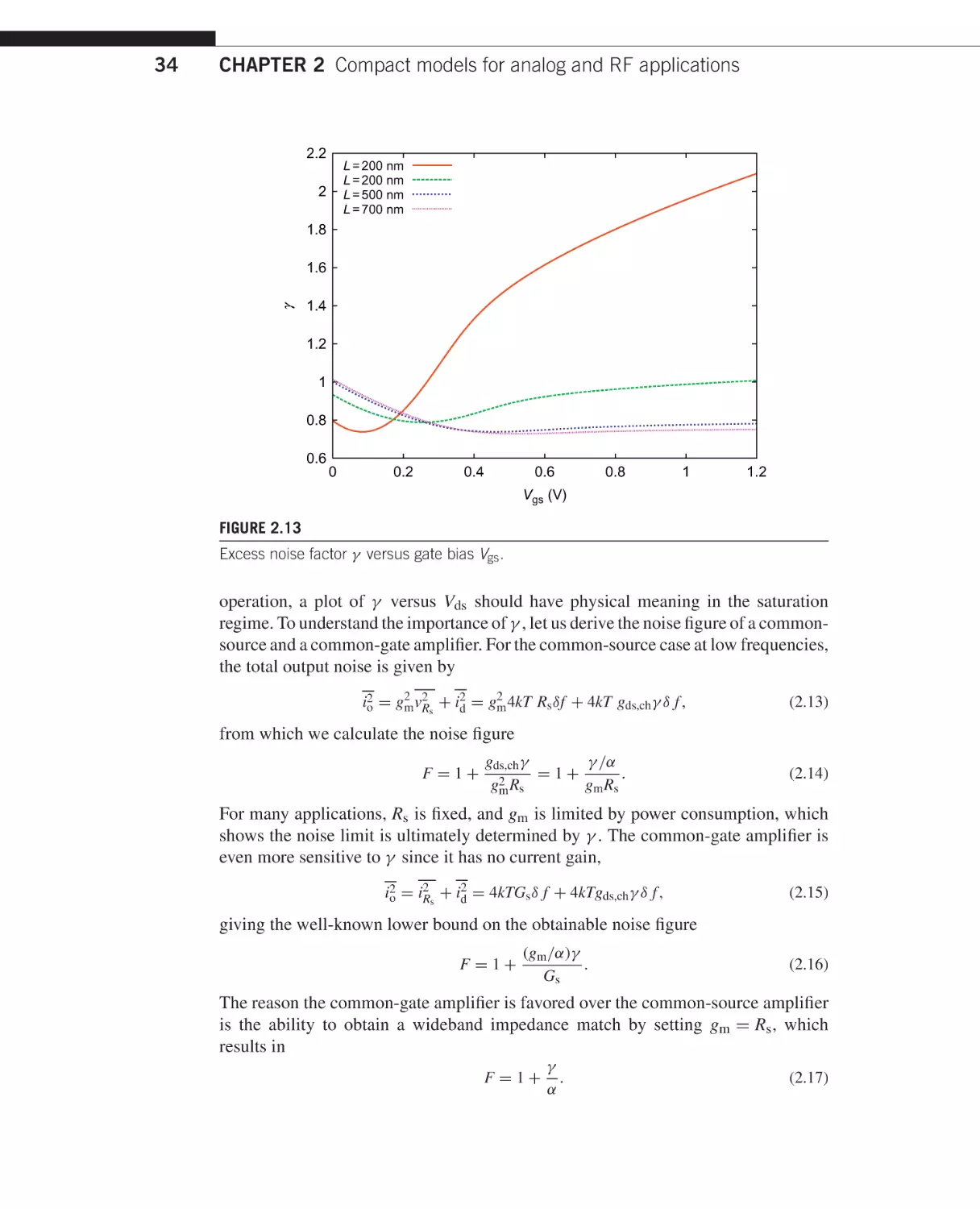
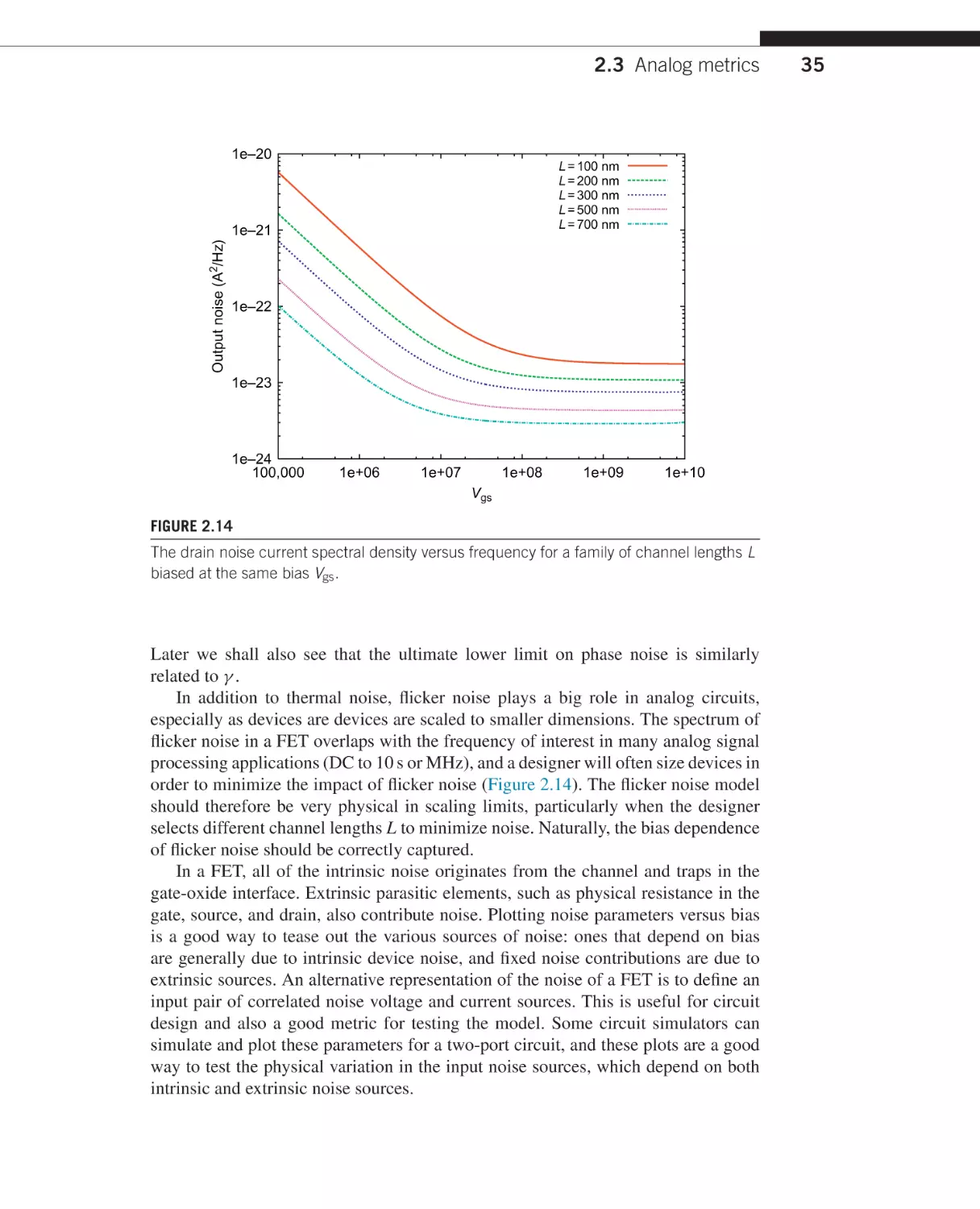
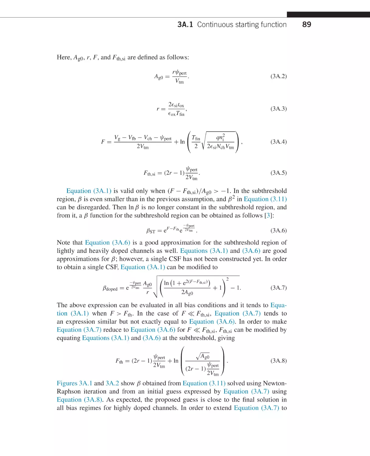
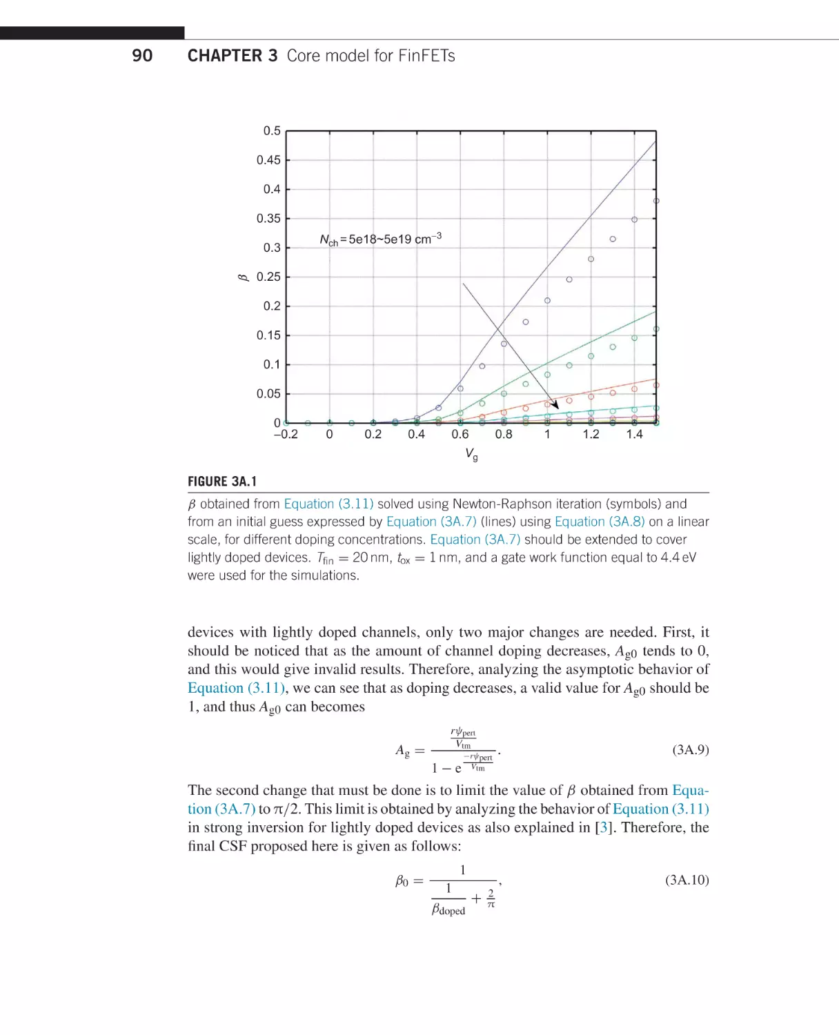
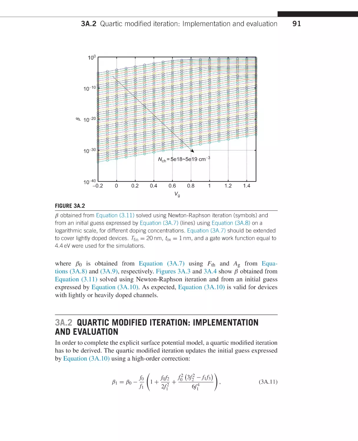
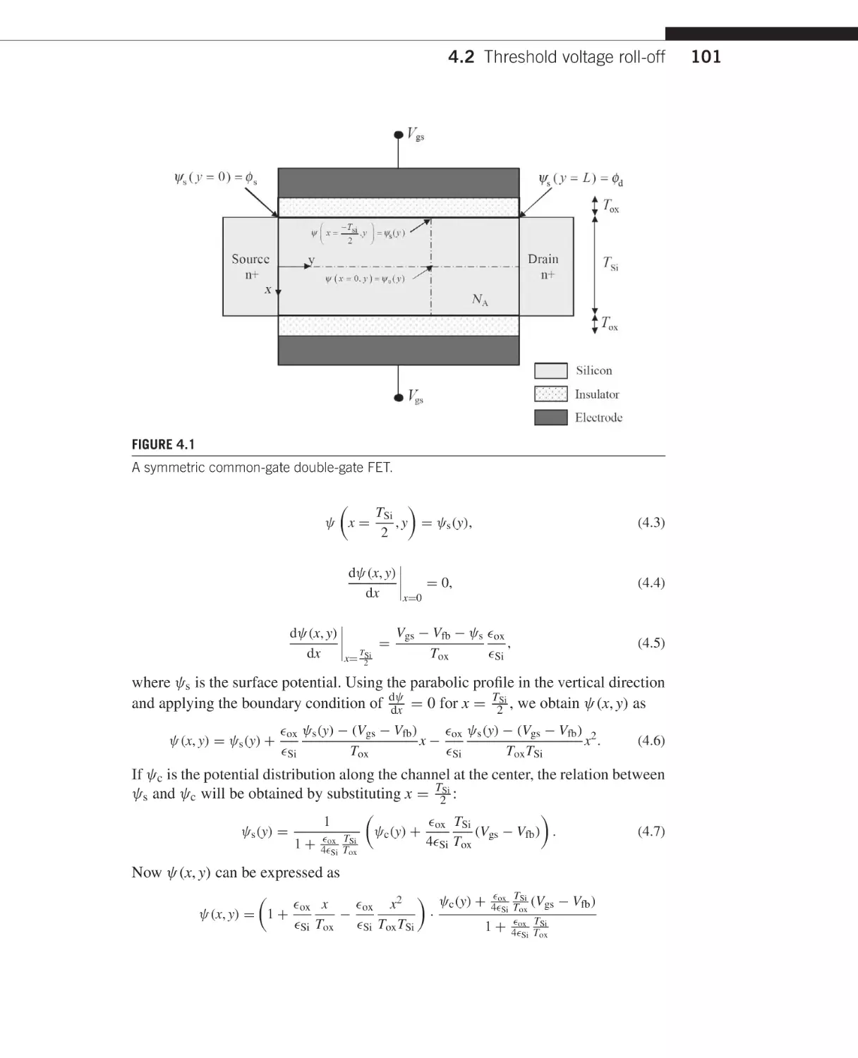
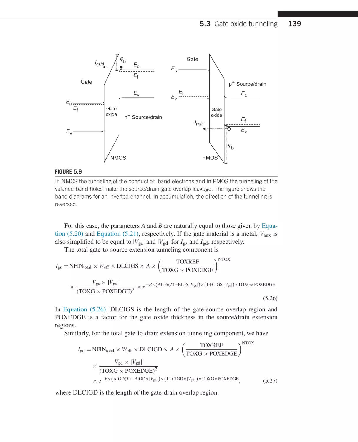
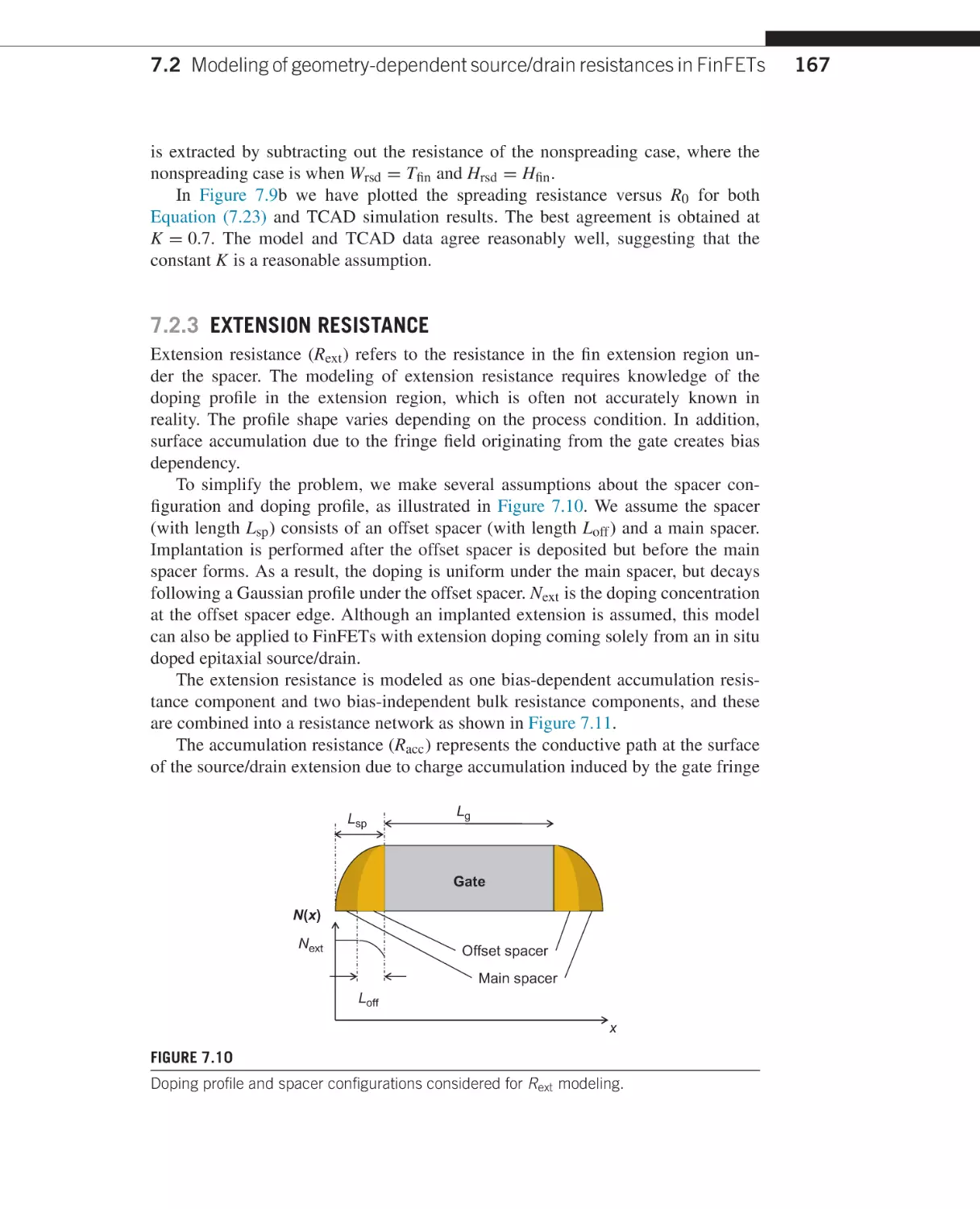
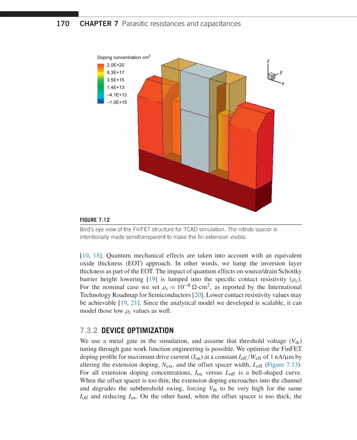
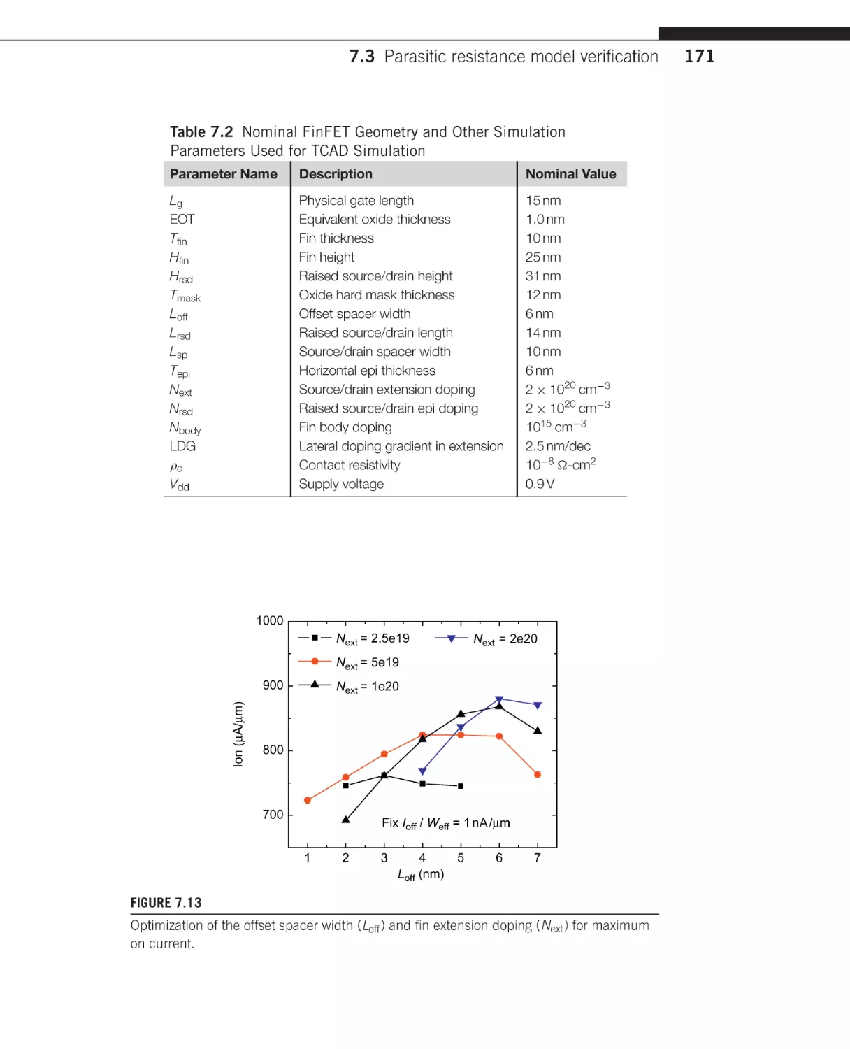
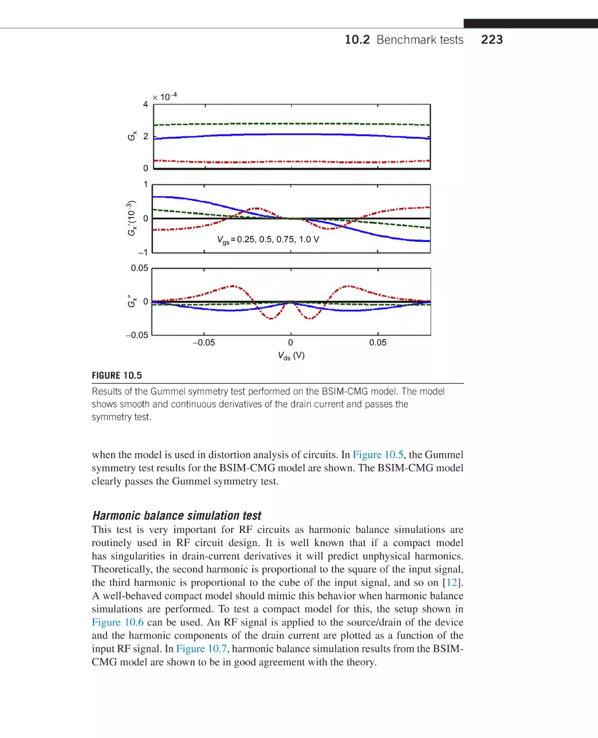
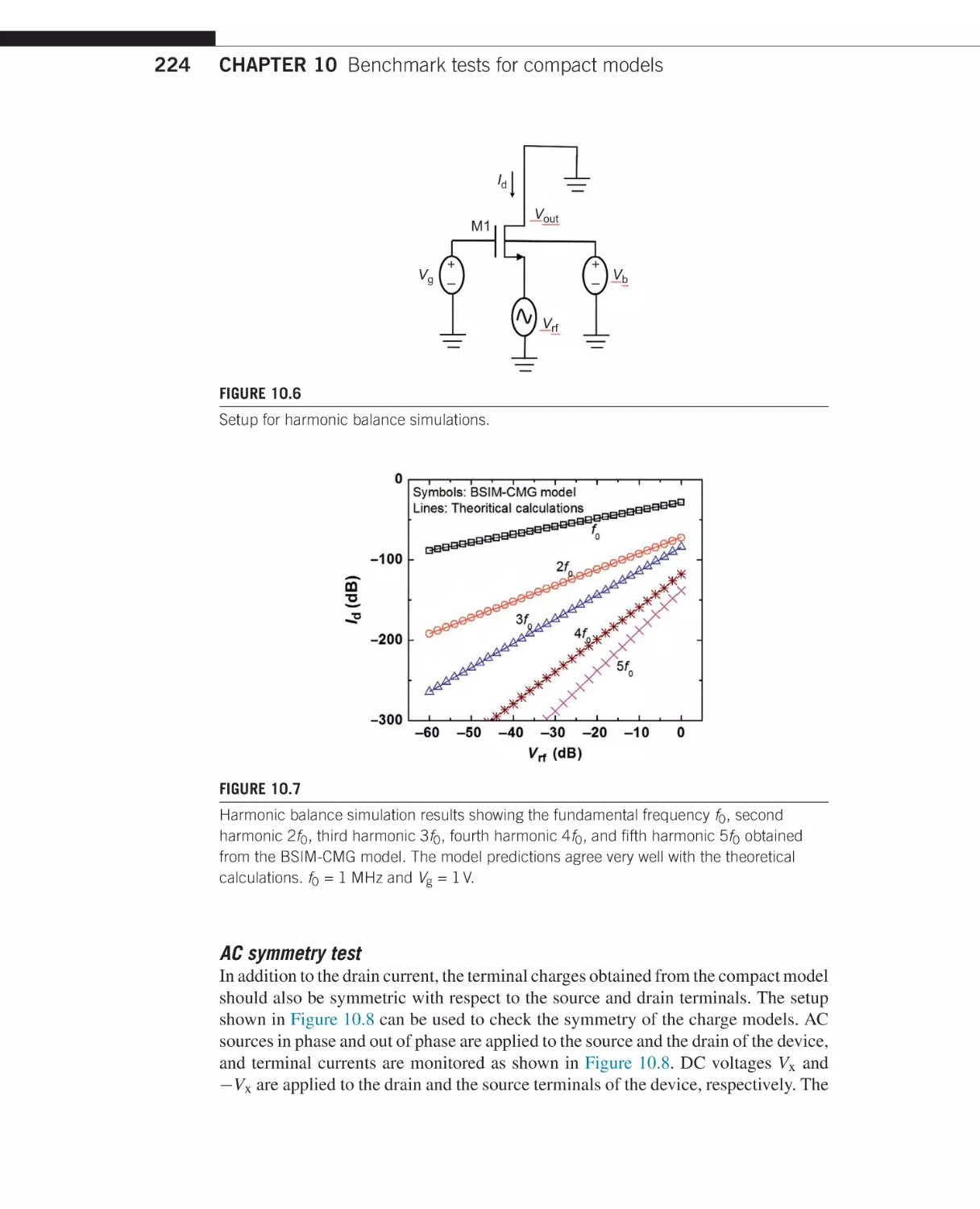
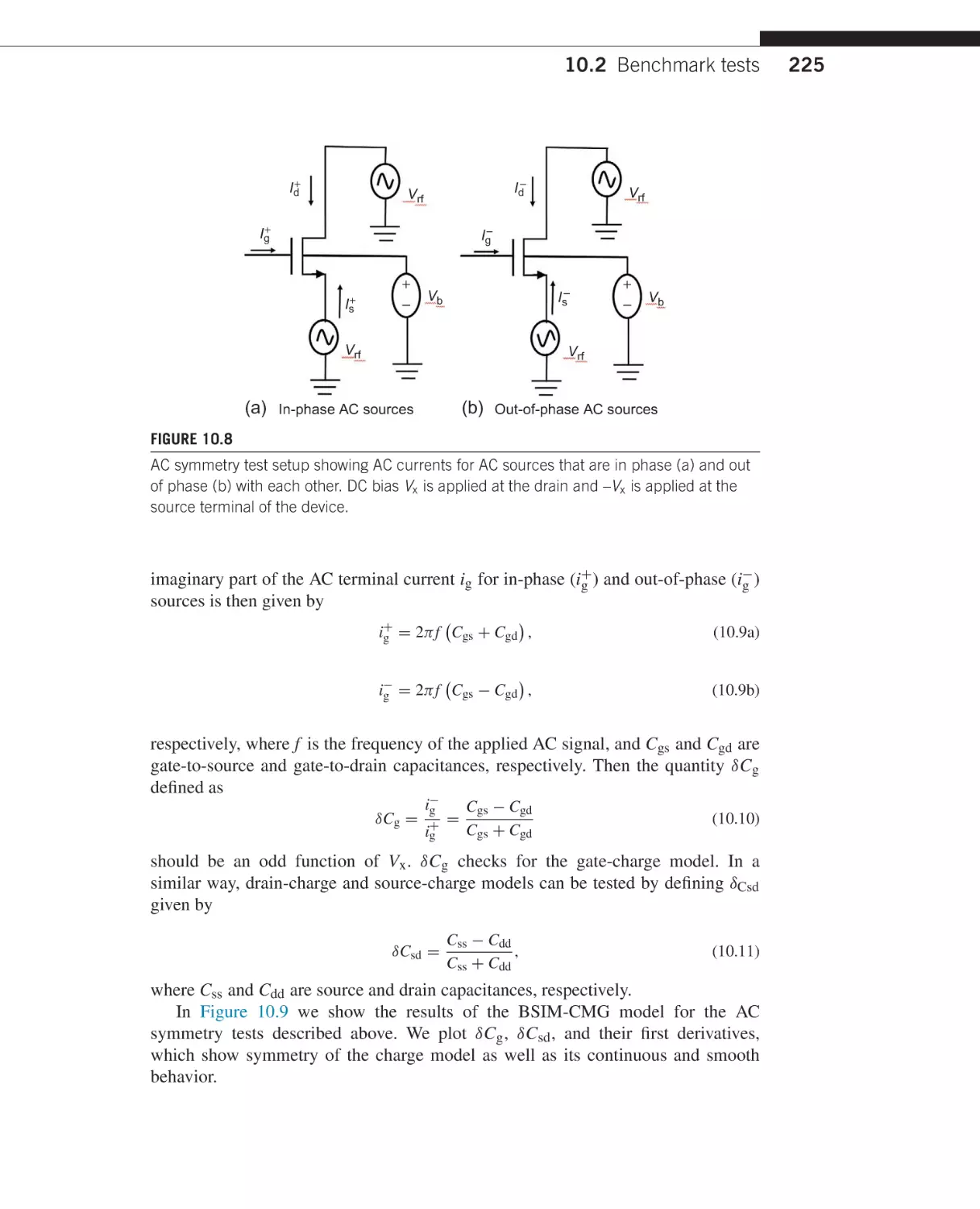
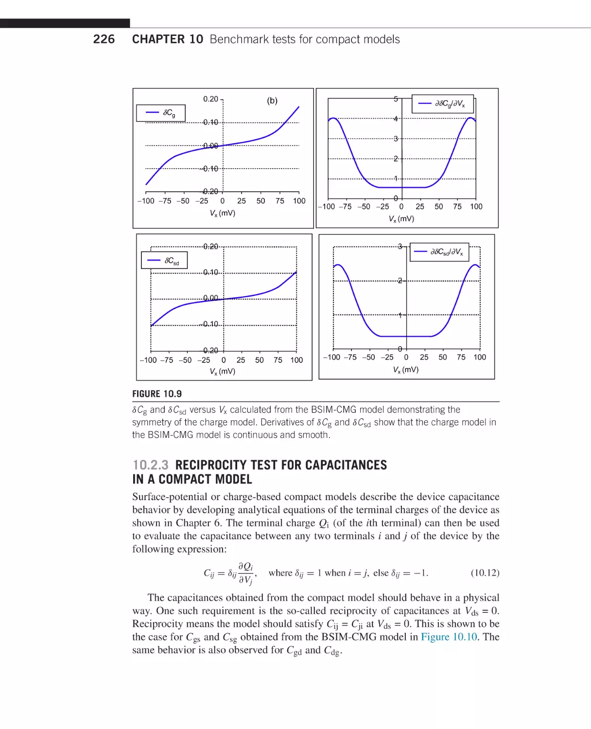
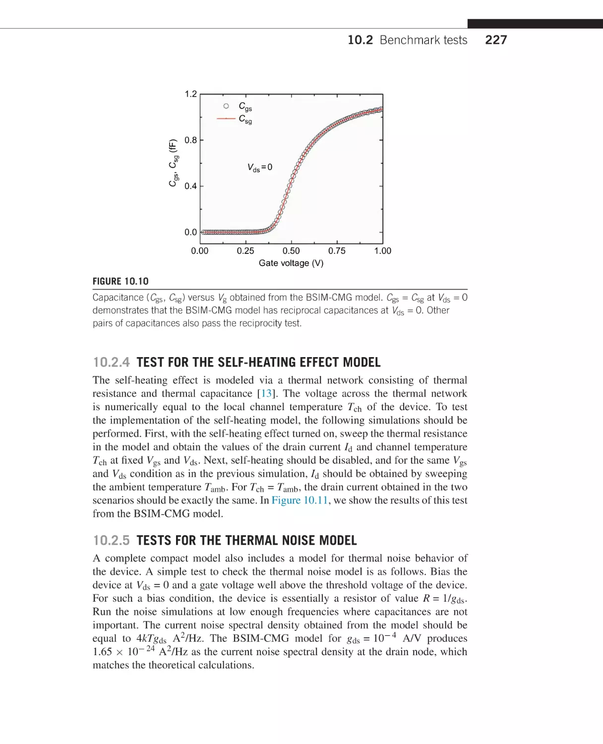
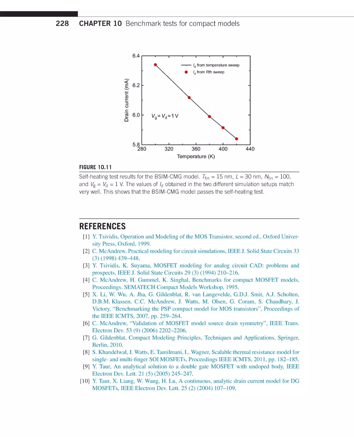
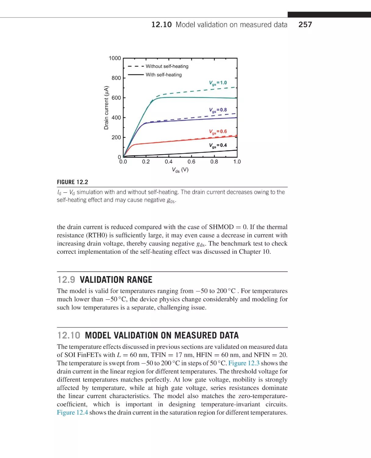
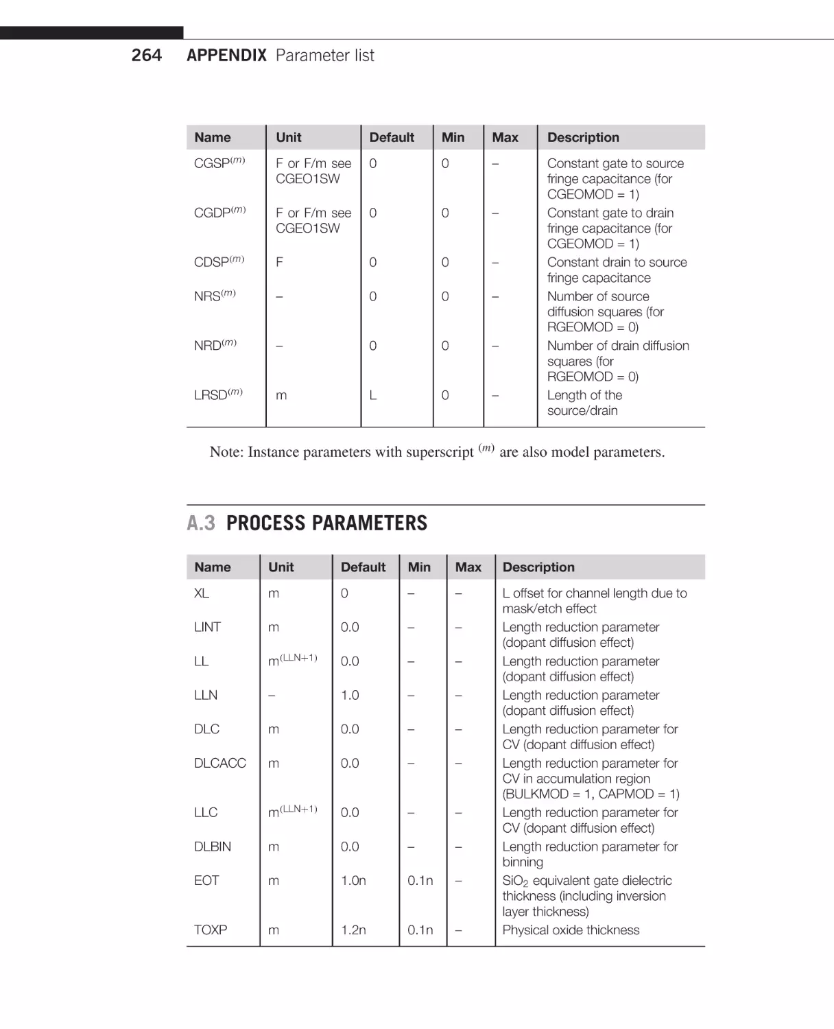
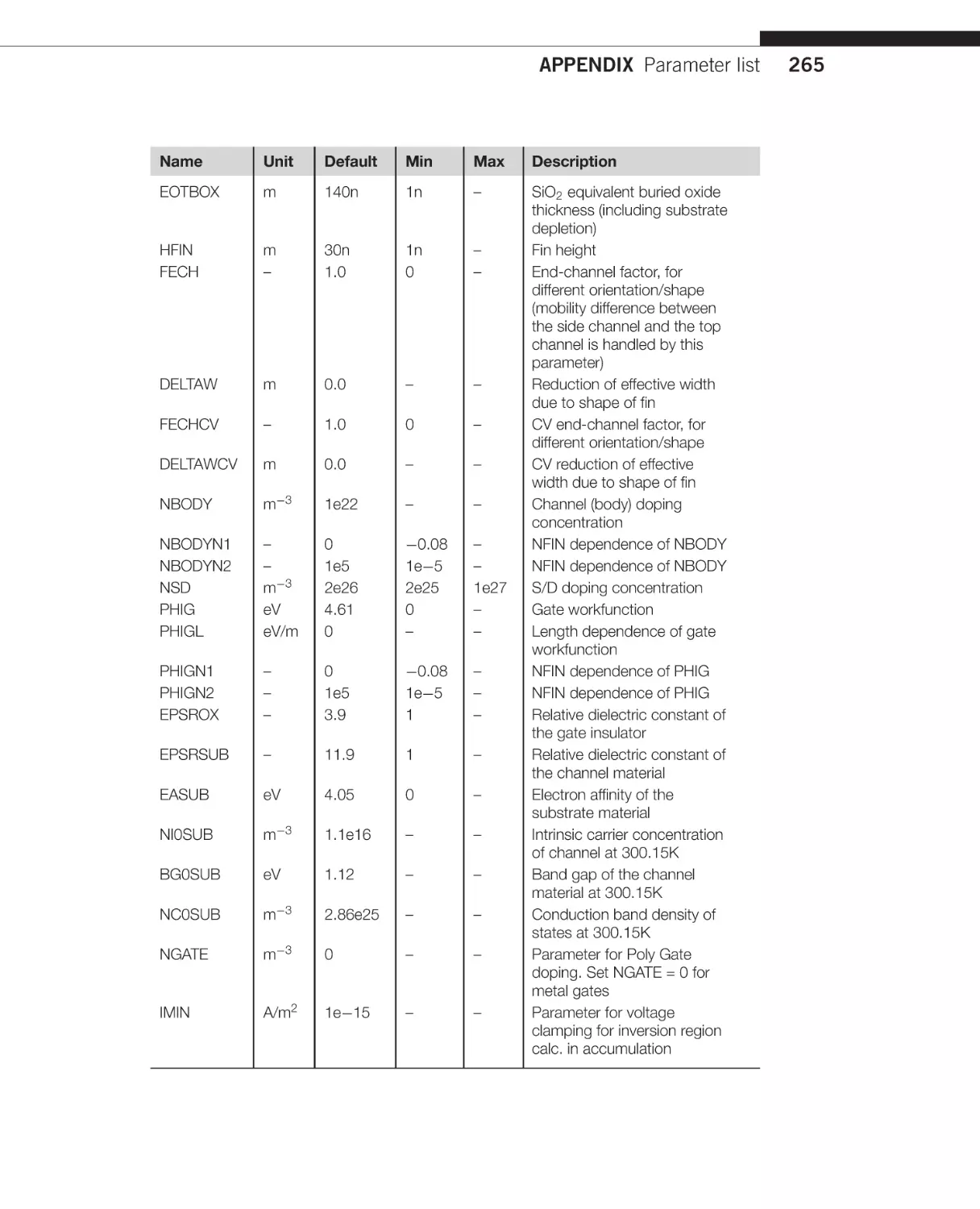
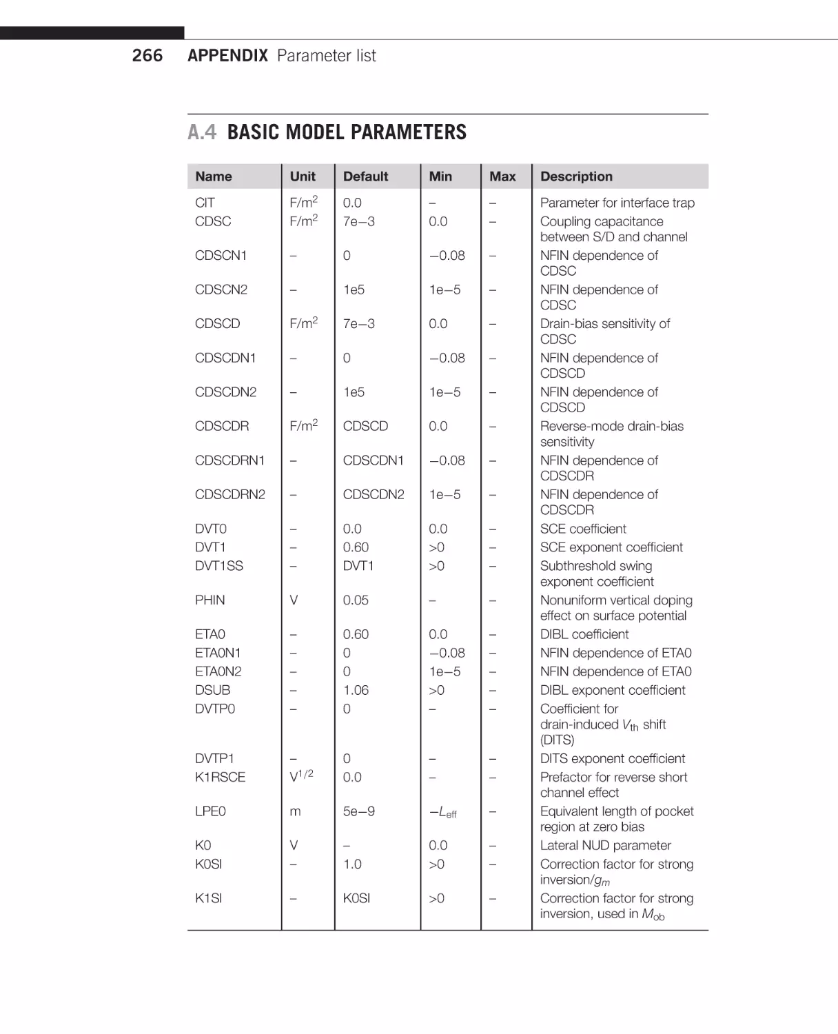
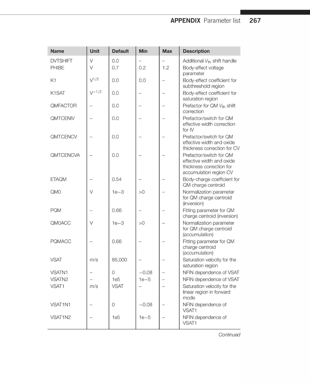
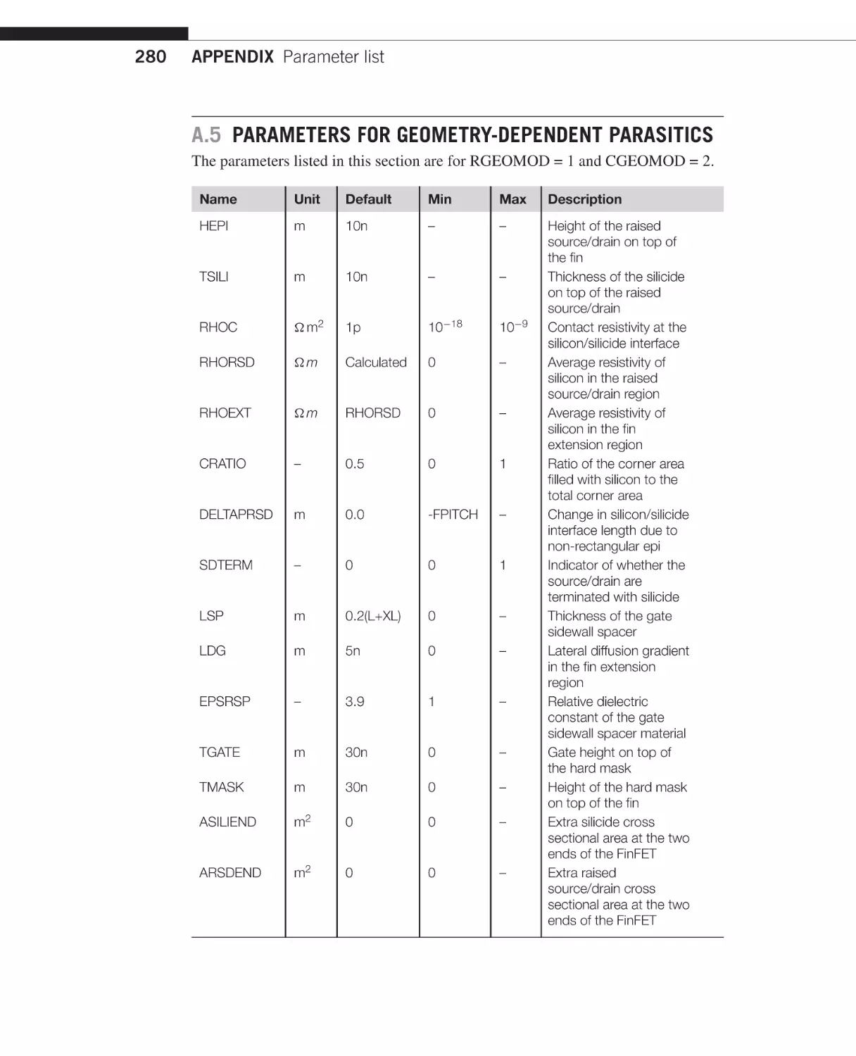
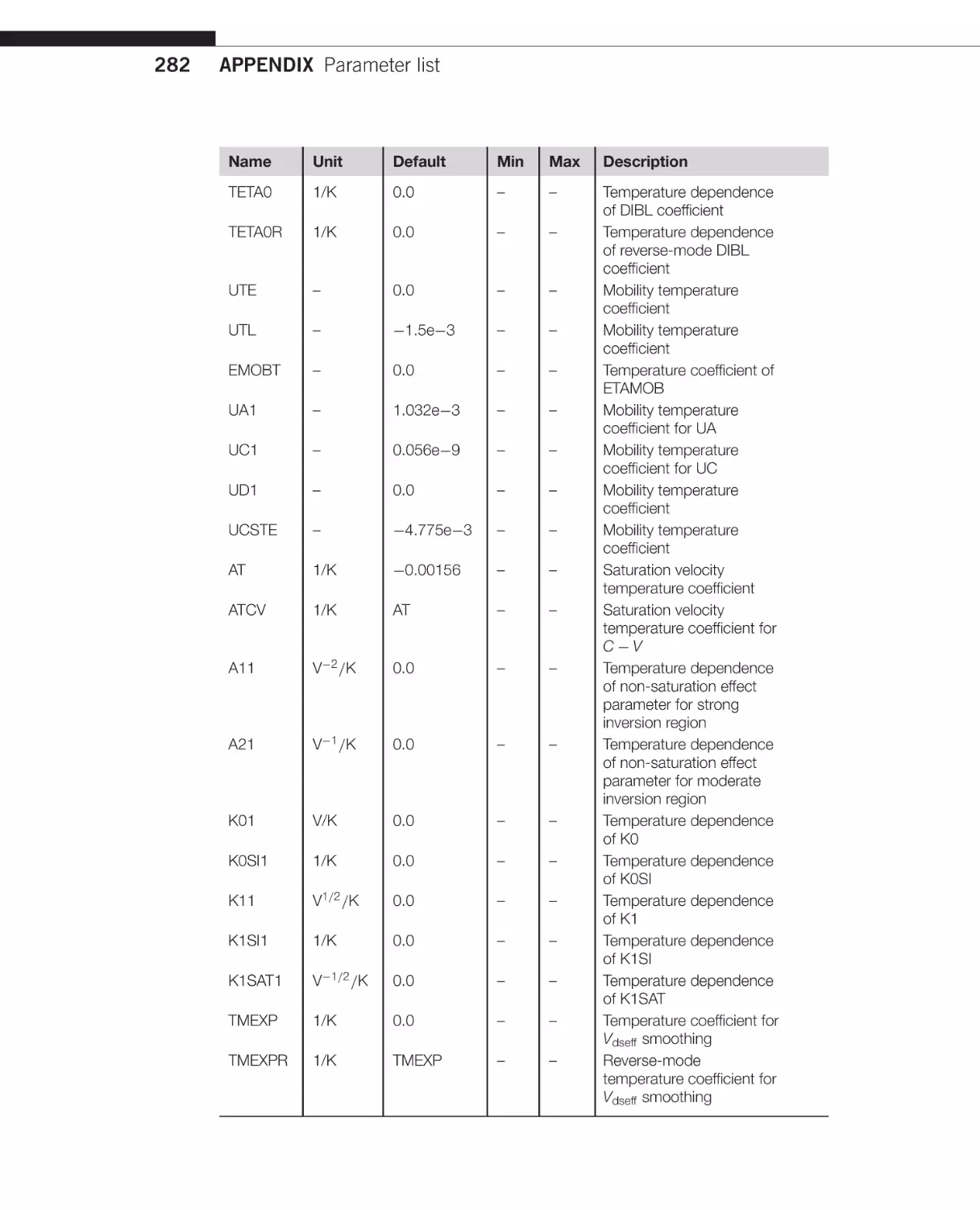
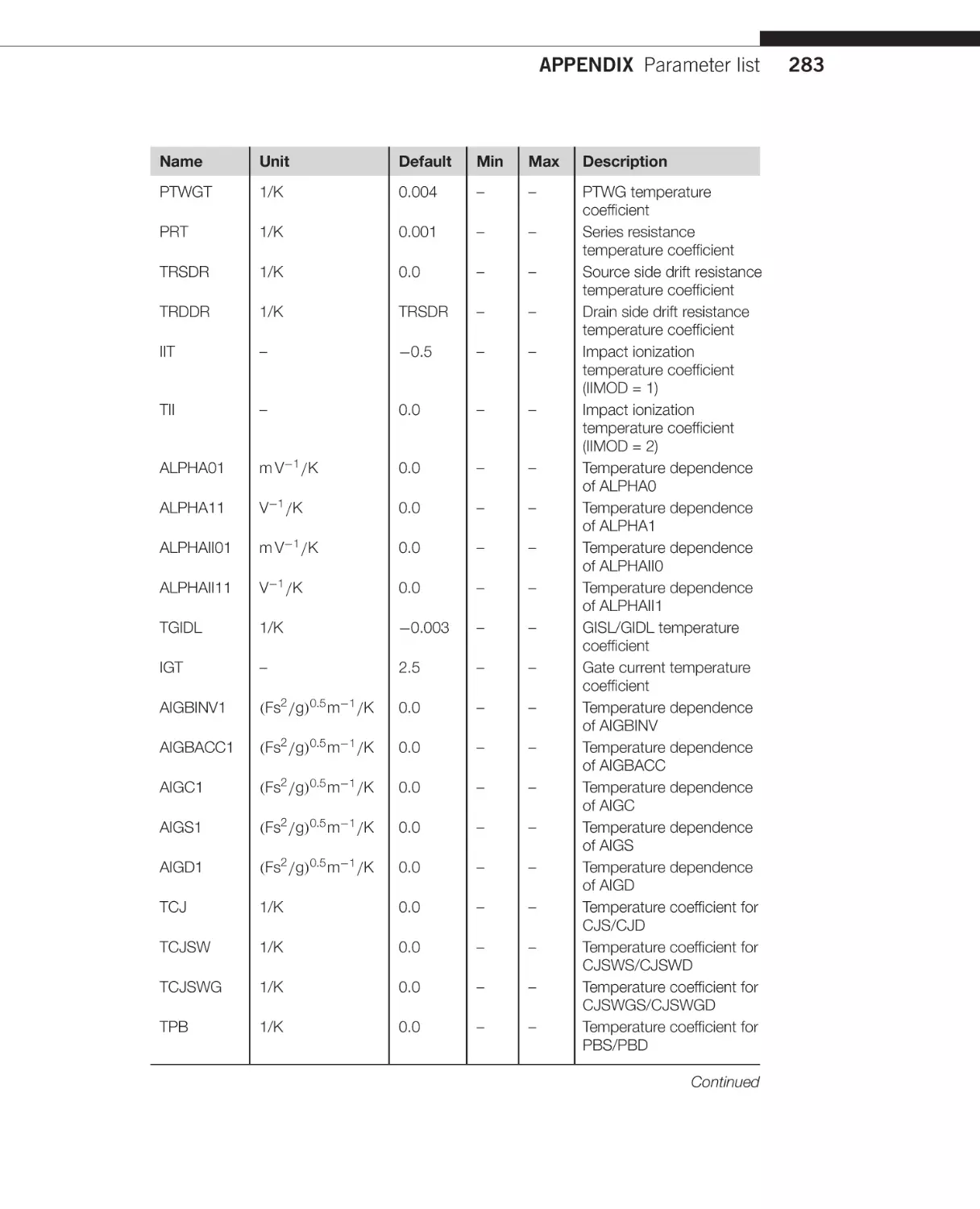
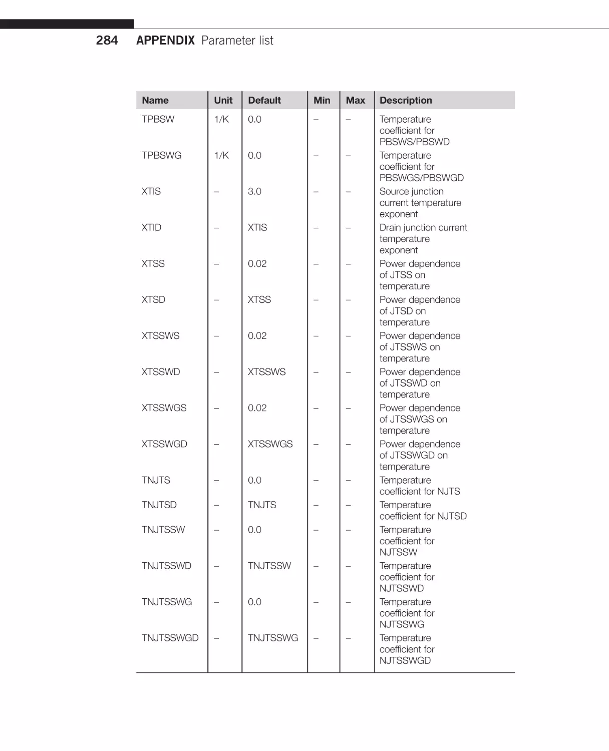
/


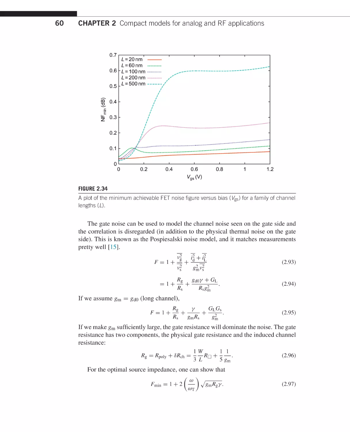


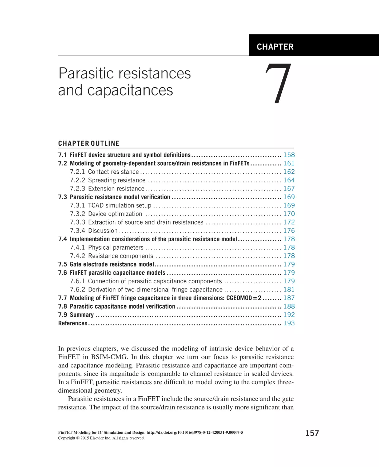


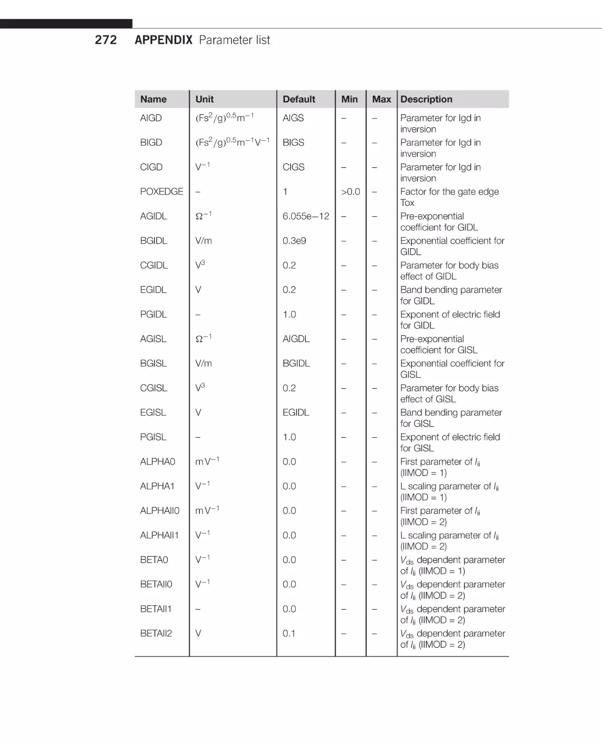
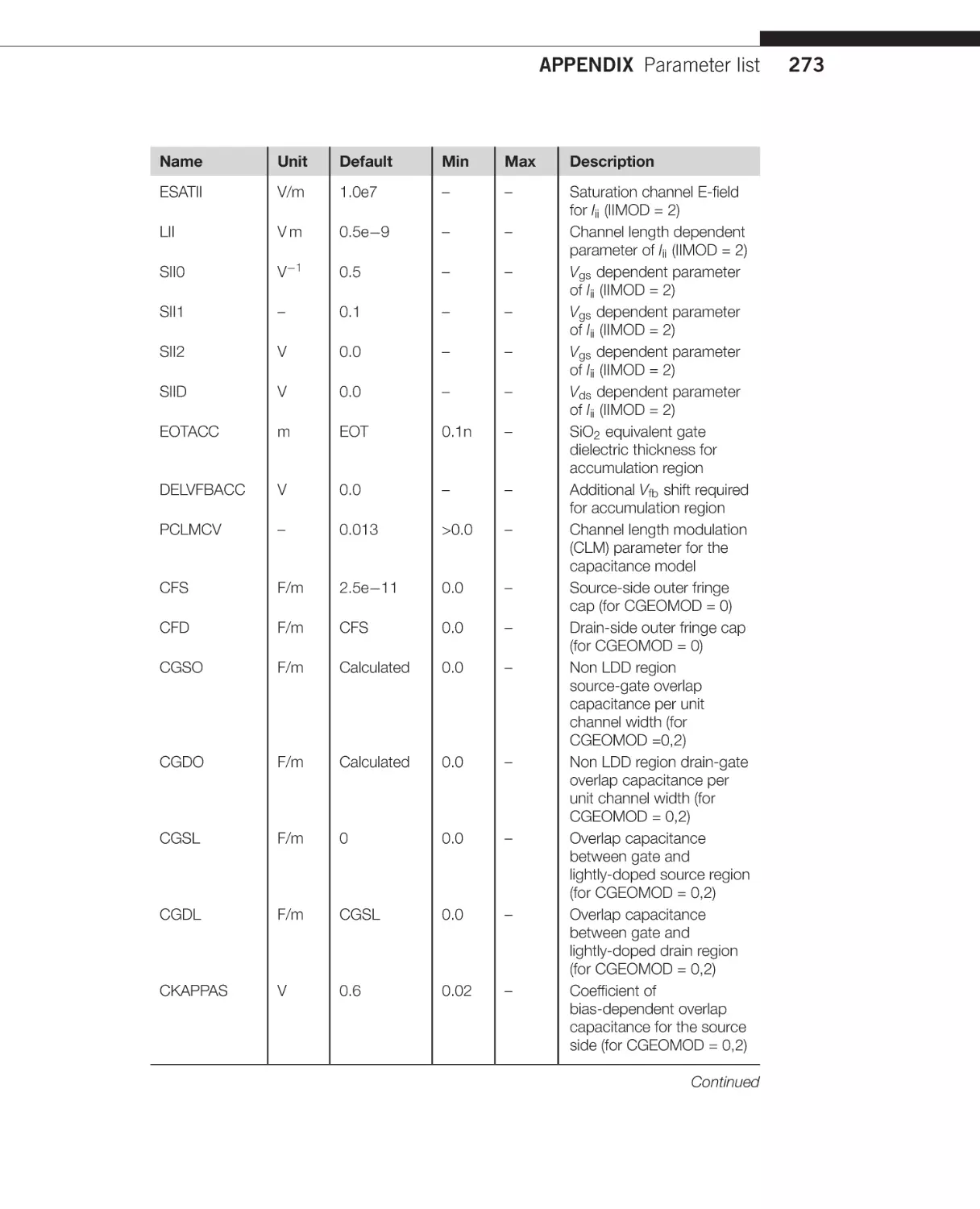
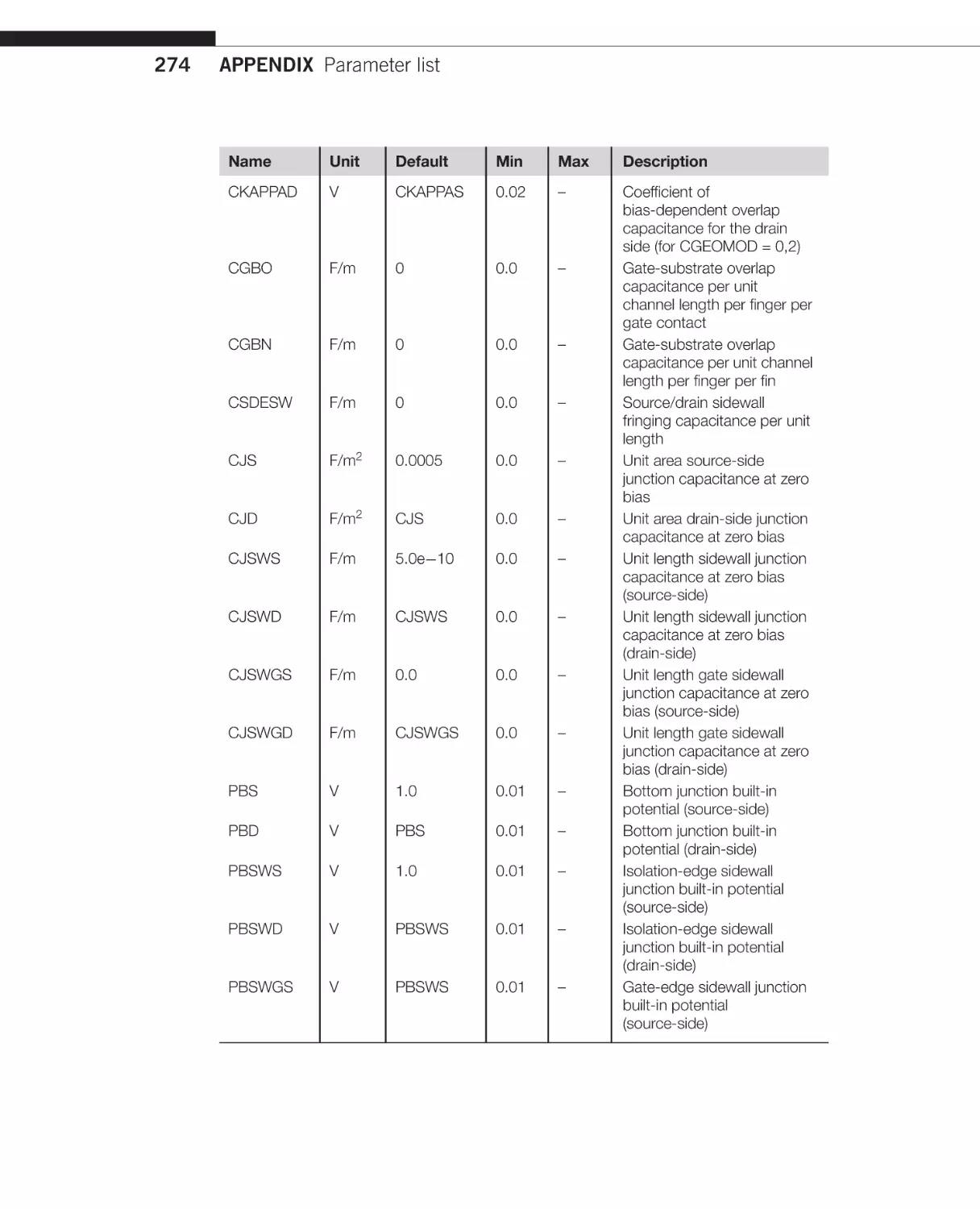
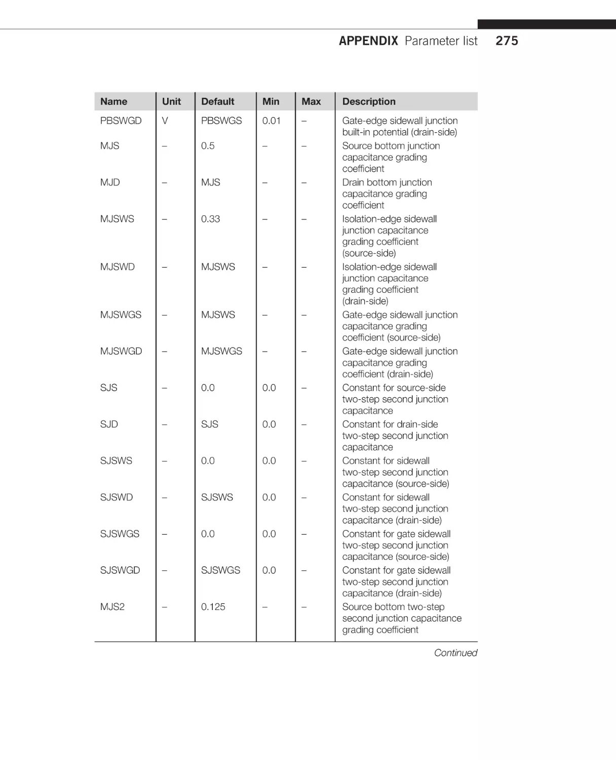
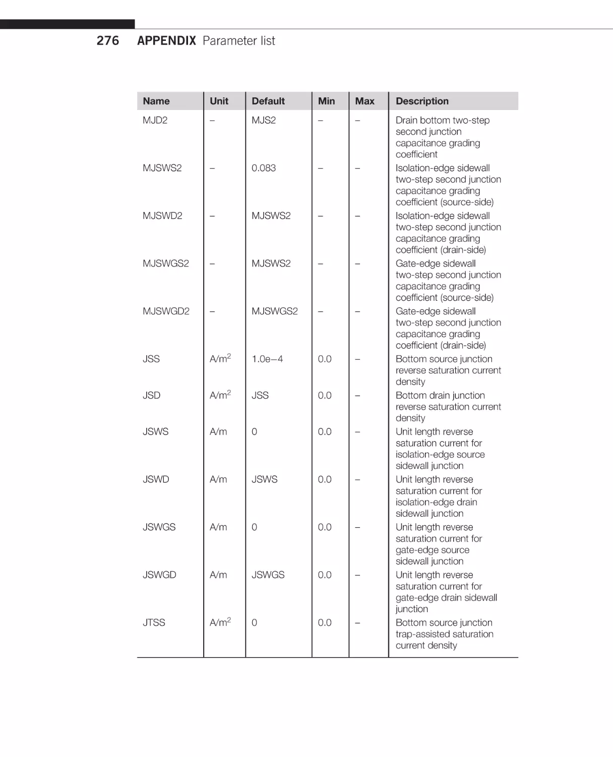
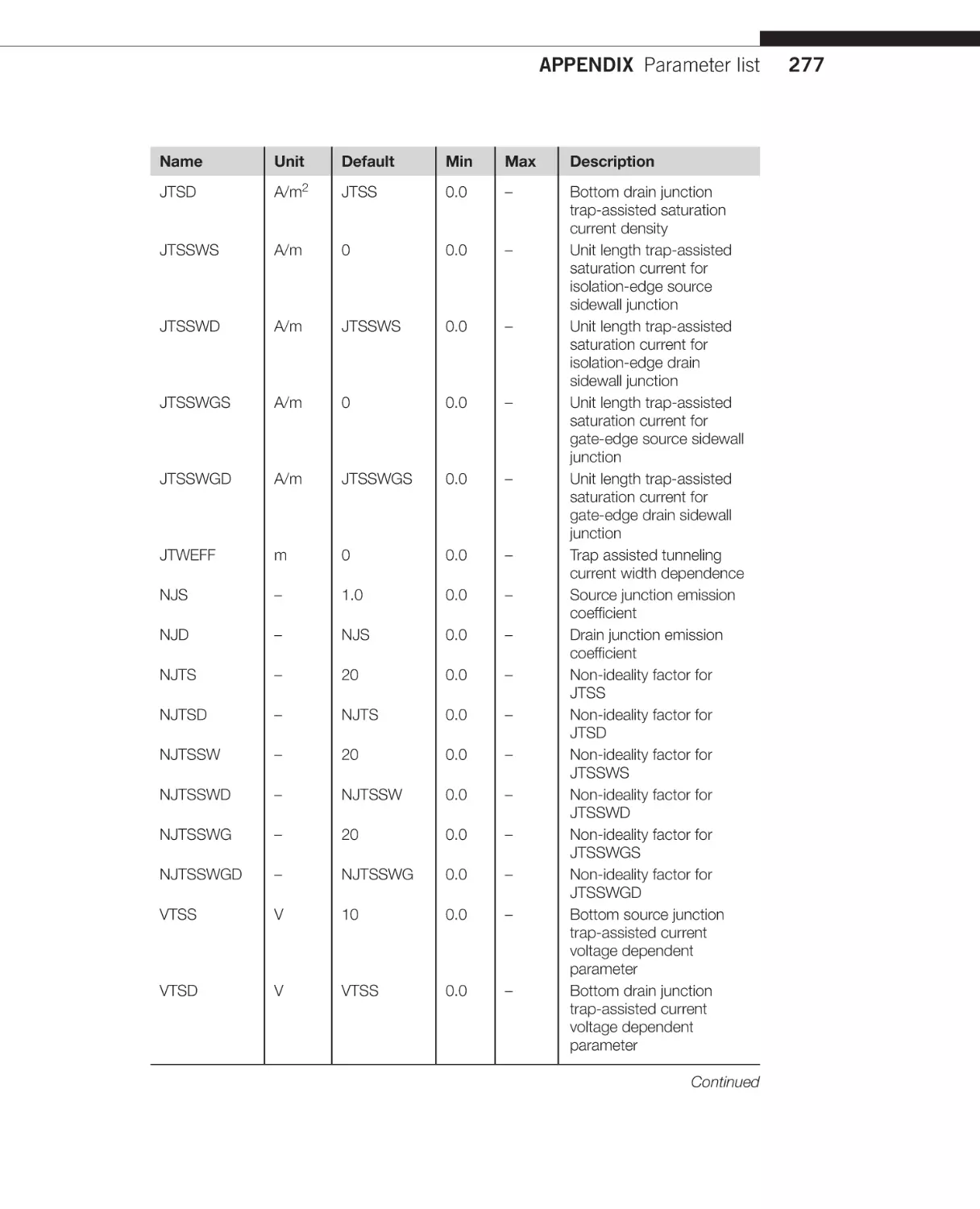
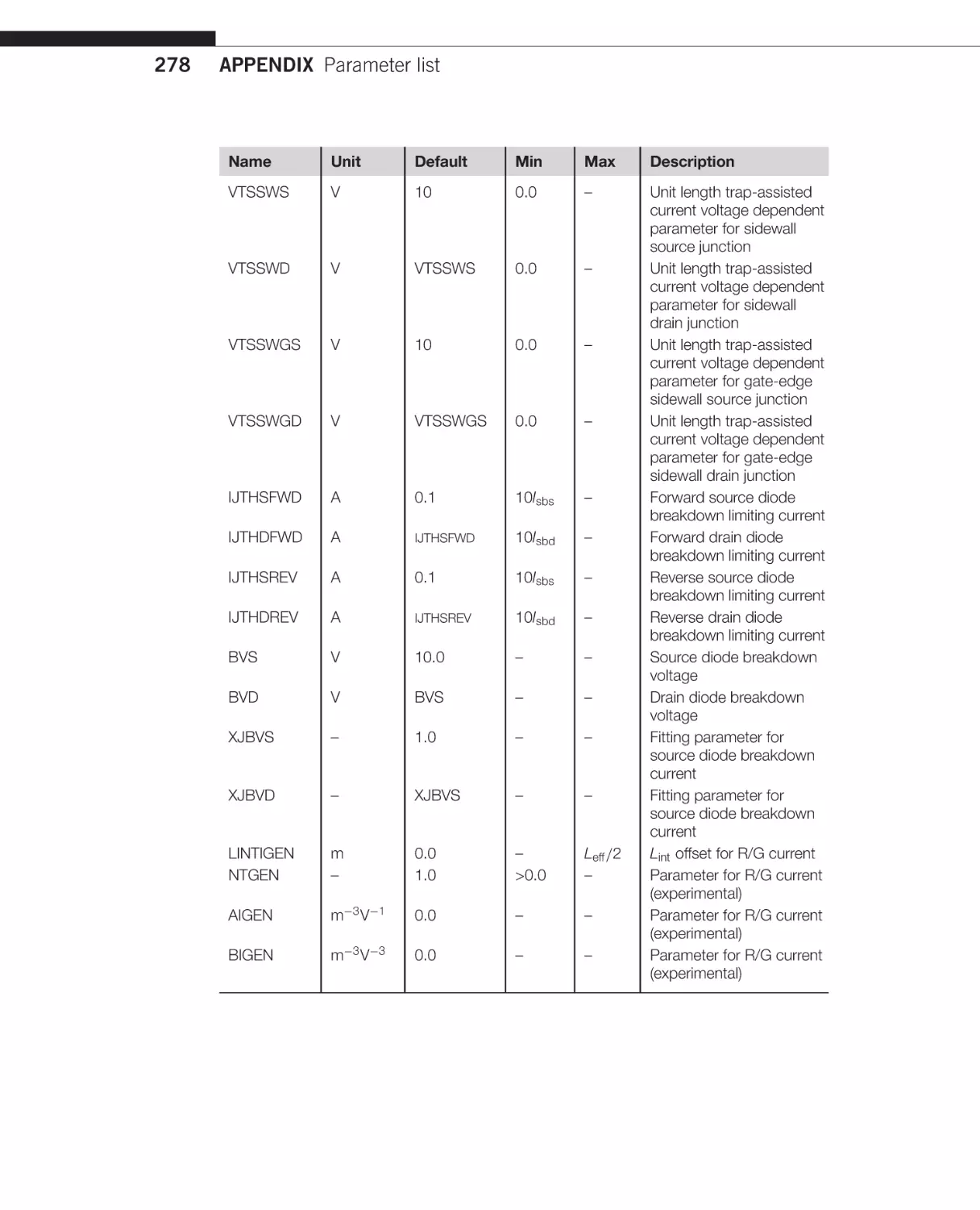
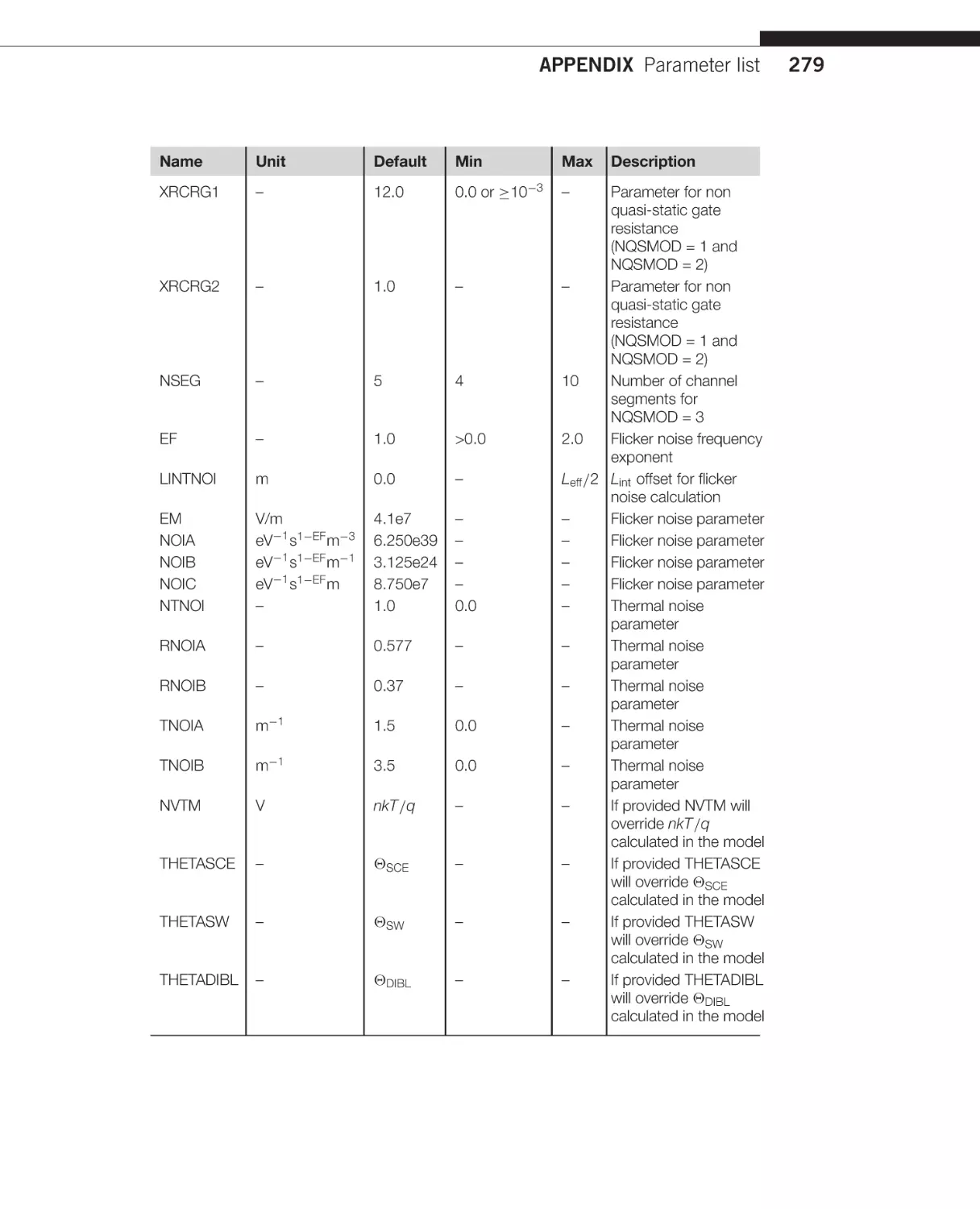


Text
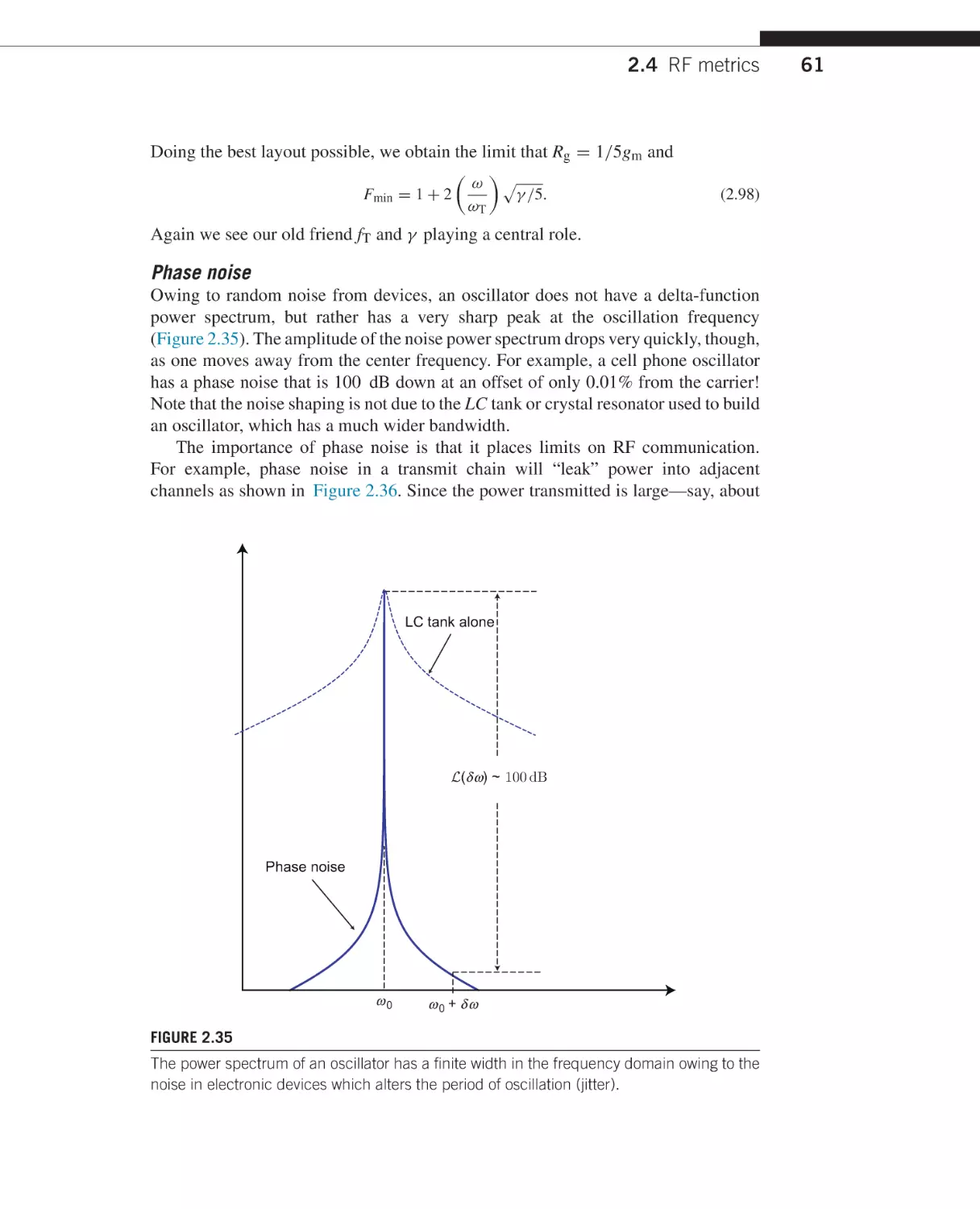
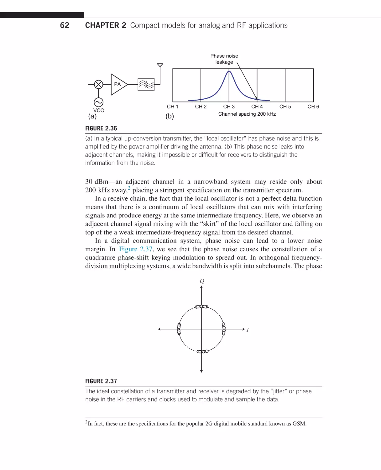
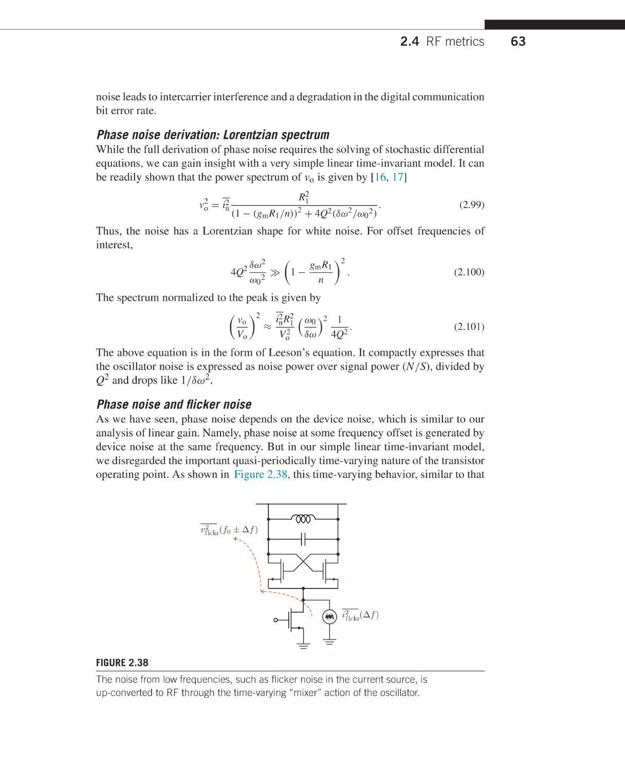
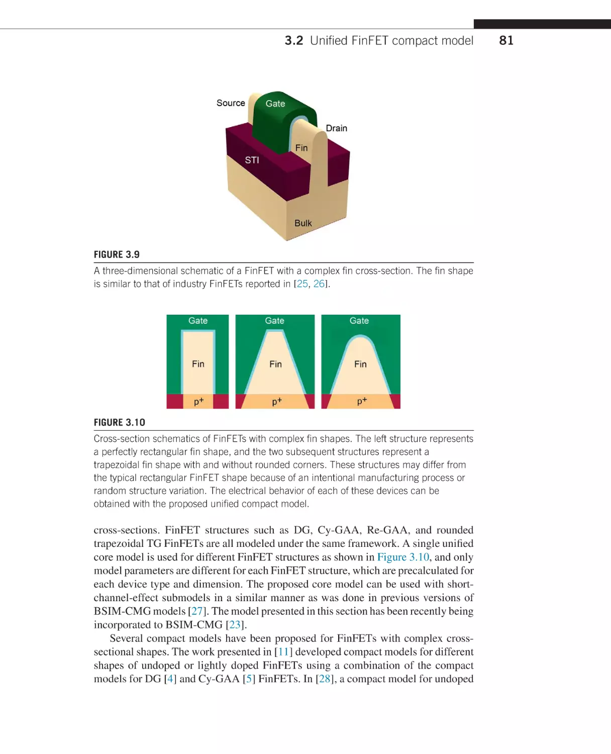
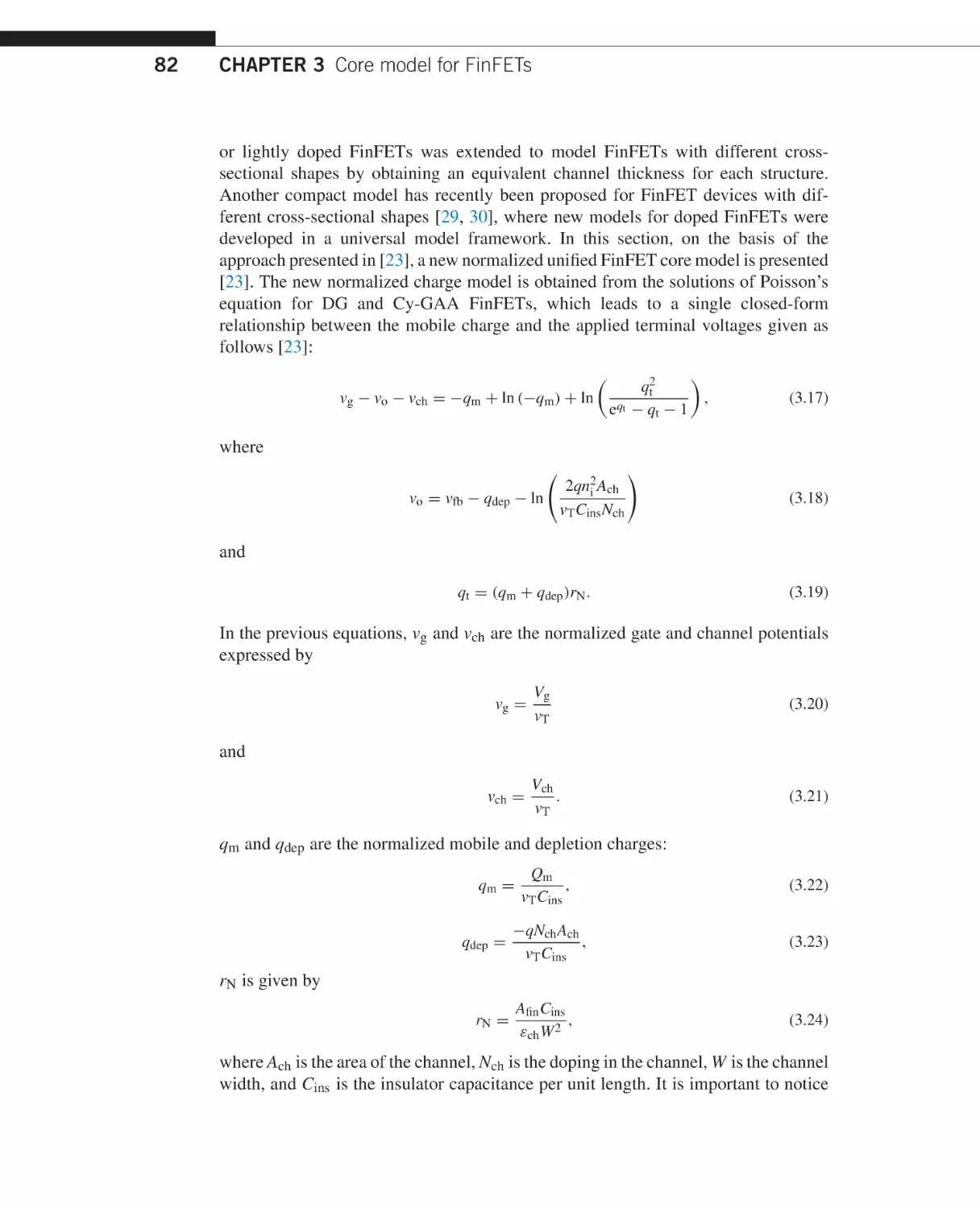
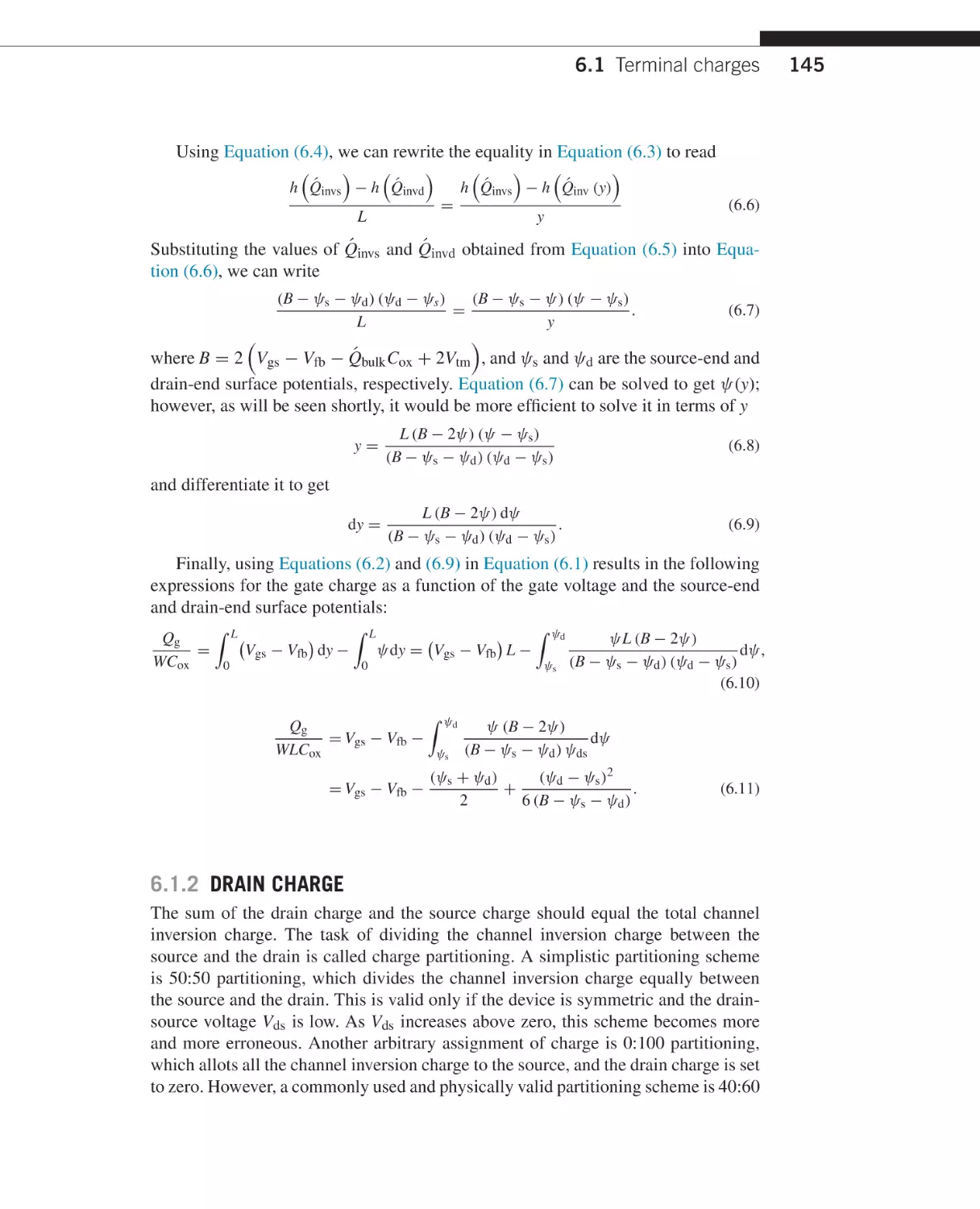
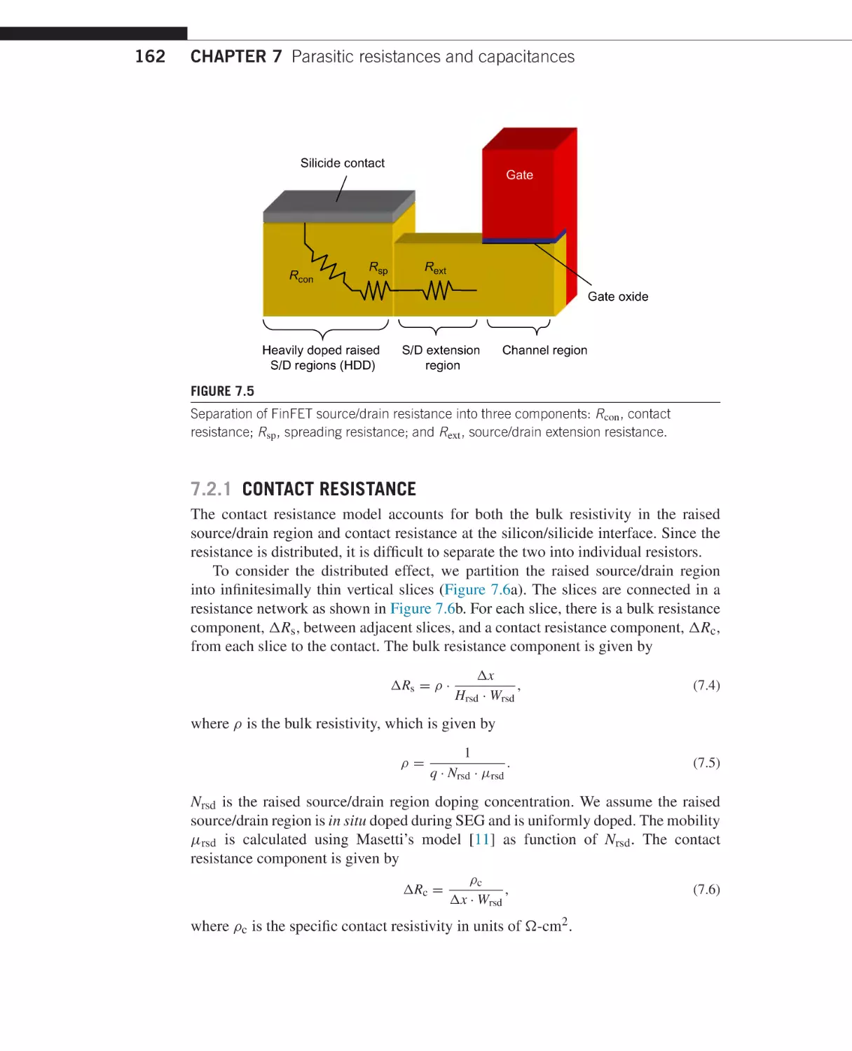
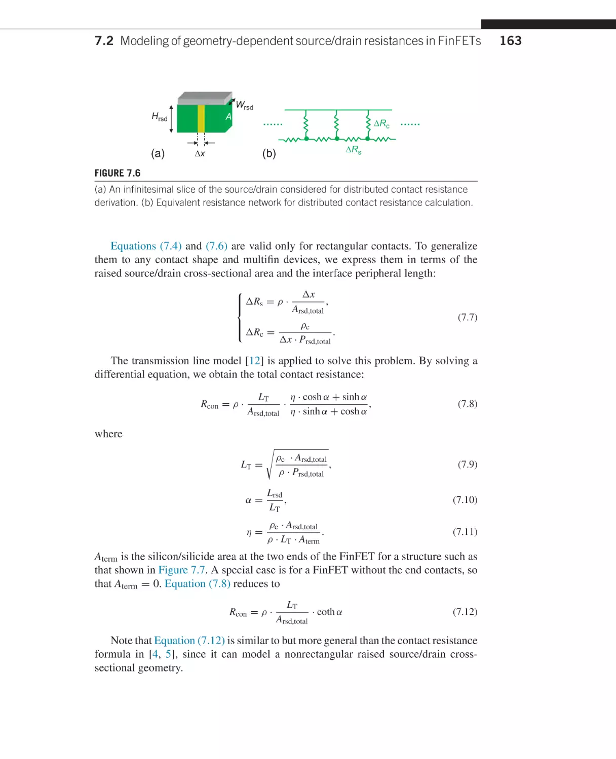
FinFET Modeling
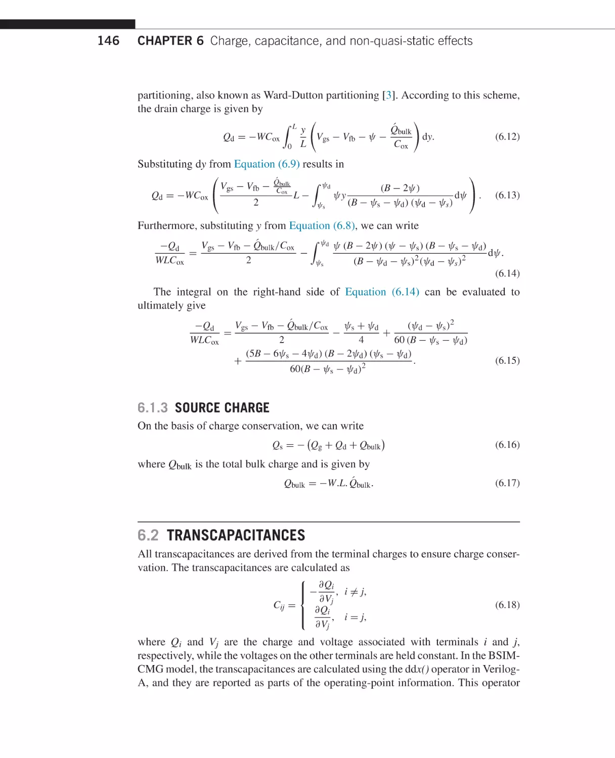
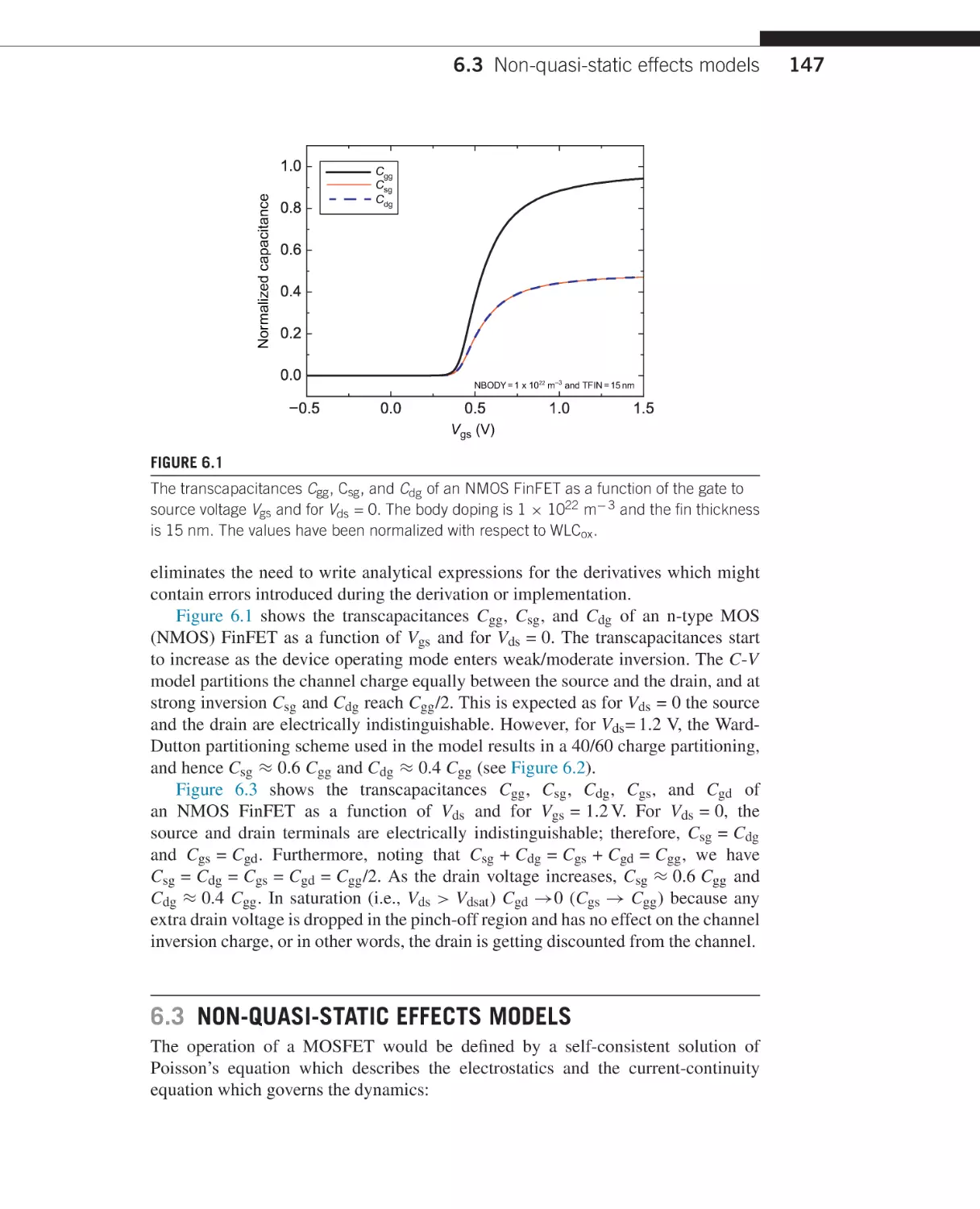
for IC Simulation
and Design
Using the BSIM-CMG Standard
Yogesh Singh Chauhan
Darsen D. Lu
Sriramkumar Vanugopalan
Sourabh Khandelwal
Juan Pablo Duarte
Navid Paydavosi
Ai Niknejad
Chenming Hu
AMSTERDAM • BOSTON • HEIDELBERG • LONDON
NEW YORK • OXFORD • PARIS • SAN DIEGO
SAN FRANCISCO • SINGAPORE • SYDNEY • TOKYO
Academic Press is an imprint of Elsevier
Academic Press is an imprint of Elsevier
125 London Wall, London, EC2Y 5AS, UK
525 B Street, Suite 1800, San Diego, CA 92101-4495, USA
225 Wyman Street, Waltham, MA 02451, USA
The Boulevard, Langford Lane, Kidlington, Oxford OX5 1GB, UK
Copyright © 2015 Elsevier Inc. All rights reserved.
No part of this publication may be reproduced or transmitted in any form or by any means,
electronic or mechanical, including photocopying, recording, or any information storage and
retrieval system, without permission in writing from the publisher. Details on how to seek
permission, further information about the Publisher’s permissions policies and our
arrangements with organizations such as the Copyright Clearance Center and the Copyright
Licensing Agency, can be found at our website: www.elsevier.com/permissions.
This book and the individual contributions contained in it are protected under copyright by
the Publisher (other than as may be noted herein).
Notices
Knowledge and best practice in this field are constantly changing. As new research and
experience broaden our understanding, changes in research methods, professional practices,
or medical treatment may become necessary.
Practitioners and researchers must always rely on their own experience and knowledge in
evaluating and using any information, methods, compounds, or experiments described herein.
In using such information or methods they should be mindful of their own safety and the
safety of others, including parties for whom they have a professional responsibility.
To the fullest extent of the law, neither the Publisher nor the authors, contributors, or editors,
assume any liability for any injury and/or damage to persons or property as a matter of
products liability, negligence or otherwise, or from any use or operation of any methods,
products, instructions, or ideas contained in the material herein.
Library of Congress Cataloging-in-Publication Data
A catalog record for this book is available from the Library of Congress
British Library Cataloguing in Publication Data
A catalogue record for this book is available from the British Library
For information on all Academic Press publications
visit our web site at store.elsevier.com
Printed and bound in the USA
ISBN: 978-0-12-420031-9
Author Biographies
Yogesh S. Chauhan is an Assistant Professor in the electrical engineering department
at the Indian Institute of Technology, Kanpur. He received his Ph.D. in compact
modeling of high voltage MOSFETs in 2007 from EPFL, Switzerland. From 20072010, he was a manager at IBM, Bangalore, where he led a compact modeling
team, focusing on RF bulk and SOI transistors and ESD modeling. From 20102012, he was a postdoctoral fellow at the University of California, Berkeley, where
he worked on the development of bulk and multigate transistor models, including
BSIM6, BSIM-IMG and BSIM-CMG. He received the IBM Faculty Award in 2013
for his contribution to compact modeling. He has co-authored over 50 conference and
journal publications in the field of device compact modeling.
Darsen D. Lu was one of the key contributors of the industry standard FinFET
compact model, BSIM-CMG, and thin-body SOI compact model, BSIM-IMG. He
received his B.Sc. in electrical engineering in 2005, from National Tsing Hua
University, Hsinchu, Taiwan, and his M.Sc. and Ph.D. in electrical engineering from
the University of California, Berkeley, in 2007 and 2011 respectively. Since 2011,
he has been a research scientist at the IBM Thomas J. Watson Research Center,
Yorktown Heights, New York. His current research focuses on the modeling of novel
semiconductor devices such as SiGe FinFETs, phase change memory and carbonbased transistors.
Sriramkumar Venugopalan received his M.Sc. and Ph.D. in electrical engineering
at the University of California, Berkeley and his B.Sc. from the Indian Institute of
Technology (IIT), Kanpur. While at Berkeley he worked in the BSIM Group and
pursued research and development of multi-gate transistor compact SPICE models
that contributed to the industry standard BSIM-CMG model. He has authored and coauthored more than 30 research papers in the area of semiconductor device SPICE
models and integrated circuit design. Currently Dr. Venugopalan is with Samsung
Electronics pursuing RF integrated circuit design in advanced semiconductor technology nodes.
Sourabh Khandelwal is currently a Postdoctoral Researcher in the BSIM Group,
University of California, Berkeley. He received his Ph.D. from the Norwegian
University of Science and Technology in 2013 and his M.Sc. from the Indian Institute
of Technology (IIT), Bombay in 2007. From 2007–2010 he worked as a research
engineer at the IBM Semiconductor Research and Development Centre, developing
compact models for RF SOI devices. He holds a patent and has authored several
research papers in the area of device modeling and characterization. His Ph.D. work
on the GaN compact model is under consideration for industry standardization by the
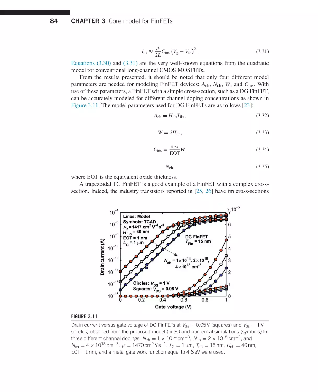
Compact Model Coalition.
ix
x
Author Biographies
Juan Pablo Duarte Sepúlveda is currently working towards his Ph.D. at the
University of California, Berkeley. He received his B.Sc. in 2010 and his M.Sc. in
2012, both in electrical engineering from the Korea Advanced Institute of Science
and Technology (KAIST). He held a position as a lecturer at the Universidad Tecnica
Federico Santa Maria, Valparaiso, Chile, in 2012. He has authored many papers
on nanoscale semiconductor device modeling and characterization. He received the
Best Student Paper Award at the 2013 International Conference on Simulation of
Semiconductor Processes and Devices (SISPAD) for the paper: Unified FinFET
Compact Model: Modelling Trapezoidal Triple-Gate FinFETs.
Navid Paydavosi received his Ph.D. in Micro-Electro-Mechanical Systems (MEMS)
and Nanosystems from the University of Alberta, Canada in 2011. He worked for the
BSIM Group at the University of California, Berkeley, as a post-doctoral scholar from
2012 to 2014. He has published several research papers on the theory and modeling of
modern Si-MOSFETs and there future alternatives, including carbon-based and IIIV high electron mobility devices. Currently Dr. Paydavosi is with Intel Corporation,
Oregon as a device engineer working on process technology development.
Ali M. Niknejad received his B.Sc in electrical engineering from the University of
California, Los Angeles, in 1994, and his M.Sc. and Ph.D., also in electrical engineering, from the University of California, Berkeley, in 1997 and 2000 respectively. He
is currently a professor in the EECS department at UC Berkeley and Faculty Director
of the Berkeley Wireless Research Center (BWRC) Group. Professor Niknejad was
the recipient of the 2012 ASEE Frederick Emmons Terman Award for his work and
textbook on electromagnetics and RF integrated circuits. He has co-authored over
200 conference and journal publications in the field of integrated circuits and device
compact modeling. His focus areas of research include analog, RF, mixed-signal,
mm-wave circuits, device physics and compact modeling, and numerical techniques
in electromagnetics.
Chenming Hu is Distinguished Chair, Professor Emeritus at the University of
California, Berkeley. He was the Chief Technology Officer of TSMC and founder
of Celestry Design Technologies. He is best known for developing the revolutionary
3D transistor FinFET that powers semiconductor chips beyond 20nm. He also led
the development of BSIM - the industry standard transistor model that is used in
designing most of the integrated circuits in the world. He is a member of the US
Academy of Engineering, the Chinese Academy of Science, and Academia Sinica.
His honors include the Asian American Engineer of the Year Award, the IEEE
Andrew Grove Award and Solid Circuits Award as well as the Nishizawa Medal, and
UC Berkeley’s highest honor for teaching - the Berkeley Distinguished Teaching
Award.
Preface
If you have opened this book, you probably know that the first 3D transistor, the
FinFET, and its adoption by industry for its power and speed advantages have been
the biggest semiconductor news in recent years. The FinFET has been called the most
drastic shift in semiconductor technology in over 40 years.
Because a book reflects the background of its authors, it serves the readers for us
to describe our background. We are two professors and six current or former Ph.D.
students or postdoctoral researchers of the University of California, Berkeley. One of
the professors (C.H.) was the lead inventor and developer of the FinFET. The other
professor (A.N.) pioneered the field of 100 GHz CMOS. All the coauthors are or
were members of the BSIM research group that created the industry-standard FinFET
model for simulation and design of FinFET-based ICs. BSIM planar CMOS models
have been used to design IC products with estimated cumulative sales of a trillion
US dollars since 1997. One may expect the BSIM FinFET model to have a similarly
large impact in the future.
We wrote this book for IC designers, device engineers, researchers, and students.
It presents the what, why, and how of the FinFET and compact modeling; models for
analog and RF applications; and a thorough discussion of the BSIM FinFET model
(BSIM-CMG). We start from the ABC of the FinFET and end with the XYZ of the
FinFET model. Even if you are familiar with BSIM-CMG, you may be surprised to
learn that it can model FinFETs with arbitrary fin shapes such as trapezoidal, roundcorner, cylindrical, and even asymmetrical shapes. It also models FinFETs employing
non-silicon channel materials such as SiGe, Ge, and InGaAs. You are holding the best
handbook for the FinFET model for IC simulation.
We do not claim to have created the equations and model presented in this
book. Many other former members of the BSIM group contributed to the creation of
BISM-CMG. We acknowledge their indirect contributions to this book. Most notably,
Chung-Hsun Lin and Mohan Dunga were the first student developers of BSIM-CMG,
starting in 2004. Other direct or indirect contributors to the book include Walter Li,
Wei-Man Lin, Shijin Yao, Muhammed Karim, Chandan Yadav, and Avirup Dasgupta.
We thank the many industry BSIM users who helped to make BSIM-CMG
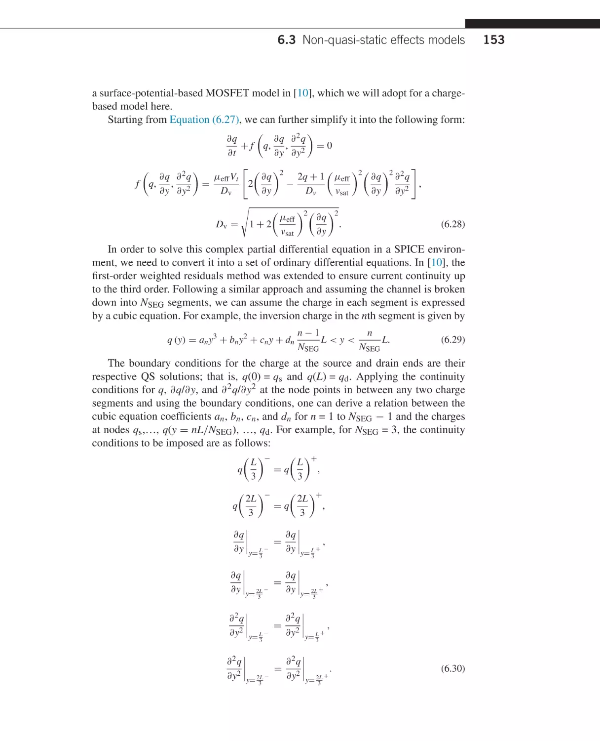
a better model for their corporate employers. They did so by testing the beta
model and pointing out its weaknesses in accuracy or robustness during the 2year-long evaluation and (uncontested) election process of the standard FinFET
model. The list includes R. Williams (IBM); A.S. Roy, S. Mudanai (Intel); K.-W. Su,
W.-K. Lee, M.-C. Jeng (Taiwan Semiconductor Manufacturing Company); J.-S. Goo
(Globalfoundries); P. Lee (Micron Technology); Q. Wang, J. Wang, W. Liu
xi
xii
Preface
(Synopsys); J. Xie, F. Zhao (Cadence); A. Ramadan, S. Mohamed, A.-E. Ahmed
(Mentor Graphics); P. O’Halloran (Tiburon Design Automation); B. Chen, S. Mertens
(Accelicon/Agilent, now Keysight Technologies); J. Ma (ProPlus); and G. Coram
(Analog Devices).
Most importantly, we wish to express our deepest gratitude to our families, who
tolerated and made tolerable our long hours in the office and at computers.
And we thank you, dear readers, for giving our book meaning by using it.
The authors
CHAPTER
FinFET—From device concept
to standard compact model
1
CHAPTER OUTLINE
1.1 The root cause of short-channel effects in the twenty-first century MOSFETs . . . . . . . . . 2
1.2 The thin-body MOSFET concept . . . . . . . . . . . . . . . . . . . . . . . . . . . . . . . . . . . . . . . . . . . . . . . . . . . . . . . . 4
1.3 The FinFET and a new scaling path for MOSFETs . . . . . . . . . . . . . . . . . . . . . . . . . . . . . . . . . . . . . . 4
1.4 Ultra-thin-body FET . . . . . . . . . . . . . . . . . . . . . . . . . . . . . . . . . . . . . . . . . . . . . . . . . . . . . . . . . . . . . . . . . . . . 6
1.5 FinFET compact model—the bridge between FinFET technology and IC design . . . . . . . 7
1.6 A brief history of the first standard compact model, BSIM . . . . . . . . . . . . . . . . . . . . . . . . . . . . . 8
1.7 Core and real-device models . . . . . . . . . . . . . . . . . . . . . . . . . . . . . . . . . . . . . . . . . . . . . . . . . . . . . . . . . . 9
1.8 The industry standard FinFET compact model. . . . . . . . . . . . . . . . . . . . . . . . . . . . . . . . . . . . . . . . .11
References . . . . . . . . . . . . . . . . . . . . . . . . . . . . . . . . . . . . . . . . . . . . . . . . . . . . . . . . . . . . . . . . . . . . . . . . . . . . . . . . .12
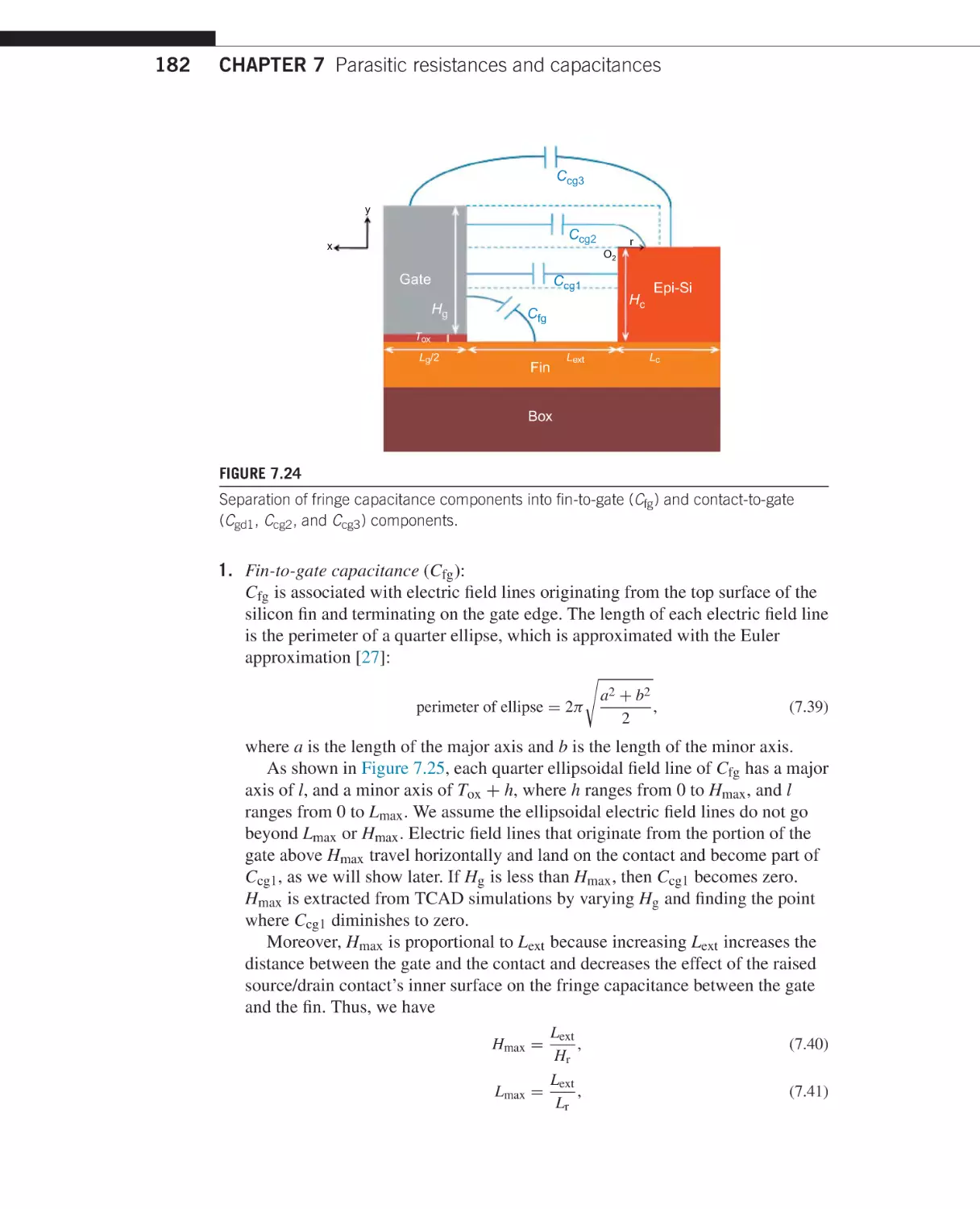
Part of the semiconductor industry’s formula for success is to make incremental
changes, not drastic changes. The planar MOSFET has served the electronics industry
well for 40 years. Aggressive engineering has managed to reduce its size again
and again without change to its basic structure. Yet the IC design window for
performance, power consumption, and sensitivity to device variation has shrunk to the
point that a major change to a better transistor structure is unavoidable. The FinFET
is that new better transistor. Adopting the FinFET has been called the most drastic
shift in semiconductor technology in over 40 years. The FinFET provides relief from
the performance, power, and device variation predicaments that the IC industry has
struggled with in the past decade. More importantly, it redirects device scaling from
a path heading for the cliff to a new one that allows scaling to continue onward as
long as lithography allows.
A brand new transistor requires a new design infrastructure to enable the design
of FinFET-based circuits and products. The foundation of the infrastructure is a
computationally very efficient mathematical model that nevertheless represents a
FinFET very accurately. It is called a compact model, or a SPICE model.
This chapter presents the FinFET—what it is, what it does, and what new scaling
concept inspired its invention. This chapter also introduces the role of a compact
model in the semiconductor industry and the industry’s first and dominant standard
FinFET Modeling for IC Simulation and Design. http://dx.doi.org/10.1016/B978-0-12-420031-9.00001-4
Copyright © 2015 Elsevier Inc. All rights reserved.
1
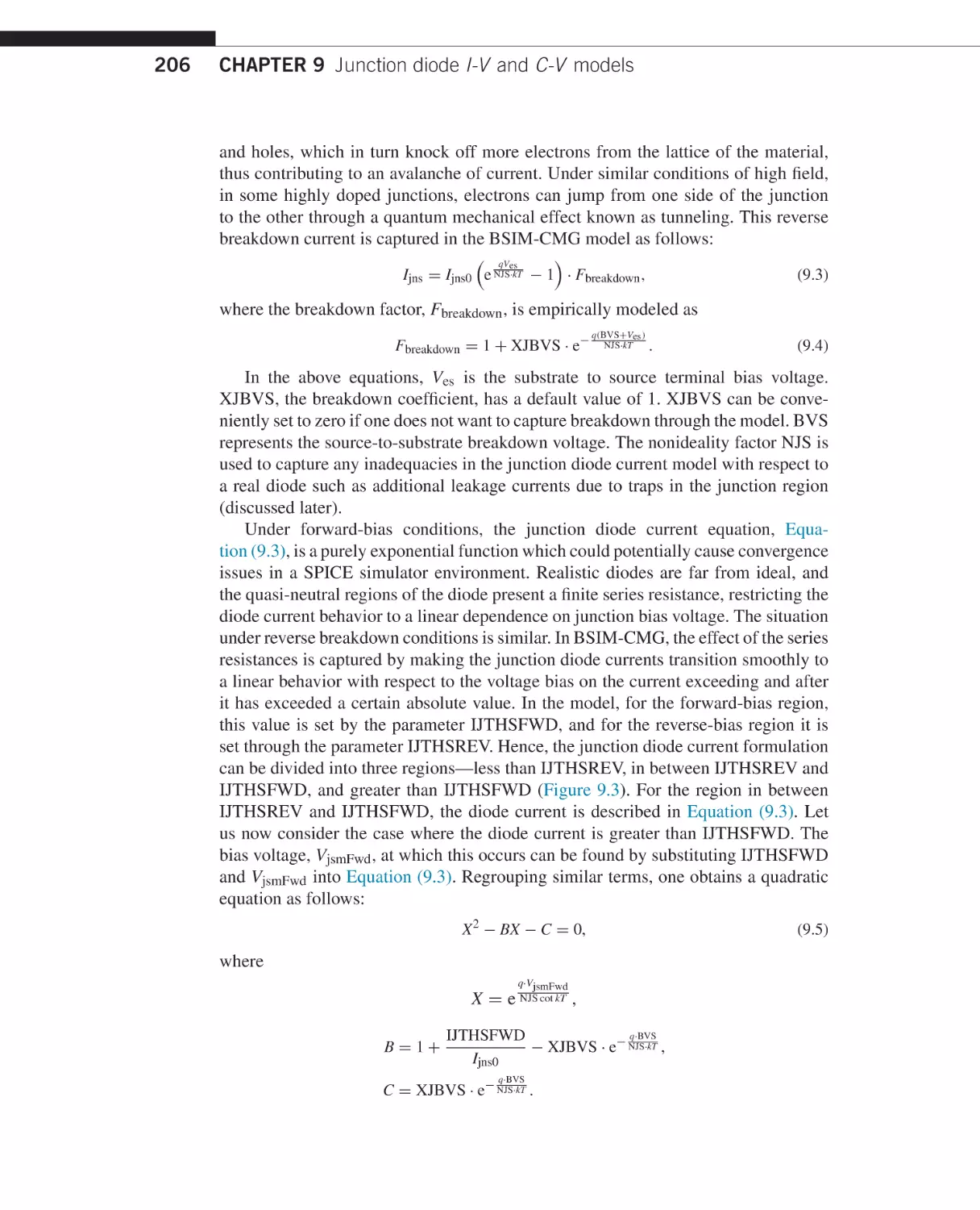
CHAPTER 1 FinFET—From device concept to standard compact model
compact model, BSIM. The BSIM FinFET model is enabling the design of new
generations of ICs with higher performance, lower power consumption, and higher
layout density.
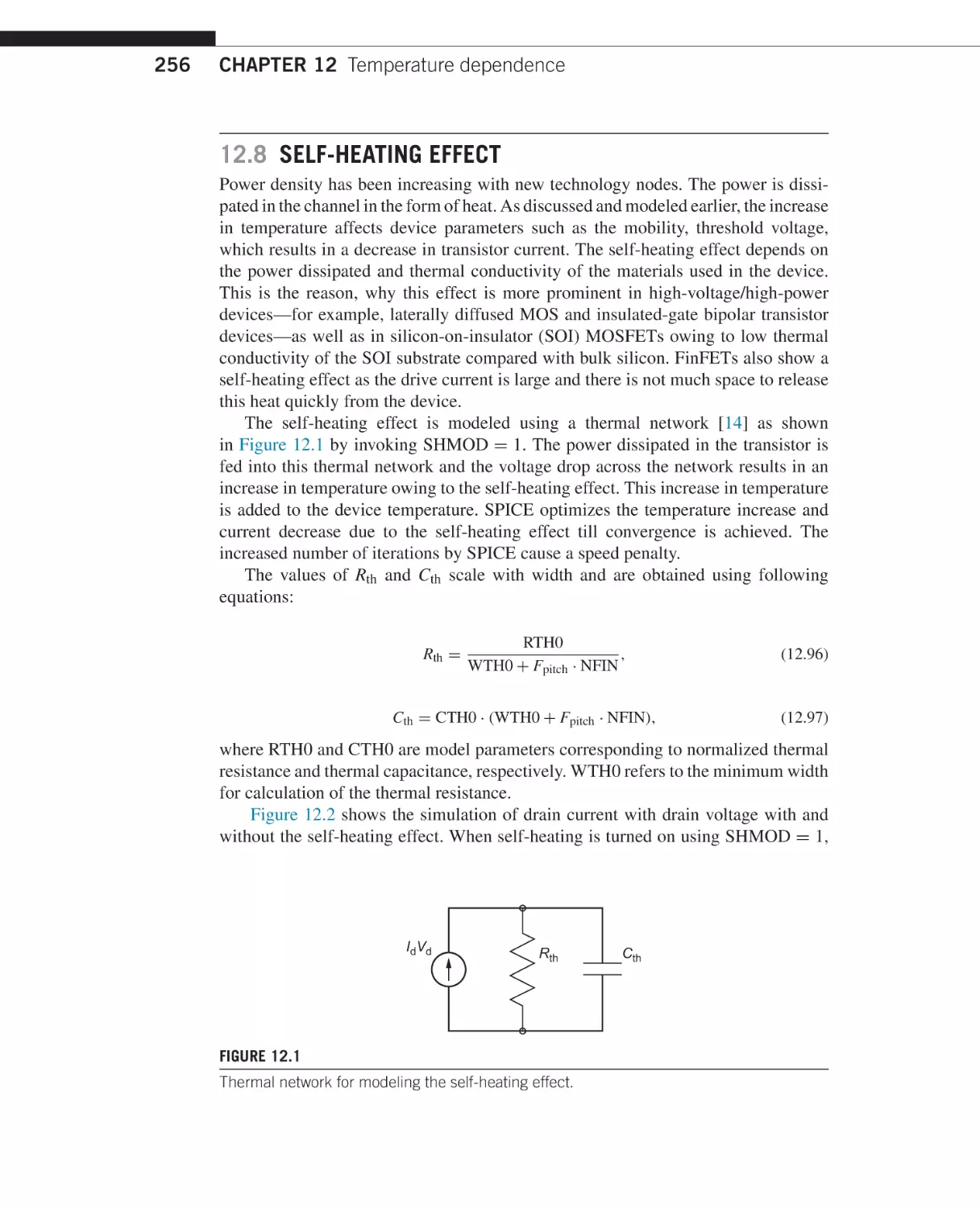
1.1 THE ROOT CAUSE OF SHORT-CHANNEL EFFECTS
IN THE TWENTY-FIRST CENTURY MOSFETs
What is the basic concept behind this remarkable FinFET? In order to understand the
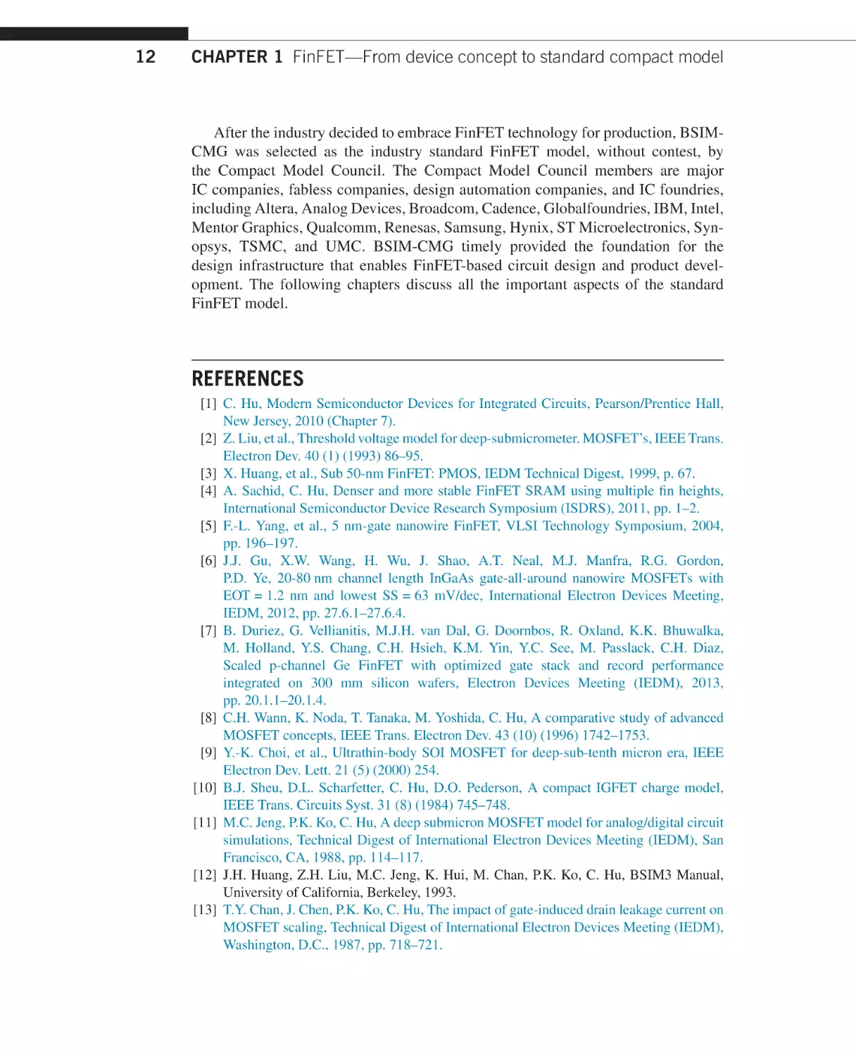
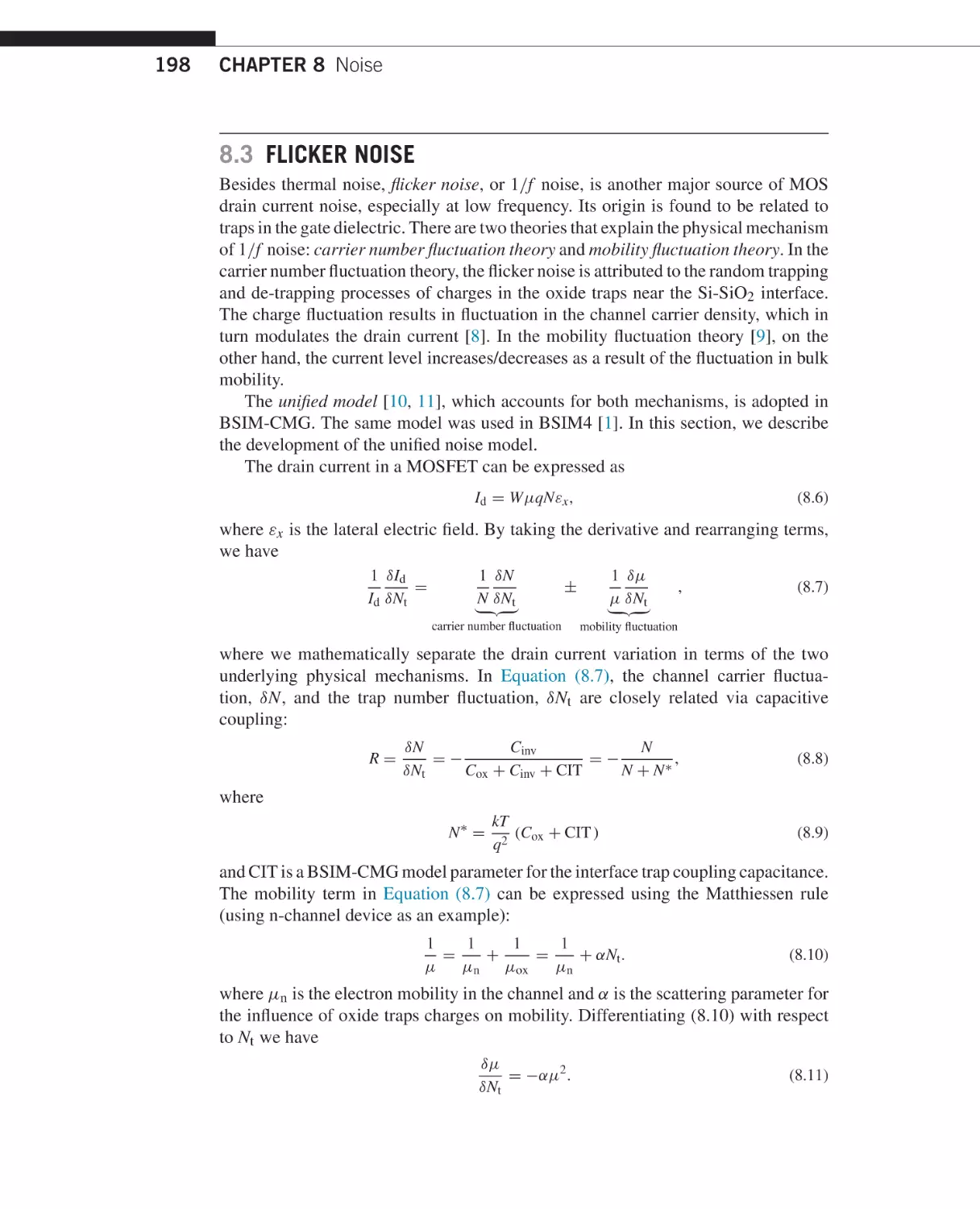
pain reliever, we must first understand the pain itself. As the gate length shrinks,
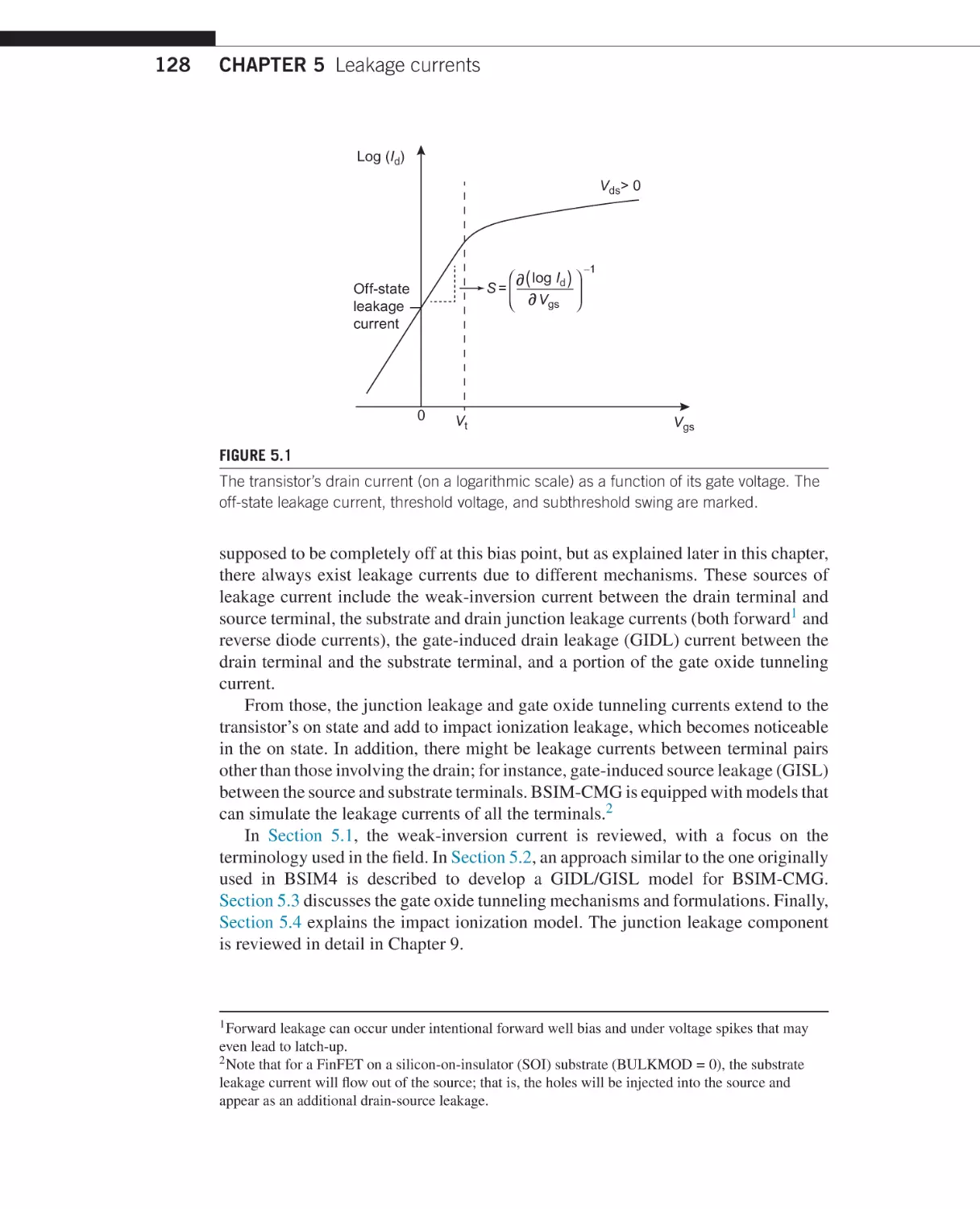
the MOSFET’s Id -Vg characteristics degrade in two major ways as illustrated in
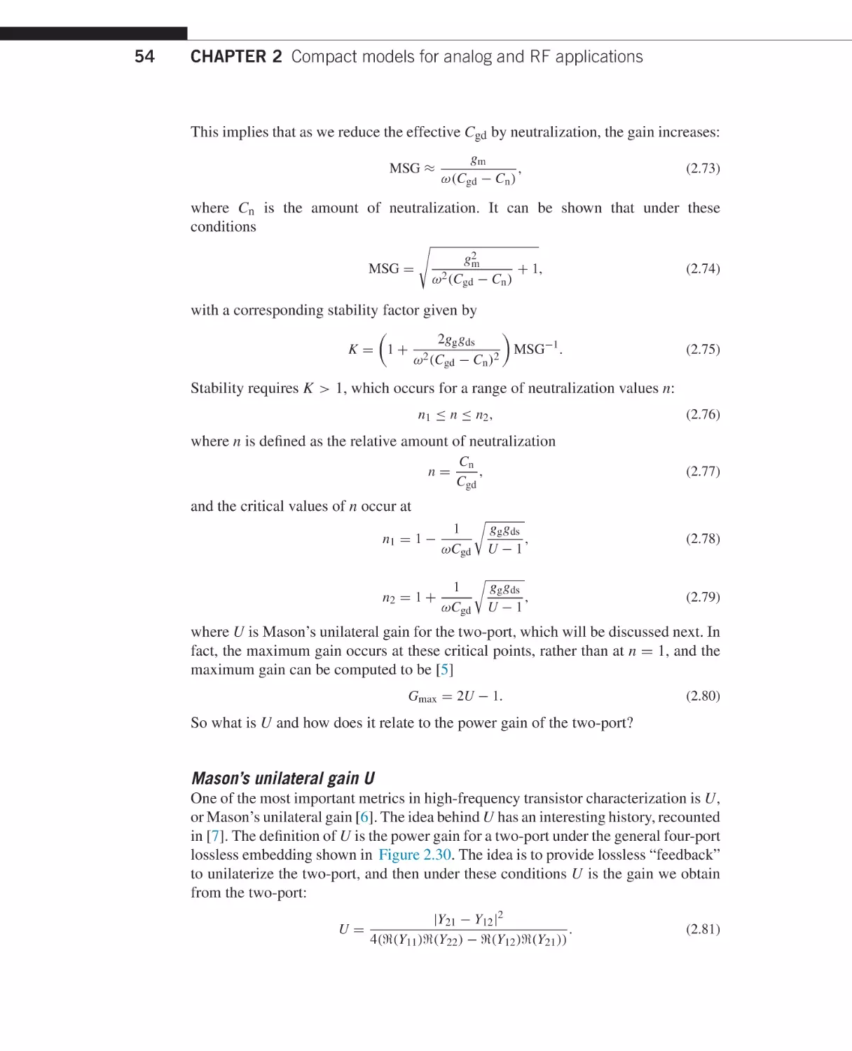
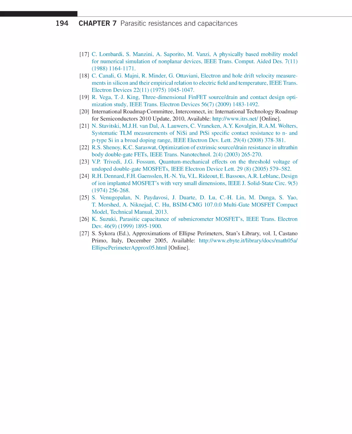
Figure 1.1. First, the subthreshold swing (S) degrades and Vt decreases—that is,
the device cannot be turned off easily by lowering Vg . Second, S and Vt become
increasingly sensitive to Lg variations—that is, device variations become more
problematic. These problems are known as short-channel effects.
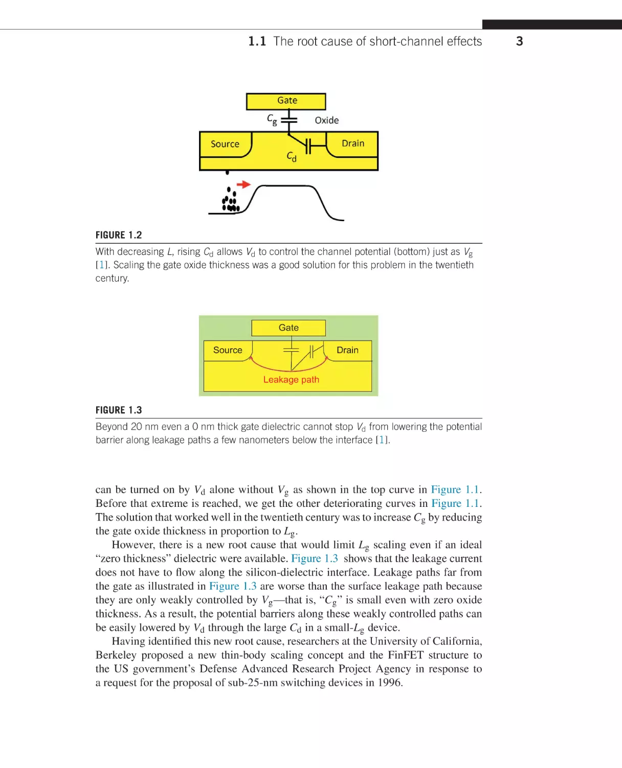
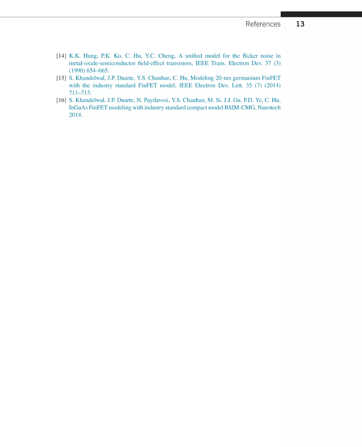
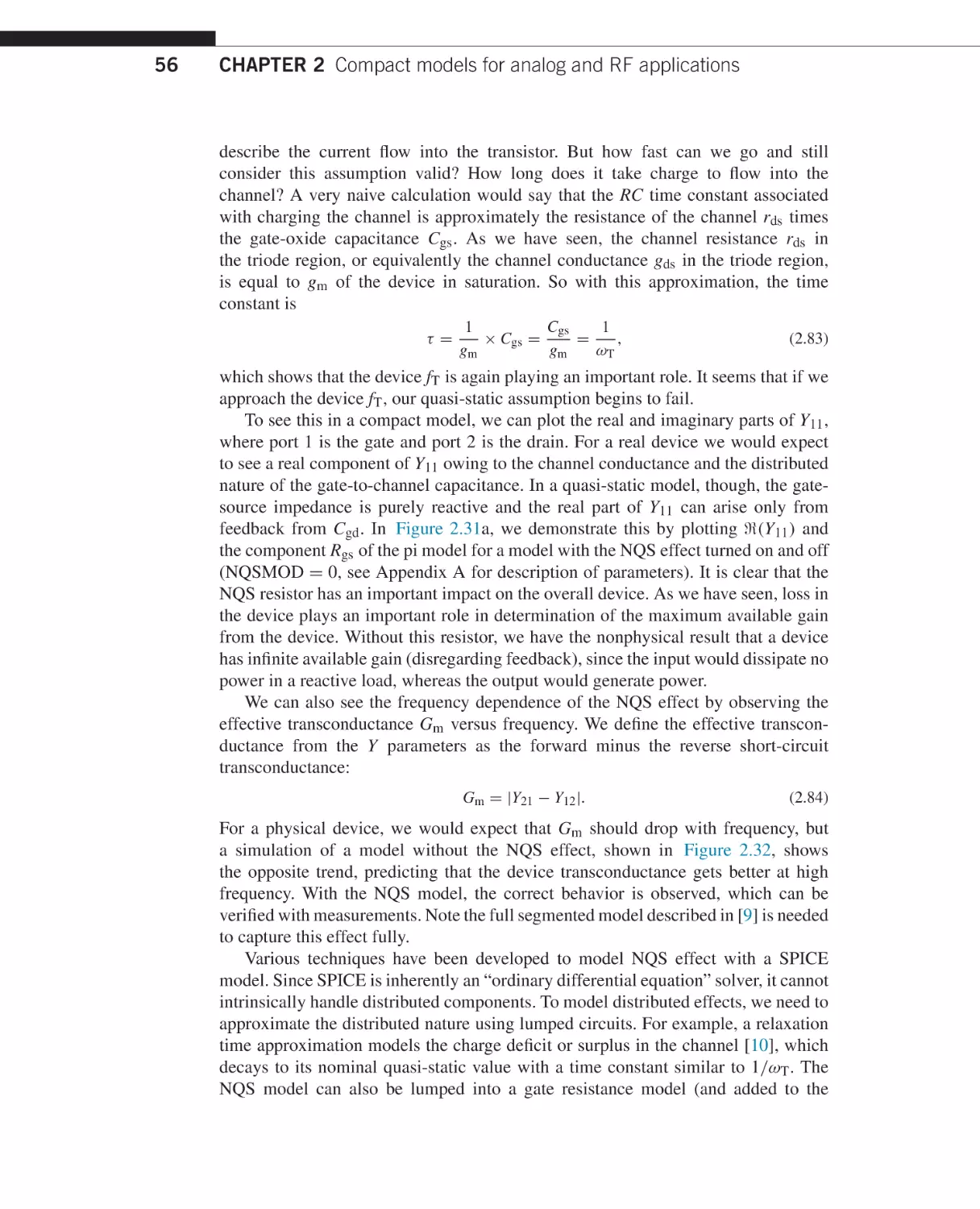
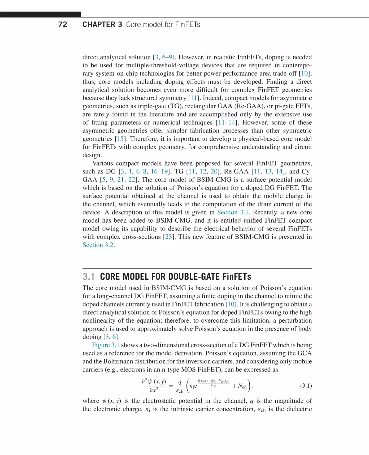
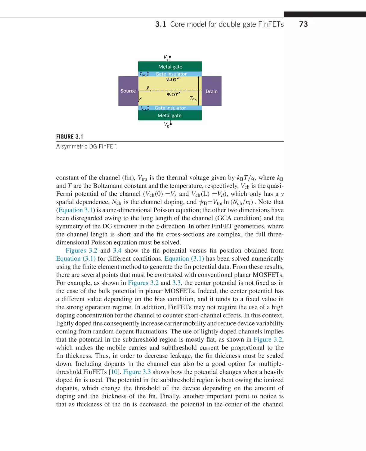
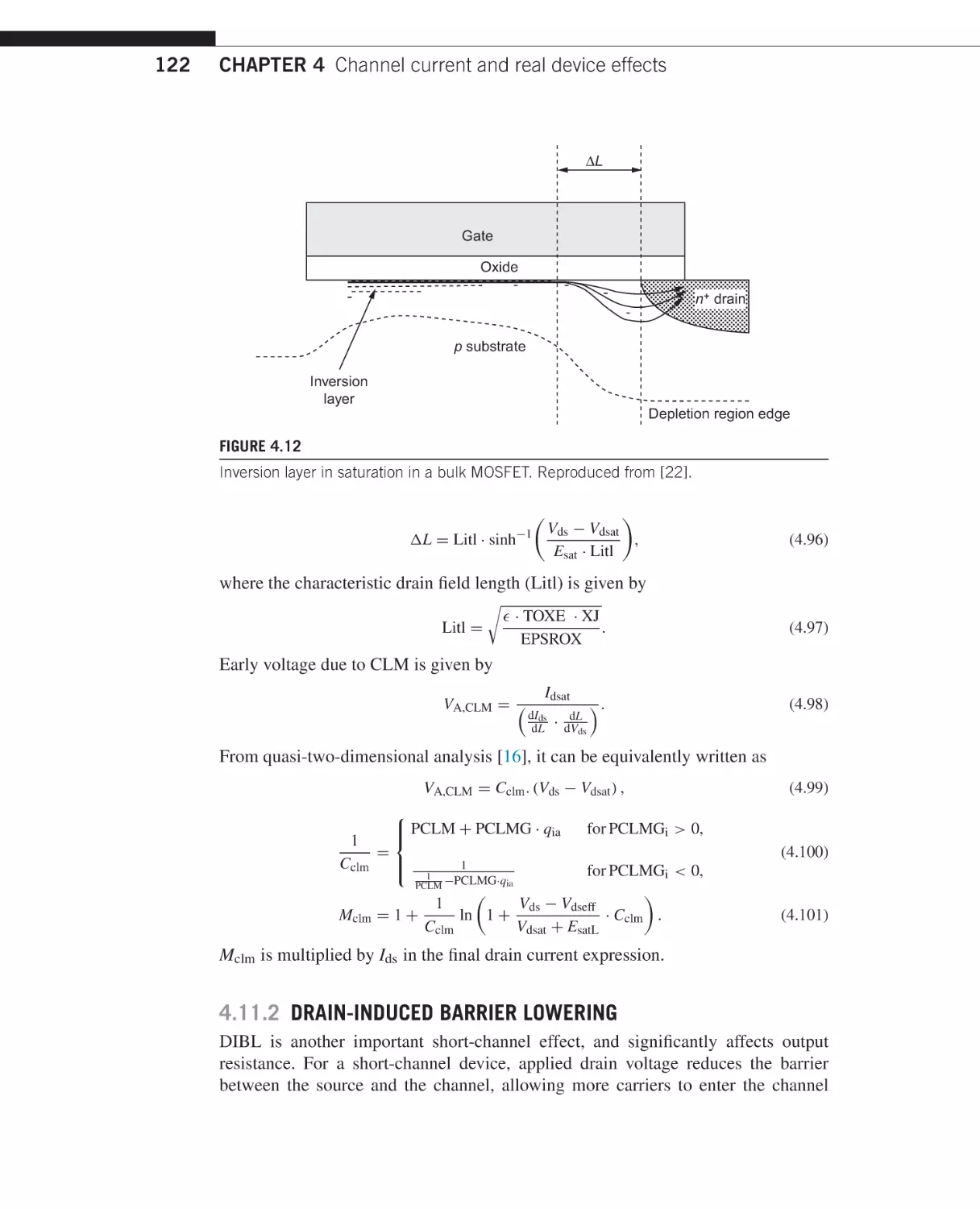
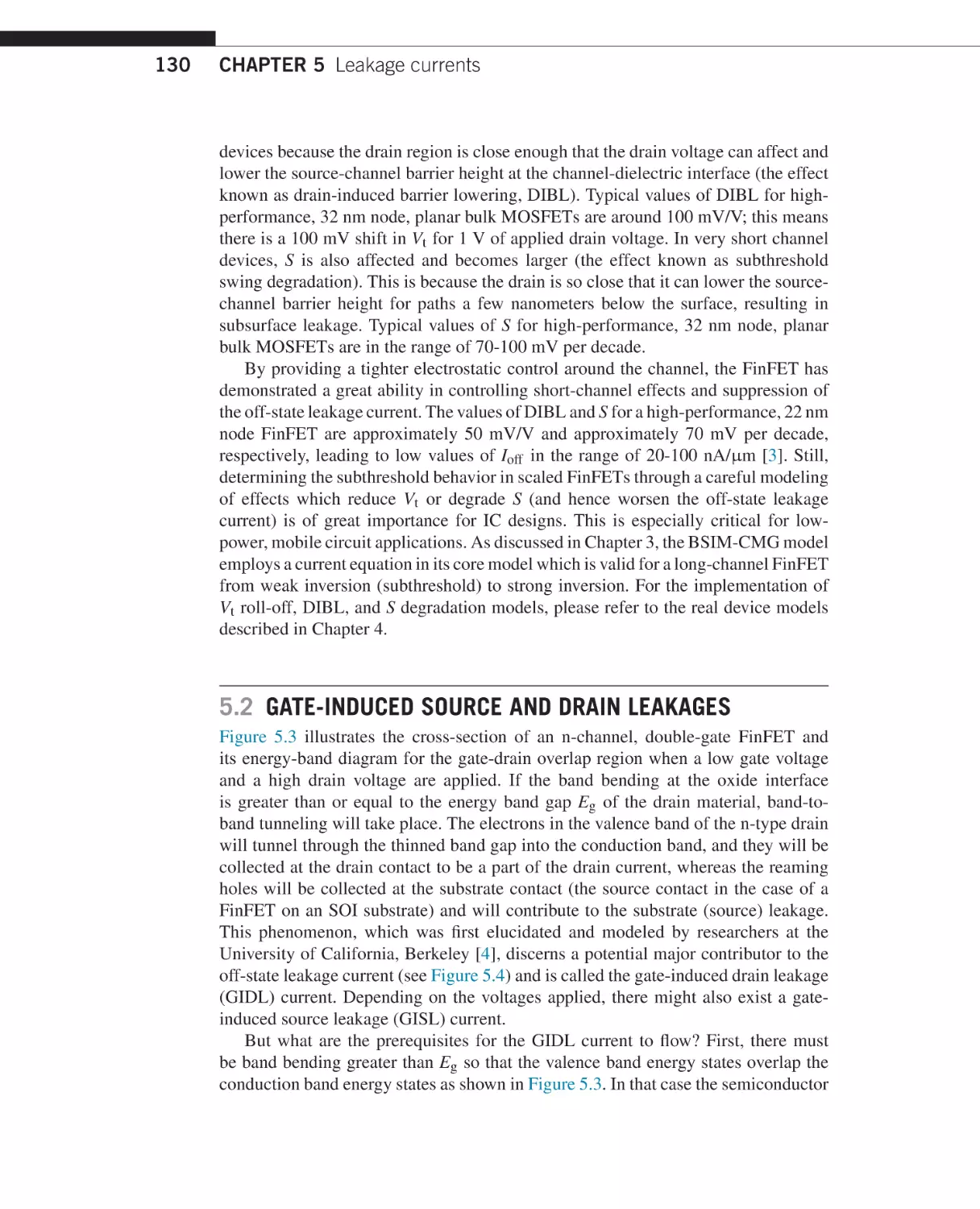
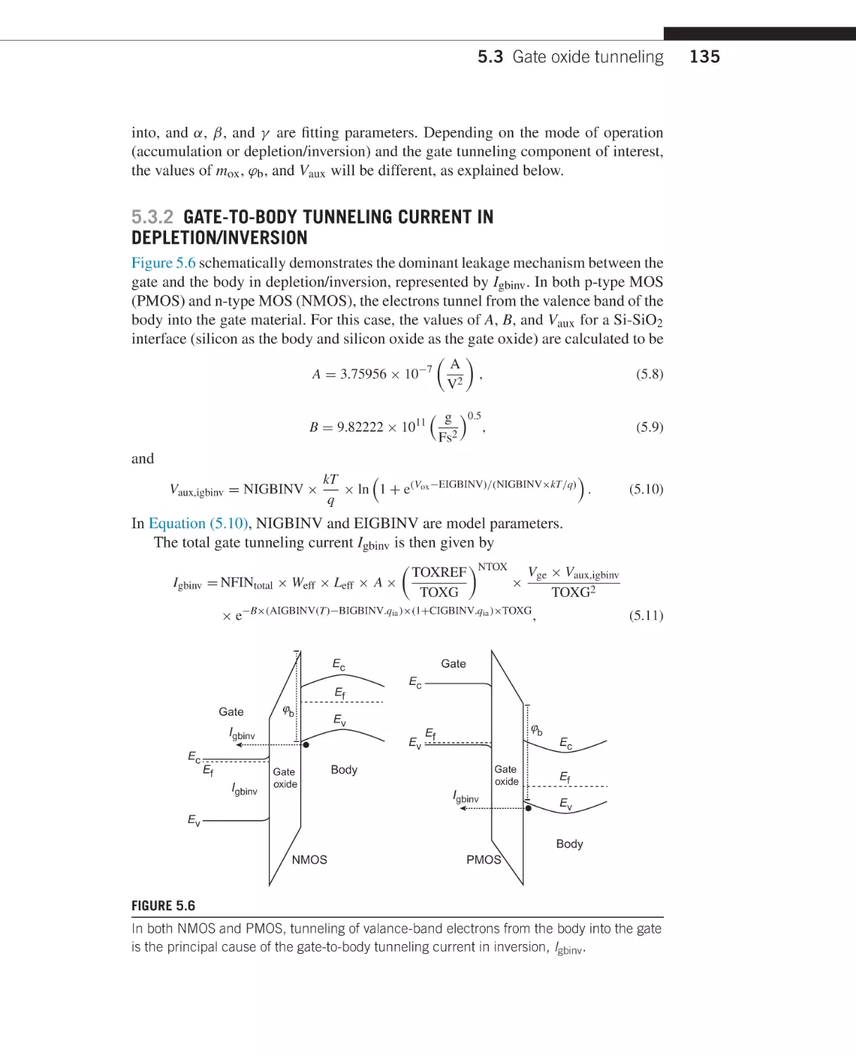
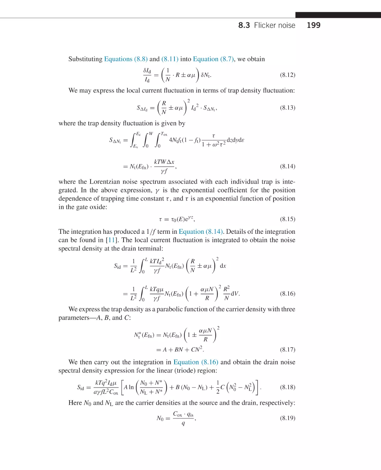
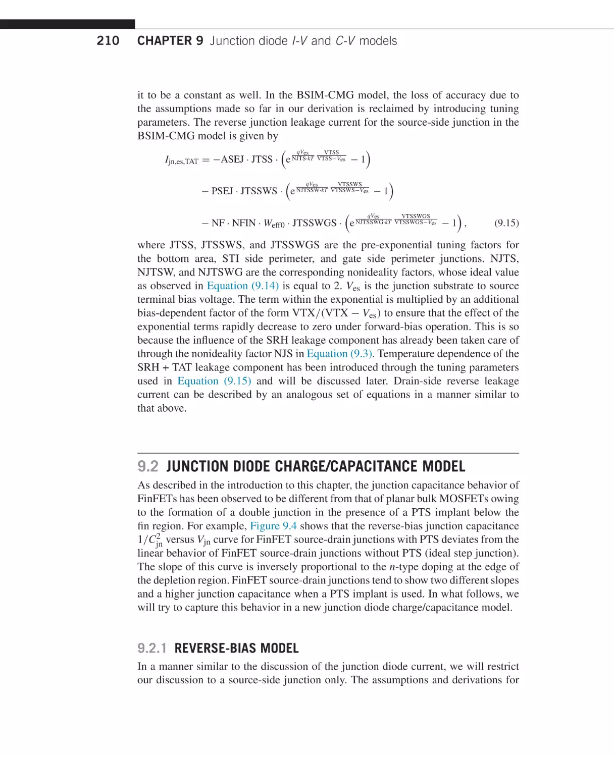
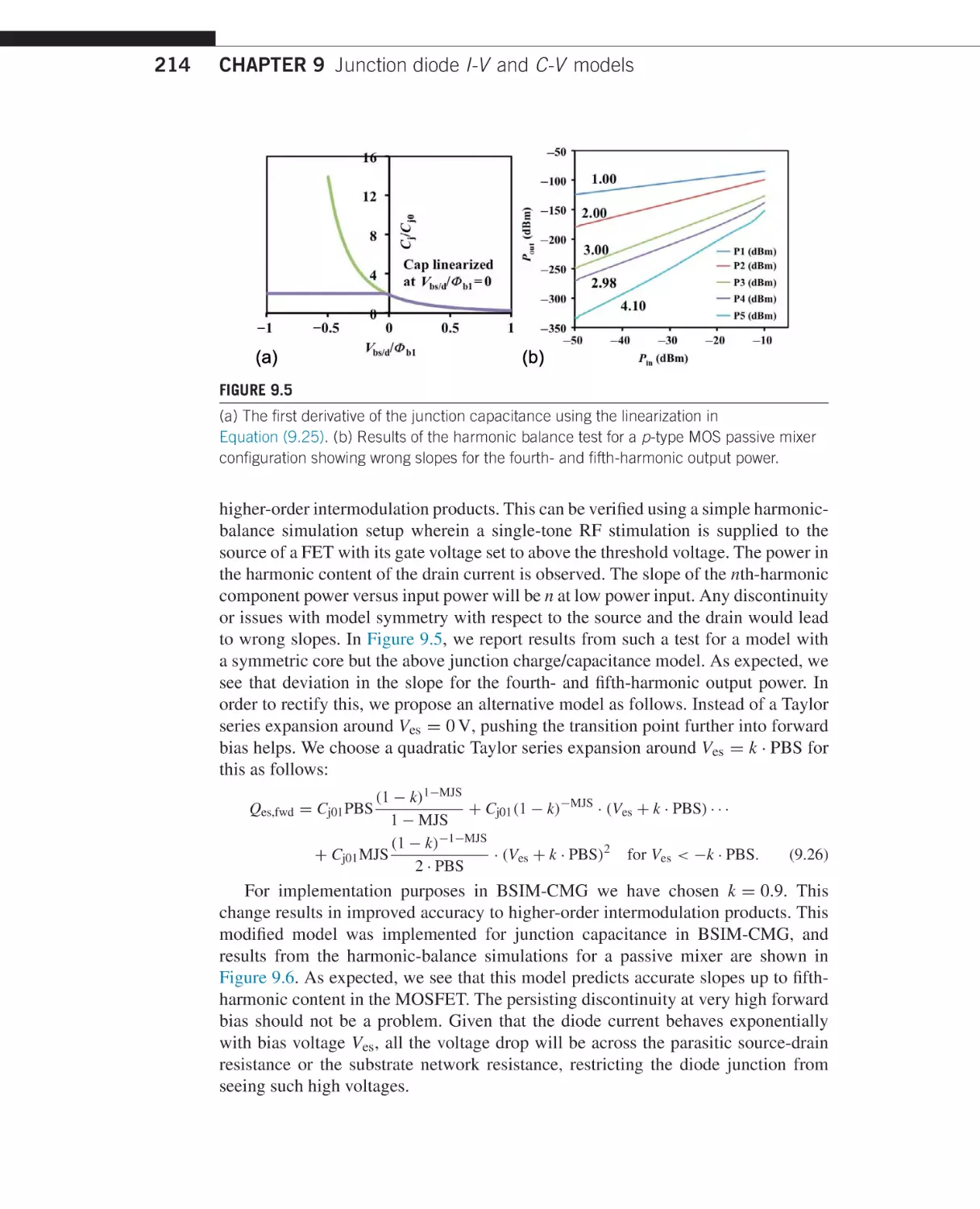
Figure 1.2 shows the root cause of short-channel effects in the twentieth century
MOSFETs [1]. A transistor is turned on and off when Vg lowers and raises the
potential of the channel (and thus the potential barrier between the channel and
the source) through the gate-to-channel capacitance, Cg . In an ideal transistor, the
channel potential is controlled only by Vg and Cg . In a real transistor, the channel
potential is also subjected to the influence of Vd through Cd . When Lg is large, Cd
is much smaller than Cg and the drain voltage does not interfere with Vg ’s role as
the sole controlling voltage. As Lg decreases, Cd increases [1, 2] and Vg loses its
absolute control. In extreme cases, Vg has less control than Vd and the transistor
10-3
Drain current, IDS (A/mm)
2
10-5
10-7
Size
shrink
10-9
10-11
0.0
0.3
0.6
0.9
Gate voltage, VGS (V)
FIGURE 1.1
Shrinking gate length makes the sub-Vt swing larger, and Vt and Ioff more sensitive to
gate critical dimension variation and random dopant fluctuation.
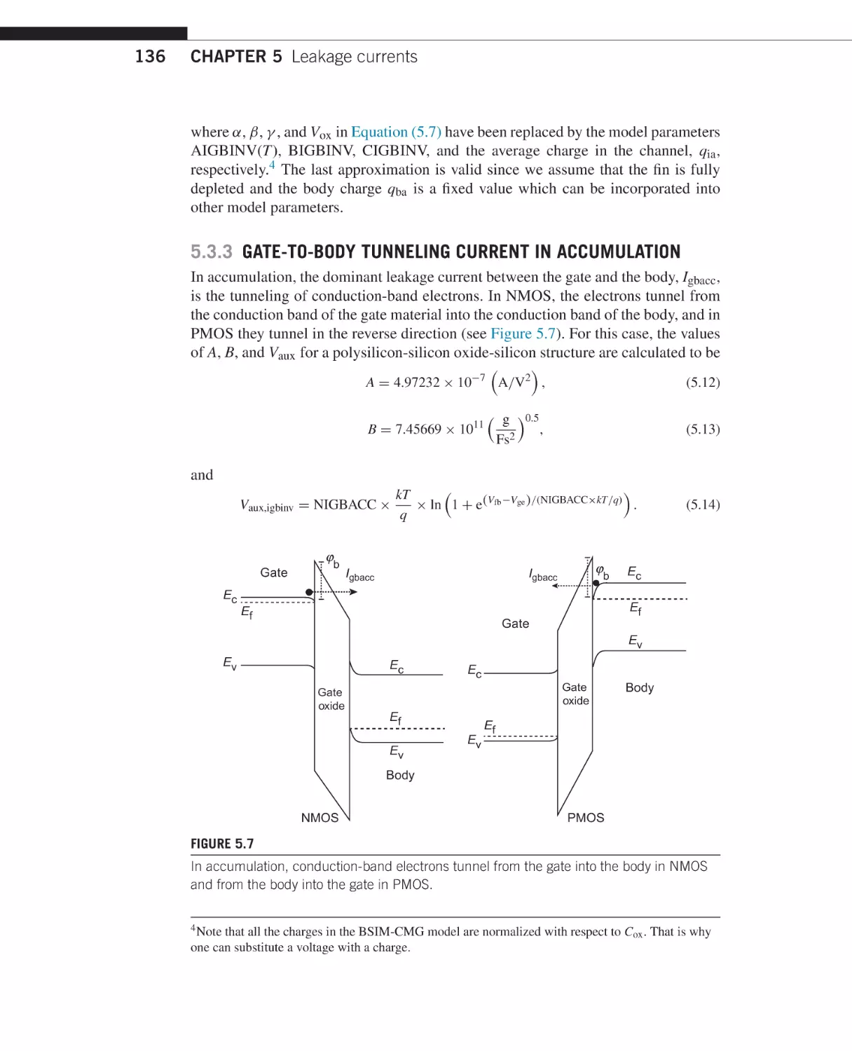
1.1 The root cause of short-channel effects
FIGURE 1.2
With decreasing L, rising Cd allows Vd to control the channel potential (bottom) just as Vg
[1]. Scaling the gate oxide thickness was a good solution for this problem in the twentieth
century.
Gate
Source
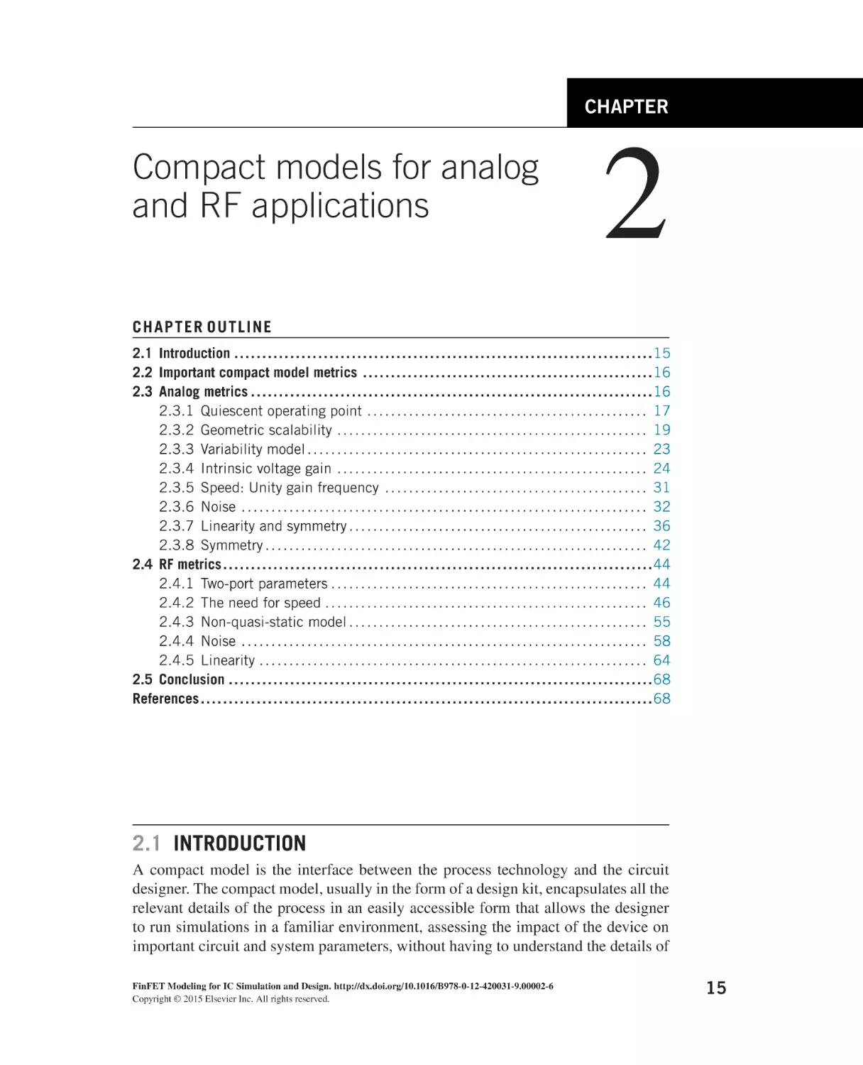
Drain
Leakage path
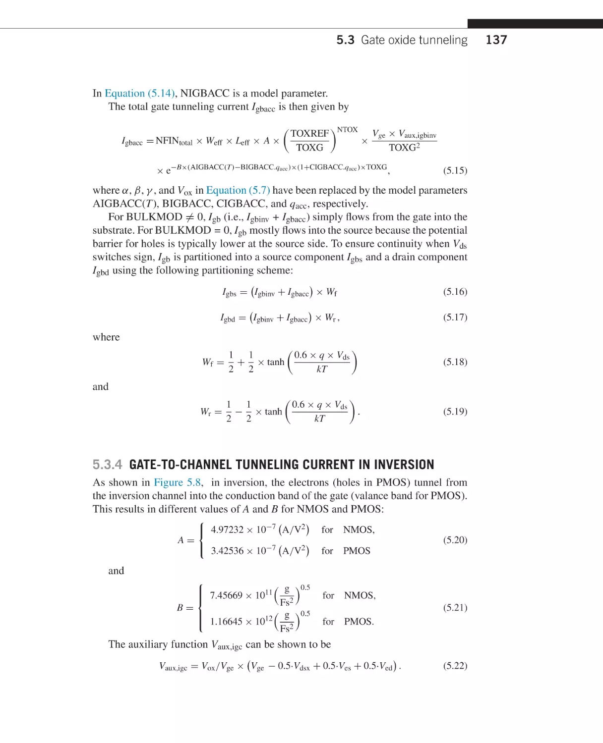
FIGURE 1.3
Beyond 20 nm even a 0 nm thick gate dielectric cannot stop Vd from lowering the potential
barrier along leakage paths a few nanometers below the interface [1].
can be turned on by Vd alone without Vg as shown in the top curve in Figure 1.1.
Before that extreme is reached, we get the other deteriorating curves in Figure 1.1.
The solution that worked well in the twentieth century was to increase Cg by reducing
the gate oxide thickness in proportion to Lg .
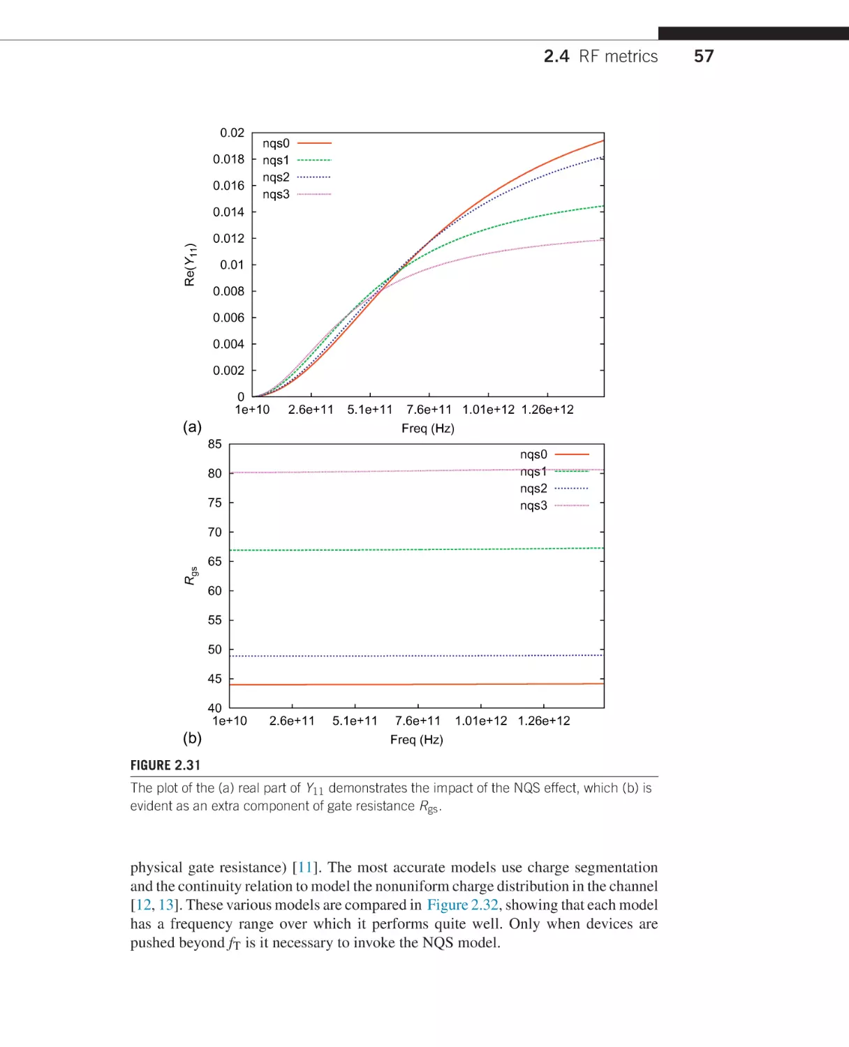
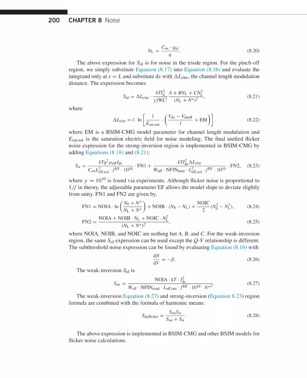
However, there is a new root cause that would limit Lg scaling even if an ideal
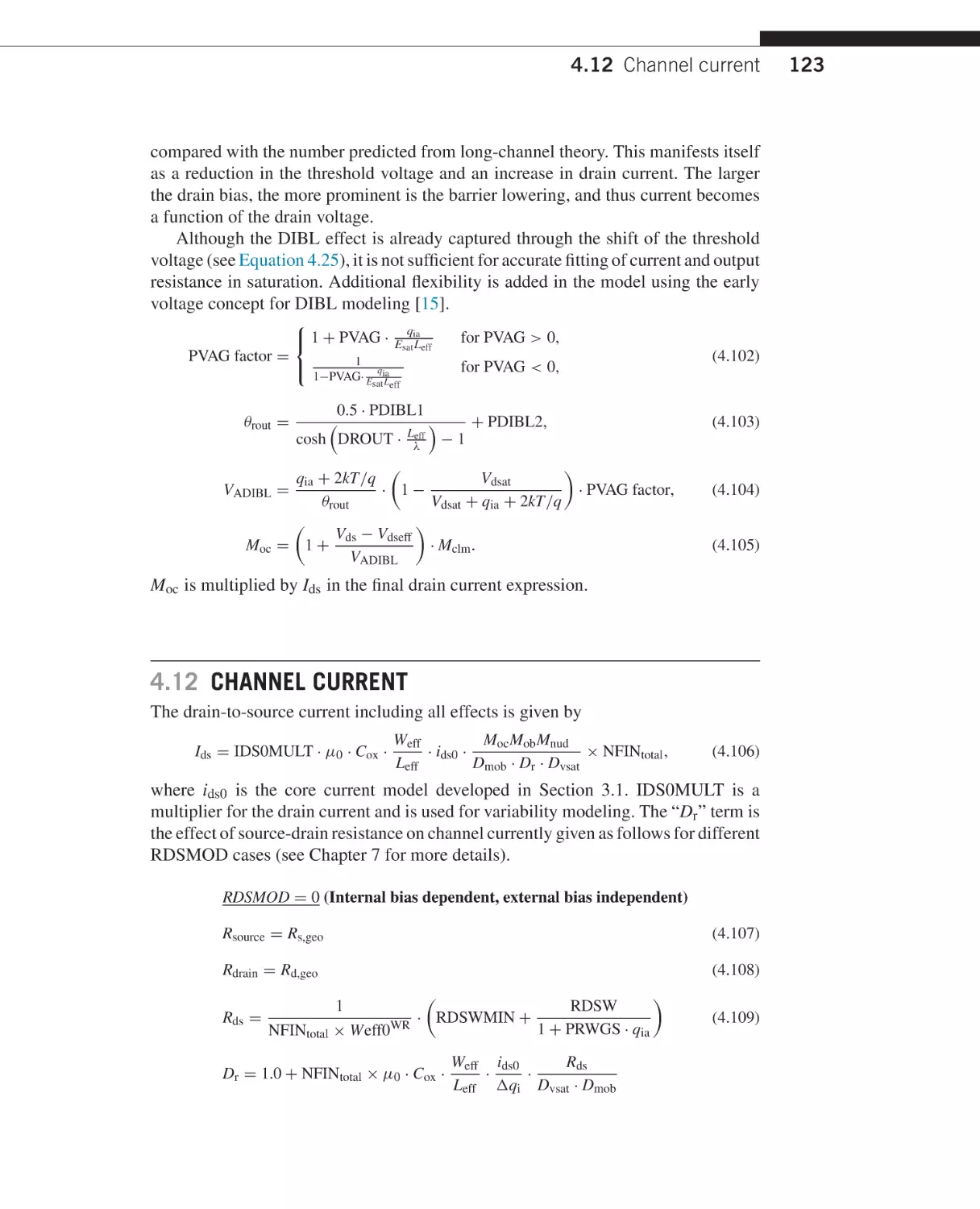
“zero thickness” dielectric were available. Figure 1.3 shows that the leakage current
does not have to flow along the silicon-dielectric interface. Leakage paths far from
the gate as illustrated in Figure 1.3 are worse than the surface leakage path because
they are only weakly controlled by Vg —that is, “Cg ” is small even with zero oxide
thickness. As a result, the potential barriers along these weakly controlled paths can
be easily lowered by Vd through the large Cd in a small-Lg device.
Having identified this new root cause, researchers at the University of California,
Berkeley proposed a new thin-body scaling concept and the FinFET structure to
the US government’s Defense Advanced Research Project Agency in response to
a request for the proposal of sub-25-nm switching devices in 1996.
3
4
CHAPTER 1 FinFET—From device concept to standard compact model
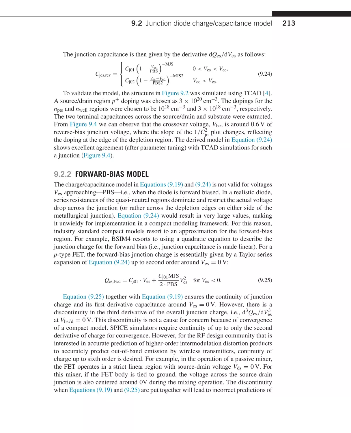
FIGURE 1.4
A thin silicon body eliminates the leakage paths in Figure 1.3 (top) and leakage current
density is low near the gate and highest in the center of the body (bottom) [1].
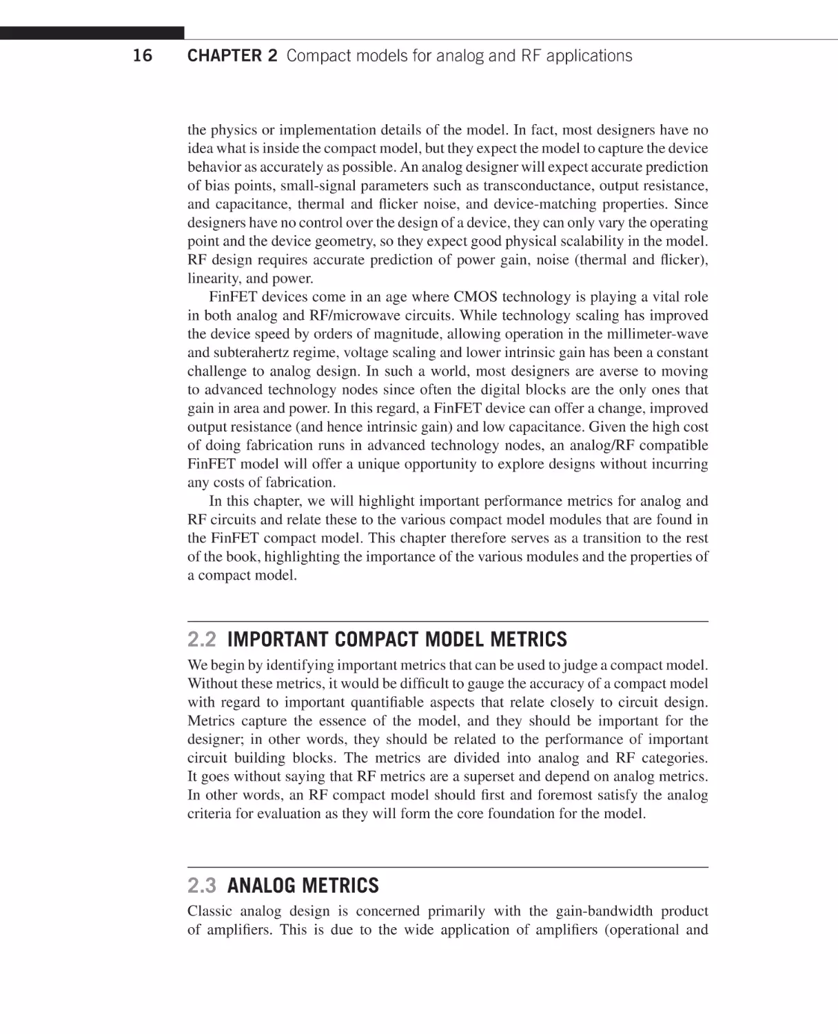
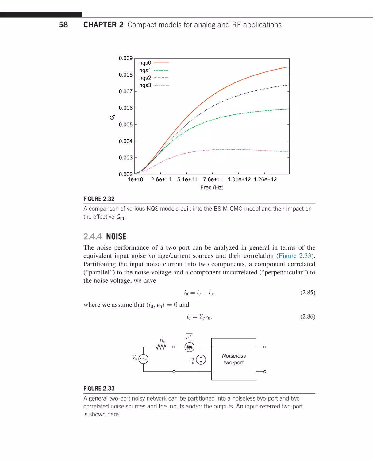
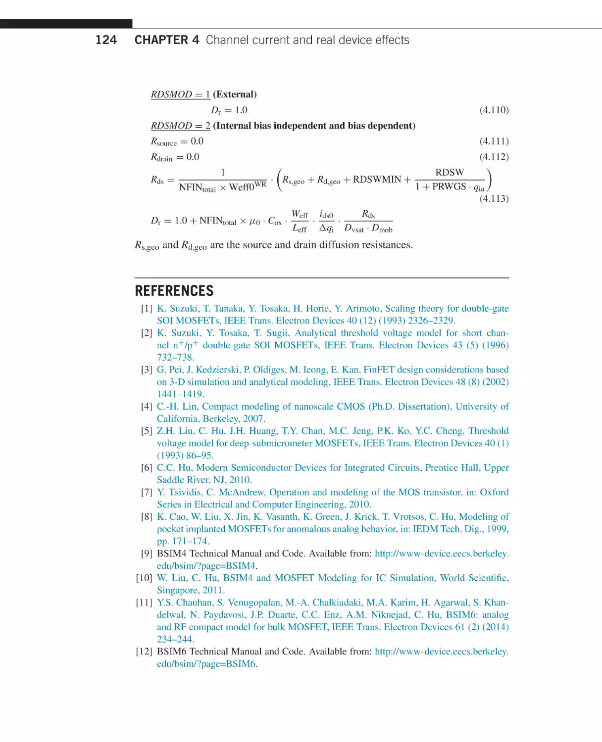
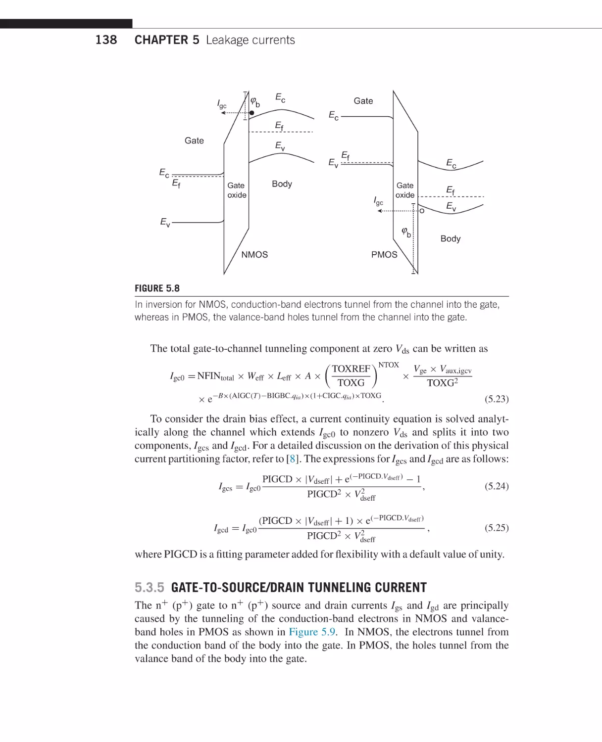
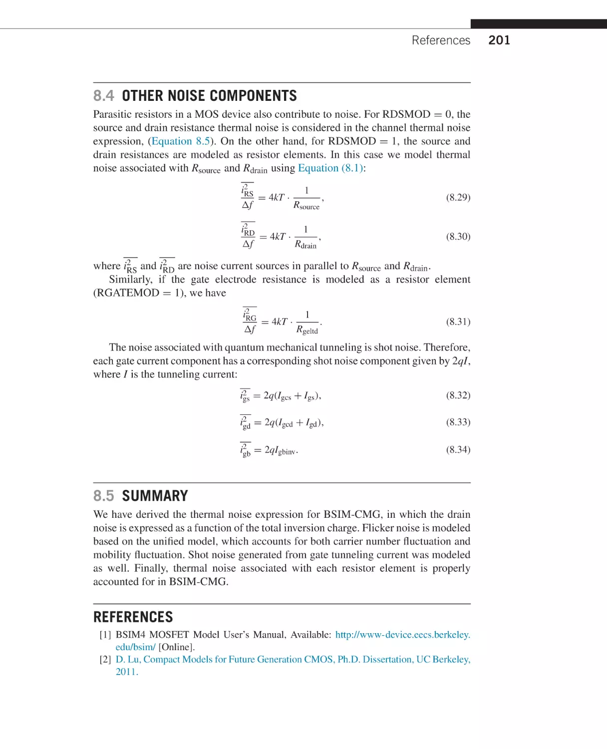
1.2 THE THIN-BODY MOSFET CONCEPT
Figure 1.4 shows a MOSFET whose body is a thin piece of silicon with gates
above and below it. If the body is thin, any lines drawn between the source and
the drain (any potential leakage paths) would not be far from one or the other
gate. The thin-body concept eliminates the need for heavy channel doping for
suppressing the short-channel effects. Channel doping may still be used to adjust
the threshold voltage in the near term, but that function can be performed by gate
metal work function engineering in order to realize the full potential of future thinbody transistors. Random dopant fluctuation, a major and fundamental contributor to
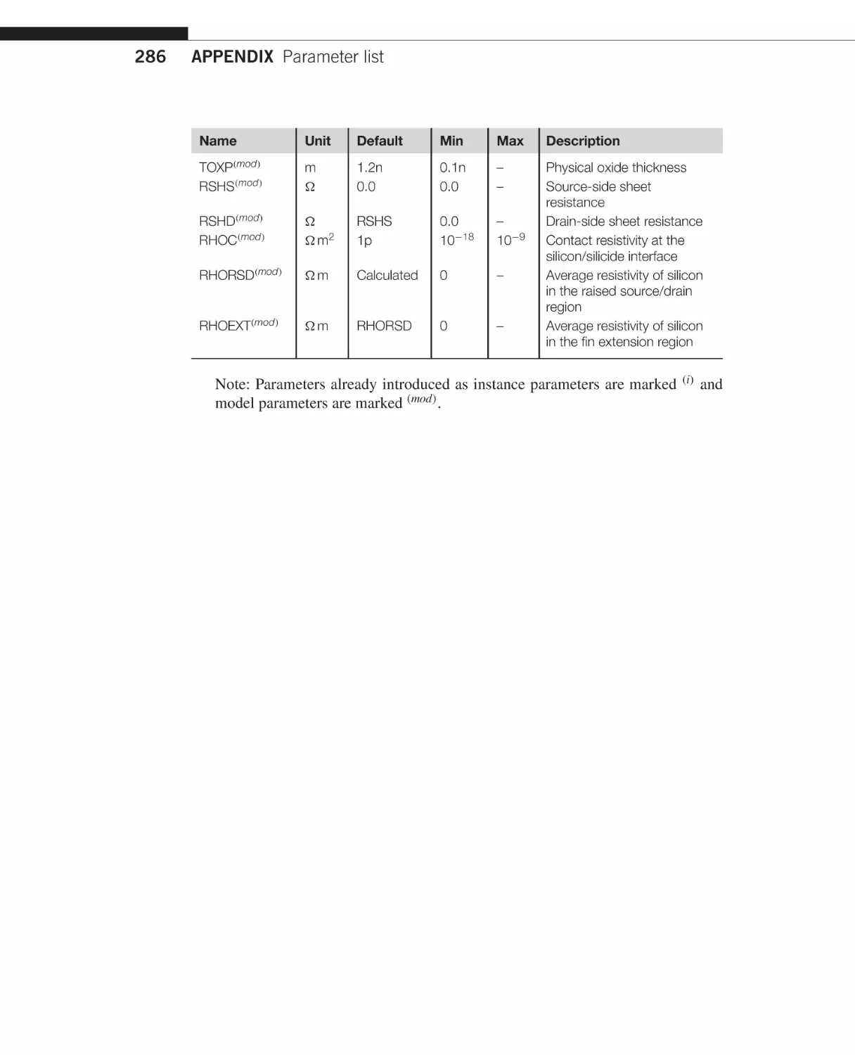
device variation, can be eliminated. Channel carrier mobility and junction leakage are
improved. An undoped body reduces the electric field normal to the semiconductor
and oxide interface. This should improve the temperature bias instability (negativebias temperature instability and positive-bias temperature instability) and the gate
dielectric tunneling leakage and wear out.
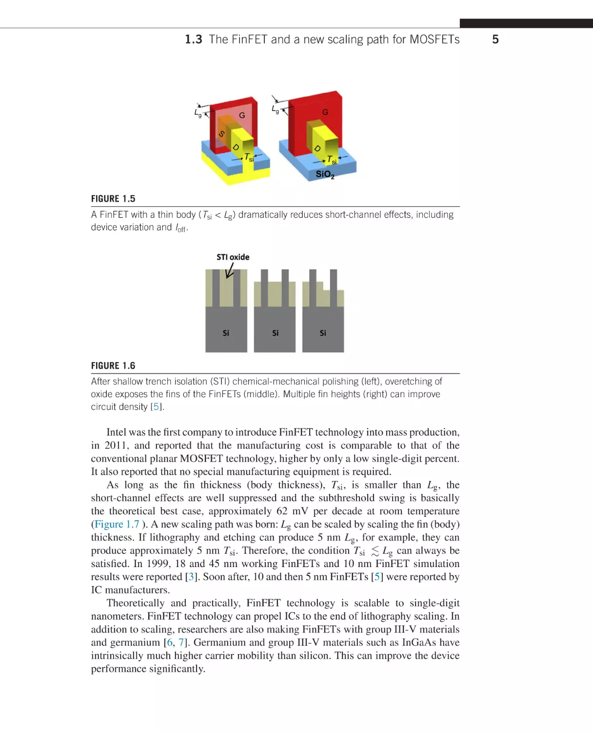
1.3 THE FinFET AND A NEW SCALING PATH FOR MOSFETs
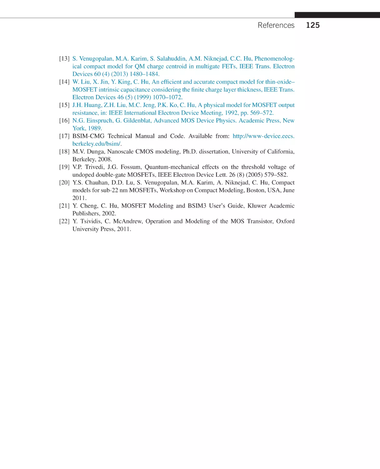
The FinFET in Figure 1.5 is a manufacturable version of the thin-body transistor
in Figure 1.4. The thin body is shaped like a fish fin and is created with the
usual patterning and etching technologies. The fin can be constructed on silicon-oninsulator (SOI) or lower-cost bulk substrates. The fin is then processed into a FinFET
in very much the same way as for processing of a planar MOSFET because the fin is
shorter than the gate thickness, so the structure is quasi-planar.
A FinFET is dense and manufacturable. Figure 1.6 shows that the only major
new fabrication step is overetching of the shallow trench isolation oxide. A FinFET
occupies less silicon area than a planar MOSFET because the channel width (W) of
a FinFET [3] is the peripheral length of the fin that includes all sides of the fin crosssection, and W can be significantly larger than the fin pitch. The multiple fin height
[4] in Figure 1.6 can improve the density of SRAM. In the future, a fin height increase
may supplement lithography shrinkage.
1.3 The FinFET and a new scaling path for MOSFETs
Lg
G
Lg
G
S
D
D
Tsi
Tsi
SiO2
FIGURE 1.5
A FinFET with a thin body (Tsi < Lg ) dramatically reduces short-channel effects, including
device variation and Ioff .
FIGURE 1.6
After shallow trench isolation (STI) chemical-mechanical polishing (left), overetching of
oxide exposes the fins of the FinFETs (middle). Multiple fin heights (right) can improve
circuit density [5].
Intel was the first company to introduce FinFET technology into mass production,
in 2011, and reported that the manufacturing cost is comparable to that of the
conventional planar MOSFET technology, higher by only a low single-digit percent.
It also reported that no special manufacturing equipment is required.
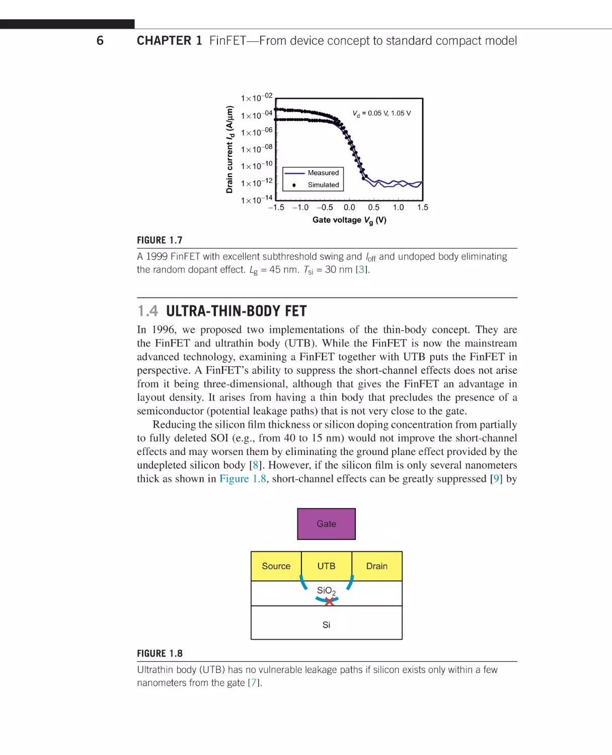
As long as the fin thickness (body thickness), Tsi , is smaller than Lg , the
short-channel effects are well suppressed and the subthreshold swing is basically
the theoretical best case, approximately 62 mV per decade at room temperature
(Figure 1.7 ). A new scaling path was born: Lg can be scaled by scaling the fin (body)
thickness. If lithography and etching can produce 5 nm Lg , for example, they can
produce approximately 5 nm Tsi . Therefore, the condition Tsi Lg can always be
satisfied. In 1999, 18 and 45 nm working FinFETs and 10 nm FinFET simulation
results were reported [3]. Soon after, 10 and then 5 nm FinFETs [5] were reported by
IC manufacturers.
Theoretically and practically, FinFET technology is scalable to single-digit
nanometers. FinFET technology can propel ICs to the end of lithography scaling. In
addition to scaling, researchers are also making FinFETs with group III-V materials
and germanium [6, 7]. Germanium and group III-V materials such as InGaAs have
intrinsically much higher carrier mobility than silicon. This can improve the device
performance significantly.
5
CHAPTER 1 FinFET—From device concept to standard compact model
1 × 10−02
Drain current Id (A/mm)
6
1 × 10−04
Vd = 0.05 V, 1.05 V
1 × 10−06
1 × 10−08
1 × 10⁻¹⁰
Measured
1 × 10⁻¹²
1 × 10⁻¹⁴
−1.5
Simulated
−1.0
−0.5
0.0
0.5
1.0
1.5
Gate voltage Vg (V)
FIGURE 1.7
A 1999 FinFET with excellent subthreshold swing and Ioff and undoped body eliminating
the random dopant effect. Lg = 45 nm. Tsi = 30 nm [3].
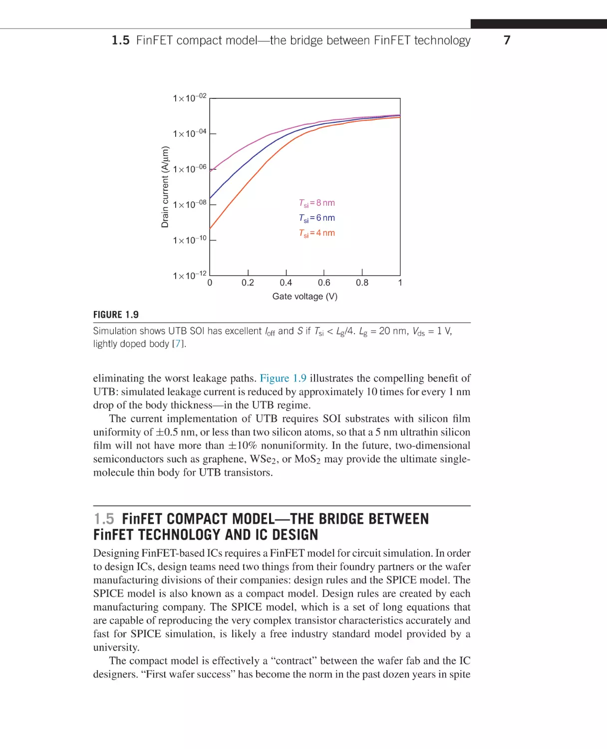
1.4 ULTRA-THIN-BODY FET
In 1996, we proposed two implementations of the thin-body concept. They are
the FinFET and ultrathin body (UTB). While the FinFET is now the mainstream
advanced technology, examining a FinFET together with UTB puts the FinFET in
perspective. A FinFET’s ability to suppress the short-channel effects does not arise
from it being three-dimensional, although that gives the FinFET an advantage in
layout density. It arises from having a thin body that precludes the presence of a
semiconductor (potential leakage paths) that is not very close to the gate.
Reducing the silicon film thickness or silicon doping concentration from partially
to fully deleted SOI (e.g., from 40 to 15 nm) would not improve the short-channel
effects and may worsen them by eliminating the ground plane effect provided by the
undepleted silicon body [8]. However, if the silicon film is only several nanometers
thick as shown in Figure 1.8, short-channel effects can be greatly suppressed [9] by
Gate
Source
UTB
Drain
SiO2
Si
FIGURE 1.8
Ultrathin body (UTB) has no vulnerable leakage paths if silicon exists only within a few
nanometers from the gate [7].
1.5 FinFET compact model—the bridge between FinFET technology
1 × 10−02
Drain current (A/µm)
1 × 10−04
1 × 10−06
Tsi = 8 nm
1 × 10−08
Tsi = 6 nm
Tsi = 4 nm
1 × 10⁻¹⁰
1 × 10⁻¹²
0
0.2
0.4
0.6
0.8
1
Gate voltage (V)
FIGURE 1.9
Simulation shows UTB SOI has excellent Ioff and S if Tsi < Lg /4. Lg = 20 nm, Vds = 1 V,
lightly doped body [7].
eliminating the worst leakage paths. Figure 1.9 illustrates the compelling benefit of
UTB: simulated leakage current is reduced by approximately 10 times for every 1 nm
drop of the body thickness—in the UTB regime.
The current implementation of UTB requires SOI substrates with silicon film
uniformity of ±0.5 nm, or less than two silicon atoms, so that a 5 nm ultrathin silicon
film will not have more than ±10% nonuniformity. In the future, two-dimensional
semiconductors such as graphene, WSe2 , or MoS2 may provide the ultimate singlemolecule thin body for UTB transistors.
1.5 FinFET COMPACT MODEL—THE BRIDGE BETWEEN
FinFET TECHNOLOGY AND IC DESIGN
Designing FinFET-based ICs requires a FinFET model for circuit simulation. In order
to design ICs, design teams need two things from their foundry partners or the wafer
manufacturing divisions of their companies: design rules and the SPICE model. The
SPICE model is also known as a compact model. Design rules are created by each
manufacturing company. The SPICE model, which is a set of long equations that
are capable of reproducing the very complex transistor characteristics accurately and
fast for SPICE simulation, is likely a free industry standard model provided by a
university.
The compact model is effectively a “contract” between the wafer fab and the IC
designers. “First wafer success” has become the norm in the past dozen years in spite
7
8
CHAPTER 1 FinFET—From device concept to standard compact model
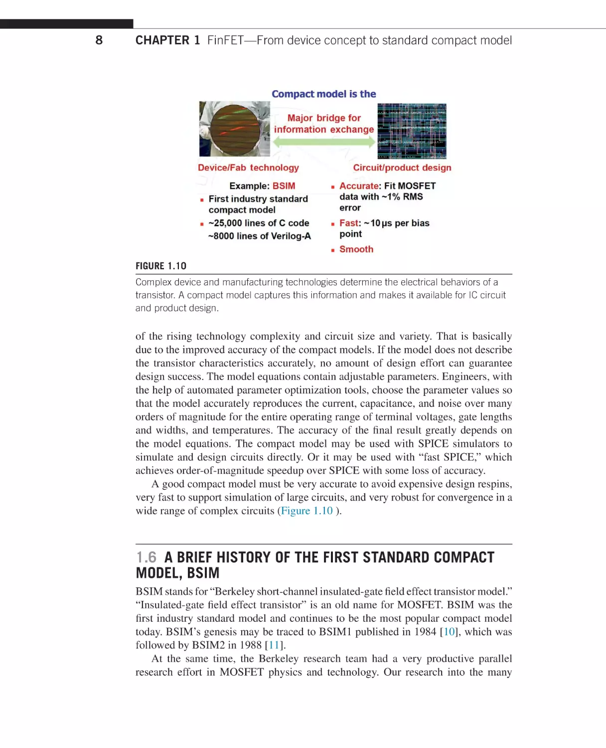
FIGURE 1.10
Complex device and manufacturing technologies determine the electrical behaviors of a
transistor. A compact model captures this information and makes it available for IC circuit
and product design.
of the rising technology complexity and circuit size and variety. That is basically
due to the improved accuracy of the compact models. If the model does not describe
the transistor characteristics accurately, no amount of design effort can guarantee
design success. The model equations contain adjustable parameters. Engineers, with
the help of automated parameter optimization tools, choose the parameter values so
that the model accurately reproduces the current, capacitance, and noise over many
orders of magnitude for the entire operating range of terminal voltages, gate lengths
and widths, and temperatures. The accuracy of the final result greatly depends on
the model equations. The compact model may be used with SPICE simulators to
simulate and design circuits directly. Or it may be used with “fast SPICE,” which
achieves order-of-magnitude speedup over SPICE with some loss of accuracy.
A good compact model must be very accurate to avoid expensive design respins,
very fast to support simulation of large circuits, and very robust for convergence in a
wide range of complex circuits (Figure 1.10 ).
1.6 A BRIEF HISTORY OF THE FIRST STANDARD COMPACT
MODEL, BSIM
BSIM stands for “Berkeley short-channel insulated-gate field effect transistor model.”
“Insulated-gate field effect transistor” is an old name for MOSFET. BSIM was the
first industry standard model and continues to be the most popular compact model
today. BSIM’s genesis may be traced to BSIM1 published in 1984 [10], which was
followed by BSIM2 in 1988 [11].
At the same time, the Berkeley research team had a very productive parallel
research effort in MOSFET physics and technology. Our research into the many
1.7 Core and real-device models
devices’ physics effects and behaviors of aggressively scaled MOSFETs gradually
built a collection of models for Vt dependence of bias and gate length, mobility
degradation, velocity saturation effect, output conductance, unified flicker noise
theory, etc. Eventually, these models became the building blocks for new versions
of BSIM models.
BSIM3 incorporated some of the new original device physics models. That
approach was a marked departure from all previous compact models, including
BSIM1 and BSIM2. Those models used simplistic device physics and relied heavily
on “curve fitting.” That approach may be acceptable for modeling Id versus Vd , for
example, but is inadequate for modeling the transconductance and the higher-order
derivatives.
BSIM3 [12] was such an improvement over the previous models that the Compact
Model Council, an industry standard organization formed in 1995, selected BSIM3v3
as the world’s first industry standard model. Soon after, BSIM3 replaced many dozens
of SPICE models in use in 1995. BSIM has been provided by the University of
California, Berkeley to users worldwide royalty free following the tradition of the
Berkeley SPICE.
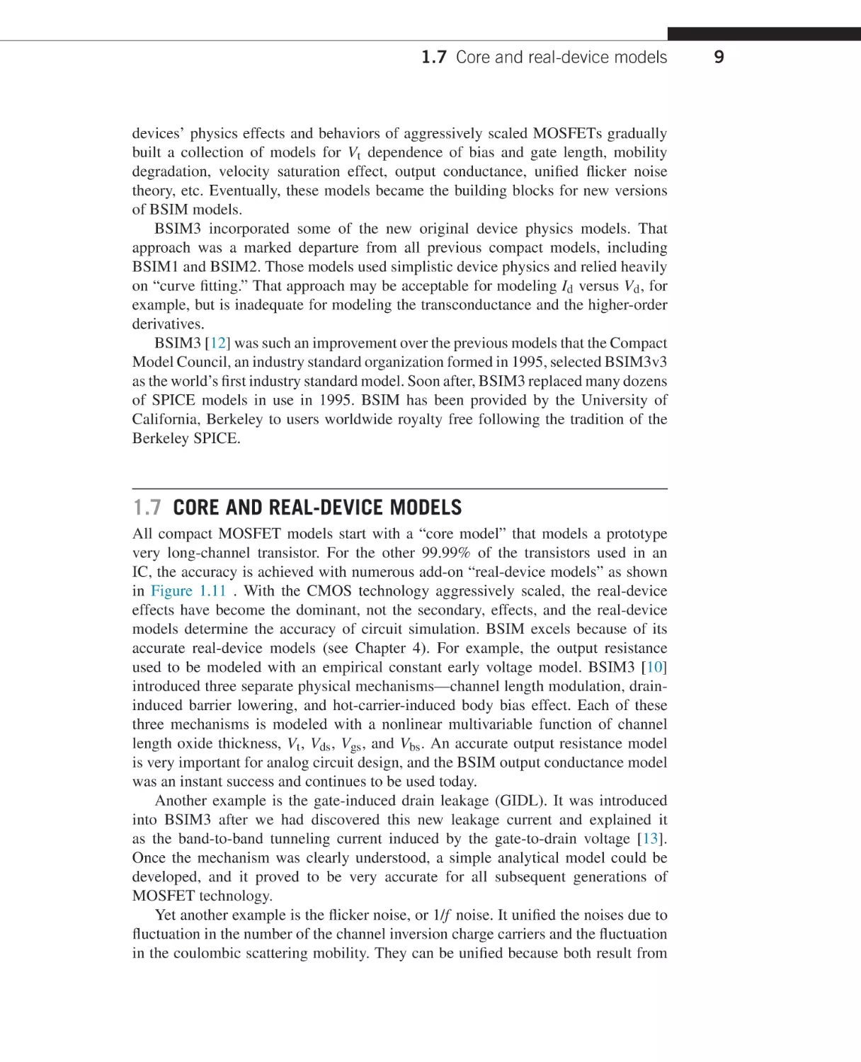
1.7 CORE AND REAL-DEVICE MODELS
All compact MOSFET models start with a “core model” that models a prototype
very long-channel transistor. For the other 99.99% of the transistors used in an
IC, the accuracy is achieved with numerous add-on “real-device models” as shown
in Figure 1.11 . With the CMOS technology aggressively scaled, the real-device
effects have become the dominant, not the secondary, effects, and the real-device
models determine the accuracy of circuit simulation. BSIM excels because of its
accurate real-device models (see Chapter 4). For example, the output resistance
used to be modeled with an empirical constant early voltage model. BSIM3 [10]
introduced three separate physical mechanisms—channel length modulation, draininduced barrier lowering, and hot-carrier-induced body bias effect. Each of these
three mechanisms is modeled with a nonlinear multivariable function of channel
length oxide thickness, Vt , Vds , Vgs , and Vbs . An accurate output resistance model
is very important for analog circuit design, and the BSIM output conductance model
was an instant success and continues to be used today.
Another example is the gate-induced drain leakage (GIDL). It was introduced
into BSIM3 after we had discovered this new leakage current and explained it
as the band-to-band tunneling current induced by the gate-to-drain voltage [13].
Once the mechanism was clearly understood, a simple analytical model could be
developed, and it proved to be very accurate for all subsequent generations of
MOSFET technology.
Yet another example is the flicker noise, or 1/f noise. It unified the noises due to
fluctuation in the number of the channel inversion charge carriers and the fluctuation
in the coulombic scattering mobility. They can be unified because both result from
9
10
CHAPTER 1 FinFET—From device concept to standard compact model
FIGURE 1.11
A compact model is formed from a simple (long-channel) model and numerous
real-device models. The latter constitute 90% of the model and are responsible for the
global accuracy.
the capture and emission of electrons or holes by the charge traps in SiO2 near the
interface [14]. We validated the model in detail using the random telegraphic noise
measurements that can only be observed in transistors with such small length and
width that one transistor contains only one or two observable oxide traps. These
physics studies led to an accurate BSIM unified flicker noise model.
Even more complex real-device models include the gate tunneling leakage model,
the self-heating model, the floating body model, and the non-quasi-static model. The
real-device models account for 80-90% of the model code, simulation time, and the
model development effort. They are responsible for the accuracy of the compact
model and the IC simulation. Many of the BSIM real-device models developed years
ago are still valid for and are used in the FinFET standard compact model. These are
described in Chapters 4–6.
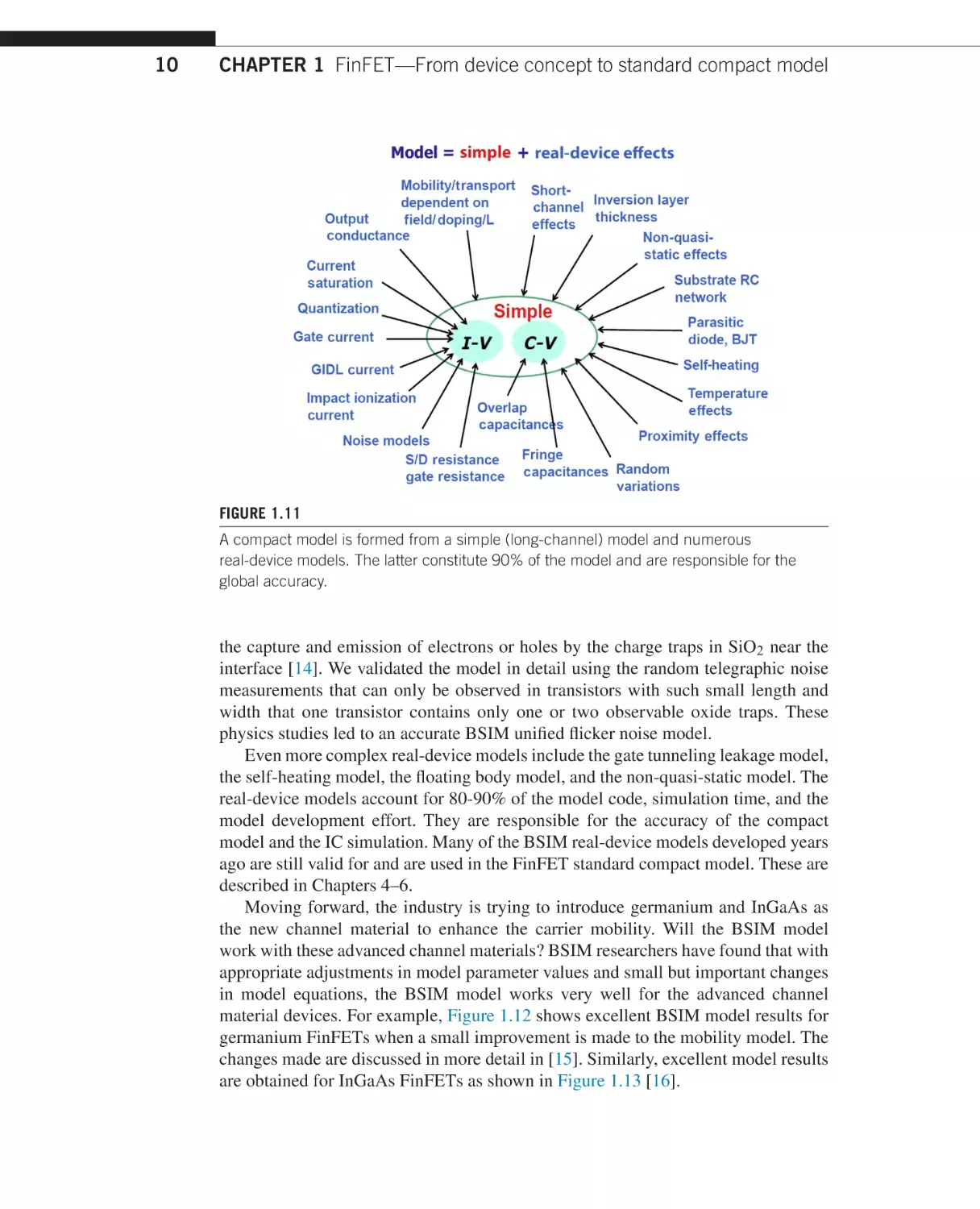
Moving forward, the industry is trying to introduce germanium and InGaAs as
the new channel material to enhance the carrier mobility. Will the BSIM model
work with these advanced channel materials? BSIM researchers have found that with
appropriate adjustments in model parameter values and small but important changes
in model equations, the BSIM model works very well for the advanced channel
material devices. For example, Figure 1.12 shows excellent BSIM model results for
germanium FinFETs when a small improvement is made to the mobility model. The
changes made are discussed in more detail in [15]. Similarly, excellent model results
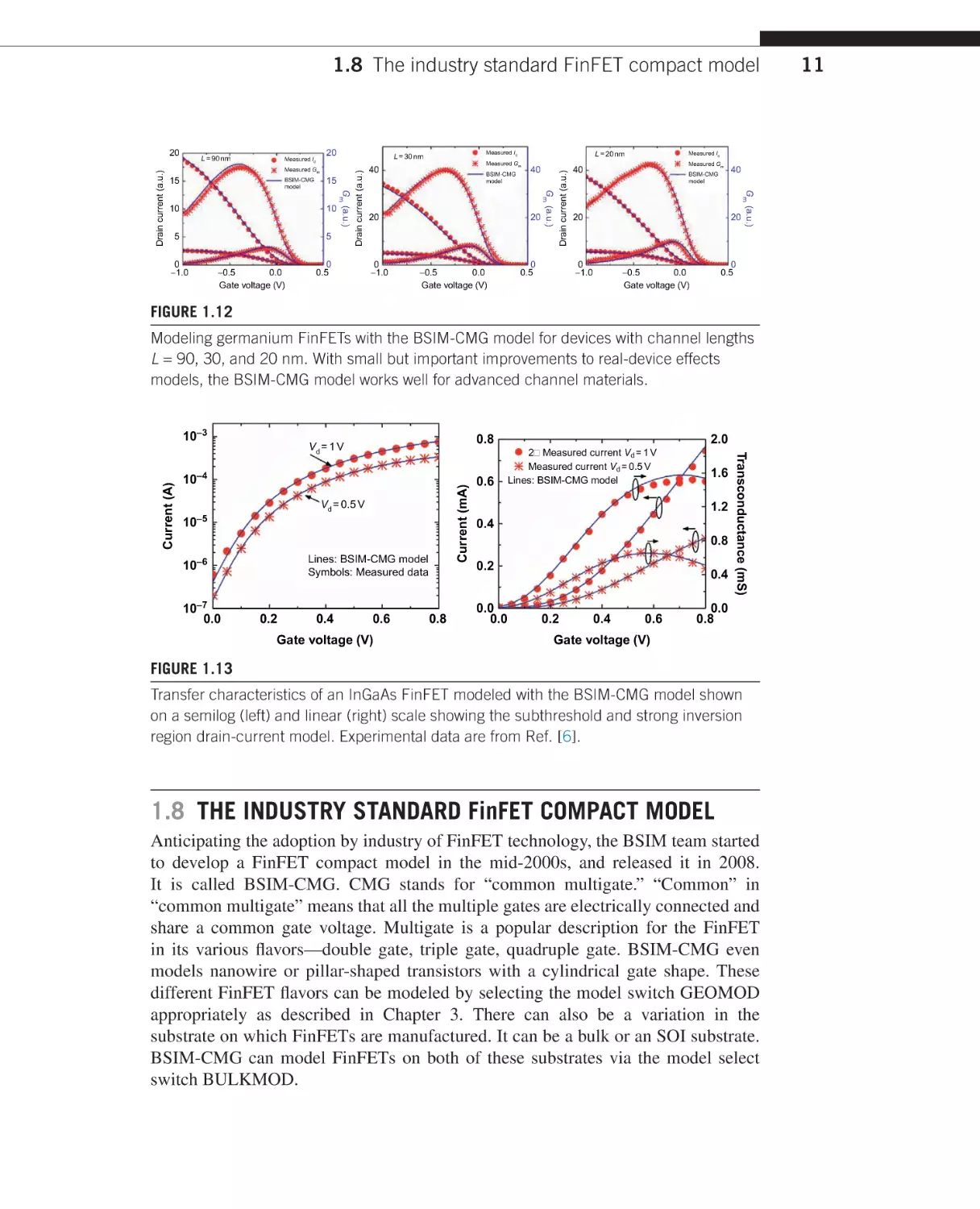
are obtained for InGaAs FinFETs as shown in Figure 1.13 [16].
1.8 The industry standard FinFET compact model
15
15
10
5
5
0
-1.0
-0.5
0.0
Gate voltage (V)
0
0.5
BSIM-CMG
model
20
0
-1.0
40
20
-0.5
0.0
Gate voltage (V)
Measured Gm
BSIM-CMG
model
20
40
20
0
-1.0
0
0.5
Measured Id
40
Gm (a.u.)
10
L = 20 nm
Measured Gm
40
Gm (a.u.)
BSIM-CMG
model
Measured Id
L = 30 nm
Measured Gm
Drain current (a.u.)
20
Measured Id
Drain current (a.u.)
L = 90 nm
Gm (a.u.)
Drain current (a.u.)
20
0
0.5
-0.5
0.0
Gate voltage (V)
FIGURE 1.12
Modeling germanium FinFETs with the BSIM-CMG model for devices with channel lengths
L = 90, 30, and 20 nm. With small but important improvements to real-device effects
models, the BSIM-CMG model works well for advanced channel materials.
Current (mA)
10–4
Vd = 0.5 V
10–5
Lines: BSIM-CMG model
Symbols: Measured data
10–6
10–7
0.0
0.2
0.4
2.0
0.8
Vd = 1 V
0.6
Gate voltage (V)
0.8
0.6
2 Measured current Vd = 1 V
Measured current Vd = 0.5 V
Lines: BSIM-CMG model
1.6
1.2
0.4
0.8
0.2
0.0
0.0
0.4
0.2
0.4
0.6
Transconductance (mS)
Current (A)
10–3
0.0
0.8
Gate voltage (V)
FIGURE 1.13
Transfer characteristics of an InGaAs FinFET modeled with the BSIM-CMG model shown
on a semilog (left) and linear (right) scale showing the subthreshold and strong inversion
region drain-current model. Experimental data are from Ref. [6].
1.8 THE INDUSTRY STANDARD FinFET COMPACT MODEL
Anticipating the adoption by industry of FinFET technology, the BSIM team started
to develop a FinFET compact model in the mid-2000s, and released it in 2008.
It is called BSIM-CMG. CMG stands for “common multigate.” “Common” in
“common multigate” means that all the multiple gates are electrically connected and
share a common gate voltage. Multigate is a popular description for the FinFET
in its various flavors—double gate, triple gate, quadruple gate. BSIM-CMG even
models nanowire or pillar-shaped transistors with a cylindrical gate shape. These
different FinFET flavors can be modeled by selecting the model switch GEOMOD
appropriately as described in Chapter 3. There can also be a variation in the
substrate on which FinFETs are manufactured. It can be a bulk or an SOI substrate.
BSIM-CMG can model FinFETs on both of these substrates via the model select
switch BULKMOD.
11
12
CHAPTER 1 FinFET—From device concept to standard compact model
After the industry decided to embrace FinFET technology for production, BSIMCMG was selected as the industry standard FinFET model, without contest, by
the Compact Model Council. The Compact Model Council members are major
IC companies, fabless companies, design automation companies, and IC foundries,
including Altera, Analog Devices, Broadcom, Cadence, Globalfoundries, IBM, Intel,
Mentor Graphics, Qualcomm, Renesas, Samsung, Hynix, ST Microelectronics, Synopsys, TSMC, and UMC. BSIM-CMG timely provided the foundation for the
design infrastructure that enables FinFET-based circuit design and product development. The following chapters discuss all the important aspects of the standard
FinFET model.
REFERENCES
[1] C. Hu, Modern Semiconductor Devices for Integrated Circuits, Pearson/Prentice Hall,
New Jersey, 2010 (Chapter 7).
[2] Z. Liu, et al., Threshold voltage model for deep-submicrometer. MOSFET’s, IEEE Trans.
Electron Dev. 40 (1) (1993) 86–95.
[3] X. Huang, et al., Sub 50-nm FinFET: PMOS, IEDM Technical Digest, 1999, p. 67.
[4] A. Sachid, C. Hu, Denser and more stable FinFET SRAM using multiple fin heights,
International Semiconductor Device Research Symposium (ISDRS), 2011, pp. 1–2.
[5] F.-L. Yang, et al., 5 nm-gate nanowire FinFET, VLSI Technology Symposium, 2004,
pp. 196–197.
[6] J.J. Gu, X.W. Wang, H. Wu, J. Shao, A.T. Neal, M.J. Manfra, R.G. Gordon,
P.D. Ye, 20-80 nm channel length InGaAs gate-all-around nanowire MOSFETs with
EOT = 1.2 nm and lowest SS = 63 mV/dec, International Electron Devices Meeting,
IEDM, 2012, pp. 27.6.1–27.6.4.
[7] B. Duriez, G. Vellianitis, M.J.H. van Dal, G. Doornbos, R. Oxland, K.K. Bhuwalka,
M. Holland, Y.S. Chang, C.H. Hsieh, K.M. Yin, Y.C. See, M. Passlack, C.H. Diaz,
Scaled p-channel Ge FinFET with optimized gate stack and record performance
integrated on 300 mm silicon wafers, Electron Devices Meeting (IEDM), 2013,
pp. 20.1.1–20.1.4.
[8] C.H. Wann, K. Noda, T. Tanaka, M. Yoshida, C. Hu, A comparative study of advanced
MOSFET concepts, IEEE Trans. Electron Dev. 43 (10) (1996) 1742–1753.
[9] Y.-K. Choi, et al., Ultrathin-body SOI MOSFET for deep-sub-tenth micron era, IEEE
Electron Dev. Lett. 21 (5) (2000) 254.
[10] B.J. Sheu, D.L. Scharfetter, C. Hu, D.O. Pederson, A compact IGFET charge model,
IEEE Trans. Circuits Syst. 31 (8) (1984) 745–748.
[11] M.C. Jeng, P.K. Ko, C. Hu, A deep submicron MOSFET model for analog/digital circuit
simulations, Technical Digest of International Electron Devices Meeting (IEDM), San
Francisco, CA, 1988, pp. 114–117.
[12] J.H. Huang, Z.H. Liu, M.C. Jeng, K. Hui, M. Chan, P.K. Ko, C. Hu, BSIM3 Manual,
University of California, Berkeley, 1993.
[13] T.Y. Chan, J. Chen, P.K. Ko, C. Hu, The impact of gate-induced drain leakage current on
MOSFET scaling, Technical Digest of International Electron Devices Meeting (IEDM),
Washington, D.C., 1987, pp. 718–721.
References
[14] K.K. Hung, P.K. Ko, C. Hu, Y.C. Cheng, A unified model for the flicker noise in
metal-oxide-semiconductor field-effect transistors, IEEE Trans. Electron Dev. 37 (3)
(1990) 654–665.
[15] S. Khandelwal, J.P. Duarte, Y.S. Chauhan, C. Hu, Modeling 20-nm germanium FinFET
with the industry standard FinFET model, IEEE Electron Dev. Lett. 35 (7) (2014)
711–713.
[16] S. Khandelwal, J.P. Duarte, N. Paydavosi, Y.S. Chauhan, M. Si, J.J. Gu, P.D. Ye, C. Hu,
InGaAs FinFET modeling with industry standard compact model BSIM-CMG, Nanotech
2014.
13
CHAPTER
Compact models for analog
and RF applications
2
CHAPTER OUTLINE
2.1 Introduction . . . . . . . . . . . . . . . . . . . . . . . . . . . . . . . . . . . . . . . . . . . . . . . . . . . . . . . . . . . . . . . . . . . . . . . . . . .15
2.2 Important compact model metrics . . . . . . . . . . . . . . . . . . . . . . . . . . . . . . . . . . . . . . . . . . . . . . . . . . . .16
2.3 Analog metrics . . . . . . . . . . . . . . . . . . . . . . . . . . . . . . . . . . . . . . . . . . . . . . . . . . . . . . . . . . . . . . . . . . . . . . . .16
2.3.1 Quiescent operating point . . . . . . . . . . . . . . . . . . . . . . . . . . . . . . . . . . . . . . . . . . . . . . . 17
2.3.2 Geometric scalability . . . . . . . . . . . . . . . . . . . . . . . . . . . . . . . . . . . . . . . . . . . . . . . . . . . . 19
2.3.3 Variability model . . . . . . . . . . . . . . . . . . . . . . . . . . . . . . . . . . . . . . . . . . . . . . . . . . . . . . . . . 23
2.3.4 Intrinsic voltage gain . . . . . . . . . . . . . . . . . . . . . . . . . . . . . . . . . . . . . . . . . . . . . . . . . . . . 24
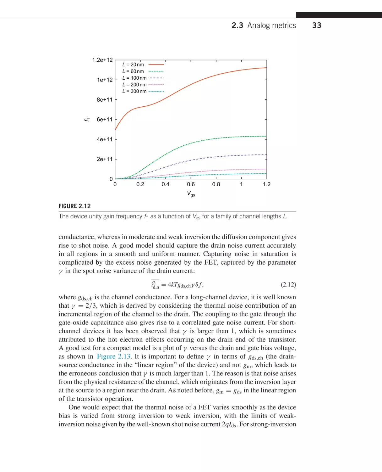
2.3.5 Speed: Unity gain frequency . . . . . . . . . . . . . . . . . . . . . . . . . . . . . . . . . . . . . . . . . . . . 31
2.3.6 Noise . . . . . . . . . . . . . . . . . . . . . . . . . . . . . . . . . . . . . . . . . . . . . . . . . . . . . . . . . . . . . . . . . . . . 32
2.3.7 Linearity and symmetry . . . . . . . . . . . . . . . . . . . . . . . . . . . . . . . . . . . . . . . . . . . . . . . . . . 36
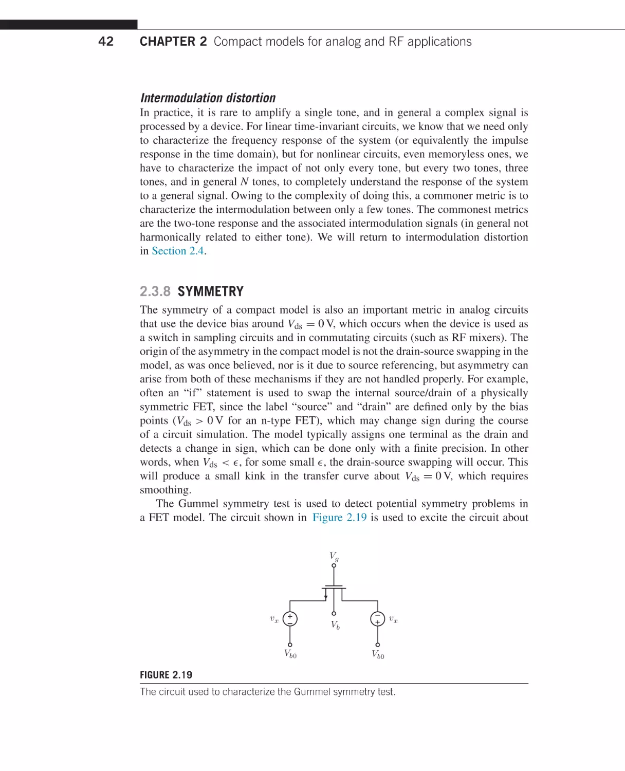
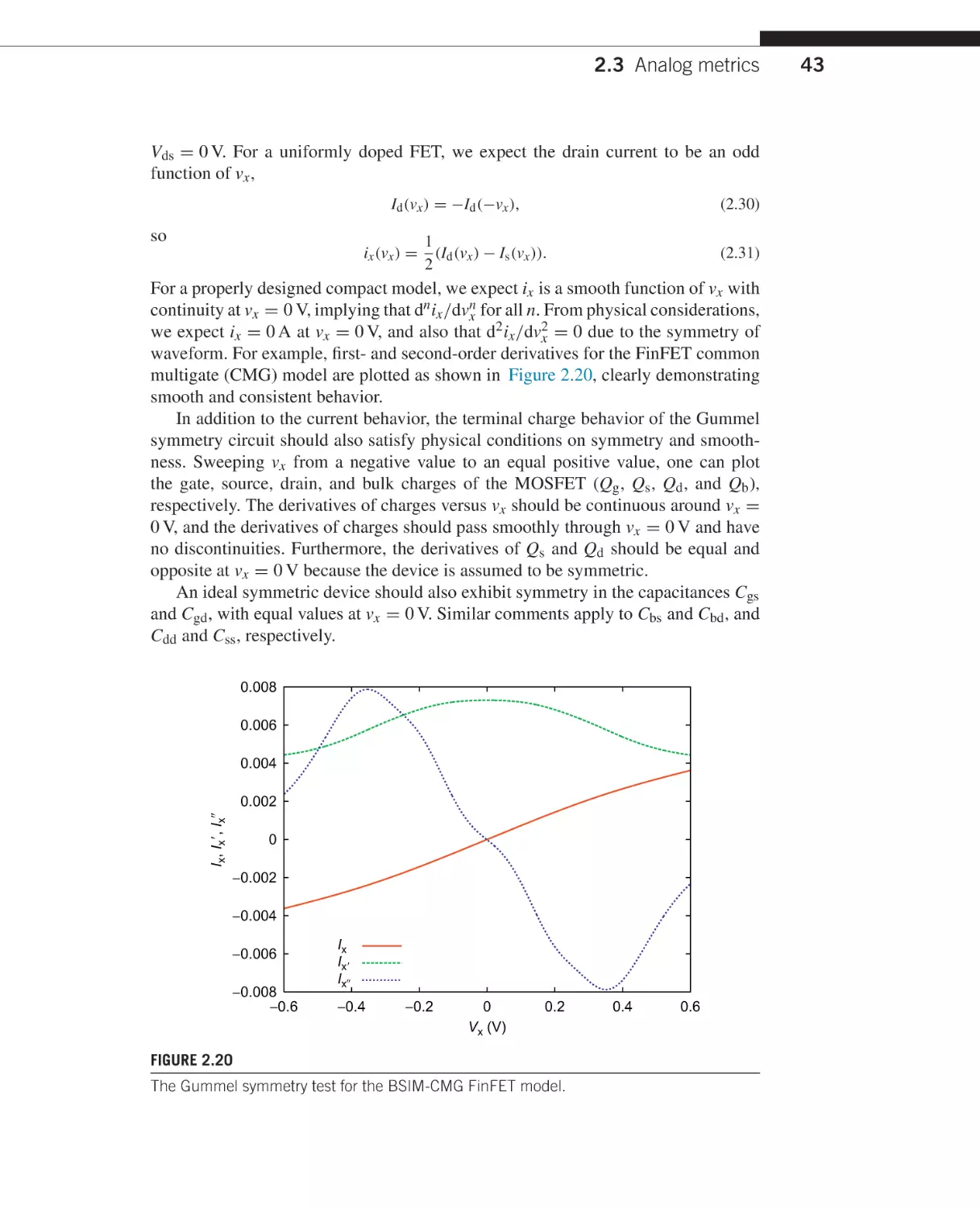
2.3.8 Symmetry . . . . . . . . . . . . . . . . . . . . . . . . . . . . . . . . . . . . . . . . . . . . . . . . . . . . . . . . . . . . . . . . 42
2.4 RF metrics . . . . . . . . . . . . . . . . . . . . . . . . . . . . . . . . . . . . . . . . . . . . . . . . . . . . . . . . . . . . . . . . . . . . . . . . . . . . .44
2.4.1 Two-port parameters . . . . . . . . . . . . . . . . . . . . . . . . . . . . . . . . . . . . . . . . . . . . . . . . . . . . . 44
2.4.2 The need for speed . . . . . . . . . . . . . . . . . . . . . . . . . . . . . . . . . . . . . . . . . . . . . . . . . . . . . . 46
2.4.3 Non-quasi-static model . . . . . . . . . . . . . . . . . . . . . . . . . . . . . . . . . . . . . . . . . . . . . . . . . . 55
2.4.4 Noise . . . . . . . . . . . . . . . . . . . . . . . . . . . . . . . . . . . . . . . . . . . . . . . . . . . . . . . . . . . . . . . . . . . . 58
2.4.5 Linearity . . . . . . . . . . . . . . . . . . . . . . . . . . . . . . . . . . . . . . . . . . . . . . . . . . . . . . . . . . . . . . . . . 64
2.5 Conclusion . . . . . . . . . . . . . . . . . . . . . . . . . . . . . . . . . . . . . . . . . . . . . . . . . . . . . . . . . . . . . . . . . . . . . . . . . . . .68
References . . . . . . . . . . . . . . . . . . . . . . . . . . . . . . . . . . . . . . . . . . . . . . . . . . . . . . . . . . . . . . . . . . . . . . . . . . . . . . . . .68
2.1 INTRODUCTION
A compact model is the interface between the process technology and the circuit
designer. The compact model, usually in the form of a design kit, encapsulates all the
relevant details of the process in an easily accessible form that allows the designer
to run simulations in a familiar environment, assessing the impact of the device on
important circuit and system parameters, without having to understand the details of
FinFET Modeling for IC Simulation and Design. http://dx.doi.org/10.1016/B978-0-12-420031-9.00002-6
Copyright © 2015 Elsevier Inc. All rights reserved.
15
16
CHAPTER 2 Compact models for analog and RF applications
the physics or implementation details of the model. In fact, most designers have no
idea what is inside the compact model, but they expect the model to capture the device
behavior as accurately as possible. An analog designer will expect accurate prediction
of bias points, small-signal parameters such as transconductance, output resistance,
and capacitance, thermal and flicker noise, and device-matching properties. Since
designers have no control over the design of a device, they can only vary the operating
point and the device geometry, so they expect good physical scalability in the model.
RF design requires accurate prediction of power gain, noise (thermal and flicker),
linearity, and power.
FinFET devices come in an age where CMOS technology is playing a vital role
in both analog and RF/microwave circuits. While technology scaling has improved
the device speed by orders of magnitude, allowing operation in the millimeter-wave
and subterahertz regime, voltage scaling and lower intrinsic gain has been a constant
challenge to analog design. In such a world, most designers are averse to moving
to advanced technology nodes since often the digital blocks are the only ones that
gain in area and power. In this regard, a FinFET device can offer a change, improved
output resistance (and hence intrinsic gain) and low capacitance. Given the high cost
of doing fabrication runs in advanced technology nodes, an analog/RF compatible
FinFET model will offer a unique opportunity to explore designs without incurring
any costs of fabrication.
In this chapter, we will highlight important performance metrics for analog and
RF circuits and relate these to the various compact model modules that are found in
the FinFET compact model. This chapter therefore serves as a transition to the rest
of the book, highlighting the importance of the various modules and the properties of
a compact model.
2.2 IMPORTANT COMPACT MODEL METRICS
We begin by identifying important metrics that can be used to judge a compact model.
Without these metrics, it would be difficult to gauge the accuracy of a compact model
with regard to important quantifiable aspects that relate closely to circuit design.
Metrics capture the essence of the model, and they should be important for the
designer; in other words, they should be related to the performance of important
circuit building blocks. The metrics are divided into analog and RF categories.
It goes without saying that RF metrics are a superset and depend on analog metrics.
In other words, an RF compact model should first and foremost satisfy the analog
criteria for evaluation as they will form the core foundation for the model.
2.3 ANALOG METRICS
Classic analog design is concerned primarily with the gain-bandwidth product
of amplifiers. This is due to the wide application of amplifiers (operational and
2.3 Analog metrics
transconductance amplifiers) as core building blocks and the use of feedback to
linearize these blocks, making their performance predictable over the process and
with temperature variation. Device currents are selected to minimize power while
meeting speed requirements. Moreover, noise is of paramount importance in analog
circuits as it determines the resolution, or lower end of the dynamic range, of the
signal processing chain. The upper end of the dynamic range is determined by a
voltage swing, which is related to the supply voltage and the linearity of the amplifier
(and hence transistors). In many cases, linearity is a secondary concern because of
the application of feedback, which inherently linearizes stages by trading gain for
linearity. Owing to the lower supply voltage and lower intrinsic gain, the loop gain
of a closed-loop system is dropping with technology scaling, making nonlinearity a
more prominent concern even in analog applications. In the other extreme, people
are exploring open loop design by relying on digital signal processing techniques to
measure and correct for analog errors.
In fact, analog design is increasingly mixed-signal design. Pure analog design
is very rare, or mostly confined to high-voltage applications. A FinFET device
will live in a very mixed-signal environment, where sample time and charge processing will take place side by side with traditional linear voltage/current analog
techniques. Moreover, FinFET devices will form the core of switches for the purpose
of tuning and calibration, and often devices in these applications will experience
voltage excursions that invert the device polarity (source-drain switch), requiring
model symmetry. In sampled time systems, signal-dependent charge injection is
important for quantifying the nonlinearity and systematic errors in analog signal
processing.
2.3.1 QUIESCENT OPERATING POINT
In many respects, analog design comes down to biasing transistors correctly.1 Circuit
topologies are often selected on the basis of performance requirements, and the job
of the circuit designer is to ensure that the transistors remain at the proper quiescent
operation point with process variation and temperature variation. This is often a
challenging task, as supply voltages scale to 1 V, and there is often very little margin,
forcing designers to use biasing schemes that can compensate for variations in the
device threshold voltage VT with counter variations of another device. This means
that they will trust the model’s ability to track temperature or process variations (say,
in the transistor geometric dimensions and doping). This places a high burden on a
compact model since its current-voltage (I-V) behavior must be built on a physical
foundation that inherently can predict these changes. Often students of compact
modeling ask why one cannot simply reduce compact modeling to a mathematical
exercise in curve fitting. The answer is partly that a mathematical model that fits the
I-V curves from measured data without knowledge of any device physics would fail
1A
saying attributed to Barrie Gilbert.
17
18
CHAPTER 2 Compact models for analog and RF applications
to predict the I-V curve for a small change in a physical parameter, such as doping or
temperature. In theory, all these variations could be captured by a compact model, but
technology foundries cannot afford to run thousands of combinatorial experiments to
capture these variations, and instead rely on the compact model to reproduce these
effects.
This reliance on physical trends is in contrast to the requirement of absolute
accuracy. Absolute accuracy is fictional since the actual device of a sample will
differ from the test structures used to measure the I-V curves. This process variation
is an inevitable fact of fabricating integrated circuits with microscopic dimensions.
In fact, it is remarkable that we are able to reproduce device behavior to the
level of accuracy measured in the field, given that modern minimum-sized devices
are limited by doping variation due to only a small number of dopant atoms.
In fact, performance is more fundamentally becoming limited by quantum mechanical fluctuations due to the small dimensions and small number of charge carriers
and dopants.
Most compact models are built from a physical core which is derived using a longchannel pseudo-two-dimensional transistor. The transistor charge Q-V characteristics
are derived using only vertical fields, and currents are in turn derived by introducing
a tangential field along the channel. The advantage of this approach is that it allows
a closed-form equation to be derived without resorting to numerical integration. The
most accurate solutions are the so-called surface potential solutions, which relate
device charge to the surface potential along the channel. The downside is that the
relationship between surface potential and device terminal voltages is not explicit,
requiring Newton-Raphson style iteration to determine the solution. Moreover, the
sensitivity to the surface potential is quite high, requiring very accurate convergence.
But careful study of the convergence properties of the core equations allows these
iterations to terminate in a fixed number of iterations, in effect unrolling the loops.
The advantage of these “toy” models is that they are physically derived, and hence
can capture the physical behavior of the device over the voltage excursions from
accumulation, depletion, and weak inversion to moderate and strong inversion. Most
importantly, the model can predict I-V and Q-V behavior in various stages of
inversion, from weak to moderate inversion and to strong inversion. The moderate
region is increasingly important for analog circuit operation since it allows the
designer to trade off speed for gain and high transconductance efficiency (see below).
Another important aspect of the compact model is its ability to self-saturate.
In other words, as the drain voltage is varied from tens of millivolts to the full
supply voltage across the device, the saturation in the current should happen in a
smooth and natural manner. In a classical long-channel transistor, saturation occurs
owing to the so-called pinch-off effect. In a modern device, saturation occurs earlier
owing to velocity saturation of carriers, arising from the high-field effects. Once
a device is saturated, the I-V curve variation is due to the output conductance of
the device, which is an accumulated sum of various complex mechanisms such
as channel length modulation, drain-induced barrier lowering (DIBL), and impact
2.3 Analog metrics
ionization. Correct prediction of the curvature in this regime of operation is critical for
analog circuits since the intrinsic gain will be determined by the slope of the Ids -Vds
curve.
Finally, leakage currents play a critical role in discrete-time and low-power
applications. Similarly to digital circuits, leakage currents are a concern when the
device is “off,” which happens when it is biased well below the threshold voltage.
A real device will conduct very little current in this regime, but such a small current
can quickly discharge a small capacitor, which introduces an error when sampling
and storing a voltage on a capacitor.
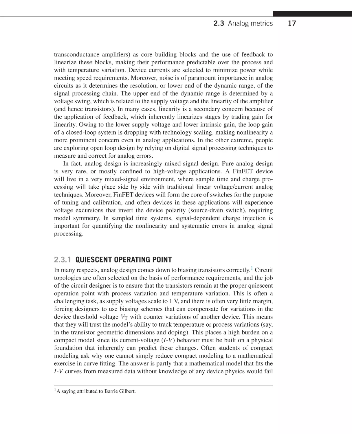
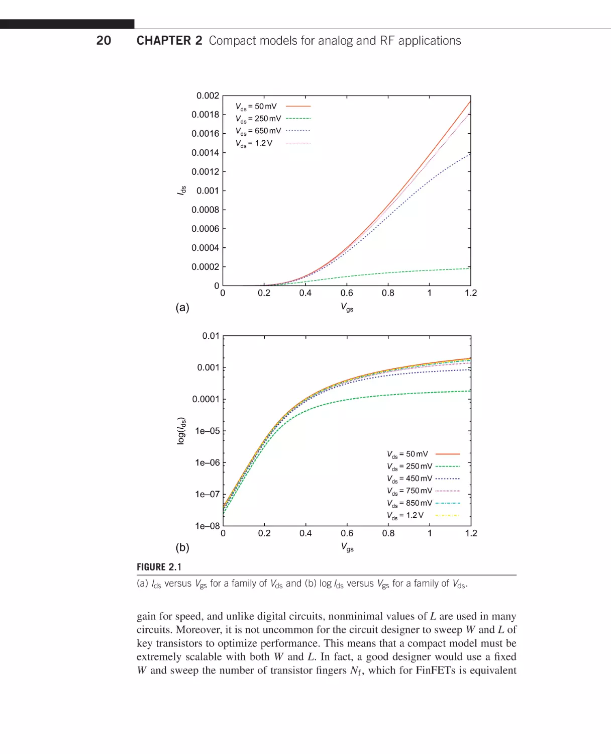
How does one quantify these observations? The I-V curve of a given transistor
with fixed dimension (W and L) reveals the most salient features. For example, a plot
of Ids versus Vgs for a family of Vds (Figure 2.1a) quickly reveals how well a model
can predict the device current with absolute bias voltage. If a device is biased in
weak or moderate inversion, then the logarithmic plot is more useful as it expands
this regime of operation (Figure 2.1b). A plot of the current versus drain-source
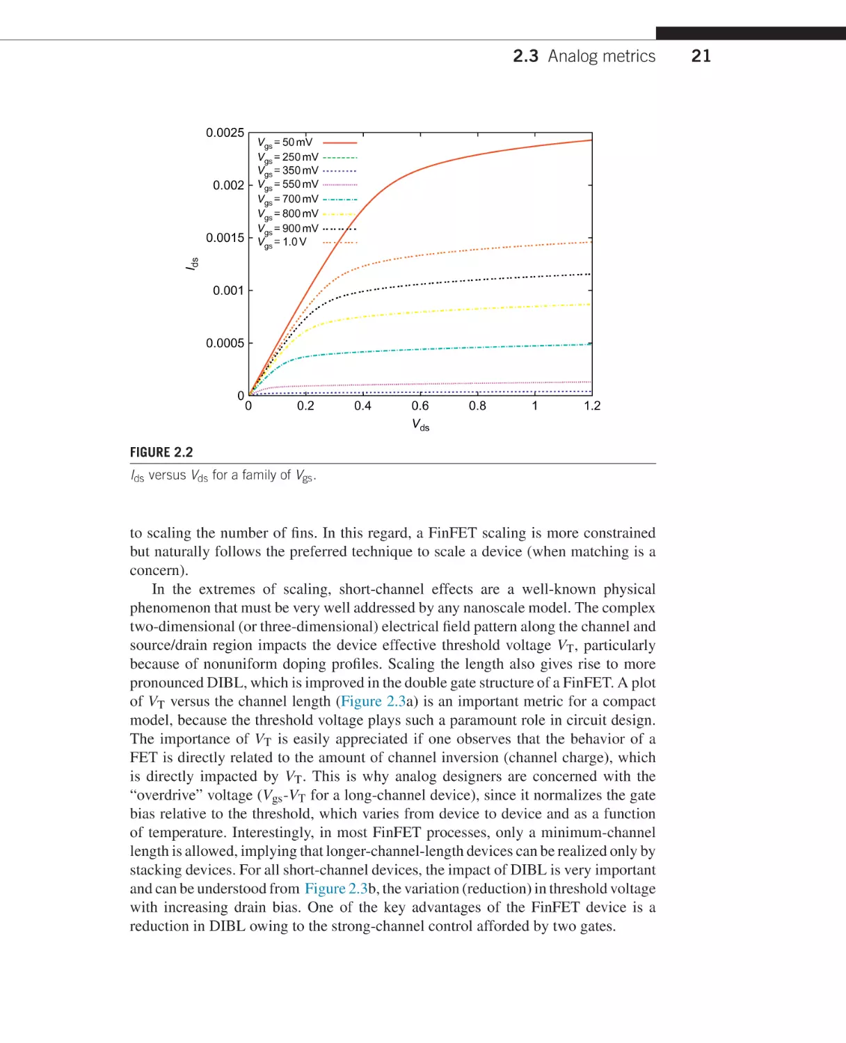
voltage or a plot of Ids versus Vds for a family of Vgs (Figure 2.2) shows the current
saturation behavior of a compact model and the accuracy of the model in saturation,
which is critical for predicting the output conductance. The output conductance is
more easily observed using small-signal parameters as discussed shortly, but certain
trends can be observed even from the raw I-V curves, such as predictions of higher or
lower current, which are consistently observed even from the I-V curves. Even though
absolute accuracy is not important, such a consistent discrepancy reveals that certain
device physics are missing in the compact model (or the device extraction was done
incompletely).
If the device has a bulk terminal, then the body bias effect should also be included
in these plots by varying the body bias and observing the predictability of the
model. In this plot, we observe a shift in the threshold voltage of the device. If
two independent gates are available, these curves should be plotted for both gates.
In practice, many “back gates” will be used for leakage control (threshold shift)
and may not be able to invert the channel, so the plots are very similar to those
for bulk devices. For “common-gate” devices without a body contact, the plot of
Vgs is then the only relevant curve. In these cases, it may be important to measure
the I-V curves using pulsed mode measurements to avoid self-heating. Even though
most devices have thin fins that are fully depleted, under the right conditions partial
depletion may introduce kinks in the I-V curve that should be modeled correctly. DC
and pulsed measurements with various back-gate/body biasing should reveal these
device intricacies and the model should be verified to reproduce these effects.
2.3.2 GEOMETRIC SCALABILITY
Aside from the bias point, the only other variable under the control of a designer is
the transistor geometry. Analog circuits make extensive use of L and W to trade off
19
CHAPTER 2 Compact models for analog and RF applications
0.002
Vds = 50 mV
0.0018
Vds = 250 mV
Vds = 650 mV
0.0016
Vds = 1.2 V
0.0014
Ids
0.0012
0.001
0.0008
0.0006
0.0004
0.0002
0
0
0.2
0.4
(a)
0.6
Vgs
0.8
1
1.2
0.01
0.001
0.0001
log(Ids)
20
1e–05
Vds = 50 mV
1e–06
Vds = 250 mV
Vds = 450 mV
Vds = 750 mV
1e–07
Vds = 850 mV
Vds = 1.2 V
1e–08
(b)
0
0.2
0.4
0.6
Vgs
0.8
1
1.2
FIGURE 2.1
(a) Ids versus Vgs for a family of Vds and (b) log Ids versus Vgs for a family of Vds .
gain for speed, and unlike digital circuits, nonminimal values of L are used in many
circuits. Moreover, it is not uncommon for the circuit designer to sweep W and L of
key transistors to optimize performance. This means that a compact model must be
extremely scalable with both W and L. In fact, a good designer would use a fixed
W and sweep the number of transistor fingers Nf , which for FinFETs is equivalent
2.3 Analog metrics
0.0025
Vgs = 50 mV
Vgs = 250 mV
Vgs = 350 mV
Vgs = 550 mV
Vgs = 700 mV
Vgs = 800 mV
Vgs = 900 mV
Vgs = 1.0 V
0.002
Ids
0.0015
0.001
0.0005
0
0
0.2
0.4
0.6
Vds
0.8
1
1.2
FIGURE 2.2
Ids versus Vds for a family of Vgs .
to scaling the number of fins. In this regard, a FinFET scaling is more constrained
but naturally follows the preferred technique to scale a device (when matching is a
concern).
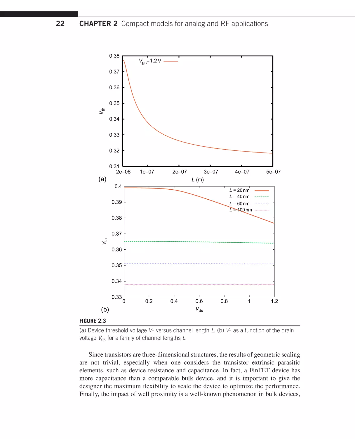
In the extremes of scaling, short-channel effects are a well-known physical
phenomenon that must be very well addressed by any nanoscale model. The complex
two-dimensional (or three-dimensional) electrical field pattern along the channel and
source/drain region impacts the device effective threshold voltage VT , particularly
because of nonuniform doping profiles. Scaling the length also gives rise to more
pronounced DIBL, which is improved in the double gate structure of a FinFET. A plot
of VT versus the channel length (Figure 2.3a) is an important metric for a compact
model, because the threshold voltage plays such a paramount role in circuit design.
The importance of VT is easily appreciated if one observes that the behavior of a
FET is directly related to the amount of channel inversion (channel charge), which
is directly impacted by VT . This is why analog designers are concerned with the
“overdrive” voltage (Vgs -VT for a long-channel device), since it normalizes the gate
bias relative to the threshold, which varies from device to device and as a function
of temperature. Interestingly, in most FinFET processes, only a minimum-channel
length is allowed, implying that longer-channel-length devices can be realized only by
stacking devices. For all short-channel devices, the impact of DIBL is very important
and can be understood from Figure 2.3b, the variation (reduction) in threshold voltage
with increasing drain bias. One of the key advantages of the FinFET device is a
reduction in DIBL owing to the strong-channel control afforded by two gates.
21
CHAPTER 2 Compact models for analog and RF applications
0.38
Vgs=1.2 V
0.37
0.36
Vth
0.35
0.34
0.33
0.32
0.31
2e−08
1e−07
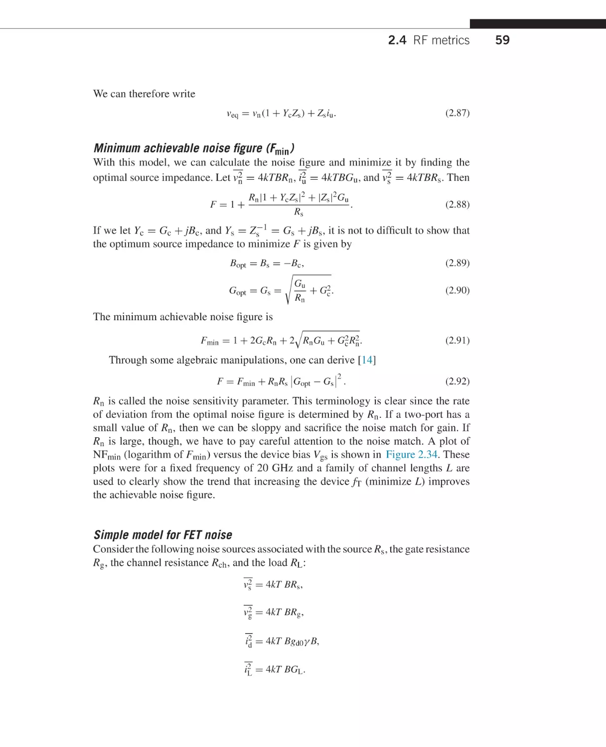
2e−07
3e−07
4e−07
5e−07
L (m)
(a)
0.4
L = 20 nm
L = 40 nm
0.39
L = 60 nm
L = 100 nm
0.38
0.37
Vth
22
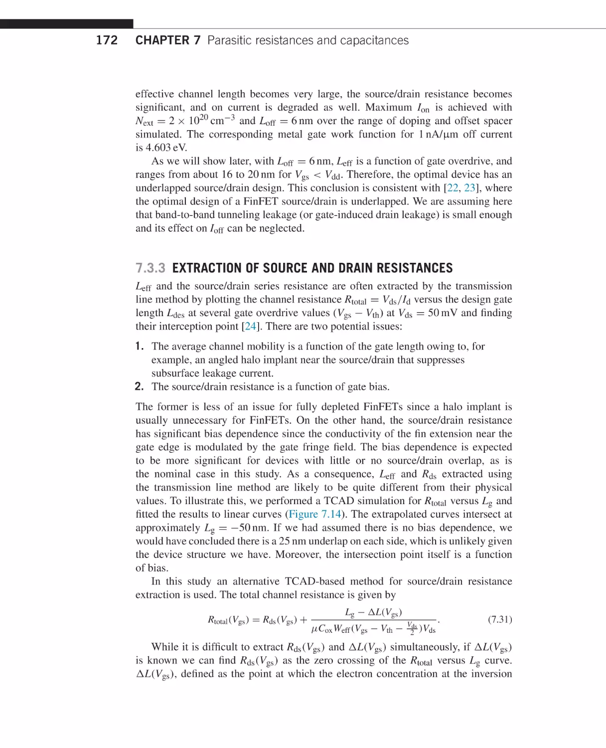
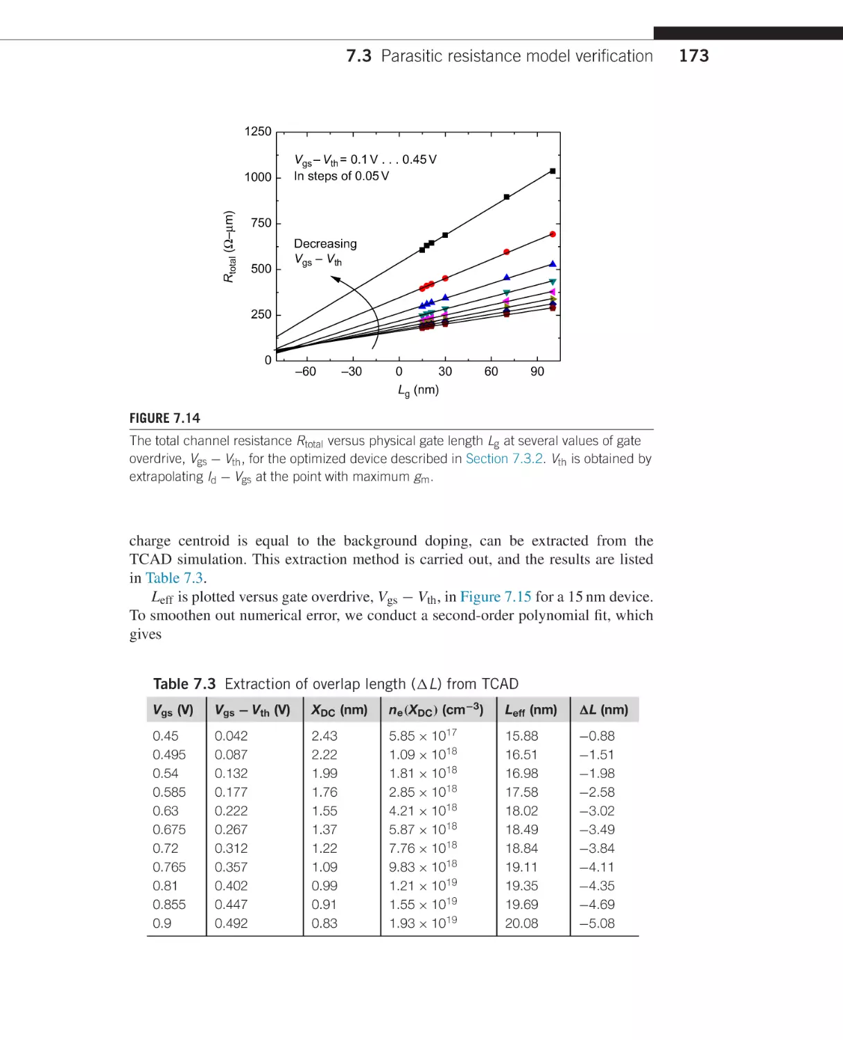
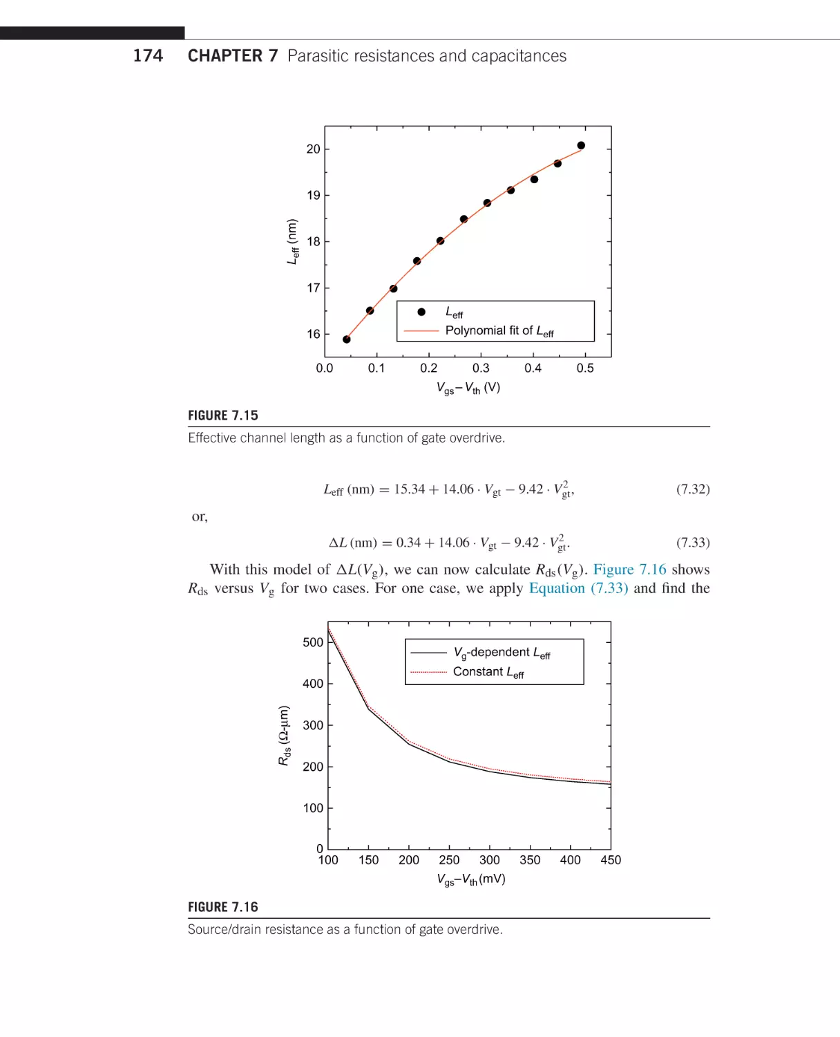
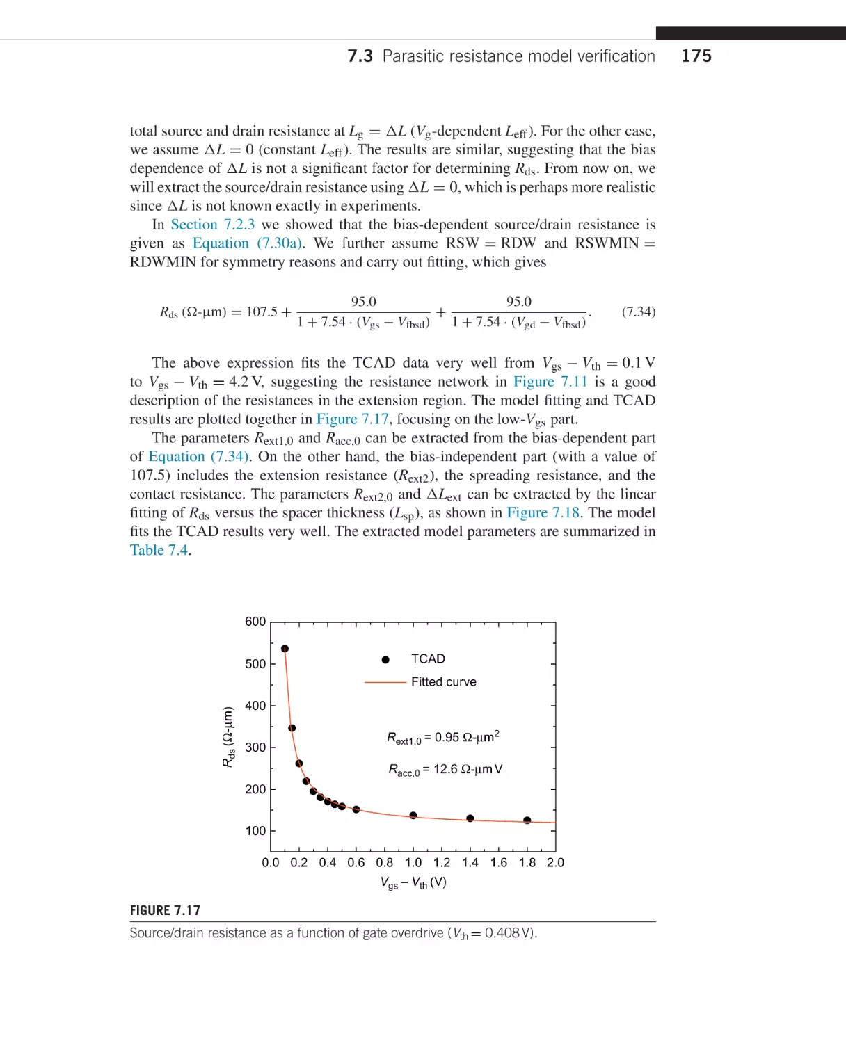
0.36
0.35
0.34
0.33
(b)
0
0.2
0.4
0.6
Vds
0.8
1
1.2
FIGURE 2.3
(a) Device threshold voltage VT versus channel length L. (b) VT as a function of the drain
voltage Vds for a family of channel lengths L.
Since transistors are three-dimensional structures, the results of geometric scaling
are not trivial, especially when one considers the transistor extrinsic parasitic
elements, such as device resistance and capacitance. In fact, a FinFET device has
more capacitance than a comparable bulk device, and it is important to give the
designer the maximum flexibility to scale the device to optimize the performance.
Finally, the impact of well proximity is a well-known phenomenon in bulk devices,
2.3 Analog metrics
which forces designers to use many dummy fingers in their layouts to reduce the
impact on the variation in threshold voltage and mobility. These effects, which are
mostly extrinsic to the device, must be well modeled and captured. Given the smaller
dimensions of a FinFET and its three-dimensional structure, the impact of stress
and strain is even more pronounced, and can have both a positive and a detrimental
impact on the device.
2.3.3 VARIABILITY MODEL
It is extremely important to capture device variation. Variation has many sources,
including systematic and random fluctuations. Systematic variations include layoutdependent effects, such as the variation in the threshold voltage VT as a function of
the distance to the well, whereas random variations arise from natural variation in
doping profiles and lithographic variations. These variations are usually categorized
into device-to-device mismatch for closely spaced transistors, die-to-die variations,
and wafer-to-wafer variations, often just called process variation. In other words, we
are interested in both the variation for a single transistor from die to die and also
that between a pair of “matched” transistors within the same die. Since circuit yield
is a strong function of the variation of transistor performance, designers go to great
lengths to ensure that their circuits operate over all possible process, voltage, and
temperature variations. A common practice is to deliver transistor parameters for
particular corners, such as “fast,” “nominal,” and “slow” corners for transistors (and
other devices such as resistors and capacitors). If we just take transistor variations into
account, since two flavors of transistors are used (n-type MOS and p-type MOS), this
results in five separate corners that must be checked, often called SS, FF, SF, FS, and
TT (“S” for “slow,” “F” for “fast,” and “T” for “typical”).
While corner models are prevalent in industry, they are actually overpessimistic
in most circumstances. The corner cases often represent worst-case conditions that
occur very rarely in practice (Six Sigma), and designing circuits to meet corner
cases requires overdesign, resulting in larger area and higher current consumption.
A more attractive approach is statistical variation, where the model cards are derived
by varying the actual physical parameters that vary, such as doping levels and
lithographic dimensions. This underscores the need for compact models that are
physically derived so that the statistical variation in basic physical parameters leads
to correct variation in the model card parameters. When the model is nonphysical,
it is very difficult to come up with a set of basic parameters to vary in the model
card to match observed measurements of transistor variations. Even using principal
component analysis on compact models with nonphysical origin in equations has not
yielded satisfactory results.
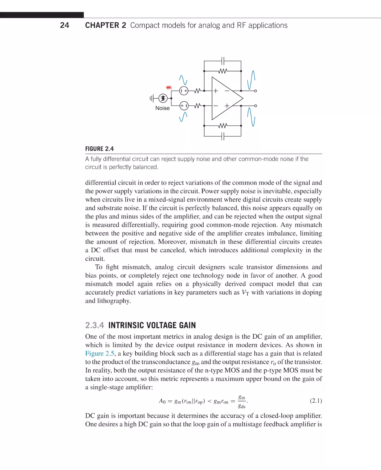
An accurate mismatch model is another key model requirement. In fact, one may
argue that mismatch is ultimately the biggest enemy of an analog circuit designer.
The reason for this is due to the need for high levels of common-mode rejection and
supply insensitivity in analog circuits. For example, the circuit in Figure 2.4 is a
typical building block in amplifiers and filters in analog circuits. It is realized as a
23
CHAPTER 2 Compact models for analog and RF applications
+
Noise
+
24
FIGURE 2.4
A fully differential circuit can reject supply noise and other common-mode noise if the
circuit is perfectly balanced.
differential circuit in order to reject variations of the common mode of the signal and
the power supply variations in the circuit. Power supply noise is inevitable, especially
when circuits live in a mixed-signal environment where digital circuits create supply
and substrate noise. If the circuit is perfectly balanced, this noise appears equally on
the plus and minus sides of the amplifier, and can be rejected when the output signal
is measured differentially, requiring good common-mode rejection. Any mismatch
between the positive and negative side of the amplifier creates imbalance, limiting
the amount of rejection. Moreover, mismatch in these differential circuits creates
a DC offset that must be canceled, which introduces additional complexity in the
circuit.
To fight mismatch, analog circuit designers scale transistor dimensions and
bias points, or completely reject one technology node in favor of another. A good
mismatch model again relies on a physically derived compact model that can
accurately predict variations in key parameters such as VT with variations in doping
and lithography.
2.3.4 INTRINSIC VOLTAGE GAIN
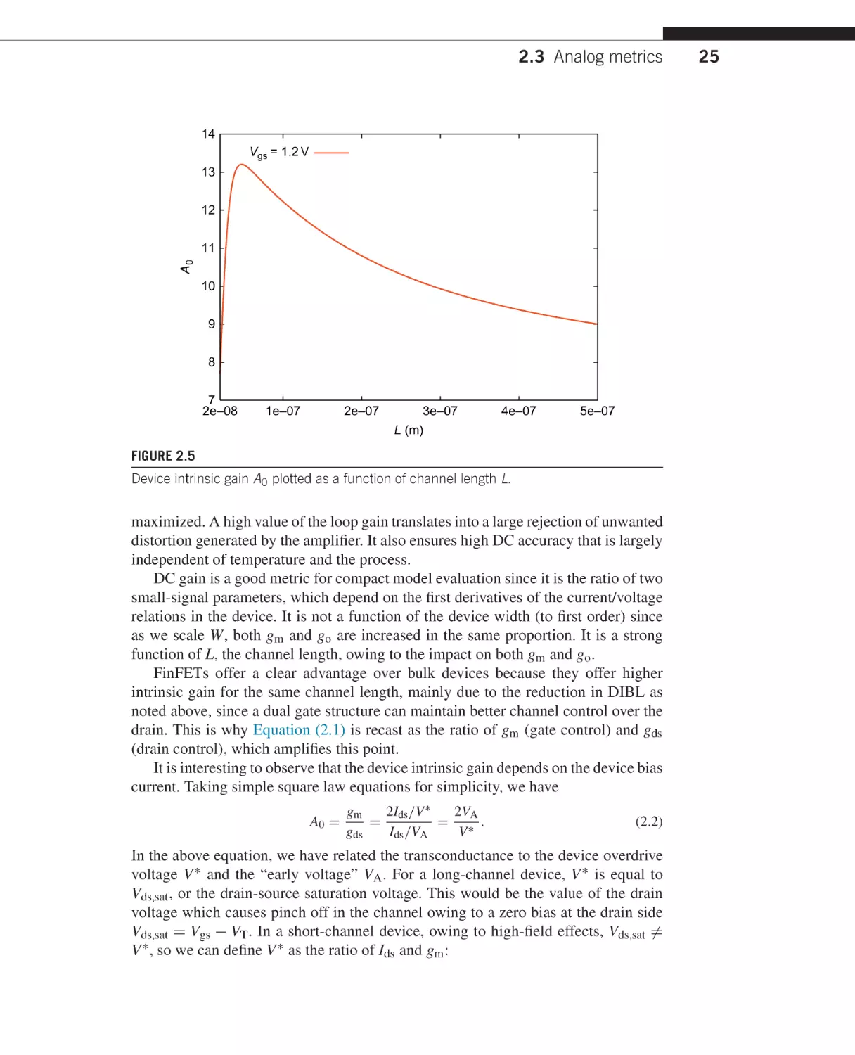
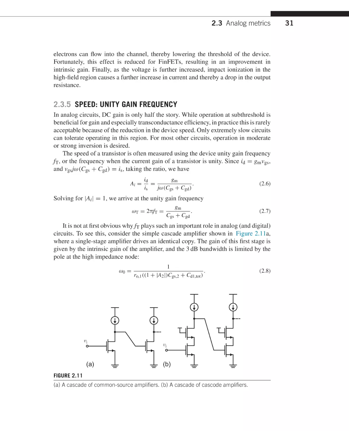
One of the most important metrics in analog design is the DC gain of an amplifier,
which is limited by the device output resistance in modern devices. As shown in
Figure 2.5, a key building block such as a differential stage has a gain that is related
to the product of the transconductance gm and the output resistance ro of the transistor.
In reality, both the output resistance of the n-type MOS and the p-type MOS must be
taken into account, so this metric represents a maximum upper bound on the gain of
a single-stage amplifier:
A0 = gm (ron ||rop ) < gm ron =
gm
.
gds
(2.1)
DC gain is important because it determines the accuracy of a closed-loop amplifier.
One desires a high DC gain so that the loop gain of a multistage feedback amplifier is
2.3 Analog metrics
14
Vgs = 1.2 V
13
12
A0
11
10
9
8
7
2e–08
1e–07
2e–07
3e–07
L (m)
4e–07
5e–07
FIGURE 2.5
Device intrinsic gain A0 plotted as a function of channel length L.
maximized. A high value of the loop gain translates into a large rejection of unwanted
distortion generated by the amplifier. It also ensures high DC accuracy that is largely
independent of temperature and the process.
DC gain is a good metric for compact model evaluation since it is the ratio of two
small-signal parameters, which depend on the first derivatives of the current/voltage
relations in the device. It is not a function of the device width (to first order) since
as we scale W, both gm and go are increased in the same proportion. It is a strong
function of L, the channel length, owing to the impact on both gm and go .
FinFETs offer a clear advantage over bulk devices because they offer higher
intrinsic gain for the same channel length, mainly due to the reduction in DIBL as
noted above, since a dual gate structure can maintain better channel control over the
drain. This is why Equation (2.1) is recast as the ratio of gm (gate control) and gds
(drain control), which amplifies this point.
It is interesting to observe that the device intrinsic gain depends on the device bias
current. Taking simple square law equations for simplicity, we have
A0 =
gm
2Ids /V ∗
2VA
=
= ∗ .
gds
Ids /VA
V
(2.2)
In the above equation, we have related the transconductance to the device overdrive
voltage V ∗ and the “early voltage” VA . For a long-channel device, V ∗ is equal to
Vds,sat , or the drain-source saturation voltage. This would be the value of the drain
voltage which causes pinch off in the channel owing to a zero bias at the drain side
Vds,sat = Vgs − VT . In a short-channel device, owing to high-field effects, Vds,sat =
V ∗ , so we can define V ∗ as the ratio of Ids and gm :
25
CHAPTER 2 Compact models for analog and RF applications
45
L = 20 nm
L = 30 nm
L = 40 nm
L = 60 nm
40
35
30
25
A0
26
20
15
10
5
0
0
0.2
0.4
0.6
Vgs
0.8
1
1.2
FIGURE 2.6
Device intrinsic gain A0 versus Vgs .
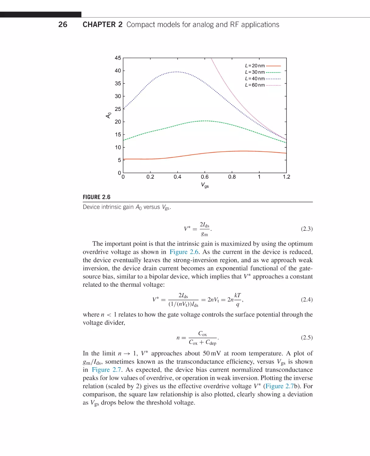
V∗ =
2Ids
.
gm
(2.3)
The important point is that the intrinsic gain is maximized by using the optimum
overdrive voltage as shown in Figure 2.6. As the current in the device is reduced,
the device eventually leaves the strong-inversion region, and as we approach weak
inversion, the device drain current becomes an exponential functional of the gatesource bias, similar to a bipolar device, which implies that V ∗ approaches a constant
related to the thermal voltage:
V∗ =
2Ids
kT
= 2nVt = 2n ,
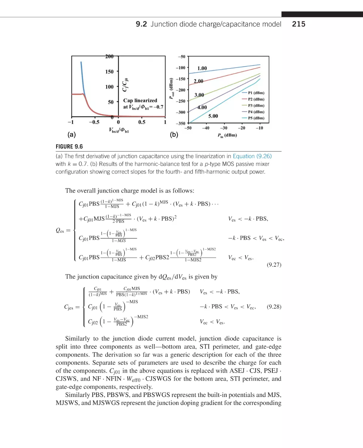
(1/(nVt ))Ids
q
(2.4)
where n < 1 relates to how the gate voltage controls the surface potential through the
voltage divider,
n=
Cox
.
Cox + Cdep
(2.5)
In the limit n → 1, V ∗ approaches about 50 mV at room temperature. A plot of
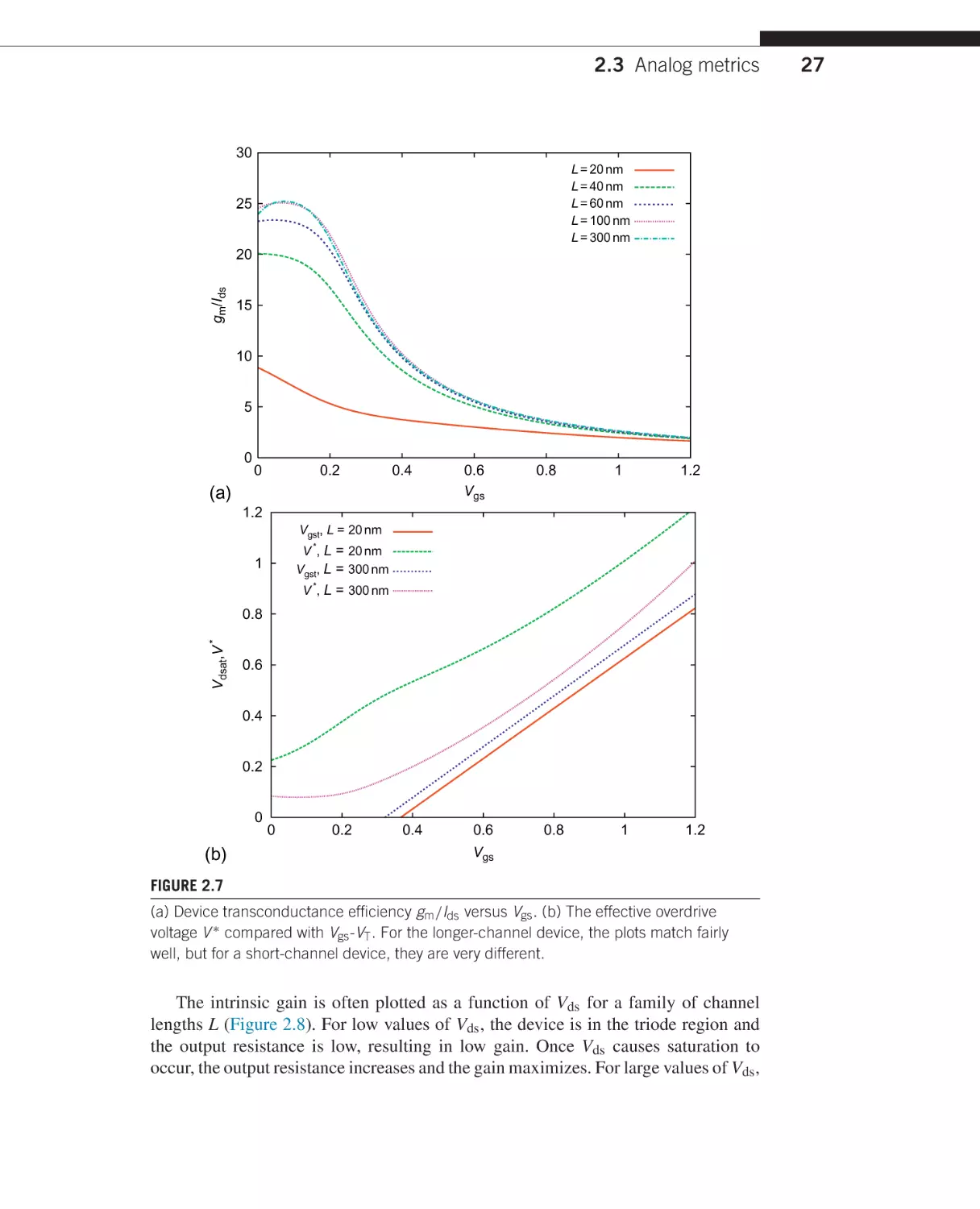
gm /Ids , sometimes known as the transconductance efficiency, versus Vgs is shown
in Figure 2.7. As expected, the device bias current normalized transconductance
peaks for low values of overdrive, or operation in weak inversion. Plotting the inverse
relation (scaled by 2) gives us the effective overdrive voltage V ∗ (Figure 2.7b). For
comparison, the square law relationship is also plotted, clearly showing a deviation
as Vgs drops below the threshold voltage.
2.3 Analog metrics
30
L = 20 nm
L = 40 nm
L = 60 nm
L = 100 nm
L = 300 nm
25
gm/Ids
20
15
10
5
0
0
0.2
0.4
(a)
0.6
Vgs
0.8
1
1.2
1.2
Vgst, L = 20 nm
V *, L = 20 nm
Vgst, L = 300 nm
1
V *, L = 300 nm
Vdsat,V *
0.8
0.6
0.4
0.2
0
(b)
0
0.2
0.4
0.6
0.8
1
1.2
Vgs
FIGURE 2.7
(a) Device transconductance efficiency gm /Ids versus Vgs . (b) The effective overdrive
voltage V ∗ compared with Vgs -VT . For the longer-channel device, the plots match fairly
well, but for a short-channel device, they are very different.
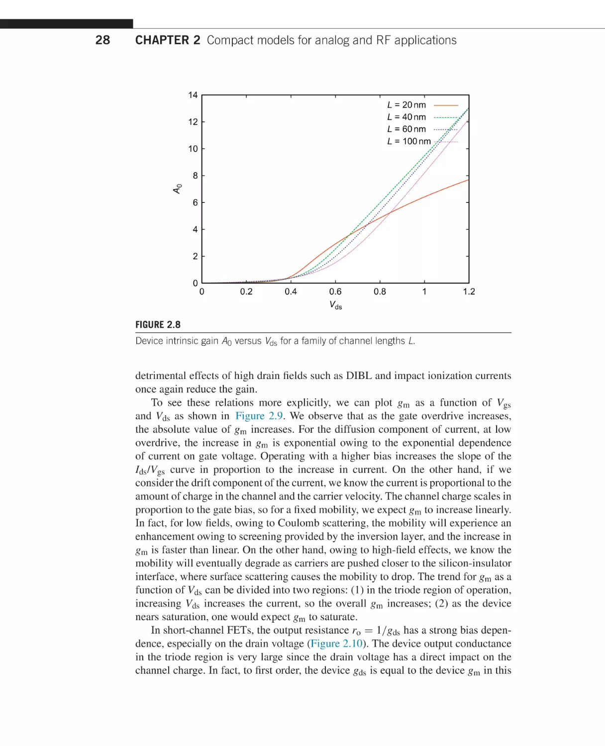
The intrinsic gain is often plotted as a function of Vds for a family of channel
lengths L (Figure 2.8). For low values of Vds , the device is in the triode region and
the output resistance is low, resulting in low gain. Once Vds causes saturation to
occur, the output resistance increases and the gain maximizes. For large values of Vds ,
27
CHAPTER 2 Compact models for analog and RF applications
14
L = 20 nm
L = 40 nm
L = 60 nm
L = 100 nm
12
10
8
A0
28
6
4
2
0
0
0.2
0.4
0.6
Vds
0.8
1
1.2
FIGURE 2.8
Device intrinsic gain A0 versus Vds for a family of channel lengths L.
detrimental effects of high drain fields such as DIBL and impact ionization currents
once again reduce the gain.
To see these relations more explicitly, we can plot gm as a function of Vgs
and Vds as shown in Figure 2.9. We observe that as the gate overdrive increases,
the absolute value of gm increases. For the diffusion component of current, at low
overdrive, the increase in gm is exponential owing to the exponential dependence
of current on gate voltage. Operating with a higher bias increases the slope of the
Ids /Vgs curve in proportion to the increase in current. On the other hand, if we
consider the drift component of the current, we know the current is proportional to the
amount of charge in the channel and the carrier velocity. The channel charge scales in
proportion to the gate bias, so for a fixed mobility, we expect gm to increase linearly.
In fact, for low fields, owing to Coulomb scattering, the mobility will experience an
enhancement owing to screening provided by the inversion layer, and the increase in
gm is faster than linear. On the other hand, owing to high-field effects, we know the
mobility will eventually degrade as carriers are pushed closer to the silicon-insulator
interface, where surface scattering causes the mobility to drop. The trend for gm as a
function of Vds can be divided into two regions: (1) in the triode region of operation,
increasing Vds increases the current, so the overall gm increases; (2) as the device
nears saturation, one would expect gm to saturate.
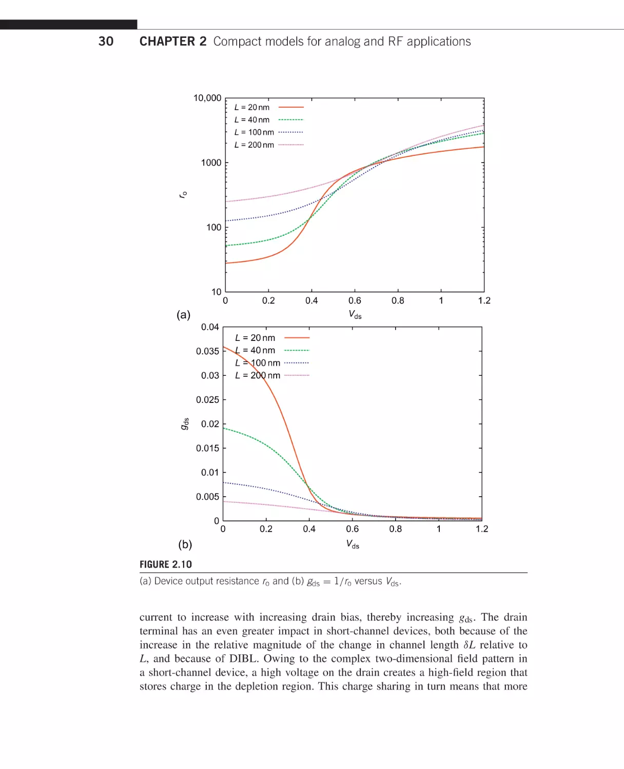
In short-channel FETs, the output resistance ro = 1/gds has a strong bias dependence, especially on the drain voltage (Figure 2.10). The device output conductance
in the triode region is very large since the drain voltage has a direct impact on the
channel charge. In fact, to first order, the device gds is equal to the device gm in this
2.3 Analog metrics
0.005
L = 20 nm
L = 40 nm
L = 100 nm
L = 200 nm
L = 300 nm
0.0045
0.004
0.0035
gm
0.003
0.0025
0.002
0.0015
0.001
0.0005
0
0
0.2
0.4
0.6
0.8
1
1.2
0.8
1
1.2
Vgs
(a)
0.005
L = 20 nm
L = 40 nm
L = 100 nm
L = 200 nm
0.0045
0.004
0.0035
gm
0.003
0.0025
0.002
0.0015
0.001
0.0005
0
(b)
0
0.2
0.4
0.6
Vds
FIGURE 2.9
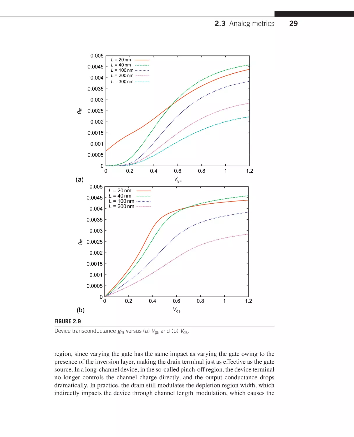
Device transconductance gm versus (a) Vgs and (b) Vds .
region, since varying the gate has the same impact as varying the gate owing to the
presence of the inversion layer, making the drain terminal just as effective as the gate
source. In a long-channel device, in the so-called pinch-off region, the device terminal
no longer controls the channel charge directly, and the output conductance drops
dramatically. In practice, the drain still modulates the depletion region width, which
indirectly impacts the device through channel length modulation, which causes the
29
CHAPTER 2 Compact models for analog and RF applications
10,000
L = 20 nm
L = 40 nm
L = 100 nm
L = 200 nm
ro
1000
100
10
0
0.2
0.4
(a)
0.6
Vds
0.8
1
1.2
0.6
0.8
1
1.2
0.04
L = 20 nm
L = 40 nm
L = 100 nm
L = 200 nm
0.035
0.03
0.025
gds
30
0.02
0.015
0.01
0.005
0
(b)
0
0.2
0.4
Vds
FIGURE 2.10
(a) Device output resistance ro and (b) gds = 1/ro versus Vds .
current to increase with increasing drain bias, thereby increasing gds . The drain
terminal has an even greater impact in short-channel devices, both because of the
increase in the relative magnitude of the change in channel length δL relative to
L, and because of DIBL. Owing to the complex two-dimensional field pattern in
a short-channel device, a high voltage on the drain creates a high-field region that
stores charge in the depletion region. This charge sharing in turn means that more
2.3 Analog metrics
electrons can flow into the channel, thereby lowering the threshold of the device.
Fortunately, this effect is reduced for FinFETs, resulting in an improvement in
intrinsic gain. Finally, as the voltage is further increased, impact ionization in the
high-field region causes a further increase in current and thereby a drop in the output
resistance.
2.3.5 SPEED: UNITY GAIN FREQUENCY
In analog circuits, DC gain is only half the story. While operation at subthreshold is
beneficial for gain and especially transconductance efficiency, in practice this is rarely
acceptable because of the reduction in the device speed. Only extremely slow circuits
can tolerate operating in this region. For most other circuits, operation in moderate
or strong inversion is desired.
The speed of a transistor is often measured using the device unity gain frequency
fT , or the frequency when the current gain of a transistor is unity. Since id = gm vgs ,
and vgs jω(Cgs + Cgd ) = is , taking the ratio, we have
Ai =
id
gm
=
.
is
jω(Cgs + Cgd )
(2.6)
Solving for |Ai | = 1, we arrive at the unity gain frequency
ωT = 2πfT =
gm
.
Cgs + Cgd
(2.7)
It is not at first obvious why fT plays such an important role in analog (and digital)
circuits. To see this, consider the simple cascade amplifier shown in Figure 2.11a,
where a single-stage amplifier drives an identical copy. The gain of this first stage is
given by the intrinsic gain of the amplifier, and the 3 dB bandwidth is limited by the
pole at the high impedance node:
ω0 =
vi
(a)
1
.
ro,1 ((1 + |A2 |)Cgs,2 + Cd1,tot )
vi
(b)
FIGURE 2.11
(a) A cascade of common-source amplifiers. (b) A cascade of cascode amplifiers.
(2.8)
31
32
CHAPTER 2 Compact models for analog and RF applications
Here Cd1,tot is the total drain capacitance (Cgd + Cds + Cwire + · · · ), and the effect
of Miller multiplication is captured by boosting the second-stage input capacitance
by the gain A2 . If the second stage is a cascode with a small voltage gain between the
gate and the drain, then A2 can be made smaller than unity to minimize its impact.
So if we disregard the Miller effect, we have
ω0 =
1
,
ro (Cgs + Cd,tot )
(2.9)
as an upper bound. In most applications, we intend to embed this amplifier in a
feedback loop, so the gain-bandwidth product of interest is
A0 ω0 < gm ro
gm
1
=
≈ ωT ,
ro (Cgs + Cd,tot )
Cgs + Cd,tot
(2.10)
which bears a resemblance to the unity gain of the transistor itself. So in an
approximate fashion, we can see that the maximum gain-bandwidth product of an
amplifier is in fact limited by the device unity gain frequency. Even in a digital circuit,
we find that fT plays a key role. Consider the time constant of a simple gate, such as
an inverter. If the fan out of an inverter is unity, in other words the inverter drives an
identical copy of itself, then the load of the inverter is approximately Cgs + Cd,tot .
The discharge current takes a complicated form, but to first order the transistor acts
like a switch with on-conductance gds = gm (in the triode region), so the discharge
time is given by
τT =
Cgs
1
=
.
gm
ωT
(2.11)
A plot of fT as a function of Vgs for different channel lengths is shown in Figure 2.12. The bias and geometry dependency on gm have already been discussed.
The remaining dependency is on the device capacitance, including the gate-to-source
capacitance Cgs and the gate-to-drain capacitance. It is important to note that fT is
usually measured using scattering parameters, and so using the “DC” values of gm and
C will fail to capture fT at high frequency. We will return to this point in Section 2.4.
In a long-channel device, Cgs is usually the dominant capacitor, since Cgd occurs
only from the small overlap between the gate terminal and the drain region. In a real
device, a considerable portion of the capacitance may be due to extrinsic capacitors in
the wiring. In modern devices, the gate-drain overlap region is a significant fraction
and Cgd can be comparable to Cgs . In a FinFET, owing to the three-dimensional
structure, a considerable amount of fringing capacitance increases Cgd compared
with a bulk device. For these reasons, FinFET fT suffers compared with that of an
equivalent bulk device. In reality, bulk devices cannot scale to FinFET dimensions,
so the comparison is not fair. Nevertheless, this requires a very good extrinsic FET
model to accompany the intrinsic model.
2.3.6 NOISE
Thermal noise is relatively well understood in FETs and should form the core of any
model. When drift current dominates, the thermal noise is a function of the channel
2.3 Analog metrics
1.2e+12
L = 20 nm
L = 60 nm
L = 100 nm
L = 200 nm
L = 300 nm
1e+12
fT
8e+11
6e+11
4e+11
2e+11
0
0
0.2
0.4
0.6
0.8
1
1.2
Vgs
FIGURE 2.12
The device unity gain frequency fT as a function of Vgs for a family of channel lengths L.
conductance, whereas in moderate and weak inversion the diffusion component gives
rise to shot noise. A good model should capture the drain noise current accurately
in all regions in a smooth and uniform manner. Capturing noise in saturation is
complicated by the excess noise generated by the FET, captured by the parameter
γ in the spot noise variance of the drain current:
i2d,n = 4kTgds,ch γ δ f ,
(2.12)
where gds,ch is the channel conductance. For a long-channel device, it is well known
that γ = 2/3, which is derived by considering the thermal noise contribution of an
incremental region of the channel to the drain. The coupling to the gate through the
gate-oxide capacitance also gives rise to a correlated gate noise current. For shortchannel devices it has been observed that γ is larger than 1, which is sometimes
attributed to the hot electron effects occurring on the drain end of the transistor.
A good test for a compact model is a plot of γ versus the drain and gate bias voltage,
as shown in Figure 2.13. It is important to define γ in terms of gds,ch (the drainsource conductance in the “linear region” of the device) and not gm , which leads to
the erroneous conclusion that γ is much larger than 1. The reason is that noise arises
from the physical resistance of the channel, which originates from the inversion layer
at the source to a region near the drain. As noted before, gm = gds in the linear region
of the transistor operation.
One would expect that the thermal noise of a FET varies smoothly as the device
bias is varied from strong inversion to weak inversion, with the limits of weakinversion noise given by the well-known shot noise current 2qIds . For strong-inversion
33
CHAPTER 2 Compact models for analog and RF applications
2.2
L = 200 nm
L = 200 nm
L = 500 nm
L = 700 nm
2
1.8
1.6
g
34
1.4
1.2
1
0.8
0.6
0
0.2
0.4
0.6
0.8
1
1.2
Vgs (V)
FIGURE 2.13
Excess noise factor γ versus gate bias Vgs .
operation, a plot of γ versus Vds should have physical meaning in the saturation
regime. To understand the importance of γ , let us derive the noise figure of a commonsource and a common-gate amplifier. For the common-source case at low frequencies,
the total output noise is given by
i2o = g2m v2Rs + i2d = g2m 4kT Rs δf + 4kT gds,ch γ δ f ,
(2.13)
from which we calculate the noise figure
F =1+
gds,ch γ
γ /α
=1+
.
gm Rs
g2m Rs
(2.14)
For many applications, Rs is fixed, and gm is limited by power consumption, which
shows the noise limit is ultimately determined by γ . The common-gate amplifier is
even more sensitive to γ since it has no current gain,
i2o = i2Rs + i2d = 4kTGs δ f + 4kTgds,ch γ δ f ,
(2.15)
giving the well-known lower bound on the obtainable noise figure
F =1+
(gm /α)γ
.
Gs
(2.16)
The reason the common-gate amplifier is favored over the common-source amplifier
is the ability to obtain a wideband impedance match by setting gm = Rs , which
results in
F =1+
γ
.
α
(2.17)
2.3 Analog metrics
1e–20
L = 100 nm
L = 200 nm
L = 300 nm
L = 500 nm
L = 700 nm
Output noise (A2/Hz)
1e–21
1e–22
1e–23
1e–24
100,000
1e+06
1e+07
1e+08
1e+09
1e+10
Vgs
FIGURE 2.14
The drain noise current spectral density versus frequency for a family of channel lengths L
biased at the same bias Vgs .
Later we shall also see that the ultimate lower limit on phase noise is similarly
related to γ .
In addition to thermal noise, flicker noise plays a big role in analog circuits,
especially as devices are devices are scaled to smaller dimensions. The spectrum of
flicker noise in a FET overlaps with the frequency of interest in many analog signal
processing applications (DC to 10 s or MHz), and a designer will often size devices in
order to minimize the impact of flicker noise (Figure 2.14). The flicker noise model
should therefore be very physical in scaling limits, particularly when the designer
selects different channel lengths L to minimize noise. Naturally, the bias dependence
of flicker noise should be correctly captured.
In a FET, all of the intrinsic noise originates from the channel and traps in the
gate-oxide interface. Extrinsic parasitic elements, such as physical resistance in the
gate, source, and drain, also contribute noise. Plotting noise parameters versus bias
is a good way to tease out the various sources of noise: ones that depend on bias
are generally due to intrinsic device noise, and fixed noise contributions are due to
extrinsic sources. An alternative representation of the noise of a FET is to define an
input pair of correlated noise voltage and current sources. This is useful for circuit
design and also a good metric for testing the model. Some circuit simulators can
simulate and plot these parameters for a two-port circuit, and these plots are a good
way to test the physical variation in the input noise sources, which depend on both
intrinsic and extrinsic noise sources.
35
36
CHAPTER 2 Compact models for analog and RF applications
2.3.7 LINEARITY AND SYMMETRY
Harmonic distortion
Linearity, or the ability of an analog circuit to faithfully reproduce the input signal
at the output (amplified or buffered), is an important metric, although it receives less
attention than gain and speed. The reason is simple, since most analog circuits employ
feedback, which has the ability to reject the distortion produced by devices by the
loop gain of the circuit. Open loop amplifiers are much commoner in RF circuits, so
intrinsic device nonlinearity is still an important metric. Even in modern nanoscale
devices, linearity is playing a bigger role as loop gains drop (owing to the drop in
intrinsic gain). Furthermore, when FETs are used as switches, particularly in sampled
time systems, the distortion produced by the device is sampled and processed along
with the signal.
The source of distortion is easy to understand since the I-V characteristics of a
FET are described by nonlinear equations of terminal voltages:
Ids = f (Vgs , Vds , Vbs ).
(2.18)
Expanding the above relation into a Taylor series of Vgs , while holding Vds and Vbs
constant, and disregarding the DC, we have the following “Gm ” nonlinearity power
series:
ids = gm1 vgs + gm2 v2gs + gm3 v3gs + · · · ,
(2.19)
where lowercase symbols denote AC quantities. The first term, gm1 , is nothing but the
transconductance of the device. The curvature of the I-V curve gives rise to higherorder coefficients which describe the deviation of AC from the quiescent operating
point for a small deviation of the gate-source voltage about the bias point. In a similar
way, we can derive a power series in terms of the drain-source voltage,
ids = gds1 vds + gds2 v2ds + gds3 v3ds + · · · ,
(2.20)
and, in general, a two-dimensional power series can be derived when both the gatesource voltage and the drain-source voltage vary. In practice, to keep things simple,
it is common to deal only with one-dimensional power series relations.
The commonest way to measure the nonlinearity of a block is to find the harmonic
distortion (HD), which is defined by driving an amplifier with a pure sinusoid and
observing the harmonics at the output:
ids = gm1 Ags cos(ωt) + gm2 A2gs cos2 (ωt) + g3m3 A3gs cos3 (ωt) + · · · .
(2.21)
For example, cos2 (x) = 0.5(1 + cos(2x)), or the square term produces DC and the
second harmonic. Likewise, cubing the signal gives
cos3 (x) = cos(x) cos2 (x) = 0.5(cos(x) + cos(x) cos(2x))
1
1
=
cos(x) + (cos(x) + cos(3x))
2
2
3
1
= cos(x) + cos(3x),
4
4
which contains the fundamental signal and the third harmonic.
(2.22)
(2.23)
(2.24)
2.3 Analog metrics
In general, with use of a binomial expansion on the sum of complex exponentials,
it is not very difficult to show that the nth odd power produces harmonics starting from
the fundamental and every odd harmonic (first, third, fifth, …, nth), whereas an nth
even power produces all even harmonics starting from DC (zero, second, fourth, sixth,
…, nth). In other words, even harmonics generate DC and every even harmonic up
to n (0 × ω, 2 × ω, . . . , n × ω). Odd harmonics generate the fundamental and every
odd harmonic up to n (1 × ω, 3 × ω, . . . , n × ω). This allows us to write the following
equation for the harmonics of the output drain current when the input is excited by a
sinusoid:
3
ids = gm1 Ags + gm3 A3gs + · · ·
4
+
+
1
gm2 A2gs + · · ·
2
1
gm3 A3gs + · · ·
4
cos(ωt)
(2.25a)
cos(2ωt)
(2.25b)
cos(3ωt) + · · · .
(2.25c)
The important point is that each harmonic arises from a potentially infinite set of
powers, but for small excursions from the bias point, the most dominant terms are
the smallest powers. This last point is important, and may seem like a contraction,
but in fact it follows from the assumption of a “small-signal” or “weak” distortion.
For example, for a practical device, when the equation is put into a power series, one
finds that the relevant quantity is a normalized voltage vgs /V ∗ (overdrive voltage), or
in weak inversion, vgs q/kT, so as long as the normalized voltage excursion is small,
raising this to an increasingly larger power produces an increasingly smaller quantity
in the power series. Under these conditions, the lowest-order powers completely
dominate the behavior of the device distortion generation.
Given these conditions for weak distortion, the HD is defined as the ratio of the
amplitude of the harmonic to the fundamental. For example,
HD2 =
gm2 (A2gs /2)
V2ω
1 gm2
=
=
Ags
Vω
gm1 Ags
2 gm1
(2.26)
HD3 =
gm3 (A3gs /4)
V3ω
1 gm3 2
=
=
A .
Vω
gm1 Ags
4 gm1 gs
(2.27)
and
As shown in Figure 2.15, as we sweep the amplitude of the input sinusoid, the magnitude of the second harmonic increases quadratically, whereas the third harmonic
grows cubically, so their HD ratios exhibit a power law with one order less (linear
and quadratic). As the amplitude grows beyond the small-signal distortion regime,
eventually higher-order terms dominate and the slopes change.
To show the importance of overdrive voltage, plots of HD2 and HD3 versus Vgs
are shown in Figure 2.16. The physical reason for the improvement in HD with Vgs
is quite simply related to the fact that the electric fields in the device are related to the
overdrive voltage, and lower fields produce more linear relations as expected. The dip
37
CHAPTER 2 Compact models for analog and RF applications
-120
-140
Fund
2nd
3rd
-160
-180
PHD
-200
-220
-240
-260
-280
-300
-320
-40
-30
-20
-10
Pin (dBm)
0
10
FIGURE 2.15
The HD currents at 2ω and 3ω versus the input amplitude Pin (dBm) applied at the
gate/source showing the characteristic slope of 2 and 3 on a log scale. Note the bias is
fixed at Vgs .
−10
HD2
HD3
−20
−30
−40
−50
HD2,3
38
−60
−70
−80
−90
−100
−110
0
0.2
0.4
0.6
Vgs (V)
0.8
1
1.2
FIGURE 2.16
HD2 and HD3 versus the bias Vgs for a fixed swing vgs (−30 dBm). Note the “sweet spot”
for HD3 .
2.3 Analog metrics
in HD3 is a consequence of gm3 = 0 for a particular bias point, sometimes called the
“sweet spot” of a MOSFET.
While we have defined HD for Gm nonlinearity, the same metrics can be defined
for any other pair of currents/voltages in the device. While Gm nonlinearity is the
commonest type of nonlinearity, output conductance nonlinearity is perhaps a close
contender. Since HD is a strong function of the device bias point, it is hard to define a
universal metric. The modeling engineer should ensure that the model reproduces
the distortion at a range of different bias voltages (both Vgs and Vds ), and most
importantly, it is important to ensure that the slope of the HD products follows the
above relations for weak inputs. For example, on a log scale, the third harmonic signal
should have a slope of 3 when the input is very weak, and any deviation from this
slope indicates a problem in the compact model.
This is because we expect all the compact model curves to be smooth and infinitely
differentiable, which means that we can always define a power series and prove that
the slope is indeed 3. But if the compact model has a source of an abrupt nonlinearity,
then a nonsmooth curve will not follow our predictions. A classic example is an “if”
statement in the compact model that changes the device I-V behavior (e.g., a diode
model that has a hard saturation). If the signal is biased near this “if” statement, then
even a small deviation produces a kink in the I-V transfer (a point where the slope
is not defined). Keep in mind that for a strong enough signal, this assumption breaks
down since the fundamental power is affected by all odd harmonics, which causes
the slope to change dramatically, but this occurs only when a device is driven very
hard (deep compression).
While it is not possible to check every possible HD product, it is good practice to
check HD2 through HD5 to make sure all curves follow the correct slopes predicted
by small-signal distortion. Since distortion arises from the large signal behavior of
a transistor, it has to be simulated using transient or steady-state simulation, such
as periodic steady-state analysis using shooting in SpectreRF or harmonic balance
simulation. The same can be obtained from a transient simulation by calculating the
fast Fourier transform of the output waveform and plotting harmonic powers. Classic
SPICE also includes a disto statement that is similar to an AC analysis, but includes
the effect of higher-order harmonics as we have done.
Gain compression
A very important metric is the gain compression that naturally occurs in all devices
owing to nonlinearity. For example, if we plot the effective transconductance Gm
of a device versus the input swing, we obtain a curve as shown in Figure 2.17. As
expected, for small input voltages vgs , Gm = gm , but as we increase the swing, the
transconductance either increases or drops. The reason for this change in Gm is related
to the fact that all odd harmonics of the I-V relation generate fundamental current
(gm,2k−1 for k > 1 in our power series), and these currents can be in phase or out of
phase with the fundamental generated by gm1 . If we examine Equation (2.25), we
find that the fundamental output current amplitude is given by
39
CHAPTER 2 Compact models for analog and RF applications
0.003
Vgs = 0.2 V
Vgs = 0.4 V
Vgs = 0.6 V
Vgs = 0.8 V
Vgs = 1.0 V
0.0025
0.002
Gm
40
0.0015
0.001
0.0005
0
0
0.05
0.1
0.15
0.2
0.25
0.3
0.35
0.4
0.45
0.5
Vin (V)
FIGURE 2.17
The transconductance gain compression versus the signal swing vgs .
3
ids,ω = gm1 vgs + gm3 v3gs + · · · .
4
(2.28)
If we normalize this current by the gate drive amplitude vgs , we obtain the effective
transconductance
Gm =
ids,ω
3
= gm1 + gm3 v2gs + · · · .
vgs
4
(2.29)
So we see that the effective transconductance is related to the gate-source voltage
excursion vgs . For very small swings, in fact the small-signal limit for vgs → 0, then
Gm = gm1 as expected. But for larger swings, depending on the sign of gm3 , the
transconductance can increase or decrease. The increase in transconductance, or more
generally gain, is called gain expansion. Likewise, a decrease in gain is called gain
compression. In the plot in Figure 2.17, when the device is biased in weak inversion,
the gain is expansive owing to the exponential nature of the device I-V curve. For
higher bias points, the gain is compressive owing to the high-field mobility effects in
the FET.
Note that we have explicitly separated the gain into its components Gm and Ro
since gain expansion also occurs owing to the limited output swing (headroom) and
output resistance Ro of a device. In practice, both act in conjunction to determine the
overall gain compression characteristics.
Since all transistors operate with a fixed headroom, eventually the voltage swing
must be clipped by the rails, and then the gain therefore drops, leading to an eventual
compressive characteristic (Figure 2.18). But the shape of the compression, in
2.3 Analog metrics
10
Gain
RL = 1 K
RL = 2 K
RL = 8 K
RL = 20 K
1
0.1
−50
−40
−30
−20
−10
0
10
Pin (dBm)
FIGURE 2.18
The voltage gain compression versus the signal swing Pin (dBm). The drain is biased at
1.2 V using an ideal inductor and the load resistor RL is varied. Note that high values of RL
have higher gain, but compress earlier owing to the drain voltage swing (rather than the Gm
compression).
particular regions of expansion and compression, is related to the device nonlinearity
and is a good way to gauge the accuracy of a compact model. For example, Gm
compression occurs due to high-field effects and mobility degradation. While these
effects are visible on the I-V curve as well, here the effects are measured by the slopes
of the I-V curve, which may not be as apparent to the naked eye.
Memory effects
To keep things simple, we have explicitly disregarded all capacitive nonlinearity in
the FET. This means that we have assumed that the drain current is an instantaneous
function of the gate-source and drain-source voltages, which is not true in practice.
Owing to the presence of both linear and nonlinear capacitance at the terminals of a
FET, the situation is much more complicated, requiring a Volterra series description
instead of a power series relation [1]. In practice, in most analog circuits, these
so-called memory effects are disregarded. This is justified in practice if the device
is operated well below the cutoff frequency of the transistor, allowing the quasistatic assumption to be valid, and well below the poles of the amplifier, so that the
amplitudes of signals are not attenuated or signals are not phase shifted as the signals
travel through a transistor. These conditions are often met for the desired signals that
are processed by analog circuits, but not for the harmonics.
41
CHAPTER 2 Compact models for analog and RF applications
Intermodulation distortion
In practice, it is rare to amplify a single tone, and in general a complex signal is
processed by a device. For linear time-invariant circuits, we know that we need only
to characterize the frequency response of the system (or equivalently the impulse
response in the time domain), but for nonlinear circuits, even memoryless ones, we
have to characterize the impact of not only every tone, but every two tones, three
tones, and in general N tones, to completely understand the response of the system
to a general signal. Owing to the complexity of doing this, a commoner metric is to
characterize the intermodulation between only a few tones. The commonest metrics
are the two-tone response and the associated intermodulation signals (in general not
harmonically related to either tone). We will return to intermodulation distortion
in Section 2.4.
2.3.8 SYMMETRY
The symmetry of a compact model is also an important metric in analog circuits
that use the device bias around Vds = 0 V, which occurs when the device is used as
a switch in sampling circuits and in commutating circuits (such as RF mixers). The
origin of the asymmetry in the compact model is not the drain-source swapping in the
model, as was once believed, nor is it due to source referencing, but asymmetry can
arise from both of these mechanisms if they are not handled properly. For example,
often an “if” statement is used to swap the internal source/drain of a physically
symmetric FET, since the label “source” and “drain” are defined only by the bias
points (Vds > 0 V for an n-type FET), which may change sign during the course
of a circuit simulation. The model typically assigns one terminal as the drain and
detects a change in sign, which can be done only with a finite precision. In other
words, when Vds < , for some small , the drain-source swapping will occur. This
will produce a small kink in the transfer curve about Vds = 0 V, which requires
smoothing.
The Gummel symmetry test is used to detect potential symmetry problems in
a FET model. The circuit shown in Figure 2.19 is used to excite the circuit about
Vg
vx +
V b0
Vb
+
42
vx
V b0
FIGURE 2.19
The circuit used to characterize the Gummel symmetry test.
2.3 Analog metrics
Vds = 0 V. For a uniformly doped FET, we expect the drain current to be an odd
function of vx ,
Id (vx ) = −Id (−vx ),
so
ix (vx ) =
(2.30)
1
(Id (vx ) − Is (vx )).
2
(2.31)
For a properly designed compact model, we expect ix is a smooth function of vx with
continuity at vx = 0 V, implying that dn ix /dvnx for all n. From physical considerations,
we expect ix = 0 A at vx = 0 V, and also that d2 ix /dv2x = 0 due to the symmetry of
waveform. For example, first- and second-order derivatives for the FinFET common
multigate (CMG) model are plotted as shown in Figure 2.20, clearly demonstrating
smooth and consistent behavior.
In addition to the current behavior, the terminal charge behavior of the Gummel
symmetry circuit should also satisfy physical conditions on symmetry and smoothness. Sweeping vx from a negative value to an equal positive value, one can plot
the gate, source, drain, and bulk charges of the MOSFET (Qg , Qs , Qd , and Qb ),
respectively. The derivatives of charges versus vx should be continuous around vx =
0 V, and the derivatives of charges should pass smoothly through vx = 0 V and have
no discontinuities. Furthermore, the derivatives of Qs and Qd should be equal and
opposite at vx = 0 V because the device is assumed to be symmetric.
An ideal symmetric device should also exhibit symmetry in the capacitances Cgs
and Cgd , with equal values at vx = 0 V. Similar comments apply to Cbs and Cbd , and
Cdd and Css , respectively.
0.008
0.006
0.004
Ix, Ix⬘, Ix⬙
0.002
0
−0.002
−0.004
−0.006
−0.008
−0.6
Ix
Ix⬘
Ix⬙
−0.4
−0.2
0
Vx (V)
0.2
FIGURE 2.20
The Gummel symmetry test for the BSIM-CMG FinFET model.
0.4
0.6
43
44
CHAPTER 2 Compact models for analog and RF applications
2.4 RF METRICS
A good analog compact model is the foundation for a good RF compact model. In
addition to the already mentioned important metrics for analog circuits, we find that
RF circuits require new modules in the compact model to capture gate resistance,
substrate resistance, and non-quasi-static (NQS) effects. Since many RF circuits do
not use feedback, they are more sensitive to distortion produced by the transistors,
placing stronger demands on the accuracy of the model. Finally, since inductors can
be used to tune out capacitive parasitic elements, there are also lower tolerances for
error in the capacitance of the device. Furthermore, we find that fT is not the best
metric for speed, although it continues to play an important role.
2.4.1 TWO-PORT PARAMETERS
At higher frequencies, it is much commoner to rely on two-port parameters of a
transistor. The reasons for the importance of two-port parameters, as opposed to say
a hybrid-pi model or a full compact model, are both historical and practical. In the
past, compact models were relatively simple and did not capture the detailed device
behavior and extrinsic parasitic elements, particularly for operation near fT of the
device when NQS effects are important to model. An RF model that includes the
intrinsic device and packaging parasitic elements can become extremely complex for
analysis by hand (Figure 2.21). To circumvent this issue, designers often relied on
measured two-port parameters at high frequency, rather than the extrapolated model
behavior from I-V/C-V curves, in order to understand the device behavior.
Two-port parameters have many limitations, most importantly arising from their
small-signal assumption and their frequency dependence. But many RF circuits
G
Rge
S
Cgse
Cgde
Rse
Rde
Cbse
Cbde
Rs,bs
D
Rs,bd
Rbe
B
FIGURE 2.21
A full FET model includes the intrinsic transistor in addition to external parasitic elements.
2.4 RF metrics
Cm
Yp
Rin
Cin
Y11 = Yp + Ym
Yo
+
vin
−
Ym
gm vin
ro
Y22 = Yo + Ym
Co
Y21 = gm − Ym
Y12 = −Ym
FIGURE 2.22
The measured Y parameters can be converted directly into circuit pi parameters using the
relations shown. Since this is an oversimplified model, the parameters are frequency
dependent.
(power amplifiers are a good exception to this) operate with weak signals (signals
captured off the air) over a narrow range of frequencies (so-called narrowband
communication) and the small-signal narrowband assumption is valid in many
circumstances, especially if there are no interfering signals. Moreover, by using
measured two-port (or three/four-port) parameters over a range of bias points, on
can construct a table-lookup model to capture the dynamics for modulating signals.
The benefit of two-port parameters is that they are completely general and capture
all of the transistor dynamics (by definition) at a particular frequency of interest.
Moreover, they can be used to answer some very general questions about a transistor
device, such as “What is the maximum possible power gain for a device?” For these
reasons, we will make extensive use of two-port parameters and the rich theory to
delve into these questions.
Two-port parameters from a measured device are often compared to a compact
model as a metric, but often many details are hard to decipher directly from these
parameters as both circuit designers and device engineers have more intuition for
circuits and small-signal equivalent circuits. A good solution is to convert general
two-port parameters into an equivalent circuit representation, such as the popular
hybrid-pi model, in order to gain intuition about how well the model matches
measurements. Keep in mind that the two-port parameters vary with frequency,
so the equivalent circuit will also vary, but if the two-port is chosen wisely, then
many of the parameters remain fairly constant. For example, if we consider the twoport parameters of a transistor in the common-source configuration, as shown in
Figure 2.22, then it is easy to show that the equivalent pi circuit is related to the
Y parameters as follows:
Y11 = Yπ + Yμ ,
(2.32)
Y22 = Yo + Yμ ,
(2.33)
Y21 = gm − Yμ ,
(2.34)
Y12 = −Yμ .
(2.35)
We can solve these equations for four pi-circuit parameters from measured results:
Yπ = Y11 + Y12 ,
(2.36)
45
46
CHAPTER 2 Compact models for analog and RF applications
Yμ = −Y12 ,
(2.37)
Yo = Y22 + Y12 ,
(2.38)
Gm = Y21 − Y12 .
(2.39)
It is important to note that Yμ and Gm are in general complex. The real part of
Cμ reflects that the feedback in a transistor can experience a phase shift at high
frequencies, and the imaginary part of Gm reflects the same in the forward direction.
It is convenient to think of Gm in magnitude/phase terms,
Gm = |Gm |∠Gm ,
(2.40)
and it is also convenient to decompose the input network Yπ from a shunt representation to a series one, since in practice the gate resistance is fairly constant with
frequency:
Yπ = jωCπ + Gπ =
1
.
(1/(jωCgs )) + Rg
(2.41)
The output network, on the other hand, is already in a convenient form:
Yo = jωCds + go .
(2.42)
Since these capacitors and resistors represent the entire transistor, they are in fact
lumped representations of many sources of capacitance arising from both the intrinsic
device and the extrinsic parasitic elements, including the substrate network. Note that
this common-source representation cannot capture the model accuracy for source
side parasitic elements, which may be different owing to layout differences. For
this reason, a two-port representation is not complete and a three-port or four-port
characterization is preferred (for the back gate or second gate of the device). For a
typical device, a plot of the pi parameters is shown in Figure 2.23. Over a narrow
range of frequencies, these parameters are relatively constant and a good indication
of the device behavior for a fixed operating point.
2.4.2 THE NEED FOR SPEED
RF circuits work from low gigahertz to several thousand gigahertz, from the so-called
RF spectrum, to the millimeter-wave spectrum, and even at “terahertz” frequencies.
There is a quest to run circuits as fast as possible to exploit new bandwidth and to
maximize communication rates. For analog circuits, we found that fT was a good
substitute for estimating the gain-bandwidth product of a circuit. But in RF circuits,
capacitive parasitic elements can be tuned out and the transistor can be operated over
a narrow bandwidth at frequencies in excess of fT . So what is the right metric for a
transistor?
Let us start with a simple exercise and derive the gain and bandwidth for the
cascade of tuned amplifiers shown in Figure 2.24. Here the voltage gain per stage is
limited not by the output resistance, but by the inductor quality factor QL :
Av = gm ro ||RL ≈ gm QL ωL.
(2.43)
2.4 RF metrics
5.5e–14
5e–14
Cgs
4.5e–14
Cgd
4e–14
Cgs, Cgd
3.5e–14
3e–14
2.5e–14
2e–14
1.5e–14
1e–14
5e–15
0
1e+10 2e+10 3e+10 4e+10 5e+10 6e+10 7e+10 8e+10 9e+10 1e+11
Freq (Hz)
200
Rgs
Rds
Rgs, Rds
150
100
50
0
0
1e+10 2e+10 3e+10 4e+10 5e+10 6e+10 7e+10 8e+10 9e+10 1e+11
Freq (Hz)
FIGURE 2.23
The capacitance and resistance pi parameters of a core device versus frequency. Over a
wide range of frequency, these parameters are constant and correspond closely to the
oft-used hybrid-pi equivalent circuit model.
47
48
CHAPTER 2 Compact models for analog and RF applications
FIGURE 2.24
The cascade of tuned amplifier stages. L is chosen to tune out the capacitive parasitic
elements at the drain node of each transistor at the desired operating frequency.
For a fixed device transconductance gm , we wish to maximize the product of QL
and the inductance, L. We wish to use the smallest possible inductors in order to
minimize their physical area. The value of L is not arbitrary, though, and at minimum
it must tune out the next-stage capacitance. So for simplicity, let us assume no explicit
capacitance is added to the circuit so that CL = Cgs + Cgd . To minimize Cgd , we can
use a cascode stage as shown. So to first order,
Av = gm QL ωL = gm QL
1
gm
QL
=
.
ωCgs (1 + μ)
Cgs (1 + μ) ω
(2.44)
Interestingly, we see that fT has found its way into our equation,
Av ≈
fT
QL ,
f
(2.45)
which states that our center frequency f times the gain is limited by the fT and
QL product. This drives the well-known point of the importance role played by the
passive devices at RF frequencies. But is this equation fundamental? No, since we
just took a fixed topology common-source amplifier and found the voltage gain per
stage in a cascade of identical stages.
A more fundamental question is given a transistor, what is the maximum gain
that one can obtain under the optimal conditions? A related question is, what the
maximum frequency where one can in fact get power gain from a transistor?
A unique aspect of RF circuits is that power gain is often more important than
voltage gain, since RF circuits must drive (or are driven by) fixed impedances, often
with a low value of 50 . In this case, a more relevant question is what is the most
gain we can get out of a transistor? The well-known result from two-port theory is
that the gain is maximized by biconjugate matching, or in other words by designing
the source and load admittance to be conjugately matched with the input and output
admittance of the two-port:
y12 z21 ∗
∗
Ys = Yin
= y11 −
,
y22 + YL
(2.46)
2.4 RF metrics
y12 y21 ∗
∗
YL = Yout
= y22 −
,
y11 + Ys
(2.47)
where yij are the two-port Y parameters of the two-port (transistor), and Ys and YL are
the source and load admittance. If these values are fixed (e.g., by the antenna port),
then an impedance transformation network can be used to obtain the optimal Ys and
YL given above. A very interesting result is that if the above source/load impedance
exists, then the maximum gain obtainable is given by
Gmax =
Y21
K − K2 − 1 ,
Y12
(2.48)
where K ≥ 1 is the stability factor of the two-port:
K=
2(Y11 )(Y22 ) − (Y12 Y21 )
.
|Y12 Y21 |
(2.49)
A stable two-port has K ≥ 1, which means that it will not oscillate for any physical
load or source admittance ((YS|L ) > 0). By definition, an unstable two-port has
infinite gain since it generates an output signal for a zero input, which is why we
restrict our choice to K ≥ 1. Since the gain increases as we reduce the stability factor,
a common metric is the maximum stable gain (MSG):
MSG = Gmax |K=1 =
Y21
.
Y12
(2.50)
The way to understand the MSG metric is to imagine that you have a two-port that
is conditionally stable, so that K < 1. Instability implies that the input and/or output
admittance of the two-port has a negative real part, (YS|L ) < 0. We can make this
two-port stable by intentionally adding loss to its ports until the net real part is zero,
(YS|L ) = 0. At this point, the two-port is conditionally stable and its gain is given
by MSG. While adding any more loss makes the two-port stabler, it also reduces
the gain.
An example may shed some light on this. Consider a FET transistor modeled
by the simple hybrid-pi model shown in Figure 2.25. At very low frequency, the
FET is unconditionally stable since Cμ provides negligible feedback. But for higher
frequencies, for an inductive load, it is easy to see that the input admittance has
a negative real part since the current flowing through the feedback capacitor has a
quadrature phase relation with the voltage at the drain:
Cm
Cp
+
vin
−
gm vin
FIGURE 2.25
The hybrid-pi model for a simple FET transistor amplifier.
ro
Co
49
50
CHAPTER 2 Compact models for analog and RF applications
iμ = (vg − vd )jωCμ ≈ (vg − vg (−gm jωL))jωCμ
= vg (jωCμ − gm ω2 LCμ ),
(Yin ) =
iπ + iμ
vg
(2.51)
(2.52)
= −gm ω2 LCμ .
(2.53)
A more exact relation can be derived directly from the complete two-port parameters:
Yin = Y11 −
Y12 Y21
.
jωL + Y22
(2.54)
These relations can be simplified to
Yin = jω(Cπ + Cμ ) −
≈ jω(Cπ + Cμ ) −
−jωCμ gm
go + jωCo + (1/(jωL))
(2.55)
−jωCμ gm
,
1/(jωL)
(2.56)
(Yin ) ≈ −gm ω2 LCμ ,
(2.57)
which matches our intuitive calculation above. The key point is that the approximation is valid in the frequency range when the inductive load presents a higher
susceptance to the device output conductance and susceptance. This can easily
happen in a real device. To make the device stable, one can either add gate resistance
to the device or add shunt resistance (or series) in a manner to increase the real
component of the load voltage compared with the imaginary part. By doing this, we
can improve the stability factor to the point K = 1.
The maximum gain of a device is then dependent on the value of K. For K < 1,
the maximum gain is obtained by stabilizing the device and is given by the MSG. For
K > 1, the maximum gain is given by Equation (2.48). A plot of the maximum gain
for a typical device, then, follows the curve shown in Figure 2.26. There is a kink in
the curve at the point where K crosses unity as described.
For the example device, we can derive K from Equation (2.49);
K=
(jωCμ (gm − jωCμ ))
2
ωCμ g2m + ω2 Cμ
ωCμ
=
.
2
g2m + ω2 Cμ
(2.58)
(2.59)
For frequencies of interest, ωCμ gm ,
K≈
ωCμ
< 1,
gm
(2.60)
which shows that the transistor is conditionally stable as predicted before. Note that
we have disregarded the physical gate resistance in a real device, which changes the
above calculation since we assumed (Y11 ) = 0.
2.4 RF metrics
100
K<1
10
GM SG
K>1
U
Gmax
1
fmax
1e+11
FIGURE 2.26
The maximum gain available from a transistor two-port has two regions: when K < 1,
it is given by MSG, and for higher frequencies when K > 1, it is given by Gmax or the
available gain.
The maximum unity power gain frequency (fmax )
The commonest figure of merit for a high-frequency performance of a transistor is
the maximum frequency of oscillation, fmax , or equivalently, the highest frequency at
which we can obtain power gain from a transistor. Let us work with a simple hybridpi model as before, but introduce gate resistance and disregard Cμ (for simplicity), as
shown in Figure 2.27. In this case, owing to the unilateral nature (Y12 = 0), we can
simply find the maximum gain by impedance matching the source and load directly:
∗
Zs = Zin
= Rg +
1
jωCgs
∗
= Rg + jωLs ,
(2.61)
∗
= (Go + jωCds )∗ = Go + jωLd .
YL = Yout
(2.62)
Under these matched conditions, the power gain is easily calculated without recourse
to the full two-port parameters since the reactances are absorbed by the source/load
as shown in Figure 2.27:
Ri
+
vs
–
Ri
Cgs
+
vin
–
gmvin
Rds
Cds
Rds
FIGURE 2.27
A simple model for a FET used to calculate the power gain. The model does not include
feedback capacitance but includes gate resistance.
51
52
CHAPTER 2 Compact models for analog and RF applications
1
1 vs vs
1 v2s
Vin Iin = ·
·
=
,
2
2 2 2Ri
8 Ri
2
2
v2
1 gm ro
1
gm ro vs 1
.
PL = o =
· vπ =
·
2ro
2ro
2
2ro
2
2Ri ωCπ
Pin =
(2.63)
(2.64)
Taking the ratio, and noting that gm /Cπ ≈ ωT , we have a simple expression for the
power gain:
ω 2 r 1
T
o
v2s ,
ω
R2i 32
PL
1 ro ωT 2
=
.
Gp =
Pin
4 Ri
ω
PL =
(2.65)
(2.66)
Now we are in a position to find the maximum frequency fmax for which the transistor
provides power gain:
1 ro
fT 2
Gp = 1 =
,
4 Ri
fmax
fT ro
fmax =
.
2 Ri
(2.67)
(2.68)
Despite the simplicity of our transistor model, this equation is very insightful as it
connects the maximum power gain to the device fT , or unity gain frequency. This
affirms our faith in fT as an important metric for RF and analog circuits, but it also
shows that fT is not the complete story. The device fmax may in fact be larger than fT if
the output resistance ro is a large factor bigger than the device input resistance Ri . For
example, it can be shown that Ri depends on the gate polysilicon resistance and the
channel resistance as seen from the gate terminal (gate AC travels through the gate
oxide and flows out through the channel and into the source and drain terminals).
In the limit, if we lay out the device with many fingers to minimize the physical
gate resistance (see Figure 2.28), only the channel resistance contributes to Ri [2]
(see Section 2.4.3 for more details):
FIGURE 2.28
The origin of gate resistance has two components: from the physical gate material, which is
minimized with a layout using multifinger devices, and the actual channel resistance,
which is unavoidable and layout invariant.
2.4 RF metrics
Ri ≈
so
fmax =
fT
2
1
,
5gm
ro
fT
fT
=
5gm ro =
5A0 .
1/(5gm )
2
2
(2.69)
(2.70)
Since for any respectable transistor A0 > 1, we have fmax > fT . We have disregarded
the feedback capacitor Cμ , which also plays a critical role. A more thorough analysis
yields the following expression for fmax [3], which is very similar to the one adopted
by the International Technology Roadmap for Semiconductors [4]:
fT
fmax ≈
,
2 Rg gm Cgd /Cgg + Rg + rch + Rs gds
(2.71)
which highlights the importance of minimizing the loss in the device, such as the
drain resistance Rd , source resistance Rs , and gate resistance Rg (part of Ri in our
hybrid-pi model, the rest coming from rch ). These parasitic elements are in large part
determined by the layout and the process technology, which is a good metric for
testing both the intrinsic and the extrinsic transistor model.
In RF circuits we can neutralize this capacitance by connecting an inductor Lμ
in parallel to resonate it out at any given frequency and over a narrow bandwidth. In
differential circuits, we can neutralize the capacitance with a cross-coupled matching
capacitor as shown in Figure 2.29. In fact, is the optimal Lμ the value that completely
cancels the capacitance?
For a FET we know that Y21 ≈ gm and Y12 ≈ jωCgd , so
MSG =
Y21
gm
.
≈
Y12
ωCgd
(2.72)
C⬁
−iµ
(a)
iµ
(b)
FIGURE 2.29
Two techniques to neutralize the feedback capacitance (Cgd ) in a FET include adding (a)
an inductor in shunt to resonate out the capacitance, and (b) alternatively in a fully
differential or balanced amplifier, cross-coupling to produce a negative capacitance in
shunt which works over a broad frequency range.
53
54
CHAPTER 2 Compact models for analog and RF applications
This implies that as we reduce the effective Cgd by neutralization, the gain increases:
MSG ≈
gm
,
ω(Cgd − Cn )
(2.73)
where Cn is the amount of neutralization. It can be shown that under these
conditions
MSG =
g2m
+ 1,
ω2 (Cgd − Cn )
(2.74)
with a corresponding stability factor given by
2gg gds
K = 1+ 2
ω (Cgd − Cn )2
MSG−1 .
(2.75)
Stability requires K > 1, which occurs for a range of neutralization values n:
n1 ≤ n ≤ n2 ,
(2.76)
where n is defined as the relative amount of neutralization
n=
Cn
,
Cgd
and the critical values of n occur at
1
n1 = 1 −
ωCgd
n2 = 1 +
1
ωCgd
(2.77)
gg gds
,
U−1
(2.78)
gg gds
,
U−1
(2.79)
where U is Mason’s unilateral gain for the two-port, which will be discussed next. In
fact, the maximum gain occurs at these critical points, rather than at n = 1, and the
maximum gain can be computed to be [5]
Gmax = 2U − 1.
(2.80)
So what is U and how does it relate to the power gain of the two-port?
Mason’s unilateral gain U
One of the most important metrics in high-frequency transistor characterization is U,
or Mason’s unilateral gain [6]. The idea behind U has an interesting history, recounted
in [7]. The definition of U is the power gain for a two-port under the general four-port
lossless embedding shown in Figure 2.30. The idea is to provide lossless “feedback”
to unilaterize the two-port, and then under these conditions U is the gain we obtain
from the two-port:
U=
|Y21 − Y12 |2
.
4((Y11 )(Y22 ) − (Y12 )(Y21 ))
(2.81)
2.4 RF metrics
Va
V
+
−
−
Y0
Ia
Y
+
I
+
+
−
−
FIGURE 2.30
A two-port network Y is embedded into a four-port network Y 0 providing lossless feedback
to unilaterize the device.
The U function has several important properties:
1. If U > 1, the two-port is active; if U ≤ 1, the two-port is passive.
2. U is the maximum unilateral power gain of a device under a lossless reciprocal
embedding.
3. U is the maximum gain of a three-terminal device regardless of the common
terminal.
These properties have contributed to the widespread use of U as a metric to test a
transistor power gain, and it is a good metric to test a compact model for the same
reasons. Unlike MSG, U is extremely sensitive to the loss of a device. This is because
even if K < 1, we can add a network around the device to make it unilateral, and
hence stable, and then we can extract the MSG from the device in this configuration.
We find that the less loss there is in a device, the more gain we can extract, in stark
contrast to MSG, which in fact requires us to add loss to stabilize the device when
K < 1. For these reasons, we find it much easier to match a model to data for MSG
rather than U. U is a function of what really matters to obtain power gain, and it is
therefore the metric of choice.
Is U the maximum possible power gain we can obtain? As we have already seen
in the case of neutralization, it is not in fact the maximum. While neutralization
provides a gain of 2U − 1, it can be shown that the maximum possible gain is as high
as [8]
Gmax = 2U − 1 + 2 U(U − 1) ≈ 4U.
(2.82)
2.4.3 NON-QUASI-STATIC MODEL
In the derivation of most compact models, the I-V relations and C-V relations
are derived independently, with the implicit assumption that charges respond instantaneously to external voltages. This assumption is known as the quasi-static
assumption, which states that if the voltages at the terminals of a device are varied
slowly enough, then we would expect the C-V relations and I-V relations to accurately
55
56
CHAPTER 2 Compact models for analog and RF applications
describe the current flow into the transistor. But how fast can we go and still
consider this assumption valid? How long does it take charge to flow into the
channel? A very naive calculation would say that the RC time constant associated
with charging the channel is approximately the resistance of the channel rds times
the gate-oxide capacitance Cgs . As we have seen, the channel resistance rds in
the triode region, or equivalently the channel conductance gds in the triode region,
is equal to gm of the device in saturation. So with this approximation, the time
constant is
τ=
Cgs
1
1
× Cgs =
=
,
gm
gm
ωT
(2.83)
which shows that the device fT is again playing an important role. It seems that if we
approach the device fT , our quasi-static assumption begins to fail.
To see this in a compact model, we can plot the real and imaginary parts of Y11 ,
where port 1 is the gate and port 2 is the drain. For a real device we would expect
to see a real component of Y11 owing to the channel conductance and the distributed
nature of the gate-to-channel capacitance. In a quasi-static model, though, the gatesource impedance is purely reactive and the real part of Y11 can arise only from
feedback from Cgd . In Figure 2.31a, we demonstrate this by plotting (Y11 ) and
the component Rgs of the pi model for a model with the NQS effect turned on and off
(NQSMOD = 0, see Appendix A for description of parameters). It is clear that the
NQS resistor has an important impact on the overall device. As we have seen, loss in
the device plays an important role in determination of the maximum available gain
from the device. Without this resistor, we have the nonphysical result that a device
has infinite available gain (disregarding feedback), since the input would dissipate no
power in a reactive load, whereas the output would generate power.
We can also see the frequency dependence of the NQS effect by observing the
effective transconductance Gm versus frequency. We define the effective transconductance from the Y parameters as the forward minus the reverse short-circuit
transconductance:
Gm = |Y21 − Y12 |.
(2.84)
For a physical device, we would expect that Gm should drop with frequency, but
a simulation of a model without the NQS effect, shown in Figure 2.32, shows
the opposite trend, predicting that the device transconductance gets better at high
frequency. With the NQS model, the correct behavior is observed, which can be
verified with measurements. Note the full segmented model described in [9] is needed
to capture this effect fully.
Various techniques have been developed to model NQS effect with a SPICE
model. Since SPICE is inherently an “ordinary differential equation” solver, it cannot
intrinsically handle distributed components. To model distributed effects, we need to
approximate the distributed nature using lumped circuits. For example, a relaxation
time approximation models the charge deficit or surplus in the channel [10], which
decays to its nominal quasi-static value with a time constant similar to 1/ωT . The
NQS model can also be lumped into a gate resistance model (and added to the
2.4 RF metrics
0.02
0.018
0.016
nqs0
nqs1
nqs2
nqs3
Re(Y11)
0.014
0.012
0.01
0.008
0.006
0.004
0.002
0
1e+10
2.6e+11
5.1e+11
(a)
85
7.6e+11 1.01e+12 1.26e+12
Freq (Hz)
nqs0
nqs1
nqs2
nqs3
80
75
Rgs
70
65
60
55
50
45
40
1e+10
(b)
2.6e+11
5.1e+11
7.6e+11 1.01e+12 1.26e+12
Freq (Hz)
FIGURE 2.31
The plot of the (a) real part of Y11 demonstrates the impact of the NQS effect, which (b) is
evident as an extra component of gate resistance Rgs .
physical gate resistance) [11]. The most accurate models use charge segmentation
and the continuity relation to model the nonuniform charge distribution in the channel
[12, 13]. These various models are compared in Figure 2.32, showing that each model
has a frequency range over which it performs quite well. Only when devices are
pushed beyond fT is it necessary to invoke the NQS model.
57
CHAPTER 2 Compact models for analog and RF applications
0.009
0.008
nqs0
nqs1
nqs2
nqs3
0.007
0.006
Gm
58
0.005
0.004
0.003
0.002
1e+10
2.6e+11
5.1e+11
7.6e+11 1.01e+12 1.26e+12
Freq (Hz)
FIGURE 2.32
A comparison of various NQS models built into the BSIM-CMG model and their impact on
the effective Gm .
2.4.4 NOISE
The noise performance of a two-port can be analyzed in general in terms of the
equivalent input noise voltage/current sources and their correlation (Figure 2.33).
Partitioning the input noise current into two components, a component correlated
(“parallel”) to the noise voltage and a component uncorrelated (“perpendicular”) to
the noise voltage, we have
in = ic + iu ,
(2.85)
where we assume that iu , vn = 0 and
ic = Yc vn .
Rs
Vs
(2.86)
v 2n
i 2n
Noiseless
two-port
FIGURE 2.33
A general two-port noisy network can be partitioned into a noiseless two-port and two
correlated noise sources and the inputs and/or the outputs. An input-referred two-port
is shown here.
2.4 RF metrics
We can therefore write
veq = vn (1 + Yc Zs ) + Zs iu .
(2.87)
Minimum achievable noise figure (Fmin )
With this model, we can calculate the noise figure and minimize it by finding the
optimal source impedance. Let v2n = 4kTBRn , i2u = 4kTBGu , and v2s = 4kTBRs . Then
F =1+
Rn |1 + Yc Zs |2 + |Zs |2 Gu
.
Rs
(2.88)
If we let Yc = Gc + jBc , and Ys = Zs−1 = Gs + jBs , it is not to difficult to show that
the optimum source impedance to minimize F is given by
Bopt = Bs = −Bc ,
Gopt = Gs =
(2.89)
Gu
+ G2c .
Rn
(2.90)
The minimum achievable noise figure is
Fmin = 1 + 2Gc Rn + 2 Rn Gu + G2c R2n .
(2.91)
Through some algebraic manipulations, one can derive [14]
2
F = Fmin + Rn Rs Gopt − Gs .
(2.92)
Rn is called the noise sensitivity parameter. This terminology is clear since the rate
of deviation from the optimal noise figure is determined by Rn . If a two-port has a
small value of Rn , then we can be sloppy and sacrifice the noise match for gain. If
Rn is large, though, we have to pay careful attention to the noise match. A plot of
NFmin (logarithm of Fmin ) versus the device bias Vgs is shown in Figure 2.34. These
plots were for a fixed frequency of 20 GHz and a family of channel lengths L are
used to clearly show the trend that increasing the device fT (minimize L) improves
the achievable noise figure.
Simple model for FET noise
Consider the following noise sources associated with the source Rs , the gate resistance
Rg , the channel resistance Rch , and the load RL :
v2s = 4kT BRs ,
v2g = 4kT BRg ,
i2d = 4kT Bgd0 γ B,
i2L = 4kT BGL .
59
CHAPTER 2 Compact models for analog and RF applications
0.7
L = 20 nm
L = 60 nm
0.6 L = 100 nm
L = 200 nm
0.5 L = 500 nm
NFmin (dB)
60
0.4
0.3
0.2
0.1
0
0
0.2
0.4
0.6
Vgs (V)
0.8
1
1.2
FIGURE 2.34
A plot of the minimum achievable FET noise figure versus bias (Vgs ) for a family of channel
lengths (L).
The gate noise can be used to model the channel noise seen on the gate side and
the correlation is disregarded (in addition to the physical thermal noise on the gate
side). This is known as the Pospiesalski noise model, and it matches measurements
pretty well [15].
F = 1+
= 1+
v2g
v2s
+
i2d + i2L
g2m v2s
Rg
gd0 γ + GL
+
.
Rs
Rs g2m
(2.93)
(2.94)
If we assume gm = gd0 (long channel),
F =1+
Rg
γ
GL Gs
+
+ 2 .
Rs
gm Rs
gm
(2.95)
If we make gm sufficiently large, the gate resistance will dominate the noise. The gate
resistance has two components, the physical gate resistance and the induced channel
resistance:
Rg = Rpoly + δRch =
1W
1 1
R +
.
3 L
5 gm
(2.96)
For the optimal source impedance, one can show that
Fmin = 1 + 2
ω
ωT
gm Rg γ .
(2.97)
2.4 RF metrics
Doing the best layout possible, we obtain the limit that Rg = 1/5gm and
Fmin = 1 + 2
ω
ωT
γ /5.
(2.98)
Again we see our old friend fT and γ playing a central role.
Phase noise
Owing to random noise from devices, an oscillator does not have a delta-function
power spectrum, but rather has a very sharp peak at the oscillation frequency
(Figure 2.35). The amplitude of the noise power spectrum drops very quickly, though,
as one moves away from the center frequency. For example, a cell phone oscillator
has a phase noise that is 100 dB down at an offset of only 0.01% from the carrier!
Note that the noise shaping is not due to the LC tank or crystal resonator used to build
an oscillator, which has a much wider bandwidth.
The importance of phase noise is that it places limits on RF communication.
For example, phase noise in a transmit chain will “leak” power into adjacent
channels as shown in Figure 2.36. Since the power transmitted is large—say, about
LC tank alone
L(d w) ~ 100 dB
Phase noise
w0
w 0 + dw
FIGURE 2.35
The power spectrum of an oscillator has a finite width in the frequency domain owing to the
noise in electronic devices which alters the period of oscillation (jitter).
61
62
CHAPTER 2 Compact models for analog and RF applications
Phase noise
leakage
PA
VCO
(a)
CH 1
CH 2
(b)
CH 3
CH 4
CH 5
Channel spacing 200 kHz
CH 6
FIGURE 2.36
(a) In a typical up-conversion transmitter, the “local oscillator” has phase noise and this is
amplified by the power amplifier driving the antenna. (b) This phase noise leaks into
adjacent channels, making it impossible or difficult for receivers to distinguish the
information from the noise.
30 dBm—an adjacent channel in a narrowband system may reside only about
200 kHz away,2 placing a stringent specification on the transmitter spectrum.
In a receive chain, the fact that the local oscillator is not a perfect delta function
means that there is a continuum of local oscillators that can mix with interfering
signals and produce energy at the same intermediate frequency. Here, we observe an
adjacent channel signal mixing with the “skirt” of the local oscillator and falling on
top of the a weak intermediate-frequency signal from the desired channel.
In a digital communication system, phase noise can lead to a lower noise
margin. In Figure 2.37, we see that the phase noise causes the constellation of a
quadrature phase-shift keying modulation to spread out. In orthogonal frequencydivision multiplexing systems, a wide bandwidth is split into subchannels. The phase
Q
I
FIGURE 2.37
The ideal constellation of a transmitter and receiver is degraded by the “jitter” or phase
noise in the RF carriers and clocks used to modulate and sample the data.
2 In
fact, these are the specifications for the popular 2G digital mobile standard known as GSM.
2.4 RF metrics
noise leads to intercarrier interference and a degradation in the digital communication
bit error rate.
Phase noise derivation: Lorentzian spectrum
While the full derivation of phase noise requires the solving of stochastic differential
equations, we can gain insight with a very simple linear time-invariant model. It can
be readily shown that the power spectrum of vo is given by [16, 17]
v2o = i2n
R21
(1 − (gm R1 /n)) + 4Q2 (δω2 /ω0 2 )
2
.
(2.99)
Thus, the noise has a Lorentzian shape for white noise. For offset frequencies of
interest,
4Q2
δω2
ω0 2
1−
gm R1
n
2
.
(2.100)
i2n R21 ω0 2 1
.
Vo2 δω 4Q2
(2.101)
The spectrum normalized to the peak is given by
vo
Vo
2
≈
The above equation is in the form of Leeson’s equation. It compactly expresses that
the oscillator noise is expressed as noise power over signal power (N/S), divided by
Q2 and drops like 1/δω2 .
Phase noise and flicker noise
As we have seen, phase noise depends on the device noise, which is similar to our
analysis of linear gain. Namely, phase noise at some frequency offset is generated by
device noise at the same frequency. But in our simple linear time-invariant model,
we disregarded the important quasi-periodically time-varying nature of the transistor
operating point. As shown in Figure 2.38, this time-varying behavior, similar to that
2
vflckr
(f0 ± Δf )
i2f lckr(Δf )
FIGURE 2.38
The noise from low frequencies, such as flicker noise in the current source, is
up-converted to RF through the time-varying “mixer” action of the oscillator.
63
64
CHAPTER 2 Compact models for analog and RF applications
of a mixer, allows noise from low frequency to mix up and appear around the RF
carrier. Thus, in RF circuits, noise at low frequency (due to flicker) is also important
and cannot be disregarded.
2.4.5 LINEARITY
At RF frequencies, in addition to HD metrics, there is also considerable interest
in intermodulation distortion, especially odd-order intermodulation. The reason for
this is that many RF systems are narrowband and thus a bandpass network can
attenuate distortion products that fall out of the desired band, such as harmonics,
but odd-order intermodulation products fall into the band and cannot be filtered.
Moreover, even-order intermodulation products have DC components that are important in direct-conversion applications, since most of the signal processing is at the
baseband (DC).
To derive the intermodulation of a general nonlinearity, we can follow the same
approach as before. Consider applying a two-tone signal to a memoryless nonlinearity
described by a power series:
ids = gm1 (Vgs1 cos(ω1 t) + Vgs2 cos(ω2 t)) + gm2 (Vgs1 cos(ω1 t) + Vgs2 cos(ω2 t))2 + · · · .
(2.102)
If we focus only on the second power term, we see that in addition to harmonics at
2ω1,2 we also generate a new second-order intermodulation (IM2 ) term,
1 + cos(2ω1,2 )
2
+ 2Vgs1 cos(ω1 t)Vgs2 cos(ω2 t),
2
gm2 (Vgs1 cos(ω1 t) + Vgs2 cos(ω2 t))2 = gm2 Vgs,1,2
(2.103)
where the latter term can be simplified to
= · · · + gm2 Vgs1 Vgs2 (cos(ω1 + ω2 )t + cos(ω1 − ω2 )t).
(2.104)
These two “sum and difference” frequency terms are the second-order intermodulation terms. The ratio of their power relative to the fundamental is used to define the
IM2 metric (by applying equal voltages for both tones):
IM2 =
2
gm2 Vgs,1
gm1 Vgs
=
gm2
Vgs .
gm1
(2.105)
We see that for a memoryless system, IM2 is in fact related to HD2 (see Equation 2.26)
as follows:
IM2 = 2HD2 .
(2.106)
This relationship clearly breaks down if there is memory in the system. A simple
low-pass filter will attenuate HD2 but leave the low-frequency difference tone at
ω1 − ω2 intact.
In a similar way, we can proceed to analyze the third-order two-tone response,
building from here
2.4 RF metrics
= · · · + gm3 (Vgs1 cos(ω1 t) + Vgs2 cos(ω2 t))3
(2.107)
= · · · + gm3 (Vgs1 cos(ω1 t) + Vgs2 cos(ω2 t))2 (Vgs1 cos(ω1 t) + Vgs2 cos(ω2 t))
(2.108)
1
(cos(2ω1,2 ) + 1)
2
+ cos(ω1 + ω2 )t + cos(ω1 − ω2 )t (Vgs1 cos(ω1 t) + Vgs2 cos(ω2 t)).
(2.109)
= · · · + gm3 Vgs1 Vgs2
Expanding the products, we see terms that now have terms at 2ω2 + ω1 and 2ω1 + ω2 ,
generated by
1 1
+
cos(ω1 + ω2 )t × cos(ω1,2 t),
2 4
(2.110)
and also terms at 2ω2 − ω1 and 2ω1 − ω2 , generated by
1 1
+
cos(ω1 − ω2 )t × cos(ω1,2 t).
2 4
(2.111)
These are called the third-order intermodulation terms, or IM3 . Computing the ratio
of the third-order intermodulation to the fundamental (with equal powers in each
tone), we have
IM3 =
3 (3/4)
gm3 Vgs
gm1 Vgs
=
3 gm3 2
V .
4 gm1 gs
(2.112)
We see that IM3 also has many of the same features as HD3 ; in fact, for a memoryless
system they are related by a factor of 3. What is notably different about IM3 (and in
fact all odd-order intermodulation products) is that there are spectral tones created
in band, or near the original two-tone frequencies. In particular, these tones are at
2ω2 − ω1 and 2ω1 − ω2 , and as ω1 ≈ ω2 in a narrowband system, these distortion
products fall in band and can do the most harm. It is for this reason that IM3 plays
such an important role in RF systems.
Figure 2.39 displays the output signal at the fundamental versus the distortion
products at frequencies ω2 − ω1 (second order) and 2ω2 − ω1 (third order). The
distance between the fundamental curve and the second- and third-order curves is
the intermodulation on a log scale. The intercept (extrapolated) is another metric that
is often used to describe the third- and second-order intermodulation with a single
number. By definition, at the intercept, VIIP is the input signal level such that the
distortion product and the fundamental output have equal magnitude.
IM3 and IM2 are plotted versus the signal power in Figure 2.40. These plots are
very similar to the HD plots and have a slope of 2 and 1, respectively, on a decibel
scale. Compared with the previous plots, the slopes are 1 minus the slope of the
power that generates the nonlinearity, since IM2 and IM3 are ratios normalized by
the fundamental.
For the second-order distortion products,
IM2 = 1 =
gm2
VIIP,2 ,
gm1
(2.113)
65
CHAPTER 2 Compact models for analog and RF applications
–40
–60
–80
Fund
2nd
3rd
Ids,f1,f1-f2,2f2-f1
–100
–120
2 dB:1 dB
–140
–160
–180
3 dB:1 dB
–200
–220
–240
–260
–30
–20
–10
0
Pin (dBm)
10
20
30
FIGURE 2.39
The power of fundamental and the second and third intermodulation products as a
function of signal power. The intermodulation products have a slope of 2 and 3 dB per
decibel increase in signal power and the distance to the fundamental is the intermodulation
ratio on a log scale.
0
–20
im2
im3
–40
1 dB:1 dB
IMim2,im3
66
–60
–80
2 dB:1 dB
–100
–120
–140
–30
–20
–10
0
10
20
30
Pin (dBm)
FIGURE 2.40
IM2 and IM3 as a function of signal power have a slope of 1 and 2 dB per decibel increase
in signal power, respectively.
2.4 RF metrics
VIIP,2 =
gm1
,
gm3
(2.114)
For the third-order distortion products,
IM3 = 1 =
VIIP,3 =
3 gm3 2
V
,
4 gm1 IIP,3
4 gm1
.
3 gm3
(2.115)
(2.116)
The advantage of the intercept is that we can calculate (or measure) it once, and then
for any given input signal level power, we can simply apply the rule that the IM3
relation grows by 2 dB for every 1 dB of back-off from the intercept, whereas the
IM2 relation grows decibel for decibel.
Memory effects
As previously mentioned, for RF systems we expect that any reactance in the circuit,
such as device capacitors, will interact with the distortion products generated by the
transistor nonlinearity and attenuate (and perhaps magnify) the distortion products.
This extra complication is handled by using a Volterra series [1] in place of a power
series. Moreover, any nonlinearity in the capacitors (such as the variation of Cgs with
signal power) will also create distortion products. This means that the I-V and C-V
relations both need to be extracted accurately for RF applications. From a compact
modeling perspective, a simple solution is to focus on the C-V curve of the device
and ensure a good fit. Similarly to the case of the I-V curve, the fit needs to be very
good in the sense that not only must the absolute values fit the measurements, but
the curves must be smooth and symmetric since distortion products are created by
the derivatives of the C-V curve. Owing to space limitations, the details of this are
omitted here.
Other distortion metrics
While IM2 and IM3 are excellent vehicles for understanding the distortion generation
in narrowband systems, when an actual modulation is applied to a transistor, all
intermodulation products produce distortion, causing the spectrum of the signal to
expand. This is called spectral regrowth, and in addition to corruption of the modulation pattern, it also introduces unwanted out-of-band interference, in particular to
neighboring channels (in a frequency-division multiplexed system). The distortion in
the modulation pattern is measured by the error vector magnitude, which measures the
deviation from the ideal constellation points due to the nonlinearity (and noise). As
these metrics are more applicable at the system level, rather than at the device level,
they are hard to use directly in compact modeling. In practice, if intermodulation
products match up to several orders, this is a good sign that the compact model is
representing the distortion products well. In particular, the intermodulation products
must also match for different tone spacings (even though simple theory predicts the
67
68
CHAPTER 2 Compact models for analog and RF applications
intermodulation products do not depend on tone spacing, the more detailed Volterra
series analysis will show otherwise). Furthermore, three or more tones should be used
to emulate the effect of a broadband modulation, such as an orthogonal frequencydivision multiplexing or multitone signal.
2.5 CONCLUSION
Today, compact models play a key binding role between technology and circuits, for
diverse applications including precision analog, digital, mixed signal, and RF and
millimeter-wave applications. These vast applications place stringent demands on
the accuracy of the compact model, requiring extensive testing and validation. In this
chapter, we have examined important properties of a compact model for both analog
and RF applications. We have seen that common metrics such as threshold voltage
variation, intrinsic gain, device unity gain fT , maximum oscillation frequency fmax ,
minimum achievable noise figure Fmin , and Mason’s unilateral gain U all play an
important role in evaluating the accuracy of a compact model. We have also seen
that other metrics and properties that capture linearity, device variability, symmetry,
and other subtler factors are also important. Many subsequent chapters will focus on
compact model modules that directly impact these metrics.
REFERENCES
[1] W.J. Rugh, Nonlinear System Theory: The Volterra-Wiener Approach, Johns Hopkins
University Press, Baltimore, 1981.
[2] A.M. Niknejad, Electromagnetics for High-Speed Analog and Digital Communication
Circuits, Cambridge University Press, Cambridge, 2007.
[3] C. Doan, S. Emami, A. Niknejad, R. Brodersen, Millimeter-wave CMOS design, IEEE
J. Solid State Circuits 40 (1) (2005) 144–155.
[4] International Technology Roadmap for Semiconductor, RF and Analog/Mixed-Signal
Technologies (RFAMS). Available from: http://www.itrs.net/.
[5] Z. Deng, A. Niknejad, A layout-based optimal neutralization technique for mm-wave differential amplifiers, in: IEEE Radio Frequency Integrated Circuits Symposium (RFIC),
May 23–25, 2010, pp. 355–358.
[6] S.J. Mason, Power gain in feedback amplifiers, Trans. IRE Professional Group Circuit
Theory CT-1 (2) (1954) 20–25.
[7] M.S. Gupta, Power gain in feedback amplifiers, a classic revisited, IEEE Trans. Microw.
Theory Tech. 40 (5) (1992) 864–879.
[8] S.V. Thyagarajan, A.M. Niknejad, Manuscript in preparation.
[9] S. Venugopalan, From Poisson to silicon—advancing compact SPICE models for IC
design (Ph.D. dissertation), Electrical Engineering and Computer Sciences, University
of California at Berkeley, Technical Report No. UCB/EECS-2013-166, http://www.eecs.
berkeley.edu/Pubs/TechRpts/2013/EECS-2013-166.html.
[10] M. Chan, K. Hui, R. Neff, C. Hu, P.K. Ko, A relaxation time approach to model
the non-quasi-static transient effects in MOSFETs, in: International Electron Devices
Meeting, Technical Digest, December 1994, pp. 169–172.
References
[11] X. Jin, J.-J. Ou, C.-H. Chen, W. Liu, M.J. Deen, P.R. Gray, C. Hu, An effective gate
resistance model for CMOS RF and noise modeling, in: International Electron Devices
Meeting (IEDM), Technical Digest, December 1998, pp. 961, 964.
[12] A.J. Scholten, R. van Langevelde, L.F. Tiemeijer, R.J. Havens, D.B.M. Klaassen, Compact MOS modelling for RF CMOS circuit simulation, Simulation of Semiconductor
Processes and Devices, Springer, Vienna, 2001, pp. 194–201.
[13] H. Wang, T.-L. Chen, G. Gildenblat, Quasi-static and nonquasi-static compact MOSFET
models based on symmetric linearization of the bulk and inversion charges, IEEE Trans.
Electron Devices 50 (11) (2003) 2262–2272.
[14] D.M. Pozar, Microwave Engineering, second ed., Wiley, New York, NY, 1997.
[15] M.W. Pospieszalski, On the measurement of noise parameters of microwave two-ports,
IEEE MTT-S Int. Microw. Symp. Digest 34 (4) (1986) 456–458.
[16] D. Leeson, A simple model of feedback oscillator noise spectrum, Proc. IEEE 54 (2)
(1966) 329–330.
[17] A.M. Niknejad, R.G. Meyer, Design, Simulation and Applications of Inductors and
Transformers for Si RF ICs, Kluwer Academic Publishers, Boston, 2000.
69
CHAPTER
Core model for FinFETs
3
CHAPTER OUTLINE
3.1 Core model for double-gate FinFETs . . . . . . . . . . . . . . . . . . . . . . . . . . . . . . . . . . . . . . . . . . . . . . . . .72
3.2 Unified FinFET compact model. . . . . . . . . . . . . . . . . . . . . . . . . . . . . . . . . . . . . . . . . . . . . . . . . . . . . . .80
Chapter 3 Appendix: Explicit surface potential model . . . . . . . . . . . . . . . . . . . . . . . . . . . . . . . . . . . . .87
3A.1 Continuous starting function . . . . . . . . . . . . . . . . . . . . . . . . . . . . . . . . . . . . . . . . . . . . . . . . . . . . . . . . .88
3A.2 Quartic modified iteration: Implementation and evaluation. . . . . . . . . . . . . . . . . . . . . . . . . .91
References . . . . . . . . . . . . . . . . . . . . . . . . . . . . . . . . . . . . . . . . . . . . . . . . . . . . . . . . . . . . . . . . . . . . . . . . . . . . . . . . .96
In the implementation of circuit simulators, compact models are preferred over other
numerical approaches because the former can offer, in addition to good computational
efficiency, good accuracy [1]. The good accuracy of a compact model mainly lies
in the amount of physics and the assumptions behind its mathematical derivation.
Indeed, FinFETs are constructed in the nanoscale regime; therefore, accurate compact models must include several physical effects: charge quantization, gate oxide
tunneling, gate capacitance degradation, short-channel effects, etc.
Most of the compact models are based on a “core model,” which is a model
obtained using a long-channel assumption, the so-called gradual-channel approximation (GCA) [2], and simplifying other physical effects such as charge quantization
or gate oxide tunneling. A core model is crucial for the completed compact model
because it gives the basis of a mathematical framework which is continuous and
smooth, a key requirement for a robust model. In this context, core models are further
improved by the inclusion of correction terms that represent advanced physical effects
[1, 3]. Regularly, core models are obtained by solving Poisson’s equation under the
GCA condition and assuming Boltzmann statistics for the carriers. Even though
the use of the GCA condition and Boltzmann statistics alleviates the difficulty in
obtaining a solution from Poisson’s equation, a direct analytical solution is available
only for the cases of undoped double-gate (DG) [4] and cylindrical gate-all-around
(Cy-GAA) FETs [5], where the three-dimensional Poisson’s equation can be reduced
to a one-dimensional form. If depletion charges arising from dopants are included,
Poisson’s equation becomes highly nonlinear. It is then more challenging to obtain a
FinFET Modeling for IC Simulation and Design. http://dx.doi.org/10.1016/B978-0-12-420031-9.00003-8
Copyright © 2015 Elsevier Inc. All rights reserved.
71
72
CHAPTER 3 Core model for FinFETs
direct analytical solution [3, 6–9]. However, in realistic FinFETs, doping is needed
to be used for multiple-threshold-voltage devices that are required in contemporary system-on-chip technologies for better power performance-area trade-off [10];
thus, core models including doping effects must be developed. Finding a direct
analytical solution becomes even more difficult for complex FinFET geometries
because they lack structural symmetry [11]. Indeed, compact models for asymmetric
geometries, such as triple-gate (TG), rectangular GAA (Re-GAA), or pi-gate FETs,
are rarely found in the literature and are accomplished only by the extensive use
of fitting parameters or numerical techniques [11–14]. However, some of these
asymmetric geometries offer simpler fabrication processes than other symmetric
geometries [15]. Therefore, it is important to develop a physical-based core model
for FinFETs with complex geometry, for comprehensive understanding and circuit
design.
Various compact models have been proposed for several FinFET geometries,
such as DG [3, 4, 6–8, 16–19], TG [11, 12, 20], Re-GAA [11, 13, 14], and CyGAA [5, 9, 21, 22]. The core model of BSIM-CMG is a surface potential model
which is based on the solution of Poisson’s equation for a doped DG FinFET. The
surface potential obtained at the channel is used to obtain the mobile charge in
the channel, which eventually leads to the computation of the drain current of the
device. A description of this model is given in Section 3.1. Recently, a new core
model has been added to BSIM-CMG, and it is entitled unified FinFET compact
model owing its capability to describe the electrical behavior of several FinFETs
with complex cross-sections [23]. This new feature of BSIM-CMG is presented in
Section 3.2.
3.1 CORE MODEL FOR DOUBLE-GATE FinFETs
The core model used in BSIM-CMG is based on a solution of Poisson’s equation
for a long-channel DG FinFET, assuming a finite doping in the channel to mimic the
doped channels currently used in FinFET fabrication [10]. It is challenging to obtain a
direct analytical solution of Poisson’s equation for doped FinFETs owing to the high
nonlinearity of the equation; therefore, to overcome this limitation, a perturbation
approach is used to approximately solve Poisson’s equation in the presence of body
doping [3, 6].
Figure 3.1 shows a two-dimensional cross-section of a DG FinFET which is being
used as a reference for the model derivation. Poisson’s equation, assuming the GCA
and the Boltzmann distribution for the inversion carriers, and considering only mobile
carriers (e.g., electrons in an n-type MOS FinFET), can be expressed as
∂ 2 ψ (x, y)
q
=
εch
∂x2
ni e
ψ(x,y)−ψB −Vch (y)
Vtm
+ Nch ,
(3.1)
where ψ(x, y) is the electrostatic potential in the channel, q is the magnitude of
the electronic charge, ni is the intrinsic carrier concentration, εch is the dielectric
3.1 Core model for double-gate FinFETs
Vg
Metal gate
Gate insulator
tox
y
Source
Drain
x
tox
Tfin
Gate insulator
Metal gate
Vg
FIGURE 3.1
A symmetric DG FinFET.
constant of the channel (fin), Vtm is the thermal voltage given by kB T/q, where kB
and T are the Boltzmann constant and the temperature, respectively, Vch is the quasiFermi potential of the channel (Vch (0) =Vs and Vch (L) =Vd ), which only has a y
spatial dependence, Nch is the channel doping, and ψB =Vtm ln (Nch /ni ) . Note that
(Equation 3.1) is a one-dimensional Poisson equation; the other two dimensions have
been disregarded owing to the long length of the channel (GCA condition) and the
symmetry of the DG structure in the z-direction. In other FinFET geometries, where
the channel length is short and the fin cross-sections are complex, the full threedimensional Poisson equation must be solved.
Figures 3.2 and 3.4 show the fin potential versus fin position obtained from
Equation (3.1) for different conditions. Equation (3.1) has been solved numerically
using the finite element method to generate the fin potential data. From these results,
there are several points that must be contrasted with conventional planar MOSFETs.
For example, as shown in Figures 3.2 and 3.3, the center potential is not fixed as in
the case of the bulk potential in planar MOSFETs. Indeed, the center potential has
a different value depending on the bias condition, and it tends to a fixed value in
the strong operation regime. In addition, FinFETs may not require the use of a high
doping concentration for the channel to counter short-channel effects. In this context,
lightly doped fins consequently increase carrier mobility and reduce device variability
coming from random dopant fluctuations. The use of lightly doped channels implies
that the potential in the subthreshold region is mostly flat, as shown in Figure 3.2,
which makes the mobile carries and subthreshold current be proportional to the
fin thickness. Thus, in order to decrease leakage, the fin thickness must be scaled
down. Including dopants in the channel can also be a good option for multiplethreshold FinFETs [10]. Figure 3.3 shows how the potential changes when a heavily
doped fin is used. The potential in the subthreshold region is bent owing the ionized
dopants, which change the threshold of the device depending on the amount of
doping and the thickness of the fin. Finally, another important point to notice is
that as thickness of the fin is decreased, the potential in the center of the channel
73
CHAPTER 3 Core model for FinFETs
1
0.9
Vg = 0-1 V
Fin potential (V)
0.8
0.7
0.6
0.5
0.4
0.3
0.2
−0.5
0
0.5
x/Tfin
FIGURE 3.2
Fin potential versus position obtained from the numerical solution of Equation (3.1) for a
lightly doped fin. Nch = 1 × 1015 cm−3 , Tfin = 20 nm, tox = 1 nm, and Vch = 0 V were
used for the simulation.
1
0.9
Vg = 0-1 V
0.8
Fin potential (V)
74
0.7
0.6
0.5
0.4
−0.5
0
x/Tfin
0.5
FIGURE 3.3
Fin potential versus position obtained from the numerical solution of Equation (3.1) for a
doped fin. Nch = 5 × 1018 cm−3 , Tfin = 20 nm, tox = 1 nm, and Vch = 0 V were used for
the simulation.
3.1 Core model for double-gate FinFETs
0.85
Fin potential (V)
0.8
Tfin = 2-20 nm
0.75
0.7
0.65
−0.5
0
x/Tfin
0.5
FIGURE 3.4
Fin potential versus position obtained from the numerical solution of Equation (3.1) for
different fin thicknesses at strong-inversion bias. Nch = 1 × 1015 cm−3 , Vch = 0 V,
Tfin = 20 nm, tox = 1 nm, and Vg = 1 V were used for the simulation. As Tfin decreases, the
center potential increases, which increases the number of mobile carriers in the center of
the fin.
increases as shown in Figure 3.3. An increase of the center potential increases the
number of mobile carriers in the center of the fin, where mobility is greater than at
the surface, and thus higher mobility can be obtained for those carriers. Figures 3.2
and 3.3 are obtained by a numerical solution which is not suitable for a compact
modeling perspective; therefore, a compact model will be presented starting from
Equation (3.1).
In order to obtain the potential in the channel for Equation (3.1), ψ is written
following the perturbation approach [3]:
ψ (x, y) ∼
= ψ1 (x, y) + ψ2 (x, y) .
(3.2)
Here, ψ1 is the potential contribution due to the inversion carriers and without the
effect of the ionized dopants, Nch , and is given by
B −Vch (y)
∂ 2 ψ1 (x, y)
qni ψ1 (x,y)−ψ
Vtm
=
e
,
2
εch
∂x
(3.3)
and ψ2 is the potential contribution due to the presence of the ionized dopants Nch ,
and without the effect of the inversion carriers; it is the perturbation potential and is
given by
75
76
CHAPTER 3 Core model for FinFETs
∂ 2 ψ2 (x, y)
qNch
=
.
2
εch
∂x
(3.4)
The geometrical symmetry of a DG FinFET leads to the fact that the vertical
component of the electric field Ex at the center of the channel is zero, and then it
is possible to integrate Equation (3.3) twice to obtain ψ1 (x, y) as a function of the
potential in the center of the body ψ0 (y):
⎡
⎛
⎞⎤
2 ψ0 (y)−Vch (y)
q
n
x
i
ψ1 (x, y) = ψ0 (y) − 2Vtm ln ⎣cos ⎝
e Vtm
× ⎠ ⎦.
2εch Vtm Nch
2
(3.5)
In order to find ψ2 , it is also possible to apply Ex = 0 at the center of the
channel and set ψ2 (x = 0, y) = 0. Then, integrating Equation (3.4) twice, one can
obtain
ψ2 (x, y) =
qNch x2
.
2εch
(3.6)
The surface potential ψs at any point y along the surface is obtained by evaluating the
sum of ψ1 and ψ2 at the surface of the fin:
ψs (y) ∼
= ψ1 (−Tfin /2, y) + ψ2 (−T fin /2, y).
(3.7)
Gauss’s law and the boundary conditions at the channel-insulator interface lead to a
second important equation:
Vgs = Vfb + ψs (y) + εch Exs /Cox ,
(3.8)
where Vgs is the gate voltage, Vfb is the flat-band voltage, Cox is the gate oxide
capacitance per unit area, given by εox /Tox , where εox and Tox are the oxide
dielectric constant and oxide thickness, respectively, and Exs is the vertical component of the electric field at the surface, which can be obtained by integrating
Equation (3.1),
Exs =
−ψ −V (y)
ψ0 (y)
ψB
ψs (y)
B ch
2qni
V
V
V
V
tm
tm
tm
tm
Vtm e
−e
e
+e
(ψs (y) − ψ0 (y)) .
εch
(3.9)
Equations (3.7) and (3.8) represent a self-consistent system of equations
that can be used to obtain ψ0 and ψs . However, through a change of variable
given by
β=
n2i ψ0 −Vch Tfin
q
e Vtm
,
2ch Vtm Nch
2
Equations (3.7) and (3.8) can be written as a single equation:
(3.10)
3.1 Core model for double-gate FinFETs
Vgs − Vfb −V ch
2
2εch Vtm Nch
f (β) ≡ ln β − ln (cos β) −
+ ln
2Vtm
Tfin
qni 2
⎛
⎞
ψpert
ψpert
2εch 2 ⎝ e Vtm
β
+
− 1⎠ +
ψpert − 2V tm ln (cos β) = 0,
2
Tfin Cox
cos2 β
Vtm
(3.11)
where ψpert is given by ψ2 evaluated at x = Tfin /2. Equation (3.11) is an implicit
equation in β which must be solved using numerical methods. Then, once β has
been calculated, the surface potential and the charge in the channel can be obtained.
Figure 3.5 shows the surface potential obtained from Equation (3.11) and the
numerical solution of Equation (3.1) for different doping concentrations. The amount
of doping in the channel determines the threshold voltage of the device as shown in
Figure 3.6, which represents the mobile charge density obtained from the proposed
compact model and the numerical solution of Figure 3.6 for different doping concentrations. In the case of lightly doped DG FinFETs, the thickness of the channel
determines the mobile carrier charge density in the channel in a linear manner as
shown in Figure 3.7.
Solving Equation (3.11) using numerical methods is not practical for compact
modeling applications because the use of them increases the computation time and
may cause divergence problems [24]. Therefore, Equation (3.11) is solved by first
using an analytical approximation for the initial guess, followed by two quartic
1
0.9
Surface potential (V)
0.8
0.7
0.6
0.5
0.4
1e15 cm-3
0.3
1e18 cm-3
0.2
5e18 cm-3
1e19 cm-3
0.1
0
0.2
0.4
0.6
Gate voltage (V)
0.8
1
FIGURE 3.5
Surface potential versus Vg of DG FinFETs (Tfin = 20 nm) at Vds = 0.0 V obtained from
the proposed model (lines) and numerical simulations (symbols) for different channel
doping.
77
Mobile charge density (C/cm2)
CHAPTER 3 Core model for FinFETs
10-10
10-15
1e15 cm-3
1e18 cm-3
5e18 cm
10-20
1e19 cm
0
0.2
0.4
0.6
Gate voltage (V)
-3
-3
0.8
1
FIGURE 3.6
Mobile electron charge density versus Vg of DG FinFETs (Tfin = 20 nm) at Vds = 0.0 V
obtained from the proposed model (lines) and numerical simulations (symbols) for different
channel doping.
10-6
Mobile charge density (C/cm2)
78
10-7
10-8
10-9
10 nm
20 nm
10-10
0.2
30 nm
0.3
0.4
0.5
0.6
0.7
Gate voltage (V)
0.8
0.9
1
FIGURE 3.7
Mobile electron charge density versus Vg of DG FinFETs (using an intrinsic fin channel) at
Vds = 0.0 V obtained from the proposed model (lines) and numerical simulations (symbols)
for different fin thicknesses.
3.1 Core model for double-gate FinFETs
modified iterations [32]. This approach makes the model numerically robust and
accurate (see Section 3.2). The surface potentials at the source end ψs and drain
end ψd are calculated by setting Vch = Vs and Vch = Vd , respectively. For a lightly
doped body, Equation (3.11) can be simplified further [3] to speed up the simulation.
This option can be selected in BSIM-CMG by setting the parameter COREMOD.
A separate model has been derived for the cylindrical gate geometry, which has been
discussed in detail in [22].
In order to complete the core model, the drain-to-source current Ids model in
BSIM-CMG is obtained from a solution of the drift-diffusion equation, assuming
a long-channel DG FinFET:
Ids (y) = μ(T)WQinv (y)
dVch
,
dy
(3.12)
where μ(T) is the low-field and temperature-dependent mobility, W is the total effective width, and Qinv is the inversion charge per unit area in the body. Equation (3.12)
includes drift and diffusion transport mechanisms through the use of the quasi-Fermi
potential.
Integrating both sides of Equation (3.12), and considering the fact that under
quasi-static operation Ids is constant along the channel, one can express Equation (3.12) in its integral form:
Ids =
W
μ(T)
L
Qinv,d
Qinv
Qinv,s
dVch
dQinv
dQinv ,
(3.13)
where L is the effective channel length, and Qinv,s and Qinv,d are the inversion charge
densities at the source and drain ends, respectively, given by
Qinv,d/s = Cox (Vgs − Vfb − ψd/s ) − Qbulk .
(3.14)
Here, Qbulk is the fixed depletion charge and is given by qNch Tfin and ψd/s are
obtained by solving Equation (3.11). The term dVch /dQinv in Equation (3.13) can
be calculated as a function of Qinv using a simple, but accurate, implicit equation for
Qinv [3]:
ψs (y)−ψB −Vch (y)
2V tm
Qinv (y) ≈ 2qni εch Vtm e
Qinv (y)
,
Qinv (y) + Q0
(3.15)
where Q0 = Qbulk + 5Cfin Vtm , with Cfin = εch /Tfin . With use of this approximation,
Equation (3.13) can be integrated analytically, leading to the following basic equation
for Ids :
Ids = μ (T) .
2
2
W Qinv,s − Qinv,d
Q0 + Qinv,s
.
+ 2V tm (Qinv,s − Qinv,d ) − Vtm Q0 ln
.
L
2Cox
Q0 + Qinv,d
(3.16)
Note that Qinv charges are calculated using Equations (3.11) and (3.13). Figure 3.8
shows an example drain current obtained from the proposed model and numerical
79
CHAPTER 3 Core model for FinFETs
⫻10−5
8
10−4
Vds = 0.05 V
Vds = 0.2 V
Vds = 0.3 V
Vds = 0.4 V
Vds = 0.5 V
7
10−6
6
10−8
5
Drain current (A)
Drain current (A)
80
4
3
10−10
10−12
2
Vds = 0.05 V
Vds = 0.2 V
Vds = 0.3 V
Vds = 0.4 V
Vds = 0.5 V
10−14
1
10−16
0
0
0.2
0.4
0.6
0.8
Gate voltage (V)
1
0
0.2
0.4
0.6
0.8
Gate voltage (V)
1
FIGURE 3.8
Drain current versus Vg of DG FinFETs (using an intrinsic fin channel) at different Vds
values obtained from the proposed model (lines) and numerical simulations (symbols).
Linear (left) and logarithmic (right) scales are shown. Hfin = L = 1 μm, tox = 1 nm,
Nch = 1 × 1018 cm−3 , μe = 100 cm2 V −1 s−1 , and a gate work function equal to 4.6 eV
were used for the simulations.
simulations. It shows that BSIM-CMG captures the behavior of a FinFET under all
bias conditions: subthreshold, triode, and saturation conditions.
3.2 UNIFIED FINFET COMPACT MODEL
The typical rectangular cross-section of FinFETs is hardly found in industry FinFETs.
Indeed, whether intentional or due to manufacturing variation, industry FinFET
cross-sections are nonuniform and similar to rounded trapezoidal shapes [25, 26],
as shown in Figure 3.9. In order to capture fin shape effects on device performance,
a compact model for FinFETs with complex cross-sections is important. In this
section, the unified FinFET compact model is presented for devices with complex fin
3.2 Unified FinFET compact model
FIGURE 3.9
A three-dimensional schematic of a FinFET with a complex fin cross-section. The fin shape
is similar to that of industry FinFETs reported in [25, 26].
FIGURE 3.10
Cross-section schematics of FinFETs with complex fin shapes. The left structure represents
a perfectly rectangular fin shape, and the two subsequent structures represent a
trapezoidal fin shape with and without rounded corners. These structures may differ from
the typical rectangular FinFET shape because of an intentional manufacturing process or
random structure variation. The electrical behavior of each of these devices can be
obtained with the proposed unified compact model.
cross-sections. FinFET structures such as DG, Cy-GAA, Re-GAA, and rounded
trapezoidal TG FinFETs are all modeled under the same framework. A single unified
core model is used for different FinFET structures as shown in Figure 3.10, and only
model parameters are different for each FinFET structure, which are precalculated for
each device type and dimension. The proposed core model can be used with shortchannel-effect submodels in a similar manner as was done in previous versions of
BSIM-CMG models [27]. The model presented in this section has been recently being
incorporated to BSIM-CMG [23].
Several compact models have been proposed for FinFETs with complex crosssectional shapes. The work presented in [11] developed compact models for different
shapes of undoped or lightly doped FinFETs using a combination of the compact
models for DG [4] and Cy-GAA [5] FinFETs. In [28], a compact model for undoped
81
82
CHAPTER 3 Core model for FinFETs
or lightly doped FinFETs was extended to model FinFETs with different crosssectional shapes by obtaining an equivalent channel thickness for each structure.
Another compact model has recently been proposed for FinFET devices with different cross-sectional shapes [29, 30], where new models for doped FinFETs were
developed in a universal model framework. In this section, on the basis of the
approach presented in [23], a new normalized unified FinFET core model is presented
[23]. The new normalized charge model is obtained from the solutions of Poisson’s
equation for DG and Cy-GAA FinFETs, which leads to a single closed-form
relationship between the mobile charge and the applied terminal voltages given as
follows [23]:
vg − vo − vch = −qm + ln (−qm ) + ln
q2t
,
eqt − qt − 1
(3.17)
where
2qn2i Ach
vo = vfb − qdep − ln
vT Cins Nch
(3.18)
and
qt = (qm + qdep )rN .
(3.19)
In the previous equations, vg and vch are the normalized gate and channel potentials
expressed by
vg =
Vg
vT
(3.20)
vch =
Vch
.
vT
(3.21)
and
qm and qdep are the normalized mobile and depletion charges:
Qm
,
vT Cins
(3.22)
−qNch Ach
,
vT Cins
(3.23)
Afin Cins
,
εch W 2
(3.24)
qm =
qdep =
rN is given by
rN =
where Ach is the area of the channel, Nch is the doping in the channel, W is the channel
width, and Cins is the insulator capacitance per unit length. It is important to notice
3.2 Unified FinFET compact model
that on the right side of Equation (3.17) there are three terms that determine the
behavior of the charge in the channel: a linear term, which is important in the stronginversion region, the first logarithm term, which is important in the subthreshold
region, and the last logarithm term, which is important in the moderate-inversion
region. Therefore, Equation (3.17) can represent the mobile carrier concentration
in the channel for all bias conditions in a continuous and smooth manner, which is
crucial for circuit simulation success.
The normalized drain current is obtained from the solution of the Poisson-carrier
transport equation [23] and is represented by
ids =
q
q2m
qm m,d
− 2qm − qH ln 1 −
,
2
qH qm,s
(3.25)
1
− qdep .
rN
(3.26)
where
qH =
The drain current normalization is given by
ids =
−Ids L
.
μm v2T Cins
(3.27)
Equation (3.25) has three terms that determine the behavior of the current under
different bias conditions. The first term, quadratic, is important in the saturation
and triode conditions, the second term, linear, is important in the triode and
subthreshold conditions, and the last term, logarithmic, is important in the
subthreshold and moderate-inversion conditions. This shows that Equation (3.25)
represent the drain current characteristics in all regions of device operation—
that is, subthreshold, linear, and saturation regions—in a continuous and explicit
expression. Considering each region of operation, the proposed model can be reduced
to simple expressions. In the subthreshold region, the drain current is approximately
given by
Ids
Vg − Vth
μ 2
−Vds
≈ vT Cins exp
× 1 − exp
,
L
vT
vT
(3.28)
where Vth is the threshold voltage of FinFETs [30]. Note that Equation (3.28)
is independent of Cins for undoped devices; thus, Equation (3.28) can be further
simplified to
Ids
n2i
Vg − Vfb
μ
−Vds
≈ Ach vT q
exp
× 1 − exp
.
L
Nch
vT
vT
(3.29)
With use of Equation (3.29) it is possible to conclude that to decrease the leakage
in lightly doped FinFETs, Ach must be scaled down. The drain currents in the linear
and saturation regions are approximately given by
Ids ≈
μ
Cins Vg − Vth − Vds /2 Vds ,
L
(3.30)
83
84
CHAPTER 3 Core model for FinFETs
Ids ≈
2
μ
Cins Vg − Vth .
2L
(3.31)
Equations (3.30) and (3.31) are the very well-known equations from the quadratic
model for conventional long-channel CMOS MOSFETs.
From the results presented, it should be noted that only four different model
parameters are needed for modeling FinFET devices: Ach , Nch , W, and Cins . With
use of these parameters, a FinFET with a simple cross-section, such as a DG FinFET,
can be accurately modeled for different channel doping concentrations as shown in
Figure 3.11. The model parameters used for DG FinFETs are as follows [23]:
Ach = Hfin Tfin ,
(3.32)
W = 2Hfin ,
(3.33)
Cins =
εins
W,
EOT
Nch ,
(3.34)
(3.35)
where EOT is the equivalent oxide thickness.
A trapezoidal TG FinFET is a good example of a FinFET with a complex crosssection. Indeed, the industry transistors reported in [25, 26] have fin cross-sections
FIGURE 3.11
Drain current versus gate voltage of DG FinFETs at Vds = 0.05 V (squares) and Vds = 1 V
(circles) obtained from the proposed model (lines) and numerical simulations (symbols) for
three different channel dopings: Nch = 1 × 1014 cm−3 , Nch = 2 × 1018 cm−3 , and
Nch = 4 × 1018 cm−3 . μ = 1470 cm2 V s−1 , LG = 1 μm, Tch = 15 nm, Hch = 40 nm,
EOT = 1 nm, and a metal gate work function equal to 4.6 eV were used.
3.2 Unified FinFET compact model
similar to trapezoidal shapes. The proposed model can be used to model these types
of devices through the use of the following four model parameters:
Ach = Hfin
W=2
(Tfin,top + Tfin,base )
,
2
(Tfin,base − Tfin,top )2
2 +T
+ Hfin
fin,top ,
4
Cins =
εins
W,
EOT
Nch .
(3.36)
(3.37)
(3.38)
(3.39)
With use of these parameters, trapezoidal TG FinFETs can be accurately modeled as
shown in Figure 3.12, where a trapezoidal TG FinFET has been doped at different
doping concentrations as used in chips with multithreshold voltage levels.
In the case of a channel dimension variation, the model can accurately predict
the trend of current changes as shown in Figure 3.13. Note that a Tfin,top variation is
more important for the on current than a Tfin,base variation. In addition, the off current
varies linearly as function of Tfin,top or Tfin,base , as expected.
The proposed model accurately models experimental long-channel FinFETs
without the use of fitting parameters as shown in Figures 3.14 and 3.15, which
FIGURE 3.12
Id versus Vg of trapezoidal TG FinFETs (Tfin,top = 15 nm and Tfin,base = 25 nm) at
Vds = 0.05 V (squares) and Vds = 1 V (circles) obtained from the proposed model (lines)
and numerical simulations (symbols) for three different channel dopings:
Nch = 1 × 1014 cm−3 , Nch = 2 × 1018 cm−3 , and Nch = 4 × 1018 cm−3 .
85
CHAPTER 3 Core model for FinFETs
FIGURE 3.13
Normalized (Ids /Ids,max ) on (circles) and off (triangles) drain currents.
SOI FinFET
LG = 10 µm
SOI FinFET
LG = 10 µm
Vds = 1 V
Drain current
Vds = 1 V
gm
86
Vds = 0.05 V
0
1
0.5
Gate voltage (V)
Vds = 0.05 V
0
0.5
1
Gate voltage (V)
FIGURE 3.14
Drain current versus gate voltage (left) for a long-channel silicon-on-insulator (SOI) FinFET
obtained from experimental data and from the proposed model using only the ideal unified
long-channel core model. There is also good agreement for transconductance (right)
between the model and experimental data. The symbols represent the experimental data
and the lines represent the proposed model.
Chapter 3 Appendix: Explicit surface potential model
SOI FinFET
LG = 10 µm
Vg = 0.2-1 V
Vg = 0.2-1 V
gDS
Drain current
SOI FinFET
LG = 10 µm
0
0.5
1
Drain voltage (V)
0
0.5
1
Drain voltage (V)
FIGURE 3.15
Drain current versus drain voltage (left) for a long-channel SOI FinFET obtained from
experimental data and from the proposed model using only the ideal unified long-channel
core model. There is also good agreement for the output conductance (right) between the
model and experimental data. The symbols represent the experimental data and the lines
represent the proposed model.
compare the proposed core compact model and the data from a fabricated longchannel FinFET. Note that only a mobility model was included additionally to the
core model in producing the figures. The accuracy of the proposed model is tested by
agreement between the data and the model for the drain current and its derivatives.
This is a very important test because gm and gds are crucial quantities in the ultimate
performance of circuits constructed from these FinFETs.
CHAPTER 3 APPENDIX: EXPLICIT SURFACE POTENTIAL
MODEL
The surface potential model used in BSIM-CMG was initially derived in an implicit
form in Section 3.1, and relies on numerical calculations to be solved, such as the
Newton-Raphson method [31, 32]. The Newton-Raphson method uses an iterative
algorithm that start from an initial guess and then keeps refining it until the method
arrives at a final solution. This refinement is done by approximating the function
to be solved for the given guess by a linear system, which is then used to obtain
the new guess for the solution [33]. Although the Newton-Raphson method could
potentially result in a rapid convergence (e.g., quadratic [32, 33]), convergence is not
guaranteed. Indeed, it could potentially fail by, for example, getting into an infinite
loop. This is not practical for compact models, where convergence and speed are
key requirements. However, by making sure that the initial guess is close enough
87
88
CHAPTER 3 Core model for FinFETs
to the final solution and that the solution is not singular—that is, the derivative of
the function is nonzero at the solution—one can ensure that the Newton-Raphson
method will result in convergence [32]. Therefore, in order to implement the model
proposed in Section 3.1 in a circuit simulator, a good initial guess formula, the socalled continuous starting function (CSF) [24], for Equation (3.11) is presented in
this section. In addition, the Newton-Raphson method can be replaced for a higherorder method such as the quartic modified iteration [32]. The main difference between
the quartic modified and Newton-Raphson iterations is that first refines the initial
guess by approximating the function to be solved using a high-order approximation, instead of the linear one used in the Newton-Raphson iteration. Therefore,
quartic modified iteration could give faster convergence, which would reduce the
number of iterations needed to solve Equation (3.11), making the proposed compact
model fast.
3A.1 CONTINUOUS STARTING FUNCTION
An initial guess for Equation (3.11) was proposed in [3]. It was derived by considering
the asymptotic behavior of β in Equation (3.11) under the two main regimes of
operation: subthreshold regime and strong-inversion regime. Although the initial
guess proposed in [3] works well for most conditions, it has a few important
issues that must be solved. First, it is not a single continuous and smooth starting
function because it was constructed by taking the minimum between two different
functions. The lack of smoothness implies a higher number of iterations needed to
arrive at a final solution. The second issue is that the initial guess does not work
very well for devices with highly doped or wide channels, where β can be as low
as 1 × 10⁻¹⁵ . This makes the model unstable depending on the device geometry
and bias conditions. This a critical point, especially when a compact model is
used for circuit-device optimization where the optimization algorithm could bring
the evaluation of the model to extreme conditions. Because of the aforementioned
issues, in this section a new CSF is proposed to solve Equation (3.11). In a similar
manner as the initial guess proposed in [3], the new CSF will be obtained by
considering the asymptotic behavior of Equation (3.11); however, the highly doped
condition will be considered first to later apply the derived CSF to lightly doped
channels.
In the case of a FinFET device with a highly doped channel, ψpert is large and
β tends to 0, which makes cos β to tend to 1 and ln(cos β) tend to 0. Using these
assumptions and disregarding ln β term, which is close to being constant in the stronginversion condition, we can obtain a β function for highly doped channel FinFETs
in the strong-inversion region by solving Equation (3.11) for the β 2 term inside the
square root:
βsi = e
−ψpert
2Vtm
Ag0
r
2
F − Fth,si
+1
Ag0
− 1.
(3A.1)
3A.1 Continuous starting function
Here, Ag0 , r, F, and Fth,si are defined as follows:
Ag0 =
r=
rψpert
.
Vtm
(3A.2)
2si tox
,
ox Tfin
(3A.3)
⎛
⎞
2
qn
Vg − Vfb − Vch − ψpert
T
fin
i
⎠,
F=
+ ln ⎝
2Vtm
2
2si Nch Vtm
Fth,si = (2r − 1)
ψpert
.
2Vtm
(3A.4)
(3A.5)
Equation (3A.1) is valid only when (F − Fth,si )/Ag0 > −1. In the subthreshold
region, β is even smaller than in the previous assumption, and β 2 in Equation (3.11)
can be disregarded. Then ln β is no longer constant in the subthreshold region, and
from it, a β function for the subthreshold region can be obtained as follows [3]:
βST = eF−Fth e
−ψpert
2Vtm
.
(3A.6)
Note that Equation (3A.6) is a good approximation for the subthreshold region of
lightly and heavily doped channels as well. Equations (3A.1) and (3A.6) are good
approximations for β; however, a single CSF has not been constructed yet. In order
to obtain a single CSF, Equation (3A.1) can be modified to
βdoped = e
−ψpert
2Vtm
2
2(F−Fth,si )
Ag0
ln 1 + e
+ 1 − 1.
r
2Ag0
(3A.7)
The above expression can be evaluated in all bias conditions and it tends to Equation (3A.1) when F > Fth . In the case of F Fth,si , Equation (3A.7) tends to
an expression similar but not exactly equal to Equation (3A.6). In order to make
Equation (3A.7) reduce to Equation (3A.6) for F Fth,si , Fth,si can be modified by
equating Equations (3A.1) and (3A.6) at the subthreshold, giving
⎞
⎜
⎟
Ag0
⎟.
+ ln ⎜
⎝
ψpert ⎠
(2r − 1)
2Vtm
⎛
Fth = (2r − 1)
ψpert
2Vtm
(3A.8)
Figures 3A.1 and 3A.2 show β obtained from Equation (3.11) solved using NewtonRaphson iteration and from an initial guess expressed by Equation (3A.7) using
Equation (3A.8). As expected, the proposed guess is close to the final solution in
all bias regimes for highly doped channels. In order to extend Equation (3A.7) to
89
CHAPTER 3 Core model for FinFETs
0.5
0.45
0.4
0.35
0.3
b
90
Nch = 5e18~5e19 cm−3
0.25
0.2
0.15
0.1
0.05
0
−0.2
0
0.2
0.4
0.6
0.8
1
1.2
1.4
Vg
FIGURE 3A.1
β obtained from Equation (3.11) solved using Newton-Raphson iteration (symbols) and
from an initial guess expressed by Equation (3A.7) (lines) using Equation (3A.8) on a linear
scale, for different doping concentrations. Equation (3A.7) should be extended to cover
lightly doped devices. Tfin = 20 nm, tox = 1 nm, and a gate work function equal to 4.4 eV
were used for the simulations.
devices with lightly doped channels, only two major changes are needed. First, it
should be noticed that as the amount of channel doping decreases, Ag0 tends to 0,
and this would give invalid results. Therefore, analyzing the asymptotic behavior of
Equation (3.11), we can see that as doping decreases, a valid value for Ag0 should be
1, and thus Ag0 can becomes
Ag =
rψpert
Vtm
1−e
−rψpert
Vtm
.
(3A.9)
The second change that must be done is to limit the value of β obtained from Equation (3A.7) to π/2. This limit is obtained by analyzing the behavior of Equation (3.11)
in strong inversion for lightly doped devices as also explained in [3]. Therefore, the
final CSF proposed here is given as follows:
β0 =
1
1
βdoped
,
+
2
π
(3A.10)
3A.2 Quartic modified iteration: Implementation and evaluation
100
b
10−10
10−20
10−30
Nch = 5e18~5e19 cm−3
10−40
−0.2
0
0.2
0.4
0.6
Vg
0.8
1
1.2
1.4
FIGURE 3A.2
β obtained from Equation (3.11) solved using Newton-Raphson iteration (symbols) and
from an initial guess expressed by Equation (3A.7) (lines) using Equation (3A.8) on a
logarithmic scale, for different doping concentrations. Equation (3A.7) should be extended
to cover lightly doped devices. Tfin = 20 nm, tox = 1 nm, and a gate work function equal to
4.4 eV were used for the simulations.
where β0 is obtained from Equation (3A.7) using Fth and Ag from Equations (3A.8) and (3A.9), respectively. Figures 3A.3 and 3A.4 show β obtained from
Equation (3.11) solved using Newton-Raphson iteration and from an initial guess
expressed by Equation (3A.10). As expected, Equation (3A.10) is valid for devices
with lightly or heavily doped channels.
3A.2 QUARTIC MODIFIED ITERATION: IMPLEMENTATION
AND EVALUATION
In order to complete the explicit surface potential model, a quartic modified iteration
has to be derived. The quartic modified iteration updates the initial guess expressed
by Equation (3A.10) using a high-order correction:
f0
β1 = β0 −
f1
f02 3f22 − f1 f3
f0 f2
1+ 2 +
,
2f1
6f14
(3A.11)
91
CHAPTER 3 Core model for FinFETs
1.6
Nch = 1e15, 1e17~1e19 cm−3
1.4
1.2
1
b
92
0.8
0.6
0.4
0.2
0
−0.2
0.2
0
0.4
0.6
Vg
0.8
1
1.2
1.4
FIGURE 3A.3
β obtained from Equation (3.11) solved using Newton-Raphson iteration (symbols) and
from the proposed CSF expressed by Equation (3A.10) (lines) on a linear scale, for
different doping concentrations. Equation (3A.10) is valid for devices with lightly or heavily
doped channels. Note that for lightly doped devices β has a similar behavior, which
changes as the amount of doping is increased. Tfin = 20 nm, tox = 1 nm, and a gate work
function equal to 4.4 eV were used for the simulations.
where fn is the nth derivative of Equation (3.11) with respect to β—that is, fn =
∂nf
∂β n |β=β0 . Using this algorithm, one can calculate an explicit surface potential model
using the following steps:
1. Calculate the CSF in the following order:
Ta =
ψpert
2
Vtm
;
(3A.12a)
ψpert
Tb = e Vtm ;
(3A.12b)
Tc = 2Vtm ;
(3A.12c)
r=
2si tox
;
ox Tfin
(3A.12d)
3A.2 Quartic modified iteration: Implementation and evaluation
102
Nch = 1e15, 1e17~1e19 cm−3
100
b
10−2
10−4
10−6
10−8
10−10
−0.2
0
0.2
0.4
0.6
Vg
0.8
1
1.2
1.4
FIGURE 3A.4
β obtained from Equation (3.11) solved using Newton-Raphson iteration (symbols) and
from the proposed CSF expressed by Equation (3A.10) (lines) on a logarithmic scale, for
different doping concentrations. Equation (3A.10) is valid for devices with lightly or heavily
doped channels. Note that for lightly doped devices β has a similar behavior, which
changes as the amount of doping is increased. Tfin = 20 nm, tox = 1 nm, and a gate work
function equal to 4.4 eV were used for the simulations.
rψpert
Vtm
Ag =
;
−rψpert
1 − e Vtm
(3A.12e)
⎛
Fth = (2r − 1)
βdoped
ψpert
2Vtm
⎞
⎜
⎟
Ag
⎟;
+ ln ⎜
⎝
ψpert ⎠
(2r − 1)
2Vtm
−ψpert
2
ln 1 + e2(F−Fth )
A
g
= e 2Vtm
+ 1 − 1;
r
2Ag
(3A.12f)
(3A.12g)
93
94
CHAPTER 3 Core model for FinFETs
1
β0 =
1
βdoped
2
π
+
.
(3A.12h)
2. Compute
tan g0 = tan β0 ,
(3A.13a)
cos g0 = cos β0 ,
(3A.13b)
sec g0 = cos g0−1 ,
(3A.13c)
sec g0sq = sec g02 ,
(3A.13d)
ln g0 = ln β0 .
(3A.13e)
3. Compute
T0 = 1 + β0 tan g0,
(3A.14a)
T1 = β02 (Tb sec g0sq − 1) + Tabb (ψpert − Tc ln(cos g0)),
(3A.14b)
T2 = T 1 ,
(3A.14c)
T3 = −2β + Tabb Tc tan g0 + 2Tb β sec g0sqT0 ,
(3A.14d)
T4 = −2 + 2Tb β02 sec g0sq2 + sec g0sq(2Tb + Ta Tc + 8Tb β tan
g0 + 4Tb β02 tan g02 ),
(3A.14e)
T5 = 2 tan g0T4 + 4(3Tb β sec g0sq2 T0 + tan g0
+2Tb sec g0sqT0 tan g0).
(3A.14f)
4. Compute the following derivatives:
f0 = ln g0 − ln(cos g0) + rT2 − F
f1 = β −1 + tan g0 +
rT3
2T2
f0 =
(3A.15b)
rT32
+
rT4
2T2
+ 2 sec g0sq tan g0 +
3rT3
f2 = −β0−2 + sec g0sq −
2β0−3
(3A.15a)
4T23
4T23
(3A.15c)
T32
2T22
− T4 +
rT5
.
2T2
(3A.15d)
3A.2 Quartic modified iteration: Implementation and evaluation
5. Update β0 to β1 using a quartic modified iteration:
f0
β1 = β0 −
f1
f02 3f22 − f1 f3
f0 f2
1+ 2 +
.
2f1
6f14
(3A.16a)
Steps 2-5 can be performed more than once. The number of iterations can be
obtained by doing an extensive analysis of the proposed model accuracy under
different device and bias conditions. Figure 3A.5 shows the error of β obtained from
the proposed explicit surface potential model with one and two iterations with respect
to β obtained using the Newton-Raphson method under all different combinations
(more than 52,500 simulations) of doping concentration (1 × 10¹⁵ to 1 × 1019 cm−3 ),
channel width (1-30 nm), dielectric thickness (0.5-5 nm), gate voltage (−0.2 to
1.5 V), and temperature (−100 to 100 ◦ C). With one Householder iteration, the
RMS error is 0.28%, with a peak error of 2.47%. With two Householder iterations,
the RMS error is 1.58 × 10⁻⁶ %, with a peak error of 3.31 × 10⁻⁵ %. Therefore,
only two iterations are needed to obtain an accurate solution of β as shown in
Figure 3A.6.
Error % b NR versus b 1iter and b 2iter
102
100
10−2
10−4
10−6
−0.2
0
0.2
0.4
0.6
Vg
0.8
1
1.2
1.4
FIGURE 3A.5
Error of β obtained from the proposed explicit surface potential model with one (lines) and
two (symbols) iterations with respect to β obtained using the Newton-Raphson method
under all different combinations of doping concentration (1 × 10¹⁵ to 1 × 1019 cm−3 ),
channel width (1-30 nm), dielectric thickness (0.5-5 nm), gate voltage (−0.2 to 1.5 V), and
temperature (−100 to 100 ◦ C).
95
CHAPTER 3 Core model for FinFETs
1.6
Nch = 1e15, 1e17~1e19 cm−3
1.4
1.2
1
b
96
0.8
0.6
0.4
0.2
0
−0.2
0
0.2
0.4
0.6
0.8
1
1.2
1.4
Vg
FIGURE 3A.6
β obtained from Equation (3.11) solved using Newton-Raphson iteration (symbols) and
from the proposed explicit surface potential model using two Householder iterations (lines)
on a linear scale, for different doping concentrations. Tfin = 20 nm, tox = 1 nm, and a gate
work function equal to 4.4 eV were used for the simulations.
REFERENCES
[1] A. Ortiz-Conde, F. Garcia-Sanchez, J. Muci, S. Malobabic, J. Liou, A review of
core compact models for undoped double-gate SOI MOSFETs, IEEE Trans. Electron
Devices 54 (1) (2007) 131–140.
[2] H. Pao, C. Sah, Effects of diffusion current on characteristics of metal-oxide (insulator)-semiconductor transistors, Solid State Electron. 9 (10) (1966) 927–937.
[3] M. Dunga, Nanoscale CMOS Modeling, University of California, Berkeley, 2008.
[4] Y. Taur, An analytical solution to a double-gate MOSFET with undoped body, IEEE
Electron Device Lett. 21 (5) (2000) 245–247.
[5] Y. Chen, J. Luo, A comparative study of double-gate and surrounding-gate MOSFETs
in strong inversion and accumulation using an analytical model, Integration 1 (2)
(2001) 6.
[6] M. Dunga, C. Lin, X. Xi, D. Lu, A. Niknejad, C. Hu, Modeling advanced FET
technology in a compact model, IEEE Trans. Electron Devices 53 (9) (2006)
1971–1978.
[7] O. Moldovan, A. Cerdeira, D. Jimenez, J. Raskin, V. Kilchytska, D. Flandre, N. Collaert,
B. Iņiguez, Compact model for highly-doped double-gate SOI MOSFETs targeting
baseband analog applications, Solid State Electron. 51 (5) (2007) 655–661.
References
[8] F. Liu, L. Zhang, J. Zhang, J. He, M. Chan, Effects of body doping on threshold
voltage and channel potential of symmetric DG MOSFETs with continuous solution
from accumulation to strong-inversion regions, Semicond. Sci. Technol. 24 (2009)
085005.
[9] F. Liu, J. He, L. Zhang, J. Zhang, J. Hu, C. Ma, M. Chan, A charge-based model for
long-channel cylindrical surrounding-gate MOSFETs from intrinsic channel to heavily
doped body, IEEE Trans. Electron Devices 55 (8) (2008) 2187–2194.
[10] C.-H. Lin, R. Kambhampati, R. Miller, T. Hook, A. Bryant, W. Haensch, P. Oldiges,
I. Lauer, T. Yamashita, V. Basker, et al., Channel doping impact on FinFETs for
22 nm and beyond, in: IEEE 2012 Symposium on VLSI Technology (VLSIT), 2012,
pp. 15–16.
[11] B. Yu, J. Song, Y. Yuan, W. Lu, Y. Taur, A unified analytic drain current model for
multiple-gate MOSFETs, IEEE Trans. Electron Devices 55 (8) (2008) 2157–2163.
[12] A. Tsormpatzoglou, C. Dimitriadis, R. Clerc, G. Pananakakis, G. Ghibaudo, Semianalytical modeling of short-channel effects in lightly doped silicon trigate MOSFETs,
IEEE Trans. Electron Devices 55 (10) (2008) 2623–2631.
[13] E. Moreno, J. Roldán, F. Ruiz, D. Barrera, A. Godoy, F. Gámiz, An analytical model for
square GAA MOSFETs including quantum effects, Solid State Electron. 54 (11) (2010)
1463–1469.
[14] E. Moreno Perez, J. Roldan Aranda, F. Garcia Ruiz, D. Barrera Rosillo, M. Ibanez Perez,
A. Godoy, F. Gamiz, An inversion-charge analytical model for square gate-all-around
MOSFETs, IEEE Trans. Electron Devices 58 (9) (2011) 2854–2861.
[15] J. Park, J. Colinge, C. Diaz, Pi-gate SOI MOSFET, IEEE Electron Device Lett. 22 (8)
(2001) 405–406.
[16] Y. Taur, X. Liang, W. Wang, H. Lu, A continuous, analytic drain-current model for DG
MOSFETs, IEEE Electron Device Lett. 25 (2) (2004) 107–109.
[17] J. Sallese, F. Krummenacher, F. Prégaldiny, C. Lallement, A. Roy, C. Enz, A design
oriented charge-based current model for symmetric DG MOSFET and its correlation
with the EKV formalism, Solid State Electron. 49 (3) (2005) 485–489.
[18] A. Ortiz-Conde, F. García Sánchez, J. Muci, Rigorous analytic solution for the drain
current of undoped symmetric dual-gate MOSFETs, Solid State Electron. 49 (4) (2005)
640–647.
[19] G. Smit, A. Scholten, G. Curatola, R. van Langevelde, G. Gildenblat, D. Klaassen,
PSP-based scalable compact FinFET model, Proc. NSTI Nanotech. 3 (2007) 520–525.
[20] H. Abd El Hamid, J. Guitart, V. Kilchytska, D. Flandre, B. Iniguez, A 3-D analytical
physically based model for the subthreshold swing in undoped trigate FinFETs, IEEE
Trans. Electron Devices 54 (9) (2007) 2487–2496.
[21] D. Jiménez, B. Iniguez, J. Sune, L. Marsal, J. Pallares, J. Roig, D. Flores, Continuous
analytic IV model for surrounding-gate MOSFETs, IEEE Electron Device Lett. 25 (8)
(2004) 571–573.
[22] S. Venugopalan, D. Lu, Y. Kawakami, P. Lee, A. Niknejad, C. Hu, BSIM-CG: a
compact model of cylindrical/surround gate MOSFET for circuit simulations, Solid
State Electron. 67 (1) (2012) 79–89.
[23] J.P. Duarte, N. Paydavosi, S. Venugopalan, A. Sachid, C. Hu, Unified FinFET compact
model: modelling trapezoidal triple-gate FinFETs, in: SISPAD, 2013.
[24] B. Yu, H. Lu, M. Liu, Y. Taur, Explicit continuous models for double-gate and
surrounding-gate MOSFETs, IEEE Trans. Electron Devices 54 (10) (2007) 2715–2722.
97
98
CHAPTER 3 Core model for FinFETs
[25] C.-Y. Chang, T.-L. Lee, C. Wann, L.-S. Lai, H.-M. Chen, C.-C. Yeh, C.-S. Chang, C.-C.
Ho, J.-C. Sheu, T.-M. Kwok, et al., A 25-nm gate-length FinFET transistor module
for 32 nm node, in: 2009 IEEE International Electron Devices Meeting (IEDM), 2009,
pp. 1–4.
[26] C. Auth, C. Allen, A. Blattner, D. Bergstrom, M. Brazier, M. Bost, M. Buehler,
V. Chikarmane, T. Ghani, T. Glassman, et al., A 22 nm high performance and low-power
CMOS technology featuring fully-depleted tri-gate transistors, self-aligned contacts
and high density MIM capacitors, in: IEEE 2012 Symposium on VLSI Technology
(VLSIT), 2012, pp. 131–132.
[27] N. Paydavosi, S. Venugopalan, Y.S. Chauhan, J. Duarte, S. Jandhyala, A. Niknejad,
C. Hu, BSIM-SPICE models enable FinFET and UTB IC designs, IEEE Access 1
(2013) 201.
[28] N. Chevillon, J.-M. Sallese, C. Lallement, F. Prégaldiny, M. Madec, J. Sedlmeir,
J. Aghassi, Generalization of the concept of equivalent thickness and capacitance to
multigate MOSFETs modeling, IEEE Trans. Electron Devices 59 (1) (2012) 60–71.
[29] J.P. Duarte, S.-J. Choi, D.-I. Moon, J.-H. Ahn, J.-Y. Kim, S. Kim, Y.-K. Choi, A
universal core model for multiple-gate field-effect transistors. Part I: charge model,
IEEE Trans. Electron Devices 60 (2) (2013) 840–847.
[30] J.P. Duarte, S.-J. Choi, D.-I. Moon, J.-H. Ahn, J.-Y. Kim, S. Kim, Y.-K. Choi, A
universal core model for multiple-gate field-effect transistors. Part II: drain current
model, IEEE Trans. Electron Devices 60 (2) (2013) 848–855.
[31] W.H. Press, B.P. Flannery, S.A. Teukolsky, W. Vetterling, B. Flannery, Numerical
recipes: the art of scientific computing (FORTRAN), 1989.
[32] P. Sebah, X. Gourdon, Newtons method and high order iterations, Technical report, 2001. Available from: http://numbers.computation.free.fr/Constants/Algorithms/
newton.html.
[33] J. Roychowdhury, Numerical Simulation and Modelling of Electronic and Biochemical
Systems, Now Publishers, Inc., Hanover, MA, 2009.
CHAPTER
Channel current and real
device effects
4
CHAPTER OUTLINE
4.1
4.2
4.3
4.4
4.5
4.6
Introduction . . . . . . . . . . . . . . . . . . . . . . . . . . . . . . . . . . . . . . . . . . . . . . . . . . . . . . . . . . . . . . . . . . . . . . . . . .99
Threshold voltage roll-off . . . . . . . . . . . . . . . . . . . . . . . . . . . . . . . . . . . . . . . . . . . . . . . . . . . . . . . . . . 100
Subthreshold slope degradation . . . . . . . . . . . . . . . . . . . . . . . . . . . . . . . . . . . . . . . . . . . . . . . . . . . 106
Quantum mechanical vth correction . . . . . . . . . . . . . . . . . . . . . . . . . . . . . . . . . . . . . . . . . . . . . . . 107
Vertical-field mobility degradation . . . . . . . . . . . . . . . . . . . . . . . . . . . . . . . . . . . . . . . . . . . . . . . . 109
Drain saturation voltage, vdsat . . . . . . . . . . . . . . . . . . . . . . . . . . . . . . . . . . . . . . . . . . . . . . . . . . . . . 109
4.6.1 Extrinsic case (RDSMOD = 1 and 2) . . . . . . . . . . . . . . . . . . . . . . . . . . . . . . . . . 110
4.6.2 Intrinsic case (RDSMOD = 0) . . . . . . . . . . . . . . . . . . . . . . . . . . . . . . . . . . . . . . . . 111
4.7 Velocity saturation model . . . . . . . . . . . . . . . . . . . . . . . . . . . . . . . . . . . . . . . . . . . . . . . . . . . . . . . . . 114
4.8 Quantum mechanical effects . . . . . . . . . . . . . . . . . . . . . . . . . . . . . . . . . . . . . . . . . . . . . . . . . . . . . . 115
4.8.1 Effective width model . . . . . . . . . . . . . . . . . . . . . . . . . . . . . . . . . . . . . . . . . . . . . . . 118
4.8.2 Effective oxide thickness/effective capacitance . . . . . . . . . . . . . . . . . . . . . 118
4.8.3 Charge centroid calculation for accumulation . . . . . . . . . . . . . . . . . . . . . . . 119
4.9 Lateral nonuniform doping model. . . . . . . . . . . . . . . . . . . . . . . . . . . . . . . . . . . . . . . . . . . . . . . . . . 119
4.10 Body effect model for a bulk FinFET (BULKMOD = 1) . . . . . . . . . . . . . . . . . . . . . . . . . . . . . . 119
4.11 Output resistance model . . . . . . . . . . . . . . . . . . . . . . . . . . . . . . . . . . . . . . . . . . . . . . . . . . . . . . . . . . . 120
4.11.1 Channel-length modulation . . . . . . . . . . . . . . . . . . . . . . . . . . . . . . . . . . . . . . . . . . 121
4.11.2 Drain-induced barrier lowering. . . . . . . . . . . . . . . . . . . . . . . . . . . . . . . . . . . . . . . 122
4.12 Channel current . . . . . . . . . . . . . . . . . . . . . . . . . . . . . . . . . . . . . . . . . . . . . . . . . . . . . . . . . . . . . . . . . . . 123
References . . . . . . . . . . . . . . . . . . . . . . . . . . . . . . . . . . . . . . . . . . . . . . . . . . . . . . . . . . . . . . . . . . . . . . . . . . . . . . . 124
4.1 INTRODUCTION
This chapter discusses the channel current modeling in the BSIM-CMG model.
Modeling of the core current valid for a wide-long double-gate MOSFET was
discussed in Chapter 3. Some of the important effects affecting channel current in
short-channel/medium-channel-length devices are described here. The short-channel
FinFET Modeling for IC Simulation and Design. http://dx.doi.org/10.1016/B978-0-12-420031-9.00004-X
Copyright © 2015 Elsevier Inc. All rights reserved.
99
100
CHAPTER 4 Channel current and real device effects
effects in FinFETs are the same as those in bulk MOSFETs but are less severe owing
to better electrostatic control on the channel from multiple gates in a FinFET. Some
of the dominant effects are
•
•
•
•
•
•
•
•
threshold voltage (Vth ) roll-off,
subthreshold slope (SS) (n) degradation,
mobility degradation due to the vertical electric field,
carrier velocity saturation,
the series resistance effect (see Chapter 7),
drain-induced barrier lowering (DIBL),
channel-length modulation (CLM), and
quantum mechanical effects.
4.2 THRESHOLD VOLTAGE ROLL-OFF
In a short-channel device, the drain starts affecting the potential barrier seen by
carriers while entering from the source side as the source is in close proximity to
the drain. Although there are numerous models for modeling of threshold voltage
roll-off in double-gate devices, BSIM-CMG uses a physical but simple model such
that it is computationally efficient and implementable.
Short-channel effects originate from the influence of a two-dimensional field in
the channel. The two-dimensional Poisson equation inside the body in the subthreshold regime, where inversion carriers can be disregarded compared with bulk charge,
can be written as
d2 ψ(x, y) d2 ψ(x, y)
qNA
+
=
,
Si
dx2
dy2
(4.1)
where NA is the channel doping concentration. Here the x-axis is perpendicular and
the y-axis is parallel to the channel. ψ(x, y) is the electrostatic potential at any point
(x, y) in the channel.
Characteristic length
The characteristic field penetration length, also known as the scale length, is an
important parameter which defines the amount of the short-channel effect in the
transistor and captures the variation in the amount of the drain field penetrating into
the silicon body. It is a function of physical parameters such as TSi and Tox [1, 2].
To develop the characteristic length model, a parabolic potential profile in the
channel perpendicular to the silicon-insulator interface (x-direction in Figure 4.1) is
assumed as follows:
ψ(x, y) = C0 (y) + C1 (y)x + C2 (y)x2 .
(4.2)
C0 , C1 , and C2 are independent of x but are functions of y. These can be obtained by
applying three boundary conditions along the silicon body:
4.2 Threshold voltage roll-off
FIGURE 4.1
A symmetric common-gate double-gate FET.
TSi
ψ x=
, y = ψs (y),
2
(4.3)
dψ(x, y)
= 0,
dx x=0
(4.4)
Vgs − Vfb − ψs ox
dψ(x, y)
=
,
dx x= TSi
Tox
Si
(4.5)
2
where ψs is the surface potential. Using the parabolic profile in the vertical direction
TSi
and applying the boundary condition of dψ
dx = 0 for x = 2 , we obtain ψ(x, y) as
ψ(x, y) = ψs (y) +
ox ψs (y) − (Vgs − Vfb )
ox ψs (y) − (Vgs − Vfb ) 2
x−
x .
Si
Tox
Si
Tox TSi
(4.6)
If ψc is the potential distribution along the channel at the center, the relation between
ψs and ψc will be obtained by substituting x = T2Si :
ψs (y) =
1
1+
ox TSi
4Si Tox
ψc (y) +
ox TSi
(Vgs − Vfb ) .
4Si Tox
(4.7)
Now ψ(x, y) can be expressed as
ox
ψc (y) + 4
ox x
ox x2
Si
ψ(x, y) = 1 +
−
·
Si Tox
Si Tox TSi
1+
TSi
Tox (Vgs
ox TSi
4Si Tox
− Vfb )
101
102
CHAPTER 4 Channel current and real device effects
−
ox x
ox x2
(Vgs − Vfb ) +
(Vgs − Vfb ).
Si Tox
Si Tox TSi
(4.8)
So, by using the equations above, we get
d2 ψc (y) Vgs − Vfb − ψc (y)
qNA
+
=
,
Si
dx2
λ2
λ=
ox
Si
1+
ox TSi
4Si Tox
(4.9)
TSi Tox .
(4.10)
This expression for the characteristic length (λ) is derived for a double-gate FET.
Increasing the number of gates in a transistor improves the electrostatic control,
thereby decreasing the penetration of the drain field. Thus, λ is different for different
multigate architectures. To develop λ of a triple-gate structure, we need to include
the gate control on the channel from the top and the sidewalls. For this, a threedimensional Poisson equation with appropriate boundary conditions needs to be
solved. Similarly, we need to consider the control of all four gates in quadruple-gate
FETs. Solving Poisson’s equation for triple-gate or quadruple-gate FETs is complex
and cannot be done in a compact model. The alternative approach is to use the existing
λ of a double-gate FET and a single gate to develop λ for other multiple-gate FETs.
The compact form of unified λ developed for all multigate devices and used in BSIMCMG is as follows [3, 4]:
λc =
2
1
λ
where
λHfin =
Si
4ox
1+
1
+
2 ,
(4.11)
λHfin
ox TSi
2Si Tox
Hfin Tox ,
(4.12)
Hfin is the height of fin and
= 0 for a double-gate FET (GEOMOD = 0),
1
for a triple-gate FET (GEOMOD = 1),
2
= 1 for a surround-gate FET (GEOMOD = 2, 3).
=
(4.13)
(4.14)
(4.15)
See Appendix for description of different model parameters and switches (e.g.,
GEOMOD used above).
Channel potential
The electrostatic potential profile along the channel is developed using the twodimensional Poisson equation (4.1) and taking a small rectangular box of width δy
and height T2Si in the channel. After the application of Gauss’s law on the rectangular
box at position y along the channel, we get the following:
4.2 Threshold voltage roll-off
TSi
· Ey (y) − Ey (y + δy) + δy Ex
2
−TSi
2
− Ex (0) = q
TSi δyNA
.
2Si
(4.16)
To simplify Equation (4.16), we divide both side by δy, and the result can be written
as follows:
TSi [Ey (y) − Ey (y + δy)]
·
+ Ex
2
δy
−TSi
2
− Ex (0) = q
TSi NA
.
2Si
(4.17)
With the use of the relationship Ey = − ∂ψ∂ys (y) , and by replacing Ex −T2 Si and Ex (0)
with their values from Equations (4.4) and (4.5), we get following relation from
Equation (4.17):
λ2 ·
∂ 2 ψs (y)
qNA TSi
=
ψ
(y)
−
V
−
V
−
,
s
gs
fb
2Cox
∂y2
(4.18)
where λ is the characteristic length. The surface potentials at the source and drain ends
are ψs0 = Vs + Vbi and ψs0 = Vds + Vbi , respectively. Solving Equation (4.18), we
obtain ψs (y), and using Equation 4.7, we can get ψc (y) as follows [5]:
ψc (y) = VSL + (Vbi − VSL )
sinh
sinh
L−y
λ
L
λ
+ (Vbi + Vds − VSL )
sinh
sinh
y
λ
.
L
λ
(4.19)
Vbi is the built-in potential at the source end, and VSL is equivalent to the center
potential for a long-channel transistor:
VSL = Vgs − Vfb −
qNA 2
λ .
Si
(4.20)
As sinh(0) = 0, it is apparent that ψc (y) reduces to Vbi for y = 0 and to Vds for
y = L. Note the similarity between the center potential given by Equation (4.19)
and the surface potential obtained from similar two-dimensional analysis in bulk
MOSFETs [5–7]. For a long-channel transistor (L λ) in the middle of the channel,
the terms in the ratios in Equation (4.19) are both e−L/2λ , which is very small;
hence, ψc approaches VSL as expected. For a short-channel transistor (L is not large
compared with λ), ψc will be larger than VSL .
The threshold voltage (Vth ) is the value of the gate voltage above which the surface
potential is approximately pinned in strong inversion [5, 6]. In all BSIM models, this
is denoted by ψst (see Equation 4.22). The potential Equation (4.19) is a minimum
at approximately x = L/2, and the inversion charge density is also a minimum at this
point [5, 7].
The difference in the threshold voltage (VT ) between a short-channel transistor
and a long-channel transistor is equivalent to the difference in ψc in these transistors at the onset of strong inversion such that the value of ψc (x = L/2) from
Equation (4.19) is equal to its long-channel value of ψst :
103
104
CHAPTER 4 Channel current and real device effects
VT = −
2(Vbi − VSL ) + Vds
.
L
2 cosh 2λ
−2
(4.21)
This expression has two important effects modeled through a single equation:
first, the length dependence of Vth and second, the drain bias effect on Vth . To provide
more flexibility in the fitting of experimental data, BSIM-CMG models these through
separate VT terms along with different parameters.
Threshold voltage roll-off
Decrease of the threshold voltage with decrease in the channel length is called
threshold voltage roll-off. For Vth roll-off modeling at small Vds , we can put Vds = 0
in Equation (4.21). Also, the center potential at the source end (VSL ) can be taken as
the surface potential at the source side in the subthreshold region (ψst ). Thus,
ψst = 0.4 + PHIN +
B.
(4.22)
The Vth roll-off in BSIM-CMG is modeled as
Vth,SCE = −
1
2
· DVT0
cosh DVT1 ·
Leff
λ
−1
· (Vbi − ψst ),
(4.23)
where two parameters, DVT0 and DVT1, have been added for flexibility in parameter
extraction (see Appendix for description of parameters). An important point to keep
in mind during implementation is the numerical robustness. The cosh(x) used above
is a smooth function and is symmetric around x = 0. For large x, it goes to 1 and can
cause a divide-by-zero problem. To avoid this issue, BSIM-CMG uses the following
approximation for x > 40:
1
2
cosh(x) − 1
=
1
2
ex +e−x
2
1
−1
≈ − e2x = e−x .
(4.24)
2
DIBL effect on the threshold voltage
In short-channel devices, the drain voltage starts affecting the peak of the barrier
height seen by the carriers as shown in Chapter 1. This is called DIBL. The decrease
in barrier height results in a decrease in the threshold voltage. As mentioned earlier,
Equation (4.21) also captures the drain bias effect on the threshold voltage. Another
impact of DIBL is seen on the Ids -Vds characteristics, where it causes a finite slope in
Ids -Vds and increases output conductance. This is discussed in Section 4.11.
To model DIBL, Equation (4.21) is modified as follows with two extra parameters
for more flexibility in parameter extraction:
Vth,DIBL = −
0.5 · ETA0a
DVTP1
· Vdsx + DVTP0 · Vdsx
.
cosh DSUB · Lλeff − 1
(4.25)
The second term on the right-hand side of equation above is added to model longchannel DIBL, which is also called drain-induced threshold shift [5, 8].
4.2 Threshold voltage roll-off
Reverse short-channel effect
To reduce short-channel effects in a given technology, halo implants are used near
the source and the drain. Although FinFETs are considered lightly doped devices,
there could be intentional halo doping in the channel for threshold voltage control or
unintentional doping caused by punch-through implants. The halo doping results in
an increase in threshold voltage with decreasing channel length as the average doping
in the channel increases. This is called a reverse short-channel effect.
The reverse short-channel effect model is taken from BSIM4 and is given by
Vth,RSCE = K1RSCE ·
LPE0
1+
− 1 · ψst .
Leff
(4.26)
Finally, all effects are combined in a single threshold voltage shift as follows:
Vth,all = Vth,SCE + Vth,DIBL + Vth,RSCE + Vth,temp ,
Vgsfb = Vgs −
− Vth,all − DVTSHIFT.
(4.27)
(4.28)
Here, Vth,temp is the effect of temperature on the threshold voltage and DVTSHIFT is a parameter to model variability.
Figure 4.2 shows the validation of short-channel effects for variation in different
physical parameters. Figure 4.3 shows the roll-off in Vth extracted from the model
for different Tox and compares it against Vth obtained from two-dimensional TCAD
simulations. The smaller the Tox , the closer the gate electrode is to the inversion layer,
enforcing a stronger electrostatic gate control and hence smaller Vth roll-off.
FIGURE 4.2
Threshold voltage roll-off of double-gate FETs for different TSi . The model demonstrates
excellent scalability when compared with two-dimensional TCAD simulations. Reproduced
from [18].
105
CHAPTER 4 Channel current and real device effects
0.0
Vds = –50 mV
Vds = –1.0 V
–0.1
Threshold voltage (V)
106
–0.2
–0.3
–0.4
0.1
1
Gate length (µm)
FIGURE 4.3
Model validation with experimental data of threshold voltage variation due to DIBL at
Vss = −1.0 V as compared with Vds = −1.0 V of a lightly doped body
(Nc = 2 × 1015 cm−3 ) for a p-type silicon-on-insulator (SOI) FinFET with Nfin = 20,
EOT = 2.0 nm, Hfin = 60 nm, and Tfin = 22 nm. From [20].
4.3 SUBTHRESHOLD SLOPE DEGRADATION
Short-channel effects also degrade the SS. This degradation in the SS is due to the
gate bias dependence of the VSL term. This is modeled similarly to the modeling in
BSIM4 as follows:
ψst = 0.4 + PHIN +
0.5
· (CDSC + CDSCD · Vdsx ),
cosh DVT1SS · Lλeff − 1
⎧
CIT + Cdsc
⎪
⎪
·
1
+
if GEOMOD = 3,
⎪
⎨
(2Csi ) Cox
n=
⎪
CIT + Cdsc
⎪
⎪
if GEOMOD = 3 (nanowire).
⎩· 1+
Cox
Cdsc =
B,
(4.29)
(4.30)
(4.31)
This n is multiplied by the thermal voltage in the surface potential equation.
Although it is an empirical formulation, it gives the desired effect as observed
experimentally. Figure 4.4 shows the validation of the SS model with experimental
data for different lengths in a p-type MOS FinFET.
4.4 Quantum mechanical vth correction
110
SS (mV/dec)
100
Vds = –50 mV
90
80
70
60
50
0.1
1
Gate length (µm)
FIGURE 4.4
Model comparison with experimental data of SS for a p-type SOI FinFET with Nfin = 20,
EOT = 2.0 nm, Hfin = 60 nm, and Tfin = 22 nm.
4.4 QUANTUM MECHANICAL Vth CORRECTION
The channel thickness in FinFETs plays an important role in the device characteristics. To control short-channel effects, the thickness of the channel is reduced. The
reduction in film thickness induces a significant amount of geometrical confinement
and converts these devices into a two-dimensional system. This geometrical confinement becomes more and more significant with reduction in the film thickness. It
is well known from quantum mechanics that confinement brings about quantization
of the energy levels. The ground-state sub-band energy level always lies above the
conduction band edge. The energy difference between the conduction band edge and
ground-state sub-band energy levels increases as we decrease the film thickness.
This difference pushes the Fermi level up and brings it closer to the ground-state
energy. This indicates that for the same bias condition, the quantum mechanical
inversion charge density Qi qm will be less than the classical inversion charge density
Qcl
i . As a result, the quantum mechanical threshold voltage of the device becomes
higher than the conventional threshold value. The change in the threshold voltage
due to energy quantization in BSIM-CMG is introduced through Vt,QM . In the
derivation of Vt,QM , the Schrödinger equation is solved assuming a linear potential
profile for the solution of Poisson’s equation across the body/channel assuming
Maxwell-Boltzmann statistics in the weak region. To get accurate Vth for thin film
thicknesses, two energy levels E0 and E1 are used in the Vt,QM derivation given
below. QMFACTOR also serves as a switch here.
107
CHAPTER 4 Channel current and real device effects
If GEOMOD = 3, then [17, 19]
E0 =
2 π2
,
2mx · TFIN2
(4.32)
E0 =
2 π2
,
2mx · TFIN2
(4.33)
E1 = 4E0 ,
(4.34)
E1 = 4E0 ,
(4.35)
γ = 1 + exp
E0 − E1
kT
+
E0 − E0
g md
E0 − E1
· exp
+ exp
,
gmd
kT
kT
(4.36)
where is the reduced Planck’s constant, Nc is the 3D effective density of states
) is the subband energy, i.e., the separation
for the conduction band, E0/1 (E0/1
between the 0th or 1st subband in the unprimed (primed) valley and the bottom of the
conduction band at surface, and g(g ) and md (md ) are the degeneracy and density of
states effective mass in the unprimed (primed) valley, respectively.
E0
kT
kT
g · md
·
−
ln
·
γ
.
q
q
π2 Nc TFIN
Vt,QM = QMFACTORi ·
(4.37)
If GEOMOD = 3 (nanowire), then
E0,QM =
2 (2.4048)2
,
2mx · R2
Vt,QM = QMFACTOR ·
(4.38)
E0,QM
.
q
(4.39)
0.16
1
Drain current (mA/µm)
108
Classical
Quantum
0.12
0.01
1E-4
0.08
1E-6
0.04
1E-8
1E-10
0.0
0.2
0.4
0.6
Gate voltage (V)
0.8
0.00
1.0
FIGURE 4.5
Ids -Vgs comparison with and without the quantum mechanical effect.
4.6 Drain saturation voltage, vdsat
Figure 4.5 shows a comparison of the drain current with and without the quantum
mechanical effect. See also the discussion on quantum confinement in Section 4.8.
4.5 VERTICAL-FIELD MOBILITY DEGRADATION
The vertical-field-dependent mobility model of BSIM-CMG includes the mobility
degradation due to different scattering mechanisms, such as phonon scattering,
surface roughness scattering, and coulomb scattering. The model has been taken
from BSIM4 but uses charges instead of the threshold voltage. The effect of mobility
degradation is captured through the Dmob term in the drain current. The unified
mobility model used in BSIM-CMG can be expressed as
μeff =
where
Dmob =
⎧
EU
⎪
⎪
⎨ 1 + UA · (Eeff ) +
UD
1
2·
q
1+ qia
U0
,
Dmob
(4.40)
BULKMOD = 0,
UCS
b
EU
⎪
⎪
⎩ 1 + (UA + UC · Veseff ) · (Eeff ) +
1
2·
UD
q
1+ qia
UCS
BULKMOD = 1,
b
(4.41)
where
qis + qid
,
2
qb + η · qia
= 10−8 ·
,
ratio · EOT
qia =
Eeff
Dmob =
Dmob
.
U0MULT
(4.42)
(4.43)
(4.44)
In Equation (4.41), UA, UC, and UD are used for phonon-surface roughness scattering, the body effect coefficient for mobility, and columbic scattering, respectively.
U0MULT is a multiplier parameter used for variability modeling. and its default value
is 1.0. See Appendix for description of parameters.
4.6 DRAIN SATURATION VOLTAGE, Vdsat
Current saturation can happen owing to pinch-off or velocity saturation or even from
source-side velocity limiting. Drain saturation voltage (Vdsat ) is needed to get the
effective drain voltage Vdseff , which in turn is used to calculate the surface potential
at the drain side (ψd ). Note that Vdsat is a function of applied Vgs only. In other words,
Vdsat depends only on the surface potential at the source side (ψs ) and not on Vds .
Also, the presence of source/drain resistance in the transistor affects Vdsat . The Vdsat
expression in BSIM-CMG is adopted from BSIM4 with the required modification.
For the convenience of the reader, we present the detailed derivation of Vdsat for
RDSMOD = 0 and RDSMOD = 1.
109
110
CHAPTER 4 Channel current and real device effects
4.6.1 EXTRINSIC CASE (RDSMOD = 1 AND 2)
In the extrinsic case, source/drain resistances are modeled using external resistors—
that is, RDSMOD = 1 and 2 (see Chapter 7).
When sufficiently high drain voltage is applied, the lateral electric field is large
enough to cause carrier velocity to saturate near the drain end. In this case, the
channel has different behavior of carrier velocities adjacent to the source and the
drain ends. Adjacent to the source end, the velocity depends on the lateral field, while
adjacent to the drain end, it saturates and becomes field independent. At the boundary
between the two portions, the channel voltage is equal to the drain saturation voltage
Vdsat and the lateral electric field is equal to Esat [9, 10]. To use the drain current
expression of BSIM4 in the derivation
of Vdsat for BSIM-CMG,
we replace Abulk = 1
kT
kT
and Vgsteff + 2 q = KSATIV · Vgsfbeff − ψs + 2 q , where KSATIV is a model
parameter and has a default value of 1.0. The modified drain expression in the stronginversion region of operation at any point y in the channel along the channel length
is expressed as follows:
Ids = Weff · Cox KSATIV · Vgsfbeff
kT
− ψs + 2
q
− V(y) · υ(y),
(4.45)
where υ(y) is carrier velocity at any point y in the channel and it depends upon the
lateral electric field in the channel as follows,
υ(y) =
μ · Ey if Ey < Esat ,
if Ey > Esat ,
υsat
(4.46)
where μ is the mobility of the charge carriers in the channel and includes the effect
of the lateral electric field as follows,
μ=
μeff
1+
E(y)
Esat
.
(4.47)
The drain current before the saturation condition (i.e., in the linear or triode region of
operation) in the channel can be obtained with the help of Equations (4.45) and (4.47):
Ey =
Vdsat
0
Ids = μeff · Cox ·
dV(y)
= f Ids , ψs , Vgsfbeff , Vds ,
dy
Leff
1 · dV(y) =
f Ids , ψs , Vgsfbeff , Vds · dy,
(4.48)
(4.49)
0
Weff
1
kT
Vds
·
·
KSATIV
·
V
−
ψ
+
2
−
· Vds .
gsfbeff
s
Leff 1 + Vds
q
2
Esat ·Leff
(4.50)
4.6 Drain saturation voltage, vdsat
Now, using Equations (4.45) and (4.50)) and exploiting the drain current continuity
at the boundary of the linear and saturation regions of operation (at Vds = Vdsat ), we
can write
Weff
1
kT
Vdsat
·
·
KSATIV
·
V
−
ψ
+
2
−
· Vdsat
gsfbeff
s
Leff 1 + Vdsat
q
2
Esat ·Leff
kT
· Cox KSATIV · Vgsfbeff − ψs + 2
− Vdsat · υsat ,
(4.51)
q
μeff · Cox ·
= Weff
or
1
Vdsat
1
kT
−
· Vdsat
·
·
KSATIV
·
V
−
ψ
+
2
gsfbeff
s
Leff 1 + Vdsat
q
2
Esat ·Leff
kT
υsat
= KSATIV · Vgsfbeff − ψs + 2
− Vdsat ·
.
q
μeff
(4.52)
In Equation (4.52), after replacing μυsat
with E2sat and Esat · Leff with EsatL and
eff
rearranging, we get the solution for Vdsat in a compact form as follows [6]:
Vdsat
EsatL · KSATIV · Vgsfbeff − ψs + 2kT
q
.
=
2kT
EsatL + KSATIV · Vgsfbeff − ψs + q
(4.53)
4.6.2 INTRINSIC CASE (RDSMOD = 0)
In the intrinsic case, part of source/drain resistances is modeled using an internal
resistor—that is, RDSMOD = 0 (see Chapter 7).
As the resistance effect is included in the current equation in this case (see the Dr
term in Section 4.12), Vdsat also changes from the intrinsic case. The series resistances
cause a fraction of the applied drain voltage to drop across them. As a result, Vdsat
increases as compared with Equation (4.53). Vdsat in the case of RDSMOD = 0 in
BSIM-CMG is implemented in a similar way as in BSIM4 [9, 10] to reduce the
complexity. The modified intrinsic drain current (without considering source/drain
resistances) expression for Ids0 after putting λ = 1, Abulk = 1, and Vgsteff + 2 kT
q =
KSATIV · Vgsfbeff − ψs + 2 kT
q in the BSIM4 model can be written as follows:
Ids0
Weff · Cox · KSATIV · Vgsfbeff − ψs + 2 kT
q
=
· μeff · Vds
ds
1 + EsatV·L
eff
⎛
⎞
V
ds
⎠.
× ⎝1 −
2 · KSATIV · Vgsfbeff − ψs + 2 kT
q
(4.54)
Here, KSATIV is a model parameter, and it has a default value of 1.0. After
considering the source/drain resistance Rds (V) and applying Ohm’s law, we can write
111
112
CHAPTER 4 Channel current and real device effects
the drain current as follows:
Ids =
Vds
,
Rch + Rds
(4.55)
or
Ids =
Ids0
1+
Rds ·Ids0
Vds
,
(4.56)
ds
where Rch = IVds0
when Rds = 0. The drain current in the saturation region of
operation can be expressed as follows:
Ids,sat = Weff · qch (V(y) = Vdsat ) · VSAT,
(4.57)
kT
Ids,sat = Weff · Cox · KSATIV · Vgsfbeff − ψs + 2
· VSAT
q
⎛
⎞
V
dsat
⎠.
× ⎝1 −
KSATIV · Vgsfbeff − ψs + 2 kT
q
(4.58)
At Vds = Vdsat , the channel current expressed by Equation (4.56) will be equal to
the drain current in Equation (4.58) (i.e., Ids,sat ):
Ids0 (Vdsat )
1+
Rds ·Ids0
Vdsat
kT
· VSAT
= Weff · Cox · KSATIV · Vgsfbeff − ψs + 2
q
⎛
× ⎝1 −
⎞
Vdsat
⎠.
KSATIV · Vgsfbeff − ψs + 2 kT
q
(4.59)
After putting the value of Ids0 from Equation (4.56) in Equation (4.59), we can write
the equation above as follows:
1+
Weff ·Cox ·KSATIV· Vgsfbeff −ψs +2 kT
q
Vdsat
· μeff · Vdsat × 1 −
V
2·KSATIV· Vgsfbeff −ψs +2 kT
1+ E dsat
q
sat ·Leff
kT
W
·C
·KSATIV·
V
−ψ
+2
s
eff ox
gsfbeff
q
Rds
V
dsat
· μeff · Vdsat × 1 −
V
Vdsat ·
2·KSATIV· Vgsfbeff −ψs +2 kT
1+ E dsat
·L
q
sat eff
kT
= Weff · Cox · KSATIV · Vgsfbeff − ψs + 2
· VSAT
q
⎛
× ⎝1 −
⎞
Vdsat
⎠.
KSATIV · Vgsfbeff − ψs + 2 kT
q
(4.60)
In Equation (4.60), if we put μeff = 2·VSAT
and Esat · Leff = EsatL and after some
Esat
manipulation and rearranging, we get the following form of Equation (4.60):
4.6 Drain saturation voltage, vdsat
Vdsat · 2 · KSATIV · Vgsfbeff − ψs + 2 kT
q − Vdsat
EsatL + Vdsat + Weff · Cox · VSAT · 2 · KSATIV · Vgsfbeff − ψs + 2 kT
−
V
· Rds
dsat
q
kT
− Vdsat ,
= KSATIV · Vgsfbeff − ψs + 2
q
(4.61)
2
Weff · Cox · VSAT · Rds · Vdsat
− 3Weff · Cox · VSAT · Rds · KSATIV · Vgsfbeff
× Vdsat − KSATIV · Vgsfbeff
kT
− ψs + 2
q
kT
− ψs + 2
q
+ EsatL · Vdsat
kT 2
× 2Weff · Cox · VSAT · KSATIV · Vgsfbeff − ψs + 2
q
kT
+ EsatL · KSATIV · Vgsfbeff − ψs + 2
= 0.
q
(4.62)
Equation (4.62) is now converted into the standard form of a · x2 − b · x + c = 0,
and it can be written as follows:
a
· V 2 − b · Vdsat + c = 0,
2 dsat
(4.63)
where
a = 2 · Weff VSATCox · Rds ,
b = EsatL + KSATIV Vgsfbeff − ψs + 2
kT
q
(4.64)
3
1 + Ta ,
2
(4.65)
kT
kT
c = KSATIV Vgsfbeff − ψs + 2
EsatL + Ta · KSATIV · Vgsfbeff − ψs + 2
.
q
q
(4.66)
Vdsat in terms of Ta , Tb , and Tc can then be written as follows:
Vdsat =
Tb −
(Tb )2 − 2 · Ta Tc
.
Ta
(4.67)
Once Vdsat has been evaluated, Vdseff is calculated using the following formula:
Vdseff =
1+
Vds
MEXP
Vds
Vdsat
1
MEXP
.
(4.68)
The interpolation function used in Vdseff for a smooth transition from Vds to Vdsat
ensures symmetry around Vdseff = 0. Another beauty of this function is that it forces
113
CHAPTER 4 Channel current and real device effects
1.0
MEXP = 20
MEXP = 6
MEXP = 4
Vdsat
0.8
Vdseff (V)
114
0.6
0.4
0.2
0.0
0.0
0.5
1.0
1.5
2.0
Vds (V)
FIGURE 4.6
The effective drain-source voltage Vdseff (solid lines) versus Vds for various values of MEXP.
Vdseff to be zero when Vds = 0 without being affected, by the compiler’s numerical
precision (Figure 4.6).
4.7 VELOCITY SATURATION MODEL
The effect of velocity saturation on the drain current in BSIM-CMG is included
through Dvsat . The velocity saturation model in BSIM-CMG is similar to that for
BSIM6 bulk MOSFETs [11, 12]:
Esat1 =
2 · VSAT1 · Dmob
,
μ0
(4.69)
where VSAT1 (= VSAT by default) has been provided for extra flexibility for separate
tuning of Vdsat and current.
1 + DELTAVSAT +
Dvsat =
qi
Esat1 ·Leff
1 + DELTAVSAT
PSAT
1
PSAT
1
PSAT
+
1
· PTWG · qia · ψ 2 ,
2
(4.70)
where DELTAVSAT, PSAT, and PTWG are velocity saturation parameters. Dmob is
the vertical-field-induced mobility degradation given by Equation (4.41). The default
value of the PSAT parameter is 2. In Equation (4.70), the second term containing
ψ 2 is added empirically to have more flexibility in the model for better fitting of
the gmsat behavior.
4.8 Quantum mechanical effects
Some devices do not exhibit prominent or abrupt velocity saturation. The parameters A1 and A2 are used to tune this nonsaturation effect to fit Idsat or gmsat :
T0 = max
Nsat =
1+
A1 +
A2
qia + 2.0 ·
nkT
q
· q2i , −1
√
1 + T0
,
2
Dvsat = Dvsat · Nsat .
,
(4.71)
(4.72)
(4.73)
4.8 QUANTUM MECHANICAL EFFECTS
The quantum mechanical effects in multigate field effect devices are more influential
in the device characteristics than in conventional bulk MOSFETs. Multigate devices
have additional effects arising from geometrical confinement along with the electrical
confinement. It is well known that quantum mechanical effects cause the average
charge location to shift away from the interface (called charge centroid shift)
[14]. In BSIM-CMG, the threshold voltage shift due to bias-dependent groundstate sub-band energy is considered in the surface potential calculation as given
by Equation (4.32). The charge centroid shift in BSIM-CMG is modeled through
variation of the oxide thickness and width [13] and the quantum mechanical effect is
activated by the parameters QMTCENIV and QMTCENCV for I-V and C-V characteristics, respectively. The charge centroid in the inversion region can be expressed as
[10, 13, 14]
Tcen =
1+
Tcen0
,
qia +ETAQM·qba PQM
QM0
(4.74)
where ETAQM, QM0, and PQM are parameters which vary the location of the
charge centroid with applied bias. Tcen0 used in the equation above is calculated
from geometrical parameters—that is, the fin height and fin width in the case of a
double-gate FET and a triple-gate FET and the radius of nanowire in the case of
nanowire. With sue of coupled Poisson-Schrödinger equations, it has been shown that
Tcen0 varies from 0.25Tfin for a thick fin to 0.351Tfin for a thin fin in a double-gate
FET. To model this dependence, an empirical function is used in BSIM-CMG, and is
given by [13]
Tcen0
Tfin
= 0.25 + (0.351 − 0.25) exp
,
Tfin
T0
(4.75)
115
CHAPTER 4 Channel current and real device effects
where T0 is a fitting parameter. Similarly, nanowire has the following relation between
Tcen0 and the nanowire radius R:
Tcen0
R
,
= 0.334 + (0.576 − 0.334) exp
R
R0
(4.76)
where R0 is a fitting parameter. The functions used for Tcen0 are validated for different
thicknesses and radii with TCAD data and show an excellent match as shown in
Figure 4.7. The variation of charge centroid with gate voltage (or inversion charge)
given by Equation (4.74) is also validated with TCAD simulations as shown in
Figure 4.8. After a certain critical charge in the channel, the centroid shifts toward
the gate-oxide channel interface with increasing gate bias (Figure 4.9).
Norm. centroid (Tcen0 / Tfin)
0.32
0.3
TCAD data
Predictive model
Vgs-Vfb~0.1 V
0.28
0.26
0
20
40
60
Tfin (nm)
(a)
0.5
Norm. centroid (Tcen0 / R)
116
0.45
Vgs-Vfb =~0.1 V
0.4
0.35
0.3
(b)
TCAD data
Predictive model
0
10
20
30
R (nm)
FIGURE 4.7
Dependency of the charge centroid on channel thickness for a double-gate FET and a
nanowire FET at low gate voltages [13].
4.8 Quantum mechanical effects
Norm. charge centroid (Tcen/Tfin)
0.35
0.3
0.25
0.2
Tfin = 5, 8, 10, 15, 20 nm
Nbody = 1015 /cm3
0.15
0.1
10−15
10−10
Qinv (C/cm2)
10−5
FIGURE 4.8
Shifting of the charge centroid with inversion charge in the channel. The figure shows
shifting of the charge centroid toward the Si-SiO2 interface after a critical charge value
depending upon the channel thickness [13].
1.4E-13
1.2E-13
Cgg (F)
1.0E-13
8.0E-14
6.0E-14
Model, no QM
4.0E-14
Model, with QM
TCAD, no QM
2.0E-14
TCAD, with QM
0.0E+00
−0.4
0
0.4
0.8
Vgs (V)
1.2
1.6
2
FIGURE 4.9
Small-signal gate capacitance (Cgg ) versus gate voltage for a long-channel double-gate FET
with Tfin = 15 nm and Tox = 1.5 nm [13].
The shifting of the centroid causes the width to vary with the applied bias—that
is, the width increases as centroid shifts toward interface with an increase in gate
voltage, saturating in deep strong inversion. The effective width for I-V character-
117
118
CHAPTER 4 Channel current and real device effects
istics is calculated from QMTCENIV and Tcen . Similarly, the effective width and
effective oxide thickness for C-V characteristics are calculated from QMTCENCV
and Tcen .
4.8.1 EFFECTIVE WIDTH MODEL
The expressions for the effective width for different multigate structures are given
below, and these are used in current and capacitance modules:
Weff = Weff0 − · QMTCENIV · Tcen ,
(4.77)
Weff,CV = Weff,CV0 − · QMTCENCV · Tcen ,
(4.78)
where
= 0 for a double-gate FET (GEOMOD = 0),
(4.79)
= 4 for a triple-gate FET (GEOMOD = 1),
(4.80)
= 8 for a quadruple-gate FET (GEOMOD = 2),
(4.81)
= 2π for a surround-gate FET (GEOMOD = 3).
(4.82)
In these calculations, the effective width changes from Weff0 and Weff,CV0 only
when QMTCENIV and QMTCENCV, respectively, are nonzero. By default, C-V
calculations use the same parameter values as used in the I-V model, unless the value
of QMTCENCV is provided separately in the model card.
4.8.2 EFFECTIVE OXIDE THICKNESS/EFFECTIVE CAPACITANCE
A quantum mechanical effect on C-V characteristics is enabled by a nonzero value
of QMTCENCV. When QMTCENCV = 0, the effective insulator capacitance Cox,eff
is used for the C-V calculation but I-V characteristics always use Cox . For Cox,eff
evaluation, Tcen is added to the scaled physical oxide thickness (TOXP) to account
for any dielectric material.
If QMTCENCV = 0, then
Cox,eff =
⎧
⎪
⎪
⎨
⎪
⎪
⎩
3.9·0
3.9
TOXP EPSROX
+Tcen · QMTCENCV
GEOMOD = 3,
ratio
R·
1
ratio
ln
R
R−Tcen
3.9·0
3.9
ln 1+ TOXP
+ EPSROX
R
GEOMOD = 3.
(4.83)
If QMTCENCV = 0, then
Cox,eff = Cox .
(4.84)
4.10 Body effect model for a bulk FinFET (BULKMOD = 1)
4.8.3 CHARGE CENTROID CALCULATION FOR ACCUMULATION
If QMTCENCV = 0, then
Cox,acc =
⎧
⎪
⎪
⎪
⎪
⎪
⎪
⎪
⎨
⎪
⎪
⎪
⎪
⎪
⎪
⎪
⎩
3.9
TOXP EPSROX
+
⎡
⎛
3.9·0
Tcen0
· QMTCENCVA
ratio
qi,acc PQMACC
1+ QM0ACC
3.9·0 ⎞
⎢
⎜
⎢
⎜
R·⎢ 1 ln⎜
⎣ ratio ⎝ R−
GEOMOD = 3,
R
Tcen0
qi,acc PQMACC
1+ QM0ACC
⎤
GEOMOD = 3,
⎟
⎥
⎟
⎥
3.9
ln 1+ TOXP
⎟+ EPSROX
⎥
R
⎠
⎦
(4.85)
If QMTCENCV = 0, then
Cox,acc =
3.9 · 0
.
EOTACC
(4.86)
4.9 LATERAL NONUNIFORM DOPING MODEL
Lateral nonuniform doping along the length of the channel leads to I-V and C-V
displaying different threshold voltages. However, the consistent-surface-potentialbased I-V and C-V model does not allow for the use of different Vth values. A
straightforward method would be to recompute the surface potentials at the source
and drain ends twice for I-V and C-V separately, breaking the consistency but at
the expense of computation time. The following model has been introduced as a
multiplicative factor to the drain current (I-V) to allow for that Vth shift:
Mnud = e
−
K0(T)
K0SI(T) · qia +2.0 · nkT
q
.
(4.87)
This model should be applied after the C-V extraction step to match the Vth for
the subthreshold region in the Id(lin) -Vg curve. The parameter K0 is used to fit the
subthreshold region, while the parameter K0SI helps reclaim the fit in the inversion
region.
4.10 BODY EFFECT MODEL FOR A BULK FinFET
(BULKMOD = 1)
A small amount of body bias effect can be captured from the following model. This
model is applicable only for I-V and not for C-V.
Vesx = Ves − 0.5 · (Vds − Vdsx ),
(4.88)
Veseff = min(Vesx , 0.95 · PHIBEi ),
(4.89)
dVthBE
= PHIBEi − Veseff − PHIBEi ,
(4.90)
119
CHAPTER 4 Channel current and real device effects
Mob = exp −dVthBE
K1(T) + K1SAT(T) · Vdsx
K1SI(T) · qia + 2.0 ·
nkT
q
.
(4.91)
The lateral nonuniform doping model and the body effect model are empirical and
have their limits as to how much Vth shift can be achieved without distorting the I-V
curve. Overusage could lead to negative gm or negative gds . The lateral nonuniform
doping model could be used in combination with the mobility model to achieve
high Vth shift between C-V and I-V curves to avoid any distortion of higher-order
derivatives.
4.11 OUTPUT RESISTANCE MODEL
Analog behavior of a transistor, to a large extent, depends on the output resistance as
gain is proportional to ggdsm . Therefore, it is extremely important to correctly model
it for different biases and dimensions. The continuous shrinking of geometrical
dimensions has resulted in a significant increase in short-channel effects on the output
resistance and has posed additional modeling challenges to model engineers. Earlier
compact models accounted only for CLM and therefore were inaccurate. The first
comprehensive analytical scalable compact model of output resistance of a bulk
MOSFET was proposed by Huang et al. [15].
Figure 4.10 shows the variation of typical on resistance of a short-channel bulk
MOSFET with drain bias. As indicated in the figure, different short-channel effects,
14
3.0
Triode
CLM
DIBL
SCBE
12
2.5
10
2.0
8
1.5
6
1.0
4
0.5
2
0
0.0
0
1
2
3
Vds (V)
FIGURE 4.10
Drain current and on resistance variation with drain bias [15].
4
Rout (KOhms)
Ids (mA)
120
4.11 Output resistance model
affect different regions of the characteristics. BSIM-CMG employs an early voltage
(VA ) based model for the output conductance, similarly to BSIM4 and BSIM6
[10, 12, 15].
Drain current is a weak function of drain voltage in the saturation region. It can
be approximated as
dIds (Vgs , Vds )
Ids (Vgs , Vds ) = Ids (Vgs , Vdsat ) +
(Vds − Vdsat )
dVds
Vds − Vdsat
= Idsat 1 +
,
VA
(4.92)
(4.93)
where
Idsat = Ids (Vgs , Vdsat ),
Idsat
.
VA =
(4.94)
(4.95)
dIds
dVds
4.11.1 CHANNEL-LENGTH MODULATION
Figure 4.11 shows that in saturation, the MOSFET channel can be visualized as
composed of two parts—one extending from the source to the saturation point and
the other extending from the saturation point to the drain. The saturation point of
the channel is a function of drain bias and shifts toward the source as drain bias
is increased. As a result, the effective channel length reduces and the drain current
increases with drain voltage even in saturation. The reduction in channel length is an
increasing function of Vds -Vdsat . This effect is called CLM. The same arguments can
safely be extended to multigate transistors.
As shown in Figure 4.12, the inversion layer near the drain is located below the
surface, and accurate modeling of CLM requires two-dimensional analysis in that
region. The channel-length reduction is given by [9, 16, 17]
Tox
Gate
Source
Drain
Triode or
non saturation
region
X
Y
X=0
V=0
Saturation
region
X = Xc
V = Vc
X=L
V = Vds
FIGURE 4.11
Representation of a bulk MOSFET in the saturation region. Reproduced from [21].
121
122
CHAPTER 4 Channel current and real device effects
ΔL
Gate
Oxide
n+ drain
p substrate
Inversion
layer
Depletion region edge
FIGURE 4.12
Inversion layer in saturation in a bulk MOSFET. Reproduced from [22].
−1
L = Litl · sinh
Vds − Vdsat
,
Esat · Litl
(4.96)
where the characteristic drain field length (Litl) is given by
Litl =
· TOXE · XJ
.
EPSROX
(4.97)
Early voltage due to CLM is given by
VA,CLM =
Idsat
dIds
dL
·
dL
dVds
.
(4.98)
From quasi-two-dimensional analysis [16], it can be equivalently written as
VA,CLM = Cclm . (Vds − Vdsat ) ,
1
Cclm
Mclm
=
⎧
⎪
⎨ PCLM + PCLMG · qia
⎪
⎩
(4.99)
for PCLMGi > 0,
for PCLMGi < 0,
1
Vds − Vdseff
=1+
ln 1 +
· Cclm .
Cclm
Vdsat + EsatL
1
(4.100)
1
PCLM −PCLMG·qia
(4.101)
Mclm is multiplied by Ids in the final drain current expression.
4.11.2 DRAIN-INDUCED BARRIER LOWERING
DIBL is another important short-channel effect, and significantly affects output
resistance. For a short-channel device, applied drain voltage reduces the barrier
between the source and the channel, allowing more carriers to enter the channel
4.12 Channel current
compared with the number predicted from long-channel theory. This manifests itself
as a reduction in the threshold voltage and an increase in drain current. The larger
the drain bias, the more prominent is the barrier lowering, and thus current becomes
a function of the drain voltage.
Although the DIBL effect is already captured through the shift of the threshold
voltage (see Equation 4.25), it is not sufficient for accurate fitting of current and output
resistance in saturation. Additional flexibility is added in the model using the early
voltage concept for DIBL modeling [15].
PVAG factor =
θrout =
VADIBL
Moc
⎧
⎨ 1 + PVAG ·
⎩
1
1−PVAG· E
qia
Esat Leff
for PVAG > 0,
(4.102)
for PVAG < 0,
qia
sat Leff
0.5 · PDIBL1
+ PDIBL2,
cosh DROUT · Lλeff − 1
(4.103)
qia + 2kT/q
Vdsat
=
· 1−
· PVAG factor,
θrout
Vdsat + qia + 2kT/q
Vds − Vdseff
= 1+
· Mclm .
VADIBL
(4.104)
(4.105)
Moc is multiplied by Ids in the final drain current expression.
4.12 CHANNEL CURRENT
The drain-to-source current including all effects is given by
Ids = IDS0MULT · μ0 · Cox ·
Weff
Moc Mob Mnud
· ids0 ·
× NFINtotal ,
Leff
Dmob · Dr · Dvsat
(4.106)
where ids0 is the core current model developed in Section 3.1. IDS0MULT is a
multiplier for the drain current and is used for variability modeling. The “Dr ” term is
the effect of source-drain resistance on channel currently given as follows for different
RDSMOD cases (see Chapter 7 for more details).
RDSMOD = 0 (Internal bias dependent, external bias independent)
Rsource = Rs,geo
(4.107)
Rdrain = Rd,geo
(4.108)
Rds =
1
RDSW
· RDSWMIN +
1 + PRWGS · qia
NFINtotal × Weff0WR
Dr = 1.0 + NFINtotal × μ0 · Cox ·
Weff ids0
Rds
·
·
Leff qi Dvsat · Dmob
(4.109)
123
124
CHAPTER 4 Channel current and real device effects
RDSMOD = 1 (External)
Dr = 1.0
(4.110)
RDSMOD = 2 (Internal bias independent and bias dependent)
Rsource = 0.0
Rdrain = 0.0
(4.111)
(4.112)
1
RDSW
· Rs,geo + Rd,geo + RDSWMIN +
1 + PRWGS · qia
NFINtotal × Weff0WR
(4.113)
Weff ids0
Rds
Dr = 1.0 + NFINtotal × μ0 · Cox ·
·
·
Leff qi Dvsat · Dmob
Rds =
Rs,geo and Rd,geo are the source and drain diffusion resistances.
REFERENCES
[1] K. Suzuki, T. Tanaka, Y. Tosaka, H. Horie, Y. Arimoto, Scaling theory for double-gate
SOI MOSFETs, IEEE Trans. Electron Devices 40 (12) (1993) 2326–2329.
[2] K. Suzuki, Y. Tosaka, T. Sugii, Analytical threshold voltage model for short channel n+ /p+ double-gate SOI MOSFETs, IEEE Trans. Electron Devices 43 (5) (1996)
732–738.
[3] G. Pei, J. Kedzierski, P. Oldiges, M. Ieong, E. Kan, FinFET design considerations based
on 3-D simulation and analytical modeling, IEEE Trans. Electron Devices 48 (8) (2002)
1441–1419.
[4] C.-H. Lin, Compact modeling of nanoscale CMOS (Ph.D. Dissertation), University of
California, Berkeley, 2007.
[5] Z.H. Liu, C. Hu, J.H. Huang, T.Y. Chan, M.C. Jeng, P.K. Ko, Y.C. Cheng, Threshold
voltage model for deep-submicrometer MOSFETs, IEEE Trans. Electron Devices 40 (1)
(1993) 86–95.
[6] C.C. Hu, Modern Semiconductor Devices for Integrated Circuits, Prentice Hall, Upper
Saddle River, NJ, 2010.
[7] Y. Tsividis, C. McAndrew, Operation and modeling of the MOS transistor, in: Oxford
Series in Electrical and Computer Engineering, 2010.
[8] K. Cao, W. Liu, X. Jin, K. Vasanth, K. Green, J. Krick, T. Vrotsos, C. Hu, Modeling of
pocket implanted MOSFETs for anomalous analog behavior, in: IEDM Tech. Dig., 1999,
pp. 171–174.
[9] BSIM4 Technical Manual and Code. Available from: http://www-device.eecs.berkeley.
edu/bsim/?page=BSIM4.
[10] W. Liu, C. Hu, BSIM4 and MOSFET Modeling for IC Simulation, World Scientific,
Singapore, 2011.
[11] Y.S. Chauhan, S. Venugopalan, M.-A. Chalkiadaki, M.A. Karim, H. Agarwal, S. Khandelwal, N. Paydavosi, J.P. Duarte, C.C. Enz, A.M. Niknejad, C. Hu, BSIM6: analog
and RF compact model for bulk MOSFET, IEEE Trans. Electron Devices 61 (2) (2014)
234–244.
[12] BSIM6 Technical Manual and Code. Available from: http://www-device.eecs.berkeley.
edu/bsim/?page=BSIM6.
References
[13] S. Venugopalan, M.A. Karim, S. Salahuddin, A.M. Niknejad, C.C. Hu, Phenomenological compact model for QM charge centroid in multigate FETs, IEEE Trans. Electron
Devices 60 (4) (2013) 1480–1484.
[14] W. Liu, X. Jin, Y. King, C. Hu, An efficient and accurate compact model for thin-oxide–
MOSFET intrinsic capacitance considering the finite charge layer thickness, IEEE Trans.
Electron Devices 46 (5) (1999) 1070–1072.
[15] J.H. Huang, Z.H. Liu, M.C. Jeng, P.K. Ko, C. Hu, A physical model for MOSFET output
resistance, in: IEEE International Electron Device Meeting, 1992, pp. 569–572.
[16] N.G. Einspruch, G. Gildenblat, Advanced MOS Device Physics. Academic Press, New
York, 1989.
[17] BSIM-CMG Technical Manual and Code. Available from: http://www-device.eecs.
berkeley.edu/bsim/.
[18] M.V. Dunga, Nanoscale CMOS modeling, Ph.D. dissertation, University of California,
Berkeley, 2008.
[19] V.P. Trivedi, J.G. Fossum, Quantum-mechanical effects on the threshold voltage of
undoped double-gate MOSFETs, IEEE Electron Device Lett. 26 (8) (2005) 579–582.
[20] Y.S. Chauhan, D.D. Lu, S. Venugopalan, M.A. Karim, A. Niknejad, C. Hu, Compact
models for sub-22 nm MOSFETs, Workshop on Compact Modeling, Boston, USA, June
2011.
[21] Y. Cheng, C. Hu, MOSFET Modeling and BSIM3 User’s Guide, Kluwer Academic
Publishers, 2002.
[22] Y. Tsividis, C. McAndrew, Operation and Modeling of the MOS Transistor, Oxford
University Press, 2011.
125
CHAPTER
Leakage currents
5
CHAPTER OUTLINE
5.1 Weak-inversion current . . . . . . . . . . . . . . . . . . . . . . . . . . . . . . . . . . . . . . . . . . . . . . . . . . . . . . . . . . . . . 129
5.2 Gate-induced source and drain leakages . . . . . . . . . . . . . . . . . . . . . . . . . . . . . . . . . . . . . . . . . . . 130
5.2.1 GIDL/GISL current formulation in BSIM-CMG . . . . . . . . . . . . . . . . . . . . . . . . . . 132
5.3 Gate oxide tunneling . . . . . . . . . . . . . . . . . . . . . . . . . . . . . . . . . . . . . . . . . . . . . . . . . . . . . . . . . . . . . . . . 133
5.3.1 Gate oxide tunneling formulation in BSIM-CMG. . . . . . . . . . . . . . . . . . . . . . . . 134
5.3.2 Gate-to-body tunneling current in depletion/inversion . . . . . . . . . . . . . . . . . . 135
5.3.3 Gate-to-body tunneling current in accumulation . . . . . . . . . . . . . . . . . . . . . . . 136
5.3.4 Gate-to-channel tunneling current in inversion . . . . . . . . . . . . . . . . . . . . . . . . . 137
5.3.5 Gate-to-source/drain tunneling current . . . . . . . . . . . . . . . . . . . . . . . . . . . . . . . . . 138
5.4 Impact ionization . . . . . . . . . . . . . . . . . . . . . . . . . . . . . . . . . . . . . . . . . . . . . . . . . . . . . . . . . . . . . . . . . . . 140
References . . . . . . . . . . . . . . . . . . . . . . . . . . . . . . . . . . . . . . . . . . . . . . . . . . . . . . . . . . . . . . . . . . . . . . . . . . . . . . . 141
During the past four decades, while IC manufacturers were continually reducing
the physical size of planar silicon MOSFETs in order to improve their speed and
power efficiency and to lower the fabrication cost per transistor, an undesirable
effect was growing in parallel. Because of short-channel effects, the leakage current
and, consequently, the leakage (static) power dissipation were increasing. Today,
conventional planar, bulk MOSFET scaling has reached a point where almost half
of the power that is dissipated in a chip is due to the static leakage power. The
conventional bulk MOSFET scaling is coming to an end not because of fabrication difficulties, rather because of the fact that further scaling would not decrease
power dissipation and may in fact increase it. As described in Chapter 1, the
FinFET architecture could greatly reduce the short-channel effects, convincing
the industry to alter the architecture of the traditional MOSFET from planar to
FinFET.
If we plot the drain current Id of a typical MOSFET (on a logarithmic scale) as
a function of its gate voltage Vgs for a nonzero drain voltage Vds = 0, the value of
the intersection with the drain current axis gives the off-state leakage current (see
Figure 5.1). Typically, the transistor’s off-state leakage current for Vds equal to the
supply voltage Vdd is defined as the off-state current, Ioff . Ideally, the transistor is
FinFET Modeling for IC Simulation and Design. http://dx.doi.org/10.1016/B978-0-12-420031-9.00005-1
Copyright © 2015 Elsevier Inc. All rights reserved.
127
128
CHAPTER 5 Leakage currents
Log (Id)
Vds> 0
⎛
S=⎜
⎝
Off-state
leakage
current
0
Vt
( log Id ) ⎞
Vgs
−1
⎟
⎠
Vgs
FIGURE 5.1
The transistor’s drain current (on a logarithmic scale) as a function of its gate voltage. The
off-state leakage current, threshold voltage, and subthreshold swing are marked.
supposed to be completely off at this bias point, but as explained later in this chapter,
there always exist leakage currents due to different mechanisms. These sources of
leakage current include the weak-inversion current between the drain terminal and
source terminal, the substrate and drain junction leakage currents (both forward1 and
reverse diode currents), the gate-induced drain leakage (GIDL) current between the
drain terminal and the substrate terminal, and a portion of the gate oxide tunneling
current.
From those, the junction leakage and gate oxide tunneling currents extend to the
transistor’s on state and add to impact ionization leakage, which becomes noticeable
in the on state. In addition, there might be leakage currents between terminal pairs
other than those involving the drain; for instance, gate-induced source leakage (GISL)
between the source and substrate terminals. BSIM-CMG is equipped with models that
can simulate the leakage currents of all the terminals.2
In Section 5.1, the weak-inversion current is reviewed, with a focus on the
terminology used in the field. In Section 5.2, an approach similar to the one originally
used in BSIM4 is described to develop a GIDL/GISL model for BSIM-CMG.
Section 5.3 discusses the gate oxide tunneling mechanisms and formulations. Finally,
Section 5.4 explains the impact ionization model. The junction leakage component
is reviewed in detail in Chapter 9.
1 Forward leakage can occur under intentional forward well bias and under voltage spikes that may
even lead to latch-up.
2 Note that for a FinFET on a silicon-on-insulator (SOI) substrate (BULKMOD = 0), the substrate
leakage current will flow out of the source; that is, the holes will be injected into the source and
appear as an additional drain-source leakage.
5.1 Weak-inversion current
5.1 WEAK-INVERSION CURRENT
Assuming a room-temperature n-channel MOSFET with Vgs < Vt , there are always
some electrons in the source diffusion region that have enough energy to pass over the
source-channel barrier and reach the drain side (see Figure 5.2). These electrons will
create a nonzero Id for Vds > 0. This is known as the weak-inversion or subthreshold
current, and it is the dominant leakage mechanism in modern devices. Since the
number of these carriers is exponentially increased by an applied gate voltage below
the threshold voltage, the weak-inversion current is represented by a straight line with
a finite slope in a semilog plot as shown in Figure 5.1. The reverse of the slope of
this line is known as the subthreshold swing S, and it has units of millivolts of the
gate voltage per decade of the drain current. The ideal value of S is approximately
60 mV per decade. This value is a fundamental limit and represents the fact that Vg
needs to be increased by at least 60 mV in order to achieve a factor of 10 increase
in current over the potential barrier. To beat this limit, the carriers must additionally
tunnel through the barrier. Tunneling may be afforded by a microelectromechanical
system switch [1] or a tunneling transistor based on gate-induced band-to-bandtunneling [2].
Why is the subthreshold leakage a big concern in the recent CMOS technology
nodes? As can be visualized through Figure 5.1, reducing Vt , which is equivalent to
shifting the entire curve to the left, or increasing S, which makes the slope shallower,
will increase the off-state leakage current exponentially, and hence will increase the
static power dissipation. Short-channel MOSFETs inherently have smaller threshold
voltages owing to two-dimensional electrostatics which originates from the proximity
of the source and drain regions and their charge sharing with the gate (the effect
known as Vt roll-off). The effect is enhanced at higher drain voltages in short-channel
Vg
COX
CDEP
Ec
Channel
Ev
Source
FIGURE 5.2
The potential barrier at the source/channel determines the subthreshold current. The
current can be increased by 10 times for a 60 mV decrease in the potential barrier or
equivalently for a 60 × (1 + CDEP /COX ) mV increase in Vg . The thin body of the FinFET
becomes fully depleted for a small value of applied Vg ; this makes CDEP equal zero and S
roughly 60 mV for the FinFET.
129
130
CHAPTER 5 Leakage currents
devices because the drain region is close enough that the drain voltage can affect and
lower the source-channel barrier height at the channel-dielectric interface (the effect
known as drain-induced barrier lowering, DIBL). Typical values of DIBL for highperformance, 32 nm node, planar bulk MOSFETs are around 100 mV/V; this means
there is a 100 mV shift in Vt for 1 V of applied drain voltage. In very short channel
devices, S is also affected and becomes larger (the effect known as subthreshold
swing degradation). This is because the drain is so close that it can lower the sourcechannel barrier height for paths a few nanometers below the surface, resulting in
subsurface leakage. Typical values of S for high-performance, 32 nm node, planar
bulk MOSFETs are in the range of 70-100 mV per decade.
By providing a tighter electrostatic control around the channel, the FinFET has
demonstrated a great ability in controlling short-channel effects and suppression of
the off-state leakage current. The values of DIBL and S for a high-performance, 22 nm
node FinFET are approximately 50 mV/V and approximately 70 mV per decade,
respectively, leading to low values of Ioff in the range of 20-100 nA/μm [3]. Still,
determining the subthreshold behavior in scaled FinFETs through a careful modeling
of effects which reduce Vt or degrade S (and hence worsen the off-state leakage
current) is of great importance for IC designs. This is especially critical for lowpower, mobile circuit applications. As discussed in Chapter 3, the BSIM-CMG model
employs a current equation in its core model which is valid for a long-channel FinFET
from weak inversion (subthreshold) to strong inversion. For the implementation of
Vt roll-off, DIBL, and S degradation models, please refer to the real device models
described in Chapter 4.
5.2 GATE-INDUCED SOURCE AND DRAIN LEAKAGES
Figure 5.3 illustrates the cross-section of an n-channel, double-gate FinFET and
its energy-band diagram for the gate-drain overlap region when a low gate voltage
and a high drain voltage are applied. If the band bending at the oxide interface
is greater than or equal to the energy band gap Eg of the drain material, band-toband tunneling will take place. The electrons in the valence band of the n-type drain
will tunnel through the thinned band gap into the conduction band, and they will be
collected at the drain contact to be a part of the drain current, whereas the reaming
holes will be collected at the substrate contact (the source contact in the case of a
FinFET on an SOI substrate) and will contribute to the substrate (source) leakage.
This phenomenon, which was first elucidated and modeled by researchers at the
University of California, Berkeley [4], discerns a potential major contributor to the
off-state leakage current (see Figure 5.4) and is called the gate-induced drain leakage
(GIDL) current. Depending on the voltages applied, there might also exist a gateinduced source leakage (GISL) current.
But what are the prerequisites for the GIDL current to flow? First, there must
be band bending greater than Eg so that the valence band energy states overlap the
conduction band energy states as shown in Figure 5.3. In that case the semiconductor
5.2 Gate-induced source and drain leakages
Vgs
Gate
metal
Gate
oxide
Gate oxide
Efm
Source
n+
To substrate contact
Tfin
Drain overlap
Drain
n+
Efs
n-type drain
extension
Vds
Gate oxide
Gate metal
(a)
Ec
Efd
Vgs
Eg
(b)
Ev
FIGURE 5.3
(a) Cross-section of the fin of a FinFET, and (b) illustration of the energy-band diagram
along the dashed line in (a). The substrate contact is normal to and below the page.
surface in the gate-drain overlap region is in deep depletion, with the band bending
being much larger than 2ϕB .3
The surface potential can exceed 2ϕB because there is no inversion hole layer at
the surface. There is no hole layer at the surface because any hole there would drift
and diffuse to the body/substrate because of the built-in junction potential plus any
substrate-drain reverse bias. However, with a forward-biased substrate-drain junction,
the holes may remain at the interface and form an inversion layer and cause the band
bending to be pinned at roughly 2ϕB , a value smaller than Eg , thereby suppressing
the GIDL current. In the case of a FinFET on an SOI substrate, holes build up in the
floating body and raise the body potential until the body-source junction is slightly
forward biased, enabling the GIDL-generated holes to be injected into the n+ source.
Second, the electric field needs to be large; that is, the tunneling barrier needs to be
narrow. Compared with a planar MOSFET, both of these conditions are more difficult
to meet in a FinFET because the potential at both sides of the thin fin is raised or
lowered by the same Vg . Therefore, lightly doped and very thin fin FinFETs can
have negligible GIDL. Try to convince yourself of this by looking at Figure 5.3 and
remember the Poisson equation.
In addition, defects or traps in tunneling lead to trap-assisted band-to-band
tunneling by providing stepping stones along the tunneling path; therefore, GIDL
current is larger in the presence of defects created by ion implantation. Use of
solid-source diffusion instead of implantation for drain creation or use of a laser for
activation of dopants and annealing has been shown to reduce GIDL [5, Chapter 3].
3ϕ
B
is the difference between the Fermi potential and the intrinsic potential in the drain.
131
132
CHAPTER 5 Leakage currents
Log (Id)
Vds = Vdd
Vds = 50 mV
GIDL
DIBL component
Vgs
0
FIGURE 5.4
Contributions of DIBL and GIDL to the transistor’s off-state leakage current. The position of
the dip caused by GIDL will vary around Vgs = 0 depending on Vdd , the channel material,
doping, and trap density.
5.2.1 GIDL/GISL CURRENT FORMULATION IN BSIM-CMG
The band-to-band tunneling current density from the Wentzel-Kramers-Brillouin
(WKB) approximation is given by
J = A × Es × e−B/Es ,
(5.1)
where A is a preexponential constant related to the density of states of both the
emitting side and the receiving side, B is a physical exponential parameter which
depends on Eg and the carrier’s effective mass in the tunneling direction (approximately 20 MV/cm for silicon), and Es is the surface electric field in the drain. With
use of Gauss’s law at the onset of GIDL, when the band bending in the drain is equal
to Eg , Es is given by
Es =
Vds − Vgs + Vfbsd − Eg
,
ratio × EOT
(5.2)
where Vfbsd is the flat-band voltage between the gate and the drain, ratio is the ratio
of the dielectric constant of the substrate material EPSRSUB over that of silicon
dioxide, and EOT is the equivalent oxide thickness. Equations (5.1) and (5.2) lead to
the following equation for the GIDL current in BSIM-CMG:
Igidl0 = NFINtotal ×W eff × AGIDL ×
Vdg + Vfbsd − EGIDL
ratio × EOT
× e(−(ratio ×EOT×BGIDL)/(Vdg +Vfbsd −EGIDL))
PGIDL
(5.3)
5.3 Gate oxide tunneling
where the constants A and B in Equation (5.1) and Eg in Equation (5.2) have been
replaced by the model parameters AGIDL and BGIDL, and EGIDL, respectively, and
PGIDL has been introduced for more flexibility in fitting the measured data.
The GISL current is calculated in the same manner:
Igisl0 = NFINtotal ×W eff × AGISL ×
Vsg + Vfbsd − EGISL
ratio × EOT
× e(−(ratio ×EOT×BGISL)/(Vsg +Vfbsd −EGISL))
PGISL
(5.4)
In addition to the Vdg dependence present in Equation (5.3), in bulk FinFETs
(BULKMOD = 0), the GIDL current is also affected by the substrate bias for small
values of Vde (the drain to substrate voltage) as the deep depletion condition in the
drain surface starts to fail. The total GIDL current is obtained by multiplying Igidl0
from Equation (5.3) by an empirical factor for modeling the low Vde effect as follows:
Igidl
⎧
⎪
Vde 3
⎨ I
gidl0 ×
=
CGIDL + Vde 3
⎪
⎩
0
Vde ≥ 0
(5.5)
Vde < 0
In Equation (5.5), CGIDL is a non-negative fitting parameter. A similar equation
holds for the GISL current:
Igisl =
⎧
⎨
⎩
Igisl0 ×
0
Vse 3
CGISL + Vse 3
Vse > 0
(5.6)
Vse ≤ 0
For a FinFET on an SOI substrate (BULKMOD = 0), Igidl0 and Igisl0 are multiplied by Vds and Vsd , respectively. These terms are negligible in comparison with the
exponential terms proceeding them, but will guarantee that no GIDL or GISL current
is flowing when the drain and source are at the same voltage.
5.3 GATE OXIDE TUNNELING
For decades, to help the gate to keep its supremacy against the drain in controlling
the source-to-channel barrier, the gate silicon dioxide (silicon oxynitride) thickness
was scaled down in proportion to Lg . In the early years of this century, the tunneling
through the scaled silicon oxynitride started to dominate the transistor’s off-state
leakage current, making it intolerable. A thicker dielectric layer with a higher
dielectric constant (κ) was required. A thick, high-κ gate oxide could retain the
control of the gate over the channel with orders of magnitude reduction in dielectric
leakage current compared with SiO2 of the same EOT. Furthermore, a metal gate
eliminates the polysilicon gate depletion effect which was effectively increasing the
gate dielectric thickness and thus reducing the gate control of the channel. Highκ oxides, in general, were also found to form a better interface with metal gates
133
134
CHAPTER 5 Leakage currents
than the traditional polysilicon gate. This led to the introduction of high-κ metalgate technology in the 45 nm node [6], which was extended to the successive nodes.
However, the gate tunneling leakage through the gate oxide remains a significant and
increasing concern as each new technology generation requires a smaller EOT.
5.3.1 GATE OXIDE TUNNELING FORMULATION IN BSIM-CMG
The gate oxide tunneling in the BSIM-CMG model inherits a similar formulation to
that of BSIM4. Although the formulation has been derived for a polysilicon-silicon
oxide gate stack, it turns out to be accurate enough to be used for high-κ metal-gate
technology thanks to its flexibility. As illustrated in Figure 5.5, the gate tunneling
current is composed of several mechanisms: the gate-to-body leakage current Igb , the
leakage currents through gate-to-source and gate-to-drain overlaps Igs and Igd , and the
gate-to-inverted channel tunneling current Igc . Part of Igc is collected by the source
(Igcs ), while the rest goes to the drain (Igcd ). Igb , Igs , Igd , and Igc are determined from
the MOS capacitor, dielectric leakage model described below. Then, Igc is extended
to nonzero Vds and partitioned into Igcs and Igcd .
On the basis of the early work of Lee and Hu [7], the dielectric tunneling leakage
current density of a MOS capacitor can be modeled as
Jg = A ×
where A =
TOXREF
TOXG
NTOX
q2 /(8π hϕb ),
×
Vge × Vaux
× e−B×(α−β.|Vox |)×(1+γ .|Vox |)×TOXG ,
TOXG2
(5.7)
3/2
B = 8π 2qmox ϕb
/3h, ϕb is the tunneling barrier
height, mox is the effective carrier mass in the oxide, TOXG is the oxide thickness
(different from the physical oxide thickness TOXP to introduce more flexibility),
TOXREF is the reference oxide thickness at which all the parameters are extracted,
NTOX is a fitting parameter that defaults to 1, Vaux is an auxiliary function which
represents the density of tunneling carriers as well as available energy states to tunnel
Gate metal
Igs
Igb
Igc
Igd
Gate Oxide
Source
n+
Igcd
Igcs
To body contact
Drain
n+
FIGURE 5.5
Half cross-section of the fin of the FinFET shown in Figure 5.2. The components of the
tunneling current are shown. Igs and Igd are tunneling currents in the gate-to-source/drain
overlap regions; Igb flows between the gate and the body; Igc is the gate-to-channel
tunneling current and it is partitioned into Igcs and Igcd , which flow out of the source and
drain, respectively.
5.3 Gate oxide tunneling
into, and α, β, and γ are fitting parameters. Depending on the mode of operation
(accumulation or depletion/inversion) and the gate tunneling component of interest,
the values of mox , ϕb , and Vaux will be different, as explained below.
5.3.2 GATE-TO-BODY TUNNELING CURRENT IN
DEPLETION/INVERSION
Figure 5.6 schematically demonstrates the dominant leakage mechanism between the
gate and the body in depletion/inversion, represented by Igbinv . In both p-type MOS
(PMOS) and n-type MOS (NMOS), the electrons tunnel from the valence band of the
body into the gate material. For this case, the values of A, B, and Vaux for a Si-SiO2
interface (silicon as the body and silicon oxide as the gate oxide) are calculated to be
A = 3.75956 × 10⁻⁷
B = 9.82222 × 10¹¹
A
V2
,
g
Fs2
(5.8)
0.5
,
(5.9)
and
Vaux,igbinv = NIGBINV ×
kT
× ln 1 + e(Vox −EIGBINV)/(NIGBINV×kT/q) .
q
(5.10)
In Equation (5.10), NIGBINV and EIGBINV are model parameters.
The total gate tunneling current Igbinv is then given by
Igbinv = NFINtotal × Weff × Leff × A ×
TOXREF
TOXG
NTOX
×
Vge × Vaux,igbinv
TOXG2
× e−B×(AIGBINV(T)−BIGBINV.qia )×(1+CIGBINV.qia )×TOXG ,
Ec
Gate
jb
Igbinv
Ec
Ef
Igbinv
Gate
oxide
Ef
Ev
(5.11)
Gate
Ec
jb
E
Ev f
Body
Gate
oxide
Igbinv
Ec
Ef
Ev
Ev
Body
NMOS
PMOS
FIGURE 5.6
In both NMOS and PMOS, tunneling of valance-band electrons from the body into the gate
is the principal cause of the gate-to-body tunneling current in inversion, Igbinv .
135
136
CHAPTER 5 Leakage currents
where α, β, γ , and Vox in Equation (5.7) have been replaced by the model parameters
AIGBINV(T), BIGBINV, CIGBINV, and the average charge in the channel, qia ,
respectively.4 The last approximation is valid since we assume that the fin is fully
depleted and the body charge qba is a fixed value which can be incorporated into
other model parameters.
5.3.3 GATE-TO-BODY TUNNELING CURRENT IN ACCUMULATION
In accumulation, the dominant leakage current between the gate and the body, Igbacc ,
is the tunneling of conduction-band electrons. In NMOS, the electrons tunnel from
the conduction band of the gate material into the conduction band of the body, and in
PMOS they tunnel in the reverse direction (see Figure 5.7). For this case, the values
of A, B, and Vaux for a polysilicon-silicon oxide-silicon structure are calculated to be
A = 4.97232 × 10⁻⁷ A/V2 ,
B = 7.45669 × 10¹¹
g
Fs2
(5.12)
0.5
,
(5.13)
and
Vaux,igbinv = NIGBACC ×
Gate
Ec
jb
kT
× ln 1 + e(Vfb −Vge )/(NIGBACC×kT/q) .
q
Igbacc
jb
Igbacc
(5.14)
Ec
Ef
Ef
Gate
Ev
Ev
Ec
Gate
oxide
Ec
Gate
oxide
Ef
Ev
Ev
Body
Ef
Body
NMOS
PMOS
FIGURE 5.7
In accumulation, conduction-band electrons tunnel from the gate into the body in NMOS
and from the body into the gate in PMOS.
4 Note that all the charges in the BSIM-CMG model are normalized with respect to C . That is why
ox
one can substitute a voltage with a charge.
5.3 Gate oxide tunneling
In Equation (5.14), NIGBACC is a model parameter.
The total gate tunneling current Igbacc is then given by
Igbacc = NFINtotal × Weff × Leff × A ×
TOXREF
TOXG
NTOX
×
Vge × Vaux,igbinv
TOXG2
× e−B×(AIGBACC(T)−BIGBACC.qacc )×(1+CIGBACC.qacc )×TOXG ,
(5.15)
where α, β, γ , and Vox in Equation (5.7) have been replaced by the model parameters
AIGBACC(T), BIGBACC, CIGBACC, and qacc , respectively.
For BULKMOD = 0, Igb (i.e., Igbinv + Igbacc ) simply flows from the gate into the
substrate. For BULKMOD = 0, Igb mostly flows into the source because the potential
barrier for holes is typically lower at the source side. To ensure continuity when Vds
switches sign, Igb is partitioned into a source component Igbs and a drain component
Igbd using the following partitioning scheme:
Igbs = Igbinv + Igbacc × Wf
(5.16)
Igbd = Igbinv + Igbacc × Wr ,
(5.17)
where
Wf =
1 1
0.6 × q × Vds
+ × tanh
2 2
kT
(5.18)
Wr =
1 1
0.6 × q × Vds
− × tanh
.
2 2
kT
(5.19)
and
5.3.4 GATE-TO-CHANNEL TUNNELING CURRENT IN INVERSION
As shown in Figure 5.8, in inversion, the electrons (holes in PMOS) tunnel from
the inversion channel into the conduction band of the gate (valance band for PMOS).
This results in different values of A and B for NMOS and PMOS:
A=
and
B=
⎧
⎨ 4.97232 × 10⁻⁷ A/V2
for
NMOS,
⎩ 3.42536 × 10⁻⁷ A/V2
for
PMOS
⎧
⎪
⎪
⎨ 7.45669 × 10¹¹
for
NMOS,
for
PMOS.
⎪
⎪
⎩ 1.16645 × 10¹²
g
Fs2
g
Fs2
(5.20)
0.5
(5.21)
0.5
The auxiliary function Vaux,igc can be shown to be
Vaux,igc = Vox /Vge × Vge − 0.5·Vdsx + 0.5·Ves + 0.5·Ved .
(5.22)
137
138
CHAPTER 5 Leakage currents
Ec
jb
Igc
Ef
Gate
Ec
Ef
Ev
Gate
Ec
E
Ev f
Ec
Body
Gate
oxide
Igc
Gate
oxide
Ev
Ef
Ev
jb
Body
PMOS
NMOS
FIGURE 5.8
In inversion for NMOS, conduction-band electrons tunnel from the channel into the gate,
whereas in PMOS, the valance-band holes tunnel from the channel into the gate.
The total gate-to-channel tunneling component at zero Vds can be written as
Igc0 = NFINtotal × Weff × Leff × A ×
TOXREF
TOXG
NTOX
×
Vge × Vaux,igcv
TOXG2
× e−B×(AIGC(T)−BIGBC.qia )×(1+CIGC.qia )×TOXG .
(5.23)
To consider the drain bias effect, a current continuity equation is solved analytically along the channel which extends Igc0 to nonzero Vds and splits it into two
components, Igcs and Igcd . For a detailed discussion on the derivation of this physical
current partitioning factor, refer to [8]. The expressions for Igcs and Igcd are as follows:
PIGCD × |Vdseff | + e(−PIGCD.Vdseff ) − 1
,
2
PIGCD2 × Vdseff
(5.24)
(PIGCD × |Vdseff | + 1) × e(−PIGCD.Vdseff )
,
2
PIGCD2 × Vdseff
(5.25)
Igcs = Igc0
Igcd = Igc0
where PIGCD is a fitting parameter added for flexibility with a default value of unity.
5.3.5 GATE-TO-SOURCE/DRAIN TUNNELING CURRENT
The n+ (p+ ) gate to n+ (p+ ) source and drain currents Igs and Igd are principally
caused by the tunneling of the conduction-band electrons in NMOS and valanceband holes in PMOS as shown in Figure 5.9. In NMOS, the electrons tunnel from
the conduction band of the body into the gate. In PMOS, the holes tunnel from the
valance band of the body into the gate.
5.3 Gate oxide tunneling
jb
Igs/d
Gate
Ec
Ec
Ef
Gate
p+ Source/drain
Ev
Ec
Ef
Gate
oxide
Ev
Ef
Ec
Gate
oxide
n+ Source/drain
Ef
Igs/d
Ev
Ev
jb
NMOS
PMOS
FIGURE 5.9
In NMOS the tunneling of the conduction-band electrons and in PMOS the tunneling of the
valance-band holes make the source/drain-gate overlap leakage. The figure shows the
band diagrams for an inverted channel. In accumulation, the direction of the tunneling is
reversed.
For this case, the parameters A and B are naturally equal to those given by Equation (5.20) and Equation (5.21), respectively. If the gate material is a metal, Vaux is
also simplified to be equal to |Vgs | and |Vgd | for Igs and Igd , respectively.
The total gate-to-source extension tunneling component is
Igs = NFINtotal × Weff × DLCIGS × A ×
×
Vgs × |Vgs |
(TOXG × POXEDGE)2
TOXREF
TOXG × POXEDGE
NTOX
× e−B×(AIGS(T)−BIGS.|Vgs |)×(1+CIGS.|Vgs |)×TOXG×POXEDGE .
(5.26)
In Equation (5.26), DLCIGS is the length of the gate-source overlap region and
POXEDGE is a factor for the gate oxide thickness in the source/drain extension
regions.
Similarly, for the total gate-to-drain extension tunneling component, we have
Igd = NFINtotal × Weff × DLCIGD × A ×
×
TOXREF
TOXG × POXEDGE
NTOX
Vgd × |Vgd |
(TOXG × POXEDGE)2
× e−B×(AIGD(T)−BIGD×|Vgd |)×(1+CIGD×|Vgd |)×TOXG×POXEDGE ,
where DLCIGD is the length of the gate-drain overlap region.
(5.27)
139
140
CHAPTER 5 Leakage currents
5.4 IMPACT IONIZATION
In the transistor on state, because of the high electric field near the drain end of the
channel, carriers in this region can gain enough kinetic energy to ionize the lattice
atoms when they collide. This collision frees an electron from the valance-band and
leaves a hole behind. The generated hole will drift to the substrate and it will increase
the substrate leakage. The released high-energy electron (hot carrier) is collected by
the drain and it will be a part of the drain current. Also, there is chance that the
generated hot electron travels along the gate field and penetrates into the gate oxide.
Hot carrier injection into the gate oxide over time can damage the oxide and cause
reliability problems.
The local impact ionization current Iii (y) can be written as a function of the
channel current (increase in the number of carriers will increase the chance of
collisions) and the strength of the local electric field (the stronger the electric field,
the higher the kinetic energy of the carriers) as follows:
Iii (y) = Ids .Ai e−Bi /El (y)
(5.28)
where Ai and Bi are two material constants and represent how often the impact
ionization events take place and the critical field to trigger the events, respectively,
and El (y) is the longitudinal electric field along the transport direction. By integrating Equation (5.28) along the length of the channel where velocity saturation happens,
we can write the total impact ionization current as
Iii = Ids .Ai
y=ĺ
e−Bi /El (y) dy,
(5.29)
y=0
where y = 0 is the starting point of the velocity saturation region and ĺ is the length of
this region. The integration in Equation (5.29) can be performed (see [9, Chapter 4]
for details) to give the following equation for the BSIM-CMG impact ionization
model:
Iii =
Ai
.Ids . (Vds − Vdsat ) . e(−Bi .λ)/(Vds −Vdsat ) ,
Bi
(5.30)
where Vdsat is the saturation voltage and λ is the characteristic length (see Chapter 4).
The first impact ionization model (IIMOD = 1) implements Equation (5.30) as
ALPHA0
Iii = ALPHA1 +
.Ids . (Vds − Vdseff ) . e−BETA0/(Vds −Vdseff ) .
Leff
(5.31)
In Equation (5.31), Vdseff is the effective drain voltage resulting from the smooth
transition of Vds to Vdsat (see Chapter 4), ALPHA1 and BETA0 are a fitting parameter,
and the term ALPHA0/Leff has been introduced to improve the length dependence of
Iii over a wide range of channel lengths.
There are approximations involved in deriving Equations (5.30) and (5.31),
including a linear dependence of El (y) on (Vds − Vdsat ). The BSIM-CMG’s second
References
impact ionization model can be activated (IIMOD = 2) and used if a more flexible
model is needed:
ALPHA0
Vdiff
Iii = ALPHA1 +
.Ids . exp
,
2
Leff
BETAII2 + BETAII1.Vdiff + BETAII0.Vdiff
(5.32)
VgsStep =
Vdiff = Vds − Vdsatii ,
(5.33)
LII
Vdsatii = VgsStep 1 −
,
Leff
(5.34)
ESATII.Leff
1 + ESATII.Leff
SII0.Vgsfbeff
1
.
+ SII2
1 + SII1.Vgsfbeff
1 + SIID.Vds
(5.35)
Here, BETAII0, BETAII1, BETAII2, and SIID are parameters for Vds dependence, LII is a channel-length-dependent parameter, SII0, SII1, and SII2 are
Vgs -dependent fitting parameters, and ESATII is the channel saturation field with the
default value of 1 × 10⁷ V/m.
REFERENCES
[1] H. Kam, V. Pott, R. Nathanael, J. Jeon, E. Alon, T.-J.K. Liu, Design and reliability
of a micro-relay technology for zero-standby-power digital logic applications, Electron
Devices Meeting (IEDM), 2009 IEEE International, 7–9 December 2009, pp. 1–4.
[2] K. Jeon, W.Y. Loh, P. Patel, et al., Si tunnel transistors with a novel silicided source and
46 mV/dec swing, in: VLSI Symp. Tech. Dig., June 2010, pp. 121–122.
[3] C.-H. Jan, U. Bhattacharya, R. Brain, S.-J. Choi, G. Curello, G. Gupta, W. Hafez, M. Jang,
M. Kang, K. Komeyli, T. Leo, N. Nidhi, L. Pan, J. Park, K. Phoa, A. Rahman, C. Staus,
H. Tashiro, C. Tsai, P. Vandervoorn, L. Yang, J.-Y. Yeh, P. Bai, A 22 nm SoC platform
technology featuring 3-D tri-gate and high-k/metal gate, optimized for ultra low power,
high performance and high density SoC applications, Electron Devices Meeting (IEDM),
2012 IEEE International, 10–13 December 2012, pp. 3.1.1–3.1.4.
[4] T.-Y. Chan, J. Chen, P.-K. Ko, C. Hu, The impact of gate-induced drain leakage current
on MOSFET scaling, Electron Devices Meeting, 1987 International, vol. 33, 1987,
pp. 718–721.
[5] C.C. Hu, Modern Semiconductor Devices for Integrated Circuits, Prentice Hall, Upper
Saddle River, 2009.
[6] C. Auth, M. Buehler, A. Cappellani, C.-H. Choi, G. Ding, W. Han, S. Joshi, B. McIntyre,
M. Prince, P. Ranade, J. Sandford, C. Thomas, 45 nm high-k + metal-gate strain-enhanced
transistors, Intel Technol. J. 12 (2) (2008) 77–86.
[7] W.-C. Lee, C. Hu, Modeling gate and substrate currents due to conduction- and valence-band electron and hole tunneling [CMOS technology], 2000 Symposium on VLSI
Technology. Digest of Technical Papers, 13–15 June 2000, pp. 198–199.
141
142
CHAPTER 5 Leakage currents
[8] K.M. Cao, W.-C. Lee, W. Liu, X. Jin, P. Su, S.K.H. Fung, J.X. An, B. Yu, C. Hu, BSIM4
gate leakage model including source-drain partition, Electron Devices Meeting, 2000.
IEDM’00. Technical Digest International, 10–13 December 2000, pp. 815–818.
[9] W. Liu, C.C. Hu, BSIM4 and MOSFET Modeling for IC Simulation, World Scientific,
Singapore, 2011.
CHAPTER
Charge, capacitance, and
non-quasi-static effects
6
CHAPTER OUTLINE
6.1 Terminal charges . . . . . . . . . . . . . . . . . . . . . . . . . . . . . . . . . . . . . . . . . . . . . . . . . . . . . . . . . . . . . . . . . . . 144
6.1.1 Gate charge . . . . . . . . . . . . . . . . . . . . . . . . . . . . . . . . . . . . . . . . . . . . . . . . . . . . . . . . . . . . . 144
6.1.2 Drain charge . . . . . . . . . . . . . . . . . . . . . . . . . . . . . . . . . . . . . . . . . . . . . . . . . . . . . . . . . . . . 145
6.1.3 Source charge . . . . . . . . . . . . . . . . . . . . . . . . . . . . . . . . . . . . . . . . . . . . . . . . . . . . . . . . . . 146
6.2 Transcapacitances . . . . . . . . . . . . . . . . . . . . . . . . . . . . . . . . . . . . . . . . . . . . . . . . . . . . . . . . . . . . . . . . . . 146
6.3 Non-quasi-static effects models . . . . . . . . . . . . . . . . . . . . . . . . . . . . . . . . . . . . . . . . . . . . . . . . . . . . 147
6.3.1 Relaxation time approximation model . . . . . . . . . . . . . . . . . . . . . . . . . . . . . . . . . . 149
6.3.2 Channel-induced gate resistance model . . . . . . . . . . . . . . . . . . . . . . . . . . . . . . . . 151
6.3.3 Charge segmentation model . . . . . . . . . . . . . . . . . . . . . . . . . . . . . . . . . . . . . . . . . . . . 152
References . . . . . . . . . . . . . . . . . . . . . . . . . . . . . . . . . . . . . . . . . . . . . . . . . . . . . . . . . . . . . . . . . . . . . . . . . . . . . . . 155
Essential to IC design with a FinFET is a compact model that can accurately predict
the device dynamic behavior in addition to DC/operating point analysis. This is
because in practical circuits, the transistor’s terminal voltages are not static and they
vary with the applied, time-dependent, large or small signals. The functionality of
such circuits is determined through AC and transient analyses. AC analysis needs the
capacitances associated with the terminals of the transistor. To analyze the transient
behavior, it is essential to model the charges stored in the transistor. The BSIM-CMG
C-V model defines both the charges and the associated capacitances for the FinFET.
This chapter discusses only the intrinsic transistor charge and capacitances, and the
details of source/drain and gate overlap regions and real source and drain contacts
are left for Chapter 7. Those will create parasitic overlap and fringe capacitances
that should be added to the intrinsic model described here. This method is consistent
with the historical approach toward transistor modeling, such as with traditional
MOSFETs [1] and bipolar transistors [2], where electrostatics and transport within
an internal transistor are used to create a core model, and external parasitic components (which will vary with the overall device structure) are then added around
this core.
FinFET Modeling for IC Simulation and Design. http://dx.doi.org/10.1016/B978-0-12-420031-9.00006-3
Copyright © 2015 Elsevier Inc. All rights reserved.
143
144
CHAPTER 6 Charge, capacitance, and non-quasi-static effects
Advanced RF electronics also requires that compact models accurately predict
the device high-frequency behavior at least up to the transistor’s current-gain cutoff
frequency (fT ), and preferably, somewhat beyond. This requires the incorporation of
the non-quasi-static (NQS) effects in the compact model. We start this chapter by
deriving the terminal charges and transcapacitances, and conclude by describing the
BSIM-CMG’s NQS models.
6.1 TERMINAL CHARGES
6.1.1 GATE CHARGE
The total gate charge Qg is the integral of the local channel charge density Q́ch 1 over
the effective channel length L:
Qg = −W
L
Q́ch (y) dy
(6.1)
0
where W is the total width of the FinFET and y is the transport direction along the
channel. The value of Q́ch (y) from Gauss’s law is given by
Q́ch (y) = −Cox Vgs − Vfb − ψ (y)
(6.2)
where Cox is the oxide capacitance per unit area and ψ is the surface potential. To be
able to evaluate the integral in Equation (6.1) analytically, a closed-form expression
for the variation of ψ along the channel is desired. We start with the current continuity
Ids (L) = Ids (y) ∀ 0 ≤ y ≤ L
(6.3)
and the following simplified—but adequately accurate—expression for the current:
Ids (y) =
In Equation (6.4), h(Q) =
Q2
2Cox
μW
h Q́invs − h Q́inv (y) .
L
(6.4)
+ 2Vtm Q, Vtm is the thermal voltage given by kB T/q,
where kB and T are the Boltzmann constant and the temperature, respectively, Q́invs
is the inversion charge density at the source end, and Q́inv (y) is the inversion charge
density at position y given by
Q́inv (y) = −Cox Vgs − Vfb − ψ (y) −
Q́bulk
Cox
(6.5)
where Q́bulk is the fixed depletion charge density2 and is given by q × NBODY ×
TFIN. Here NBODY is the doping concentration of the channel and TFIN is thickness
of the channel (see Appendix for description of parameters).
1 Throughout
2 The
this chapter, charge quantities with a prime are charge density per unit area.
thin body of the FinFET becomes fully depleted for a small value of applied Vgs .
6.1 Terminal charges
Using Equation (6.4), we can rewrite the equality in Equation (6.3) to read
h Q́invs − h Q́invd
=
L
h Q́invs − h Q́inv (y)
(6.6)
y
Substituting the values of Q́invs and Q́invd obtained from Equation (6.5) into Equation (6.6), we can write
(B − ψs − ψd ) (ψd − ψs )
(B − ψs − ψ) (ψ − ψs )
=
.
L
y
(6.7)
where B = 2 Vgs − Vfb − Q́bulk Cox + 2Vtm , and ψs and ψd are the source-end and
drain-end surface potentials, respectively. Equation (6.7) can be solved to get ψ(y);
however, as will be seen shortly, it would be more efficient to solve it in terms of y
y=
L (B − 2ψ) (ψ − ψs )
(B − ψs − ψd ) (ψd − ψs )
(6.8)
L (B − 2ψ) dψ
.
(B − ψs − ψd ) (ψd − ψs )
(6.9)
and differentiate it to get
dy =
Finally, using Equations (6.2) and (6.9) in Equation (6.1) results in the following
expressions for the gate charge as a function of the gate voltage and the source-end
and drain-end surface potentials:
Qg
=
WCox
L
Vgs − Vfb dy −
0
L
ψdy = Vgs − Vfb L −
0
Qg
= Vgs − Vfb −
WLCox
ψd
ψs
ψd
ψs
ψL (B − 2ψ)
dψ,
(B − ψs − ψd ) (ψd − ψs )
(6.10)
ψ (B − 2ψ)
dψ
(B − ψs − ψd ) ψds
(ψs + ψd )
(ψd − ψs )2
= Vgs − Vfb −
+
.
2
6 (B − ψs − ψd )
(6.11)
6.1.2 DRAIN CHARGE
The sum of the drain charge and the source charge should equal the total channel
inversion charge. The task of dividing the channel inversion charge between the
source and the drain is called charge partitioning. A simplistic partitioning scheme
is 50:50 partitioning, which divides the channel inversion charge equally between
the source and the drain. This is valid only if the device is symmetric and the drainsource voltage Vds is low. As Vds increases above zero, this scheme becomes more
and more erroneous. Another arbitrary assignment of charge is 0:100 partitioning,
which allots all the channel inversion charge to the source, and the drain charge is set
to zero. However, a commonly used and physically valid partitioning scheme is 40:60
145
146
CHAPTER 6 Charge, capacitance, and non-quasi-static effects
partitioning, also known as Ward-Dutton partitioning [3]. According to this scheme,
the drain charge is given by
Qd = −WCox
0
L
y
Q́bulk
Vgs − Vfb − ψ −
L
Cox
dy.
(6.12)
Substituting dy from Equation (6.9) results in
⎛
Qd = −WCox ⎝
Vgs − Vfb −
2
Q́bulk
Cox
L−
ψd
ψs
⎞
(B − 2ψ)
ψy
dψ ⎠ .
(B − ψs − ψd ) (ψd − ψs )
(6.13)
Furthermore, substituting y from Equation (6.8), we can write
Vgs − Vfb − Q́bulk /Cox
−Qd
=
−
WLCox
2
ψd
ψs
ψ (B − 2ψ) (ψ − ψs ) (B − ψs − ψd )
(B − ψd − ψs )2 (ψd − ψs )2
dψ.
(6.14)
The integral on the right-hand side of Equation (6.14) can be evaluated to
ultimately give
Vgs − Vfb − Q́bulk /Cox
ψs + ψd
−Qd
(ψd − ψs )2
=
−
+
WLCox
2
4
60 (B − ψs − ψd )
(5B − 6ψs − 4ψd ) (B − 2ψd ) (ψs − ψd )
+
.
60(B − ψs − ψd )2
(6.15)
6.1.3 SOURCE CHARGE
On the basis of charge conservation, we can write
Qs = − Qg + Qd + Qbulk
(6.16)
where Qbulk is the total bulk charge and is given by
Qbulk = −W.L. Q́bulk .
(6.17)
6.2 TRANSCAPACITANCES
All transcapacitances are derived from the terminal charges to ensure charge conservation. The transcapacitances are calculated as
⎧
∂Qi
⎪
⎪
, i = j,
⎨−
∂Vj
Cij =
⎪ ∂Qi
⎪
, i = j,
⎩
∂Vj
(6.18)
where Qi and Vj are the charge and voltage associated with terminals i and j,
respectively, while the voltages on the other terminals are held constant. In the BSIMCMG model, the transcapacitances are calculated using the ddx() operator in VerilogA, and they are reported as parts of the operating-point information. This operator
6.3 Non-quasi-static effects models
Normalized capacitance
Cgg
Csg
Cdg
NBODY = 1 x 10²² m–3 and TFIN = 15 nm
–
Vgs (V)
FIGURE 6.1
The transcapacitances Cgg , Csg , and Cdg of an NMOS FinFET as a function of the gate to
source voltage Vgs and for Vds = 0. The body doping is 1 × 10²² m− 3 and the fin thickness
is 15 nm. The values have been normalized with respect to WLCox .
eliminates the need to write analytical expressions for the derivatives which might
contain errors introduced during the derivation or implementation.
Figure 6.1 shows the transcapacitances Cgg , Csg , and Cdg of an n-type MOS
(NMOS) FinFET as a function of Vgs and for Vds = 0. The transcapacitances start
to increase as the device operating mode enters weak/moderate inversion. The C-V
model partitions the channel charge equally between the source and the drain, and at
strong inversion Csg and Cdg reach Cgg /2. This is expected as for Vds = 0 the source
and the drain are electrically indistinguishable. However, for Vds = 1.2 V, the WardDutton partitioning scheme used in the model results in a 40/60 charge partitioning,
and hence Csg ≈ 0.6 Cgg and Cdg ≈ 0.4 Cgg (see Figure 6.2).
Figure 6.3 shows the transcapacitances Cgg , Csg , Cdg , Cgs , and Cgd of
an NMOS FinFET as a function of Vds and for Vgs = 1.2 V. For Vds = 0, the
source and drain terminals are electrically indistinguishable; therefore, Csg = Cdg
and Cgs = Cgd . Furthermore, noting that Csg + Cdg = Cgs + Cgd = Cgg , we have
Csg = Cdg = Cgs = Cgd = Cgg /2. As the drain voltage increases, Csg ≈ 0.6 Cgg and
Cdg ≈ 0.4 Cgg . In saturation (i.e., Vds > Vdsat ) Cgd →0 (Cgs → Cgg ) because any
extra drain voltage is dropped in the pinch-off region and has no effect on the channel
inversion charge, or in other words, the drain is getting discounted from the channel.
6.3 NON-QUASI-STATIC EFFECTS MODELS
The operation of a MOSFET would be defined by a self-consistent solution of
Poisson’s equation which describes the electrostatics and the current-continuity
equation which governs the dynamics:
147
CHAPTER 6 Charge, capacitance, and non-quasi-static effects
z
Cgg
Csg
Cdg
–
Vgs (V)
FIGURE 6.2
The transcapacitances from Figure 6.1 for Vds = 1.2 V. The Ward-Dutton partitioning used
in the model results in Csg ≈ 0.6 Cgg and Cdg ≈ 0.4 Cgg .
Cgg
Csg
Cdg
Cgs
Cgd
Normalized capacitance
148
NBODY = 1 x 10²² m–3 and TFIN = 15 nm
Vds (V)
FIGURE 6.3
The transcapacitances Cgg , Csg , Cdg , Cgs , and Cgd of an NMOS FinFET as a function of the
drain to source voltage Vds and for Vgs = 1.2 V. The BSIM-CMG capacitance-voltage model
captures all the important physics as described in the text.
6.3 Non-quasi-static effects models
∂ 2ψ
ρ
=
2
ch
∂y
W
∂ Q́ (y, t)
∂I (y, t)
=
.
∂t
∂y
(6.19)
(6.20)
Here, y is the direction along the channel, ψ is the surface potential, ρ is the volume
charge density (both mobile and fixed charges, in reciprocal cubic centimeters), Q́ is
the channel mobile charge (in reciprocal square centimeters), t is time, and I(y, t) is
the current in the channel. The gradual channel approximation is assumed in the onedimensional Poisson’s equation; that is, the vertical field dominates over the lateral
field along the channel. The continuity equation implies that there will be no buildup
of charge at any position along the channel.
In modern MOSFET compact models such as BSIM-CMG, the quasi-static (QS)
assumption is evoked (i.e., ∂ Q́ /∂t = 0) and a steady-state drain current expression
is derived to describe the DC operation. The AC or the small-signal operation is
described by the terminal charges. The QS assumption implies that the steadystate current and the channel charges are established instantaneously after terminal
voltages are applied to the device. This is not true when the device is subject to high
slew rate (high dV/dt) signals—either large voltage swings in a short time or very high
frequency signals with frequencies approaching or higher than the cutoff frequency
fT of the transistor. There is an inherent delay in the response of the transistor’s
currents and charges to applied voltages (often visualized as a distributed resistancecapacitance network). As research opens new avenues for circuit applications, today’s
circuit designs are either approaching fT (such as terahertz CMOS) or being subject to
high slew rate signals such as in CMOS RF power amplifiers. One needs to note that
fT is a function of the terminal voltages, especially the gate voltage (see Figure 2.12).
Today, many circuit applications are subjected to near subthreshold gate voltages to
lower the operating power, and hence they will inherently have lower fT than that
reported as a figure of merit for that device (which is usually at the highest operating
voltage). For these cases, compact models are required to support the NQS mode of
operation to be able to predict the circuit’s behavior accurately.
The BSIM-CMG model offers three different NQS models. Each of these can
be turned on/off by NQSMOD switch. Setting NQSMOD = 0 turns off all the NQS
models and switches to QS calculations.
6.3.1 RELAXATION TIME APPROXIMATION MODEL
A simple and elegant way to capture the NQS behavior of the channel is to use the
relaxation time approach and track the deficient or surplus charge in the channel,
which is given by [4]
dQch,eq
dQdef
dQdef
=
−
dt
dt
τ
(6.21)
149
150
CHAPTER 6 Charge, capacitance, and non-quasi-static effects
where Qdef = Qch,nqs − Qch,eq is the deficient/surplus channel charge, Qch,nqs is the
channel charge considering NQS effects, Qch,eq is the channel charge at steady-state
equilibrium or the QS charge, and τ is the relaxation time constant given as follows:
NF μeff .W
kT −1
τ = XRCRG1.
.
.
Cox qia + XRCRG2
NFIN
L
q
(6.22)
In Equation (6.22), qia is the average charge in the channel and model parameters
XRCRG1 and XRCRG2 are used to improve the model’s flexibility. NF and NFIN
denote the number of gate fingers and number of fins, respectively (see Appendix for
description of parameters).
Within a SPICE environment, Equation (6.21) is implemented as a subcircuit
whose node voltage tracks the deficient/surplus charge, Qdef (see Figure 6.4). The
source and drain terminal charges are then given by
Qd,nqs = Xpart
Qdef
τ
and
Qs,nqs = 1 − Xpart
(6.23)
Qdef
τ
(6.24)
respectively. In Equations (6.23) and (6.24), Xpart is a bias-dependent partitioning
fraction and it is approximated to its QS equivalent given by
Xpart =
Qd
.
Qd + Qs
(6.25)
The calculated terminal charges Qd,nqs and Qs,nqs replace their QS equivalents Qd
and Qs , respectively. The NQS body charge Qbulk,nqs is the same as Qbulk since
the body terminal charge does not experience any NQS effect (e.g., the holes in an
NMOS traverse through a p-doped bulk region quickly). A more rigorous evaluation
of this approach found it to be accurate up to 2 × fT when compared with technology
computer-aided design-based simulations [5]. This NQS model can be activated by
setting NQSMOD = 2.
def
ID = I D (
d
ch ,eq
1F
1
)+
part
def
def
dt
Is = Is (
) + (1−
part
)
FIGURE 6.4
A relaxation time approach for capturing non-quasi-static effects. The resistancecapacitance subcircuit represents Equation (6.21) for SPICE implementation and it is
solved self-consistently with the MOSFET.
def
6.3 Non-quasi-static effects models
Before using the model, one has to extract the parameters XRCRG1 and XRCRG1 from the high-frequency measured data. The default values of 12 and 1 for
XRCRG1 and XRCRG2, respectively, are obtained from the equivalent resistance
of a distributed transmission line model with double-side contact (here source and
drain).
6.3.2 CHANNEL-INDUCED GATE RESISTANCE MODEL
Another first-order model that helps to capture the NQS effects in the channel is
the channel-induced gate resistance model [6]. This model is activated by setting
NQSMOD = 1. In this method, the bias-dependent gate resistance Rii is added
at the gate terminal3 whose value is proportional to the channel resistance (see
Figure 6.5 ). This resistance should not to be confused with the physical gate electrode
resistance. The induced gate resistance is obtained from the relaxation time constant
in Equation (6.22) as follows [7, Appendix D]:
Rii =
τ
.
WLCox
(6.26)
While this method performs similarly to the relaxation time approach in terms of
accuracy up to fT , it is restricted in terms of applicability. This model should be used
in cases where the gate terminal is excited only by an input signal. NQS effects for
applications such as passive mixers or common-gate low-noise amplifiers where the
Rgeltd
Cgso
Rii
Cgdo
Cox
FIGURE 6.5
A channel-induced gate resistance Rii is added in series with the gate physical electrode
resistance Rgeltd to capture the non-quasi-static effects for a gate-terminal-excited FinFET.
Cgso and Cgdo are the parasitic capacitances.
3 A gate node is introduced between the intrinsic gate and the physical gate electrode for this purpose.
This node collapses to the intrinsic gate if the user turns off this model.
151
152
CHAPTER 6 Charge, capacitance, and non-quasi-static effects
source terminal is excited cannot be captured by this model. However, the relaxation
time constant approach is valid for all terminal excitations as we recalculate all the
terminal charges.
6.3.3 CHARGE SEGMENTATION MODEL
If the channel length approaches infinitesimally small values, the carrier transit times
through the channel tend to become small. For this device, the QS approximation
is still valid. Using this concept, we can then visualize a transistor as a series of
connected shorter channel length transistors or as we shall refer to them here as
“charge segments” (owing to each smaller transistor carrying part of the whole
channel charge). Figure 6.6 schematically shows such a representation. A chargebased version of the continuity equation in Equation (6.20) can be written as follows
[7, Appendix D]:
⎛
∂q
∂
+ μeff Vt
∂t
∂y
⎜
⎜
⎜
⎜
⎝
⎞
0.5 1 +
(2q + 1)
1+2
2
μeff ∂q
vsat ∂y
⎟
∂q ⎟
⎟ = 0.
∂y ⎟
⎠
(6.27)
This equation is valid at any point along the channel and includes velocity
saturation effects. The solution to this continuity equation along the channel captures
the NQS effects. One way to accomplish this in a SPICE simulator environment is
through a simple series connection of QS transistors, commonly known as the channel
segmentation approach [8, 9]. If implemented within a compact model skillfully with
care by not including short-channel effects for each segment (whose channel length
is L/NSEG , where NSEG is the number of segments) or by not adding series resistance
and parasitic capacitance multiple times for each segment, this method captures all
the important features of NQS effects. However, often this approach is ill constrained,
leading to longer simulation times or non-convergence.
A solution to the above continuity equation where the continuity constraint is
imposed not just on the first derivative but even on the second and third derivatives
is required. One such solution was developed using a spline-collocation method for
G
S
D
qis
q1
q2
qN−2
qN−1
qid
FIGURE 6.6
NSEG = N charge segments in a MOSFET channel for simulation of non-quasi-static effects.
qi represents the channel charge at the ith intermediate node.
6.3 Non-quasi-static effects models
a surface-potential-based MOSFET model in [10], which we will adopt for a chargebased model here.
Starting from Equation (6.27), we can further simplify it into the following form:
∂q
∂q ∂ 2 q
+ f q, , 2 = 0
∂t
∂y ∂y
∂q ∂ 2 q
∂q 2 2q + 1 μeff 2 ∂q 2 ∂ 2 q
μeff Vt
f q, , 2 =
2
−
,
∂y ∂y
Dv
∂y
Dv
vsat
∂y ∂y2
μeff 2 ∂q 2
Dv = 1 + 2
.
vsat
∂y
(6.28)
In order to solve this complex partial differential equation in a SPICE environment, we need to convert it into a set of ordinary differential equations. In [10], the
first-order weighted residuals method was extended to ensure current continuity up
to the third order. Following a similar approach and assuming the channel is broken
down into NSEG segments, we can assume the charge in each segment is expressed
by a cubic equation. For example, the inversion charge in the nth segment is given by
q (y) = an y3 + bn y2 + cn y + dn
n
n−1
L<y<
L.
NSEG
NSEG
(6.29)
The boundary conditions for the charge at the source and drain ends are their
respective QS solutions; that is, q(0) = qs and q(L) = qd . Applying the continuity
conditions for q, ∂q/∂y, and ∂ 2 q/∂y2 at the node points in between any two charge
segments and using the boundary conditions, one can derive a relation between the
cubic equation coefficients an , bn , cn , and dn for n = 1 to NSEG − 1 and the charges
at nodes qs ,…, q(y = nL/NSEG ), …, qd . For example, for NSEG = 3, the continuity
conditions to be imposed are as follows:
−
+
L
L
q
=q
,
3
3
+
2L −
2L
=q
,
3
3
∂q
∂q
=
,
∂y y= L −
∂y y= L +
q
3
3
∂q
∂q
=
,
∂y y= 2L −
∂y y= 2L +
3
3
∂ 2 q
∂ 2 q
= 2
,
∂y2 y= L −
∂y y= L +
3
3
∂ 2 q
∂ 2 q
=
.
∂y2 y= 2L −
∂y2 y= 2L +
3
3
(6.30)
153
154
CHAPTER 6 Charge, capacitance, and non-quasi-static effects
Additionally, at the boundaries
∂ 2 q
∂ 2 q
=
= 0.
∂y2 y=0
∂y2 y=L
(6.31)
The solution for the NSEG = 3 case can be found in [10], and was derived in the
context of a double gate FET charge model.
The values
for the so-derived coefficients
∂2q
and
the
assumptions that go into a
,
remain the same. Only the function f q, ∂q
∂y ∂y2
short-channel drain current equation change with the FET architecture.
The continuity equation at the nth node can be written as
∂qn
∂qn ∂ 2 qn
+ fn qn ,
,
=0
∂t
∂y ∂y2
(6.32)
where qn denotes the instantaneous channel charge at the nth node. We note that
the derivatives of the charge ∂q/∂y and ∂ 2 q/∂y2 at the intermediate nodes can be
expressed as a function of the node charges (since the coefficients an , etc., are a linear
function of the node charges after imposing Equations (6.30) and (6.31) [11].4 Thus
the continuity equation at the nth node changes to
∂qn
+ fn (qs , q1 , q2 , . . . , qn , . . . , qd ) = 0.
∂t
(6.33)
NSEG − 1 such continuity equations for all nodes can be written in a similar way.
Therefore, the partial differential equation (6.28) has been converted to NSEG − 1
ordinary differential equations. These NSEG − 1 ordinary differential equations are
coupled as the channel charge at the nth node depends on the charge at all the
other nodes through the source function, fn (). These NSEG − 1 ordinary differential
equations can be represented as NSEG − 1 resistance-capacitance subcircuits within
a SPICE simulator (see Figure 6.7). For SPICE implementation purposes, the resistor
RNQS is chosen to be a large value (1000) to facilitate convergence and the capacitance
CNQS is unity.
The terminal charges Qd,nqs and Qs,nqs at the drain end and the source end,
respectively, can be obtained by integrating the cubic segments using the WardDutton partition scheme as follows:
Qd,nqs
L y
Qd,nqs = −WCox
q (y) dy
L
0
,
1
1
L
4
2L
11
= −WCox
qs + q
+ q
+ qd
90
10
3
15
3
90
y
q (y) dy,
L
0
11
4
L
1
2L
1
= − WCox
qs + q
+ q
+ qd .
90
15
3
10
3
90
Qs,nqs = − WCox
Qs,nqs
(6.34)
L
1−
(6.35)
4 A matrix-based evaluation of the coefficients of the node charges to express the charge derivatives
for any NSEG can be found in [12].
References
( ,
1, 2, … ,
,…,
)
CNQS
1F
RNQS
(large)
FIGURE 6.7
R-C subcircuit representation of Equation (6.33). The node voltage here represents the
channel charge at the nth intermediate node.
The overall gate terminal charge Qg,nqs can then be obtained as follows:
Qg,nqs = − Qs,nqs + Qd,nqs + Qbulk .
(6.36)
The above expressions for Qd,nqs , Qs,nqs , and Qg,nqs replace their QS equivalent
charges derived in Section 6.1. This model can be selected by setting NQSMOD = 3.
REFERENCES
[1] Y. Tsividis, Operation and Modeling of the MOS Transistor, second ed., McGraw-Hill,
New York, 1999.
[2] R.L. Pritchard, Electrical Characteristics of Transistors, McGraw-Hill, New York, 1967.
[3] S.-Y. Oh, D. Ward, R. Dutton, Transient analysis of MOS transistors, IEEE J. Solid State
Circuits 15 (4) (1980) 636–643.
[4] M. Chan, K. Hui, C. Hu, P.-K. Ko, A robust and physical BSIM3 non-quasistatic transient
and AC small-signal model for circuit simulation, IEEE Trans. Electron Dev. 45 (4)
(1998) 834–841.
[5] Z. Zhu, G. Gildenblat, C. Mcandrew, I.-S. Lim, Accurate RTA-based nonquasistatic
MOSFET model for RF and mixed-signal simulations, IEEE Trans. Electron Dev. 59
(5) (2012) 1236–1244.
[6] X. Jin, J.-J. Ou, C.-H. Chen, W. Liu, M. Deen, P. Gray, C. Hu, An effective gate
resistance model for CMOS RF and noise modeling, International Electron Devices
Meeting (IEDM) Technical Digest, 1998, pp. 961–964.
[7] S. Venugopalan, From Poisson to silicon—advancing compact SPICE models for IC
design, Ph.D. dissertation, Dept. Elect. Eng., Univ. of California, Berkeley, CA, 2013.
[8] A. Scholten, L. Tiemeijer, P. De Vreede, D.B.M. Klaassen, A large signal non-quasi-static
MOS model for RF circuit simulation, International Electron Devices Meeting (IEDM)
Technical Digest, 1999, pp. 163–166.
155
156
CHAPTER 6 Charge, capacitance, and non-quasi-static effects
[9] M. Bucher, A. Bazigos, An efficient channel segmentation approach for a large-signal
NQS MOSFET model, Solid State Electron. 52 (2) (2008) 275–281.
[10] H. Wang, X. Li, W. Wu, G. Gildenblat, R. van Langevelde, G.D.J. Smit, A. Scholten,
D.B.M. Klaassen, A unified nonquasi-static MOSFET model for large-signal and smallsignal simulations, IEEE Trans. Electron Dev. 53 (9) (2006) 2035–2043.
[11] S. Sarkar, A.S. Roy, S. Mahapatra, United large and small signal non-quasi-static
model for long channel symmetric DG MOSFET, Solid State Electron. 54 (11) (2010)
1421–1429.
[12] PSP 103.1 documentation [Online]. Available: http://pspmodel.asu.edu/psp_
documentation.htm, 2009.
CHAPTER
Parasitic resistances
and capacitances
7
CHAPTER OUTLINE
7.1 FinFET device structure and symbol definitions . . . . . . . . . . . . . . . . . . . . . . . . . . . . . . . . . . . . . 158
7.2 Modeling of geometry-dependent source/drain resistances in FinFETs . . . . . . . . . . . . . 161
7.2.1 Contact resistance . . . . . . . . . . . . . . . . . . . . . . . . . . . . . . . . . . . . . . . . . . . . . . . . . . . . . . 162
7.2.2 Spreading resistance . . . . . . . . . . . . . . . . . . . . . . . . . . . . . . . . . . . . . . . . . . . . . . . . . . . 164
7.2.3 Extension resistance . . . . . . . . . . . . . . . . . . . . . . . . . . . . . . . . . . . . . . . . . . . . . . . . . . . . 167
7.3 Parasitic resistance model verification . . . . . . . . . . . . . . . . . . . . . . . . . . . . . . . . . . . . . . . . . . . . . 169
7.3.1 TCAD simulation setup . . . . . . . . . . . . . . . . . . . . . . . . . . . . . . . . . . . . . . . . . . . . . . . . . 169
7.3.2 Device optimization . . . . . . . . . . . . . . . . . . . . . . . . . . . . . . . . . . . . . . . . . . . . . . . . . . . . 170
7.3.3 Extraction of source and drain resistances . . . . . . . . . . . . . . . . . . . . . . . . . . . . . 172
7.3.4 Discussion . . . . . . . . . . . . . . . . . . . . . . . . . . . . . . . . . . . . . . . . . . . . . . . . . . . . . . . . . . . . . . 176
7.4 Implementation considerations of the parasitic resistance model . . . . . . . . . . . . . . . . . . 178
7.4.1 Physical parameters . . . . . . . . . . . . . . . . . . . . . . . . . . . . . . . . . . . . . . . . . . . . . . . . . . . . 178
7.4.2 Resistance components . . . . . . . . . . . . . . . . . . . . . . . . . . . . . . . . . . . . . . . . . . . . . . . . 178
7.5 Gate electrode resistance model. . . . . . . . . . . . . . . . . . . . . . . . . . . . . . . . . . . . . . . . . . . . . . . . . . . . 179
7.6 FinFET parasitic capacitance models . . . . . . . . . . . . . . . . . . . . . . . . . . . . . . . . . . . . . . . . . . . . . . . 179
7.6.1 Connection of parasitic capacitance components . . . . . . . . . . . . . . . . . . . . . . 179
7.6.2 Derivation of two-dimensional fringe capacitance . . . . . . . . . . . . . . . . . . . . . . 181
7.7 Modeling of FinFET fringe capacitance in three dimensions: CGEOMOD = 2 . . . . . . . . 187
7.8 Parasitic capacitance model verification . . . . . . . . . . . . . . . . . . . . . . . . . . . . . . . . . . . . . . . . . . . 188
7.9 Summary . . . . . . . . . . . . . . . . . . . . . . . . . . . . . . . . . . . . . . . . . . . . . . . . . . . . . . . . . . . . . . . . . . . . . . . . . . . . 192
References . . . . . . . . . . . . . . . . . . . . . . . . . . . . . . . . . . . . . . . . . . . . . . . . . . . . . . . . . . . . . . . . . . . . . . . . . . . . . . . 193
In previous chapters, we discussed the modeling of intrinsic device behavior of a
FinFET in BSIM-CMG. In this chapter we turn our focus to parasitic resistance
and capacitance modeling. Parasitic resistance and capacitance are important components, since its magnitude is comparable to channel resistance in scaled devices.
In a FinFET, parasitic resistances are difficult to model owing to the complex threedimensional geometry.
Parasitic resistances in a FinFET include the source/drain resistance and the gate
resistance. The impact of the source/drain resistance is usually more significant than
FinFET Modeling for IC Simulation and Design. http://dx.doi.org/10.1016/B978-0-12-420031-9.00007-5
Copyright © 2015 Elsevier Inc. All rights reserved.
157
158
CHAPTER 7 Parasitic resistances and capacitances
the gate resistance. This is especially true with the recent introduction of the metal
gate technology [1], in which highly conductive metal is used as the gate material.
The 2012 International Technology Roadmap for Semiconductors [2] assumes a 33%
degradation in Id,sat owing to source/drain series resistance for state-of-the-art MOSFET technology. An accurate model for source/drain resistance in FinFETs is needed.
The gate resistance is present owing to the finite conductivity of the gate material. At
DC the gate current is very small, so the gate resistance does not alter the transistor’s
DC behavior. However, it does impact the AC behavior such as CMOS switching
delay. A compact analytical model for gate resistances in FinFETs is available [3].
Several models for source/drain resistances in FinFETs have been proposed. Dixit
et al. [4] proposed a comprehensive source/drain resistance model for a double-gate
MOSFET with lithography-defined source and drain, and verified it with TCAD and
measured data. Tekleab and Zeitzoff [5] extended it to consider more than one contact
surface. However, these models are limited to rectangular source/drain contacts.
FinFETs are expected to have several fins in parallel to have sufficient current
driving capability. Research has shown that high layout density can be achieved
if the multiple fins are enlarged and eventually merged using a selective epitaxial
growth (SEG) process, forming a connected three-dimensional raised source/drain
contact [6, 7]. The cross-section of such a raised source/drain is likely nonrectangular.
This needs to be considered. Moreover, it has been shown that the performance
of a fully depleted FinFET is the best with an underlaped source and drain [8, 9].
Devices with an underlaped source and drain have large bias-dependent source/drain
resistance. However, both Dixit et al. [4] and Tekleab and Zeitzoff [5] considered
bias-independent resistances only.
In BSIM-CMG, both bias-dependent and geometry-dependent parasitic resistance
for FinFETs are modeled. We will show that the model is applicable to raised
source/drain FinFETs with nonrectangular source/drain cross-section. To verify the
model and demonstrate its predictivity, we will compare it with three-dimensional
TCAD simulations. In addition, we will also discuss the modeling of bias-dependent
source and drain resistances in the FinFET with source/drain underlap.
In this chapter, we also discuss the modeling of capacitance for BSIM-CMG.
We show how the fringe capacitance is separated into gate-to-fin, gate-to-contact
components in the top and sides of the fin, as well as the corners. Each component
is separately derived with a semi-empirical approach and added together. We also
show that the model can be generalized to single-fin as well as multi-fin cases. The
model agrees well with the more accurate finite-element-based TCAD simulation.
Additional parasitic capacitance elements such as junction capacitance are also
modeled in BSIM-CMG with consideration of the unique FinFET geometry.
7.1 FinFET DEVICE STRUCTURE AND SYMBOL DEFINITIONS
In this study we consider FinFETs in which the selective epitaxial growth (SEG)
process is applied to merge individual fins. Single-fin FinFETs and multifin FinFETs
will likely coexist on the same wafer. Therefore, we assume both single-fin and
7.1 FinFET device structure and symbol definitions
Extension (under spacer)
Source
Drain
Gate
Raised source and drain
FIGURE 7.1
Bird’s-eye view of a raised source/drain FinFET.
multifin FinFETs will be subject to source/drain SEG, even though fin merging is
not necessary for single-fin FinFETs.
A three-dimensional drawing of the raised source/drain FinFET is shown in
Figure 7.1. For simplicity we show only one fin of a multifin FinFET. The channel
portion of the fin is wrapped on three sides by the gate stack. The source and drain
silicon are enlarged by SEG to reduce resistances. For multifin FinFETs, a larger
source and drain also makes contacting easier. The thin region not covered by the
gate is the extension region. It is not subject to SEG because it is protected by the
spacer (not shown in Figure 7.1) during epitaxial growth. The metallic region on top
of the raised source and drain is the silicide. For single-fin FinFETs, depending on
the process, the silicide may wrap around the raised source/drain on three sides.
Figure 7.2 shows a cross-sectional view of a FinFET along the source-to-drain
direction. The insulating material on top of the fin and beneath the gate with height
Lg
Doping concentration (cm3)
2.0E+20
Tgate
Lrsd
8.3E+17
3.5E+15
Tmask
1.5E+13
Lsp
Hepi
–4.1E+12
–9.9E+14
Drain
Source
Hfin
Buried oxide
FIGURE 7.2
Cross-section of a raised source/drain double-gate FinFET and symbol definitions. This
figure is generated with Sentaurus TCAD simulation tool [10].
159
160
CHAPTER 7 Parasitic resistances and capacitances
Table 7.1 Symbol Definition
Parameter Name
Definition
Lg
Lsp
Lrsd
Hfin
Tgate
Hepi
Fpitch
Tfin
Cratio
NFIN
Arsd
ARSDEND
DELTAPRSD
PRSDEND
Gate length
Spacer thickness
Raised source/drain length
Fin height
Gate height
Height of epitaxial silicon above fin
Fin pitch of a multifin FinFET
Fin thickness
Ratio of the corner area filled with silicon to the total corner area
Total number of fins in the FinFET
Per-fin component of the raised source/drain area
End component of the raised source/drain area
Correction term for silicide/epitaxial silicon interfacial length per fin
End component of silicide/epitaxial silicon interfacial length
Tmask is the hard mask. In some FinFET processes, a hard mask is used for fin etching
and is left on top of the fin and is never removed. Since the top surface of the fin
channel does not conduct current, the device becomes a double-gate FinFET. In other
processes, no hard mask is used. Instead Tmask = Tox and the top surface has current
conduction. Such a FinFET is a triple-gate FinFET. FinFETs may also be classified
by substrate type into silicon-on-insulator (SOI) FinFETs and bulk FinFETs. For
example, Figure 7.2 shows an SOI FinFET, for which the fin is situated on top of
the buried oxide. Table 7.1 lists the definition of the symbols.
SEG results in a faceted raised source/drain [6]. The final raised source/drain may
look something like the drawing in Figure 7.3. The corresponding cross-sectional
diagram, cut in the direction parallel to the gate, is shown in Figure 7.4.
Gate
Silicide
Arsd
Fpitch
Raised source/drain
FIGURE 7.3
Bird’s-eye view of a FinFET with nonrectangular source and drain epitaxy and top silicide.
This figure is generated with Sentaurus TCAD simulation tool [10].
7.2 Modeling of geometry-dependent source/drain resistances in FinFETs
Tsili
Hepi
Tfin
Hfin
Corners
Fpitch
FIGURE 7.4
Two-dimensional cross-section of a FinFET with nonrectangular source and drain epitaxy
and top silicide.
The cross-sectional area of the raised source/drain is Arsd . For generality, the
source/drain resistance is modeled as function of Arsd regardless of its shape. Arsd
in a structure such as that shown in Figure 7.4 is given by
Arsd = Fpitch · Hfin + Tfin + (Fpitch − Tfin ) · Cratio · HEPI ,
(7.1)
where Cratio is the ratio of the corner area filled with silicon to the total corner area.
In the example given in Figure 7.4, Cratio is 0.5.
Most FinFET devices in a digital circuit will have multiple fins. For multifin
devices, the source/drain resistance is modeled as a function of the total area and
perimeter, which are given by
Arsd,total = Arsd × NFIN + ARSDEND,
Prsd,total = (Fpitch + DELTAPRSD) × NFIN + PRSDEND,
(7.2)
(7.3)
ARSDEND and PRSDEND are the end components associated with the first and
last fins.
7.2 MODELING OF GEOMETRY-DEPENDENT SOURCE/DRAIN
RESISTANCES IN FinFETs
The FinFET source/drain resistance can be separated into three components, as
illustrated in Figure 7.5:
1. Contact resistance (Rcon ): The combined resistance due to the raised
source/drain region bulk resistivity and the silicon/silicide interface resistance.
2. Spreading resistance (Rsp ): The resistance due to current spreading from the
source/drain extension into the raised source/drain.
3. Extension resistance (Rext ): The bias-dependent resistance in the thin
source/drain extension region under the spacer.
We will discuss about each of these components in the following three subsections.
161
162
CHAPTER 7 Parasitic resistances and capacitances
Silicide contact
Gate
Rcon
Rsp
Rext
Gate oxide
Heavily doped raised
S/D regions (HDD)
S/D extension
region
Channel region
FIGURE 7.5
Separation of FinFET source/drain resistance into three components: Rcon , contact
resistance; Rsp , spreading resistance; and Rext , source/drain extension resistance.
7.2.1 CONTACT RESISTANCE
The contact resistance model accounts for both the bulk resistivity in the raised
source/drain region and contact resistance at the silicon/silicide interface. Since the
resistance is distributed, it is difficult to separate the two into individual resistors.
To consider the distributed effect, we partition the raised source/drain region
into infinitesimally thin vertical slices (Figure 7.6a). The slices are connected in a
resistance network as shown in Figure 7.6b. For each slice, there is a bulk resistance
component, Rs , between adjacent slices, and a contact resistance component, Rc ,
from each slice to the contact. The bulk resistance component is given by
Rs = ρ ·
x
,
Hrsd · Wrsd
(7.4)
where ρ is the bulk resistivity, which is given by
ρ=
1
q · Nrsd · μrsd
.
(7.5)
Nrsd is the raised source/drain region doping concentration. We assume the raised
source/drain region is in situ doped during SEG and is uniformly doped. The mobility
μrsd is calculated using Masetti’s model [11] as function of Nrsd . The contact
resistance component is given by
Rc =
ρc
,
x · Wrsd
where ρc is the specific contact resistivity in units of -cm2 .
(7.6)
7.2 Modeling of geometry-dependent source/drain resistances in FinFETs
Wrsd
Hrsd
(a)
A
ΔRc
……
Δx
(b)
……
Δ Rs
FIGURE 7.6
(a) An infinitesimal slice of the source/drain considered for distributed contact resistance
derivation. (b) Equivalent resistance network for distributed contact resistance calculation.
Equations (7.4) and (7.6) are valid only for rectangular contacts. To generalize
them to any contact shape and multifin devices, we express them in terms of the
raised source/drain cross-sectional area and the interface peripheral length:
⎧
x
⎪
⎪
⎨ Rs = ρ · Arsd,total ,
⎪
ρc
⎪
⎩ Rc =
.
x · Prsd,total
(7.7)
The transmission line model [12] is applied to solve this problem. By solving a
differential equation, we obtain the total contact resistance:
Rcon = ρ ·
LT
η · cosh α + sinh α
·
,
Arsd,total η · sinh α + cosh α
(7.8)
where
LT =
ρc · Arsd,total
,
ρ · Prsd,total
(7.9)
α=
Lrsd
,
LT
(7.10)
η=
ρc · Arsd,total
.
ρ · LT · Aterm
(7.11)
Aterm is the silicon/silicide area at the two ends of the FinFET for a structure such as
that shown in Figure 7.7. A special case is for a FinFET without the end contacts, so
that Aterm = 0. Equation (7.8) reduces to
Rcon = ρ ·
LT
· coth α
Arsd,total
(7.12)
Note that Equation (7.12) is similar to but more general than the contact resistance
formula in [4, 5], since it can model a nonrectangular raised source/drain crosssectional geometry.
163
164
CHAPTER 7 Parasitic resistances and capacitances
FIGURE 7.7
FinFET with a nonrectangular epitaxial source/drain and silicide on the top and at the two
ends. This figure is generated with Sentaurus TCAD simulation tool [10].
7.2.2 SPREADING RESISTANCE
When current flows from the source/drain extension region into the raised
source/drain region, it spreads out gradually. We model the resistance increase due
to such spreading as a new component, the spreading resistance. This spreading
phenomenon is also known as current crowding.
The top view of the raised source/drain and extension regions is shown in
Figure 7.8, with the gray area representing the region through which the current flows.
We assume that the current spreading boundary is at an angle θ to the fin direction.
We first consider a case where the cross-sections of the extension and the raised
source/drain are both squares. In between, each current flow cross-section is also a
square. We assume the side length of the squares increases linearly with position.
Consequently each slice in the spreading region with thickness x has resistance of
q
Raised
S/D
S/D ext.
Δx
Lsp
FIGURE 7.8
Illustration of current spreading path from the source/drain extension region into the raised
source/drain region.
7.2 Modeling of geometry-dependent source/drain resistances in FinFETs
ρ · x
R = √
Afin + 2 · x · tan θ
2
,
(7.13)
where Afin is the cross-sectional area of the fin extension, which is
Afin = Hfin · Tfin .
(7.14)
The resistance in the spreading resistance is given by an integral from 0 to L1 :
L1
R=
0
ρ · dx
√
Afin + 2 · x · tan θ
2
,
(7.15)
where L1 satisfies the relation
2 · L1 · tan θ =
Arsd −
Afin .
(7.16)
After carrying out the integration, we obtain the total resistance in the spreading
region:
R=
ρ · cot θ
2
1
1
−√
√
Arsd
Afin
.
(7.17)
If we carry out the same analysis for a circular fin extension and a circular raised
source/drain, we will obtain a similar result:
R=
ρ · cot θ
√
π
1
1
−√
√
Arsd
Afin
.
(7.18)
To be more general we express the resistance in the spreading region as
R=
ρ · cot θ
s
1
1
−√
√
Arsd
Afin
,
(7.19)
where the shape parameter s depends on the shape of the fin extension and the raised
source/drain.
We can also calculate R , the total resistance in the same region if there were no
spreading:
R =
ρ · L1
ρ · cot θ
=
Arsd −
Arsd
s · Arsd
Afin .
(7.20)
Since the spreading resistance is defined as the increase in resistance, it is the
difference between R and R , which is
Rsp
ρ · cot θ
=
·
s
We define
R0 = ρ
√
1
2
Afin
−√
+
.
√
Arsd
Arsd
Afin
√
1
2
Afin
−√
+
√
Arsd
Arsd
Afin
(7.21)
(7.22)
and let
Rsp = K · R0 ,
(7.23)
where the slope factor K is
K=
cot θ
.
s
(7.24)
165
CHAPTER 7 Parasitic resistances and capacitances
We hypothesize that K is insensitive to the device geometry in the range we are
interested in.
To test the hypothesis, three-dimensional TCAD simulations are performed to
compute Rsp . We simulate test structures that consist of a uniformly doped silicon
block with contacts on both sides, as illustrated in Figure 7.9a. The specific contact
resistivity is set to a very small value so that its effect is negligible.1 The doping
concentration is set to Nsd = 2 × 1020 cm−3 . The dimensions of the left-side contact
are fixed at Hrsd = 60 nm and Wrsd = 45 nm. The height of the right-side contact
varies from Hfin = 30 nm to Hfin = 60 nm in steps of 5 nm, and the width varies
simultaneously from Tfin = 15 nm to Tfin = 45 nm in steps of 5 nm. For each case
five different raised source/drain length, Lrsd , are simulated. The spreading resistance
Lrsd
Wrsd
Hfin
Rrsd
Tfin
(a)
120
Lrsd = 20 nm
Lrsd = 40 nm
Lrsd = 60 nm
Lrsd = 80 nm
Lrsd = 100 nm
100
Spreading resistance (Ω)
166
80
60
40
K = 0.6
K = 0.7
K = 0.8
20
0
0
(b)
20
40
60
R0 (Ω)
80
100
FIGURE 7.9
Extraction of spreading resistance: (a) the test structure and (b) extraction of the slope
factor, K .
1 ρ is set to 10−12 -cm2 in the TCAD simulation. In TCAD tools, we are generally not allowed to
c
set ρc to zero.
7.2 Modeling of geometry-dependent source/drain resistances in FinFETs
is extracted by subtracting out the resistance of the nonspreading case, where the
nonspreading case is when Wrsd = Tfin and Hrsd = Hfin .
In Figure 7.9b we have plotted the spreading resistance versus R0 for both
Equation (7.23) and TCAD simulation results. The best agreement is obtained at
K = 0.7. The model and TCAD data agree reasonably well, suggesting that the
constant K is a reasonable assumption.
7.2.3 EXTENSION RESISTANCE
Extension resistance (Rext ) refers to the resistance in the fin extension region under the spacer. The modeling of extension resistance requires knowledge of the
doping profile in the extension region, which is often not accurately known in
reality. The profile shape varies depending on the process condition. In addition,
surface accumulation due to the fringe field originating from the gate creates bias
dependency.
To simplify the problem, we make several assumptions about the spacer configuration and doping profile, as illustrated in Figure 7.10. We assume the spacer
(with length Lsp ) consists of an offset spacer (with length Loff ) and a main spacer.
Implantation is performed after the offset spacer is deposited but before the main
spacer forms. As a result, the doping is uniform under the main spacer, but decays
following a Gaussian profile under the offset spacer. Next is the doping concentration
at the offset spacer edge. Although an implanted extension is assumed, this model
can also be applied to FinFETs with extension doping coming solely from an in situ
doped epitaxial source/drain.
The extension resistance is modeled as one bias-dependent accumulation resistance component and two bias-independent bulk resistance components, and these
are combined into a resistance network as shown in Figure 7.11.
The accumulation resistance (Racc ) represents the conductive path at the surface
of the source/drain extension due to charge accumulation induced by the gate fringe
Lsp
Lg
Gate
N(x)
Next
Offset spacer
Main spacer
Loff
x
FIGURE 7.10
Doping profile and spacer configurations considered for Rext modeling.
167
168
CHAPTER 7 Parasitic resistances and capacitances
Racc
Rext2
Rext1
FIGURE 7.11
Subcircuit for resistance modeling in the accumulation region.
fields [4]. The accumulation resistance is significant and needs to be properly
considered, especially for devices with little or no source/drain to gate overlap and
that have a relatively small doping concentration at the gate edge. The accumulation
resistance is modeled using the following expression:
Racc =
Racc0
,
Hfin · (Vgs(d) − Vfbsd )
(7.25)
where Vfbsd is the flatband voltage at the source and drain. The accumulation resistance is inversely proportional to the conduction charge density, which is proportional
to Vgs(d) − Vfbsd .
The bulk resistance of the fin extension is modeled as two separate components:
Rext1 and Rext2 . Rext1 represents the bulk resistance of the fin beneath the accumulated
part of the source/drain. We assume it is partially under the offset spacer and partially
under the main spacer. Rext1 is given by
Rext1 =
Rext1,0
.
Hfin Tfin
(7.26)
We have lumped the complex doping profile and mobility change due to doping
into the variable Rext1,0 .
Further away from the gate, there is no accumulation at the surface but only
conductivity in the bulk of the fin. We model it with the following expression:
Rext2 =
Rext2,0 · (Lsp − Lext )
,
Hfin Tfin
(7.27)
where we have assumed Rext2 is located under the main spacer where the doping is
horizontally uniform.
After combining the three resistance components into a network as shown in
Figure 7.11, we obtain the full expression for extension resistance:
Rext =
Rext1,0
Rext2,0 · (Lsp − Lext )
Racc0
+
.
Hfin (Vgs(d) − Vfbsd )
Hfin Tfin
Hfin Tfin
(7.28)
The above equation can be simplified to
Rext =
Rext1,0
Hfin Tfin
1+
Rext1,0
Tfin Racc0
· (Vgs(d) − Vfbsd )
+
Rext2,0 · (Lsp − Lext )
,
Hfin Tfin
(7.29)
7.3 Parasitic resistance model verification
which, interestingly, turns out to have the same bias dependence as the BSIM4
model [13]2 :
Rs =
1
Weff
RSW
+ RSWMIN ,
1 + PRWG · (Vgs − Vfbsd )
(7.30a)
Rd =
1
Weff
RDW
+ RDWMIN .
1 + PRWG · (Vgd − Vfbsd )
(7.30b)
7.3 PARASITIC RESISTANCE MODEL VERIFICATION
In this section, verification of the model with three-dimensional TCAD simulation
is presented. The details of the TCAD simulation setup, the separation of biasdependent and bias-independent source/drain resistances, and the comparison of the
model versus TCAD simulation are discussed. In addition, we present our findings
that the traditional transmission line method overestimates Leff , and the physical Leff
must be extracted by other means.
7.3.1 TCAD SIMULATION SETUP
Three-dimensional numerical simulations of the FinFET are carried out using TCAD.
In this section the details of the simulation setup are presented.
The simulation grid is created with Sentaurus Structure Editor [14] and the mesh
generation program Noffset3D [15]. A bird’s-eye view of the FinFET simulation
structure is shown in Figure 7.12. Because of symmetry, only one-half of the FinFET
needs to be simulated. This reduces the total number of grid points by half and
speeds up the simulation with no change in accuracy. The spacer is intentionally made
transparent to show the fin extension region. The raised source/drain has a wrappedaround contact. The top and sides of the raised source/drain as well as the source/drain
end planes are in contact with silicide. Such contact is possible for FinFETs with
an unmerged epitaxial source/drain or SRAM FinFETs with a single fin per device.
With a hard mask on top of the fin, the structure is a double-gate FinFET. Moreover,
the device is situated on top of the buried oxide; therefore, it is an SOI FinFET.
The nominal geometry considered in this study is a linearly scaled version of that
of a manufacturable FinFET technology [16]. Table 7.2 lists the nominal FinFET
geometry and other simulation parameters for TCAD simulation.
The current-voltage characteristics are simulated using Sentaurus Device [10].
Doping-dependent mobility is modeled using the Masseti mode [11]. Mobility
degradation at high vertical fields is accounted for with the enhanced Lombardi
model [10, 17]. Velocity saturation is modeled using the extended Canali model
2 PRWB is set to 0. We consider the case when RDSMOD = 1, which activates the external resistance
model.
169
170
CHAPTER 7 Parasitic resistances and capacitances
Doping concentration cm3
2.0E+20
z
8.3E+17
3.5E+15
1.4E+13
y
x
–4.1E+12
–1.0E+15
FIGURE 7.12
Bird’s eye view of the FinFET structure for TCAD simulation. The nitride spacer is
intentionally made semitransparent to make the fin extension visible.
[10, 18]. Quantum mechanical effects are taken into account with an equivalent
oxide thickness (EOT) approach. In other words, we lump the inversion layer
thickness as part of the EOT. The impact of quantum effects on source/drain Schottky
barrier height lowering [19] is lumped into the specific contact resistivity (ρc ).
For the nominal case we set ρc = 10−8 -cm2 , as reported by the International
Technology Roadmap for Semiconductors [20]. Lower contact resistivity values may
be achievable [19, 21]. Since the analytical model we developed is scalable, it can
model those low ρc values as well.
7.3.2 DEVICE OPTIMIZATION
We use a metal gate in the simulation, and assume that threshold voltage (Vth )
tuning through gate work function engineering is possible. We optimize the FinFET
doping profile for maximum drive current (Ion ) at a constant Ioff /Weff of 1 nA/µm by
altering the extension doping, Next , and the offset spacer width, Loff (Figure 7.13).
For all extension doping concentrations, Ion versus Loff is a bell-shaped curve.
When the offset spacer is too thin, the extension doping encroaches into the channel
and degrades the subthreshold swing, forcing Vth to be very high for the same
Ioff and reducing Ion . On the other hand, when the offset spacer is too thick, the
7.3 Parasitic resistance model verification
Table 7.2 Nominal FinFET Geometry and Other Simulation
Parameters Used for TCAD Simulation
Parameter Name
Description
Nominal Value
Lg
EOT
Tfin
Hfin
Hrsd
Tmask
Loff
Lrsd
Lsp
Tepi
Next
Nrsd
Nbody
LDG
ρc
Vdd
Physical gate length
Equivalent oxide thickness
Fin thickness
Fin height
Raised source/drain height
Oxide hard mask thickness
Offset spacer width
Raised source/drain length
Source/drain spacer width
Horizontal epi thickness
Source/drain extension doping
Raised source/drain epi doping
Fin body doping
Lateral doping gradient in extension
Contact resistivity
Supply voltage
15 nm
1.0 nm
10 nm
25 nm
31 nm
12 nm
6 nm
14 nm
10 nm
6 nm
2 × 1020 cm−3
2 × 1020 cm−3
1015 cm−3
2.5 nm/dec
10−8 -cm2
0.9 V
1000
Next = 2.5e19
Next = 2e20
Next = 5e19
Next = 1e20
Ion (μA/μm)
900
800
700
Fix Ioff / Weff = 1 nA /μm
1
2
3
4
Loff (nm)
5
6
7
FIGURE 7.13
Optimization of the offset spacer width (Loff ) and fin extension doping (Next ) for maximum
on current.
171
172
CHAPTER 7 Parasitic resistances and capacitances
effective channel length becomes very large, the source/drain resistance becomes
significant, and on current is degraded as well. Maximum Ion is achieved with
Next = 2 × 1020 cm−3 and Loff = 6 nm over the range of doping and offset spacer
simulated. The corresponding metal gate work function for 1 nA/µm off current
is 4.603 eV.
As we will show later, with Loff = 6 nm, Leff is a function of gate overdrive, and
ranges from about 16 to 20 nm for Vgs < Vdd . Therefore, the optimal device has an
underlapped source/drain design. This conclusion is consistent with [22, 23], where
the optimal design of a FinFET source/drain is underlapped. We are assuming here
that band-to-band tunneling leakage (or gate-induced drain leakage) is small enough
and its effect on Ioff can be neglected.
7.3.3 EXTRACTION OF SOURCE AND DRAIN RESISTANCES
Leff and the source/drain series resistance are often extracted by the transmission
line method by plotting the channel resistance Rtotal = Vds /Id versus the design gate
length Ldes at several gate overdrive values (Vgs − Vth ) at Vds = 50 mV and finding
their interception point [24]. There are two potential issues:
1. The average channel mobility is a function of the gate length owing to, for
example, an angled halo implant near the source/drain that suppresses
subsurface leakage current.
2. The source/drain resistance is a function of gate bias.
The former is less of an issue for fully depleted FinFETs since a halo implant is
usually unnecessary for FinFETs. On the other hand, the source/drain resistance
has significant bias dependence since the conductivity of the fin extension near the
gate edge is modulated by the gate fringe field. The bias dependence is expected
to be more significant for devices with little or no source/drain overlap, as is
the nominal case in this study. As a consequence, Leff and Rds extracted using
the transmission line method are likely to be quite different from their physical
values. To illustrate this, we performed a TCAD simulation for Rtotal versus Lg and
fitted the results to linear curves (Figure 7.14). The extrapolated curves intersect at
approximately Lg = −50 nm. If we had assumed there is no bias dependence, we
would have concluded there is a 25 nm underlap on each side, which is unlikely given
the device structure we have. Moreover, the intersection point itself is a function
of bias.
In this study an alternative TCAD-based method for source/drain resistance
extraction is used. The total channel resistance is given by
Rtotal (Vgs ) = Rds (Vgs ) +
Lg − L(Vgs )
μCox Weff (Vgs − Vth −
Vds
2 )Vds
.
(7.31)
While it is difficult to extract Rds (Vgs ) and L(Vgs ) simultaneously, if L(Vgs )
is known we can find Rds (Vgs ) as the zero crossing of the Rtotal versus Lg curve.
L(Vgs ), defined as the point at which the electron concentration at the inversion
7.3 Parasitic resistance model verification
1250
Rtotal (Ω–μm)
1000
Vgs – Vth = 0.1 V . . . 0.45 V
In steps of 0.05 V
750
500
Decreasing
Vgs – Vth
250
0
–60
–30
0
30
Lg (nm)
60
90
FIGURE 7.14
The total channel resistance Rtotal versus physical gate length Lg at several values of gate
overdrive, Vgs − Vth , for the optimized device described in Section 7.3.2. Vth is obtained by
extrapolating Id − Vgs at the point with maximum gm .
charge centroid is equal to the background doping, can be extracted from the
TCAD simulation. This extraction method is carried out, and the results are listed
in Table 7.3.
Leff is plotted versus gate overdrive, Vgs − Vth , in Figure 7.15 for a 15 nm device.
To smoothen out numerical error, we conduct a second-order polynomial fit, which
gives
Table 7.3 Extraction of overlap length (L) from TCAD
Vgs (V)
0.45
0.495
0.54
0.585
0.63
0.675
0.72
0.765
0.81
0.855
0.9
Vgs − Vth (V)
0.042
0.087
0.132
0.177
0.222
0.267
0.312
0.357
0.402
0.447
0.492
XDC (nm)
ne (XDC ) (cm−3 )
Leff (nm)
L (nm)
2.43
2.22
1.99
1.76
1.55
1.37
1.22
1.09
0.99
0.91
0.83
5.85 × 10¹⁷
15.88
16.51
16.98
17.58
18.02
18.49
18.84
19.11
19.35
19.69
20.08
−0.88
−1.51
−1.98
−2.58
−3.02
−3.49
−3.84
−4.11
−4.35
−4.69
−5.08
1.09 × 10¹⁸
1.81 × 10¹⁸
2.85 × 10¹⁸
4.21 × 10¹⁸
5.87 × 10¹⁸
7.76 × 10¹⁸
9.83 × 10¹⁸
1.21 × 10¹⁹
1.55 × 10¹⁹
1.93 × 10¹⁹
173
CHAPTER 7 Parasitic resistances and capacitances
20
Leff (nm)
19
18
17
Leff
Polynomial fit of Leff
16
0.0
0.1
0.2
0.3
0.4
0.5
Vgs – Vth (V)
FIGURE 7.15
Effective channel length as a function of gate overdrive.
2
Leff (nm) = 15.34 + 14.06 · Vgt − 9.42 · Vgt
,
(7.32)
2
L (nm) = 0.34 + 14.06 · Vgt − 9.42 · Vgt
.
(7.33)
or,
With this model of L(Vg ), we can now calculate Rds (Vg ). Figure 7.16 shows
Rds versus Vg for two cases. For one case, we apply Equation (7.33) and find the
500
Vg-dependent Leff
Constant Leff
400
Rds (Ω-μm)
174
300
200
100
0
100
150
200
250
300
Vgs–Vth (mV)
FIGURE 7.16
Source/drain resistance as a function of gate overdrive.
350
400
450
7.3 Parasitic resistance model verification
total source and drain resistance at Lg = L (Vg -dependent Leff ). For the other case,
we assume L = 0 (constant Leff ). The results are similar, suggesting that the bias
dependence of L is not a significant factor for determining Rds . From now on, we
will extract the source/drain resistance using L = 0, which is perhaps more realistic
since L is not known exactly in experiments.
In Section 7.2.3 we showed that the bias-dependent source/drain resistance is
given as Equation (7.30a). We further assume RSW = RDW and RSWMIN =
RDWMIN for symmetry reasons and carry out fitting, which gives
Rds (-µm) = 107.5 +
95.0
95.0
+
.
1 + 7.54 · (Vgs − Vfbsd ) 1 + 7.54 · (Vgd − Vfbsd )
(7.34)
The above expression fits the TCAD data very well from Vgs − Vth = 0.1 V
to Vgs − Vth = 4.2 V, suggesting the resistance network in Figure 7.11 is a good
description of the resistances in the extension region. The model fitting and TCAD
results are plotted together in Figure 7.17, focusing on the low-Vgs part.
The parameters Rext1,0 and Racc,0 can be extracted from the bias-dependent part
of Equation (7.34). On the other hand, the bias-independent part (with a value of
107.5) includes the extension resistance (Rext2 ), the spreading resistance, and the
contact resistance. The parameters Rext2,0 and Lext can be extracted by the linear
fitting of Rds versus the spacer thickness (Lsp ), as shown in Figure 7.18. The model
fits the TCAD results very well. The extracted model parameters are summarized in
Table 7.4.
600
500
TCAD
Rds (Ω-μm)
Fitted curve
400
300
Rext1,0 = 0.95 Ω-μm2
Racc,0 = 12.6 Ω-μm V
200
100
0.0 0.2 0.4 0.6 0.8 1.0 1.2 1.4 1.6 1.8 2.0
Vgs – Vth (V)
FIGURE 7.17
Source/drain resistance as a function of gate overdrive (Vth = 0.408 V).
175
CHAPTER 7 Parasitic resistances and capacitances
190
185
Rext2,0 = 12.0 Ω-μm
180
ΔLext = 3.3 nm
175
Rds (Ω-μm)
176
170
165
160
155
TCAD
150
Fitted curve
145
8
10
12
14
Spacer thickness (nm)
16
FIGURE 7.18
Source/drain resistance as a function of spacer thickness at Vgs = 0.9 V, Vds = 50 mV.
The channel resistance has been subtracted out.
Table 7.4 Summary of Extracted
Parameters
Parameter Name
Value
Units
Rext1,0
Racc,0
Rext2,0
Lext
0.95
12.6
12.0
3.3
-µm2
-µm V
-µm
nm
To verify Equation (7.8), we also plot the total source/drain resistance versus the
raised source/drain length (Lrsd ) in Figure 7.19. The model agrees with the TCAD
simulation well without the need to introduce a fitting parameter for the contact
resistance.
7.3.4 DISCUSSION
On the basis of the fitted model, individual resistance components are plotted
(Figure 7.20). For the nominal case (with specific contact resistivity ρc = 10−8 cm2 ), the extension resistance is larger than the contact resistance even at Vgs = Vdd .
This is due to the underlapped source/drain junction design with large extension
resistance considered in this study.
Figure 7.20 also suggests that the spreading resistance is a relatively small component. Therefore, the error introduced with constant angle approximation should not
have a significant impact on the overall result.
7.3 Parasitic resistance model verification
350
rc = 1.0 Ω-μm2
Rds (Ω-μm)
300
rc = 2.0 Ω-μm2
rc = 3.0 Ω-μm2
250
200
150
100
10
20
30
40
Raised source/drain length (nm)
FIGURE 7.19
Source/drain resistance as a function of raised source/drain length at Vgs = 0.9 V,
Vds = 50 mV. The channel resistance has been subtracted out.
160
140
Rtotal
Rds * Weff (Ω-μm)
120
100
80
Rext
60
40
0
10
Rcon
Rsp
20
15
20
25
30
35
40
45
Raised source/drain length (nm)
FIGURE 7.20
Breakdown of source/drain resistance into individual components: contact resistance
(Rcon ), extension resistance (Rext ), and spreading resistance (Rsp ).
The saturation of contact resistance at around 30 nm raised source/drain length
(Figures 7.19 and 7.20) suggests that further lengthening the source/drain has less
benefit. In practice, the gate pitch is fixed for a given technology, and the room for
raised source/drain length optimization is limited.
177
178
CHAPTER 7 Parasitic resistances and capacitances
7.4 IMPLEMENTATION CONSIDERATIONS OF THE PARASITIC
RESISTANCE MODEL
In this section we describe the practical implementation considerations of the contact,
spreading, and extension resistance models in BSIM-CMG.
7.4.1 PHYSICAL PARAMETERS
The bulk resistivity parameter ρ affects both the contact and the spreading resistance
models. The user can specify ρ via the parameter RHORSD. Otherwise, BSIM-CMG
computes ρ using Masetti’s model [11] as described in Section 7.2.1.
The formulations of the fin cross-sectional area Afin and the raised source and
drain cross-sectional area Arsd are implemented in BSIM-CMG as described in
Section 7.1. Special consideration is given to the rare case where the top of the
epitaxial source/drain is below the top of the fin (Hepi < 0). In such a case Afin is
reduced to Tfin × (Hfin + Hepi ).
7.4.2 RESISTANCE COMPONENTS
Since the FinFET extension resistance model has the same mathematical form as the
planar BSIM4 model, we adopt the same parameter naming conventions (rather than
Rext1 , Rext2 , Recc , etc., in Section 7.2.3).
Like BSIM4, two options for source/drain resistance implementation are provided
in BSIM-CMG. If RDSMOD = 0, the extension resistance is implemented as a current
degradation factor that is multiplied by the drain current.3 On the other hand, if
RDSMOD = 1, the extension resistance is implemented as two resistors in series with
the transistor.
To be consistent with prior BSIM models, we provide users with the option to set
RGEOMOD = 0 to specify geometry-dependent parasitic source/drain resistances
via the sheet resistance parameters RSHS and RSHD, where
Rs,geo = NRS · RSHS,
(7.35)
Rd,geo = NRD · RSHD.
(7.36)
In such a case the spreading and contact resistance models described in this
chapter are not used for calculations.
If, on the other hand, the user sets RGEOMOD = 1, the spreading and contact
resistance formulations described in this chapter will be used.
The spreading resistance model in BSIM-CMG is implemented as Equation (7.23). The default K is set to about 0.4, which corresponds to θ = 55◦ . This value
originated from an early study and is kept unchanged for backward compatibility
reasons.
RDSMOD = 0, the gate bias dependence term is modified from Vgs(d) − Vfbsd to the average
channel inversion charge density qia . This is to avoid a hump in drain current behavior, which may
appear because Vgs(d) − Vfbsd with RDSMOD = 0 is forced to zero via a smoothing function when it is
negative.
3 For
7.6 FinFET parasitic capacitance models
The contact resistance model in BSIM-CMG is implemented as Equation (7.8).
The raised source/drain area and the end contact are assumed to be the same (Arsd =
Aterm ) if the user sets SDTERM = 1. Otherwise, if SDTERM = 0, no end contact is
considered and the contact resistance formulation falls to Equation (7.12).
Whether RGEOMOD = 0 or RGEOMOD = 1, Rs,geo and Rd,geo are implemented
as resistors in series with the transistor. Note that if RGEOMOD = 1, five fitting
parameters are introduced to capture extra geometry dependency [25].
7.5 GATE ELECTRODE RESISTANCE MODEL
The gate electrode resistance model can be switched on by setting RGATEMOD = 1.
This introduces an internal node “ge.” The gate electrode resistor (Rgeltd ) is placed
between the external “g” node and the internal “ge” node.
The gate electrode resistance model takes into account the number of gate contacts, NGCON. NGCON = 1 indicates single-sided contact; NGCON = 2 indicates
double-sided contact. Rgeltd is given by
Rgeltd =
⎧
⎨
⎩
RGEXT+RGFIN·NFIN/3
NF
for NGCON = 1,
RGEXT/2+RGFIN·NFIN/12
NF
for NGCON = 2.
(7.37)
7.6 FinFET PARASITIC CAPACITANCE MODELS
In addition to the intrinsic capacitance as described in Chapter 8, BSIM-CMG
models both the overlap capacitance (Cov ), which is bias dependent, and the fringe
capacitance (Cfr ), which typically has weak or negligible bias dependence. We often
use Cov to capture the bias-dependent C-V characteristics of a given device over the
bias range of interest. On the other hand, Cfr provides scaling of the capacitance
across device geometries. For Cfr , BSIM-CMG offers three models with different
levels of complexity, which users can select via the model parameter CGEOMOD.
In this chapter, we focus on CGEOMOD = 2, which is the most complete and
physics-based model. Its superior scalability with respect to geometrical parameters
as compared with CGEOMOD = 0 and CGEOMOD = 1 makes it better suited for
device variability modeling.
7.6.1 CONNECTION OF PARASITIC CAPACITANCE COMPONENTS
Both Cfr and Cov have gate-to-source and gate-to-drain components. For
CGEOMOD = 0 and CGEOMOD = 2, the respective fringe and overlap components are lumped together and connected between the gate and the inner source or
drain nodes, as illustrated in Figure 7.21.
To offer modeling flexibility, a special case is CGEOMOD = 1, where the fringe
components are connected to the outer source/drain nodes, whereas the overlap
components, being closer to the channel, are connected to the inner source/drain
nodes (Figure 7.22).
179
180
CHAPTER 7 Parasitic resistances and capacitances
Rgeltd
Rii
Cgs,ov + Cgs,fr
Cgd,ov + Cgd,fr
Rsource
Rdrain
FIGURE 7.21
R-C network for CGEOMOD = 0 and CGEOMOD = 2. In this illustration the non-quasistatic resistance (Rii ), gate electrode resistance (Rgeltd ), and external source and drain
resistances (Rsource and Rdrain ) are all turned on by setting NQSMOD = 1,
RGATEMOD = 1, and RDSMOD = 1.
Rgeltd
Rii
Cgs,fr
Cgs,ov
Cgd,ov
Rsource
Cgd,fr
Rdrain
Cds,fr
FIGURE 7.22
R-C network for CGEOMOD = 1. In this illustration the non-quasi-static resistance (Rii ),
gate electrode resistance (Rgeltd ), and external source and drain resistances (Rsource and
Rdrain ) are all turned on by setting NQSMOD = 1, RGATEMOD = 1, and RDSMOD = 1.
7.6 FinFET parasitic capacitance models
Details of CGEOMOD = 0 and CGEOMOD = 1 can be found in the BSIMCMG technical manual [25].
7.6.2 DERIVATION OF TWO-DIMENSIONAL FRINGE CAPACITANCE
In planar MOSFETs, perpendicular surfaces of the gate edge and the source/drain
allow a simple conformal mapping equation to calculate the fringe capacitance
(e.g., [26]). In a FinFET, however, to the best of our knowledge, no known exact
two-dimensional conformal mapping method exists, given a raised source and drain
structure as illustrated in Figure 7.23.
Considering Figure 7.23, we adopt a solution where the total capacitance is
decomposed into a fin-to-gate component, Cfg , and a fin-to-channel component,
Ccg . Ccg is further separated into Ccg1 , Ccg2 , and Ccg3 , which have distinct electric
field line trajectories (Figure 7.24). Other parasitic components are expected to be
relatively small.
Each component is calculated by summing infinitesimal capacitors, each having
a capacitance of
C =
ox
A
,
d
(7.38)
where A is the area of the infinitesimal capacitor, and d is the length of the electric
field line.
Nitride spacer
Lg/2
Lc
Hg
Hc
Gate
Oxide
Tox
Contact
Lext
Channel
Fin
FIGURE 7.23
Two-dimensional half-device cross-section for the FinFET, where the potential distribution
in the nitride region must be solved to derive the capacitance.
181
182
CHAPTER 7 Parasitic resistances and capacitances
Ccg3
y
Ccg2
x
r
O2
Ccg1
Gate
Hg
Hc
Cfg
Epi-Si
Tox
Lg/2
Fin
Lext
Lc
Box
FIGURE 7.24
Separation of fringe capacitance components into fin-to-gate (Cfg ) and contact-to-gate
(Cgd1 , Ccg2 , and Ccg3 ) components.
1. Fin-to-gate capacitance (Cfg ):
Cfg is associated with electric field lines originating from the top surface of the
silicon fin and terminating on the gate edge. The length of each electric field line
is the perimeter of a quarter ellipse, which is approximated with the Euler
approximation [27]:
perimeter of ellipse = 2π
a2 + b2
,
2
(7.39)
where a is the length of the major axis and b is the length of the minor axis.
As shown in Figure 7.25, each quarter ellipsoidal field line of Cfg has a major
axis of l, and a minor axis of Tox + h, where h ranges from 0 to Hmax , and l
ranges from 0 to Lmax . We assume the ellipsoidal electric field lines do not go
beyond Lmax or Hmax . Electric field lines that originate from the portion of the
gate above Hmax travel horizontally and land on the contact and become part of
Ccg1 , as we will show later. If Hg is less than Hmax , then Ccg1 becomes zero.
Hmax is extracted from TCAD simulations by varying Hg and finding the point
where Ccg1 diminishes to zero.
Moreover, Hmax is proportional to Lext because increasing Lext increases the
distance between the gate and the contact and decreases the effect of the raised
source/drain contact’s inner surface on the fringe capacitance between the gate
and the fin. Thus, we have
Lext
,
Hr
Lext
=
,
Lr
Hmax =
(7.40)
Lmax
(7.41)
7.6 FinFET parasitic capacitance models
Hg
Gate
Cfg
Hmax
h
l
Tox
Lext
o1
Lmax
Fin
FIGURE 7.25
Electric field lines in the fin-to-gate region.
where Hr = HR0 + HR1 ×
×
Hc
Hg +Tox
Hg +Tox
Hc ,
and Lr = LRA + LRB × Lext + LRC
If we limit h and l to Hmax and Lmax , the electric field lines in the gate-to-fin
region have one axis of the ellipse varying from 0 to Lmax and the other axis
varying from Tox to Hmax + Tox . To simplify the integration, the rates of change
in the two axes are assumed to be proportional to each other. We may express h
as a function of l:
h=
Hmax
1
·l=
· l.
Lmax
Hr − Lr
(7.42)
The length of the electric field line is calculated from Equations (7.39) to (7.42):
⎛
d(l) =
1⎜
⎜2π
4⎝
Tox +
1
L r Hr
2
⎞
+ l2
2
⎟
⎟.
⎠
(7.43)
With use of Equations (7.38) and (7.43), the fin-to-gate capacitance per unit
width becomes
√
Cfg,sat =
Lmax
sp
0
1
dl =
d(l)
sp
2 2
π
Lmax
0
1
Tox +
1
Hr ·Lr
2
dl.
(7.44)
+ l2
We integrate Equation (7.44) and introduce a constant fitting parameter CF1.
Cfg,sat becomes
√
2 2 sp r
Cfg,sat = CF1 · √
·
π r2 + 1
⎞
⎛
2
(r2 + 1) (rTox )2 + 2rLmax Tox + (r2 + 1)Lmax
+ rTox + (r2 + 1)Lmax
⎠,
ln ⎝
√
rTox 1 + r2 + 1
(7.45)
where r = Hr · Lr .
183
184
CHAPTER 7 Parasitic resistances and capacitances
Equation (7.45) is calculated under the assumption that gate height (Hg ) is
larger than Hmax , and as a result Cfg does not change as we increase Hg . We
denote this situation as the saturation condition. On the other hand, if Hg is less
than Hmax , the entire gate sidewall belongs to the fin-to-gate region. In this case
Cfg is, to first order, a logarithmic function of Hg . We denote this as the log
condition. Cfg,log per unit length can be expressed as
Cfg,log = sp
⎡
⎛√
⎞
⎤
√
k
+
1
(Tox + Hg )2 + (k · Hg )2 + Tox + (k + 1)Hg
2
2
⎣ √
⎠ + WL⎦ ,
· ln ⎝
π k+1
Tox (k + 2) + (k + 2)2 + 1
(7.46)
max
where k = HLg +T
, and WL is a fitting parameter.
ox
A smoothing function with a fitting parameter DELTA (δ) is used to describe
the transition from Cfg,log to Cfg,sat . The final Cfg is expressed as
⎛
Cfg = Hfin ⎝Cfg,sat −
(Cfg,sat − Cfg,log − δ) +
⎞
(Cfg,sat − Cfg,log − δ)2 + 4δCfg,sat
⎠.
2
(7.47)
2. Source/drain contact to gate capacitance (Ccg ):
The contact-to-gate capacitance, Ccg , describes the capacitance between the gate
and the epitaxially grown source/drain contact. The contact is assumed to be
rectangular, as shown in Figure 7.24. Ccg includes Ccg1 , Ccg2 , and Ccg3 . Each
component denotes the capacitance originating from different surfaces of the
gate/contact. In addition, we introduce a fitting parameter C0CG to provide
constant offset. The total Ccg can be expressed as
Ccg = Hfin · (Ccg1 + Ccg2 + Ccg3 +
sp
· C0CG).
(7.48)
In the following sections, expressions for each capacitance are developed
under the assumption that gate height is larger than the contact height
(Hg + Tox > Hc ).
Note that of the three Ccg components, only Ccg1 and Ccg2 are implemented
in BSIM-CMG because in practice, the region which Ccg3 covers usually falls
into the scope of adjacent structures, and the corresponding capacitances need
not be included.
a. Ccg1 :
Ccg1 is a simple parallel plate capacitance between the gate and the contact,
as illustrated in Figure 7.24. Using Equation (7.38), we derive the
capacitance per unit height:
Ccg1 =
sp
Hg − Hmax
Lext
if Hg ≥ Hmax .
(7.49)
7.6 FinFET parasitic capacitance models
As mentioned earlier, if Hg < Hmax then the entire inner sidewall of the
gate belongs to the fin-to-gate region. This also means
Ccg1 = 0
if Hg < Hmax .
(7.50)
A smoothing function combines Equations (7.49) and (7.50) into a
continuous equation:
Ccg1 =
#
1
· ln 1 + exp CNON ·
CNON
Hg − Hmax
sp
Lext
$
,
(7.51)
where CNON ensures the exponential term is comparable to 1 when Hg is
close to Hmax .
However, Equation (7.51) assumes Ccg1 spans the entire height of the
gate above Hmax . If the contact is not tall enough, this will become
physically incorrect. Therefore, the final expression for Ccg1 as implemented
in BSIM-CMG is
Ccg1 =
#
1
· ln 1 + exp CNON ·
CNON
sp
min(Hc , Hg + Tox ) − Hmax
Lext
$
. (7.52)
Note that Hg in Equation (7.51) is replaced with min(Hc , Hg + Tox ).
b. Ccg2 :
The electric field lines of Ccg2 originate from the gate sidewall, travel a
distance Lext horizontally, and then follow a quarter circle until they
terminate on top of the contact (Figure 7.24). The quarter circle has a radius
of r centered at the corner of the contact (marked as O2 in Figure 7.24).
Therefore, the expression for the length of the electric field lines is
d = Lext +
2π r
,
4
(7.53)
where the radius, r, varies from 0 to R:
R=
%
%
1
Hc
Hc %%
Hc %%
H ·
=
1
−
,
2
Hg + Tox
2 %
Hg + Tox %
(7.54)
H = |Hg + Tox − Hc |.
H is the difference between the gate height plus Tox and the contact
height. The capacitance in the region beyond R belongs to Ccg3 . We perform
integration from 0 to R to obtain Ccg2 per unit height:
Ccg2 =
R
sp
0
1
Lext +
dr =
2πr
4
2 sp
Lext + 0.5πR
ln
.
π
Lext
(7.55)
c. Ccg3 :
Ccg3 describes the capacitance with electric field lines originating from the
top of the gate and terminating on the top of the contact. This is modeled by
two capacitances in series: Ccg3a and Ccg3b . Ccg3b is a simple parallel plate
capacitance characterized by the area of the contact surface and the
horizontal distance:
185
186
CHAPTER 7 Parasitic resistances and capacitances
Ccg3b =
sp
Lc − R
.
H
(7.56)
Ccg3a is characterized by an equation similar to that for Cfg except with
semicircular electric fields with diameters ranging from Lext to
Lext + Lc + Lg /2. Only half of the gate length is considered because the
other half would contribute to the same parasitic capacitance on the other
side of the FinFET. Equation (7.57) results from a similar derivation:
Ccg3a =
Lext + Lc + Lg /2
2 sp
ln
.
Lext + R
π (Lc − R) + Lg /2
(7.57)
The equation for Ccg3a is derived assuming that the gate is thicker than the
contact epitaxy. If the opposite is true, then the values for Lg /2 and Lc are
swapped, resulting in the same equation. The total Ccg3 is described by the
series combination of the two capacitances:
1
Ccg3 =
1
Ccg3a
+
1
Ccg3b
.
(7.58)
As mentioned earlier in this section, Ccg3 is not implemented in
BSIM-CMG. Instead, capacitance in the region covered by Ccg3 is modeled
outside of BSIM-CMG.
d. Generalization to contacts taller than the gate:
Special consideration for the corner case where Hg + Tox < Hc is required.
In FinFETs, the gate is usually taller than the raised source/drain contact in
the vertical direction so we do not encounter this corner case. However,
when we use the same model to describe parasitic capacitance on the side of
the fin, Hg becomes the gate width on the side of the fin, and Hc becomes
the contact width over the original fin. In such a case, Hg + Tox can be less
than Hc for a single-fin FinFET or for the last fin in a multifin FinFET.
Several simple changes to the Ccg model are required to cover such a case.
First, the width of the parallel plate capacitance in Ccg1 becomes
(Hg + Tox ) − (Hmax + Tox ). A more general expression for Ccg1 is
Ccg1 =
#
1
· ln 1 + exp CNON ·
CNON
sp
min(Hg + Tox , Hc ) − (Hmax + Tox )
Lext
$
.
(7.59)
Second, for Ccg2 , a more general expression for R is
R=
Hg + Tox
1
Hc
H · min
,
2
Hc
Hg + Tox
.
(7.60)
Ccg3 does require minimal modification for the different geometry. All
instances of Lc and Lg /2 are swapped with each other. Ccg3a , the
semicircular portion, remains unchanged because the variables Lc and Lg /2
are commutative. The use of the absolute value in Equation (7.55) also
allows H to be general. The term Lc − R in the numerator of
7.7 Modeling of FinFET fringe capacitance in three dimensions: CGEOMOD = 2
L
Equation (7.56) is replaced by 2g − R. In general, Lc in Equation (7.56) can
be replaced by a variable L defined as
&
Lc
if Hg + Tox > Hc ,
Lg
if Hg + Tox < Hc .
(7.61)
Equation (7.58) is still appropriate for Ccg3 .
7.7 MODELING OF FinFET FRINGE CAPACITANCE IN THREE
DIMENSIONS: CGEOMOD = 2
In the previous section, we developed a model for the region between the gate
and the raised source/drain contact. In three-dimensional FinFETs (Figure 7.26)
the situation is more complex. To simplify the problem, we separate the threedimensional capacitances into a top component (Ctop ), two side components (Cside ),
and two corner components (Ccorner ), as illustrated in Figure 7.27.
The top component is exactly the two-dimensional capacitance model multiplied
by the fin width (Tfin ). The side component also uses the two-dimensional formulation, but with Hc replaced by Tc , and Hg replaced by Wg (see Figure 7.26 for symbol
definitions), and multiplied by the fin height (Hfin ). Ccorner is modeled as a simple
parallel plate capacitor with the two plates separated by a distance of Lext :
Fin extension
z
Lc
x
Lg/2
y
Tfin
Hg
Gate
Hfin
Hc
Tc
Contact
Wg
Lext
Doping concentration
2.0E+20
8.3E+17
3.5E+15
1.4E+13
−4.1E+12
FIGURE 7.26
Structure of a single fin in a three-dimensional FinFET for TCAD simulations and symbol
definitions.
187
188
CHAPTER 7 Parasitic resistances and capacitances
z
Cside
Ccorner
x
Ctop
y
Ccorner
Epi-Si
Gate
Cside
Doping concentration
2.0E+20
Box
8.3E+17
3.5E+15
1.4E+13
−4.1E+12
FIGURE 7.27
Composition of simpler capacitances to sum up to the whole parasitic capacitance.
Ccorner =
ox
min(Tc , Wg + Tox ) · Hc
.
Lext
(7.62)
The total capacitance for a multifin FinFET with NFIN fins is modeled as
Cf = NFIN × (2Ccorner + 2Cside + Ctop ).
(7.63)
7.8 PARASITIC CAPACITANCE MODEL VERIFICATION
The analytical model for parasitic capacitance in FinFETs is developed with many
degrees of freedom to allow a variety of device architectures to be modeled. Inherent
to the model assumptions, there are a few fitting parameters whose value needs to
be determined. We determine these values by comparison with numerical simulations (TCAD). Figures 7.28–7.30 verify the parasitic capacitance of each region
by comparison with two-dimensional TCAD simulations. Figures 7.31 and 7.32
verify the total gate parasitic capacitance by comparison with three-dimensional
TCAD simulations. The fitting parameter values for the best match with the TCAD
simulations are listed in Table 7.5. All parameters are kept unchanged for these
verifications, except for C0CG.
In Figure 7.28, the fin-to-gate capacitance (Cfg ) per unit thickness is plotted versus
Hg for different values of Lext . As expected from the model, the saturation and log
regions are shown: at first, Cfg grows logarithmically with Hg because Hg + Tox is
still smaller than Hmax . Then, Cfg becomes nearly constant because it goes into the
saturation region after Hg + Tox > Hmax . Figure 7.29 exhibits contact source/drain
7.8 Parasitic capacitance model verification
Noramalized Cfg (fF/μm)
0.26
0.24
Lext = 20 nm
Lext = 25 nm
Lext = 30 nm
Lext = 35 nm
Lext = 40 nm
0.22
0.20
0.18
0.16
0
10
20
30
40
50
60
70
80
Hg (nm)
FIGURE 7.28
Normalized Cfg (fin-to-gate capacitance per unit thickness) versus Hg at different Lext . The
lines represent the model, and the symbols represent two-dimensional TCAD simulations.
Normalized Ccg1 (fF/μm)
0.5
Lext = 15-40 nm
0.4
In steps of 5 nm
Tc = Wg + Tox
Tox = 1 nm
0.3
Increasing Lext
0.2
0.1
0.0
0
25
50
75
100
Hc (nm)
FIGURE 7.29
Normalized Ccg1 (Ccg1 per unit thickness) versus Hc at different Lext . The lines represent
the model, and the symbols represent two-dimensional TCAD simulations.
to gate capacitance versus Hc at different Lext , where we keep Hg + Tox = Hc . With
Hg + Tox = Hc we force Ccg2 to zero according to Figure 7.24. Ccg3 is outside the
simulation structure in this comparison. Figure 7.30 shows the verification of total
Ccg . In this case we simulated a structure as depicted in Figure 7.24, where Ccg2 and
Ccg3 are nonzero owing to uneven Hg + Tox and Hc .
189
CHAPTER 7 Parasitic resistances and capacitances
0.15
Tc = 20-40 nm
Normalized Ccg (fF/μm)
In steps of 2 nm
0.12
0.09
Increasing Tc
0.06
20
25
30
35
40
45
50
Hg (nm)
FIGURE 7.30
Normalized Ccg (Ccg per unit thickness) versus Hg at different Hc . C0CG = 0.4. The lines
represent the model, and the symbols represent two-dimensional TCAD simulations.
20
15
Cf (aF)
190
10
Hfin = 20 nm
Hfin = 30 nm
Hfin = 40 nm
5
0
10
20
30
Tc (nm)
40
50
FIGURE 7.31
Total parasitic capacitance versus Tc at different Hfin for the middle-fin case. The lines
represent the model, and the symbols represent three-dimensional TCAD simulations.
Figures 7.31 and 7.32 verify the total gate parasitic capacitance in the middlefin and edge-fin cases from Figure 7.33, respectively. The value of C0CG is 0.47 in
both situations. In the middle-fin case (Figure 7.31), the total parasitic capacitance is
plotted versus Tc (equals Wg + Tox ) at Hfin = 20, 30, and 40 nm. In the edge-fin case
(Figure 7.32), the total parasitic capacitance is plotted versus Wg at different Tc .
7.8 Parasitic capacitance model verification
35
Tc: 10-30 nm
In steps of 5 nm
Cf (aF)
Decreasing
Tc
30
25
10
20
30
Wg (nm)
40
50
FIGURE 7.32
Total parasitic capacitance versus Wg at different Tc for the edge-fin case. The lines
represent the model, and the symbols represent three-dimensional TCAD simulations.
Table 7.5 Extracted Parameters for the Compact Fringe Capacitance
Model
Parameter Name
Value (TCAD Calibration)
Value (BSIM-CMG)a
LRA
LRB
LRC
WR0
WR1
HL
CF1
1.05
0.0025
−0.01
2.3
0.2
2.6
0.935
DELTA (δ)
C0CGb
CNON
1.2 × 10⁻¹²
0.47
1.7 × 10¹²
1.05
0.0
0.0
2.3
0.2
12.27
0.70 for a double-gate FinFET
0.85 for a triple-gate FinFET
1.2 × 10⁻¹²
0.47
1.7 × 10¹²
a Values
implemented in BSIM-CMG are a result of additional calibration,
which gives slightly different values from those used in the verification
shown in this chapter.
b C0CG is a fitting parameter which the user is allowed to tune to match data.
191
192
CHAPTER 7 Parasitic resistances and capacitances
Wg + Tox = Tc
Wg + Tox ≠ Tc
Gate contact
Middle-fin
Edge-fin
FIGURE 7.33
Top view of a four-fin FinFET with possible adaptations of the capacitance model to
calculate the fringe capacitance in each section.
7.9 SUMMARY
In BSIM-CMG, we model both the parasitic resistance and the parasitic capacitances
in FinFETs.
As far as parasitic resistance is concerned, we have developed a simple gate
electrode resistance model, as well as a bias- and geometry-dependent parasitic
source/drain resistance model. The gate electrode resistance model is capable of
modeling single-sided contacts or double-sided contacts. As far as source and drain
resistances are concerned, the geometry dependence of contact, spreading, and
extension resistances is well modeled. The transmission-line-based contact resistance
model predicts the dependence on epi height, fin pitch, contact length, cross-sectional
shape of the epi, etc., and models various different contact silicidation schemes.
Spreading resistance and extension resistance expressions were developed. The
extension resistance exhibits bias dependence owing to the fringe field from the
gate. The model was validated against TCAD simulations. The extension resistance
model captures the gate bias dependence of source/drain resistance very well even for
an underlapped device where the resistance has strong bias dependency. Resistance
breakdown analysis shows that the spreading resistance is negligibly small, whereas
extension and contact resistances dominate.
A parasitic gate capacitance model was developed for a two-dimensional slice of
the FinFET structure and later extended to the complete three-dimensional structure
using symmetry. It is composed of a gate-to-fin region (Cfg ) that is characterized
by elliptical field lines from the gate to the fin, and a gate-to-contact region (Ccg ),
further separated into the various possible surfaces on the contact or gate for the flux
to pass through. Ccg1 is essentially a parallel plate capacitance that levels off to zero
at low gate or contact thicknesses. Ccg2 has field lines emanating from the side of
References
the gate to the top of the contact, which is characterized by a straight line plus a
quarter-circle. Ccg3 has field lines emanating from the top of the gate to the top of the
contact. Its electric field lines can be modeled as a large half-circle plus straight line.
Also, a parallel plate capacitance is used to describe Ccorner . The total capacitance
was verified with two-dimensional and three-dimensional TCAD simulations and was
found to be accurate for a wide range of dimensions. The fitting parameters used were
found to be suitable for the wide range of dimensions tested.
REFERENCES
[1] K. Mistry, et al., A 45 nm logic technology with high-k + metal gate transistors, strained
silicon, 9 Cu interconnect layers, 193 nm dry patterning, and 100% Pb-free packaging,
in: International Electron Devices Meeting Technical Digest, 2007, pp. 247–250.
[2] International Roadmap Committee, Process integration, devices, and structures, in:
International Technology Roadmap for Semiconductors 2012 Update, 2012, Available:
http://www.itrs.net/ [Online].
[3] W. Wu, M. Chan, Gate resistance modeling of multifin MOS devices, IEEE Electron Dev.
Lett. 27 (1) (2006) 68–70.
[4] A. Dixit, A. Kottantharayil, N. Collaert, M. Goodwin, M. Jurczak, K. De Meyer, Analysis
of the parasitic S/D resistance in multiple-gate FETs, IEEE Trans. Electron Devices
52 (6) (2005) 1132–1140.
[5] D. Tekleab, P. Zeitzoff, Modeling and analysis of parasitic resistance in double
gate FinFETs, in: Proceedings of the IEEE International SOI Conference, 2008,
pp. 51–52.
[6] J. Kedzierski, M. Ieong, E. Nowak, T.S. Kanarsky, Y. Zhang, R. Roy, D. Boyd, D. Fried,
H.-S.P. Wong, Extension and source/drain design for high-performance FinFET devices,
IEEE Trans. Electron Dev. 50 (4) (2003) 952–958.
[7] H. Shang, et al., Investigation of FinFET devices for 32 nm technologies and beyond, in:
Symposium on VLSI Technology Digest of Papers, 2006, pp. 54–55.
[8] R.S. Sheony, K.C. Saraswat, Optimization of extrinsic source/drain resistance in ultrathin
body double-gate FETs, IEEE Trans. Nanotechnol. 2 (4) (2003) 265–270.
[9] V. Trivedi, J.G. Fossum, M.M. Chowdhury, Nanoscale FinFETs with gate-source/drain
underlap, IEEE Trans. Electron Devices 52 (1) (2005) 56–62.
[10] Sentaurus Device, Synopsys, Inc., September 2008.
[11] G. Masetti, M. Severi, S. Solmi, Modeling of carrier mobility against carrier concentration in arsenic-, phosphorus-, and boron-doped silicon, IEEE Trans. Electron Devices
30 (7) (1983) 764–769.
[12] H.H. Berger, Model for contacts to planar devices, Solid-State Electron. 15 (1972)
145–158.
[13] BSIM4 Model, Department of Electrical Engineering and Computer Science, UC Berkeley, Available: http://www-device.eecs.berkeley.edu/~bsim3/bsim4.html [Online].
[14] Sentaurus Structure Editor, Synopsys, Inc., September 2008.
[15] Noffset 3D, Synopsys, Inc., September 2008.
[16] H. Kawasaki, et al., Demonstration of highly scaled FinFET SRAM cells with high-K
metal gate and investigation of characteristic variability for the 32 nm node and beyond,
in: International Electron Devices Meeting Technical Digest, 2008, pp. 237-240.
193
194
CHAPTER 7 Parasitic resistances and capacitances
[17] C. Lombardi, S. Manzini, A. Saporito, M. Vanzi, A physically based mobility model
for numerical simulation of nonplanar devices, IEEE Trans. Comput. Aided Des. 7(11)
(1988) 1164-1171.
[18] C. Canali, G. Majni, R. Minder, G. Ottaviani, Electron and hole drift velocity measurements in silicon and their empirical relation to electric field and temperature, IEEE Trans.
Electron Devices 22(11) (1975) 1045-1047.
[19] R. Vega, T.-J. King, Three-dimensional FinFET source/drain and contact design optimization study, IEEE Trans. Electron Devices 56(7) (2009) 1483-1492.
[20] International Roadmap Committee, Interconnect, in: International Technology Roadmap
for Semiconductors 2010 Update, 2010, Available: http://www.itrs.net/ [Online].
[21] N. Stavitski, M.J.H. van Dal, A. Lauwers, C. Vrancken, A.Y. Kovalgin, R.A.M. Wolters,
Systematic TLM measurements of NiSi and PtSi specific contact resistance to n- and
p-type Si in a broad doping range, IEEE Electron Dev. Lett. 29(4) (2008) 378-381.
[22] R.S. Shenoy, K.C. Saraswat, Optimization of extrinsic source/drain resistance in ultrathin
body double-gate FETs, IEEE Trans. Nanotechnol. 2(4) (2003) 265-270.
[23] V.P. Trivedi, J.G. Fossum, Quantum-mechanical effects on the threshold voltage of
undoped double-gate MOSFETs, IEEE Electron Device Lett. 29 (8) (2005) 579–582.
[24] R.H. Dennard, F.H. Gaensslen, H.-N. Yu, V.L. Rideout, E. Bassous, A.R. Leblanc, Design
of ion implanted MOSFET’s with very small dimensions, IEEE J. Solid-State Circ. 9(5)
(1974) 256-268.
[25] S. Venugopalan, N. Paydavosi, J. Duarte, D. Lu, C.-H. Lin, M. Dunga, S. Yao,
T. Morshed, A. Niknejad, C. Hu, BSIM-CMG 107.0.0 Multi-Gate MOSFET Compact
Model, Technical Manual, 2013.
[26] K. Suzuki, Parasitic capacitance of submicrometer MOSFET’s, IEEE Trans. Electron
Dev. 46(9) (1999) 1895-1900.
[27] S. Sykora (Ed.), Approximations of Ellipse Perimeters, Stan’s Library, vol. I, Castano
Primo, Italy, December 2005, Available: http://www.ebyte.it/library/docs/math05a/
EllipsePerimeterApprox05.html [Online].
CHAPTER
Noise
8
CHAPTER OUTLINE
8.1 Introduction . . . . . . . . . . . . . . . . . . . . . . . . . . . . . . . . . . . . . . . . . . . . . . . . . . . . . . . . . . . . . . . . . . . . . . . . . 195
8.2 Thermal noise . . . . . . . . . . . . . . . . . . . . . . . . . . . . . . . . . . . . . . . . . . . . . . . . . . . . . . . . . . . . . . . . . . . . . . . 196
8.3 Flicker noise . . . . . . . . . . . . . . . . . . . . . . . . . . . . . . . . . . . . . . . . . . . . . . . . . . . . . . . . . . . . . . . . . . . . . . . . 198
8.4 Other noise components . . . . . . . . . . . . . . . . . . . . . . . . . . . . . . . . . . . . . . . . . . . . . . . . . . . . . . . . . . . . 201
8.5 Summary . . . . . . . . . . . . . . . . . . . . . . . . . . . . . . . . . . . . . . . . . . . . . . . . . . . . . . . . . . . . . . . . . . . . . . . . . . . . 201
References . . . . . . . . . . . . . . . . . . . . . . . . . . . . . . . . . . . . . . . . . . . . . . . . . . . . . . . . . . . . . . . . . . . . . . . . . . . . . . . 201
8.1 INTRODUCTION
From a microscopic point of view, carrier transport in electronic devices is √
a stochastic
process. Electrons and holes move randomly at their thermal velocity ( 3kT/m ≈
107 cm/s). The transport models and BSIM-CMG I-V expressions described in
previous chapters model only the average current, which does not take into account
such random motion of carriers. On the other hand, the stochastic nature of carrier
movement gives rise to a time-dependent fluctuation in the current. This phenomenon
is described by noise models. In this chapter, we will focus on the noise models in
BSIM-CMG.
The physics of noise in FinFETs of fully depleted devices is similar to that
in planar MOSFETs. For this reason, the model expressions well established for
planar MOSFETs, such as those in the BSIM4 model [1], can be adopted with some
modifications. Quantitative differences, such as different mobility owing to different
channel surface orientation in FinFETs (mostly 110) versus planar devices (100),
are accounted for via the use of FinFET mobility parameter values.
Noise components include thermal noise associated with the channel, the source,
the drain, and the substrate, flicker or 1/f noise, and shot noise, as we will describe
in the following sections.
FinFET Modeling for IC Simulation and Design. http://dx.doi.org/10.1016/B978-0-12-420031-9.00008-7
Copyright © 2015 Elsevier Inc. All rights reserved.
195
196
CHAPTER 8 Noise
8.2 THERMAL NOISE
Thermal noise (Nyquist noise or Johnson noise) associated with a conductive (or
resistive) element is given in terms of the noise spectral density:
S
= 4kTG,
f
(8.1)
where G is the conductance of the element. For a MOSFET operating in the linear
region, the channel conductance can be expressed in the long-channel limit as
G=
Ids
μeff qinv
W
= μeff
Qinv =
,
2
Vds
Leff
Leff
(8.2)
where Qinv denotes the inversion charge density per unit area, and qinv is the total
inversion charge in the device channel. The above expression is well established for
long-channel MOSFETs.
The total resistance is the sum of the channel resistance and external source and
drain resistances:
2
Leff
1
.
= Rdsi +
G
μeff qinv
(8.3)
Substituting Equation (8.3) into Equation (8.1), we have
Sid =
4kTμeff qinv
.
2
μeff qinv Rdsi + Leff
(8.4)
where we denoted the drain noise spectral density as Sid . The above expression is
identical to the charge-based model in BSIM4 (selected by setting tnoiMod = 0 in
BSIM4).
For short-channel devices, drain noise is usually larger than what the longchannel theory predicts. The noise increase for short-channel devices is typically
accounted for with a multiplication factor γ . In BSIM-CMG, γ is represented by
the model parameter NTNOI. The final thermal noise expression including NTNOI
becomes
Sid = NTNOI ·
4kTμeff qinv
.
2
μeff qinv Rdsi + Leff
(8.5)
Although Equation (8.5) is derived for MOSFET operation in the linear region,
the same expression is applicable to the saturation region as well. This is because the
thermal noise in the saturation region coincides with that in the linear region near the
onset of saturation (Figure 8.1).
Besides noise from the drain to the source (Sid ), thermal noise due to carrier
fluctuation in the channel can be coupled to the gate as well through the gate dielectric.
This is known as induced gate noise. The theory for induced gate noise modeling
2 , where ω is
is well established [2–6]. Induced gate noise is proportional to ω2 Leff
2π times the frequency of operation. Therefore, induced gate noise is important for
longer-channel devices or at very high frequency (Figure 8.2). A model for induced
gate noise was developed and available for implementation in BSIM-CMG [2].
8.2 Thermal noise
1.0
Vgs = 2.0 V
0.9
(SI)
0.8
Vgs = 0 V
0.7
g
(WI)
0.6
0.5
0.4
Lines: Verilog-A
Symbols: SPICE3
L = 10 µm
I-V Fitted to Chen et al. TED 2001
0.3
1E–3
0.01
0.1
1
10
Vds (V)
FIGURE 8.1
Simulated γ versus drain voltage in the weak (Vgs = 0) and strong (Vgs = 2.0) inversion
regions for a long-channel planar MOSFET. In weak inversion, drain noise coincides with
2qId [2].
Sig
1E-17
Sid
Sid, Sig (V2/Hz)
1E-20
1E-23
1E-26
1E-29
1E-32
1E-35
1M
130 nm predictive technology model
10M
100M
1G
10G
100G
1T
Frequency (Hz)
FIGURE 8.2
Evaluation of drain noise (Sid ) and induced gate noise (Sig ) versus frequency for the
130 nm BSIM4-based predictive technology model [7] (L = 130 nm, tnoiMod = 1,
fnoiMod = 0). Sig is much smaller than Sid until the frequency of operation is larger than
100 GHz.
197
198
CHAPTER 8 Noise
8.3 FLICKER NOISE
Besides thermal noise, flicker noise, or 1/f noise, is another major source of MOS
drain current noise, especially at low frequency. Its origin is found to be related to
traps in the gate dielectric. There are two theories that explain the physical mechanism
of 1/f noise: carrier number fluctuation theory and mobility fluctuation theory. In the
carrier number fluctuation theory, the flicker noise is attributed to the random trapping
and de-trapping processes of charges in the oxide traps near the Si-SiO2 interface.
The charge fluctuation results in fluctuation in the channel carrier density, which in
turn modulates the drain current [8]. In the mobility fluctuation theory [9], on the
other hand, the current level increases/decreases as a result of the fluctuation in bulk
mobility.
The unified model [10, 11], which accounts for both mechanisms, is adopted in
BSIM-CMG. The same model was used in BSIM4 [1]. In this section, we describe
the development of the unified noise model.
The drain current in a MOSFET can be expressed as
Id = WμqNεx ,
(8.6)
where εx is the lateral electric field. By taking the derivative and rearranging terms,
we have
1 δId
=
Id δNt
1 δN
N δN
t
1 δμ
μ δN
t
±
carrier number fluctuation
,
(8.7)
mobility fluctuation
where we mathematically separate the drain current variation in terms of the two
underlying physical mechanisms. In Equation (8.7), the channel carrier fluctuation, δN, and the trap number fluctuation, δNt are closely related via capacitive
coupling:
R=
N
δN
Cinv
=−
=−
,
δNt
Cox + Cinv + CIT
N + N∗
(8.8)
kT
(Cox + CIT )
q2
(8.9)
where
N∗ =
and CIT is a BSIM-CMG model parameter for the interface trap coupling capacitance.
The mobility term in Equation (8.7) can be expressed using the Matthiessen rule
(using n-channel device as an example):
1
1
1
1
=
+
=
+ αNt .
μ
μn
μox
μn
(8.10)
where μn is the electron mobility in the channel and α is the scattering parameter for
the influence of oxide traps charges on mobility. Differentiating (8.10) with respect
to Nt we have
δμ
= −αμ2 .
δNt
(8.11)
8.3 Flicker noise
Substituting Equations (8.8) and (8.11) into Equation (8.7), we obtain
δId
=
Id
1
· R ± αμ δNt .
N
(8.12)
We may express the local current fluctuation in terms of trap density fluctuation:
SId =
R
± αμ
N
2
Id 2 · SNt ,
(8.13)
where the trap density fluctuation is given by
SNt =
Ec
Ev
W
Tox
4Nt ft (1 − ft )
0
0
= Nt (Efn ) ·
τ
dzdydε
1 + ω2 τ 2
kTWx
,
γf
(8.14)
where the Lorentzian noise spectrum associated with each individual trap is integrated. In the above expression, γ is the exponential coefficient for the position
dependence of trapping time constant τ , and τ is an exponential function of position
in the gate oxide:
τ = τ0 (E)eγ z ,
(8.15)
The integration has produced a 1/f term in Equation (8.14). Details of the integration
can be found in [11]. The local current fluctuation is integrated to obtain the noise
spectral density at the drain terminal:
Sid =
=
1
L2
1
L2
L
0
0
L
2
R
kTId 2
Nt (Efn )
± αμ dx
γf
N
kTqμ
αμN 2 R2
Nt (Efn ) 1 +
dV.
γf
R
N
(8.16)
We express the trap density as a parabolic function of the carrier density with three
parameters—A, B, and C:
αμN 2
Nt∗ (Efn ) = Nt (Efn ) 1 ±
R
= A + BN + CN 2 .
(8.17)
We then carry out the integration in Equation (8.16) and obtain the drain noise
spectral density expression for the linear (triode) region:
Sid =
kTq2 Id μ
N0 + N ∗
1
A
ln
+ B (N0 − NL ) + C N02 − NL2
NL + N ∗
2
aγ fL2 Cox
.
(8.18)
Here N0 and NL are the carrier densities at the source and the drain, respectively:
N0 =
Cox · qis
,
q
(8.19)
199
200
CHAPTER 8 Noise
NL =
Cox · qid
.
q
(8.20)
The above expression for Sid is for noise in the triode region. For the pinch-off
region, we simply substitute Equation (8.17) into Equation (8.16) and evaluate the
integrand only at x = L and substitute dx with Lclm , the channel length modulation
distance. The expression becomes
Sid = Lclm ·
kTId2 A + BNL + CNL2
,
γ fWL2 (NL + N ∗ )2
where
Lclm = l · ln
1
Esat,noi
·
(8.21)
Vds − Vdseff
+ EM
l
.
(8.22)
where EM is a BSIM-CMG model parameter for channel length modulation and
Esat,noi is the saturation electric field for noise modeling. The final unified flicker
noise expression for the strong-inversion region is implemented in BSIM-CMG by
adding Equations (8.18) and (8.21):
Ssi =
2 L
kTIds
kTq2 μeff Ids
clm
· FN1 +
· FN2,
2
EF
10
· f · 10
Weff · NFINtotal · Leff,noi
· f EF · 1010
2
Cox Leff,noi
(8.23)
where γ = 1010 is found via experiments. Although flicker noise is proportional to
1/f in theory, the adjustable parameter EF allows the model slope to deviate slightly
from unity. FN1 and FN2 are given by,
FN1 = NOIA · ln
FN2 =
N0 + N ∗
NL + N ∗
+ NOIB · (N0 − NL ) +
NOIC 2
(N0 − NL2 ),
2
NOIA + NOIB · NL + NOIC · NL2
,
(NL + N ∗ )2
(8.24)
(8.25)
where NOIA, NOIB, and NOIC are nothing but A, B, and C. For the weak-inversion
region, the same Sid expression can be used except the Q-V relationship is different.
The subthreshold noise expression can be found by evaluating Equation (8.16) with
dN
= −β.
dV
(8.26)
The weak-inversion Sid is
Swi =
2
NOIA · kT · Ids
Weff · NFINtotal · Leff,noi · f EF · 1010 · N ∗ 2
.
(8.27)
The weak-inversion Equation (8.27) and strong-inversion (Equation 8.23) region
formula are combined with the formula of harmonic means:
Sid,flicker =
Swi Ssi
.
Swi + Ssi
(8.28)
The above expression is implemented in BSIM-CMG and other BSIM models for
flicker noise calculations.
References
8.4 OTHER NOISE COMPONENTS
Parasitic resistors in a MOS device also contribute to noise. For RDSMOD = 0, the
source and drain resistance thermal noise is considered in the channel thermal noise
expression, (Equation 8.5). On the other hand, for RDSMOD = 1, the source and
drain resistances are modeled as resistor elements. In this case we model thermal
noise associated with Rsource and Rdrain using Equation (8.1):
i2RS
1
= 4kT ·
,
f
Rsource
(8.29)
i2RD
1
= 4kT ·
,
f
Rdrain
(8.30)
where i2RS and i2RD are noise current sources in parallel to Rsource and Rdrain .
Similarly, if the gate electrode resistance is modeled as a resistor element
(RGATEMOD = 1), we have
i2RG
1
.
= 4kT ·
f
Rgeltd
(8.31)
The noise associated with quantum mechanical tunneling is shot noise. Therefore,
each gate current component has a corresponding shot noise component given by 2qI,
where I is the tunneling current:
i2gs = 2q(Igcs + Igs ),
(8.32)
i2gd = 2q(Igcd + Igd ),
(8.33)
i2gb = 2qIgbinv .
(8.34)
8.5 SUMMARY
We have derived the thermal noise expression for BSIM-CMG, in which the drain
noise is expressed as a function of the total inversion charge. Flicker noise is modeled
based on the unified model, which accounts for both carrier number fluctuation and
mobility fluctuation. Shot noise generated from gate tunneling current was modeled
as well. Finally, thermal noise associated with each resistor element is properly
accounted for in BSIM-CMG.
REFERENCES
[1] BSIM4 MOSFET Model User’s Manual, Available: http://www-device.eecs.berkeley.
edu/bsim/ [Online].
[2] D. Lu, Compact Models for Future Generation CMOS, Ph.D. Dissertation, UC Berkeley,
2011.
201
202
CHAPTER 8 Noise
[3] A. Van der Ziel, Gate noise in field effect transistors at moderate high frequencies, Proc.
IEEE 51 (3) (1963) 461–467.
[4] J.C.J. Paasschens, A.J. Scholten, R. van Langevelde, Generalizations of the KlaassenPrins equation for calculating the noise of semiconductor devices, IEEE Trans. Electron
Devices 52 (11) (2005) 2463–2472.
[5] A.J. Scholten, L.F. Tiemeijer, R. van Langevelde, R.J. Havens, A.T.A. Zegers-van
Duijnhoven, V.C. Venezia, Noise modeling for RF CMOS circuit simulation, IEEE Trans.
Electron Devices 50 (3) (2003) 618–632.
[6] J.-S. Goo, W. Liu, C. Chang-Hoon, K.R. Green, Z. Yu, T.H. Lee, R.W. Dutton, The
equivalence of van der Ziel and BSIM4 models in modeling the induced gate noise
of MOSFETs, in: International Electron Devices Meeting Technical Digest, 2000,
pp. 811–814.
[7] Predictive Technology Model (PTM), School of Electrical, Computer, and Electrical
Engineering, Arizona State University, Available: http://ptm.asu.edu/ [Online].
[8] S. Christensson, I. Lundstrom, C. Svensson, Low frequency noise in MOS transistors—I
theory, Solid-State Electron. 11 (1968) 797.
[9] L.K.J. Vandamme, Model for 1/f noise in MOS transistors biased in the linear region,
Solid-State Electron. 23 (1980) 317.
[10] K.K. Hung, P. Ko, C. Hu, Y. Cheng, A unified model for the flicker noise in metal-oxide-semiconductor field-effect transistors, IEEE Trans. Electron Devices 37 (3) (1990)
654–665.
[11] K.K. Hung, P.K. Ko, C. Hu, Y.C. Cheng, A physics-based MOSFET noise model for
circuit simulations, IEEE Trans. Electron Devices 37 (5) (1990) 1323–1333.
CHAPTER
Junction diode I-V
and C-V models
9
CHAPTER OUTLINE
9.1 Junction diode current model . . . . . . . . . . . . . . . . . . . . . . . . . . . . . . . . . . . . . . . . . . . . . . . . . . . . . . . 205
9.1.1 Reverse-bias additional leakage model . . . . . . . . . . . . . . . . . . . . . . . . . . . . . . . . . 208
9.2 Junction diode charge/capacitance model . . . . . . . . . . . . . . . . . . . . . . . . . . . . . . . . . . . . . . . . . . 210
9.2.1 Reverse-bias model . . . . . . . . . . . . . . . . . . . . . . . . . . . . . . . . . . . . . . . . . . . . . . . . . . . . . 210
9.2.2 Forward-bias model . . . . . . . . . . . . . . . . . . . . . . . . . . . . . . . . . . . . . . . . . . . . . . . . . . . . . 213
References . . . . . . . . . . . . . . . . . . . . . . . . . . . . . . . . . . . . . . . . . . . . . . . . . . . . . . . . . . . . . . . . . . . . . . . . . . . . . . . 216
As the channel length is scaled down, the traditional planar bulk MOSFET incurs
an increased amount of undesired subsurface leakage current from the source to
the drain. This region below the interface is controlled less by the gate and more
by the source-drain electric fields. In planar transistors, halo implants below the
source and drain regions were used to mitigate this current. With decreasing channel
length, we saw the need for increasing the number of halo implants that almost
merged together from either side. However with further scaling, an ever-higher
halo implant dosage could not be used. The semiconductor industry moved away
from planar transistors, creating the need for multigate transistors where the threedimensional nature of the channel allowed better gate control over the channel.
Today, FinFETs on bulk and silicon-on-insulator substrates have moved into mass
production.
FinFETs, owing to their three-dimensional nature, are manufactured through a
set of process steps that slightly differ from those used for the traditional bulk planar
MOSFETs. FinFETs on a bulk substrate have a region just below the fin that is less
controlled by the gate. An electric field from the source and drain regions would
extend into the region below the fin, creating subsurface leakage (although lesser in
magnitude compared with planar transistors of the same channel length). In order
to weaken these fields, some amount of punch-through stop (PTS) implant (aka
ground plane doping) is employed for bulk FinFETs in production [1]. Figure 9.1
illustrates a cross-section of a p-type FinFET showing the presence of this implant
just below the actual fin region. This implant below the intrinsic fin region will
diffuse laterally under the source/drain junction region. The use of a high-dose well
FinFET Modeling for IC Simulation and Design. http://dx.doi.org/10.1016/B978-0-12-420031-9.00009-9
Copyright © 2015 Elsevier Inc. All rights reserved.
203
204
CHAPTER 9 Junction diode I-V and C-V models
Tfin
Hfin
STI
Punchthrough stop
implant
ni
npts
STI
nwell
FIGURE 9.1
Cross-section of a bulk p-type FinFET showing a punch-through stop implant below the fin.
Gate and oxide regions are not shown.
implant will lead to an increase of the junction tunneling current leakage component.
Thus, the magnitude of doping in this region will have to be less than or equal to
the magnitude of well doping. In Figure 9.2, the cross-section of a p-type FinFET
under the source/drain region is illustrated; this leads to the creation of a double
junction with two different n-type dopings p+ |npts |nwell as a general case. When the
reverse bias applied to this junction is increased (e.g., through increased positive drain
voltage), the depletion region edge will traverse through the npts region and could
enter the nwell region too. This leads to a deviation in the behavior of source/drain
junction diodes from that of an ideal uniformly doped p+ |n type of step junction
diode observed in planar bulk MOSFETs. In terms of just the junction diode currents,
the difference is imperceptible as the reverse-bias currents are rather very small in
Tfin
Hfin
p+
STI
npts
p+|npts|nwell
junction
STI
nwell
FIGURE 9.2
Punch-through stop implant below the fin diffuses laterally below the source/drain junction
region, leading to a p + |npts |nwell type of junction. Gate and oxide regions are now shown.
9.1 Junction diode current model
magnitude. For this reason, the junction diode current model in BSIM-CMG follows
a modeling philosophy similar to that for planar bulk MOSFETs (such as in the
BSIM4 model). A comprehensive junction diode current model that captures reverse
breakdown as well as the effect of finite series parasitic resistance has been adopted
in BSIM-CMG. However, the behavior of reverse-bias junction diode capacitance
has been observed to be markedly different from that in planar bulk MOSFETs.
A new junction capacitance model has been developed to capture this processinduced subtlety in the bulk FinFET junction region. Compared with BSIM4, the
forward-bias junction diode capacitance model has been improved as well by taking
into consideration the accuracy of higher-order harmonic currents for RF CMOS IC
designs.
9.1 JUNCTION DIODE CURRENT MODEL
From the Boltzmann transport model one can derive an analytic expression for the
ideal junction current as follows:
qV
jn
Ijn = Ijn0 e kT − 1 ,
(9.1)
where Vjn is the voltage bias across the diode and Ijn0 is the reverse-bias saturation
current of the junction. In BSIM-CMG (similarly to compact models for planar
bulk MOSFET), the source/drain-substrate junction diode regions are broken down
into three distinct regions for the purpose of modeling—the junction bottom or the
area component, the shallow trench isolation (STI) side junction or the perimeter
component, and the MOSFET gate-edge component. These are captured through a
distinct set of parameters for the source side and the drain side. In what follows, we
will restrict our discussion to the source-side junction diode current. The drain-side
junction diode current equations resemble the source-side junction current equations
but with a different set of parameters. The different sets of parameters for the source
side and the drain side allow us to capture any asymmetry in the source-side and
drain-side junctions such as in a multifinger FinFET.
The reverse-bias saturation current is given by
Ijns0 = ASEJ · JSS + PSEJ · JSWS + Weff · NF · NFIN · JSWGS,
(9.2)
where ASEJ is the bottom area and PSEJ is the STI side perimeter of the junction,
and JSS, JSWS, and JSWGS are the bottom, STI side and gate-edge reverse-bias
saturation current densities. Under reverse-bias conditions, the ideal diode current
equation, Equation (9.1) predicts a constant reverse saturation current. However, real
junction diodes exhibit junction current that tends to increase with the magnitude
of the reverse bias (owing to various leakage currents, as discussed later) and
after a certain reverse-bias voltage, an exponential increase in current due to a
phenomenon known as breakdown. For large reverse-bias voltages, the depletion
region of the junction experiences high electric fields that tend to accelerate electrons
205
206
CHAPTER 9 Junction diode I-V and C-V models
and holes, which in turn knock off more electrons from the lattice of the material,
thus contributing to an avalanche of current. Under similar conditions of high field,
in some highly doped junctions, electrons can jump from one side of the junction
to the other through a quantum mechanical effect known as tunneling. This reverse
breakdown current is captured in the BSIM-CMG model as follows:
qVes
Ijns = Ijns0 e NJS·kT − 1 · Fbreakdown ,
(9.3)
where the breakdown factor, Fbreakdown , is empirically modeled as
Fbreakdown = 1 + XJBVS · e−
q(BVS+Ves )
NJS·kT
.
(9.4)
In the above equations, Ves is the substrate to source terminal bias voltage.
XJBVS, the breakdown coefficient, has a default value of 1. XJBVS can be conveniently set to zero if one does not want to capture breakdown through the model. BVS
represents the source-to-substrate breakdown voltage. The nonideality factor NJS is
used to capture any inadequacies in the junction diode current model with respect to
a real diode such as additional leakage currents due to traps in the junction region
(discussed later).
Under forward-bias conditions, the junction diode current equation, Equation (9.3), is a purely exponential function which could potentially cause convergence
issues in a SPICE simulator environment. Realistic diodes are far from ideal, and
the quasi-neutral regions of the diode present a finite series resistance, restricting the
diode current behavior to a linear dependence on junction bias voltage. The situation
under reverse breakdown conditions is similar. In BSIM-CMG, the effect of the series
resistances is captured by making the junction diode currents transition smoothly to
a linear behavior with respect to the voltage bias on the current exceeding and after
it has exceeded a certain absolute value. In the model, for the forward-bias region,
this value is set by the parameter IJTHSFWD, and for the reverse-bias region it is
set through the parameter IJTHSREV. Hence, the junction diode current formulation
can be divided into three regions—less than IJTHSREV, in between IJTHSREV and
IJTHSFWD, and greater than IJTHSFWD (Figure 9.3). For the region in between
IJTHSREV and IJTHSFWD, the diode current is described in Equation (9.3). Let
us now consider the case where the diode current is greater than IJTHSFWD. The
bias voltage, VjsmFwd , at which this occurs can be found by substituting IJTHSFWD
and VjsmFwd into Equation (9.3). Regrouping similar terms, one obtains a quadratic
equation as follows:
X 2 − BX − C = 0,
where
q·VjsmFwd
X = e NJS cot kT ,
B=1+
q·BVS
IJTHSFWD
− XJBVS · e− NJS·kT ,
Ijns0
q·BVS
C = XJBVS · e− NJS·kT .
(9.5)
Iins
9.1 Junction diode current model
IJTHSFWD
VjsmRev
Ves
0
VjsmFwd
IJTHSREV
FIGURE 9.3
Junction diode current for the three regions as described in the BSIM-CMG model.
One can then solve for the value of VjsmFed as
VjsmFwd
√
B + B2 + 4C
NJS · kT
log
.
=
q
2
(9.6)
A first-order Taylor expansion of Equation (9.3) at Ves = VjsmFwd is then used to
obtain the junction diode current expression for a diode junction current greater than
IJTHSFWD, which is given as follows:
Ijns = IJTHSFWD + kslopeFwd · Ves − VjsmFwd
(9.7)
where the slope factor kslopeFwd can be obtained from the first-order derivative of
Equation (9.3) with respect to Ves at Ves = VjsmFwd :
kslopeFwd =
qIjns0
NJS · kT
e
qVjsmFwd
NJS·kT
+ XJBVS · e−
BVS+Ves
NJS·kT
.
(9.8)
For reverse bias, the diode current equation, Equation (9.3), captures reverse
breakdown. However, for large reverse bias (negative Ves ) the term Fbreakdown
dominates and increases exponentially. The effect of series resistance is captured by
making the diode junction current linear in a fashion similar to the way we dealt with
forward-bias behavior. Under reverse breakdown, the diode junction current can be
approximated as follows:
207
208
CHAPTER 9 Junction diode I-V and C-V models
Ijns,rev = Ijns0 Fbreakdown
(9.9)
The bias voltage at which we transition to a linear behavior, VjsmRev , can be found
by substituting Ijns,rev = IJTHSREV and Ves = VjsmRev into the above equation. We
then arrive at
VjsmRev = −BVS −
IJTHSREV − Ijns0
NJS · kT
.
log
q
XJBVS · Ijns0
(9.10)
With a first-order Taylor expansion of Equation (9.9) at Ves = VjsmRev , the
reverse-bias junction diode current for values less than IJTHSREV is given by
qVes
Ijns = e NJS·kT − 1 IJTHSREV + kslopeRev (Ves − VjsmRev ) .
(9.11)
Finally, the overall source-side diode junction current in the BSIM-CMG model
is given as
Ijns
⎧ qVes
NJS·kT − 1
⎪
e
IJTHSREV + kslopeRev (Ves − VjsmRev )
⎪
⎨
qVes
= Ijns0 e NJS·kT
−
1
· Fbreakdown
⎪
⎪
⎩
IJTHSFWD + kslopeFwd · Ves − VjsmFwd
Ves < VjsmRev ,
VjsmRev < Ves < VjsmFwd ,
Ves > VjsmFwd .
(9.12)
9.1.1 REVERSE-BIAS ADDITIONAL LEAKAGE MODEL
Junction diodes in MOSFETs are known to exhibit three different leakage current
phenomena.
Firstly, the electron and hole generation-recombination trap centers are known
to lead to Shockley-Reed-Hall (SRH) current. These trap centers are present owing
to impurities and physical lattice defects in the silicon that are formed during the
junction formation. Semiconductor fabrication steps such as annealing strive to keep
the density of these trap centers below a certain limit. Of these traps, only the
traps that fall into the depletion region of the junctions contribute to the leakage
current. In the forward-bias mode of operation, these traps facilitate net electron-hole
recombination, while under reverse bias there is net electron-hole generation. The
built-in electric field in the depletion regions helps separate/recombine the electronhole pair, leading to the SRH leakage current.
Heavily doped (1019 cm−3 ) junctions also exhibit leakage current owing to bandto-band tunneling (BTBT). BTBT-based current is usually observed when the built-in
electric field exceeds 10 MV/cm. This quantum mechanical process occurs without
the aid of traps across a physically thin energy barrier region. This component of
1
2
current is proportional to Edep,max
e Edep,max , where Edep,max is the magnitude of the
maximum built-in electric field in the depletion region. This electric field is higher
under reverse bias than forward bias of operation and hence the BTBT current is
higher as well. However, such high amounts of doping are usually avoided in carefully
engineered modern CMOS devices to keep this leakage component well under
control. For this reason, we will not aim to capture this component in our model.
9.1 Junction diode current model
Finally the trap centers discussed above could also aid in electron and hole
tunneling across the depletion region in the junction. This trap-assisted tunneling
(TAT) leakage current component is very significant under reverse-bias operation
(also high built-in electric field) of the diode. One can visualize TAT as electric-fieldenhanced SRH current. Under this condition, electrons from the valence band of the
p-type region hop into a trap in the depletion region and hop out into the conduction
band of the n-type region of the diode. The tunneling probability is exponentially
dependent on the physical distance of the hop. In this case, the two-step trap-assisted
hop has a higher probability than a single hop from a p-type to an n-type region
(as in BTBT). In advanced CMOS technologies this component of leakage current
under reverse-bias operation is found to be dominant, leading to increasing leakage
current with bias as opposed to a saturating behavior of the ideal diode current under
reverse bias.
All three leakage phenomena discussed above are present in both forward-biasmode and reverse-bias-mode junction currents. Under forward-bias their impact is
seen only for low bias well before the diode turn on, where model accuracy is
not expected. For this reason and to save on model computation time, instead of
separate equations, a correction to the junction diode current equation discussed in
the previous section is proposed in the form of a nonideality factor. This nonideality
factor is captured through the parameter NJS used in Equation (9.3). However,
under reverse-bias operation, where the leakage currents are significant (in terms
of magnitude as well as bias-dependent behavior) compared with the diode reverse
saturation current, a semiempirical model is used to capture both the SRH and the
TAT leakage currents.
The field-enhanced SRH current or the TAT current is given by [2, 3]
KSRH · (1 + TAT ) ·
Ijn,TAT =
depletion region
Vjn
e kT − 1
e
ψ+0.5Vjn
kT
+
−ψ+0.5Vjn
kT
+2
· dψ,
(9.13)
where KSRH accounts for the SRH electron/hole trap capture cross-section and trap
density in the depletion region, TAT is a field enhancement factor in order to
account for the TAT leakage current, and Vjn is the bias voltage across the junction.
Unfortunately, the integral in Equation (9.13) does not have an analytic solution,
and we have to resort to some approximations to obtain one. Although it has been
shown in [3] that TAT is a field-dependent function, we will approximate it to be a
constant here. The term in the denominator inside the integral can be replaced with
its maximum value that occurs at the metallurgical junction. One can then obtain
a closed-form expression for the integral, and the SRH + TAT junction current is
given by
Ijn,TAT = KSRH · (1 + TAT ) · Wdep · e
Vjn
2kT
−1 ,
(9.14)
where Wdep is the depletion width. As Wdep is a weak function of the bias across the
junction compared with the rest of the terms, not much accuracy is lost if we assume
209
210
CHAPTER 9 Junction diode I-V and C-V models
it to be a constant as well. In the BSIM-CMG model, the loss of accuracy due to
the assumptions made so far in our derivation is reclaimed by introducing tuning
parameters. The reverse junction leakage current for the source-side junction in the
BSIM-CMG model is given by
qVes
Ijn,es,TAT = −ASEJ · JTSS · e NJTS·kT
VTSS
VTSS−Ves
qVes
− PSEJ · JTSSWS · e NJTSSW·kT
−1
VTSSWS
VTSSWS−Ves
−1
qVes
− NF · NFIN · Weff0 · JTSSWGS · e NJTSSWG·kT
VTSSWGS
VTSSWGS−Ves
−1 ,
(9.15)
where JTSS, JTSSWS, and JTSSWGS are the pre-exponential tuning factors for
the bottom area, STI side perimeter, and gate side perimeter junctions. NJTS,
NJTSW, and NJTSWG are the corresponding nonideality factors, whose ideal value
as observed in Equation (9.14) is equal to 2. Ves is the junction substrate to source
terminal bias voltage. The term within the exponential is multiplied by an additional
bias-dependent factor of the form VTX/(VTX − Ves ) to ensure that the effect of the
exponential terms rapidly decrease to zero under forward-bias operation. This is so
because the influence of the SRH leakage component has already been taken care of
through the nonideality factor NJS in Equation (9.3). Temperature dependence of the
SRH + TAT leakage component has been introduced through the tuning parameters
used in Equation (9.15) and will be discussed later. Drain-side reverse leakage
current can be described by an analogous set of equations in a manner similar to
that above.
9.2 JUNCTION DIODE CHARGE/CAPACITANCE MODEL
As described in the introduction to this chapter, the junction capacitance behavior of
FinFETs has been observed to be different from that of planar bulk MOSFETs owing
to the formation of a double junction in the presence of a PTS implant below the
fin region. For example, Figure 9.4 shows that the reverse-bias junction capacitance
2 versus V curve for FinFET source-drain junctions with PTS deviates from the
1/Cjn
jn
linear behavior of FinFET source-drain junctions without PTS (ideal step junction).
The slope of this curve is inversely proportional to the n-type doping at the edge of
the depletion region. FinFET source-drain junctions tend to show two different slopes
and a higher junction capacitance when a PTS implant is used. In what follows, we
will try to capture this behavior in a new junction diode charge/capacitance model.
9.2.1 REVERSE-BIAS MODEL
In a manner similar to the discussion of the junction diode current, we will restrict
our discussion to a source-side junction only. The assumptions and derivations for
9.2 Junction diode charge/capacitance model
3.0E + 29
2.5E + 29
1/Cjn2 (F−2)
2.0E + 29
1.5E + 29
1.0E + 29
With PTS implant: Model
W/o PTS implant: Model
With PTS implant: TCAD
With well implant: TCAD
5.0E + 28
0.0E + 00
0
1
0.5
1.5
|Vbs/d| (V)
FIGURE 9.4
2 versus V plot in comparison
The p + |npts |nwell junction exhibits two slopes in a 1/Cjn
jn
with the single slope of the ideal step junction. The doping values used were
p + = 3 × 1020 cm−3 , npts = 1018 cm−3 , and nwell = 3 × 1018 cm−3 . Lines represent the
results obtained using the model, and symbols represent the results obtained using TCAD.
the drain-side junction are similar. First we will derive a junction charge model
for the well-known simple case of a single junction p|n diode capacitance model
for reverse bias [2]. From the Poisson equation describing the electrostatics of the
charge carriers in the p- and n-type regions for a diode, the junction depletion depth
is given by
Ves MJS
Wdep,jn = Wdep0 · 1 −
,
PBS
(9.16)
where Ves is the voltage across the source-side junction, Wdep0 is the zero-bias
junction depletion width, PBS represents the source-side junction built-in voltage,
and MJS is the junction doping grading coefficient (which is equal to 0.5 for an ideal
step junction). The junction capacitance is then given as
Cjes =
Cjes0
ε0 εr
=
Wdep,jn
1−
Ves
PBS
MJS ,
(9.17)
where εr is the relative dielectric constant of the junction material and Cjes0 is the
zero-bias junction capacitance. The junction depletion charge density is obtained by
integrating the above equation over voltage as follows:
Qes =
1−MJS
Cjes0 PBS
Ves
1− 1−
.
1 − MJS
PBS
(9.18)
211
212
CHAPTER 9 Junction diode I-V and C-V models
In order to capture the effect of the double junction especially the observed change
in slope of the capacitance as shown before, the above charge model can be enhanced
as follows:
Qes,rev =
⎧
1−MJS
Ves
1− 1− PBS
⎪
⎪
⎪
⎨ Cj01 PBS
0 < Ves < Vec ,
1−MJS
⎪
⎪
⎪
⎩
Cj01 PBS
1−MJS
Vec
1− 1− PBS
1−MJS
+ Cj02 PBS2
1−MJS2
1− 1− Vesφ−Vec
b2
1−MJS2
Vec < Ves ,
(9.19)
where Cj01 and Cj02 are the zero-bias capacitance values and PBS and PBS2 are the
barrier height of the p+ |nwell and p+ |npts junctions. MJS and MJS2 represent the
gradient of the p+ |npts and npts |nwell junctions. We can observe that the first term
in Equation (9.19) is the same as that for a single junction diode. Equation (9.19)
maintains charge continuity at the crossover voltage Ves = Vec . The continuity of the
first and second derivatives of charge also needs to be ascertained for accuracy in the
prediction of higher harmonic power content in the output of a transistor in analog/RF
circuit simulations. The continuity of the first derivative of charge in Equation (9.19)
(which is also the junction capacitance) at Ves = Vec yields
Vec −MJS
Cj01 1 −
= Cj02 .
PBS
(9.20)
Ensuring continuity of the second derivative of the charge (first derivative of
capacitance) at Ves = Vec gives rise to the following condition:
Cj01 MJS
1−
Vec
PBS
−1−MJS
=
PBS
Cj02 MJS2
.
PBS2
(9.21)
These conditions, Equations (9.20) and (9.21), are factored into the parameter
2 − V (Figure 9.4), the
extraction process. In the junction capacitance curve, 1/Cjn
es
first slope region corresponding to the depletion edge traversing the PTS implant
region is used to extract the values for the parameters Cj01 , PBS, and MJS in a
similar way as for a single junction diode. Among the four remaining parameters
(Vec , Cj02 , PBS2, and MJS2) that correspond to the nwell region (the second slope
region), Equations (9.20) and (9.21) allow us the flexibility to choose only two of
them. We chose Cj02 and PBS2, which signify the depth of the PTS implant nwell
region boundary and the nwell region doping concentration. The parameters Vec and
PBS2 are then determined by simultaneously solving Equations (9.20) and (9.21)
using the values chosen for Cj02 and MJS2:
Vec = PBS · 1 −
PBS2 =
Cj01
Cj02
1
MJS
,
PBS · MJS2 · Cj02
−1−MJS .
Vec
Cj01 · MJS · 1 − PBS
(9.22)
(9.23)
9.2 Junction diode charge/capacitance model
The junction capacitance is then given by the derivative dQes /dVes as follows:
Cjes,rev
⎧
⎪
⎨ Cj01 1 −
=
⎪
⎩ Cj02 1 −
Ves
PBS
−MJS
Ves −Vec
PBS2
−MJS2
0 < Ves < Vec ,
Vec < Ves .
(9.24)
To validate the model, the structure in Figure 9.2 was simulated using TCAD [4].
A source/drain region p+ doping was chosen as 3 × 1020 cm−3 . The dopings for the
npts and nwell regions were chosen to be 1018 cm−3 and 3 × 1018 cm−3 , respectively.
The two terminal capacitances across the source/drain and substrate were extracted.
From Figure 9.4 we can observe that the crossover voltage, Vbc , is around 0.6 V of
2 plot changes, reflecting
reverse-bias junction voltage, where the slope of the 1/Cjn
the doping at the edge of the depletion region. The derived model in Equation (9.24)
shows excellent agreement (after parameter tuning) with TCAD simulations for such
a junction (Figure 9.4).
9.2.2 FORWARD-BIAS MODEL
The charge/capacitance model in Equations (9.19) and (9.24) is not valid for voltages
Ves approaching—PBS—i.e., when the diode is forward biased. In a realistic diode,
series resistances of the quasi-neutral regions dominate and restrict the actual voltage
drop across the junction (or rather across the depletion edges on either side of the
metallurgical junction). Equation (9.24) would result in very large values, making
it unwieldy for implementation in a compact modeling framework. For this reason,
industry standard compact models resort to an approximation for the forward-bias
region. For example, BSIM4 resorts to using a quadratic equation to describe the
junction charge for the forward bias (i.e., junction capacitance is made linear). For a
p-type FET, the forward-bias junction charge is essentially given by a Taylor series
expansion of Equation (9.24) up to second order around Ves = 0 V:
Qes,fwd = Cj01 · Ves +
Cj01 MJS 2
V
2 · PBS es
for Ves < 0.
(9.25)
Equation (9.25) together with Equation (9.19) ensures the continuity of junction
charge and its first derivative capacitance around Ves = 0 V. However, there is a
3
discontinuity in the third derivative of the overall junction charge, i.e., d3 Qes /dVes
at Vbs/d = 0 V. This discontinuity is not a cause for concern because of convergence
of a compact model. SPICE simulators require continuity of up to only the second
derivative of charge for convergence. However, for the RF design community that is
interested in accurate prediction of higher-order intermodulation distortion products
to accurately predict out-of-band emission by wireless transmitters, continuity of
charge up to sixth order is desired. For example, in the operation of a passive mixer,
the FET operates in a strict linear region with source-drain voltage Vds = 0 V. For
this mixer, if the FET body is tied to ground, the voltage across the source-drain
junction is also centered around 0V during the mixing operation. The discontinuity
when Equations (9.19) and (9.25) are put together will lead to incorrect predictions of
213
214
CHAPTER 9 Junction diode I-V and C-V models
FIGURE 9.5
(a) The first derivative of the junction capacitance using the linearization in
Equation (9.25). (b) Results of the harmonic balance test for a p-type MOS passive mixer
configuration showing wrong slopes for the fourth- and fifth-harmonic output power.
higher-order intermodulation products. This can be verified using a simple harmonicbalance simulation setup wherein a single-tone RF stimulation is supplied to the
source of a FET with its gate voltage set to above the threshold voltage. The power in
the harmonic content of the drain current is observed. The slope of the nth-harmonic
component power versus input power will be n at low power input. Any discontinuity
or issues with model symmetry with respect to the source and the drain would lead
to wrong slopes. In Figure 9.5, we report results from such a test for a model with
a symmetric core but the above junction charge/capacitance model. As expected, we
see that deviation in the slope for the fourth- and fifth-harmonic output power. In
order to rectify this, we propose an alternative model as follows. Instead of a Taylor
series expansion around Ves = 0 V, pushing the transition point further into forward
bias helps. We choose a quadratic Taylor series expansion around Ves = k · PBS for
this as follows:
(1 − k)1−MJS
+ Cj01 (1 − k)−MJS · (Ves + k · PBS) · · ·
1 − MJS
(1 − k)−1−MJS
+ Cj01 MJS
· (Ves + k · PBS)2 for Ves < −k · PBS.
2 · PBS
Qes,fwd = Cj01 PBS
(9.26)
For implementation purposes in BSIM-CMG we have chosen k = 0.9. This
change results in improved accuracy to higher-order intermodulation products. This
modified model was implemented for junction capacitance in BSIM-CMG, and
results from the harmonic-balance simulations for a passive mixer are shown in
Figure 9.6. As expected, we see that this model predicts accurate slopes up to fifthharmonic content in the MOSFET. The persisting discontinuity at very high forward
bias should not be a problem. Given that the diode current behaves exponentially
with bias voltage Ves , all the voltage drop will be across the parasitic source-drain
resistance or the substrate network resistance, restricting the diode junction from
seeing such high voltages.
9.2 Junction diode charge/capacitance model
FIGURE 9.6
(a) The first derivative of junction capacitance using the linearization in Equation (9.26)
with k = 0.7. (b) Results of the harmonic-balance test for a p-type MOS passive mixer
configuration showing correct slopes for the fourth- and fifth-harmonic output power.
The overall junction charge model is as follows:
Qes =
⎧
1−MJS
MJS · (V + k · PBS) · · ·
⎪
Cj01 PBS (1−k)
es
⎪
1−MJS + Cj01 (1 − k)
⎪
⎪
⎪
⎪
⎪
−1−MJS
⎪
⎪
+Cj01 MJS (1−k)
· (Ves + k · PBS)2
⎪
2·PBS
⎪
⎨
Ves < −k · PBS,
1−MJS
Ves
1− 1− PBS
⎪
⎪
⎪
Cj01 PBS
⎪
1−MJS
⎪
⎪
⎪
⎪
1−MJS
1−MJS2
⎪
⎪
Vec
−Vec
⎪
1− 1− PBS
1− 1− VesPBS2
⎩
Cj01 PBS
+ Cj02 PBS2
1−MJS
1−MJS2
−k · PBS < Ves < Vec ,
Vec < Ves .
(9.27)
The junction capacitance given by dQes /dVes is given by
Cjes =
⎧
⎪
⎪
⎪
⎪
⎪
⎨
Cj01
(1−k)MJS
+
Cj01 1 −
⎪
⎪
⎪
⎪
⎪
⎩ Cj02 1 −
Cj01 MJS
PBS(1−k)1+MJS
Ves
PBS
−MJS
Ves −Vec
PBS2
−MJS2
· (Ves + k · PBS)
Ves < −k · PBS,
−k · PBS < Ves < Vec ,
(9.28)
Vec < Ves .
Similarly to the junction diode current model, junction diode capacitance is
split into three components as well—bottom area, STI perimeter, and gate-edge
components. The derivation so far was a generic description for each of the three
components. Separate sets of parameters are used to describe the charge for each
of the components. Cj01 in the above equations is replaced with ASEJ · CJS, PSEJ ·
CJSWS, and NF · NFIN · Weff0 · CJSWGS for the bottom area, STI perimeter, and
gate-edge components, respectively.
Similarly PBS, PBSWS, and PBSWGS represent the built-in potentials and MJS,
MJSWS, and MJSWGS represent the junction doping gradient for the corresponding
215
216
CHAPTER 9 Junction diode I-V and C-V models
components, respectively. In the BSIM-CMG model, Cj02 is described relative to Cj01
using a new parameter: Cj02 = SJS · Cj01 . SJS, SJSWS, and SJSWGS would be the
parameters that correspond to the three diode components for this purpose. MJS2,
MJSWS2, and MJSWGS2 are the parameters describing the doping gradient of the
second junction for all the components. If in a technology the effect of the second
junction is not very strong, one can conveniently set SJS, SJSWS, and SJSWGS
to zero. This would convert the model to the default single step junction diode
capacitance.
REFERENCES
[1] K. Okano, T. Izumida, H. Kawasaki, A. Kaneko, A. Yagishita, T. Kanemura, M. Kondo,
S. Ito, N. Aoki, K. Miyano, T. Ono, K. Yahashi, K. Iwade, T. Kubota, T. Matsushitaand, I.
Mizushima, S. Inaba, K. Ishimaru, K. Suguro, K. Eguchi, Y. Tsunashima, H. Ishiuchi,
Process integration technology and device characteristics of CMOS FinFET on bulk
silicon substrate with sub-10 nm fin width and 20 nm gate length, in: International Electron
Devices Meeting Technical Digest (IEDM), 2005, pp. 721–724.
[2] S.M. Sze, K.K. Ng, Physics of Semiconductor Devices, Wiley, New York, 2006.
[3] G.A.M. Hurkx, D.B.M. Klaassen, M.P.G. Knuvers, A new recombination model for device
simulation including tunneling, IEEE Trans. Electron Devices 39 (2) (1992) 331–338.
[4] Sentaurus Device, Synopsys, Inc., 2013.
CHAPTER
Benchmark tests
for compact models
10
CHAPTER OUTLINE
10.1 Asymptotic correctness . . . . . . . . . . . . . . . . . . . . . . . . . . . . . . . . . . . . . . . . . . . . . . . . . . . . . . . . . . . . 218
10.2 Benchmark tests . . . . . . . . . . . . . . . . . . . . . . . . . . . . . . . . . . . . . . . . . . . . . . . . . . . . . . . . . . . . . . . . . . . 219
10.2.1 Tests for checking physical behavior in weak-inversion and
strong-inversion regions. . . . . . . . . . . . . . . . . . . . . . . . . . . . . . . . . . . . . . . . . . . . . . 219
10.2.2 Symmetry tests . . . . . . . . . . . . . . . . . . . . . . . . . . . . . . . . . . . . . . . . . . . . . . . . . . . . . . 222
10.2.3 Reciprocity test for capacitances in a compact model. . . . . . . . . . . . . . . 226
10.2.4 Test for the self-heating effect model . . . . . . . . . . . . . . . . . . . . . . . . . . . . . . . . 227
10.2.5 Tests for the thermal noise model . . . . . . . . . . . . . . . . . . . . . . . . . . . . . . . . . . . 227
References . . . . . . . . . . . . . . . . . . . . . . . . . . . . . . . . . . . . . . . . . . . . . . . . . . . . . . . . . . . . . . . . . . . . . . . . . . . . . . . 228
As discussed in Chapter 1, compact models are critically important for circuit
simulations. They must not only meet the accuracy requirement, but must also be
mathematically and physically robust for the convergence of the simulations. Circuit
simulators, while trying to find the solutions of the Kirchhoff current laws and
Kirchhoff voltage laws of a network, continuously use the compact models of the
components present in the network. A well-behaved compact model increases the
chance of finding the solution. It is thus very important to test a compact model for
its robustness with respect to convergence before deploying it in a circuit simulator.
Testing a compact model becomes particularly important if it is to be used in RF
and analog circuit design. This is because RF/analog circuit simulations require a
more advanced type of simulation algorithm, such as harmonic balance, and these
force more stringent requirements on the compact models for convergence. So, how
can one test the compact model for convergence? One simple check of the quality
of compact models is via the principle of asymptotic correctness. This checks if the
model behaves as expected in extreme input conditions. Another, more involved way
to evaluate the physical behavior of a compact model is via several benchmark tests
developed over the years [1–7]. These tests have been designed to check different
aspects of a compact model. We discuss both the asymptotic correctness principle
and different benchmark tests in this chapter. The BSIM-CMG model is taken as an
example, and all the benchmark tests are performed on it.
FinFET Modeling for IC Simulation and Design. http://dx.doi.org/10.1016/B978-0-12-420031-9.00010-5
Copyright © 2015 Elsevier Inc. All rights reserved.
217
218
CHAPTER 10 Benchmark tests for compact models
10.1 ASYMPTOTIC CORRECTNESS
This is a simple principle to check for potential problems in a compact model. As
the model inputs such as device geometry, temperature, or bias go to extreme values
(both extremely large and extremely small), the model equations should behave in a
physical manner and should not have any numerical problems. The following simple
examples illustrate this principle.
The forward bias diode current increases exponentially with the applied voltage,
and can be represented by the expression
I = I0 eVa /Vth .
(10.1)
Here Va is the applied voltage, Vth is the thermal voltage, and I0 is a model
parameter. Although this equation can fit the measured data very well, it will
predict nonzero current at zero applied bias! This is clearly unphysical and a clear
violation of the principle of asymptotic correctness. A better model for the diode
current is
I = I0 eVa /Vth − 1 .
(10.2)
Equation (10.2) ensures there is zero current for zero bias and is an asymptotically
correct model.
Another example is the modeling of the device geometry dependence of the
thermal resistance (RTH ) in silicon-on-insulator MOSFETs. RTH decreases with an
increase in the area and perimeter of the device [8]. A simple way to model this would
be to write
RTH =
RTHA
RTHP
+
,
WL
W +L
(10.3)
where RTHA and RTHP are fitting parameters, and W and L are the device width and
length, respectively. The denominators in Equation (10.3) represent the area (WL)
and the perimeter (W + L) of the device. Although Equation (10.3) can fit the data
for a limited set of devices, this equation will behave in an unphysical way as one
of L or W decreases to an extremely small value as it would predict a very large
value for the thermal resistance. Physically, RTH should be finite if W or L becomes
small as heat conduction can take place from the perimeter of the device. Thus, this
model is asymptotically incorrect. A better approach is to think in terms of thermal
conductance as
RTH =
1
1
=
,
GTH
GTHA WL + GTHP (W + L)
(10.4)
where GTHA and GTHP are fitting parameters. Equation (10.4) is well behaved
asymptotically and is a better model than Equation (10.2). In summary, the principle
of asymptotic correctness is about checking the physical sanity of a model under
extreme input conditions of applied bias, geometry, etc.
10.2 Benchmark tests
10.2 BENCHMARK TESTS
A benchmark test is a specific type of simulation performed with the model. The
output is compared with physically correct results to see how a compact model fares.
Over the years, several benchmark tests have been designed to check various aspects
of a compact model as discussed in following subsections.
10.2.1 TESTS FOR CHECKING PHYSICAL BEHAVIOR IN
WEAK-INVERSION AND STRONG-INVERSION REGIONS
These tests check if the model behavior is physically correct in weak-inversion
and strong-inversion regions. The strong-inversion region is obviously important;
however, the weak-inversion region of operation is becoming increasingly important
with the decreasing supply voltages in the advanced technology nodes. Also, analog
and RF circuits/devices are routinely biased in the weak-inversion region (see Chapter 2), further underlining its importance. The benchmark tests for weak-inversion and
strong-inversion regions are the slope ratio (SR) test, the output conductance test, and
the volume inversion test. These are described below.
Slope ratio test
This test checks if a compact model takes care of the different drain-to-source
voltage Vds dependence of drain-to-source current Ids in weak-inversion and stronginversion regions. In the weak-inversion region, the Vds dependence of Ids can be
expressed as
Ids α 1 − e−(Vds /Vth ) ,
(10.5)
where Vth is the thermal voltage. In the strong-inversion region (linear condition) Ids
becomes a linear function of Vds . To see if the compact model captures this important
difference, SR is calculated from the weak-inversion region to the strong-inversion
region. SR is defined as
SR =
(Ids2 + Ids1 ) (Vds2 − Vds1 )
,
(Ids2 − Ids1 ) (Vds2 + Vds1 )
(10.6)
where Ids1 and Ids2 are drain-to-source currents at drain-to-source voltages Vds1 and
Vds2 , respectively. At room temperature, SR should smoothly and monotonically
decrease from a value close to 1.3 to 1.0 on moving from weak to strong inversion.
This variation in SR from weak to strong inversion can be worked out by inserting
the physically correct Vds dependence of Ids in respective regions.
In Figure 10.1, we show that the BSIM-CMG model passes this test and SR
calculated from the model indeed varies smoothly between the values discussed
above. Note that the value of SR in weak inversion is temperature dependent owing
to the presence of thermal voltage Vth in Equation (10.5).
219
CHAPTER 10 Benchmark tests for compact models
1.4
BSIM-CMG model
Slope ratio
220
1.2
1.0
0.0
1.0
0.5
Gate voltage (V)
1.5
FIGURE 10.1
SR calculated using the BSIM-CMG model at room temperature. Vds1 = 10 mV and
Vds2 = 20 mV were used for the calculations. Tfin = 15 nm, L = 1 µm, and Nfin = 10.
Conductance test
This test also checks if the model captures the difference in behavior of Ids with Vds
in weak-inversion and strong-inversion regions. From Equation (10.5) it can be seen
that in the weak-inversion region
∂
gds exp (Vds /Vth ) = 0,
∂Vds
(10.7)
where gds = ∂Ids /∂Vds is the output conductance. Hence, if gds exp(Vds /Vth ) is plotted
versus Vds in the weak-inversion region, the line should be absolutely flat. As we
move from weak to strong inversion, there is a finite slope seen in the plot of gds
exp(Vds /Vth ) versus Vds . In Figure 10.2, we show that the BSIM-CMG model behaves
in the physically correct manner.
Volume inversion test
In the subthreshold region of thin-body lightly doped multigate devices, the gate bias
moves the energy bands not just at the surface but across the full body thickness of the
device [9, 10]. This causes inversion to occur in the full body thickness of the device
as opposed to only at the surface in the case of bulk MOSFETs. This phenomenon
is called volume inversion. It occurs only in the subthreshold region as in strong
inversion the carriers at the surface screen the electric field from reaching deep inside
the silicon body. As a result of volume inversion, the subthreshold current in these
devices increases with an increase in the fin thickness Tfin . This phenomenon should
be captured by the compact model. A compact model can be tested to find if it does
capture volume inversion by obtaining the subthreshold current of a long-channel
Gd exp(Vds/Vth) (A/V)
10.2 Benchmark tests
10-4
10-6
Weak-to
strong-inversion region
10-8
10-10
0
15
Drain voltage (mV)
30
FIGURE 10.2
Result of the output conductance test in weak- and strong-inversion regions using the
BSIM-CMG model. Vg = 0–0.6 V in steps of 0.2 V. Tfin = 15 nm, L = 1 µm, and Nfin = 10.
10-3
Drain current (A)
Tfin = 10, 20, 30 nm
10-6
10-9
Id: Tfin = 10 nm
Id: Tfin = 20 nm
Id: Tfin = 30 nm
0.0
0.2
0.4
Gate voltage (V)
0.6
FIGURE 10.3
Subthreshold current obtained from the BSIM-CMG model. The current increases with an
increase in fin thickness Tfin owing to the volume inversion effect.
device for various fin thicknesses. A long-channel device is used to avoid any
complication with results coming from short-channel effects. All the real device
effects (see Chapter 4) should be turned off in the model. The subthreshold current
should increase with increasing fin thickness. In Figure 10.3, we show simulations
from the BSIM-CMG model for device fin thicknesses Tfin = 10, 20, and 30 nm. The
subthreshold current increases with the increase in Tfin , demonstrating that the BSIMCMG model captures the volume inversion phenomenon.
221
222
CHAPTER 10 Benchmark tests for compact models
10.2.2 SYMMETRY TESTS
Physically, a MOSFET is symmetric with respect to the source and drain terminals.
Ideally this characteristic should be reflected by the compact model. However, there
can be approximations in the compact model which do not treat the drain and the
source in the same way. For example, the body effect is often modeled as a function of
body-to-source voltage, but not body-to-drain voltage. This may cause a violation of
source-drain symmetry by the compact model. It has been shown that simulations
of circuits such as pass gates are not even qualitatively correct if a compact model
violates this source-drain symmetry requirement [11]. The benchmark tests which
can be used to check the model symmetry are described in this section along with the
results for the BSIM-CMG model for each of these tests.
Gummel symmetry test
The Gummel symmetry test is a standard way of testing the symmetry of the draincurrent model. The simulation setup for this test is shown in Figure 10.4. A voltage
source Vx is applied at the drain terminal and −Vx is applied at the source terminal.
Vx is swept from a negative value to a positive value (typically 0.1 V) for a set of Vg
and Vb . If the model is symmetric, it should satisfy
Ix Vg , Vx , −Vx , Vb = −Ix Vg , −Vx , Vx , Vb
(10.8)
It follows from Equation (10.8) that the odd-order derivatives of Ix with respect
to Vx are even functions, while the even-order derivatives are odd functions of Vx . In
addition to checking the symmetry in Ix , this test is also used to see the continuity
and smoothness of Ix . This can be checked by plotting first-, second-, third-,
and higher-order derivatives of Ix with respect to Vx obtained from this setup. A wellbehaved compact model should have smooth and continuous derivatives of Ix at least
up to fifth order. Smoothness and continuity of derivatives is especially important
+
– +Vx
Ix
M1
+
– Vb
+
Vg –
+
– –Vx
FIGURE 10.4
Setup for the Gummel symmetry test. M1 is the device under test simulated using its
compact model.
10.2 Benchmark tests
Gx
4
× 10−4
2
0
Gx⬘(10−3)
1
0
Vgs = 0.25, 0.5, 0.75, 1.0 V
−1
Gx⬙
0.05
0
−0.05
−0.05
0
Vds (V)
0.05
FIGURE 10.5
Results of the Gummel symmetry test performed on the BSIM-CMG model. The model
shows smooth and continuous derivatives of the drain current and passes the
symmetry test.
when the model is used in distortion analysis of circuits. In Figure 10.5, the Gummel
symmetry test results for the BSIM-CMG model are shown. The BSIM-CMG model
clearly passes the Gummel symmetry test.
Harmonic balance simulation test
This test is very important for RF circuits as harmonic balance simulations are
routinely used in RF circuit design. It is well known that if a compact model
has singularities in drain-current derivatives it will predict unphysical harmonics.
Theoretically, the second harmonic is proportional to the square of the input signal,
the third harmonic is proportional to the cube of the input signal, and so on [12].
A well-behaved compact model should mimic this behavior when harmonic balance
simulations are performed. To test a compact model for this, the setup shown in
Figure 10.6 can be used. An RF signal is applied to the source/drain of the device
and the harmonic components of the drain current are plotted as a function of the
input RF signal. In Figure 10.7, harmonic balance simulation results from the BSIMCMG model are shown to be in good agreement with the theory.
223
224
CHAPTER 10 Benchmark tests for compact models
Id
M1
Vg
Vout
+
–
+
Vb
–
Vrf
FIGURE 10.6
Setup for harmonic balance simulations.
FIGURE 10.7
Harmonic balance simulation results showing the fundamental frequency f0 , second
harmonic 2f0 , third harmonic 3f0 , fourth harmonic 4f0 , and fifth harmonic 5f0 obtained
from the BSIM-CMG model. The model predictions agree very well with the theoretical
calculations. f0 = 1 MHz and Vg = 1 V.
AC symmetry test
In addition to the drain current, the terminal charges obtained from the compact model
should also be symmetric with respect to the source and drain terminals. The setup
shown in Figure 10.8 can be used to check the symmetry of the charge models. AC
sources in phase and out of phase are applied to the source and the drain of the device,
and terminal currents are monitored as shown in Figure 10.8. DC voltages Vx and
−Vx are applied to the drain and the source terminals of the device, respectively. The
10.2 Benchmark tests
Id+
Id–
Vrf
Ig+
Vrf
Ig–
Is+
+
–
Vb
Is–
Vrf
+
–
Vb
Vrf
(a) In-phase AC sources
(b) Out-of-phase AC sources
FIGURE 10.8
AC symmetry test setup showing AC currents for AC sources that are in phase (a) and out
of phase (b) with each other. DC bias Vx is applied at the drain and –Vx is applied at the
source terminal of the device.
−
imaginary part of the AC terminal current ig for in-phase (i+
g ) and out-of-phase (ig )
sources is then given by
i+
g = 2π f Cgs + Cgd ,
(10.9a)
i−
g = 2π f Cgs − Cgd ,
(10.9b)
respectively, where f is the frequency of the applied AC signal, and Cgs and Cgd are
gate-to-source and gate-to-drain capacitances, respectively. Then the quantity δCg
defined as
δCg =
i−
g
i+
g
=
Cgs − Cgd
Cgs + Cgd
(10.10)
should be an odd function of Vx . δCg checks for the gate-charge model. In a
similar way, drain-charge and source-charge models can be tested by defining δCsd
given by
δCsd =
Css − Cdd
,
Css + Cdd
(10.11)
where Css and Cdd are source and drain capacitances, respectively.
In Figure 10.9 we show the results of the BSIM-CMG model for the AC
symmetry tests described above. We plot δCg , δCsd , and their first derivatives,
which show symmetry of the charge model as well as its continuous and smooth
behavior.
225
226
CHAPTER 10 Benchmark tests for compact models
0.20
5
(b)
dCg
∂dCg/∂Vx
4
0.10
3
0.00
2
−0.10
1
−0.20
−100 −75 −50 −25
0
25
50
75
100
Vx (mV)
0
−100 −75 −50 −25
0
25
50
75
100
Vx (mV)
0.20
3
∂dCsd/∂Vx
dCsd
0.10
2
0.00
1
−0.10
−0.20
−100 −75 −50 −25 0 25
Vx (mV)
50
75
100
−100 −75 −50 −25
0
0
25
50
75
100
Vx (mV)
FIGURE 10.9
δC g and δC sd versus Vx calculated from the BSIM-CMG model demonstrating the
symmetry of the charge model. Derivatives of δC g and δC sd show that the charge model in
the BSIM-CMG model is continuous and smooth.
10.2.3 RECIPROCITY TEST FOR CAPACITANCES
IN A COMPACT MODEL
Surface-potential or charge-based compact models describe the device capacitance
behavior by developing analytical equations of the terminal charges of the device as
shown in Chapter 6. The terminal charge Qi (of the ith terminal) can then be used
to evaluate the capacitance between any two terminals i and j of the device by the
following expression:
Cij = δij
∂Qi
,
∂Vj
where δij = 1 when i = j, else δij = −1.
(10.12)
The capacitances obtained from the compact model should behave in a physical
way. One such requirement is the so-called reciprocity of capacitances at Vds = 0.
Reciprocity means the model should satisfy Cij = Cji at Vds = 0. This is shown to be
the case for Cgs and Csg obtained from the BSIM-CMG model in Figure 10.10. The
same behavior is also observed for Cgd and Cdg .
10.2 Benchmark tests
1.2
Cgs, Csg (fF)
Cgs
Csg
0.8
Vds = 0
0.4
0.0
0.00
0.25
0.50
0.75
Gate voltage (V)
1.00
FIGURE 10.10
Capacitance (Cgs , Csg ) versus Vg obtained from the BSIM-CMG model. Cgs = Csg at Vds = 0
demonstrates that the BSIM-CMG model has reciprocal capacitances at Vds = 0. Other
pairs of capacitances also pass the reciprocity test.
10.2.4 TEST FOR THE SELF-HEATING EFFECT MODEL
The self-heating effect is modeled via a thermal network consisting of thermal
resistance and thermal capacitance [13]. The voltage across the thermal network
is numerically equal to the local channel temperature Tch of the device. To test
the implementation of the self-heating model, the following simulations should be
performed. First, with the self-heating effect turned on, sweep the thermal resistance
in the model and obtain the values of the drain current Id and channel temperature
Tch at fixed Vgs and Vds . Next, self-heating should be disabled, and for the same Vgs
and Vds condition as in the previous simulation, Id should be obtained by sweeping
the ambient temperature Tamb . For Tch = Tamb , the drain current obtained in the two
scenarios should be exactly the same. In Figure 10.11, we show the results of this test
from the BSIM-CMG model.
10.2.5 TESTS FOR THE THERMAL NOISE MODEL
A complete compact model also includes a model for thermal noise behavior of
the device. A simple test to check the thermal noise model is as follows. Bias the
device at Vds = 0 and a gate voltage well above the threshold voltage of the device.
For such a bias condition, the device is essentially a resistor of value R = 1/gds .
Run the noise simulations at low enough frequencies where capacitances are not
important. The current noise spectral density obtained from the model should be
equal to 4kTgds A2 /Hz. The BSIM-CMG model for gds = 10− 4 A/V produces
1.65 × 10− 24 A2 /Hz as the current noise spectral density at the drain node, which
matches the theoretical calculations.
227
CHAPTER 10 Benchmark tests for compact models
6.4
Id from temperature sweep
Id from Rth sweep
Drain current (mA)
228
6.2
6.0
5.8
280
Vg = Vd =1 V
320
360
400
Temperature (K)
440
FIGURE 10.11
Self-heating test results for the BSIM-CMG model. Tfin = 15 nm, L = 30 nm, Nfin = 100,
and Vg = Vd = 1 V. The values of Id obtained in the two different simulation setups match
very well. This shows that the BSIM-CMG model passes the self-heating test.
REFERENCES
[1] Y. Tsividis, Operation and Modeling of the MOS Transistor, second ed., Oxford University Press, Oxford, 1999.
[2] C. McAndrew, Practical modeling for circuit simulations, IEEE J. Solid State Circuits 33
(3) (1998) 439–448.
[3] Y. Tsividis, K. Suyama, MOSFET modeling for analog circuit CAD: problems and
prospects, IEEE J. Solid State Circuits 29 (3) (1994) 210–216.
[4] C. McAndrew, H. Gummel, K. Singhal, Benchmarks for compact MOSFET models,
Proceedings. SEMATECH Compact Models Workshop, 1995.
[5] X. Li, W. Wu, A. Jha, G. Gildenblat, R. van Langevelde, G.D.J. Smit, A.J. Scholten,
D.B.M. Klassen, C.C. McAndrew, J. Watts, M. Olsen, G. Coram, S. Chaudhary, J.
Victory, “Benchmarking the PSP compact model for MOS transistors”, Proceedings of
the IEEE ICMTS, 2007, pp. 259–264.
[6] C. McAndrew, “Validation of MOSFET model source drain symmetry”, IEEE Trans.
Electron Dev. 53 (9) (2006) 2202–2206.
[7] G. Gildenblat, Compact Modeling Principles, Techniques and Applications, Springer,
Berlin, 2010.
[8] S. Khandelwal, J. Watts, E. Tamilmani, L. Wagner, Scalable thermal resistance model for
single- and multi-finger SOI MOSFETs, Proceedings IEEE ICMTS, 2011, pp. 182–185.
[9] Y. Taur, An analytical solution to a double gate MOSFET with undoped body, IEEE
Electron Dev. Lett. 21 (5) (2005) 245–247.
[10] Y. Taur, X. Liang, W. Wang, H. Lu, A continuous, analytic drain current model for DG
MOSFETs, IEEE Electron Dev. Lett. 25 (2) (2004) 107–109.
References
[11] K. Joardar, K.K. Gullapalli, C.C. McAndrew, M.E. Burnham, A. Wild, An improved
MOSFET model for circuit simulation, IEEE Trans. Electron Dev. 45 (1) (1998)
104–148.
[12] T.H. Lee, The Design of CMOS Radio Frequency Integrated Circuits, second ed.,
Cambridge University Press, Cambridge, 2004.
[13] BSIMSOI4.6 Users’ Manual, BSIM Group. Available: http://www-device.eecs.berkeley.
edu/bsim/.
229
CHAPTER
BSIM-CMG model
parameter extraction
11
CHAPTER OUTLINE
11.1 Parameter extraction background . . . . . . . . . . . . . . . . . . . . . . . . . . . . . . . . . . . . . . . . . . . . . . . . . 232
11.2 BSIM-CMG parameter extraction strategy . . . . . . . . . . . . . . . . . . . . . . . . . . . . . . . . . . . . . . . . . 233
11.3 Conclusion . . . . . . . . . . . . . . . . . . . . . . . . . . . . . . . . . . . . . . . . . . . . . . . . . . . . . . . . . . . . . . . . . . . . . . . . . 242
References . . . . . . . . . . . . . . . . . . . . . . . . . . . . . . . . . . . . . . . . . . . . . . . . . . . . . . . . . . . . . . . . . . . . . . . . . . . . . . . 242
Compact models contain many parameters to model various effects in the device
as described in Chapter 4. Model equations are parameterized for the following
reasons:
(1) The core model derivation is for an “ideal” device; for instance, the channel
doping profile is known and perfectly uniform and the mobility is known and
its dependence on gate voltage is negligible. As a result, the core model cannot
predict an actual transistor’s characteristics, even for a long-channel transistor,
accurately enough for IC design without some fitting parameters. Parameters
are required to match the model to the measured characteristics of the actual
device.
(2) There are many real-device effects which are practically impossible to model
with sufficient accuracy and computational speed without using fitting parameters. In such cases, simple equations based on good understanding of the
device physics can do wonders to capture the complex effects of voltage biases
and device geometry on the device behaviors in general, and very accurately
with the help of a few fitting parameters. For instance, the output resistance as a
function of Vds , Vgs , Vbs , and L (see Figure 11.8) could not be accurately
modeled by pure “curve fitting” until physics-based model equations were
introduced (see Section 4.11 of Chapter 4). One should not equate the use of
fitting parameters with pure curve fitting.
(3) Model parameters are also needed because the device geometry—for example,
the shape of the corner—or doping profile is not known exactly or has
manufacturing variations.
FinFET Modeling for IC Simulation and Design. http://dx.doi.org/10.1016/B978-0-12-420031-9.00011-7
Copyright © 2015 Elsevier Inc. All rights reserved.
231
232
CHAPTER 11 BSIM-CMG model parameter extraction
In fact, judicial introduction of parameters in the model is extremely important for
its practical use. Extracting the values of these parameters is thus a critical step before
using the model for circuit design. Indeed, model accuracy and sometimes even its
convergence properties heavily depend on the extracted values of the parameters.
This chapter discusses the parameter extraction procedure for the BSIM-CMG model.
Model results for measured data with channel length ranging from 30 nm to 10 µm
are shown for the BSIM-CMG model.
11.1 PARAMETER EXTRACTION BACKGROUND
As discussed earlier, a compact model contains many parameters in order to capture
various physical effects in the device. The parameter values are found by fitting
a variety of measured data, such as Id −Vg , Id −Vd , Cgg −Vg , and Id −Vg , at multiple ambient temperatures, for example. Extraction of parameter values is thus a
multidimensional optimization problem. In fact, optimization algorithms such as
the Levenberg-Marquardt algorithm [1] and the genetic algorithm [2] and particle
swarm optimization are quite regularly used for parameter extraction [3, 4]. There
are many commercial tools available for parameter extraction, such as BSIMProPlus
[5], ICCAP [6], MBP [7], and UTMOST [8]. However, in order to use these
sophisticated algorithms and tools effectively, an understanding of the model equations along with the parameters and the device characteristics they affect is very
important.
Before starting a parameter extraction process, one must understand an important
classification of parameters. Generally, parameters in a compact model are classified
as global and local parameters. This classification can be understood as follows.
Consider the case when the parameter extraction is to be performed for a single
device. The parameter extraction engineer needs only tune the parameters specific
to particular effects such as U0 and RDSW without exercising the geometry dependence of these parameters. The parameter set obtained after such an extraction is
a “local” set as it applies to a specific geometry device. On the other hand, when
parameter extraction is performed for a range of channel lengths and widths, the
geometry dependence of the “local” parameters needs to be invoked. For instance,
the mobility parameter U0 is found to decrease with channel length and this L
dependence is modeled via AU0 and BU0. Hence, while U0 being “local” is specific
to a device, the parameters AU0 and BU0 can be termed global parameters. The
various length-scaling equations introduced in the BSIM-CMG model are described
in [9]. In a standard CMOS technology, various device geometries for the same
flavor of device—for example, n-channel high-performance (low threshold voltage)
MOSFET—are manufactured to cater to different circuit design needs. A compact
model should be able to predict the electrical behavior accurately for various device
geometries. This is possible only when the global parameter set is extracted for the
device flavor. In the next section, we discuss the global parameter extraction strategy
for the BSIM-CMG model.
11.2 BSIM-CMG parameter extraction strategy
11.2 BSIM-CMG PARAMETER EXTRACTION STRATEGY
A complete global parameter extraction flow is shown in Figure 11.1. It starts from
parameter initialization to the extraction of noise model parameters. Here, we discuss
mainly the drain-current parameter extraction strategy for the BSIM-CMG model at
room temperature. It can be divided into the following steps:
1. The first step in the parameter extraction process is to fix the values of
the parameters which are directly measured or specified by the user. These
parameters are the device geometry, the model selector switches, and the
parameters which can be taken directly from the technology information. A list
of such parameters in the BSIM-CMG model [9] is given in Table 11.1.
Here, the parameters with suffix MOD are model selector switches. These
parameters are used in the model either to turn on/off a specific effect such as
GIDLMOD or to invoke a different set of equations to model the same effect
like RDSMOD. It is good practice to turn off a specific effect via these model
selector parameters if the effect is not present in the data or is not important for
the final application in which the model will be used. This avoids unnecessary
model equation evaluations and improves model speed.
2. After the above-mentioned parameters have been set to appropriate values, the
global parameters should be initialized. This step is indicated as the parameter
initialization step in Figure 11.1. It consist of three substeps, each setting
specific parameters. The following trends in the measured data should be
observed for this:
Table 11.1 Parameters that Should Be Set Before
Starting the Extraction Flow
Parameter Name
Description
EOT
HFIN
TFIN
L
NFIN
NF
NBODY
BULKMOD
GIDLMOD
GEOMOD
RDSMOD
DEVTYPE
NGATE
Gate oxide thickness
Fin height
Fin thickness
Fin length drawn
Number of fins
Number of fingers in parallel
Channel doping concentration
0: SOI; 1: bulk
0: off; l: on
0: double gate; 1: triple gate; 2: quadruple gate
0: internal; 1: external
0: PMOS; l: NMOS
0: metal gate; > 0: poly-gate doping
233
CHAPTER 11 BSIM-CMG model parameter extraction
2.1 Plot the resistance Rd = Vd (∼ 0.05 V)/Id (Vg ) versus L. Make a linear fit to
this curve. Extrapolate each straight line and find the intersection point.
The lines intersect at (L, Rseries ). The values of parameters LINT = L/2
and RDSW = Rseries are thus obtained. An example of such a curve if given
in Figure 11.2. This step is becoming increasingly important in scaled
technology owing to the high Rseries as compared with the intrinsic channel
resistance. It is possible and in fact quite common for L to be negative in
FIGURE 11.1
Parameter extraction flowchart for the BSIM-CMG model.
Output resistance @ Vd ~ 0.05 V
234
400
Vgs-Vth = 0.3 V
Vgs-Vth = 0.4 V
Vgs-Vth = 0.5 V
300
200
100
0
0
20
80
40
60
Gate length (nm)
100
120
FIGURE 11.2
Plot showing Vds (∼ 0.05 V)/Ids versus L for different values of Vg . The lines intersect at
(L, Rseries ).
11.2 BSIM-CMG parameter extraction strategy
Vth roll off Lin (V)
aggressive production technologies. While not intuitive, this is true because
of the light doping in the source and drain just outside the gate edges and
the small gate oxide thickness. The gate voltage has a stronger effect on the
conductance of this region than the impurity doping. According to
MOSFET theory, the channel conductance is controlled by the gate voltage,
while the source drain conductance is constant. Therefore, this region ought
to belong to the channel more than the source drain. A compact model such
as BSIM-CMG not only captures this effect but also provides additional
parameters to describe the small Vg dependence of the resistance of the
source drain (region outside L + L) as shown in Section 4.12 of
Chapter 4 and 7.2 of Chapter 7.
2.2 Plot the threshold voltage (Vth ) difference Vth = Vth(short) −Vth(long)
versus L for Vd ∼ 0.05 V and Vd = Vdd . Vth can be extracted from either a
constant-current or maximum-slope extrapolation algorithm. From this
plot, parameters associated with short-channel effects (SCE) and reverse
SCE (RSCE) can be extracted. These parameters are DVT0, DVT1, ETA0,
DSUB, K1RSCE, and LPE0. An example plot is shown in Figure 11.3.
SCE are observed as the decrease of Vth for short-channel-length devices,
while the opposite is true for RSCE. Usually an increase in Vth with
0
−0.2
10−8
Vth roll off Sat (V)
Vth roll off at
Vd ~ 0.05 V
−0.1
10−7
10−6
10−5
0
−0.2
Vth roll off at
Vd ~ Vdd
−0.4
10−8
10−7
10−6
10−5
Gate length (m)
FIGURE 11.3
Vth roll-off curves for linear and saturation drain-voltage conditions are used to extract SCE
and RSCE model parameters.
235
CHAPTER 11 BSIM-CMG model parameter extraction
decreasing channel length (RSCE) is seen only for linear Vth
(Vd ∼ 0.05 V), while the saturation condition Vth (Vd = Vdd ) decreases
with channel-length reduction. This different behavior in linear and
saturation condition Vth can be modeled in BSIM-CMG by appropriately
tuning the RSCE and drain-induced barrier lowering (DIBL) parameters.
2.3 Plot the subthreshold slope SS = (d log10 Id /dVg )− 1 versus L for both the
linear condition and the saturation condition. The subthreshold slope
parameters CDSC, CDSCD, and DVT1SS can be extracted from this plot.
An example plot is shown in Figure 11.4. Typically, SS increases as
channel length is reduced, indicating a poorer gate control for short-channel
devices. This behavior can be accurately modeled via the SS parameters in
the BSIM-CMG model. The adjustment of SS parameters will change the
Vth versus L fits obtained in the previous step. It is good practice to keep an
eye on the Vth fits too while adjusting the SS parameters.
Step 2 is useful not only to initialize the values of the global parameters,
but also to remove outliers from the measured data. If a device is seen to be
too far from the generally observed trends when plotting Vth , SS, and Rds
versus L, it is possible that the device is an outlier. An outlier device can
arise because of incorrect measurements or fabrication issues. The model
parameters should not be adjusted to fit this device because it is not a
representative device for this geometry.
SSlin (mV/dec)
150
Subthreshold
slope at Vd ~ 0.05 V
100
50
10−8
10−7
10−6
10−5
200
SSsat (mV/dec)
236
150
Subthreshold
slope at Vd ~ Vdd
100
50
10−8
10−7
10−6
Gate length (m)
10−5
FIGURE 11.4
SS versus L for linear and saturation conditions are used to extract CDSC, CDSCD, and
DVT1SS.
11.2 BSIM-CMG parameter extraction strategy
3. Once the scaling parameters have been set to reasonable values, the next step
focuses on the fitting of linear Id −Vg curves for long- and short-channel
devices. It is divided into the following substeps:
3.1 First the work function, interface charge, and mobility parameters are
extracted for a long-channel device. The work-function parameter PHIG
and the interface charge parameter CIT are extracted by fitting the threshold
voltage and the subthreshold slope of the Id −Vg curve, while the mobility
parameters are extracted from the Id −Vg curve at Vg values above Vth . The
Gm −Vg curve is also very useful in extracting these parameters, especially
the mobility degradation parameters such as UA, UD, EU, and ETAMOB.
Table 11.2 shows the model parameters along with the experimental data
from which they should be extracted in this step. Note that U00 , UA0 , and
UD0 are the global parameters present in the length-scaling equations for
local parameters U0, UA, and UD, respectively.
3.2 Extraction of the above-mentioned parameters can slightly change the Vth
versus L and SS versus L behavior of the model in the linear condition.
Therefore, Vth roll-off and the SS scaling parameters set in step 2 should be
fine-tuned. Table 11.3 shows the parameters which should be fine-tuned at
this stage.
3.3 Next, the low-field-mobility scaling parameters can be extracted from the
Id −Vg characteristics of the long-channel and the medium-channel-length
devices. The parameter names and extraction method are indicated in
Table 11.4.
Table 11.2 Long-Channel Work Function, Interface Charge, and Mobility
Parameter Names and the Experimental Data from Which They Should
Be Extracted
Extracted Parameters
Device and Experimental Data
Extraction Methodology
PHIG, CIT
A long device Id versus
Vg @ Vd ∼ 0.05 V
A long device Id versus
Vg @ Vd ∼ 0.05 V
Observe subthreshold
region offset and slope
Observe strong inversion
region Idlin and Gm lin
U00 , UA0 , UD0 , EU,
ETAMOB
Table 11.3 Model Parameters Which Should Be Fine-Tuned in Step 3.2
Extracted Parameters
Device and Experimental Data Extraction Methodology
DVT0, DVT1, CDSC, DVT2 Both short and medium
devices Id versus Vg @
Vd ∼ 0.05 V
Observe subthreshold
region of all devices in the
same plot. Optimize
DVT0, DVT1, CDSC,
DVT2
237
CHAPTER 11 BSIM-CMG model parameter extraction
Table 11.4 Extraction of the Low-Field-Mobility Scaling Parameters for
Long-Channel and Medium-Channel-Length Devices
Extracted Parameters
Device and Experimental Data
Extraction Methodology
UP, LPA
Long and medium devices Id
versus Vg @ Vd ∼ 0.05 V
LPA
U0 [L] = U00 × (1−UP × L−
)
eff
Observe strong
inversion region Idlin and
Gm lin, extract U0[L] to
get UP, LP, i.e., for
each Li
Up to this stage, the linear-condition subthreshold and strong-inversion
current for long-channel and medium-channel-length devices is fitted to the
data. Low-field mobility is extracted from a long-channel device since
short-channel devices suffer from series resistance and enhanced mobility
degradation effects.
3.4 After step 3.3, short-channel device parameters for the linear condition can
be extracted. For this, linear Id −Vg and Gm −Vg for short-channel and
medium-channel-length devices should be plotted. Observe the values of
UA(L), UD(L), RDSW(L), and L(L) required to fit the various channel
lengths. The L dependence seen for UA, UD, RDSW, and L can then be
fitted using the global parameters AUA, BUA, AUB, BUB, ARDSW,
BRDSW, LL, and LLN simultaneously. Typically, L dependence of
L is not required, and it is included in the model for additional flexibility.
This step may also require fine-tuning of the low-field-mobility scaling
parameters UA and LPA. An example plot of the channel-length
dependence of low-field mobility is shown in Figure 11.5.
1000
U0 (cm2/(VS))
238
800
U0 vs. Leff
Power law fitting
600
400
2
FIGURE 11.5
Low-field mobility versus channel length.
6
4
Gate length (µm)
8
10
11.2 BSIM-CMG parameter extraction strategy
FIGURE 11.6
Sample fitting results obtained with the BSIM-CMG model after extraction of linear Id −Vg
parameters for devices with channel lengths varying from 10 µm to 30 nm.
This completes step 3, which consisted of fitting linear Id −Vg from
long-channel to short-channel devices. A sample fitting result obtained
after this step is shown in Figure 11.6.
4. After the linear Id −Vg characteristics have been fitted, the saturation Id −Vg can
be fitted. Similarly to step 3, this step is also be divided into various substeps:
4.1 First, the DIBL parameters for long-channel and medium-channel-length
devices should be optimized. Table 11.5 shows the parameters and
indicates the data which should be used for their extraction. CDSCD can be
tuned to fit SS in the saturation condition without a significant impact on
the linear SS. ETA0 can be extracted from fitting the saturation Vth .
4.2 The velocity saturation parameters for long-channel and
medium-channel-length devices should be extracted after optimizing the
DIBL parameters. These parameters are shown in Table 11.6. Here,
PARAM0 (e.g., VSAT0 in Table 11.6) is the global parameter modeling the
geometry dependence of the local parameter PARAM (e.g., VSAT in
Table 11.6). VSAT1 is used in the output conductance model, while VSAT
is used in the calculation of saturation voltage Vdsat (see Sections 4.6
and 4.7 of Chapter 4). Typically, VSAT should be equal to VSAT1, and they
Table 11.5 DIBL Effect Parameters and the Experimental Data from Which
They Should Be Extracted
Extracted Parameters
Device and Experimental Data
Extraction Methodology
ETA0, DSUB, CDSCD
Short and long devices
Id versus Vg @ Vd ∼ Vdd
Observe subthreshold
region of all devices in
the same plot. Optimize
ETA0, DSUB, CDSCD
239
240
CHAPTER 11 BSIM-CMG model parameter extraction
Table 11.6 Velocity Saturation Parameters for Long-Channel and
Medium-Channel-Length Devices
Extracted Parameters
Device and Experimental Data
VSAT0 , VSAT10 , PTWG0 , Long device and medium
KSATIV0 , MEXP0
devices Id versus Vg @
Vd ∼ Vdd
Extraction Methodology
Observe strong inversion
region Id sat, Gm sat, Id Vd
are provided separately in the BSIM-CMG model for additional flexibility
in fitting. PTWG is an empirical parameter introduced in the BSIM-CMG
model to improve the model fitting of saturation Gm −Vg characteristics.
4.3 After the fitting for long-channel and medium-channel-length devices, the
velocity saturation parameters for short-channel devices should be
extracted. The length scaling of the velocity saturation parameters should
be used for this purpose. The parameter names and the extraction method
are given in Table 11.7.
A sample model result obtained after this step is shown in Figure 11.7 on
a linear and a semilog scale.
5. Once the saturation Id −Vg characteristics have been fitted, the output
characteristics should be looked at. For a long-channel device, the output
characteristics should already fit well to the measured data. A fine-tuning of the
long-channel output characteristics can be done using the parameter MEXP,
which models the transition between linear and saturation regions. For
short-channel devices, the output conductance parameters should be tuned as
shown in Table 11.8. The output conductance parameters are for channel-length
modulation, DIBL, and SCE. Each of these effects impacts in specific regions of
the Id −Vd characteristics as discussed in Section 4.11 of Chapter 4. Accurate
modeling of output conductance is facilitated by the model parameters CLM,
Table 11.7 Velocity Saturation Parameters for Short-Channel Devices
Extracted Parameters
Device & Experimental Data
Extraction Methodology
AYSAT, AVSAT1, APTWG,
BVSAT, BVSAT1, BPTWG
Short and medium
devices Id versus Vg @
Vd ∼ Vdd
a.
b.
Observe strong
inversion region of
Id sat and Gm sat.
Find VSAT1[Li ] = Xi ,
VSAT [Li ] = Yi ,
PTWG[Li ] = Zi to fit
data
Extract AVSATl,
BVSATl from (Li ,Xi );
AVSAT.BVSAT from
(Li ,Yi ); APTWG,
BPTWG from (Li ,Zi )
11.2 BSIM-CMG parameter extraction strategy
FIGURE 11.7
Fitting results obtained for saturation Id −Vg characteristics with the BSIM-CMG model
for PMOS devices with channel lengths varying from 10 µm to 30 nm.
Table 11.8 BSIM-CMG Parameters for Fitting the Output Characteristics
Extracted Parameters
Device and Experimental Data
MEXP[L], PCLM, PDIBL1, Long and short devices Id
PDIBL2, DROUT, PVAG
versus Vd @ differently Vg
Extraction Methodology
Observe strong inversion
region Id versus Vd and
Gd versus Vd @ different
Vg
DIBL, and SCE. For further improvement in the fitting, the L dependence of
MEXP can be used. A sample fitting for Id −Vd and Gd −Vd after this step is
shown in Figure 11.8 for an L = 90 nm n-type MOS device.
6. Once the drain-current model parameters for all the device have been extracted,
the parameters for additional effects such as gate-induced drain leakage (GIDL),
gate leakage, and temperature dependence can be extracted from the region of
the device characteristic they dominate. Gate-leakage current parameter
extraction may change the fitting of large-area (wide long-channel) devices
slightly, while the GIDL model parameters may slightly affect the off-state
current predicted by the model. The temperature dependence of device
characteristics is modeled via the temperature dependence of key model
parameters such mobility and threshold voltage (see Chapter 12). The
temperature parameters can be easily extracted from device characteristics
measured at multiple ambient temperatures.
7. This completes the guideline steps for extraction for BSIM-CMG drain-current
model parameters. It was shown that the BSIM-CMG model parameters can be
extracted systematically to fit devices with channel lengths ranging from long to
very short. More advanced model extraction such as extraction of RF model
parameters can follow the steps indicated in [9] for the BSIM6 model.
241
CHAPTER 11 BSIM-CMG model parameter extraction
N-channel MOS
Lg = 90 nm
1012
Vg = 0-1.0 V
Output resistance (Ohm)
1.5
Drain current (mA)
242
1.0
0.5
0.0
0.0
0.2
0.4
0.6
0.8
Drain voltage (V)
1.0
Vg = 0-1.0 V
1011
1010
N-channel MOS
Lg = 90 nm
109
108
107
106
105
104
0.0
0.2
0.4
0.6
0.8
1.0
Drain voltage (V)
FIGURE 11.8
Fitting results obtained for Id −Vd and Gd −Vd using the BSIM-CMG model.
11.3 CONCLUSION
In conclusion, parameter extraction steps for the BSIM-CMG model were discussed
in this chapter. These steps are guideline steps, and there can be variations on these
depending on the availability or unavailability of certain measurement data. The
significance of modeling a specific region of the device characteristics also depends
on the final application of the model. This may also alter the parameter extraction
flow. In any case, after parameter extraction, it is important to do a sanity check on the
extracted values. The parameter values should lie in a sensible range and scale with
the device geometry and ambient temperature in a reasonable way. It is good practice
to run the benchmark tests discussed in Chapter 10 on the model card obtained after
the parameter extraction.
REFERENCES
[1] K. Levenberg, A method for the solution of certain non-linear problems in least squares,
Q. J. Appl. Math. II (1944) 164–168.
[2] D.E. Goldberg, Genetic Algorithm in Search, Optimization and Machine Learning,
Addison-Wesley Professional, Boston, MA, 1989.
[3] A.M. Chopde, S. Khandelwal, R.A. Thakker, M.B. Patil, K.G. Anil, Parameter extraction
for MOS Model 11 using particle swarm optimization, Proceedings of the International
Workshop on Physics of Semiconductor Devices, 2007, pp. 253–256.
[4] J. Watts, C. Bittner, D. Heaberlin, J. Hoffman, Extraction of compact model parameters
for ULSI MOSFETs using a genetic algorithm, Proceedings of the International Conference on Modeling and Simulation of Microsystems, November 1999, pp. 176–179.
[5] BSIMProPlus, Proplus, http://www.proplussolutions.com/en/pro1/Advanced-SPICEModeling-Platform---BSIMProPlus.html.
[6] ICCAP Users’ Manual, Agilent Technologies, Available: http://cp.literature.agilent.com/
litweb/pdf/iccap2008/iccap2008.html.
References
[7] Model Parameter Builder Users’ Manual, Accelicon (now Agilent), Available: http://
www.home.agilent.com/en/pc-2112961/model-builder-program-silicon-focuseddevice-modeling-software?nid=33185.0.00&cc=US&lc=eng.
[8] UTMOST Users’ Manual, Silvaco, Available: http://www.silvaco.com/products/analog_
mixed_signal/device_characterization_modeling/utmost_III.html.
[9] BSIM-CMG Users’ Manual, BSIM Group. Available: http://www-device.eecs.berkeley.
edu/bsim/.
[10] S. Yao, T. Morshed, D.D. Lu, S. Venugopalan, W. Xiong, C.R. Cleaelin, A. M. Niknejad,
C. Hu, Global parameter extraction for a multi-gate MOSFET compact model, Proc.
ICMTS March 2010, pp. 9.1–9.4.
[11] S. Venugopalan, K. Dandu, S. Martin, R. Taylor, C. Cirba, X. Zhang, A.M. Niknejad,
C. Hu, A non-iterative physical procedure for RF CMOS compact model extraction using
BSIM6, Proc. CICC 2012, pp. 1–4.
243
CHAPTER
Temperature dependence
12
CHAPTER OUTLINE
12.1
Semiconductor properties . . . . . . . . . . . . . . . . . . . . . . . . . . . . . . . . . . . . . . . . . . . . . . . . . . . . . . . . 246
12.1.1 Band gap temperature dependence . . . . . . . . . . . . . . . . . . . . . . . . . . . . . . . . 246
12.1.2 Temperature dependence of Nc , Vbi , and B . . . . . . . . . . . . . . . . . . . . . . . 246
12.1.3 Temperature dependence of the intrinsic carrier concentration . . . . 247
12.2 Temperature dependence of the threshold voltage. . . . . . . . . . . . . . . . . . . . . . . . . . . . . . . 247
12.2.1 Temperature dependence of drain-induced barrier lowering. . . . . . . . 248
12.2.2 Temperature dependence of the body effect . . . . . . . . . . . . . . . . . . . . . . . 248
12.2.3 Subthreshold swing . . . . . . . . . . . . . . . . . . . . . . . . . . . . . . . . . . . . . . . . . . . . . . . . 248
12.3 Temperature dependence of mobility . . . . . . . . . . . . . . . . . . . . . . . . . . . . . . . . . . . . . . . . . . . . 249
12.4 Temperature dependence of velocity saturation . . . . . . . . . . . . . . . . . . . . . . . . . . . . . . . . . 249
12.4.1 Temperature dependence of the nonsaturation effect . . . . . . . . . . . . . . 250
12.5 Temperature dependence of leakage currents . . . . . . . . . . . . . . . . . . . . . . . . . . . . . . . . . . . 250
12.5.1 Gate current . . . . . . . . . . . . . . . . . . . . . . . . . . . . . . . . . . . . . . . . . . . . . . . . . . . . . . . . 250
12.5.2 Gate-induced drain/source leakage . . . . . . . . . . . . . . . . . . . . . . . . . . . . . . . . . 250
12.5.3 Impact ionization . . . . . . . . . . . . . . . . . . . . . . . . . . . . . . . . . . . . . . . . . . . . . . . . . . . 251
12.6 Temperature dependence of parasitic source/drain resistances . . . . . . . . . . . . . . . . . 251
12.7 Temperature dependence of source/drain diode characteristics . . . . . . . . . . . . . . . . 252
12.7.1 Direct current model . . . . . . . . . . . . . . . . . . . . . . . . . . . . . . . . . . . . . . . . . . . . . . . 252
12.7.2 Capacitance . . . . . . . . . . . . . . . . . . . . . . . . . . . . . . . . . . . . . . . . . . . . . . . . . . . . . . . . 254
12.7.3 Trap-assisted tunneling current . . . . . . . . . . . . . . . . . . . . . . . . . . . . . . . . . . . . 254
12.8 Self-heating effect . . . . . . . . . . . . . . . . . . . . . . . . . . . . . . . . . . . . . . . . . . . . . . . . . . . . . . . . . . . . . . . 256
12.9 Validation range. . . . . . . . . . . . . . . . . . . . . . . . . . . . . . . . . . . . . . . . . . . . . . . . . . . . . . . . . . . . . . . . . . 257
12.10 Model validation on measured data . . . . . . . . . . . . . . . . . . . . . . . . . . . . . . . . . . . . . . . . . . . . . . 257
References . . . . . . . . . . . . . . . . . . . . . . . . . . . . . . . . . . . . . . . . . . . . . . . . . . . . . . . . . . . . . . . . . . . . . . . . . . . . . . . 260
It is well known that any change in operating temperature will affect the device
characteristics and hence change circuit performance. In fact, the major reason for
not increasing the operating frequency of microprocessors is the power density, which
leads to a huge increase in temperature, thereby affecting performance and reliability.
For any model, it is essential to provide accurate device characteristics for the entire
temperature range. Ideally, the model should be able to predict this behavior for all
temperatures, but this is not possible practically. Normally most compact MOSFET
FinFET Modeling for IC Simulation and Design. http://dx.doi.org/10.1016/B978-0-12-420031-9.00012-9
Copyright © 2015 Elsevier Inc. All rights reserved.
245
246
CHAPTER 12 Temperature dependence
models are valid and tested for −50 to 150 ◦ C, which is also the normal operation
range of most of the circuits. An accurate temperature model requires accurate
modeling of the temperature dependence of the different device parameters, such
as threshold voltage, mobility, parasitic source/drain resistances, and source-drain
junction parameters. Here, we briefly describe the temperature dependence models
of BSIM-CMG.
The nominal parameter extraction is assumed to have been performed at TNOM,
which is a model parameter. Generally, TNOM is taken as 300.15 K as nominal
extraction is done at room temperature.
12.1 SEMICONDUCTOR PROPERTIES
The basic properties of intrinsic and extrinsic semiconductors change with temperature and are discussed in detail in device physics books [1]. Here, we will discuss a
few of these which involve model parameters as they may need to be modified during
parameter extraction.
12.1.1 BAND GAP TEMPERATURE DEPENDENCE
The band gap of a semiconductor decreases with an increase in temperature [2].
The spacing between atoms increases when the amplitude of the atomic vibrations
increases owing to the increased thermal energy. The increased interatomic
spacing decreases the potential seen by the electrons in the semiconductor,
which in turn reduces the size of the energy band gap [3]. The temperature
dependence of the band gap is modeled empirically in the literature using Varshni’s
expression [4]:
Eg = BG0SUB −
TBGASUB · T 2
,
T + TBGBSUB
(12.1)
where T is the temperature in kelvins, and BG0SUB, TBGASUB, and TBGBSUB
are the model parameters.
The direct modulation of the interatomic distance, such as by applying high
compressive (tensile) stress, also causes an increase (decrease) of the band gap. This
principle is used in all modern integrated circuits—strained silicon transistor.
12.1.2 TEMPERATURE DEPENDENCE OF NC , Vbi , AND B
The temperature dependence of the effective density of states, source-drain built-in
potential, and B are given by
NC = NC0SUB ·
T
300.15
3/2
,
(12.2)
12.2 Temperature dependence of the threshold voltage
Vbi =
kT
NSD · NBODY
· ln
,
q
n2i
(12.3)
B =
NBODY
kT
· ln
.
q
ni
(12.4)
12.1.3 TEMPERATURE DEPENDENCE OF THE INTRINSIC CARRIER
CONCENTRATION
The intrinsic carrier concentration is expressed as
ni =
Eg
NC NV · exp −
,
2kT
(12.5)
where NC and NV are the effective density of states in the conduction and valence
bands, respectively, and are a function of temperature (proportional to T 3/2 ). The
main temperature dependence of ni comes from the exponential part, which causes
ni to increase with an increase in temperature. This is why a semiconductor becomes
“intrinsic” at very high temperatures as ni can become larger than the dopant
concentration. At the other extreme (at very low temperatures), there may be a freezeout effect, which causes dopant nonionization. This is why undoped group III-V
semiconductor materials are preferred over silicon at cryogenic temperatures to avoid
freeze-out.
Taking out the temperature dependence from Equation (12.5) and denoting ni as
parameter NI0SUB at T = TNOM, we can write
ni = NI0SUB ·
T
TNOM
3/2
· exp
Eg
BG0SUB
−
2k · TNOM 2k · T
,
(12.6)
where BG0SUB is a parameter which refers to the band gap at T = TNOM.
12.2 TEMPERATURE DEPENDENCE OF THE THRESHOLD
VOLTAGE
The threshold voltage (Vth ) decreases with an increase in temperature owing to a shift
in the Fermi energy level and a decrease in the band gap. Although the temperature
dependence of semiconductor properties is captured through their parameters as
described earlier, we do not use it for the threshold voltage. The main reason for this
approach is to decouple different effects and thereby parameters to provide flexibility
in model fitting.
This dependence of the threshold voltage is almost linear for long-channel devices
[5] for a wide range of temperature and is modeled as [6–8]
KT1L1
T
Vth (T) = Vth (TNOM, L, Vds ) + KT1 +
−1 .
L
TNOM
(12.7)
247
248
CHAPTER 12 Temperature dependence
The term KT1L/L is introduced to aid in better fitting. The temperature dependence
of the band gap Eg , the surface potential φs at threshold, and the intrinsic
carrier concentration ni are all accounted for by KT1, which is represented
by a simple linear equation. This is done to simplify parameter extraction
and make the model easier to fit. The temperature dependence of Eg and
ni is maintained while evaluating the saturation current of the source-drain
junction.
12.2.1 TEMPERATURE DEPENDENCE OF DRAIN-INDUCED BARRIER
LOWERING
Normally, the drain voltage dependence of the threshold voltage—that is, draininduced barrier lowering in a MOSFET, is independent of temperature [6]. However,
to provide flexibility for better fitting across drain bias especially for short-channel
devices, the parameter TETA0 is provided:
ETA0(T) = ETA0 · [1 − TETA0 · (T − TNOM)],
(12.8)
ETA0R(T) = ETA0R · [1 − TETA0R · (T − TNOM)].
(12.9)
The parameter TETA0R can be used when ASYMMOD = 1.
12.2.2 TEMPERATURE DEPENDENCE OF THE BODY EFFECT
The substrate bias effect may also have a temperature dependence, which is
captured by
K0(T) = K0 + K01 · (T − TNOM),
(12.10)
K1(T) = K1 + K11 · (T − TNOM),
(12.11)
K0SI(T) = K0SI + K0SI1 · (T − TNOM),
(12.12)
K1SI(T) = K1SI + KISI1 · (T − TNOM),
(12.13)
KISAT(T) = KISAT + KISAT1 · (T − TNOM).
(12.14)
12.2.3 SUBTHRESHOLD SWING
The subthreshold swing is very sensitive to temperature as diffusion current dominates in this region of operation. The off current increases exponentially with a decrease in temperature. The subthreshold slope varies almost linearly with temperature
and is modeled as
SS = 1 + TSS · (T − TNOM).
(12.15)
The temperature-dependent subthreshold factor SS is multiplied to n in (4.31),
which is then used in the surface potential calculation.
12.4 Temperature dependence of velocity saturation
12.3 TEMPERATURE DEPENDENCE OF MOBILITY
There has been lot of research on accurate modeling of the temperature dependence
of mobility [9, 10]. The characteristics of carrier mobility in the inversion layer
are governed by three major scattering mechanisms: phonon scattering, surface
scattering, and coulomb scattering (including ionized impurity scattering and interface charge scattering). Each of these scattering mechanisms dominates over the
others in different temperature ranges [11]; for example, phonon scattering becomes
the dominant mechanism at temperatures above 250 K, while coulomb scattering
becomes important for very low temperatures. The temperature dependence of lowfield mobility is modeled as
μ0 (T) = U0 ·
T
TNOM
UTE
+ UTL · (T − TNOM),
(12.16)
where T is the temperature in kelvins and TNOM is the temperature at which the
nominal model parameters are extracted. In the mobility model, ETAMOB, UA, UC,
UD, and UCS also have temperature dependence and are modeled by the following
equations:
ETAMOB(T) = ETAMOB · [1 + EMOBT · (T − TNOM)] ,
(12.17)
UA(T) = UA + UA1 · (T − TNOM),
(12.18)
UC(T) = UC · [1 + UC1 · (T − TNOM)] ,
(12.19)
UD(T) = UD ·
T
TNOM
UCS(T) = UCS ·
UD1
T
TNOM
,
(12.20)
UCSTE
,
(12.21)
The parameters U0, ETAMOB, UA, UC, UD, and UCS are extracted at nominal
temperature.
12.4 TEMPERATURE DEPENDENCE OF VELOCITY
SATURATION
The carrier velocity saturates at high field as discussed and modeled in Chapter 6. The
electron velocity in the inversion layer decreases with an increase in temperature owing to increased scattering caused by lattice vibrations. The temperature dependence
of the saturation velocity (vSAT ) in the inversion layer is linear as demonstrated
experimentally in the literature [6–8], and is modeled as follows in BSIM-CMG:
VSAT(T) = VSAT · [1 − AT · (T − TNOM)],
(12.22)
VSAT1(T) = VSAT1 · [1 − AT · (T − TNOM)],
(12.23)
VSAT1R(T) = VSAT1R · [1 − AT · (T − TNOM)],
(12.24)
249
250
CHAPTER 12 Temperature dependence
VSATCV(T) = VSATCV · [1 − AT · (T − TNOM)],
(12.25)
PTWG(T) = PTWG · [1 − PTWGT · (T − TNOM)],
(12.26)
PTWGR(T) = PTWGR · [1 − PTWGT · (T − TNOM)],
(12.27)
MEXP(T) = MEXP · [1 + TMEXP · (T − TNOM)],
(12.28)
The saturation velocity is a weak function of temperature in contrast to the
other quantities in a MOSFET. This is why, a MOSFET will not provide significant
gain when used at low temperatures as the saturation current does not increase
significantly.
12.4.1 TEMPERATURE DEPENDENCE OF THE NONSATURATION
EFFECT
The temperature dependence of the nonsaturation effect (Equation 4.71) is also
modeled linearly as follows:
A1(T) = A1 + A11 · (T − TNOM),
(12.29)
A2(T) = A2 + A21 · (T − TNOM).
(12.30)
12.5 TEMPERATURE DEPENDENCE OF LEAKAGE CURRENTS
The temperature dependence of leakage currents is modeled empirically as follows:
12.5.1 GATE CURRENT
AIGBINV(T) = AIGBINV + AIGBINV1 · (T − TNOM),
(12.31)
AIGBACC(T) = AIGBACC + AIGBACC1 · (T − TNOM),
(12.32)
AIGC(T) = AIGC + AIGC1 · (T − TNOM),
(12.33)
AIGS(T) = AIGS + AIGS1 · (T − TNOM),
(12.34)
AIGD(T) = AIGD + AIGD1 · (T − TNOM),
IGT
T
igtemp =
.
TNOM
(12.35)
(12.36)
This igtemp is multiplied by the gate current equation.
12.5.2 GATE-INDUCED DRAIN/SOURCE LEAKAGE
BGIDL(T) = BGIDL · [1 + TGIDL · (T − TNOM)],
(12.37)
BGISL(T) = BGISL · [1 + TGIDL · (T − TNOM)].
(12.38)
12.6 Temperature dependence of parasitic source/drain resistances
12.5.3 IMPACT IONIZATION
ALPHA0(T) = ALPHA0 + ALPHA01 · (T − TNOM),
(12.39)
ALPHA1(T) = ALPHA1 + ALPHA11 · (T − TNOM),
(12.40)
ALPHAII0(T) = ALPHAII0 + ALPHAII01 · (T − TNOM),
(12.41)
ALPHAII1(T) = ALPHAII1 + ALPHAII11 · (T − TNOM),
IIT
T
BETA0(T) = BETA0 ·
,
TNOM
T
SII0(T) = SII0 1 + TII
−1 .
TNOM
(12.42)
(12.43)
(12.44)
12.6 TEMPERATURE DEPENDENCE OF PARASITIC
SOURCE/DRAIN RESISTANCES
For FinFETs or in general any short-channel device, parasitic source/drain resistances
significantly decrease the drive current. The accurate modeling of these parasitic
resistances has already been discussed in detail in Chapter 7. The contact resistance,
diffusion resistance, and spreading resistance at the edge of the inversion layer
may have different temperature coefficients because of different materials and/or
doping combinations. All of these resistances are taken into account in the model
for Rds , which increases linearly with increasing temperature [6, 8] and is modeled
as follows,
For RDSMOD = 1 and ASYMOD = 0,
RSWMIN(T) = RSWMIN · [1 + PRT · (T − TNOM)],
(12.45)
RDWMIN(T) = RDWMIN · [1 + PRT · (T − TNOM)],
(12.46)
RSW(T) = RSW · [1 + PRT · (T − TNOM)],
(12.47)
RDW(T) = RDW · [1 + PRT · (T − TNOM)].
(12.48)
For RDSMOD = 0 and 2,
RDSWMIN(T) = RDSWMIN · [1 + PRT · (T − TNOM)],
(12.49)
RDSW(T) = RDSW · [1 + PRT · (T − TNOM)],
(12.50)
RSWMIN(T) = RSWMIN · [1 + PRT · (T − TNOM)],
(12.51)
RDWMIN(T) = RDWMIN · [1 + PRT · (T − TNOM)].
(12.52)
For RDSMOD = 2,
Rs,geo (T) = Rs,geo · [1 + PRT · (T − TNOM)],
(12.53)
Rd,geo (T) = Rd,geo · [1 + PRT · (T − TNOM)].
(12.54)
251
252
CHAPTER 12 Temperature dependence
For RDSMOD = 1 and ASYMOD = 1, the following parameters may be used
to bring asymmetry to the temperature dependence of the drain-side and source-side
resistances;
RSDR(T) = RSDR · [1 + TRSDR · (T − TNOM)],
(12.55)
RSDRR(T) = RSDRR · [1 + TRSDR · (T − TNOM)],
(12.56)
RDDR(T) = RDDR · [1 + TRDDR · (T − TNOM)],
(12.57)
RDDRR(T) = RDDRR · [1 + TRDDR · (T − TNOM)].
(12.58)
12.7 TEMPERATURE DEPENDENCE OF SOURCE/DRAIN DIODE
CHARACTERISTICS
The p-n junction diode has temperature dependence in both of its components—
that is, current and capacitance. Both of these need to be modeled at the zero-bias
condition. The temperature dependence of direct current comes from the saturation
current, which in turn gets it from the temperature dependence of the intrinsic carrier
density (ni ) and the energy band gap (Eg ) [5, 12, 13]. The temperature dependence
of the junction capacitance depends on the temperature dependence of the dielectric
constant of silicon and the junction built-in potential [5, 13].
12.7.1 DIRECT CURRENT MODEL
The saturation current comprises the generation current caused by thermal generation
of electron-hole pairs inside the depletion region and the diffusion current due to
minority carriers diffusing across the depletion region [1]. Both of these currents are
a strong function of temperature as follows:
Eg
Igeneration ∝ ni ∝ T 3/2 exp −
,
2kT
(12.59)
Eg
Idiffussion ∝ ni 2 ∝ T 3 exp −
.
kT
(12.60)
As explained in Chapter 9, both of these are combined in a single current equation
as shown below (parameter names used from source-side junctions):
Isaturation ∝ T XTIS exp −
or
Eg
NJS · kT
Isaturation ∝ exp ln T XTIS exp −
,
Eg
NJS · kT
(12.61)
,
(12.62)
12.7 Temperature dependence of source/drain diode characteristics
or
Isaturation
E
− kTg + XTIS · ln T
∝ exp
NJS
.
(12.63)
The parameter XTIS is a junction current temperature exponent and NJS is a
junctions emission coefficient.
The source-side and drain-side junction saturation currents are modeled as follows.
The source-side junction saturation current is given by
Isbs = Jss (T) · ASEJ + Jsws (T) · PSEJ + Jswgs (T) · Weff0 · NFINtotal ,
(12.64)
where ASEJ is the area of the bottom of the source and PSEJ is the perimeter, Jss
is the saturation current density (per unit area) at the bottom of the junction, Jsws is
the saturation sidewall current density (per unit length), and Jswgs is the gate sidewall
saturation current density (per unit length). Using Equation (12.63), we can write the
temperature dependence of the source-side current densities as follows:
Eg,TNOM
Jss (T) = JSS · exp
−
kTNOM
Eg,TNOM
kTNOM
Jsws (T) = JSWS · exp
Eg
kT
+ XTIS · ln
NJS
−
Eg,TNOM
Jswgs (T) = JSWGS · exp
kTNOM
T
TNOM
Eg
kT
+ XTIS · ln
NJS
−
Eg
kT
,
T
TNOM
+ XTIS · ln
NJS
(12.65)
,
T
TNOM
(12.66)
.
(12.67)
Similarly, for the drain side, we have
Isbd = Jsd (T) · ADEJ + Jswd (T) · PDEJ + Jswgd (T) · Weff0 · NFINtotal ,
(12.68)
where ADEJ is the area of the bottom of the drain and PDEJ is the perimeter, Jsd is
the saturation current density (per unit area) at the bottom of the junction, Jswd is the
saturation sidewall current density (per unit length), and Jswgd is the gate sidewall
saturation current density (per unit length). Using Equation (12.63), we can write the
temperature dependence of the drain-side current densities as follows:
Eg,TNOM
Jsd (T) = JSD · exp
kTNOM
−
Eg,TNOM
Jswd (T) = JSWD · exp
kTNOM
Eg
kT
−
Eg,TNOM
Jswgd (T) = JSWGD · exp
kTNOM
+ XTID · ln
NJD
T
TNOM
Eg
kT
+ XTID · ln
NJD
−
Eg
kT
,
T
TNOM
+ XTID · ln
NJD
(12.69)
T
TNOM
,
(12.70)
.
(12.71)
253
254
CHAPTER 12 Temperature dependence
12.7.2 CAPACITANCE
The temperature dependence of the junction capacitances is modeled through
temperature-dependent zero-bias capacitances per unit area or per unit length, and
temperature-dependent junction built-in potentials.
On the source side, the temperature dependence of the junction capacitances and
potentials is defined as
CJS(T) = CJS[1 + TCJ(T − TNOM)],
(12.72)
CJSWS(T) = CJSWS[1 + TCJSW(T − TNOM)],
(12.73)
CJSWGS(T) = CJSWGS[1 + TCJSWG(T − TNOM)],
(12.74)
PBS(T) = PBS(TNOM) − TPB(T − TNOM),
(12.75)
PBSWS(T) = PBSWS(TNOM) − TPBSW(T − TNOM),
(12.76)
PBSWGS(T) = PBSWGS(TNOM) − TPBSWG(T − TNOM),
(12.77)
where CJS is the junction capacitance at the bottom, CJSWS is the junction capacitance at the source sidewall, CJSWGS is the junction capacitance at the gate sidewall,
PBS is the junction potential at the bottom, PBSWS is the junction capacitance at the
source sidewall, and PBSWGS is the junction capacitance at the gate sidewall.
Similarly, on the drain side, we have
CJD(T) = CJD[1 + TCJ(T − TNOM)],
(12.78)
CJSWD(T) = CJSWD[1 + TCJSW(T − TNOM)],
(12.79)
CJSWGD(T) = CJSWGD[1 + TCJSWG(T − TNOM)],
(12.80)
PBD(T) = PBD(TNOM) − TPB(T − TNOM),
(12.81)
PBSWD(T) = PBSWD(TNOM) − TPBSW(T − TNOM),
(12.82)
PBSWGD(T) = PBSWGD(TNOM) − TPBSWG(T − TNOM),
(12.83)
where CJD is the junction capacitance at the bottom, CJSWD is the junction
capacitance at the source sidewall, CJSWGD is the junction capacitance at the
gate sidewall, PBD is the junction potential at the bottom, PBSWD is the junction
capacitance at the source sidewall, and PBSWGD is the junction capacitance at the
gate sidewall.
12.7.3 TRAP-ASSISTED TUNNELING CURRENT
The temperature dependence for the trap-assisted tunneling saturation current has
been modeled as follows.
On the source side, we have
Eg,TNOM · XTSS ·
Jtss (T) = JTSS · exp
kT
T
TNOM
−1
,
(12.84)
12.7 Temperature dependence of source/drain diode characteristics
Jtssws (T) = JTSSWS · exp
Jtsswgs (T) = JTSSWGS×
Eg,TNOM · XTSSWS ·
kT
T
TNOM
−1
,
Eg,TNOM · XTSSWGS ·
JTWEFF
+ 1 ×exp
Weff0
kT
(12.85)
T
TNOM
−1
,
(12.86)
where Jtss is the current density for the junction bottom, Jtssws is the current density
for the junction sidewall, and Jtsswgs is the current density for the gate sidewall.
Similarly, on the drain side, we have
T
−1
Eg,TNOM · XTSD · TNOM
Jtsd (T) = JTSD · exp
,
kT
T
Eg,TNOM · XTSSWD · TNOM
−1
,
Jtsswd (T) = JTSSWD · exp
kT
Eg,TNOM · XTSSWGD ·
JTWEFF
+1 ×exp
Jtsswgd (T) = JTSSWGD×
Weff0
kT
(12.87)
(12.88)
T
TNOM
−1
,
(12.89)
where Jtsd is current density for the junction bottom, Jtsswd is the current density for
the junction sidewall, and Jtsswgd is the current density for the gate sidewall.
The body diode nonideality factors are also dependent on temperature and are
modeled as follows.
For the source side, we have
T
NJTS(T) = NJTS × 1 + TNJTS ·
−1 ,
TNOM
T
−1 ,
NJTSSW(T) = NJTSSW × 1 + TNJTSSW ·
TNOM
T
−1 ,
NJTSSWG(T) = NJTSSWG × 1 + TNJTSSWG ·
TNOM
(12.90)
(12.91)
(12.92)
where NJTS corresponds to the junction bottom, NJTSSW corresponds to the
sidewall, and NJTSSWG corresponds to the gate sidewall.
Similarly, on the drain side, we have
NJTSD(T) = NJTSD × 1 + TNJTSD ·
T
−1 ,
TNOM
T
NJTSSWD(T) = NJTSSWD × 1 + TNJTSSWD ·
−1 ,
TNOM
T
NJTSSWGD(T) = NJTSSWGD × 1 + TNJTSSWGD ·
−1 ,
TNOM
(12.93)
(12.94)
(12.95)
where NJTSD corresponds to the junction bottom, NJTSSWD corresponds to the
sidewall, and NJTSSWGD corresponds to the gate sidewall.
255
256
CHAPTER 12 Temperature dependence
12.8 SELF-HEATING EFFECT
Power density has been increasing with new technology nodes. The power is dissipated in the channel in the form of heat. As discussed and modeled earlier, the increase
in temperature affects device parameters such as the mobility, threshold voltage,
which results in a decrease in transistor current. The self-heating effect depends on
the power dissipated and thermal conductivity of the materials used in the device.
This is the reason, why this effect is more prominent in high-voltage/high-power
devices—for example, laterally diffused MOS and insulated-gate bipolar transistor
devices—as well as in silicon-on-insulator (SOI) MOSFETs owing to low thermal
conductivity of the SOI substrate compared with bulk silicon. FinFETs also show a
self-heating effect as the drive current is large and there is not much space to release
this heat quickly from the device.
The self-heating effect is modeled using a thermal network [14] as shown
in Figure 12.1 by invoking SHMOD = 1. The power dissipated in the transistor is
fed into this thermal network and the voltage drop across the network results in an
increase in temperature owing to the self-heating effect. This increase in temperature
is added to the device temperature. SPICE optimizes the temperature increase and
current decrease due to the self-heating effect till convergence is achieved. The
increased number of iterations by SPICE cause a speed penalty.
The values of Rth and Cth scale with width and are obtained using following
equations:
Rth =
RTH0
,
WTH0 + Fpitch · NFIN
Cth = CTH0 · (WTH0 + Fpitch · NFIN),
(12.96)
(12.97)
where RTH0 and CTH0 are model parameters corresponding to normalized thermal
resistance and thermal capacitance, respectively. WTH0 refers to the minimum width
for calculation of the thermal resistance.
Figure 12.2 shows the simulation of drain current with drain voltage with and
without the self-heating effect. When self-heating is turned on using SHMOD = 1,
IdVd
Rth
FIGURE 12.1
Thermal network for modeling the self-heating effect.
Cth
12.10 Model validation on measured data
1000
Without self-heating
Drain current (µA)
800
With self-heating
Vgs = 1.0
600
Vgs = 0.8
400
Vgs = 0.6
200
Vgs = 0.4
0
0.0
0.2
0.4
0.6
Vds (V)
0.8
1.0
FIGURE 12.2
Id − Vd simulation with and without self-heating. The drain current decreases owing to the
self-heating effect and may cause negative gds .
the drain current is reduced compared with the case of SHMOD = 0. If the thermal
resistance (RTH0) is sufficiently large, it may even cause a decrease in current with
increasing drain voltage, thereby causing negative gds . The benchmark test to check
correct implementation of the self-heating effect was discussed in Chapter 10.
12.9 VALIDATION RANGE
The model is valid for temperatures ranging from −50 to 200 ◦ C . For temperatures
much lower than −50 ◦ C, the device physics change considerably and modeling for
such low temperatures is a separate, challenging issue.
12.10 MODEL VALIDATION ON MEASURED DATA
The temperature effects discussed in previous sections are validated on measured data
of SOI FinFETs with L = 60 nm, TFIN = 17 nm, HFIN = 60 nm, and NFIN = 20.
The temperature is swept from −50 to 200 ◦ C in steps of 50 ◦ C. Figure 12.3 shows the
drain current in the linear region for different temperatures. The threshold voltage for
different temperatures matches perfectly. At low gate voltage, mobility is strongly
affected by temperature, while at high gate voltage, series resistances dominate
the linear current characteristics. The model also matches the zero-temperaturecoefficient, which is important in designing temperature-invariant circuits.
Figure 12.4 shows the drain current in the saturation region for different temperatures.
257
CHAPTER 12 Temperature dependence
250
200
−50 °C to 200 °C in steps
of 50 °C
Drain current (µA)
Increasing T
150
100
50
LG = 60 nm
20 fins
0
0.0
0.2
1⫻10–3
1⫻10–6
Drain current (A)
0.4
0.6
0.8
1.0
Vgs (V)
(a)
−50 °C to 200 °C in steps
of 50 °C
Increasing T
1⫻10–9
1⫻10–12
LG = 60 nm
20 fins
1⫻10–15
–0.4
–0.2
0.0
0.2
0.4
0.8
1.0
Vgs (V)
(b)
0.7
0.6
−50 °C to 200 °C in steps
of 50 °C
0.5
Gm (mS)
258
0.4
LG = 60 nm
20 fins
0.3
0.2
0.1
Increasing T
0.0
0.0
(c)
0.2
0.4
0.6
Vgs (V)
FIGURE 12.3
(a) Drain current on a linear axis, (b) drain current on a log axis, and (c) transconductance
versus gate bias in the linear region of operation (Vds = 50 mV) for T = −50 ◦ C to 200 ◦ C
in steps of 50 ◦ C. The experimental data are from an SOI FinFET with L = 60 nm,
TFIN = 17 nm, HFIN = 60 nm, and NFIN = 20.
Drain current (A)
12.10 Model validation on measured data
1⫻10–3
−50 °C to 200 °C in steps
of 50 °C
1⫻10–6
Increasing T
1⫻10–9
1⫻10–12
LG = 60 nm
20 fins
1⫻10–15
–0.4
–0.2
0.0
0.2
0.4
Vgs (V)
(a)
1400
Drain current (µA)
1200
−50 °C to 200 °C in steps
of 50 °C
1000
Increasing T
800
600
400
LG = 60 nm
20 fins
200
0
0.0
0.2
0.4
0.6
0.8
1.0
Vgs (V)
(b)
2.5
−50 °C to 200 °C in steps
of 50 °C
Gm (mS)
2.0
1.5
LG = 60 nm
20 fins
Increasing T
1.0
0.5
0.0
0.0
(c)
0.2
0.4
0.6
0.8
1.0
Vds (V)
FIGURE 12.4
(a) Drain current on a linear axis, (b) drain current on a log axis, and (c) transconductance
versus gate bias in the saturation region of operation (Vds = 1.0 V) for T = −50 to 200 ◦ C
in steps of 50 ◦ C. The experimental data are from an SOI FinFET with L = 60 nm,
TFIN = 17 nm, HFIN = 60 nm, and NFIN = 20.
259
260
CHAPTER 12 Temperature dependence
In saturation, the current is dominated by velocity saturation and the model shows
an excellent match with experimental data.
REFERENCES
[1] C. Hu, Modern Semiconductor Devices for Integrated Circuits, Prentice Hall, New Jersey,
2010.
[2] H.Y. Fan, Temperature dependence of the energy gap in semiconductors, Phys. Rev. 82
(6) (1951) 900–905.
[3] B.V. Zeghbroeck, Principles of semiconductor devices, [Online] Available URL: http://
ecee.colorado.edu/~bart/book/contents.htm.
[4] Y.P. Varshni, Temperature dependence of the energy gap in semiconductors, Physica 34
(1) (1967) 149–154.
[5] S.M. Sze, Physics of Semiconductor Devices, Wiley, New York, 1981.
[6] Y. Cheng, et al., Modeling temperature effects of quarter micrometer MOSFETs in
BSIM3v3 for circuit simulation, Semicond. Sci. Technol. 12 (1997) 1349–1354.
[7] J.H. Huang, et al., BSIM3 Manual (Version 2.0), University of California, Berkeley,
March 1994.
[8] Y. Cheng, et al., BSIM3 version 3.1 Users Manual, University of California, Berkeley,
Memorandum No. UCB/ERL M97/2, 1997.
[9] M.S. Liang, J.Y. Choi, P.K. Ko, C. Hu, Inversion-layer capacitance and mobility of very
thin gate-oxide MOSFETs, IEEE Trans. Electron Dev. ED-33 (1986) 409.
[10] C.L. Huang, G.S. Gildenblat, Measurements and modeling of the n-channel MOSFET
inversion layer mobility and device characteristics in the temperature range 60-300K,
IEEE Trans. Electron Devices ED-37 (1990) 1289–1300.
[11] Y. Cheng, C. Hu, MOSFET Modeling and BSIM3 User’s Guide, Kluwer Academic
Publishers, Norwell, MA, 1999.
[12] G. Massobrio, P. Antognetti, Semiconductor Device Modeling with SPICE, McGraw-Hill, Inc., New York, 1993.
[13] N. Arora, MOSFET Models for VLSI Circuit Simulation, Springer-Verlag, Vienna,
New York, 1994.
[14] P. Su, S.K.H. Fung, S. Tang, F. Assaderaghi, C. Hu, BSIMPD: a partial-depletion SOI
MOSFET model for deep-submicron CMOS designs, Proceedings of the IEEE Custom
Integrated Circuits Conference, 2000, pp. 197–200.
APPENDIX
Parameter list
CHAPTER OUTLINE
A.1
A.2
A.3
A.4
A.5
A.6
A.7
Model controllers . . . . . . . . . . . . . . . . . . . . . . . . . . . . . . . . . . . . . . . . . . . . . . . . . . . . . . . . . . . . . . . . . . . 261
Instance parameters . . . . . . . . . . . . . . . . . . . . . . . . . . . . . . . . . . . . . . . . . . . . . . . . . . . . . . . . . . . . . . . . 263
Process parameters . . . . . . . . . . . . . . . . . . . . . . . . . . . . . . . . . . . . . . . . . . . . . . . . . . . . . . . . . . . . . . . . . 264
Basic model parameters . . . . . . . . . . . . . . . . . . . . . . . . . . . . . . . . . . . . . . . . . . . . . . . . . . . . . . . . . . . . 266
Parameters for geometry-dependent parasitics . . . . . . . . . . . . . . . . . . . . . . . . . . . . . . . . . . . . . 280
Parameters for temperature dependence and self-heating . . . . . . . . . . . . . . . . . . . . . . . . . 281
Parameters for variability modeling. . . . . . . . . . . . . . . . . . . . . . . . . . . . . . . . . . . . . . . . . . . . . . . . . 285
A.1 MODEL CONTROLLERS
Name
Unit
Default
Min
Max
Description
TYPE
BULKMOD
–
–
NMOS
0
PMOS
0
NMOS
1
COREMOD
–
0
0
1
GEOMOD
–
1
0
3
CGEOMOD
–
0
0
1
NMOS = 1, PMOS = 0
Substrate model selector;
0 = multi-gate on SOI substrate,
1 = multi-gate on bulk substrate.
Simplified surface potential
selector; 0 = turn off, 1 = turn on
(lightly-doped or undoped)
Structure selector; 0 = double
gate, 1 = triple gate,
2 = quadruple gate,
3 = cylindrical gate
For CGEOMOD = 1 only,
GEO1SW = 1 enables the
parameters COVS, COVD,
CGSP, and CGDP to be in F per
fin, per gate-finger, per unit
channel width
Continued
261
262
APPENDIX Parameter list
Name
Unit
Default
Min
Max
Description
RDSMOD
–
0
0
1
ASYMMOD
–
0
0
1
IGCMOD
–
0
0
1
IGBMOD
–
0
0
1
GIDLMOD
–
0
0
1
IIMOD
–
0
0
2
NQSMOD
–
0
0
1
SHMOD
–
0
0
1
RGATEMOD
–
0
0
1
RGEOMOD
–
0
0
1
CGEOMOD
–
0
0
2
CAPMOD
–
0
0
1
TEMPMOD
–
0
0
1
TNOIMOD
–
0
0
2
Bias-dependent, source/drain
extension resistance model
selector; 0 = internal bias
dependent, 1 = external,
2 = internal
Asymmetric I-V model selector;
0 = turn off, reverse mode
parameters ignored, 1 = turn on
Model selector for Igc, Igs, and
Igd; 1 = turn on, 0 = turn off
Model selector for Igb; 1 = turn
on, 0 = turn off
GIDL/GISL current switcher;
1 = turn on, 0 = turn off
Impact ionization model switch;
0 = OFF, 1 = BSIM4 based,
2 = BSIMSOI based
NQS gate resistor and gi node
switcher; 1 = turn on, 0 = turn off
Self-heating and T node
switcher; 1 = turn on, 0 = turn off
Gate electrode resistor and ge
node switcher; 1 = turn on,
0 = turn off
Bias independent parasitic
resistance model selector
Parasitic capacitance model
selector
Accumulation region
capacitance model selector;
0 = no accumulation
capacitance, 1 = accumulation
capacitance included
Temperature dependence model
selector
Thermal noise model selector;
0 = charge-based, 1 = holistic,
2 = correlated noise model
APPENDIX Parameter list
A.2 INSTANCE PARAMETERS
Name
Unit
Default
Min
Max
Description
L(m)
D(m)
m
m
30n
40n
1n
1n
–
–
TFIN(m)
FPITCH(m)
NF
NFIN(m)
NGCON(m)
ASEO(m)
m
m
–
–
–
m2
15n
80n
1
1
1
0
1n
TFIN
1
>0
1
0
–
–
–
–
2
–
ADEO(m)
m2
0
0
–
PSEO(m)
m
0
0
–
PDEO(m)
m
0
0
–
ASEJ(m)
m2
0
0
–
ADEJ(m)
m2
0
0
–
PSEJ(m)
m
0
0
–
PDEJ(m)
m
0
0
–
COVS(m)
F or F/m see
CGEO1SW
0
0
–
COVD(m)
F or F/m see
CGEO1SW
CVOS
0
–
Designed gate length
Diameter of cylinder (for
GEOMOD = 3)
Body (fin) thickness
Fin pitch
Number of fingers
Number of fins per finger
Number of gate contacts
Source to substrate
overlap area through
oxide (all fingers)
Drain to substrate
overlap area through
oxide (all fingers)
Perimeter of source to
substrate overlap region
through oxide (all fingers)
Perimeter of drain to
substrate overlap region
through oxide (all fingers)
Source junction area (all
fingers; for bulk
MuGFETs,
BULKMOD = 1)
Drain junction area (all
fingers; for bulk
MuGFETs,
BULKMOD = 1)
Source junction
perimeter (all fingers; for
bulk MuGFETs,
BULKMOD = 1)
Drain junction perimeter
(all fingers; for bulk
MuGFETs,
BULKMOD = 1)
Constant gate to source
overlap capacitance (for
CGEOMOD = 1)
Constant gate to drain
overlap capacitance (for
CGEOMOD = 1)
Continued
263
264
APPENDIX Parameter list
Name
Unit
Default
Min
Max
Description
CGSP(m)
F or F/m see
CGEO1SW
0
0
–
CGDP(m)
F or F/m see
CGEO1SW
0
0
–
CDSP(m)
F
0
0
–
NRS(m)
–
0
0
–
NRD(m)
–
0
0
–
LRSD(m)
m
L
0
–
Constant gate to source
fringe capacitance (for
CGEOMOD = 1)
Constant gate to drain
fringe capacitance (for
CGEOMOD = 1)
Constant drain to source
fringe capacitance
Number of source
diffusion squares (for
RGEOMOD = 0)
Number of drain diffusion
squares (for
RGEOMOD = 0)
Length of the
source/drain
Note: Instance parameters with superscript (m) are also model parameters.
A.3 PROCESS PARAMETERS
Name
Unit
Default
Min
Max
Description
XL
m
0
–
–
LINT
m
0.0
–
–
LL
m(LLN+1)
0.0
–
–
LLN
–
1.0
–
–
DLC
m
0.0
–
–
DLCACC
m
0.0
–
–
LLC
m(LLN+1)
0.0
–
–
DLBIN
m
0.0
–
–
EOT
m
1.0n
0.1n
–
TOXP
m
1.2n
0.1n
–
L offset for channel length due to
mask/etch effect
Length reduction parameter
(dopant diffusion effect)
Length reduction parameter
(dopant diffusion effect)
Length reduction parameter
(dopant diffusion effect)
Length reduction parameter for
CV (dopant diffusion effect)
Length reduction parameter for
CV in accumulation region
(BULKMOD = 1, CAPMOD = 1)
Length reduction parameter for
CV (dopant diffusion effect)
Length reduction parameter for
binning
SiO2 equivalent gate dielectric
thickness (including inversion
layer thickness)
Physical oxide thickness
APPENDIX Parameter list
Name
Unit
Default
Min
Max
Description
EOTBOX
m
140n
1n
–
HFIN
FECH
m
–
30n
1.0
1n
0
–
–
DELTAW
m
0.0
–
–
FECHCV
–
1.0
0
–
DELTAWCV
m
0.0
–
–
NBODY
m−3
1e22
–
–
NBODYN1
NBODYN2
NSD
PHIG
PHIGL
–
–
m−3
eV
eV/m
0
1e5
2e26
4.61
0
−0.08
1e−5
2e25
0
–
–
–
1e27
–
–
PHIGN1
PHIGN2
EPSROX
–
–
–
0
1e5
3.9
−0.08
1e−5
1
–
–
–
EPSRSUB
–
11.9
1
–
EASUB
eV
4.05
0
–
NI0SUB
m−3
1.1e16
–
–
BG0SUB
eV
1.12
–
–
NC0SUB
m−3
2.86e25
–
–
NGATE
m−3
0
–
–
IMIN
A/m2
1e−15
–
–
SiO2 equivalent buried oxide
thickness (including substrate
depletion)
Fin height
End-channel factor, for
different orientation/shape
(mobility difference between
the side channel and the top
channel is handled by this
parameter)
Reduction of effective width
due to shape of fin
CV end-channel factor, for
different orientation/shape
CV reduction of effective
width due to shape of fin
Channel (body) doping
concentration
NFIN dependence of NBODY
NFIN dependence of NBODY
S/D doping concentration
Gate workfunction
Length dependence of gate
workfunction
NFIN dependence of PHIG
NFIN dependence of PHIG
Relative dielectric constant of
the gate insulator
Relative dielectric constant of
the channel material
Electron affinity of the
substrate material
Intrinsic carrier concentration
of channel at 300.15K
Band gap of the channel
material at 300.15K
Conduction band density of
states at 300.15K
Parameter for Poly Gate
doping. Set NGATE = 0 for
metal gates
Parameter for voltage
clamping for inversion region
calc. in accumulation
265
266
APPENDIX Parameter list
A.4 BASIC MODEL PARAMETERS
Name
Unit
Default
Min
Max
Description
CIT
CDSC
F/m2
F/m2
0.0
7e−3
–
0.0
–
–
CDSCN1
–
0
−0.08
–
CDSCN2
–
1e5
1e−5
–
CDSCD
F/m2
7e−3
0.0
–
CDSCDN1
–
0
−0.08
–
CDSCDN2
–
1e5
1e−5
–
CDSCDR
F/m2
CDSCD
0.0
–
CDSCDRN1
–
CDSCDN1
−0.08
–
CDSCDRN2
–
CDSCDN2
1e−5
–
DVT0
DVT1
DVT1SS
–
–
–
0.0
0.60
DVT1
0.0
>0
>0
–
–
–
PHIN
V
0.05
–
–
ETA0
ETA0N1
ETA0N2
DSUB
DVTP0
–
–
–
–
–
0.60
0
0
1.06
0
0.0
−0.08
1e−5
>0
–
–
–
–
–
–
DVTP1
K1RSCE
–
V1/2
0
0.0
–
–
–
–
LPE0
m
5e−9
−Leff
–
K0
K0SI
V
–
–
1.0
0.0
>0
–
–
K1SI
–
K0SI
>0
–
Parameter for interface trap
Coupling capacitance
between S/D and channel
NFIN dependence of
CDSC
NFIN dependence of
CDSC
Drain-bias sensitivity of
CDSC
NFIN dependence of
CDSCD
NFIN dependence of
CDSCD
Reverse-mode drain-bias
sensitivity
NFIN dependence of
CDSCDR
NFIN dependence of
CDSCDR
SCE coefficient
SCE exponent coefficient
Subthreshold swing
exponent coefficient
Nonuniform vertical doping
effect on surface potential
DIBL coefficient
NFIN dependence of ETA0
NFIN dependence of ETA0
DIBL exponent coefficient
Coefficient for
drain-induced Vth shift
(DITS)
DITS exponent coefficient
Prefactor for reverse short
channel effect
Equivalent length of pocket
region at zero bias
Lateral NUD parameter
Correction factor for strong
inversion/gm
Correction factor for strong
inversion, used in Mob
APPENDIX Parameter list
Name
Unit
Default
Min
Max
Description
DVTSHIFT
PHIBE
V
V
0.0
0.7
–
0.2
–
1.2
K1
V1/2
0.0
0.0
–
K1SAT
V−1/2
0.0
–
–
QMFACTOR
–
0.0
–
–
QMTCENIV
–
0.0
–
–
QMTCENCV
–
0.0
–
–
QMTCENCVA
–
0.0
–
–
ETAQM
–
0.54
–
–
QM0
V
1e−3
>0
–
PQM
–
0.66
–
–
QM0ACC
V
1e−3
>0
–
PQMACC
–
0.66
–
–
VSAT
m/s
85,000
–
–
VSATN1
VSATN2
VSAT1
–
–
m/s
0
1e5
VSAT
−0.08
1e−5
–
–
–
–
VSAT1N1
–
0
−0.08
–
VSAT1N2
–
1e5
1e−5
–
Additional Vth shift handle
Body-effect voltage
parameter
Body-effect coefficient for
subthreshold region
Body-effect coefficient for
saturation region
Prefactor for QM Vth shift
correction
Prefactor/switch for QM
effective width correction
for IV
Prefactor/switch for QM
effective width and oxide
thickness correction for CV
Prefactor/switch for QM
effective width and oxide
thickness correction for
accumulation region CV
Body-charge coefficient for
QM charge centroid
Normalization parameter
for QM charge centroid
(inversion)
Fitting parameter for QM
charge centroid (inversion)
Normalization parameter
for QM charge centroid
(accumulation)
Fitting parameter for QM
charge centroid
(accumulation)
Saturation velocity for the
saturation region
NFIN dependence of VSAT
NFIN dependence of VSAT
Saturation velocity for the
linear region in forward
mode
NFIN dependence of
VSAT1
NFIN dependence of
VSAT1
Continued
267
268
APPENDIX Parameter list
Name
Unit
Default
Min
Max
Description
VSAT1R
m/s
VSAT1
–
–
VSAT1RN1
–
VSAT1N1
−0.08
–
VSAT1RN2
–
VSAT1N2
1e−5
–
DELTAVSAT
–
1.0
0.01
–
PSAT
–
2.0
2.0
–
KSATIV
–
1.0
–
–
VSATCV
m/s
VSAT
–
–
DELTAVSATCV
–
DELTAVSAT
0.01
–
PSATCV
–
PSAT
2.0
–
MEXP
–
4
2
–
MEXPR
–
MEXP
2
–
PTWG
V−2
0.0
–
–
PTWGR
V−2
PTWG
–
–
A1
V−2
0.0
–
–
A2
V−1
0.0
–
–
U0
U0N1
m2 /V s
–
3e−2
0
–
−0.08
–
–
U0N2
–
1e5
1e−5
–
Saturation velocity for
the linear region in
reverse mode
NFIN dependence of
VSAT1R
NFIN dependence of
VSAT1R
Velocity saturation
parameter in the linear
region
Exponent for field for
velocity saturation
Parameter for long
channel Vdsat
Saturation velocity for
the capacitance model
Velocity saturation
parameter in the linear
region for the
capacitance model
Exponent for field for
velocity saturation for
the capacitance model
Smoothing function
factor for Vdsat
Reverse-mode
smoothing function
factor for Vdsat
Correction factor for
velocity saturation in
forward mode
Correction factor for
velocity saturation in
reverse mode
Non-saturation effect
parameter in strong
inversion region
Non-saturation effect
parameter in moderate
inversion region
Low field mobility
NFIN dependence of
U0
NFIN dependence of
U0
APPENDIX Parameter list
Name
Unit
Default
Min
Max
Description
CHARGEWF
–
0
−1
1
ETAMOB
UP
LPA
–
µmLPA
–
2.0
0.0
1.0
–
–
–
–
–
–
UA
(cm/MV)EU
0.3
>0.0
–
UC
(1.0e−6*cm/MV2 )EU
0.0
–
–
EU
cm/MV
2.5
>0.0
–
UD
cm/MV
0.0
>0.0
–
UCS
–
1.0
>0.0
–
PCLM
–
0.013
>0.0
–
PCLMG
–
0
–
–
RDSWMIN
µWR
m
0.0
0.0
–
RDSW
µWR
m
100
0.0
–
RSWMIN
µWR
m
0.0
0.0
–
RSW
µWR
m
50
0.0
–
RDWMIN
µWR
m
0.0
0.0
–
Average channel charge
weighting (sampling)
factor, +1: source-side,
0 : middle, −1 :
drain-side
Effective field parameter
Mobility L coefficient
Mobility L power
coefficient
Phonon/surface
roughness scattering
parameter
Body effect coefficient
for mobility
(BULKMOD = 1)
Phonon/surface
roughness scattering
parameter
Columbic scattering
parameter
Columbic scattering
parameter
Channel length
modulation (CLM)
parameter
Gate bias dependent
parameter for channel
length modulation (CLM)
RDSMOD = 0 S/D
extension resistance per
unit width at high Vgs
RDSMOD = 0 zero bias
S/D extension
resistance per unit width
RDSMOD = 1 source
extension resistance per
unit width at high Vgs
RDSMOD = 1 zero bias
source extension
resistance per unit width
RDSMOD = 1 drain
extension resistance per
unit width at high Vgs
Continued
269
270
APPENDIX Parameter list
Name
Unit
Default
Min
Max
Description
RDW
µWR
m
50
0.0
–
RSDR
V−PRSDR
0.0
0.0
–
RSDRR
V−PRSDR
RSDR
0.0
–
RDDR
V−PRDDR
RSDR
0.0
–
RSDRR
V−PRDDR
RDDR
0.0
–
PRWGS
V−1
0.0
0.0
–
PRWGD
V−1
PRWGS
0.0
–
PRSDR
–
1.0
0.0
–
PRDDR
–
PRSDR
0.0
–
WR
–
1.0
–
–
RGEXT
0.0
0.0
–
RGFIN
1.0e−3
1.0e−3
–
RSHS
0.0
0.0
–
RSHD
PDIBL1
–
RSHS
1.30
0.0
0.0
–
–
PDIBL1R
–
PDIBL1
0.0
–
PDIBL2
–
2e−4
0.0
–
DROUT
–
1.06
>0.0
–
PVAG
–
1.0
–
–
RDSMOD = 1 zero bias
drain extension resistance
per unit width
RDSMOD = 1 source side
drift resistance parameter
in forward mode
RDSMOD = 1 source side
drift resistance parameter
in reverse mode
RDSMOD = 1 drain side
drift resistance parameter
in forward mode
RDSMOD = 1 drain side
drift resistance parameter
in reverse mode
Source side
quasi-saturation parameter
Drain side quasi-saturation
parameter
RDSMOD = 1 drain side
drift resistance parameter
in forward mode
RDSMOD = 1 drain side
drift resistance parameter
in reverse mode
W dependence parameter
of S/D extension resistance
Effective gate electrode
external resistance
(experimental)
Effective gate electrode
resistance per fin per finger
Source-side sheet
resistance
Drain-side sheet resistance
Parameter for DIBL effect
on rout in forward mode
Parameter for DIBL effect
on rout in reverse mode
Parameter for DIBL effect
on rout
L dependence of DIBL
effect on rout
Vgs dependence on early
voltage
APPENDIX Parameter list
Name
Unit
Default
Min
Max
Description
TOXREF
m
1.2nm
>0.0
–
TOXG
m
TOXP
>0.0
–
NTOX
–
1.0
–
–
AIGBINV
(Fs2 /g)0.5 m−1
1.11e−2
–
–
BIGBINV
(Fs2 /g)0.5 m−1 V −1
9.49e−4
–
–
CIGBINV
V−1
6.00e−3
–
–
EIGBINV
V
1.1
–
–
NIGBINV
–
3.0
>0.0
–
AIGBACC
(Fs2 /g)0.5 m−1
1.36e−2
–
–
BIGBACC
(Fs2 /g)0.5 m−1 V−1
1.71e−3
–
–
CIGBACC
V−1
7.5e−2
–
–
NIGBACC
–
1.0
>0.0
–
AIGC
(Fs2 /g)0.5 m−1
1.36e−2
–
–
BIGC
(Fs2 /g)0.5 m−1 V−1
1.71e−3
–
–
CIGC
V−1
0.075
–
–
PIGCD
–
1.0
>0.0
–
DLCIGS
AIGS
m
(Fs2 /g)0.5 m−1
0.0
1.36e−2
–
–
–
–
BIGS
(Fs2 /g)0.5 m−1 V−1
1.71e−3
–
–
CIGS
V−1
0.075
–
–
DLCIGD
m
DLCIGS
–
–
Nominal gate oxide
thickness for gate
tunneling current
Oxide thickness for gate
current model
Exponent for gate oxide
ratio
Parameter for Igb in
inversion
Parameter for Igb in
inversion
Parameter for Igb in
inversion
Parameter for Igb in
inversion
Parameter for Igb in
inversion
Parameter for Igb in
accumulation
Parameter for Igb in
accumulation
Parameter for Igb in
accumulation
Parameter for Igb in
accumulation
Parameter for Igc in
inversion
Parameter for Igc in
inversion
Parameter for Igc in
inversion
Vds dependence of Igcs
and Igcd
Delta L for Igs model
Parameter for Igs in
inversion
Parameter for Igs in
inversion
Parameter for Igs in
inversion
Delta L for Igd model
Continued
271
272
APPENDIX Parameter list
Name
Unit
Default
Min
Max Description
AIGD
(Fs2 /g)0.5 m−1
AIGS
–
–
BIGD
(Fs2 /g)0.5 m−1 V−1
BIGS
–
–
CIGD
V−1
CIGS
–
–
POXEDGE
–
1
>0.0
–
AGIDL
−1
6.055e−12
–
–
BGIDL
V/m
0.3e9
–
–
CGIDL
V3
0.2
–
–
EGIDL
V
0.2
–
–
PGIDL
–
1.0
–
–
AGISL
−1
AIGDL
–
–
BGISL
V/m
BGIDL
–
–
CGISL
V3
0.2
–
–
EGISL
V
EGIDL
–
–
PGISL
–
1.0
–
–
ALPHA0
m V−1
0.0
–
–
ALPHA1
V−1
0.0
–
–
ALPHAII0
m V−1
0.0
–
–
ALPHAII1
V−1
0.0
–
–
BETA0
V−1
0.0
–
–
BETAII0
V−1
0.0
–
–
BETAII1
–
0.0
–
–
BETAII2
V
0.1
–
–
Parameter for Igd in
inversion
Parameter for Igd in
inversion
Parameter for Igd in
inversion
Factor for the gate edge
Tox
Pre-exponential
coefficient for GIDL
Exponential coefficient for
GIDL
Parameter for body bias
effect of GIDL
Band bending parameter
for GIDL
Exponent of electric field
for GIDL
Pre-exponential
coefficient for GISL
Exponential coefficient for
GISL
Parameter for body bias
effect of GISL
Band bending parameter
for GISL
Exponent of electric field
for GISL
First parameter of Iii
(IIMOD = 1)
L scaling parameter of Iii
(IIMOD = 1)
First parameter of Iii
(IIMOD = 2)
L scaling parameter of Iii
(IIMOD = 2)
Vds dependent parameter
of Iii (IIMOD = 1)
Vds dependent parameter
of Iii (IIMOD = 2)
Vds dependent parameter
of Iii (IIMOD = 2)
Vds dependent parameter
of Iii (IIMOD = 2)
APPENDIX Parameter list
Name
Unit
Default
Min
Max
Description
ESATII
V/m
1.0e7
–
–
LII
Vm
0.5e−9
–
–
SII0
V−1
0.5
–
–
SII1
–
0.1
–
–
SII2
V
0.0
–
–
SIID
V
0.0
–
–
EOTACC
m
EOT
0.1n
–
DELVFBACC
V
0.0
–
–
PCLMCV
–
0.013
>0.0
–
CFS
F/m
2.5e−11
0.0
–
CFD
F/m
CFS
0.0
–
CGSO
F/m
Calculated
0.0
–
CGDO
F/m
Calculated
0.0
–
CGSL
F/m
0
0.0
–
CGDL
F/m
CGSL
0.0
–
CKAPPAS
V
0.6
0.02
–
Saturation channel E-field
for Iii (IIMOD = 2)
Channel length dependent
parameter of Iii (IIMOD = 2)
Vgs dependent parameter
of Iii (IIMOD = 2)
Vgs dependent parameter
of Iii (IIMOD = 2)
Vgs dependent parameter
of Iii (IIMOD = 2)
Vds dependent parameter
of Iii (IIMOD = 2)
SiO2 equivalent gate
dielectric thickness for
accumulation region
Additional Vfb shift required
for accumulation region
Channel length modulation
(CLM) parameter for the
capacitance model
Source-side outer fringe
cap (for CGEOMOD = 0)
Drain-side outer fringe cap
(for CGEOMOD = 0)
Non LDD region
source-gate overlap
capacitance per unit
channel width (for
CGEOMOD =0,2)
Non LDD region drain-gate
overlap capacitance per
unit channel width (for
CGEOMOD = 0,2)
Overlap capacitance
between gate and
lightly-doped source region
(for CGEOMOD = 0,2)
Overlap capacitance
between gate and
lightly-doped drain region
(for CGEOMOD = 0,2)
Coefficient of
bias-dependent overlap
capacitance for the source
side (for CGEOMOD = 0,2)
Continued
273
274
APPENDIX Parameter list
Name
Unit
Default
Min
Max
Description
CKAPPAD
V
CKAPPAS
0.02
–
CGBO
F/m
0
0.0
–
CGBN
F/m
0
0.0
–
CSDESW
F/m
0
0.0
–
CJS
F/m2
0.0005
0.0
–
CJD
F/m2
CJS
0.0
–
CJSWS
F/m
5.0e−10
0.0
–
CJSWD
F/m
CJSWS
0.0
–
CJSWGS
F/m
0.0
0.0
–
CJSWGD
F/m
CJSWGS
0.0
–
PBS
V
1.0
0.01
–
PBD
V
PBS
0.01
–
PBSWS
V
1.0
0.01
–
PBSWD
V
PBSWS
0.01
–
PBSWGS
V
PBSWS
0.01
–
Coefficient of
bias-dependent overlap
capacitance for the drain
side (for CGEOMOD = 0,2)
Gate-substrate overlap
capacitance per unit
channel length per finger per
gate contact
Gate-substrate overlap
capacitance per unit channel
length per finger per fin
Source/drain sidewall
fringing capacitance per unit
length
Unit area source-side
junction capacitance at zero
bias
Unit area drain-side junction
capacitance at zero bias
Unit length sidewall junction
capacitance at zero bias
(source-side)
Unit length sidewall junction
capacitance at zero bias
(drain-side)
Unit length gate sidewall
junction capacitance at zero
bias (source-side)
Unit length gate sidewall
junction capacitance at zero
bias (drain-side)
Bottom junction built-in
potential (source-side)
Bottom junction built-in
potential (drain-side)
Isolation-edge sidewall
junction built-in potential
(source-side)
Isolation-edge sidewall
junction built-in potential
(drain-side)
Gate-edge sidewall junction
built-in potential
(source-side)
APPENDIX Parameter list
Name
Unit
Default
Min
Max
Description
PBSWGD
V
PBSWGS
0.01
–
MJS
–
0.5
–
–
MJD
–
MJS
–
–
MJSWS
–
0.33
–
–
MJSWD
–
MJSWS
–
–
MJSWGS
–
MJSWS
–
–
MJSWGD
–
MJSWGS
–
–
SJS
–
0.0
0.0
–
SJD
–
SJS
0.0
–
SJSWS
–
0.0
0.0
–
SJSWD
–
SJSWS
0.0
–
SJSWGS
–
0.0
0.0
–
SJSWGD
–
SJSWGS
0.0
–
MJS2
–
0.125
–
–
Gate-edge sidewall junction
built-in potential (drain-side)
Source bottom junction
capacitance grading
coefficient
Drain bottom junction
capacitance grading
coefficient
Isolation-edge sidewall
junction capacitance
grading coefficient
(source-side)
Isolation-edge sidewall
junction capacitance
grading coefficient
(drain-side)
Gate-edge sidewall junction
capacitance grading
coefficient (source-side)
Gate-edge sidewall junction
capacitance grading
coefficient (drain-side)
Constant for source-side
two-step second junction
capacitance
Constant for drain-side
two-step second junction
capacitance
Constant for sidewall
two-step second junction
capacitance (source-side)
Constant for sidewall
two-step second junction
capacitance (drain-side)
Constant for gate sidewall
two-step second junction
capacitance (source-side)
Constant for gate sidewall
two-step second junction
capacitance (drain-side)
Source bottom two-step
second junction capacitance
grading coefficient
Continued
275
276
APPENDIX Parameter list
Name
Unit
Default
Min
Max
Description
MJD2
–
MJS2
–
–
MJSWS2
–
0.083
–
–
MJSWD2
–
MJSWS2
–
–
MJSWGS2
–
MJSWS2
–
–
MJSWGD2
–
MJSWGS2
–
–
JSS
A/m2
1.0e−4
0.0
–
JSD
A/m2
JSS
0.0
–
JSWS
A/m
0
0.0
–
JSWD
A/m
JSWS
0.0
–
JSWGS
A/m
0
0.0
–
JSWGD
A/m
JSWGS
0.0
–
JTSS
A/m2
0
0.0
–
Drain bottom two-step
second junction
capacitance grading
coefficient
Isolation-edge sidewall
two-step second junction
capacitance grading
coefficient (source-side)
Isolation-edge sidewall
two-step second junction
capacitance grading
coefficient (drain-side)
Gate-edge sidewall
two-step second junction
capacitance grading
coefficient (source-side)
Gate-edge sidewall
two-step second junction
capacitance grading
coefficient (drain-side)
Bottom source junction
reverse saturation current
density
Bottom drain junction
reverse saturation current
density
Unit length reverse
saturation current for
isolation-edge source
sidewall junction
Unit length reverse
saturation current for
isolation-edge drain
sidewall junction
Unit length reverse
saturation current for
gate-edge source
sidewall junction
Unit length reverse
saturation current for
gate-edge drain sidewall
junction
Bottom source junction
trap-assisted saturation
current density
APPENDIX Parameter list
Name
Unit
Default
Min
Max
Description
JTSD
A/m2
JTSS
0.0
–
JTSSWS
A/m
0
0.0
–
JTSSWD
A/m
JTSSWS
0.0
–
JTSSWGS
A/m
0
0.0
–
JTSSWGD
A/m
JTSSWGS
0.0
–
JTWEFF
m
0
0.0
–
NJS
–
1.0
0.0
–
NJD
–
NJS
0.0
–
NJTS
–
20
0.0
–
NJTSD
–
NJTS
0.0
–
NJTSSW
–
20
0.0
–
NJTSSWD
–
NJTSSW
0.0
–
NJTSSWG
–
20
0.0
–
NJTSSWGD
–
NJTSSWG
0.0
–
VTSS
V
10
0.0
–
VTSD
V
VTSS
0.0
–
Bottom drain junction
trap-assisted saturation
current density
Unit length trap-assisted
saturation current for
isolation-edge source
sidewall junction
Unit length trap-assisted
saturation current for
isolation-edge drain
sidewall junction
Unit length trap-assisted
saturation current for
gate-edge source sidewall
junction
Unit length trap-assisted
saturation current for
gate-edge drain sidewall
junction
Trap assisted tunneling
current width dependence
Source junction emission
coefficient
Drain junction emission
coefficient
Non-ideality factor for
JTSS
Non-ideality factor for
JTSD
Non-ideality factor for
JTSSWS
Non-ideality factor for
JTSSWD
Non-ideality factor for
JTSSWGS
Non-ideality factor for
JTSSWGD
Bottom source junction
trap-assisted current
voltage dependent
parameter
Bottom drain junction
trap-assisted current
voltage dependent
parameter
Continued
277
278
APPENDIX Parameter list
Name
Unit
Default
Min
Max
Description
VTSSWS
V
10
0.0
–
VTSSWD
V
VTSSWS
0.0
–
VTSSWGS
V
10
0.0
–
VTSSWGD
V
VTSSWGS
0.0
–
IJTHSFWD
A
0.1
10Isbs
–
IJTHDFWD
A
IJTHSFWD
10Isbd
–
IJTHSREV
A
0.1
10Isbs
–
IJTHDREV
A
IJTHSREV
10Isbd
–
BVS
V
10.0
–
–
BVD
V
BVS
–
–
XJBVS
–
1.0
–
–
XJBVD
–
XJBVS
–
–
LINTIGEN
NTGEN
m
–
0.0
1.0
–
>0.0
Leff /2
–
AIGEN
m−3 V−1
0.0
–
–
BIGEN
m−3 V−3
0.0
–
–
Unit length trap-assisted
current voltage dependent
parameter for sidewall
source junction
Unit length trap-assisted
current voltage dependent
parameter for sidewall
drain junction
Unit length trap-assisted
current voltage dependent
parameter for gate-edge
sidewall source junction
Unit length trap-assisted
current voltage dependent
parameter for gate-edge
sidewall drain junction
Forward source diode
breakdown limiting current
Forward drain diode
breakdown limiting current
Reverse source diode
breakdown limiting current
Reverse drain diode
breakdown limiting current
Source diode breakdown
voltage
Drain diode breakdown
voltage
Fitting parameter for
source diode breakdown
current
Fitting parameter for
source diode breakdown
current
Lint offset for R/G current
Parameter for R/G current
(experimental)
Parameter for R/G current
(experimental)
Parameter for R/G current
(experimental)
APPENDIX Parameter list
Name
Unit
Default
Min
Max
XRCRG1
–
12.0
0.0 or ≥10−3
–
XRCRG2
–
1.0
–
NSEG
–
5
4
EF
–
1.0
>0.0
LINTNOI
m
0.0
–
EM
NOIA
NOIB
NOIC
NTNOI
V/m
eV−1 s1−EF m−3
eV−1 s1−EF m−1
eV−1 s1−EF m
–
4.1e7
6.250e39
3.125e24
8.750e7
1.0
–
–
–
–
0.0
RNOIA
–
0.577
–
RNOIB
–
0.37
–
TNOIA
m−1
1.5
0.0
TNOIB
m−1
3.5
0.0
NVTM
V
nkT/q
–
THETASCE
–
SCE
–
THETASW
–
SW
–
THETADIBL
–
DIBL
–
Description
Parameter for non
quasi-static gate
resistance
(NQSMOD = 1 and
NQSMOD = 2)
–
Parameter for non
quasi-static gate
resistance
(NQSMOD = 1 and
NQSMOD = 2)
10
Number of channel
segments for
NQSMOD = 3
2.0
Flicker noise frequency
exponent
Leff /2 Lint offset for flicker
noise calculation
–
Flicker noise parameter
–
Flicker noise parameter
–
Flicker noise parameter
–
Flicker noise parameter
–
Thermal noise
parameter
–
Thermal noise
parameter
–
Thermal noise
parameter
–
Thermal noise
parameter
–
Thermal noise
parameter
–
If provided NVTM will
override nkT/q
calculated in the model
–
If provided THETASCE
will override SCE
calculated in the model
–
If provided THETASW
will override SW
calculated in the model
–
If provided THETADIBL
will override DIBL
calculated in the model
279
280
APPENDIX Parameter list
A.5 PARAMETERS FOR GEOMETRY-DEPENDENT PARASITICS
The parameters listed in this section are for RGEOMOD = 1 and CGEOMOD = 2.
Name
Unit
Default
Min
Max
Description
HEPI
m
10n
–
–
TSILI
m
10n
–
–
RHOC
m2
1p
10−18
10−9
RHORSD
m
Calculated
0
–
RHOEXT
m
RHORSD
0
–
CRATIO
–
0.5
0
1
DELTAPRSD
m
0.0
-FPITCH
–
SDTERM
–
0
0
1
LSP
m
0.2(L+XL)
0
–
LDG
m
5n
0
–
EPSRSP
–
3.9
1
–
TGATE
m
30n
0
–
TMASK
m
30n
0
–
ASILIEND
m2
0
0
–
ARSDEND
m2
0
0
–
Height of the raised
source/drain on top of
the fin
Thickness of the silicide
on top of the raised
source/drain
Contact resistivity at the
silicon/silicide interface
Average resistivity of
silicon in the raised
source/drain region
Average resistivity of
silicon in the fin
extension region
Ratio of the corner area
filled with silicon to the
total corner area
Change in silicon/silicide
interface length due to
non-rectangular epi
Indicator of whether the
source/drain are
terminated with silicide
Thickness of the gate
sidewall spacer
Lateral diffusion gradient
in the fin extension
region
Relative dielectric
constant of the gate
sidewall spacer material
Gate height on top of
the hard mask
Height of the hard mask
on top of the fin
Extra silicide cross
sectional area at the two
ends of the FinFET
Extra raised
source/drain cross
sectional area at the two
ends of the FinFET
APPENDIX Parameter list
Name
Unit
Default
Min
Max
Description
PRSDEND
m
0
0
–
NSDE
m−3
2 × 1025
1025
1026
RGEOA
–
1.0
–
–
RGEOB
m−1
0
–
–
RGEOC
m−1
0
–
–
RGEOD
m−1
0
–
–
RGEOE
m−1
0
–
–
CGEOA
–
1.0
–
–
CGEOB
m−1
0
–
–
CGEOC
m−1
0
–
–
CGEOD
m−1
0
–
–
CGEOE
–
1.0
–
–
Extra silicon/silicide
interface perimeter at the
two ends of the FinFET
Active doping
concentration at the
channel edge
Fitting parameter for
RGEOMOD = 1
Fitting parameter for
RGEOMOD = 1
Fitting parameter for
RGEOMOD = 1
Fitting parameter for
RGEOMOD = 1
Fitting parameter for
RGEOMOD = 1
Fitting parameter for
CGEOMOD = 2
Fitting parameter for
CGEOMOD = 2
Fitting parameter for
CGEOMOD = 2
Fitting parameter for
CGEOMOD = 2
Fitting parameter for
CGEOMOD = 2
A.6 PARAMETERS FOR TEMPERATURE DEPENDENCE AND
SELF-HEATING
Name
Unit
Default
Min
Max
Description
TNOM
C
27
−273.15
–
TBGASUB
TBGBSUB
KT1(b)
KT1L
TSS
eV/K
K
V
Vm
1/K
7.02e−4
1108.0
0.0
0.0
0.0
–
–
–
–
–
–
–
–
–
–
Temperature at which the model
is extracted (in Celsius)
Bandgap temperature coefficient
Bandgap temperature coefficient
Vth temperature coefficient
Vth temperature coefficient
Subthreshold swing temperature
coefficient
Continued
281
282
APPENDIX Parameter list
Name
Unit
Default
Min
Max
Description
TETA0
1/K
0.0
–
–
TETA0R
1/K
0.0
–
–
UTE
–
0.0
–
–
UTL
–
−1.5e−3
–
–
EMOBT
–
0.0
–
–
UA1
–
1.032e−3
–
–
UC1
–
0.056e−9
–
–
UD1
–
0.0
–
–
UCSTE
–
−4.775e−3
–
–
AT
1/K
−0.00156
–
–
ATCV
1/K
AT
–
–
A11
V−2 /K
0.0
–
–
A21
V−1 /K
0.0
–
–
K01
V/K
0.0
–
–
K0SI1
1/K
0.0
–
–
K11
V1/2 /K
0.0
–
–
K1SI1
1/K
0.0
–
–
K1SAT1
V−1/2 /K
0.0
–
–
TMEXP
1/K
0.0
–
–
TMEXPR
1/K
TMEXP
–
–
Temperature dependence
of DIBL coefficient
Temperature dependence
of reverse-mode DIBL
coefficient
Mobility temperature
coefficient
Mobility temperature
coefficient
Temperature coefficient of
ETAMOB
Mobility temperature
coefficient for UA
Mobility temperature
coefficient for UC
Mobility temperature
coefficient
Mobility temperature
coefficient
Saturation velocity
temperature coefficient
Saturation velocity
temperature coefficient for
C−V
Temperature dependence
of non-saturation effect
parameter for strong
inversion region
Temperature dependence
of non-saturation effect
parameter for moderate
inversion region
Temperature dependence
of K0
Temperature dependence
of K0SI
Temperature dependence
of K1
Temperature dependence
of K1SI
Temperature dependence
of K1SAT
Temperature coefficient for
Vdseff smoothing
Reverse-mode
temperature coefficient for
Vdseff smoothing
APPENDIX Parameter list
Name
Unit
Default
Min
Max
Description
PTWGT
1/K
0.004
–
–
PRT
1/K
0.001
–
–
TRSDR
1/K
0.0
–
–
TRDDR
1/K
TRSDR
–
–
IIT
–
−0.5
–
–
TII
–
0.0
–
–
ALPHA01
m V−1 /K
0.0
–
–
ALPHA11
V−1 /K
0.0
–
–
ALPHAII01
m V−1 /K
0.0
–
–
ALPHAII11
V−1 /K
0.0
–
–
TGIDL
1/K
−0.003
–
–
IGT
–
2.5
–
–
AIGBINV1
(Fs2 /g)0.5 m−1 /K
0.0
–
–
AIGBACC1
(Fs2 /g)0.5 m−1 /K
0.0
–
–
AIGC1
(Fs2 /g)0.5 m−1 /K
0.0
–
–
AIGS1
(Fs2 /g)0.5 m−1 /K
0.0
–
–
AIGD1
(Fs2 /g)0.5 m−1 /K
0.0
–
–
TCJ
1/K
0.0
–
–
TCJSW
1/K
0.0
–
–
TCJSWG
1/K
0.0
–
–
TPB
1/K
0.0
–
–
PTWG temperature
coefficient
Series resistance
temperature coefficient
Source side drift resistance
temperature coefficient
Drain side drift resistance
temperature coefficient
Impact ionization
temperature coefficient
(IIMOD = 1)
Impact ionization
temperature coefficient
(IIMOD = 2)
Temperature dependence
of ALPHA0
Temperature dependence
of ALPHA1
Temperature dependence
of ALPHAII0
Temperature dependence
of ALPHAII1
GISL/GIDL temperature
coefficient
Gate current temperature
coefficient
Temperature dependence
of AIGBINV
Temperature dependence
of AIGBACC
Temperature dependence
of AIGC
Temperature dependence
of AIGS
Temperature dependence
of AIGD
Temperature coefficient for
CJS/CJD
Temperature coefficient for
CJSWS/CJSWD
Temperature coefficient for
CJSWGS/CJSWGD
Temperature coefficient for
PBS/PBD
Continued
283
284
APPENDIX Parameter list
Name
Unit
Default
Min
Max
Description
TPBSW
1/K
0.0
–
–
TPBSWG
1/K
0.0
–
–
XTIS
–
3.0
–
–
XTID
–
XTIS
–
–
XTSS
–
0.02
–
–
XTSD
–
XTSS
–
–
XTSSWS
–
0.02
–
–
XTSSWD
–
XTSSWS
–
–
XTSSWGS
–
0.02
–
–
XTSSWGD
–
XTSSWGS
–
–
TNJTS
–
0.0
–
–
TNJTSD
–
TNJTS
–
–
TNJTSSW
–
0.0
–
–
TNJTSSWD
–
TNJTSSW
–
–
TNJTSSWG
–
0.0
–
–
TNJTSSWGD
–
TNJTSSWG
–
–
Temperature
coefficient for
PBSWS/PBSWD
Temperature
coefficient for
PBSWGS/PBSWGD
Source junction
current temperature
exponent
Drain junction current
temperature
exponent
Power dependence
of JTSS on
temperature
Power dependence
of JTSD on
temperature
Power dependence
of JTSSWS on
temperature
Power dependence
of JTSSWD on
temperature
Power dependence
of JTSSWGS on
temperature
Power dependence
of JTSSWGD on
temperature
Temperature
coefficient for NJTS
Temperature
coefficient for NJTSD
Temperature
coefficient for
NJTSSW
Temperature
coefficient for
NJTSSWD
Temperature
coefficient for
NJTSSWG
Temperature
coefficient for
NJTSSWGD
A.7 Parameters for variability modeling
Name
Unit
Default
Min
Max
Description
RTH0
m K/W
0.01
0.0
–
CTH0
W s/m/K
1.0e−5
0.0
–
WTH0
m
0.0
0.0
–
Thermal resistance for
self-heating calculation
Thermal capacitance
for self-heating
calculation
Width-dependence
coefficient for
self-heating calculation
A.7 PARAMETERS FOR VARIABILITY MODELING
A set of parameters causing variability in device behavior are identified. Users can
associate appropriate variability function as appropriate. The list is open to modification with users feedbacks and suggestions. Other than DELVTRAND, UOMULT, and
IDS0MULT, the parameters listed here were already introduced previously as either
instance parameters or model parameters. All of the following parameters should be
elevated to instance parameter status, if required for variability modeling, or should
be delegated to a model parameter status (unless introduced before as an instance
parameter).
Name
Unit
Default
Min
Max
Description
DTEMP
K
0.0
–
–
DELVTRAND
V
0.0
–
–
U0MULT
–
1.0
–
–
IDS0MULT
–
1.0
–
–
TFIN(i)
FPITCH(i)
XL(mod)
m
m
m
15n
80n
0
1n
TFIN
–
–
–
–
NBODY(mod)
m−3
1e22
1e18
5e24
EOT(mod)
m
1.0n
0.1n
–
Device temperature shift
handle
Threshold voltage shift
handle
Multiplier to mobility (or
more precisely divides
Dmob ,Dmobs )
Multiplier to source-drain
channel current
Body (fin) thickness
Fin pitch
L offset for channel length
due to mask/etch effect
Channel (body) doping
concentration
SiO2 equivalent gate
dielectric thickness
(including inversion layer
thickness)
285
286
APPENDIX Parameter list
Name
Unit
Default
Min
Max
Description
TOXP(mod)
RSHS(mod)
m
1.2n
0.0
0.1n
0.0
–
–
RSHD(mod)
RHOC(mod)
m2
RSHS
1p
0.0
10−18
–
10−9
RHORSD(mod)
m
Calculated
0
–
RHOEXT(mod)
m
RHORSD
0
–
Physical oxide thickness
Source-side sheet
resistance
Drain-side sheet resistance
Contact resistivity at the
silicon/silicide interface
Average resistivity of silicon
in the raised source/drain
region
Average resistivity of silicon
in the fin extension region
Note: Parameters already introduced as instance parameters are marked
model parameters are marked (mod) .
(i)
and
Index
Note: Page numbers followed by f indicate figures and t indicate tables.
A
AC symmetry test, 222–224, 223f , 224f
Analog compact model
application, 16–17
gain-bandwidth product, 16–17
gain compression, 39–41, 40f , 41f
geometric scaling
DIBL, 21
performance optimization, 19–21
three-dimensional structures, 22–23
threshold voltage vs. channel length, 21, 22f
Gummel symmetry test, 42–43, 42f , 43f
harmonic distortion
drain-source voltage, 36
even harmonics, 37
Gm nonlinearity, 39
input sinusoid, 36, 37, 38f
loop gain, 36
odd harmonics, 37
power series, 39
second harmonic vs. third harmonic signal,
37–39, 38f
terminal voltage, 36
transient/steady-state simulation, 39
weak distortion, 37
intermodulation distortion, 42
intrinsic gain
channel length, 24–25, 25f
Coulomb scattering, 28
device bias current, 25–26
gate source vs. drain source voltage, 28, 29f
optimum overdrive voltage, 26, 26f , 27f
output conductance, 28–31
output resistance, 28–31, 30f
single-stage amplifier, 24–25
small-signal parameters, 25
transconductance efficiency vs. gate source
voltage, 26, 27f
V ds function, 27–28, 28f
memory effects, 41
mixed-signal design, 17
quiescent operation point
absolute accuracy, 18
convergence properties, 18
device current vs. absolute bias voltage, 19, 20f
device current vs. drain-source voltage, 19, 21f
I-V curves, 17–18
leakage currents, 19
Newton-Raphson iteration, 18
surface potential solution, 18
threshold voltage, 19
velocity saturation, 18–19
signal-dependent charge injection, 17
speed, unity gain frequency, 31–32, 31f , 33f
thermal noise
common-gate amplifier, 33–35
extrinsic noise sources, 35
flicker noise, 35, 35f
intrinsic noise sources, 35
spot noise variance vs. gate bias voltage,
32–33, 34f
variability modeling
differential circuit, 23–24, 24f
doping and lithography, 24
physical parameters, 23
random variations, 23
systematic variations, 23
transistor performance, 23
Asymptotic correctness, 216–217
B
Band-to-band tunneling (BTBT) leakage current,
206–207
Body effect model, 119–120
BSIM-CMG model
bird’s-eye view, 156–157, 157f , 158, 159f
channel current modeling
body effect model, 119–120
channel length modulation, 121–122
characteristic length model, 100–102
DIBL effect, 104–105, 122–123
drain saturation voltage, 109–114
drain-to-source current, 123
electrostatic potential profile, 102–104
geometrical confinement, (see Quantum
mechanical effect)
lateral nonuniform doping, 119
output resistance model, 120–123
reverse short-channel effect, 105
SS degradation, 106, 107f
threshold voltage roll-off, 104
velocity saturation model, 114–118
vertical field mobility degradation, 109
cross-sectional diagram, 158, 159f
287
288
Index
BSIM-CMG model (Continued)
doped double-gate FET
Boltzmann distribution, 72, 73f
drift-diffusion equation, 79
fin potential vs. fin position, 73–75,
74f , 75f
Gauss’s law and boundary condition,
75–76
GCA condition, 72, 73f
mobile charge density, 76–77, 78f
parameter COREMOD, 77–79
perturbation potential, 75–76
Poisson’s equation, 72
saturation condition, 79–80, 80f
subthreshold region, 79–80, 80f
surface potential, 76–77, 77f (see also
Newton-Raphson method)
triode region, 79–80, 80f
drain charge, 143–144
flicker noise
carrier number fluctuation theory, 196
definition, 196
drain current, 196
drain noise spectral density, 197–198
mobility fluctuation theory, 196
strong-inversion region, 198
trap density fluctuation, 197
unified model, 196
weak-inversion region, 198
gate charge, 142–143
gate electrode resistance model (see Parasitic
resistance)
gate-induced drain leakage, 130–131
gate oxide tunneling, 132–133,
132f
model parameters (see Parameter extraction)
NQS model (see Non-quasi-static (NQS) effects)
parasitic capacitance (see Parasitic capacitance)
quasi-static assumption, 147
shot noise, 198–199
SOI, 157–158, 157f
source charge, 144
source/drain resistance
components, 159, 160f
contact resistance (Rcon ), 159, 160–161, 161f ,
162f
extension resistance (Rext ), 159, 165–167,
165f , 166f
spreading resistance (Rsp ), 159, 161–165,
162f , 164f
symbol definition, 157–158, 158t
thermal noise, 194, 195f
unified compact model
channel doping concentration, 84, 84f
Cy-GAA FET, 81–83
drain current normalization, 83–84
long-channel silicon-on-insulator, 85–87,
86f , 87f
rounded trapezoidal shape, 80–81, 81f
trapezoidal TG FinFET, 84, 85, 85f , 86f
C
Channel induced gate resistance model, 149–150,
149f
Channel length modulation (CLM), 121–122
Charge/capacitance model
forward-bias model
BSIM-CMG, 212–213, 214
junction capacitance, 211–212, 212f , 213
junction charge, 211–212, 213
PBS, 211–212
reverse-bias model
charge density, 209–210
junction capacitance, 208, 209–211, 209f
junction depletion depth, 209–210
Charge segmentation model
boundary conditions, 151
continuity equation, 150, 152
gate terminal charge, 153
spline-collocation method, 150–151
Ward-Dutton partitioning, 152
CLM. See Channel length modulation (CLM)
Compact model
AC symmetry test, 222–224, 223f , 224f
analog metrics (see Analog compact model)
asymptotic correctness, 216–217
Gummel symmetry test, 220–221, 220f , 221f
harmonic balance simulation test, 222, 222f , 223f
reciprocity test, capacitances, 225, 225f
RF metrics. (see RF compact model)
self-heating effect, 225–226, 226f
source-drain symmetry, 219–220
thermal noise, 226
weak and strong inversion region
conductance test, 218, 219f
slope ratio test, 217–218, 218f
volume inversion test, 219, 220f
Contact resistance (Rcon ), 159, 160–161, 161f , 162f
Continuous starting function (CSF)
doping concentration, 89–90, 90f , 91f , 92f , 93f
strong-inversion region, 88–89
subthreshold region, 88, 89–90
Core model. See BSIM-CMG model
CSF. See Continuous starting function (CSF)
Cylindrical gate-all-around (Cy-GAA) FET, 81–83
Index
D
Drain-induced barrier lowering (DIBL)
intrinsic gain, 27–28
off-state leakage current, 129, 130f
parameters, 237, 237t
threshold voltage, 21, 22f , 104–105, 105f ,
122–123
Drain saturation voltage
RDSMOD = 0, 111–114
RDSMOD = 1 and 2, 110–111
E
Extension resistance (Rext )
accumulation resistance (Racc ), 165–166
components, 166–167
definition, 165
doping profile, 165, 165f
resistance modeling, 165, 166f
spacer configurations, 165, 165f
F
Flicker noise
carrier number fluctuation theory, 196
definition, 196
drain current, 196
drain noise spectral density, 197–198
mobility fluctuation theory, 196
phase noise, 63–64, 63f
standard compact model, 9–10
strong-inversion region, 198
thermal noise, 35, 35f
trap density fluctuation, 197
unified model, 196
weak-inversion region, 198
G
Gate-induced drain leakage (GIDL), 9
BSIM-CMG model, 130–131
deep depletion, 128–129
hole layers, 129
narrow tunneling barrier, 129
solid-source diffusion, 129
Gate-induced source leakage (GISL), 128, 131
Gate oxide tunneling
BSIM-CMG model, 132–133, 132f
gate-to-body, 133–135, 133f , 134f
gate-to-channel, 135–136, 136f
high-κ oxide interfaces, 131–132
source/drain current, 136–137, 137f
Genetic algorithm, 230
GIDL. See Gate-induced drain leakage (GIDL)
GISL. See Gate-induced source leakage (GISL)
Gradual-channel approximation (GCA) condition,
72, 73f
Gummel symmetry test
drain-current model, 24f , 25f , 31–32
potential symmetry problem, detection, 42–43,
42f , 43f
H
Harmonic balance simulation test, 222,
222f , 223f
Hybrid-pi model
frequency dependence, 44–45
intrinsic transistor, 44, 44f
Mason’s unilateral gain U, 54–55, 55f
maximum gain
capacitance neutralization, 53–54, 53f
channel resistance, 51, 52f
physical gate resistance, 51, 52f
power gain, 51, 51f
quadrature phase relation, 49–50, 49f
source and load admittance, 48–49
stability factor, 48–49, 50, 51f
pi-circuit parameters, 45–46, 45f , 47f
small-signal assumption, 44–45
tuned amplifier, 46–48, 48f
Y parameters, 45–46, 45f
I
Impact ionization model
intrinsic gain, 28f , 134
temperature dependence, 249
velocity saturation model, 138–139
Induced gate noise, 194, 195f
Inversion charge density, 142, 176
J
Johnson–Nyquist noise. See Thermal noise model
Junction diode
current model
BSIM-CMG model, 204, 205f , 206, 207–208
BTBT-based current, 206–207
first-order Taylor expansion, 205, 206
ideal junction current, 203
quadratic equation, 204
reverse-bias saturation current, 203–204
SRH leakage current, 206, 207–208
TAT leakage current, 207–208
junction capacitance (see Charge/capacitance
model)
planar bulk MOSFETs, 201–203
p-type FinFET, 201–203, 202f
punch-through stop implant, 201–203, 202f
289
290
Index
L
Lateral nonuniform doping model, 119
Leakage current modeling. See Off-state leakage
current
Levenberg-Marquardt algorithm, 230
M
Metal-oxide-semiconductor field-effect transistor
(MOSFET)
charge segmentation, 150f
drain current, 196
lithography scaling
germanium and group III-V materials, 5
manufacturing cost, 5
shallow trench isolation oxide, 4, 5f
subthreshold swing, 5, 6f
thin body transistor, 4, 5f
power dissipation, 125
saturation region, 121, 121f , 122f
short-channel effects
gate critical dimension variation, 2, 2f
gate oxide thickness, reduction, 2–3, 2f , 3f
leakage paths, 3, 3f
random dopant fluctuation, 2, 2f
standard compact model
accuracy, 9, 10f
BSIM-CMG, 8–9, 11–12
CMOS technology, 9
core model, 9
flicker noise, 9–10
germanium, 10, 11f
GIDL, 9
random telegraphic noise, 9–10
real device model, 9, 10, 10f
SPICE simulation, 7–8, 8f
transfer characteristics, 10, 11f
ultrathin body
advantages, 6
channel doping, 4, 4f
leakage current, simulation, 6–7, 7f
nanometers, 6–7, 6f
random dopant fluctuation, 4, 4f
temperature bias instability, 4
tunneling leakage, 4
two-dimensional semiconductors, 7
weak-inversion current, 127–128
Mobility degradation, 109
N
Newton-Raphson method
continuous starting function
doping concentration, 89–90, 90f , 91f ,
92f , 93f
strong-inversion region, 88–89
subthreshold region, 88, 89–90
quartic modified iteration
explicit surface potential model, 91–95,
95f , 96f
high-order correction, 91–95
Non-quasi-static (NQS) effects
channel induced gate resistance model, 149–150,
149f
charge segmentation model
boundary conditions, 151
continuity equation, 150, 152
gate terminal charge, 153
spline-collocation method, 150–151
Ward-Dutton partitioning, 152
effective transconductance Gm vs. frequency,
56, 58f
lumped circuits, 56–57, 58f
RC time constant, 55–56
relaxation time approximation model, 147–149,
148f
Y11 component, 56, 57f
NQS effects. See Non-quasi-static (NQS) effects
O
Off-state leakage current
gate-induced drain leakage
BSIM-CMG model, 130–131
deep depletion, 128–129
hole layer, formation, 129
narrow tunneling barrier, 129
solid-source diffusion, 129
gate oxide tunneling
BSIM-CMG model, 132–133, 132f
gate-to-body, 133–135, 133f , 134f
gate-to-channel, 135–136, 136f
high-κ oxide interfaces, 131–132
source/drain current, 136–137, 137f
impact ionization model, 138–139
weak-inversion current
electrostatic control, 128
source-channel barrier, 127, 127f
subthreshold swing, 126f , 127
P
Parameter extraction
core model derivation, 229
genetic algorithm, 230
global parameters, 230
DIBL effect parameters, 237, 237t
drain-current model parameters, 239
extraction flowchart, 231, 231t, 232f
Index
interface charge, 235, 235t
low-field-mobility, 235, 236, 236f , 236t
mobility parameters, 235, 235t
resistance scaling, 232, 232f
saturation I d - V g characteristics, 238, 239f
subthreshold slope parameters, 234, 234f
threshold voltage difference, 233, 233f
velocity saturation, 237, 238, 238t
work function, 235, 235t
Levenberg-Marquardt algorithm, 230
local parameters, 230
particle swarm optimization, 230
real-device effects, 229, 240f
Parasitic capacitance
three-dimensional fringe capacitance, 185–186,
185f , 186f
two-dimensional fringe capacitance
contact-to-gate capacitance (Ccg ), 180f , 182,
183, 184
fin-to-gate capacitance (Cfg ), 180, 180f , 181f
Parasitic resistance
contact resistance model, 177
definition, 155
device optimization, 168–170, 169f
extension resistance model, 176
gate electrode resistance model, 177
gate resistance, 156
individual resistance components, 174, 175f
NQS, 177, 178f
physical parameters, 176
SEG process, 156
source/drain resistance
effective channel length, 171–172, 172f
extracted model parameters, 173, 174t
gate voltage, 171–173, 172f , 173f
potential issues, 170
spacer thickness, 173, 174f
total channel resistance, 170–171, 171f
vs. raised source/drain length, 174, 175f
spreading resistance model, 176
TCAD simulation (see TCAD simulation)
Q
Quantum mechanical effect
charge centroid, 115–116, 116f , 117f , 119
effective oxide thickness/capacitance, 118
effective width model, 118
threshold voltage, 107–108, 108f
R
Relaxation time approximation model, 147–149,
148f
Reverse short-channel effect, 105
RF compact model
intermodulation distortion
second-order intermodulation, 64, 65, 66f
spectral regrowth, 67–68
third-order intermodulation, 64–65, 66f
two-tone signal, 64
Volterra series, 67
minimum achievable noise figure, 59, 60f
noise voltage, 58–59, 58f
NQS
effective transconductance Gm vs. frequency,
56, 58f
lumped circuits, 56–57, 58f
RC time constant, 55–56
Y11 component, 56, 57f
phase noise
digital communication system, 62–63, 62f
flicker noise, 63–64, 63f
frequency domain, 61, 61f
local oscillator, 61–62, 62f
Lorentzian spectrum, 63
Pospiesalski noise model, 59–61
two-port parameters (see Hybrid-pi model)
S
Selective epitaxial growth (SEG) process, 156–157
Self-heating effects, 225–226, 226f
Shockley-Reed-Hall (SRH) current, 206, 207–208
Short-channel effects (SCE)
channel length modulation, 121–122
characteristic length model, 100–102
DIBL effect, 104–105, 122–123
gate critical dimension variation, 2, 2f
gate oxide thickness, reduction, 2–3, 2f , 3f
geometrical confinement (see Quantum
mechanical effect)
leakage paths, 3, 3f
output resistance model, 120–123
random dopant fluctuation, 2, 2f
reverse short-channel effect, 105
SS degradation, 106, 107f
threshold voltage roll-off, 104
velocity saturation model, 114–118
vertical field mobility degradation, 109
Shot noise, 198–199
Silicon-on-insulator (SOI)
drain current vs. gate voltage, 85–87, 86f
low thermal conductivity, 254
measured data validation, 255–258, 256f , 257f
simulation, 6–7, 7f
source-to-drain direction, 157–158, 157f
SS model, 75f , 163
Slope ratio test, 217–218, 218f
291
292
Index
Spreading resistance (Rsp )
cross-sectional area, 162
resistance, 163
slope factor, 164f , 165
source/drain region, 161–162, 162f
test structure, 164–165, 164f
Subthreshold slope (SS) degradation,
106, 107f
T
TCAD simulation
bird-eye view, 167, 168f
end-fin cases, 188, 189f
fin-to-gate capacitance, 186–187, 187f
four-fin FinFET, 188, 189f
middle-fin cases, 188, 188f
parameters, 167, 169t
source/drain to gate capacitance, 186–187,
187f , 188f
Temperature dependence
leakage current
gate current, 248
gate-induced drain/source leakage, 249
impact ionization, 249
measured data validation, 255–258, 256f , 257f
mobility, 247
nonsaturation effect, 248
parasitic source/drain resistances, 249–250
saturation velocity, 247–248
self-heating effect, 254–255, 254f , 255f
semiconductor properties
band gap, 244
density of states, 245
intrinsic carrier concentration, 245
source-drain built-in potential, 245
source/drain diode characteristics
direct current model, 250–252
junction capacitances, 252
trap-assisted tunneling saturation current,
252–254
threshold voltage
body effect, 246
drain induced barrier lowering, 246
subthreshold swing, 246–247
validation range, 255
Thermal noise model
charge-based model, 194
common-gate amplifier, 33–35
extrinsic noise sources, 35
flicker noise, 35, 35f
induced gate noise, 194, 195f
intrinsic noise sources, 35
noise spectral density, 194
parameter NTNOI, 194
saturation and linear region, 194, 195f
spot noise variance vs. gate bias voltage, 32–33,
34f
tests, 226
Threshold voltage roll-off, 104, 105f
Transcapacitance, 144–145, 145f , 146f
Trap-assisted tunneling (TAT) leakage current,
207–208
U
Ultrathin body (UTB) silicon
advantages, 6
channel doping, 4, 4f
leakage current, simulation, 6–7, 7f
nanometers, 6–7, 6f
random dopant fluctuation, 4, 4f
temperature bias instability, 4
tunneling leakage, 4
two-dimensional semiconductors, 7
Unified compact model
channel doping concentration, 84, 84f
Cy-GAA FET, 81–83
drain current normalization, 83–84
long-channel silicon-on-insulator, 85–87,
86f , 87f
rounded trapezoidal shape, 80–81, 81f
trapezoidal TG FinFET, 84, 85,
85f , 86f
V
Velocity saturation model
channel current modeling, 114–118
impact ionization model, 138–139
temperature dependence, 247–248
Volume inversion test, 219, 220f
W
Ward-Dutton partitioning, 143–144, 145,
146f , 152
Wentzel-Kramers-Brillouin (WKB) approximation,
130