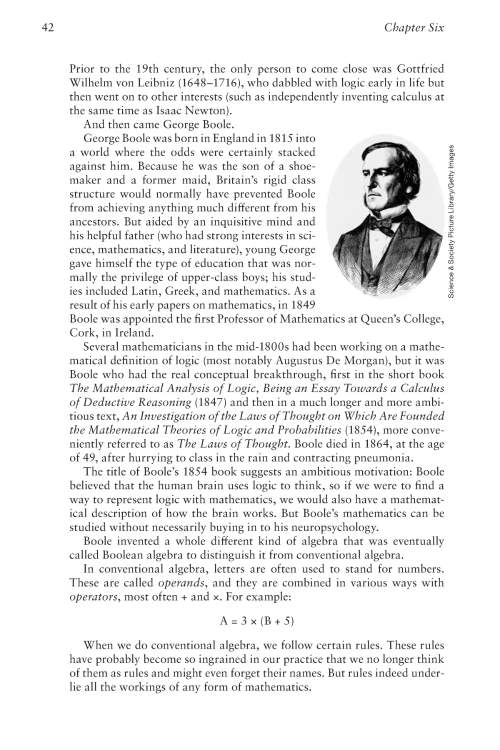
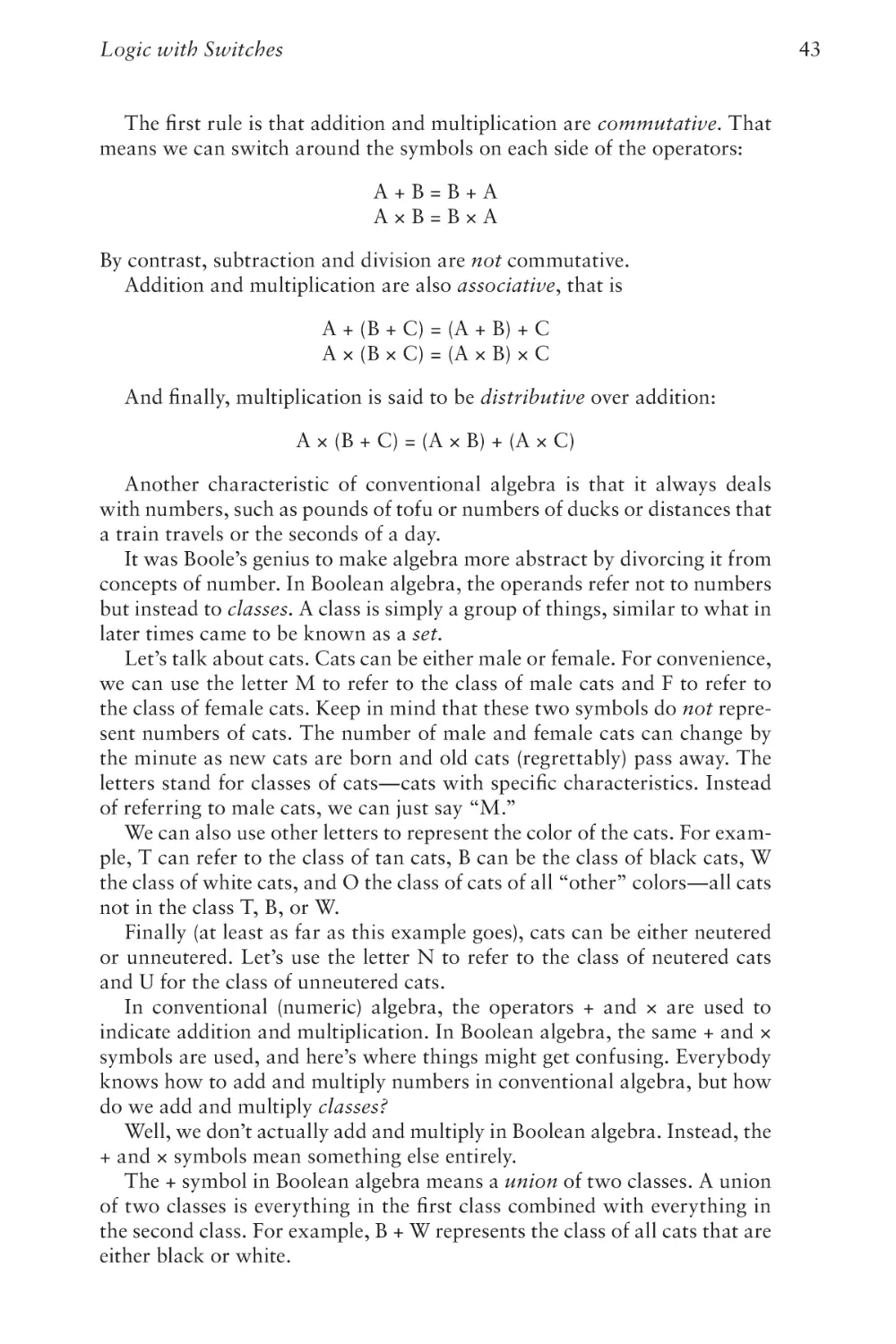
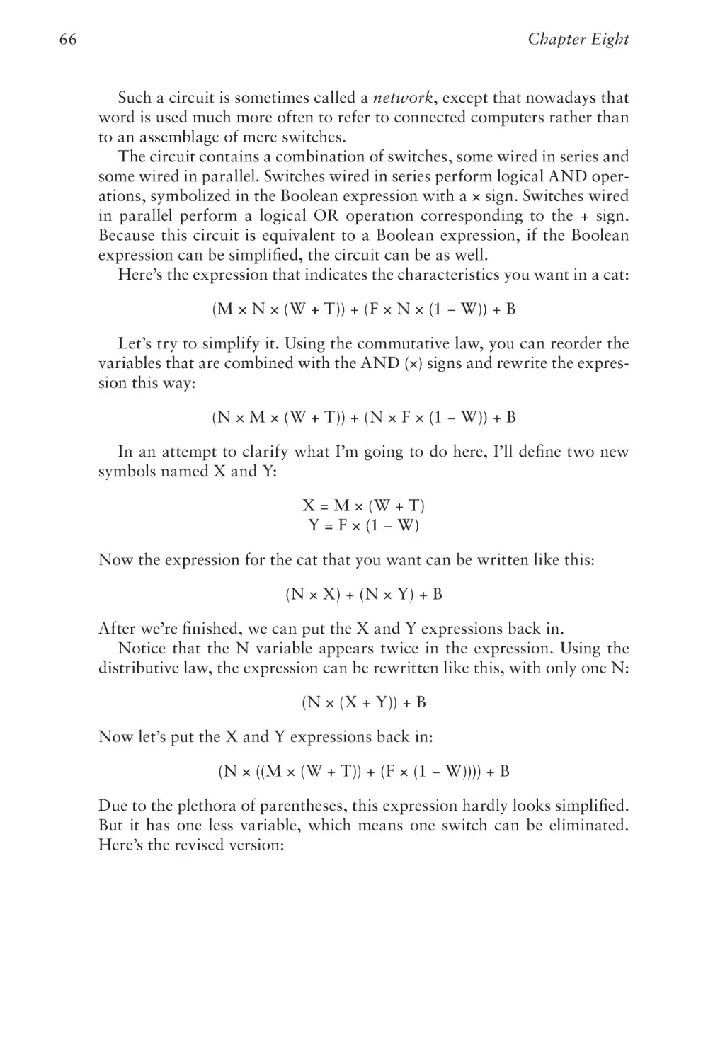
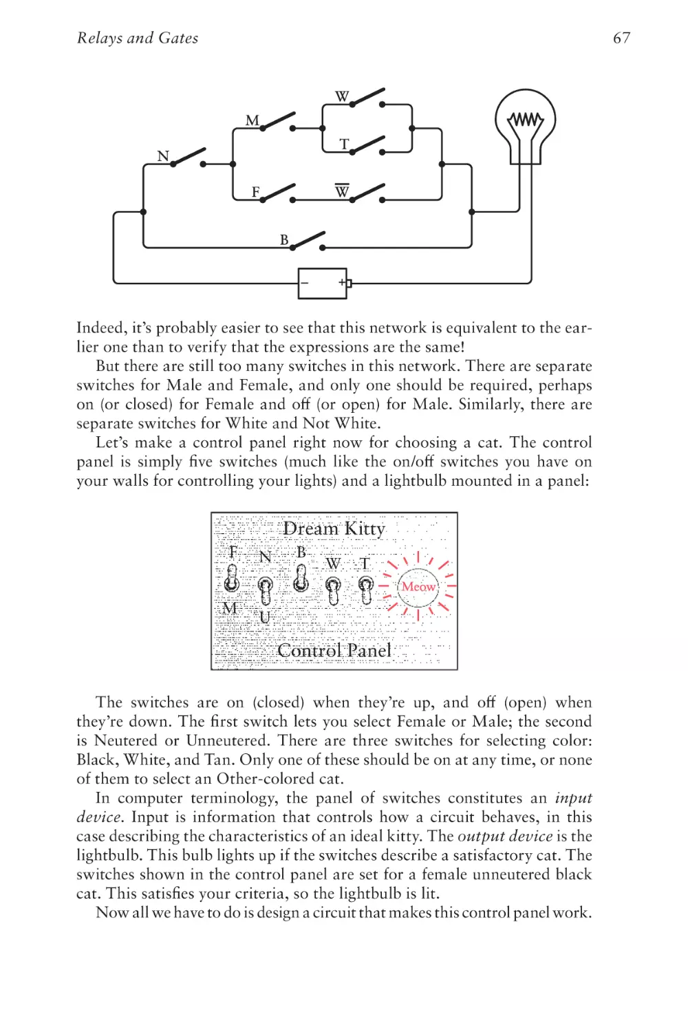
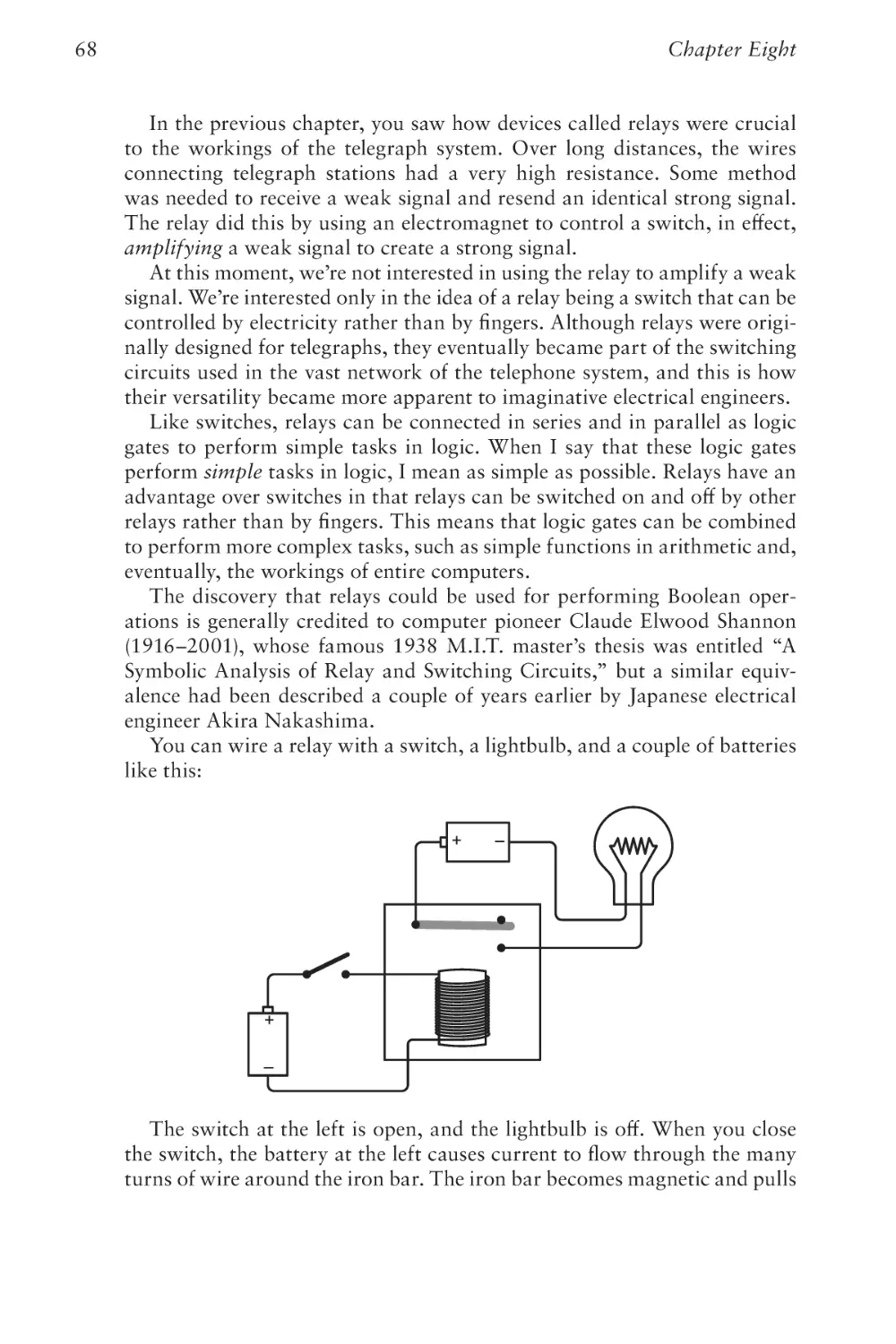
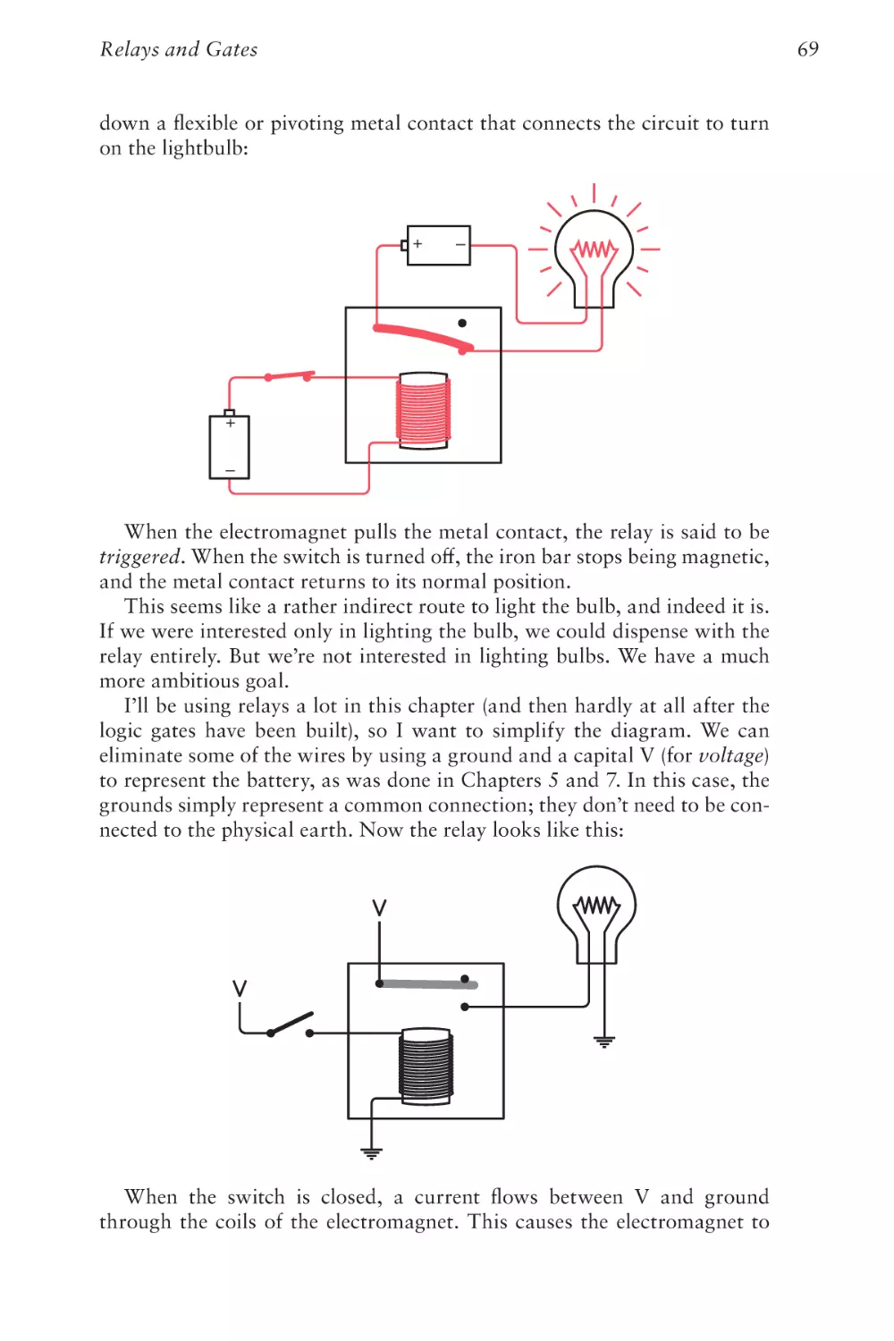
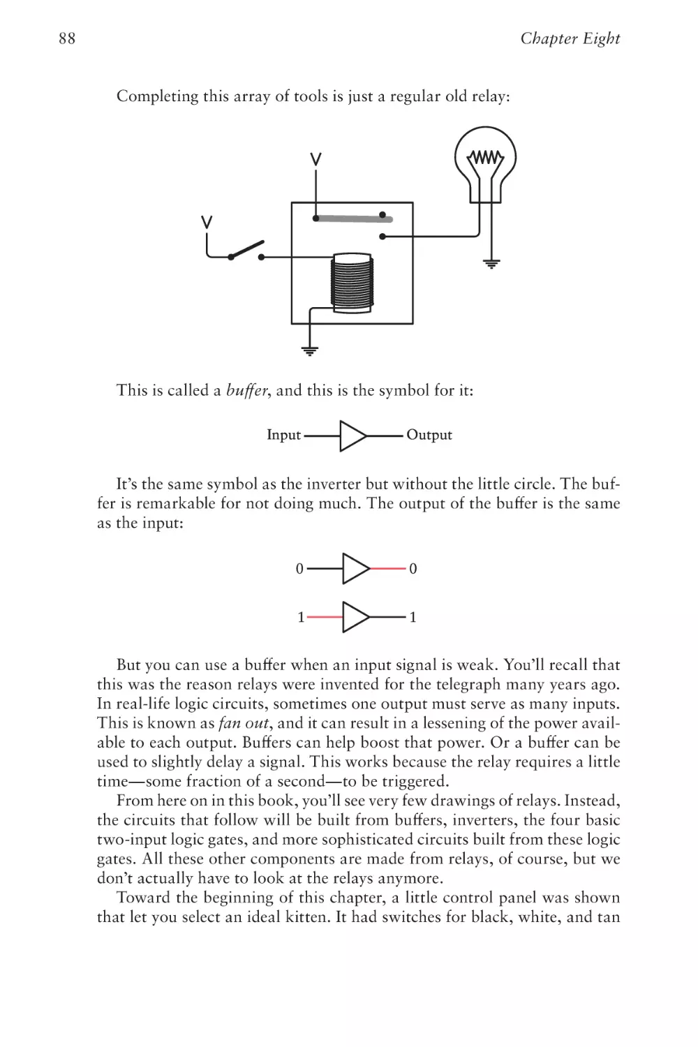
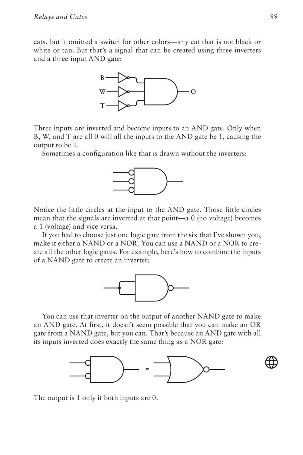
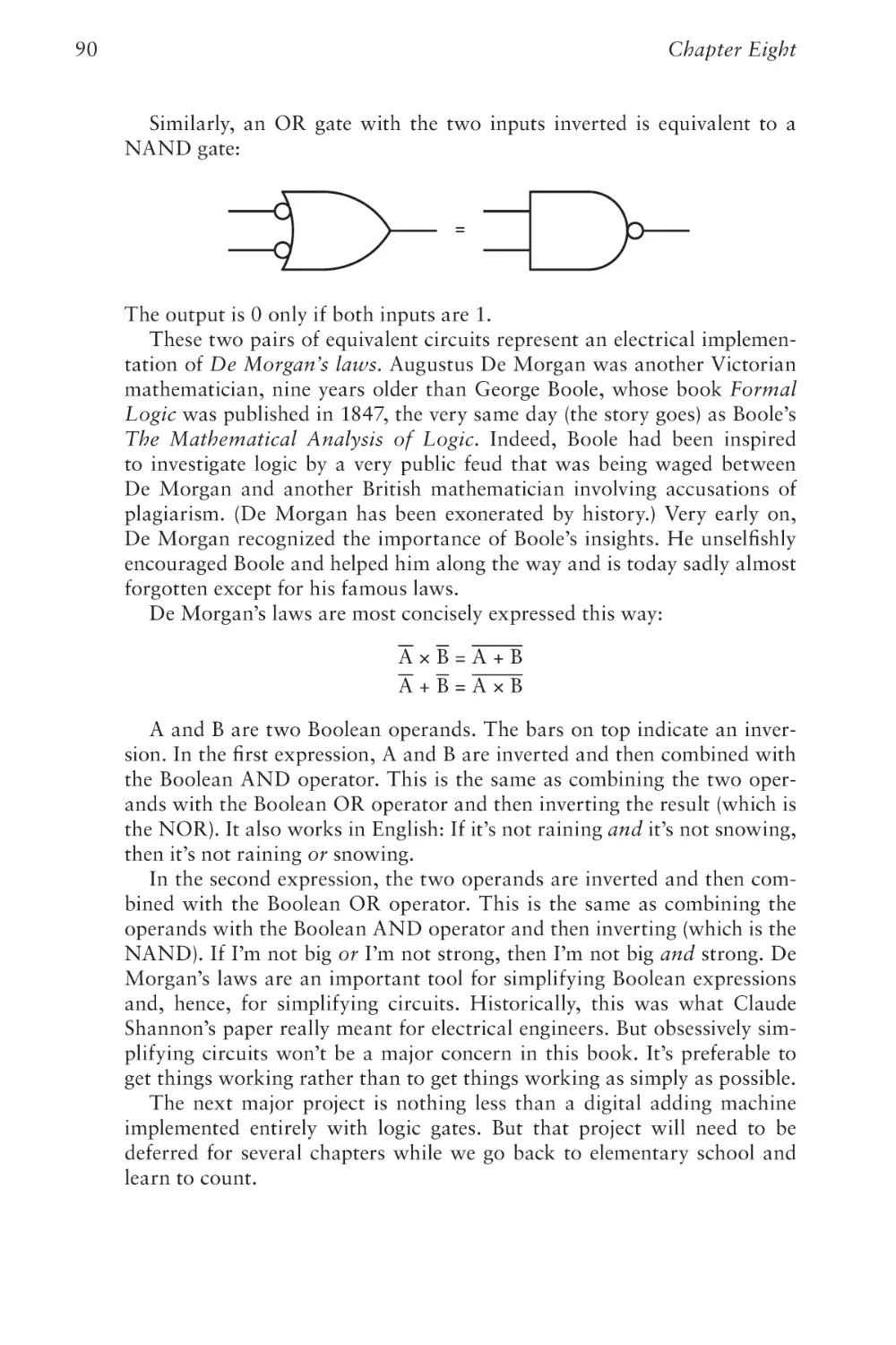
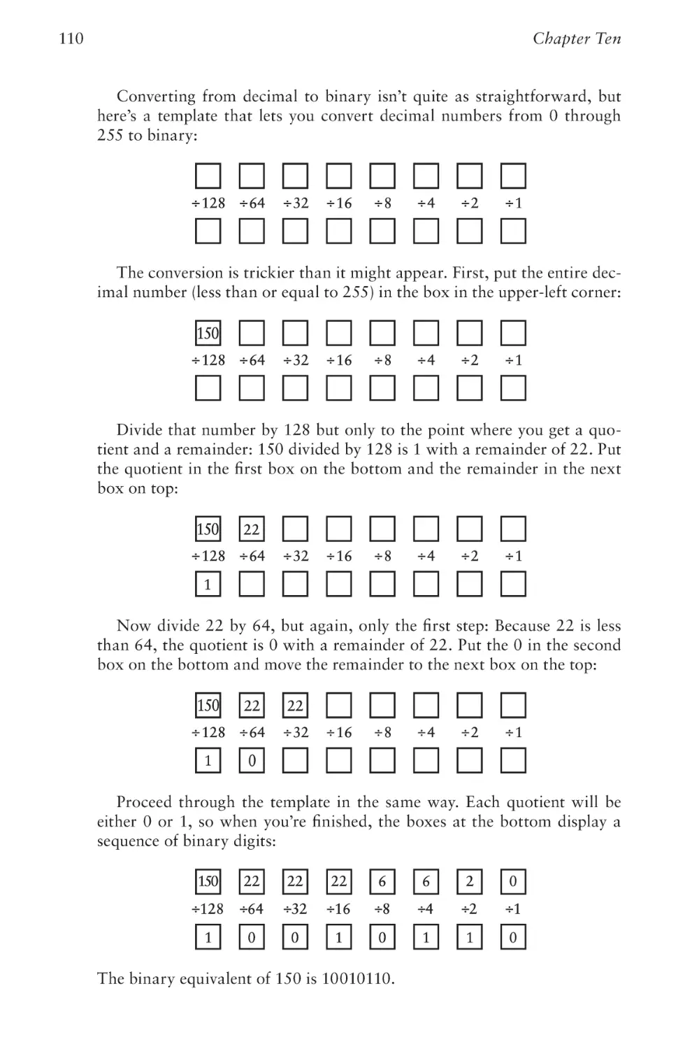
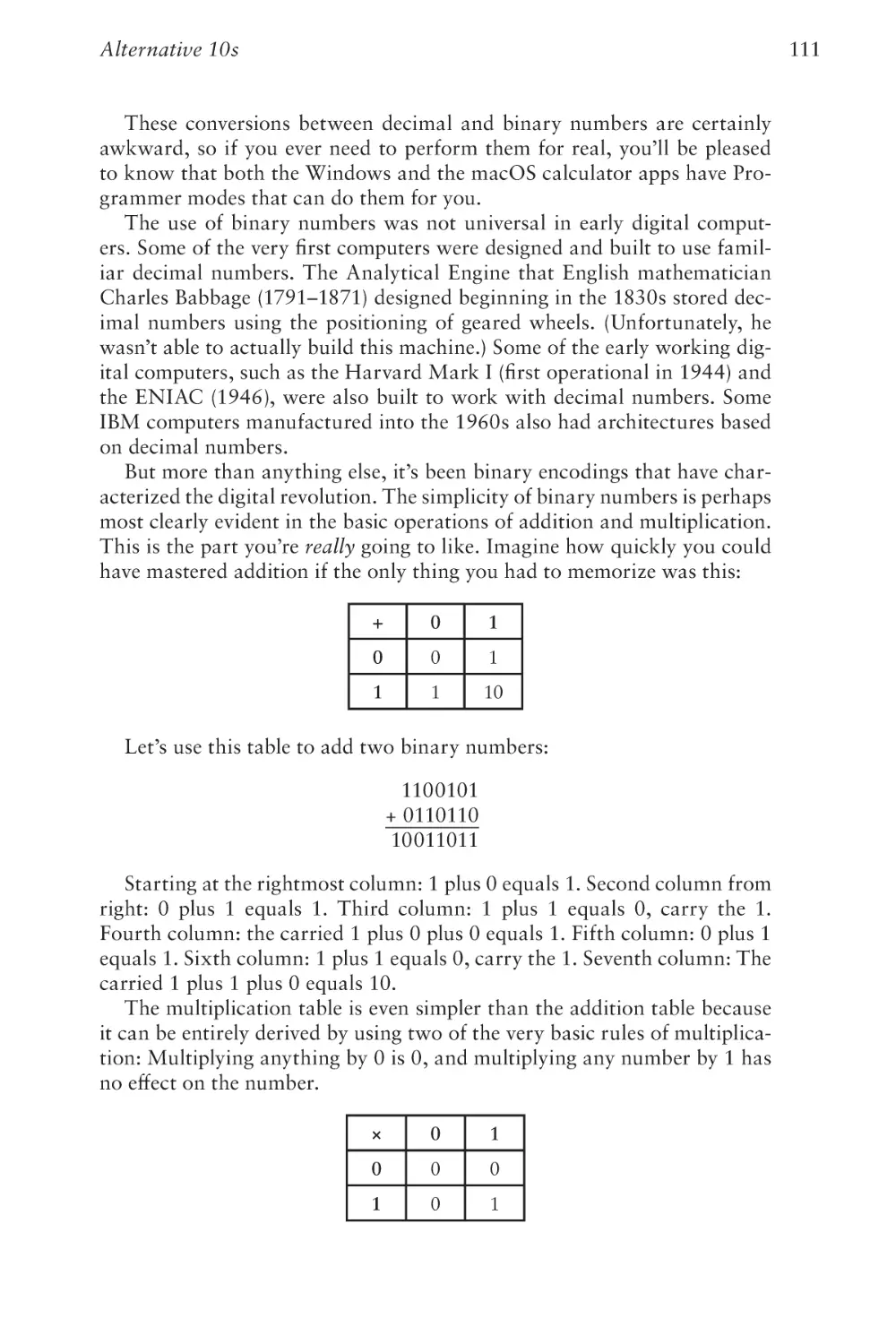
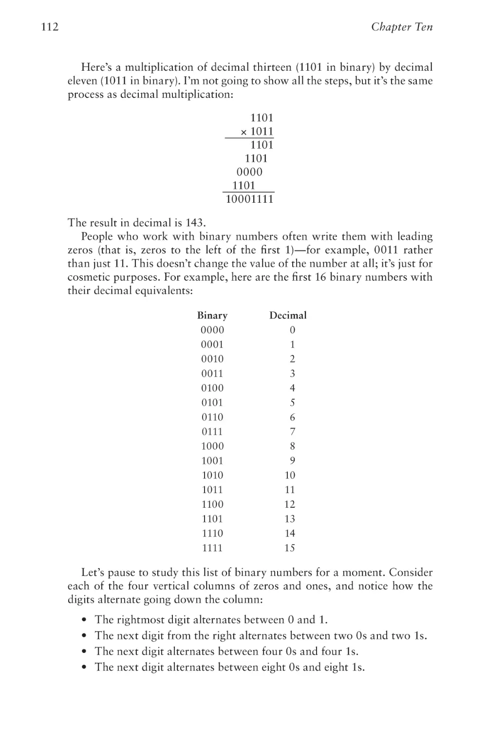
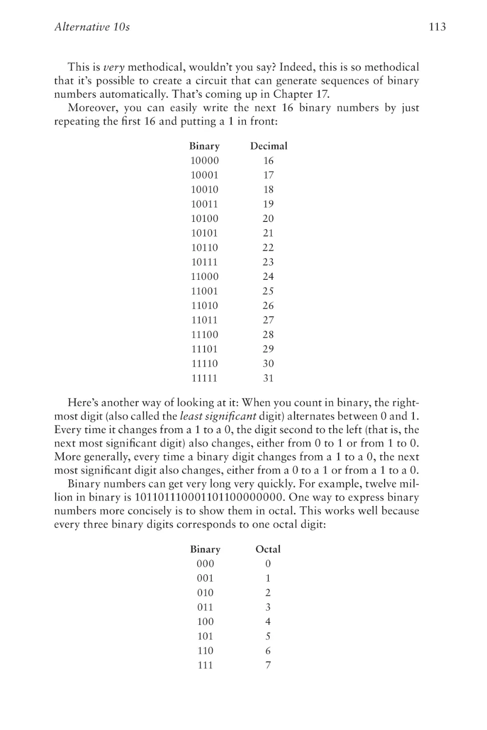
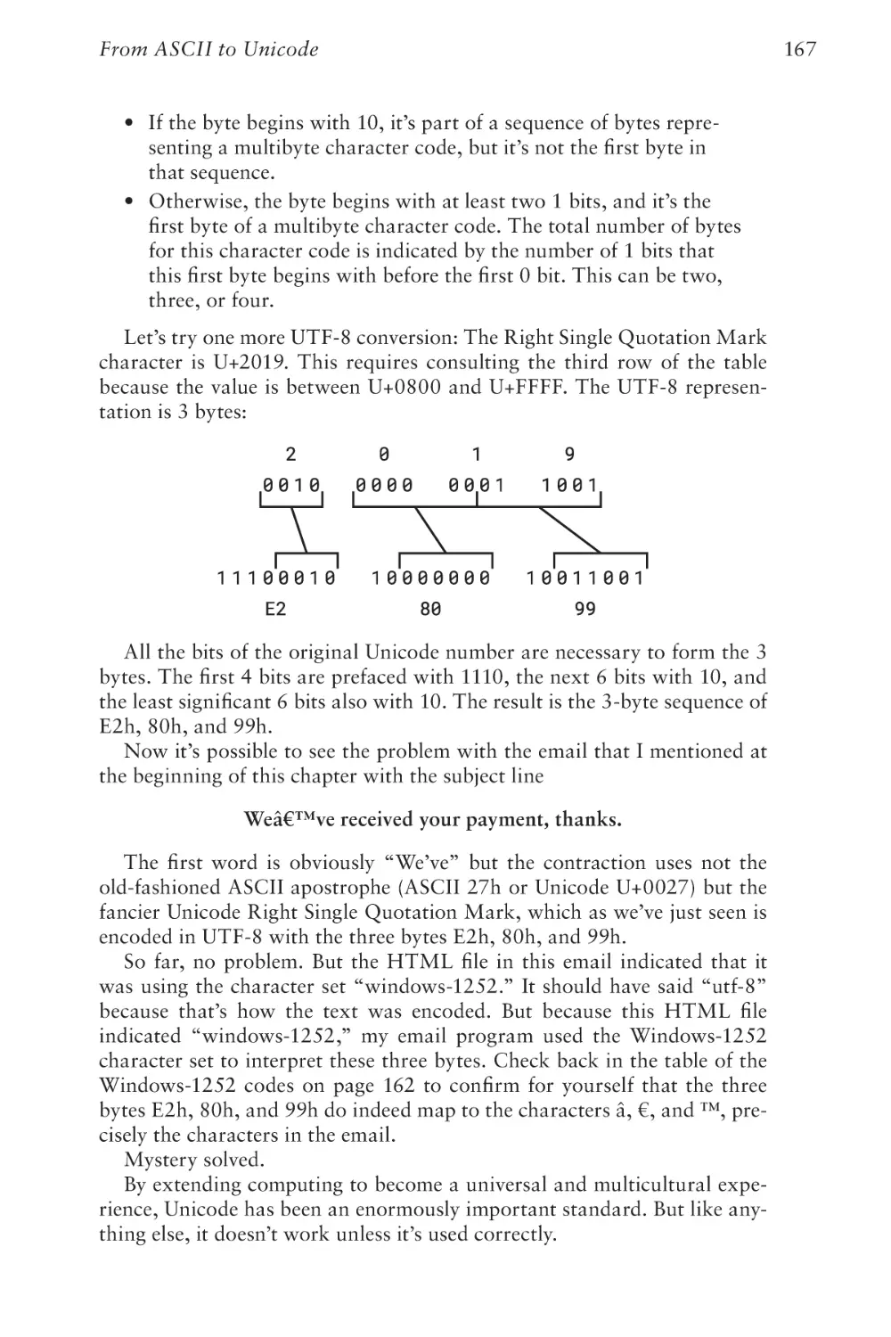
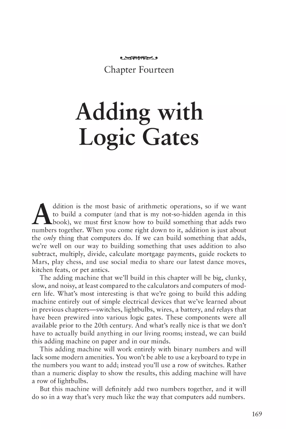
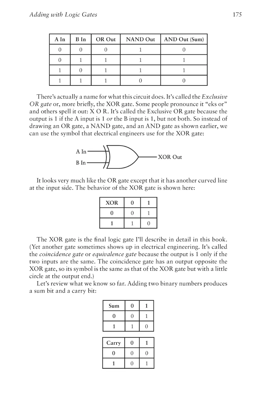
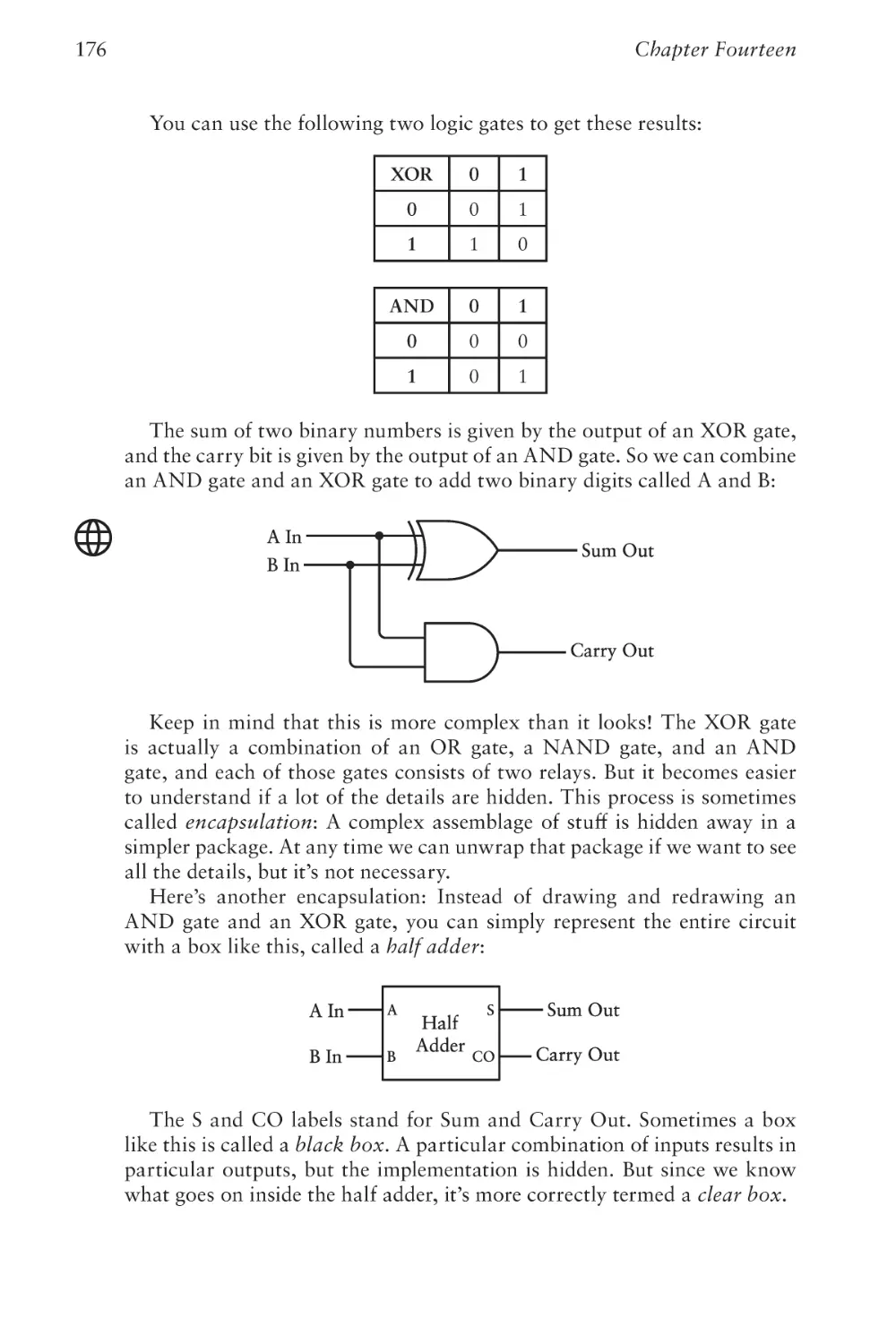
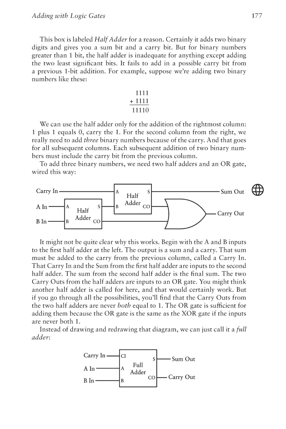
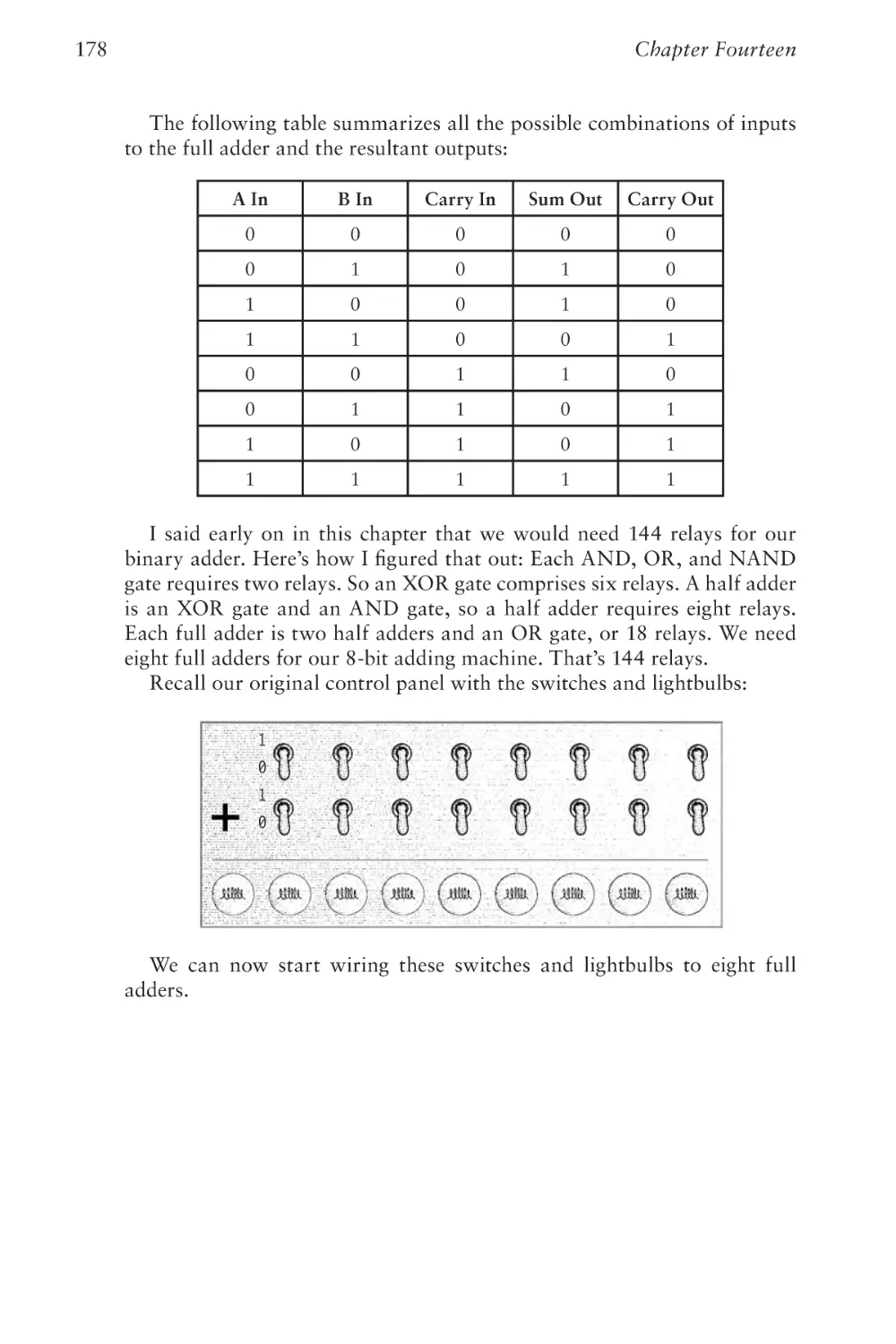
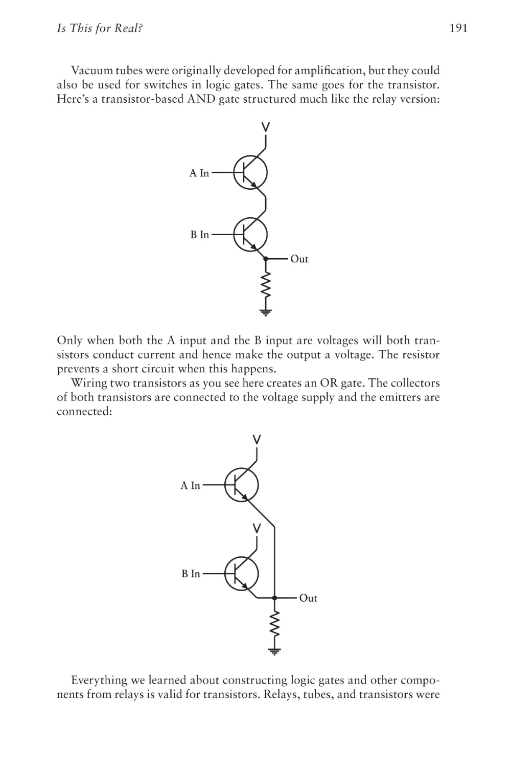
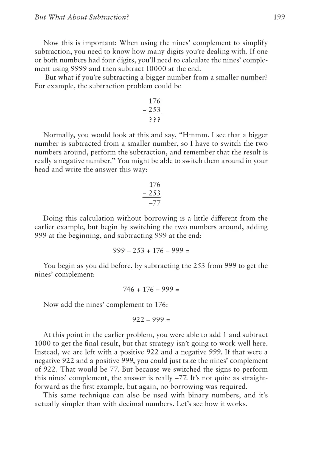
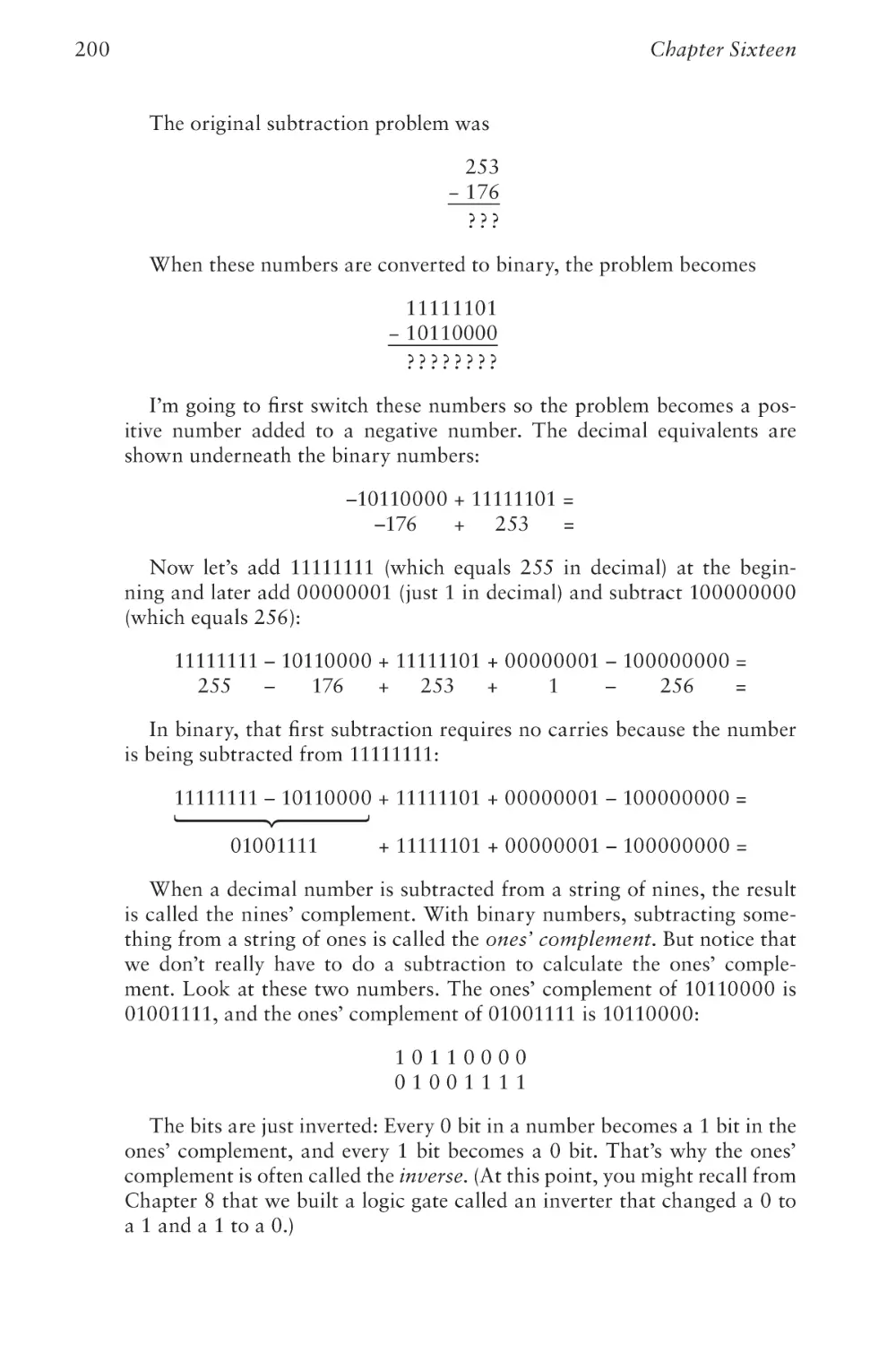
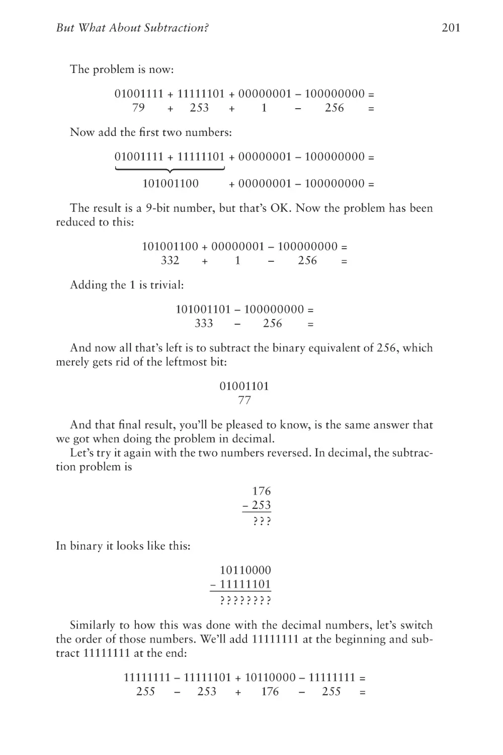
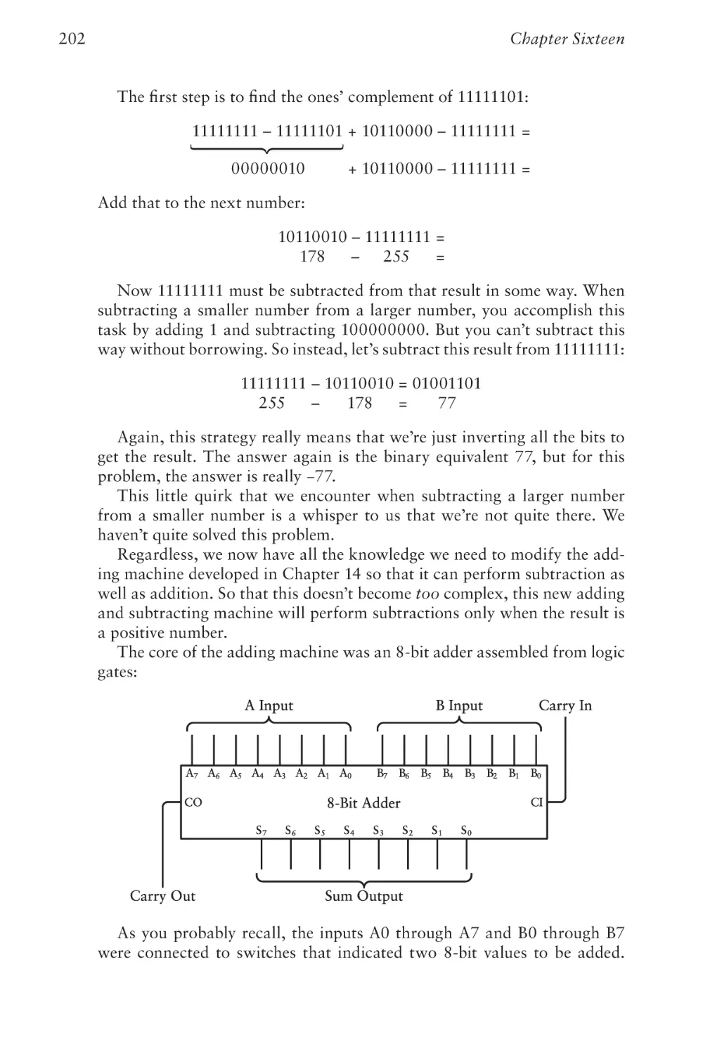
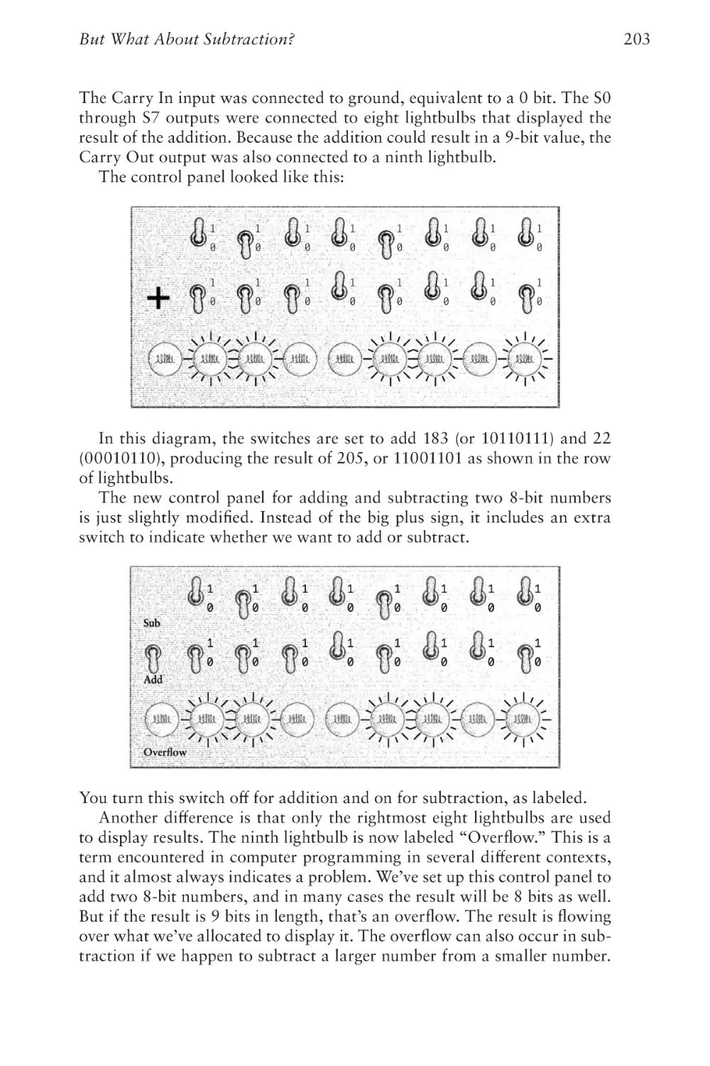
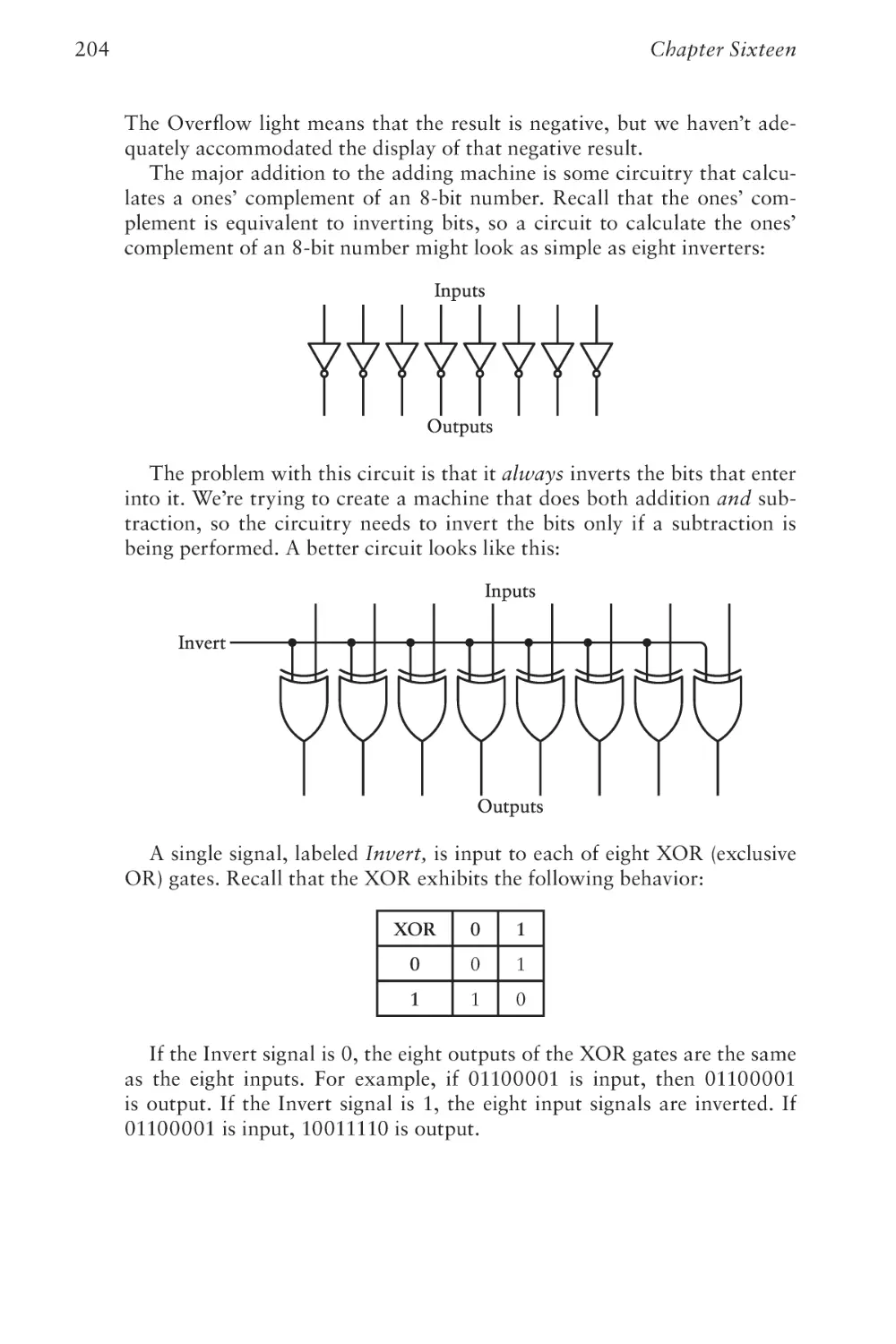
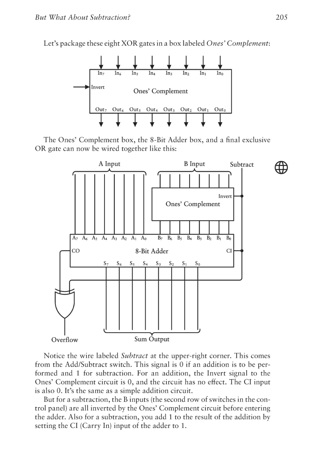
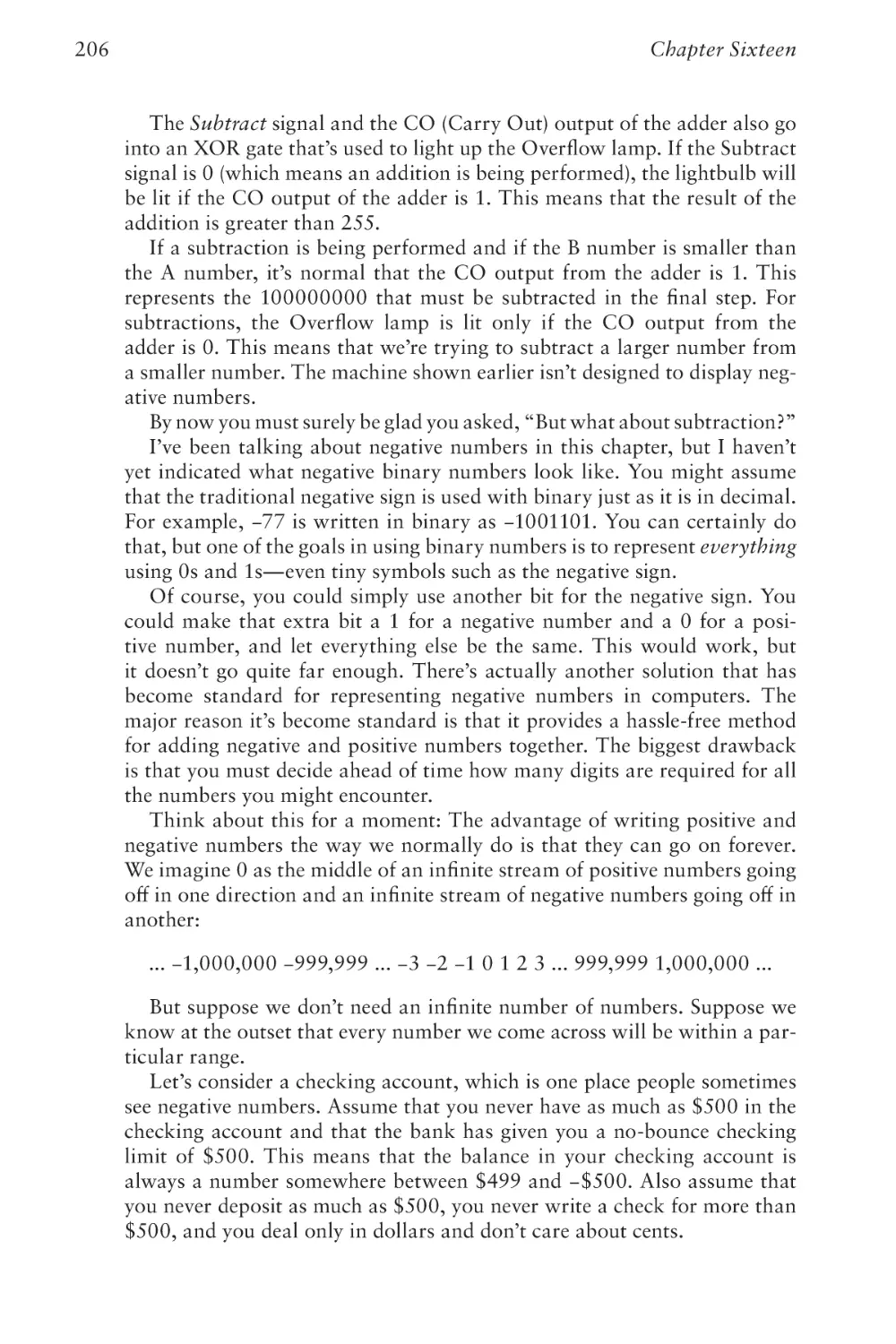
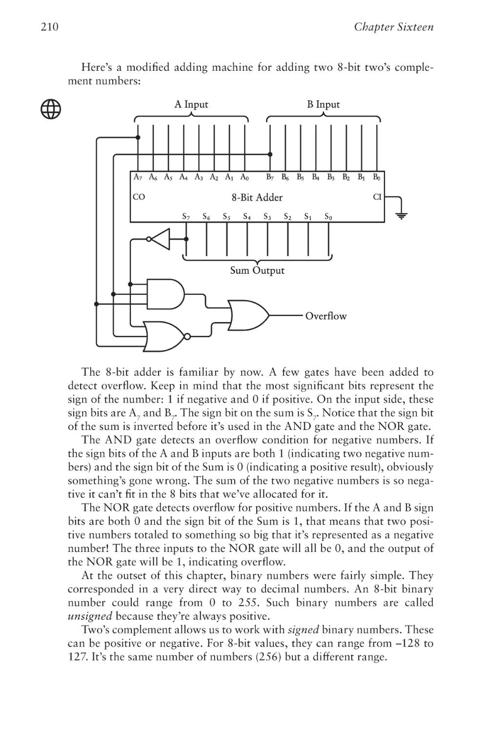
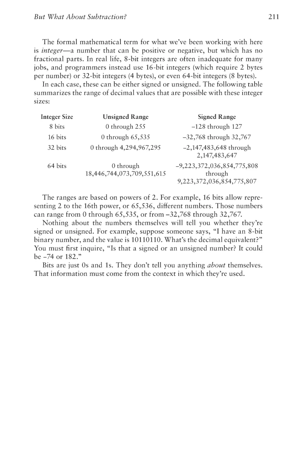
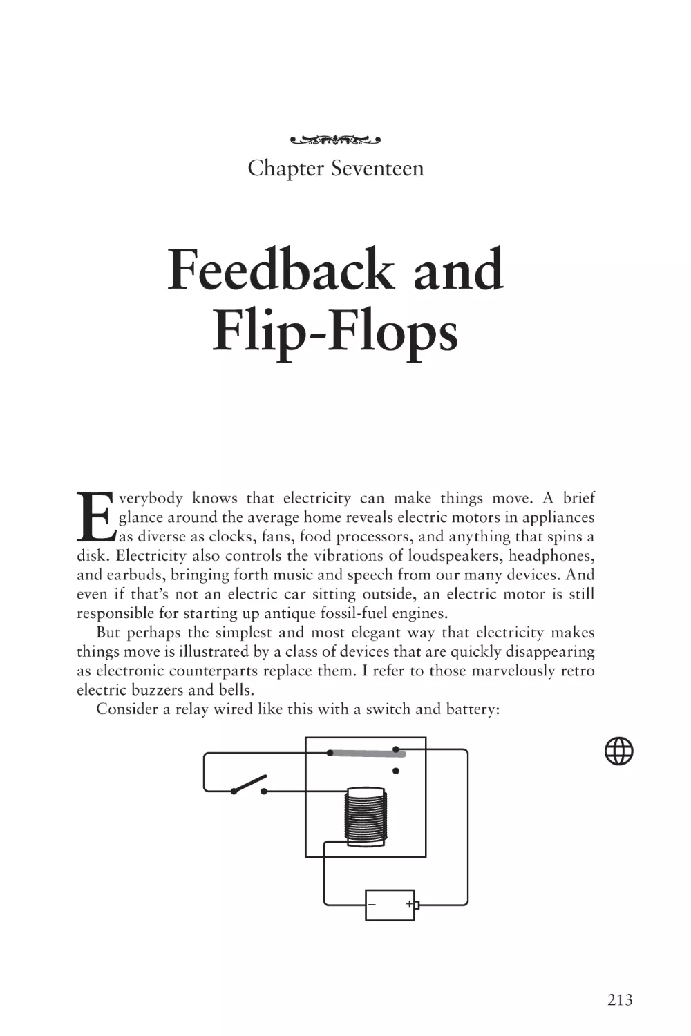
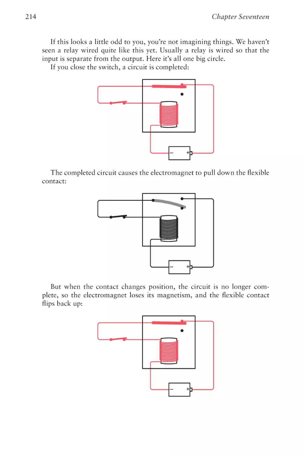
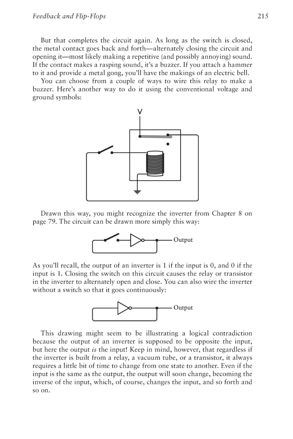
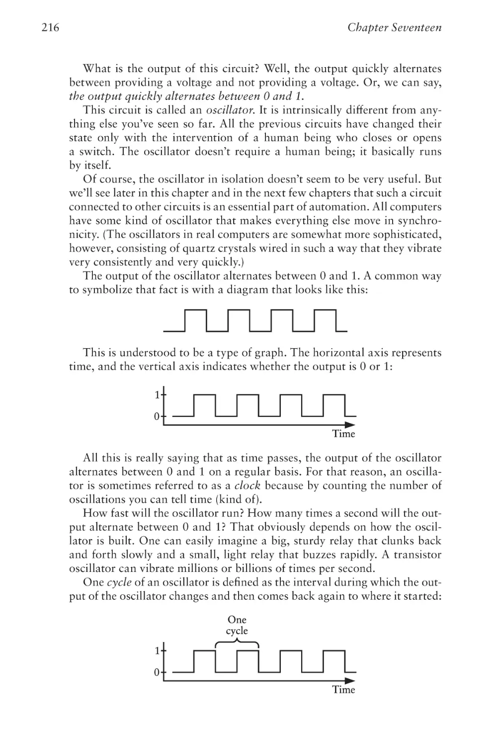
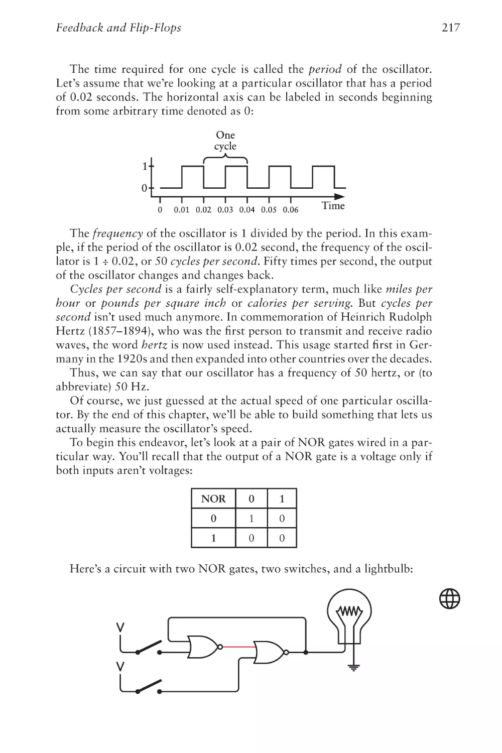
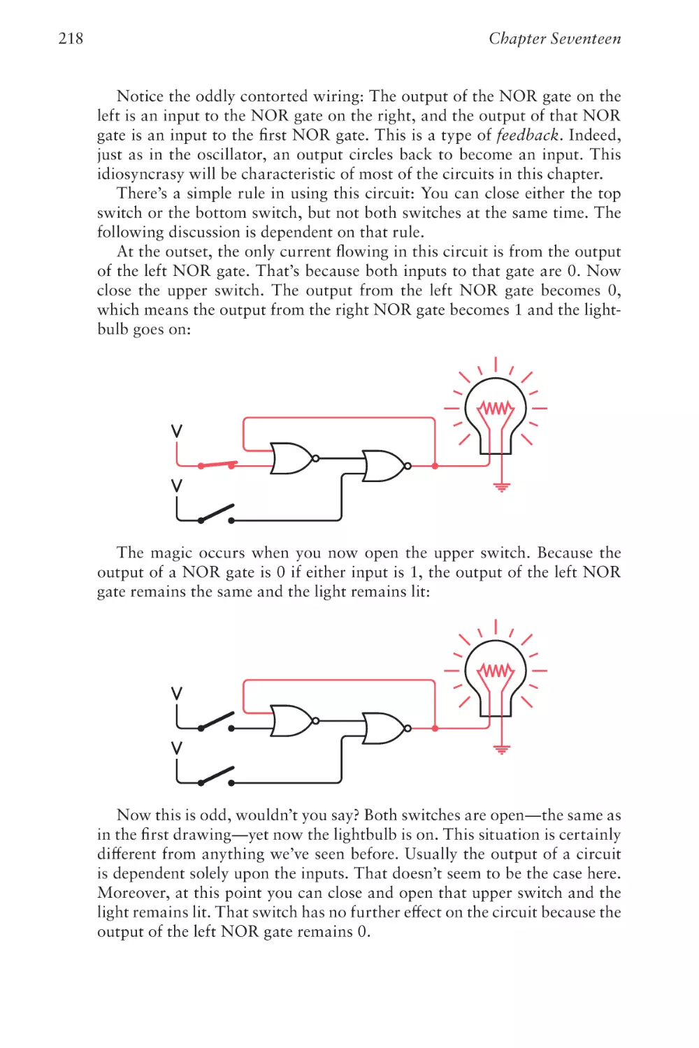
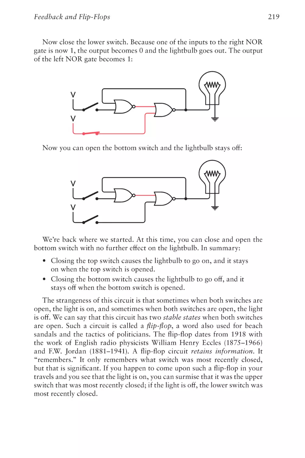
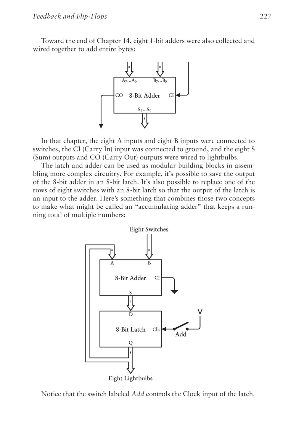
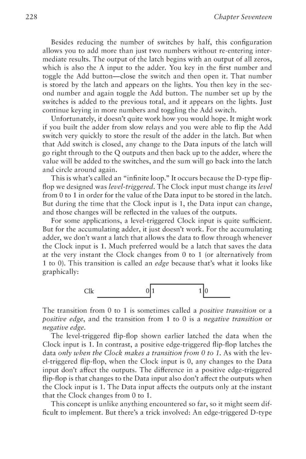
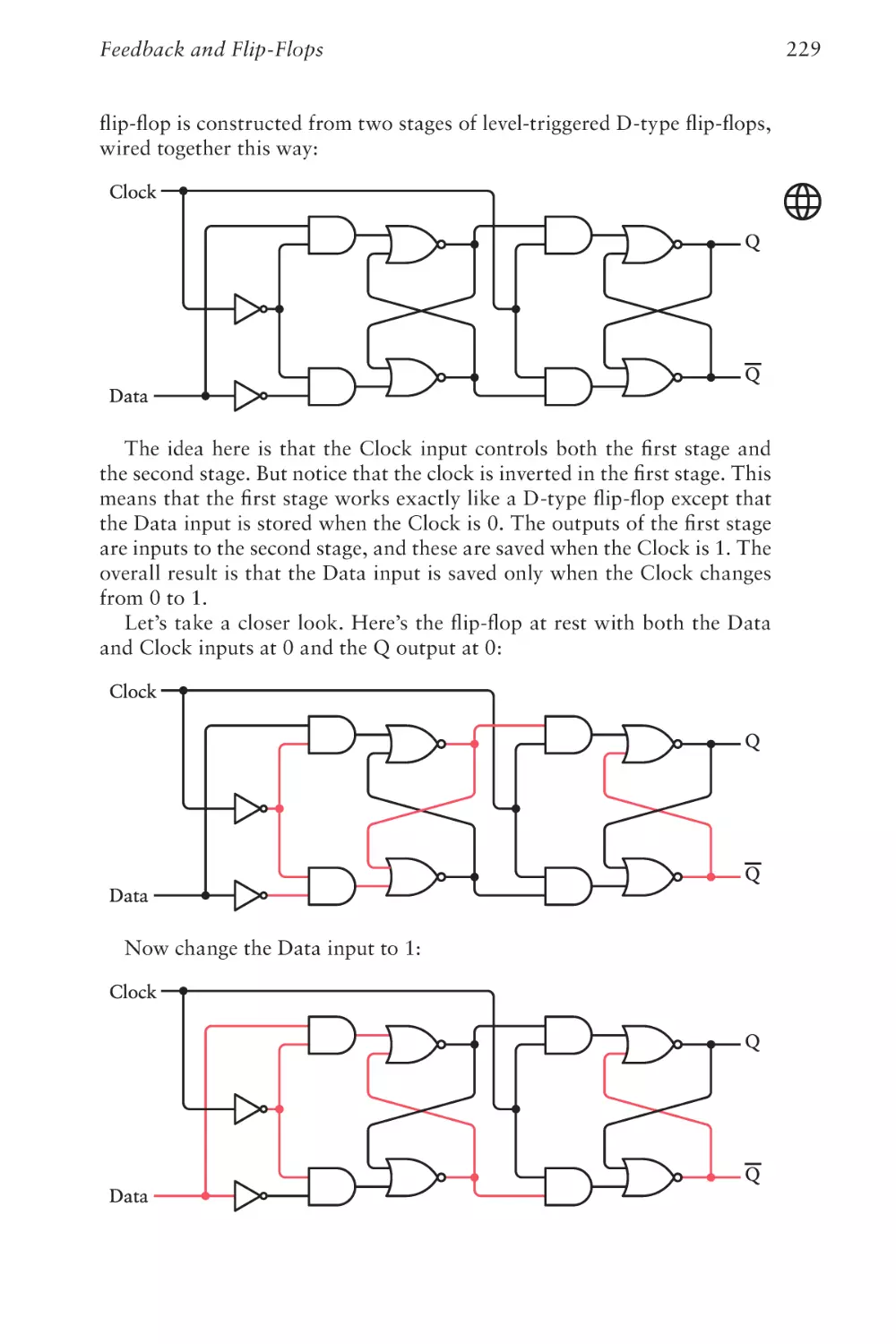
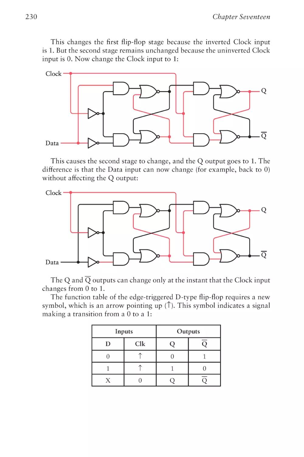
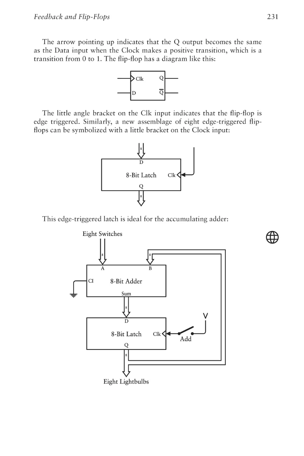
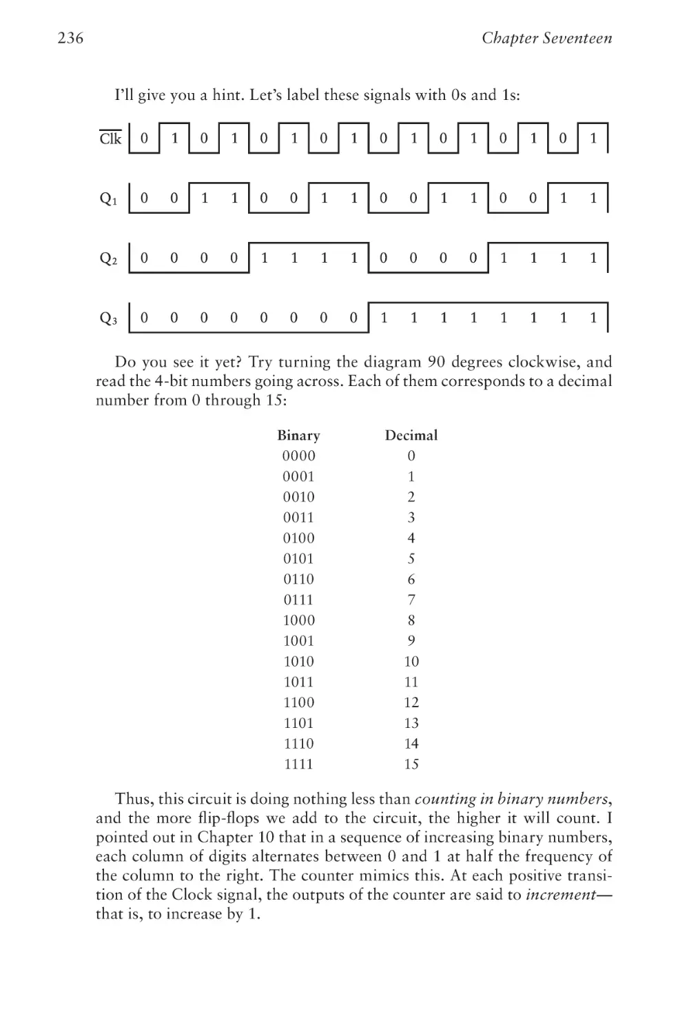
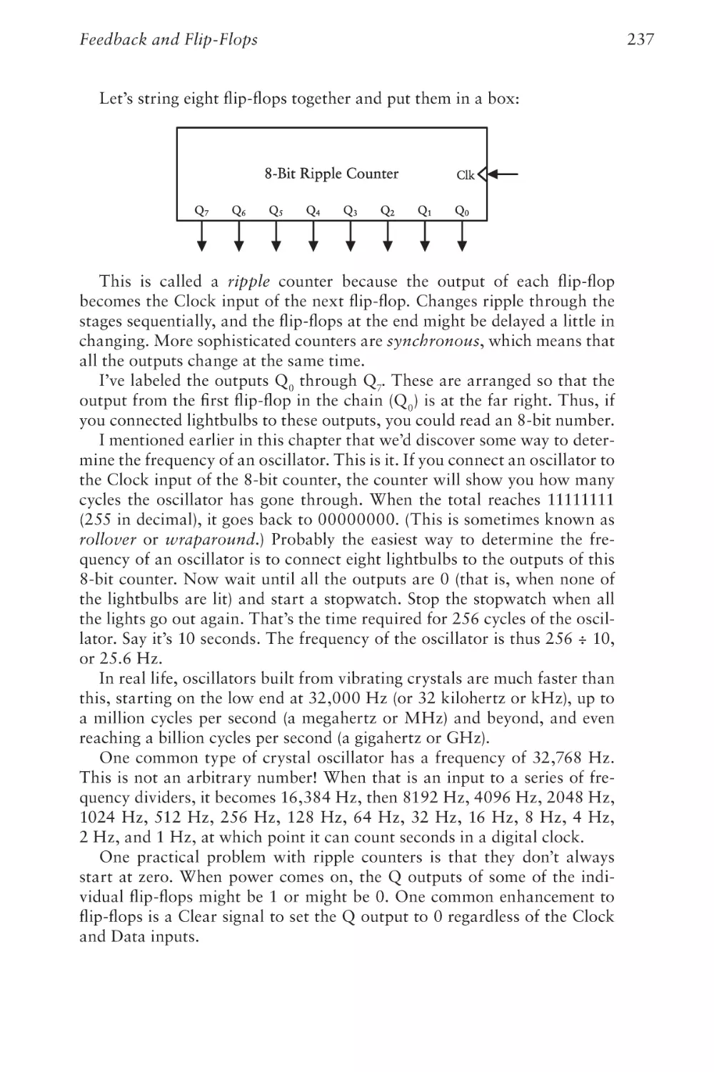
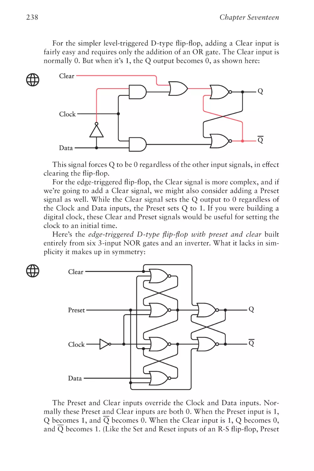
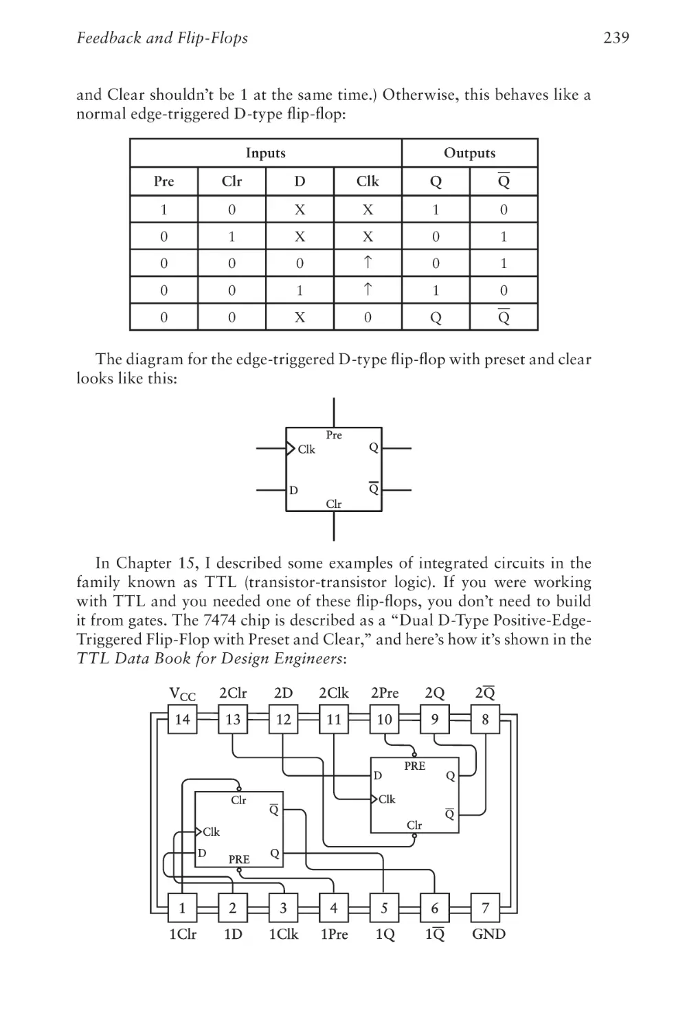
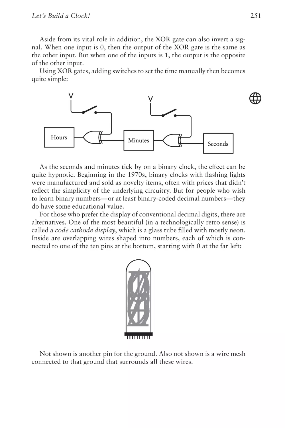
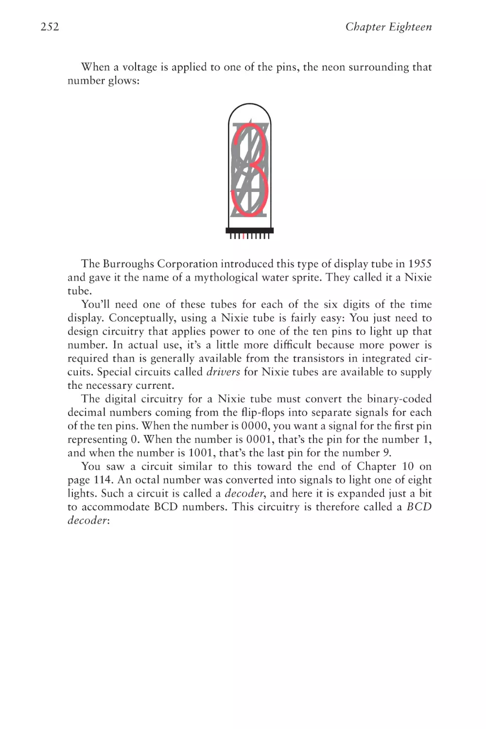
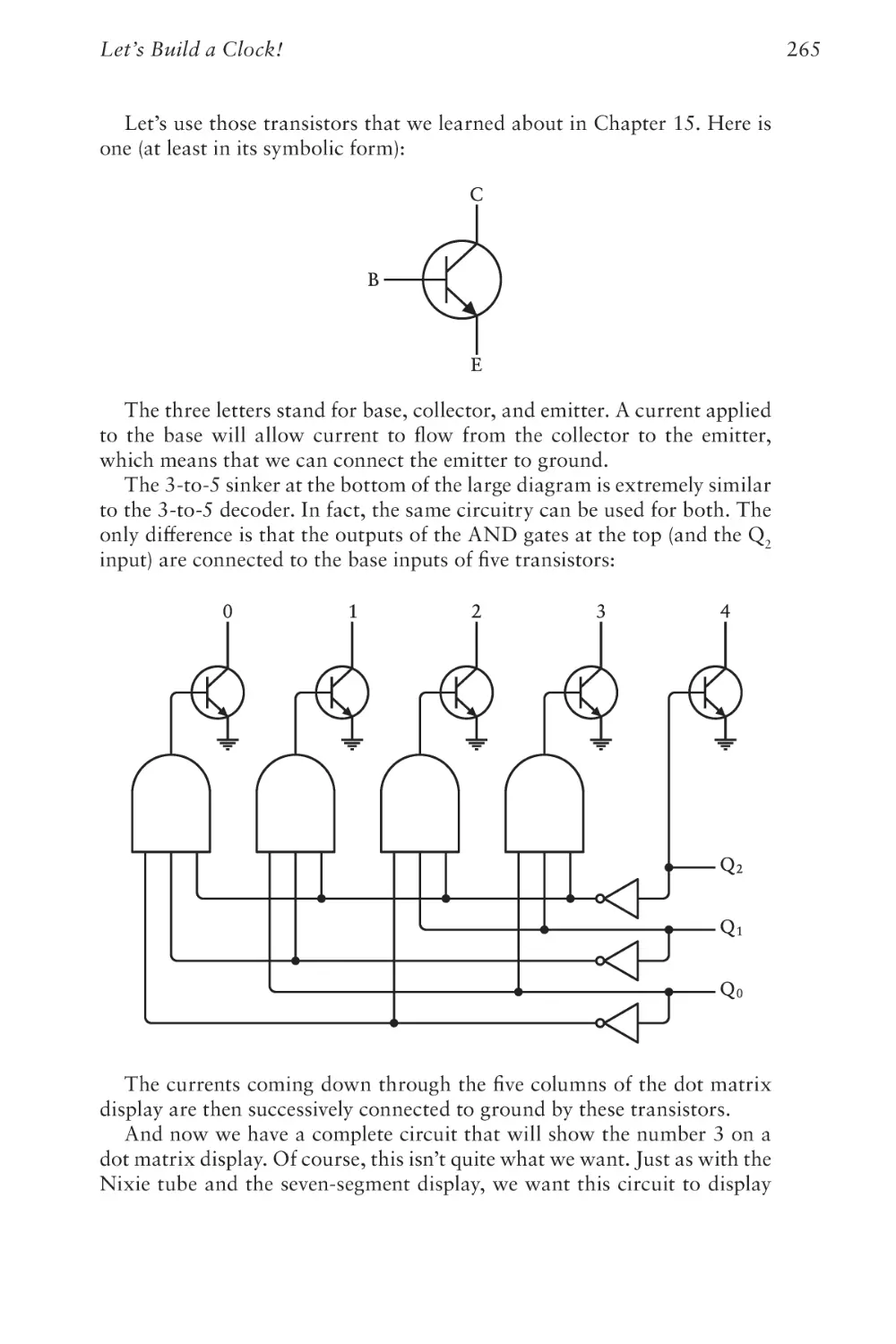
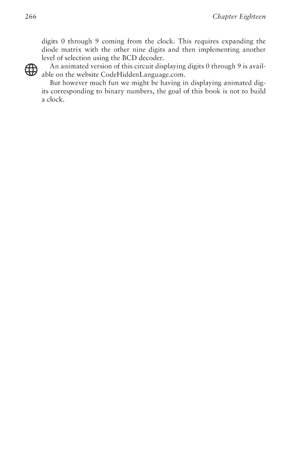
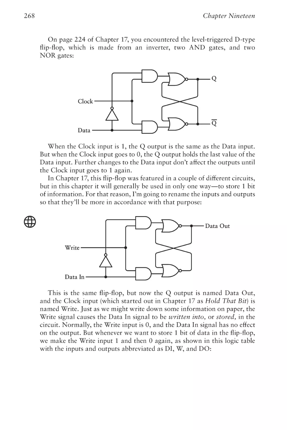
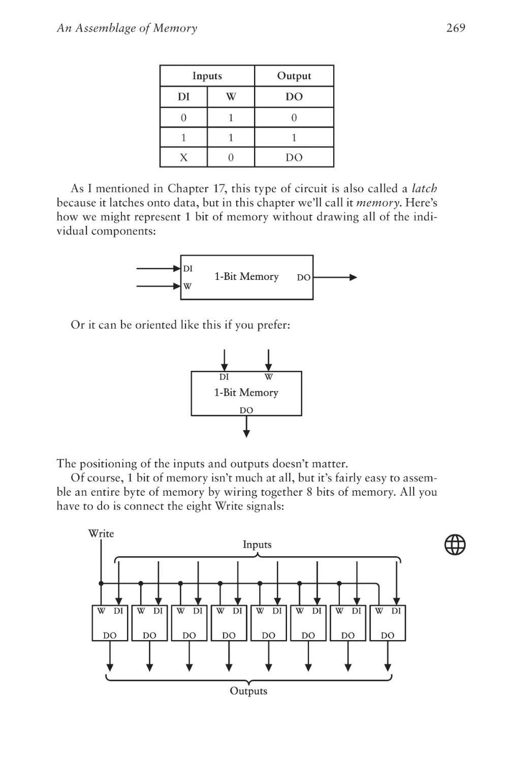
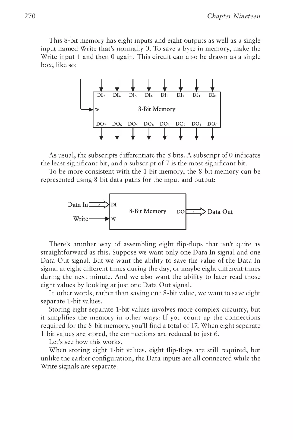
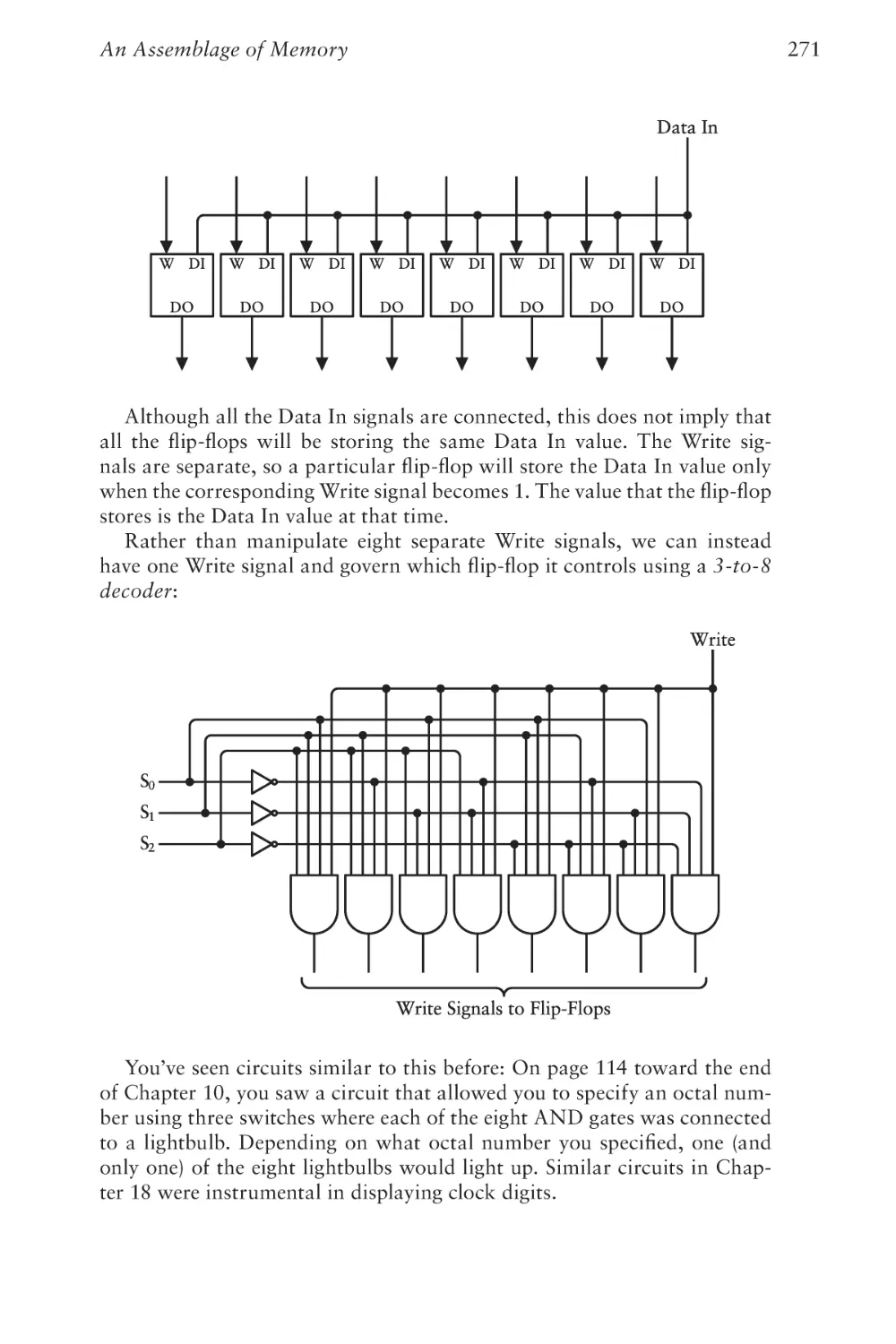
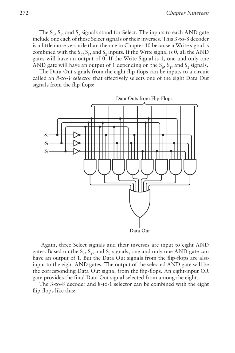
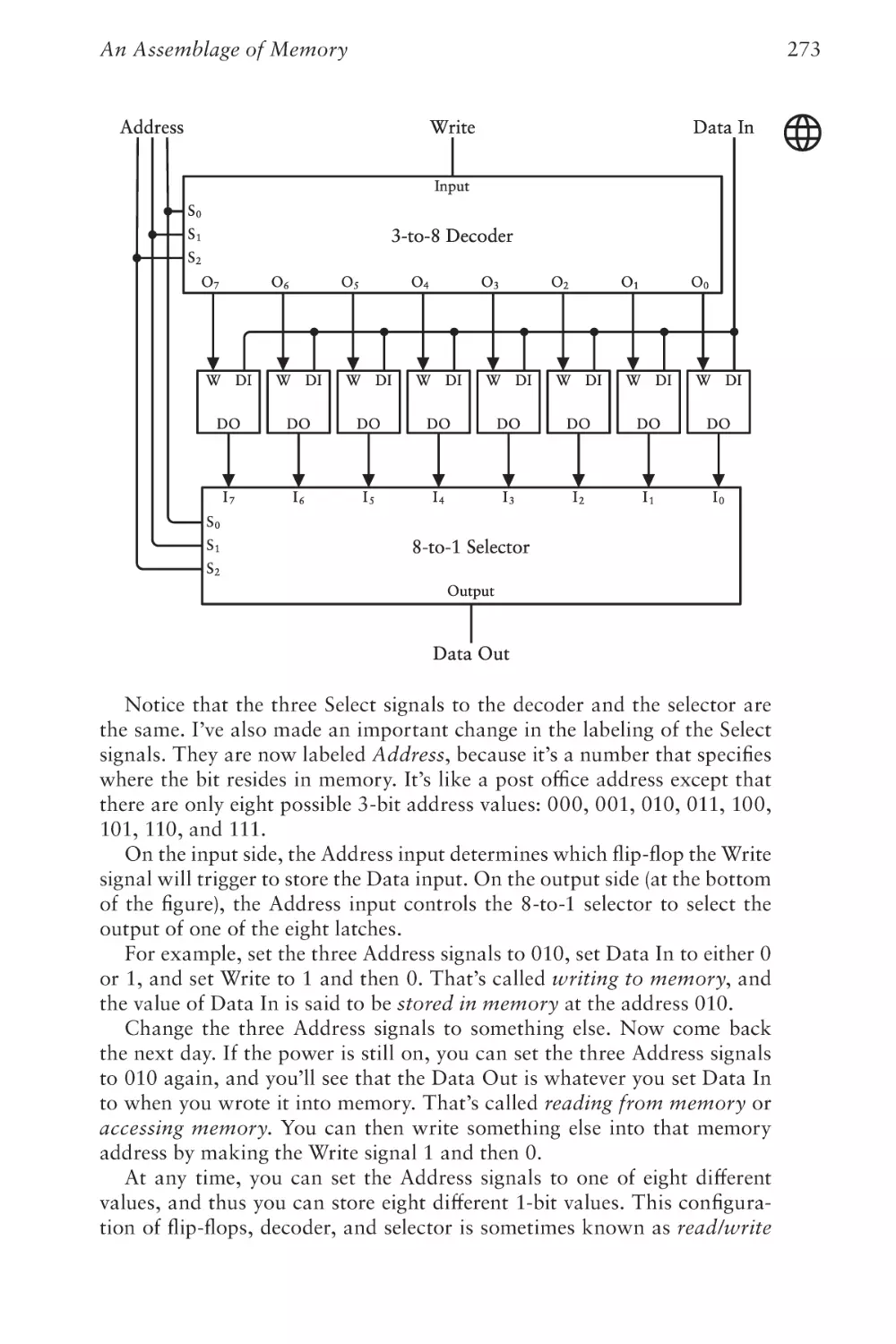
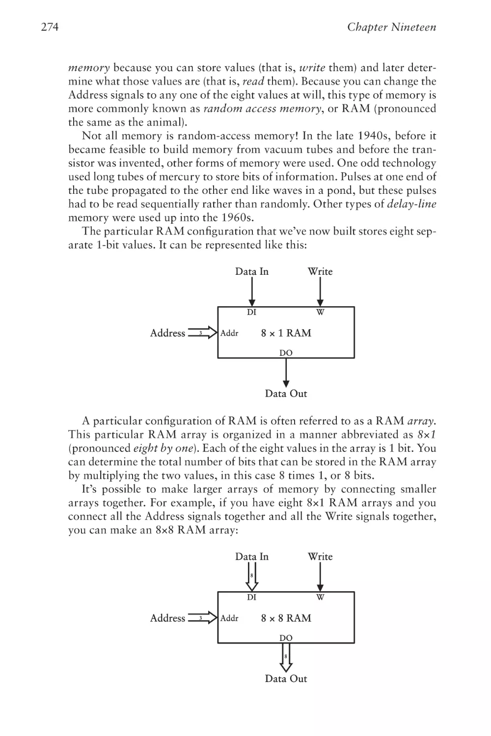
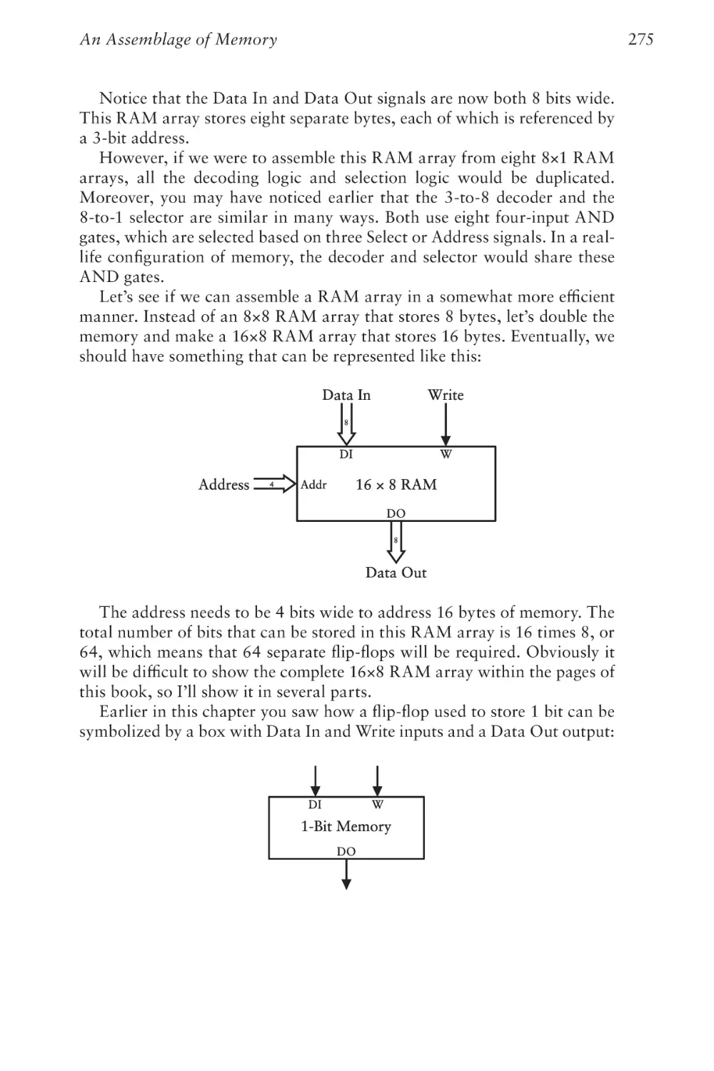
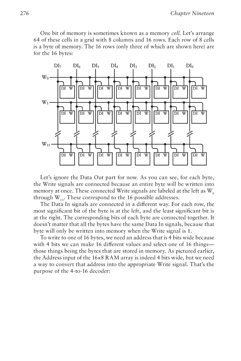
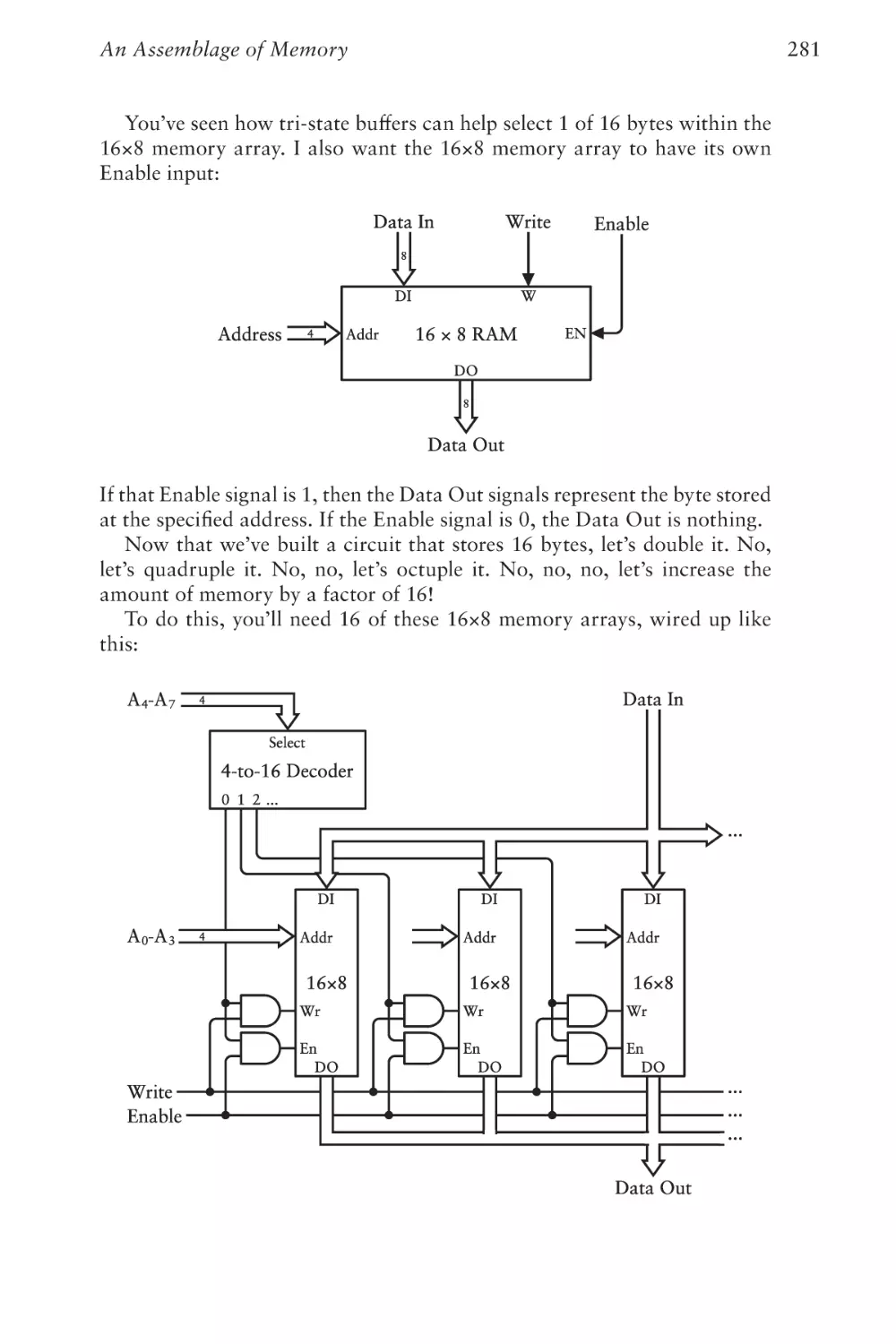
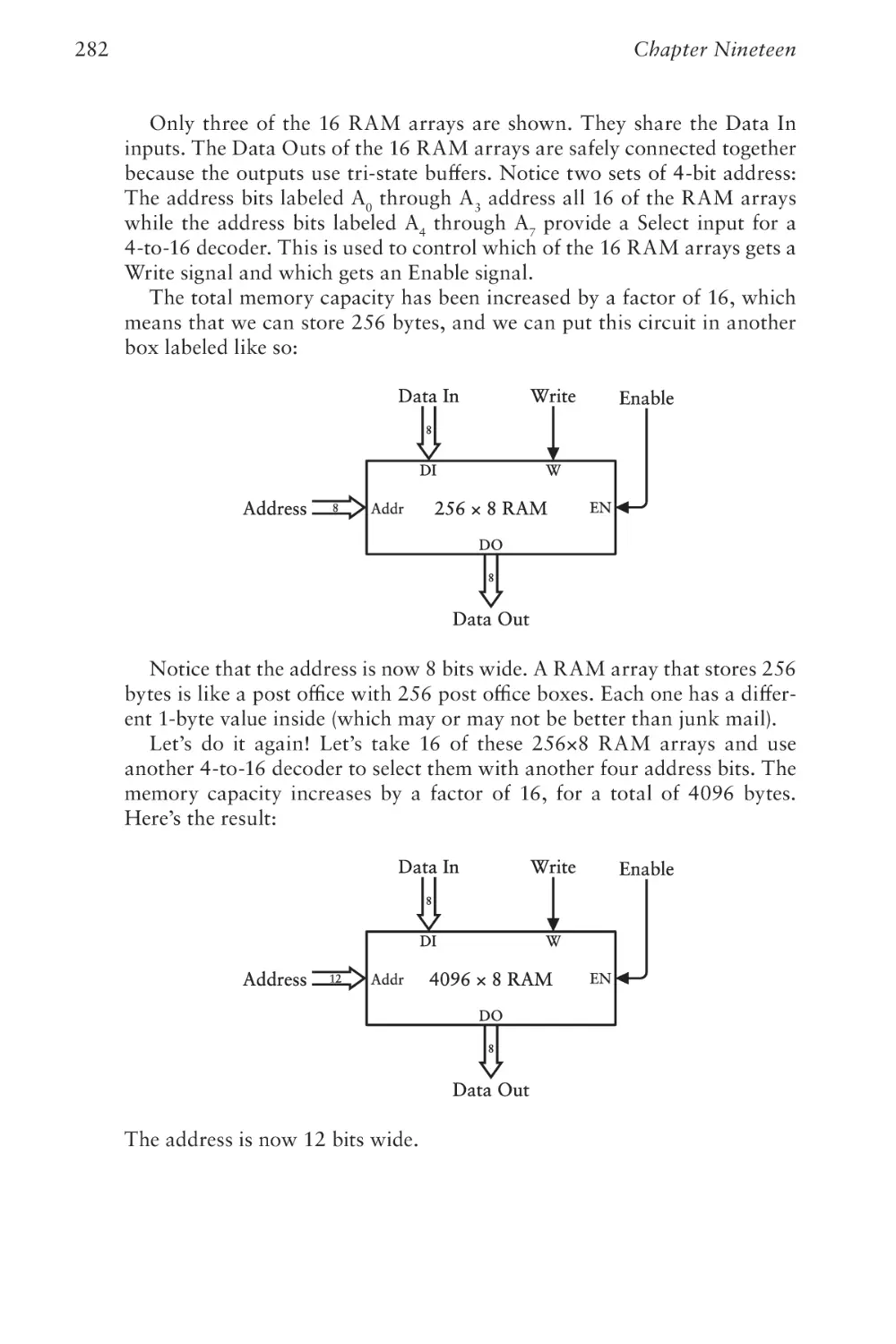
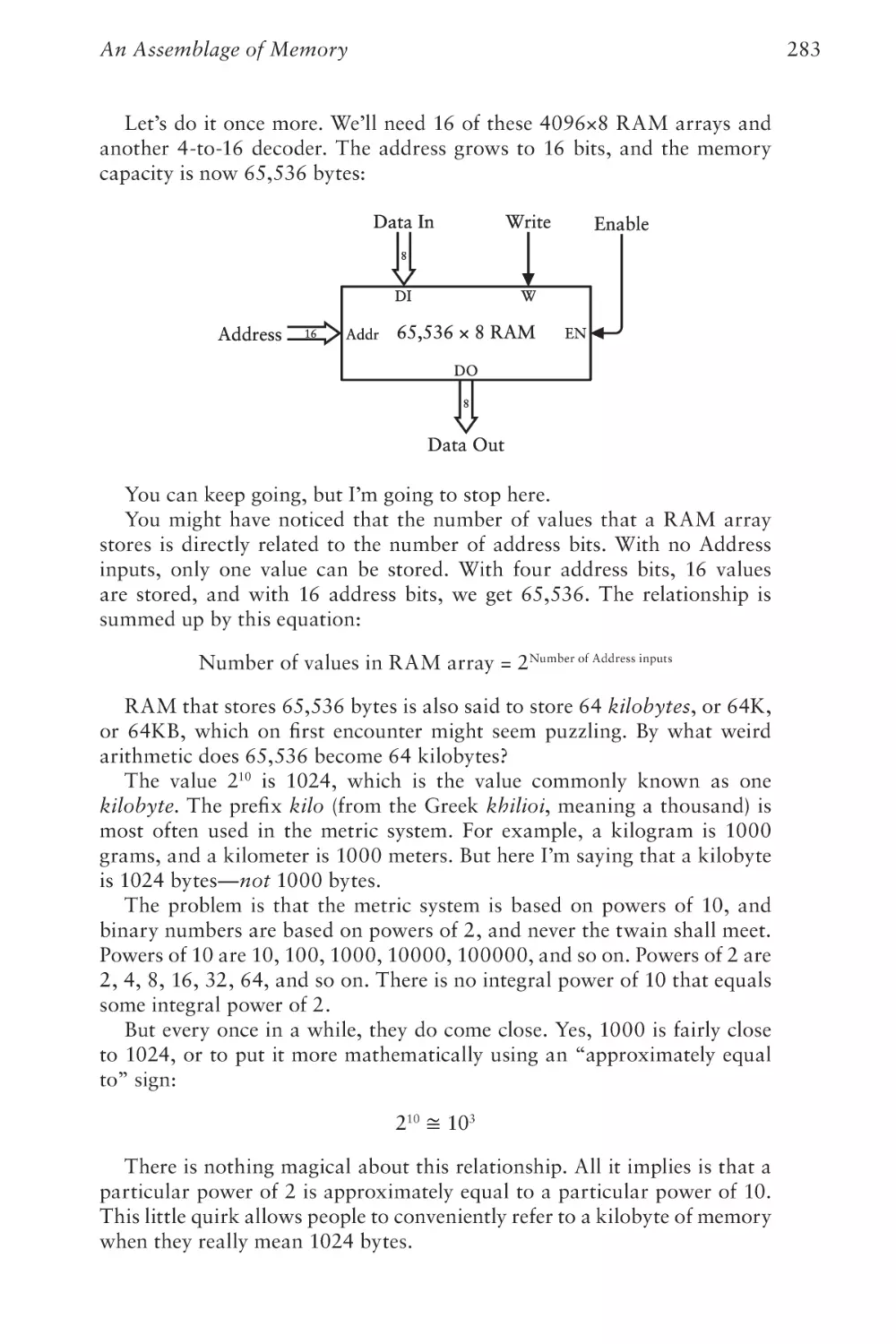
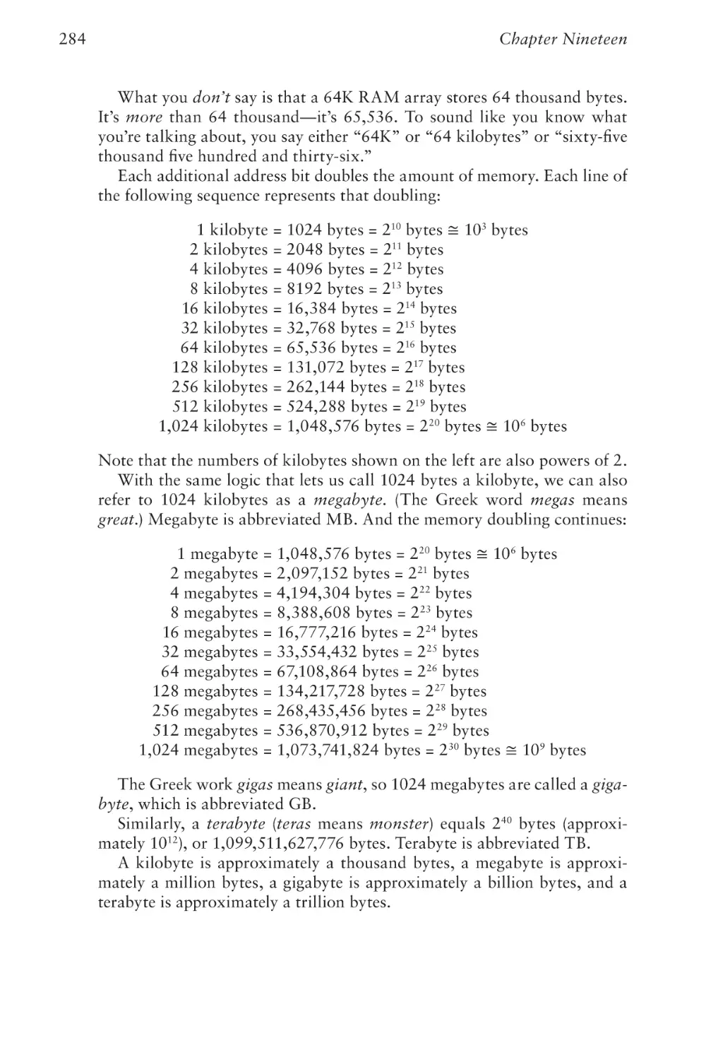
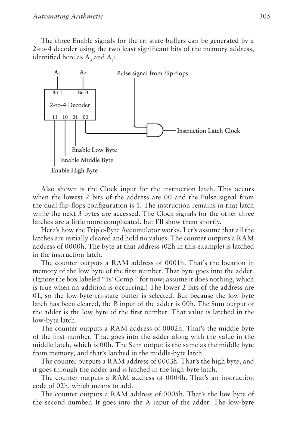
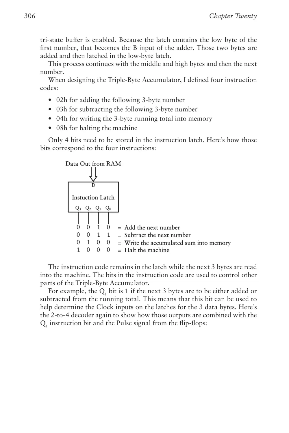
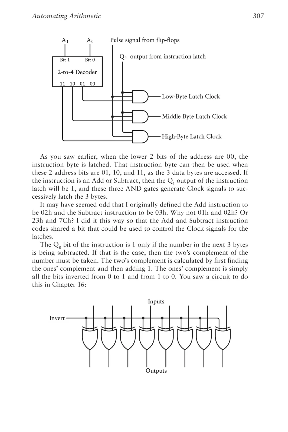
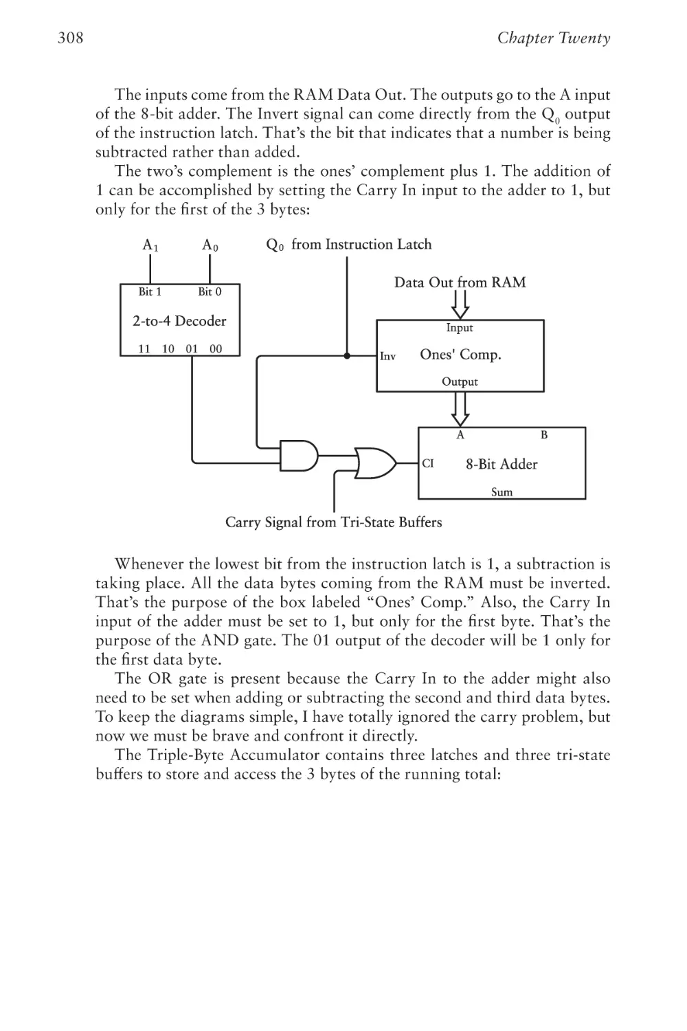
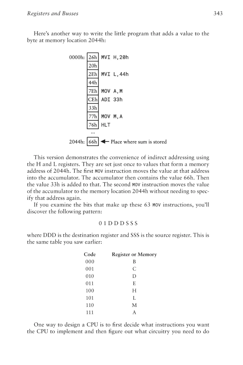
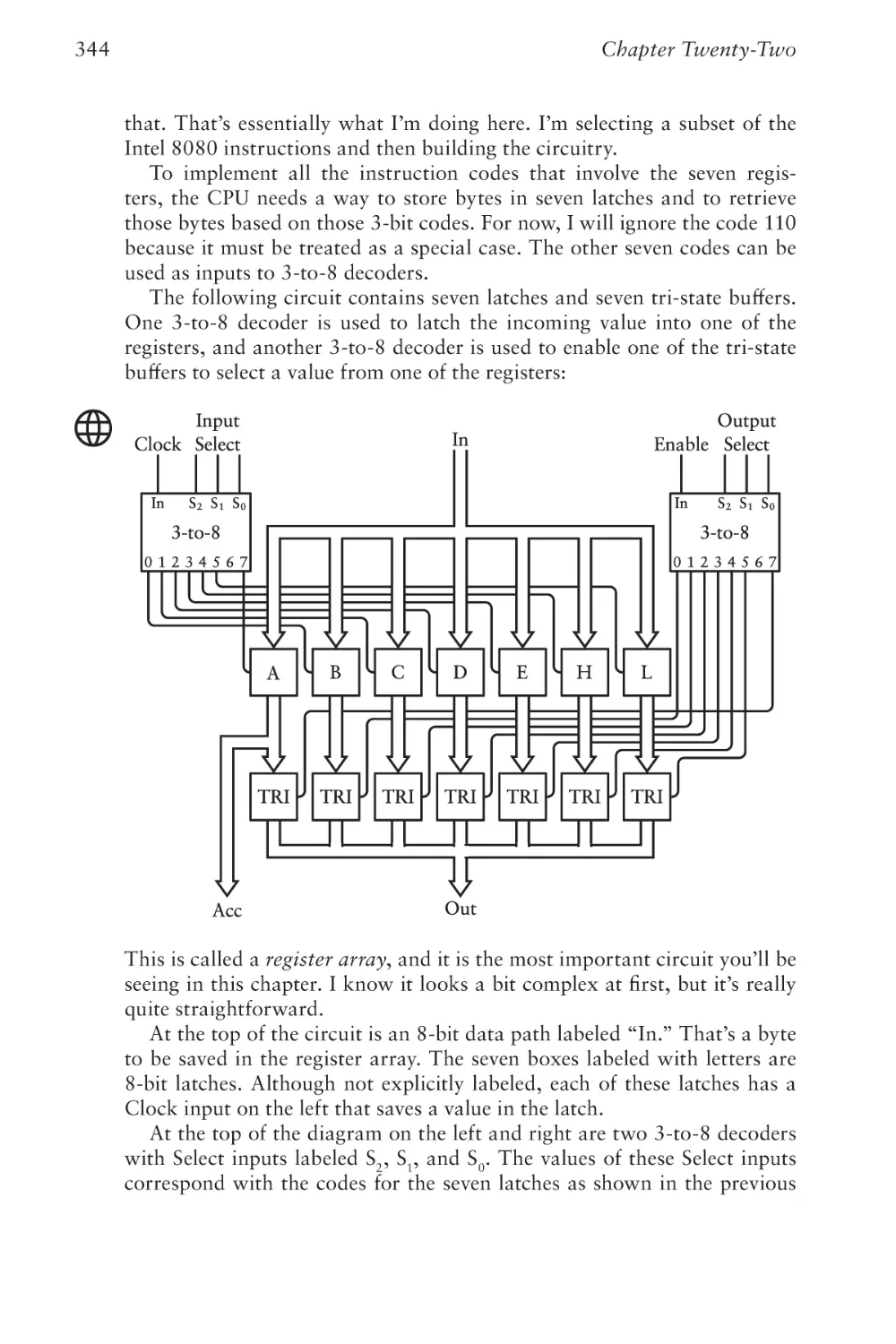
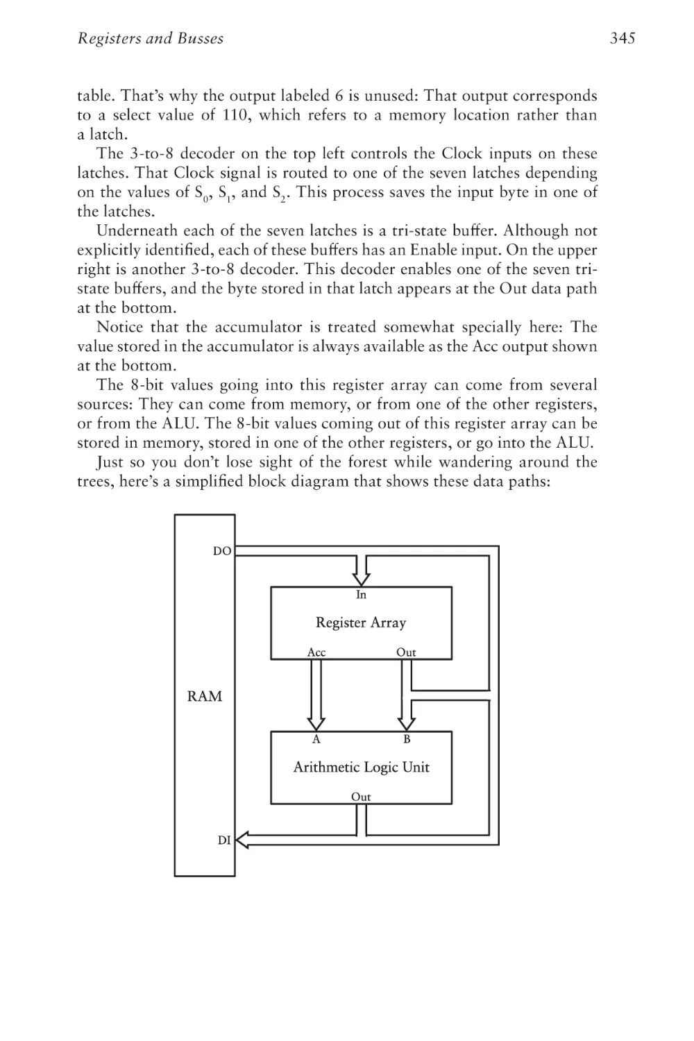
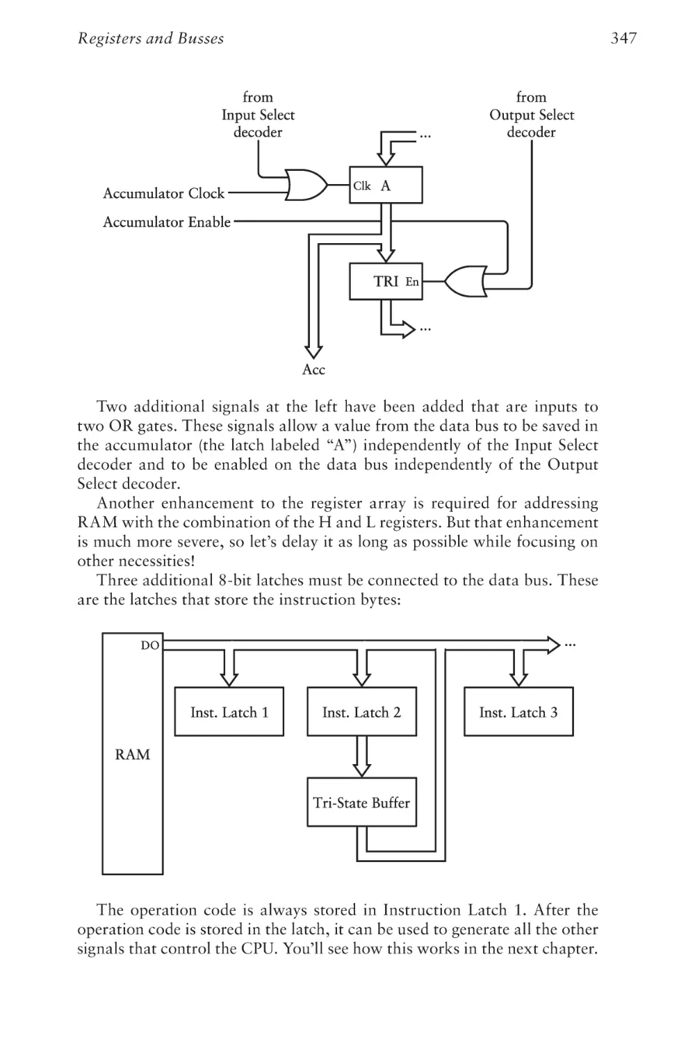
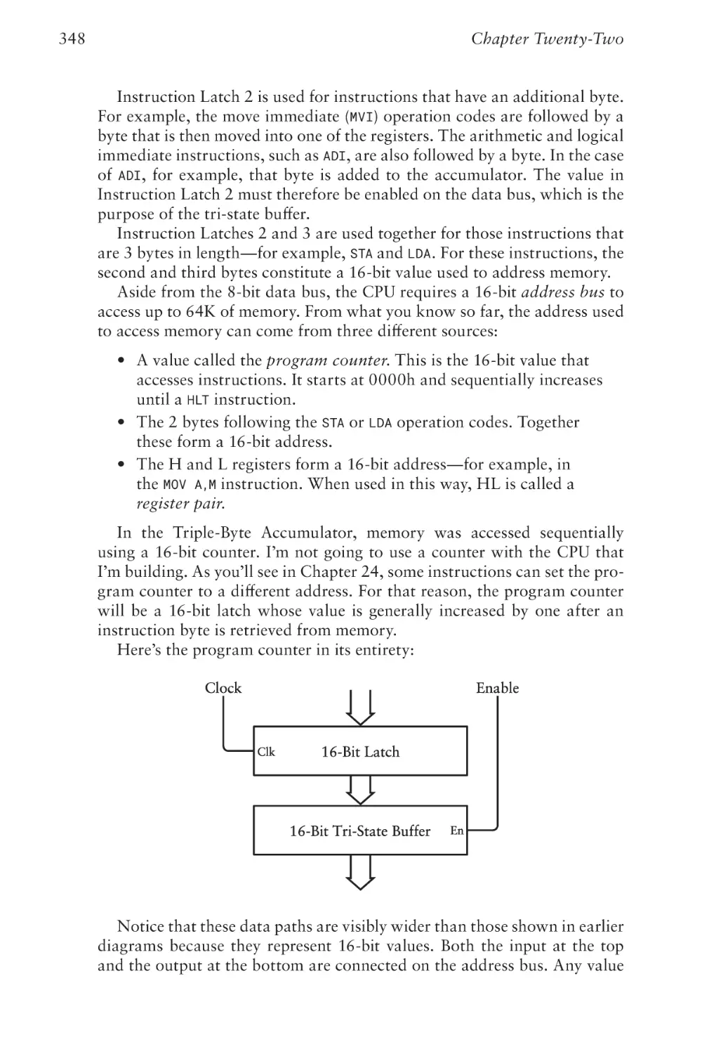
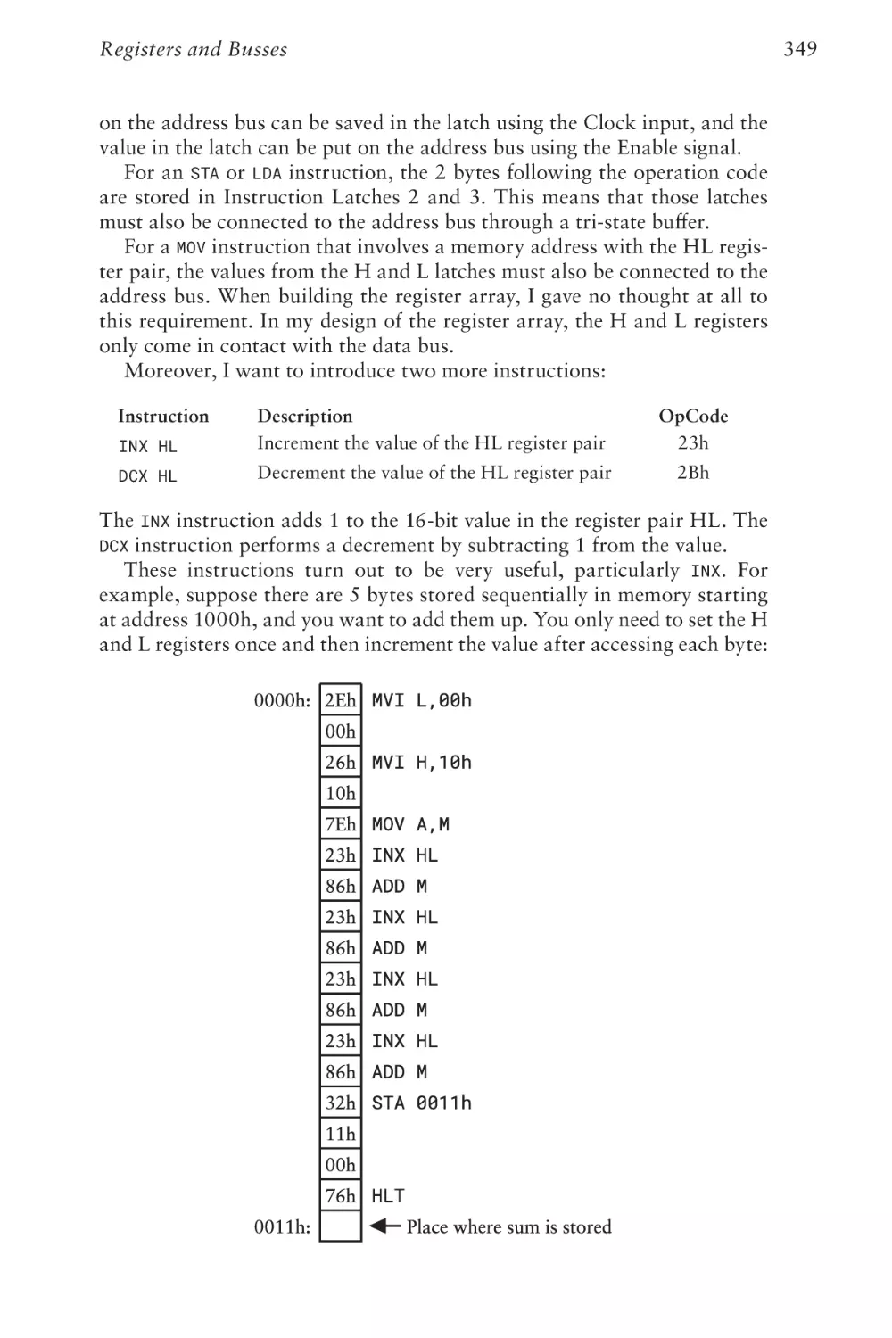
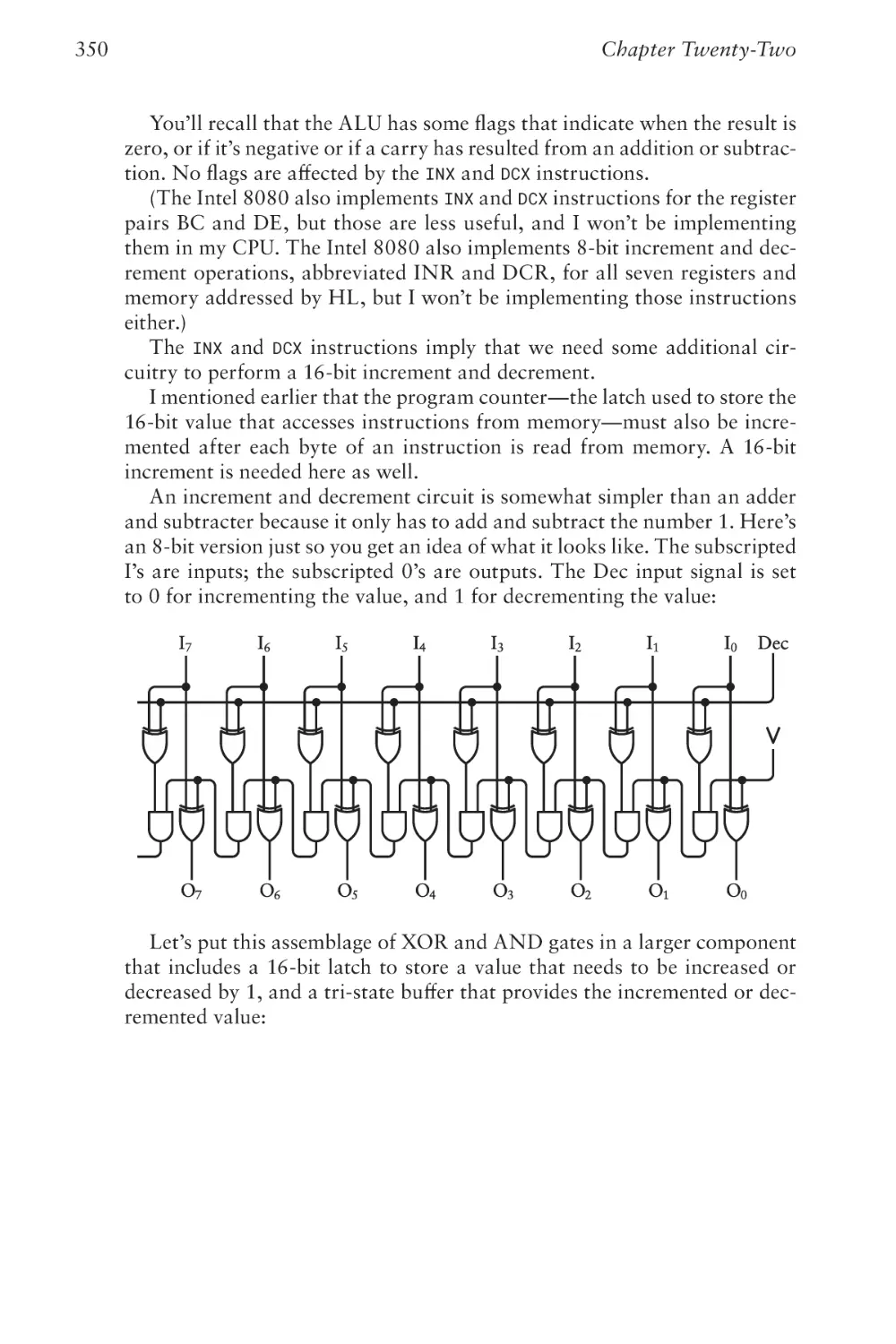
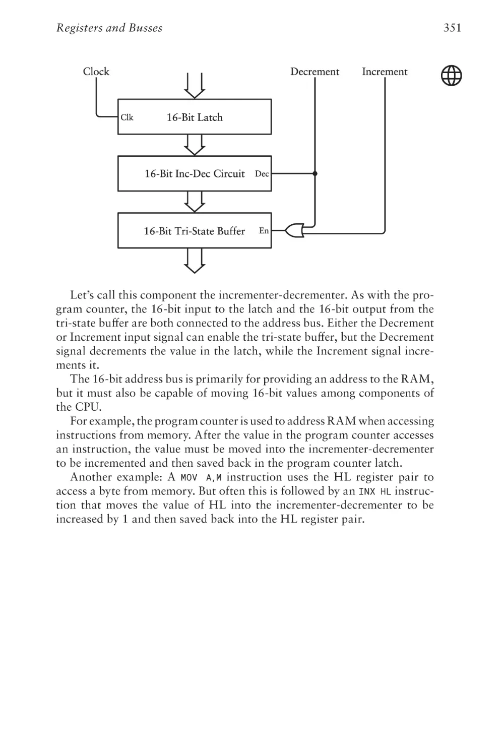
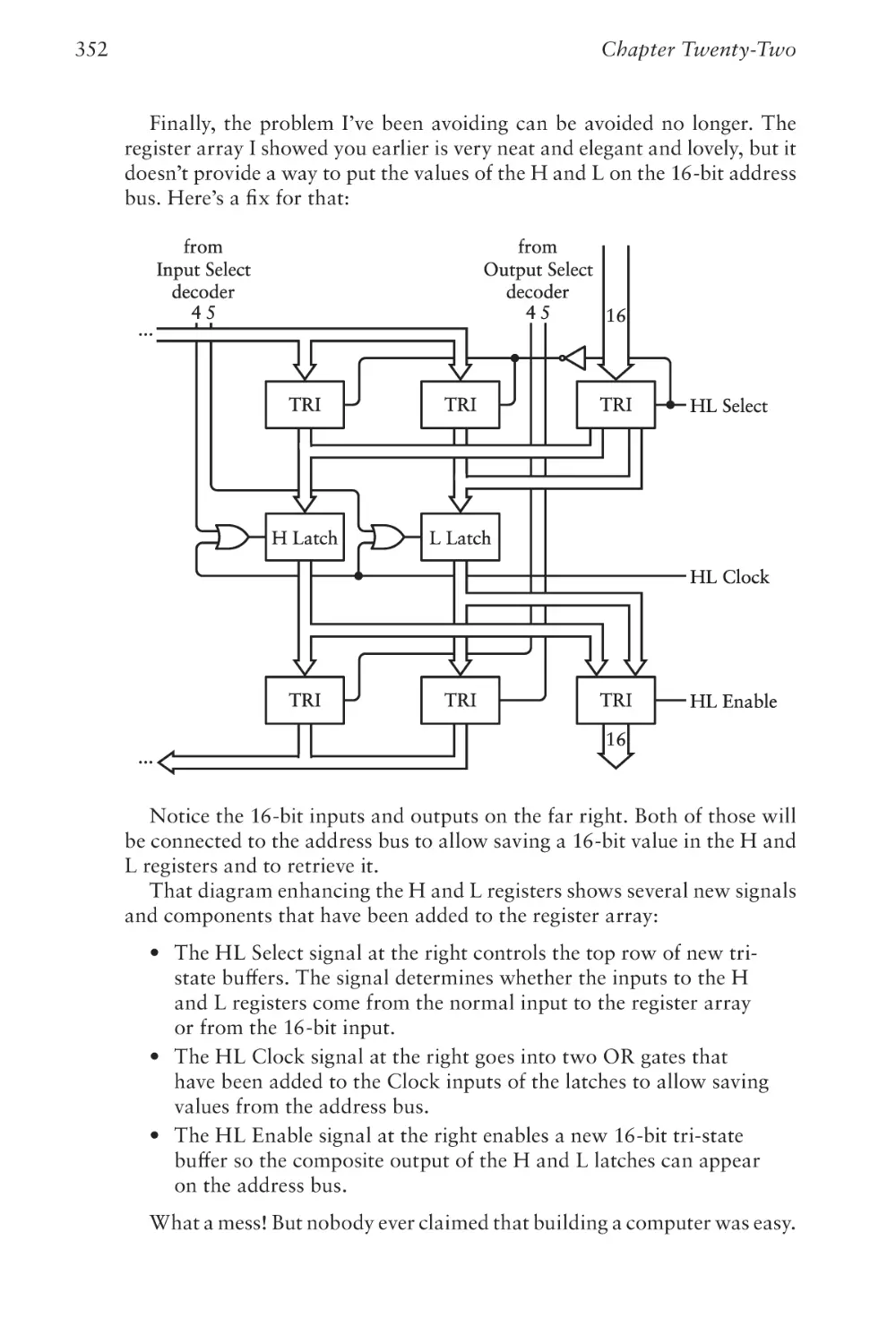
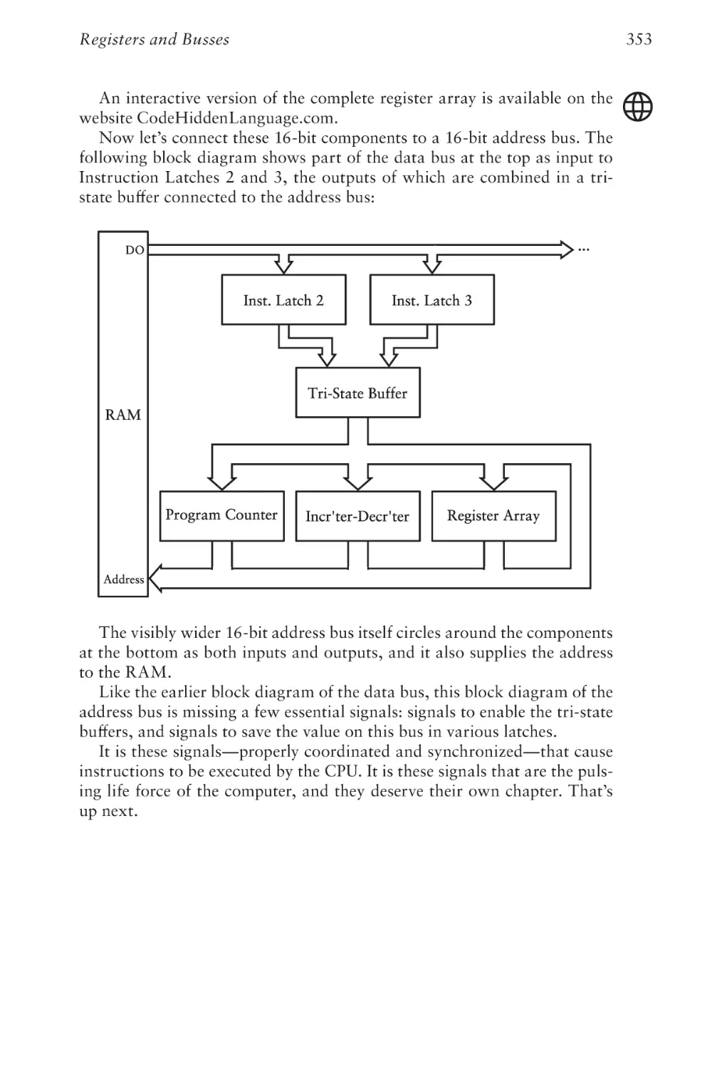
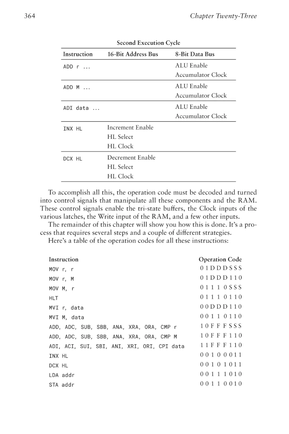
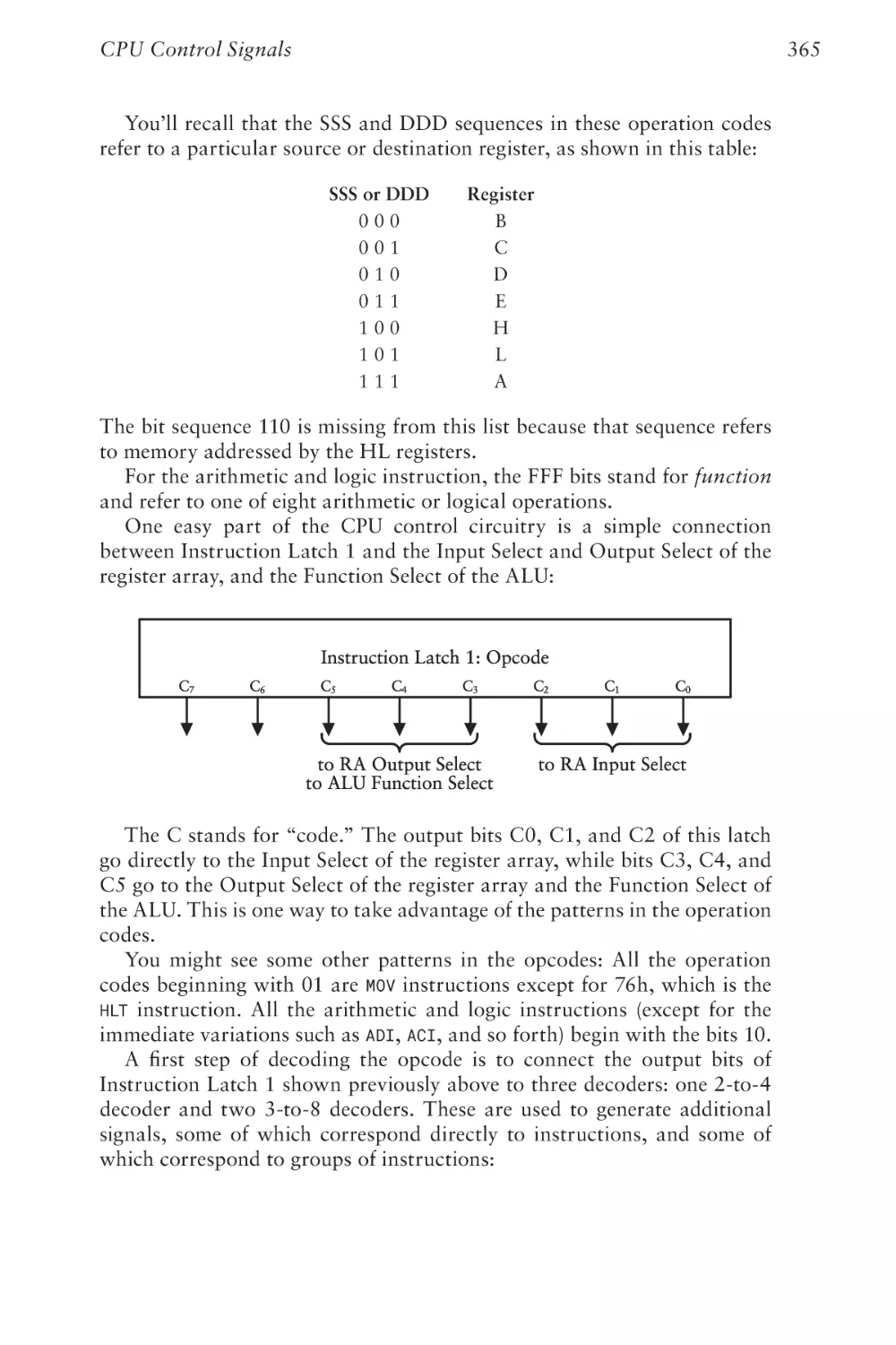
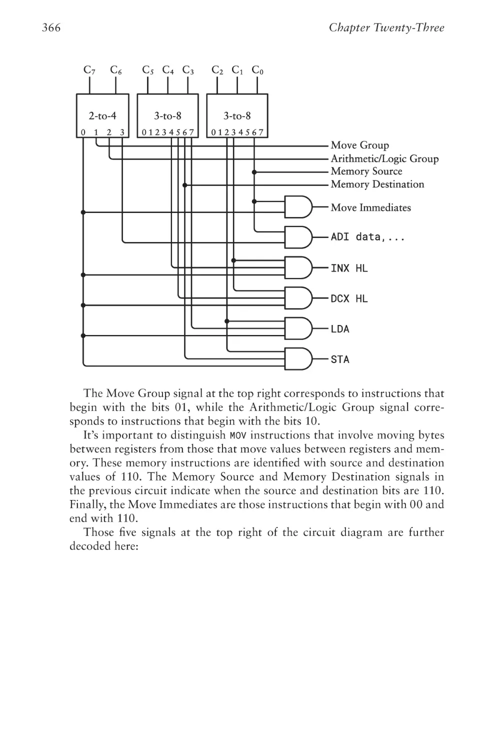
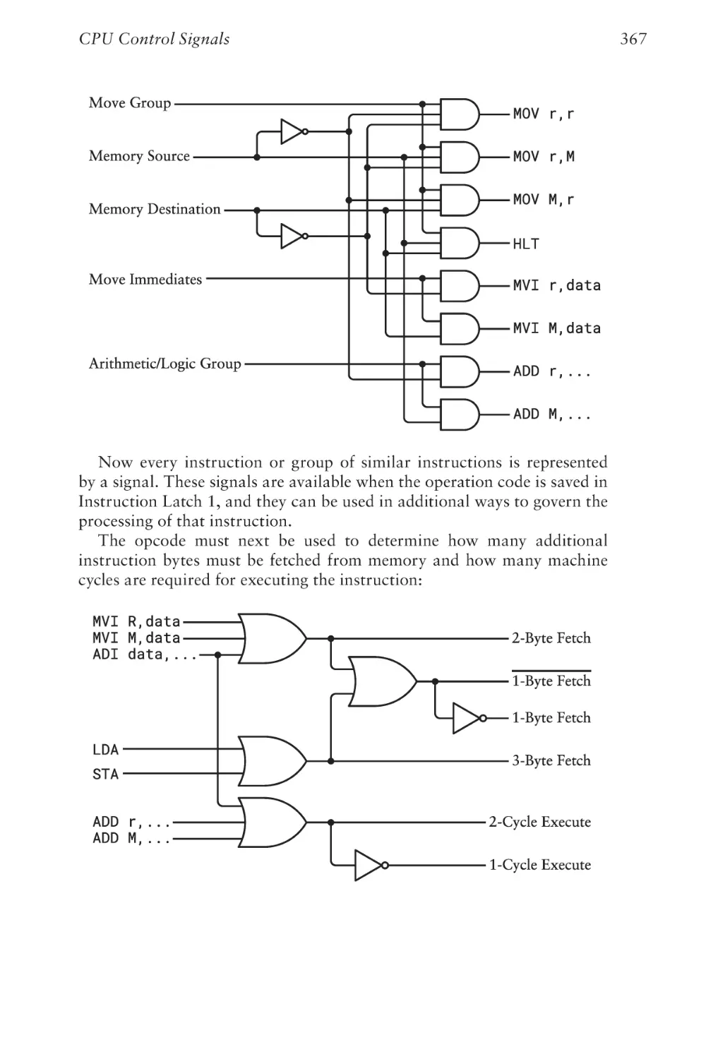
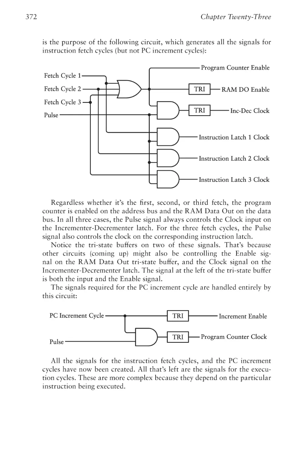
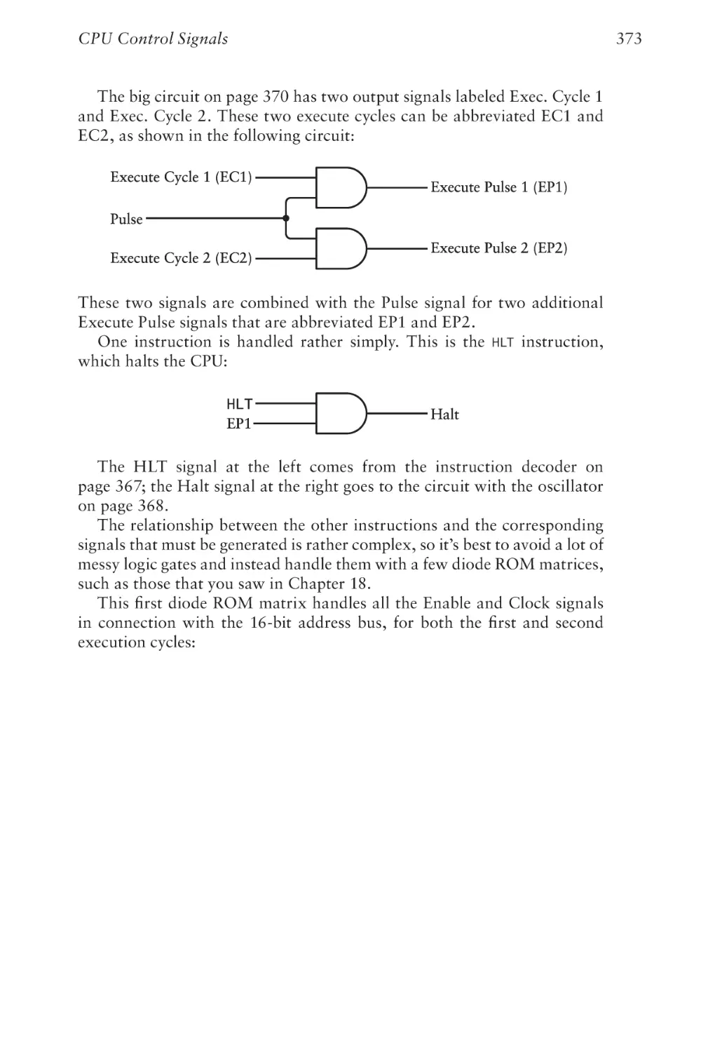
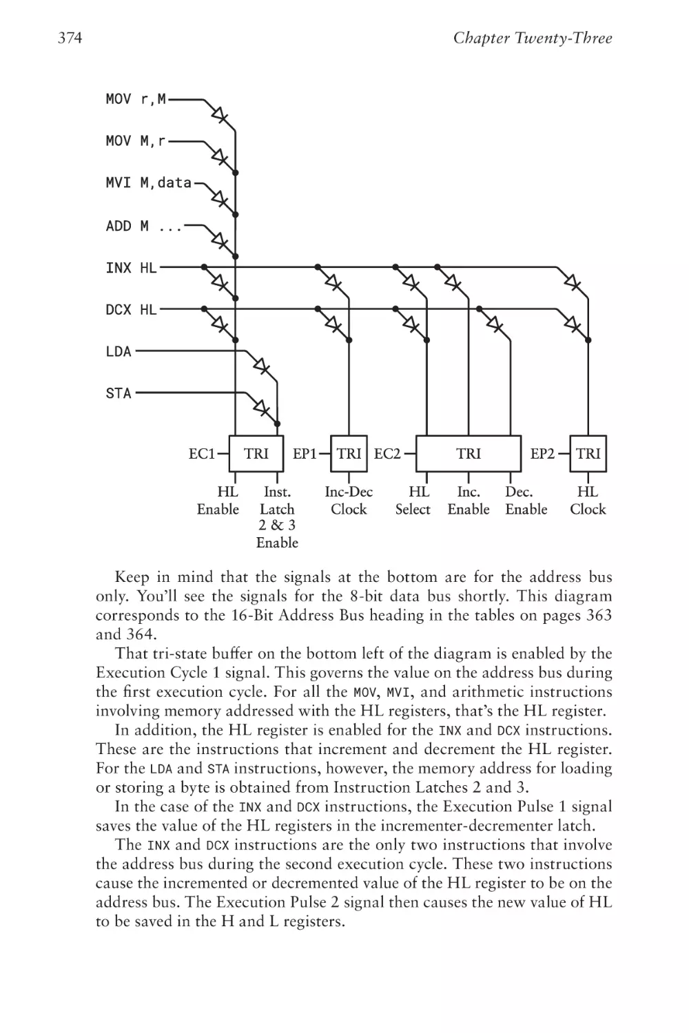
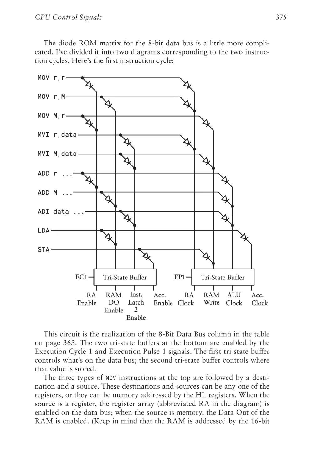
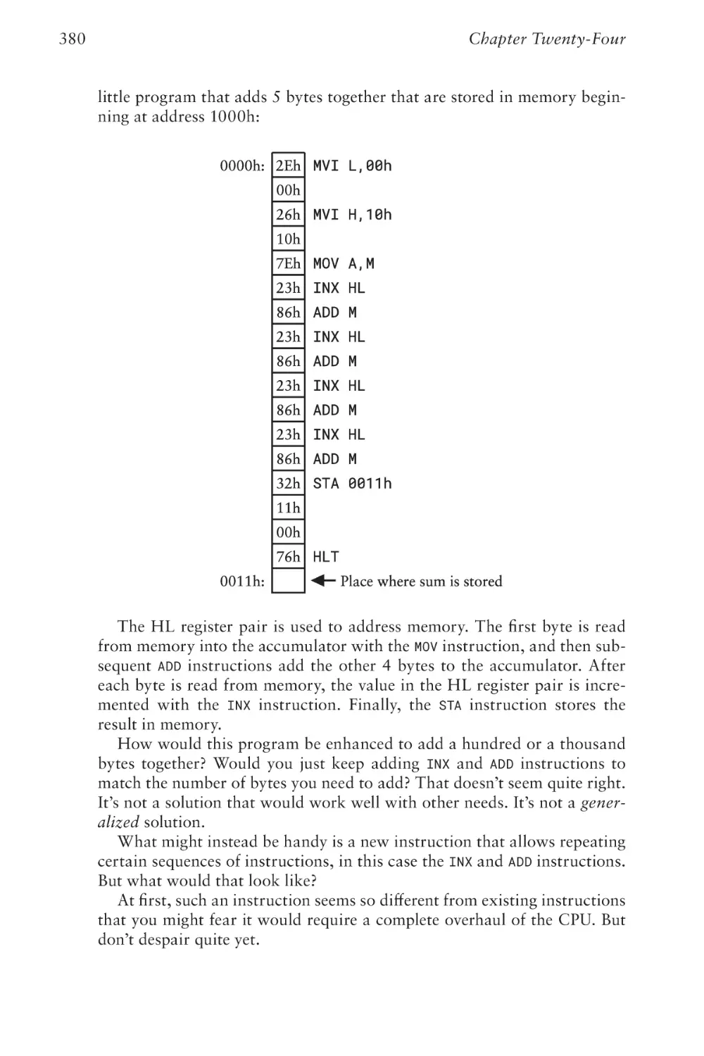
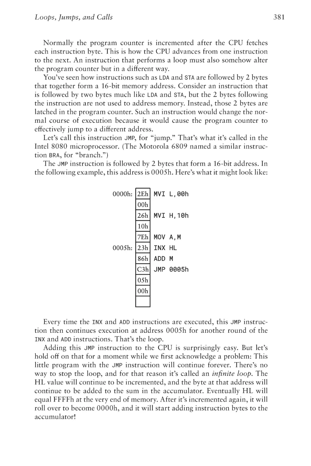
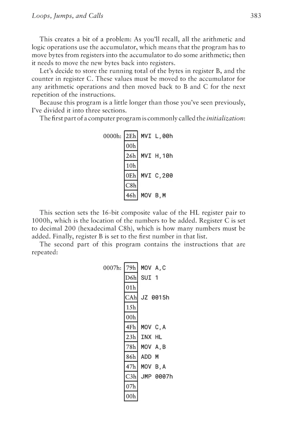
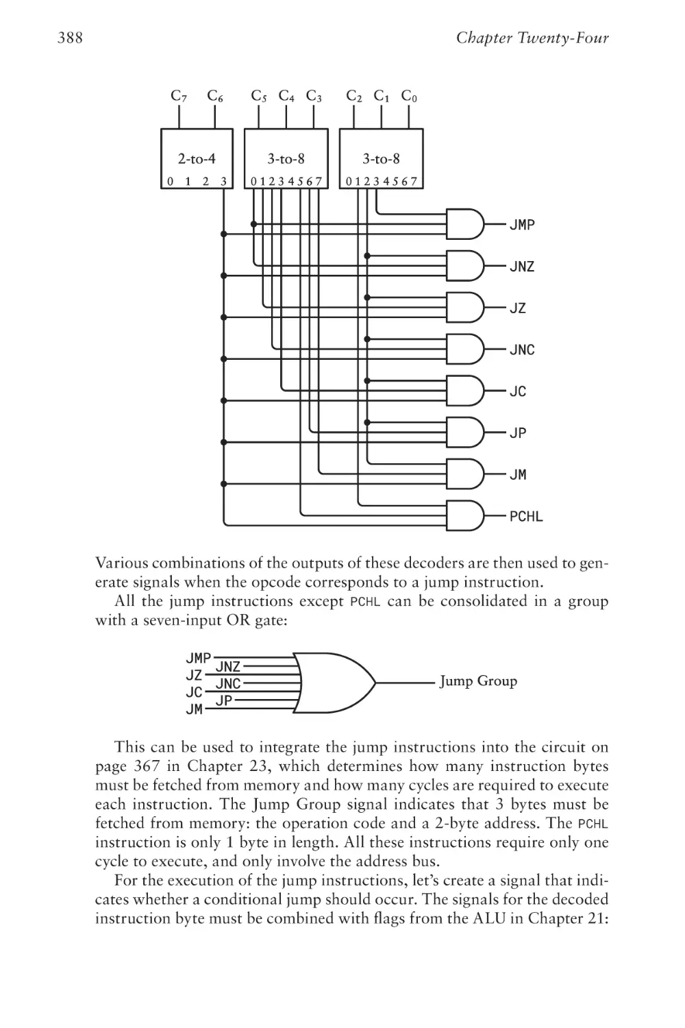
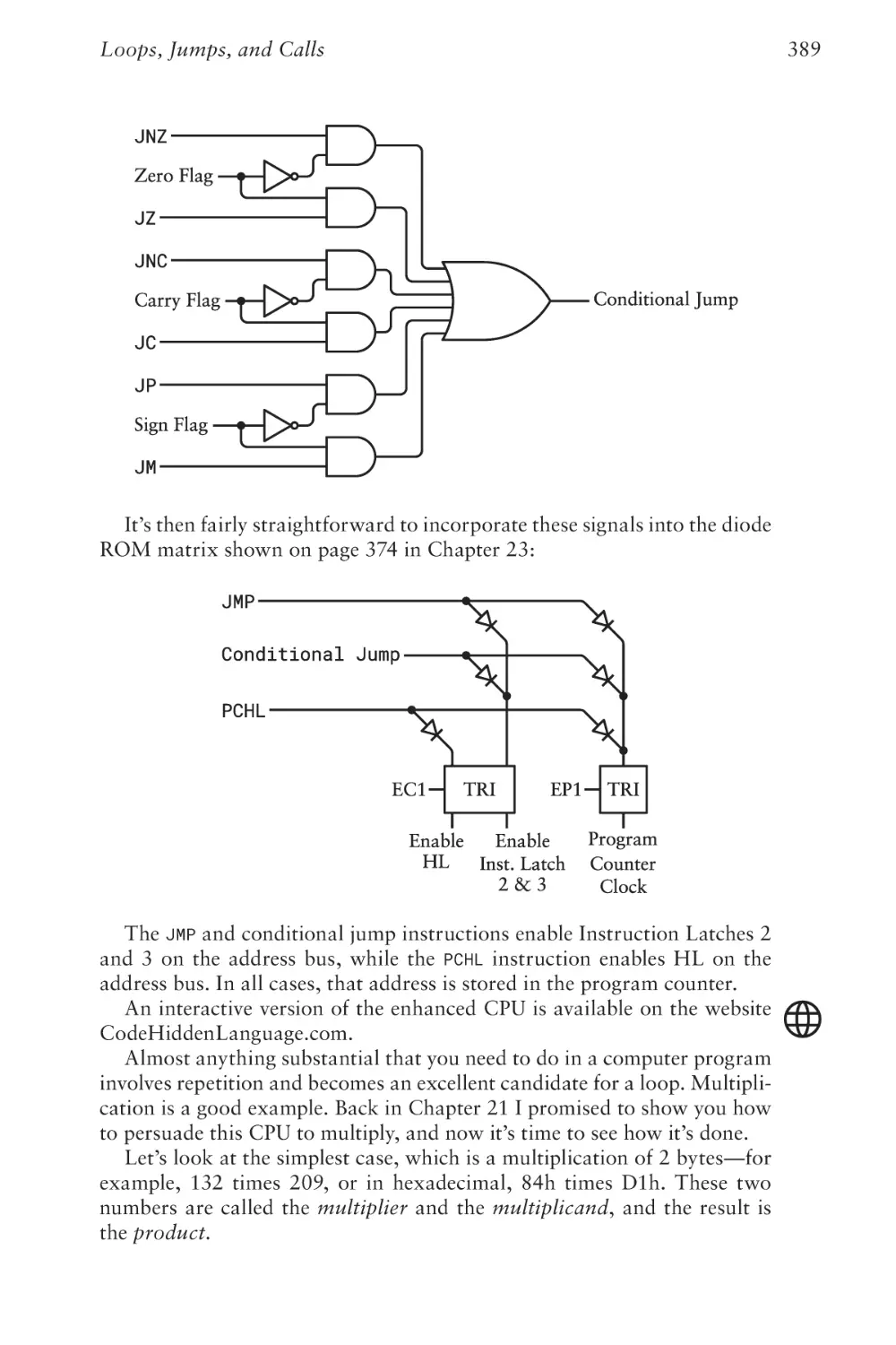
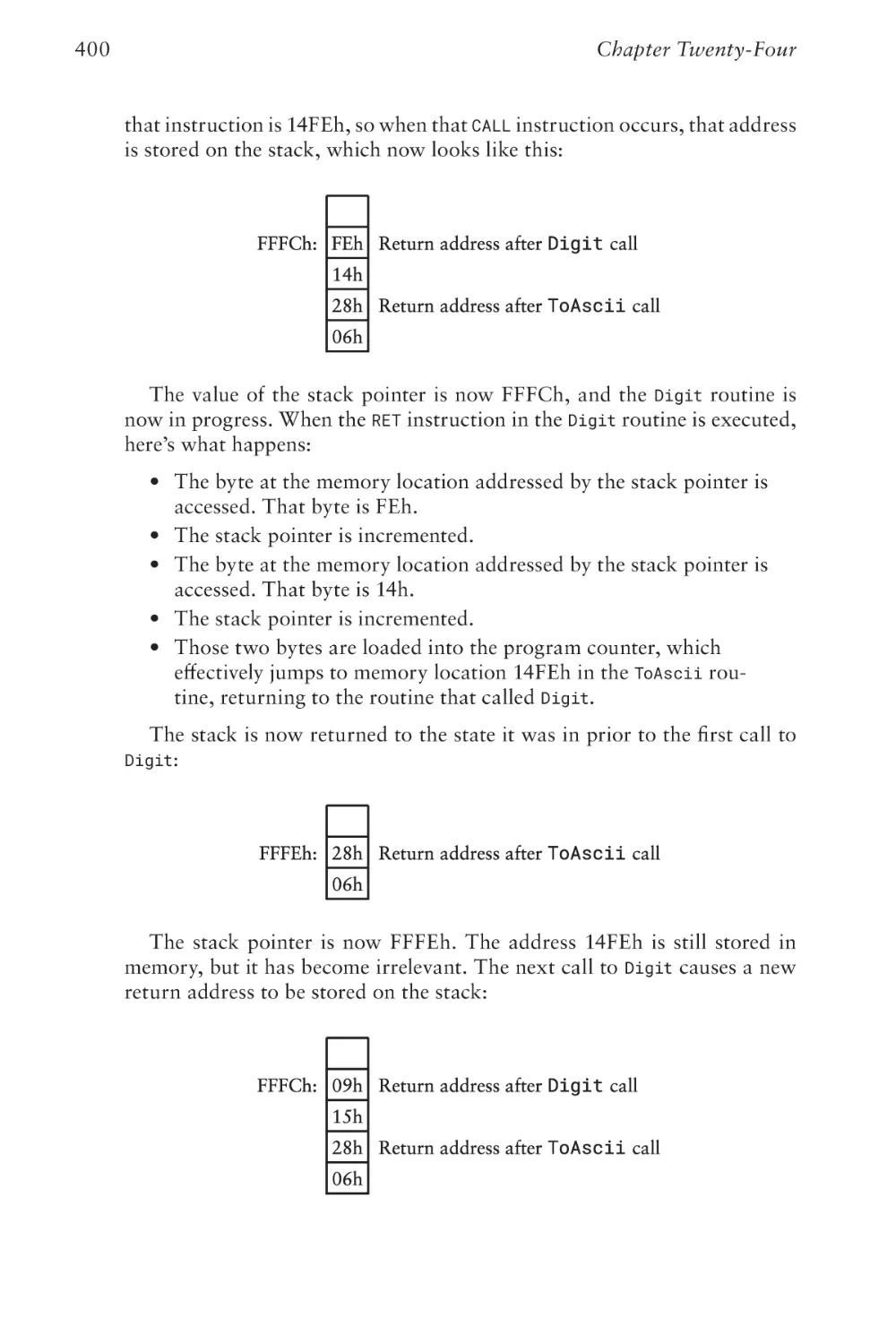
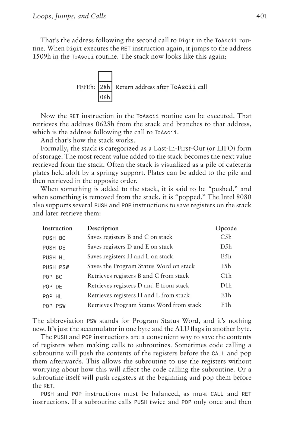
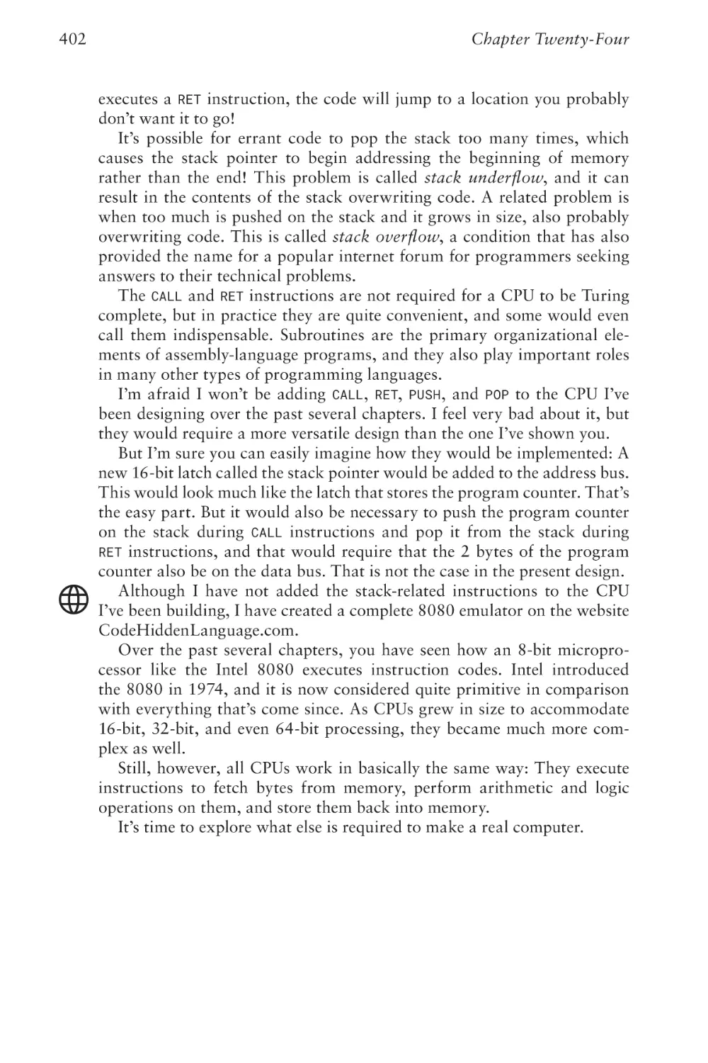
/


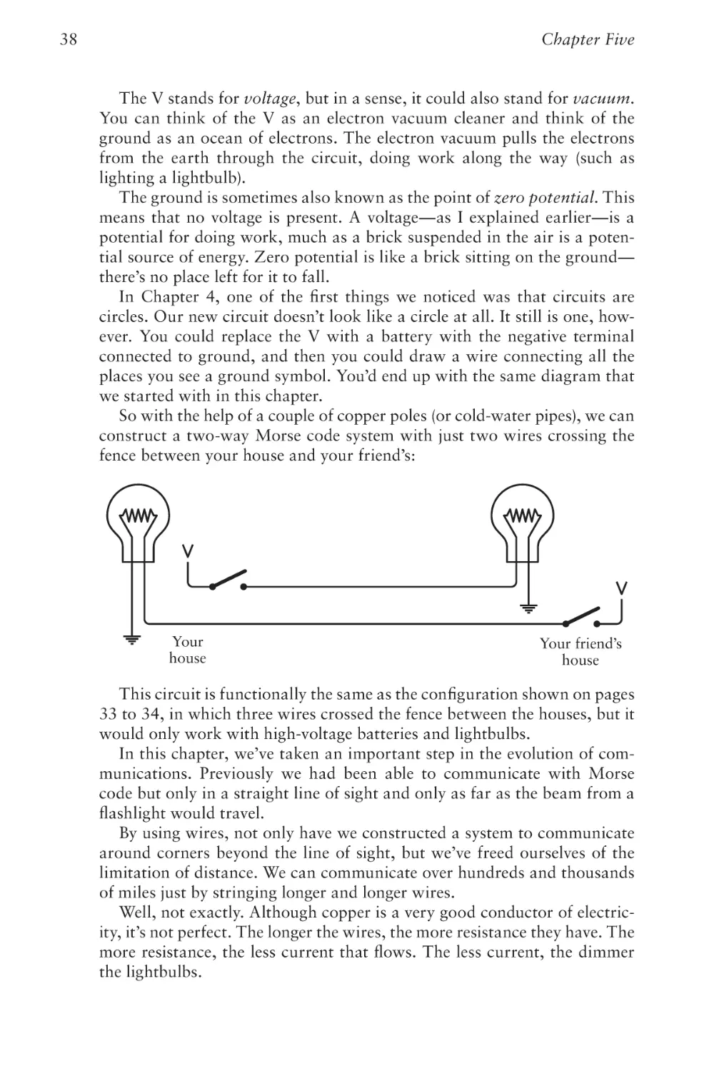
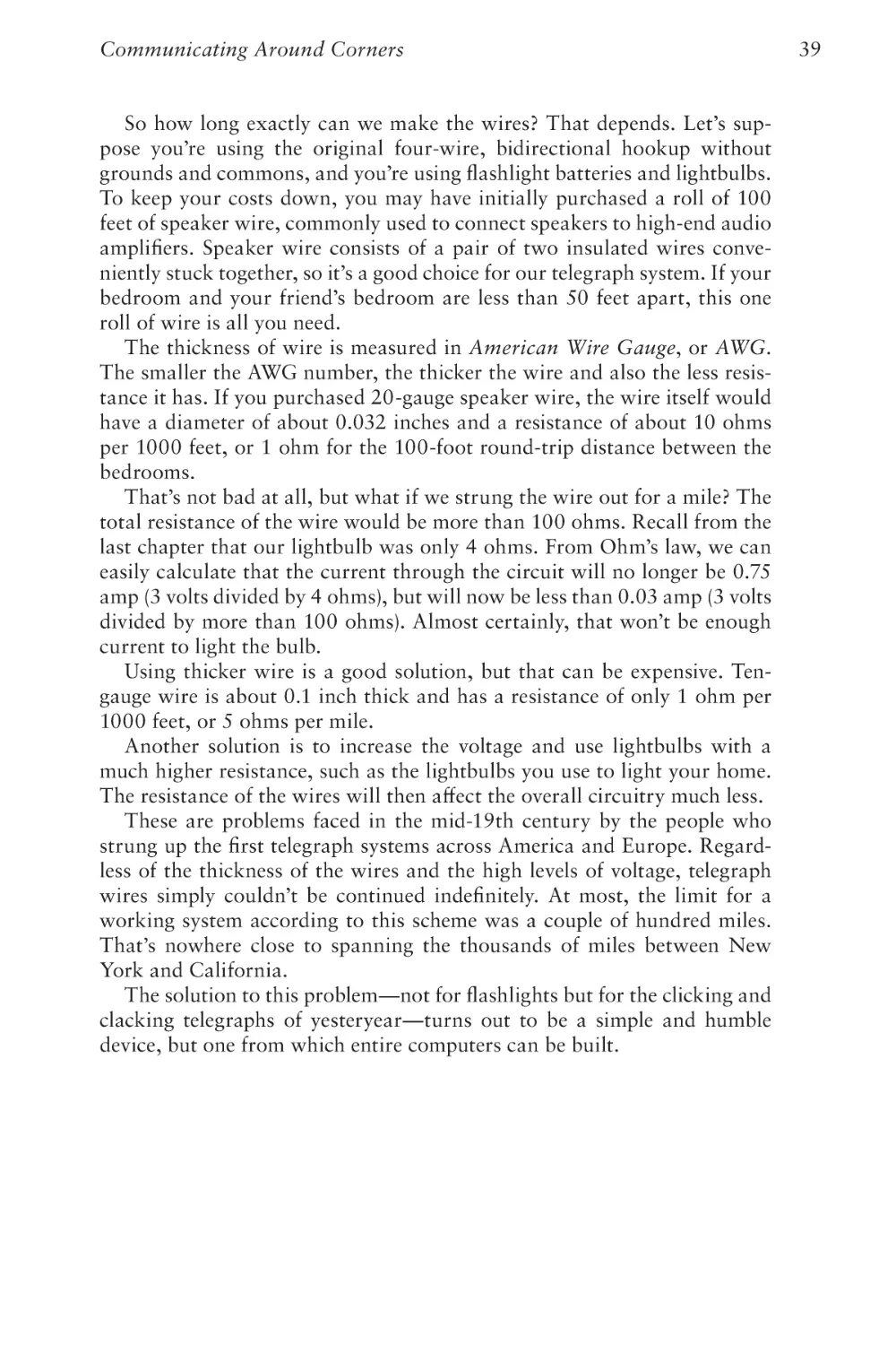


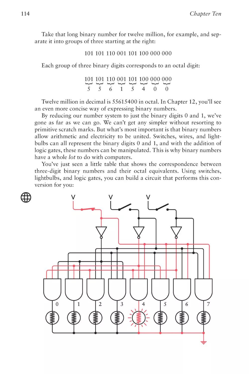
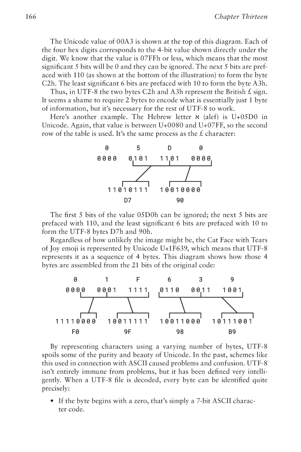


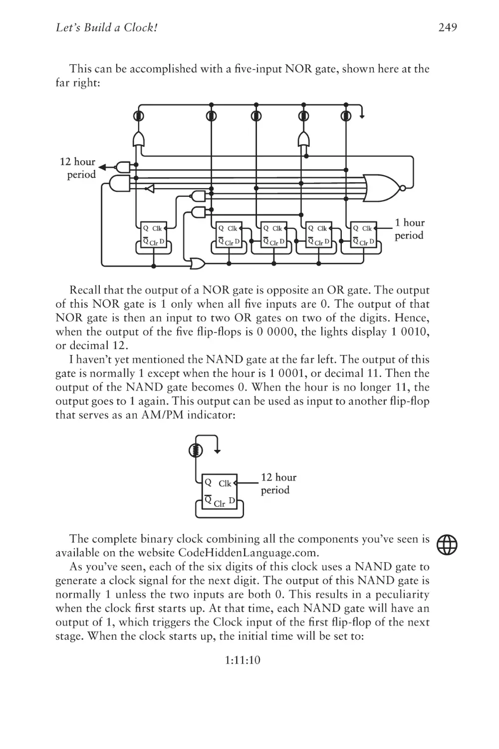
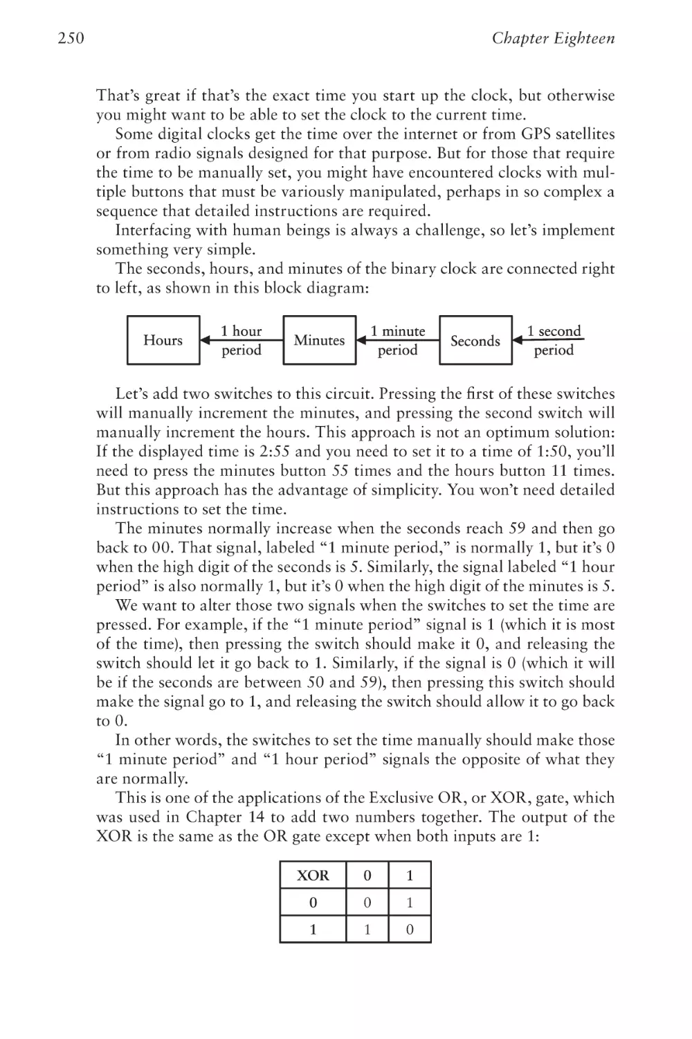
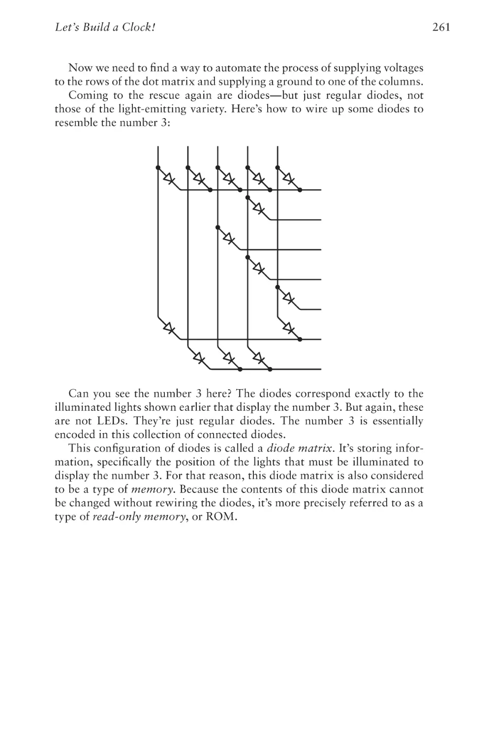
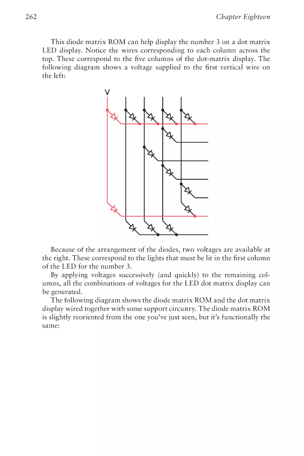
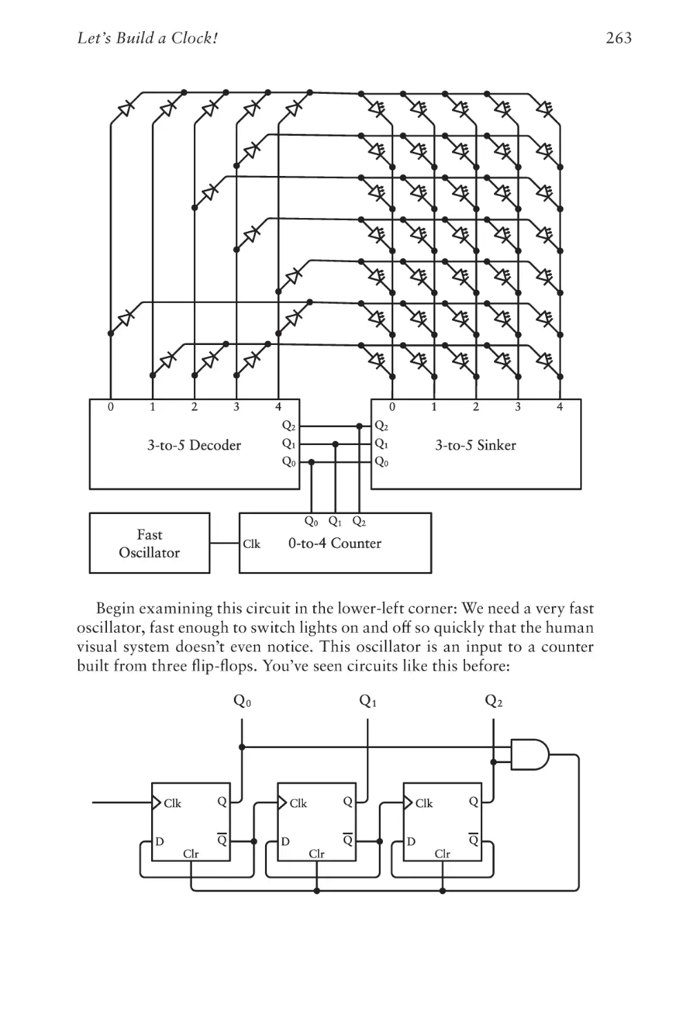
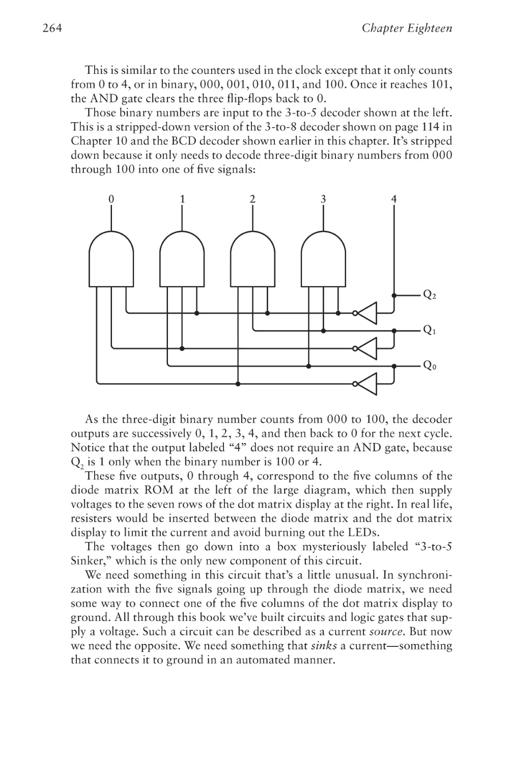

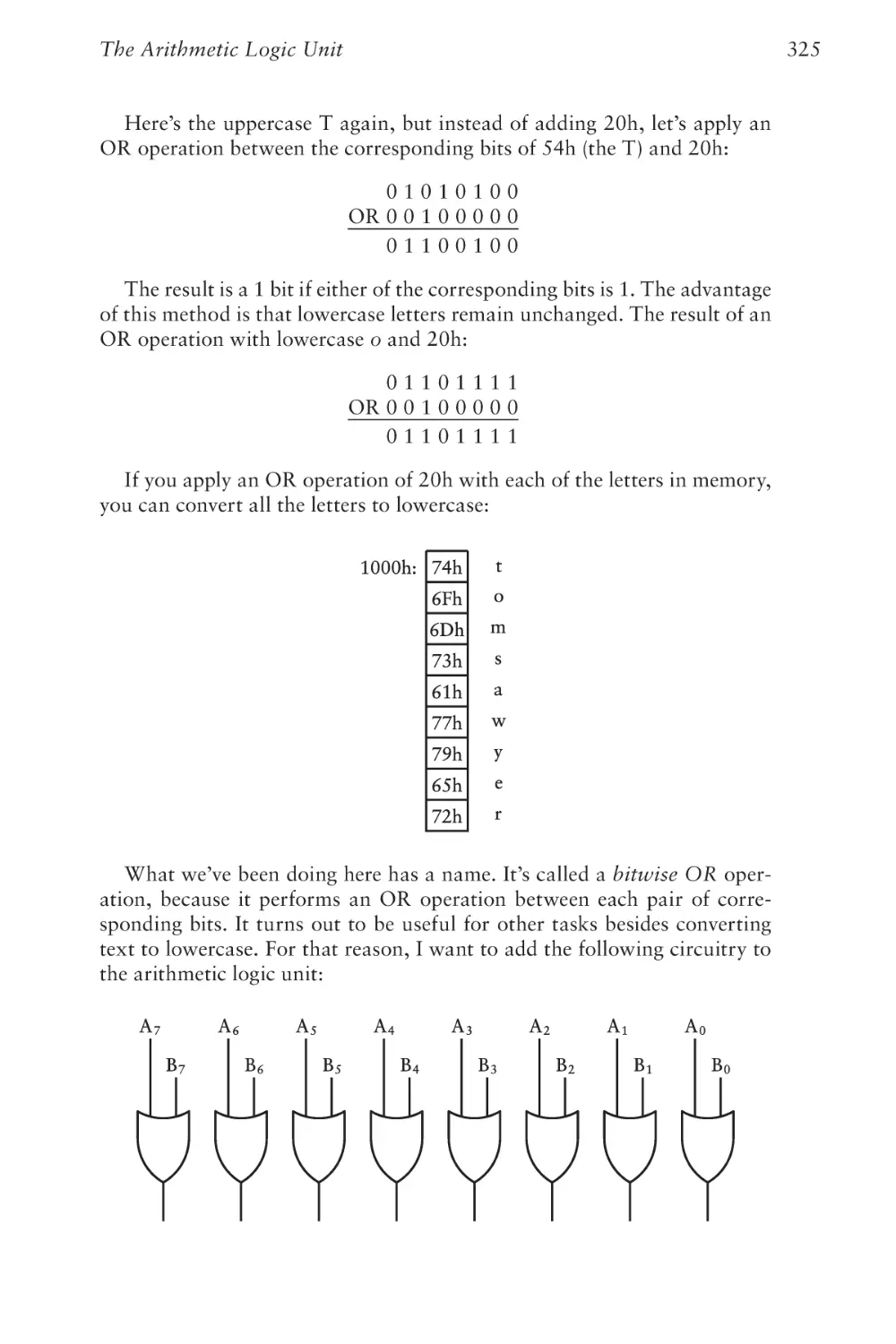


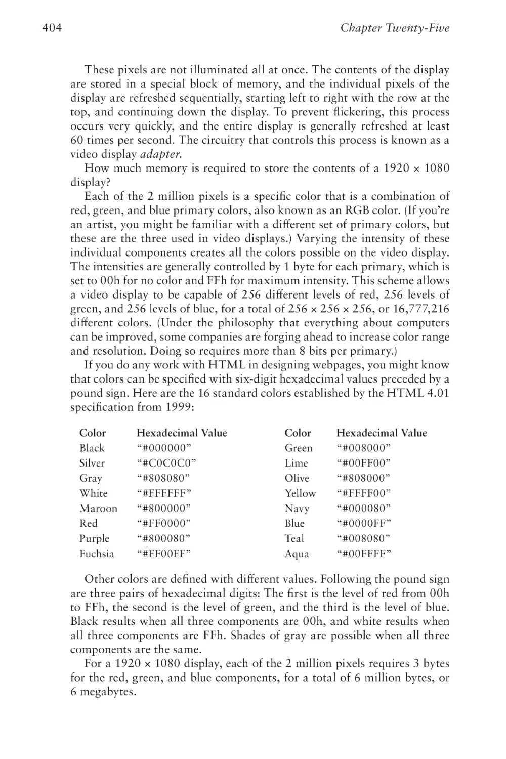


Text
The Hidden Language of
Computer Hardware and Software
C
O
1000011
1001111
S E C O N D
D
1000100
E
1000101
E D I T I O N
CHARLES PETZOLD
Code: The Hidden Language of Computer Hardware and Software: Second Edition
Published with the authorization of Microsoft Corporation by: Pearson Education, Inc.
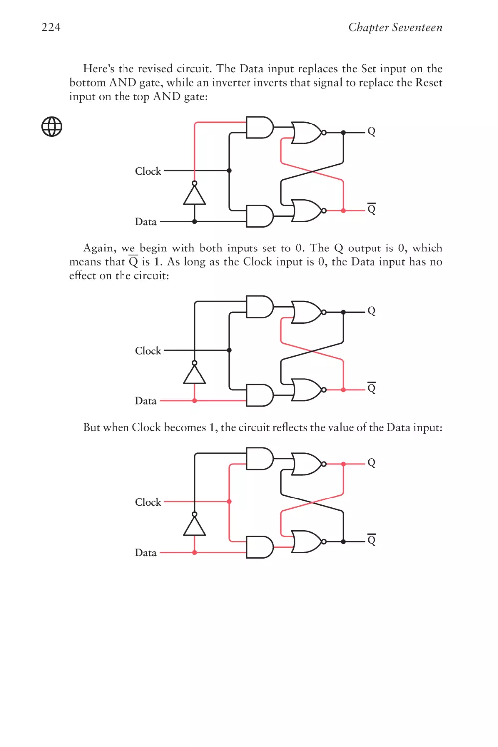
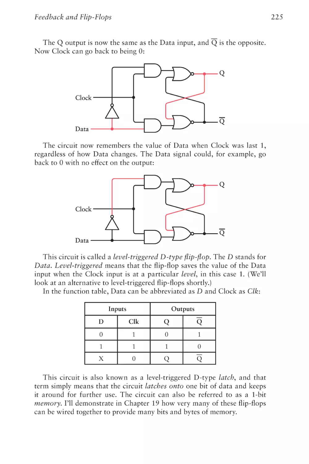
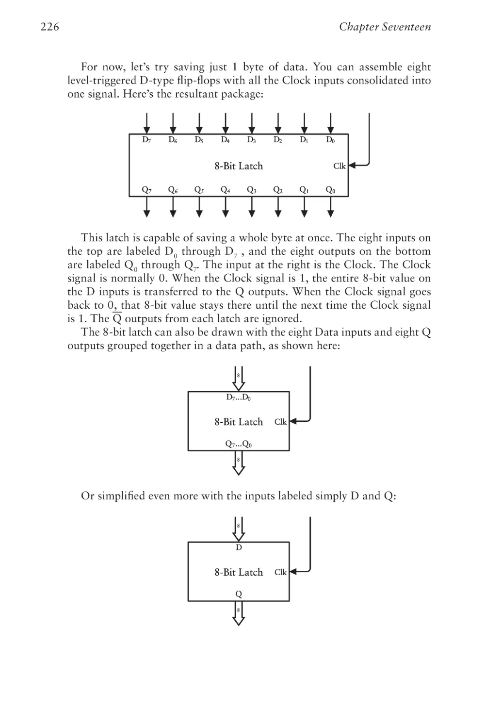
Copyright © 2023 by Charles Petzold.
All rights reserved. This publication is protected by copyright, and permission must be
obtained from the publisher prior to any prohibited reproduction, storage in a retrieval
system, or transmission in any form or by any means, electronic, mechanical, photocopying, recording, or likewise. For information regarding permissions, request forms, and the
appropriate contacts within the Pearson Education Global Rights & Permissions Department, please visit www.pearson.com/permissions.
No patent liability is assumed with respect to the use of the information contained herein.
Although every precaution has been taken in the preparation of this book, the publisher
and author assume no responsibility for errors or omissions. Nor is any liability assumed
for damages resulting from the use of the information contained herein.
ISBN-13: 978-0-13-790910-0
ISBN-10: 0-13-790910-1
Library of Congress Control Number: 2022939292
ScoutAutomatedPrintCode
Trademarks
Microsoft and the trademarks listed at http://www.microsoft.com on the “Trademarks”
webpage are trademarks of the Microsoft group of companies. All other marks are property of their respective owners.
Warning and Disclaimer
Every effort has been made to make this book as complete and as accurate as possible, but
no warranty or fitness is implied. The information provided is on an “as is” basis. The
author, the publisher, and Microsoft Corporation shall have neither liability nor responsibility to any person or entity with respect to any loss or damages arising from the information contained in this book or from the use of the programs accompanying it.
Special Sales
For information about buying this title in bulk quantities, or for special sales opportunities
(which may include electronic versions; custom cover designs; and content particular to
your business, training goals, marketing focus, or branding interests), please contact our
corporate sales department at corpsales@pearsoned.com or (800) 382-3419.
For government sales inquiries, please contact governmentsales@pearsoned.com.
For questions about sales outside the U.S., please contact intlcs@pearson.com.
Contents
Preface to the Second Edition
v
About the Author
ix
Chapter One
Best Friends
1
Chapter Two
Codes and Combinations
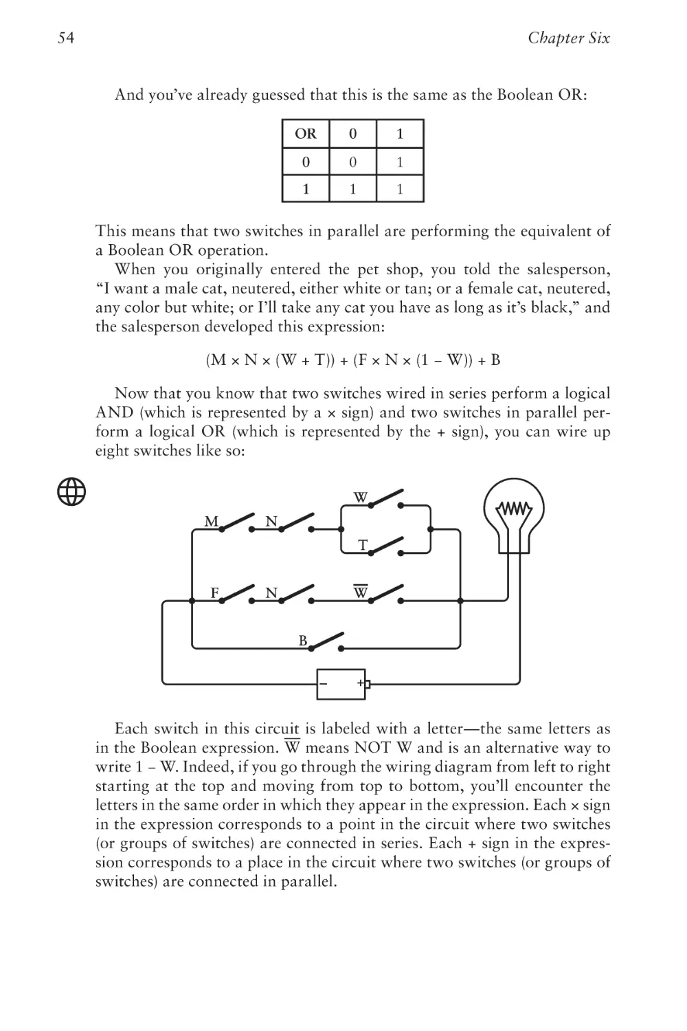
7
Chapter Three
Braille and Binary Codes
13
Chapter Four
Anatomy of a Flashlight
21
Chapter Five
Communicating Around Corners
31
Chapter Six
Logic with Switches
41
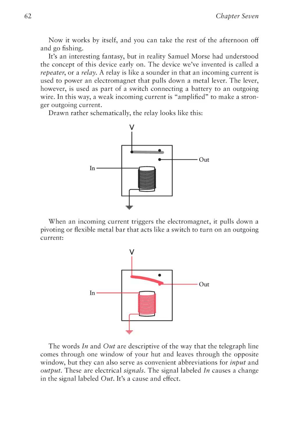
Chapter Seven
Telegraphs and Relays
57
Chapter Eight
Relays and Gates
65
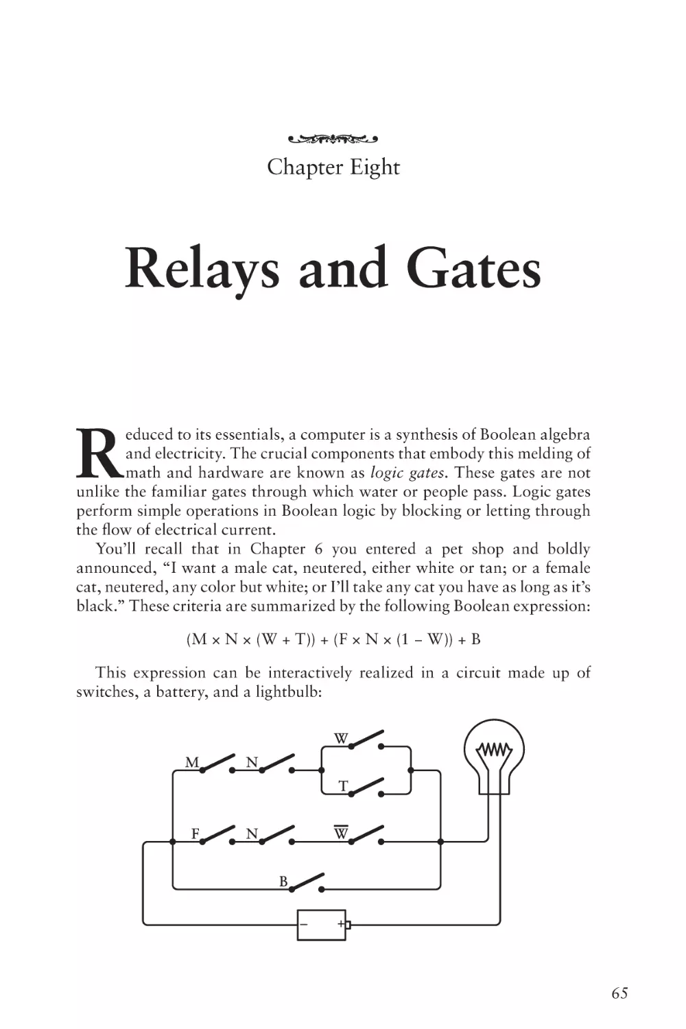
Chapter Nine
Our Ten Digits
91
Chapter Ten
Alternative 10s
99
Chapter Eleven
Bit by Bit by Bit
117
Chapter Twelve
Bytes and Hexadecimal
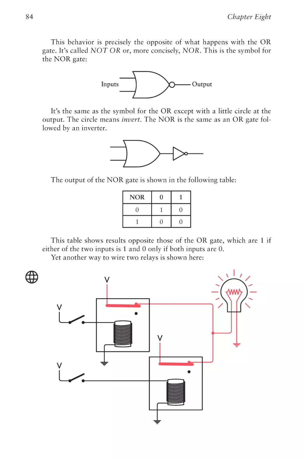
139
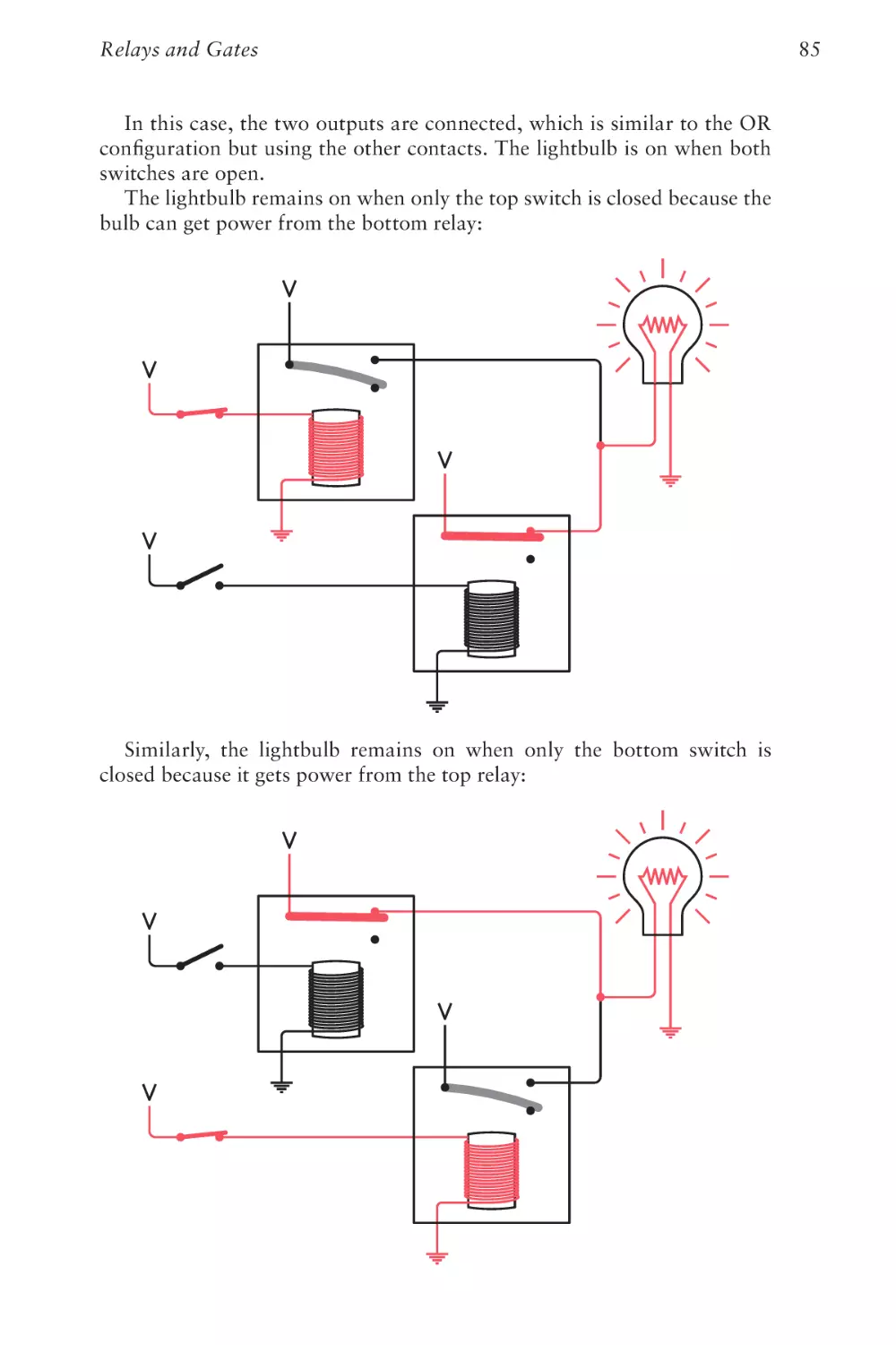
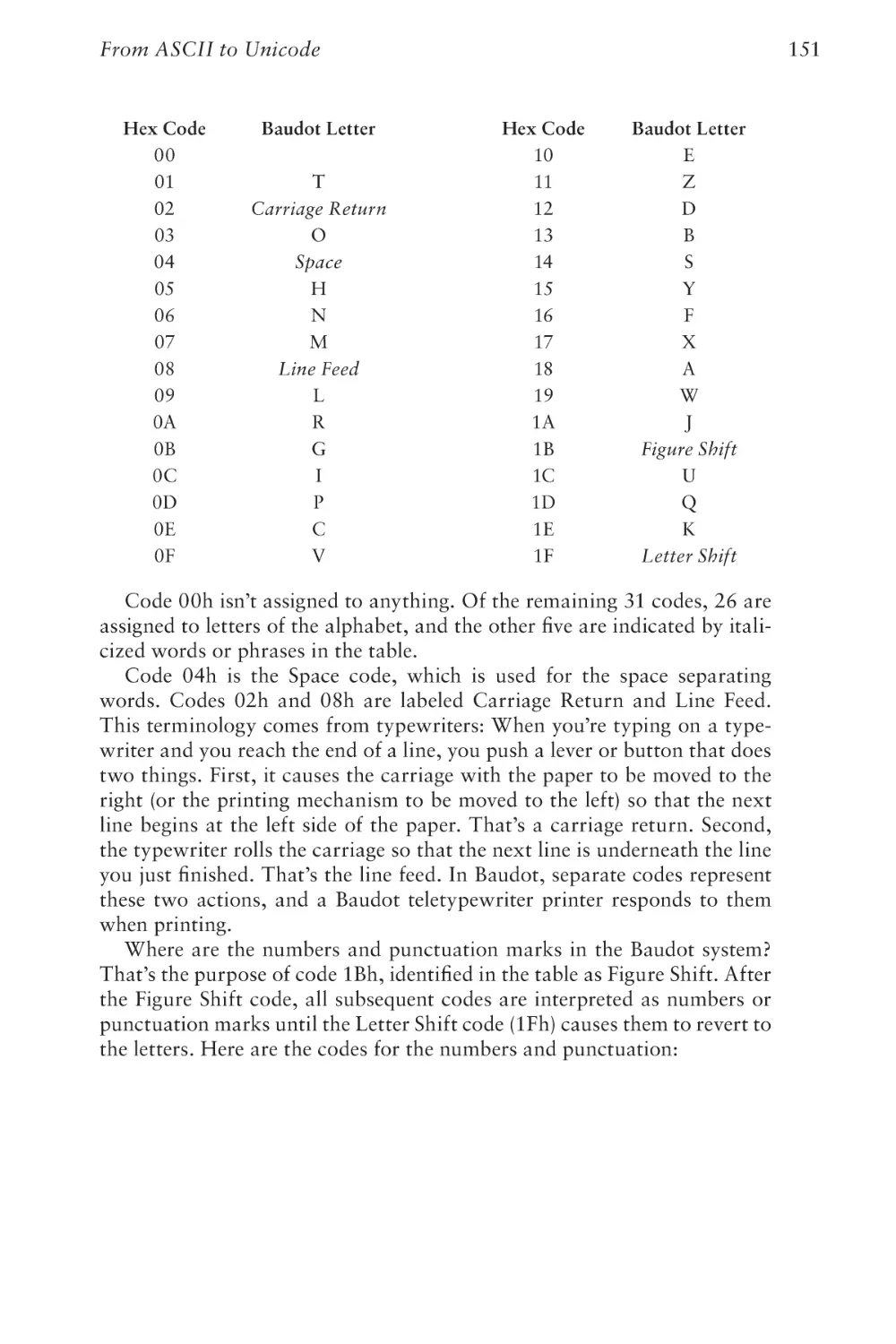
Chapter Thirteen
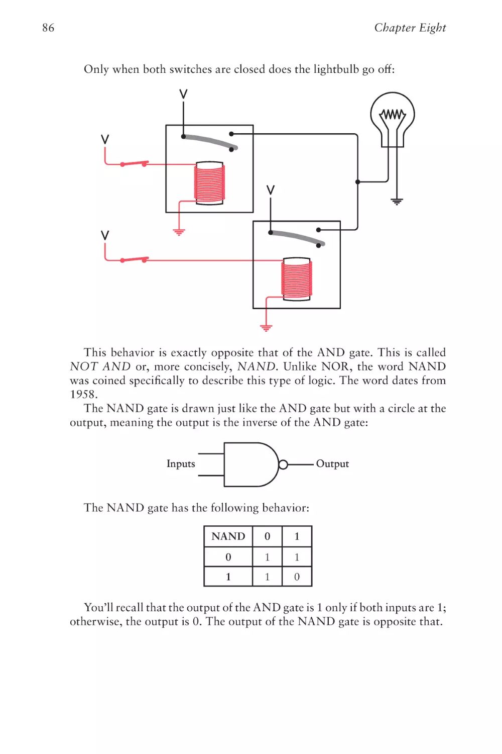
From ASCII to Unicode
149
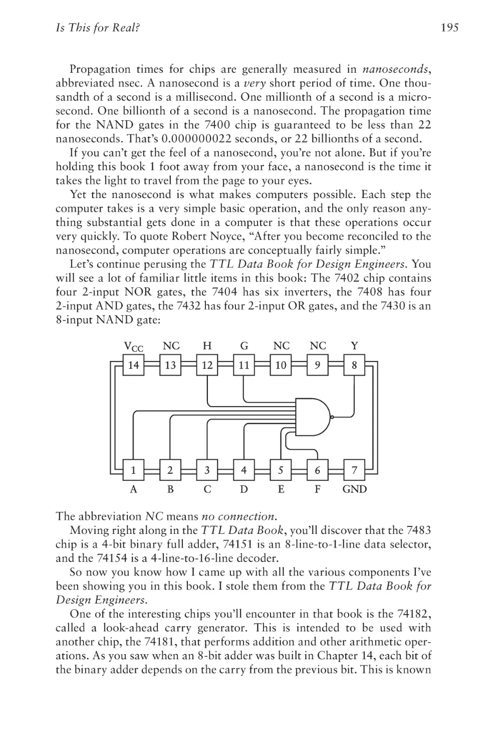
Chapter Fourteen
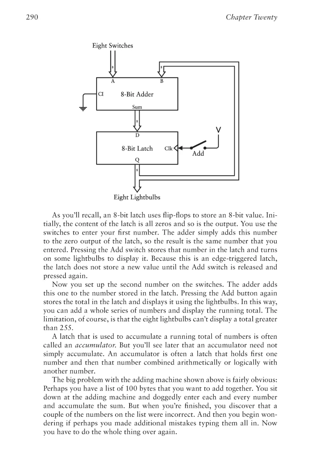
Adding with Logic Gates
169
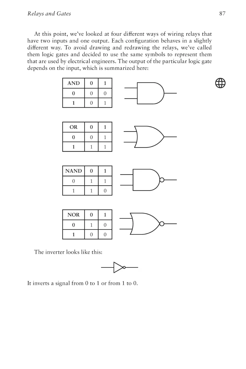
Chapter Fifteen
Is This for Real?
183
Chapter Sixteen
But What About Subtraction?
197
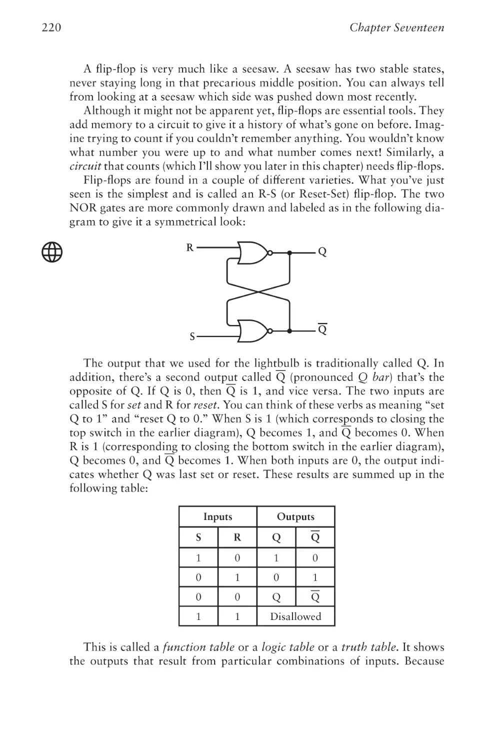
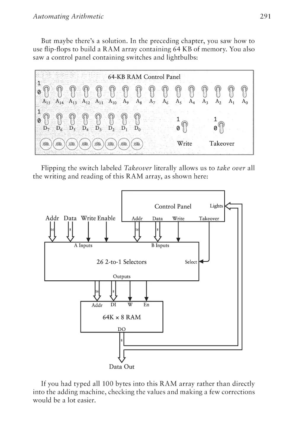
Chapter Seventeen
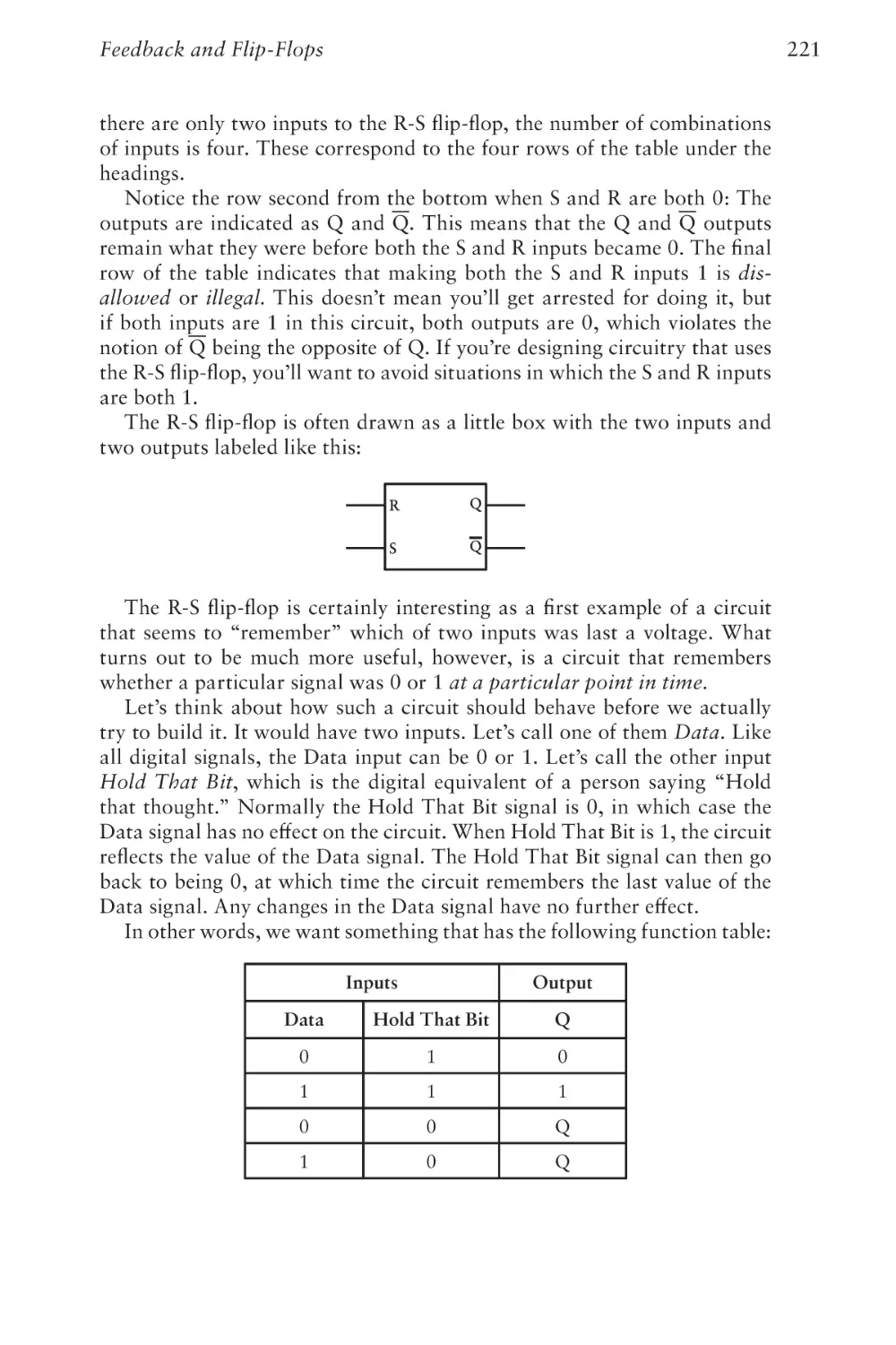
Feedback and Flip-Flops
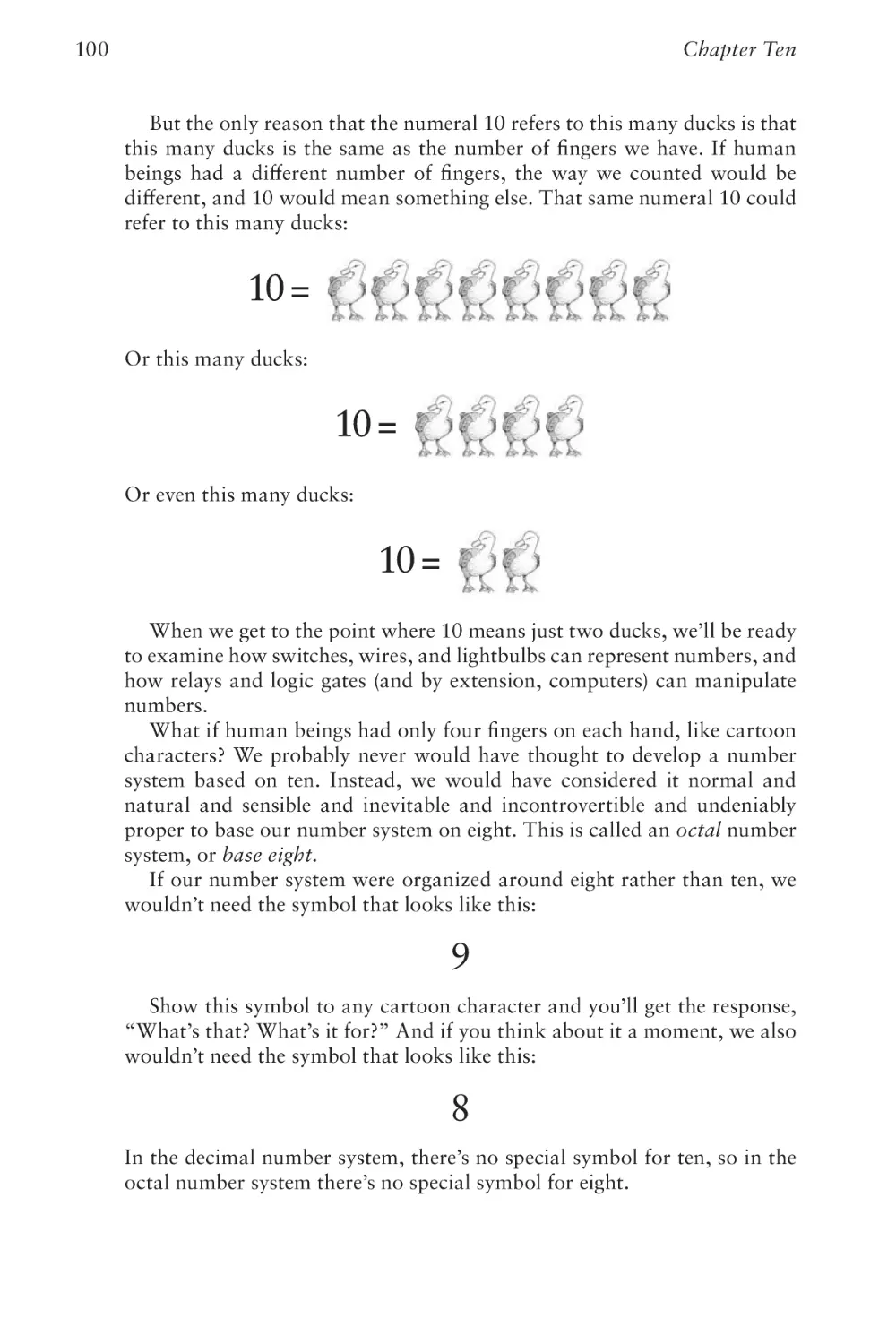
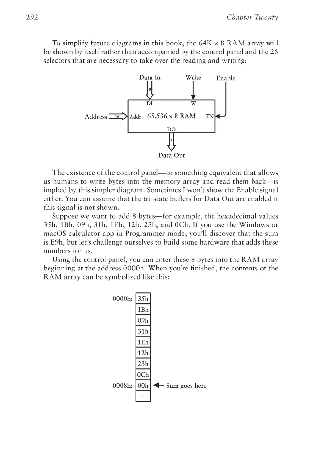
213
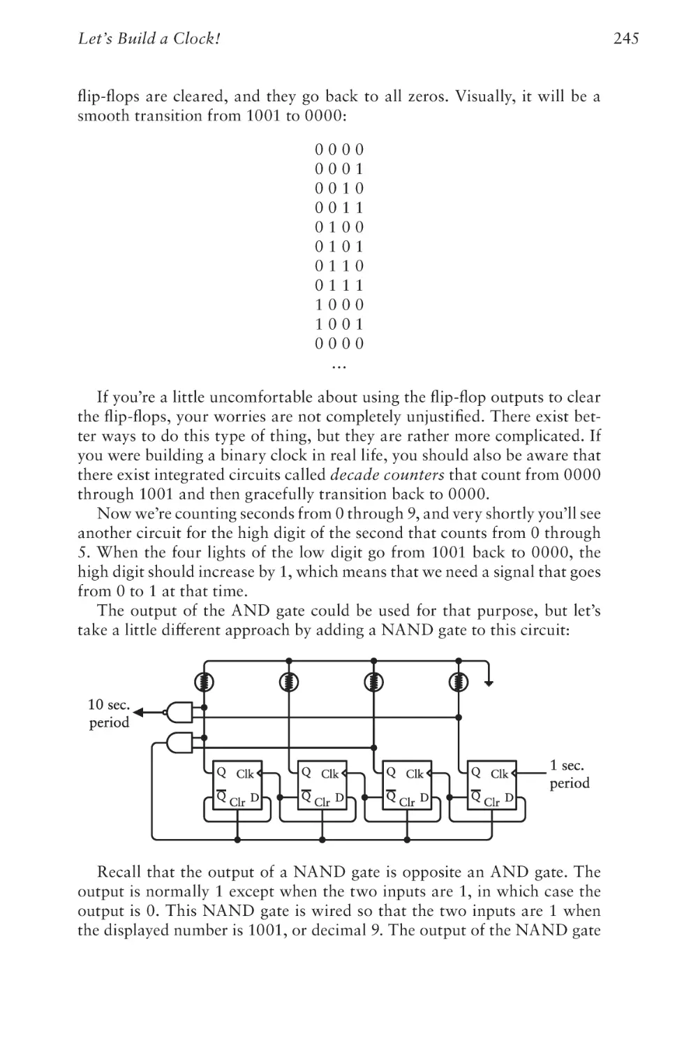
Chapter Eighteen
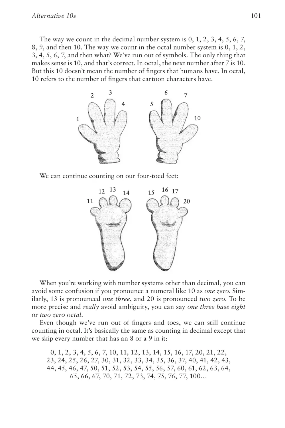
Let’s Build a Clock!
241
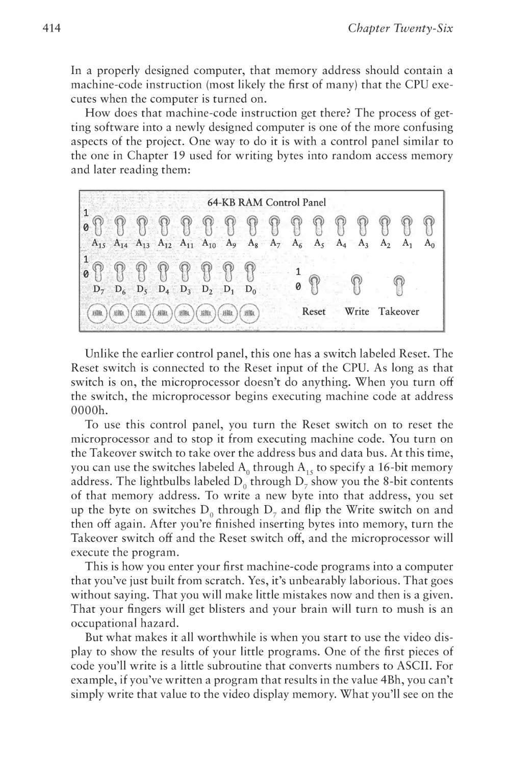
Chapter Nineteen
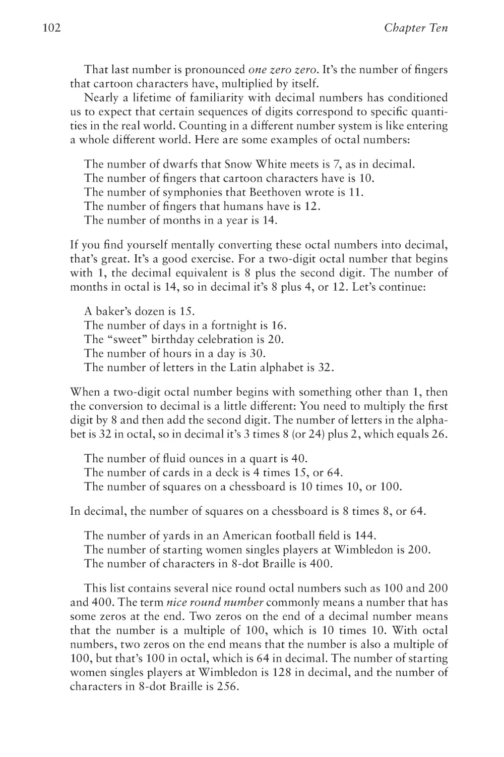
An Assemblage of Memory
267
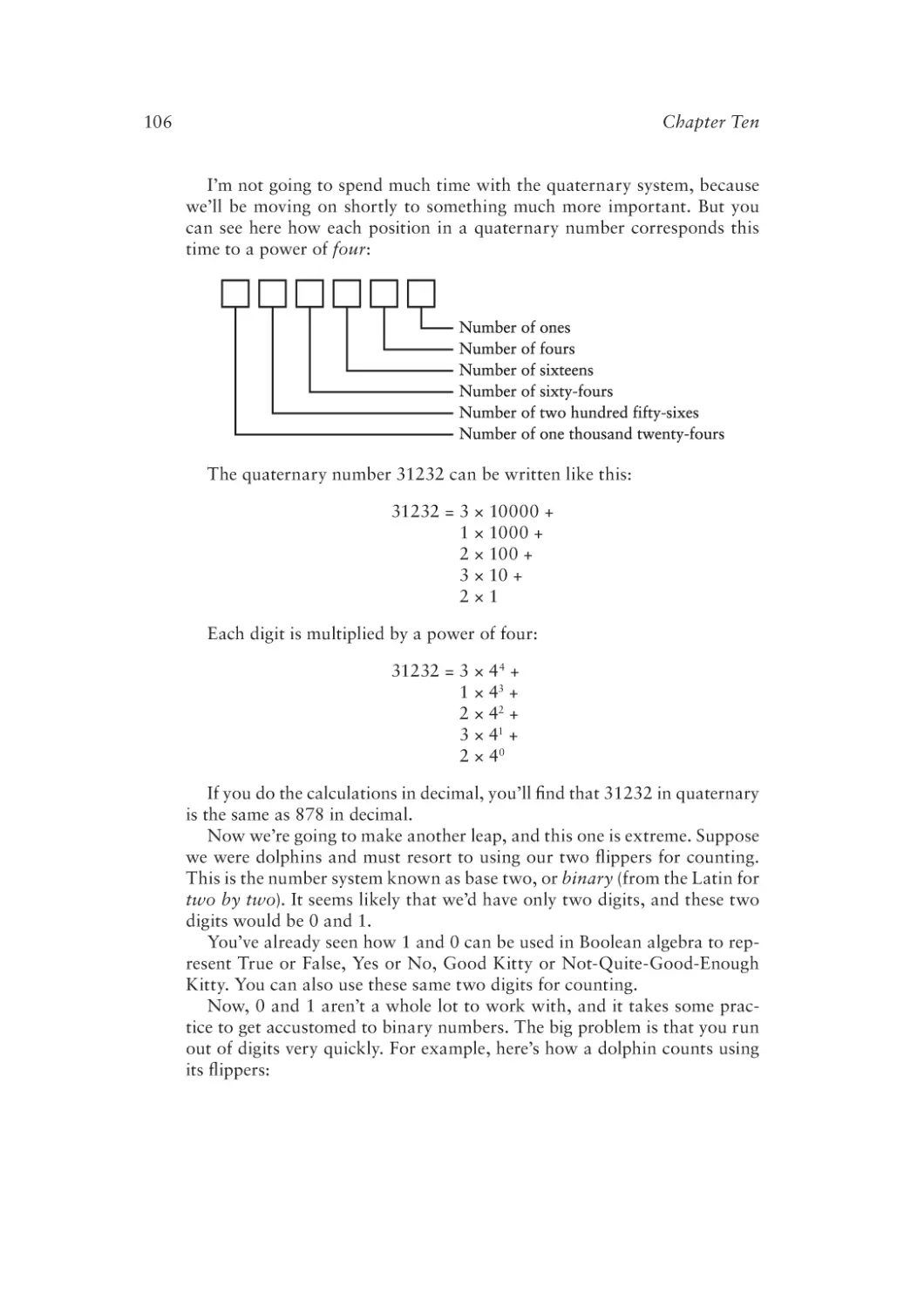
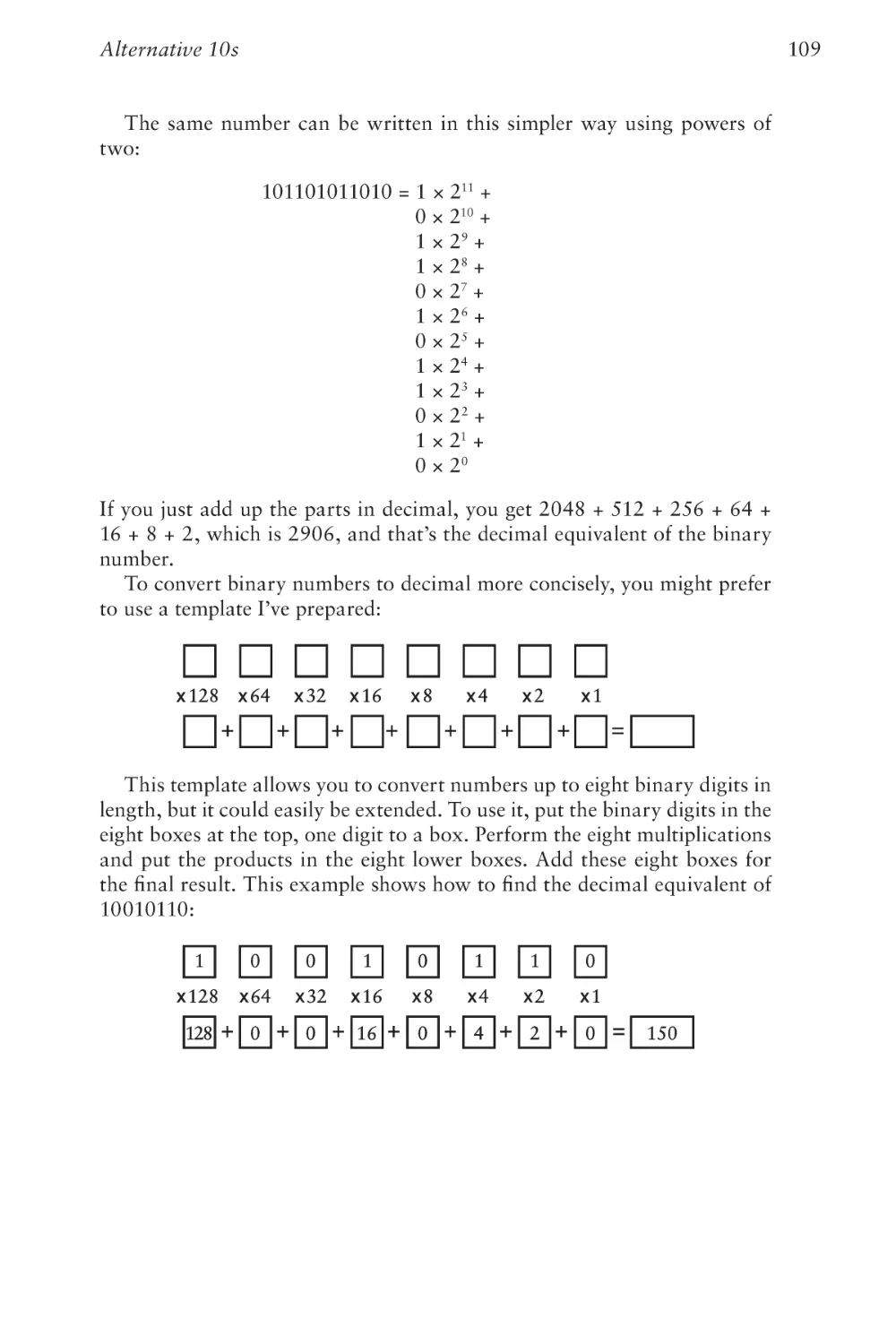
Chapter Twenty
Automating Arithmetic
289
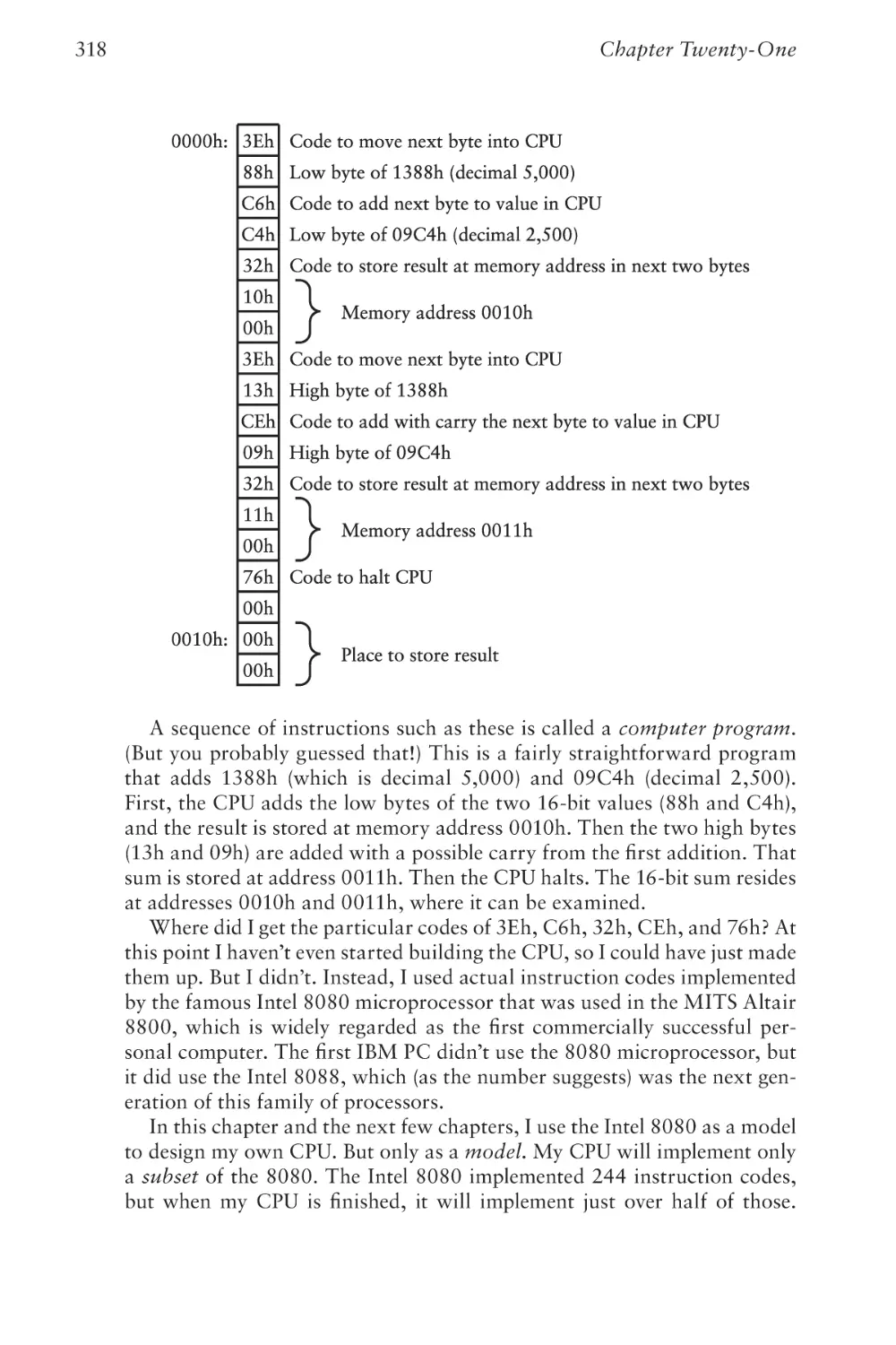
Chapter Twenty-One
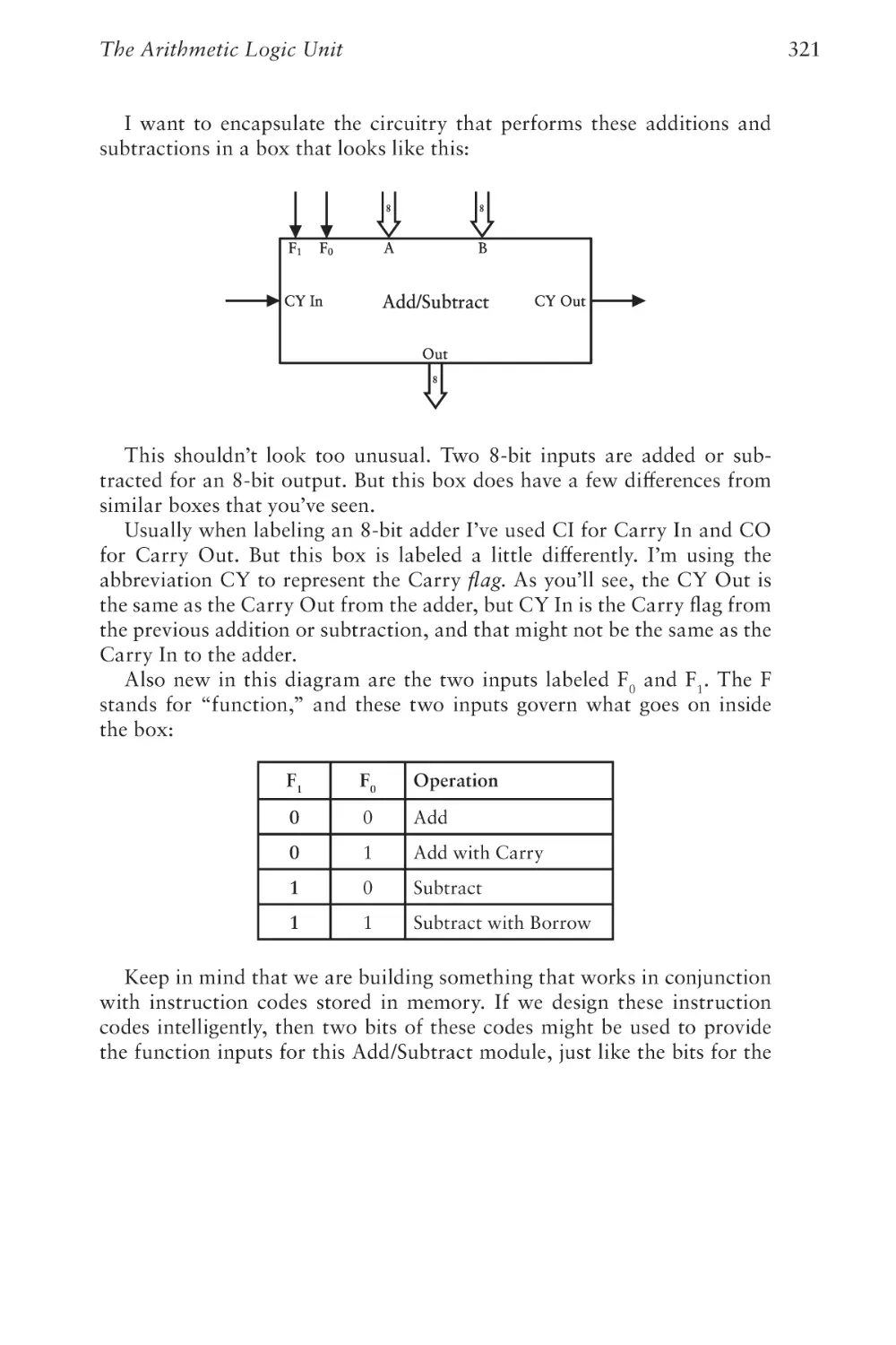
The Arithmetic Logic Unit
315
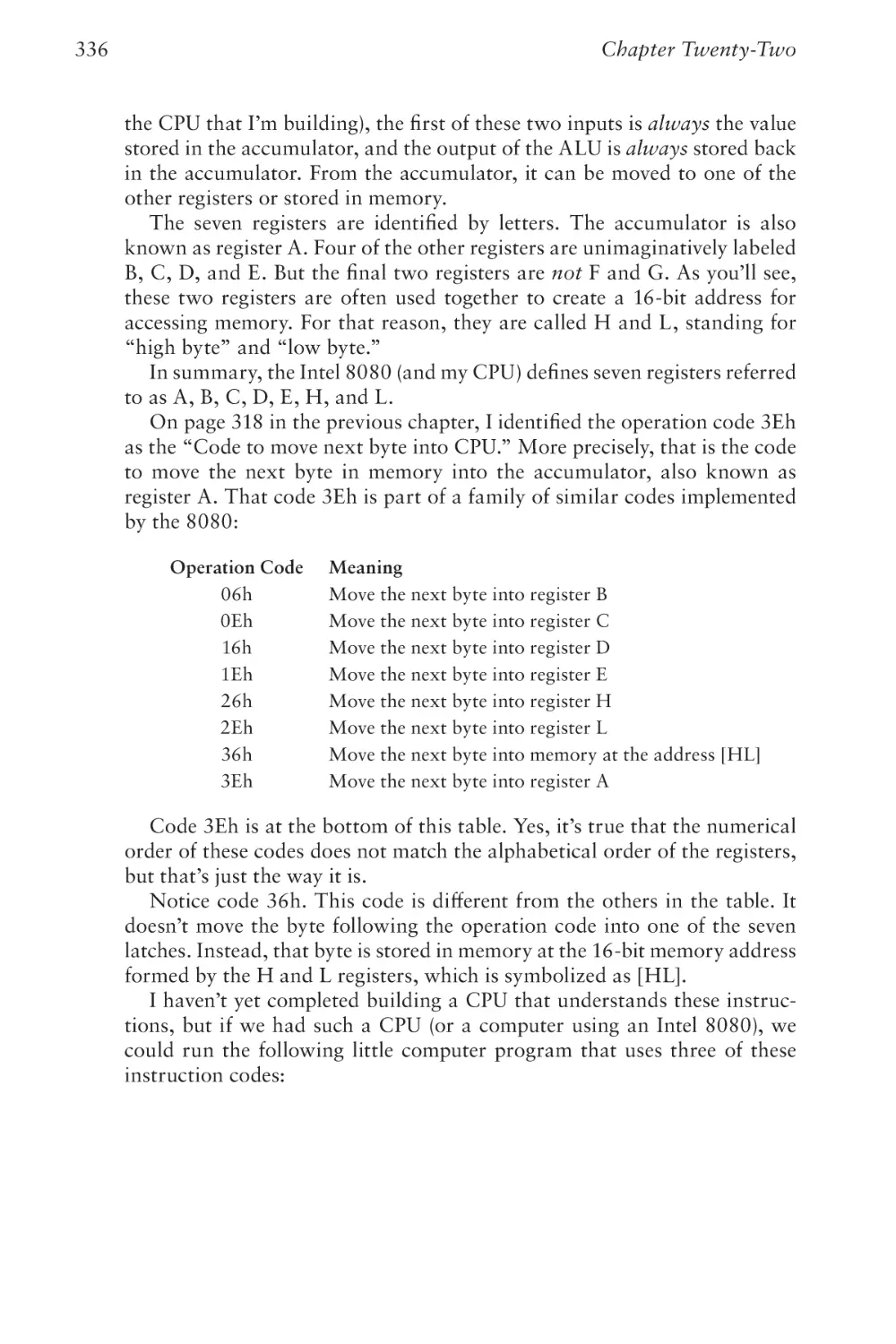
Chapter Twenty-Two
Registers and Busses
335
Chapter Twenty-Three
CPU Control Signals
355
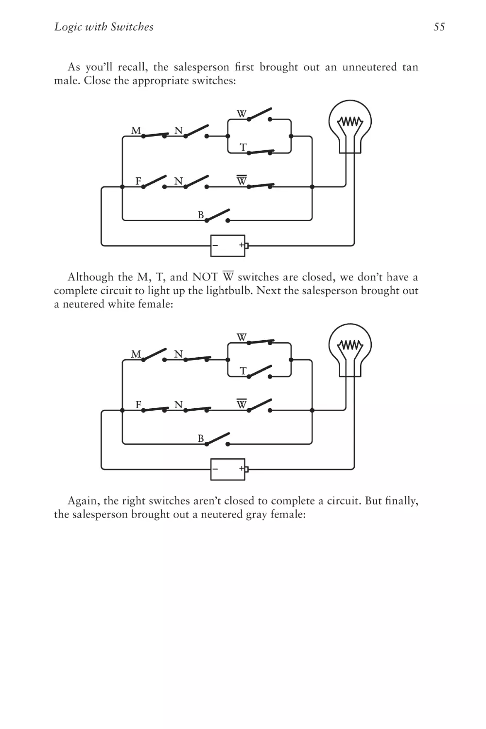
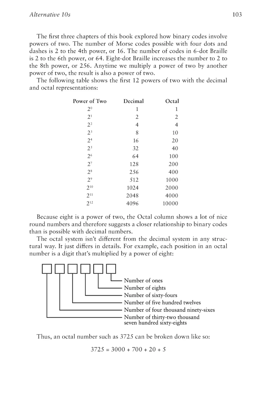
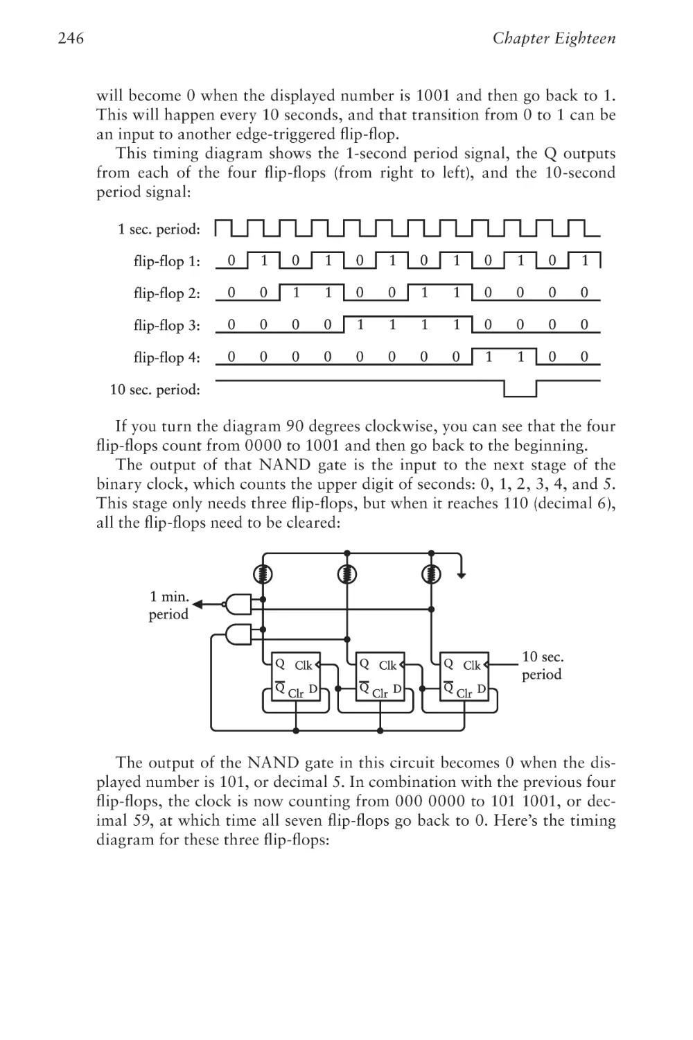
iii
Code
iv
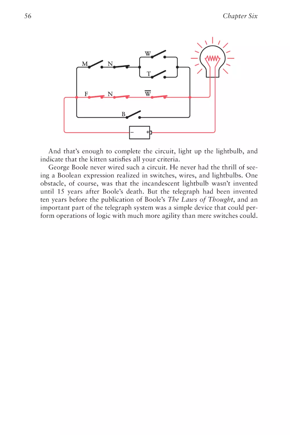
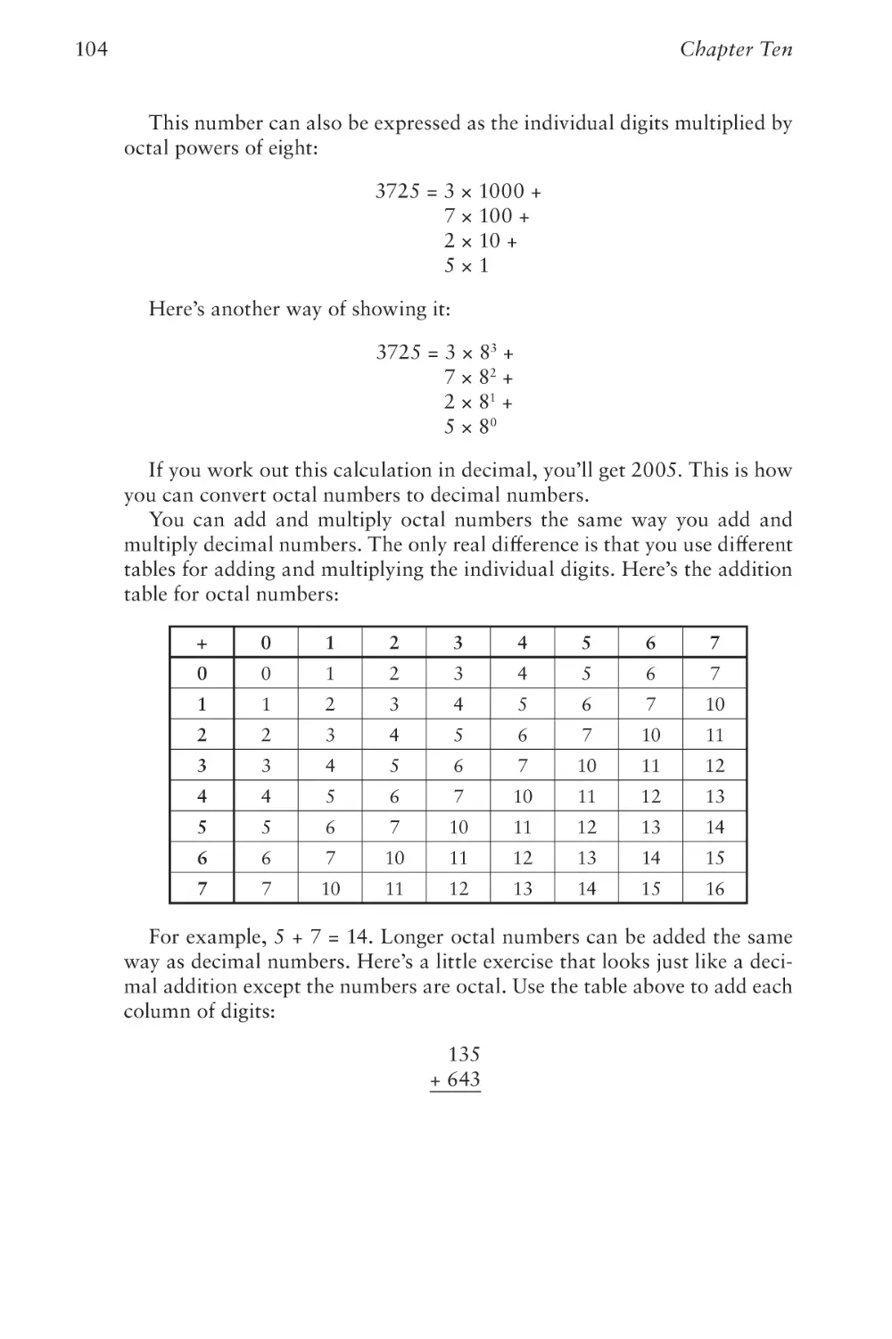
Chapter Twenty-Four
Loops, Jumps, and Calls
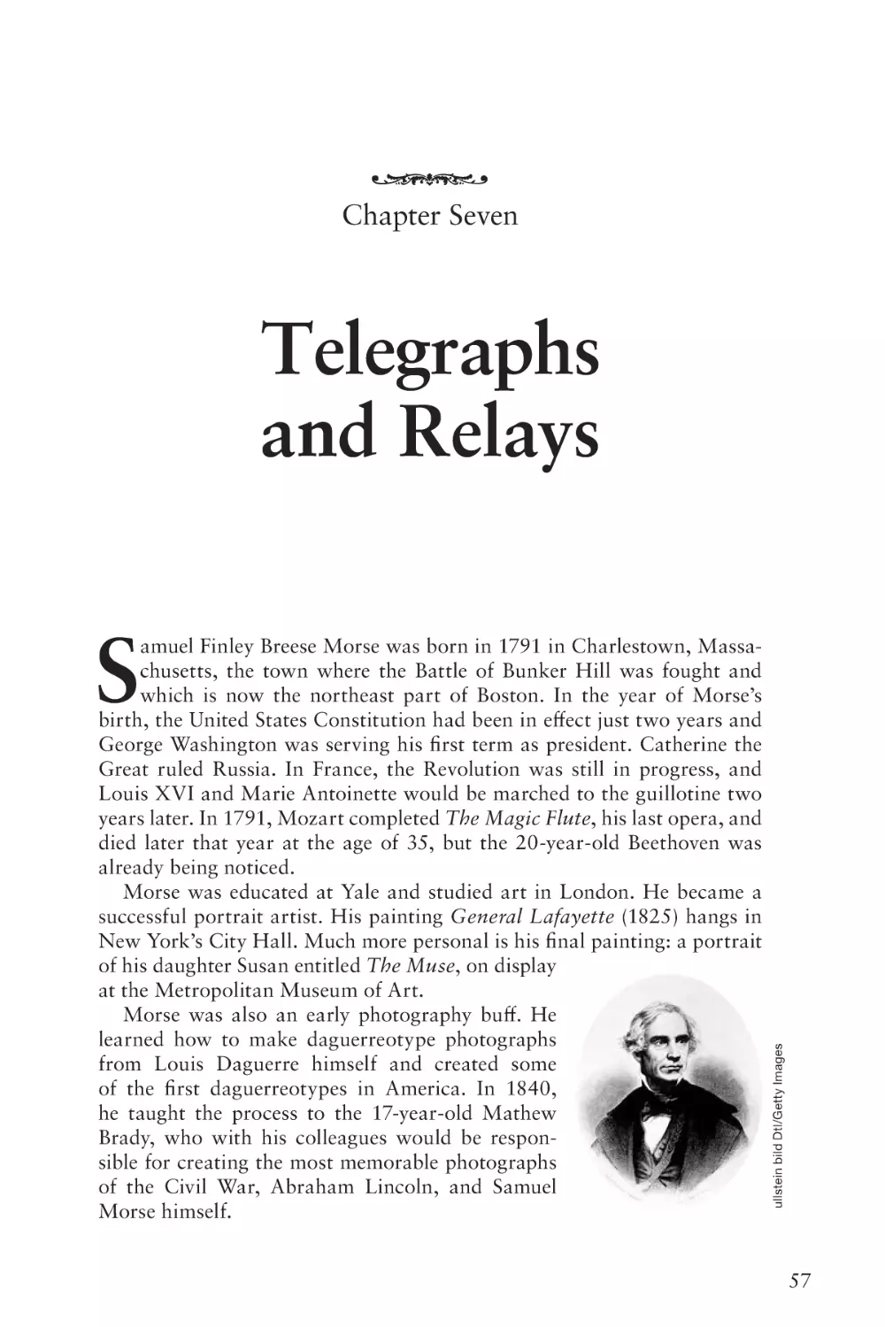
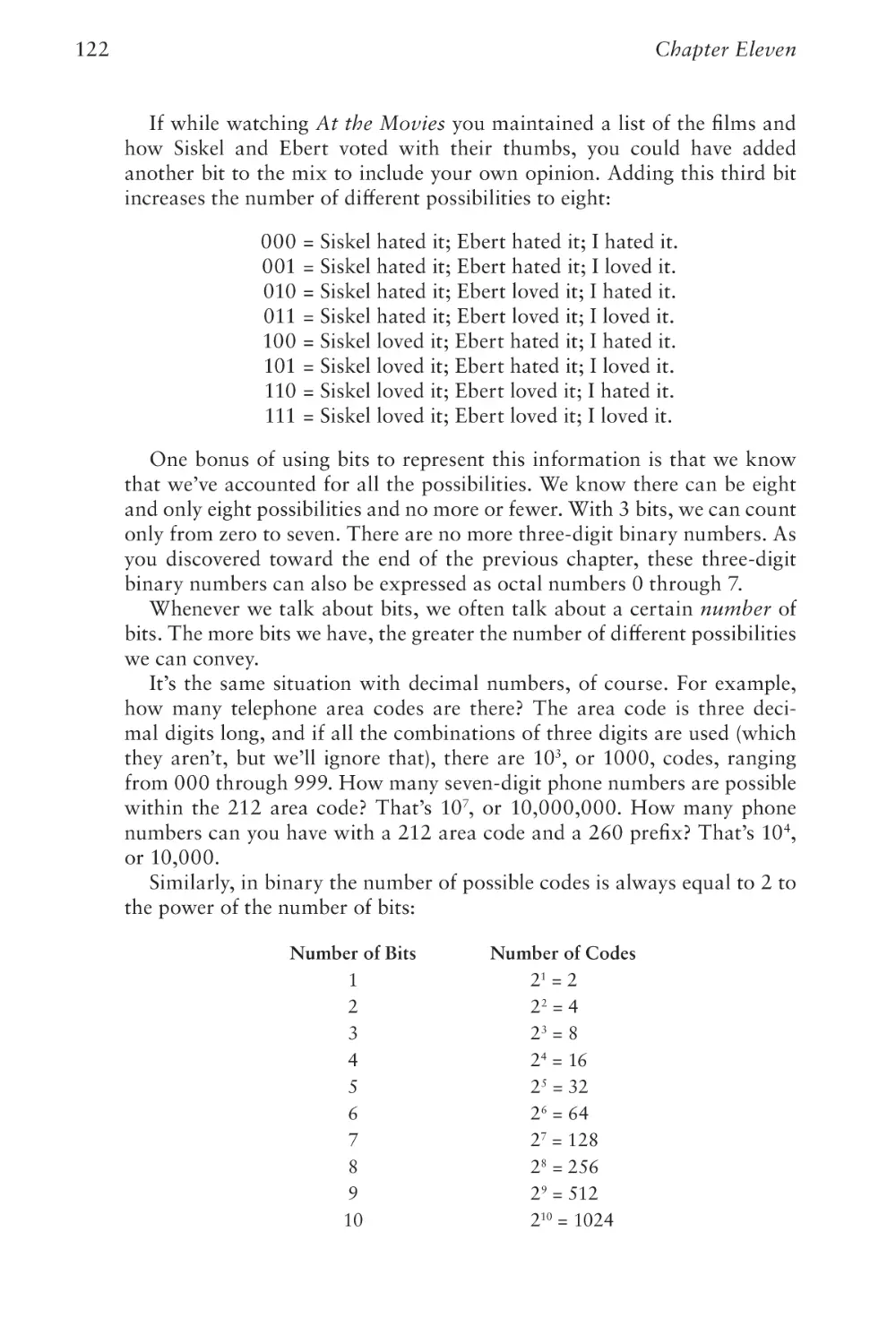
379
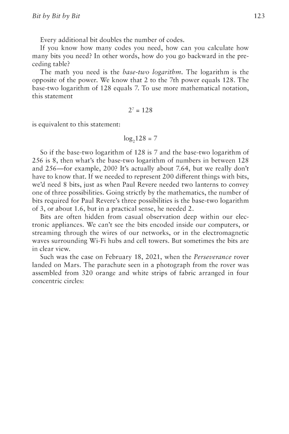
Chapter Twenty-Five
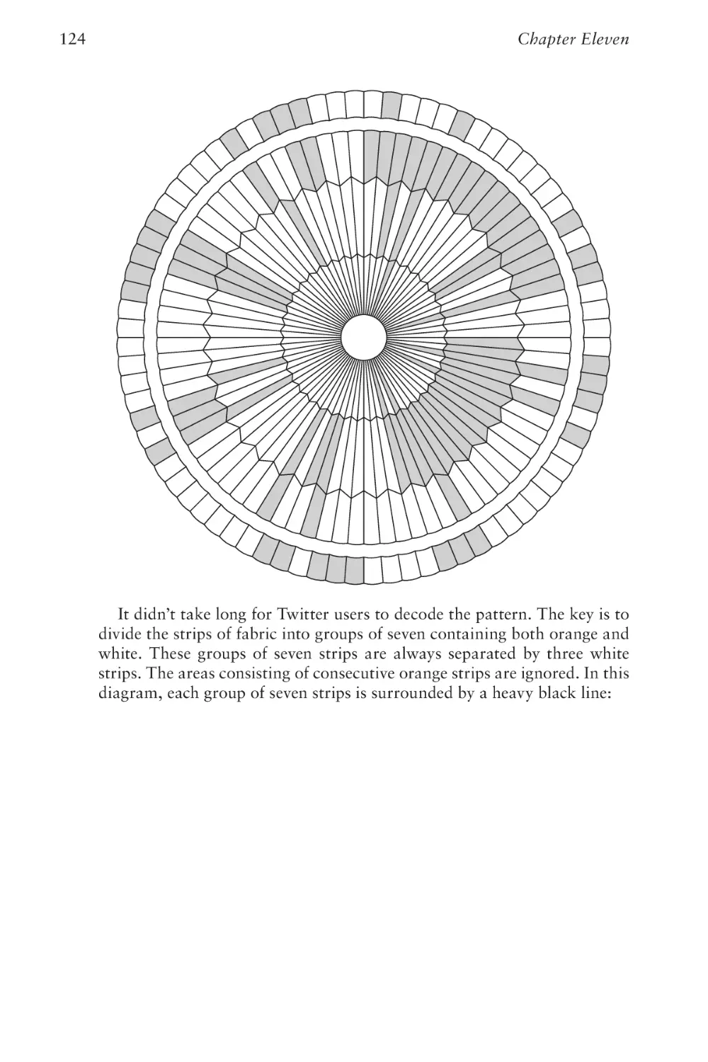
Peripherals
403
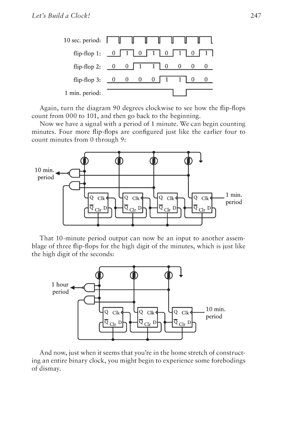
Chapter Twenty-Six
The Operating System
413
Chapter Twenty-Seven
Coding
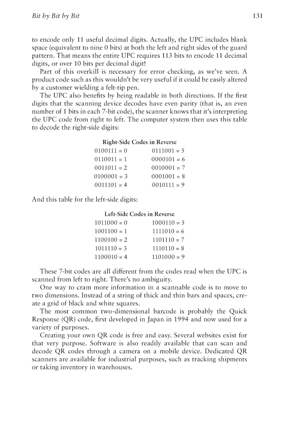
425
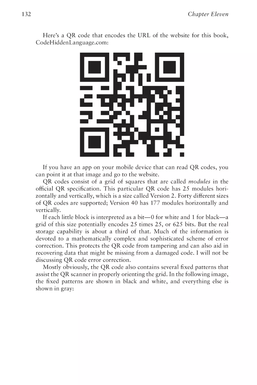
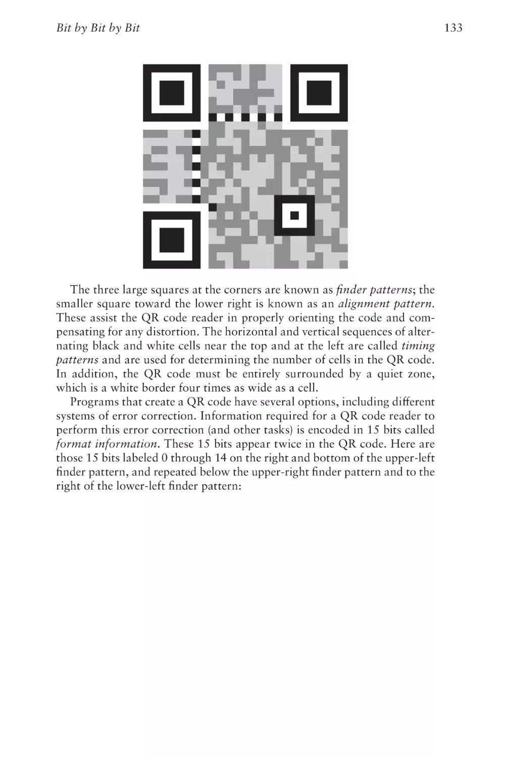
Chapter Twenty-Eight
The World Brain
447
Index
461
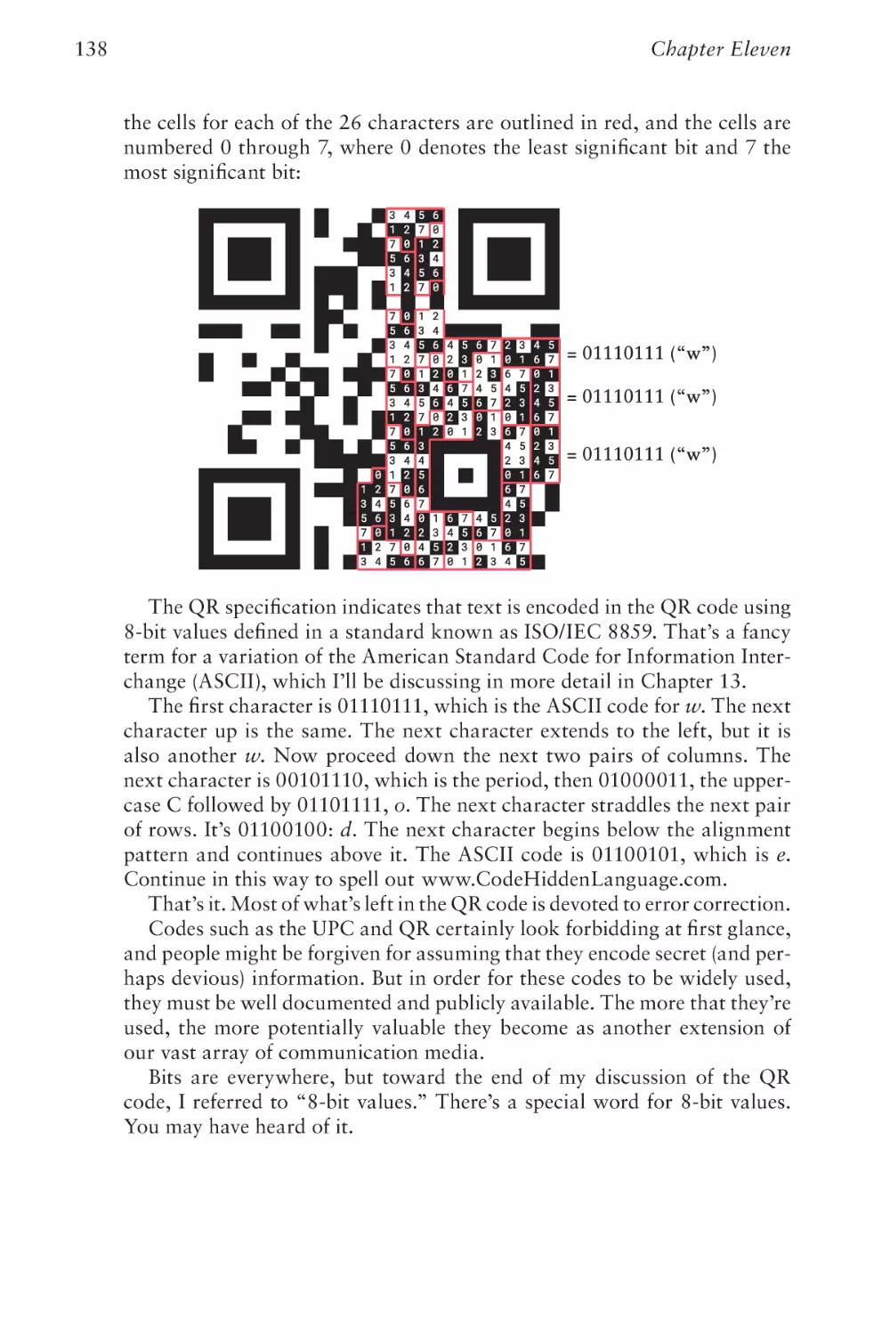
Preface to the
Second Edition
T
he first edition of this book was published in September 1999. With
much delight I realized that I had finally written a book that would
never need revising! This was in stark contrast to my first book,
which was about programming applications for Microsoft Windows. That
one had already gone through five editions in just ten years. My second
book on the OS/2 Presentation Manager (the what?) became obsolete much
more quickly. But Code, I was certain, would last forever.
My original idea with Code was to start with very simple concepts but
slowly build to a very deep understanding of the workings of digital computers. Through this steady progression up the hill of knowledge, I would
employ a minimum of metaphors, analogies, and silly illustrations, and
instead use the language and symbols of the actual engineers who design
and build computers. I also had a very clever trick up my sleeve: I would use
ancient technologies to demonstrate universal principles under the assumption that these ancient technologies were already quite old and would never
get older. It was as if I were writing a book about the internal combustion
engine but based on the Ford Model T.
I still think that my approach was sound, but I was wrong in some of
the details. As the years went by, the book started to show its age. Some of
the cultural references became stale. Phones and fingers supplemented keyboards and mice. The internet certainly existed in 1999, but it was nothing
like what it eventually became. Unicode—the text encoding that allows a
uniform representation of all the world’s languages as well as emojis—got
less than a page in the first edition. And JavaScript, the programming language that has become pervasive on the web, wasn’t mentioned at all.
Those problems would probably have been easy to fix, but there existed
another aspect of the first edition that continued to bother me. I wanted
to show the workings of an actual CPU—the central processing unit that
v
Code
vi
forms the brain, heart, and soul of a computer—but the first edition didn’t
quite make it. I felt that I had gotten close to this crucial breakthrough but
then I had given up. Readers didn’t seem to complain, but to me it was a
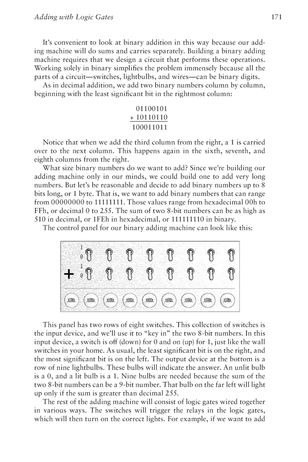
glaring flaw.
That deficiency has been corrected in this second edition. That’s why it’s
some 70 pages longer. Yes, it’s a longer journey, but if you come along with
me through the pages of this second edition, we shall dive much deeper into
the internals of the CPU. Whether this will be a more pleasurable experience for you or not, I do not know. If you feel like you’re going to drown,
please come up for air. But if you make it through Chapter 24, you should
feel quite proud, and you’ll be pleased to know that the remainder of the
book is a breeze.
The Companion Website
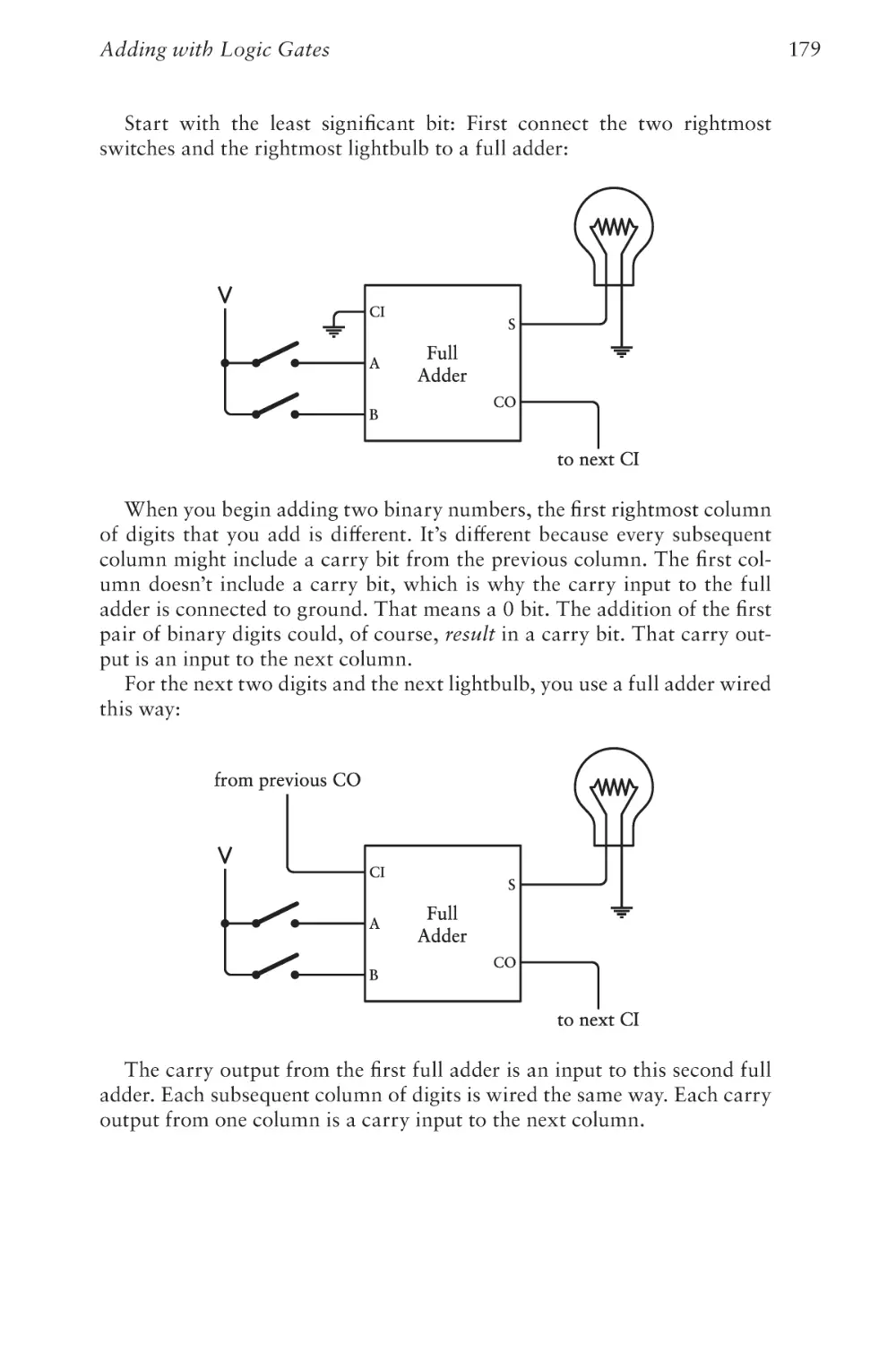
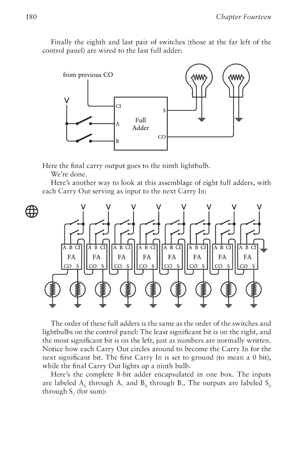
The first edition of Code used the color red in circuit diagrams
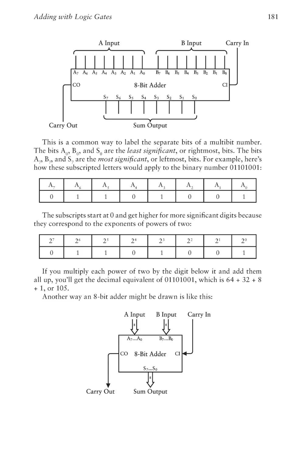
to indicate the flow of electricity. The second edition does that
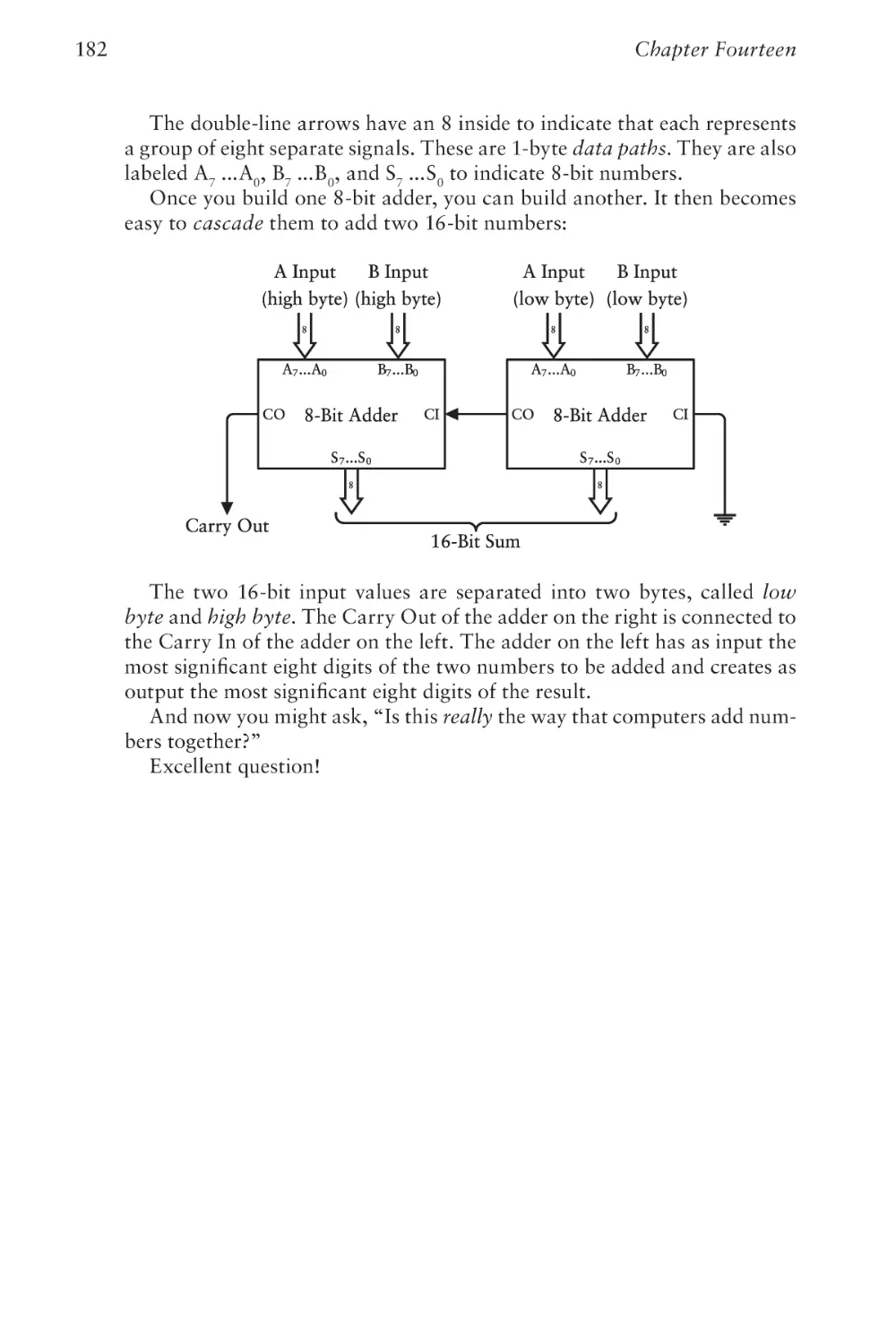
as well, but the workings of these circuits are now also illustrated in a more graphically interactive way on a new website
called CodeHiddenLanguage.com.
You’ll be reminded of this website occasionally throughout the pages of
this book, but we’re also using a special icon, which you’ll see in the margin
of this paragraph. Hereafter, whenever you see that icon—usually accompanying a circuit diagram—you can explore the workings of the circuit on
the website. (For those who crave the technical background, I programmed
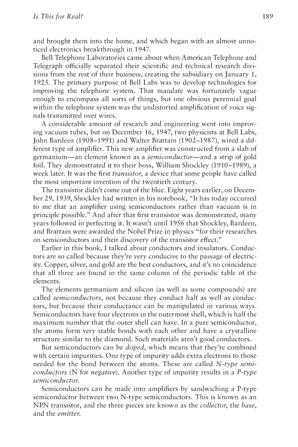
these web graphics in JavaScript using the HTML5 canvas element.)
The CodeHiddenLanguage.com website is entirely free to use. There is
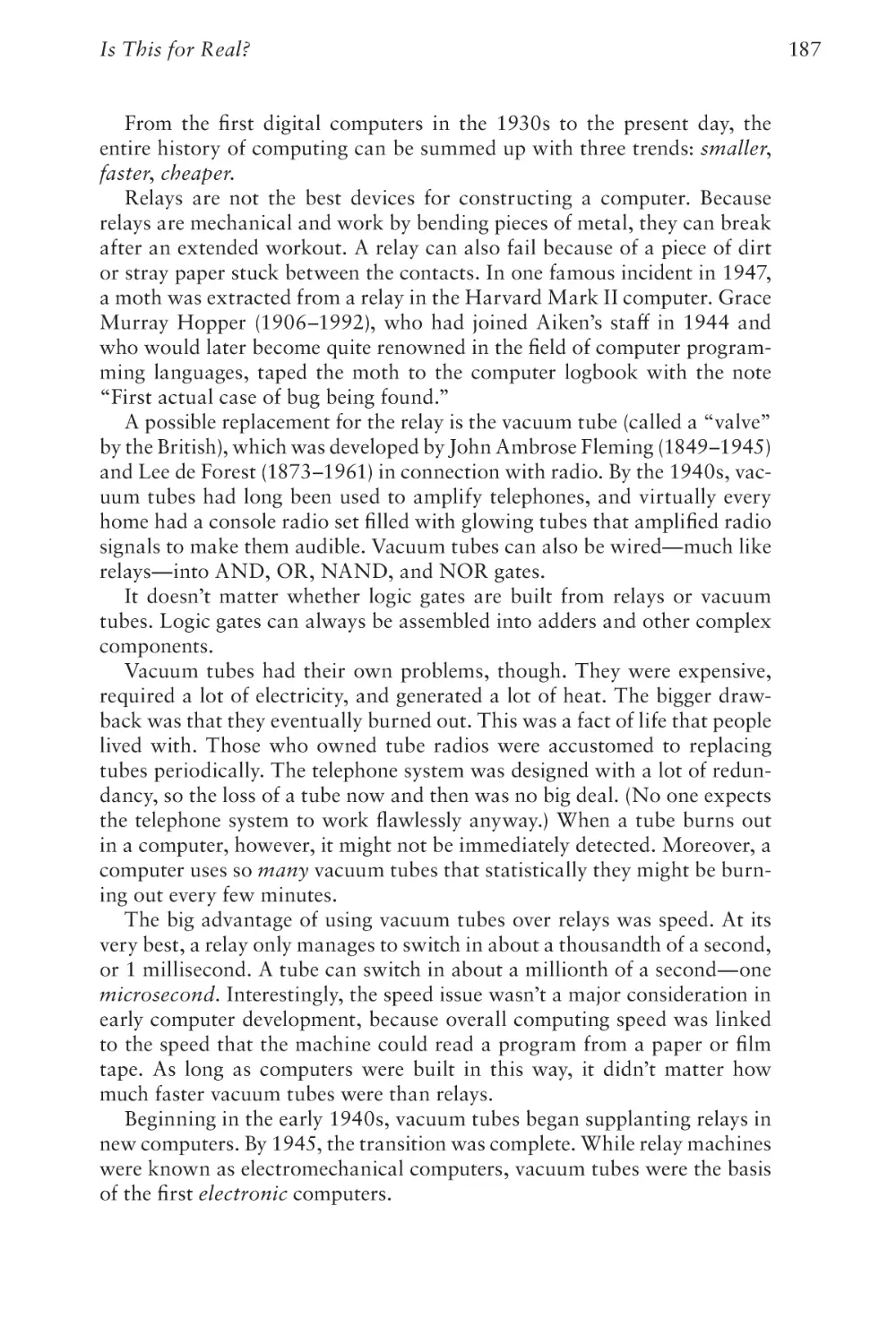
no paywall, and the only advertisement you’ll see is for the book itself. In
a few of the examples, the website uses cookies, but only to allow you to
store some information on your computer. The website doesn’t track you
or do anything evil.
I will also be using the website for clarifications or corrections of material in the book.
The People Responsible
The name of one of the people responsible for this book is on the cover;
some others are no less indispensable but appear on the colophon page at
the very end of this book.
In particular, I want to call out Executive Editor Haze Humbert, who
approached me about the possibility of a second edition uncannily at precisely the right moment that I was ready to do it. I commenced work in
January 2021, and she skillfully guided us through the ordeal, even as the
book went several months past its deadline and when I needed some reassurance that I hadn’t completely jumped the shark.
Code
vii
The project editor for the first edition was Kathleen Atkins, who also
understood what I was trying to do and provided many pleasant hours of
collaboration. My agent at that time was Claudette Moore, who also saw
the value of such a book and convinced Microsoft Press to publish it.
The technical editor for the first edition was Jim Fuchs, who I remember catching a lot of embarrassing errors. For the second edition, technical
reviewers Mark Seemann and Larry O’Brien also caught a few flubs and
helped me make these pages better than they would have been otherwise.
I thought that I had figured out the difference between “compose” and
“comprise” decades ago, but apparently I have not. Correcting errors like
that was the invaluable contribution of copy editor Scout Festa. I have
always relied on the kindness of copyeditors, who too often remain anonymous strangers but who battle indefatigably against imprecision and abuse
of language.
Any errors that remain in this book are solely my responsibility.
I want to again thank my beta readers of the first edition: Sheryl Canter,
Jan Eastlund, the late Peter Goldeman, Lynn Magalska, and Deirdre
Sinnott (who later became my wife).
The numerous illustrations in the first edition were the work of the late
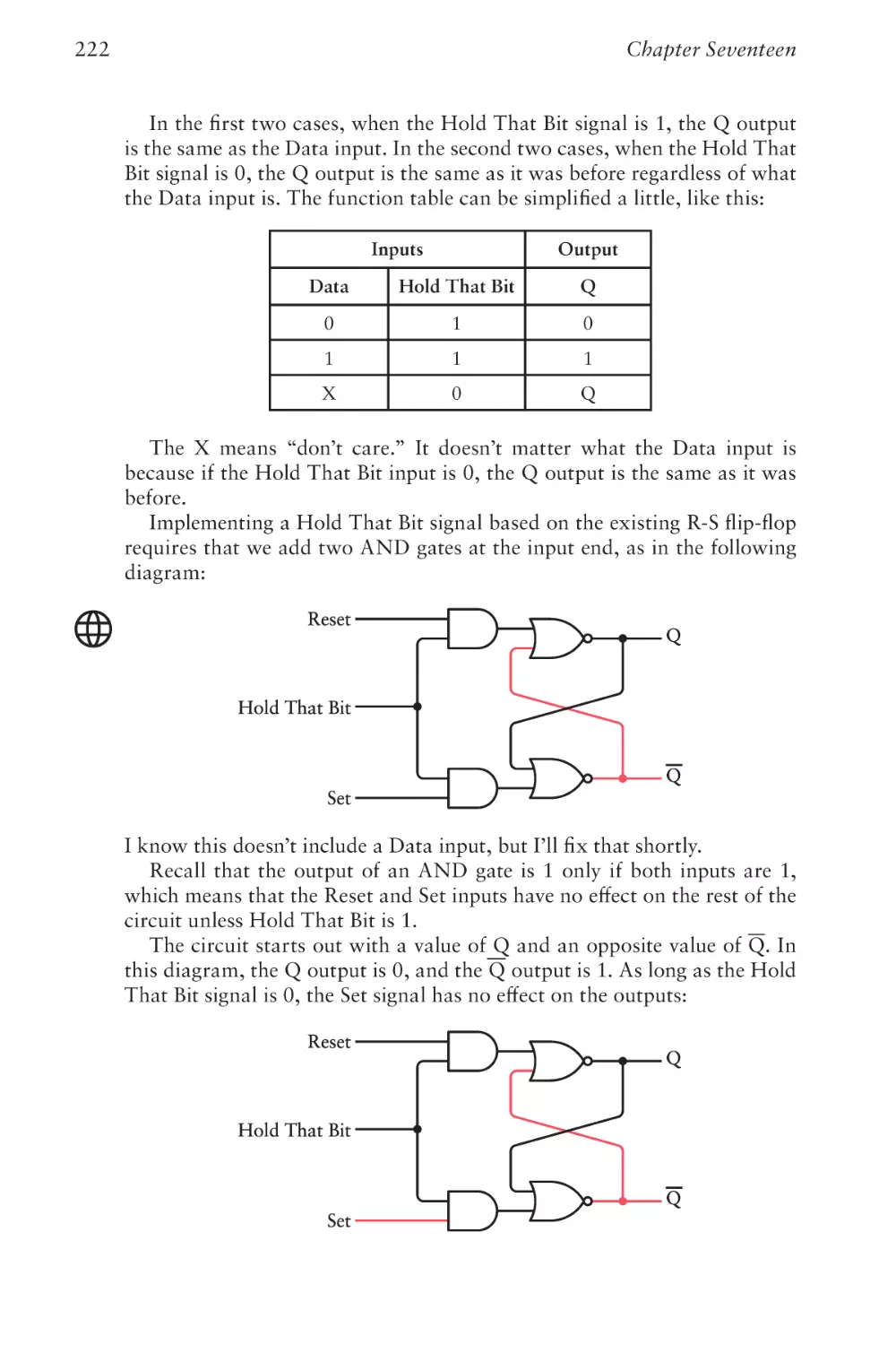
Joel Panchot, who I understand was deservedly proud of his work on this
book. Many of his illustrations remain, but the need for additional circuit
diagrams inclined me to redo all the circuits for the sake of consistency.
(More technical background: These illustrations were generated by a program I wrote in C# using the SkiaSharp graphics library to generate Scalable Vector Graphics files. Under the direction of Senior Content Producer
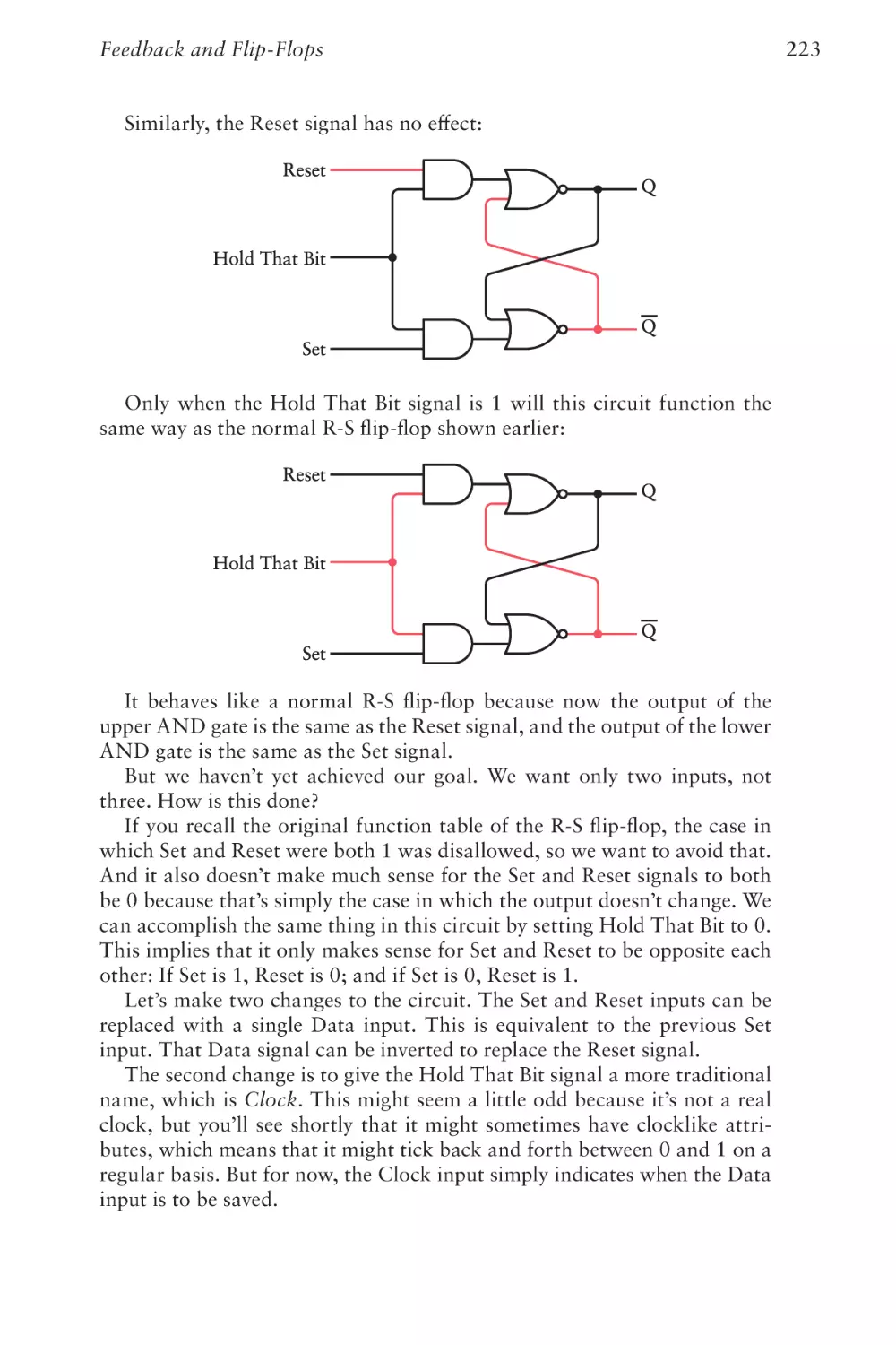
Tracey Croom, the SVG files were converted into Encapsulated PostScript
for setting up the pages using Adobe InDesign.)
And Finally
I want to dedicate this book to the two most important women in my life.
My mother battled adversities that would have destroyed a lesser person.
She provided a strong direction to my life without ever holding me back.
We celebrated her 95th (and final) birthday during the writing of this book.
My wife, Deirdre Sinnott, has been essential and continues to make me
proud of her achievements, her support, and her love.
And to the readers of the first edition, whose kind feedback has been
extraordinarily gratifying.
Charles Petzold
May 9, 2022
Code
viii
Pearson’s Commitment to
Diversity, Equity, and Inclusion
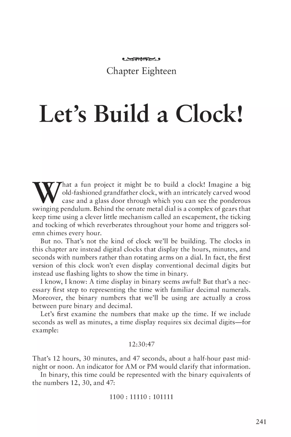
Pearson is dedicated to creating bias-free content that reflects the diversity
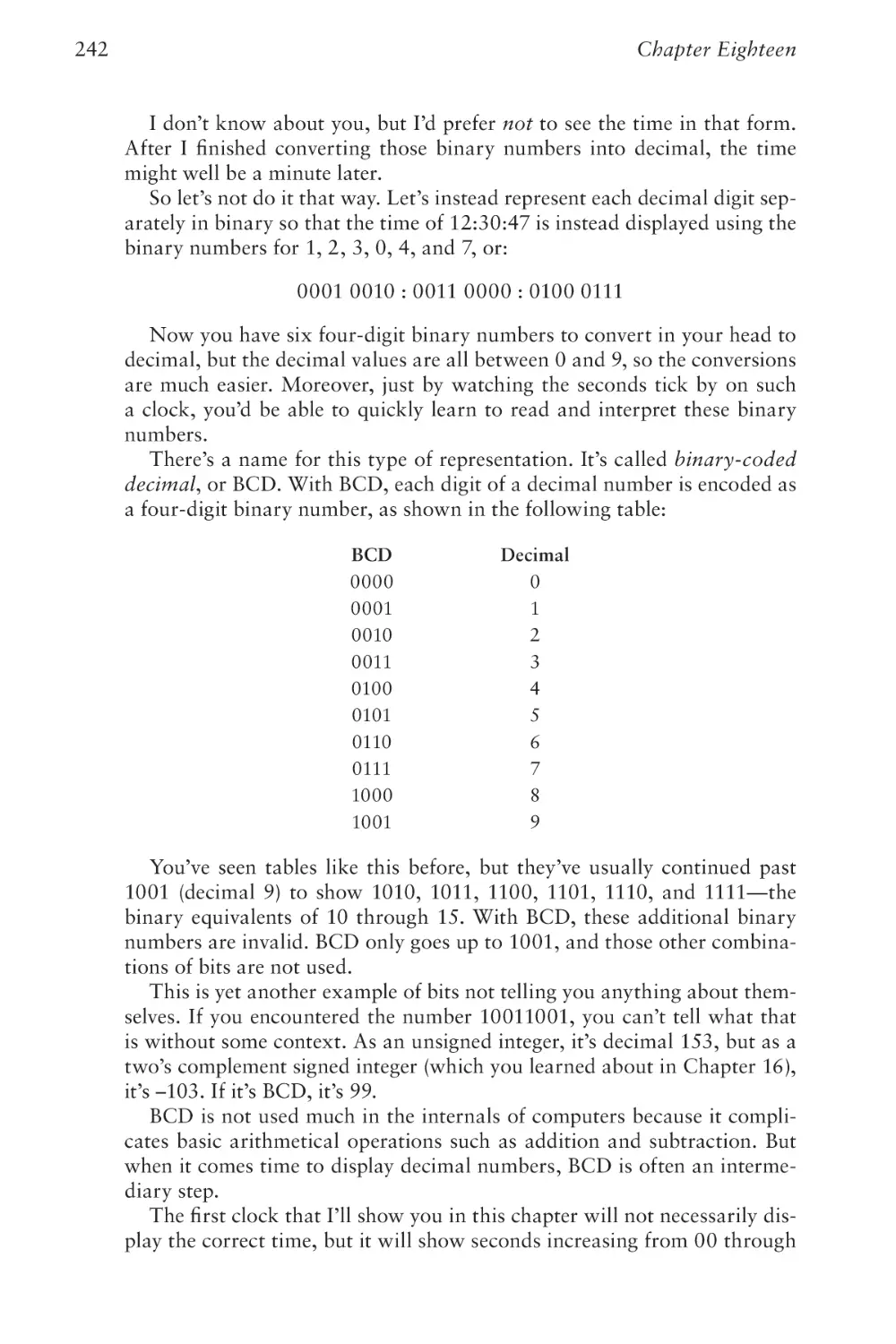
of all learners. We embrace the many dimensions of diversity, including but
not limited to race, ethnicity, gender, socioeconomic status, ability, age,
sexual orientation, and religious or political beliefs.
Education is a powerful force for equity and change in our world. It
has the potential to deliver opportunities that improve lives and enable
economic mobility. As we work with authors to create content for every
product and service, we acknowledge our responsibility to demonstrate
inclusivity and incorporate diverse scholarship so that everyone can achieve
their potential through learning. As the world’s leading learning company,
we have a duty to help drive change and live up to our purpose to help more
people create a better life for themselves and to create a better world.
Our ambition is to purposefully contribute to a world where:
• Everyone has an equitable and lifelong opportunity to succeed
through learning.
• Our educational products and services are inclusive and represent
the rich diversity of learners.
• Our educational content accurately reflects the histories and
experiences of the learners we serve.
• Our educational content prompts deeper discussions with
learners and motivates them to expand their own learning
(and worldview).
While we work hard to present unbiased content, we want to hear from
you about any concerns or needs with this Pearson product so that we can
investigate and address them.
• Please contact us with concerns about any potential bias at
https://www.pearson.com/report-bias.html.
About
the Author
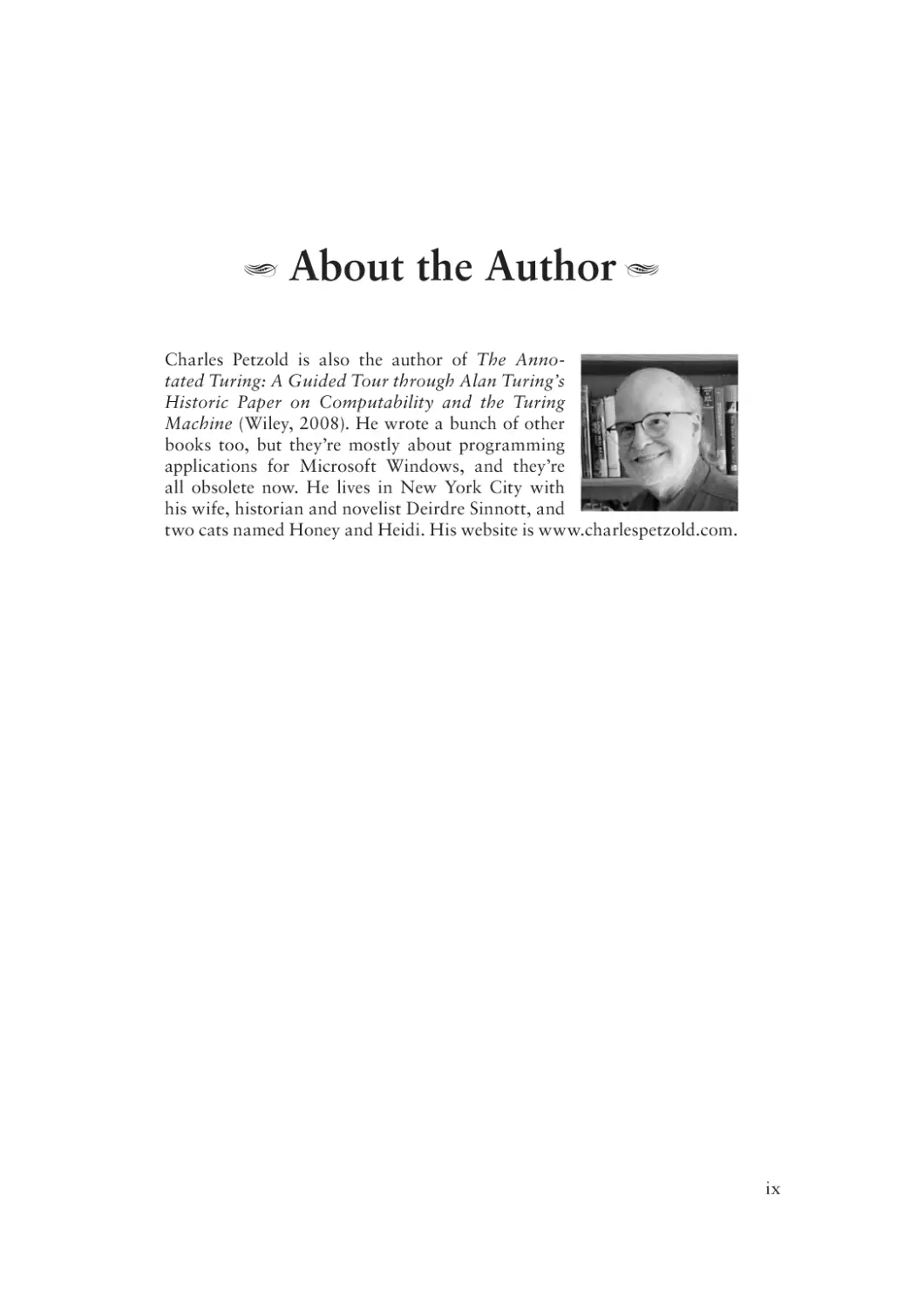
Charles Petzold is also the author of The Annotated Turing: A Guided Tour through Alan Turing’s
Historic Paper on Computability and the Turing
Machine (Wiley, 2008). He wrote a bunch of other
books too, but they’re mostly about programming
applications for Microsoft Windows, and they’re
all obsolete now. He lives in New York City with
his wife, historian and novelist Deirdre Sinnott, and
two cats named Honey and Heidi. His website is www.charlespetzold.com.
ix
code (kōd) n.
1. a. A system of signals used to represent letters or numbers in
transmitting messages.
b. A system of symbols, letters, or words given certain arbitrary
meanings, used for transmitting messages requiring secrecy or
brevity….
2. a. The information that constitutes a specific computer program.
b. A system of symbols and rules that serve as instructions for a
computer….
— The American Heritage Dictionary of the English Language
(online edition)
Chapter One
Best Friends
Y
ou’re 10 years old. Your best friend lives across the street. The windows of your bedrooms actually face each other. Every night, after
your parents have declared bedtime at the usual indecently early
hour, you still need to exchange thoughts, observations, secrets, gossip,
jokes, and dreams. No one can blame you. The impulse to communicate is,
after all, one of the most human of traits.
While the lights are still on in your bedrooms, you and your best friend
can wave to each other from the windows and, using broad gestures and
rudimentary body language, convey a thought or two. But more sophisticated exchanges seem difficult, and once the parents have decreed “Lights
out!” stealthier solutions are necessary.
How to communicate? If you’re lucky enough to have a cell phone at the
age of 10, perhaps a secret call or silent texting might work. But what if
your parents have a habit of confiscating cell phones at bedtime, and even
shutting down the Wi-Fi? A bedroom without electronic communication is
a very isolated room indeed.
What you and your best friend do own, however, are flashlights. Everyone knows that flashlights were invented to let kids read books under the
bed covers; flashlights also seem perfect for the job of communicating
after dark. They’re certainly quiet enough, and the light is highly directional and probably won’t seep out under the bedroom door to alert your
suspicious folks.
Can flashlights be made to speak? It’s certainly worth a try. You learned
how to write letters and words on paper in first grade, so transferring that
knowledge to the flashlight seems reasonable. All you have to do is stand
at your window and draw the letters with light. For an O, you turn on
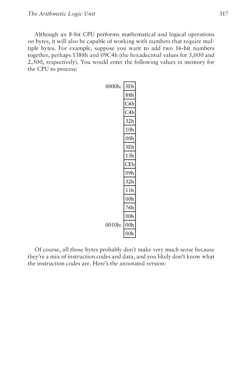
the flashlight, sweep a circle in the air, and turn off the switch. For an I,
you make a vertical stroke. But, as you quickly discover, this method is a
disaster. As you watch your friend’s flashlight making swoops and lines in
1
2
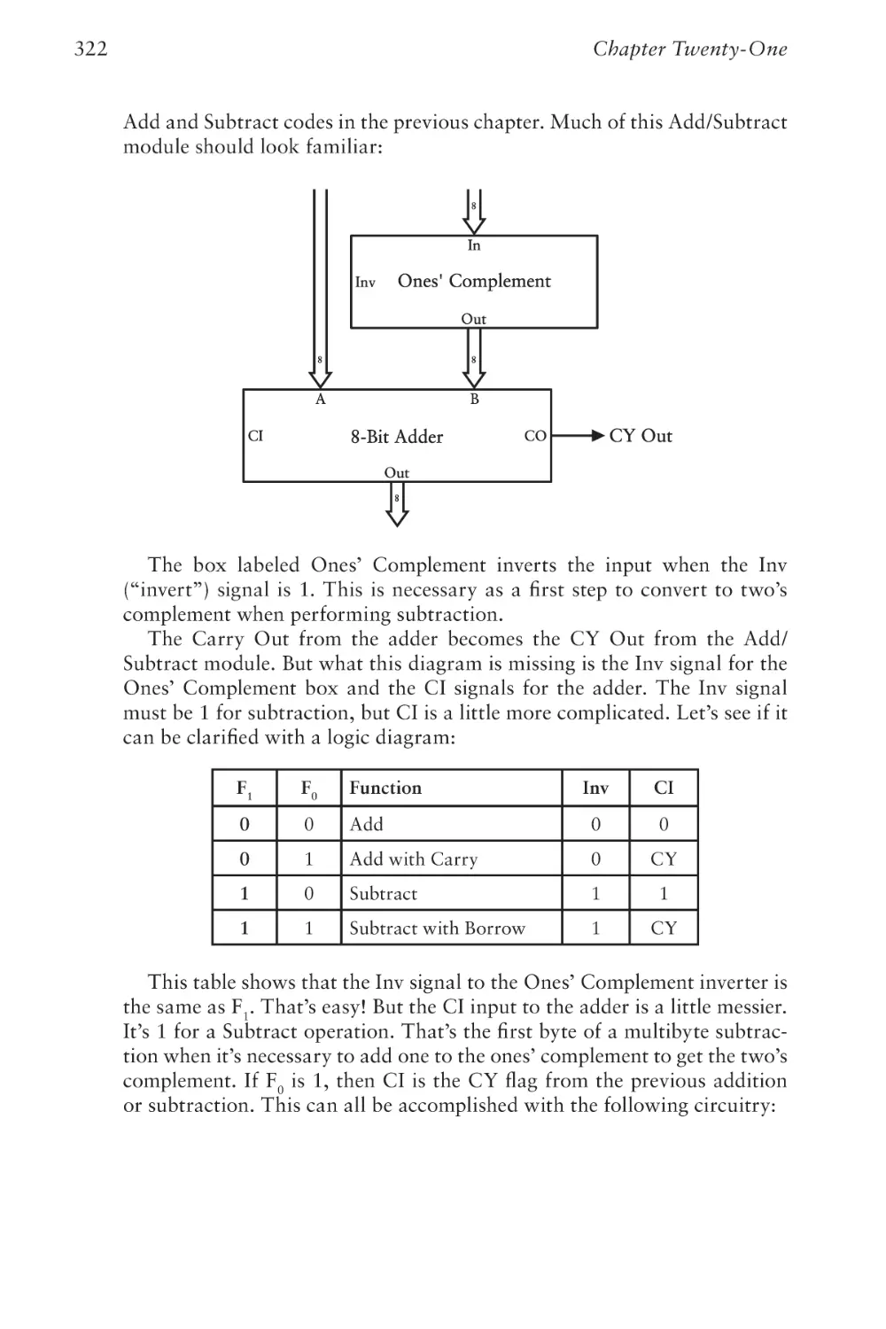
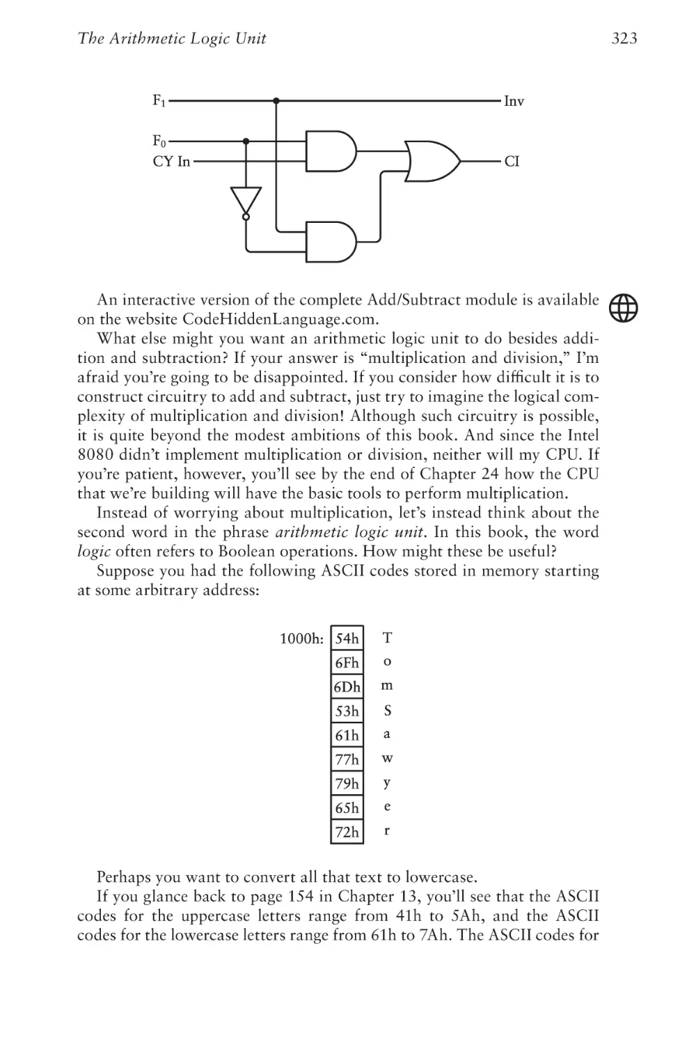
Chapter One
the air, you find that it’s too hard to assemble the multiple strokes together
in your head. These swirls and slashes of light are just not precise enough.
Perhaps you once saw a movie in which a couple of sailors signaled to
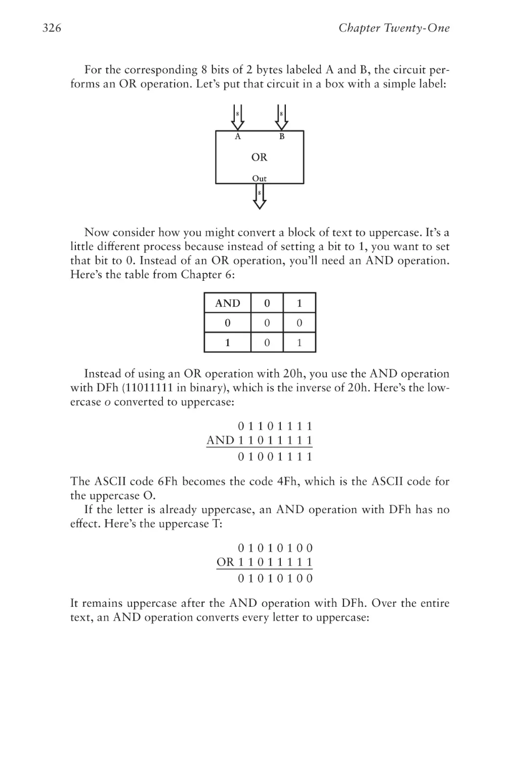
each other across the sea with blinking lights. In another movie, a spy wiggled a mirror to reflect the sunlight into a room where another spy lay
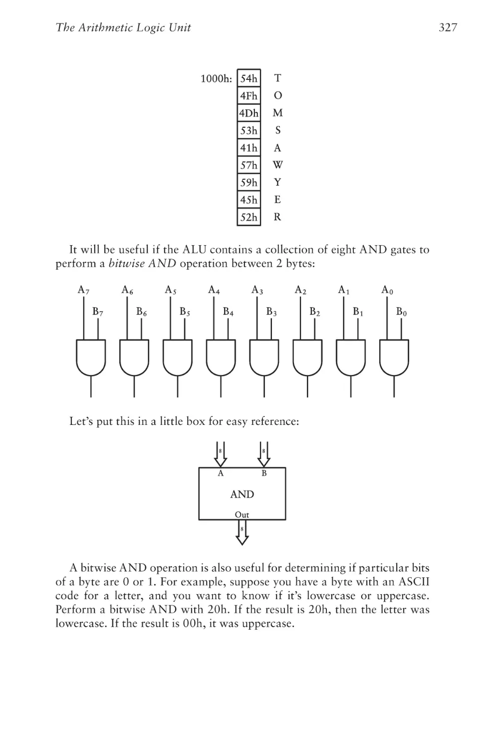
captive. Maybe that’s the solution. So you first devise a simple technique:
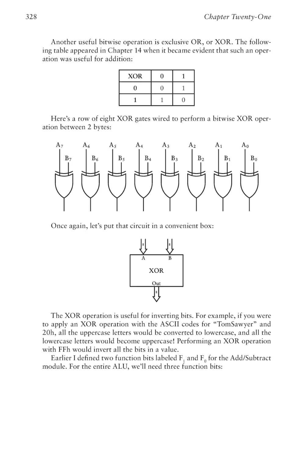
Each letter of the alphabet corresponds to a series of flashlight blinks. An A
is 1 blink, a B is 2 blinks, a C is 3 blinks, and so on to 26 blinks for Z. The
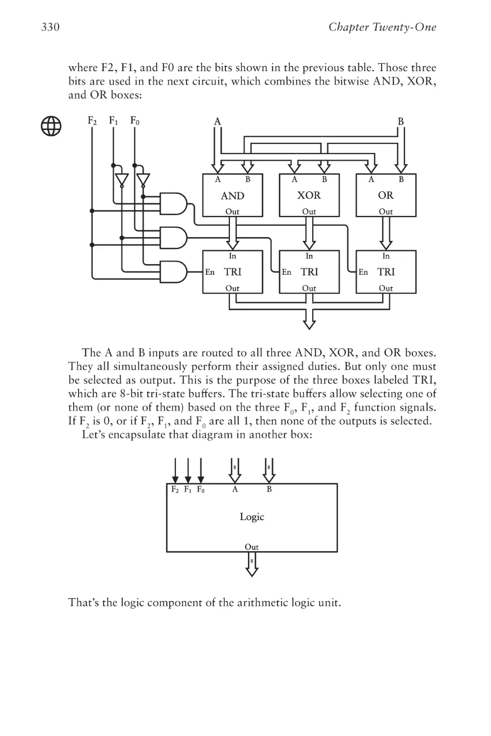
word BAD is 2 blinks, 1 blink, and 4 blinks with little pauses between the
letters so you won’t mistake the 7 blinks for a G. You’ll pause a bit longer
between words.
This seems promising. The good news is that you no longer have to wave
the flashlight in the air; all you need do is point and click. The bad news
is that one of the first messages you try to send (“How are you?”) turns
out to require a grand total of 131 blinks of light! Moreover, you forgot
about punctuation, so you don’t know how many blinks correspond to a
question mark.
But you’re close. Surely, you think, somebody must have faced this
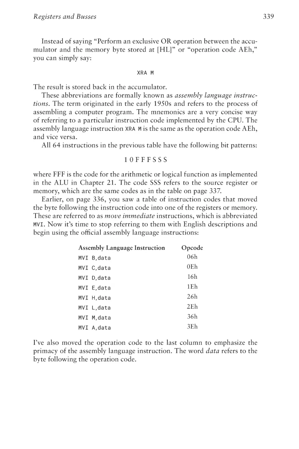
problem before, and you’re absolutely right. With a trip to the library or
an internet search, you discover a marvelous invention known as Morse
code. It’s exactly what you’ve been looking for, even though you must now
relearn how to “write” all the letters of the alphabet.
Here’s the difference: In the system you invented, every letter of the
alphabet is a certain number of blinks, from 1 blink for A to 26 blinks
for Z. In Morse code, you have two kinds of blinks—short blinks and long
blinks. This makes Morse code more complicated, of course, but in actual
use it turns out to be much more efficient. The sentence “How are you?”
now requires only 32 blinks (some short, some long) rather than 131, and
that’s including a code for the question mark.
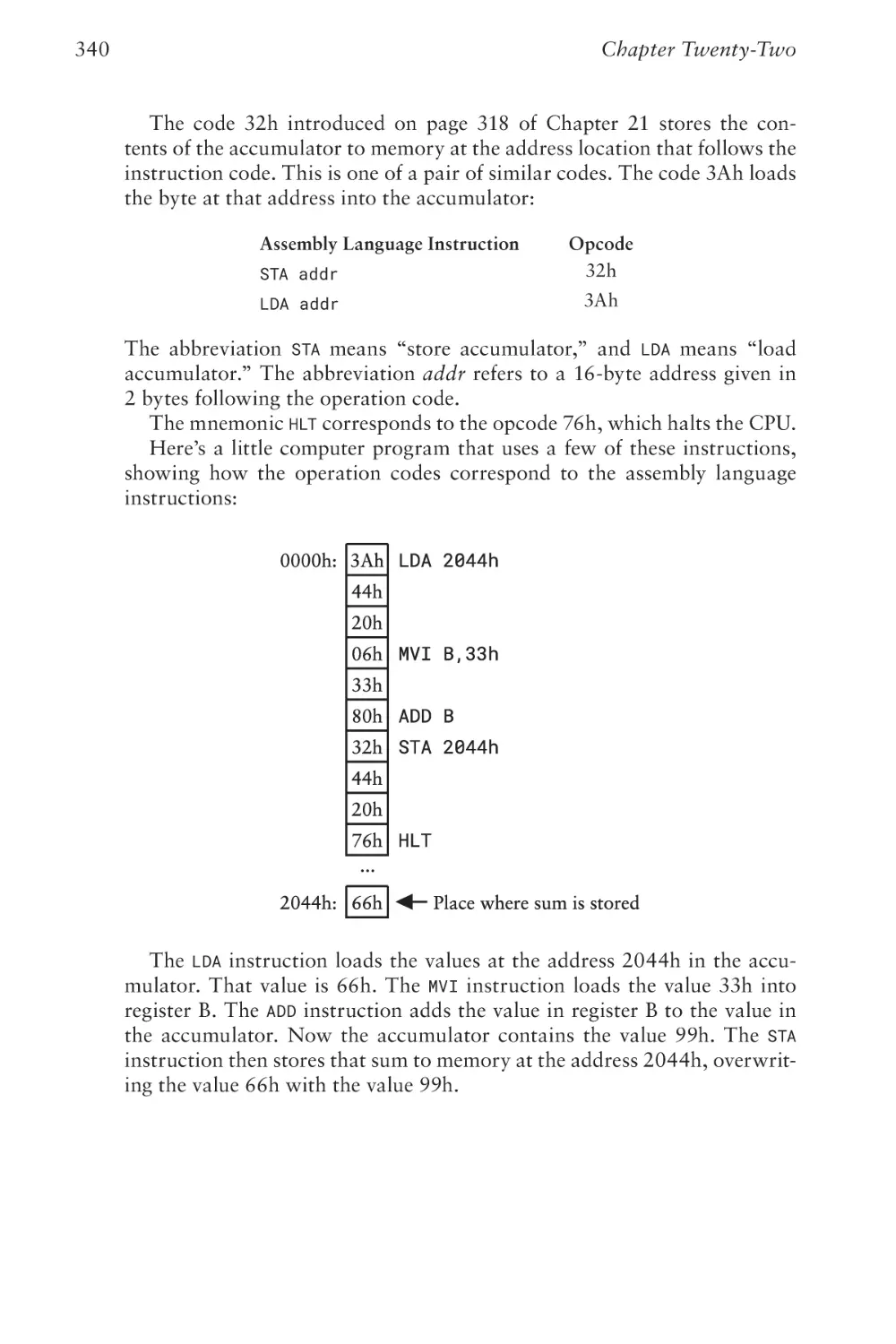
When discussing how Morse code works, people don’t talk about “short
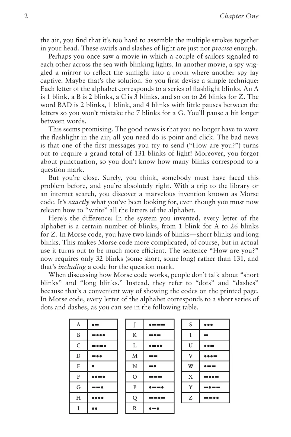
blinks” and “long blinks.” Instead, they refer to “dots” and “dashes”
because that’s a convenient way of showing the codes on the printed page.
In Morse code, every letter of the alphabet corresponds to a short series of
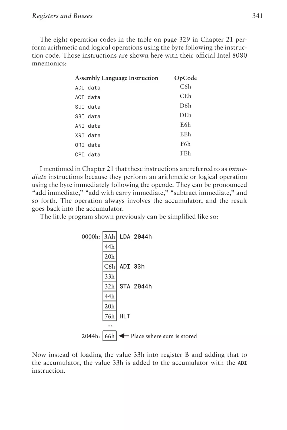
dots and dashes, as you can see in the following table.
Best Friends
Although Morse code has absolutely nothing to do with computers,
becoming familiar with the nature of codes is an essential preliminary to
achieving a deep understanding of the hidden languages and inner structures of computer hardware and software.
In this book, the word code usually means a system for transferring
information among people, between people and computers, or within computers themselves.
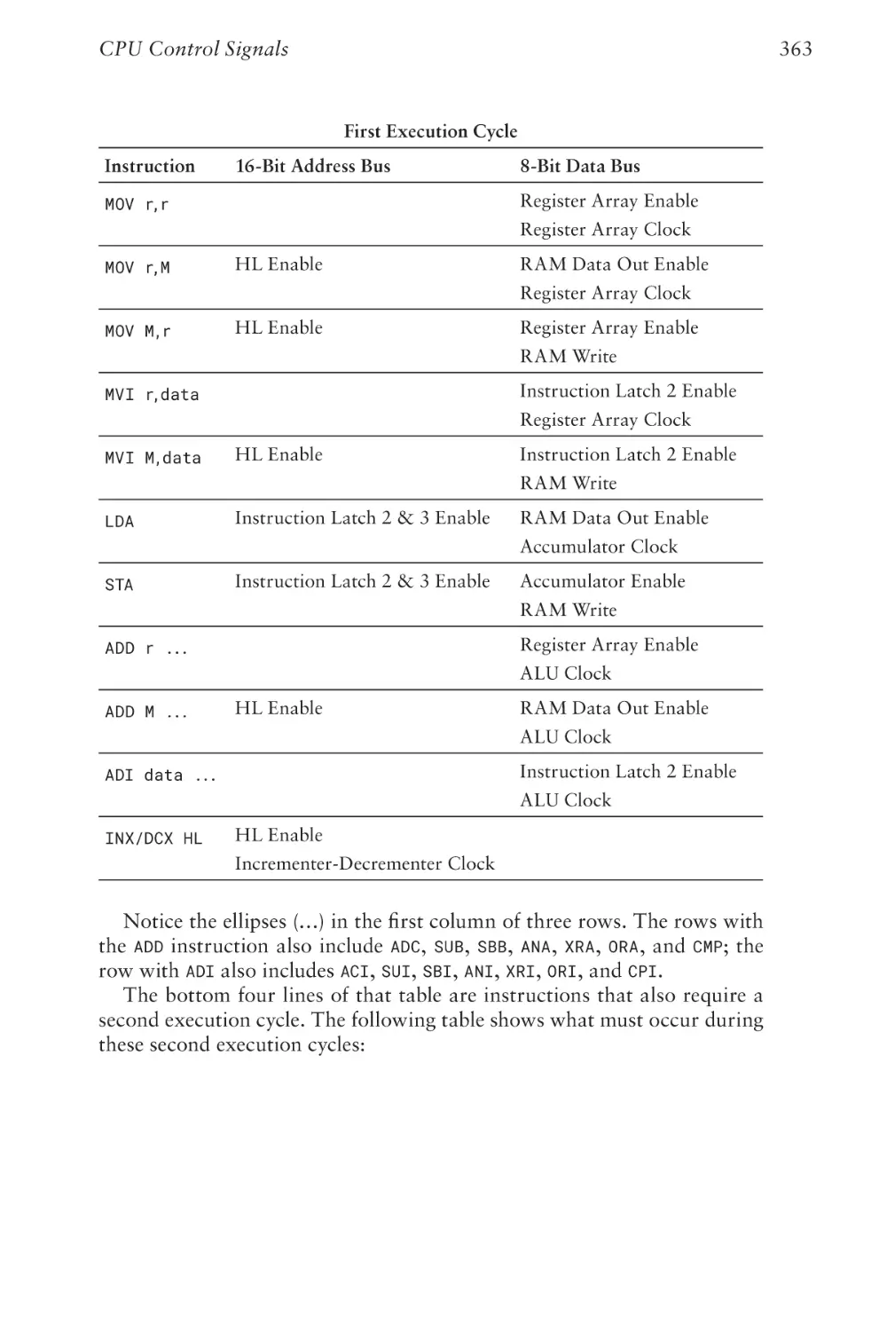
A code lets you communicate. Sometimes codes are secret, but most
codes are not. Indeed, most codes must be well understood because they’re
the basis of human communication.
The sounds we make with our mouths to form words constitute a code
that is intelligible to anyone who can hear our voices and understands the
language that we speak. We call this code “the spoken word” or “speech.”
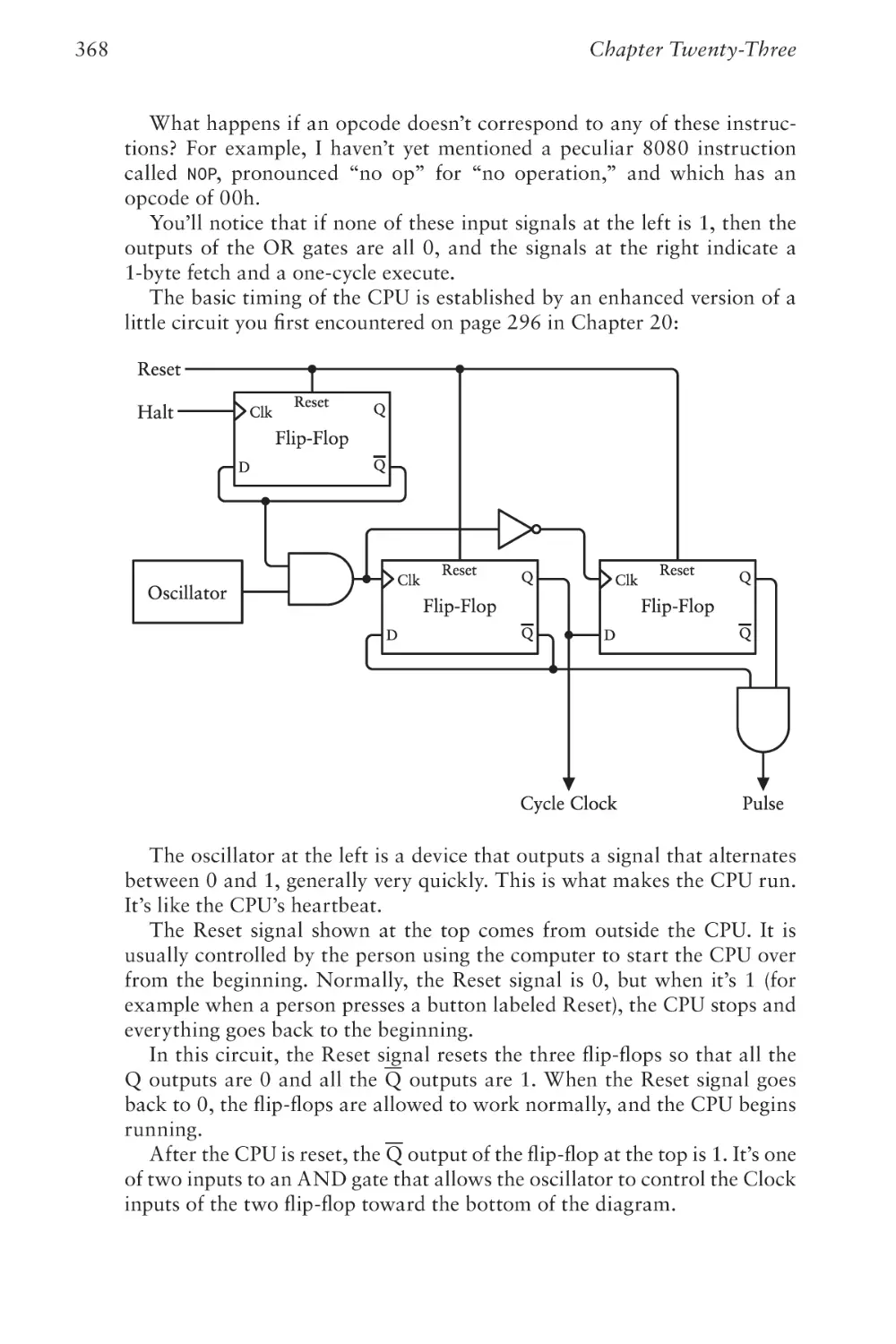
Within deaf communities, various sign languages employ the hands
and arms to form movements and gestures that convey individual letters
of words or whole words and concepts. The two systems most common in
North America are American Sign Language (ASL), which was developed
in the early 19th century at the American School for the Deaf, and Langue
des signes Québécoise (LSQ), which is a variation of French sign language.
We use another code for words on paper or other media, called “the written word” or “text.” Text can be written or keyed by hand and then printed
in newspapers, magazines, and books or displayed digitally on a range of
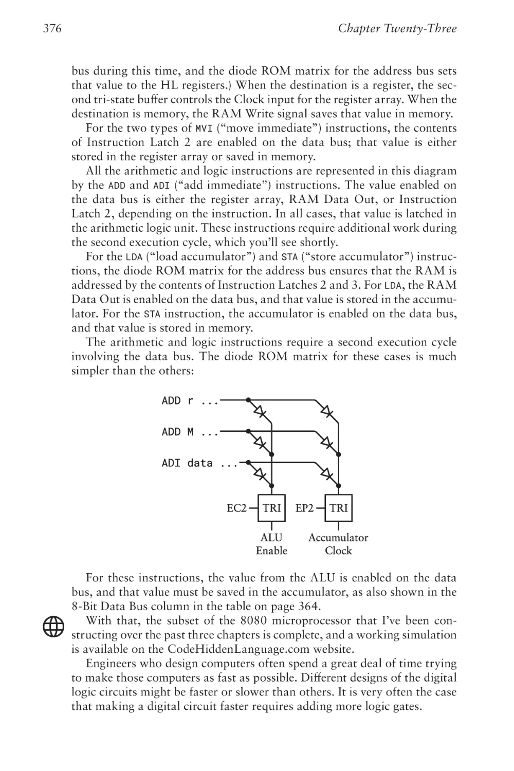
devices. In many languages, a strong correspondence exists between speech
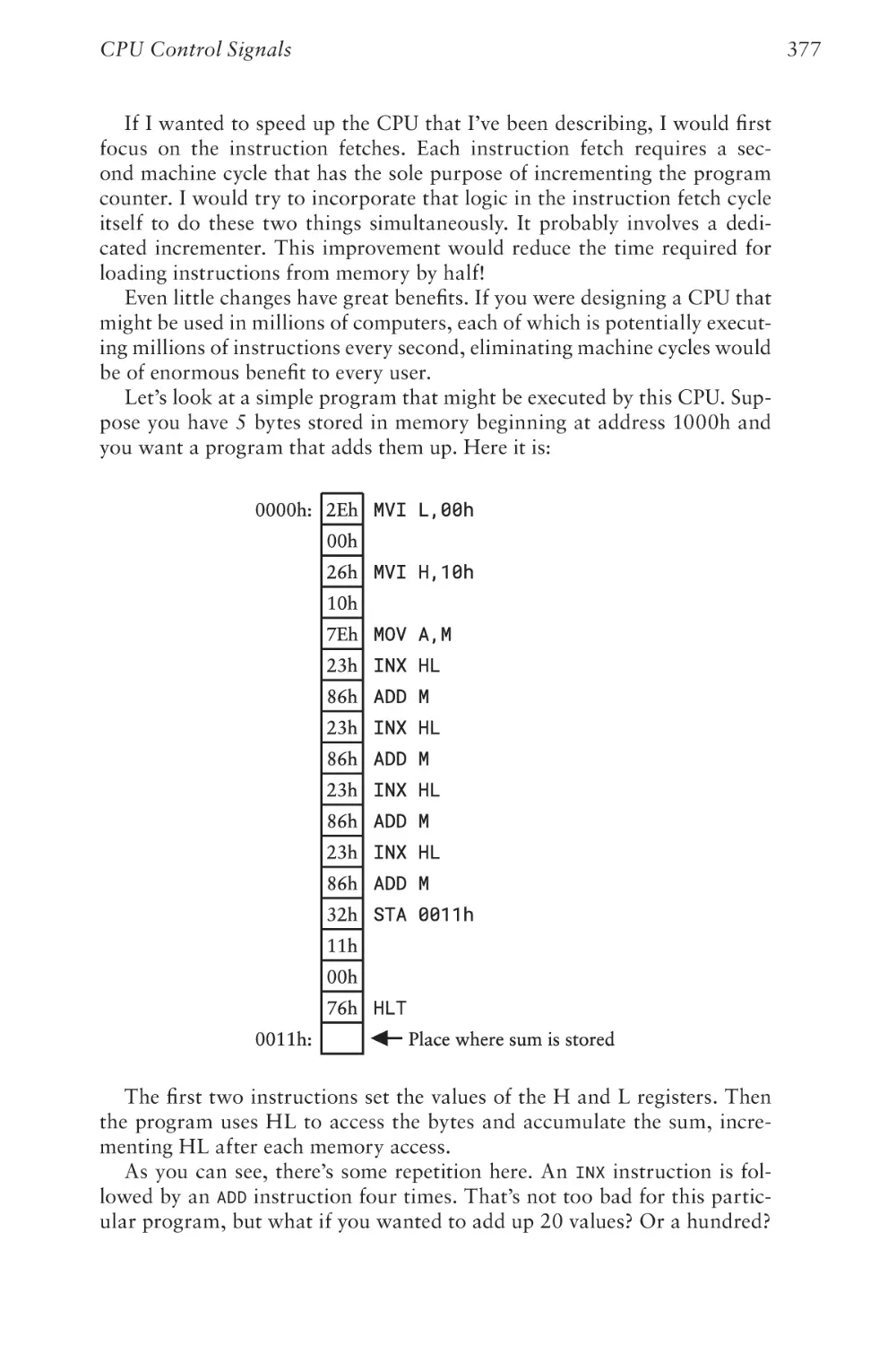
and text. In English, for example, letters and groups of letters correspond
(more or less) to spoken sounds.
For people who are visually impaired, the written word can be replaced
with Braille, which uses a system of raised dots that correspond to letters, groups of letters, and whole words. (I discuss Braille in more detail in
Chapter 3.)
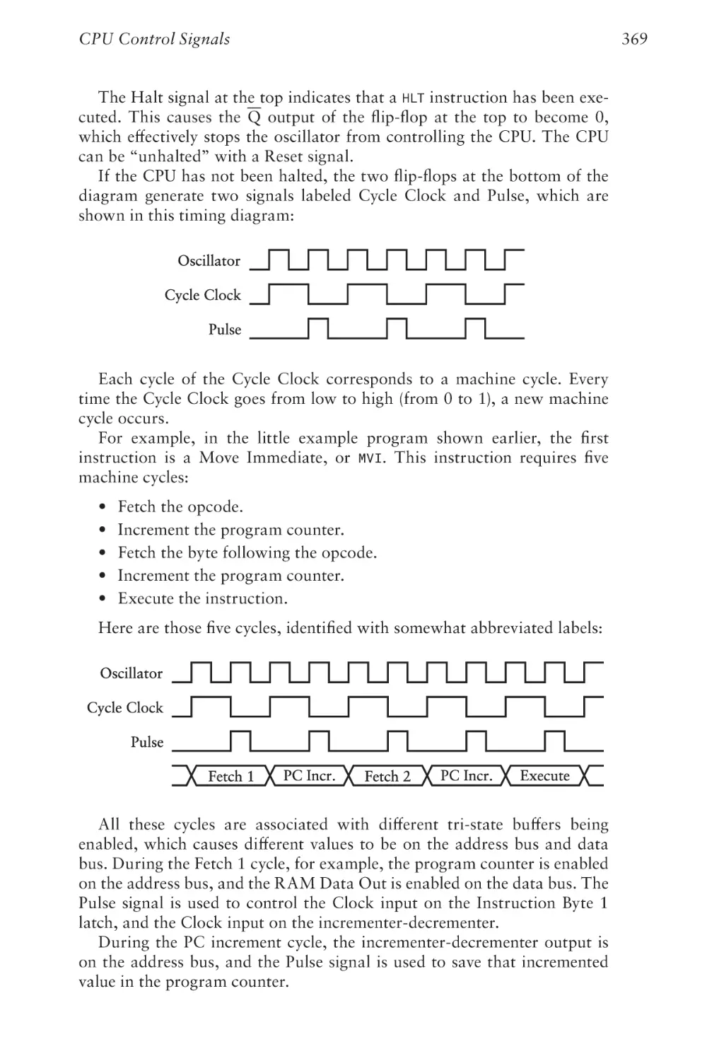
When spoken words must be transcribed into text very quickly, stenography or shorthand is useful. In courts of law or for generating real-time
closed captioning for televised news or sports programs, stenographers
use a stenotype machine with a simplified keyboard incorporating its own
codes corresponding to text.
We use a variety of different codes for communicating among ourselves
because some codes are more convenient than others. The code of the spoken word can’t be stored on paper, so the code of the written word is used
instead. Silently exchanging information across a distance in the dark isn’t
possible with speech or paper. Hence, Morse code is a convenient alternative. A code is useful if it serves a purpose that no other code can.
As we shall see, various types of codes are also used in computers to store
and communicate text, numbers, sounds, music, pictures, and movies, as
well as instructions within the computer itself. Computers can’t easily deal
with human codes because computers can’t precisely duplicate the ways in
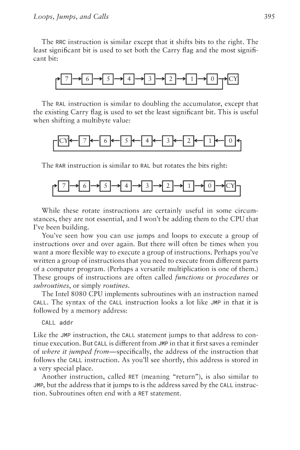
which human beings use their eyes, ears, mouths, and fingers. Teaching
3
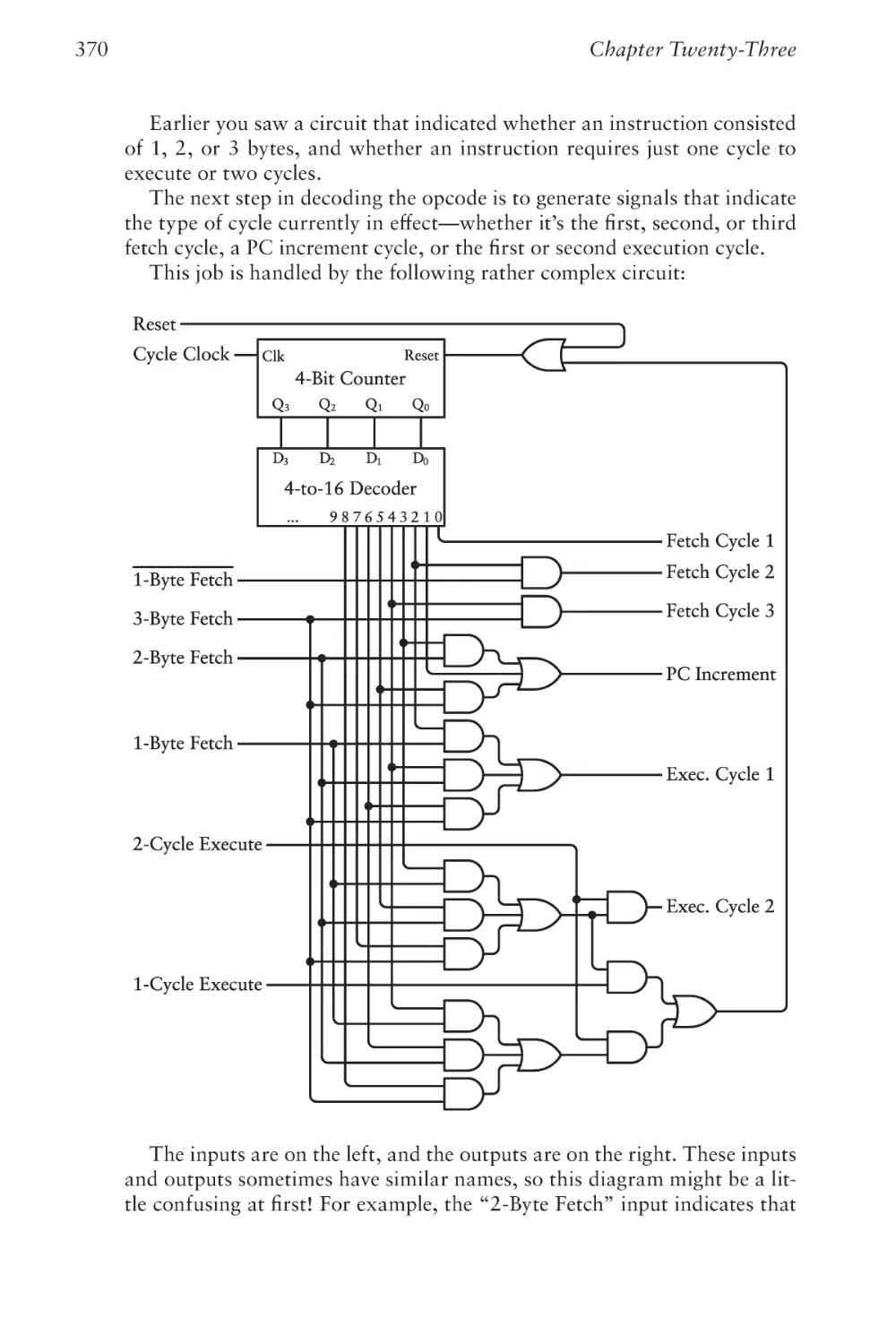
4
Chapter One
computers to speak is hard, and persuading them to understand speech is
even harder.
But much progress has been made. Computers have now been enabled to
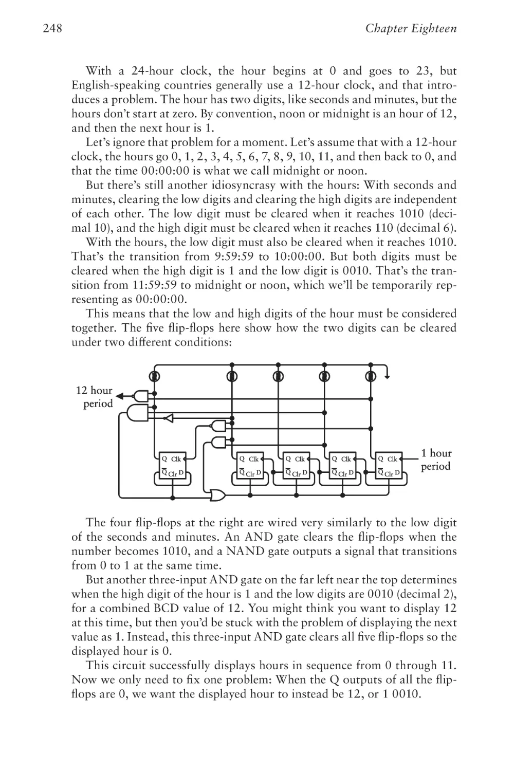
capture, store, manipulate, and render many types of information used in
human communication, including the visual (text and pictures), the aural
(spoken words, sounds, and music), or a combination of both (animations
and movies). All of these types of information require their own codes.
Even the table of Morse code you just saw is itself a code of sorts. The
table shows that each letter is represented by a series of dots and dashes. Yet
we can’t actually send dots and dashes. When sending Morse code with a
flashlight, the dots and dashes correspond to blinks.
Sending Morse code with a flashlight requires turning the flashlight
switch on and off quickly for a dot, and somewhat longer for a dash. To
send an A, for example, you turn the flashlight on and off quickly and then
on and off not quite as quickly, followed by a pause before the next character. By convention, the length of a dash should be about three times that
of a dot. The person on the receiving end sees the short blink and the long
blink and knows that it’s an A.
Pauses between the dots and dashes of Morse code are crucial. When
you send an A, for example, the flashlight should be off between the dot
and the dash for a period of time equal to about one dot. Letters in the
same word are separated by longer pauses equal to about the length of
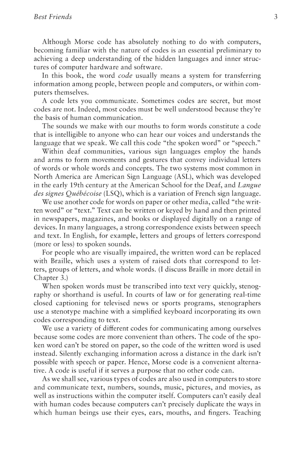
one dash. For example, here’s the Morse code for “hello,” illustrating the
pauses between the letters:
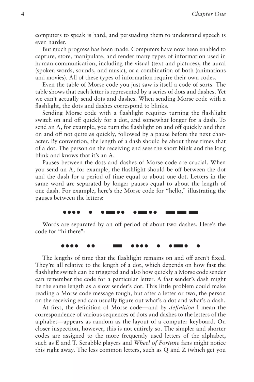
Words are separated by an off period of about two dashes. Here’s the
code for “hi there”:
The lengths of time that the flashlight remains on and off aren’t fixed.
They’re all relative to the length of a dot, which depends on how fast the
flashlight switch can be triggered and also how quickly a Morse code sender
can remember the code for a particular letter. A fast sender’s dash might
be the same length as a slow sender’s dot. This little problem could make
reading a Morse code message tough, but after a letter or two, the person
on the receiving end can usually figure out what’s a dot and what’s a dash.
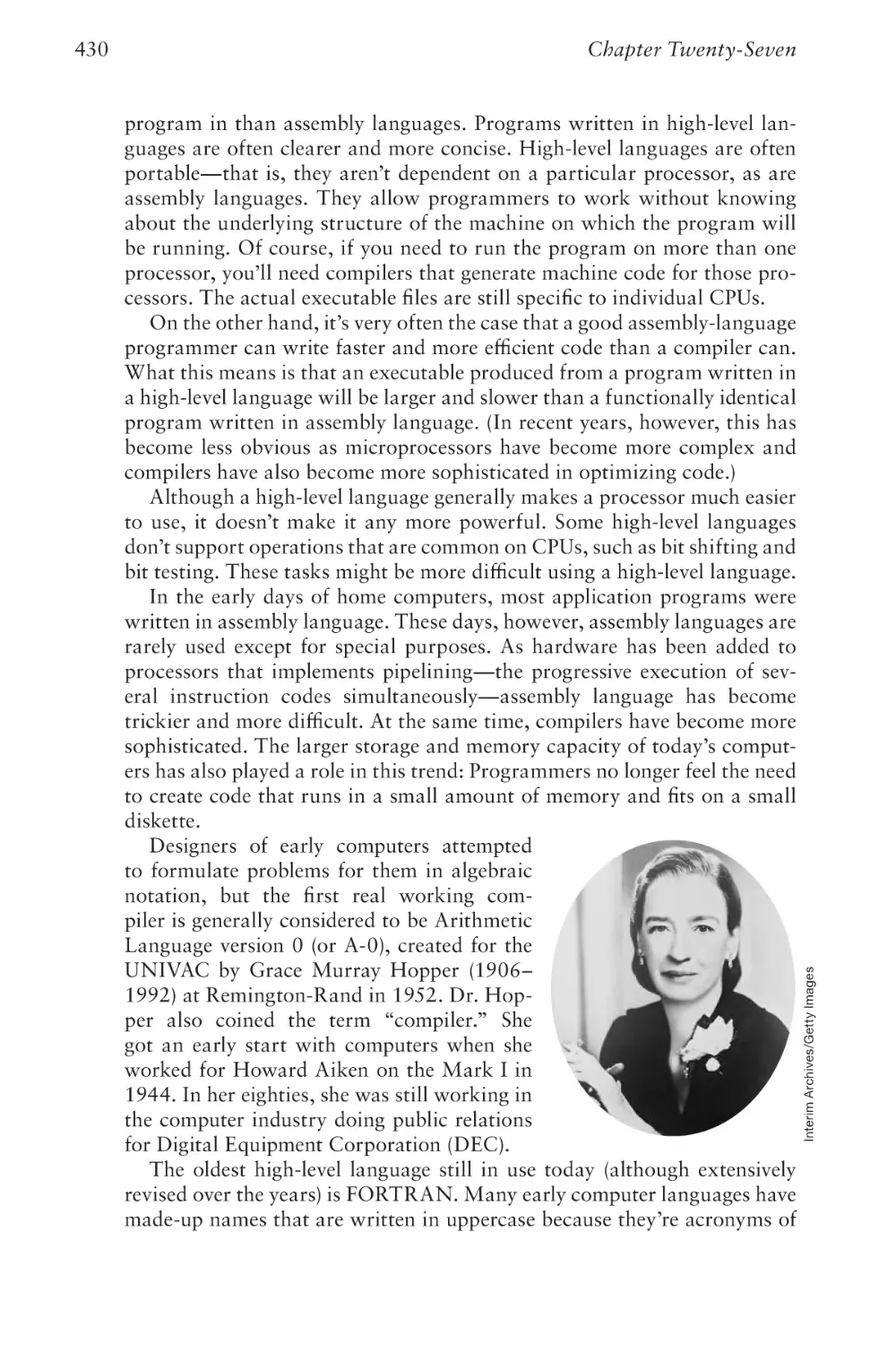
At first, the definition of Morse code—and by definition I mean the
correspondence of various sequences of dots and dashes to the letters of the
alphabet—appears as random as the layout of a computer keyboard. On
closer inspection, however, this is not entirely so. The simpler and shorter
codes are assigned to the more frequently used letters of the alphabet,
such as E and T. Scrabble players and Wheel of Fortune fans might notice
this right away. The less common letters, such as Q and Z (which get you
Best Friends
10 points in Scrabble and rarely appear in Wheel of Fortune puzzles), have
longer codes.
Almost everyone knows a little Morse code. Three dots, three dashes,
and three dots represent SOS, the international distress signal. SOS isn’t an
abbreviation for anything—it’s simply an easy-to-remember Morse code
sequence. During the Second World War, the British Broadcasting Corporation prefaced some radio broadcasts with the beginning of Beethoven’s
Fifth Symphony—BAH, BAH, BAH, BAHMMMMM—which Beethoven
didn’t know at the time he composed the music would someday be the
Morse code for V, for Victory.
One drawback of Morse code is that it doesn’t differentiate between
uppercase and lowercase letters. But in addition to representing letters,
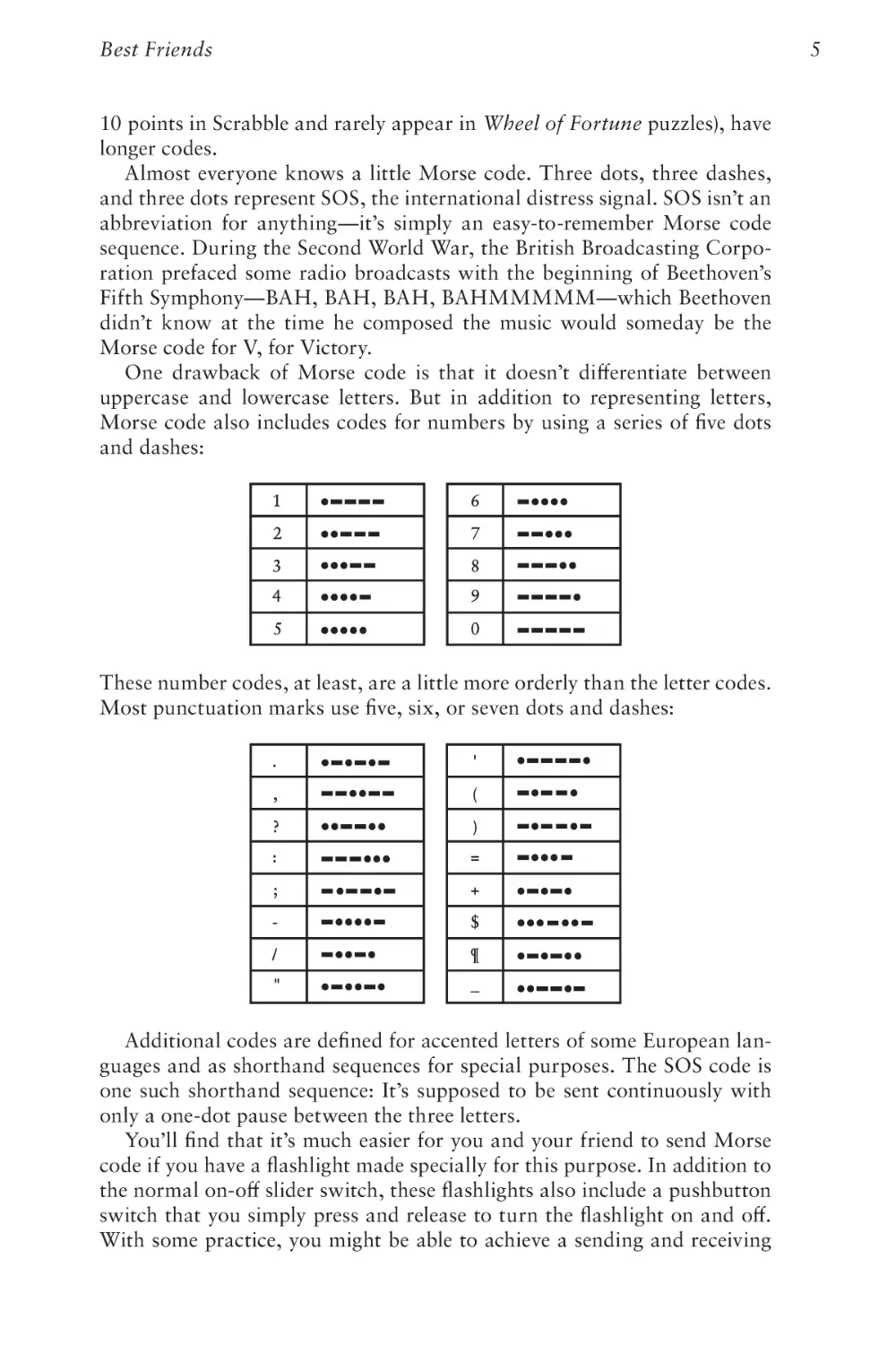
Morse code also includes codes for numbers by using a series of five dots
and dashes:
These number codes, at least, are a little more orderly than the letter codes.
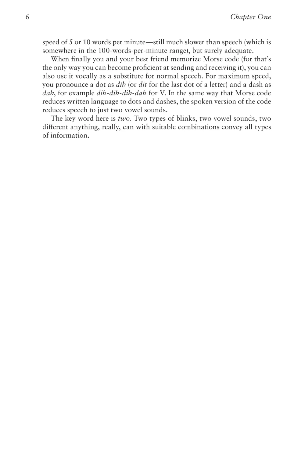
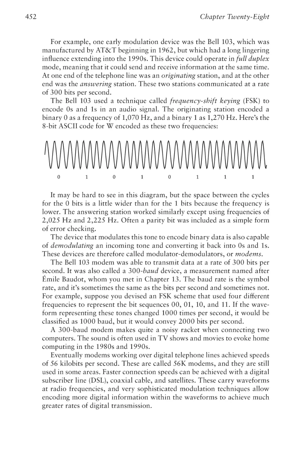
Most punctuation marks use five, six, or seven dots and dashes:
Additional codes are defined for accented letters of some European languages and as shorthand sequences for special purposes. The SOS code is
one such shorthand sequence: It’s supposed to be sent continuously with
only a one-dot pause between the three letters.
You’ll find that it’s much easier for you and your friend to send Morse
code if you have a flashlight made specially for this purpose. In addition to
the normal on-off slider switch, these flashlights also include a pushbutton
switch that you simply press and release to turn the flashlight on and off.
With some practice, you might be able to achieve a sending and receiving
5
6
Chapter One
speed of 5 or 10 words per minute—still much slower than speech (which is
somewhere in the 100-words-per-minute range), but surely adequate.
When finally you and your best friend memorize Morse code (for that’s
the only way you can become proficient at sending and receiving it), you can
also use it vocally as a substitute for normal speech. For maximum speed,
you pronounce a dot as dih (or dit for the last dot of a letter) and a dash as
dah, for example dih-dih-dih-dah for V. In the same way that Morse code
reduces written language to dots and dashes, the spoken version of the code
reduces speech to just two vowel sounds.
The key word here is two. Two types of blinks, two vowel sounds, two
different anything, really, can with suitable combinations convey all types
of information.
Chapter Two
Codes and
Combinations
M
orse code was invented around 1837 by Samuel Finley Breese
Morse (1791–1872), whom we shall meet more properly later
in this book. It was further developed by others, most notably
Alfred Vail (1807–1859), and it evolved into a couple of different versions.
The system described in this book is more formally known as International
Morse code.
The invention of Morse code goes hand in hand with the invention of
the telegraph, which I’ll also examine in more detail later in this book. Just
as Morse code provides a good introduction to the nature of codes, the
telegraph includes hardware that can mimic the workings of a computer.
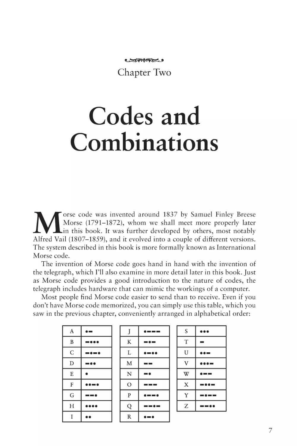
Most people find Morse code easier to send than to receive. Even if you
don’t have Morse code memorized, you can simply use this table, which you
saw in the previous chapter, conveniently arranged in alphabetical order:
7
Chapter Two
8
Receiving Morse code and translating it back into words is considerably
harder and more time consuming than sending because you must work
backward to figure out the letter that corresponds to a particular coded
sequence of dots and dashes. If you don’t have the codes memorized and
you receive a dash-dot-dash-dash, you have to scan through the table letter
by letter before you finally discover that it’s the letter Y.
The problem is that we have a table that provides this translation:
Alphabetical letter → Morse code dots and dashes
But we don’t have a table that lets us go backward:
Morse code dots and dashes → Letter of the alphabet
In the early stages of learning Morse code, such a table would certainly
be convenient. But it’s not at all obvious how we could construct it. There’s
nothing in those dots and dashes that we can put into alphabetical order.
So let’s forget about alphabetical order. Perhaps a better approach to
organizing the codes might be to group them based on how many dots and
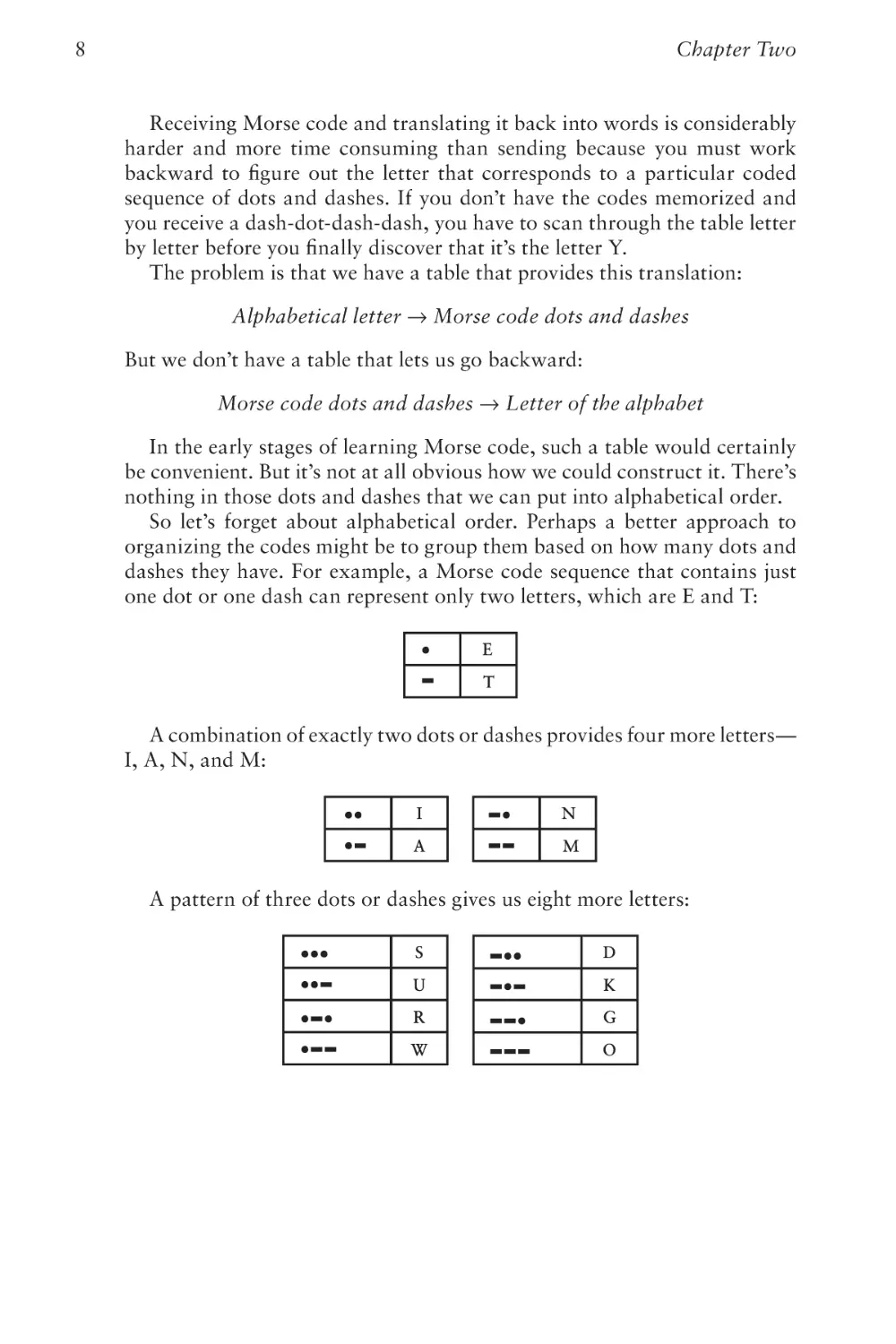
dashes they have. For example, a Morse code sequence that contains just
one dot or one dash can represent only two letters, which are E and T:
A combination of exactly two dots or dashes provides four more letters—
I, A, N, and M:
A pattern of three dots or dashes gives us eight more letters:
Codes and Combinations
9
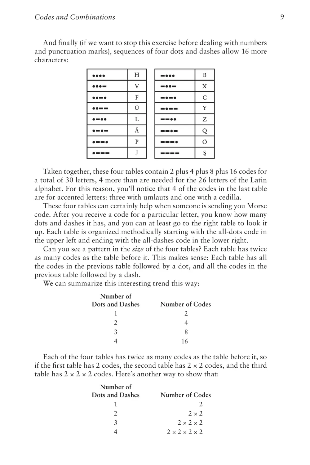
And finally (if we want to stop this exercise before dealing with numbers
and punctuation marks), sequences of four dots and dashes allow 16 more
characters:
Taken together, these four tables contain 2 plus 4 plus 8 plus 16 codes for
a total of 30 letters, 4 more than are needed for the 26 letters of the Latin
alphabet. For this reason, you’ll notice that 4 of the codes in the last table
are for accented letters: three with umlauts and one with a cedilla.
These four tables can certainly help when someone is sending you Morse
code. After you receive a code for a particular letter, you know how many
dots and dashes it has, and you can at least go to the right table to look it
up. Each table is organized methodically starting with the all-dots code in
the upper left and ending with the all-dashes code in the lower right.
Can you see a pattern in the size of the four tables? Each table has twice
as many codes as the table before it. This makes sense: Each table has all
the codes in the previous table followed by a dot, and all the codes in the
previous table followed by a dash.
We can summarize this interesting trend this way:
Number of
Dots and Dashes
1
2
3
4
Number of Codes
2
4
8
16
Each of the four tables has twice as many codes as the table before it, so
if the first table has 2 codes, the second table has 2 × 2 codes, and the third
table has 2 × 2 × 2 codes. Here’s another way to show that:
Number of
Dots and Dashes
1
2
3
4
Number of Codes
2
2×2
2×2×2
2×2×2×2
Chapter Two
10
Once we’re dealing with a number multiplied by itself, we can start using
exponents to show powers. For example, 2 × 2 × 2 × 2 can be written as
24 (2 to the 4th power). The numbers 2, 4, 8, and 16 are all powers of 2
because you can calculate them by multiplying 2 by itself. The summary
can also be shown like this:
Number of
Dots and Dashes
1
2
3
4
Number of Codes
21
22
23
24
This table has become very simple. The number of codes is simply 2 to
the power of the number of dots and dashes:
number of codes = 2number of dots and dashes
Powers of 2 tend to show up a lot in codes, and particularly in this book.
You’ll see another example in the next chapter.
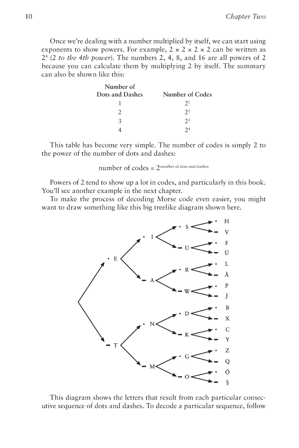
To make the process of decoding Morse code even easier, you might
want to draw something like this big treelike diagram shown here.
This diagram shows the letters that result from each particular consecutive sequence of dots and dashes. To decode a particular sequence, follow
Codes and Combinations
11
the arrows from left to right. For example, suppose you want to know
which letter corresponds to the code dot-dash-dot. Begin at the left and
choose the dot; then continue moving right along the arrows and choose
the dash and then another dot. The letter is R, shown next to the third dot.
If you think about it, constructing such a table was probably necessary
for defining Morse code in the first place. First, it ensures that you don’t
make the silly mistake of using the same code for two different letters!
Second, you’re assured of using all the possible codes without making the
sequences of dots and dashes unnecessarily long.
At the risk of extending this table beyond the limits of the printed page,
we could continue it for codes of five dots and dashes. A sequence of exactly
five dots and dashes gives us 32 (2 × 2 × 2 × 2 × 2, or 25) additional codes.
Normally that would be enough for the ten numbers and 16 punctuation
symbols defined in Morse code, and indeed, the numbers are encoded with
five dots and dashes. But many of the other codes that use a sequence of five
dots and dashes represent accented letters rather than punctuation marks.
To include all the punctuation marks, the system must be expanded to
six dots and dashes, which gives us 64 (2 × 2 × 2 × 2 × 2 × 2, or 26) additional codes for a grand total of 2 + 4 + 8 + 16 + 32 + 64, or 126, characters.
That’s overkill for Morse code, which leaves many of these longer codes
undefined, which used in this context refers to a code that doesn’t stand for
anything. If you were receiving Morse code and you got an undefined code,
you could be pretty sure that somebody made a mistake.
Because we were clever enough to develop this little formula,
number of codes = 2number of dots and dashes
we could continue figuring out how many codes we get from using longer
sequences:
Number of
Dots and Dashes
1
2
3
4
5
6
7
8
9
10
Number of Codes
21 = 2
22 = 4
23 = 8
24 = 16
25 = 32
26 = 64
27 = 128
28 = 256
29 = 512
210 = 1024
Fortunately, we don’t have to actually write out all the possible codes
to determine how many there would be. All we have to do is multiply 2 by
itself over and over again.
12
Chapter Two
Morse code is said to be binary (literally meaning two by two) because
the components of the code consist of only two things—a dot and a dash.
That’s similar to a coin, which can land only on the head side or the tail
side. Coins that are flipped ten times can have 1024 different sequences of
heads and tails.
Combinations of binary objects (such as coins) and binary codes (such as
Morse code) are always described by powers of two. Two is a very important number in this book.
Chapter Three
Braille and
Binary Codes
ullstein bild Dtl/Getty Images
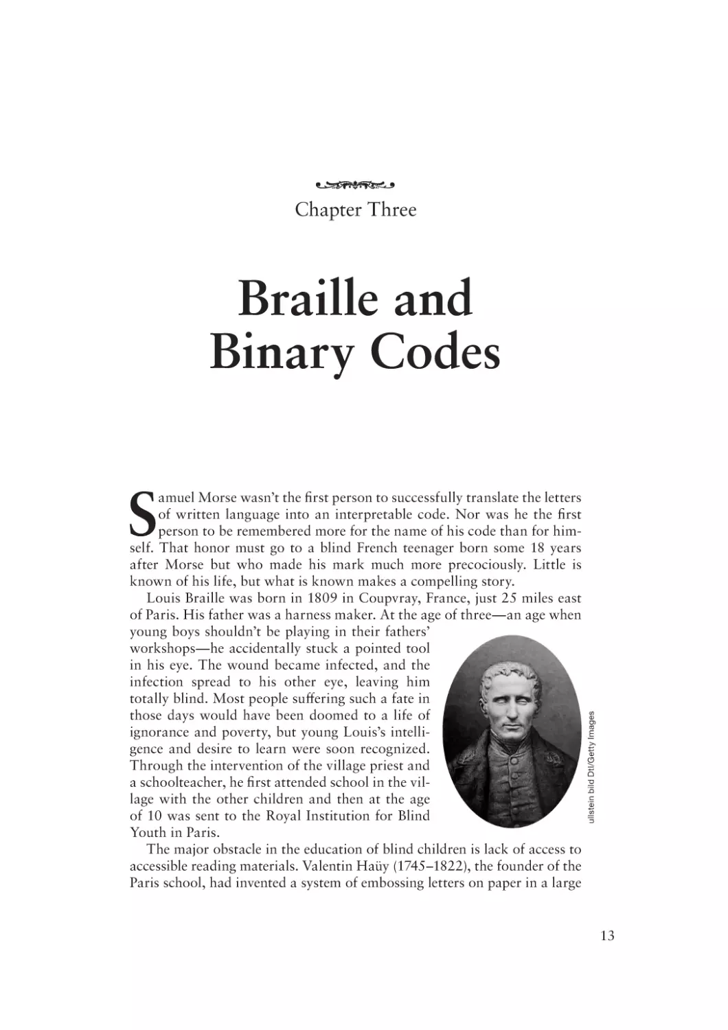
S
amuel Morse wasn’t the first person to successfully translate the letters
of written language into an interpretable code. Nor was he the first
person to be remembered more for the name of his code than for himself. That honor must go to a blind French teenager born some 18 years
after Morse but who made his mark much more precociously. Little is
known of his life, but what is known makes a compelling story.
Louis Braille was born in 1809 in Coupvray, France, just 25 miles east
of Paris. His father was a harness maker. At the age of three—an age when
young boys shouldn’t be playing in their fathers’
workshops—he accidentally stuck a pointed tool
in his eye. The wound became infected, and the
infection spread to his other eye, leaving him
totally blind. Most people suffering such a fate in
those days would have been doomed to a life of
ignorance and poverty, but young Louis’s intelligence and desire to learn were soon recognized.
Through the intervention of the village priest and
a schoolteacher, he first attended school in the village with the other children and then at the age
of 10 was sent to the Royal Institution for Blind
Youth in Paris.
The major obstacle in the education of blind children is lack of access to
accessible reading materials. Valentin Haüy (1745–1822), the founder of the
Paris school, had invented a system of embossing letters on paper in a large
13
Chapter Three
14
rounded font that could be read by touch. But this system was very difficult
to use, and only a few books had been produced using this method.
The sighted Haüy was stuck in a paradigm. To him, an A was an A was
an A, and the letter A must look (or feel) like an A. (If given a flashlight
to communicate, he might have tried drawing letters in the air, as we did
before we discovered it didn’t work very well.) Haüy probably didn’t realize
that a type of code quite different from embossed letters might be more
appropriate for sightless people.
The origins of an alternative type of code came from an unexpected
source. Charles Barbier, a captain of the French army, had by 1815 devised
a system of writing later called écriture nocturne, or “night writing.” This
system used a pattern of raised dots on heavy paper and was intended for
use by soldiers in passing notes to each other in the dark when quiet was
necessary. The soldiers could poke these dots into the back of the paper
using an awl-like stylus. The raised dots could then be read with the fingers.
Louis Braille became familiar with Barbier’s system at the age of 12. He
liked the use of raised dots, not only for the ease in reading with the fingers
but also because it was easy to write. A student in the classroom equipped
with paper and a stylus could actually take notes and read them back.
Braille diligently worked to improve the system and within three years (at
the age of 15) had come up with his own, the basics of which are still used
today. For many years, the system was known only within the school, but
it gradually made its way to the rest of the world. In 1835, Louis Braille
contracted tuberculosis, which would eventually kill him shortly after his
43rd birthday, in 1852.
Today, various versions of the Braille system compete with audiobooks
for providing blind people with access to the written word, but Braille
remains an invaluable system and the only way to read for people who are
both blind and deaf. In recent decades, Braille has become more familiar
to the general public as elevators and automatic teller machines have used
Braille to become more accessible.
What I’ll do in this chapter is dissect the Braille code and show you how
it works. You don’t have to actually learn Braille or memorize anything.
The sole purpose of this exercise is to get some additional insight into the
nature of codes.
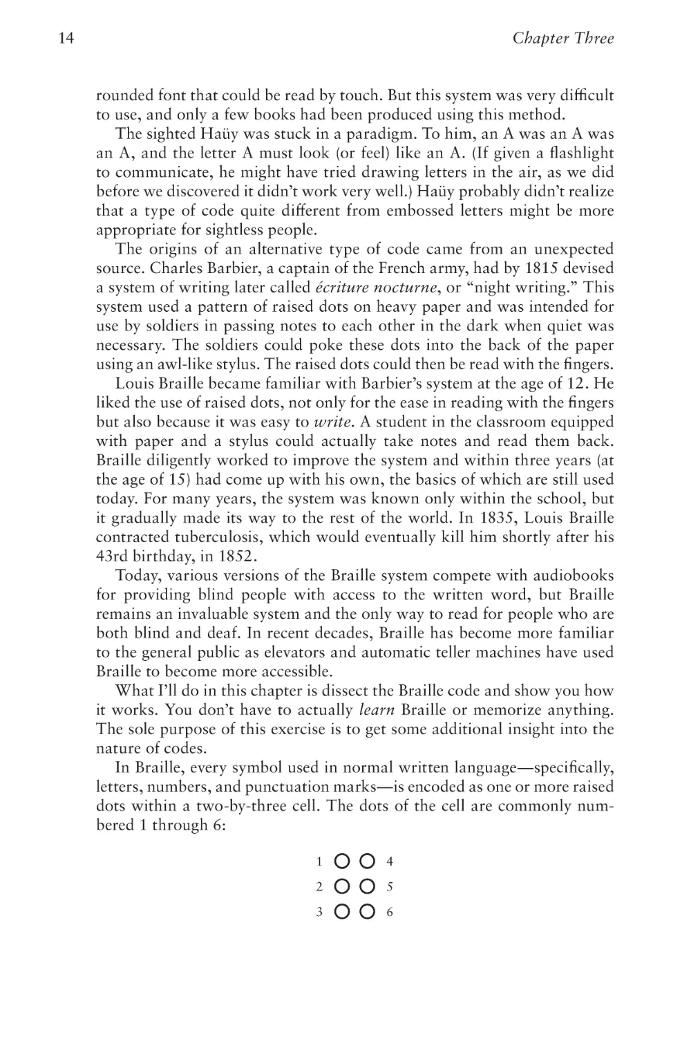
In Braille, every symbol used in normal written language—specifically,
letters, numbers, and punctuation marks—is encoded as one or more raised
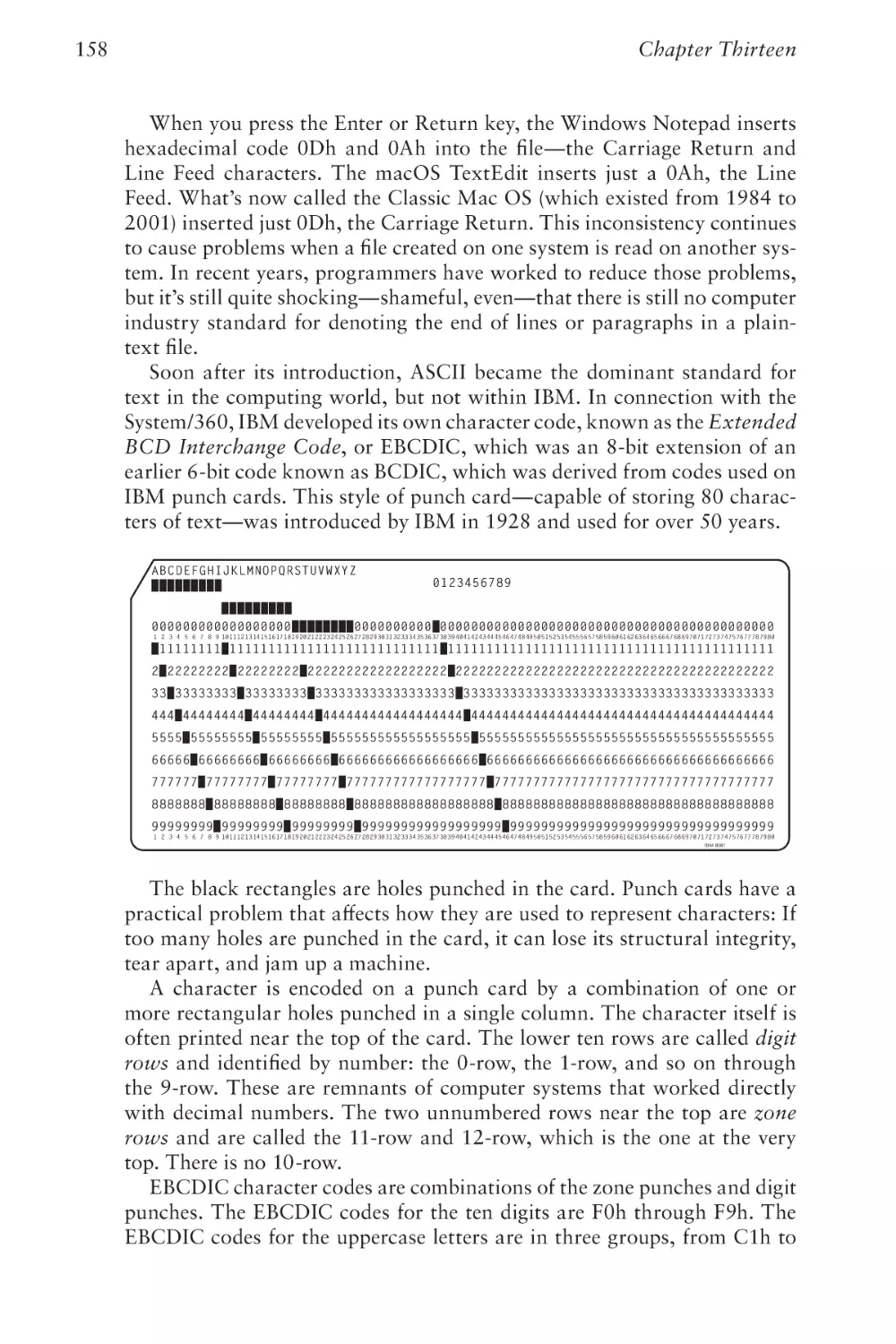
dots within a two-by-three cell. The dots of the cell are commonly numbered 1 through 6:
1
4
2
5
3
6
Braille and Binary Codes
Special typewriters were developed to emboss the Braille dots into the
paper, and these days, computer-driven embossers do the job.
Because embossing in Braille just a couple of pages of this book would be
prohibitively expensive, I’ve used a notation common for showing Braille
on the printed page. In this notation, all six dots in the cell are shown.
Large dots indicate the parts of the cell where the paper is raised. Small
dots indicate the parts of the cell that are flat. For example, in the Braille
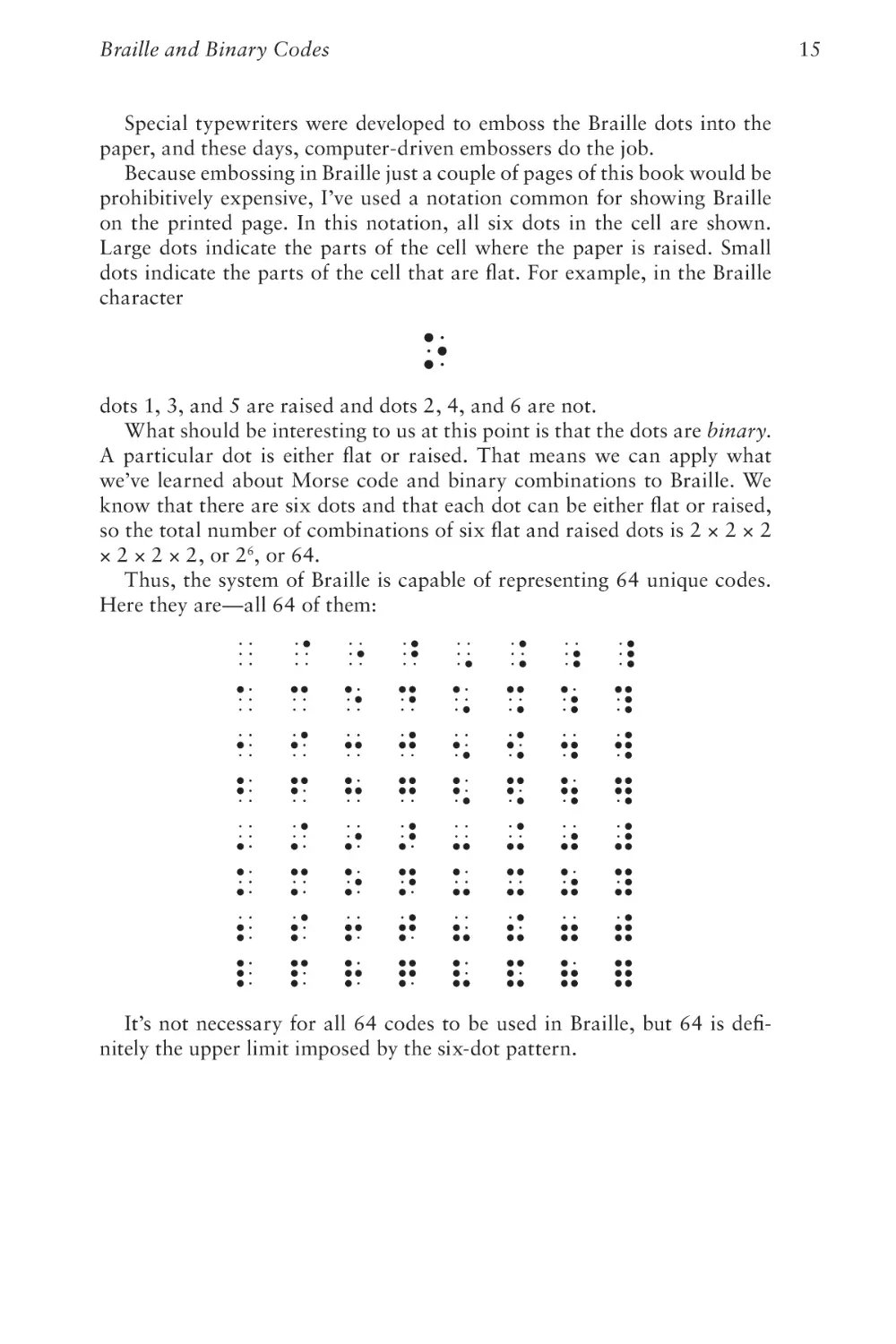
character
dots 1, 3, and 5 are raised and dots 2, 4, and 6 are not.
What should be interesting to us at this point is that the dots are binary.
A particular dot is either flat or raised. That means we can apply what
we’ve learned about Morse code and binary combinations to Braille. We
know that there are six dots and that each dot can be either flat or raised,
so the total number of combinations of six flat and raised dots is 2 × 2 × 2
× 2 × 2 × 2, or 26, or 64.
Thus, the system of Braille is capable of representing 64 unique codes.
Here they are—all 64 of them:
It’s not necessary for all 64 codes to be used in Braille, but 64 is definitely the upper limit imposed by the six-dot pattern.
15
16
Chapter Three
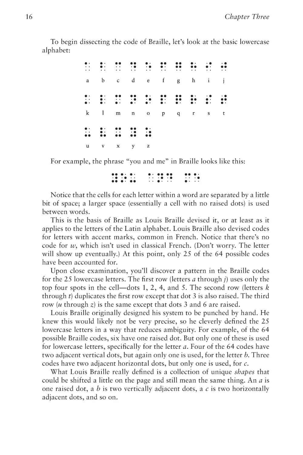
To begin dissecting the code of Braille, let’s look at the basic lowercase
alphabet:
For example, the phrase “you and me” in Braille looks like this:
Notice that the cells for each letter within a word are separated by a little
bit of space; a larger space (essentially a cell with no raised dots) is used
between words.
This is the basis of Braille as Louis Braille devised it, or at least as it
applies to the letters of the Latin alphabet. Louis Braille also devised codes
for letters with accent marks, common in French. Notice that there’s no
code for w, which isn’t used in classical French. (Don’t worry. The letter
will show up eventually.) At this point, only 25 of the 64 possible codes
have been accounted for.
Upon close examination, you’ll discover a pattern in the Braille codes
for the 25 lowercase letters. The first row (letters a through j) uses only the
top four spots in the cell—dots 1, 2, 4, and 5. The second row (letters k
through t) duplicates the first row except that dot 3 is also raised. The third
row (u through z) is the same except that dots 3 and 6 are raised.
Louis Braille originally designed his system to be punched by hand. He
knew this would likely not be very precise, so he cleverly defined the 25
lowercase letters in a way that reduces ambiguity. For example, of the 64
possible Braille codes, six have one raised dot. But only one of these is used
for lowercase letters, specifically for the letter a. Four of the 64 codes have
two adjacent vertical dots, but again only one is used, for the letter b. Three
codes have two adjacent horizontal dots, but only one is used, for c.
What Louis Braille really defined is a collection of unique shapes that
could be shifted a little on the page and still mean the same thing. An a is
one raised dot, a b is two vertically adjacent dots, a c is two horizontally
adjacent dots, and so on.
Braille and Binary Codes
Codes are often susceptible to errors. An error that occurs as a code
is written (for example, when a student of Braille marks dots in paper) is
called an encoding error. An error made reading the code is called a decoding error. In addition, there can also be transmission errors—for example,
when a page containing Braille is damaged in some way.
More sophisticated codes often incorporate various types of built-in
error correction. In this sense, Braille as originally defined by Louis Braille
is a sophisticated coding system: It uses redundancy to allow a little imprecision in the punching and reading of the dots.
Since the days of Louis Braille, the Braille code has been expanded in
various ways, including systems to notate mathematics and music. Currently the system used most often in published English text is called Grade 2
Braille. Grade 2 Braille uses many contractions in order to use less paper
and to speed reading. For example, if letter codes appear by themselves,
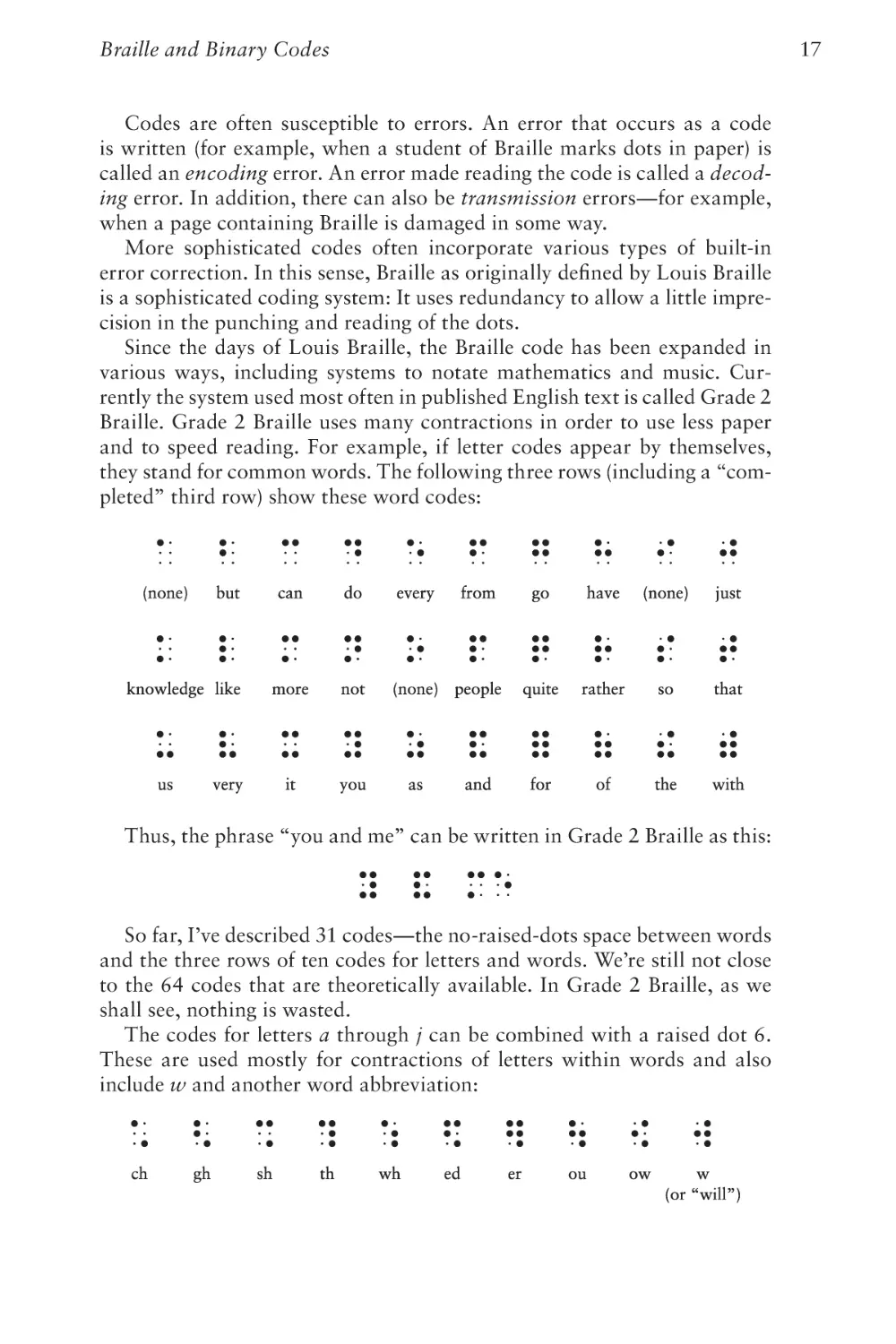
they stand for common words. The following three rows (including a “completed” third row) show these word codes:
Thus, the phrase “you and me” can be written in Grade 2 Braille as this:
So far, I’ve described 31 codes—the no-raised-dots space between words
and the three rows of ten codes for letters and words. We’re still not close
to the 64 codes that are theoretically available. In Grade 2 Braille, as we
shall see, nothing is wasted.
The codes for letters a through j can be combined with a raised dot 6.
These are used mostly for contractions of letters within words and also
include w and another word abbreviation:
17
Chapter Three
18
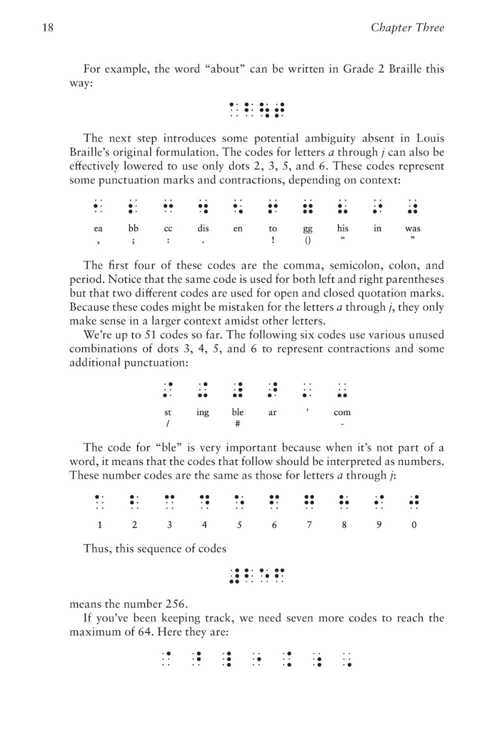
For example, the word “about” can be written in Grade 2 Braille this
way:
The next step introduces some potential ambiguity absent in Louis
Braille’s original formulation. The codes for letters a through j can also be
effectively lowered to use only dots 2, 3, 5, and 6. These codes represent
some punctuation marks and contractions, depending on context:
The first four of these codes are the comma, semicolon, colon, and
period. Notice that the same code is used for both left and right parentheses
but that two different codes are used for open and closed quotation marks.
Because these codes might be mistaken for the letters a through j, they only
make sense in a larger context amidst other letters.
We’re up to 51 codes so far. The following six codes use various unused
combinations of dots 3, 4, 5, and 6 to represent contractions and some
additional punctuation:
The code for “ble” is very important because when it’s not part of a
word, it means that the codes that follow should be interpreted as numbers.
These number codes are the same as those for letters a through j:
Thus, this sequence of codes
means the number 256.
If you’ve been keeping track, we need seven more codes to reach the
maximum of 64. Here they are:
Braille and Binary Codes
The first (a raised dot 4) is used as an accent indicator. The others are
used as prefixes for some contractions and also for some other purposes:
When dots 4 and 6 are raised (the fifth code in this row), the code is a
numeric decimal point or an emphasis indicator, depending on context.
When dots 5 and 6 are raised (the sixth code), it’s a letter indicator that
counterbalances a number indicator.
And finally (if you’ve been wondering how Braille encodes capital letters)
we have dot 6—the capital indicator. This indicates that the letter that
follows is uppercase. For example, we can write the name of the original
creator of this system as
This sequence begins with a capital indicator, followed by the letter l, the
contraction ou, the letters i and s, a space, another capital indicator, and
the letters b, r, a, i, l, l, and e. (In actual use, the name might be abbreviated
even more by eliminating the last two letters, which aren’t pronounced, or
by spelling it “brl.”)
In summary, we’ve seen how six binary elements (the dots) yield 64 possible codes and no more. It just so happens that many of these 64 codes perform double duty depending on their context. Of particular interest is the
number indicator along with the letter indicator that undoes the number
indicator. These codes alter the meaning of the codes that follow them—
from letters to numbers and from numbers back to letters. Codes such as
these are often called precedence, or shift, codes. They alter the meaning of
all subsequent codes until the shift is undone.
A shift code is similar to holding down the Shift key on a computer
keyboard, and it’s so named because the equivalent key on old typewriters
mechanically shifted the mechanism to type uppercase letters.
The Braille capital indicator means that the following letter (and only
the following letter) should be uppercase rather than lowercase. A code
such as this is known as an escape code. Escape codes let you “escape”
from the normal interpretation of a code and interpret it differently. Shift
codes and escape codes are common when written languages are represented by binary codes, but they can introduce complexities because individual codes can’t be interpreted on their own without knowing what codes
came before.
As early as 1855, some advocates of Braille began expanding the system
with another row of two dots. Eight-dot Braille has been used for some special purposes, such as music, stenography, and Japanese kanji characters.
Because it increases the number of unique codes to 28, or 256, it’s also been
convenient in some computer applications, allowing lowercase and uppercase letters, numbers, and punctuation to all have their own unique codes
without the annoyances of shift and escape codes.
19
This page intentionally left blank
Chapter Four
Anatomy
of a Flashlight
F
lashlights are useful for numerous tasks, of which reading under the
covers and sending coded messages are only the two most obvious.
The common household flashlight can also take center stage in an
educational show-and-tell of the ubiquitous stuff known as electricity.
Electricity is an amazing phenomenon, managing to be pervasively
useful while remaining largely mysterious, even to people who pretend to
know how it works. Fortunately, we need to understand only a few basic
concepts to comprehend how electricity is used inside computers.
The flashlight is certainly one of the simpler electrical appliances found
in most homes. Disassemble a typical flashlight and you’ll find that it consists of one or more batteries, a lightbulb, a switch, some metal pieces, and
a case to hold everything together.
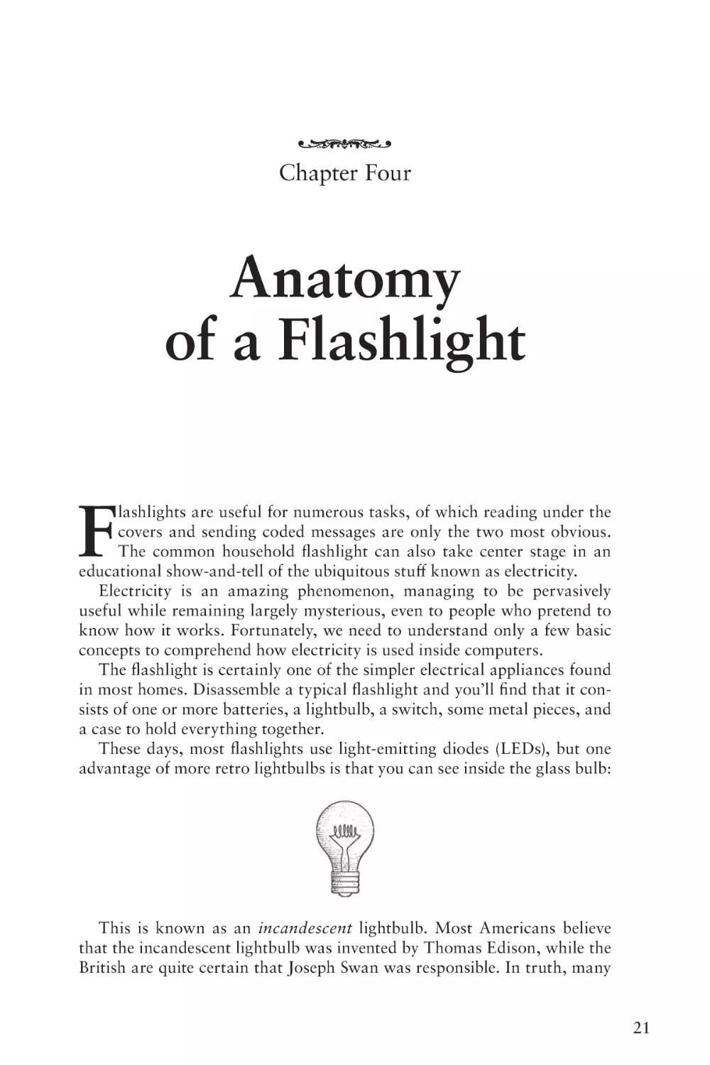
These days, most flashlights use light-emitting diodes (LEDs), but one
advantage of more retro lightbulbs is that you can see inside the glass bulb:
This is known as an incandescent lightbulb. Most Americans believe
that the incandescent lightbulb was invented by Thomas Edison, while the
British are quite certain that Joseph Swan was responsible. In truth, many
21
22
Chapter Four
other scientists and inventors made crucial strides before either Edison or
Swan got involved.
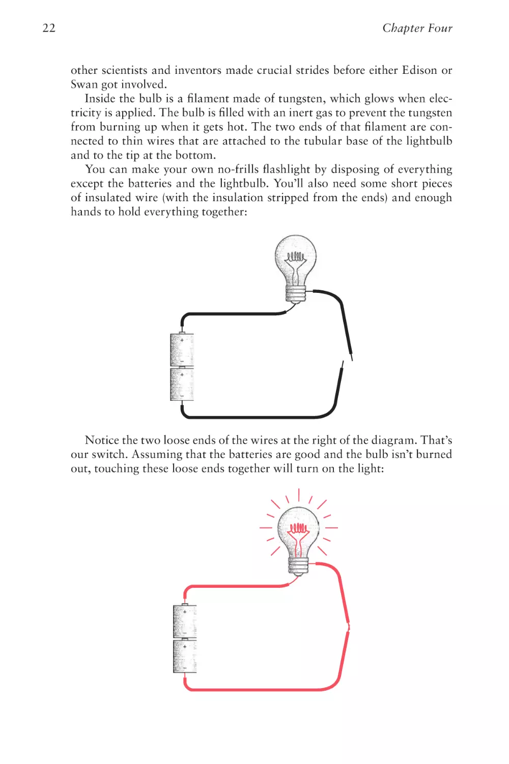
Inside the bulb is a filament made of tungsten, which glows when electricity is applied. The bulb is filled with an inert gas to prevent the tungsten
from burning up when it gets hot. The two ends of that filament are connected to thin wires that are attached to the tubular base of the lightbulb
and to the tip at the bottom.
You can make your own no-frills flashlight by disposing of everything
except the batteries and the lightbulb. You’ll also need some short pieces
of insulated wire (with the insulation stripped from the ends) and enough
hands to hold everything together:
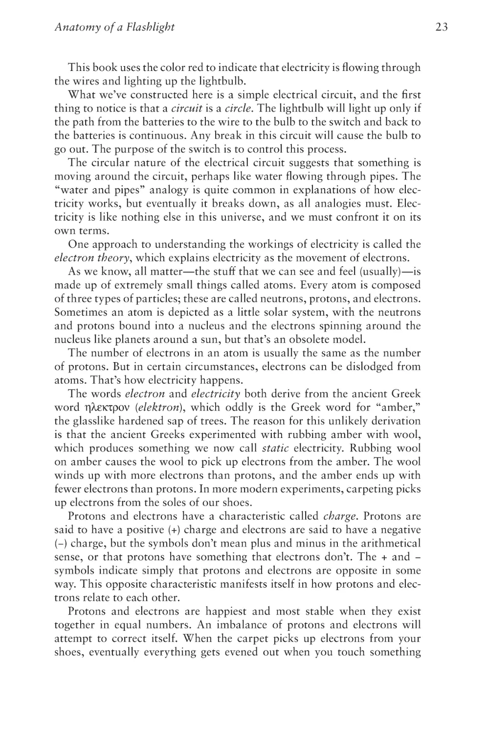
Notice the two loose ends of the wires at the right of the diagram. That’s
our switch. Assuming that the batteries are good and the bulb isn’t burned
out, touching these loose ends together will turn on the light:
Anatomy of a Flashlight
This book uses the color red to indicate that electricity is flowing through
the wires and lighting up the lightbulb.
What we’ve constructed here is a simple electrical circuit, and the first
thing to notice is that a circuit is a circle. The lightbulb will light up only if
the path from the batteries to the wire to the bulb to the switch and back to
the batteries is continuous. Any break in this circuit will cause the bulb to
go out. The purpose of the switch is to control this process.
The circular nature of the electrical circuit suggests that something is
moving around the circuit, perhaps like water flowing through pipes. The
“water and pipes” analogy is quite common in explanations of how electricity works, but eventually it breaks down, as all analogies must. Electricity is like nothing else in this universe, and we must confront it on its
own terms.
One approach to understanding the workings of electricity is called the
electron theory, which explains electricity as the movement of electrons.
As we know, all matter—the stuff that we can see and feel (usually)—is
made up of extremely small things called atoms. Every atom is composed
of three types of particles; these are called neutrons, protons, and electrons.
Sometimes an atom is depicted as a little solar system, with the neutrons
and protons bound into a nucleus and the electrons spinning around the
nucleus like planets around a sun, but that’s an obsolete model.
The number of electrons in an atom is usually the same as the number
of protons. But in certain circumstances, electrons can be dislodged from
atoms. That’s how electricity happens.
The words electron and electricity both derive from the ancient Greek
word ηλεκτρον (elektron), which oddly is the Greek word for “amber,”
the glasslike hardened sap of trees. The reason for this unlikely derivation
is that the ancient Greeks experimented with rubbing amber with wool,
which produces something we now call static electricity. Rubbing wool
on amber causes the wool to pick up electrons from the amber. The wool
winds up with more electrons than protons, and the amber ends up with
fewer electrons than protons. In more modern experiments, carpeting picks
up electrons from the soles of our shoes.
Protons and electrons have a characteristic called charge. Protons are
said to have a positive (+) charge and electrons are said to have a negative
(−) charge, but the symbols don’t mean plus and minus in the arithmetical
sense, or that protons have something that electrons don’t. The + and −
symbols indicate simply that protons and electrons are opposite in some
way. This opposite characteristic manifests itself in how protons and electrons relate to each other.
Protons and electrons are happiest and most stable when they exist
together in equal numbers. An imbalance of protons and electrons will
attempt to correct itself. When the carpet picks up electrons from your
shoes, eventually everything gets evened out when you touch something
23
24
Chapter Four
and feel a spark. That spark of static electricity is the movement of electrons by a rather circuitous route from the carpet through your body and
back to your shoes.
Static electricity isn’t limited to the little sparks produced by fingers
touching doorknobs. During storms, the bottoms of clouds accumulate
electrons while the tops of clouds lose electrons; eventually, the imbalance
is evened out with a bolt of lightning. Lightning is a lot of electrons moving
very quickly from one spot to another.
The electricity in the flashlight circuit is obviously much better mannered than a spark or a lightning bolt. The light burns steadily and continuously because the electrons aren’t just jumping from one place to another.
As one atom in the circuit loses an electron to another atom nearby, it
grabs another electron from an adjacent atom, which grabs an electron
from another adjacent atom, and so on. The electricity in the circuit is the
passage of electrons from atom to atom.
This doesn’t happen all by itself. We can’t just wire up any old bunch
of stuff and expect some electricity to happen. We need something to precipitate the movement of electrons around the circuit. Looking back at our
diagram of the no-frills flashlight, we can safely assume that the thing that
begins the movement of electricity is not the wires and not the lightbulb, so
it’s probably the batteries.
The batteries used in flashlights are usually cylindrical and labeled D, C,
A, AA, or AAA depending on the size. The flat end of the battery is labeled
with a minus sign (−); the other end has a little protrusion labeled with a
plus sign (+).
Batteries generate electricity through a chemical reaction. The chemicals
in batteries are chosen so that the reactions between them generate spare
electrons on the side of the battery marked with a minus sign (called the
negative terminal, or anode) and demand extra electrons on the other side
of the battery (the positive terminal, or cathode). In this way, chemical
energy is converted to electrical energy.
The batteries used in flashlights generate about 1.5 volts of electricity. I’ll
discuss what this means shortly.
The chemical reaction can’t proceed unless there’s some way that the
extra electrons can be taken away from the negative terminal of the battery
and delivered back to the positive terminal. This occurs with an electrical
circuit that connects the two terminals. The electrons travel around this
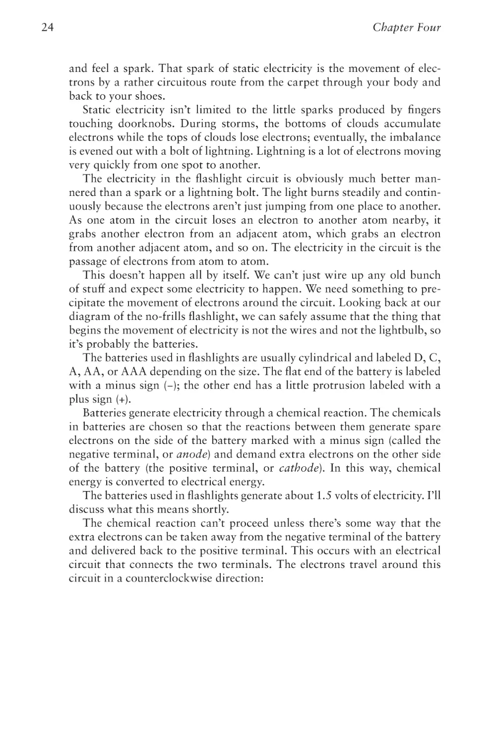
circuit in a counterclockwise direction:
Anatomy of a Flashlight
Electrons from the chemicals in the batteries might not so freely mingle
with the electrons in the copper wires if not for a simple fact: All electrons,
wherever they’re found, are identical. There’s nothing that distinguishes a
copper electron from any other electron.
Notice that both batteries are facing the same direction. The positive end
of the bottom battery takes electrons from the negative end of the top battery. It’s as if the two batteries have been combined into one larger battery
with a positive terminal at one end and a negative terminal at the other end.
The combined battery is 3 volts rather than 1.5 volts.
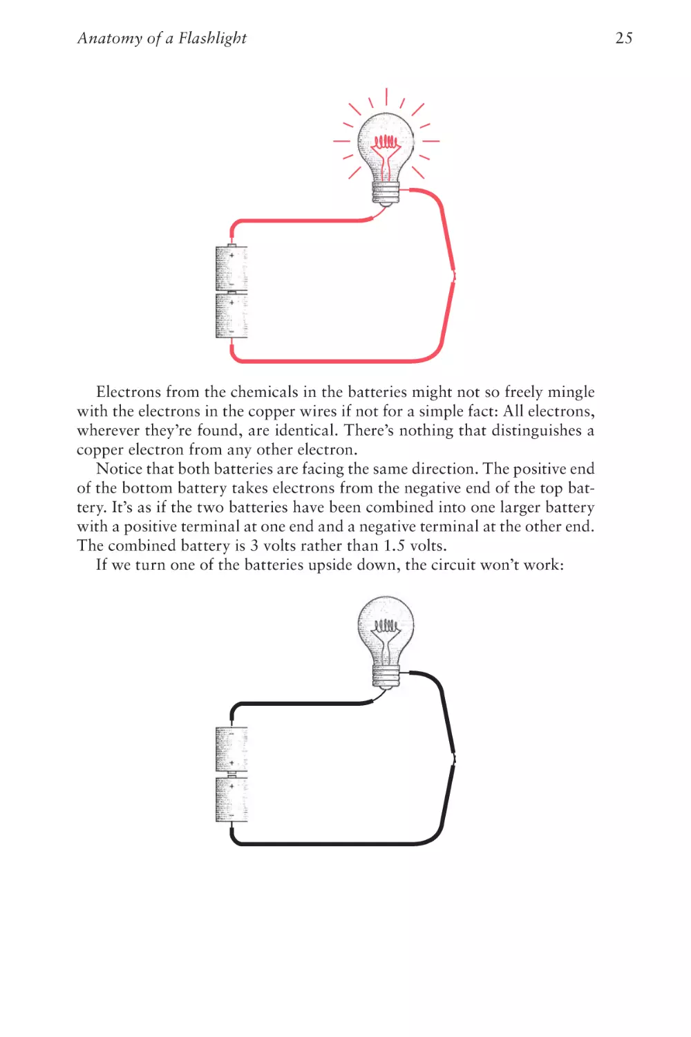
If we turn one of the batteries upside down, the circuit won’t work:
25
26
Chapter Four
The two positive ends of the battery need electrons for the chemical reactions, but there’s no way electrons can get to them because they’re attached
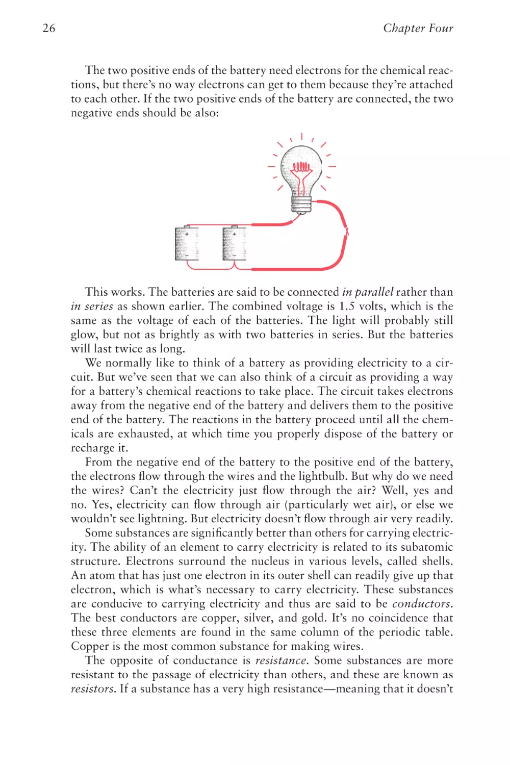
to each other. If the two positive ends of the battery are connected, the two
negative ends should be also:
This works. The batteries are said to be connected in parallel rather than
in series as shown earlier. The combined voltage is 1.5 volts, which is the
same as the voltage of each of the batteries. The light will probably still
glow, but not as brightly as with two batteries in series. But the batteries
will last twice as long.
We normally like to think of a battery as providing electricity to a circuit. But we’ve seen that we can also think of a circuit as providing a way
for a battery’s chemical reactions to take place. The circuit takes electrons
away from the negative end of the battery and delivers them to the positive
end of the battery. The reactions in the battery proceed until all the chemicals are exhausted, at which time you properly dispose of the battery or
recharge it.
From the negative end of the battery to the positive end of the battery,
the electrons flow through the wires and the lightbulb. But why do we need
the wires? Can’t the electricity just flow through the air? Well, yes and
no. Yes, electricity can flow through air (particularly wet air), or else we
wouldn’t see lightning. But electricity doesn’t flow through air very readily.
Some substances are significantly better than others for carrying electricity. The ability of an element to carry electricity is related to its subatomic
structure. Electrons surround the nucleus in various levels, called shells.
An atom that has just one electron in its outer shell can readily give up that
electron, which is what’s necessary to carry electricity. These substances
are conducive to carrying electricity and thus are said to be conductors.
The best conductors are copper, silver, and gold. It’s no coincidence that
these three elements are found in the same column of the periodic table.
Copper is the most common substance for making wires.
The opposite of conductance is resistance. Some substances are more
resistant to the passage of electricity than others, and these are known as
resistors. If a substance has a very high resistance—meaning that it doesn’t
Anatomy of a Flashlight
27
conduct electricity much at all—it’s known as an insulator. Rubber and
plastic are good insulators, which is why these substances are often used to
coat wires. Cloth and wood are also good insulators, as is dry air. Just about
anything will conduct electricity, however, if the voltage is high enough.
Copper has a very low resistance, but it still has some resistance. The
longer a wire, the higher its resistance. If you tried wiring a flashlight with
wires that were miles long, the resistance in the wires would be so high that
the flashlight wouldn’t work.
The thicker a wire, the lower its resistance. This may be somewhat counterintuitive. You might imagine that a thick wire requires much more electricity to “fill it up.” But actually the thickness of the wire makes available
many more electrons to move through the wire.
I’ve mentioned voltage but haven’t defined it. What does it mean when
a battery has 1.5 volts? Actually, voltage—named after Count Alessandro
Volta (1745–1827), who invented the first battery in 1800—is one of the
more difficult concepts of elementary electricity. Voltage refers to a potential for doing work. Voltage exists whether or not something is hooked up
to a battery.
Consider a brick. Sitting on the floor, the brick has very little potential.
Held in your hand four feet above the floor, the brick has more potential.
All you need do to realize this potential is drop the brick. Held in your hand
at the top of a tall building, the brick has much more potential. In all three
cases, you’re holding the brick and it’s not doing anything, but the potential
is different.
A much easier concept in electricity is the notion of current. Current
is related to the number of electrons actually zipping around the circuit.
Current is measured in amperes, named after André-Marie Ampère (1775–
1836), but often called just amps, as in “a 10-amp fuse.” To get one amp
of current, you need over 6 quintillion electrons flowing past a particular
point per second. That’s 6 followed by 18 zeros, or 6 billion billions.
The water-and-pipes analogy helps out here: Current is similar to the
amount of water flowing through a pipe. Voltage is similar to the water
pressure. Resistance is similar to the width of a pipe—the smaller the pipe,
the greater the resistance. So the more water pressure you have, the more
water that flows through the pipe. The smaller the pipe, the less water that
flows through it. The amount of water flowing through a pipe (the current)
is directly proportional to the water pressure (the voltage) and inversely
proportional to the skinniness of the pipe (the resistance).
In electricity, you can calculate how much current is flowing through
a circuit if you know the voltage and the resistance. Resistance—the tendency of a substance to impede the flow of electrons—is measured in
ohms, named after Georg Simon Ohm (1789–1854), who also proposed
the famous Ohm’s law. The law states
I=E/R
28
Chapter Four
where I is traditionally used to represent current in amperes, E is used to
represent voltage (it stands for electromotive force), and R is resistance.
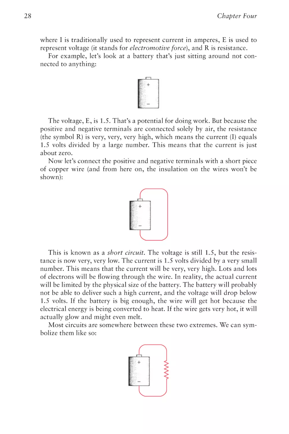
For example, let’s look at a battery that’s just sitting around not connected to anything:
The voltage, E, is 1.5. That’s a potential for doing work. But because the
positive and negative terminals are connected solely by air, the resistance
(the symbol R) is very, very, very high, which means the current (I) equals
1.5 volts divided by a large number. This means that the current is just
about zero.
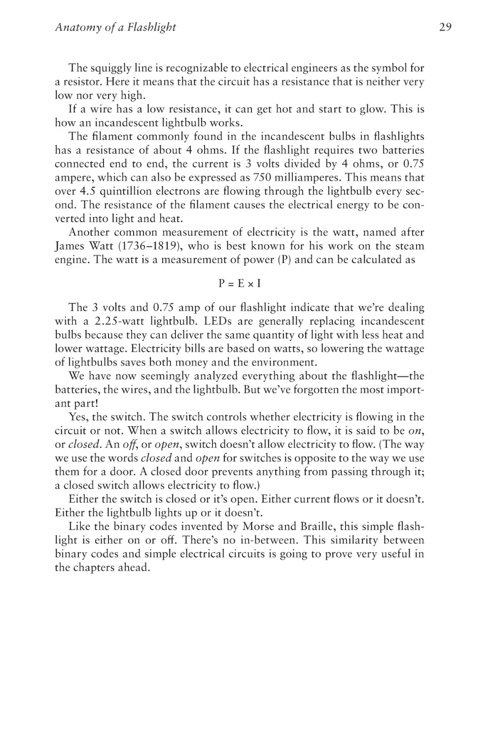
Now let’s connect the positive and negative terminals with a short piece
of copper wire (and from here on, the insulation on the wires won’t be
shown):
This is known as a short circuit. The voltage is still 1.5, but the resistance is now very, very low. The current is 1.5 volts divided by a very small
number. This means that the current will be very, very high. Lots and lots
of electrons will be flowing through the wire. In reality, the actual current
will be limited by the physical size of the battery. The battery will probably
not be able to deliver such a high current, and the voltage will drop below
1.5 volts. If the battery is big enough, the wire will get hot because the
electrical energy is being converted to heat. If the wire gets very hot, it will
actually glow and might even melt.
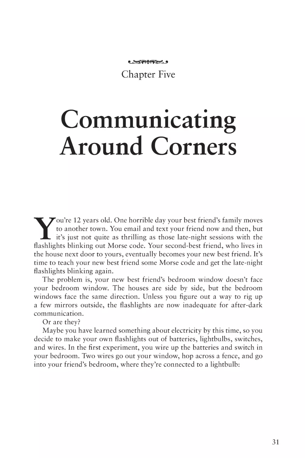
Most circuits are somewhere between these two extremes. We can symbolize them like so:
Anatomy of a Flashlight
29
The squiggly line is recognizable to electrical engineers as the symbol for
a resistor. Here it means that the circuit has a resistance that is neither very
low nor very high.
If a wire has a low resistance, it can get hot and start to glow. This is
how an incandescent lightbulb works.
The filament commonly found in the incandescent bulbs in flashlights
has a resistance of about 4 ohms. If the flashlight requires two batteries
connected end to end, the current is 3 volts divided by 4 ohms, or 0.75
ampere, which can also be expressed as 750 milliamperes. This means that
over 4.5 quintillion electrons are flowing through the lightbulb every second. The resistance of the filament causes the electrical energy to be converted into light and heat.
Another common measurement of electricity is the watt, named after
James Watt (1736–1819), who is best known for his work on the steam
engine. The watt is a measurement of power (P) and can be calculated as
P=E×I
The 3 volts and 0.75 amp of our flashlight indicate that we’re dealing
with a 2.25-watt lightbulb. LEDs are generally replacing incandescent
bulbs because they can deliver the same quantity of light with less heat and
lower wattage. Electricity bills are based on watts, so lowering the wattage
of lightbulbs saves both money and the environment.
We have now seemingly analyzed everything about the flashlight—the
batteries, the wires, and the lightbulb. But we’ve forgotten the most important part!
Yes, the switch. The switch controls whether electricity is flowing in the
circuit or not. When a switch allows electricity to flow, it is said to be on,
or closed. An off, or open, switch doesn’t allow electricity to flow. (The way
we use the words closed and open for switches is opposite to the way we use
them for a door. A closed door prevents anything from passing through it;
a closed switch allows electricity to flow.)
Either the switch is closed or it’s open. Either current flows or it doesn’t.
Either the lightbulb lights up or it doesn’t.
Like the binary codes invented by Morse and Braille, this simple flashlight is either on or off. There’s no in-between. This similarity between
binary codes and simple electrical circuits is going to prove very useful in
the chapters ahead.
This page intentionally left blank
Chapter Five
Communicating
Around Corners
Y
ou’re 12 years old. One horrible day your best friend’s family moves
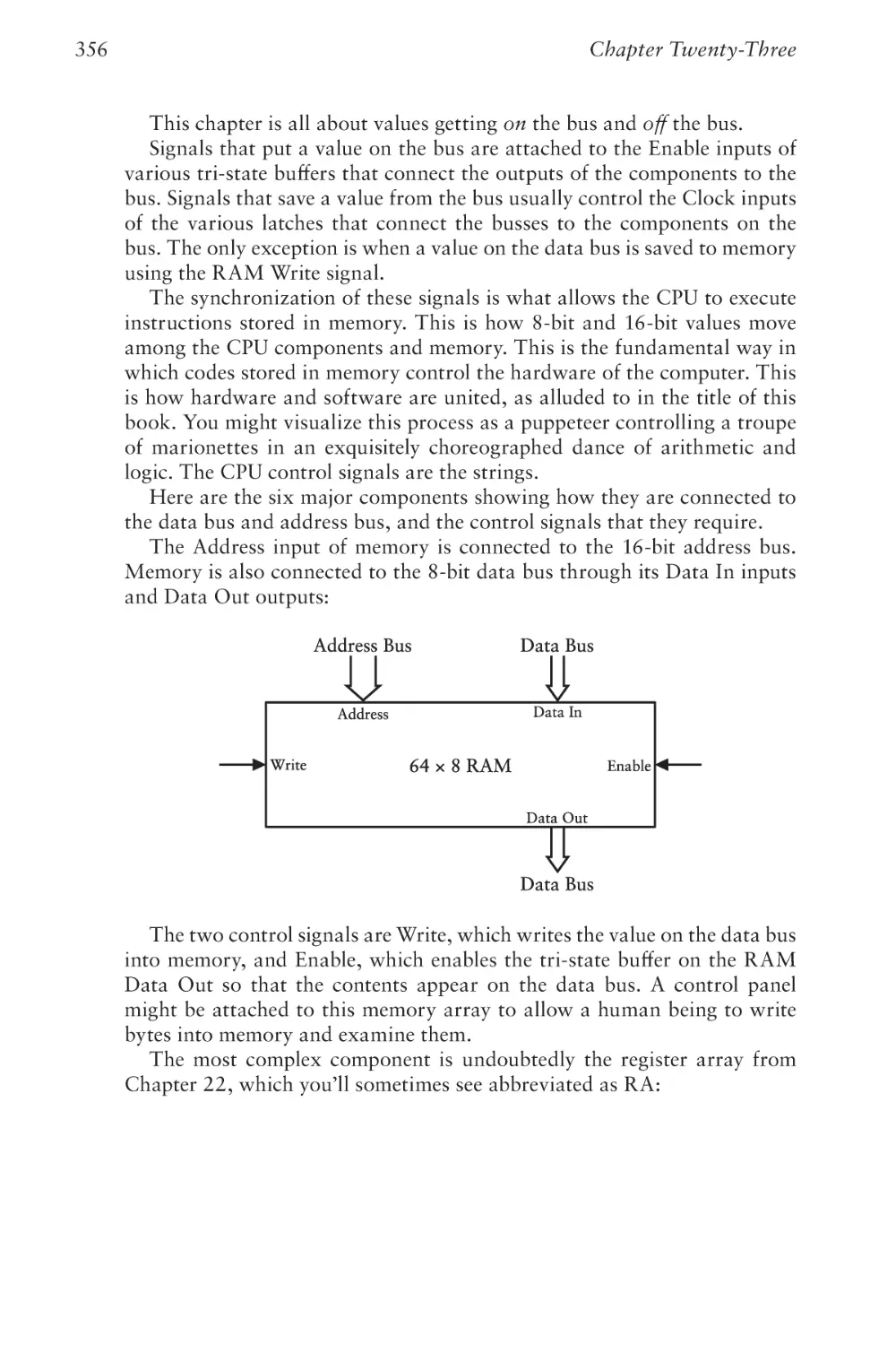
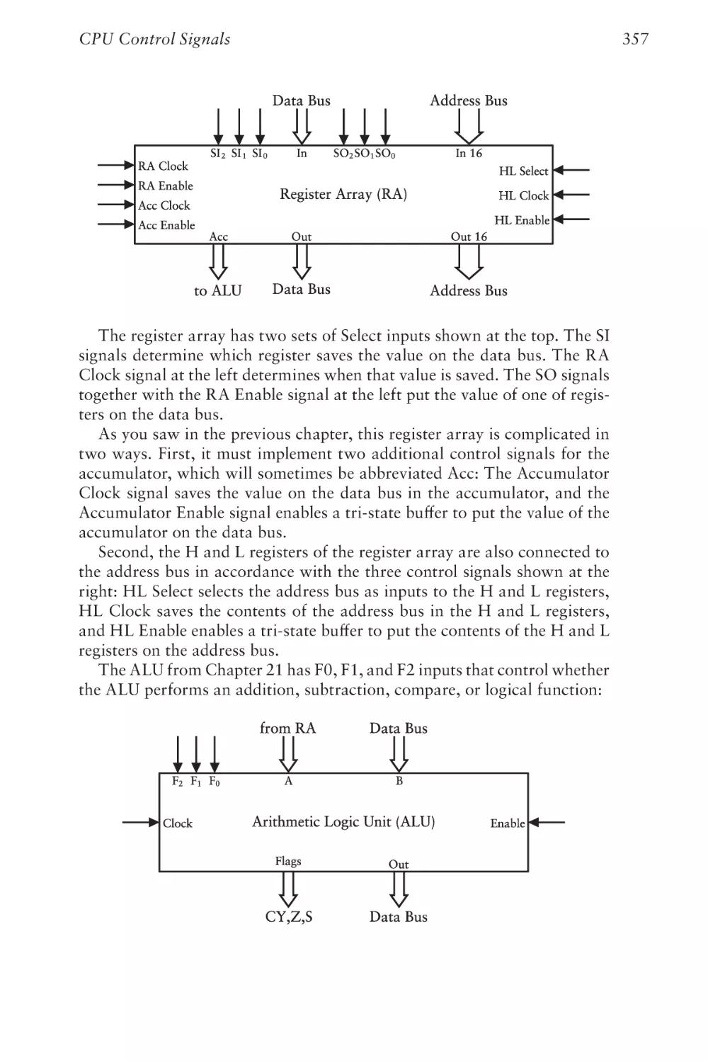
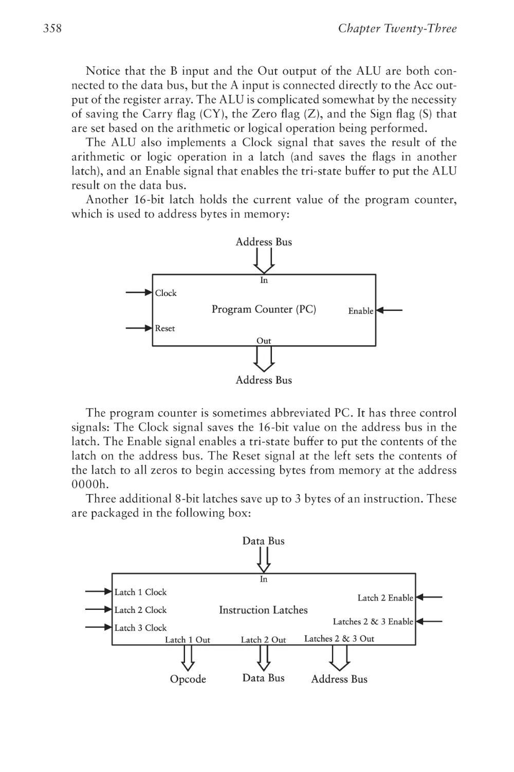
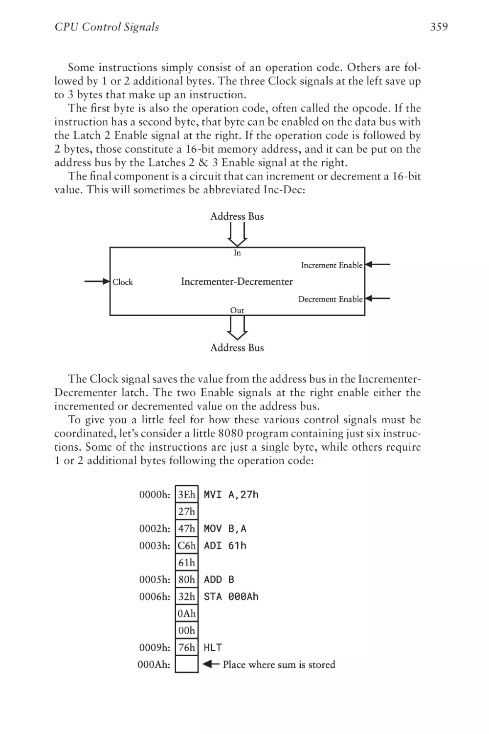
to another town. You email and text your friend now and then, but
it’s just not quite as thrilling as those late-night sessions with the
flashlights blinking out Morse code. Your second-best friend, who lives in
the house next door to yours, eventually becomes your new best friend. It’s
time to teach your new best friend some Morse code and get the late-night
flashlights blinking again.
The problem is, your new best friend’s bedroom window doesn’t face
your bedroom window. The houses are side by side, but the bedroom
windows face the same direction. Unless you figure out a way to rig up
a few mirrors outside, the flashlights are now inadequate for after-dark
communication.
Or are they?
Maybe you have learned something about electricity by this time, so you
decide to make your own flashlights out of batteries, lightbulbs, switches,
and wires. In the first experiment, you wire up the batteries and switch in
your bedroom. Two wires go out your window, hop across a fence, and go
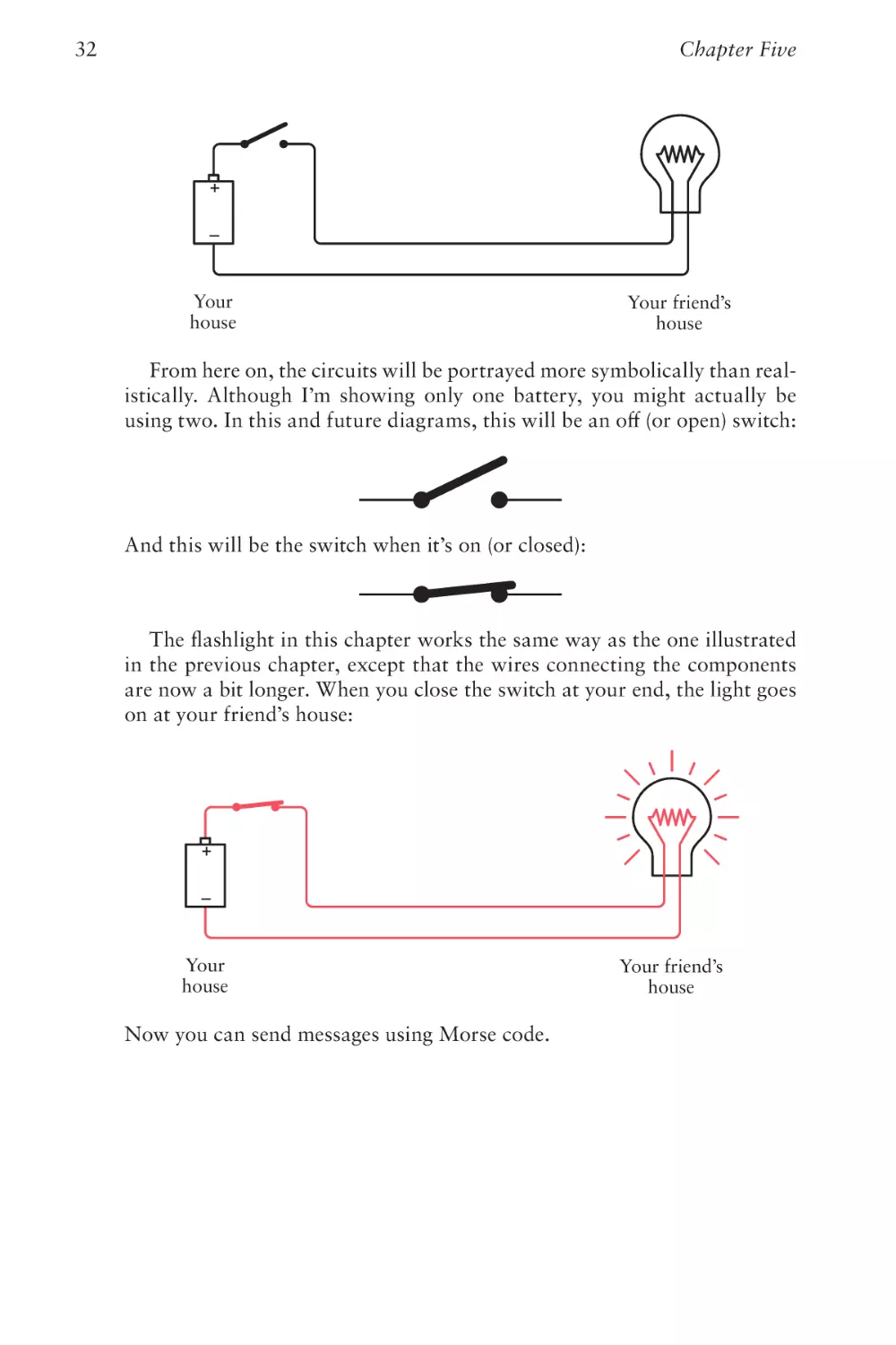
into your friend’s bedroom, where they’re connected to a lightbulb:
31
Chapter Five
32
Your
house
Your friend’s
house
From here on, the circuits will be portrayed more symbolically than realistically. Although I’m showing only one battery, you might actually be
using two. In this and future diagrams, this will be an off (or open) switch:
And this will be the switch when it’s on (or closed):
The flashlight in this chapter works the same way as the one illustrated
in the previous chapter, except that the wires connecting the components
are now a bit longer. When you close the switch at your end, the light goes
on at your friend’s house:
Your
house
Now you can send messages using Morse code.
Your friend’s
house
Communicating Around Corners
33
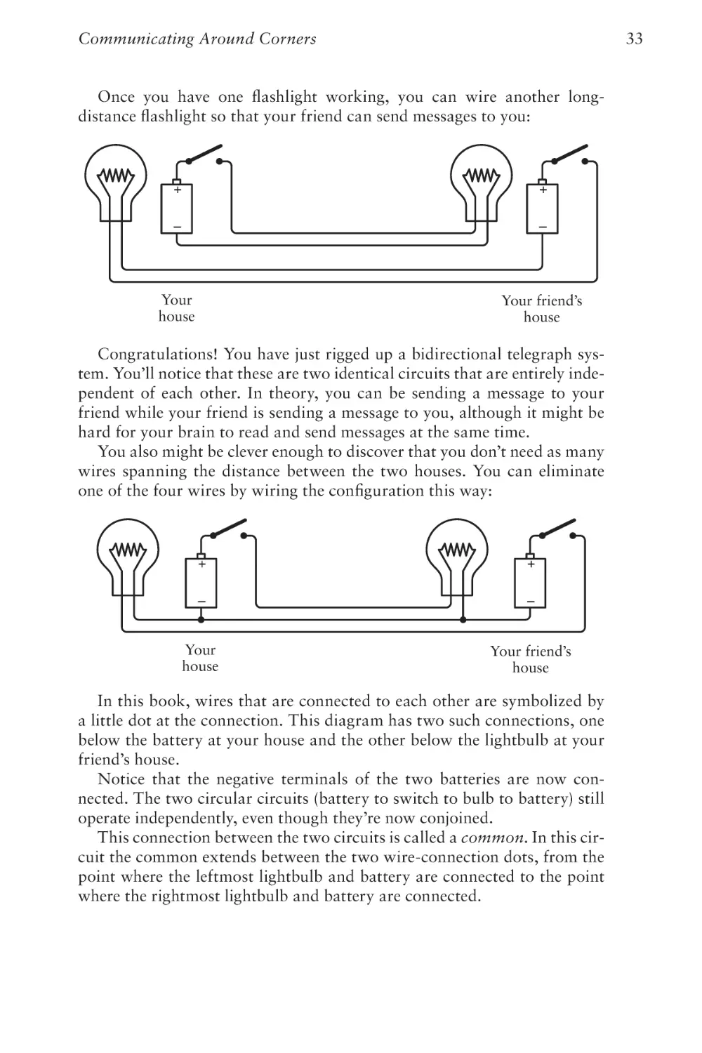
Once you have one flashlight working, you can wire another longdistance flashlight so that your friend can send messages to you:
Your
house
Your friend’s
house
Congratulations! You have just rigged up a bidirectional telegraph system. You’ll notice that these are two identical circuits that are entirely independent of each other. In theory, you can be sending a message to your
friend while your friend is sending a message to you, although it might be
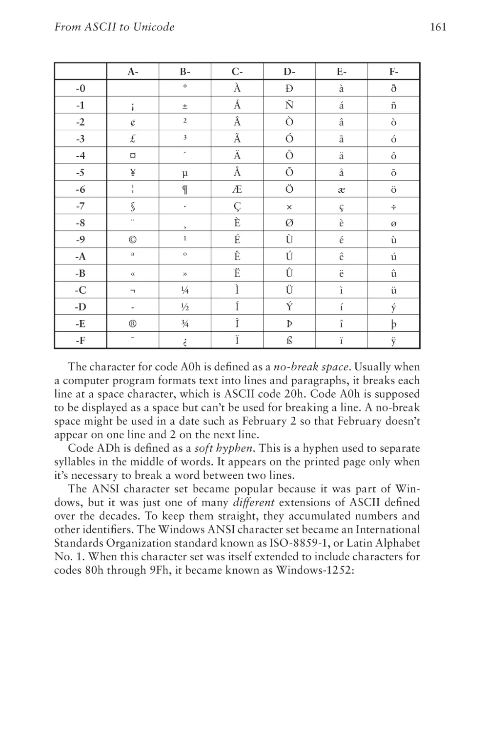
hard for your brain to read and send messages at the same time.
You also might be clever enough to discover that you don’t need as many
wires spanning the distance between the two houses. You can eliminate
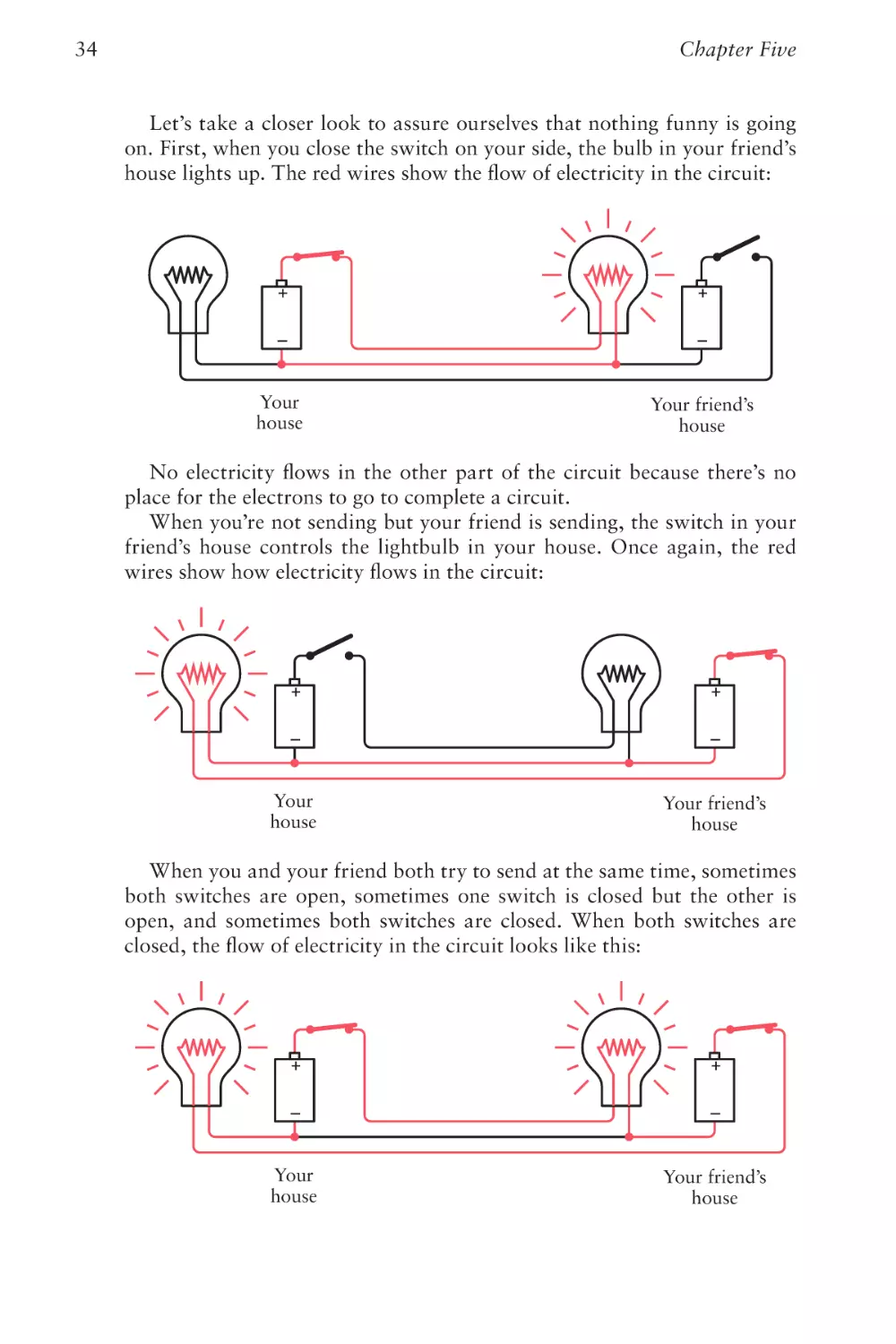
one of the four wires by wiring the configuration this way:
Your
house
Your friend’s
house
In this book, wires that are connected to each other are symbolized by
a little dot at the connection. This diagram has two such connections, one
below the battery at your house and the other below the lightbulb at your
friend’s house.
Notice that the negative terminals of the two batteries are now connected. The two circular circuits (battery to switch to bulb to battery) still
operate independently, even though they’re now conjoined.
This connection between the two circuits is called a common. In this circuit the common extends between the two wire-connection dots, from the
point where the leftmost lightbulb and battery are connected to the point
where the rightmost lightbulb and battery are connected.
Chapter Five
34
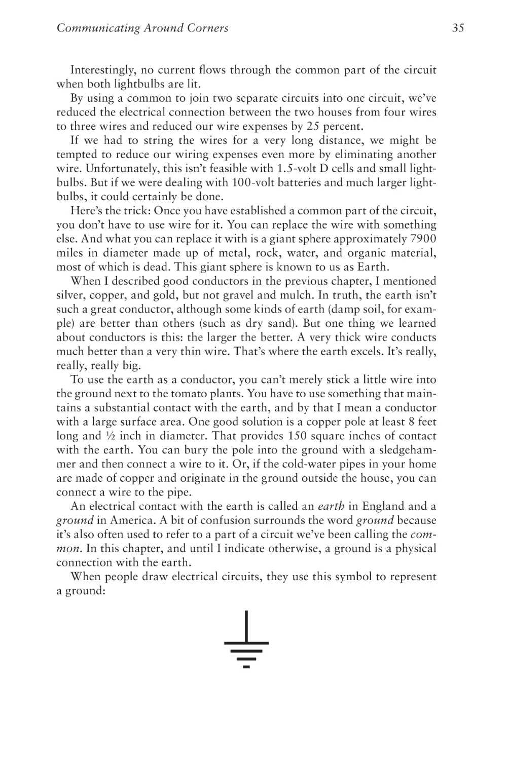
Let’s take a closer look to assure ourselves that nothing funny is going
on. First, when you close the switch on your side, the bulb in your friend’s
house lights up. The red wires show the flow of electricity in the circuit:
Your
house
Your friend’s
house
No electricity flows in the other part of the circuit because there’s no
place for the electrons to go to complete a circuit.
When you’re not sending but your friend is sending, the switch in your
friend’s house controls the lightbulb in your house. Once again, the red
wires show how electricity flows in the circuit:
Your
house
Your friend’s
house
When you and your friend both try to send at the same time, sometimes
both switches are open, sometimes one switch is closed but the other is
open, and sometimes both switches are closed. When both switches are
closed, the flow of electricity in the circuit looks like this:
Your
house
Your friend’s
house
Communicating Around Corners
Interestingly, no current flows through the common part of the circuit
when both lightbulbs are lit.
By using a common to join two separate circuits into one circuit, we’ve
reduced the electrical connection between the two houses from four wires
to three wires and reduced our wire expenses by 25 percent.
If we had to string the wires for a very long distance, we might be
tempted to reduce our wiring expenses even more by eliminating another
wire. Unfortunately, this isn’t feasible with 1.5-volt D cells and small lightbulbs. But if we were dealing with 100-volt batteries and much larger lightbulbs, it could certainly be done.
Here’s the trick: Once you have established a common part of the circuit,
you don’t have to use wire for it. You can replace the wire with something
else. And what you can replace it with is a giant sphere approximately 7900
miles in diameter made up of metal, rock, water, and organic material,
most of which is dead. This giant sphere is known to us as Earth.
When I described good conductors in the previous chapter, I mentioned
silver, copper, and gold, but not gravel and mulch. In truth, the earth isn’t
such a great conductor, although some kinds of earth (damp soil, for example) are better than others (such as dry sand). But one thing we learned
about conductors is this: the larger the better. A very thick wire conducts
much better than a very thin wire. That’s where the earth excels. It’s really,
really, really big.
To use the earth as a conductor, you can’t merely stick a little wire into
the ground next to the tomato plants. You have to use something that maintains a substantial contact with the earth, and by that I mean a conductor
with a large surface area. One good solution is a copper pole at least 8 feet
long and ½ inch in diameter. That provides 150 square inches of contact
with the earth. You can bury the pole into the ground with a sledgehammer and then connect a wire to it. Or, if the cold-water pipes in your home
are made of copper and originate in the ground outside the house, you can
connect a wire to the pipe.
An electrical contact with the earth is called an earth in England and a
ground in America. A bit of confusion surrounds the word ground because
it’s also often used to refer to a part of a circuit we’ve been calling the common. In this chapter, and until I indicate otherwise, a ground is a physical
connection with the earth.
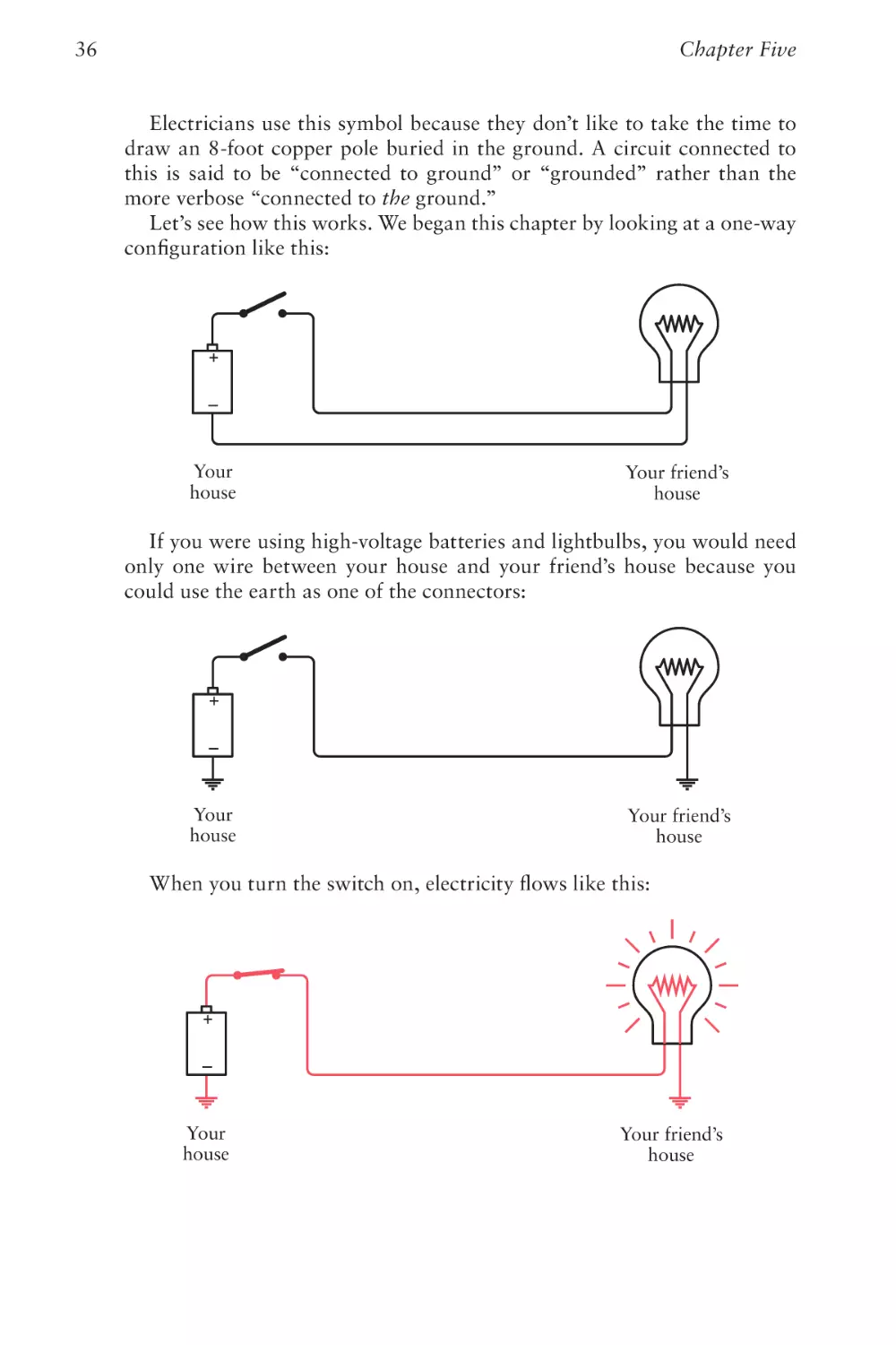
When people draw electrical circuits, they use this symbol to represent
a ground:
35
Chapter Five
36
Electricians use this symbol because they don’t like to take the time to
draw an 8-foot copper pole buried in the ground. A circuit connected to
this is said to be “connected to ground” or “grounded” rather than the
more verbose “connected to the ground.”
Let’s see how this works. We began this chapter by looking at a one-way
configuration like this:
Your
house
Your friend’s
house
If you were using high-voltage batteries and lightbulbs, you would need
only one wire between your house and your friend’s house because you
could use the earth as one of the connectors:
Your
house
Your friend’s
house
When you turn the switch on, electricity flows like this:
Your
house
Your friend’s
house
Communicating Around Corners
37
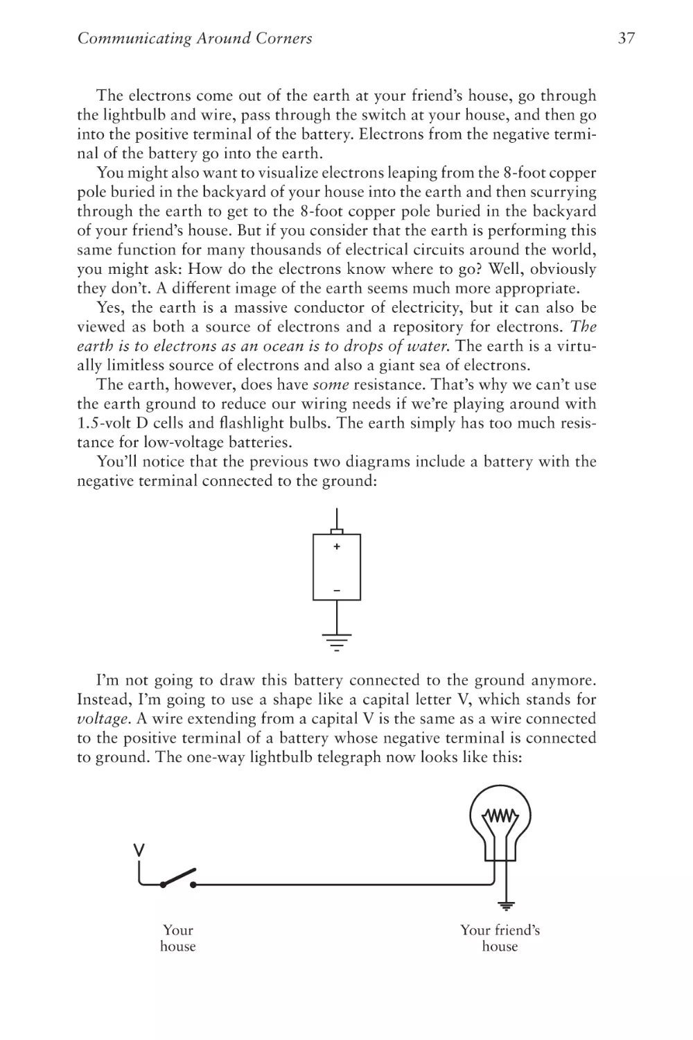
The electrons come out of the earth at your friend’s house, go through
the lightbulb and wire, pass through the switch at your house, and then go
into the positive terminal of the battery. Electrons from the negative terminal of the battery go into the earth.
You might also want to visualize electrons leaping from the 8-foot copper
pole buried in the backyard of your house into the earth and then scurrying
through the earth to get to the 8-foot copper pole buried in the backyard
of your friend’s house. But if you consider that the earth is performing this
same function for many thousands of electrical circuits around the world,
you might ask: How do the electrons know where to go? Well, obviously
they don’t. A different image of the earth seems much more appropriate.
Yes, the earth is a massive conductor of electricity, but it can also be
viewed as both a source of electrons and a repository for electrons. The
earth is to electrons as an ocean is to drops of water. The earth is a virtually limitless source of electrons and also a giant sea of electrons.
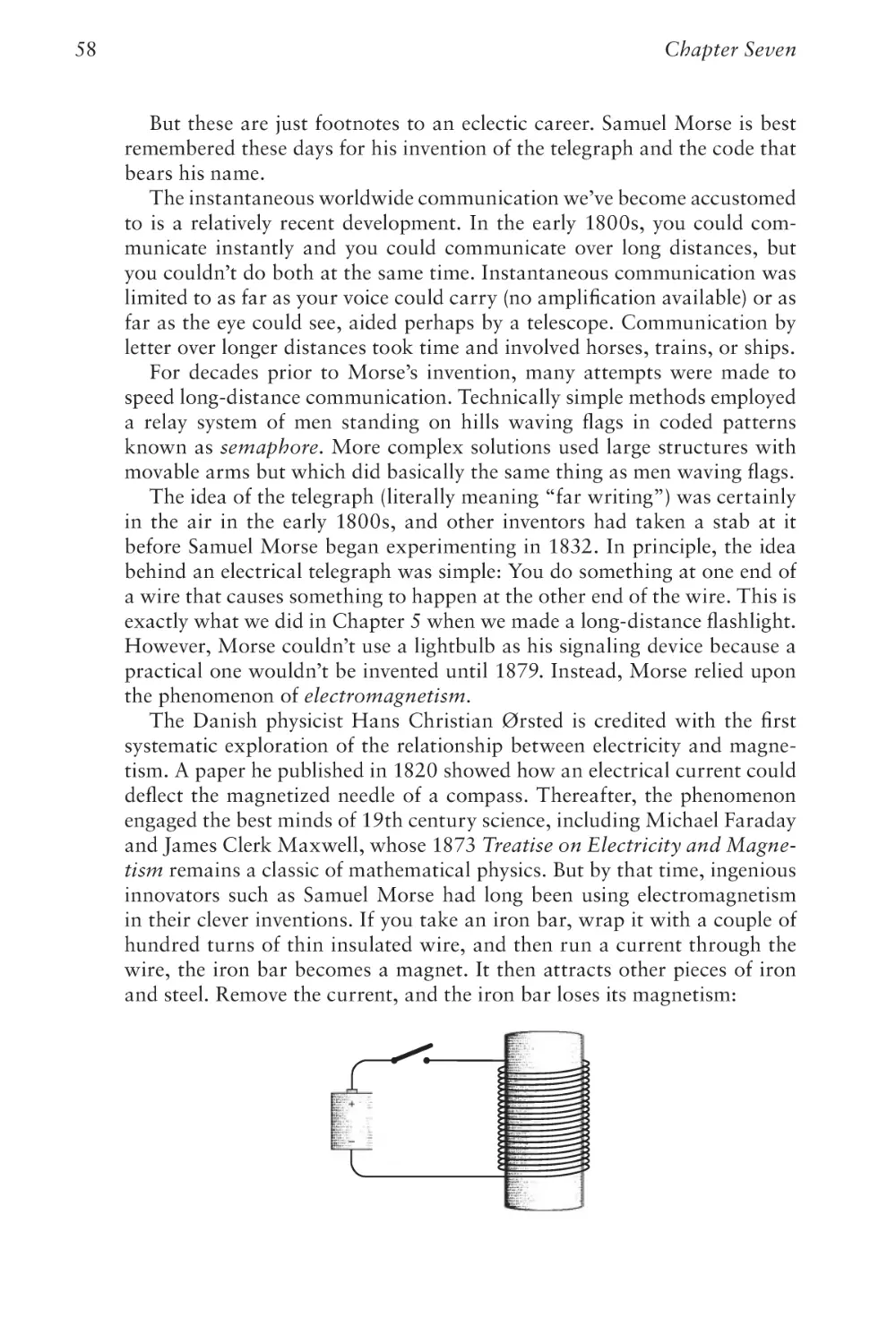
The earth, however, does have some resistance. That’s why we can’t use
the earth ground to reduce our wiring needs if we’re playing around with
1.5-volt D cells and flashlight bulbs. The earth simply has too much resistance for low-voltage batteries.
You’ll notice that the previous two diagrams include a battery with the
negative terminal connected to the ground:
I’m not going to draw this battery connected to the ground anymore.
Instead, I’m going to use a shape like a capital letter V, which stands for
voltage. A wire extending from a capital V is the same as a wire connected
to the positive terminal of a battery whose negative terminal is connected
to ground. The one-way lightbulb telegraph now looks like this:
Your
house
Your friend’s
house
Chapter Five
38
The V stands for voltage, but in a sense, it could also stand for vacuum.
You can think of the V as an electron vacuum cleaner and think of the
ground as an ocean of electrons. The electron vacuum pulls the electrons
from the earth through the circuit, doing work along the way (such as
lighting a lightbulb).
The ground is sometimes also known as the point of zero potential. This
means that no voltage is present. A voltage—as I explained earlier—is a
potential for doing work, much as a brick suspended in the air is a potential source of energy. Zero potential is like a brick sitting on the ground—
there’s no place left for it to fall.
In Chapter 4, one of the first things we noticed was that circuits are
circles. Our new circuit doesn’t look like a circle at all. It still is one, however. You could replace the V with a battery with the negative terminal
connected to ground, and then you could draw a wire connecting all the
places you see a ground symbol. You’d end up with the same diagram that
we started with in this chapter.
So with the help of a couple of copper poles (or cold-water pipes), we can
construct a two-way Morse code system with just two wires crossing the
fence between your house and your friend’s:
Your
house
Your friend’s
house
This circuit is functionally the same as the configuration shown on pages
33 to 34, in which three wires crossed the fence between the houses, but it
would only work with high-voltage batteries and lightbulbs.
In this chapter, we’ve taken an important step in the evolution of communications. Previously we had been able to communicate with Morse
code but only in a straight line of sight and only as far as the beam from a
flashlight would travel.
By using wires, not only have we constructed a system to communicate
around corners beyond the line of sight, but we’ve freed ourselves of the
limitation of distance. We can communicate over hundreds and thousands
of miles just by stringing longer and longer wires.
Well, not exactly. Although copper is a very good conductor of electricity, it’s not perfect. The longer the wires, the more resistance they have. The
more resistance, the less current that flows. The less current, the dimmer
the lightbulbs.
Communicating Around Corners
So how long exactly can we make the wires? That depends. Let’s suppose you’re using the original four-wire, bidirectional hookup without
grounds and commons, and you’re using flashlight batteries and lightbulbs.
To keep your costs down, you may have initially purchased a roll of 100
feet of speaker wire, commonly used to connect speakers to high-end audio
amplifiers. Speaker wire consists of a pair of two insulated wires conveniently stuck together, so it’s a good choice for our telegraph system. If your
bedroom and your friend’s bedroom are less than 50 feet apart, this one
roll of wire is all you need.
The thickness of wire is measured in American Wire Gauge, or AWG.
The smaller the AWG number, the thicker the wire and also the less resistance it has. If you purchased 20-gauge speaker wire, the wire itself would
have a diameter of about 0.032 inches and a resistance of about 10 ohms
per 1000 feet, or 1 ohm for the 100-foot round-trip distance between the
bedrooms.
That’s not bad at all, but what if we strung the wire out for a mile? The
total resistance of the wire would be more than 100 ohms. Recall from the
last chapter that our lightbulb was only 4 ohms. From Ohm’s law, we can
easily calculate that the current through the circuit will no longer be 0.75
amp (3 volts divided by 4 ohms), but will now be less than 0.03 amp (3 volts
divided by more than 100 ohms). Almost certainly, that won’t be enough
current to light the bulb.
Using thicker wire is a good solution, but that can be expensive. Tengauge wire is about 0.1 inch thick and has a resistance of only 1 ohm per
1000 feet, or 5 ohms per mile.
Another solution is to increase the voltage and use lightbulbs with a
much higher resistance, such as the lightbulbs you use to light your home.
The resistance of the wires will then affect the overall circuitry much less.
These are problems faced in the mid-19th century by the people who
strung up the first telegraph systems across America and Europe. Regardless of the thickness of the wires and the high levels of voltage, telegraph
wires simply couldn’t be continued indefinitely. At most, the limit for a
working system according to this scheme was a couple of hundred miles.
That’s nowhere close to spanning the thousands of miles between New
York and California.
The solution to this problem—not for flashlights but for the clicking and
clacking telegraphs of yesteryear—turns out to be a simple and humble
device, but one from which entire computers can be built.
39
This page intentionally left blank
Chapter Six
Logic with Switches
W
hat is truth? Aristotle thought that logic had something to do
with it. The collection of his teachings known as the Organon
(which dates from the fourth century BCE) is the earliest extensive writing on the subject of logic. To the ancient Greeks, logic was a
means of analyzing language in the search for truth and thus was considered a form of philosophy. The basis of Aristotle’s logic was the syllogism.
The most famous syllogism (which isn’t actually found in the works of
Aristotle) is
All men are mortal;
Socrates is a man;
Hence, Socrates is mortal.
In a syllogism, two premises are assumed to be correct, and from these a
conclusion is deduced.
The mortality of Socrates might seem straightforward enough, but there
are many varieties of syllogisms. For example, consider the following two
premises, proposed by the 19th-century mathematician Charles Dodgson
(also known as Lewis Carroll):
All philosophers are logical;
An illogical man is always obstinate.
The conclusion—Some obstinate persons are not philosophers—isn’t
obvious at all. Notice the unexpected and disturbing appearance of the
word some.
For over two thousand years, mathematicians wrestled with Aristotle’s
logic, attempting to corral it using mathematical symbols and operators.
41
Prior to the 19th century, the only person to come close was Gottfried
Wilhelm von Leibniz (1648–1716), who dabbled with logic early in life but
then went on to other interests (such as independently inventing calculus at
the same time as Isaac Newton).
And then came George Boole.
George Boole was born in England in 1815 into
a world where the odds were certainly stacked
against him. Because he was the son of a shoemaker and a former maid, Britain’s rigid class
structure would normally have prevented Boole
from achieving anything much different from his
ancestors. But aided by an inquisitive mind and
his helpful father (who had strong interests in science, mathematics, and literature), young George
gave himself the type of education that was normally the privilege of upper-class boys; his studies included Latin, Greek, and mathematics. As a
result of his early papers on mathematics, in 1849
Boole was appointed the first Professor of Mathematics at Queen’s College,
Cork, in Ireland.
Several mathematicians in the mid-1800s had been working on a mathematical definition of logic (most notably Augustus De Morgan), but it was
Boole who had the real conceptual breakthrough, first in the short book
The Mathematical Analysis of Logic, Being an Essay Towards a Calculus
of Deductive Reasoning (1847) and then in a much longer and more ambitious text, An Investigation of the Laws of Thought on Which Are Founded
the Mathematical Theories of Logic and Probabilities (1854), more conveniently referred to as The Laws of Thought. Boole died in 1864, at the age
of 49, after hurrying to class in the rain and contracting pneumonia.
The title of Boole’s 1854 book suggests an ambitious motivation: Boole
believed that the human brain uses logic to think, so if we were to find a
way to represent logic with mathematics, we would also have a mathematical description of how the brain works. But Boole’s mathematics can be
studied without necessarily buying in to his neuropsychology.
Boole invented a whole different kind of algebra that was eventually
called Boolean algebra to distinguish it from conventional algebra.
In conventional algebra, letters are often used to stand for numbers.
These are called operands, and they are combined in various ways with
operators, most often + and ×. For example:
A = 3 × (B + 5)
When we do conventional algebra, we follow certain rules. These rules
have probably become so ingrained in our practice that we no longer think
of them as rules and might even forget their names. But rules indeed underlie all the workings of any form of mathematics.
Science & Society Picture Library/Getty Images
Chapter Six
42
Logic with Switches
43
The first rule is that addition and multiplication are commutative. That
means we can switch around the symbols on each side of the operators:
A+B=B+A
A×B=B×A
By contrast, subtraction and division are not commutative.
Addition and multiplication are also associative, that is
A + (B + C) = (A + B) + C
A × (B × C) = (A × B) × C
And finally, multiplication is said to be distributive over addition:
A × (B + C) = (A × B) + (A × C)
Another characteristic of conventional algebra is that it always deals
with numbers, such as pounds of tofu or numbers of ducks or distances that
a train travels or the seconds of a day.
It was Boole’s genius to make algebra more abstract by divorcing it from
concepts of number. In Boolean algebra, the operands refer not to numbers
but instead to classes. A class is simply a group of things, similar to what in
later times came to be known as a set.
Let’s talk about cats. Cats can be either male or female. For convenience,
we can use the letter M to refer to the class of male cats and F to refer to
the class of female cats. Keep in mind that these two symbols do not represent numbers of cats. The number of male and female cats can change by
the minute as new cats are born and old cats (regrettably) pass away. The
letters stand for classes of cats—cats with specific characteristics. Instead
of referring to male cats, we can just say “M.”
We can also use other letters to represent the color of the cats. For example, T can refer to the class of tan cats, B can be the class of black cats, W
the class of white cats, and O the class of cats of all “other” colors—all cats
not in the class T, B, or W.
Finally (at least as far as this example goes), cats can be either neutered
or unneutered. Let’s use the letter N to refer to the class of neutered cats
and U for the class of unneutered cats.
In conventional (numeric) algebra, the operators + and × are used to
indicate addition and multiplication. In Boolean algebra, the same + and ×
symbols are used, and here’s where things might get confusing. Everybody
knows how to add and multiply numbers in conventional algebra, but how
do we add and multiply classes?
Well, we don’t actually add and multiply in Boolean algebra. Instead, the
+ and × symbols mean something else entirely.
The + symbol in Boolean algebra means a union of two classes. A union
of two classes is everything in the first class combined with everything in
the second class. For example, B + W represents the class of all cats that are
either black or white.
Chapter Six
44
The × symbol in Boolean algebra means an intersection of two classes.
An intersection of two classes is everything that is in both the first class
and the second class. For example, F × T represents the class of all cats that
are both female and tan. As in conventional algebra, we can write F × T as
F·T or simply FT (which is what Boole preferred). You can think of the two
letters as two adjectives strung together: “female tan” cats.
To avoid confusion between conventional algebra and Boolean algebra,
sometimes the symbols ∪ and ∩ are used for union and intersection instead
of + and ×. But part of Boole’s liberating influence on mathematics was to
make the use of familiar operators more abstract, so I’ve decided to stick
with his decision not to introduce new symbols into his algebra.
The commutative, associative, and distributive rules all hold for Boolean
algebra. What’s more, in Boolean algebra the + operator is distributive over
the × operator. This isn’t true of conventional algebra:
W + (B × F) = (W + B) × (W + F)
The union of white cats and black female cats is the same as the intersection of two unions: the union of white cats and black cats, and the union of
white cats and female cats. This is somewhat difficult to grasp, but it works.
Three more symbols are necessary to complete Boolean algebra. Two
of these symbols might look like numbers, but they’re really not because
they’re treated a little differently than numbers. The symbol 1 in Boolean
algebra means “the universe”—that is, everything we’re talking about. In
this example, the symbol 1 means “the class of all cats.” Thus,
M+F=1
This means that the union of male cats and female cats is the class of all
cats. Similarly, the union of tan cats and black cats and white cats and other
colored cats is also the class of all cats:
T+B+W+O=1
And you achieve the class of all cats this way, too:
N+U=1
The 1 symbol can be used with a minus sign to indicate the universe
excluding something. For example,
1–M
is the class of all cats except the male cats. The universe excluding all male
cats is the same as the class of female cats:
1–M=F
Logic with Switches
45
The third symbol that we need is the 0 (zero), and in Boolean algebra the
0 means an empty class—a class of nothing. The empty class results when
we take an intersection of two mutually exclusive classes—for example,
cats that are both male and female:
F×M=0
Notice that the 1 and 0 symbols sometimes work the same way in Boolean algebra as in conventional algebra. For example, the intersection of all
cats and female cats is the class of female cats:
1×F=F
The intersection of no cats and female cats is the class of no cats:
0×F=0
The union of no cats and all female cats is the class of female cats:
0+F=F
But sometimes the result doesn’t look the same as in conventional
algebra. For example, the union of all cats and female cats is the class of
all cats:
1+F=1
This doesn’t make much sense in conventional algebra.
Because F is the class of all female cats, and (1 − F) is the class of all cats
that aren’t female, the union of these two classes is 1:
F + (1 − F) = 1
And the intersection of the two classes is 0:
F × (1 − F) = 0
Historically, this formulation represents an important concept in logic:
It’s called the law of contradiction, and it indicates that something can’t be
both itself and the opposite of itself.
Where Boolean algebra really looks different from conventional algebra
is in a statement like this:
F×F=F
The statement makes perfect sense in Boolean algebra: The intersection
of female cats and female cats is still the class of female cats. But it sure
wouldn’t look quite right if F referred to a number. Boole considered
X2 = X
Chapter Six
46
to be the single statement that differentiates his algebra from conventional
algebra. Another Boolean statement that looks funny in terms of conventional algebra is this:
F+F=F
The union of female cats and female cats is still the class of female cats.
Boolean algebra provides a mathematical method for solving the syllogisms of Aristotle. Let’s look at the first two-thirds of that famous syllogism
again, but now using gender-neutral language:
All persons are mortal;
Socrates is a person.
We’ll use P to represent the class of all persons, M to represent the class
of mortal things, and S to represent the class of Socrates. What does it
mean to say that “all persons are mortal”? It means that the intersection
of the class of all persons and the class of all mortal things is the class of
all persons:
P×M=P
It would be wrong to say that P × M = M, because the class of all mortal
things includes cats, dogs, and elm trees.
Saying, “Socrates is a person” means that the intersection of the class
containing Socrates (a very small class) and the class of all persons (a much
larger class) is the class containing Socrates:
S×P=S
Because we know from the first equation that P equals (P × M), we can
substitute that into the second equation:
S × (P × M) = S
By the associative law, this is the same as
(S × P) × M = S
But we already know that (S × P) equals S, so we can simplify by using
this substitution:
S×M=S
And now we’re finished. This formula tells us that the intersection of
Socrates and the class of all mortal things is S, which means that Socrates
is mortal. If we found instead that (S × M) equaled 0, we’d conclude that
Socrates wasn’t mortal. If we found that (S × M) equaled M, the conclusion
would have to be that all mortals were Socrates!
Logic with Switches
47
Using Boolean algebra might seem like overkill for proving this obvious fact (particularly considering that Socrates demonstrated his mortality 2400 years ago), but Boolean algebra can also be used to determine
whether something satisfies a certain set of criteria.
Perhaps one day you walk into a pet shop and say to the salesperson, “I
want a male cat, neutered, either white or tan; or a female cat, neutered,
any color but white; or I’ll take any cat you have as long as it’s black.” And
the salesperson says to you, “So you want a cat from the class of cats represented by the following expression:
(M × N × (W + T)) + (F × N × (1 − W)) + B
Right?” And you say, “Yes! Exactly!”
In verifying that the salesperson is correct, you might want to represent
the concepts of union and intersection using the words OR and AND. I’m
capitalizing these words because the words normally represent concepts in
English, but they can also represent operations in Boolean algebra. When
you form a union of two classes, you’re actually accepting things from the
first class OR the second class. And when you form an intersection, you’re
accepting only those things in both the first class AND the second class. In
addition, you can use the word NOT wherever you see a 1 followed by a
minus sign. In summary,
• + (a union) can also mean OR.
• × (an intersection) can also mean AND.
• 1 − (the universe without something) means NOT.
So the expression can also be written like this:
(M AND N AND (W OR T)) OR (F AND N AND (NOT W)) OR B
This is very nearly what you said. Notice how the parentheses clarify
your intentions. You want a cat from one of three classes:
(M AND N AND (W OR T))
OR
(F AND N AND (NOT W))
OR
B
With this formula written down, the salesperson can perform something
called a Boolean test. This involves another variation of Boolean algebra,
where the letters refer to properties or characteristics or attributes of cats,
and they can be assigned the numbers 0 or 1. The numeral 1 means Yes,
True, this particular cat satisfies these criteria, while the numeral 0 means
No, False, this cat doesn’t satisfy these criteria.
Chapter Six
48
First the salesperson brings out an unneutered tan male. Here’s the
expression of acceptable cats:
(M × N × (W + T)) + (F × N × (1 − W)) + B
And here’s how it looks with 0s and 1s substituted:
(1 × 0 × (0 + 1)) + (0 × 0 × (1 − 0)) + 0
Notice that the only symbols assigned 1s are M and T because the cat is
male and tan.
What we must do now is simplify this expression. If it simplifies to 1,
the cat satisfies your criteria; if it simplifies to 0, the cat doesn’t. While
we’re simplifying the expression, keep in mind that we’re not really adding
and multiplying, although generally we can pretend that we are. Most of
the same rules apply when + means OR and × means AND. (Sometimes in
modern texts the symbols ∧ and ∨ are used for AND and OR instead of ×
and +. But here’s where the + and × signs perhaps ease the job, because the
rules are similar to conventional algebra.)
When the × sign means AND, the possible results are
0×0=0
0×1=0
1×0=0
1×1=1
In other words, the result is 1 only if both the left operand AND the right
operand are 1. This operation works exactly the same way as regular multiplication, and it can be summarized in a little table. The operation is shown
in the upper-left corner, and the possible combinations of operators are
shown in the top row and the left column:
AND
0
1
0
0
0
1
0
1
When the + sign means OR, the possible results are
0+0=0
0+1=1
1+0=1
1+1=1
The result is 1 if either the left operand OR the right operand is 1. This
operation produces results very similar to those of regular addition, except
Logic with Switches
49
that in this case 1 + 1 equals 1. (If a cat is tan or if a cat is tan means that
it’s tan.) The OR operation can be summarized in another little table:
OR
0
1
0
0
1
1
1
1
We’re ready to use these tables to calculate the result of the expression
(1 × 0 × 1) + (0 × 0 × 1) + 0 = 0 + 0 + 0 = 0
The result 0 means No, False, this kitty won’t do.
Next the salesperson brings out a neutered white female. The original
expression was
(M × N × (W + T)) + (F × N × (1 − W)) + B
Substitute the 0s and 1s again:
(0 × 1 × (1 + 0)) + (1 × 1 × (1 − 1)) + 0
And simplify it:
(0 × 1 × 1) + (1 × 1 × 0) + 0 = 0 + 0 + 0 = 0
And another poor kitten must be rejected.
Next the salesperson brings out a neutered gray female. (Gray qualifies
as an “other” color—not white or black or tan.) Here’s the expression:
(0 × 1 × (0 + 0)) + (1 × 1 × (1 − 0)) + 0
Now simplify it:
(0 × 1 × 0) + (1 × 1 × 1) + 0 = 0 + 1 + 0 = 1
The final result 1 means Yes, True, a kitten has found a home. (And it was
the cutest one too!)
Later that evening, when the kitten is curled up sleeping in your lap, you
wonder whether you could have wired some switches and a lightbulb to
help you determine whether particular kittens satisfied your criteria. (Yes,
you are a strange kid.) Little do you realize that you’re about to make a crucial conceptual breakthrough. You’re about to perform some experiments
that will unite the algebra of George Boole with electrical circuitry and
thus make possible the design and construction of digital computers. But
don’t let that intimidate you.
50
Chapter Six
To begin your experiment, you connect a lightbulb and battery as you
would normally, but you use two switches instead of one:
The world icon in the outer margin indicates that an interactive version
of the circuit is available on the website CodeHiddenLanguage.com.
Switches connected in this way—one right after the other—are said to
be wired in series. If you close the left switch, nothing happens:
Similarly, if you leave the left switch open and close the right switch,
nothing happens. The lightbulb lights up only if both the left switch and the
right switch are closed, as shown here:
Logic with Switches
51
The key word here is and. Both the left switch and the right switch must
be closed for the current to flow through the circuit.
This circuit is performing a little exercise in logic. In effect, the lightbulb
is answering the question “Are both switches closed?” We can summarize
the workings of this circuit in the following table:
Left Switch
Open
Open
Closed
Closed
Right Switch
Open
Closed
Open
Closed
Lightbulb
Not lit
Not lit
Not lit
Lit
If you think of the switches and the lightbulb as Boolean operators, then
these states can be assigned numbers of 0 and 1. A 0 can mean “switch is
open” and a 1 can mean “switch is closed.” A lightbulb has two states; a
0 can mean “lightbulb is not lit” and a 1 can mean “lightbulb is lit.” Now
let’s simply rewrite the table:
Left Switch
0
0
1
1
Right Switch
0
1
0
1
Lightbulb
0
0
0
1
Notice that if we swap the left switch and the right switch, the results
are the same. We really don’t have to identify which switch is which. So
the table can be rewritten to resemble the AND and OR tables that were
shown earlier:
Switches
in Series
0
1
0
0
0
1
0
1
And indeed, this is the same as the AND table. Check it out:
AND
0
1
0
0
0
1
0
1
This simple circuit is actually performing an AND operation in Boolean
algebra.
Chapter Six
52
Now try connecting the two switches a little differently:
These switches are said to be connected in parallel. The difference
between this and the preceding connection is that this lightbulb will light
if you close the top switch:
or close the bottom switch:
Logic with Switches
53
or close both switches:
The lightbulb lights if the top switch or the bottom switch is closed. The
key word here is or.
Again, the circuit is performing an exercise in logic. The lightbulb
answers the question “Is either switch closed?” The following table summarizes how this circuit works:
Left Switch
Open
Open
Closed
Closed
Right Switch
Open
Closed
Open
Closed
Lightbulb
Not lit
Lit
Lit
Lit
Again, using 0 to mean an open switch or an unlit lightbulb and 1 to
mean a closed switch or a lit lightbulb, this table can be rewritten this way:
Left Switch
0
0
1
1
Right Switch
0
1
0
1
Lightbulb
0
1
1
1
Again, it doesn’t matter if the two switches are swapped, so the table can
also be rewritten like this:
Switches
in Parallel
0
1
0
0
1
1
1
1
Chapter Six
54
And you’ve already guessed that this is the same as the Boolean OR:
OR
0
1
0
0
1
1
1
1
This means that two switches in parallel are performing the equivalent of
a Boolean OR operation.
When you originally entered the pet shop, you told the salesperson,
“I want a male cat, neutered, either white or tan; or a female cat, neutered,
any color but white; or I’ll take any cat you have as long as it’s black,” and
the salesperson developed this expression:
(M × N × (W + T)) + (F × N × (1 − W)) + B
Now that you know that two switches wired in series perform a logical
AND (which is represented by a × sign) and two switches in parallel perform a logical OR (which is represented by the + sign), you can wire up
eight switches like so:
Each switch in this circuit is labeled with a letter—the same letters as
in the Boolean expression. W means NOT W and is an alternative way to
write 1 − W. Indeed, if you go through the wiring diagram from left to right
starting at the top and moving from top to bottom, you’ll encounter the
letters in the same order in which they appear in the expression. Each × sign
in the expression corresponds to a point in the circuit where two switches
(or groups of switches) are connected in series. Each + sign in the expression corresponds to a place in the circuit where two switches (or groups of
switches) are connected in parallel.
Logic with Switches
As you’ll recall, the salesperson first brought out an unneutered tan
male. Close the appropriate switches:
Although the M, T, and NOT W switches are closed, we don’t have a
complete circuit to light up the lightbulb. Next the salesperson brought out
a neutered white female:
Again, the right switches aren’t closed to complete a circuit. But finally,
the salesperson brought out a neutered gray female:
55
56
Chapter Six
And that’s enough to complete the circuit, light up the lightbulb, and
indicate that the kitten satisfies all your criteria.
George Boole never wired such a circuit. He never had the thrill of seeing a Boolean expression realized in switches, wires, and lightbulbs. One
obstacle, of course, was that the incandescent lightbulb wasn’t invented
until 15 years after Boole’s death. But the telegraph had been invented
ten years before the publication of Boole’s The Laws of Thought, and an
important part of the telegraph system was a simple device that could perform operations of logic with much more agility than mere switches could.
Chapter Seven
Telegraphs
and Relays
ullstein bild Dtl/Getty Images
S
amuel Finley Breese Morse was born in 1791 in Charlestown, Massachusetts, the town where the Battle of Bunker Hill was fought and
which is now the northeast part of Boston. In the year of Morse’s
birth, the United States Constitution had been in effect just two years and
George Washington was serving his first term as president. Catherine the
Great ruled Russia. In France, the Revolution was still in progress, and
Louis XVI and Marie Antoinette would be marched to the guillotine two
years later. In 1791, Mozart completed The Magic Flute, his last opera, and
died later that year at the age of 35, but the 20-year-old Beethoven was
already being noticed.
Morse was educated at Yale and studied art in London. He became a
successful portrait artist. His painting General Lafayette (1825) hangs in
New York’s City Hall. Much more personal is his final painting: a portrait
of his daughter Susan entitled The Muse, on display
at the Metropolitan Museum of Art.
Morse was also an early photography buff. He
learned how to make daguerreotype photographs
from Louis Daguerre himself and created some
of the first daguerreotypes in America. In 1840,
he taught the process to the 17-year-old Mathew
Brady, who with his colleagues would be responsible for creating the most memorable photographs
of the Civil War, Abraham Lincoln, and Samuel
Morse himself.
57
58
Chapter Seven
But these are just footnotes to an eclectic career. Samuel Morse is best
remembered these days for his invention of the telegraph and the code that
bears his name.
The instantaneous worldwide communication we’ve become accustomed
to is a relatively recent development. In the early 1800s, you could communicate instantly and you could communicate over long distances, but
you couldn’t do both at the same time. Instantaneous communication was
limited to as far as your voice could carry (no amplification available) or as
far as the eye could see, aided perhaps by a telescope. Communication by
letter over longer distances took time and involved horses, trains, or ships.
For decades prior to Morse’s invention, many attempts were made to
speed long-distance communication. Technically simple methods employed
a relay system of men standing on hills waving flags in coded patterns
known as semaphore. More complex solutions used large structures with
movable arms but which did basically the same thing as men waving flags.
The idea of the telegraph (literally meaning “far writing”) was certainly
in the air in the early 1800s, and other inventors had taken a stab at it
before Samuel Morse began experimenting in 1832. In principle, the idea
behind an electrical telegraph was simple: You do something at one end of
a wire that causes something to happen at the other end of the wire. This is
exactly what we did in Chapter 5 when we made a long-distance flashlight.
However, Morse couldn’t use a lightbulb as his signaling device because a
practical one wouldn’t be invented until 1879. Instead, Morse relied upon
the phenomenon of electromagnetism.
The Danish physicist Hans Christian Ørsted is credited with the first
systematic exploration of the relationship between electricity and magnetism. A paper he published in 1820 showed how an electrical current could
deflect the magnetized needle of a compass. Thereafter, the phenomenon
engaged the best minds of 19th century science, including Michael Faraday
and James Clerk Maxwell, whose 1873 Treatise on Electricity and Magnetism remains a classic of mathematical physics. But by that time, ingenious
innovators such as Samuel Morse had long been using electromagnetism
in their clever inventions. If you take an iron bar, wrap it with a couple of
hundred turns of thin insulated wire, and then run a current through the
wire, the iron bar becomes a magnet. It then attracts other pieces of iron
and steel. Remove the current, and the iron bar loses its magnetism:
Telegraphs and Relays
This might look like a short circuit, but the wire wrapped around the
iron bar is usually very thin, and there’s enough of it to constitute sufficient
electrical resistance.
The electromagnet is the foundation of the telegraph. Turning the switch
on and off at one end causes the electromagnet to do something at the
other end.
Morse’s first telegraphs were actually more complex than the ones that
later evolved. Morse felt that a telegraph system should actually write something on paper, or as computer users would later phrase it, “produce a hard
copy.” This wouldn’t necessarily be words, of course, because that would
be too complex. But something should be written on paper, whether it be
squiggles or dots and dashes. Notice that Morse was stuck in a paradigm
that required paper and reading, much like Valentin Haüy’s notion that
books for blind people should use raised letters of the alphabet.
Although Samuel Morse notified the patent office in 1836 that he had
invented a successful telegraph, it wasn’t until 1843 that he was able to persuade Congress to fund a public demonstration of the device. The historic
day was May 24, 1844, when a telegraph line rigged between Washington,
D.C., and Baltimore, Maryland, successfully carried a biblical message
from Numbers 23:23: “What hath God wrought!”—not a question but
meaning “Look what God has done!”
The traditional telegraph “key” used for sending messages looks like this:
Despite the fancy appearance, this is just a switch designed for maximum speed. The most comfortable way to use the key for long periods of
time is to hold the handle between thumb, forefinger, and middle finger and
tap it up and down. A short tap produces a Morse code dot, and a longer
tap a Morse code dash.
At the other end of the wire was a receiver that was basically an electromagnet pulling a metal lever. Originally, the electromagnet controlled a
pen. As the pen bounced up and down, it drew dots and dashes on paper
from a roll that was slowly pulled by a wound-up spring. A person who
could read Morse code would then transcribe the dots and dashes into
letters and words.
Of course, we humans are a lazy species as well as an ingenious one, and
telegraph operators soon discovered that they could transcribe the code
simply by listening to the pen bounce up and down. The pen mechanism
was eventually eliminated in favor of the traditional telegraph “sounder,”
which looked something like this:
59
60
Chapter Seven
That bar at the top was normally held in the horizontal position by a
weight or spring inside the vertical part at the left, but it could also pivot.
When the telegraph key was pressed, the electromagnet pulled the pivotable
bar down and it made a “click” noise. When the key was released, the bar
sprang back to its normal position, making a “clack” noise. A fast “clickclack” was a dot; a slower “click…clack” was a dash.
The key, the sounder, a battery, and some wires can be connected just
like the lightbulb telegraph in the preceding chapter:
As we discovered, you don’t need two wires connecting the two telegraph stations. One wire will suffice if the voltage is high enough and the
earth provides the other half of the circuit.
As we did in Chapter 5, we can replace the battery connected to the
ground with a capital V. So the complete one-way setup looks something
like this:
Two-way communication simply requires another key and sounder. This
is similar to what we did earlier.
The invention of the telegraph truly marks the beginning of modern
communication. For the first time, people were able to communicate farther than the eye could see or the ear could hear and faster than a horse
Telegraphs and Relays
could gallop. That this invention used a binary code is all the more intriguing. In later forms of electrical and wireless communication, including the
telephone, radio, and television, binary codes were abandoned, only to later
make an appearance in computers, followed by many other binary codes in
virtually all kinds of electronic media.
Morse’s telegraph triumphed over other designs in part because it was
tolerant of bad line conditions. If you strung a wire between a key and a
sounder, it usually worked. Other telegraph systems were not quite as forgiving. But as I discussed in Chapter 5, the longer a length of wire becomes,
the more resistance it has to the flow of electricity. This was a major impediment to long-distance telegraphy. Although some telegraph lines used up
to 300 volts and could work over a 300-mile length, wires couldn’t be
extended indefinitely.
One obvious solution is to have a relay system. Every couple of hundred
miles or so, a person equipped with a sounder and a key could receive a
message and resend it.
Now imagine that you have been hired by the telegraph company to
be part of this relay system. They have put you in a little hut with a table
and a chair somewhere between New York and California. A wire coming
through the east window is connected to a sounder. Your telegraph key is
connected to a battery and wire going out the west window. Your job is to
receive messages originating in New York and to resend them, eventually
to reach California. An identical configuration relays messages from California to New York.
At first, you prefer to receive an entire message before resending it. You
write down the letters that correspond to the clicks of the sounder, and
when the message is finished, you start sending it using your key. Eventually you get the knack of sending the message as you’re hearing it without
having to write the whole thing down. This saves time.
One day while resending a message, you look at the bar on the sounder
bouncing up and down, and you look at your fingers bouncing the key up
and down. You look at the sounder again, and at the key again, realize that
the sounder is bouncing up and down the same way the key is bouncing up
and down. So you go outside and pick up a little piece of wood and you use
the wood and some string to physically connect the sounder and the key:
61
62
Chapter Seven
Now it works by itself, and you can take the rest of the afternoon off
and go fishing.
It’s an interesting fantasy, but in reality Samuel Morse had understood
the concept of this device early on. The device we’ve invented is called a
repeater, or a relay. A relay is like a sounder in that an incoming current is
used to power an electromagnet that pulls down a metal lever. The lever,
however, is used as part of a switch connecting a battery to an outgoing
wire. In this way, a weak incoming current is “amplified” to make a stronger outgoing current.
Drawn rather schematically, the relay looks like this:
When an incoming current triggers the electromagnet, it pulls down a
pivoting or flexible metal bar that acts like a switch to turn on an outgoing
current:
The words In and Out are descriptive of the way that the telegraph line
comes through one window of your hut and leaves through the opposite
window, but they can also serve as convenient abbreviations for input and
output. These are electrical signals. The signal labeled In causes a change
in the signal labeled Out. It’s a cause and effect.
Telegraphs and Relays
The relay is a remarkable device. It’s a switch, surely, but a switch that’s
turned on and off not by human hands but by an electrical current. You
could do amazing things with such devices. You could actually assemble
much of a computer with them.
Yes, this relay thing is much too sweet an invention to leave sitting
around the telegraphy museum. Let’s grab one and stash it inside our jacket
and walk quickly past the guards. An idea is brewing in our minds.
63
This page intentionally left blank
Chapter Eight
Relays and Gates
R
educed to its essentials, a computer is a synthesis of Boolean algebra
and electricity. The crucial components that embody this melding of
math and hardware are known as logic gates. These gates are not
unlike the familiar gates through which water or people pass. Logic gates
perform simple operations in Boolean logic by blocking or letting through
the flow of electrical current.
You’ll recall that in Chapter 6 you entered a pet shop and boldly
announced, “I want a male cat, neutered, either white or tan; or a female
cat, neutered, any color but white; or I’ll take any cat you have as long as it’s
black.” These criteria are summarized by the following Boolean expression:
(M × N × (W + T)) + (F × N × (1 − W)) + B
This expression can be interactively realized in a circuit made up of
switches, a battery, and a lightbulb:
65
Chapter Eight
66
Such a circuit is sometimes called a network, except that nowadays that
word is used much more often to refer to connected computers rather than
to an assemblage of mere switches.
The circuit contains a combination of switches, some wired in series and
some wired in parallel. Switches wired in series perform logical AND operations, symbolized in the Boolean expression with a × sign. Switches wired
in parallel perform a logical OR operation corresponding to the + sign.
Because this circuit is equivalent to a Boolean expression, if the Boolean
expression can be simplified, the circuit can be as well.
Here’s the expression that indicates the characteristics you want in a cat:
(M × N × (W + T)) + (F × N × (1 − W)) + B
Let’s try to simplify it. Using the commutative law, you can reorder the
variables that are combined with the AND (×) signs and rewrite the expression this way:
(N × M × (W + T)) + (N × F × (1 − W)) + B
In an attempt to clarify what I’m going to do here, I’ll define two new
symbols named X and Y:
X = M × (W + T)
Y = F × (1 − W)
Now the expression for the cat that you want can be written like this:
(N × X) + (N × Y) + B
After we’re finished, we can put the X and Y expressions back in.
Notice that the N variable appears twice in the expression. Using the
distributive law, the expression can be rewritten like this, with only one N:
(N × (X + Y)) + B
Now let’s put the X and Y expressions back in:
(N × ((M × (W + T)) + (F × (1 − W)))) + B
Due to the plethora of parentheses, this expression hardly looks simplified.
But it has one less variable, which means one switch can be eliminated.
Here’s the revised version:
Relays and Gates
67
Indeed, it’s probably easier to see that this network is equivalent to the earlier one than to verify that the expressions are the same!
But there are still too many switches in this network. There are separate
switches for Male and Female, and only one should be required, perhaps
on (or closed) for Female and off (or open) for Male. Similarly, there are
separate switches for White and Not White.
Let’s make a control panel right now for choosing a cat. The control
panel is simply five switches (much like the on/off switches you have on
your walls for controlling your lights) and a lightbulb mounted in a panel:
Dream Kitty
F
M
N
B
W
T
U
Control Panel
The switches are on (closed) when they’re up, and off (open) when
they’re down. The first switch lets you select Female or Male; the second
is Neutered or Unneutered. There are three switches for selecting color:
Black, White, and Tan. Only one of these should be on at any time, or none
of them to select an Other-colored cat.
In computer terminology, the panel of switches constitutes an input
device. Input is information that controls how a circuit behaves, in this
case describing the characteristics of an ideal kitty. The output device is the
lightbulb. This bulb lights up if the switches describe a satisfactory cat. The
switches shown in the control panel are set for a female unneutered black
cat. This satisfies your criteria, so the lightbulb is lit.
Now all we have to do is design a circuit that makes this control panel work.
68
Chapter Eight
In the previous chapter, you saw how devices called relays were crucial
to the workings of the telegraph system. Over long distances, the wires
connecting telegraph stations had a very high resistance. Some method
was needed to receive a weak signal and resend an identical strong signal.
The relay did this by using an electromagnet to control a switch, in effect,
amplifying a weak signal to create a strong signal.
At this moment, we’re not interested in using the relay to amplify a weak
signal. We’re interested only in the idea of a relay being a switch that can be
controlled by electricity rather than by fingers. Although relays were originally designed for telegraphs, they eventually became part of the switching
circuits used in the vast network of the telephone system, and this is how
their versatility became more apparent to imaginative electrical engineers.
Like switches, relays can be connected in series and in parallel as logic
gates to perform simple tasks in logic. When I say that these logic gates
perform simple tasks in logic, I mean as simple as possible. Relays have an
advantage over switches in that relays can be switched on and off by other
relays rather than by fingers. This means that logic gates can be combined
to perform more complex tasks, such as simple functions in arithmetic and,
eventually, the workings of entire computers.
The discovery that relays could be used for performing Boolean operations is generally credited to computer pioneer Claude Elwood Shannon
(1916–2001), whose famous 1938 M.I.T. master’s thesis was entitled “A
Symbolic Analysis of Relay and Switching Circuits,” but a similar equivalence had been described a couple of years earlier by Japanese electrical
engineer Akira Nakashima.
You can wire a relay with a switch, a lightbulb, and a couple of batteries
like this:
The switch at the left is open, and the lightbulb is off. When you close
the switch, the battery at the left causes current to flow through the many
turns of wire around the iron bar. The iron bar becomes magnetic and pulls
Relays and Gates
69
down a flexible or pivoting metal contact that connects the circuit to turn
on the lightbulb:
+
–
+
–
When the electromagnet pulls the metal contact, the relay is said to be
triggered. When the switch is turned off, the iron bar stops being magnetic,
and the metal contact returns to its normal position.
This seems like a rather indirect route to light the bulb, and indeed it is.
If we were interested only in lighting the bulb, we could dispense with the
relay entirely. But we’re not interested in lighting bulbs. We have a much
more ambitious goal.
I’ll be using relays a lot in this chapter (and then hardly at all after the
logic gates have been built), so I want to simplify the diagram. We can
eliminate some of the wires by using a ground and a capital V (for voltage)
to represent the battery, as was done in Chapters 5 and 7. In this case, the
grounds simply represent a common connection; they don’t need to be connected to the physical earth. Now the relay looks like this:
When the switch is closed, a current flows between V and ground
through the coils of the electromagnet. This causes the electromagnet to
70
Chapter Eight
pull the flexible metal contact. That connects the circuit between V, the
lightbulb, and ground. The bulb lights up:
These diagrams of the relay show two voltage sources and two grounds,
but in all the diagrams in this chapter, all the V’s can be connected to one
another, and all the grounds can be connected to one another.
More abstractly, the relay can be shown without the switch and lightbulb but labeled with inputs and outputs:
If a current is flowing through the input (for example, if a switch connects the input to V), the electromagnet is triggered, and the output has
a voltage.
Relays and Gates
The input of a relay need not be a switch, and the output of a relay need
not be a lightbulb. The output of one relay can be connected to the input of
another relay, for example, like this:
These relays are said to be cascaded. When you turn the switch on, the
first relay is triggered, which then provides a voltage to the second relay.
The second relay is triggered, and the light goes on:
Connecting relays is the key to building logic gates.
71
72
Chapter Eight
Just as two switches can be connected in series, two relays can be connected in series:
Now there are two switches on two relays. The output of the top relay
supplies a voltage to the second relay. As you can see, when both switches
are open, the lightbulb isn’t lit. We can try closing the top switch:
Relays and Gates
Still the lightbulb doesn’t light, because the bottom switch is still open
and that relay isn’t triggered. We can try opening the top switch and closing
the bottom switch:
The lightbulb is still not lit. The current can’t reach the lightbulb because
the first relay isn’t triggered. The only way to get the bulb to light up is to
close both switches:
73
74
Chapter Eight
Now both relays are triggered, and current can flow between V, the
lightbulb, and ground.
Like the two switches wired in series that you saw in Chapter 6, these
two relays are performing a little exercise in logic. The bulb lights up only
if both relays are triggered. These two relays wired in series are known as
an AND gate because it is performing a Boolean AND operation.
To avoid excessive drawing, electrical engineers have a special symbol
for an AND gate. That symbol looks like this:
This is the first of six basic logic gates. The AND gate has two inputs
and one output. You’ll often see the AND gate drawn with the inputs at the
left and the output at the right. That’s because people who are accustomed
to reading from left to right prefer reading electrical diagrams from left to
right. But the AND gate can just as well be drawn with the inputs at the
top, the right, or the bottom.
The previous diagram with two relays connected in series is symbolized
more succinctly like this:
Notice that this symbol for the AND gate not only takes the place of two
relays wired in series, but it also implies that the top relay is connected to a
voltage and that both relays are connected to ground. Again, the lightbulb
lights up only if both the top switch and the bottom switch are closed.
That’s why it’s called an AND gate.
If we think of the absence of a voltage as a 0, and the presence of a
voltage as a 1, the output of the AND gate is dependent on inputs like this:
Relays and Gates
75
As with the two switches wired in series, the AND gate can also be
described in this little table:
AND
0
1
0
0
0
1
0
1
The inputs of the AND gate don’t necessarily have to be connected to
switches, and the output doesn’t necessarily have to be connected to a lightbulb. The output of one AND gate can be an input to a second AND gate,
like this:
This bulb will light up only if all three switches are closed. Only if the
top two switches are closed will the output of the first AND gate output
a voltage, and only if the third switch is also closed will the second AND
gate output a voltage.
This configuration can also be expressed by this symbol:
It’s called a 3-input AND gate. The output is 1 only if all the inputs are 1.
You can also create AND gates with many more inputs.
76
Chapter Eight
The next logic gate requires two relays that are wired in parallel, like this:
Notice that the outputs of the two relays are connected to each other.
This connected output then provides power for the lightbulb. Either one of
the two relays is enough to light the bulb. For example, if we close the top
switch, the bulb lights up. The bulb is getting power from the top relay:
Relays and Gates
Similarly, if we leave the top switch open but close the bottom switch,
the bulb lights up:
The bulb also lights if both switches are closed:
77
Chapter Eight
78
We’ve made a circuit in which the bulb lights up if the top switch or the
bottom switch is closed. The key word here is or, so this is called the OR
gate. Electrical engineers use a symbol for the OR gate that looks like this:
It’s somewhat similar to the symbol for the AND gate except that the
input side is rounded, much like the O in OR. (That might help you to
remember which is which.)
The output of the OR gate supplies a voltage if either of the two inputs
has a voltage. Again, if we say that the absence of a voltage is 0 and the
presence of a voltage is 1, the OR gate has four possible states:
The output of the OR gate can be summarized the same way as the AND
gate:
OR
0
1
0
0
1
1
1
1
OR gates can also have more than two inputs. The output of such a gate
is 1 if any of the inputs are 1; the output is 0 only if all the outputs are 0.
The relays that I’ve been showing you here are called double-throw
relays. At rest, the pivoting metal bar at the top is touching one contact,
and when the electromagnet pulls it, it hits another contact. The lower contact is called the normally open output. That’s the one we’ve been using,
but we could just as well use the upper contact, called normally closed.
When we use this upper contact, the output of the relay is reversed. The
lightbulb is on when the input switch is open:
Relays and Gates
When the input switch is closed, the bulb goes out:
A single relay wired in this way is called an inverter. It’s represented by
a special symbol that looks like this:
It’s called an inverter because it inverts 0 (no voltage) to 1 (voltage) and
vice versa:
This is a realization of the Boolean NOT operator.
79
Chapter Eight
80
Sometimes when people see the top inverter here, they ask, “How can
there be a voltage at the output if there’s no voltage at the input? Where
does that voltage come from?” Keep in mind that the inverter is actually a
relay that is connected to a voltage.
With the inverter, the AND gate, and the OR gate, we can start wiring
the control panel to automate a choice of the ideal kitty. Here it is again:
Dream Kitty
F
M
N
B
W
T
U
Control Panel
Let’s begin with the switches. The first switch is closed for female and
open for male. Thus we can generate two signals that we’ll call F and M,
like this:
When F is 1, M will be 0, and vice versa. Similarly, the second switch is
closed for a neutered cat and open for an unneutered cat:
The other three switches select the color: black, white, or tan. Here are
all three wired to a voltage:
Relays and Gates
Some simple rules govern how you can connect gates and inverters: The
output of one gate (or inverter) can be the input to one or more other gates
(or inverters). But do not connect the outputs of two or more gates (or
inverters) to one another.
The simplified version of the cat-selection expression was
(N × ((M × (W + T)) + (F × (1 − W)))) + B
For every + sign in this expression, there must be an OR gate in the circuit. For every × sign, there must be an AND gate.
The symbols down the left side of the circuit diagram are in the same
order as they appear in the expression. These signals come from the previous three illustrations. Notice the use of another inverter for the (1 − W)
part of the expression.
Now you might say, “That’s a heck of a lot of relays,” and yes, that’s
true. There are two relays in every AND gate and OR gate, and one relay
for each inverter. But I’m afraid you’ll be seeing a lot more relays in the
chapters ahead. Just be thankful you don’t actually have to buy them and
wire them at home. (Unless you want to.)
I mentioned earlier that there are six standard logic gates. You’ve already
seen three, and now it’s time for the others. The first two use the normally
closed output of the relay that is used for the inverter. This output has a
voltage present when the relay is untriggered. For example, in this configuration the output from one relay supplies power to a second relay. With
both inputs off, the lightbulb is on:
81
Chapter Eight
82
If the top switch is closed, the bulb goes off:
Relays and Gates
The light goes off because power is no longer being supplied to the
second relay. Similarly, if the top switch is open but the bottom switch is
closed, the light is also off:
And if both switches are closed, the lightbulb is off:
83
Chapter Eight
84
This behavior is precisely the opposite of what happens with the OR
gate. It’s called NOT OR or, more concisely, NOR. This is the symbol for
the NOR gate:
It’s the same as the symbol for the OR except with a little circle at the
output. The circle means invert. The NOR is the same as an OR gate followed by an inverter.
The output of the NOR gate is shown in the following table:
NOR
0
1
0
1
0
1
0
0
This table shows results opposite those of the OR gate, which are 1 if
either of the two inputs is 1 and 0 only if both inputs are 0.
Yet another way to wire two relays is shown here:
Relays and Gates
In this case, the two outputs are connected, which is similar to the OR
configuration but using the other contacts. The lightbulb is on when both
switches are open.
The lightbulb remains on when only the top switch is closed because the
bulb can get power from the bottom relay:
Similarly, the lightbulb remains on when only the bottom switch is
closed because it gets power from the top relay:
85
Chapter Eight
86
Only when both switches are closed does the lightbulb go off:
This behavior is exactly opposite that of the AND gate. This is called
NOT AND or, more concisely, NAND. Unlike NOR, the word NAND
was coined specifically to describe this type of logic. The word dates from
1958.
The NAND gate is drawn just like the AND gate but with a circle at the
output, meaning the output is the inverse of the AND gate:
The NAND gate has the following behavior:
NAND
0
1
0
1
1
1
1
0
You’ll recall that the output of the AND gate is 1 only if both inputs are 1;
otherwise, the output is 0. The output of the NAND gate is opposite that.
Relays and Gates
87
At this point, we’ve looked at four different ways of wiring relays that
have two inputs and one output. Each configuration behaves in a slightly
different way. To avoid drawing and redrawing the relays, we’ve called
them logic gates and decided to use the same symbols to represent them
that are used by electrical engineers. The output of the particular logic gate
depends on the input, which is summarized here:
AND
0
1
0
0
0
1
0
1
OR
0
1
0
0
1
1
1
1
NAND
0
1
0
1
1
1
1
0
NOR
0
1
0
1
0
1
0
0
The inverter looks like this:
It inverts a signal from 0 to 1 or from 1 to 0.
Chapter Eight
88
Completing this array of tools is just a regular old relay:
This is called a buffer, and this is the symbol for it:
It’s the same symbol as the inverter but without the little circle. The buffer is remarkable for not doing much. The output of the buffer is the same
as the input:
But you can use a buffer when an input signal is weak. You’ll recall that
this was the reason relays were invented for the telegraph many years ago.
In real-life logic circuits, sometimes one output must serve as many inputs.
This is known as fan out, and it can result in a lessening of the power available to each output. Buffers can help boost that power. Or a buffer can be
used to slightly delay a signal. This works because the relay requires a little
time—some fraction of a second—to be triggered.
From here on in this book, you’ll see very few drawings of relays. Instead,
the circuits that follow will be built from buffers, inverters, the four basic
two-input logic gates, and more sophisticated circuits built from these logic
gates. All these other components are made from relays, of course, but we
don’t actually have to look at the relays anymore.
Toward the beginning of this chapter, a little control panel was shown
that let you select an ideal kitten. It had switches for black, white, and tan
Relays and Gates
cats, but it omitted a switch for other colors—any cat that is not black or
white or tan. But that’s a signal that can be created using three inverters
and a three-input AND gate:
Three inputs are inverted and become inputs to an AND gate. Only when
B, W, and T are all 0 will all the inputs to the AND gate be 1, causing the
output to be 1.
Sometimes a configuration like that is drawn without the inverters:
Notice the little circles at the input to the AND gate. Those little circles
mean that the signals are inverted at that point—a 0 (no voltage) becomes
a 1 (voltage) and vice versa.
If you had to choose just one logic gate from the six that I’ve shown you,
make it either a NAND or a NOR. You can use a NAND or a NOR to create all the other logic gates. For example, here’s how to combine the inputs
of a NAND gate to create an inverter:
You can use that inverter on the output of another NAND gate to make
an AND gate. At first, it doesn’t seem possible that you can make an OR
gate from a NAND gate, but you can. That’s because an AND gate with all
its inputs inverted does exactly the same thing as a NOR gate:
The output is 1 only if both inputs are 0.
89
Chapter Eight
90
Similarly, an OR gate with the two inputs inverted is equivalent to a
NAND gate:
The output is 0 only if both inputs are 1.
These two pairs of equivalent circuits represent an electrical implementation of De Morgan’s laws. Augustus De Morgan was another Victorian
mathematician, nine years older than George Boole, whose book Formal
Logic was published in 1847, the very same day (the story goes) as Boole’s
The Mathematical Analysis of Logic. Indeed, Boole had been inspired
to investigate logic by a very public feud that was being waged between
De Morgan and another British mathematician involving accusations of
plagiarism. (De Morgan has been exonerated by history.) Very early on,
De Morgan recognized the importance of Boole’s insights. He unselfishly
encouraged Boole and helped him along the way and is today sadly almost
forgotten except for his famous laws.
De Morgan’s laws are most concisely expressed this way:
A×B=A+B
A+B=A×B
A and B are two Boolean operands. The bars on top indicate an inversion. In the first expression, A and B are inverted and then combined with
the Boolean AND operator. This is the same as combining the two operands with the Boolean OR operator and then inverting the result (which is
the NOR). It also works in English: If it’s not raining and it’s not snowing,
then it’s not raining or snowing.
In the second expression, the two operands are inverted and then combined with the Boolean OR operator. This is the same as combining the
operands with the Boolean AND operator and then inverting (which is the
NAND). If I’m not big or I’m not strong, then I’m not big and strong. De
Morgan’s laws are an important tool for simplifying Boolean expressions
and, hence, for simplifying circuits. Historically, this was what Claude
Shannon’s paper really meant for electrical engineers. But obsessively simplifying circuits won’t be a major concern in this book. It’s preferable to
get things working rather than to get things working as simply as possible.
The next major project is nothing less than a digital adding machine
implemented entirely with logic gates. But that project will need to be
deferred for several chapters while we go back to elementary school and
learn to count.
Chapter Nine
Our Ten Digits
T
he idea that language is merely a code seems readily acceptable.
Many of us at least attempted to learn a foreign language in high
school, so we’re willing to acknowledge that the animal we call a cat
in English can also be a gato, chat, Katze, кошка, or γάτα.
Numbers, however, seem less culturally malleable. Regardless of the
language we speak and the way we pronounce the numbers, just about
everybody we’re likely to come in contact with on this planet writes them
the same way:
1 2 3 4 5 6 7 8 9 10
Isn’t mathematics called “the universal language” for a reason?
Numbers are certainly the most abstract codes we deal with on a regular
basis. When we see the number
3
we don’t immediately need to relate it to anything. We might visualize
3 apples or 3 of something else, but we’d be just as comfortable learning
from context that the number refers to a child’s birthday, a television channel, a hockey score, the number of cups of flour in a cake recipe, or the
month of March. Because our numbers are so abstract to begin with, it’s
more difficult for us to understand that this number of apples
91
Chapter Nine
92
doesn’t necessarily have to be denoted by the symbol
3
Much of this chapter and the next will be devoted to persuading ourselves that this many apples
can also be indicated by writing
11
Once we’ve reached that point, it will be possible to begin representing
numbers in electrical circuits and eventually in computers. But the better
we understand how our familiar numbers work, the more prepared we’ll
be to make that leap.
From the time our species first began counting, we’ve used our fingers
to help. Most civilizations have consequently based their number systems
around ten. The only significant exceptions are a few number systems built
around five, or 20, or 60, which are all closely related to ten. (The ancient
Babylonian number system based on 60 persists in our reckoning of the
time in seconds and minutes.) There is nothing inherently special about our
number system apart from its relationship to the physiology of the human
hand. Had our species developed with eight or twelve fingers, our ways of
counting would be a little different. It’s no coincidence that the word digit
can refer to fingers or toes as well as to numbers or that the words five and
fist have similar roots.
In that sense, using a base-ten, or decimal (from the Latin for ten), number system is completely arbitrary. Yet we endow numbers based on ten
with an almost magical significance and give them special names. Ten years
is a decade; ten decades is a century; ten centuries is a millennium. A thousand thousands is a million; a thousand millions is a billion. These numbers
are all powers of ten:
101 = 10
102 = 100
103 = 1000 (thousand)
104 = 10,000
105 = 100,000
106 = 1,000,000 (million)
107 = 10,000,000
108 = 100,000,000
109 = 1,000,000,000 (billion)
Our Ten Digits
93
Most historians believe that numbers were originally invented to count
things, such as people, possessions, and transactions in commerce. For
example, if someone owned four ducks, that might be recorded with drawings of four ducks:
Eventually the person whose job it was to draw the ducks thought, “Why
do I have to draw four ducks? Why can’t I draw one duck and indicate that
there are four of them with, I don’t know, a scratch mark or something?”
And then there came the day when someone had 27 ducks, and the
scratch marks got ridiculous:
Someone said, “There’s got to be a better way,” and a number system
was born.
Of all the early number systems, only Roman numerals are still in common use. You find them on the faces of clocks and watches, used for dates
on monuments and statues, for some chapter and page numbering in books,
for some items in an outline, and—most annoyingly—for the copyright
notice in movies: The question “What year was this picture made?” can
often be answered only if one is quick enough to decipher MCMLIII as the
tail end of the credits goes by.
Twenty-seven ducks in Roman numerals is:
The concept here is easy enough: The X stands for ten scratch marks and
the V stands for five scratch marks.
The symbols of Roman numerals that survive today are:
I V X L C D M
94
Chapter Nine
The I is a one. This could be derived from a scratch mark or a single
raised finger. The V, which is possibly a symbol for a hand, stands for five.
Two V’s make an X, which stands for ten. The L is a fifty. The letter C
comes from the word centum, which is Latin for a hundred. D is five hundred. Finally, M comes from the Latin word mille, or a thousand. With a
thousand left-right paces, you’ll walk about a mile.
Although we might not agree, for a long time Roman numerals were
considered to be easy to add and subtract, and that’s why they survived so
long in Europe for bookkeeping. Indeed, when adding two Roman numerals, you simply combine all the symbols from both numbers and then simplify the result using just a few rules: Five I’s make a V, two V’s make an X,
five X’s make an L, and so forth.
But multiplying and dividing Roman numerals is difficult. Many other
early number systems (such as that of the ancient Greeks) are similarly inadequate for working with numbers in a sophisticated manner. The ancient
Greeks developed an extraordinary geometry that is still taught virtually
unchanged in high schools today, but they aren’t known for their algebra.
The number system we use today is known as the Hindu-Arabic or
Indo-Arabic. It is of Indian origin but was brought to Europe by Arab
mathematicians. Of particular renown is the Persian mathematician
Muhammed ibn Musa al-Khwarizmi (from whose name we have derived
the word algorithm) who wrote a book on algebra around 820 CE that
used the Hindu system of counting. A Latin translation dates from about
1145 CE and was influential in hastening the transition throughout Europe
from Roman numerals to our present Hindu-Arabic system.
The Hindu-Arabic number system differs from previous number systems
in three ways:
• The Hindu-Arabic number system is said to be positional, which
means that a particular digit represents a different quantity
depending on where it is found in the number. Where digits
appear in a number is actually more significant than the digits
themselves! Both 100 and 1,000,000 have only a single 1 in them,
yet we all know that a million is much larger than a hundred.
• Virtually all early number systems have something that the
Hindu-Arabic system does not have, and that’s a special symbol
for the number ten. In our number system, there’s no special
symbol for ten.
• On the other hand, virtually all of the early number systems are
missing something that the Hindu-Arabic system has, and which
turns out to be much more important than a symbol for ten. And
that’s the zero.
Yes, the zero. The lowly zero is without a doubt one of the most important inventions in the history of numbers and mathematics. It supports
positional notation because it allows us to immediately see the difference
Our Ten Digits
95
between 25 and 205 and 250. The zero also eases many mathematical operations that are awkward in nonpositional systems, particularly multiplication and division.
The whole structure of Hindu-Arabic numbers is revealed in the way we
pronounce them. Take 4825, for instance. We say “four thousand, eight
hundred, twenty-five.” That means
four thousands
eight hundreds
two tens and
five.
Or we can write the components like this:
4825 = 4000 + 800 + 20 + 5
Or breaking it down even further, we can write the number this way:
4825 = 4 × 1000 +
8 × 100 +
2 × 10 +
5×1
Or, using powers of ten, the number can be written like this:
4825 = 4 × 10³ +
8 × 10² +
2 × 101 +
5 × 10 0
Remember that any number to the 0 power equals 1.
Each position in a multidigit number has a particular meaning. The seven
boxes shown here let us represent any number from 0 through 9,999,999:
Since each position corresponds to a power of ten, a special symbol for
ten isn’t required, because ten is represented by setting the 1 in a different
position and using 0 as a placeholder.
Chapter Nine
96
What’s also really nice is that fractional quantities shown as digits to the
right of a decimal point follow this same pattern. The number 42,705.684 is
4 × 10,000 +
2 × 1000 +
7 × 100 +
0 × 10 +
5×1+
6 ÷ 10 +
8 ÷ 100 +
4 ÷ 1000
Notice that the last three lines use division rather than multiplication.
This number can also be written without any division, like this:
4 × 10,000 +
2 × 1000 +
7 × 100 +
0 × 10 +
5×1+
6 × 0.1 +
8 × 0.01 +
4 × 0.001
Or, using powers of ten, the number is
4 × 10⁴ +
2 × 10³ +
7 × 10² +
0 × 101 +
5 × 10 0 +
6 × 10 –1 +
8 × 10 –2 +
4 × 10 –3
Notice that the exponents go down to zero and then become negative
numbers. Our number system is so familiar to us that we don’t often recognize the elegance of its underlying structure.
We know that 3 plus 4 equals 7. Similarly, 30 plus 40 equals 70, 300
plus 400 equals 700, and 3000 plus 4000 equals 7000. This is the beauty
of the Hindu-Arabic system. When you add decimal numbers of any length,
you follow a procedure that breaks down the problem into steps. Each
step involves nothing more complicated than adding pairs of single-digit
numbers. That’s why a long time ago someone forced you to memorize an
addition table:
Our Ten Digits
97
+
0
1
2
3
4
5
6
7
8
9
0
0
1
2
3
4
5
6
7
8
9
1
1
2
3
4
5
6
7
8
9
10
2
2
3
4
5
6
7
8
9
10
11
3
3
4
5
6
7
8
9
10
11
12
4
4
5
6
7
8
9
10
11
12
13
5
5
6
7
8
9
10
11
12
13
14
6
6
7
8
9
10
11
12
13
14
15
7
7
8
9
10
11
12
13
14
15
16
8
8
9
10
11
12
13
14
15
16
17
9
9
10
11
12
13
14
15
16
17
18
Find the two numbers you wish to add in the top row and the left column.
Follow down and across to get the sum. For example, 4 plus 6 equals 10.
Similarly, when you need to multiply two decimal numbers, you follow
a somewhat more complicated procedure but still one that breaks down the
problem so that you need do nothing more complex than adding or multiplying single-digit decimal numbers. Your early schooling probably also
entailed memorizing a multiplication table:
×
0
1
2
3
4
5
6
7
8
9
0
0
0
0
0
0
0
0
0
0
0
1
0
1
2
3
4
5
6
7
8
9
2
0
2
4
6
8
10
12
14
16
18
3
0
3
6
9
12
15
18
21
24
27
4
0
4
8
12
16
20
24
28
32
36
5
0
5
10
15
20
25
30
35
40
45
6
0
6
12
18
24
30
36
42
48
54
7
0
7
14
21
28
35
42
49
56
63
8
0
8
16
24
32
40
48
56
64
72
9
0
9
18
27
36
45
54
63
72
81
What’s best about the positional system of notation is not how well it
works, but how well it works for counting systems not based on ten. Our
number system isn’t necessarily appropriate for everyone. One big problem
with our base-ten system of numbers is that it doesn’t have any relevance
for cartoon characters. Most cartoon characters have only four fingers on
each hand (or paw), so they prefer a number system that’s based on eight.
Interestingly enough, much of what we know about decimal numbering
can be applied to a number system more appropriate for our friends in
cartoons.
This page intentionally left blank
Chapter Ten
Alternative 10s
T
en is an exceptionally important number to us humans. Ten is the
number of fingers and toes most of us have, and we certainly prefer
to have all ten of each. Because our fingers are convenient for counting, we humans have developed an entire number system that’s based on
the number ten.
As I discussed in the previous chapter, our conventional number system
is called base ten, or decimal. Decimal numbers seem so natural to us that
it’s difficult at first to conceive of alternatives. Indeed, when we see 10, we
can’t help but think that it refers to this many ducks:
99
Chapter Ten
100
But the only reason that the numeral 10 refers to this many ducks is that
this many ducks is the same as the number of fingers we have. If human
beings had a different number of fingers, the way we counted would be
different, and 10 would mean something else. That same numeral 10 could
refer to this many ducks:
Or this many ducks:
Or even this many ducks:
When we get to the point where 10 means just two ducks, we’ll be ready
to examine how switches, wires, and lightbulbs can represent numbers, and
how relays and logic gates (and by extension, computers) can manipulate
numbers.
What if human beings had only four fingers on each hand, like cartoon
characters? We probably never would have thought to develop a number
system based on ten. Instead, we would have considered it normal and
natural and sensible and inevitable and incontrovertible and undeniably
proper to base our number system on eight. This is called an octal number
system, or base eight.
If our number system were organized around eight rather than ten, we
wouldn’t need the symbol that looks like this:
9
Show this symbol to any cartoon character and you’ll get the response,
“What’s that? What’s it for?” And if you think about it a moment, we also
wouldn’t need the symbol that looks like this:
8
In the decimal number system, there’s no special symbol for ten, so in the
octal number system there’s no special symbol for eight.
Alternative 10s
The way we count in the decimal number system is 0, 1, 2, 3, 4, 5, 6, 7,
8, 9, and then 10. The way we count in the octal number system is 0, 1, 2,
3, 4, 5, 6, 7, and then what? We’ve run out of symbols. The only thing that
makes sense is 10, and that’s correct. In octal, the next number after 7 is 10.
But this 10 doesn’t mean the number of fingers that humans have. In octal,
10 refers to the number of fingers that cartoon characters have.
We can continue counting on our four-toed feet:
When you’re working with number systems other than decimal, you can
avoid some confusion if you pronounce a numeral like 10 as one zero. Similarly, 13 is pronounced one three, and 20 is pronounced two zero. To be
more precise and really avoid ambiguity, you can say one three base eight
or two zero octal.
Even though we’ve run out of fingers and toes, we can still continue
counting in octal. It’s basically the same as counting in decimal except that
we skip every number that has an 8 or a 9 in it:
0, 1, 2, 3, 4, 5, 6, 7, 10, 11, 12, 13, 14, 15, 16, 17, 20, 21, 22,
23, 24, 25, 26, 27, 30, 31, 32, 33, 34, 35, 36, 37, 40, 41, 42, 43,
44, 45, 46, 47, 50, 51, 52, 53, 54, 55, 56, 57, 60, 61, 62, 63, 64,
65, 66, 67, 70, 71, 72, 73, 74, 75, 76, 77, 100…
101
Chapter Ten
102
That last number is pronounced one zero zero. It’s the number of fingers
that cartoon characters have, multiplied by itself.
Nearly a lifetime of familiarity with decimal numbers has conditioned
us to expect that certain sequences of digits correspond to specific quantities in the real world. Counting in a different number system is like entering
a whole different world. Here are some examples of octal numbers:
The number of dwarfs that Snow White meets is 7, as in decimal.
The number of fingers that cartoon characters have is 10.
The number of symphonies that Beethoven wrote is 11.
The number of fingers that humans have is 12.
The number of months in a year is 14.
If you find yourself mentally converting these octal numbers into decimal,
that’s great. It’s a good exercise. For a two-digit octal number that begins
with 1, the decimal equivalent is 8 plus the second digit. The number of
months in octal is 14, so in decimal it’s 8 plus 4, or 12. Let’s continue:
A baker’s dozen is 15.
The number of days in a fortnight is 16.
The “sweet” birthday celebration is 20.
The number of hours in a day is 30.
The number of letters in the Latin alphabet is 32.
When a two-digit octal number begins with something other than 1, then
the conversion to decimal is a little different: You need to multiply the first
digit by 8 and then add the second digit. The number of letters in the alphabet is 32 in octal, so in decimal it’s 3 times 8 (or 24) plus 2, which equals 26.
The number of fluid ounces in a quart is 40.
The number of cards in a deck is 4 times 15, or 64.
The number of squares on a chessboard is 10 times 10, or 100.
In decimal, the number of squares on a chessboard is 8 times 8, or 64.
The number of yards in an American football field is 144.
The number of starting women singles players at Wimbledon is 200.
The number of characters in 8-dot Braille is 400.
This list contains several nice round octal numbers such as 100 and 200
and 400. The term nice round number commonly means a number that has
some zeros at the end. Two zeros on the end of a decimal number means
that the number is a multiple of 100, which is 10 times 10. With octal
numbers, two zeros on the end means that the number is also a multiple of
100, but that’s 100 in octal, which is 64 in decimal. The number of starting
women singles players at Wimbledon is 128 in decimal, and the number of
characters in 8-dot Braille is 256.
Alternative 10s
103
The first three chapters of this book explored how binary codes involve
powers of two. The number of Morse codes possible with four dots and
dashes is 2 to the 4th power, or 16. The number of codes in 6-dot Braille
is 2 to the 6th power, or 64. Eight-dot Braille increases the number to 2 to
the 8th power, or 256. Anytime we multiply a power of two by another
power of two, the result is also a power of two.
The following table shows the first 12 powers of two with the decimal
and octal representations:
Power of Two
20
21
22
23
24
25
26
27
28
29
210
211
212
Decimal
1
2
4
8
16
32
64
128
256
512
1024
2048
4096
Octal
1
2
4
10
20
40
100
200
400
1000
2000
4000
10000
Because eight is a power of two, the Octal column shows a lot of nice
round numbers and therefore suggests a closer relationship to binary codes
than is possible with decimal numbers.
The octal system isn’t different from the decimal system in any structural way. It just differs in details. For example, each position in an octal
number is a digit that’s multiplied by a power of eight:
Thus, an octal number such as 3725 can be broken down like so:
3725 = 3000 + 700 + 20 + 5
Chapter Ten
104
This number can also be expressed as the individual digits multiplied by
octal powers of eight:
3725 = 3 × 1000 +
7 × 100 +
2 × 10 +
5×1
Here’s another way of showing it:
3725 = 3 × 83 +
7 × 82 +
2 × 81 +
5 × 80
If you work out this calculation in decimal, you’ll get 2005. This is how
you can convert octal numbers to decimal numbers.
You can add and multiply octal numbers the same way you add and
multiply decimal numbers. The only real difference is that you use different
tables for adding and multiplying the individual digits. Here’s the addition
table for octal numbers:
+
0
1
2
3
4
5
6
7
0
0
1
2
3
4
5
6
7
1
1
2
3
4
5
6
7
10
2
2
3
4
5
6
7
10
11
3
3
4
5
6
7
10
11
12
4
4
5
6
7
10
11
12
13
5
5
6
7
10
11
12
13
14
6
6
7
10
11
12
13
14
15
7
7
10
11
12
13
14
15
16
For example, 5 + 7 = 14. Longer octal numbers can be added the same
way as decimal numbers. Here’s a little exercise that looks just like a decimal addition except the numbers are octal. Use the table above to add each
column of digits:
135
+ 643
Alternative 10s
105
Each column of digits adds up to a number greater than octal 7, so each
column has a carry to the next column. The result is 1000.
Similarly, 2 times 2 is still 4 in octal. But 3 times 3 isn’t 9. How could
it be? Instead, 3 times 3 is 11. You can see the entire octal multiplication
table here:
×
0
1
2
3
4
5
6
7
0
0
0
0
0
0
0
0
0
1
0
1
2
3
4
5
6
7
2
0
2
4
6
10
12
14
16
3
0
3
6
11
14
17
22
25
4
0
4
10
14
20
24
30
34
5
0
5
12
17
24
31
36
43
6
0
6
14
22
30
36
44
52
7
0
7
16
25
34
43
52
61
This table shows that 4 × 6 equals 30, which is 24 in decimal.
Octal is as valid a number system as decimal. But let’s go further. Now
that we’ve developed a numbering system for cartoon characters, let’s
develop something that’s appropriate for lobsters. Lobsters don’t have fingers exactly, but lobsters of the Homarus americanus species do have pincers at the ends of their two long front legs. An appropriate number system
for lobsters is the quaternary system, or base four:
Counting in quaternary goes like this: 0, 1, 2, 3, 10, 11, 12, 13, 20, 21,
22, 23, 30, 31, 32, 33, 100, 101, 102, 103, 110, 111, 112, 113, 120, and
so forth.
Chapter Ten
106
I’m not going to spend much time with the quaternary system, because
we’ll be moving on shortly to something much more important. But you
can see here how each position in a quaternary number corresponds this
time to a power of four:
The quaternary number 31232 can be written like this:
31232 = 3 × 10000 +
1 × 1000 +
2 × 100 +
3 × 10 +
2×1
Each digit is multiplied by a power of four:
31232 = 3 × 44 +
1 × 43 +
2 × 42 +
3 × 41 +
2 × 40
If you do the calculations in decimal, you’ll find that 31232 in quaternary
is the same as 878 in decimal.
Now we’re going to make another leap, and this one is extreme. Suppose
we were dolphins and must resort to using our two flippers for counting.
This is the number system known as base two, or binary (from the Latin for
two by two). It seems likely that we’d have only two digits, and these two
digits would be 0 and 1.
You’ve already seen how 1 and 0 can be used in Boolean algebra to represent True or False, Yes or No, Good Kitty or Not-Quite-Good-Enough
Kitty. You can also use these same two digits for counting.
Now, 0 and 1 aren’t a whole lot to work with, and it takes some practice to get accustomed to binary numbers. The big problem is that you run
out of digits very quickly. For example, here’s how a dolphin counts using
its flippers:
Alternative 10s
Yes, in binary the next number after 1 is 10. This is startling, but it
shouldn’t really be a surprise. No matter what number system we use, whenever we run out of single digits, the first two-digit number is always 10. In
binary we count like this:
0, 1, 10, 11, 100, 101, 110, 111, 1000, 1001, 1010, 1011, 1100,
1101, 1110, 1111, 10000, 10001…
These numbers might look large, but they’re really not. It’s more accurate to say that binary numbers get long very quickly rather than large:
The number of heads that humans have is 1.
The number of flippers on a dolphin is 10.
The number of teaspoons in a tablespoon is 11.
The number of sides to a square is 100.
The number of fingers on one human hand is 101.
The number of legs on an insect is 110.
The number of days in a week is 111.
The number of musicians in an octet is 1000.
The number of innings in a baseball game is 1001.
The number of gallons in a cowboy hat is 1010.
and so forth.
In a multidigit binary number, the positions of the digits correspond to
powers of two:
107
Chapter Ten
108
So anytime we have a binary number composed of a 1 followed by all
zeros, that number is a power of two, and the power is the same as the
number of zeros. Here’s our expanded table of the powers of two demonstrating this rule:
Power of Two
20
21
22
23
24
25
26
27
28
29
210
211
212
Decimal
1
2
4
8
16
32
64
128
256
512
1024
2048
4096
Octal
1
2
4
10
20
40
100
200
400
1000
2000
4000
10000
Quaternary
1
2
10
20
100
200
1000
2000
10000
20000
100000
200000
1000000
Binary
1
10
100
1000
10000
100000
1000000
10000000
100000000
1000000000
10000000000
100000000000
1000000000000
Suppose we encounter the binary number 101101011010. This can be
written as:
101101011010 = 1 × 100000000000 +
0 × 10000000000 +
1 × 1000000000 +
1 × 100000000 +
0 × 10000000 +
1 × 1000000 +
0 × 100000 +
1 × 10000 +
1 × 1000 +
0 × 100 +
1 × 10 +
0×1
Alternative 10s
109
The same number can be written in this simpler way using powers of
two:
101101011010 = 1 × 211 +
0 × 210 +
1 × 29 +
1 × 28 +
0 × 27 +
1 × 26 +
0 × 25 +
1 × 24 +
1 × 23 +
0 × 22 +
1 × 21 +
0 × 20
If you just add up the parts in decimal, you get 2048 + 512 + 256 + 64 +
16 + 8 + 2, which is 2906, and that’s the decimal equivalent of the binary
number.
To convert binary numbers to decimal more concisely, you might prefer
to use a template I’ve prepared:
This template allows you to convert numbers up to eight binary digits in
length, but it could easily be extended. To use it, put the binary digits in the
eight boxes at the top, one digit to a box. Perform the eight multiplications
and put the products in the eight lower boxes. Add these eight boxes for
the final result. This example shows how to find the decimal equivalent of
10010110:
Chapter Ten
110
Converting from decimal to binary isn’t quite as straightforward, but
here’s a template that lets you convert decimal numbers from 0 through
255 to binary:
The conversion is trickier than it might appear. First, put the entire decimal number (less than or equal to 255) in the box in the upper-left corner:
Divide that number by 128 but only to the point where you get a quotient and a remainder: 150 divided by 128 is 1 with a remainder of 22. Put
the quotient in the first box on the bottom and the remainder in the next
box on top:
Now divide 22 by 64, but again, only the first step: Because 22 is less
than 64, the quotient is 0 with a remainder of 22. Put the 0 in the second
box on the bottom and move the remainder to the next box on the top:
Proceed through the template in the same way. Each quotient will be
either 0 or 1, so when you’re finished, the boxes at the bottom display a
sequence of binary digits:
The binary equivalent of 150 is 10010110.
Alternative 10s
111
These conversions between decimal and binary numbers are certainly
awkward, so if you ever need to perform them for real, you’ll be pleased
to know that both the Windows and the macOS calculator apps have Programmer modes that can do them for you.
The use of binary numbers was not universal in early digital computers. Some of the very first computers were designed and built to use familiar decimal numbers. The Analytical Engine that English mathematician
Charles Babbage (1791–1871) designed beginning in the 1830s stored decimal numbers using the positioning of geared wheels. (Unfortunately, he
wasn’t able to actually build this machine.) Some of the early working digital computers, such as the Harvard Mark I (first operational in 1944) and
the ENIAC (1946), were also built to work with decimal numbers. Some
IBM computers manufactured into the 1960s also had architectures based
on decimal numbers.
But more than anything else, it’s been binary encodings that have characterized the digital revolution. The simplicity of binary numbers is perhaps
most clearly evident in the basic operations of addition and multiplication.
This is the part you’re really going to like. Imagine how quickly you could
have mastered addition if the only thing you had to memorize was this:
+
0
1
0
0
1
1
1
10
Let’s use this table to add two binary numbers:
1100101
+ 0110110
10011011
Starting at the rightmost column: 1 plus 0 equals 1. Second column from
right: 0 plus 1 equals 1. Third column: 1 plus 1 equals 0, carry the 1.
Fourth column: the carried 1 plus 0 plus 0 equals 1. Fifth column: 0 plus 1
equals 1. Sixth column: 1 plus 1 equals 0, carry the 1. Seventh column: The
carried 1 plus 1 plus 0 equals 10.
The multiplication table is even simpler than the addition table because
it can be entirely derived by using two of the very basic rules of multiplication: Multiplying anything by 0 is 0, and multiplying any number by 1 has
no effect on the number.
×
0
1
0
0
0
1
0
1
Chapter Ten
112
Here’s a multiplication of decimal thirteen (1101 in binary) by decimal
eleven (1011 in binary). I’m not going to show all the steps, but it’s the same
process as decimal multiplication:
1101
× 1011
1101
1101
0000
1101
10001111
The result in decimal is 143.
People who work with binary numbers often write them with leading
zeros (that is, zeros to the left of the first 1)—for example, 0011 rather
than just 11. This doesn’t change the value of the number at all; it’s just for
cosmetic purposes. For example, here are the first 16 binary numbers with
their decimal equivalents:
Binary
0000
0001
0010
0011
0100
0101
0110
0111
1000
1001
1010
1011
1100
1101
1110
1111
Decimal
0
1
2
3
4
5
6
7
8
9
10
11
12
13
14
15
Let’s pause to study this list of binary numbers for a moment. Consider
each of the four vertical columns of zeros and ones, and notice how the
digits alternate going down the column:
•
•
•
•
The rightmost digit alternates between 0 and 1.
The next digit from the right alternates between two 0s and two 1s.
The next digit alternates between four 0s and four 1s.
The next digit alternates between eight 0s and eight 1s.
Alternative 10s
113
This is very methodical, wouldn’t you say? Indeed, this is so methodical
that it’s possible to create a circuit that can generate sequences of binary
numbers automatically. That’s coming up in Chapter 17.
Moreover, you can easily write the next 16 binary numbers by just
repeating the first 16 and putting a 1 in front:
Binary
10000
10001
10010
10011
10100
10101
10110
10111
11000
11001
11010
11011
11100
11101
11110
11111
Decimal
16
17
18
19
20
21
22
23
24
25
26
27
28
29
30
31
Here’s another way of looking at it: When you count in binary, the rightmost digit (also called the least significant digit) alternates between 0 and 1.
Every time it changes from a 1 to a 0, the digit second to the left (that is, the
next most significant digit) also changes, either from 0 to 1 or from 1 to 0.
More generally, every time a binary digit changes from a 1 to a 0, the next
most significant digit also changes, either from a 0 to a 1 or from a 1 to a 0.
Binary numbers can get very long very quickly. For example, twelve million in binary is 101101110001101100000000. One way to express binary
numbers more concisely is to show them in octal. This works well because
every three binary digits corresponds to one octal digit:
Binary
000
001
010
011
100
101
110
111
Octal
0
1
2
3
4
5
6
7
Chapter Ten
114
Take that long binary number for twelve million, for example, and separate it into groups of three starting at the right:
101 101 110 001 101 100 000 000
Each group of three binary digits corresponds to an octal digit:
}
}
}
}
}
}
}
}
101 101 110 001 101 100 000 000
5
5
6
1
5
4
0
0
Twelve million in decimal is 55615400 in octal. In Chapter 12, you’ll see
an even more concise way of expressing binary numbers.
By reducing our number system to just the binary digits 0 and 1, we’ve
gone as far as we can go. We can’t get any simpler without resorting to
primitive scratch marks. But what’s most important is that binary numbers
allow arithmetic and electricity to be united. Switches, wires, and lightbulbs can all represent the binary digits 0 and 1, and with the addition of
logic gates, these numbers can be manipulated. This is why binary numbers
have a whole lot to do with computers.
You’ve just seen a little table that shows the correspondence between
three-digit binary numbers and their octal equivalents. Using switches,
lightbulbs, and logic gates, you can build a circuit that performs this conversion for you:
Alternative 10s
This circuit undoubtedly looks terribly forbidding at first glance, rather
like a nightmare assemblage of intersecting highways in a foreign city where
all the traffic signs are unreadable. But it’s actually quite methodical. Little
dots indicate when wires are connected to each other. Otherwise, the wires
are not connected and just overlap.
The circuit begins at the top with three switches to represent a threedigit binary numbers. These switches are closed for 1 and open for 0. This
example shows how the binary number 100 is represented. At the bottom
are eight lightbulbs labeled 0 through 7. Just one of them lights up depending on what switches are closed:.
It’s probably easier to understand the circuit from the bottom up: Each
of the eight lightbulbs at the bottom is powered by a three-input AND gate.
The output of the AND gate is 1 only if all three inputs are 1. The three
inputs to each of the AND gates correspond to the three switches, sometimes directly and sometimes with the signal inverted by the three inverters
directly under the switches. Recall that if the input to an inverter is 0, the
output is 1, and if the input is 1, the output is 0.
The three switches at the top are shown closed, open, and open, which
denotes the binary number 100. If you trace through the red lines, the most
significant digit of 1 is one of the inputs to the AND gate associated with
octal number 4. The next digit (the switch in the center) is inverted before
it becomes an input to that same AND gate. The least significant digit (the
switch at the right) is also inverted before it becomes the third input to that
AND gate. Thus, the AND gate associated with the octal digit 4 has all
three inputs set to 1, and that’s why the output is 1.
Similarly, each of the other seven AND gates has as input a different
combination of the signals from the switches or the inverted signals.
This little device is called a 3-to-8 decoder. The name implies that a
three-digit binary number is a code that represents one of eight possibilities.
Another circuit, called an 8-to-3 encoder, performs the opposite task.
For this job, let’s create a different type of switch that allows selecting one
of eight positions. In real life, you could make something like this switch
with thumb tacks or nails and a piece of metal cut from a can:
115
116
Chapter Ten
Each of the binary digits at the bottom is displayed using a lightbulb
driven by a four-input OR gate. The output of the OR gate is 1 if any of the
four inputs is 1. When the switch at top selects the octal digit 6, the first
and second OR gates have an input of 1, which sets the output of these OR
gates to 1, showing the binary digits 110. Notice that the 0 position of the
switch at the top left is not connected to anything. That’s because the octal
number 0 is the binary number 000, so no lightbulb needs to be lit.
Sometime around 1947, the American mathematician John Wilder Tukey
(1915–2000) realized that the phrase binary digit was likely to assume a
much greater importance in the years ahead as computers became more
prevalent. He decided to coin a new, shorter word to replace the unwieldy
five syllables of binary digit. He considered bigit and binit but settled
instead on the short, simple, elegant, and perfectly lovely word bit.
Chapter Eleven
Bit by Bit by Bit
A
story dating from at least the 1950s tells of a man traveling home
after a stint in a distant prison. He doesn’t know if he’ll be welcomed back, so he requests a sign in the form of some cloth tied
around a branch of a tree. In one version of the story, the man is traveling
by train to his family, and he hopes to see a white ribbon on an apple tree.
In another, he’s traveling by bus to his wife, and he’s looking for a yellow
handkerchief on an oak tree. In both versions of the story, the man arrives
to see the tree covered with hundreds of these banners, leaving no doubt of
his welcome.
The story was popularized in 1973 with the hit song “Tie a Yellow Ribbon Round the Ole Oak Tree,” and since then, displaying a yellow ribbon
has also become a custom when family members or loved ones are away
at war.
The man who requested that yellow ribbon wasn’t asking for elaborate
explanations or extended discussion. He didn’t want any ifs, ands, or buts.
Despite the complex feelings and emotional histories that would have been
at play, all the man really wanted was a simple yes or no. He wanted a yellow ribbon to mean “Yes, even though you messed up big time and you’ve
been in prison for three years, I still want you back with me under my
roof.” And he wanted the absence of a yellow ribbon to mean “Don’t even
think about stopping here.”
These are two clear-cut, mutually exclusive alternatives. Equally effective as the yellow ribbon (but perhaps more awkward to put into song lyrics)
would be a traffic sign in the front yard: perhaps “Merge” or “Wrong Way.”
Or a sign hung on the door: “Open” or “Closed.”
Or a flashlight in the window, turned on or off.
117
118
Chapter Eleven
You can choose from lots of ways to say yes or no if that’s all you need
to say. You don’t need a sentence to say yes or no; you don’t need a word,
and you don’t even need a letter. All you need is a bit, and by that I mean
all you need is a 0 or a 1.
As you discovered in the two previous chapters, there’s nothing all that
special about the decimal number system that we normally use for counting. It’s pretty clear that we base our number system on ten because that’s
the number of fingers we have. We could just as reasonably base our number system on eight (if we were cartoon characters) or four (if we were
lobsters) or even two (if we were dolphins).
There’s nothing special about the decimal number system, but there is
something special about binary, because binary is the simplest number system possible. There are only two binary digits—0 and 1. If we want something simpler than binary, we’ll have to get rid of the 1, and then we’ll be
left with just a 0, and we can’t do much of anything with just that.
The word bit, coined to mean binary digit, is surely one of the loveliest
words invented in connection with computers. Of course, the word has the
normal meaning, “a small portion, degree, or amount,” and that normal
meaning is perfect because one binary digit is a very small quantity indeed.
Sometimes when a word is invented, it also assumes a new meaning.
That’s certainly true in this case. Beyond the binary digits used by dolphins
for counting, the bit has come to be regarded in the computer age as the
basic building block of information.
Now that’s a bold statement, and of course, bits aren’t the only things
that convey information. Letters and words and Morse code and Braille
and decimal digits convey information as well. The thing about the bit is
that it conveys very little information. A bit of information is the tiniest
amount of information possible, even if that information is as important
as the yellow ribbon. Anything less than a bit is no information at all. But
because a bit represents the smallest amount of information possible, more
complex information can be conveyed with multiple bits.
“Listen, my children, and you shall hear / Of the midnight ride of Paul
Revere,” wrote Henry Wadsworth Longfellow, and while he might not
have been historically accurate when describing how Paul Revere alerted
the American colonies that the British had invaded, he did provide a
thought-provoking example of the use of bits to communicate important
information:
He said to his friend “If the British march
By land or sea from the town to-night,
Hang a lantern aloft in the belfry arch
Of the North Church tower as a signal light—
One, if by land, and two, if by sea…”
Bit by Bit by Bit
119
To summarize, Paul Revere’s friend has two lanterns. If the British are
invading by land, he will put just one lantern in the church tower. If the
British are coming by sea, he will put both lanterns in the church tower.
However, Longfellow isn’t explicitly mentioning all the possibilities. He
left unspoken a third possibility, which is that the British aren’t invading
just yet. Longfellow implies that this circumstance will be conveyed by the
absence of lanterns in the church tower.
Let’s assume that the two lanterns are actually permanent fixtures in the
church tower. Normally they aren’t lit:
This means that the British aren’t yet invading. If one of the lanterns is lit,
or
the British are coming by land. If both lanterns are lit,
the British are coming by sea.
Chapter Eleven
120
Each lantern is a bit and can be represented by a 0 or 1. The story of the
yellow ribbon demonstrates that only one bit is necessary to convey one of
two possibilities. If Paul Revere needed only to be alerted that the British
were invading and not where they were coming from, one lantern would
have sufficed. The lantern would have been lit for an invasion and unlit for
another evening of peace.
Conveying one of three possibilities requires another lantern. Once that
second lantern is present, however, the two bits allow communicating one
of four possibilities:
00 = The British aren’t invading tonight.
01 = They’re coming by land.
10 = They’re coming by land.
11 = They’re coming by sea.
What Paul Revere did by sticking to just three possibilities was actually
quite sophisticated. In the lingo of communication theory, he used redundancy to offset the effect of noise. The word noise is used in communication theory to refer to anything that interferes with communication. A
bad mobile connection is an obvious example of noise that interferes with
a phone communication. Communication over the phone is usually successful even in the presence of noise because spoken language is heavily
redundant. We don’t need to hear every syllable of every word in order to
understand what’s being said.
In the case of the lanterns in the church tower, noise can refer to the
darkness of the night and the distance of Paul Revere from the tower, both
of which might prevent him from distinguishing one lantern from the other.
Here’s the crucial passage in Longfellow’s poem:
And lo! As he looks, on the belfry’s height
A glimmer, and then a gleam of light!
He springs to the saddle, the bridle he turns,
But lingers and gazes, till full on his sight
A second lamp in the belfry burns!
It certainly doesn’t sound as if Paul Revere was in a position to figure out
exactly which one of the two lanterns was first lit.
The essential concept here is that information represents a choice among
two or more possibilities. When we talk to another person, every word we
speak is a choice among all the words in the dictionary. If we numbered
all the words in the dictionary from 1 through 351,482, we could just as
accurately carry on conversations using the numbers rather than words.
(Of course, both participants would need dictionaries in which the words
are numbered identically, as well as plenty of patience.)
Bit by Bit by Bit
121
The flip side of this is that any information that can be reduced to a
choice among two or more possibilities can be expressed using bits. Needless to say, there are plenty of forms of human communication that do not
represent choices among discrete possibilities and that are also vital to our
existence. This is why people don’t form romantic relationships with computers. (Let’s hope not, anyway.) If you can’t express something in words,
pictures, or sounds, you’re not going to be able to encode the information
in bits. Nor would you want to.
For over a decade toward the end of the 20th century, the film critics Gene Siskel and Robert Ebert demonstrated a use of bits in the TV
program they hosted, called At the Movies. After delivering their more
detailed movie reviews they would issue a final verdict with a thumbs-up
or a thumbs-down.
If those two thumbs are bits, they can represent four possibilities:
00
01
10
11
= They both hated it.
= Siskel hated it; Ebert loved it.
= Siskel loved it; Ebert hated it.
= They both loved it.
The first bit is the Siskel bit, which is 0 if Siskel hated the movie and 1 if
he liked it. Similarly, the second bit is the Ebert bit.
So back in the day of At the Movies, if your friend asked you, “What was
the verdict from Siskel and Ebert about that new movie Impolite Encounter?” instead of answering, “Siskel gave it a thumbs-up and Ebert gave it
a thumbs-down” or even “Siskel liked it; Ebert didn’t,” you could have
simply said, “One zero,” or if you converted to quaternary, “Two.” As long
as your friend knew which was the Siskel bit and which was the Ebert bit,
and that a 1 bit meant thumbs-up and a 0 bit meant thumbs-down, your
answer would be perfectly understandable. But you and your friend have
to know the code.
We could have declared initially that a 1 bit meant a thumbs-down and
a 0 bit meant a thumbs-up. That might seem counterintuitive. Naturally,
we like to think of a 1 bit as representing something affirmative and a
0 bit as the opposite, but it’s really just an arbitrary assignment. The only
requirement is that everyone who uses the code must know what the 0 and
1 bits mean.
The meaning of a particular bit or collection of bits is always understood
contextually. The meaning of a yellow ribbon around a particular oak tree
is probably known only to the person who put it there and the person who’s
supposed to see it. Change the color, the tree, or the date, and it’s just a
meaningless scrap of cloth. Similarly, to get some useful information out
of Siskel and Ebert’s hand gestures, at the very least we need to know what
movie is under discussion.
Chapter Eleven
122
If while watching At the Movies you maintained a list of the films and
how Siskel and Ebert voted with their thumbs, you could have added
another bit to the mix to include your own opinion. Adding this third bit
increases the number of different possibilities to eight:
000 = Siskel hated it; Ebert hated it; I hated it.
001 = Siskel hated it; Ebert hated it; I loved it.
010 = Siskel hated it; Ebert loved it; I hated it.
011 = Siskel hated it; Ebert loved it; I loved it.
100 = Siskel loved it; Ebert hated it; I hated it.
101 = Siskel loved it; Ebert hated it; I loved it.
110 = Siskel loved it; Ebert loved it; I hated it.
111 = Siskel loved it; Ebert loved it; I loved it.
One bonus of using bits to represent this information is that we know
that we’ve accounted for all the possibilities. We know there can be eight
and only eight possibilities and no more or fewer. With 3 bits, we can count
only from zero to seven. There are no more three-digit binary numbers. As
you discovered toward the end of the previous chapter, these three-digit
binary numbers can also be expressed as octal numbers 0 through 7.
Whenever we talk about bits, we often talk about a certain number of
bits. The more bits we have, the greater the number of different possibilities
we can convey.
It’s the same situation with decimal numbers, of course. For example,
how many telephone area codes are there? The area code is three decimal digits long, and if all the combinations of three digits are used (which
they aren’t, but we’ll ignore that), there are 103, or 1000, codes, ranging
from 000 through 999. How many seven-digit phone numbers are possible
within the 212 area code? That’s 107, or 10,000,000. How many phone
numbers can you have with a 212 area code and a 260 prefix? That’s 104,
or 10,000.
Similarly, in binary the number of possible codes is always equal to 2 to
the power of the number of bits:
Number of Bits
1
2
3
4
5
6
7
8
9
10
Number of Codes
21 = 2
22 = 4
23 = 8
24 = 16
25 = 32
26 = 64
27 = 128
28 = 256
29 = 512
210 = 1024
Bit by Bit by Bit
123
Every additional bit doubles the number of codes.
If you know how many codes you need, how can you calculate how
many bits you need? In other words, how do you go backward in the preceding table?
The math you need is the base-two logarithm. The logarithm is the
opposite of the power. We know that 2 to the 7th power equals 128. The
base-two logarithm of 128 equals 7. To use more mathematical notation,
this statement
27 = 128
is equivalent to this statement:
log 2128 = 7
So if the base-two logarithm of 128 is 7 and the base-two logarithm of
256 is 8, then what’s the base-two logarithm of numbers in between 128
and 256—for example, 200? It’s actually about 7.64, but we really don’t
have to know that. If we needed to represent 200 different things with bits,
we’d need 8 bits, just as when Paul Revere needed two lanterns to convey
one of three possibilities. Going strictly by the mathematics, the number of
bits required for Paul Revere’s three possibilities is the base-two logarithm
of 3, or about 1.6, but in a practical sense, he needed 2.
Bits are often hidden from casual observation deep within our electronic appliances. We can’t see the bits encoded inside our computers, or
streaming through the wires of our networks, or in the electromagnetic
waves surrounding Wi-Fi hubs and cell towers. But sometimes the bits are
in clear view.
Such was the case on February 18, 2021, when the Perseverance rover
landed on Mars. The parachute seen in a photograph from the rover was
assembled from 320 orange and white strips of fabric arranged in four
concentric circles:
124
Chapter Eleven
It didn’t take long for Twitter users to decode the pattern. The key is to
divide the strips of fabric into groups of seven containing both orange and
white. These groups of seven strips are always separated by three white
strips. The areas consisting of consecutive orange strips are ignored. In this
diagram, each group of seven strips is surrounded by a heavy black line:
Bit by Bit by Bit
Each of these groups is a binary number with a white strip representing
0 and an orange strip representing 1. Right above the inner circle is the
first group. Going clockwise, these seven strips encode the binary number
0000100, or decimal 4. The 4th letter of the alphabet is D. The next one
going clockwise is 0000001, or decimal 1. That’s an A. Next is 0010010,
or decimal 18. The 18th letter of the alphabet is R. Next is 00000101, or
decimal 5, which is an E. The first word is DARE.
Now jump to the next outer level. The bits are 0001101, or decimal 13,
the letter M. When you finish, you’ll spell out three words, a phrase that
originated with Teddy Roosevelt and that has become the unofficial motto
of the NASA Jet Propulsion Laboratory.
125
126
Chapter Eleven
Around the outer circle are some encoded numbers as well, revealing
the latitude and longitude of the Jet Propulsion Laboratory: 34°11′58″N
118°10′31″W. With the simple coding system used here, there’s nothing
that distinguishes letters and numbers. The numbers 10 and 11 that are
part of the geographic coordinates could be the letters J and K. Only the
context tells us that they’re numbers.
Perhaps the most common visual display of binary digits is the ubiquitous Universal Product Code (UPC), that little barcode symbol that appears
on virtually every packaged item that we purchase. The UPC is one of
dozens of barcodes used for various purposes. If you have the printed version of this book, you’ll see on the back cover another type of barcode that
encodes the book’s International Standard Book Number, or ISBN.
Although the UPC inspired some paranoia when it was first introduced,
it’s really an innocent little thing, invented for the purpose of automating
retail checkout and inventory, which it does fairly successfully. Prior to the
UPC, it wasn’t possible for supermarket registers to provide an itemized
sales receipt. Now it’s commonplace.
Bit by Bit by Bit
127
Of interest to us here is that the UPC is a binary code, although it might
not seem like one at first. It might be interesting to decode the UPC and
examine how it works.
In its most common form, the UPC is a collection of 30 vertical black
bars of various widths, divided by gaps of various widths, along with some
digits. For example, this is the UPC that appears on the 10¾-ounce can of
Campbell’s Chicken Noodle Soup:
0
5 1000 0 1251
7
That same UPC appeared in the first edition of this book. It hasn’t
changed in over 20 years!
We’re tempted to try to visually interpret the UPC in terms of thin bars
and black bars, narrow gaps and wide gaps, and indeed, that’s one way to
look at it. The black bars in the UPC can have four different widths, with
the thicker bars being two, three, or four times the width of the thinnest
bar. Similarly, the wider gaps between the bars are two, three, or four times
the width of the thinnest gap.
But another way to look at the UPC is as a series of bits. Keep in mind
that the whole barcode symbol isn’t exactly what the scanner “sees” at the
checkout counter. The scanner doesn’t try to interpret the numbers printed
at the bottom, for example, because that would require a more sophisticated computing technique, known as optical character recognition, or
OCR. Instead, the scanner sees just a thin slice of this whole block. The
UPC is as large as it is to give the checkout person something to aim the
scanner at. The slice that the scanner sees can be represented like this:
This looks almost like Morse code, doesn’t it? In fact, the original invention of scannable barcodes was partially inspired by Morse code.
As the computer scans this information from left to right, it assigns a 1
bit to the first black bar it encounters and a 0 bit to the next white gap. The
subsequent gaps and bars are read as a series of 1, 2, 3, or 4 bits in a row,
depending on the width of the gap or the bar. The correspondence of the
scanned barcode to bits is simply:
10100011010110001001100100011010001101000110101010111001011001101101100100111011001101000100101
Chapter Eleven
128
So the entire UPC is simply a series of 95 bits. In this particular example,
the bits can be grouped as follows:
Bits
101
Meaning
Left-had guard pattern
0001101
0110001
0011001
0001101
0001101
0001101
Left-side digits
01010
Center guard pattern
1110010
1100110
1101100
1001110
1100110
1000100
Right-side digits
101
Right-hand guard pattern
The first 3 bits are always 101. This is known as the left-hand guard
pattern, and it allows the computer-scanning device to get oriented. From
the guard pattern, the scanner can determine the width of the bars and
gaps that correspond to single bits. Otherwise, the UPC would have to be a
specific size on all packages.
The left-hand guard pattern is followed by six groups of 7 bits each.
You’ll see shortly how each of these is a code for a numeric digit 0 through 9.
A 5-bit center guard pattern follows. The presence of this fixed pattern
(always 01010) is a form of built-in error checking. If the computer scanner
doesn’t find the center guard pattern where it’s supposed to be, it won’t
acknowledge that it has interpreted the UPC. This center guard pattern is
one of several precautions against a code that has been tampered with or
badly printed.
The center guard pattern is followed by another six groups of 7 bits each,
which are then followed by a right-hand guard pattern, which is always
101. This guard pattern at the end allows the UPC code to be scanned
backward (that is, right to left) as well as forward.
So the entire UPC encodes 12 numeric digits. The left side of the UPC
encodes six digits, each requiring 7 bits. You can use the following table to
decode these bits:
Bit by Bit by Bit
129
Left-Side Codes
0001101 = 0
0110001 = 5
0011001 = 1
0101111 = 6
0010011 = 2
0111011 = 7
0111101 = 3
0110111 = 8
0100011 = 4
0001011 = 9
Notice that each 7-bit code begins with a 0 and ends with a 1. If the
scanner encounters a 7-bit code on the left side that begins with a 1 or ends
with a 0, it knows either that it hasn’t correctly read the UPC code or that
the code has been tampered with. Notice also that each code has only two
groups of consecutive 1 bits. This implies that each digit corresponds to
two vertical bars in the UPC code.
Examine these codes more closely, and you’ll discover that they all have
an odd number of 1 bits. This is another form of error and consistency
checking, known as parity. A group of bits has even parity if it has an even
number of 1 bits and odd parity if it has an odd number of 1 bits. Thus, all
of these codes have odd parity.
To interpret the six 7-bit codes on the right side of the UPC, use the
following table:
Right-Side Codes
1110010 = 0
1001110 = 5
1100110 = 1
1010000 = 6
1101100 = 2
1000100 = 7
1000010 = 3
1001000 = 8
1011100 = 4
1110100 = 9
These codes are the opposites or complements of the earlier codes:
Wherever a 0 appeared is now a 1, and vice versa. These codes always
begin with a 1 and end with a 0. In addition, they have an even number of
1 bits, which is even parity.
So now we’re equipped to decipher the UPC. Using the two preceding tables, we can determine that the 12 decimal digits encoded in the
10¾-ounce can of Campbell’s Chicken Noodle Soup are
0 51000 01251 7
This is very disappointing. As you can see, these are precisely the same
numbers that are conveniently printed at the bottom of the UPC. (This
makes a lot of sense: If the scanner can’t read the code for some reason,
the person at the register can manually enter the numbers. Indeed, you’ve
undoubtedly seen this happen.) We didn’t have to go through all that work
Chapter Eleven
130
to decode the numbers, and moreover, we haven’t come close to revealing
any secret information. Yet there isn’t anything left in the UPC to decode.
Those 30 vertical lines resolve to just 12 digits.
Of the 12 decimal digits, the first (a 0 in this case) is known as the
number system character. A 0 means that this is a regular UPC code. If the
UPC appeared on variable-weight grocery items such as meat or produce,
the code would be a 2. Coupons are coded with a 5.
The next five digits make up the manufacturer code. In this case, 51000
is the code for the Campbell Soup Company. All Campbell products have
this code. The five digits that follow (01251) are the code for a particular
product of that company—in this case, the code for a 10 ¾-ounce can of
Chicken Noodle Soup. This product code has meaning only when combined with the manufacturer’s code. Another company’s chicken noodle
soup might have a different product code, and a product code of 01251
might mean something totally different from another manufacturer.
Contrary to popular belief, the UPC doesn’t include the price of the item.
That information has to be retrieved from the computer that the store uses
in conjunction with the checkout scanners.
The final digit (a 7 in this case) is called the modulo check character.
This character enables yet another form of error checking. You can try
it out: Assign each of the first 11 digits (0 51000 01251 in our example)
a letter:
A BCDEF GHIJK
Now calculate the following:
3 × (A + C + E + G + I + K) + (B + D + F + H + J)
and subtract that from the next highest multiple of 10. In the case of Campbell’s Chicken Noodle Soup, we have
3 × (0 + 1 + 0 + 0 + 2 + 1) + (5 + 0 + 0 + 1 + 5) = 3 × 4 + 11 = 23
The next highest multiple of 10 is 30, so
30 − 23 = 7
and that’s the modulo check character printed and encoded in the UPC.
This is a form of redundancy. If the computer controlling the scanner
doesn’t calculate the same modulo check character as the one encoded in
the UPC, the computer won’t accept the UPC as valid.
Normally, only 4 bits would be required to specify a decimal digit from
0 through 9. The UPC uses 7 bits per digit. Overall, the UPC uses 95 bits
Bit by Bit by Bit
131
to encode only 11 useful decimal digits. Actually, the UPC includes blank
space (equivalent to nine 0 bits) at both the left and right sides of the guard
pattern. That means the entire UPC requires 113 bits to encode 11 decimal
digits, or over 10 bits per decimal digit!
Part of this overkill is necessary for error checking, as we’ve seen. A
product code such as this wouldn’t be very useful if it could be easily altered
by a customer wielding a felt-tip pen.
The UPC also benefits by being readable in both directions. If the first
digits that the scanning device decodes have even parity (that is, an even
number of 1 bits in each 7-bit code), the scanner knows that it’s interpreting
the UPC code from right to left. The computer system then uses this table
to decode the right-side digits:
Right-Side Codes in Reverse
0100111 = 0
0111001 = 5
0110011 = 1
0000101 = 6
0011011 = 2
0010001 = 7
0100001 = 3
0001001 = 8
0011101 = 4
0010111 = 9
And this table for the left-side digits:
Left-Side Codes in Reverse
1011000 = 0
1000110 = 5
1001100 = 1
1111010 = 6
1100100 = 2
1101110 = 7
1011110 = 3
1110110 = 8
1100010 = 4
1101000 = 9
These 7-bit codes are all different from the codes read when the UPC is
scanned from left to right. There’s no ambiguity.
One way to cram more information in a scannable code is to move to
two dimensions. Instead of a string of thick and thin bars and spaces, create a grid of black and white squares.
The most common two-dimensional barcode is probably the Quick
Response (QR) code, first developed in Japan in 1994 and now used for a
variety of purposes.
Creating your own QR code is free and easy. Several websites exist for
that very purpose. Software is also readily available that can scan and
decode QR codes through a camera on a mobile device. Dedicated QR
scanners are available for industrial purposes, such as tracking shipments
or taking inventory in warehouses.
132
Chapter Eleven
Here’s a QR code that encodes the URL of the website for this book,
CodeHiddenLanguage.com:
If you have an app on your mobile device that can read QR codes, you
can point it at that image and go to the website.
QR codes consist of a grid of squares that are called modules in the
official QR specification. This particular QR code has 25 modules horizontally and vertically, which is a size called Version 2. Forty different sizes
of QR codes are supported; Version 40 has 177 modules horizontally and
vertically.
If each little block is interpreted as a bit—0 for white and 1 for black—a
grid of this size potentially encodes 25 times 25, or 625 bits. But the real
storage capability is about a third of that. Much of the information is
devoted to a mathematically complex and sophisticated scheme of error
correction. This protects the QR code from tampering and can also aid in
recovering data that might be missing from a damaged code. I will not be
discussing QR code error correction.
Mostly obviously, the QR code also contains several fixed patterns that
assist the QR scanner in properly orienting the grid. In the following image,
the fixed patterns are shown in black and white, and everything else is
shown in gray:
Bit by Bit by Bit
The three large squares at the corners are known as finder patterns; the
smaller square toward the lower right is known as an alignment pattern.
These assist the QR code reader in properly orienting the code and compensating for any distortion. The horizontal and vertical sequences of alternating black and white cells near the top and at the left are called timing
patterns and are used for determining the number of cells in the QR code.
In addition, the QR code must be entirely surrounded by a quiet zone,
which is a white border four times as wide as a cell.
Programs that create a QR code have several options, including different
systems of error correction. Information required for a QR code reader to
perform this error correction (and other tasks) is encoded in 15 bits called
format information. These 15 bits appear twice in the QR code. Here are
those 15 bits labeled 0 through 14 on the right and bottom of the upper-left
finder pattern, and repeated below the upper-right finder pattern and to the
right of the lower-left finder pattern:
133
Chapter Eleven
134
Bits are sometimes labeled with numbers like this to indicate how they
constitute a longer value. The bit labeled 0 is the least significant bit and
appears at the far right of the number. The bit labeled 14 is the most significant bit and appears at the left. If white cells are 0 bits and black cells are
1 bits, here is that complete 15-bit number:
111001011110011
Why is bit 0 the least significant bit? Because it occupies the position
in the full number corresponding to 2 to the zero power. (See the top of
page 109 if you need a reminder of how bits compose a number.)
The actual numeric value of this 15-bit number is not important, because
it consolidates three pieces of information. The two most significant bits
indicate one of four error-correction levels. The ten least significant bits
specify a 10-bit BCH code used for error correction. (BCH stands for the
inventors of this type of code: Bose, Chaudhuri, and Hocquenghem. But I
promised I wouldn’t discuss the QR code error correction!)
In between the 2-bit error-correction level and the 10-bit BCH code are
three bits that are not used for error correction. I’ve highlighted those three
bits in bold:
111001011110011
It turns out that QR code readers work best when there are approximately an equal number of black and white squares. With some encoded
information, this will not be the case. The program that creates the QR
code is responsible for selecting a mask pattern that evens out the number
of black and white squares. This mask pattern is applied to the QR code to
flip selected cells from white or black, or black to white, and hence the bits
that they represent from 0 to 1 and from 1 to 0.
Bit by Bit by Bit
The documentation of the QR code defines eight different mask patterns
that can be specified by the eight 3-bit sequences 000, 001, 010, 011, 100,
101, 110, and 111. The value in the QR code that we’re examining is 100,
and that corresponds to a mask pattern consisting of a series of horizontal
lines alternating every other row:
Every cell in the original QR code that corresponds to a white area in
this mask remains unchanged. Every cell that corresponds to a black area
must be flipped from white to black, or from black to white. Notice that the
mask avoids altering the fixed areas and the QR information area. Here’s
what happens when this mask is applied to the original QR code:
135
Chapter Eleven
136
The mask doesn’t change the fixed and information areas. Otherwise,
if you compare this image with the original QR code, you’ll see that the
top row is reversed in color, the second row is the same, the third row is
reversed, and so on.
Now we’re ready to start digging into the actual data. Begin with the
four bits in the lower-right corner. In the following image, those cells are
numbered 0 through 3, where 3 is the most significant bit and 0 is the least
significant bit:
These four bits are known as the data type indicator, and they indicate
what kind of data is encoded in the QR code. Here are a few of the possible
values:
Date-Type Indicator
0001
0010
0100
1000
Meaning
Numbers only
Uppercase letters and numbers
Text encoded as 8-bit values
Japanese kanji
The value for this QR code is 0100, meaning that the data consists of
8-bit values that encode text.
The next item is stored in the eight cells above the data type indicator.
These eight bits are numbered 0 through 7 in this illustration:
Bit by Bit by Bit
This value is 00011010, which is 26 in decimal. That’s the number of
characters encoded in the QR code.
The order of these characters is systematic but weird. The characters
begin right above the character count. Each character usually—though not
always—occupies an area that is two cells wide and four cells tall, and the
characters wind through the grid like this:
Not all characters occupy areas that are two cells wide and four cells
tall. Fortunately, the official QR specification is quite precise about how
the bits are oriented when the area is not rectangular. In this next image,
137
138
Chapter Eleven
the cells for each of the 26 characters are outlined in red, and the cells are
numbered 0 through 7, where 0 denotes the least significant bit and 7 the
most significant bit:
The QR specification indicates that text is encoded in the QR code using
8-bit values defined in a standard known as ISO/IEC 8859. That’s a fancy
term for a variation of the American Standard Code for Information Interchange (ASCII), which I’ll be discussing in more detail in Chapter 13.
The first character is 01110111, which is the ASCII code for w. The next
character up is the same. The next character extends to the left, but it is
also another w. Now proceed down the next two pairs of columns. The
next character is 00101110, which is the period, then 01000011, the uppercase C followed by 01101111, o. The next character straddles the next pair
of rows. It’s 01100100: d. The next character begins below the alignment
pattern and continues above it. The ASCII code is 01100101, which is e.
Continue in this way to spell out www.CodeHiddenLanguage.com.
That’s it. Most of what’s left in the QR code is devoted to error correction.
Codes such as the UPC and QR certainly look forbidding at first glance,
and people might be forgiven for assuming that they encode secret (and perhaps devious) information. But in order for these codes to be widely used,
they must be well documented and publicly available. The more that they’re
used, the more potentially valuable they become as another extension of
our vast array of communication media.
Bits are everywhere, but toward the end of my discussion of the QR
code, I referred to “8-bit values.” There’s a special word for 8-bit values.
You may have heard of it.
Chapter Twelve
Bytes and
Hexadecimal
I
ndividual bits can make big statements: yes or no, true or false, pass or
fail. But most commonly, multiple bits are grouped together to represent numbers and, from there, all kinds of data, including text, sound,
music, pictures, and movies. A circuit that adds two bits together is interesting, but a circuit that adds multiple bits is on its way to becoming part
of an actual computer.
For convenience in moving and manipulating bits, computer systems
often group a certain number of bits into a quantity called a word. The
length or size of this word—meaning the number of bits that compose the
word—becomes crucial to the architecture of the computer because all the
computer’s data moves in groups of either one word or multiple words.
Some early computer systems used word lengths that were multiples of
6 bits, such as 12, 18, or 24 bits. These word lengths have a very special
appeal for the simple reason that the values are easily represented with
octal numbers. As you’ll recall, the octal digits are 0, 1, 2, 3, 4, 5, 6, and 7,
which correspond to 3-bit values, as shown in this table:
Binary
000
001
010
011
100
101
110
111
Octal
0
1
2
3
4
5
6
7
139
140
Chapter Twelve
A 6-bit word can be represented by precisely two octal digits, and the
other word sizes of 12, 18, and 24 bits are just multiples of that. A 24-bit
word requires eight octal digits.
But the computer industry went in a slightly different direction. Once
the importance of binary numbers was recognized, it must have seemed
almost perverse to work with word sizes, such as 6, 12, 18, or 24, that are
not powers of two and are instead multiples of three.
Enter the byte.
The word byte originated at IBM, probably around 1956. It had its origins in the word bite but was spelled with a y so that nobody would mistake
the word for bit. Initially, a byte meant simply the number of bits in a particular data path. But by the mid-1960s, in connection with the development of IBM’s large complex of business computers called the System/360,
the word byte came to mean a group of 8 bits.
That stuck; 8 bits to a byte is now a universal measurement of digital
data.
As an 8-bit quantity, a byte can take on values from 00000000 through
11111111, which can represent decimal numbers from 0 through 255, or
one of 28, or 256, different things. It turns out that 8 is quite a nice bite
size of bits, not too small and not too large. The byte is right, in more ways
than one. As you’ll see in the chapters ahead, a byte is ideal for storing
text because many written languages around the world can be represented
with fewer than 256 characters. And where 1 byte is inadequate (for representing, for example, the ideographs of Chinese, Japanese, and Korean),
2 bytes—which allow the representation of 216, or 65,536, things—usually
works just fine. A byte is also ideal for representing gray shades in blackand-white photographs because the human eye can differentiate approximately 256 shades of gray. For color on video displays, 3 bytes work well to
represent the color’s red, green, and blue components.
The personal computer revolution began in the late 1970s and early 1980s
with 8-bit computers. Subsequent technical advances doubled the number
of bits used within the computer: from 16-bit to 32-bit to 64-bit—2 bytes,
4 bytes, and 8 bytes, respectively. For some special purposes, 128-bit and
256-bit computers also exist.
Half a byte—that is, 4 bits—is sometimes referred to as a nibble (and is
sometimes spelled nybble), but this word doesn’t come up in conversation
nearly as often as byte.
Because bytes show up a lot in the internals of computers, it’s convenient
to be able to refer to their values more succinctly than as a string of binary
digits. You can certainly use octal for this purpose: For the byte 10110110,
for example, you can divide the bits into groups of three starting at the right
and then convert each of these groups to octal using the table shown above:
Bytes and Hexadecimal
141
The octal number 266 is more succinct than 10110110, but there’s a
basic incompatibility between bytes and octal: Eight doesn’t divide equally
by three, which means that the octal representation of a 16-bit number
isn’t the same as the octal representations of the 2 bytes that compose the
16-bit number:
In order for the representations of multibyte values to be consistent with
the representations of the individual bytes, we need a number system in
which each byte is divided into an equal number of bits.
We could divide each byte into four values of 2 bits each. That would
be the base four, or quaternary, system described in Chapter 10. But that’s
probably not as succinct as we’d like.
Or we could divide the byte into two values of 4 bits each. This would
require using the number system known as base 16.
Base 16. Now that’s something we haven’t looked at yet, and for good
reason. The base 16 number system is called hexadecimal, and even the
word itself is a mess. Most words that begin with the hexa prefix (such as
hexagon or hexapod or hexameter) refer to six of something. Hexadecimal is supposed to mean sixteen, or six plus decimal. And even though I
have been instructed to make the text of this book conform to the online
Microsoft Style Guide, which clearly states, “Don’t abbreviate as hex,”
everyone always does and I might sometimes also.
The name of the number system isn’t hexadecimal’s only peculiarity. In
decimal, we count like this:
0 1 2 3 4 5 6 7 8 9 10 11 12…
In octal, we no longer need digits 8 and 9:
0 1 2 3 4 5 6 7 10 11 12…
But hexadecimal is different because it requires more digits than does
decimal. Counting in hexadecimal goes something like this:
0 1 2 3 4 5 6 7 8 9 need some more number symbols here 10 11 12
where 10 (pronounced one-zero) is actually 16 in decimal. But what do we
use for those six missing symbols? Where do they come from? They weren’t
Chapter Twelve
142
handed down to us in tradition like the rest of our number symbols, so the
rational thing to do is make up six new symbols, for example:
Unlike the symbols used for most of our numbers, these have the benefit
of being easy to remember and identify with the actual quantities they represent. There’s a 10-gallon cowboy hat, an American football (11 players
on a team), a dozen donuts, a black cat (associated with unlucky 13), a full
moon that occurs about a fortnight (14 days) after the new moon, and a
dagger that reminds us of the assassination of Julius Caesar on the ides (the
15th day) of March.
But no. Unfortunately (or perhaps, much to your relief), we really aren’t
going to be using footballs and donuts to write hexadecimal numbers. It
could have been done that way, but it wasn’t. Instead, the hexadecimal
notation in common use ensures that everybody gets really confused and
stays that way. Those six missing hexadecimal digits are instead represented by the first six letters of the Latin alphabet, like this:
0 1 2 3 4 5 6 7 8 9 A B C D E F 10 11 12…
The following table shows the conversion between binary, hexadecimal,
and decimal:
Binary
0000
0001
0010
0011
0100
0101
0110
0111
1000
1001
1010
1011
1100
1101
1110
1111
Hexadecimal
0
1
2
3
4
5
6
7
8
9
A
B
C
D
E
F
Decimal
0
1
2
3
4
5
6
7
8
9
10
11
12
13
14
15
Bytes and Hexadecimal
143
It’s not pleasant using letters to represent numbers (and the confusion
increases when numbers are used to represent letters), but hexadecimal
is here to stay. It exists for one reason and one reason only: to represent
the values of bytes as succinctly as reasonably possible, and that it does
quite well.
Each byte is 8 bits, or two hexadecimal digits ranging from 00 to FF.
The byte 10110110 is the hexadecimal number B6, and the byte 01010111
is the hexadecimal number 57.
Now B6 is obviously hexadecimal because of the letter, but 57 could be
a decimal number. To avoid confusion, we need some way to easily differentiate decimal and hexadecimal numbers. Such a way exists. In fact, there
are about 20 different ways to denote hexadecimal numbers in different
programming languages and environments. In this book, I’ll be using a
lowercase h following the number, like B6h or 57h.
Here’s a table of a few representative 1-byte hexadecimal numbers and
their decimal equivalents:
Binary
00000000
00010000
00011000
00100000
01000000
01100100
10000000
11000000
11001000
11100000
11110000
11111111
Hexadecimal
00h
10h
18h
20h
40h
64h
80h
C0h
C8h
E0h
F0h
FFh
Decimal
0
16
24
32
64
100
128
192
200
224
240
255
Like binary numbers, hexadecimal numbers are often written with leading zeros to make clear that we’re working with a specific number of digits. For longer binary numbers, every four binary digits correspond to a
hexadecimal digit. A 16-bit value is 2 bytes and four hexadecimal digits. A
32-bit value is 4 bytes and eight hexadecimal digits.
With the widespread use of hexadecimal, it has become common to
write long binary numbers with dashes or spaces every four digits. For
example, the binary number 0010010001101000101011001110 is a little
less frightening when written as 0010 0100 0110 1000 1010 1100 1110
or 0010-0100-0110-1000-1010-1100-1110, and the correspondence with
hexadecimal digits becomes clearer:
}
}
}
}
}
}
}
0010 0100 0110 1000 1010 1100 1110
2
4
6
8
A
C
E
Chapter Twelve
144
That’s the seven-digit hexadecimal number 2468ACE, which is all the
even hexadecimal digits in a row. (When cheerleaders chant “2 4 6 8 A C E!
Work for that Comp Sci degree!” you know your college is perhaps a little
too nerdy.)
If you’ve done any work with HTML, the Hypertext Markup Language
used in webpages on the internet, you might already be familiar with one
common use of hexadecimal. Each colored dot (or pixel) on your computer
screen is a combination of three additive primary colors: red, green, and
blue, referred to as an RGB color. The intensity or brightness of each of
those three components is given by a byte value, which means that 3 bytes
are required to specify a particular color. Often on HTML pages, the color
of something is indicated with a six-digit hexadecimal value preceded by a
pound sign. For example, the red shade used in the illustrations in this book
is the color value #E74536, which means a red value of E7h, a green value
of 45h, and a blue value of 36h. This color can alternatively be specified
on HTML pages with the equivalent decimal values, like this: rgb (231,
69, 54).
Knowing that 3 bytes are required to specify the color of each pixel
on the computer screen, it’s possible to do a little arithmetic and derive
some other information: If your computer screen contains 1920 pixels horizontally and 1080 pixels vertically (the standard high-definition television
dimensions), then the total number of bytes required to store the image for
that display is 1920 times 1080 times 3 bytes, or 6,220,800 bytes.
Each primary color can range from 0 to 255, which means that the total
number of combinations can result in 256 times 256 times 256 unique colors, or 16,777,216. In hexadecimal that number is 100h times 100h times
100h, or 1000000h.
In a hexadecimal number, the positions of each digit correspond to powers of 16:
The hexadecimal number 9A48Ch is
9A48Ch = 9 × 10000h +
A × 1000h +
4 × 100h +
8 × 10h +
C × 1h
Bytes and Hexadecimal
145
This can be written using powers of 16:
9A48Ch = 9 × 164 +
A × 163 +
4 × 162 +
8 × 161 +
C × 160
Or using the decimal equivalents of those powers:
9A48Ch = 9 × 65,536 +
A × 4096 +
4 × 256 +
8 × 16 +
C×1
Notice that there’s no ambiguity in writing the single digits of the number
(9, A, 4, 8, and C) without indicating the number base. A 9 by itself is a 9
whether it’s decimal or hexadecimal. And an A is obviously hexadecimal—
equivalent to 10 in decimal.
Converting all the digits to decimal lets us actually do the calculation:
9A48Ch = 9 × 65,536 +
10 × 4096 +
4 × 256 +
8 × 16 +
12 × 1
And the answer is 631,948. This is how hexadecimal numbers are converted to decimal.
Here’s a template for converting any four-digit hexadecimal number to
decimal:
For example, here’s the conversion of 79ACh. Keep in mind that the
hexadecimal digits A and C are decimal 10 and 12, respectively:
146
Chapter Twelve
Converting decimal numbers to hexadecimal generally requires divisions. If the number is 255 or smaller, you know that it can be represented
by 1 byte, which is two hexadecimal digits. To calculate those two digits,
divide the number by 16 to get the quotient and the remainder. For example, for the decimal number 182, divide it by 16 to get 11 (which is a B in
hexadecimal) with a remainder of 6. The hexadecimal equivalent is B6h.
If the decimal number you want to convert is smaller than 65,536, the
hexadecimal equivalent will have four digits or fewer. Here’s a template for
converting such a number to hexadecimal:
You start by putting the entire decimal number in the box in the upperleft corner:
Divide that number by 4096, but only to get a quotient and remainder.
The quotient goes in the first box on the bottom, and the remainder goes
in the next box on top:
Now divide that remainder by 256, but only to get a quotient of 9 and a
new remainder of 172. Continue the process:
The decimal numbers 10 and 12 correspond to hexadecimal A and C, so
the result is 79ACh.
Another approach to converting decimal numbers through 65,535 to
hexadecimal involves first separating the number into 2 bytes by dividing
by 256. Then for each byte, divide by 16. Here’s a template for doing it:
Bytes and Hexadecimal
147
Start at the top. With each division, the quotient goes in the box to the
left, and the remainder goes in the box to the right. For example, here’s the
conversion of 51,966:
The hexadecimal digits are 12, 10, 15, and 14, or CAFE, which looks
more like a word than a number! (And if you go there, you may prefer to
order your coffee 56,495.)
As for every other number base, there’s an addition table associated with
hexadecimal:
+
0
1
2
3
4
5
6
7
8
9
A
B
C
D
E
F
0
0
1
2
3
4
5
6
7
8
9
A
B
C
D
E
F
1
1
2
3
4
5
6
7
8
9
A
B
C
D
E
F
10
2
3
4
5
6
7
8
9 A B C D
2
3
4
5
6
7
8
9 A B C D
3
4
5
6
7
8
9 A B C D E
4
5
6
7
8
9 A B C D E
F
5
6
7
8
9 A B C D E
F 10
6
7
8
9 A B C D E
F 10 11
7
8
9 A B C D E
F 10 11 12
8
9 A B C D E
F 10 11 12 13
9 A B C D E
F 10 11 12 13 14
A B C D E
F 10 11 12 13 14 15
B C D E
F 10 11 12 13 14 15 16
C D E
F 10 11 12 13 14 15 16 17
D E F 10 11 12 13 14 15 16 17 18
E F 10 11 12 13 14 15 16 17 18 19
F 10 11 12 13 14 15 16 17 18 19 1A
10 11 12 13 14 15 16 17 18 19 1A 1B
11 12 13 14 15 16 17 18 19 1A 1B 1C
E
E
F
10
11
12
13
14
15
16
17
18
19
1A
1B
1C
1D
F
F
10
11
12
13
14
15
16
17
18
19
1A
1B
1C
1D
1E
Chapter Twelve
148
You can use the table and normal carry rules to add hexadecimal
numbers:
4A3378E2
+ 877AB982
D1AE3264
If you prefer not to do these calculations by hand, both the Windows
and macOS calculator apps have a Programmer mode that lets you do
arithmetic in binary, octal, and hexadecimal, and convert between these
number systems.
Or you can build the 8-bit binary adder in Chapter 14.
Chapter Thirteen
From ASCII
to Unicode
E
very time we tap on a tablet or poke on our phones or sit down at
a laptop or desktop computer, we’re dealing with text. We’re either
reading text, typing text, or cutting and pasting text from one place
to another—from webpages to word processors, from email to social networks, from quips we see online to friends that we message.
None of this would be possible without a standardized way to represent
text characters in computer bits and bytes. Character encoding is easily
the most vital computer standard. This standard is crucial for the ability
of modern communication to transcend the differences between computer
systems and applications, between hardware and software manufacturers,
and even between national boundaries.
Yet the representation of text on computers can still sometimes fail.
In early 2021 as I began revising this chapter, I received an email from a
web-hosting provider with the subject line
We’ve received your payment, thanks.
You’ve undoubtedly seen such oddities yourself, and they seem bizarre,
but by the end of this chapter, you’ll know exactly how such a thing can
happen.
This book began with a discussion of two systems for representing text
with binary codes. Morse code might not seem like a pure binary code at
first because it involves short dots and longer dashes with various lengths
149
150
Chapter Thirteen
of pauses between the dots and dashes. But recall that everything in Morse
code is a multiple of the length of a dot: A dash is three times the length of
a dot, pauses between letters are the length of a dash, and pauses between
words are the length of two dashes. If a dot is a single 1 bit, then a dash is
three 1 bits in a row, while pauses are strings of 0 bits. Here are the words
“HI THERE” in Morse code with the equivalent binary digits:
Morse code is categorized as a variable bit-length code because different
characters require a different number of bits.
Braille is much simpler in this regard. Each character is represented by
an array of six dots, and each dot can be either raised or not raised. Braille
is unmistakably a 6-bit code, which means that each character can be represented by a 6-bit value. One little catch is that additional Braille characters are necessary to represent numbers and uppercase letters. You might
recall that numbers in Braille require a shift code—a Braille character that
changes the meaning of subsequent characters.
Shift codes also show up in another early binary code, invented in connection with a printing telegraph in the 1870s. This was the work of Émile
Baudot, an officer in the French Telegraph Service, and the code is still
known by his name. Baudot code was used into the 1960s—for example,
by Western Union for sending and receiving text messages called telegrams.
You might even today hear a computer old-timer refer to transmission
speeds of binary data as baud rates.
The Baudot code was often used in the teletypewriter, a device that has a
keyboard that looks something like a typewriter, except that it has only 30
keys and a spacebar. The keys are switches that cause a binary code to be
generated and sent down the teletypewriter’s output cable, one bit after the
other. Teletypewriters also contain a printing mechanism. Codes coming
through the teletypewriter’s input cable trigger electromagnets that print
characters on paper.
Baudot is a 5-bit code, so there are only 32 possible codes, in hexadecimal ranging from 00h through 1Fh. Here’s how these 32 available codes
correspond to the letters of the alphabet:
From ASCII to Unicode
Hex Code
00
01
02
03
04
05
06
07
08
09
0A
0B
0C
0D
0E
0F
Baudot Letter
T
Carriage Return
O
Space
H
N
M
Line Feed
L
R
G
I
P
C
V
151
Hex Code
10
11
12
13
14
15
16
17
18
19
1A
1B
1C
1D
1E
1F
Baudot Letter
E
Z
D
B
S
Y
F
X
A
W
J
Figure Shift
U
Q
K
Letter Shift
Code 00h isn’t assigned to anything. Of the remaining 31 codes, 26 are
assigned to letters of the alphabet, and the other five are indicated by italicized words or phrases in the table.
Code 04h is the Space code, which is used for the space separating
words. Codes 02h and 08h are labeled Carriage Return and Line Feed.
This terminology comes from typewriters: When you’re typing on a typewriter and you reach the end of a line, you push a lever or button that does
two things. First, it causes the carriage with the paper to be moved to the
right (or the printing mechanism to be moved to the left) so that the next
line begins at the left side of the paper. That’s a carriage return. Second,
the typewriter rolls the carriage so that the next line is underneath the line
you just finished. That’s the line feed. In Baudot, separate codes represent
these two actions, and a Baudot teletypewriter printer responds to them
when printing.
Where are the numbers and punctuation marks in the Baudot system?
That’s the purpose of code 1Bh, identified in the table as Figure Shift. After
the Figure Shift code, all subsequent codes are interpreted as numbers or
punctuation marks until the Letter Shift code (1Fh) causes them to revert to
the letters. Here are the codes for the numbers and punctuation:
Chapter Thirteen
152
Hex Code
00
01
02
03
04
05
06
07
08
09
0A
0B
0C
0D
0E
0F
Baudot Figure
Hex Code
10
11
12
13
14
15
16
17
18
19
1A
1B
1C
1D
1E
1F
5
Carriage Return
9
Space
#
,
.
Line Feed
)
4
&
8
0
:
=
Baudot Figure
3
+
Who Are You?
?
‘
6
$
/
2
Bell
Figure Shift
7
1
(
Letter Shift
That table shows how these codes were used in the United States. Outside the US, codes 05h, 0Bh, and 16h were often used for the accented
letters of some European languages. The Bell code is supposed to ring an
audible bell on the teletypewriter. The “Who Are You?” code activates a
mechanism for a teletypewriter to identify itself.
Like Morse code, Baudot doesn’t differentiate between uppercase and
lowercase. The sentence
I SPENT $25 TODAY.
is represented by the following stream of hexadecimal data:
I
S
P
E
N
T
$
2
5
T
O
D
A
Y
.
0C 04 14 0D 10 06 01 04 1B 16 19 01 1F 04 01 03 12 18 15 1B 07 02 08
Notice the three shift codes: 1Bh right before the dollar sign, 1Fh after the
number, and 1Bh again before the final period. The line concludes with
codes for the carriage return and line feed.
Unfortunately, if you sent this stream of data to a teletypewriter printer
twice in a row, it would come out like this:
I SPENT $25 TODAY.
8 '03,5 $25 TODAY.
What happened? The last shift code the printer received before the second line was a Figure Shift code, so the codes at the beginning of the second
line are interpreted as numbers until the next Letter Shift code.
From ASCII to Unicode
153
Problems like this are the typically nasty results of using shift codes.
When the time came to replace Baudot with something more modern and
versatile, it was considered preferable to avoid shift codes and to define
separate codes for lowercase and uppercase letters.
How many bits do you need for such a code? If you focus just on English
and begin adding up the characters, you’ll need 52 codes just for the uppercase and lowercase letters in the Latin alphabet, and ten codes for the digits
0 through 9. You’re up to 62 already. Throw in a few punctuation marks,
and that’s more than 64, which is the limit for 6 bits. But there’s now some
leeway before exceeding 128 characters, which would then require 8 bits.
So the answer is: 7. You need 7 bits to represent all the characters that
normally occur in English text without shift codes.
What replaced Baudot was a 7-bit code called the American Standard
Code for Information Interchange, abbreviated ASCII, and referred to
with the unlikely pronunciation of ['askē]. It was formalized in 1967 and
remains the single most important standard in the entire computer industry.
With one big exception (which I’ll describe soon), whenever you encounter
text on a computer, you can be sure that ASCII is involved in some way.
As a 7-bit code, ASCII uses binary codes 0000000 through 1111111,
which are hexadecimal codes 00h through 7Fh. You’re going to see all
128 ASCII codes shortly, but I want to divide the codes into four groups
of 32 each and then skip the first 32 codes initially because these codes are
conceptually a bit more difficult than the others. The second group of 32
codes includes punctuation and the ten numeric digits. This table shows the
hexadecimal codes from 20h to 3Fh, and the characters that correspond to
those codes:
Hex Code
20
21
22
23
24
25
26
27
28
29
2A
2B
2C
2D
2E
2F
ASCII Character
Space
!
“
#
$
%
&
‘
(
)
*
+
,
.
/
Hex Code
30
31
32
33
34
35
36
37
38
39
3A
3B
3C
3D
3E
3F
ASCII Character
0
1
2
3
4
5
6
7
8
9
:
;
<
=
>
?
Notice that 20h is the space character that divides words and sentences.
Chapter Thirteen
154
The next 32 codes include the uppercase letters and some additional
punctuation. Aside from the @ sign and the underscore, these punctuation
symbols aren’t normally found on typewriters, but they’ve come to be standard on computer keyboards.
Hex Code
40
41
42
43
44
45
46
47
48
49
4A
4B
4C
4D
4E
4F
ASCII Character
@
A
B
C
D
E
F
G
H
I
J
K
L
M
N
O
Hex Code
50
51
52
53
54
55
56
57
58
59
5A
5B
5C
5D
5E
5F
ASCII Character
P
Q
R
S
T
U
V
W
X
Y
Z
[
\
]
^
−
The next 32 characters include all the lowercase letters and some additional punctuation, again not often found on typewriters but standard on
computer keyboards:
Hex Code
60
61
62
63
64
65
66
67
68
69
6A
6B
6C
6D
6E
6F
ASCII Character
`
a
b
c
d
e
f
g
h
i
j
k
l
m
n
o
Hex Code
70
71
72
73
74
75
76
77
78
79
7A
7B
7C
7D
7E
ASCII Character
p
q
r
s
t
u
v
w
x
y
z
{
|
}
~
From ASCII to Unicode
155
Notice that this table is missing the last character corresponding to code
7Fh. You’ll see it shortly.
The text string
Hello, you!
can be represented in ASCII using the hexadecimal codes
H e l l o ,
y o u !
48 65 6C 6C 6F 2C 20 79 6F 75 21
Notice the comma (code 2Ch), the space (code 20h), and the exclamation point (code 21h), as well as the codes for the letters. Here’s another
short sentence:
I am 12 years old.
And its ASCII representation:
I
a m
1 2
y e a r s
o l d .
49 20 61 6D 20 31 32 20 79 65 61 72 73 20 6F 6C 64 2E
Notice that the number 12 in this sentence is represented by the hexadecimal numbers 31h and 32h, which are the ASCII codes for the digits 1
and 2. When the number 12 is part of a text stream, it should not be represented by the hexadecimal codes 01h and 02h, or the hexadecimal code
0Ch. These codes all mean something else in ASCII.
A particular uppercase letter in ASCII differs from its lowercase counterpart by 20h. This fact makes it quite easy for computer programs to
convert between uppercase and lowercase letters: Just add 20h to the code
for an uppercase letter to convert to lowercase, and subtract 20h to convert
lowercase to uppercase. (But you don’t even need to add. Only a single bit
needs be changed to convert between uppercase and lowercase. You’ll see
techniques to do jobs like that later in this book.)
The 95 ASCII codes you’ve just seen are said to refer to graphic characters
because they have a visual representation. ASCII also includes 33 control
characters that have no visual representation but instead perform certain
functions. For the sake of completeness, here are the 33 ASCII control characters, but don’t worry if they seem mostly incomprehensible. At the time
that ASCII was developed, it was intended mostly for teletypewriters, and
many of these codes are currently quite obscure.
Chapter Thirteen
156
Hex Code
00
01
02
03
04
05
06
07
08
09
0A
0B
0C
0D
0E
0F
10
11
12
13
14
15
16
17
18
19
1A
1B
1C
1D
1E
1F
7F
Acronym
NUL
SOH
STX
ETX
EOT
ENQ
ACK
BEL
BS
HT
LF
VT
FF
CR
SO
SI
DLE
DC1
DC2
DC3
DC4
NAK
SYN
ETB
CAN
EM
SUB
ESC
FS
GS
RS
US
DEL
ASCII Control Character Name
Null (Nothing)
Start of Heading
Start of Text
End of Text
End of Transmission
Enquiry (i.e., Inquiry)
Acknowledge
Bell
Backspace
Horizontal Tabulation
Line Feed
Vertical Tabulation
Form Feed
Carriage Return
Shift-Out
Shift-In
Data Link Escape
Device Control 1
Device Control 2
Device Control 3
Device Control 4
Negative Acknowledge
Synchronous Idle
End of Transmission Block
Cancel
End of Medium
Substitute Character
Escape
File Separator or Information Separator 4
Group Separator or Information Separator 3
Record Separator or Information Separator 2
Unit Separator or Information Separator 1
Delete
The idea here is that control characters can be intermixed with graphic
characters to do some rudimentary formatting of the text. This is easiest to
understand if you think of a device—such as a teletypewriter or a simple
printer—that types characters on a page in response to a stream of ASCII
codes. The device’s printing head normally responds to character codes by
printing a character and moving one space to the right. The most important
control characters alter this behavior.
From ASCII to Unicode
157
For example, consider the hexadecimal character string
41 09 42 09 43 09
The 09 character is a Horizontal Tabulation code, or Tab for short. If
you think of all the horizontal character positions on the printer page as
being numbered starting with 0, the Tab code usually means to print the
next character at the next horizontal position that’s a multiple of 8, like this:
A
B
C
This is a handy way to keep text lined up in columns.
Even today, some computer printers respond to a Form Feed code (OCh)
by ejecting the current page and starting a new page.
The Backspace code can be used for printing composite characters on
some old printers. For example, suppose the computer controlling the teletypewriter wanted to display a lowercase e with a grave accent mark, like
so: è. This could be achieved by using the hexadecimal codes 65 08 60.
By far the most important control codes are Carriage Return and Line
Feed, which have the same meaning as the similar Baudot codes. On some
older computer printers, the Carriage Return code moved the printing head
to the left side of the page on the same line, and the Line Feed code moved
the printing head one line down. Both codes were generally required to go
to a new line. A Carriage Return could be used by itself to print over an
existing line, and a Line Feed could be used by itself to skip to the next line
without moving to the left margin.
Text, pictures, music, and video can all be stored on the computer in
the form of files, which are collections of bytes identified by a name. These
filenames often consist of a descriptive name indicating the contents of the
file, and an extension, usually three or four letters indicating the type of
the file. Files consisting of ASCII characters often have the filename extension txt for “text.” ASCII doesn’t include codes for italicized text, or boldface, or various fonts and font sizes. All that fancy stuff is characteristic
of what’s called formatted text or rich text. ASCII is for plain text. On a
Windows desktop computer, the Notepad program can create plain-text
files; under macOS, the TextEdit program does the same (although that is
not its default behavior). Both these programs allow you to choose a font
and font size, but that’s only for viewing the text. That information is not
stored with the text itself.
Both Notepad and TextEdit respond to the Enter or Return key by ending the current line and moving to the beginning of the next line. But these
programs also perform word wrapping: As you type and come to the rightmost edge of the window, the program will automatically continue your
typing on the next line, and the continued text really becomes part of a
paragraph rather than individual lines. You press the Enter or Return key
to mark the end of that paragraph and begin a new paragraph.
Chapter Thirteen
158
When you press the Enter or Return key, the Windows Notepad inserts
hexadecimal code 0Dh and 0Ah into the file—the Carriage Return and
Line Feed characters. The macOS TextEdit inserts just a 0Ah, the Line
Feed. What’s now called the Classic Mac OS (which existed from 1984 to
2001) inserted just 0Dh, the Carriage Return. This inconsistency continues
to cause problems when a file created on one system is read on another system. In recent years, programmers have worked to reduce those problems,
but it’s still quite shocking—shameful, even—that there is still no computer
industry standard for denoting the end of lines or paragraphs in a plaintext file.
Soon after its introduction, ASCII became the dominant standard for
text in the computing world, but not within IBM. In connection with the
System/360, IBM developed its own character code, known as the Extended
BCD Interchange Code, or EBCDIC, which was an 8-bit extension of an
earlier 6-bit code known as BCDIC, which was derived from codes used on
IBM punch cards. This style of punch card—capable of storing 80 characters of text—was introduced by IBM in 1928 and used for over 50 years.
ABCDEFGHIJKLMNOPQRSTUVWXYZ
0123456789
00000000000000000000000000000000000000000000000000000000000000000000000000000000
1 2 3 4 5 6 7 8 9 101112 1314151617181920212223242526272829303132333435363738394041424344454647484950515253545556575859 606162636465666768697071727374757677787980
11111111111111111111111111111111111111111111111111111111111111111111111111111111
22222222222222222222222222222222222222222222222222222222222222222222222222222222
33333333333333333333333333333333333333333333333333333333333333333333333333333333
44444444444444444444444444444444444444444444444444444444444444444444444444444444
55555555555555555555555555555555555555555555555555555555555555555555555555555555
66666666666666666666666666666666666666666666666666666666666666666666666666666666
77777777777777777777777777777777777777777777777777777777777777777777777777777777
88888888888888888888888888888888888888888888888888888888888888888888888888888888
99999999999999999999999999999999999999999999999999999999999999999999999999999999
1 2 3 4 5 6 7 8 9 101112 1314151617181920212223242526272829303132333435363738394041424344454647484950515253545556575859 606162636465666768697071727374757677787980
IBM 8081
The black rectangles are holes punched in the card. Punch cards have a
practical problem that affects how they are used to represent characters: If
too many holes are punched in the card, it can lose its structural integrity,
tear apart, and jam up a machine.
A character is encoded on a punch card by a combination of one or
more rectangular holes punched in a single column. The character itself is
often printed near the top of the card. The lower ten rows are called digit
rows and identified by number: the 0-row, the 1-row, and so on through
the 9-row. These are remnants of computer systems that worked directly
with decimal numbers. The two unnumbered rows near the top are zone
rows and are called the 11-row and 12-row, which is the one at the very
top. There is no 10-row.
EBCDIC character codes are combinations of the zone punches and digit
punches. The EBCDIC codes for the ten digits are F0h through F9h. The
EBCDIC codes for the uppercase letters are in three groups, from C1h to
From ASCII to Unicode
C9h, from D1h to D9h, and from E2h to E9h. EBCDIC codes for lowercase
letters are also in three groups, from 81h to 89h, from 91h to 99h, and from
A2h to A9h.
In ASCII, all the uppercase and lowercase letters are in continuous
sequences. This makes it convenient to alphabetically sort ASCII data.
EBCDIC, however, has gaps in the sequences of the letters, making sorting more complex. Fortunately, at this time EBCDIC is mostly a historical
curiosity rather than something you’ll likely encounter in your personal or
professional life.
At the time that ASCII was being developed, memory was very expensive.
Some people felt that to conserve memory, ASCII should be a 6-bit code
using a shift character to differentiate between lowercase and uppercase
letters. Once that idea was rejected, others believed that ASCII should be
an 8-bit code because it was considered more likely that computers would
have 8-bit architectures than they would 7-bit architectures. Of course,
8-bit bytes are now the standard, and although ASCII is technically a 7-bit
code, it’s almost universally stored as 8-bit values.
The equivalence of bytes and ASCII characters is certainly convenient
because we can get a rough sense of how much computer memory a particular text document requires simply by counting the characters. For example, Herman Melville’s Moby-Dick; or, The Whale is about 1.25 million
characters and therefore occupies 1.25 million bytes of computer storage.
From this information, an approximate word count can also be derived:
The average word is considered to be five characters in length, and counting
the space that appears between words, Moby-Dick is therefore about 200
thousand words in length.
A plain-text file of Moby-Dick can be downloaded from the Project
Gutenberg website (gutenberg.org) along with many other works of classic
literature in the public domain. Although Project Gutenberg pioneered the
availability of books in plain text, it also makes available these same books
in a couple of e-book formats as well as in HTML (Hypertext Markup
Language).
As the format used for webpages throughout the internet, HTML is definitely the most popular rich-text format. HTML adds fancy formatting to
plain text by using snippets of markup or tags. But what’s interesting is that
HTML uses normal ASCII characters for markup, so an HTML file is also
a normal plain-text file. When viewed as plain text, HTML looks like this:
This is some <b>bold</b> text, and this is some <i>italic</i> text.
The angle brackets are just ASCII codes 3Ch and 3Eh. But when interpreted as HTML, a web browser can display that text like this:
This is some bold text, and this is some italic text.
It’s the same text but just rendered in different ways.
159
160
Chapter Thirteen
ASCII is certainly the most important standard in the computer industry, but even from the beginning the deficiencies were obvious. The big
problem is that the American Standard Code for Information Interchange
is just too darn American! Indeed, ASCII is hardly suitable even for other
nations whose principal language is English. ASCII includes a dollar sign,
but where is the British pound sign? Where it fails badly is in dealing
with the accented letters used in many Western European languages, to
say nothing of the non-Latin alphabets used in Europe, including Greek,
Arabic, Hebrew, and Cyrillic, or the Brahmi scripts of India and Southeast Asia, including Devanagari, Bengali, Thai, and Tibetan. And how
can a 7-bit code possibly handle the tens of thousands of ideographs of
Chinese, Japanese, and Korean and the ten thousand–odd Hangul syllables
of Korean?
Including all the world’s languages in ASCII would have been much too
ambitious a goal in the 1960s, but the needs of some other nations were
kept in mind, although only with rudimentary solutions. According to the
published ASCII standard, ten ASCII codes (40h, 5Bh, 5Ch, 5Dh, 5Eh,
60h, 7Bh, 7Ch, 7Dh, and 7Eh) are available to be redefined for national
uses. In addition, the number sign (#) can be replaced by the British pound
sign (£), and the dollar sign ($) can be replaced by a generalized currency
sign (¤). Obviously, replacing symbols makes sense only when everyone
involved in using a particular text document containing these redefined
codes knows about the change.
Because many computer systems store characters as 8-bit values, it’s
possible to devise something called an extended ASCII character set that
contains 256 characters rather than just 128. In such a character set, the
first 128 codes, with hexadecimal values 00h through 7Fh, are defined just
as they are in ASCII, but the next 128 codes (80h through FFh) can be
whatever you want. This technique was used to define additional character
codes to accommodate accented letters and non-Latin alphabets. Unfortunately, ASCII was extended many times in many different ways.
When Microsoft Windows was first released, it supported an extension
of ASCII that Microsoft called the ANSI character set, although it had not
actually been approved by the American National Standards Institute. The
additional characters for codes A0h through FFh are mostly useful symbols
and accented letters commonly found in European languages. In this table,
the high-order nibble of the hexadecimal character code is shown in the top
row; the low-order nibble is shown in the left column:
From ASCII to Unicode
A-0
161
B-
C-
D-
E-
F-
°
À
Ð
à
ð
-1
¡
±
Á
Ñ
á
ñ
-2
¢
²
Â
Ò
â
ò
-3
£
³
Ã
Ó
ã
ó
-4
¤
´
Ä
Ô
ä
ô
-5
¥
µ
Å
Õ
å
õ
-6
¦
¶
Æ
Ö
æ
ö
-7
§
·
Ç
×
ç
÷
-8
¨
¸
È
Ø
è
ø
-9
©
¹
É
Ù
é
ù
-A
ª
º
Ê
Ú
ê
ú
-B
«
»
Ë
Û
ë
û
-C
¬
¼
Ì
Ü
ì
ü
-D
-
½
Í
Ý
í
ý
-E
®
¾
Î
Þ
î
þ
-F
¯
¿
Ï
ß
ï
ÿ
The character for code A0h is defined as a no-break space. Usually when
a computer program formats text into lines and paragraphs, it breaks each
line at a space character, which is ASCII code 20h. Code A0h is supposed
to be displayed as a space but can’t be used for breaking a line. A no-break
space might be used in a date such as February 2 so that February doesn’t
appear on one line and 2 on the next line.
Code ADh is defined as a soft hyphen. This is a hyphen used to separate
syllables in the middle of words. It appears on the printed page only when
it’s necessary to break a word between two lines.
The ANSI character set became popular because it was part of Windows, but it was just one of many different extensions of ASCII defined
over the decades. To keep them straight, they accumulated numbers and
other identifiers. The Windows ANSI character set became an International
Standards Organization standard known as ISO-8859-1, or Latin Alphabet
No. 1. When this character set was itself extended to include characters for
codes 80h through 9Fh, it became known as Windows-1252:
Chapter Thirteen
162
8-0
9-
A-
€
-1
B-
C-
D-
E-
F-
°
À
Ð
à
ð
‘
¡
±
Á
Ñ
á
ñ
-2
‚
’
¢
²
Â
Ò
â
ò
-3
ƒ
“
£
³
Ã
Ó
ã
ó
-4
„
”
¤
´
Ä
Ô
ä
ô
-5
…
•
¥
µ
Å
Õ
å
õ
-6
†
–
¦
¶
Æ
Ö
æ
ö
-7
‡
—
§
·
Ç
×
ç
÷
-8
ˆ
˜
¨
¸
È
Ø
è
ø
-9
‰
™
©
¹
É
Ù
é
ù
-A
Š
š
ª
º
Ê
Ú
ê
ú
-B
‹
›
«
»
Ë
Û
ë
û
-C
Œ
œ
¬
¼
Ì
Ü
ì
ü
-
½
Í
Ý
í
ý
ž
®
¾
Î
Þ
î
þ
Ÿ
¯
¿
Ï
ß
ï
ÿ
-D
-E
-F
Ž
The number 1252 is called a code page identifier, a term that originated
at IBM to differentiate different versions of EBCDIC. Various code pages
were associated with countries requiring their own accented characters and
even entire alphabets, such as Greek, Cyrillic, and Arabic. To properly render character data, it was necessary to know what code page was involved.
This became most crucial on the internet, where information at the top of
an HTML file (known as the header) indicates the code page used to create
the webpage.
ASCII was also extended in more radical ways to encode the ideographs of Chinese, Japanese, and Korean. In one popular encoding—called
Shift-JIS (Japanese Industrial Standard)—codes 81h through 9Fh actually
represent the initial byte of a 2-byte character code. In this way, ShiftJIS allows for the encoding of about 6000 additional characters. Unfortunately, Shift-JIS isn’t the only system that uses this technique. Three other
standard double-byte character sets (DBCS) became popular in Asia.
The existence of multiple incompatible double-byte character sets is
only one of their problems. Another problem is that some characters—
specifically, the normal ASCII characters—are represented by 1-byte codes,
while the thousands of ideographs are represented by 2-byte codes. This
makes it difficult to work with such character sets.
If you think this sounds like a mess, you’re not alone, so can somebody
please come up with a solution?
From ASCII to Unicode
163
Under the assumption that it’s preferable to have just one unambiguous
character encoding system that’s suitable for all the world’s languages, several major computer companies got together in 1988 and began developing
an alternative to ASCII known as Unicode. Whereas ASCII is a 7-bit code,
Unicode is a 16-bit code. (Or at least that was the original idea.) In its
original conception, each and every character in Unicode would require 2
bytes, with character codes ranging from 0000h through FFFFh to represent 65,536 different characters. That was considered sufficient for all the
world’s languages that are likely to be used in computer communication,
with room for expansion.
Unicode didn’t start from scratch. The first 128 characters of Unicode—
codes 0000h through 007Fh—are the same as the ASCII characters. Also,
Unicode codes 00A0h through 00FFh are the same as the Latin Alphabet
No. 1 extension of ASCII that I described earlier. Other worldwide standards are also incorporated into Unicode.
Although a Unicode code is just a hexadecimal value, the standard way
of indicating it is by prefacing the value with a capital U and a plus sign.
Here are a few representative Unicode characters:
Hexadecimal Code
U+0041
U+00A3
U+03C0
U+0416
U+05D0
U+0BEB
U+2018
U+2019
U+20AC
U+221E
Character
A
£
π
Ж
א
௫
‘
’
€
∞
Description
Latin Capital Letter A
Pound Sign
Greek Small Letter Pi
Cyrillic Capital Letter Zhe
Hebrew Letter Alef
Tamil Digit Five
Left Single Quotation Mark
Right Single Quotation Mark
Euro Sign
Infinity
Many more can be found on the website run by the Unicode Consortium, unicode.org, which offers a fascinating tour of the richness of the
world’s written languages and symbology. Scroll down to the bottom of the
home page and click Code Charts for a portal into images of more characters than you ever believed possible.
But moving from an 8-bit character code to a 16-bit code raises problems
of its own: Different computers read 16-bit values in different ways. For
example, consider these two bytes:
20h ACh
Some computers would read that sequence as the 16-bit value 20ACh,
the Unicode code for the Euro sign. These computers are referred to as
big-endian machines, meaning that the most significant byte (the big end) is
Chapter Thirteen
164
first. Other computers are little-endian machines. (The terminology comes
from Gulliver’s Travels, wherein Jonathan Swift describes a conflict about
which side of a soft-boiled egg to break.) Little-endian machines read that
value as AC20h, which in Unicode is the character 갠 in the Korean Hangul
alphabet.
To get around this problem, Unicode defines a special character called
the byte order mark, or BOM, which is U+FEFF. This is supposed to be
placed at the beginning of a file of 16-bit Unicode values. If the first two
bytes in the file are FEh and FFh, the file is in big-endian order. If they’re
FFh and FEh, the file is in little-endian order.
By the mid-1990s, just as Unicode was starting to catch on, it became
necessary to go beyond 16 bits to include scripts that have become extinct
but are still necessary to represent for historic reasons and to include
numerous new symbols. Some of these new symbols were those popular
and delightful characters known as emojis.
At the time of this writing (the year 2021), Unicode has been expanded
to become a 21-bit code with values ranging through U+10FFFF, potentially supporting over 1 million different characters. Here are a just a few of
the characters that couldn’t be accommodated with a 16-bit code:
Hexadecimal Code
U+1302C
U+1F025
U+1F3BB
U+1F47D
U+1F614
U+1F639
Character
𓀬
🀥
🎻
👽
😔
😹
Description
Egyptian Hieroglyphs A039
Mahjong Tile Chrysanthemum
Violin
Extraterrestrial Alien
Pensive Face
Cat Face with Tears of Joy
Including emojis in Unicode might seem frivolous, but only if you believe
that it’s acceptable for an emoji entered in a text message to show up as
something completely different on the recipient’s phone. Misunderstandings could result, and relationships could suffer!
Of course, people’s needs regarding Unicode are different. Particularly
when rendering ideographs of Asian languages, it’s necessary to make
extensive use of Unicode. Other documents and webpages have more modest needs. Many can do just fine with plain old ASCII. For that reason,
several different methods have been defined for storing and transmitting
Unicode text. These are called Unicode transformation formats, or UTFs.
The most straightforward of the Unicode transformation formats is
UTF-32. All Unicode characters are defined as 32-bit values. The 4 bytes
required for each character can be specified in either little-endian order or
big-endian order.
The drawback of UTF-32 is that it uses lots of space. A plain-text file
containing the text of Moby-Dick would increase in size from 1.25 million
bytes in ASCII to 5 million bytes in Unicode. And considering that Unicode
uses only 21 of the 32 bits, 11 bits are wasted for each character.
From ASCII to Unicode
165
One compromise is UTF-16. With this format, most Unicode characters are defined with 2 bytes, but characters with codes above U+FFFF are
defined with 4 bytes. An area in the original Unicode specification from
U+D800 through U+DFFF was left unassigned for this purpose.
The most important Unicode transformation format is UTF-8, which is
now used extensively throughout the internet. A recent statistic indicates
that 97% of all webpages now use UTF-8. That’s about as much of a universal standard as you can want. Project Gutenberg’s plain-text files are
all UTF-8. Windows Notepad and macOS TextEdit save files in UTF-8 by
default.
UTF-8 is a compromise between flexibility and concision. The biggest
advantage of UTF-8 is that it’s backward compatible with ASCII. This
means that a file consisting solely of 7-bit ASCII codes stored as bytes is
automatically a UTF-8 file.
To make this compatibility possible, all other Unicode characters are
stored with 2, 3, or 4 bytes, depending upon their value. The following
table summarizes how UTF-8 works:
Unicode Range
U+0000 to U+007F
U+0080 to U+07FF
U+0800 to U+FFFF
U+10000 to U+10FFFF
Bit
Count
7
11
16
21
Byte Sequence
0xxxxxxx
110xxxxx 10xxxxxx
1110xxxx 10xxxxxx 10xxxxxx
11110xxx 10xxxxxx 10xxxxxx 10xxxxxx
For the ranges of codes shown in the first column, each character is
uniquely identified with a number of bits shown in the second column.
These bits are then prefaced with 1s and 0s, as shown in the third column,
to form a sequence of bytes. The numbers of x’s in the third column is the
same as the count in the second column.
The first row of the table indicates that if the character is from the original collection of 7-bit ASCII codes, the UTF-8 encoding of that character is
a 0 bit followed by those 7 bits, which is the same as the ASCII code itself.
Characters with Unicode values of U+0080 and greater require 2 or
more bytes. For example, the British pound sign (£) is Unicode U+00A3.
Because this value is between U+0080 and U+07FF, the second row of the
table indicates that it’s encoded in UTF-8 with 2 bytes. For values in this
range, only the least significant 11 bits need to be used to derive the 2-byte
encoding, as shown here:
166
Chapter Thirteen
The Unicode value of 00A3 is shown at the top of this diagram. Each of
the four hex digits corresponds to the 4-bit value shown directly under the
digit. We know that the value is 07FFh or less, which means that the most
significant 5 bits will be 0 and they can be ignored. The next 5 bits are prefaced with 110 (as shown at the bottom of the illustration) to form the byte
C2h. The least significant 6 bits are prefaced with 10 to form the byte A3h.
Thus, in UTF-8 the two bytes C2h and A3h represent the British £ sign.
It seems a shame to require 2 bytes to encode what is essentially just 1 byte
of information, but it’s necessary for the rest of UTF-8 to work.
Here’s another example. The Hebrew letter ( אalef) is U+05D0 in
Unicode. Again, that value is between U+0080 and U+07FF, so the second
row of the table is used. It’s the same process as the £ character:
The first 5 bits of the value 05D0h can be ignored; the next 5 bits are
prefaced with 110, and the least significant 6 bits are prefaced with 10 to
form the UTF-8 bytes D7h and 90h.
Regardless of how unlikely the image might be, the Cat Face with Tears
of Joy emoji is represented by Unicode U+1F639, which means that UTF-8
represents it as a sequence of 4 bytes. This diagram shows how those 4
bytes are assembled from the 21 bits of the original code:
By representing characters using a varying number of bytes, UTF-8
spoils some of the purity and beauty of Unicode. In the past, schemes like
this used in connection with ASCII caused problems and confusion. UTF-8
isn’t entirely immune from problems, but it has been defined very intelligently. When a UTF-8 file is decoded, every byte can be identified quite
precisely:
• If the byte begins with a zero, that’s simply a 7-bit ASCII character code.
From ASCII to Unicode
• If the byte begins with 10, it’s part of a sequence of bytes representing a multibyte character code, but it’s not the first byte in
that sequence.
• Otherwise, the byte begins with at least two 1 bits, and it’s the
first byte of a multibyte character code. The total number of bytes
for this character code is indicated by the number of 1 bits that
this first byte begins with before the first 0 bit. This can be two,
three, or four.
Let’s try one more UTF-8 conversion: The Right Single Quotation Mark
character is U+2019. This requires consulting the third row of the table
because the value is between U+0800 and U+FFFF. The UTF-8 representation is 3 bytes:
All the bits of the original Unicode number are necessary to form the 3
bytes. The first 4 bits are prefaced with 1110, the next 6 bits with 10, and
the least significant 6 bits also with 10. The result is the 3-byte sequence of
E2h, 80h, and 99h.
Now it’s possible to see the problem with the email that I mentioned at
the beginning of this chapter with the subject line
We’ve received your payment, thanks.
The first word is obviously “We’ve” but the contraction uses not the
old-fashioned ASCII apostrophe (ASCII 27h or Unicode U+0027) but the
fancier Unicode Right Single Quotation Mark, which as we’ve just seen is
encoded in UTF-8 with the three bytes E2h, 80h, and 99h.
So far, no problem. But the HTML file in this email indicated that it
was using the character set “windows-1252.” It should have said “utf-8”
because that’s how the text was encoded. But because this HTML file
indicated “windows-1252,” my email program used the Windows-1252
character set to interpret these three bytes. Check back in the table of the
Windows-1252 codes on page 162 to confirm for yourself that the three
bytes E2h, 80h, and 99h do indeed map to the characters â, €, and ™, precisely the characters in the email.
Mystery solved.
By extending computing to become a universal and multicultural experience, Unicode has been an enormously important standard. But like anything else, it doesn’t work unless it’s used correctly.
167
This page intentionally left blank
Chapter Fourteen
Adding with
Logic Gates
A
ddition is the most basic of arithmetic operations, so if we want
to build a computer (and that is my not-so-hidden agenda in this
book), we must first know how to build something that adds two
numbers together. When you come right down to it, addition is just about
the only thing that computers do. If we can build something that adds,
we’re well on our way to building something that uses addition to also
subtract, multiply, divide, calculate mortgage payments, guide rockets to
Mars, play chess, and use social media to share our latest dance moves,
kitchen feats, or pet antics.
The adding machine that we’ll build in this chapter will be big, clunky,
slow, and noisy, at least compared to the calculators and computers of modern life. What’s most interesting is that we’re going to build this adding
machine entirely out of simple electrical devices that we’ve learned about
in previous chapters—switches, lightbulbs, wires, a battery, and relays that
have been prewired into various logic gates. These components were all
available prior to the 20th century. And what’s really nice is that we don’t
have to actually build anything in our living rooms; instead, we can build
this adding machine on paper and in our minds.
This adding machine will work entirely with binary numbers and will
lack some modern amenities. You won’t be able to use a keyboard to type in
the numbers you want to add; instead you’ll use a row of switches. Rather
than a numeric display to show the results, this adding machine will have
a row of lightbulbs.
But this machine will definitely add two numbers together, and it will
do so in a way that’s very much like the way that computers add numbers.
169
Chapter Fourteen
170
Adding binary numbers is a lot like adding decimal numbers. When you
want to add two decimal numbers such as 245 and 673, you break the
problem into simpler steps. Each step requires only that you add a pair of
decimal digits. In this example, you begin with 5 plus 3. The problem goes
a lot faster if you memorized an addition table sometime during your life.
The big advantage of binary numbers over decimal is the simplicity of
the addition table:
+
0
1
0
0
1
1
1
10
If you actually grew up with a community of dolphins and memorized
this table in dolphin school, you might have squeaked and whistled aloud:
0 plus 0 equals 0.
0 plus 1 equals 1.
1 plus 0 equals 1.
1 plus 1 equals 0, carry the 1.
You can rewrite the addition table with leading zeros so that each result
is a 2-bit value:
+
0
1
0
00
01
1
01
10
Viewed like this, adding a pair of binary numbers results in two bits,
which are called the sum bit and the carry bit (as in “1 plus 1 equals 0,
carry the 1”). Now we can divide the binary addition table into two tables,
the first one for the sum bit:
Sum
0
1
0
0
1
1
1
0
And the second one for the carry bit:
Carry
0
1
0
0
0
1
0
1
Adding with Logic Gates
171
It’s convenient to look at binary addition in this way because our adding machine will do sums and carries separately. Building a binary adding
machine requires that we design a circuit that performs these operations.
Working solely in binary simplifies the problem immensely because all the
parts of a circuit—switches, lightbulbs, and wires—can be binary digits.
As in decimal addition, we add two binary numbers column by column,
beginning with the least significant bit in the rightmost column:
01100101
+ 10110110
100011011
Notice that when we add the third column from the right, a 1 is carried
over to the next column. This happens again in the sixth, seventh, and
eighth columns from the right.
What size binary numbers do we want to add? Since we’re building our
adding machine only in our minds, we could build one to add very long
numbers. But let’s be reasonable and decide to add binary numbers up to 8
bits long, or 1 byte. That is, we want to add binary numbers that can range
from 00000000 to 11111111. Those values range from hexadecimal 00h to
FFh, or decimal 0 to 255. The sum of two 8-bit numbers can be as high as
510 in decimal, or 1FEh in hexadecimal, or 111111110 in binary.
The control panel for our binary adding machine can look like this:
This panel has two rows of eight switches. This collection of switches is
the input device, and we’ll use it to “key in” the two 8-bit numbers. In this
input device, a switch is off (down) for 0 and on (up) for 1, just like the wall
switches in your home. As usual, the least significant bit is on the right, and
the most significant bit is on the left. The output device at the bottom is a
row of nine lightbulbs. These bulbs will indicate the answer. An unlit bulb
is a 0, and a lit bulb is a 1. Nine bulbs are needed because the sum of the
two 8-bit numbers can be a 9-bit number. That bulb on the far left will light
up only if the sum is greater than decimal 255.
The rest of the adding machine will consist of logic gates wired together
in various ways. The switches will trigger the relays in the logic gates,
which will then turn on the correct lights. For example, if we want to add
Chapter Fourteen
172
01100101 and 10110110 (the two numbers shown in the preceding example), we throw the appropriate switches as shown here:
The bulbs light up to indicate the answer of 100011011. (Well, let’s hope
so, anyway. We haven’t built it yet!)
I mentioned in a previous chapter that I’ll be using lots of relays in this
book. The 8-bit adding machine we’re building in this chapter requires no
fewer than 144 relays—18 for each of the eight pairs of bits we’re adding
together. If I showed you the completed circuit in its entirety, you’d definitely freak. There’s no way that anyone could make sense of 144 relays
wired together in strange ways. Instead, I’ll approach this problem in simpler incremental steps.
Maybe you saw right away a connection between logic gates and binary
addition when you looked at the table of the carry bit that results from
adding two 1-bit numbers together:
Carry
0
1
0
0
0
1
0
1
You might have realized that this was identical to the logical operation
known as AND, and the output of an AND gate shown in Chapter 8:
AND
0
1
0
0
0
1
0
1
Or like this if the two inputs are labeled:
A
B
AND
0
0
0
0
1
0
1
0
0
1
1
1
Adding with Logic Gates
173
Rather than draw a bunch of relays, electrical engineers symbolize an
AND gate like this:
The inputs at the left are labeled A and B for the two bits being added.
The AND gate output at the right is the carry bit for the addition of these
two binary digits.
Aha! We’re definitely making progress. A somewhat more difficult task
is persuading some relays to behave like this:
Sum
0
1
0
0
1
1
1
0
This is the other half of the problem in adding a pair of binary digits.
The sum bit turns out to be not quite as straightforward as the carry bit,
but we’ll get there.
The first thing to realize is that the OR logical operation is close to what
we want except for the case in the lower-right corner:
OR
0
1
0
0
1
1
1
1
You might recall from Chapter 8 that the OR gate is symbolized like
this:
Also similar to what we want is the NAND (or Not AND) logical operation, which has an output the opposite of the AND gate. This is the same as
the sum of two one-bit numbers except for the case in the upper-left corner:
NAND
0
1
0
1
1
1
1
0
Chapter Fourteen
174
Here’s how the NAND gate is represented:
It’s the same as an AND gate except with a little circle on the right symbolizing that the output is the opposite of the AND.
Let’s connect both an OR gate and a NAND gate to the same inputs.
As usual, the small dots show where wires are connected; otherwise, they
just overlap:
The following table summarizes the outputs of these OR and NAND
gates and compares that to what we want for the adding machine:
A In
B In
OR Out
NAND Out
What we want
0
0
0
1
0
0
1
1
1
1
1
0
1
1
1
1
1
1
0
0
Notice that what we want is 1 only if the output from the OR gate and
the NAND gate are both 1. This suggests that these two outputs can be an
input to an AND gate:
Notice that there are still only two inputs and one output in this entire
circuit. The two inputs go into both the OR gate and the NAND gate. The
outputs from the OR and NAND gates go into the AND gate, and that
gives us exactly what we want:
Adding with Logic Gates
175
A In
B In
OR Out
NAND Out
AND Out (Sum)
0
0
0
1
0
0
1
1
1
1
1
0
1
1
1
1
1
1
0
0
There’s actually a name for what this circuit does. It’s called the Exclusive
OR gate or, more briefly, the XOR gate. Some people pronounce it “eks or”
and others spell it out: X O R. It’s called the Exclusive OR gate because the
output is 1 if the A input is 1 or the B input is 1, but not both. So instead of
drawing an OR gate, a NAND gate, and an AND gate as shown earlier, we
can use the symbol that electrical engineers use for the XOR gate:
It looks very much like the OR gate except that it has another curved line
at the input side. The behavior of the XOR gate is shown here:
XOR
0
1
0
0
1
1
1
0
The XOR gate is the final logic gate I’ll describe in detail in this book.
(Yet another gate sometimes shows up in electrical engineering. It’s called
the coincidence gate or equivalence gate because the output is 1 only if the
two inputs are the same. The coincidence gate has an output opposite the
XOR gate, so its symbol is the same as that of the XOR gate but with a little
circle at the output end.)
Let’s review what we know so far. Adding two binary numbers produces
a sum bit and a carry bit:
Sum
0
1
0
0
1
1
1
0
Carry
0
1
0
0
0
1
0
1
Chapter Fourteen
176
You can use the following two logic gates to get these results:
XOR
0
1
0
0
1
1
1
0
AND
0
1
0
0
0
1
0
1
The sum of two binary numbers is given by the output of an XOR gate,
and the carry bit is given by the output of an AND gate. So we can combine
an AND gate and an XOR gate to add two binary digits called A and B:
Keep in mind that this is more complex than it looks! The XOR gate
is actually a combination of an OR gate, a NAND gate, and an AND
gate, and each of those gates consists of two relays. But it becomes easier
to understand if a lot of the details are hidden. This process is sometimes
called encapsulation: A complex assemblage of stuff is hidden away in a
simpler package. At any time we can unwrap that package if we want to see
all the details, but it’s not necessary.
Here’s another encapsulation: Instead of drawing and redrawing an
AND gate and an XOR gate, you can simply represent the entire circuit
with a box like this, called a half adder:
The S and CO labels stand for Sum and Carry Out. Sometimes a box
like this is called a black box. A particular combination of inputs results in
particular outputs, but the implementation is hidden. But since we know
what goes on inside the half adder, it’s more correctly termed a clear box.
Adding with Logic Gates
177
This box is labeled Half Adder for a reason. Certainly it adds two binary
digits and gives you a sum bit and a carry bit. But for binary numbers
greater than 1 bit, the half adder is inadequate for anything except adding
the two least significant bits. It fails to add in a possible carry bit from
a previous 1-bit addition. For example, suppose we’re adding two binary
numbers like these:
1111
+ 1111
11110
We can use the half adder only for the addition of the rightmost column:
1 plus 1 equals 0, carry the 1. For the second column from the right, we
really need to add three binary numbers because of the carry. And that goes
for all subsequent columns. Each subsequent addition of two binary numbers must include the carry bit from the previous column.
To add three binary numbers, we need two half adders and an OR gate,
wired this way:
It might not be quite clear why this works. Begin with the A and B inputs
to the first half adder at the left. The output is a sum and a carry. That sum
must be added to the carry from the previous column, called a Carry In.
That Carry In and the Sum from the first half adder are inputs to the second
half adder. The sum from the second half adder is the final sum. The two
Carry Outs from the half adders are inputs to an OR gate. You might think
another half adder is called for here, and that would certainly work. But
if you go through all the possibilities, you’ll find that the Carry Outs from
the two half adders are never both equal to 1. The OR gate is sufficient for
adding them because the OR gate is the same as the XOR gate if the inputs
are never both 1.
Instead of drawing and redrawing that diagram, we can just call it a full
adder:
Chapter Fourteen
178
The following table summarizes all the possible combinations of inputs
to the full adder and the resultant outputs:
A In
B In
Carry In
Sum Out
Carry Out
0
0
0
0
0
0
1
0
1
0
1
0
0
1
0
1
1
0
0
1
0
0
1
1
0
0
1
1
0
1
1
0
1
0
1
1
1
1
1
1
I said early on in this chapter that we would need 144 relays for our
binary adder. Here’s how I figured that out: Each AND, OR, and NAND
gate requires two relays. So an XOR gate comprises six relays. A half adder
is an XOR gate and an AND gate, so a half adder requires eight relays.
Each full adder is two half adders and an OR gate, or 18 relays. We need
eight full adders for our 8-bit adding machine. That’s 144 relays.
Recall our original control panel with the switches and lightbulbs:
We can now start wiring these switches and lightbulbs to eight full
adders.
Adding with Logic Gates
Start with the least significant bit: First connect the two rightmost
switches and the rightmost lightbulb to a full adder:
When you begin adding two binary numbers, the first rightmost column
of digits that you add is different. It’s different because every subsequent
column might include a carry bit from the previous column. The first column doesn’t include a carry bit, which is why the carry input to the full
adder is connected to ground. That means a 0 bit. The addition of the first
pair of binary digits could, of course, result in a carry bit. That carry output is an input to the next column.
For the next two digits and the next lightbulb, you use a full adder wired
this way:
The carry output from the first full adder is an input to this second full
adder. Each subsequent column of digits is wired the same way. Each carry
output from one column is a carry input to the next column.
179
180
Chapter Fourteen
Finally the eighth and last pair of switches (those at the far left of the
control panel) are wired to the last full adder:
Here the final carry output goes to the ninth lightbulb.
We’re done.
Here’s another way to look at this assemblage of eight full adders, with
each Carry Out serving as input to the next Carry In:
The order of these full adders is the same as the order of the switches and
lightbulbs on the control panel: The least significant bit is on the right, and
the most significant bit is on the left, just as numbers are normally written.
Notice how each Carry Out circles around to become the Carry In for the
next significant bit. The first Carry In is set to ground (to mean a 0 bit),
while the final Carry Out lights up a ninth bulb.
Here’s the complete 8-bit adder encapsulated in one box. The inputs
are labeled A0 through A7 and B0 through B7. The outputs are labeled S0
through S7 (for sum):
Adding with Logic Gates
181
This is a common way to label the separate bits of a multibit number.
The bits A0, B0, and S0 are the least significant, or rightmost, bits. The bits
A7, B7, and S7 are the most significant, or leftmost, bits. For example, here’s
how these subscripted letters would apply to the binary number 01101001:
A7
A6
A5
A4
A3
A2
A1
A0
0
1
1
0
1
0
0
1
The subscripts start at 0 and get higher for more significant digits because
they correspond to the exponents of powers of two:
27
26
25
24
23
22
21
20
0
1
1
0
1
0
0
1
If you multiply each power of two by the digit below it and add them
all up, you’ll get the decimal equivalent of 01101001, which is 64 + 32 + 8
+ 1, or 105.
Another way an 8-bit adder might be drawn is like this:
182
Chapter Fourteen
The double-line arrows have an 8 inside to indicate that each represents
a group of eight separate signals. These are 1-byte data paths. They are also
labeled A7 ...A0, B7 ...B0, and S7 ...S0 to indicate 8-bit numbers.
Once you build one 8-bit adder, you can build another. It then becomes
easy to cascade them to add two 16-bit numbers:
The two 16-bit input values are separated into two bytes, called low
byte and high byte. The Carry Out of the adder on the right is connected to
the Carry In of the adder on the left. The adder on the left has as input the
most significant eight digits of the two numbers to be added and creates as
output the most significant eight digits of the result.
And now you might ask, “Is this really the way that computers add numbers together?”
Excellent question!
Chapter Fifteen
Is This for Real?
I
n the previous chapter, you saw how you can wire relays together to
make a 1-bit adder and then combine eight of them to add two bytes
together. You even saw how those 8-bit adders could be cascaded to
add even larger numbers, and you may have wondered, Is this really how
computers add numbers?
Well, yes and no. One big difference is that computers today are no longer made from relays. But they were at one time.
In November 1937, a researcher at Bell Labs named George Stibitz
(1904–1995) took home a couple of relays used in telephone switching circuits. On his kitchen table, he combined these relays with batteries, two
lightbulbs, and two switches he made from strips of metal cut from tin
cans. It was a 1-bit adder, just as you saw in the previous chapter. Stibitz
later called it the “Model K” because he constructed it on his kitchen table.
The Model K adder was what would later be called a “proof of concept”
that demonstrated that relays could perform arithmetic. Bell Labs authorized a project to continue this work, and by 1940, the Complex Number Computer was in operation. It consisted of somewhat over 400 relays
and was dedicated to multiplying complex numbers, which are numbers
consisting of both a real and an imaginary part. (Imaginary numbers are
square roots of negative numbers and are useful in scientific and engineering applications.) Multiplying two complex numbers requires four separate
multiplications and two additions. The Complex Number Computer could
handle complex numbers with real and imaginary parts of up to eight decimal digits. It took about a minute to perform this multiplication.
This was not the first relay-based computer. Chronologically, the first
one was constructed by Conrad Zuse (1910–1995), who as an engineering
student in 1935 began building a machine in his parents’ apartment in
Berlin. His first machine, called the Z1, didn’t use relays but simulated the
183
184
Chapter Fifteen
function of relays entirely mechanically. His Z2 machine did use relays and
could be programmed with holes punched in old 35mm movie film.
Meanwhile, around 1937, Harvard graduate student Howard Aiken
(1900–1973) needed some way to perform lots of repetitive calculations.
This led to a collaboration between Harvard and IBM that resulted in the
Automated Sequence Controlled Calculator (ASCC), eventually known as
the Harvard Mark I, completed in 1943. In operation, the clicking of the
relays in this machine produced a very distinctive sound that to one person
sounded “like a roomful of ladies knitting.” The Mark II was the largest
relay-based machine, using 13,000 relays. The Harvard Computation Laboratory, headed by Aiken, taught the first classes in computer science.
These relay-based computers—also called electromechanical computers
because they combined electricity and mechanical devices—were the first
working digital computers.
The word digital to describe these computers was coined by George Stibitz in 1942 to distinguish them from analog computers, which had been in
common use for several decades.
One of the great analog computers was the Differential Analyzer constructed by MIT professor Vannevar Bush (1890–1974) and his students
between 1927 and 1932. This machine used rotating disks, axles, and gears
to solve differential equations, which are equations involving calculus. The
solution to a differential equation is not a number but a function, and the
Differential Analyzer would print a graph of this function on paper.
Analog computers can be traced back further into history with
the Tide-Predicting Machine designed by physicist William Thomson
(1824–1907), later known as Lord Kelvin. In the 1860s, Thomson conceived a way to analyze the rise and fall of tides, and to break down the
patterns into a series of sine curves of various frequencies and amplitudes.
In Thomson’s words, the object of his Tide-Predicting Machine was “to
substitute brass for brain in the great mechanical labour of calculating the
elementary constituents of the whole tidal rise and fall.” In other words, it
used wheels, gears, and pullies to add the component sine curves and print
the result on a roll of paper, showing the rise and fall of tides in the future.
Both the Differential Analyzer and Tide-Predicting Machine were capable of printing graphs, but what’s interesting is that they did this without
calculating the numbers that define the graph! This is a characteristic of
analog computers.
At least as early as 1879, William Thomson knew the difference between
analog and digital computers, but he used different terms. Instruments like
his tide predictor he called “continuous calculating machines” to differentiate them from “purely arithmetical” machines such as “the grand but
partially realized conceptions of calculating machines by Babbage.”
Thomson is referring to the famous work of English mathematician
Charles Babbage (1791–1871). In retrospect, Babbage is historically anomalous in that he attempted to build a digital computer long before even
analog computers were common!
At the time of Babbage (and for long afterward) a computer was a person who calculated
numbers for hire. Tables of logarithms were frequently used to simplify multiplication, and tables
of trigonometric functions were essential for nautical navigation and other purposes. If you wanted
to publish a new set of mathematical tables, you
would hire a bunch of computers, set them working, and then assemble the results. Errors could
creep in at any stage of this process, of course,
from the initial calculation to setting up the type
to print the final pages.
Charles Babbage was a very meticulous person
who experienced much distress upon encountering errors in mathematical
tables. Beginning about 1820 he had an idea that he could build an engine
that would construct these tables automatically, even to the point of setting
up the type for printing.
Babbage’s first machine was called the Difference Engine, so named
because it would perform a specific job related to the creation of mathematical tables. It was well known that constructing a table of logarithms doesn’t
require calculating the logarithm for each and every value. Instead, logarithms could be calculated for select values, and then numbers in between
could be calculated by interpolation, using what were called differences in
relatively simple calculations.
Babbage designed his Difference Engine to calculate these differences.
It used gears to represent decimal digits, and would have been capable of
addition and subtraction. But despite some funding from the British government, it was never completed, and Babbage abandoned the Difference
Engine in 1833.
By that time, Babbage had an even better idea, for a machine that he
called the Analytical Engine. Through repeated design and redesign (with
a few small models and parts actually built), it consumed Babbage off and
on until his death. The Analytical Engine is the closest thing to a digital
computer that the 19th century has to offer. In Babbage’s design, it has a
store (comparable to our concept of memory) and a mill, which performs
the arithmetic. Multiplication could be handled by repeated addition, and
division by repeated subtraction.
What’s most intriguing about the Analytical Engine is that it could be
programmed using cards punched with holes. Babbage got this idea from
the innovative automated looms developed by Joseph Marie Jacquard
(1752–1834). The Jacquard loom (circa 1801) used cardboard sheets with
punched holes to control the weaving of patterns in silk. Jacquard’s own
tour de force was a self-portrait in black and white silk that required about
10,000 cards.
Babbage never left us with a comprehensive, coherent description of
what he was trying to do with his Analytical Engine. He was much more
185
Bettmann/Getty Images
Is This for Real?
Chapter Fifteen
eloquent when writing a mathematical justification of miracles or composing a diatribe condemning street musicians.
It was up to Augusta Ada Byron, Countess of Lovelace (1815–1852),
to compensate for Babbage’s lapse. She was the only legitimate daughter
of the poet Lord Byron but was steered into mathematics by her mother
to counteract what was perceived as a dangerous poetical temperament that Ada might have
inherited from her father. Lady Lovelace studied with logician Augustus de Morgan (who
has previously made an appearance in Chapters 6 and 8 of this book) and was fascinated
by Babbage’s machine.
When the opportunity came to translate
an Italian article about the Analytical Engine,
Ada Lovelace took on the job. Her translation was published in 1843, but she added a
series of notes that expanded the article to
three times its original length. One of these
notes contained a sample set of instructions for Babbage’s machine, therefore positioning Lovelace not quite as the first computer programmer (that
would be Babbage himself), but as the first person who published a computer program.
Those of us who have subsequently published tutorial computer programs in magazines and books can consider ourselves children of Ada.
To Ada Lovelace we owe perhaps the most poetical of descriptions of
Babbage’s machine when she wrote “We may say that the Analytical Engine
weaves algebraical patterns just as the Jacquard-loom weaves flowers and
leaves.”
Lovelace also had a precociously visionary view of computing going
beyond the mere calculation of numbers. Anything that could be expressed
in numbers was a possible subject for the Analytical Engine:
Supposing, for instance, that the fundamental relations of pitched
sounds in the science of harmony and of musical composition were susceptible of such expression and adaptations, the engine might compose
elaborate and scientific pieces of music of any degree of complexity
or extent.
Considering that Babbage and Samuel Morse were almost exact contemporaries, and that Babbage also knew the work of George Boole, it’s
unfortunate that he didn’t make the crucial connection between telegraph
relays and mathematical logic. It was only in the 1930s that clever engineers
began building computers from relays. The Harvard Mark I was the first
computer to print mathematical tables, finally realizing Babbage’s dream
over a hundred years later.
Hulton Archive/Stringer/Getty Images
186
Is This for Real?
From the first digital computers in the 1930s to the present day, the
entire history of computing can be summed up with three trends: smaller,
faster, cheaper.
Relays are not the best devices for constructing a computer. Because
relays are mechanical and work by bending pieces of metal, they can break
after an extended workout. A relay can also fail because of a piece of dirt
or stray paper stuck between the contacts. In one famous incident in 1947,
a moth was extracted from a relay in the Harvard Mark II computer. Grace
Murray Hopper (1906–1992), who had joined Aiken’s staff in 1944 and
who would later become quite renowned in the field of computer programming languages, taped the moth to the computer logbook with the note
“First actual case of bug being found.”
A possible replacement for the relay is the vacuum tube (called a “valve”
by the British), which was developed by John Ambrose Fleming (1849–1945)
and Lee de Forest (1873–1961) in connection with radio. By the 1940s, vacuum tubes had long been used to amplify telephones, and virtually every
home had a console radio set filled with glowing tubes that amplified radio
signals to make them audible. Vacuum tubes can also be wired—much like
relays—into AND, OR, NAND, and NOR gates.
It doesn’t matter whether logic gates are built from relays or vacuum
tubes. Logic gates can always be assembled into adders and other complex
components.
Vacuum tubes had their own problems, though. They were expensive,
required a lot of electricity, and generated a lot of heat. The bigger drawback was that they eventually burned out. This was a fact of life that people
lived with. Those who owned tube radios were accustomed to replacing
tubes periodically. The telephone system was designed with a lot of redundancy, so the loss of a tube now and then was no big deal. (No one expects
the telephone system to work flawlessly anyway.) When a tube burns out
in a computer, however, it might not be immediately detected. Moreover, a
computer uses so many vacuum tubes that statistically they might be burning out every few minutes.
The big advantage of using vacuum tubes over relays was speed. At its
very best, a relay only manages to switch in about a thousandth of a second,
or 1 millisecond. A tube can switch in about a millionth of a second—one
microsecond. Interestingly, the speed issue wasn’t a major consideration in
early computer development, because overall computing speed was linked
to the speed that the machine could read a program from a paper or film
tape. As long as computers were built in this way, it didn’t matter how
much faster vacuum tubes were than relays.
Beginning in the early 1940s, vacuum tubes began supplanting relays in
new computers. By 1945, the transition was complete. While relay machines
were known as electromechanical computers, vacuum tubes were the basis
of the first electronic computers.
187
Chapter Fifteen
At the Moore School of Electrical Engineering (University of Pennsylvania), J. Presper Eckert (1919–1995) and John Mauchly (1907–1980)
designed the ENIAC (Electronic Numerical Integrator and Computer). It
used 18,000 vacuum tubes and was completed in late 1945. In sheer tonnage (about 30), the ENIAC was the largest computer that was ever (and
probably will ever be) made. Eckert and Mauchly’s attempt to patent the
computer was, however, thwarted by a competing claim by John V. Atanasoff (1903–1995), who earlier designed an electronic computer that never
worked quite right.
The ENIAC attracted the interest of mathematician John von Neumann (1903–1957).
Since 1930, the Hungarian-born von Neumann
(whose last name is pronounced noy mahn) had
been living in the United States. A flamboyant
man who had a reputation for doing complex
arithmetic in his head, von Neumann was a
mathematics professor at the Princeton Institute for Advanced Study, and he did research
in everything from quantum mechanics to the
application of game theory to economics.
Von Neumann helped design the successor
to the ENIAC, the EDVAC (Electronic Discrete
Variable Automatic Computer). Particularly in the 1946 paper “Preliminary Discussion of the Logical Design of an Electronic Computing Instrument,” coauthored with Arthur W. Burks and Herman H. Goldstine, he
described several features of a computer that made the EDVAC a considerable advance over the ENIAC. The ENIAC used decimal numbers, but the
designers of the EDVAC felt that the computer should use binary numbers
internally. The computer should also have as much memory as possible, and
this memory should be used for storing both program code and data as the
program was being executed. (Again, this wasn’t the case with the ENIAC.
Programming the ENIAC was a matter of throwing switches and plugging
in cables.) This design came to be known as the stored-program concept.
These design decisions were such an important evolutionary step that today
we speak of von Neumann architecture in computers.
In 1948, the Eckert-Mauchly Computer Corporation (later part of Remington Rand) began work on what would become the first commercially
available computer—the Universal Automatic Computer, or UNIVAC. It
was completed in 1951, and the first one was delivered to the Bureau of the
Census. The UNIVAC made its prime-time network debut on CBS, when
it was used to predict the results of the 1952 presidential election. Anchorman Walter Cronkite referred to it as an “electronic brain.” Also in 1952,
IBM announced the company’s first commercial computer system, the 701.
And thus began a long history of corporate and governmental computing. However interesting that history might be, we’re going to pursue
another historical track—a track that shrank the cost and size of computers
Bettmann/Getty Images
188
Is This for Real?
and brought them into the home, and which began with an almost unnoticed electronics breakthrough in 1947.
Bell Telephone Laboratories came about when American Telephone and
Telegraph officially separated their scientific and technical research divisions from the rest of their business, creating the subsidiary on January 1,
1925. The primary purpose of Bell Labs was to develop technologies for
improving the telephone system. That mandate was fortunately vague
enough to encompass all sorts of things, but one obvious perennial goal
within the telephone system was the undistorted amplification of voice signals transmitted over wires.
A considerable amount of research and engineering went into improving vacuum tubes, but on December 16, 1947, two physicists at Bell Labs,
John Bardeen (1908–1991) and Walter Brattain (1902–1987), wired a different type of amplifier. This new amplifier was constructed from a slab of
germanium—an element known as a semiconductor—and a strip of gold
foil. They demonstrated it to their boss, William Shockley (1910–1989), a
week later. It was the first transistor, a device that some people have called
the most important invention of the twentieth century.
The transistor didn’t come out of the blue. Eight years earlier, on December 29, 1939, Shockley had written in his notebook, “It has today occurred
to me that an amplifier using semiconductors rather than vacuum is in
principle possible.” And after that first transistor was demonstrated, many
years followed in perfecting it. It wasn’t until 1956 that Shockley, Bardeen,
and Brattain were awarded the Nobel Prize in physics “for their researches
on semiconductors and their discovery of the transistor effect.”
Earlier in this book, I talked about conductors and insulators. Conductors are so called because they’re very conducive to the passage of electricity. Copper, silver, and gold are the best conductors, and it’s no coincidence
that all three are found in the same column of the periodic table of the
elements.
The elements germanium and silicon (as well as some compounds) are
called semiconductors, not because they conduct half as well as conductors, but because their conductance can be manipulated in various ways.
Semiconductors have four electrons in the outermost shell, which is half the
maximum number that the outer shell can have. In a pure semiconductor,
the atoms form very stable bonds with each other and have a crystalline
structure similar to the diamond. Such materials aren’t good conductors.
But semiconductors can be doped, which means that they’re combined
with certain impurities. One type of impurity adds extra electrons to those
needed for the bond between the atoms. These are called N-type semiconductors (N for negative). Another type of impurity results in a P-type
semiconductor.
Semiconductors can be made into amplifiers by sandwiching a P-type
semiconductor between two N-type semiconductors. This is known as an
NPN transistor, and the three pieces are known as the collector, the base,
and the emitter.
189
Chapter Fifteen
190
Here’s a schematic diagram of an NPN transistor:
A small voltage on the base can control a much larger voltage passing
from the collector to the emitter. If there’s no voltage on the base, it effectively turns off the transistor.
Transistors are usually packaged in little metal cans about a quarter-inch
in diameter with three wires poking out:
The transistor inaugurated solid-state electronics, which means that
transistors don’t require vacuums and are built from solids, specifically
semiconductors and most commonly silicon. Besides being much smaller
than vacuum tubes, transistors require much less power, generate much
less heat, and last longer. Carrying around a tube radio in your pocket was
inconceivable. But a transistor radio could be powered by a small battery,
and unlike tubes, it wouldn’t get hot. Carrying a transistor radio in your
pocket became possible for some lucky people opening presents on Christmas morning in 1954. Those first pocket radios used transistors made by
Texas Instruments, an important company of the semiconductor revolution.
However, the very first commercial applications of the transistor were
hearing aids. In commemorating the heritage of Alexander Graham Bell in
his lifelong work with deaf people, AT&T allowed hearing aid manufacturers to use transistor technology without paying any royalties.
The first transistor television debuted in 1960, and today tube appliances have almost disappeared. (Not entirely, however. Some audiophiles
and electric guitarists continue to prefer the sound of tube amplifiers to
their transistor counterparts.)
In 1956, Shockley left Bell Labs to form Shockley Semiconductor Laboratories. He moved to Palo Alto, California, where he had grown up. His
was the first such company to locate in that area. In time, other semiconductor and computer companies set up business there, and the area south
of San Francisco is now informally known as Silicon Valley.
Is This for Real?
Vacuum tubes were originally developed for amplification, but they could
also be used for switches in logic gates. The same goes for the transistor.
Here’s a transistor-based AND gate structured much like the relay version:
Only when both the A input and the B input are voltages will both transistors conduct current and hence make the output a voltage. The resistor
prevents a short circuit when this happens.
Wiring two transistors as you see here creates an OR gate. The collectors
of both transistors are connected to the voltage supply and the emitters are
connected:
Everything we learned about constructing logic gates and other components from relays is valid for transistors. Relays, tubes, and transistors were
191
192
Chapter Fifteen
all initially developed primarily for purposes of amplification but can be
connected in similar ways to make logic gates out of which computers can
be built. The first transistor computers were built in 1956, and within a few
years tubes had been abandoned for the design of new computers.
Transistors certainly make computers more reliable, smaller, and less
power hungry, but they don’t necessarily make computers any simpler to
construct. The transistor lets you fit more logic gates in a smaller space, but
you still have to worry about all the interconnections of these components.
It’s just as difficult wiring transistors to make logic gates as it is wiring
relays and vacuum tubes.
As you’ve already discovered, however, certain combinations of transistors show up repeatedly. Pairs of transistors are almost always wired
as gates. Gates are often wired into adders, or into decoders or encoders
such as you saw at the end of Chapter 10. In Chapter 17, you’ll soon see a
crucially important configuration of logic gates called the flip-flop, which
has the ability to store bits, and a counter that counts in binary numbers.
Assembling these circuits would be much easier if the transistors were prewired in common configurations.
This idea seems to have been proposed first by British physicist Geoffrey
Dummer (1909–2002) in a speech in May 1952. “I would like to take a
peep into the future,” he said.
With the advent of the transistor and the work in semiconductors
generally, it seems now possible to envisage electronic equipment in a
solid block with no connecting wires. The block may consist of layers
of insulating, conducting, rectifying and amplifying materials, the
electrical functions being connected directly by cutting out areas of the
various layers.
A working product, however, would have to wait a few years.
Without knowing about the Dummer prediction, in July 1958 it occurred
to Jack Kilby (1923–2005) of Texas Instruments that multiple transistors
as well as resistors and other electrical components could be made from a
single piece of silicon. Six months later, in January 1959, basically the same
idea occurred to Robert Noyce (1927–1990). Noyce had originally worked
for Shockley Semiconductor Laboratories, but in 1957 he and seven other
scientists had left and started Fairchild Semiconductor Corporation.
In the history of technology, simultaneous invention is more common
than one might suspect. Although Kilby had invented the device six months
before Noyce, and Texas Instruments had applied for a patent before Fairchild, Noyce was issued a patent first. Legal battles ensued, and only after
a decade were they finally settled to everyone’s satisfaction. Although they
never worked together, Kilby and Noyce are today regarded as the coinventors of the integrated circuit, or IC, commonly called the chip.
Integrated circuits are manufactured through a complex process that
involves layering thin wafers of silicon that are precisely doped and etched
Is This for Real?
in different areas to form microscopic components. Although it’s expensive
to develop a new integrated circuit, they benefit from mass production—
the more you make, the cheaper they become.
The actual silicon chip is thin and delicate, so it must be securely packaged, both to protect the chip and to provide some way for the components
in the chip to be connected to other chips. Early integrated circuits were
packaged in a couple of different ways, but the most common is the rectangular plastic dual inline package (or DIP), with 14, 16, or as many as
40 pins protruding from the side:
This is a 16-pin chip. If you hold the chip so the little indentation is at the
left (as shown), the pins are numbered 1 through 16 beginning at the lower
left and circling around the right side to end with pin 16 at the upper left.
The pins on each side are exactly 1⁄10 inch apart.
Throughout the 1960s, the space program and the arms race fueled the
early integrated circuits market. On the civilian side, the first commercial
product that contained an integrated circuit was a hearing aid sold by Zenith
in 1964. In 1971, Texas Instruments began selling the first pocket calculator, and Pulsar the first digital watch. (Obviously the IC in a digital watch
is packaged much differently from the example just shown.) Many other
products that incorporated integrated circuits in their design followed.
In 1965, Gordon E. Moore (then at Fairchild and later a cofounder of
Intel Corporation) noticed that technology was improving in such a way
that the number of transistors that could fit on a single chip had doubled every year since 1959. He predicted that this trend would continue.
The actual trend was a little slower, so Moore’s law (as it was eventually
called) was modified to predict a doubling of transistors on a chip every
18 months. This is still an astonishingly fast rate of progress and reveals
why home computers always seem to become outdated in just a few short
years. Moore’s law seems to have broken down in the second decade of the
21st century, but reality is still coming close to the prediction.
Several different technologies were used to fabricate the components that
make up integrated circuits. Each of these technologies is sometimes called
a family of ICs. By the mid-1970s, two families were prevalent: TTL (pronounced tee tee ell) and CMOS (see moss).
TTL stands for transistor-transistor logic. These chips were preferred
by those for whom speed was a primary consideration. CMOS (complementary metal-oxide-semiconductor) chips used less power and were more
tolerant of variations in voltages, but they weren’t as fast as TTL.
193
194
Chapter Fifteen
If in the mid-1970s you were a digital design engineer (which meant that
you designed larger circuits from ICs), a permanent fixture on your desk
would be a 1¼-inch-thick book first published in 1973 by Texas Instruments called The TTL Data Book for Design Engineers. This is a complete reference to the 7400 (seventy-four hundred) series of TTL integrated
circuits sold by Texas Instruments and several other companies, so called
because each IC in this family is identified by a number beginning with the
digits 74.
Every integrated circuit in the 7400 series consists of logic gates that are
prewired in a particular configuration. Some chips provide simple prewired
gates that you can use to create larger components; other chips provide
common components.
The first IC in the 7400 series is number 7400 itself, which is described in
the TTL Data Book as “Quadruple 2-Input Positive-NAND Gates.” What
this means is that this particular integrated circuit contains four 2-input
NAND gates. They’re called positive NAND gates because a 5-volt input
(or thereabouts) corresponds to logical 1 and a zero voltage corresponds to
0. This is a 14-pin chip, and a little diagram in the data book shows how
the pins correspond to the inputs and outputs:
This diagram is a top view of the chip (pins on the bottom) with the little
indentation (shown on page 193) at the left.
Pin 14 is labeled VCC and is equivalent to the V symbol that I’ve been
using to indicate a voltage. Pin 7 is labeled GND for ground. Every integrated circuit that you use in a particular circuit must be connected to
a common 5-volt power supply and a common ground. Each of the four
NAND gates in the 7400 chip has two inputs and one output. They work
independently of each other.
One important fact to know about a particular integrated circuit is
the propagation time—the time it takes for a change in the inputs to be
reflected in the output.
Is This for Real?
Propagation times for chips are generally measured in nanoseconds,
abbreviated nsec. A nanosecond is a very short period of time. One thousandth of a second is a millisecond. One millionth of a second is a microsecond. One billionth of a second is a nanosecond. The propagation time
for the NAND gates in the 7400 chip is guaranteed to be less than 22
nanoseconds. That’s 0.000000022 seconds, or 22 billionths of a second.
If you can’t get the feel of a nanosecond, you’re not alone. But if you’re
holding this book 1 foot away from your face, a nanosecond is the time it
takes the light to travel from the page to your eyes.
Yet the nanosecond is what makes computers possible. Each step the
computer takes is a very simple basic operation, and the only reason anything substantial gets done in a computer is that these operations occur
very quickly. To quote Robert Noyce, “After you become reconciled to the
nanosecond, computer operations are conceptually fairly simple.”
Let’s continue perusing the TTL Data Book for Design Engineers. You
will see a lot of familiar little items in this book: The 7402 chip contains
four 2-input NOR gates, the 7404 has six inverters, the 7408 has four
2-input AND gates, the 7432 has four 2-input OR gates, and the 7430 is an
8-input NAND gate:
The abbreviation NC means no connection.
Moving right along in the TTL Data Book, you’ll discover that the 7483
chip is a 4-bit binary full adder, 74151 is an 8-line-to-1-line data selector,
and the 74154 is a 4-line-to-16-line decoder.
So now you know how I came up with all the various components I’ve
been showing you in this book. I stole them from the TTL Data Book for
Design Engineers.
One of the interesting chips you’ll encounter in that book is the 74182,
called a look-ahead carry generator. This is intended to be used with
another chip, the 74181, that performs addition and other arithmetic operations. As you saw when an 8-bit adder was built in Chapter 14, each bit of
the binary adder depends on the carry from the previous bit. This is known
195
196
Chapter Fifteen
as a ripple carry. The bigger the numbers you want to add, the slower you’ll
get the result.
A look-ahead carry generator is designed to ameliorate this trend by
providing circuitry specifically for calculating a carry bit in less time than
the adder itself could. This special circuitry requires more logic gates, of
course, but it speeds up the total addition time. Sometimes a circuit can be
improved by redesigning it so that logic gates can be removed, but it is very
often the case that a circuit can be speeded up by adding more logic gates
to handle specific problems.
Logic gates aren’t metaphors or imaginary objects. They are very real.
Logic gates and adders were once built out of relays, and then relays were
replaced by vacuum tubes, and vacuum tubes were replaced by transistors,
and transistors were replaced by integrated circuits. But the underlying concepts remained exactly the same.
Chapter Sixteen
But What About
Subtraction?
A
fter you’ve convinced yourself that relays, tubes, or transistors can
indeed be wired together to add binary numbers, you might ask,
“But what about subtraction?” Rest assured that you’re not making a nuisance of yourself by asking questions like this; you’re actually
being quite perceptive. Addition and subtraction complement each other in
some ways, but the mechanics of the two operations are quite different. An
addition marches consistently from the rightmost column of digits to the
leftmost column. Each carry from one column is added to the next column.
But we don’t carry in subtraction; instead, we borrow, and that involves an
intrinsically different mechanism—a messy back-and-forth kind of thing.
For example, let’s look at a typical borrow-laden subtraction problem:
253
− 176
???
If you’re like me, as soon as you look at that rightmost column and see
that 6 is greater than 3, you say Yuck. You need to borrow from the next
column to the left, and that column needs a borrow as well. I won’t go
through the gory details, but if you do it correctly (or you’ve made the same
mistakes I have), you’ll get an answer of 77:
253
− 176
77
197
Chapter Sixteen
198
Now how are we ever going to persuade a bunch of logic gates to go
through the perverse logic necessary to get that result?
Well, we’re not going to try. Instead, we’re going to use a little technique
that lets us subtract without borrowing. This might look like a trick at first,
but it is a crucial first step for understanding how negative numbers are
stored in computers.
You were probably told early on in your education that subtraction is
the same as the addition of a negative number. In one sense, this is useless information because it doesn’t make subtraction any easier. But it does
mean that we can rewrite that subtraction as a positive number added to a
negative number:
–176 + 253 =
Now I want to throw another couple of numbers in there—one positive
and one negative—so that we’re adding a series of four numbers:
1000 – 176 + 253 – 1000 =
We’re adding 1000 and then subtracting 1000, so it shouldn’t make any
difference to the result. We know that 1000 is 999 plus 1, so instead of
starting with 1000, we can start with 999 and then add 1 in later. The
string of numbers gets even longer, but it’s still equivalent:
999 – 176 + 253 + 1 – 1000 =
This is certainly a lot of clutter, but let’s start working on this from left
to right. The first step is a subtraction: 999 minus 176. Amazingly enough,
you don’t need to borrow! It’s easy to calculate that 999 minus 176 is 823:
823 + 253 + 1 – 1000 =
Subtracting a number from a string of 9s results in a number called the
nines’ complement. The nines’ complement of 176 is 823. And it works in
reverse: The nines’ complement of 823 is 176. What’s nice is this: No matter what the number is, calculating the nines’ complement never requires
a borrow.
The next two steps just involve addition. First add 253 to 823 to get the
result 1076:
1076 + 1 – 1000 =
Then add 1 and subtract 1000:
1077 – 1000 = 77
And it’s the same answer as before but accomplished without a single nasty
borrow.
But What About Subtraction?
199
Now this is important: When using the nines’ complement to simplify
subtraction, you need to know how many digits you’re dealing with. If one
or both numbers had four digits, you’ll need to calculate the nines’ complement using 9999 and then subtract 10000 at the end.
But what if you’re subtracting a bigger number from a smaller number?
For example, the subtraction problem could be
176
− 253
???
Normally, you would look at this and say, “Hmmm. I see that a bigger
number is subtracted from a smaller number, so I have to switch the two
numbers around, perform the subtraction, and remember that the result is
really a negative number.” You might be able to switch them around in your
head and write the answer this way:
176
− 253
–77
Doing this calculation without borrowing is a little different from the
earlier example, but begin by switching the two numbers around, adding
999 at the beginning, and subtracting 999 at the end:
999 – 253 + 176 – 999 =
You begin as you did before, by subtracting the 253 from 999 to get the
nines’ complement:
746 + 176 – 999 =
Now add the nines’ complement to 176:
922 – 999 =
At this point in the earlier problem, you were able to add 1 and subtract
1000 to get the final result, but that strategy isn’t going to work well here.
Instead, we are left with a positive 922 and a negative 999. If that were a
negative 922 and a positive 999, you could just take the nines’ complement
of 922. That would be 77. But because we switched the signs to perform
this nines’ complement, the answer is really –77. It’s not quite as straightforward as the first example, but again, no borrowing was required.
This same technique can also be used with binary numbers, and it’s
actually simpler than with decimal numbers. Let’s see how it works.
Chapter Sixteen
200
The original subtraction problem was
253
− 176
???
When these numbers are converted to binary, the problem becomes
11111101
− 10110000
????????
I’m going to first switch these numbers so the problem becomes a positive number added to a negative number. The decimal equivalents are
shown underneath the binary numbers:
–10110000 + 11111101 =
–176
+ 253
=
Now let’s add 11111111 (which equals 255 in decimal) at the beginning and later add 00000001 (just 1 in decimal) and subtract 100000000
(which equals 256):
11111111 – 10110000 + 11111101 + 00000001 – 100000000 =
255
–
176
+ 253
+
1
–
256
=
In binary, that first subtraction requires no carries because the number
is being subtracted from 11111111:
11111111 – 10110000 + 11111101 + 00000001 – 100000000 =
01001111
+ 11111101 + 00000001 – 100000000 =
When a decimal number is subtracted from a string of nines, the result
is called the nines’ complement. With binary numbers, subtracting something from a string of ones is called the ones’ complement. But notice that
we don’t really have to do a subtraction to calculate the ones’ complement. Look at these two numbers. The ones’ complement of 10110000 is
01001111, and the ones’ complement of 01001111 is 10110000:
10110000
01001111
The bits are just inverted: Every 0 bit in a number becomes a 1 bit in the
ones’ complement, and every 1 bit becomes a 0 bit. That’s why the ones’
complement is often called the inverse. (At this point, you might recall from
Chapter 8 that we built a logic gate called an inverter that changed a 0 to
a 1 and a 1 to a 0.)
But What About Subtraction?
201
The problem is now:
01001111 + 11111101 + 00000001 – 100000000 =
79
+ 253
+
1
–
256
=
Now add the first two numbers:
01001111 + 11111101 + 00000001 – 100000000 =
101001100
+ 00000001 – 100000000 =
The result is a 9-bit number, but that’s OK. Now the problem has been
reduced to this:
101001100 + 00000001 – 100000000 =
332
+
1
–
256
=
Adding the 1 is trivial:
101001101 – 100000000 =
333
–
256
=
And now all that’s left is to subtract the binary equivalent of 256, which
merely gets rid of the leftmost bit:
01001101
77
And that final result, you’ll be pleased to know, is the same answer that
we got when doing the problem in decimal.
Let’s try it again with the two numbers reversed. In decimal, the subtraction problem is
176
− 253
???
In binary it looks like this:
10110000
− 11111101
????????
Similarly to how this was done with the decimal numbers, let’s switch
the order of those numbers. We’ll add 11111111 at the beginning and subtract 11111111 at the end:
11111111 – 11111101 + 10110000 – 11111111 =
255
– 253
+
176
– 255
=
Chapter Sixteen
202
The first step is to find the ones’ complement of 11111101:
11111111 – 11111101 + 10110000 – 11111111 =
00000010
+ 10110000 – 11111111 =
Add that to the next number:
10110010 – 11111111 =
178
– 255
=
Now 11111111 must be subtracted from that result in some way. When
subtracting a smaller number from a larger number, you accomplish this
task by adding 1 and subtracting 100000000. But you can’t subtract this
way without borrowing. So instead, let’s subtract this result from 11111111:
11111111 – 10110010 = 01001101
255
–
178
=
77
Again, this strategy really means that we’re just inverting all the bits to
get the result. The answer again is the binary equivalent 77, but for this
problem, the answer is really −77.
This little quirk that we encounter when subtracting a larger number
from a smaller number is a whisper to us that we’re not quite there. We
haven’t quite solved this problem.
Regardless, we now have all the knowledge we need to modify the adding machine developed in Chapter 14 so that it can perform subtraction as
well as addition. So that this doesn’t become too complex, this new adding
and subtracting machine will perform subtractions only when the result is
a positive number.
The core of the adding machine was an 8-bit adder assembled from logic
gates:
As you probably recall, the inputs A0 through A7 and B0 through B7
were connected to switches that indicated two 8-bit values to be added.
But What About Subtraction?
203
The Carry In input was connected to ground, equivalent to a 0 bit. The S0
through S7 outputs were connected to eight lightbulbs that displayed the
result of the addition. Because the addition could result in a 9-bit value, the
Carry Out output was also connected to a ninth lightbulb.
The control panel looked like this:
1
1
1
1
1
1
1
1
0
0
0
0
0
0
0
0
1
1
1
1
1
1
1
1
0
0
0
0
0
0
0
0
In this diagram, the switches are set to add 183 (or 10110111) and 22
(00010110), producing the result of 205, or 11001101 as shown in the row
of lightbulbs.
The new control panel for adding and subtracting two 8-bit numbers
is just slightly modified. Instead of the big plus sign, it includes an extra
switch to indicate whether we want to add or subtract.
You turn this switch off for addition and on for subtraction, as labeled.
Another difference is that only the rightmost eight lightbulbs are used
to display results. The ninth lightbulb is now labeled “Overflow.” This is a
term encountered in computer programming in several different contexts,
and it almost always indicates a problem. We’ve set up this control panel to
add two 8-bit numbers, and in many cases the result will be 8 bits as well.
But if the result is 9 bits in length, that’s an overflow. The result is flowing
over what we’ve allocated to display it. The overflow can also occur in subtraction if we happen to subtract a larger number from a smaller number.
Chapter Sixteen
204
The Overflow light means that the result is negative, but we haven’t adequately accommodated the display of that negative result.
The major addition to the adding machine is some circuitry that calculates a ones’ complement of an 8-bit number. Recall that the ones’ complement is equivalent to inverting bits, so a circuit to calculate the ones’
complement of an 8-bit number might look as simple as eight inverters:
The problem with this circuit is that it always inverts the bits that enter
into it. We’re trying to create a machine that does both addition and subtraction, so the circuitry needs to invert the bits only if a subtraction is
being performed. A better circuit looks like this:
A single signal, labeled Invert, is input to each of eight XOR (exclusive
OR) gates. Recall that the XOR exhibits the following behavior:
XOR
0
1
0
0
1
1
1
0
If the Invert signal is 0, the eight outputs of the XOR gates are the same
as the eight inputs. For example, if 01100001 is input, then 01100001
is output. If the Invert signal is 1, the eight input signals are inverted. If
01100001 is input, 10011110 is output.
But What About Subtraction?
Let’s package these eight XOR gates in a box labeled Ones’ Complement:
The Ones’ Complement box, the 8-Bit Adder box, and a final exclusive
OR gate can now be wired together like this:
Notice the wire labeled Subtract at the upper-right corner. This comes
from the Add/Subtract switch. This signal is 0 if an addition is to be performed and 1 for subtraction. For an addition, the Invert signal to the
Ones’ Complement circuit is 0, and the circuit has no effect. The CI input
is also 0. It’s the same as a simple addition circuit.
But for a subtraction, the B inputs (the second row of switches in the control panel) are all inverted by the Ones’ Complement circuit before entering
the adder. Also for a subtraction, you add 1 to the result of the addition by
setting the CI (Carry In) input of the adder to 1.
205
206
Chapter Sixteen
The Subtract signal and the CO (Carry Out) output of the adder also go
into an XOR gate that’s used to light up the Overflow lamp. If the Subtract
signal is 0 (which means an addition is being performed), the lightbulb will
be lit if the CO output of the adder is 1. This means that the result of the
addition is greater than 255.
If a subtraction is being performed and if the B number is smaller than
the A number, it’s normal that the CO output from the adder is 1. This
represents the 100000000 that must be subtracted in the final step. For
subtractions, the Overflow lamp is lit only if the CO output from the
adder is 0. This means that we’re trying to subtract a larger number from
a smaller number. The machine shown earlier isn’t designed to display negative numbers.
By now you must surely be glad you asked, “But what about subtraction?”
I’ve been talking about negative numbers in this chapter, but I haven’t
yet indicated what negative binary numbers look like. You might assume
that the traditional negative sign is used with binary just as it is in decimal.
For example, −77 is written in binary as −1001101. You can certainly do
that, but one of the goals in using binary numbers is to represent everything
using 0s and 1s—even tiny symbols such as the negative sign.
Of course, you could simply use another bit for the negative sign. You
could make that extra bit a 1 for a negative number and a 0 for a positive number, and let everything else be the same. This would work, but
it doesn’t go quite far enough. There’s actually another solution that has
become standard for representing negative numbers in computers. The
major reason it’s become standard is that it provides a hassle-free method
for adding negative and positive numbers together. The biggest drawback
is that you must decide ahead of time how many digits are required for all
the numbers you might encounter.
Think about this for a moment: The advantage of writing positive and
negative numbers the way we normally do is that they can go on forever.
We imagine 0 as the middle of an infinite stream of positive numbers going
off in one direction and an infinite stream of negative numbers going off in
another:
... −1,000,000 −999,999 ... −3 −2 −1 0 1 2 3 ... 999,999 1,000,000 ...
But suppose we don’t need an infinite number of numbers. Suppose we
know at the outset that every number we come across will be within a particular range.
Let’s consider a checking account, which is one place people sometimes
see negative numbers. Assume that you never have as much as $500 in the
checking account and that the bank has given you a no-bounce checking
limit of $500. This means that the balance in your checking account is
always a number somewhere between $499 and −$500. Also assume that
you never deposit as much as $500, you never write a check for more than
$500, and you deal only in dollars and don’t care about cents.
But What About Subtraction?
This set of conditions means that the range of numbers you deal with in
using your checking account is −500 through 499. That’s a total of 1000
numbers. This restriction implies that you can use just three decimal digits
and no negative sign to represent all the numbers you need. The trick is
that you really don’t need positive numbers ranging from 500 through 999.
That’s because you’ve already established that the maximum positive number you need is 499. So the three-digit numbers from 500 through 999 can
actually represent negative numbers. Here’s how it works:
To mean –500, use 500.
To mean –499, use 501.
To mean –498, use 502.
(and so forth)
To mean –2, use 998.
To mean –1, use 999.
To mean 0, use 000.
To mean 1, use 001.
To mean 2, use 002.
(and so forth)
To mean 497, use 497.
To mean 498, use 498.
To mean 499, use 499.
In other words, every three-digit number that begins with a 5, 6, 7, 8,
or 9 is actually a negative number. Instead of negative and positive numbers
extending in two directions from zero, like this:
−500 −499 −498 ... −4 −3 −2 −1 0 1 2 3 4 ... 497 498 499
They can be written this way:
500 501 502 ... 996 997 998 999 000 001 002 003 004 ... 497 498 499
Notice that this forms a circle of sorts. The lowest negative number
(500) looks as if it continues from the highest positive number (499). And
the number 999 (which is actually −1) is one less than zero. Adding 1 to
999, you’d normally get 1000. But since we’re only dealing with three digits, it’s actually 000.
This type of notation is called ten’s complement. To convert a threedigit negative number to ten’s complement, subtract it from 999 and add 1.
In other words, the ten’s complement is the nines’ complement plus one. For
example, to write −255 in ten’s complement, subtract it from 999 to get 744
and then add 1 to get 745.
When using ten’s complement, you don’t subtract numbers at all. Everything is addition.
207
Chapter Sixteen
208
Suppose you have a checking account balance of $143. You write a check
for $78. Normally you do the calculation of your new balance like this:
143
– 78
65
It’s a subtraction involving two carries. But in ten’s complement, −78 is
written as 999 − 078 + 1, or 922, so it’s just:
143
+ 922
1065
Ignore the overflow and the result is again $65. If you then write a check
for $150, you have to add −150, which in ten’s complement equals 850:
65
+ 850
915
The result begins with a 9, so it’s a negative number equal to –$85.
The equivalent system in binary is called two’s complement, and it’s the
standard way of representing positive and negative numbers in computers.
Let’s assume that we’re working with bytes, so everything is represented
by 8-bit numbers. These range from 00000000 to 11111111. Up until now
we’ve thought of these numbers as corresponding to decimal numbers 0
through 255. But if you also want to express negative numbers, every 8-bit
number that begins with a 1 will actually represent a negative number, as
shown in the following table:
Binary
10000000
10000001
10000010
10000011
Decimal
−128
−127
−126
−125
11111101
11111110
11111111
00000000
00000001
00000010
−3
−2
−1
0
1
2
01111100
01111101
01111110
01111111
124
125
126
127
But What About Subtraction?
209
The range of numbers that you can represent is now limited to −128
through +127. The most significant (leftmost) bit is known as the sign bit.
The sign bit is 1 for negative numbers and 0 for positive numbers.
To calculate the two’s complement, first calculate the ones’ complement
and then add 1. This is equivalent to inverting all the digits and adding 1.
For example, the decimal number 125 is 01111101. To express −125 in
two’s complement, first invert the digits of 01111101 to get 10000010, and
then add 1 to get 10000011. You can verify the result using the preceding
table. To go backward, do the same thing—invert all the bits and add 1.
The big advantage of this system is that positive and negative numbers
can be expressed without using negative signs. Perhaps an even bigger
advantage is that it lets us freely add positive and negative numbers using
only the rules of addition. For example, let’s add the binary equivalents of
−127 and 124. Using the preceding table as a cheat sheet, this is simply
10000001
+ 01111100
11111101
The result is equivalent to −3 in decimal.
What you need to watch out for here is overflow. That’s when the result
of an addition is greater than 127. For example, suppose you add 125 to
itself:
01111101
+ 01111101
11111010
Because the high bit of the sum is set to 1, the result must be interpreted
as a negative number, specifically the binary equivalent of −6. Obviously
adding two positive numbers cannot make a negative number, but this is
exactly what happens. It’s peculiar and obviously incorrect.
Something similar happens when −125 is added to itself:
10000011
+ 10000011
100000110
This also indicates a problem: We decided at the outset that we’re
restricting ourselves to 8-bit numbers, so the leftmost digit of the result
must be ignored. The rightmost 8 bits are equivalent to 6, which is a positive number.
In general, the result of an addition involving positive and negative two’s
complement numbers is invalid if the sign bits of the two operands are the
same, but the sign bit of the result is different. The result is always valid
when adding a positive number and a negative number, because the result
is always in the range –128 to 127.
210
Chapter Sixteen
Here’s a modified adding machine for adding two 8-bit two’s complement numbers:
The 8-bit adder is familiar by now. A few gates have been added to
detect overflow. Keep in mind that the most significant bits represent the
sign of the number: 1 if negative and 0 if positive. On the input side, these
sign bits are A7 and B7. The sign bit on the sum is S7. Notice that the sign bit
of the sum is inverted before it’s used in the AND gate and the NOR gate.
The AND gate detects an overflow condition for negative numbers. If
the sign bits of the A and B inputs are both 1 (indicating two negative numbers) and the sign bit of the Sum is 0 (indicating a positive result), obviously
something’s gone wrong. The sum of the two negative numbers is so negative it can’t fit in the 8 bits that we’ve allocated for it.
The NOR gate detects overflow for positive numbers. If the A and B sign
bits are both 0 and the sign bit of the Sum is 1, that means that two positive numbers totaled to something so big that it’s represented as a negative
number! The three inputs to the NOR gate will all be 0, and the output of
the NOR gate will be 1, indicating overflow.
At the outset of this chapter, binary numbers were fairly simple. They
corresponded in a very direct way to decimal numbers. An 8-bit binary
number could range from 0 to 255. Such binary numbers are called
unsigned because they’re always positive.
Two’s complement allows us to work with signed binary numbers. These
can be positive or negative. For 8-bit values, they can range from –128 to
127. It’s the same number of numbers (256) but a different range.
But What About Subtraction?
211
The formal mathematical term for what we’ve been working with here
is integer—a number that can be positive or negative, but which has no
fractional parts. In real life, 8-bit integers are often inadequate for many
jobs, and programmers instead use 16-bit integers (which require 2 bytes
per number) or 32-bit integers (4 bytes), or even 64-bit integers (8 bytes).
In each case, these can be either signed or unsigned. The following table
summarizes the range of decimal values that are possible with these integer
sizes:
Integer Size
Unsigned Range
Signed Range
8 bits
0 through 255
–128 through 127
16 bits
0 through 65,535
–32,768 through 32,767
32 bits
0 through 4,294,967,295
−2,147,483,648 through
2,147,483,647
64 bits
0 through
18,446,744,073,709,551,615
−9,223,372,036,854,775,808
through
9,223,372,036,854,775,807
The ranges are based on powers of 2. For example, 16 bits allow representing 2 to the 16th power, or 65,536, different numbers. Those numbers
can range from 0 through 65,535, or from –32,768 through 32,767.
Nothing about the numbers themselves will tell you whether they’re
signed or unsigned. For example, suppose someone says, “I have an 8-bit
binary number, and the value is 10110110. What’s the decimal equivalent?”
You must first inquire, “Is that a signed or an unsigned number? It could
be −74 or 182.”
Bits are just 0s and 1s. They don’t tell you anything about themselves.
That information must come from the context in which they’re used.
This page intentionally left blank
Chapter Seventeen
Feedback and
Flip-Flops
E
verybody knows that electricity can make things move. A brief
glance around the average home reveals electric motors in appliances
as diverse as clocks, fans, food processors, and anything that spins a
disk. Electricity also controls the vibrations of loudspeakers, headphones,
and earbuds, bringing forth music and speech from our many devices. And
even if that’s not an electric car sitting outside, an electric motor is still
responsible for starting up antique fossil-fuel engines.
But perhaps the simplest and most elegant way that electricity makes
things move is illustrated by a class of devices that are quickly disappearing
as electronic counterparts replace them. I refer to those marvelously retro
electric buzzers and bells.
Consider a relay wired like this with a switch and battery:
213
214
Chapter Seventeen
If this looks a little odd to you, you’re not imagining things. We haven’t
seen a relay wired quite like this yet. Usually a relay is wired so that the
input is separate from the output. Here it’s all one big circle.
If you close the switch, a circuit is completed:
The completed circuit causes the electromagnet to pull down the flexible
contact:
But when the contact changes position, the circuit is no longer complete, so the electromagnet loses its magnetism, and the flexible contact
flips back up:
Feedback and Flip-Flops
But that completes the circuit again. As long as the switch is closed,
the metal contact goes back and forth—alternately closing the circuit and
opening it—most likely making a repetitive (and possibly annoying) sound.
If the contact makes a rasping sound, it’s a buzzer. If you attach a hammer
to it and provide a metal gong, you’ll have the makings of an electric bell.
You can choose from a couple of ways to wire this relay to make a
buzzer. Here’s another way to do it using the conventional voltage and
ground symbols:
Drawn this way, you might recognize the inverter from Chapter 8 on
page 79. The circuit can be drawn more simply this way:
As you’ll recall, the output of an inverter is 1 if the input is 0, and 0 if the
input is 1. Closing the switch on this circuit causes the relay or transistor
in the inverter to alternately open and close. You can also wire the inverter
without a switch so that it goes continuously:
This drawing might seem to be illustrating a logical contradiction
because the output of an inverter is supposed to be opposite the input,
but here the output is the input! Keep in mind, however, that regardless if
the inverter is built from a relay, a vacuum tube, or a transistor, it always
requires a little bit of time to change from one state to another. Even if the
input is the same as the output, the output will soon change, becoming the
inverse of the input, which, of course, changes the input, and so forth and
so on.
215
216
Chapter Seventeen
What is the output of this circuit? Well, the output quickly alternates
between providing a voltage and not providing a voltage. Or, we can say,
the output quickly alternates between 0 and 1.
This circuit is called an oscillator. It is intrinsically different from anything else you’ve seen so far. All the previous circuits have changed their
state only with the intervention of a human being who closes or opens
a switch. The oscillator doesn’t require a human being; it basically runs
by itself.
Of course, the oscillator in isolation doesn’t seem to be very useful. But
we’ll see later in this chapter and in the next few chapters that such a circuit
connected to other circuits is an essential part of automation. All computers
have some kind of oscillator that makes everything else move in synchronicity. (The oscillators in real computers are somewhat more sophisticated,
however, consisting of quartz crystals wired in such a way that they vibrate
very consistently and very quickly.)
The output of the oscillator alternates between 0 and 1. A common way
to symbolize that fact is with a diagram that looks like this:
This is understood to be a type of graph. The horizontal axis represents
time, and the vertical axis indicates whether the output is 0 or 1:
All this is really saying that as time passes, the output of the oscillator
alternates between 0 and 1 on a regular basis. For that reason, an oscillator is sometimes referred to as a clock because by counting the number of
oscillations you can tell time (kind of).
How fast will the oscillator run? How many times a second will the output alternate between 0 and 1? That obviously depends on how the oscillator is built. One can easily imagine a big, sturdy relay that clunks back
and forth slowly and a small, light relay that buzzes rapidly. A transistor
oscillator can vibrate millions or billions of times per second.
One cycle of an oscillator is defined as the interval during which the output of the oscillator changes and then comes back again to where it started:
Feedback and Flip-Flops
217
The time required for one cycle is called the period of the oscillator.
Let’s assume that we’re looking at a particular oscillator that has a period
of 0.02 seconds. The horizontal axis can be labeled in seconds beginning
from some arbitrary time denoted as 0:
The frequency of the oscillator is 1 divided by the period. In this example, if the period of the oscillator is 0.02 second, the frequency of the oscillator is 1 ÷ 0.02, or 50 cycles per second. Fifty times per second, the output
of the oscillator changes and changes back.
Cycles per second is a fairly self-explanatory term, much like miles per
hour or pounds per square inch or calories per serving. But cycles per
second isn’t used much anymore. In commemoration of Heinrich Rudolph
Hertz (1857–1894), who was the first person to transmit and receive radio
waves, the word hertz is now used instead. This usage started first in Germany in the 1920s and then expanded into other countries over the decades.
Thus, we can say that our oscillator has a frequency of 50 hertz, or (to
abbreviate) 50 Hz.
Of course, we just guessed at the actual speed of one particular oscillator. By the end of this chapter, we’ll be able to build something that lets us
actually measure the oscillator’s speed.
To begin this endeavor, let’s look at a pair of NOR gates wired in a particular way. You’ll recall that the output of a NOR gate is a voltage only if
both inputs aren’t voltages:
NOR
0
1
0
1
0
1
0
0
Here’s a circuit with two NOR gates, two switches, and a lightbulb:
218
Chapter Seventeen
Notice the oddly contorted wiring: The output of the NOR gate on the
left is an input to the NOR gate on the right, and the output of that NOR
gate is an input to the first NOR gate. This is a type of feedback. Indeed,
just as in the oscillator, an output circles back to become an input. This
idiosyncrasy will be characteristic of most of the circuits in this chapter.
There’s a simple rule in using this circuit: You can close either the top
switch or the bottom switch, but not both switches at the same time. The
following discussion is dependent on that rule.
At the outset, the only current flowing in this circuit is from the output
of the left NOR gate. That’s because both inputs to that gate are 0. Now
close the upper switch. The output from the left NOR gate becomes 0,
which means the output from the right NOR gate becomes 1 and the lightbulb goes on:
The magic occurs when you now open the upper switch. Because the
output of a NOR gate is 0 if either input is 1, the output of the left NOR
gate remains the same and the light remains lit:
Now this is odd, wouldn’t you say? Both switches are open—the same as
in the first drawing—yet now the lightbulb is on. This situation is certainly
different from anything we’ve seen before. Usually the output of a circuit
is dependent solely upon the inputs. That doesn’t seem to be the case here.
Moreover, at this point you can close and open that upper switch and the
light remains lit. That switch has no further effect on the circuit because the
output of the left NOR gate remains 0.
Feedback and Flip-Flops
Now close the lower switch. Because one of the inputs to the right NOR
gate is now 1, the output becomes 0 and the lightbulb goes out. The output
of the left NOR gate becomes 1:
Now you can open the bottom switch and the lightbulb stays off:
We’re back where we started. At this time, you can close and open the
bottom switch with no further effect on the lightbulb. In summary:
• Closing the top switch causes the lightbulb to go on, and it stays
on when the top switch is opened.
• Closing the bottom switch causes the lightbulb to go off, and it
stays off when the bottom switch is opened.
The strangeness of this circuit is that sometimes when both switches are
open, the light is on, and sometimes when both switches are open, the light
is off. We can say that this circuit has two stable states when both switches
are open. Such a circuit is called a flip-flop, a word also used for beach
sandals and the tactics of politicians. The flip-flop dates from 1918 with
the work of English radio physicists William Henry Eccles (1875–1966)
and F.W. Jordan (1881–1941). A flip-flop circuit retains information. It
“remembers.” It only remembers what switch was most recently closed,
but that is significant. If you happen to come upon such a flip-flop in your
travels and you see that the light is on, you can surmise that it was the upper
switch that was most recently closed; if the light is off, the lower switch was
most recently closed.
219
Chapter Seventeen
220
A flip-flop is very much like a seesaw. A seesaw has two stable states,
never staying long in that precarious middle position. You can always tell
from looking at a seesaw which side was pushed down most recently.
Although it might not be apparent yet, flip-flops are essential tools. They
add memory to a circuit to give it a history of what’s gone on before. Imagine trying to count if you couldn’t remember anything. You wouldn’t know
what number you were up to and what number comes next! Similarly, a
circuit that counts (which I’ll show you later in this chapter) needs flip-flops.
Flip-flops are found in a couple of different varieties. What you’ve just
seen is the simplest and is called an R-S (or Reset-Set) flip-flop. The two
NOR gates are more commonly drawn and labeled as in the following diagram to give it a symmetrical look:
The output that we used for the lightbulb is traditionally called Q. In
addition, there’s a second output called Q (pronounced Q bar) that’s the
opposite of Q. If Q is 0, then Q is 1, and vice versa. The two inputs are
called S for set and R for reset. You can think of these verbs as meaning “set
Q to 1” and “reset Q to 0.” When S is 1 (which corresponds to closing the
top switch in the earlier diagram), Q becomes 1, and Q becomes 0. When
R is 1 (corresponding to closing the bottom switch in the earlier diagram),
Q becomes 0, and Q becomes 1. When both inputs are 0, the output indicates whether Q was last set or reset. These results are summed up in the
following table:
Inputs
Outputs
S
R
Q
Q
1
0
1
0
0
1
0
1
0
0
Q
Q
1
1
Disallowed
This is called a function table or a logic table or a truth table. It shows
the outputs that result from particular combinations of inputs. Because
Feedback and Flip-Flops
221
there are only two inputs to the R-S flip-flop, the number of combinations
of inputs is four. These correspond to the four rows of the table under the
headings.
Notice the row second from the bottom when S and R are both 0: The
outputs are indicated as Q and Q. This means that the Q and Q outputs
remain what they were before both the S and R inputs became 0. The final
row of the table indicates that making both the S and R inputs 1 is disallowed or illegal. This doesn’t mean you’ll get arrested for doing it, but
if both inputs are 1 in this circuit, both outputs are 0, which violates the
notion of Q being the opposite of Q. If you’re designing circuitry that uses
the R-S flip-flop, you’ll want to avoid situations in which the S and R inputs
are both 1.
The R-S flip-flop is often drawn as a little box with the two inputs and
two outputs labeled like this:
The R-S flip-flop is certainly interesting as a first example of a circuit
that seems to “remember” which of two inputs was last a voltage. What
turns out to be much more useful, however, is a circuit that remembers
whether a particular signal was 0 or 1 at a particular point in time.
Let’s think about how such a circuit should behave before we actually
try to build it. It would have two inputs. Let’s call one of them Data. Like
all digital signals, the Data input can be 0 or 1. Let’s call the other input
Hold That Bit, which is the digital equivalent of a person saying “Hold
that thought.” Normally the Hold That Bit signal is 0, in which case the
Data signal has no effect on the circuit. When Hold That Bit is 1, the circuit
reflects the value of the Data signal. The Hold That Bit signal can then go
back to being 0, at which time the circuit remembers the last value of the
Data signal. Any changes in the Data signal have no further effect.
In other words, we want something that has the following function table:
Inputs
Output
Data
Hold That Bit
Q
0
1
0
1
1
1
0
0
Q
1
0
Q
Chapter Seventeen
222
In the first two cases, when the Hold That Bit signal is 1, the Q output
is the same as the Data input. In the second two cases, when the Hold That
Bit signal is 0, the Q output is the same as it was before regardless of what
the Data input is. The function table can be simplified a little, like this:
Inputs
Output
Data
Hold That Bit
Q
0
1
0
1
1
1
X
0
Q
The X means “don’t care.” It doesn’t matter what the Data input is
because if the Hold That Bit input is 0, the Q output is the same as it was
before.
Implementing a Hold That Bit signal based on the existing R-S flip-flop
requires that we add two AND gates at the input end, as in the following
diagram:
I know this doesn’t include a Data input, but I’ll fix that shortly.
Recall that the output of an AND gate is 1 only if both inputs are 1,
which means that the Reset and Set inputs have no effect on the rest of the
circuit unless Hold That Bit is 1.
The circuit starts out with a value of Q and an opposite value of Q. In
this diagram, the Q output is 0, and the Q output is 1. As long as the Hold
That Bit signal is 0, the Set signal has no effect on the outputs:
Feedback and Flip-Flops
Similarly, the Reset signal has no effect:
Only when the Hold That Bit signal is 1 will this circuit function the
same way as the normal R-S flip-flop shown earlier:
It behaves like a normal R-S flip-flop because now the output of the
upper AND gate is the same as the Reset signal, and the output of the lower
AND gate is the same as the Set signal.
But we haven’t yet achieved our goal. We want only two inputs, not
three. How is this done?
If you recall the original function table of the R-S flip-flop, the case in
which Set and Reset were both 1 was disallowed, so we want to avoid that.
And it also doesn’t make much sense for the Set and Reset signals to both
be 0 because that’s simply the case in which the output doesn’t change. We
can accomplish the same thing in this circuit by setting Hold That Bit to 0.
This implies that it only makes sense for Set and Reset to be opposite each
other: If Set is 1, Reset is 0; and if Set is 0, Reset is 1.
Let’s make two changes to the circuit. The Set and Reset inputs can be
replaced with a single Data input. This is equivalent to the previous Set
input. That Data signal can be inverted to replace the Reset signal.
The second change is to give the Hold That Bit signal a more traditional
name, which is Clock. This might seem a little odd because it’s not a real
clock, but you’ll see shortly that it might sometimes have clocklike attributes, which means that it might tick back and forth between 0 and 1 on a
regular basis. But for now, the Clock input simply indicates when the Data
input is to be saved.
223
224
Chapter Seventeen
Here’s the revised circuit. The Data input replaces the Set input on the
bottom AND gate, while an inverter inverts that signal to replace the Reset
input on the top AND gate:
Again, we begin with both inputs set to 0. The Q output is 0, which
means that Q is 1. As long as the Clock input is 0, the Data input has no
effect on the circuit:
But when Clock becomes 1, the circuit reflects the value of the Data input:
Feedback and Flip-Flops
225
The Q output is now the same as the Data input, and Q is the opposite.
Now Clock can go back to being 0:
The circuit now remembers the value of Data when Clock was last 1,
regardless of how Data changes. The Data signal could, for example, go
back to 0 with no effect on the output:
This circuit is called a level-triggered D-type flip-flop. The D stands for
Data. Level-triggered means that the flip-flop saves the value of the Data
input when the Clock input is at a particular level, in this case 1. (We’ll
look at an alternative to level-triggered flip-flops shortly.)
In the function table, Data can be abbreviated as D and Clock as Clk:
Inputs
Outputs
D
Clk
Q
Q
0
1
0
1
1
1
1
0
X
0
Q
Q
This circuit is also known as a level-triggered D-type latch, and that
term simply means that the circuit latches onto one bit of data and keeps
it around for further use. The circuit can also be referred to as a 1-bit
memory. I’ll demonstrate in Chapter 19 how very many of these flip-flops
can be wired together to provide many bits and bytes of memory.
226
Chapter Seventeen
For now, let’s try saving just 1 byte of data. You can assemble eight
level-triggered D-type flip-flops with all the Clock inputs consolidated into
one signal. Here’s the resultant package:
This latch is capable of saving a whole byte at once. The eight inputs on
the top are labeled D0 through D7 , and the eight outputs on the bottom
are labeled Q0 through Q7. The input at the right is the Clock. The Clock
signal is normally 0. When the Clock signal is 1, the entire 8-bit value on
the D inputs is transferred to the Q outputs. When the Clock signal goes
back to 0, that 8-bit value stays there until the next time the Clock signal
is 1. The Q outputs from each latch are ignored.
The 8-bit latch can also be drawn with the eight Data inputs and eight Q
outputs grouped together in a data path, as shown here:
Or simplified even more with the inputs labeled simply D and Q:
Feedback and Flip-Flops
Toward the end of Chapter 14, eight 1-bit adders were also collected and
wired together to add entire bytes:
In that chapter, the eight A inputs and eight B inputs were connected to
switches, the CI (Carry In) input was connected to ground, and the eight S
(Sum) outputs and CO (Carry Out) outputs were wired to lightbulbs.
The latch and adder can be used as modular building blocks in assembling more complex circuitry. For example, it’s possible to save the output
of the 8-bit adder in an 8-bit latch. It’s also possible to replace one of the
rows of eight switches with an 8-bit latch so that the output of the latch is
an input to the adder. Here’s something that combines those two concepts
to make what might be called an “accumulating adder” that keeps a running total of multiple numbers:
Notice that the switch labeled Add controls the Clock input of the latch.
227
228
Chapter Seventeen
Besides reducing the number of switches by half, this configuration
allows you to add more than just two numbers without re-entering intermediate results. The output of the latch begins with an output of all zeros,
which is also the A input to the adder. You key in the first number and
toggle the Add button—close the switch and then open it. That number
is stored by the latch and appears on the lights. You then key in the second number and again toggle the Add button. The number set up by the
switches is added to the previous total, and it appears on the lights. Just
continue keying in more numbers and toggling the Add switch.
Unfortunately, it doesn’t quite work how you would hope. It might work
if you built the adder from slow relays and you were able to flip the Add
switch very quickly to store the result of the adder in the latch. But when
that Add switch is closed, any change to the Data inputs of the latch will
go right through to the Q outputs and then back up to the adder, where the
value will be added to the switches, and the sum will go back into the latch
and circle around again.
This is what’s called an “infinite loop.” It occurs because the D-type flipflop we designed was level-triggered. The Clock input must change its level
from 0 to 1 in order for the value of the Data input to be stored in the latch.
But during the time that the Clock input is 1, the Data input can change,
and those changes will be reflected in the values of the outputs.
For some applications, a level-triggered Clock input is quite sufficient.
But for the accumulating adder, it just doesn’t work. For the accumulating
adder, we don’t want a latch that allows the data to flow through whenever
the Clock input is 1. Much preferred would be a latch that saves the data
at the very instant the Clock changes from 0 to 1 (or alternatively from
1 to 0). This transition is called an edge because that’s what it looks like
graphically:
The transition from 0 to 1 is sometimes called a positive transition or a
positive edge, and the transition from 1 to 0 is a negative transition or
negative edge.
The level-triggered flip-flop shown earlier latched the data when the
Clock input is 1. In contrast, a positive edge-triggered flip-flop latches the
data only when the Clock makes a transition from 0 to 1. As with the level-triggered flip-flop, when the Clock input is 0, any changes to the Data
input don’t affect the outputs. The difference in a positive edge-triggered
flip-flop is that changes to the Data input also don’t affect the outputs when
the Clock input is 1. The Data input affects the outputs only at the instant
that the Clock changes from 0 to 1.
This concept is unlike anything encountered so far, so it might seem difficult to implement. But there’s a trick involved: An edge-triggered D-type
Feedback and Flip-Flops
flip-flop is constructed from two stages of level-triggered D-type flip-flops,
wired together this way:
The idea here is that the Clock input controls both the first stage and
the second stage. But notice that the clock is inverted in the first stage. This
means that the first stage works exactly like a D-type flip-flop except that
the Data input is stored when the Clock is 0. The outputs of the first stage
are inputs to the second stage, and these are saved when the Clock is 1. The
overall result is that the Data input is saved only when the Clock changes
from 0 to 1.
Let’s take a closer look. Here’s the flip-flop at rest with both the Data
and Clock inputs at 0 and the Q output at 0:
Now change the Data input to 1:
229
Chapter Seventeen
230
This changes the first flip-flop stage because the inverted Clock input
is 1. But the second stage remains unchanged because the uninverted Clock
input is 0. Now change the Clock input to 1:
This causes the second stage to change, and the Q output goes to 1. The
difference is that the Data input can now change (for example, back to 0)
without affecting the Q output:
The Q and Q outputs can change only at the instant that the Clock input
changes from 0 to 1.
The function table of the edge-triggered D-type flip-flop requires a new
symbol, which is an arrow pointing up (↑). This symbol indicates a signal
making a transition from a 0 to a 1:
Inputs
Outputs
D
Clk
Q
Q
0
↑
0
1
1
↑
1
0
X
0
Q
Q
Feedback and Flip-Flops
The arrow pointing up indicates that the Q output becomes the same
as the Data input when the Clock makes a positive transition, which is a
transition from 0 to 1. The flip-flop has a diagram like this:
The little angle bracket on the Clk input indicates that the flip-flop is
edge triggered. Similarly, a new assemblage of eight edge-triggered flipflops can be symbolized with a little bracket on the Clock input:
This edge-triggered latch is ideal for the accumulating adder:
231
232
Chapter Seventeen
This accumulating adder is not handling the Carry Out signal very well.
If the addition of two numbers exceeds 255, the Carry Out is just ignored,
and the lightbulbs will show a sum less than what it should be. One possible solution is to make the adder and latch all 16 bits wide, or at least
wider than the largest sum you’ll encounter. But let’s hold off on solving
that problem.
Another issue is that there’s no way to clear this adder to begin a new
running total. But there is an indirect way to do it. In the previous chapter
you learned about ones’ complement and two’s complement, and you can
use those concepts: If the running total is 10110001, for example, enter the
ones’ complement (01001110) on the switches and add. That total will be
11111111. Now enter just 00000001 on the switches and add again. Now
all the lightbulbs will be off, and the adder is cleared.
Let’s now explore another type of circuit using the edge-triggered D-type
flip-flop. You’ll recall the oscillator constructed at the beginning of this
chapter. The output of the oscillator alternates between 0 and 1:
Let’s connect the output of the oscillator to the Clock input of the
edge-triggered D-type flip-flop. And let’s connect the Q output to the
D input:
The output of the flip-flop is itself an input to the flip-flop. It’s feedback
upon feedback! (In practice, this could present a problem. The oscillator
is constructed out of a relay or other switching component that’s flipping
back and forth as fast as it can. The output of the oscillator is connected to
the components that make up the flip-flop. These other components might
not be able to keep up with the speed of the oscillator. To avoid these problems, let’s assume that the oscillator is much slower than the flip-flops used
elsewhere in these circuits.)
To see what happens in this circuit, let’s look at a function table that
illustrates the various changes. It’s a little tricky, so let’s take it step by step.
Feedback and Flip-Flops
233
Begin with the Clock input at 0 and the Q output at 0. That means that the
Q output is 1, which is connected to the D input:
Inputs
Outputs
D
Clk
Q
Q
1
0
0
1
When the Clock input changes from 0 to 1, the Q output will become
the same as the D input:
Inputs
Outputs
D
Clk
Q
Q
1
0
0
1
1
↑
1
0
The Clock input is now 1. But because the Q output changes to 0, the D
input will also change to 0:
Inputs
Outputs
D
Clk
Q
Q
1
0
0
1
1
↑
1
0
0
1
1
0
The Clock input changes back to 0 without affecting the outputs:
Inputs
Outputs
D
Clk
Q
Q
1
0
0
1
1
↑
1
0
0
1
1
0
0
0
1
0
Chapter Seventeen
234
Now the Clock input changes to 1 again. Because the D input is 0, the Q
output becomes 0, and the Q output becomes 1:
Inputs
Outputs
D
Clk
Q
Q
1
0
0
1
1
↑
1
0
0
1
1
0
0
0
1
0
0
↑
0
1
So the D input also becomes 1:
Inputs
Outputs
D
Clk
Q
Q
1
0
0
1
1
↑
1
0
0
1
1
0
0
0
1
0
0
↑
0
1
1
1
0
1
What’s happening here can be summed up very simply: Every time the
Clock input changes from 0 to 1, the Q output changes, either from 0 to
1 or from 1 to 0. The situation is clearer if we look at the timing diagram:
When the Clock input goes from 0 to 1, the value of D (which is the same
as Q) is transferred to Q, thus also changing Q and D for the next transition of the Clock input from 0 to 1.
Feedback and Flip-Flops
Earlier I mentioned that the rate at which a signal oscillates between 0
and 1 is called the frequency and is measured in Hertz (and abbreviated
Hz), which is equivalent to cycles per second. If the frequency of the oscillator is 20 Hz (which means 20 cycles per second), the frequency of the Q
output is half that, or 10 Hz. For this reason, such a circuit—in which the
Q output is routed back to the Data input of a flip-flop—is also known as
a frequency divider.
Of course, the output from the frequency divider can be the Clock input
of another frequency divider to divide the frequency once again. Here’s an
arrangement of just three of these cascading flip-flops, but the row could
be extended:
Let’s look at the four signals I’ve labeled at the top of that diagram:
I’ll admit that I’ve started and ended this diagram at an opportune spot,
but there’s nothing dishonest about it: The circuit will repeat this pattern
over and over again. But do you recognize anything familiar about it?
235
Chapter Seventeen
236
I’ll give you a hint. Let’s label these signals with 0s and 1s:
Do you see it yet? Try turning the diagram 90 degrees clockwise, and
read the 4-bit numbers going across. Each of them corresponds to a decimal
number from 0 through 15:
Binary
0000
0001
0010
0011
0100
0101
0110
0111
1000
1001
1010
1011
1100
1101
1110
1111
Decimal
0
1
2
3
4
5
6
7
8
9
10
11
12
13
14
15
Thus, this circuit is doing nothing less than counting in binary numbers,
and the more flip-flops we add to the circuit, the higher it will count. I
pointed out in Chapter 10 that in a sequence of increasing binary numbers,
each column of digits alternates between 0 and 1 at half the frequency of
the column to the right. The counter mimics this. At each positive transition of the Clock signal, the outputs of the counter are said to increment—
that is, to increase by 1.
Feedback and Flip-Flops
Let’s string eight flip-flops together and put them in a box:
This is called a ripple counter because the output of each flip-flop
becomes the Clock input of the next flip-flop. Changes ripple through the
stages sequentially, and the flip-flops at the end might be delayed a little in
changing. More sophisticated counters are synchronous, which means that
all the outputs change at the same time.
I’ve labeled the outputs Q0 through Q7. These are arranged so that the
output from the first flip-flop in the chain (Q0) is at the far right. Thus, if
you connected lightbulbs to these outputs, you could read an 8-bit number.
I mentioned earlier in this chapter that we’d discover some way to determine the frequency of an oscillator. This is it. If you connect an oscillator to
the Clock input of the 8-bit counter, the counter will show you how many
cycles the oscillator has gone through. When the total reaches 11111111
(255 in decimal), it goes back to 00000000. (This is sometimes known as
rollover or wraparound.) Probably the easiest way to determine the frequency of an oscillator is to connect eight lightbulbs to the outputs of this
8-bit counter. Now wait until all the outputs are 0 (that is, when none of
the lightbulbs are lit) and start a stopwatch. Stop the stopwatch when all
the lights go out again. That’s the time required for 256 cycles of the oscillator. Say it’s 10 seconds. The frequency of the oscillator is thus 256 ÷ 10,
or 25.6 Hz.
In real life, oscillators built from vibrating crystals are much faster than
this, starting on the low end at 32,000 Hz (or 32 kilohertz or kHz), up to
a million cycles per second (a megahertz or MHz) and beyond, and even
reaching a billion cycles per second (a gigahertz or GHz).
One common type of crystal oscillator has a frequency of 32,768 Hz.
This is not an arbitrary number! When that is an input to a series of frequency dividers, it becomes 16,384 Hz, then 8192 Hz, 4096 Hz, 2048 Hz,
1024 Hz, 512 Hz, 256 Hz, 128 Hz, 64 Hz, 32 Hz, 16 Hz, 8 Hz, 4 Hz,
2 Hz, and 1 Hz, at which point it can count seconds in a digital clock.
One practical problem with ripple counters is that they don’t always
start at zero. When power comes on, the Q outputs of some of the individual flip-flops might be 1 or might be 0. One common enhancement to
flip-flops is a Clear signal to set the Q output to 0 regardless of the Clock
and Data inputs.
237
238
Chapter Seventeen
For the simpler level-triggered D-type flip-flop, adding a Clear input is
fairly easy and requires only the addition of an OR gate. The Clear input is
normally 0. But when it’s 1, the Q output becomes 0, as shown here:
This signal forces Q to be 0 regardless of the other input signals, in effect
clearing the flip-flop.
For the edge-triggered flip-flop, the Clear signal is more complex, and if
we’re going to add a Clear signal, we might also consider adding a Preset
signal as well. While the Clear signal sets the Q output to 0 regardless of
the Clock and Data inputs, the Preset sets Q to 1. If you were building a
digital clock, these Clear and Preset signals would be useful for setting the
clock to an initial time.
Here’s the edge-triggered D-type flip-flop with preset and clear built
entirely from six 3-input NOR gates and an inverter. What it lacks in simplicity it makes up in symmetry:
The Preset and Clear inputs override the Clock and Data inputs. Normally these Preset and Clear inputs are both 0. When the Preset input is 1,
Q becomes 1, and Q becomes 0. When the Clear input is 1, Q becomes 0,
and Q becomes 1. (Like the Set and Reset inputs of an R-S flip-flop, Preset
Feedback and Flip-Flops
239
and Clear shouldn’t be 1 at the same time.) Otherwise, this behaves like a
normal edge-triggered D-type flip-flop:
Inputs
Outputs
Pre
Clr
D
Clk
Q
Q
1
0
X
X
1
0
0
1
X
X
0
1
0
0
0
↑
0
1
0
0
1
↑
1
0
0
0
X
0
Q
Q
The diagram for the edge-triggered D-type flip-flop with preset and clear
looks like this:
In Chapter 15, I described some examples of integrated circuits in the
family known as TTL (transistor-transistor logic). If you were working
with TTL and you needed one of these flip-flops, you don’t need to build
it from gates. The 7474 chip is described as a “Dual D-Type Positive-EdgeTriggered Flip-Flop with Preset and Clear,” and here’s how it’s shown in the
TTL Data Book for Design Engineers:
240
Chapter Seventeen
We have now persuaded telegraph relays and transistors to add, subtract, and count in binary numbers. We’ve also seen how flip-flops can store
bits and bytes. This is the first step to constructing an essential component
of computers known as memory.
But let’s first have some fun.
Chapter Eighteen
Let’s Build a Clock!
W
hat a fun project it might be to build a clock! Imagine a big
old-fashioned grandfather clock, with an intricately carved wood
case and a glass door through which you can see the ponderous
swinging pendulum. Behind the ornate metal dial is a complex of gears that
keep time using a clever little mechanism called an escapement, the ticking
and tocking of which reverberates throughout your home and triggers solemn chimes every hour.
But no. That’s not the kind of clock we’ll be building. The clocks in
this chapter are instead digital clocks that display the hours, minutes, and
seconds with numbers rather than rotating arms on a dial. In fact, the first
version of this clock won’t even display conventional decimal digits but
instead use flashing lights to show the time in binary.
I know, I know: A time display in binary seems awful! But that’s a necessary first step to representing the time with familiar decimal numerals.
Moreover, the binary numbers that we’ll be using are actually a cross
between pure binary and decimal.
Let’s first examine the numbers that make up the time. If we include
seconds as well as minutes, a time display requires six decimal digits—for
example:
12:30:47
That’s 12 hours, 30 minutes, and 47 seconds, about a half-hour past midnight or noon. An indicator for AM or PM would clarify that information.
In binary, this time could be represented with the binary equivalents of
the numbers 12, 30, and 47:
1100 : 11110 : 101111
241
Chapter Eighteen
242
I don’t know about you, but I’d prefer not to see the time in that form.
After I finished converting those binary numbers into decimal, the time
might well be a minute later.
So let’s not do it that way. Let’s instead represent each decimal digit separately in binary so that the time of 12:30:47 is instead displayed using the
binary numbers for 1, 2, 3, 0, 4, and 7, or:
0001 0010 : 0011 0000 : 0100 0111
Now you have six four-digit binary numbers to convert in your head to
decimal, but the decimal values are all between 0 and 9, so the conversions
are much easier. Moreover, just by watching the seconds tick by on such
a clock, you’d be able to quickly learn to read and interpret these binary
numbers.
There’s a name for this type of representation. It’s called binary-coded
decimal, or BCD. With BCD, each digit of a decimal number is encoded as
a four-digit binary number, as shown in the following table:
BCD
0000
0001
0010
0011
0100
0101
0110
0111
1000
1001
Decimal
0
1
2
3
4
5
6
7
8
9
You’ve seen tables like this before, but they’ve usually continued past
1001 (decimal 9) to show 1010, 1011, 1100, 1101, 1110, and 1111—the
binary equivalents of 10 through 15. With BCD, these additional binary
numbers are invalid. BCD only goes up to 1001, and those other combinations of bits are not used.
This is yet another example of bits not telling you anything about themselves. If you encountered the number 10011001, you can’t tell what that
is without some context. As an unsigned integer, it’s decimal 153, but as a
two’s complement signed integer (which you learned about in Chapter 16),
it’s –103. If it’s BCD, it’s 99.
BCD is not used much in the internals of computers because it complicates basic arithmetical operations such as addition and subtraction. But
when it comes time to display decimal numbers, BCD is often an intermediary step.
The first clock that I’ll show you in this chapter will not necessarily display the correct time, but it will show seconds increasing from 00 through
Let’s Build a Clock!
59, and then minutes 00 through 59, and then hours. The decision to display the time in BCD implies that each of the six decimal digits of the time
can be calculated individually, beginning with the seconds. Here are the six
digits that compose the time, with the valid ranges of values:
•
•
•
•
•
•
Seconds, low digit, ranging from 0 through 9.
Seconds, high digit, ranging from 0 through 5.
Minutes, low digit, ranging from 0 through 9.
Minutes, high digit, ranging from 0 through 5.
Hours, low digit, ranging from 0 through 9.
Hours, high digit, either 0 or 1.
The low digit of the seconds increases steadily from 0 through 9. Every
time that low digit reaches 9, it rolls over (or resets) to 0, and the high seconds digit is incremented (that is, increases) by 1: from 0 to 1, then to 2,
to 3, to 4, and finally to 5. When the seconds reach 59, the next value is 00,
and the minute increases by 1.
Each of the six digits in the time requires a separate circuit, which then
affects the next circuit.
Let’s begin with the low digit of the seconds. You might begin by wiring
up four edge-triggered flip-flops in a row, similar to the way that flip-flops
were wired on page 235 of Chapter 17 to create a ripple counter. Each of
the Q outputs of the flip-flops is connected to a light:
In Chapter 17, the flip-flops were wired from left to right; here they’re
wired from right to left. As you’ll see shortly, this arrangement allows the
lights to display readable binary numbers.
The input at the far right is an oscillator of some sort with a frequency
of 1 Hertz, or one cycle per second. The period of this oscillator—the time
required for one cycle—is 1 divided by the frequency, or 1 second. Every
second that one-second oscillator goes from 0 to 1 and then back to 0.
The outputs of each flip-flop are Q and Q, which are opposite values. If
Q is 0, then Q is 1. Each of the flip-flops has its Q output connected to its D
(or Data) input. When the Clock input transitions from 0 to 1, that D input
becomes the Q output. When that Q output transitions from 0 to 1, it also
changes the state of the next leftmost flip-flop.
For the first flip-flop at the right, the Q output will be 0 for one second
and 1 for the next second, turning the light off for a second and then on for
a second. The period is two seconds, and the frequency has been divided in
243
Chapter Eighteen
244
half. The second flip-flop from the right halves that frequency again, turning its light on for two seconds and then off for two seconds. And so forth.
The result is that the four blinking lights count the seconds in binary:
0000
0001
0010
0011
0100
…
1110
1111
0000
…
The lights will count 0000 to 1111 and then back to 0000, completing a
cycle every 16 seconds.
But this is not what we want! We want the lights to count from 0000 to
1001 every 10 seconds. After it gets to 1001 (decimal 9) we want it to go
back to 0.
Fortunately, we have used flip-flops that have a Clear input labeled Clr at
the bottom of the flip-flop. When this Clear input is set to 1, the Q output
of the flip-flop becomes 0 regardless of the other inputs. Moreover, all those
Clear inputs can be set to 1 at the same time, causing the displayed number
to go back to 0000.
When should these Clear inputs be set to 1? A displayed value of 1001
(decimal 9) is valid, but the next value 1010 (decimal 10) is not valid. So
when the output of the four flip-flops is 1010—which is 10 in decimal—we
want all the flip-flops cleared to zero.
This can be accomplished with an AND gate connected to two of the
flip-flop Q outputs:
In real life, the transistors that make up the flip-flops will be so fast that
you won’t see the transition from 1010 to 0000. As soon as the Q outputs
of the four flip-flops become 1010, the output of the AND gate is 1, the
Let’s Build a Clock!
245
flip-flops are cleared, and they go back to all zeros. Visually, it will be a
smooth transition from 1001 to 0000:
0000
0001
0010
0011
0100
0101
0110
0111
1000
1001
0000
…
If you’re a little uncomfortable about using the flip-flop outputs to clear
the flip-flops, your worries are not completely unjustified. There exist better ways to do this type of thing, but they are rather more complicated. If
you were building a binary clock in real life, you should also be aware that
there exist integrated circuits called decade counters that count from 0000
through 1001 and then gracefully transition back to 0000.
Now we’re counting seconds from 0 through 9, and very shortly you’ll see
another circuit for the high digit of the second that counts from 0 through
5. When the four lights of the low digit go from 1001 back to 0000, the
high digit should increase by 1, which means that we need a signal that goes
from 0 to 1 at that time.
The output of the AND gate could be used for that purpose, but let’s
take a little different approach by adding a NAND gate to this circuit:
Recall that the output of a NAND gate is opposite an AND gate. The
output is normally 1 except when the two inputs are 1, in which case the
output is 0. This NAND gate is wired so that the two inputs are 1 when
the displayed number is 1001, or decimal 9. The output of the NAND gate
246
Chapter Eighteen
will become 0 when the displayed number is 1001 and then go back to 1.
This will happen every 10 seconds, and that transition from 0 to 1 can be
an input to another edge-triggered flip-flop.
This timing diagram shows the 1-second period signal, the Q outputs
from each of the four flip-flops (from right to left), and the 10-second
period signal:
If you turn the diagram 90 degrees clockwise, you can see that the four
flip-flops count from 0000 to 1001 and then go back to the beginning.
The output of that NAND gate is the input to the next stage of the
binary clock, which counts the upper digit of seconds: 0, 1, 2, 3, 4, and 5.
This stage only needs three flip-flops, but when it reaches 110 (decimal 6),
all the flip-flops need to be cleared:
The output of the NAND gate in this circuit becomes 0 when the displayed number is 101, or decimal 5. In combination with the previous four
flip-flops, the clock is now counting from 000 0000 to 101 1001, or decimal 59, at which time all seven flip-flops go back to 0. Here’s the timing
diagram for these three flip-flops:
Let’s Build a Clock!
Again, turn the diagram 90 degrees clockwise to see how the flip-flops
count from 000 to 101, and then go back to the beginning.
Now we have a signal with a period of 1 minute. We can begin counting
minutes. Four more flip-flops are configured just like the earlier four to
count minutes from 0 through 9:
That 10-minute period output can now be an input to another assemblage of three flip-flops for the high digit of the minutes, which is just like
the high digit of the seconds:
And now, just when it seems that you’re in the home stretch of constructing an entire binary clock, you might begin to experience some forebodings
of dismay.
247
248
Chapter Eighteen
With a 24-hour clock, the hour begins at 0 and goes to 23, but
English-speaking countries generally use a 12-hour clock, and that introduces a problem. The hour has two digits, like seconds and minutes, but the
hours don’t start at zero. By convention, noon or midnight is an hour of 12,
and then the next hour is 1.
Let’s ignore that problem for a moment. Let’s assume that with a 12-hour
clock, the hours go 0, 1, 2, 3, 4, 5, 6, 7, 8, 9, 10, 11, and then back to 0, and
that the time 00:00:00 is what we call midnight or noon.
But there’s still another idiosyncrasy with the hours: With seconds and
minutes, clearing the low digits and clearing the high digits are independent
of each other. The low digit must be cleared when it reaches 1010 (decimal 10), and the high digit must be cleared when it reaches 110 (decimal 6).
With the hours, the low digit must also be cleared when it reaches 1010.
That’s the transition from 9:59:59 to 10:00:00. But both digits must be
cleared when the high digit is 1 and the low digit is 0010. That’s the transition from 11:59:59 to midnight or noon, which we’ll be temporarily representing as 00:00:00.
This means that the low and high digits of the hour must be considered
together. The five flip-flops here show how the two digits can be cleared
under two different conditions:
The four flip-flops at the right are wired very similarly to the low digit
of the seconds and minutes. An AND gate clears the flip-flops when the
number becomes 1010, and a NAND gate outputs a signal that transitions
from 0 to 1 at the same time.
But another three-input AND gate on the far left near the top determines
when the high digit of the hour is 1 and the low digits are 0010 (decimal 2),
for a combined BCD value of 12. You might think you want to display 12
at this time, but then you’d be stuck with the problem of displaying the next
value as 1. Instead, this three-input AND gate clears all five flip-flops so the
displayed hour is 0.
This circuit successfully displays hours in sequence from 0 through 11.
Now we only need to fix one problem: When the Q outputs of all the flipflops are 0, we want the displayed hour to instead be 12, or 1 0010.
Let’s Build a Clock!
249
This can be accomplished with a five-input NOR gate, shown here at the
far right:
Recall that the output of a NOR gate is opposite an OR gate. The output
of this NOR gate is 1 only when all five inputs are 0. The output of that
NOR gate is then an input to two OR gates on two of the digits. Hence,
when the output of the five flip-flops is 0 0000, the lights display 1 0010,
or decimal 12.
I haven’t yet mentioned the NAND gate at the far left. The output of this
gate is normally 1 except when the hour is 1 0001, or decimal 11. Then the
output of the NAND gate becomes 0. When the hour is no longer 11, the
output goes to 1 again. This output can be used as input to another flip-flop
that serves as an AM/PM indicator:
The complete binary clock combining all the components you’ve seen is
available on the website CodeHiddenLanguage.com.
As you’ve seen, each of the six digits of this clock uses a NAND gate to
generate a clock signal for the next digit. The output of this NAND gate is
normally 1 unless the two inputs are both 0. This results in a peculiarity
when the clock first starts up. At that time, each NAND gate will have an
output of 1, which triggers the Clock input of the first flip-flop of the next
stage. When the clock starts up, the initial time will be set to:
1:11:10
Chapter Eighteen
250
That’s great if that’s the exact time you start up the clock, but otherwise
you might want to be able to set the clock to the current time.
Some digital clocks get the time over the internet or from GPS satellites
or from radio signals designed for that purpose. But for those that require
the time to be manually set, you might have encountered clocks with multiple buttons that must be variously manipulated, perhaps in so complex a
sequence that detailed instructions are required.
Interfacing with human beings is always a challenge, so let’s implement
something very simple.
The seconds, hours, and minutes of the binary clock are connected right
to left, as shown in this block diagram:
Let’s add two switches to this circuit. Pressing the first of these switches
will manually increment the minutes, and pressing the second switch will
manually increment the hours. This approach is not an optimum solution:
If the displayed time is 2:55 and you need to set it to a time of 1:50, you’ll
need to press the minutes button 55 times and the hours button 11 times.
But this approach has the advantage of simplicity. You won’t need detailed
instructions to set the time.
The minutes normally increase when the seconds reach 59 and then go
back to 00. That signal, labeled “1 minute period,” is normally 1, but it’s 0
when the high digit of the seconds is 5. Similarly, the signal labeled “1 hour
period” is also normally 1, but it’s 0 when the high digit of the minutes is 5.
We want to alter those two signals when the switches to set the time are
pressed. For example, if the “1 minute period” signal is 1 (which it is most
of the time), then pressing the switch should make it 0, and releasing the
switch should let it go back to 1. Similarly, if the signal is 0 (which it will
be if the seconds are between 50 and 59), then pressing this switch should
make the signal go to 1, and releasing the switch should allow it to go back
to 0.
In other words, the switches to set the time manually should make those
“1 minute period” and “1 hour period” signals the opposite of what they
are normally.
This is one of the applications of the Exclusive OR, or XOR, gate, which
was used in Chapter 14 to add two numbers together. The output of the
XOR is the same as the OR gate except when both inputs are 1:
XOR
0
1
0
0
1
1
1
0
Let’s Build a Clock!
Aside from its vital role in addition, the XOR gate can also invert a signal. When one input is 0, then the output of the XOR gate is the same as
the other input. But when one of the inputs is 1, the output is the opposite
of the other input.
Using XOR gates, adding switches to set the time manually then becomes
quite simple:
As the seconds and minutes tick by on a binary clock, the effect can be
quite hypnotic. Beginning in the 1970s, binary clocks with flashing lights
were manufactured and sold as novelty items, often with prices that didn’t
reflect the simplicity of the underlying circuitry. But for people who wish
to learn binary numbers—or at least binary-coded decimal numbers—they
do have some educational value.
For those who prefer the display of conventional decimal digits, there are
alternatives. One of the most beautiful (in a technologically retro sense) is
called a code cathode display, which is a glass tube filled with mostly neon.
Inside are overlapping wires shaped into numbers, each of which is connected to one of the ten pins at the bottom, starting with 0 at the far left:
Not shown is another pin for the ground. Also not shown is a wire mesh
connected to that ground that surrounds all these wires.
251
252
Chapter Eighteen
When a voltage is applied to one of the pins, the neon surrounding that
number glows:
The Burroughs Corporation introduced this type of display tube in 1955
and gave it the name of a mythological water sprite. They called it a Nixie
tube.
You’ll need one of these tubes for each of the six digits of the time
display. Conceptually, using a Nixie tube is fairly easy: You just need to
design circuitry that applies power to one of the ten pins to light up that
number. In actual use, it’s a little more difficult because more power is
required than is generally available from the transistors in integrated circuits. Special circuits called drivers for Nixie tubes are available to supply
the necessary current.
The digital circuitry for a Nixie tube must convert the binary-coded
decimal numbers coming from the flip-flops into separate signals for each
of the ten pins. When the number is 0000, you want a signal for the first pin
representing 0. When the number is 0001, that’s the pin for the number 1,
and when the number is 1001, that’s the last pin for the number 9.
You saw a circuit similar to this toward the end of Chapter 10 on
page 114. An octal number was converted into signals to light one of eight
lights. Such a circuit is called a decoder, and here it is expanded just a bit
to accommodate BCD numbers. This circuitry is therefore called a BCD
decoder:
Let’s Build a Clock!
I know that this circuitry looks insane, but it’s extremely methodical.
The BCD number coming from four flip-flops is at the bottom. The red
wires in the figure indicate that this number is currently 0101, the binary
number for 5. Each of those four signals is inverted with an inverter, and
various combinations of the original signals and the inverted signals all go
into the ten four-input AND gates. For the AND gate corresponding to 5—
the AND gate just to the right of center—the four inputs are:
•
•
•
•
The least significant (rightmost) BCD bit
The next-most significant BCD bit, inverted
The next-most significant BCD bit
The most significant (leftmost) BCD bit, inverted
These four inputs are all 1 only for the BCD number 0101.
253
254
Chapter Eighteen
A more common approach to displaying decimal numbers is a sevensegment display. This consists of seven elongated lights arranged in a simple
pattern:
When these displays are manufactured, generally there are seven pins
on the back, one for each of the seven segments. An eighth pin is for the
ground. Voltages applied to combinations of those seven pins light up the
appropriate segments to show a particular decimal digit:
For the ease of wiring up the seven-segment display, each of the segments
is assigned an identifying letter:
Let’s Build a Clock!
255
The following table shows what segments must be lit for each decimal
digit 0 through 9:
Digit
a
b
c
d
e
f
g
0
1
1
1
1
1
1
0
1
0
1
1
0
0
0
0
2
1
1
0
1
1
0
1
3
1
1
1
1
0
0
1
4
0
1
1
0
0
1
1
5
1
0
1
1
0
1
1
6
1
0
1
1
1
1
1
7
1
1
1
0
0
0
0
8
1
1
1
1
1
1
1
9
1
1
1
1
0
1
1
Signals corresponding to the decimal digits are already available. They
are the outputs of the AND gates in the BCD decoder that was just used to
light up the Nixie tube.
Let’s look at the “a” segment first. This segment must be lit when the
decimal number is 0, 2, 3, 5, 6, 7, 8, or 9. This means that the outputs of
the eight AND gates corresponding to those numbers can be inputs to an
eight-input OR gate:
You can do something similar for the segments “b” through “g.”
Or you might seek something a little simpler.
The “a” segment is lit up for numbers 0, 2, 3, 5, 6, 7, 8, or 9, which
means that it’s not lit up for numbers 1 and 4. Therefore, you can use the
outputs of the two AND gates corresponding to 1 and 4 as inputs to a normal two-input NOR gate:
256
Chapter Eighteen
The output of this NOR gate is 1 except when the inputs are the 1 or 4
signals. For these two numbers, the top segment is not illuminated.
These two approaches aren’t exactly the same. There might be times
when you want the seven-segment display to be entirely blank rather than
displaying a decimal digit. This can be achieved if none of the ten signals
from the AND gates in a BCD decoder are 1. The eight-input OR gate
would work correctly in that situation, but the two-input NOR gate would
continue to illuminate the top segment.
If your seven-segment display will always be displaying a digit, then a
seven-segment decoder can be built from a BCD decoder as shown here:
Notice that NOR gates are used for five of the segments, but an OR gate
and an inverter can be used for the other two.
Notice also that the AND gate at the far right isn’t connected to anything! This AND gate is associated with the display of digit 9, and all the
segments for that digit are illuminated by the NOR gates and the inverter.
Seven-segment displays can also be wired to display the additional digits
of hexadecimal numbers, but you’ll need some way to distinguish the hexadecimal B from an 8, and a hexadecimal D from a 0. One solution requires
mixing uppercase and lowercase. Here are the letters A, b, C, d, E, and F:
Let’s Build a Clock!
To represent all 26 letters, you’d need a few more segments, including diagonal segments. Common solutions are 14-segment displays and
16-segment displays.
You might wonder if you’ll need decoding circuitry for every digit that
you need to display. You can do that if you want to, but to reduce the
amount of circuitry, there are alternatives. A technique called multiplexing allows the decoding circuitry to be shared among multiple digits. The
inputs to the decoder can be quickly shifted among different sources, and
the outputs of the decoder can go to all the displays simultaneously. However, in synchronization with the shifting of the decoder among various
sources, only one display is grounded. At any one time, only one digit is
illuminated, but the shifting among the displays happens so fast that it’s
usually not noticeable.
Still another approach to displaying numbers and letters is called a dot
matrix, which is a collection of round lights arranged horizontally and
vertically in a grid. The smallest grid that can handle all the numbers,
punctuation, and unaccented letters of the Latin alphabet is five dots wide
and seven dots tall, called a 5-by-7 dot matrix, shown here displaying the
number 3:
You might think that these little lights can be independently controlled
using the technique shown earlier for the seven-segment display. But that
wouldn’t work well. There are 35 of these little lights, and turning them off
and on individually would require quite a lot of circuitry. Instead, a different approach is used.
257
258
Chapter Eighteen
Those 35 lights are light-emitting diodes, or LEDS. Diodes are small
electrical components that are symbolized like this:
Diodes allow electrical current to flow in only one direction—in this
case, from left to right. The vertical line at the right symbolizes how the
diode blocks current that would otherwise flow from right to left.
A light-emitting diode is a diode that shoots out photons as the current
is flowing through. These photons register in our eyes as light. LEDs are
commonly symbolized just like diodes but with little arrows representing
rays of light:
Over recent decades, as LEDs have become brighter and cheaper, they
now commonly light up our homes with less electricity and less heat than
other types of bulbs.
The 35 LEDs that make up a 5-by-7 dot matrix display are wired like
this:
Each LED is at the intersection of a row and column. In each row of
LEDs, the diode inputs are connected, and in each column the outputs
are connected. (An alternative scheme is for the inputs to be connected in
columns and the outputs connected in rows, but there’s no substantial difference in how it works overall.)
Let’s Build a Clock!
This organization reduces the number of connections from 35 to only 12
for the 7 rows and 5 columns.
The downside is that you can illuminate only one row or one column of
lights at a time. At first this seems horribly restrictive, but there’s a trick:
If the rows and columns of the dot matrix are displayed in sequence very
quickly, it will seem as if the entire display is lit up at once.
Look back at how the number 3 is displayed by the dot matrix. In the
leftmost column, two lights are lit up: the top light, and the second to bottom. This can be accomplished by supplying a voltage to those two rows,
and supplying a ground to the first column, like so:
If you trace through all the possible connections from the voltages to the
ground, you’ll see that the diodes prohibit all other paths except those for
the two illuminated lights.
For the second column of lights for the number 3, the top and bottom
lights are lit up. To accomplish that, apply voltages to those two rows and
supply a ground for the second column:
259
260
Chapter Eighteen
The other columns work similarly. For the rightmost column of the number 3, three lights must be lit up. Apply voltages to those rows, and supply
a ground on that column:
Let’s Build a Clock!
Now we need to find a way to automate the process of supplying voltages
to the rows of the dot matrix and supplying a ground to one of the columns.
Coming to the rescue again are diodes—but just regular diodes, not
those of the light-emitting variety. Here’s how to wire up some diodes to
resemble the number 3:
Can you see the number 3 here? The diodes correspond exactly to the
illuminated lights shown earlier that display the number 3. But again, these
are not LEDs. They’re just regular diodes. The number 3 is essentially
encoded in this collection of connected diodes.
This configuration of diodes is called a diode matrix. It’s storing information, specifically the position of the lights that must be illuminated to
display the number 3. For that reason, this diode matrix is also considered
to be a type of memory. Because the contents of this diode matrix cannot
be changed without rewiring the diodes, it’s more precisely referred to as a
type of read-only memory, or ROM.
261
262
Chapter Eighteen
This diode matrix ROM can help display the number 3 on a dot matrix
LED display. Notice the wires corresponding to each column across the
top. These correspond to the five columns of the dot-matrix display. The
following diagram shows a voltage supplied to the first vertical wire on
the left:
Because of the arrangement of the diodes, two voltages are available at
the right. These correspond to the lights that must be lit in the first column
of the LED for the number 3.
By applying voltages successively (and quickly) to the remaining columns, all the combinations of voltages for the LED dot matrix display can
be generated.
The following diagram shows the diode matrix ROM and the dot matrix
display wired together with some support circuitry. The diode matrix ROM
is slightly reoriented from the one you’ve just seen, but it’s functionally the
same:
Let’s Build a Clock!
Begin examining this circuit in the lower-left corner: We need a very fast
oscillator, fast enough to switch lights on and off so quickly that the human
visual system doesn’t even notice. This oscillator is an input to a counter
built from three flip-flops. You’ve seen circuits like this before:
263
264
Chapter Eighteen
This is similar to the counters used in the clock except that it only counts
from 0 to 4, or in binary, 000, 001, 010, 011, and 100. Once it reaches 101,
the AND gate clears the three flip-flops back to 0.
Those binary numbers are input to the 3-to-5 decoder shown at the left.
This is a stripped-down version of the 3-to-8 decoder shown on page 114 in
Chapter 10 and the BCD decoder shown earlier in this chapter. It’s stripped
down because it only needs to decode three-digit binary numbers from 000
through 100 into one of five signals:
As the three-digit binary number counts from 000 to 100, the decoder
outputs are successively 0, 1, 2, 3, 4, and then back to 0 for the next cycle.
Notice that the output labeled “4” does not require an AND gate, because
Q2 is 1 only when the binary number is 100 or 4.
These five outputs, 0 through 4, correspond to the five columns of the
diode matrix ROM at the left of the large diagram, which then supply
voltages to the seven rows of the dot matrix display at the right. In real life,
resisters would be inserted between the diode matrix and the dot matrix
display to limit the current and avoid burning out the LEDs.
The voltages then go down into a box mysteriously labeled “3-to-5
Sinker,” which is the only new component of this circuit.
We need something in this circuit that’s a little unusual. In synchronization with the five signals going up through the diode matrix, we need
some way to connect one of the five columns of the dot matrix display to
ground. All through this book we’ve built circuits and logic gates that supply a voltage. Such a circuit can be described as a current source. But now
we need the opposite. We need something that sinks a current—something
that connects it to ground in an automated manner.
Let’s Build a Clock!
Let’s use those transistors that we learned about in Chapter 15. Here is
one (at least in its symbolic form):
The three letters stand for base, collector, and emitter. A current applied
to the base will allow current to flow from the collector to the emitter,
which means that we can connect the emitter to ground.
The 3-to-5 sinker at the bottom of the large diagram is extremely similar
to the 3-to-5 decoder. In fact, the same circuitry can be used for both. The
only difference is that the outputs of the AND gates at the top (and the Q2
input) are connected to the base inputs of five transistors:
The currents coming down through the five columns of the dot matrix
display are then successively connected to ground by these transistors.
And now we have a complete circuit that will show the number 3 on a
dot matrix display. Of course, this isn’t quite what we want. Just as with the
Nixie tube and the seven-segment display, we want this circuit to display
265
266
Chapter Eighteen
digits 0 through 9 coming from the clock. This requires expanding the
diode matrix with the other nine digits and then implementing another
level of selection using the BCD decoder.
An animated version of this circuit displaying digits 0 through 9 is available on the website CodeHiddenLanguage.com.
But however much fun we might be having in displaying animated digits corresponding to binary numbers, the goal of this book is not to build
a clock.
Chapter Nineteen
An Assemblage
of Memory
A
s we rouse ourselves from sleep every morning, memory fills in the
blanks. We remember where we are, what we did the day before,
and what we plan to do today. These memories might come in a
rush or a dribble, and maybe after some minutes a few lapses might persist
(“Funny, I don’t remember wearing my socks to bed”), but all in all we can
usually reassemble our lives and achieve enough continuity to commence
another day.
Of course, human memory isn’t very orderly. Try to remember something about high school geometry and you’re likely to start thinking about
the day there was a fire drill just as the teacher was about to explain what
QED meant.
Nor is human memory foolproof. Indeed, writing was probably invented
specifically to compensate for the failings of our memory.
We write and we later read. We save and we later retrieve. We store and
we later access. The function of memory is to keep the information intact
between those two events. Anytime we store information, we’re making use
of different types of memory. Just within the previous century, media for
storing information has included paper, plastic discs, and magnetic tape, as
well as various types of computer memory.
Even telegraph relays—when assembled into logic gates and then
flip-flops—can store information. As we’ve seen, a flip-flop is capable of
storing 1 bit. This isn’t a whole lot of information, but it’s a start. For once
we know how to store 1 bit, we can easily store 2, or 3, or more.
267
268
Chapter Nineteen
On page 224 of Chapter 17, you encountered the level-triggered D-type
flip-flop, which is made from an inverter, two AND gates, and two
NOR gates:
When the Clock input is 1, the Q output is the same as the Data input.
But when the Clock input goes to 0, the Q output holds the last value of the
Data input. Further changes to the Data input don’t affect the outputs until
the Clock input goes to 1 again.
In Chapter 17, this flip-flop was featured in a couple of different circuits,
but in this chapter it will generally be used in only one way—to store 1 bit
of information. For that reason, I’m going to rename the inputs and outputs
so that they’ll be more in accordance with that purpose:
This is the same flip-flop, but now the Q output is named Data Out,
and the Clock input (which started out in Chapter 17 as Hold That Bit) is
named Write. Just as we might write down some information on paper, the
Write signal causes the Data In signal to be written into, or stored, in the
circuit. Normally, the Write input is 0, and the Data In signal has no effect
on the output. But whenever we want to store 1 bit of data in the flip-flop,
we make the Write input 1 and then 0 again, as shown in this logic table
with the inputs and outputs abbreviated as DI, W, and DO:
An Assemblage of Memory
269
Inputs
Output
DI
W
DO
0
1
0
1
1
1
X
0
DO
As I mentioned in Chapter 17, this type of circuit is also called a latch
because it latches onto data, but in this chapter we’ll call it memory. Here’s
how we might represent 1 bit of memory without drawing all of the individual components:
Or it can be oriented like this if you prefer:
The positioning of the inputs and outputs doesn’t matter.
Of course, 1 bit of memory isn’t much at all, but it’s fairly easy to assemble an entire byte of memory by wiring together 8 bits of memory. All you
have to do is connect the eight Write signals:
270
Chapter Nineteen
This 8-bit memory has eight inputs and eight outputs as well as a single
input named Write that’s normally 0. To save a byte in memory, make the
Write input 1 and then 0 again. This circuit can also be drawn as a single
box, like so:
As usual, the subscripts differentiate the 8 bits. A subscript of 0 indicates
the least significant bit, and a subscript of 7 is the most significant bit.
To be more consistent with the 1-bit memory, the 8-bit memory can be
represented using 8-bit data paths for the input and output:
There’s another way of assembling eight flip-flops that isn’t quite as
straightforward as this. Suppose we want only one Data In signal and one
Data Out signal. But we want the ability to save the value of the Data In
signal at eight different times during the day, or maybe eight different times
during the next minute. And we also want the ability to later read those
eight values by looking at just one Data Out signal.
In other words, rather than saving one 8-bit value, we want to save eight
separate 1-bit values.
Storing eight separate 1-bit values involves more complex circuitry, but
it simplifies the memory in other ways: If you count up the connections
required for the 8-bit memory, you’ll find a total of 17. When eight separate
1-bit values are stored, the connections are reduced to just 6.
Let’s see how this works.
When storing eight 1-bit values, eight flip-flops are still required, but
unlike the earlier configuration, the Data inputs are all connected while the
Write signals are separate:
An Assemblage of Memory
Although all the Data In signals are connected, this does not imply that
all the flip-flops will be storing the same Data In value. The Write signals are separate, so a particular flip-flop will store the Data In value only
when the corresponding Write signal becomes 1. The value that the flip-flop
stores is the Data In value at that time.
Rather than manipulate eight separate Write signals, we can instead
have one Write signal and govern which flip-flop it controls using a 3-to-8
decoder:
You’ve seen circuits similar to this before: On page 114 toward the end
of Chapter 10, you saw a circuit that allowed you to specify an octal number using three switches where each of the eight AND gates was connected
to a lightbulb. Depending on what octal number you specified, one (and
only one) of the eight lightbulbs would light up. Similar circuits in Chapter 18 were instrumental in displaying clock digits.
271
272
Chapter Nineteen
The S0, S1, and S2 signals stand for Select. The inputs to each AND gate
include one each of these Select signals or their inverses. This 3-to-8 decoder
is a little more versatile than the one in Chapter 10 because a Write signal is
combined with the S0, S1, and S2 inputs. If the Write signal is 0, all the AND
gates will have an output of 0. If the Write Signal is 1, one and only one
AND gate will have an output of 1 depending on the S0, S1, and S2 signals.
The Data Out signals from the eight flip-flops can be inputs to a circuit
called an 8-to-1 selector that effectively selects one of the eight Data Out
signals from the flip-flops:
Again, three Select signals and their inverses are input to eight AND
gates. Based on the S0, S1, and S2 signals, one and only one AND gate can
have an output of 1. But the Data Out signals from the flip-flops are also
input to the eight AND gates. The output of the selected AND gate will be
the corresponding Data Out signal from the flip-flops. An eight-input OR
gate provides the final Data Out signal selected from among the eight.
The 3-to-8 decoder and 8-to-1 selector can be combined with the eight
flip-flops like this:
An Assemblage of Memory
Notice that the three Select signals to the decoder and the selector are
the same. I’ve also made an important change in the labeling of the Select
signals. They are now labeled Address, because it’s a number that specifies
where the bit resides in memory. It’s like a post office address except that
there are only eight possible 3-bit address values: 000, 001, 010, 011, 100,
101, 110, and 111.
On the input side, the Address input determines which flip-flop the Write
signal will trigger to store the Data input. On the output side (at the bottom
of the figure), the Address input controls the 8-to-1 selector to select the
output of one of the eight latches.
For example, set the three Address signals to 010, set Data In to either 0
or 1, and set Write to 1 and then 0. That’s called writing to memory, and
the value of Data In is said to be stored in memory at the address 010.
Change the three Address signals to something else. Now come back
the next day. If the power is still on, you can set the three Address signals
to 010 again, and you’ll see that the Data Out is whatever you set Data In
to when you wrote it into memory. That’s called reading from memory or
accessing memory. You can then write something else into that memory
address by making the Write signal 1 and then 0.
At any time, you can set the Address signals to one of eight different
values, and thus you can store eight different 1-bit values. This configuration of flip-flops, decoder, and selector is sometimes known as read/write
273
274
Chapter Nineteen
memory because you can store values (that is, write them) and later determine what those values are (that is, read them). Because you can change the
Address signals to any one of the eight values at will, this type of memory is
more commonly known as random access memory, or RAM (pronounced
the same as the animal).
Not all memory is random-access memory! In the late 1940s, before it
became feasible to build memory from vacuum tubes and before the transistor was invented, other forms of memory were used. One odd technology
used long tubes of mercury to store bits of information. Pulses at one end of
the tube propagated to the other end like waves in a pond, but these pulses
had to be read sequentially rather than randomly. Other types of delay-line
memory were used up into the 1960s.
The particular RAM configuration that we’ve now built stores eight separate 1-bit values. It can be represented like this:
A particular configuration of RAM is often referred to as a RAM array.
This particular RAM array is organized in a manner abbreviated as 8×1
(pronounced eight by one). Each of the eight values in the array is 1 bit. You
can determine the total number of bits that can be stored in the RAM array
by multiplying the two values, in this case 8 times 1, or 8 bits.
It’s possible to make larger arrays of memory by connecting smaller
arrays together. For example, if you have eight 8×1 RAM arrays and you
connect all the Address signals together and all the Write signals together,
you can make an 8×8 RAM array:
An Assemblage of Memory
Notice that the Data In and Data Out signals are now both 8 bits wide.
This RAM array stores eight separate bytes, each of which is referenced by
a 3-bit address.
However, if we were to assemble this RAM array from eight 8×1 RAM
arrays, all the decoding logic and selection logic would be duplicated.
Moreover, you may have noticed earlier that the 3-to-8 decoder and the
8-to-1 selector are similar in many ways. Both use eight four-input AND
gates, which are selected based on three Select or Address signals. In a reallife configuration of memory, the decoder and selector would share these
AND gates.
Let’s see if we can assemble a RAM array in a somewhat more efficient
manner. Instead of an 8×8 RAM array that stores 8 bytes, let’s double the
memory and make a 16×8 RAM array that stores 16 bytes. Eventually, we
should have something that can be represented like this:
The address needs to be 4 bits wide to address 16 bytes of memory. The
total number of bits that can be stored in this RAM array is 16 times 8, or
64, which means that 64 separate flip-flops will be required. Obviously it
will be difficult to show the complete 16×8 RAM array within the pages of
this book, so I’ll show it in several parts.
Earlier in this chapter you saw how a flip-flop used to store 1 bit can be
symbolized by a box with Data In and Write inputs and a Data Out output:
275
276
Chapter Nineteen
One bit of memory is sometimes known as a memory cell. Let’s arrange
64 of these cells in a grid with 8 columns and 16 rows. Each row of 8 cells
is a byte of memory. The 16 rows (only three of which are shown here) are
for the 16 bytes:
Let’s ignore the Data Out part for now. As you can see, for each byte,
the Write signals are connected because an entire byte will be written into
memory at once. These connected Write signals are labeled at the left as W0
through W15. These correspond to the 16 possible addresses.
The Data In signals are connected in a different way. For each row, the
most significant bit of the byte is at the left, and the least significant bit is
at the right. The corresponding bits of each byte are connected together. It
doesn’t matter that all the bytes have the same Data In signals, because that
byte will only be written into memory when the Write signal is 1.
To write to one of 16 bytes, we need an address that is 4 bits wide because
with 4 bits we can make 16 different values and select one of 16 things—
those things being the bytes that are stored in memory. As pictured earlier,
the Address input of the 16×8 RAM array is indeed 4 bits wide, but we need
a way to convert that address into the appropriate Write signal. That’s the
purpose of the 4-to-16 decoder:
An Assemblage of Memory
This is the most complex decoder that you’ll see in this book! Each of the
16 AND gates has four inputs, which correspond to the four Address signals and their inverses. I’ve identified the output of these AND gates with
numbers corresponding to the values of the four address bits.
This decoder helps generate the Write signals for the 16 bytes of the 16×8
RAM array: Each of the outputs of the AND gates in the decoder is an
input to another AND gate that includes the single Write signal:
These are the signals to write the Data In byte into memory in the illustration on page 276.
We are done with the inputs, and all that’s left are the Data Out signals
from each of the 64 memory cells. This one is hard because each of the eight
columns of bits must be handled separately. For example, here’s an abbreviated circuit that handles the leftmost column of the 16×8 RAM array on
277
278
Chapter Nineteen
page 276. It shows how the Data Out signals of the 16 memory cells can be
combined with the 16 outputs of the 4-to-16 decoder to select only one of
those memory cells:
The 16 outputs from the 4-to-16 decoder are shown at the left. Each
of these is an input to an AND gate. The other input to the AND gate is
a Data Out from one of the 16 memory cells from the first column of the
figure on page 276. The outputs of those 16 AND gates go into a giant
16-input OR gate. The result is DO7, which is the most significant bit of the
Data Out byte.
The worst part about this circuit is that it needs to be duplicated for each
of the 8 bits in the byte!
Fortunately, there’s a better way.
At any time, only one of the 16 outputs of the 4-to-16 decoder will have
an output of 1, which in reality is a voltage. The rest will have an output
of 0, indicating ground. Consequently, only one of the AND gates will have
an output of 1—and only then if the Data Out of that particular memory
cell is 1—and the rest will have an output of 0. The only reason for the
giant OR gate is to detect whether any of its inputs is 1.
We could get rid of the giant OR gate if we could just connect all the outputs of the AND gates together. But in general, directly connecting outputs
of logic gates is not allowed because voltages might be connected directly
to grounds, and that’s a short circuit. But there is a way to do this using a
transistor, like this:
An Assemblage of Memory
If the signal from the 4-to-16 decoder is 1, then the Data Out signal from
the transistor emitter will be the same as the DO (Data Out) signal from the
memory cell—either a voltage or a ground. But if the signal from the 4-to-16
decoder is 0, then the transistor doesn’t let anything pass through, and the
Data Out signal from the transistor emitter will be nothing—neither a voltage nor a ground. This means that all the Data Out signals from a row of
these transistors can be connected without creating a short circuit.
Here’s the abbreviated memory array again just showing the Data Out
connections. The outputs of the 4-to-16 decoder are at the left, and the
complete Data Out signals are at the bottom. Not shown are little resistors
at those Data Out signals to ensure that they are either 1 or 0:
The complete 16×8 RAM array is on CodeHiddenLanguage.com.
279
280
Chapter Nineteen
These transistors are the basis of a circuit called a tri-state buffer. A tristate buffer can have one of three outputs: ground, indicating logical 0; a
voltage, indicating logical 1; or nothing at all—neither ground nor voltage,
just as if it’s not connected to anything.
A single tri-state buffer is symbolized like this:
It looks like a buffer but with an additional Enable signal. If that Enable
signal is 1, then the Output is the same as the Input. Otherwise, the Output
is said to “float” as if it’s not connected to anything.
The tri-state buffer allows us to break the rule that prohibits connecting
the outputs of logic gates. The outputs of multiple tri-state buffers can be
connected without creating a short circuit—just as long as only one of them
is enabled at any time.
Generally tri-state buffers are more useful when packaged to handle an
entire byte with a single Enable signal:
That configuration of tri-state buffers I’ll symbolize with a box like this:
In future diagrams, if I don’t have room to label the box with its full
name, I’ll use just “Tri-State” or “TRI.”
An Assemblage of Memory
You’ve seen how tri-state buffers can help select 1 of 16 bytes within the
16×8 memory array. I also want the 16×8 memory array to have its own
Enable input:
If that Enable signal is 1, then the Data Out signals represent the byte stored
at the specified address. If the Enable signal is 0, the Data Out is nothing.
Now that we’ve built a circuit that stores 16 bytes, let’s double it. No,
let’s quadruple it. No, no, let’s octuple it. No, no, no, let’s increase the
amount of memory by a factor of 16!
To do this, you’ll need 16 of these 16×8 memory arrays, wired up like
this:
281
Chapter Nineteen
282
Only three of the 16 RAM arrays are shown. They share the Data In
inputs. The Data Outs of the 16 RAM arrays are safely connected together
because the outputs use tri-state buffers. Notice two sets of 4-bit address:
The address bits labeled A0 through A3 address all 16 of the RAM arrays
while the address bits labeled A4 through A7 provide a Select input for a
4-to-16 decoder. This is used to control which of the 16 RAM arrays gets a
Write signal and which gets an Enable signal.
The total memory capacity has been increased by a factor of 16, which
means that we can store 256 bytes, and we can put this circuit in another
box labeled like so:
Notice that the address is now 8 bits wide. A RAM array that stores 256
bytes is like a post office with 256 post office boxes. Each one has a different 1-byte value inside (which may or may not be better than junk mail).
Let’s do it again! Let’s take 16 of these 256×8 RAM arrays and use
another 4-to-16 decoder to select them with another four address bits. The
memory capacity increases by a factor of 16, for a total of 4096 bytes.
Here’s the result:
The address is now 12 bits wide.
An Assemblage of Memory
283
Let’s do it once more. We’ll need 16 of these 4096×8 RAM arrays and
another 4-to-16 decoder. The address grows to 16 bits, and the memory
capacity is now 65,536 bytes:
You can keep going, but I’m going to stop here.
You might have noticed that the number of values that a RAM array
stores is directly related to the number of address bits. With no Address
inputs, only one value can be stored. With four address bits, 16 values
are stored, and with 16 address bits, we get 65,536. The relationship is
summed up by this equation:
Number of values in RAM array = 2Number of Address inputs
RAM that stores 65,536 bytes is also said to store 64 kilobytes, or 64K,
or 64KB, which on first encounter might seem puzzling. By what weird
arithmetic does 65,536 become 64 kilobytes?
The value 210 is 1024, which is the value commonly known as one
kilobyte. The prefix kilo (from the Greek khilioi, meaning a thousand) is
most often used in the metric system. For example, a kilogram is 1000
grams, and a kilometer is 1000 meters. But here I’m saying that a kilobyte
is 1024 bytes—not 1000 bytes.
The problem is that the metric system is based on powers of 10, and
binary numbers are based on powers of 2, and never the twain shall meet.
Powers of 10 are 10, 100, 1000, 10000, 100000, and so on. Powers of 2 are
2, 4, 8, 16, 32, 64, and so on. There is no integral power of 10 that equals
some integral power of 2.
But every once in a while, they do come close. Yes, 1000 is fairly close
to 1024, or to put it more mathematically using an “approximately equal
to” sign:
210 ≅ 103
There is nothing magical about this relationship. All it implies is that a
particular power of 2 is approximately equal to a particular power of 10.
This little quirk allows people to conveniently refer to a kilobyte of memory
when they really mean 1024 bytes.
284
Chapter Nineteen
What you don’t say is that a 64K RAM array stores 64 thousand bytes.
It’s more than 64 thousand—it’s 65,536. To sound like you know what
you’re talking about, you say either “64K” or “64 kilobytes” or “sixty-five
thousand five hundred and thirty-six.”
Each additional address bit doubles the amount of memory. Each line of
the following sequence represents that doubling:
1 kilobyte = 1024 bytes = 210 bytes ≅ 103 bytes
2 kilobytes = 2048 bytes = 211 bytes
4 kilobytes = 4096 bytes = 212 bytes
8 kilobytes = 8192 bytes = 213 bytes
16 kilobytes = 16,384 bytes = 214 bytes
32 kilobytes = 32,768 bytes = 215 bytes
64 kilobytes = 65,536 bytes = 216 bytes
128 kilobytes = 131,072 bytes = 217 bytes
256 kilobytes = 262,144 bytes = 218 bytes
512 kilobytes = 524,288 bytes = 219 bytes
1,024 kilobytes = 1,048,576 bytes = 220 bytes ≅ 106 bytes
Note that the numbers of kilobytes shown on the left are also powers of 2.
With the same logic that lets us call 1024 bytes a kilobyte, we can also
refer to 1024 kilobytes as a megabyte. (The Greek word megas means
great.) Megabyte is abbreviated MB. And the memory doubling continues:
1 megabyte = 1,048,576 bytes = 220 bytes ≅ 106 bytes
2 megabytes = 2,097,152 bytes = 221 bytes
4 megabytes = 4,194,304 bytes = 222 bytes
8 megabytes = 8,388,608 bytes = 223 bytes
16 megabytes = 16,777,216 bytes = 224 bytes
32 megabytes = 33,554,432 bytes = 225 bytes
64 megabytes = 67,108,864 bytes = 226 bytes
128 megabytes = 134,217,728 bytes = 227 bytes
256 megabytes = 268,435,456 bytes = 228 bytes
512 megabytes = 536,870,912 bytes = 229 bytes
1,024 megabytes = 1,073,741,824 bytes = 230 bytes ≅ 109 bytes
The Greek work gigas means giant, so 1024 megabytes are called a gigabyte, which is abbreviated GB.
Similarly, a terabyte (teras means monster) equals 240 bytes (approximately 1012), or 1,099,511,627,776 bytes. Terabyte is abbreviated TB.
A kilobyte is approximately a thousand bytes, a megabyte is approximately a million bytes, a gigabyte is approximately a billion bytes, and a
terabyte is approximately a trillion bytes.
An Assemblage of Memory
Ascending into regions that few have traveled, a petabyte equals
250 bytes, or 1,125,899,906,842,624 bytes, which is approximately 1015, or
a quadrillion. An exabyte equals 260 bytes, or 1,152,921,504,606,846,976
bytes, approximately 1018, or a quintillion.
Just to provide you with a little grounding, desktop computers purchased at the time that the first edition of this book was written, in 1999,
commonly had 32 MB or 64 MB or sometimes 128 MB of random-access
memory. At the time this second edition is being written, in 2021, desktop
computers commonly have 4, 8, or 16 GB of RAM. (And don’t get too confused just yet—I haven’t mentioned anything about storage that is retained
when the power is shut off, including hard drives and solid-state drives
[SSD]; I’m only talking about RAM here.)
People, of course, speak in shorthand. Somebody who has 65,536 bytes
of memory will say, “I have 64K (and I’m a visitor from the year 1980).”
Somebody who has 33,554,432 bytes will say, “I have 32 megs.” And those
that have 8,589,934,592 bytes of memory will say, “I’ve got 8 gigs (and I’m
not talking music).”
Sometimes people will refer to kilobits or megabits (notice bits rather
than bytes), but this is rare when speaking about memory. Almost always
when people talk about memory, they’re talking number of bytes, not bits.
Usually when kilobits or megabits come up in conversation, it will be in
connection with data being transmitted over a wire or through the air, generally in connection with high-speed internet connections called “broadband,” and will occur in such phrases as “kilobits per second” or “megabits
per second.”
You now know how to construct RAM in any array size you want (at
least in your head), but I’ve stopped at 65,536 bytes of memory.
Why 64 KB? Why not 32 KB or 128 KB? Because 65,536 is a nice round
number. It’s 216. This RAM array has a 16-bit address—2 bytes exactly. In
hexadecimal, the address ranges from 0000h through FFFFh.
As I implied earlier, 64 KB was a common amount of memory in personal computers purchased around 1980, but it wasn’t quite like I’ve shown
you here. Memory constructed from flip-flops is more precisely called static
read-only memory. By 1980, dynamic RAM, or DRAM, was taking over
and soon became dominant. DRAM requires only one transistor and one
capacitor for each memory cell. A capacitor is a device used in electronics
that contains two separated electrical conductors. A capacitor can store an
electric charge, but not indefinitely. The key to making DRAM work is that
these charges are refreshed thousands of times per second.
Both static RAM and dynamic RAM are called volatile memory. A constant source of electricity is required to hold the data. When the power goes
off, volatile memory forgets everything it once knew.
It will be advantageous for us to have a control panel that lets us manage
these 64KB of memory—to write values into memory or examine them.
285
286
Chapter Nineteen
Such a control panel has 16 switches to indicate an address, eight switches
to define an 8-bit value that we want to write into memory, another switch
for the Write signal itself, and eight lightbulbs to display a particular
8-bit value:
All the switches are shown in their off (0) positions. I’ve also included a
switch labeled Takeover. The purpose of this switch is to let other circuits
use the same memory that the control panel is connected to. When the
switch is set to 0 (as shown), the rest of the switches on the control panel
don’t do anything. When the Takeover switch is set to 1, however, the control panel has exclusive control over the memory.
Implementing that Takeover switch is a job for a bunch of 2-to-1 selectors, which are quite simple in comparison with the larger decoders and
selectors in this chapter:
When the Select signal is 0, the output of the OR gate is the same as the
A input. When the Select signal is 1, the B input is selected.
An Assemblage of Memory
We need 26 of these 2-to-1 selectors—16 for the Address signals, eight
for the Data input switches, and two more for the Write switch and the
Enable signal. Here’s the circuit:
When the Takeover switch is open, the Address, Data input, Write, and
Enable inputs to the 64K × 8 RAM array come from external signals shown
at the top left of the 2-to-1 selectors. When the Takeover switch is closed,
the Address, Data input, and Write signals to the RAM array come from
switches on the control panel, and Enable is set to 1. In either case, the
Data Out signals from the RAM array go back to the eight lightbulbs in the
control panel and possibly someplace else.
When the Takeover switch is closed, you can use the 16 Address switches
to select any of 65,536 addresses. The lightbulbs show you the 8-bit value
currently stored in memory at that address. You can use the eight Data
switches to define a new value, and you can write that value into memory
using the Write switch.
The 64K × 8 RAM array and control panel can certainly help you keep
track of any 65,536 8-bit values you may need to have handy. But we have
also left open the opportunity for something else—some other circuitry
perhaps—to use the values that are stored in memory and to write other
ones in as well.
287
Chapter Nineteen
If you think this scenario is improbable, you might want to look at the
cover of the famous January 1975 issue of Popular Electronics, which featured a story about the first home computer, the Altair 8800:
Retro AdArchives/Alamy Stock Photo
288
The front of this computer is a control panel with nothing but switches
and lights, and if you count the long row of switches toward the bottom,
you’ll discover that there are 16 of them.
A coincidence? I don’t think so.
Chapter Twenty
Automating
Arithmetic
T
he human species is often amazingly inventive and industrious but
at the same time profoundly lazy. It’s very clear that we humans
don’t like to work. This aversion to work is so extreme—and our
ingenuity so acute—that we’re eager to devote countless hours designing
and building clever devices that might shave a few minutes off our workday. Few fantasies tickle the human pleasure center more than a vision
of relaxing in a hammock watching some newfangled contraption we just
built mow the lawn.
I’m afraid I won’t be showing plans for an automatic lawn-mowing
machine in these pages. But in this chapter, I’ll begin taking you through
a progression of ever more sophisticated machines that will automate the
process of adding and subtracting numbers. This hardly sounds earthshattering, I know. But these machines will gradually become so versatile
that they will be able to solve virtually any problem that makes use of
addition and subtraction, as well as Boolean logic, and that includes a great
many problems indeed.
Of course, with sophistication comes complexity, so some of this might
be rough going. No one will blame you if you skim over the excruciating
details. At times, you might rebel and promise that you’ll not seek electronic assistance for a math problem ever again. But stick with me, because
eventually we’ll have invented a machine that can legitimately be called a
computer.
The last adder we looked at was in Chapter 17 on page 231. That version
included an 8-bit edge-triggered latch that accumulated a running total of
numbers entered on one set of eight switches:
289
290
Chapter Twenty
As you’ll recall, an 8-bit latch uses flip-flops to store an 8-bit value. Initially, the content of the latch is all zeros and so is the output. You use the
switches to enter your first number. The adder simply adds this number
to the zero output of the latch, so the result is the same number that you
entered. Pressing the Add switch stores that number in the latch and turns
on some lightbulbs to display it. Because this is an edge-triggered latch,
the latch does not store a new value until the Add switch is released and
pressed again.
Now you set up the second number on the switches. The adder adds
this one to the number stored in the latch. Pressing the Add button again
stores the total in the latch and displays it using the lightbulbs. In this way,
you can add a whole series of numbers and display the running total. The
limitation, of course, is that the eight lightbulbs can’t display a total greater
than 255.
A latch that is used to accumulate a running total of numbers is often
called an accumulator. But you’ll see later that an accumulator need not
simply accumulate. An accumulator is often a latch that holds first one
number and then that number combined arithmetically or logically with
another number.
The big problem with the adding machine shown above is fairly obvious:
Perhaps you have a list of 100 bytes that you want to add together. You sit
down at the adding machine and doggedly enter each and every number
and accumulate the sum. But when you’re finished, you discover that a
couple of the numbers on the list were incorrect. And then you begin wondering if perhaps you made additional mistakes typing them all in. Now
you have to do the whole thing over again.
Automating Arithmetic
But maybe there’s a solution. In the preceding chapter, you saw how to
use flip-flops to build a RAM array containing 64 KB of memory. You also
saw a control panel containing switches and lightbulbs:
Flipping the switch labeled Takeover literally allows us to take over all
the writing and reading of this RAM array, as shown here:
If you had typed all 100 bytes into this RAM array rather than directly
into the adding machine, checking the values and making a few corrections
would be a lot easier.
291
292
Chapter Twenty
To simplify future diagrams in this book, the 64K × 8 RAM array will
be shown by itself rather than accompanied by the control panel and the 26
selectors that are necessary to take over the reading and writing:
The existence of the control panel—or something equivalent that allows
us humans to write bytes into the memory array and read them back—is
implied by this simpler diagram. Sometimes I won’t show the Enable signal
either. You can assume that the tri-state buffers for Data Out are enabled if
this signal is not shown.
Suppose we want to add 8 bytes—for example, the hexadecimal values
35h, 1Bh, 09h, 31h, 1Eh, 12h, 23h, and 0Ch. If you use the Windows or
macOS calculator app in Programmer mode, you’ll discover that the sum
is E9h, but let’s challenge ourselves to build some hardware that adds these
numbers for us.
Using the control panel, you can enter these 8 bytes into the RAM array
beginning at the address 0000h. When you’re finished, the contents of the
RAM array can be symbolized like this:
Automating Arithmetic
This is how I’ll be showing a section of memory from now on. The
boxes represent the contents of the memory. Each byte of memory is in a
box. The address of that box is at the left. Not every address needs to be
indicated, because the addresses are sequential and you can always figure
out what address applies to a particular box. At the right are some comments about this memory. This particular comment suggests that we want
to build something that adds up the first 8 bytes and then writes the sum to
the first memory location that contains a byte of 00h, which in this case is
at address 0008h.
Of course, you’re not limited to storing just eight numbers. If you have
100 numbers, you’ll store these numbers at addresses 0000h through
0063h. Now we face the challenge of connecting the RAM array to the
accumulating adder from Chapter 17, which once again looks like this:
Those switches and lightbulbs are no longer needed because we have
switches and lightbulbs on the control panel that is connected to the memory array. We can replace the switches to the adder with the Data Out
293
294
Chapter Twenty
signals from the RAM array. And instead of the output from the latch
lighting up lightbulbs, we can route that output to the Data In inputs of
the RAM:
Of course, this is missing a few pieces. It doesn’t show you what’s connected to the Clock signal on the latch, which is essential for storing the
accumulated sum. It also doesn’t show what’s connected to a Write signal
on the RAM, which is essential for storing the final result. The RAM is also
missing a 16-bit address necessary for accessing the contents.
The Address input to the RAM must increase sequentially, beginning
at 0000h, then 0001h, 0002h, 0003, and so forth. This is a job for a
counter built from a row of cascading flip-flops, such as the one you saw on
page 237 of Chapter 17:
Automating Arithmetic
Notice that the data path from the counter output is a little wider to symbolize 16 bits rather than just 8.
This counter provides the Address input for the RAM:
I call this machine the Automated Accumulating Adder.
Of course, by adding a counter to provide the address for the RAM,
we’ve introduced another missing Clock signal that’s necessary to increase
the value of the counter. But we’re on our way. All the main 8-bit and 16-bit
data paths have been defined. Now all we need are three signals:
• The Clock input for the counter
• The Clock input for the latch
• The Write input for the random-access memory
Signals of this sort are sometimes known collectively as control signals,
and they often turn out to be the most complex part of a circuit such as this.
These three signals must be coordinated and synchronized.
295
296
Chapter Twenty
The Clock input for the counter causes the counter to increment to the
next address, from 0000h to 0001h, and then from 0001h to 0002h, and
so on. That address accesses a particular byte of memory, which goes into
the adder along with the output of the latch. The Clock input on the latch
must then store that new sum. In real life, the memory access and the addition take a little bit of time, which means that the Clock input on the latch
must occur sometime after the Clock signal on the counter, and similarly,
the next Clock signal on the counter must occur sometime after the Clock
signal on the latch.
To accomplish this, let’s wire up two flip-flops like this:
The oscillator at the far left is just something that alternates between
0 and 1. It can be very fast, such as a crystal oscillator used in clocks and
computers, or it could be as simple as a switch or button that you press with
your finger.
The first flip-flop is wired to divide that frequency in half, such as you
saw toward the end of Chapter 17. The Q output of that flip-flop becomes
the Clock input to the counter, which increments the counter’s value on
every transition from 0 to 1. Here’s the timing diagram for the first flip-flop:
The bottom row of the timing diagram symbolizes how the counter output
changes.
Automating Arithmetic
The Clock input to the second flip-flop is opposite that of the first flipflop, and the D input is the Q output from the first flip-flop, which means
that the Q output from the second flip-flop is offset one cycle from the Q
output of the first one. For purposes of comparison, the following diagram
includes the counter output from the previous diagram:
The AND gate combines the Q output from the first flip-flop and the Q
output from the second flip-flop. I will be calling that output from the AND
gate the Pulse.
This Pulse signal becomes the Clock input of the latch:
We want to make sure that enough time is available for the value from
the counter to address the memory, and for the data from the memory to be
added to the previous sum before it is saved in the latch. The objective is to
ensure that everything is stable before the latch saves the new sum. In other
words, we want to avoid glitches. This has been accomplished: The counter
output remains constant when the Pulse signal is 1.
The other signal that’s required in the Automated Accumulating Adder
is the memory Write signal. I mentioned earlier that we want to write the
accumulated sum to the first memory location that has a value of 00h. That
memory location can be detected by tapping into the Data Out signals from
the RAM and running them into an 8-bit NOR gate. The output of this
297
298
Chapter Twenty
NOR gate is 1 if all the individual Data Out values are 0. That output can
then be combined with the Pulse output from the flip-flop configuration:
An interactive version of the complete Automated Accumulating Adder
is available on the website CodeHiddenLanguage.com.
No provision has been made for stopping the Automated Accumulating
Adder from continuing forever. As long as the oscillator keeps generating a
signal that alternates between 0 and 1, the counter will continue to access
the memory. If the other bytes in the memory are equal to 00h, the circuitry
will write the completed sum into those locations.
Eventually, if the oscillator keeps going, the counter will reach FFFFh,
and then it will roll over to the value 0000h and start the accumulated
addition again. But this time, it will add all the values in memory to the
sum already calculated.
To have some control over this process, you’ll probably want to add a
button or switch labeled Clear. The counter providing the memory address
is built from edge-triggered flip-flops, so it probably has a Clear input. The
latch is built from edge-triggered flip-flops as well, and edge-triggered flipflops have been used for generating the control signals. This Clear button
can clear the counter and the latch and stop the pair of flip-flops from
working. You can then enter new values into memory and start the addition
process again.
But the biggest problem with the Automated Accumulating Adder is that
it’s limited to adding mere bytes, and bytes can only range in value from
00h to FFh, or 255 in decimal.
The example job that I described for this Automated Accumulating
Adder was an addition of the 8 bytes 35h, 1Bh, 09h, 31h, 1Eh, 12h, 23h,
and 0Ch, which sum up to E9h, or 233 in decimal. But suppose there were
a ninth byte of 20h. The sum would then have been 109h. But that’s no
longer a 1-byte value. The output of the 8-bit adder would be just 09h, and
that’s what would be stored in memory. The Carry Out signal of the adder
would indicate that the sum exceeds FFh, but the Automated Accumulating
Adder isn’t doing anything with that signal.
Suppose you want to use the Automated Accumulating Adder to verify
deposits in your checking account. In the United States, money is reckoned
Automating Arithmetic
using dollars and cents—for example, $1.25—and many other countries
have similar systems. To store that value in a byte, you’ll need to convert
it to a whole number by multiplying by 100 to get 125 cents, which is 7Dh
in hexadecimal.
That means that if you want to use bytes for storing money amounts,
you are limited to values up to FFh, or 255 in decimal, or a mere $2.55.
You’ll need to use more bytes for larger amounts. How about two bytes?
Two-byte values can range from 0000h to FFFFh, or 65,535 in decimal,
or $655.35.
That’s much better, but you’ll probably also want to represent negative amounts of money as well as positive amounts—for example, when
your checking account is overdrawn. That means using two’s complement,
which I discussed in Chapter 16. With two’s complement, the maximum
positive 16-bit value is 7FFFh, or 32,767 in decimal, and the minimum
negative value is 8000h, which is –32,768. That would allow money values
between –$327.68 and $327.67.
Let’s try 3 bytes. Using two’s complement, 3-byte values can range from
800000h to 7FFFFFh, or from –8,388,608 to 8,388,607 in decimal, which
translates into money values from –$83,886.08 to $83,886.07. I suspect
that is a much safer range for most people’s checking accounts, so let’s go
with it.
How can the automated adder be enhanced to add 3-byte values rather
than just 1-byte values?
The easy answer is to expand the memory to store 24-bit values, and to
build 24-bit adders and latches.
But maybe that’s not practical. Maybe you’ve already invested in creating a 64K × 8 RAM array, and you already have an 8-bit adder, and these
can’t be easily replaced.
If we stick with 8-bit memory, 24-bit values can be stored by splitting
them into three consecutive memory locations. But the crucial question is:
What direction?
And what do I mean by that?
Suppose you want to store the value $10,000.00. That’s 1,000,000 cents
or 0F4240h in hexadecimal, which is the 3 bytes 0Fh, 42h, and 40h. These
3 bytes can be referred to as the “high,” “middle,” and “low” bytes. But
they can be stored in memory in one of two ways. Do we store the 3 bytes
in this order?
299
Chapter Twenty
300
Or in this order?
You might ask: What’s the customary way of doing it? Or: What’s the
time-honored industry-standard way of doing it? Unfortunately, the answer
to those questions is: Both. Some computers do it one way; others do it the
other way.
These two methods for storing multibyte values are known as bigendian and little-endian. I mentioned this difference in Chapter 13 when
discussing Unicode. The terms come from Jonathan Swift’s satirical novel
Gulliver’s Travels (Part I, Chapters 4 and later), which describes how the
people of Lilliput had been embroiled in a long controversy over whether
to break an egg at the smaller or larger end. In the computer industry, it is
not so much a controversy as a basic difference that everyone has learned
to live with.
At first glance, the big-endian approach seems more sensible because
it’s the same order in which we would normally write the bytes. The littleendian approach looks backwards because it begins with the least significant byte.
And yet, if you were reading multibyte values from memory for purposes
of addition, you’d want to begin with the least significant byte. The addition of the least significant byte might generate a carry that is used in the
addition of the next more significant byte.
For that reason, I will store bytes in the little-endian format—least significant byte first. But that only applies to the order when stored in memory. When showing hexadecimal values otherwise, I’ll continue to show the
most significant byte first.
In describing what this new machine does, I’ll be speaking in terms of
“deposits” and “withdrawals” as if it were calculating a balance for a bank
account. But it could just as well apply to expenses and income when running a small business, or assets and liabilities.
Let’s begin with two deposits of $450.00 and $350.00. In hexadecimal
these are added like so:
00 AF C8
+ 00 88 B8
01 38 80
As each pair of bytes is added starting at the right, a carry is generated
that affects the next pair of bytes.
Automating Arithmetic
301
Now let’s withdraw $500.00 from that sum, which is 00C350h in
hexadecimal:
01 38 80
– 00 C3 50
In Chapter 16 I described how binary numbers are subtracted. You first
convert the number being subtracted to two’s complement and then add.
To find the two’s complement of 00C350h, invert all the bits (0 bits become
1 and 1 bits become 0) to get FF3CAFh, and then add 1 to get FF3CB0h.
Now add that:
01 38 80
+ FF 3C B0
00 75 30
In decimal, that sum is 30,000, or $300. Now let’s withdraw another
$500:
00 75 30
+ FF 3C B0
FF B1 E0
The result is a negative number. Our balance has dropped below zero!
To determine that negative value, again invert all the bits to get 004E1Fh
and add 1 to get 004E20h, or 20,000 in decimal. The balance is –$200.00.
Fortunately, we have more money coming in. This time the deposit is a
whopping $2000.00, or 030D40h. Add that to the previous negative result:
FF B1 E0
+ 03 0D 40
02 BF 20
And that, I’m pleased to say, is 180,000 in decimal, or $1800.00.
That’s the type of job I want this new machine to do. I want it to add and
subtract 3-byte values that are stored in memory, and I want it to write the
result back into memory.
And I do want it to subtract. I want a withdrawal of $500 to be stored
as the 3 bytes 00, C3, and 50, and not in two’s complement. I want the
machine to do the work for us in calculating the two’s complement.
But if all the numbers are stored in memory as positive values, then
deposits and withdrawals look the same. How can they be distinguished?
We need something to accompany the numbers in memory to identify
what we want to do with them. After considering this problem—perhaps
overnight if you need to—you might have the brilliant idea of preceding
each number in memory with a code of some sort. One code could mean
“add the following 3-byte value,” and another code could mean “subtract
302
Chapter Twenty
the following 3-byte value.” Here’s how it might look in memory for the
example problem I just discussed:
I chose a code of 02h to indicate that the next 3-byte value is to be added
to the running total, and a code of 03h to indicate subtraction. These codes
are somewhat arbitrary, but not entirely. (You’ll soon see what I mean.)
Codes such as these are sometimes called instruction codes or operation
codes or opcodes. They instruct a machine reading the memory what to
do, and the machine responds by performing certain operations such as
addition or subtraction.
The contents of the memory can now be differentiated as code and data.
In this example, each code byte precedes 3 data bytes.
Now that we have codes to add and subtract values, let’s devise another
code to store the running total in memory immediately following the code,
and another code to halt the machine so it doesn’t continue running with
nothing to do:
Automating Arithmetic
Let’s call the machine that performs this wondrous feat the Triple-Byte
Accumulator. Like the Automated Accumulating Adder, it will continue to
access a 64K × 8 memory array, and it will accumulate the running total
using an 8-bit adder. But the number of latches must be increased to four—
one to store the instruction code and the other three to store the running
total. Here are all the major components and data paths:
303
304
Chapter Twenty
To avoid overwhelming the diagram, none of the numerous control signals is shown. I’ll spend much of the rest of the chapter showing you these
control signals. Also not shown in this already complex diagram are the
inputs to these various boxes that the control signals are attached to—for
example, the Clock inputs to the counter and the latches, the Enable signals
for the tri-state buffers, and the Write signal for the RAM.
Just as with the Automated Accumulating Adder, the Triple-Byte Accumulator has a 16-bit counter that provides an address for the random-access
memory. The Clock input for this counter comes from the same configuration of two flip-flops shown earlier.
The Triple-Byte Accumulator has four latches: The first is labeled
“Inst. Latch,” which stands for “instruction latch.” This is used to hold
the instruction code from memory addresses 0000h, 0004h, 0008h, and
so forth.
The other three latches are labeled “High,” “Mid,” and “Low.” These
are used to store the 3 bytes of the running total. The input to these three
latches is the Sum output of the adder. The outputs go into three boxes
labeled “Tri-State,” which are tri-state buffers, described in the previous
chapter. These boxes have Enable signals not shown in the illustration. As
with any tri-state buffer, if the Enable signal is 1, then the Outputs are the
same as the Inputs—0 if the input is 0, and 1 if the input is 1. But if the
Enable signal is 0, then the Outputs are neither 0 nor 1—neither a voltage
nor a ground, but instead nothing. That’s the third state.
Each of the three tri-state buffers shown in the Triple-Byte Accumulator
has its own Enable signal. At any time, only one of these three Enable signals is set to 1. This allows the outputs of the three tri-state buffers to be
connected to each other without conflicts between voltages and grounds.
The Enable signals control which of the three latch outputs goes to the
RAM Data In and to the B input to the adder.
These three Enable signals depend on the two least significant bits of the
memory address generated by the counter. The bytes in memory have been
stored in a very methodical manner: First an instruction byte and then the
low, middle, and high bytes of a 3-byte number. The roles of these 4 bytes
correspond to the two least significant bits of the memory address. These
2 bits increase from 00 to 01 to 10 to 11 over and over again so that each
value corresponds to a particular type of byte in memory:
• If the lower 2 bits of the address are 00, then the byte at that
address is an instruction code.
• If the lower 2 bits of the address are 01, then the byte at that
address is the least significant byte (the low byte) of the number
to be added or subtracted.
• Similarly, if the lower 2 bits are 10, then it’s the middle byte.
• If the lower 2 bits are 11, then it’s the high byte.
Automating Arithmetic
The three Enable signals for the tri-state buffers can be generated by a
2-to-4 decoder using the two least significant bits of the memory address,
identified here as A0 and A1:
Also shown is the Clock input for the instruction latch. This occurs
when the lowest 2 bits of the address are 00 and the Pulse signal from
the dual flip-flops configuration is 1. The instruction remains in that latch
while the next 3 bytes are accessed. The Clock signals for the other three
latches are a little more complicated, but I’ll show them shortly.
Here’s how the Triple-Byte Accumulator works. Let’s assume that all the
latches are initially cleared and hold no values: The counter outputs a RAM
address of 0000h. The byte at that address (02h in this example) is latched
in the instruction latch.
The counter outputs a RAM address of 0001h. That’s the location in
memory of the low byte of the first number. That byte goes into the adder.
(Ignore the box labeled “1s’ Comp.” for now; assume it does nothing, which
is true when an addition is occurring.) The lower 2 bits of the address are
01, so the low-byte tri-state buffer is selected. But because the low-byte
latch has been cleared, the B input of the adder is 00h. The Sum output of
the adder is the low byte of the first number. That value is latched in the
low-byte latch.
The counter outputs a RAM address of 0002h. That’s the middle byte
of the first number. That goes into the adder along with the value in the
middle latch, which is 00h. The Sum output is the same as the middle byte
from memory, and that’s latched in the middle-byte latch.
The counter outputs a RAM address of 0003h. That’s the high byte, and
it goes through the adder and is latched in the high-byte latch.
The counter outputs a RAM address of 0004h. That’s an instruction
code of 02h, which means to add.
The counter outputs a RAM address of 0005h. That’s the low byte of
the second number. It goes into the A input of the adder. The low-byte
305
Chapter Twenty
306
tri-state buffer is enabled. Because the latch contains the low byte of the
first number, that becomes the B input of the adder. Those two bytes are
added and then latched in the low-byte latch.
This process continues with the middle and high bytes and then the next
number.
When designing the Triple-Byte Accumulator, I defined four instruction
codes:
•
•
•
•
02h for adding the following 3-byte number
03h for subtracting the following 3-byte number
04h for writing the 3-byte running total into memory
08h for halting the machine
Only 4 bits need to be stored in the instruction latch. Here’s how those
bits correspond to the four instructions:
The instruction code remains in the latch while the next 3 bytes are read
into the machine. The bits in the instruction code are used to control other
parts of the Triple-Byte Accumulator.
For example, the Q1 bit is 1 if the next 3 bytes are to be either added or
subtracted from the running total. This means that this bit can be used to
help determine the Clock inputs on the latches for the 3 data bytes. Here’s
the 2-to-4 decoder again to show how those outputs are combined with the
Q1 instruction bit and the Pulse signal from the flip-flops:
Automating Arithmetic
As you saw earlier, when the lower 2 bits of the address are 00, the
instruction byte is latched. That instruction byte can then be used when
these 2 address bits are 01, 10, and 11, as the 3 data bytes are accessed. If
the instruction is an Add or Subtract, then the Q1 output of the instruction
latch will be 1, and these three AND gates generate Clock signals to successively latch the 3 bytes.
It may have seemed odd that I originally defined the Add instruction to
be 02h and the Subtract instruction to be 03h. Why not 01h and 02h? Or
23h and 7Ch? I did it this way so that the Add and Subtract instruction
codes shared a bit that could be used to control the Clock signals for the
latches.
The Q0 bit of the instruction is 1 only if the number in the next 3 bytes
is being subtracted. If that is the case, then the two’s complement of the
number must be taken. The two’s complement is calculated by first finding
the ones’ complement and then adding 1. The ones’ complement is simply
all the bits inverted from 0 to 1 and from 1 to 0. You saw a circuit to do
this in Chapter 16:
307
308
Chapter Twenty
The inputs come from the RAM Data Out. The outputs go to the A input
of the 8-bit adder. The Invert signal can come directly from the Q0 output
of the instruction latch. That’s the bit that indicates that a number is being
subtracted rather than added.
The two’s complement is the ones’ complement plus 1. The addition of
1 can be accomplished by setting the Carry In input to the adder to 1, but
only for the first of the 3 bytes:
Whenever the lowest bit from the instruction latch is 1, a subtraction is
taking place. All the data bytes coming from the RAM must be inverted.
That’s the purpose of the box labeled “Ones’ Comp.” Also, the Carry In
input of the adder must be set to 1, but only for the first byte. That’s the
purpose of the AND gate. The 01 output of the decoder will be 1 only for
the first data byte.
The OR gate is present because the Carry In to the adder might also
need to be set when adding or subtracting the second and third data bytes.
To keep the diagrams simple, I have totally ignored the carry problem, but
now we must be brave and confront it directly.
The Triple-Byte Accumulator contains three latches and three tri-state
buffers to store and access the 3 bytes of the running total:
Automating Arithmetic
But not exactly. To accommodate the carry bit, two of these latches need
to store 9 bits: the 8 bits of the sum as well as the Carry Out from the
adder. Two of the tri-state buffers also need to handle nine bits so that a
carry from the low-byte addition can be used in the middle-byte addition,
and a carry from the middle-byte addition can be used when adding the
high byte:
309
310
Chapter Twenty
Notice that the Carry Out signal from the adder is stored in the lowbyte and mid-byte latches, but these values then go into the mid-byte and
high-byte tri-state buffers, which I know looks very odd. Here’s why it’s
like that:
When the low bytes are added, the Carry In input of the adder is 0 for
an addition and 1 for a subtraction. (That’s the other input to the OR gate.)
That addition might result in a carry. The Carry Out output of the adder
is saved by the low-byte latch. However, that carry bit must be used when
adding the middle byte. That’s why the value of the carry bit in the low
latch is another input to the tri-state buffer of the middle byte. Similarly,
a carry resulting from the addition of the middle bytes must be used when
adding the high bytes.
We’re in the home stretch now. All the addition and subtraction are now
being handled. What hasn’t been handled yet is the instruction code 04h.
That’s for writing the 3 bytes into memory. This circuit uses the Q2 bit
stored in the instruction latch:
The RAM Write signal is generated only when the lower 2 bits of the
RAM address are 01, 10, or 11, corresponding to the 3 data bytes. That’s
the purpose of the inverter. When those address bits are 01, 10, or 11, the
three successive tri-state buffers are enabled. If the Q2 bit is 1 (indicating a
Write instruction) and the Pulse signal from the flip-flop configuration is 1,
then the 3 bytes are successively written into memory.
The final instruction is 08h, meaning Halt. This is an easy one. When
the Q3 bit from the instruction latch is 1, we essentially want the oscillator
that has been running the whole show to stop working:
Automating Arithmetic
It would also be convenient to add a Clear button, which clears the contents of the flip-flops, the counter, and all the latches in preparation for
accumulating another running total.
An interactive version of the complete Triple-Byte Accumulator is available on the website CodeHiddenLanguage.com.
By now it should be obvious why I defined the four instruction codes the
way I did. I wanted to use the bits directly in the circuit. I wanted one bit
to indicate an addition or subtraction, another bit to indicate subtraction,
another for writing the result into memory, and another to halt. If I had just
used the numbers 01h, 02h, 03h, and 04h, additional circuitry would have
been necessary to decode those values into separate signals.
It should also be obvious why I decided to use 3 bytes for storing each
number rather than 4. This allowed using the A0 and A1 bits of the memory address to control the various latches in a very direct manner. If I had
used 4 bytes for each number, then the operation codes would have been
stored at memory address 0000h, 0005h, 000Ah, 000Fh, 0012h, and so
forth, which would have made it more difficult to store everything in the
correct latches.
I am now ready to define two words that appear in the title of this book:
hardware and software. The Triple-Byte Accumulator clearly illustrates the
distinction: The hardware is all the circuitry, while the software consists of
the codes and data stored in memory. They are called “soft” because they
are easy to change. If you mistype one of the numbers, or mix up the codes
for addition and subtraction, you can easily change the values. Meanwhile,
the circuitry is much harder to change. That is true even if the circuitry is
only simulated, as on the CodeHiddenLanguage.com website, rather than
consisting of real-world wires and transistors.
Yet the Triple-Byte Accumulator demonstrates a very intimate connection between hardware and software. The codes and numbers are stored
in flip-flops in memory, and the bits that make up these values become
signals that integrate with the rest of the hardware. On the most basic
level, both hardware and software are just electrical signals interacting
with logic gates.
If you were to build your own Triple-Byte Accumulator and use it to
keep track of your small-business finances, you might be justifiably nervous
if the business begins succeeding more than you anticipated. You might
311
312
Chapter Twenty
easily encounter an income or expense that exceeds the machine’s 3-byte
capacity. This machine is not easily expandable. The 3-byte limit is built
into the hardware.
I’m afraid we must regard the Triple-Byte Accumulator as a dead end.
Fortunately, nothing that we’ve learned in building it will go to waste. We
have in fact discovered something very important.
We’ve made the amazing revelation that a machine can be built that
responds to codes stored in memory. The Triple-Byte Accumulator used
just four codes, but if instruction codes are stored as bytes, it’s possible to
define as many as 256 different codes for doing all sorts of tasks. These 256
different tasks might be quite simple, but conceivably they can be versatile
enough to be combined into more complex tasks.
The key here is that the simpler tasks are implemented in hardware,
while the more complex tasks are implemented in software as combinations
of instruction codes.
If you had decided to build such a versatile machine in the year 1970,
you would have had a big job ahead of you. But by the year 1980, you
wouldn’t need to build it at all! You could buy a chip called a microprocessor that could access 64 KB of memory and interpret nearly 256 different
instruction codes.
The first “computer on a chip” became available in November 1971. It
was built by Intel and called the 4004. This was a 4-bit processor that contained 2,250 transistors and could access 4KB of memory. By mid-1972,
Intel had released their first 8-bit microprocessor, the 8008, which could
access 16 KB of memory.
These chips didn’t have quite enough versatility and memory capacity to
be fashioned into personal computers with keyboards and displays. They
were mostly designed for embedded systems, where they would work in
concert with other digital logic, perhaps to control some machinery or perform dedicated tasks.
Then in April 1974 the Intel 8080 arrived. This was an 8-bit processor
with about 4,500 transistors that could access 64 KB of memory. The Intel
8080 was packaged in a 40-pin chip:
The Intel 8080 was ready for the big time. This is the microprocessor
used in the first home computer, the Altair 8800 shown on the cover of
Popular Electronics at the end of Chapter 19, and it was the granddaddy of
the Intel 16-bit microprocessors used in the first IBM Personal Computer
(PC), released in August 1981.
Automating Arithmetic
Meanwhile, Motorola was also making microprocessors. The Motorola
6800, also available in 1974, was another 8-bit microprocessor that could
access 64 KB of memory. A simplified version of the 6800 was released by
MOS Technology in 1975 and called the MOS 6502. This was the chip
that Steve Wozniak (born 1950) used in the influential Apple II computer,
released in June 1977.
Although the Intel 8080 and Motorola 6800 were similar in some
ways—they were both 8-bit microprocessors packaged in 40-pin chips that
could access 64 KB of memory—the instruction codes that they implemented were completely different. They also differed in in another fundamental way: Earlier I discussed the big-endian and little-endian approaches
to storing multibyte numbers. The Motorola 6800 was a big-endian microprocessor, storing multibyte values with the most significant byte first. The
Intel 8080 was little-endian, storing the least significant byte first.
Beginning in the next chapter, I’m going to take you inside the Intel
8080 by attempting to build one. I won’t be using anything except basic
components that you’ve already seen, such as logic gates, flip-flops, adders,
latches, and tri-state buffers.
I won’t finish this ambitious project. My version of the Intel 8080 won’t
be as powerful as the real thing. But I’ll get far enough that by the time I’m
done, you’ll have an exceptionally deep understanding of what’s going on
inside a computer.
313
This page intentionally left blank
Chapter Twenty-One
The Arithmetic
Logic Unit
T
he modern computer is a complex assemblage of myriad components, but they can roughly be divided into three categories:
• Memory
• The central processing unit, or CPU
• Input and output (I/O) devices, often called peripherals
You learned in Chapter 19 how random-access memory is constructed
and structured and how each byte in memory is accessed through an address.
In Chapter 20 you saw how the contents of memory can store numbers and
how codes stored in memory can control circuitry that manipulates these
numbers. In the more general case, the contents of memory can also contain text, pictures, music, movies, and anything else that can be represented
digitally—that is, with 0s and 1s. The instruction codes that are stored in
memory are often referred to collectively as code, and everything else as
data. In other words, memory contains code and data.
Computers also include several input and output (I/O) devices, often
called peripherals. Which peripherals a particular computer includes
depends greatly on whether the computer sits on a desk, folds up under an
arm, resides in a pocket or purse, or is hidden away in a microwave oven, a
robot vacuum cleaner, or a car.
The most visible I/O devices on a desktop computer are the video display, keyboard, and mouse, and perhaps a printer sitting in the corner. A
laptop might have a touchpad rather than a mouse, while a phone performs
all those functions on a single screen. All these computers include a device
315
316
Chapter Twenty-One
for mass storage, perhaps a hard drive on a desktop computer, a solid-state
drive (SSD) on a laptop, and flash storage on a phone, perhaps augmented
by external storage such as thumb drives.
Other I/O devices are less obvious, such as circuits to play sound and
music, circuits to connect to the internet via an ethernet connector or
Wi-Fi, circuits that pick up Global Positioning System (GPS) signals to tell
you where you are and where you’re going, and even devices that detect
gravity and motion to determine how your phone is oriented and moving
relative to the earth.
But the subject of this chapter (and the next three chapters) is the CPU,
which is sometimes called the “heart” or the “soul” or the “brain” of the
computer, depending on your metaphorical preference.
Chapter 20 described a Triple-Byte Accumulator that consisted of a
counter to access memory, an adder, and latches. Everything was controlled
by circuitry that used codes stored in memory to add and subtract numbers
and later to write a running total into memory.
A CPU is very much like that Triple-Byte Accumulator, except that it
is generalized to respond to many different codes. Consequently, a CPU is
much more versatile than that previous machine.
The CPU that I’ll begin building in the pages of this book will work
with bytes. That means it can be categorized as an 8-bit CPU or an 8-bit
processor. But it will be capable of addressing 64K of random-access memory, which requires a 16-bit memory address, or 2 bytes. Although an 8-bit
CPU primarily works with bytes, it must also be capable of working with
16-bit values to a limited extent in connection with this memory address.
Although this CPU won’t exist in the material world, it will (in theory, at
least) be capable of reading code and data from memory to perform many
different types of arithmetic and logical tasks. In terms of arithmetic and
logic processing capabilities, it will be equivalent to any other digital computer, no matter how sophisticated.
Over the years as 8-bit CPUs gave way to 16-bit CPUs and then 32-bit
CPUs and 64-bit CPUs, these more advanced CPUs did not become capable of different types of processing tasks. They instead perform the same
tasks faster. In some cases that speed makes all the difference—for example, when the CPU is decoding a stream of data that encodes a movie. An
8-bit CPU can do this same processing, but it would probably be too slow
to display the movie at the speed at which it was meant to be seen.
The Arithmetic Logic Unit
Although an 8-bit CPU performs mathematical and logical operations
on bytes, it will also be capable of working with numbers that require multiple bytes. For example, suppose you want to add two 16-bit numbers
together, perhaps 1388h and 09C4h (the hexadecimal values for 5,000 and
2,500, respectively). You would enter the following values in memory for
the CPU to process:
Of course, all those bytes probably don’t make very much sense because
they’re a mix of instruction codes and data, and you likely don’t know what
the instruction codes are. Here’s the annotated version:
317
318
Chapter Twenty-One
A sequence of instructions such as these is called a computer program.
(But you probably guessed that!) This is a fairly straightforward program
that adds 1388h (which is decimal 5,000) and 09C4h (decimal 2,500).
First, the CPU adds the low bytes of the two 16-bit values (88h and C4h),
and the result is stored at memory address 0010h. Then the two high bytes
(13h and 09h) are added with a possible carry from the first addition. That
sum is stored at address 0011h. Then the CPU halts. The 16-bit sum resides
at addresses 0010h and 0011h, where it can be examined.
Where did I get the particular codes of 3Eh, C6h, 32h, CEh, and 76h? At
this point I haven’t even started building the CPU, so I could have just made
them up. But I didn’t. Instead, I used actual instruction codes implemented
by the famous Intel 8080 microprocessor that was used in the MITS Altair
8800, which is widely regarded as the first commercially successful personal computer. The first IBM PC didn’t use the 8080 microprocessor, but
it did use the Intel 8088, which (as the number suggests) was the next generation of this family of processors.
In this chapter and the next few chapters, I use the Intel 8080 as a model
to design my own CPU. But only as a model. My CPU will implement only
a subset of the 8080. The Intel 8080 implemented 244 instruction codes,
but when my CPU is finished, it will implement just over half of those.
The Arithmetic Logic Unit
Regardless, you will still have an excellent idea of what goes on in the very
heart (or soul or brain) of a computer.
I’ve been referring to these codes as instruction codes or operation codes
or opcodes. They are also known as machine codes because they are used
directly by the machine—the circuitry that constitutes the central processing unit. The little computer program shown earlier is an example of a
machine code program.
All the 8080 instruction codes are just 1 byte. However, some of them
require 1 or 2 additional bytes following the instruction byte. In the example above, the instruction codes 3Eh, C6h, and CEh are always followed
by another byte. These are known as 2-byte instructions because the byte
that follows the operation code is really part of the same instruction. The
instruction code 32h is followed by 2 bytes that define a memory address.
This is one of several 3-byte instructions. Many instructions don’t require
any additional bytes, such as the code 76h, which halts the CPU. This variation in the length of instructions will certainly complicate the design of
the CPU.
The particular sequence of codes and data in the previous example does
not represent the best way to add two 16-bit numbers together. The instruction codes and the data are all jumbled together. Often it’s better to keep
the code and data in separate areas of memory. You’ll get a better idea of
how this works in the next chapter.
A central processing unit itself is composed of several components. The
remainder of this chapter focuses on the most fundamental part of the
CPU, which is known as the arithmetic logic unit, or ALU. This is the part
of the CPU that adds and subtracts, as well as performing a couple of other
useful tasks.
In an 8-bit CPU, the ALU is only capable of 8-bit addition and subtraction. But very often, we need to work with numbers that are 16 bits wide,
or 24 bits, or 32 bits, and maybe even larger. As you’ve seen, these large
numbers must be added and subtracted in bytes, starting with the least
significant byte. Each subsequent 1-byte addition or subtraction must take
into account the carry from the previous operation.
This implies that our ALU must be capable of the following basic
operations:
• Add one 8-bit number to another.
• Add one 8-bit number to another with the possible carry from the
previous addition. This is known as addition with carry.
• Subtract one 8-bit number from another.
• Subtract one 8-bit number from another with the possible carry
from the previous subtraction. This is called subtraction with
carry or, more commonly, subtraction with borrow, which is just
slightly different terminology for the same thing.
319
Chapter Twenty-One
320
For convenience, let’s shorten the descriptions of these four operations:
•
•
•
•
Add
Add with Carry
Subtract
Subtract with Borrow
Eventually I will be abbreviating these descriptions even more. Keep in
mind that the Add with Carry and the Subtract with Borrow operations use
the carry bit from the previous addition or subtraction. That bit could be 0
or 1, depending on whether the operation resulted in a carry or not. This
means that the ALU must save the carry bit from one operation to use in
the next operation.
As usual, handling the carry bit makes basic arithmetic considerably
more complex than it would be without carries.
For example, suppose you needed to add a pair of 32-bit numbers, which
are 4 bytes each. You’d first add the two least significant bytes. That addition might result in a carry, or it might not. Let’s call that carry the Carry
flag, since it signifies that a carry resulted from the addition. That Carry
flag might be 0 or 1. You’d then add the two next more-significant bytes
with that Carry flag from the previous addition and continue with the other
bytes.
The addition of a pair of 32-bit numbers requires four operations for the
four pairs of bytes:
•
•
•
•
Add
Add with Carry
Add with Carry
Add with Carry
The process is similar for subtraction, except that the number being subtracted is converted to two’s complement, as discussed in Chapter 16: All
the 0 bits become 1, and all the 1 bits become 0. For the first byte of a multibyte number, a 1 is added by setting the carry input of the adder. A subtraction of one 32-bit number from another thus also requires four operations:
•
•
•
•
Subtract
Subtract with Borrow
Subtract with Borrow
Subtract with Borrow
The Arithmetic Logic Unit
321
I want to encapsulate the circuitry that performs these additions and
subtractions in a box that looks like this:
This shouldn’t look too unusual. Two 8-bit inputs are added or subtracted for an 8-bit output. But this box does have a few differences from
similar boxes that you’ve seen.
Usually when labeling an 8-bit adder I’ve used CI for Carry In and CO
for Carry Out. But this box is labeled a little differently. I’m using the
abbreviation CY to represent the Carry flag. As you’ll see, the CY Out is
the same as the Carry Out from the adder, but CY In is the Carry flag from
the previous addition or subtraction, and that might not be the same as the
Carry In to the adder.
Also new in this diagram are the two inputs labeled F0 and F1. The F
stands for “function,” and these two inputs govern what goes on inside
the box:
F1
F0
Operation
0
0
Add
0
1
Add with Carry
1
0
Subtract
1
1
Subtract with Borrow
Keep in mind that we are building something that works in conjunction
with instruction codes stored in memory. If we design these instruction
codes intelligently, then two bits of these codes might be used to provide
the function inputs for this Add/Subtract module, just like the bits for the
Chapter Twenty-One
322
Add and Subtract codes in the previous chapter. Much of this Add/Subtract
module should look familiar:
The box labeled Ones’ Complement inverts the input when the Inv
(“invert”) signal is 1. This is necessary as a first step to convert to two’s
complement when performing subtraction.
The Carry Out from the adder becomes the CY Out from the Add/
Subtract module. But what this diagram is missing is the Inv signal for the
Ones’ Complement box and the CI signals for the adder. The Inv signal
must be 1 for subtraction, but CI is a little more complicated. Let’s see if it
can be clarified with a logic diagram:
F1
F0
Function
Inv
CI
0
0
Add
0
0
0
1
Add with Carry
0
CY
1
0
Subtract
1
1
1
1
Subtract with Borrow
1
CY
This table shows that the Inv signal to the Ones’ Complement inverter is
the same as F1. That’s easy! But the CI input to the adder is a little messier.
It’s 1 for a Subtract operation. That’s the first byte of a multibyte subtraction when it’s necessary to add one to the ones’ complement to get the two’s
complement. If F0 is 1, then CI is the CY flag from the previous addition
or subtraction. This can all be accomplished with the following circuitry:
The Arithmetic Logic Unit
An interactive version of the complete Add/Subtract module is available
on the website CodeHiddenLanguage.com.
What else might you want an arithmetic logic unit to do besides addition and subtraction? If your answer is “multiplication and division,” I’m
afraid you’re going to be disappointed. If you consider how difficult it is to
construct circuitry to add and subtract, just try to imagine the logical complexity of multiplication and division! Although such circuitry is possible,
it is quite beyond the modest ambitions of this book. And since the Intel
8080 didn’t implement multiplication or division, neither will my CPU. If
you’re patient, however, you’ll see by the end of Chapter 24 how the CPU
that we’re building will have the basic tools to perform multiplication.
Instead of worrying about multiplication, let’s instead think about the
second word in the phrase arithmetic logic unit. In this book, the word
logic often refers to Boolean operations. How might these be useful?
Suppose you had the following ASCII codes stored in memory starting
at some arbitrary address:
Perhaps you want to convert all that text to lowercase.
If you glance back to page 154 in Chapter 13, you’ll see that the ASCII
codes for the uppercase letters range from 41h to 5Ah, and the ASCII
codes for the lowercase letters range from 61h to 7Ah. The ASCII codes for
323
Chapter Twenty-One
324
corresponding uppercase and lowercase letters differ by 20h. If you know
that a letter is uppercase, you can convert it to lowercase by adding 20h to
the ASCII code. For example, you can add 20h to 54h, which is the ASCII
code for uppercase T, to get 74h, which is the ASCII code for lowercase t.
Here’s the addition in binary:
01010100
+00100000
01110100
But you can’t do that for all the letters. If you add 20h to 6Fh, which is
the ASCII code for the lowercase o, you’ll get 8Fh, which isn’t an ASCII
code at all:
01101111
+00100000
10001111
But look closely at the bit patterns. Here’s the uppercase and lowercase
A, which are ASCII codes 41h and 61h:
A: 0 1 0 0 0 0 0 1
a: 0 1 1 0 0 0 0 1
And here’s uppercase and lowercase Z, which are ASCII codes 5Ah and
7Ah:
Z: 0 1 0 1 1 0 1 0
z: 0 1 1 1 1 0 1 0
For all the letters, the only difference between the uppercase and lowercase letters is a single bit, which is the third bit from the left. You can
convert uppercase to lowercase by setting that bit to 1. It doesn’t matter if
the letter is already lowercase, because that bit would already be set.
So instead of adding 20h, it makes more sense to use a Boolean OR operation on each pair of bits. Do you recall this table from Chapter 6?
OR
0
1
0
0
1
1
1
1
The result of an OR operation is 1 if either of the two operands is 1.
The Arithmetic Logic Unit
325
Here’s the uppercase T again, but instead of adding 20h, let’s apply an
OR operation between the corresponding bits of 54h (the T) and 20h:
01010100
OR 0 0 1 0 0 0 0 0
01100100
The result is a 1 bit if either of the corresponding bits is 1. The advantage
of this method is that lowercase letters remain unchanged. The result of an
OR operation with lowercase o and 20h:
01101111
OR 0 0 1 0 0 0 0 0
01101111
If you apply an OR operation of 20h with each of the letters in memory,
you can convert all the letters to lowercase:
What we’ve been doing here has a name. It’s called a bitwise OR operation, because it performs an OR operation between each pair of corresponding bits. It turns out to be useful for other tasks besides converting
text to lowercase. For that reason, I want to add the following circuitry to
the arithmetic logic unit:
Chapter Twenty-One
326
For the corresponding 8 bits of 2 bytes labeled A and B, the circuit performs an OR operation. Let’s put that circuit in a box with a simple label:
Now consider how you might convert a block of text to uppercase. It’s a
little different process because instead of setting a bit to 1, you want to set
that bit to 0. Instead of an OR operation, you’ll need an AND operation.
Here’s the table from Chapter 6:
AND
0
1
0
0
0
1
0
1
Instead of using an OR operation with 20h, you use the AND operation
with DFh (11011111 in binary), which is the inverse of 20h. Here’s the lowercase o converted to uppercase:
01101111
AND 1 1 0 1 1 1 1 1
01001111
The ASCII code 6Fh becomes the code 4Fh, which is the ASCII code for
the uppercase O.
If the letter is already uppercase, an AND operation with DFh has no
effect. Here’s the uppercase T:
01010100
OR 1 1 0 1 1 1 1 1
01010100
It remains uppercase after the AND operation with DFh. Over the entire
text, an AND operation converts every letter to uppercase:
The Arithmetic Logic Unit
It will be useful if the ALU contains a collection of eight AND gates to
perform a bitwise AND operation between 2 bytes:
Let’s put this in a little box for easy reference:
A bitwise AND operation is also useful for determining if particular bits
of a byte are 0 or 1. For example, suppose you have a byte with an ASCII
code for a letter, and you want to know if it’s lowercase or uppercase.
Perform a bitwise AND with 20h. If the result is 20h, then the letter was
lowercase. If the result is 00h, it was uppercase.
327
Chapter Twenty-One
328
Another useful bitwise operation is exclusive OR, or XOR. The following table appeared in Chapter 14 when it became evident that such an operation was useful for addition:
XOR
0
1
0
0
1
1
1
0
Here’s a row of eight XOR gates wired to perform a bitwise XOR operation between 2 bytes:
Once again, let’s put that circuit in a convenient box:
The XOR operation is useful for inverting bits. For example, if you were
to apply an XOR operation with the ASCII codes for “TomSawyer” and
20h, all the uppercase letters would be converted to lowercase, and all the
lowercase letters would become uppercase! Performing an XOR operation
with FFh would invert all the bits in a value.
Earlier I defined two function bits labeled F1 and F0 for the Add/Subtract
module. For the entire ALU, we’ll need three function bits:
The Arithmetic Logic Unit
329
F2
F1
F0
Operation
0
0
0
Add
0
0
1
Add with Carry
0
1
0
Subtract
0
1
1
Subtract with Borrow
1
0
0
Bitwise AND
1
0
1
Bitwise XOR
1
1
0
Bitwise OR
1
1
1
Compare
I am not assigning these function codes arbitrarily. As you’ll see, these
codes are implied by the actual instruction codes implemented by the Intel
8080 microprocessor. Besides the bitwise AND, XOR, and OR, you’ll see
that another operation, called Compare, has been added to the table. I’ll
discuss that shortly.
Toward the beginning of this chapter I showed you a little program with
operation codes C6h and CEh, which performed an addition with the next
byte in memory. The C6h code is a regular addition, while CEh is an addition with carry. These are called immediate instructions because they use
the next byte following the operation code. In the Intel 8080, those two
codes are part of a family of eight operation codes, shown here:
Instruction
Opcode
Add Immediate
C6h
Add with Carry Immediate
CEh
Subtract Immediate
D6h
Subtract with Borrow Immediate
DEh
AND Immediate
E6h
XOR Immediate
EEh
OR Immediate
F6h
Compare Immediate
FEh
These opcodes have the following general form:
1 1 F 2 F1 F 0 1 1 0
330
Chapter Twenty-One
where F2, F1, and F0 are the bits shown in the previous table. Those three
bits are used in the next circuit, which combines the bitwise AND, XOR,
and OR boxes:
The A and B inputs are routed to all three AND, XOR, and OR boxes.
They all simultaneously perform their assigned duties. But only one must
be selected as output. This is the purpose of the three boxes labeled TRI,
which are 8-bit tri-state buffers. The tri-state buffers allow selecting one of
them (or none of them) based on the three F0, F1, and F2 function signals.
If F2 is 0, or if F2 , F1, and F0 are all 1, then none of the outputs is selected.
Let’s encapsulate that diagram in another box:
That’s the logic component of the arithmetic logic unit.
The Arithmetic Logic Unit
The table above shows that if F2 , F1, and F0 are all 1, then a Compare
operation is performed. What does this mean?
Sometimes it’s useful to determine if one number is less than, greater
than, or equal to another. How do you do this? Basically, it’s a subtraction.
Subtract byte B from byte A. If the result is zero, you know that the two
numbers are equal. Otherwise, if the Carry flag is set, then byte B is larger
than byte A, and if the Carry flag is not set, byte A is larger.
The Compare operation is the same as the Subtract operation with the
important distinction that the result isn’t saved anywhere. Instead, the
Carry flag is saved.
But for a Compare operation, it’s also necessary to know if the result of
the operation was zero, which indicates that the two bytes are equal to each
other. This implies the need for another flag, called the Zero flag, which
must be saved along with the Carry flag.
While we’re at it, let’s add another flag, called the Sign flag. This flag is
set if the most significant bit of the result of an operation is 1. If the number
is in two’s complement, the Sign flag indicates whether the number is negative or positive. The flag is 1 if the number is negative and 0 if the number
is positive.
(The Intel 8080 actually defines five flags. I won’t be implementing the
Auxiliary Carry flag, which indicates whether a carry results from the least
significant 4 bits of the adder to the most significant 4 bits. This is necessary for implementing an Intel 8080 instruction called Decimal Adjust
Accumulator, which converts the value in the accumulator from binary to
binary-coded decimal, or BCD, which I discussed when building clocks
in Chapter 18. My CPU won’t implement that instruction. The other flag
I won’t be implementing is the Parity flag, which is 1 if the result of the
arithmetic or logical operation has an even number of 1 bits. This is fairly
easy to implement with seven XOR gates, but it’s much less useful than the
other flags.)
It turns out that for some programming tasks, the Compare operation is
more important than addition and subtract. For example, suppose you’re
writing a program that finds some text on a webpage. This involves comparing the characters of the text on the webpage with the characters of the
text you want to find.
331
332
Chapter Twenty-One
The entire arithmetic logic unit combines the Add/Subtract module and
the Logic module with some rather messy support circuity:
The two boxes labeled TRI are tri-state buffers. The Logic module
enables an output only for the three combinations of F0, F1, and F2 that
select AND, OR, and XOR operations. The tri-state buffer on the output of
the Add/Subtract module is enabled only if F2 is 0, which indicates addition
or subtraction.
Toward the bottom, two latches have their Clk inputs connected to a
Clock input at the bottom left that applies to the entire ALU. Another tristate buffer is controlled by an Enable signal at the bottom left that is also
an input to the ALU. The tri-state buffer on the bottom right is the composite output from the Add/Subtract and Logic modules.
Most of the logic gates in the diagram are devoted to the Carry flag
(abbreviated as CY). The Carry flag should be set if the F2 signal is 0
(indicating an addition or subtraction operation) or F1 and F0 are 1, which
indicates a Compare operation.
The Arithmetic Logic Unit
The three flags are inputs to the latch in the center at the bottom. An
eight-input NOR gate determines if the result of an operation is all zeros.
That’s the Zero flag (abbreviated as Z). The high bit of the data output is
the Sign flag (abbreviated as S). Although there are only three flags, they
are treated as 3 bits of a byte as they are output from the ALU. The Carry
flag then circles back up to the top to provide the CY In input of the Add/
Sub module.
The next step is to hide all that messy logic in a simple box:
The arithmetic logic unit is complete!
Although the ALU is an extremely important component of the central
processing unit, the CPU needs more than a way to perform arithmetic and
logical operations on numbers. It needs a way to get numbers into the ALU,
and a way to store the results and move them around. That’s the next step.
333
This page intentionally left blank
Chapter Twenty-Two
Registers and Busses
M
any of the routine operations of a computer involve moving stuff
around, and by “stuff” I mean bytes of course. We experience
this movement of bytes every time we load or save a file, when
streaming music or movies, or when videoconferencing. Sometimes if those
bytes don’t move fast enough, sound or video can freeze or become garbled.
We’ve all been there.
On a more micro level, bytes also move within the central processing
unit (CPU) itself. Bytes move from memory into the CPU, and into the
arithmetic logic unit (ALU). Results from the ALU sometimes go back into
the ALU for additional arithmetic or logical operations before eventually
being moved into memory.
This movement of bytes within the CPU is not quite as glamorous as the
number crunching of the ALU, but it is just as essential.
As these bytes are moved within the CPU, they are stored in a collection
of latches. This is a concept that should be familiar from the Triple-Byte
Accumulator in Chapter 20. That machine contained four 8-bit latches, one
for storing an instruction code and the other three for storing data bytes.
The CPU that I’m building in these chapters is based on the Intel 8080
microprocessor, and it will require more than just four latches. I won’t
show you all of them right away. I first want to focus on seven very special
8-bit latches that can be directly controlled by CPU instructions. These
latches are called registers, and a primary purpose of these registers is to
store bytes as they are processed by the ALU.
All seven of these registers are important, but one of them is especially
important, and that one is called the accumulator.
How special is the accumulator? As you’ll recall from the previous chapter, the ALU has two inputs labeled A and B. In the Intel 8080 (and hence,
335
Chapter Twenty-Two
336
the CPU that I’m building), the first of these two inputs is always the value
stored in the accumulator, and the output of the ALU is always stored back
in the accumulator. From the accumulator, it can be moved to one of the
other registers or stored in memory.
The seven registers are identified by letters. The accumulator is also
known as register A. Four of the other registers are unimaginatively labeled
B, C, D, and E. But the final two registers are not F and G. As you’ll see,
these two registers are often used together to create a 16-bit address for
accessing memory. For that reason, they are called H and L, standing for
“high byte” and “low byte.”
In summary, the Intel 8080 (and my CPU) defines seven registers referred
to as A, B, C, D, E, H, and L.
On page 318 in the previous chapter, I identified the operation code 3Eh
as the “Code to move next byte into CPU.” More precisely, that is the code
to move the next byte in memory into the accumulator, also known as
register A. That code 3Eh is part of a family of similar codes implemented
by the 8080:
Operation Code
06h
0Eh
16h
1Eh
26h
2Eh
36h
3Eh
Meaning
Move the next byte into register B
Move the next byte into register C
Move the next byte into register D
Move the next byte into register E
Move the next byte into register H
Move the next byte into register L
Move the next byte into memory at the address [HL]
Move the next byte into register A
Code 3Eh is at the bottom of this table. Yes, it’s true that the numerical
order of these codes does not match the alphabetical order of the registers,
but that’s just the way it is.
Notice code 36h. This code is different from the others in the table. It
doesn’t move the byte following the operation code into one of the seven
latches. Instead, that byte is stored in memory at the 16-bit memory address
formed by the H and L registers, which is symbolized as [HL].
I haven’t yet completed building a CPU that understands these instructions, but if we had such a CPU (or a computer using an Intel 8080), we
could run the following little computer program that uses three of these
instruction codes:
Registers and Busses
337
Three of these codes—26h, 2Eh, and 36h—are in the table I just showed
you. The first moves the next byte in memory (which is 00h) into register H. The second moves the byte 08h into register L. The registers H and L
together now form the memory address 0008h. The third instruction code
is 36h, which means to store the next byte (which is 55h) into memory at
[HL], which is the address formed by the H and L registers. Finally, the
code 76h is encountered, which halts the CPU.
The use of registers H and L to form a 16-bit memory address is known
as indirect addressing, and while it might not be obvious at the moment, it
turns out to be very useful.
If you examine the bits in the eight operation codes in the previous table,
you’ll discover a pattern. All these eight codes are made up of these bits:
00DDD110
where DDD is a 3-bit code for the destination of the byte, as shown in the
following table:
Code
000
001
010
011
100
101
110
111
Register or Memory
B
C
D
E
H
L
[HL] or M
A
Code 110 in this table indicates a memory location addressed by the
16-bit combination of registers H and L. I personally prefer to denote that
memory location as [HL], but Intel’s documentation of the 8080 refers to it
as M (standing for memory, of course) as if M were simply another register.
Chapter Twenty-Two
338
If all the operation codes supported by an 8-bit processor are 1 byte in
length, how many operation codes can there be? Obviously 256. It turns
out that the Intel 8080 only defines 244 instruction codes, leaving 12 8-bit
values undefined. So far, you’ve seen two tables of eight instruction codes
each, the first in Chapter 21 on page 329, and eight more in the table on
page 336. On page 318 in Chapter 21, you were also introduced to codes
32h, which stores a byte in a memory address that follows the instruction
code, and 76h, which halts the processor.
Hold on to your hat, because the next table contains 64 operation codes:
Arithmetic or Logical Operation
Source
ADD
ADC
SUB
SBB
ANA
XRA
ORA
CMP
B
80h
88h
90h
98h
A0h
A8h
B0h
B8h
C
81h
89h
91h
99h
A1h
A9h
B1h
B9h
D
82h
8Ah
92h
9Ah
A2h
AAh
B2h
BAh
E
83h
8Bh
93h
9Bh
A3h
ABh
B3h
BBh
H
84h
8Ch
94h
9Ch
A4h
ACh
B4h
BCh
L
85h
8Dh
95h
9Dh
A5h
ADh
B5h
BDh
M
86h
8Eh
96h
9Eh
A6h
AEh
B6h
BEh
A
87h
8Fh
97h
9Fh
A7h
AFh
B7h
BFh
This table contains more than a quarter of all the operation codes implemented by the Intel 8080. These operations constitute the core of the arithmetical and logical functions supported by the CPU.
At the top of the eight columns of operation codes you’ll see threeletter abbreviations for Add, Add with Carry, Subtract, and Subtract with
Borrow; the logical operations AND, XOR, and OR; and Compare. These
are the abbreviations that Intel uses in its documentation of the 8080 microprocessor. You can think of them as mnemonics—that is, simple words to
help you remember longer operations—but they also play an important role
when writing programs for the 8080.
Each of the eight arithmetic and logical operations can be combined
with a source shown in the leftmost column, which lists the seven registers
and memory accessed by [HL].
These abbreviations provide convenient ways to refer to the instruction
codes. For example, instead of saying “code to add the content of register E
to the accumulator” or “operation code 83h,” you can simply say:
ADD E
The sum of register E and the accumulator is stored back in the accumulator.
Registers and Busses
339
Instead of saying “Perform an exclusive OR operation between the accumulator and the memory byte stored at [HL]” or “operation code AEh,”
you can simply say:
XRA M
The result is stored back in the accumulator.
These abbreviations are formally known as assembly language instructions. The term originated in the early 1950s and refers to the process of
assembling a computer program. The mnemonics are a very concise way
of referring to a particular instruction code implemented by the CPU. The
assembly language instruction XRA M is the same as the operation code AEh,
and vice versa.
All 64 instructions in the previous table have the following bit patterns:
10FFFSSS
where FFF is the code for the arithmetic or logical function as implemented
in the ALU in Chapter 21. The code SSS refers to the source register or
memory, which are the same codes as in the table on page 337.
Earlier, on page 336, you saw a table of instruction codes that moved
the byte following the instruction code into one of the registers or memory.
These are referred to as move immediate instructions, which is abbreviated
MVI. Now it’s time to stop referring to them with English descriptions and
begin using the official assembly language instructions:
Assembly Language Instruction
MVI B,data
Opcode
06h
MVI C,data
0Eh
MVI D,data
16h
MVI E,data
1Eh
MVI H,data
26h
MVI L,data
2Eh
MVI M,data
36h
MVI A,data
3Eh
I’ve also moved the operation code to the last column to emphasize the
primacy of the assembly language instruction. The word data refers to the
byte following the operation code.
Chapter Twenty-Two
340
The code 32h introduced on page 318 of Chapter 21 stores the contents of the accumulator to memory at the address location that follows the
instruction code. This is one of a pair of similar codes. The code 3Ah loads
the byte at that address into the accumulator:
Assembly Language Instruction
STA addr
Opcode
32h
LDA addr
3Ah
The abbreviation STA means “store accumulator,” and LDA means “load
accumulator.” The abbreviation addr refers to a 16-byte address given in
2 bytes following the operation code.
The mnemonic HLT corresponds to the opcode 76h, which halts the CPU.
Here’s a little computer program that uses a few of these instructions,
showing how the operation codes correspond to the assembly language
instructions:
The LDA instruction loads the values at the address 2044h in the accumulator. That value is 66h. The MVI instruction loads the value 33h into
register B. The ADD instruction adds the value in register B to the value in
the accumulator. Now the accumulator contains the value 99h. The STA
instruction then stores that sum to memory at the address 2044h, overwriting the value 66h with the value 99h.
Registers and Busses
341
The eight operation codes in the table on page 329 in Chapter 21 perform arithmetic and logical operations using the byte following the instruction code. Those instructions are shown here with their official Intel 8080
mnemonics:
Assembly Language Instruction
ADI data
OpCode
C6h
ACI data
CEh
SUI data
D6h
SBI data
DEh
ANI data
E6h
XRI data
EEh
ORI data
F6h
CPI data
FEh
I mentioned in Chapter 21 that these instructions are referred to as immediate instructions because they perform an arithmetic or logical operation
using the byte immediately following the opcode. They can be pronounced
“add immediate,” “add with carry immediate,” “subtract immediate,” and
so forth. The operation always involves the accumulator, and the result
goes back into the accumulator.
The little program shown previously can be simplified like so:
Now instead of loading the value 33h into register B and adding that to
the accumulator, the value 33h is added to the accumulator with the ADI
instruction.
Chapter Twenty-Two
342
The Intel 8080 also defines 63 instructions that move bytes from one
register to another, from the memory address [HL] to a register, or from a
register to that memory address:
Opcodes for MOV destination,source
Destination
Source
B
C
D
E
H
L
M
A
B
40h
48h
50h
58h
60h
68h
70h
78h
C
41h
49h
51h
59h
61h
69h
71h
79h
D
42h
4Ah
52h
5Ah
62h
6Ah
72h
7Ah
E
43h
4Bh
53h
5Bh
63h
6Bh
73h
7Bh
H
44h
4Ch
54h
5Ch
64h
6Ch
74h
7Ch
L
45h
4Dh
55h
5Dh
65h
6Dh
75h
7Dh
M
46h
4Eh
56h
5Eh
66h
6Eh
A
47h
4Fh
57h
5Fh
67h
6Fh
7Eh
77h
7Fh
These are called move instructions, abbreviated with the 8080 mnemonic
These 63 instructions are written with both the destination register
and source register. The code 69h is
MOV.
MOV L,C
The destination register appears first, and the source register is second.
Watch out! This convention can be confusing at first. This instruction
means to move the byte in register C to register L. Perhaps you can visualize
it like this, with a little arrow showing how the byte is moved:
Move L ← C
The previous content of register L is replaced with the value from register C. The content of register C does not change, and afterwards C and L
contain the same value.
Notice that seven of these instructions don’t really do anything because
the source and destination registers are the same, for example:
MOV C,C
Moving the contents of a register to itself doesn’t do anything.
However, there is no MOV M,M instruction. That would be operation code
76h, which is instead used for the instruction that halts the computer,
abbreviated HLT.
Registers and Busses
343
Here’s another way to write the little program that adds a value to the
byte at memory location 2044h:
This version demonstrates the convenience of indirect addressing using
the H and L registers. They are set just once to values that form a memory
address of 2044h. The first MOV instruction moves the value at that address
into the accumulator. The accumulator then contains the value 66h. Then
the value 33h is added to that. The second MOV instruction moves the value
of the accumulator to the memory location 2044h without needing to specify that address again.
If you examine the bits that make up these 63 MOV instructions, you’ll
discover the following pattern:
01DDDSSS
where DDD is the destination register and SSS is the source register. This is
the same table you saw earlier:
Code
000
001
010
011
100
101
110
111
Register or Memory
B
C
D
E
H
L
M
A
One way to design a CPU is to first decide what instructions you want
the CPU to implement and then figure out what circuitry you need to do
344
Chapter Twenty-Two
that. That’s essentially what I’m doing here. I’m selecting a subset of the
Intel 8080 instructions and then building the circuitry.
To implement all the instruction codes that involve the seven registers, the CPU needs a way to store bytes in seven latches and to retrieve
those bytes based on those 3-bit codes. For now, I will ignore the code 110
because it must be treated as a special case. The other seven codes can be
used as inputs to 3-to-8 decoders.
The following circuit contains seven latches and seven tri-state buffers.
One 3-to-8 decoder is used to latch the incoming value into one of the
registers, and another 3-to-8 decoder is used to enable one of the tri-state
buffers to select a value from one of the registers:
This is called a register array, and it is the most important circuit you’ll be
seeing in this chapter. I know it looks a bit complex at first, but it’s really
quite straightforward.
At the top of the circuit is an 8-bit data path labeled “In.” That’s a byte
to be saved in the register array. The seven boxes labeled with letters are
8-bit latches. Although not explicitly labeled, each of these latches has a
Clock input on the left that saves a value in the latch.
At the top of the diagram on the left and right are two 3-to-8 decoders
with Select inputs labeled S2 , S1, and S0. The values of these Select inputs
correspond with the codes for the seven latches as shown in the previous
Registers and Busses
table. That’s why the output labeled 6 is unused: That output corresponds
to a select value of 110, which refers to a memory location rather than
a latch.
The 3-to-8 decoder on the top left controls the Clock inputs on these
latches. That Clock signal is routed to one of the seven latches depending
on the values of S0, S1, and S2 . This process saves the input byte in one of
the latches.
Underneath each of the seven latches is a tri-state buffer. Although not
explicitly identified, each of these buffers has an Enable input. On the upper
right is another 3-to-8 decoder. This decoder enables one of the seven tristate buffers, and the byte stored in that latch appears at the Out data path
at the bottom.
Notice that the accumulator is treated somewhat specially here: The
value stored in the accumulator is always available as the Acc output shown
at the bottom.
The 8-bit values going into this register array can come from several
sources: They can come from memory, or from one of the other registers,
or from the ALU. The 8-bit values coming out of this register array can be
stored in memory, stored in one of the other registers, or go into the ALU.
Just so you don’t lose sight of the forest while wandering around the
trees, here’s a simplified block diagram that shows these data paths:
345
346
Chapter Twenty-Two
Much is missing from this diagram. Only shown are the major 8-bit
data paths. Besides the path from the Acc output of the register array to
the A input of the arithmetic logic unit, all the other inputs and outputs
are interconnected. Even the Data Output of the RAM is connected to the
RAM Data Input!
This is possible because all the outputs of these components go through
tri-state buffers, only one of which is enabled at any time. That enabled
value can then be stored in memory with the Write signal, or stored in one
of the seven registers in the register array, or a result of an arithmetic or
logical operation can be stored in the ALU.
The connection between all the inputs and outputs is called a data bus.
It’s a data path that is common to the inputs and outputs of all the components. When a tri-state buffer connected to the data bus is enabled, that
byte is available all over the data bus, and it can be used by any other component on the data bus.
This data bus is only for 8-bit data. There will be another bus for the
16-bit memory address because that address can also come from a variety of sources. That 16-bit bus is called the address bus, and you’ll see it
shortly.
Now for some annoying details. I sincerely wish that the register array
were as simple as the circuit that I showed you on page 344, but it’s going
to need a couple of enhancements.
The register array that I’ve shown you is great for the MOV instructions
that involve moving a byte from one register to another. Indeed, the 3-to-8
decoders were implemented in the register array with the MOV instruction in
mind: The contents of one register can be enabled on the data bus, and that
value can be stored in another register.
But this register array doesn’t work for the STA and LDA instructions.
Those instructions store a value from the accumulator into memory and
load a value from memory into the accumulator. Other instructions also
involve the accumulator. All the arithmetic and logic instructions store the
result in the accumulator.
For that reason, the accumulator section of the register array must be
enhanced somewhat to allow a value to be stored in the accumulator and
later retrieved from the accumulator independently of the 3-to-8 decoders.
This can be accomplished with just a little additional logic in the register
array that involves only the accumulator latch and tri-state buffer:
Registers and Busses
Two additional signals at the left have been added that are inputs to
two OR gates. These signals allow a value from the data bus to be saved in
the accumulator (the latch labeled “A”) independently of the Input Select
decoder and to be enabled on the data bus independently of the Output
Select decoder.
Another enhancement to the register array is required for addressing
RAM with the combination of the H and L registers. But that enhancement
is much more severe, so let’s delay it as long as possible while focusing on
other necessities!
Three additional 8-bit latches must be connected to the data bus. These
are the latches that store the instruction bytes:
The operation code is always stored in Instruction Latch 1. After the
operation code is stored in the latch, it can be used to generate all the other
signals that control the CPU. You’ll see how this works in the next chapter.
347
348
Chapter Twenty-Two
Instruction Latch 2 is used for instructions that have an additional byte.
For example, the move immediate (MVI) operation codes are followed by a
byte that is then moved into one of the registers. The arithmetic and logical
immediate instructions, such as ADI, are also followed by a byte. In the case
of ADI, for example, that byte is added to the accumulator. The value in
Instruction Latch 2 must therefore be enabled on the data bus, which is the
purpose of the tri-state buffer.
Instruction Latches 2 and 3 are used together for those instructions that
are 3 bytes in length—for example, STA and LDA . For these instructions, the
second and third bytes constitute a 16-bit value used to address memory.
Aside from the 8-bit data bus, the CPU requires a 16-bit address bus to
access up to 64K of memory. From what you know so far, the address used
to access memory can come from three different sources:
• A value called the program counter. This is the 16-bit value that
accesses instructions. It starts at 0000h and sequentially increases
until a HLT instruction.
• The 2 bytes following the STA or LDA operation codes. Together
these form a 16-bit address.
• The H and L registers form a 16-bit address—for example, in
the MOV A,M instruction. When used in this way, HL is called a
register pair.
In the Triple-Byte Accumulator, memory was accessed sequentially
using a 16-bit counter. I’m not going to use a counter with the CPU that
I’m building. As you’ll see in Chapter 24, some instructions can set the program counter to a different address. For that reason, the program counter
will be a 16-bit latch whose value is generally increased by one after an
instruction byte is retrieved from memory.
Here’s the program counter in its entirety:
Notice that these data paths are visibly wider than those shown in earlier
diagrams because they represent 16-bit values. Both the input at the top
and the output at the bottom are connected on the address bus. Any value
Registers and Busses
349
on the address bus can be saved in the latch using the Clock input, and the
value in the latch can be put on the address bus using the Enable signal.
For an STA or LDA instruction, the 2 bytes following the operation code
are stored in Instruction Latches 2 and 3. This means that those latches
must also be connected to the address bus through a tri-state buffer.
For a MOV instruction that involves a memory address with the HL register pair, the values from the H and L latches must also be connected to the
address bus. When building the register array, I gave no thought at all to
this requirement. In my design of the register array, the H and L registers
only come in contact with the data bus.
Moreover, I want to introduce two more instructions:
Instruction
INX HL
Description
Increment the value of the HL register pair
OpCode
23h
DCX HL
Decrement the value of the HL register pair
2Bh
The INX instruction adds 1 to the 16-bit value in the register pair HL. The
DCX instruction performs a decrement by subtracting 1 from the value.
These instructions turn out to be very useful, particularly INX. For
example, suppose there are 5 bytes stored sequentially in memory starting
at address 1000h, and you want to add them up. You only need to set the H
and L registers once and then increment the value after accessing each byte:
350
Chapter Twenty-Two
You’ll recall that the ALU has some flags that indicate when the result is
zero, or if it’s negative or if a carry has resulted from an addition or subtraction. No flags are affected by the INX and DCX instructions.
(The Intel 8080 also implements INX and DCX instructions for the register
pairs BC and DE, but those are less useful, and I won’t be implementing
them in my CPU. The Intel 8080 also implements 8-bit increment and decrement operations, abbreviated INR and DCR, for all seven registers and
memory addressed by HL, but I won’t be implementing those instructions
either.)
The INX and DCX instructions imply that we need some additional circuitry to perform a 16-bit increment and decrement.
I mentioned earlier that the program counter—the latch used to store the
16-bit value that accesses instructions from memory—must also be incremented after each byte of an instruction is read from memory. A 16-bit
increment is needed here as well.
An increment and decrement circuit is somewhat simpler than an adder
and subtracter because it only has to add and subtract the number 1. Here’s
an 8-bit version just so you get an idea of what it looks like. The subscripted
I’s are inputs; the subscripted 0’s are outputs. The Dec input signal is set
to 0 for incrementing the value, and 1 for decrementing the value:
Let’s put this assemblage of XOR and AND gates in a larger component
that includes a 16-bit latch to store a value that needs to be increased or
decreased by 1, and a tri-state buffer that provides the incremented or decremented value:
Registers and Busses
Let’s call this component the incrementer-decrementer. As with the program counter, the 16-bit input to the latch and the 16-bit output from the
tri-state buffer are both connected to the address bus. Either the Decrement
or Increment input signal can enable the tri-state buffer, but the Decrement
signal decrements the value in the latch, while the Increment signal increments it.
The 16-bit address bus is primarily for providing an address to the RAM,
but it must also be capable of moving 16-bit values among components of
the CPU.
For example, the program counter is used to address RAM when accessing
instructions from memory. After the value in the program counter accesses
an instruction, the value must be moved into the incrementer-decrementer
to be incremented and then saved back in the program counter latch.
Another example: A MOV A,M instruction uses the HL register pair to
access a byte from memory. But often this is followed by an INX HL instruction that moves the value of HL into the incrementer-decrementer to be
increased by 1 and then saved back into the HL register pair.
351
352
Chapter Twenty-Two
Finally, the problem I’ve been avoiding can be avoided no longer. The
register array I showed you earlier is very neat and elegant and lovely, but it
doesn’t provide a way to put the values of the H and L on the 16-bit address
bus. Here’s a fix for that:
Notice the 16-bit inputs and outputs on the far right. Both of those will
be connected to the address bus to allow saving a 16-bit value in the H and
L registers and to retrieve it.
That diagram enhancing the H and L registers shows several new signals
and components that have been added to the register array:
• The HL Select signal at the right controls the top row of new tristate buffers. The signal determines whether the inputs to the H
and L registers come from the normal input to the register array
or from the 16-bit input.
• The HL Clock signal at the right goes into two OR gates that
have been added to the Clock inputs of the latches to allow saving
values from the address bus.
• The HL Enable signal at the right enables a new 16-bit tri-state
buffer so the composite output of the H and L latches can appear
on the address bus.
What a mess! But nobody ever claimed that building a computer was easy.
Registers and Busses
An interactive version of the complete register array is available on the
website CodeHiddenLanguage.com.
Now let’s connect these 16-bit components to a 16-bit address bus. The
following block diagram shows part of the data bus at the top as input to
Instruction Latches 2 and 3, the outputs of which are combined in a tristate buffer connected to the address bus:
The visibly wider 16-bit address bus itself circles around the components
at the bottom as both inputs and outputs, and it also supplies the address
to the RAM.
Like the earlier block diagram of the data bus, this block diagram of the
address bus is missing a few essential signals: signals to enable the tri-state
buffers, and signals to save the value on this bus in various latches.
It is these signals—properly coordinated and synchronized—that cause
instructions to be executed by the CPU. It is these signals that are the pulsing life force of the computer, and they deserve their own chapter. That’s
up next.
353
This page intentionally left blank
Chapter Twenty-Three
CPU Control Signals
A
n old adage commonly heard in engineering circles contends that
the last 10% of a project requires 90% of the work. Regardless how
distressing this idea might seem, it’s something to keep in mind.
We’ve already made great progress in constructing a computer, but we’re
not yet finished. What’s left isn’t quite 90% of the work, but the home
stretch might be a little further away than it seems.
The central processing unit (CPU) that I’ve been designing is based on
the Intel 8080 microprocessor. The arithmetic logic unit (ALU) and the
register array shown in the previous two chapters constitute major parts of
this CPU. The ALU performs arithmetic and logic operations on bytes. The
register array contains latches for seven registers identified by the letters
A, B, C, D, E, H, and L. You’ve also seen that three additional latches are
required for saving the instruction byte and the one or two additional bytes
that follow some instructions.
These components are connected to each other and to random access
memory (RAM) through two data busses: an 8-bit data bus that ferries
bytes among the components, and a 16-bit address bus used for a memory
address. In the previous chapter, you’ve also seen a program counter that
maintains an address for this RAM and an incrementer-decrementer that
increments and decrements a 16-bit memory address.
The two busses provide the main source of connection between these
components, but the components are also connected with a more complex
collection of control signals, so called because they control these components to work together in executing instructions stored in memory.
Most of these control signals are of two general types:
• Signals that put a value on one of the two busses
• Signals that save a value from one of the two busses
355
356
Chapter Twenty-Three
This chapter is all about values getting on the bus and off the bus.
Signals that put a value on the bus are attached to the Enable inputs of
various tri-state buffers that connect the outputs of the components to the
bus. Signals that save a value from the bus usually control the Clock inputs
of the various latches that connect the busses to the components on the
bus. The only exception is when a value on the data bus is saved to memory
using the RAM Write signal.
The synchronization of these signals is what allows the CPU to execute
instructions stored in memory. This is how 8-bit and 16-bit values move
among the CPU components and memory. This is the fundamental way in
which codes stored in memory control the hardware of the computer. This
is how hardware and software are united, as alluded to in the title of this
book. You might visualize this process as a puppeteer controlling a troupe
of marionettes in an exquisitely choreographed dance of arithmetic and
logic. The CPU control signals are the strings.
Here are the six major components showing how they are connected to
the data bus and address bus, and the control signals that they require.
The Address input of memory is connected to the 16-bit address bus.
Memory is also connected to the 8-bit data bus through its Data In inputs
and Data Out outputs:
The two control signals are Write, which writes the value on the data bus
into memory, and Enable, which enables the tri-state buffer on the RAM
Data Out so that the contents appear on the data bus. A control panel
might be attached to this memory array to allow a human being to write
bytes into memory and examine them.
The most complex component is undoubtedly the register array from
Chapter 22, which you’ll sometimes see abbreviated as RA:
CPU Control Signals
The register array has two sets of Select inputs shown at the top. The SI
signals determine which register saves the value on the data bus. The RA
Clock signal at the left determines when that value is saved. The SO signals
together with the RA Enable signal at the left put the value of one of registers on the data bus.
As you saw in the previous chapter, this register array is complicated in
two ways. First, it must implement two additional control signals for the
accumulator, which will sometimes be abbreviated Acc: The Accumulator
Clock signal saves the value on the data bus in the accumulator, and the
Accumulator Enable signal enables a tri-state buffer to put the value of the
accumulator on the data bus.
Second, the H and L registers of the register array are also connected to
the address bus in accordance with the three control signals shown at the
right: HL Select selects the address bus as inputs to the H and L registers,
HL Clock saves the contents of the address bus in the H and L registers,
and HL Enable enables a tri-state buffer to put the contents of the H and L
registers on the address bus.
The ALU from Chapter 21 has F0, F1, and F2 inputs that control whether
the ALU performs an addition, subtraction, compare, or logical function:
357
358
Chapter Twenty-Three
Notice that the B input and the Out output of the ALU are both connected to the data bus, but the A input is connected directly to the Acc output of the register array. The ALU is complicated somewhat by the necessity
of saving the Carry flag (CY), the Zero flag (Z), and the Sign flag (S) that
are set based on the arithmetic or logical operation being performed.
The ALU also implements a Clock signal that saves the result of the
arithmetic or logic operation in a latch (and saves the flags in another
latch), and an Enable signal that enables the tri-state buffer to put the ALU
result on the data bus.
Another 16-bit latch holds the current value of the program counter,
which is used to address bytes in memory:
The program counter is sometimes abbreviated PC. It has three control
signals: The Clock signal saves the 16-bit value on the address bus in the
latch. The Enable signal enables a tri-state buffer to put the contents of the
latch on the address bus. The Reset signal at the left sets the contents of
the latch to all zeros to begin accessing bytes from memory at the address
0000h.
Three additional 8-bit latches save up to 3 bytes of an instruction. These
are packaged in the following box:
CPU Control Signals
Some instructions simply consist of an operation code. Others are followed by 1 or 2 additional bytes. The three Clock signals at the left save up
to 3 bytes that make up an instruction.
The first byte is also the operation code, often called the opcode. If the
instruction has a second byte, that byte can be enabled on the data bus with
the Latch 2 Enable signal at the right. If the operation code is followed by
2 bytes, those constitute a 16-bit memory address, and it can be put on the
address bus by the Latches 2 & 3 Enable signal at the right.
The final component is a circuit that can increment or decrement a 16-bit
value. This will sometimes be abbreviated Inc-Dec:
The Clock signal saves the value from the address bus in the IncrementerDecrementer latch. The two Enable signals at the right enable either the
incremented or decremented value on the address bus.
To give you a little feel for how these various control signals must be
coordinated, let’s consider a little 8080 program containing just six instructions. Some of the instructions are just a single byte, while others require
1 or 2 additional bytes following the operation code:
359
360
Chapter Twenty-Three
This program doesn’t do much. The first instruction moves the value
27h into register A, also known as the accumulator. The MOV instruction
then copies that value to register B. The value 61h is added to the accumulator, which then contains the value 88h. The value in register B is then
added to that, bringing the value up to AFh. The STA instruction stores that
value in memory at the address 000Ah. The HLT instruction halts the CPU
because there’s nothing left to be done in this program.
Let’s ponder what the CPU needs to do to execute these instructions.
The CPU uses a value called the program counter to address memory and
move the instructions into the instruction latches. The program counter is
initialized to the value 0000h to access the first instruction from memory.
That instruction is MVI, or Move Immediate, which is intended to move the
value 27h into the accumulator.
A sequence of five steps is required to process that first instruction. Each
step involves putting something on the address bus and saving it elsewhere,
or putting something on the data bus and saving it elsewhere, or both.
The first step is to address RAM with the program counter value of
0000h and store the value 3Eh from memory in Instruction Latch 1. This
requires four control signals involving both the address bus and data bus:
• Program Counter Enable: Puts the program counter on the
address bus. That value is 0000h.
• RAM Data Out Enable: Puts the value of RAM at that address on
the data bus. That value is 3Eh.
• Incrementer-Decrementer Clock: Saves the value on the address
bus in the incrementer-decrementer.
• Instruction Latch 1 Clock: Saves the value on the data bus in
Instruction Latch 1.
The second step increments the program counter. This involves just the
address bus:
• Increment Enable: Puts the incremented value of the
incrementer-decrementer on the address bus. That value is
now 0001h.
• Program Counter Clock: Saves that incremented value in the
program counter.
Now that the first instruction byte has been saved in Instruction Latch 1,
it can be used to control subsequent steps. In this case, the third and fourth
steps are the same as the first and second steps except that they access the
byte at memory address 0001h and save it in Instruction Latch 2.
These steps that read instruction bytes from memory are called the
instruction fetch. They have the purpose of accessing instruction bytes
from memory and storing them in the instruction latches. For the instruction MVI 27h, the value 27h is now in Instruction Latch 2. That value must
CPU Control Signals
361
be moved into the accumulator. This is the fifth step, which is termed the
execution of the instruction:
• Instruction Latch 2 Enable: Puts the value of that latch on the
data bus.
• Accumulator Clock: Saves the value on the data bus in the
accumulator.
Notice that all five of these steps involve at most just one value on the
address bus and one value on the data bus. Any value put on one of the two
busses is then saved elsewhere.
Now it’s on to the second instruction, which is MOV B,A . Because this
instruction is only 1 byte in length, only two steps are required for the
instruction fetch. The execution step is:
• Register Array Enable: Puts the value in the register array on the
data bus.
• Register Array Clock: Saves the value on the data bus in the register array.
Wait a minute! The description of this execution step mentions only the
register array, and not registers A and B, which is what this step requires!
Why is that?
It’s simple: The bits that compose the 8080 MOV instructions are of the
form
01DDDSSS
where DDD is the destination register and SSS is the source register. The
operation code has been saved in Instruction Latch 1. The register array has
two sets of 3-bit Select signals that determine which register is the source
and which is the destination. As you’ll see, these signals come from the
opcode stored in Instruction Latch 1, so it’s only necessary to enable the
register array and latch the register array to complete the execution.
An Add Immediate instruction comes next:
ADI 61h
This is one of eight similar instructions of the form
11FFF110
where FFF refers to the function that the instruction performs: Add, Add
with Carry, Subtract, Subtract with Borrow, AND, XOR, OR, or Compare. You’ll recall that the ALU has a 3-bit Function input corresponding
to these values. This means that the three function bits from the opcode in
Instruction Latch 1 can be directly routed to the ALU.
362
Chapter Twenty-Three
After the 2 bytes of the ADI instruction are fetched, the execution of the
instruction requires two more steps. Here’s the first:
• Instruction Latch 2 Enable: Puts the value 61h on the data bus.
• ALU Clock: Saves the ALU result and flags in latches.
A second execution step is required to move that result into the accumulator:
• ALU Enable: Puts the ALU result on the data bus.
• Accumulator Clock: Saves that value in the accumulator.
The ADD instruction that comes next similarly requires two execution
steps. The first is:
• Register Array Enable: Puts register B on the data bus.
• ALU Clock: Saves the result of the addition and the flags.
The second execution step is the same as the execution of the ADI instruction.
The STA instruction requires six steps for the instruction fetch. The
2 bytes following the STA instruction are stored in Instruction Latches 2
and 3. The execution step requires the following control signals:
• Instruction Latches 2 & 3 Enable: Puts the second and third
instruction bytes on the address bus to address RAM.
• Accumulator Enable: Puts the value of the accumulator on the
data bus.
• RAM Write: Writes the value on the data bus into memory.
The HLT instruction does something unique, which is stop the CPU from
executing further instructions. I’ll save the implementation of that for later
in this chapter.
These steps that I’ve been describing are also called cycles, much like the
wash, rinse, and spin cycles of a washing machine. More technically, they
are referred to as machine cycles. In the CPU that I’m building, instruction
bytes are accessed from memory in one cycle that is always followed by
another cycle that increments the program counter. Thus, depending on
whether the instruction has 1, 2, or 3 bytes, the CPU must execute two,
four, or six cycles.
Instruction execution requires one or two machine cycles, depending
on the instruction being executed. Here’s a table showing what must occur
during the first execution cycle of all the instructions that I’ve introduced
so far:
CPU Control Signals
363
First Execution Cycle
Instruction
16-Bit Address Bus
8-Bit Data Bus
Register Array Enable
MOV r,r
Register Array Clock
MOV r,M
HL Enable
RAM Data Out Enable
Register Array Clock
MOV M,r
HL Enable
Register Array Enable
RAM Write
Instruction Latch 2 Enable
MVI r,data
Register Array Clock
MVI M,data
HL Enable
Instruction Latch 2 Enable
RAM Write
LDA
Instruction Latch 2 & 3 Enable
RAM Data Out Enable
Accumulator Clock
STA
Instruction Latch 2 & 3 Enable
Accumulator Enable
RAM Write
Register Array Enable
ADD r ...
ALU Clock
ADD M ...
HL Enable
RAM Data Out Enable
ALU Clock
Instruction Latch 2 Enable
ADI data ...
ALU Clock
INX/DCX HL
HL Enable
Incrementer-Decrementer Clock
Notice the ellipses (…) in the first column of three rows. The rows with
the ADD instruction also include ADC, SUB, SBB, ANA , XRA , ORA , and CMP; the
row with ADI also includes ACI, SUI, SBI, ANI, XRI, ORI, and CPI.
The bottom four lines of that table are instructions that also require a
second execution cycle. The following table shows what must occur during
these second execution cycles:
Chapter Twenty-Three
364
Second Execution Cycle
Instruction
16-Bit Address Bus
8-Bit Data Bus
ALU Enable
ADD r ...
Accumulator Clock
ALU Enable
ADD M ...
Accumulator Clock
ALU Enable
ADI data ...
Accumulator Clock
INX HL
Increment Enable
HL Select
HL Clock
DCX HL
Decrement Enable
HL Select
HL Clock
To accomplish all this, the operation code must be decoded and turned
into control signals that manipulate all these components and the RAM.
These control signals enable the tri-state buffers, the Clock inputs of the
various latches, the Write input of the RAM, and a few other inputs.
The remainder of this chapter will show you how this is done. It’s a process that requires several steps and a couple of different strategies.
Here’s a table of the operation codes for all these instructions:
Instruction
MOV r, r
Operation Code
01DDDSSS
MOV r, M
0 1 D D D 110
MOV M, r
01 1 1 0SSS
HLT
0 1 1 1 0 1 10
MVI r, data
0 0 D D D110
MVI M, data
00 1 1 0 110
ADD, ADC, SUB, SBB, ANA, XRA, ORA, CMP r
10F F F SSS
ADD, ADC, SUB, SBB, ANA, XRA, ORA, CMP M
10 F F F 110
ADI, ACI, SUI, SBI, ANI, XRI, ORI, CPI data
11 F F F 110
INX HL
0 0 1 0 0 011
DCX HL
0 0 1 0 1 011
LDA addr
0 0 1 1 1 010
STA addr
0 0 1 1 0 010
CPU Control Signals
365
You’ll recall that the SSS and DDD sequences in these operation codes
refer to a particular source or destination register, as shown in this table:
SSS or DDD
000
001
010
011
100
101
111
Register
B
C
D
E
H
L
A
The bit sequence 110 is missing from this list because that sequence refers
to memory addressed by the HL registers.
For the arithmetic and logic instruction, the FFF bits stand for function
and refer to one of eight arithmetic or logical operations.
One easy part of the CPU control circuitry is a simple connection
between Instruction Latch 1 and the Input Select and Output Select of the
register array, and the Function Select of the ALU:
The C stands for “code.” The output bits C0, C1, and C2 of this latch
go directly to the Input Select of the register array, while bits C3, C4, and
C5 go to the Output Select of the register array and the Function Select of
the ALU. This is one way to take advantage of the patterns in the operation
codes.
You might see some other patterns in the opcodes: All the operation
codes beginning with 01 are MOV instructions except for 76h, which is the
HLT instruction. All the arithmetic and logic instructions (except for the
immediate variations such as ADI, ACI, and so forth) begin with the bits 10.
A first step of decoding the opcode is to connect the output bits of
Instruction Latch 1 shown previously above to three decoders: one 2-to-4
decoder and two 3-to-8 decoders. These are used to generate additional
signals, some of which correspond directly to instructions, and some of
which correspond to groups of instructions:
366
Chapter Twenty-Three
The Move Group signal at the top right corresponds to instructions that
begin with the bits 01, while the Arithmetic/Logic Group signal corresponds to instructions that begin with the bits 10.
It’s important to distinguish MOV instructions that involve moving bytes
between registers from those that move values between registers and memory. These memory instructions are identified with source and destination
values of 110. The Memory Source and Memory Destination signals in
the previous circuit indicate when the source and destination bits are 110.
Finally, the Move Immediates are those instructions that begin with 00 and
end with 110.
Those five signals at the top right of the circuit diagram are further
decoded here:
CPU Control Signals
Now every instruction or group of similar instructions is represented
by a signal. These signals are available when the operation code is saved in
Instruction Latch 1, and they can be used in additional ways to govern the
processing of that instruction.
The opcode must next be used to determine how many additional
instruction bytes must be fetched from memory and how many machine
cycles are required for executing the instruction:
367
368
Chapter Twenty-Three
What happens if an opcode doesn’t correspond to any of these instructions? For example, I haven’t yet mentioned a peculiar 8080 instruction
called NOP, pronounced “no op” for “no operation,” and which has an
opcode of 00h.
You’ll notice that if none of these input signals at the left is 1, then the
outputs of the OR gates are all 0, and the signals at the right indicate a
1-byte fetch and a one-cycle execute.
The basic timing of the CPU is established by an enhanced version of a
little circuit you first encountered on page 296 in Chapter 20:
The oscillator at the left is a device that outputs a signal that alternates
between 0 and 1, generally very quickly. This is what makes the CPU run.
It’s like the CPU’s heartbeat.
The Reset signal shown at the top comes from outside the CPU. It is
usually controlled by the person using the computer to start the CPU over
from the beginning. Normally, the Reset signal is 0, but when it’s 1 (for
example when a person presses a button labeled Reset), the CPU stops and
everything goes back to the beginning.
In this circuit, the Reset signal resets the three flip-flops so that all the
Q outputs are 0 and all the Q outputs are 1. When the Reset signal goes
back to 0, the flip-flops are allowed to work normally, and the CPU begins
running.
After the CPU is reset, the Q output of the flip-flop at the top is 1. It’s one
of two inputs to an AND gate that allows the oscillator to control the Clock
inputs of the two flip-flop toward the bottom of the diagram.
CPU Control Signals
The Halt signal at the top indicates that a HLT instruction has been executed. This causes the Q output of the flip-flop at the top to become 0,
which effectively stops the oscillator from controlling the CPU. The CPU
can be “unhalted” with a Reset signal.
If the CPU has not been halted, the two flip-flops at the bottom of the
diagram generate two signals labeled Cycle Clock and Pulse, which are
shown in this timing diagram:
Each cycle of the Cycle Clock corresponds to a machine cycle. Every
time the Cycle Clock goes from low to high (from 0 to 1), a new machine
cycle occurs.
For example, in the little example program shown earlier, the first
instruction is a Move Immediate, or MVI. This instruction requires five
machine cycles:
•
•
•
•
•
Fetch the opcode.
Increment the program counter.
Fetch the byte following the opcode.
Increment the program counter.
Execute the instruction.
Here are those five cycles, identified with somewhat abbreviated labels:
All these cycles are associated with different tri-state buffers being
enabled, which causes different values to be on the address bus and data
bus. During the Fetch 1 cycle, for example, the program counter is enabled
on the address bus, and the RAM Data Out is enabled on the data bus. The
Pulse signal is used to control the Clock input on the Instruction Byte 1
latch, and the Clock input on the incrementer-decrementer.
During the PC increment cycle, the incrementer-decrementer output is
on the address bus, and the Pulse signal is used to save that incremented
value in the program counter.
369
370
Chapter Twenty-Three
Earlier you saw a circuit that indicated whether an instruction consisted
of 1, 2, or 3 bytes, and whether an instruction requires just one cycle to
execute or two cycles.
The next step in decoding the opcode is to generate signals that indicate
the type of cycle currently in effect—whether it’s the first, second, or third
fetch cycle, a PC increment cycle, or the first or second execution cycle.
This job is handled by the following rather complex circuit:
The inputs are on the left, and the outputs are on the right. These inputs
and outputs sometimes have similar names, so this diagram might be a little confusing at first! For example, the “2-Byte Fetch” input indicates that
CPU Control Signals
the instruction is 2 bytes in length. The “Fetch Cycle 2” output indicates
that the second byte of the instruction is currently being fetched.
The Reset signal at the top is the same as the Reset signal in the previous circuit; this is initiated by a person using the CPU to start it from the
beginning. In addition, the 4-Bit Counter can also be reset from a signal at
the bottom of the circuit.
The Cycle Clock advances the counter. Because this is a 4-bit counter,
it can count from binary 0000 to 1111, which is decimal 0 to 15. These
outputs go directly to a 4-to-16 decoder below the counter. The binary
number from the counter is decoded into potentially 16 different sequential
outputs, but this circuit uses only the first 9. Each of these outputs indicates a new machine cycle, whether it be a fetch cycle, a program counter
increment cycle (which is abbreviated “PC Increment” in the diagram), or
an execution cycle.
As the decoder outputs advance through 0, 1, 2, 3, and so forth, the
following signals are generated:
0. Fetch Cycle 1
1. Program Counter Increment
2. Fetch Cycle 2 but only if the instruction is not a 1-byte fetch
3. Program Counter Increment for a 2-byte or 3-byte fetch
4. Fetch Cycle 3 but only if the 3-Byte Fetch signal is 1
5. Program Counter Increment for a 3-byte fetch
The Fetch Cycle 1 signal and the first Program Counter Increment signal
are always generated. After that, the opcode has been fetched, loaded into
Instruction Latch 1, and partially decoded, so all the input signals at the
left of the diagram are available.
At most, an instruction requires three fetch cycles, each of which is followed by a PC increment cycle and two execution cycles, for a total of 8,
corresponding to the decoder outputs 0 through 7.
The logic is messy to account for combinations of multibyte fetches and
multiple execution cycles. For example, the Execution Cycle 1 signal at the
right can be the third cycle for instructions that require a 1-byte fetch, or
the fifth cycle for instructions that require a 2-byte fetch, or the seventh
cycle for instructions that require a 3-byte fetch.
The reset logic at the bottom is the most complex. It can occur as early
as the fourth cycle for an instruction that requires one fetch cycle and one
execution cycle, or the ninth cycle for an instruction that requires three
fetch cycles and two execution cycles.
During the three fetch cycles, the program counter is enabled on the
16-bit bus, and the RAM Data Out is enabled on the 8-bit bus. The Pulse
signal stores the value on the address bus in the incrementer-decrementer
and the value on the data bus in one of the three instruction latches. This
371
372
Chapter Twenty-Three
is the purpose of the following circuit, which generates all the signals for
instruction fetch cycles (but not PC increment cycles):
Regardless whether it’s the first, second, or third fetch, the program
counter is enabled on the address bus and the RAM Data Out on the data
bus. In all three cases, the Pulse signal always controls the Clock input on
the Incrementer-Decrementer latch. For the three fetch cycles, the Pulse
signal also controls the clock on the corresponding instruction latch.
Notice the tri-state buffers on two of these signals. That’s because
other circuits (coming up) might also be controlling the Enable signal on the RAM Data Out tri-state buffer, and the Clock signal on the
Incrementer-Decrementer latch. The signal at the left of the tri-state buffer
is both the input and the Enable signal.
The signals required for the PC increment cycle are handled entirely by
this circuit:
All the signals for the instruction fetch cycles, and the PC increment
cycles have now been created. All that’s left are the signals for the execution cycles. These are more complex because they depend on the particular
instruction being executed.
CPU Control Signals
The big circuit on page 370 has two output signals labeled Exec. Cycle 1
and Exec. Cycle 2. These two execute cycles can be abbreviated EC1 and
EC2, as shown in the following circuit:
These two signals are combined with the Pulse signal for two additional
Execute Pulse signals that are abbreviated EP1 and EP2.
One instruction is handled rather simply. This is the HLT instruction,
which halts the CPU:
The HLT signal at the left comes from the instruction decoder on
page 367; the Halt signal at the right goes to the circuit with the oscillator
on page 368.
The relationship between the other instructions and the corresponding
signals that must be generated is rather complex, so it’s best to avoid a lot of
messy logic gates and instead handle them with a few diode ROM matrices,
such as those that you saw in Chapter 18.
This first diode ROM matrix handles all the Enable and Clock signals
in connection with the 16-bit address bus, for both the first and second
execution cycles:
373
374
Chapter Twenty-Three
Keep in mind that the signals at the bottom are for the address bus
only. You’ll see the signals for the 8-bit data bus shortly. This diagram
corresponds to the 16-Bit Address Bus heading in the tables on pages 363
and 364.
That tri-state buffer on the bottom left of the diagram is enabled by the
Execution Cycle 1 signal. This governs the value on the address bus during
the first execution cycle. For all the MOV, MVI, and arithmetic instructions
involving memory addressed with the HL registers, that’s the HL register.
In addition, the HL register is enabled for the INX and DCX instructions.
These are the instructions that increment and decrement the HL register.
For the LDA and STA instructions, however, the memory address for loading
or storing a byte is obtained from Instruction Latches 2 and 3.
In the case of the INX and DCX instructions, the Execution Pulse 1 signal
saves the value of the HL registers in the incrementer-decrementer latch.
The INX and DCX instructions are the only two instructions that involve
the address bus during the second execution cycle. These two instructions
cause the incremented or decremented value of the HL register to be on the
address bus. The Execution Pulse 2 signal then causes the new value of HL
to be saved in the H and L registers.
CPU Control Signals
The diode ROM matrix for the 8-bit data bus is a little more complicated. I’ve divided it into two diagrams corresponding to the two instruction cycles. Here’s the first instruction cycle:
This circuit is the realization of the 8-Bit Data Bus column in the table
on page 363. The two tri-state buffers at the bottom are enabled by the
Execution Cycle 1 and Execution Pulse 1 signals. The first tri-state buffer
controls what’s on the data bus; the second tri-state buffer controls where
that value is stored.
The three types of MOV instructions at the top are followed by a destination and a source. These destinations and sources can be any one of the
registers, or they can be memory addressed by the HL registers. When the
source is a register, the register array (abbreviated RA in the diagram) is
enabled on the data bus; when the source is memory, the Data Out of the
RAM is enabled. (Keep in mind that the RAM is addressed by the 16-bit
375
376
Chapter Twenty-Three
bus during this time, and the diode ROM matrix for the address bus sets
that value to the HL registers.) When the destination is a register, the second tri-state buffer controls the Clock input for the register array. When the
destination is memory, the RAM Write signal saves that value in memory.
For the two types of MVI (“move immediate”) instructions, the contents
of Instruction Latch 2 are enabled on the data bus; that value is either
stored in the register array or saved in memory.
All the arithmetic and logic instructions are represented in this diagram
by the ADD and ADI (“add immediate”) instructions. The value enabled on
the data bus is either the register array, RAM Data Out, or Instruction
Latch 2, depending on the instruction. In all cases, that value is latched in
the arithmetic logic unit. These instructions require additional work during
the second execution cycle, which you’ll see shortly.
For the LDA (“load accumulator”) and STA (“store accumulator”) instructions, the diode ROM matrix for the address bus ensures that the RAM is
addressed by the contents of Instruction Latches 2 and 3. For LDA , the RAM
Data Out is enabled on the data bus, and that value is stored in the accumulator. For the STA instruction, the accumulator is enabled on the data bus,
and that value is stored in memory.
The arithmetic and logic instructions require a second execution cycle
involving the data bus. The diode ROM matrix for these cases is much
simpler than the others:
For these instructions, the value from the ALU is enabled on the data
bus, and that value must be saved in the accumulator, as also shown in the
8-Bit Data Bus column in the table on page 364.
With that, the subset of the 8080 microprocessor that I’ve been constructing over the past three chapters is complete, and a working simulation
is available on the CodeHiddenLanguage.com website.
Engineers who design computers often spend a great deal of time trying
to make those computers as fast as possible. Different designs of the digital
logic circuits might be faster or slower than others. It is very often the case
that making a digital circuit faster requires adding more logic gates.
CPU Control Signals
If I wanted to speed up the CPU that I’ve been describing, I would first
focus on the instruction fetches. Each instruction fetch requires a second machine cycle that has the sole purpose of incrementing the program
counter. I would try to incorporate that logic in the instruction fetch cycle
itself to do these two things simultaneously. It probably involves a dedicated incrementer. This improvement would reduce the time required for
loading instructions from memory by half!
Even little changes have great benefits. If you were designing a CPU that
might be used in millions of computers, each of which is potentially executing millions of instructions every second, eliminating machine cycles would
be of enormous benefit to every user.
Let’s look at a simple program that might be executed by this CPU. Suppose you have 5 bytes stored in memory beginning at address 1000h and
you want a program that adds them up. Here it is:
The first two instructions set the values of the H and L registers. Then
the program uses HL to access the bytes and accumulate the sum, incrementing HL after each memory access.
As you can see, there’s some repetition here. An INX instruction is followed by an ADD instruction four times. That’s not too bad for this particular program, but what if you wanted to add up 20 values? Or a hundred?
377
378
Chapter Twenty-Three
And what if these weren’t bytes you wanted to add but 16-bit or 32-bit
values requiring more instructions to accumulate the sum?
Can repetition like this be avoided? Can there be an instruction that
causes other sequences of instructions to be repeated? But what does that
look like? And how does it work?
This topic is so important that an entire chapter is devoted to it!
Chapter Twenty-Four
Loops, Jumps,
and Calls
O
ur lives are full of repetition. We count the days through the natural rhythms of the rotation of the earth, the revolution of the moon
around the earth, and of the earth around the sun. Each day is
different, but our lives are often structured by standard routines that are
similar from day to day.
In a sense, repetition is also the essence of computing. Nobody needs a
computer to add two numbers together. (Let’s hope not, anyway!) But adding a thousand or a million numbers together? That’s a job for a computer.
This relationship of computing and repetition was obvious early on. In
Ada Lovelace’s famous 1843 discussion of Charles Babbage’s Analytical
Engine, she wrote:
Both for brevity and for distinctness, a recurring group is called a
cycle. A cycle of operations, then, must be understood to signify any
set of operations which is repeated more than once. It is equally a
cycle, whether it be repeated twice only, or an indefinite number of
times; for it is the fact of a repetition occurring at all that constitutes
it such. In many cases of analysis there is a recurring group of one or
more cycles; that is, a cycle of a cycle, or a cycle of cycles.
In modern terminology, these cycles are often called loops. What she calls
a cycle of a cycle is now called a nested loop.
The CPU that I’ve been building over the past several chapters seems
deficient in that regard. At the end of the previous chapter, I showed you a
379
380
Chapter Twenty-Four
little program that adds 5 bytes together that are stored in memory beginning at address 1000h:
The HL register pair is used to address memory. The first byte is read
from memory into the accumulator with the MOV instruction, and then subsequent ADD instructions add the other 4 bytes to the accumulator. After
each byte is read from memory, the value in the HL register pair is incremented with the INX instruction. Finally, the STA instruction stores the
result in memory.
How would this program be enhanced to add a hundred or a thousand
bytes together? Would you just keep adding INX and ADD instructions to
match the number of bytes you need to add? That doesn’t seem quite right.
It’s not a solution that would work well with other needs. It’s not a generalized solution.
What might instead be handy is a new instruction that allows repeating
certain sequences of instructions, in this case the INX and ADD instructions.
But what would that look like?
At first, such an instruction seems so different from existing instructions
that you might fear it would require a complete overhaul of the CPU. But
don’t despair quite yet.
Loops, Jumps, and Calls
Normally the program counter is incremented after the CPU fetches
each instruction byte. This is how the CPU advances from one instruction
to the next. An instruction that performs a loop must also somehow alter
the program counter but in a different way.
You’ve seen how instructions such as LDA and STA are followed by 2 bytes
that together form a 16-bit memory address. Consider an instruction that
is followed by two bytes much like LDA and STA , but the 2 bytes following
the instruction are not used to address memory. Instead, those 2 bytes are
latched in the program counter. Such an instruction would change the normal course of execution because it would cause the program counter to
effectively jump to a different address.
Let’s call this instruction JMP, for “jump.” That’s what it’s called in the
Intel 8080 microprocessor. (The Motorola 6809 named a similar instruction BRA , for “branch.”)
The JMP instruction is followed by 2 bytes that form a 16-bit address. In
the following example, this address is 0005h. Here’s what it might look like:
Every time the INX and ADD instructions are executed, this JMP instruction then continues execution at address 0005h for another round of the
INX and ADD instructions. That’s the loop.
Adding this JMP instruction to the CPU is surprisingly easy. But let’s
hold off on that for a moment while we first acknowledge a problem: This
little program with the JMP instruction will continue forever. There’s no
way to stop the loop, and for that reason it’s called an infinite loop. The
HL value will continue to be incremented, and the byte at that address will
continue to be added to the sum in the accumulator. Eventually HL will
equal FFFFh at the very end of memory. After it’s incremented again, it will
roll over to become 0000h, and it will start adding instruction bytes to the
accumulator!
381
Chapter Twenty-Four
382
Loops are extremely important in programming, but just as important is
looping sometimes but not always.
Is there something already in the CPU that might be able to control
whether a jump occurs or not?
Yes, there is. You’ll recall that the arithmetic logic unit (ALU) built in
Chapter 21 saves several flags in a latch. These are the Carry flag, the Zero
flag, and the Sign flag, and they indicate, respectively, whether the ALU
operation caused a carry, whether the result was equal to zero, and whether
the high bit of the result was 1, indicating a negative two’s complement
number.
We might conceive of an instruction that only jumps if the Zero flag is
set, or if the Zero flag is not set. In fact, we might define a little collection
of jump instructions:
Instruction
JMP addr
Description
Jump
Opcode
C3h
JNZ addr
Jump if the Zero flag is not set
C2h
JZ addr
Jump if the Zero flag is set
CAh
JNC addr
Jump if the Carry flag is not set
D2h
JC addr
Jump if the Carry flag is set
DAh
JP addr
Jump if positive (the Sign flag is not set)
F2h
JM addr
Jump if minus (the Sign flag is set)
FAh
I am not inventing these instructions and operation codes! These are
instructions implemented by the Intel 8080 microprocessor that I’m using
as a guide in building my own subset of that CPU. The addr in the first
column is a 2-byte memory address that follows the opcode.
The JMP instruction is known as an unconditional jump. It causes the
CPU to alter its normal course of execution regardless of the settings of
the ALU flags. The others are known as conditional jumps. These instructions alter the program counter only if certain flags are set or not set in the
ALU. (The 8080 CPU also implements two more conditional jumps that
are based on the Parity flag. I mentioned that flag in Chapter 21, but my
CPU doesn’t implement it.)
Let’s see how these conditional jumps might work in a program. Suppose you want to add up 200 bytes that are stored in memory beginning at
address 1000h.
The trick here is to use one of the registers to store a value called a
counter. The counter begins at the value 200, which is the number of bytes
to add. Every time a byte is accessed and added, this counter is decremented.
At any time, the value of the counter indicates the number of bytes left to
add. When it reaches zero, the job is completed.
This means that the program needs to juggle two arithmetic operations.
It needs to maintain a running total of the bytes that it’s adding up, and it
needs to decrement the counter every time it adds a new byte.
Loops, Jumps, and Calls
This creates a bit of a problem: As you’ll recall, all the arithmetic and
logic operations use the accumulator, which means that the program has to
move bytes from registers into the accumulator to do some arithmetic; then
it needs to move the new bytes back into registers.
Let’s decide to store the running total of the bytes in register B, and the
counter in register C. These values must be moved to the accumulator for
any arithmetic operations and then moved back to B and C for the next
repetition of the instructions.
Because this program is a little longer than those you’ve seen previously,
I’ve divided it into three sections.
The first part of a computer program is commonly called the initialization:
This section sets the 16-bit composite value of the HL register pair to
1000h, which is the location of the numbers to be added. Register C is set
to decimal 200 (hexadecimal C8h), which is how many numbers must be
added. Finally, register B is set to the first number in that list.
The second part of this program contains the instructions that are
repeated:
383
384
Chapter Twenty-Four
This section begins by copying the value of the counter to the accumulator. The SUI instruction subtracts 1 from that number. The first time
through, the value 200 becomes 199. If that value is zero (which it obviously isn’t yet), the JZ instruction jumps to the address 0015h, which is the
next address after this block. This kind of instruction is known as breaking
out of the loop.
Otherwise, the value in the accumulator (which is now 199 during the
first time through) is moved back to register C. Now HL can be incremented with INX. The running total (stored in register B) is moved to A.
The value at memory address HL is added to that, and then the new total
is copied back to register B. Then an unconditional JMP instruction jumps
up to the top for the next time through.
Each of these times through the code is commonly called an iteration.
Eventually, the value in register C will be 1, and when 1 is subtracted from
that, it equals zero, and the JZ instruction jumps to address 0015h:
Register B contains the final sum of all 200 numbers. It’s moved into the
accumulator in preparation for the STA instruction, which stores the value
in memory. The program is then halted.
Notice that the program is very easy to modify if the numbers to be
added reside at a different memory location or if there are more or less than
200. All that information is set at the very top of the program and can easily be changed. It’s always a good idea when writing a computer program
to think about how it might be changed in the future.
It is very rarely the case that computer programs can be written only
one way. There’s a slightly different way to write this program that involves
only one jump instruction. This version starts out almost like the first one:
Loops, Jumps, and Calls
The only difference is that the value in register C is set to 199 rather than
200. You’ll see the reason for this shortly.
The middle of the program has been rearranged. Now it begins by incrementing HL and adding the next value on the list:
After the next value is added, the counter value in register C is moved
to A, decreased by 1, and the new value is moved back into register A.
Then the JNZ instruction jumps to the top of the loop if the result of the SUI
instruction is not zero.
If the result of the SUI instruction is zero, then the program continues
with the next instruction after JNZ. This is the conclusion of the program
that stores the accumulated sum in memory and halts:
By removing one of the jump instructions, the program has been shortened by 3 bytes, but it might seem a little more complex. Do you see why
register C needs to be set to 199 rather than 200? It’s because that value is
being modified and examined after a value from memory has been added.
If there were only two numbers in the list to be added, both those numbers
would be accessed before the first iteration of the JNZ instruction. Hence,
C would have to be initialized to 1 rather than 2. This program wouldn’t
work at all for only one byte in the list. Do you see why?
385
Chapter Twenty-Four
386
It’s common to make mistakes when determining how many times a
loop must be iterated. Problems like these are so common in programming
that they were given a name. They are referred to as off-by-one errors.
Perhaps you don’t know how many numbers need to be added, but you
do know that the last number in the list is 00h. This 00h value signals to
your program that the list is complete. Such a value is sometimes called
a sentinel. In this case, you’d want to use a Compare instruction to compare the value from memory with 00h to determine when to break out of
the loop.
Starting with this alternate program that uses a sentinel, I want to stop
showing you values in memory, and just show you the instructions. Instead
of showing you memory addresses, I’m going to use words that are called
labels. They may look like words, but they still represent locations in memory. The labels are followed by colons:
Start:
Loop:
End:
Result:
MVI L,00h
MVI H,10h
MVI B,00h
MOV A,M
CPI 00h
JZ End
ADD B
MOV B,A
INX HL
JMP Loop
MOV A,B
STA Result
HLT
After the next value in memory has been loaded into the accumulator
with the MOV A,M instruction, the CPI instruction compares it with 00h. If
A equals 00h, the Zero flag is set, and the JZ instruction jumps to the end.
Otherwise, the value is added to the running total in B, and HL is incremented for the next iteration.
Using labels allows us to avoid figuring out the memory addresses of the
instructions, but it’s always possible to calculate the memory locations of
these labels. If the program starts at memory location 0000h, then the first
three instructions require 2 bytes each, so the label Loop represents memory
address 0006h. The next seven instructions occupy a total of 12 bytes, so
the label End is the memory address 0012h, and Result is 0017h.
If you haven’t surmised this already, the conditional jump is a very
important feature of a CPU, but it’s perhaps much more important than
you might realize. Let me tell you why.
In 1936, a 24-year-old graduate of Cambridge University named Alan
Turing set out to solve a problem in mathematical logic, posed by German
mathematician David Hilbert, known as the Entscheidungsproblem, or
Loops, Jumps, and Calls
decision problem: Is there a process that could
determine whether an arbitrary statement in
mathematical logic is decidable—that is, could it
be determined whether the statement were true
or false?
In answering this question, Alan Turing took
an extremely unusual approach. He hypothesized
the existence of a simple computing machine that
functioned by simple rules. He did not actually
build this machine. It was instead a computer
of the mind. But besides proving the Entscheidungsproblem false, he established some basic
concepts of digital computing that have had an
impact far beyond this problem in mathematical logic.
The imaginary computing machine that Turing invented is now known
as a Turing machine, and in terms of computational ability, it is functionally equivalent to all the digital computers that have been built since then.
(If you’re curious about exploring Turing’s original paper describing his
imaginary computer, my book The Annotated Turing: A Guided Tour
through Alan Turing’s Historic Paper on Computability and the Turing
Machine might be helpful.)
Different digital computers run at different speeds; they can access different amounts of memory and storage; they have different types of hardware attached to them. But in processing power, they are all functionally
equivalent. They can all do the same type of tasks because they all have one
very special feature: a conditional jump based on the result of an arithmetic
operation.
All programming languages that support a conditional jump (or something equivalent to it) are fundamentally equivalent. These programming
languages are said to be Turing complete. Nearly all programming languages satisfy this condition, but markup languages—such as the HyperText
Markup Language (HTML) used in webpages—are not Turing complete.
Besides the jump instructions that I listed earlier in this chapter, another
instruction is useful for performing jumps. This one is based on the value
in HL:
Instruction
PCHL
Description
Copy HL into the program counter
Opcode
E9h
The seven jump instructions and PCHL are fairly easily incorporated
into the timing circuitry shown in the previous chapter. In the circuit on
page 366 in Chapter 23, recall that the three decoders have inputs corresponding to the 8 bits of the operation code:
Pictures from History/Universal Images Group/Getty Images
387
388
Chapter Twenty-Four
Various combinations of the outputs of these decoders are then used to generate signals when the opcode corresponds to a jump instruction.
All the jump instructions except PCHL can be consolidated in a group
with a seven-input OR gate:
This can be used to integrate the jump instructions into the circuit on
page 367 in Chapter 23, which determines how many instruction bytes
must be fetched from memory and how many cycles are required to execute
each instruction. The Jump Group signal indicates that 3 bytes must be
fetched from memory: the operation code and a 2-byte address. The PCHL
instruction is only 1 byte in length. All these instructions require only one
cycle to execute, and only involve the address bus.
For the execution of the jump instructions, let’s create a signal that indicates whether a conditional jump should occur. The signals for the decoded
instruction byte must be combined with flags from the ALU in Chapter 21:
Loops, Jumps, and Calls
It’s then fairly straightforward to incorporate these signals into the diode
ROM matrix shown on page 374 in Chapter 23:
The JMP and conditional jump instructions enable Instruction Latches 2
and 3 on the address bus, while the PCHL instruction enables HL on the
address bus. In all cases, that address is stored in the program counter.
An interactive version of the enhanced CPU is available on the website
CodeHiddenLanguage.com.
Almost anything substantial that you need to do in a computer program
involves repetition and becomes an excellent candidate for a loop. Multiplication is a good example. Back in Chapter 21 I promised to show you how
to persuade this CPU to multiply, and now it’s time to see how it’s done.
Let’s look at the simplest case, which is a multiplication of 2 bytes—for
example, 132 times 209, or in hexadecimal, 84h times D1h. These two
numbers are called the multiplier and the multiplicand, and the result is
the product.
389
Chapter Twenty-Four
390
In general, multiplying one byte by another creates a product that is
2 bytes wide. For my example, it’s easy to calculate the product as 27,588
or 6BC4h, but let’s have the CPU do it.
In the past I’ve used registers H and L for a 16-bit memory address, but
you can alternatively use H and L as normal 8-bit registers, or you can use
the register pair HL to store a 2-byte value. In this example, I’ll use HL to
store the product. The code to multiply two bytes begins by setting the B
register to the multiplicand and C to the multiplier, and the H and L registers to zero:
Start:
MVI
MVI
MVI
MVI
B,D1h
C,84h
H,00h
L,00h
; Set B to multiplicand
; Set C to multiplier
; Initialize HL to zero
I’ve added little descriptions of the instructions at the right following a
semicolon. These are known as comments, and the use of a semicolon to
preface a comment can be found in Intel’s original documentation of the
8080 CPU.
I’m first going to show you a simple way to multiply two numbers, which
is just repeated addition. I’ll be adding the multiplier to the HL registers a
number of times equal to the multiplicand.
The first step is to check whether the multiplicand (stored in register B)
is zero. If so, the multiplication is complete:
Loop:
MOV A,B
CPI 00h
JZ Done
; Check whether B is zero
; All finished if that’s the case
If that’s not the case, then the multiplier (stored in register C) is added
to the contents of registers H and L. Notice that this is essentially a 16-bit
addition: C is added to L by first moving the contents of L to the accumulator, and then zero is added to H with a possible carry resulting from the
first addition:
MOV
ADD
MOV
MOV
ACI
MOV
A,L
C
L,A
A,H
00h
H,A
; Add C to HL
Now the multiplicand in register B is decremented, indicating one fewer
number to be added to HL, and the program jumps back up to Loop for
another iteration:
MOV
SBI
MOV
JMP
A,B
01h
B,A
Loop
; Decrement B
; Repeat calculation
Loops, Jumps, and Calls
391
When the earlier jump to the Done label occurs, the multiplication is
finished, and the HL registers contain the product:
Done:
HLT
; HL contains result
This is not the best way to multiply two bytes, but it has the advantage
of being easy to understand. Solutions of this type are sometimes called
brute-force approaches. No consideration is being given to performing the
multiplication as quickly as possible. The code doesn’t even compare the
two numbers to use the smaller of these numbers for the loop. Adding just
a little more code to the program would allow performing 132 additions of
209 rather than 209 additions of 132.
Is there a better way to perform this multiplication? Consider how you
do a decimal multiplication on paper:
132
× 209
1188
264
27588
The two numbers under the first underline are 132 times 9, and then 132
times 2 shifted left two spaces, effectively 132 times 200. Notice that you
don’t even need to write down 132 times 0, because that’s just zero. Rather
than performing 209 additions or 132 additions, only two numbers need
to be added!
What does this multiplication look like in binary? The multiplier (which
is 132 in decimal) is 10000100 in binary, and the multiplicand (209 in decimal) is 11010001 in binary:
10000100
× 11010001
10000100
10000100
10000100
10000100
110101111000100
For each bit in the multiplicand (11010001) starting at the right, multiply that bit by the multiplier (10000100). If the bit is 1, then the result is
the multiplier, shifted left for each bit. If the bit is 0, the result is 0 so it can
be ignored.
Under the first underline are just four instances of the multiplier
(10000100). There are only four because there are only four 1s in the multiplicand (11010001).
Chapter Twenty-Four
392
This approach reduces the number of additions to a bare minimum. Performing the multiplication like this becomes even more essential if you are
multiplying 16-bit or 32-bit numbers.
But it also seems more complicated in some ways. We’re going to need to
test which bits of the multiplicand are 1 and which bits are 0.
This testing of bits makes use of the 8080 ANA (AND with accumulator)
instruction. This instruction performs a bitwise AND operation between two
bytes. It’s called a bitwise AND because for each bit, the result is 1 if the corresponding bits of two bytes are 1, but 0 otherwise.
Let’s put the multiplicand in register D. In this example, that’s the
byte D1h:
MVI D,D1h
How can you tell if the least significant bit of register D is 1? Perform an
operation between D and the value 01h. You can first set register E to
this value:
ANA
MVI E,01h
Because the ALU works only with the accumulator, you’ll need to move
one of the numbers into the accumulator first:
MOV A,D
ANA E
The result of this AND operation is 1 if the rightmost bit of D (the least
significant bit) is 1 and 0 otherwise. This means that the Zero flag is set
if the rightmost bit of D is 0. That flag allows a conditional jump to be
performed.
For the next bit, you’ll need to perform an AND operation not with 01h
but with 02h, and for the remaining bits you’ll be performing AND operations with 04h, 08h, 10h, 20h, 40h, and 80h. Look at this sequence for a
moment and you might realize that each value is twice the previous value:
01h doubled is 02h, and that doubled is 04h, and that doubled is 08h, and
so forth. This is useful information!
Register E starts out at 01h. You can double it by adding it to itself:
MOV A,E
ADD E
MOV E,A
Now the value in E equals 02h. Execute those three instructions again, and
it equals 04h, then 08h, and so on. What this simple operation essentially
does is progressively shift a bit from the least significant position to the
most significant position, from 01h to 80h.
It will also be necessary to shift the multiplier to add to the result. That
means that the multiplier will no longer fit in an 8-bit register, and it must
somehow be treated as a 16-bit value. For that reason, the multiplier is first
Loops, Jumps, and Calls
393
stored in register C, but register B is set to 0. You can treat registers B and C
as a pair that stores this 16-bit multiplier, and it can be shifted for the 16-bit
additions. The combination of registers B and C can be referred to as BC.
Here’s how the registers are initialized for this new and improved
multiplier:
Start:
MVI D,D1h
MVI C,84h
MVI B,00h
; Multiplicand
; Store multiplier in BC
MVI E,01h
MVI H,00h
MVI L,00h
; Bit tester
; Use HL for 2-byte result
The Loop section begins by testing whether a bit in the multiplicand is
a 1 or 0:
Loop:
MOV A,D
ANA E
JZ Skip
; Test whether bit is 0 or 1
If the bit is 1, the result is not zero, and the following code is executed to
add the value of the BC register pair to the HL register pair. But the 8-bit
registers need to be handled individually. Notice that ADD is used for the low
bytes, while ADC is used for the high byte to take account of a carry:
MOV
ADD
MOV
MOV
ADC
MOV
A,L
C
L,A
A,H
B
H,A
; Add BC to HL
If you were using a real Intel 8080 rather than the subset that I’ve constructed, you could replace those six instructions with DAD BC, which very
conveniently adds BC to HL. DAD is one of several 8080 instructions that
work with 16-bit values.
The next job is to double the value of BC, essentially shifting it leftward
for the next addition. This code is executed regardless of whether BC has
been added to HL or not:
Skip:
MOV
ADD
MOV
MOV
ADC
MOV
A,C
C
C,A
A,B
B
B,A
; Double BC, the multiplier
The next step is to double the value of register E, which is the bit tester.
If the value is not zero, then it jumps back up to the Loop label for another
iteration.
Chapter Twenty-Four
394
MOV
ADD
MOV
JNZ
A,E
E
E,A
Loop
; Double E, the bit tester
The code following the Loop label is executed exactly eight times. After E
has been doubled eight times, the 8-bit register overflows, and E now equals
zero. The multiplication is complete:
Done:
HLT
; HL contains result
If you need to multiply two 16-bit values or two 32-bit values, the job
obviously gets rather more complicated, and you’ll need to use more registers. When you run out of registers for storing intermediate values, you can
use an area of memory for temporary storage. A small block of memory
used in that way is commonly referred to as scratchpad memory.
The object of this exercise is not to frighten you. The object is not to
dissuade you from pursuing a career in computer programming. It is to
demonstrate that an assemblage of logic gates that respond to codes stored
in memory can indeed combine very simple operations to perform complex
tasks.
In real-life computer programming, multiplication is much easier using
high-level languages (as they are called), which I’ll discuss in Chapter 27. It
is the magic of software that other people have done the hard work so you
don’t have to.
Multiplication in machine code requires shifting bits, which was accomplished earlier by adding a value to itself. If you were working with a real
Intel 8080 microprocessor rather than the subset I’ve built, you would have
a better way to shift bits. The Intel 8080 contains four instructions that
perform bit shifting without the nuisance of adding registers to themselves.
They are called rotate instructions:
Instruction
RLC
Description
Rotate left
Opcode
07h
RRC
Rotate right
0Fh
RAL
Rotate left through carry
17h
RAR
Rotate right through carry
1Fh
These instructions always perform the operation on the value in the
accumulator, and they affect the Carry flag.
The RLC instruction shifts the bits of the accumulator to the left. However, the most significant bit is used to set both the Carry flag and the least
significant bit:
CY
7
6
5
4
3
2
1
0
Loops, Jumps, and Calls
395
The RRC instruction is similar except that it shifts bits to the right. The
least significant bit is used to set both the Carry flag and the most significant bit:
7
6
5
4
3
2
1
0
CY
The RAL instruction is similar to doubling the accumulator, except that
the existing Carry flag is used to set the least significant bit. This is useful
when shifting a multibyte value:
CY
7
6
5
4
3
2
1
0
The RAR instruction is similar to RAL but rotates the bits right:
7
6
5
4
3
2
1
0
CY
While these rotate instructions are certainly useful in some circumstances, they are not essential, and I won’t be adding them to the CPU that
I’ve been building.
You’ve seen how you can use jumps and loops to execute a group of
instructions over and over again. But there will often be times when you
want a more flexible way to execute a group of instructions. Perhaps you’ve
written a group of instructions that you need to execute from different parts
of a computer program. (Perhaps a versatile multiplication is one of them.)
These groups of instructions are often called functions or procedures or
subroutines, or simply routines.
The Intel 8080 CPU implements subroutines with an instruction named
CALL. The syntax of the CALL instruction looks a lot like JMP in that it is
followed by a memory address:
CALL addr
Like the JMP instruction, the CALL statement jumps to that address to continue execution. But CALL is different from JMP in that it first saves a reminder
of where it jumped from—specifically, the address of the instruction that
follows the CALL instruction. As you’ll see shortly, this address is stored in
a very special place.
Another instruction, called RET (meaning “return”), is also similar to
JMP, but the address that it jumps to is the address saved by the CALL instruction. Subroutines often end with a RET statement.
Chapter Twenty-Four
396
Here are the 8080 instructions for CALL and RET:
Instruction
CALL
Description
Jumps to a subroutine
RET
Returns from a subroutine
Opcode
CDh
C9h
The Intel 8080 also supports conditional calls and conditional returns, but
these are used much less frequently than are CALL and RET.
Let’s look at a practical example. Suppose you were writing a program
where you need to display the value of a byte—for example, the byte 5Bh.
You saw in Chapter 13 how you can use ASCII to display letters, numbers,
and symbols. But you can’t display the value of the byte 5Bh using the
ASCII code 5Bh. That’s the ASCII code for a left square bracket character! Instead, a byte such as 5Bh would need to be converted into two
ASCII codes:
• 35h, which is the ASCII code for the character 5
• 42h, which is the ASCII code for the character B
This conversion displays the value of bytes in a way that people understand
(or at least people who know hexadecimal).
The strategy here is to first separate the byte into two parts: the top 4
bits and the bottom 4 bits, sometimes called nibbles. In this example, the
byte 5Bh is separated into 05h and 0Bh.
Then, each of these 4-bit values is converted into ASCII. For values from
0h to 9h, the ASCII codes are 30h to 39h for the characters 0 through 9.
(See the tables on pages 153 and 154 in Chapter 13 if you need an ASCII
refresher.) For values from Ah to Fh, the ASCII codes are 41h to 46h for
the characters.
Here’s a little subroutine that converts a 4-bit value in the accumulator
into ASCII:
Loops, Jumps, and Calls
I’ve reverted back to showing the memory locations because they’re
important to demonstrate what’s going on here. This subroutine happens
to begin at memory location 1532h, but there’s nothing special about that.
It just happens to be where I decided this subroutine resides in memory.
The subroutine assumes that the accumulator contains the value to be
converted. Such an assumed value is often called an argument or parameter
to the subroutine.
The subroutine begins with a Compare Immediate instruction, which
sets the ALU flags as if it had performed a subtraction. If the accumulator
contains 05h (for example), subtracting 0Ah from that number requires a
borrow, so the instruction sets the Carry flag. Because the Carry flag is set,
the JC instruction jumps to the instruction at the label Number, which adds
30h to the accumulator, making it 35h, the ASCII code for the number 5.
If instead the accumulator contains something like the value 0Bh, a borrow is not required when 0Ah is subtracted. The CPI instruction does not
set the Carry flag, so no jump occurs. First, 07h is added to the accumulator (making it 0Bh plus 07h, or 12h, in this example), and then the second
ADI instruction adds 30h, making it 42h, the ASCII code for the letter B.
Adding two values is a little trick to make use of the second ADI instruction
for both letters and numbers.
In either case, the next instruction is a RET, which ends the subroutine.
I said we’d be writing a subroutine that converted a whole byte into two
ASCII codes. This second subroutine has two CALL instructions to Digit,
once with the low nibble and then with the high nibble. At the beginning of
the subroutine, the byte to be converted is in the accumulator, and results
are stored in registers H and L. This subroutine, called ToAscii, happens to
reside beginning at memory address 14F8h:
397
398
Chapter Twenty-Four
This subroutine first saves the original byte in B, and then the ANI (AND
Immediate) instruction performs a bitwise AND operation with 0Fh to
preserve only the low four bits. Then it makes a CALL to the Digit subroutine, located at address 1532h. That result is saved in L. The original byte
is retrieved from register B, and then four RRC instructions shift the high
nibble down to the low 4 bits. After another ANI instruction is another call
to Digit. That result is stored in register H, and the subroutine ends with
the RET instruction.
Let’s see how this works. Somewhere else might be a little snippet of
code that contains a CALL instruction for the ToAscii subroutine, located
at 14F8h:
Loops, Jumps, and Calls
When the program continues at address 0628h, the values of H and L
contain ASCII codes for the two digits of 5Bh.
How do CALL and RET work?
I mentioned earlier that when a CALL instruction is executed, an address
is stored in a very special place that allows the code to resume after the
subroutine has completed. That very special place is called the stack. It’s an
area of memory that is located as far from everything else as possible. In
an 8-bit CPU like the Intel 8080, the stack resides at the very end of memory.
The Intel 8080 contains a 16-bit register called the stack pointer. When
the 8080 is reset, the stack pointer is initialized to the address 0000h.
However, a program can change that address with the instructions SPHL
(set stack pointer from HL) or LXI SP (load stack pointer from immediate
address). But let’s leave it at the default value of 0000h.
When the Intel 8080 executes the CALL ToAscii instruction, several
things happen in sequence:
• The stack pointer is decremented. Because it was initially set to
the value 0000h, decrementing causes it to become the value
FFFFh, which is the maximum 16-bit value, and which points to
the last byte of 16-bit memory.
• The high byte of the address following the CALL instruction
(which is address 0628h, and is the current value of the program
counter) is saved in memory at the location addressed by the stack
pointer. That byte is 06h.
• The stack pointer is decremented, now becoming the value FFFEh.
• The low byte of the address following the CALL instruction is
saved in memory at the location addressed by the stack pointer.
That byte is 28h.
• The address in the CALL statement (14F8h) is loaded into the
program counter, in effect jumping to that address. This is the
address of the ToAscii routine.
The upper area of RAM now looks like this:
The CALL instruction has effectively left a little trail of breadcrumbs to
find its way back home.
The ToAscii routine is now being executed. It too has a CALL instruction
to the Digit routine. The memory location in the ToAscii routine following
399
Chapter Twenty-Four
400
that instruction is 14FEh, so when that CALL instruction occurs, that address
is stored on the stack, which now looks like this:
The value of the stack pointer is now FFFCh, and the Digit routine is
now in progress. When the RET instruction in the Digit routine is executed,
here’s what happens:
• The byte at the memory location addressed by the stack pointer is
accessed. That byte is FEh.
• The stack pointer is incremented.
• The byte at the memory location addressed by the stack pointer is
accessed. That byte is 14h.
• The stack pointer is incremented.
• Those two bytes are loaded into the program counter, which
effectively jumps to memory location 14FEh in the ToAscii routine, returning to the routine that called Digit.
The stack is now returned to the state it was in prior to the first call to
Digit:
The stack pointer is now FFFEh. The address 14FEh is still stored in
memory, but it has become irrelevant. The next call to Digit causes a new
return address to be stored on the stack:
Loops, Jumps, and Calls
401
That’s the address following the second call to Digit in the ToAscii routine. When Digit executes the RET instruction again, it jumps to the address
1509h in the ToAscii routine. The stack now looks like this again:
Now the RET instruction in the ToAscii routine can be executed. That
retrieves the address 0628h from the stack and branches to that address,
which is the address following the call to ToAscii.
And that’s how the stack works.
Formally, the stack is categorized as a Last-In-First-Out (or LIFO) form
of storage. The most recent value added to the stack becomes the next value
retrieved from the stack. Often the stack is visualized as a pile of cafeteria
plates held aloft by a springy support. Plates can be added to the pile and
then retrieved in the opposite order.
When something is added to the stack, it is said to be “pushed,” and
when something is removed from the stack, it is “popped.” The Intel 8080
also supports several PUSH and POP instructions to save registers on the stack
and later retrieve them:
Instruction
PUSH BC
Description
Saves registers B and C on stack
Opcode
C5h
PUSH DE
Saves registers D and E on stack
D5h
PUSH HL
Saves registers H and L on stack
E5h
PUSH PSW
Saves the Program Status Word on stack
F5h
POP BC
Retrieves registers B and C from stack
C1h
POP DE
Retrieves registers D and E from stack
D1h
POP HL
Retrieves registers H and L from stack
E1h
POP PSW
Retrieves Program Status Word from stack
F1h
The abbreviation PSW stands for Program Status Word, and it’s nothing
new. It’s just the accumulator in one byte and the ALU flags in another byte.
The PUSH and POP instructions are a convenient way to save the contents
of registers when making calls to subroutines. Sometimes code calling a
subroutine will push the contents of the registers before the CALL and pop
them afterwards. This allows the subroutine to use the registers without
worrying about how this will affect the code calling the subroutine. Or a
subroutine itself will push registers at the beginning and pop them before
the RET.
PUSH and POP instructions must be balanced, as must CALL and RET
instructions. If a subroutine calls PUSH twice and POP only once and then
402
Chapter Twenty-Four
executes a RET instruction, the code will jump to a location you probably
don’t want it to go!
It’s possible for errant code to pop the stack too many times, which
causes the stack pointer to begin addressing the beginning of memory
rather than the end! This problem is called stack underflow, and it can
result in the contents of the stack overwriting code. A related problem is
when too much is pushed on the stack and it grows in size, also probably
overwriting code. This is called stack overflow, a condition that has also
provided the name for a popular internet forum for programmers seeking
answers to their technical problems.
The CALL and RET instructions are not required for a CPU to be Turing
complete, but in practice they are quite convenient, and some would even
call them indispensable. Subroutines are the primary organizational elements of assembly-language programs, and they also play important roles
in many other types of programming languages.
I’m afraid I won’t be adding CALL, RET, PUSH , and POP to the CPU I’ve
been designing over the past several chapters. I feel very bad about it, but
they would require a more versatile design than the one I’ve shown you.
But I’m sure you can easily imagine how they would be implemented: A
new 16-bit latch called the stack pointer would be added to the address bus.
This would look much like the latch that stores the program counter. That’s
the easy part. But it would also be necessary to push the program counter
on the stack during CALL instructions and pop it from the stack during
RET instructions, and that would require that the 2 bytes of the program
counter also be on the data bus. That is not the case in the present design.
Although I have not added the stack-related instructions to the CPU
I’ve been building, I have created a complete 8080 emulator on the website
CodeHiddenLanguage.com.
Over the past several chapters, you have seen how an 8-bit microprocessor like the Intel 8080 executes instruction codes. Intel introduced
the 8080 in 1974, and it is now considered quite primitive in comparison
with everything that’s come since. As CPUs grew in size to accommodate
16-bit, 32-bit, and even 64-bit processing, they became much more complex as well.
Still, however, all CPUs work in basically the same way: They execute
instructions to fetch bytes from memory, perform arithmetic and logic
operations on them, and store them back into memory.
It’s time to explore what else is required to make a real computer.
Chapter Twenty-Five
Peripherals
T
he central processing unit (CPU) is certainly the most important
component of a computer, but it must be supplemented with other
hardware. As you’ve seen, a computer also requires random access
memory (RAM) that contains both machine-code instructions for the processor to execute and data for these instructions to access. As you’ll also
recall, RAM is volatile—it loses its contents when the power is turned off.
So another useful component of a computer is a long-term mass storage
device that can retain code and data in the absence of power.
The computer must also include some way for those instructions to get
into RAM, and some way for the results of the program to be examined.
Modern computers also have microphones, cameras, and speakers, as well
as radio transmitters and receivers that connect to Wi-Fi, Bluetooth devices,
and the satellites that make up the Global Positioning System (GPS).
These are known as input devices and output devices, commonly referred
to collectively by the abbreviation I/O and more generally as peripherals.
The most obvious peripheral is likely the video display because that’s
what you’re often staring at regardless of whether you use a desktop computer, a laptop, a tablet, or a cellphone. Perhaps you’re staring at a video
display while reading this very book!
All video displays in common use today create an image composed of
rows and columns of pixels, which are little colored dots that you can see
if you examine a display with a magnifying glass. The composite number
of rows and columns of pixels is often referred to as the display resolution.
For example, the standard high-definition television (HDTV) resolution
is denoted as 1920 × 1080, which means 1,920 pixels horizontally and
1,080 pixels vertically, for a total of about 2 million pixels, each of which
can be a different color. This has almost become the minimum resolution
of computer displays.
403
Chapter Twenty-Five
404
These pixels are not illuminated all at once. The contents of the display
are stored in a special block of memory, and the individual pixels of the
display are refreshed sequentially, starting left to right with the row at the
top, and continuing down the display. To prevent flickering, this process
occurs very quickly, and the entire display is generally refreshed at least
60 times per second. The circuitry that controls this process is known as a
video display adapter.
How much memory is required to store the contents of a 1920 × 1080
display?
Each of the 2 million pixels is a specific color that is a combination of
red, green, and blue primary colors, also known as an RGB color. (If you’re
an artist, you might be familiar with a different set of primary colors, but
these are the three used in video displays.) Varying the intensity of these
individual components creates all the colors possible on the video display.
The intensities are generally controlled by 1 byte for each primary, which is
set to 00h for no color and FFh for maximum intensity. This scheme allows
a video display to be capable of 256 different levels of red, 256 levels of
green, and 256 levels of blue, for a total of 256 × 256 × 256, or 16,777,216
different colors. (Under the philosophy that everything about computers
can be improved, some companies are forging ahead to increase color range
and resolution. Doing so requires more than 8 bits per primary.)
If you do any work with HTML in designing webpages, you might know
that colors can be specified with six-digit hexadecimal values preceded by a
pound sign. Here are the 16 standard colors established by the HTML 4.01
specification from 1999:
Color
Black
Silver
Gray
White
Maroon
Red
Purple
Fuchsia
Hexadecimal Value
“#000000”
“#C0C0C0”
“#808080”
“#FFFFFF”
“#800000”
“#FF0000”
“#800080”
“#FF00FF”
Color
Green
Lime
Olive
Yellow
Navy
Blue
Teal
Aqua
Hexadecimal Value
“#008000”
“#00FF00”
“#808000”
“#FFFF00”
“#000080”
“#0000FF”
“#008080”
“#00FFFF”
Other colors are defined with different values. Following the pound sign
are three pairs of hexadecimal digits: The first is the level of red from 00h
to FFh, the second is the level of green, and the third is the level of blue.
Black results when all three components are 00h, and white results when
all three components are FFh. Shades of gray are possible when all three
components are the same.
For a 1920 × 1080 display, each of the 2 million pixels requires 3 bytes
for the red, green, and blue components, for a total of 6 million bytes, or
6 megabytes.
Peripherals
In previous chapters, I treated the RAM that a CPU accesses as a monolithic block of memory. In reality, memory containing code and data is usually shared with memory devoted to the video display. This configuration
allows the computer to update the video display very quickly just by writing
bytes into RAM, allowing very high-speed graphical animations.
The 8-bit CPU that I built over the past several chapters has a 16-bit
memory address that is capable of addressing 64 kilobytes of memory.
Obviously you cannot fit 6 megabytes of video memory into 64 kilobytes of
memory! (Actually, you might rig up something in which multiple chunks
of memory are swapped in and out of the CPU’s memory space, but it
would certainly slow things down.)
This is why high-resolution video displays became feasible only when
memory became cheap, and when more powerful CPUs could access this
memory with more agility. A 32-bit CPU can access memory in 32-bit data
chunks, and for that reason, video display memory is often arranged with
4 bytes per pixel rather than just the 3 required for the red, green, and blue
components. This means that video memory for a 1920 × 1080 display
requires 8 megabytes of memory rather than just 6 megabytes.
This video memory is generally arranged in the same order in which
the display is refreshed. First row first, starting with the leftmost pixel: 3
bytes for the red, green, and blue components, and an unused byte. Drawing anything on the screen—be it text or graphics—requires a program to
determine what pixels to set in the graphics memory.
Computer graphics often involves mathematical tools associated with
analytic geometry. The entire display—or a smaller rectangular area of the
display—can be treated as a simple coordinate system in which every pixel
is a point that is referenced with horizontal and vertical (x, y) coordinates.
For example, the pixel at position (10, 5) is ten pixels from the left and
five pixels down. Drawing a diagonal line from that point to the position
(15, 10) involves coloring the pixels at points (10, 5), (11, 6), (12, 7), (13, 8),
(14, 9), and (15, 10). Other types of lines and curves are more complex, of
course, but there are plenty of software tools to help out.
Text is a subset of graphics. Each character of a particular font is defined
by a collection of straight lines and curves with additional information
(called “hints”) that allow text to be rendered for maximum readability.
Three-dimensional graphics get much more complex, involving various
types of shading to indicate the effect of light and shadows. Nowadays,
programs are often assisted by a graphics processing unit (GPU) that does
some of the heavy mathematics often required for 3D graphics.
When personal computers first became available, high-resolution displays were just not feasible. The first graphics display available for the
IBM PC was called the Color Graphics Adapter (CGA), which was capable of three graphics formats (or modes): 160 × 100 pixels with 16 colors
(but using 1 byte per pixel), 320 × 200 pixels with four colors (2 bits per
pixel), and 640 × 200 pixels with two colors (1 bit per pixel). Regardless
405
Chapter Twenty-Five
406
of the graphics mode, only 16,000 bytes of memory were required. For
example, 320 pixels across times 200 pixels down times ¼ byte per pixel
equals 16,000.
Some early computer displays were not capable of displaying graphics at
all and were limited to text. This is another way to reduce memory requirements, and this was the rationale behind the Monochrome Display Adapter
(MDA), the other display available with early IBM PCs. The MDA was
capable only of displaying 25 lines of 80-character text in one color, which
was green on a black background. Each character was specified by an 8-bit
ASCII code and was accompanied by an “attribute” byte that could be used
for brightness, reverse video, underlining, or blinking. The number of bytes
required for storing the contents of the display was therefore 25 × 80 × 2,
or 4,000 bytes. The video adapter contained circuitry that used read-only
memory to convert each ASCII character to rows and columns of pixels.
Just as a CPU contains internal busses to move data between the CPU components, the CPU itself is often connected to external busses that move data
between the CPU, memory, and peripherals.
Memory for the video display occupies the regular memory space of the
CPU. Other peripherals might do so also. This is called memory-mapped
I/O. But a CPU might define a separate bus for accessing peripherals, and it
might include special facilities for working with these input/output devices.
In the previous several chapters, I’ve been building a CPU based on the
Intel 8080 microprocessor. Among the 244 instructions implemented by
the 8080 are two instructions named IN and OUT:
Instruction
IN port
Description
Read a byte from input
Opcode
DBh
OUT port
Write a byte to output
D3h
Both instructions are followed by an 8-bit port number, which is similar
to a memory address but is only 8 bits wide and intended specifically for
I/O devices. The IN instruction reads from that port and saves the result in
the accumulator. The OUT instruction writes the contents of the accumulator to that port. A special signal from the 8080 indicates whether it is
accessing RAM (the normal case) or accessing an I/O port.
For example, consider the keyboard on a desktop or laptop computer.
Each key on the keyboard is a simple switch that is closed when the key is
pressed. Each key is identified by a unique code. This keyboard might be
set up to be accessed as port number 25h. A program could execute the
instruction:
IN 25h
The accumulator would then contain a code indicating what key has been
pressed.
It’s tempting to assume that this code is the ASCII code for the key. But
it’s neither practical nor desirable to design hardware that figures out the
Peripherals
407
ASCII code. For example, the A key on the keyboard could correspond to
the ASCII code 41h or 61h depending on whether a user also pressed the
Shift key, which is the key that determines whether a typed letter is lowercase or uppercase. Also, computer keyboards have many keys (such as
function keys and arrow keys) that don’t correspond to ASCII characters
at all. A short computer program can figure out what ASCII code (if any)
corresponds to a particular key being pressed on the keyboard.
But how would the program know when a key has been pressed on the
keyboard? One approach is for the program to check the keyboard very
frequently. This approach is called polling. But a better approach is for the
keyboard to somehow inform the CPU when a key has been pressed. In the
general case, an I/O device can inform a CPU of such an event by issuing an
interrupt, which is just a special signal going to the CPU.
To assist with interrupts, the 8080 CPU implemented eight instructions
called restart instructions:
Instruction
RST 0
Description
Call address 0000h
Opcode
C7h
RST 1
Call address 0008h
CFh
RST 2
Call address 0010h
D7h
RST 3
Call address 0018h
DFh
RST 4
Call address 0020h
E7h
RST 5
Call address 0028h
EFh
RST 6
Call address 0030h
F7h
RST 7
Call address 0038h
FFh
Each of these instructions causes the CPU to save the current program
counter on the stack and then jump to the memory address 0000h, 0008h,
0010h, and so forth. A RST 0 is essentially the same as a CPU reset, but the
others might contain jump or call instructions.
Here’s how this works: The 8080 CPU included an external interrupt
signal. When a peripheral device (such as a physical keyboard) sets this
interrupt signal, it also puts the byte for one of these reset instructions on
the data bus. That memory location contains code to handle that particular
I/O device.
This is called interrupt-driven I/O. The CPU doesn’t have to bother polling the I/O devices. It can be doing other tasks until the I/O device uses the
interrupt signal to inform the CPU that something new has happened. This
is how a keyboard can inform the CPU that a key has been pressed.
It’s also desirable to use interrupts for the mouse on a desktop or laptop
computer, a touchpad on a laptop, or a touchscreen on a tablet or cellphone.
A mouse seems to be connected very directly to the video display. After
all, you move the mouse up, down, left, or right on your desk, and the
mouse pointer moves accordingly on the screen. But that connection is
Chapter Twenty-Five
408
really just an illusion. The mouse is delivering electrical pulses indicating
the direction it’s moved. It is the responsibility of software to redraw the
mouse pointer in different locations. Besides movement, the mouse also
signals the computer when a mouse button has been pressed and when it’s
released, or when a scroll button is turned.
A touchscreen is usually a layer on top of a video display that can detect
a change in electrical capacitance when touched by a finger. The touchscreen can indicate the location of one or more fingers using the same (x, y)
coordinates that a program uses to display graphics to the screen. Programs
can be informed when a finger touches the screen, when it is removed from
the screen, and by how it moves when it’s touching the screen. This information can then assist the program in performing various tasks, such as
scrolling the screen or dragging a graphical object across the screen. A
program can also interpret the movement of two-finger gestures such as
pinch and zoom.
Everything in the computer is digital. Everything is a number. Yet the
real world is often analog. Our perceptions of light and sound seem continuous rather than being of discrete numeric values.
To assist in converting real-world analog data into numbers and back
again, two devices have been invented:
• The analog-to-digital converter (ADC)
• The digital-to-analog converter (DAC)
The input of an ADC is a voltage that can vary continuously between
two values, and the output is a binary number representing that voltage.
ADCs commonly have 8-bit or 16-bit outputs. For example, the output of
an 8-bit ADC might be 00h for an input voltage of zero volts, 80h for 2.5
volts, and FFh for 5 volts.
The DAC goes the other way. The input is a binary number, perhaps
8 bits or 16 bits in width, and the output is a voltage corresponding to that
number.
DACs are used in video displays to convert the digital values of the pixels
into voltages that govern the intensity of light emitted from the red, green,
and blue components of each pixel.
Digital cameras use an array of active-pixel sensors (APS) that respond
to light by emitting a voltage that is then converted to numbers with an
ADC. The result is an object called a bitmap, which is a rectangular array
of pixels, each of which is a particular color. Just as with the memory in
a video display, the pixels of a bitmap are stored sequentially, row by row
starting with the top row and ending with the bottom, and within each row
from left to right.
Bitmaps can be huge. The camera on my cellphone creates images that
are 4032 pixels wide and 3024 pixels high. But not all that data is necessary
to reproduce the image. For that reason, engineers and mathematicians
have devised several techniques to reduce the number of bytes required to
store bitmaps. This is called compression.
Peripherals
One simple form of bitmap compression is run-length encoding, or RLE.
For example, if there are ten pixels of the same color in a row, the bitmap
need only store that pixel and the number 10. But this works well only for
images that contain large swaths of the same color.
A more sophisticated file-compression scheme that’s still in common
use is the Graphics Interchange Format, or GIF, pronounced jif like the
brand of peanut butter (though not everyone agrees). It was developed in
1987 by the former online service CompuServe. GIF files use a compression
technique called LZW (standing for its creators, Lempel, Zif, and Welch),
which detects patterns of differently valued pixels rather than just consecutive strings of same-value pixels. GIF files also incorporate a rudimentary
animation facility using multiple images.
More sophisticated than GIF is Portable Network Graphics (PNG), dating from 1996. PNG effectively converts adjacent pixel values to differences
between the values, which are generally smaller numbers that can be more
efficiently compressed.
A GIF or PNG file is not necessarily smaller than the original uncompressed bitmap! If some bitmaps are reduced in size by a particular compression process, others must be increased in size. This can happen for
images with a great many colors or much detail.
In that case, other techniques become useful. Introduced in 1992, the
JPEG (pronounced jay-peg) file format has become enormously popular for
bitmap files of real-world images. Today’s cellphone cameras create JPEG
files ready to be shared or transferred to another computer.
JPEG stands for the Joint Photographic Experts Group, and unlike previous compression techniques, it is based on psychovisual research to exploit
the way that the human eye perceives images. In particular, JPEG compression can discard sharp transitions in colors, which reduces the amount of
data necessary to reproduce the image. Quite sophisticated mathematics
are employed!
The disadvantage of JPEG is that it’s not reversible: You can’t go back
to exactly the original image after it’s compressed. In contrast, GIF and
PNG are reversible; nothing is lost in the compression process. For this reason, GIF and PNG are referred to as lossless compression techniques, while
JPEG is categorized as a form of lossy compression. Information is lost, and
in extreme cases, this can result in visual distortions.
Computers often have a microphone that detects sounds from the real
world, and a speaker that creates sounds.
Sound is vibration. Human vocal cords vibrate, a tuba vibrates, a tree
falling in a forest vibrates, and these objects cause air molecules to move.
The air alternately pushes and pulls, compresses and thins, back and forth
some hundreds or thousands of times a second. The air in turn vibrates our
eardrums, and we sense sound.
A microphone responds to these vibrations by producing an electrical current whose voltage varies analogously to the sound waves. Also
409
410
Chapter Twenty-Five
analogous to these waves of sound are the little hills and valleys in the
surface of the tin foil cylinder that Thomas Edison used to record and play
back sound in the first phonograph in 1877, and the hills and valleys in the
grooves of vinyl records still beloved by modern audiophiles and enthusiasts of retro technologies.
But for computers, this voltage needs to be digitized—that is, turned into
numbers—and that’s another job for the ADC.
Digitized sound made a big consumer splash in 1983 with the compact
disc (CD), which became the biggest consumer electronics success story
ever. The CD was developed by Philips and Sony to store 74 minutes of
digitized sound on one side of a disc 12 centimeters in diameter. The length
of 74 minutes was chosen so that Beethoven’s Ninth Symphony could fit on
one CD. (Or so the story goes.)
Sound is encoded on a CD using a technique called pulse code modulation, or PCM. Despite the fancy name, PCM is conceptually a fairly simple process: The voltage representing a sound wave is converted to digital
values at a constant rate and stored. During playback, the numbers are
converted to an electrical current again using a DAC.
The voltage of the sound wave is converted to numbers at a constant
rate known as the sampling rate. In 1928, Harry Nyquist of Bell Telephone
Laboratories showed that a sampling rate must be at least twice the maximum frequency that needs to be recorded and played back. It’s commonly
assumed that humans hear sounds ranging from 20 Hz to 20,000 Hz. The
sampling frequency used for CDs is a bit more than double that maximum,
specifically 44,100 samples per second.
The number of bits per sample determines the dynamic range of the CD,
which is the difference between the loudest and the softest sound that can
be recorded and played back. This is somewhat complicated: As the electrical current varies back and forth as an analog of the sound waves, the
peaks that it hits represent the waveform’s amplitude. What we perceive
as the intensity of the sound is proportional to twice the amplitude. A bel
(which is three-quarters of Alexander Graham Bell’s last name) is a tenfold
increase in intensity; a decibel is one-tenth of a bel. One decibel represents
approximately the smallest increase in loudness that a person can perceive.
It turns out that the use of 16 bits per sample allows a dynamic range of
96 decibels, which is approximately the difference between the threshold of
hearing (below which we can’t hear anything) and the threshold of pain,
louder than which might prompt us to hold our hands over our ears. The
compact disc uses 16 bits per sample.
For each second of sound, a compact disc contains 44,100 samples of
2 bytes each. But you probably want stereo as well, so double that for a
total of 176,400 bytes per second. That’s 10,584,000 bytes per minute of
sound. (Now you know why digital recording of sound wasn’t common
before the 1980s.) The full 74 minutes of stereo sound on the CD requires
783,216,000 bytes. Later CDs increased that capacity somewhat.
Peripherals
Although CDs have faded in importance in recent years, the concepts of
digital sound remain the same. Because you don’t always need CD quality
when recording and playing back sound on home computers, lower sampling rates are often available, including 22,050 Hz, 11,025 Hz, and 8000
Hz. You can record using a smaller sample size of 8 bits, and you can cut
the data in half by recording monophonically.
Just as with bitmaps, it’s often useful to compress audio files to reduce
storage and decrease the amount of time required to transfer files between
computers. One popular compression technique for audio is MP3, which
originated as part of a compression technique for movies called MPEG
(standing for Moving Picture Experts Group). MP3 is lossy compression
but based on psychoacoustic analysis to reduce data that does not appreciably contribute to the perception of the music.
Bitmaps compressed with GIF, PNG, or JPEG, and audio compressed
with MP3, can occupy memory, particularly while a program is working
with the information, but very often they’re stored as files on some kind of
storage device.
As you’ll recall, random access memory—whether constructed from
relays, tubes, or transistors—loses its contents when the electrical power
is shut off. For this reason, a complete computer also needs something for
long-term storage. One time-honored approach involves punching holes
in paper or cardboard, such as in IBM punch cards. In the early days of
small computers, rolls of paper tape were punched with holes to save programs and data and to later reload them into memory. A step up from that
was using audio cassette tapes, which were also popular in the 1980s for
recording and playing music. These were just a smaller version of the magnetic tapes used by large computers for mass storage of data.
Tape, however, isn’t an ideal medium for storage and retrieval because
it’s not possible to move quickly to an arbitrary spot on the tape. It can take
a lot of time to fast-forward or rewind.
A medium geometrically more conducive to fast access is the disk. The
disk itself is spun around its center, while one or more heads attached to
arms can be moved from the outside of the disk to the inside. Any area
on the disk can be accessed very quickly. Bits are recorded by magnetizing small areas of the disk. The first disk drives used for computers were
invented at IBM in 1956. The Random Access Method of Accounting and
Control (RAMAC) contained 50 metal disks 2 feet in diameter and could
store 5 megabytes of data.
Popular on personal computers were smaller single sheets of coated
plastic inside a protective casing made of cardboard or plastic. These were
called floppy disks or diskettes and started out as 8 inches in diameter, then
5.25 inches, and then 3.5 inches. Floppy disks could be removed from the
disk drive, allowing them to be used for transferring data from one computer to another. Diskettes were also an important distribution medium of
commercial software. Diskettes have all but disappeared except for a little
411
412
Chapter Twenty-Five
drawing of a 3.5-inch diskette, which survives as the Save icon in many
computer applications.
A hard disk still found inside some personal computers usually contains
multiple metal disks permanently built into the drive. Hard disks are generally faster than floppy disks and can store more data, but the disks themselves can’t easily be removed.
These days, storage is more often in the form of a solid-state drive (SSD)
built either inside the computer (or tablet or cellphone) or as flash memory
in a portable thumb drive.
Mass-storage devices must accommodate files of various sizes that might
originate from a variety of sources on the computer. To facilitate this, the
mass-storage device is divided into areas of a fixed size, called sectors.
Floppy disks and hard drives often had a sector size of 512 bytes. SSDs
often have sector sizes of 512 bytes and 4,096 bytes.
Every file is stored in one or more sectors. If the sector size is 512 bytes
and the file is less than 512 bytes, storing the file requires only one sector,
but any remaining space can’t be used for anything else. A file that is 513
bytes requires two sectors, and a file that is a megabyte in size requires
4,096 sectors.
The sectors associated with a particular file don’t have to be consecutive.
They can be spread out all over the drive. As files are deleted, sectors are
freed up for other files. As new files are created, available sectors are used,
but the sectors are not necessarily grouped together.
Keeping track of all this—including the whole process of storing files
and retrieving them—is the province of an extremely important piece of
software known as the operating system.
Chapter Twenty-Six
The Operating
System
W
e have, at long last, assembled—at least in our imaginations—
what seems to be a complete computer. This computer has a central processing unit (CPU), some random access memory (RAM),
a keyboard, a video display whose memory is part of RAM, and some kind
of mass-storage device. All the hardware is in place, and we eye with excitement the on/off switch that will power it up and bring it to life. Perhaps this
project has evoked in your mind the labors of Victor Frankenstein as he
assembled his monster, or Geppetto as he built the wooden puppet that he
will name Pinocchio.
But we’re still missing something, and it’s neither the power of a lightning bolt nor the purity of a wish upon a star. Go ahead: Turn on this new
computer and tell us what you see.
As the screen blinks on, it displays pure random garbage. If you’ve constructed a graphics adapter, there will be dots of many colors but nothing coherent. For a text-only video adapter, you’ll see random characters.
This is as we expect. Semiconductor memory loses its contents when the
power is off and begins in a random and unpredictable state when it first
gets power. All the RAM that’s been constructed for the microprocessor
contains random bytes. The microprocessor begins executing these random bytes as if they were machine code. This won’t cause anything bad to
happen—the computer won’t blow up, for instance—but it won’t be very
productive either.
What we’re missing here is software. When a microprocessor is first
turned on or is reset, it begins executing machine code at a particular
memory address. In the case of the Intel 8080, that address is 0000h.
413
414
Chapter Twenty-Six
In a properly designed computer, that memory address should contain a
machine-code instruction (most likely the first of many) that the CPU executes when the computer is turned on.
How does that machine-code instruction get there? The process of getting software into a newly designed computer is one of the more confusing
aspects of the project. One way to do it is with a control panel similar to
the one in Chapter 19 used for writing bytes into random access memory
and later reading them:
Unlike the earlier control panel, this one has a switch labeled Reset. The
Reset switch is connected to the Reset input of the CPU. As long as that
switch is on, the microprocessor doesn’t do anything. When you turn off
the switch, the microprocessor begins executing machine code at address
0000h.
To use this control panel, you turn the Reset switch on to reset the
microprocessor and to stop it from executing machine code. You turn on
the Takeover switch to take over the address bus and data bus. At this time,
you can use the switches labeled A0 through A15 to specify a 16-bit memory
address. The lightbulbs labeled D0 through D7 show you the 8-bit contents
of that memory address. To write a new byte into that address, you set
up the byte on switches D0 through D7 and flip the Write switch on and
then off again. After you’re finished inserting bytes into memory, turn the
Takeover switch off and the Reset switch off, and the microprocessor will
execute the program.
This is how you enter your first machine-code programs into a computer
that you’ve just built from scratch. Yes, it’s unbearably laborious. That goes
without saying. That you will make little mistakes now and then is a given.
That your fingers will get blisters and your brain will turn to mush is an
occupational hazard.
But what makes it all worthwhile is when you start to use the video display to show the results of your little programs. One of the first pieces of
code you’ll write is a little subroutine that converts numbers to ASCII. For
example, if you’ve written a program that results in the value 4Bh, you can’t
simply write that value to the video display memory. What you’ll see on the
The Operating System
screen in that case is the letter K because that’s the letter that corresponds
to the ASCII code 4Bh. Instead, you need to display two ASCII characters:
34h, which is the ASCII code for 4, and 42h, which is the ASCII code for B.
You’ve already seen some code that does just that: the ToAscii routine on
page 398 in Chapter 24.
One of your highest priorities is probably getting rid of that ridiculous
control panel, and that involves writing a keyboard handler: a program
that reads characters typed from the keyboard, stores them in memory, and
also writes them to the screen. Transferring characters from the keyboard
to the screen is sometimes called echoing, and it gives the illusion of a direct
connection between keyboard and display.
You might want to expand this keyboard handler into something that
executes simple commands—that is, something useful for the keyboard
handler to do. The code that you write to handle these commands is now
termed a command processor. To keep it simple at first, you decide on just
three commands. These three commands correspond to the first letter that
is typed on the line:
• W for Write
• D for Display
• R for Run
Your keyboard handler executes these commands when you hit the Enter
key to signal that you’re finished typing the command.
If the line of text begins with a W, the command means to Write some
bytes into memory. The line you type on the screen looks something like
this:
W 1020 35 4F 78 23 9B AC 67
This command instructs the command processor to write the hexadecimal
bytes 35h, 4Fh, and so on into memory beginning at address 1020h. For
this job, the keyboard handler needs to convert ASCII codes to bytes—a
reversal of the ToAscii conversion that I demonstrated earlier.
If the line of text begins with a D, the command means Display some
bytes in memory. The line you type on the screen looks like this:
D 1030
The command processor responds by displaying bytes stored beginning at
location 1030h. You can use the Display command to examine the contents
of memory.
If the line of text begins with an R, the command means Run. Such a
command looks like this:
R 1000
This command means “Run the program that’s stored beginning at address
1000h.” The command processor can store 1000h in the register pair HL
415
416
Chapter Twenty-Six
and then execute the instruction PCHL, which loads the program counter
from register pair HL, effectively jumping to that address.
Getting this keyboard handler and command processor working is an
important milestone. Once you have it, you no longer need suffer the indignity of the control panel. Entering data from the keyboard is easier, faster,
and classier.
Of course, you still have the problem that all the code you’ve entered disappears when you turn off the power. For that reason, you’ll probably want
to store all this new code in read-only memory, or ROM. In the early days
of microprocessors such as the Intel 8080, it became possible to program
ROM chips in the privacy of your home. Programmable read-only memory
(PROM) chips are programmable only once. Erasable programmable readonly memory (EPROM) chips can be programmed and reprogrammed
after being entirely erased by exposure to ultraviolet light.
This ROM containing your keyboard handler would then occupy the
address space beginning at 0000h formerly occupied by RAM. You’d still
keep the RAM, of course, but it would occupy a somewhat higher address
in the memory space.
The creation of the command processor is an important milestone not
only because it provides a faster means to enter bytes into memory but also
because the computer is now interactive.
Once you have the command processor in ROM, you can start experimenting with writing data from memory to the disk drive and reading the
data back into memory. Storing programs and data on the disk is much
safer than storing them in RAM (where they’ll disappear if the power fails)
and much more flexible than storing them in ROM.
Eventually you might want to add some new commands to the command
processor. For example, an S command might mean to Store some memory
in a particular group of disk sectors, while the L command does a Load of
the contents of those disk sectors into memory.
Of course, you’ll have to keep track of what you’re storing in which disk
sectors. You’ll probably keep a pad and pencil handy for this purpose. And
be careful: You can’t just store some code located at one address and then
later load it back into memory at another address and expect it to work. All
the Jump and Call instructions will be wrong because they indicate the old
addresses. Also, you might have a program that’s longer than the sector size
of your disk, so you’ll need to store it in several sectors. Some sectors on the
disk will already be occupied by other programs or data, so the free sectors
available for storing a long program might not be consecutive on the disk.
Eventually, you could decide that the manual clerical work involved in
keeping track of where everything is stored on the disk is just too much. At
this point, you’re ready for a file system.
A file system is software that organizes data into files. A file is simply
a collection of related data that occupies one or more sectors on the disk.
Most importantly, each file is identified by a name that helps you remember
The Operating System
what the file contains. You can think of the disk as resembling a file cabinet
in which each file has a little tab that indicates its name.
A file system is almost always part of a larger collection of software
known as an operating system. The keyboard handler and command processor we’ve been building in this chapter could certainly evolve into an
operating system. But instead of trudging through that long evolutionary
process, let’s take a look instead at a real operating system and get a feel for
what it does and how it works.
Historically, the most important operating system for 8-bit microprocessors was CP/M, originally standing for Control Program/Monitor but
later renamed Control Program for Microcomputers. It was written in the
mid-1970s for the Intel 8080 microprocessor by Gary Kildall (1942–1994),
who later founded Digital Research Incorporated (DRI).
CP/M was stored on a disk, but most of the disk was available for storing
your own files. The CP/M file system is fairly simple, but it satisfies two
major requirements: First, each file on the disk is identified by a name that
is also stored on the disk. Second, files don’t have to occupy consecutive
sectors on a disk. It often happens that as files of various sizes are created
and deleted, free space on the disk becomes fragmented. The ability of a
file system to store a large file in nonconsecutive sectors is very useful. The
table that equates files with their disk sectors is also stored on the disk.
Under CP/M, each file is identified with a two-part name. The first part
is known as the filename and can have up to eight characters, and the second part is known as the file type or extension and can have up to three
characters. There are several standard file types. For example, TXT indicates a text file (that is, a file containing only ASCII codes and readable
by us humans), and COM (which is short for command) indicates a file
containing 8080 machine-code instructions—a program.
This file-naming convention came to be known as 8.3 (pronounced eight
dot three), indicating the maximum eight letters before the period and the
three letters after. Although modern file systems have removed the limitation of eight characters and three characters, this general convention for
naming files is still quite common.
Computers that used CP/M contained ROM with a small piece of code
known as a bootstrap loader, so called because that code effectively pulls
the rest of the operating system up by its bootstraps. The bootstrap loader
loads the very first sector from the diskette into memory and runs it. This
sector contains code to load the rest of CP/M into memory. The entire process is called booting the operating system, a term that is still widely used.
CP/M itself was organized in a hierarchy: At the lowest level was the
Basic Input/Output System, or BIOS (pronounced BY-ohss). This contained
code that directly accessed the hardware of the computer, including reading
and writing disk sectors. Every manufacturer of a computer that ran CP/M
would provide their own BIOS for their particular assemblage of hardware.
417
Chapter Twenty-Six
418
Next in the hierarchy was the Basic Disk Operating System, or BDOS
(pronounced BE-doss). The primary function of the BDOS is to organize
the disk sectors handled by the BIOS into files.
When CP/M finishes loading into memory, it runs a program called the
Console Command Processor (CCP) to display a prompt on the screen:
A>
In computers that have more than one disk drive, the A refers to the first
disk drive, the one from which CP/M was loaded. The prompt is your signal to type something and press the Enter key. Most of the commands are
for working with files, such as listing them (DIR for directory), erasing them
(ERA), renaming them (REN), and displaying the contents (TYPE). A name
that CP/M doesn’t recognize is assumed to be a program stored somewhere
on disk.
CP/M also contained a collection of subroutines that programs could use
to read from the keyboard, write characters to the video display, save data
in a file on the disk, and load the contents of that file back into memory.
Programs running under CP/M did not need to access the hardware of
the computers directly because the BDOS portion of CP/M used the BIOS
portion to access the hardware. This means that a program written for
CP/M could run on any computer running CP/M without knowing about
the underlying hardware. This is a principle known as device independence, and it was crucial to the development of commercial software. Later
on, such programs became known as applications or apps.
A collection of subroutines provided by an operating system is known
as an application programming interface, or API. In an ideal world, the
programmer of an application program needs to know only about the API
and not how an API is implemented or the hardware it accesses. In reality,
sometimes a little more knowledge is found to be helpful.
To a computer user, an operating system is the user interface, or UI. In
the case of CP/M, this was the command-line interface (CLI) implemented
by the CCP. To a programmer, an operating system is also the API—the
collection of subroutines available for an application program.
In the case of CP/M, these subroutines had a common entry point at
location 0005h in memory, and a program would use one of these subroutines by making a call to that memory location:
CALL 0005h
Or simply:
CALL 5
This was known as the “Call 5” interface!
The specific routine was specified by the value of register C. Here are a
few examples:
The Operating System
C Register
01h
02h
09h
15h
16h
20h
21h
22h
CP/M Call 5 function
Console Input (read a character from the keyboard)
Console Output (write a character to the display)
Print String (display a string of characters)
Open File (use an existing file)
Close File (stop using a file)
Read Sequential (read bytes from the file)
Write Sequential (write bytes to the file)
Make File (create a new file)
Often one of these functions would require more information. For
example, when C is 09h, the register pair DE contains an address of ASCII
characters to write to the display. The dollar sign ($) is used to mark the
end of the string.
What does CALL 5 actually do? The memory location at 0005h is set
up by CP/M to contain a JMP instruction, which jumps to a location in the
BDOS part of CP/M, which then checks the value of the C register and
jumps to the appropriate subroutine.
CP/M was once a very popular operating system for the 8080 and remains
historically important. CP/M was the major influence behind a 16-bit operating system named QDOS (Quick and Dirty Operating System) written
by Tim Paterson of Seattle Computer Products for Intel’s 16-bit 8086 and
8088 chips. QDOS was eventually renamed 86-DOS and licensed by Microsoft Corporation. Under the name MS-DOS (Microsoft Disk Operating
System, pronounced em ess dahs, like the German article das), the operating system was licensed to IBM for the first IBM Personal Computer,
introduced in 1981. Although a 16-bit version of CP/M (called CP/M-86)
was also available for the IBM PC, MS-DOS quickly became the standard.
MS-DOS (called PC-DOS on IBM’s computers) was also licensed to other
manufacturers that created computers compatible with the IBM PC.
As the name implies, MS-DOS is primarily a disk operating system, as
was Apple DOS, created in 1978 for the Apple II. Very little was provided
apart from the ability to write files to disks, and later read those files.
In theory, application programs are supposed to access the hardware of
the computer only through the interfaces provided by the operating system.
But many programmers of the 1970s and 1980s often bypassed the operating system, particularly in dealing with the video display. Programs that
directly wrote bytes into video display memory ran faster than programs
that didn’t. Indeed, for some applications—such as those that needed to
display graphics on the video display—the operating system was totally
inadequate. What many programmers liked most about these early operating system was that they “stayed out of the way” and let programmers
write programs that ran as fast as the hardware allowed.
419
420
Chapter Twenty-Six
The first indication that home computers were going to be much different
from their larger and more expensive cousins was probably the application
VisiCalc. Designed and programmed by Dan Bricklin (born 1951) and Bob
Frankston (born 1949) and introduced in 1979 for the Apple II, VisiCalc
used the screen to give the user a two-dimensional view of a spreadsheet.
Prior to VisiCalc, a spreadsheet was a wide piece of paper with rows and
columns generally used for doing a series of calculations. VisiCalc replaced
the paper with the video display, allowing the user to move around the
spreadsheet, enter numbers and formulas, and recalculate everything after
a change.
What was amazing about VisiCalc is that it was an application that
could not be duplicated on larger computers. A program such as VisiCalc
needs to update the screen very quickly. For this reason, it wrote directly
to the random-access memory used for the Apple II’s video display. This
memory is part of the address space of the microprocessor. This was not
how large computers were designed or operated.
The faster a computer can respond to the keyboard and alter the video
display, the tighter the potential interaction between user and computer.
Most of the software written in the first decade of the personal computer
(through the 1980s) wrote directly to video display memory. Because IBM
set a hardware standard that other computer manufacturers adhered to,
software manufacturers could bypass the operating system and use the
hardware directly without fear that their programs wouldn’t run right (or
at all) on some machines. If all the PC clones had different hardware interfaces to their video displays, it would have been too difficult for software
manufacturers to accommodate all the different designs.
But as applications proliferated, problems surfaced. The most successful
applications took over the whole screen and implemented a sophisticated
UI based around the keyboard. But each application had its own ideas
about the UI, which meant that skills learned in one application couldn’t
be leveraged into others. Programs also couldn’t coexist well. Moving from
one program to another generally required ending the running program
and starting up the next.
A much different vision of personal computing had been developing for
several years at the Palo Alto Research Center (PARC), which was founded
by Xerox in 1970 in part to help develop products that would allow the
company to enter the computer industry.
The first big project at PARC was the Alto, designed and built in 1972
and 1973. By the standards of those years, it was an impressive piece of
work. The floor-standing system unit had 16-bit processing, two 3 MB disk
drives, and 128 KB of memory (expandable to 512 KB). The Alto preceded
the availability of 16-bit single-chip microprocessors, so the processor had
to be build from about 200 integrated circuits.
The video display was one of several unusual aspects of the Alto. The
screen was approximately the size and shape of a sheet of paper—8 inches
wide and 10 inches high. It ran in a graphics mode with 606 pixels
The Operating System
horizontally by 808 pixels vertically, for a total of 489,648 pixels. One bit
of memory was devoted to each pixel, which meant that each pixel could
be either black or white. The total amount of memory devoted to the video
display was 64 KB, which was part of the address space of the processor.
By writing into this video display memory, software could draw pictures
on the screen or display text in different fonts and sizes. Rather than using
the video display simply to echo text typed by the keyboard, the screen
became a two-dimensional high-density array of information and a more
direct source of user input.
The Alto also included a little device called a mouse, which rolled on the
table and contained three buttons. This was an invention of engineer and
inventor Douglas Engelbart (1925–2013) while at the Sanford Research
Center. By rolling the mouse on the desk, the user of the Alto could position
a pointer on the screen and interact with onscreen objects.
Over the remainder of the 1970s, programs written for the Alto developed some very interesting characteristics. Multiple programs were put
into windows and displayed on the same screen simultaneously. The video
graphics of the Alto allowed software to go beyond text and truly mirror
the user’s imagination. Graphical objects (such as buttons and menus and
little pictures called icons) became part of the user interface. The mouse
was used for selecting windows or triggering the graphical objects to perform program functions.
This was software that went beyond the user interface into user intimacy, software that facilitated the extension of the computer into realms
beyond those of simple number crunching, software that was designed—to
quote the title of a paper written by Douglas Engelbart in 1963—“for the
Augmentation of Man’s Intellect.”
The Alto was the beginning of the graphical user interface, or GUI,
often pronounced gooey, and much of the pioneering conceptual work is
attributed to Alan Kay (born 1940). But Xerox didn’t sell the Alto (one
would have cost over $30,000 if they had), and over a decade passed before
the ideas in the Alto would be embodied in a successful consumer product.
In 1979, Steve Jobs and a contingent from Apple Computer visited PARC
and were quite impressed with what they saw. But it took them over three
years to introduce a computer that had a graphical interface. This was the
ill-fated Apple Lisa in January 1983. A year later, however, Apple introduced the much more successful Macintosh.
The original Macintosh had a Motorola 68000 microprocessor, 64 KB
of ROM containing the operating system, 128 KB of RAM, a 3.5-inch
diskette drive (storing 400 KB per diskette), a keyboard, a mouse, and a
video display capable of displaying 512 pixels horizontally by 342 pixels
vertically. (The display itself measured only 9 inches diagonally.) That’s a
total of 175,104 pixels. Each pixel was associated with 1 bit of memory and
could be colored either black or white, so about 22 KB were required for
the video display RAM.
421
422
Chapter Twenty-Six
The hardware of the original Macintosh was elegant but hardly revolutionary. What made the Mac so different from other computers available
in 1984 was the Macintosh operating system, generally referred to as the
system software at the time and later known as Mac OS, and currently as
macOS.
A text-based single-user operating system such as CP/M or MS-DOS or
Apple DOS isn’t very large, and most of the API supports the file system.
A graphical operating system such as macOS, however, is much larger and
has hundreds of API functions. Each of them is identified by a name that
describes what the function does.
While a text-based operating system such as MS-DOS provides a couple
of simple API functions to let application programs display text on the
screen in a teletypewriter manner, a graphical operating system such as
macOS must provide a way for programs to display graphics on the screen.
In theory, this can be accomplished by implementing a single API function
that lets an application set the color of a pixel at a particular horizontal
and vertical coordinate. But it turns out that this is inefficient and results
in very slow graphics.
It makes more sense for the operating system to provide a complete
graphics programming system, which means that the operating system
includes API functions to draw lines, rectangles, and curves as well as text.
Lines can be either solid or composed of dashes or dots. Rectangles and
ellipses can be filled with various patterns. Text can be displayed in various
fonts and sizes and with effects such as boldfacing and underlining. The
graphics system is responsible for determining how to render these graphical objects as a collection of dots on the display.
Programs running under a graphical operating system use the same APIs
to draw graphics on both the computer’s video display and the printer. A
word processing application can thus display a document on the screen so
that it looks very similar to the document later printed, a feature known
as WYSIWYG (pronounced wizzy wig). This is an acronym for “What you
see is what you get,” the contribution to computer lingo by the comedian
Flip Wilson in his Geraldine persona.
Part of the appeal of a graphical user interface is that different applications have similar UIs and leverage a user’s experience. This means that
the operating system must also support API functions that let applications
implement various components of the user interface, such as buttons and
menus. Although the GUI is generally viewed as an easy environment for
users, it’s also just as importantly a better environment for programmers.
Programmers can implement a modern user interface without reinventing
the wheel.
Even before the introduction of the Macintosh, several companies had
begun to create a graphical operating system for the IBM PC and compatibles. In one sense, the Apple developers had an easier job because they
were designing the hardware and software together. The Macintosh system
software had to support only one type of diskette drive, one type of video
The Operating System
display, and two printers. Implementing a graphical operating system for
the PC, however, required supporting many different pieces of hardware.
Moreover, although the IBM PC had been introduced just a few years
earlier (in 1981), many people had grown accustomed to using their favorite
MS-DOS applications and weren’t ready to give them up. It was considered
very important for a graphical operating system for the PC to run MS-DOS
applications as well as applications designed expressly for the new operating system. (The Macintosh didn’t run Apple II software, primarily because
it used a different microprocessor.)
In 1985, Digital Research (the company behind CP/M) introduced GEM
(the Graphical Environment Manager), VisiCorp (the company marketing
VisiCalc) introduced VisiOn, and Microsoft released Windows version 1.0,
which was quickly perceived as being the probable winner in the “windows
wars.” But it wasn’t until the May 1990 release of Windows 3.0 that Windows began to attract a significant number of users, eventually to become
the dominant operating system for desktops and laptops. Despite the superficially similar appearances of the Macintosh and Windows, the APIs for
the two systems are completely different.
Phones and tablets are another story, however. Although there are many
similarities in the graphical interfaces of phones, tablets, and larger personal
computers, these APIs are also different. Currently the phone and tablet
market is dominated by operating systems created by Android and Apple.
Although not quite visible to most users of computers, the legacy and
influence of the operating system UNIX remains a powerful presence.
UNIX was developed in the early 1970s at Bell Telephone Laboratories
largely by Ken Thompson (born 1943) and Dennis Ritchie (1941– 2011),
who also had some of the best beards in the computer industry. The funny
name of the operating system is a play on words: UNIX was originally
written as a less hardy version of an earlier operating system named Multics (which stands for Multiplexed Information and Computing Services),
which Bell Labs had been codeveloping with MIT and GE.
Among hardcore computer programmers, UNIX is the most beloved
operating system of all time. While most operating systems are written for
specific computers, UNIX was designed to be portable, which means that
it can be adapted to run on a variety of computers.
Bell Labs was a subsidiary of American Telephone & Telegraph at the
time UNIX was developed and therefore subject to court decrees intended
to curb AT&T’s monopoly position in the telephone industry. Originally,
AT&T was prohibited from marketing UNIX; the company was obliged to
license it to others. So beginning in 1973, UNIX was extensively licensed
to universities, corporations, and the government. In 1983, AT&T was
allowed back into the computer business and released its own version
of UNIX.
The result is that there’s no single version of UNIX. There are, instead,
a variety of different versions known under different names running on
different computers sold by different vendors. Lots of people have put
423
424
Chapter Twenty-Six
their fingers into UNIX and left their fingerprints behind. Still, however, a
prevalent “UNIX philosophy” seems to guide people as they add pieces to
UNIX. Part of that philosophy is using text files as a common denominator. Many little UNIX command-line programs (called utilities) read text
files, do something with them, and then write to another text file. UNIX
utilities can be strung together in chains that do different types of processing on these text files.
The most interesting development for UNIX in recent years has been the
Free Software Foundation (FSF) and the GNU project, both founded by
Richard Stallman (born 1953). GNU (pronounced not like the animal but
instead with a distinct G at the beginning) stands for “GNU’s Not UNIX,”
which, of course, it’s not. Instead, GNU is intended to be compatible with
UNIX but distributed in a manner that prevents the software from becoming proprietary. The GNU project has resulted in the creation of many
UNIX-compatible utilities and tools, and also Linux, which is the core (or
kernel) of a UNIX-compatible operating system.
Written largely by Finnish programmer Linus Torvalds (born 1969),
Linux has become quite popular in recent years. The Android operating
system is based on the Linux kernel, large supercomputers use Linux exclusively, and Linux is also quite common on internet servers.
But the internet is a subject for the final chapter in this book.
Chapter Twenty-Seven
Coding
A
ll computers execute machine code, but programming in machine
code is like eating with a toothpick. The bites are so small and the
process so laborious that dinner takes forever. Likewise, the bytes
of machine code perform the tiniest and simplest imaginable computing
tasks—loading a number from memory into the processor, adding it to
another, storing the result back to memory—so that it’s difficult to imagine
how they contribute to an entire meal.
We have at least progressed from that primitive era at the beginning
of the previous chapter, when we were using switches on a control panel
to enter binary data into memory. In that chapter, we discovered that we
could write simple programs that let us use the keyboard and the video
display to enter and examine hexadecimal bytes of machine code. This was
certainly better, but it’s not the last word in improvements.
As you know, the bytes of machine code are associated with certain
short mnemonics, such as MOV, ADD, JMP, and HLT, that let us refer to the
machine code in something vaguely resembling English. These mnemonics
are often written with operands that further indicate what the machinecode instruction does. For example, the 8080 machine-code byte 46h
causes the microprocessor to move into register B the byte stored at the
memory address referenced by the 16-bit value in the register pair HL. This
is more concisely written as
MOV B,M
where the M stands for “memory.” The total collection of these mnemonics (with some additional features) is a programming language of a type
called assembly language. It’s much easier to write programs in assembly
machine code. The only problem is that the CPU can’t understand assembly
language directly!
425
Chapter Twenty-Seven
426
In the early days of working with such a primitive computer, you’d probably spend a lot of time writing assembly-language programs on paper.
Only when you were satisfied that you had something that might work
would you then hand-assemble it, which means that you’d convert the
assembly-language statements to machine-code bytes by hand using a chart
or other reference material, and then enter them into memory.
What makes hand assembling so hard are all the jumps and calls. To
hand-assemble a JMP or CALL instruction, you have to know the exact binary
address of the destination, and that is dependent on having all the other
machine code instructions in place. It’s much better to have the computer
do this conversion for you. But how would this be done?
You might first write a text editor, which is a program that allows you
to type lines of text and save them as a file. (Unfortunately, you’d have to
hand-assemble this program.) You could then create text files containing
assembly-language instructions. You would also need to hand-assemble
another program, called an assembler. This program would read a text file
containing assembly-language instructions and convert those instructions
into machine code, which would be saved in another file. The contents of
that file could then be loaded into memory for execution.
If you were running the CP/M operating system on your 8080 computer,
much of this work would already be done for you. You’d already have all
the tools you need. The text editor is named ED.COM and lets you create
and modify text files. (Simple modern-day text editors include Notepad
in Windows, and TextEdit included in macOS on Apple computers.) Let’s
suppose you create a text file with the name PROGRAM1.ASM. The ASM
file type indicates that this file contains an assembly-language program.
The file might look something like this:
ORG 0100h
LXI DE,Text
MVI C,9
CALL 5
RET
Text: DB 'Hello!$'
END
This file has a couple of statements we haven’t seen before. The first one
is an ORG (for Origin) statement. This statement does not correspond to an
8080 instruction. Instead, it indicates that the address of the next statement
is to begin at address 0100h, which is the address where CP/M loads programs into memory.
The next statement is an LXI (Load Extended Immediate) instruction,
which loads a 16-bit value into the register pair DE. This is one of several Intel 8080 instructions that my CPU doesn’t implement. In this case,
that 16-bit value is given as the label Text. That label is located near the
bottom of the program in front of a DB (Data Byte) statement, something else we haven’t seen before. The DB statement can be followed by
Coding
several bytes separated by commas or (as I do here) by some text in single
quotation marks.
The MVI (Move Immediate) statement moves the value 9 into register C.
The CALL 5 statement makes a call into the CP/M operating system, which
looks at the value in register C and jumps to the appropriate function. That
function displays a string of characters beginning at the address given by
the DE register pair and stopping when a dollar sign is encountered. (You’ll
notice that the text in the last line of the program ends with a dollar sign.
The use of a dollar sign to signify the end of a character string is quite odd,
but that’s the way CP/M happens to work.) The final RET statement ends
the program and returns control to CP/M. (That’s actually one of several
ways to end a CP/M program.) The END statement indicates the end of the
assembly-language file.
So now you have a text file containing seven lines of text. The next step
is to assemble it. CP/M includes a program named ASM.COM, which is
the CP/M assembler. You run ASM.COM from the CP/M command line
like this:
ASM PROGRAM1.ASM
The ASM program examines the file PROGRAM1.ASM and creates a
new file, named PROGRAM1.COM, that contains the machine code corresponding to the assembly-language statements that we wrote. (Actually
there’s another step in the process, but it’s not important in this account of
what happens.)
The PROGRAM1.COM file contains the following 16 bytes:
11 09 01 0E 09 CD 05 00 C9 48 65 6C 6C 6F 21 24
The first 3 bytes are the LXI instruction, the next 2 are the MVI instruction, the next 3 are the CALL instruction, and the next is the RET instruction.
The last 7 bytes are the ASCII characters for the five letters of “Hello,” the
exclamation point, and the dollar sign. You can then run the PROGRAM1
program from the CP/M command line:
PROGRAM1
The operating system loads that program into memory and runs. Appearing on the screen will be the greeting
Hello!
An assembler such as ASM.COM reads an assembly-language program (often called a source-code file) and writes out to a file containing
machine code—an executable file. In the grand scheme of things, assemblers are fairly simple programs because there’s a one-to-one correspondence between the assembly-language mnemonics and machine code. The
assembler works by separating each line of text into mnemonics and arguments and then comparing these small words and letters with a list that
427
Chapter Twenty-Seven
428
the assembler maintains of all the possible mnemonics and arguments.
This is a process called parsing, and it involves a lot of CMP instructions
followed by conditional jumps. These comparisons reveal which machinecode instructions correspond to each statement.
The string of bytes contained in the PROGRAM1.COM file begins with
11h, which is the LXI instruction. This is followed by the bytes 09h and
01h, which constitute the 16-bit address 0109h. The assembler figures out
this address for you: If the LXI instruction itself is located at 0100h (as it
is when CP/M loads the program into memory to run), address 0109h is
where the text string begins. Generally a programmer using an assembler
doesn’t need to worry about the specific addresses associated with different
parts of the program.
The first person to write the first assembler had to hand-assemble the
program, of course. A person who writes a new (perhaps improved) assembler for the same computer can write it in assembly language and then use
the first assembler to assemble it. Once the new assembler is assembled, it
can assemble itself.
Every time a new microprocessor is developed, a new assembler is needed.
The new assembler, however, can first be written on an existing computer
using that computer’s assembler. This is called a cross-assembler. The
assembler runs on Computer A but creates code that runs on Computer B.
An assembler eliminates the less creative aspects of assembly-language
program (the hand-assembling part), but assembly language still has two
major problems. You’ve probably already surmised that the first problem is
that programming in assembly language can be very tedious. You’re working down on the level of the CPU, and you have to worry about every little
thing.
The second problem is that assembly language isn’t portable. If you were
to write an assembly-language program for the Intel 8080, it would not run
on the Motorola 6800. You must rewrite the program in 6800 assembly
language. This probably won’t be as difficult as writing the original program because you’ve already solved the major organizational and algorithmic problems. But it’s still a lot of work.
Much of what computers do is mathematical calculation, but the way
that math is carried out in assembly language is clumsy and awkward. It
would be much preferable to instead express mathematical operations using
a time-honored algebraic notation, for example:
Angle = 27.5
Hypotenuse = 125.2
Height = Hypotenuse × Sine(Angle)
If this text were actually part of a computer program, each of the three lines
would be known as a statement. In programming, as in algebra, names
such as Angle, Hypotenuse, and Height are called variables because they
can be set to different values. The equals sign indicates an assignment: The
variable Angle is set to the value 27.5, and Hypotenuse is set to 125.2. Sine
Coding
is a function. Somewhere is some code that calculates the trigonometric
sine of an angle and returns that value.
Keep in mind also that these numbers are not the integers common in
assembly language; these are numbers with decimal points and fractional
parts. In computing lingo, they are known as floating-point numbers.
If such statements were in a text file, it should be possible to write
an assembly-language program that reads the text file and converts the
algebraic expressions to machine code to perform the calculation. Well,
why not?
What you’re on the verge of creating here is known as a high-level programming language. Assembly language is considered a low-level language
because it’s very close to the hardware of the computer. Although the term
high-level is used to describe any programming language other than assembly language, some languages are higher level than others. If you were the
president of a company and you could sit at your computer and type in (or
better yet, just prop your feet up on the desk and dictate) “Calculate all the
profits and losses for this year, write up an annual report, print off a couple
of thousand copies, and send them to all our stockholders,” you would be
working with a very high-level language indeed! In the real world, programming languages don’t come anywhere close to that ideal.
Human languages are the result of thousands of years of complex influences, random changes, and adaptations. Even artificial languages such as
Esperanto betray their origins in real language. High-level computer languages, however, are more deliberate conceptions. The challenge of inventing a programming language is quite appealing to some people because the
language defines how a person conveys instructions to the computer. When
I wrote the first edition of this book, I found a 1993 estimate that there had
been over 1000 high-level languages invented and implemented since the
beginning of the 1950s. At year-end 2021, a website entitled the Online
Historical Encyclopedia of Programming Languages (hopl.info) puts the
total at 8,945.
Of course, it’s not enough to simply define a high-level language, which
involves developing a syntax to express all the things you want to do with
the language. You must also write a compiler, which is the program that
converts the statements of your high-level language to machine code. Like
an assembler, a compiler must read through a source-code file character by
character and break it down into short words and symbols and numbers. A
compiler, however, is much more complex than an assembler. An assembler
is simplified somewhat because of the one-to-one correspondence between
assembly-language statements and machine code. A compiler usually must
translate a single statement of a high-level language into many machinecode instructions. Compilers aren’t easy to write. Whole books are devoted
to their design and construction.
High-level languages have advantages and disadvantages. A primary
advantage is that high-level languages are usually easier to learn and to
429
Chapter Twenty-Seven
program in than assembly languages. Programs written in high-level languages are often clearer and more concise. High-level languages are often
portable—that is, they aren’t dependent on a particular processor, as are
assembly languages. They allow programmers to work without knowing
about the underlying structure of the machine on which the program will
be running. Of course, if you need to run the program on more than one
processor, you’ll need compilers that generate machine code for those processors. The actual executable files are still specific to individual CPUs.
On the other hand, it’s very often the case that a good assembly-language
programmer can write faster and more efficient code than a compiler can.
What this means is that an executable produced from a program written in
a high-level language will be larger and slower than a functionally identical
program written in assembly language. (In recent years, however, this has
become less obvious as microprocessors have become more complex and
compilers have also become more sophisticated in optimizing code.)
Although a high-level language generally makes a processor much easier
to use, it doesn’t make it any more powerful. Some high-level languages
don’t support operations that are common on CPUs, such as bit shifting and
bit testing. These tasks might be more difficult using a high-level language.
In the early days of home computers, most application programs were
written in assembly language. These days, however, assembly languages are
rarely used except for special purposes. As hardware has been added to
processors that implements pipelining—the progressive execution of several instruction codes simultaneously—assembly language has become
trickier and more difficult. At the same time, compilers have become more
sophisticated. The larger storage and memory capacity of today’s computers has also played a role in this trend: Programmers no longer feel the need
to create code that runs in a small amount of memory and fits on a small
diskette.
Designers of early computers attempted
to formulate problems for them in algebraic
notation, but the first real working compiler is generally considered to be Arithmetic
Language version 0 (or A-0), created for the
UNIVAC by Grace Murray Hopper (1906–
1992) at Remington-Rand in 1952. Dr. Hopper also coined the term “compiler.” She
got an early start with computers when she
worked for Howard Aiken on the Mark I in
1944. In her eighties, she was still working in
the computer industry doing public relations
for Digital Equipment Corporation (DEC).
The oldest high-level language still in use today (although extensively
revised over the years) is FORTRAN. Many early computer languages have
made-up names that are written in uppercase because they’re acronyms of
Interim Archives/Getty Images
430
Coding
sorts. FORTRAN is a combination of the first three letters of FORmula
and the first four letters of TRANslation. It was developed at IBM for the
704 series of computers in the mid-1950s. For many years, FORTRAN
was considered the language of choice for scientists and engineers. It has
very extensive floating-point support and even supports complex numbers,
which are combinations of real and imaginary numbers.
COBOL—which stands for COmmon Business Oriented Language—is
another old programming language that is still in use, primarily in financial
institutions. COBOL was created by a committee of representatives from
American industries and the US Department of Defense beginning in 1959,
but it was influenced by Grace Hopper’s early compilers. In part, COBOL
was designed so that managers, while probably not doing the actual coding, could at least read the program code and check that it was doing what
it was supposed to be doing. (In real life, however, this rarely occurs.)
An extremely influential programming language that is not in use today
(except possibly by hobbyists) is ALGOL. ALGOL stands for ALGOrithmic Language, but ALGOL also shares its name with the second brightest
star in the constellation Perseus. Originally designed by an international
committee in 1957 and 1958, ALGOL is the direct ancestor of many popular general-purpose languages of the past half century. It pioneered a concept eventually known as structured programming. Even today, sometimes
people refer to “ALGOL-like” programming languages.
ALGOL established programming constructs that are now common to
nearly all programming language. These were associated with certain keywords, which are words within the programming language to indicate particular operations. Multiple statements were combined into blocks, which
were executed under certain conditions or with a particular number of
iterations.
The if statement executes a statement or block of statement based on a
logical condition—for example, if the variable height is less than 55. The
for statement executes a statement or block of statements multiple times,
usually based on incrementing a variable. An array is a collection of values
of the same type—for example, the names of cities. Programs were organized into blocks and functions.
Although versions of FORTRAN, COBOL, and ALGOL were available
for home computers, none of them had quite the impact on small machines
that BASIC did.
BASIC (Beginner’s All-purpose Symbolic Instruction Code) was developed in 1964 by John Kemeny and Thomas Kurtz, of the Dartmouth Mathematics department, in connection with Dartmouth’s time-sharing system.
Most students at Dartmouth weren’t math or engineering majors and hence
couldn’t be expected to mess around with the complexity of computers
and difficult program syntax. A Dartmouth student sitting at a terminal
could create a BASIC program by simply typing BASIC statements preceded by numbers. The numbers indicated the order of the statements in the
431
Chapter Twenty-Seven
432
program. The first BASIC program in the first published BASIC instruction
manual was
10 LET X = (7 + 8) / 3
20 PRINT X
30 END
Many subsequent implementations of BASIC have been in the form of
interpreters rather than compilers. While a compiler reads a source-code
file and creates an executable file of machine code, an interpreter reads
source code and executes it directly without creating an executable file.
Interpreters are easier to write than compilers, but the execution time of
the interpreted program tends to be slower than that of a compiled program. On home computers, BASIC got an early start when buddies Bill
Gates (born 1955) and Paul Allen (born 1953) wrote a BASIC interpreter
for the Altair 8800 in 1975 and jump-started their company, Microsoft
Corporation.
The Pascal programming language inherited much of its structure from
ALGOL but included features from COBOL. Pascal was designed in the
late 1960s by Swiss computer science professor Niklaus Wirth (born 1934).
It was quite popular with early IBM PC programmers, but in a very specific
form: the product Turbo Pascal, introduced by Borland International in
1983 for the bargain price of $49.95. Turbo Pascal was written by Danish
student Anders Hejlsberg (born 1960) and came complete with an integrated
development environment (or IDE). The text editor and the compiler were
combined in a single program that facilitated very fast programming. Integrated development environments had been popular on large mainframe
computers, but Turbo Pascal heralded their arrival on small machines.
Pascal was also a major influence on Ada, a language developed for use
by the United States Department of Defense. The language was named
after Augusta Ada Byron, who appeared in Chapter 15 as the chronicler of
Charles Babbage’s Analytical Engine.
And then there’s C, a much-beloved programming language created
between 1969 and 1973 largely by Dennis M. Ritchie at Bell Telephone
Laboratories. People often ask why the language is called C. The simple
answer is that it was derived from an early language called B, which was
a simplified version of BCPL (Basic CPL), which was derived from CPL
(Combined Programming Language).
Most programming languages seek to eliminate remnants of assembly
language such as memory addresses. But C does not. C includes a feature
called the pointer, which is basically a memory address. Pointers were very
convenient for programmers who knew how to use them, but dangerous for
nearly everyone else. By their ability to write over important areas of memory, pointers were a common source of bugs. Programmer Alan I. Holub
wrote a book about C entitled Enough Rope to Shoot Yourself in the Foot.
C became the grandparent for a series of languages that were safer than
C and added the facility to work with objects, which are programming
Coding
entities that combine code and data in a very structured way. The most
famous of these languages are C++, created by Danish computer scientist
Bjarne Stroustrup (born 1950) in 1985; Java, designed by James Gosling
(born 1955) at the Oracle Corporation in 1995; and C#, originally designed
by Anders Hejlsberg at Microsoft in 2000. At the time of this writing,
one of the most used programming languages is another C-influenced language called Python, originally designed by Dutch programmer Guido von
Rossum (born 1956) in 1991. But if you’re reading this book in the 2030s
or 2040s, you might be familiar with languages that haven’t even been
invented yet!
Different high-level programming languages compel the programmer to
think in different ways. For example, some newer programming languages
focus on manipulating functions rather than variables. These are referred to
as functional programming languages, and for a programmer accustomed
to working with conventional procedural languages, they can initially seem
quite strange. Yet they offer alternative solutions that can inspire programmers to entirely reorient their way of approaching problems. Regardless of
the language, however, the CPU still executes the same old machine code.
Yet there are ways in which software can smooth over the differences
among various CPUs and their native machine codes. Software can emulate
various CPUs, allowing people to run old software and ancient computer
games on modern computers. (This is nothing new: When Bill Gates and
Paul Allen decided to write a BASIC interpreter for the Altair 8800, they
tested it on an Intel 8080 emulator program that they wrote on a DEC
PDP-10 mainframe computer at Harvard University.) Java and C# can be
compiled into machine-code-like intermediate code that is then converted
into machine code when the program is executed. A project called LLVM
is intended to provide a virtual link between any high-level programming
language and any set of instructions implemented by a CPU.
This is the magic of software. With sufficient memory and speed, any
digital computer can do anything that any other digital computer can do.
This is the implication of Alan Turing’s work on computability in the 1930s.
Yet what Turing also demonstrated is that there are certain algorithmic
problems that will forever be out of reach of the digital computer, and one
of these problems has startling implications: You can’t write a computer
program that determines if another computer program is working correctly! This means that we can never be assured that our programs are
working the way they should.
This is a sobering thought, and it’s why extensive testing and debugging
are so important a part of the process of developing software.
One of the most successful C-influenced languages is JavaScript, originally designed by Brendan Eich (born 1961) at Netscape and first appearing
in 1995. JavaScript is the language that webpages use to provide interactive
capabilities that go beyond the simple presentation of text and bitmaps
managed by HTML, the Hypertext Markup Language. As of this writing,
almost 98% of the top 10 million websites use at least some JavaScript.
433
434
Chapter Twenty-Seven
All web browsers in common use today understand JavaScript, which
means that you can begin writing JavaScript programs on a desktop or laptop computer without downloading or installing any additional programming tools.
So… would you like to experiment with some JavaScript yourself?
All you need do is create an HTML file that contains some JavaScript
using the Windows Notepad or macOS TextEdit program. You save it to a
file and then load it into your favorite web browser, such as Edge, Chrome,
or Safari.
On Windows, run the Notepad program. (You might need to find it
using the Search facility on the Start menu.) It’s ready for you to type in
some text.
On macOS, run the TextEdit program. (You might need to locate it
using Spotlight Search.) On the first screen that comes up, click the New
Document button. TextEdit is designed to create a rich-text file that contains text formatting information. You don’t want that. You want a plaintext file, so in the Format menu, select Make Plain Text. Also, in the Edit
menu’s Spelling and Grammar section, deselect the options to check and
correct your spelling.
Now type in the following:
<html>
<head>
<title>My JavaScript</title>
</head>
<body>
<p id="result">Program results go here!</p>
<script>
// JavaScript programs go here
</script>
</body>
</html>
This is HTML, which is based around tags that surround various sections of the file. The whole file begins with an <html> tag and ends with
the </html> tag that encloses everything else. Within that, the <head> section encloses a <title> that will appear at the top of the webpage. The
<body> section encloses a <p> (“paragraph”) with the text “Program results
go here!”
The <body> section also encloses a <script> section. That’s where your
JavaScript programs will reside. There’s already a little program there that
consists solely of a line that begins with two slashes. Those two slashes
indicate that this line is a comment. Everything following the two slashes
to the end of the line is for the benefit of humans reading the program. It is
ignored when the JavaScript is executed.
Coding
As you type these lines into Notepad or TextEdit, you don’t need to
indent everything as I’ve done. You can even put much of it on the same line.
But for sanity’s sake, put the <script> and </script> tags on separate lines.
Now save that file someplace: In either Notepad or TextEdit, select
Save from the File menu. Select a location to save the file; the computer’s Desktop is convenient. Name the file MyJavaScriptExperiment.html
or something similar. The filename extension following the period is very
important. Make sure that it’s html. TextEdit will ask you to verify that’s
what you really want. You do!
After you save the file, don’t close Notepad or TextEdit just yet. Keep it
open so you can make additional changes to the file.
Now find that file you just saved and double-click it. Windows or macOS
should load that file into your default web browser. The title of the webpage
should be “My JavaScript” and the upper-left corner of the webpage should
say “Program results go here!” If not, check that everything has been typed
into the file without errors.
Here’s the process for experimenting with JavaScript: In Notepad or
TextEdit you enter some JavaScript between the <script> and </script>
tags and then save the file again. Now go to the web browser and refresh
the page, probably by clicking a circular arrow icon. In this way, you can
run a different JavaScript program or a variation of some program with
two steps: Save the new version of the file; then refresh the page in the web
browser.
Here’s a reasonable first program that you can type in the area between
the <script> and </script> tags:
let message = "Hello from my JavaScript program!";
document.getElementById("result").innerHTML = message;
This program contains two statements, each occupying a different line and
ending with a semicolon.
In the first statement, the word let is a JavaScript keyword (meaning
that it’s a special word that has meaning within JavaScript), and message is
a variable. You can use the let keyword to set that variable to something,
and you can later set it to something else. You don’t need to use the word
message. You can use msg or anything else that begins with a letter and
doesn’t contain spaces or punctuation. In this program, the variable message
is set to a string of characters that begin and end with quotation marks.
You can put whatever message you want between those quotation marks.
The second statement is definitely more obscure and complex, but it
is required to allow the JavaScript to interact with the HTML. The keyword document refers to the webpage. Within the webpage, getElementById
searches for an HTML element with the name “result.” That’s the <p> tag,
and innerHTML means to put the contents of the message variable between
the <p> and </p> tags as if you had originally typed it there.
435
436
Chapter Twenty-Seven
This second statement is long and messy because JavaScript must be
capable of accessing or altering anything on the webpage, so it must be
flexible enough to do that.
Compilers and interpreters are fussier about spelling than old-fashioned English teachers, so be sure to type that second statement as shown!
JavaScript is a case-sensitive language, which means that it differentiates
between uppercase and lowercase. Make sure you’ve typed innerHTML correctly; the words InnerHTML or innerHtml won’t work! That’s why you want
to turn off spelling correction in the macOS TextEdit program. Otherwise,
TextEdit will change let to Let, and that won’t work.
When you save this new version of the file and refresh the page in the
web browser, you’ll see that message in the upper-left corner. If you don’t,
check your work!
Let’s try another simple program using the same file. If you don’t want to
delete the program that you already wrote, put it between these two special
sequences of symbols:
/*
let message = "Hello from my JavaScript program!";
document.getElementById("result").innerHTML = message;
*/
To JavaScript, anything between /* and */ is treated as a comment and
ignored. Like many languages influenced by C, JavaScript has two kinds of
comments: multiline comments using /* and */, and single-line comments
using //.
The next program does some arithmetic:
let a = 535.43;
let b = 289.771;
let c = a * b;
document.getElementById("result").innerHTML = c;
As in many programming languages, multiplication is specified by an
asterisk rather than a times sign because the standard multiplication sign is
not part of the ASCII character set.
Notice that the last statement is the same as the previous program except
now the inner HTML between the <p> tags is being set to the variable c,
which is the product of the two numbers. JavaScript doesn’t care if you set
the inner HTML to a string of characters or to a number. It’ll do what’s
necessary to display the result.
One of the most important features in high-level languages is the loop.
You’ve seen how loops are done in assembly language with the JMP instruction and conditional jumps. Some high-level languages include a statement
called goto that is very similar to a jump. But goto statements are discouraged except for special purposes. A program that requires many jumps
Coding
soon becomes very difficult to manage. The technical term is spaghetti
code, because the jumps seem to get all tangled up with each other. For this
reason, JavaScript doesn’t even implement a goto.
Modern high-level programming languages manage loops without
jumping all over the place. For example, suppose you want to add all the
numbers between 1 and 100. Here’s one way to write that program with a
JavaScript loop:
let total = 0;
let number = 1;
while (number <= 100)
{
total = total + number;
number = number + 1;
}
document.getElementById("result").innerHTML = total;
Don’t worry about the blank lines. I use those to separate various parts
of the program for clarity. It begins with an initialization section where
two variables are set to initial values. The loop consists of the while statement and the block of code between the curly braces. If the number variable
is less than or equal to 100, the block of code is executed. This adds number
to total and increases number by 1. When number becomes greater than
100, the program continues with the statement following the right curly
bracket. That statement displays the result.
You might be puzzled if you encounter an algebra problem with these
two statements:
total = total + number;
number = number + 1;
How can total equal total plus number? Doesn’t that mean that number is
zero? And how can number equal number plus one?
In JavaScript, the equals sign doesn’t symbolize equality. It is instead
an assignment operator. The variable on the left of the equals sign is set
to the value calculated on the right of the equals sign. In other words, the
value on the right of the equals sign “goes into” the variable on the left. In
JavaScript (as in C), testing whether two variables are equal involves two
equals signs (==).
For these two statements, JavaScript implements a couple of shortcuts
that it has borrowed from C. These two statements can be abbreviated
like this:
total += number;
number += 1;
437
Chapter Twenty-Seven
438
The combination of the plus sign and the equals sign means to add what’s
on the right to the variable on the left.
It is very common for variables to be incremented by 1, such as number is
here, so the statement that increments number can be abbreviated like this:
number++;
Moreover, the two statements can be combined into one:
total += number++;
The value of number is added to total and then number is increased by 1! But
that might be a bit obscure and confusing to people who are not quite as
skilled at programming as you are, so you might want to avoid it.
Another common way to write this program is with a loop based on the
keyword for:
let total = 0;
for (let number = 1; number <= 100; number++)
{
total += number;
}
document.getElementById("result").innerHTML = total;
The for statement contains three clauses separated by semicolons: The
first initializes the number variable to 1. The block of code within the curly
brackets is executed only if the second clause is true—that is, if number is
less than or equal to 100. After that block of code is executed, number is
incremented. Moreover, because the block of code contains only one statement, the curly braces can be removed.
Here’s a little program that loops through numbers from 1 to 100 and
displays the square roots of those numbers:
for (let number = 1; number <= 100; number++)
{
document.getElementById("result").innerHTML +=
"The square root of " + number + " is " +
Math.sqrt(number) + "<br />";
}
The block of code executed within the loop is only one statement, but
the statement is so long that I’ve written it on three lines. Notice that the
first of these three lines ends with +=, meaning that what follows is added
to the inner HTML of the <p> tag, creating more text with each iteration
of the loop. What’s added to the inner HTML is a combination of text and
numbers. Notice in particular Math.sqrt, which is a JavaScript function
that calculates the square root. It’s part of the JavaScript language. (Such a
function is sometimes called a builtin function.) Also notice the <br /> tag,
which is an HTML line break.
Coding
When the program is finished, you’ll see a long list of text. You’ll probably need to scroll the page to see all of it!
The next program that I’ll show you here implements a famous algorithm
for finding prime numbers, called the sieve of Eratosthenes. Eratosthenes
(176–194 BCE) was the librarian of the legendary library at Alexandria
and is also remembered for accurately calculating the circumference of the
earth.
Prime numbers are those whole numbers that are equally divisible only
by themselves and 1. The first prime number is 2 (the only even prime
number), and the primes continue with 3, 5, 7, 11, 13, 17, 19, 23, 29, and
so forth.
Eratosthenes’s technique begins with a list of the positive whole numbers
beginning with 2. Because 2 is a prime number, cross out all the numbers
that are multiples of 2. (That’s all the even numbers except 2.) Those numbers aren’t primes. Because 3 is a prime number, cross out all the numbers
that are multiples of 3. We already know 4 isn’t a prime number because it
has been crossed out. The next prime is 5, so cross out all the multiples of 5.
Continue in this way. What you have left are the prime numbers.
This JavaScript program implementing this algorithm uses a common
programming entity called an array. An array is much like a variable in
that it has a name, but the array stores multiple items, each of which is referenced by an index enclosed in square brackets following the array name.
The array in this program is named primes, and it contains 10,000 Boolean values. In JavaScript, Boolean values are either true or false, which
are JavaScript keywords. (You’ve been familiar with this concept since
Chapter 6!)
Here’s how the program creates the array named primes and how it initially sets all the values of that array to true:
let primes = [];
for (let index = 0; index < 10000; index++)
{
primes.push(true);
}
There’s a much shorter way to do this, but it’s a little more obscure:
let primes = new Array(10000).fill(true);
The main calculation involves two for loops, one inside the other. (The
second for loop is said to be nested in the first.) Two variables for indexing
the array are required, and instead of using variations of the word index,
I’ve used the much shorter i1 and i2. Variables names can include numbers,
but the names must begin with letters:
for (let i1 = 2; i1 <= 100; i1++)
{
439
Chapter Twenty-Seven
440
}
if (primes[i1])
{
for (let i2 = 2; i2 < 10000 / i1; i2++)
{
primes[i1 * i2] = false;
}
}
The first for loop increments the i1 variable from 2 to 100, which is the
square root of 10,000. The if statement executes the next part only if that
array element is true, indicating that it’s a prime. That second loop begins
increasing the i2 variable from 2. The product of i1 and i2 is therefore
2 times i1, 3 times i1, 4 times i1, and so forth, and those numbers are not
prime, so the array element is set to false.
It might seem odd to increase i1 only up to 100, and i2 only up to
10,000 divided by i1, but that’s all that’s necessary to encompass all the
primes up to 10,000.
The final part of the program displays the results:
for (let index = 2; index < 10000; index++)
{
if (primes[index])
{
document.getElementById("result").innerHTML +=
index + " ";
}
}
If programming in JavaScript interests you, please do not continue using
Notepad or TextEdit! There are much better tools available that will let
you know when you’ve spelled something incorrectly or blundered in some
other way.
If you’d like to examine some simple JavaScript programs that have been
heavily commented to provide a type of tutorial, see this chapter section on
CodeHiddenLanguage.com.
Sometimes people squabble over whether programming is an art or a
science. On the one hand, college curricula are called Computer Science,
but on the other hand, you have books such as Donald Knuth’s famous The
Art of Computer Programming series. Programming has elements of both
science and art, but it’s really something else. “Rather,” wrote physicist
Richard Feynman, “computer science is like engineering—it is all about
getting something to do something.”
Quite often, this is an uphill battle. As you might have discovered, it is
very easy to make errors in computer programs and to spend much time
tracking down those errors. Debugging is an art (or a science, or a feat of
engineering) in itself.
Coding
441
What you’ve seen is just the proverbial tip of the iceberg in JavaScript
programming. But history tells us to be cautious around icebergs! Sometimes, the computer itself does something unexpected. For example, try
this little JavaScript program:
let a = 55.2;
let b = 27.8;
let c = a * b;
document.getElementById("result").innerHTML = c;
What this program displays is 1534.5600000000002, which doesn’t look
right, and it’s not right. The correct result is simply 1534.56.
What happened?
Floating-point numbers are exceptionally important in computing, so
a standard was established in 1985 by the Institute of Electrical and Electronics Engineers (IEEE), and also recognized by the American National
Standards Institute (ANSI). ANSI/IEEE Std 754-1985 is called the IEEE
Standard for Binary Floating-Point Arithmetic. It is not very lengthy as
standards go—just 18 pages—but it spells out the details of encoding
floating-point numbers in a convenient manner. It’s one of the most important standards in all computing and is used by virtually all contemporary
computers and computer programs that you’re likely to encounter.
The IEEE floating-point standard defines two basic formats: single precision, which requires 4 bytes per number, and double precision, which
requires 8 bytes per number. Some programming languages give you a
choice which to use; JavaScript uses double precision exclusively.
The IEEE standard is based on the representation of numbers in scientific notation, where a number is in two parts: a significand or mantissa is
multiplied by 10 to an integer power called the exponent:
42,705.7846 = 4.27057846 × 10⁴
This particular representation is referred to as a normalized format because
the mantissa has only one digit to the left of the decimal point.
The IEEE standard represents floating-point numbers in the same way,
but in binary. All of the binary numbers that you’ve seen in this book so
far have been integers, but it’s also possible to use binary notation for fractional numbers. For example, consider this binary number:
101.1101
Don’t call that period a “decimal point”! Because this is a binary number,
that period is more properly called a binary point. The digits to the left of
the binary point compose the integer part, and the digits to the right of the
binary point compose the fractional point.
When converting binary to decimal in Chapter 10, you saw how digits correspond to powers of 2. Digits to the right of the binary point are
Chapter Twenty-Seven
442
similar except they correspond to negative powers of 2. The binary number
101.1101 can be converted to decimal by multiplying the bits by the corresponding positive and negative powers of 2 from left to right:
1 × 22 +
0 × 21 +
1 × 20 +
1 × 2−1 +
1 × 2−2 +
0 × 2−3 +
1 × 2−4
Those negative powers of two can be calculated by starting at 1 and
repeatedly dividing by 2:
1×4+
0×2+
1×1+
1 × 0.5 +
1 × 0.25 +
0 × 0.125 +
1 × 0.0625
By this calculation, the decimal equivalent of 101.1101 is 5.8125.
In the normalized form of decimal scientific notation, the significand has
only one digit to the left of the decimal point. Similarly, in binary scientific
notation, the normalized significand also has only one digit to the left of
the binary point. The number 101.1101 is expressed as
1.011101 × 22
One implication of this rule is that a normalized binary floating-point
number always has a 1 and nothing else at the left of the binary point.
The IEEE standard for a double-precision floating-point number requires
8 bytes. The 64 bits are allocated like this:
s = 1-Bit Sign
e = 11-Bit Exponent
f = 52-Bit Significand Fraction
Because the significand of a normalized binary floating-point number
always has a 1 to the left of the binary point, that bit is not included in the
storage of floating-point numbers in the IEEE format. The 52-bit fractional
part of the significand is the only part stored. So even though only 52 bits
are used to store the significand, the precision is said to be 53 bits. You’ll
get a feel for what 53-bit precision means in a moment.
The 11-bit exponent part can range from 0 through 2047. This is called a
biased exponent, because a number called the bias must be subtracted from
Coding
443
the exponent for the signed exponent that actually applies. For doubleprecision floating-point numbers, this bias is 1023.
The number represented by these values of s (the sign bit), e (the exponent), and f (the significand fraction) is
(−1)s × 1.f × 2e−1023
That negative 1 to the s power is a mathematician’s annoyingly clever
way of saying, “If s is 0, the number is positive (because anything to the
0 power equals 1); and if s is 1, the number is negative (because −1 to the
1 power is −1).”
The next part of the expression is 1.f, which means a 1 followed by a
binary point, followed by the 52 bits of the significand fraction. This is
multiplied by 2 to a power. The exponent is the 11-bit biased exponent
stored in memory minus 1023.
I’m glossing over a few details. For example, with what I’ve described,
there’s no way to represent zero! This is a special case, but the IEEE standard can also accommodate negative zero (to represent very small negative
numbers), positive and negative infinity, and a value known as NaN, which
stands for “Not a Number.” These special cases are an important part of
the floating-point standard.
The number 101.1101 that I used for an example earlier is stored with a
52-bit mantissa of
0111 0100 0000 0000 0000 0000 0000 0000 0000 0000 0000 0000 0000
I’ve put spaces every four digits to make it more readable. The biased
exponent is 1025, so the number is
1.011101 × 21025–1023 = 1.011101 × 22
Aside from zero, the smallest positive or negative double-precision
floating-point number is
1.0000000000000000000000000000000000000000000000000000 × 2 −1022
That’s 52 zeros following the binary point. The largest is
1.1111111111111111111111111111111111111111111111111111 × 21023
The range in decimal is approximately 2.2250738585072014 × 10 –308 to
1.7976931348623158 × 10308. Ten to the 308th power is a very big number.
It’s 1 followed by 308 decimal zeros.
The 53 bits of the significand (including the 1 bit that’s not included)
is a resolution approximately equivalent to 16 decimal digits, but it does
have limits. For example, the two numbers 140,737,488,355,328.00 and
140,737,488,355,328.01 are stored exactly the same. In your computer
programs, these two numbers are identical.
Chapter Twenty-Seven
444
Another problem is that the vast majority of decimal fractions are not
stored exactly. For example, consider the decimal number 1.1. This is stored
with a 52-bit mantissa of
0001 1001 1001 1001 1001 1001 1001 1001 1001 1001 1001 1001 1010
That’s the fractional part to the right of the binary point. The complete
binary number for decimal 1.1 is this:
1.0001 1001 1001 1001 1001 1001 1001 1001 1001 1001 1001 1001 1010
If you start converting this number to decimal, you’ll start like this:
1 + 2 –3 + 2-4 + 2 –7 + 2 –8 + 2 –11 + …
This is equivalent to
1 + 0.0625 + 0.03125 + 0.00390625 + 0.001953125 + 0.000244140625 + …
And eventually you’ll find that it doesn’t equal decimal 1.1 but instead
equals
1.10000000000000008881…
And once you start performing arithmetic operations on numbers that
are not represented exactly, you’ll also get results that are not exact. And
that’s why JavaScript indicates that multiplying 55.2 and 27.8 results in
1534.5600000000002.
We are accustomed to thinking about numbers as existing in a continuum without any gaps. By necessity, however, computers store discrete values. The study of discrete mathematics provides some theoretical support
to the mathematics of digital computers.
Another layer of complexity in floating-point arithmetic involves the
calculation of fun stuff such as roots and exponents and logarithms and
trigonometric functions. But all these jobs can be done with the four
basic floating-point operations: addition, subtraction, multiplication, and
division.
For example, the trigonometric sine can be calculated with a series
expansion, like this:
sin(x) = x −
x3 x5 x7 …
+
−
+
3! 5 7!
The x argument must be in radians, of which there are 2π in 360 degrees.
The exclamation point is a factorial sign. It means to multiply together all
the integers from 1 through the indicated number. For example, 5! equals
1 × 2 × 3 × 4 × 5. That’s just a multiplication. The exponent in each term
is also a multiplication. The rest is just division, addition, and subtraction.
Coding
The only really scary part is the ellipsis at the end, which means to continue the calculations forever. In reality, however, if you restrict yourself to
the range 0 through π/2 (from which all other sine values can be derived),
you don’t have to go anywhere close to forever. After about a dozen terms,
you’re accurate to the 53-bit resolution of double-precision numbers.
Of course, computers are supposed to make things easy for people, so
the chore of writing a bunch of routines to do floating-point arithmetic
seems at odds with that goal. That’s the beauty of software, though. Once
somebody writes the floating-point routines for a particular machine, other
people can use them. Floating-point arithmetic is so important to scientific
and engineering applications that it’s traditionally been given a very high
priority. In the early days of computers, writing floating-point routines was
always one of the first software jobs after building a new type of computer.
Programming languages usually contain whole libraries of math functions.
You’ve already seen the Javascript Math.sqrt function.
It also makes sense to design special hardware that does floating-point
calculations directly. The first commercial computer that included optional
floating-point hardware was the IBM 704 in 1954. The 704 stored all numbers as 36-bit values. For floating-point numbers, that broke down to a
27-bit significand, an 8-bit exponent, and a sign bit. The floating-point
hardware could do addition, subtraction, multiplication, and division.
Other floating-point functions had to be implemented in software.
Hardware floating-point arithmetic came to the desktop in 1980, when
Intel released the 8087 Numeric Data Coprocessor chip, a type of integrated circuit usually referred to these days as a math coprocessor or a
floating-point unit (FPU). The 8087 is called a coprocessor because it
couldn’t be used by itself. It could be used only in conjunction with the
8086 and 8088, Intel’s first 16-bit microprocessors. At the time, the 8087
was considered to be the most sophisticated integrated circuit ever made,
but eventually math coprocessors were included in the CPU itself.
Today’s programmers use floating-point numbers as if they were simply
part of the computer, as they indeed are.
445
This page intentionally left blank
Chapter Twenty-Eight
The World Brain
I
n 1936 and 1937, English author Herbert George Wells gave a series
of public lectures on a rather peculiar topic. By this time, H. G. Wells
was in his early seventies. His famous science fictions novels—The Time
Machine, The Island of Doctor Moreau, The Invisible Man, and The War
of the Worlds—had been published in the 1890s and made him famous.
But Wells had evolved into a public intellectual who thought deeply about
social and political issues and shared these thoughts with the public.
The lectures that Wells delivered in 1936 and 1937 were published in
book form in 1938 under the title World Brain. In these talks, Wells proposed a type of encyclopedia, but not one that would be created for commercial purposes and sold door-to-door. This World Encyclopedia would
encapsulate global knowledge in a way that had not been done before.
These were precarious times in Europe: Memories of the Great War just
two decades earlier were still fresh, and yet Europe seemed to be hurtling
toward another continent-engulfing conflict. As an optimist and utopianist,
Wells believed that science, rationality, and knowledge were the best tools
to guide the world to its future. The World Encyclopedia that he proposed
would contain
… the ruling concepts of our social order, the outlines and main particulars in all fields of knowledge, an exact and reasonably detailed
picture of our universe, a general history of the world, and … a
trustworthy and complete system of reference to primary sources of
knowledge.
In short, it would present “a common interpretation of reality” and a
“mental unification.”
447
448
Chapter Twenty-Eight
Such an encyclopedia would need to be continually updated with our
expanding knowledge of the world, but in the process of its development,
it would become
… a sort of mental clearing house for the mind, a depot where knowledge and ideas are received, sorted, summarized, digested, clarified,
and compared… . It would constitute the material beginning of a real
World Brain.
The first embryonic digital computers were just being built in the 1930s,
and it is unlikely that Wells had any knowledge of them, so he really had no
choice but to conceive of this encyclopedia in the form of books: “twenty or
thirty or forty volumes.” But he was familiar with the emerging technology
of microfilm:
It seems possible that in the near future, we shall have microscopic
libraries of record, in which a photograph of every important book and
document in the world will be stowed away and made easily available
for the inspection of the student… . The time is close at hand when any
student, in any part of the world, will be able to sit with his projector
in his own study at his or her convenience to examine any book, any
document, in an exact replica.
What a vision of the future!
Less than a decade later, in 1945, the engineer and inventor Vannevar
Bush had a similar vision, but slightly more advanced.
Bush had already made his mark in the history of computing. Beginning
in 1927, Bush and his students in the department of electrical engineering
at the Massachusetts Institute of Technology constructed a differential analyzer, a seminal analog computer that solved differential equations. By the
early 1930s, he was dean of engineering and a vice president at MIT.
Bush’s obituary in 1974 in the New York Times called him “the paradigm of the engineer—a man who got things done,” whether that be solving technical problems or cutting through government bureaucracy. During
the Second World War, Bush was in charge of coordinating over 30,000
scientists and engineers in the war effort, including overseeing the Manhattan Project, which created the first atom bomb. For several decades,
Bush was a major advocate for the involvement of scientists and engineers
in public policy.
Toward the end of WWII, Bush wrote a now famous article for the July
1945 issue of the Atlantic Monthly. Entitled “As We May Think,” it in
retrospect seems quite prophetic. An abridged version of the article was
published in a September issue of Life magazine and accompanied by some
fanciful illustrations.
The World Brain
Like Wells, Bush focused on information and the difficulty of keeping
up with it:
There is a growing mountain of research. But there is increased evidence that we are being bogged down today as specialization extends.
The investigator is staggered by the findings and conclusions of thousands of other workers—conclusions which he cannot find time to
grasp, much less to remember, as they appear… . The difficulty seems
to be, not so much that we publish unduly in view of the extent and
variety of present day interests, but rather that publication has been
extended far beyond our present ability to make real use of the record.
The summation of human experience is being expanded at a prodigious
rate, and the means we use for threading through the consequent maze
to the momentarily important item is the same as was used in the days
of square-rigged ships.
Bush was aware of rapidly evolving technology that might help the scientist of the future. He conceives of a camera strapped to the forehead
that might be triggered whenever something needs to be recorded. He
speaks about microfilm, of “facsimile transmission” of documents, and of
machines that might record human speech directly and convert it to text.
But toward the end of the article, Bush identifies a remaining problem:
“… for we can enormously extend the record; yet even in its present bulk
we can hardly consult it.” Most information is organized and indexed
alphabetically, but that’s clearly inadequate:
The human mind does not work that way. It operates by association.
With one item in its grasp, it snaps instantly to the next that is suggested by the association of thoughts, in accordance with some intricate web of trails carried by the cells of the brain.
Bush conceives of a machine, a “mechanized private file and library,” an
elaborate desk that stores microfilm and makes it easily accessible. And he
gives it a name: “memex.”
Most of the memex contents are purchased on microfilm ready for
insertion. Books of all sorts, pictures, current periodicals, newspapers,
are thus obtained and dropped into place. Business correspondence
takes the same path. And there is provision for direct entry. On the
top of the memex is a transparent platen. On this are placed longhand
notes, photographs, memoranda, all sorts of things. When one is in
place, the depression of a lever causes it to be photographed onto the
next blank space in a section of the memex… .
But most importantly, marginal notes and comments can be added to
these documents and united by “associative indexing.”
449
450
Chapter Twenty-Eight
This is the essential feature of the memex. The process of tying two
items together is the important thing… . Moreover, when numerous items have been thus joined together to form a trail, they can be
reviewed in turn, rapidly or slowly, by deflecting a lever like that used
for turning the pages of a book. It is exactly as though the physical
items had been gathered together from widely separated sources and
bound together to form a new book… . Wholly new forms of encyclopedias will appear, ready made with a mesh of associative trails
running through them, ready to be dropped into the memex and
there amplified.
Bush even anticipated the lazy convenience of not being forced to remember anything, because the user of this machine “can reacquire the privilege
of forgetting the manifold things he does not need to have immediately
at hand, with some assurance that he can find them again if they prove
important.”
In 1965, two decades after Bush wrote of the memex, the prospect of
realizing this dream in computer form was becoming possible. Computer
visionary Ted Nelson (born 1937) took up the challenge of modernizing
the memex in an article entitled “Complex Information Processing: A File
Structure for the Complex, the Changing and the Indeterminate,” published in ACM ’65, the proceedings of a conference of the Association for
Computing Machinery. The abstract begins
The kinds of file structures required if we are to use the computer for
personal files and as an adjunct to creativity are wholly different in
character from those customary in business and scientific data processing. They need to provide the capacity for intricate and idiosyncratic
arrangements, total modifiability, undecided alternatives, and thorough
internal documentation.
Referencing Bush’s article on memex, Nelson asserts “The hardware is
ready” for a computer realization. His proposed file structure is both ambitious and enticing, and he needs to invent a new word to describe it:
Let me introduce the world “hypertext” to mean a body of written or
pictorial material interconnected in such a complex way that it could
not conveniently be presented or represented on paper. It may contain
summaries, or maps of its contents and their interrelations; it may
contain annotations, additions and footnotes from scholars who have
examined it. Let me suggest that such an object and system, properly
designed and administered, could have great potential for education, increasing the student’s range of choices, his sense of freedom,
his motivation, and his intellectual grasp. Such a system could grow
indefinitely, gradually including more and more of the world’s written
knowledge. However, its internal file structure would have to be built
to accept growth, change and complex informational arrangements.
The World Brain
In these writings of H. G. Wells, Vannevar Bush, and Ted Nelson, it
is evident that at least some people were thinking about the internet long
before it became feasible.
Communicating among computers over long distances is a formidable task. The internet itself originated from research by the United States
Department of Defense in the 1960s. The Advanced Research Projects
Agency Network (ARPANET) became operational in 1971 and established
many of the concepts of the internet. Perhaps the most crucial was packet
switching, which is the technique of separating data into smaller packets
that are accompanied by information known as a header.
For example, suppose Computer A contains a text file of 30,000 bytes
in size. Computer B is connected in some way to Computer A. It issues a
request for this text file from Computer A through signals sent through
the connection. Computer A responds by first dividing this text file into 20
parts of 1500 bytes each. Each of these packets contains a header section
that identifies the source (Computer A), the destination (Computer B), the
name of the file, and numbers identifying the packets—for example, part 7
out of 20. Computer B would acknowledge the receipt of each packet and
then reassemble the file. If it were missing a particular packet (perhaps lost
in transmission), it would request another copy of that packet.
The header might also contain a checksum, which is a number calculated in some standard way from all the bytes of the file. Whenever Computer B receives a packet, it performs this calculation and checks the result
against the checksum. If it doesn’t match, it must assume that the packet
was corrupted in transmission. It requests another copy of the packet.
Packet switching has several advantages over sending the file in its
entirety. First, the connection between the two computers would be available for sharing with other computers exchanging their own packets. No
one computer could tie up the system with a large file request. Also, if
errors are detected in a packet, only that packet needs to be re-sent rather
than the entire file.
Throughout this book you’ve seen how digital information is conveyed
through wires. A current flowing through a wire is a binary 1, and the
absence of a current is a binary 0. But the wires in the circuits shown in this
book are quite short. Conveying digital information over longer distances
requires different strategies.
Telephone landlines became the earliest means of long-distance digital
communication, primarily because they already existed and were conveniently available. But the telephone system was designed for people talking
and listening to each other. Technically, the telephone system conveys audio
waveforms in the range of 300 Hz to 3400 Hz, which is considered sufficient for human speech.
One simple approach to converting binary 0s and 1s to an audio waveform is through a process of modulation, which is altering an analog audio
signal in some way so that it encodes digital information.
451
452
Chapter Twenty-Eight
For example, one early modulation device was the Bell 103, which was
manufactured by AT&T beginning in 1962, but which had a long lingering
influence extending into the 1990s. This device could operate in full duplex
mode, meaning that it could send and receive information at the same time.
At one end of the telephone line was an originating station, and at the other
end was the answering station. These two stations communicated at a rate
of 300 bits per second.
The Bell 103 used a technique called frequency-shift keying (FSK) to
encode 0s and 1s in an audio signal. The originating station encoded a
binary 0 as a frequency of 1,070 Hz, and a binary 1 as 1,270 Hz. Here’s the
8-bit ASCII code for W encoded as these two frequencies:
It may be hard to see in this diagram, but the space between the cycles
for the 0 bits is a little wider than for the 1 bits because the frequency is
lower. The answering station worked similarly except using frequencies of
2,025 Hz and 2,225 Hz. Often a parity bit was included as a simple form
of error checking.
The device that modulates this tone to encode binary data is also capable
of demodulating an incoming tone and converting it back into 0s and 1s.
These devices are therefore called modulator-demodulators, or modems.
The Bell 103 modem was able to transmit data at a rate of 300 bits per
second. It was also called a 300-baud device, a measurement named after
Émile Baudot, whom you met in Chapter 13. The baud rate is the symbol
rate, and it’s sometimes the same as the bits per second and sometimes not.
For example, suppose you devised an FSK scheme that used four different
frequencies to represent the bit sequences 00, 01, 10, and 11. If the waveform representing these tones changed 1000 times per second, it would be
classified as 1000 baud, but it would convey 2000 bits per second.
A 300-baud modem makes quite a noisy racket when connecting two
computers. The sound is often used in TV shows and movies to evoke home
computing in the 1980s and 1990s.
Eventually modems working over digital telephone lines achieved speeds
of 56 kilobits per second. These are called 56K modems, and they are still
used in some areas. Faster connection speeds can be achieved with a digital
subscriber line (DSL), coaxial cable, and satellites. These carry waveforms
at radio frequencies, and very sophisticated modulation techniques allow
encoding more digital information within the waveforms to achieve much
greater rates of digital transmission.
The World Brain
A different communication medium is used for much of the intercontinental internet cabling as well as for connections among coastal areas.
Buried under the sea are myriad fiber-optic cables. These are cables made of
thin fibers of glass or plastic that carry beams of infrared light. Light normally doesn’t bend, of course, but the light bounces off the internal surface
of the fiber so the fibers can bend and still work well.
Several hundred of these fibers are generally bundled together in a cable,
allowing each fiber to carry a separate transmission. Some fibers can themselves carry multiple signals. Digital information is encoded in fiber-optic
cables by pulsing the light: The light is effectively turned off and on very
quickly, where off is a 0 and on is a 1. This is what enables the high-speed
communication required of the modern internet.
Topology is also crucial: The internet could have been created by constructing one massive computer somewhere in the world and connecting
every other computer to that one machine. In some ways, this would make
the internet a lot simpler. But this simple scheme clearly has disadvantages:
People who live a long distance from that central computer would suffer
greater delays, and if that giant computer ever crashed, it would bring
down the entire world’s internet.
Instead, the internet is decentralized, with much redundancy and no single point of failure. There do exist very big computers that store lots of data.
These are called servers, while smaller computers that access this data are
sometimes called clients. But the client computers that we use don’t connect
to servers directly. Instead, you access the internet through an internet service provider (ISP). You probably know who your ISP is because you likely
pay them a monthly fee. If you access the internet through a cellphone, then
your phone carrier is also your ISP.
Besides wires and cables and radio waves, everything on the internet
is interconnected through routers, so called because they provide a route
between client and server. You might have a router in your home as part
of the modem through which you access the internet, or as part of a Wi-Fi
hub. These routers contain jacks for Ethernet cables that can be used to
physically connect computers and perhaps a printer.
The routers that compose the interlocking parts of the internet are more
sophisticated than these home routers. Most of these routers are connected
to other routers, to which they convey packets, and these routers are in turn
connected to other routers, making up a complex mesh. Routers contain
their own CPUs because they store routing tables or an algorithmic routing
policy that describes the best route for a packet to reach its destination.
The other piece of ubiquitous hardware is the network interface controller, or NIC. Every NIC has a unique identifier that is a permanent part of
the hardware. This identifier is the media access control, or MAC, address.
A MAC address consists of a total of 12 hexadecimal digits, sometimes in
six groups of two digits each.
453
454
Chapter Twenty-Eight
Every piece of hardware connected to the internet has its own MAC
address. Desktop and laptop computers usually have multiple addresses
for the computer’s Ethernet connection, Wi-Fi, and Bluetooth, which can
connect to nearby devices through radio waves. You can discover these
MAC addresses through the Settings information on your computer. Your
modem and Wi-Fi hub also have MAC addresses that are probably printed
on labels on these devices. Your cellphone likely has Wi-Fi and Bluetooth
MAC addresses. The use of 12 hexadecimal digits for the MAC address
suggests that the world won’t run out of them soon. There are over 30,000
MAC addresses for every human on the planet.
Although the internet supports several distinct services, such as email
and file-sharing, most people interact with the internet through the World
Wide Web, which was largely invented by English scientist Tim Berners-Lee
(born 1955) in 1989. In creating the web, he adopted the word “hypertext,”
which had been coined by Ted Nelson when Berners-Lee was 10 years old.
The basic type of document on the web is called a page or a webpage and
consists of text using the Hypertext Markup Language (HTML). You saw
a little bit of HTML in the previous chapter. HTML documents contain
text tags such as <p> to denote a paragraph, <h1> for a top-level heading,
and <img> for a bitmap image.
One of the most important HTML tags is <a>, standing for anchor. The
anchor tag encloses a hyperlink, which is usually a short text string that
is formatted differently (often with an underline) and that when clicked
or tapped loads a different webpage. This is how multiple webpages are
linked. Sometimes links can be different parts of a bigger document—much
like a table of contents in a book—and sometimes links can provide reference sources or additional information so that continuing to invoke links
digs deeper into a topic.
In the couple of decades of its existence, the web has grown enormously.
Neither H. G. Wells nor Vannevar Bush could possibly have envisioned
the potential for online research, for shopping, and for entertainment, nor
experience the joy of cat videos, and the perverse appeal of engaging in
vicious political disputes with strangers. Indeed, the computer revolution
prior to the internet now seems incomplete in retrospect. The internet has
become the pinnacle and culmination of the computer revolution, and the
success of this revolution must be judged on how well the internet has made
the world a better place. That is a subject for minds capable of much deeper
thinking than mine.
Pages on the web are identified with a Uniform Resource Locator, or
URL. One of the pages on the website that I built for this book has the URL
https://www.CodeHiddenLanguage.com/Chapter27/index.html
This URL consists of a domain name(www.CodeHiddenLanguage.com),
a directory (Chapter27), and an HTML file (index.html). The URL begins
with something called a protocol. The http prefix stands for Hypertext
The World Brain
Transfer Protocol, while https is the secure variant of HTTP. These protocols describe how a program such as a web browser obtains pages from a
website.
(Somewhat confusingly, there is also something called a Uniform
Resource Identifier, or URI, which has much the same format as a URL but
which can be used as a unique identifier rather than referencing a webpage.)
Any application running on a modern computer can make a call to
the operating system for initiating what is called an HTTP request. The
program need do little more than specify a URL as a text string such as
“https://www.CodeHiddenLanguage.com.” Sometime later (but not long,
let us hope), the application receives an HTTP response giving the application the requested page. If the request fails, the response will be an error
code. For example, if the client requests a file that doesn’t exist (for example, https://www.CodeHiddenLanguage.com/FakePage.html), the response
will be the familiar 404 code, which indicates that the webpage couldn’t
be found.
What happens between that request and response is a quite elaborate
communication between the client making the request and the server
responding to it.
The URL of the website is only the human-friendly pseudonym for the
real identifier of the website, which is an Internet Protocol (IP) address—
for example, 50.87.147.75. That’s a Version 4 IP address, which is a 32-bit
number. The Version 6 IP address uses 128 bits. To obtain the IP address of
the website, the web browser (or another application) accesses the Domain
Name System (DNS), which is like a large directory that maps URLs to IP
addresses.
The IP address of a website is fixed; the client computer also has an
IP address that is probably assigned to the computer by the ISP. Increasingly, household appliances have IP addresses that are accessible locally
through your computer. The appliances are examples of the internet of
things, or IOT.
At any rate, when your web browser makes an HTTP request for a webpage, the client communicates with the server through a set of protocols
known collectively as TCP/IP, meaning Transmission Control Protocol and
Internet Protocol. These are the protocols that divide a file into packets
and that preface the data with header information. The headers include
source and destination IP addresses, which remain the same throughout
the progress of the packets through the various routers that connect the
client and the server. The header also contains source and destination MAC
addresses. These change as the packet moves from router to router.
Most of these routers contain a routing table or a routing policy that
indicates the most efficient router to continue the trip of the request from
client to server, and the trip of the response from server to client. This
routing of packets through routers is certainly the most complex aspect of
the internet.
455
Chapter Twenty-Eight
456
When you first access the CodeHiddenLanguage.com website, you probably enter something like
CodeHiddenLanguage.com
into your web browser. You don’t need to selectively capitalize the domain
name as I’ve done. Domain names are case insensitive.
The browser itself will preface that domain name with https when making the HTTP request. Notice that no file is specified. When the server
receives a request for the CodeHiddenLanguage.com website, information
associated with the website includes a list that indicates what file should be
returned. For this website, the file at the top of this list is default.html. It’s
the same as if you had typed
CodeHiddenLanguage.com/default.html
in the web browser. That’s the home page of the website. Web browsers
allow you to view the HTML file directly through an option such as View
Page Source.
When the web browser gets that default.html file, it begins the job of
parsing, which I described in Chapter 27. This involves going through the
text of the HTML file character by character, identifying all the tags, and
laying out the page. On the CPU level, parsing generally involves a lot of
CMP instructions followed by conditional jumps. This is a job usually relegated to a chunk of software called an HTML engine, which is probably
written in C++. In displaying the page, the web browser uses the operating
system’s graphics facilities.
In the parsing of default.html, the web browser will discover that this
file refers to another file, named style.css. This is a text file with Cascading
Style Sheets (CSS) information that describes the details of how the page is
formatted. The web browser makes another HTTP request to obtain this
file. Farther down the default.html page, the web browser finds a reference
to a JPEG file named Code2Cover.jpg. That’s is an image of the cover of
this book. Another HTTP request retrieves that file.
Farther down the page is a list of some of the chapters in the book, with
links to other pages in the website. The browser does not load those other
pages quite yet but displays them as hyperlinks.
When you click the link for Chapter 6, for example, the browser makes
an HTTP request for https://www.codehiddenlanguage.com/Chapter06.
Once again, no file is specified, but the server checks its list. The default.html
file is at the top, but that file doesn’t exist in the Chapter06 folder. Next on
the list is index.html, and that’s the file that’s returned.
The browser then begins parsing that page. That page also refers to the
style.css file, but the web browser has cached that file, which means that
it has saved that file for future use and doesn’t need to download it again.
That index.html page has several <iframe> tags that refer to other HTML
files. Those files are downloaded as well. Those files have <script> sections
The World Brain
that list several JavaScript files. Those JavaScript files are now downloaded
so that the JavaScript code can be parsed and executed.
It used to be that JavaScript code was interpreted by the web browser
as it was parsed. These days, however, web browsers contain JavaScript
engines that compile the JavaScript—not all at once but only when it’s
needed. This is a technique called just-in-time (JIT) compiling.
Although the CodeHiddenLanguage.com website delivers interactive
graphics to your desktop, the HTML pages themselves are static. It is also
possible for a server to deliver dynamic web content. When a server receives
a particular URL, it can do whatever it wants with it, and the server can
create HTML files on the fly and deliver them back to the client.
Sometimes a series of query strings are attached to a URL. These generally follow a question mark and are separated by ampersands. The server
can parse and interpret these as well. Servers also support a URL style
called REST (representational state transfer), which involves moving data
files from the server to the client. These facilities are known as server-side
because they involve programs running on the server, while JavaScript is a
client-side programming language. Client-side programs in JavaScript can
interact with server-side programs on the server.
Web programming offers a staggering wealth of options, as the myriad
varieties of websites prove. As more and more processing and data storage
moves to servers, these servers have become collectively known as the cloud.
As more and more of the personal data of users are stored on the cloud, the
actual computers that people use to create or access that data become less
important. The cloud makes the computing experience user-centric rather
than hardware-centric.
Do you wonder what H. G. Wells or Vannevar Bush would have thought
about the internet?
Both Wells and Bush optimistically believed that it was essential to
improve our access to the knowledge and wisdom of the world. It’s hard to
argue with that. But equally obvious is that providing this access doesn’t
automatically propel civilization into a golden age. People tend now to
be more overwhelmed than ever by the quantity of information available
rather than feeling that they can manage it.
In the sense that the internet represents a sampling of many different
types of people and personalities and beliefs and interests, it is certainly
some sort of World Brain. But it is definitely not the “common interpretation of reality” that Wells desired. Almost as prevalent as authentic knowledge are unnerving manifestations of crank science and conspiracy theories.
I think Wells would have loved the idea of Google Books
(books.google.com), which has been formed from scanning and digitizing
books and magazines from different libraries. Many of these books—those
not still under copyright—are fully accessible. Unfortunately, the creators
of Google Books apparently forgot about the catalog cards, and instead
force the user to rely entirely on search facilities, which are themselves
457
458
Chapter Twenty-Eight
seriously flawed. This fundamental problem often makes it maddeningly
difficult to find something specific in Google Books.
Almost in complete contrast to Google Books is JSTOR (www.jstor.org),
short for Journal Storage, a collection of academic journals whose articles
have been organized and catalogued in a gloriously meticulous manner.
JSTOR started out as a restricted site, but after a shameful incident involving the prosecution and tragic suicide of a programmer determined to make
the contents of JSTOR freely available, it has been made much more accessible to the general public.
For those who can read traditional Western music notation, the International Music Score Library Project (imslp.org) is to music scores what
Google Books is to books. IMSLP is an enormous repository of digitized
scores that are no longer in copyright, and they are fortunately catalogued
and indexed in a highly usable manner.
If you think about the ideas of Vannevar Bush and Ted Nelson in regard
to the ability to create our own web of documents, something seems to be
missing. Websites such as Google Books, JSTOR, and IMSLP are resistant
to the type of arbitrary linking that they envisioned. Modern word processing and spreadsheet applications accept storing links to sources of information, but not in a very flexible manner.
The website that comes closest to Wells’s concept of a World Encyclopedia is obviously Wikipedia (wikipedia.org). The basic concept of
Wikipedia—an encyclopedia that can be edited by its users—could easily have resulted in something that degenerated into chaos and consequent
uselessness. But under the studious and conscientious direction of Jimmy
Wales (born 1966), it has instead become the single most essential website
on the internet.
In World Brain, H. G. Wells wrote
An Encyclopedia appealing to all mankind can admit no narrowing
dogmas without at the same time admitting corrective criticism. It will
have to be guarded editorially and with the utmost jealousy against
the incessant invasion of narrowing propaganda. It will have a general
flavour of what many people will call scepticism. Myth, however venerated, it must treat as myth and not as a symbolical rendering of some
higher truth or any such evasion. Visions and projects and theories it
must distinguish from bed-rock fact. It will necessarily press strongly
against national delusions of grandeur, and against all sectarian
assumptions. It will necessarily be for and not indifferent to that world
community of which it must become at last an essential part. If that is
what you call bias, bias the World Encyclopedia will certainly have. It
will have, and it cannot help but have, a bias for organization, comparison, construction and creation. It is an essentially creative project. It
has to be the dominant factor in directing the growth of a new world.
The World Brain
Those are ambitious goals, and it is impressive how close Wikipedia has
come to meeting these requirements.
I suspect that most of us remain not quite as optimistic as Wells in
believing that the simple presence of a body of knowledge can help guide
the world to a better future. We are sometimes told that if we build it, they
will come, and however much we might want to believe that, it’s not a guarantee. Human nature rarely conforms to expectations.
Yet we must all do what we can.
459
This page intentionally left blank
Index
Numbers
0 (zero) and 1 (one)
Boolean algebra, 45
AND gates and, 74–75
importance of, 94–95
as “no” and “yes,” 47, 117–118
8-bit adder, 180–182, 202, 205, 210, 227, 303
6800 microprocessor, 313, 421, 428
8080 microprocessor. see Intel 8080
A
accumulating adders, 227–228, 231–232,
290, 293
accumulators, 335–341, 343, 345–346, 383
adding machines
8-bit edge-triggered, 289–290
ALU as, 319–323
automated, 289–314
logic gate based, 169–182
relay computers as, 183–184
subtraction with, 202–206, 210
addition tables, 97, 104, 111
address bus, 346, 348
Aiken, Howard, 184, 430
algebra, 42–44
ALGOL, 431
algorithms, 94, 439
al-Khwarizmi, Muhammed ibn Musa, 94
Allen, Paul, 432, 433
Altair 8800, 288, 312, 318
Alto, 420–421
ALU (arithmetic logic unit)
accumulator in, 335–336
bitwise AND operations, 327
byte movement in, 335
flags, 333
function bits, 328
function of, 319, 320, 355
inputs, 332, 357–358
Ampère, André-Marie, 27
amperes/amps, 27, 28
amplifying signals, 62, 68, 88, 189
analog, 184, 408
Analytical Engine, 185, 186
AND (class intersection), 47, 48, 51, 54, 66
AND gates
3-input, 75, 89, 115
clock building with, 255–256
flip-flop, 222, 223, 224, 238, 248, 268
memory assembly, 268, 271, 272, 275,
277, 278
output/input, 87, 172
silicon chip, 195
subtraction with, 210
symbol for, 74–75
transistor-based, 191
AND operators, 90, 326, 392
Android, 423
anodes, 24
ANSI character set, 160, 161, 441
API (application programming interface),
418, 422
Apple, 421, 422, 423
Apple DOS, 422
Apple II, 419, 420
apps, 418
area codes, 122
arguments, 397
Aristotle, 41, 46
Arithmetic Language, 430
ASCII (American Standard Code for
Information Interchange)
ALU use, 323–324, 326
characters, 153–158
converting numbers to, 414–415
extensions, 160–162
keyboards codes and, 406–407
memory and, 159
ASL (American Sign Language), 3
ASM program, 426–427
assembly language, 425–430
associative indexing, 449
associative rules, 43, 44, 46
AT&T, 423, 452
Atanasoff, John V., 188
Atkins, Kathleen, viii–ix
atoms, 23
Automated Accumulating Adder, 295, 297,
298, 303, 304
AWG (American Wire Gauge), 49
B
Babbage, Charles, 111, 184–186
Barbier, Charles, 14
barcodes, product, 126–131
Bardeen, John, 189
base-two logarithm, 123
base-ten system, 92, 97, 99
BASIC, 431–432
batteries, 24–26, 33
Baudot codes, 150–153
461
Code
462
BCD (binary-coded decimal), 242–243,
252–253, 331
BDOS (Basic Disk Operating System), 418
Bell 103, 452
Bell Labs, 183, 189, 423
Berners-Lee, Tim, 454
big-endian method, 163, 164, 300, 313
binary codes
Braille, 15, 19, 150
electrical circuits and, 29
Morse code, 6, 12, 149–150
powers of two in, 103
shift and escape codes in, 19
telegraph’s use of, 61
binary numbering
adding machines for, 169–182
adding/multiplying, 111–112, 391
bits as digits in, 116, 118
counting in, 236
decimal equivalents, 112–113, 441
digital revolution via, 111
electricity and, 114
hexadecimals and, 142, 143
octal equivalents, 113–114
possibilities conveyed by, 120–123
subtraction and, 200–202
system described, 106–109
two’s complement, 208
BIOS (Basic Input/Output System), 417, 418
bitmaps, 408
bits
building blocks as, 118
coining of term, 116
hidden messages in, 123–126
memory and, 285
multiples of, 139
possibilities conveyed by, 121–123
QR code, 132, 134–138
sum and carry, 170–171
UPC barcodes, 126–131
bitwise AND operation, 327, 392
bitwise OR operation, 325
blocks, 431
BOM (byte order mark), 164
Boole, George, 42, 44, 49, 56
Boolean algebra, 42–56, 90, 323, 439
Boolean tests, 47–56
bootstrap loader, 417
borrowing, in subtraction, 197–199
Braille
code description, 14–19
communication via, 3, 150
eight-dot, 19
Grade 2, 17–19
invention of, 13–14
Braille, Louis, 13, 16, 17
Brattain, Walter, 189
Burks, Arthur W., 188
Bush, Vannevar, 184, 448–450, 451, 457
busses, 346, 348, 355, 356
buzzers, 213–215
Byron, Augusta Ada, 186, 379, 432
bytes
ASCII characters and, 159
assembling memory, 269
hexadecimal system and, 140–141, 143
movement within the CPU, 335–339, 342
C
C programming language, 432–433
CALL instruction, 395–402, 426, 427
cameras, digital, 408–409
Campbell’s products, 127, 129, 130
Carriage Return code, 157–158
carry bits, 170–172, 175, 177, 179, 196
cascading, 182
cathodes, 24
CDs (compact discs), 410
cells, memory, 276
characters
Braille, 16, 17–19
EBCDIC, 158
encoding, 149
graphic and control, 155–156
Morse code, 2–6, 7–11
non-Latin coding, 160, 162
charge, electrical, 23–24
chips, 192–196, 312
circuits, electrical
batteries in, 26
binary counters, 236
binary numbers and, 29, 114
commons in, 33–35
De Morgan’s laws for, 90
description of, 22–24, 26–29
grounds/earths in, 35–38
hardware as, 311
increment/decrement, 350
logic exercises via, 53
memory within, 219–220
networks, 65–66
non-circular, 38
oscillator, 213–216
seven register CPU, 344–346
tri-state buffers, 280–281
writing relay, 67–88
classes, algebraic, 43–45, 47
Clear inputs, 238, 244, 298
clients, 453
clock building, 241–266
Clock input, 216, 223, 228–231, 295–297
Index
cloud, the, 457
CMOS chips, 193
COBOL, 431
code cathode displays, 251
code page identifiers, 162
Code: The Hidden Language of Computer
Hardware and Software (Petzold), vii–ix
CodeHiddenLanguage.com, viii, 132, 454,
455, 456
codes
ASCII, 153–158
Baudot codes, 150–153
binary. see binary codes
Braille, 14–19
coding and, 425–445
communication via, 1–3
errors in, 17
keyboard, 406–407
language as, 91
Morse code, 2–6, 7–12
precedence/shift, 19
Quick Response (QR) code, 131–138
UBC barcodes, 126–131
used by computers, 3–4
see also instruction codes; operation codes
coding, 425–445
coin flips, 12
color, pixel, 144, 404
command processor, 415–416
comments, 390
commons, in circuits, 33–35
communication
around corners, 31–33, 38
bits for, 123–126
development of, 1–2, 3
long-distance digital, 451–452
noise and, 120
telegraph, 58–60
commutative rules, 43, 44
Compare operation, 331
compilers, 429, 430, 432
Complex Number Computer, 183
compression, 408–409, 411
computers
adding machines as, 169
chips, 192–196
components of, 315
decimal-based, 111
history of, 183–189
language of, 3–4
microprocessors in, 312–313
transistors in, 189–192
use of electricity in, 21
conditional jump, 382, 386, 387
conductors, electrical, 26, 33–35, 189
463
control panels
binary adding machine, 171, 178, 203
RAM, 285–287, 291
software installs via, 414
wiring, 67–88
control signals, 295, 355–378
conventional algebra, 42, 43–44, 45–46
counters, 192, 236–237, 382
counting
binary number, 236
decade counters, 245
decimal, 92
early systems of, 93
flip-flops for, 220, 294
CP/M (Control Program for Microcomputers),
417–419, 422, 426
CPU (central processing unit)
components, 319, 356–359
control signals, 355–378
function of, vii–viii, 316, 402
machine cycles, 360–362
movement of bytes in, 335–348
program for, 317–319
speed of, 316
current, 27, 28, 264
cycles, 360–362, 379
cycles, oscillator, 216, 217
D
daguerreotypes, 57
data
bytes following codes as, 339
communication long-distance, 451–452
level-triggered flip-flop, 220–225
memory as code and, 315, 319
data bus, 346, 355
Data In, 221–231, 235, 238, 268–274, 287
Data Out, 272–287, 292, 293, 297, 298
data type indicators, 136
DBCS (double-byte character sets), 162
De Morgan, Augustus, 90, 186
De Morgan’s laws, 90
debugging, 433, 440
decade counters, 245
decimal system
BCD (binary-coded decimal), 242–243
binary conversions, 109–113, 441
computers based on, 111
counting in, 92
counting in the, 97
hexadecimals and, 142, 143, 145–148
multiplication in, 391
naturalness of, 99
octal conversions, 102–104
subtraction and, 199, 200–201, 206–210
Code
464
decoders/decoding
2-to-4, 305, 306–307
3-to-5, 264, 265
3-to-8, 115, 271, 272, 344
4-to-16, 276–279, 282
BCD, 252–256, 266
errors, 17
Unicode, 165–167
decrements, 350, 355, 369, 390
Difference Engine, 185
Differential Analyzer, 184
digitization
analog/digital conversion, 408
clock, 241–266
data, as bytes, 140
sound, 409–411
diodes, 258, 261
disks, storage, 411–412, 418
display, clock, 251–266
display, video, 403–406, 408, 420–421
distributive rules, 43, 44
Dodgson, Charles, 41
dollar/number conversion, 298–302
dot matrix, 257–258
DRAM (dynamic RAM), 285
Dummer, Geoffrey, 192
E
earth, grounding via, 35–38
EBCDIC (Extended BCD Interchange Code),
158–159
Ebert, Robert, 121–122
Eccles, William Henry, 219
edge-triggered flip-flop, 228–239, 243,
289–290
Edison, Thomas, 21, 410
EDVAC (Electronic Discrete Variable
Automatic Computer), 188
electrical circuits. see circuits, electrical
electricity, 21–29, 114, 213–215
electromagnetism, 58–59, 68–70, 214
electromechanical computers, 184
electromotive force, 28
electrons, 23–26, 37
emojis, 164
Enable signal, 280, 281, 304
encapsulation, 176
encoders/encoding, 17, 115, 149
Engelbart, Douglas, 421
ENIAC (Electronic Numerical Integrator and
Computer), 188
Eratosthenes, 439
errors, 17, 163, 386
escape codes, 19
exabytes, 285
Exclusive OR gate, 175–176
executable files, 427, 430
execution, instruction, 361, 363, 364, 372–376
F
fan outs, 88
feedback, 218
Festa, Scout, ix
Feynman, Richard, 440
fiber-optic cables, 453
filenames, 157, 417
files, 416–417, 427
flags, 331, 333
flashlights, 1–6, 21–29
Fleming, John Ambrose, 187
flip-flops
building, 217–240
clock made of, 243–249
memory storage via, 267–273
floating-point numbers, 441–445
Forest, Lee de, 187
Formal Logic (De Morgan), 90
FORTRAN, 430–431
fractions, 96, 211, 441–444
frequency, oscillator, 217, 235, 237
frequency dividers, 235, 296
Fuchs, Jim, ix
full adders, 177, 179–180
function tables, 220–223, 225, 230, 232
G
Gates, Bill, 432, 433
GIF (Graphics Interchange Format), 409
gigabytes, 284
GNU, 424
Goldstine, Herman H., 188
Google Books, 457, 458
Grade 2 Braille, 17–19
graphics, 405–406, 409, 422, 423
grounds, electrical, 35–38, 264
GUI (graphics user interface), 421, 422
H
half adder, 176–177
halt, 360, 369, 373
hardware, computer
accessing, 419
defined, 311
logic gates and, 65
relays in, 63
software united with, 356
telegraphs and, 7
Harvard Mark I/II, 111, 184, 186, 187, 430
Haüy, Valentin, 13, 14
hertz, 217
Index
Hertz, Heinrich Rudolph, 217
hexadecimal (base 16) system
ASCII/hex conversion, 153–157
Baudot codes and, 150–153
description of, 141–148
moving from 8-bit to, 163
Unicode and, 163, 166
high-level languages, 394, 429–441
Hilbert, David, 386
Hindu-Arabic number system, 93–95
Hopper, Grace Murray, 430, 431
HTML (Hypertext Markup Language), 144,
159, 387, 404, 434, 454, 457
HTTP (Hypertext Transfer Protocol),
454–455, 456
Humbert, Haze, viii
hypertext, 450, 454
I
IBM, 140, 158, 188, 312, 411, 420, 431
IBM PC, 419, 422, 423
IC (integrated circuit) chips, 192–196
IEEE standards, 441, 442, 443
IMSLP (International Music Score Library
Project), 458
incandescent lightbulbs, 21, 29
increments, 243, 350, 355, 369, 371
indexing, associative, 449
indirect addressing, 337, 343
infinite loops, 228
initialization, 383, 437
input/output (I/O) devices, 315–316, 403–412
inputs
adding machine, 171
AND gate, 74–75, 89, 174
buffer, 88
devices, 67
frequency divider, 235
inverter, 215
NAND gate, 86
NOR gate, 84
OR gate, 78
propagation time, 194
relay, 70–71
R-S flip-flop, 220–225
telegraph, 62
instruction codes, 302, 304, 306, 311, 312,
315, 319. see also operation codes
instruction fetch, 360, 371
insulators, 27
integers, 211
integrated circuit/chip, 192–196
Intel 8080
flags, 331
instructions, 319, 329
465
I/O ports, 406
microprocessors, 312, 318
operating system, 417
operation codes, 336–351
registers, 336
text editor, 426
Intel 8087, 445
internet, the, vii, 451–459
interrupt-driven I/O, 407
intersection of classes, 44, 47
inversion, 200, 202
Invert signal, 204
inverters
circuitry, 215
defined, 79
flip-flop, 268
function of, 87
OR gates plus, 84
rules governing, 80
3-input AND gates, 89
IP (Internet Protocol) address, 455
ISO/IEC 8859, 138
iterations, 384
J
Jacquard loom, 185, 186
JavaScript, vii, 433–441, 457
Jobs, Steve, 421
Jordan, F. W., 219
JPEG, 409
JSTOR, 458
jump instructions, 381–385, 387–389, 426
K
Kemeny, John, 431
keyboard handler, 415–416
keyboards, 406–407, 420
keywords, 435
Kilby, Jack, 192
Kildall, Gary, 417
kilobytes, 283
knowledge, shared, 447–448, 457–458
Knuth, Donald, 440
Kurtz, Thomas, 431
L
labels, 386
language
code as, 3
high-level, 394, 429–441
numbers as, 91
programming, 425–430, 432–433
written, 3, 14, 19, 140
Langue des signes Québécoise (LSQ), 3
466
latches, 225, 226, 269, 304, 335, 338, 347, 358
law of contradiction, 45
The Laws of Thought (Boole), 56
LEDs (light-emitting diodes), 29, 258–266
Leibniz, Gottfried Wilhelm von, 42
level-triggered flip-flop, 220–225, 229
lightbulbs, incandescent, 21–22
lightning, 24
Line Feed code, 157–158
Linux, 424
little-endien method, 163, 300, 313
logarithms, 123, 185
logic
ALU function, 323, 330, 331
Aristotelian, 41–42, 46
electrical circuits as, 53
law of contradiction, 45
mathematical proving of, 42, 46
logic gates
adding with, 169–182
ALU, 332
AND gates, 74–75
connected relays as, 68, 71–75
hardware and software and, 311
math + hardware as, 65
NAND gates, 84–86
NOR gates, 81–84
OR gates, 76–78
rules governing, 80
silicon chip, 194
speed and, 376
technology progression of, 196
transistors for, 191–192
XOR gates, 175–176
Longfellow, Henry Wadsworth, 118
loops, 379, 381–384, 389, 436, 439
M
MAC addresses, 453, 454
machine codes, 317–319, 413–414
Macintosh, 421–422, 423
macOS, 422
mask patterns, 134–136
The Mathematical Analysis of Logic
(Boole), 90
mathematics
analytical geometry, 405
floating-point arithmetic, 441–445
logic and, 42
logic gates and, 65
see also Boolean algebra
Mauchly, John, 188
megabytes, 284
memex, 449, 450
Code
memory
accessing, 348
address, 273–277, 282–287, 293–296, 337
ASCII and, 159
busses, 356
code and data as, 315, 319
constructing, 240
diode matrix, 261
early computer, 188
flip-flops for, 220–225, 267–274, 285
human, 267
labels, 386
sound, 411
storage, 267–268, 411–412
Unicode format, 164–165
units of, 284–285
video display, 403–406
see also RAM arrays
memory-mapped I/O, 406
microphones, 409–411
microprocessors, 312–313, 318, 413, 414, 421.
see also Intel 8080
Microsoft, 160, 419, 423, 432
mnemonics, 338, 425, 427, 428
modems, 452
modulation, 451–452
modules, QR code, 132
Moore, Claudette, viii–ix
Moore, Gordon E., 193
Moore’s laws, 193
Morse, Samuel Finley Breese, 7, 57–59
Morse code
around corners, 31–33, 38
binary, 12
communication via, 2–6, 149–150
decoding tables, 7–11
letters and numbers in, 2, 5, 7
punctuation in, 5
scannable barcodes and, 127
telegraph transmission of, 59
translating, 7–8
undefined codes, 11
MOS 6502, 313
Motorola 6800, 313, 421, 428
mouse, 407–408, 421
move immediate instructions, 339, 341,
369, 427
move instructions, 342, 346, 349, 366
MP3, 411
MS-DOS, 419, 422, 423
multiplexing, 257
multiplication, 323, 389–395
multiplication tables, 97, 105, 111
music, digitized, 458
Index
N
Nakashima, Akira, 68
NAND gates, 84–90, 173–174, 194, 195,
245–247
nanoseconds, 195
NASA Jet Propulsion Laboratory, 125
negative numbers, 198, 199, 200,
206–211, 442
Nelson, Ted, 450, 451, 454
nested loops, 379, 439
networks, 66
neutrons, 23
nibbles, 140, 160, 396, 397
NIC (network interface control), 453
nines’ complement, 198
Nixie tubes, 251–252, 255
noise, 120
NOR gates
7402 chip, 195
clock building with, 249, 255–256
flip-flop, 217–220, 268
inputs/outputs, 87
subtraction with, 210
versatility of, 89
wiring, 81–84
normalized format, 441, 442
NOT operators, 47, 54, 55, 79, 84
Noyce, Robert, 192, 195
NPN transistor, 189–190
numbers/numbering
Braille, 18
counting, 92
dollar/number conversion, 298–302
floating-point, 441–445
language of, 91
Morse code, 5
Roman numerals, 93–94
see also specific system by name
Nyquist, Harry, 410
O
O’Brien, Larry, ix
octal (base eight) numbering, 100–105,
113–114, 139–141, 271
Ohm, Georg Simon, 27
ohms, 27, 39
Ohm’s Law, 27–28, 39
ones’ complement, 200, 205, 308
operands, 42, 90
operating system, 412, 413–424
operation codes, 302, 319, 329,
336–344. see also control signals;
instruction codes
OR (union of classes), 47, 48, 51, 54, 66
467
OR gates
clock building with, 255
inputs/outputs, 87, 116, 174–175, 238
silicon chip, 195
symbol for, 173
transistor-based, 191
wiring, 76–78
OR operators, 90, 324–326
Organon (Aristotle), 41
oscillators, 216, 232, 235, 237, 263, 296, 368
outputs
adding machine, 171
AND gate, 74–75
buffer, 88
devices, 67
frequency divider, 235
inverter, 215
NAND gate, 86, 174
NOR gate, 84
OR gate, 78, 174
relay, 70–71
R-S flip-flop, 220–225
telegraph, 62
overflow, 203–204, 209, 402
P
packet switching, 451
Panchot, Joel, ix
parameters, 397
PARC (Palo Alto Research Center), 420
parity, 129
Pascal language, 432
Paterson, Tim, 419
patterns, QR code, 133–136
PCM (pulse code modulation), 410
Pearson Education, Inc., x
period, oscillator, 217, 243
peripherals, 315, 403–412
Perseverance rover parachute, 123–126
petabytes, 285
phones, 423
pixels
color of, 144
compressing, 408–409
video display, 403–405, 420–421
plain text files, 157–158
PNG (Portable Network Graphics), 409
ports, I/O, 406
positional notation, 94–97
possibilities, conveying, 120–123
potential, 27, 28, 38
precedence codes, 19
prime number algorithm, 439
program counter, 348, 350, 351, 358, 360
programmers, 419, 428, 430
468
programs, computer, 317–318, 387, 419,
425–445
PROM chips, 416
propagation time, 194
protons, 23
punctuation, 5, 18
PUSH/POP instructions, 401
Q
QDOS (Quick and Dirty Operating
System), 419
quaternary system, 105, 106, 108, 141
Quick Response (QR) code, 131–138
R
RAM (random-access memory) arrays,
274–287, 291–295, 347, 350, 403
read/write memory, 273–274
registers, 335–353, 355, 356–357
relays/repeaters
adding machine, 172, 178
cascaded, 71–75
computers with, 183–184, 186, 187
double-throw, 78
electrically triggered, 68–69
series of, 71–75
telegraph, 62–63
wiring, 67–88, 214
repetition, 379
reset, 368, 371, 414
resistors, electrical
earth as, 37
insulators, 26–27
ohms measuring, 28–29
wire length and, 38–39, 61
resolution, 403
restart instructions, 407
RET statement, 395–402
Revere, Paul, 118–120
ripple counters, 237
Ritchie, Dennis, 423
ROM (read-only memory), 261–262, 264, 416
ROM matrices, 373, 375, 376, 389
Roman numerals, 93–94
rotate instructions, 394–395
routers, 453, 455
routines, 395–398
Royal Institution for Blind Youth, 13
R-S (Reset-Set) flip-flops, 220–225
rules, mathematical, 42–43
S
saving data, 225
scratchpad memory, 394
sectors, 412
Seemann, Mark, ix
Code
selectors, 286–287
semiconductors, 189
sentinels, 386
servers, 453, 457
sets, algebraic, 43
Shannon, Claude Elwood, 68, 90
shift codes, 19, 150–153
Shockley, William, 189, 190
short circuits, 28, 278–279
sieve of Eratosthenes, 439
sign bit, 209
signal amplification, 68, 88, 189
signals, control, 295, 355–378
signed/unsigned numbers, 210–211
silicon, 189, 190
silicon chips, 193
simple-to-complex operations, 394
sink, current, 264
Sinnott, Dierdre, ix
Siskel, Gene, 121–122
software
compatibility, 433
defined, 311
hardware united with, 356
operating system, 412, 413–424
solid-state electronics, 190, 412
sound, 409–411
source, current, 264
source-code file, 427
speed, computing, 195, 376–377, 420
stacks, 399–402
statements, 428, 431, 435
static electricity, 23–24
Stibitz, George, 183, 184
storage
LIFO, 401
memory, 267, 268, 411–412
operating system, 416
see also memory
Stroustrup, Bjarne, 433
structured programming, 431
subroutines, 395–398, 418
subtraction, 197–211, 301, 302, 307, 308,
319–323
sum bits, 170–171, 173, 175, 177
SVG (Scalable Vector Graphics), ix
Swan, Joseph, 21
switches, electrical
binary codes and, 29
circuits to trigger, 67–70
digital clock, 250
on/off diagram, 32
parallel line of, 52–56, 66
relay, 63
series of, 50, 66, 72–74
syllogisms, 41, 46
Index
T
tablets, 423
tags, 434, 454
Takeover switch, 286, 287, 291
TCP/IP, 455
telegraph, the
bidirectional, 31–33
computer hardware and, 7
invention of, 58–61
relays/repeaters, 62
wire length for, 39
telephone system, 68
teletypewriters, 150, 152
ten, 92, 94–97, 99
tens’ complement, 207
terabytes, 284
terminals, battery, 25–26
text
changing case, 323–327
character encoding, 149
editor, 426
memory for, 405–406
plain text files, 157–158, 159
word wrapping, 157–158
Thompson, Ken, 423
Thomson, William, 184
Tide-Predicting Machine, 184
Torvalds, Linus, 424
touchscreen, 408
transistors, 189–192, 265, 278–281
transmission errors, 17
triggering relays, 68–69
Triple-Byte Accumulator, 303–306, 311,
312, 316
tri-state buffers, 280–281, 292, 304, 308, 332,
346, 369
true/false values, 439–440
TTL chips, 193, 239
TTL Data Book for Design Engineers, 194,
195, 239
Tukey, John Wilder, 116
tungsten, 22
Turing, Alan, 386, 387
Turing complete programs, 387
two, 12
two’s complement, 208, 210, 308
U
UI (user interface), 418, 420
unconditional jump, 382
underflow, 402
Unicode, vii, 163–167
469
union of classes, 43, 47
UNIVAC (Universal Automatic
Computer), 188
UNIX, 423–424
unsigned numbers, 210–211
UPC (Universal Product Code), 126–131
URL (Uniform Resource Locator), 454–455
V
vacuum tubes, 187, 191
Vail, Alfred, 7
video display, 403–406, 408, 420–421
VisiCalc, 420
volatile memory, 285, 403
Volta, Count Alessandro, 27
voltage, 27, 28, 37–38
Von Neumann, John, 188
W
Watt, James, 29
web browsers, 456
websites, 454–455
Wells, H. G., 447, 451, 457, 459
Wilson, Flip, 422
Windows, 160, 161, 423
wires
adding machine, 171–172
communication around corners via, 38
connectivity via, 22, 26
flip-flop, 217–220
internet, 452–453
resistance and length of, 38–39, 61
resistance and thickness of, 27
switches along, 23
triggering relays with, 68–69
vacuum tubes, 187
Wirth, Niklaus, 432
words, bits comprising, 139, 140
World Encyclopedia, 447–448, 458
Wozniak, Steve, 313
Write signals, 268–273
WYSIWYG (What you see is what you
get), 422
X
Xerox, 421
XOR gates, 175–176, 204–205, 250–251
Z
Zuse, Conrad, 183
Colophon
The manuscript for this book was prepared using
Microsoft Word for Microsoft 365. Pages were composed using InDesign 2021, with text and display
type in Sabon. Composed pages were delivered to
the printer as electronic prepress files.
Executive Editor
Haze Humbert
Project Manager
Tracey Croom
Cover Graphic Designer
Chuti Prasertsith with Greg Hickman
Interior Book Design
Kim Scott, Bumpy Design
Illustrator
Charles Petzold with Vived Graphics
Compositor
Kim Scott, Bumpy Design
Copy Editor
Scout Festa
Proofreader
Kim Wimpsett
Indexer
Rachel Kuhn