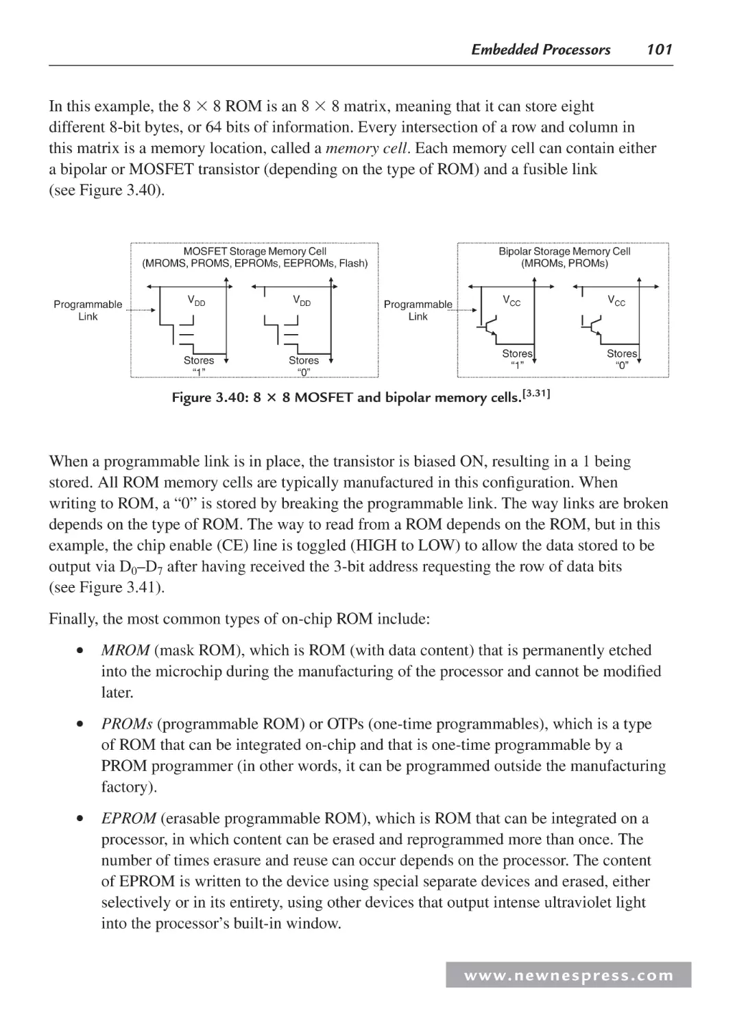
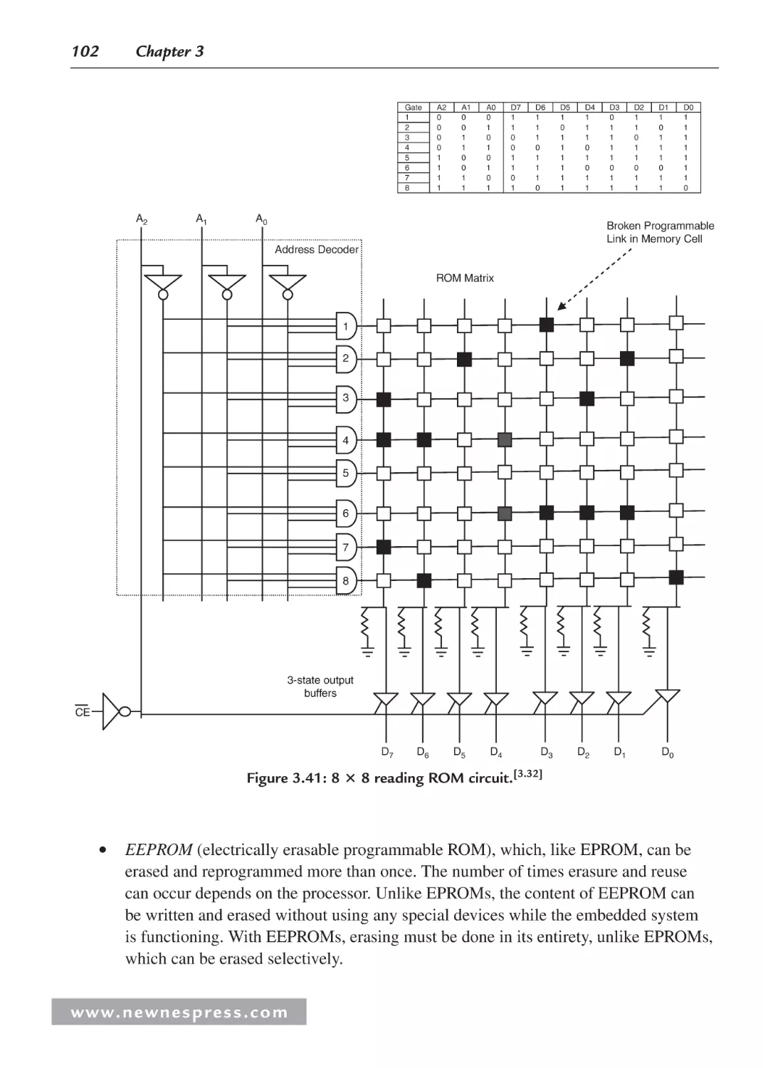
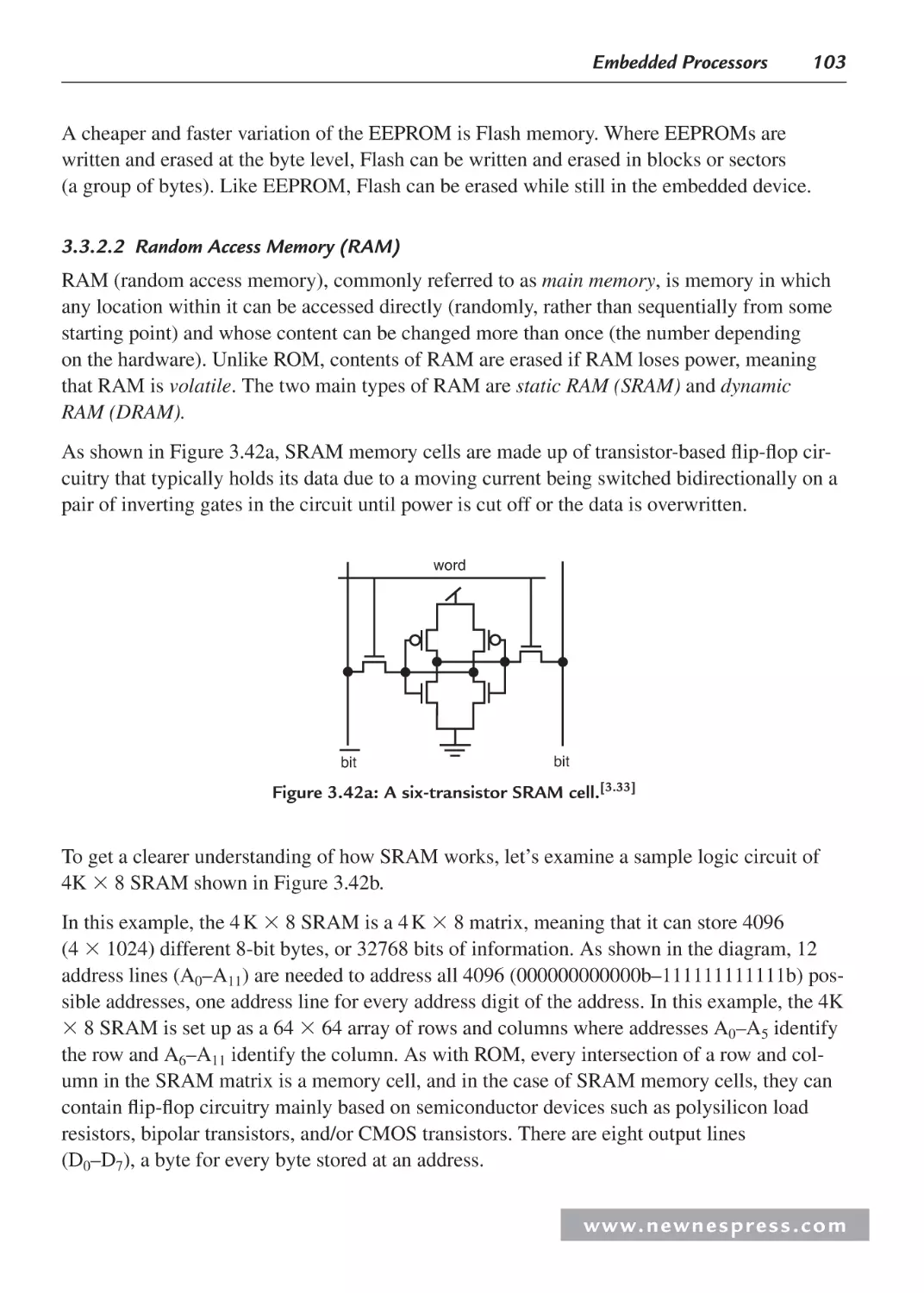
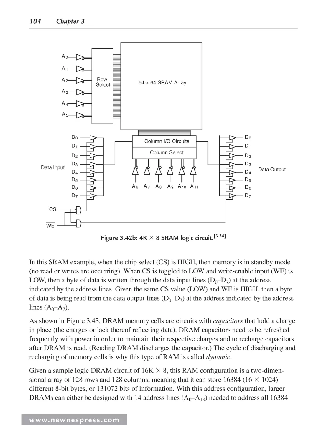
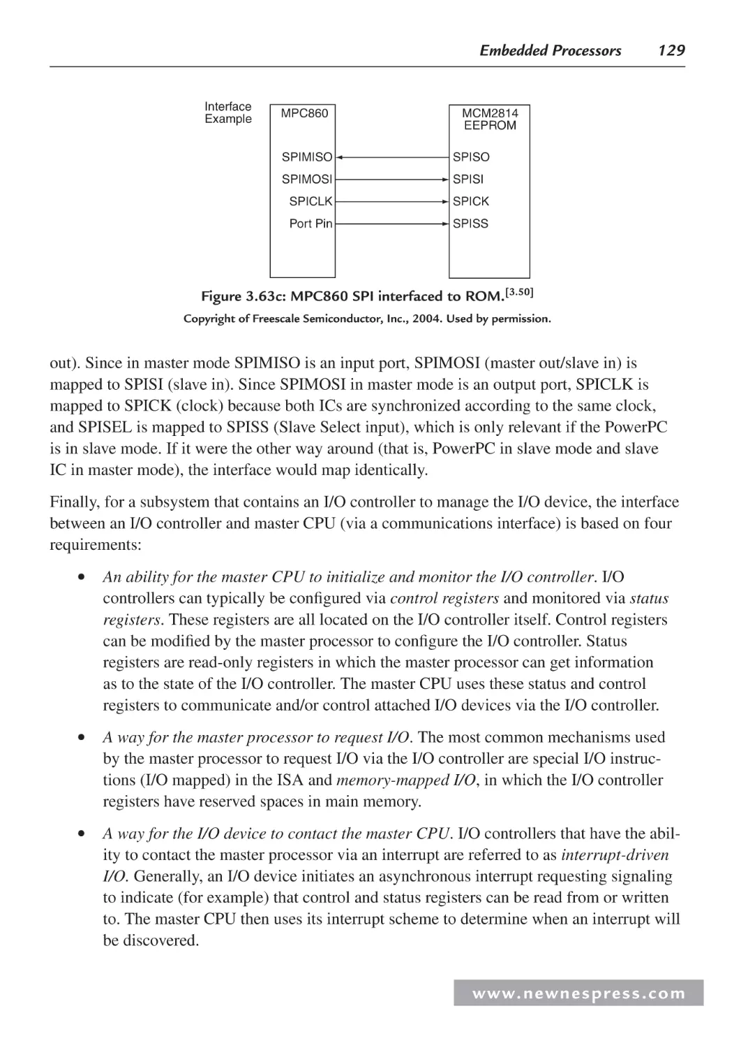
/


Author: Ganssle Jack Noergaard Tammy Eady Fred Edwards Lewin
Tags: computer systems computer technologies
ISBN: 978-0-7506-8584-9
Year: 2008
Similar


Text
Embedded Hardware
Newnes Know It All Series
PIC Microcontrollers: Know It All
Lucio Di Jasio, Tim Wilmshurst, Dogan Ibrahim, John Morton,
Martin Bates, Jack Smith, D.W. Smith, and Chuck Hellebuyck
ISBN: 978-0-7506-8615-0
Embedded Software: Know It All
Jean Labrosse, Jack Ganssle, Tammy Noergaard, Robert Oshana, Colin Walls, Keith Curtis,
Jason Andrews, David J. Katz, Rick Gentile, Kamal Hyder, and Bob Perrin
ISBN: 978-0-7506-8583-2
Embedded Hardware: Know It All
Jack Ganssle, Tammy Noergaard, Fred Eady, Creed Huddleston, Lewin Edwards,
David J. Katz, Rick Gentile, Ken Arnold, Kamal Hyder, and Bob Perrin
ISBN: 978-0-7506-8584-9
Wireless Networking: Know It All
Praphul Chandra, Daniel M. Dobkin, Alan Bensky, Ron Olexa,
David A. Lide, and Farid Dowla
ISBN: 978-0-7506-8582-5
RF & Wireless Technologies: Know It All
Bruce Fette, Roberto Aiello, Praphul Chandra, Daniel Dobkin,
Alan Bensky, Douglas Miron, David A. Lide, Farid Dowla, and Ron Olexa
ISBN: 978-0-7506-8581-8
For more information on these and other Newnes titles visit: www.newnespress.com
Embedded Hardware
Jack Ganssle
Tammy Noergaard
Fred Eady
Lewin Edwards
David J. Katz
Rick Gentile
Ken Arnold
Kamal Hyder
Bob Perrin
Creed Huddleston
AMSTERDAM • BOSTON • HEIDELBERG • LONDON
NEW YORK • OXFORD • PARIS • SAN DIEGO
SAN FRANCISCO • SINGAPORE • SYDNEY • TOKYO
Newnes is an imprint of Elsevier
Cover image by iStockphoto
Newnes is an imprint of Elsevier
30 Corporate Drive, Suite 400, Burlington, MA 01803, USA
Linacre House, Jordan Hill, Oxford OX2 8DP, UK
Copyright © 2008 by Elsevier Inc. All rights reserved.
No part of this publication may be reproduced, stored in a retrieval system, or
transmitted in any form or by any means, electronic, mechanical, photocopying,
recording, or otherwise, without the prior written permission of the publisher.
Permissions may be sought directly from Elsevier’s Science & Technology Rights
Department in Oxford, UK: phone: (44) 1865 843830, fax: (44) 1865 853333,
E-mail: permissions@elsevier.com. You may also complete your request online via
the Elsevier homepage (http://elsevier.com), by selecting “Support & Contact”
then “Copyright and Permission” and then “Obtaining Permissions.”
Recognizing the importance of preserving what has been written,
Elsevier prints its books on acid-free paper whenever possible.
Library of Congress Cataloging-in-Publication Data
Ganssle, Jack G.
Embedded hardware / Jack Ganssle ... [et al.].
p. cm.
Includes index.
ISBN 978-0-7506-8584-9 (alk. paper)
1. Embedded computer systems. I. Title.
TK7895.E42G37 2007
004.16—dc22
2007027559
British Library Cataloguing-in-Publication Data
A catalogue record for this book is available from the British Library.
For information on all Newnes publications
visit our Web site at www.books.elsevier.com
07
08
09
10
10
9
8
7
6
5
4
3
2
1
Typeset by Charon Tec Ltd (A Macmillan Company), Chennai, India
www.charontec.com
Printed in the United States of America
Contents
About the Authors ....................................................................................................................xiii
Chapter 1: Embedded Hardware Basics ..................................................................................... 1
1.1 Lesson One on Hardware: Reading Schematics............................................................ 1
1.2 The Embedded Board and the von Neumann Model .................................................... 5
1.3 Powering the Hardware ................................................................................................. 9
1.3.1 A Quick Comment on Analog Vs. Digital Signals ............................................ 10
1.4 Basic Electronics ......................................................................................................... 12
1.4.1 DC Circuits ........................................................................................................ 12
1.4.2 AC Circuits ........................................................................................................ 21
1.4.3 Active Devices ................................................................................................... 28
1.5 Putting It Together: A Power Supply .......................................................................... 32
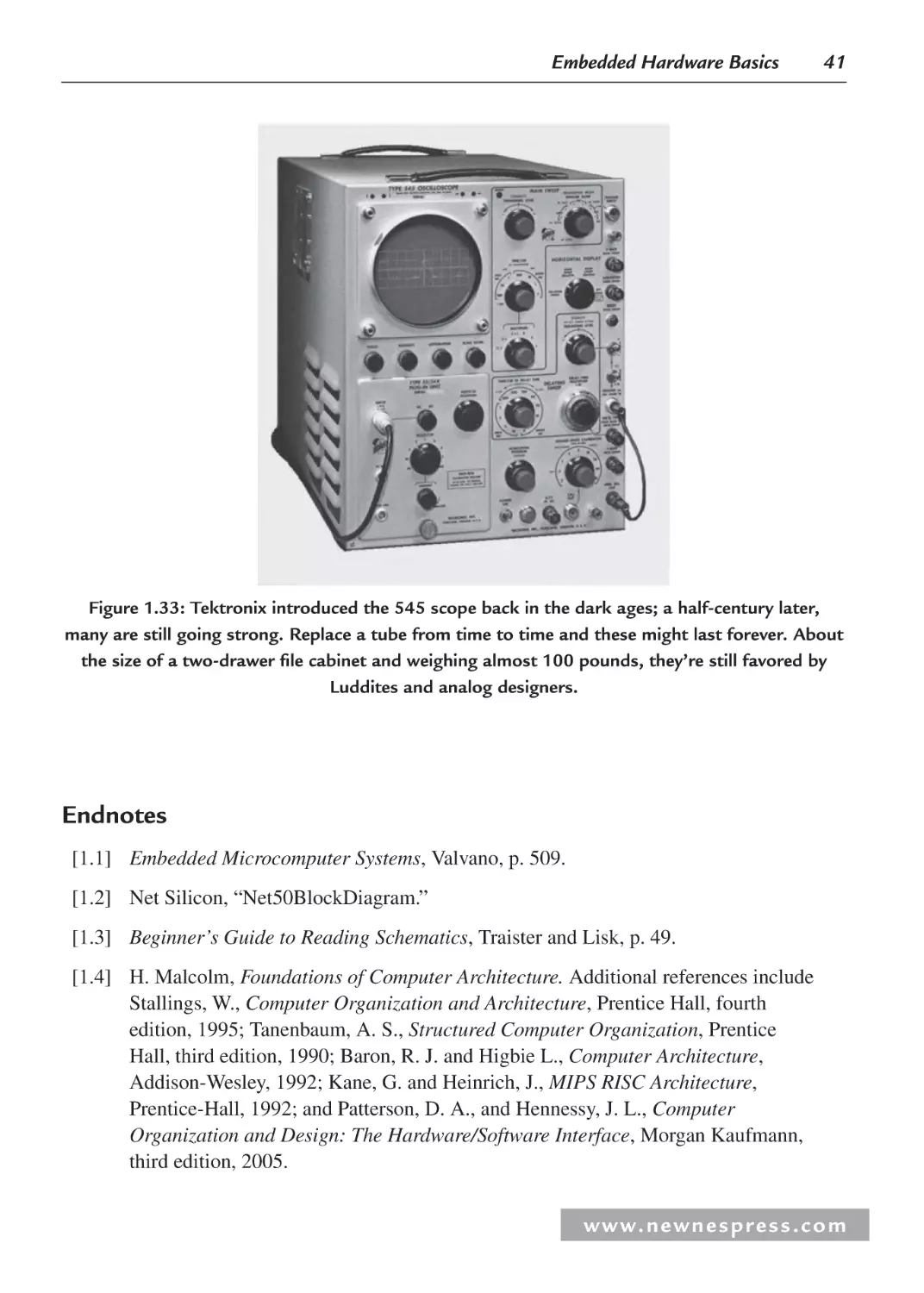
1.5.1 The Scope .......................................................................................................... 35
1.5.2 Controls .............................................................................................................. 35
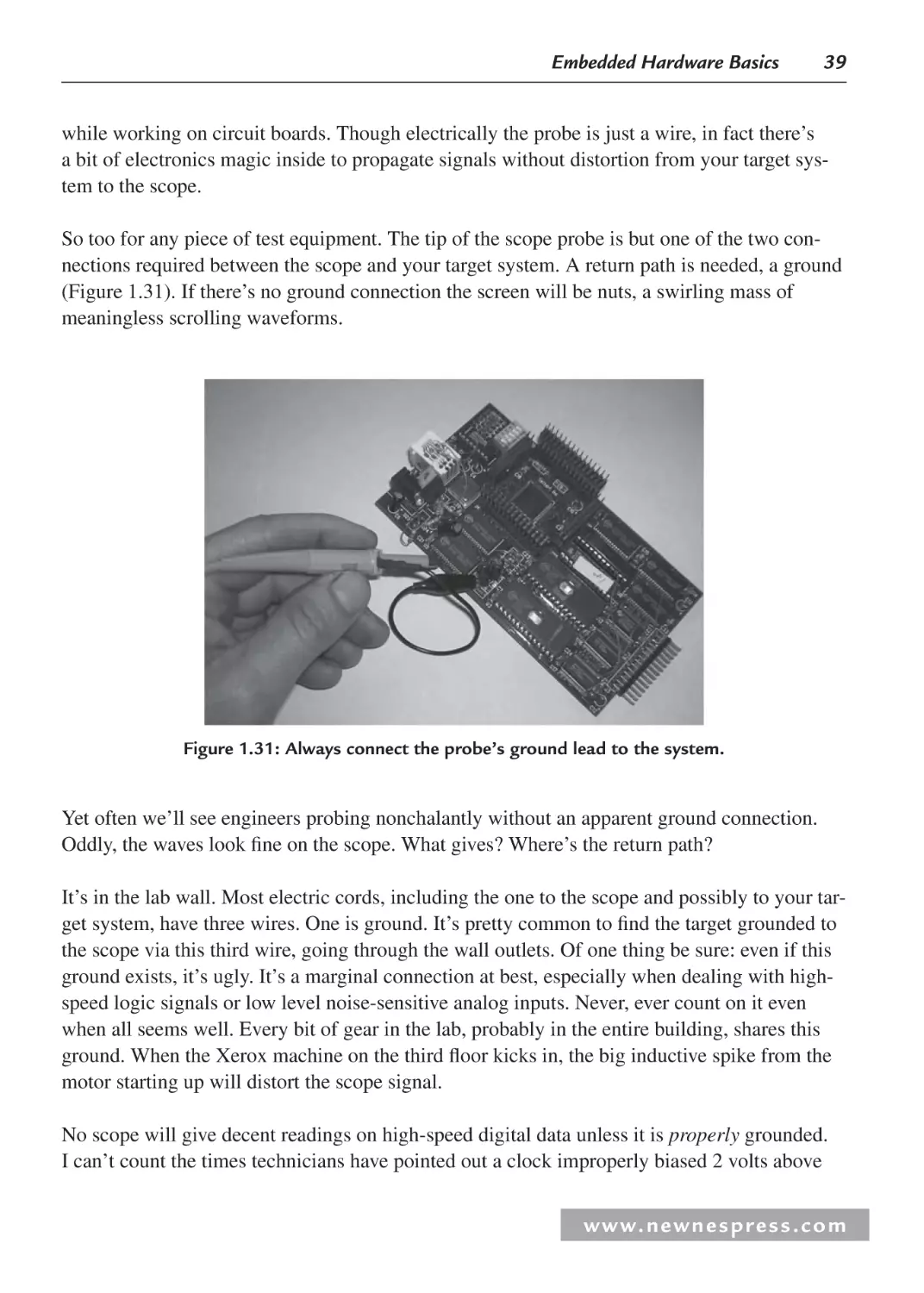
1.5.3 Probes................................................................................................................. 38
Endnotes ............................................................................................................................. 41
Chapter 2: Logic Circuits .......................................................................................................... 43
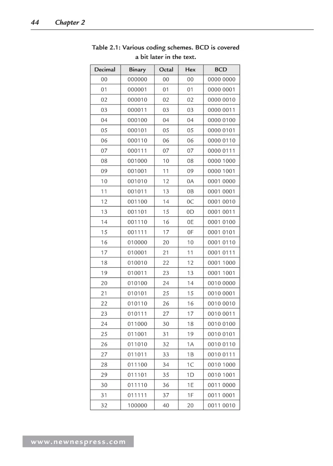
2.1 Coding ......................................................................................................................... 43
2.1.1 BCD .................................................................................................................. 46
2.2 Combinatorial Logic.................................................................................................... 47
2.2.1 NOT Gate .......................................................................................................... 47
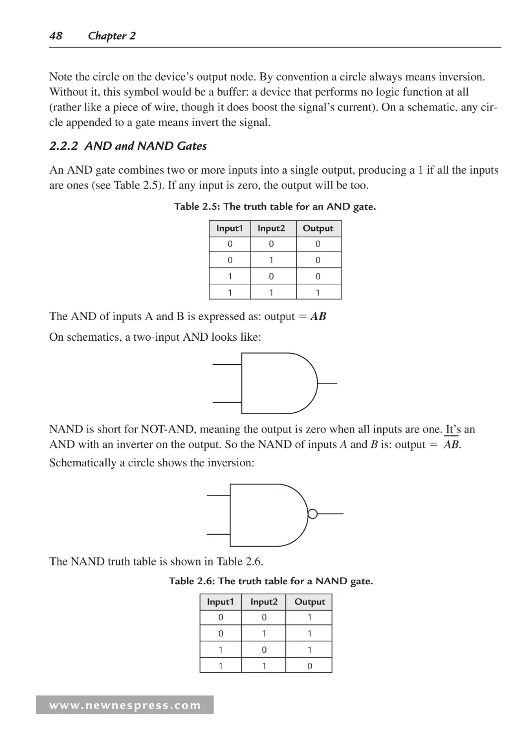
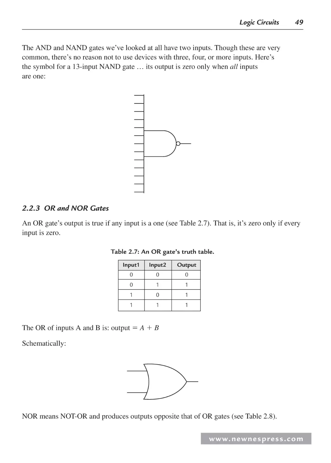
2.2.2 AND and NAND Gates ..................................................................................... 48
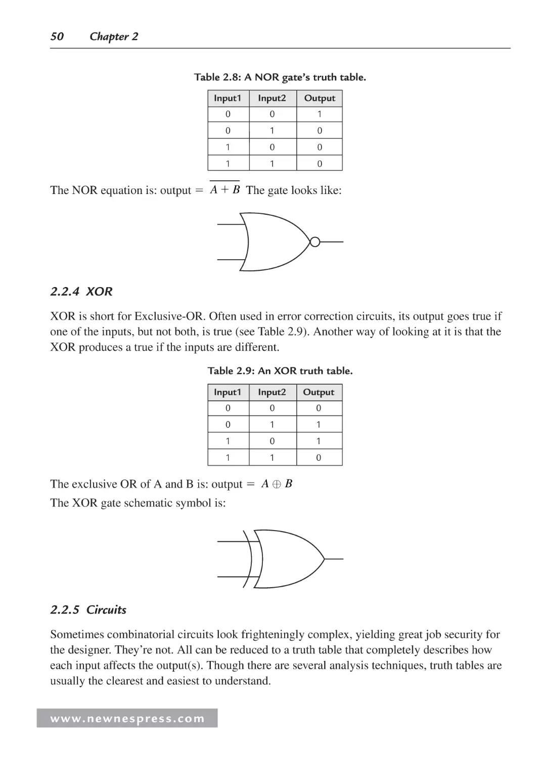
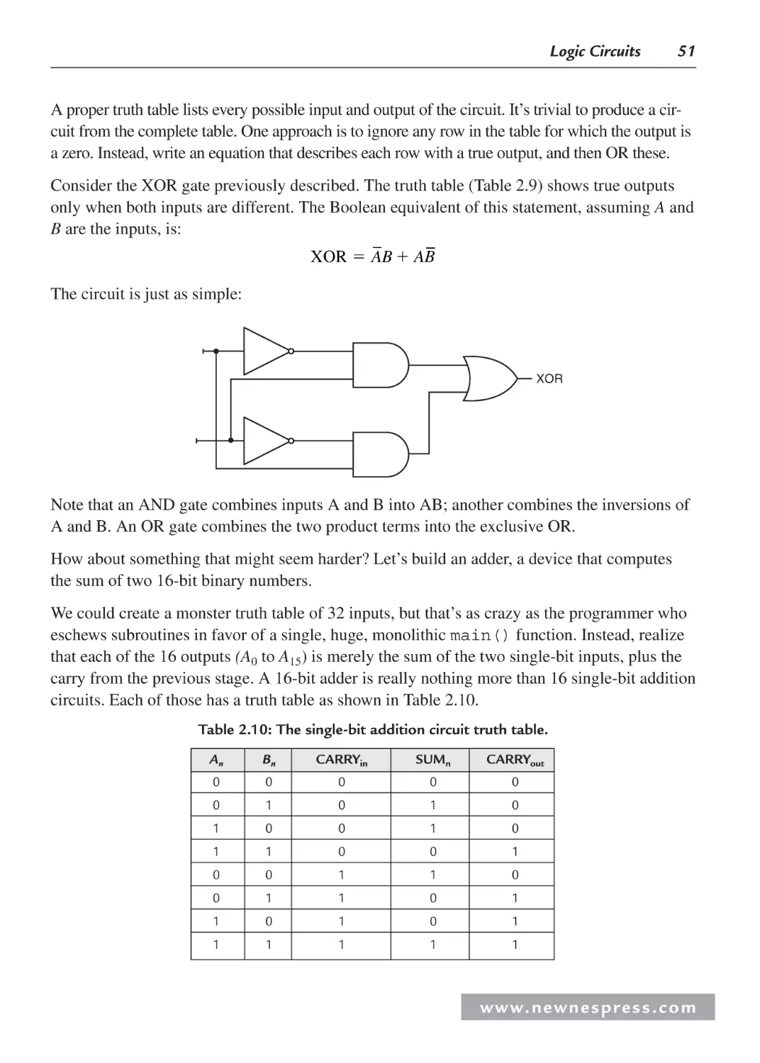
2.2.3 OR and NOR Gates ........................................................................................... 49
2.2.4 XOR .................................................................................................................. 50
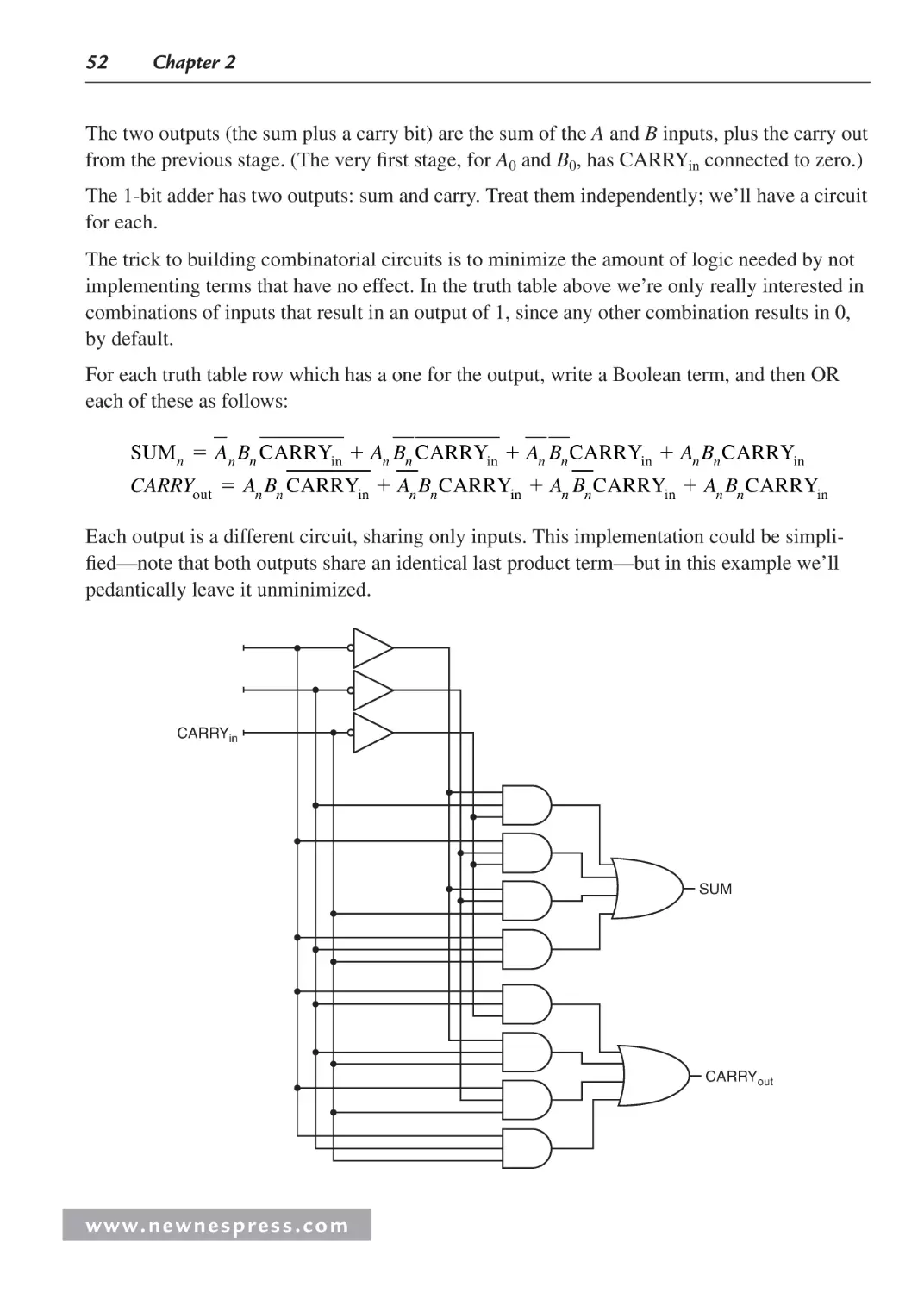
2.2.5 Circuits .............................................................................................................. 50
2.2.6 Tristate Devices ................................................................................................. 53
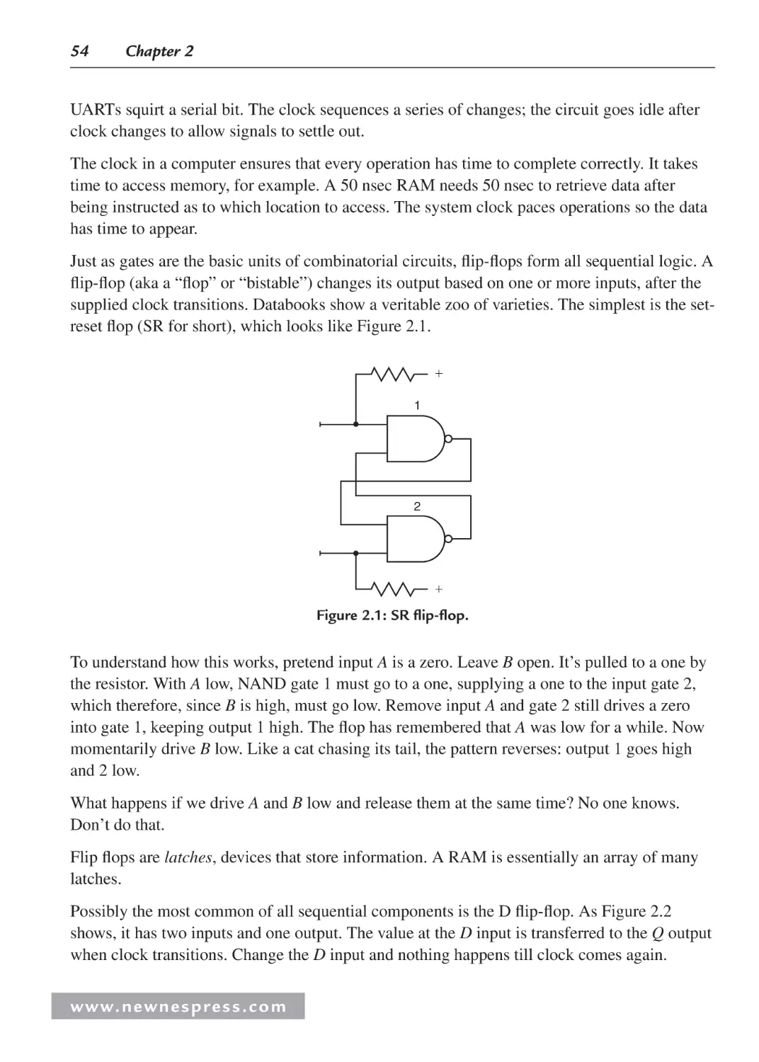
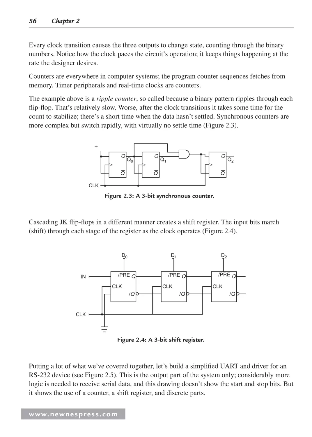
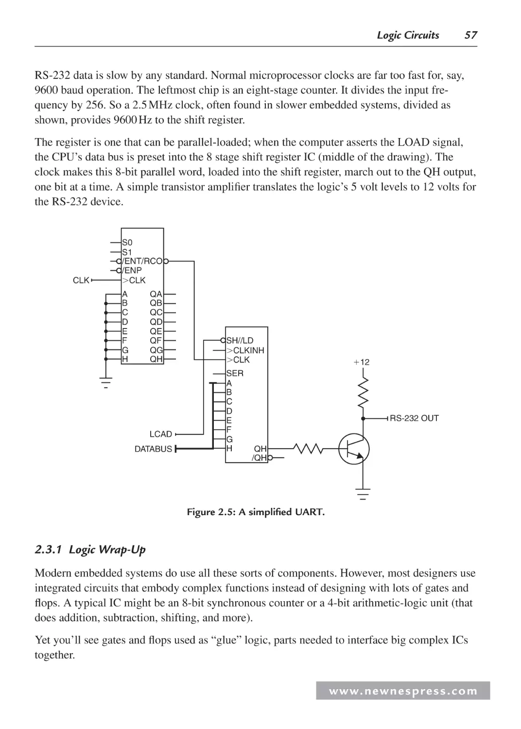
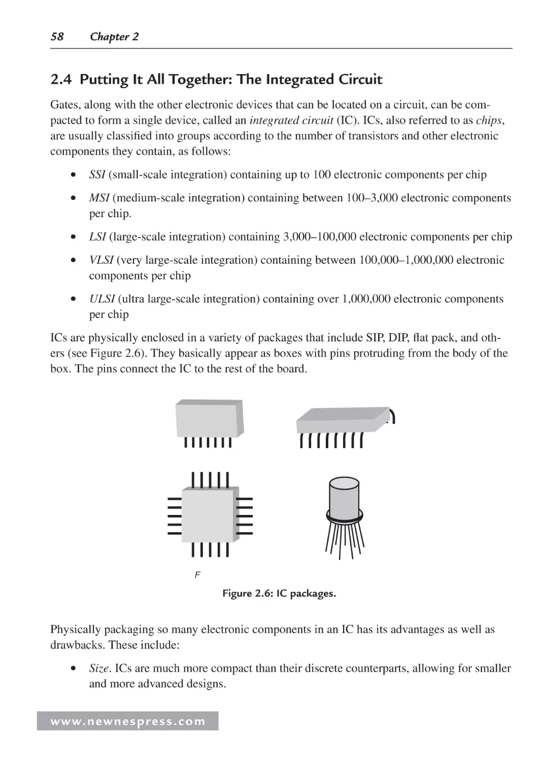
2.3 Sequential Logic .......................................................................................................... 53
2.3.1 Logic Wrap-Up ................................................................................................. 57
2.4 Putting It All Together: The Integrated Circuit ........................................................... 58
Endnotes ............................................................................................................................. 61
w w w. n e w n e s p r e s s . c o m
vi
Contents
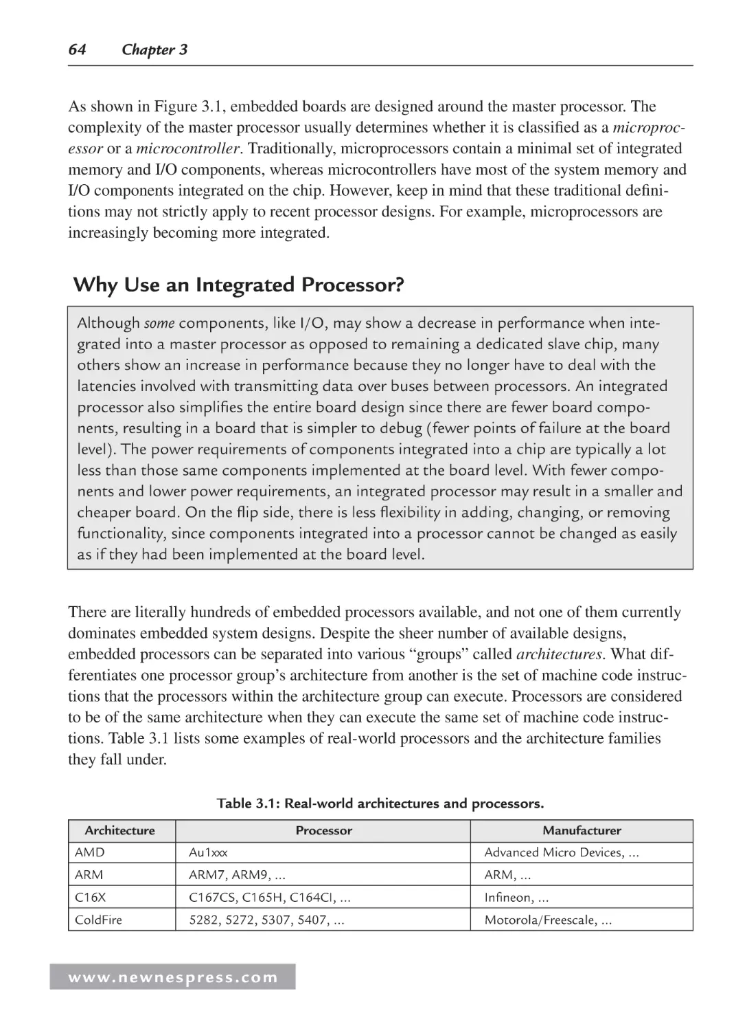
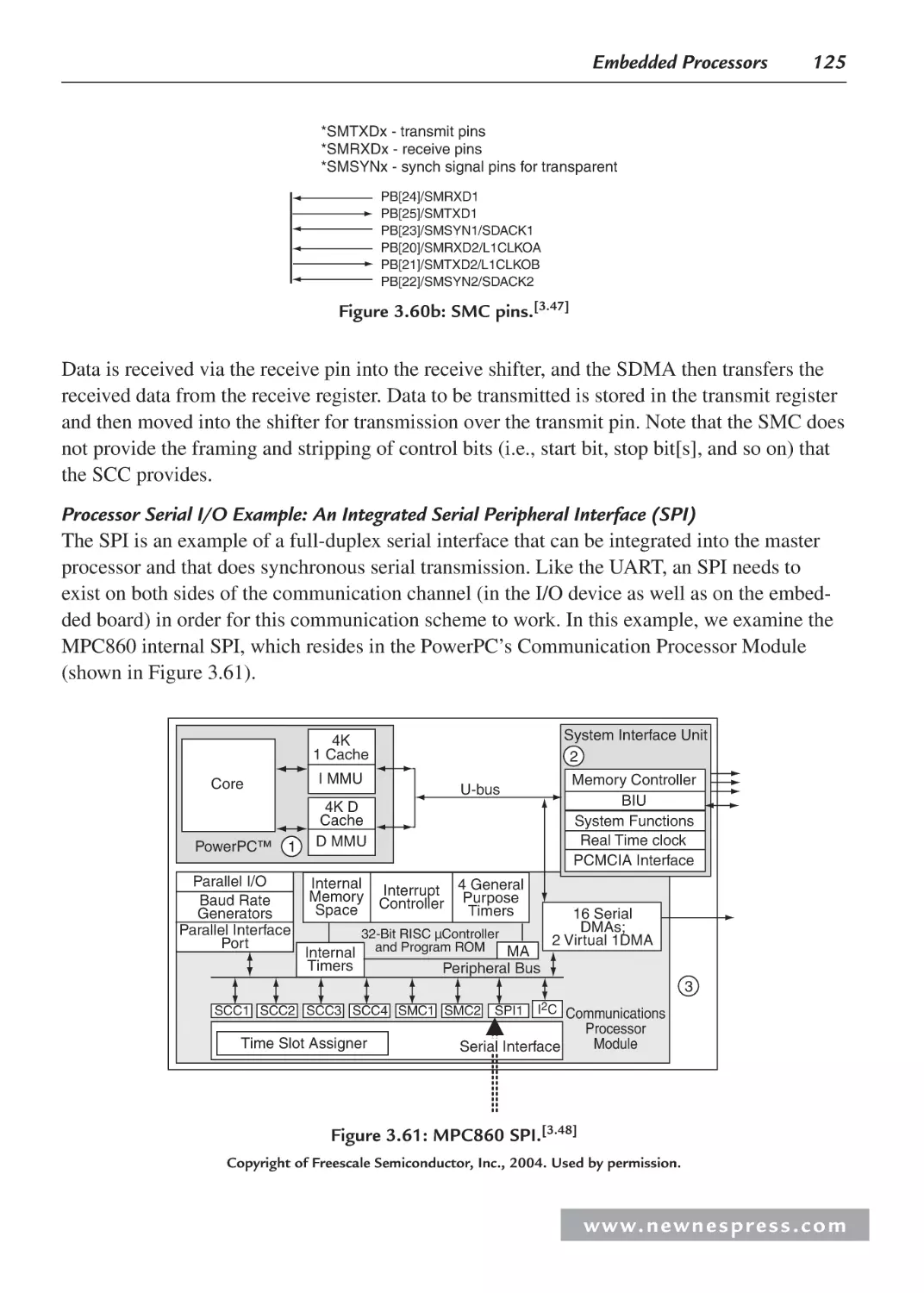
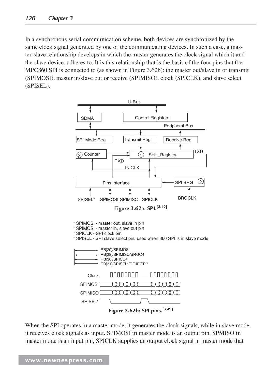
Chapter 3: Embedded Processors.............................................................................................. 63
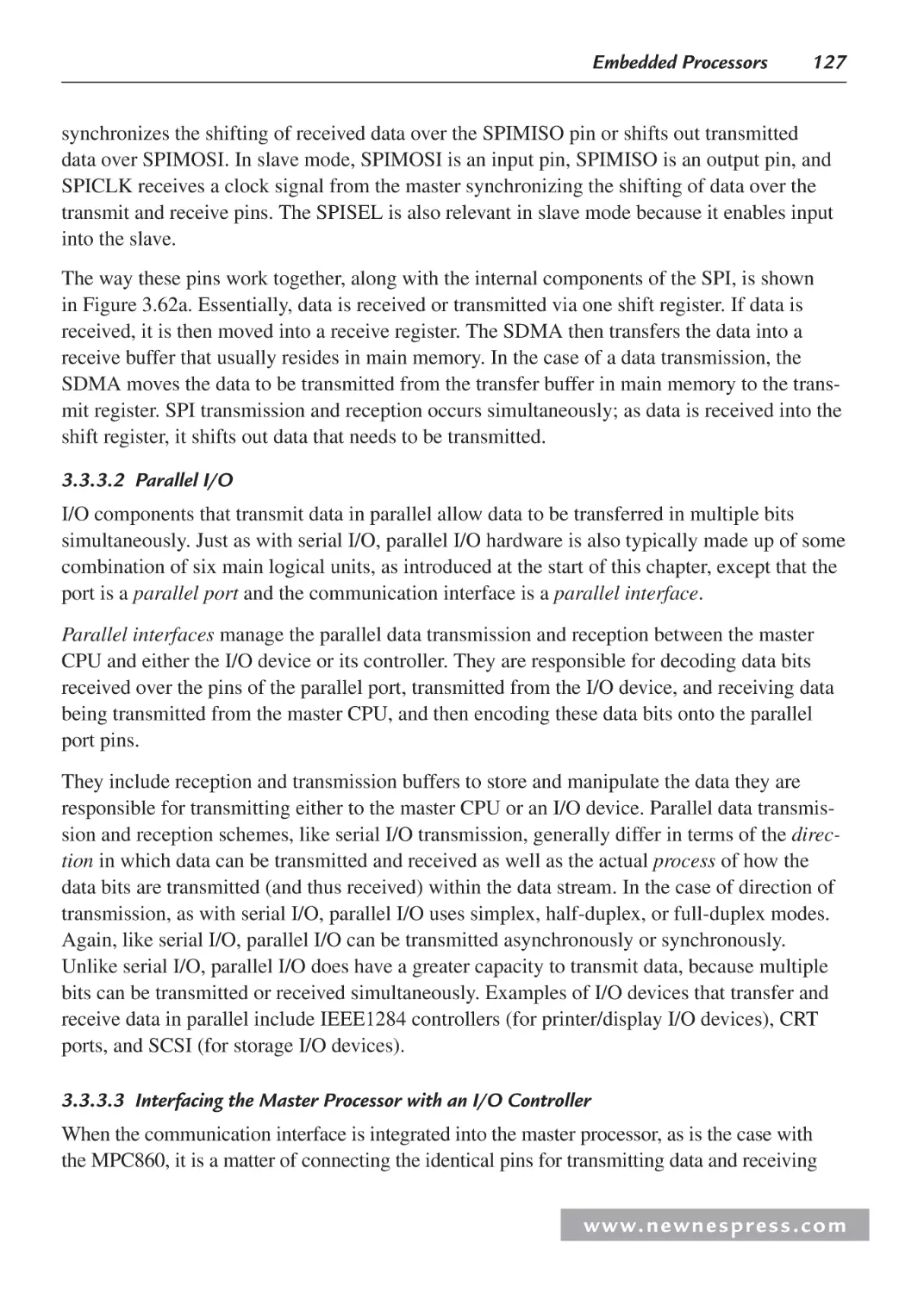
3.1 Introduction ................................................................................................................. 63
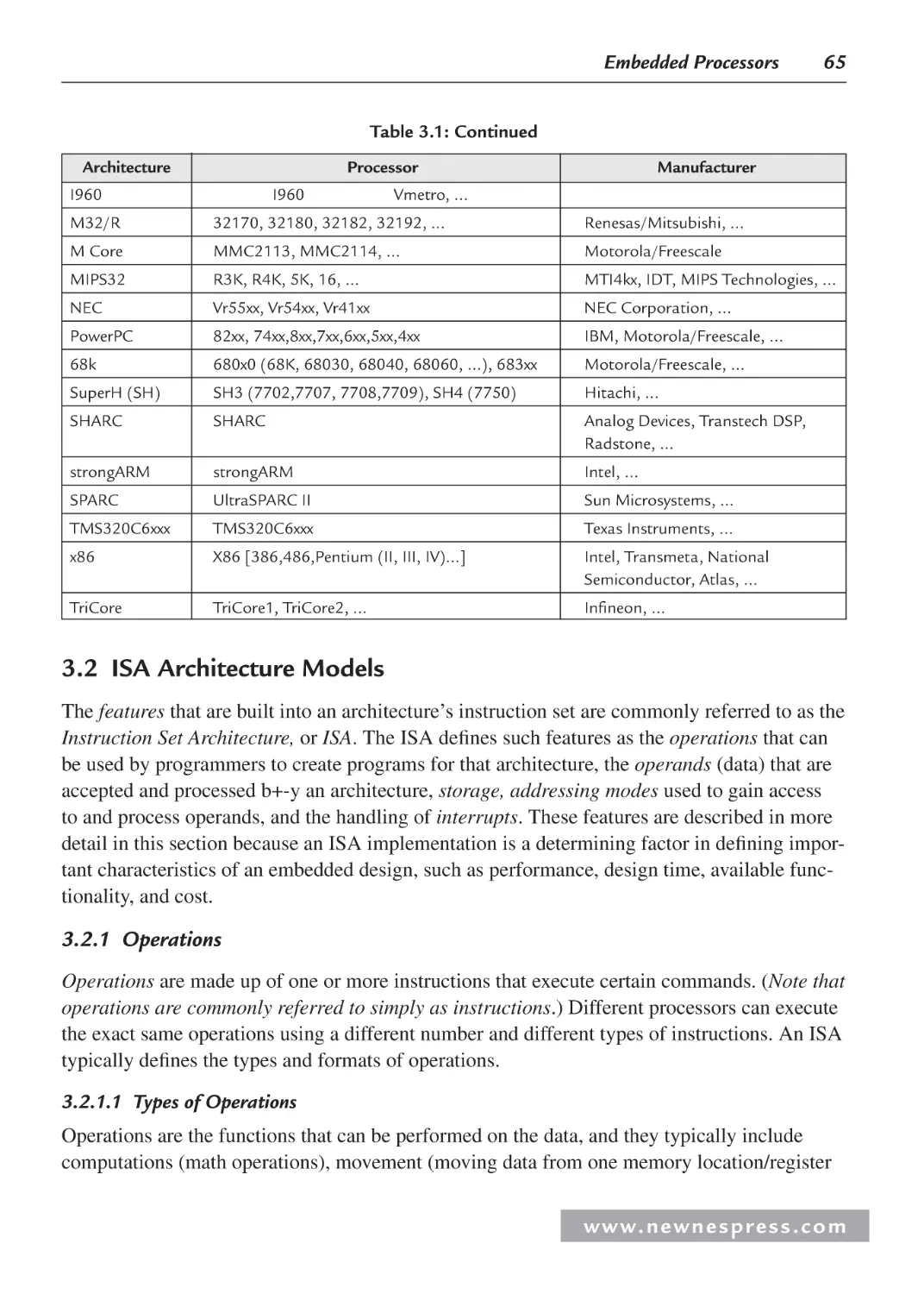
3.2 ISA Architecture Models............................................................................................. 65
3.2.1 Operations ......................................................................................................... 65
3.2.2 Operands ........................................................................................................... 68
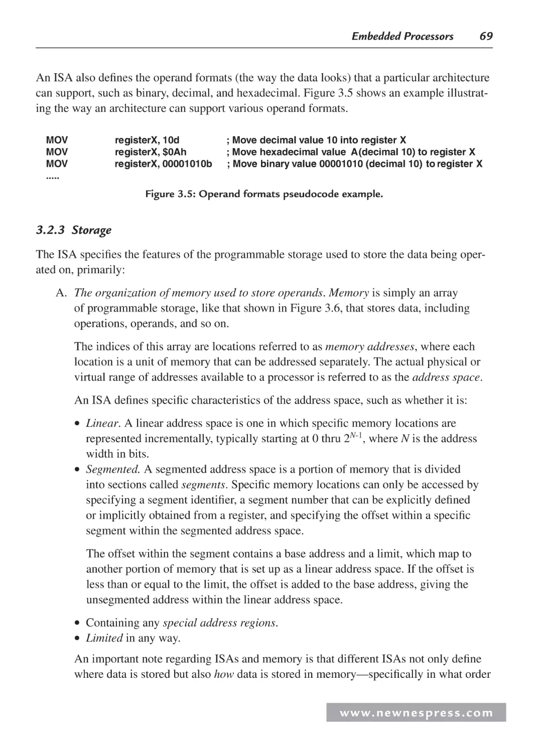
3.2.3 Storage .............................................................................................................. 69
3.2.4 Addressing Modes............................................................................................. 71
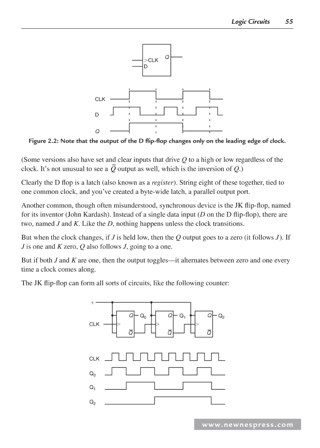
3.2.5 Interrupts and Exception Handling ................................................................... 72
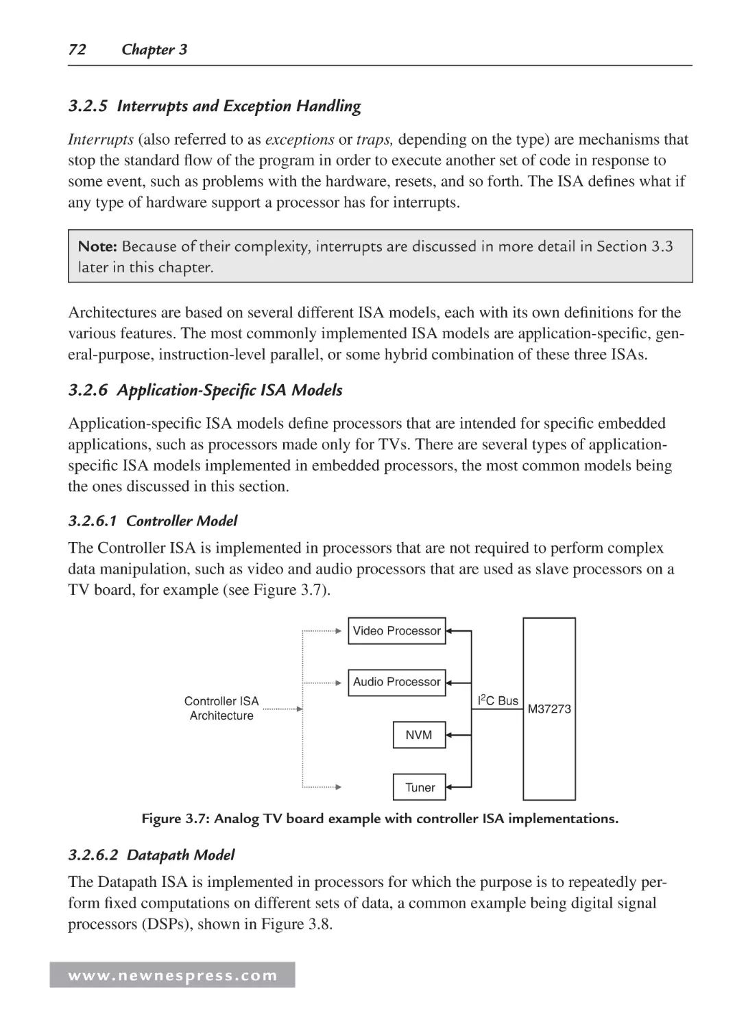
3.2.6 Application-Specific ISA Models ..................................................................... 72
3.2.7 General-Purpose ISA Models ........................................................................... 74
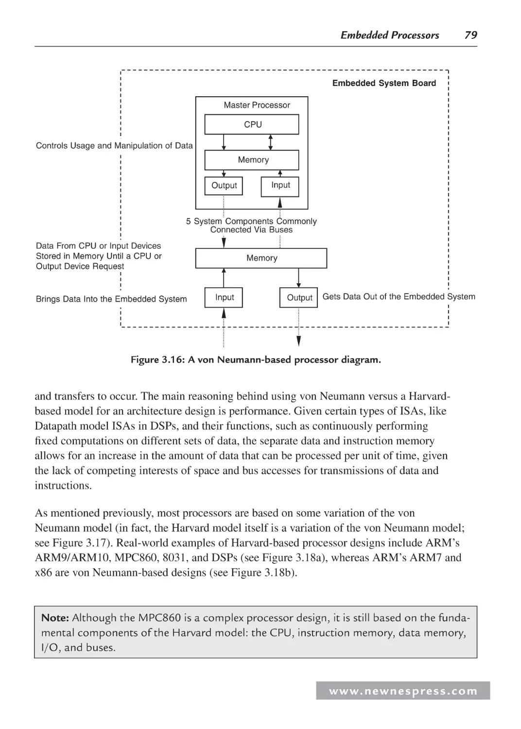
3.2.8 Instruction-Level Parallelism ISA Models ........................................................ 76
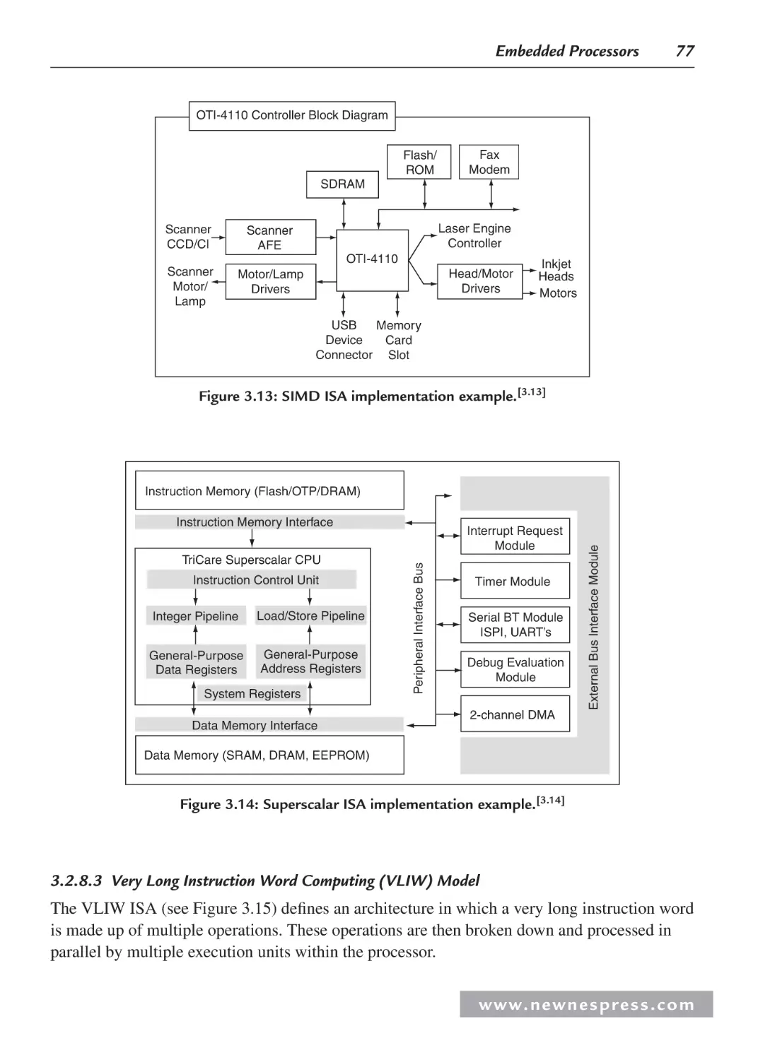
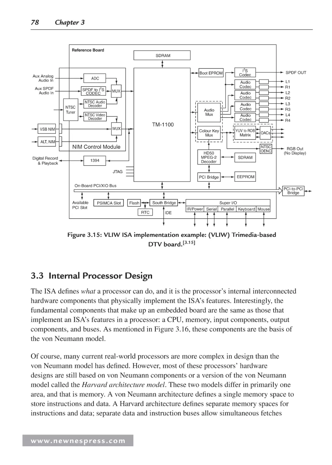
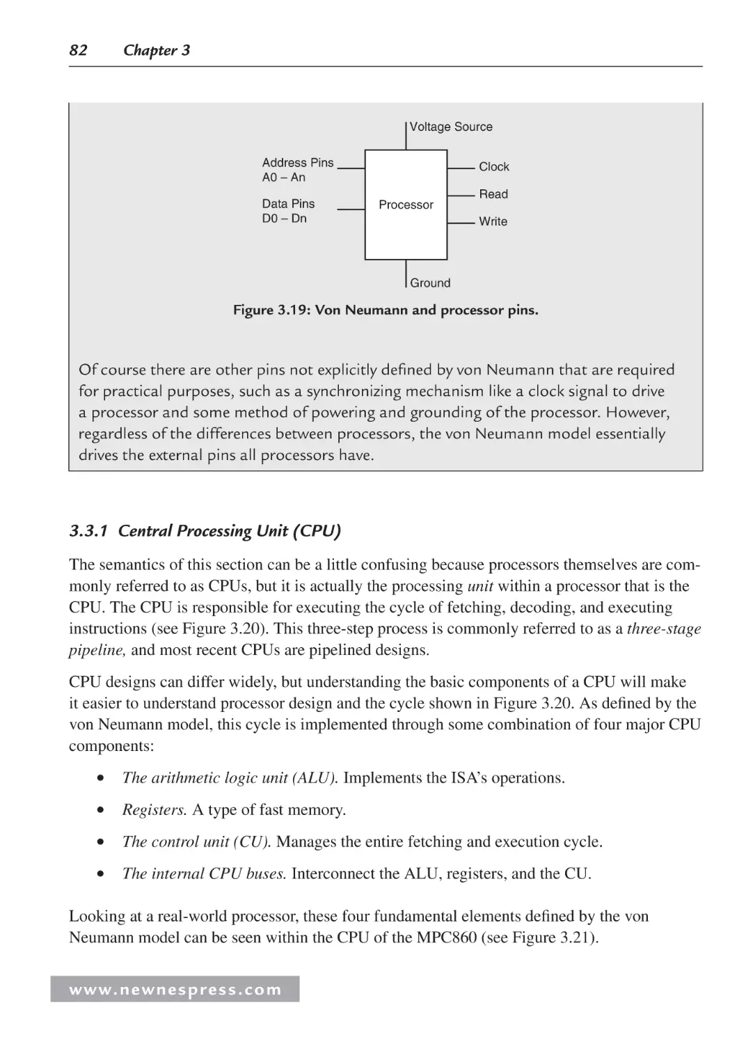
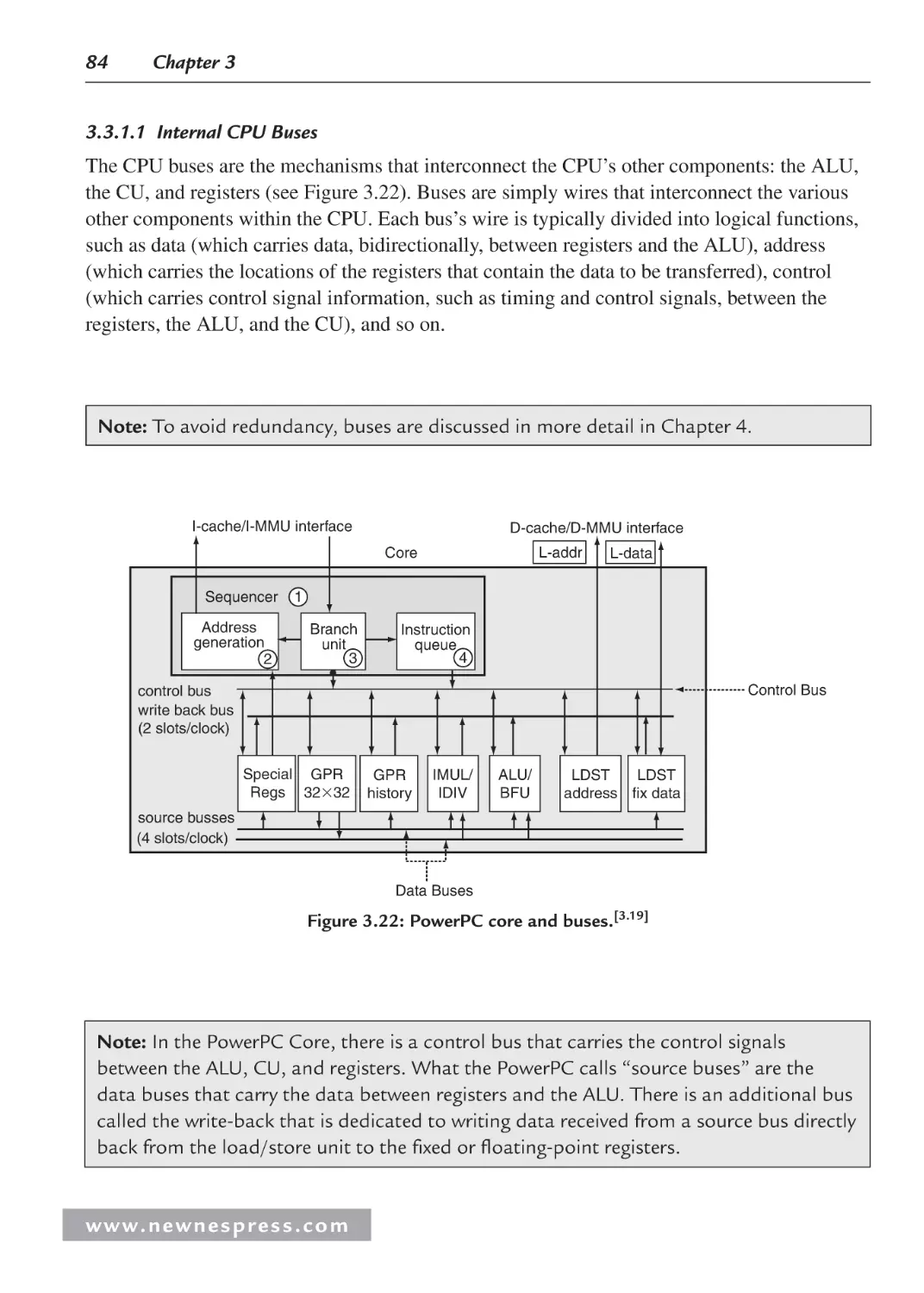
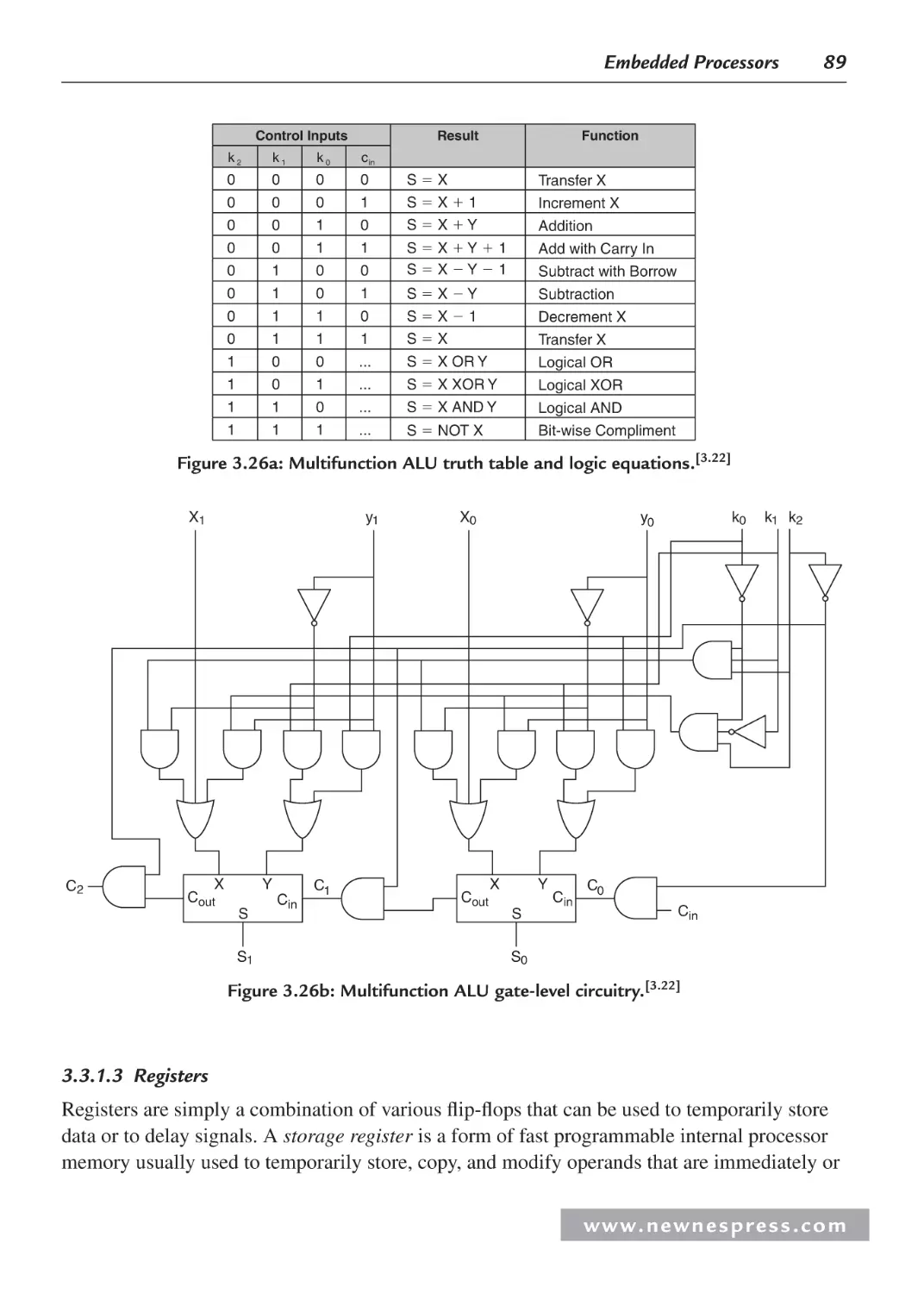
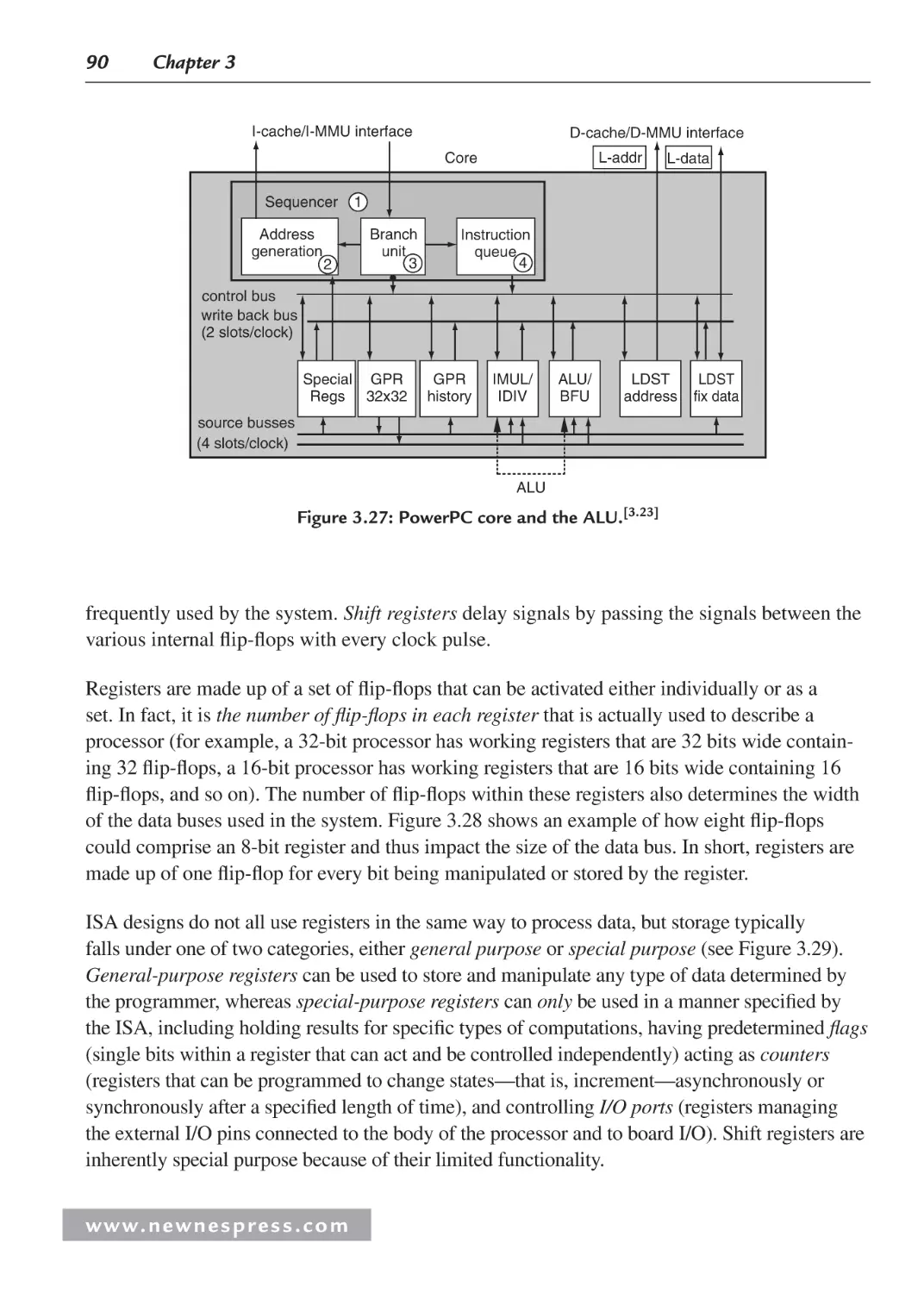
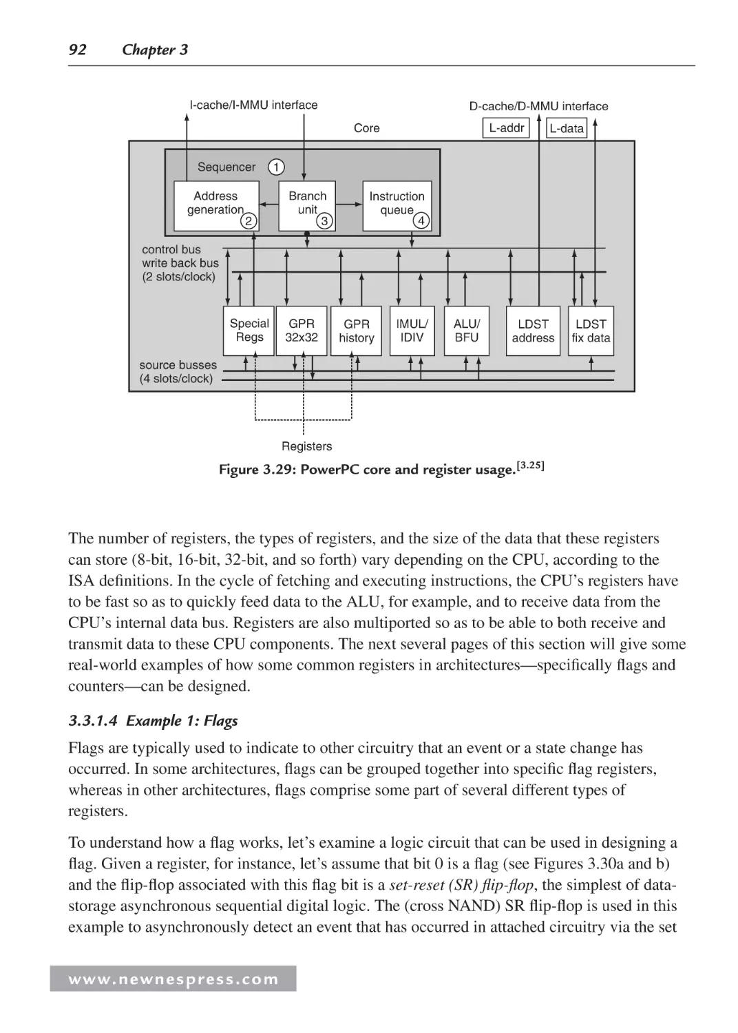
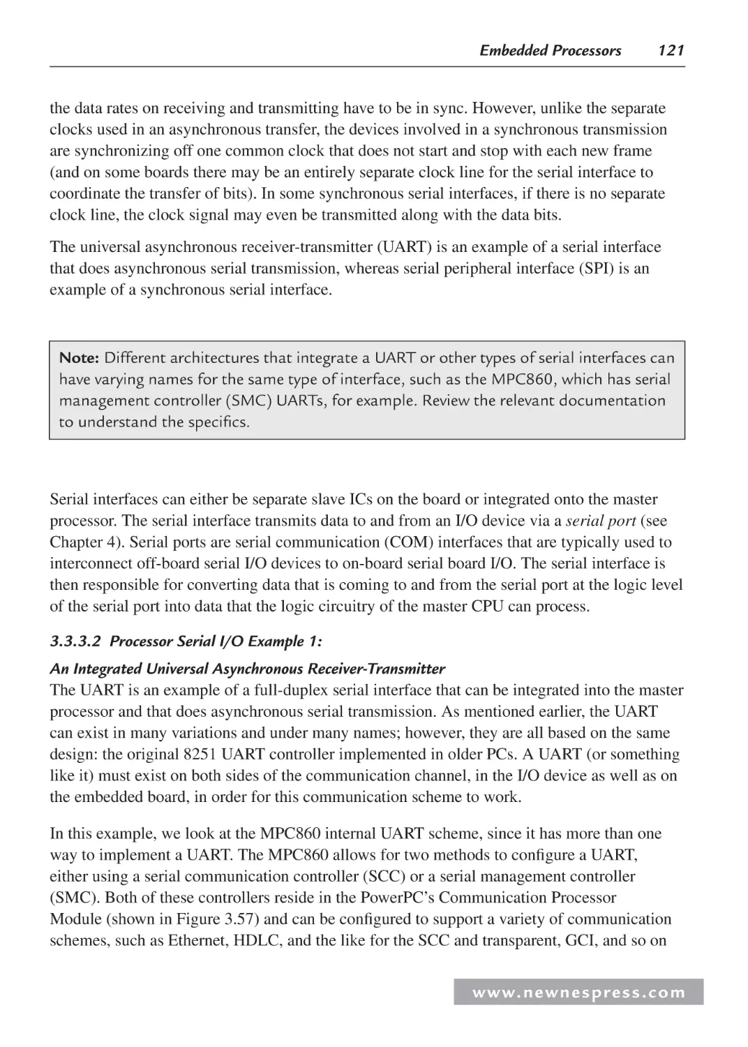
3.3 Internal Processor Design ............................................................................................ 78
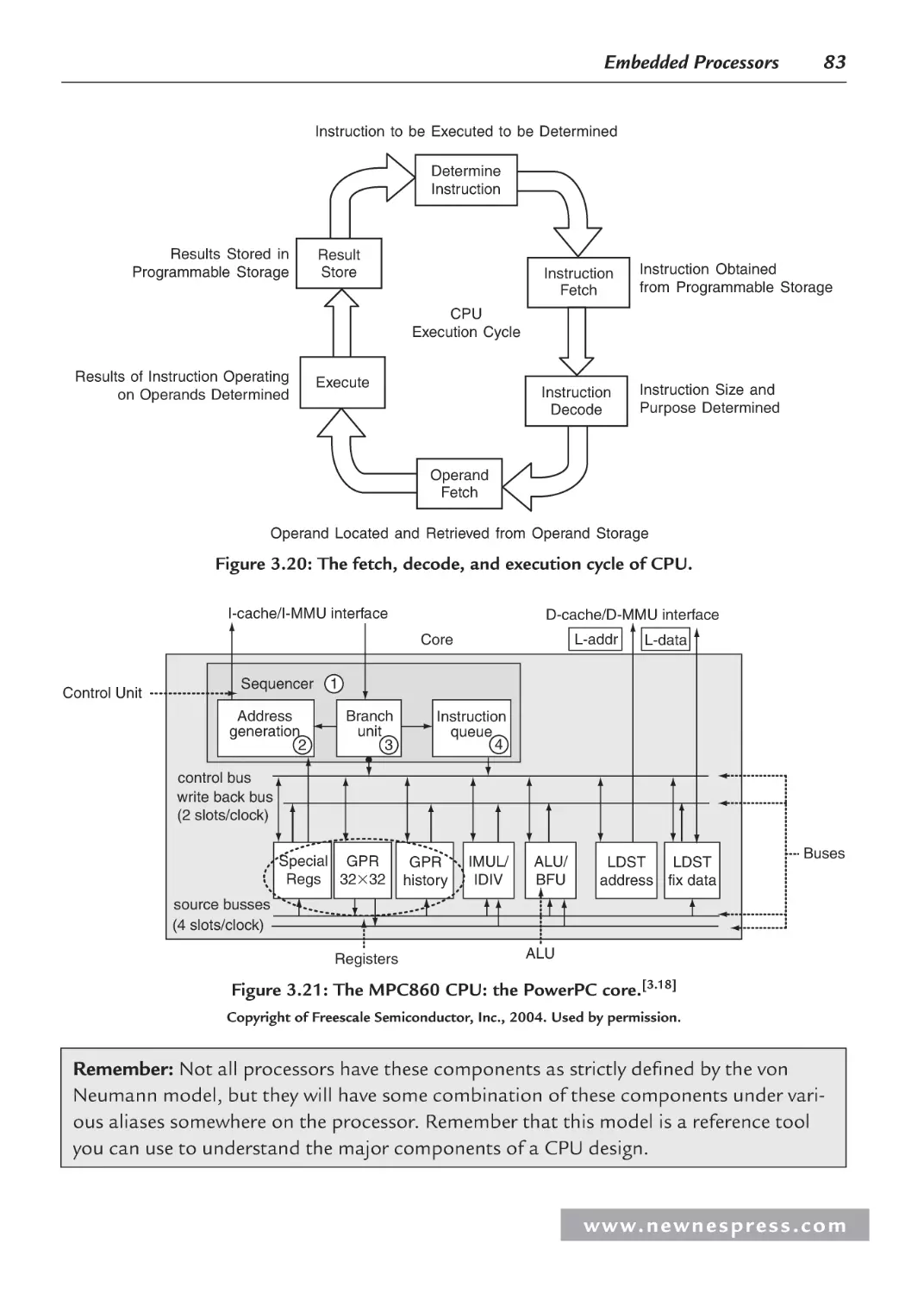
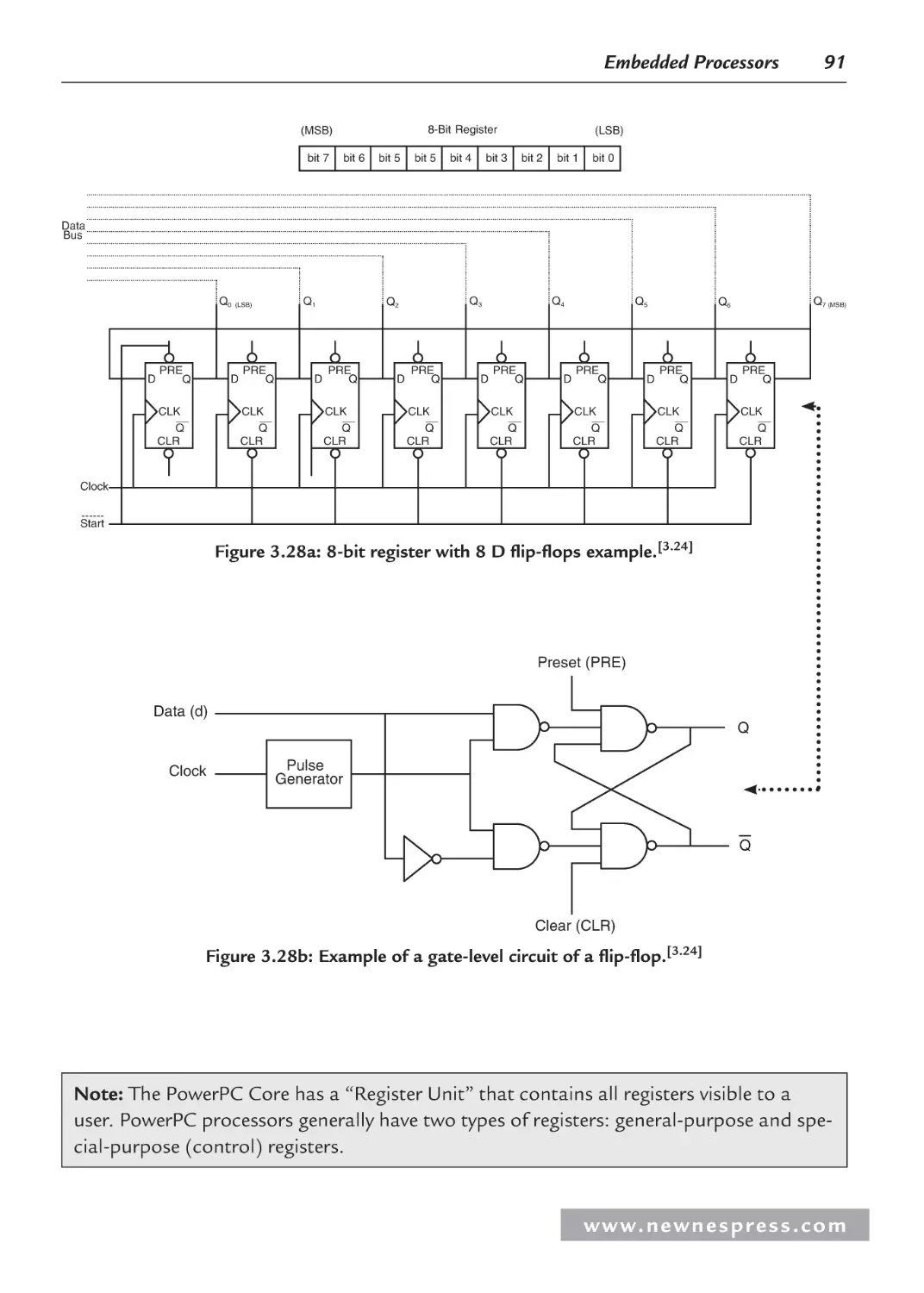
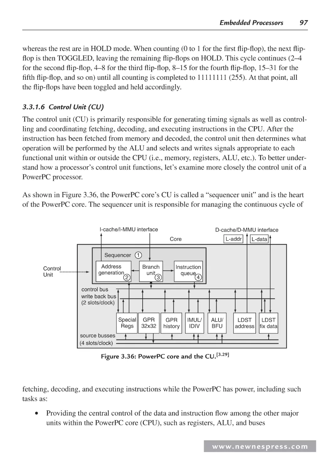
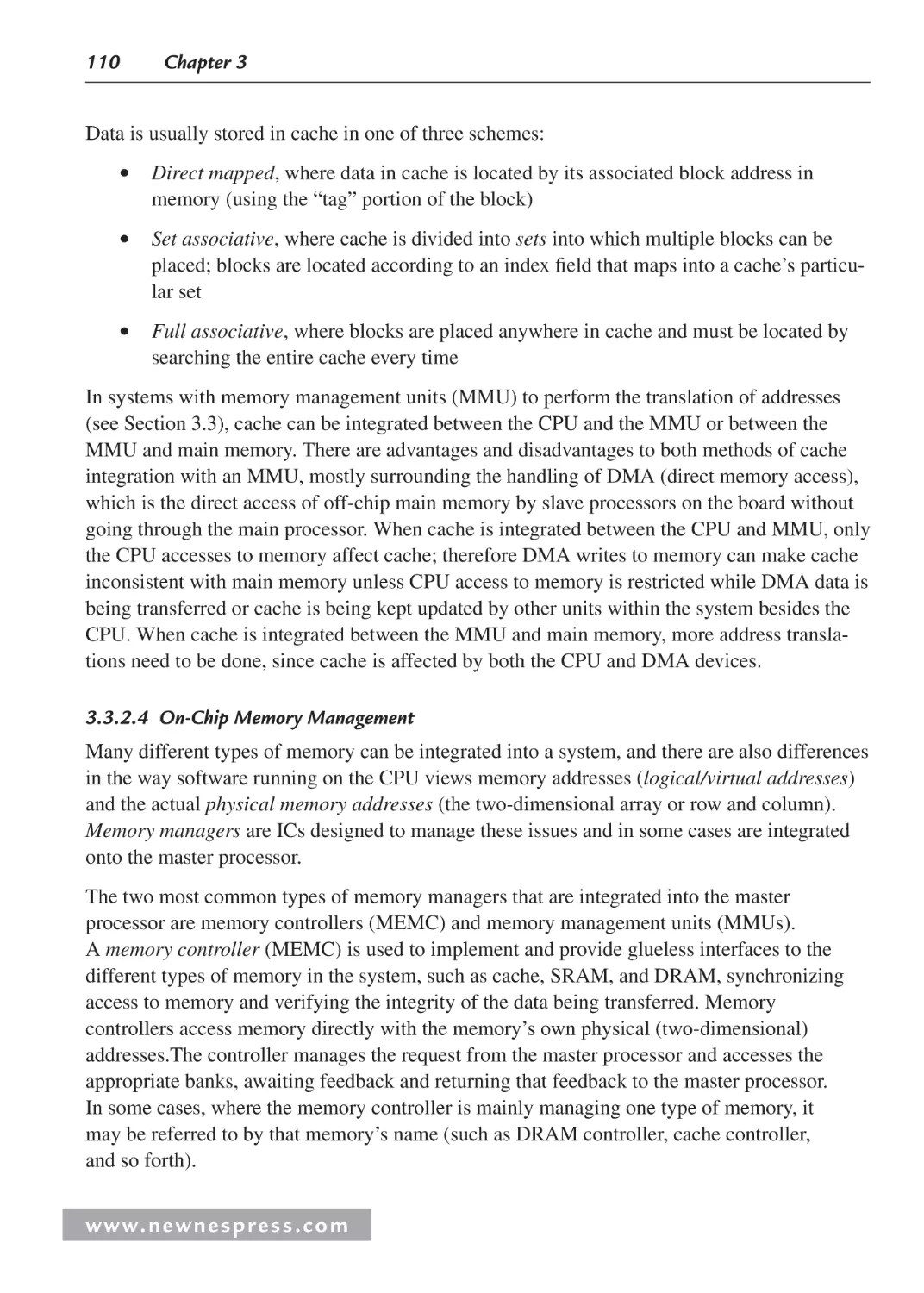
3.3.1 Central Processing Unit (CPU) ......................................................................... 82
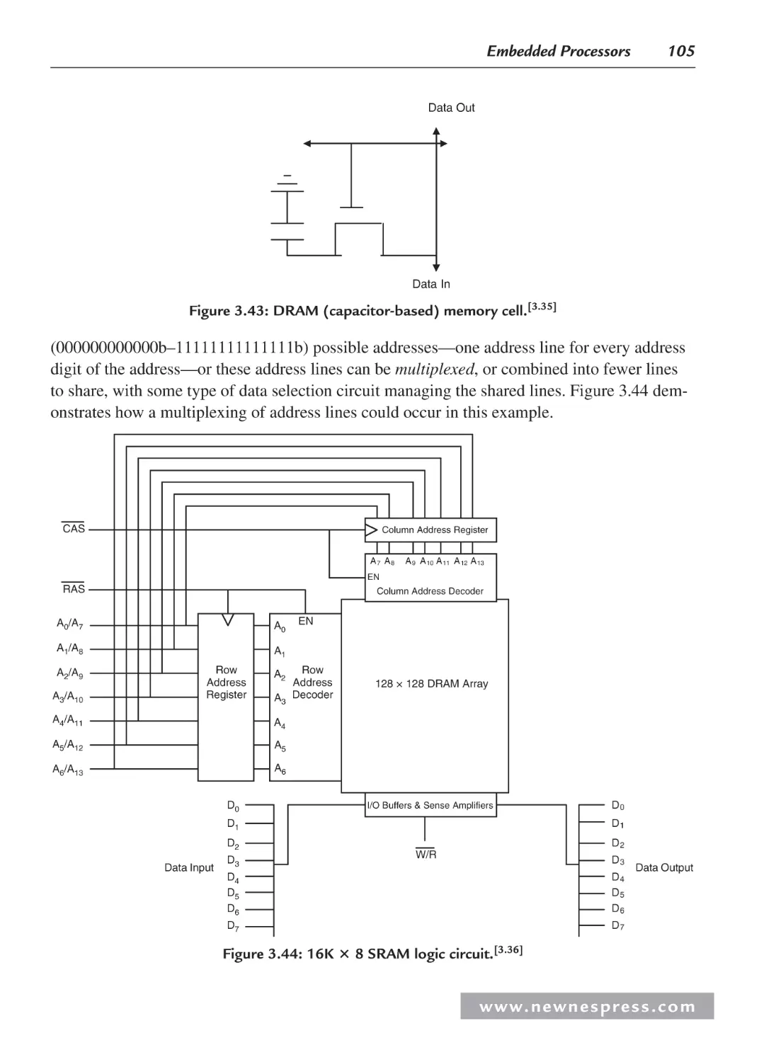
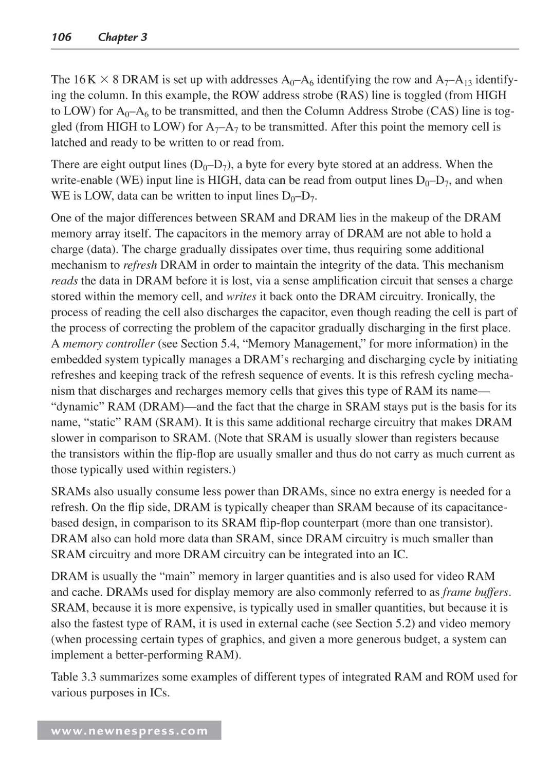
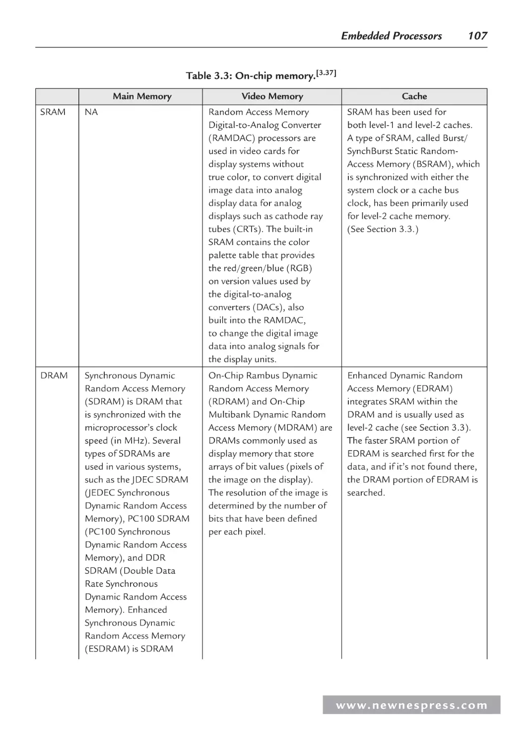
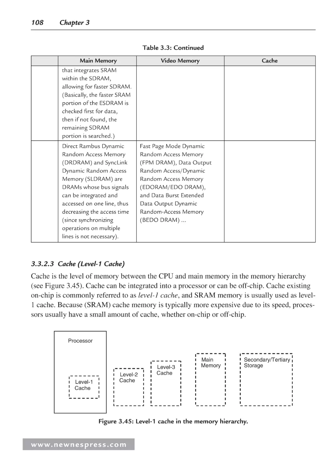
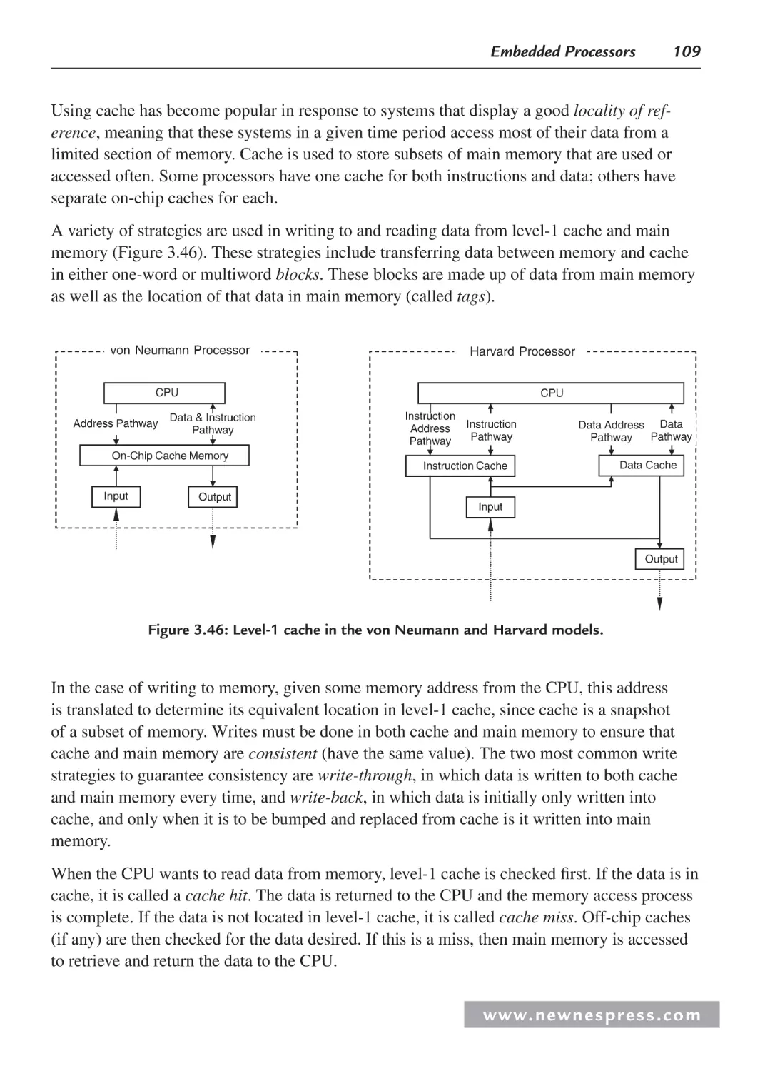
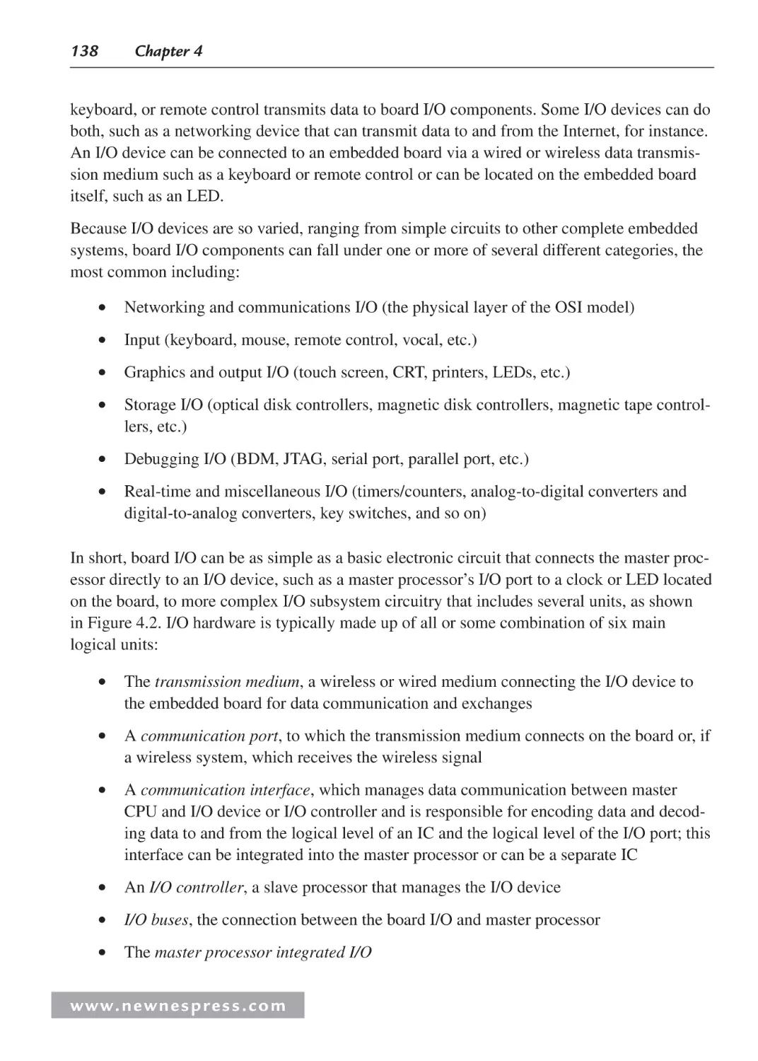
3.3.2 On-Chip Memory .............................................................................................. 99
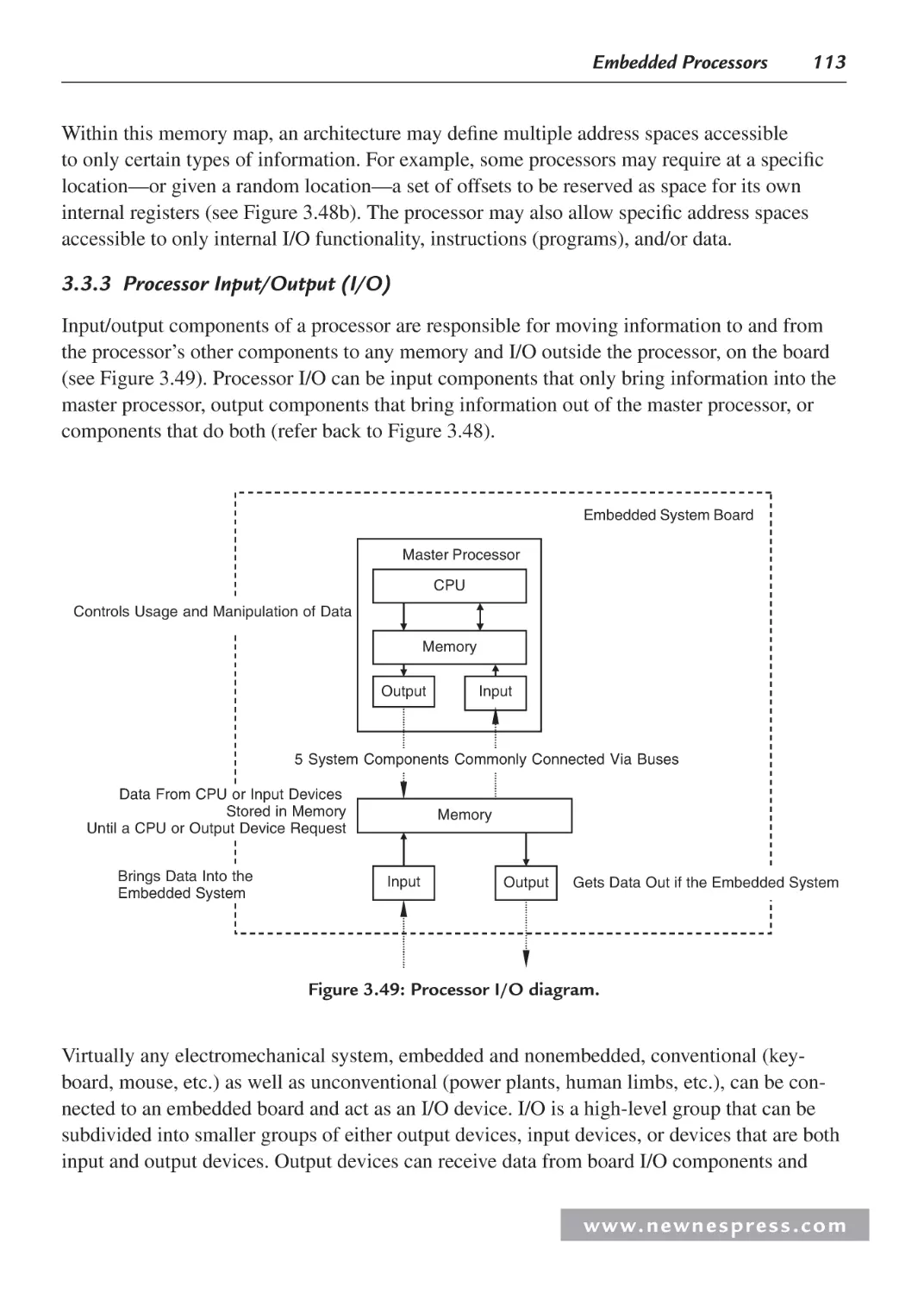
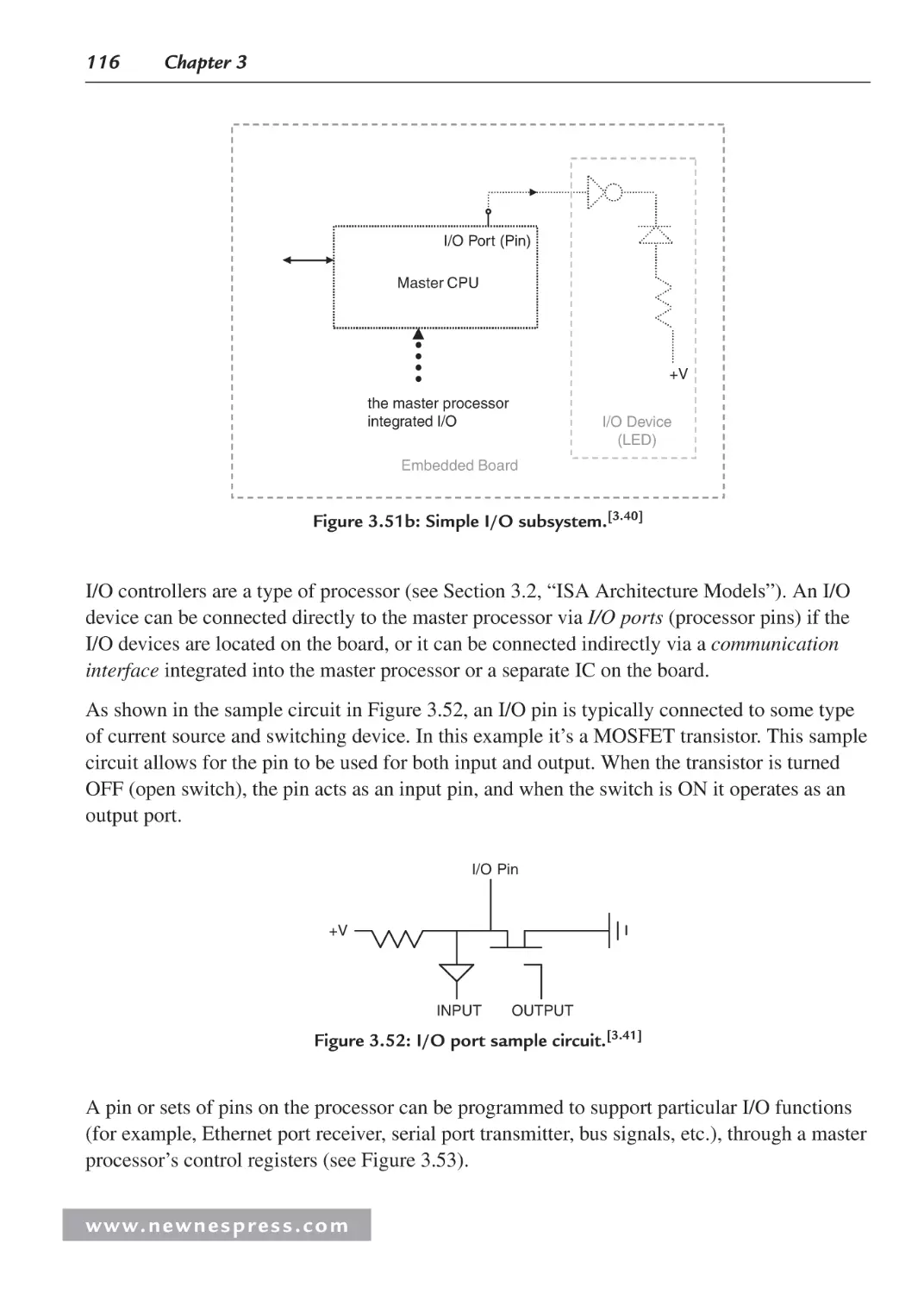
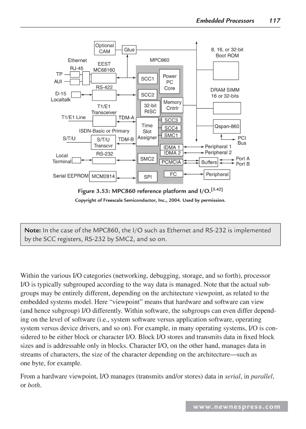
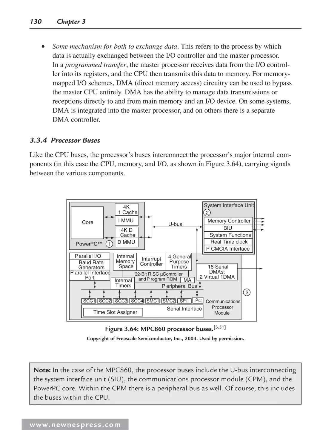
3.3.3 Processor Input/Output (I/O)........................................................................... 113
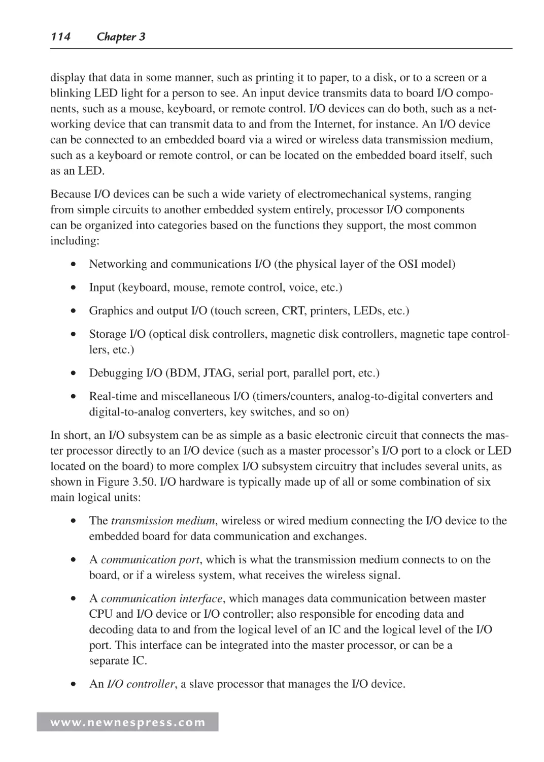
3.3.4 Processor Buses............................................................................................... 130
3.4 Processor Performance .............................................................................................. 131
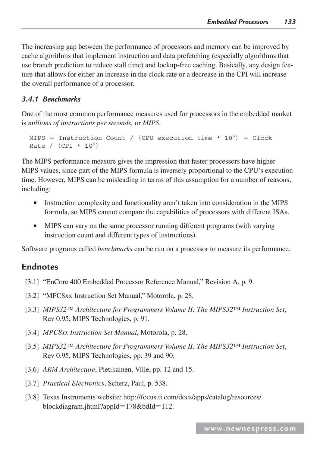
3.4.1 Benchmarks ..................................................................................................... 133
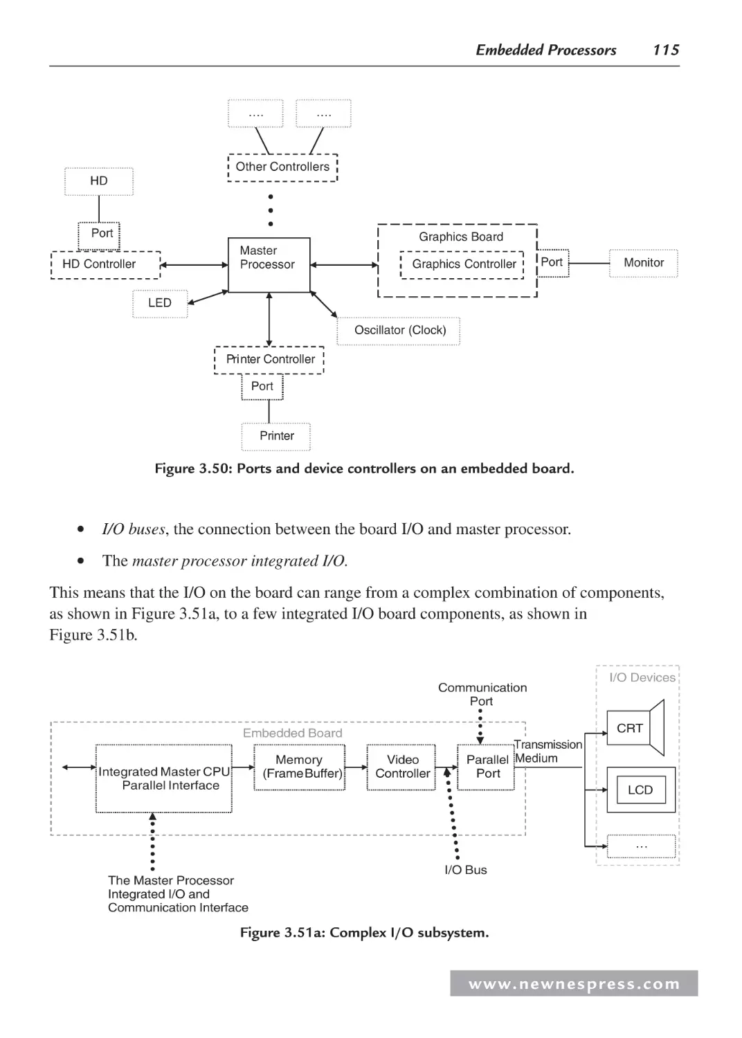
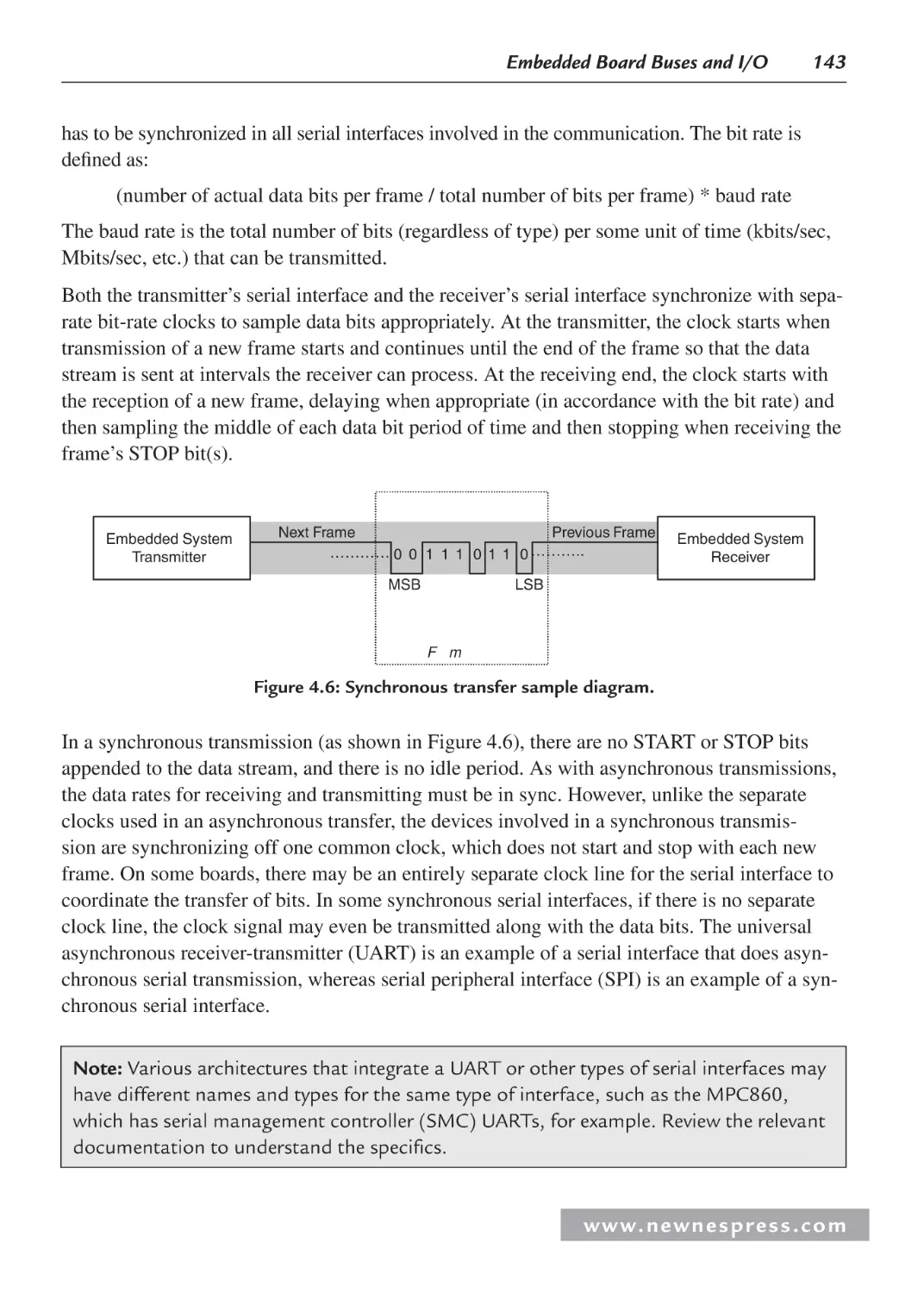
Endnotes ........................................................................................................................... 133
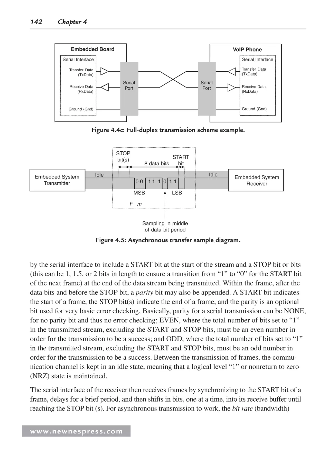
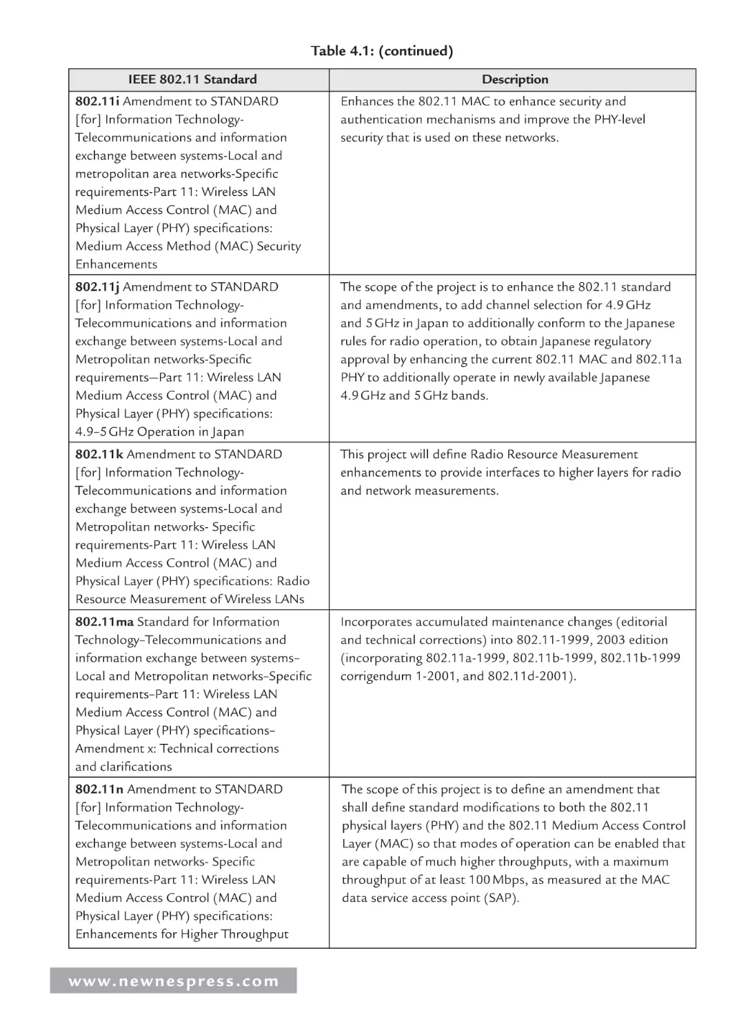
Chapter 4: Embedded Board Buses and I/O ........................................................................... 137
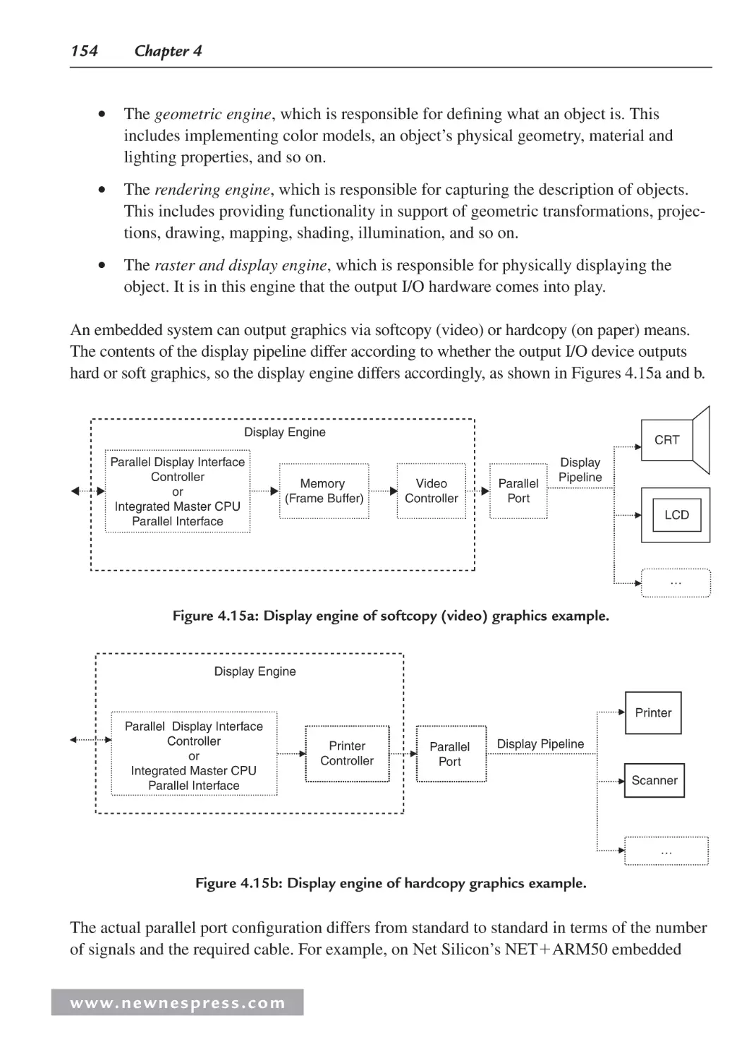
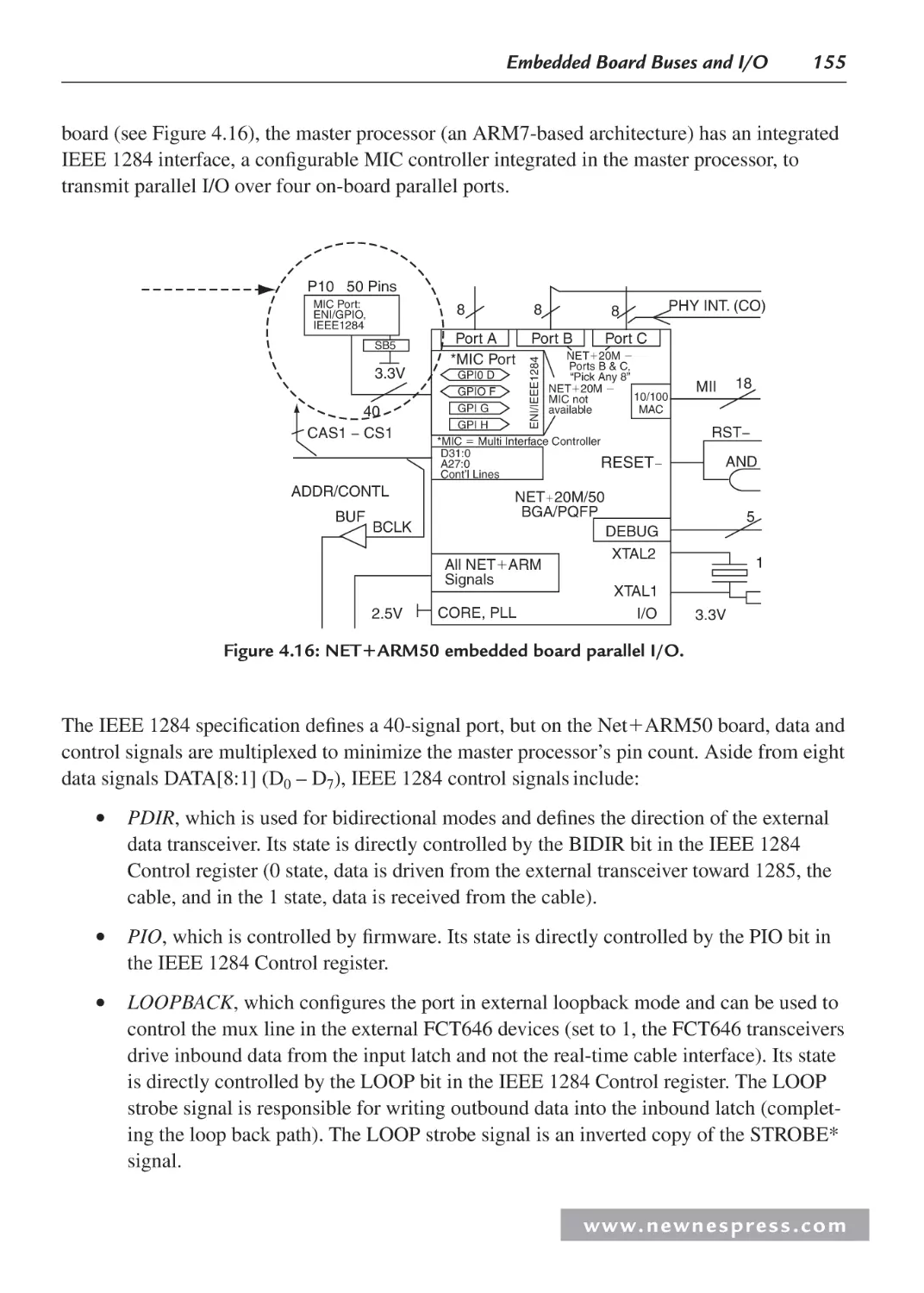
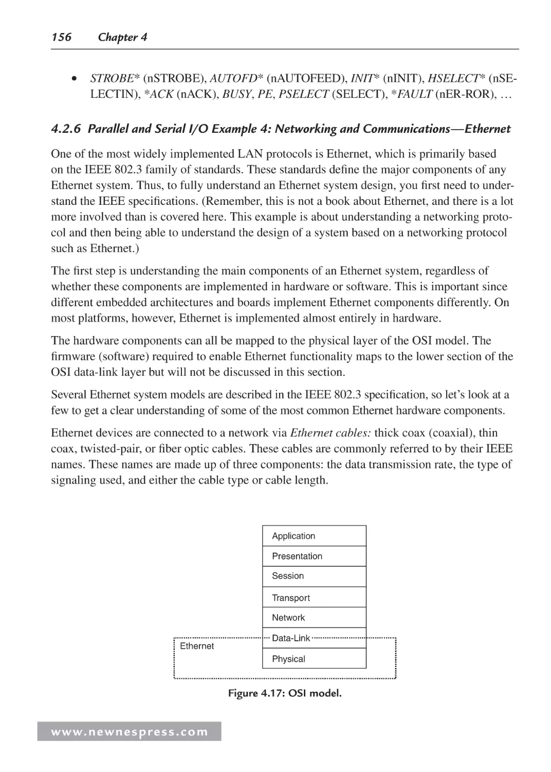
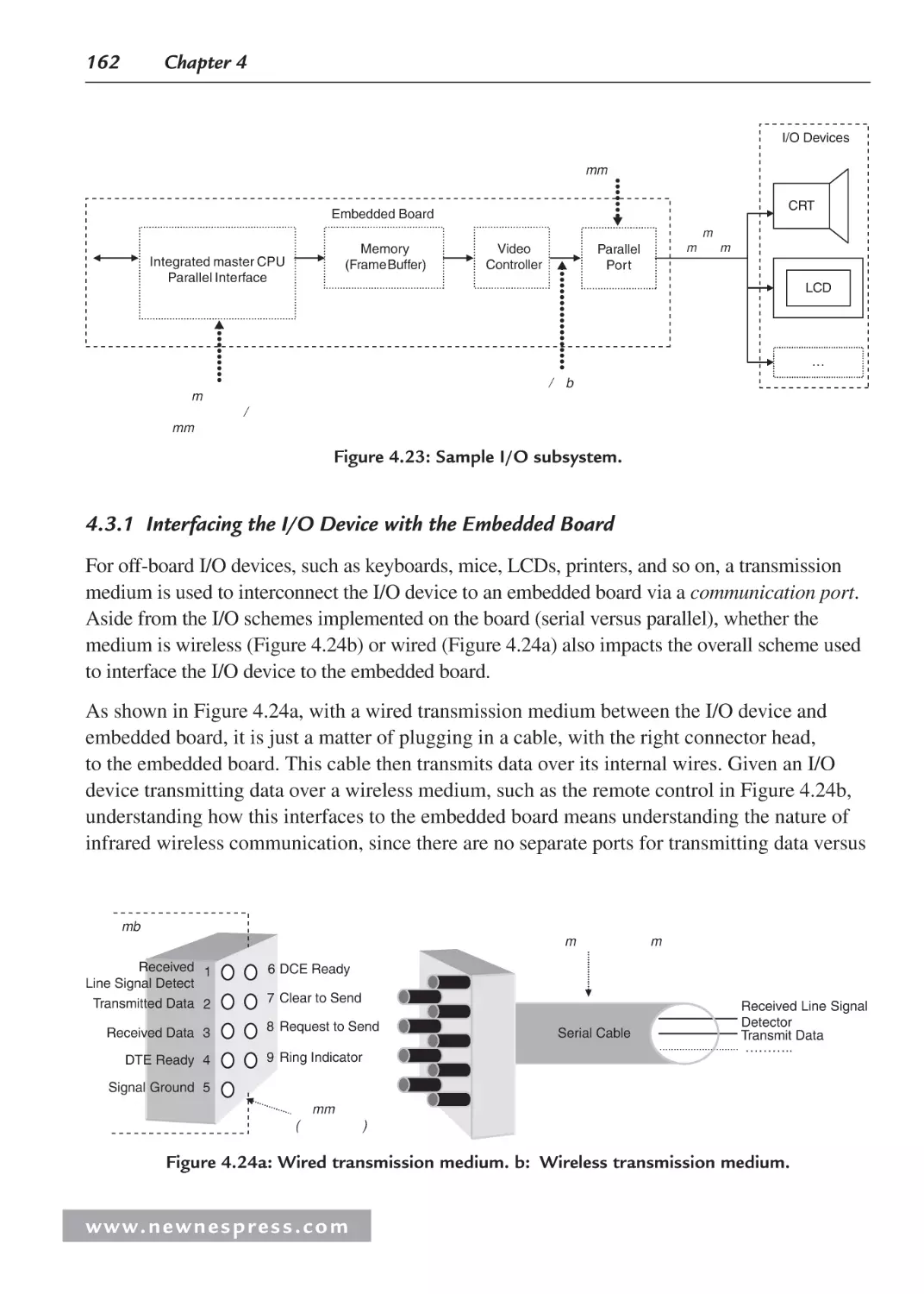
4.1 Board I/O ................................................................................................................... 137
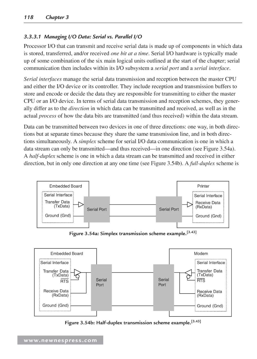
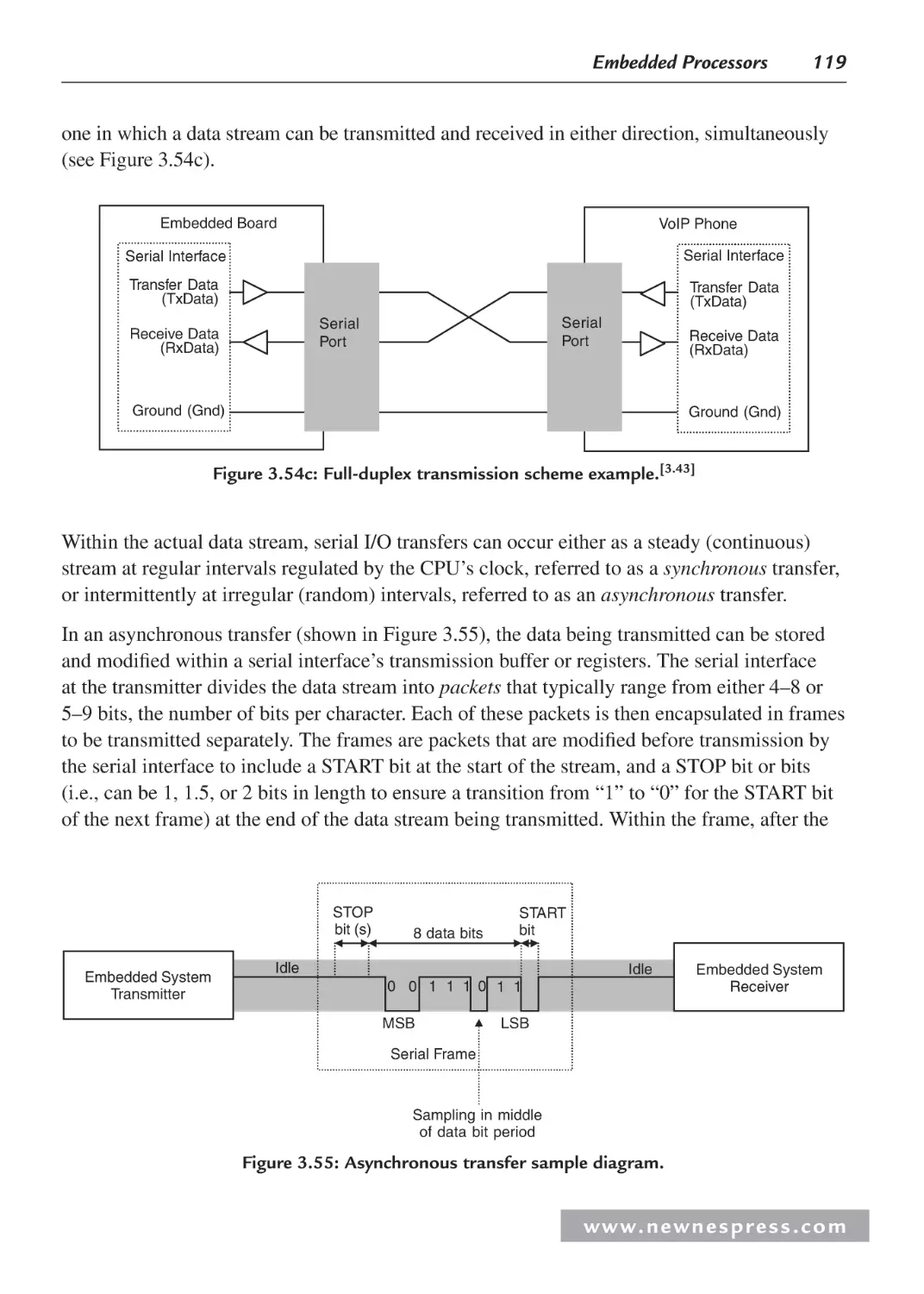
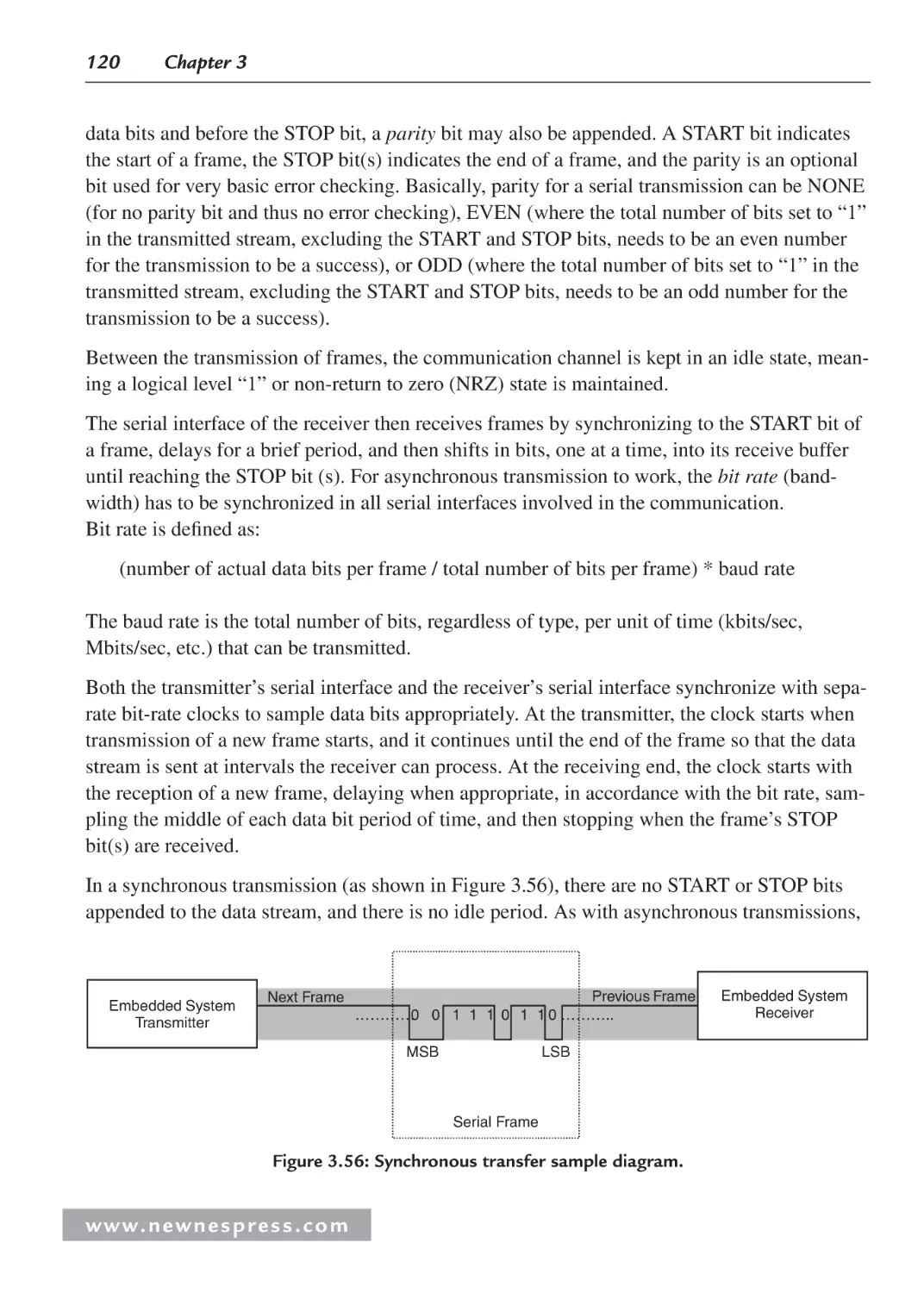
4.2 Managing Data: Serial vs. Parallel I/O ...................................................................... 140
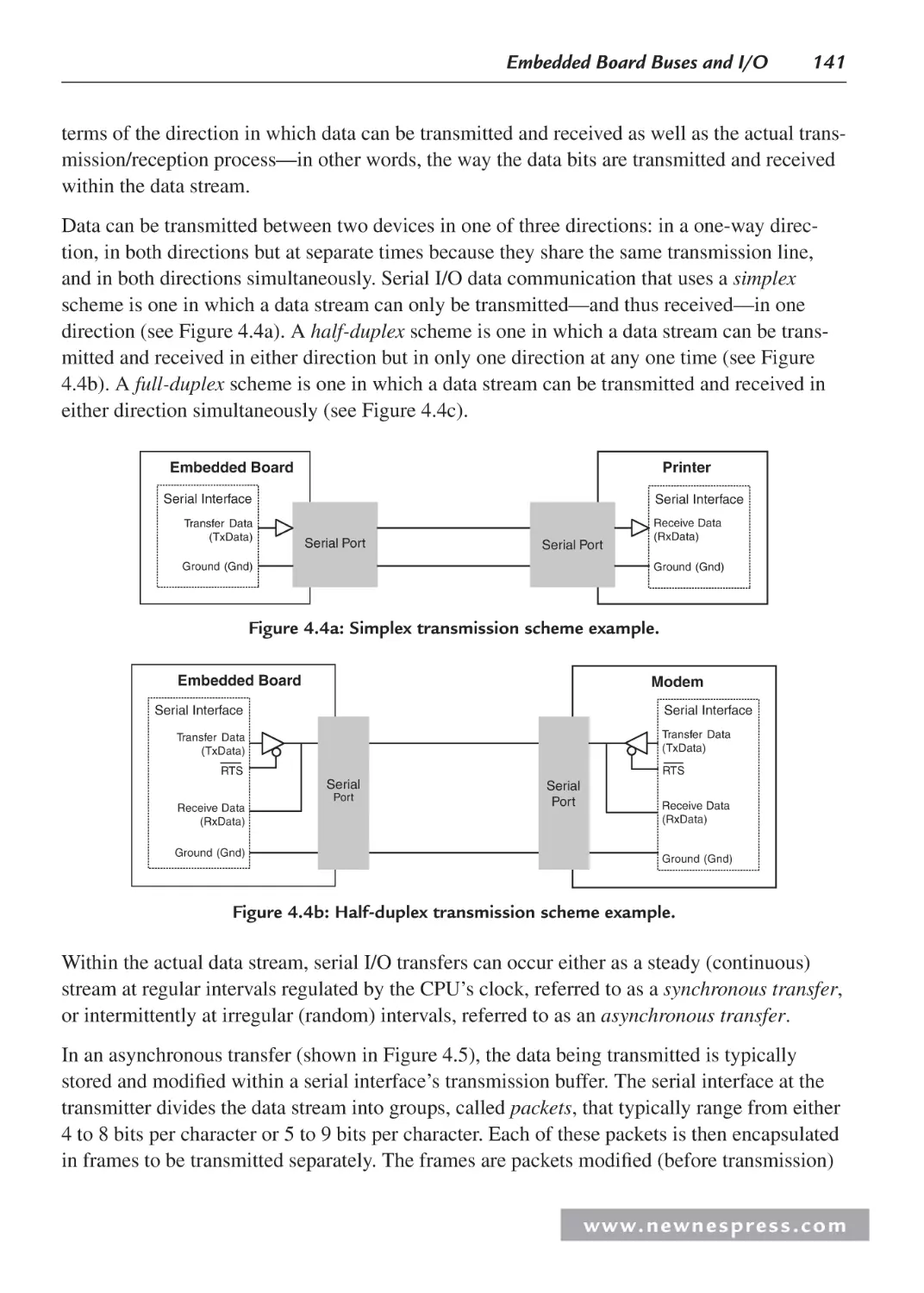
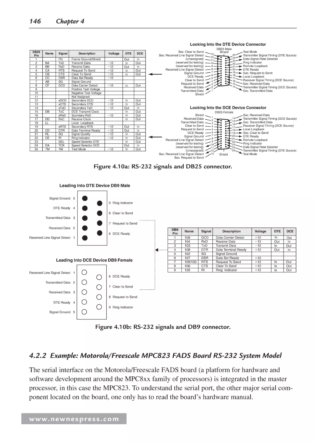
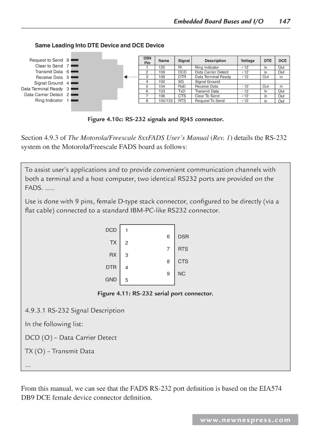
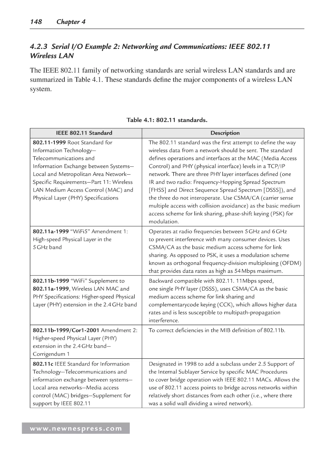
4.2.1 Serial I/O Example 1: Networking and Communications: RS-232 ................ 144
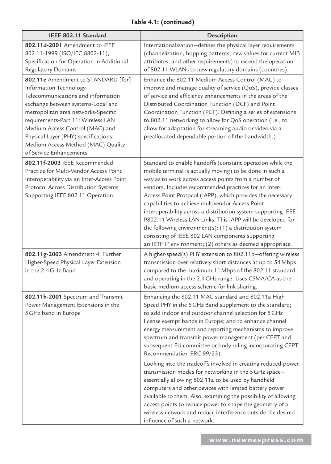
4.2.2 Example: Motorola/Freescale MPC823 FADS Board
RS-232 System Model .................................................................................... 146
4.2.3 Serial I/O Example 2: Networking and Communications:
IEEE 802.11 Wireless LAN ............................................................................ 148
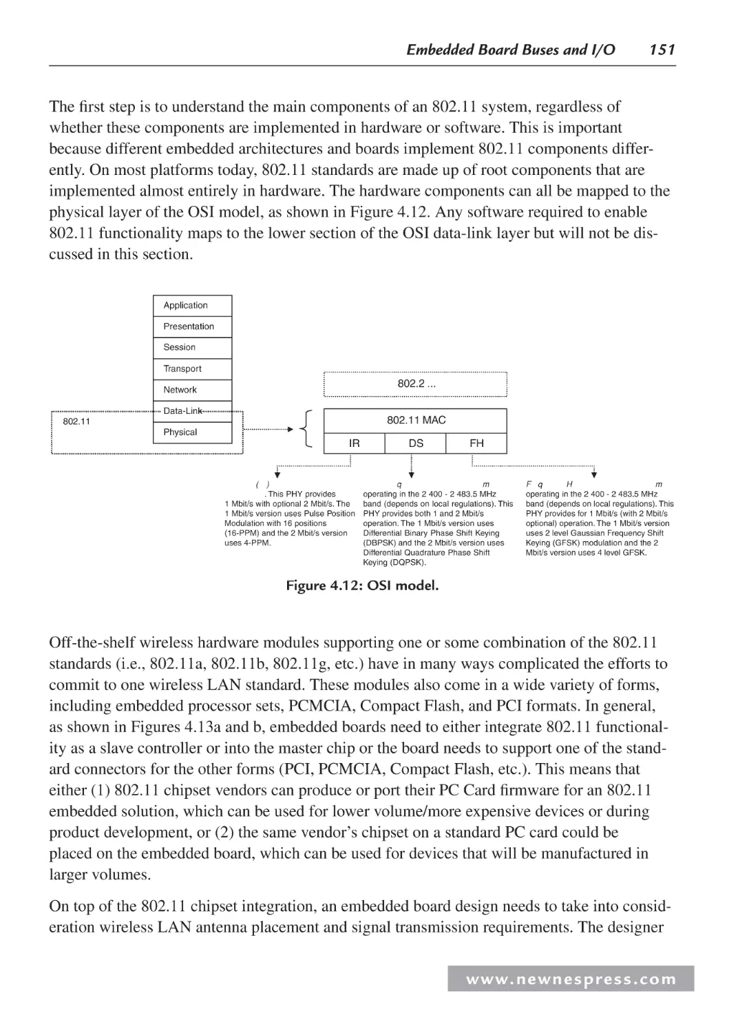
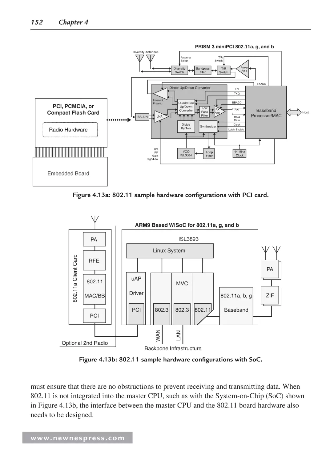
4.2.4 Parallel I/O ...................................................................................................... 153
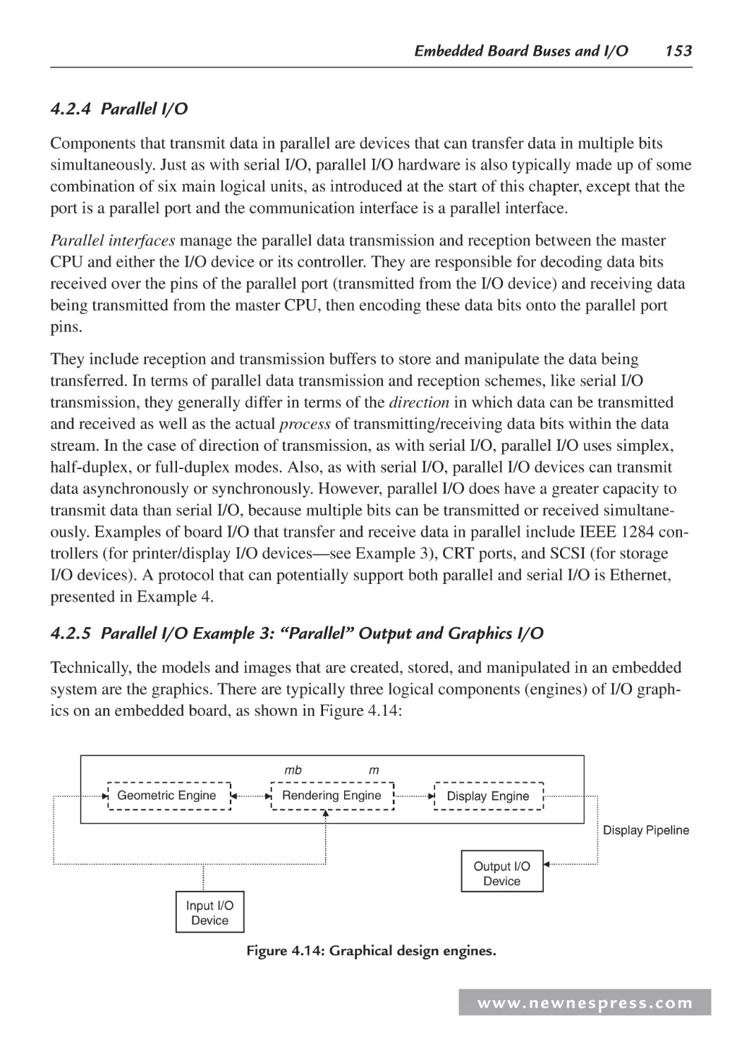
4.2.5 Parallel I/O Example 3: “Parallel” Output and Graphics I/O ......................... 153
4.2.6 Parallel and Serial I/O Example 4: Networking and
Communications—Ethernet ............................................................................ 156
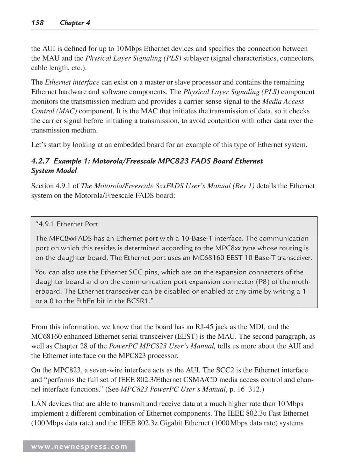
4.2.7 Example 1: Motorola/Freescale MPC823 FADS Board
Ethernet System Model ................................................................................... 158
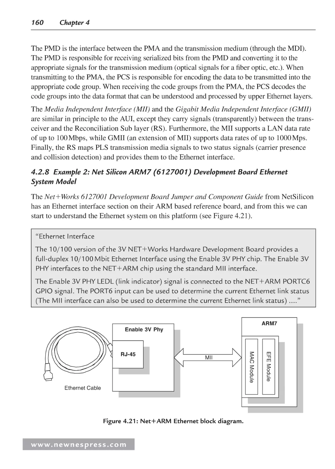
4.2.8 Example 2: Net Silicon ARM7 (6127001) Development
Board Ethernet System Model ........................................................................ 160
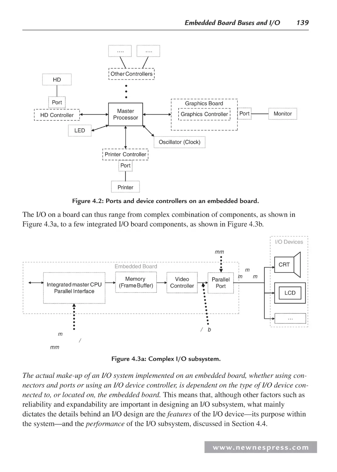
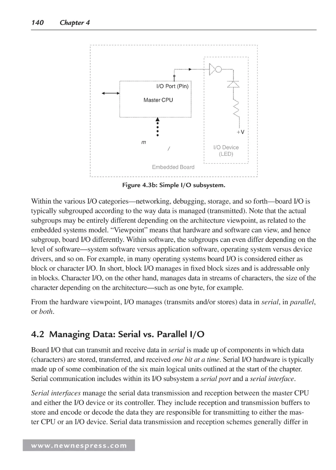
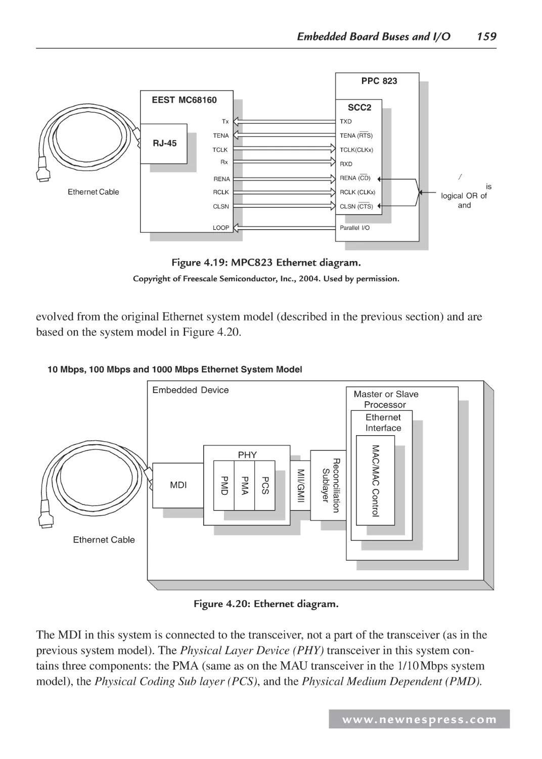
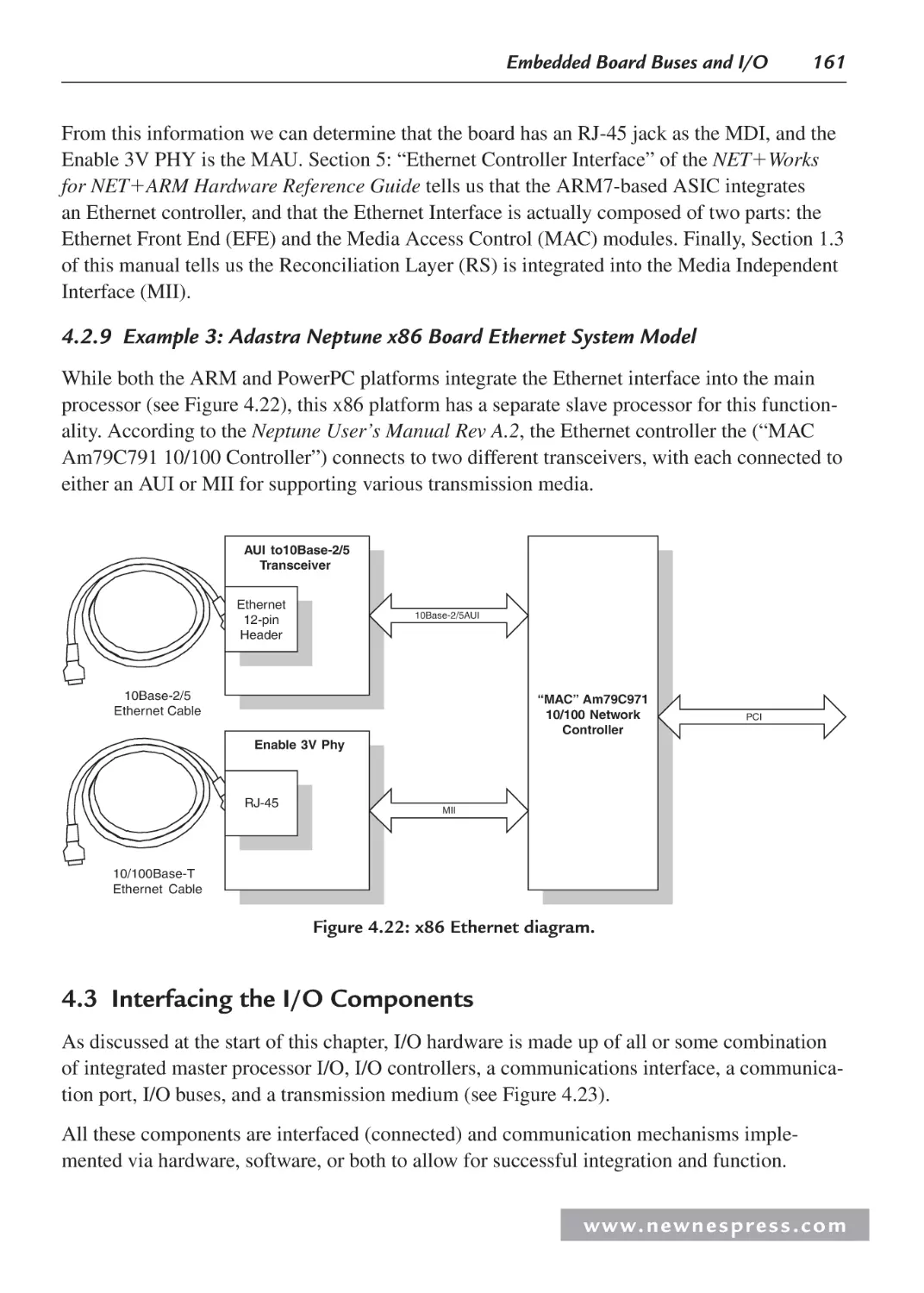
4.2.9 Example 3: Adastra Neptune x86 Board Ethernet System Model .................. 161
4.3 Interfacing the I/O Components ................................................................................ 161
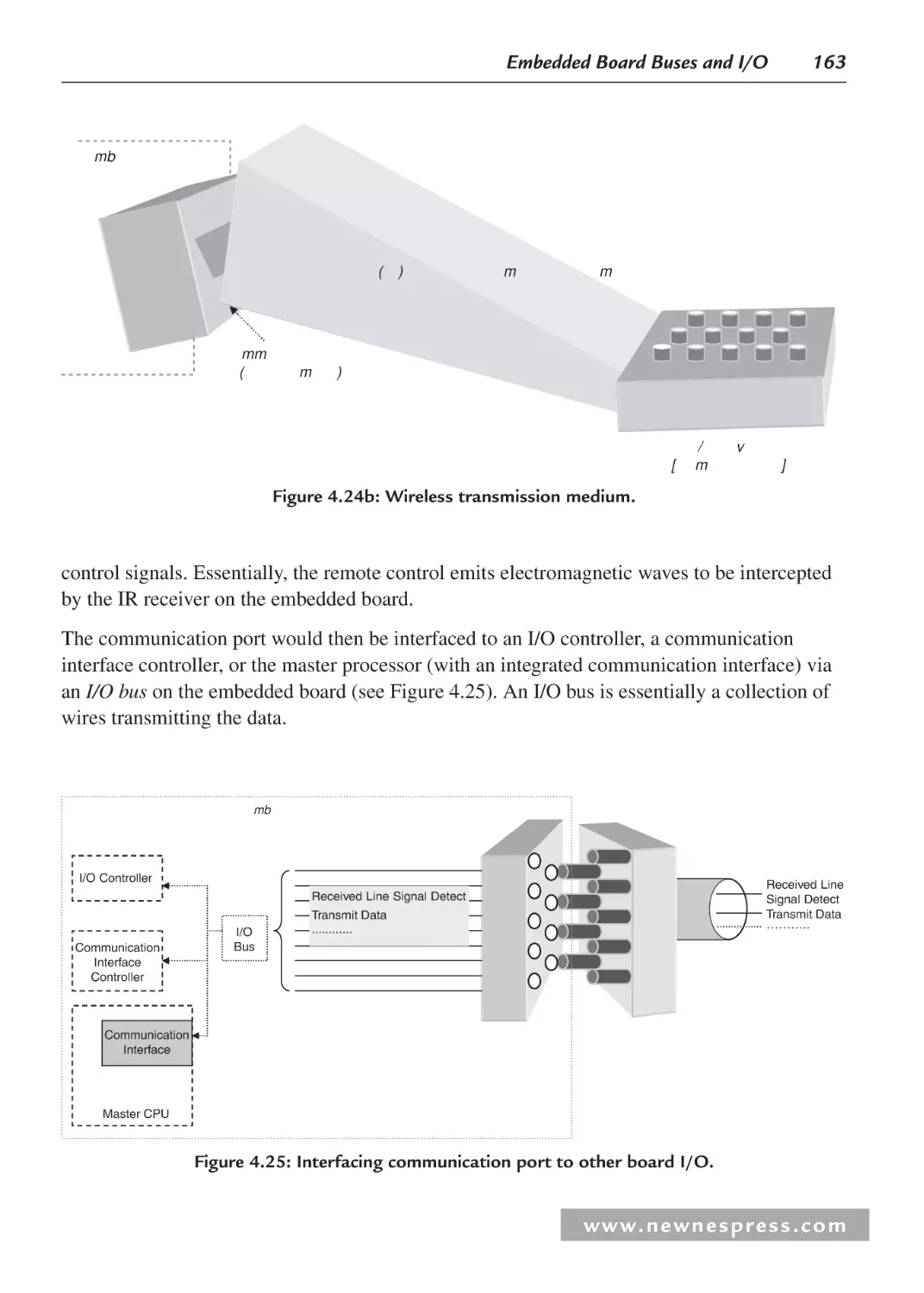
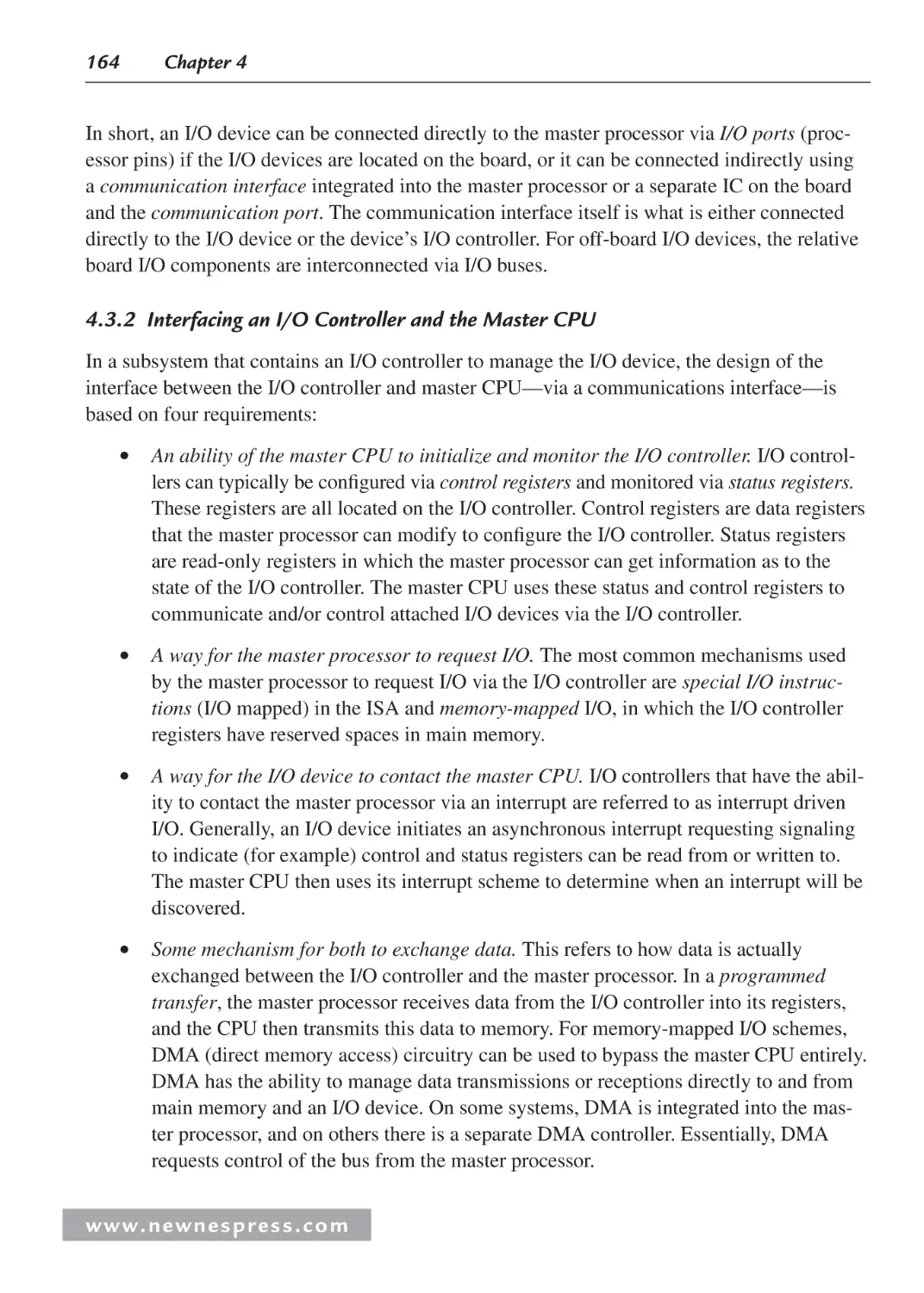
4.3.1 Interfacing the I/O Device with the Embedded Board .................................... 162
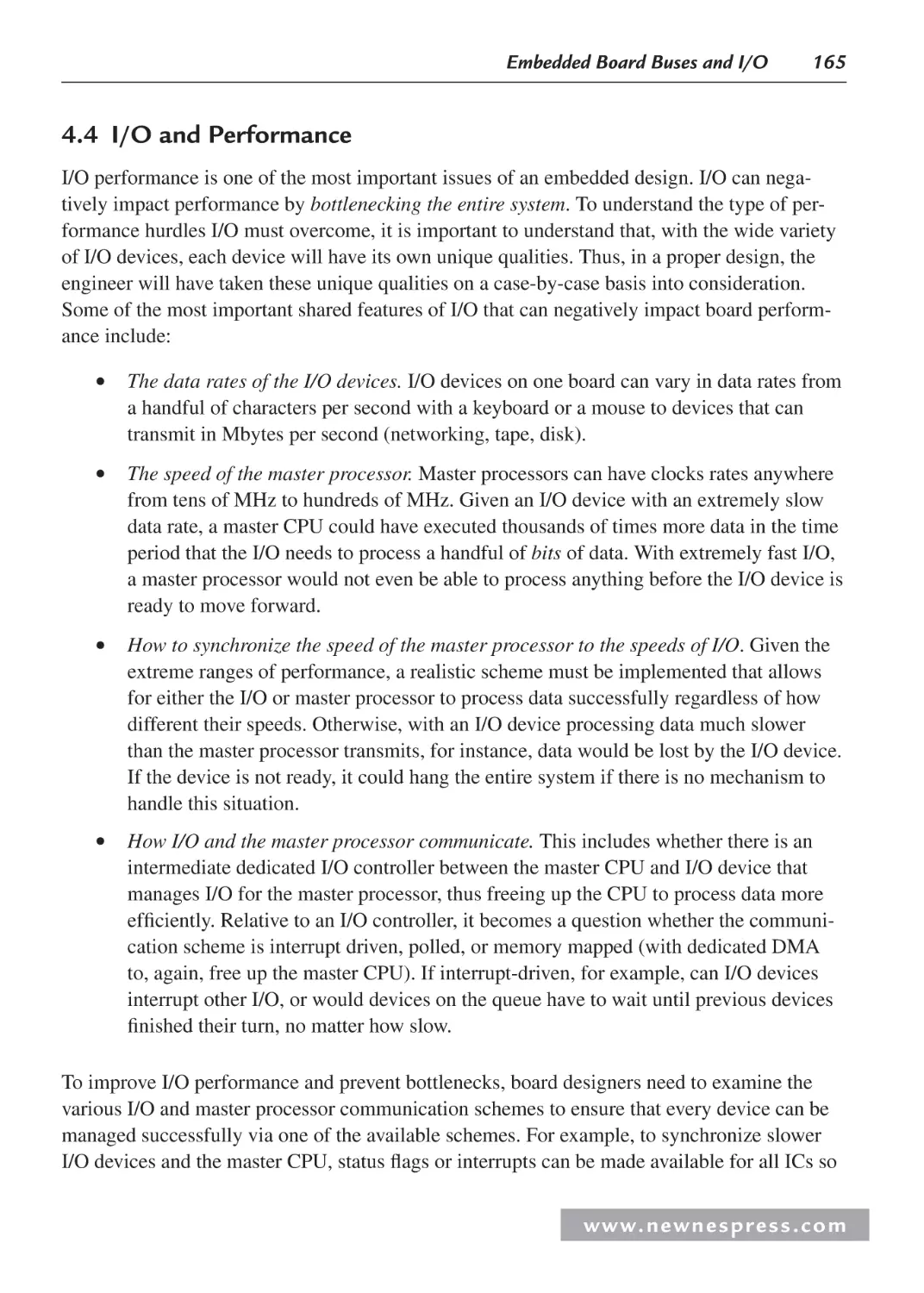
4.3.2 Interfacing an I/O Controller and the Master CPU ......................................... 164
www. n e wn e s p res s .c o m
Contents
vii
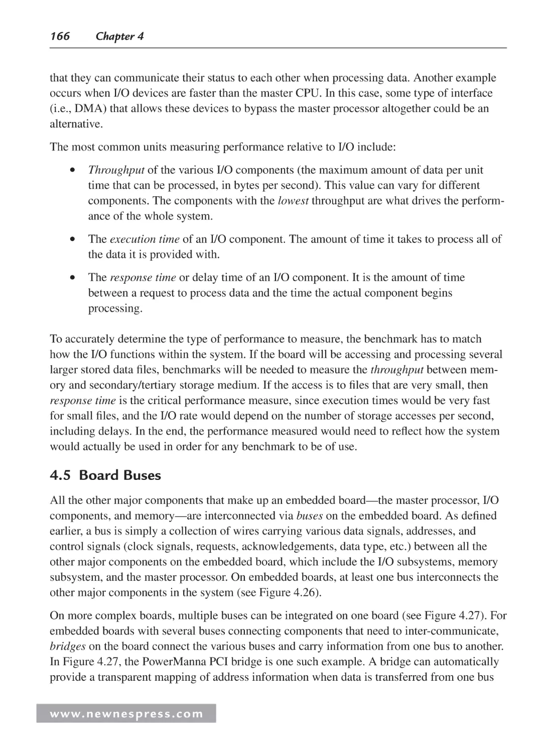
4.4 I/O and Performance ................................................................................................. 165
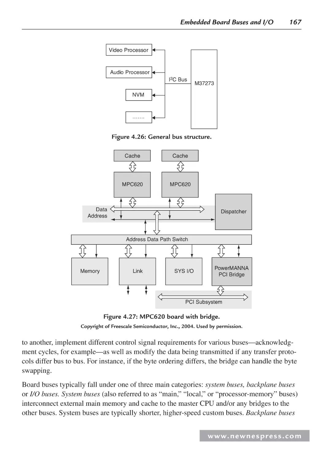
4.5 Board Buses ............................................................................................................... 166
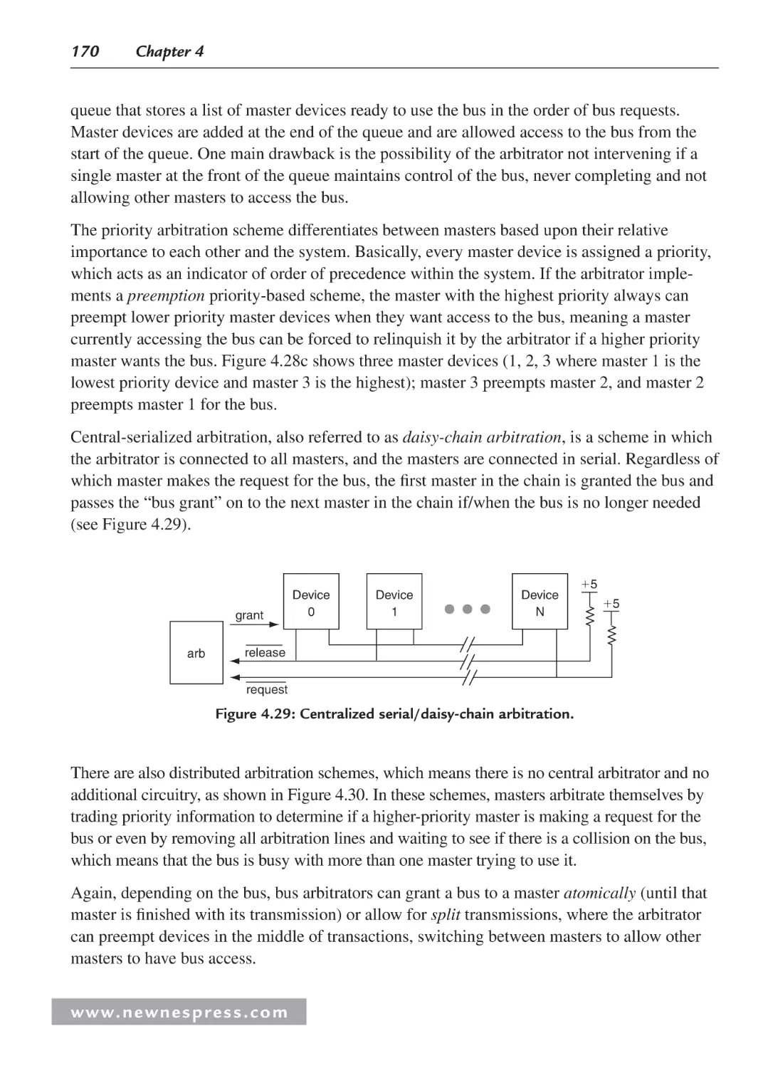
4.6 Bus Arbitration and Timing....................................................................................... 168
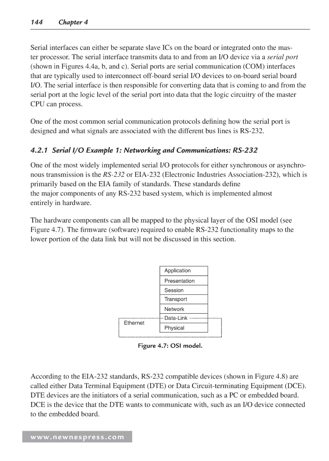
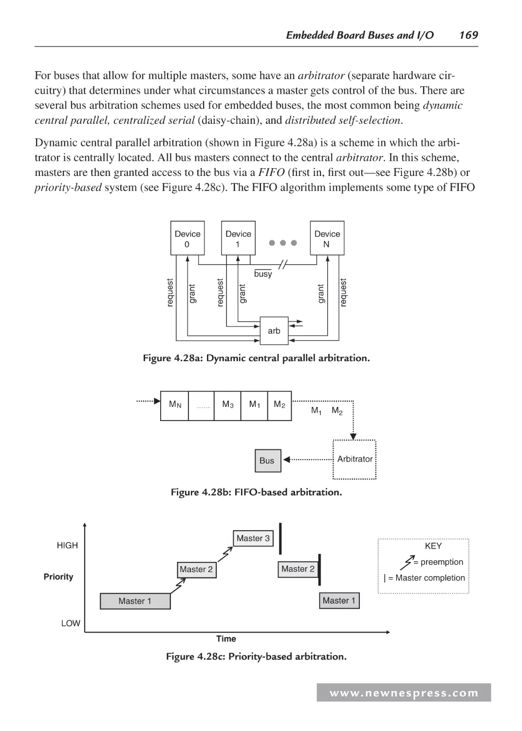
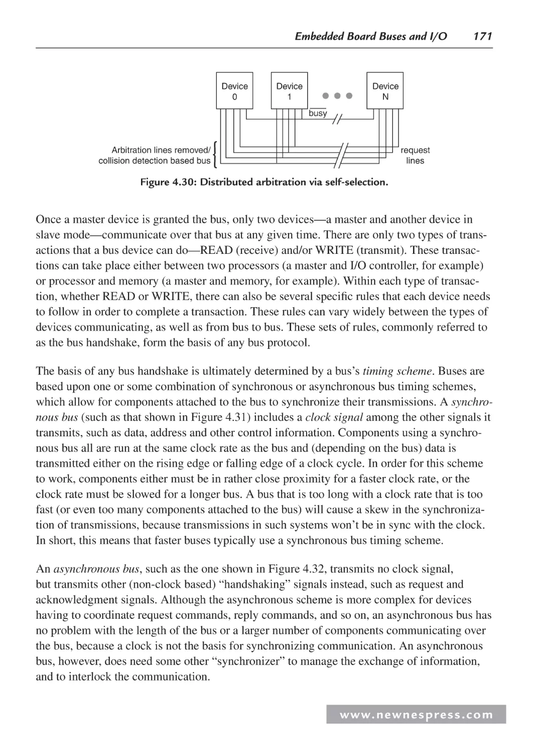
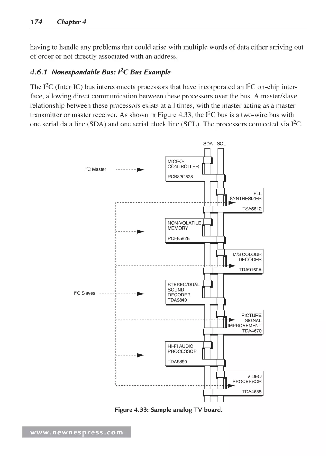
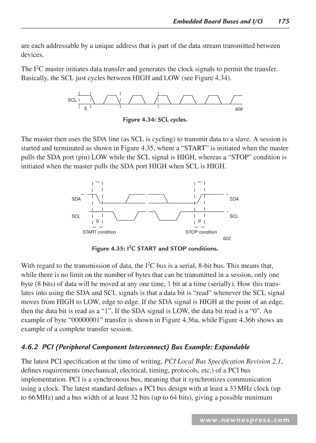
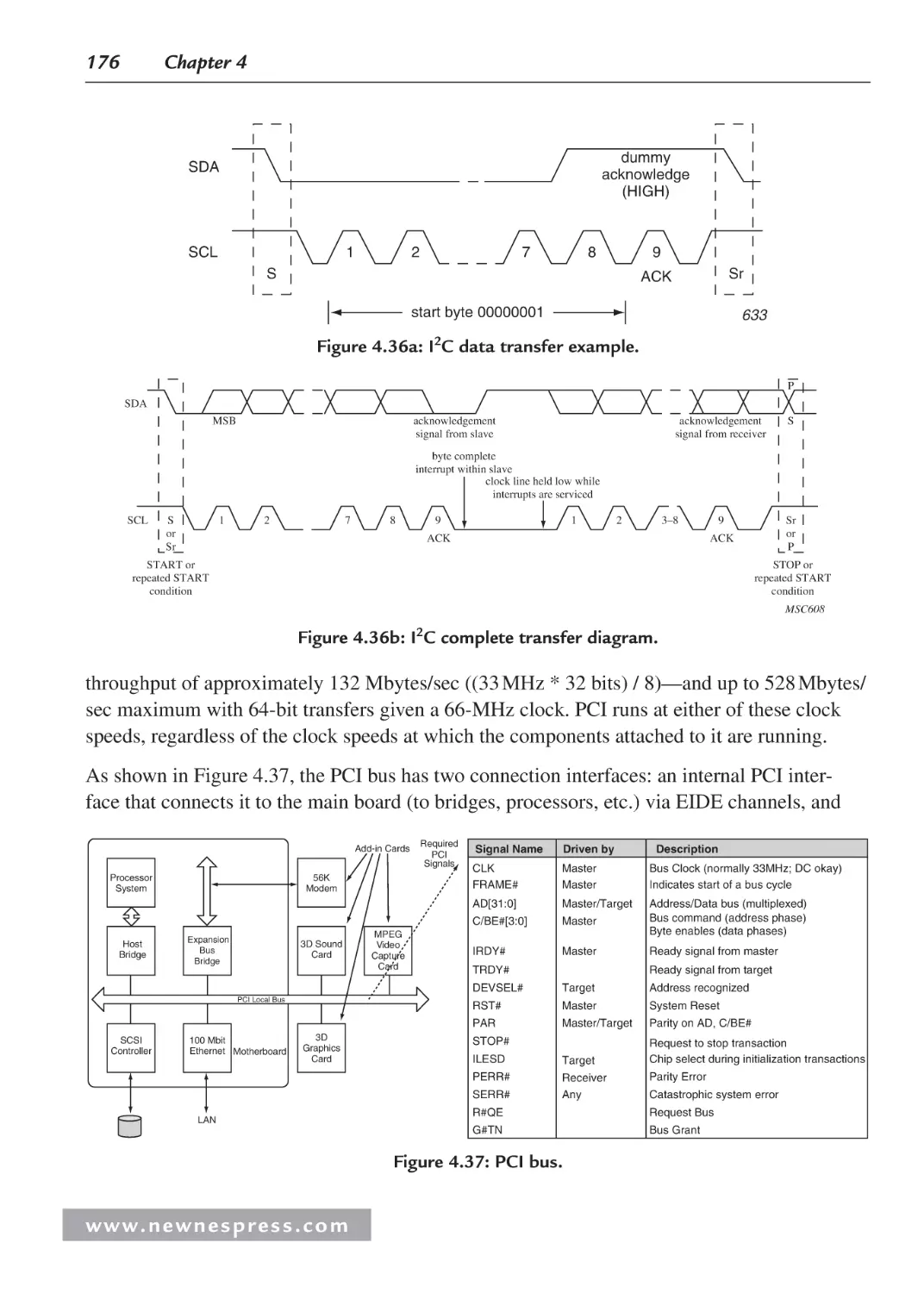
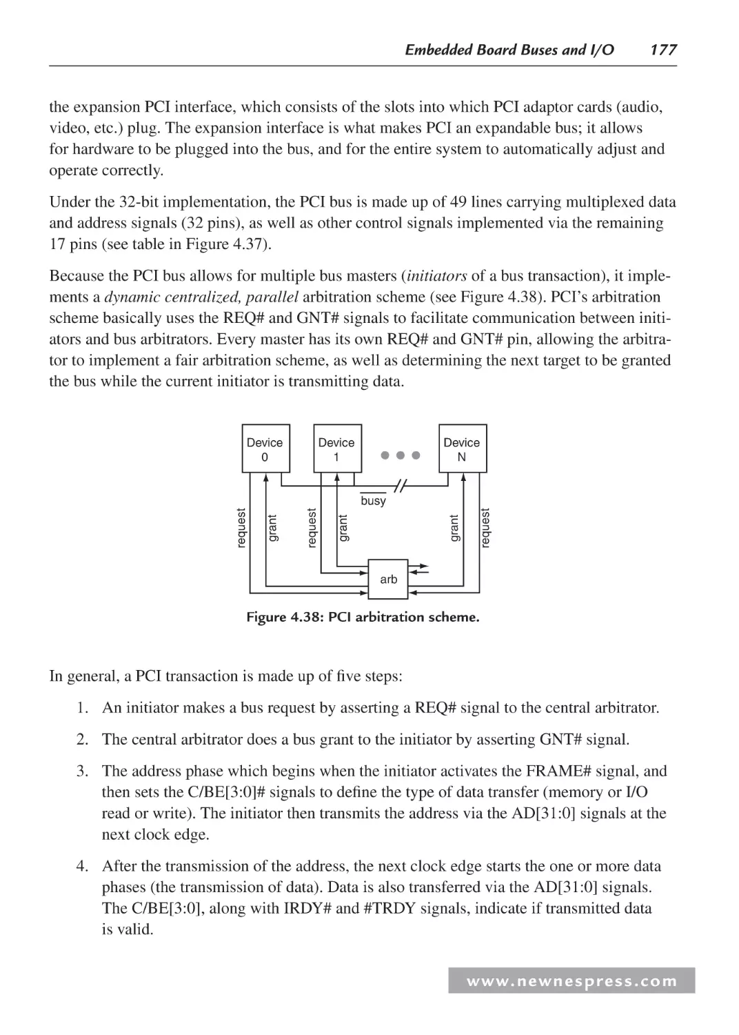
4.6.1 Nonexpandable Bus: I2C Bus Example .......................................................... 174
4.6.2 PCI (Peripheral Component Interconnect)
Bus Example: Expandable ..............................................................................175
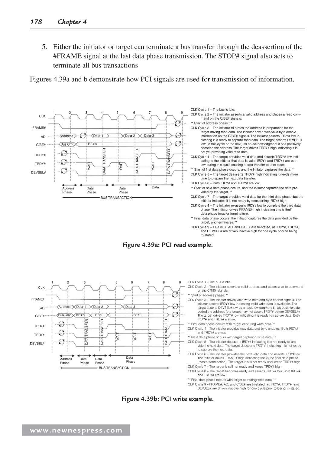
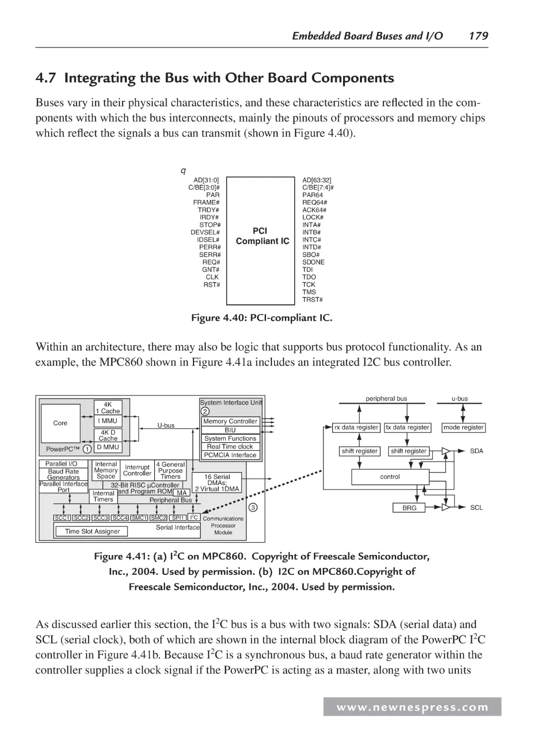
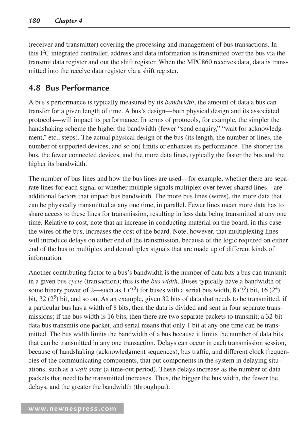
4.7 Integrating the Bus with Other Board Components .................................................. 179
4.8 Bus Performance ....................................................................................................... 180
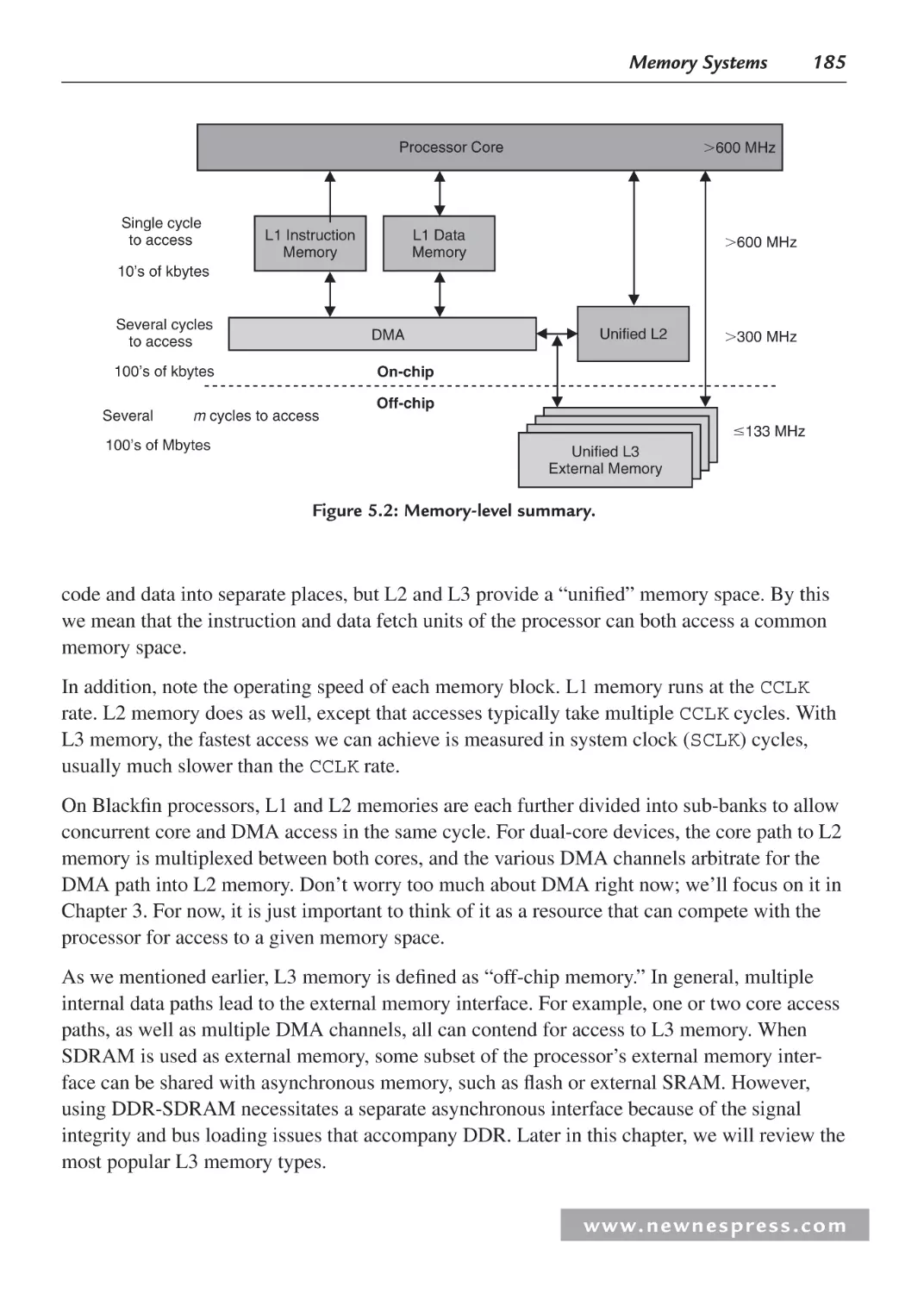
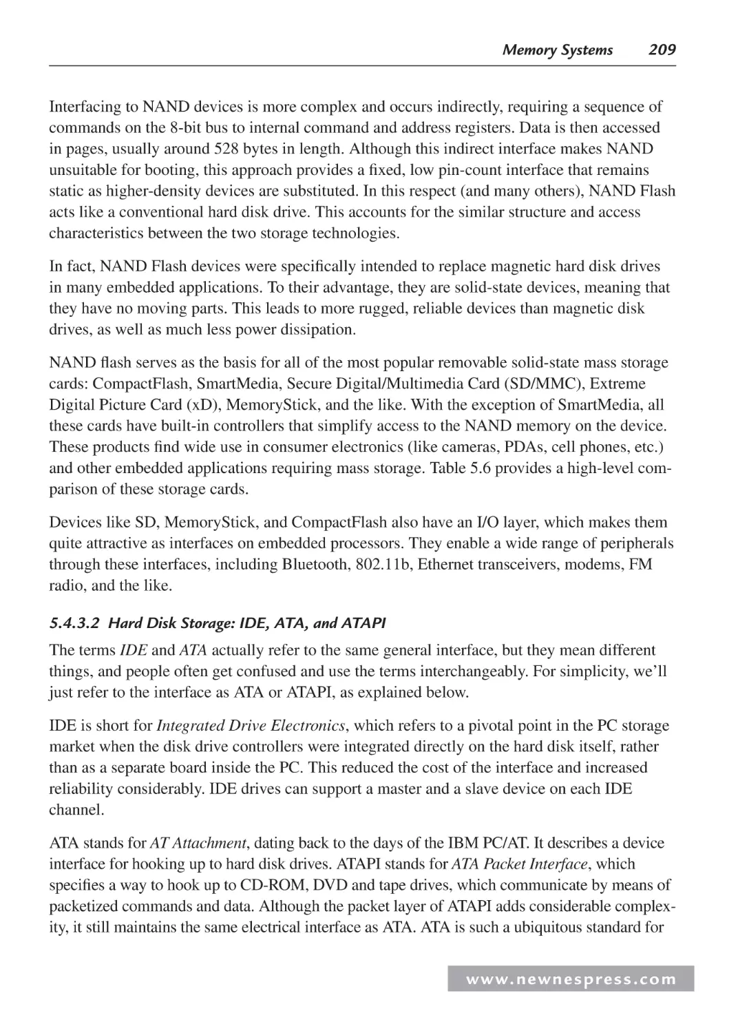
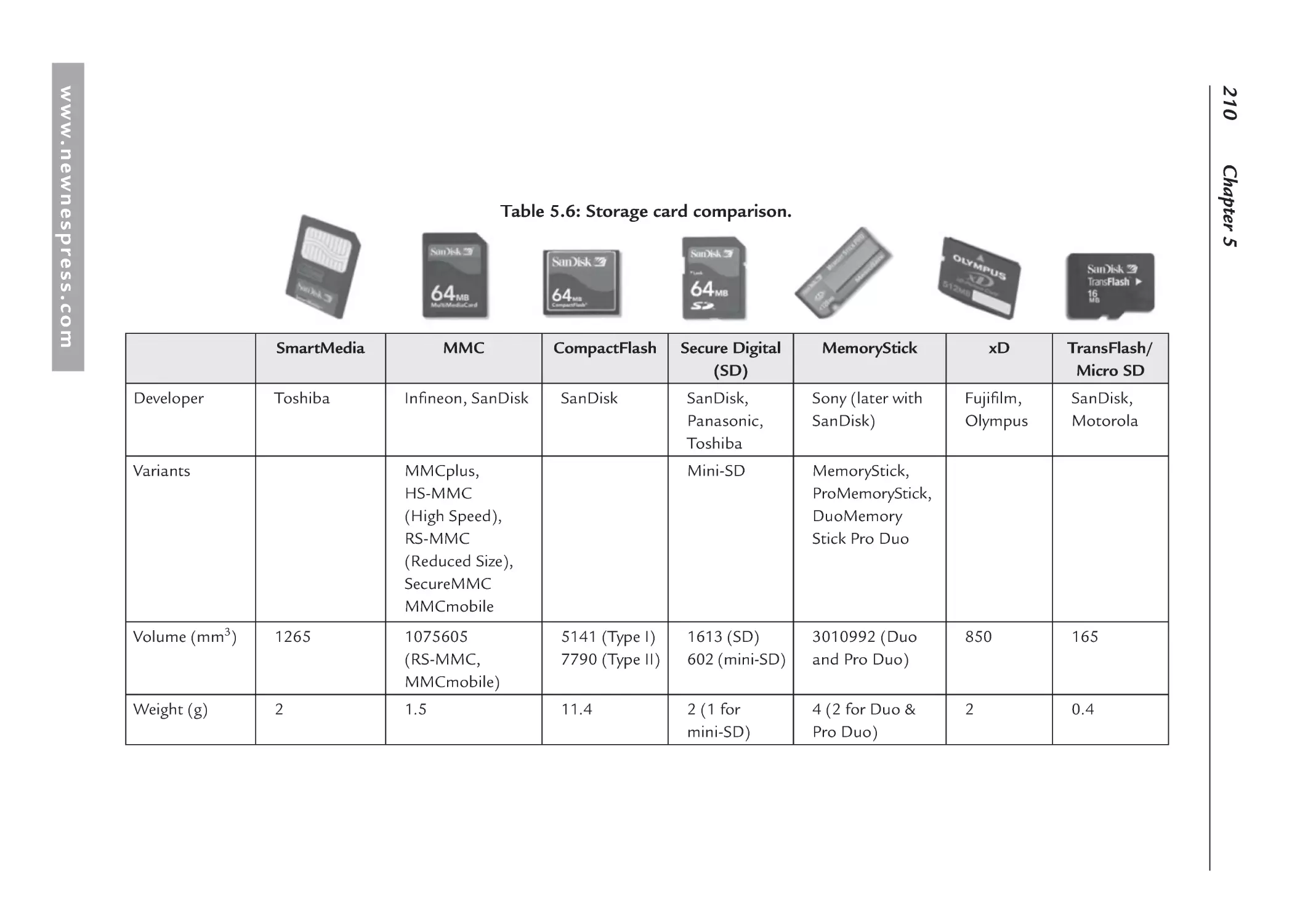
Chapter 5: Memory Systems................................................................................................... 183
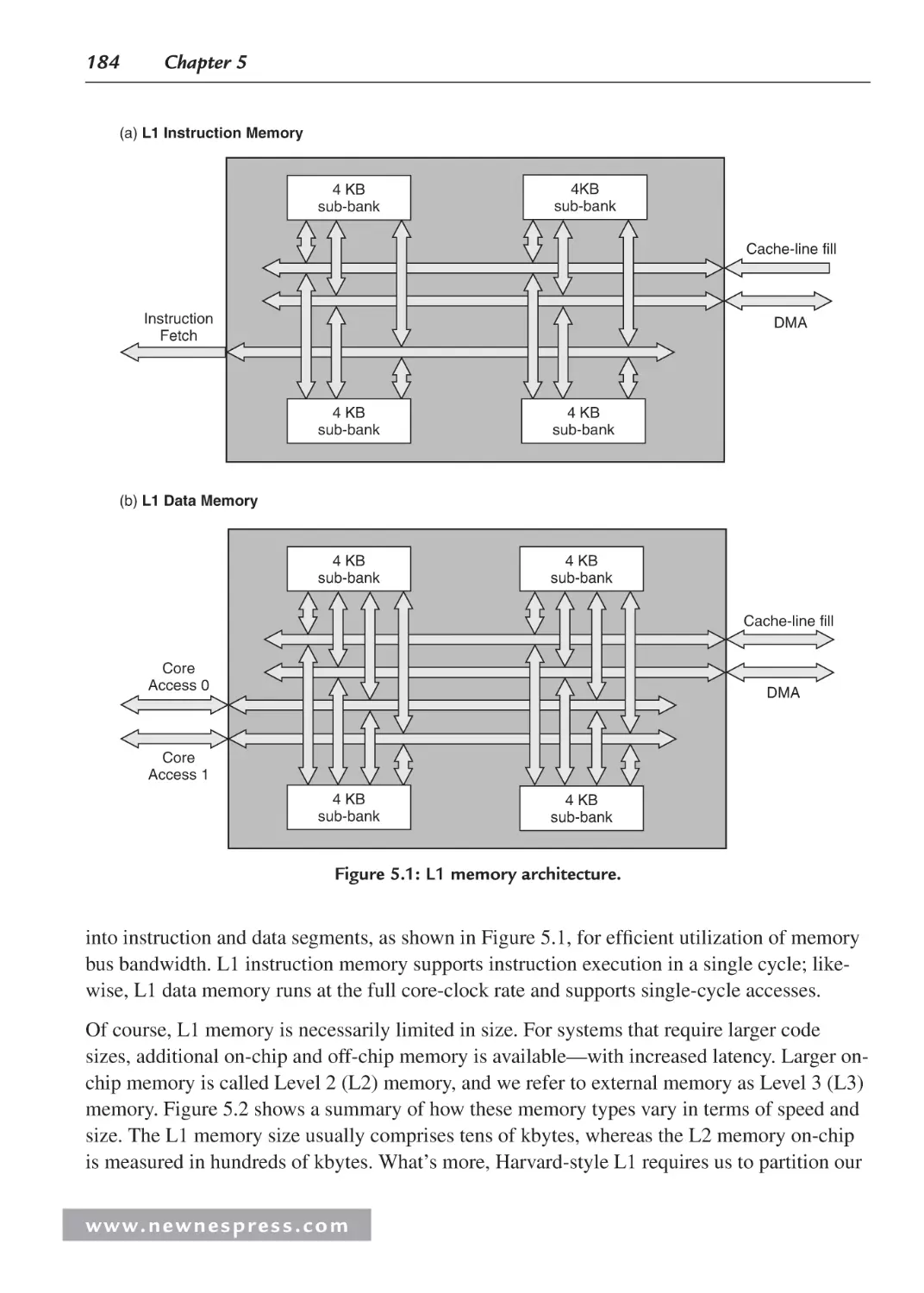
5.1 Introduction ............................................................................................................... 183
5.2 Memory Spaces ......................................................................................................... 183
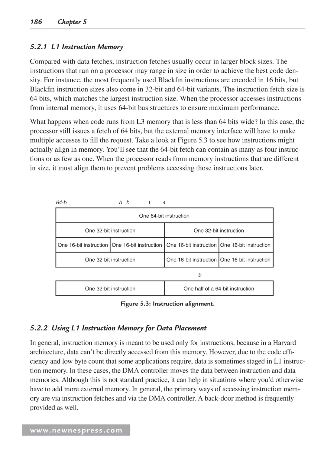
5.2.1 L1 Instruction Memory ................................................................................... 186
5.2.2 Using L1 Instruction Memory for Data Placement ......................................... 186
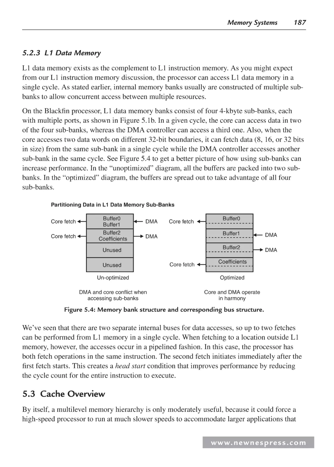
5.2.3 L1 Data Memory ............................................................................................. 187
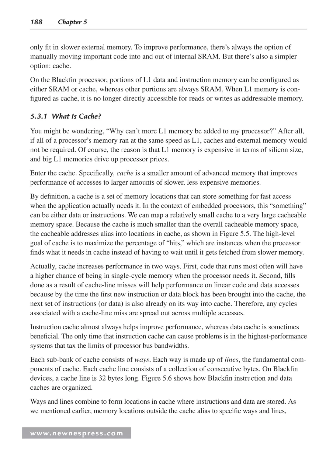
5.3 Cache Overview ........................................................................................................ 187
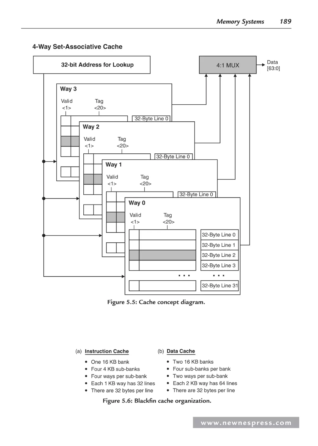
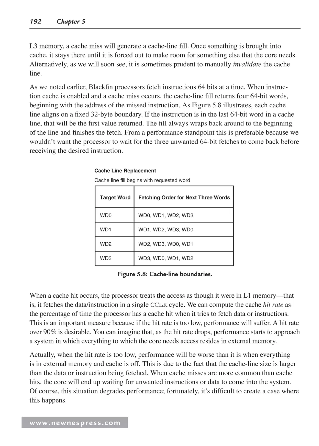
5.3.1 What Is Cache? ............................................................................................... 188
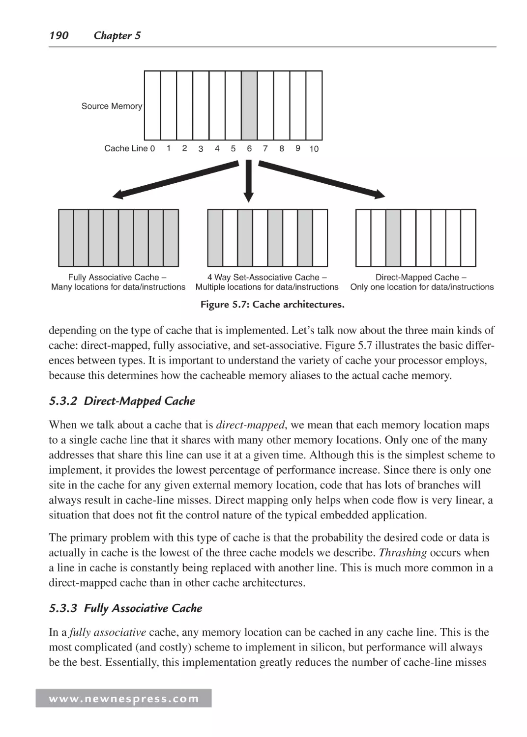
5.3.2 Direct-Mapped Cache ..................................................................................... 190
5.3.3 Fully Associative Cache .................................................................................. 190
5.3.4 N-Way Set-Associative Cache ........................................................................ 191
5.3.5 More Cache Details ......................................................................................... 191
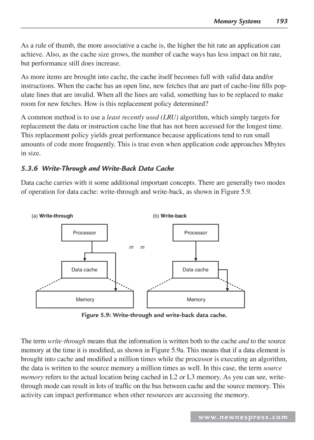
5.3.6 Write-Through and Write-Back Data Cache................................................... 193
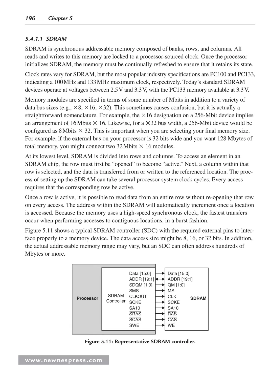
5.4 External Memory ....................................................................................................... 195
5.4.1 Synchronous Memory ..................................................................................... 195
5.4.2 Asynchronous Memory ................................................................................... 203
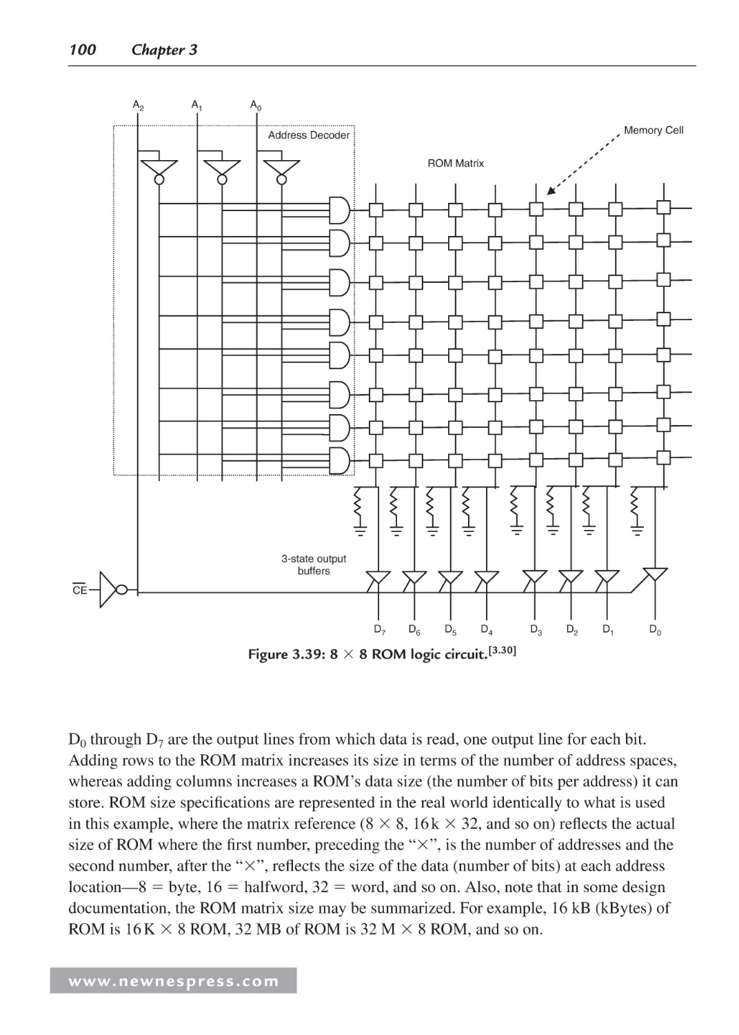
5.4.3 Nonvolatile Memories ..................................................................................... 206
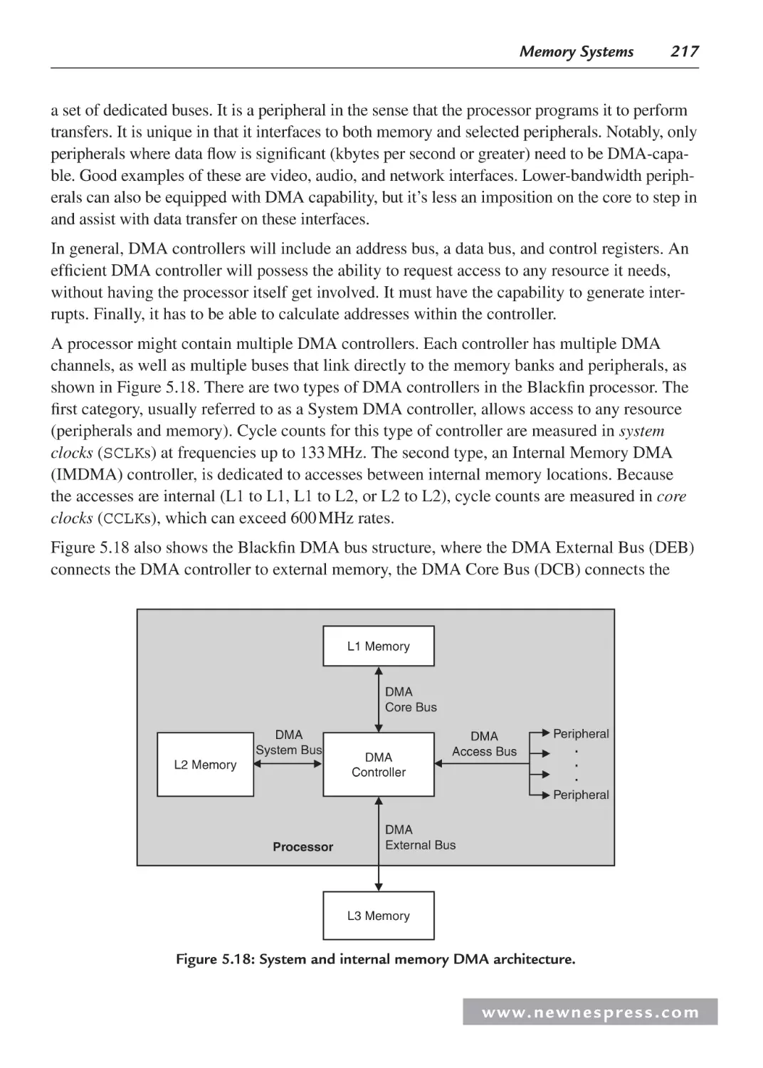
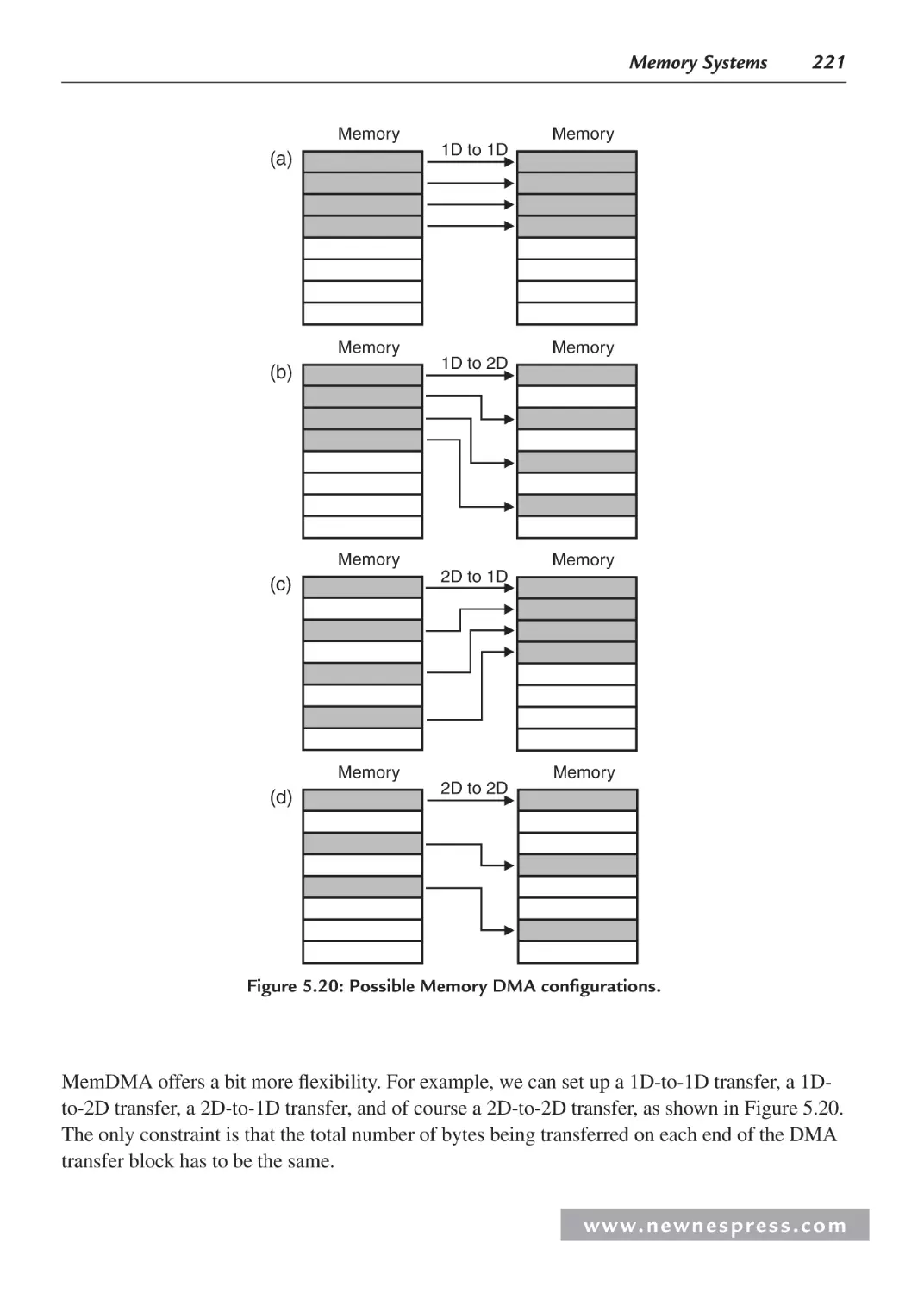
5.5 Direct Memory Access .............................................................................................. 214
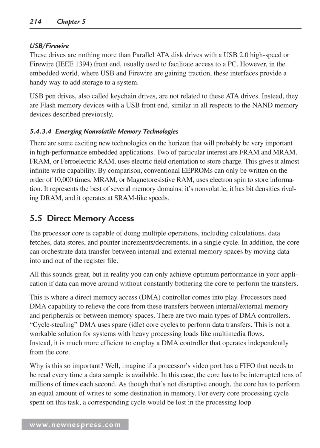
5.5.1 DMA Controller Overview ............................................................................. 215
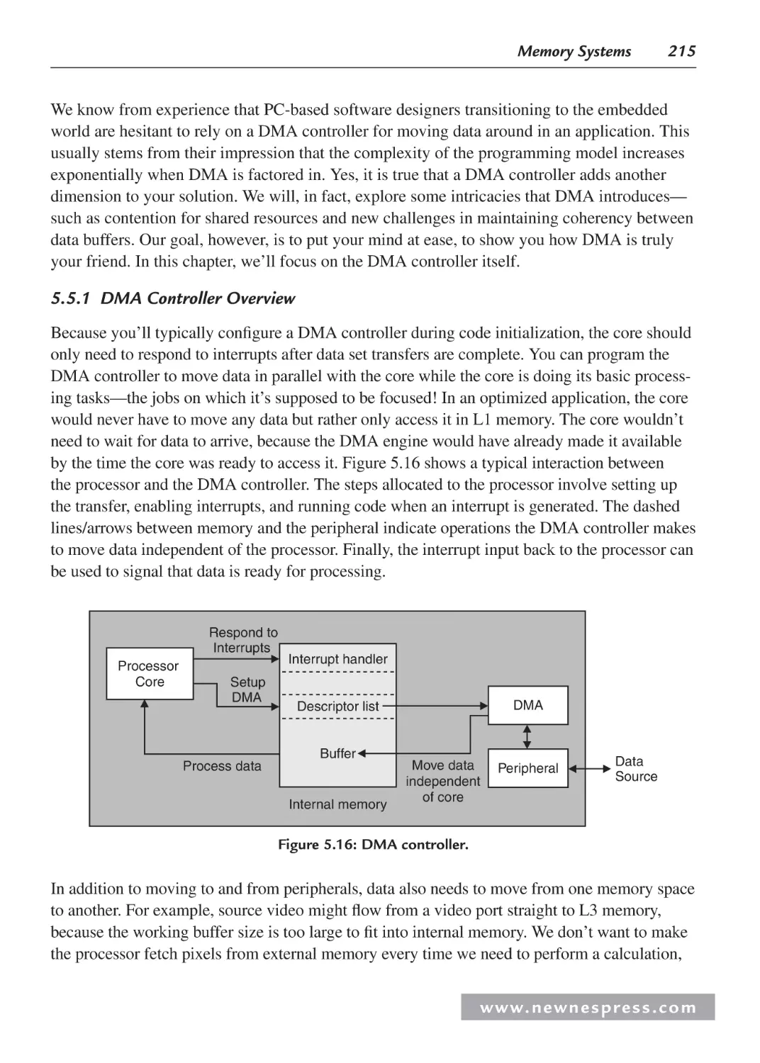
5.5.2 More on the DMA Controller ......................................................................... 216
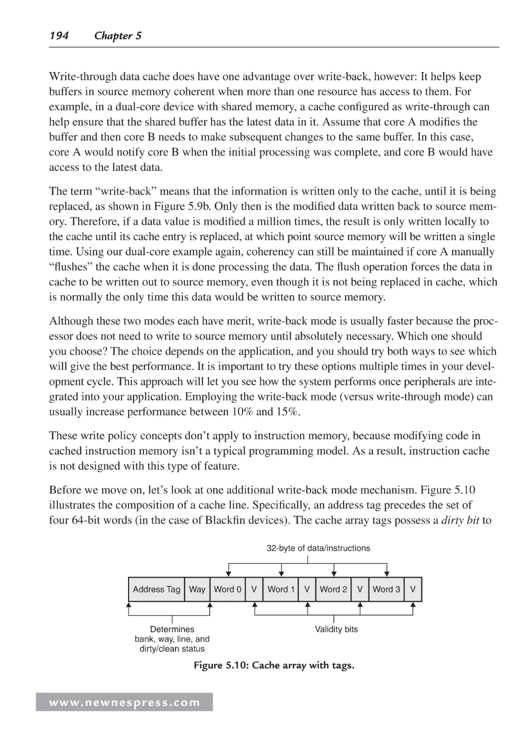
5.5.3 Programming the DMA Controller ................................................................. 218
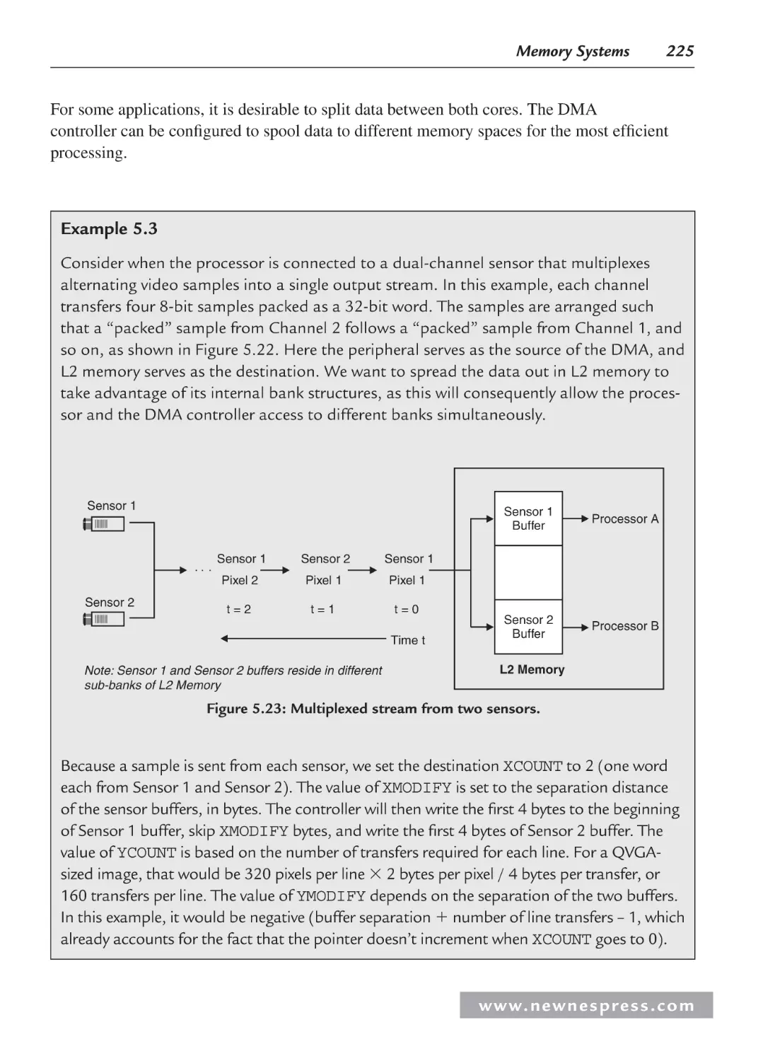
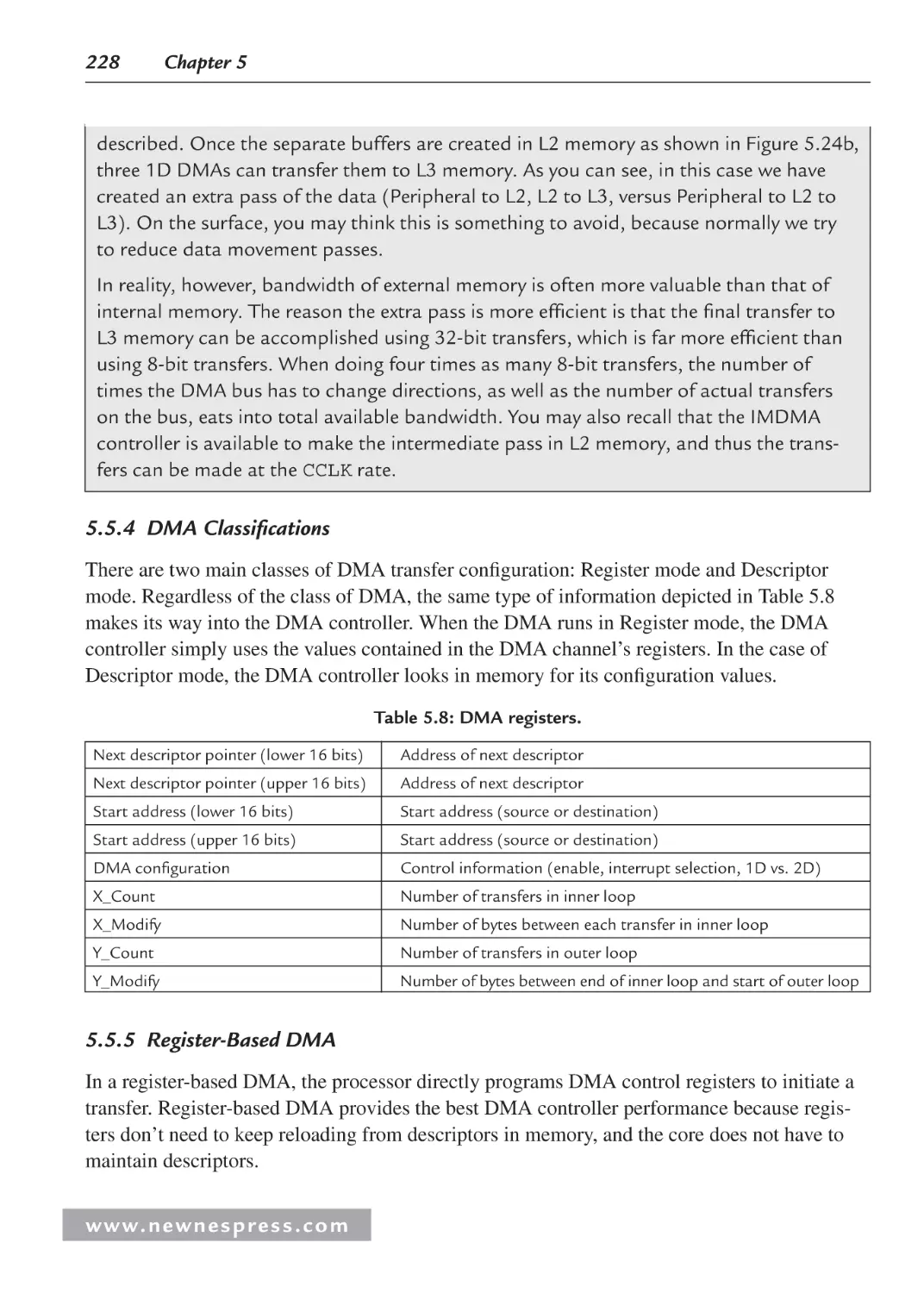
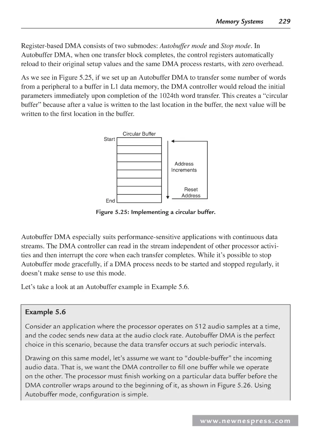
5.5.4 DMA Classifications ....................................................................................... 228
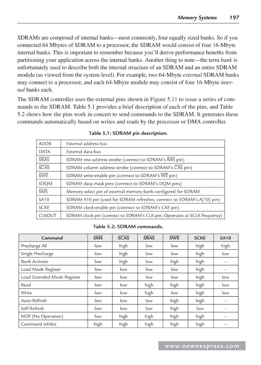
5.5.5 Register-Based DMA ...................................................................................... 228
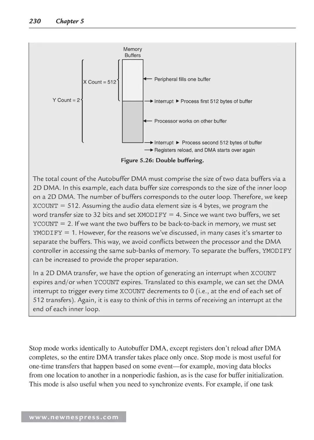
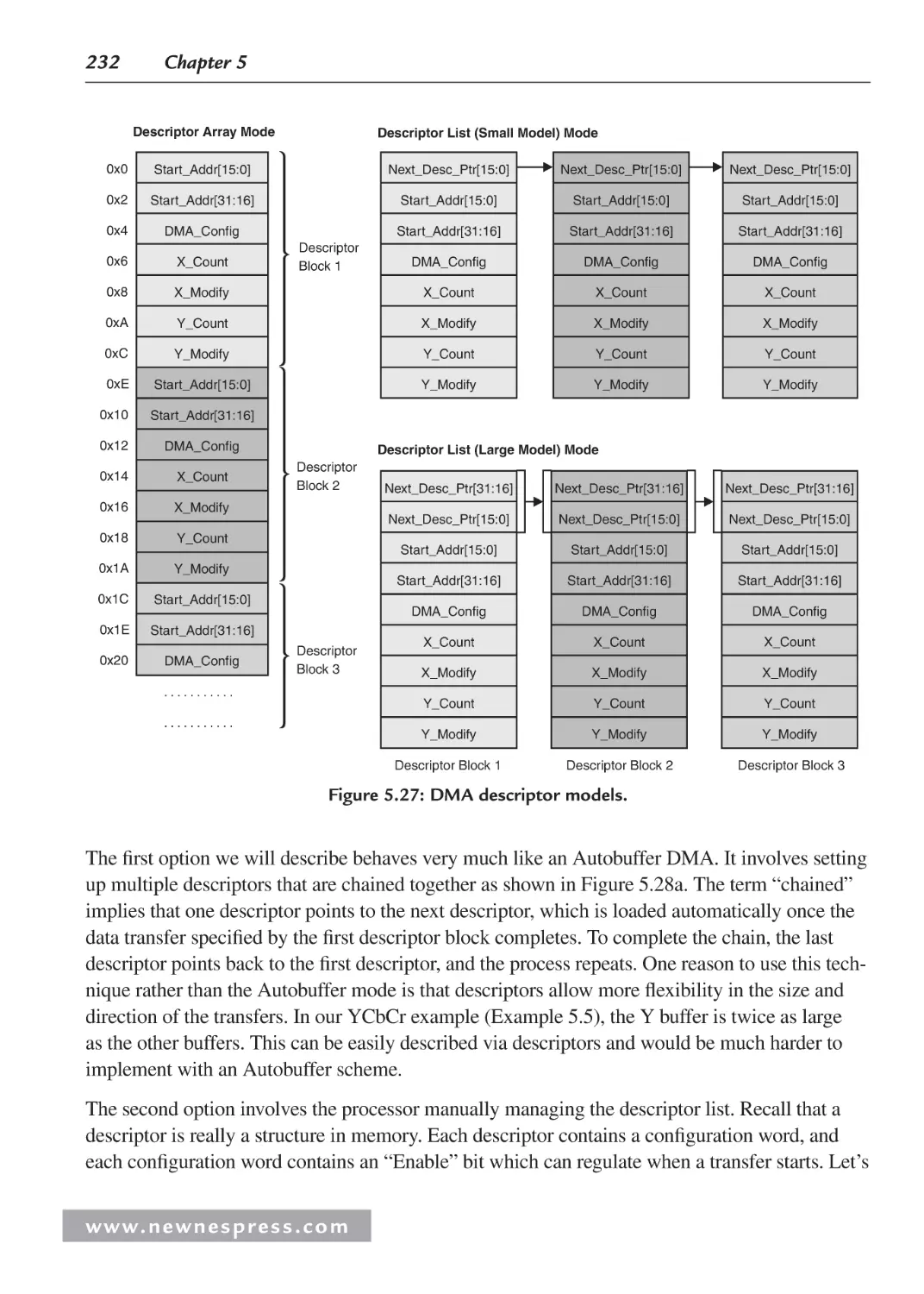
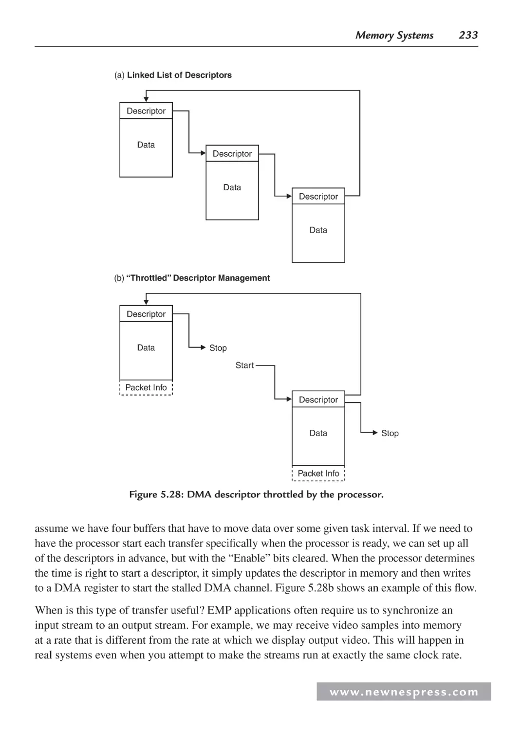
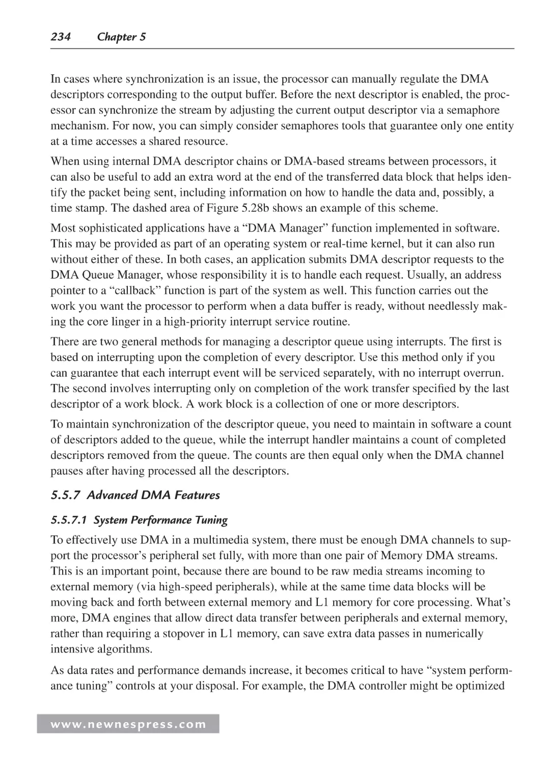
5.5.6 Descriptor-Based DMA .................................................................................. 231
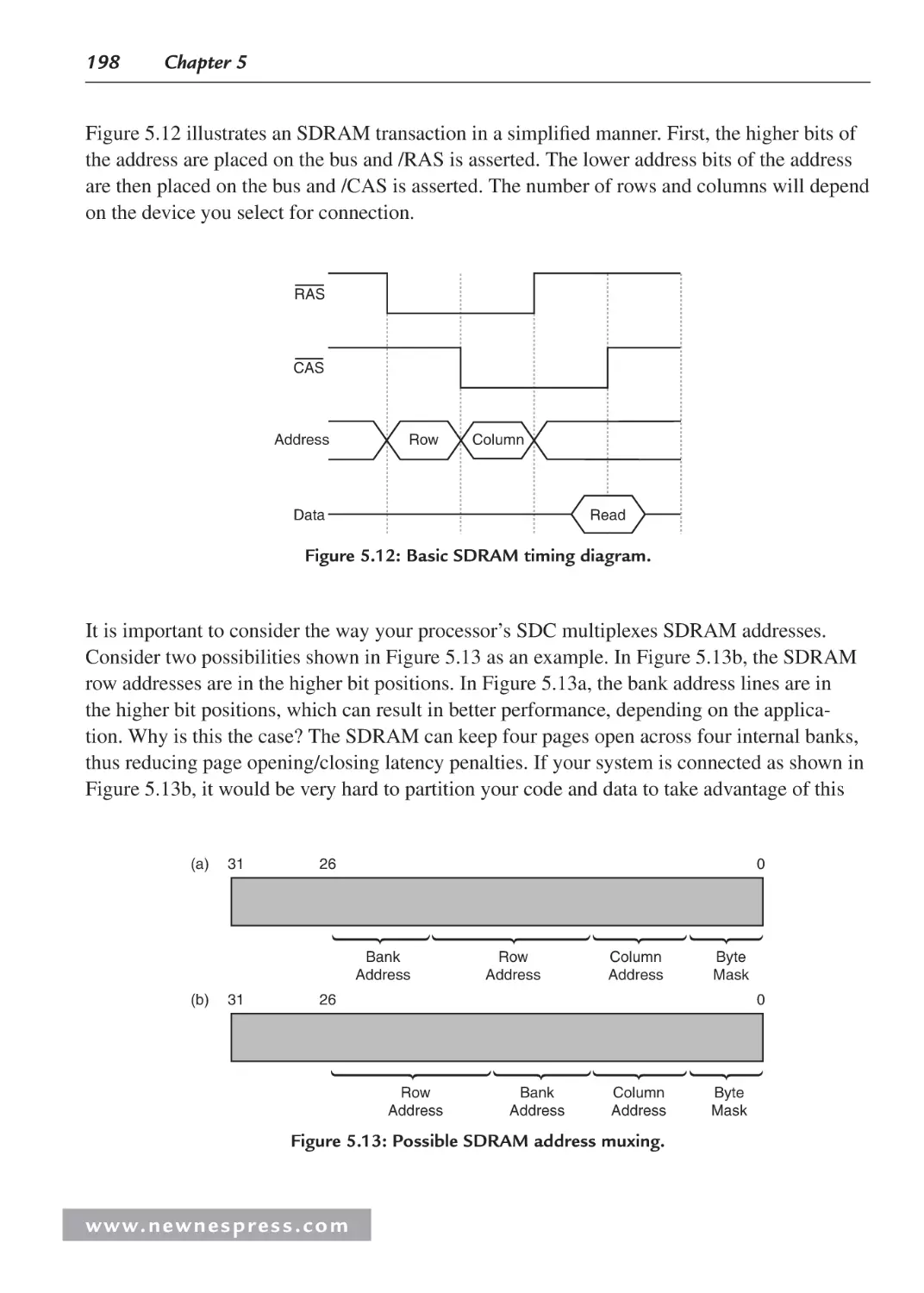
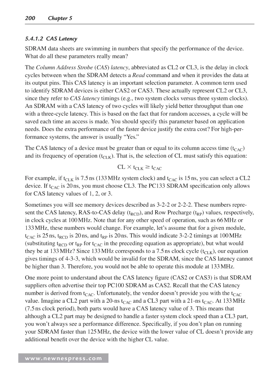
5.5.7 Advanced DMA Features ................................................................................ 234
Endnotes ........................................................................................................................... 236
Chapter 6: Timing Analysis in Embedded Systems................................................................ 239
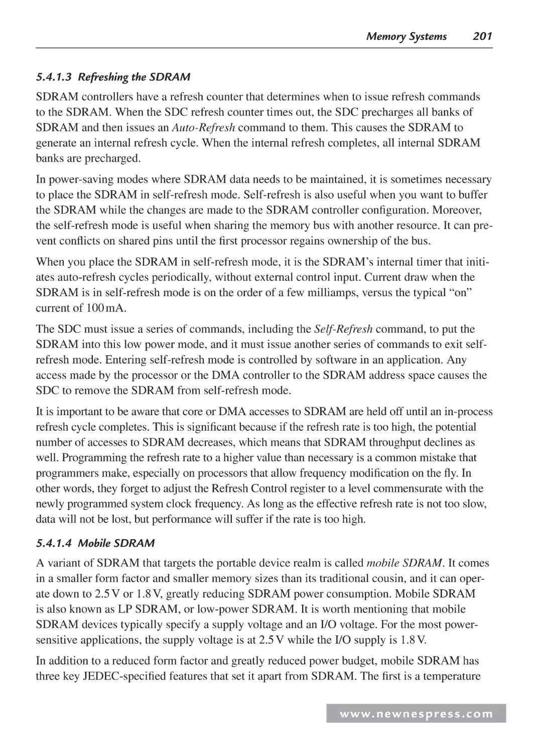
6.1 Introduction ............................................................................................................... 239
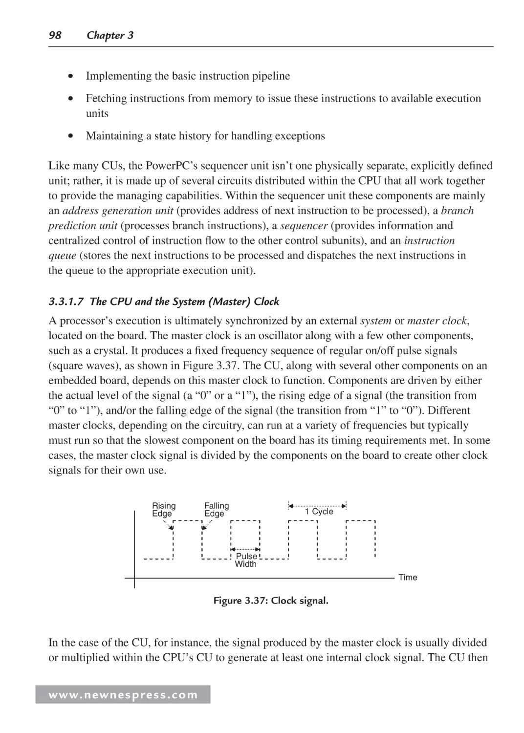
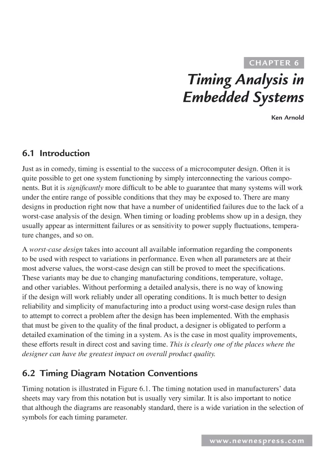
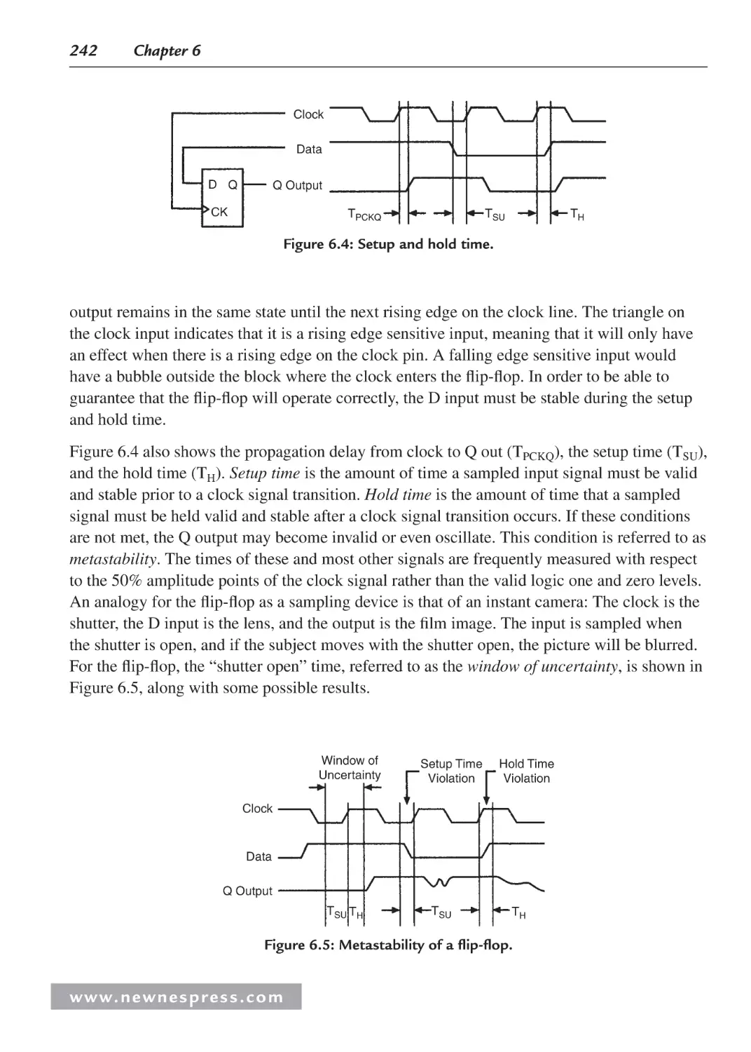
6.2 Timing Diagram Notation Conventions .................................................................... 239
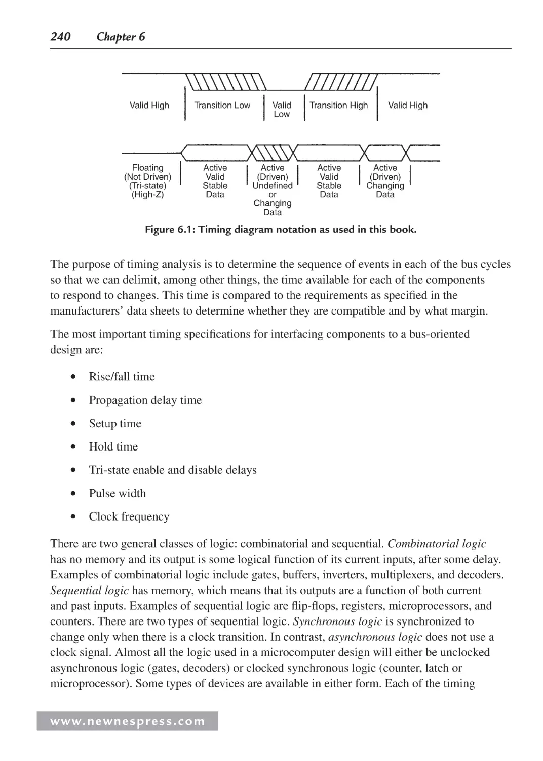
6.2.1 Rise and Fall Times ......................................................................................... 241
w w w. n e w n e s p r e s s . c o m
viii
Contents
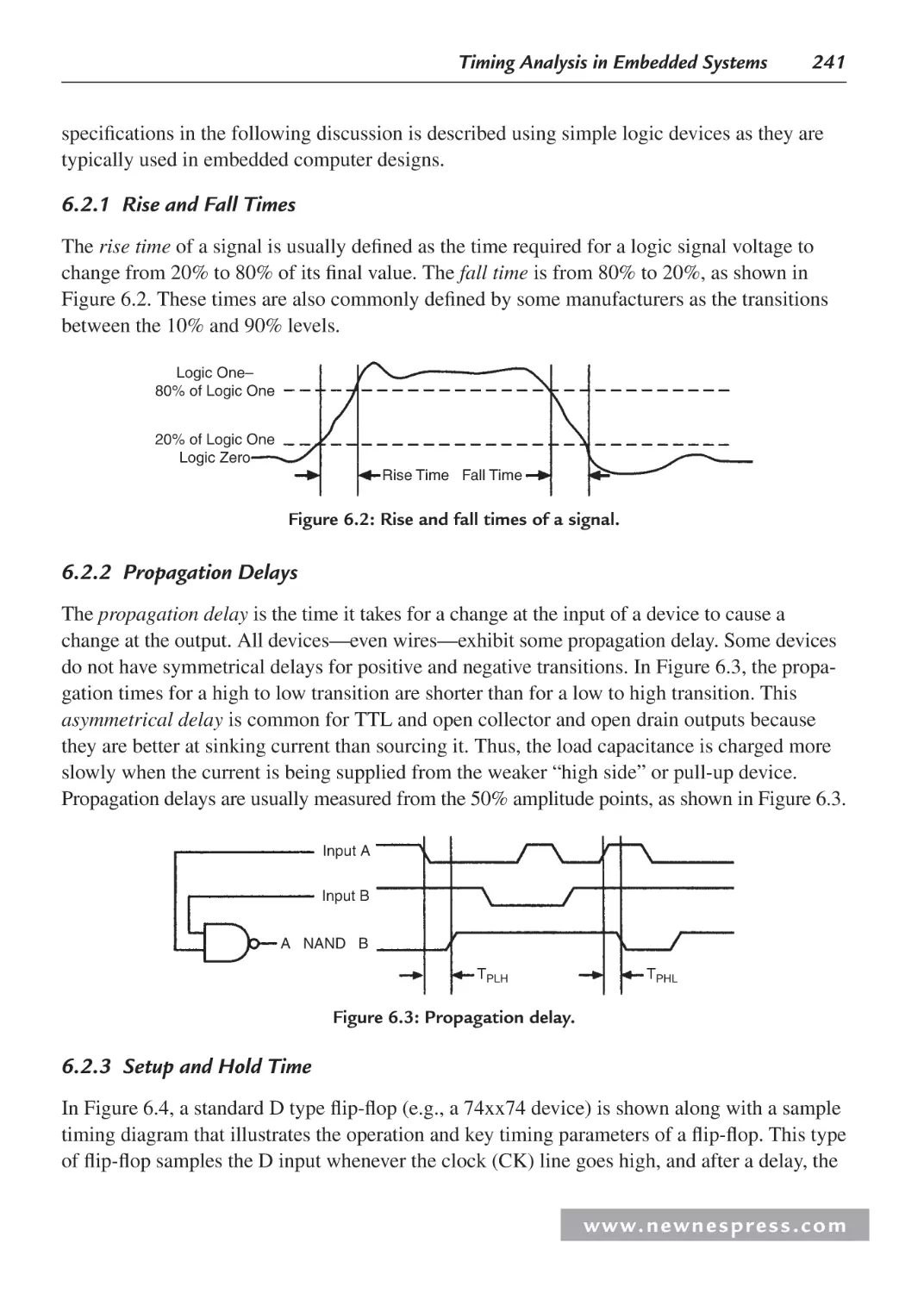
6.2.2 Propagation Delays ......................................................................................... 241
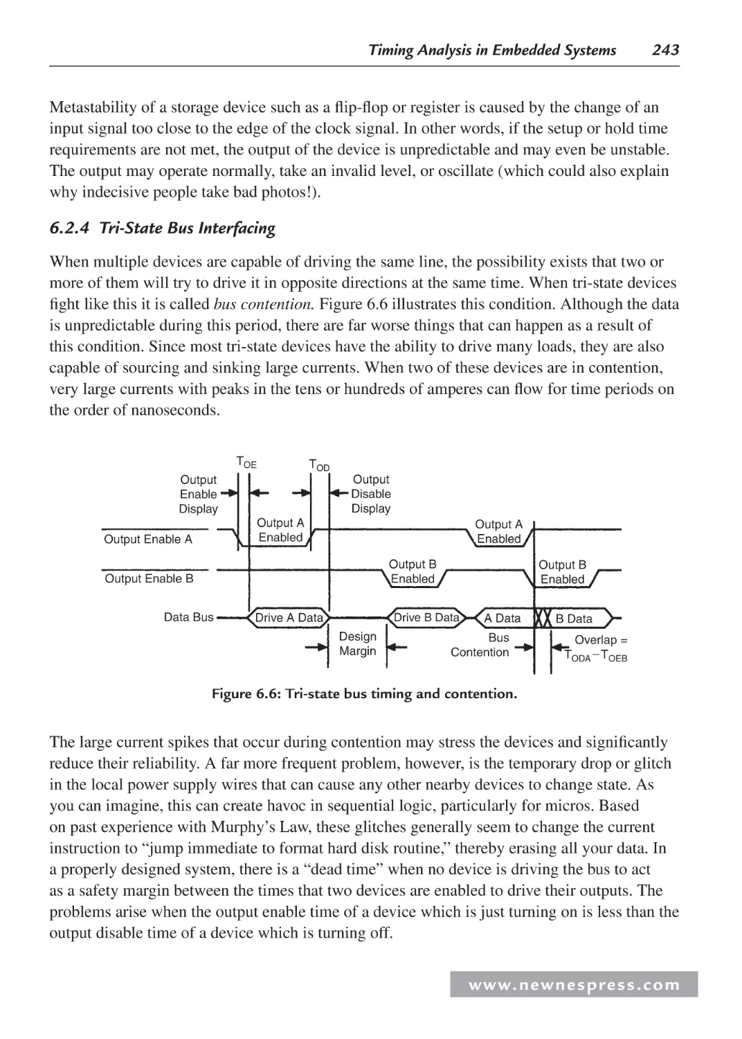
6.2.3 Setup and Hold Time....................................................................................... 241
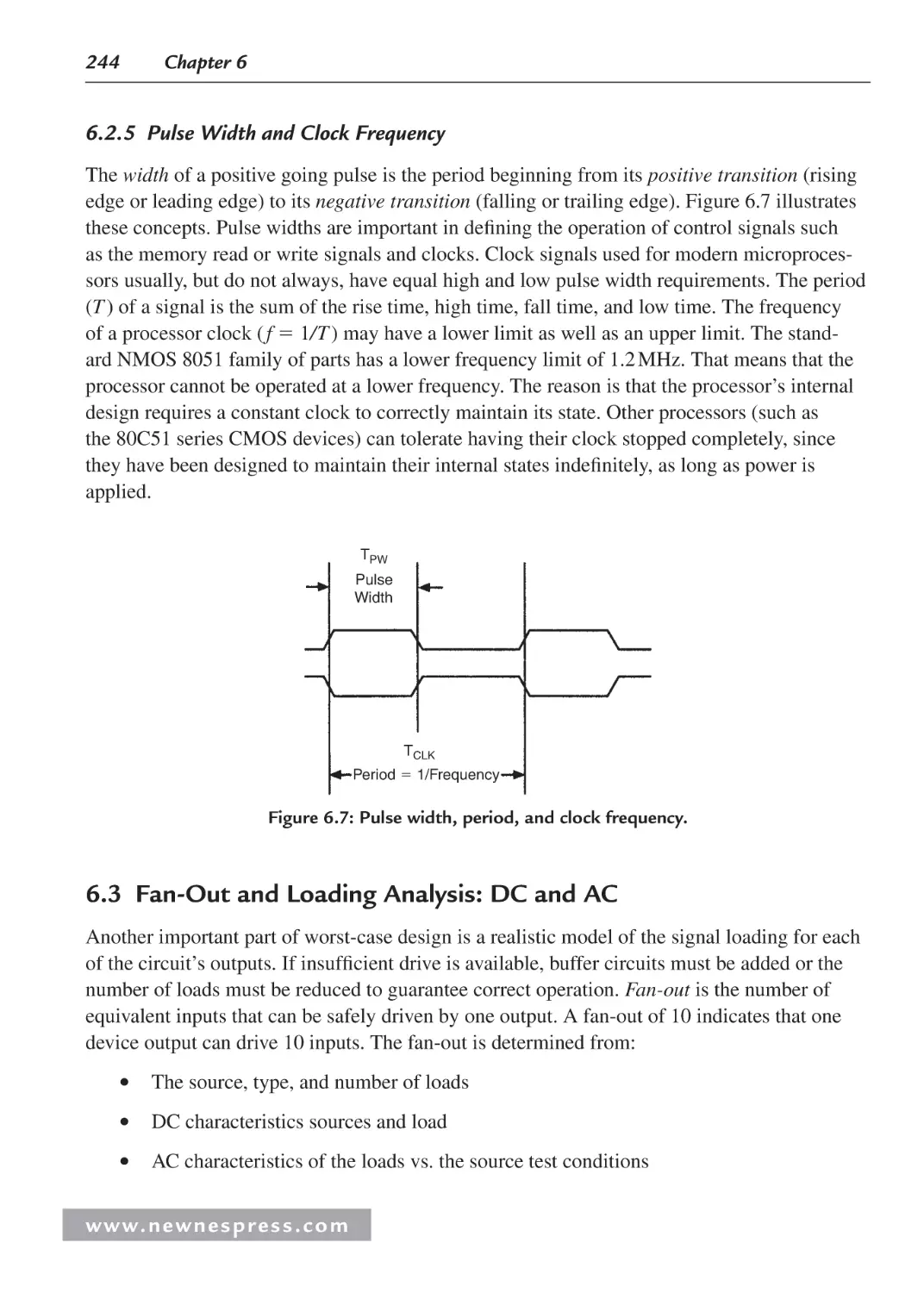
6.2.4 Tri-State Bus Interfacing ................................................................................. 243
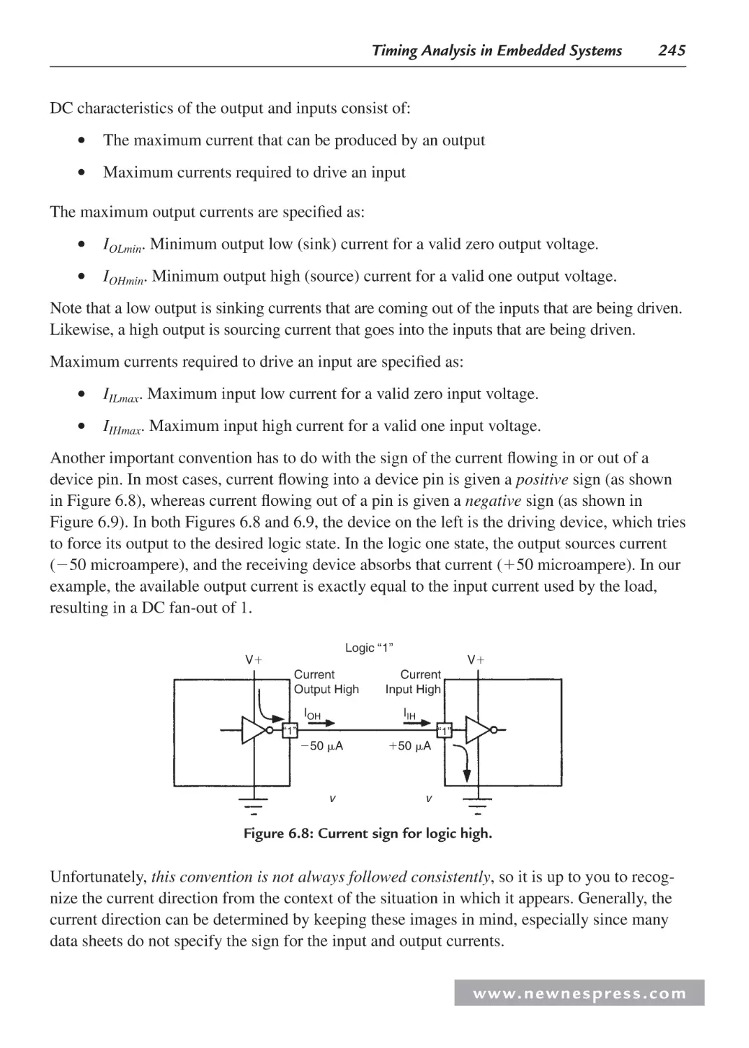
6.2.5 Pulse Width and Clock Frequency .................................................................. 244
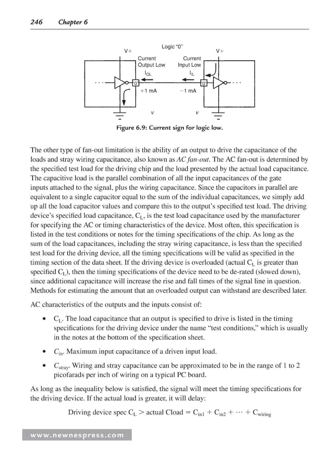
6.3 Fan-Out and Loading Analysis: DC and AC ............................................................. 244
6.3.1 Calculating Wiring Capacitance...................................................................... 247
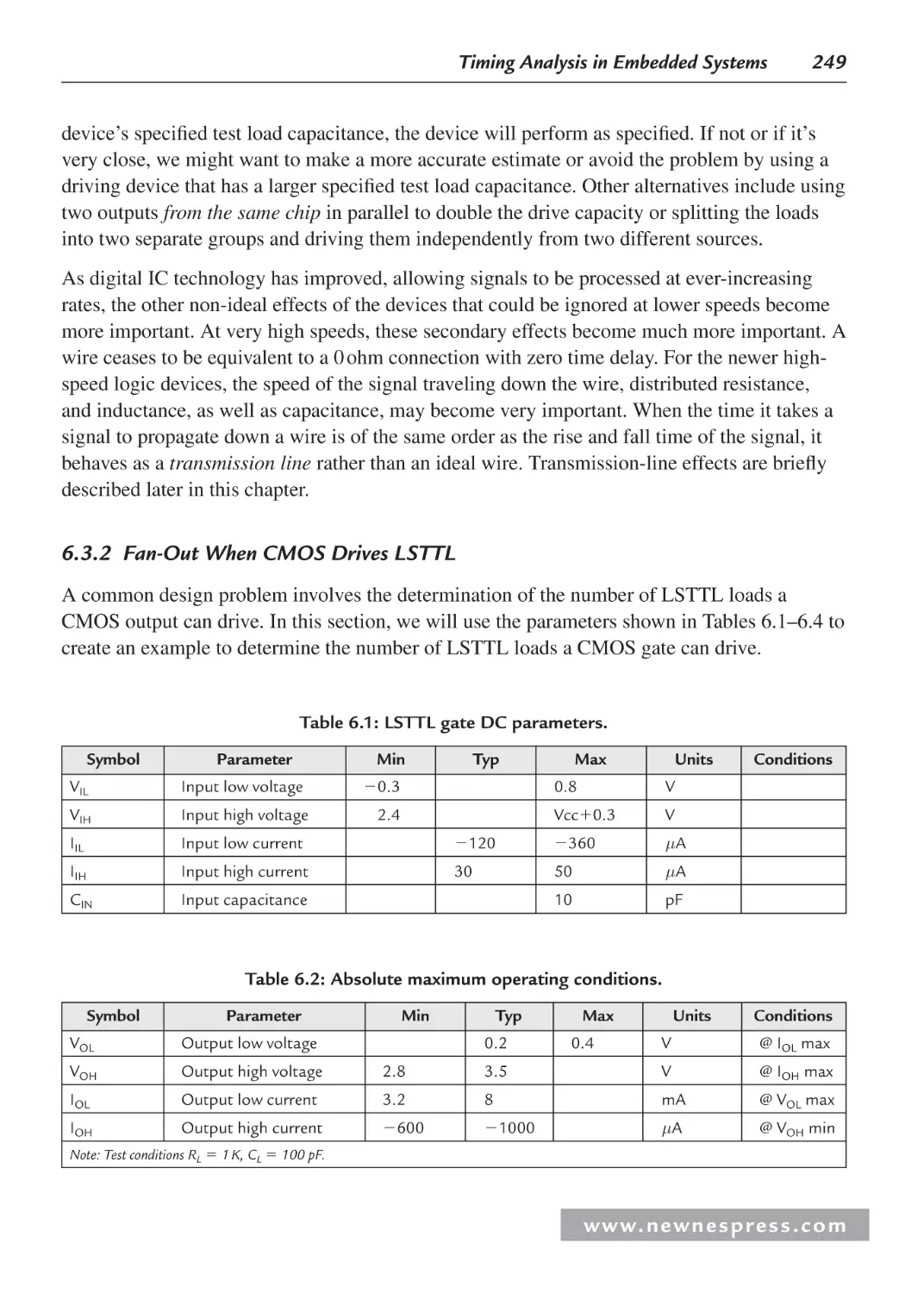
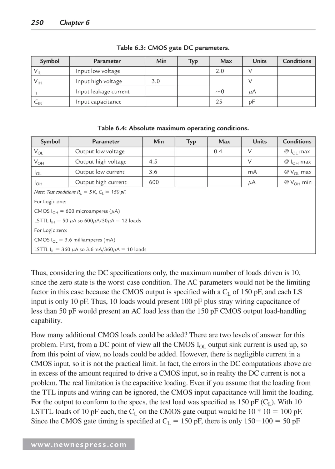
6.3.2 Fan-Out When CMOS Drives LSTTL ............................................................ 249
6.3.3 Transmission-Line Effects .............................................................................. 251
6.3.4 Ground Bounce ............................................................................................... 253
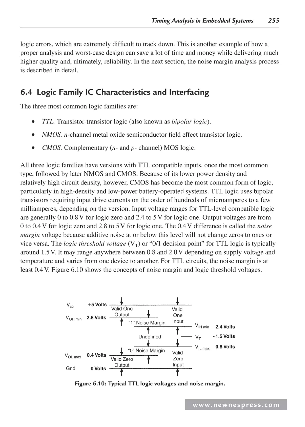
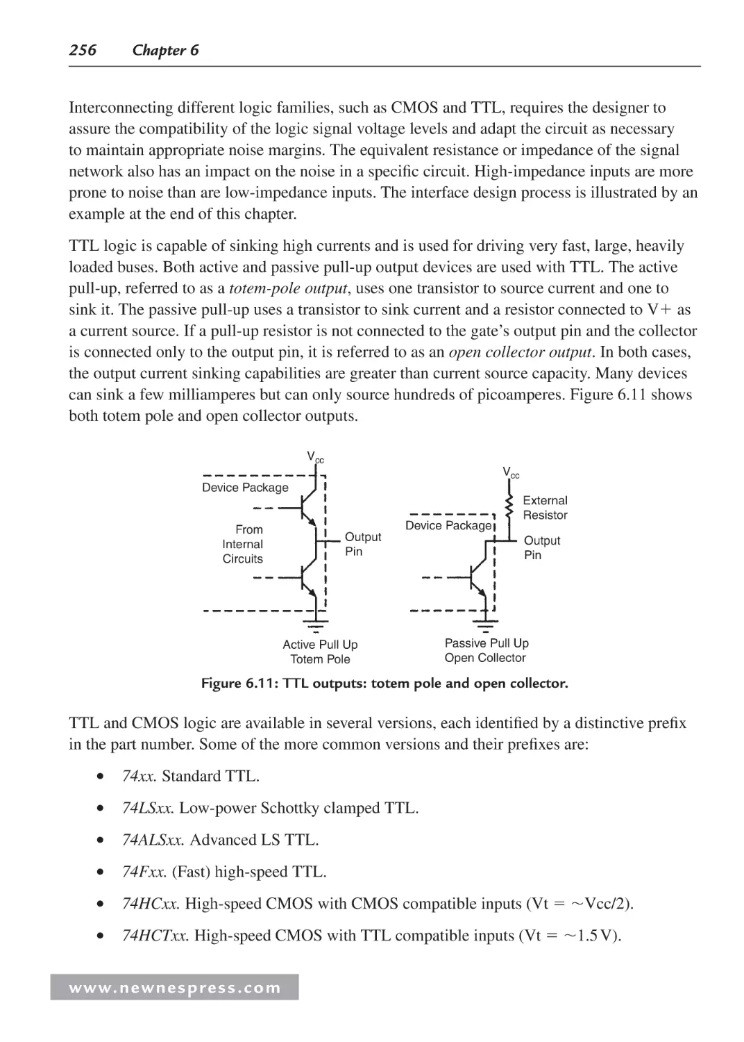
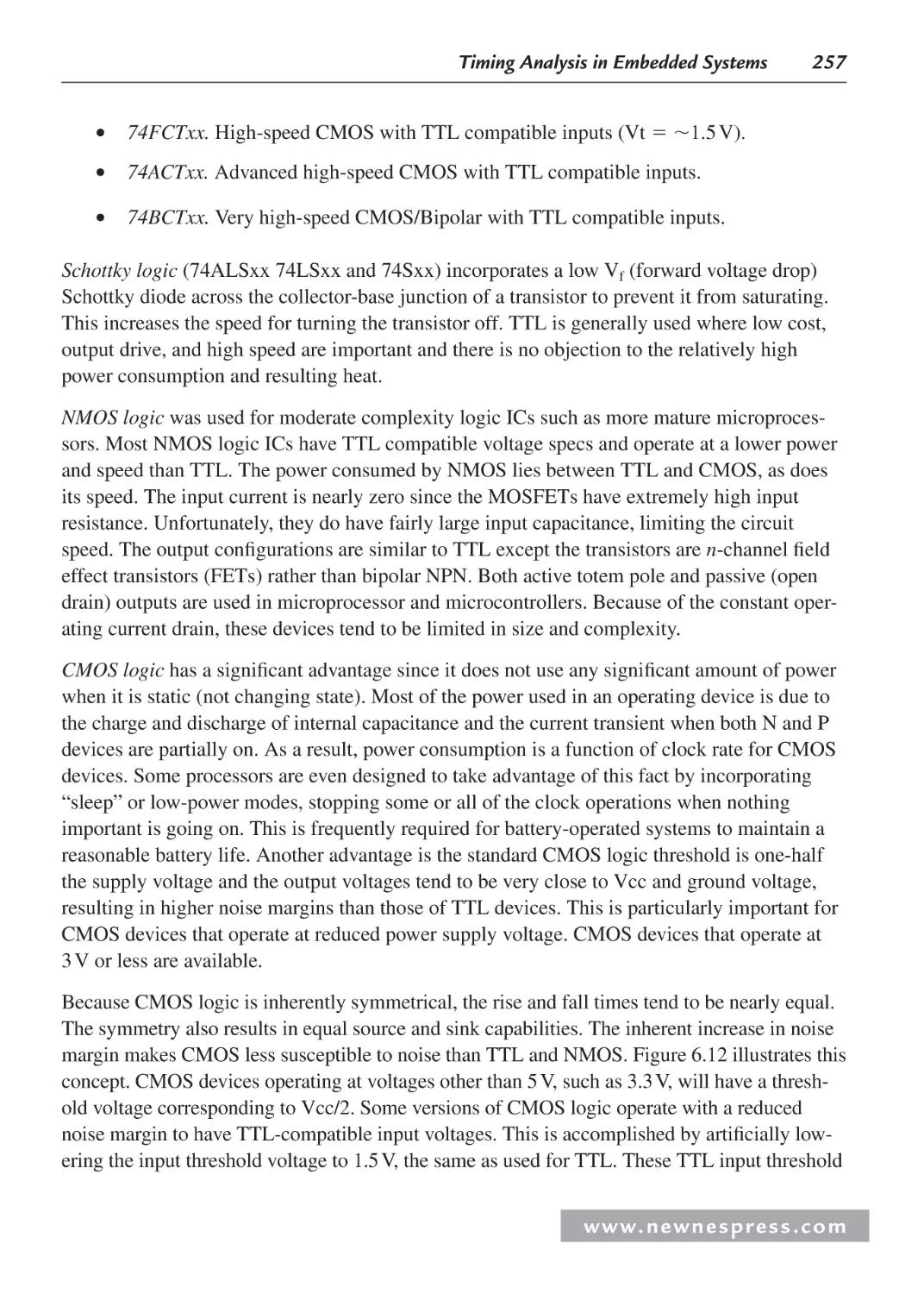
6.4 Logic Family IC Characteristics and Interfacing ...................................................... 255
6.4.1 Interfacing TTL Compatible Signals to 5 V CMOS ....................................... 258
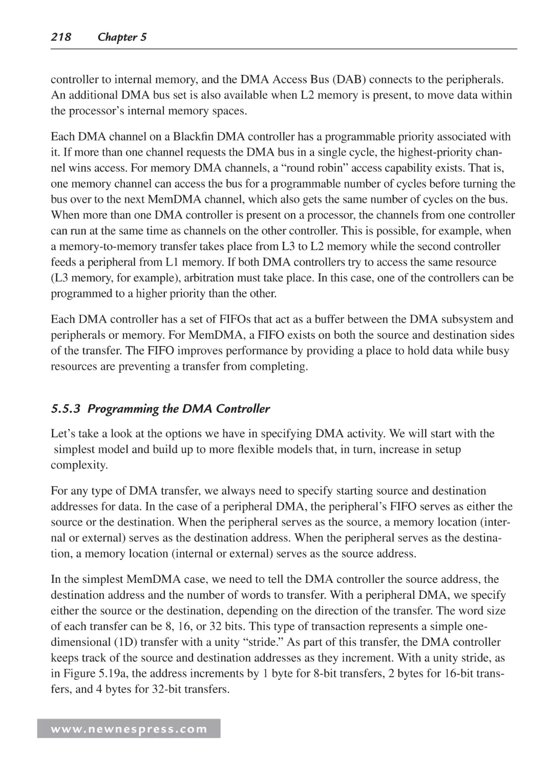
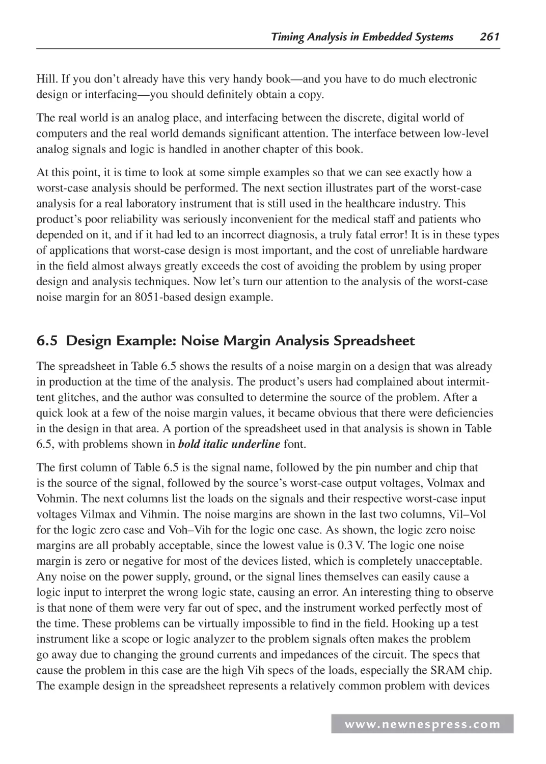
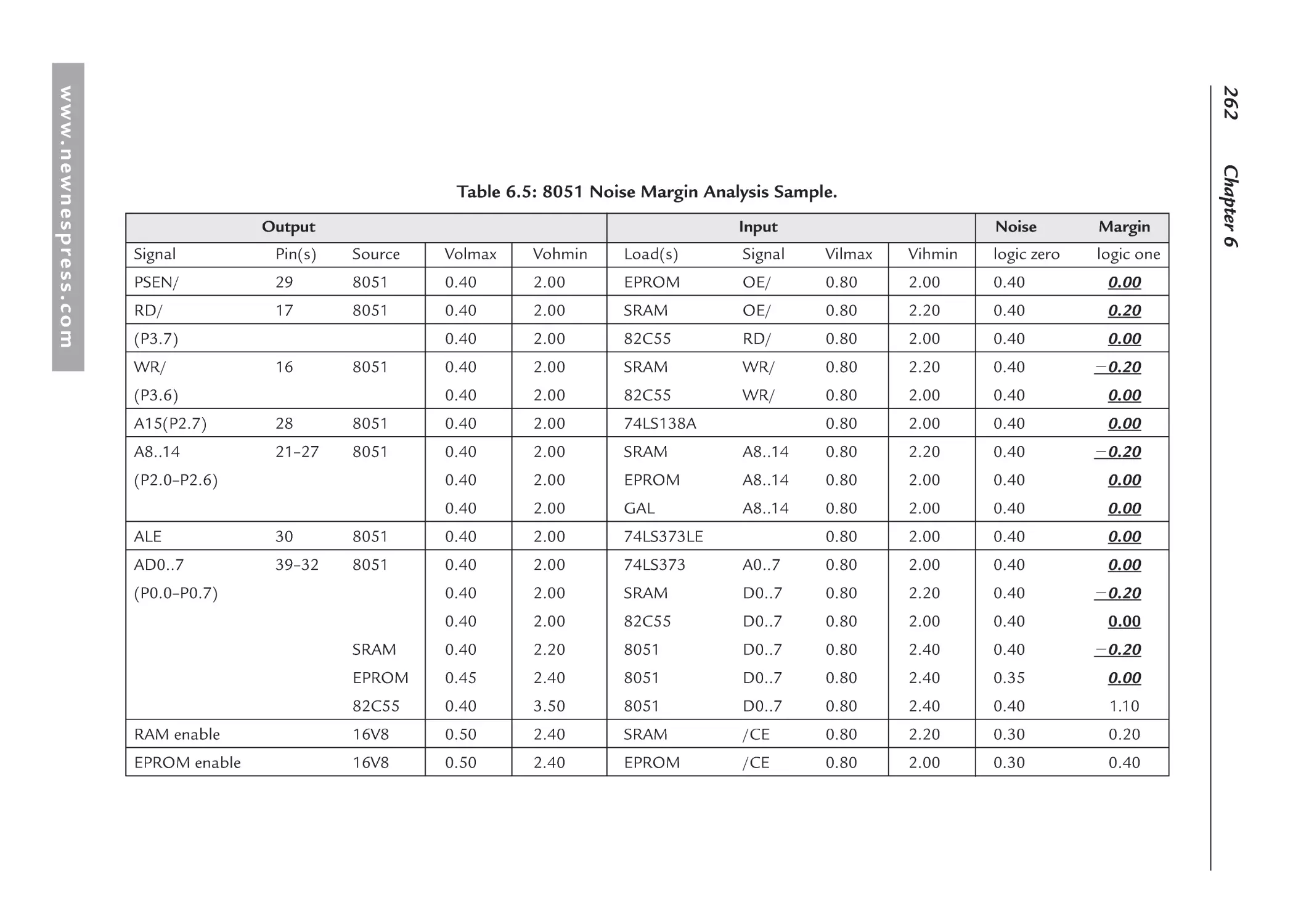
6.5 Design Example: Noise Margin Analysis Spreadsheet ............................................. 261
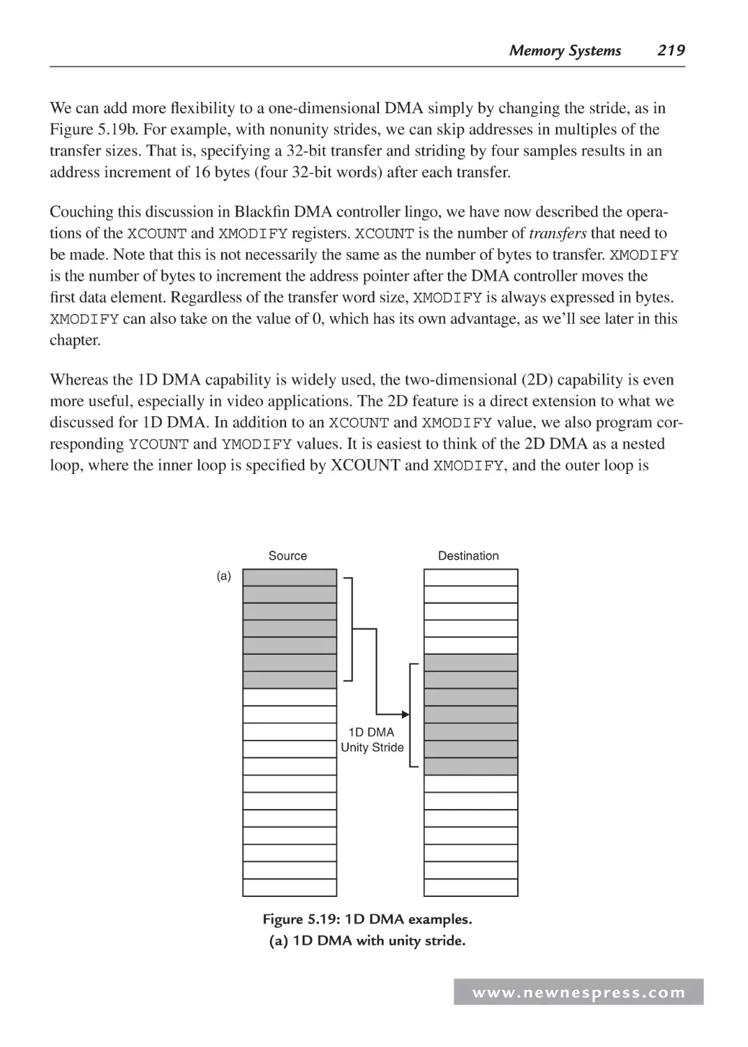
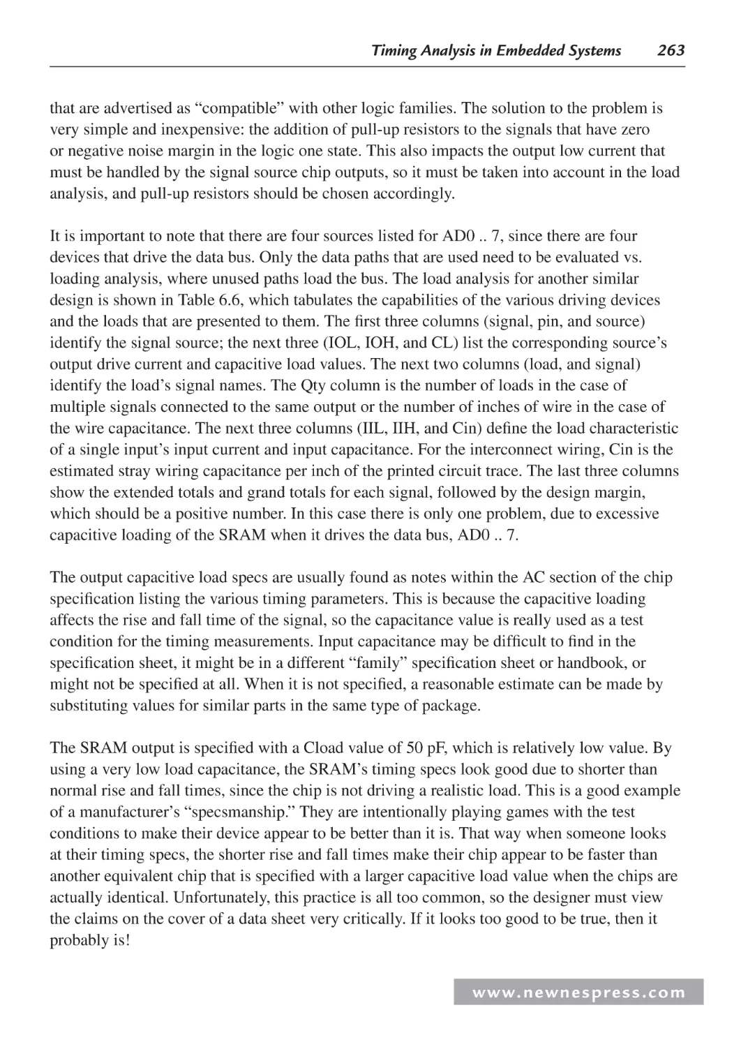
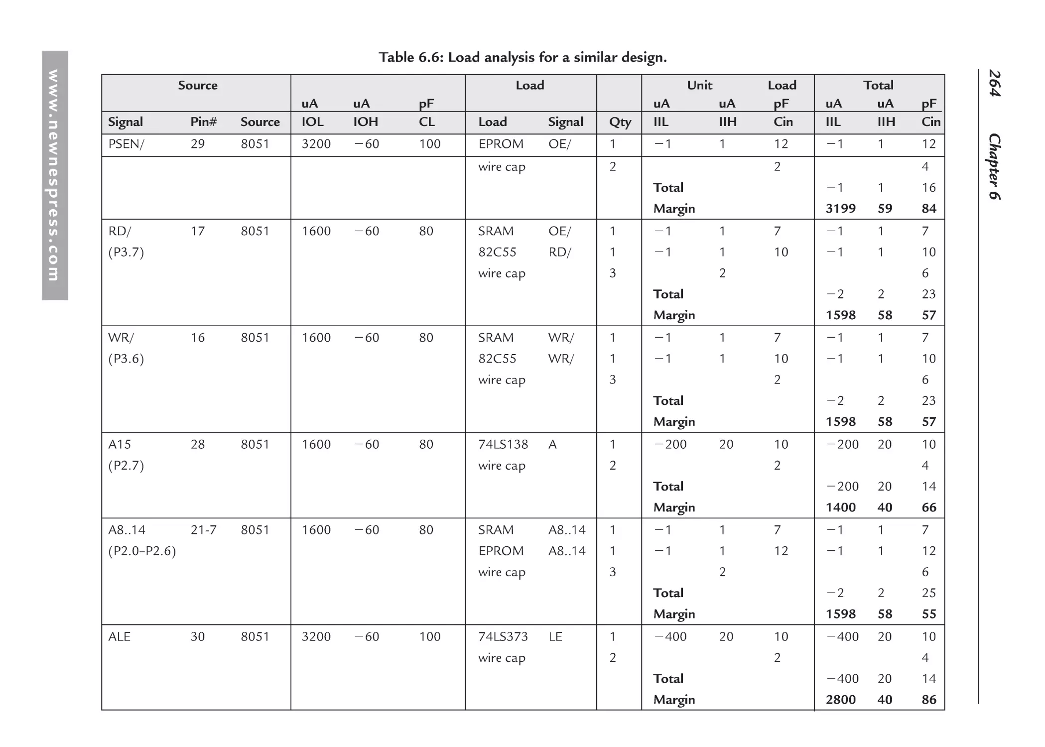
6.6 Worst-Case Timing Analysis Example...................................................................... 270
Endnotes ........................................................................................................................... 272
Chapter 7: Choosing a Microcontroller and Other Design Decisions .................................... 273
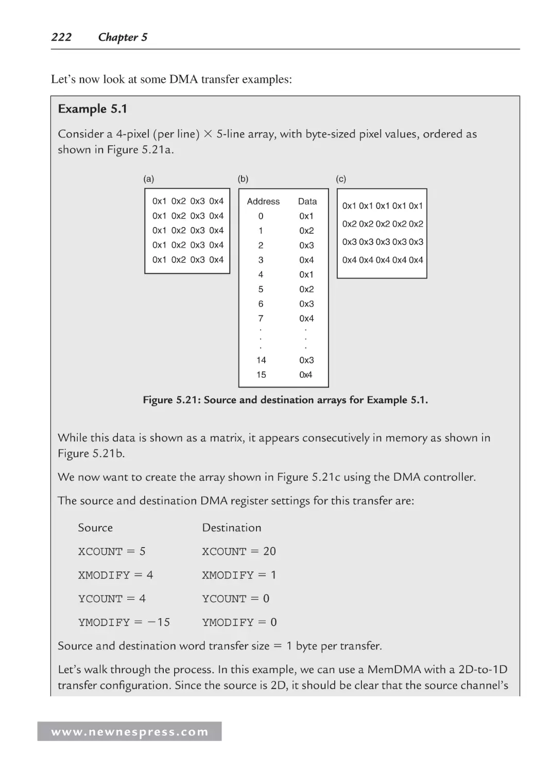
7.1 Introduction ............................................................................................................... 273
7.2 Choosing the Right Core ........................................................................................... 276
7.3 Building Custom Peripherals with FPGAs................................................................ 281
7.4 Whose Development Hardware to Use—Chicken or Egg?....................................... 282
7.5 Recommended Laboratory Equipment ...................................................................... 285
7.6 Development Toolchains ........................................................................................... 286
7.7 Free Embedded Operating Systems .......................................................................... 289
7.8 GNU and You: How Using “Free” Software Affects Your Product .......................... 295
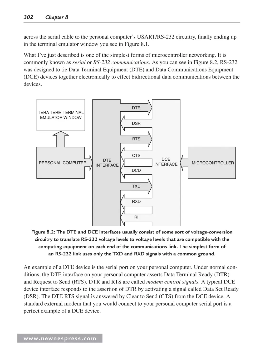
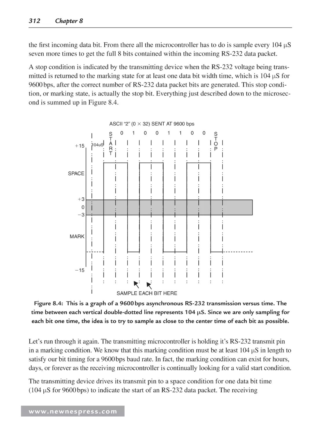
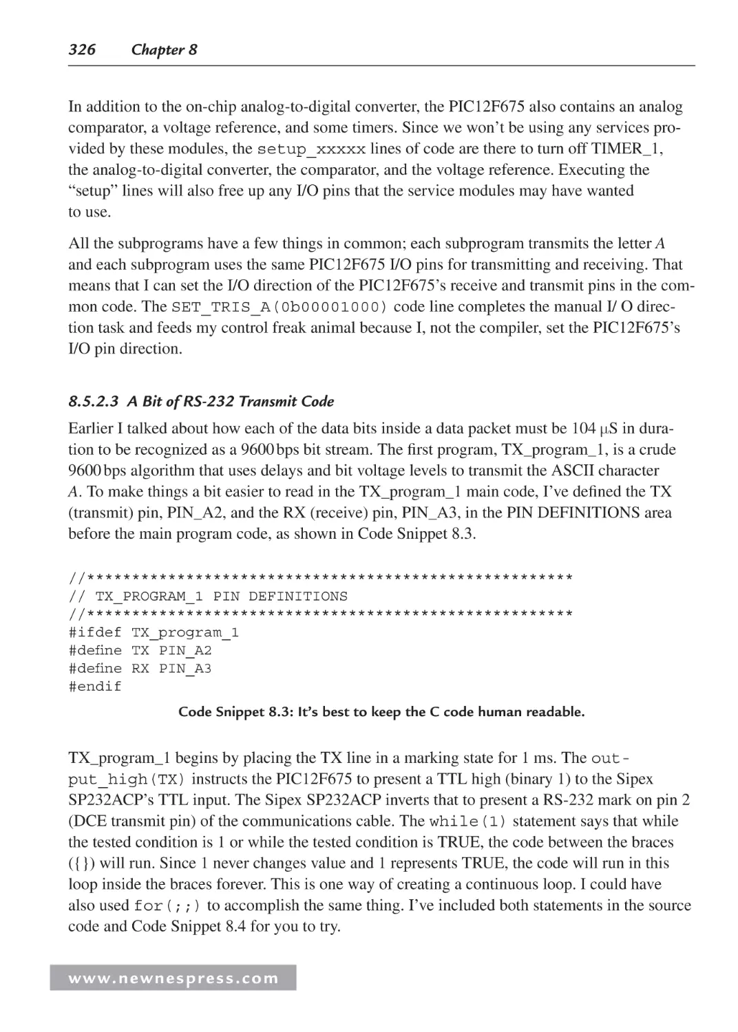
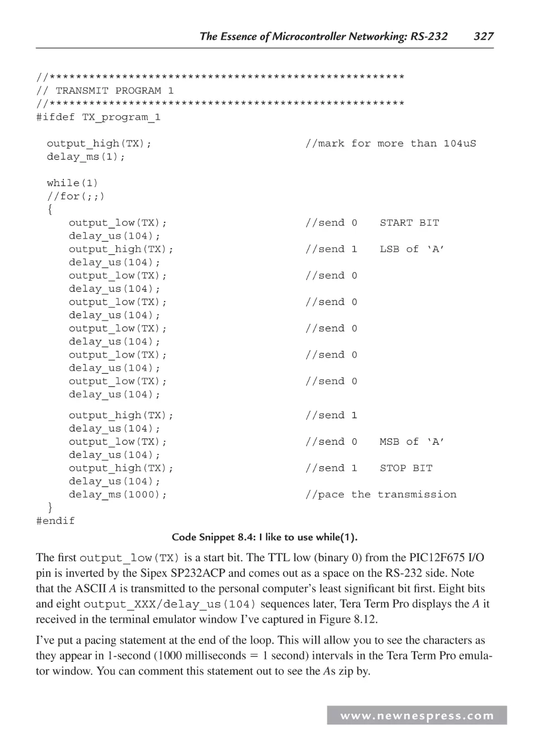
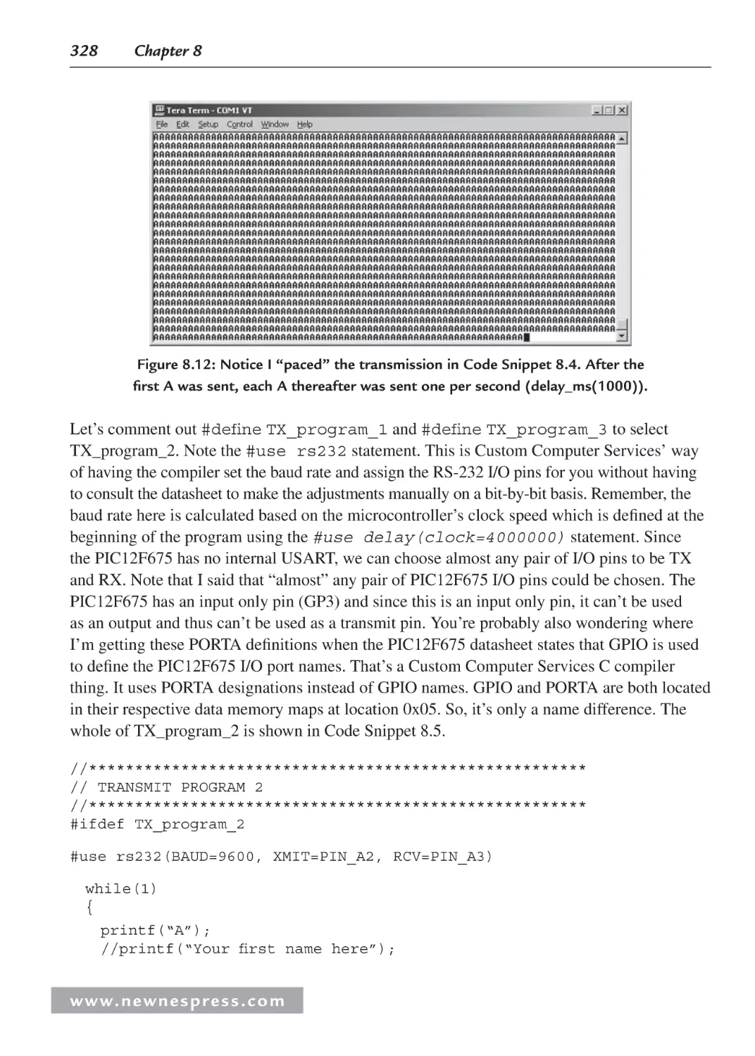
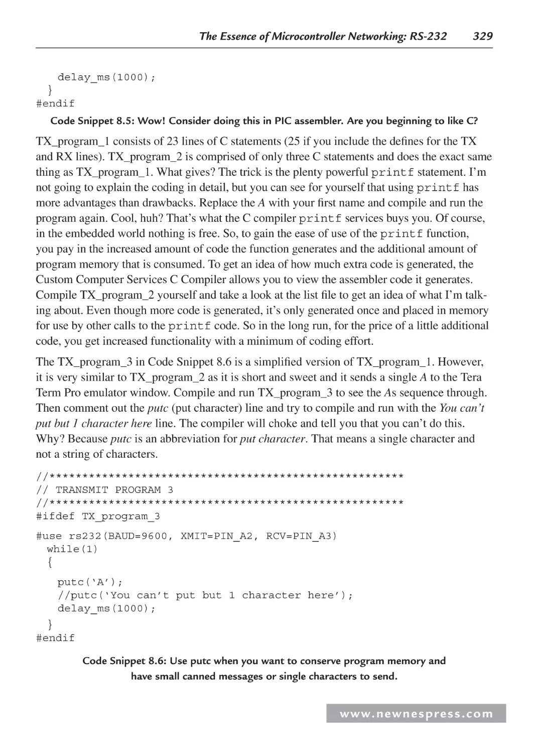
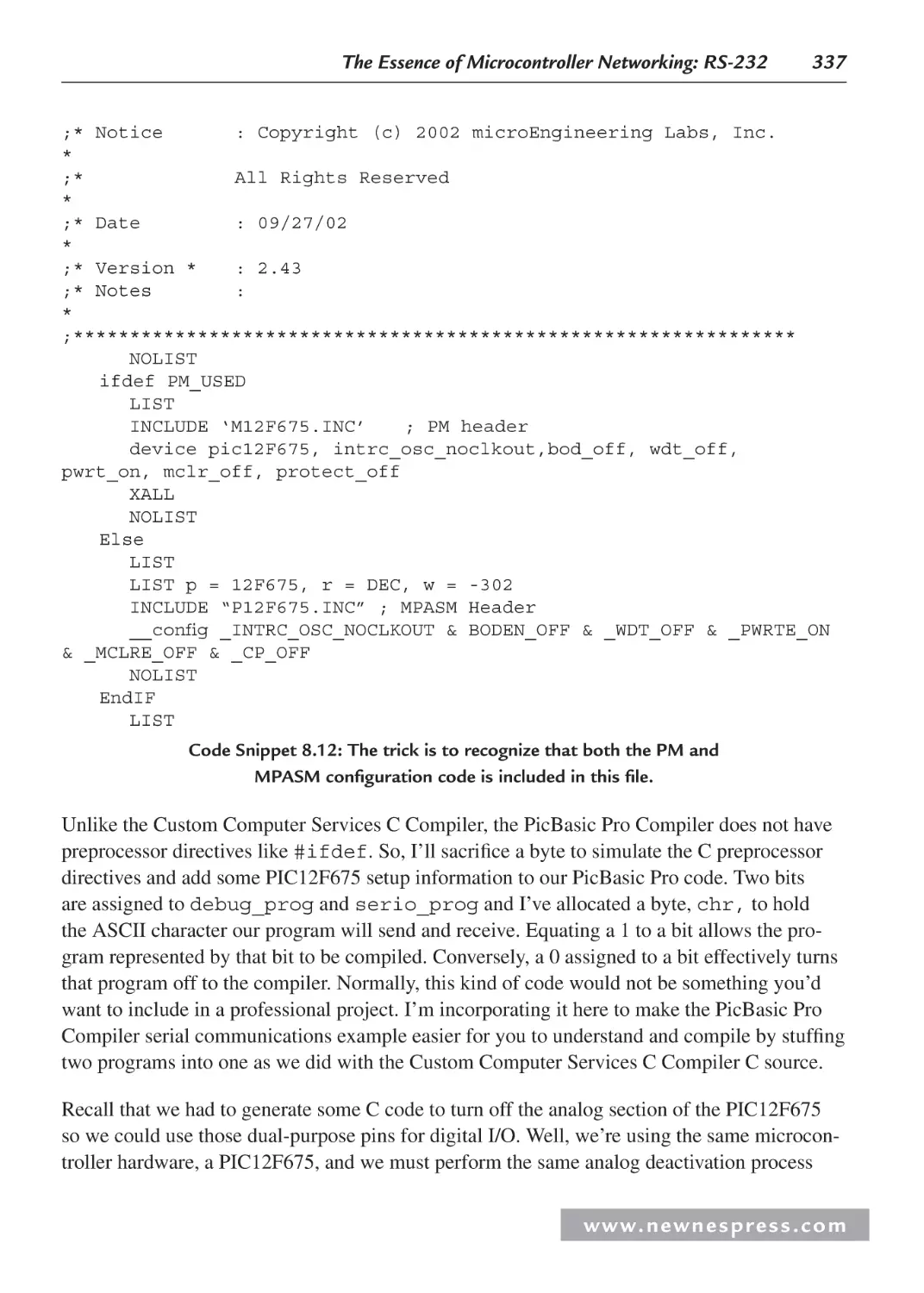
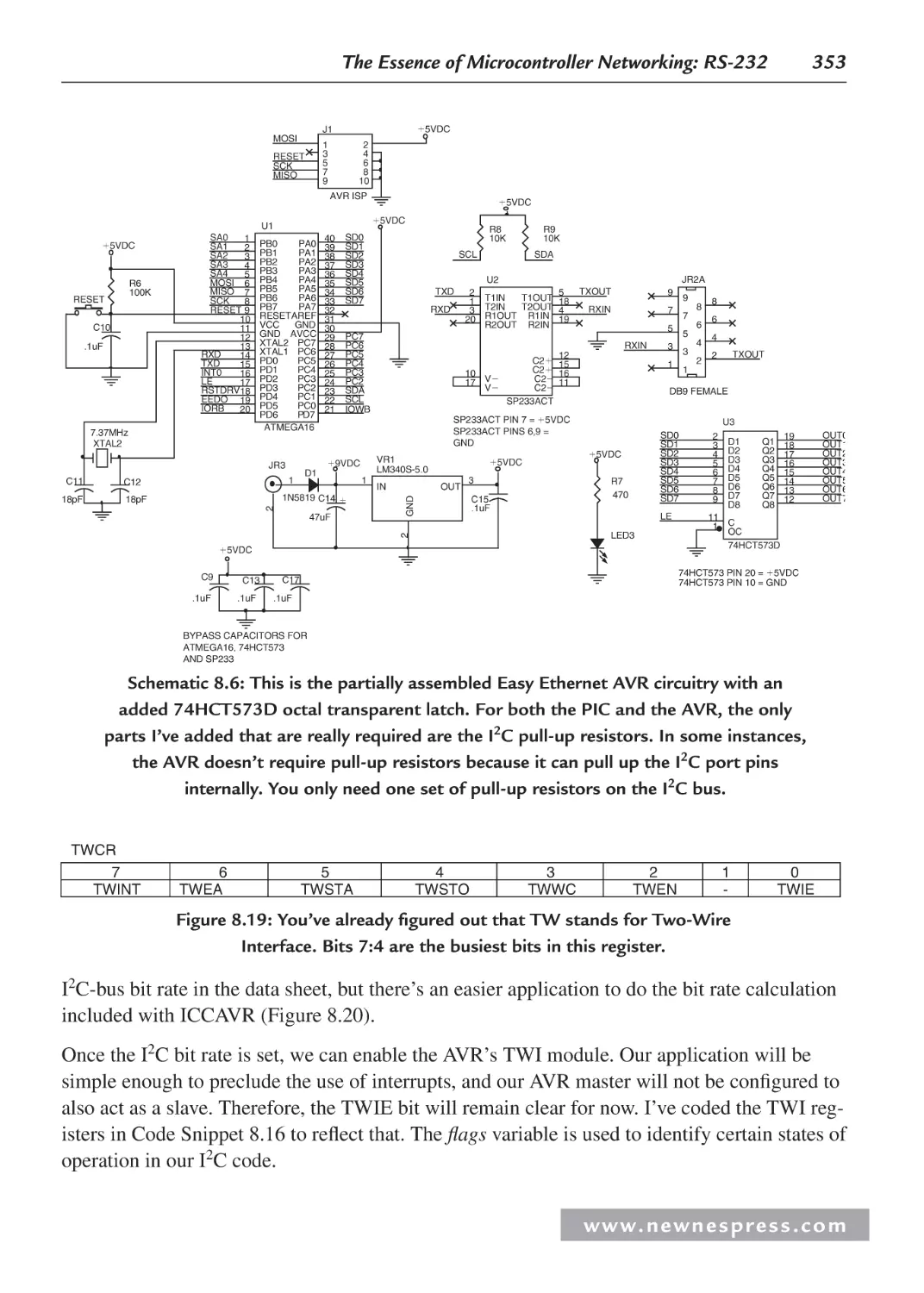
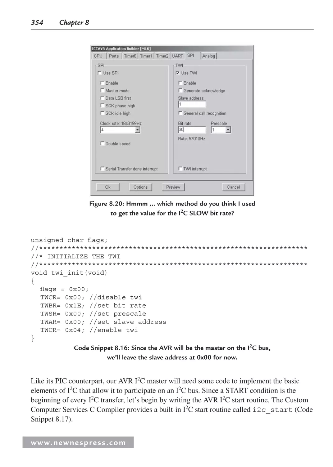
Chapter 8: The Essence of Microcontroller Networking: RS-232.......................................... 301
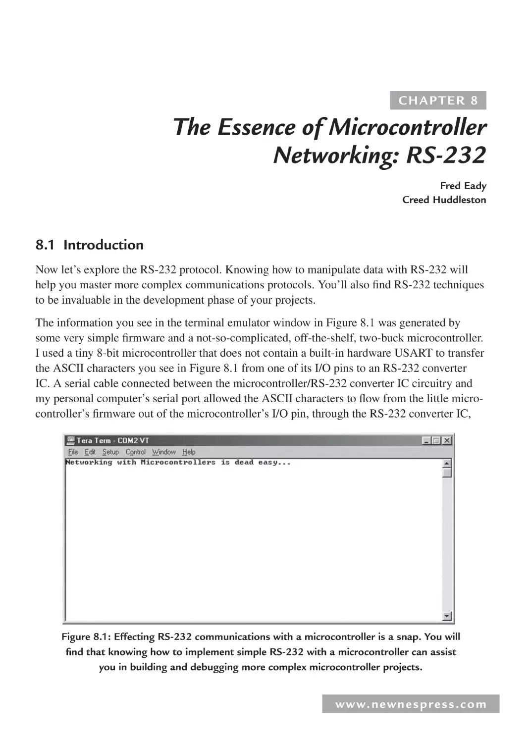
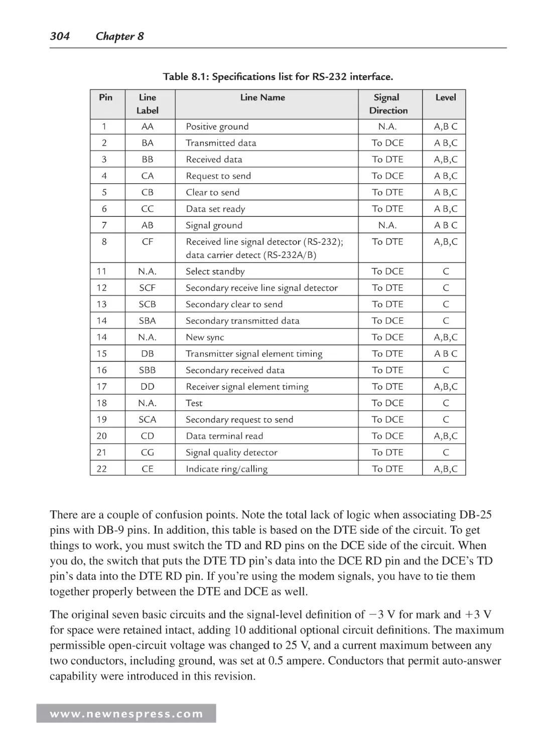
8.1 Introduction ............................................................................................................... 301
8.2 Some History ............................................................................................................. 303
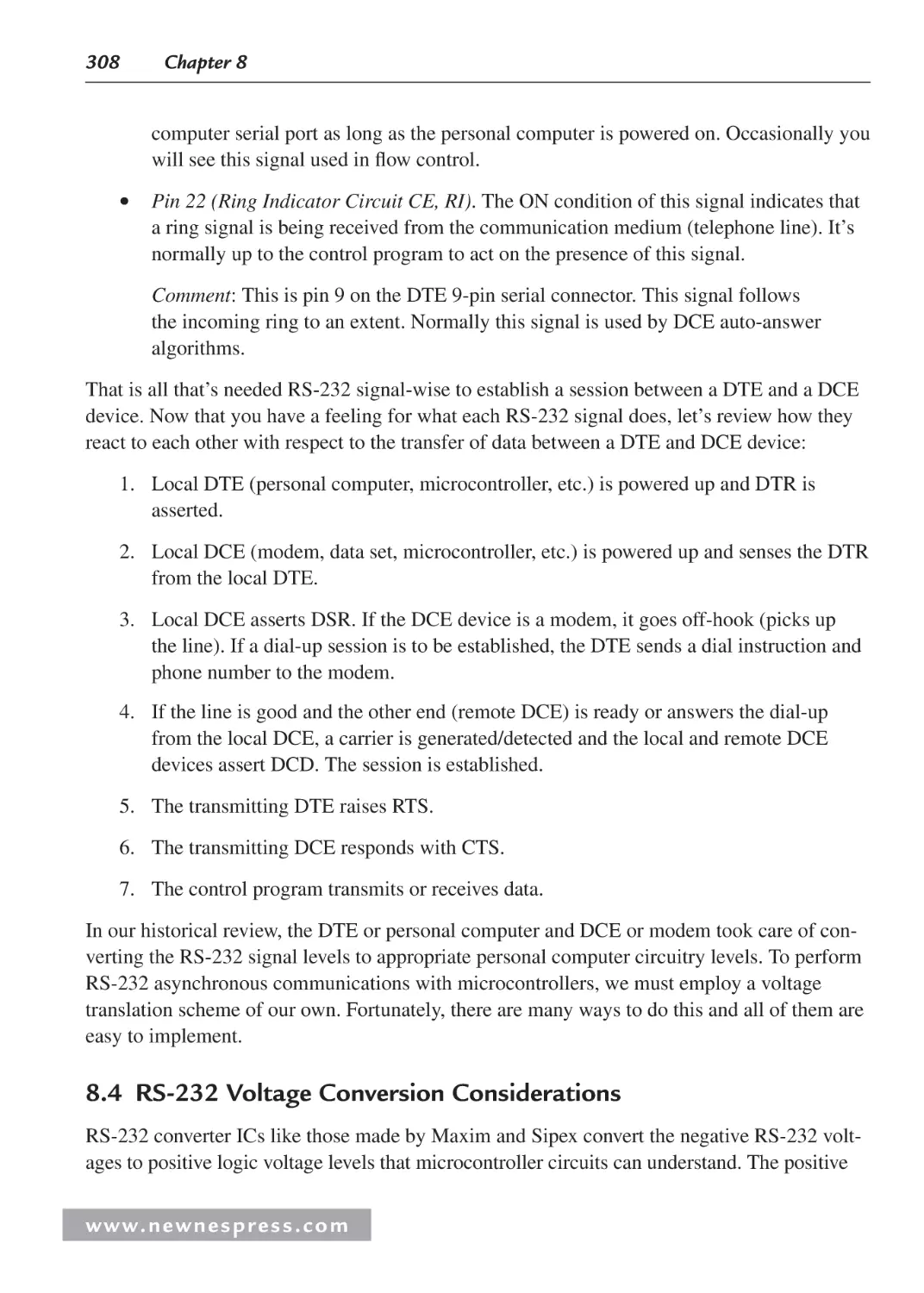
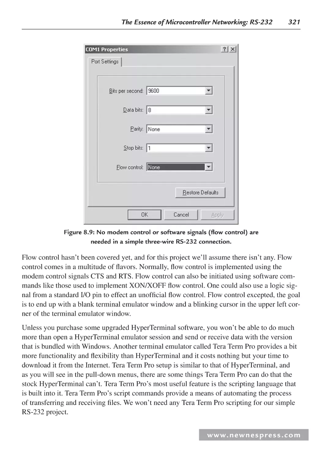
8.3 RS-232 Standard Operating Procedure ..................................................................... 305
8.4 RS-232 Voltage Conversion Considerations ............................................................. 308
8.5 Implementing RS-232 with a Microcontroller .......................................................... 310
8.5.1 Basic RS-232 Hardware .................................................................................. 310
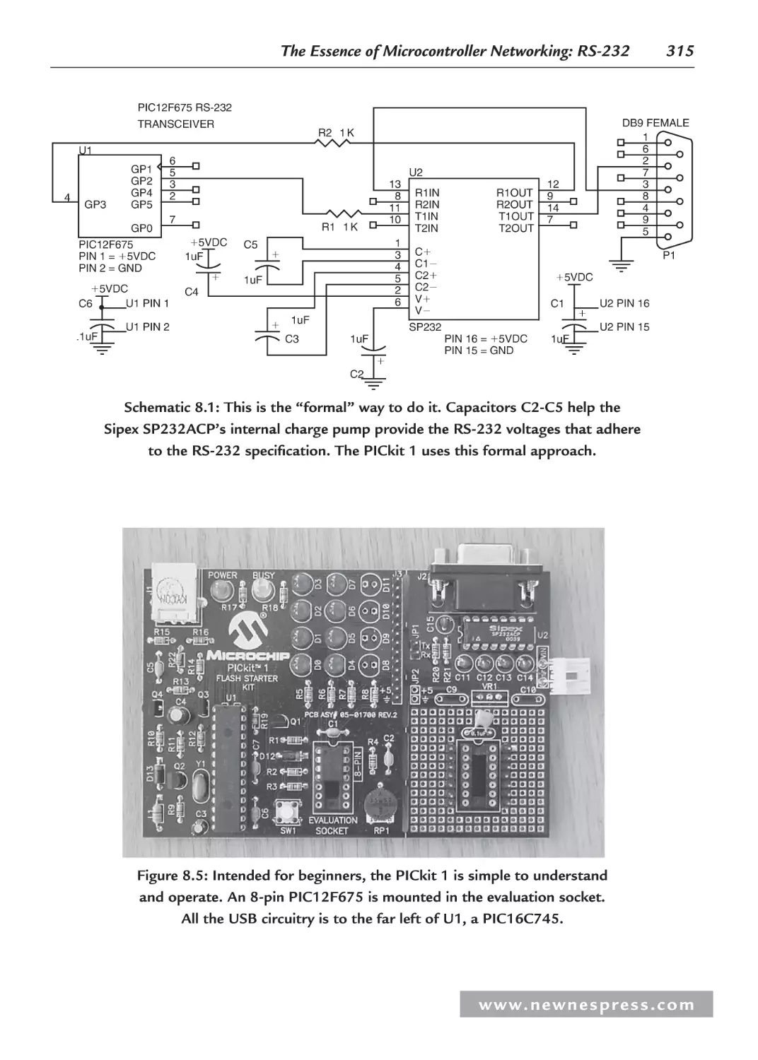
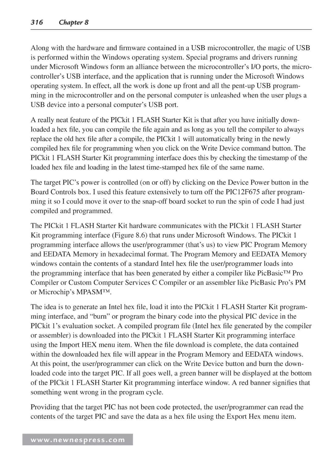
8.5.2 Building a Simple Microcontroller RS-232 Transceiver ................................ 313
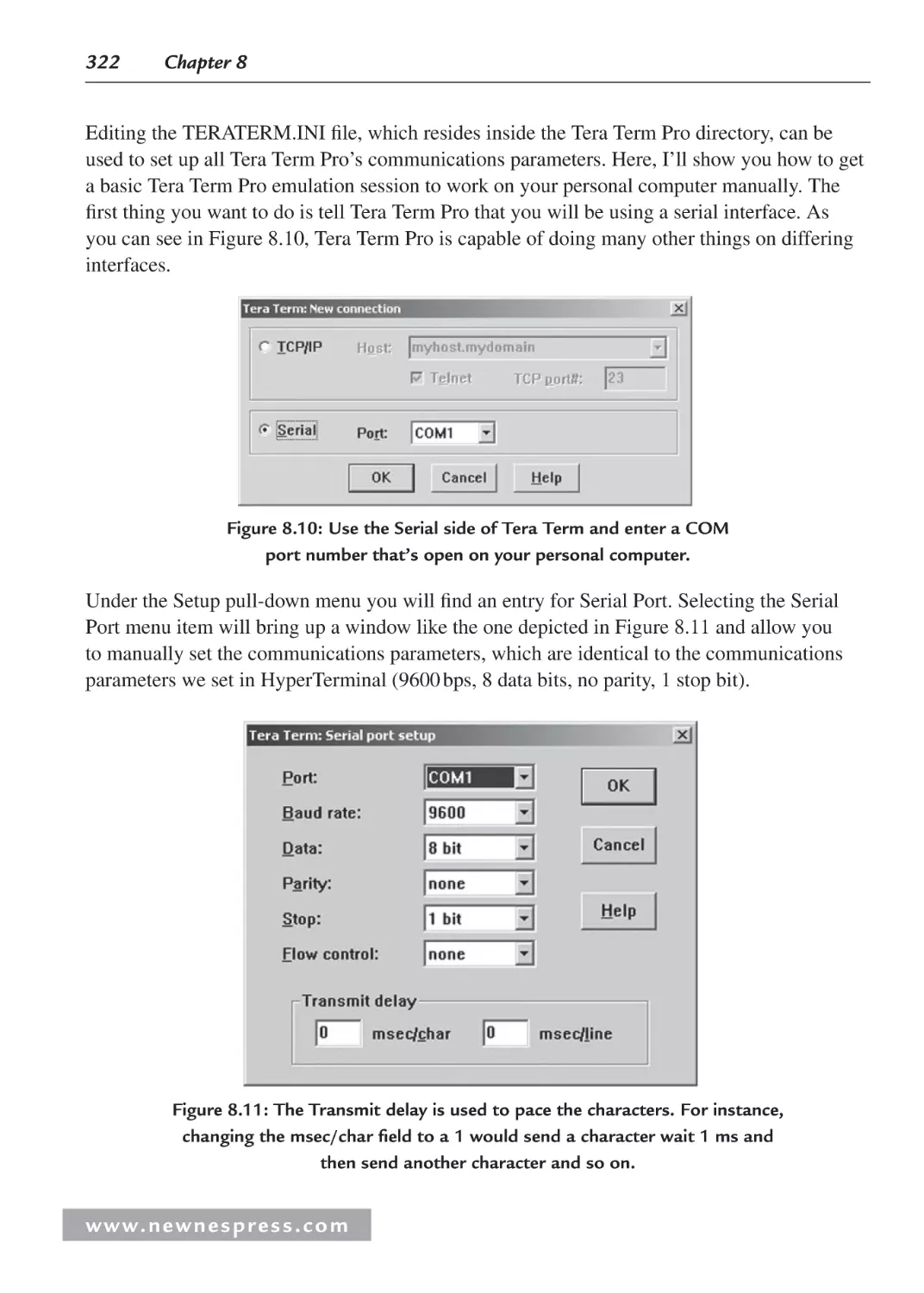
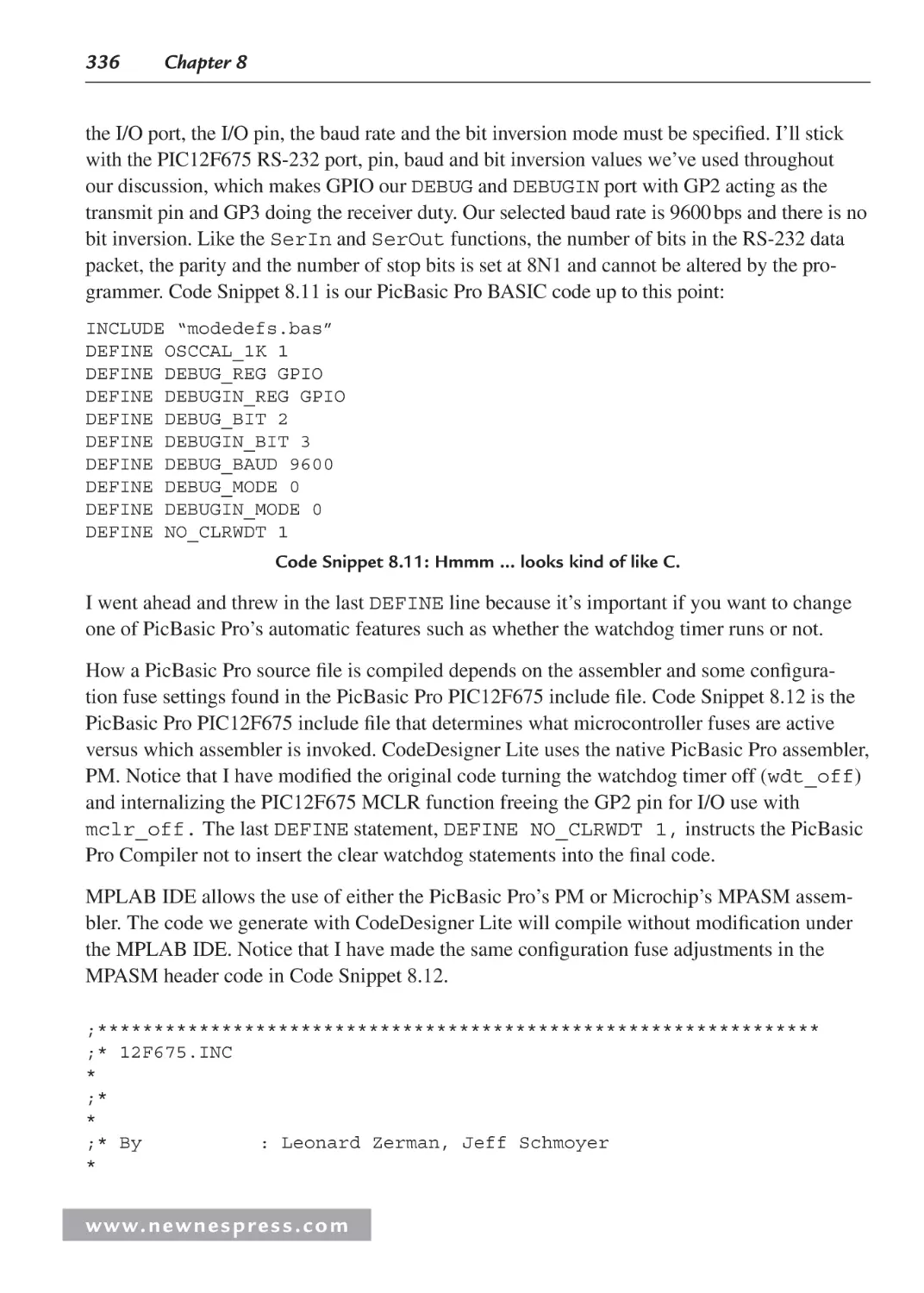
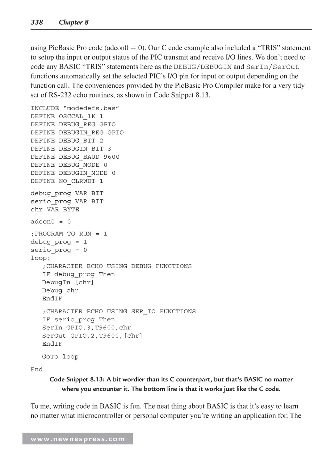
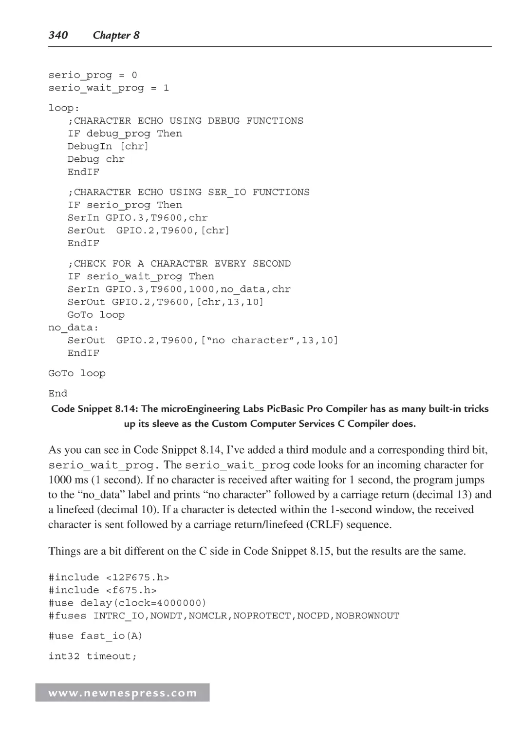
8.6 Writing RS-232 Microcontroller Routines in BASIC ............................................... 333
8.7 Building Some RS-232 Communications Hardware................................................. 339
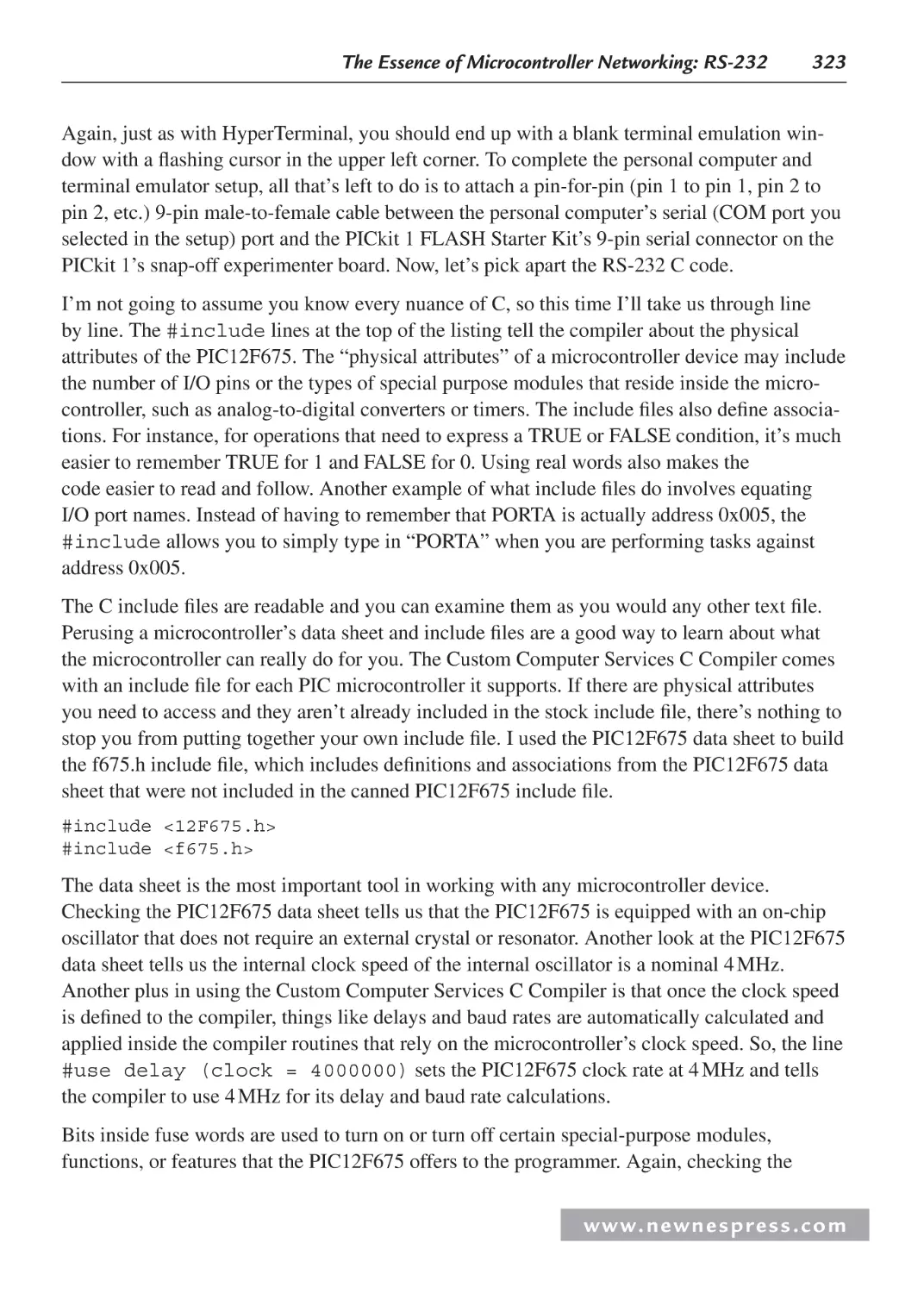
8.7.1 A Few More BASIC RS-232 Instructions....................................................... 339
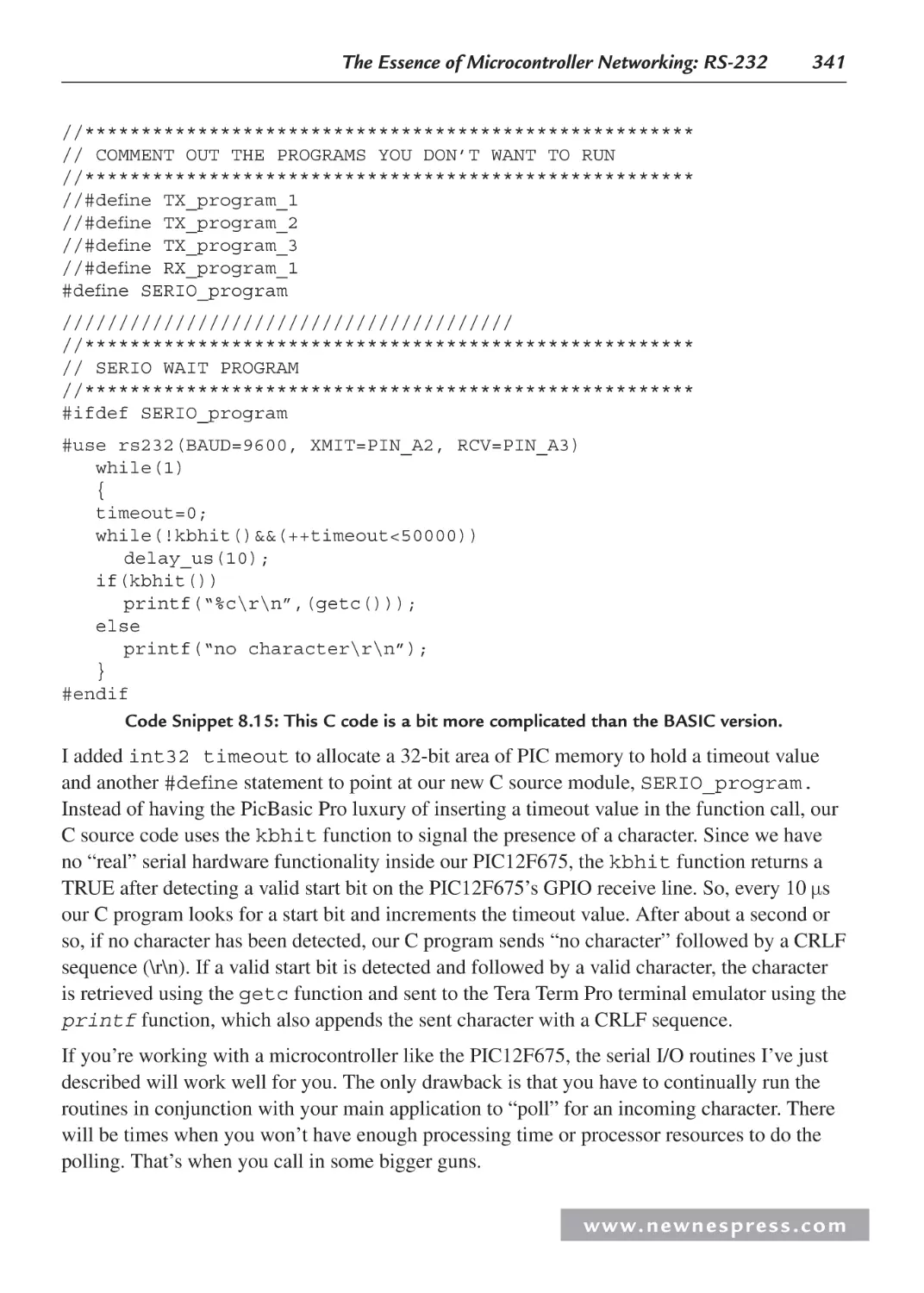
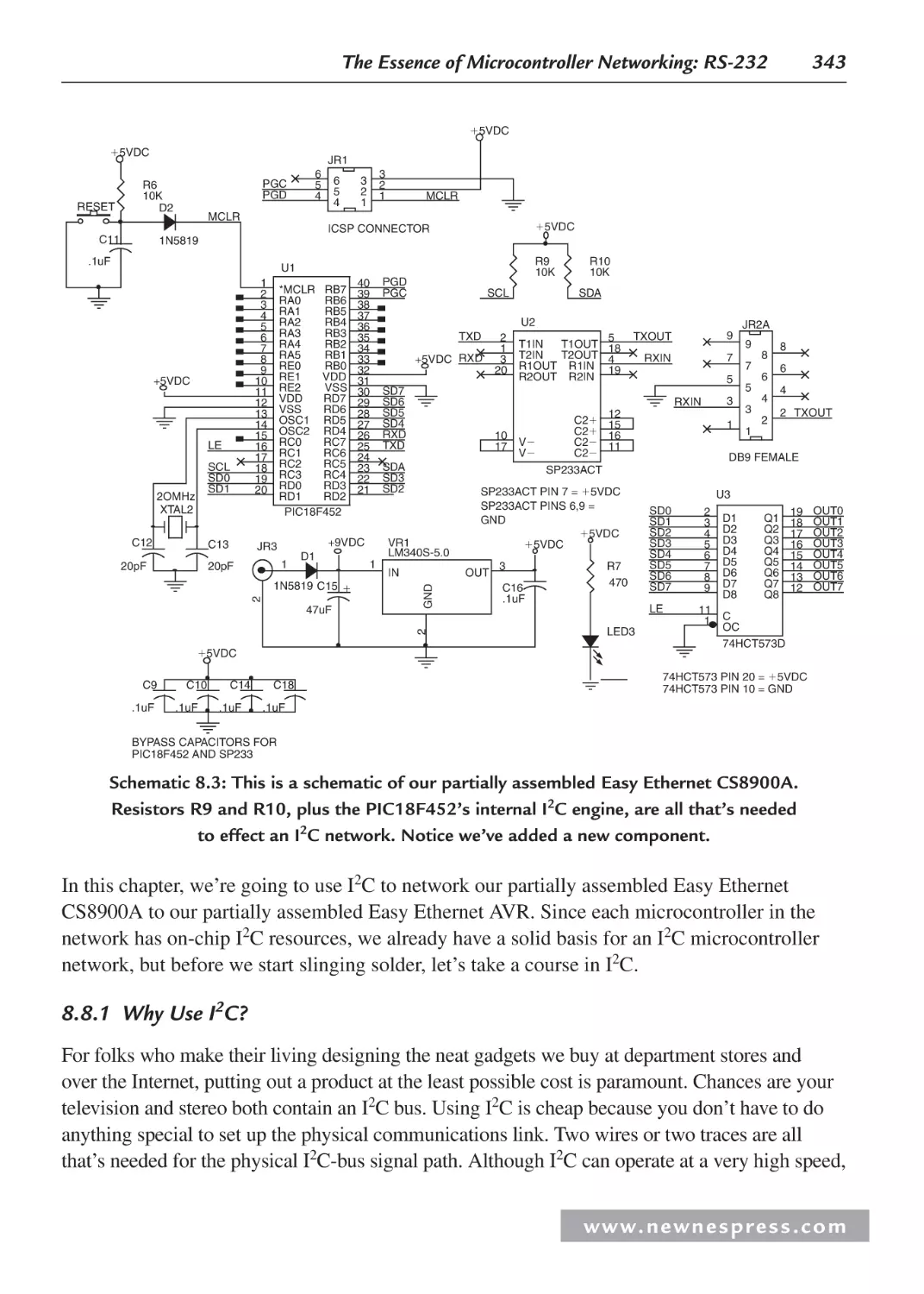
8.8 I2C: The Other Serial Protocol .................................................................................. 342
8.8.1 Why Use I2C?.................................................................................................. 343
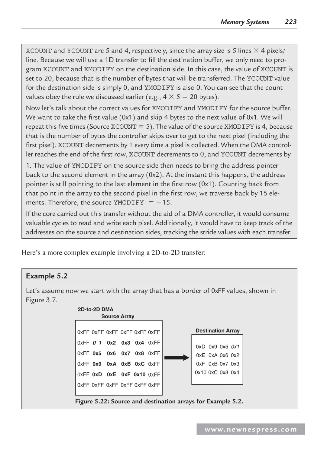
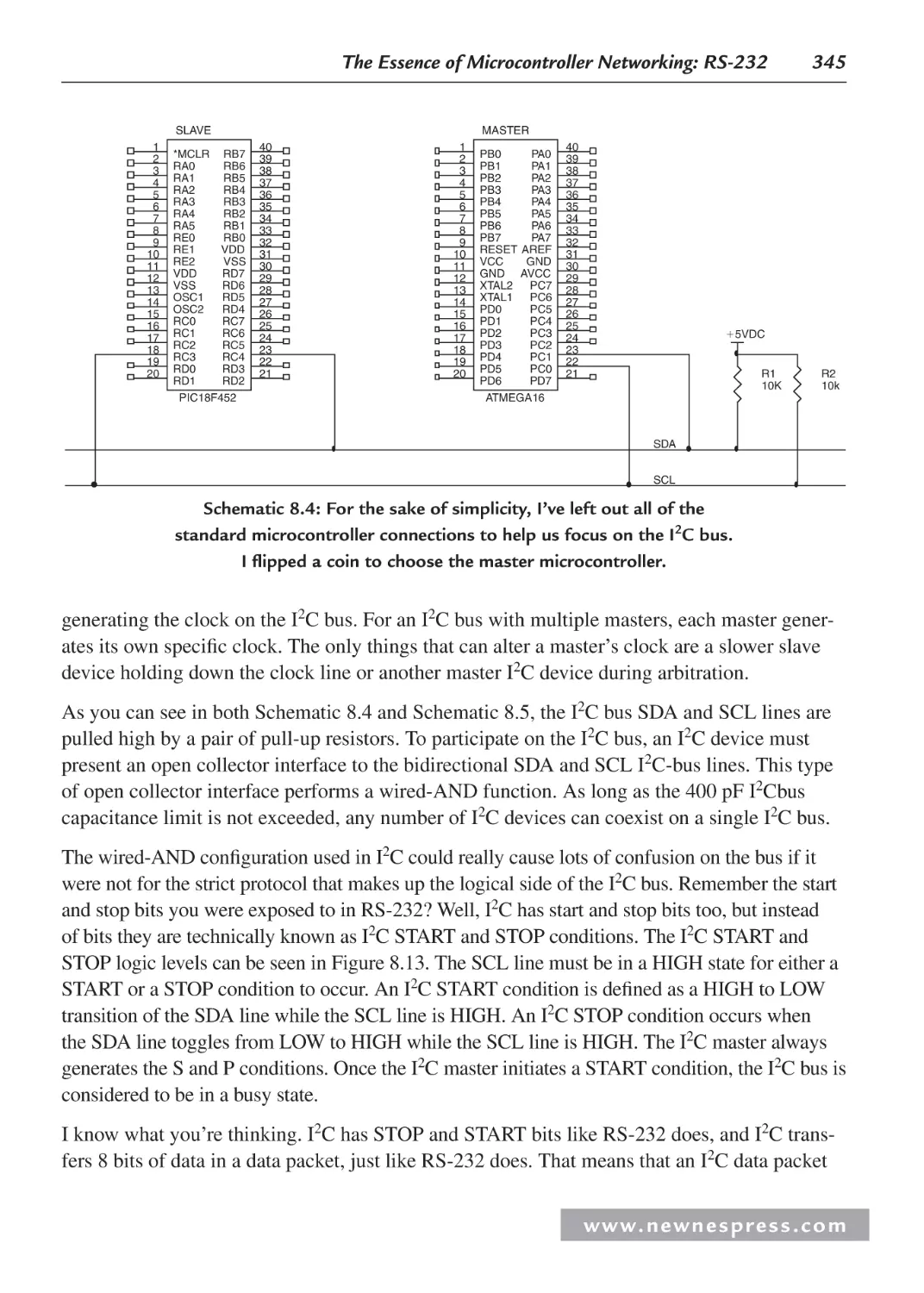
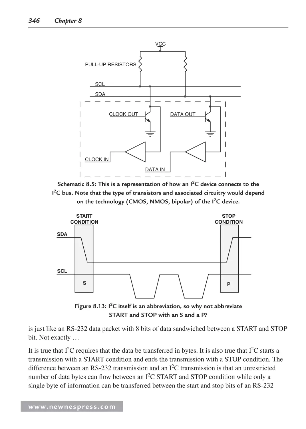
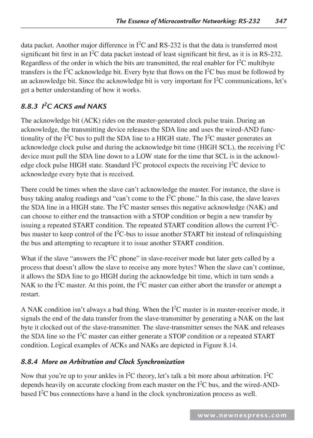
8.8.2 The I2C Bus ..................................................................................................... 344
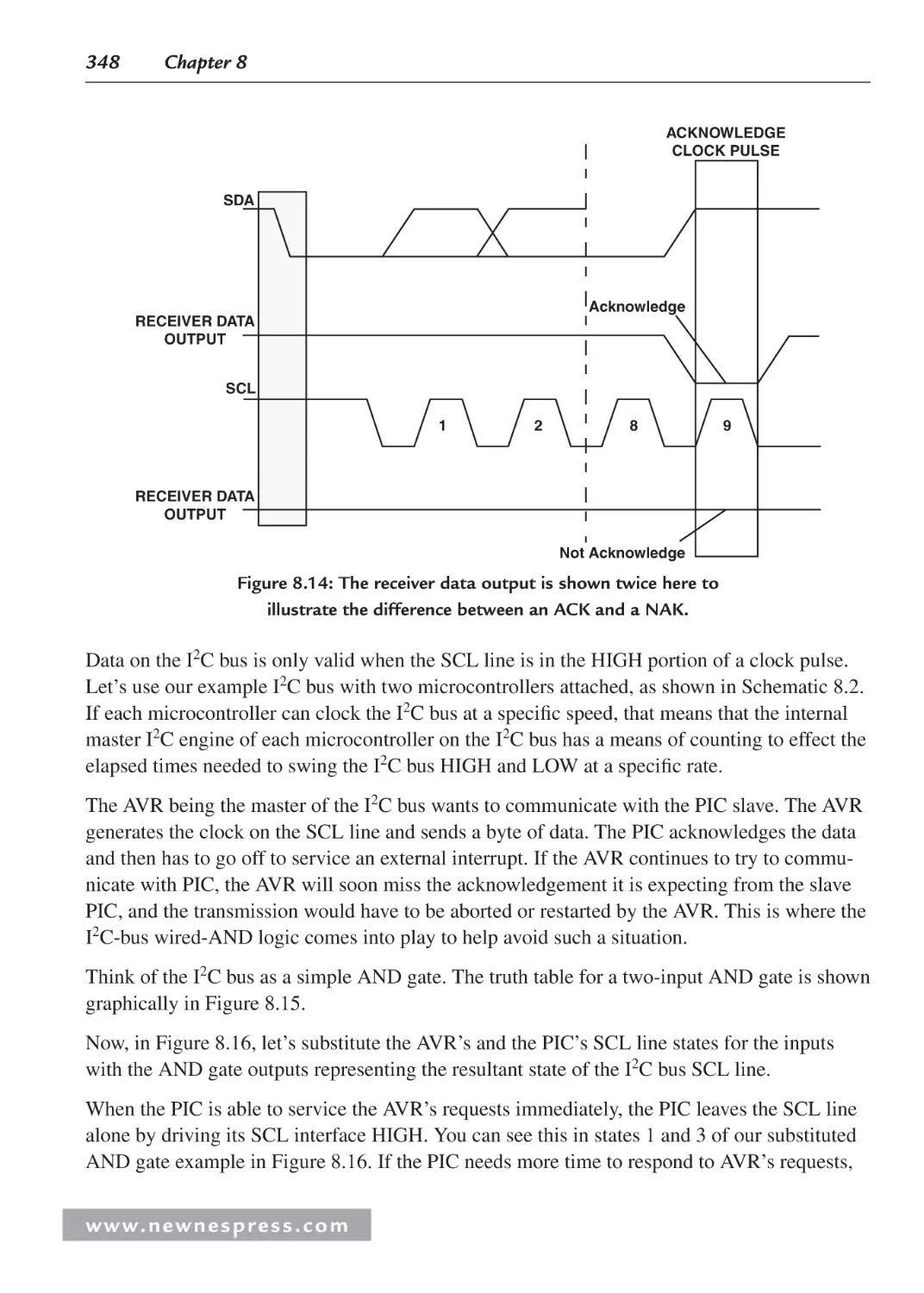
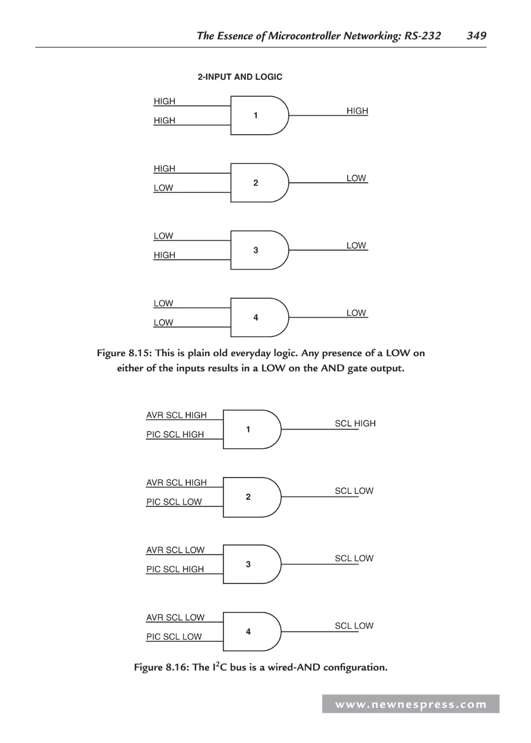
8.8.3 I2C ACKS and NAKS ..................................................................................... 347
www. n e wn e s p res s .c o m
Contents
ix
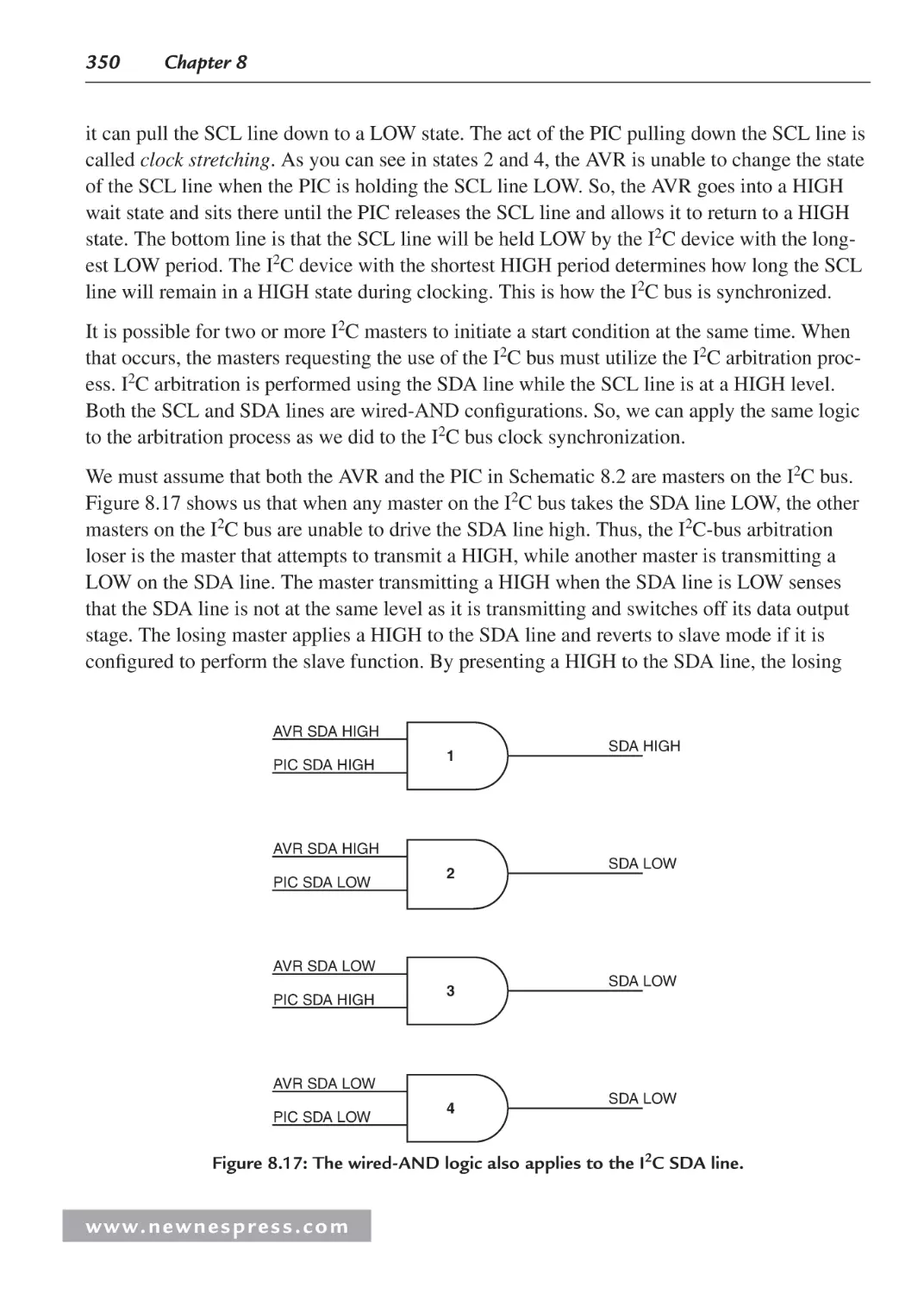
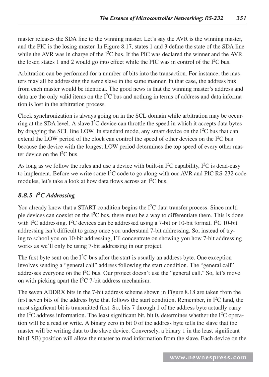
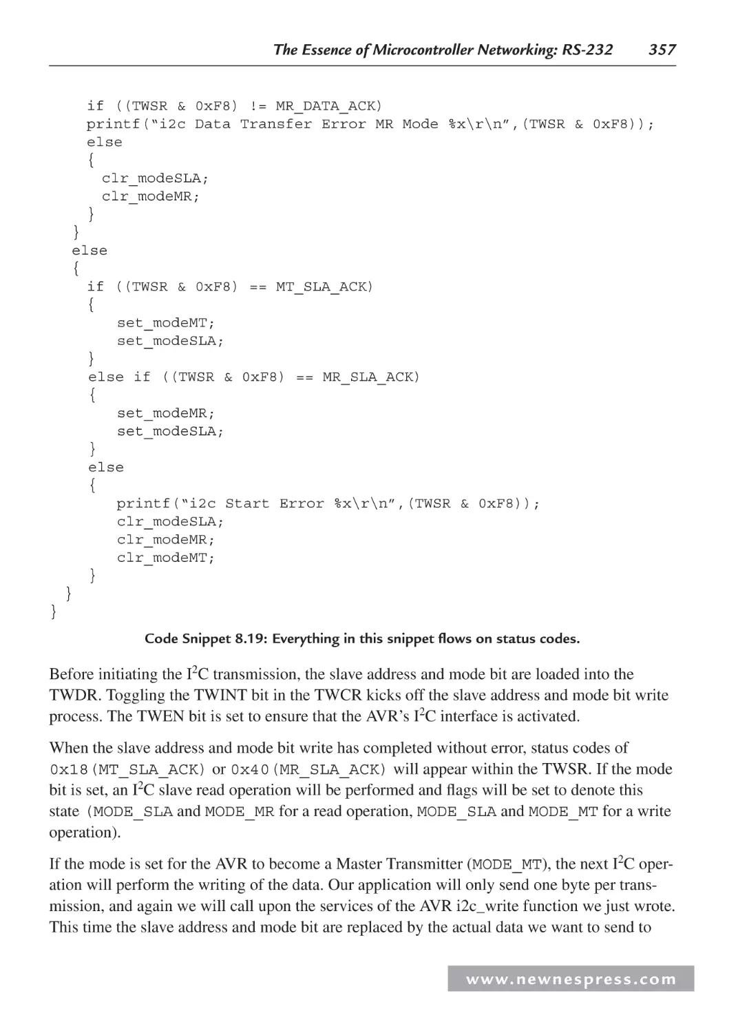
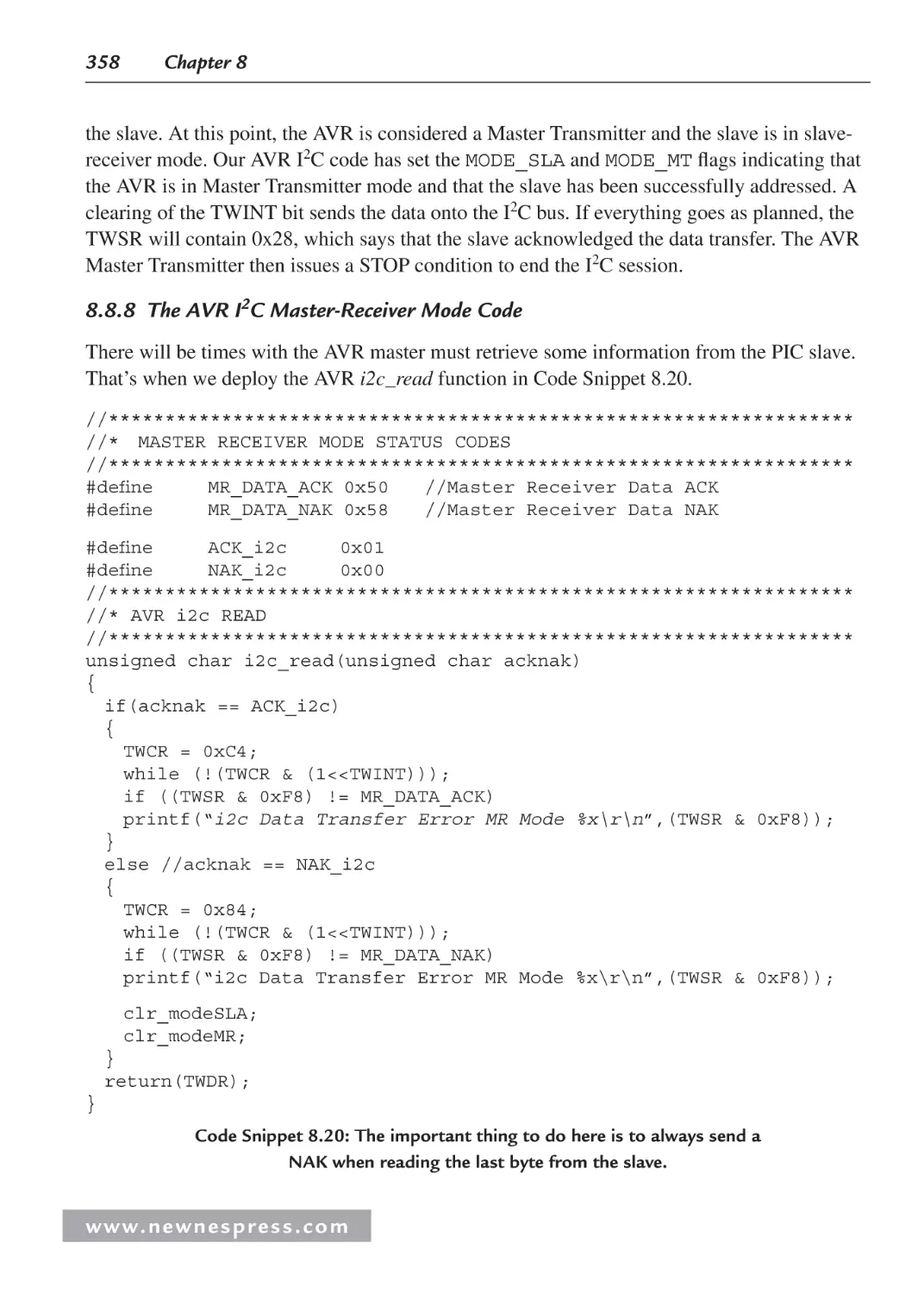
8.8.4 More on Arbitration and Clock Synchronization .......................................... 347
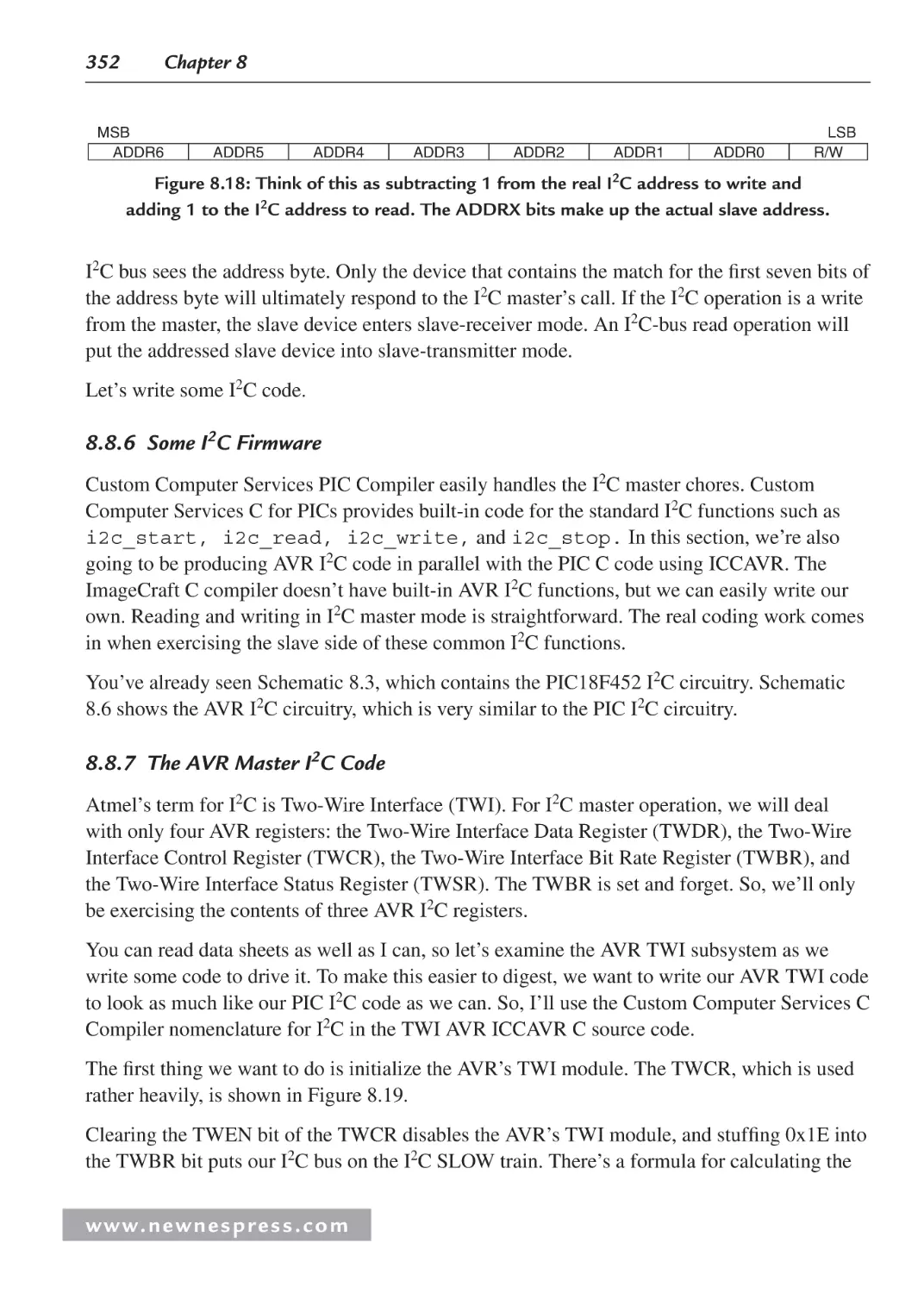
8.8.5 I2C Addressing .............................................................................................. 351
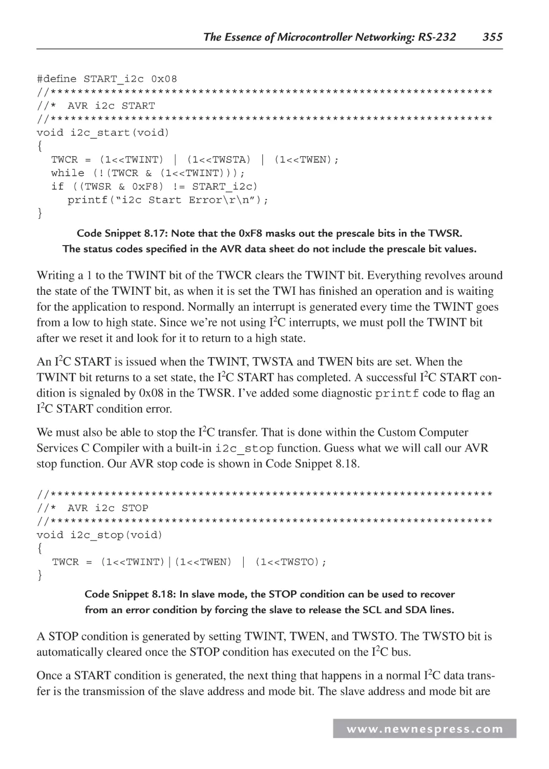
8.8.6 Some I2C Firmware ....................................................................................... 352
8.8.7 The AVR Master I2C Code............................................................................ 352
8.8.8 The AVR I2C Master-Receiver Mode Code .................................................. 358
8.8.9 The PIC I2C Slave-Transmitter Mode Code ................................................. 359
8.8.10 The AVR-to-PIC I2C Communications Ball ................................................. 365
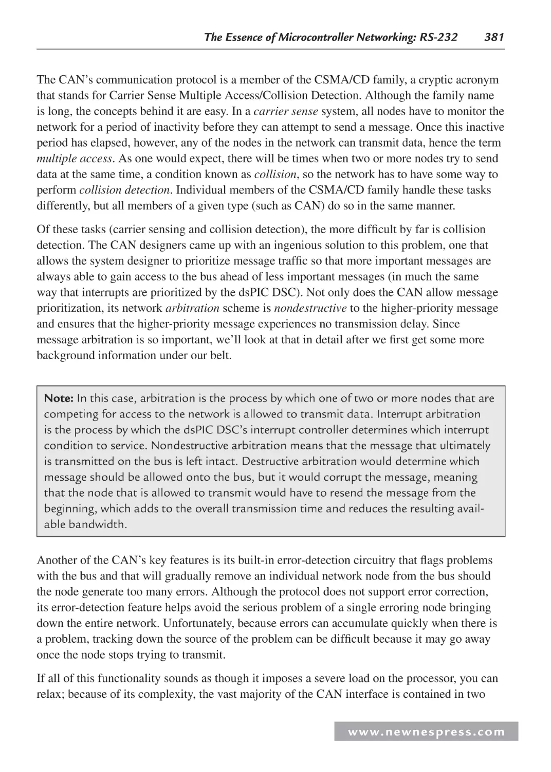
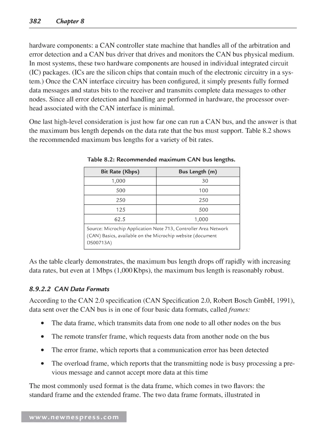
8.9 Communication Options............................................................................................ 378
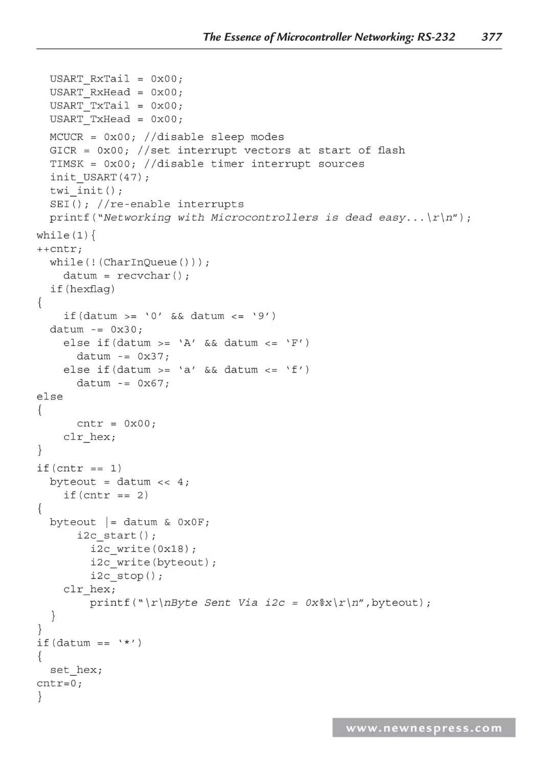
8.9.1 The Serial Peripheral Interface Port .............................................................. 378
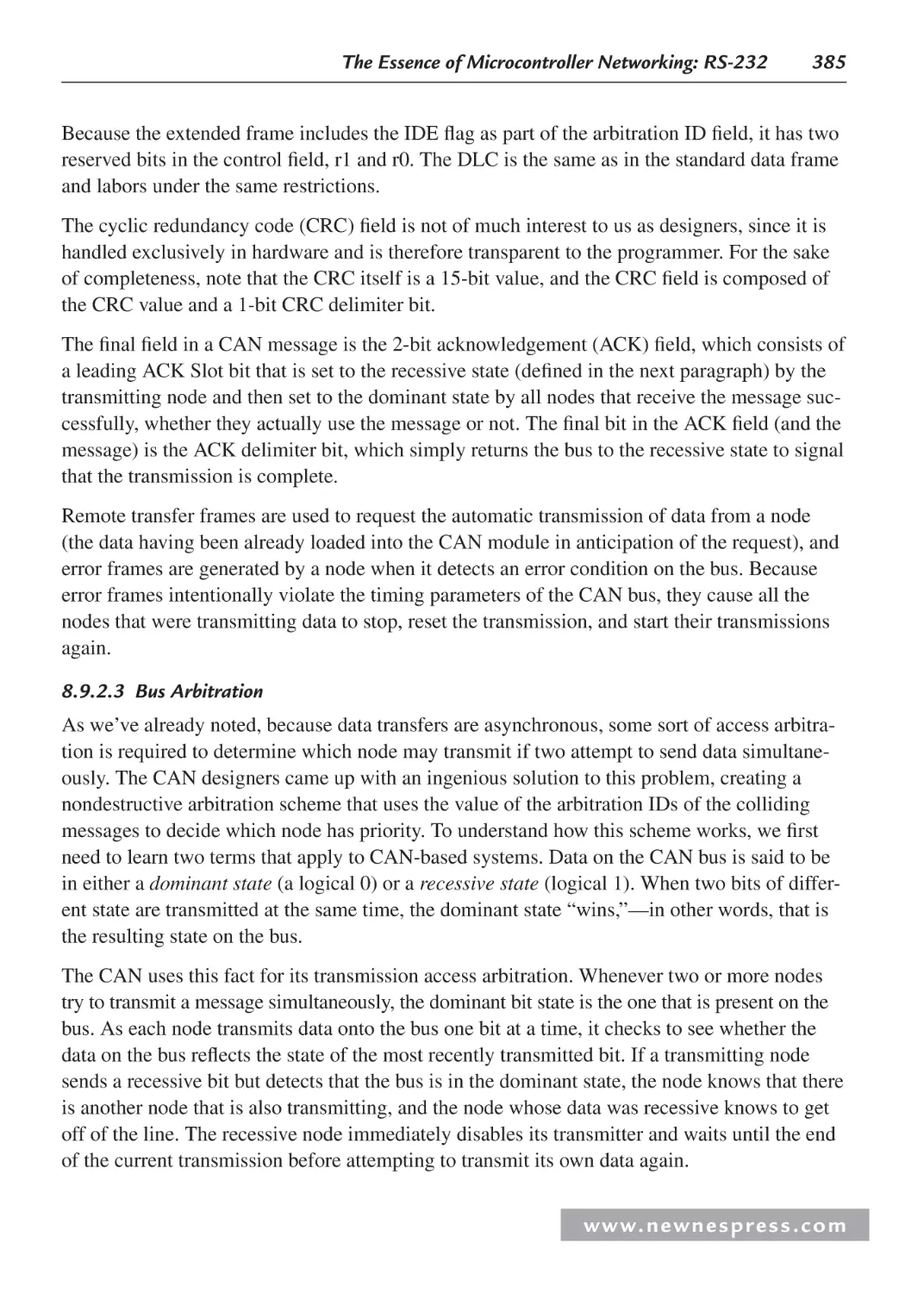
8.9.2 The Controller Area Network ....................................................................... 380
8.9.3 Acceptance Filters ......................................................................................... 386
Endnote ............................................................................................................................. 387
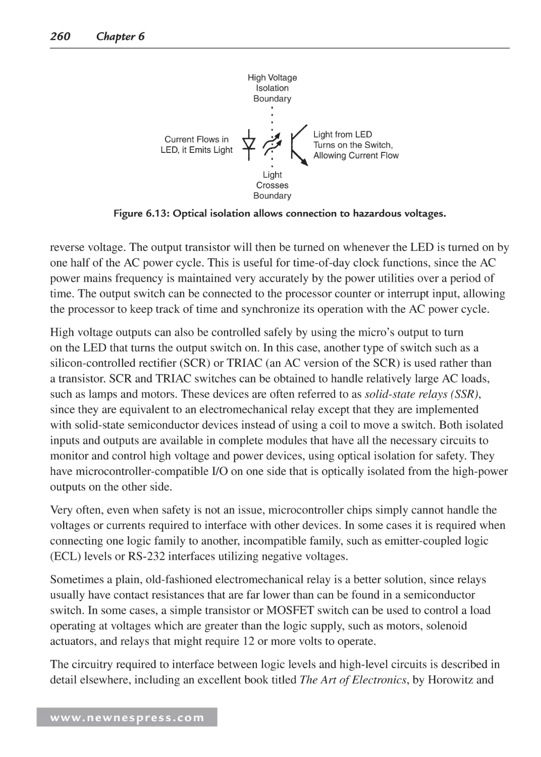
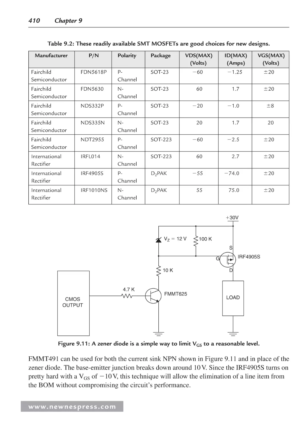
Chapter 9: Interfacing to Sensors and Actuators .................................................................... 389
9.1 Introduction ............................................................................................................... 389
9.2 Digital Interfacing ..................................................................................................... 389
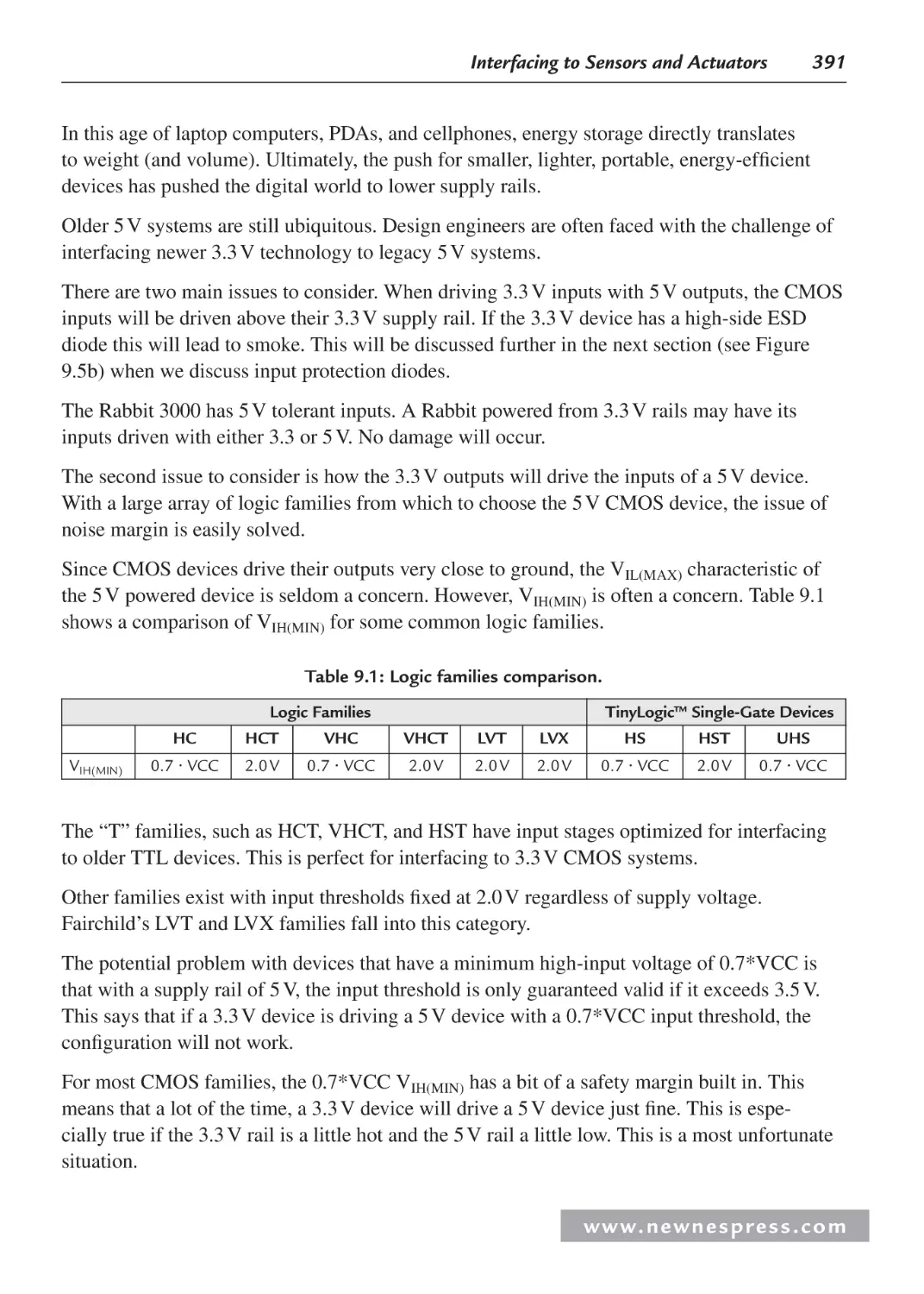
9.2.1 Mixing 3.3 and 5 V Devices ......................................................................... 389
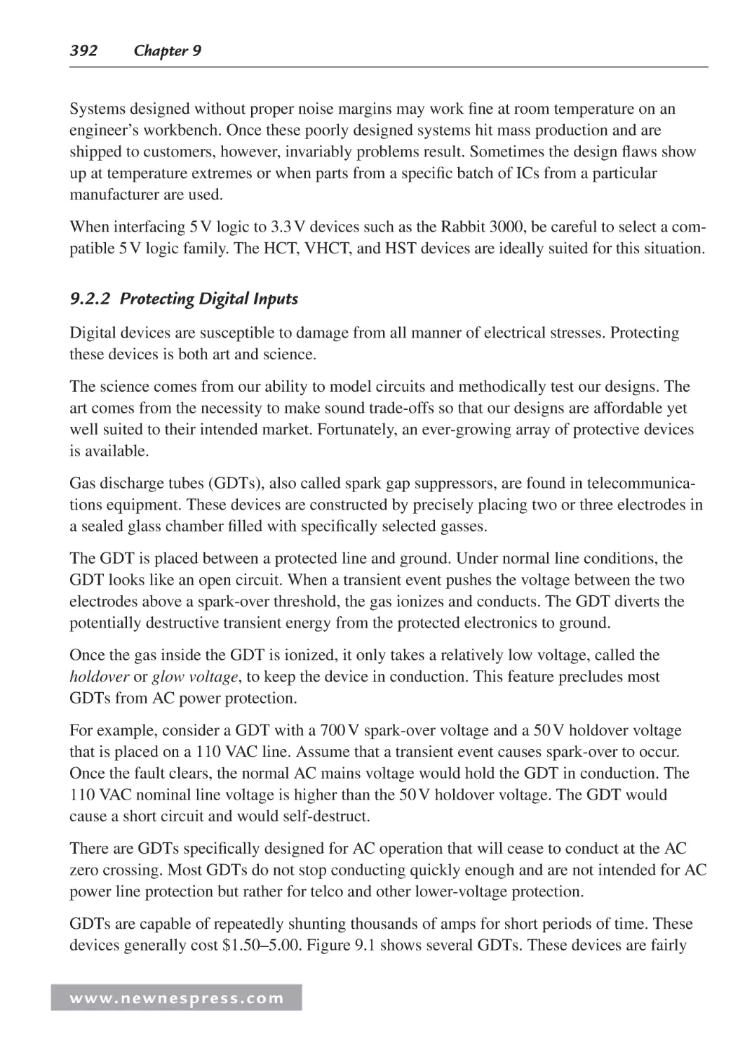
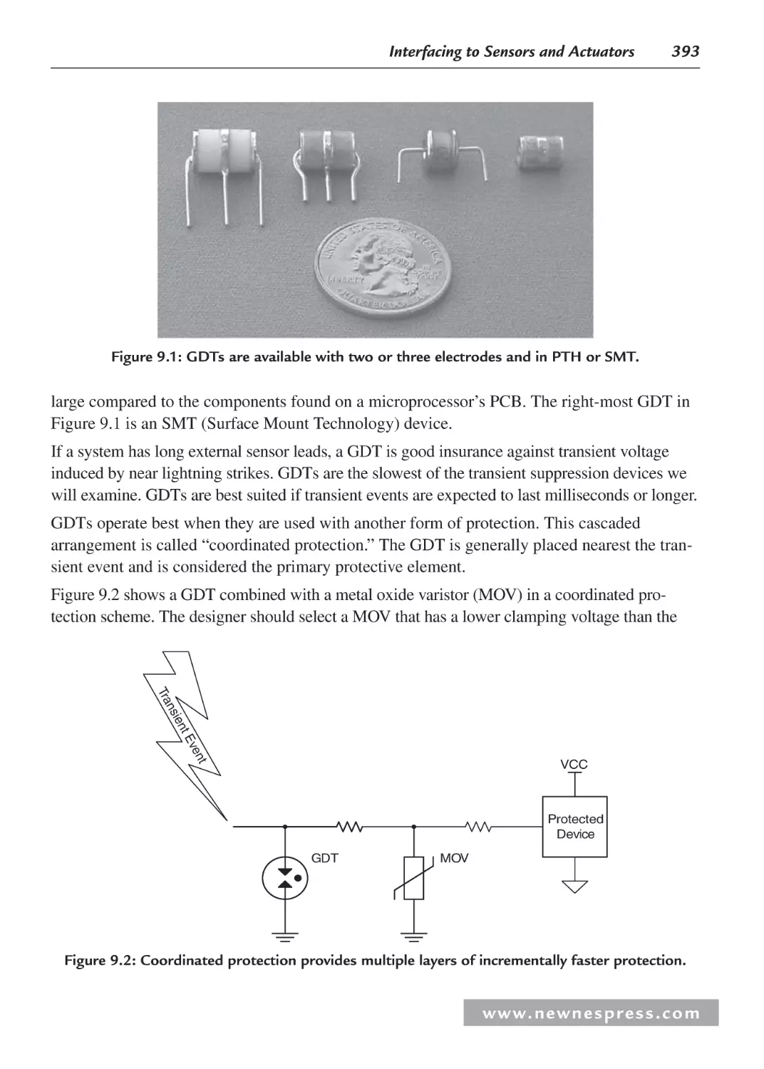
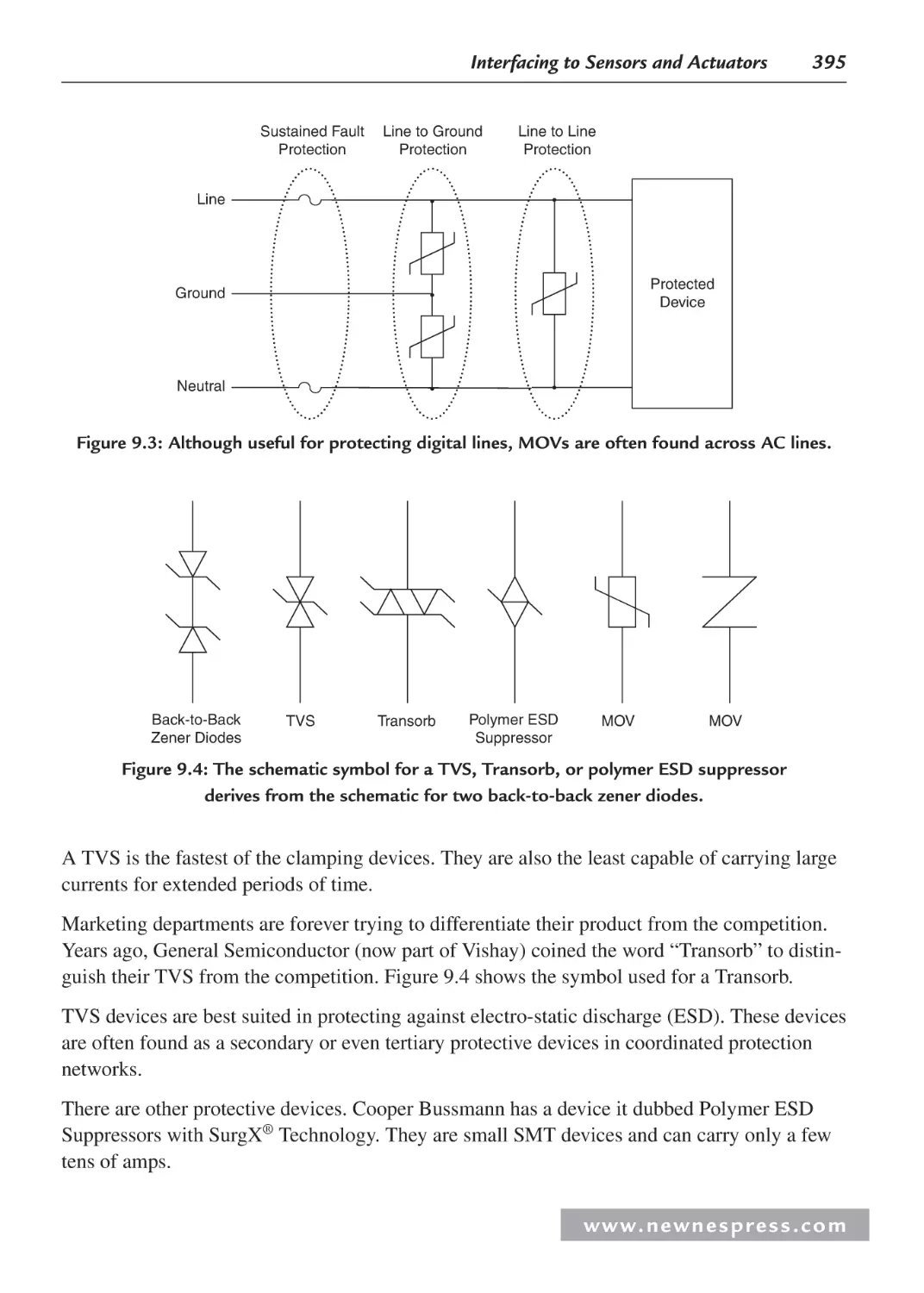
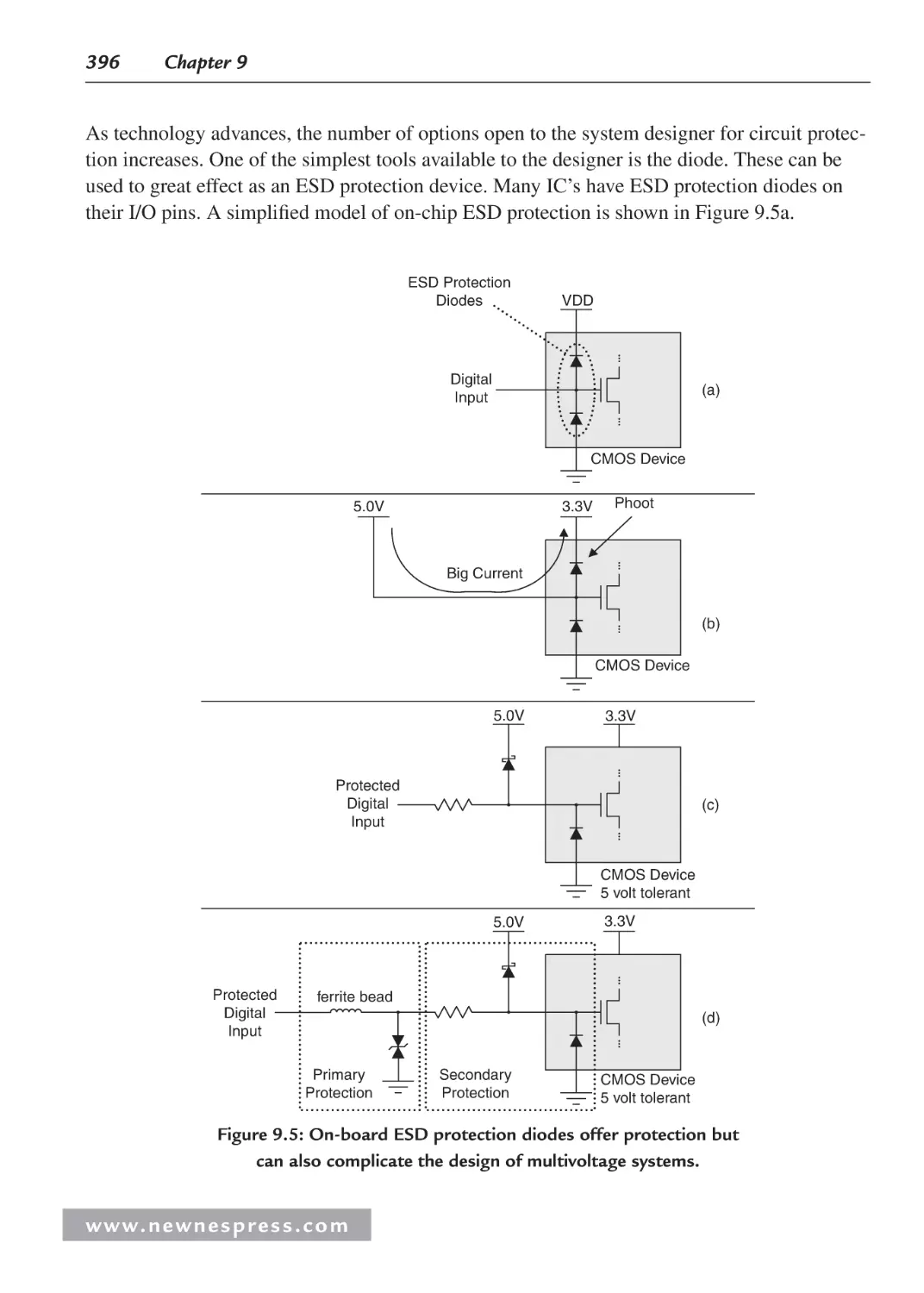
9.2.2 Protecting Digital Inputs ............................................................................... 392
9.2.3 Expanding Digital Inputs .............................................................................. 398
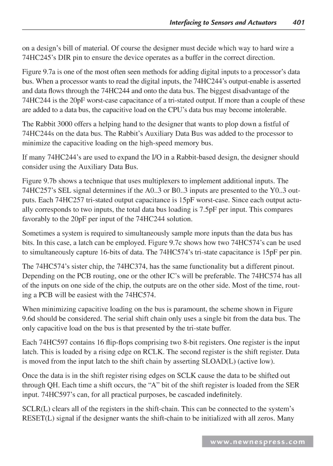
9.2.4 Expanding Digital Outputs............................................................................ 402
9.3 High-Current Outputs ................................................................................................ 404
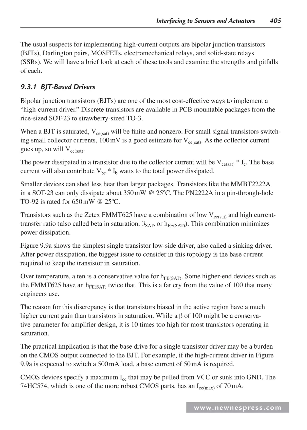
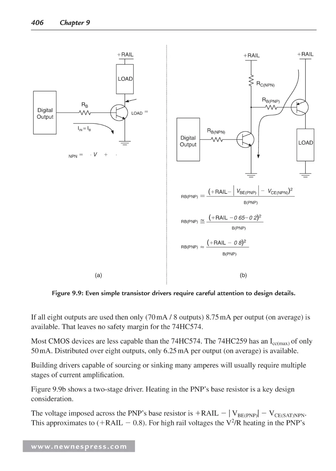
9.3.1 BJT-Based Drivers ........................................................................................ 405
9.3.2 MOSFETs ..................................................................................................... 409
9.3.3 Electromechanical Relays ............................................................................. 411
9.3.4 Solid-State Relays ......................................................................................... 417
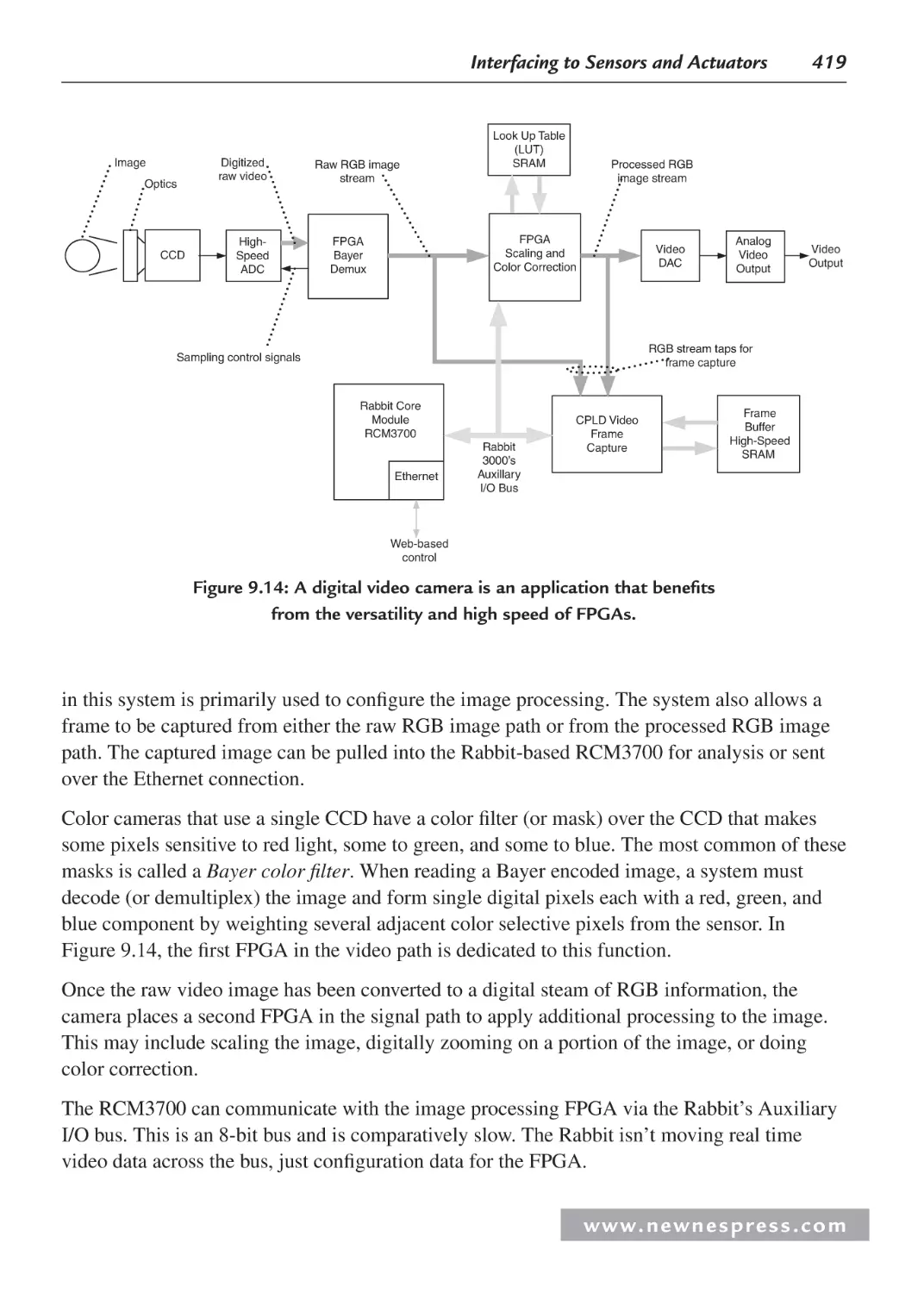
9.4 CPLDs and FPGAs .................................................................................................... 418
9.5 Analog Interfacing: An Overview ............................................................................. 420
9.5.1 ADCs ............................................................................................................. 420
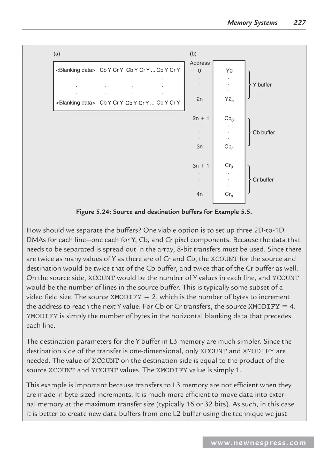
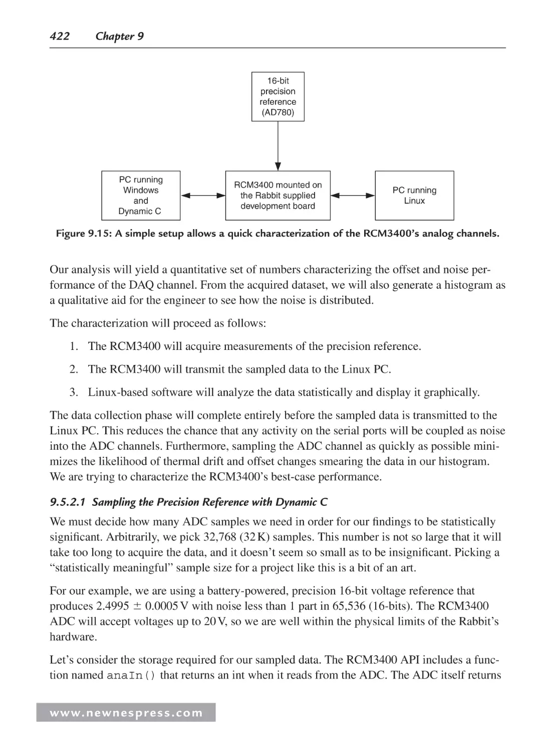
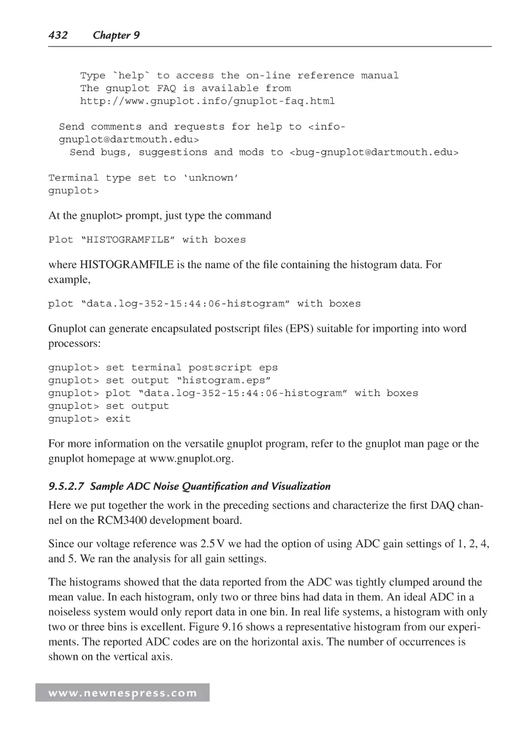
9.5.2 Project 1: Characterizing an Analog Channel ............................................... 421
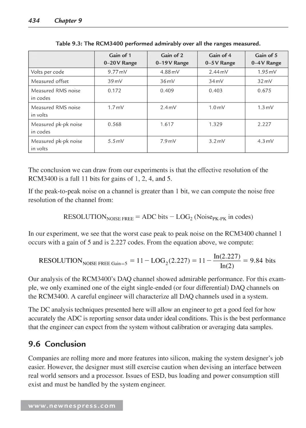
9.6 Conclusion ................................................................................................................. 434
Endnote ............................................................................................................................. 435
Chapter 10: Other Useful Hardware Design Tips and Techniques ......................................... 437
10.1 Introduction ............................................................................................................. 437
10.2 Diagnostics .............................................................................................................. 437
10.3 Connecting Tools ..................................................................................................... 438
10.4 Other Thoughts ........................................................................................................ 439
10.5 Construction Methods ............................................................................................. 440
10.5.1 Power and Ground Planes ............................................................................ 441
10.5.2 Ground Problems ......................................................................................... 441
w w w. n e w n e s p r e s s . c o m
x
Contents
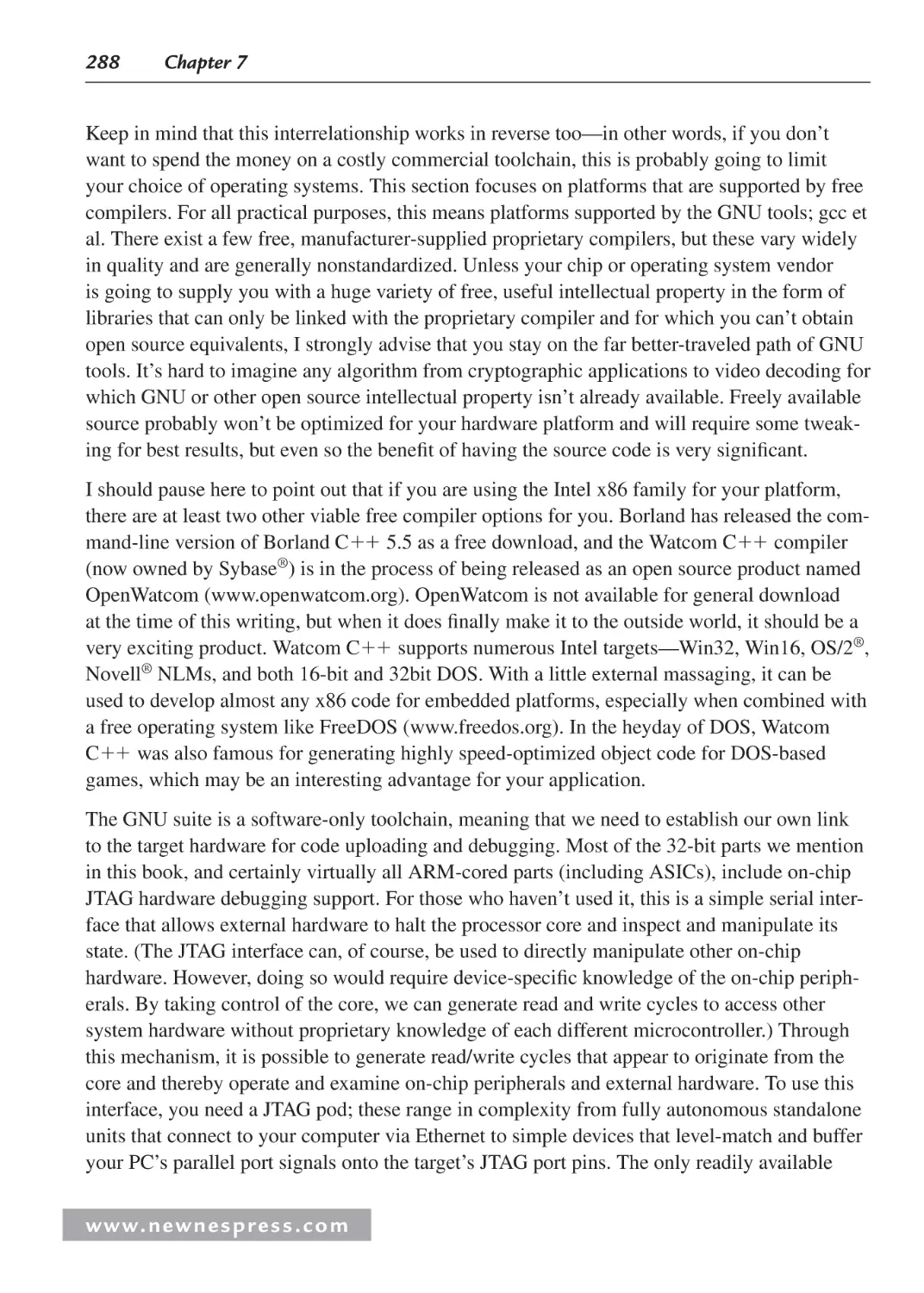
10.6 Electromagnetic Compatibility ............................................................................. 442
10.7 Electrostatic Discharge Effects ............................................................................. 442
10.7.1 Fault Tolerance .......................................................................................... 443
10.8 Hardware Development Tools ............................................................................... 444
10.8.1 Instrumentation Issues ............................................................................... 445
10.9 Software Development Tools ................................................................................ 445
10.10 Other Specialized Design Considerations ............................................................. 446
10.10.1 Thermal Analysis and Design ................................................................. 446
10.10.2 Battery-Powered System Design Considerations .................................... 447
10.11 Processor Performance Metrics ............................................................................. 448
10.11.1 IPS ........................................................................................................... 448
10.11.2 OPS .......................................................................................................... 448
10.11.3 Benchmarks ............................................................................................. 449
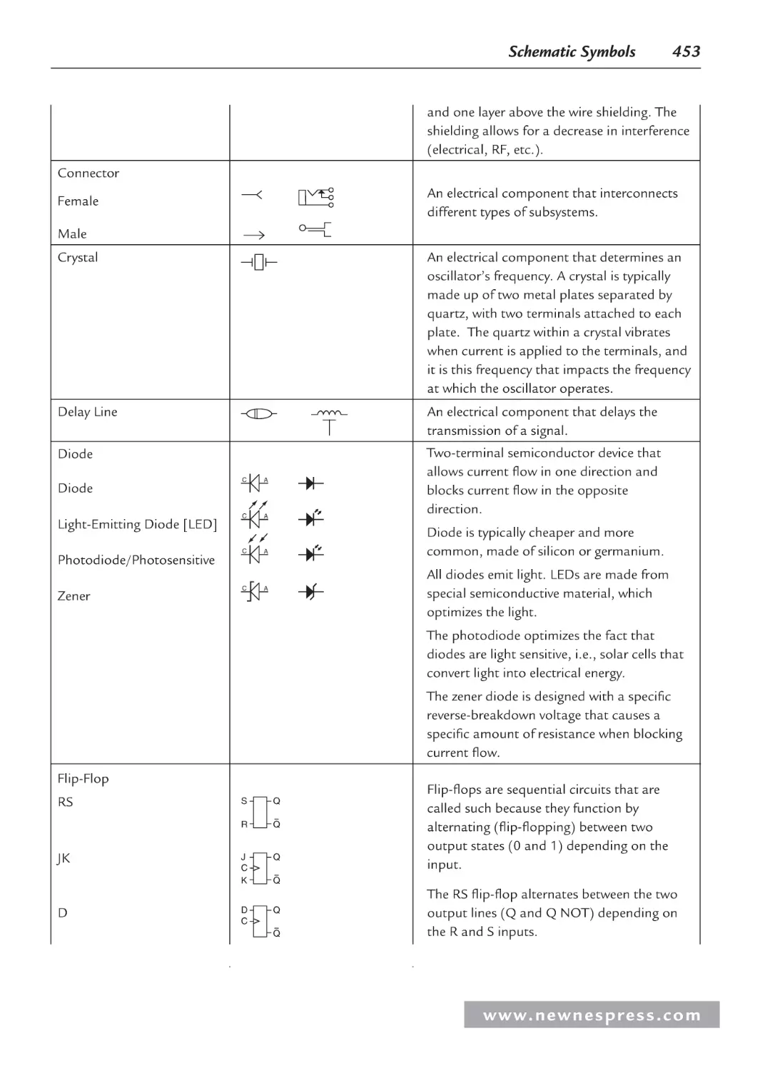
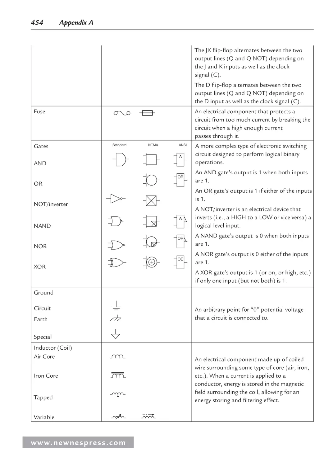
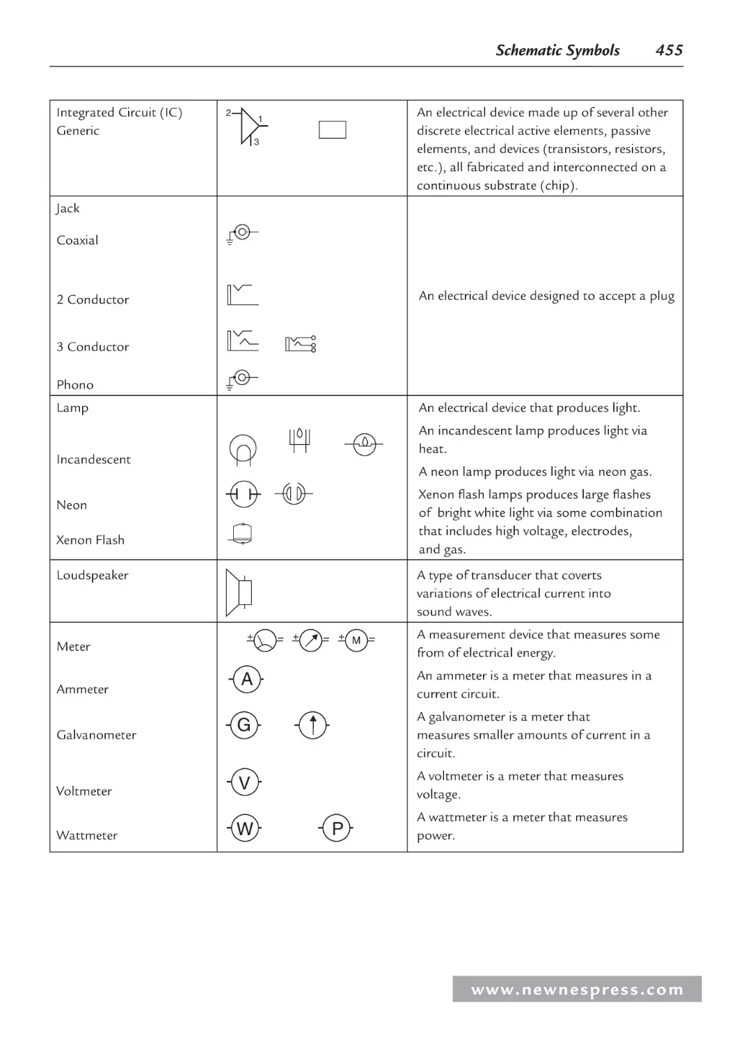
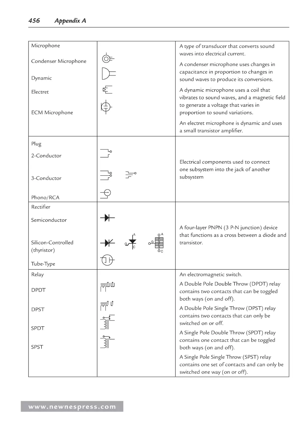
Appendix A: Schematic Symbols ........................................................................................... 451
Appendix B: Acronyms and Abbreviations ............................................................................ 459
Appendix C: PC Board Design Issues .................................................................................... 469
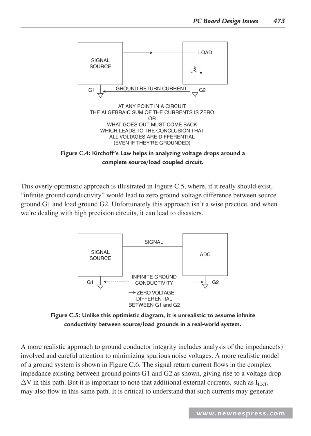
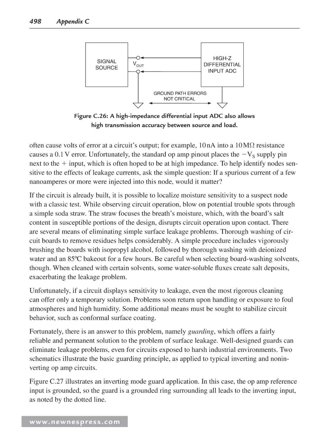
C.1 Introduction............................................................................................................. 469
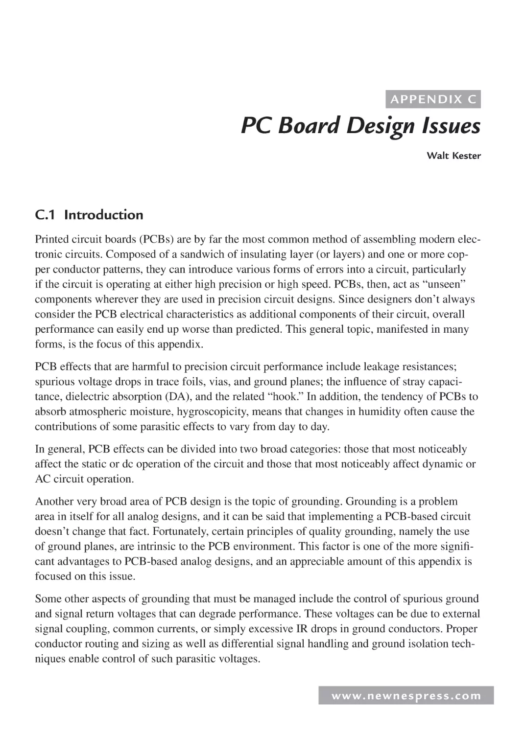
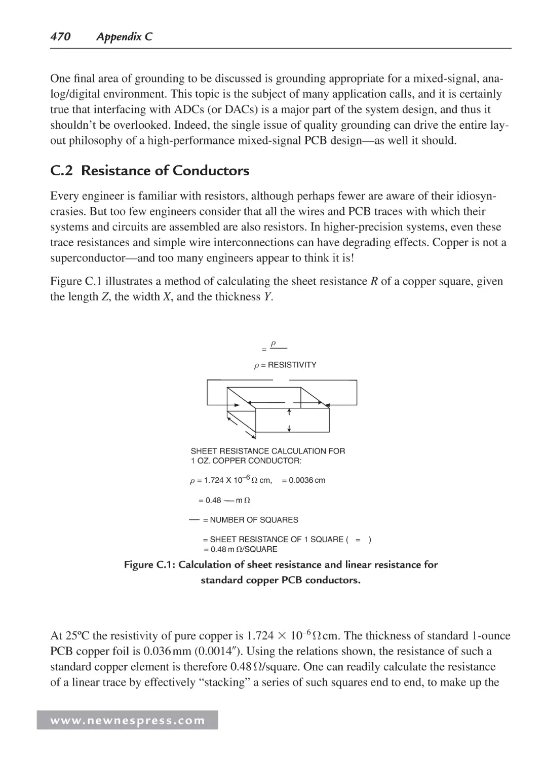
C.2 Resistance of Conductors ....................................................................................... 470
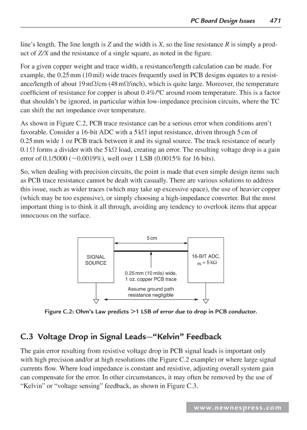
C.3 Voltage Drop in Signal Leads—“Kelvin” Feedback .............................................. 471
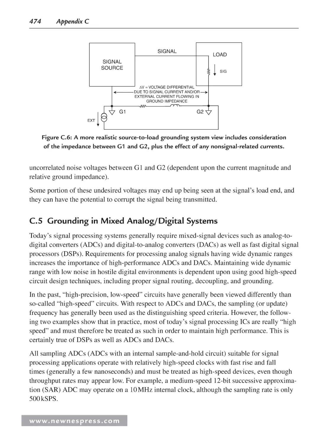
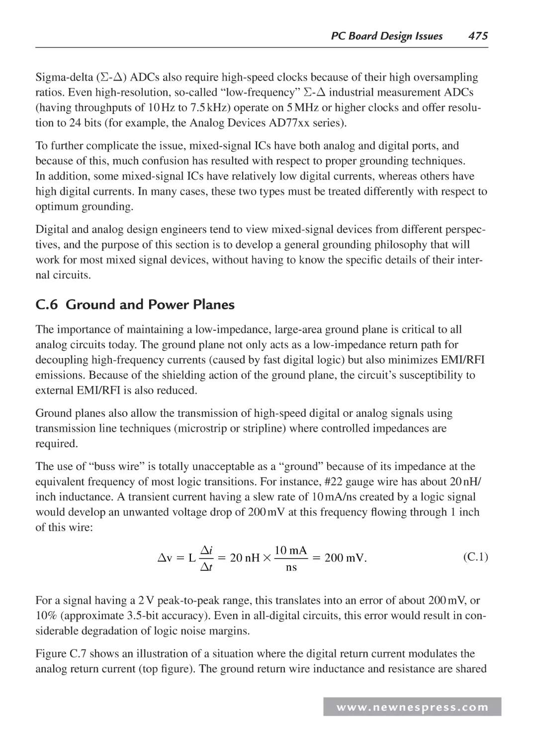
C.4 Signal Return Currents ........................................................................................... 472
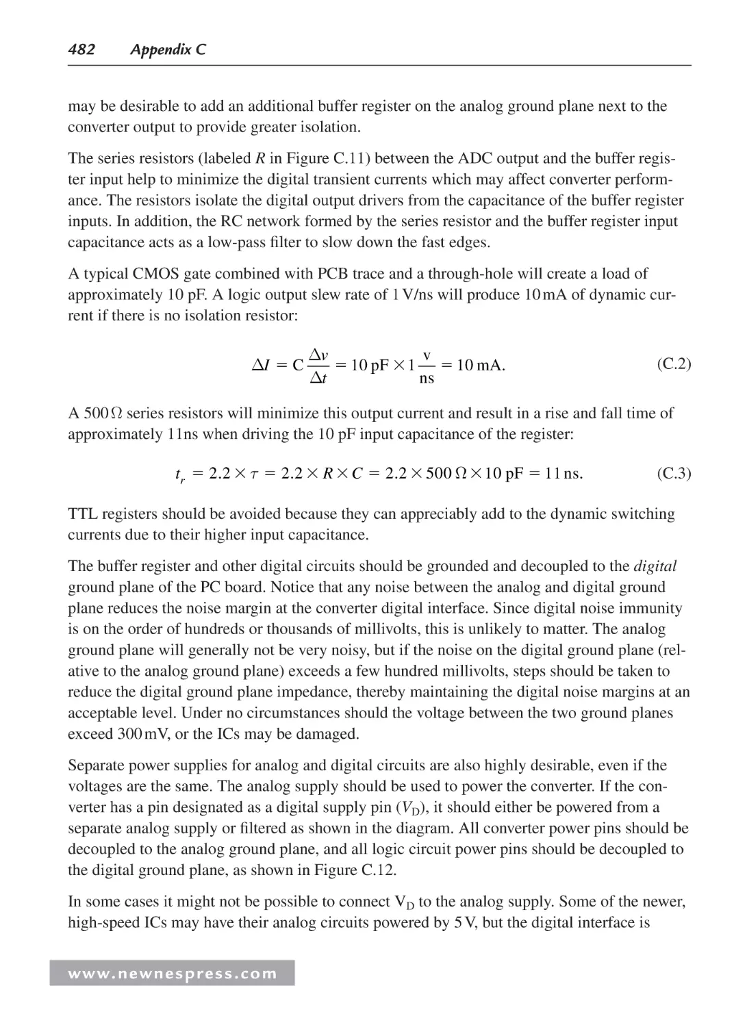
C.5 Grounding in Mixed Analog/Digital Systems ........................................................ 474
C.6 Ground and Power Planes ....................................................................................... 475
C.7 Double-Sided versus Multilayer Printed Circuit Boards ........................................ 477
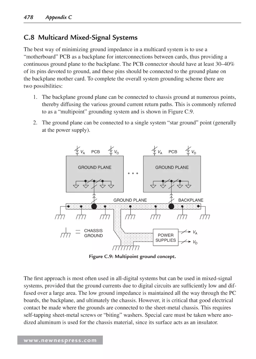
C.8 Multicard Mixed-Signal Systems ........................................................................... 478
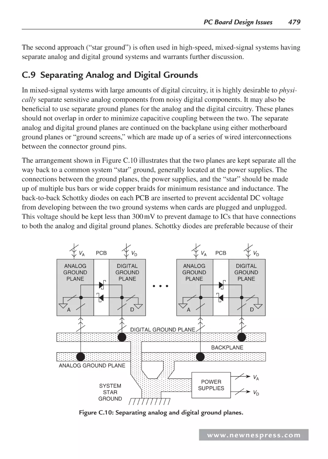
C.9 Separating Analog and Digital Grounds ................................................................. 479
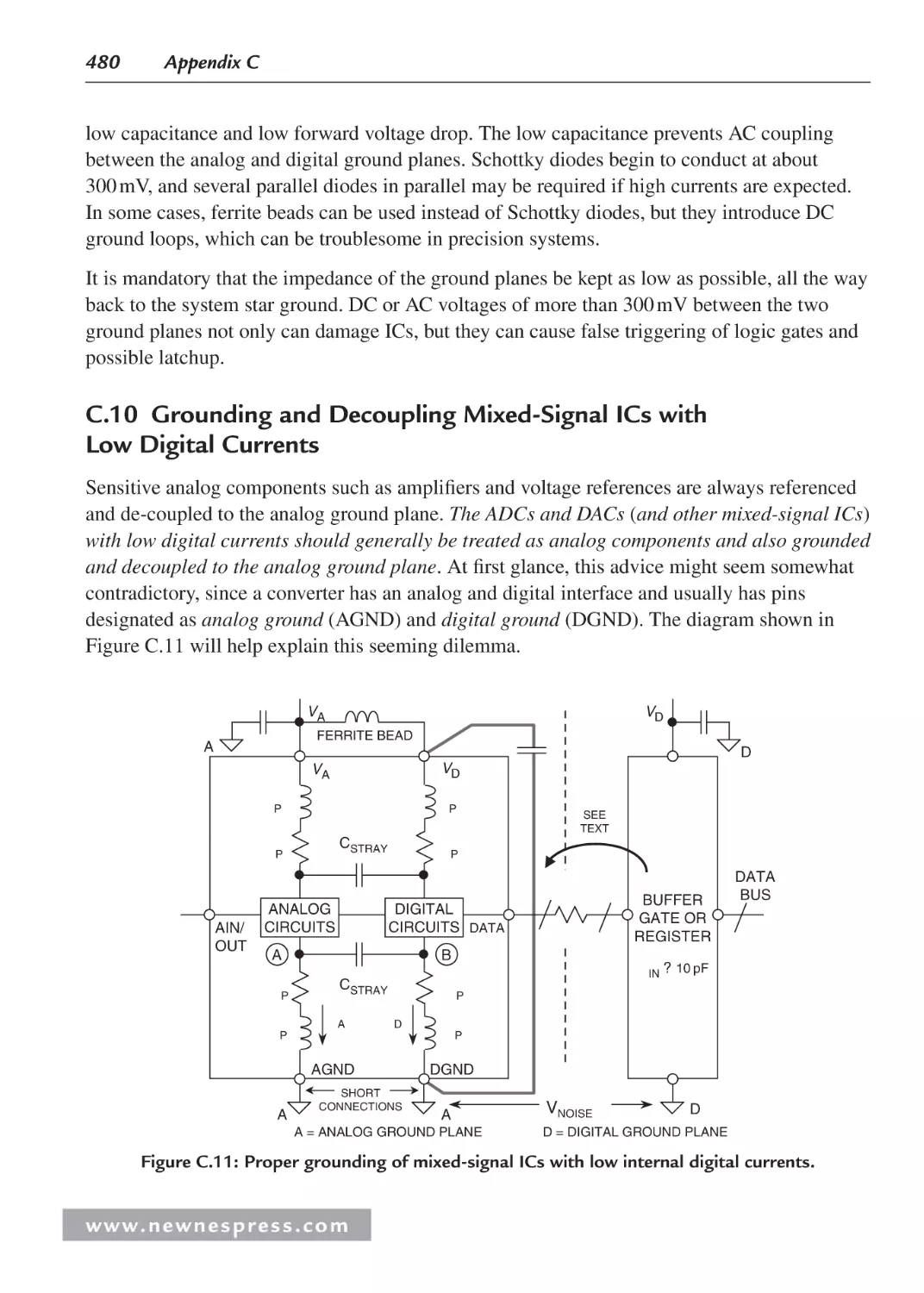
C.10 Grounding and Decoupling Mixed-Signal ICs with Low Digital Currents ............ 480
C.11 Treat the ADC Digital Outputs with Care .............................................................. 481
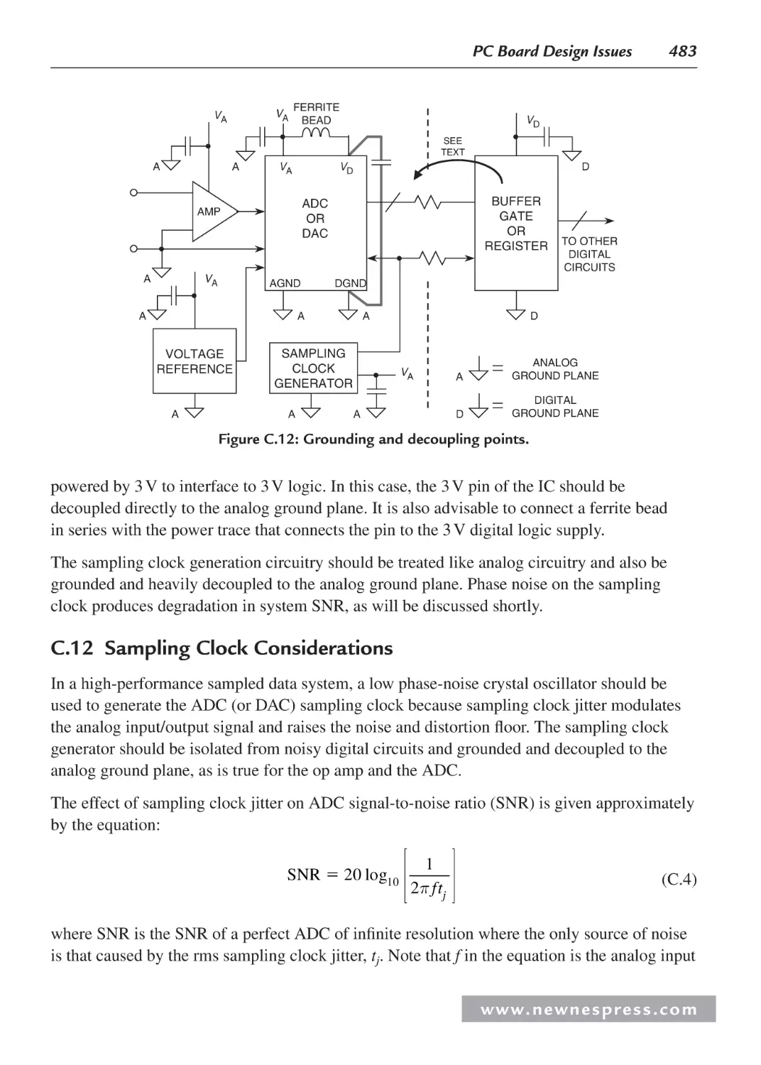
C.12 Sampling Clock Considerations ............................................................................. 483
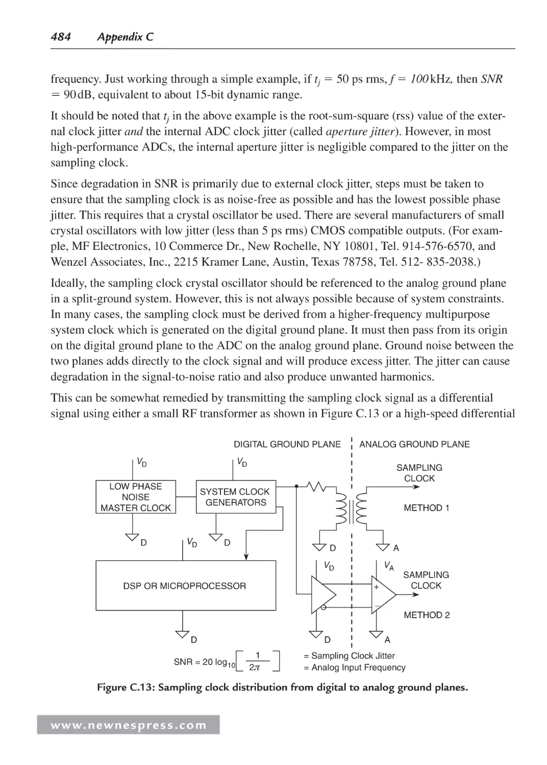
C.13 The Origins of the Confusion About Mixed-Signal Grounding: Applying
Single-Card Grounding Concepts to Multicard Systems ........................................485
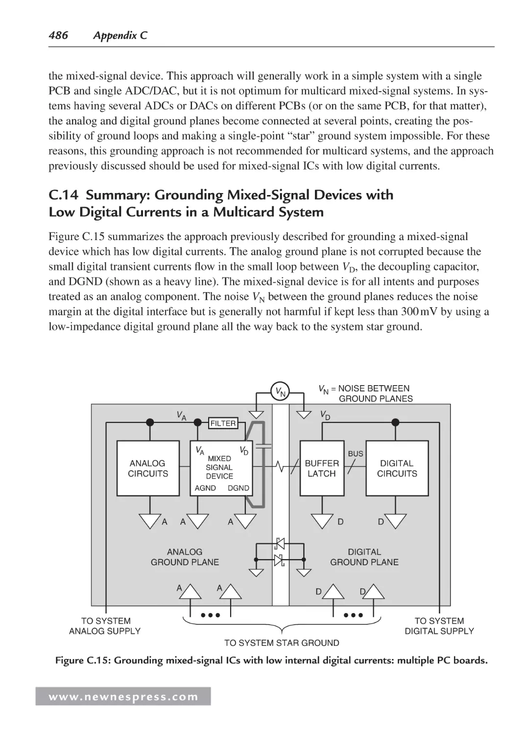
C.14 Summary: Grounding Mixed-Signal Devices with Low Digital Currents in a
Multicard System ...................................................................................................486
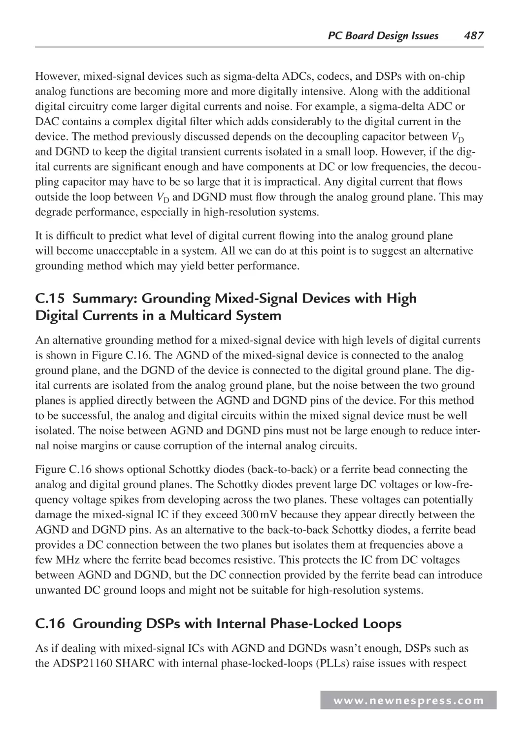
C.15 Summary: Grounding Mixed-Signal Devices with High Digital
Currents in a Multicard System ..............................................................................487
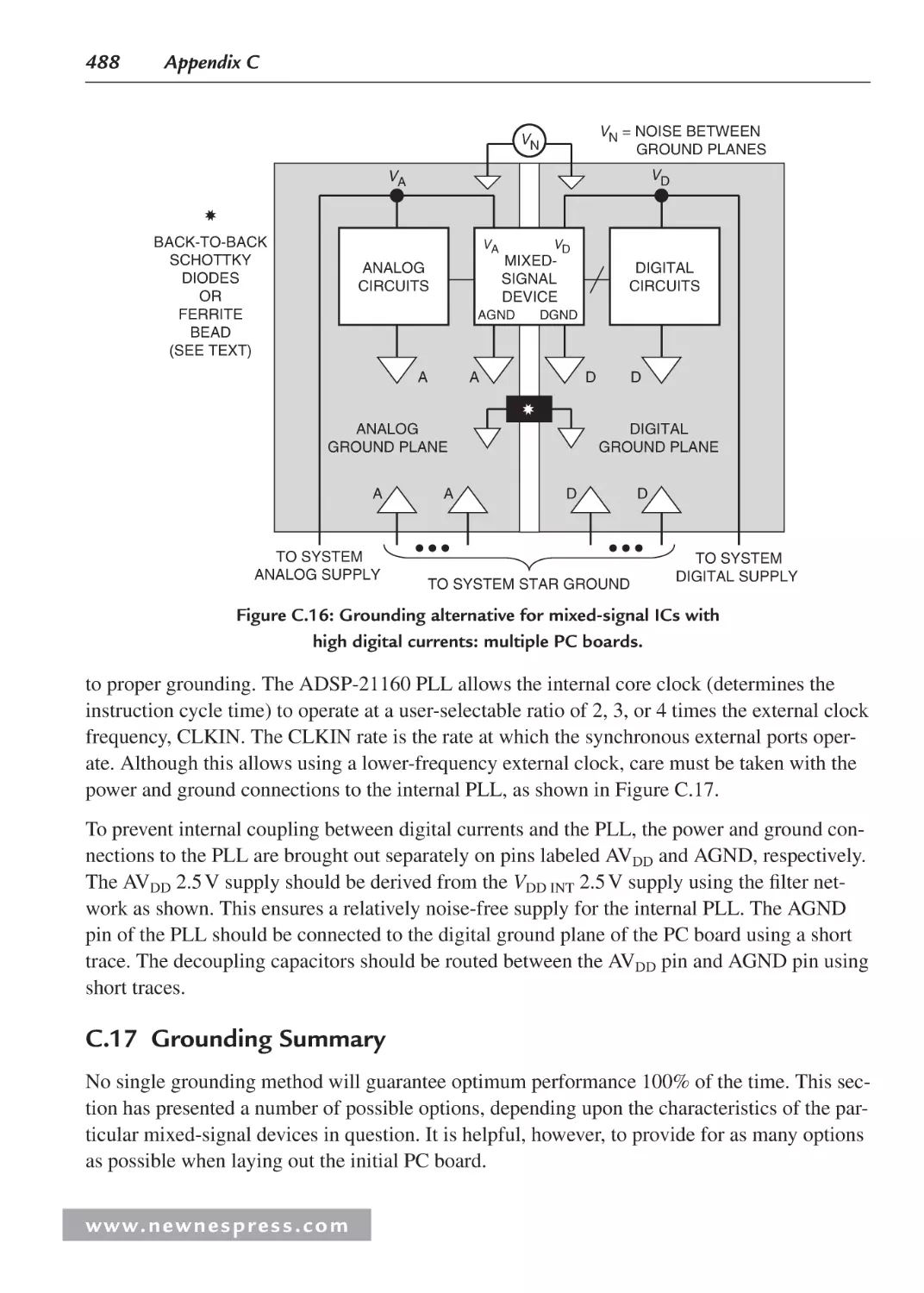
C.16 Grounding DSPs with Internal Phase-Locked Loops ............................................. 487
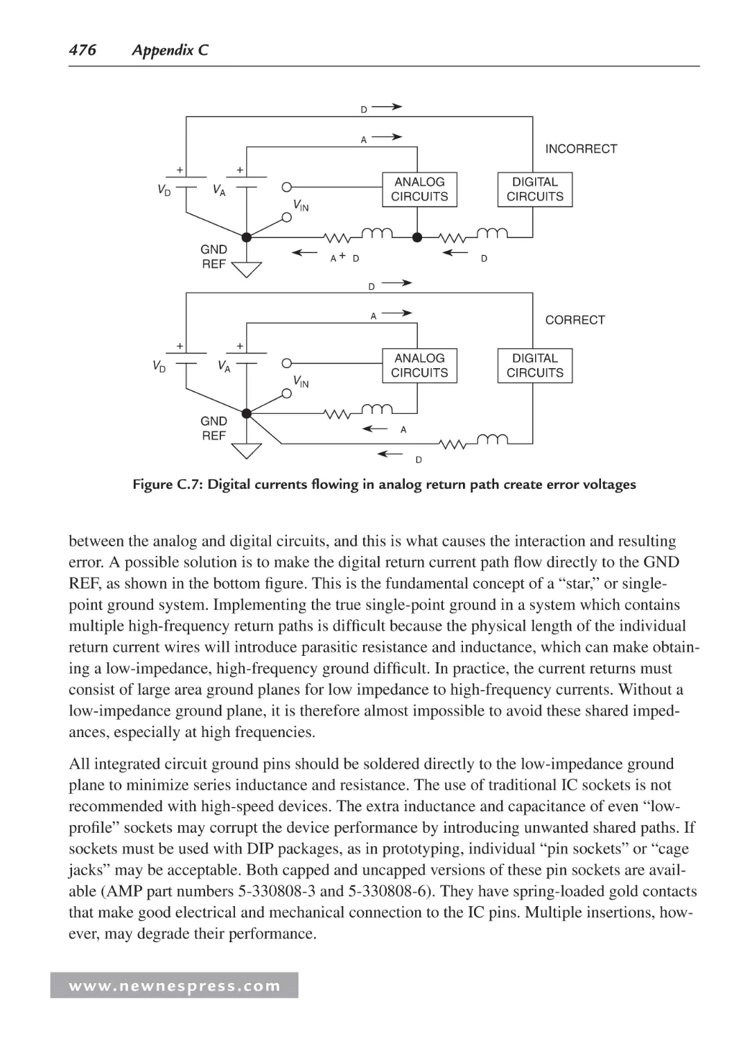
C.17 Grounding Summary .............................................................................................. 488
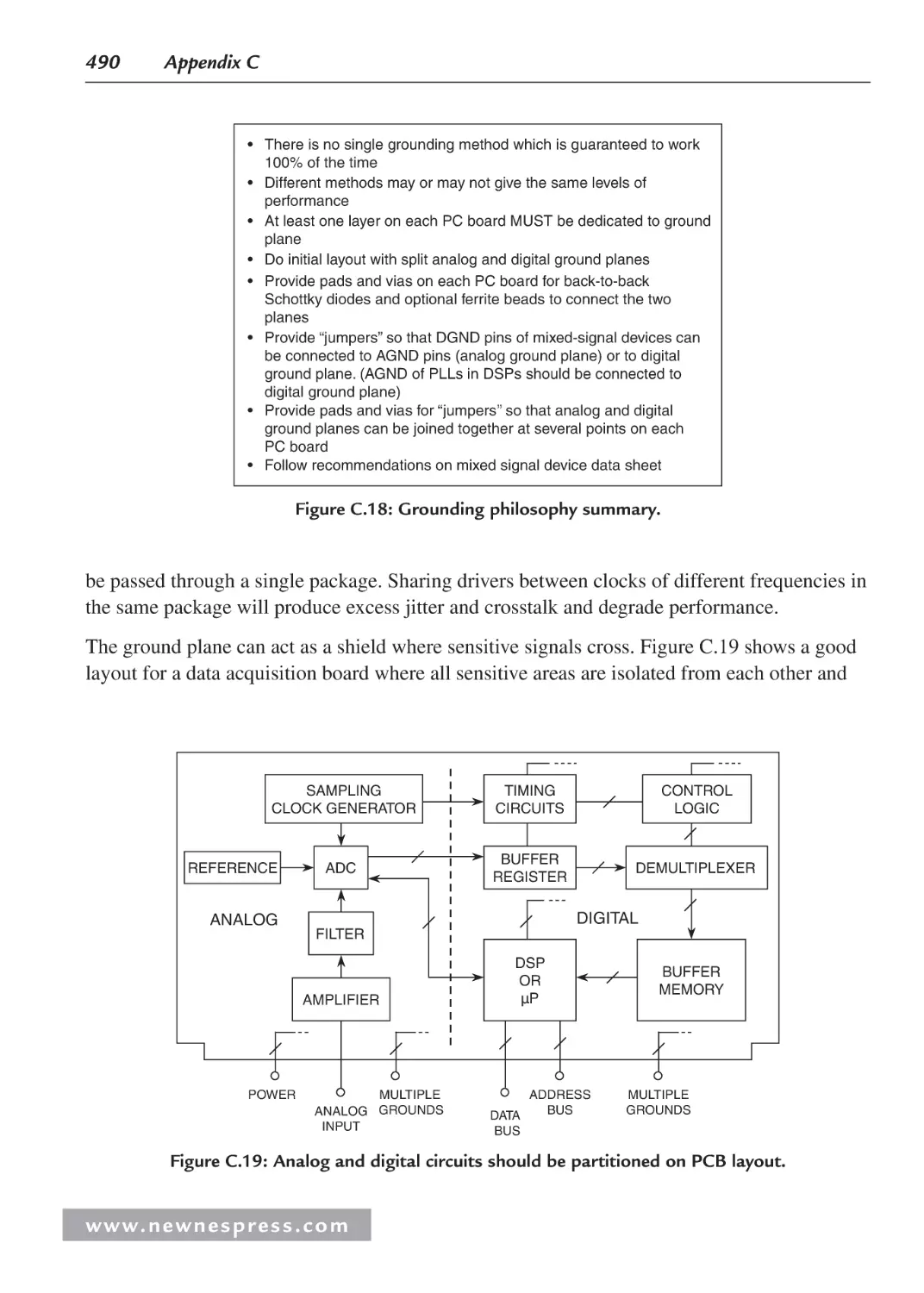
C.18 Some General PC Board Layout Guidelines for Mixed-Signal Systems ............... 489
www. n e wn e s p res s .c o m
Contents
xi
C.19 Skin Effect .............................................................................................................. 491
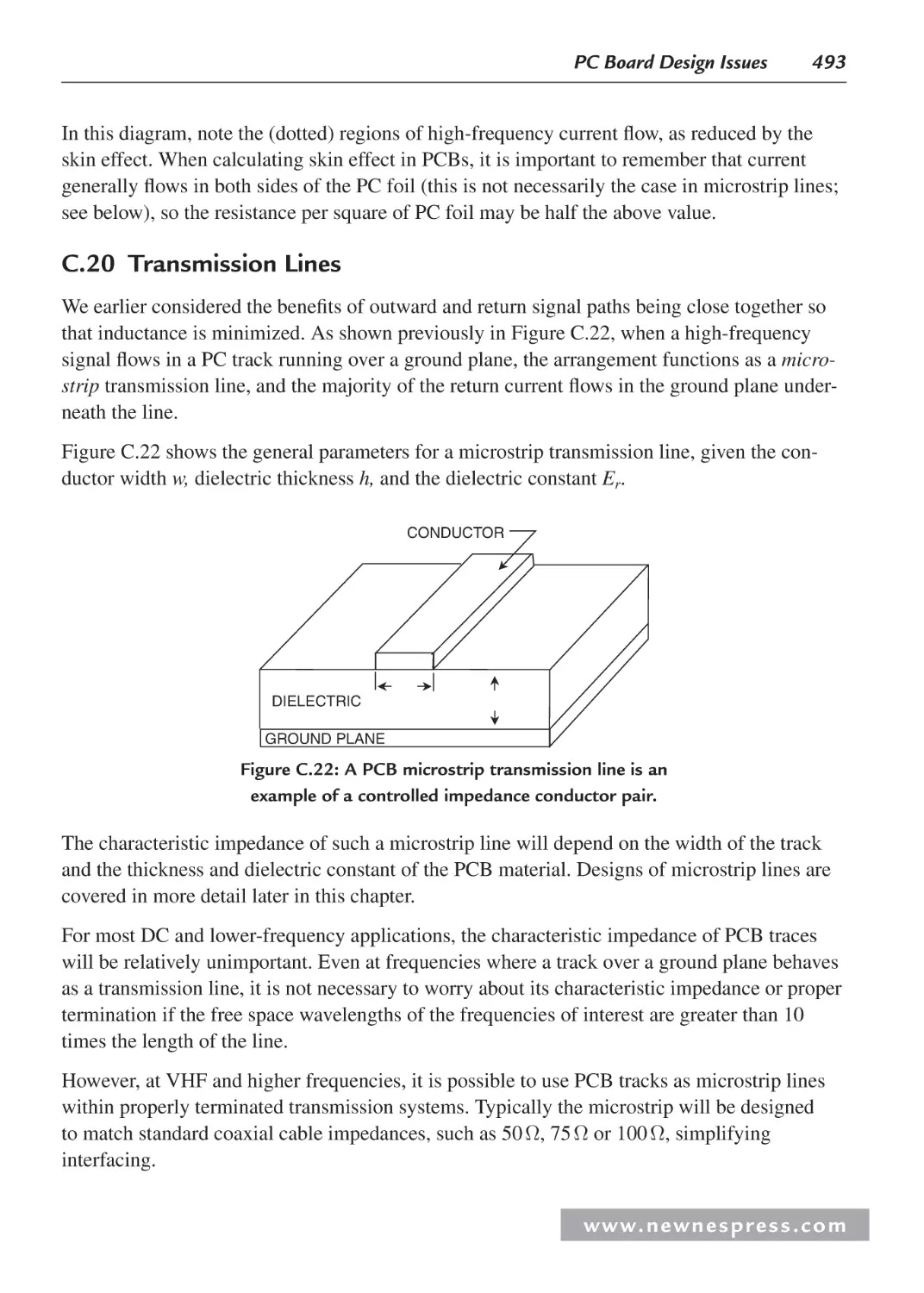
C.20 Transmission Lines ................................................................................................. 493
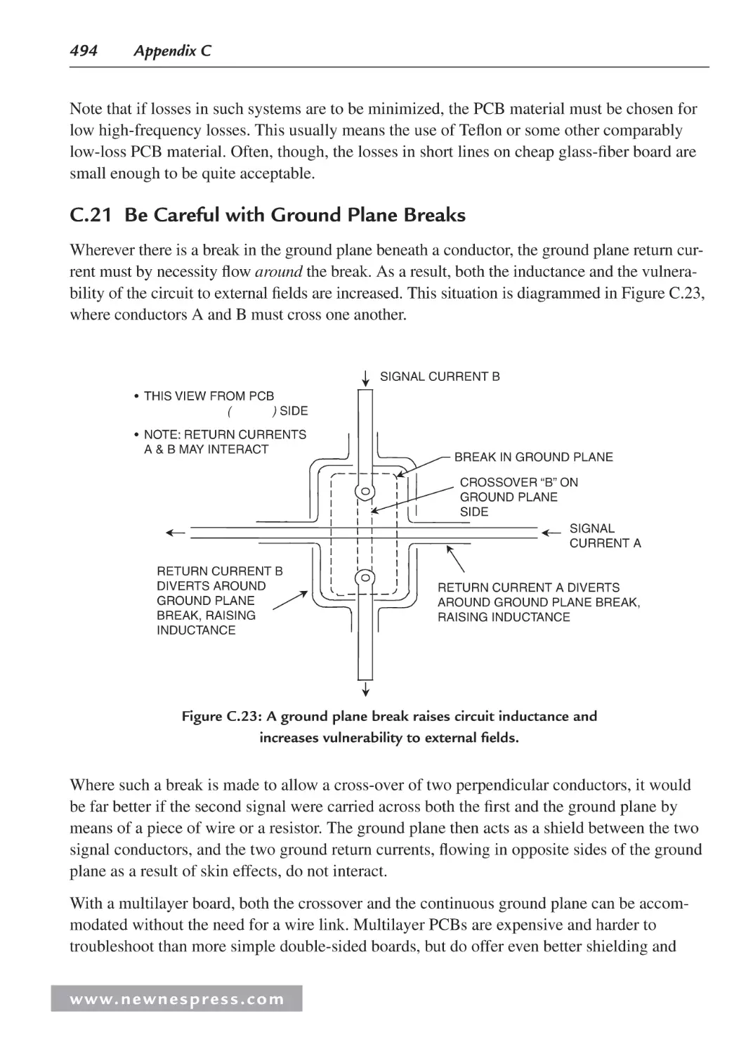
C.21 Be Careful with Ground Plane Breaks.................................................................... 494
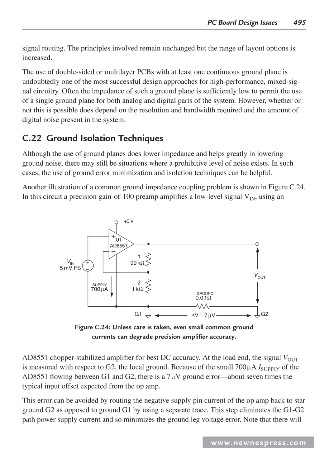
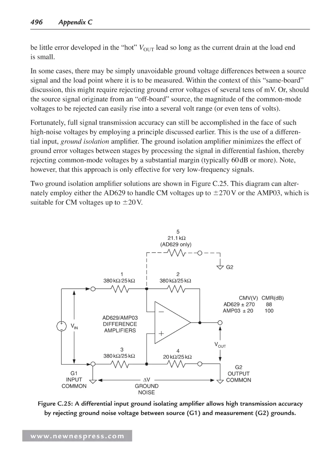
C.22 Ground Isolation Techniques .................................................................................. 495
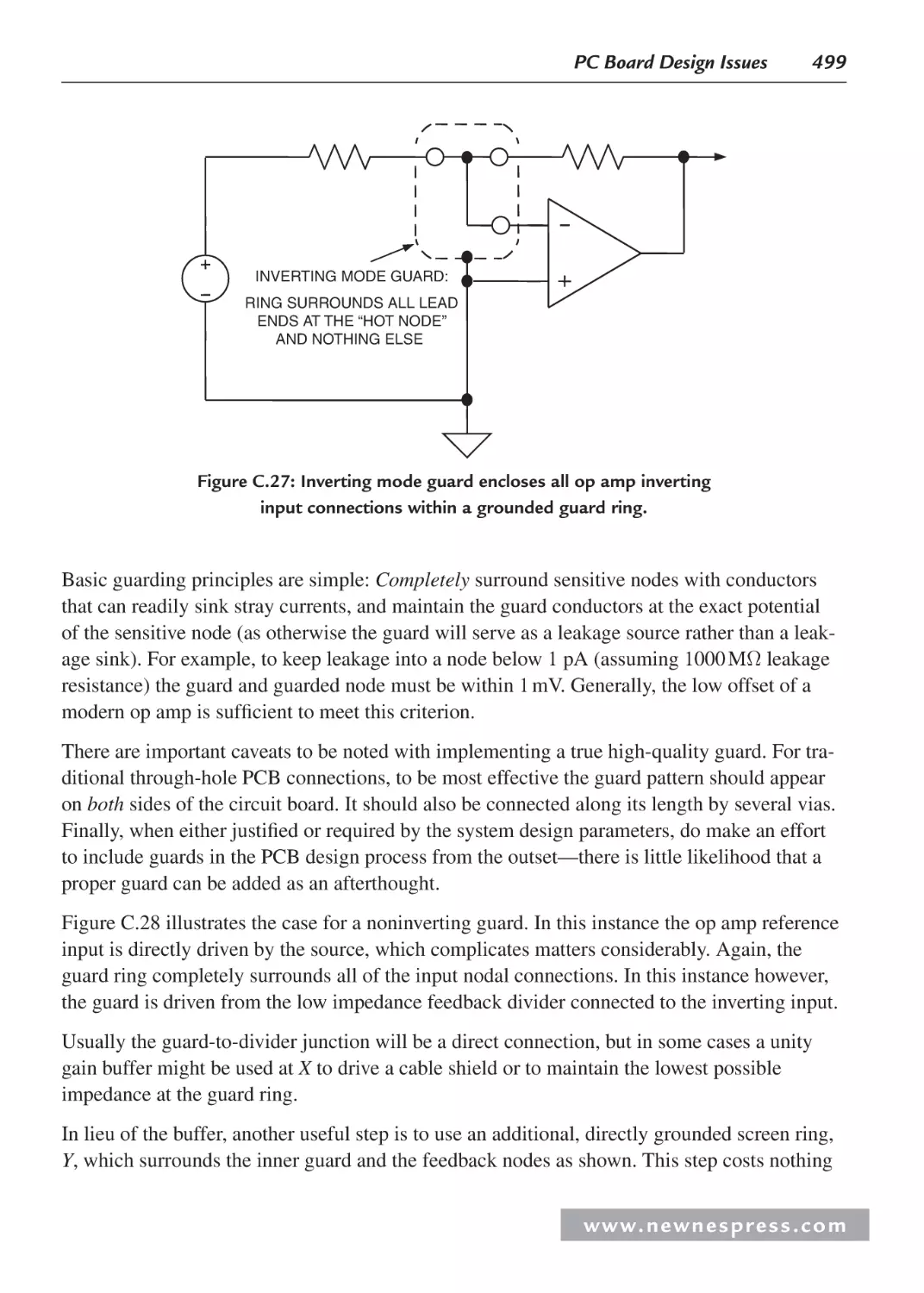
C.23 Static PCB Effects .................................................................................................. 497
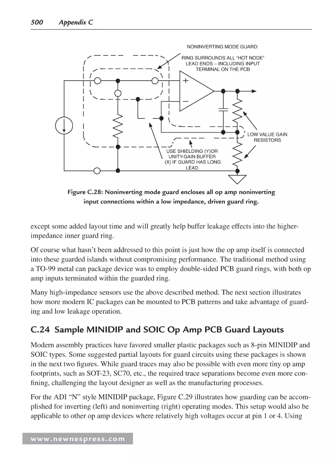
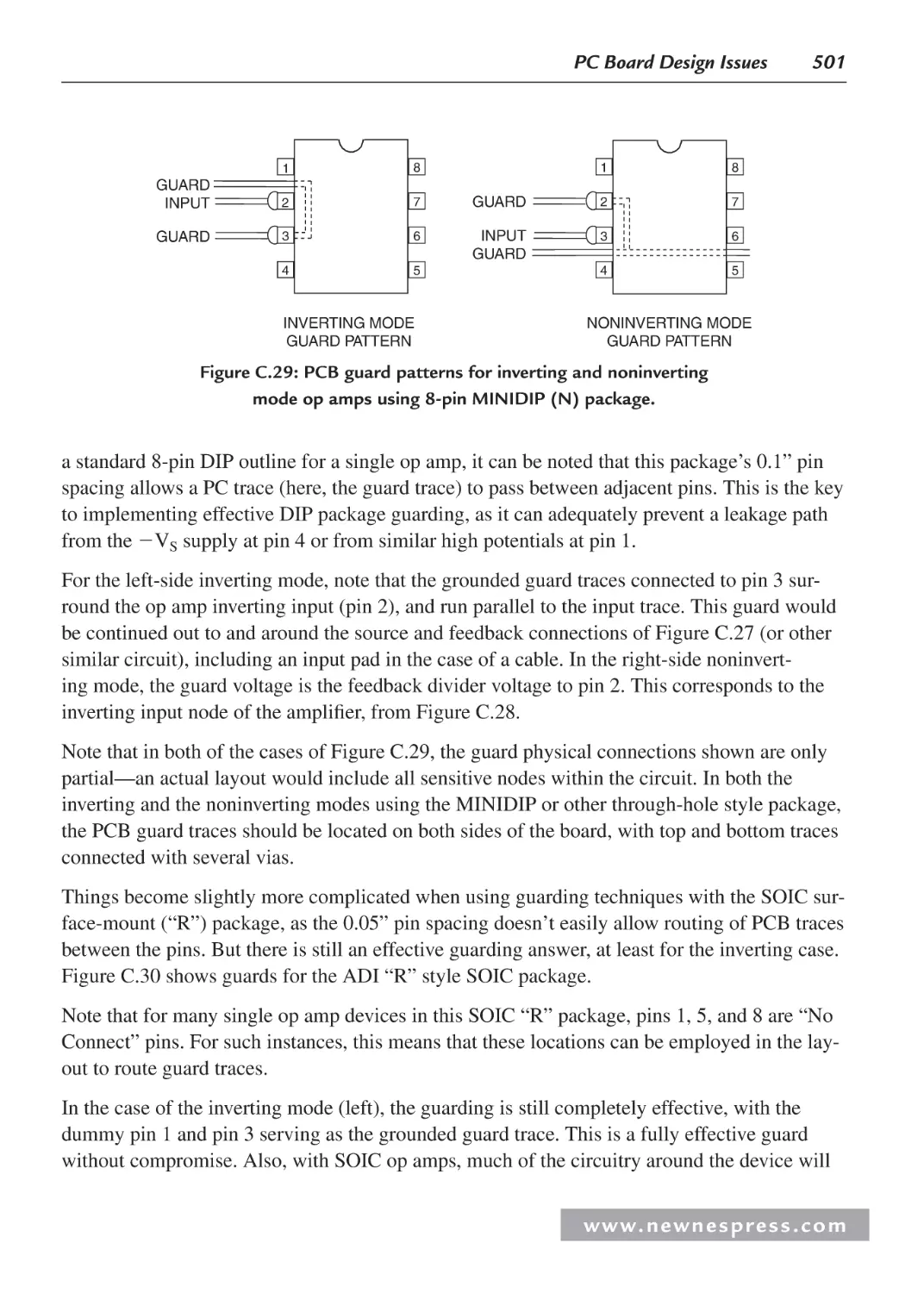
C.24 Sample MINIDIP and SOIC Op Amp PCB Guard Layouts................................... 500
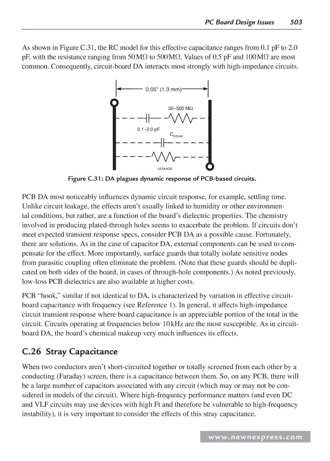
C.25 Dynamic PCB Effects ............................................................................................. 502
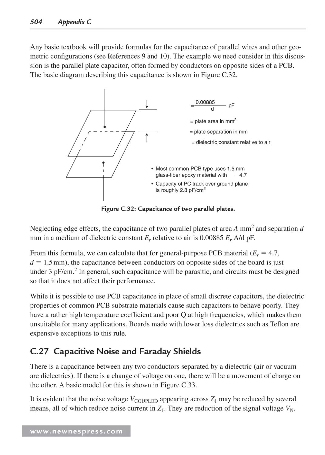
C.26 Stray Capacitance ................................................................................................... 503
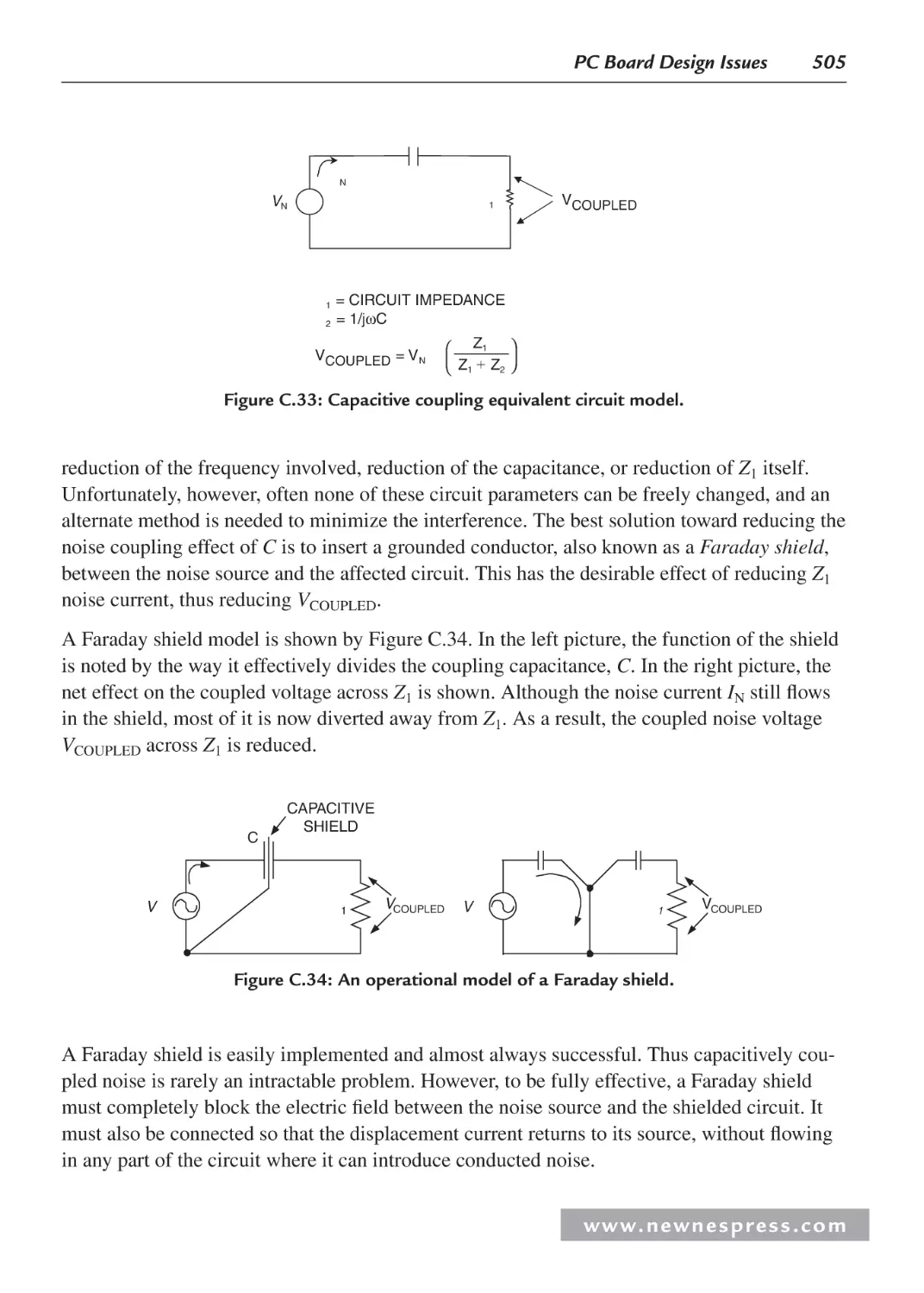
C.27 Capacitive Noise and Faraday Shields .................................................................... 504
C.28 The Floating Shield Problem .................................................................................. 506
C.29 Buffering ADCs Against Logic Noise .................................................................... 506
Endnotes ........................................................................................................................... 509
Acknowledgments ........................................................................................................... 509
Index ....................................................................................................................................... 511
w w w. n e w n e s p r e s s . c o m
This page intentionally left blank
About the Authors
Ken Arnold (Chapters 6 and 10) is the author of Embedded Controller Hardware Design.
He is the Embedded Computer Engineering Program Coordinator and an instructor at UCSD
Extension, as well as founding director of the On-Line University of California, where he
manages, develops and teaches courses in engineering and embedded systems design. Ken
has been developing commercial embedded systems and teaching others how for more than
two decades. As the champion of the embedded program at UCSD, he lead the inception and
growth of the program as well as introducing the world’s first on-line embedded course well
over a decade ago. Ken was also the founder and CEO of HiTech Equipment Corp., CTO of
Wireless Innovation, and engineering chief at General Dynamics.
Fred Eady (Chapter 8) is the author of Networking and Internetworking with
Microcontrollers. As an engineering consultant, he has implemented communications
networks for the space program and designed hardware and firmware for the medical, retail
and public utility industries. He currently writes a monthly embedded design column for a
popular electronics enthusiast magazine. Fred also composes monthly articles for a popular
robotics magazine. Fred has been dabbling in electronics for over 30 years. His embedded
design expertise spans the spectrum and includes Intel’s 8748 and 8051 microcontrollers,
the entire Microchip PIC microcontroller family and the Atmel AVR microcontrollers. Fred
recently retired from his consulting work and is focused on writing magazine columns and
embedded design books.
Lewin Edwards (Chapter 7) is the author of Embedded System Design on a Shoestring. He hails
from Adelaide, Australia. His career began with five years of security and encryption software at
PC-Plus Systems. The next five years were spent developing networkable multimedia appliances
at Digi-Frame in Port Chester, NY. Since 2004 he has been developing security and fire safety
devices at a Fortune 100 company in New York. He has written numerous technical articles and
three embedded systems books, with a fourth due in early 2008.
Jack Ganssle (Chapters 1, 2, and 10) is the author of The Firmware Handbook. He has written
over 500 articles and six books about embedded systems, as well as a book about his sailing
fiascos. He started developing embedded systems in the early 70s using the 8008. He’s started
and sold three electronics companies, including one of the bigger embedded tool businesses.
He’s developed or managed over 100 embedded products, from deep-sea navigation gear to
w w w. n e w n e s p r e s s . c o m
xiv
About the Authors
the White House security system... and one instrument that analyzed cow poop! He’s currently
a member of NASA’s Super Problem Resolution Team, a group of outside experts formed to
advise NASA in the wake of Columbia’s demise, and serves on the boards of several high-tech
companies. Jack now gives seminars to companies world-wide about better ways to develop
embedded systems.
Rick Gentile (Chapter 5) is the author of Embedded Media Processing. Rick joined ADI
in 2000 as a Senior DSP Applications Engineer, and he currently leads the Processor
Applications Group, which is responsible for Blackfin, SHARC and TigerSHARC processors.
Prior to joining ADI, Rick was a Member of the Technical Staff at MIT Lincoln Laboratory,
where he designed several signal processors used in a wide range of radar sensors. He has
authored dozens of articles and presented at multiple technical conferences. He received a
B.S. in 1987 from the University of Massachusetts at Amherst and an M.S. in 1994 from
Northeastern University, both in Electrical and Computer Engineering.
Creed Huddleston (Chapter 8) is the author of Intelligent Sensor Design Using the Microchip
dsPIC. With over twenty years of experience designing real-time embedded systems, he is
President and founder of Real-Time by Design, LLC, a certified Microchip Design Partner
based in Raleigh, NC that specializes in the creation of hard real-time intelligent sensing
systems. In addition to his duties with Real-Time by Design, Creed also serves on the
Advisory Board of Quickfilter Technologies Inc., a Texas-based company producing mixedsignal integrated circuits that provide high-speed analog signal conditioning and digital signal
processing in a single package. A graduate of Rice University in Houston, TX with a BSEE
degree, Creed performed extensive graduate work in digital signal processing at the University
of Texas at Arlington before heading east to start Omnisys. To her great credit and his great
fortune, Creed and his wife Lisa have been married for 23 years and have three wonderful
children: Kate, Beth, and Dan.
Kamal Hyder (Chapter 9) is the author of Embedded Systems Design Using the Rabbit 3000
Microprocessor. He started his career with an embedded microcontroller manufacturer. He
then wrote CPU microcode for Tandem Computers for a number of years, and was a Product
Manager at Cisco Systems, working on next-generation switching platforms. He is currently
with Brocade Communications as Senior Group Product Manager. Kamal’s BS is in EE/CS
from the University of Massachusetts, Amherst, and he has an MBA in finance/marketing
from Santa Clara University.
David Katz (Chapter 5) is the author of Embedded Media Processing. He has over 15 years
of experience in circuit and system design. Currently, he is the Blackfin Applications Manager
at Analog Devices, Inc., where he focuses on specifying new convergent processors. He has
published over 100 embedded processing articles domestically and internationally, and he has
presented several conference papers in the field. Previously, he worked at Motorola, Inc., as a
www. n e wn e s p res s .c o m
About the Authors
xv
senior design engineer in cable modem and automation groups. David holds both a B.S. and
M. Eng. in Electrical Engineering from Cornell University.
Walt Kester (Appendix C) is the editor of Data Conversion Handbook. He is a corporate
staff applications engineer at Analog Devices. For more than 35 years at Analog Devices,
he has designed, developed, and given applications support for high-speed ADCs, DACs,
SHAs, op amps, and analog multiplexers. Besides writing many papers and articles, he
prepared and edited eleven major applications books which form the basis for the Analog
Devices world-wide technical seminar series including the topics of op amps, data conversion,
power management, sensor signal conditioning, mixed-signal, and practical analog design
techniques. Walt has a BSEE from NC State University and MSEE from Duke University.
Tammy Noergaard (Chapters 1, 2, 3, 4, Appendices B and C) is the author of Embedded
Systems Architecture. Since beginning her embedded systems career in 1995, she has had
wide experience in product development, system design and integration, operations, sales,
marketing, and training. Noergaard worked for Sony as a lead software engineer developing
and testing embedded software for analog TVs. At Wind River she was the liaison engineer
between developmental engineers and customers to provide design expertise, systems
configuration, systems integration, and training for Wind River embedded software (OS,
Java, device drivers, etc.) and all associated hardware for a variety of embedded systems in
the Consumer Electronic market. Most recently she was a Field Engineering Specialist and
Consultant with Esmertec North America, providing project management, system design,
system integration, system configuration, support and expertise for various embedded Java
systems using Jbed in everything from control systems to medical devices to digital TVs.
Noergaard has lectured to engineering classes at the University of California at Berkeley and
Stanford, the Embedded Internet Conference, and the Java User’s Group in San Jose, among
others.
Bob Perrin (Chapter 9) is the author of Embedded Systems Design Using the Rabbit 3000
Microprocessor. He got his start in electronics at the age of nine when his mother gave him
a “150-in-one Projects” kit from Radio Shack for Christmas. He grew up programming a
Commodore PET. In 1990, Bob graduated with a BSEE from Washington State University.
Since then Bob has been working as an engineer designing digital and analog electronics.
He has published about twenty technical articles, most with Circuit Cellar.
w w w. n e w n e s p r e s s . c o m
This page intentionally left blank
CHAPTER 1
CHAPTR
Embedded Hardware Basics
Jack Ganssle
Tammy Noergaard
1.1 Lesson One on Hardware: Reading Schematics
This section is equally important for embedded hardware and software engineers. Before
diving into the details, note that it is important for all embedded designers to be able to understand the diagrams and symbols that hardware engineers create and use to describe their hardware designs to the outside world. These diagrams and symbols are the keys to quickly and
efficiently understanding even the most complex hardware design, regardless of how much or
little practical experience one has in designing hardware. They also contain the information an
embedded programmer needs to design any software that requires compatibility with the hardware, and they provide insight to a programmer as to how to successfully communicate the
hardware requirements of the software to a hardware engineer.
There are several different types of engineering hardware drawings, including:
•
Block diagrams, which typically depict the major components of a board (processors,
buses, I/O, memory) or a single component (a processor, for example) at a systems
architecture or higher level. In short, a block diagram is a basic overview of the hardware, with implementation details abstracted out. While a block diagram can reflect
the actual physical layout of a board containing these major components, it mainly
depicts how different components or units within a component function together at a
systems architecture level. Block diagrams are used extensively throughout this book
(in fact, Figures 1.5a–e later in this chapter are examples of block diagrams) because
they are the simplest method by which to depict and describe the components within a
system. The symbols used within a block diagram are simple, such as squares or rectangles for chips and straight lines for buses. Block diagrams are typically not detailed
enough for a software designer to be able to write all the low-level software accurately
enough to control the hardware (without a lot of headaches, trial and error, and even
some burned-out hardware!). However, they are very useful in communicating a basic
overview of the hardware, as well as providing a basis for creating more detailed
hardware diagrams.
•
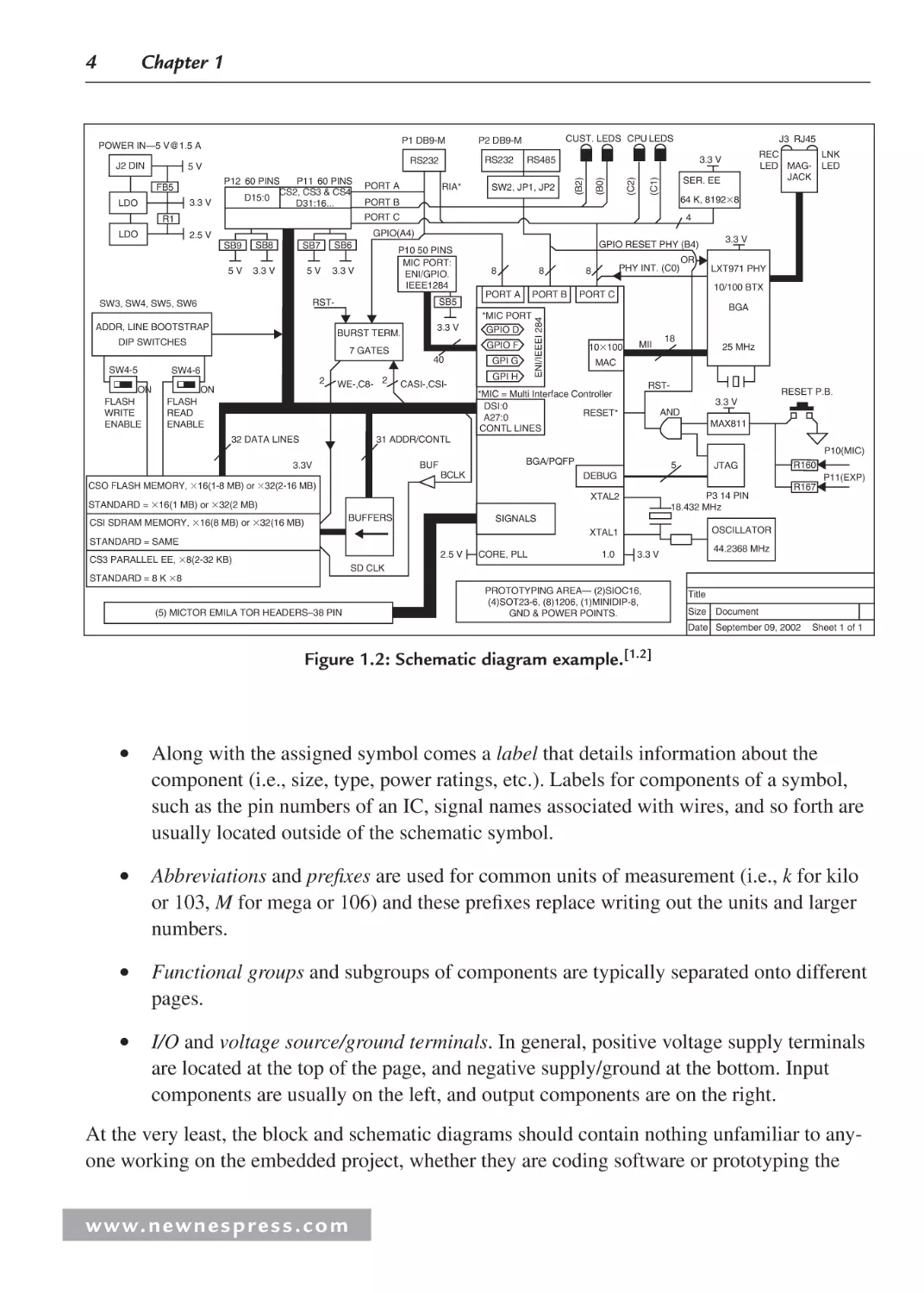
Schematics. Schematics are electronic circuit diagrams that provide a more detailed
view of all the devices within a circuit or within a single component—everything from
w w w. n e w n e s p r e s s . c o m
2
Chapter 1
processors down to resistors. A schematic diagram is not meant to depict the physical
layout of the board or component, but provides information on the flow of data in the
system, defining what signals are assigned where—which signals travel on the various
lines of a bus, appear on the pins of a processor, and so on. In schematic diagrams,
schematic symbols are used to depict all the components within the system. They
typically do not look anything like the physical components they represent but are a
type of “shorthand” representation based on some type of schematic symbol standard.
A schematic diagram is the most useful diagram to both hardware and software
designers trying to determine how a system actually operates, to debug hardware, or
to write and debug the software managing the hardware. See Appendix A for a list of
commonly used schematic symbols.
•
Wiring diagrams. These diagrams represent the bus connections between the major
and minor components on a board or within a chip. In wiring diagrams, vertical and
horizontal lines are used to represent the lines of a bus, and either schematic symbols
or more simplified symbols (that physically resemble the other components on the
board or elements within a component) are used. These diagrams may represent an
approximate depiction of the physical layout of a component or board.
•
Logic diagrams/prints. Logic diagrams/prints are used to show a wide variety of circuit
information using logical symbols (AND, OR, NOT, XOR, and so on) and logical inputs
and outputs (the 1’s and 0’s). These diagrams do not replace schematics, but they can be
useful in simplifying certain types of circuits in order to understand how they function.
•
Timing diagrams. Timing diagrams display timing graphs of various input and output
signals of a circuit, as well as the relationships between the various signals. They are
the most common diagrams (after block diagrams) in hardware user manuals and data
sheets.
Regardless of the type, to understand how to read and interpret these diagrams, it is important
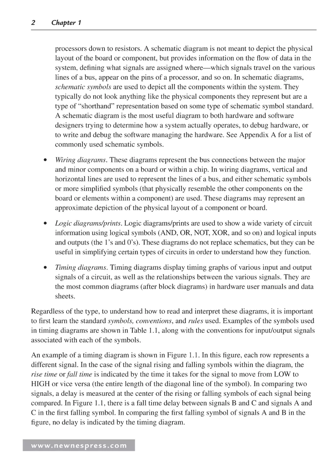
to first learn the standard symbols, conventions, and rules used. Examples of the symbols used
in timing diagrams are shown in Table 1.1, along with the conventions for input/output signals
associated with each of the symbols.
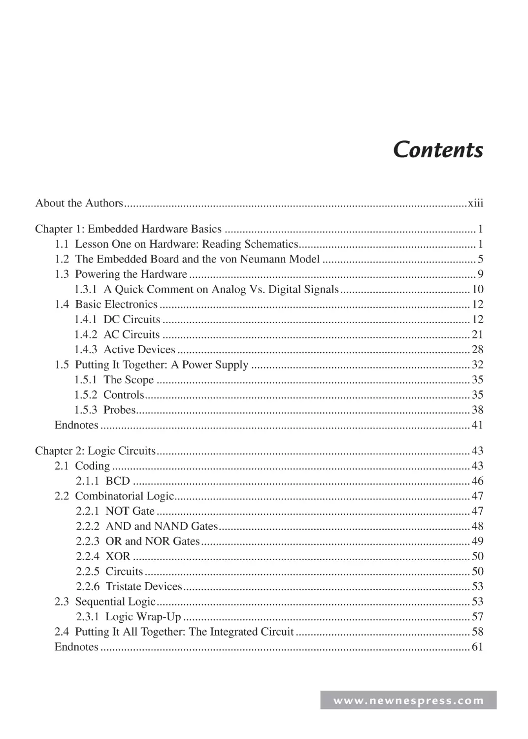
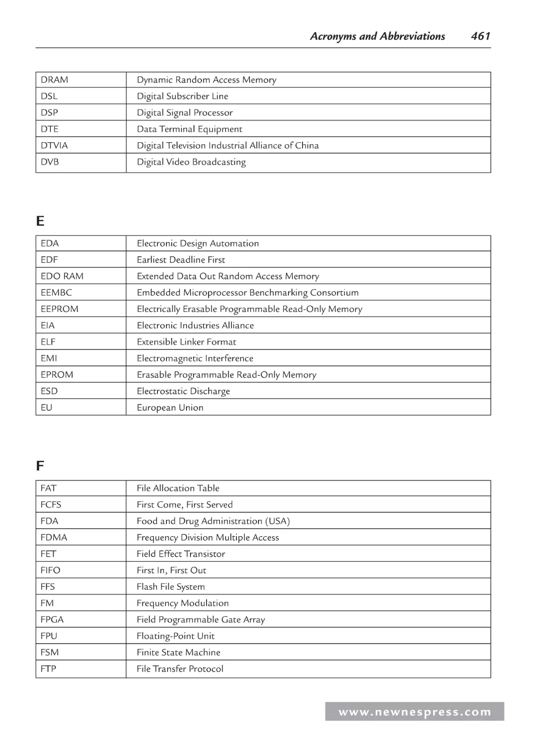
An example of a timing diagram is shown in Figure 1.1. In this figure, each row represents a
different signal. In the case of the signal rising and falling symbols within the diagram, the
rise time or fall time is indicated by the time it takes for the signal to move from LOW to
HIGH or vice versa (the entire length of the diagonal line of the symbol). In comparing two
signals, a delay is measured at the center of the rising or falling symbols of each signal being
compared. In Figure 1.1, there is a fall time delay between signals B and C and signals A and
C in the first falling symbol. In comparing the first falling symbol of signals A and B in the
figure, no delay is indicated by the timing diagram.
www. n e wn e s p res s .c o m
Embedded Hardware Basics
3
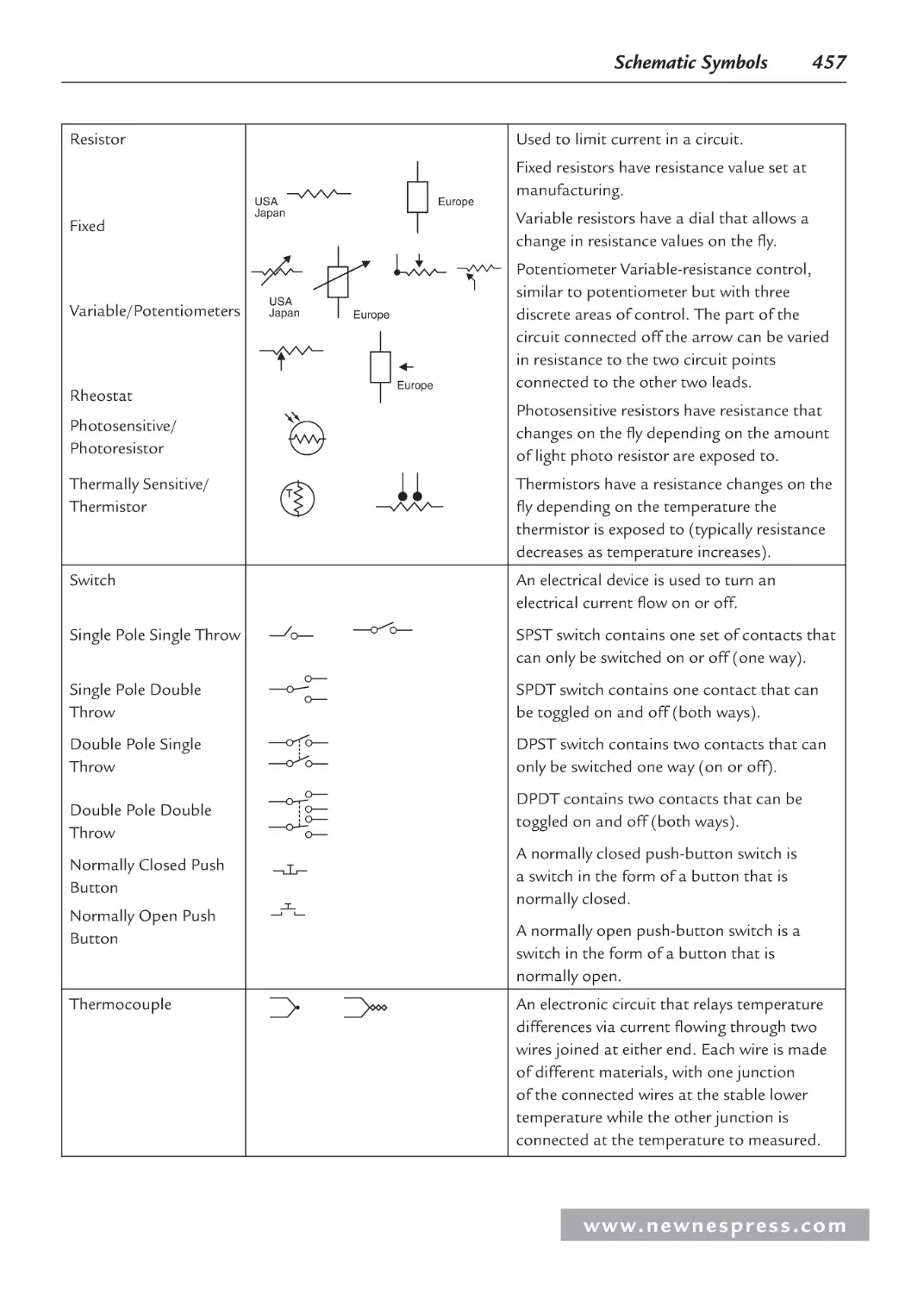
Table 1.1: Timing diagrams symbol table.[1.1]
Symbol
Input Signals
Output Signals
Input signal must be valid
Output signal will be valid
Input signal doesn’t affect
system, will work regardless
Indeterminate output signal
Garbage signal (nonsense)
Output signal not driven
(floating), tristate, HiZ, high
impedance
If the input signal rises:
Output signal will rise
If the input signal falls:
Output signal will fall
Rise Time
Fall Time
Signal A
Signal B
Delay
Signal C
…….
Figure 1.1: Timing diagram example.
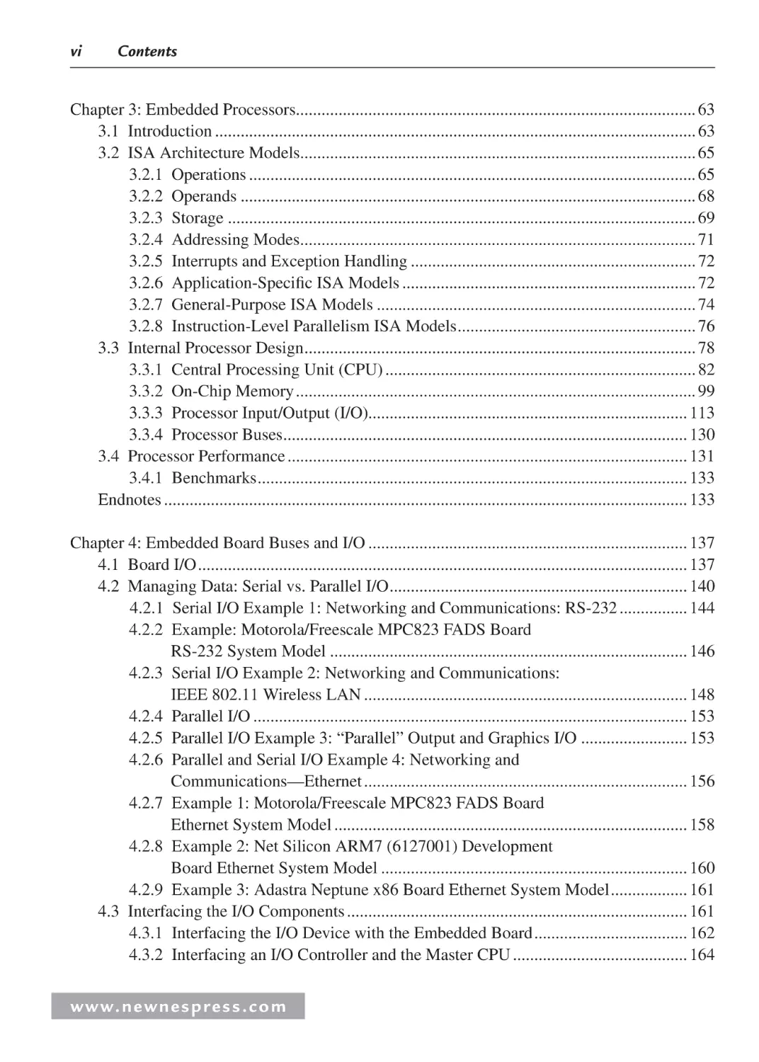
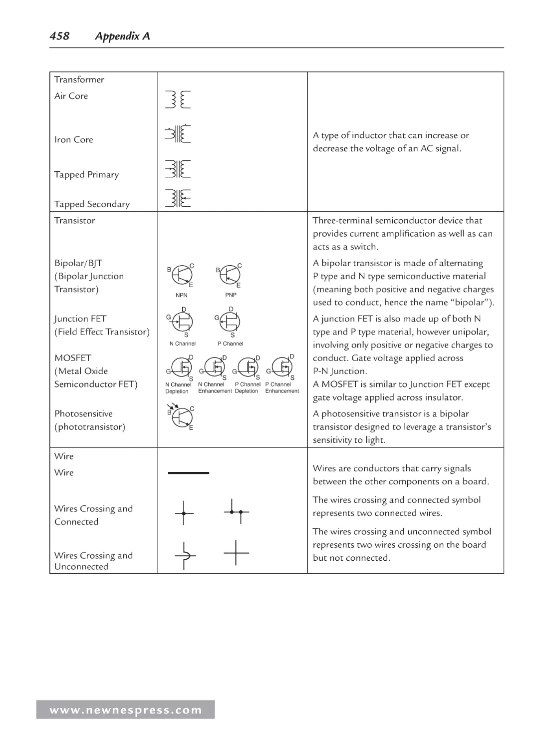
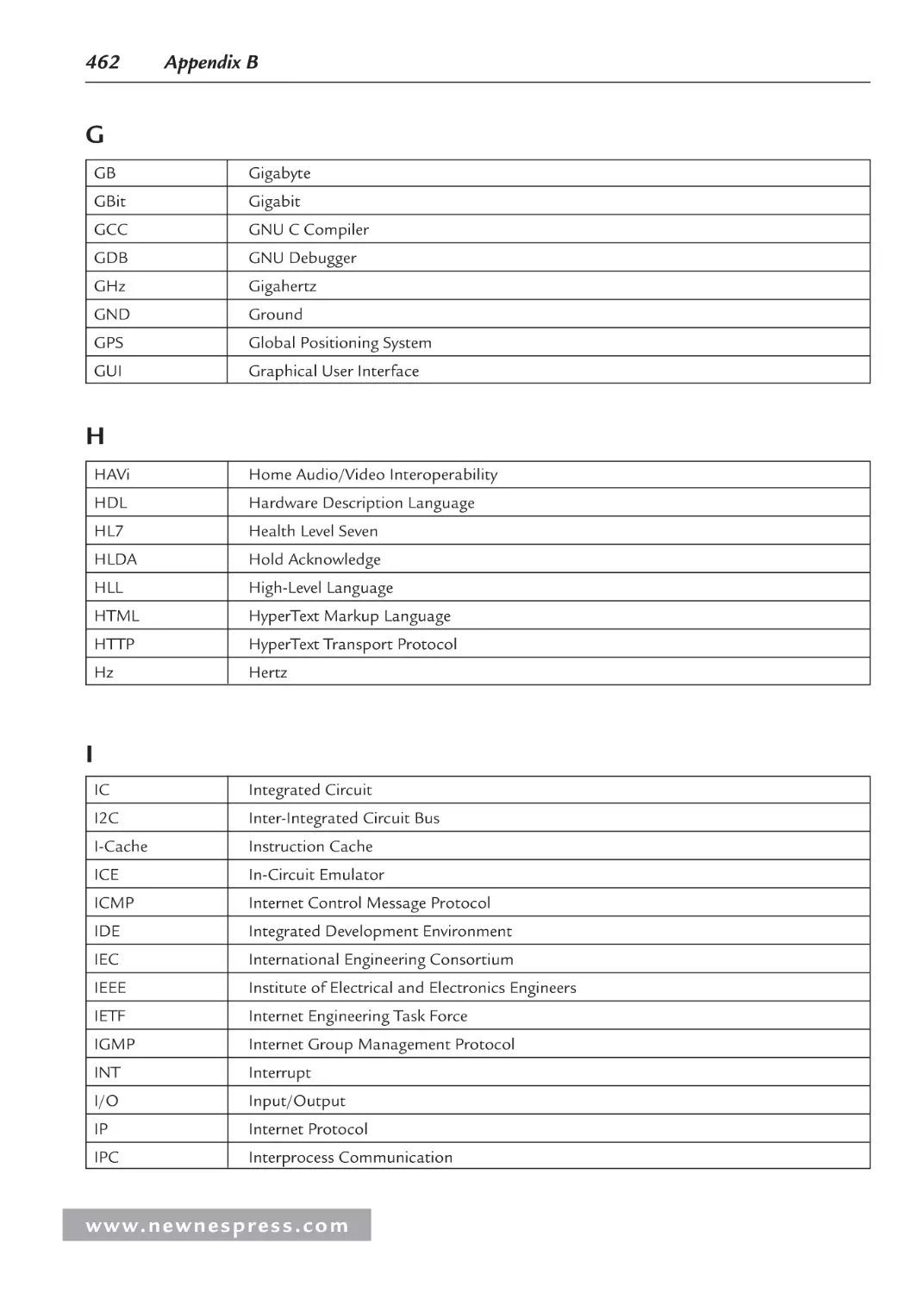
Schematic diagrams are much more complex than their timing diagram counterparts. As introduced earlier this chapter, schematics provide a more detailed view of all the devices within a
circuit or within a single component. Figure 1.2 shows an example of a schematic diagram.
In the case of schematic diagrams, some of the conventions and rules include:
•
A title section is located at the bottom of each schematic page, listing information
that includes, but is not limited to, the name of the circuit, the name of the hardware
engineer responsible for the design, the date, and a list of revisions made to the design
since its conception.
•
The use of schematic symbols indicating the various components of a circuit (see
Appendix A).
w w w. n e w n e s p r e s s . c o m
Chapter 1
3.3 V
P11 60 PINS
P12 60 PINS
CS2, CS3 & CS4
D15:0
D31:16...
RIA*
SB9
5V
SB8
SB7
3.3 V
5V
SER. EE
SB6
4
P10 50 PINS
MIC PORT:
ENI/GPIO.
IEEE1284
3.3 V
ADDR, LINE BOOTSTRAP
SB5
BURST TERM.
DIP SWITCHES
3.3 V
40
SW4-6
2
WE-,C8- 2
GPIO RESET PHY (B4)
8
8
PORT A
PORT B
*MIC PORT
GPIO D
GPIO F
7 GATES
ON
FLASH
READ
ENABLE
CASI-,CSI-
GPI G
GPI H
PHY INT. (C0)
8
3.3 V
OR
LXT971 PHY
10/100 BTX
PORT C
BGA
10100
MII
18
25 MHz
MAC
RST-
*MIC = Multi Interface Controller
DSI:0
RESET*
A27:0
RESET P.B.
3.3 V
AND
MAX811
CONTL LINES
32 DATA LINES
LNK
LED
64 K, 81928
RST-
SW3, SW4, SW5, SW6
ON
FLASH
WRITE
ENABLE
SW2, JP1, JP2
PORT B
GPIO(A4)
2.5 V
SW4-5
J3 RJ45
REC
LED MAGJACK
3.3 V
PORT C
R1
LDO
PORT A
CUST. LEDS CPU LEDS
RS485
(C1)
FB5
LDO
RS232
(C2)
5V
P2 DB9-M
RS232
(B0)
J2 DIN
P1 DB9-M
(B2)
POWER IN—5 V@1.5 A
ENI/IEEEI 284
4
31 ADDR/CONTL
P10(MIC)
BGA/PQFP
BUF
3.3V
BCLK
CSO FLASH MEMORY, 16(1-8 MB) or 32(2-16 MB)
5
R167
P3 14 PIN
18.432 MHz
BUFFERS
SIGNALS
OSCILLATOR
XTAL1
STANDARD = SAME
2.5 V
CS3 PARALLEL EE, 8(2-32 KB)
R160
P11(EXP)
XTAL2
STANDARD = 16(1 MB) or 32(2 MB)
CSI SDRAM MEMORY, 16(8 MB) or 32(16 MB)
JTAG
DEBUG
CORE, PLL
1.0
44.2368 MHz
3.3 V
SD CLK
STANDARD = 8 K 8
(5) MICTOR EMILA TOR HEADERS–38 PIN
PROTOTYPING AREA— (2)SIOC16,
(4)SOT23-6, (8)1206, (1)MINIDIP-8,
GND & POWER POINTS.
Title
Size Document
Date September 09, 2002
Sheet 1 of 1
Figure 1.2: Schematic diagram example.[1.2]
•
Along with the assigned symbol comes a label that details information about the
component (i.e., size, type, power ratings, etc.). Labels for components of a symbol,
such as the pin numbers of an IC, signal names associated with wires, and so forth are
usually located outside of the schematic symbol.
•
Abbreviations and prefixes are used for common units of measurement (i.e., k for kilo
or 103, M for mega or 106) and these prefixes replace writing out the units and larger
numbers.
•
Functional groups and subgroups of components are typically separated onto different
pages.
•
I/O and voltage source/ground terminals. In general, positive voltage supply terminals
are located at the top of the page, and negative supply/ground at the bottom. Input
components are usually on the left, and output components are on the right.
At the very least, the block and schematic diagrams should contain nothing unfamiliar to anyone working on the embedded project, whether they are coding software or prototyping the
www. n e wn e s p res s .c o m
Embedded Hardware Basics
5
hardware. This means becoming familiar with everything from where the name of the diagram
is located to how the states of the components shown within the diagrams are represented.
One of the most efficient ways of learning how to learn to read and/or create a hardware diagram is via the Traister and Lisk method[1.3], which involves:
Step 1. Learning the basic symbols that can make up the type of diagram, such as timing or
schematic symbols. To aid in the learning of these symbols, rotate between this step and
steps 2 and/or 3.
Step 2. Reading as many diagrams as possible until reading them becomes boring (in that
case, rotate between this step and steps 1 and/or 3) or comfortable (so there is no longer
the need to look up every other symbol while reading).
Step 3. Writing a diagram to practice simulating what has been read, again until it becomes
either boring (which means rotating back through steps 1 and/or 2) or comfortable.
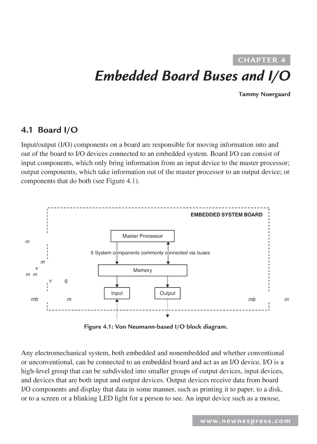
1.2 The Embedded Board and the von Neumann Model
In embedded devices, all the electronics hardware resides on a board, also referred to as a
printed wiring board (PW) or printed circuit board (PCB). PCBs are often made of thin sheets
of fiberglass. The electrical path of the circuit is printed in copper, which carries the electrical signals between the various components connected on the board. All electronic components that make up the circuit are connected to this board, either by soldering, plugging into
a socket, or some other connection mechanism. All the hardware on an embedded board is
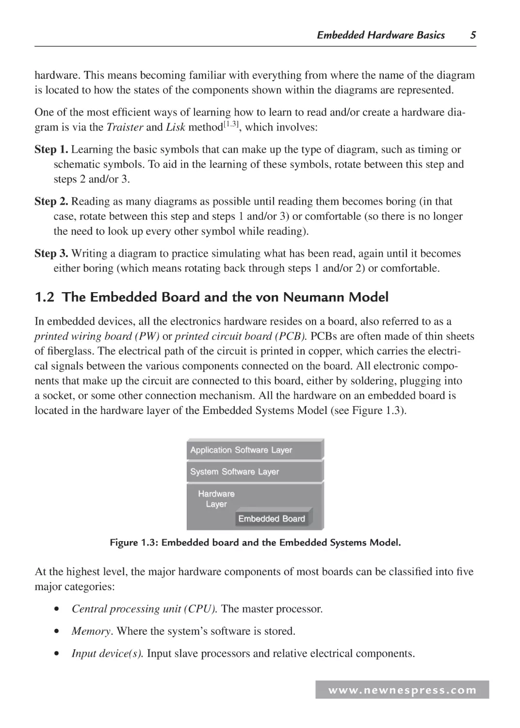
located in the hardware layer of the Embedded Systems Model (see Figure 1.3).
Application Software Layer
System Software Layer
Hardware
Layer
Embedded Board
Figure 1.3: Embedded board and the Embedded Systems Model.
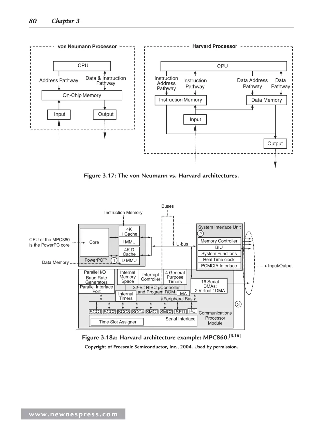
At the highest level, the major hardware components of most boards can be classified into five
major categories:
•
•
•
Central processing unit (CPU). The master processor.
Memory. Where the system’s software is stored.
Input device(s). Input slave processors and relative electrical components.
w w w. n e w n e s p r e s s . c o m
6
Chapter 1
•
Output device(s). Output slave processors and relative electrical components.
•
Data pathway(s)/bus(es). Interconnects the other components, providing a “highway”
for data to travel on from one component to another, including any wires, bus bridges,
and/or bus controllers.
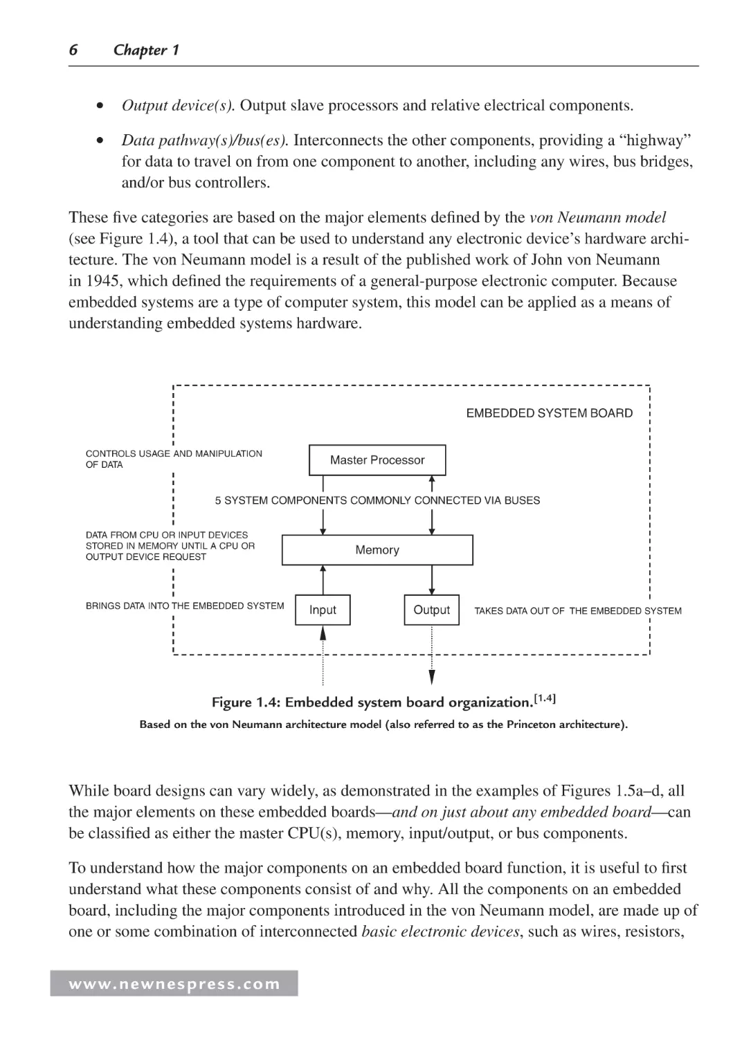
These five categories are based on the major elements defined by the von Neumann model
(see Figure 1.4), a tool that can be used to understand any electronic device’s hardware architecture. The von Neumann model is a result of the published work of John von Neumann
in 1945, which defined the requirements of a general-purpose electronic computer. Because
embedded systems are a type of computer system, this model can be applied as a means of
understanding embedded systems hardware.
EMBEDDED SYSTEM BOARD
CONTROLS USAGE AND MANIPULATION
OF DATA
Master Processor
5 SYSTEM COMPONENTS COMMONLY CONNECTED VIA BUSES
DATA FROM CPU OR INPUT DEVICES
STORED IN MEMORY UNTIL A CPU OR
OUTPUT DEVICE REQUEST
BRINGS DATA INTO THE EMBEDDED SYSTEM
Memory
Input
Output
TAKES DATA OUT OF THE EMBEDDED SYSTEM
Figure 1.4: Embedded system board organization.[1.4]
Based on the von Neumann architecture model (also referred to as the Princeton architecture).
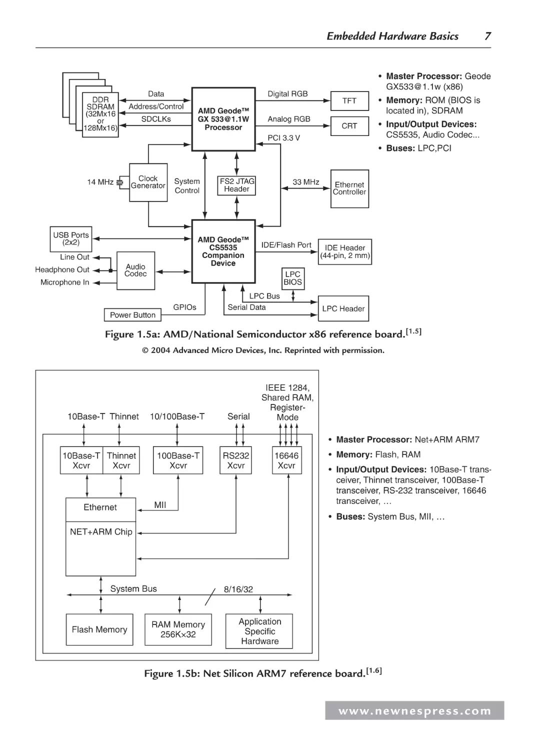
While board designs can vary widely, as demonstrated in the examples of Figures 1.5a–d, all
the major elements on these embedded boards—and on just about any embedded board—can
be classified as either the master CPU(s), memory, input/output, or bus components.
To understand how the major components on an embedded board function, it is useful to first
understand what these components consist of and why. All the components on an embedded
board, including the major components introduced in the von Neumann model, are made up of
one or some combination of interconnected basic electronic devices, such as wires, resistors,
www. n e wn e s p res s .c o m
Embedded Hardware Basics
Data
DDR
SDRAM
(32Mx16
or
128Mx16)
Digital RGB
Address/Control
SDCLKs
AMD Geode™
GX 533@1.1W
Processor
Analog RGB
7
• Master Processor: Geode
GX533@1.1w (x86)
TFT
• Memory: ROM (BIOS is
located in), SDRAM
CRT
• Input/Output Devices:
CS5535, Audio Codec...
PCI 3.3 V
• Buses: LPC,PCI
Clock
Generator
14 MHz
System
Control
USB Ports
(2x2)
AMD Geode™
CS5535
Companion
Device
Line Out
Audio
Codec
Headphone Out
FS2 JTAG
Header
33 MHz
IDE/Flash Port
Ethernet
Controller
IDE Header
(44-pin, 2 mm)
LPC
BIOS
Microphone In
GPIOs
LPC Bus
Serial Data
Power Button
LPC Header
Figure 1.5a: AMD/National Semiconductor x86 reference board.[1.5]
© 2004 Advanced Micro Devices, Inc. Reprinted with permission.
10Base-T Thinnet
10/100Base-T
Serial
IEEE 1284,
Shared RAM,
RegisterMode
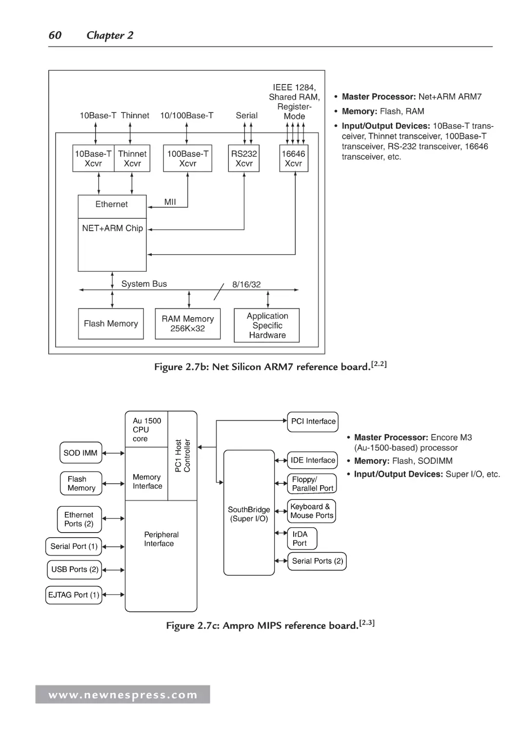
• Master Processor: Net+ARM ARM7
10Base-T Thinnet
Xcvr
Xcvr
Ethernet
100Base-T
Xcvr
RS232
Xcvr
16646
Xcvr
MII
• Memory: Flash, RAM
• Input/Output Devices: 10Base-T transceiver, Thinnet transceiver, 100Base-T
transceiver, RS-232 transceiver, 16646
transceiver, …
• Buses: System Bus, MII, …
NET+ARM Chip
System Bus
Flash Memory
RAM Memory
256K×32
8/16/32
Application
Specific
Hardware
Figure 1.5b: Net Silicon ARM7 reference board.[1.6]
w w w. n e w n e s p r e s s . c o m
8
Chapter 1
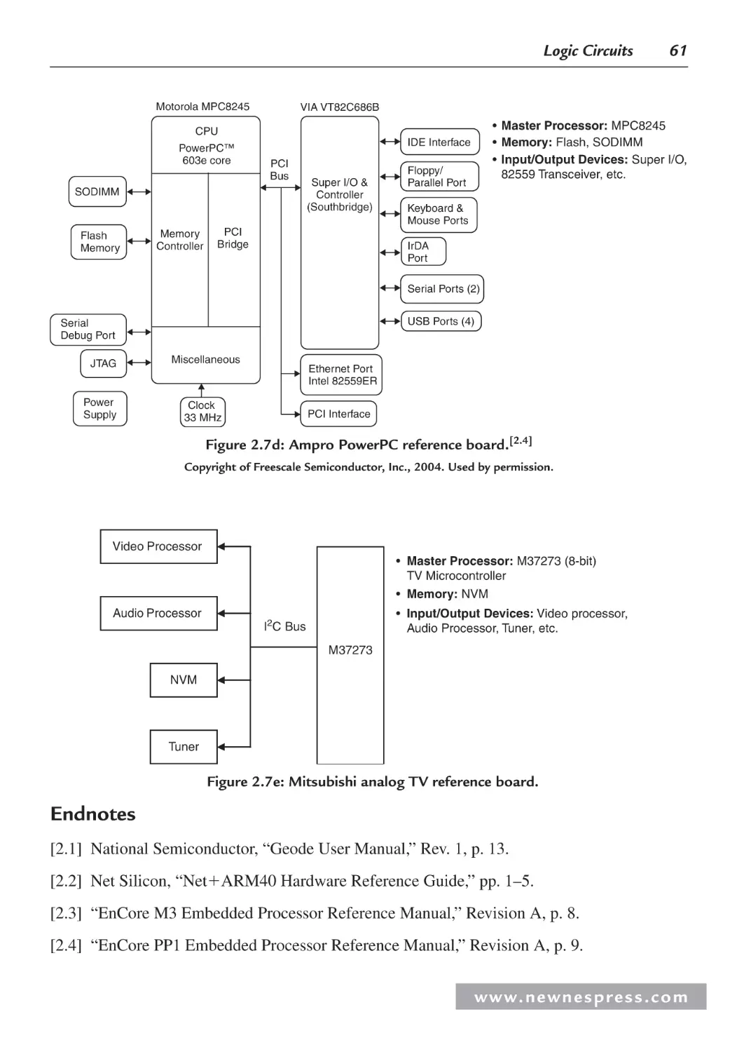
Au 1500
CPU
core
PCI Interface
Flash
Memory
• Memory: Flash, SODIMM
PC1 Host
Controller
SOD IMM
IDE Interface
Memory
Interface
• Input/Output Devices: Super I/O,…
• Buses: PCI, …
Floppy/
Parallel Port
SouthBridge
(Super I/O)
Ethernet
Ports (2)
Serial Port (1)
• Master Processor: Encore M3
(Au-1500-based) processor
Keyboard &
Mouse Ports
IrDA
Port
Peripheral
Interface
Serial Ports (2)
USB Ports (2)
EJTAG Port (1)
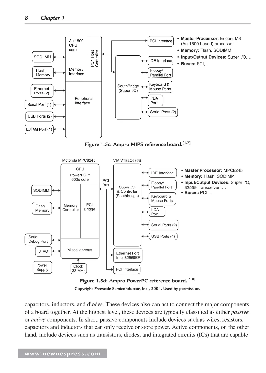
Figure 1.5c: Ampro MIPS reference board.[1.7]
Motorola MPC8245
VIA VT82C686B
CPU
PowerPC™
603e core
SODIMM
Flash
Memory
Memory
Controller
IDE Interface
PCI
Bus
Super I/O
& Controller
(Southbridge)
PCI
Bridge
Floppy/
Parallel Port
Keyboard &
Mouse Ports
• Master Processor: MPC8245
• Memory: Flash, SODIMM
• Input/Output Devices: Super I/O,
82559 Transceiver, …
• Buses: PCI, …
IrDA
Port
Serial Ports (2)
USB Ports (4)
Serial
Debug Port
JTAG
Power
Supply
Miscellaneous
Clock
33 MHz
Ethernet Port
Intel 82559ER
PCI Interface
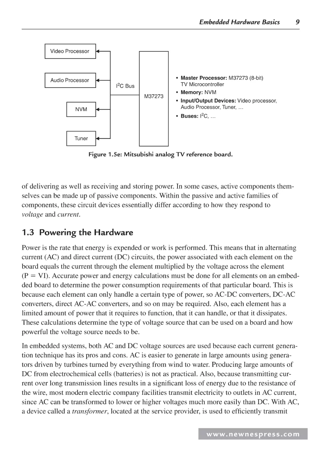
Figure 1.5d: Ampro PowerPC reference board.[1.8]
Copyright Freescale Semiconductor, Inc., 2004. Used by permission.
capacitors, inductors, and diodes. These devices also can act to connect the major components
of a board together. At the highest level, these devices are typically classified as either passive
or active components. In short, passive components include devices such as wires, resistors,
capacitors and inductors that can only receive or store power. Active components, on the other
hand, include devices such as transistors, diodes, and integrated circuits (ICs) that are capable
www. n e wn e s p res s .c o m
Embedded Hardware Basics
9
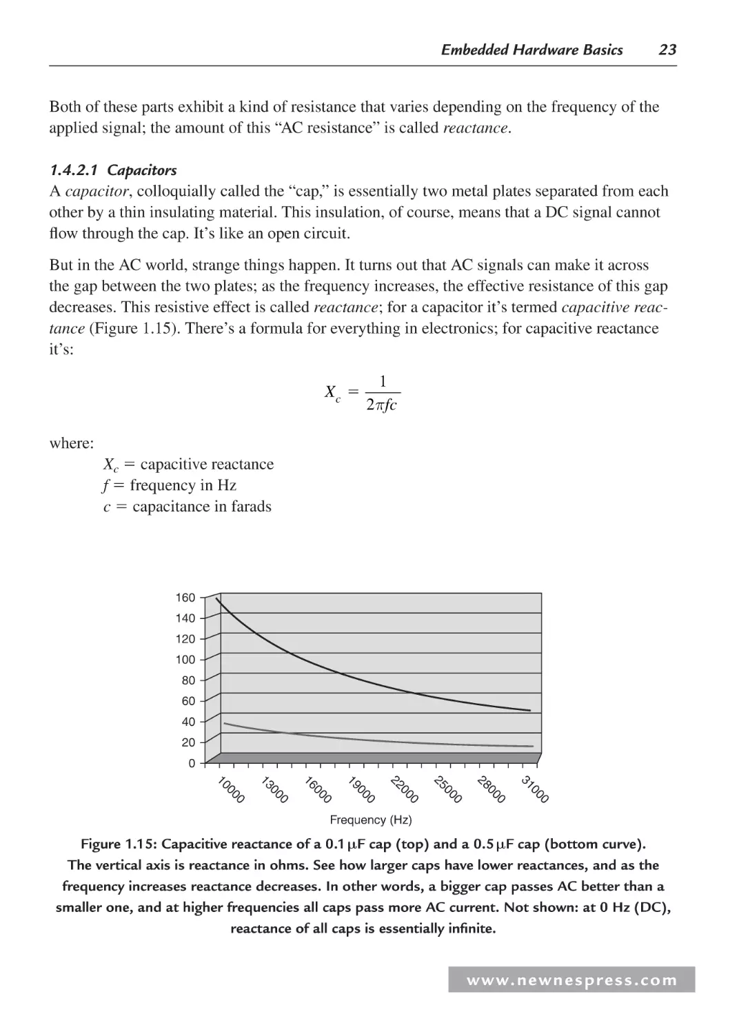
Video Processor
Audio Processor
I2C Bus
M37273
NVM
• Master Processor: M37273 (8-bit)
TV Microcontroller
• Memory: NVM
• Input/Output Devices: Video processor,
Audio Processor, Tuner, …
• Buses: I2C, …
Tuner
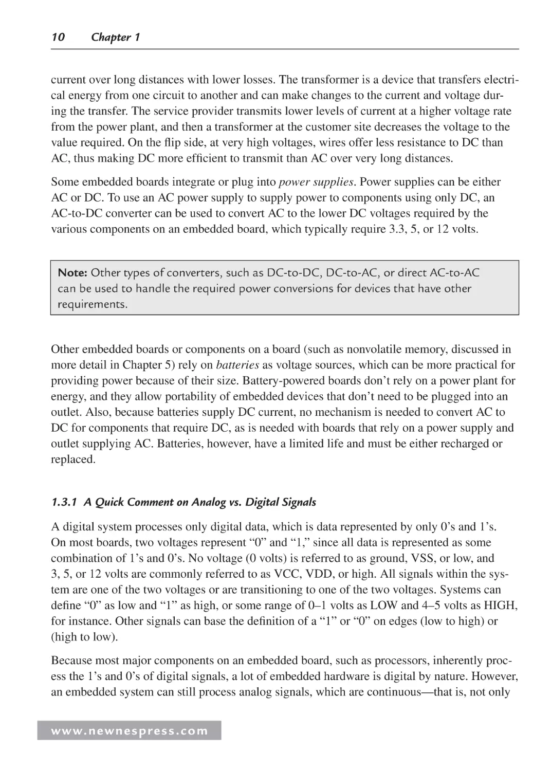
Figure 1.5e: Mitsubishi analog TV reference board.
of delivering as well as receiving and storing power. In some cases, active components themselves can be made up of passive components. Within the passive and active families of
components, these circuit devices essentially differ according to how they respond to
voltage and current.
1.3 Powering the Hardware
Power is the rate that energy is expended or work is performed. This means that in alternating
current (AC) and direct current (DC) circuits, the power associated with each element on the
board equals the current through the element multiplied by the voltage across the element
(P VI). Accurate power and energy calculations must be done for all elements on an embedded board to determine the power consumption requirements of that particular board. This is
because each element can only handle a certain type of power, so AC-DC converters, DC-AC
converters, direct AC-AC converters, and so on may be required. Also, each element has a
limited amount of power that it requires to function, that it can handle, or that it dissipates.
These calculations determine the type of voltage source that can be used on a board and how
powerful the voltage source needs to be.
In embedded systems, both AC and DC voltage sources are used because each current generation technique has its pros and cons. AC is easier to generate in large amounts using generators driven by turbines turned by everything from wind to water. Producing large amounts of
DC from electrochemical cells (batteries) is not as practical. Also, because transmitting current over long transmission lines results in a significant loss of energy due to the resistance of
the wire, most modern electric company facilities transmit electricity to outlets in AC current,
since AC can be transformed to lower or higher voltages much more easily than DC. With AC,
a device called a transformer, located at the service provider, is used to efficiently transmit
w w w. n e w n e s p r e s s . c o m
10
Chapter 1
current over long distances with lower losses. The transformer is a device that transfers electrical energy from one circuit to another and can make changes to the current and voltage during the transfer. The service provider transmits lower levels of current at a higher voltage rate
from the power plant, and then a transformer at the customer site decreases the voltage to the
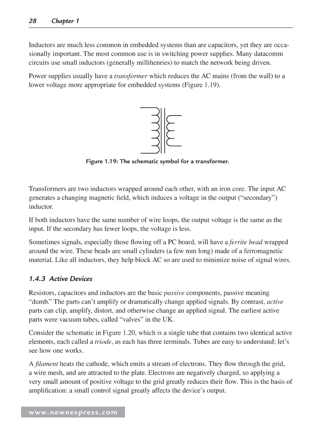
value required. On the flip side, at very high voltages, wires offer less resistance to DC than
AC, thus making DC more efficient to transmit than AC over very long distances.
Some embedded boards integrate or plug into power supplies. Power supplies can be either
AC or DC. To use an AC power supply to supply power to components using only DC, an
AC-to-DC converter can be used to convert AC to the lower DC voltages required by the
various components on an embedded board, which typically require 3.3, 5, or 12 volts.
Note: Other types of converters, such as DC-to-DC, DC-to-AC, or direct AC-to-AC
can be used to handle the required power conversions for devices that have other
requirements.
Other embedded boards or components on a board (such as nonvolatile memory, discussed in
more detail in Chapter 5) rely on batteries as voltage sources, which can be more practical for
providing power because of their size. Battery-powered boards don’t rely on a power plant for
energy, and they allow portability of embedded devices that don’t need to be plugged into an
outlet. Also, because batteries supply DC current, no mechanism is needed to convert AC to
DC for components that require DC, as is needed with boards that rely on a power supply and
outlet supplying AC. Batteries, however, have a limited life and must be either recharged or
replaced.
1.3.1 A Quick Comment on Analog vs. Digital Signals
A digital system processes only digital data, which is data represented by only 0’s and 1’s.
On most boards, two voltages represent “0” and “1,” since all data is represented as some
combination of 1’s and 0’s. No voltage (0 volts) is referred to as ground, VSS, or low, and
3, 5, or 12 volts are commonly referred to as VCC, VDD, or high. All signals within the system are one of the two voltages or are transitioning to one of the two voltages. Systems can
define “0” as low and “1” as high, or some range of 0–1 volts as LOW and 4–5 volts as HIGH,
for instance. Other signals can base the definition of a “1” or “0” on edges (low to high) or
(high to low).
Because most major components on an embedded board, such as processors, inherently process the 1’s and 0’s of digital signals, a lot of embedded hardware is digital by nature. However,
an embedded system can still process analog signals, which are continuous—that is, not only
www. n e wn e s p res s .c o m
Embedded Hardware Basics
11
1’s and 0’s but values in between as well. Obviously, a mechanism is needed on the board to
convert analog signals to digital signals. An analog signal is digitized by a sampling process,
and the resulting digital data can be translated back into a voltage “wave” that mirrors the
original analog waveform.
Real-World Advice
Inaccurate Signals: Problems with Noise in Analog and Digital Signals
One of the most serious problems in both the analog and digital signal realm involves
noise distorting incoming signals, thus corrupting and affecting the accuracy of data.
Noise is generally any unwanted signal alteration from an input source, any part of the
input signal generated from something other than a sensor, or even noise generated from
the sensor itself. Noise is a common problem with analog signals. Digital signals, on the
other hand, are at greater risk if the signals are not generated locally to the embedded
processor, so any digital signals coming across a longer transmission medium are the
most susceptible to noise problems.
Analog noise can come from a wide variety of sources—radio signals, lightning, power
lines, the microprocessor, or the analog sensing electronics themselves. The same is true
for digital noise, which can come from mechanical contacts used as computer inputs,
dirty slip rings that transmit power/data, limits in accuracy/dependability of input
source, and so forth.
The key to reducing either analog or digital noise is: (1) to follow basic design guidelines to avoid problems with noise. In the case of analog noise, this includes not mixing
analog and digital grounds, keeping sensitive electronic elements on the board a sufficient distance from elements switching current, limiting length of wires with low signal
levels/high impedance, etc. With digital signals, this means routing signal wires away
from noise-inducing high current cables, shielding wires, transmitting signals using correct techniques, etc. (2) to clearly identify the root cause of the problem, which means
exactly what is causing the noise. With point (2), once the root cause of the noise has
been identified, a hardware or software fix can be implemented. Techniques for reducing
analog noise include filtering out frequencies not needed and averaging the signal inputs,
whereas digital noise is commonly addressed via transmitting correction codes/parity bits and/or adding additional hardware to the board to correct any problems with
received data.
—Based on the articles “Minimizing Analog Noise” (May 1997),“Taming Analog Noise”
(November 1992), and “Smoothing Digital Inputs” (October 1992), by Jack Ganssle, in
Embedded Systems Programming Magazine.
w w w. n e w n e s p r e s s . c o m
12
Chapter 1
1.4 Basic Electronics
In this section, we will review some electronics fundamentals.
1.4.1 DC Circuits
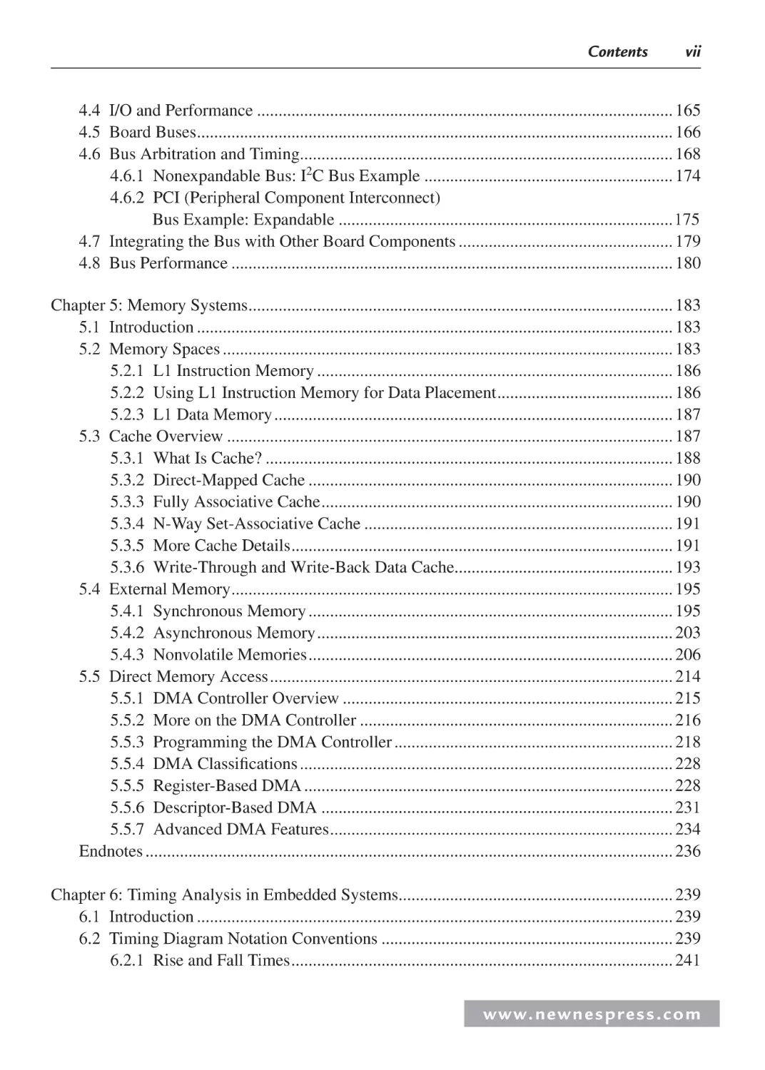
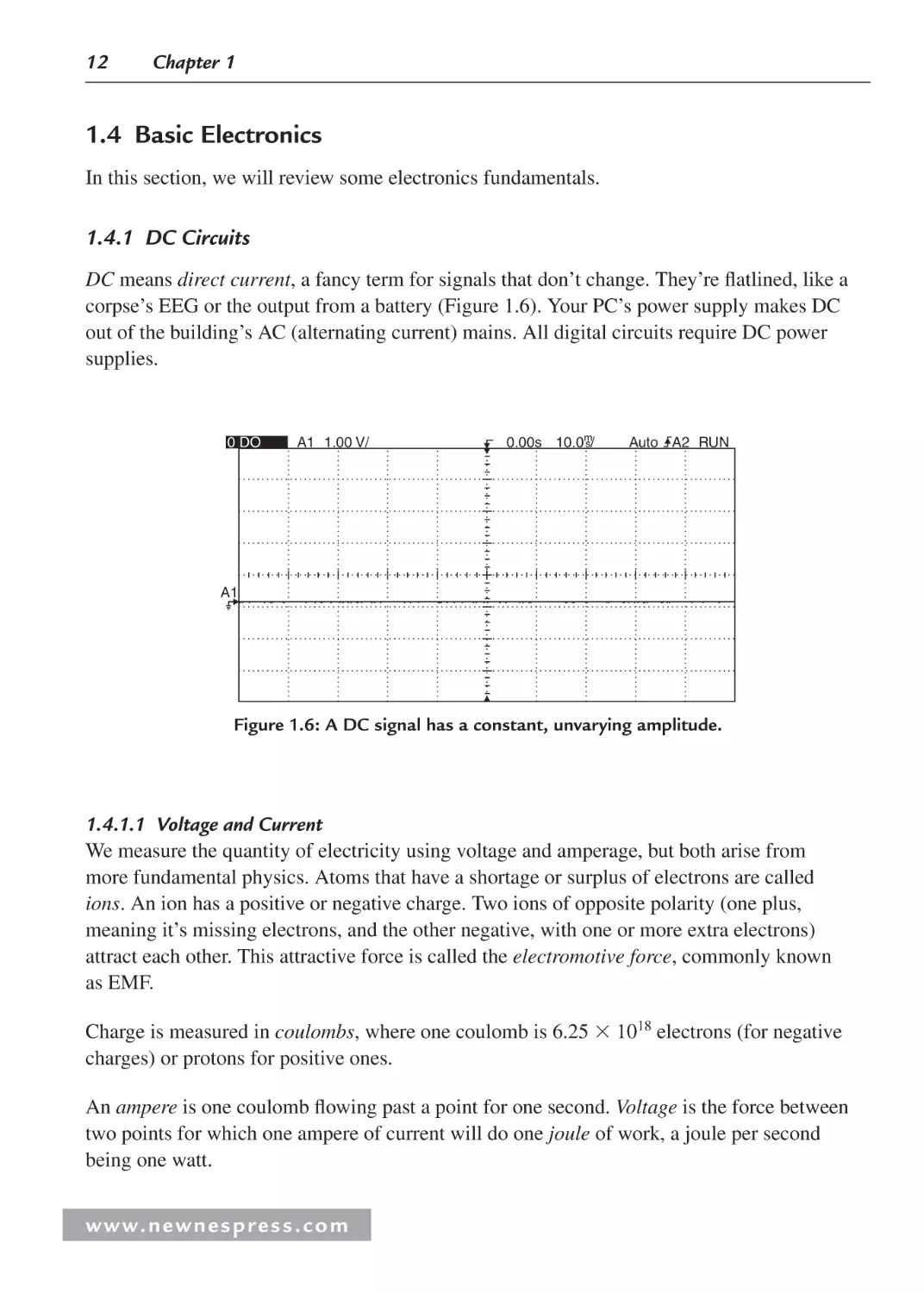
DC means direct current, a fancy term for signals that don’t change. They’re flatlined, like a
corpse’s EEG or the output from a battery (Figure 1.6). Your PC’s power supply makes DC
out of the building’s AC (alternating current) mains. All digital circuits require DC power
supplies.
0 DO
A1 1.00 V/
0.00s 10.0m
s/
Auto A2 RUN
A1
Figure 1.6: A DC signal has a constant, unvarying amplitude.
1.4.1.1 Voltage and Current
We measure the quantity of electricity using voltage and amperage, but both arise from
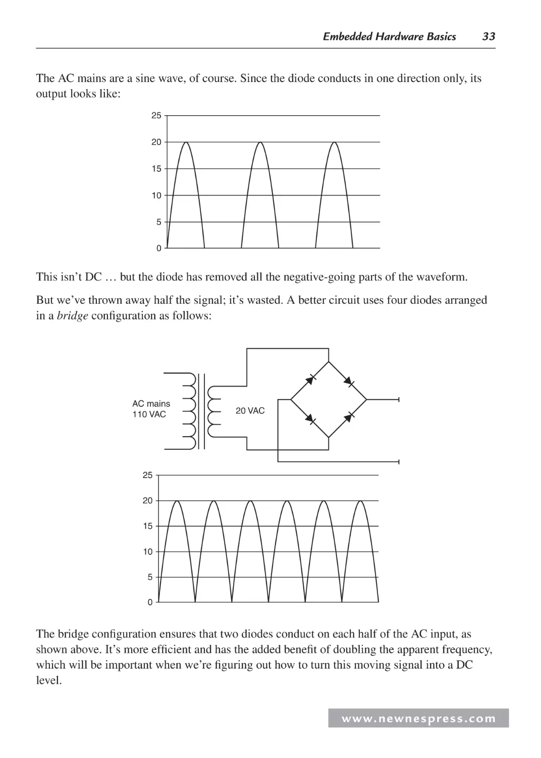
more fundamental physics. Atoms that have a shortage or surplus of electrons are called
ions. An ion has a positive or negative charge. Two ions of opposite polarity (one plus,
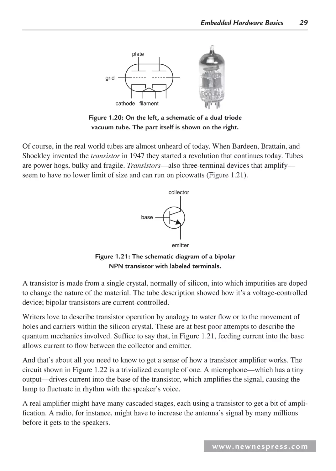
meaning it’s missing electrons, and the other negative, with one or more extra electrons)
attract each other. This attractive force is called the electromotive force, commonly known
as EMF.
Charge is measured in coulombs, where one coulomb is 6.25 1018 electrons (for negative
charges) or protons for positive ones.
An ampere is one coulomb flowing past a point for one second. Voltage is the force between
two points for which one ampere of current will do one joule of work, a joule per second
being one watt.
www. n e wn e s p res s .c o m
Embedded Hardware Basics
13
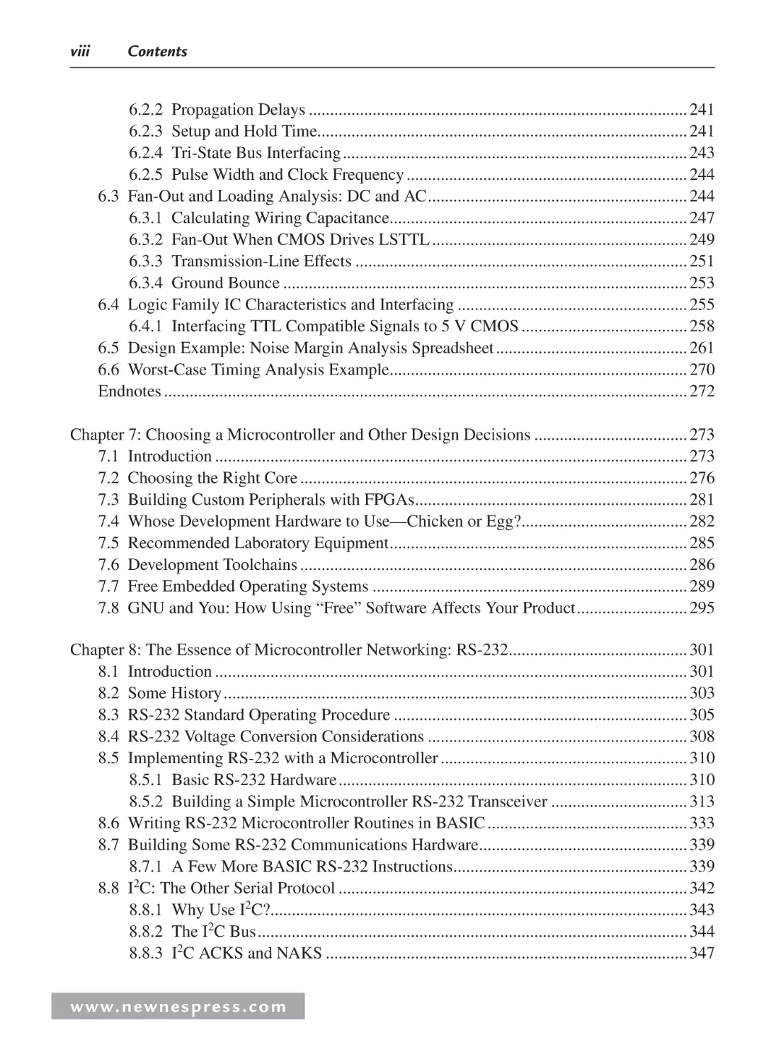
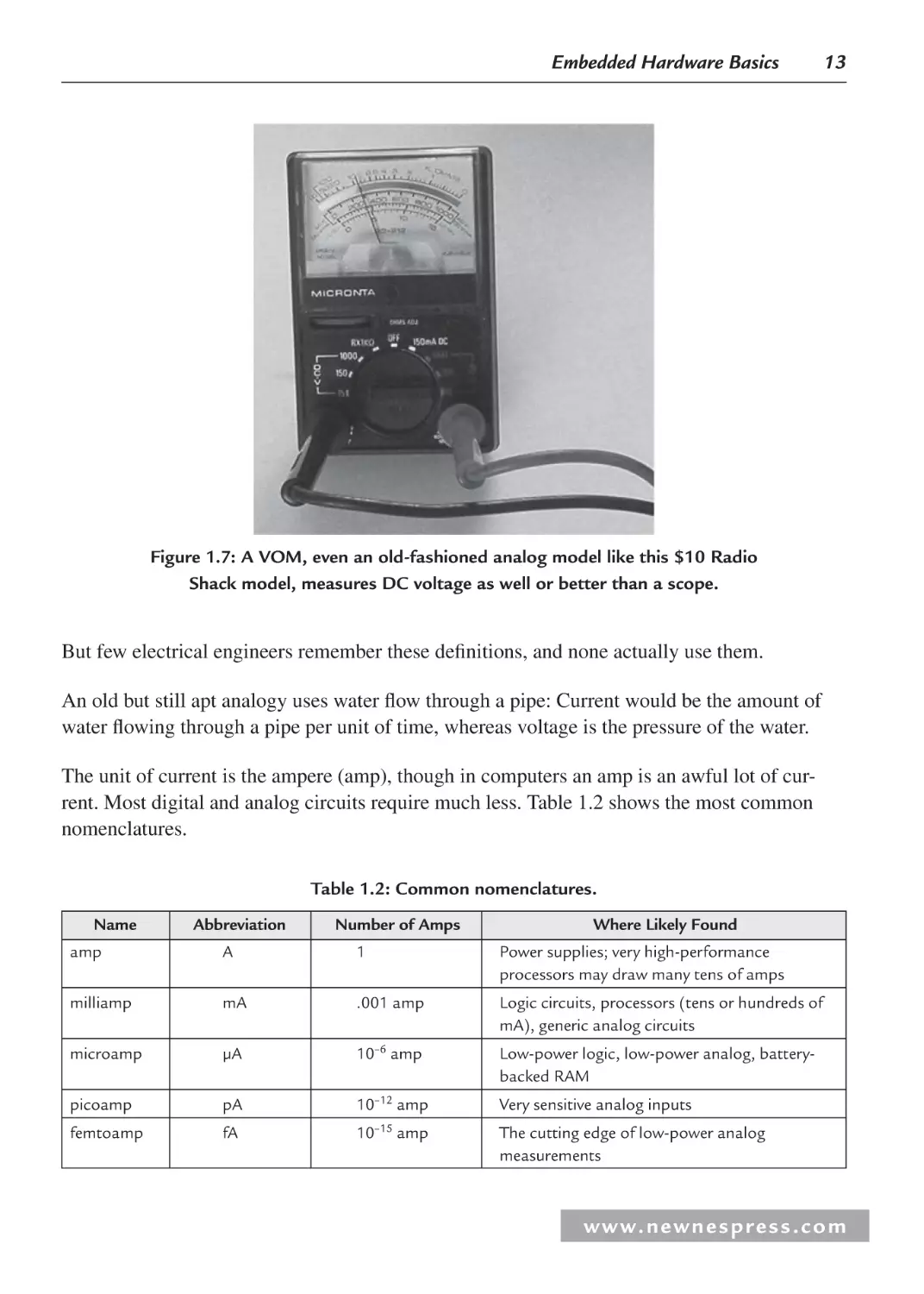
Figure 1.7: A VOM, even an old-fashioned analog model like this $10 Radio
Shack model, measures DC voltage as well or better than a scope.
But few electrical engineers remember these definitions, and none actually use them.
An old but still apt analogy uses water flow through a pipe: Current would be the amount of
water flowing through a pipe per unit of time, whereas voltage is the pressure of the water.
The unit of current is the ampere (amp), though in computers an amp is an awful lot of current. Most digital and analog circuits require much less. Table 1.2 shows the most common
nomenclatures.
Table 1.2: Common nomenclatures.
Name
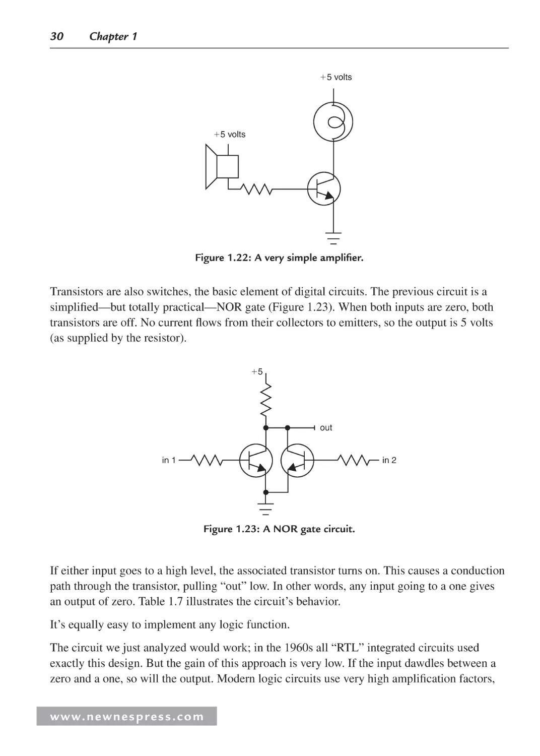
Abbreviation
Number of Amps
Where Likely Found
amp
A
1
Power supplies; very high-performance
processors may draw many tens of amps
milliamp
mA
.001 amp
Logic circuits, processors (tens or hundreds of
mA), generic analog circuits
microamp
µA
10–6 amp
Low-power logic, low-power analog, batterybacked RAM
picoamp
pA
10–12 amp
Very sensitive analog inputs
femtoamp
fA
10–15 amp
The cutting edge of low-power analog
measurements
w w w. n e w n e s p r e s s . c o m
14
Chapter 1
Most embedded systems have a far less extreme range of voltages. Typical logic and microprocessor power supplies range from a volt or 2–5 volts. Analog power supplies rarely exceed
plus and minus 15 volts. Some analog signals from sensors might go down to the millivolt
(.001 volt) range. Radio receivers can detect microvolt-level signals, but they do this using
quite sophisticated noise-rejection techniques.
1.4.1.2 Resistors
As electrons travel through wires, components, or accidentally through a poor soul’s body,
they encounter resistance, which is the tendency of the conductor to limit electron flow.
A vacuum is a perfect resistor: no current flows through it. Air’s pretty close, but since water
is a decent conductor, humidity does allow some electricity to flow in air.
Superconductors are the only materials with zero resistance, a feat achieved through the magic
of quantum mechanics at extremely low temperatures, on the order of that of liquid nitrogen
and colder. Everything else exhibits some resistance, even the very best wires. Feel the power
cord of your 1500 watt ceramic heater—it’s warm, indicating some power is lost in the cord
due to the wire’s resistance.
We measure resistance in ohms; the more ohms, the poorer the conductor. The Greek capital
omega (Ω) is the symbol denoting ohms.
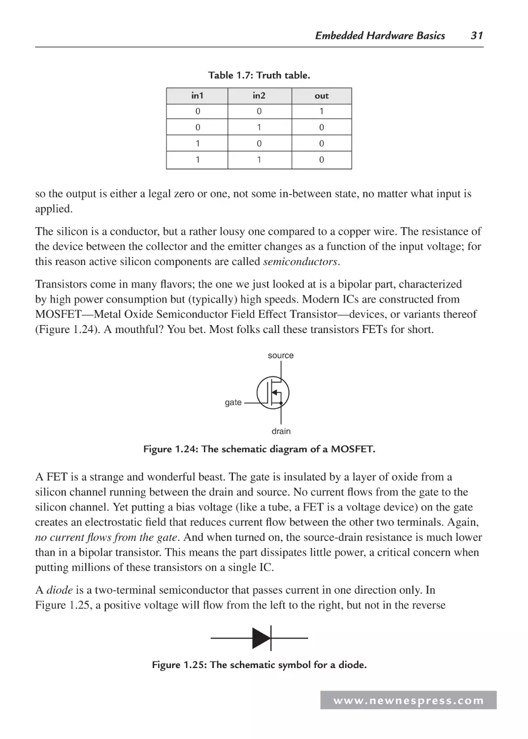
Resistance, voltage, and amperage are all related by the most important of all formulas in electrical engineering. Ohm’s Law states:
EIR
where E is voltage in volts, I is current in amps, and R is resistance in ohms. (EEs like to use E
for volts because it indicates electromotive force.)
What does this mean in practice? Feed one amp of current through a one-ohm load and there
will be one volt developed across the load. Double the voltage and, if resistance stays the
same, the current doubles.
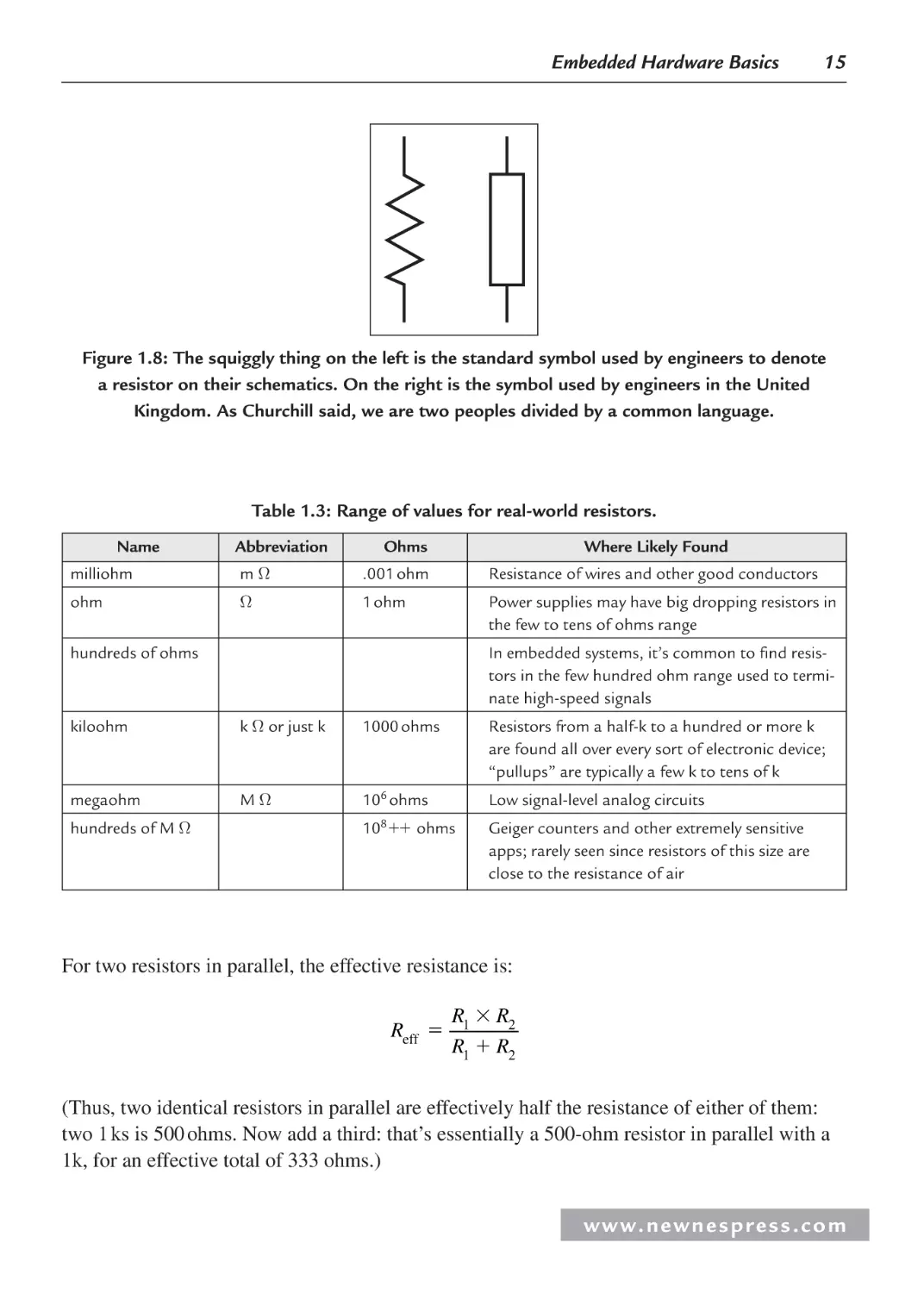
Though all electronic components have resistance, a resistor is a device specifically made to
reduce conductivity (Figure 1.8 and Table 1.3). We use them everywhere. The volume control
on a stereo (at least, the nondigital ones) is a resistor whose value changes as you rotate the
knob; more resistance reduces the signal and hence the speaker output.
What happens when you connect resistors together? For resistors in series, the total effective
resistance is the sum of the values:
Reff R1 R2
www. n e wn e s p res s .c o m
Embedded Hardware Basics
15
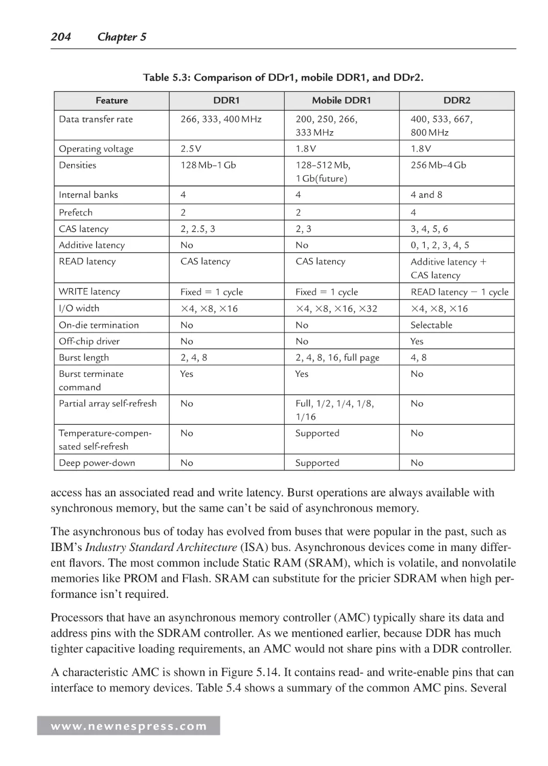
Figure 1.8: The squiggly thing on the left is the standard symbol used by engineers to denote
a resistor on their schematics. On the right is the symbol used by engineers in the United
Kingdom. As Churchill said, we are two peoples divided by a common language.
Table 1.3: Range of values for real-world resistors.
Name
Abbreviation
Ohms
Where Likely Found
milliohm
mΩ
.001 ohm
Resistance of wires and other good conductors
ohm
Ω
1 ohm
Power supplies may have big dropping resistors in
the few to tens of ohms range
hundreds of ohms
In embedded systems, it’s common to find resistors in the few hundred ohm range used to terminate high-speed signals
kiloohm
k Ω or just k
1000 ohms
Resistors from a half-k to a hundred or more k
are found all over every sort of electronic device;
“pullups” are typically a few k to tens of k
megaohm
MΩ
106 ohms
Low signal-level analog circuits
10 ohms
Geiger counters and other extremely sensitive
apps; rarely seen since resistors of this size are
close to the resistance of air
hundreds of M Ω
8
For two resistors in parallel, the effective resistance is:
Reff
R1 R2
R1 R2
(Thus, two identical resistors in parallel are effectively half the resistance of either of them:
two 1 ks is 500 ohms. Now add a third: that’s essentially a 500-ohm resistor in parallel with a
1k, for an effective total of 333 ohms.)
w w w. n e w n e s p r e s s . c o m
16
Chapter 1
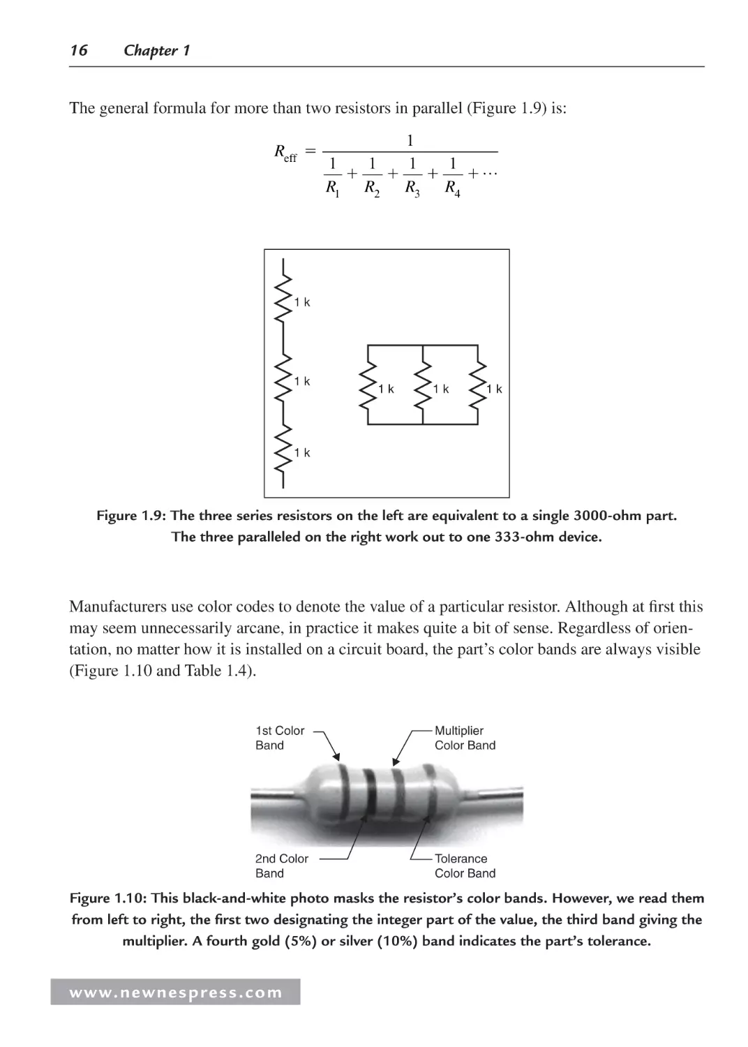
The general formula for more than two resistors in parallel (Figure 1.9) is:
Reff
1
1
1
1
1 …
R1 R2 R3 R4
1k
1k
1k
1k
1k
1k
Figure 1.9: The three series resistors on the left are equivalent to a single 3000-ohm part.
The three paralleled on the right work out to one 333-ohm device.
Manufacturers use color codes to denote the value of a particular resistor. Although at first this
may seem unnecessarily arcane, in practice it makes quite a bit of sense. Regardless of orientation, no matter how it is installed on a circuit board, the part’s color bands are always visible
(Figure 1.10 and Table 1.4).
1st Color
Band
Multiplier
Color Band
2nd Color
Band
Tolerance
Color Band
Figure 1.10: This black-and-white photo masks the resistor’s color bands. However, we read them
from left to right, the first two designating the integer part of the value, the third band giving the
multiplier. A fourth gold (5%) or silver (10%) band indicates the part’s tolerance.
www. n e wn e s p res s .c o m
Embedded Hardware Basics
17
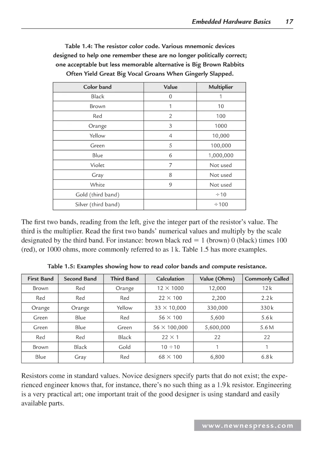
Table 1.4: The resistor color code. Various mnemonic devices
designed to help one remember these are no longer politically correct;
one acceptable but less memorable alternative is Big Brown Rabbits
Often Yield Great Big Vocal Groans When Gingerly Slapped.
Color band
Value
Multiplier
Black
0
1
Brown
1
10
Red
2
100
Orange
3
1000
Yellow
4
10,000
Green
5
100,000
Blue
6
1,000,000
Violet
7
Not used
Gray
8
Not used
White
9
Not used
Gold (third band)
10
Silver (third band)
100
The first two bands, reading from the left, give the integer part of the resistor’s value. The
third is the multiplier. Read the first two bands’ numerical values and multiply by the scale
designated by the third band. For instance: brown black red 1 (brown) 0 (black) times 100
(red), or 1000 ohms, more commonly referred to as 1 k. Table 1.5 has more examples.
Table 1.5: Examples showing how to read color bands and compute resistance.
First Band
Second Band
Third Band
Calculation
Value (Ohms)
Commonly Called
Brown
Red
Orange
12 1000
12,000
12 k
Red
Red
Red
22 100
2,200
2.2 k
Orange
Orange
Yellow
33 10,000
330,000
330 k
Green
Blue
Red
56 100
5,600
5.6 k
Green
Blue
Green
56 100,000
5,600,000
5.6 M
Red
Red
Black
22 1
22
22
Brown
Black
Gold
10 10
1
1
Blue
Gray
Red
68 100
6,800
6.8 k
Resistors come in standard values. Novice designers specify parts that do not exist; the experienced engineer knows that, for instance, there’s no such thing as a 1.9 k resistor. Engineering
is a very practical art; one important trait of the good designer is using standard and easily
available parts.
w w w. n e w n e s p r e s s . c o m
18
Chapter 1
1.4.1.3 Circuits
Electricity always flows in a loop. A battery left disconnected discharges only very slowly
because there’s no loop, no connection of any sort (other than the nonzero resistance of humid
air) between the two terminals. To make a lamp light, connect one lead to each battery terminal; electrons can now run in a loop from the battery’s negative terminal, through the lamp,
and back into the battery.
There are only two types of circuits: series and parallel. All real designs use combinations of
these. A series circuit connects loads in a circular string; current flows around through each
load in sequence (Figure 1.11). In a series circuit, the current is the same in every load.
R1
2k
12 volts
R2
10 k
Figure 1.11: In a series circuit, the electrons flow through one load and then
into another. The current in each resistor is the same; the voltage
dropped across each depends on the resistor’s value.
It’s easy to calculate any parameter of a series circuit. In Figure 1.11, a 12-volt battery powers
two series resistors. Ohm’s Law tells us that the current flowing through the circuit is the voltage (12 in this case) divided by the resistance (the sum of the two resistors, or 12 k).
Total current is thus:
I V R (12 volts) (2000 10,000 ohms) 12 12000 0.001 amp 1 mA
(Remember that mA is the abbreviation for milliamps.)
So what’s the voltage across either of the resistors? In a series circuit, the current is identical
in all loads, but the voltage developed across each load is a function of the load’s resistance
and the current. Again, Ohm’s Law holds the secret. The voltage across R1 is the current in
the resistor times its resistance, or:
VR1 IR1 0.001 amps 2000 ohms 2 volts
www. n e wn e s p res s .c o m
Embedded Hardware Basics
19
Since the battery places 12 volts across the entire resistor string, the voltage dropped on R2
must be 12 – 2, or 10 volts. Don’t believe that? Use Mr. Ohm’s wonderful equation on R2 to
find:
VR2 IR2 0.001 amps 10,000 ohms 10 volts
It’s easy to extend this to any number of parts wired in series.
Parallel circuits have components wired so both pins connect (Figure 1.12). Current flows
through both parts, though the amount of current depends on the resistance of each leg of the
circuit. The voltage on each component, though, is identical.
12 volts
R1
R2
2k
10 k
Figure 1.12: R1 and R2 are in parallel, both driven by the 12-volt battery.
We can compute the current in each leg much as we did for the series circuit. In the preceding
case, the battery applies 12 volts to both resistors. The current through R1 is:
IR 12 volts 2,000 ohms 12 2000 0.006 amps 6 mA
1
Through R2:
IR 12 volts 10,000 ohms 0.0012 amps 1.2 mA
2
Real circuits are usually a combination of series and parallel elements (Figure 1.13). Even in
these more complex, more realistic cases, it’s still very simple to compute anything one wants
to know.
R1
1k
10 volts
R3
R2
5.6 k
2k
Figure 1.13: A series/parallel circuit.
w w w. n e w n e s p r e s s . c o m
20
Chapter 1
Let’s analyze the circuit shown in Figure 1.13. There’s only one trick: cleverly combine complicated elements into simpler ones. Let’s start by figuring the current flowing out of the battery. It’s much too hard to do this calculation until we remember that two resistors in parallel
look like a single resistor with a lower value.
Start by figuring the current flowing out of the battery and through R1. We can turn this into a
series circuit (in which the current flowing is the same through all the components) by replacing R3 and R2 with a single resistor with the same effective value as these two paralleled components. That’s:
REFF
R2 R3
5600 2000
1474 ohms
R1 R3
5600 2000
So the circuit is identical to one with two series resistors: R1, still 1 k, and REFF at 1474 ohms.
Ohm’s Law gives the current flowing out of the battery and through these two resistors:
i
V
10
0.004 amps 4 mA
R1 REFF
1000 1474
Ohm’s Law remains the font of all wisdom in basic circuit analysis and readily tells us the
voltage dropped across R1:
V iR1 0.004 amps 1000 ohms 4 volts
Clearly, since the battery provides 10 volts, the voltage across the paralleled pair R2 and R3 is
6 volts.
1.4.1.4 Power
Power is the product of voltage and current and is expressed in watts. One watt is one volt
times one amp. A milliwatt is a thousandth of a watt; a microwatt is a millionth.
You can think of power as the total amount of electricity present. A thousand volts sounds
like a lot of electricity, but if there’s only a microamp available, that’s a paltry milliwatt—not
much power at all.
Power is also current2 times resistance:
P I2 R
Electronic components like resistors and ICs consume a certain amount of volts and amps.
An IC doesn’t move, make noise, or otherwise release energy (other than exerting a minimal
amount of energy in sending signals to other connected devices), so almost all the energy
consumed gets converted to heat. All components have maximum power dissipation ratings;
exceed these at your peril.
www. n e wn e s p res s .c o m
Embedded Hardware Basics
21
If a part feels warm it’s dissipating a reasonable fraction of a watt. If it’s hot but you can keep
your finger on it, then it’s probably operating within specs, though many analog components
want to run cooler. If you pull back, not burned, but the heat is too much for your finger, then
in most cases (be wary of the wimp factor; some people are more heat sensitive than others)
the device is too hot and either needs external cooling (heat sink, fan, etc.), has failed, or your
circuit exceeds heat parameters. A burn or near burn or discoloration of the device means
there’s trouble brewing in all but exceptional conditions (e.g., high-energy parts like power
resistors).
A PC’s processor has so many transistors, each losing a bit of heat, that the entire part might
consume and eliminate 100 watts. That’s far more than the power required to destroy the
chip. Designers expend a huge effort in building heat sinks and fans to transfer the energy in
the part to the air.
Figure 1.14: This 10-ohm resistor, with 12 volts applied, draws 833 mA. P ⴝ I2R,
so it’s sucking about 7 watts. Unfortunately, this particular part is rated for 1/4 watt max,
so it is on fire. Few recent college grads have a visceral feel for current, power, and
heat, so this demo makes their eyes go like saucers.
The role of heat sinks and fans is to remove the heat from the circuits and dump it into the
air before the devices burn up. The fact that a part dissipates a lot of energy and wants to run
hot is not bad as long as proper thermal design removes the energy from the device before it
exceeds its max temp rating (Figure 1.14).
1.4.2 AC Circuits
AC is short for alternating current, which is any signal that’s not DC. AC signals vary with
time. The mains in your house supply AC electricity in the shape of a sine wave: the voltage
w w w. n e w n e s p r e s s . c o m
22
Chapter 1
varies from a large negative to a large positive voltage 60 times per second (in the United
States and Japan) or 50 times per second (in most of the rest of the world).
AC signals can be either periodic, which means they endlessly and boringly repeat forever, or
aperiodic, the opposite. Static from your FM radio is largely aperiodic since it’s quite random.
The bit stream on any address or data line from a micro is mostly aperiodic, at least over short
times, as it’s a complex changing pattern driven by the software.
The rate at which a periodic AC signal varies is called its frequency, which is measured in
hertz (Hz for short). One Hz means the waveform repeats once per second. A thousand Hz is
a kHz (kilohertz), a million Hz is the famous MHz by which so many microprocessor clock
rates are defined, and a billion Hz is a GHz.
The reciprocal of Hz is period. That is, where the frequency in hertz defines the signal’s repetition rate, the period is the time it takes for the signal to go through a cycle.
Mathematically:
Period in seconds 1 frequency in Hz
Thus, a processor running at 1 GHz has a clock period of 1 nanosecond—one billionth of a
second. No kidding. In that brief flash of time, even light goes but a bare foot. Though your
1.8 GHz PC may seem slow loading Word, it’s cranking instructions at a mind-boggling rate.
Wavelength relates a signal’s period—and thus its frequency—to a physical “size.” It’s the distance between repeating elements and is given by:
Wavelength in meters
c
300,000,000 meters/second
frequency
frequency in Hz
where c is the speed of light.
An FM radio station at about 100 MHz has a wavelength of 3 meters. AM signals, on the other
hand, are around 1 MHz, so each sine wave is 300 meters long. A 2.4-GHz cordless phone
runs at a wavelength a bit over 10 cm.
As the frequency of an AC signal increases, things get weird. The basic ideas of DC circuits
still hold but need to be extended considerably. Just as relativity builds on Newtonian mechanics to describe fast-moving systems, electronics needs new concepts to properly describe fast
AC circuits.
Resistance, in particular, is really a subset of the real nature of electronic circuits. It turns out
that there are three basic kinds of resistive components; each behaves somewhat differently.
We’ve already looked at resistors; the other two components are capacitors and inductors.
www. n e wn e s p res s .c o m
Embedded Hardware Basics
23
Both of these parts exhibit a kind of resistance that varies depending on the frequency of the
applied signal; the amount of this “AC resistance” is called reactance.
1.4.2.1 Capacitors
A capacitor, colloquially called the “cap,” is essentially two metal plates separated from each
other by a thin insulating material. This insulation, of course, means that a DC signal cannot
flow through the cap. It’s like an open circuit.
But in the AC world, strange things happen. It turns out that AC signals can make it across
the gap between the two plates; as the frequency increases, the effective resistance of this gap
decreases. This resistive effect is called reactance; for a capacitor it’s termed capacitive reactance (Figure 1.15). There’s a formula for everything in electronics; for capacitive reactance
it’s:
Xc
1
2πfc
where:
Xc capacitive reactance
f frequency in Hz
c capacitance in farads
160
140
120
100
80
60
40
20
0
00
0
31
0
00
28
0
00
25
0
0
00
22
00
19
0
00
16
0
00
13
0
00
10
Frequency (Hz)
Figure 1.15: Capacitive reactance of a 0.1 μF cap (top) and a 0.5 μF cap (bottom curve).
The vertical axis is reactance in ohms. See how larger caps have lower reactances, and as the
frequency increases reactance decreases. In other words, a bigger cap passes AC better than a
smaller one, and at higher frequencies all caps pass more AC current. Not shown: at 0 Hz (DC),
reactance of all caps is essentially infinite.
w w w. n e w n e s p r e s s . c o m
24
Chapter 1
Capacitors thus pass only changing signals (Table 1.6). The current flowing through a cap is:
I
dV
dt
(If your calculus is rusty or nonexistent, this simply means that the current flow is proportional
to the change in voltage over time.)
In other words, the faster the signal changes, the more current flows.
Table 1.6: Range of values for real-world capacitors.
Name
Abbreviation
Farads
picofarad
pF
12
10
microfarad
μF
106 farad
Decoupling caps on chips are about .01 to
.1 μF; low-freq decoupling runs about 10 μF,
big power supply caps might be 1000 μF.
farad
F
1 farad
One farad is a huge capacitor and generally
does not exist. A few vendors sell “supercaps”
that have values up to a few farads, but these
are unusual. Sometimes used to supply backup
power to RAM when the system is turned off.
farad
Where Likely Found
Padding caps on microprocessor crystals,
oscillators, analog feedback loops.
In real life there’s no such thing as a perfect capacitor. All leak a certain amount of DC and
exhibit other more complex behavior. For that reason, there’s quite a range of different types
of parts.
In most embedded systems you’ll see one of two types of capacitors (Figure 1.16). The first
are the polarized ones, devices which have a plus and a minus terminal. Connect one backward and the part will likely explode!
Polarized devices have large capacitance values: tens to thousands of microfarads. They’re
most often used in power supplies to remove the AC component from filtered signals.
Consider the equation of capacitive reactance: large cap values pass lower-frequency signals
efficiently. Typical construction today is from a material called tantalum; seasoned EEs often
call these devices tantalums. You’ll see tantalum caps on PC boards to provide a bit of bulk
storage of the power supply.
Smaller caps are made from a variety of materials. These have values from a few picofarads to
a fraction of a microfarad. They’re often used to “decouple” the power supply on a PCB (i.e.,
to short high-frequency switching from power to ground, so the logic signals don’t get coupled
into the power supply). Most PCBs have dozens or hundreds of these parts scattered around.
www. n e wn e s p res s .c o m
Embedded Hardware Basics
25
Figure 1.16: Schematic symbols for capacitors. The one on the left is a generic,
generally low-valued (under 1 μF) part. On the right the plus sign shows that
the cap is polarized. Installed backward, it’s likely to explode.
We can wire capacitors in series and in parallel; compute the total effective capacitance using
the rules opposite those for resistors. So, for two caps in parallel, sum their values to get the
effective capacitance. In a series configuration the total effective capacitance is:
Ceff
1
1
1
1 …
C1 C2 C3
Note that this rule is for figuring the total capacitance of the circuit, not for computing the
total reactance. More on that shortly.
One useful characteristic of a capacitor is that it can store a charge. Connect one to a battery
or power supply and it will store that voltage. Remove the battery and (for a perfect, lossless
part) the capacitor will still hold that voltage. Real parts leak a bit; ones rated at under 1 μF or
so discharge rapidly. Larger parts store the charge longer.
Interesting things happen when you wire a cap and a resistor in series. The resistor limits current to the capacitor, causing it to charge slowly. Suppose the circuit shown in Figure 1.17 is
dead, no voltage at all applied. Now turn on the switch. Though we’ve applied a DC signal,
the sudden transition from 0 to 5 volts is AC.
dV
Current flows due to the I
rule; dV is the sudden edge from flipping the switch.
dt
But the input goes from an AC-edge to steady-state DC, so current stops flowing pretty
quickly. How fast? That’s defined by the circuit’s time constant.
A resistor and capacitor in series is colloquially called an RC circuit. The graph shows how
the voltage across the capacitor increases over time. The time constant of any circuit is pretty
well approximated by:
t RC
for R in ohms, C in farads, and t in seconds.
w w w. n e w n e s p r e s s . c o m
26
Chapter 1
Figure 1.17: Close the switch and the voltage applied to the RC circuit looks like
the top curve. The lower graph shows how the capacitor’s voltage builds
slowly with time, headed asymptotically toward the upper curve.
This formula tells us that after RC seconds the capacitor will be charged to 63.2% of the battery’s voltage. After another RC seconds, another 63.2%, for a total of 86.5%.
Analog circuits use a lot of RC circuits; in a microprocessor it’s still common to see them controlling the CPU’s reset input. Apply power to the system and all the logic comes up, but the
RC’s time constant keeps reset asserted low for a while, giving the processor time to initialize
itself.
The most common use of capacitors in the digital portion of an embedded system is to decouple the logic chips’ power pins. A medium value part (0.01 to 0.1 μF) is tied between power
and ground very close to the power leads on nearly every digital chip. The goal is to keep
power supplied to the chips as clean as possible—close to a perfect DC signal.
Why would this be an issue? After all, the system’s power supply provides a nearly perfect DC
level. It turns out that as a fast logic chip switches between zero and one it can draw immense
amounts of power for a short, subnanosecond, time. The power supply cannot respond quickly
enough to regulate that, and since there’s some resistance and reactance between the supply
and the chip’s pins, what the supply provides and what the chip sees are somewhat different.
The decoupling capacitor shorts this very high-frequency (i.e., short transient) signal on Vcc
to ground. It also provides a tiny bit of localized power storage that helps overcome the instantaneous voltage drop between the power supply and the chip.
Most designs also include a few tantalum bulk storage devices scattered around the PC board,
also connected between Vcc and ground. Typically these are 10 to 50 μF each. They are even
more effective bulk storage parts to help minimize the voltage drop chips would otherwise see.
You’ll often see very small caps (on the order of 20 pF) connected to microprocessor drive
crystals. These help the device oscillate reliably.
www. n e wn e s p res s .c o m
Embedded Hardware Basics
27
Analog circuits make many wonderful and complex uses of caps. It’s easy to build integrators
and differentiators from these parts, as well as analog hold circuits that memorize a signal for
a short period of time. Common values in these sorts of applications range from 100 pF to
fractions of a microfarad.
1.4.2.2 Inductors
An inductor is, in a sense, the opposite of a capacitor. Caps block DC but offer diminishing
resistance (really, reactance) to AC signals as the frequency increases. An inductor, on the
other hand, passes DC with zero resistance (for an idealized part), but the resistance (reactance) increases proportionately to the frequency.
Physically an inductor is a coil of wire and is often referred to as a coil. A simple straight wire
exhibits essentially no inductance. Wrap a wire in a loop and it’s less friendly to AC signals.
Add more loops, or make them smaller, or put a bit of ferrous metal in the loop, and inductance increases. Electromagnets are inductors, as is the field winding in an alternator or motor.
An iron core inductor is wound around a slug of metal, which increases the device’s inductance substantially (Figure 1.18).
Figure 1.18: Schematic symbols of two inductors. The one on the
left is an “air core”; the one on the right is an “iron core.”
Inductance is measured in henries (H). Inductive reactance is the tendency of an inductor to
block AC and is given by:
XL 2πLf
where:
XL Inductive reactance
f frequency in Hz
L inductance in henries
Clearly, as the frequency goes to zero (DC), reactance does as well.
Inductors follow the resistor rules for parallel and series combinations: add the value (in henries) when in series, and use the division rule when in parallel.
w w w. n e w n e s p r e s s . c o m
28
Chapter 1
Inductors are much less common in embedded systems than are capacitors, yet they are occasionally important. The most common use is in switching power supplies. Many datacomm
circuits use small inductors (generally millihenries) to match the network being driven.
Power supplies usually have a transformer which reduces the AC mains (from the wall) to a
lower voltage more appropriate for embedded systems (Figure 1.19).
Figure 1.19: The schematic symbol for a transformer.
Transformers are two inductors wrapped around each other, with an iron core. The input AC
generates a changing magnetic field, which induces a voltage in the output (“secondary”)
inductor.
If both inductors have the same number of wire loops, the output voltage is the same as the
input. If the secondary has fewer loops, the voltage is less.
Sometimes signals, especially those flowing off a PC board, will have a ferrite bead wrapped
around the wire. These beads are small cylinders (a few mm long) made of a ferromagnetic
material. Like all inductors, they help block AC so are used to minimize noise of signal wires.
1.4.3 Active Devices
Resistors, capacitors and inductors are the basic passive components, passive meaning
“dumb.” The parts can’t amplify or dramatically change applied signals. By contrast, active
parts can clip, amplify, distort, and otherwise change an applied signal. The earliest active
parts were vacuum tubes, called “valves” in the UK.
Consider the schematic in Figure 1.20, which is a single tube that contains two identical active
elements, each called a triode, as each has three terminals. Tubes are easy to understand; let’s
see how one works.
A filament heats the cathode, which emits a stream of electrons. They flow through the grid,
a wire mesh, and are attracted to the plate. Electrons are negatively charged, so applying a
very small amount of positive voltage to the grid greatly reduces their flow. This is the basis of
amplification: a small control signal greatly affects the device’s output.
www. n e wn e s p res s .c o m
Embedded Hardware Basics
29
plate
grid
cathode filament
Figure 1.20: On the left, a schematic of a dual triode
vacuum tube. The part itself is shown on the right.
Of course, in the real world tubes are almost unheard of today. When Bardeen, Brattain, and
Shockley invented the transistor in 1947 they started a revolution that continues today. Tubes
are power hogs, bulky and fragile. Transistors—also three-terminal devices that amplify—
seem to have no lower limit of size and can run on picowatts (Figure 1.21).
collector
base
emitter
Figure 1.21: The schematic diagram of a bipolar
NPN transistor with labeled terminals.
A transistor is made from a single crystal, normally of silicon, into which impurities are doped
to change the nature of the material. The tube description showed how it’s a voltage-controlled
device; bipolar transistors are current-controlled.
Writers love to describe transistor operation by analogy to water flow or to the movement of
holes and carriers within the silicon crystal. These are at best poor attempts to describe the
quantum mechanics involved. Suffice to say that, in Figure 1.21, feeding current into the base
allows current to flow between the collector and emitter.
And that’s about all you need to know to get a sense of how a transistor amplifier works. The
circuit shown in Figure 1.22 is a trivialized example of one. A microphone—which has a tiny
output—drives current into the base of the transistor, which amplifies the signal, causing the
lamp to fluctuate in rhythm with the speaker’s voice.
A real amplifier might have many cascaded stages, each using a transistor to get a bit of amplification. A radio, for instance, might have to increase the antenna’s signal by many millions
before it gets to the speakers.
w w w. n e w n e s p r e s s . c o m
30
Chapter 1
5 volts
5 volts
Figure 1.22: A very simple amplifier.
Transistors are also switches, the basic element of digital circuits. The previous circuit is a
simplified—but totally practical—NOR gate (Figure 1.23). When both inputs are zero, both
transistors are off. No current flows from their collectors to emitters, so the output is 5 volts
(as supplied by the resistor).
5
out
in 1
in 2
Figure 1.23: A NOR gate circuit.
If either input goes to a high level, the associated transistor turns on. This causes a conduction
path through the transistor, pulling “out” low. In other words, any input going to a one gives
an output of zero. Table 1.7 illustrates the circuit’s behavior.
It’s equally easy to implement any logic function.
The circuit we just analyzed would work; in the 1960s all “RTL” integrated circuits used
exactly this design. But the gain of this approach is very low. If the input dawdles between a
zero and a one, so will the output. Modern logic circuits use very high amplification factors,
www. n e wn e s p res s .c o m
Embedded Hardware Basics
31
Table 1.7: Truth table.
in1
in2
out
0
0
1
0
1
0
1
0
0
1
1
0
so the output is either a legal zero or one, not some in-between state, no matter what input is
applied.
The silicon is a conductor, but a rather lousy one compared to a copper wire. The resistance of
the device between the collector and the emitter changes as a function of the input voltage; for
this reason active silicon components are called semiconductors.
Transistors come in many flavors; the one we just looked at is a bipolar part, characterized
by high power consumption but (typically) high speeds. Modern ICs are constructed from
MOSFET—Metal Oxide Semiconductor Field Effect Transistor—devices, or variants thereof
(Figure 1.24). A mouthful? You bet. Most folks call these transistors FETs for short.
source
gate
drain
Figure 1.24: The schematic diagram of a MOSFET.
A FET is a strange and wonderful beast. The gate is insulated by a layer of oxide from a
silicon channel running between the drain and source. No current flows from the gate to the
silicon channel. Yet putting a bias voltage (like a tube, a FET is a voltage device) on the gate
creates an electrostatic field that reduces current flow between the other two terminals. Again,
no current flows from the gate. And when turned on, the source-drain resistance is much lower
than in a bipolar transistor. This means the part dissipates little power, a critical concern when
putting millions of these transistors on a single IC.
A diode is a two-terminal semiconductor that passes current in one direction only. In
Figure 1.25, a positive voltage will flow from the left to the right, but not in the reverse
Figure 1.25: The schematic symbol for a diode.
w w w. n e w n e s p r e s s . c o m
32
Chapter 1
direction. This seems a little thing, but it’s incredibly useful. Figure 1.26 shows a circuit
that implements an OR gate without a transistor.
out
in 1
in 2
5
Figure 1.26: A diode OR circuit.
If both inputs are logic one, the output is a one (pulled up to 5 by the resistor). Any input
going low will drag the output low as well. Yet the diodes ensure that a low-going input
doesn’t drag the other input down.
1.5 Putting It Together: A Power Supply
A power supply is a simple yet common circuit that uses many of the components we’ve
discussed. The input is 110 volts AC (or 220 volts in Europe, 100 in Japan, 240 in the UK).
Output might be 5 volts DC for logic circuits. How do we get from high voltage AC input to
5 volts DC?
The first step is to convert the AC mains to a lower voltage AC, as follows:
AC mains
110 VAC
20 VAC
Now let’s turn that lower voltage AC into DC. A diode does the trick nicely:
AC mains
110 VAC
www. n e wn e s p res s .c o m
20 VAC
Embedded Hardware Basics
33
The AC mains are a sine wave, of course. Since the diode conducts in one direction only, its
output looks like:
25
20
15
10
5
0
This isn’t DC … but the diode has removed all the negative-going parts of the waveform.
But we’ve thrown away half the signal; it’s wasted. A better circuit uses four diodes arranged
in a bridge configuration as follows:
AC mains
110 VAC
20 VAC
25
20
15
10
5
0
The bridge configuration ensures that two diodes conduct on each half of the AC input, as
shown above. It’s more efficient and has the added benefit of doubling the apparent frequency,
which will be important when we’re figuring out how to turn this moving signal into a DC
level.
w w w. n e w n e s p r e s s . c o m
34
Chapter 1
The average of this signal is clearly a positive voltage; if only we had a way to create an average value. Turns out that a capacitor does just that:
AC mains
110 VAC
20 VAC
A huge-value capacitor filters best—typical values are in the thousands of microfarads.
The output is a pretty decent DC wave, but we’re not done yet. The load—the device this circuit will power—will draw varying amounts of current. The diodes and transformer both have
resistance. If the load increases, current flow goes up, so the drop across the parts will increase
(Ohm’s Law tells us E IR, and as I goes up, so does E). Logic circuits are very sensitive to
fluctuations in their power, so some form of regulation is needed.
A regulator takes varying DC in and produces a constant DC level out. For example:
AC mains
110 VAC
20 VAC
The odd-looking part in the middle is a zener diode. The voltage drop across the zener is
always constant, so if, for example, this is a 3-volt part, the intersection of the diode and the
resistor will always be 3 volts.
The regulator’s operation is straightforward. The zener’s output is a constant voltage. The
triangle is a bit of magic—an error amplifier circuit—that compares the zener’s constant voltage to the output of the power supply (at the node formed by the two resistors). If the output
voltage goes up, the error amplifier applies less bias to the base of the transistor, making it
conduct less … and lowering the supply’s output. The transistor is key to the circuit; it’s sort
of like a variable resistor controlled by the error amp.
www. n e wn e s p res s .c o m
Embedded Hardware Basics
35
If, say, 20 volts of unregulated DC go into the transistor from the bridge and capacitor, and the
supply delivers 5 volts to the logic, there’s 15 volts dropped across the transistor. If the supply
provides even just two amps of current, that’s 30 watts (15 volts times two amps) dissipated by
that semiconductor—a lot of heat! Careful heatsinking will keep the device from burning up.
1.5.1 The Scope
The oscilloscope (colloquially known as the “scope”) is the most basic tool used for troubleshooting and understanding electronic circuits. Without some understanding of this most critical of all tools, you’ll be like a blind person trying to understand color.
The scope has only one function: it displays a graph of the signal or signals you’re probing
(Figure 1.27). The horizontal axis is usually time; the vertical is amplitude, a fancy electronics
term for voltage.
Figure 1.27: A sea of knobs. Don’t be intimidated. There’s a logical grouping to these.
Master them and wow your friends and family. Photo courtesy of Tektronix, Inc.
1.5.2 Controls
In Figure 1.28, note first the two groups of controls labeled “vertical input 1” and “vertical
input 2.” This is a two-channel scope, by far the most common kind, which allows you to sample and display two different signals at the same time.
The vertical controls are simple. “Position” allows you to move the graphed signal up and
down on the screen to the most convenient viewing position. When you’re looking at two signals it allows you to separate them, so they don’t overlap confusingly.
w w w. n e w n e s p r e s s . c o m
36
TDS 220
Chapter 1
TWO CHANNEL
DIGITIAL REAL-TIME OSCILLOSCOPE
100 MHz
1 m/s
MEASURE
SAVE/RECALL
ACQUIRE
AUTOSET
MENUS
CURSOR
UTILITY
DISPLAY
VERTICAL
HARDCOPY
RUN/STOP
HORIZONTAL
TRIGGER
POSITION
POSITION
POSITION
LEVEL
MATH
CURSOR1 MENU
CH 1
MENU
CURSOR2
CH 2
MENU
HORIZONTAL
MENU
TRIGGER MENU
VOLTS/DIV
VOLTS/DIV
HOLDOFF
SEC/DIV
SET LEVEL TO 50%
FORCE TRIGGER
5V
PROBE COMP
-5VΩ
2MV
CH 1
5V
2MV
CH 2
5V
2MV
TRIGGER VIEW
EXT TRIG
Figure 1.28: Typical oscilloscope front panel. Picture courtesy Tektronix, Inc.
“Volts/div” is short for volts-per-division. You’ll note the screen is a matrix of 1 cm by 1 cm
boxes; each is a “division.” If the “volts/div” control is set to 2, then a two-volt signal extends
over a single division. A five-volt signal will use 2.5 divisions. Set this control so the signal is
easy to see. A reasonable setting for TTL (5-volt) logic is 2 volts/div.
The “coupling” control selects “DC”—which means what you see is what you get. That is, the
signal goes unmolested into the scope. “AC” feeds the input through a capacitor; since caps
cannot pass DC signals, this essentially subtracts DC bias (Figure 1.29).
The “mode” control lets us look at the signal on either channel, or both simultaneously.
Now check out the horizontal controls. These handle the scope’s “time base,” so called
because the horizontal axis is always the time axis.
The “position” control moves the trace left and right, analogously to the vertical channel’s
knob of the same name.
“Time/div” sets the horizontal axis’ scale. If set to 20 nsec/div, for example, each cm on the
screen corresponds to 20 nsec of time. Figure 1.30 shows the same signal displayed using
two different time base settings; it’s more compressed in the left picture simply because at
2000 μsec/div more pulses occur in the 1 cm division mark.
www. n e wn e s p res s .c o m
m
0 DO A1 200v/
μ
0.00s 500s/
A1 RUN
A1
m
0 DO A1 200v/
μ
0.00s 500s/
A1 RUN
A1
Figure 1.29: The signal is an AC waveform riding on top of a constant DC signal. On the
left we’re observing it with the scope set to DC coupling; note how the AC component is moved
up by the amount of DC (in other words, the total signal is the DC component ⴙ the AC).
On the right we’ve changed the coupling control to “AC”; the DC bias is removed and the AC
component of the signal rides in the middle of the screen.
m
0 DO A1 2.00v/
μ
0.00s 2.00s/
A1 RUN
A1
m
0 DO A1 2.00v/
μ
0.00s 2.00s/
A1 RUN
A1
Figure 1.30: The left picture shows a signal with the time base set to 2000 μsec/division;
the right is the same signal, but now we’re sweeping at 200 μsec/division. Though the
data is unchanged, the signal looks compressed. Also note that the 5-volt signal extends
over 2.5 vertical boxes, since the gain is set to 2 volts/div. The first rule of scoping is
to know the horizontal and vertical settings.
w w w. n e w n e s p r e s s . c o m
38
Chapter 1
The last bank of knobs—those labeled “trigger”—are perhaps the most important of all.
Though you see a line on the screen, it’s formed by a dot swept across from left to right,
repeatedly, at a very high speed. How fast? The dot moves at the speed you’ve set in the
time/div knob. At 1 sec/div the dot takes 10 seconds to traverse the normal 10 cm-wide scope
screen. More usual speeds for digital work are in the few microseconds to nanosecond range,
so the dot moves faster than any eye can track.
Most of the signals we examine are more or less repetitive: it’s pretty much the same old
waveform over and over again. The trigger controls tell the scope when to start sweeping the
dot across the screen. The alternative—if the dot started on the left side at a random time—
would result in a very quickly scrolling screen, which no one could follow.
Twiddling the “trigger level” control sets the voltage at which the dot starts its inexorable leftto-right sweep. Set it to 6 volts and the normal 5-volt logic signal will never get high enough
that the dot starts. The screen stays blank. Crank it to zero and the dot runs continuously,
unsynchronized to the signal, creating a scrambled mess on the scope screen.
Set trigger level to 2 volts or so, and as the digital signal traverses from 0 to 5 volts the dot
starts scanning, synchronizing to the signal.
It’s most dramatic to learn how this control works when you’re sampling a sine wave. As you
twirl the knob clockwise (from a low trigger voltage to a higher one) the displayed sine wave
shifts to the left. That is, the scan starts later and later since the triggering circuit waits for an
ever-increasing signal voltage before starting.
“Trigger Menu” calls up a number of trigger selection criteria. Select “trigger on positive
edge” and the scope starts sweeping when the signal goes from a low level through the trigger
voltage set with the “Trigger Level” knob. “Trigger on negative edge” starts the sweep when
the signal falls from a high level through the level.
Every scope today has more features than normal humans can possibly remember, let alone
use. Various on-screen menus let you do math on the inputs (add them and so on), store signals that occur once, and much, much more. The instrument is just like a new PC application.
Sure, it’s nice to read the manual, but don’t be afraid to punch a lot of buttons and see what
happens. Most functions are pretty intuitive.
1.5.3 Probes
A “probe” connects the scope to your system. Experienced engineers’ fingers are
permanently bent a bit, warped from too many years holding the scope probe in hand
www. n e wn e s p res s .c o m
Embedded Hardware Basics
39
while working on circuit boards. Though electrically the probe is just a wire, in fact there’s
a bit of electronics magic inside to propagate signals without distortion from your target system to the scope.
So too for any piece of test equipment. The tip of the scope probe is but one of the two connections required between the scope and your target system. A return path is needed, a ground
(Figure 1.31). If there’s no ground connection the screen will be nuts, a swirling mass of
meaningless scrolling waveforms.
Figure 1.31: Always connect the probe’s ground lead to the system.
Yet often we’ll see engineers probing nonchalantly without an apparent ground connection.
Oddly, the waves look fine on the scope. What gives? Where’s the return path?
It’s in the lab wall. Most electric cords, including the one to the scope and possibly to your target system, have three wires. One is ground. It’s pretty common to find the target grounded to
the scope via this third wire, going through the wall outlets. Of one thing be sure: even if this
ground exists, it’s ugly. It’s a marginal connection at best, especially when dealing with highspeed logic signals or low level noise-sensitive analog inputs. Never, ever count on it even
when all seems well. Every bit of gear in the lab, probably in the entire building, shares this
ground. When the Xerox machine on the third floor kicks in, the big inductive spike from the
motor starting up will distort the scope signal.
No scope will give decent readings on high-speed digital data unless it is properly grounded.
I can’t count the times technicians have pointed out a clock improperly biased 2 volts above
w w w. n e w n e s p r e s s . c o m
40
Chapter 1
ground, convinced they found the fault in a particular system, only to be bemused and
embarrassed when a good scope ground showed the signal in its correct 0 to 5 volt glory.
Ground the probe and thus the scope to your target using the little wire that emits from the
end of the probe. As circuits get faster, shorten the wire. The very shortest ground lead
results in the least signal distortion (see Figure 1.32.)
Figure 1.32: Here we probe a complex nonembedded circuit. Note the displayed
waveform. A person is an antenna that picks up the 60 Hz hum radiated from the
power lines in the walls around us. Some say engineers are particularly sensitive
(though not their spouses).
Yet most scope probes come with crummy little lead alligator clips on the ground wire that are
impossible to connect to an IC. The frustrated engineer might clip this to a clip lead that has
a decent “grabber” end. Those extra 6–12 inches of ground may very well trash the display,
showing a waveform that is not representative of reality. It’s best to cut the alligator clip off
the probe and solder a micrograbber on in its place.
One of the worst mistakes we make is neglecting probes. Crummy probes will turn that wonderful 1-GHz instrument into junk. After watching us hang expensive probes on the floor,
mixed in with all sorts of other debris, few bosses are willing to fork over the $150 that
Tektronix or Agilent demands. But the $50 alternatives are junk. Buy the best and take good
care of them (see Figure 1.33.)
www. n e wn e s p res s .c o m
Embedded Hardware Basics
41
Figure 1.33: Tektronix introduced the 545 scope back in the dark ages; a half-century later,
many are still going strong. Replace a tube from time to time and these might last forever. About
the size of a two-drawer file cabinet and weighing almost 100 pounds, they’re still favored by
Luddites and analog designers.
Endnotes
[1.1] Embedded Microcomputer Systems, Valvano, p. 509.
[1.2] Net Silicon, “Net50BlockDiagram.”
[1.3] Beginner’s Guide to Reading Schematics, Traister and Lisk, p. 49.
[1.4] H. Malcolm, Foundations of Computer Architecture. Additional references include
Stallings, W., Computer Organization and Architecture, Prentice Hall, fourth
edition, 1995; Tanenbaum, A. S., Structured Computer Organization, Prentice
Hall, third edition, 1990; Baron, R. J. and Higbie L., Computer Architecture,
Addison-Wesley, 1992; Kane, G. and Heinrich, J., MIPS RISC Architecture,
Prentice-Hall, 1992; and Patterson, D. A., and Hennessy, J. L., Computer
Organization and Design: The Hardware/Software Interface, Morgan Kaufmann,
third edition, 2005.
w w w. n e w n e s p r e s s . c o m
42
Chapter 1
[1.5] National Semiconductor, “Geode User Manual,” Rev. 1, p. 13.
[1.6] Net Silicon, “NetARM40 Hardware Reference Guide,” pp. 1–5.
[1.7] “EnCore M3 Embedded Processor Reference Manual,” Revision A, p. 8.
[1.8] “EnCore PP1 Embedded Processor Reference Manual,” Revision A, p. 9.
www. n e wn e s p res s .c o m
CHAPTER 2
Logic Circuits
Jack Ganssle
Tammy Noergaard
2.1 Coding
The unhappy fact that most microprocessor books start with a chapter on coding and number
systems reflects the general level of confusion on this, the most fundamental of all computer
topics.
Numbers are existential nothings, mere representations of abstract quantitative ideas. We
humans have chosen to measure the universe and itemize our bank accounts, so we have
developed a number of arbitrary ways to count.
All number systems have a base, the number of unique identifiers combined to form numbers.
The most familiar is decimal, base 10, which uses the 10 symbols 0 through 9. Binary is base
2 and can construct any integer using nothing more than the symbols 0 and 1. Any number
system using any base is possible and in fact much work has been done in higher-order systems like base 64—which obviously must make use of a lot of odd symbols to get 64 unique
identifiers. Computers mostly use binary, octal (base 8), and hexadecimal (base 16, usually
referred to as “hex”; see Table 2.1).
Why binary? Simply because logic circuits are primitive constructs cheaply built in huge quantities. By restricting the electronics to two values only—on and off—we care little if the voltage
drifts from 2 to 5. It’s possible to build trinary logic, base 3, which uses 0, 1, and 2. The output
of a device in certain ranges represents each of these quantities. But defining three bands means
something like: 0 to 1 volt is a zero, 2 to 3 volts a 1, and 4 to 5 a 2. By contrast, binary logic
says anything lower than (for TTL logic) 0.8 volts is a 0 and anything above 2 a 1. That’s easy
to make cheaply.
Why hex? Newcomers to hexadecimal find the use of letters baffling. Remember that “A” is as
meaningless as “5”; both simply represent values. Unfortunately “A” viscerally means something that’s not a number to those of us raised to read.
Hex combines four binary digits into a single number. It’s compact. “8B” is much easier and
less prone to error than “10001011.”
w w w. n e w n e s p r e s s . c o m
44
Chapter 2
Table 2.1: Various coding schemes. BCD is covered
a bit later in the text.
Decimal
Binary
Octal
Hex
BCD
00
000000
00
00
0000 0000
01
000001
01
01
0000 0001
02
000010
02
02
0000 0010
03
000011
03
03
0000 0011
04
000100
04
04
0000 0100
05
000101
05
05
0000 0101
06
000110
06
06
0000 0110
07
000111
07
07
0000 0111
08
001000
10
08
0000 1000
09
001001
11
09
0000 1001
10
001010
12
0A
0001 0000
11
001011
13
0B
0001 0001
12
001100
14
0C
0001 0010
13
001101
15
0D
0001 0011
14
001110
16
0E
0001 0100
15
001111
17
0F
0001 0101
16
010000
20
10
0001 0110
17
010001
21
11
0001 0111
18
010010
22
12
0001 1000
19
010011
23
13
0001 1001
20
010100
24
14
0010 0000
21
010101
25
15
0010 0001
22
010110
26
16
0010 0010
23
010111
27
17
0010 0011
24
011000
30
18
0010 0100
25
011001
31
19
0010 0101
26
011010
32
1A
0010 0110
27
011011
33
1B
0010 0111
28
011100
34
1C
0010 1000
29
011101
35
1D
0010 1001
30
011110
36
1E
0011 0000
31
011111
37
1F
0011 0001
32
100000
40
20
0011 0010
www. n e wn e s p res s .c o m
Logic Circuits
45
Why octal? Base 8 is an aberration created by early programmers afraid of the implications
of using letters to denote numbers. It’s a grouping of three binary digits to represent the quantities 0 through 7. It’s less compact than hex but was well suited to some early mainframe
computers that used 36-bit words. Twelve octal digits exactly fills one 36-bit word (12 times
3 bits per digit). Hex doesn’t quite divide into 36 bits evenly. Today, though, virtually all computers are 8, 16, 32, or 64 bits, all of which are cleanly divisible by 4, so the octal dinosaur is
rarely used.
To convert from one base to another, just remember that the following rule constructs any integer in any number system:
Number … C4 b4 C3 b3 C2 b2 C1 b1 C0
Each of the C’s are coefficients—the digit representing a value, and b is the base. So, the decimal number 123 really is three digits that represent the value:
123 1 102 2 101 3
D’oh, right? This pedantic bit of obviousness, though, tells us how to convert any number to
base 10. For binary, the binary number 10110:
101102 1 24 0 23 1 22 1 21 0 20
2210
A1C in hex is:
A1C16 A 162 1 161 C 160
10 162 1 161 12 160
258810
Converting from decimal to another base is a bit more work. First, you need a cheat sheet, one
that most developers quickly memorize for binary and hex, as shown in Table 2.2.
To convert 1234 decimal to hex, for instance, use the table to find the largest even power of
16 that goes into the number (in this case 162, or 256 base 10). Then see how many times you
can subtract this number without the result going negative. In this case, we can take 256 from
1234 four times. The first digit of the result is thus 4.
First digit 4. Remainder 1234 – 4 * 256 210
Now, how many times can we subtract 161 from the remainder (210) without going negative?
The answer is 13, or D in hex.
Second digit D. Remainder 210 – 13*16 2
w w w. n e w n e s p r e s s . c o m
46
Chapter 2
Table 2.2: Binary and hex cheat sheet.
Decimal
Binary
0
1
2
2
21
4
22
8
23
16
24
32
25
64
26
128
27
256
28
512
29
1024
210
2048
211
4096
212
8192
213
16384
214
32768
215
65536
216
Hex
160
161
162
163
164
Following the same algorithm for the 160 placeholder, we see a final result of 4D2. For
another example, convert 41007 decimal to hex:
163 goes into 41007 10 times before the remainder goes negative, so the first digit is 10
(A in hex).
The remainder is: 41007 – 10 * 163 47
162 cannot go into 47 without going negative. The second digit is therefore 0.
161 goes into 47 twice. The next digit is 2.
Remainder 47 – 2 * 161 15
The final digit is 15 (F in hex).
Final result: A02F
2.1.1 BCD
BCD stands for binary coded decimal. The BCD representation of a number is given in groups
of four bits; each group expresses one decimal digit. The normal base 2 binary codes map to
www. n e wn e s p res s .c o m
Logic Circuits
47
the 10 digits 0 through 9. Just as the decimal number 10 requires two digits, its equivalent in
BCD uses two groups of four bits: 0001 0000. Each group maps to one of the decimal digits.
It’s terribly inefficient, because the codes from 1010 to 1111 are never used. Yet BCD matches
the base 10 way we count. It’s often used in creating displays that show numerics.
2.2 Combinatorial Logic
Combinatorial logic is that whose state always reflects the inputs. There’s no memory; past
events have no impact on present outputs.
An adder is a typical combinatorial device: the output is always just the sum of the inputs—no
more, no less.
The easiest way to understand how any combinatorial circuit works—be it a single component
or a hundred interconnected ICs—is via a truth table, a matrix that defines every possible
combination of inputs and outputs. We know, for example, that a wire’s output is always the
same as its input, as reflected in its table (see Table 2.3).
Table 2.3: The truth table for a wire’s output and input.
In
Out
0
0
1
1
Gates are the basic building blocks of combinatorial circuits. Though there’s no limit to the
varieties available, most are derived from AND, OR, and NOT gates.
2.2.1 NOT Gate
The simplest of all gates inverts the input. It’s the opposite of a wire, as shown by the truth
table in Table 2.4.
Table 2.4: A gate’s truth table.
In
Out
0
1
1
0
The Boolean expression is a bar over a signal: the NOT of an input A is A. Any expression can
have an inverse, A B is the NOT of A B.
The schematic symbol is:
w w w. n e w n e s p r e s s . c o m
48
Chapter 2
Note the circle on the device’s output node. By convention a circle always means inversion.
Without it, this symbol would be a buffer: a device that performs no logic function at all
(rather like a piece of wire, though it does boost the signal’s current). On a schematic, any circle appended to a gate means invert the signal.
2.2.2 AND and NAND Gates
An AND gate combines two or more inputs into a single output, producing a 1 if all the inputs
are ones (see Table 2.5). If any input is zero, the output will be too.
Table 2.5: The truth table for an AND gate.
Input1
Input2
Output
0
0
0
0
1
0
1
0
0
1
1
1
The AND of inputs A and B is expressed as: output AB
On schematics, a two-input AND looks like:
NAND is short for NOT-AND, meaning the output is zero when all inputs are one. It’s an
AND with an inverter on the output. So the NAND of inputs A and B is: output AB.
Schematically a circle shows the inversion:
The NAND truth table is shown in Table 2.6.
Table 2.6: The truth table for a NAND gate.
www. n e wn e s p res s .c o m
Input1
Input2
Output
0
0
1
0
1
1
1
0
1
1
1
0
Logic Circuits
49
The AND and NAND gates we’ve looked at all have two inputs. Though these are very
common, there’s no reason not to use devices with three, four, or more inputs. Here’s
the symbol for a 13-input NAND gate … its output is zero only when all inputs
are one:
2.2.3 OR and NOR Gates
An OR gate’s output is true if any input is a one (see Table 2.7). That is, it’s zero only if every
input is zero.
Table 2.7: An OR gate’s truth table.
Input1
Input2
Output
0
0
0
0
1
1
1
0
1
1
1
1
The OR of inputs A and B is: output A B
Schematically:
NOR means NOT-OR and produces outputs opposite that of OR gates (see Table 2.8).
w w w. n e w n e s p r e s s . c o m
50
Chapter 2
Table 2.8: A NOR gate’s truth table.
Input1
Input2
Output
0
0
1
0
1
0
1
0
0
1
1
0
The NOR equation is: output A B The gate looks like:
2.2.4 XOR
XOR is short for Exclusive-OR. Often used in error correction circuits, its output goes true if
one of the inputs, but not both, is true (see Table 2.9). Another way of looking at it is that the
XOR produces a true if the inputs are different.
Table 2.9: An XOR truth table.
Input1
Input2
Output
0
0
0
0
1
1
1
0
1
1
1
0
The exclusive OR of A and B is: output A ⊕ B
The XOR gate schematic symbol is:
2.2.5 Circuits
Sometimes combinatorial circuits look frighteningly complex, yielding great job security for
the designer. They’re not. All can be reduced to a truth table that completely describes how
each input affects the output(s). Though there are several analysis techniques, truth tables are
usually the clearest and easiest to understand.
www. n e wn e s p res s .c o m
Logic Circuits
51
A proper truth table lists every possible input and output of the circuit. It’s trivial to produce a circuit from the complete table. One approach is to ignore any row in the table for which the output is
a zero. Instead, write an equation that describes each row with a true output, and then OR these.
Consider the XOR gate previously described. The truth table (Table 2.9) shows true outputs
only when both inputs are different. The Boolean equivalent of this statement, assuming A and
B are the inputs, is:
XOR AB AB
The circuit is just as simple:
A
XOR
B
Note that an AND gate combines inputs A and B into AB; another combines the inversions of
A and B. An OR gate combines the two product terms into the exclusive OR.
How about something that might seem harder? Let’s build an adder, a device that computes
the sum of two 16-bit binary numbers.
We could create a monster truth table of 32 inputs, but that’s as crazy as the programmer who
eschews subroutines in favor of a single, huge, monolithic main() function. Instead, realize
that each of the 16 outputs (A0 to A15) is merely the sum of the two single-bit inputs, plus the
carry from the previous stage. A 16-bit adder is really nothing more than 16 single-bit addition
circuits. Each of those has a truth table as shown in Table 2.10.
Table 2.10: The single-bit addition circuit truth table.
An
Bn
CARRYin
SUMn
CARRYout
0
0
0
0
0
0
1
0
1
0
1
0
0
1
0
1
1
0
0
1
0
0
1
1
0
0
1
1
0
1
1
0
1
0
1
1
1
1
1
1
w w w. n e w n e s p r e s s . c o m
52
Chapter 2
The two outputs (the sum plus a carry bit) are the sum of the A and B inputs, plus the carry out
from the previous stage. (The very first stage, for A0 and B0, has CARRYin connected to zero.)
The 1-bit adder has two outputs: sum and carry. Treat them independently; we’ll have a circuit
for each.
The trick to building combinatorial circuits is to minimize the amount of logic needed by not
implementing terms that have no effect. In the truth table above we’re only really interested in
combinations of inputs that result in an output of 1, since any other combination results in 0,
by default.
For each truth table row which has a one for the output, write a Boolean term, and then OR
each of these as follows:
SUMn An Bn CARRYin An Bn CARRYin An Bn CARRYin An Bn CARRYin
CARRYout An Bn CARRYin An Bn CARRYin An Bn CARRYin An Bn CARRYin
Each output is a different circuit, sharing only inputs. This implementation could be simplified—note that both outputs share an identical last product term—but in this example we’ll
pedantically leave it unminimized.
An
Bn
CARRYin
SUMn
CARRYout
www. n e wn e s p res s .c o m
Logic Circuits
53
The drawing looks intricate, but does nothing more than the two simple equations above.
Drawing the entire circuit for two 16-bit input numbers would cover a rather large sheet of
paper, yet is merely a vast amount of duplicated simplicity.
And so, just as programmers manipulate the very smallest of things (ones and zeroes) in massive quantities to create applications, digital designers use gates and other brain-dead bits of
minimalism to build entire computers.
This is the essence of all combinatorial design. Savvy engineers will work hard to reduce the
complexity of a circuit and therefore reduce parts count, by noticing repetitive patterns, using
truth tables, DeMorgan’s theorem, and other tools. Sometimes it’s hard to figure out how a circuit works, because we’re viewing the result of lots of work done to minimize part count. It’s
analogous to trying to make sense of an object file, without the source. Possible, but tedious.
2.2.6 Tristate Devices
Though all practical digital circuits are binary, there are occasions when it’s useful to have a
state other than a zero or one. Consider busses: a dozen interconnected RAM chips, for example, all use the same data bus. Yet if more than one tries to drive that bus at a time, the result
is babble, chaos. Bus circuits expect each connected component to behave itself, talking only
when all other components are silent.
But what does the device do when it is supposed to be quiet? Driving a one or zero is a seriously Bad Thing because either will scramble any other device’s attempt to talk. Yet ones and
zeroes are the only legitimate binary codes.
Enter the tristate. This is a nonbinary state when a bus-connected device is physically turned
off. It’s driving neither a zero nor a one; rather, the output floats, electrically disconnected
from the rest of the circuit.
Bus devices like memories have a control pin, usually named “Output Enable” (OE for short),
that, when unasserted, puts the component’s output pins into a tristate condition, floating them
free of the circuit.
2.3 Sequential Logic
The output of sequential logic reflects both the inputs and the previous state of the
circuit. That is, it remembers the past and incorporates history into the present. A counter
whose output is currently 101, for instance, remembers that state to know the next value must
be 110.
Sequential circuits are always managed by one or more clocks. A clock is a square wave (or at
least one that’s squarish) that repeats at a fixed frequency. Every sequential circuit is idle until
the clock transitions; then, for a moment, everything changes. Counters count. Timers tick.
w w w. n e w n e s p r e s s . c o m
54
Chapter 2
UARTs squirt a serial bit. The clock sequences a series of changes; the circuit goes idle after
clock changes to allow signals to settle out.
The clock in a computer ensures that every operation has time to complete correctly. It takes
time to access memory, for example. A 50 nsec RAM needs 50 nsec to retrieve data after
being instructed as to which location to access. The system clock paces operations so the data
has time to appear.
Just as gates are the basic units of combinatorial circuits, flip-flops form all sequential logic. A
flip-flop (aka a “flop” or “bistable”) changes its output based on one or more inputs, after the
supplied clock transitions. Databooks show a veritable zoo of varieties. The simplest is the setreset flop (SR for short), which looks like Figure 2.1.
1
A
2
B
Figure 2.1: SR flip-flop.
To understand how this works, pretend input A is a zero. Leave B open. It’s pulled to a one by
the resistor. With A low, NAND gate 1 must go to a one, supplying a one to the input gate 2,
which therefore, since B is high, must go low. Remove input A and gate 2 still drives a zero
into gate 1, keeping output 1 high. The flop has remembered that A was low for a while. Now
momentarily drive B low. Like a cat chasing its tail, the pattern reverses: output 1 goes high
and 2 low.
What happens if we drive A and B low and release them at the same time? No one knows.
Don’t do that.
Flip flops are latches, devices that store information. A RAM is essentially an array of many
latches.
Possibly the most common of all sequential components is the D flip-flop. As Figure 2.2
shows, it has two inputs and one output. The value at the D input is transferred to the Q output
when clock transitions. Change the D input and nothing happens till clock comes again.
www. n e wn e s p res s .c o m
Logic Circuits
CLK
D
55
Q
CLK
D
Q
Figure 2.2: Note that the output of the D flip-flop changes only on the leading edge of clock.
(Some versions also have set and clear inputs that drive Q to a high or low regardless of the
clock. It’s not unusual to see a Q output as well, which is the inversion of Q.)
Clearly the D flop is a latch (also known as a register). String eight of these together, tied to
one common clock, and you’ve created a byte-wide latch, a parallel output port.
Another common, though often misunderstood, synchronous device is the JK flip-flop, named
for its inventor (John Kardash). Instead of a single data input (D on the D flip-flop), there are
two, named J and K. Like the D, nothing happens unless the clock transitions.
But when the clock changes, if J is held low, then the Q output goes to a zero (it follows J). If
J is one and K zero, Q also follows J, going to a one.
But if both J and K are one, then the output toggles—it alternates between zero and one every
time a clock comes along.
The JK flip-flop can form all sorts of circuits, like the following counter:
J
CLK
Q
K
Q0
J
Q
Q
K
Q1
J
Q
Q2
Q
K
Q
CLK
Q0
Q1
Q2
w w w. n e w n e s p r e s s . c o m
56
Chapter 2
Every clock transition causes the three outputs to change state, counting through the binary
numbers. Notice how the clock paces the circuit’s operation; it keeps things happening at the
rate the designer desires.
Counters are everywhere in computer systems; the program counter sequences fetches from
memory. Timer peripherals and real-time clocks are counters.
The example above is a ripple counter, so called because a binary pattern ripples through each
flip-flop. That’s relatively slow. Worse, after the clock transitions it takes some time for the
count to stabilize; there’s a short time when the data hasn’t settled. Synchronous counters are
more complex but switch rapidly, with virtually no settle time (Figure 2.3).
J
Q
K
Q0
J
K
Q
Q
J
Q1
Q
Q
K
Q2
Q
CLK
Figure 2.3: A 3-bit synchronous counter.
Cascading JK flip-flops in a different manner creates a shift register. The input bits march
(shift) through each stage of the register as the clock operates (Figure 2.4).
IN
D0
D1
D2
J /PRE Q
J /PRE Q
J /PRE Q
CLK
K
CLK
K
CLK
K
/Q
/Q
/Q
CLK
Figure 2.4: A 3-bit shift register.
Putting a lot of what we’ve covered together, let’s build a simplified UART and driver for an
RS-232 device (see Figure 2.5). This is the output part of the system only; considerably more
logic is needed to receive serial data, and this drawing doesn’t show the start and stop bits. But
it shows the use of a counter, a shift register, and discrete parts.
www. n e wn e s p res s .c o m
Logic Circuits
57
RS-232 data is slow by any standard. Normal microprocessor clocks are far too fast for, say,
9600 baud operation. The leftmost chip is an eight-stage counter. It divides the input frequency by 256. So a 2.5 MHz clock, often found in slower embedded systems, divided as
shown, provides 9600 Hz to the shift register.
The register is one that can be parallel-loaded; when the computer asserts the LOAD signal,
the CPU’s data bus is preset into the 8 stage shift register IC (middle of the drawing). The
clock makes this 8-bit parallel word, loaded into the shift register, march out to the QH output,
one bit at a time. A simple transistor amplifier translates the logic’s 5 volt levels to 12 volts for
the RS-232 device.
CLK
S0
S1
/ENT/RCO
/ENP
CLK
A
B
C
D
E
F
G
H
QA
QB
QC
QD
QE
QF
QG
QH
LCAD
DATABUS
SH//LD
CLKINH
CLK
SER
A
B
C
D
E
F
G
H
12
RS-232 OUT
QH
/QH
Figure 2.5: A simplified UART.
2.3.1 Logic Wrap-Up
Modern embedded systems do use all these sorts of components. However, most designers use
integrated circuits that embody complex functions instead of designing with lots of gates and
flops. A typical IC might be an 8-bit synchronous counter or a 4-bit arithmetic-logic unit (that
does addition, subtraction, shifting, and more).
Yet you’ll see gates and flops used as “glue” logic, parts needed to interface big complex ICs
together.
w w w. n e w n e s p r e s s . c o m
58
Chapter 2
2.4 Putting It All Together: The Integrated Circuit
Gates, along with the other electronic devices that can be located on a circuit, can be compacted to form a single device, called an integrated circuit (IC). ICs, also referred to as chips,
are usually classified into groups according to the number of transistors and other electronic
components they contain, as follows:
•
•
•
•
•
SSI (small-scale integration) containing up to 100 electronic components per chip
MSI (medium-scale integration) containing between 100–3,000 electronic components
per chip.
LSI (large-scale integration) containing 3,000–100,000 electronic components per chip
VLSI (very large-scale integration) containing between 100,000–1,000,000 electronic
components per chip
ULSI (ultra large-scale integration) containing over 1,000,000 electronic components
per chip
ICs are physically enclosed in a variety of packages that include SIP, DIP, flat pack, and others (see Figure 2.6). They basically appear as boxes with pins protruding from the body of the
box. The pins connect the IC to the rest of the board.
SIP
DIP
Flat pack
Metal can
Figure 2.6: IC packages.
Physically packaging so many electronic components in an IC has its advantages as well as
drawbacks. These include:
•
Size. ICs are much more compact than their discrete counterparts, allowing for smaller
and more advanced designs.
www. n e wn e s p res s .c o m
Logic Circuits
59
•
Speed. The buses interconnecting the various IC components are much, much smaller
(and thus faster) than on a circuit with the equivalent discrete parts.
•
Power. ICs typically consume much less power than their discrete counterparts.
•
Reliability. Packaging typically protects IC components from interference (dirt,
heat, corrosion, etc.) far better than if these components were located discretely
on a board.
•
Debugging. It is usually simpler to replace one IC than try to track down one component that failed among 100,000 (for example) components.
•
Usability. Not all components can be put into an IC, especially those components
that generate a large amount of heat, such as higher value inductors or high-powered
amplifiers.
In short, ICs are the master processors, slave processors, and memory chips located on embedded boards (see Figures 2.7a–e).
DDR
SDRAM
(32Mx16
or
128Mx16)
Data
Digital RGB
Address/Control
SDCLKs
AMD Geode™
GX 533@1.1W
Processor
Analog RGB
• Master Processor: Geode
GX533@1.1w (x86)
TFT
• Memory: ROM (BIOS is
located in), SDRAM
CRT
• Input/Output Devices:
CS5535, Audio Codec...
PCI 3.3 V
• Buses: LPC,PCI
14 MHz
Clock
Generator
System
Control
USB Ports
(2x2)
AMD Geode™
CS5535
Companion
Device
Line Out
Headphone Out
FS2 JTAG
Header
Audio
Codec
33 MHz
IDE/Flash Port
IDE Header
(44-pin, 2 mm)
LPC
BIOS
Microphone In
GPIOs
Power Button
Ethernet
Controller
LPC Bus
Serial Data
LPC Header
Figure 2.7a: AMD/National Semiconductor x86 reference board.[2.1]
© 2004 Advanced Micro Devices, Inc. Reprinted with permission.
w w w. n e w n e s p r e s s . c o m
60
Chapter 2
ICs
10Base-T Thinnet
10/100Base-T
10Base-T Thinnet
Xcvr
Xcvr
100Base-T
Xcvr
Serial
IEEE 1284,
Shared RAM,
RegisterMode
RS232
Xcvr
16646
Xcvr
• Master Processor: Net+ARM ARM7
• Memory: Flash, RAM
• Input/Output Devices: 10Base-T transceiver, Thinnet transceiver, 100Base-T
transceiver, RS-232 transceiver, 16646
transceiver, etc.
MII
Ethernet
NET+ARM Chip
System Bus
8/16/32
RAM Memory
256K×32
Flash Memory
Application
Specific
Hardware
Figure 2.7b: Net Silicon ARM7 reference board.[2.2]
SOD IMM
Flash
Memory
PCI Interface ICs
IDE Interface
Memory
Interface
Floppy/
Parallel Port
SouthBridge
(Super I/O)
Ethernet
Ports (2)
Serial Port (1)
• Master Processor: Encore M3
(Au-1500-based) processor
PC1 Host
Controller
Au 1500
CPU
core
Peripheral
Interface
• Memory: Flash, SODIMM
• Input/Output Devices: Super I/O, etc.
Keyboard &
Mouse Ports
IrDA
Port
Serial Ports (2)
USB Ports (2)
EJTAG Port (1)
Figure 2.7c: Ampro MIPS reference board.[2.3]
www. n e wn e s p res s .c o m
Logic Circuits
Motorola MPC8245
ICs
VIA VT82C686B
• Master Processor: MPC8245
• Memory: Flash, SODIMM
• Input/Output Devices: Super I/O,
82559 Transceiver, etc.
CPU
PowerPC™
603e core
IDE Interface
PCI
Bus
SODIMM
Flash
Memory
Memory
Controller
Super I/O &
Controller
(Southbridge)
PCI
Bridge
61
Floppy/
Parallel Port
Keyboard &
Mouse Ports
IrDA
Port
Serial Ports (2)
USB Ports (4)
Serial
Debug Port
JTAG
Power
Supply
Miscellaneous
Ethernet Port
Intel 82559ER
Clock
33 MHz
PCI Interface
Figure 2.7d: Ampro PowerPC reference board.[2.4]
Copyright of Freescale Semiconductor, Inc., 2004. Used by permission.
ICs
Video Processor
• Master Processor: M37273 (8-bit)
TV Microcontroller
• Memory: NVM
Audio Processor
• Input/Output Devices: Video processor,
Audio Processor, Tuner, etc.
I2C Bus
M37273
NVM
Tuner
Figure 2.7e: Mitsubishi analog TV reference board.
Endnotes
[2.1] National Semiconductor, “Geode User Manual,” Rev. 1, p. 13.
[2.2] Net Silicon, “NetARM40 Hardware Reference Guide,” pp. 1–5.
[2.3] “EnCore M3 Embedded Processor Reference Manual,” Revision A, p. 8.
[2.4] “EnCore PP1 Embedded Processor Reference Manual,” Revision A, p. 9.
w w w. n e w n e s p r e s s . c o m
This page intentionally left blank
CHAPTER 3
Embedded Processors
Tammy Noergaard
3.1 Introduction
Processors are the main functional units of an embedded board and are primarily responsible
for processing instructions and data. An electronic device contains at least one master processor, acting as the central controlling device, and can have additional slave processors that work
with and are controlled by the master processor. These slave processors may either extend the
instruction set of the master processor or act to manage memory, buses, and I/O (input/output)
devices. In the block diagram of an x86 reference board, shown in Figure 3.1, the Atlas STPC
is the master processor, and the super I/O and Ethernet controllers are slave processors.
SDRAM
(SODIMM)
CRT/TFT to
Baseboard
Keyboard
& Mouse to
Baseboard
Serial Ports
To Baseboard
CPU
Core
PCI Bus to
Baseboard
STPC® Atlas
(Computer
In a Chip)
IDE to
Baseboard
HostPeripheral
Interface
Ethernet
Controller
USB (4) to
Baseboard
Internal Bus
Real Time
Clock (RTC)
Parallel/Floppy
to
Baseboard
BIOS
Super I/O
Controller
Infrared to
Baseboard
Figure 3.1: Ampro’s Encore 400 board.[3.1]
w w w. n e w n e s p r e s s . c o m
64
Chapter 3
As shown in Figure 3.1, embedded boards are designed around the master processor. The
complexity of the master processor usually determines whether it is classified as a microprocessor or a microcontroller. Traditionally, microprocessors contain a minimal set of integrated
memory and I/O components, whereas microcontrollers have most of the system memory and
I/O components integrated on the chip. However, keep in mind that these traditional definitions may not strictly apply to recent processor designs. For example, microprocessors are
increasingly becoming more integrated.
Why Use an Integrated Processor?
Although some components, like I/O, may show a decrease in performance when integrated into a master processor as opposed to remaining a dedicated slave chip, many
others show an increase in performance because they no longer have to deal with the
latencies involved with transmitting data over buses between processors. An integrated
processor also simplifies the entire board design since there are fewer board components, resulting in a board that is simpler to debug (fewer points of failure at the board
level). The power requirements of components integrated into a chip are typically a lot
less than those same components implemented at the board level. With fewer components and lower power requirements, an integrated processor may result in a smaller and
cheaper board. On the flip side, there is less flexibility in adding, changing, or removing
functionality, since components integrated into a processor cannot be changed as easily
as if they had been implemented at the board level.
There are literally hundreds of embedded processors available, and not one of them currently
dominates embedded system designs. Despite the sheer number of available designs,
embedded processors can be separated into various “groups” called architectures. What differentiates one processor group’s architecture from another is the set of machine code instructions that the processors within the architecture group can execute. Processors are considered
to be of the same architecture when they can execute the same set of machine code instructions. Table 3.1 lists some examples of real-world processors and the architecture families
they fall under.
Table 3.1: Real-world architectures and processors.
Architecture
Processor
Manufacturer
AMD
Au1xxx
Advanced Micro Devices, …
ARM
ARM7, ARM9, …
ARM, …
C16X
C167CS, C165H, C164CI, …
Infineon, …
ColdFire
5282, 5272, 5307, 5407, …
Motorola/Freescale, …
www. n e wn e s p res s .c o m
Embedded Processors
65
Table 3.1: Continued
Architecture
Processor
I960
I960
Manufacturer
Vmetro, …
M32/R
32170, 32180, 32182, 32192, …
Renesas/Mitsubishi, …
M Core
MMC2113, MMC2114, …
Motorola/Freescale
MIPS32
R3K, R4K, 5K, 16, …
MTI4kx, IDT, MIPS Technologies, …
NEC
Vr55xx, Vr54xx, Vr41xx
NEC Corporation, …
PowerPC
82xx, 74xx,8xx,7xx,6xx,5xx,4xx
IBM, Motorola/Freescale, …
68k
680x0 (68K, 68030, 68040, 68060, …), 683xx
Motorola/Freescale, …
SuperH (SH)
SH3 (7702,7707, 7708,7709), SH4 (7750)
Hitachi, …
SHARC
SHARC
Analog Devices, Transtech DSP,
Radstone, …
strongARM
strongARM
Intel, …
SPARC
UltraSPARC II
Sun Microsystems, …
TMS320C6xxx
TMS320C6xxx
Texas Instruments, …
x86
X86 [386,486,Pentium (II, III, IV)…]
Intel, Transmeta, National
Semiconductor, Atlas, …
TriCore
TriCore1, TriCore2, …
Infineon, …
3.2 ISA Architecture Models
The features that are built into an architecture’s instruction set are commonly referred to as the
Instruction Set Architecture, or ISA. The ISA defines such features as the operations that can
be used by programmers to create programs for that architecture, the operands (data) that are
accepted and processed b+-y an architecture, storage, addressing modes used to gain access
to and process operands, and the handling of interrupts. These features are described in more
detail in this section because an ISA implementation is a determining factor in defining important characteristics of an embedded design, such as performance, design time, available functionality, and cost.
3.2.1 Operations
Operations are made up of one or more instructions that execute certain commands. (Note that
operations are commonly referred to simply as instructions.) Different processors can execute
the exact same operations using a different number and different types of instructions. An ISA
typically defines the types and formats of operations.
3.2.1.1 Types of Operations
Operations are the functions that can be performed on the data, and they typically include
computations (math operations), movement (moving data from one memory location/register
w w w. n e w n e s p r e s s . c o m
66
Chapter 3
to another), branches (conditional/unconditional moves to another area of code to process),
input/output operations (data transmitted between I/O components and master processor), and
context switching operations (where location register information is temporarily stored when
switching to some routine to be executed and, after execution, by the recovery of the temporarily stored information, there is a switch back to executing the original instruction stream).
The instruction set on a popular lower-end processor, the 8051, includes just over 100 instructions for math, data transfer, bit variable manipulation, logical operations, branch flow and
control, and so on. In comparison, a higher-end MPC823 (Motorola/Freescale PowerPC)
has an instruction set a little larger than that of the 8051 but with many of the same types of
operations contained in the 8051 set, along with an additional handful, including integer
operations/floating-point (math) operations, load and store operations, branch and flow
control operations, processor control operations, memory synchronization operations,
PowerPC VEA operations, and so on. Figure 3.2a lists examples of common operations
defined in an ISA.
Math and Logical
Shift/Rotate
Load/Store
Add
Subtract
Multiply
Divide
AND
OR
XOR
…..
Logical Shift Right
Logical Shift Left
Rotate Right
Rotate Left
…..
Stack PUSH
Stack POP
Load
Store
…..
Compare Instructions…
Move Instructions…
Branch Instructions …
…..
Figure 3.2a: Sample ISA operations.
In short, different processors can have similar types of operations, but they usually have different overall instruction sets. As mentioned, what is also important to note is that different architectures can have operations with the same purpose (add, subtract, compare, etc.), but
the operations may have different names or internally operate much differently, as seen in
Figures 3.2b and c.
CMP crfD,L,rA,rB …
a ← EXTS(rA)
b ← EXTS(rB)
if a<b then c ← 0b100
else if a>b then c ← 0b010
else c ← 0b001
CR[4 * crfD-4 *crfD +3] ← c || XER[SO}
Figure 3.2b: MPC823 compare operation.[3.2]
Copyright of Freescale Semiconductor, Inc., 2004. Used by permission.
www. n e wn e s p res s .c o m
Embedded Processors
67
C.cond.S fs, ft
C.cond.D fs, ft …
The MIPS32/MIPS 1 compare
operation is a floating point
operation. The value in floating
point register fs is compared to
the value in floating point register ft. The MIPS I architecture
defines a single floating point
condition code, implemented
as the coprocessor 1 condition
signal (Cp1Cond) and the C bit in
the FP Control/Status register.
if SNaN(ValueFPR(fs, fmt)) or SNaN(ValueFPR(ft, fmt)) or
QNaN(ValueFPR(fs, fmt)) or QNaN(ValueFPR(ft, fmt)) then
less ← false
equal ← false
unordered ← true
if (SNaN(ValueFPR(fs,fmt)) or SNaN(ValueFPR(ft,fmt))) or
(cond3 and (QNaN(ValueFPR(fs,fmt)) or QNaN(ValueFPR(ft,fmt)))) then
SignalException(InvalidOperation)
endif
else
less ← ValueFPR(fs, fmt) <fmt ValueFPR(ft, fmt)
equal ← ValueFPR(fs, fmt) =fmt ValueFPR(ft, fmt)
unordered ← false
endif
condition ← (cond2 and less) or (cond1 and equal)
or (cond0 and unordered)
SetFPConditionCode(cc, condition)
Figure 3.2c: MIPS32/MIPS I – compare operation.[3.3]
3.2.1.2 Operation Formats
The format of an operation is the actual number and combination of bits (1’s and 0’s) that represent the operation and is commonly referred to as the operation code, or opcode. MPC823
opcodes, for instance, are structured the same and are all 6 bits long (0–63 decimal) (see
Figure 3.3a). MIPS32/MIPS I opcodes are also 6 bits long, but the opcode can vary as to
where it is located, as shown in Figure 3.3b. An architecture like the SA-1100, which is based
on the ARM v4 Instruction Set, can have several instruction set formats, depending on the
type of operation being performed (see Figure 3.3c).
Reserved
CMP crfD,L,rA,rB
31
0
crfD
5 6
0 L
A
8 9 10 11
B
15 16
0
0000000000
20 21
30 31
Figure 3.3a: MPC823 “CMP” operation size.[3.4]
Copyright of Freescale Semiconductor, Inc., 2004. Used by permission.
C condS fs, ft
31
ADD rd, rs,rt
26 25
COP1
010001
6
21 20
16 15
11 10
fmt
ft
fs
5
5
5
8 7 6 5 4 3
0
A FC
cc 0
cond
0 11
3
1 1 2
4
31
26 25
SPECIAL
000000
6
21 20
16 15
11 10
rs
rt
rd
5
5
5
6 5
0
0
ADD
00000
100000
5
6
Figure 3.3b: MIPS32/MIPS I “CMP” and “ADD” operation sizes and locations.
[3.5]
w w w. n e w n e s p r e s s . c o m
68
Chapter 3
Instruction Type
Data Processing1/PSR Transfer
Multiply
Long Multiply
Swap
Load & Store Byte/Word
Halfword Transfer : Immediate Offset
Halfword Transfer : Register Offset
Branch
Branch Exchange
Coprocessor Data Transfer
Coprocessor Data Operation
Coprocessor Register Transfer
Software Interrupt
…
1 - Data Processing OpCodes
31
2827
1615
S
Rn
87
Rd
0
Cond
0 0 I Opcode
Operand2
Cond
0 0 0 0 0 0 A S
Rd
Rn
Rs
1 0 0 1
Cond
0 0 0 0 1 U A S
RdHi
RdLo
Rs
1 0 0 1
Rm
Cond
0 0 0 1 0 B 0 0
Rn
Rd
0 0 0 0 1 0 0 1
Rm
Cond
01 I P U BW L
Rn
Rd
Cond
1 0 0 P U SW L
Rn
Cond
00 0 P U 1W L
Rn
Rd
Offset 1 1 S H 1 Offset2
Cond
00 0 P U 0W L
Rn
Rd
0 0 0 0 1 S H1
Cond
10 1 L
Cond
0 0 0 1 0 0 1 0 1 1 1 1 1 1 1 1 1 1 1 1 0 0 0 1
Cond
1 1 0 P U NW L
Cond
1 1 1 0
Cond
1 1 1 0
Cond
1 1 1 1
Rm
Offset
Register List
Rm
Offset
CPNum
Rn
Rn
CRd
Offset
Op1
CRn
CRd
CPNum
Op2
0
CRm
Op1 L
CRn
Rd
CPNum
Op2
1
CRm
SWI Number
0000 = AND − Rd: = Op1 AND Op2
0001 = EOR − Rd: = Op1 EOR Op2
0010 = SUR − Rd: = Op1 − Op2
0011 = RSB − Rd: = Op2 − Op1
0100 = ADD − Rd: = Op1 + Op2
0101 = ADC − Rd: = Op1 + Op2 + C
0110 = SEC − Rd: = Op2 − Op1 + C −1
0111 = RSC − Rd: = Op2 − Op1 + C − 1
1000 = TST − set condition codes on Op1 AND Op2
1001 = TEQ − set condition codes on Op1 EOR Op2
1010 = CMP − set condition codes on Op1 − Op2
1011 = CMN − set condition codes on Op1 + Op2
1100 = ORR − Rd: = Op1 OR Op2
1101 = MOV − Rd: = Op2
1110 = BIC − Rd: = Op1 AND NOT Op2
1111 = MVN − Rd: = NOT Op2
Figure 3.3c: SA-1100 instruction.[3.6]
3.2.2 Operands
Operands are the data that operations manipulate. An ISA defines the types and formats of
operands for a particular architecture. For example, in the case of the MPC823 (Motorola/
Freescale PowerPC), SA-1110 (Intel StrongARM), and many other architectures, the ISA
defines simple operand types of bytes (8 bits), halfwords (16 bits), and words (32 bits). More
complex data types such as integers, characters, or floating point are based on the simple types
shown in Figure 3.4.
0
7
byte
0
15
halfword
0
31
word
Figure 3.4: Simple operand types.
www. n e wn e s p res s .c o m
Embedded Processors
69
An ISA also defines the operand formats (the way the data looks) that a particular architecture
can support, such as binary, decimal, and hexadecimal. Figure 3.5 shows an example illustrating the way an architecture can support various operand formats.
MOV
MOV
MOV
.....
registerX, 10d
registerX, $0Ah
registerX, 00001010b
; Move decimal value 10 into register X
; Move hexadecimal value A (decimal 10) to register X
; Move binary value 00001010 (decimal 10) to register X
Figure 3.5: Operand formats pseudocode example.
3.2.3 Storage
The ISA specifies the features of the programmable storage used to store the data being operated on, primarily:
A. The organization of memory used to store operands. Memory is simply an array
of programmable storage, like that shown in Figure 3.6, that stores data, including
operations, operands, and so on.
The indices of this array are locations referred to as memory addresses, where each
location is a unit of memory that can be addressed separately. The actual physical or
virtual range of addresses available to a processor is referred to as the address space.
An ISA defines specific characteristics of the address space, such as whether it is:
•
•
Linear. A linear address space is one in which specific memory locations are
represented incrementally, typically starting at 0 thru 2N-1, where N is the address
width in bits.
Segmented. A segmented address space is a portion of memory that is divided
into sections called segments. Specific memory locations can only be accessed by
specifying a segment identifier, a segment number that can be explicitly defined
or implicitly obtained from a register, and specifying the offset within a specific
segment within the segmented address space.
The offset within the segment contains a base address and a limit, which map to
another portion of memory that is set up as a linear address space. If the offset is
less than or equal to the limit, the offset is added to the base address, giving the
unsegmented address within the linear address space.
•
•
Containing any special address regions.
Limited in any way.
An important note regarding ISAs and memory is that different ISAs not only define
where data is stored but also how data is stored in memory—specifically in what order
w w w. n e w n e s p r e s s . c o m
70
Chapter 3
A2
A1
A0
Memory Cell
Address Decoder
ROM Matrix
3-state output
buffers
CE
D7
D6
D5
D4
D3
D2
D1
D0
Figure 3.6: Block diagram of memory array.[3.7]
the bits (or bytes) that make up the data are stored, or byte ordering. The two byteordering approaches are big-endian, in which the most significant byte or bit is stored
first, and little-endian, in which the least significant bit or byte is stored first.
For example:
•
•
•
68000 and SPARC are big-endian
x86 is little-endian
ARM, MIPS and PowerPC can be configured as either big-endian or little-endian
using a bit in their machine state registers
B. Register set. A register is simply fast programmable memory normally used to store
operands that are immediately or frequently used. A processor’s set of registers is
commonly referred to as the register set or the register file. Different processors have
www. n e wn e s p res s .c o m
Embedded Processors
71
different register sets, and the number of registers in their sets varies between very few
to several hundred (even over a thousand). For example, the SA-1110 register set has
37 32-bit registers, whereas the MPC823, on the other hand, has about a few hundred
registers (general purpose, special purpose, floating-point, etc.).
C. How registers are used. An ISA defines which registers can be used for what
transactions, such as special purpose or floating point, and which can be used by the
programmer in a general fashion (general-purpose registers).
As a final note on registers, one of many ways processors can be referenced is
according to the size (in bits) of data that can be processed and the size (in bits) of
the memory space that can be addressed in a single instruction by that processor. This
specifically relates back to the basic building block of registers, the flip-flop; we’ll
discuss this concept in more detail in Section 3.3.
Commonly used embedded processors support 4-bit, 8-bit, 16-bit, 32-bit, and/or
64-bit processing, as shown in Table 3.2. Some processors can process larger amounts
of data and can access larger memory spaces in a single instruction, such as 128-bit
architectures, but they are not commonly used in embedded designs.
Table 3.2: “X”-bit architecture examples.
“X”-Bit
Architecture
4
Intel 4004, …
8
Mitsubishi M37273, 8051, 68HC08, Intel 8008/8080/8086, …
16
ST ST10, TI MSP430, Intel 8086/286, …
32
68K, PowerPC, ARM, x86 (386), MIPS32, …
3.2.4 Addressing Modes
Addressing modes define the way the processor can access operand storage. In fact, the use of
registers is partly determined by the ISA’s Memory Addressing Modes. The two most common
types of addressing mode models are:
•
Load-store architecture, which only allows operations to process data in registers,
not anywhere else in memory. For example, the PowerPC architecture has only
one addressing mode for load and store instructions: register plus displacement
(supporting register indirect with immediate index, register indirect with index, etc.).
•
Register-memory architecture, which allows operations to be processed within both
registers and other types of memory. Intel’s i960 Jx processor is an example of an
addressing mode architecture that is based on the register-memory model (supporting
absolute, register indirect, etc.).
w w w. n e w n e s p r e s s . c o m
72
Chapter 3
3.2.5 Interrupts and Exception Handling
Interrupts (also referred to as exceptions or traps, depending on the type) are mechanisms that
stop the standard flow of the program in order to execute another set of code in response to
some event, such as problems with the hardware, resets, and so forth. The ISA defines what if
any type of hardware support a processor has for interrupts.
Note: Because of their complexity, interrupts are discussed in more detail in Section 3.3
later in this chapter.
Architectures are based on several different ISA models, each with its own definitions for the
various features. The most commonly implemented ISA models are application-specific, general-purpose, instruction-level parallel, or some hybrid combination of these three ISAs.
3.2.6 Application-Specific ISA Models
Application-specific ISA models define processors that are intended for specific embedded
applications, such as processors made only for TVs. There are several types of applicationspecific ISA models implemented in embedded processors, the most common models being
the ones discussed in this section.
3.2.6.1 Controller Model
The Controller ISA is implemented in processors that are not required to perform complex
data manipulation, such as video and audio processors that are used as slave processors on a
TV board, for example (see Figure 3.7).
Video Processor
Audio Processor
I2C Bus
Controller ISA
Architecture
M37273
NVM
Tuner
Figure 3.7: Analog TV board example with controller ISA implementations.
3.2.6.2 Datapath Model
The Datapath ISA is implemented in processors for which the purpose is to repeatedly perform fixed computations on different sets of data, a common example being digital signal
processors (DSPs), shown in Figure 3.8.
www. n e wn e s p res s .c o m
Embedded Processors
Analog Baseband
RF Section
73
Antenna
Microphone
Voice
Codec
DSP
RF
Codec
QPSK
Modulator
Signal
Conditioning
RF
Speaker
Amplifier
Neg
Supply
Keyboard
ARM
Control
PA Control
Display
Supply Voltage
Supervisor
IrDA
PMOS
Switches
Battery
Vin
Vout
Analog
Section
EN
Battery/Temp
Monitor
Vin
Vout
Digital
Section
EN
Power Management
Vin
Vout
RF
Section
EN
Integrated Power Supplies
Figure 3.8: Board example with datapath ISA implementation: digital cellphone.[3.8]
3.2.6.3 Finite State Machine with Datapath (FSMD) Model
The FSMD ISA is an implementation based on a combination of the Datapath ISA and the
Controller ISA for processors that are not required to perform complex data manipulation
and must repeatedly perform fixed computations on different sets of data. Common examples
of an FSMD implementation are application-specific integrated circuits (ASICs), shown in
Figure 3.9; programmable logic devices (PLDs), and field-programmable gate arrays
(FPGAs, which are essentially more complex PLDs).
DATA
Zoom/
AF
SDRAM
ADDR
MPEG-4
ASIC
DATA
Controller
Sensor
ADDR
Mics
Speakers
ITU656
Buttons
Flash
Memory
Card
USB
LCD
Figure 3.9: Board example with FSMD ISA implementation: solid-state digital camcorder.[3.9]
w w w. n e w n e s p r e s s . c o m
74
Chapter 3
3.2.6.4 Java Virtual Machine (JVM) Model
The JVM ISA is based on one of the Java Virtual Machine standards. Real-world JVMs can be
implemented in an embedded system via hardware, such as in aJile’s aj-80 and aj-100 processors, for example (Figure 3.10).
GPIO Headers
SPI Header
Touch
Screen
Controller
50-Pin
LCD
Connector
LCD
Controller
RJ-45
10Base-T
Ethernet
Controller
1−4 MB
Flash
Memory
aJ-100
1 MB
SRAM
IEEE 1149 Interface
2 × RS-232
Figure 3.10: JVM ISA implementation example.[3.10]
3.2.7 General-Purpose ISA Models
General-purpose ISA models are typically implemented in processors targeted to be used in
a wide variety of systems, rather than only in specific types of embedded systems. The most
common types of general-purpose ISA architectures implemented in embedded processors are
those discussed in this section.
3.2.7.1 Complex Instruction Set Computing (CISC) Model
The CISC ISA, as its name implies, defines complex operations made up of several instructions (see Figure 3.11). Common examples of architectures that implement a CISC ISA are
Intel’s 86 and Motorola/Freescale’s 68000 families of processors.
3.2.7.2 Reduced Instruction Set Computing (RISC) Model
In contrast to CISC, the RISC ISA (see Figure 3.12) usually defines:
•
•
An architecture with simpler and/or fewer operations made up of fewer instructions
An architecture that has a reduced number of cycles per available operation
www. n e wn e s p res s .c o m
Embedded Processors
DDR
SDRAM
(32M 16
or
128M 16)
Data
75
Digital RGB
Address/Control
SDCLKs
TFT
AMD Geode™
GX 533@1.1W
Processor
Analog RGB
CRT
PCI 3.3V
14 MHz
Clock
Generator
System
Control
USB Ports
(2 2)
AMD Geode™
CS5535
Companion
Device
Line Out
Headphone Out
FS2 JTAG
Header
Audio
Codec
33 MHz
IDE/Flash Port
Ethernet
Controller
IDE Header
(44-pin, 2 mm)
LPC
BIOS
Microphone In
LPC Bus
GPIOs
Serial Data
LPC Header
Power Button
Figure 3.11: CISC ISA implementation example.[3.11]
© 2004 Advanced Micro Devices, Inc. Reprinted with permission.
Many RISC processors have only one-cycle operations, whereas CISCs typically have multiple-cycle operations. ARM, PowerPC, SPARC, and MIPS are just a few examples of RISCbased architectures.
A Final Note on CISC vs. RISC
In the area of general-purpose computing, note that many current processor designs
fall under the CISC or RISC category primarily because of their heritage. RISC processors have become more complex, while CISC processors have become more efficient to
compete with their RISC counterparts, thus blurring the lines between the definition of a
RISC versus a CISC architecture. Technically, these processors have both RISC and CISC
attributes, regardless of their definitions.
w w w. n e w n e s p r e s s . c o m
76
Chapter 3
10Base-T Thinnet
10Base-T Thinnet
Xcvr
Xcvr
Ethernet
10/100Base-T
100Base-T
Xcvr
Serial
RS232
Xcvr
IEEE 1284,
Shared RAM,
RegisterMode
16646
Xcvr
MII
NETARM Chip
System Bus
Flash Memory
RAM Memory
256K32
8/16/32
Application
Specific
Hardware
Figure 3.12: RISC ISA implementation example.[3.12]
3.2.8 Instruction-Level Parallelism ISA Models
Instruction-level parallelism ISA architectures are similar to general-purpose ISAs,
except that they execute multiple instructions in parallel, as the name implies. In fact,
instruction-level parallelism ISAs are considered higher evolutions of the RISC ISA, which
typically has one-cycle operations, one of the main reasons that RISCs are the basis for
parallelism. Examples of instruction-level parallelism ISAs include those discussed in this
section.
3.2.8.1 Single Instruction, Multiple Data (SIMD) Model
The SIMD Machine ISA (see Figure 3.13) is designed to process an instruction simultaneously on multiple data components that require action to be performed on them.
3.2.8.2 Superscalar Machine Model
The superscalar ISA (see Figure 3.14) is able to process multiple instructions simultaneously
within one clock cycle through the implementation of multiple functional components within
the processor.
www. n e wn e s p res s .c o m
Embedded Processors
77
OTI-4110 Controller Block Diagram
Flash/
ROM
Fax
Modem
SDRAM
Scanner
CCD/CI
Scanner
AFE
Scanner
Motor/
Lamp
Motor/Lamp
Drivers
Laser Engine
Controller
OTI-4110
Head/Motor
Drivers
Inkjet
Heads
Motors
USB
Memory
Device
Card
Connector Slot
Figure 3.13: SIMD ISA implementation example.[3.13]
Instruction Memory Interface
Instruction Control Unit
Integer Pipeline
Load/Store Pipeline
General-Purpose
Data Registers
General-Purpose
Address Registers
System Registers
Data Memory Interface
Peripheral Interface Bus
TriCare Superscalar CPU
Interrupt Request
Module
Timer Module
Serial BT Module
ISPI, UART’s
Debug Evaluation
Module
2-channel DMA
External Bus Interface Module
Instruction Memory (Flash/OTP/DRAM)
Data Memory (SRAM, DRAM, EEPROM)
Figure 3.14: Superscalar ISA implementation example.[3.14]
3.2.8.3 Very Long Instruction Word Computing (VLIW) Model
The VLIW ISA (see Figure 3.15) defines an architecture in which a very long instruction word
is made up of multiple operations. These operations are then broken down and processed in
parallel by multiple execution units within the processor.
w w w. n e w n e s p r e s s . c o m
78
Chapter 3
Reference Board
SDRAM
I2S
Codec
Boot EPROM
Aux Analog
Audio In
ADC
Aux SPDF
Audio In
SPDF to I2S
CODEC
NTSC
Tuner
MUX
Audio
Codec
NTSC Audio
Decoder
Audio
Codec
Audio
Mux
NTSC Video
Decoder
Audio
Codec
TM-1100
MUX
VSB NIM
SPDF OUT
L1
R1
L2
R2
L3
R3
L4
R4
Audio
Codec
Colour Key
Mux
YUV to ROB
Matrix
OACs
ALT, NIM
NIM Control Module
Digital Record
& Playback
1394
NTSC
OENC
HD50
MPEG-2
Decoder
SDRAM
PCI Bridge
EEPROM
RGB Out
(No Display)
JTAG
On-Board PCI/XIO Bus
Available
PCI Slot
PSIMCA Slot
PCI-to-PCI
Bridge
South Bridge
Flash
RTC
IDE
Super I/O
IR/Power Serial
Parallel Keyboard Mouse
Figure 3.15: VLIW ISA implementation example: (VLIW) Trimedia-based
DTV board.[3.15]
3.3 Internal Processor Design
The ISA defines what a processor can do, and it is the processor’s internal interconnected
hardware components that physically implement the ISA’s features. Interestingly, the
fundamental components that make up an embedded board are the same as those that
implement an ISA’s features in a processor: a CPU, memory, input components, output
components, and buses. As mentioned in Figure 3.16, these components are the basis of
the von Neumann model.
Of course, many current real-world processors are more complex in design than the
von Neumann model has defined. However, most of these processors’ hardware
designs are still based on von Neumann components or a version of the von Neumann
model called the Harvard architecture model. These two models differ in primarily one
area, and that is memory. A von Neumann architecture defines a single memory space to
store instructions and data. A Harvard architecture defines separate memory spaces for
instructions and data; separate data and instruction buses allow simultaneous fetches
www. n e wn e s p res s .c o m
Embedded Processors
79
Embedded System Board
Master Processor
CPU
Controls Usage and Manipulation of Data
Memory
Output
Input
5 System Components Commonly
Connected Via Buses
Data From CPU or Input Devices
Stored in Memory Until a CPU or
Output Device Request
Brings Data Into the Embedded System
Memory
Input
Output
Gets Data Out of the Embedded System
Figure 3.16: A von Neumann-based processor diagram.
and transfers to occur. The main reasoning behind using von Neumann versus a Harvardbased model for an architecture design is performance. Given certain types of ISAs, like
Datapath model ISAs in DSPs, and their functions, such as continuously performing
fixed computations on different sets of data, the separate data and instruction memory
allows for an increase in the amount of data that can be processed per unit of time, given
the lack of competing interests of space and bus accesses for transmissions of data and
instructions.
As mentioned previously, most processors are based on some variation of the von
Neumann model (in fact, the Harvard model itself is a variation of the von Neumann model;
see Figure 3.17). Real-world examples of Harvard-based processor designs include ARM’s
ARM9/ARM10, MPC860, 8031, and DSPs (see Figure 3.18a), whereas ARM’s ARM7 and
x86 are von Neumann-based designs (see Figure 3.18b).
Note: Although the MPC860 is a complex processor design, it is still based on the fundamental components of the Harvard model: the CPU, instruction memory, data memory,
I/O, and buses.
w w w. n e w n e s p r e s s . c o m
80
Chapter 3
Harvard Processor
von Neumann Processor
CPU
Address Pathway
CPU
Data & Instruction
Pathway
On-Chip Memory
Input
Instruction
Address
Pathway
Instruction
Pathway
Data Address Data
Pathway
Pathway
Instruction Memory
Data Memory
Output
Input
Output
Figure 3.17: The von Neumann vs. Harvard architectures.
Buses
Instruction Memory
System Interface Unit
2
4K
1 Cache
CPU of the MPC860
is the PowerPC core
Data Memory
I MMU
Core
PowerPC™
1
Parallel I/O
Baud Rate
Generators
Parallel Interface
Port
4K D
Cache
D MMU
U-bus
Memory Controller
BIU
System Functions
Real Time clock
PCMCIA Interface
Internal
4 General
Memory Interrupt
Controller Purpose
Space
Timers
16 Serial
DMAs;
32-Bit RISC µController
2
Virtual
1DMA
Internal and Program ROM MA
Timers
Peripheral Bus
3
SCC1 SCC2 SCC3 SCC4 SMC1 SMC2 SPI1 I2C Communications
Processor
Serial Interface
Time Slot Assigner
Module
Figure 3.18a: Harvard architecture example: MPC860.[3.16]
Copyright of Freescale Semiconductor, Inc., 2004. Used by permission.
www. n e wn e s p res s .c o m
Input/Output
Embedded Processors
SYSREF
Clock Module
System PLL
DOTREF
DOTCLK PLL
x86 CPU Core
16 KB Icache
16 KB Dcache
Integer
Unit
TLB
SDCLKs
64-Bit
DDR
Test/Reset
Interface
GeodeLink™
Memory
Controller (GLMC)
81
Graphics Processor (GP)
BLT Engine
MMU
Load/Store
FPU
ROP Unit
Bus Controller Unit
Alpha Compositing
GeodeLink™ Interface Unit 0
(GLIU0)
64-bit DDR SDRAM
GeodeLink™
Control
Processor (GLCP)
Display Controller (DC)
Compression Buffer
GeodeLink™ Interface Unit 1
(GLIU1)
Palette RAM
Timing
Power Mgmnt
HW VGA
Test
RGB
YUV
Video Processor (VP)
Diagnostic
AMD Geode™
I/O Companion
Device
Interface
Video Scalar
GeodeLink™
PCI Bridge
(GLPCI)
TFT
Controller
Video Mixer
Alpha Blender
38-Bit DAC
AMD Geode™
CS5535 Companion Device
PCI
TFT
(Flat Panel)
CRT
Figure 3.18b: A von Neumann architecture example: x86.[3.17]
Note: x86 is a complex processor design based on the von Neumann model in which,
unlike the MPC860 processor, instructions and data share the same memory space.
Why Talk About the von Neumann Model?
The von Neumann model not only impacts the internals of a processor (what you don’t
see) but it shapes what you do see and what you can access within a processor. As discussed in Chapter 2, ICs—and a processor is an IC—have protruding pins that connect
them to the board. Different processors vary widely in the number of pins and their associated signals, but the components of the von Neumann model, both at the board and
at the internal processor level, also define the signals that all processors have. As shown
in Figure 3.19, to accommodate board memory, processors typically have address and
data signals to read and write data to and from memory. To communicate to memory or
I/O, a processor usually has some type of READ and WRITE pins to indicate it wants to
retrieve or transmit data.
w w w. n e w n e s p r e s s . c o m
82
Chapter 3
Voltage Source
Address Pins
A0 – An
Data Pins
D0 – Dn
Clock
Processor
Read
Write
Ground
Figure 3.19: Von Neumann and processor pins.
Of course there are other pins not explicitly defined by von Neumann that are required
for practical purposes, such as a synchronizing mechanism like a clock signal to drive
a processor and some method of powering and grounding of the processor. However,
regardless of the differences between processors, the von Neumann model essentially
drives the external pins all processors have.
3.3.1 Central Processing Unit (CPU)
The semantics of this section can be a little confusing because processors themselves are commonly referred to as CPUs, but it is actually the processing unit within a processor that is the
CPU. The CPU is responsible for executing the cycle of fetching, decoding, and executing
instructions (see Figure 3.20). This three-step process is commonly referred to as a three-stage
pipeline, and most recent CPUs are pipelined designs.
CPU designs can differ widely, but understanding the basic components of a CPU will make
it easier to understand processor design and the cycle shown in Figure 3.20. As defined by the
von Neumann model, this cycle is implemented through some combination of four major CPU
components:
•
•
•
•
The arithmetic logic unit (ALU). Implements the ISA’s operations.
Registers. A type of fast memory.
The control unit (CU). Manages the entire fetching and execution cycle.
The internal CPU buses. Interconnect the ALU, registers, and the CU.
Looking at a real-world processor, these four fundamental elements defined by the von
Neumann model can be seen within the CPU of the MPC860 (see Figure 3.21).
www. n e wn e s p res s .c o m
Embedded Processors
83
Instruction to be Executed to be Determined
Determine
Instruction
Results Stored in
Programmable Storage
Result
Store
Instruction
Fetch
Instruction Obtained
from Programmable Storage
Instruction
Decode
Instruction Size and
Purpose Determined
CPU
Execution Cycle
Results of Instruction Operating
on Operands Determined
Execute
Operand
Fetch
Operand Located and Retrieved from Operand Storage
Figure 3.20: The fetch, decode, and execution cycle of CPU.
I-cache/I-MMU interface
D-cache/D-MMU interface
L-addr
Core
Control Unit
Sequencer
Address
generation
2
L-data
1
Branch
unit
3
Instruction
queue
4
control bus
write back bus
(2 slots/clock)
Special GPR
Regs 3232
GPR
history
IMUL/
IDIV
ALU/
BFU
LDST
LDST
address fix data
Buses
source busses
(4 slots/clock)
Registers
ALU
Figure 3.21: The MPC860 CPU: the PowerPC core.[3.18]
Copyright of Freescale Semiconductor, Inc., 2004. Used by permission.
Remember: Not all processors have these components as strictly defined by the von
Neumann model, but they will have some combination of these components under various aliases somewhere on the processor. Remember that this model is a reference tool
you can use to understand the major components of a CPU design.
w w w. n e w n e s p r e s s . c o m
84
Chapter 3
3.3.1.1 Internal CPU Buses
The CPU buses are the mechanisms that interconnect the CPU’s other components: the ALU,
the CU, and registers (see Figure 3.22). Buses are simply wires that interconnect the various
other components within the CPU. Each bus’s wire is typically divided into logical functions,
such as data (which carries data, bidirectionally, between registers and the ALU), address
(which carries the locations of the registers that contain the data to be transferred), control
(which carries control signal information, such as timing and control signals, between the
registers, the ALU, and the CU), and so on.
Note: To avoid redundancy, buses are discussed in more detail in Chapter 4.
I-cache/I-MMU interface
D-cache/D-MMU interface
L-addr
Core
Sequencer
Address
generation
2
L-data
1
Branch
unit
3
Instruction
queue
4
Control Bus
control bus
write back bus
(2 slots/clock)
Special GPR
Regs 3232
GPR
history
IMUL/
IDIV
ALU/
BFU
LDST
LDST
address fix data
source busses
(4 slots/clock)
Data Buses
Figure 3.22: PowerPC core and buses.[3.19]
Note: In the PowerPC Core, there is a control bus that carries the control signals
between the ALU, CU, and registers. What the PowerPC calls “source buses” are the
data buses that carry the data between registers and the ALU. There is an additional bus
called the write-back that is dedicated to writing data received from a source bus directly
back from the load/store unit to the fixed or floating-point registers.
www. n e wn e s p res s .c o m
Embedded Processors
85
3.3.1.2 Arithmetic Logic Unit (ALU)
The arithmetic logic unit (ALU) implements the comparison, mathematical, and logical operations defined by the ISA. The format and types of operations implemented in the CPU’s ALU
can vary depending on the ISA. Considered the core of any processor, the ALU is responsible for accepting multiple n-bit binary operands and performing any logical (AND, OR,
NOT, etc.), mathematical (, –, *, etc.), and comparison (,, , etc.) operations on these
operands.
The ALU is a combinational logic circuit that can have one or more inputs and only one output. An ALU’s output is dependent only on inputs applied at that instant, as a function of time,
and “no” past conditions (see Chapter 2 on gates). The basic building block of most ALUs
(from the simplest to the multifunctional) is considered the full adder, a logic circuit that takes
three 1-bit numbers as inputs and produces two 1-bit numbers. The way this actually works
will be discussed in more detail later this section.
To understand how a full adder works, let us first examine the mechanics of adding binary
numbers (0’s and 1’s) together:
C in …
C in
X n … X1 X0
+ Yn … Y1 Y0
----------------------------------
Sn … S1
+ …
Cout …
S0
+
+
Cout Cout
Starting with two 1-bit numbers, adding them will produce, at most, a 2-bit number:
X0
Y0
S0
Cout
0
0
0
0
0
1
1
0
1
0
1
0
1
1
0
1
Q 0b + 0b = 0b
Q 0b + 1b = 0b
Q 1b + 0b = 1b
Q 1b + 1b = 10b (or 2d) In binary addition of 2 1-bit numbers, when
the count exceeds 10 (the binary of 2 decimal), the 1 (Cout) is carried
and added to the next row of numbers thus resulting in a 2-bit number.
w w w. n e w n e s p r e s s . c o m
86
Chapter 3
This simple addition of two 1-bit numbers can be executed via a half-adder circuit, a logical
circuit that takes two 1-bit numbers as inputs and produces a 2-bit output. Half-adder circuits,
like all logical circuits, can be designed using several possible combinations of gates, such as
the combinations shown in Figure 3.23.
Half Adder using XOR and AND gates
X0
Y0
Half Adder using NOR and AND gates
X0
S0
S0
Cout
Cout
Y0
Figure 3.23a: Half-adder logic circuits.[3.20]
X
C
Y
HA
S
Figure 3.23b: Half-adder logic symbol.[3.20]
To add a larger number, the adder circuit must increase in complexity, and this is where the
full adder comes into play. In trying to add two-digit numbers, for example, a full adder must
be used in conjunction with a half adder. The half adder takes care of adding the first digits
of the two numbers to be added (i.e., x0, y0, and so on); the full adder’s three 1-bit inputs are
the second digits of the two numbers to be added (i.e., x1, y1,…) along with the carry in (Cin)
from the half adder’s addition of the first digits. The half adder’s output is the sum (S0) along
with the carry out (Cout) of the first digit’s addition operation; the two 1-bit outputs of the full
adder are the sum (S1) along with the carry out (Cout) of the second digits’ addition operation.
Figure 3.24a shows the logic equations and truth table, Figure 3.24b shows the logic symbol,
and Figure 3.24c shows an example of a full adder at the gate level, in this case, a combination
XOR and NAND gate.
www. n e wn e s p res s .c o m
Embedded Processors
X
0
0
0
0
1
1
1
1
Y
0
0
1
1
0
0
1
1
Cin
0
1
0
1
0
1
0
1
S
0
1
1
0
1
0
0
1
Cout
0
0
0
1
0
1
1
1
87
Sum (S) = XYCin + XYCin + XYCin + XY Cin
Carry Out (Cout) = XY + X Cin = Y Cin
Figure 3.24a: Full adder truth table and logic equations.[3.21]
X
Cout
Y
FA
C in
S
Figure 3.24b: Full adder logic symbol.[3.21]
X
S
Y
Cin
Cout
Figure 3.24c: Full adder gate-level circuit.[3.21]
To add larger numbers, additional full adders can then be integrated (cascaded) to the halfadder/full-adder hybrid circuit (see Figure 3.25). The example shown in this figure is the basis
of the ripple-carry adder (one of many types of adders), in which n full adders are cascaded
so that the carry produced by the lower stages propagates (ripples) through to the higher stages
in order for the addition operation to complete successfully.
Multifunction ALUs that provide addition operations, along with other mathematical and logical operations, are designed around the adder circuitry, with additional circuitry incorporated
w w w. n e w n e s p r e s s . c o m
88
Chapter 3
C in …
C in
X n … X1 X0
+ Yn … Y1 Y0
----------------------------------
Sn … S1
+ …
Cout …
Xn
X
Cout
X2
Yn
Y
FA
S
Cout
Sn
+
+
Cout Cout
X1
Y2
X
Cin
S0
Y
FA
S
S2
X
Cin
Cout
X0
Y1
X
Y
FA
S
S1
Most Significant Bit
Y0
Cin
Cout
Y
HA
S
S0
Least Significant Bit
Figure 3.25: Cascaded adders.
for performing subtraction, logical AND, logical OR, and so on (see Figure 3.26a). The logic
diagram shown in Figure 3.26b is an example of two stages of an n-bit multifunction ALU.
The circuit in Figure 3.26 is based on the ripple-carry adder that was just described. In the logic
circuit in Figure 3.26b, control inputs k0, k1, k2, and cin determine the function performed on
the operand or operands. Operand inputs are X xn-1 … x1x0 and Y yn-1 … y1y0 and the
output is sum (S) sn-1 … s1s0 where the ALU saves the generated results varies with different
architectures. With the PowerPC shown in Figure 3.27, results are saved in a register called an
Accumulator. Results can also be saved in memory (on a stack or elsewhere) or in some hybrid
combination of these locations.
Note: In the PowerPC core, the ALU is part of the “Fixed Point Unit” that implements
all fixed-point instructions other than load/store instructions. The ALU is responsible
for fixed-point logic, add, and subtract instruction implementation. In the case of the
PowerPC, generated results of the ALU are stored in an Accumulator. Also, note that the
PowerPC has an IMUL/IDIV unit (essentially another ALU) specifically for performing
multiplication and division operations.
www. n e wn e s p res s .c o m
Embedded Processors
Control Inputs
Result
89
Function
k2
k1
k0
c in
0
0
0
0
SX
Transfer X
0
0
0
1
Increment X
0
0
1
0
SX1
S X Y
0
0
1
1
Add with Carry In
0
1
0
0
S X Y 1
S X Y 1
0
1
0
1
S X Y
Subtraction
0
1
1
0
Decrement X
0
1
1
1
SX1
SX
1
0
0
...
S X OR Y
Logical OR
1
0
1
...
S X XOR Y
Logical XOR
1
1
0
...
S X AND Y
Logical AND
1
1
1
...
S NOT X
Bit-wise Compliment
Addition
Subtract with Borrow
Transfer X
Figure 3.26a: Multifunction ALU truth table and logic equations.[3.22]
X1
C2
X
Cout
y1
Y
S
S1
Cin
C1
X0
Cout
y0
X
Y
S
Cin
k0
k1 k2
C0
Cin
S0
Figure 3.26b: Multifunction ALU gate-level circuitry.[3.22]
3.3.1.3 Registers
Registers are simply a combination of various flip-flops that can be used to temporarily store
data or to delay signals. A storage register is a form of fast programmable internal processor
memory usually used to temporarily store, copy, and modify operands that are immediately or
w w w. n e w n e s p r e s s . c o m
90
Chapter 3
I-cache/I-MMU interface
D-cache/D-MMU interface
L-addr
Core
Sequencer
Address
generation
2
L-data
1
Branch
unit
3
Instruction
queue
4
control bus
write back bus
(2 slots/clock)
Special GPR
Regs 32x32
GPR
history
IMUL/
IDIV
ALU/
BFU
LDST
address
LDST
fix data
source busses
(4 slots/clock)
ALU
Figure 3.27: PowerPC core and the ALU.[3.23]
frequently used by the system. Shift registers delay signals by passing the signals between the
various internal flip-flops with every clock pulse.
Registers are made up of a set of flip-flops that can be activated either individually or as a
set. In fact, it is the number of flip-flops in each register that is actually used to describe a
processor (for example, a 32-bit processor has working registers that are 32 bits wide containing 32 flip-flops, a 16-bit processor has working registers that are 16 bits wide containing 16
flip-flops, and so on). The number of flip-flops within these registers also determines the width
of the data buses used in the system. Figure 3.28 shows an example of how eight flip-flops
could comprise an 8-bit register and thus impact the size of the data bus. In short, registers are
made up of one flip-flop for every bit being manipulated or stored by the register.
ISA designs do not all use registers in the same way to process data, but storage typically
falls under one of two categories, either general purpose or special purpose (see Figure 3.29).
General-purpose registers can be used to store and manipulate any type of data determined by
the programmer, whereas special-purpose registers can only be used in a manner specified by
the ISA, including holding results for specific types of computations, having predetermined flags
(single bits within a register that can act and be controlled independently) acting as counters
(registers that can be programmed to change states—that is, increment—asynchronously or
synchronously after a specified length of time), and controlling I/O ports (registers managing
the external I/O pins connected to the body of the processor and to board I/O). Shift registers are
inherently special purpose because of their limited functionality.
www. n e wn e s p res s .c o m
Embedded Processors
8-Bit Register
(MSB)
bit 7
bit 6
bit 5
bit 5
bit 4
bit 3
91
(LSB)
bit 2
bit 1
bit 0
Data
Bus
Q0
D
PRE
Q
(LSB)
D
CLK
__
Q
CLR
PRE
Q
CLK
__
Q
CLR
Q1
D
Q3
Q2
PRE
Q
CLK
__
Q
CLR
D
PRE
Q
CLK
__
Q
CLR
D
Q4
PRE
Q
CLK
__
Q
CLR
D
Q5
PRE
Q
CLK
__
Q
CLR
D
Q7 (MSB)
Q6
PRE
Q
CLK
__
Q
CLR
D
PRE
Q
CLK
__
Q
CLR
Clock
-----Start
Figure 3.28a: 8-bit register with 8 D flip-flops example.[3.24]
Preset (PRE)
Data (d)
Q
Clock
Pulse
Generator
Q
Clear (CLR)
Figure 3.28b: Example of a gate-level circuit of a flip-flop.[3.24]
Note: The PowerPC Core has a “Register Unit” that contains all registers visible to a
user. PowerPC processors generally have two types of registers: general-purpose and special-purpose (control) registers.
w w w. n e w n e s p r e s s . c o m
92
Chapter 3
I-cache/I-MMU interface
D-cache/D-MMU interface
L-addr
Core
Sequencer
L-data
1
Address
generation
2
Branch
unit
3
Instruction
queue
4
control bus
write back bus
(2 slots/clock)
Special
Regs
GPR
32x32
GPR
history
IMUL/
IDIV
ALU/
BFU
LDST
address
LDST
fix data
source busses
(4 slots/clock)
Registers
Figure 3.29: PowerPC core and register usage.[3.25]
The number of registers, the types of registers, and the size of the data that these registers
can store (8-bit, 16-bit, 32-bit, and so forth) vary depending on the CPU, according to the
ISA definitions. In the cycle of fetching and executing instructions, the CPU’s registers have
to be fast so as to quickly feed data to the ALU, for example, and to receive data from the
CPU’s internal data bus. Registers are also multiported so as to be able to both receive and
transmit data to these CPU components. The next several pages of this section will give some
real-world examples of how some common registers in architectures—specifically flags and
counters—can be designed.
3.3.1.4 Example 1: Flags
Flags are typically used to indicate to other circuitry that an event or a state change has
occurred. In some architectures, flags can be grouped together into specific flag registers,
whereas in other architectures, flags comprise some part of several different types of
registers.
To understand how a flag works, let’s examine a logic circuit that can be used in designing a
flag. Given a register, for instance, let’s assume that bit 0 is a flag (see Figures 3.30a and b)
and the flip-flop associated with this flag bit is a set-reset (SR) flip-flop, the simplest of datastorage asynchronous sequential digital logic. The (cross NAND) SR flip-flop is used in this
example to asynchronously detect an event that has occurred in attached circuitry via the set
www. n e wn e s p res s .c o m
Embedded Processors
(MSB)
bit N
N-Bit Register
……
bit 2
93
(LSB)
bit 1
bit 0
Figure 3.30a: N-bit register with flag and SR flip-flop example.[3.26]
Data
Bus
Q0 (LSB)
Q0
….
QN (MSB)
Preset (PRE)
Q
S
S
PRE
Q
flip-flop
S
R
flip-flop
flip-flop
Q
CLR
Q
Clock
Start
CLR
Figure 3.30b: SR flip-flop gate-level circuit example.[3.26]
(S) or reset (R) input signal of the flip-flop. When the set/reset signal changes from 0 to 1 or 1
to 0, it immediately changes the state of the flip-flop, which results, depending on the input, in
the flip-flop setting or resetting.
3.3.1.5 Example 2: Counters
As mentioned at the beginning of this section, registers can also be designed to be counters,
programmed to increment or decrement either asynchronously or synchronously, such as
with a processor’s program counter (PC) or timers, which are essentially counters that count
clock cycles. An asynchronous counter is a register whose flip-flops are not driven by the
same central clock signal. Figure 3.31a shows an example of a 8-bit MOD-256 (modulus-256)
asynchronous counter using JK flip-flops (which have 128 binary states—capable of counting between 0 and 255, 128 * 2 256). This counter is a binary counter, made up of 1’s and
0’s, with 8 digits, one flip-flop per digit. It loops counting between 00000000 and 11111111,
recycling back to 00000000 when 11111111 is reached, ready to start over with the count.
Increasing the size of the counter—the maximum number of digits the counter can count
to—is only a matter of adding a flip-flop for every additional digit.
w w w. n e w n e s p r e s s . c o m
94
Chapter 3
+5 Volts
PRE
PRE
PRE
PRE
J
Q
J
Q
J
Q
J
K
Q
K
Q
K
Q
K
PRE
Q
J
Q
K
PRE
Q
J
Q
K
PRE
Q
J
Q
K
PRE
Q
J
Q
K
Q
CLK
….
CLR
____
CLR
CLR
divide-by-4
divide-by-2
Q0
CLR
divide-by-8
divide-by-16
Q2
Q1
(LSB)
CLR
CLR
divide-by-32
Q3
CLR
divide-by-64
Q4
CLR
divide-by-128
CLR
Q
divide-by-256
Q6
Q5
Q7 (MSB)
[3.27]
Figure 3.31a: An 8-bit MOD-256 asynchronous counter example.
PRE CLR CLK
0
1
x
1
x
0
0
0
x
1
1
1
1
1
1
1
1
1
1
0.1
J
x
x
x
0
0
1
1
1
K Q Q
x 1 0
x 0 1
x 1 1
0 Q0 Q0
1 0 0
0 0 0
1 Q0 Q0
1 Q0 Q0
Mode
Preset
Clear
Unused
Hold
Reset
Set
Toggle
Hold
Q
Q
CLR
PRE
J
K
CLK
Figure 3.31b: JK flip-flop truth
table.[3.27]
Figure 3.31c: JK flip-flop gate-level diagram.[3.27]
All the flip-flops of the counter are fixed in toggle mode; looking at the counter’s truth table in
Figure 3.31b under toggle mode, the flip-flop inputs (J and K) are both 1 (HIGH). In toggle
mode, the first flip-flop’s output (Q0) switches to the opposite of its current state at each active
clock HIGH-to-LOW (falling) edge (see Figure 3.32).
Rising
Edge
Falling
Edge
1 Cycle
Pulse
Width
CLK
Q0
Output switch Output switch Output switch Output switch
(0 to 1)
(1 to 0)
(0 to 1)
(1 to 0)
Figure 3.32: First flip-flop CLK timing waveform for MOD-256 counter.
www. n e wn e s p res s .c o m
Embedded Processors
95
As shown in Figure 3.32, the result of toggle mode is that Q0, the output of the first flip-flop,
has half the frequency of the CLK signal that was input into its flip-flop. Q0 becomes the CLK
signal for the next flip-flop in the counter. As shown in the timing diagram in Figure 3.33,
Q1, the output of the second flip-flop signal has half the frequency of the CLK signal that was
input into it (one-quarter of the original CLK signal).
Rising
Edge
CLK of
1st Flip-Flop
Falling
Edge
1 Cycle
Pulse
Width
CLK of
2nd Flip-Flop (Q0)
Q1
Output switch
(0 to 1)
Output switch
(1 to 0)
Output switch
(0 to 1)
Figure 3.33: Second flip-flop CLK timing waveform for MOD-256 counter.
This cycle in which the output signals for the preceding flip-flops become the CLK signals
for the next flip-flops continues until the last flip-flop is reached. The division of the CLK
signal originally input into the first flip-flop can be seen in Figure 3.31a. The combination of
output switching of all the flip-flops on the falling edges of the outputs of the previous flipflop, which acts as their CLK signals, is how the counter is able to count from 00000000 to
11111111 (see Figure 3.34).
With synchronous counters, all flip-flops within the counter are driven by a common clock
input signal. Again using JK flip-flops, Figure 3.35 demonstrates how a MOD-256 synchronous counter circuitry differs from a MOD-256 asynchronous counter (the previous example).
The five additional AND gates (two of which are not explicitly shown due to the scale of the
diagram) in the synchronous counter example in Figure 3.35 serve to put the flip-flops either in
HOLD mode if inputs J and K 0 (LOW) or in TOGGLE mode if inputs J and K 1 (HIGH).
Refer to the JK flip-flop truth table in Figure 3.30b. The synchronous counter in this example
works because the first flip-flop is always in TOGGLE mode at the start of the count 00000000,
w w w. n e w n e s p r e s s . c o m
CLK of
1st Flip-Flop
CLK of
2nd Flip-Flop
CLK of
3rd Flip-Flop
CLK of
4th Flip-Flop
CLK of
5th Flip-Flop
CLK of
6th Flip-Flop
CLK of
7th Flip-Flop
CLK of
8th Flip-Flop
Counting
00000000–00000111
Counting
Counting
Counting
Counting
Counting
Counting
Counting
00001000–00001111 00010000–00010111 00011000–00100000 00100001–00101000 00101001–00110000 00110001–01000000 01000001–01001000
Figure 3.34: All flip-flop CLK timing waveforms for MOD-256 counter.
+5 Volts
PRE
J
PRE
Q
PRE
flip-flop 1
flip-flop 3
K
K
K
Q
Q
PRE
J
Q
........
CLR
J
CLR
Q
CLR
J
K
Q
flip-flop 8
Q
CLR
Q
CLK
CLR
divide-by-2
divide-by-8
divide-by-4
Q0 (LSB)
Q1
divide-by-256
divide-by- ...
Q2
Q...
Q0 (MSB)
[3.28]
Figure 3.35: An 8-bit MOD-256 synchronous counter example.
www. n e wn e s p res s .c o m
Embedded Processors
97
whereas the rest are in HOLD mode. When counting (0 to 1 for the first flip-flop), the next flipflop is then TOGGLED, leaving the remaining flip-flops on HOLD. This cycle continues (2–4
for the second flip-flop, 4–8 for the third flip-flop, 8–15 for the fourth flip-flop, 15–31 for the
fifth flip-flop, and so on) until all counting is completed to 11111111 (255). At that point, all
the flip-flops have been toggled and held accordingly.
3.3.1.6 Control Unit (CU)
The control unit (CU) is primarily responsible for generating timing signals as well as controlling and coordinating fetching, decoding, and executing instructions in the CPU. After the
instruction has been fetched from memory and decoded, the control unit then determines what
operation will be performed by the ALU and selects and writes signals appropriate to each
functional unit within or outside the CPU (i.e., memory, registers, ALU, etc.). To better understand how a processor’s control unit functions, let’s examine more closely the control unit of a
PowerPC processor.
As shown in Figure 3.36, the PowerPC core’s CU is called a “sequencer unit” and is the heart
of the PowerPC core. The sequencer unit is responsible for managing the continuous cycle of
I-cache/I-MMU interface
D-cache/D-MMU interface
L-addr
Core
Sequencer
Control
Unit
Address
generation
2
L-data
1
Branch
unit
3
Instruction
queue
4
control bus
write back bus
(2 slots/clock)
Special GPR
Regs 32x32
GPR
history
IMUL/
IDIV
ALU/
BFU
LDST
LDST
address fix data
source busses
(4 slots/clock)
Figure 3.36: PowerPC core and the CU.[3.29]
fetching, decoding, and executing instructions while the PowerPC has power, including such
tasks as:
•
Providing the central control of the data and instruction flow among the other major
units within the PowerPC core (CPU), such as registers, ALU, and buses
w w w. n e w n e s p r e s s . c o m
98
Chapter 3
•
•
Implementing the basic instruction pipeline
•
Maintaining a state history for handling exceptions
Fetching instructions from memory to issue these instructions to available execution
units
Like many CUs, the PowerPC’s sequencer unit isn’t one physically separate, explicitly defined
unit; rather, it is made up of several circuits distributed within the CPU that all work together
to provide the managing capabilities. Within the sequencer unit these components are mainly
an address generation unit (provides address of next instruction to be processed), a branch
prediction unit (processes branch instructions), a sequencer (provides information and
centralized control of instruction flow to the other control subunits), and an instruction
queue (stores the next instructions to be processed and dispatches the next instructions in
the queue to the appropriate execution unit).
3.3.1.7 The CPU and the System (Master) Clock
A processor’s execution is ultimately synchronized by an external system or master clock,
located on the board. The master clock is an oscillator along with a few other components,
such as a crystal. It produces a fixed frequency sequence of regular on/off pulse signals
(square waves), as shown in Figure 3.37. The CU, along with several other components on an
embedded board, depends on this master clock to function. Components are driven by either
the actual level of the signal (a “0” or a “1”), the rising edge of a signal (the transition from
“0” to “1”), and/or the falling edge of the signal (the transition from “1” to “0”). Different
master clocks, depending on the circuitry, can run at a variety of frequencies but typically
must run so that the slowest component on the board has its timing requirements met. In some
cases, the master clock signal is divided by the components on the board to create other clock
signals for their own use.
Rising
Edge
Falling
Edge
1 Cycle
Pulse
Width
Time
Figure 3.37: Clock signal.
In the case of the CU, for instance, the signal produced by the master clock is usually divided
or multiplied within the CPU’s CU to generate at least one internal clock signal. The CU then
www. n e wn e s p res s .c o m
Embedded Processors
99
uses internal clock signals to control and coordinate the fetching, decoding, and executing of
instructions.
3.3.2 On-Chip Memory
The CPU goes to memory to get what it needs to process, because it is in memory that all the
data and instructions to be executed by the system are stored. Embedded platforms have a
memory hierarchy, a collection of different types of memory, each with unique speeds, sizes,
and usages (see Figure 3.38). Some of this memory can be physically integrated on the processor, such as registers, read-only memory (ROM), certain types of random access memory
(RAM), and level-1 cache.
Processor
Level-1
Cache
Level-2
Cache
Level-3
Cache
Main
Memory
Secondary/Tertiary
Storage
Figure 3.38: Memory hierarchy.
3.3.2.1 Read-Only Memory (ROM)
On-chip ROM is memory integrated into a processor that contains data or instructions that
remain even when there is no power in the system, due to a small, longer-life battery, and
therefore is considered to be nonvolatile memory (NVM). The content of on-chip ROM usually can only be read by the system it is used in.
To get a clearer understanding of how ROM works, let’s examine a sample logic circuit of
8 8 ROM, shown in Figure 3.39. This ROM includes three address lines (log28) for all
eight words, meaning that the 3-bit addresses ranging from 000 to 111 will each represent one
of the 8 bytes.
Note that different ROM designs can include a wide variety of addressing configurations
for the exact same matrix size, and this addressing scheme is just an example of one such
scheme.
w w w. n e w n e s p r e s s . c o m
100
Chapter 3
A2
A1
A0
Memory Cell
Address Decoder
ROM Matrix
3-state output
buffers
CE
D7
D6
D5
D4
D3
D2
D1
D0
Figure 3.39: 8 8 ROM logic circuit.[3.30]
D0 through D7 are the output lines from which data is read, one output line for each bit.
Adding rows to the ROM matrix increases its size in terms of the number of address spaces,
whereas adding columns increases a ROM’s data size (the number of bits per address) it can
store. ROM size specifications are represented in the real world identically to what is used
in this example, where the matrix reference (8 8, 16 k 32, and so on) reflects the actual
size of ROM where the first number, preceding the “”, is the number of addresses and the
second number, after the “”, reflects the size of the data (number of bits) at each address
location—8 byte, 16 halfword, 32 word, and so on. Also, note that in some design
documentation, the ROM matrix size may be summarized. For example, 16 kB (kBytes) of
ROM is 16 K 8 ROM, 32 MB of ROM is 32 M 8 ROM, and so on.
www. n e wn e s p res s .c o m
Embedded Processors
101
In this example, the 8 8 ROM is an 8 8 matrix, meaning that it can store eight
different 8-bit bytes, or 64 bits of information. Every intersection of a row and column in
this matrix is a memory location, called a memory cell. Each memory cell can contain either
a bipolar or MOSFET transistor (depending on the type of ROM) and a fusible link
(see Figure 3.40).
MOSFET Storage Memory Cell
(MROMS, PROMS, EPROMs, EEPROMs, Flash)
Programmable
Link
VDD
VDD
Stores
“1”
Stores
“0”
Bipolar Storage Memory Cell
(MROMs, PROMs)
Programmable
Link
VCC
VCC
Stores
“1”
Stores
“0”
Figure 3.40: 8 ⴛ 8 MOSFET and bipolar memory cells.[3.31]
When a programmable link is in place, the transistor is biased ON, resulting in a 1 being
stored. All ROM memory cells are typically manufactured in this configuration. When
writing to ROM, a “0” is stored by breaking the programmable link. The way links are broken
depends on the type of ROM. The way to read from a ROM depends on the ROM, but in this
example, the chip enable (CE) line is toggled (HIGH to LOW) to allow the data stored to be
output via D0–D7 after having received the 3-bit address requesting the row of data bits
(see Figure 3.41).
Finally, the most common types of on-chip ROM include:
•
MROM (mask ROM), which is ROM (with data content) that is permanently etched
into the microchip during the manufacturing of the processor and cannot be modified
later.
•
PROMs (programmable ROM) or OTPs (one-time programmables), which is a type
of ROM that can be integrated on-chip and that is one-time programmable by a
PROM programmer (in other words, it can be programmed outside the manufacturing
factory).
•
EPROM (erasable programmable ROM), which is ROM that can be integrated on a
processor, in which content can be erased and reprogrammed more than once. The
number of times erasure and reuse can occur depends on the processor. The content
of EPROM is written to the device using special separate devices and erased, either
selectively or in its entirety, using other devices that output intense ultraviolet light
into the processor’s built-in window.
w w w. n e w n e s p r e s s . c o m
102
Chapter 3
Gate
1
2
3
4
5
6
7
8
A2
A1
A2
0
0
0
0
1
1
1
1
A1
0
0
1
1
0
0
1
1
A0
0
1
0
1
0
1
0
1
D7
1
1
0
0
1
1
0
1
D6
1
1
1
0
1
1
1
0
D5
1
0
1
1
1
1
1
1
D4
1
1
1
0
1
0
1
1
A0
D3
0
1
1
1
1
0
1
1
D2
1
1
0
1
1
0
1
1
D1
1
0
1
1
1
0
1
1
D0
1
1
1
1
1
1
1
0
Broken Programmable
Link in Memory Cell
Address Decoder
ROM Matrix
1
2
3
4
5
6
7
8
3-state output
buffers
CE
D7
D6
D5
D4
D3
D2
D1
D0
Figure 3.41: 8 ⴛ 8 reading ROM circuit.
[3.32]
•
EEPROM (electrically erasable programmable ROM), which, like EPROM, can be
erased and reprogrammed more than once. The number of times erasure and reuse
can occur depends on the processor. Unlike EPROMs, the content of EEPROM can
be written and erased without using any special devices while the embedded system
is functioning. With EEPROMs, erasing must be done in its entirety, unlike EPROMs,
which can be erased selectively.
www. n e wn e s p res s .c o m
Embedded Processors
103
A cheaper and faster variation of the EEPROM is Flash memory. Where EEPROMs are
written and erased at the byte level, Flash can be written and erased in blocks or sectors
(a group of bytes). Like EEPROM, Flash can be erased while still in the embedded device.
3.3.2.2 Random Access Memory (RAM)
RAM (random access memory), commonly referred to as main memory, is memory in which
any location within it can be accessed directly (randomly, rather than sequentially from some
starting point) and whose content can be changed more than once (the number depending
on the hardware). Unlike ROM, contents of RAM are erased if RAM loses power, meaning
that RAM is volatile. The two main types of RAM are static RAM (SRAM) and dynamic
RAM (DRAM).
As shown in Figure 3.42a, SRAM memory cells are made up of transistor-based flip-flop circuitry that typically holds its data due to a moving current being switched bidirectionally on a
pair of inverting gates in the circuit until power is cut off or the data is overwritten.
word
bit
bit
Figure 3.42a: A six-transistor SRAM cell.[3.33]
To get a clearer understanding of how SRAM works, let’s examine a sample logic circuit of
4K 8 SRAM shown in Figure 3.42b.
In this example, the 4 K 8 SRAM is a 4 K 8 matrix, meaning that it can store 4096
(4 1024) different 8-bit bytes, or 32768 bits of information. As shown in the diagram, 12
address lines (A0–A11) are needed to address all 4096 (000000000000b–111111111111b) possible addresses, one address line for every address digit of the address. In this example, the 4K
8 SRAM is set up as a 64 64 array of rows and columns where addresses A0–A5 identify
the row and A6–A11 identify the column. As with ROM, every intersection of a row and column in the SRAM matrix is a memory cell, and in the case of SRAM memory cells, they can
contain flip-flop circuitry mainly based on semiconductor devices such as polysilicon load
resistors, bipolar transistors, and/or CMOS transistors. There are eight output lines
(D0–D7), a byte for every byte stored at an address.
w w w. n e w n e s p r e s s . c o m
104
Chapter 3
A0
A1
Row
Select
A2
64 × 64 SRAM Array
A3
A4
A5
D0
Column I/O Circuits
D1
Column Select
D2
Data Input
D0
D1
D2
D3
D3
D4
D5
D6
D4
D5
D6
A6
A7
A8
A 9 A 10 A 11
D7
Data Output
D7
CS
WE
Figure 3.42b: 4K 8 SRAM logic circuit.[3.34]
In this SRAM example, when the chip select (CS) is HIGH, then memory is in standby mode
(no read or writes are occurring). When CS is toggled to LOW and write-enable input (WE) is
LOW, then a byte of data is written through the data input lines (D0–D7) at the address
indicated by the address lines. Given the same CS value (LOW) and WE is HIGH, then a byte
of data is being read from the data output lines (D0–D7) at the address indicated by the address
lines (A0–A7).
As shown in Figure 3.43, DRAM memory cells are circuits with capacitors that hold a charge
in place (the charges or lack thereof reflecting data). DRAM capacitors need to be refreshed
frequently with power in order to maintain their respective charges and to recharge capacitors
after DRAM is read. (Reading DRAM discharges the capacitor.) The cycle of discharging and
recharging of memory cells is why this type of RAM is called dynamic.
Given a sample logic DRAM circuit of 16K 8, this RAM configuration is a two-dimensional array of 128 rows and 128 columns, meaning that it can store 16384 (16 1024)
different 8-bit bytes, or 131072 bits of information. With this address configuration, larger
DRAMs can either be designed with 14 address lines (A0–A13) needed to address all 16384
www. n e wn e s p res s .c o m
Embedded Processors
105
Data Out
Data In
Figure 3.43: DRAM (capacitor-based) memory cell.[3.35]
(000000000000b–11111111111111b) possible addresses—one address line for every address
digit of the address—or these address lines can be multiplexed, or combined into fewer lines
to share, with some type of data selection circuit managing the shared lines. Figure 3.44 demonstrates how a multiplexing of address lines could occur in this example.
CAS
Column Address Register
A7 A8
A 9 A 10 A 11 A 12 A 13
EN
RAS
Column Address Decoder
A0/A7
A0
A1/A8
A2/A9
A3/A10
EN
A1
Row
Address
Register
Row
Address
A3 Decoder
A2
A4/A11
A4
A5/A12
A5
A6/A13
A6
D0
128 × 128 DRAM Array
I/O Buffers & Sense Amplifiers
D1
D2
Data Input
D3
D0
D1
D2
W/R
D3
D4
D5
D6
D4
D5
D6
D7
D7
Data Output
Figure 3.44: 16K ⴛ 8 SRAM logic circuit.[3.36]
w w w. n e w n e s p r e s s . c o m
106
Chapter 3
The 16 K 8 DRAM is set up with addresses A0–A6 identifying the row and A7–A13 identifying the column. In this example, the ROW address strobe (RAS) line is toggled (from HIGH
to LOW) for A0–A6 to be transmitted, and then the Column Address Strobe (CAS) line is toggled (from HIGH to LOW) for A7–A7 to be transmitted. After this point the memory cell is
latched and ready to be written to or read from.
There are eight output lines (D0–D7), a byte for every byte stored at an address. When the
write-enable (WE) input line is HIGH, data can be read from output lines D0–D7, and when
WE is LOW, data can be written to input lines D0–D7.
One of the major differences between SRAM and DRAM lies in the makeup of the DRAM
memory array itself. The capacitors in the memory array of DRAM are not able to hold a
charge (data). The charge gradually dissipates over time, thus requiring some additional
mechanism to refresh DRAM in order to maintain the integrity of the data. This mechanism
reads the data in DRAM before it is lost, via a sense amplification circuit that senses a charge
stored within the memory cell, and writes it back onto the DRAM circuitry. Ironically, the
process of reading the cell also discharges the capacitor, even though reading the cell is part of
the process of correcting the problem of the capacitor gradually discharging in the first place.
A memory controller (see Section 5.4, “Memory Management,” for more information) in the
embedded system typically manages a DRAM’s recharging and discharging cycle by initiating
refreshes and keeping track of the refresh sequence of events. It is this refresh cycling mechanism that discharges and recharges memory cells that gives this type of RAM its name—
“dynamic” RAM (DRAM)—and the fact that the charge in SRAM stays put is the basis for its
name, “static” RAM (SRAM). It is this same additional recharge circuitry that makes DRAM
slower in comparison to SRAM. (Note that SRAM is usually slower than registers because
the transistors within the flip-flop are usually smaller and thus do not carry as much current as
those typically used within registers.)
SRAMs also usually consume less power than DRAMs, since no extra energy is needed for a
refresh. On the flip side, DRAM is typically cheaper than SRAM because of its capacitancebased design, in comparison to its SRAM flip-flop counterpart (more than one transistor).
DRAM also can hold more data than SRAM, since DRAM circuitry is much smaller than
SRAM circuitry and more DRAM circuitry can be integrated into an IC.
DRAM is usually the “main” memory in larger quantities and is also used for video RAM
and cache. DRAMs used for display memory are also commonly referred to as frame buffers.
SRAM, because it is more expensive, is typically used in smaller quantities, but because it is
also the fastest type of RAM, it is used in external cache (see Section 5.2) and video memory
(when processing certain types of graphics, and given a more generous budget, a system can
implement a better-performing RAM).
Table 3.3 summarizes some examples of different types of integrated RAM and ROM used for
various purposes in ICs.
www. n e wn e s p res s .c o m
Embedded Processors
107
Table 3.3: On-chip memory.[3.37]
Main Memory
Video Memory
Cache
SRAM
NA
Random Access Memory
Digital-to-Analog Converter
(RAMDAC) processors are
used in video cards for
display systems without
true color, to convert digital
image data into analog
display data for analog
displays such as cathode ray
tubes (CRTs). The built-in
SRAM contains the color
palette table that provides
the red/green/blue (RGB)
on version values used by
the digital-to-analog
converters (DACs), also
built into the RAMDAC,
to change the digital image
data into analog signals for
the display units.
SRAM has been used for
both level-1 and level-2 caches.
A type of SRAM, called Burst/
SynchBurst Static RandomAccess Memory (BSRAM), which
is synchronized with either the
system clock or a cache bus
clock, has been primarily used
for level-2 cache memory.
(See Section 3.3.)
DRAM
Synchronous Dynamic
Random Access Memory
(SDRAM) is DRAM that
is synchronized with the
microprocessor’s clock
speed (in MHz). Several
types of SDRAMs are
used in various systems,
such as the JDEC SDRAM
(JEDEC Synchronous
Dynamic Random Access
Memory), PC100 SDRAM
(PC100 Synchronous
Dynamic Random Access
Memory), and DDR
SDRAM (Double Data
Rate Synchronous
Dynamic Random Access
Memory). Enhanced
Synchronous Dynamic
Random Access Memory
(ESDRAM) is SDRAM
On-Chip Rambus Dynamic
Random Access Memory
(RDRAM) and On-Chip
Multibank Dynamic Random
Access Memory (MDRAM) are
DRAMs commonly used as
display memory that store
arrays of bit values (pixels of
the image on the display).
The resolution of the image is
determined by the number of
bits that have been defined
per each pixel.
Enhanced Dynamic Random
Access Memory (EDRAM)
integrates SRAM within the
DRAM and is usually used as
level-2 cache (see Section 3.3).
The faster SRAM portion of
EDRAM is searched first for the
data, and if it’s not found there,
the DRAM portion of EDRAM is
searched.
w w w. n e w n e s p r e s s . c o m
108
Chapter 3
Table 3.3: Continued
Main Memory
Video Memory
Cache
that integrates SRAM
within the SDRAM,
allowing for faster SDRAM.
(Basically, the faster SRAM
portion of the ESDRAM is
checked first for data,
then if not found, the
remaining SDRAM
portion is searched.)
Direct Rambus Dynamic
Random Access Memory
(DRDRAM) and SyncLink
Dynamic Random Access
Memory (SLDRAM) are
DRAMs whose bus signals
can be integrated and
accessed on one line, thus
decreasing the access time
(since synchronizing
operations on multiple
lines is not necessary).
Fast Page Mode Dynamic
Random Access Memory
(FPM DRAM), Data Output
Random Access/Dynamic
Random Access Memory
(EDORAM/EDO DRAM),
and Data Burst Extended
Data Output Dynamic
Random-Access Memory
(BEDO DRAM) …
3.3.2.3 Cache (Level-1 Cache)
Cache is the level of memory between the CPU and main memory in the memory hierarchy
(see Figure 3.45). Cache can be integrated into a processor or can be off-chip. Cache existing
on-chip is commonly referred to as level-1 cache, and SRAM memory is usually used as level1 cache. Because (SRAM) cache memory is typically more expensive due to its speed, processors usually have a small amount of cache, whether on-chip or off-chip.
Processor
Level-1
Cache
Level-2
Cache
Level-3
Cache
Main
Memory
Secondary/Tertiary
Storage
Figure 3.45: Level-1 cache in the memory hierarchy.
www. n e wn e s p res s .c o m
Embedded Processors
109
Using cache has become popular in response to systems that display a good locality of reference, meaning that these systems in a given time period access most of their data from a
limited section of memory. Cache is used to store subsets of main memory that are used or
accessed often. Some processors have one cache for both instructions and data; others have
separate on-chip caches for each.
A variety of strategies are used in writing to and reading data from level-1 cache and main
memory (Figure 3.46). These strategies include transferring data between memory and cache
in either one-word or multiword blocks. These blocks are made up of data from main memory
as well as the location of that data in main memory (called tags).
von Neumann Processor
Harvard Processor
CPU
Address Pathway
CPU
Data & Instruction
Pathway
On-Chip Cache Memory
Input
Output
Instruction
Address Instruction
Pathway
Pathway
Data Address Data
Pathway
Pathway
Instruction Cache
Data Cache
Input
Output
Figure 3.46: Level-1 cache in the von Neumann and Harvard models.
In the case of writing to memory, given some memory address from the CPU, this address
is translated to determine its equivalent location in level-1 cache, since cache is a snapshot
of a subset of memory. Writes must be done in both cache and main memory to ensure that
cache and main memory are consistent (have the same value). The two most common write
strategies to guarantee consistency are write-through, in which data is written to both cache
and main memory every time, and write-back, in which data is initially only written into
cache, and only when it is to be bumped and replaced from cache is it written into main
memory.
When the CPU wants to read data from memory, level-1 cache is checked first. If the data is in
cache, it is called a cache hit. The data is returned to the CPU and the memory access process
is complete. If the data is not located in level-1 cache, it is called cache miss. Off-chip caches
(if any) are then checked for the data desired. If this is a miss, then main memory is accessed
to retrieve and return the data to the CPU.
w w w. n e w n e s p r e s s . c o m
110
Chapter 3
Data is usually stored in cache in one of three schemes:
•
Direct mapped, where data in cache is located by its associated block address in
memory (using the “tag” portion of the block)
•
Set associative, where cache is divided into sets into which multiple blocks can be
placed; blocks are located according to an index field that maps into a cache’s particular set
•
Full associative, where blocks are placed anywhere in cache and must be located by
searching the entire cache every time
In systems with memory management units (MMU) to perform the translation of addresses
(see Section 3.3), cache can be integrated between the CPU and the MMU or between the
MMU and main memory. There are advantages and disadvantages to both methods of cache
integration with an MMU, mostly surrounding the handling of DMA (direct memory access),
which is the direct access of off-chip main memory by slave processors on the board without
going through the main processor. When cache is integrated between the CPU and MMU, only
the CPU accesses to memory affect cache; therefore DMA writes to memory can make cache
inconsistent with main memory unless CPU access to memory is restricted while DMA data is
being transferred or cache is being kept updated by other units within the system besides the
CPU. When cache is integrated between the MMU and main memory, more address translations need to be done, since cache is affected by both the CPU and DMA devices.
3.3.2.4 On-Chip Memory Management
Many different types of memory can be integrated into a system, and there are also differences
in the way software running on the CPU views memory addresses (logical/virtual addresses)
and the actual physical memory addresses (the two-dimensional array or row and column).
Memory managers are ICs designed to manage these issues and in some cases are integrated
onto the master processor.
The two most common types of memory managers that are integrated into the master
processor are memory controllers (MEMC) and memory management units (MMUs).
A memory controller (MEMC) is used to implement and provide glueless interfaces to the
different types of memory in the system, such as cache, SRAM, and DRAM, synchronizing
access to memory and verifying the integrity of the data being transferred. Memory
controllers access memory directly with the memory’s own physical (two-dimensional)
addresses.The controller manages the request from the master processor and accesses the
appropriate banks, awaiting feedback and returning that feedback to the master processor.
In some cases, where the memory controller is mainly managing one type of memory, it
may be referred to by that memory’s name (such as DRAM controller, cache controller,
and so forth).
www. n e wn e s p res s .c o m
Embedded Processors
111
Memory management units (MMUs) are used to translate logical addresses into physical
addresses (memory mapping) as well as handle memory security, control cache, handle bus
arbitration between the CPU and memory, and generate appropriate exceptions. Figure 3.47
shows the MPC860, which has both an integrated MMU (in the core) and an integrated memory controller (in the system interface unit).
System Interface Unit
2
4K
1 Cache
I MMU
Core
PowerPC™
1
Parallel I/O
Baud Rate
Generators
Parallel Interface
Port
Memory Controller
BIU
System Functions
Real Time clock
PCMCIA Interface
U-bus
4K D
Cache
D MMU
Internal Interrupt 4 General
Memory Controller
Purpose
Space
Timers
16 Serial
DMAs;
2 Virtual 1DMA
32-Bit RISC µController
MA
Internal and Program ROM
Timers
Peripheral Bus
3
SCC1 SCC2 SCC3 SCC4 SMC1 SMC2
Time Slot Assigner
SPI1
I2C Communications
Serial Interface
Processor
Module
Figure 3.47: Memory management and the MPC860.[3.38]
Copyright of Freescale Semiconductor, Inc., 2004. Used by permission.
In the case of translated addresses, the MMU can use level-1 cache on the processor, or portions of cache allocated as buffers for caching address translations, commonly referred to as
the translation lookaside buffer, or TLB, to store the mappings of logical addresses to physical addresses. MMUs also must support the various schemes in translating addresses, mainly
segmentation, paging, or some combination of both schemes. In general, segmentation is the
division of logical memory into large variable-size sections, whereas paging is the dividing of
logical memory into smaller fixed-size units.
The memory protection schemes then provide shared, read/write, or read-only accessibility to
the various pages and/or segments. If a memory access is not defined or allowed, an interrupt
is typically triggered. An interrupt is also triggered if a page or segment isn’t accessible during address translation (i.e., in the case of a paging scheme, a page fault, etc.). At that point
the interrupt would need to be handled; the page or segment would need to be retrieved from
secondary memory, for example.
The scheme supporting segmentation and/or paging of the MMU typically depends on the
software—that is, the operating system.
w w w. n e w n e s p r e s s . c o m
112
Chapter 3
3.3.2.5 Memory Organization
Memory organization includes not only the makeup of the memory hierarchy of the particular platform but also the internal organization of memory, specifically what different portions
of memory may or may not be used for as well as how all the different types of memory are
organized and accessed by the rest of the system. For example, some architectures may split
memory so that a portion stores only instructions and another only stores data. The SHARC
DSP contains integrated memory that is divided into separate memory spaces (sections of
memory) for data and programs (instructions). In the case of the ARM architectures, some are
based on the von Neumann model (for example, ARM7), which means that it has one memory
space for instructions and data, whereas other ARM architectures (namely ARM9) are based
on the Harvard model, meaning memory is divided into a section for data and a separate
section for instructions.
The master processor, along with the software, treats memory as one large one-dimensional
array, called a memory map (see Figure 3.48). This map serves to clearly define what address
or set of addresses are occupied by what components.
FFFF FFFF
0000 0000
Figure 3.48a: Memory map.
FFFF FFFF
0000 0000
Address
Offset
000
004
00 8-00D
00E
010
014
018
01C
020
…. ….
Register
SIU module configuration register (SIUMCR)
System Protection Control Register (SYPCR)
Reserved
Software Service Register (SWSR)
SIU Interrupt Pending Register (SIPEND)
SIU Interrupt Mask Register (SIMASK)
SIU Interrupt Edge/Level Register (SIEL)
SIU Interrupt Vector Register (SIVEC)
Transfer Error Status Register (TESR)
Figure 3.48b: MPC860 registers within a memory map.[3.39]
Copyright of Freescale Semiconductor, Inc., 2004. Used by permission.
www. n e wn e s p res s .c o m
Size
32 bits
32 bits
6 bytes
16 bits
32 bits
32 bits
32 bits
32 bits
32 bits
….
Embedded Processors
113
Within this memory map, an architecture may define multiple address spaces accessible
to only certain types of information. For example, some processors may require at a specific
location—or given a random location—a set of offsets to be reserved as space for its own
internal registers (see Figure 3.48b). The processor may also allow specific address spaces
accessible to only internal I/O functionality, instructions (programs), and/or data.
3.3.3 Processor Input/Output (I/O)
Input/output components of a processor are responsible for moving information to and from
the processor’s other components to any memory and I/O outside the processor, on the board
(see Figure 3.49). Processor I/O can be input components that only bring information into the
master processor, output components that bring information out of the master processor, or
components that do both (refer back to Figure 3.48).
Embedded System Board
Master Processor
CPU
Controls Usage and Manipulation of Data
Memory
Output
Input
5 System Components Commonly Connected Via Buses
Data From CPU or Input Devices
Stored in Memory
Until a CPU or Output Device Request
Brings Data Into the
Embedded System
Memory
Input
Output
Gets Data Out if the Embedded System
Figure 3.49: Processor I/O diagram.
Virtually any electromechanical system, embedded and nonembedded, conventional (keyboard, mouse, etc.) as well as unconventional (power plants, human limbs, etc.), can be connected to an embedded board and act as an I/O device. I/O is a high-level group that can be
subdivided into smaller groups of either output devices, input devices, or devices that are both
input and output devices. Output devices can receive data from board I/O components and
w w w. n e w n e s p r e s s . c o m
114
Chapter 3
display that data in some manner, such as printing it to paper, to a disk, or to a screen or a
blinking LED light for a person to see. An input device transmits data to board I/O components, such as a mouse, keyboard, or remote control. I/O devices can do both, such as a networking device that can transmit data to and from the Internet, for instance. An I/O device
can be connected to an embedded board via a wired or wireless data transmission medium,
such as a keyboard or remote control, or can be located on the embedded board itself, such
as an LED.
Because I/O devices can be such a wide variety of electromechanical systems, ranging
from simple circuits to another embedded system entirely, processor I/O components
can be organized into categories based on the functions they support, the most common
including:
•
•
•
•
Networking and communications I/O (the physical layer of the OSI model)
•
•
Debugging I/O (BDM, JTAG, serial port, parallel port, etc.)
Input (keyboard, mouse, remote control, voice, etc.)
Graphics and output I/O (touch screen, CRT, printers, LEDs, etc.)
Storage I/O (optical disk controllers, magnetic disk controllers, magnetic tape controllers, etc.)
Real-time and miscellaneous I/O (timers/counters, analog-to-digital converters and
digital-to-analog converters, key switches, and so on)
In short, an I/O subsystem can be as simple as a basic electronic circuit that connects the master processor directly to an I/O device (such as a master processor’s I/O port to a clock or LED
located on the board) to more complex I/O subsystem circuitry that includes several units, as
shown in Figure 3.50. I/O hardware is typically made up of all or some combination of six
main logical units:
•
The transmission medium, wireless or wired medium connecting the I/O device to the
embedded board for data communication and exchanges.
•
A communication port, which is what the transmission medium connects to on the
board, or if a wireless system, what receives the wireless signal.
•
A communication interface, which manages data communication between master
CPU and I/O device or I/O controller; also responsible for encoding data and
decoding data to and from the logical level of an IC and the logical level of the I/O
port. This interface can be integrated into the master processor, or can be a
separate IC.
•
An I/O controller, a slave processor that manages the I/O device.
www. n e wn e s p res s .c o m
Embedded Processors
….
115
….
Other Controllers
HD
Port
Graphics Board
Master
Processor
HD Controller
Graphics Controller
Port
Monitor
LED
Oscillator (Clock)
Printer Controller
Port
Printer
Figure 3.50: Ports and device controllers on an embedded board.
•
•
I/O buses, the connection between the board I/O and master processor.
The master processor integrated I/O.
This means that the I/O on the board can range from a complex combination of components,
as shown in Figure 3.51a, to a few integrated I/O board components, as shown in
Figure 3.51b.
Communication
Port
CRT
Embedded Board
Memory
(Frame Buffer)
Integrated Master CPU
Parallel Interface
I/O Devices
Video
Controller
Transmission
Parallel Medium
Port
LCD
…
The Master Processor
Integrated I/O and
Communication Interface
I/O Bus
Figure 3.51a: Complex I/O subsystem.
w w w. n e w n e s p r e s s . c o m
116
Chapter 3
I/O Port (Pin)
Master CPU
+V
the master processor
integrated I/O
I/O Device
(LED)
Embedded Board
Figure 3.51b: Simple I/O subsystem.[3.40]
I/O controllers are a type of processor (see Section 3.2, “ISA Architecture Models”). An I/O
device can be connected directly to the master processor via I/O ports (processor pins) if the
I/O devices are located on the board, or it can be connected indirectly via a communication
interface integrated into the master processor or a separate IC on the board.
As shown in the sample circuit in Figure 3.52, an I/O pin is typically connected to some type
of current source and switching device. In this example it’s a MOSFET transistor. This sample
circuit allows for the pin to be used for both input and output. When the transistor is turned
OFF (open switch), the pin acts as an input pin, and when the switch is ON it operates as an
output port.
I/O Pin
+V
INPUT
OUTPUT
Figure 3.52: I/O port sample circuit.[3.41]
A pin or sets of pins on the processor can be programmed to support particular I/O functions
(for example, Ethernet port receiver, serial port transmitter, bus signals, etc.), through a master
processor’s control registers (see Figure 3.53).
www. n e wn e s p res s .c o m
Embedded Processors
Optional
CAM
Ethernet
RJ-45
TP
AUI
MPC860
SCC1
RS-422
D-15
Localtalk
Power
PC
Core
SCC2
32-bit
RISC
T1/E1
Transceiver
T1/E1 Line
TDM-A
RS-232
SMC2
Serial EEPROM MCM2814
DRAM SIMM
16 or 32-bits
Memory
Cntrlr
SCC3
Time
ISDN-Basic or Primary
Slot
S/T/U
TDM-B Assigner
S/T/U
Transcvr
Local
Terminal
8, 16, or 32-bit
Boot ROM
Glue
EEST
MC68160
117
SPI
SCC4
SMC1
IDMA 1
IDMA 2
PCMCIA
FC
Qspan-860
Peripheral 1
Peripheral 2
Buffers
PCI
Bus
Port A
Port B
Peripheral
Figure 3.53: MPC860 reference platform and I/O.[3.42]
Copyright of Freescale Semiconductor, Inc., 2004. Used by permission.
Note: In the case of the MPC860, the I/O such as Ethernet and RS-232 is implemented
by the SCC registers, RS-232 by SMC2, and so on.
Within the various I/O categories (networking, debugging, storage, and so forth), processor
I/O is typically subgrouped according to the way data is managed. Note that the actual subgroups may be entirely different, depending on the architecture viewpoint, as related to the
embedded systems model. Here “viewpoint” means that hardware and software can view
(and hence subgroup) I/O differently. Within software, the subgroups can even differ depending on the level of software (i.e., system software versus application software, operating
system versus device drivers, and so on). For example, in many operating systems, I/O is considered to be either block or character I/O. Block I/O stores and transmits data in fixed block
sizes and is addressable only in blocks. Character I/O, on the other hand, manages data in
streams of characters, the size of the character depending on the architecture—such as
one byte, for example.
From a hardware viewpoint, I/O manages (transmits and/or stores) data in serial, in parallel,
or both.
w w w. n e w n e s p r e s s . c o m
118
Chapter 3
3.3.3.1 Managing I/O Data: Serial vs. Parallel I/O
Processor I/O that can transmit and receive serial data is made up of components in which data
is stored, transferred, and/or received one bit at a time. Serial I/O hardware is typically made
up of some combination of the six main logical units outlined at the start of the chapter; serial
communication then includes within its I/O subsystem a serial port and a serial interface.
Serial interfaces manage the serial data transmission and reception between the master CPU
and either the I/O device or its controller. They include reception and transmission buffers to
store and encode or decide the data they are responsible for transmitting to either the master
CPU or an I/O device. In terms of serial data transmission and reception schemes, they generally differ as to the direction in which data can be transmitted and received, as well as in the
actual process of how the data bits are transmitted (and thus received) within the data stream.
Data can be transmitted between two devices in one of three directions: one way, in both directions but at separate times because they share the same transmission line, and in both directions simultaneously. A simplex scheme for serial I/O data communication is one in which a
data stream can only be transmitted—and thus received—in one direction (see Figure 3.54a).
A half-duplex scheme is one in which a data stream can be transmitted and received in either
direction, but in only one direction at any one time (see Figure 3.54b). A full-duplex scheme is
Embedded Board
Printer
Serial Interface
Transfer Data
(TxData)
Serial Interface
Serial Port
Serial Port
Ground (Gnd)
Receive Data
(RxData)
Ground (Gnd)
Figure 3.54a: Simplex transmission scheme example.[3.43]
Embedded Board
Modem
Serial Interface
Transfer Data
(TxData)
RTS
Serial Interface
Serial
Port
Serial
Port
Transfer Data
(TxData)
RTS
Receive Data
(RxData)
Receive Data
(RxData)
Ground (Gnd)
Ground (Gnd)
Figure 3.54b: Half-duplex transmission scheme example.[3.43]
www. n e wn e s p res s .c o m
Embedded Processors
119
one in which a data stream can be transmitted and received in either direction, simultaneously
(see Figure 3.54c).
Embedded Board
VoIP Phone
Serial Interface
Serial Interface
Transfer Data
(TxData)
Transfer Data
(TxData)
Serial
Port
Serial
Port
Receive Data
(RxData)
Receive Data
(RxData)
Ground (Gnd)
Ground (Gnd)
Figure 3.54c: Full-duplex transmission scheme example.[3.43]
Within the actual data stream, serial I/O transfers can occur either as a steady (continuous)
stream at regular intervals regulated by the CPU’s clock, referred to as a synchronous transfer,
or intermittently at irregular (random) intervals, referred to as an asynchronous transfer.
In an asynchronous transfer (shown in Figure 3.55), the data being transmitted can be stored
and modified within a serial interface’s transmission buffer or registers. The serial interface
at the transmitter divides the data stream into packets that typically range from either 4–8 or
5–9 bits, the number of bits per character. Each of these packets is then encapsulated in frames
to be transmitted separately. The frames are packets that are modified before transmission by
the serial interface to include a START bit at the start of the stream, and a STOP bit or bits
(i.e., can be 1, 1.5, or 2 bits in length to ensure a transition from “1” to “0” for the START bit
of the next frame) at the end of the data stream being transmitted. Within the frame, after the
STOP
bit (s)
Embedded System
Transmitter
8 data bits
START
bit
Idle
Idle
0 0 1 1 1 0 1 1
MSB
Embedded System
Receiver
LSB
Serial Frame
Sampling in middle
of data bit period
Figure 3.55: Asynchronous transfer sample diagram.
w w w. n e w n e s p r e s s . c o m
120
Chapter 3
data bits and before the STOP bit, a parity bit may also be appended. A START bit indicates
the start of a frame, the STOP bit(s) indicates the end of a frame, and the parity is an optional
bit used for very basic error checking. Basically, parity for a serial transmission can be NONE
(for no parity bit and thus no error checking), EVEN (where the total number of bits set to “1”
in the transmitted stream, excluding the START and STOP bits, needs to be an even number
for the transmission to be a success), or ODD (where the total number of bits set to “1” in the
transmitted stream, excluding the START and STOP bits, needs to be an odd number for the
transmission to be a success).
Between the transmission of frames, the communication channel is kept in an idle state, meaning a logical level “1” or non-return to zero (NRZ) state is maintained.
The serial interface of the receiver then receives frames by synchronizing to the START bit of
a frame, delays for a brief period, and then shifts in bits, one at a time, into its receive buffer
until reaching the STOP bit (s). For asynchronous transmission to work, the bit rate (bandwidth) has to be synchronized in all serial interfaces involved in the communication.
Bit rate is defined as:
(number of actual data bits per frame / total number of bits per frame) * baud rate
The baud rate is the total number of bits, regardless of type, per unit of time (kbits/sec,
Mbits/sec, etc.) that can be transmitted.
Both the transmitter’s serial interface and the receiver’s serial interface synchronize with separate bit-rate clocks to sample data bits appropriately. At the transmitter, the clock starts when
transmission of a new frame starts, and it continues until the end of the frame so that the data
stream is sent at intervals the receiver can process. At the receiving end, the clock starts with
the reception of a new frame, delaying when appropriate, in accordance with the bit rate, sampling the middle of each data bit period of time, and then stopping when the frame’s STOP
bit(s) are received.
In a synchronous transmission (as shown in Figure 3.56), there are no START or STOP bits
appended to the data stream, and there is no idle period. As with asynchronous transmissions,
Embedded System
Transmitter
Next Frame
Previous Frame
…………0 0 1 1 1 0 1 1 0 ………..
MSB
LSB
Serial Frame
Figure 3.56: Synchronous transfer sample diagram.
www. n e wn e s p res s .c o m
Embedded System
Receiver
Embedded Processors
121
the data rates on receiving and transmitting have to be in sync. However, unlike the separate
clocks used in an asynchronous transfer, the devices involved in a synchronous transmission
are synchronizing off one common clock that does not start and stop with each new frame
(and on some boards there may be an entirely separate clock line for the serial interface to
coordinate the transfer of bits). In some synchronous serial interfaces, if there is no separate
clock line, the clock signal may even be transmitted along with the data bits.
The universal asynchronous receiver-transmitter (UART) is an example of a serial interface
that does asynchronous serial transmission, whereas serial peripheral interface (SPI) is an
example of a synchronous serial interface.
Note: Different architectures that integrate a UART or other types of serial interfaces can
have varying names for the same type of interface, such as the MPC860, which has serial
management controller (SMC) UARTs, for example. Review the relevant documentation
to understand the specifics.
Serial interfaces can either be separate slave ICs on the board or integrated onto the master
processor. The serial interface transmits data to and from an I/O device via a serial port (see
Chapter 4). Serial ports are serial communication (COM) interfaces that are typically used to
interconnect off-board serial I/O devices to on-board serial board I/O. The serial interface is
then responsible for converting data that is coming to and from the serial port at the logic level
of the serial port into data that the logic circuitry of the master CPU can process.
3.3.3.2 Processor Serial I/O Example 1:
An Integrated Universal Asynchronous Receiver-Transmitter
The UART is an example of a full-duplex serial interface that can be integrated into the master
processor and that does asynchronous serial transmission. As mentioned earlier, the UART
can exist in many variations and under many names; however, they are all based on the same
design: the original 8251 UART controller implemented in older PCs. A UART (or something
like it) must exist on both sides of the communication channel, in the I/O device as well as on
the embedded board, in order for this communication scheme to work.
In this example, we look at the MPC860 internal UART scheme, since it has more than one
way to implement a UART. The MPC860 allows for two methods to configure a UART,
either using a serial communication controller (SCC) or a serial management controller
(SMC). Both of these controllers reside in the PowerPC’s Communication Processor
Module (shown in Figure 3.57) and can be configured to support a variety of communication
schemes, such as Ethernet, HDLC, and the like for the SCC and transparent, GCI, and so on
w w w. n e w n e s p r e s s . c o m
122
Chapter 3
System Interface Unit
4K
1 Cache
2
I MMU
Core
PowerPC™
1
Parallel I/O
Baud Rate
Generators
Parallel Interface
Port
Memory Controller
U-bus
BIU
System Functions
Real Time clock
PCMCIA Interface
4K D
Cache
D MMU
Internal
4 General
Interrupt
Memory
Purpose
Controller
Space
Timers
32-Bit RISC µController
Internal and Program ROM MA
16 Serial
DMAs;
2 Virtual 1DMA
Peripheral Bus
Timers
3
I2C Communications
Processor
Serial Interface
Module
SCC1 SCC2 SCC3 SCC4 SMC1 SMC2 SPI1
Time Slot Assigner
Figure 3.57: MPC860 UARTs.[3.44]
Copyright of Freescale Semiconductor, Inc., 2004. Used by permission.
for SMCs. In this example, however, we are only examining both being configured and functioning as a UART.
MPC860 SCC in UART Mode
As introduced at the start of this section, in an asynchronous transfer, the data being transmitted can be stored and modified within a serial interface’s transmission buffer. With the SCCs
on the MPC860, there are two UART first-in/first-out (FIFO) buffers, one for receiving data
for the processor and one for transmitting data to external I/O (see Figures 3.58a and b). Both
buffers are typically allocated space in main memory.
Baud Rate
Generator(s) CLKx
U-Bus
MUX
Control Registers
SDMA
Clock Generator
Peripheral Bus
Internal Clocks
Receive
Data
Register
RxD
Shifter
Transmit
Data
Register
Shifter
Control
Unit
TxD
Figure 3.58a: SCC in receive mode.[3.45]
www. n e wn e s p res s .c o m
SYNC
Embedded Processors
123
U-Bus
TCLKx
DPLL
and Clock
Recovery
RCLKx
Control Registers
SDMA
Clock Generator
Peripheral Bus
CDx*
Receive
Control
Unit
Internal Clocks
Receive
Data
FIFO
Transmit
Data
FIFO
Shifter
Shifter
Transmit
Control
Unit
RTS*
CTS*
TxD
RxD
Decoder
Delimiter
Delimiter
Encoder
Figure 3.58b: SCC in transmit mode.[3.45]
As shown in Figures 3.58a and b, along with the reception and transmission buffers there are
control registers to define the baud rate, the number of bits per character, the parity, and the
length of the stop bit, among other things. As shown in Figures 3.58a and b as well as 3.59,
there are five pins, extending out from the PowerPC chip, that the SCC is connected to for
data transmission and reception: transmit (TxD), receive (RxD), carrier detect (CDx), collision
on the transceiver (CTSx), and request-to-send (RTS). The way these pins work together is
described in the next few paragraphs.
SCC Pin Summary
* TXDx - transmit pins
* RXDx - receive pins
* CDx - carrier detect pins
* CTSx - clear-to-send pins
* RTSx - request-to-send pins
PA[15] / RXD1
PA[14] / TXD1
PC[10] / CD1*/TGATE 1
PC[11] / CTS1*
PB[19] / RTS1*/L1ST1 or PC[15]/RTS1*/L1ST1 / DREQ0
PA[13] / RXD2
PA[12] / TSD2
PC[8] / CD2* / TGATE2
PC[9] / CTS2*
PB[18] / RTS2* / L1ST1 or PC[14] / RTS2* / L1ST2 / DREQ1
PD[11] / RXD3
PD[10] / TSD3
PC[6] / CD3* / L1RSYNCB
PC[7] / CTS3* / SDACK2 / L1TSYNCB
PD[7] / RTS3*
PD[9] / RXD4
PD[8] / TXD4
PC[4] / CD4* / L1RSYNCA
PC[5] / CTS4* / SDACK1 / L1TSYNCA
PD[6] / RTS4*
Figure 3.59: SCC pinouts.[3.46]
w w w. n e w n e s p r e s s . c o m
124
Chapter 3
In either receive or transmit modes, the internal SCC clock is activated. In asynchronous
transfers, every UART has its own internal clock that, though unsynchronized with the
clock in the UART of the external I/O device, is set at the same baud rate as that of the UART
it is in communication with. The carrier detect (CDx) is then asserted to allow the SCC to
receive data, or the collision on the transceiver (CTSx) is asserted to allow the SCC to
transmit data.
As mentioned, data is encapsulated into frames in asynchronous serial transmissions. When
transmitting data, the SDMA transfers the data to the transmit FIFO and the request-to-send
pin asserts (because it is a transmit control pin and asserts when data is loaded into the transmit FIFO). The data is then transferred (in parallel) to the shifter. The shifter shifts the data
(in serial) into the delimiter, which appends the framing bits (i.e., start bits, stop bits, and so
on). The frame is then sent to the encoder for encoding before transmission. In the case of an
SCC receiving data, the framed data is then decoded by the decoder and sent to the delimiter
to strip the received frame of nondata bits, such as start bit, stop bit(s), and so on. The data
is then shifted serially into the shifter, which transfers (in parallel) the received data into the
receive data FIFO. Finally, the SDMA transfers the received data to another buffer for continued processing by the processor.
MPC860 SMC in UART Mode
As shown in Figure 3.60a, the internal design of the SMC differs greatly from the internal
design of the SCC (shown in Figures 3.58a and b), and in fact has fewer capabilities than
an SCC. An SMC has no encoder, decoder, delimiter, or receive/transmit FIFO buffers.
It uses registers instead. As shown in Figure 3.60b, there are only three pins that an SMC
is connected to: a transmit pin (SMTXDx), a receive pin (SMRXDx), and sync signal pin
(SMSYN). The sync pin is used in transparent transmissions to control receive and transmit
operations.
Baud Rate
Generator(s) CLKx
U-Bus
MUX
Control Registers
SDMA
Clock Generator
Peripheral Bus
Internal Clocks
Receive
Data
Register
RxD
Shifter
Control
Unit
Transmit
Data
Register
Shifter
TxD
Figure 3.60a: SMC.[3.47]
www. n e wn e s p res s .c o m
SYNC
Embedded Processors
125
*SMTXDx - transmit pins
*SMRXDx - receive pins
*SMSYNx - synch signal pins for transparent
PB[24]/SMRXD1
PB[25]/SMTXD1
PB[23]/SMSYN1/SDACK1
PB[20]/SMRXD2/L1CLKOA
PB[21]/SMTXD2/L1CLKOB
PB[22]/SMSYN2/SDACK2
Figure 3.60b: SMC pins.[3.47]
Data is received via the receive pin into the receive shifter, and the SDMA then transfers the
received data from the receive register. Data to be transmitted is stored in the transmit register
and then moved into the shifter for transmission over the transmit pin. Note that the SMC does
not provide the framing and stripping of control bits (i.e., start bit, stop bit[s], and so on) that
the SCC provides.
Processor Serial I/O Example: An Integrated Serial Peripheral Interface (SPI)
The SPI is an example of a full-duplex serial interface that can be integrated into the master
processor and that does synchronous serial transmission. Like the UART, an SPI needs to
exist on both sides of the communication channel (in the I/O device as well as on the embedded board) in order for this communication scheme to work. In this example, we examine the
MPC860 internal SPI, which resides in the PowerPC’s Communication Processor Module
(shown in Figure 3.61).
System Interface Unit
2
4K
1 Cache
I MMU
Core
PowerPC™
1
Parallel I/O
Baud Rate
Generators
Parallel Interface
Port
Memory Controller
BIU
System Functions
Real Time clock
PCMCIA Interface
U-bus
4K D
Cache
D MMU
Internal Interrupt 4 General
Memory Controller
Purpose
Space
Timers
16 Serial
DMAs;
2 Virtual 1DMA
32-Bit RISC µController
Internal and Program ROM MA
Timers
Peripheral Bus
3
SCC1 SCC2 SCC3 SCC4 SMC1 SMC2
Time Slot Assigner
SPI1
I2C Communications
Serial Interface
Processor
Module
Figure 3.61: MPC860 SPI.[3.48]
Copyright of Freescale Semiconductor, Inc., 2004. Used by permission.
w w w. n e w n e s p r e s s . c o m
126
Chapter 3
In a synchronous serial communication scheme, both devices are synchronized by the
same clock signal generated by one of the communicating devices. In such a case, a master-slave relationship develops in which the master generates the clock signal which it and
the slave device, adheres to. It is this relationship that is the basis of the four pins that the
MPC860 SPI is connected to (as shown in Figure 3.62b): the master out/slave in or transmit
(SPIMOSI), master in/slave out or receive (SPIMISO), clock (SPICLK), and slave select
(SPISEL).
U-Bus
Control Registers
SDMA
Peripheral Bus
Transmit Reg
SPI Mode Reg
3 Counter
1
Receive Reg
TXD
Shift_Register
RXD
IN CLK
SPI BRG
Pins Interface
SPISEL*
SPIMOSI SPIMISO SPICLK
2
BRGCLK
[3.49]
Figure 3.62a: SPI.
* SPIMOSI - master out, slave in pin
* SPIMOSI - master in, slave out pin
* SPICLK - SPI clock pin
* SPISEL - SPI slave select pin, used when 860 SPI is in slave mode
PB[29]/SPIMOSI
PB[28]/SPIMISO/BRGO4
PB[30]/SPICLK
PB[31]/SPISEL*/REJECT1*
Clock
SPIMOSI
SPIMISO
SPISEL*
Figure 3.62b: SPI pins.[3.49]
When the SPI operates in a master mode, it generates the clock signals, while in slave mode,
it receives clock signals as input. SPIMOSI in master mode is an output pin, SPMISO in
master mode is an input pin, SPICLK supplies an output clock signal in master mode that
www. n e wn e s p res s .c o m
Embedded Processors
127
synchronizes the shifting of received data over the SPIMISO pin or shifts out transmitted
data over SPIMOSI. In slave mode, SPIMOSI is an input pin, SPIMISO is an output pin, and
SPICLK receives a clock signal from the master synchronizing the shifting of data over the
transmit and receive pins. The SPISEL is also relevant in slave mode because it enables input
into the slave.
The way these pins work together, along with the internal components of the SPI, is shown
in Figure 3.62a. Essentially, data is received or transmitted via one shift register. If data is
received, it is then moved into a receive register. The SDMA then transfers the data into a
receive buffer that usually resides in main memory. In the case of a data transmission, the
SDMA moves the data to be transmitted from the transfer buffer in main memory to the transmit register. SPI transmission and reception occurs simultaneously; as data is received into the
shift register, it shifts out data that needs to be transmitted.
3.3.3.2 Parallel I/O
I/O components that transmit data in parallel allow data to be transferred in multiple bits
simultaneously. Just as with serial I/O, parallel I/O hardware is also typically made up of some
combination of six main logical units, as introduced at the start of this chapter, except that the
port is a parallel port and the communication interface is a parallel interface.
Parallel interfaces manage the parallel data transmission and reception between the master
CPU and either the I/O device or its controller. They are responsible for decoding data bits
received over the pins of the parallel port, transmitted from the I/O device, and receiving data
being transmitted from the master CPU, and then encoding these data bits onto the parallel
port pins.
They include reception and transmission buffers to store and manipulate the data they are
responsible for transmitting either to the master CPU or an I/O device. Parallel data transmission and reception schemes, like serial I/O transmission, generally differ in terms of the direction in which data can be transmitted and received as well as the actual process of how the
data bits are transmitted (and thus received) within the data stream. In the case of direction of
transmission, as with serial I/O, parallel I/O uses simplex, half-duplex, or full-duplex modes.
Again, like serial I/O, parallel I/O can be transmitted asynchronously or synchronously.
Unlike serial I/O, parallel I/O does have a greater capacity to transmit data, because multiple
bits can be transmitted or received simultaneously. Examples of I/O devices that transfer and
receive data in parallel include IEEE1284 controllers (for printer/display I/O devices), CRT
ports, and SCSI (for storage I/O devices).
3.3.3.3 Interfacing the Master Processor with an I/O Controller
When the communication interface is integrated into the master processor, as is the case with
the MPC860, it is a matter of connecting the identical pins for transmitting data and receiving
w w w. n e w n e s p r e s s . c o m
128
Chapter 3
data from the master processor to an I/O controller. The remaining control pins are then connected according to their function. In Figure 3.63a, for instance, the request to send (RTS) on the
PowerPC is connected to transmit enable (TENA) on the Ethernet controller, since RTS is automatically asserted if data is loaded into the transmit FIFO, indicating to the controller that data
is on its way. The collision on the transceiver (CTS) on the PowerPC is connected to the clear to
send (CLSN) on the Ethernet controller, and the carrier detect (CD) is connected to the receive
enable (RENA) pin, since when either CD or CTS is asserted, a transmission or data reception
can take place. If the controller does not clear to send or receive enable to indicate data is on its
way to the PowerPC, no transmission or reception can take place. Figure 3.63b shows a MPC860
SMC interfaced to an RS-232 IC, which takes the SMC signals (transmit pin [SMTXDx] and
receive pin [SMRXDx]) and maps them to an RS-232 port in this example.
Finally, Figure 3.63c shows an example of a PowerPC SPI in master mode interfaced with
some slave IC, in which the SPIMISO (master in/slave out) is mapped to SPISO (SPI slave
MPC860
TXD1
TX
MC68160
RTS1*
TENA
TPTX
CLKn
TCLK
TPTX
RXD1
RX
CD1*
RENA
CLKm
RCLK
CTS1*
CLSN
TPRX
TPRX
Figure 3.63a: MPC860 SCC UART interfaced to Ethernet controller.[3.50]
Copyright of Freescale Semiconductor, Inc., 2004. Used by permission.
MC145707DW
C1+
C2+
10µF
10µF
SMTXD1
C1−
C2−
DI1
DI2
DI3
Tx1
TX2
Tx3
Rx1
Rx2
Rx3
SMRXD1
Parallel
I/O Pin
DO1
DO2
DO3
RS232 Enable
STB
RSCD1*
CTS1*
TXD1* RS232
RXD1* Connector
DTR1*
Figure 3.63b: MPC860 SMC interfaced to RS-232.[3.50]
Copyright of Freescale Semiconductor, Inc., 2004. Used by permission.
www. n e wn e s p res s .c o m
Embedded Processors
Interface
Example
MPC860
129
MCM2814
EEPROM
SPIMISO
SPISO
SPIMOSI
SPISI
SPICLK
SPICK
Port Pin
SPISS
Figure 3.63c: MPC860 SPI interfaced to ROM.[3.50]
Copyright of Freescale Semiconductor, Inc., 2004. Used by permission.
out). Since in master mode SPIMISO is an input port, SPIMOSI (master out/slave in) is
mapped to SPISI (slave in). Since SPIMOSI in master mode is an output port, SPICLK is
mapped to SPICK (clock) because both ICs are synchronized according to the same clock,
and SPISEL is mapped to SPISS (Slave Select input), which is only relevant if the PowerPC
is in slave mode. If it were the other way around (that is, PowerPC in slave mode and slave
IC in master mode), the interface would map identically.
Finally, for a subsystem that contains an I/O controller to manage the I/O device, the interface
between an I/O controller and master CPU (via a communications interface) is based on four
requirements:
•
An ability for the master CPU to initialize and monitor the I/O controller. I/O
controllers can typically be configured via control registers and monitored via status
registers. These registers are all located on the I/O controller itself. Control registers
can be modified by the master processor to configure the I/O controller. Status
registers are read-only registers in which the master processor can get information
as to the state of the I/O controller. The master CPU uses these status and control
registers to communicate and/or control attached I/O devices via the I/O controller.
•
A way for the master processor to request I/O. The most common mechanisms used
by the master processor to request I/O via the I/O controller are special I/O instructions (I/O mapped) in the ISA and memory-mapped I/O, in which the I/O controller
registers have reserved spaces in main memory.
•
A way for the I/O device to contact the master CPU. I/O controllers that have the ability to contact the master processor via an interrupt are referred to as interrupt-driven
I/O. Generally, an I/O device initiates an asynchronous interrupt requesting signaling
to indicate (for example) that control and status registers can be read from or written
to. The master CPU then uses its interrupt scheme to determine when an interrupt will
be discovered.
w w w. n e w n e s p r e s s . c o m
130
•
Chapter 3
Some mechanism for both to exchange data. This refers to the process by which
data is actually exchanged between the I/O controller and the master processor.
In a programmed transfer, the master processor receives data from the I/O controller into its registers, and the CPU then transmits this data to memory. For memorymapped I/O schemes, DMA (direct memory access) circuitry can be used to bypass
the master CPU entirely. DMA has the ability to manage data transmissions or
receptions directly to and from main memory and an I/O device. On some systems,
DMA is integrated into the master processor, and on others there is a separate
DMA controller.
3.3.4 Processor Buses
Like the CPU buses, the processor’s buses interconnect the processor’s major internal components (in this case the CPU, memory, and I/O, as shown in Figure 3.64), carrying signals
between the various components.
System Interface Unit
2
4K
1 Cache
Core
I MMU
PowerPC™
4K D
Cache
D MMU
1
P arallel I/O
Baud Rate
Generators
P arallel Interface
Port
Internal
Memory
Space
U-bus
Interrupt
Controller
4 General
Purpose
Timers
32-Bit RISC µController
Internal and P rogram ROM MA
Timers
Memory Controller
BIU
System Functions
Real Time clock
P CMCIA Interface
16 Serial
DMAs;
2 Virtual 1DMA
P eripheral Bus
3
I 2C Communications
P rocessor
Serial Interface
Module
SCC1 SCC2 SCC3 SCC4 SMC1 SMC2 SPI1
Time Slot Assigner
Figure 3.64: MPC860 processor buses.[3.51]
Copyright of Freescale Semiconductor, Inc., 2004. Used by permission.
Note: In the case of the MPC860, the processor buses include the U-bus interconnecting
the system interface unit (SIU), the communications processor module (CPM), and the
PowerPC core. Within the CPM there is a peripheral bus as well. Of course, this includes
the buses within the CPU.
www. n e wn e s p res s .c o m
Embedded Processors
131
A key feature of processor buses is their width, which is the number of bits that can be transmitted at any one time. This can vary depending on both the buses implemented within the
processor—for example: x86 contains bus widths of 16/32/64, 68K has 8/16/32/ 64 bit buses,
MIPS 32 has 32 bit buses, and so forth—as well as the ISA register size definitions. Each
bus also has a bus speed (in MHz) that impacts the performance of the processor. Buses
implemented in real-world processor designs include the U, peripheral, and CPM buses in the
MPC8xx family of processors and the C and X buses in the x86 Geode.
To avoid redundancy, buses are covered in more detail in Chapter 4, and more examples are
provided there.
3.4 Processor Performance
There are several measures of processor performance, but are all based on the processor’s
behavior over a given length of time. One of the most common definitions of processor performance is a processor’s throughput, the amount of work the CPU completes in a given
period of time.
A processor’s execution is ultimately synchronized by an external system or master clock,
located on the board. The master clock is simply an oscillator producing a fixed frequency
sequence of regular on/off pulse signals that is usually divided or multiplied within the CPU’s
CU (control unit) to generate at least one internal clock signal running at a constant number
of clock cycles per second, or clock rate, to control and coordinate the fetching, decoding, and
execution of instructions. The CPU’s clock rate is expressed in MHz (megahertz).
Using the clock rate, the CPU’s execution time, which is the total time the processor takes
to process some program in seconds per program (total number of bytes), can be calculated.
From the clock rate, the length of time a CPU takes to complete a clock cycle is the inverse of
the clock rate (1/clock rate), called the clock period or cycle time and expressed in seconds per
cycle. The processor’s clock rate or clock period is usually located in the processor’s specification documentation.
Looking at the instruction set, the CPI (average number of clock cycles per instruction) can be
determined in several ways. One way is to obtain the CPI for each instruction (from the processor’s instruction set manual) and multiply that by the frequency of that instruction, then add
up the numbers for the total CPI.
CPI Σ (CPI per instruction * instruction frequency)
At this point the total CPU’s execution time can be determined by:
CPU execution time in seconds per program (total number of
instructions per program or instruction count) * (CPI in number
w w w. n e w n e s p r e s s . c o m
132
Chapter 3
of cycle cycles / instruction) * (clock period in seconds per
cycle) ((instruction count) * (CPI in number of cycle cycles /
instruction)) / (clock rate in MHz)
The processor’s average execution rate, also referred to as throughput or bandwidth, reflects
the amount of work the CPU does in a period of time and is the inverse of the CPU’s execution time:
CPU throughput (in bytes/sec or MB/sec) 1 / CPU execution
time CPU performance
Knowing the performance of two architectures (Geode and SA-1100, for example), the speedup of one architecture over another can then be calculated as follows:
Performance(Geode) / Performance (SA-1100) Execution Time
(SA-1100) / Execution Time (Geode) X
Therefore, Geode is X times faster than SA-1100.
Other definitions of performance besides throughput include:
•
A processor’s responsiveness, or latency, which is the length of elapsed time a
processor takes to respond to some event
•
A processor’s availability, which is the amount of time the processor runs normally
without failure; reliability, the average time between failures or MTBF (mean time
between failures); and recoverability, the average time the CPU takes to recover from
failure or mean time to recover (MTTR)
On a final note, a processor’s internal design determines a processor’s clock rate and the CPI;
thus a processor’s performance depends on which ISA is implemented and how the ISA is
implemented. For example, architectures that implement Instruction-level Parallelism ISA
models have better performance over the application-specific and general-purpose based
processors due to the parallelism that occurs within these architectures. Performance can be
improved because of the actual physical implementations of the ISA within the processor,
such as implementing pipelining in the ALU.
Note: There are variations on the full adder that provide additional performance
improvements, such as the carry lookahead adder (CLA), carry completion adder, conditional sum adder, carry select adder, and so on. In fact, some algorithms that can
improve the performance of a processor do so by designing the ALU to be able to process logical and mathematical instructions at a higher throughput—a technique called
pipelining.
www. n e wn e s p res s .c o m
Embedded Processors
133
The increasing gap between the performance of processors and memory can be improved by
cache algorithms that implement instruction and data prefetching (especially algorithms that
use branch prediction to reduce stall time) and lockup-free caching. Basically, any design feature that allows for either an increase in the clock rate or a decrease in the CPI will increase
the overall performance of a processor.
3.4.1 Benchmarks
One of the most common performance measures used for processors in the embedded market
is millions of instructions per seconds, or MIPS.
MIPS Instruction Count / (CPU execution time * 106) Clock
Rate / (CPI * 106)
The MIPS performance measure gives the impression that faster processors have higher
MIPS values, since part of the MIPS formula is inversely proportional to the CPU’s execution
time. However, MIPS can be misleading in terms of this assumption for a number of reasons,
including:
•
Instruction complexity and functionality aren’t taken into consideration in the MIPS
formula, so MIPS cannot compare the capabilities of processors with different ISAs.
•
MIPS can vary on the same processor running different programs (with varying
instruction count and different types of instructions).
Software programs called benchmarks can be run on a processor to measure its performance.
Endnotes
[3.1] “EnCore 400 Embedded Processor Reference Manual,” Revision A, p. 9.
[3.2] “MPC8xx Instruction Set Manual,” Motorola, p. 28.
[3.3] MIPS32™ Architecture for Programmers Volume II: The MIPS32™ Instruction Set,
Rev 0.95, MIPS Technologies, p. 91.
[3.4] MPC8xx Instruction Set Manual, Motorola, p. 28.
[3.5] MIPS32™ Architecture for Programmers Volume II: The MIPS32™ Instruction Set,
Rev 0.95, MIPS Technologies, pp. 39 and 90.
[3.6] ARM Architecture, Pietikainen, Ville, pp. 12 and 15.
[3.7] Practical Electronics, Scherz, Paul, p. 538.
[3.8] Texas Instruments website: http://focus.ti.com/docs/apps/catalog/resources/
blockdiagram.jhtml?appId178&bdId112.
w w w. n e w n e s p r e s s . c o m
134
Chapter 3
[3.9] “A Highly Integrated MPEG-4 ASIC for SDCAM Application,” Chung-Ta Lee,
Jun Zhu, Yi Liu, and Kou-Hu Tzou, p. 4.
[3.10] aJile Systems website: www.ajile.com.
[3.11] National Semiconductor, “Geode User’s Manual,” Rev. 1.
[3.12] Net Silicon “NetARM40 Hardware Reference Guide.”
[3.13] Zoran website: www.zoran.com.
[3.14] Infineon Technologies website: www.infineon.com.
[3.15] Philips Semiconductor website: www.semiconductors.philips.com.
[3.16] Freescale, “MPC860 PowerQUICC User’s Manual.”
[3.17] National Semiconductor, “Geode User’s Manual,” Rev. 1.
[3.18] Freescale, “MPC860 PowerQUICC User’s Manual.”
[3.19] Freescale, “MPC860 PowerQUICC User’s Manual.”
[3.20] Practical Electronics, Scherz, Paul.
[3.21] The Electrical Engineering Handbook, Dorf, p. 1742.
[3.22] The Electrical Engineering Handbook, Dorf, p. 1742.
[3.23] Freescale, “MPC860 PowerQUICC User’s Manual.”
[3.24] Practical Electronics, Scherz, Paul.
[3.25] Freescale, “MPC860 PowerQUICC User’s Manual.”
[3.26] Practical Electronics, Scherz, Paul.
[3.27] Practical Electronics, Scherz, Paul.
[3.28] Practical Electronics, Scherz, Paul.
[3.29] Freescale, “MPC860 PowerQUICC User’s Manual.”
[3.30] Practical Electronics, Scherz, Paul, p. 538.
[3.31] Practical Electronics, Scherz, Paul.
[3.32] Practical Electronics, Scherz, Paul.
[3.33] Computer Organization and Programming, Ramm, Dietolf, p. 14.
[3.34] Practical Electronics, Scherz, Paul.
[3.35] Practical Electronics, Scherz, Paul.
www. n e wn e s p res s .c o m
Embedded Processors
135
[3.36] Practical Electronics, Scherz, Paul.
[3.37] “This RAM, That RAM, Which Is Which?” Robbins, Justin.
[3.38] Freescale, “MPC860 PowerQUICC User’s Manual.”
[3.39] Freescale, “MPC860 PowerQUICC User’s Manual.”
[3.40] Computers as Components, Wolf, Wayne, p. 206.
[3.41] Embedded Controller Hardware Design, Arnold, Ken, Newnes Press.
[3.42] Freescale, “MPC860 Training Manual.”
[3.43] Embedded Microcomputer Systems, Valvano.
[3.44] Freescale, “MPC860 Training Manual.”
[3.45] Freescale, “MPC860 PowerQUICC User’s Manual.”
[3.46] Freescale, “MPC860 Training Manual.”
[3.47] Freescale, “MPC860 Training Manual.”
[3.48] Freescale, “MPC860 PowerQUICC User’s Manual.”
[3.49] Freescale, “MPC860 Training Manual.”
[3.50] Freescale, “MPC860 Training Manual.”
[3.51] Freescale, “MPC860 PowerQUICC User’s Manual.”
w w w. n e w n e s p r e s s . c o m
This page intentionally left blank
CHAPTER 4
Embedded Board Buses and I/O
Tammy Noergaard
4.1 Board I/O
Input/output (I/O) components on a board are responsible for moving information into and
out of the board to I/O devices connected to an embedded system. Board I/O can consist of
input components, which only bring information from an input device to the master processor;
output components, which take information out of the master processor to an output device; or
components that do both (see Figure 4.1).
EMBEDDED SYSTEM BOARD
Controls usage and
manipulation of data
Master Processor
5 System components commonly connected via buses
Data from CPU or input
devices stored in
memory until a CPU
or output device request
Brings data into the
Embedded System
Memory
Input
Output
Gets data out of the
Embedded System
Figure 4.1: Von Neumann-based I/O block diagram.
Any electromechanical system, both embedded and nonembedded and whether conventional
or unconventional, can be connected to an embedded board and act as an I/O device. I/O is a
high-level group that can be subdivided into smaller groups of output devices, input devices,
and devices that are both input and output devices. Output devices receive data from board
I/O components and display that data in some manner, such as printing it to paper, to a disk,
or to a screen or a blinking LED light for a person to see. An input device such as a mouse,
w w w. n e w n e s p r e s s . c o m
138
Chapter 4
keyboard, or remote control transmits data to board I/O components. Some I/O devices can do
both, such as a networking device that can transmit data to and from the Internet, for instance.
An I/O device can be connected to an embedded board via a wired or wireless data transmission medium such as a keyboard or remote control or can be located on the embedded board
itself, such as an LED.
Because I/O devices are so varied, ranging from simple circuits to other complete embedded
systems, board I/O components can fall under one or more of several different categories, the
most common including:
•
•
•
•
Networking and communications I/O (the physical layer of the OSI model)
•
•
Debugging I/O (BDM, JTAG, serial port, parallel port, etc.)
Input (keyboard, mouse, remote control, vocal, etc.)
Graphics and output I/O (touch screen, CRT, printers, LEDs, etc.)
Storage I/O (optical disk controllers, magnetic disk controllers, magnetic tape controllers, etc.)
Real-time and miscellaneous I/O (timers/counters, analog-to-digital converters and
digital-to-analog converters, key switches, and so on)
In short, board I/O can be as simple as a basic electronic circuit that connects the master processor directly to an I/O device, such as a master processor’s I/O port to a clock or LED located
on the board, to more complex I/O subsystem circuitry that includes several units, as shown
in Figure 4.2. I/O hardware is typically made up of all or some combination of six main
logical units:
•
The transmission medium, a wireless or wired medium connecting the I/O device to
the embedded board for data communication and exchanges
•
A communication port, to which the transmission medium connects on the board or, if
a wireless system, which receives the wireless signal
•
A communication interface, which manages data communication between master
CPU and I/O device or I/O controller and is responsible for encoding data and decoding data to and from the logical level of an IC and the logical level of the I/O port; this
interface can be integrated into the master processor or can be a separate IC
•
•
•
An I/O controller, a slave processor that manages the I/O device
I/O buses, the connection between the board I/O and master processor
The master processor integrated I/O
www. n e wn e s p res s .c o m
Embedded Board Buses and I/O
….
139
….
Other Controllers
HD
Port
Graphics Board
Master
Processor
HD Controller
Graphics Controller
Port
Monitor
LED
Oscillator (Clock)
Printer Controller
Port
Printer
Figure 4.2: Ports and device controllers on an embedded board.
The I/O on a board can thus range from complex combination of components, as shown in
Figure 4.3a, to a few integrated I/O board components, as shown in Figure 4.3b.
I/O Devices
Communication port
CRT
Embedded Board
Integrated master CPU
Parallel Interface
Memory
(Frame Buffer)
Video
Controller
Parallel
Port
Transmission
medium
LCD
…
The master processor
integrated I/O and
communication interface
I/O bus
Figure 4.3a: Complex I/O subsystem.
The actual make-up of an I/O system implemented on an embedded board, whether using connectors and ports or using an I/O device controller, is dependent on the type of I/O device connected to, or located on, the embedded board. This means that, although other factors such as
reliability and expandability are important in designing an I/O subsystem, what mainly
dictates the details behind an I/O design are the features of the I/O device—its purpose within
the system—and the performance of the I/O subsystem, discussed in Section 4.4.
w w w. n e w n e s p r e s s . c o m
140
Chapter 4
I/O Port (Pin)
Master CPU
V
The master processor
integrated I/O
I/O Device
(LED)
Embedded Board
Figure 4.3b: Simple I/O subsystem.
Within the various I/O categories—networking, debugging, storage, and so forth—board I/O is
typically subgrouped according to the way data is managed (transmitted). Note that the actual
subgroups may be entirely different depending on the architecture viewpoint, as related to the
embedded systems model. “Viewpoint” means that hardware and software can view, and hence
subgroup, board I/O differently. Within software, the subgroups can even differ depending on the
level of software—system software versus application software, operating system versus device
drivers, and so on. For example, in many operating systems board I/O is considered either as
block or character I/O. In short, block I/O manages in fixed block sizes and is addressable only
in blocks. Character I/O, on the other hand, manages data in streams of characters, the size of the
character depending on the architecture—such as one byte, for example.
From the hardware viewpoint, I/O manages (transmits and/or stores) data in serial, in parallel,
or both.
4.2 Managing Data: Serial vs. Parallel I/O
Board I/O that can transmit and receive data in serial is made up of components in which data
(characters) are stored, transferred, and received one bit at a time. Serial I/O hardware is typically
made up of some combination of the six main logical units outlined at the start of the chapter.
Serial communication includes within its I/O subsystem a serial port and a serial interface.
Serial interfaces manage the serial data transmission and reception between the master CPU
and either the I/O device or its controller. They include reception and transmission buffers to
store and encode or decode the data they are responsible for transmitting to either the master CPU or an I/O device. Serial data transmission and reception schemes generally differ in
www. n e wn e s p res s .c o m
Embedded Board Buses and I/O
141
terms of the direction in which data can be transmitted and received as well as the actual transmission/reception process—in other words, the way the data bits are transmitted and received
within the data stream.
Data can be transmitted between two devices in one of three directions: in a one-way direction, in both directions but at separate times because they share the same transmission line,
and in both directions simultaneously. Serial I/O data communication that uses a simplex
scheme is one in which a data stream can only be transmitted—and thus received—in one
direction (see Figure 4.4a). A half-duplex scheme is one in which a data stream can be transmitted and received in either direction but in only one direction at any one time (see Figure
4.4b). A full-duplex scheme is one in which a data stream can be transmitted and received in
either direction simultaneously (see Figure 4.4c).
Embedded Board
Printer
Serial Interface
Transfer Data
(TxData)
Serial Interface
Serial Port
Serial Port
Ground (Gnd)
Receive Data
(RxData)
Ground (Gnd)
Figure 4.4a: Simplex transmission scheme example.
Embedded Board
Modem
Serial Interface
Serial Interface
Transfer Data
(TxData)
Transfer Data
(TxData)
RTS
RTS
Serial
Port
Receive Data
(RxData)
Ground (Gnd)
Serial
Port
Receive Data
(RxData)
Ground (Gnd)
Figure 4.4b: Half-duplex transmission scheme example.
Within the actual data stream, serial I/O transfers can occur either as a steady (continuous)
stream at regular intervals regulated by the CPU’s clock, referred to as a synchronous transfer,
or intermittently at irregular (random) intervals, referred to as an asynchronous transfer.
In an asynchronous transfer (shown in Figure 4.5), the data being transmitted is typically
stored and modified within a serial interface’s transmission buffer. The serial interface at the
transmitter divides the data stream into groups, called packets, that typically range from either
4 to 8 bits per character or 5 to 9 bits per character. Each of these packets is then encapsulated
in frames to be transmitted separately. The frames are packets modified (before transmission)
w w w. n e w n e s p r e s s . c o m
142
Chapter 4
Embedded Board
VoIP Phone
Serial Interface
Serial Interface
Transfer Data
(TxData)
Transfer Data
(TxData)
Serial
Port
Receive Data
(RxData)
Serial
Port
Receive Data
(RxData)
Ground (Gnd)
Ground (Gnd)
Figure 4.4c: Full-duplex transmission scheme example.
STOP
bit(s)
Embedded System
Transmitter
8 data bits
START
bit
Idle
Idle
0 0 11 1 0 1 1
MSB
Embedded System
Receiver
LSB
Serial Frame
Sampling in middle
of data bit period
Figure 4.5: Asynchronous transfer sample diagram.
by the serial interface to include a START bit at the start of the stream and a STOP bit or bits
(this can be 1, 1.5, or 2 bits in length to ensure a transition from “1” to “0” for the START bit
of the next frame) at the end of the data stream being transmitted. Within the frame, after the
data bits and before the STOP bit, a parity bit may also be appended. A START bit indicates
the start of a frame, the STOP bit(s) indicate the end of a frame, and the parity is an optional
bit used for very basic error checking. Basically, parity for a serial transmission can be NONE,
for no parity bit and thus no error checking; EVEN, where the total number of bits set to “1”
in the transmitted stream, excluding the START and STOP bits, must be an even number in
order for the transmission to be a success; and ODD, where the total number of bits set to “1”
in the transmitted stream, excluding the START and STOP bits, must be an odd number in
order for the transmission to be a success. Between the transmission of frames, the communication channel is kept in an idle state, meaning that a logical level “1” or nonreturn to zero
(NRZ) state is maintained.
The serial interface of the receiver then receives frames by synchronizing to the START bit of a
frame, delays for a brief period, and then shifts in bits, one at a time, into its receive buffer until
reaching the STOP bit (s). For asynchronous transmission to work, the bit rate (bandwidth)
www. n e wn e s p res s .c o m
Embedded Board Buses and I/O
143
has to be synchronized in all serial interfaces involved in the communication. The bit rate is
defined as:
(number of actual data bits per frame / total number of bits per frame) * baud rate
The baud rate is the total number of bits (regardless of type) per some unit of time (kbits/sec,
Mbits/sec, etc.) that can be transmitted.
Both the transmitter’s serial interface and the receiver’s serial interface synchronize with separate bit-rate clocks to sample data bits appropriately. At the transmitter, the clock starts when
transmission of a new frame starts and continues until the end of the frame so that the data
stream is sent at intervals the receiver can process. At the receiving end, the clock starts with
the reception of a new frame, delaying when appropriate (in accordance with the bit rate) and
then sampling the middle of each data bit period of time and then stopping when receiving the
frame’s STOP bit(s).
Embedded System
Transmitter
Next Frame
Previous Frame
………… 0 0 1 1 1 0 1 1 0 ………..
MSB
Embedded System
Receiver
LSB
Serial Frame
Figure 4.6: Synchronous transfer sample diagram.
In a synchronous transmission (as shown in Figure 4.6), there are no START or STOP bits
appended to the data stream, and there is no idle period. As with asynchronous transmissions,
the data rates for receiving and transmitting must be in sync. However, unlike the separate
clocks used in an asynchronous transfer, the devices involved in a synchronous transmission are synchronizing off one common clock, which does not start and stop with each new
frame. On some boards, there may be an entirely separate clock line for the serial interface to
coordinate the transfer of bits. In some synchronous serial interfaces, if there is no separate
clock line, the clock signal may even be transmitted along with the data bits. The universal
asynchronous receiver-transmitter (UART) is an example of a serial interface that does asynchronous serial transmission, whereas serial peripheral interface (SPI) is an example of a synchronous serial interface.
Note: Various architectures that integrate a UART or other types of serial interfaces may
have different names and types for the same type of interface, such as the MPC860,
which has serial management controller (SMC) UARTs, for example. Review the relevant
documentation to understand the specifics.
w w w. n e w n e s p r e s s . c o m
144
Chapter 4
Serial interfaces can either be separate slave ICs on the board or integrated onto the master processor. The serial interface transmits data to and from an I/O device via a serial port
(shown in Figures 4.4a, b, and c). Serial ports are serial communication (COM) interfaces
that are typically used to interconnect off-board serial I/O devices to on-board serial board
I/O. The serial interface is then responsible for converting data that is coming to and from the
serial port at the logic level of the serial port into data that the logic circuitry of the master
CPU can process.
One of the most common serial communication protocols defining how the serial port is
designed and what signals are associated with the different bus lines is RS-232.
4.2.1 Serial I/O Example 1: Networking and Communications: RS-232
One of the most widely implemented serial I/O protocols for either synchronous or asynchronous transmission is the RS-232 or EIA-232 (Electronic Industries Association-232), which is
primarily based on the EIA family of standards. These standards define
the major components of any RS-232 based system, which is implemented almost
entirely in hardware.
The hardware components can all be mapped to the physical layer of the OSI model (see
Figure 4.7). The firmware (software) required to enable RS-232 functionality maps to the
lower portion of the data link but will not be discussed in this section.
Application
Presentation
Session
Transport
Network
Ethernet
Data-Link
Physical
Figure 4.7: OSI model.
According to the EIA-232 standards, RS-232 compatible devices (shown in Figure 4.8) are
called either Data Terminal Equipment (DTE) or Data Circuit-terminating Equipment (DCE).
DTE devices are the initiators of a serial communication, such as a PC or embedded board.
DCE is the device that the DTE wants to communicate with, such as an I/O device connected
to the embedded board.
www. n e wn e s p res s .c o m
Embedded Board Buses and I/O
Transmission Medium
DTE
Embedded System 1
145
DCE
Embedded System 2
Figure 4.8: Serial network diagram.
The core of the RS-232 specification is called the RS-232 interface (see Figure 4.9). The RS232 interface defines the details of the serial port and the signals, along with some additional
circuitry that maps signals from a synchronous serial interface (such as SPI) or an asynchronous serial interface (such as UART) to the serial port and by extension to the I/O device
itself. By defining the details of the serial port, RS-232 also defines the transmission medium,
which is the serial cable. The same RS-232 interface must exist on both sides of a serial communication transmission (DTE and DCE or embedded board and I/O device), connected by an
RS-232 serial cable, in order for this scheme to work.
RS-232 System Model
Embedded Device
Master or Slave Processor
RS-232 Interface
Serial Port
UART
RS-232 Cable
Figure 4.9: Serial components block diagram.
The actual physics behind the serial port—the number of signals and their definitions—
differs among the different EIA232 standards. The parent RS-232 standard defines a total
of 25 signals, along with a connector, called a DB25 connector, on either end of a wired
transmission medium, shown in Figure 4.10a. The EIA RS-232 Standard EIA574 defines
only nine signals (a subset of the original 25) that are compatible with a DB9 connector
(shown in Figure 4.10b), whereas the EIA561 standard defines eight signals (again a subset
of the original RS-232 25 signals) compatible with an RJ45 connector (see
Figure 4.10c).
Two DTE devices can interconnect to each other using an internal wiring variation on serial
cables called null modem serial cables. Since DTE devices transmit and receive data on the
same pins, these null modem pins are swapped so that the transmit and receive connections on
each DTE device are coordinated.
w w w. n e w n e s p r e s s . c o m
146
Chapter 4
Looking Into the DTE Device Connector
DB25
Pin
1
2
3
4
5
6
7
8
9
10
11
12
13
14
15
16
17
18
19
20
21
22
23
24
25
Name
Signal
BA
BB
CA
CB
CC
AB
CF
FG
TxD
RxD
RTS
CTS
DSR
SG
DCD
DB
DD
LL
CD
RL
CE
DA
TM
sDCD
sCTS
sTxD
TxC
sRxD
RxC
sRTS
DTR
SQ
RI
SEL
TCK
TM
Description
Frame Ground/Shield
Transmit Data
Receive Data
Request To Send
Clear To Send
Data Set Ready
Signal Ground
Data Carrier Detect
Positive Test Voltage
Negative Test Voltage
Not Assigned
Secondary DCD
Secondary CTS
Secondary TxD
DCE Transmit Clock
Scondary RxD
Receive Clock
Local Loopback
Secondary RTS
Data Terminal Ready
Signal Quality
Ring Indicator
Speed Selector DTE
Speed Selector DCE
Test Mode
Voltage
DTE
DCE
Out
In
Out
In
In
In
Out
In
Out
Out
12
In
Out
12
12
12
In
In
Out
In
In
In
Out
Out
In
Out
Out
Out
Out
Out
In
In
In
Out
In
In
In
Out
Out
Out
In
Out
12
12
12
12
12
12
12
12
12
12
12
Sec. Clear to Send
Sec. Received Line Signal Detect
(Unassigned)
(reserved for testing)
(reserved for testing)
Received Line Signal Detect
Signal Ground
DCE Ready
Clear to Send
Request to Send
Received Data
Transmitted Data
Shield
13
12
11
10
9
8
7
6
5
4
3
2
1
DB25 Male
Shield
25
24
23
22
21
20
19
18
17
16
15
14
Test Mode
Transmitter Signal Timing (DTE Source)
Data Signal Rate Selector
Ring Indicator
Remote Loopback
DTE Ready
Sec. Request to Send
Local Loopback
Receiver Signal Timing (DCE Source)
Sec. Received Data
Transmitter Signal Timing (DCE Source)
Sec. Transmitted Data
Looking Into the DCE Device Connector
DB25 Female
Shield
Received Data
Transmitted Data
Clear to Send
Request to Send
DCE Ready
Signal Ground
Received Line Signal Detect
(reserved for testing)
(reserved for testing)
(Unassigned)
Sec. Received Line Signal Detect
Sec. Request to Send
1
2
3
4
5
6
7
8
9
10
11
12
13
14
15
16
17
18
19
20
21
22
23
24
25
Shield
Sec. Received Data
Transmitter Signal Timing (DCE Source)
Sec. Transmitted Data
Receiver Signal Timing (DCE Source)
Local Loopback
Sec. Clear to Send
DTE Ready
Remote Loopback
Ring Indicator
Data Signal Rate Selector
Transmitter Signal Timing (DTE Source)
Test Mode
Figure 4.10a: RS-232 signals and DB25 connector.
Leading Into DTE Device DB9 Male
Signal Ground 5
9 Ring Indicator
DTE Ready 4
8 Clear to Send
Transmitted Data 3
7 Request to Send
Received Data 2
6 DCE Ready
Received Line Signal Detect 1
Leading Into DCE Device DB9 Female
Received Line Signal Detect 1
DB9
Pin
1
2
3
4
5
6
7
8
9
Name
Signal
109
104
103
108
102
107
105/133
106
125
DCD
RxD
TxD
DTR
SG
DSR
RTS
CTS
RI
Description
Data Carrier Detect
Receive Data
Transmit Data
Data Terminal Ready
Signal Ground
Data Set Ready
Request To Send
Clear To Send
Ring Indicator
Voltage
DTE
DCE
12
12
12
12
In
Out
In
Out
Out
In
Out
In
12
12
12
12
In
In
In
Out
Out
Out
6 DCE Ready
Transmitted Data 2
7 Clear to Send
Received Data 3
8 Request to Send
DTE Ready 4
9 Ring Indicator
Signal Ground 5
Figure 4.10b: RS-232 signals and DB9 connector.
4.2.2 Example: Motorola/Freescale MPC823 FADS Board RS-232 System Model
The serial interface on the Motorola/Freescale FADS board (a platform for hardware and
software development around the MPC8xx family of processors) is integrated in the master
processor, in this case the MPC823. To understand the serial port, the other major serial component located on the board, one only has to read the board’s hardware manual.
www. n e wn e s p res s .c o m
Embedded Board Buses and I/O
147
Same Leading Into DTE Device and DCE Device
Request to Send
Clear to Send
Transmit Data
Receive Data
Signal Ground
Data Terminal Ready
Data Carrier Detect
Ring Indicator
DB9
Pin
1
2
3
4
5
6
7
8
8
7
6
5
4
3
2
1
Name
Signal
125
109
108
102
104
103
106
105/133
RI
DCD
DTR
SG
RxD
TxD
CTS
RTS
Description
Ring Indicator
Data Carrier Detect
Data Terminal Ready
Signal Ground
Receive Data
Transmit Data
Clear To Send
Request To Send
Voltage
DTE
DCE
12
12
12
In
In
Out
Out
Out
In
12
12
12
12
Out
In
In
In
In
Out
Out
Out
Figure 4.10c: RS-232 signals and RJ45 connector.
Section 4.9.3 of The Motorola/Freescale 8xxFADS User’s Manual (Rev. 1) details the RS-232
system on the Motorola/Freescale FADS board as follows:
To assist user’s applications and to provide convenient communication channels with
both a terminal and a host computer, two identical RS232 ports are provided on the
FADS. …..
Use is done with 9 pins, female D-type stack connector, configured to be directly (via a
flat cable) connected to a standard IBM-PC-like RS232 connector.
DCD
1
TX
2
RX
3
DTR
4
GND
5
6
DSR
7
RTS
8
CTS
9
NC
Figure 4.11: RS-232 serial port connector.
4.9.3.1 RS-232 Signal Description
In the following list:
DCD (O) – Data Carrier Detect
TX (O) – Transmit Data
…
From this manual, we can see that the FADS RS-232 port definition is based on the EIA574
DB9 DCE female device connector definition.
w w w. n e w n e s p r e s s . c o m
148
Chapter 4
4.2.3 Serial I/O Example 2: Networking and Communications: IEEE 802.11
Wireless LAN
The IEEE 802.11 family of networking standards are serial wireless LAN standards and are
summarized in Table 4.1. These standards define the major components of a wireless LAN
system.
Table 4.1: 802.11 standards.
IEEE 802.11 Standard
Description
802.11-1999 Root Standard for
Information Technology—
Telecommunications and
Information Exchange between Systems—
Local and Metropolitan Area Network—
Specific Requirements—Part 11: Wireless
LAN Medium Access Control (MAC) and
Physical Layer (PHY) Specifications
The 802.11 standard was the first attempt to define the way
wireless data from a network should be sent. The standard
defines operations and interfaces at the MAC (Media Access
Control) and PHY (physical interface) levels in a TCP/IP
network. There are three PHY layer interfaces defined (one
IR and two radio: Frequency-Hopping Spread Spectrum
[FHSS] and Direct Sequence Spread Spectrum [DSSS]), and
the three do not interoperate. Use CSMA/CA (carrier sense
multiple access with collision avoidance) as the basic medium
access scheme for link sharing, phase-shift keying (PSK) for
modulation.
802.11a-1999 “WiFi5” Amendment 1:
High-speed Physical Layer in the
5 GHz band
Operates at radio frequencies between 5 GHz and 6 GHz
to prevent interference with many consumer devices. Uses
CSMA/CA as the basic medium access scheme for link
sharing. As opposed to PSK, it uses a modulation scheme
known as orthogonal frequency-division multiplexing (OFDM)
that provides data rates as high as 54 Mbps maximum.
802.11b-1999 “WiFi” Supplement to
802.11a-1999, Wireless LAN MAC and
PHY Specifications: Higher-speed Physical
Layer (PHY) extension in the 2.4 GHz band
Backward compatible with 802.11. 11Mbps speed,
one single PHY layer (DSSS), uses CSMA/CA as the basic
medium access scheme for link sharing and
complementarycode keying (CCK), which allows higher data
rates and is less susceptible to multipath-propagation
interference.
802.11b-1999/Cor1-2001 Amendment 2:
Higher-speed Physical Layer (PHY)
extension in the 2.4 GHz band—
Corrigendum 1
To correct deficiencies in the MIB definition of 802.11b.
802.11c IEEE Standard for Information
Technology—Telecommunications and
information exchange between systems—
Local area networks—Media access
control (MAC) bridges—Supplement for
support by IEEE 802.11
Designated in 1998 to add a subclass under 2.5 Support of
the Internal Sublayer Service by specific MAC Procedures
to cover bridge operation with IEEE 802.11 MACs. Allows the
use of 802.11 access points to bridge across networks within
relatively short distances from each other (i.e., where there
was a solid wall dividing a wired network).
www. n e wn e s p res s .c o m
Table 4.1: (continued)
IEEE 802.11 Standard
Description
802.11d-2001 Amendment to IEEE
802.11-1999 (ISO/IEC 8802-11),
Specification for Operation in Additional
Regulatory Domains
Internationalization—defines the physical layer requirements
(channelization, hopping patterns, new values for current MIB
attributes, and other requirements) to extend the operation
of 802.11 WLANs to new regulatory domains (countries).
802.11e Amendment to STANDARD [for]
Information TechnologyTelecommunications and information
exchange between systems-Local and
metropolitan area networks-Specific
requirements-Part 11: Wireless LAN
Medium Access Control (MAC) and
Physical Layer (PHY) specifications:
Medium Access Method (MAC) Quality
of Service Enhancements
Enhance the 802.11 Medium Access Control (MAC) to
improve and manage quality of service (QoS), provide classes
of service and efficiency enhancements in the areas of the
Distributed Coordination Function (DCF) and Point
Coordination Function (PCF). Defining a series of extensions
to 802.11 networking to allow for QoS operation (i.e., to
allow for adaptation for streaming audio or video via a
preallocated dependable portion of the bandwidth.)
802.11f-2003 IEEE Recommended
Practice for Multi-Vendor Access Point
Interoperability via an Inter-Access Point
Protocol Across Distribution Systems
Supporting IEEE 802.11 Operation
Standard to enable handoffs (constant operation while the
mobile terminal is actually moving) to be done in such a
way as to work across access points from a number of
vendors. Includes recommended practices for an InterAccess Point Protocol (IAPP), which provides the necessary
capabilities to achieve multivendor Access Point
interoperability across a distribution system supporting IEEE
P802.11 Wireless LAN Links. This IAPP will be developed for
the following environment(s): (1) a distribution system
consisting of IEEE 802 LAN components supporting
an IETF IP environment; (2) others as deemed appropriate.
802.11g-2003 Amendment 4: Further
Higher-Speed Physical Layer Extension
in the 2.4 GHz Baud
A higher-speed(s) PHY extension to 802.11b—offering wireless
transmission over relatively short distances at up to 54 Mbps
compared to the maximum 11 Mbps of the 802.11 standard
and operating in the 2.4 GHz range. Uses CSMA/CA as the
basic medium access scheme for link sharing.
802.11h-2001 Spectrum and Transmit
Power Management Extensions in the
5 GHz band in Europe
Enhancing the 802.11 MAC standard and 802.11a High
Speed PHY in the 5 GHz Band supplement to the standard;
to add indoor and outdoor channel selection for 5 GHz
license exempt bands in Europe; and to enhance channel
energy measurement and reporting mechanisms to improve
spectrum and transmit power management (per CEPT and
subsequent EU committee or body ruling incorporating CEPT
Recommendation ERC 99/23).
Looking into the tradeoffs involved in creating reduced-power
transmission modes for networking in the 5 GHz space—
essentially allowing 802.11a to be used by handheld
computers and other devices with limited battery power
available to them. Also, examining the possibility of allowing
access points to reduce power to shape the geometry of a
wireless network and reduce interference outside the desired
influence of such a network.
w w w. n e w n e s p r e s s . c o m
Table 4.1: (continued)
IEEE 802.11 Standard
Description
802.11i Amendment to STANDARD
[for] Information TechnologyTelecommunications and information
exchange between systems-Local and
metropolitan area networks-Specific
requirements-Part 11: Wireless LAN
Medium Access Control (MAC) and
Physical Layer (PHY) specifications:
Medium Access Method (MAC) Security
Enhancements
Enhances the 802.11 MAC to enhance security and
authentication mechanisms and improve the PHY-level
security that is used on these networks.
802.11j Amendment to STANDARD
[for] Information TechnologyTelecommunications and information
exchange between systems-Local and
Metropolitan networks-Specific
requirements—Part 11: Wireless LAN
Medium Access Control (MAC) and
Physical Layer (PHY) specifications:
4.9–5 GHz Operation in Japan
The scope of the project is to enhance the 802.11 standard
and amendments, to add channel selection for 4.9 GHz
and 5 GHz in Japan to additionally conform to the Japanese
rules for radio operation, to obtain Japanese regulatory
approval by enhancing the current 802.11 MAC and 802.11a
PHY to additionally operate in newly available Japanese
4.9 GHz and 5 GHz bands.
802.11k Amendment to STANDARD
[for] Information TechnologyTelecommunications and information
exchange between systems-Local and
Metropolitan networks- Specific
requirements-Part 11: Wireless LAN
Medium Access Control (MAC) and
Physical Layer (PHY) specifications: Radio
Resource Measurement of Wireless LANs
This project will define Radio Resource Measurement
enhancements to provide interfaces to higher layers for radio
and network measurements.
802.11ma Standard for Information
Technology–Telecommunications and
information exchange between systems–
Local and Metropolitan networks–Specific
requirements–Part 11: Wireless LAN
Medium Access Control (MAC) and
Physical Layer (PHY) specifications–
Amendment x: Technical corrections
and clarifications
Incorporates accumulated maintenance changes (editorial
and technical corrections) into 802.11-1999, 2003 edition
(incorporating 802.11a-1999, 802.11b-1999, 802.11b-1999
corrigendum 1-2001, and 802.11d-2001).
802.11n Amendment to STANDARD
[for] Information TechnologyTelecommunications and information
exchange between systems-Local and
Metropolitan networks- Specific
requirements-Part 11: Wireless LAN
Medium Access Control (MAC) and
Physical Layer (PHY) specifications:
Enhancements for Higher Throughput
The scope of this project is to define an amendment that
shall define standard modifications to both the 802.11
physical layers (PHY) and the 802.11 Medium Access Control
Layer (MAC) so that modes of operation can be enabled that
are capable of much higher throughputs, with a maximum
throughput of at least 100 Mbps, as measured at the MAC
data service access point (SAP).
www. n e wn e s p res s .c o m
Embedded Board Buses and I/O
151
The first step is to understand the main components of an 802.11 system, regardless of
whether these components are implemented in hardware or software. This is important
because different embedded architectures and boards implement 802.11 components differently. On most platforms today, 802.11 standards are made up of root components that are
implemented almost entirely in hardware. The hardware components can all be mapped to the
physical layer of the OSI model, as shown in Figure 4.12. Any software required to enable
802.11 functionality maps to the lower section of the OSI data-link layer but will not be discussed in this section.
Application
Presentation
Session
Transport
802.2 ...
Network
Data-Link
802.11 MAC
802.11
Physical
IR
Infrared (IR) Pulse Position
Modulation. This PHY provides
1 Mbit/s with optional 2 Mbit/s. The
1 Mbit/s version uses Pulse Position
Modulation with 16 positions
(16-PPM) and the 2 Mbit/s version
uses 4-PPM.
DS
FH
Direct Sequence Spread Spectrum
operating in the 2 400 - 2 483.5 MHz
band (depends on local regulations). This
PHY provides both 1 and 2 Mbit/s
operation. The 1 Mbit/s version uses
Differential Binary Phase Shift Keying
(DBPSK) and the 2 Mbit/s version uses
Differential Quadrature Phase Shift
Keying (DQPSK).
Frequency Hopping Spread Spectrum
operating in the 2 400 - 2 483.5 MHz
band (depends on local regulations). This
PHY provides for 1 Mbit/s (with 2 Mbit/s
optional) operation. The 1 Mbit/s version
uses 2 level Gaussian Frequency Shift
Keying (GFSK) modulation and the 2
Mbit/s version uses 4 level GFSK.
Figure 4.12: OSI model.
Off-the-shelf wireless hardware modules supporting one or some combination of the 802.11
standards (i.e., 802.11a, 802.11b, 802.11g, etc.) have in many ways complicated the efforts to
commit to one wireless LAN standard. These modules also come in a wide variety of forms,
including embedded processor sets, PCMCIA, Compact Flash, and PCI formats. In general,
as shown in Figures 4.13a and b, embedded boards need to either integrate 802.11 functionality as a slave controller or into the master chip or the board needs to support one of the standard connectors for the other forms (PCI, PCMCIA, Compact Flash, etc.). This means that
either (1) 802.11 chipset vendors can produce or port their PC Card firmware for an 802.11
embedded solution, which can be used for lower volume/more expensive devices or during
product development, or (2) the same vendor’s chipset on a standard PC card could be
placed on the embedded board, which can be used for devices that will be manufactured in
larger volumes.
On top of the 802.11 chipset integration, an embedded board design needs to take into consideration wireless LAN antenna placement and signal transmission requirements. The designer
w w w. n e w n e s p r e s s . c o m
152
Chapter 4
PRISM 3 miniPCI 802.11a, g, and b
Diversity Antennas
Antenna
Select
Diversity
Switch
T/R
Switch
Bandpass
filter
Power
Amp
T/R
Switch
TXAGC
Direct Up/Down Converter
TXI
TXQ
Transmit
Preamp
PCI, PCMCIA, or
Compact Flash Card
BALUN
BBAGC
Quadrature
Up/Down
Converter
Low
Pass
Filter
LNA
Divide
By Two
Radio Hardware
RX
RF
Gain
High/Low
RX
Amp
Synthesizer
RXI
RXQ
Data
Baseband
Processor/MAC
Host
Clock
Latch Enable
VCO
ISL3084
Loop
Filter
44 MHz
Clock
Embedded Board
Figure 4.13a: 802.11 sample hardware configurations with PCI card.
ARM9 Based WiSoC for 802.11a, g, and b
ISL3893
PA
RFE
PA
MAC/BB
uAP
MVC
Driver
PCI
802.11a, b, g
802.3
802.3
LAN
802.11
WAN
802.11a Client Card
Linux System
802.11
ZIF
Baseband
PCI
Optional 2nd Radio
Backbone Infrastructure
Figure 4.13b: 802.11 sample hardware configurations with SoC.
must ensure that there are no obstructions to prevent receiving and transmitting data. When
802.11 is not integrated into the master CPU, such as with the System-on-Chip (SoC) shown
in Figure 4.13b, the interface between the master CPU and the 802.11 board hardware also
needs to be designed.
www. n e wn e s p res s .c o m
Embedded Board Buses and I/O
153
4.2.4 Parallel I/O
Components that transmit data in parallel are devices that can transfer data in multiple bits
simultaneously. Just as with serial I/O, parallel I/O hardware is also typically made up of some
combination of six main logical units, as introduced at the start of this chapter, except that the
port is a parallel port and the communication interface is a parallel interface.
Parallel interfaces manage the parallel data transmission and reception between the master
CPU and either the I/O device or its controller. They are responsible for decoding data bits
received over the pins of the parallel port (transmitted from the I/O device) and receiving data
being transmitted from the master CPU, then encoding these data bits onto the parallel port
pins.
They include reception and transmission buffers to store and manipulate the data being
transferred. In terms of parallel data transmission and reception schemes, like serial I/O
transmission, they generally differ in terms of the direction in which data can be transmitted
and received as well as the actual process of transmitting/receiving data bits within the data
stream. In the case of direction of transmission, as with serial I/O, parallel I/O uses simplex,
half-duplex, or full-duplex modes. Also, as with serial I/O, parallel I/O devices can transmit
data asynchronously or synchronously. However, parallel I/O does have a greater capacity to
transmit data than serial I/O, because multiple bits can be transmitted or received simultaneously. Examples of board I/O that transfer and receive data in parallel include IEEE 1284 controllers (for printer/display I/O devices—see Example 3), CRT ports, and SCSI (for storage
I/O devices). A protocol that can potentially support both parallel and serial I/O is Ethernet,
presented in Example 4.
4.2.5 Parallel I/O Example 3: “Parallel” Output and Graphics I/O
Technically, the models and images that are created, stored, and manipulated in an embedded
system are the graphics. There are typically three logical components (engines) of I/O graphics on an embedded board, as shown in Figure 4.14:
Embedded System
Geometric Engine
Rendering Engine
Display Engine
Display Pipeline
Output I/O
Device
Input I/O
Device
Figure 4.14: Graphical design engines.
w w w. n e w n e s p r e s s . c o m
154
Chapter 4
•
The geometric engine, which is responsible for defining what an object is. This
includes implementing color models, an object’s physical geometry, material and
lighting properties, and so on.
•
The rendering engine, which is responsible for capturing the description of objects.
This includes providing functionality in support of geometric transformations, projections, drawing, mapping, shading, illumination, and so on.
•
The raster and display engine, which is responsible for physically displaying the
object. It is in this engine that the output I/O hardware comes into play.
An embedded system can output graphics via softcopy (video) or hardcopy (on paper) means.
The contents of the display pipeline differ according to whether the output I/O device outputs
hard or soft graphics, so the display engine differs accordingly, as shown in Figures 4.15a and b.
Display Engine
Parallel Display Interface
Controller
or
Integrated Master CPU
Parallel Interface
Memory
(Frame Buffer)
CRT
Video
Controller
Parallel
Port
Display
Pipeline
LCD
…
Figure 4.15a: Display engine of softcopy (video) graphics example.
Display Engine
Printer
Parallel Display Interface
Controller
or
Integrated Master CPU
Parallel Interface
Printer
Controller
Parallel
Port
Display Pipeline
Scanner
…
Figure 4.15b: Display engine of hardcopy graphics example.
The actual parallel port configuration differs from standard to standard in terms of the number
of signals and the required cable. For example, on Net Silicon’s NETARM50 embedded
www. n e wn e s p res s .c o m
Embedded Board Buses and I/O
155
board (see Figure 4.16), the master processor (an ARM7-based architecture) has an integrated
IEEE 1284 interface, a configurable MIC controller integrated in the master processor, to
transmit parallel I/O over four on-board parallel ports.
P10 50 Pins
8
SB5
3.3V
40
CAS1 − CS1
ADDR/CONTL
BUF
8
Port A
*MIC Port
PHY INT. (CO)
Port C
NET20M
Ports B & C,
“Pick Any 8”
NET20M
10/100
MIC not
MAC
available
GPI0 D
GPIO F
GPI G
GPI H
*MIC Multi Interface Controller
D31:0
A27:0
RESET
Cont’l Lines
18
MII
RST−
AND
NET20M/50
BGA/PQFP
BCLK
All NETARM
Signals
2.5V
8
Port B
ENI/IEEE1284
MIC Port:
ENI/GPIO,
IEEE1284
CORE, PLL
5
DEBUG
XTAL2
XTAL1
I/O
1
3.3V
Figure 4.16: NETⴙARM50 embedded board parallel I/O.
The IEEE 1284 specification defines a 40-signal port, but on the NetARM50 board, data and
control signals are multiplexed to minimize the master processor’s pin count. Aside from eight
data signals DATA[8:1] (D0 – D7), IEEE 1284 control signals include:
•
PDIR, which is used for bidirectional modes and defines the direction of the external
data transceiver. Its state is directly controlled by the BIDIR bit in the IEEE 1284
Control register (0 state, data is driven from the external transceiver toward 1285, the
cable, and in the 1 state, data is received from the cable).
•
PIO, which is controlled by firmware. Its state is directly controlled by the PIO bit in
the IEEE 1284 Control register.
•
LOOPBACK, which configures the port in external loopback mode and can be used to
control the mux line in the external FCT646 devices (set to 1, the FCT646 transceivers
drive inbound data from the input latch and not the real-time cable interface). Its state
is directly controlled by the LOOP bit in the IEEE 1284 Control register. The LOOP
strobe signal is responsible for writing outbound data into the inbound latch (completing the loop back path). The LOOP strobe signal is an inverted copy of the STROBE*
signal.
w w w. n e w n e s p r e s s . c o m
156
•
Chapter 4
STROBE* (nSTROBE), AUTOFD* (nAUTOFEED), INIT* (nINIT), HSELECT* (nSELECTIN), *ACK (nACK), BUSY, PE, PSELECT (SELECT), *FAULT (nER-ROR), …
4.2.6 Parallel and Serial I/O Example 4: Networking and Communications—Ethernet
One of the most widely implemented LAN protocols is Ethernet, which is primarily based
on the IEEE 802.3 family of standards. These standards define the major components of any
Ethernet system. Thus, to fully understand an Ethernet system design, you first need to understand the IEEE specifications. (Remember, this is not a book about Ethernet, and there is a lot
more involved than is covered here. This example is about understanding a networking protocol and then being able to understand the design of a system based on a networking protocol
such as Ethernet.)
The first step is understanding the main components of an Ethernet system, regardless of
whether these components are implemented in hardware or software. This is important since
different embedded architectures and boards implement Ethernet components differently. On
most platforms, however, Ethernet is implemented almost entirely in hardware.
The hardware components can all be mapped to the physical layer of the OSI model. The
firmware (software) required to enable Ethernet functionality maps to the lower section of the
OSI data-link layer but will not be discussed in this section.
Several Ethernet system models are described in the IEEE 802.3 specification, so let’s look at a
few to get a clear understanding of some of the most common Ethernet hardware components.
Ethernet devices are connected to a network via Ethernet cables: thick coax (coaxial), thin
coax, twisted-pair, or fiber optic cables. These cables are commonly referred to by their IEEE
names. These names are made up of three components: the data transmission rate, the type of
signaling used, and either the cable type or cable length.
Application
Presentation
Session
Transport
Network
Ethernet
Data-Link
Physical
Figure 4.17: OSI model.
www. n e wn e s p res s .c o m
Embedded Board Buses and I/O
157
For example, a 10Base-T cable is an Ethernet cable that handles a data transmission rate of
10 Mbps (million bits per second), will only carry Ethernet signals (baseband signaling), and
is a twisted-pair cable. A 100Base-F cable is an Ethernet cable that handles a data transmission rate of 100 Mbps, supports baseband signaling, and is a fiber optic cable. Thick or thin
coax cables transmit at speeds of 10 Mbps and support baseband signaling but differ in the
length of maximum segments cut for these cables (500 meters for thick coax, 200 meters for
thin coax). Thus, these thick coax cables are called 10Base-5 (short for 500), and thin coax
cables are called 10Base-2 (short for 200).
The Ethernet cable must then be connected to the embedded device. The type of cable, along
with the board I/O (communication interface, communication port, etc.), determines whether
the Ethernet I/O transmission is serial or parallel. The Medium Dependent Interface (MDI)
is the network port on the board into which the Ethernet cable plugs. Different MDIs exist for
the different types of Ethernet cables. For example, a 10Base-T cable has a RJ-45 jack as the
MDI. In the system model of Figure 4.18, the MDI is an integrated part of the transceiver.
1 Mbps and 10 Mbps Ethernet System Model
Embedded Device
Master or Slave
Processor
Ethernet Interface
PMA
AUI
PLS
MDI
MAC/MAC Control
MAU
Ethernet Cable
Figure 4.18: Ethernet components diagram.
A transceiver is the physical device that receives and transmits the data bits; in this case it is
the Medium Attachment Unit (MAU). The MAU contains not only the MDI but the Physical
Medium Attachment (PMA) component as well. It is the PMA which “contains the functions for
transmission, reception, and” depending on the transceiver, “collision detection, clock recovery
and skew alignment” (p. 25, IEEE 802.3 Spec). Basically, the PMA serializes (breaks down into
a bit stream) code groups received for transmission over the transmission medium or deserializes
bits received from the transmission medium and converts these bits into code groups.
The transceiver is then connected to an Attachment Unit Interface (AUI), which carries the
encoded signals between an MAU and the Ethernet interface in a processor. Specifically,
w w w. n e w n e s p r e s s . c o m
158
Chapter 4
the AUI is defined for up to 10 Mbps Ethernet devices and specifies the connection between
the MAU and the Physical Layer Signaling (PLS) sublayer (signal characteristics, connectors,
cable length, etc.).
The Ethernet interface can exist on a master or slave processor and contains the remaining
Ethernet hardware and software components. The Physical Layer Signaling (PLS) component
monitors the transmission medium and provides a carrier sense signal to the Media Access
Control (MAC) component. It is the MAC that initiates the transmission of data, so it checks
the carrier signal before initiating a transmission, to avoid contention with other data over the
transmission medium.
Let’s start by looking at an embedded board for an example of this type of Ethernet system.
4.2.7 Example 1: Motorola/Freescale MPC823 FADS Board Ethernet
System Model
Section 4.9.1 of The Motorola/Freescale 8xxFADS User’s Manual (Rev 1) details the Ethernet
system on the Motorola/Freescale FADS board:
“4.9.1 Ethernet Port
The MPC8xxFADS has an Ethernet port with a 10-Base-T interface. The communication
port on which this resides is determined according to the MPC8xx type whose routing is
on the daughter board. The Ethernet port uses an MC68160 EEST 10 Base-T transceiver.
You can also use the Ethernet SCC pins, which are on the expansion connectors of the
daughter board and on the communication port expansion connector (P8) of the motherboard. The Ethernet transceiver can be disabled or enabled at any time by writing a 1
or a 0 to the EthEn bit in the BCSR1.”
From this information, we know that the board has an RJ-45 jack as the MDI, and the
MC68160 enhanced Ethernet serial transceiver (EEST) is the MAU. The second paragraph, as
well as Chapter 28 of the PowerPC MPC823 User’s Manual, tells us more about the AUI and
the Ethernet interface on the MPC823 processor.
On the MPC823, a seven-wire interface acts as the AUI. The SCC2 is the Ethernet interface
and “performs the full set of IEEE 802.3/Ethernet CSMA/CD media access control and channel interface functions.” (See MPC823 PowerPC User’s Manual, p. 16–312.)
LAN devices that are able to transmit and receive data at a much higher rate than 10 Mbps
implement a different combination of Ethernet components. The IEEE 802.3u Fast Ethernet
(100 Mbps data rate) and the IEEE 802.3z Gigabit Ethernet (1000 Mbps data rate) systems
www. n e wn e s p res s .c o m
Embedded Board Buses and I/O
159
PPC 823
EEST MC68160
SCC2
TXD
Tx
RJ-45
TENA
TENA (RTS)
TCLK
TCLK(CLKx)
Rx
Ethernet Cable
RXD
RENA
RENA (CD)
RCLK
RCLK (CLKx)
CLSN
CLSN (CTS)
LOOP
Parallel I/O
PLS/Carrier
Sense Signal is
logical OR of
RENA and CLSN
Figure 4.19: MPC823 Ethernet diagram.
Copyright of Freescale Semiconductor, Inc., 2004. Used by permission.
evolved from the original Ethernet system model (described in the previous section) and are
based on the system model in Figure 4.20.
10 Mbps, 100 Mbps and 1000 Mbps Ethernet System Model
Embedded Device
Master or Slave
Processor
Ethernet
Interface
MAC/MAC Control
MII/GMII
PCS
PMA
PMD
MDI
Reconciliation
Sublayer
PHY
Ethernet Cable
Figure 4.20: Ethernet diagram.
The MDI in this system is connected to the transceiver, not a part of the transceiver (as in the
previous system model). The Physical Layer Device (PHY) transceiver in this system contains three components: the PMA (same as on the MAU transceiver in the 1/10 Mbps system
model), the Physical Coding Sub layer (PCS), and the Physical Medium Dependent (PMD).
w w w. n e w n e s p r e s s . c o m
160
Chapter 4
The PMD is the interface between the PMA and the transmission medium (through the MDI).
The PMD is responsible for receiving serialized bits from the PMD and converting it to the
appropriate signals for the transmission medium (optical signals for a fiber optic, etc.). When
transmitting to the PMA, the PCS is responsible for encoding the data to be transmitted into the
appropriate code group. When receiving the code groups from the PMA, the PCS decodes the
code groups into the data format that can be understood and processed by upper Ethernet layers.
The Media Independent Interface (MII) and the Gigabit Media Independent Interface (GMII)
are similar in principle to the AUI, except they carry signals (transparently) between the transceiver and the Reconciliation Sub layer (RS). Furthermore, the MII supports a LAN data rate
of up to 100 Mbps, while GMII (an extension of MII) supports data rates of up to 1000 Mps.
Finally, the RS maps PLS transmission media signals to two status signals (carrier presence
and collision detection) and provides them to the Ethernet interface.
4.2.8 Example 2: Net Silicon ARM7 (6127001) Development Board Ethernet
System Model
The NetWorks 6127001 Development Board Jumper and Component Guide from NetSilicon
has an Ethernet interface section on their ARM based reference board, and from this we can
start to understand the Ethernet system on this platform (see Figure 4.21).
“Ethernet Interface
The 10/100 version of the 3V NETWorks Hardware Development Board provides a
full-duplex 10/100 Mbit Ethernet Interface using the Enable 3V PHY chip. The Enable 3V
PHY interfaces to the NETARM chip using the standard MII interface.
The Enable 3V PHY LEDL (link indicator) signal is connected to the NETARM PORTC6
GPIO signal. The PORT6 input can be used to determine the current Ethernet link status
(The MII interface can also be used to determine the current Ethernet link status) .…”
ARM7
Enable 3V Phy
Ethernet Cable
Figure 4.21: NetⴙARM Ethernet block diagram.
www. n e wn e s p res s .c o m
EFE Module
MII
MAC Module
RJ-45
Embedded Board Buses and I/O
161
From this information we can determine that the board has an RJ-45 jack as the MDI, and the
Enable 3V PHY is the MAU. Section 5: “Ethernet Controller Interface” of the NETWorks
for NETARM Hardware Reference Guide tells us that the ARM7-based ASIC integrates
an Ethernet controller, and that the Ethernet Interface is actually composed of two parts: the
Ethernet Front End (EFE) and the Media Access Control (MAC) modules. Finally, Section 1.3
of this manual tells us the Reconciliation Layer (RS) is integrated into the Media Independent
Interface (MII).
4.2.9 Example 3: Adastra Neptune x86 Board Ethernet System Model
While both the ARM and PowerPC platforms integrate the Ethernet interface into the main
processor (see Figure 4.22), this x86 platform has a separate slave processor for this functionality. According to the Neptune User’s Manual Rev A.2, the Ethernet controller the (“MAC
Am79C791 10/100 Controller”) connects to two different transceivers, with each connected to
either an AUI or MII for supporting various transmission media.
AUI to10Base-2/5
Transceiver
Ethernet
12-pin
Header
10Base-2/5AUI
10Base-2/5
Ethernet Cable
“MAC” Am79C971
10/100 Network
Controller
PCI
Enable 3V Phy
RJ-45
MII
10/100Base-T
Ethernet Cable
Figure 4.22: x86 Ethernet diagram.
4.3 Interfacing the I/O Components
As discussed at the start of this chapter, I/O hardware is made up of all or some combination
of integrated master processor I/O, I/O controllers, a communications interface, a communication port, I/O buses, and a transmission medium (see Figure 4.23).
All these components are interfaced (connected) and communication mechanisms implemented via hardware, software, or both to allow for successful integration and function.
w w w. n e w n e s p r e s s . c o m
162
Chapter 4
I/O Devices
Communication port
CRT
Embedded Board
Memory
(Frame Buffer)
Integrated master CPU
Parallel Interface
Video
Controller
Parallel
Port
Transmission
medium
LCD
…
I/O bus
The master processor
integrated I/O and
communication interface
Figure 4.23: Sample I/O subsystem.
4.3.1 Interfacing the I/O Device with the Embedded Board
For off-board I/O devices, such as keyboards, mice, LCDs, printers, and so on, a transmission
medium is used to interconnect the I/O device to an embedded board via a communication port.
Aside from the I/O schemes implemented on the board (serial versus parallel), whether the
medium is wireless (Figure 4.24b) or wired (Figure 4.24a) also impacts the overall scheme used
to interface the I/O device to the embedded board.
As shown in Figure 4.24a, with a wired transmission medium between the I/O device and
embedded board, it is just a matter of plugging in a cable, with the right connector head,
to the embedded board. This cable then transmits data over its internal wires. Given an I/O
device transmitting data over a wireless medium, such as the remote control in Figure 4.24b,
understanding how this interfaces to the embedded board means understanding the nature of
infrared wireless communication, since there are no separate ports for transmitting data versus
Embedded Board
Transmission Medium
Received 1
Line Signal Detect
Transmitted Data 2
Received Data 3
DTE Ready 4
6 DCE Ready
7 Clear to Send
8 Request to Send
9 Ring Indicator
Serial Cable
Received Line Signal
Detector
Transmit Data
………..
Signal Ground 5
Communication Port
(Serial Port)
Figure 4.24a: Wired transmission medium. b: Wireless transmission medium.
www. n e wn e s p res s .c o m
Embedded Board Buses and I/O
163
Embedded Board
Infrared (IR) Wireless Transmission Medium
Communication Port
(IR Transmitter)
I/O Device
[Remote Control]
Figure 4.24b: Wireless transmission medium.
control signals. Essentially, the remote control emits electromagnetic waves to be intercepted
by the IR receiver on the embedded board.
The communication port would then be interfaced to an I/O controller, a communication
interface controller, or the master processor (with an integrated communication interface) via
an I/O bus on the embedded board (see Figure 4.25). An I/O bus is essentially a collection of
wires transmitting the data.
Embedded Board
I/O Controller
Received Line
Signal Detect
Transmit Data
………..
Received Line Signal Detect
Communication
Interface
Controller
I/O
Bus
Transmit Data
............
Communication
Interface
Master CPU
Figure 4.25: Interfacing communication port to other board I/O.
w w w. n e w n e s p r e s s . c o m
164
Chapter 4
In short, an I/O device can be connected directly to the master processor via I/O ports (processor pins) if the I/O devices are located on the board, or it can be connected indirectly using
a communication interface integrated into the master processor or a separate IC on the board
and the communication port. The communication interface itself is what is either connected
directly to the I/O device or the device’s I/O controller. For off-board I/O devices, the relative
board I/O components are interconnected via I/O buses.
4.3.2 Interfacing an I/O Controller and the Master CPU
In a subsystem that contains an I/O controller to manage the I/O device, the design of the
interface between the I/O controller and master CPU—via a communications interface—is
based on four requirements:
•
An ability of the master CPU to initialize and monitor the I/O controller. I/O controllers can typically be configured via control registers and monitored via status registers.
These registers are all located on the I/O controller. Control registers are data registers
that the master processor can modify to configure the I/O controller. Status registers
are read-only registers in which the master processor can get information as to the
state of the I/O controller. The master CPU uses these status and control registers to
communicate and/or control attached I/O devices via the I/O controller.
•
A way for the master processor to request I/O. The most common mechanisms used
by the master processor to request I/O via the I/O controller are special I/O instructions (I/O mapped) in the ISA and memory-mapped I/O, in which the I/O controller
registers have reserved spaces in main memory.
•
A way for the I/O device to contact the master CPU. I/O controllers that have the ability to contact the master processor via an interrupt are referred to as interrupt driven
I/O. Generally, an I/O device initiates an asynchronous interrupt requesting signaling
to indicate (for example) control and status registers can be read from or written to.
The master CPU then uses its interrupt scheme to determine when an interrupt will be
discovered.
•
Some mechanism for both to exchange data. This refers to how data is actually
exchanged between the I/O controller and the master processor. In a programmed
transfer, the master processor receives data from the I/O controller into its registers,
and the CPU then transmits this data to memory. For memory-mapped I/O schemes,
DMA (direct memory access) circuitry can be used to bypass the master CPU entirely.
DMA has the ability to manage data transmissions or receptions directly to and from
main memory and an I/O device. On some systems, DMA is integrated into the master processor, and on others there is a separate DMA controller. Essentially, DMA
requests control of the bus from the master processor.
www. n e wn e s p res s .c o m
Embedded Board Buses and I/O
165
4.4 I/O and Performance
I/O performance is one of the most important issues of an embedded design. I/O can negatively impact performance by bottlenecking the entire system. To understand the type of performance hurdles I/O must overcome, it is important to understand that, with the wide variety
of I/O devices, each device will have its own unique qualities. Thus, in a proper design, the
engineer will have taken these unique qualities on a case-by-case basis into consideration.
Some of the most important shared features of I/O that can negatively impact board performance include:
•
The data rates of the I/O devices. I/O devices on one board can vary in data rates from
a handful of characters per second with a keyboard or a mouse to devices that can
transmit in Mbytes per second (networking, tape, disk).
•
The speed of the master processor. Master processors can have clocks rates anywhere
from tens of MHz to hundreds of MHz. Given an I/O device with an extremely slow
data rate, a master CPU could have executed thousands of times more data in the time
period that the I/O needs to process a handful of bits of data. With extremely fast I/O,
a master processor would not even be able to process anything before the I/O device is
ready to move forward.
•
How to synchronize the speed of the master processor to the speeds of I/O. Given the
extreme ranges of performance, a realistic scheme must be implemented that allows
for either the I/O or master processor to process data successfully regardless of how
different their speeds. Otherwise, with an I/O device processing data much slower
than the master processor transmits, for instance, data would be lost by the I/O device.
If the device is not ready, it could hang the entire system if there is no mechanism to
handle this situation.
•
How I/O and the master processor communicate. This includes whether there is an
intermediate dedicated I/O controller between the master CPU and I/O device that
manages I/O for the master processor, thus freeing up the CPU to process data more
efficiently. Relative to an I/O controller, it becomes a question whether the communication scheme is interrupt driven, polled, or memory mapped (with dedicated DMA
to, again, free up the master CPU). If interrupt-driven, for example, can I/O devices
interrupt other I/O, or would devices on the queue have to wait until previous devices
finished their turn, no matter how slow.
To improve I/O performance and prevent bottlenecks, board designers need to examine the
various I/O and master processor communication schemes to ensure that every device can be
managed successfully via one of the available schemes. For example, to synchronize slower
I/O devices and the master CPU, status flags or interrupts can be made available for all ICs so
w w w. n e w n e s p r e s s . c o m
166
Chapter 4
that they can communicate their status to each other when processing data. Another example
occurs when I/O devices are faster than the master CPU. In this case, some type of interface
(i.e., DMA) that allows these devices to bypass the master processor altogether could be an
alternative.
The most common units measuring performance relative to I/O include:
•
Throughput of the various I/O components (the maximum amount of data per unit
time that can be processed, in bytes per second). This value can vary for different
components. The components with the lowest throughput are what drives the performance of the whole system.
•
The execution time of an I/O component. The amount of time it takes to process all of
the data it is provided with.
•
The response time or delay time of an I/O component. It is the amount of time
between a request to process data and the time the actual component begins
processing.
To accurately determine the type of performance to measure, the benchmark has to match
how the I/O functions within the system. If the board will be accessing and processing several
larger stored data files, benchmarks will be needed to measure the throughput between memory and secondary/tertiary storage medium. If the access is to files that are very small, then
response time is the critical performance measure, since execution times would be very fast
for small files, and the I/O rate would depend on the number of storage accesses per second,
including delays. In the end, the performance measured would need to reflect how the system
would actually be used in order for any benchmark to be of use.
4.5 Board Buses
All the other major components that make up an embedded board—the master processor, I/O
components, and memory—are interconnected via buses on the embedded board. As defined
earlier, a bus is simply a collection of wires carrying various data signals, addresses, and
control signals (clock signals, requests, acknowledgements, data type, etc.) between all the
other major components on the embedded board, which include the I/O subsystems, memory
subsystem, and the master processor. On embedded boards, at least one bus interconnects the
other major components in the system (see Figure 4.26).
On more complex boards, multiple buses can be integrated on one board (see Figure 4.27). For
embedded boards with several buses connecting components that need to inter-communicate,
bridges on the board connect the various buses and carry information from one bus to another.
In Figure 4.27, the PowerManna PCI bridge is one such example. A bridge can automatically
provide a transparent mapping of address information when data is transferred from one bus
www. n e wn e s p res s .c o m
Embedded Board Buses and I/O
167
Video Processor
Audio Processor
I2C Bus
M37273
NVM
…….
Figure 4.26: General bus structure.
Cache
Cache
MPC620
MPC620
Data
Address
Dispatcher
Address Data Path Switch
Memory
Link
SYS I/O
PowerMANNA
PCI Bridge
PCI Subsystem
Figure 4.27: MPC620 board with bridge.
Copyright of Freescale Semiconductor, Inc., 2004. Used by permission.
to another, implement different control signal requirements for various buses—acknowledgment cycles, for example—as well as modify the data being transmitted if any transfer protocols differ bus to bus. For instance, if the byte ordering differs, the bridge can handle the byte
swapping.
Board buses typically fall under one of three main categories: system buses, backplane buses
or I/O buses. System buses (also referred to as “main,” “local,” or “processor-memory” buses)
interconnect external main memory and cache to the master CPU and/or any bridges to the
other buses. System buses are typically shorter, higher-speed custom buses. Backplane buses
w w w. n e w n e s p r e s s . c o m
168
Chapter 4
are also typically faster buses that interconnect memory, the master processor, and I/O, all on
one bus. I/O buses, also referred to as “expansion,” “external,” or “host” buses, in effect act as
extensions of the system bus to connect the remaining components to the master CPU, to each
other, to the system bus via a bridge, and/or to the embedded system itself, via an I/O communication port. I/O buses are typically standardized buses that can be either shorter, higherspeed buses such as PCI and USB, or longer, slower buses such as SCSI.
The major difference between system buses and I/O buses is the possible presence of IRQ
(interrupt request) control signals on an I/O bus. There are a variety of ways I/O and the master processor can communicate, and interrupts are one of the most common methods. An IRQ
line allows for I/O devices on a bus to indicate to the master processor that an event has taken
place or an operation has been completed by a signal on that IRQ bus line. Different I/O buses
can have different impacts on interrupt schemes. An ISA bus, for example, requires that each
card that generates interrupts must be assigned its own unique IRQ value (via setting switches
or jumpers on the card). The PCI bus, on the other hand, allows two or more I/O cards to share
the same IRQ value.
Within each bus category, buses can be further divided into whether the bus is expandable or
nonexpandable. An expandable bus (PCMCIA, PCI, IDE, SCSI, USB, and so on) is one in
which additional components can be plugged into the board on the fly, whereas a nonexpandable
bus (DIB, VME, I2C are examples) is one in which additional components cannot be simply
plugged into the board and then communicate over that bus to the other components.
While systems implementing expandable buses are more flexible because components
can be added ad-hoc to the bus and work “out of the box,” expandable buses tend to be
more expensive to implement. If the board is not initially designed with all of the possible
types of components that could be added in the future in mind, performance can be negatively
impacted by the addition of too many “draining” or poorly designed components onto the
expandable bus.
4.6 Bus Arbitration and Timing
Associated with every bus is some type of protocol that defines how devices gain access to the
bus (arbitration), the rules attached devices must follow to communicate over the bus (handshaking), and the signals associated with the various bus lines.
Board devices obtain access to a bus using a bus arbitration scheme. Bus arbitration is based
upon devices being classified as either master devices (devices that can initiate a bus transaction) or slave devices (devices which can only gain access to a bus in response to a master
device’s request). The simplest arbitration scheme is for only one device on the board—the
master processor—to be allowed to be master, while all other components are slave devices. In
this case, no arbitration is necessary when there can only be one master.
www. n e wn e s p res s .c o m
Embedded Board Buses and I/O
169
For buses that allow for multiple masters, some have an arbitrator (separate hardware circuitry) that determines under what circumstances a master gets control of the bus. There are
several bus arbitration schemes used for embedded buses, the most common being dynamic
central parallel, centralized serial (daisy-chain), and distributed self-selection.
Dynamic central parallel arbitration (shown in Figure 4.28a) is a scheme in which the arbitrator is centrally located. All bus masters connect to the central arbitrator. In this scheme,
masters are then granted access to the bus via a FIFO (first in, first out—see Figure 4.28b) or
priority-based system (see Figure 4.28c). The FIFO algorithm implements some type of FIFO
Device
N
grant
grant
busy
request
Device
1
request
grant
request
Device
0
arb
Figure 4.28a: Dynamic central parallel arbitration.
MN
……..
M3
M1
M2
M1
M2
Arbitrator
Bus
Figure 4.28b: FIFO-based arbitration.
Master 3
HIGH
= preemption
Master 2
Master 2
Priority
KEY
| = Master completion
Master 1
Master 1
LOW
Time
Figure 4.28c: Priority-based arbitration.
w w w. n e w n e s p r e s s . c o m
170
Chapter 4
queue that stores a list of master devices ready to use the bus in the order of bus requests.
Master devices are added at the end of the queue and are allowed access to the bus from the
start of the queue. One main drawback is the possibility of the arbitrator not intervening if a
single master at the front of the queue maintains control of the bus, never completing and not
allowing other masters to access the bus.
The priority arbitration scheme differentiates between masters based upon their relative
importance to each other and the system. Basically, every master device is assigned a priority,
which acts as an indicator of order of precedence within the system. If the arbitrator implements a preemption priority-based scheme, the master with the highest priority always can
preempt lower priority master devices when they want access to the bus, meaning a master
currently accessing the bus can be forced to relinquish it by the arbitrator if a higher priority
master wants the bus. Figure 4.28c shows three master devices (1, 2, 3 where master 1 is the
lowest priority device and master 3 is the highest); master 3 preempts master 2, and master 2
preempts master 1 for the bus.
Central-serialized arbitration, also referred to as daisy-chain arbitration, is a scheme in which
the arbitrator is connected to all masters, and the masters are connected in serial. Regardless of
which master makes the request for the bus, the first master in the chain is granted the bus and
passes the “bus grant” on to the next master in the chain if/when the bus is no longer needed
(see Figure 4.29).
grant
arb
Device
0
Device
1
Device
N
5
5
release
request
Figure 4.29: Centralized serial/daisy-chain arbitration.
There are also distributed arbitration schemes, which means there is no central arbitrator and no
additional circuitry, as shown in Figure 4.30. In these schemes, masters arbitrate themselves by
trading priority information to determine if a higher-priority master is making a request for the
bus or even by removing all arbitration lines and waiting to see if there is a collision on the bus,
which means that the bus is busy with more than one master trying to use it.
Again, depending on the bus, bus arbitrators can grant a bus to a master atomically (until that
master is finished with its transmission) or allow for split transmissions, where the arbitrator
can preempt devices in the middle of transactions, switching between masters to allow other
masters to have bus access.
www. n e wn e s p res s .c o m
Embedded Board Buses and I/O
Device
0
Device
1
171
Device
N
busy
Arbitration lines removed/
collision detection based bus
request
lines
Figure 4.30: Distributed arbitration via self-selection.
Once a master device is granted the bus, only two devices—a master and another device in
slave mode—communicate over that bus at any given time. There are only two types of transactions that a bus device can do—READ (receive) and/or WRITE (transmit). These transactions can take place either between two processors (a master and I/O controller, for example)
or processor and memory (a master and memory, for example). Within each type of transaction, whether READ or WRITE, there can also be several specific rules that each device needs
to follow in order to complete a transaction. These rules can vary widely between the types of
devices communicating, as well as from bus to bus. These sets of rules, commonly referred to
as the bus handshake, form the basis of any bus protocol.
The basis of any bus handshake is ultimately determined by a bus’s timing scheme. Buses are
based upon one or some combination of synchronous or asynchronous bus timing schemes,
which allow for components attached to the bus to synchronize their transmissions. A synchronous bus (such as that shown in Figure 4.31) includes a clock signal among the other signals it
transmits, such as data, address and other control information. Components using a synchronous bus all are run at the same clock rate as the bus and (depending on the bus) data is
transmitted either on the rising edge or falling edge of a clock cycle. In order for this scheme
to work, components either must be in rather close proximity for a faster clock rate, or the
clock rate must be slowed for a longer bus. A bus that is too long with a clock rate that is too
fast (or even too many components attached to the bus) will cause a skew in the synchronization of transmissions, because transmissions in such systems won’t be in sync with the clock.
In short, this means that faster buses typically use a synchronous bus timing scheme.
An asynchronous bus, such as the one shown in Figure 4.32, transmits no clock signal,
but transmits other (non-clock based) “handshaking” signals instead, such as request and
acknowledgment signals. Although the asynchronous scheme is more complex for devices
having to coordinate request commands, reply commands, and so on, an asynchronous bus has
no problem with the length of the bus or a larger number of components communicating over
the bus, because a clock is not the basis for synchronizing communication. An asynchronous
bus, however, does need some other “synchronizer” to manage the exchange of information,
and to interlock the communication.
w w w. n e w n e s p r e s s . c o m
172
Chapter 4
SDA SCL
MICROCONTROLLER
Carries Clock Signal
PCB83C528
PLL
SYNTHESIZER
TSA5512
NON-VOLATILE
MEMORY
PCF8582E
M/S COLOUR
DECODER
TDA9160A
STEREO/DUAL
SOUND
DECODER
TDA9840
PICTURE
SIGNAL
IMPROVEMENT
TDA4670
HI-FI AUDIO
PROCESSOR
TDA9860
VIDEO
PROCESSOR
TDA4685
Figure 4.31: I2C bus with SCL clock.
The two most basic protocols that start any bus handshaking are the master indicating or
requesting a transaction (a READ or WRITE) and the slave responding to the transaction
indication or request (for example, an acknowledgment/ACK or enquiry/ENQ). The basis of
these two protocols are control signals transmitted either via a dedicated control bus line or
over a data line. Whether it’s a request for data at a memory location, or the value of an I/O
controller’s control or status registers, if the slave responds in the affirmative to the master
device’s transaction request, then either an address of the data involved in the transaction is
www. n e wn e s p res s .c o m
Embedded Board Buses and I/O
173
The SCSI specification defines 50 bus signals, half of which are tied to
ground. The 18 SCSI bus signals that are relevant to understanding SCSI
transactions are shown below. Nine of these signals are used to initiate
and control transactions, and nine are used for data transfer (8 data bits
plus a parity bit).
Local bus
-toSCSI Bus
Bridge
25-pin
parallel port
SCSI bus/
IDE bus
128 Kbits
Other
CD-ROM
(650 MB)
External floppy,
#2 hard drive,
scanner, etc.
High-density
storage
input device
Signal
Name
Description
/BSY
Busy
Indicates that the bus is in use.
/SEL
/C/D
Select
Control/Data
The initiator uses this signal to select a target.
The target uses this signal to indicate whether the information being transferred is
control information (signal asserted) or data (signal negated).
/I/O
Input/Output
The target uses this signal to specify the direction of the data movement with respect to the initiator. When the signal is asserted, data flows to the initiator; when
negated, data flows to the target.
/REQ
Message
Request
This signal is used by the target during the message phase.
The target uses this signal to start a request/acknowledge handshake.
/ACK
Acknowledge
This signal is used by the initiator to end a request/acknowledge handshake.
/ATN
Attention
The initiator uses this signal to inform the target that the initiator has a message
ready. The target retrieves the message, at its convenience, by transitioning to a
message-out bus phase.
/RST
Reset
This signal is used to clear all devices and operations from the bus, and force the
bus into the bus free phase. The Macintosh computer asserts this signal at startup.
SCSI peripheral devices should never assert this signal.
/DB0/DB7,
/DBP
Data
Eight data signals, numbered 0 to 7, and the parity signal. Macintosh computers
generate proper SCSI parity, but the original SCSI Manager does not detect parity
errors in SCSI transactions.
/MSG
Figure 4.32: SCSI bus.
exchanged via a dedicated address bus line or data line, or this address is transmitted as part
of the same transmission as the initial transaction request. If the address is valid, then a data
exchange takes place over a data line (plus or minus a variety of acknowledgments over other
lines or multiplexed into the same stream). Again, note that handshaking protocols vary with
different buses. For example, where one bus requires the transmission of enquiries and/or
acknowledgments with every transmission, other buses may simply allow the broadcast of
master transmissions to all bus (slave) devices, and only the slave device related to the transaction transmits data back to the sender. Another example of differences between handshaking
protocols might be that, instead of a complex exchange of control signal information being
required, a clock could be the basis of all handshaking.
Buses can also incorporate a variety of transferring mode schemes, which dictate how the
bus transfers the data. The most common schemes are single, where an address transmission
precedes every word transmission of data, and blocked, where the address is transmitted only
once for multiple words of data. A blocked transferring scheme can increase the bandwidth
of a bus (without the added space and time for retransmitting the same address), and is sometimes referred to as burst transfer scheme. It is commonly used in certain types of memory
transactions, such as cache transactions. A blocked scheme, however, can negatively impact
bus performance in that other devices may have to wait longer to access the bus. Some of the
strengths of the single transmission scheme include not requiring slave devices to have buffers
to store addresses and the multiple words of data associated with the address, as well as not
w w w. n e w n e s p r e s s . c o m
174
Chapter 4
having to handle any problems that could arise with multiple words of data either arriving out
of order or not directly associated with an address.
4.6.1 Nonexpandable Bus: I2C Bus Example
The I2C (Inter IC) bus interconnects processors that have incorporated an I2C on-chip interface, allowing direct communication between these processors over the bus. A master/slave
relationship between these processors exists at all times, with the master acting as a master
transmitter or master receiver. As shown in Figure 4.33, the I2C bus is a two-wire bus with
one serial data line (SDA) and one serial clock line (SCL). The processors connected via I2C
SDA SCL
MICROCONTROLLER
I2C Master
PCB83C528
PLL
SYNTHESIZER
TSA5512
NON-VOLATILE
MEMORY
PCF8582E
M/S COLOUR
DECODER
TDA9160A
STEREO/DUAL
SOUND
DECODER
TDA9840
I2C Slaves
PICTURE
SIGNAL
IMPROVEMENT
TDA4670
HI-FI AUDIO
PROCESSOR
TDA9860
VIDEO
PROCESSOR
TDA4685
Figure 4.33: Sample analog TV board.
www. n e wn e s p res s .c o m
Embedded Board Buses and I/O
175
are each addressable by a unique address that is part of the data stream transmitted between
devices.
The I2C master initiates data transfer and generates the clock signals to permit the transfer.
Basically, the SCL just cycles between HIGH and LOW (see Figure 4.34).
SCL
S
MSC609
Figure 4.34: SCL cycles.
The master then uses the SDA line (as SCL is cycling) to transmit data to a slave. A session is
started and terminated as shown in Figure 4.35, where a “START” is initiated when the master
pulls the SDA port (pin) LOW while the SCL signal is HIGH, whereas a “STOP” condition is
initiated when the master pulls the SDA port HIGH when SCL is HIGH.
SDA
SDA
SCL
SCL
S
START condition
P
STOP condition
MBC622
Figure 4.35: I2C START and STOP conditions.
With regard to the transmission of data, the I2C bus is a serial, 8-bit bus. This means that,
while there is no limit on the number of bytes that can be transmitted in a session, only one
byte (8 bits) of data will be moved at any one time, 1 bit at a time (serially). How this translates into using the SDA and SCL signals is that a data bit is “read” whenever the SCL signal
moves from HIGH to LOW, edge to edge. If the SDA signal is HIGH at the point of an edge,
then the data bit is read as a “1”. If the SDA signal is LOW, the data bit read is a “0”. An
example of byte “00000001” transfer is shown in Figure 4.36a, while Figure 4.36b shows an
example of a complete transfer session.
4.6.2 PCI (Peripheral Component Interconnect) Bus Example: Expandable
The latest PCI specification at the time of writing, PCI Local Bus Specification Revision 2.1,
defines requirements (mechanical, electrical, timing, protocols, etc.) of a PCI bus
implementation. PCI is a synchronous bus, meaning that it synchronizes communication
using a clock. The latest standard defines a PCI bus design with at least a 33 MHz clock (up
to 66 MHz) and a bus width of at least 32 bits (up to 64 bits), giving a possible minimum
w w w. n e w n e s p r e s s . c o m
176
Chapter 4
dummy
acknowledge
(HIGH)
SDA
SCL
1
2
7
8
9
S
Sr
ACK
start byte 00000001
MBC633
2
Figure 4.36a: I C data transfer example.
P
SDA
MSB
acknowledgement
signal from slave
acknowledgement
signal from receiver
S
byte complete
interrupt within slave
clock line held low while
interrupts are serviced
SCL
S
or
Sr
1
2
7
8
9
1
2
3–8
ACK
9
Sr
or
P
ACK
START or
repeated START
condition
STOP or
repeated START
condition
MSC608
2
Figure 4.36b: I C complete transfer diagram.
throughput of approximately 132 Mbytes/sec ((33 MHz * 32 bits) / 8)—and up to 528 Mbytes/
sec maximum with 64-bit transfers given a 66-MHz clock. PCI runs at either of these clock
speeds, regardless of the clock speeds at which the components attached to it are running.
As shown in Figure 4.37, the PCI bus has two connection interfaces: an internal PCI interface that connects it to the main board (to bridges, processors, etc.) via EIDE channels, and
Add-in Cards
Processor
System
Host
Bridge
56K
Modem
Expansion
Bus
Bridge
3D Sound
Card
PCI Local Bus
SCSI
Controller
100 Mbit
Ethernet Motherboard
3D
Graphics
Card
MPEG
Video
Capture
Card
Required
PCI
Signals
Signal Name
Driven by
CLK
FRAME#
Master
Master
Bus Clock (normally 33MHz; DC okay)
Indicates start of a bus cycle
AD[31:0]
Master/Target
C/BE#[3:0]
Master
Address/Data bus (multiplexed)
Bus command (address phase)
Byte enables (data phases)
IRDY#
Master
Ready signal from master
TRDY#
Ready signal from target
DEVSEL#
Target
Address recognized
RST#
Master
System Reset
PAR
Master/Target
Parity on AD, C/BE#
ILESD
Target
Request to stop transaction
Chip select during initialization transactions
PERR#
Receiver
Any
STOP#
SERR#
LAN
Parity Error
Catastrophic system error
R#QE
Request Bus
G#TN
Bus Grant
Figure 4.37: PCI bus.
www. n e wn e s p res s .c o m
Description
Embedded Board Buses and I/O
177
the expansion PCI interface, which consists of the slots into which PCI adaptor cards (audio,
video, etc.) plug. The expansion interface is what makes PCI an expandable bus; it allows
for hardware to be plugged into the bus, and for the entire system to automatically adjust and
operate correctly.
Under the 32-bit implementation, the PCI bus is made up of 49 lines carrying multiplexed data
and address signals (32 pins), as well as other control signals implemented via the remaining
17 pins (see table in Figure 4.37).
Because the PCI bus allows for multiple bus masters (initiators of a bus transaction), it implements a dynamic centralized, parallel arbitration scheme (see Figure 4.38). PCI’s arbitration
scheme basically uses the REQ# and GNT# signals to facilitate communication between initiators and bus arbitrators. Every master has its own REQ# and GNT# pin, allowing the arbitrator to implement a fair arbitration scheme, as well as determining the next target to be granted
the bus while the current initiator is transmitting data.
Device
0
Device
1
Device
N
request
grant
grant
request
grant
request
busy
arb
Figure 4.38: PCI arbitration scheme.
In general, a PCI transaction is made up of five steps:
1. An initiator makes a bus request by asserting a REQ# signal to the central arbitrator.
2. The central arbitrator does a bus grant to the initiator by asserting GNT# signal.
3. The address phase which begins when the initiator activates the FRAME# signal, and
then sets the C/BE[3:0]# signals to define the type of data transfer (memory or I/O
read or write). The initiator then transmits the address via the AD[31:0] signals at the
next clock edge.
4. After the transmission of the address, the next clock edge starts the one or more data
phases (the transmission of data). Data is also transferred via the AD[31:0] signals.
The C/BE[3:0], along with IRDY# and #TRDY signals, indicate if transmitted data
is valid.
w w w. n e w n e s p r e s s . c o m
178
Chapter 4
5. Either the initiator or target can terminate a bus transfer through the deassertion of the
#FRAME signal at the last data phase transmission. The STOP# signal also acts to
terminate all bus transactions
Figures 4.39a and b demonstrate how PCI signals are used for transmission of information.
1
2
3
4
5
6
7
8
9
CLK
FRAME#
WAIT
WAIT
DATA TRANSFER
Data
Phase
TRDY#
DEVSEL#
WAIT
Address
Phase
IRDY#
DATA TRANSFER
BE#’s
DATA TRANSFER
C/BE#
Bus Cmd
Data-3
Data-2
Data-1
Address
AD
Data
Data
Phase
BUS TRANSACTION
CLK Cycle 1 – The bus is idle.
CLK Cycle 2 – The initiator asserts a valid address and places a read command on the C/BE# signals.
** Start of address phase. **
CLK Cycle 3 – The initiator tri-states the address in preparation for the
target driving read data. The initiator now drives valid byte enable
information on the C/BE# signals. The initiator asserts IRDY# low indicating it is ready to capture read data. The target asserts DEVSEL#
low (in this cycle or the next) as an acknowledgment it has positively
decoded the address. The target drives TRDY# high indicating it is
not yet providing valid read data.
CLK Cycle 4 – The target provides valid data and asserts TRDY# low indicating to the initiator that data is valid. IRDY# and TRDY# are both
low during this cycle causing a data transfer to take place.
** Start of first data phase occurs, and the initiator captures the data. **
CLK Cycle 5 – The target deasserts TRDY# high indicating it needs more
time to prepare the next data transfer.
CLK Cycle 6 – Both IRDY# and TRDY# are low.
** Start of next data phase occurs, and the initiator captures the data provided by the target. **
CLK Cycle 7 – The target provides valid data for the third data phase, but the
initiator indicates it is not ready by deasserting IRDY# high.
CLK Cycle 8 – The initiator re-asserts IRDY# low to complete the third data
phase. The initiator drives FRAME# high indicating this is the
nalfi
data phase (master termination).
** Final data phase occurs, the initiator captures the data provided by the
target, and terminates. **
CLK Cycle 9 – FRAME#, AD, and C/BE# are tri-stated, as IRDY#, TRDY#,
and DEVSEL# are driven inactive high for one cycle prior to being
tri-stated.
Figure 4.39a: PCI read example.
1
2
3
4
5
6
7
8
9
CLK
FRAME#
DEVSEL#
Address
Phase
Data-3
Data
Phase
WAIT
Data
Phase
BE#3
WAIT
BE#2
DATA TRANSFER
IRDY#
TRDY#
Data-2
Data
Phase
BUS TRANSACTION
DATA TRANSFER
Data-1
BE#’s
WAIT
Address
Bus Cmd
DATA TRANSFER
AD
C/BE#
CLK Cycle 1 – The bus is idle.
CLK Cycle 2 – The initiator asserts a valid address and places a write command
on the C/BE# signals.
** Start of address phase. **
CLK Cycle 3 – The initiator drives valid write data and byte enable signals. The
initiator asserts IRDY# low indicating valid write data is available. The
target asserts DEVSEL# low as an acknowledgment it has positively decoded the address (the target may not assert TRDY# before DEVSEL#).
The target drives TRDY# low indicating it is ready to capture data. Both
IRDY# and TRDY# are low.
** First data phase occurs with target capturing write data. **
CLK Cycle 4 – The initiator provides new data and byte enables. Both IRDY#
and TRDY# are low.
** Next data phase occurs with target capturing write data. **
CLK Cycle 5 – The initiator deasserts IRDY# indicating it is not ready to provide the next data. The target deasserts TRDY# indicating it is not ready
to capture the next data.
CLK Cycle 6 – The initiator provides the next valid data and asserts IRDY# low.
The initiator drives FRAME# high indicating this is the final data phase
(master termination). The target is still not ready and keeps TRDY# high.
CLK Cycle 7 – The target is still not ready and keeps TRDY# high.
CLK Cycle 8 – The target becomes ready and asserts TRDY# low. Both IRDY#
and TRDY# are low.
** Final data phase occurs with target capturing write data. **
CLK Cycle 9 – FRAME#, AD, and C/BE# are tri-stated, as IRDY#, TRDY#, and
DEVSEL# are driven inactive high for one cycle prior to being tri-stated.
Figure 4.39b: PCI write example.
www. n e wn e s p res s .c o m
Embedded Board Buses and I/O
179
4.7 Integrating the Bus with Other Board Components
Buses vary in their physical characteristics, and these characteristics are reflected in the components with which the bus interconnects, mainly the pinouts of processors and memory chips
which reflect the signals a bus can transmit (shown in Figure 4.40).
Required Pins
AD[31:0]
C/BE[3:0]#
PAR
FRAME#
TRDY#
IRDY#
STOP#
DEVSEL#
IDSEL#
PERR#
SERR#
REQ#
GNT#
CLK
RST#
Optional Pins
PCI
Compliant IC
AD[63:32]
C/BE[7:4]#
PAR64
REQ64#
ACK64#
LOCK#
INTA#
INTB#
INTC#
INTD#
SBO#
SDONE
TDI
TDO
TCK
TMS
TRST#
Figure 4.40: PCI-compliant IC.
Within an architecture, there may also be logic that supports bus protocol functionality. As an
example, the MPC860 shown in Figure 4.41a includes an integrated I2C bus controller.
4K
1 Cache
Core
PowerPC™ 1
I MMU
U-bus
4K D
Cache
D MMU
System Interface Unit
2
Memory Controller
BIU
System Functions
Real Time clock
PCMCIA Interface
Parallel I/O
Internal Interrupt 4 General
Memory Controller
Purpose
Baud Rate
Space
Timers
16 Serial
Generators
DMAs;
Parallel Interface
32-Bit RISC µController
2 Virtual 1DMA
Port
Internal and Program ROM MA
Timers
Peripheral Bus
Time Slot Assigner
rx data register
shift register
tx data register
shift register
u-bus
mode register
SDA
control
3
SCC1 SCC2 SCC3 SCC4 SMC1 SMC2
peripheral bus
BRG
SCL
I2C Communications
Processor
Interface
Module
SPI1
Serial
Figure 4.41: (a) I2C on MPC860. Copyright of Freescale Semiconductor,
Inc., 2004. Used by permission. (b) I2C on MPC860.Copyright of
Freescale Semiconductor, Inc., 2004. Used by permission.
As discussed earlier this section, the I2C bus is a bus with two signals: SDA (serial data) and
SCL (serial clock), both of which are shown in the internal block diagram of the PowerPC I2C
controller in Figure 4.41b. Because I2C is a synchronous bus, a baud rate generator within the
controller supplies a clock signal if the PowerPC is acting as a master, along with two units
w w w. n e w n e s p r e s s . c o m
180
Chapter 4
(receiver and transmitter) covering the processing and management of bus transactions. In
this I2C integrated controller, address and data information is transmitted over the bus via the
transmit data register and out the shift register. When the MPC860 receives data, data is transmitted into the receive data register via a shift register.
4.8 Bus Performance
A bus’s performance is typically measured by its bandwidth, the amount of data a bus can
transfer for a given length of time. A bus’s design—both physical design and its associated
protocols—will impact its performance. In terms of protocols, for example, the simpler the
handshaking scheme the higher the bandwidth (fewer “send enquiry,” “wait for acknowledgment,” etc., steps). The actual physical design of the bus (its length, the number of lines, the
number of supported devices, and so on) limits or enhances its performance. The shorter the
bus, the fewer connected devices, and the more data lines, typically the faster the bus and the
higher its bandwidth.
The number of bus lines and how the bus lines are used—for example, whether there are separate lines for each signal or whether multiple signals multiplex over fewer shared lines—are
additional factors that impact bus bandwidth. The more bus lines (wires), the more data that
can be physically transmitted at any one time, in parallel. Fewer lines mean more data has to
share access to these lines for transmission, resulting in less data being transmitted at any one
time. Relative to cost, note that an increase in conducting material on the board, in this case
the wires of the bus, increases the cost of the board. Note, however, that multiplexing lines
will introduce delays on either end of the transmission, because of the logic required on either
end of the bus to multiplex and demultiplex signals that are made up of different kinds of
information.
Another contributing factor to a bus’s bandwidth is the number of data bits a bus can transmit
in a given bus cycle (transaction); this is the bus width. Buses typically have a bandwidth of
some binary power of 2—such as 1 (20) for buses with a serial bus width, 8 (23) bit, 16 (24)
bit, 32 (25) bit, and so on. As an example, given 32 bits of data that needs to be transmitted, if
a particular bus has a width of 8 bits, then the data is divided and sent in four separate transmissions; if the bus width is 16 bits, then there are two separate packets to transmit; a 32-bit
data bus transmits one packet, and serial means that only 1 bit at any one time can be transmitted. The bus width limits the bandwidth of a bus because it limits the number of data bits
that can be transmitted in any one transaction. Delays can occur in each transmission session,
because of handshaking (acknowledgment sequences), bus traffic, and different clock frequencies of the communicating components, that put components in the system in delaying situations, such as a wait state (a time-out period). These delays increase as the number of data
packets that need to be transmitted increases. Thus, the bigger the bus width, the fewer the
delays, and the greater the bandwidth (throughput).
www. n e wn e s p res s .c o m
Embedded Board Buses and I/O
181
For buses with more complex handshaking protocols, the transferring scheme implemented
can greatly impact performance. A block transfer scheme allows for greater bandwidth over
the single transfer scheme, because of the fewer handshaking exchanges per blocks versus single words, bytes (or whatever) of data. On the flip side, block transfers can add to the latency
due to devices waiting longer for bus access, since a block transfer-based transaction lasts
longer than a single transfer-based transaction. A common solution for this type of latency
is a bus that allows for split transactions, where the bus is released during the handshaking,
such as while waiting for a reply to acknowledgement. This allows for other transactions to
take place, and allows the bus not to have to remain idle waiting for devices of one transaction. However, it does add to the latency of the original transaction by requiring that the bus be
acquired more than once for a single transaction.
w w w. n e w n e s p r e s s . c o m
This page intentionally left blank
CHAPTER 5
Memory Systems
David J. Katz
Rick Gentile
5.1 Introduction
To attain maximum performance, an embedded processor should have independent bus structures to fetch data and instructions concurrently. This feature is a fundamental part of what’s
known as a Harvard architecture. Nomenclature aside, it doesn’t take a Harvard grad to see
that, without independent bus structures, every instruction or data fetch would be in the critical
path of execution. Moreover, instructions would need to be fetched in small increments (most
likely one at a time) because each data access the processor makes would need to utilize the
same bus. In the end, performance would be horrible.
With separate buses for instructions and data, on the other hand, the processor can continue to
fetch instructions while data is accessed simultaneously, saving valuable cycles. In addition,
with separate buses a processor can pipeline its operations. This leads to increased performance (higher attainable core-clock speeds) because the processor can initiate future operations
before it has finished its currently executing instructions.
So it’s easy to understand why today’s high-performance devices have more than one bus each
for data and instructions. In Blackfin processors, for instance, each core can fetch up to 64 bits
of instructions and two 32-bit data words in a single core-clock (CCLK) cycle. Alternately, it
can fetch 64 bits of instructions and one data word in the same cycle as it writes a data word.
There are many excellent references on the Harvard architecture (see Endnotes). However,
because it is a straightforward concept, we will instead focus on the memory hierarchy underlying the Harvard architecture.
5.2 Memory Spaces
Embedded processors have hierarchical memory architectures that strive to balance several
levels of memory with differing sizes and performance levels. The memory closest to the core
processor (known as Level 1, or L1, memory) operates at the full core-clock rate. The use of
the term closest is literal in that L1 memory is physically close to the core processor on the
silicon die so as to achieve the highest operating speeds. L1 memory is most often partitioned
w w w. n e w n e s p r e s s . c o m
184
Chapter 5
(a) L1 Instruction Memory
4 KB
sub-bank
4KB
sub-bank
Cache-line fill
Instruction
Fetch
DMA
4 KB
sub-bank
4 KB
sub-bank
4 KB
sub-bank
4 KB
sub-bank
(b) L1 Data Memory
Cache-line fill
Core
Access 0
DMA
Core
Access 1
4 KB
sub-bank
4 KB
sub-bank
Figure 5.1: L1 memory architecture.
into instruction and data segments, as shown in Figure 5.1, for efficient utilization of memory
bus bandwidth. L1 instruction memory supports instruction execution in a single cycle; likewise, L1 data memory runs at the full core-clock rate and supports single-cycle accesses.
Of course, L1 memory is necessarily limited in size. For systems that require larger code
sizes, additional on-chip and off-chip memory is available—with increased latency. Larger onchip memory is called Level 2 (L2) memory, and we refer to external memory as Level 3 (L3)
memory. Figure 5.2 shows a summary of how these memory types vary in terms of speed and
size. The L1 memory size usually comprises tens of kbytes, whereas the L2 memory on-chip
is measured in hundreds of kbytes. What’s more, Harvard-style L1 requires us to partition our
www. n e wn e s p res s .c o m
Memory Systems
600 MHz
Processor Core
Single cycle
to access
L1 Data
Memory
L1 Instruction
Memory
185
600 MHz
10’s of kbytes
Several cycles
to access
100’s of kbytes
300 MHz
On-chip
Several system cycles to access
100’s of Mbytes
Unified L2
DMA
Off-chip
133 MHz
Unified L3
External Memory
Figure 5.2: Memory-level summary.
code and data into separate places, but L2 and L3 provide a “unified” memory space. By this
we mean that the instruction and data fetch units of the processor can both access a common
memory space.
In addition, note the operating speed of each memory block. L1 memory runs at the CCLK
rate. L2 memory does as well, except that accesses typically take multiple CCLK cycles. With
L3 memory, the fastest access we can achieve is measured in system clock (SCLK) cycles,
usually much slower than the CCLK rate.
On Blackfin processors, L1 and L2 memories are each further divided into sub-banks to allow
concurrent core and DMA access in the same cycle. For dual-core devices, the core path to L2
memory is multiplexed between both cores, and the various DMA channels arbitrate for the
DMA path into L2 memory. Don’t worry too much about DMA right now; we’ll focus on it in
Chapter 3. For now, it is just important to think of it as a resource that can compete with the
processor for access to a given memory space.
As we mentioned earlier, L3 memory is defined as “off-chip memory.” In general, multiple
internal data paths lead to the external memory interface. For example, one or two core access
paths, as well as multiple DMA channels, all can contend for access to L3 memory. When
SDRAM is used as external memory, some subset of the processor’s external memory interface can be shared with asynchronous memory, such as flash or external SRAM. However,
using DDR-SDRAM necessitates a separate asynchronous interface because of the signal
integrity and bus loading issues that accompany DDR. Later in this chapter, we will review the
most popular L3 memory types.
w w w. n e w n e s p r e s s . c o m
186
Chapter 5
5.2.1 L1 Instruction Memory
Compared with data fetches, instruction fetches usually occur in larger block sizes. The
instructions that run on a processor may range in size in order to achieve the best code density. For instance, the most frequently used Blackfin instructions are encoded in 16 bits, but
Blackfin instruction sizes also come in 32-bit and 64-bit variants. The instruction fetch size is
64 bits, which matches the largest instruction size. When the processor accesses instructions
from internal memory, it uses 64-bit bus structures to ensure maximum performance.
What happens when code runs from L3 memory that is less than 64 bits wide? In this case, the
processor still issues a fetch of 64 bits, but the external memory interface will have to make
multiple accesses to fill the request. Take a look at Figure 5.3 to see how instructions might
actually align in memory. You’ll see that the 64-bit fetch can contain as many as four instructions or as few as one. When the processor reads from memory instructions that are different
in size, it must align them to prevent problems accessing those instructions later.
64-bit instruction fetch can be between 1 and 4 instructions
One 64-bit instruction
One 32-bit instruction
One 32-bit instruction
One 16-bit instruction One 16-bit instruction One 16-bit instruction One 16-bit instruction
One 32-bit instruction
One 16-bit instruction One 16-bit instruction
In addition, portions of instructions can be fetched
One 32-bit instruction
One half of a 64-bit instruction
Figure 5.3: Instruction alignment.
5.2.2 Using L1 Instruction Memory for Data Placement
In general, instruction memory is meant to be used only for instructions, because in a Harvard
architecture, data can’t be directly accessed from this memory. However, due to the code efficiency and low byte count that some applications require, data is sometimes staged in L1 instruction memory. In these cases, the DMA controller moves the data between instruction and data
memories. Although this is not standard practice, it can help in situations where you’d otherwise
have to add more external memory. In general, the primary ways of accessing instruction memory are via instruction fetches and via the DMA controller. A back-door method is frequently
provided as well.
www. n e wn e s p res s .c o m
Memory Systems
187
5.2.3 L1 Data Memory
L1 data memory exists as the complement to L1 instruction memory. As you might expect
from our L1 instruction memory discussion, the processor can access L1 data memory in a
single cycle. As stated earlier, internal memory banks usually are constructed of multiple subbanks to allow concurrent access between multiple resources.
On the Blackfin processor, L1 data memory banks consist of four 4-kbyte sub-banks, each
with multiple ports, as shown in Figure 5.1b. In a given cycle, the core can access data in two
of the four sub-banks, whereas the DMA controller can access a third one. Also, when the
core accesses two data words on different 32-bit boundaries, it can fetch data (8, 16, or 32 bits
in size) from the same sub-bank in a single cycle while the DMA controller accesses another
sub-bank in the same cycle. See Figure 5.4 to get a better picture of how using sub-banks can
increase performance. In the “unoptimized” diagram, all the buffers are packed into two subbanks. In the “optimized” diagram, the buffers are spread out to take advantage of all four
sub-banks.
Partitioning Data in L1 Data Memory Sub-Banks
Core fetch
Core fetch
Buffer0
Buffer1
Buffer2
Coefficients
DMA
Core fetch
DMA
Unused
Unused
Core fetch
Buffer0
Buffer1
DMA
Buffer2
DMA
Coefficients
Un-optimized
Optimized
DMA and core conflict when
accessing sub-banks
Core and DMA operate
in harmony
Figure 5.4: Memory bank structure and corresponding bus structure.
We’ve seen that there are two separate internal buses for data accesses, so up to two fetches
can be performed from L1 memory in a single cycle. When fetching to a location outside L1
memory, however, the accesses occur in a pipelined fashion. In this case, the processor has
both fetch operations in the same instruction. The second fetch initiates immediately after the
first fetch starts. This creates a head start condition that improves performance by reducing
the cycle count for the entire instruction to execute.
5.3 Cache Overview
By itself, a multilevel memory hierarchy is only moderately useful, because it could force a
high-speed processor to run at much slower speeds to accommodate larger applications that
w w w. n e w n e s p r e s s . c o m
188
Chapter 5
only fit in slower external memory. To improve performance, there’s always the option of
manually moving important code into and out of internal SRAM. But there’s also a simpler
option: cache.
On the Blackfin processor, portions of L1 data and instruction memory can be configured as
either SRAM or cache, whereas other portions are always SRAM. When L1 memory is configured as cache, it is no longer directly accessible for reads or writes as addressable memory.
5.3.1 What Is Cache?
You might be wondering, “Why can’t more L1 memory be added to my processor?” After all,
if all of a processor’s memory ran at the same speed as L1, caches and external memory would
not be required. Of course, the reason is that L1 memory is expensive in terms of silicon size,
and big L1 memories drive up processor prices.
Enter the cache. Specifically, cache is a smaller amount of advanced memory that improves
performance of accesses to larger amounts of slower, less expensive memories.
By definition, a cache is a set of memory locations that can store something for fast access
when the application actually needs it. In the context of embedded processors, this “something”
can be either data or instructions. We can map a relatively small cache to a very large cacheable
memory space. Because the cache is much smaller than the overall cacheable memory space,
the cacheable addresses alias into locations in cache, as shown in Figure 5.5. The high-level
goal of cache is to maximize the percentage of “hits,” which are instances when the processor
finds what it needs in cache instead of having to wait until it gets fetched from slower memory.
Actually, cache increases performance in two ways. First, code that runs most often will have
a higher chance of being in single-cycle memory when the processor needs it. Second, fills
done as a result of cache-line misses will help performance on linear code and data accesses
because by the time the first new instruction or data block has been brought into the cache, the
next set of instructions (or data) is also already on its way into cache. Therefore, any cycles
associated with a cache-line miss are spread out across multiple accesses.
Instruction cache almost always helps improve performance, whereas data cache is sometimes
beneficial. The only time that instruction cache can cause problems is in the highest-performance
systems that tax the limits of processor bus bandwidths.
Each sub-bank of cache consists of ways. Each way is made up of lines, the fundamental components of cache. Each cache line consists of a collection of consecutive bytes. On Blackfin
devices, a cache line is 32 bytes long. Figure 5.6 shows how Blackfin instruction and data
caches are organized.
Ways and lines combine to form locations in cache where instructions and data are stored. As
we mentioned earlier, memory locations outside the cache alias to specific ways and lines,
www. n e wn e s p res s .c o m
Memory Systems
189
4-Way Set-Associative Cache
32-bit Address for Lookup
4:1 MUX
Data
[63:0]
Way 3
Valid
<1>
Tag
<20>
32-Byte Line 0
Way 2
Valid
<1>
32-Byte Line 1
Tag 32-Byte Line 2
<20>
32-Byte Line 3
32-Byte Line 0
...
...
Way 1
32-Byte Line 1
32-Byte
LineLine
31 31
Tag 32-Byte Line 2
<20>
32-Byte Line 3
32-Byte Line 0
Valid
<1>
...
...
Way 0
Valid
<1>
32-Byte
32-Byte Line
31 Line 1
Tag 32-Byte Line 2
<20>
32-Byte Line 3
32-Byte Line 0
...
...
32-Byte
32-Byte Line
31 Line 1
32-Byte Line 2
...
32-Byte Line 3
...
32-Byte Line 31
Figure 5.5: Cache concept diagram.
(a) Instruction Cache
•
•
•
•
•
One 16 KB bank
Four 4 KB sub-banks
Four ways per sub-bank
Each 1 KB way has 32 lines
There are 32 bytes per line
(b) Data Cache
•
•
•
•
•
Two 16 KB banks
Four sub-banks per bank
Two ways per sub-bank
Each 2 KB way has 64 lines
There are 32 bytes per line
Figure 5.6: Blackfin cache organization.
w w w. n e w n e s p r e s s . c o m
190
Chapter 5
Source Memory
Cache Line 0
1
2
Fully Associative Cache –
Many locations for data/instructions
3
4
5
6
7
8
9
10
4 Way Set-Associative Cache –
Multiple locations for data/instructions
Direct-Mapped Cache –
Only one location for data/instructions
Figure 5.7: Cache architectures.
depending on the type of cache that is implemented. Let’s talk now about the three main kinds of
cache: direct-mapped, fully associative, and set-associative. Figure 5.7 illustrates the basic differences between types. It is important to understand the variety of cache your processor employs,
because this determines how the cacheable memory aliases to the actual cache memory.
5.3.2 Direct-Mapped Cache
When we talk about a cache that is direct-mapped, we mean that each memory location maps
to a single cache line that it shares with many other memory locations. Only one of the many
addresses that share this line can use it at a given time. Although this is the simplest scheme to
implement, it provides the lowest percentage of performance increase. Since there is only one
site in the cache for any given external memory location, code that has lots of branches will
always result in cache-line misses. Direct mapping only helps when code flow is very linear, a
situation that does not fit the control nature of the typical embedded application.
The primary problem with this type of cache is that the probability the desired code or data is
actually in cache is the lowest of the three cache models we describe. Thrashing occurs when
a line in cache is constantly being replaced with another line. This is much more common in a
direct-mapped cache than in other cache architectures.
5.3.3 Fully Associative Cache
In a fully associative cache, any memory location can be cached in any cache line. This is the
most complicated (and costly) scheme to implement in silicon, but performance will always
be the best. Essentially, this implementation greatly reduces the number of cache-line misses
www. n e wn e s p res s .c o m
Memory Systems
191
in steady-state operation. Because all addresses map to all sites in the cache, the probability
increases that what you want to be in cache will actually be there.
5.3.4 N-Way Set-Associative Cache
The previous two cache designs represent the two ends of the performance spectrum. The final
design we will discuss is actually the most common implementation. It is called the N-way setassociative cache, where N is typically 2 or 4. This scheme represents a compromise between
the two previously mentioned types of cache. In this scenario, the cache comprises sets of N
lines each, and any memory address can be cached in any of those N lines within a set. This
improves hit ratios over the direct-mapped cache, without the added design complexity and
silicon area of the fully associative design. Even so, it achieves performance very close to that
of the fully associative model.
In Blackfin processors, the data cache is two-way set-associative, and the instruction cache is
four-way set-associative. This mostly has to do with the typical profile of execution and data
access patterns in an embedded application. Remember, the number of ways increases the
number of locations within the cache to which each address can alias, so it makes sense to
have more for instruction cache, where addressing normally spans a larger range.
5.3.5 More Cache Details
As we saw in Figure 5.6, a cache structure is made up of lines and ways. But there’s certainly
more to cache than this. Let’s take a closer look.
Each line also has a “tag array” that the processor uses to find matches in the cache. When an
instruction executes from a cached external memory location, the processor first checks the
tag array to see if the desired address is in cache. It also checks the “validity bit” to determine
whether a cache line is valid or invalid. If a line is valid, this means that the contents of this
cache line contain values that can be used directly. On the other hand, when the line is invalid,
its contents can’t be used.
As we stated before, a cache hit refers to a case when the data (or instruction) the core wants
to access is already in the cache. Likewise, a cache miss refers to the case when the processor
needs information from the cache that is not yet present. When this happens, a cache-line fill
commences.
As noted earlier, the information in the tag array determines whether a match exists or not. At
the simplest level, a cache-line fill is just a series of fetches made from cacheable memory.
The difference is that when cache is off, the core fetches only what it needs, and when cache is
on, the core may actually fetch more than it needs (or hopefully, what it will need soon!).
So, as an example, let’s assume that cache is enabled and the location being accessed has
been configured as cacheable. The first time a processor accesses a specific location in, say,
w w w. n e w n e s p r e s s . c o m
192
Chapter 5
L3 memory, a cache miss will generate a cache-line fill. Once something is brought into
cache, it stays there until it is forced out to make room for something else that the core needs.
Alternatively, as we will soon see, it is sometimes prudent to manually invalidate the cache
line.
As we noted earlier, Blackfin processors fetch instructions 64 bits at a time. When instruction cache is enabled and a cache miss occurs, the cache-line fill returns four 64-bit words,
beginning with the address of the missed instruction. As Figure 5.8 illustrates, each cache
line aligns on a fixed 32-byte boundary. If the instruction is in the last 64-bit word in a cache
line, that will be the first value returned. The fill always wraps back around to the beginning
of the line and finishes the fetch. From a performance standpoint this is preferable because we
wouldn’t want the processor to wait for the three unwanted 64-bit fetches to come back before
receiving the desired instruction.
Cache Line Replacement
Cache line fill begins with requested word
Target Word
Fetching Order for Next Three Words
WD0
WD0, WD1, WD2, WD3
WD1
WD1, WD2, WD3, WD0
WD2
WD2, WD3, WD0, WD1
WD3
WD3, WD0, WD1, WD2
Figure 5.8: Cache-line boundaries.
When a cache hit occurs, the processor treats the access as though it were in L1 memory—that
is, it fetches the data/instruction in a single CCLK cycle. We can compute the cache hit rate as
the percentage of time the processor has a cache hit when it tries to fetch data or instructions.
This is an important measure because if the hit rate is too low, performance will suffer. A hit rate
over 90% is desirable. You can imagine that, as the hit rate drops, performance starts to approach
a system in which everything to which the core needs access resides in external memory.
Actually, when the hit rate is too low, performance will be worse than it is when everything
is in external memory and cache is off. This is due to the fact that the cache-line size is larger
than the data or instruction being fetched. When cache misses are more common than cache
hits, the core will end up waiting for unwanted instructions or data to come into the system.
Of course, this situation degrades performance; fortunately, it’s difficult to create a case where
this happens.
www. n e wn e s p res s .c o m
Memory Systems
193
As a rule of thumb, the more associative a cache is, the higher the hit rate an application can
achieve. Also, as the cache size grows, the number of cache ways has less impact on hit rate,
but performance still does increase.
As more items are brought into cache, the cache itself becomes full with valid data and/or
instructions. When the cache has an open line, new fetches that are part of cache-line fills populate lines that are invalid. When all the lines are valid, something has to be replaced to make
room for new fetches. How is this replacement policy determined?
A common method is to use a least recently used (LRU) algorithm, which simply targets for
replacement the data or instruction cache line that has not been accessed for the longest time.
This replacement policy yields great performance because applications tend to run small
amounts of code more frequently. This is true even when application code approaches Mbytes
in size.
5.3.6 Write-Through and Write-Back Data Cache
Data cache carries with it some additional important concepts. There are generally two modes
of operation for data cache: write-through and write-back, as shown in Figure 5.9.
(a) Write-through
(b) Write-back
Processor
Processor
Updated at same time
Data cache
Data cache
Memory
Memory
Updated only
when entry replaced
in data cache
Figure 5.9: Write-through and write-back data cache.
The term write-through means that the information is written both to the cache and to the source
memory at the time it is modified, as shown in Figure 5.9a. This means that if a data element is
brought into cache and modified a million times while the processor is executing an algorithm,
the data is written to the source memory a million times as well. In this case, the term source
memory refers to the actual location being cached in L2 or L3 memory. As you can see, writethrough mode can result in lots of traffic on the bus between cache and the source memory. This
activity can impact performance when other resources are accessing the memory.
w w w. n e w n e s p r e s s . c o m
194
Chapter 5
Write-through data cache does have one advantage over write-back, however: It helps keep
buffers in source memory coherent when more than one resource has access to them. For
example, in a dual-core device with shared memory, a cache configured as write-through can
help ensure that the shared buffer has the latest data in it. Assume that core A modifies the
buffer and then core B needs to make subsequent changes to the same buffer. In this case,
core A would notify core B when the initial processing was complete, and core B would have
access to the latest data.
The term “write-back” means that the information is written only to the cache, until it is being
replaced, as shown in Figure 5.9b. Only then is the modified data written back to source memory. Therefore, if a data value is modified a million times, the result is only written locally to
the cache until its cache entry is replaced, at which point source memory will be written a single
time. Using our dual-core example again, coherency can still be maintained if core A manually
“flushes” the cache when it is done processing the data. The flush operation forces the data in
cache to be written out to source memory, even though it is not being replaced in cache, which
is normally the only time this data would be written to source memory.
Although these two modes each have merit, write-back mode is usually faster because the processor does not need to write to source memory until absolutely necessary. Which one should
you choose? The choice depends on the application, and you should try both ways to see which
will give the best performance. It is important to try these options multiple times in your development cycle. This approach will let you see how the system performs once peripherals are integrated into your application. Employing the write-back mode (versus write-through mode) can
usually increase performance between 10% and 15%.
These write policy concepts don’t apply to instruction memory, because modifying code in
cached instruction memory isn’t a typical programming model. As a result, instruction cache
is not designed with this type of feature.
Before we move on, let’s look at one additional write-back mode mechanism. Figure 5.10
illustrates the composition of a cache line. Specifically, an address tag precedes the set of
four 64-bit words (in the case of Blackfin devices). The cache array tags possess a dirty bit to
32-byte of data/instructions
Address Tag Way Word 0
Determines
bank, way, line, and
dirty/clean status
V
Word 1
V
Word 2
Validity bits
Figure 5.10: Cache array with tags.
www. n e wn e s p res s .c o m
V
Word 3
V
Memory Systems
195
mark data that has changed in cache under write-back mode. For example, if we read a value
from memory that ends up in cache and the value is subsequently modified by the processor,
it is marked as “dirty.” The cache uses this bit as a reminder that before the data is completely
removed from cache, it needs to be written out to its source memory. Processors often have a
victim buffer that holds data that was replaced in the cache. Let’s consider why and how this
helps performance.
When a data miss occurs in write-back mode and the entire cache contains valid data, something must be removed from the cache to hold the data about to be fetched. Recall that when
this happens, the cache (assuming an LRU policy) will replace the data least recently used.
What if there’s “dirty” data in the line that is replaced—that is, data which has changed and
needs to be updated in the source memory? The processor is most immediately interested in
obtaining data for the currently executing instruction. If it had to wait for the dirty data to be
written back to source memory, and then wait again for the new data to be fetched, the core
would stall longer than desired. This is where the victim buffer comes in; it holds the data
that needs to be written back, while the core gets its new data quickly. Once the cache-line fill
completes, the victim buffer empties and the source memory is current.
5.4 External Memory
So far in this chapter, our discussions have centered on internal memory resources. Let’s now
focus on the many storage options available external to the processor. We generically refer to
external memory as “L3” throughout this text, but you will soon see that the choices for L3
memory vary considerably in terms of the way they operate and their primary uses. They all
can play an important role in media-based applications. We will start with the highest-performance volatile memories and move to various nonvolatile options. It is important to note
here that the synchronous and asynchronous memories described here are directly memorymapped to a processor’s memory space. Some of the other memories we’ll discuss later in this
chapter, such as NAND flash, are also mapped to an external memory bank, but they have to
be indirectly accessed.
5.4.1 Synchronous Memory
We begin our discussion with synchronous memory because it is the highest-performance
external memory. It’s widely available and provides a very cost-effective way to add large
amounts of memory without completely sacrificing performance. We focus on SDRAM technology to provide a good foundation for understanding, but then we’ll proceed to an overview
of current and near-term follow-ons to SDRAM: DDR-SDRAM 1 and 2.
Both SDRAM and DDR are widely available and very cost-effective because the personal
computer industry uses this type of memory in standard DIMM modules.
w w w. n e w n e s p r e s s . c o m
196
Chapter 5
5.4.1.1 SDRAM
SDRAM is synchronous addressable memory composed of banks, rows, and columns. All
reads and writes to this memory are locked to a processor-sourced clock. Once the processor
initializes SDRAM, the memory must be continually refreshed to ensure that it retains its state.
Clock rates vary for SDRAM, but the most popular industry specifications are PC100 and PC133,
indicating a 100 MHz and 133 MHz maximum clock, respectively. Today’s standard SDRAM
devices operate at voltages between 2.5 V and 3.3 V, with the PC133 memory available at 3.3 V.
Memory modules are specified in terms of some number of Mbits in addition to a variety of
data bus sizes (e.g., 8, 16, 32). This sometimes causes confusion, but it is actually a
straightforward nomenclature. For example, the 16 designation on a 256-Mbit device implies
an arrangement of 16 Mbits 16. Likewise, for a 32 bus width, a 256-Mbit device would be
configured as 8 Mbits 32. This is important when you are selecting your final memory size.
For example, if the external bus on your processor is 32 bits wide and you want 128 Mbytes of
total memory, you might connect two 32 Mbits 16 modules.
At its lowest level, SDRAM is divided into rows and columns. To access an element in an
SDRAM chip, the row must first be “opened” to become “active.” Next, a column within that
row is selected, and the data is transferred from or written to the referenced location. The process of setting up the SDRAM can take several processor system clock cycles. Every access
requires that the corresponding row be active.
Once a row is active, it is possible to read data from an entire row without re-opening that row
on every access. The address within the SDRAM will automatically increment once a location
is accessed. Because the memory uses a high-speed synchronous clock, the fastest transfers
occur when performing accesses to contiguous locations, in a burst fashion.
Figure 5.11 shows a typical SDRAM controller (SDC) with the required external pins to interface properly to a memory device. The data access size might be 8, 16, or 32 bits. In addition,
the actual addressable memory range may vary, but an SDC can often address hundreds of
Mbytes or more.
Processor
Data [15:0]
ADDR [19:1]
SDQM [1:0]
SMS
SDRAM CLKOUT
Controller SCKE
SA10
SRAS
SCAS
SWE
Data [15:0]
ADDR [19:1]
QM [1:0]
MS
CLK
SDRAM
SCKE
SA10
RAS
CAS
WE
Figure 5.11: Representative SDRAM controller.
www. n e wn e s p res s .c o m
Memory Systems
197
SDRAMs are composed of internal banks—most commonly, four equally sized banks. So if you
connected 64 Mbytes of SDRAM to a processor, the SDRAM would consist of four 16-Mbyte
internal banks. This is important to remember because you’ll derive performance benefits from
partitioning your application across the internal banks. Another thing to note—the term bank is
unfortunately used to describe both the internal structure of an SDRAM and an entire SDRAM
module (as viewed from the system level). For example, two 64-Mbyte external SDRAM banks
may connect to a processor, and each 64-Mbyte module may consist of four 16-Mbyte internal banks each.
The SDRAM controller uses the external pins shown in Figure 5.11 to issue a series of commands to the SDRAM. Table 5.1 provides a brief description of each of the pins, and Table
5.2 shows how the pins work in concert to send commands to the SDRAM. It generates these
commands automatically based on writes and reads by the processor or DMA controller.
Table 5.1: SDRAM pin description.
ADDR
External address bus
DATA
External data bus
SRAS
SDRAM row address strobe (connect to SDRAM’s RAS pin)
SCAS
SDRAM column address strobe (connect to SDRAM’s CAS pin)
SWE
SDRAM write-enable pin (connect to SDRAM’s WE pin)
SDQM
SDRAM data mask pins (connect to SDRAM’s DQM pins)
SMS
Memory select pin of external memory bank configured for SDRAM
SA10
SDRAM A10 pin (used for SDRAM refreshes; connect to SDRAM’s A[10] pin)
SCKE
SDRAM clock-enable pin (connect to SDRAM’s CKE pin)
CLKOUT
SDRAM clock pin (connect to SDRAM’s CLK pin; Opverates at SCLK frequency)
Table 5.2: SDRAM commands.
Command
SMS
SCAS
SRAS
SWE
SCKE
SA10
Precharge All
low
high
low
low
high
high
Single Precharge
low
high
low
low
high
low
Bank Activate
low
high
low
high
high
–
Load Mode Register
low
low
low
low
high
–
Load Extended Mode Register
low
low
low
low
high
low
Read
low
low
high
high
high
low
Write
low
low
high
low
high
low
Auto-Refresh
low
low
low
high
high
–
Self-Refresh
low
low
low
high
low
–
NOP (No Operation)
low
high
high
high
high
–
Command Inhibit
high
high
high
high
high
–
w w w. n e w n e s p r e s s . c o m
198
Chapter 5
Figure 5.12 illustrates an SDRAM transaction in a simplified manner. First, the higher bits of
the address are placed on the bus and /RAS is asserted. The lower address bits of the address
are then placed on the bus and /CAS is asserted. The number of rows and columns will depend
on the device you select for connection.
RAS
CAS
Address
Row
Column
Data
Read
Figure 5.12: Basic SDRAM timing diagram.
It is important to consider the way your processor’s SDC multiplexes SDRAM addresses.
Consider two possibilities shown in Figure 5.13 as an example. In Figure 5.13b, the SDRAM
row addresses are in the higher bit positions. In Figure 5.13a, the bank address lines are in
the higher bit positions, which can result in better performance, depending on the application. Why is this the case? The SDRAM can keep four pages open across four internal banks,
thus reducing page opening/closing latency penalties. If your system is connected as shown in
Figure 5.13b, it would be very hard to partition your code and data to take advantage of this
(a)
31
26
0
Bank
Address
(b)
31
Row
Address
Column
Address
Byte
Mask
26
0
Row
Address
Bank
Address
Column
Address
Figure 5.13: Possible SDRAM address muxing.
www. n e wn e s p res s .c o m
Byte
Mask
Memory Systems
199
feature. Specifically, you would have to slice up your data and code and essentially interleave
it in memory to make use of all open rows.
Let’s now discuss briefly some of the key commands that the SDRAM controller uses to interface with the memory device.
The Bank Activate command causes the SDRAM to open an internal bank (specified by the
bank address) in a row (specified by the row address). The pins that are used for the bank
and row addresses depend on the mappings of Figure 5.13. When the SDC issues the Bank
Activate command, the SDRAM opens a new row address in the dedicated bank. The memory
in the open internal bank and row is referred to as the open page. The Bank Activate command
must be applied before issuing a read or write command.
The Precharge command closes a specific internal bank in the active page or all internal banks
in the page.
The Precharge All command precharges all internal banks at the same time before executing
an auto-refresh.
A Read/Write command executes if the next read/write access is in the present active page.
During the Read command, the SDRAM controller drives the column address. The delay
between Bank Activate and Read commands is determined by the tRCD parameter in the
SDRAM data sheet. The SDRAM then makes data available after the CAS latency period
described below.
In the Write command, the SDRAM controller drives the column address. The write data
becomes valid in the same cycle. The delay between Bank Activate and Write commands is
determined by the tRCD parameter in the SDRAM data sheet.
Whenever a page miss occurs (an access to a location on a row that is not open), the SDC executes a Precharge command followed by a Bank Activate command before executing the Read
or Write command. If there is a page hit, the Read or Write command can be issued immediately without requiring the Precharge command.
The Command Inhibit and NOP commands are similar in that they have no effect on the current operations of the SDRAM. The only difference between the two is that the NOP is used
when the actual SDRAM bank has been selected.
The Load Mode command is used to initialize an SDRAM chip. Load Extended Mode is an
additional initialization command that’s used for mobile SDRAMs.
Auto-Refresh and Self-Refresh commands regulate the way the contents of the SDRAM are
refreshed periodically. We’ll talk more about them shortly.
w w w. n e w n e s p r e s s . c o m
200
Chapter 5
5.4.1.2 CAS Latency
SDRAM data sheets are swimming in numbers that specify the performance of the device.
What do all these parameters really mean?
The Column Address Strobe (CAS) latency, abbreviated as CL2 or CL3, is the delay in clock
cycles between when the SDRAM detects a Read command and when it provides the data at
its output pins. This CAS latency is an important selection parameter. A common term used
to identify SDRAM devices is either CAS2 or CAS3. These actually represent CL2 or CL3,
since they refer to CAS latency timings (e.g., two system clocks versus three system clocks).
An SDRAM with a CAS latency of two cycles will likely yield better throughput than one
with a three-cycle latency. This is based on the fact that for random accesses, a cycle will be
saved each time an access is made. You should specify this parameter based on application
needs. Does the extra performance of the faster device justify the extra cost? For high-performance systems, the answer is usually “Yes.”
The CAS latency of a device must be greater than or equal to its column access time (tCAC)
and its frequency of operation (tCLK). That is, the selection of CL must satisfy this equation:
CL tCLK
tCAC
For example, if tCLK is 7.5 ns (133 MHz system clock) and tCAC is 15 ns, you can select a CL2
device. If tCAC is 20 ns, you must choose CL3. The PC133 SDRAM specification only allows
for CAS latency values of 1, 2, or 3.
Sometimes you will see memory devices described as 3-2-2 or 2-2-2. These numbers represent the CAS latency, RAS-to-CAS delay (tRCD), and Row Precharge (tRP) values, respectively,
in clock cycles at 100 MHz. Note that for any other speed of operation, such as 66 MHz or
133 MHz, these numbers would change. For example, let’s assume that for a given module,
tCAC is 25 ns, tRCD is 20 ns, and tRP is 20 ns. This would indicate 3-2-2 timings at 100 MHz
(substituting tRCD or tRP for tCAC in the preceding equation as appropriate), but what would
they be at 133 MHz? Since 133 MHz corresponds to a 7.5 ns clock cycle (tCLK), our equation
gives timings of 4-3-3, which would be invalid for the SDRAM, since the CAS latency cannot
be higher than 3. Therefore, you would not be able to operate this module at 133 MHz.
One more point to understand about the CAS latency figure (CAS2 or CAS3) is that SDRAM
suppliers often advertise their top PC100 SDRAM as CAS2. Recall that the CAS latency
number is derived from tCAC. Unfortunately, the vendor doesn’t provide you with the tCAC
value. Imagine a CL2 part with a 20-ns tCAC and a CL3 part with a 21-ns tCAC. At 133 MHz
(7.5 ns clock period), both parts would have a CAS latency value of 3. This means that
although a CL2 part may be designed to handle a faster system clock speed than a CL3 part,
you won’t always see a performance difference. Specifically, if you don’t plan on running
your SDRAM faster than 125 MHz, the device with the lower value of CL doesn’t provide any
additional benefit over the device with the higher CL value.
www. n e wn e s p res s .c o m
Memory Systems
201
5.4.1.3 Refreshing the SDRAM
SDRAM controllers have a refresh counter that determines when to issue refresh commands
to the SDRAM. When the SDC refresh counter times out, the SDC precharges all banks of
SDRAM and then issues an Auto-Refresh command to them. This causes the SDRAM to
generate an internal refresh cycle. When the internal refresh completes, all internal SDRAM
banks are precharged.
In power-saving modes where SDRAM data needs to be maintained, it is sometimes necessary
to place the SDRAM in self-refresh mode. Self-refresh is also useful when you want to buffer
the SDRAM while the changes are made to the SDRAM controller configuration. Moreover,
the self-refresh mode is useful when sharing the memory bus with another resource. It can prevent conflicts on shared pins until the first processor regains ownership of the bus.
When you place the SDRAM in self-refresh mode, it is the SDRAM’s internal timer that initiates auto-refresh cycles periodically, without external control input. Current draw when the
SDRAM is in self-refresh mode is on the order of a few milliamps, versus the typical “on”
current of 100 mA.
The SDC must issue a series of commands, including the Self-Refresh command, to put the
SDRAM into this low power mode, and it must issue another series of commands to exit selfrefresh mode. Entering self-refresh mode is controlled by software in an application. Any
access made by the processor or the DMA controller to the SDRAM address space causes the
SDC to remove the SDRAM from self-refresh mode.
It is important to be aware that core or DMA accesses to SDRAM are held off until an in-process
refresh cycle completes. This is significant because if the refresh rate is too high, the potential
number of accesses to SDRAM decreases, which means that SDRAM throughput declines as
well. Programming the refresh rate to a higher value than necessary is a common mistake that
programmers make, especially on processors that allow frequency modification on the fly. In
other words, they forget to adjust the Refresh Control register to a level commensurate with the
newly programmed system clock frequency. As long as the effective refresh rate is not too slow,
data will not be lost, but performance will suffer if the rate is too high.
5.4.1.4 Mobile SDRAM
A variant of SDRAM that targets the portable device realm is called mobile SDRAM. It comes
in a smaller form factor and smaller memory sizes than its traditional cousin, and it can operate down to 2.5 V or 1.8 V, greatly reducing SDRAM power consumption. Mobile SDRAM
is also known as LP SDRAM, or low-power SDRAM. It is worth mentioning that mobile
SDRAM devices typically specify a supply voltage and an I/O voltage. For the most powersensitive applications, the supply voltage is at 2.5 V while the I/O supply is 1.8 V.
In addition to a reduced form factor and greatly reduced power budget, mobile SDRAM has
three key JEDEC-specified features that set it apart from SDRAM. The first is a temperature
w w w. n e w n e s p r e s s . c o m
202
Chapter 5
compensated self-refresh mode. The second is a partial array self-refresh capability, and the
third is a “deep power-down” mode.
The temperature-compensated self-refresh capability allows you to program the mobile SDRAM
device to automatically adjust its refresh rate in self-refresh mode to accommodate case temperature changes. Some mobile devices assume you will connect a temperature sensor to the case
and adjust the parameters associated with this feature. Others have a built-in temperature sensor.
Either way, the goal is to save power by adjusting the frequency of self-refresh to the minimum
level necessary to retain the data.
The partial array self-refresh feature allows you to control which banks within a mobile SDRAM
are actually refreshed when the device is in self-refresh mode. You can program the device so
that 100%, 50%, or 25% of the banks are kept in self-refresh mode. Obviously, any data you
need to keep must reside in a bank that is self-refreshed. The other banks are then used for data
that does not need to be retained during power-saving modes.
Finally, the deep power-down feature allows you to remove power from the device via a write
to the control register of the SDRAM chip to prevent any current draw during self-refresh mode
(thus saving hundreds of μA). Of course, all data is lost when you do this, but this mode can be
very useful in applications in which the entire board is not powered down (e.g., some components are operational and are powered by the same regulator) but you want to extend the battery
life as long as possible.
5.4.1.5 Double Data Rate (DDR) SDRAM/DDR1
SDRAM and mobile SDRAM chips provide the bulk of today’s synchronous memory in production. This is quickly changing, however, as an evolved synchronous memory architecture provides increased performance. Double data rate (DDR) SDRAM provides a direct path to double
memory bandwidth in an application. In addition, although the industry has more or less skipped
2.5 V SDRAM devices (with the notable exception of mobile SDRAM), standard DDR1 chips
are all at 2.5 V.
The traditional SDRAM controller often shares processor pins with various types of asynchronous memory, but the DDR specification is much tighter to allow for much faster operation.
As such, a DDR memory module will not share pins with other types of memory. Additionally,
DDR memories require a DDR controller to interface with them; a processor’s SDRAM controller is incompatible with DDR memory.
As the name suggests, a key difference between SDRAM and DDR is that whereas SDRAM
allows synchronous data access on each clock cycle, DDR allows synchronous access on both
edges of the clock—hence the term double data rate. This results in an immediate increase in
peak performance when you use DDR in an application.
www. n e wn e s p res s .c o m
Memory Systems
203
As an example, whereas the peak transfer rate of a PC133 SDRAM running at 133 MHz
would be 4 bytes 133 MHz, the maximum peak transfer rate of the equivalent DDR1 module running at the same frequency is 4 bytes 266 MHz.
Another important advantage DDR has over SDRAM is the size of the “prefetch” it accepts.
DDR1 has a prefetch size of 2n, which means that data accesses occur in pairs. When reads
are performed, each access results in a fetch of two data words. The same is true for a single
write access—that is, two data words must be sent.
This means that the minimum burst size of DDR1 is two external data words. For reads, the
DDR controller can choose to ignore either of the words, but the cycles associated with both
will still be spent. So you can see that although this feature greatly enhances performance of
sequential accesses, it erodes performance on random accesses.
DDR SDRAM also includes a strobe-based data bus. The device that drives the data signals
also drives the data strobes. This device is the DDR module for reads and the DDR controller for writes. These strobes allow for higher data rates by eliminating the synchronous clock
model to which SDRAM adheres.
When all these DDR feature enhancements are combined, performance really shines. For
example, at 400 MHz, DDR1 increases memory bandwidth to 3.2 Gbytes/s, compared to
PC133 SDRAM theoretical bandwidth of 133 MHz 4 bytes, or 532 Mbytes/s.
Just as a low-power version of SDRAM exists, mobile DDR1 also exists, with many similarities to mobile SDRAM. Mobile DDR1 devices run as low as 1.8 V. Another advantage of
mobile DDR1 is that there is no minimum clock rate of operation. This compares favorably to
standard DDR1, whose approximate 80 MHz minimum operating frequency can cause problems in power-sensitive applications.
5.4.1.6 DDR2 SDRAM
DDR2 SDRAM is the second generation of DDR SDRAM. It offers data rates of up to
6.4 Gbytes/s, lower power consumption, and improvements in packaging. It achieves this higher
level of performance and lower power consumption through faster clocks, 1.8 V operation and
signaling, and a simplified command set. Like DDR1, DDR2 has a mobile variety as well,
targeted for handheld devices.
Table 5.3 shows a summary of the differences between DDR1, mobile DDR1, and DDR2.
It should be noted that DDR1 is not compatible with a conventional SDRAM interface, and
DDR2 is not compatible with DDR1. However, DDR2 is planned to be forward-compatible
with next-generation DDR technology.
5.4.2 Asynchronous Memory
As we have just seen, SDRAM and its successors both are accessed in a synchronous manner.
Asynchronous memory, as you can guess, does not operate synchronously to a clock. Each
w w w. n e w n e s p r e s s . c o m
204
Chapter 5
Table 5.3: Comparison of DDr1, mobile DDR1, and DDr2.
Feature
DDR1
Mobile DDR1
DDR2
Data transfer rate
266, 333, 400 MHz
200, 250, 266,
333 MHz
400, 533, 667,
800 MHz
Operating voltage
2.5 V
1.8 V
1.8 V
Densities
128 Mb–1 Gb
128–512 Mb,
1 Gb(future)
256 Mb–4 Gb
Internal banks
4
4
4 and 8
Prefetch
2
2
4
CAS latency
2, 2.5, 3
2, 3
3, 4, 5, 6
Additive latency
No
No
0, 1, 2, 3, 4, 5
READ latency
CAS latency
CAS latency
Additive latency
CAS latency
WRITE latency
Fixed 1 cycle
Fixed 1 cycle
READ latency 1 cycle
I/O width
4, 8, 16
4, 8, 16, 32
4, 8, 16
On-die termination
No
No
Selectable
Off-chip driver
No
No
Yes
Burst length
2, 4, 8
2, 4, 8, 16, full page
4, 8
Burst terminate
command
Yes
Yes
No
Partial array self-refresh
No
Full, 1/2, 1/4, 1/8,
1/16
No
Temperature-compensated self-refresh
No
Supported
No
Deep power-down
No
Supported
No
access has an associated read and write latency. Burst operations are always available with
synchronous memory, but the same can’t be said of asynchronous memory.
The asynchronous bus of today has evolved from buses that were popular in the past, such as
IBM’s Industry Standard Architecture (ISA) bus. Asynchronous devices come in many different flavors. The most common include Static RAM (SRAM), which is volatile, and nonvolatile
memories like PROM and Flash. SRAM can substitute for the pricier SDRAM when high performance isn’t required.
Processors that have an asynchronous memory controller (AMC) typically share its data and
address pins with the SDRAM controller. As we mentioned earlier, because DDR has much
tighter capacitive loading requirements, an AMC would not share pins with a DDR controller.
A characteristic AMC is shown in Figure 5.14. It contains read- and write-enable pins that can
interface to memory devices. Table 5.4 shows a summary of the common AMC pins. Several
www. n e wn e s p res s .c o m
Memory Systems
DATA [15:0]
ADDR [19:1]
ABE [1:0]
Asynchronous
AMS
Memory
Processor
Controller ARDY
AOE
ARE
AWE
205
DATA [15:0]
ADDR [19:1]
ABE [1:0]
AMS
SRAM
ARDY
OE
RE
WE
Figure 5.14: A typical asynchronous memory controller (AMC).
Table 5.4: Typical AMC pins.
ADDR
External address bus (outputs)
DATA
External data bus (inputs/outputs)
AMS
Asynchronous memory selects (outputs)
AWE
Asynchronous memory write enable (output)
ARE
Asynchronous memory read enable (output)
AOE
Asynchronous memory read enable (output)
ARDY
Asynchronous memory ready response (input)
ABE[1:0]
Byte enables (outputs)
memory-select lines allow the AMC to choose which of several connected devices it’s talking
to at a given point in time. The AMC has programmable wait states and setup/hold timing for
each connected device, to accommodate a wide array of asynchronous memories.
The AMC is especially useful because, in addition to interfacing with memory devices, it
allows connection to many other types of components. For example, FIFOs and FPGAs easily map to an asynchronous bank. Chip sets for USB and Ethernet, as well as bridges to many
other popular peripherals, also easily interface to the asynchronous memory interface.
When connecting a nonmemory device to an AMC, it is always best to use a DMA channel to
move data into and out of the device, especially when the interface is shared with SDRAM.
Access to these types of components usually consumes multiple system clock cycles, whereas
an SDRAM access can occur in a single system clock cycle. Be aware that, when the AMC
and SDC share the same L3 memory bus, slow accesses on an asynchronous bank could hold
off access to a SDRAM bank considerably.
Synchronous random access memory (synchronous SRAM) is also available for higher performance than traditional SRAMs provide, at increased cost. Synchronous SRAM devices are
capable of either pipelined or flow-through functionality. These devices take the asynchronous
devices one step closer to SDRAM by providing a burst capability.
w w w. n e w n e s p r e s s . c o m
206
Chapter 5
Whereas synchronous SRAM provides for higher performance than ordinary SRAM, other technologies allow for lower power. Pseudo-SRAM (and a variant called CellularRAM) connect to
a processor via an SDRAM-like interface. Additionally, they sport an I/O supply requirement in
line with other processor I/O (2.5 V or 3.3 V, for instance) while powering the Vcc supply of the
memory itself at 1.8 V. This presents a good compromise that allows processors to take advantage of some power savings even when they don’t have 1.8 V-capable I/O.
Figure 5.15 shows a high-level view comparing several representative types of external memory from the dual standpoints of performance and capacity.
1000
Capacity (Mbits)
R2
D
M
RA
SD
Mo
bile
DD
1
DR
AM
R
SD
bile
DD
R1
bile
R2
DD
Mo
Mo
M
RA
PS
AM
1
SR
t
urs
AM
SR
B
Throughput (Mbytes/sec)
r
we
Lo
r
we
po
Figure 5.15: External memory comparison of performance and capacity.
5.4.3 Nonvolatile Memories
Nonvolatile memories—memories that retain their contents even when not powered—come in
several forms. The simplest, a ROM (read-only memory), is written once (at the factory) but
can be read many times. A PROM, or Programmable ROM, also can only be written once, but
this can be done in the field, not just at the time of manufacture. An erasable PROM (EPROM)
can be reprogrammed after erasing its contents via ultraviolet light exposure. An electrically
erasable PROM (EEPROM), commonly used today, needs only electricity for erasure. A Flash
www. n e wn e s p res s .c o m
Memory Systems
207
EEPROM takes this technology one step further by allowing data to be stored and erased in
blocks, rather than in byte-sized increments. This significantly speeds up access rates to Flash
memories compared with regular EEPROM access times. Finally, a burst-mode Flash sharply
reduces read access times for sequential bytes by adding a few extra control pins to the standard Flash interface.
5.4.3.1 NAND and NOR Flash Memories
The two main types of nonvolatile Flash memory widely used today are NOR-based and
NAND-based. There are many differences between these two technologies, each of which is
optimal for certain classes of use. Table 5.5 gives a rundown of their major characteristics.
Table 5.5: Summary of NOR and NAND Flash characteristics.
Trait
NOR Flash
NAND Flash
Capacity/bit density
Low (64 MB)
High (16–512 MB)
Directly execute code from?
Yes
No
Erase performance
Very slow (5 sec)
Fast (3 ms)
Write performance
Slow
Fast
Read performance
Fast
Medium
Reliability
OK
Low; requires error checking and
bad-block checking
Erase cycles
10 K–100 K
100–1000 K
Life span
OK
Excellent (10 NOR)
Interface
ISA-like/MCU-friendly; (Addr
Data Control), Serial
(SPI or I2C)
I/O only (command sequence)
Pin count
High
Low
Access method
Random
Sequential
Ease-of-use
Easy; memory-mapped address
data scheme
Difficult (file system needed)
Cost/bit
High
Low
Primary usage
Low-density, high-speed code
access, some data storage
High-density data block storage
Bootable?
Yes
Not generally
Power/Energy Dissipation
Higher (due to long program and
erase cycles)
Lower
Fundamentally, NAND and NOR Flash technologies differ in the structure of their respective memory cell arrays. In NOR devices, memory cells are connected in parallel between a
bit line and ground, such that selecting any number of memory cells can end up grounding
a bit line. Because this is similar to a wired-OR configuration, it is termed NOR Flash. This
w w w. n e w n e s p r e s s . c o m
208
Chapter 5
arrangement enables very fast read times and thus makes NOR Flash a good candidate for random access—a trait associated with processor code.
NAND realizes a more efficient cell architecture that results in only about half the space taken
by a NOR cell. However, this space-saving layout connects memory cells in series, sharing
bit-select lines across several cells. To ground a bit line, an entire group of memory cells must
be turned on simultaneously. This makes NAND Flashes a poor choice for random accesses,
but it provides excellent cell compactness. What’s more, it allows several NAND cells to
be programmed simultaneously, providing very fast write performance compared to NOR
devices.
NOR Flash holds the edge in read access speed, but NAND is superior in programming and
erasing speeds. Erase time is especially crucial because Flash devices must all be erased (each
bit set to 1) before programming occurs (selectively setting bits back to 0). Therefore, erasing
is an integral part of writing to a Flash device. Moreover, NAND Flashes can tolerate many
more erase cycles than NOR Flashes can, usually on the order of tenfold, thus providing much
longer life spans than NOR devices.
One intricacy of NAND Flashes is that a file system is necessary to use them. This is because,
to maintain high yields, NAND Flashes are shipped with randomly located bad blocks. It is
the job of the file system (running on the embedded processor) to find these bad blocks, tag
them, and avoid using them. Usually, the memory vendor has already scanned and marked the
bad blocks at the factory, and the file system just needs to maintain a table of where these are
located, keeping in mind that some additional bad blocks will be formed over the lifetime of
the part. The good news is that because each block is independent of all others, the failure of
one block has no impact on the operation of others.
As it turns out, NOR Flash can also have bad blocks, but manufacturers typically allocate
extra blocks on the chip to substitute for any bad blocks discovered during factory tests.
NAND has no such spare blocks because it’s assumed that a file system is necessary anyway
for the mass storage systems of which NAND devices are a part.
As another consideration, NAND is somewhat prone to bit errors due to periodic programming (one bit error out of every 10 billion bits programmed). Therefore, error-correcting codes
(Hamming codes, usually) are employed by the file system to detect and correct bit errors.
As far as processor interface, NOR devices have a couple of options. For one, they hook
directly up to the asynchronous memory controller of microprocessors, with the conventional
address and data bus lines as well as write/read/select control. Depending on the address space
desired, this interface can encompass a large number of pins. As a slower, lower pin-count
alternative, serial Flash devices can connect through just a few wires via an SPI or I2C interface. Here, the address and data are multiplexed on the serial bus to achieve memory access
rates only a fraction of those attainable using parallel address/data buses.
www. n e wn e s p res s .c o m
Memory Systems
209
Interfacing to NAND devices is more complex and occurs indirectly, requiring a sequence of
commands on the 8-bit bus to internal command and address registers. Data is then accessed
in pages, usually around 528 bytes in length. Although this indirect interface makes NAND
unsuitable for booting, this approach provides a fixed, low pin-count interface that remains
static as higher-density devices are substituted. In this respect (and many others), NAND Flash
acts like a conventional hard disk drive. This accounts for the similar structure and access
characteristics between the two storage technologies.
In fact, NAND Flash devices were specifically intended to replace magnetic hard disk drives
in many embedded applications. To their advantage, they are solid-state devices, meaning that
they have no moving parts. This leads to more rugged, reliable devices than magnetic disk
drives, as well as much less power dissipation.
NAND flash serves as the basis for all of the most popular removable solid-state mass storage
cards: CompactFlash, SmartMedia, Secure Digital/Multimedia Card (SD/MMC), Extreme
Digital Picture Card (xD), MemoryStick, and the like. With the exception of SmartMedia, all
these cards have built-in controllers that simplify access to the NAND memory on the device.
These products find wide use in consumer electronics (like cameras, PDAs, cell phones, etc.)
and other embedded applications requiring mass storage. Table 5.6 provides a high-level comparison of these storage cards.
Devices like SD, MemoryStick, and CompactFlash also have an I/O layer, which makes them
quite attractive as interfaces on embedded processors. They enable a wide range of peripherals
through these interfaces, including Bluetooth, 802.11b, Ethernet transceivers, modems, FM
radio, and the like.
5.4.3.2 Hard Disk Storage: IDE, ATA, and ATAPI
The terms IDE and ATA actually refer to the same general interface, but they mean different
things, and people often get confused and use the terms interchangeably. For simplicity, we’ll
just refer to the interface as ATA or ATAPI, as explained below.
IDE is short for Integrated Drive Electronics, which refers to a pivotal point in the PC storage
market when the disk drive controllers were integrated directly on the hard disk itself, rather
than as a separate board inside the PC. This reduced the cost of the interface and increased
reliability considerably. IDE drives can support a master and a slave device on each IDE
channel.
ATA stands for AT Attachment, dating back to the days of the IBM PC/AT. It describes a device
interface for hooking up to hard disk drives. ATAPI stands for ATA Packet Interface, which
specifies a way to hook up to CD-ROM, DVD and tape drives, which communicate by means of
packetized commands and data. Although the packet layer of ATAPI adds considerable complexity, it still maintains the same electrical interface as ATA. ATA is such a ubiquitous standard for
w w w. n e w n e s p r e s s . c o m
210
Chapter 5
www. n e wn e s p res s .c o m
Table 5.6: Storage card comparison.
SmartMedia
Developer
Toshiba
MMC
Infineon, SanDisk
CompactFlash
SanDisk
MMCplus,
HS-MMC
(High Speed),
RS-MMC
(Reduced Size),
SecureMMC
MMCmobile
Variants
Secure Digital
(SD)
MemoryStick
xD
TransFlash/
Micro SD
SanDisk,
Panasonic,
Toshiba
Sony (later with
SanDisk)
Fujifilm,
Olympus
SanDisk,
Motorola
Mini-SD
MemoryStick,
ProMemoryStick,
DuoMemory
Stick Pro Duo
Volume (mm3)
1265
1075605
(RS-MMC,
MMCmobile)
5141 (Type I)
7790 (Type II)
1613 (SD)
602 (mini-SD)
3010992 (Duo
and Pro Duo)
850
165
Weight (g)
2
1.5
11.4
2 (1 for
mini-SD)
4 (2 for Duo &
Pro Duo)
2
0.4
Interface pins
22
7–13
50
9
10
18
8
Present capacity
128 MB
1 GB
8 GB
2 GB (1 GB
for mini-SD)
128 MB 4 GB (Pro
and Pro Duo)
1 GB
512 MB
Content security
ID copy
protection
Depends on
variant
No
CPRM, SD
MagicGate
ID copy
protection
CPRM, SD
Max data
transfer rate
1 MB/s Write,
3.5 MB/s Read
Up to 52 MB/s
(depends on
variant)
66 MB/s
10 MB/s
1.8 MB/s Write,
2.5 MB/s Read,
20 MB/s (Pro and
Pro Duo)
3 MB/s
Write,
5 MB/s
Read
1.8 MB/s
typical
Comments
No on-board
controller,
limited
capacity
Small form factor,
compatible with
SD interfaces
IDEcompatible
Mini-SD has
adapter to fit
SD card slot
Mostly Sony
products, supports real-time
DVD-quality
video transfer
Adapters
available
to other
card types
bridges
between
embedded
and removable memory
worlds
I/O capability?
No
No
Yes
Yes
Yes
No
No
Voltage
3.3 V/5 V
3.3 V (1.8 V/3.3 V
for MMCplus and
MMCmobile)
3.3 V/5 V
3.3 V
3.3 V
3.3 V
3.3 V
Interface
8-bit I/O
SPI, MMC
IDE
SPI, SD
MemoryStick
NAND
Flash
SPI, SD
Memory Systems
211
w w w. n e w n e s p r e s s . c o m
212
Chapter 5
mass storage (dwarfing SCSI, for instance) that ATA-compliant storage has found its way into
the PC-MCIA and CompactFlash worlds as well.
The ATA interface specifies the way commands are passed through to the hard drive controller, interpreted, and processed. The interface consists of eight basic registers: seven are used
by the processor’s I/O subsystem to set up a read or write access, and the eighth one is used to
perform block reads/writes in 512-byte chunks called sectors. Each sector has 256 words, and
each access utilizes a 16-bit data bus.
The original scheme for addressing drive data followed a CHS method of accessing a particular cylinder, head, and sector (CHS) of the hard disk. A more intuitive mode known as logical
block addressing (LBA), in which each sector on a hard disk has its own unique identification
number, was soon added. LBA led the way toward breaking through the 8 GB addressing barrier inherent in the CHS approach (which allows for only 1,024 cylinders, 256 heads, and 63
sectors).
ATA lays down timing requirements for control and data accesses. It offers two modes of data
access—Programmed I/O (PIO) and DMA—each offering various levels of performance. PIO
modes operate in analogous fashion to direct processor accesses to the hard drive. That is, the
processor has to schedule time out of what it’s doing to set up and complete a data processing
cycle. DMA modes, on the other hand, allow data transfer between the drive and processor
memory to occur without core intervention. The term Ultra DMA refers to higher-performance levels of DMA that involve double-edge clocking, where data is transferred on both the
rising and falling edges of the clock. Ultra DMA usually requires an 80-conductor IDE cable
(instead of the standard 40-pin one for parallel ATA drives) for better noise immunity at the
higher transfer rates, and it also incorporates cyclical redundancy checking (CRC) for error
reduction.
Table 5.7 lists the several different levels of ATA, starting with ATA-1 and extending to ATA/
ATAPI-7, which is still under development. At Level 4, ATAPI was introduced, so every level
from 4 onward is designated ATA/ATAPI. The levels differ mainly in I/O transfer rates, DMA
capability, and reliability. All new drives at a given ATA level are supposed to be backwardcompatible to the previous ATA levels.
5.4.3.3 Other Hard Drive Interfaces
SATA
Serial ATA (SATA) is a follow-on to ATA that serializes the parallel ATA data interface, thus
reducing electrical noise and increasing performance while allowing for longer, skinnier
cabling. SATA uses differential signaling at very high clock rates to achieve data transfer rates
of several hundred megabytes per second. SATA sheds the legacy 5 V power supply baggage
that parallel ATA carries, and its differential signaling operates in the range of 200–300 mV.
More good news: It’s software-compatible with parallel ATA. This allows simple
www. n e wn e s p res s .c o m
Memory Systems
213
Table 5.7 ATAPI summary.
ATA Version
Max PIO
Transfer Rate
(MB/s)
Max DMA
Transfer Rate
(MB/s)
Added Features
ATA-1
8.3
8.3
Original standard for IDE drives
ATA-2
16.7
16.7
ATA-3
16.7
16.7
Improved reliability, Drive security, SMART
(self-monitoring)
ATA/ATAPI-4
16.7
33.3
Packet Interface extension. Ultra DMA (80-conductor
ribbon cable), CRC error checking and correction
ATA/ATAPI-5
16.7
66.7
Faster Ultra DMA transfer modes
ATA/ATAPI-6
16.7
100
Support for drives larger than 137 GB
ATA/ATAPI-7
16.7
133
SATA and DVR support
Logical Block Addressing
Block Transfers
SATA-to-parallel-ATA converters to translate between the two technologies in the near term,
without disturbing the software layer underneath the different physical layers. On the downside,
SATA allows only for point-to-point connections between a controller and a device, although
external port multipliers are available to effect a point-to-multipoint scheme.
SATA is targeted primarily at the PC market, to improve reliability and increase data transfer
speeds. It will slowly make its way into embedded applications, first targeting those systems
where the storage density of solid state flash cards isn’t adequate, leaving parallel or serial
ATA as the only options. But as flash card densities grow into the several-Gbyte range, they
will maintain a firm foothold in a wide swath of embedded applications due to the increased
reliability of their solid-state nature and their small form factors.
SCSI
SCSI stands for Small Computer Systems Interface, a high-end interconnect that outperforms
ATA but is also much more complex. It offers expandability to many more devices than ATA
and has a feature set geared toward higher performance. SCSI is more expensive than ATA for
the same storage capacity, and it’s typically the realm of niche applications, not very popular
in the embedded world.
Microdrive
The Microdrive is an actual miniature hard disk in a CompactFlash Type II form factor. Invented by IBM, the product line is now owned and propagated by Hitachi. Whereas
CompactFlash is a solid-state memory, Microdrives are modeled after conventional magnetically based hard drives, with tiny spinning platters. For this reason, they are not as rugged and
reliable as CompactFlash memory, and they also consume more power. Currently they are
available at capacities up to several gigabytes.
w w w. n e w n e s p r e s s . c o m
214
Chapter 5
USB/Firewire
These drives are nothing more than Parallel ATA disk drives with a USB 2.0 high-speed or
Firewire (IEEE 1394) front end, usually used to facilitate access to a PC. However, in the
embedded world, where USB and Firewire are gaining traction, these interfaces provide a
handy way to add storage to a system.
USB pen drives, also called keychain drives, are not related to these ATA drives. Instead, they
are Flash memory devices with a USB front end, similar in all respects to the NAND memory
devices described previously.
5.4.3.4 Emerging Nonvolatile Memory Technologies
There are some exciting new technologies on the horizon that will probably be very important
in high-performance embedded applications. Two of particular interest are FRAM and MRAM.
FRAM, or Ferroelectric RAM, uses electric field orientation to store charge. This gives it almost
infinite write capability. By comparison, conventional EEPROMs can only be written on the
order of 10,000 times. MRAM, or Magnetoresistive RAM, uses electron spin to store information. It represents the best of several memory domains: it’s nonvolatile, it has bit densities rivaling DRAM, and it operates at SRAM-like speeds.
5.5 Direct Memory Access
The processor core is capable of doing multiple operations, including calculations, data
fetches, data stores, and pointer increments/decrements, in a single cycle. In addition, the core
can orchestrate data transfer between internal and external memory spaces by moving data
into and out of the register file.
All this sounds great, but in reality you can only achieve optimum performance in your application if data can move around without constantly bothering the core to perform the transfers.
This is where a direct memory access (DMA) controller comes into play. Processors need
DMA capability to relieve the core from these transfers between internal/external memory
and peripherals or between memory spaces. There are two main types of DMA controllers.
“Cycle-stealing” DMA uses spare (idle) core cycles to perform data transfers. This is not a
workable solution for systems with heavy processing loads like multimedia flows.
Instead, it is much more efficient to employ a DMA controller that operates independently
from the core.
Why is this so important? Well, imagine if a processor’s video port has a FIFO that needs to
be read every time a data sample is available. In this case, the core has to be interrupted tens of
millions of times each second. As though that’s not disruptive enough, the core has to perform
an equal amount of writes to some destination in memory. For every core processing cycle
spent on this task, a corresponding cycle would be lost in the processing loop.
www. n e wn e s p res s .c o m
Memory Systems
215
We know from experience that PC-based software designers transitioning to the embedded
world are hesitant to rely on a DMA controller for moving data around in an application. This
usually stems from their impression that the complexity of the programming model increases
exponentially when DMA is factored in. Yes, it is true that a DMA controller adds another
dimension to your solution. We will, in fact, explore some intricacies that DMA introduces—
such as contention for shared resources and new challenges in maintaining coherency between
data buffers. Our goal, however, is to put your mind at ease, to show you how DMA is truly
your friend. In this chapter, we’ll focus on the DMA controller itself.
5.5.1 DMA Controller Overview
Because you’ll typically configure a DMA controller during code initialization, the core should
only need to respond to interrupts after data set transfers are complete. You can program the
DMA controller to move data in parallel with the core while the core is doing its basic processing tasks—the jobs on which it’s supposed to be focused! In an optimized application, the core
would never have to move any data but rather only access it in L1 memory. The core wouldn’t
need to wait for data to arrive, because the DMA engine would have already made it available
by the time the core was ready to access it. Figure 5.16 shows a typical interaction between
the processor and the DMA controller. The steps allocated to the processor involve setting up
the transfer, enabling interrupts, and running code when an interrupt is generated. The dashed
lines/arrows between memory and the peripheral indicate operations the DMA controller makes
to move data independent of the processor. Finally, the interrupt input back to the processor can
be used to signal that data is ready for processing.
Respond to
Interrupts
Processor
Core
Setup
DMA
Process data
Interrupt handler
DMA
Descriptor list
Buffer
Internal memory
Move data
independent
of core
Peripheral
Data
Source
Figure 5.16: DMA controller.
In addition to moving to and from peripherals, data also needs to move from one memory space
to another. For example, source video might flow from a video port straight to L3 memory,
because the working buffer size is too large to fit into internal memory. We don’t want to make
the processor fetch pixels from external memory every time we need to perform a calculation,
w w w. n e w n e s p r e s s . c o m
216
Chapter 5
so a memory-to-memory DMA (MemDMA for short) can bring pixels into L1 or L2 memory
for more efficient access times. Figure 5.17 shows some typical DMA data flows.
Memory
Peripheral
(a)
DMA
FIFO
Memory
Peripheral
(b)
DMA
FIFO
Memory
Memory
(c)
DMA
Figure 5.17: Typical DMA flows.
So far we’ve focused on data movement, but a DMA transfer doesn’t always have to involve
data. We can use code overlays to improve performance, configuring the DMA controller to
move code into L1 instruction memory before execution. The code is usually staged in larger
external memory.
In this chapter, we will use the Blackfin processor’s DMA controller as a model to illustrate
the basic concepts of direct memory access and how it can boost system performance. We will
also offer some helpful ways to manage the DMA controller and review examples of “twodimensional” transfers that can save valuable data passes by markedly reducing the time an
application spends traversing a data buffer.
5.5.2 More on the DMA Controller
A DMA controller is a unique peripheral devoted to moving data around a system. Think of it as
a controller that connects internal and external memories with each DMA-capable peripheral via
www. n e wn e s p res s .c o m
Memory Systems
217
a set of dedicated buses. It is a peripheral in the sense that the processor programs it to perform
transfers. It is unique in that it interfaces to both memory and selected peripherals. Notably, only
peripherals where data flow is significant (kbytes per second or greater) need to be DMA-capable. Good examples of these are video, audio, and network interfaces. Lower-bandwidth peripherals can also be equipped with DMA capability, but it’s less an imposition on the core to step in
and assist with data transfer on these interfaces.
In general, DMA controllers will include an address bus, a data bus, and control registers. An
efficient DMA controller will possess the ability to request access to any resource it needs,
without having the processor itself get involved. It must have the capability to generate interrupts. Finally, it has to be able to calculate addresses within the controller.
A processor might contain multiple DMA controllers. Each controller has multiple DMA
channels, as well as multiple buses that link directly to the memory banks and peripherals, as
shown in Figure 5.18. There are two types of DMA controllers in the Blackfin processor. The
first category, usually referred to as a System DMA controller, allows access to any resource
(peripherals and memory). Cycle counts for this type of controller are measured in system
clocks (SCLKs) at frequencies up to 133 MHz. The second type, an Internal Memory DMA
(IMDMA) controller, is dedicated to accesses between internal memory locations. Because
the accesses are internal (L1 to L1, L1 to L2, or L2 to L2), cycle counts are measured in core
clocks (CCLKs), which can exceed 600 MHz rates.
Figure 5.18 also shows the Blackfin DMA bus structure, where the DMA External Bus (DEB)
connects the DMA controller to external memory, the DMA Core Bus (DCB) connects the
L1 Memory
DMA
Core Bus
DMA
System Bus
L2 Memory
DMA
Controller
DMA
Access Bus
Peripheral
.
.
.
Peripheral
Processor
DMA
External Bus
L3 Memory
Figure 5.18: System and internal memory DMA architecture.
w w w. n e w n e s p r e s s . c o m
218
Chapter 5
controller to internal memory, and the DMA Access Bus (DAB) connects to the peripherals.
An additional DMA bus set is also available when L2 memory is present, to move data within
the processor’s internal memory spaces.
Each DMA channel on a Blackfin DMA controller has a programmable priority associated with
it. If more than one channel requests the DMA bus in a single cycle, the highest-priority channel wins access. For memory DMA channels, a “round robin” access capability exists. That is,
one memory channel can access the bus for a programmable number of cycles before turning the
bus over to the next MemDMA channel, which also gets the same number of cycles on the bus.
When more than one DMA controller is present on a processor, the channels from one controller
can run at the same time as channels on the other controller. This is possible, for example, when
a memory-to-memory transfer takes place from L3 to L2 memory while the second controller
feeds a peripheral from L1 memory. If both DMA controllers try to access the same resource
(L3 memory, for example), arbitration must take place. In this case, one of the controllers can be
programmed to a higher priority than the other.
Each DMA controller has a set of FIFOs that act as a buffer between the DMA subsystem and
peripherals or memory. For MemDMA, a FIFO exists on both the source and destination sides
of the transfer. The FIFO improves performance by providing a place to hold data while busy
resources are preventing a transfer from completing.
5.5.3 Programming the DMA Controller
Let’s take a look at the options we have in specifying DMA activity. We will start with the
simplest model and build up to more flexible models that, in turn, increase in setup
complexity.
For any type of DMA transfer, we always need to specify starting source and destination
addresses for data. In the case of a peripheral DMA, the peripheral’s FIFO serves as either the
source or the destination. When the peripheral serves as the source, a memory location (internal or external) serves as the destination address. When the peripheral serves as the destination, a memory location (internal or external) serves as the source address.
In the simplest MemDMA case, we need to tell the DMA controller the source address, the
destination address and the number of words to transfer. With a peripheral DMA, we specify
either the source or the destination, depending on the direction of the transfer. The word size
of each transfer can be 8, 16, or 32 bits. This type of transaction represents a simple onedimensional (1D) transfer with a unity “stride.” As part of this transfer, the DMA controller
keeps track of the source and destination addresses as they increment. With a unity stride, as
in Figure 5.19a, the address increments by 1 byte for 8-bit transfers, 2 bytes for 16-bit transfers, and 4 bytes for 32-bit transfers.
www. n e wn e s p res s .c o m
Memory Systems
219
We can add more flexibility to a one-dimensional DMA simply by changing the stride, as in
Figure 5.19b. For example, with nonunity strides, we can skip addresses in multiples of the
transfer sizes. That is, specifying a 32-bit transfer and striding by four samples results in an
address increment of 16 bytes (four 32-bit words) after each transfer.
Couching this discussion in Blackfin DMA controller lingo, we have now described the operations of the XCOUNT and XMODIFY registers. XCOUNT is the number of transfers that need to
be made. Note that this is not necessarily the same as the number of bytes to transfer. XMODIFY
is the number of bytes to increment the address pointer after the DMA controller moves the
first data element. Regardless of the transfer word size, XMODIFY is always expressed in bytes.
XMODIFY can also take on the value of 0, which has its own advantage, as we’ll see later in this
chapter.
Whereas the 1D DMA capability is widely used, the two-dimensional (2D) capability is even
more useful, especially in video applications. The 2D feature is a direct extension to what we
discussed for 1D DMA. In addition to an XCOUNT and XMODIFY value, we also program corresponding YCOUNT and YMODIFY values. It is easiest to think of the 2D DMA as a nested
loop, where the inner loop is specified by XCOUNT and XMODIFY, and the outer loop is
Destination
Source
(a)
1D DMA
Unity Stride
Figure 5.19: 1D DMA examples.
(a) 1D DMA with unity stride.
w w w. n e w n e s p r e s s . c o m
220
Chapter 5
Source
Destination
(b)
1D DMA
Non-unity
Stride
Figure 5.19: (Continued)
(b) 1D DMA with nonunity stride.
specified by YCOUNT and YMODIFY. A 1D DMA can then be viewed simply as an “inner
loop” of the 2D transfer of the form:
for y = 1 to YCOUNT STEP YMODIFY /* 2D with outer loop */
for x = 1 to XCOUNT STEP XMODIFY /* 1D inner loop */
{
/*Loop goes here */
}
While XMODIFY determines the stride value the DMA controller takes every time XCOUNT
decrements, YMODIFY determines the stride taken whenever YCOUNT decrements. As is the
case with XCOUNT and XMODIFY, YCOUNT is specified in terms of the number of transfers,
while YMODIFY is specified as a number of bytes. Notably, YMODIFY can be negative, which
allows the DMA controller to wrap back around to the beginning of the buffer. We’ll explore
this feature shortly.
For a peripheral DMA, the “memory side” of the transfer can be either 1D or 2D. On the peripheral side, though, it is always a 1D transfer. The only constraint is that the total number of bytes
transferred on each side (source and destination) of the DMA must be the same. For example, if
we were feeding a peripheral from three 10-byte buffers, the peripheral would have to be set to
transfer 30 bytes using any possible combination of supported transfer width and transfer count
values available.
www. n e wn e s p res s .c o m
Memory Systems
Memory
Memory
1D to 1D
(a)
Memory
Memory
1D to 2D
(b)
Memory
Memory
2D to 1D
(c)
Memory
(d)
221
Memory
2D to 2D
Figure 5.20: Possible Memory DMA configurations.
MemDMA offers a bit more flexibility. For example, we can set up a 1D-to-1D transfer, a 1Dto-2D transfer, a 2D-to-1D transfer, and of course a 2D-to-2D transfer, as shown in Figure 5.20.
The only constraint is that the total number of bytes being transferred on each end of the DMA
transfer block has to be the same.
w w w. n e w n e s p r e s s . c o m
222
Chapter 5
Let’s now look at some DMA transfer examples:
Example 5.1
Consider a 4-pixel (per line) 5-line array, with byte-sized pixel values, ordered as
shown in Figure 5.21a.
(b)
(a)
(c)
0x1 0x2 0x3 0x4
Address
Data
0x1 0x2 0x3 0x4
0
0x1
0x1 0x2 0x3 0x4
1
0x2
0x1 0x2 0x3 0x4
2
0x3
0x3 0x3 0x3 0x3 0x3
0x1 0x2 0x3 0x4
3
0x4
0x4 0x4 0x4 0x4 0x4
4
0x1
5
0x2
6
0x3
7
.
.
.
0x4
.
.
.
14
0x3
15
0x4
0x1 0x1 0x1 0x1 0x1
0x2 0x2 0x2 0x2 0x2
Figure 5.21: Source and destination arrays for Example 5.1.
While this data is shown as a matrix, it appears consecutively in memory as shown in
Figure 5.21b.
We now want to create the array shown in Figure 5.21c using the DMA controller.
The source and destination DMA register settings for this transfer are:
Source
Destination
XCOUNT 5
XCOUNT 20
XMODIFY 4
XMODIFY 1
YCOUNT 4
YCOUNT 0
YMODIFY 15
YMODIFY 0
Source and destination word transfer size 1 byte per transfer.
Let’s walk through the process. In this example, we can use a MemDMA with a 2D-to-1D
transfer configuration. Since the source is 2D, it should be clear that the source channel’s
www. n e wn e s p res s .c o m
Memory Systems
223
XCOUNT and YCOUNT are 5 and 4, respectively, since the array size is 5 lines 4 pixels/
line. Because we will use a 1D transfer to fill the destination buffer, we only need to program XCOUNT and XMODIFY on the destination side. In this case, the value of XCOUNT is
set to 20, because that is the number of bytes that will be transferred. The YCOUNT value
for the destination side is simply 0, and YMODIFY is also 0. You can see that the count
values obey the rule we discussed earlier (e.g., 4 5 20 bytes).
Now let’s talk about the correct values for XMODIFY and YMODIFY for the source buffer.
We want to take the first value (0x1) and skip 4 bytes to the next value of 0x1. We will
repeat this five times (Source XCOUNT 5). The value of the source XMODIFY is 4, because
that is the number of bytes the controller skips over to get to the next pixel (including the
first pixel). XCOUNT decrements by 1 every time a pixel is collected. When the DMA controller reaches the end of the first row, XCOUNT decrements to 0, and YCOUNT decrements by
1. The value of YMODIFY on the source side then needs to bring the address pointer
back to the second element in the array (0x2). At the instant this happens, the address
pointer is still pointing to the last element in the first row (0x1). Counting back from
that point in the array to the second pixel in the first row, we traverse back by 15 elements. Therefore, the source YMODIFY 15.
If the core carried out this transfer without the aid of a DMA controller, it would consume
valuable cycles to read and write each pixel. Additionally, it would have to keep track of the
addresses on the source and destination sides, tracking the stride values with each transfer.
Here’s a more complex example involving a 2D-to-2D transfer:
Example 5.2
Let’s assume now we start with the array that has a border of 0xFF values, shown in
Figure 3.7.
2D-to-2D DMA
Source Array
0xFF 0xFF 0xFF 0xFF 0xFF 0xFF
Destination Array
0xFF 0x1
0x2
0x3 0x4 0xFF
0xFF 0x5
0x6
0x7 0x8 0xFF
0xFF 0x9
0xA 0xB 0xC 0xFF
0xF 0xB 0x7 0x3
0xFF 0xD 0xE 0xF 0x10 0xFF
0x10 0xC 0x8 0x4
0xD 0x9 0x5 0x1
0xE 0xA 0x6 0x2
0xFF 0xFF 0xFF 0xFF 0xFF 0xFF
Figure 5.22: Source and destination arrays for Example 5.2.
w w w. n e w n e s p r e s s . c o m
224
Chapter 5
We want to keep only the inner square of the source matrix (shown in bold), but we also
want to rotate the matrix 90 degrees, as shown in Figure 5.22.
The register settings below will produce the transformation shown in this example, and
now we will explain why.
Source
Destination
XCOUNT 4
XCOUNT 4
XMODIFY 1
XMODIFY 4
YCOUNT 4
YCOUNT 4
YMODIFY 3
YMODIFY 13
As a first step, we need to determine how to access data in the source array. As the DMA
controller reads each byte from the source array, the destination builds the output array
1 byte at a time.
How do we get started? Well, let’s look at the first byte that we want to move in the
input array. It is shown in italics as 0x1. This will help us select the start address of the
source buffer. We then want to sequentially read the next three bytes before we skip over
the “border” bytes. The transfer size is assumed to be 1 byte for this example.
Because the controller reads 4 bytes in a row before skipping over some bytes to move
to the next line in the array, the source XCOUNT is 4. Because the controller increments
the address by 1 as it collects 0x2, 0x3, and 0x4, the source XMODIFY 1. When the
controller finishes the first line, the source YCOUNT decrements by 1. Since we are transferring four lines, the source YCOUNT 4. Finally, the source YMODIFY 3, because as
we discussed earlier, the address pointer does not increment by XMODIFY after XCOUNT
goes from 1 to 0. Setting YMODIFY 3 ensures the next fetch will be 0x5.
On the destination side of the transfer, we will again program the location of the 0x1 byte
as the initial destination address. Since the second byte fetched from the source address
was 0x2, the controller will need to write this value to the destination address next. As
you can in see in the destination array in Figure 5.22, the destination address has to first
be incremented by 4, which defines the destination XMODIFY value. Since the destination array is 4 4 in size, the values of both the destination XCOUNT and YCOUNT are 4.
The only value left is the destination YMODIFY. To calculate this value, we must compute
how many bytes the destination address moves back in the array. After the destination
YCOUNT decrements for the first time, the destination address is pointing to the value
0x4. The resulting destination YMODIFY value of 13 will ensure that a value of 0x5 is
written to the desired location in the destination buffer.
www. n e wn e s p res s .c o m
Memory Systems
225
For some applications, it is desirable to split data between both cores. The DMA
controller can be configured to spool data to different memory spaces for the most efficient
processing.
Example 5.3
Consider when the processor is connected to a dual-channel sensor that multiplexes
alternating video samples into a single output stream. In this example, each channel
transfers four 8-bit samples packed as a 32-bit word. The samples are arranged such
that a “packed” sample from Channel 2 follows a “packed” sample from Channel 1, and
so on, as shown in Figure 5.22. Here the peripheral serves as the source of the DMA, and
L2 memory serves as the destination. We want to spread the data out in L2 memory to
take advantage of its internal bank structures, as this will consequently allow the processor and the DMA controller access to different banks simultaneously.
Sensor 1
.. .
Sensor 2
Sensor 1
Sensor 2
Sensor 1
Pixel 2
Pixel 1
Pixel 1
t=2
t=1
t=0
Time t
Note: Sensor 1 and Sensor 2 buffers reside in different
sub-banks of L2 Memory
Sensor 1
Buffer
Processor A
Sensor 2
Buffer
Processor B
L2 Memory
Figure 5.23: Multiplexed stream from two sensors.
Because a sample is sent from each sensor, we set the destination XCOUNT to 2 (one word
each from Sensor 1 and Sensor 2). The value of XMODIFY is set to the separation distance
of the sensor buffers, in bytes. The controller will then write the first 4 bytes to the beginning
of Sensor 1 buffer, skip XMODIFY bytes, and write the first 4 bytes of Sensor 2 buffer. The
value of YCOUNT is based on the number of transfers required for each line. For a QVGAsized image, that would be 320 pixels per line 2 bytes per pixel / 4 bytes per transfer, or
160 transfers per line. The value of YMODIFY depends on the separation of the two buffers.
In this example, it would be negative (buffer separation number of line transfers – 1, which
already accounts for the fact that the pointer doesn’t increment when XCOUNT goes to 0).
w w w. n e w n e s p r e s s . c o m
226
Chapter 5
Earlier, we mentioned that it’s useful in some applications to set XMODIFY to 0. A short
example will illustrate this concept.
Example 5.4
Consider the case where we want to zero-fill a large section—say, 1024 bytes—of L3
memory. To do so, we can first create a 32-bit buffer in internal memory that contains
all zeros, and then perform core writes to the block of external memory, but then the
core would not be available to do more useful tasks.
So why not use a simple 1D DMA instead? In this case, if we assume a 32-bit word transfer size, the XCOUNT values for the source and destination are (1024 bytes/4 bytes per
transfer), or simply 256 transfers. The XMODIFY value for the destination will be 4 bytes.
The source value of XMODIFY can be set to 0 to ensure that the address of the source
pointer stays on the same 32-bit word in the source buffer, meaning that only a single
32-bit “zero word” is needed in L1 memory. This will cause the source side of the DMA to
continually fetch the value of 0x0000 from the same L1 location, which is subsequently
written to the buffer in external memory.
The previous examples show how the DMA controller can move data around without bothering
the core to calculate the source and destination addresses. Everything we have shown so far can
be accomplished by programming the DMA controller at system initialization.
The next example will provide some insight into implications of transfer sizes in a DMA operation. The DMA bus structure consists of individual buses that are either 16- or 32-bits wide.
When 8-bit data is not packed into 16-bit or 32-bit words (by either the memory or peripheral
subsystems), some portion of the bus in question goes unused. Example 5.5 considers the scenario where a video port sends 8-bit YCbCr data straight into L2 memory. (Don’t worry if you
are not too familiar with the term YCbCr—you will be after reading Chapter 6!).
Example 5.5
Assume we have Field 1 of a 4:2:2 YCbCr video buffer in L2 memory as shown in
Figure 5.24a. We would like to separate the data into discrete Y, Cb and Cr buffers in L3
memory where we can fit the entire field of data, since L2 memory can’t hold the entire
field for large image sizes. The peripheral sends data to L2 memory in the same order
in which the camera sends it. Because there is no re-ordering of the data on the first
pass into L2 memory, the word transfer size should be maximized (e.g., to 32 bits). This
ensures that the best performance is achieved when the data enters the processor.
www. n e wn e s p res s .c o m
Memory Systems
(a)
227
(b)
<Blanking data> Cb Y Cr Y Cb Y Cr Y ... Cb Y Cr Y
.
.
.
.
.
.
.
.
.
.
.
.
<Blanking data> Cb Y Cr Y Cb Y Cr Y ... Cb Y Cr Y
Address
0
.
.
.
Y0
.
.
.
2n
Y2n
2n 1
.
.
.
Cb0
.
.
.
3n
Cbn
3n 1
.
.
.
Cr0
.
.
.
4n
Crn
Y buffer
Cb buffer
Cr buffer
Figure 5.24: Source and destination buffers for Example 5.5.
How should we separate the buffers? One viable option is to set up three 2D-to-1D
DMAs for each line—one each for Y, Cb, and Cr pixel components. Because the data that
needs to be separated is spread out in the array, 8-bit transfers must be used. Since there
are twice as many values of Y as there are of Cr and Cb, the XCOUNT for the source and
destination would be twice that of the Cb buffer, and twice that of the Cr buffer as well.
On the source side, XCOUNT would be the number of Y values in each line, and YCOUNT
would be the number of lines in the source buffer. This is typically some subset of a
video field size. The source XMODIFY 2, which is the number of bytes to increment
the address to reach the next Y value. For Cb or Cr transfers, the source XMODIFY 4.
YMODIFY is simply the number of bytes in the horizontal blanking data that precedes
each line.
The destination parameters for the Y buffer in L3 memory are much simpler. Since the
destination side of the transfer is one-dimensional, only XCOUNT and XMODIFY are
needed. The value of XCOUNT on the destination side is equal to the product of the
source XCOUNT and YCOUNT values. The XMODIFY value is simply 1.
This example is important because transfers to L3 memory are not efficient when they
are made in byte-sized increments. It is much more efficient to move data into external memory at the maximum transfer size (typically 16 or 32 bits). As such, in this case
it is better to create new data buffers from one L2 buffer using the technique we just
w w w. n e w n e s p r e s s . c o m
228
Chapter 5
described. Once the separate buffers are created in L2 memory as shown in Figure 5.24b,
three 1D DMAs can transfer them to L3 memory. As you can see, in this case we have
created an extra pass of the data (Peripheral to L2, L2 to L3, versus Peripheral to L2 to
L3). On the surface, you may think this is something to avoid, because normally we try
to reduce data movement passes.
In reality, however, bandwidth of external memory is often more valuable than that of
internal memory. The reason the extra pass is more efficient is that the final transfer to
L3 memory can be accomplished using 32-bit transfers, which is far more efficient than
using 8-bit transfers. When doing four times as many 8-bit transfers, the number of
times the DMA bus has to change directions, as well as the number of actual transfers
on the bus, eats into total available bandwidth. You may also recall that the IMDMA
controller is available to make the intermediate pass in L2 memory, and thus the transfers can be made at the CCLK rate.
5.5.4 DMA Classifications
There are two main classes of DMA transfer configuration: Register mode and Descriptor
mode. Regardless of the class of DMA, the same type of information depicted in Table 5.8
makes its way into the DMA controller. When the DMA runs in Register mode, the DMA
controller simply uses the values contained in the DMA channel’s registers. In the case of
Descriptor mode, the DMA controller looks in memory for its configuration values.
Table 5.8: DMA registers.
Next descriptor pointer (lower 16 bits)
Address of next descriptor
Next descriptor pointer (upper 16 bits)
Address of next descriptor
Start address (lower 16 bits)
Start address (source or destination)
Start address (upper 16 bits)
Start address (source or destination)
DMA configuration
Control information (enable, interrupt selection, 1D vs. 2D)
X_Count
Number of transfers in inner loop
X_Modify
Number of bytes between each transfer in inner loop
Y_Count
Number of transfers in outer loop
Y_Modify
Number of bytes between end of inner loop and start of outer loop
5.5.5 Register-Based DMA
In a register-based DMA, the processor directly programs DMA control registers to initiate a
transfer. Register-based DMA provides the best DMA controller performance because registers don’t need to keep reloading from descriptors in memory, and the core does not have to
maintain descriptors.
www. n e wn e s p res s .c o m
Memory Systems
229
Register-based DMA consists of two submodes: Autobuffer mode and Stop mode. In
Autobuffer DMA, when one transfer block completes, the control registers automatically
reload to their original setup values and the same DMA process restarts, with zero overhead.
As we see in Figure 5.25, if we set up an Autobuffer DMA to transfer some number of words
from a peripheral to a buffer in L1 data memory, the DMA controller would reload the initial
parameters immediately upon completion of the 1024th word transfer. This creates a “circular
buffer” because after a value is written to the last location in the buffer, the next value will be
written to the first location in the buffer.
Circular Buffer
Start
Address
Increments
Reset
Address
End
Figure 5.25: Implementing a circular buffer.
Autobuffer DMA especially suits performance-sensitive applications with continuous data
streams. The DMA controller can read in the stream independent of other processor activities and then interrupt the core when each transfer completes. While it’s possible to stop
Autobuffer mode gracefully, if a DMA process needs to be started and stopped regularly, it
doesn’t make sense to use this mode.
Let’s take a look at an Autobuffer example in Example 5.6.
Example 5.6
Consider an application where the processor operates on 512 audio samples at a time,
and the codec sends new data at the audio clock rate. Autobuffer DMA is the perfect
choice in this scenario, because the data transfer occurs at such periodic intervals.
Drawing on this same model, let’s assume we want to “double-buffer” the incoming
audio data. That is, we want the DMA controller to fill one buffer while we operate
on the other. The processor must finish working on a particular data buffer before the
DMA controller wraps around to the beginning of it, as shown in Figure 5.26. Using
Autobuffer mode, configuration is simple.
w w w. n e w n e s p r e s s . c o m
230
Chapter 5
Memory
Buffers
X Count = 512
Y Count = 2
Peripheral fills one buffer
Interrupt
Process first 512 bytes of buffer
Processor works on other buffer
Interrupt
Process second 512 bytes of buffer
Registers reload, and DMA starts over again
Figure 5.26: Double buffering.
The total count of the Autobuffer DMA must comprise the size of two data buffers via a
2D DMA. In this example, each data buffer size corresponds to the size of the inner loop
on a 2D DMA. The number of buffers corresponds to the outer loop. Therefore, we keep
XCOUNT 512. Assuming the audio data element size is 4 bytes, we program the
word transfer size to 32 bits and set XMODIFY 4. Since we want two buffers, we set
YCOUNT 2. If we want the two buffers to be back-to-back in memory, we must set
YMODIFY 1. However, for the reasons we’ve discussed, in many cases it’s smarter to
separate the buffers. This way, we avoid conflicts between the processor and the DMA
controller in accessing the same sub-banks of memory. To separate the buffers, YMODIFY
can be increased to provide the proper separation.
In a 2D DMA transfer, we have the option of generating an interrupt when XCOUNT
expires and/or when YCOUNT expires. Translated to this example, we can set the DMA
interrupt to trigger every time XCOUNT decrements to 0 (i.e., at the end of each set of
512 transfers). Again, it is easy to think of this in terms of receiving an interrupt at the
end of each inner loop.
Stop mode works identically to Autobuffer DMA, except registers don’t reload after DMA
completes, so the entire DMA transfer takes place only once. Stop mode is most useful for
one-time transfers that happen based on some event—for example, moving data blocks
from one location to another in a nonperiodic fashion, as is the case for buffer initialization.
This mode is also useful when you need to synchronize events. For example, if one task
www. n e wn e s p res s .c o m
Memory Systems
231
has to complete before the next transfer is initiated, Stop mode can guarantee this
sequencing.
5.5.6 Descriptor-Based DMA
DMA transfers that are descriptor-based require a set of parameters stored within memory
to initiate a DMA sequence. The descriptor contains all of the same parameters normally
programmed into the DMA control register set. However, descriptors also allow the chaining
together of multiple DMA sequences. In descriptor-based DMA operations, we can program
a DMA channel to automatically set up and start another DMA transfer after the current
sequence completes. The descriptor-based model provides the most flexibility in managing a
system’s DMA transfers.
Blackfin processors offer two main descriptor models—a Descriptor Array scheme and a
Descriptor List method. The goal of these two models is to allow a tradeoff between flexibility
and performance. Let’s take a look at how this is done.
In the Descriptor Array mode, descriptors reside in consecutive memory locations. The DMA
controller still fetches descriptors from memory, but because the next descriptor immediately
follows the current descriptor, the two words that describe where to look for the next descriptor (and their corresponding descriptor fetches) aren’t necessary. Because the descriptor does
not contain this Next Descriptor Pointer entry, the DMA controller expects a group of descriptors to follow one another in memory like an array.
A Descriptor List is used when the individual descriptors are not located “back-to-back” in
memory. There are actually multiple sub-modes here, again to allow a tradeoff between performance and flexibility. In a “small descriptor” model, descriptors include a single 16-bit
field that specifies the lower portion of the Next Descriptor Pointer field; the upper portion is
programmed separately via a register and doesn’t change. This, of course, confines descriptors
to a specific 64 K (216) page in memory. When the descriptors need to be located across
this boundary, a “large” model is available that provides 32 bits for the Next Descriptor
Pointer entry.
Regardless of the descriptor mode, using more descriptor values requires more descriptor
fetches. This is why Blackfin processors specify a “flex descriptor model” that tailors the
descriptor length to include only what’s needed for a particular transfer, as shown in Figure 5.27.
For example, if 2D DMA is not needed, the YMODIFY and YCOUNT registers do no need to be
part of the descriptor block.
5.5.6.1 Descriptor Management
So what’s the best way to manage a descriptor list? Well, the answer is application-dependent,
but it is important to understand what alternatives exist.
w w w. n e w n e s p r e s s . c o m
232
Chapter 5
Descriptor Array Mode
Descriptor List (Small Model) Mode
0x0
Start_Addr[15:0]
Next_Desc_Ptr[15:0]
Next_Desc_Ptr[15:0]
Next_Desc_Ptr[15:0]
0x2
Start_Addr[31:16]
Start_Addr[15:0]
Start_Addr[15:0]
Start_Addr[15:0]
0x4
DMA_Config
Start_Addr[31:16]
Start_Addr[31:16]
Start_Addr[31:16]
DMA_Config
DMA_Config
DMA_Config
Descriptor
Block 1
0x6
X_Count
0x8
X_Modify
X_Count
X_Count
X_Count
0xA
Y_Count
X_Modify
X_Modify
X_Modify
0xC
Y_Modify
Y_Count
Y_Count
Y_Count
0xE
Start_Addr[15:0]
Y_Modify
Y_Modify
Y_Modify
0x10
Start_Addr[31:16]
0x12
DMA_Config
0x14
X_Count
0x16
X_Modify
0x18
Y_Count
0x1A
Y_Modify
0x1C
Start_Addr[15:0]
0x1E
Start_Addr[31:16]
0x20
DMA_Config
Descriptor List (Large Model) Mode
Descriptor
Block 2
Descriptor
Block 3
...........
...........
Next_Desc_Ptr[31:16]
Next_Desc_Ptr[31:16]
Next_Desc_Ptr[31:16]
Next_Desc_Ptr[15:0]
Next_Desc_Ptr[15:0]
Next_Desc_Ptr[15:0]
Start_Addr[15:0]
Start_Addr[15:0]
Start_Addr[15:0]
Start_Addr[31:16]
Start_Addr[31:16]
Start_Addr[31:16]
DMA_Config
DMA_Config
DMA_Config
X_Count
X_Count
X_Count
X_Modify
X_Modify
X_Modify
Y_Count
Y_Count
Y_Count
Y_Modify
Y_Modify
Y_Modify
Descriptor Block 1
Descriptor Block 2
Descriptor Block 3
Figure 5.27: DMA descriptor models.
The first option we will describe behaves very much like an Autobuffer DMA. It involves setting
up multiple descriptors that are chained together as shown in Figure 5.28a. The term “chained”
implies that one descriptor points to the next descriptor, which is loaded automatically once the
data transfer specified by the first descriptor block completes. To complete the chain, the last
descriptor points back to the first descriptor, and the process repeats. One reason to use this technique rather than the Autobuffer mode is that descriptors allow more flexibility in the size and
direction of the transfers. In our YCbCr example (Example 5.5), the Y buffer is twice as large
as the other buffers. This can be easily described via descriptors and would be much harder to
implement with an Autobuffer scheme.
The second option involves the processor manually managing the descriptor list. Recall that a
descriptor is really a structure in memory. Each descriptor contains a configuration word, and
each configuration word contains an “Enable” bit which can regulate when a transfer starts. Let’s
www. n e wn e s p res s .c o m
Memory Systems
233
(a) Linked List of Descriptors
Descriptor
Data
Descriptor
Data
Descriptor
Data
(b) “Throttled” Descriptor Management
Descriptor
Data
Stop
Start
Packet Info
Descriptor
Data
Stop
Packet Info
Figure 5.28: DMA descriptor throttled by the processor.
assume we have four buffers that have to move data over some given task interval. If we need to
have the processor start each transfer specifically when the processor is ready, we can set up all
of the descriptors in advance, but with the “Enable” bits cleared. When the processor determines
the time is right to start a descriptor, it simply updates the descriptor in memory and then writes
to a DMA register to start the stalled DMA channel. Figure 5.28b shows an example of this flow.
When is this type of transfer useful? EMP applications often require us to synchronize an
input stream to an output stream. For example, we may receive video samples into memory
at a rate that is different from the rate at which we display output video. This will happen in
real systems even when you attempt to make the streams run at exactly the same clock rate.
w w w. n e w n e s p r e s s . c o m
234
Chapter 5
In cases where synchronization is an issue, the processor can manually regulate the DMA
descriptors corresponding to the output buffer. Before the next descriptor is enabled, the processor can synchronize the stream by adjusting the current output descriptor via a semaphore
mechanism. For now, you can simply consider semaphores tools that guarantee only one entity
at a time accesses a shared resource.
When using internal DMA descriptor chains or DMA-based streams between processors, it
can also be useful to add an extra word at the end of the transferred data block that helps identify the packet being sent, including information on how to handle the data and, possibly, a
time stamp. The dashed area of Figure 5.28b shows an example of this scheme.
Most sophisticated applications have a “DMA Manager” function implemented in software.
This may be provided as part of an operating system or real-time kernel, but it can also run
without either of these. In both cases, an application submits DMA descriptor requests to the
DMA Queue Manager, whose responsibility it is to handle each request. Usually, an address
pointer to a “callback” function is part of the system as well. This function carries out the
work you want the processor to perform when a data buffer is ready, without needlessly making the core linger in a high-priority interrupt service routine.
There are two general methods for managing a descriptor queue using interrupts. The first is
based on interrupting upon the completion of every descriptor. Use this method only if you
can guarantee that each interrupt event will be serviced separately, with no interrupt overrun.
The second involves interrupting only on completion of the work transfer specified by the last
descriptor of a work block. A work block is a collection of one or more descriptors.
To maintain synchronization of the descriptor queue, you need to maintain in software a count
of descriptors added to the queue, while the interrupt handler maintains a count of completed
descriptors removed from the queue. The counts are then equal only when the DMA channel
pauses after having processed all the descriptors.
5.5.7 Advanced DMA Features
5.5.7.1 System Performance Tuning
To effectively use DMA in a multimedia system, there must be enough DMA channels to support the processor’s peripheral set fully, with more than one pair of Memory DMA streams.
This is an important point, because there are bound to be raw media streams incoming to
external memory (via high-speed peripherals), while at the same time data blocks will be
moving back and forth between external memory and L1 memory for core processing. What’s
more, DMA engines that allow direct data transfer between peripherals and external memory,
rather than requiring a stopover in L1 memory, can save extra data passes in numerically
intensive algorithms.
As data rates and performance demands increase, it becomes critical to have “system performance tuning” controls at your disposal. For example, the DMA controller might be optimized
www. n e wn e s p res s .c o m
Memory Systems
235
to transfer a data word on every clock cycle. When there are multiple transfers ongoing in the
same direction (e.g., all from internal memory to external memory), this is usually the most
efficient way to operate the controller because it prevents idle time on the DMA bus.
But in cases involving multiple bidirectional video and audio streams, “direction control”
becomes obligatory in order to prevent one stream from usurping the bus entirely. For
instance, if the DMA controller always granted the DMA bus to any peripheral that was ready
to transfer a data word, overall throughput would degrade when using SDRAM. In situations
where data transfers switch direction on nearly every cycle, the latency associated with turnaround time on the SDRAM bus will lower throughput significantly. As a result, DMA controllers that have a channel-programmable burst size hold a clear advantage over those with a
fixed transfer size. Because each DMA channel can connect a peripheral to either internal or
external memory, it is also important to be able to automatically service a peripheral that may
issue an urgent request for the bus.
Other important DMA features include the ability to prioritize DMA channels to meet current peripheral task requirements, as well as the capacity to configure the corresponding DMA
interrupts to match these priority levels. These functions help insure that data buffers do not
overflow due to DMA activity on other peripherals, and they provide the programmer with
extra degrees of freedom in optimizing the entire system based on the data traffic on each
DMA channel.
5.5.7.2 External DMA
Let’s close out this chapter by spending a few minutes discussing how to DMA data between
the processor and a memory-mapped external device. When a device is memory-mapped
to an asynchronous memory bank, a MemDMA channel can move data into and out of the
external chip via the DMA FIFOs we described earlier. If the destination for this data is another
external memory bank in SDRAM, for example, the bus turns around when a few samples
have entered the DMA FIFO, and these samples are then written back out over the same external bus, to another memory bank. This process repeats for the duration of the transfer period.
Normally, these Memory DMA transfers are performed at maximum speed. Once a
MemDMA starts, data transfers continuously until the data count expires or the DMA channel
is halted. This works well when the transfer is being made as a memory-to-memory transfer,
but if one of the ends of the transfer is a memory-mapped device, this can cause the processor to service the transactions constantly, or impede the memory-mapped device from making
transfers effectively.
When the data source and/or destination is external to the processor, a separate “Handshake
DMA” mode can help throttle the MemDMA transfer, as well as improve performance
by removing the processor from having to be involved in every transfer. In this mode, the
w w w. n e w n e s p r e s s . c o m
236
Chapter 5
Memory DMA does not transfer data automatically when it is enabled. Rather, it waits for an
external trigger from another device. Once a trigger event is detected, a user-specified portion
of data is transferred, and then the Mem-DMA channel halts and waits for the next trigger.
The handshake mode can be used to control the timing of memory-to-memory transfers. In
addition, it enables the Memory DMA to operate efficiently with asynchronous FIFO-style
devices connected to the external memory bus. In the Blackfin processor, the external interface
acknowledges a Handshake DMA request by performing a programmable number of read or
write operations. It is up to the device connected to the designated external pins to de-assert or
assert the “DMA request” signal.
The Handshake DMA configuration registers control how many data transfers are performed
upon every DMA request. When set to 1, the peripheral times every individual data transfer.
If greater than 1, the external peripheral must possess sufficient buffer size to provide or consume the number of words programmed. Once the handshake transfer commences, no flow
control can hold off the DMA from transferring the entire data block.
In the next chapter, we will discuss “speculative fetches.” These are fetches that are started but
not finished. Normally, speculative fetches can cause problems for external FIFOs, because the
FIFO can’t tell the difference between an aborted access and a real access, and it increments
its read/write pointers in either case. Handshake DMA, however, eliminates this issue, because
all DMA accesses that start always finish.
Endnotes
Application Note 23710, Rev A: “Understanding Burst Mode Flash Memory Devices,”
Spansion, March 23, 2000.
“DDR2 SDRAM,” www.elpida.com/en/ddr2/advantage.html.
“DDR2—Why Consider It?” Micron Corporation, 2005, http://download.micron.com/pdf/
flyers/ddr_to_ddr2.pdf.
Dipert, Brian, “Pick a Card: Card Formats,” EDN, July 8, 2004.
Heath, Steve, Embedded Systems Design, Elsevier (Newnes), second edition, 2003.
Hennessy, J., and Patterson, D., Computer Architecture: A Quantitative Approach, Morgan
Kaufmann, third edition, 2002.
“Innovative Mobile Products Require Early Access to Optimized Solutions,” Position Paper by
Samsung Semiconductor, Inc.
Inoue, Atsushi, and Wong, Doug, “NAND Flash Applications Design Guide,” Toshiba America
Electronic Components, Inc., Revision 1.0, April 2003.
www. n e wn e s p res s .c o m
Memory Systems
237
MacNamee, C., and Rinne, K., “Semiconductor Memories,” www.ul.ie/~rinne/et4508/
ET4508_L9.pdf.
“Mobile-RAM” Application Note, V1.1, Feb. 2002, Infineon Technologies.
Pietikainen, V., and Vuori, J., Memories ITKC11 “Mobiilit sovellusalustat (Mobile
Application Platforms),” http://tisu.mit.jyu.fi/embedded/itkc11/itkc11.htm.
Tal, Arie, “Two Technologies Compared: NOR vs. NAND White Paper,” M-Systems,
Revision 1.1, July 2003.
Technical Note: TN-46-05. “General DDR SDRAM Functionality,” Micron Corporation.
Wong, Doug, “NAND Flash Performance White Paper,” Toshiba America Electronic
Components, Inc., Revision 1.0, March 2004.
w w w. n e w n e s p r e s s . c o m
This page intentionally left blank
CHAPTER 6
Timing Analysis in
Embedded Systems
CHAPTER 6
Ken Arnold
6.1 Introduction
Just as in comedy, timing is essential to the success of a microcomputer design. Often it is
quite possible to get one system functioning by simply interconnecting the various components. But it is significantly more difficult to be able to guarantee that many systems will work
under the entire range of possible conditions that they may be exposed to. There are many
designs in production right now that have a number of unidentified failures due to the lack of a
worst-case analysis of the design. When timing or loading problems show up in a design, they
usually appear as intermittent failures or as sensitivity to power supply fluctuations, temperature changes, and so on.
A worst-case design takes into account all available information regarding the components
to be used with respect to variations in performance. Even when all parameters are at their
most adverse values, the worst-case design can still be proved to meet the specifications.
These variants may be due to changing manufacturing conditions, temperature, voltage,
and other variables. Without performing a detailed analysis, there is no way of knowing
if the design will work reliably under all operating conditions. It is much better to design
reliability and simplicity of manufacturing into a product using worst-case design rules than
to attempt to correct a problem after the design has been implemented. With the emphasis
that must be given to the quality of the final product, a designer is obligated to perform a
detailed examination of the timing in a system. As is the case in most quality improvements,
these efforts result in direct cost and saving time. This is clearly one of the places where the
designer can have the greatest impact on overall product quality.
6.2 Timing Diagram Notation Conventions
Timing notation is illustrated in Figure 6.1. The timing notation used in manufacturers’ data
sheets may vary from this notation but is usually very similar. It is also important to notice
that although the diagrams are reasonably standard, there is a wide variation in the selection of
symbols for each timing parameter.
w w w. n e w n e s p r e s s . c o m
240
Chapter 6
Valid High
Transition Low
Floating
(Not Driven)
(Tri-state)
(High-Z)
Active
Valid
Stable
Data
Valid
Low
Active
(Driven)
Undefined
or
Changing
Data
Transition High
Active
Valid
Stable
Data
Valid High
Active
(Driven)
Changing
Data
Figure 6.1: Timing diagram notation as used in this book.
The purpose of timing analysis is to determine the sequence of events in each of the bus cycles
so that we can delimit, among other things, the time available for each of the components
to respond to changes. This time is compared to the requirements as specified in the
manufacturers’ data sheets to determine whether they are compatible and by what margin.
The most important timing specifications for interfacing components to a bus-oriented
design are:
•
•
•
•
•
•
•
Rise/fall time
Propagation delay time
Setup time
Hold time
Tri-state enable and disable delays
Pulse width
Clock frequency
There are two general classes of logic: combinatorial and sequential. Combinatorial logic
has no memory and its output is some logical function of its current inputs, after some delay.
Examples of combinatorial logic include gates, buffers, inverters, multiplexers, and decoders.
Sequential logic has memory, which means that its outputs are a function of both current
and past inputs. Examples of sequential logic are flip-flops, registers, microprocessors, and
counters. There are two types of sequential logic. Synchronous logic is synchronized to
change only when there is a clock transition. In contrast, asynchronous logic does not use a
clock signal. Almost all the logic used in a microcomputer design will either be unclocked
asynchronous logic (gates, decoders) or clocked synchronous logic (counter, latch or
microprocessor). Some types of devices are available in either form. Each of the timing
www. n e wn e s p res s .c o m
Timing Analysis in Embedded Systems
241
specifications in the following discussion is described using simple logic devices as they are
typically used in embedded computer designs.
6.2.1 Rise and Fall Times
The rise time of a signal is usually defined as the time required for a logic signal voltage to
change from 20% to 80% of its final value. The fall time is from 80% to 20%, as shown in
Figure 6.2. These times are also commonly defined by some manufacturers as the transitions
between the 10% and 90% levels.
Logic One–
80% of Logic One
20% of Logic One
Logic Zero
Rise Time Fall Time
Figure 6.2: Rise and fall times of a signal.
6.2.2 Propagation Delays
The propagation delay is the time it takes for a change at the input of a device to cause a
change at the output. All devices—even wires—exhibit some propagation delay. Some devices
do not have symmetrical delays for positive and negative transitions. In Figure 6.3, the propagation times for a high to low transition are shorter than for a low to high transition. This
asymmetrical delay is common for TTL and open collector and open drain outputs because
they are better at sinking current than sourcing it. Thus, the load capacitance is charged more
slowly when the current is being supplied from the weaker “high side” or pull-up device.
Propagation delays are usually measured from the 50% amplitude points, as shown in Figure 6.3.
Input A
Input B
A NAND B
TPLH
TPHL
Figure 6.3: Propagation delay.
6.2.3 Setup and Hold Time
In Figure 6.4, a standard D type flip-flop (e.g., a 74xx74 device) is shown along with a sample
timing diagram that illustrates the operation and key timing parameters of a flip-flop. This type
of flip-flop samples the D input whenever the clock (CK) line goes high, and after a delay, the
w w w. n e w n e s p r e s s . c o m
242
Chapter 6
Clock
Data
D Q
Q Output
CK
TPCKQ
TSU
TH
Figure 6.4: Setup and hold time.
output remains in the same state until the next rising edge on the clock line. The triangle on
the clock input indicates that it is a rising edge sensitive input, meaning that it will only have
an effect when there is a rising edge on the clock pin. A falling edge sensitive input would
have a bubble outside the block where the clock enters the flip-flop. In order to be able to
guarantee that the flip-flop will operate correctly, the D input must be stable during the setup
and hold time.
Figure 6.4 also shows the propagation delay from clock to Q out (TPCKQ), the setup time (TSU),
and the hold time (TH). Setup time is the amount of time a sampled input signal must be valid
and stable prior to a clock signal transition. Hold time is the amount of time that a sampled
signal must be held valid and stable after a clock signal transition occurs. If these conditions
are not met, the Q output may become invalid or even oscillate. This condition is referred to as
metastability. The times of these and most other signals are frequently measured with respect
to the 50% amplitude points of the clock signal rather than the valid logic one and zero levels.
An analogy for the flip-flop as a sampling device is that of an instant camera: The clock is the
shutter, the D input is the lens, and the output is the film image. The input is sampled when
the shutter is open, and if the subject moves with the shutter open, the picture will be blurred.
For the flip-flop, the “shutter open” time, referred to as the window of uncertainty, is shown in
Figure 6.5, along with some possible results.
Window of
Uncertainty
Setup Time
Violation
Hold Time
Violation
Clock
Data
Q Output
TSU TH
TSU
TH
Figure 6.5: Metastability of a flip-flop.
www. n e wn e s p res s .c o m
Timing Analysis in Embedded Systems
243
Metastability of a storage device such as a flip-flop or register is caused by the change of an
input signal too close to the edge of the clock signal. In other words, if the setup or hold time
requirements are not met, the output of the device is unpredictable and may even be unstable.
The output may operate normally, take an invalid level, or oscillate (which could also explain
why indecisive people take bad photos!).
6.2.4 Tri-State Bus Interfacing
When multiple devices are capable of driving the same line, the possibility exists that two or
more of them will try to drive it in opposite directions at the same time. When tri-state devices
fight like this it is called bus contention. Figure 6.6 illustrates this condition. Although the data
is unpredictable during this period, there are far worse things that can happen as a result of
this condition. Since most tri-state devices have the ability to drive many loads, they are also
capable of sourcing and sinking large currents. When two of these devices are in contention,
very large currents with peaks in the tens or hundreds of amperes can flow for time periods on
the order of nanoseconds.
TOE
TOD
Output
Disable
Display
Output
Enable
Display
Output A
Enabled
Output Enable A
Output A
Enabled
Output B
Enabled
Output Enable B
Data Bus
Output B
Enabled
Drive B Data
Drive A Data
Design
Margin
A Data
Bus
Contention
B Data
Overlap =
TODATOEB
Figure 6.6: Tri-state bus timing and contention.
The large current spikes that occur during contention may stress the devices and significantly
reduce their reliability. A far more frequent problem, however, is the temporary drop or glitch
in the local power supply wires that can cause any other nearby devices to change state. As
you can imagine, this can create havoc in sequential logic, particularly for micros. Based
on past experience with Murphy’s Law, these glitches generally seem to change the current
instruction to “jump immediate to format hard disk routine,” thereby erasing all your data. In
a properly designed system, there is a “dead time” when no device is driving the bus to act
as a safety margin between the times that two devices are enabled to drive their outputs. The
problems arise when the output enable time of a device which is just turning on is less than the
output disable time of a device which is turning off.
w w w. n e w n e s p r e s s . c o m
244
Chapter 6
6.2.5 Pulse Width and Clock Frequency
The width of a positive going pulse is the period beginning from its positive transition (rising
edge or leading edge) to its negative transition (falling or trailing edge). Figure 6.7 illustrates
these concepts. Pulse widths are important in defining the operation of control signals such
as the memory read or write signals and clocks. Clock signals used for modern microprocessors usually, but do not always, have equal high and low pulse width requirements. The period
(T ) of a signal is the sum of the rise time, high time, fall time, and low time. The frequency
of a processor clock ( f 1/T ) may have a lower limit as well as an upper limit. The standard NMOS 8051 family of parts has a lower frequency limit of 1.2 MHz. That means that the
processor cannot be operated at a lower frequency. The reason is that the processor’s internal
design requires a constant clock to correctly maintain its state. Other processors (such as
the 80C51 series CMOS devices) can tolerate having their clock stopped completely, since
they have been designed to maintain their internal states indefinitely, as long as power is
applied.
TPW
Pulse
Width
TCLK
Period 1/Frequency
Figure 6.7: Pulse width, period, and clock frequency.
6.3 Fan-Out and Loading Analysis: DC and AC
Another important part of worst-case design is a realistic model of the signal loading for each
of the circuit’s outputs. If insufficient drive is available, buffer circuits must be added or the
number of loads must be reduced to guarantee correct operation. Fan-out is the number of
equivalent inputs that can be safely driven by one output. A fan-out of 10 indicates that one
device output can drive 10 inputs. The fan-out is determined from:
•
•
•
The source, type, and number of loads
DC characteristics sources and load
AC characteristics of the loads vs. the source test conditions
www. n e wn e s p res s .c o m
Timing Analysis in Embedded Systems
245
DC characteristics of the output and inputs consist of:
•
•
The maximum current that can be produced by an output
Maximum currents required to drive an input
The maximum output currents are specified as:
•
•
IOLmin. Minimum output low (sink) current for a valid zero output voltage.
IOHmin. Minimum output high (source) current for a valid one output voltage.
Note that a low output is sinking currents that are coming out of the inputs that are being driven.
Likewise, a high output is sourcing current that goes into the inputs that are being driven.
Maximum currents required to drive an input are specified as:
•
•
IILmax. Maximum input low current for a valid zero input voltage.
IIHmax. Maximum input high current for a valid one input voltage.
Another important convention has to do with the sign of the current flowing in or out of a
device pin. In most cases, current flowing into a device pin is given a positive sign (as shown
in Figure 6.8), whereas current flowing out of a pin is given a negative sign (as shown in
Figure 6.9). In both Figures 6.8 and 6.9, the device on the left is the driving device, which tries
to force its output to the desired logic state. In the logic one state, the output sources current
(50 microampere), and the receiving device absorbs that current (50 microampere). In our
example, the available output current is exactly equal to the input current used by the load,
resulting in a DC fan-out of 1.
Logic ‘‘1’’
V
V
Current
Output High
IOH
Current
Input High
IIH
‘‘1’’
‘‘1’’
50 A
Current Out
of Pin is
Negative
50 A
Current
Into Pin is
Positive
Figure 6.8: Current sign for logic high.
Unfortunately, this convention is not always followed consistently, so it is up to you to recognize the current direction from the context of the situation in which it appears. Generally, the
current direction can be determined by keeping these images in mind, especially since many
data sheets do not specify the sign for the input and output currents.
w w w. n e w n e s p r e s s . c o m
246
Chapter 6
Logic ‘‘0’’
V
Current
Output Low
IOL
V
Current
Input Low
IIL
‘‘0’’
‘‘0’’
1 mA
1 mA
Current
Into Pin is
Positive
Current Out
of Pin is
Negative
Figure 6.9: Current sign for logic low.
The other type of fan-out limitation is the ability of an output to drive the capacitance of the
loads and stray wiring capacitance, also known as AC fan-out. The AC fan-out is determined by
the specified test load for the driving chip and the load presented by the actual load capacitance.
The capacitive load is the parallel combination of all the input capacitances of the gate
inputs attached to the signal, plus the wiring capacitance. Since the capacitors in parallel are
equivalent to a single capacitor equal to the sum of the individual capacitances, we simply add
up all the load capacitor values and compare this to the output’s specified test load. The driving
device’s specified load capacitance, CL, is the test load capacitance used by the manufacturer
for specifying the AC or timing characteristics of the device. Most often, this specification is
listed in the test conditions or notes for the timing specifications of the chip. As long as the
sum of the load capacitances, including the stray wiring capacitance, is less than the specified
test load for the driving device, all the timing specifications will be valid as specified in the
timing section of the data sheet. If the driving device is overloaded (actual CL is greater than
specified CL), then the timing specifications of the device need to be de-rated (slowed down),
since additional capacitance will increase the rise and fall times of the signal line in question.
Methods for estimating the amount that an overloaded output can withstand are described later.
AC characteristics of the outputs and the inputs consist of:
•
CL. The load capacitance that an output is specified to drive is listed in the timing
specifications for the driving device under the name “test conditions,” which is usually
in the notes at the bottom of the specification sheet.
•
•
Cin. Maximum input capacitance of a driven input load.
Cstray. Wiring and stray capacitance can be approximated to be in the range of 1 to 2
picofarads per inch of wiring on a typical PC board.
As long as the inequality below is satisfied, the signal will meet the timing specifications for
the driving device. If the actual load is greater, it will delay:
Driving device spec CL actual Cload Cin1 Cin2 … Cwiring
www. n e wn e s p res s .c o m
Timing Analysis in Embedded Systems
247
The AC fan-out is limited by the parallel combination of the logic inputs’ capacitance, Cin,
and the stray or wiring capacitance. Capacitors in parallel are additive, so the load presented to
an output is the sum of the input capacitances of the logic inputs plus the wiring capacitance.
Logic input capacitance is often difficult to find, since it might not be listed in the component
data sheet but rather in another section of the data book describing the characteristics common
to all members of a given logic family. Typical logic input capacitance ranges from 1 to 5
pF (picofarads or 1012F) but may be outside this range. The maximum load capacitance
that a device is specified to drive (CL) is usually defined in the test conditions for the timing
specifications of an integrated circuit, because it is the timing which is most affected by
capacitance. Load capacitance is usually specified in the range of 50 to 150 pF. Wiring
capacitance is often in the range of 1 to 2 pF per inch of wire for a nominal printed circuit
trace. Actual values can vary quite a bit, depending on the physical dimensions of the trace,
proximity to surrounding signals, and distance from a ground plane, as well as the dielectric
constant of the circuit board material.
6.3.1 Calculating Wiring Capacitance
The standard formula for determining capacitance is:
C (ε * A)/d
where A is the area of two closely spaced parallel plates, d is the distance between the plates,
and ε represents the permittivity of the material. (Permittivity is the measure of how easily a
material can carry electric lines of force.)
For the purposes of this section, we can define the area, A, as the trace length multiplied by the
trace width. Wiring capacitance is determined as a capacitance per unit length for a given trace
width and distance from the ground or power plane.
Let’s examine a typical situation. For an eight-layer PC board with 8 mil traces and innermost
layer ground/power planes, what is the capacitance per inch of trace on each of the signal
layers?
Here are the terms we’ll use in the equations to solve this problem and their values:
•
•
•
•
•
Trace width (w) 8 mils (one mil equals 103 inch)
Trace length (l) 1000 mils
Area (A) w times 1
Total board thickness (T) 0.062 inch
Number of layers (N) 8
w w w. n e w n e s p r e s s . c o m
248
•
•
•
•
Chapter 6
Number of layers separating power and ground plane (n) 1
Fringe effect and inter-trace stray capacitance adjustment factor ( f ) 1.7
Permittivity of air (e) 8.859 * 1012 * (coul2/(newton*m2))
Relative permittivity of glass-epoxy dielectric (er) used in this example 6
We start by determining the thickness of each dielectric layer, represented by t:
t T/(N – 1) 8.857 mils
Next we need to determine the distance between the trace and ground/power plane,
represented by d. This is found by the formula d nt, which in this case makes for a simple
calculation!
The capacitance as a function of the number of layers distance (Cd) is found by the formula:
Cd (ε * εr * A * f )/d
Using this formula,
C(l * d) 2.073 pF (layer closest to ground/power plane)
C(2 * d) 1.037 pF (layer next closest to ground/power plane)
C(3 * d) 0.691 pF (layer farthest from ground/power plane)
To find the average capacitance per inch (Cavg), then:
Cavg (C(1 * d) C(2 * d) C(3 * d))/3 1.267 pF
From this example, it is apparent that the stray wiring capacitance can vary significantly
depending on which layer of a multilayer PC board a particular trace is located. Since a signal
may travel on different layers between source and destination, exact values might be difficult
to determine.
When performing a worst-case analysis of a given design, it is most effective to calculate the
total load capacitance based on the sum of the loads’ input capacitances, plus an estimate of
the nominal wiring capacitance using 1 or 2 picofarads per inch of wiring using a rough guess
for the length of the trace.
In a typical design, we might pick the diagonal distance from one corner of the board to the
other and multiply by 1 or 2 picofarads. If the total load capacitance is less than the driving
www. n e wn e s p res s .c o m
Timing Analysis in Embedded Systems
249
device’s specified test load capacitance, the device will perform as specified. If not or if it’s
very close, we might want to make a more accurate estimate or avoid the problem by using a
driving device that has a larger specified test load capacitance. Other alternatives include using
two outputs from the same chip in parallel to double the drive capacity or splitting the loads
into two separate groups and driving them independently from two different sources.
As digital IC technology has improved, allowing signals to be processed at ever-increasing
rates, the other non-ideal effects of the devices that could be ignored at lower speeds become
more important. At very high speeds, these secondary effects become much more important. A
wire ceases to be equivalent to a 0 ohm connection with zero time delay. For the newer highspeed logic devices, the speed of the signal traveling down the wire, distributed resistance,
and inductance, as well as capacitance, may become very important. When the time it takes a
signal to propagate down a wire is of the same order as the rise and fall time of the signal, it
behaves as a transmission line rather than an ideal wire. Transmission-line effects are briefly
described later in this chapter.
6.3.2 Fan-Out When CMOS Drives LSTTL
A common design problem involves the determination of the number of LSTTL loads a
CMOS output can drive. In this section, we will use the parameters shown in Tables 6.1–6.4 to
create an example to determine the number of LSTTL loads a CMOS gate can drive.
Table 6.1: LSTTL gate DC parameters.
Symbol
Parameter
VIL
Input low voltage
VIH
Input high voltage
IIL
Input low current
IIH
Input high current
CIN
Input capacitance
Min
Typ
0.3
Max
Units
0.8
V
Vcc0.3
V
120
360
μA
30
50
μA
10
pF
2.4
Conditions
Table 6.2: Absolute maximum operating conditions.
Symbol
Parameter
Min
Typ
Max
Units
Conditions
VOL
Output low voltage
V
@ IOL max
VOH
Output high voltage
2.8
3.5
V
@ IOH max
IOL
Output low current
3.2
8
mA
@ VOL max
IOH
Output high current
600
1000
μA
@ VOH min
0.2
0.4
Note: Test conditions RL 1 K, CL 100 pF.
w w w. n e w n e s p r e s s . c o m
250
Chapter 6
Table 6.3: CMOS gate DC parameters.
Symbol
Parameter
Min
Typ
Max
2.0
Units
VIL
Input low voltage
VIH
Input high voltage
II
Input leakage current
⬃0
μA
CIN
Input capacitance
25
pF
3.0
Conditions
V
V
Table 6.4: Absolute maximum operating conditions.
Symbol
Parameter
Min
Typ
Max
Units
Conditions
VOL
Output low voltage
V
@ IOL max
VOH
Output high voltage
4.5
V
@ IOH max
IOL
Output low current
3.6
mA
@ VOL max
IOH
Output high current
600
μA
@ VOH min
0.4
Note: Test conditions RL 5 K, CL 150 pF.
For Logic one:
CMOS IOH 600 microamperes (μA)
LSTTL IIH 50 μA so 600μA/50μA 12 loads
For Logic zero:
CMOS IOL 3.6 milliamperes (mA)
LSTTL IIL 360 μA so 3.6 mA/360μA 10 loads
Thus, considering the DC specifications only, the maximum number of loads driven is 10,
since the zero state is the worst-case condition. The AC parameters would not be the limiting
factor in this case because the CMOS output is specified with a CL of 150 pF, and each LS
input is only 10 pF. Thus, 10 loads would present 100 pF plus stray wiring capacitance of
less than 50 pF would present an AC load less than the 150 pF CMOS output load-handling
capability.
How many additional CMOS loads could be added? There are two levels of answer for this
problem. First, from a DC point of view all the CMOS IOL output sink current is used up, so
from this point of view, no loads could be added. However, there is negligible current in a
CMOS input, so it is not the practical limit. In fact, the errors in the DC computations above are
in excess of the amount required to drive a CMOS input, so in reality the DC current is not a
problem. The real limitation is the capacitive loading. Even if you assume that the loading from
the TTL inputs and wiring can be ignored, the CMOS input capacitance will limit the loading.
For the output to conform to the specs, the test load was specified as 150 pF (CL). With 10
LSTTL loads of 10 pF each, the CL on the CMOS gate output would be 10 * 10 100 pF.
Since the CMOS gate timing is specified at CL 150 pF, there is only 150100 50 pF
www. n e wn e s p res s .c o m
Timing Analysis in Embedded Systems
251
left over to drive the additional CMOS loads. Since the CMOS Cin is 25 pF, the number of
additional gates that can be driven is:
50 pF/25 pF (remaining CL)/(Cin of additional CMOS inputs) 2
Practically speaking, the wiring capacitance on a PC board will generally be in the 2–3 pF
per inch range, so allowing 25 pF for wiring capacitance would permit one CMOS load in
addition to the 10 LSTTL loads from above.
What if the CMOS output were to drive only CMOS loads? The input capacitance of the
CMOS gate is 25 pF, so even if all loads were CMOS, it can only drive CL/Cin 150 pF/
25 pF 6 CMOS loads and still meet its test condition limits. Since we must also allow for
the wiring capacitance, we should limit this device to five loads, leaving 25 pF for the wiring
capacitance. The additional load capacitance from more than five devices would likely result
in timing performance that would be poorer than that specified in the data sheet. Excessive
capacitance can also make ground bounce worse, which is the change in on-chip ground
voltage due to rapid current spikes caused by charging load capacitance, developing a voltage
across the lead inductance of the driving IC.
6.3.3 Transmission-Line Effects
When you’re using high-speed logic and the rise and fall times are of the same order as the
propagation of the signal, transmission-line effects become significant. When a signal transition propagates down a wire, it will be reflected back if the signal is not absorbed at the destination end. At lower speeds the effect can be ignored, but with the fastest processors now in
use, most designers will need to consider whether the effects will have a negative impact on
their designs and take appropriate action if necessary.
Several characteristics of digital transmission lines must be addressed, including the
following:
•
•
•
•
•
•
•
•
•
Signal transition time vs. clock rate
Mutual inductance and capacitance (crosstalk)
Physical layout effects
Impedance estimates
Strip line vs. micro strip
Effects of unmatched impedances
Termination and other alternatives
Series termination vs. parallel termination
DC vs. AC termination techniques
w w w. n e w n e s p r e s s . c o m
252
Chapter 6
The techniques for high-speed design are beyond the scope of this text but are covered in
detail in an excellent text on the subject, High-Speed Digital Design: A Handbook of Black
Magic, by Howard W. Johnson and Martin Graham. In contrast with the subtitle, this subject is
easily understood by applying some very basic physics.
A transmission line is a conductor long enough that the signal at the far end of the line is
significantly different from the near end, due to the time it takes the signal to propagate from
one end to the other.
In this book, we will assume that the interconnections between the devices are not long
enough to require transmission-line analysis. To verify that this is the case we can use a simple
estimate. The rough estimate we will make is based on the idea that a wire does not have to be
analyzed as a transmission line if the signal takes longer to rise or fall than it takes to get from
one end of the wire to another. In other words, if the signal doesn’t have to travel too far, both
ends of the wire are at approximately the same voltage. To come up with a numerical value
to determine whether a signal must be treated as a transmission line, we can use a simple
calculation:
I Tr /D
where:
I Length of rising or falling edge in inches (in)
Tr Rise time in picoseconds (pS)
D Delay in picoseconds per inch (pS/in)
For traces on a standard printed circuit board, the value for D will be in the range of 100 to
200 pS/in. Depending on how much distortion you’re willing to live with, the critical trace
length will be between one-sixth and one-quarter of the length of a trace corresponding to the
signal’s transition. For a trace that is shorter than one-sixth the length of the signal’s rising
or falling edge, the circuit seldom needs to be considered to be a transmission line. Traces
that are much longer than one-quarter the length of the fastest edge will start to behave as
transmission lines, exhibiting reflections of the signal when the transition gets to the far end of
the trace and is reflected back to the near end. Once the trace is about half of the length it takes
for a logic transition to propagate, the problems become quite pronounced.
Let’s look at an example. A logic device on a standard glass-epoxy printed circuit board has a
2 nS rise time. This signal has a rising edge that is:
(2 nS)/(150 pS/in) ⬃13 inches long
That means a trace that is one-sixth that length, or about 2 inches or less, does not have to be
considered as a transmission line. If the trace is much longer than two inches, it will begin
to show significant distortions on the rising and falling edges due to the fact that there is a
www. n e wn e s p res s .c o m
Timing Analysis in Embedded Systems
253
different signal voltage at each end of the trace at the same instant, resulting in reflections of
the signal from the ends of the trace.
This is one of the most important reasons for using logic that is fast enough and not too much
faster than required to meet the timing requirements. Although it might seem tempting to buy
the fastest device available to reduce the delays in a device which does not meet the timing
requirements, doing so can result in many more difficult problems to solve.
6.3.4 Ground Bounce
Another effect of high-speed signal transitions is called ground bounce. Ground bounce occurs
when a large peak current flows through the ground pin of a chip when one or more logic
outputs change state and discharge their load capacitances through the chip’s ground pin. The
parasitic inductance of the ground pin might not seem very significant, but in the nanohenry
(109 H) range, fast transients can cause large voltages to appear across the ground pin. This
occurs most often when multiple bus signal outputs from one chip change state at the same
time. The rapid, parallel current pulses which result from charging or discharging stray bus
capacitance must be carried through the ground or power pins, which have inductance.
The voltage across an inductor is equal to the inductance times the rate of change of current
through the inductor, or:
V L * di/dt
where:
V Instantaneous voltage across the inductor (volts)
L Inductance (henry)
di/dt Rate of change of current (amperes/sec)
current i Q/t (amperes coulombs per second)
The charge on a capacitor is Q CV (coulombs farads * volts)
V L * C * (delta V )/(delta t)2
approximately, or:
V L * C * (Voh Vol)/(Tr )2
using the output voltage and rise time.
Because of the high-speed (nS) and large (amperes) peak currents, even the small nanohenry
inductance can induce a voltage transient on the order of volts. (The instantaneous voltage
w w w. n e w n e s p r e s s . c o m
254
Chapter 6
across an inductor is V L * di/dt.) For typical high-speed signals, nanohenries * amperes/
nanoseconds volts! This effect is minimized by the use of minimum circuit interconnect
trace lengths, wider ground traces, power and ground planes, and small, surface mounted IC
packages that have very short leads.
For example, a CMOS output driving a 100 pF load with a rise time of 2 nS would induce a
voltage across a typical 1 nH inductance of the chip’s ground lead:
V 1 nH * 100 pF * (4.5 – 0.5 V)/(2 nS)2 0.1 V
Although a voltage of 0.1 volt or 100 millivolts may not seem like much, remember that a part
with many outputs, such as a processor, will sometimes switch many outputs at the same time,
and the current that flows through those pins all has to flow through a single ground pin. An
8-bit output will cause 0.8 volt pulse or ground bounce. If the processor drives an 8-bit data
bus and a 16-bit address bus low at the same time, this would result in a 2.4 V bounce! The
ground bounce voltage across the ground lead inductance results in a different ground voltage
reference for the chip while the chip’s ground is bouncing. Needless to say, this ground
bounce can cause a logic level to change during the brief pulse, which can cause trouble with
circuits, such as clock signals, which are edge sensitive. This is why high-speed logic devices
may have multiple, short ground pins and may only be available in small, surface-mounted
packages. To make things even worse, if two devices overlap slightly in time driving the bus,
very large current transients may briefly generate even larger currents that in turn generate
larger ground bounce pulses. This can disturb several chips on the board at the same time.
The power supply leads are also subject to bounce for exactly the same reasons, and even
though the power supply is not used as a logic voltage reference, the resulting drop in the local
power supply voltage to the chip can result in errors.
Exact ground lead inductances may prove difficult or impossible to measure, but there is
always some inductance in the ground lead, and the longer the lead, the greater the inductance.
The example above illustrates another reason that it makes sense to avoid logic that is faster
then necessary and to use very short ground and power wires. In fact, high-speed PC boards
should use separate inner layers of a multilayer board to provide large ground and power
planes, allowing the chips’ power and ground leads to be connected using very short wires.
The magnitude of the bounce depends on the number and direction of logic transitions, so
the noise is also data dependent. This is an apparently intermittent hardware design fault
with symptoms that act like a software bug, since it might only happen at certain points in
executing a program, with certain data values.
The example also shows why it is so important to maintain sufficient tolerance to noise in the
logic. This noise tolerance is referred to as noise margin, which is covered in the next section.
Noise margin analysis is especially important in a high-speed logic design, to prevent transient
www. n e wn e s p res s .c o m
Timing Analysis in Embedded Systems
255
logic errors, which are extremely difficult to track down. This is another example of how a
proper analysis and worst-case design can save a lot of time and money while delivering much
higher quality and, ultimately, reliability. In the next section, the noise margin analysis process
is described in detail.
6.4 Logic Family IC Characteristics and Interfacing
The three most common logic families are:
•
•
•
TTL. Transistor-transistor logic (also known as bipolar logic).
NMOS. n-channel metal oxide semiconductor field effect transistor logic.
CMOS. Complementary (n- and p- channel) MOS logic.
All three logic families have versions with TTL compatible inputs, once the most common
type, followed by later NMOS and CMOS. Because of its lower power density and
relatively high circuit density, however, CMOS has become the most common form of logic,
particularly in high-density and low-power battery-operated systems. TTL logic uses bipolar
transistors requiring input drive currents on the order of hundreds of microamperes to a few
milliamperes, depending on the version. Input voltage ranges for TTL-level compatible logic
are generally 0 to 0.8 V for logic zero and 2.4 to 5 V for logic one. Output voltages are from
0 to 0.4 V for logic zero and 2.8 to 5 V for logic one. The 0.4 V difference is called the noise
margin voltage because additive noise at or below this level will not change zeros to ones or
vice versa. The logic threshold voltage (VT) or “0/1 decision point” for TTL logic is typically
around 1.5 V. It may range anywhere between 0.8 and 2.0 V depending on supply voltage and
temperature and varies from one device to another. For TTL circuits, the noise margin is at
least 0.4 V. Figure 6.10 shows the concepts of noise margin and logic threshold voltages.
Vcc
ⴙ5 Volts
VOH min
2.8 Volts
Valid One
Output
‘‘1’’ Noise Margin
Valid
One
Input
Undefined
VOL max
Gnd
0.4 Volts
0 Volts
‘‘0’’ Noise Margin
Valid Zero
Output
VIH min
VT
VIL max
2.4 Volts
~1.5 Volts
0.8 Volts
Valid
Zero
Input
Figure 6.10: Typical TTL logic voltages and noise margin.
w w w. n e w n e s p r e s s . c o m
256
Chapter 6
Interconnecting different logic families, such as CMOS and TTL, requires the designer to
assure the compatibility of the logic signal voltage levels and adapt the circuit as necessary
to maintain appropriate noise margins. The equivalent resistance or impedance of the signal
network also has an impact on the noise in a specific circuit. High-impedance inputs are more
prone to noise than are low-impedance inputs. The interface design process is illustrated by an
example at the end of this chapter.
TTL logic is capable of sinking high currents and is used for driving very fast, large, heavily
loaded buses. Both active and passive pull-up output devices are used with TTL. The active
pull-up, referred to as a totem-pole output, uses one transistor to source current and one to
sink it. The passive pull-up uses a transistor to sink current and a resistor connected to V as
a current source. If a pull-up resistor is not connected to the gate’s output pin and the collector
is connected only to the output pin, it is referred to as an open collector output. In both cases,
the output current sinking capabilities are greater than current source capacity. Many devices
can sink a few milliamperes but can only source hundreds of picoamperes. Figure 6.11 shows
both totem pole and open collector outputs.
Vcc
Vcc
Device Package
Device Package
From
Internal
Circuits
Output
Pin
Active Pull Up
Totem Pole
External
Resistor
Output
Pin
Passive Pull Up
Open Collector
Figure 6.11: TTL outputs: totem pole and open collector.
TTL and CMOS logic are available in several versions, each identified by a distinctive prefix
in the part number. Some of the more common versions and their prefixes are:
•
•
•
•
•
•
74xx. Standard TTL.
74LSxx. Low-power Schottky clamped TTL.
74ALSxx. Advanced LS TTL.
74Fxx. (Fast) high-speed TTL.
74HCxx. High-speed CMOS with CMOS compatible inputs (Vt ⬃Vcc/2).
74HCTxx. High-speed CMOS with TTL compatible inputs (Vt ⬃1.5 V).
www. n e wn e s p res s .c o m
Timing Analysis in Embedded Systems
257
74FCTxx. High-speed CMOS with TTL compatible inputs (Vt ⬃1.5 V).
•
•
74ACTxx. Advanced high-speed CMOS with TTL compatible inputs.
•
74BCTxx. Very high-speed CMOS/Bipolar with TTL compatible inputs.
Schottky logic (74ALSxx 74LSxx and 74Sxx) incorporates a low Vf (forward voltage drop)
Schottky diode across the collector-base junction of a transistor to prevent it from saturating.
This increases the speed for turning the transistor off. TTL is generally used where low cost,
output drive, and high speed are important and there is no objection to the relatively high
power consumption and resulting heat.
NMOS logic was used for moderate complexity logic ICs such as more mature microprocessors. Most NMOS logic ICs have TTL compatible voltage specs and operate at a lower power
and speed than TTL. The power consumed by NMOS lies between TTL and CMOS, as does
its speed. The input current is nearly zero since the MOSFETs have extremely high input
resistance. Unfortunately, they do have fairly large input capacitance, limiting the circuit
speed. The output configurations are similar to TTL except the transistors are n-channel field
effect transistors (FETs) rather than bipolar NPN. Both active totem pole and passive (open
drain) outputs are used in microprocessor and microcontrollers. Because of the constant operating current drain, these devices tend to be limited in size and complexity.
CMOS logic has a significant advantage since it does not use any significant amount of power
when it is static (not changing state). Most of the power used in an operating device is due to
the charge and discharge of internal capacitance and the current transient when both N and P
devices are partially on. As a result, power consumption is a function of clock rate for CMOS
devices. Some processors are even designed to take advantage of this fact by incorporating
“sleep” or low-power modes, stopping some or all of the clock operations when nothing
important is going on. This is frequently required for battery-operated systems to maintain a
reasonable battery life. Another advantage is the standard CMOS logic threshold is one-half
the supply voltage and the output voltages tend to be very close to Vcc and ground voltage,
resulting in higher noise margins than those of TTL devices. This is particularly important for
CMOS devices that operate at reduced power supply voltage. CMOS devices that operate at
3 V or less are available.
Because CMOS logic is inherently symmetrical, the rise and fall times tend to be nearly equal.
The symmetry also results in equal source and sink capabilities. The inherent increase in noise
margin makes CMOS less susceptible to noise than TTL and NMOS. Figure 6.12 illustrates this
concept. CMOS devices operating at voltages other than 5 V, such as 3.3 V, will have a threshold voltage corresponding to Vcc/2. Some versions of CMOS logic operate with a reduced
noise margin to have TTL-compatible input voltages. This is accomplished by artificially lowering the input threshold voltage to 1.5 V, the same as used for TTL. These TTL input threshold
w w w. n e w n e s p r e s s . c o m
258
Chapter 6
Vdd
VOH min
ⴙ5 Volts
Valid One
Output
4.5 Volts
‘‘1’’ Noise Margin
Valid
One
Input
VT
Undefined
VOL max
Gnd
‘‘0’’ Noise Margin
0.4 Volts
0 Volts
Valid Zero
Output
VIH min
Valid
Zero
Input
VIL max
3 Volts
2.5 Volts
2 Volts
Figure 6.12: Typical CMOS logic voltages and noise margin.
compatible circuits have a T in their number (74HCT, 74BCT, etc.), indicating they have TTL
compatible inputs. A series of high-speed logic compatible with the TTL logic family in function and input voltage is the 74HCTxx (high-speed CMOS TTL compatible) series. The advantage of the T series CMOS devices is they can be driven directly by devices having TTL output
voltage levels. The T series of CMOS devices has the disadvantage that the noise margin is less
than it is for true CMOS compatible inputs due to the shifted threshold voltage. The 74HCxx
series is pure CMOS with a threshold voltage of one-half the supply voltage (2.5 V for a 5 Vcc)
and correspondingly higher noise margins. As a result, a standard TTL output VOHmin of 2.8
volts is not enough to guarantee a logic one value for a 74HCxx gate input.
6.4.1 Interfacing TTL Compatible Signals to 5 V CMOS
Interfacing a CMOS output to a TTL input is a direct connection as long as the CMOS output
is capable of sinking the TTL device’s input low current. Interfacing a TTL output to a standard CMOS input requires the use of at least a pull-up resistor. A resistor on the TTL output to
Vcc will ensure that the output voltage is pulled high enough to guarantee the logic one output
signal is interpreted as a logic one by the CMOS input. Another useful technique when using
5 V logic to drive CMOS circuits is to use a higher-voltage open collector or open drain output
with a pull-up resistor connected to the higher supply voltage. This level-shifting technique
can also be used for driving other high-voltage circuits such as high-voltage outputs. In either
case, the objective is to guarantee that there is sufficient noise margin to guarantee a valid
logic one when the TTL compatible output drives a CMOS input.
It is important to note that when a TTL output is pulled above its normal output high voltage,
it will not source any significant current. This is because the TTL output source is equivalent
to a high resistance in series with a voltage source that is effectively limited to around 3 V,
due to internal design constraints. As the output voltage increases until it equals the internal
voltage, the output can no longer source any current. When the voltage is increased beyond the
internal circuitry (up to a limit of Vcc), the internal circuitry is equivalent to a reverse biased
www. n e wn e s p res s .c o m
Timing Analysis in Embedded Systems
259
diode, so only leakage currents in the sub-microampere range will flow into the output device.
As a result, the effect of a TTL output on external circuits is negligible when the pin is pulled
high by an external resistor.
Also, a 5 V TTL compatible output is often compatible with a 3 V CMOS device input, since
the CMOS threshold (Vcc/2 1.5 volt) is the same as a 5 volt TTL gate (TTL Vt 1.5 V).
Most of the 3 V CMOS devices are designed to withstand a 5 V input signal, so it is often
possible to interface 5 V TTL outputs directly to 3 V CMOS inputs. However, if the 3 V
CMOS inputs are not designed to handle 5 V inputs, the CMOS device could be destroyed
with an input signal greater than 3 V, so it is important to verify this. A 3 V CMOS device
output will be close to 3 V, so it can drive a 5 V TTL compatible input directly.
A 3 V CMOS output would probably be marginal driving a 5 V CMOS input (Vt Vcc/2
2.5 volt), leaving less than 0.5 V CMOS output generally cannot withstand a pull-up resistor to
5 V, it is necessary to add a level shifting IC to convert 3 V logic levels to 5 V.
Level shifters are available for converting logic levels from one family to another, including
3 V to and from 5 V, or 5 V TTL to / – V ECL (emitter-coupled logic), and 5 V levels to
/–12 V RS-232 signals. There are also special ICs for driving output loads requiring either
a high voltage or high current output, such as a light, motor or relay. Most microcontrollers
have very weak output drive capability, so external driver ICs may be necessary. These would
typically be needed to drive LEDs, a vacuum fluorescent display, or a motor. Solid-state relays
even allow large AC loads to be controlled by a micro. Likewise, there are other devices
(i.e., optical isolators), allowing high voltages (like 110 V AC inputs) to be safely converted
to logic levels for input to a microcontroller. Devices that use potentially hazardous high
voltages should be isolated from the rest of the circuitry for reasons of safety. It might be
possible to connect such devices directly to our circuits, but they would allow us to come into
contact with potentially fatal voltages. The standard 50 or 60 cycle AC power supply used
almost everywhere has the unfortunate characteristic that it is very nearly the optimal voltage
to guarantee that a human heart will stop functioning due to muscle fibrillation. Customer
death by electrocution is sure to result in the next of kin hiring an attorney to relieve you of
all your assets … unless, of course, they’re your next of kin! There are many isolation devices
available, most of which use the same basic approach.
The isolation can be accomplished using optical or magnetic means, which can provide a
barrier to transient voltages that can be on the order of thousands of volts. The barrier is
transparent and so allows light to pass, but it is made of a good insulator to prevent electrical
current from flowing across the boundary. Figure 6.13 shows a simple optical isolation circuit.
This isolation approach can be used to input high voltages to a microcontroller safely by
connecting the LED to a high-voltage source in series with a resistor and protective diode to
limit the LED’s current and prevent the LED from being exposed to the potentially destructive
w w w. n e w n e s p r e s s . c o m
260
Chapter 6
High Voltage
Isolation
Boundary
Light from LED
Turns on the Switch,
Allowing Current Flow
Current Flows in
LED, it Emits Light
Light
Crosses
Boundary
Figure 6.13: Optical isolation allows connection to hazardous voltages.
reverse voltage. The output transistor will then be turned on whenever the LED is turned on by
one half of the AC power cycle. This is useful for time-of-day clock functions, since the AC
power mains frequency is maintained very accurately by the power utilities over a period of
time. The output switch can be connected to the processor counter or interrupt input, allowing
the processor to keep track of time and synchronize its operation with the AC power cycle.
High voltage outputs can also be controlled safely by using the micro’s output to turn
on the LED that turns the output switch on. In this case, another type of switch such as a
silicon-controlled rectifier (SCR) or TRIAC (an AC version of the SCR) is used rather than
a transistor. SCR and TRIAC switches can be obtained to handle relatively large AC loads,
such as lamps and motors. These devices are often referred to as solid-state relays (SSR),
since they are equivalent to an electromechanical relay except that they are implemented
with solid-state semiconductor devices instead of using a coil to move a switch. Both isolated
inputs and outputs are available in complete modules that have all the necessary circuits to
monitor and control high voltage and power devices, using optical isolation for safety. They
have microcontroller-compatible I/O on one side that is optically isolated from the high-power
outputs on the other side.
Very often, even when safety is not an issue, microcontroller chips simply cannot handle the
voltages or currents required to interface with other devices. In some cases it is required when
connecting one logic family to another, incompatible family, such as emitter-coupled logic
(ECL) levels or RS-232 interfaces utilizing negative voltages.
Sometimes a plain, old-fashioned electromechanical relay is a better solution, since relays
usually have contact resistances that are far lower than can be found in a semiconductor
switch. In some cases, a simple transistor or MOSFET switch can be used to control a load
operating at voltages which are greater than the logic supply, such as motors, solenoid
actuators, and relays that might require 12 or more volts to operate.
The circuitry required to interface between logic levels and high-level circuits is described in
detail elsewhere, including an excellent book titled The Art of Electronics, by Horowitz and
www. n e wn e s p res s .c o m
Timing Analysis in Embedded Systems
261
Hill. If you don’t already have this very handy book—and you have to do much electronic
design or interfacing—you should definitely obtain a copy.
The real world is an analog place, and interfacing between the discrete, digital world of
computers and the real world demands significant attention. The interface between low-level
analog signals and logic is handled in another chapter of this book.
At this point, it is time to look at some simple examples so that we can see exactly how a
worst-case analysis should be performed. The next section illustrates part of the worst-case
analysis for a real laboratory instrument that is still used in the healthcare industry. This
product’s poor reliability was seriously inconvenient for the medical staff and patients who
depended on it, and if it had led to an incorrect diagnosis, a truly fatal error! It is in these types
of applications that worst-case design is most important, and the cost of unreliable hardware
in the field almost always greatly exceeds the cost of avoiding the problem by using proper
design and analysis techniques. Now let’s turn our attention to the analysis of the worst-case
noise margin for an 8051-based design example.
6.5 Design Example: Noise Margin Analysis Spreadsheet
The spreadsheet in Table 6.5 shows the results of a noise margin on a design that was already
in production at the time of the analysis. The product’s users had complained about intermittent glitches, and the author was consulted to determine the source of the problem. After a
quick look at a few of the noise margin values, it became obvious that there were deficiencies
in the design in that area. A portion of the spreadsheet used in that analysis is shown in Table
6.5, with problems shown in bold italic underline font.
The first column of Table 6.5 is the signal name, followed by the pin number and chip that
is the source of the signal, followed by the source’s worst-case output voltages, Volmax and
Vohmin. The next columns list the loads on the signals and their respective worst-case input
voltages Vilmax and Vihmin. The noise margins are shown in the last two columns, Vil–Vol
for the logic zero case and Voh–Vih for the logic one case. As shown, the logic zero noise
margins are all probably acceptable, since the lowest value is 0.3 V. The logic one noise
margin is zero or negative for most of the devices listed, which is completely unacceptable.
Any noise on the power supply, ground, or the signal lines themselves can easily cause a
logic input to interpret the wrong logic state, causing an error. An interesting thing to observe
is that none of them were very far out of spec, and the instrument worked perfectly most of
the time. These problems can be virtually impossible to find in the field. Hooking up a test
instrument like a scope or logic analyzer to the problem signals often makes the problem
go away due to changing the ground currents and impedances of the circuit. The specs that
cause the problem in this case are the high Vih specs of the loads, especially the SRAM chip.
The example design in the spreadsheet represents a relatively common problem with devices
w w w. n e w n e s p r e s s . c o m
262
Input
Output
Signal
Pin(s)
Source
Volmax
Vohmin
Load(s)
Signal
Noise
Margin
logic one
Vilmax
Vihmin
logic zero
PSEN/
29
8051
0.40
2.00
EPROM
OE/
0.80
2.00
0.40
0.00
RD/
17
8051
0.40
2.00
SRAM
OE/
0.80
2.20
0.40
0.20
0.40
2.00
82C55
RD/
0.80
2.00
0.40
0.00
2.00
SRAM
WR/
0.80
2.20
0.40
0.20
WR/
(P3.7)
WR/
16
8051
0.40
0.40
2.00
82C55
A15(P2.7)
28
8051
0.40
2.00
74LS138A
A8..14
21–27
8051
0.40
2.00
SRAM
0.40
2.00
(P3.6)
(P2.0–P2.6)
0.80
2.00
0.40
0.00
0.80
2.00
0.40
0.00
A8..14
0.80
2.20
0.40
0.20
EPROM
A8..14
0.80
2.00
0.40
0.00
A8..14
0.80
2.00
0.40
0.00
0.80
2.00
0.40
0.00
0.40
2.00
GAL
ALE
30
8051
0.40
2.00
74LS373LE
AD0..7
39–32
8051
0.40
2.00
74LS373
A0..7
0.80
2.00
0.40
0.00
0.40
2.00
SRAM
D0..7
0.80
2.20
0.40
0.20
(P0.0–P0.7)
0.40
2.00
82C55
D0..7
0.80
2.00
0.40
0.00
SRAM
0.40
2.20
8051
D0..7
0.80
2.40
0.40
0.20
EPROM
0.45
2.40
8051
D0..7
0.80
2.40
0.35
0.00
82C55
0.40
3.50
8051
D0..7
0.80
2.40
0.40
1.10
RAM enable
16V8
0.50
2.40
SRAM
/CE
0.80
2.20
0.30
0.20
EPROM enable
16V8
0.50
2.40
EPROM
/CE
0.80
2.00
0.30
0.40
Chapter 6
www. n e wn e s p res s .c o m
Table 6.5: 8051 Noise Margin Analysis Sample.
Timing Analysis in Embedded Systems
263
that are advertised as “compatible” with other logic families. The solution to the problem is
very simple and inexpensive: the addition of pull-up resistors to the signals that have zero
or negative noise margin in the logic one state. This also impacts the output low current that
must be handled by the signal source chip outputs, so it must be taken into account in the load
analysis, and pull-up resistors should be chosen accordingly.
It is important to note that there are four sources listed for AD0 .. 7, since there are four
devices that drive the data bus. Only the data paths that are used need to be evaluated vs.
loading analysis, where unused paths load the bus. The load analysis for another similar
design is shown in Table 6.6, which tabulates the capabilities of the various driving devices
and the loads that are presented to them. The first three columns (signal, pin, and source)
identify the signal source; the next three (IOL, IOH, and CL) list the corresponding source’s
output drive current and capacitive load values. The next two columns (load, and signal)
identify the load’s signal names. The Qty column is the number of loads in the case of
multiple signals connected to the same output or the number of inches of wire in the case of
the wire capacitance. The next three columns (IIL, IIH, and Cin) define the load characteristic
of a single input’s input current and input capacitance. For the interconnect wiring, Cin is the
estimated stray wiring capacitance per inch of the printed circuit trace. The last three columns
show the extended totals and grand totals for each signal, followed by the design margin,
which should be a positive number. In this case there is only one problem, due to excessive
capacitive loading of the SRAM when it drives the data bus, AD0 .. 7.
The output capacitive load specs are usually found as notes within the AC section of the chip
specification listing the various timing parameters. This is because the capacitive loading
affects the rise and fall time of the signal, so the capacitance value is really used as a test
condition for the timing measurements. Input capacitance may be difficult to find in the
specification sheet, it might be in a different “family” specification sheet or handbook, or
might not be specified at all. When it is not specified, a reasonable estimate can be made by
substituting values for similar parts in the same type of package.
The SRAM output is specified with a Cload value of 50 pF, which is relatively low value. By
using a very low load capacitance, the SRAM’s timing specs look good due to shorter than
normal rise and fall times, since the chip is not driving a realistic load. This is a good example
of a manufacturer’s “specsmanship.” They are intentionally playing games with the test
conditions to make their device appear to be better than it is. That way when someone looks
at their timing specs, the shorter rise and fall times make their chip appear to be faster than
another equivalent chip that is specified with a larger capacitive load value when the chips are
actually identical. Unfortunately, this practice is all too common, so the designer must view
the claims on the cover of a data sheet very critically. If it looks too good to be true, then it
probably is!
w w w. n e w n e s p r e s s . c o m
Table 6.6: Load analysis for a similar design.
Load
Pin#
Source
PSEN/
29
8051
3200
Unit
uA
IOH
pF
CL
Load
Signal
60
100
EPROM
OE/
wire cap
RD/
17
8051
1600
60
80
(P3.7)
16
8051
1600
60
80
(P3.6)
28
8051
1600
60
80
(P2.7)
A8..14
8051
1600
60
80
(P2.0–P2.6)
30
8051
3200
60
100
1
Total
uA
IIH
pF
Cin
12
1
1
12
2
4
Total
1
1
16
Margin
3199
59
84
1
1
1
7
1
1
7
82C55
RD/
1
1
1
10
1
1
10
Total
2
2
23
Margin
1598
58
57
3
2
6
SRAM
WR/
1
1
1
7
1
1
7
82C55
WR/
1
1
1
10
1
1
10
Total
2
2
23
Margin
1598
58
57
200
20
10
Total
200
20
14
Margin
1400
40
66
74LS138
3
A
1
2
200
20
2
10
6
2
4
SRAM
A8..14
1
1
1
7
1
1
7
EPROM
A8..14
1
1
1
12
1
1
12
wire cap
ALE
1
uA
IIL
OE/
wire cap
21-7
1
Load
pF
Cin
SRAM
wire cap
A15
uA
IIH
2
wire cap
WR/
Qty
uA
IIL
74LS373
wire cap
3
LE
1
2
6
Total
2
2
25
Margin
1598
58
55
400
20
10
400
2
20
10
2
4
Total
400
20
14
Margin
2800
40
86
Chapter 6
Signal
uA
IOL
264
www. n e wn e s p res s .c o m
Source
AD0..7
39–2
8051
3200
800
100
(P0.0–P0.7)
74LS373
A0..7
1
400
20
10
400
20
10
SRAM
D0..7
1
1
1
7
1
1
7
EPROM
D0..7
1
1
1
12
1
1
12
82C55
D0..7
1
10
10
20
10
10
20
Total
412
32
59
Margin
2788
768
41
wire cap
SRAM
1600
600
50
5
2
74LS373
A0..7
1
400
20
10
400
20
10
8051
D0..7
1
1
1
20
1
1
20
EPROM
D0..7
1
1
1
12
1
1
12
82C55
D0..7
1
10
10
20
10
10
20
412
32
72
wire cap
5
2
Total
600
100
1188
568
ⴚ22
A0..7
1
400
20
10
400
20
10
SRAM
D0..7
1
1
1
7
1
1
7
8051
D0..7
1
1
1
12
1
1
12
82C55
D0..7
1
10
10
20
10
10
20
wire cap
1600
60
80
10
Total
412
32
59
Margin
1188
568
41
1
400
20
10
400
20
10
D0..7
1
1
1
20
1
1
20
D0..7
1
1
1
12
1
1
12
1
1
1
7
1
1
7
74LS373
A0..7
8051
EPROM
SRAM
D0..7
wire cap
2
5
10
2
Total
403
23
59
Margin
1197
37
21
265
w w w. n e w n e s p r e s s . c o m
82C55
5
Timing Analysis in Embedded Systems
1600
10
74LS373
Margin
EPROM
10
266
Chapter 6
When an output like this is operated with actual capacitive load greater than the test conditions, the related timing specs for the device must be de-rated due to the degraded rise and fall
times that will occur. As long as the load capacitance is no more than twice the spec value,
this will be sufficient. The excess C load will increase the stress on the driver. If the overload
is much greater than two times normal, the device can be overstressed due to the relatively
large currents that will flow into the load capacitance on transitions when the C is charged and
discharged through the driving output. As long as the output is not overloaded too much, the
resulting increase in the rise/fall time can be estimated, resulting in a de-rated timing spec. All
we have to do is calculate the additional rise time and add that to the timing values specified
in the data sheet. To do that, we need to evaluate the output circuit’s performance. This can be
accomplished by noting that the output current drives the load capacitance from a logic low
to high or vice versa. For our purposes, we will assume that the interconnect does not behave
like a transmission line, which is most often the case for garden variety microcontroller components. If the chips used have a fast rise time and trace length greater than about one-sixth
the edge length of the pulse, it is necessary to analyze the circuit as a transmission line. In this
case we will look at the simpler problem.
By assuming a constant current charging the capacitance, the voltage will ramp linearly from
one logic level to the other. To make a rough estimate, we can use the source’s output current
and load capacitance to determine the signal slew rate and the difference between the high and
low logic levels to determine the delay. Figure 6.14 illustrates this idea.
V
Rise Time with Spec’d C
Vih min
delta V
Vil max
Rise Time
with
Excess C
T
delta T
Figure 6.14: De-rating delay for excess CL.
Let’s next look at a simple example showing how to de-rate the timing based on the
approximation technique just described.
First we make the assumption that the signal timing measurements in the data sheet are made
under the specified test conditions, usually with the output loaded by RL and CL in parallel to
www. n e wn e s p res s .c o m
Timing Analysis in Embedded Systems
267
ground. The output delay specifications in the data sheet include the internal delay as well as
the rise time. The output drive current charges CL within the specified time. The circuit can
be divided into two parts: the specified load, and the additional output current available to
drive the excess load C. So the additional delay (delta T) we are looking for depends upon the
leftover drive current (delta I) which is available to charge the excess load capacitance (delta
C). The equation for this is:
Delta T (delta V * delta C)/(delta I)
Let’s look at a typical example. An SRAM is specified with a 50 nS access time, but the
outputs are overloaded with respect to the CL spec in the data sheet. What access time spec
should be used for the actual conditions specified below?
•
•
•
The output is specified to drive CL 50 pF, but the actual load is 100 pF.
The output is specified to drive 20 mA into the load, but the load is only 10 mA.
The driven device has input voltage specs Vilmax 0.4 V, Vihmin 3.4 V.
Spec values
Actual Values
Difference
CL 50 pF
100 pF
50 pF delta C
Io 20 mA
10 mA 10
mA delta I
Voltage: Vih – Vil 3.4 – 0.4 3 V delta V
Delta T (delta V * delta C)/(delta I)
Delta T (3 V * 50 pF)/(10 mA) 15 nS
So in this case 15 nS should be added to all the output delay specs for the driving device. The
access time used should be:
Taa(actual) Taa(spec) (delta T) 50 nS 15 nS 65 nS
Since the output current from most devices is larger at the beginning of the transition and
smaller near the end of the transition, the approximation is only a rough guide. Also, the delta
V calculation is conservative, since the input threshold voltage is typically halfway between
the Vih and Vil values.
So, the estimate as shown will usually be conservative compared to actual performance. All
of the above must be used with caution and is only an approximation of the additional delay
caused by excess CL, so it is wise to allow additional margin in the timing for any de-rated
specs.
w w w. n e w n e s p r e s s . c o m
268
Chapter 6
Here’s another typical example. An LSTTL gate is to be used to drive one LSTTL load and a
CMOS processor clock input, as shown in Figure 6.15. An interface must be made which will
guarantee the CMOS input voltage requirement will be met with the same noise margin as a
standard LSTTL input. The LSTTL and CMOS gates have the specs as defined below:
Vcc
R?
CMOS
LSTTL
LSTTL
Figure 6.15: TTL-to-CMOS interface example.
LSTTL Gate DC Parameters.
Symbol
Parameter
Min
Typ
Max
Units
VIL
Input low voltage
0.3
0.8
V
VIH
Input high voltage
2.4
Vcc0.3
V
IIL
Input low current
120
360
μA
IIH
Input high current
30
60
μA
Conditions
Absolute Maximum Operating Conditions.
Symbol
Parameter
Min
Typ
Max
Units
Conditions
0.4
V
@ IOL max
V
@ IOH max
VOL
Output low voltage
VOH
Output high voltage
2.8
3.5
IOL
Output low current
3.2
8
mA
@ VOL max
IOH
Output high current
600
1000
μA
@ VOH min
Max
Units
Conditions
2.0
V
0.2
Note: Test conditions RL 1 K, CL 100 pF.
CMOS Gate DC Parameters.
Symbol
Parameter
VIL
Input low voltage
VIH
Input high voltage
II
Input leakage current
Min
Typ
3.0
V
1
μA
Here is how we would determine the answer. Since the LSTTL VOL is 0.4 V and the CMOS
VIL is 2.0 V, the CMOS input low voltage is compatible with the LSTTL low output voltage.
www. n e wn e s p res s .c o m
Timing Analysis in Embedded Systems
269
Absolute Maximum Operating Conditions.
Symbol
Parameter
Min
Typ
Max
Units
Conditions
0.4
V
@ IOL max
4.5
V
@ IOH max
VOL
Input low voltage
VOH
Output high voltage
IOL
Output low current
3.2
mA
@ VOL max
IOH
Output high current
600
μ
@ VOH max
Cin
Input capacitance
20
pF
Note: Test conditions RL 5 K, CL 150 pF.
However, the LSTTL output high voltage of VOH 2.8 V is not sufficient to meet the CMOS
input high VIhmin 3.0 V. A pull-up resistor is required to allow the LSTTL output to go to
a higher voltage, VIH Vnoise margin 3.0 0.4 3.4 V. There is no exact solution, but the
range of resistors meeting the requirements can be determined.
The lowest resistor value that will work is the value which will source enough current so the
LSTTL output is just able to sink the resistor current plus the additional LSTTL load when
the signal is low and still meets the maximum output low voltage specification. Negligible DC
current is flowing from the CMOS input. The voltage across the resistor is Vcc – VOLmax. for
the LSTTL input, or 5 – 0.4 4.6 V. The current required is I IILmax IRPU where IILmax
is the current coming from the LSTTL input load and IRPU is the current flowing through the
pull-up resistor. The current the LSTTL output must sink is the sum of the IIL of the LSTTL
load and the current through the pull-up resistor.
The equation is:
IOLmin IILmax IRPU 360 μA (Vcc – VOLmax)/Rmin
Solving for Rmin:
Rmin (5 – 0.4 volts)/(3.2 mA – 360 μA) 4.6 V/2.84 mA 1.62 kilohms
Rmin is 1.62 Kilohms
This value is also greater than specified as a test load of 1 kilohms.
The maximum acceptable value, Rmax, is determined by the minimum output high voltage
that will guarantee a CMOS high input plus noise margin. The resistor must be able to supply
the LSTTL maximum input high current and not have too large a voltage drop across it. This
will determine the upper limit for the resistor value.
Specifically, the resistor voltage is:
Vcc – (CMOS VIH min Vnoise margin) 5 – (3.0 0.4) 1.6 volts
w w w. n e w n e s p r e s s . c o m
270
Chapter 6
This voltage is maintained while sourcing the LSTTL IIH max of 60 μA.
Solving for Rmax:
Rmax 1.6 V/60 μA 26.7 kilohms maximum
Thus, the acceptable range for the pull up resistor is:
1.62 kilohms Rpu 26.7 kilohms
An acceptable standard value such as 10 kilohms would be appropriate.
Another limit relates to the rise time of the signal under load, due to the R-C time constant of
the pull-up resistor charging the load capacitance, CL. From the example above, let’s see what
the effect of this time constant is on the selection of the resistor value.
The maximum R value can be approximated by the equation:
R T/CL
where T is the rise time and CL is the total load capacitance.
Ignoring the Ioh current of the LSTTL driver, if the circuit above had an allowable rise time
T 50 nS and CL 20 pF, then the maximum R value would be:
Rmax 50 nS/20 pF 2.5
kilohms maximum to maintain the 50 nS rise time.
So a better choice might be a standard 2.2 kilohm pull-up resistor. Since the driver will supply
some current to charge the load capacitance, this is a fairly conservative value. We would also
have to allow for the additional rise time as part of the timing analysis for the low-to-high
transition.
6.6 Worst-Case Timing Analysis Example
Let’s suppose an LSTTL gate is used to enable the D input of a flip-flop frequency divider, as
shown in Figure 6.16. Figure 6.17 shows a functional timing diagram for the circuit in
Figure 6.16, and Figure 6.18 illustrates a specification timing diagram for the same circuit.
D
IN
Clock
Q
CK
Figure 6.16: Example of worst-case timing.
www. n e wn e s p res s .c o m
Timing Analysis in Embedded Systems
271
Clock
IN
D
Q
Figure 6.17: Functional timing diagram for Figure 6.16.
Clock
Q
IN
D
TPCKQ
TPLH
or
TPLH
TSU
for
FF
overall
TSU
Figure 6.18: Specification timing diagram for Figure 6.16.
Flip-Flop Timing Specs
Symbol
Min
Typ
Max
Units
TSU
10
nS
TH
1
nS
15
TPCKQ
TPWCK
10
nS
nS
50
FCLK
MHz
Gate Timing Specs
Symbol
Min
Typ
Max
TPHL
1
2
5
nS
TPLH
2
4
6
nS
Units
Test Conditions RL 1 K, CL 100 pF.
w w w. n e w n e s p r e s s . c o m
272
Chapter 6
The timing of the input signals must conform to the combined specs of both devices, as
defined below:
For the circuit shown in Figure 6.16 and the accompanying specifications, what is the
maximum guaranteed clock rate?
From the timing figures on the previous page, note that the minimum clock cycle time is
defined by the sum of the following times: the time it takes for the transition from the active
edge of the clock for the signal at D to propagate through the flip-flop through the NAND gate
and the time the signal must be stable before the next clock. The maximum propagation times
and minimum setup times are used as they are the most severe requirements.
TPCKQ TPLH TSU 15 6 10 31 nS
f 1/t 1/31nS 32.26 MHz
Now let’s determine the setup and hold time requirements for the overall circuit. The overall
setup time is lengthened by the delay of the NAND gate; therefore, the system setup time is
the sum of the flip-flop setup time and the worst-case propagation delay.
TSU(system) TPLH TSU(flip-flop) 16 nS minimum
For the overall system hold time, the hold time of the flip-flop is offset by the minimum delay
through the NAND gate, since this is the minimum amount of time that can be counted on to
delay a changing D input to the flip-flop.
TH(system) TH(flip-flop) – TPHL(min) 1 – 1 0 nS
The delay in the D signal path reduced the hold time requirement from 1 nS to 0 nS, meaning
that the input can change at the same time as the clock edge or later. This is actually an
improvement on the performance of the flip-flop by itself, which requires that the D line be
held stable for 1 nS after the clock edge.
Endnotes
Horowitz, Paul and Winfield Hill, The Art of Electronics. Cambridge, UK: Cambridge
University Press, 1989.
Johnson, Howard W., and Martin Graham, High-Speed Digital Design: A Handbook of Black
Magic. Upper Saddle River: NJ: Prentice Hall, 1993.
www. n e wn e s p res s .c o m
CHAPTER 7
Choosing a Microcontroller and
Other Design Decisions
Lewin Edwards
7.1 Introduction
The start of a complex embedded project, particularly in a small organization without engineers who can be dedicated full-time to component procurement, can be extremely stressful.
Until a first-round prototype is built and tested (and often even after this stage), it is usual for
hardware requirements to be at least slightly vague, particularly vis-à-vis the exact breakdown
of which functions are expected to be integrated into the microcontroller and which will be
off-chip. As the design engineer, some of your goals are obviously ease of firmware and hardware development, low bill-of-materials cost, and reliability of sourcing. You will probably
start with a list of hardware requirements and match those up against selection matrices from
different vendors to find a part that has as many of your features as possible on-chip.
At this point, what you really want is a vendor-neutral parametric search engine for which you
can select the performance and peripherals you want and obtain a list of suggestions collated
from everybody’s catalogs. Unfortunately, most of the search facilities available online leave
much to be desired. Many manufacturers don’t have full parametric search engines available,
and those that do obviously only list their own parts. Third-party search engines do exist, but
they are usually premium services for which you will have to pay—and again, they only list
products from manufacturers with whom they have a relationship. Also, the total startup cost
of development—evaluation boards, tools, etc.—is an important factor to us (for some readers,
perhaps even more important than the unit cost of the microcontroller), and this cost will not
be listed by parametric search engines. Finally, as with any other search facility, it can be difficult to match your needs with the list of keywords provided in the search engine.
This is one occasion when there is no substitute for peer support. Even if you think you’ve
found a perfect match already, it’s well worth searching Usenet archives (groups.google.com)
for discussions on similar applications to your own. A carefully phrased question may lead
to even more useful suggestions. Even if you are intimately familiar with every IC vendor
that impinges on your industry, you might miss a new product announcement and thereby not
know to check manufacturer X’s catalog. Sometimes the only clue you need to lead you to the
right part is the information that manufacturer X makes 32-bit microcontrollers! Furthermore,
other engineers who have worked with the part may be able to point you to low-cost, third-party
w w w. n e w n e s p r e s s . c o m
274
Chapter 7
evaluation platforms or off-the-shelf appliances that can be used as demo boards, and they will
be better positioned than anyone else to give you relatively unbiased opinions on real-world
difficulties of using a specific device.
In the early days, it is also doubly hard to make an optimal price/performance choice, because
the selection sheets generally won’t show pricing. For any part that can’t be bought anonymously off the shelf (and unfortunately the majority of 32-bit microcontrollers fall into this
category), most chip vendors expect you to establish a relationship with their distributors. This
can waste a lot of time in profitless face-to-face meetings. My own experiences with local reps
and distributors in the United States have been very patchy, and I have often found that their
knowledge of the 32-bit parts on their line card is limited to whatever bullet points the manufacturer printed on the sales literature. The distributors want accurate annual usage forecasts
before they will give you sensible pricing, and they obviously have little or no incentive to
deal with small-volume purchasers like students or hobbyists. Political difficulties related to
sales commissions also arise when you are designing the product in one country but intend to
manufacture it in another. Furthermore, the distributors and reps will be most likely to quiz
you on your other requirements and try vigorously to sell you other parts from their line card.
Although this possibly has some marginal convenience benefits if you intend to source and
manufacture locally, it certainly isn’t the ideal way of minimizing the bill-of-materials cost of
your product.
It’s all too easy to become trapped in an endless circle trying to seek an optimal solution to
all these problems, so you shouldn’t attempt it. Recognize from the outset that this is a classic
“traveling salesman” problem (perhaps even in the literal mathematical sense) and that your
goal is merely to find an acceptable solution in time to finish your project and send it to the factory (or submit it to your professor, if you’re a student). Your goal is not to find the best possible
solution. If your team has enough personnel to dedicate a lot of person-hours to sourcing components, you will probably be able to find a better solution than the one-person “team” scouring
catalogs on a time limit, but a suboptimal one-person solution can always be refined later if the
project goes into production in quantities that justify it. As in any other industry, our goal is to
develop a product that works properly and is ready to manufacture in a timely fashion.
With that said, I employ the following useful heuristics to filter my short list for 32-bit microcontroller selection:
•
The device should be available for anonymous online or catalog ordering in singlepiece quantity from at least one major distributor. (In the U.S., the big names commonly mentioned are Digi-Key, Newark, and Avnet Marshall. Digi-Key and
Newark in particular have very broad inventories and generally allow purchases in
small quantity. Avnet Marshall seems to cater more to manufacturing rather than
prototype runs; they typically have 25- or even 250-piece minimum orders
on parts.)
www. n e wn e s p res s .c o m
Choosing a Microcontroller and Other Design Decisions
275
•
Full data sheets for the device should be available without requiring a nondisclosure
agreement or committing to any kind of purchase.
•
A low-cost development board should be available for the part—either the manufacturer-recommended board, a third-party board, or even some appliance based around
the chip, as long as sufficient documentation exists to enable use of the appliance as
a test bed for your own code. You should also ask the manufacturer and distributor
if loaner boards are available; if you can borrow a board for a month or two, it will
be enough to get at least bootstrap code up and running and establish a basic level of
familiarity with the microcontroller. You can then move to your own hardware and
return the evaluation board.
•
There should be a direct technical contact available at the chip vendor, at least for
emergency issues; it should not be necessary to route all questions through distribution. (Note that I’m not advising you to abuse such a privilege—if you have a direct
manufacturer contact, it’s best to contact him or her only when absolutely necessary.
But there are times when a complex problem will take weeks to solve when there are
several layers in the communication chain, versus only a day or two if you can communicate directly with the cognoscenti at the chip manufacturer. As a small customer,
the less you use this resource, the better chance you will have that your next urgent
question will be answered speedily.)
•
The device should have been shipping to OEMs for at least three to six months.
•
•
The core should be supported by the GNU toolchain.
There should be at least one currently shipping commercial product that uses the
device, and the larger the market for this device, the better. All too often, parts that are
consumed only by small niche markets are discontinued in favor of parts with more
general applicability.
These are not absolutely binding rules (in particular, the last one can be hard to obey for
a brand-new part), but they provide a good way of thinning a short list of any undesirable
parts that are going to cause logistical problems later. The first criterion above is especially
important to note because it can give you some idea of the part’s longevity. One littlementioned fact of the microcontroller industry is that very few high-end parts are designed
only for the marketplace in general; many of the “standard” 32-bit parts and ASSPs
started life as proprietary ASICs developed under contract for some specific electronics
manufacturer. These contracts typically have large guaranteed order quantities and forwardplanned production schedules. However, once that manufacturer’s exclusivity expires,
the chip vendor is free to sell it to other people, if it conceivably has any generally applicable
function.
w w w. n e w n e s p r e s s . c o m
276
Chapter 7
The first step in this process is usually to offer the part quietly to other existing customers or
to carefully selected others, without a highly visible product announcement or other publicity.
This small group of privileged customers will, again, work on large volume pre-orders with
long-term schedules. If a chip goes on from this stage into retail distribution channels (such
as Digi-Key and other stores catering to small orders) it is a very good sign because it usually
means one of two things:
1. The chip vendor is seeking to gain market share in the field addressed by this part and
is pushing it heavily (also implying that excellent support will be available both from
the manufacturer and other users), or
2. The product is so wildly successful that the chip vendor is producing reasonable
quantities of it in advance of any firm order, in expectation of future unscheduled orders.
In either case, the part is in wide-scale production, and it is a fairly safe bet to design it into
your product. You can be reasonably certain that the part will not be discontinued in the immediate future.
7.2 Choosing the Right Core
Unfortunately, even with the greatest care in choosing parts that appear to be supported for the
long term, there are never any guarantees. Parts are discontinued or superseded all the time for
marketing reasons that are sometimes not obvious and far from predictable. For that matter,
sometimes your requirements change slightly and your previous choice of microcontroller is
suddenly no longer suitable. This is particularly annoying when a design change of this sort is
a result of entirely external forces. I have been involved in several projects where the microcontroller has been changed just before production, or even after production starts, simply
because of sudden supply shortages of other parts.
Obviously, the more careful you are in choosing a part that exactly meets your requirements,
the more disruptive it is likely to be to have to substitute a different part. A large customer
might be able to guarantee the chip vendor enough volume for them to continue occasional
production runs or even perhaps migrate an old part to a new process and continue general
production. Since we’re going to be a tiny customer, we won’t have this luxury.
The only truly effective preparation for this inevitability is to anticipate it and pick a microcontroller based around a popular core to minimize the workload of porting to a new processor when circumstances demand it. Generally speaking, there are six very widely used
32-bit cores on the market at the moment: Motorola 680x0, Intel x86, PowerPC, MIPS,
SuperH, and ARM. Numerous less popular or proprietary architectures also exist, of course;
many of these are associated with specific applications such as laser printers or DVD
players.
www. n e wn e s p res s .c o m
Choosing a Microcontroller and Other Design Decisions
277
Note: that we mention only general-purpose microprocessor cores here. DSPs are a
separate world beyond the scope of this chapter.
At the risk of antagonizing its userbase, I recommend against choosing the 680x0 series for
a new design. Use of this core appears to be in decline, and it is perhaps actually close to the
end of its life; the principal consumer use at this time is in PalmOS® devices. These PDAs are
now migrating toward ARM, and even Motorola has introduced an ARM-cored processor as
its new flagship PDA part. The entry-level laser printer market, which formerly consumed a
lot of MC68000 and MC68008 parts, has largely been dominated by cheap devices that lack
a rasterizer (they rely on the driver software running on the attached PC), so they only require
simple servo control on the printer mainboard.
Architectures based around the high-end x86 family (and code-compatible parts from AMD,
National Semiconductor, Via Technologies, etc.) have some immediate advantages:
•
You can use almost any PC-compatible operating system and free software development tools.
•
Installing operating systems is simple; in most cases there are automated installers that
will probe your hardware combination and automatically install appropriate kernels,
drivers, etc. Compare this to the norm with embedded systems, where you will need to
look at the board, work out the hardware configuration yourself, and sysgen the kernel
and driver set on external hardware, probably using a cross-compiler.
•
It is simple to interface literally thousands of peripheral components for almost any
imaginable function. Because these components are produced for the consumer market, with its enormous volumes and bloodthirsty price competition, peripheral components are cheap and fairly easy to acquire.
•
Driver support exists (within the framework of most off-the-shelf operating systems)
for almost any piece of hardware you could want to attach to your system.
•
Highly integrated mainboards are available with many possible combinations of
peripherals, in a wide variety of form factors.
•
Migrating to a slightly different hardware platform due to shortages of support parts or
evolving customer needs is relatively simple; in many cases, it simply involves recompiling and reinstalling the operating system and preparing a new master disk image for
duplication.
Having extolled the obvious virtues of these parts, we must also point out some of the
downsides:
•
x86 parts are very expensive, in production quantities, compared to RISC alternatives
of comparable performance. This may affect your ability to commercialize your device.
w w w. n e w n e s p r e s s . c o m
278
Chapter 7
Note: The first statement above needs qualification. Although the x86 CPU is quite
expensive, you might find that a given system configuration is cheaper when built around
an x86 than a RISC processor such as PowerPC because of the significant economies of
scale in producing large volumes of the x86 board.
•
There are relatively few x86 variants that are true “system on chip” devices, so you are
likely to need quite a bit of external hardware in addition to the microprocessor itself.
Often, to obtain one specific function, you will need to add a complex multifunction
part because the single function you want isn’t available as a discrete component.
Again, this brings up your system complexity and total bill-of-materials cost.
•
x86 has significant power consumption, heat, and size disadvantages. (The Transmeta
Crusoe x86-compatible device combats these disadvantages, but it is currently
rather expensive and not very many vendors have products based around this
microprocessor.)
•
Modern x86 parts and their support chips are very high-speed devices in dense packages. It is virtually impossible to hand-prototype your own design based around these
parts; unless you want to spend many thousands of dollars on equipment, at the very
least you will have to contract out some assembly work.
•
PC peripheral ICs often have very short production life spans; twelve to eighteen
months is not uncommon, so ongoing sourcing may be an issue.
•
Code to cold-boot a “bare” PC platform is usually very complicated because you have
to replace numerous layers—motherboard BIOS, expansion card BIOS, and various
OS layers. The CPU architecture is also complex.
•
Although I personally don’t consider this to be a serious downside, it bears pointing
out that JTAG-based or other hardware debugging systems aren’t usually available on
commercial single-board x86 computers.
I recommend x86 as the platform of choice if you are either building just a few of your appliance or if you are prototyping something and want to pull together a lot of miscellaneous
hardware features without spending a great deal of time debugging the hardware design. It’s
also a good choice for an initial production run that you can ship to early adopters while you
are developing a cheaper second-round customized hardware design. There are other special
situations where you might find x86 to be a good choice, but these are the major ones.
Of course, you aren’t restricted to using Intel parts; for instance, one x86-compatible part that
is fairly popular in embedded applications is the Geode series from National Semiconductor
(based on intellectual property acquired from Cyrix). This part was designed for Internet
www. n e wn e s p res s .c o m
Choosing a Microcontroller and Other Design Decisions
279
appliances and can be found in several such devices on the market today. There are also
numerous single-board computers built around Geode chips, with various peripheral functions according to the intended application. Geode was also used as the reference platform to
develop and showcase the new Microsoft Smart Display device, so the product family is likely
to be supported for quite a while.
Using x86 also doesn’t mean that your device needs to have a large PC motherboard and
expansion cards inside it. Unless your needs are highly specialized (and perhaps even if they
are), it is probable that you will be able to find a single-board computer with most or all of
your required hardware already integrated. These boards range in size from “biscuit PCs” with
the same footprint as a 5.25 disk drive down to a fairly new standard (consisting of a userdesigned baseboard holding an off-the-shelf module containing the CPU and some peripherals) usually referred to as ETX. Embedded computer boards like this typically have PC/104
expansion buses (a condensed, stackable version of ISA using 100 mil headers) or Mini-PCI.
Some of the larger boards will have regular PCI slots, but these start to make the overall
system unavoidably rather bulky, approaching the size of a normal slim-line PC.
Note that PC-compatible SBC pricing falls into two widely separated categories: industrial
and commercial. Industrial SBCs are extremely expensive—at least twice the cost of commercial versions. Commercial SBCs, though substantially more expensive than consumer-grade
PC hardware of the same nominal specifications, are a much better choice for the budgetconstrained purchaser. Many SBC vendors specialize in industrial automation only, so if the
prices you are being quoted seem unrealistically high, you should investigate other vendors
before concluding that x86 is too expensive for your project.
Moving onto the RISC platforms, MIPS, SuperH and PowerPC are good candidates for many
applications, and in particular the SuperH family is large and contains a wide variety of useful devices, though MIPS seems to be a more widely licensed core in third-party ASICs and
ASSPs. PowerPC seems to be found mainly in applications requiring very high performance.
In evaluating all these parts for various projects, I have found them to be fairly difficult to
develop with on a shoestring budget; evaluation hardware is usually costly, and most variants
of these parts are not readily available to buyers who are unable to demonstrate a need for
large quantities. However, all these cores are likely to remain available and well supported for
the foreseeable future, so they are all viable choices as long as you can obtain development
systems and parts.
At least in the case of SuperH and MIPS, your cheapest path to a prototype based on these parts
is generally to repurpose some existing piece of hardware such as a PDA; for PowerPC, I would
suggest buying a commercial single-board industrial control computer based around the chip
of interest. Be warned that this is likely to be expensive; PowerPC boards don’t have the same
kind of mass-market pricing as x86-compatible boards and you can expect to pay between two
and three times as much for a PowerPC SBC as for a comparable x86-based board.
w w w. n e w n e s p r e s s . c o m
280
Chapter 7
Bearing the above discussion in mind, unless some of the Intel arguments apply to your case,
my primary recommendation for a 32-bit embedded platform is ARM. This architecture has
many important advantages (some of these are also applicable to the other RISC platforms
mentioned above, of course):
•
It is a mature, well-understood architecture with a solid engineering history and many
refinements. The large number of current licensees and now-shipping parts makes
ARM a very safe bet for future availability.
•
The cores are small and have excellent power consumption vs. performance
characteristics.
•
Many features—coprocessors, external bus widths, memory-management unit, cache
size, etc.—are tunable by the chip designer, meaning that a core variant can be found
to meet almost any performance/size/power requirement.
•
There are a huge number of attractively priced standard, custom, and semi-custom
parts on the market with a wide variety of integrated peripherals.
•
Since ARM provides reference designs for many different peripherals as well as the
core itself, there are often similarities in peripheral control on different ARM implementations, even from different vendors. To take a trivial example, code to send data
out of a serial port can usually be ported from one ARM variant to another with little
effort.
•
Partly due to the above factors, there is a huge amount of freely available intellectual
property—reference designs, ready-ported operating systems, etc.—already extant for
this core.
The cliché is that “ARM is the 32-bit 8051,” meaning that it is the universal 32-bit microcontroller core known to everybody and used everywhere. This is barely an exaggeration; ARM is
to the embedded world what x86 is to the desktop PC world.
It’s important to keep your priority—low overall development cost—in sight at all times during the selection process. For example, I almost always reject parts that are only available in
BGA packages, because it is practically impossible to hand-build prototypes around these
devices, and it’s costly to hire an external contract assembly house to build your initial development boards. You’ll also need to consider the price and availability of evaluation hardware
for the devices you’re comparing, as well as the complexity of building a working hardware
platform of your own. For example, a chip that requires complex analog support circuitry and
careful PCB layout will be very difficult to work with in a hand-prototype environment. For
such a chip, you would quite likely be better off investing in an expensive known-good evaluation board before attempting to build your own PCB. Diving straight into the deep end by
www. n e wn e s p res s .c o m
Choosing a Microcontroller and Other Design Decisions
281
designing your own board around such a part is likely to be costly because of the need for several respins of your board to resolve layout-related and other analog issues.
7.3 Building Custom Peripherals with FPGAs
While you are evaluating different chips for your application, you are likely to find yourself
tempted by specialized system-on-chip devices offered by various manufacturers. These chips
will have interesting peripherals specific to various applications—for example, dedicated
motion compensation and colorspace conversion hardware for digital video playback or discrete cosine transform (DCT) engines for image compression, typical in devices intended for
the digital camera market. Unfortunately, these are usually precisely the sorts of devices that
are unobtainable to the hobbyist or small-scale developer. They are usually only available with
solid, up-front quantity commitments, and often nondisclosure agreements are also required.
In some cases, just to view the data sheet for a part, you will need to pay large fees to join
some kind of specialized industry cartel. (DVD/DVB playback hardware can be like this, for
instance, because of the numerous patents in the field and vested copyright interests at stake.)
Because of this annoying fact, one of the most useful money-saving skills you can acquire is
experience working with synthesizable hardware design language (HDL) code on CPLDs and
FPGAs. Using such devices, you can design your own custom peripherals, optimized for your
specific application, and avoid the trouble of trying to source a rare ASSP. FPGAs are available off-the-shelf in many different packages and complexities, and in many cases the manufacturers supply free development tools.
In fact, there are now products available, such as Altera’s Nios® and Excalibur™ devices,
which consist of a high-performance RISC core “wrapped” in an FPGA, all on the one chip.
Nios is a proprietary microcontroller core; Excalibur is built around a high-performance
ARM922T core. With a part like this, you can effectively create your own custom ASIC; it
is an extremely powerful tool and it seems likely that we can expect to see many more such
devices in the future. ARM and other vendors also supply some cores in soft form, so you
could in theory build your own entirely customized system-on-chip using a generic FPGA
device. However, because of the hefty licensing fees involved, the per-unit breakeven point is
only reachable with very large production volumes.
If you plan to use FPGAs, much as with microcontrollers you will find that the manufacturerrecommended evaluation boards and commercial development tools can be very expensive.
Trenz electronic (www.trenz-electronic.de) is one possible source of lower-cost FPGA boards.
However, you might not even need an evaluation board—FPGAs are, after all, field-programmable, and the interior functionality is controlled by the firmware you upload to them, so
you can be fairly confident about dropping an FPGA directly onto a first-run prototype PCB
and debugging your design in-circuit. If you’ve never used FPGAs before, however, I would
advise getting a small evaluation board with which to experiment. Connect the I/O lines to
w w w. n e w n e s p r e s s . c o m
282
Chapter 7
pushbuttons, LEDs, or perhaps an RS232C level-matching IC like the Maxim MAX232A and
play with the device to see what you can achieve with it.
Since I’m talking about field-programmable logic, I should also mention Opencores (www.
opencores.org), an invaluable resource of free, open source intellectual property ready to
be compiled into your FPGA. If you need a core of some sort—a UART, for example, or a
DRAM controller—then before starting to write your own, you should visit Opencores to see
if there is already a free core available for you to adapt. Opencores is something like the Linux
of hardware; at the time of writing, there are free cores for SDRAM controllers, UARTs, cryptographic hardware, microcontrollers, a VGA/LCD controller and many others.
7.4 Whose Development Hardware to Use—Chicken or Egg?
The textbook development cycle recommended by chip vendors is as follows:
1. Choose a microcontroller from the vendor’s selection matrix.
2. Buy the vendor’s evaluation board for this part.
3. Buy one of the commercial compilers and possibly a hardware debugging module
recommended for the evaluation board.
4. License one of the operating systems recommended for the evaluation board.
5. Develop your application in vitro on the evaluation board.
6. Develop your hardware.
7. Port the operating system and your known-good application to the real hardware.
One of the driving ideas behind this methodology is that the software team doesn’t have to
wait for the hardware team to finish designing and debugging the circuit. Unfortunately, as
with most textbook descriptions, the cycle described above ignores some important realities,
not the least of which is that in many small shops, the job of both the software and hardware
“teams” will be performed by a single person.
The evaluation board and software tools recommended by the chip manufacturer are usually expensive, for reasons touched upon in the introduction to this book. Additionally, if you
intend to use complex off-chip functionality, it can be extremely difficult to attach this to an
evaluation board. For instance, if you intend to implement a PCMCIA socket in your appliance and the microcontroller evaluation board doesn’t include one as an option, it could be
hard to hand-build a PCMCIA interface board and harder still to graft it onto the evaluation
board. The majority of 32-bit parts are quite closely targeted at specific applications; evaluation boards tend to have all the hardware required to demonstrate the maximum possible
bells-and-whistles configuration of the CPU’s intended application, and this can get in the way
www. n e wn e s p res s .c o m
Choosing a Microcontroller and Other Design Decisions
283
of adding your own peripherals to the evaluation board. For example, I was once evaluating a
chip targeted at the PDA market. The appliance I intended to build wasn’t a PDA, so I didn’t
need most of the hardware on the evaluation board—audio I/O, Ethernet, color LCD, touch
screen, USB interface, etc. Not only did I have to pay for all these peripherals (this particular
evaluation board is US$1500, and the microcontroller itself only costs about US$12), but I had
to cut several dozen traces, remove a 160-pin surface-mounted chip, and add literally a couple
of hundred patch wires in order to be able to bolt on my own peripherals.
Finally, and following on rather neatly from that anecdote, you should remember that the time
required to understand the memory map and any special quirks of the evaluation board, and to
get its specific combination of hardware running, is time that you are “stealing” from the task
of getting your own circuit debugged. This is an acceptable price when you have a large team
working simultaneously on the hardware and firmware of the final product, but in a smaller
or even one-person environment working on a tight time budget, it is often more efficient to
design your own circuit and start working directly on your own hardware.
There are three major ways around these problems, in roughly increasing order of difficulty:
•
Locate a third-party demonstration platform for the part of interest.
•
Locate a consumer appliance based on the chip that interests you and reverse-engineer
it enough to load your own firmware and patch on your own hardware.
•
Design your own PCB and have it etched and populated either locally or (if this is
a commercial project) by your factory; develop your firmware on this board while
debugging the hardware at the same time.
The first option is rarely available but is usually well supported by the board manufacturer. I
should point out that in some cases it can be difficult to use these development boards unless
you also possess a hardware debugging module such as a JTAG pod. Most difficulties center
around how to upload initial bootstrap code to the board. Some microcontrollers, such as the
Cirrus Logic CL-EP7212 and 7312 parts, contain a tiny on-chip bootstrap ROM that allows
you to upload code to RAM over a serial port. You can implement your own Flash loader quite
easily using this method and thereby load your own code onto any board that has a serial port.
Some evaluation board vendors will supply the board preloaded with a ROM monitor such as
Angel or gdb stubs, and you can communicate with this monitor over a serial link. In a few
instances, the board will feature socketed EPROM or Flash memory devices, which you can
simply remove and reprogram with your own code. Unfortunately, in a handful of cases, the
board is shipped with blank, soldered-down Flash memory and there is no way of getting new
code into it short of buying a JTAG pod or some other specialized hardware device. Thirdparty “demo platforms” tend to be devices that were originally designed for some specific purpose, then later sold to hobbyists with no housing but more detailed technical documentation.
w w w. n e w n e s p r e s s . c o m
284
Chapter 7
Easy field reprogrammability with minimal external equipment may not have been a design
criterion of the original appliance.
Repurposing consumer appliances can vary in complexity from extremely simple to downright impossible, depending on the microcontroller you’re interested in and its target market.
It can be exceedingly difficult to locate a consumer appliance based on the specific chipset it
contains, and you will often need to do quite a lot of reverse-engineering to determine memory maps and so forth. It also isn’t necessarily cheap to cannibalize a brand-new appliance,
though it’s almost always cheaper than buying an expensive evaluation board. The repurposing approach does have advantages for projects that meet certain prerequisites; in particular, it
works best when you have a fairly good idea of the hardware capabilities you need (at a macroscopic level, e.g., “Must have Ethernet,” “Must have TV output”) but you don’t much care
what specific parts are used in your hardware platform. As a result, this method is particularly
attractive for hobbyist and student projects that are very price-sensitive and don’t need to
worry about ongoing component availability. People in this category can revel in the rich
variety of items available on today’s surplus market.
The third development option, prototyping directly on your own circuit and debugging the
hardware and firmware simultaneously, is the option I personally use most often. Although
this method is common for low-speed 8-bit circuits, it is fairly rare in the development of
32-bit systems. However, I find it necessary to work this way because most of the projects
I work on involve bringing together several fairly complex devices that aren’t found together
on any pre-existing evaluation platform. This method does have the advantage that you can
tweak the hardware design to simplify firmware development right up until the last PCB revision before manufacture. Unfortunately, it also has the disadvantage that any bottleneck in
the hardware development timeline is also a bottleneck in the software development timeline,
which unavoidably pushes your delivery date further out.
I should warn you that prototyping like this is similar to bungee jumping: just one catastrophic failure, and you won’t get a second chance. If you make a really fatal, unpatchable
error in your PCB, in the worst-case scenario you will have to throw it away (and more than
likely the parts on it too; hand-reworked surface-mount devices have high failure rates) and
halt firmware development until the next batch of boards arrives. This can make the process
expensive, but with careful fault analysis and rigorous checking of your work before submitting a PCB layout for manufacture (“measure twice, cut once”!), you can keep the expense to
a minimum.
To summarize the above choices succinctly:
•
If your code can be developed on a readily available, affordable development board
(either third-party or direct from the chip manufacturer), you should use this development board as your prototype hardware platform.
www. n e wn e s p res s .c o m
Choosing a Microcontroller and Other Design Decisions
285
•
If you are building a one-off piece (e.g., a student project or technology demonstration), if you are certain you will never need to build more such units, and if you don’t
need to build around any specific component, your easiest route may be to repurpose a
piece of consumer equipment with appropriate hardware features.
•
If you are designing around a specific component or combination of components and
either the available evaluation boards are too expensive or it isn’t feasible to add the
peripherals you need to them, your best option is to design your own circuit, make a
couple of prototype PCBs, and debug the application directly on your own hardware.
If none of the above options seems to be right for your application, I suggest that you develop
and demonstrate your software on an embedded PC type platform and use this demonstration
to secure sufficient funding to pursue one of the options above.
7.5 Recommended Laboratory Equipment
One question that arises frequently at this point is “What other equipment do I need to buy
to equip my laboratory?” There seems to be a fairly widespread belief that developing highend embedded systems requires a great deal of expensive specialized hardware: storage
oscilloscopes, logic analyzers, in-circuit emulators, and so on. Although this equipment can
sometimes be useful, the truth is that expensive state-of-the-art equipment is only absolutely
necessary for a few special applications. For example, when developing cellular phones, to
test your device without causing annoyance to local cellular carriers and the public, you need
to be able to emulate a cellular network. To debug circuits that have extremely high-speed
buses or delicate RF or analog sections, you might also need some extra equipment, but for
a large number of embedded designs, your needs are unlikely to exceed the following major
appliances:
•
•
A reasonably feature-rich multimeter.
A good analog oscilloscope. Steer clear of generic, no-brand, entry-level scopes
intended for the hobbyist market (even if you are a hobbyist). You’ll find much better
value in a refurbished piece of name-brand equipment. A quick search of the Internet
will show you a large number of dealers who specialize in sales and rental of refurbished test equipment. (You can also buy secondhand equipment from auction sites
like eBay, but secondhand test equipment from a private seller frequently needs recalibration, especially after being shipped a long distance. It is often worth the additional
cost to buy a certified, properly packed unit from a reputable vendor of refurbished
equipment.) Brand-name units (Tektronix and Hewlett-Packard are the two most
popular) that were state-of-the-art three to five years ago are now very affordable and
more than adequate for most tasks. Your exact needs will obviously depend on
what you’re developing, but I would recommend a minimum 150 MHz bandwidth
w w w. n e w n e s p r e s s . c o m
286
Chapter 7
two-channel scope and 10x probes. Look for scopes with many triggering options—
these options give you different ways of focusing on the specific section of the waveform you’re interested in, and the more flexibility you have there, the better.
•
A laboratory power supply. It should have at least two independently adjustable DC
current-limited outputs (30 V is the maximum you’re likely to need), with inbuilt current and voltage indicators.
•
A bench-mounted illuminated magnifier. This item is mandatory when working with
surface-mounted parts, and it’s useful even when working on larger packages.
•
A temperature-controlled soldering iron. Always keep a few spare tips on hand, also—
especially if you work with surface-mount packages, you will want to keep at least
one tip filed to a very fine point. This point will erode quickly and you’ll need to keep
filing it down as necessary.
If you’re working on something that will be powered from household wall current and that you
intend to distribute to other people, it’s also a wise idea to have a variac on hand so that you can
test how your device will behave in mains brownout conditions, but this isn’t essential.
Note that I haven’t mentioned a digital oscilloscope. If you do want to buy one, by all means
do so, but I suggest you make it a secondary purchase after acquiring a good analog unit. The
main reason for this is simply cost; the same money will buy a much more capable analog
than digital scope. Digital oscilloscopes are a time-saving luxury rather than an essential for
many applications. I have a reasonably powerful digital scope on my workbench, and I rarely
power it up. In fact, I most commonly use it when I run out of channels on my analog scope
and I need to look at a large number of signals simultaneously.
I also recommend, in general, against the false economy of oscilloscope add-ons for PCs. The
quality of the analog-digital converter side of these software/hardware packages is critical to
the usefulness of the device. Expensive, high-speed data acquisition cards are outside the cost
range of interest to the average reader of this book; cheap 8-bit digitizer devices with no internal buffering (typical of low-end PC oscilloscopes, especially those sold in kit form) are not
money well spent, in my view. This type of hardware might be useful if you know you will be
spending a lot of time looking at and storing signals at audio frequencies (up to a few tens of
kilohertz); you can use the device as a poor man’s logic analyzer. As a primary signal inspection tool, I feel this hardware lacks flexibility and, at worst, may be very misleading and counter-productive because it hides information that might be vital for debugging purposes.
7.6 Development Toolchains
A large majority of 8-bit and smaller embedded systems in the real world use proprietary
(if any) operating systems, often written using a monolithic assembler/linker package.
www. n e wn e s p res s .c o m
Choosing a Microcontroller and Other Design Decisions
287
(“Proprietary” in this context means “developed specifically for one product or family of products,” rather than the more general English meaning of “exclusively owned.”) A great deal
of literature for the embedded field deals with specifics about close-tolerance timing (cycle
optimization of code) and single-byte memory-saving techniques. Professional debugging
toolchains for these parts often center around using a hardware in-circuit emulator for the
microcontroller to simulate the processor in vivo, capturing and analyzing its behavior in real
time by means of an attached PC.
Design processes and priorities are usually very different when we’re targeting 32-bit parts. To
begin with, these parts are so fast that hardware emulators are unfeasibly expensive and almost
all debugging is performed on the real microcontroller. (Sometimes the microcontroller itself
is used as a kind of in-circuit emulator using the JTAG interface. However, this serial interface
is too slow for full real-time debugging.)
Also, particularly in the case of a demonstration or hobbyist project, the designer would probably like to avoid handcrafting all the code necessary to bring up a complex system, which
implies that some kind of ready-made operating system will be used where possible. RAM
and ROM are usually plentiful, making it unnecessary for users to spend a great deal of time
squeezing a few extra bytes’ efficiency out of their code. Algorithms are also much more
complicated and have more points of interaction with each other and the external environment,
requiring a significantly different style of design rigor.
As for cycle-exact performance issues, pipeline and cache features on these more advanced
processors make hand-optimizing assembly language programs extremely difficult; in fact,
instruction timing on a cached, pipelined CPU core under varying system load can be so
complex that these systems sometimes actually appear to be nondeterministic. Optimization
for speed is generally best left to a high-level language compiler on 32-bit platforms. Only if
observed performance is inadequate and actual profiler results point to a specific area of the
code is it generally worth the effort of hand-optimizing in assembly language.
Given these differences, which tools do we choose for our exciting new 32-bit project? With a
few rather rare exceptions, the choice of embedded operating system will mandate the choice
of a particular toolchain. Despite the proliferation of fairly well-defined binary file standards
such as ELF, COFF, and PE, differences in such compiler- and linker-specific behavior as
symbolic debugging information, special directives for memory allocation, and C name
mangling semantics usually make it very difficult to move operating systems from their
intended compiler to an alien compiler. This problem is even worse with operating systems
that are shipped partly or wholly precompiled, without source code. Although it is possible,
in some cases, to force specific combinations of products to work together (e.g., object files
compiled with the ARM Developer Suite can be massaged to link with code generated by
gcc), this is rarely a wise expenditure of time.
w w w. n e w n e s p r e s s . c o m
288
Chapter 7
Keep in mind that this interrelationship works in reverse too—in other words, if you don’t
want to spend the money on a costly commercial toolchain, this is probably going to limit
your choice of operating systems. This section focuses on platforms that are supported by free
compilers. For all practical purposes, this means platforms supported by the GNU tools; gcc et
al. There exist a few free, manufacturer-supplied proprietary compilers, but these vary widely
in quality and are generally nonstandardized. Unless your chip or operating system vendor
is going to supply you with a huge variety of free, useful intellectual property in the form of
libraries that can only be linked with the proprietary compiler and for which you can’t obtain
open source equivalents, I strongly advise that you stay on the far better-traveled path of GNU
tools. It’s hard to imagine any algorithm from cryptographic applications to video decoding for
which GNU or other open source intellectual property isn’t already available. Freely available
source probably won’t be optimized for your hardware platform and will require some tweaking for best results, but even so the benefit of having the source code is very significant.
I should pause here to point out that if you are using the Intel x86 family for your platform,
there are at least two other viable free compiler options for you. Borland has released the command-line version of Borland C 5.5 as a free download, and the Watcom C compiler
(now owned by Sybase®) is in the process of being released as an open source product named
OpenWatcom (www.openwatcom.org). OpenWatcom is not available for general download
at the time of this writing, but when it does finally make it to the outside world, it should be a
very exciting product. Watcom C supports numerous Intel targets—Win32, Win16, OS/2®,
Novell® NLMs, and both 16-bit and 32bit DOS. With a little external massaging, it can be
used to develop almost any x86 code for embedded platforms, especially when combined with
a free operating system like FreeDOS (www.freedos.org). In the heyday of DOS, Watcom
C was also famous for generating highly speed-optimized object code for DOS-based
games, which may be an interesting advantage for your application.
The GNU suite is a software-only toolchain, meaning that we need to establish our own link
to the target hardware for code uploading and debugging. Most of the 32-bit parts we mention
in this book, and certainly virtually all ARM-cored parts (including ASICs), include on-chip
JTAG hardware debugging support. For those who haven’t used it, this is a simple serial interface that allows external hardware to halt the processor core and inspect and manipulate its
state. (The JTAG interface can, of course, be used to directly manipulate other on-chip
hardware. However, doing so would require device-specific knowledge of the on-chip peripherals. By taking control of the core, we can generate read and write cycles to access other
system hardware without proprietary knowledge of each different microcontroller.) Through
this mechanism, it is possible to generate read/write cycles that appear to originate from the
core and thereby operate and examine on-chip peripherals and external hardware. To use this
interface, you need a JTAG pod; these range in complexity from fully autonomous standalone
units that connect to your computer via Ethernet to simple devices that level-match and buffer
your PC’s parallel port signals onto the target’s JTAG port pins. The only readily available
www. n e wn e s p res s .c o m
Choosing a Microcontroller and Other Design Decisions
289
JTAG pod I have found that lies within a small budget is the Macraigor Wiggler, illustrated in
Figure 7.1.
Figure 7.1: Macraigor JTAG Wiggler.
The Wiggler belongs to the category of simple parallel port devices; however, it is an
extremely powerful tool. With it, you can halt the processor and inspect its state, as well as
being able to read and write hardware registers and other memory locations. This capability
will save you a lot of time when you’re working out how to bring up a new system; instead of
having to recompile, upload, and test your bootstrap code iteratively, you can simply connect
the debugger and tinker with the hardware registers directly until the peripherals are behaving
the way you want them to. Moreover, because the JTAG interface is entirely hardware-based
(on the microcontroller end), you can use it to breathe the “kiss of life” into a board with
blank Flash memory.
There are a few hardware projects that duplicate the Wiggler’s functionality (it’s a very simple
device); however, the really tricky part is not the hardware but learning the scan chain codes
for the chips you intend to debug. This information is usually closely guarded by the chip
manufacturers, and you really need to be a large corporate entity to have access to it. For
this reason, I recommend sticking with a hardware vendor like Macraigor that has good
relationships with the chip vendors, to ensure ongoing support for new parts.
7.7 Free Embedded Operating Systems
Having introduced the common choices for free development tools above, let’s briefly explore
some of the operating system choices available to us. Fortunately, the open source movement
has generated a plethora of free or nearly free operating systems, probably the best-known
w w w. n e w n e s p r e s s . c o m
290
Chapter 7
of which is Linux. One great advantage of Linux is that not only has it been ported to a great
many architectures, but the install process for many reference platforms is relatively well
documented. Being able to download a working, precompiled kernel and fairly precise installation instructions will save you an enormous amount of frustration at the start of a new
project.
In the last year or two, Linux has also attracted quite a lot of attention from the embedded
world, and as a result we are starting to see some embedded-specific features emerging in the
mainstream Linux code. For example, current kernel versions directly support ROM-based
file systems (including compressed file systems) as well as several forms of Flash technology,
including NAND Flash (SmartMedia et al) and M-Systems DiskOnChip.
For some applications, it may be valuable to note that “pure” Linux has three important
limitations:
1. It requires a hardware memory-management unit (MMU) in the target processor.
2. It is not, strictly speaking, a real-time operating system.
3. It is licensed under the GNU General Public License, which may have privacy
implications for your own code.
The reason I qualified the second point above is because off-the-shelf Linux can often be
thought of as “real time, for small values of real time.” In other words, stock Linux may be
quite real-time enough for your needs, especially if you are willing to massage the kernel a
little. Developers who are accustomed to working with actual real-time operating systems will
doubtless cringe at my cavalier treatment of this issue, but for many noncritical applications,
simply using a fast enough processor and removing unnecessary background tasks will be
sufficient to ensure that your application gets enough processor time to appear to be working
in real time. The difference between this and a true RTOS is that the RTOS will have APIs to
guarantee that, for example, a level 0 interrupt will be serviced within 2 ms of the hardware
receiving the interrupt request, or that a given process will always get at least 25 ms out of
every 100 ms of processor time. Whether or not you can get away with a non-real-time operating system depends on your application; principally, if physical or financial safety depends
on your appliance being truly real time, then you must either use a true RTOS or modify your
existing OS so that you can guarantee that any critical code will be allowed to run when it
needs to.
If you need a truly real-time version of Linux, there are a few options open to you, but probably the best-known is a commercial distribution called Hard Hat Linux from Monta Vista
Software (www.hardhatlinux.com). Monta Vista also makes a specialized version of Hard
Hat Linux for the telecommunications industry. Another option, and one that you can download freely, is RTLinux (available at www.fsmlabs.com). Despite what you might be told, the
www. n e wn e s p res s .c o m
Choosing a Microcontroller and Other Design Decisions
291
“real-time” versions of Linux are not really fundamentally different operating systems; they
essentially consist of a small real-time subsystem melded to a normal Linux system. If your
real-time needs are modest, you might be able simply to add your own minor patches to the
Linux kernel to run your own critical tasks when necessary, rather than inheriting any idiosyncrasies of someone else’s “two-pronged-kernel” real-time Linux design.
If you need a version of Linux that will run on microcontrollers lacking a memory-management
unit, there is also a version to accommodate you: ucLinux (www.uclinux.org). ucLinux is a
public project with a strong leaning toward projects that involve repurposing existing appliances such as Palm PDAs. The ucLinux website also features links to some interesting, moderately priced hobbyist 32-bit development boards based on processors such as the Motorola
Dragonball series.
Without a doubt, Linux is the operating system de rigeur in the hobbyist arena. Partly because
of the percolation of hobbyists into the commercial world and partly simply due to the operating system’s own merits, there is large and growing commercial use of and support for
Linux-based embedded solutions. For some examples of this support, you should visit www.
linuxdevices.com, which is probably the most comprehensive portal site for news of the
embedded Linux world. There are a surprising number of product announcements from major
vendors aiming at the consumer electronics market. Linux’s position as the server operating
system of choice on the Internet seems to have helped to make it the top contender to run the
next generation of networked home entertainment and other appliances. (It’s also well worth
visiting linuxdevices.com when you’re searching for a ready-built hardware platform for some
embedded application or even just for prototyping purposes. The site contains numerous interesting articles and product lists for various embedded computing platforms that can run Linux,
and of course there is no reason that you couldn’t load your own operating system onto one of
those boards. Some reviewers of this text have pointed out to me that there’s almost nothing
at this portal site that you can’t find by some reasonably diligent Web searching, but after all,
the primary purpose of a portal is to collect audience-targeted information into one convenient
location so you don’t have to do the searching legwork yourself.)
Another popular free UNIX variant is NetBSD (www.netbsd.org). This operating system has
one major advantage over Linux: It is unconditionally free. (Although the NetBSD operating
system kernel is covered by a virtually unrestricted free license, individual components of a
distribution may be covered by different licenses such as GPL.) Like Linux, NetBSD has been
ported to a huge variety of platforms and supports a wide range of miscellaneous hardware.
The main disadvantage to NetBSD is that it has not attracted very much attention from hardware OEMs, at least compared with Linux. The Linux community is sufficiently large and
vocal that hardware vendors generally provide at least token support, whereas NetBSD is a
poor cousin, relatively speaking. There is a fair amount of code interchange (within licensing
limits) between NetBSD and Linux, and a large number of Linux projects can be rebuilt on a
w w w. n e w n e s p r e s s . c o m
292
Chapter 7
NetBSD base, but overall if you are looking for sheer breadth of ready-made hardware drivers
and availability of peer support, Linux is probably a better choice. However, if it is important
to you to keep every line of code you write secret, you should look more closely at NetBSD.
Although with due care and attention to licensing details you can build a Linux system that
doesn’t require much (if any) disclosure, you may find it easier to get NetBSD past a reluctant
management team who has been frightened by or is otherwise doubtful about the legal status
of open source projects. You can simply tell your managers that NetBSD is unambiguously
free, there is no disclosure of source code required, and that will (hopefully) be the end of
those managerial objections.
Linux and NetBSD are both very “heavy” operating systems; they require a relatively large
amount of RAM and nonvolatile storage space (ROM, Flash memory, or another device such
as a hard disk). This can be mitigated to a certain degree by very carefully pruning the kernel
and deleting unnecessary binaries and libraries, and by using special slimmed-down system
libraries, but neither product was originally designed for embedded systems. Both products
are also very flexible general-purpose operating systems, and of course this flexibility comes
at a price.
A slightly lesser-known free operating system but one with growing popularity is eCos from
RedHat (sources.redhat.com/ecos). The great advantage of eCos is that it was purpose-built
from the ground up as an embedded operating system, unlike Linux and NetBSD. Although
it is monolithic in the sense that it compiles into a single library that you link with your own
program (as opposed to being a heterogeneous collection of executables, configuration files
and libraries that need to be stored in some kind of file system), eCos is a very well-designed
modular operating system. The presence or absence of drivers for various hardware, and all
configuration options, are controlled easily with conditional compile macros. RedHat even
includes the unaccustomed luxury of a graphical configuration editor that lets you set all the
build options with checkboxes, drop-down lists and so forth, and build the operating system
library with a single keystroke.
eCos can also be compiled for operation from RAM (extremely useful for debugging; you
leave the ROM monitor in control of the board and simply upload new versions of your application as you debug it), ROM (useful when you go to burn the firmware into your device!) or
a combination of RAM/ROM startup, where the code is initially located in ROM but relocates
itself to RAM for performance reasons. The operating system is supported by a highly flexible
bootloader called RedBoot; this bootloader is a very interesting product in its own right, since
it offers a simple command-line loader accessible over serial or Ethernet (where supported),
Flash rewriting commands, and other useful functionality.
At the time of writing, there are basically two publicly available versions of eCos and its support tools: an ancient “official release” and the current CVS version. (CVS is a version-control
tool commonly used in the free software world.) If you intend to play with eCos, download
www. n e wn e s p res s .c o m
Choosing a Microcontroller and Other Design Decisions
293
the current CVS version. Instructions for doing this can be found at the eCos website, sources.
redhat.com/ecos. The “official release” version is ancient; the CVS version, though it is something of a moving target (since it is not a frozen version, it changes frequently), supports many
more hardware platforms and has many more features than the old release. If you’re using
Windows, however, I do suggest you download and install the official eCos release and then
update it with the latest CVS version. By doing this, all the necessary default configuration
information, registry values, and so on can be initialized by the automated installer. Be sure to
read all the download pages carefully, however—all the old utilities supplied with the release
version of eCos must be updated manually with newer versions if you are using the CVS
version of the operating system source code.
Another operating system which isn’t truly free but is effectively free is the Palm OS. The
reason I describe it as “effectively” free is that the only way you’re likely to be using this
operating system in a shoestring-budget project is if you’re implementing your project as an
application running on a dedicated Palm device (or third-party compatible; Sony Clié, Visor,
IBM WorkPad, etc). Since the operating system comes bundled with the hardware platform
and free development tools and documentation are available, shipping applications based on
this OS is basically free. In fact, quite a few niche market products work precisely this way;
you pay for an off-the-shelf Palm device preloaded with custom application software and possibly some special external hardware such as a GPS receiver, barcode reader, or digital camera. An obvious advantage of implementing your project in this way is that as new and more
powerful hardware platforms become available, you can upgrade to them quite painlessly;
Palm will handle all the work of porting their operating system to the new hardware and you
can reap the benefits. (A similar situation applies to Windows CE. At least at the time of writing, you can download free Windows CE compilers at Microsoft’s website.) This technique,
however, barely falls under the heading of embedded systems development, and so I will not
discuss it further here.
Of course, depending on what functionality you require, it might not be necessary to port and
bring up an entire operating system simply to acquire some ready-rolled functionality.
Some vendors provide modular packages for specific functions (these are usually supplied as
precompiled libraries, so make sure that they can be linked with your toolchain of choice). For
example, US Software (now owned by Lantronix) sells standalone modules for TCP/IP networking (USNet®) and DOS/Windows-compatible VFAT file systems (USFiles®), in addition
to several embedded operating systems.
It might also be feasible for you to “mine” small fragments of code out of an existing operating system and create your own libraries. If you are thinking that this latter path is the best
route for your own project, remember that as the size of the code piece you’re extracting
increases, so do the number of structural assumptions you’re inheriting. For example, if
you want to borrow a file system driver out of an operating system, you will have to either
w w w. n e w n e s p r e s s . c o m
294
Chapter 7
modify it heavily to fit your own code or duplicate the file descriptor semantics at the top
end and the low-level disk-access device driver semantics at the bottom end, not to mention
task synchronization primitives and so on. Effectively, you may find yourself emulating or
rewriting large segments of the operating system from which you borrowed your “single”
piece of code.
Remember also that even if you start out building a prototype around a ready-made OS, it is
entirely possible to “wean” your code off that OS at a future date—though it will be much easier if you start out by designing your code with this intention in mind. When you start a new
project from scratch, it is very helpful to have some piece of code around that you can trust to
work properly, even if only for reference purposes. This is especially valuable if that piece of
code can teach you the correct method and order of initializing the components of a complex
system. For example, I once worked on a project based around an ill-documented Super-VGA
controller IC. The chip vendor actually supplied free reference source code to bring up the
SVGA chip, but it wasn’t complete and didn’t work. Fortunately, they also provided a working RTOS preloaded on the evaluation board. I obtained the necessary magic register values
to get my own code working by booting up the vendor’s proprietary RTOS, letting it initialize
the display control registers, and then dumping the entire chip state (including, as it transpired,
many undocumented registers!) to a serial port for inspection.
Because of the possibility of issues like this, you might want to use a ready-made operating
system (on your real hardware) to get your application up and running quickly, and gradually
replace parts of that operating system with code of your own until eventually you have duplicated all the desired external functionality in your own application. This is an exceptionally
valuable method of doing things when the only operating system that explicitly supports your
reference platform has expensive royalty fees but is free for in-house research use. You can
simultaneously cut your per-unit costs and your development time by starting your program
out as an application on top of the expensive OS. Once you’ve determined what services you
actually need out of the operating system, you can go through your code replacing all the
operating system calls with your own hand-written versions of the same functionality. Once
you’re done, you have a shippable proprietary application that doesn’t use any of the expensive third-party code. Obviously, this is a lot more work than simply writing your program
around a ready-made operating system, but on the other hand it does save you a lot of
debugging work in the initial bring-up stage, and it avoids potentially large operating system
license fees.
Note that this technique is subtly different from the technique of prototyping your application
code on some arbitrary hardware platform, with the intention of porting it to real hardware
once the algorithms have been verified on the demonstration hardware. Using the method
above, we are developing on our real hardware (or at least the reference platform we are using
to develop the real hardware). At any point, we could bundle together the current code base,
www. n e wn e s p res s .c o m
Choosing a Microcontroller and Other Design Decisions
295
load it onto a piece of real hardware, and call it a shippable product (at least from a functional
perspective); the only delay is caused by the need to remove expensive licensed code. By contrast, the in vitro code prototyping system doesn’t result in a shippable product until the very
end of the prototyping and porting process.
In the simplest case, you might not need to use an operating system or third-party libraries at
all; you can roll your own entirely proprietary code.
7.8 GNU and You: How Using “Free” Software Affects Your Product
In the modern era, almost any nontrivial embedded project of the type we are discussing will
require an enormous volume of essentially boilerplate code; TCP/IP networking, data compression, file systems (particularly MS-DOS-compatible FAT file systems; “Where can I get
code to read a FAT-formatted hard disk?” is a frequently asked question in embedded newsgroups), audio/video codecs, and GUI libraries are common examples. Of necessity, therefore,
implementing such a project from the ground up involves reinventing many wheels. At the
very least, this is an inefficient use of your expert time. At the worst, it can mean a project that
never gets off the ground because you don’t have the manpower needed to get the pedestrian
code finished so you can move on to building the value-added magic that makes your product
something special and saleable.
In the past, these unpleasant facts could be worked around only by purchasing expensive commercial RTOS packages. However, in recent years, many free alternatives have become available and viable, and the use of open source “free” software in commercial ventures has been
greatly legitimized.
Note: “Open source software” is a politically loaded term with multiple more or less
widely accepted meanings. In this context, I am using the phrase to mean “royalty-free
software for which the complete source code is readily available without payment of fees.”
Despite this legitimacy, there is still a state of confusion in the minds of many embedded
engineers and entrepreneurs alike as to just what it means to use open source software—what
rights and benefits it confers and what obligations it entails. This situation is not ameliorated
by the fact that most of the outspoken experts in this field are vigorously pursuing commercial
or political agendas and in many cases intentionally obscuring the facts. To fully understand
the implications of using some of this free software, it is therefore necessary to be armed with
at least small amount of background information about this political situation. Please note that
this is intentionally only a brief description, and of course it constitutes neither formal legal
advice nor a complete analysis of the social and legal issues surrounding any particular software license.
w w w. n e w n e s p r e s s . c o m
296
Chapter 7
The reason you need to read this chapter is that when you’re implementing a complex project,
sooner or later you will be forced to choose between a proprietary operating system or a free
product covered by some kind of “open source” license. Chances are good that you will be
facing one or more salespersons and free software advocates, each of whom will not necessarily present you with complete information to make your decision. Depending on your organization’s structure and history, you may also be combating misconceptions in management
about the implications of using “free” software in your product. Free software, used properly,
can be part of any totally reliable, legally sound, high-performance product; this approach to
software development can no longer be considered trailblazing, and it remains only to select
which type of free software you should be using.
The most popular free software license (in terms of lines of code freely available on the
Internet, at any rate) is unquestionably the GNU General Public License, commonly abbreviated GPL. Most Linux software, for instance, including the Linux kernel itself, is released
under this license, and most free software controversy in the public press centers around GPL.
The rationale behind GPL, simply stated, is to force all derivative works of open source products to remain open source. (The actual rationale goes somewhat deeper than this; it is based
on the idea that all software should be free, in the philosophical sense of the word; a true free
software purist abhors the concept of closed-source applications.) The two aspects of the GPL
that will affect you most are:
1. You can experiment with GPLed software as much as you want in private. You
only “accept” the license and therefore become bound by its provisions once you
“distribute” products derived from GPL code.
2. If you distribute a product that is derived from or closely linked to GPL code, your
code must also be released under the GPL. This means that you must release source
code (or disclose a means of obtaining the source code) to anyone who requests it.
There is an important exception to this rule for the Linux kernel: You do not need
to GPL a piece of software whose only link to the Linux kernel is that it calls kernel
services using documented interfaces. The original intent of this rule was to allow
people to develop Linux device drivers for products whose hardware documentation is
covered by nondisclosure agreements (an intent largely nullified by later philosophical
changes in the license), but it also provides a very useful way of allowing profitmaking use of the large amount of engineering in the Linux kernel.
For in-house prototypes and private experimental research of all kinds, the first rule above
is a largely unrestricted free ride. You can take an existing mostly GPL project (like a Linux
distribution) and use it as the foundation for your prototype without restrictions. Once you’re
satisfied that your code and/or hardware are working nicely, you can decide exactly how to
bring the product as a whole to market and remain license-compliant. However, you should
www. n e wn e s p res s .c o m
Choosing a Microcontroller and Other Design Decisions
297
plan now for what you intend to do when you commercialize your product. Otherwise, you’ll
demonstrate a fantastic but legally unsaleable prototype at a trade show, people will come to
you ready to write orders, and you’ll have a huge auditing and rewriting job before you can
cash their checks. Your options are as follows, in ascending order of person-hours typically
required:
•
Release your entire product under GPL. This option can make a lot of sense, particularly when your product is largely special hardware that just happens to require
control software (as opposed to general-purpose hardware running special software,
where all the value lies in the bundled software). If you take this route, you can also
ride a certain amount of bonus publicity from the free software movement, which will
be only too happy to promote your product as an example of embedded engineering
done right. This extra goodwill can be very useful in some markets. However, sometimes there can be other issues—typically, nondisclosure agreements required by other
product vendors you work with, patents and various other trade secret problems—that
preclude this option, even if you are personally willing to try it.
•
Establish a clear separation between GPL and non-GPL code in your product, and
open source only the GPL components of your software bundle. This technique is
exceedingly useful when your product is based around Linux, because the Linux kernel
exception to rule 2 mentioned above gives you a convenient place to draw the “GPL vs.
non-GPL” line in your software bundle. The Linux-based TiVo digital video recorder
appliance and Sharp’s range of Linux-based PDAs (such as the Zaurus SL-5600) are
excellent contemporary examples of this technique. All you are required to release are
the special device drivers and other kernel modifications you may have written to get
Linux up and running on your hardware; your application code remains secret.
•
Determine exactly what GPLed functionality you’re using, write your own implementation of all that functionality (or buy someone else’s proprietary implementation), and
remove all GPLed code from your software bundle prior to release. This is obviously
the brute-force approach. I’ve listed this option last because it is usually the most
labor-intensive, but this isn’t necessarily true for all applications. If you’re very careful
to maintain an abstraction layer between your application and external libraries and
operating system calls, or your application is of such a nature that it doesn’t require
many external services, this option might be the best for you. However, the applications that are easy to “de-GPL” in this way are precisely those applications that probably wouldn’t have required importing a whole operating system in the first place.
Besides the special rules for the Linux kernel, there are some other varieties of GPL. One of
the most useful is the “LGPL,” which originally stood for Library GPL but is now referred to
as the Lesser GPL. The LGPL is very similar to the Linux kernel license, except that it refers
w w w. n e w n e s p r e s s . c o m
298
Chapter 7
to a single library rather than the kernel itself. Libraries that are licensed under the LGPL can
be used by your program without triggering a requirement to GPL your own code, as long as
you only use documented calling mechanisms.
One of the most common licensing cases that people ask about in embedded discussion
forums is exactly how they can build Linux into their system without having to release all
their source code. The answer to this is that the code you write will fall into three categories,
with different licensing implications for each:
1. Kernel modifications. This includes patches you have made to the public sources as
well as additional loadable kernel modules you may have written. Source code for
these must be disclosed.
2. Modifications to LGPL libraries. You will need to disclose all your source code for
these.
3. Your own application. As long as you only use the kernel’s documented interfaces,
and documented interfaces to any LGPL libraries you use, your application code
can remain secret. You must not use any libraries or other modules that carry a
full GPL license, or you trigger a full GPL disclosure requirement on your own
code. You must also avoid any undocumented interfaces to LGPL libraries or the
kernel itself.
In practice, a large majority of embedded Linux projects will use exactly one library—glibc,
or a cut-down variant of it such as uclibc—without ever needing to modify it, so the caveats in
cases 2 and 3 above are never encountered.
At the opposite end of the spectrum from GPL you will find the NetBSD license. This is a
refreshingly simple license that allows you to download the free source code, experiment with
it, use it and release derivative products, with or without source code disclosure as you see fit.
The only real limitation is that your product and its advertising materials must acknowledge
the original author, typically with a phrase such as “This product includes software developed
by X.” (Some variants of the NetBSD license have dropped this last requirement.) There are
also some common-sense requirements that are in no way onerous: You agree not to use the
original author’s name to promote your derivative product, and you agree that the code you
received has no warranty. The NetBSD license is literally something for nothing; you get the
source code for free, you can distribute your binaries and charge money for them if you wish,
and there is no requirement for source code disclosure (though of course it is encouraged to
release as much as you can). A splendid example of NetBSD in widespread commercial use is
Apple’s latest generation of Macintosh operating systems.
There are innumerable other open source licenses, many of which are associated with just
one specific product. For example, the RedHat eCos operating system described in the
www. n e wn e s p res s .c o m
Choosing a Microcontroller and Other Design Decisions
299
previous chapter is released under the “RHEPL” license similar in philosophy to the NetBSD
license. All these miscellaneous licenses lie in a spectrum roughly bounded by GPL at one
end and NetBSD at the other (in terms of source code disclosure requirements vs. recognition
of proprietary trade secret rights), with special conditions in some cases. However, you
will find that the majority of the interesting open source projects in the world are
GPL-licensed.
One incidental pitfall does bear mentioning: There is a surprisingly large amount of open
source material which implements patented algorithms. For whatever reason—a love of academic freedom of speech, a desire to avoid expensive legal action, or simple lassitude—the
owners of these patents often don’t see fit to enforce them for free products. Even if you
comply with the license agreement for the freeware product, that does not imply that you
have somehow inherited a right to use the patented intellectual property in your project. For
instance, there are freeware DVD playback programs readily available on the Internet. (For
the benefit of those who know about such things, let’s leave the thorny issue of DeCSS and the
evil MPAA out of the equation and consider only an unambiguously legal freeware MPEG2 player capable of playing unencrypted, legal DVD content such as you might produce if
you use a consumer DVD recorder to convert your home movies from VHS to DVD format.)
Notwithstanding the free nature of the code license, if you use one of these players as the
core of your own consumer electronics DVD player project, you’ll find the DVD consortium
knocking on your door very quickly indeed looking for monies related to use of the DVD
video trademark. You’ll also be facing litigation on a raft of patent issues surrounding the
MPEG-2 decoder.
Several jurisdictions are currently evaluating possible changes to the way software patents are
granted, with the abolition of such patents (or at least limiting them to a few years) being one
of the options under consideration. Until such an enlightened, forward-thinking step occurs,
however, you need to be willing to research possible patent protection of the algorithms used
in your project, regardless of what the licensing conditions might be on any particular implementation that you have referenced in your code.
Whatever third-party intellectual property you wind up using—even if you don’t include
third-party code in your final product release—it is absolutely essential to maintain an audit
document for your software. This need not be a particularly onerous task; at its simplest, it can
be a document listing each item you have included in your product (operating system kernel,
third-party libraries, example source code, clip art, fonts and so on) along with a copy of the
license agreement that accompanied each of these items when you obtained them. This latter
is particularly important because some licenses evolve over time (GPL is an example)—the
license you obtain today may not be the same license that you would obtain by downloading
the software tomorrow. With this document in hand, you have a documented legal defense
against any accusations of license violations.
w w w. n e w n e s p r e s s . c o m
300
Chapter 7
One last note: With the plethora of useful open source code floating around the Internet, free
for the downloading, there might be a temptation simply to download and use whatever you
please and assume that nobody will ever know because nobody will ever see your source code.
Even ignoring the moral issues, this is suicidal folly. Anything from a disgruntled (or simply
talkative) staff member to an interested hacker or a competitor reverse-engineering your product will destroy your company; discovery is inevitable, particularly if your project turns out
to be a success. At the time of writing, several major American corporations are writhing in
the throes of government investigations into accounting fraud; if your major product contains
plagiarized code, discovery will lead to similar consequences. Worse—and this also applies to
privately held companies, because it’s not just a stock price issue—you may be unable to ship
any more units without an expensive major rewrite of your operating system. Don’t take this
kind of risk. If you use free code, honor the license.
www. n e wn e s p res s .c o m
CHAPTER 8
The Essence of Microcontroller
Networking: RS-232
Fred Eady
Creed Huddleston
8.1 Introduction
Now let’s explore the RS-232 protocol. Knowing how to manipulate data with RS-232 will
help you master more complex communications protocols. You’ll also find RS-232 techniques
to be invaluable in the development phase of your projects.
The information you see in the terminal emulator window in Figure 8.1 was generated by
some very simple firmware and a not-so-complicated, off-the-shelf, two-buck microcontroller.
I used a tiny 8-bit microcontroller that does not contain a built-in hardware USART to transfer
the ASCII characters you see in Figure 8.1 from one of its I/O pins to an RS-232 converter
IC. A serial cable connected between the microcontroller/RS-232 converter IC circuitry and
my personal computer’s serial port allowed the ASCII characters to flow from the little microcontroller’s firmware out of the microcontroller’s I/O pin, through the RS-232 converter IC,
Figure 8.1: Effecting RS-232 communications with a microcontroller is a snap. You will
find that knowing how to implement simple RS-232 with a microcontroller can assist
you in building and debugging more complex microcontroller projects.
w w w. n e w n e s p r e s s . c o m
302
Chapter 8
across the serial cable to the personal computer’s USART/RS-232 circuitry, finally ending up
in the terminal emulator window you see in Figure 8.1.
What I’ve just described is one of the simplest forms of microcontroller networking. It is
commonly known as serial or RS-232 communications. As you can see in Figure 8.2, RS-232
was designed to tie Data Terminal Equipment (DTE) and Data Communications Equipment
(DCE) devices together electronically to effect bidirectional data communications between the
devices.
DTR
TERA TERM TERMINAL
EMULATOR WINDOW
DSR
RTS
CTS
PERSONAL COMPUTER
DTE
INTERFACE
DCE
INTERFACE
MICROCONTROLLER
DCD
TXD
RXD
RI
Figure 8.2: The DTE and DCE interfaces usually consist of some sort of voltage-conversion
circuitry to translate RS-232 voltage levels to voltage levels that are compatible with the
computing equipment on each end of the communications link. The simplest form of
an RS-232 link uses only the TXD and RXD signals with a common ground.
An example of a DTE device is the serial port on your personal computer. Under normal conditions, the DTE interface on your personal computer asserts Data Terminal Ready (DTR)
and Request to Send (RTS). DTR and RTS are called modem control signals. A typical DCE
device interface responds to the assertion of DTR by activating a signal called Data Set Ready
(DSR). The DTE RTS signal is answered by Clear to Send (CTS) from the DCE device. A
standard external modem that you would connect to your personal computer serial port is a
perfect example of a DCE device.
www. n e wn e s p res s .c o m
The Essence of Microcontroller Networking: RS-232
303
8.2 Some History
In May 1960 it was evident that a standard was needed to identify the electrical interface
between computers and modems. It was decided to establish a standard voltage with standard
signal parameters and a standard nomenclature to identify the conductors in the cable that connected computers and data sets. Even today, you will sometimes hear the term data set applied
to modems and DCE equipment.
To compete as well as exist in the current communications environment, telecommunications
vendors needed common ground to assure that each vendor’s equipment set could talk to any
other vendor’s telecommunications equipment set. In other words, the industry needed a working standard. Without a standard, the whole teleprocessing industry could come to a grinding,
nonstandardized halt.
To help establish some harmony, a committee named the Electronic Industries Association
(EIA) was formed. The EIA drafted a standard known as EIA RS-232(X). Though it was a
great idea, the original specification was broad in meaning and didn’t guarantee compatibility.
The new RS-232 specification also had a competitor outside the United States, known as
the CCITT, or Consultative Committee on International Telegraphy and Telephony, recommendation V.24.
The RS-232 proposal defined a logical and physical interface between DTE equipment and
DCE equipment. The computer’s DTE serial port presents both a physical and a logical
interface to a modem or data set’s DCE port and consists of several conductors for controlling, transmitting, and receiving data. Timing and clocking signals are also intermixed within
the RS-232 interface. The logical and physical attributes of the RS-232 proposal eventually
became a set of standards known today as the EIA RS-232 interface.
Once the signals reach the DCE device, a second interface provides a physical path to the
communication channel (RF link, telephone line, fiber optic link, satellite link, and so forth).
For most of you, that second interface is a standard two-conductor analog telephone line,
which is terminated inside your modem.
The EIA standard originally identified seven interface conductors and no specific connector.
Signal voltages were defined as at least 3 V but not greater than 20 V with respect to ground.
In October 1963, RS-232 became RS-232-A and was modified to include a 25-pin connector
with a maximum cable length of 50 feet. This revision established fixed relationships between
a circuit and specific pin numbers on the 25-pin connector. Also, an alphabetic coding system
for each type of interface circuit was presented. The first character of the coding system designated A for ground, B for data, C for control, and D for clocking. Table 8.1 lays out the pinout
and various names for each RS-232 signal.
w w w. n e w n e s p r e s s . c o m
304
Chapter 8
Table 8.1: Specifications list for RS-232 interface.
Pin
Line
Label
Line Name
Signal
Direction
Level
1
AA
Positive ground
N.A.
A,B C
2
BA
Transmitted data
To DCE
A B,C
3
BB
Received data
To DTE
A,B,C
4
CA
Request to send
To DCE
A B,C
5
CB
Clear to send
To DTE
A B,C
6
CC
Data set ready
To DTE
A B,C
7
AB
Signal ground
N.A.
ABC
8
CF
Received line signal detector (RS-232);
data carrier detect (RS-232A/B)
To DTE
A,B,C
11
N.A.
Select standby
To DCE
C
12
SCF
Secondary receive line signal detector
To DTE
C
13
SCB
Secondary clear to send
To DTE
C
14
SBA
Secondary transmitted data
To DCE
C
14
N.A.
New sync
To DCE
A,B,C
15
DB
Transmitter signal element timing
To DTE
ABC
16
SBB
Secondary received data
To DTE
C
17
DD
Receiver signal element timing
To DTE
A,B,C
18
N.A.
Test
To DCE
C
19
SCA
Secondary request to send
To DCE
C
20
CD
Data terminal read
To DCE
A,B,C
21
CG
Signal quality detector
To DTE
C
22
CE
Indicate ring/calling
To DTE
A,B,C
There are a couple of confusion points. Note the total lack of logic when associating DB-25
pins with DB-9 pins. In addition, this table is based on the DTE side of the circuit. To get
things to work, you must switch the TD and RD pins on the DCE side of the circuit. When
you do, the switch that puts the DTE TD pin’s data into the DCE RD pin and the DCE’s TD
pin’s data into the DTE RD pin. If you’re using the modem signals, you have to tie them
together properly between the DTE and DCE as well.
The original seven basic circuits and the signal-level definition of 3 V for mark and 3 V
for space were retained intact, adding 10 additional optional circuit definitions. The maximum
permissible open-circuit voltage was changed to 25 V, and a current maximum between any
two conductors, including ground, was set at 0.5 ampere. Conductors that permit auto-answer
capability were introduced in this revision.
www. n e wn e s p res s .c o m
The Essence of Microcontroller Networking: RS-232
305
October 1965 brought about RS232-B, which defined terminating impedances that permitted
circuit designers to build hardware with greater reliability. Open-circuit signal levels remained
unchanged at 3 to 25 V as mark and 3 to 25 V as space, but revision B added an
important voltage specification: By specifying that signal ground on pin 7 be tied to frame
ground on pin 1 in the DCE equipment, a definite signal reference is established between DTE
and DCE devices.
The Interface Between Data Terminal Equipment and Data Communication Equipment
Employing Serial Binary Data Interchange specification was released in August 1969. It further clarified conductor definitions and stated that properly terminated RS-232 circuits shall
not exceed 15 V.
RS-232-C came along later and defined the interface between DTE and DCE. In the early
days, a piece of DTE hardware was usually a dumb terminal. The Digital Equipment
Corporation (DEC in those days; Hewlett-Packard/Compaq these days) VT100 was and is the
most well-known dumb terminal and is still emulated today.
As you would imagine, a standard DTE device should be capable of emitting and receiving
a serial data stream. As you have already seen, that includes microcontrollers and personal
computers in the “could be a DTE” category. Although DCE equipment can also transmit and
receive a serial data stream, the primary purpose of DCE equipment is to receive the DTEgenerated bit stream over an RS-232 interface and convert it to a form that’s suitable for transmission over a telecommunication medium. In the case of a personal computer modem, that
telecommunications medium is most likely a voice-grade telephone line.
Ever noticed that every serial port interface on your personal computer is male and every
modem serial port interface you’ve ever seen is female? There’s a reason for that. The RS232-C standard states that physical DTE port connectors will be male and physical DCE port
connectors will be female.
Older personal computers and modems used a 25-pin connector. Today’s 9-pin serial connectors aren’t really standards, although they have become so by proxy. The 9-pin interface first
appeared commercially on AT-class PCs in the early 1980s.
8.3 RS-232 Standard Operating Procedure
Today the majority of commercially available equipment is based on the RS-232-C or
RS-232-D standard. (The CCITT V.24 and V.28 standards are also common and widely used.)
There are 25 circuits defined in the RS-232 standard. The good news is that most of the 25
RS-232 circuits don’t have to be used to effect an asynchronous communications session
between a DTE and DCE device. Things could be different for synchronous communications
sessions that employ complex communications protocols, and that’s why the timing and clocking signals are defined in the RS-232 standard. There’s a good reason that a 9-pin connector
w w w. n e w n e s p r e s s . c o m
306
Chapter 8
is on your personal computer instead of the standard appointed 25-pin connector. You only
need nine RS-232 signal lines to communicate asynchronously using a standard asynchronous
modem. Let’s look at them from a “commented” standards point of view.
•
Pin 1 (Protective Ground Circuit, AA). This conductor is bonded to the equipment
frame and can be connected to external grounds if other regulations or applications
require it.
Comment: Normally this is either left open or connected to the signal ground. This
signal is not found in the DTE 9-pin serial connector.
•
Pin 2 (Transmitted Data Circuit BA, TD). This is the data signal generated by the
DTE. The serial bit stream from this pin is the data that’s ultimately processed by a
DCE device.
Comment: This is pin 3 on the DTE 9-pin serial connector. This is one of the three
minimum signals required to effect an RS-232 asynchronous communications session.
•
Pin 3 (Received Data Circuit BB, RD). Signals on this circuit are generated by the
DCE. The serial bit stream originates at a remote DTE device and is a product of the
receive circuitry of the local DCE device. This is usually digital data that’s produced
by an intelligent DCE or modem demodulator circuitry.
Comment: This is pin 2 on the DTE 9-pin serial connector. This is another of the
three minimum signals required to effect an RS-232 asynchronous communications
session.
•
Pin 4 (Request to Send Circuit CA, RTS). This signal prepares the DCE device for a
transmit operation. The RTS ON condition puts the DCE in transmit mode, while the
OFF condition places the DCE in receive mode. The DCE should respond to an RTS
ON by turning ON Clear to Send (CTS). Once RTS is turned OFF, it shouldn’t be
turned ON again until CTS has been turned OFF. This signal is used in conjunction
with DTR, DSR, and DCD. RTS is used extensively in flow control.
Comment: This is pin 7 on the DTE 9-pin serial connector. In simple three-wire implementations, this signal is left disconnected. Sometimes you will see this signal tied to
the CTS signal to satisfy a need for RTS and CTS to be active signals in the communications session. You will also see RTS feed CTS in a null modem arrangement.
•
Pin 5 (Clear to Send Circuit CB, CTS). This signal acknowledges the DTE when
RTS has been sensed by the DCE device and usually signals the DTE that the DCE is
ready to accept data to be transmitted. Data is transmitted across the communications
medium only when this signal is active. This signal is used in conjunction with DTR,
DSR, and DCD. CTS is used in conjunction with RTS for flow control.
www. n e wn e s p res s .c o m
The Essence of Microcontroller Networking: RS-232
307
Comment: This is pin 8 on the DTE 9-pin serial connector. In simple three-wire implementations, this signal is left disconnected. Otherwise, you’ll see it tied to RTS in null
modem arrangements or where CTS has to be an active participant in the communications session.
•
Pin 6 (Data Set Ready Circuit CC, DSR). DSR indicates to the DTE device that the
DCE equipment is connected to a valid communication medium and, in some cases,
indicates that the line is in the OFF HOOK condition. OFF HOOK is an indication
that the DCE is either in dialing mode or in session with another remote DCE. When
this signal is OFF, the DTE should be instructed to ignore all other DCE signals. If
this signal is turned off before DTR, the DTE is to assume an aborted communication
session.
Comment: This is pin 6 on the DTE 9-pin serial connector. DSR is sometimes used in
a flow control arrangement with DTR. Some modems assert DSR when power to the
modem is applied, regardless of the condition of the communications medium.
•
Pin 7 (Signal Common Circuit, AB). This conductor establishes the common-ground
reference for all interchange circuits, except Circuit AA, protective ground. The
RS-232-B specification permits this circuit to be optionally connected to protective
ground within the DCE device as necessary.
Comment: This is pin 5 on the DTE 9-pin serial connector and is the only ground
connection. This is the third wire of the minimal three-wire configuration. Thus, an
RS-232 asynchronous communications session can be effected with only three signals:
TX (Transmit Data), RX (Receive Data), and signal ground.
•
Pin 8 (Data Carrier Detect Circuit CF, DCD). This pin is also known as Received
Line Signal Detect (RSLD) or Carrier Detect (CD). This signal is active when a suitable carrier is established between the local and remote DCE devices. When this signal
is OFF, RD should be clamped to the mark state (binary 1).
Comment: This is pin 1 on the DTE 9-pin serial connector. Normally in use only if a
modem is in the communications signal path. You will also see this signal tied active
in a null modem arrangement.
•
Pin 20 (Data Terminal Ready Circuit CD, DTR). DTR signals are used to control
switching of the DCE to the communication medium. DTR ON indicates to the DCE
that connections in progress shall remain in progress, and if no sessions are in progress,
new connections can be made. DTR is normally turned off to initiate ON HOOK
(hang-up) conditions. The normal DCE response to activating DTR is to activate DSR.
Comment: This is pin 4 on the DTE 9-pin serial connector. Unless you specify differently or run a program that controls DTR, usually it is present on the personal
w w w. n e w n e s p r e s s . c o m
308
Chapter 8
computer serial port as long as the personal computer is powered on. Occasionally you
will see this signal used in flow control.
•
Pin 22 (Ring Indicator Circuit CE, RI). The ON condition of this signal indicates that
a ring signal is being received from the communication medium (telephone line). It’s
normally up to the control program to act on the presence of this signal.
Comment: This is pin 9 on the DTE 9-pin serial connector. This signal follows
the incoming ring to an extent. Normally this signal is used by DCE auto-answer
algorithms.
That is all that’s needed RS-232 signal-wise to establish a session between a DTE and a DCE
device. Now that you have a feeling for what each RS-232 signal does, let’s review how they
react to each other with respect to the transfer of data between a DTE and DCE device:
1. Local DTE (personal computer, microcontroller, etc.) is powered up and DTR is
asserted.
2. Local DCE (modem, data set, microcontroller, etc.) is powered up and senses the DTR
from the local DTE.
3. Local DCE asserts DSR. If the DCE device is a modem, it goes off-hook (picks up
the line). If a dial-up session is to be established, the DTE sends a dial instruction and
phone number to the modem.
4. If the line is good and the other end (remote DCE) is ready or answers the dial-up
from the local DCE, a carrier is generated/detected and the local and remote DCE
devices assert DCD. The session is established.
5. The transmitting DTE raises RTS.
6. The transmitting DCE responds with CTS.
7. The control program transmits or receives data.
In our historical review, the DTE or personal computer and DCE or modem took care of converting the RS-232 signal levels to appropriate personal computer circuitry levels. To perform
RS-232 asynchronous communications with microcontrollers, we must employ a voltage
translation scheme of our own. Fortunately, there are many ways to do this and all of them are
easy to implement.
8.4 RS-232 Voltage Conversion Considerations
RS-232 converter ICs like those made by Maxim and Sipex convert the negative RS-232 voltages to positive logic voltage levels that microcontroller circuits can understand. The positive
www. n e wn e s p res s .c o m
The Essence of Microcontroller Networking: RS-232
309
RS-232 voltages are converted to a microcontroller’s logical 0 (zero) voltage level. If the
microcontroller circuitry is powered by 5 VDC, then an RS-232 1 or mark is converted to a
Transistor-Transistor Logic (TTL) high or 1 and an RS-232 0 or space is translated into a TTL
low or 0. With the advent of 3 V logic, special RS-232 converter ICs that can operate at the
3 V power supply levels have been introduced. The bottom line is that the RS-232 marks and
spaces must be converted to voltage levels the microcontroller can understand before any
communications and data transfer can be realized between devices.
In reality, the full-positive and negative voltage swing called out by the RS-232 standard
doesn’t have to be employed to effect RS-232 communications links. With the right cable an
RS-232 voltage of 3 V is sufficient to generate a 1 or mark while 3 V will produce a 0
or space. The area between 3 V and 3 V (shown in Figure 8.3) is a transition zone and is
where most of the nasty line noise can and should be found. By defining this 3 V threshold,
the signal-to-noise ratio of the RS-232 physical link is improved. If a high-quality serial cable
is used and the distance between stations is relatively short, RS-232 voltages that resemble
microcontroller logic voltages can be used to transfer information between a DTE and DCE
device. In addition, using a high-quality cable could extend the 50-foot maximum cable length
specified by the RS-232 specification. Reducing the speed of the data transmission can also
extend the maximum cable length between a wired set of DTE and DCE devices as well.
15
RS-232 SIGNAL VOLTAGES
SPACE
BINARY 0
3
0
3
NOISE
ZONE
MARK
BINARY 1
15
Figure 8.3: Cheap RS-232 implementations dare to use the 0 VDC to ⫹5 VDC region for
marks and spaces with 0 VDC being a mark and anything over ⫹3 VDC representing a
space. The “NOISE ZONE” I’ve marked is actually called the transition zone.
The good news is that you don’t have to know the nitty-gritty details of the RS-232 specification
to use RS-232 as a means of communicating with a microcontroller. In fact, I’ve already given
you more RS-232 history and theory than you really need to know to make a microcontroller
talk asynchronously. Our goal is the practical application of RS-232 as it pertains to microcontrollers. So, let’s look at some RS-232 hardware and the firmware behind it.
w w w. n e w n e s p r e s s . c o m
310
Chapter 8
8.5 Implementing RS-232 with a Microcontroller
Now that you’ve completed “RS-232 History 101,” let’s look at implementing RS-232 on a
microcontroller. We’ll use the Microchip® PIC12F675 as our RS-232 engine and we’ll power
our RS-232 engine with code written with the Custom Computer Services C Compiler.
You can build the circuits in this chapter from scratch. I’ve chosen to use the Microchip
PICkit™ 1 as my “breadboard” because it contains circuitry to program the PIC12F675 and
an experimenter area that is perfectly suited for additional RS-232 circuitry.
8.5.1 Basic RS-232 Hardware
Let’s begin by looking at a simple microcontroller implementation. In its most basic form, an
operational microcontroller-based circuit consists of the microcontroller, a simple power supply, and a clock source. For this project, we’ll use the most basic of microcontrollers, an 8-pin
Microchip PIC12F675.
The PIC12F675 has an internal clock source but does not contain a USART. That means we
will have to implement the functionality of a hardware USART in the PIC12F675’s firmware.
To do that, we need to know just a bit more about RS-232 signaling. Let’s begin by designating
the desired RS-232 signaling speed, or baud rate. A common baud rate is 9600 bps (bits per
second), and most everything RS-232 can operate at this speed. So, 9600 bps it is.
At 9600 bps, our data packet bit width is the reciprocal of the baud rate, which is 104 μS (104
microseconds). The idea is to try to see if the incoming RS-232 bit is a 1 or 0 by having the
PIC12F675 microcontroller USART program check the incoming bit in the dead center of the
104 μS bit width. Since our baud rate is 9600 bps and our bit width for 9600bps is 104 μS, that
means we must have the microcontroller check the incoming bit stream every 104 μS.
There are still other things to consider. For instance, how does the microcontroller know when to
start and stop the 104 μS bit check intervals? For the answer, let’s draw again from the RS-232
specification. We assigned a speed of 9600 bps for our data stream. However, we must also specify the number of data bits that will be transmitted and received in a data packet and the number
of stop bits that will indicate the end of the data packet. We do have a choice as to the number of
data bits we can stash into a data packet. The data packet bit length choices are 5 bits, 7 bits, 8
bits, and 9 bits. Since the PIC12F675 is an 8-bit device, let’s designate a data packet as 8 bits in
length. Designating an 8-bit data packet allows the transfer of all readable ASCII characters plus
control codes and hexadecimal or Binary Coded Decimal (BCD) data. We could have chosen
7 bits for ASCII transmission as well, but 8-bit data packets are more common, and choosing a
7-bit packet inhibits sending a byte of miscellaneous information in a single-data packet.
The PIC12F675’s built-in oscillator operates at 4 MHz, which equates to an instruction execution time of 1 μS. That means that the PIC12F675 can theoretically execute 104 instructions
www. n e wn e s p res s .c o m
The Essence of Microcontroller Networking: RS-232
311
during a stop-bit width, which is the same as the data-bit width of 104 μS. That time could be
used to do some other processing if necessary—104 μS is a long time in microcontrollerland,
so for us a single-stop bit will be sufficient.
There’s another RS-232 component that can also be defined, called parity. To keep things
easy, we will not assign a parity bit. Parity bits are used to check the integrity of the data
packet by inserting an extra bit to make the number of data packet marks even or odd, depending on how the user has set up the communications equipment.
Now we have an asynchronous data stream consisting of a start bit, 8 data bits, no parity bit,
and 1 stop bit. The word asynchronous here means that the data packet can begin at any time
without regard to any predetermined timings. If receiving, the presence of a start bit signals
the PIC12F675 that a data packet is starting. So far, so good; we haven’t done or defined anything out of the RS-232 ordinary.
Let’s walk through the voltages that are generated when an RS-232 data packet is sent containing the ASCII representation of the number 2. A 2 is represented in ASCII by hexadecimal
0x32 or binary 00110010. An idle RS-232 signal is defined as having the voltage on the transmit pin maintain a marking condition for a time that exceeds one data packet bit width. For
9600 bps, the steady marking condition must be greater than 104 μS in length. As you
already know, a mark is a negative voltage between 3 and 25 V and represents a 1 in
RS-232 lingo.
To signal the start of a data packet, the transmitting device will drive the RS-232 transmit pin
positive into the space voltage region of 3 to 25 V. This transition from a steady marking
state that is greater than or equal to one data packet bit width to a spacing state is called a start
bit. Since we are running at 9600 bps, our start bit width is 104 μS, which is equal to our data
packet bit width for a baud rate of 9600 bps.
Now here’s where things get a bit tricky. Remember that the idea is to sample the incoming
bits as closely to their center as possible to determine whether the bit is a 1 or a 0. Under ideal
conditions, the start bit is recognized immediately by the receiving microcontroller. If the
104 μS interval begins at the same instant that the start bit is sensed, the microcontroller will
sample at the end of the start bit time, which is 104 μS. The first data bit in the incoming data
packet will be lost and so will the rest of the data bits because the microcontroller will be sampling the bits on their leading edges instead of in their centers.
A valid marking condition must exist before a start bit is initiated. So, with that we have a very
good idea as to when a start bit should occur. We also know from the RS-232 specification that
every valid RS-232 data packet starts with a start bit and ends with at least one stop bit. So,
to sync up with the incoming data bits within the incoming RS-232 data packet, the receiving
microcontroller is instructed to wait 1.5 RS-232 data packet bit width times after sensing a valid
start bit. This allows the receiving microcontroller to begin the bit sampling in the center of
w w w. n e w n e s p r e s s . c o m
312
Chapter 8
the first incoming data bit. From there all the microcontroller has to do is sample every 104 μS
seven more times to get the full 8 bits contained within the incoming RS-232 data packet.
A stop condition is indicated by the transmitting device when the RS-232 voltage being transmitted is returned to the marking state for at least one data bit width time, which is 104 μS for
9600 bps, after the correct number of RS-232 data packet bits are generated. This stop condition, or marking state, is actually the stop bit. Everything just described down to the microsecond is summed up in Figure 8.4.
ASCII “2” (0 32) SENT AT 9600 bps
15
104uS
0
S
T
A
R
T
1
0
0
1
1
0
0
S
T
O
P
SPACE
3
0
3
MARK
15
SAMPLE EACH BIT HERE
Figure 8.4: This is a graph of a 9600 bps asynchronous RS-232 transmission versus time. The
time between each vertical double-dotted line represents 104 μS. Since we are only sampling for
each bit one time, the idea is to try to sample as close to the center time of each bit as possible.
Let’s run through it again. The transmitting microcontroller is holding it’s RS-232 transmit pin
in a marking condition. We know that this marking condition must be at least 104 μS in length to
satisfy our bit timing for a 9600 bps baud rate. In fact, the marking condition can exist for hours,
days, or forever as the receiving microcontroller is continually looking for a valid start condition.
The transmitting device drives its transmit pin to a space condition for one data bit time
(104 μS for 9600 bps) to indicate the start of an RS-232 data packet. The receiving
www. n e wn e s p res s .c o m
The Essence of Microcontroller Networking: RS-232
313
microcontroller senses the start bit on its receive pin and waits for 156 μS (1.5 104 μS). At
the 156 μS interval, the receiving microcontroller samples what should be the center of the
least significant bit of the incoming RS-232 data packet, bit 0. The microcontroller samples
the second bit of the incoming RS-232 data packet 104 microseconds later. The receiving
microcontroller samples every 104 μS until the most significant bit of the RS-232 data packet
is sampled (bit 7 since we are sending 8-bit data packets).
The receiving microcontroller has 8 bits of data and expects to see its receive line go to a marking condition indicating a stop condition or stop bit. Note that the receiving microcontroller and
the sending microcontroller sync up on every RS-232 data packet using the start bit. From there,
every bit inside the RS-232 data packet is expected to be sent and arrive on time according to the
baud rate. Later, you’ll see that microcontrollers with internal USARTs will perform all the start
bit and receive/transmit timing tasks automatically for you. For now, let’s do it caveman style.
8.5.2 Building a Simple Microcontroller RS-232 Transceiver
To convert the RS-232 theory I’ve presented into real-world events, let’s assemble some hardware and implement a simple three-wire RS-232 session between our PIC12F675 microcontroller and a personal computer.
A personal computer is most always configured as a DTE device. Recalling what we already
know about the RS-232 specification, that implies that the personal computer’s serial port uses
a male 9-pin or male 25-pin connector. From here on out, unless I say otherwise, we’ll use the
9-pin connector and pinout for both DTE and DCE devices. So, with that, pin 3 is the DTE
transmit pin and pin 2 is the DTE receive pin. For the record, on a 25-pin male serial connector, pin 2 is the DTE transmit pin and pin 3 is the DTE receive pin. The third wire in our threewire RS-232 connection is the common ground connection. For a 9-pin male serial connector,
the ground pin is pin 5 for both DTE and DCE devices and is designated signal ground in the
RS-232 specification. From your history lesson, you know that the 25pin DTE serial connector’s signal ground is found on pin 7.
Applying logic (and your knowledge of the RS-232 specification) to the gender of the personal computer’s serial connector would lead one to believe that since a DTE device is represented by a male connector then a DCE device would most likely support a matching female
connector. Once again, logic prevails, as that is the real-world case. Again, using commonsense logic, one would be led to conclude that since the personal computer is a DTE device,
our PIC12F675 would be the center of attention in a DCE device. If that is also true, which it
is, that means I can literally plug the personal computer’s male DTE serial interface directly
into the PIC12F675’s female DCE interface and pass data between the personal computer and
the PIC12F675. What makes this possible is the DCE serial connector pinout versus the DTE
connector pinout. Basically, the DCE device’s transmit pin is connected directly to the DTE
device’s receive pin and the DTE device’s transmit pin is wired directly to the DCE device’s
w w w. n e w n e s p r e s s . c o m
314
Chapter 8
receive pin with signal ground being common between the DTE and DCE interfaces. Don’t
confuse this with a “null modem” arrangement; a null modem circuit is intended to attach a
DTE device directly to another DTE device by tying complementary modem signals to each
other. Therefore, that makes pin 3 on the DCE side the receive pin and pin 2 the DCE transmit
pin. Using the standard DTE and DCE pinouts on my connectors means that I can now communicate PIC to personal computer without the need for any special “crossed over” cables. In
fact, all I need is three wires.
8.5.2.1 RS-232 Interface Hardware
Because true RS-232 signals are not TTL compatible, the incoming RS-232 voltage levels must
be converted to voltage levels compatible with the circuitry behind the serial connector. On the
other side of that, the outgoing TTL voltage levels must be shifted to RS-232 signal levels for
transmission between the DTE and DCE devices. The easiest way to effect the RS-232 voltage
translation process and stay within the RS-232 specification’s guidelines is to use a special
RS-232 converter IC. One such IC is the industry standard Maxim MAX232CPE.
In the past, if you really wanted to adhere to the RS-232 specification you designed in a
12 V or 15 V power supply to drive the MC1488 (now called the DS1488) quad line
driver. The negative supply voltage coupled with the MC1488 made the marks possible, while
the positive 12 V provided the voltage level necessary to produce a space. On the receiving
side, an MC1489 (these days it’s called a DS1489) picked up the marks and spaces, converted
them to TTL levels and fed them to the device’s UART.
The DS1488 and DS1489 are still in production and are great choices for low-cost RS-232
interfaces if the power supply voltages are already in the design anyway. However, to really
keep it simple and within specification, using a MAX232CPE or similar IC at each end of the
RS-232 link is the way to go. The MAX232CPE requires a single 5 VDC and with the help
of four common 1 μF capacitors, the MAX232CPE internally generates the voltages necessary
to effect marks and spaces on the transmit pin using an internal charge pump. Not only does
the MAX232CPE perform the TTL-to-RS-232 conversion duties, it is the “other side” also
converting the incoming RS-232 signals into TTL voltages. The MAX232CPE charge pump is
capable of producing 10 VDC when no significant load is present.
You can build the PIC12F675-based RS-232 transceiver from scratch or you can take a valueadded and easier way out by using the Microchip PICkit™ 1 FLASH Starter Kit. Before we
move on, let’s stop and talk a little about the PICkit 1 (see Schematic 8.1 and Figure 8.5).
The PICkit 1 FLASH Starter Kit is designed to allow easy and inexpensive evaluation of
Microchip’s new 14-pin Flash-based PICs and some of the legacy 8-pin flash parts like
our PIC12F675. The PICkit 1 FLASH Starter Kit programming hardware is centered on the
PIC16C745, which contains a USB engine in addition to the normal stuff you would find in a
PIC microcontroller.
www. n e wn e s p res s .c o m
The Essence of Microcontroller Networking: RS-232
315
PIC12F675 RS-232
TRANSCEIVER
DB9 FEMALE
1
6
2
7
3
8
4
9
5
R2 1 K
U1
GP3
GP0
6
5
3
2
7
PIC12F675
PIN 1 = 5VDC
PIN 2 = GND
5VDC
U1 PIN 1
C6
U1 PIN 2
13
8
11
10
R1 1 K
5VDC
1uF
C5
1
3
4
5
2
6
1uF
C4
1uF
C3
R1IN
R2IN
T1IN
T2IN
R1OUT
R2OUT
T1OUT
T2OUT
C
C1
C2
C2
V
V
SP232
1uF
.1uF
U2
4
GP1
GP2
GP4
GP5
12
9
14
7
P1
5VDC
C1
PIN 16 = 5VDC
PIN 15 = GND
U2 PIN 16
U2 PIN 15
1uF
C2
Schematic 8.1: This is the “formal” way to do it. Capacitors C2-C5 help the
Sipex SP232ACP’s internal charge pump provide the RS-232 voltages that adhere
to the RS-232 specification. The PICkit 1 uses this formal approach.
Figure 8.5: Intended for beginners, the PICkit 1 is simple to understand
and operate. An 8-pin PIC12F675 is mounted in the evaluation socket.
All the USB circuitry is to the far left of U1, a PIC16C745.
w w w. n e w n e s p r e s s . c o m
316
Chapter 8
Along with the hardware and firmware contained in a USB microcontroller, the magic of USB
is performed within the Windows operating system. Special programs and drivers running
under Microsoft Windows form an alliance between the microcontroller’s I/O ports, the microcontroller’s USB interface, and the application that is running under the Microsoft Windows
operating system. In effect, all the work is done up front and all the pent-up USB programming in the microcontroller and on the personal computer is unleashed when the user plugs a
USB device into a personal computer’s USB port.
A really neat feature of the PICkit 1 FLASH Starter Kit is that after you have initially downloaded a hex file, you can compile the file again and as long as you tell the compiler to always
replace the old hex file after a compile, the PICkit 1 will automatically bring in the newly
compiled hex file for programming when you click on the Write Device command button. The
PICkit 1 FLASH Starter Kit programming interface does this by checking the timestamp of the
loaded hex file and loading in the latest time-stamped hex file of the same name.
The target PIC’s power is controlled (on or off) by clicking on the Device Power button in the
Board Controls box. I used this feature extensively to turn off the PIC12F675 after programming it so I could move it over to the snap-off board socket to run the spin of code I had just
compiled and programmed.
The PICkit 1 FLASH Starter Kit hardware communicates with the PICkit 1 FLASH Starter
Kit programming interface (Figure 8.6) that runs under Microsoft Windows. The PICkit 1
programming interface allows the user/programmer (that’s us) to view PIC Program Memory
and EEDATA Memory in hexadecimal format. The Program Memory and EEDATA Memory
windows contain the contents of a standard Intel hex file the user/programmer loads into
the programming interface that has been generated by either a compiler like PicBasic™ Pro
Compiler or Custom Computer Services C Compiler or an assembler like PicBasic Pro’s PM
or Microchip’s MPASM™.
The idea is to generate an Intel hex file, load it into the PICkit 1 FLASH Starter Kit programming interface, and “burn” or program the binary code into the physical PIC device in the
PICkit 1’s evaluation socket. A compiled program file (Intel hex file generated by the compiler
or assembler) is downloaded into the PICkit 1 FLASH Starter Kit programming interface
using the Import HEX menu item. When the file download is complete, the data contained
within the downloaded hex file will appear in the Program Memory and EEDATA windows.
At this point, the user/programmer can click on the Write Device button and burn the downloaded code into the target PIC. If all goes well, a green banner will be displayed at the bottom
of the PICkit 1 FLASH Starter Kit programming interface window. A red banner signifies that
something went wrong in the program cycle.
Providing that the target PIC has not been code protected, the user/programmer can read the
contents of the target PIC and save the data as a hex file using the Export Hex menu item.
www. n e wn e s p res s .c o m
The Essence of Microcontroller Networking: RS-232
317
Figure 8.6: Once you load a hex file for programming, each time you issue a
Write Device command, the PICkit 1 program finds and reloads the latest version
of the hex file you originally specified before programming the PIC.
Two other command buttons allow the user/programmer to verify existing code in a PIC
mounted in the PICkit 1 program socket with the contents of a hex file and to erase the target
PIC part.
The PICkit 1 FLASH Starter Kit shown in Figure 8.6 is a preassembled PIC development
board with an unpopulated snap-off experimenter board. The PICkit 1 FLASH Starter Kit is
unique in that it doubles as a PIC programmer, but not just any old PIC programmer. A special Visual Basic program that runs on a host personal computer controls the PICkit 1 FLASH
Starter Kit. The personal computer is attached to the PICkit 1 FLASH Starter Kit via USB.
The bonus is that all the source code for both the Visual Basic personal computer program and
the USB interface is included, in addition to the PIC tutorial and project source code. So, if
you’re curious about how PIC programmers work and have an interest in how USB works, the
PICkit 1 FLASH Starter Kit is a must-have device.
w w w. n e w n e s p r e s s . c o m
318
Chapter 8
I left the snap-off experimenter board attached to the PICkit 1 FLASH Starter Kit and rigged
a standard personal computer’s diskette drive power connector to get 5 VDC and ground
to the snap-off board. These days, personal computer power supplies are cheap, and using a
personal computer power supply gave me a power switch and keyed power receptacle for the
experimenter board side of the PICkit 1 FLASH Starter Kit while eliminating the need to solder in a 7805 5 VDC regulator and its supporting circuitry.
I also substituted a pin-for-pin compatible Sipex SP232ACP for the MAX232CPE, since I
don’t have a through-hole MAX232CPE in my parts inventory. I completed the assembly of
my PICkit 1 FLASH Starter Kit experimenter board by installing the TX (transmit) and RX
(receive) header pins and the 14 header pins around the PIC socket. Installing the headers will
allow easy connections between the Sipex SP232ACP and the PIC12F675.
Even though the pins of the 14-pin socket on the programmer side of the PICkit 1 are connected directly to LEDs, you can still use the pins to run our RS-232 transceiver project. Just
solder in the J3 header and use a jumper wire to connect the programmer side TX and RX pins
to the snap-off board’s TX and RX pins. This allows you to program and execute the programs
without having to move the PIC12F675 from the programming socket to the snap-off test
socket.
Although the PICkit 1 is nice to have, if you already have a PIC programmer that will burn the
PIC12F675 you can build up the “formal” circuit shown in Schematic 8.1 or you can get down
and dirty with the “dirty” RS-232 implementation shown in Schematic 8.2.
5VDC
PIC12F675 RS-232
TRANSCEIVER
R5
10 K
“DIRTY VERSION”
DB9 FEMALE
1
6
2
7
3
8
4
9
5
1K R4
Q2
PN2222A
P1
U1
R3
10K
4
R1 1K
Q1
PN2222A
R2
2.2K
GP3
GP1
GP2
GP4
GP5
6
5
3
2
7
GP0
5VDC
PIC12F675
U1 PIN 1
PIN 1 = 5VDC C1
PIN 2 = GND
U1 PIN 2
.1uF
Schematic 8.2: If you don’t have a MAX232 or Sipex SP232ACP on hand or if you want to save
some bucks and have some fun at the same time, lash up this “dirty” RS-232 transceiver.
www. n e wn e s p res s .c o m
The Essence of Microcontroller Networking: RS-232
319
In the “dirty” version, Q1, Q2, and the five resistors perform the RS-232 voltage conversion.
Any positive voltage coming in on P1’s pin 3 that is capable of turning on Q1 will be considered “RS-232 OK” and will pass as a binary 0, or space, to the PIC12F675’s GP3 receive
pin. If the incoming RS-232 voltages are up to specification and the RS-232 cable is of good
quality, this receiver circuit formed by Q1, R1, and R2 will work very well in most instances.
The same is true for the transmit circuit, which is driven using Q2, R4, and R5. If the RS-232
cable is not too long and is of a high quality, Q2 will send a “dirty” mark (0 VDC instead of
3 VDC or better) when it is turned on by the PIC12F675’s transmit pin, GP2. A clean space
will be transmitted when Q2 is off. If your project can tolerate possible RS-232 bit errors, the
“dirty” RS-232 circuitry shown in Schematic 8.2 is a cheap and easy way to implement an RS232 link.
8.5.2.2 Writing Some Simple RS-232 Firmware
No matter which direction you took, “dirty” PICkit 1 or homebrew “formal,” I’m sure you’ll
agree that the RS-232 hardware was easy to obtain and assemble. The RS-232 code for our
minimal RS-232 system is just as easy to write.
A variety of C compilers on the market target the Microchip PIC® family of microcontrollers.
I’ve chosen to use the Custom Computer Services C Compiler for Microchip PIC microcontrollers to write the code for the PICkit 1 FLASH Starter Kit RS-232 circuit I’ve assembled.
The inexpensive Custom Computer Services C Compiler is easy to use and has features
that take the pain out of writing code for PICs. I’ve written a couple of programs that simply
send the ASCII character A to a HyperTerminal™ or Tera Term Pro™ terminal emulator
program.
For those of you who don’t “do” C, I’ve selected the PicBasic Pro Compiler from microEngineering Labs to represent the RS-232 firmware on the BASIC side of the house. Like Custom
Computer Services C Compiler, the PicBasic Pro Compiler is dedicated to producing clean
and tight code for Microchip PIC microcontrollers.
Before I describe the code, let’s make sure you have your terminal emulator set up
correctly. HyperTerminal is included as an accessory communications program with the
Microsoft Windows operating system. It’s fairly easy to prepare HyperTerminal to
receive our RS-232 data. Once you open HyperTerminal, the first thing you want to do is
name your session. In Figure 8.7, I named my HyperTerminal session “Simple PIC
RS-232.”
After you name your session, another window like the one in Figure 8.8 will appear, asking
which COM port you want to use. That all depends on what’s available on your machine. In
my case, I had both COM ports 1 and 2 open and chose COM 1.
w w w. n e w n e s p r e s s . c o m
320
Chapter 8
Figure 8.7: Doing this allows you to save the HyperTerminal session with a name for later use.
Figure 8.8: Select an open COM port on your personal computer here.
The final step in setting up your HyperTerminal session is the definition of the communications parameters. We defined those earlier as 9600 bps, no parity bit, 8 data bits, and 1 stop bit.
Set up your serial port as it is shown in Figure 8.9.
www. n e wn e s p res s .c o m
The Essence of Microcontroller Networking: RS-232
321
Figure 8.9: No modem control or software signals (flow control) are
needed in a simple three-wire RS-232 connection.
Flow control hasn’t been covered yet, and for this project we’ll assume there isn’t any. Flow
control comes in a multitude of flavors. Normally, flow control is implemented using the
modem control signals CTS and RTS. Flow control can also be initiated using software commands like those used to implement XON/XOFF flow control. One could also use a logic signal from a standard I/O pin to effect an unofficial flow control. Flow control excepted, the goal
is to end up with a blank terminal emulator window and a blinking cursor in the upper left corner of the terminal emulator window.
Unless you purchase some upgraded HyperTerminal software, you won’t be able to do much
more than open a HyperTerminal emulator session and send or receive data with the version
that is bundled with Windows. Another terminal emulator called Tera Term Pro provides a bit
more functionality and flexibility than HyperTerminal and it costs nothing but your time to
download it from the Internet. Tera Term Pro setup is similar to that of HyperTerminal, and
as you will see in the pull-down menus, there are some things Tera Term Pro can do that the
stock HyperTerminal can’t. Tera Term Pro’s most useful feature is the scripting language that
is built into it. Tera Term Pro’s script commands provide a means of automating the process
of transferring and receiving files. We won’t need any Tera Term Pro scripting for our simple
RS-232 project.
w w w. n e w n e s p r e s s . c o m
322
Chapter 8
Editing the TERATERM.INI file, which resides inside the Tera Term Pro directory, can be
used to set up all Tera Term Pro’s communications parameters. Here, I’ll show you how to get
a basic Tera Term Pro emulation session to work on your personal computer manually. The
first thing you want to do is tell Tera Term Pro that you will be using a serial interface. As
you can see in Figure 8.10, Tera Term Pro is capable of doing many other things on differing
interfaces.
Figure 8.10: Use the Serial side of Tera Term and enter a COM
port number that’s open on your personal computer.
Under the Setup pull-down menu you will find an entry for Serial Port. Selecting the Serial
Port menu item will bring up a window like the one depicted in Figure 8.11 and allow you
to manually set the communications parameters, which are identical to the communications
parameters we set in HyperTerminal (9600 bps, 8 data bits, no parity, 1 stop bit).
Figure 8.11: The Transmit delay is used to pace the characters. For instance,
changing the msec/char field to a 1 would send a character wait 1 ms and
then send another character and so on.
www. n e wn e s p res s .c o m
The Essence of Microcontroller Networking: RS-232
323
Again, just as with HyperTerminal, you should end up with a blank terminal emulation window with a flashing cursor in the upper left corner. To complete the personal computer and
terminal emulator setup, all that’s left to do is to attach a pin-for-pin (pin 1 to pin 1, pin 2 to
pin 2, etc.) 9-pin male-to-female cable between the personal computer’s serial (COM port you
selected in the setup) port and the PICkit 1 FLASH Starter Kit’s 9-pin serial connector on the
PICkit 1’s snap-off experimenter board. Now, let’s pick apart the RS-232 C code.
I’m not going to assume you know every nuance of C, so this time I’ll take us through line
by line. The #include lines at the top of the listing tell the compiler about the physical
attributes of the PIC12F675. The “physical attributes” of a microcontroller device may include
the number of I/O pins or the types of special purpose modules that reside inside the microcontroller, such as analog-to-digital converters or timers. The include files also define associations. For instance, for operations that need to express a TRUE or FALSE condition, it’s much
easier to remember TRUE for 1 and FALSE for 0. Using real words also makes the
code easier to read and follow. Another example of what include files do involves equating
I/O port names. Instead of having to remember that PORTA is actually address 0x005, the
#include allows you to simply type in “PORTA” when you are performing tasks against
address 0x005.
The C include files are readable and you can examine them as you would any other text file.
Perusing a microcontroller’s data sheet and include files are a good way to learn about what
the microcontroller can really do for you. The Custom Computer Services C Compiler comes
with an include file for each PIC microcontroller it supports. If there are physical attributes
you need to access and they aren’t already included in the stock include file, there’s nothing to
stop you from putting together your own include file. I used the PIC12F675 data sheet to build
the f675.h include file, which includes definitions and associations from the PIC12F675 data
sheet that were not included in the canned PIC12F675 include file.
#include <12F675.h>
#include <f675.h>
The data sheet is the most important tool in working with any microcontroller device.
Checking the PIC12F675 data sheet tells us that the PIC12F675 is equipped with an on-chip
oscillator that does not require an external crystal or resonator. Another look at the PIC12F675
data sheet tells us the internal clock speed of the internal oscillator is a nominal 4 MHz.
Another plus in using the Custom Computer Services C Compiler is that once the clock speed
is defined to the compiler, things like delays and baud rates are automatically calculated and
applied inside the compiler routines that rely on the microcontroller’s clock speed. So, the line
#use delay (clock = 4000000) sets the PIC12F675 clock rate at 4 MHz and tells
the compiler to use 4 MHz for its delay and baud rate calculations.
Bits inside fuse words are used to turn on or turn off certain special-purpose modules,
functions, or features that the PIC12F675 offers to the programmer. Again, checking the
w w w. n e w n e s p r e s s . c o m
324
Chapter 8
PIC12F675 data sheet, we know that the PIC12F675 can be instructed to use the internal
oscillator or depend on an external crystal arrangement. The INTRC_I/O fuse instruction
sets a fuse bit that activates the PIC12F675’s internal 4 MHz oscillator. In addition to selecting
the clock type, the INTRC_I/O bit deactivates the clock signal from being accessible via a
PIC12F675 I/O line.
#fuses INTRC_IO,NOWDT,NOMCLR,NOPROTECT,NOCPD,NOBROWNOUT
The next fuse instruction, NOWDT, deactivates the PIC12F675 watchdog function. Watchdog
timers are commonly used to monitor the microcontroller’s execution of instructions. If the
microcontroller “hangs” or “loops” and the watchdog timer doesn’t get reset, the microcontroller is forced to reset itself and restart the application that is programmed into it. For simple
programs like this one, the watchdog timer function is not necessary.
As you’ve probably already figured out, the “NO” in front of the rest of the fuse instructions
turns off a particular PIC12F675 function. NOMCLR saves an I/O line on the PIC12F675 by
not requiring the MCLR reset pin to be offered to the programmer externally. Instead, the
MCLR pin function is performed internal to the PIC12F675.
Activating code protection makes it impossible to read the PIC12F675’s program memory
with a PIC programmer. Since I haven’t written any code that would stop an alien attack,
NOPROTECT and NOCPD allow the code loaded into the PIC12F675 program memory to be
accessed by the standard methods.
I’m also not anticipating my personal computer power’s supply voltages to dip or “brown out”
under load, so there is no need for brownout protection, and NOBROWNOUT is pretty obvious
as to how I feel about that.
While we’re on the fuse bit subject, the Custom Computer Services C Compiler has a really
nice pull-down View menu feature that describes and lists the valid fuses for the microcontroller you’re writing code for. In that same pull-down View menu, the compiler also gives
you access to the microcontroller datasheets, which are stored in a directory as standard PDF
files. The scope of this book isn’t really about teaching you C or tutoring you on how to use
the Custom Computer Services C Compiler. However, as we continue on this networking hop,
I’ll point out goodies inside the compiler packages that will help you write the best code with
the least effort. If you’re not a C person, who knows—you might pick up enough C to become
proficient with the language.
The Custom Computer Services C Compiler does many things behind the scenes to assist
you but sometimes it comes at the expense of extra code that is generated by the compiler. If
you’re a control freak like I am, I want to be in command as much as possible. So, the #use
fast_io(A) code line tells the Custom Computer Services C Compiler to allow me and not
the compiler to determine the direction (input or output) of each PIC I/O line.
www. n e wn e s p res s .c o m
The Essence of Microcontroller Networking: RS-232
325
Our simple RS-232 C program actually consists of three subprograms: TX_program_1, TX_
program_2, and TX_program_3. Each program does the same thing—transmits the ASCII
character 0x41, or A. By simply placing each subprogram between a set of #ifdef and
#endif preprocessor statements, I can compile one of the subprograms at a time by “defining” which program is active during the compilation time. The subprogram to compile is
chosen by “commenting out” the other subprograms I don’t want to be compiled. For instance,
to select TX_program_1 in Code Snippet 8.1, I comment out #define TX_program_2 and
#define TX_program_3. When I run the Custom Computer Services C Compiler, all that
will be included in the final output file will be the common code plus all the code between
#ifdef TX_program_1 and its corresponding #endif preprocessor statement. I’ve used
the Custom Computer Services C Compiler to write more complex programs, and you’ll get a
taste of that as we progress.
//******************************************************
// COMMENT OUT THE PROGRAMS YOU DON’T WANT TO RUN
//******************************************************
#define TX_program_1
//this program will be compiled
//#define TX_program_2
//this program will not be compiled
//#define TX_program_3
//this program will not be compiled
Code Snippet 8.1: When you begin to write larger C microcontroller programs,
you’ll use the // to comment out parts of code instead of deleting them.
All C programs have a main function like the one shown in Code Snippet 8.2. The main
microcontroller application program actually flows inside the main function braces. In our RS232 code, any code that is not fenced in by #ifdef TX_program_x and a related #endif
is always compiled and can react with the selected TX_program_x code segment.
//******************************************************
// MAIN PROGRAM STARTS HERE
//******************************************************
// This code fragment will always be compiled
void main() {
setup_adc_ports(0);
setup_adc(ADC_OFF);
setup_timer_1(T1_DISABLED);
setup_comparator(NC_NC_NC_NC);
setup_vref(FALSE);
//PORTA pin 2 = TX line
SET_TRIS_A(0b00001000); //PORTA pin 3 = RX line
Code Snippet 8.2: The Custom Computer Services C Compiler
program wizard generated all the setup statements.
w w w. n e w n e s p r e s s . c o m
326
Chapter 8
In addition to the on-chip analog-to-digital converter, the PIC12F675 also contains an analog
comparator, a voltage reference, and some timers. Since we won’t be using any services provided by these modules, the setup_xxxxx lines of code are there to turn off TIMER_1,
the analog-to-digital converter, the comparator, and the voltage reference. Executing the
“setup” lines will also free up any I/O pins that the service modules may have wanted
to use.
All the subprograms have a few things in common; each subprogram transmits the letter A
and each subprogram uses the same PIC12F675 I/O pins for transmitting and receiving. That
means that I can set the I/O direction of the PIC12F675’s receive and transmit pins in the common code. The SET_TRIS_A(0b00001000) code line completes the manual I/ O direction task and feeds my control freak animal because I, not the compiler, set the PIC12F675’s
I/O pin direction.
8.5.2.3 A Bit of RS-232 Transmit Code
Earlier I talked about how each of the data bits inside a data packet must be 104 μS in duration to be recognized as a 9600 bps bit stream. The first program, TX_program_1, is a crude
9600 bps algorithm that uses delays and bit voltage levels to transmit the ASCII character
A. To make things a bit easier to read in the TX_program_1 main code, I’ve defined the TX
(transmit) pin, PIN_A2, and the RX (receive) pin, PIN_A3, in the PIN DEFINITIONS area
before the main program code, as shown in Code Snippet 8.3.
//******************************************************
// TX_PROGRAM_1 PIN DEFINITIONS
//******************************************************
#ifdef TX_program_1
#define TX PIN_A2
#define RX PIN_A3
#endif
Code Snippet 8.3: It’s best to keep the C code human readable.
TX_program_1 begins by placing the TX line in a marking state for 1 ms. The output_high(TX) instructs the PIC12F675 to present a TTL high (binary 1) to the Sipex
SP232ACP’s TTL input. The Sipex SP232ACP inverts that to present a RS-232 mark on pin 2
(DCE transmit pin) of the communications cable. The while(1) statement says that while
the tested condition is 1 or while the tested condition is TRUE, the code between the braces
({}) will run. Since 1 never changes value and 1 represents TRUE, the code will run in this
loop inside the braces forever. This is one way of creating a continuous loop. I could have
also used for(;;) to accomplish the same thing. I’ve included both statements in the source
code and Code Snippet 8.4 for you to try.
www. n e wn e s p res s .c o m
The Essence of Microcontroller Networking: RS-232
327
//******************************************************
// TRANSMIT PROGRAM 1
//******************************************************
#ifdef TX_program_1
output_high(TX);
delay_ms(1);
//mark for more than 104uS
while(1)
//for(;;)
{
output_low(TX);
delay_us(104);
output_high(TX);
delay_us(104);
output_low(TX);
delay_us(104);
output_low(TX);
delay_us(104);
output_low(TX);
delay_us(104);
output_low(TX);
delay_us(104);
output_low(TX);
delay_us(104);
output_high(TX);
delay_us(104);
output_low(TX);
delay_us(104);
output_high(TX);
delay_us(104);
delay_ms(1000);
//send 0
START BIT
//send 1
LSB of ‘A’
//send 0
//send 0
//send 0
//send 0
//send 0
//send 1
//send 0
MSB of ‘A’
//send 1
STOP BIT
//pace the transmission
}
#endif
Code Snippet 8.4: I like to use while(1).
The first output_low(TX) is a start bit. The TTL low (binary 0) from the PIC12F675 I/O
pin is inverted by the Sipex SP232ACP and comes out as a space on the RS-232 side. Note
that the ASCII A is transmitted to the personal computer’s least significant bit first. Eight bits
and eight output_XXX/delay_us(104) sequences later, Tera Term Pro displays the A it
received in the terminal emulator window I’ve captured in Figure 8.12.
I’ve put a pacing statement at the end of the loop. This will allow you to see the characters as
they appear in 1-second (1000 milliseconds 1 second) intervals in the Tera Term Pro emulator window. You can comment this statement out to see the As zip by.
w w w. n e w n e s p r e s s . c o m
328
Chapter 8
Figure 8.12: Notice I “paced” the transmission in Code Snippet 8.4. After the
first A was sent, each A thereafter was sent one per second (delay_ms(1000)).
Let’s comment out #define TX_program_1 and #define TX_program_3 to select
TX_program_2. Note the #use rs232 statement. This is Custom Computer Services’ way
of having the compiler set the baud rate and assign the RS-232 I/O pins for you without having
to consult the datasheet to make the adjustments manually on a bit-by-bit basis. Remember, the
baud rate here is calculated based on the microcontroller’s clock speed which is defined at the
beginning of the program using the #use delay(clock=4000000) statement. Since
the PIC12F675 has no internal USART, we can choose almost any pair of I/O pins to be TX
and RX. Note that I said that “almost” any pair of PIC12F675 I/O pins could be chosen. The
PIC12F675 has an input only pin (GP3) and since this is an input only pin, it can’t be used
as an output and thus can’t be used as a transmit pin. You’re probably also wondering where
I’m getting these PORTA definitions when the PIC12F675 datasheet states that GPIO is used
to define the PIC12F675 I/O port names. That’s a Custom Computer Services C compiler
thing. It uses PORTA designations instead of GPIO names. GPIO and PORTA are both located
in their respective data memory maps at location 0x05. So, it’s only a name difference. The
whole of TX_program_2 is shown in Code Snippet 8.5.
//******************************************************
// TRANSMIT PROGRAM 2
//******************************************************
#ifdef TX_program_2
#use rs232(BAUD=9600, XMIT=PIN_A2, RCV=PIN_A3)
while(1)
{
printf(“A”);
//printf(“Your first name here”);
www. n e wn e s p res s .c o m
The Essence of Microcontroller Networking: RS-232
329
delay_ms(1000);
}
#endif
Code Snippet 8.5: Wow! Consider doing this in PIC assembler. Are you beginning to like C?
TX_program_1 consists of 23 lines of C statements (25 if you include the defines for the TX
and RX lines). TX_program_2 is comprised of only three C statements and does the exact same
thing as TX_program_1. What gives? The trick is the plenty powerful printf statement. I’m
not going to explain the coding in detail, but you can see for yourself that using printf has
more advantages than drawbacks. Replace the A with your first name and compile and run the
program again. Cool, huh? That’s what the C compiler printf services buys you. Of course,
in the embedded world nothing is free. So, to gain the ease of use of the printf function,
you pay in the increased amount of code the function generates and the additional amount of
program memory that is consumed. To get an idea of how much extra code is generated, the
Custom Computer Services C Compiler allows you to view the assembler code it generates.
Compile TX_program_2 yourself and take a look at the list file to get an idea of what I’m talking about. Even though more code is generated, it’s only generated once and placed in memory
for use by other calls to the printf code. So in the long run, for the price of a little additional
code, you get increased functionality with a minimum of coding effort.
The TX_program_3 in Code Snippet 8.6 is a simplified version of TX_program_1. However,
it is very similar to TX_program_2 as it is short and sweet and it sends a single A to the Tera
Term Pro emulator window. Compile and run TX_program_3 to see the As sequence through.
Then comment out the putc (put character) line and try to compile and run with the You can’t
put but 1 character here line. The compiler will choke and tell you that you can’t do this.
Why? Because putc is an abbreviation for put character. That means a single character and
not a string of characters.
//******************************************************
// TRANSMIT PROGRAM 3
//******************************************************
#ifdef TX_program_3
#use rs232(BAUD=9600, XMIT=PIN_A2, RCV=PIN_A3)
while(1)
{
putc(‘A’);
//putc(‘You can’t put but 1 character here’);
delay_ms(1000);
}
#endif
Code Snippet 8.6: Use putc when you want to conserve program memory and
have small canned messages or single characters to send.
w w w. n e w n e s p r e s s . c o m
330
Chapter 8
As you can see from the example code, using C for RS-232 work removes most of the housekeeping hassles associated with setting up RS-232 hardware and lets you concentrate on
getting your data transferred from point A to point B. If I haven’t convinced you that C is
the easier road to RS-232 happiness and if you just really have to write some assembler to
transmit a byte, Code Snippet 8.7 is a working example of C-less assembler RS-232 transmit
routine:
;*********** RS-232 TRANSMIT SUBROUTINE
;
SENDIT
MOVWF
XMTREG
;LOAD BYTE TO TRANSMIT
XMTR
MOVLW
8
;LOAD NUMBER OF BITS TO SEND
MOVWF
COUNT
BCF
RS232,TX
;WRITE 0 TO SERIAL PORT
CALL
DELAY1
;WAIT 1 BIT PERIOD
XNEXT
BCF
STATUS,C
;CLEAR CARRY
RRF
XMTREG,F
;ROTATE TRANSMIT REGISTER RIGHT THRU CARRY
BTFSC
STATUS,C
;CHECK CARRY STATUS AFTER THE ROTATE
BSF
RS232,TX
;IF CARRY IS SET, WRITE A 1 TO SERIAL PORT
BTFSS
STATUS,C
;CHECK CARRY STATUS AFTER THE ROTATE
BCF
RS232,TX
;IF CARRY IS CLEAR, WRITE A 0 TO SERIAL PORT
CALL
DELAY1
DECFSZ
COUNT,F
;DECREMENT THE COUNT REGISTER
GOTO
XNEXT
;NOT DONE, GO GET NEXT BIT AND SEND IT
BSF
RS232,TX
;Send Stop Bit
CALL
DELAY1
;WAIT ONE BIT PERIOD
RETLW
0
;DONE, RETURN TO CALLER
DELAY1
MOVLW
BAUD
;104uS for 9600 BAUD
STARTUP
MOVWF
DLYCNT
REDO1
NOP
NOP
NOP
DECFSZ
DLYCNT,F
GOTO
REDO1
RETLW
0
Code Snippet 8.7: This homegrown code was all I had when I started
writing microcontroller RS-232 communications functions.
To make the assembler transmit routine work, all you have to do is calculate the bit delay
time (number of cycles to expend) versus the clock frequency your project is using and plug
www. n e wn e s p res s .c o m
The Essence of Microcontroller Networking: RS-232
331
your results into the BAUD variable. Remember, if you choose to do this as a C program, the C
compiler and its related RS-232 libraries perform the automagic RS-232 setup work.
Now that you have an idea of the hows and whys of sending data with a minimal microcontroller
like the PIC12F675, let’s figure out how to make that PIC12F675 receive RS-232 data.
8.5.2.4 Some RS-232 Receive Code
One would believe that we could take what we know about data packet timing and write a few
lines of C code akin to TX_program_1 to receive some characters from our Tera Term Pro
session. That cannot easily be done, however; even though your RS-232 receive C code will
consist of mostly C statements, you’ll probably still end up writing the time-critical routines in
assembler. We actually got lucky in TX_program_1 because our delay loop overhead was small
enough to not disrupt our data packet bit timing. Why reinvent the wheel by writing RS-232
receive code from scratch? Let the C compiler and RS-232 libraries do the work. Code Snippet
8.8 is an example of writing a receive routine in Microchip assembler for our PIC12F675.
;*********** RS-232 RECEIVE SUBROUTINE
;
GETBYTE
CLRF
RCVREG
BTFSC
RS232,RD
;LOOK FOR A START BIT
GOTO
GETBYTE
CALL
RCVR
MOVLW
MOVWF
R_NEXT
BCF
BTFSC
BSF
RRF
CALL
DECFSZ
GOTO
RETLW
STARTBIT
;go do start bit delay
8
COUNT
;load W with 8
;load w to count
STATUS,C
RS232,RD
STATUS,C
RCVREG,F
DELAY1
COUNT,F
R_NEXT
;clear the carry bit
;look for data bit
;if 0..skip this instruction
;ROTATE BIT FROM CARRY INTO RECREG
;go wait 104 uS
;decrement COUNT..skip if 0
;skip this instruction if COUNT=0
0
STARTBIT
MOVLW
GOTO
DELAY1
MOVLW
STARTUP
MOVWF
STARTDLY
STARTUP
;DELAY FOR 156uS
BAUD
;104uS for 9600 BAUD
DLYCNT
w w w. n e w n e s p r e s s . c o m
332
Chapter 8
REDO1
NOP
NOP
NOP
DECFSZ
GOTO
RETLW
DLYCNT,F
REDO1
0
Code Snippet 8.8: Timing is very critical in this code, and the faster the
baud rate, the more critical the timing becomes.
Again, to make this code return a character you have to calculate the value of the BAUD variable,
which depends on the microcontroller’s clock frequency and the amount of loop overhead in the
code. In short, you have to count instruction cycles and translate them to elapsed time to set the
BAUD value correctly. This is how I used to do it before the introduction of C for PIC microcontrollers. I can tell you that if you don’t have a way to view the register values in the debugging
process, you will be forced to use time-consuming, trial-and-error coding techniques.
What if you wanted to transmit a random character and not just the character A? I ask this
question because if we are to continue with our building of simple RS-232 routines, we
must be able to view the results of our receive algorithms. Assuming we would want to test
the assembler RS-232 receive code you were just introduced to, how would we transmit the
received character to our Tera Term Pro emulator session?
What if we chose to use TX_program_1 to echo the character received by our RS-232 receive
assembler program? TX_program_1 would need some heavy-duty modifications to scan the
received character’s bits and translate them to output_low or output_high states used
in the TX_program_1 algorithm. The overhead of the code needed for the TX_program_1
modification would most likely interfere with the RS-232 data packet bit timing and cause the
RS-232 transmit character code to fail or operate erratically. In that case, incorporating the
assembler transmit routine would be a better choice than modifying the TX_program_1 code.
Although there is nothing wrong with either the assembler transmit code or the assembler
receive code, a couple of simple C statements can eliminate a truckload of RS-232 coding
grief. Those little C statements are putc and getc. The getc instruction performs the
same task as our RS-232 assembler receive routine. Code Snippet 8.9 an example of how the
getc function is written in a C program.
#use rs232(BAUD=9600, XMIT=PIN_A2, RCV=PIN_A3)
int8 character_in;
//Receive a character
character_in = getc();
Code Snippet 8.9: This simple concept will take you far when you’re writing
your own microcontroller RS-232 communications programs.
www. n e wn e s p res s .c o m
The Essence of Microcontroller Networking: RS-232
333
The variable character_in is a byte, which is defined by the int8 (8-bit integer) data
type descriptor. The getc function returns a character, which in this code snippet’s case is
placed in the character_in memory location.
Let’s write a C program called RX_program_1 that receives a keyboarded character from
our Tera Term Pro session and echoes it back to the same Tera Term Pro session. Don’t
blink or you’ll miss it. The whole program consumes three lines of actual code in Code
Snippet 8.10.
//******************************************************
// RECEIVE PROGRAM 1
//******************************************************
#ifdef RX_program_1
#use rs232(BAUD=9600, XMIT=PIN_A2, RCV=PIN_A3)
while(1){
putc(getc());
}
#endif
Code Snippet 8.10: The getc function is called first, and as soon as a character is received, the
putc part of the statement pushes the character out of the microcontroller’s serial port.
Ah—the beauty of C! In RX_program_1, the getc function is executed first and returns an
8-bit character. The putc function sends the results of the getc function, which is the keyboarded and received ASCII character, out to the Tera Term Pro session. The while(1)
statement assures that this get and put operation will continue until power is removed from the
PIC12F675.
You are trained to and can now write and execute a basic RS-232 routine in either C or assembler using the smallest of microcontrollers. It’s also evident (I hope) that C is the easier choice.
Notice I used the word “easier” and not the word “better,” because there could be situations
where C is “too big” for your application. In those cases, assembler can be more efficient and
more compact. What if neither programming C nor assembler is comfortable for you? Keep
reading. Most of you will be in for a pleasant surprise.
8.6 Writing RS-232 Microcontroller Routines in BASIC
In embedded design, it’s difficult for “hardware engineers” to avoid software, or at least
firmware. In the preceding chapter, I’ve attempted to convert those of you that are still writing your microcontroller code in assembler to writing your microcontroller code using the C
programming language. However, I learned personal computer assembler first, and then as the
personal computer BASIC language evolved I moved to that as my primary personal computer
programming language. After getting a grip on just what programming was, I finally ended
w w w. n e w n e s p r e s s . c o m
334
Chapter 8
up using C for most of my personal computer programming needs. Note that I said “most of,”
not “all of.” If the personal computer application fits, I will revert to using some form of the
BASIC programming language because BASIC is still a viable and powerful programming
tool. This section will prove to you that the BASIC language is just as meaningful and just as
powerful in the microcontroller programming world as it still is today in the personal computer programming environment.
At first, this wasn’t as “BASIC” as I would have liked. It took some effort to understand
the PicBasic Pro system, but once I had a grasp of what was going on, things got better in
a hurry.
Like the Custom Computer Services C Compiler, microEngineering Labs’ PicBasic Pro has
very good intentions about making things easy for the PIC programmer. For instance, in
PicBasic Pro the watchdog timer is enabled by default and the PicBasic Pro compiler automatically inserts clear watchdog timer commands into the code at the appropriate locations. Akin to
Custom Computer Services C Compiler, some PicBasic Pro instructions actually change the PIC
port pin to an input pin or output pin automatically to effect their function. The PicBasic Pro
built-in functions SerIn and SerOut are examples of PicBasic Pro instructions that automatically set the I/O pin direction (input for SerIn and output for SerOut) when called.
PicBasic Pro comes with its own special IDE, CodeDesigner Lite, and also melds seamlessly
with the latest version of MPLAB IDE. Let’s put together a simple PicBasic Pro program
using CodeDesigner Lite that receives a character from Tera Term Pro and then echoes that
character back to Tera Term Pro.
Just like before, the first thing we must do is provide a means of defining the RS-232 baud
rate, parity setting, stop bit setting, and bit inversion setting. In PicBasic Pro, the bit inversion setting is used to emulate an RS-232 converter IC when connecting the serial I/O pins
directly to another serial device such as your personal computer’s serial port. Remember that
the TTL bits in the data packet are inverted and voltage-shifted after passing through the Sipex
SP232ACP RS-232 converter on our PICkit 1. A binary 1 becomes a mark or negative voltage
and a binary 0 becomes a positive voltage space. If you look at the voltage levels of an RS-232
signal, you’ll see that it is possible to fool a serial interface using the PIC’s TTL I/ O levels.
Most serial ports will sense a TTL low (1.8 V or below) as a mark and a TTL high (3 V and
above) as a space. If we use a PIC microcontroller to send an A without using an RS-232 converter IC, the TTL binary sequence LSB (least significant bit) to MSB (most significant bit)
would look like this:
START BIT (0) 10000010 (1) STOP BIT
If an RS-232 converter IC is used, we know that a binary 1 becomes a mark and a binary 0
translates to a space on the RS-232 side of the converter IC. In this case, we don’t have the
inversion (and voltage conversion) at the sending serial port because the RS-232 converter IC
www. n e wn e s p res s .c o m
The Essence of Microcontroller Networking: RS-232
335
is not in the circuit. If the receiving side of our serial link uses an RS-232 converter IC, the
incoming data will be presented to the receiving device’s application inverted. So, after its
RS-232 converter at the receiver does its thing, the receiving device would actually see:
START BIT (1) 01111101 (0) STOP BIT
What a mess. First of all, the start bit will not be recognized and will be seen as the first data
bit. Second, the binary pattern is an inverse of the character A and because the start bit was
detected one bit too late, the data bit are shifted as a result. Finally, the stop bit is wrong and if
this bit pattern gets through to the application at all, the stop bit will be incorrectly recognized
as a data bit. The receiving application will most likely throw this RS-232 data packet (and
any similar to this that follow) in the trash. PicBasic Pro’s bit inversion option is used to avoid
situations like the one we just discussed that stem from not having an RS-232 converter IC at
one end of the link. As you can see, the bit inversion takes the place of an RS232 converter IC
and allows direct connection to a “true” serial port. Although you can hook raw microcontroller port I/O pins directly to an RS-232 port, be careful as the RS-232 voltages will damage
your microcontroller.
PicBasic Pro’s SerIn and SerOut functions use predefined modes to set up the baud rate.
The modes are defined in an include file that comes with the PicBasic Pro Compiler package
called modedefs.bas. For the SerIn and SerOut functions, 8N1 (8 data bits, no parity
and 1 stop bit) is the default setting for an RS-232 data packet and can’t be changed. We’ll
choose 9600 bps as our baud rate and since we do have a Sipex SP232ACP RS-232 converter
IC in our PICkit 1 circuit there is no need to specify bit inversion. Thus, our mode will be
specified as T9600, where the T stands for True. If inversion were required, our mode specification would change to N9600, with N signifying that the TTL data will be inverted.
Another automatic feature of PicBasic Pro is its assumption that the target PIC is running a
4 MHz clock. Although other clock speeds can be defined, the 4 MHz clock default is a good
thing for us since our PIC12F675 is running on its internal 4 MHz clock. To maintain as accurate an internal clock as possible, the PIC12F675 uses an oscillator calibration value called
OSCCAL. The OSCCAL value is kept in program memory space. The PicBasic Pro “DEFINE
OSCCAL_1K” definition automatically moves the OSCCAL value that resides in program
memory to the OSCCAL register every time the program is run. If you’re not careful, you
can erase the OSCCAL value. No worries. The PICkit 1 host program has an option that will
rebuild the OSCCAL value for you.
There’s another way to generate serial I/O using PicBasic Pro. The DEBUG and DEBUGIN
functions allow most any I/O pin to become a serial transmitter or serial receiver. As you may
ascertain from their names, the DEBUG functions are primarily intended to help you debug your
code by allowing you to insert the DEBUG statements at various points inside your code to send
variable values to a Tera Term Pro or HyperTerminal session. To use the DEBUG functions
w w w. n e w n e s p r e s s . c o m
336
Chapter 8
the I/O port, the I/O pin, the baud rate and the bit inversion mode must be specified. I’ll stick
with the PIC12F675 RS-232 port, pin, baud and bit inversion values we’ve used throughout
our discussion, which makes GPIO our DEBUG and DEBUGIN port with GP2 acting as the
transmit pin and GP3 doing the receiver duty. Our selected baud rate is 9600 bps and there is no
bit inversion. Like the SerIn and SerOut functions, the number of bits in the RS-232 data
packet, the parity and the number of stop bits is set at 8N1 and cannot be altered by the programmer. Code Snippet 8.11 is our PicBasic Pro BASIC code up to this point:
INCLUDE “modedefs.bas”
DEFINE OSCCAL_1K 1
DEFINE DEBUG_REG GPIO
DEFINE DEBUGIN_REG GPIO
DEFINE DEBUG_BIT 2
DEFINE DEBUGIN_BIT 3
DEFINE DEBUG_BAUD 9600
DEFINE DEBUG_MODE 0
DEFINE DEBUGIN_MODE 0
DEFINE NO_CLRWDT 1
Code Snippet 8.11: Hmmm … looks kind of like C.
I went ahead and threw in the last DEFINE line because it’s important if you want to change
one of PicBasic Pro’s automatic features such as whether the watchdog timer runs or not.
How a PicBasic Pro source file is compiled depends on the assembler and some configuration fuse settings found in the PicBasic Pro PIC12F675 include file. Code Snippet 8.12 is the
PicBasic Pro PIC12F675 include file that determines what microcontroller fuses are active
versus which assembler is invoked. CodeDesigner Lite uses the native PicBasic Pro assembler,
PM. Notice that I have modified the original code turning the watchdog timer off (wdt_off)
and internalizing the PIC12F675 MCLR function freeing the GP2 pin for I/O use with
mclr_off. The last DEFINE statement, DEFINE NO_CLRWDT 1, instructs the PicBasic
Pro Compiler not to insert the clear watchdog statements into the final code.
MPLAB IDE allows the use of either the PicBasic Pro’s PM or Microchip’s MPASM assembler. The code we generate with CodeDesigner Lite will compile without modification under
the MPLAB IDE. Notice that I have made the same configuration fuse adjustments in the
MPASM header code in Code Snippet 8.12.
;****************************************************************
;* 12F675.INC
*
;*
*
;* By
: Leonard Zerman, Jeff Schmoyer
*
www. n e wn e s p res s .c o m
The Essence of Microcontroller Networking: RS-232
337
;* Notice
: Copyright (c) 2002 microEngineering Labs, Inc.
*
;*
All Rights Reserved
*
;* Date
: 09/27/02
*
;* Version *
: 2.43
;* Notes
:
*
;****************************************************************
NOLIST
ifdef PM_USED
LIST
INCLUDE ‘M12F675.INC’
; PM header
device pic12F675, intrc_osc_noclkout,bod_off, wdt_off,
pwrt_on, mclr_off, protect_off
XALL
NOLIST
Else
LIST
LIST p = 12F675, r = DEC, w = -302
INCLUDE “P12F675.INC” ; MPASM Header
__config _INTRC_OSC_NOCLKOUT & BODEN_OFF & _WDT_OFF & _PWRTE_ON
& _MCLRE_OFF & _CP_OFF
NOLIST
EndIF
LIST
Code Snippet 8.12: The trick is to recognize that both the PM and
MPASM configuration code is included in this file.
Unlike the Custom Computer Services C Compiler, the PicBasic Pro Compiler does not have
preprocessor directives like #ifdef. So, I’ll sacrifice a byte to simulate the C preprocessor
directives and add some PIC12F675 setup information to our PicBasic Pro code. Two bits
are assigned to debug_prog and serio_prog and I’ve allocated a byte, chr, to hold
the ASCII character our program will send and receive. Equating a 1 to a bit allows the program represented by that bit to be compiled. Conversely, a 0 assigned to a bit effectively turns
that program off to the compiler. Normally, this kind of code would not be something you’d
want to include in a professional project. I’m incorporating it here to make the PicBasic Pro
Compiler serial communications example easier for you to understand and compile by stuffing
two programs into one as we did with the Custom Computer Services C Compiler C source.
Recall that we had to generate some C code to turn off the analog section of the PIC12F675
so we could use those dual-purpose pins for digital I/O. Well, we’re using the same microcontroller hardware, a PIC12F675, and we must perform the same analog deactivation process
w w w. n e w n e s p r e s s . c o m
338
Chapter 8
using PicBasic Pro code (adcon0 0). Our C code example also included a “TRIS” statement
to setup the input or output status of the PIC transmit and receive I/O lines. We don’t need to
code any BASIC “TRIS” statements here as the DEBUG/DEBUGIN and SerIn/SerOut
functions automatically set the selected PIC’s I/O pin for input or output depending on the
function call. The conveniences provided by the PicBasic Pro Compiler make for a very tidy
set of RS-232 echo routines, as shown in Code Snippet 8.13.
INCLUDE “modedefs.bas”
DEFINE OSCCAL_1K 1
DEFINE DEBUG_REG GPIO
DEFINE DEBUGIN_REG GPIO
DEFINE DEBUG_BIT 2
DEFINE DEBUGIN_BIT 3
DEFINE DEBUG_BAUD 9600
DEFINE DEBUG_MODE 0
DEFINE DEBUGIN_MODE 0
DEFINE NO_CLRWDT 1
debug_prog VAR BIT
serio_prog VAR BIT
chr VAR BYTE
adcon0 = 0
;PROGRAM TO RUN = 1
debug_prog = 1
serio_prog = 0
loop:
;CHARACTER ECHO USING DEBUG FUNCTIONS
IF debug_prog Then
DebugIn [chr]
Debug chr
EndIF
;CHARACTER ECHO USING SER_IO FUNCTIONS
IF serio_prog Then
SerIn GPIO.3,T9600,chr
SerOut GPIO.2,T9600,[chr]
EndIF
GoTo loop
End
Code Snippet 8.13: A bit wordier than its C counterpart, but that’s BASIC no matter
where you encounter it. The bottom line is that it works just like the C code.
To me, writing code in BASIC is fun. The neat thing about BASIC is that it’s easy to learn
no matter what microcontroller or personal computer you’re writing an application for. The
www. n e wn e s p res s .c o m
The Essence of Microcontroller Networking: RS-232
339
microEngineering Labs PicBasic Pro package is easy to use and powerful in function. No matter which programming language you choose to write your RS-232 code, you’ll need some
hardware that is capable of turning your typing into reality. Let’s round up some RS-232 components, a PIC microcontroller, and turn on the soldering iron.
8.7 Building Some RS-232 Communications Hardware
Enough theory and coding already—let’s solder some stuff. But before we can start connecting components together to form our physical hardware, there are a few more things you need
to know about microcontrollers and RS-232.
Up to now we’ve been sending and receiving under the guidance of the RS-232 standard
with a microcontroller that doesn’t contain any internal serial communications circuitry. The
PicBasic Pro Compiler and the Custom Computer Services C Compiler compensate for this
lack of circuitry and allow us to emulate the missing serial hardware using the compiler’s
firmware. The firmware implementation of a serial port works fine until you have to do other
things and look for incoming serial data simultaneously.
8.7.1 A Few More BASIC RS-232 Instructions
When other tasks are being serviced by the microcontroller, it may be possible to miss an
incoming RS-232 message. PicBasic Pro handles this situation by allowing the user/programmer to “time out” after checking for incoming serial data. Let’s add Code Snippet 8.14,
another module to our PicBasic Pro source code to demonstrate how that would work.
INCLUDE “modedefs.bas”
DEFINE OSCCAL_1K 1
DEFINE DEBUG_REG GPIO
DEFINE DEBUGIN_REG GPIO
DEFINE DEBUG_BIT 2
DEFINE DEBUGIN_BIT 3
DEFINE DEBUG_BAUD 9600
DEFINE DEBUG_MODE 0
DEFINE DEBUGIN_MODE 0
DEFINE NO_CLRWDT 1
;get mode defs
;serial out GP2
;serial in GP3
;9600,N,8,1
;no inversion
;no inversion
;don’t add clrwdt
debug_prog VAR BIT
serio_prog VAR BIT
serio_wait_prog VAR BIT
chr VAR BYTE
;for ASCII character
adcon0 = 0
;turn off analog I/O
;PROGRAM TO RUN = 1
debug_prog = 0
w w w. n e w n e s p r e s s . c o m
340
Chapter 8
serio_prog = 0
serio_wait_prog = 1
loop:
;CHARACTER ECHO USING DEBUG FUNCTIONS
IF debug_prog Then
DebugIn [chr]
Debug chr
EndIF
;CHARACTER ECHO USING SER_IO FUNCTIONS
IF serio_prog Then
SerIn GPIO.3,T9600,chr
SerOut GPIO.2,T9600,[chr]
EndIF
;CHECK FOR A CHARACTER EVERY SECOND
IF serio_wait_prog Then
SerIn GPIO.3,T9600,1000,no_data,chr
SerOut GPIO.2,T9600,[chr,13,10]
GoTo loop
no_data:
SerOut GPIO.2,T9600,[“no character”,13,10]
EndIF
GoTo loop
End
Code Snippet 8.14: The microEngineering Labs PicBasic Pro Compiler has as many built-in tricks
up its sleeve as the Custom Computer Services C Compiler does.
As you can see in Code Snippet 8.14, I’ve added a third module and a corresponding third bit,
serio_wait_prog. The serio_wait_prog code looks for an incoming character for
1000 ms (1 second). If no character is received after waiting for 1 second, the program jumps
to the “no_data” label and prints “no character” followed by a carriage return (decimal 13) and
a linefeed (decimal 10). If a character is detected within the 1-second window, the received
character is sent followed by a carriage return/linefeed (CRLF) sequence.
Things are a bit different on the C side in Code Snippet 8.15, but the results are the same.
#include <12F675.h>
#include <f675.h>
#use delay(clock=4000000)
#fuses INTRC_IO,NOWDT,NOMCLR,NOPROTECT,NOCPD,NOBROWNOUT
#use fast_io(A)
int32 timeout;
www. n e wn e s p res s .c o m
The Essence of Microcontroller Networking: RS-232
341
//******************************************************
// COMMENT OUT THE PROGRAMS YOU DON’T WANT TO RUN
//******************************************************
//#define TX_program_1
//#define TX_program_2
//#define TX_program_3
//#define RX_program_1
#define SERIO_program
////////////////////////////////////////
//******************************************************
// SERIO WAIT PROGRAM
//******************************************************
#ifdef SERIO_program
#use rs232(BAUD=9600, XMIT=PIN_A2, RCV=PIN_A3)
while(1)
{
timeout=0;
while(!kbhit()&&(++timeout<50000))
delay_us(10);
if(kbhit())
printf(“%c\r\n”,(getc()));
else
printf(“no character\r\n”);
}
#endif
Code Snippet 8.15: This C code is a bit more complicated than the BASIC version.
I added int32 timeout to allocate a 32-bit area of PIC memory to hold a timeout value
and another #define statement to point at our new C source module, SERIO_program.
Instead of having the PicBasic Pro luxury of inserting a timeout value in the function call, our
C source code uses the kbhit function to signal the presence of a character. Since we have
no “real” serial hardware functionality inside our PIC12F675, the kbhit function returns a
TRUE after detecting a valid start bit on the PIC12F675’s GPIO receive line. So, every 10 μs
our C program looks for a start bit and increments the timeout value. After about a second or
so, if no character has been detected, our C program sends “no character” followed by a CRLF
sequence (\r\n). If a valid start bit is detected and followed by a valid character, the character
is retrieved using the getc function and sent to the Tera Term Pro terminal emulator using the
printf function, which also appends the sent character with a CRLF sequence.
If you’re working with a microcontroller like the PIC12F675, the serial I/O routines I’ve just
described will work well for you. The only drawback is that you have to continually run the
routines in conjunction with your main application to “poll” for an incoming character. There
will be times when you won’t have enough processing time or processor resources to do the
polling. That’s when you call in some bigger guns.
w w w. n e w n e s p r e s s . c o m
342
Chapter 8
8.8 I2C: The Other Serial Protocol
RS-232 is a great point-to-point protocol for communicating between two distinct and sometimes distant pieces of equipment. However, at times you’ll need to be able to talk to multiple electronic modules across a communications link that only spans the distance of a single
printed circuit board. It would be possible to “network” the board-sharing modules using the
RS-232 9-bit addressing protocol, but there are lots of caveats in that approach. Even though
you could eliminate the RS-232 voltage conversion circuitry, you would find yourself doing
a tremendous amount of USART transmit and receive line housekeeping. For instance, you
would have to generate an algorithm to handle collisions between modules attempting to
transmit at the same time or collisions that occur in the middle of a message another module is
already transmitting. The USART transmit and receive lines are not automatically passive or
tri-stated when inactive. Thus, you would also have to write some code to make sure the transmit and receive lines are inactive when they’re supposed to be. If you want an RS-232 LAN, it
can be done, but there is a better way.
Initially designed for use in commercial audio and video systems, the inter-IC or I2C bus is a
Philips Semiconductor creation. Just as its name implies, the I2C bus is a bidirectional twowire bus that is used to transport data between ICs (integrated circuits). Unlike RS-232, the
I2C bus doesn’t need any voltage converters or special interface parts. If an IC is I2C-bus compatible, everything needed to operate on the I2C bus is incorporated on-chip within the IC.
If you take another look at our RS-232 schematic (Schematic 8.3), you’ll see that there are
two bus lines integral to the PIC18F452: a serial data line (SDA) and a serial clock line (SCL).
The SDA and SCL bus lines make up the I2C interface, and since these lines are designated as
an integral part of the PIC18F452 that makes the PIC18F452 an I2C-compatible device. Being
I2C-compatible, the PIC18F452 has provisions for a unique I2C bus address. Using the builtin I2C functionality, the PIC18F452 can act as either the master or slave on an I2C network.
If the PIC18F452 is configured as an I2C master, it can act as a master-transmitter or masterreceiver. Conversely, if the PIC18F452 is chosen to be a slave on the I2C bus, its internal I2C
electronics can act in either slave-receiver or slave-transmitter mode. Remember one of my
RS-232 “LAN” caveats and collisions? I2C is a true multimaster bus that includes arbitration
safeguards against data collisions, which prevents data corruption on the I2C bus. Like RS232, I2C is an 8-bit bidirectional serial communications method. That’s where the similarity
ends. I2C operates at a speed of 100 kbs in standard-mode, 400 kbs in fast-mode and up to
3.4 Mbps in high-speed mode. The only limitation as to how many devices can exist on a single I2C bus is the total capacitance the devices place on the bus.
Advantages of using I2C are numerous, and there are a multitude of various I2C building
blocks to choose from. By employing I2C in a design, we can eliminate much of the auxiliary
support circuitry such as address decoders and standard logic gates needed for other communications methods.
www. n e wn e s p res s .c o m
The Essence of Microcontroller Networking: RS-232
343
5VDC
5VDC
RESET
JR1
PGC
PGD
R6
10K
D2
6
5
4
6
5
4
3
2
1
3
2
1
MCLR
MCLR
5VDC
ICSP CONNECTOR
C11
1N5819
.1uF
R9
10K
U1
LE
SCL
SD0
SD1
2OMHz
XTAL2
C12
C13
40
39
38
37
36
35
34
33
32
31
30
29
28
27
26
25
24
23
22
21
+9VDC
JR3
1
20pF
2
20pF
*MCLR RB7
RA0
RB6
RB5
RA1
RA2
RB4
RA3
RB3
RA4
RB2
RB1
RA5
RE0
RB0
RE1
VDD
RE2
VSS
VDD
RD7
VSS
RD6
OSC1 RD5
OSC2 RD4
RC0
RC7
RC1
RC6
RC5
RC2
RC3
RC4
RD0
RD3
RD1
RD2
PIC18F452
D1
1N5819 C15
SCL
TXD
+5VDC RXD
SD7
SD6
SD5
SD4
RXD
TXD
10
17
SDA
SD3
SD2
5VDC
C9
.1uF
C10
.1uF
C14
.1uF
C18
SDA
U2
5
T1OUT 18
T1IN
T2OUT 4
T2IN
R1OUT R1IN 19
R2OUT R2IN
JR2A
TXOUT
9
RXIN
7
5
3
V
V
12
C2 15
C2 16
C2 11
C2
1
9
8
7
6
5
4
3
2
8
6
4
2 TXOUT
1
DB9 FEMALE
SP233ACT
VR1
LM340S-5.0
1
2
1
3
20
R10
10K
RXIN
IN
SP233ACT PIN 7 = 5VDC
SP233ACT PINS 6,9 =
GND
5VDC
5VDC
OUT
2
47uF
PGD
PGC
GND
+5VDC
1
2
3
4
5
6
7
8
9
10
11
12
13
14
15
16
17
18
19
20
3
C16
.1uF
R7
470
U3
SD0
SD1
SD2
SD3
SD4
SD5
SD6
SD7
LE
LED3
2
3
4
5
6
7
8
9
11
1
D1
D2
D3
D4
D5
D6
D7
D8
Q1
Q2
Q3
Q4
Q5
Q6
Q7
Q8
19
18
17
16
15
14
13
12
OUT0
OUT1
OUT2
OUT3
OUT4
OUT5
OUT6
OUT7
C
OC
74HCT573D
74HCT573 PIN 20 = 5VDC
74HCT573 PIN 10 = GND
.1uF
BYPASS CAPACITORS FOR
PIC18F452 AND SP233
Schematic 8.3: This is a schematic of our partially assembled Easy Ethernet CS8900A.
Resistors R9 and R10, plus the PIC18F452’s internal I2C engine, are all that’s needed
to effect an I2C network. Notice we’ve added a new component.
In this chapter, we’re going to use I2C to network our partially assembled Easy Ethernet
CS8900A to our partially assembled Easy Ethernet AVR. Since each microcontroller in the
network has on-chip I2C resources, we already have a solid basis for an I2C microcontroller
network, but before we start slinging solder, let’s take a course in I2C.
8.8.1 Why Use I2C?
For folks who make their living designing the neat gadgets we buy at department stores and
over the Internet, putting out a product at the least possible cost is paramount. Chances are your
television and stereo both contain an I2C bus. Using I2C is cheap because you don’t have to do
anything special to set up the physical communications link. Two wires or two traces are all
that’s needed for the physical I2C-bus signal path. Although I2C can operate at a very high speed,
w w w. n e w n e s p r e s s . c o m
344
Chapter 8
most of the time that’s not a factor in the design. So, the serial nature of I2C is well suited for
low-speed control type applications. I2C also solves a majority of the design problems one would
encounter when connecting dissimilar devices on a network. Slow devices must be able to talk
to higher-speed devices and vice versa, and everyone on the network must be able to speak the
same language. Most important, somebody has to be the network boss, and as in the real world,
there could be more than one boss on the bus. I2C has an answer for all these potential problems.
8.8.2 The I2C Bus
As you already know, I2C is built around a two-wire serial bus, SDA (serial data) and SCL
(serial clock). Each device on the I2C bus is identified by a unique address. An I2C device can be
a microcontroller such as our PIC18F452, a memory device such as a standard I2C EEPROM, or
a special-purpose device like an LED display driver. Some I2C devices are capable of transmitting and receiving on the I2C bus; other I2C devices may only be able to receive. In any case, a
master-slave environment always exists on the I2C bus. The I2C master device always initiates an
I2C bus data transfer and generates the clock signals to make the data transfer happen. The I2C
device that responds to the master’s calling is considered the slave device.
Microcontrollers are normally defined as masters on a typical I2C bus, with other specialpurpose I2C devices acting as their slaves. In our application, even though all the I2C devices
are microcontrollers capable of being an I2C master, only one of the microcontrollers will be
granted master status.
If more than one master exists on a single I2C-bus, there will be conflict when one of the multiple masters attempts to transmit in unison with another peer master device on the I2C bus.
The I2C specification solves this problem with something called arbitration. Arbitration is
the process of allowing only one master to control the I2C bus at any time. Before I can really
explain arbitration to you, there are some basic I2C rules you need to know.
In an ideal world, if the master wanted to communicate with slave, the master would address
the slave. The master is now in master-transmitter mode, and the slave is in slave-receiver
mode. The master would clock-out data to the slave and terminate the data transfer after all the
desired bytes were transmitted (see Schematic 8.4).
On the other side of that, let’s say that the master wanted to receive some data from the slave.
Again, the master would clock-out an address aimed at the slave. Instead of assuming mastertransmitter mode, this time the master would become the master-receiver with the slave acting
as slave-transmitter. Data would be clocked-in by the master, which would terminate the transfer after receiving the desired bytes. For every bit of data moved, one clock pulse is generated
and the data on the SDA line must be stable during the HIGH period of SCL. The logic level
of the data line can only change when the SCL line is LOW.
Note that in either of the aforementioned cases, the master did all of the clocking and controlled the initiation and termination of the I2C session. The I2C master is always responsible for
www. n e wn e s p res s .c o m
The Essence of Microcontroller Networking: RS-232
SLAVE
1
2
3
4
5
6
7
8
9
10
11
12
13
14
15
16
17
18
19
20
*MCLR RB7
RA0
RB6
RA1
RB5
RA2
RB4
RA3
RB3
RA4
RB2
RA5
RB1
RE0
RB0
RE1
VDD
RE2
VSS
VDD
RD7
VSS
RD6
OSC1
RD5
OSC2
RD4
RC0
RC7
RC1
RC6
RC2
RC5
RC3
RC4
RD0
RD3
RD1
RD2
PIC18F452
345
MASTER
40
39
38
37
36
35
34
33
32
31
30
29
28
27
26
25
24
23
22
21
1
2
3
4
5
6
7
8
9
10
11
12
13
14
15
16
17
18
19
20
PB0
PA0
PB1
PA1
PB2
PA2
PB3
PA3
PB4
PA4
PB5
PA5
PB6
PA6
PB7
PA7
RESET AREF
VCC
GND
GND AVCC
XTAL2
PC7
XTAL1
PC6
PD0
PC5
PD1
PC4
PD2
PC3
PD3
PC2
PD4
PC1
PD5
PC0
PD6
PD7
ATMEGA16
40
39
38
37
36
35
34
33
32
31
30
29
28
27
26
25
24
23
22
21
5VDC
R1
10K
R2
10k
SDA
SCL
Schematic 8.4: For the sake of simplicity, I’ve left out all of the
standard microcontroller connections to help us focus on the I2C bus.
I flipped a coin to choose the master microcontroller.
generating the clock on the I2C bus. For an I2C bus with multiple masters, each master generates its own specific clock. The only things that can alter a master’s clock are a slower slave
device holding down the clock line or another master I2C device during arbitration.
As you can see in both Schematic 8.4 and Schematic 8.5, the I2C bus SDA and SCL lines are
pulled high by a pair of pull-up resistors. To participate on the I2C bus, an I2C device must
present an open collector interface to the bidirectional SDA and SCL I2C-bus lines. This type
of open collector interface performs a wired-AND function. As long as the 400 pF I2Cbus
capacitance limit is not exceeded, any number of I2C devices can coexist on a single I2C bus.
The wired-AND configuration used in I2C could really cause lots of confusion on the bus if it
were not for the strict protocol that makes up the logical side of the I2C bus. Remember the start
and stop bits you were exposed to in RS-232? Well, I2C has start and stop bits too, but instead
of bits they are technically known as I2C START and STOP conditions. The I2C START and
STOP logic levels can be seen in Figure 8.13. The SCL line must be in a HIGH state for either a
START or a STOP condition to occur. An I2C START condition is defined as a HIGH to LOW
transition of the SDA line while the SCL line is HIGH. An I2C STOP condition occurs when
the SDA line toggles from LOW to HIGH while the SCL line is HIGH. The I2C master always
generates the S and P conditions. Once the I2C master initiates a START condition, the I2C bus is
considered to be in a busy state.
I know what you’re thinking. I2C has STOP and START bits like RS-232 does, and I2C transfers 8 bits of data in a data packet, just like RS-232 does. That means that an I2C data packet
w w w. n e w n e s p r e s s . c o m
346
Chapter 8
VCC
PULL-UP RESISTORS
SCL
SDA
CLOCK OUT
DATA OUT
CLOCK IN
DATA IN
Schematic 8.5: This is a representation of how an I2C device connects to the
I C bus. Note that the type of transistors and associated circuitry would depend
on the technology (CMOS, NMOS, bipolar) of the I2C device.
2
START
CONDITION
STOP
CONDITION
S
P
SDA
SCL
Figure 8.13: I2C itself is an abbreviation, so why not abbreviate
START and STOP with an S and a P?
is just like an RS-232 data packet with 8 bits of data sandwiched between a START and STOP
bit. Not exactly …
It is true that I2C requires that the data be transferred in bytes. It is also true that I2C starts a
transmission with a START condition and ends the transmission with a STOP condition. The
difference between an RS-232 transmission and an I2C transmission is that an unrestricted
number of data bytes can flow between an I2C START and STOP condition while only a
single byte of information can be transferred between the start and stop bits of an RS-232
www. n e wn e s p res s .c o m
The Essence of Microcontroller Networking: RS-232
347
data packet. Another major difference in I2C and RS-232 is that the data is transferred most
significant bit first in an I2C data packet instead of least significant bit first, as it is in RS-232.
Regardless of the order in which the bits are transmitted, the real enabler for I2C multibyte
transfers is the I2C acknowledge bit. Every byte that flows on the I2C bus must be followed by
an acknowledge bit. Since the acknowledge bit is very important for I2C communications, let’s
get a better understanding of how it works.
8.8.3 I2C ACKS and NAKS
The acknowledge bit (ACK) rides on the master-generated clock pulse train. During an
acknowledge, the transmitting device releases the SDA line and uses the wired-AND functionality of the I2C bus to pull the SDA line to a HIGH state. The I2C master generates an
acknowledge clock pulse and during the acknowledge bit time (HIGH SCL), the receiving I2C
device must pull the SDA line down to a LOW state for the time that SCL is in the acknowledge clock pulse HIGH state. Standard I2C protocol expects the receiving I2C device to
acknowledge every byte that is received.
There could be times when the slave can’t acknowledge the master. For instance, the slave is
busy taking analog readings and “can’t come to the I2C phone.” In this case, the slave leaves
the SDA line in a HIGH state. The I2C master senses this negative acknowledge (NAK) and
can choose to either end the transaction with a STOP condition or begin a new transfer by
issuing a repeated START condition. The repeated START condition allows the current I2Cbus master to keep control of the I2C-bus to issue another START bit instead of relinquishing
the bus and attempting to recapture it to issue another START condition.
What if the slave “answers the I2C phone” in slave-receiver mode but later gets called by a
process that doesn’t allow the slave to receive any more bytes? When the slave can’t continue,
it allows the SDA line to go HIGH during the acknowledge bit time, which in turn sends a
NAK to the I2C master. At this point, the I2C master can either abort the transfer or attempt a
restart.
A NAK condition isn’t always a bad thing. When the I2C master is in master-receiver mode, it
signals the end of the data transfer from the slave-transmitter by generating a NAK on the last
byte it clocked out of the slave-transmitter. The slave-transmitter senses the NAK and releases
the SDA line so the I2C master can either generate a STOP condition or a repeated START
condition. Logical examples of ACKs and NAKs are depicted in Figure 8.14.
8.8.4 More on Arbitration and Clock Synchronization
Now that you’re up to your ankles in I2C theory, let’s talk a bit more about arbitration. I2C
depends heavily on accurate clocking from each master on the I2C bus, and the wired-ANDbased I2C bus connections have a hand in the clock synchronization process as well.
w w w. n e w n e s p r e s s . c o m
348
Chapter 8
ACKNOWLEDGE
CLOCK PULSE
SDA
Acknowledge
RECEIVER DATA
OUTPUT
SCL
1
2
8
9
RECEIVER DATA
OUTPUT
Not Acknowledge
Figure 8.14: The receiver data output is shown twice here to
illustrate the difference between an ACK and a NAK.
Data on the I2C bus is only valid when the SCL line is in the HIGH portion of a clock pulse.
Let’s use our example I2C bus with two microcontrollers attached, as shown in Schematic 8.2.
If each microcontroller can clock the I2C bus at a specific speed, that means that the internal
master I2C engine of each microcontroller on the I2C bus has a means of counting to effect the
elapsed times needed to swing the I2C bus HIGH and LOW at a specific rate.
The AVR being the master of the I2C bus wants to communicate with the PIC slave. The AVR
generates the clock on the SCL line and sends a byte of data. The PIC acknowledges the data
and then has to go off to service an external interrupt. If the AVR continues to try to communicate with PIC, the AVR will soon miss the acknowledgement it is expecting from the slave
PIC, and the transmission would have to be aborted or restarted by the AVR. This is where the
I2C-bus wired-AND logic comes into play to help avoid such a situation.
Think of the I2C bus as a simple AND gate. The truth table for a two-input AND gate is shown
graphically in Figure 8.15.
Now, in Figure 8.16, let’s substitute the AVR’s and the PIC’s SCL line states for the inputs
with the AND gate outputs representing the resultant state of the I2C bus SCL line.
When the PIC is able to service the AVR’s requests immediately, the PIC leaves the SCL line
alone by driving its SCL interface HIGH. You can see this in states 1 and 3 of our substituted
AND gate example in Figure 8.16. If the PIC needs more time to respond to AVR’s requests,
www. n e wn e s p res s .c o m
The Essence of Microcontroller Networking: RS-232
349
2-INPUT AND LOGIC
HIGH
1
HIGH
HIGH
HIGH
2
LOW
LOW
LOW
3
HIGH
LOW
LOW
4
LOW
LOW
Figure 8.15: This is plain old everyday logic. Any presence of a LOW on
either of the inputs results in a LOW on the AND gate output.
AVR SCL HIGH
PIC SCL HIGH
1
SCL HIGH
AVR SCL HIGH
PIC SCL LOW
2
SCL LOW
AVR SCL LOW
PIC SCL HIGH
3
SCL LOW
AVR SCL LOW
PIC SCL LOW
4
SCL LOW
Figure 8.16: The I2C bus is a wired-AND configuration.
w w w. n e w n e s p r e s s . c o m
350
Chapter 8
it can pull the SCL line down to a LOW state. The act of the PIC pulling down the SCL line is
called clock stretching. As you can see in states 2 and 4, the AVR is unable to change the state
of the SCL line when the PIC is holding the SCL line LOW. So, the AVR goes into a HIGH
wait state and sits there until the PIC releases the SCL line and allows it to return to a HIGH
state. The bottom line is that the SCL line will be held LOW by the I2C device with the longest LOW period. The I2C device with the shortest HIGH period determines how long the SCL
line will remain in a HIGH state during clocking. This is how the I2C bus is synchronized.
It is possible for two or more I2C masters to initiate a start condition at the same time. When
that occurs, the masters requesting the use of the I2C bus must utilize the I2C arbitration process. I2C arbitration is performed using the SDA line while the SCL line is at a HIGH level.
Both the SCL and SDA lines are wired-AND configurations. So, we can apply the same logic
to the arbitration process as we did to the I2C bus clock synchronization.
We must assume that both the AVR and the PIC in Schematic 8.2 are masters on the I2C bus.
Figure 8.17 shows us that when any master on the I2C bus takes the SDA line LOW, the other
masters on the I2C bus are unable to drive the SDA line high. Thus, the I2C-bus arbitration
loser is the master that attempts to transmit a HIGH, while another master is transmitting a
LOW on the SDA line. The master transmitting a HIGH when the SDA line is LOW senses
that the SDA line is not at the same level as it is transmitting and switches off its data output
stage. The losing master applies a HIGH to the SDA line and reverts to slave mode if it is
configured to perform the slave function. By presenting a HIGH to the SDA line, the losing
AVR SDA HIGH
PIC SDA HIGH
1
SDA HIGH
AVR SDA HIGH
PIC SDA LOW
2
SDA LOW
AVR SDA LOW
PIC SDA HIGH
3
SDA LOW
AVR SDA LOW
PIC SDA LOW
4
SDA LOW
Figure 8.17: The wired-AND logic also applies to the I2C SDA line.
www. n e wn e s p res s .c o m
The Essence of Microcontroller Networking: RS-232
351
master releases the SDA line to the winning master. Let’s say the AVR is the winning master,
and the PIC is the losing master. In Figure 8.17, states 1 and 3 define the state of the SDA line
while the AVR was in charge of the I2C bus. If the PIC was declared the winner and the AVR
the loser, states 1 and 2 would go into effect while the PIC was in control of the I2C bus.
Arbitration can be performed for a number of bits into the transaction. For instance, the masters may all be addressing the same slave in the same manner. In that case, the address bits
from each master would be identical. The good news is that the winning master’s address and
data are the only valid items on the I2C bus and nothing in terms of address and data information is lost in the arbitration process.
Clock synchronization is always going on in the SCL domain while arbitration may be occurring at the SDA level. A slave I2C device can throttle the speed in which it accepts data bytes
by dragging the SCL line LOW. In standard mode, any smart device on the I2C bus that can
extend the LOW period of the clock can control the speed of other devices on the I2C bus
because the device with the longest LOW period determines the top speed of every other master device on the I2C bus.
As long as we follow the rules and use a device with built-in I2C capability, I2C is dead-easy
to implement. Before we write some I2C code to go along with our AVR and PIC RS-232 code
modules, let’s take a look at how data flows across an I2C bus.
8.8.5 I2C Addressing
You already know that a START condition begins the I2C data transfer process. Since multiple devices can coexist on the I2C bus, there must be a way to differentiate them. This is done
with I2C addressing. I2C devices can be addressed using a 7-bit or 10-bit format. I2C 10-bit
addressing isn’t difficult to grasp once you understand 7-bit addressing. So, instead of trying to school you on 10-bit addressing, I’ll concentrate on showing you how 7-bit addressing
works as we’ll only be using 7-bit addressing in our project.
The first byte sent on the I2C bus after the start is usually an address byte. One exception
involves sending a “general call” address following the start condition. The “general call”
addresses everyone on the I2C bus. Our project doesn’t use the “general call.” So, let’s move
on with picking apart the I2C 7-bit address mechanism.
The seven ADDRX bits in the 7-bit address scheme shown in Figure 8.18 are taken from the
first seven bits of the address byte that follows the start condition. Remember, in I2C land, the
most significant bit is transmitted first. So, bits 7 through 1 of the address byte actually carry
the I2C address information. The least significant bit, bit 0, determines whether the I2C operation will be a read or write. A binary zero in bit 0 of the address byte tells the slave that the
master will be writing data to the slave device. Conversely, a binary 1 in the least significant
bit (LSB) position will allow the master to read information from the slave. Each device on the
w w w. n e w n e s p r e s s . c o m
352
Chapter 8
MSB
ADDR6
ADDR5
ADDR4
ADDR3
ADDR2
ADDR1
ADDR0
LSB
R/W
Figure 8.18: Think of this as subtracting 1 from the real I2C address to write and
adding 1 to the I2C address to read. The ADDRX bits make up the actual slave address.
I2C bus sees the address byte. Only the device that contains the match for the first seven bits of
the address byte will ultimately respond to the I2C master’s call. If the I2C operation is a write
from the master, the slave device enters slave-receiver mode. An I2C-bus read operation will
put the addressed slave device into slave-transmitter mode.
Let’s write some I2C code.
8.8.6 Some I2C Firmware
Custom Computer Services PIC Compiler easily handles the I2C master chores. Custom
Computer Services C for PICs provides built-in code for the standard I2C functions such as
i2c_start, i2c_read, i2c_write, and i2c_stop. In this section, we’re also
going to be producing AVR I2C code in parallel with the PIC C code using ICCAVR. The
ImageCraft C compiler doesn’t have built-in AVR I2C functions, but we can easily write our
own. Reading and writing in I2C master mode is straightforward. The real coding work comes
in when exercising the slave side of these common I2C functions.
You’ve already seen Schematic 8.3, which contains the PIC18F452 I2C circuitry. Schematic
8.6 shows the AVR I2C circuitry, which is very similar to the PIC I2C circuitry.
8.8.7 The AVR Master I2C Code
Atmel’s term for I2C is Two-Wire Interface (TWI). For I2C master operation, we will deal
with only four AVR registers: the Two-Wire Interface Data Register (TWDR), the Two-Wire
Interface Control Register (TWCR), the Two-Wire Interface Bit Rate Register (TWBR), and
the Two-Wire Interface Status Register (TWSR). The TWBR is set and forget. So, we’ll only
be exercising the contents of three AVR I2C registers.
You can read data sheets as well as I can, so let’s examine the AVR TWI subsystem as we
write some code to drive it. To make this easier to digest, we want to write our AVR TWI code
to look as much like our PIC I2C code as we can. So, I’ll use the Custom Computer Services C
Compiler nomenclature for I2C in the TWI AVR ICCAVR C source code.
The first thing we want to do is initialize the AVR’s TWI module. The TWCR, which is used
rather heavily, is shown in Figure 8.19.
Clearing the TWEN bit of the TWCR disables the AVR’s TWI module, and stuffing 0x1E into
the TWBR bit puts our I2C bus on the I2C SLOW train. There’s a formula for calculating the
www. n e wn e s p res s .c o m
The Essence of Microcontroller Networking: RS-232
5VDC
J1
MOSI
1
3
5
7
9
RESET
SCK
MISO
2
4
6
8
10
AVR ISP
RESET
C10
.1uF
7.37MHz
XTAL2
PA0
PB0
PA1
PB1
PA2
PB2
PA3
PB3
PA4
PB4
PA5
PB5
PA6
PB6
PA7
PB7
RESETAREF
VCC
GND
GND AVCC
XTAL2 PC7
XTAL1 PC6
PD0
PC5
PC4
PD1
PD2
PC3
PD3
PC2
PD4
PC1
PD5
PC0
PD6
PD7
ATMEGA16
JR3
C11
1
18pF
2
18pF
C12
D1
40
39
38
37
36
35
34
33
32
31
30
29
28
27
26
25
24
23
22
21
R8
10K
SD0
SD1
SD2
SD3
SD4
SD5
SD6
SD7
SCL
TXD
RXD
PC7
PC6
PC5
PC4
PC3
PC2
SDA
SCL
IOWB
1N5819 C14
JR2A
TXOUT
9
RXIN
7
RXIN
IN
OUT
.1uF
C13
.1uF
4
3
3
2
8
6
4
TXOUT
2
1
U3
LE
LED3
5VDC
C9
5
SD0
SD1
SD2
SD3
SD4
SD5
SD6
SD7
R7
470
C15
.1uF
6
DB9 FEMALE
5VDC
3
8
1
SP233ACT PIN 7 = 5VDC
SP233ACT PINS 6,9 =
GND
5VDC
9
7
5
12
C2 15
C2 16
10
V
C2
17
11
V
C2
SP233ACT
2
47uF
1
SDA
2
5
T1OUT 18
1 T1IN
T2OUT 4
3 T2IN
20 R1OUT R1IN 19
R2OUT R2IN
VR1
LM340S-5.0
9VDC
R9
10K
U2
GND
R6
100K
SA0
1
SA1
2
SA2
3
SA3
4
SA4
5
MOSI 6
MISO 7
SCK
8
RESET 9
10
11
12
13
RXD
14
TXD
15
INT0
16
LE
17
RSTDRV18
EEDO 19
IORB
20
5VDC
5VDC
U1
5VDC
353
2
3
4
5
6
7
8
9
D1
D2
D3
D4
D5
D6
D7
D8
19
18
17
16
15
14
13
12
Q1
Q2
Q3
Q4
Q5
Q6
Q7
Q8
OUT0
OUT1
OUT2
OUT3
OUT4
OUT5
OUT6
OUT7
11
1 C
OC
74HCT573D
74HCT573 PIN 20 = 5VDC
74HCT573 PIN 10 = GND
C17
.1uF
BYPASS CAPACITORS FOR
ATMEGA16, 74HCT573
AND SP233
Schematic 8.6: This is the partially assembled Easy Ethernet AVR circuitry with an
added 74HCT573D octal transparent latch. For both the PIC and the AVR, the only
parts I’ve added that are really required are the I2C pull-up resistors. In some instances,
the AVR doesn’t require pull-up resistors because it can pull up the I2C port pins
internally. You only need one set of pull-up resistors on the I2C bus.
TWCR
7
TWINT
6
TWEA
5
TWSTA
4
TWSTO
3
TWWC
2
TWEN
1
-
0
TWIE
Figure 8.19: You’ve already figured out that TW stands for Two-Wire
Interface. Bits 7:4 are the busiest bits in this register.
I2C-bus bit rate in the data sheet, but there’s an easier application to do the bit rate calculation
included with ICCAVR (Figure 8.20).
Once the I2C bit rate is set, we can enable the AVR’s TWI module. Our application will be
simple enough to preclude the use of interrupts, and our AVR master will not be configured to
also act as a slave. Therefore, the TWIE bit will remain clear for now. I’ve coded the TWI registers in Code Snippet 8.16 to reflect that. The flags variable is used to identify certain states of
operation in our I2C code.
w w w. n e w n e s p r e s s . c o m
354
Chapter 8
Figure 8.20: Hmmm … which method do you think I used
to get the value for the I2C SLOW bit rate?
unsigned char flags;
//******************************************************************
//* INITIALIZE THE TWI
//******************************************************************
void twi_init(void)
{
flags = 0x00;
TWCR= 0x00; //disable twi
TWBR= 0x1E; //set bit rate
TWSR= 0x00; //set prescale
TWAR= 0x00; //set slave address
TWCR= 0x04; //enable twi
}
Code Snippet 8.16: Since the AVR will be the master on the I2C bus,
we’ll leave the slave address at 0x00 for now.
Like its PIC counterpart, our AVR I2C master will need some code to implement the basic
elements of I2C that allow it to participate on an I2C bus. Since a START condition is the
beginning of every I2C transfer, let’s begin by writing the AVR I2C start routine. The Custom
Computer Services C Compiler provides a built-in I2C start routine called i2c_start (Code
Snippet 8.17).
www. n e wn e s p res s .c o m
The Essence of Microcontroller Networking: RS-232
355
#define START_i2c 0x08
//******************************************************************
//* AVR i2c START
//******************************************************************
void i2c_start(void)
{
TWCR = (1<<TWINT) | (1<<TWSTA) | (1<<TWEN);
while (!(TWCR & (1<<TWINT)));
if ((TWSR & 0xF8) != START_i2c)
printf(“i2c Start Error\r\n”);
}
Code Snippet 8.17: Note that the 0xF8 masks out the prescale bits in the TWSR.
The status codes specified in the AVR data sheet do not include the prescale bit values.
Writing a 1 to the TWINT bit of the TWCR clears the TWINT bit. Everything revolves around
the state of the TWINT bit, as when it is set the TWI has finished an operation and is waiting
for the application to respond. Normally an interrupt is generated every time the TWINT goes
from a low to high state. Since we’re not using I2C interrupts, we must poll the TWINT bit
after we reset it and look for it to return to a high state.
An I2C START is issued when the TWINT, TWSTA and TWEN bits are set. When the
TWINT bit returns to a set state, the I2C START has completed. A successful I2C START condition is signaled by 0x08 in the TWSR. I’ve added some diagnostic printf code to flag an
I2C START condition error.
We must also be able to stop the I2C transfer. That is done within the Custom Computer
Services C Compiler with a built-in i2c_stop function. Guess what we will call our AVR
stop function. Our AVR stop code is shown in Code Snippet 8.18.
//******************************************************************
//* AVR i2c STOP
//******************************************************************
void i2c_stop(void)
{
TWCR = (1<<TWINT)|(1<<TWEN) | (1<<TWSTO);
}
Code Snippet 8.18: In slave mode, the STOP condition can be used to recover
from an error condition by forcing the slave to release the SCL and SDA lines.
A STOP condition is generated by setting TWINT, TWEN, and TWSTO. The TWSTO bit is
automatically cleared once the STOP condition has executed on the I2C bus.
Once a START condition is generated, the next thing that happens in a normal I2C data transfer is the transmission of the slave address and mode bit. The slave address and mode bit are
w w w. n e w n e s p r e s s . c o m
356
Chapter 8
transmitted using an I2C write command. We’ll name our AVR code in Code Snippet 8.19
after the Custom Computer Services C Compiler I2C function called i2c_write.
#define
#define
#define
#define
addrflag
clr_modeSLA
set_modeSLA
MODE_SLA
0x01 //00000001
flags &= ~addrflag
flags |= addrflag
(flags & addrflag)
#define
#define
#define
#define
modeMRflag
clr_modeMR
set_modeMR
MODE_MR
0x02 //00000010
flags &= ~modeMRflag
flags |= modeMRflag
(flags & modeMRflag)
#define
#define
#define
#define
modeMTflag
clr_modeMT
set_modeMT
MODE_MT
0x04 //00000100
flags &= ~modeMTflag
flags |= modeMTflag
(flags & modeMTflag)
//******************************************************************
//* MASTER TRANSMITTER MODE STATUS CODES
//******************************************************************
#define MT_SLA_ACK 0x18
//Master Transmitter Slave Addr ACK
#define MT_DATA_ACK 0x28
//Master Transmitter Data ACK
//******************************************************************
//* MASTER RECEIVER MODE STATUS CODES
//******************************************************************
#define MR_SLA_ACK 0x40
//Master Receiver Slave Addr ACK
//******************************************************************
//* AVR i2c WRITE
//******************************************************************
void i2c_write(unsigned char datum)
{
TWDR = datum;
TWCR = (1<<TWINT)|(1<<TWEN);
while (!(TWCR & (1<<TWINT)));
if(MODE_SLA && MODE_MT)
{
if ((TWSR & 0xF8) != MT_DATA_ACK)
printf(“i2c Data Transfer Error MT Mode %x\r\n”,(TWSR & 0xF8));
else
{
clr_modeSLA;
clr_modeMT;
}
}
else if (MODE_SLA && MODE_MR)
{
www. n e wn e s p res s .c o m
The Essence of Microcontroller Networking: RS-232
357
if ((TWSR & 0xF8) != MR_DATA_ACK)
printf(“i2c Data Transfer Error MR Mode %x\r\n”,(TWSR & 0xF8));
else
{
clr_modeSLA;
clr_modeMR;
}
}
else
{
if ((TWSR & 0xF8) == MT_SLA_ACK)
{
set_modeMT;
set_modeSLA;
}
else if ((TWSR & 0xF8) == MR_SLA_ACK)
{
set_modeMR;
set_modeSLA;
}
else
{
printf(“i2c Start Error %x\r\n”,(TWSR & 0xF8));
clr_modeSLA;
clr_modeMR;
clr_modeMT;
}
}
}
Code Snippet 8.19: Everything in this snippet flows on status codes.
Before initiating the I2C transmission, the slave address and mode bit are loaded into the
TWDR. Toggling the TWINT bit in the TWCR kicks off the slave address and mode bit write
process. The TWEN bit is set to ensure that the AVR’s I2C interface is activated.
When the slave address and mode bit write has completed without error, status codes of
0x18(MT_SLA_ACK) or 0x40(MR_SLA_ACK) will appear within the TWSR. If the mode
bit is set, an I2C slave read operation will be performed and flags will be set to denote this
state (MODE_SLA and MODE_MR for a read operation, MODE_SLA and MODE_MT for a write
operation).
If the mode is set for the AVR to become a Master Transmitter (MODE_MT), the next I2C operation will perform the writing of the data. Our application will only send one byte per transmission, and again we will call upon the services of the AVR i2c_write function we just wrote.
This time the slave address and mode bit are replaced by the actual data we want to send to
w w w. n e w n e s p r e s s . c o m
358
Chapter 8
the slave. At this point, the AVR is considered a Master Transmitter and the slave is in slavereceiver mode. Our AVR I2C code has set the MODE_SLA and MODE_MT flags indicating that
the AVR is in Master Transmitter mode and that the slave has been successfully addressed. A
clearing of the TWINT bit sends the data onto the I2C bus. If everything goes as planned, the
TWSR will contain 0x28, which says that the slave acknowledged the data transfer. The AVR
Master Transmitter then issues a STOP condition to end the I2C session.
8.8.8 The AVR I2C Master-Receiver Mode Code
There will be times with the AVR master must retrieve some information from the PIC slave.
That’s when we deploy the AVR i2c_read function in Code Snippet 8.20.
//******************************************************************
//* MASTER RECEIVER MODE STATUS CODES
//******************************************************************
#define
MR_DATA_ACK 0x50
//Master Receiver Data ACK
#define
MR_DATA_NAK 0x58
//Master Receiver Data NAK
#define
ACK_i2c
0x01
#define
NAK_i2c
0x00
//******************************************************************
//* AVR i2c READ
//******************************************************************
unsigned char i2c_read(unsigned char acknak)
{
if(acknak == ACK_i2c)
{
TWCR = 0xC4;
while (!(TWCR & (1<<TWINT)));
if ((TWSR & 0xF8) != MR_DATA_ACK)
printf(“i2c Data Transfer Error MR Mode %x\r\n”,(TWSR & 0xF8));
}
else //acknak == NAK_i2c
{
TWCR = 0x84;
while (!(TWCR & (1<<TWINT)));
if ((TWSR & 0xF8) != MR_DATA_NAK)
printf(“i2c Data Transfer Error MR Mode %x\r\n”,(TWSR & 0xF8));
clr_modeSLA;
clr_modeMR;
}
return(TWDR);
}
Code Snippet 8.20: The important thing to do here is to always send a
NAK when reading the last byte from the slave.
www. n e wn e s p res s .c o m
The Essence of Microcontroller Networking: RS-232
359
Figure 8.21 lays out the bit pattern written to the TWCR after the START condition and slave
addressing has successfully completed. The AVR is in master-receiver mode, and the slave is
in slave-transmitter mode when the AVR i2c_read function is entered.
TWCR
7
TWINT
1
6
TWEA
1
5
TWSTA
0
4
TWSTO
0
3
TWWC
0
2
TWEN
1
1
–
0
0
TWIE
0
Figure 8.21: The TWI Enable Acknowledge (TWEA) bit is a
“don’t care” bit until we enter master-receiver mode.
Notice that we purposely set the TWEA bit, which we have been ignoring until now. Setting
the TWEA bit generates an ACK on the I2C bus when a data byte is received by the AVR
master receiver. When things go right, the TWSR will hold the value of the MR_DATA_ACK
(0x50) after each byte received by the AVR in Master Receiver mode. Our I2C application is
setup to read 4 bytes from the slave device.
The last byte we receive from the slave transmitter must be NAKed. That’s where the TWEA
bit in Figure 8.22 gets the other 7.5 minutes of its 15 minutes of fame. By writing a 0 (zero)
to the TWEA bit, a NAK is generated, which results in termination of the I2C read session
between the master receiver and the slave transmitter. The TWSR will contain a 0x58 (MR_
DATA_NAK) if all goes well with the NAK operation.
TWCR
7
TWINT
1
6
TWEA
1
5
TWSTA
0
4
TWSTO
0
3
TWWC
0
2
TWEN
1
1
–
0
0
TWIE
0
Figure 8.22: Writing a 0 to the TWEA bit temporarily disconnects the AVR from the I2C bus.
I have a project in mind. Let’s combine our AVR RS-232 skills with our newfound AVR
I2C skills to transfer data between the partially assembled Easy Ethernet AVR and the Easy
Ethernet CS8900A boards. Before we put the whole of the AVR code together, let’s write
some PIC I2C slave code first.
8.8.9 The PIC I2C Slave-Transmitter Mode Code
To implement I2C on the Microchip PIC, there are only three PIC registers we need to be
concerned with: SSPCON, SSPSTAT, and SSPBUF. SSPCON is used to determine whether
or not a collision has occurred (WCOL) and to ensure we are not stretching the clock when
we shouldn’t be (CKP 1). Clock stretching is legal for an I2C slave device when it can’t
respond in a timely manner. SSPSTAT gives us the status of the data transfer, whereas
SSPBUF is the register that actually transfers the data to and from the I2C bus.
w w w. n e w n e s p r e s s . c o m
360
Chapter 8
The PIC’s Master Synchronous Serial Port (MSSP) does several other things for us, including double buffering our received I2C data using the SSPSR/SSPBUF register combination,
providing a holding register for the slave address, and generating I2C interrupts on START
and STOP conditions. Double buffering is the act of holding or collecting data in an input or
output buffer while operating on a totally separate input or output buffer. In short, double buffering allows data to be assembled for transmission while previously accumulated data is being
transmitted. Receive double buffering occurs when the microcontroller is working on pulling
previously received data from an input buffer while yet another input buffer is taking in new
data and holding it until the microcontroller can start processing it.
As simple as the I2C concept is, if you’re not careful, you can get your I2C code wrapped
around the axel. To make I2C coding more manageable, the I2C transmission and reception
process can be broken down into five states. Everything that’s normal in I2C begins with a
START condition. The START condition must be detected (S 1) no matter what, and nothing
begins until a valid START condition is sensed. Once we have detected a valid START bit, we
can use the other bits inside the SSPSTAT register to determine which state the I2C transaction
is currently in. We used the TWSR for this in the AVR I2C code. The MSSP issues an interrupt
on every byte transfer. This allows us to write I2C code, such as the code presented in Code
Snippet 8.21, using the five states to take advantage of the MSSP module’s interrupt generation.
//******************************************************************
//*
SLAVE RAM DEFINITIONS
//*****************************************************************
int1 update_latch;
int8 index,digit;
int8 numbers[] = {0,1,2,3,4,};
//******************************************************************
//*
I2C SLAVE RECEIVE
//******************************************************************
#INT_SSP
ssp_interrupt ()
{
//#bit SMP = SSPSTAT.7
//#bit CKE = SSPSTAT.6
//#bit D_A = SSPSTAT.5
//#bit P = SSPSTAT.4
//#bit S = SSPSTAT.3
//#bit R_W = SSPSTAT.2
//#bit UA = SSPSTAT.1
//#bit BF = SSPSTAT.0
int8 dummy;
//--------------------------------------------------// The I2C code below checks for 5 states:
//---------------------------------------------------
www. n e wn e s p res s .c o m
The Essence of Microcontroller Networking: RS-232
361
// State 1: I2C write operation, last byte was an address byte.
//
// SSPSTAT bits: S = 1, D_A = 0, R_W = 0, BF = 1
//
// State 2: I2C write operation, last byte was a data byte.
//
// SSPSTAT bits: S = 1, D_A = 1, R_W = 0, BF = 1
//
// State 3: I2C read operation, last byte was an address byte.
//
// SSPSTAT bits: S = 1, D_A = 0, R_W = 1, BF = 0
//
// State 4: I2C read operation, last byte was a data byte.
//
// SSPSTAT bits: S = 1, D_A = 1, R_W = 1, BF = 0
//
// State 5: Slave I2C logic reset by NACK from master.
//
// SSPSTAT bits: S = 1, D_A = 1, R_W = 0, BF = 0
//
//--------------------------------------------------//State 1
if(S && !D_A && !R_W && BF )
dummy = SSPBUF;
//State 2
else if(S && D_A && !R_W && BF )
{
digit = SSPBUF;
update_latch = TRUE;
}
//State 3
else if(S && !D_A && R_W && !BF )
{
index = 0x00;
while(BF);
do{
WCOL = 0;
SSPBUF = numbers[index];
}while(WCOL);
++index;
CKP = 1;
}
//State 4
else if(S && D_A && R_W && !BF )
{
while(BF);
w w w. n e w n e s p r e s s . c o m
362
Chapter 8
do{
WCOL = 0;
SSPBUF = numbers[index];
}while(WCOL);
if(++index > 0x04)
index = 0x00;
CKP = 1;
}
//State 5
else if(S && D_A && !R_W && !BF )
index = 0;
}
Code Snippet 8.21: The update_latch variable and numbers[]
array will be used by in our AVR-to-PIC grand I2C ball.
The I2C SLAVE RECEIVE routine is the PIC18F452 I2C interrupt handler code that responds
to every interrupt issued by the PIC18F452’s microcontroller’s MSSP module. I’ve moved the
bit definitions of the SSPSTAT register into the routine’s air space for clarity.
Notice that in each of the five defined states that S 1 is common. The bit S is defined as the
third bit of the SSPSTAT register. If a valid START condition is detected, this bit will be set.
The slave address byte immediately follows the START bit. Since the slave microcontroller’s MSSP will always generate an interrupt if the incoming address byte matches the slave’s
internally stored address (in SPPADD), the matching address byte just received triggers our
first interrupt and its subsequent response. The MSSP module will also automatically issue an
acknowledge (ACK) pulse upon detecting an address match.
The D_A bit signals if the last byte received was data or address. In this case, we know that
a START bit was generated and was indeed followed by a 7-bit address. Therefore, D_A is
cleared to zero, indicating that the last byte received was an address byte.
The R/W bit of the address is cleared for a write operation and set for a read operation. The
R_W bit of the SSPSTAT registers reflects the level of the R/W bit in the address byte. Note
that if the operation is a write operation, the Buffer Full (BF) bit is always set, indicating that
data is in the buffer. The State 1 code runs following the reception of the address byte. The
address byte is read and discarded as the slave MSSP module has already digested the address
byte’s contents. The act of reading SSPBUF also clears the BF bit. If the BF bit is not cleared
at this point, the next incoming byte would cause an overflow condition. Let’s follow the
entire state-by-state chain of events involved with sending some data from the AVR master I2C
microcontroller to the PIC slave I2C microcontroller.
Suppose that the AVR master I2C microcontroller needs to send a message via I2C to the PIC I2C
slave microcontroller that tells the slave microcontroller to write 0x55 to its onboard 74HCT573
latch. The basic AVR TWI code would consist of what you see in Code Snippet 8.22.
www. n e wn e s p res s .c o m
The Essence of Microcontroller Networking: RS-232
363
i2c_start();
i2c_write(0x18);
i2c_write(0x55);
i2c_stop();
Code Snippet 8.22: The Easy Ethernet CS8900A’s I2C address is 0x18.
After initiating a START condition, the master microcontroller clocks out the slave microcontroller’s I2C address, hexadecimal 18 (0x18). The code i2c_write(unsigned char
datum) indicates that an I2C write operation has been requested as the R/W bit in the I2C
address byte is cleared. At this point in time, every slave microcontroller on the I2C bus is
listening on the I2C link looking to match its address against the incoming address byte. Our
PIC I2C slave microcontroller compares the incoming address with the address stored in its
SSPADD register and detects a match. The slave’s BF bit is set, an ACK pulse is generated by
the slave microcontroller’s MSSP hardware, and an SSP interrupt is generated. The PIC I2C
slave microcontroller enters the I2C SSP interrupt routine and using the SSPSTAT bits
determines that the I2C transaction is in State 1, which tells us that the last byte received was
an address byte. The BF bit is set, which means that the contents of the SSPSR register have
been transferred to the SSPBUF register. To avoid an overflow condition, the PIC’s SSPBUF
register must be read even though we don’t have any further use for the address data.
It’s the slave microcontroller’s duty to translate the incoming I2C data stream.
#define le_pin PORTC,1
#define latchdata bit_set(le_pin); \
delay_us(1); \
bit_clear(le_pin);
//******************************************************************
//* SLAVE MAIN
//******************************************************************
do{
{
if(update_latch)
{
output_d(digit);
latchdata;
update_latch = FALSE;
}
}
}while(1);
}
Code Snippet 8.23: Now you know what the update_latch variable
you saw in Code Snippet 8.21 is for.
w w w. n e w n e s p r e s s . c o m
364
Chapter 8
The data that was sent from the I2C master that is to be output to the slave’s 74HCT573 latch
was collected into the digit variable in the PIC’s I2C interrupt handler routine. In the same
stroke, the PIC I2C interrupt handler updated the update_latch flag to TRUE.
The code in Code Snippet 8.23 is the main routine that runs continuously inside the Easy
Ethernet CS8900A’s PIC18F452. The PIC I2C slave’s code picks up the state of the update_
latch variable. If the update_latch variable is TRUE, the data within the digit variable is output to the 74HCT573 latch by the latchdata macro and the update_latch
variable is cleared to a FALSE condition. Each time a value is received by the slave via the I2C
bus, it is transferred to the latch.
If the master microcontroller wants data from the slave microcontroller, State 3 starts things
off and the slave microcontroller is coaxed into slave-transmitter mode while the master
microcontroller becomes a master-receiver. In Code Snippet 8.24, the master microcontroller initiates a START condition and follows it with a “read” address byte. Since the R/W bit
is the least significant bit in the address byte, the write address is simply the base address
incremented by 1 (0x19 in our case). Incrementing the address byte has the effect of setting
the R_W bit inside the I2C address byte. In this mode the master microcontroller, not the slave
microcontroller, generates the I2C ACKs and NAKs on the I2C bus.
#define
#define
ACK_i2c
NAK_i2c
0x01
0x00
i2c_start();
i2c_write(0x19);
for(x=0;x<3;++x)
{
datum = i2c_read(ACK_i2c);
printf(“datum = 0x%x\r\n”,datum);
}
datum = i2c_read(NAK_i2c);
i2c_stop();
printf(“datum = 0x%x\r\n”,datum);
Code Snippet 8.24: No worries: We read every byte except the last within the for loop.
Things on the I2C bus are a bit busier when a master is reading from a slave. We already know
that the slave microcontroller has four bytes of information the master can access stored in
the numbers[] array. Let’s use the AVR and the I2C bus to retrieve the four bytes from the
slave’s numbers[] array and print them out to a master Tera Term Pro session.
The slave microcontroller must be ready to send the first byte of data after the ACK following the address byte. The State 3 code attempts to load the SSPBUF with that first byte of
www. n e wn e s p res s .c o m
The Essence of Microcontroller Networking: RS-232
365
data while looking out to make sure the SSPBUF is clear and ready for the byte to be loaded.
In our code, the first byte of the array numbers[] (0x00) is loaded and sent following the
reception of the address byte. The index variable is incremented to point to the next element
of the numbers[] array. Setting the CKP (SCK release control) bit assures that the slave
microcontroller is not holding the clock line low and thus “stretching” the clock.
The master microcontroller is coded to collect a total of four bytes. Since the last byte read
was not the address byte, we can move on to State 4 in the PIC interrupt handler code. The
remainder of the four bytes of data required by the master microcontroller are clocked out of
the slave-transmitter microcontroller in State 4. To halt the I2C read operation, the master generates a NAK after the last byte is read. The NAK_i2c in the i2c_read(NAK_i2c) tells
the AVR I2C read function to send the NAK. That brings us to State 5 and the end of the I2C
read operation.
8.8.10 The AVR-to-PIC I2C Communications Ball
Let’s put everything we’ve written for RS-232 and I2C for the AVR together with everything
we’ve written for RS-232 and I2C for the PIC and move some data. The source code PIC slave
application and the AVR master I2C application is contained within Code Snippets 8.25 and
8.26, respectively.
/////////////////////////////////////////////////////////////////////
// PIC I2C SLAVE DRIVER
// EASY ETHERNET CS8900A BOARD
// Author: Fred Eady
// Version: 1.0
// Date: 08/25/03
// Description: I2C SLAVE FUNCTION WITH 74HCT573 CODE
/////////////////////////////////////////////////////////////////////
#include <18F452.h>
#include <f452.h>
#device ICD=TRUE
#fuses
DEBUG,HS,NOWRT,NOWDT,NOPUT,NOPROTECT,NOBROWNOUT,NOLVP,NOCPD,NOEBTR
#id 0x0812
#use
#use
#use
#use
#use
fast_io(A)
fast_io(B)
fast_io(C)
fast_io(D)
fast_io(E)
#define esc 0x1B
w w w. n e w n e s p r e s s . c o m
366
Chapter 8
//******************************************************************
//*
I2C SLAVE ADDRESS
//******************************************************************
// LANE ADDRESS IS UPPER NIBBLE
#define i2c_addr 0x18
//******************************************************************
//*
RS232 AND I2C DEFINITIONS
//******************************************************************
#use delay(clock=20000000)
#use i2c(Slave,Slow,sda=PIN_C4,scl=PIN_C3,force_hw,address=i2c_addr)
#use rs232(baud=9600,parity=N,xmit=PIN_C6,rcv=PIN_C7)
//******************************************************************
//*
SLAVE FUNCTION PROTOTYPES
//******************************************************************
void cls(void);
//******************************************************************
//*
SLAVE RAM DEFINITIONS
//******************************************************************
int1 update_latch;
int8 index,digit;
int8 numbers[] = {0,1,2,3,4,};
#define
le_pin
PORTC,1
#define
latchdata
bit_set(le_pin); \
delay_us(1); \
bit_clear(le_pin);
//******************************************************************
//* I2C SLAVE RECEIVE
//******************************************************************
#INT_SSP
ssp_interrupt ()
{
//#bit SMP = SSPSTAT.7
//#bit CKE = SSPSTAT.6
//#bit D_A = SSPSTAT.5
//#bit P = SSPSTAT.4
//#bit S = SSPSTAT.3
//#bit R_W = SSPSTAT.2
//#bit UA = SSPSTAT.1
//#bit BF = SSPSTAT.0
int8 dummy;
//;--------------------------------------------------//; The I2C code below checks for 5 states:
//;--------------------------------------------------//; State 1: I2C write operation, last byte was an address byte.
//;
www. n e wn e s p res s .c o m
The Essence of Microcontroller Networking: RS-232
367
//; SSPSTAT bits: S = 1, D_A = 0, R_W = 0, BF = 1
//;
//; State 2: I2C write operation, last byte was a data byte.
//;
//; SSPSTAT bits: S = 1, D_A = 1, R_W = 0, BF = 1
//;
//; State 3: I2C read operation, last byte was an address byte.
//;
//; SSPSTAT bits: S = 1, D_A = 0, R_W = 1, BF = 0
//;
//; State 4: I2C read operation, last byte was a data byte.
//;
//; SSPSTAT bits: S = 1, D_A = 1, R_W = 1, BF = 0
//;
//; State 5: Slave I2C logic reset by NACK from master.
//;
//; SSPSTAT bits: S = 1, D_A = 1, R_W = 0, BF = 0
//;
//;--------------------------------------------------//State 1
if(S && !D_A && !R_W && BF )
dummy = SSPBUF;
//State 2
else if(S && D_A && !R_W && BF )
{
digit = SSPBUF;
update_latch = TRUE;
}
//State 3
else if(S && !D_A && R_W && !BF )
{
index = 0x00;
while(BF);
do{
WCOL = 0;
SSPBUF = numbers[index];
}while(WCOL);
++index;
CKP = 1;
}
//State 4
else if(S && D_A && R_W && !BF )
{
while(BF);
do{
WCOL = 0;
w w w. n e w n e s p r e s s . c o m
368
Chapter 8
SSPBUF = numbers[index];
}while(WCOL);
if(++index > 0x04)
index = 0x00;
CKP = 1;
}
//State 5
else if(S && D_A && !R_W && !BF )
index = 0;
}
void main() {
int8 x;
SET_TRIS_A(0b11111111);
SET_TRIS_B(0b11111111);
SET_TRIS_C(0b11111101);
SET_TRIS_D(0b00000000);
ADCON1 = 0x06;
//00000110 all ports set for digital
ADCON0 = 0;
update_latch = FALSE;
//******************************************************************
//*
INITIALIZE COMMON VARIABLES
//******************************************************************
SSPSTAT = 0x80;
SSPCON2 = 0x00;
//******************************************************************
//*
ENABLE SLAVE INTERRUPTS
//******************************************************************
enable_interrupts(INT_SSP);
enable_interrupts(GLOBAL);
//******************************************************************
//*
SLAVE MAIN
//******************************************************************
do{
{
if(update_latch)
{
output_d(digit);
latchdata;
update_latch = FALSE;
}
}
}while(1);
}
Code Snippet 8.25: Don’t worry; I’ve included the code on the CD-ROM
so you won’t have to burn up your fingers typing code.
www. n e wn e s p res s .c o m
The Essence of Microcontroller Networking: RS-232
369
You already have a good handle on the inner workings of the PIC I2C slave code in Code
Snippet 8.25. However, I’ve thrown in the kitchen sink in the AVR master code coming up
in Code Snippet 8.26. So, I’ll break it up and discuss the code parts as they are encountered.
Consider the rest of the code in this section as part of Code Snippet 8.26.
/////////////////////////////////////////////////////////////////////
// AVR I2C MASTER DRIVER
// EASY ETHERNET AVR BOARD
// Author: Fred Eady
// Version: 1.0
// Date: 08/26/03
// Description: RS232 FUNCTIONS AND I2C MASTER FUNCTIONS
/////////////////////////////////////////////////////////////////////
#include <iom16v.h>
#include <stdio.h>
#include <macros.h>
#pragma interrupt_handler USART_RX_interrupt:iv_USART_RX
#pragma interrupt_handler USART_TX_interrupt:iv_USART_UDRE
Code Snippet 8.26a: There’s nothing here you can’t talk about intelligently.
It looks like we’re going to include some interrupt driven RS-232 on the AVR side. The
#pragma statements in Code Snippet 8.26a are a dead giveaway. The confirmation of an
RS-232 resurrection is confirmed in Code Snippet 8.26b.
//******************************************************************
//*
FUNCTION PROTOTYPES
//******************************************************************
int recvchar( void );
int sendchar( int );
unsigned char CharInQueue(void);
void init_USART(unsigned int baud);
void twi_init(void);
void i2c_start(void);
void i2c_write(unsigned char datum);
unsigned char i2c_read(unsigned char acknak);
void i2c_stop(void);
Code Snippet 8.26b: These declarations are a preview of what’s to come.
The code in Code Snippet 8.26c should look familiar as well. All of the USART-related code
is contained in this snippet.
w w w. n e w n e s p r e s s . c o m
370
Chapter 8
//******************************************************************
//*
BAUD RATE NUMBERS FOR UBRR
//******************************************************************
#define
b9600 47 // 7.3728MHz clock
#define
b19200 23
#define
b38400 11
#define
b57600 7
#define USART_RX_BUFFER_SIZE 16
/* 1,2,4,8,16,32,64,128 or 256
bytes */
#define USART_RX_BUFFER_MASK ( USART_RX_BUFFER_SIZE - 1 )
//#if ( USART_RX_BUFFER_SIZE & USART_RX_BUFFER_MASK )
//#error RX buffer size is not a power of 2
//#endif
#define USART_TX_BUFFER_SIZE 128
/* 1,2,4,8,16,32,64,128 or 256
bytes */
#define USART_TX_BUFFER_MASK ( USART_TX_BUFFER_SIZE - 1 )
//#if ( USART_TX_BUFFER_SIZE & USART_TX_BUFFER_MASK )
//#error TX buffer size is not a power of 2
//#endif
//******************************************************************
//*
AVR RAM Definitions
//******************************************************************
unsigned char
USART_RxBuf[USART_RX_BUFFER_SIZE],USART_TxBuf[USART_TX_BUFFER_SIZE];
unsigned char USART_TxHead,USART_TxTail,USART_RxHead,USART_RxTail;
unsigned char flags,datum,byteout,cntr;
//******************************************************************
//* Init USART Function
//******************************************************************
void init_USART(unsigned int baud)
{
UCSRB = 0x00; //disable while setting baud rate
UCSRA = 0x00;
UCSRC = 0x86;
UBRRL = baud; //set baud rate lo
UBRRH = 0x00; //set baud rate hi
UCSRB = 0x98;
}
//******************************************************************
//*
USART Receive Interrupt Handler
//******************************************************************
void USART_RX_interrupt(void)
{
unsigned char data;
unsigned char tmphead;
www. n e wn e s p res s .c o m
The Essence of Microcontroller Networking: RS-232
371
data = UDR;
/* read the received data */
/* calculate buffer index */
tmphead = ( USART_RxHead + 1 ) & USART_RX_BUFFER_MASK;
USART_RxHead = tmphead;
/* store new index */
if ( tmphead == USART_RxTail )
{
/* ERROR! Receive buffer overflow */
}
USART_RxBuf[tmphead] = data; /* store received data in buffer */
}
//******************************************************************
//* USART Receive Character Function
//******************************************************************
int recvchar( void )
{
unsigned char tmptail;
/* wait for incoming data */
while ( USART_RxHead == USART_RxTail );
/* calculate buffer index */
tmptail = ( USART_RxTail + 1 ) & USART_RX_BUFFER_MASK;
USART_RxTail = tmptail;
/* store new index */
return USART_RxBuf[tmptail];
/* return data */
}
//******************************************************************
//*
USART Transmit Interrupt Handler
//******************************************************************
//interrupt [iv_USART_UDRE]
void USART_TX_interrupt(void)
{
unsigned char tmptail;
/* check if all data is transmitted */
if ( USART_TxHead != USART_TxTail )
{
/* calculate buffer index */
tmptail = ( USART_TxTail + 1 ) & USART_TX_BUFFER_MASK;
USART_TxTail = tmptail;
/* store new index */
UDR = USART_TxBuf[tmptail];
/* start transmission */
}
else
{
UCSRB &= ~(1<<UDRIE); /* disable UDRE interrupt */
}
}
w w w. n e w n e s p r e s s . c o m
372
Chapter 8
//******************************************************************
//*
USART Transmit Character Function
//******************************************************************
int sendchar( int data )
{
unsigned char tmphead;
/* calculate buffer index */
tmphead = ( USART_TxHead + 1 ) & USART_TX_BUFFER_MASK;
/* wait for free space in buffer */
while ( tmphead == USART_TxTail );
/* store data in buffer */
USART_TxBuf[tmphead] = (unsigned char)data;
USART_TxHead = tmphead;
/* store new index */
UCSRB |= (1<<UDRIE);
/* enable UDRE interrupt */
return data;
}
//******************************************************************
//* USART Character Waiting Function
//******************************************************************
unsigned char CharInQueue(void)
{
return(USART_RxHead != USART_RxTail);
}
Code Snippet 8.26c: We’ve already examined this code down to the
bit level using emulators and in-circuit debuggers.
The code in Code Snippet 8.26d is the full complement of AVR I2C routines we cloned to
match the built-in I2C functions provided by the Custom Computer Services C Compiler.
#define
#define
#define
#define
addrflag
clr_modeSLA
set_modeSLA
MODE_SLA
0x01
flags
flags
(flags
#define
#define
#define
#define
modeMRflag
clr_modeMR
set_modeMR
MODE_MR
0x02
flags
flags
flags
#define
#define
#define
#define
modeMTflag
clr_modeMT
set_modeMT
MODE_MT
0x04 //00000100
flags &= ~modeMTflag
flags |= modeMTflag
(flags & modeMTflag)
#define hexflagbit
#define clr_hex
//00000001
&= ~addrflag
|= addrflag
& addrflag)
//00000010
&= ~modeMRflag
|= modeMRflag
& modeMRflag)
0x08 //00001000
flags &= ~hexflagbit
www. n e wn e s p res s .c o m
The Essence of Microcontroller Networking: RS-232
#define set_hex
#define hexflag
flags |= hexflagbit
(flags & hexflagbit)
#define
#define
#define
#define
PORTD
0x08 //PORTD3 00001000
iorwport |= LE_pin
iorwport &= ~LE_pin
iorwport
LE_pin
set_le_pin
clr_le_pin
#define latchdata
373
set_le_pin; \
delay_us(1);\
clr_le_pin;
#define START_i2c
0x08
#define ACK_i2c
0x01
#define NAK_i2c
0x00
//******************************************************************
//*
MASTER TRANSMITTER MODE STATUS CODES
//******************************************************************
#define MT_SLA_ACK
0x18
//Master Transmitter Slave Addr ACK
#define MT_DATA_ACK
0x28
//Master Transmitter Data ACK
//******************************************************************
//* MASTER RECEIVER MODE STATUS CODES
//******************************************************************
#define MR_SLA_ACK
0x40 //Master Receiver Slave Addr ACK
#define MR_DATA_ACK 0x50 //Master Receiver Data ACK
#define MR_DATA_NAK 0x58 //Master Receiver Data NAK
//******************************************************************
//* INITIALIZE THE TWI
//******************************************************************
void twi_init(void)
{
flags = 0x00;
TWCR= 0x00; //disable twi
TWBR= 0x1E; //set bit rate
TWSR= 0x00; //set prescale
TWAR= 0x00; //set slave address
TWCR= 0x04; //enable twi
}
//******************************************************************
//*
AVR i2c START
//******************************************************************
void i2c_start(void)
{
TWCR = (1<<TWINT) | (1<<TWSTA) | (1<<TWEN);
while (!(TWCR & (1<<TWINT)));
if ((TWSR & 0xF8) != START_i2c)
printf(“i2c Start Error\r\n”);
}
w w w. n e w n e s p r e s s . c o m
374
Chapter 8
//******************************************************************
//*
AVR i2c WRITE
//******************************************************************
void i2c_write(unsigned char datum)
{
TWDR = datum;
TWCR = (1<<TWINT)|(1<<TWEN);
while (!(TWCR & (1<<TWINT)));
if(MODE_SLA && MODE_MT)
{
if ((TWSR & 0xF8) != MT_DATA_ACK)
printf(“i2c Data Transfer Error MT Mode %x\r\n”,(TWSR & 0xF8));
else
{
clr_modeSLA;
clr_modeMT;
}
}
else if (MODE_SLA && MODE_MR)
{
if ((TWSR & 0xF8) != MR_DATA_ACK)
printf(“i2c Data Transfer Error MR Mode %x\r\n”,(TWSR & 0xF8));
else
{
clr_modeSLA;
clr_modeMR;
}
}
else
{
if ((TWSR & 0xF8) == MT_SLA_ACK)
{
set_modeMT;
set_modeSLA;
}
else if ((TWSR & 0xF8) == MR_SLA_ACK)
{
set_modeMR;
set_modeSLA;
}
else
{
printf(“i2c Start Error %x\r\n”,(TWSR & 0xF8));
clr_modeSLA;
clr_modeMR;
clr_modeMT;
}
}
}
www. n e wn e s p res s .c o m
The Essence of Microcontroller Networking: RS-232
375
//******************************************************************
//* AVR i2c READ
//******************************************************************
unsigned char i2c_read(unsigned char acknak)
{
if(acknak == ACK_i2c)
{
TWCR = 0xC4;
while (!(TWCR & (1<<TWINT)));
if ((TWSR & 0xF8) != MR_DATA_ACK)
printf(“i2c Data Transfer Error MR Mode %x\r\n”,(TWSR & 0xF8));
}
Else
{
TWCR = 0x84;
while (!(TWCR & (1<<TWINT)));
if ((TWSR & 0xF8) != MR_DATA_NAK)
printf(“i2c Data Transfer Error MR Mode %x\r\n”,(TWSR & 0xF8));
clr_modeSLA;
clr_modeMR;
}
return(TWDR);
}
//******************************************************************
//* AVR i2c STOP
//******************************************************************
void i2c_stop(void)
{
TWCR = (1<<TWINT)|(1<<TWEN) | (1<<TWSTO);
}
Code Snippet 8.26d: Nothing to it so far. You haven’t seen anything
new unless you “chapter hopped” to this point.
Here’s where all our RS-232 and I2C work comes to fruition. I attached an MPLAB ICD 2 to
the Easy Ethernet CS8900A and an AVR JTAG ICE to the Easy Ethernet AVR. The PIC slave
code will run under control of MPLAB and the MPLAB ICD 2, and the AVR master code will
run on the Easy Ethernet AVR under control of the AVR JTAG ICE and AVR Studio.
I also connected the PIC’s I2C interface (SDA, SCL and ground) to the AVR’s TWI. The Easy
Ethernet CS8900A has an I2C “port,” whereas the Easy Ethernet AVR’s TWI is bundled in
with the AVR’s PORTC pins. The RS-232 communications will be handled by the AVR I2C
master, and I’ve attached the Easy Ethernet AVR’s serial port to a personal computer Tera
Term Pro serial session. All of the in-circuit debuggers are attached to a single personal computer, and Tera Term Pro, MPLAB and AVR Studio are running on that same personal
w w w. n e w n e s p r e s s . c o m
376
Chapter 8
computer. I attached the Microchip MPLAB ICD 2 using USB, and the Atmel AVR JTAG ICE
is communicating with AVR Studio using the COM1 serial port. The Easy Ethernet AVR’s
serial port is attached to the personal computer’s COM2 serial port, which is under the control
of Tera Term Pro.
OK, here’s how it all works!
The slave Easy Ethernet CS8900A is started and is listening on the I2C bus. Once the Easy
Ethernet AVR master’s USART and TWI are initialized, the Easy Ethernet throws up the
“Networking with Microcontrollers is dead easy …” banner in the Tera Term Pro window and
waits for a character to be received by the Easy Ethernet AVR’s serial port.
If the incoming character is a * (0x2A), the hexflag flag bit is set and the byte counter variable cntr is cleared. The * sets up the Easy Ethernet AVR to take the next two ASCII bytes
following the * from the Easy Ethernet AVR’s serial port and convert them into a single
hexadecimal digit. Once the hexadecimal digit is assembled, the hex digit is sent via I2C to
the slave, Easy Ethernet CS8900A, where it is latched out to the Easy Ethernet CS8900A’s
74HCT573 latch. The Easy Ethernet AVR sends a message to the Tera Term Pro session
informing you what was sent over the I2C bus.
Entering a $ symbol from the Tera Term Pro session puts the Easy Ethernet AVR into master-receiver mode, and the four bytes stored in the slave’s number[] array are read into the
AVR’s memory and displayed in the Tera Term Pro session.
If you don’t enter a * or a $ character, everything you type is echoed back to the Tera Term
Pro session.
//******************************************************************
//* MAIN MAIN MAIN MAIN MAIN MAIN MAIN MAIN MAIN MAIN MAIN MAIN
//******************************************************************
void C_task main(void)
{
unsigned char x;
CLI(); //disable all interrupts
PORTA = 0xFF;
DDRA = 0x00;
PORTB = 0xFF;
DDRB = 0x00;
PORTD = 0xFF;
DDRD = 0x00;
for(x=0;x<USART_RX_BUFFER_SIZE;++x)
USART_RxBuf[x] = ‘R’;
for(x=0;x<USART_TX_BUFFER_SIZE;++x)
USART_TxBuf[x] = ‘T’;
www. n e wn e s p res s .c o m
The Essence of Microcontroller Networking: RS-232
USART_RxTail
USART_RxHead
USART_TxTail
USART_TxHead
=
=
=
=
377
0x00;
0x00;
0x00;
0x00;
MCUCR = 0x00; //disable sleep modes
GICR = 0x00; //set interrupt vectors at start of flash
TIMSK = 0x00; //disable timer interrupt sources
init_USART(47);
twi_init();
SEI(); //re-enable interrupts
printf(“Networking with Microcontrollers is dead easy...\r\n”);
while(1){
++cntr;
while(!(CharInQueue()));
datum = recvchar();
if(hexflag)
{
if(datum >= ‘0’ && datum <= ‘9’)
datum -= 0x30;
else if(datum >= ‘A’ && datum <= ‘F’)
datum -= 0x37;
else if(datum >= ‘a’ && datum <= ‘f’)
datum -= 0x67;
else
{
cntr = 0x00;
clr_hex;
}
if(cntr == 1)
byteout = datum << 4;
if(cntr == 2)
{
byteout |= datum & 0x0F;
i2c_start();
i2c_write(0x18);
i2c_write(byteout);
i2c_stop();
clr_hex;
printf(“\r\nByte Sent Via i2c = 0x%x\r\n”,byteout);
}
}
if(datum == ‘*’)
{
set_hex;
cntr=0;
}
w w w. n e w n e s p r e s s . c o m
378
Chapter 8
else if(datum == ‘$’)
{
printf(“\r\n”);
i2c_start();
i2c_write(0x19);
for(x=0;x<3;++x)
{
datum = i2c_read(1);
printf(“datum = 0x%x\r\n”,datum);
}
datum = i2c_read(0);
i2c_stop();
printf(“datum = 0x%x\r\n”,datum);
}
else
sendchar(datum);
}
}
Code Snippet 8.26e: This little application shows just how easy it is
to move data between multiple devices using RS-232 and I2C.
You’ve succeeded in building the RS-232 and I2C hardware for both a PIC and an AVR
microcontroller. Along the way, you’ve also written some pretty nifty code to drive that
hardware.
8.9 Communication Options
A broad variety of other interfaces allow communication with other devices on the same
printed circuit board or with remote systems. These interfaces include:
•
•
The Synchronous Peripheral Interface (SPI)
The Controller Area Network (CAN) interface
Let’s look at the SPI and the CAN interfaces in detail.
8.9.1 The Serial Peripheral Interface Port
The Serial Peripheral Interface, or SPI as it is more commonly called, is a synchronous serial
interface that is designed primarily to transfer data between devices that are all located on a
single printed circuit board (PCB), although it can be used to communicate between PCBs as
well. The interface is fairly simple, consisting of a Serial Data Out (SDO) signal, a Serial Data
In (SDI) signal, a Serial Clock signal (SCK), a Chip Select (CS) signal, and a Slave Select
(SS) signal. All of these signals are single-ended digital signals, one of the reasons that the
www. n e wn e s p res s .c o m
The Essence of Microcontroller Networking: RS-232
379
SPI is not well suited to long data links or noisy environments. Because it is so easy to implement and troubleshoot, many devices, both microprocessors and peripheral chips, employ SPI.
For example, the dsPICDEM board uses one of its two SPI ports to communicate with the
on-board temperature sensor, sending configuration data to the sensor and reading temperature
and status values from it.
Over the years, the SPI has evolved to support four basic modes of operation (imaginatively
denoted Mode 1, Mode 2, Mode 3, and Mode 4), that operate in basically the same manner
but which employ different timing relationships between the SCK clock edge and the SDO
and SDI data signals to determine when to transmit data and when data is valid at the receiver.
Most devices support only a subset of these modes, so it’s important to make sure that both
the transmitting and receiving device are able to support at least one common operating mode.
Figure 8.23 shows the four possible SPI operating mode combinations. In our examples, we
will use Mode 0 since it is one of the more common configurations.
SPI Mode Combinations
CKP
CKE
SCK
0
SPI Mode 0
0
SDO
Bit 7
Bit 6
Bit 5
Bit 4
Bit 3
Bit 2
Bit 1
Bit 0
Bit 7
Bit 6
Bit 5
Bit 4
Bit 3
Bit 2
Bit 1
Bit 0
Bit 7
Bit 6
Bit 5
Bit 4
Bit 3
Bit 2
Bit 1
Bit 0
Bit 7
Bit 6
Bit 5
Bit 4
Bit 3
Bit 2
Bit 1
Bit 0
SCK
0
SPI Mode 1
1
SDO
SCK
1
SPI Mode 2
0
SDO
SCK
1
1
SPI Mode 3
SDO
Figure 8.23: The four SPI operating mode combinations.
The Microchip 16-bit Peripheral Library does a good job of implementing a useful framework
of functions to control and access SPI ports on its parts. Unlike the interfaces for the UART
and the CAN bus that we’ll look at shortly, the SPI is usually used to transfer small, often
w w w. n e w n e s p r e s s . c o m
380
Chapter 8
byte-size or word-size chunks of data. Because its transfer rate is so high, this means that we
can essentially treat the transfers as in-line operations that are completed in real-time as the
code that uses them executes. For instance, if we’re reading two bytes of temperature data
from a sensor connected via the SPI, often we can afford to issue the request and wait for the
response since the data transfer will not significantly slow our operation. This is not the case
when transferring large amounts of data through other communication ports (or even through
the SPI); generally, we have to implement a buffered, interrupt-driven framework to deal with
that situation. Fortunately, the Microchip 16-bit Peripheral Library already has all of the functionality we need.
8.9.2 The Controller Area Network
The Controller Area Network (CAN) is one of the more sophisticated of the serial interfaces.
It incorporates a very advanced internal hardware controller that supports moderate speed
(up to 1 Mbps) data transfers with built-in hardware error detection, a sophisticated message
prioritization scheme, and the ability to set filters that allow only messages of interest to be
received, all with very little processor overhead. Widely used in the automotive and industrialprocessing world, the CAN architecture offers a robust way to link together multiple nodes on
a single network.
With all of these positives, why would anyone not use the CAN interface? There are two main
reasons: complexity and cost. One big advantage of CAN is that it’s highly configurable, but
one big disadvantage is that CAN is so highly configurable. Because it’s so flexible, a CAN
topology can be used in a wide variety of applications using basically the same hardware. (In
this case, topology is simply the technical term for the arrangement of nodes in a network.)
Unfortunately, that flexibility must be configured fairly precisely or the channel will be either
unreliable or completely unusable, and debugging problems with the channel can be both
time-consuming and frustrating.
8.9.2.1 Basic CAN Architecture
Developed by Bosch in the early 1980s, the CAN architecture is pretty simple. Although the
CAN standard itself is intentionally media-neutral, one of the most common implementations
uses a single differential serial bus running at 1 Mbps (1,000,000 bits per second) or less to
connect two or more nodes together. Along with the associated ground signal, a reliable interface can consist of only three wires!
Note: Media-neutral simply means that the protocol does not specify the physical
medium required to implement the protocol. This was intentionally left out of the specification so that the protocol can operate over a variety of physical media (so long as the
media supports the ability to have a dominant and a recessive bit state).
www. n e wn e s p res s .c o m
The Essence of Microcontroller Networking: RS-232
381
The CAN’s communication protocol is a member of the CSMA/CD family, a cryptic acronym
that stands for Carrier Sense Multiple Access/Collision Detection. Although the family name
is long, the concepts behind it are easy. In a carrier sense system, all nodes have to monitor the
network for a period of inactivity before they can attempt to send a message. Once this inactive
period has elapsed, however, any of the nodes in the network can transmit data, hence the term
multiple access. As one would expect, there will be times when two or more nodes try to send
data at the same time, a condition known as collision, so the network has to have some way to
perform collision detection. Individual members of the CSMA/CD family handle these tasks
differently, but all members of a given type (such as CAN) do so in the same manner.
Of these tasks (carrier sensing and collision detection), the more difficult by far is collision
detection. The CAN designers came up with an ingenious solution to this problem, one that
allows the system designer to prioritize message traffic so that more important messages are
always able to gain access to the bus ahead of less important messages (in much the same
way that interrupts are prioritized by the dsPIC DSC). Not only does the CAN allow message
prioritization, its network arbitration scheme is nondestructive to the higher-priority message
and ensures that the higher-priority message experiences no transmission delay. Since
message arbitration is so important, we’ll look at that in detail after we first get some more
background information under our belt.
Note: In this case, arbitration is the process by which one of two or more nodes that are
competing for access to the network is allowed to transmit data. Interrupt arbitration
is the process by which the dsPIC DSC’s interrupt controller determines which interrupt
condition to service. Nondestructive arbitration means that the message that ultimately
is transmitted on the bus is left intact. Destructive arbitration would determine which
message should be allowed onto the bus, but it would corrupt the message, meaning
that the node that is allowed to transmit would have to resend the message from the
beginning, which adds to the overall transmission time and reduces the resulting available bandwidth.
Another of the CAN’s key features is its built-in error-detection circuitry that flags problems
with the bus and that will gradually remove an individual network node from the bus should
the node generate too many errors. Although the protocol does not support error correction,
its error-detection feature helps avoid the serious problem of a single erroring node bringing
down the entire network. Unfortunately, because errors can accumulate quickly when there is
a problem, tracking down the source of the problem can be difficult because it may go away
once the node stops trying to transmit.
If all of this functionality sounds as though it imposes a severe load on the processor, you can
relax; because of its complexity, the vast majority of the CAN interface is contained in two
w w w. n e w n e s p r e s s . c o m
382
Chapter 8
hardware components: a CAN controller state machine that handles all of the arbitration and
error detection and a CAN bus driver that drives and monitors the CAN bus physical medium.
In most systems, these two hardware components are housed in individual integrated circuit
(IC) packages. (ICs are the silicon chips that contain much of the electronic circuitry in a system.) Once the CAN interface circuitry has been configured, it simply presents fully formed
data messages and status bits to the receiver and transmits complete data messages to other
nodes. Since all error detection and handling are performed in hardware, the processor overhead associated with the CAN interface is minimal.
One last high-level consideration is just how far one can run a CAN bus, and the answer is that
the maximum bus length depends on the data rate that the bus must support. Table 8.2 shows
the recommended maximum bus lengths for a variety of bit rates.
Table 8.2: Recommended maximum CAN bus lengths.
Bit Rate (Kbps)
Bus Length (m)
1,000
30
500
100
250
250
125
500
62.5
1,000
Source: Microchip Application Note 713, Controller Area Network
(CAN) Basics, available on the Microchip website (document
DS00713A)
As the table clearly demonstrates, the maximum bus length drops off rapidly with increasing
data rates, but even at 1 Mbps (1,000 Kbps), the maximum bus length is reasonably robust.
8.9.2.2 CAN Data Formats
According to the CAN 2.0 specification (CAN Specification 2.0, Robert Bosch GmbH, 1991),
data sent over the CAN bus is in one of four basic data formats, called frames:
•
•
•
•
The data frame, which transmits data from one node to all other nodes on the bus
The remote transfer frame, which requests data from another node on the bus
The error frame, which reports that a communication error has been detected
The overload frame, which reports that the transmitting node is busy processing a previous message and cannot accept more data at this time
The most commonly used format is the data frame, which comes in two flavors: the
standard frame and the extended frame. The two data frame formats, illustrated in
www. n e wn e s p res s .c o m
The Essence of Microcontroller Networking: RS-232
383
Figures 8.24a and 8.24b, are essentially identical, the only real difference being the shorter
arbitration ID of the standard frame. All data frame formats have the following basic elements:
•
•
•
•
•
•
an arbitration ID field whose size varies with the frame type
A 6-bit control field
A data field of 0 to 8 bytes in length
A 2-byte CRC field
A 2-bit acknowledge field
A 1-bit end-of-frame marker
Standard (11-bit ID) CAN Data Frame Format
(44 8N)-bit Data Frame
2-bit
Acknowledge Field
0
4-bit
DLC
8-bit Data Byte
8)
8-bit Data Byte
7-bit
End of Frame
16-bit CRC Field
15-bit CRC
DLC0
11-bit ID
8N-bit Data Field (0? N
0 0 0
CRC Delimiter
ACK Slot bit
ACK Delimiter
6-bit
Control Field
ID0
RTR
IDE
RB0
DLC3
Start of Frame
ID10
12-bit Arbitration ID Field
1
1 1 1 1 1 1 1 1
Key Points
1. Each message consists of four main fields and some framing bits:
A. 12-bit Arbitration ID Field
B. 6-bit Control Field
C. 8N-bit Data Field of N data bytes
D. 16-bit CRC Field
The user has control of the first three fields only; the CAN controller
hardware sets the data in the CRC field and the framing bits.
2. A bit value of 1 is considered to be the recessive state, and a bit
value of 0 is considered to be the dominant state.
3. Bus arbitration to determine which node can transmit its message
is based on the value of the Arbitration ID field, with the message
that has the first dominant bit value in the field having priority and
thus being allowed to transmit on the bus. In practice, this means
that the lower the value of the field, the higher the message priority.
4. Standard-format data frames have priority over extended-format
data frames.
Figure 8.24a: Standard CAN data frame format.
w w w. n e w n e s p r e s s . c o m
384
Chapter 8
Extended (29-bit ID) CAN Data Frame Format
(64 8N)-bit Data Frame
2-bit
Acknowledge Field
0 0 0
8-bit Data Byte
8)
8-bit Data Byte
DLC0
1 1
8N-bit Data Field (0? N
7-bit End of
Frame
16-bit CRC Field
15-bit CRC
CRC Delimiter
ACK Slot bit
ACK Delimiter
4-bit
DLC
18-bit Extended ID
EID0
RTR
RB1
RB0
DLC3
0
11-bit ID
6-bit
Control Field
ID0
SRR
ID0
EID17
Start of Frame
ID10
32-bit Arbitration ID Field
1
1 1 1 1 1 1 1 1
Key Points
1. Each message consists of four main fields and some framing bits:
A. 32-bit Arbitration ID Field
B. 6-bit Control Field
C. 8N-bit Data Field of N data bytes
D. 16-bit CRC Field
The user has control of the first three fields only; the CAN controller
hardware sets the data in the CRC field and the framing bits.
2. A bit value of 1 is considered to be the recessive state, and a bit
value of 0 is considered to be the dominant state.
3. Bus arbitration to determine which node can transmit its message
is based on the value of the Arbitration ID field, with the message
that has the first dominant bit value in the field having priority and
thus being allowed to transmit on the bus. In practice, this means
that the lower the value of the field, the higher the message priority.
4. Because of the bus arbitration scheme and the fact that the 0valued (dominant) RTR bit of a standard data frame is aligned with
the1-valued (recessive) SRR bit of an extended data frame,
standard data frames always have priority over extended data
frames.
Figure 8.24b: Extended CAN data frame format.
Of these fields, the user has control over the arbitration ID, the control, and the data fields,
whereas the CAN controller hardware automatically generates and validates the CRC field,
the acknowledge field, and the end-of-frame marker. Let’s delve a little deeper into the fields
before examining the CAN arbitration technique.
In a standard data frame, the arbitration ID field consists of an 11-bit identifier and a 1-bit
Remote Transmission Request (RTR) flag. The extended data frame format is slightly different, but it is designed so that if there is a collision between a standard frame and an extended
frame, the standard frame has priority. For an extended frame, the identifier is 29 bits, with
the 11 most significant bits being transmitted after the Start of Frame, followed by a 1-bit
Substitute Remote Request (SRR) flag, a 1-bit Identifier Extension (IDE) flag, and then the
remaining 18 bits of the identifier, with the 1-bit RTR flag completing the field. There are also
slight differences in the control field layout for the two data frame formats, although it is 6 bits
wide in both cases. In the standard frame, the leading bit of the control field is the IDE flag,
which is followed by a single reserve bit denoted as r0 in the CAN specification. The final 4
bits of the field comprise the Data Length Code (DLC), which specifies the number of data
bytes that will follow in the message. Although the DLC is 4 bits wide, it can only assume a
value of 0 to 8, since the protocol supports a maximum of 8 data bytes per message.
www. n e wn e s p res s .c o m
The Essence of Microcontroller Networking: RS-232
385
Because the extended frame includes the IDE flag as part of the arbitration ID field, it has two
reserved bits in the control field, r1 and r0. The DLC is the same as in the standard data frame
and labors under the same restrictions.
The cyclic redundancy code (CRC) field is not of much interest to us as designers, since it is
handled exclusively in hardware and is therefore transparent to the programmer. For the sake
of completeness, note that the CRC itself is a 15-bit value, and the CRC field is composed of
the CRC value and a 1-bit CRC delimiter bit.
The final field in a CAN message is the 2-bit acknowledgement (ACK) field, which consists of
a leading ACK Slot bit that is set to the recessive state (defined in the next paragraph) by the
transmitting node and then set to the dominant state by all nodes that receive the message successfully, whether they actually use the message or not. The final bit in the ACK field (and the
message) is the ACK delimiter bit, which simply returns the bus to the recessive state to signal
that the transmission is complete.
Remote transfer frames are used to request the automatic transmission of data from a node
(the data having been already loaded into the CAN module in anticipation of the request), and
error frames are generated by a node when it detects an error condition on the bus. Because
error frames intentionally violate the timing parameters of the CAN bus, they cause all the
nodes that were transmitting data to stop, reset the transmission, and start their transmissions
again.
8.9.2.3 Bus Arbitration
As we’ve already noted, because data transfers are asynchronous, some sort of access arbitration is required to determine which node may transmit if two attempt to send data simultaneously. The CAN designers came up with an ingenious solution to this problem, creating a
nondestructive arbitration scheme that uses the value of the arbitration IDs of the colliding
messages to decide which node has priority. To understand how this scheme works, we first
need to learn two terms that apply to CAN-based systems. Data on the CAN bus is said to be
in either a dominant state (a logical 0) or a recessive state (logical 1). When two bits of different state are transmitted at the same time, the dominant state “wins,”—in other words, that is
the resulting state on the bus.
The CAN uses this fact for its transmission access arbitration. Whenever two or more nodes
try to transmit a message simultaneously, the dominant bit state is the one that is present on the
bus. As each node transmits data onto the bus one bit at a time, it checks to see whether the
data on the bus reflects the state of the most recently transmitted bit. If a transmitting node
sends a recessive bit but detects that the bus is in the dominant state, the node knows that there
is another node that is also transmitting, and the node whose data was recessive knows to get
off of the line. The recessive node immediately disables its transmitter and waits until the end
of the current transmission before attempting to transmit its own data again.
w w w. n e w n e s p r e s s . c o m
386
Chapter 8
By handling the arbitration in this manner, the CAN assures both that there is a structured
approach to transmission access and that collisions don’t result in lost data that forces all
nodes to retransmit their messages. Since the dominant state is 0, designers of CAN-based
systems select arbitration IDs such that the most important messages have low ID values and
thus the highest priorities. For instance, by choosing arbitration ID values of 000H01FH
for alarm conditions and ID values of 020H7FFH for normal operating messages, the
designer ensures that alarm messages always have priority over normal operating messages.
The example shown in Figure 8.25, in which an alarm message with an arbitration ID value of
010H is sent at the same time as a normal operating message with an arbitration ID value of
040H, illustrates this. In addition, the scheme allows both standard and extended data frames
to reside on the bus, with the standard frame messages having priority over the extended data
frames.
CAN Message Bus Arbitration
Message 1
11-bit ID
ID0
RTR
Start of Frame
ID10
12-bit Arbitration ID Field
0 1 0 0 1 1 0 1 0 1 1 0 0 ...
First non-matching Arbitration Field bit. Since
message 1 has the dominant value in that bit
position, it has priority.
Message 2
0 1 0 0 1 1 0 1 1 0 1 0 0 ...
Figure 8.25: Example arbitration of two simultaneous messages.
8.9.3 Acceptance Filters
One optional aspect of the CAN protocol that all CAN controllers implement is message filtering, which allows the controller to accept only messages whose arbitration ID fields match a
programmable bit-mapped filter value. In this case, when we refer to a filter, we’re not talking
about a digital filter that processes the digitized signal; rather, we’re referring to the process
by which only a limited group of messages that meet certain criteria are selected for processing by the CAN controller. Note that even when the controller chooses to ignore the message,
it always responds with the ACK Slot bit set appropriately. Filtering is a midlevel technique
by which we can reduce the overhead on the processor by limiting the types of messages we
www. n e wn e s p res s .c o m
The Essence of Microcontroller Networking: RS-232
387
choose to handle, whereas the acknowledgment process is a low-level requirement for ensuring the accurate delivery of the network traffic to all nodes.
Filtering the CAN messages consists of two steps, both of which are configurable by the
designer but which are executed by the CAN controller hardware. First, we need to set the
acceptance filter values (the dsPIC DSC supports up to six different filters), which are logically ANDed with the arbitration ID of each received message on a per-bit basis. The resulting
value is then compared to an acceptance mask on a per-bit basis, and if the result of applying
the filter matches the acceptance mask, the incoming message is added to the CAN receive
buffer (assuming there’s room in the buffer).
This can be a point of significant confusion for new (and sometimes more experienced) CAN
designers, so an example is appropriate. Let’s assume that we want to accept any standard
CAN data frame whose arbitration ID field is in the range of 300H to 3FFH. In that case,
the acceptance filter is simply F00H and the acceptance mask is also 300H, since ANDing the
acceptance filter with the 12-bit arbitration ID field of any received message will make the
lower byte of the arbitration ID field a don’t care condition (since the entire lower byte will
be ANDed with 0), and the filter will pass through the upper nibble. Only arbitration ID fields
whose upper nibbles are equal to 3 will match with the acceptance mask and thus be accepted.
Endnote
Microchip Application Note 713, Controller Area Network (CAN) Basics, Microchip website
(document DS00713A).
w w w. n e w n e s p r e s s . c o m
This page intentionally left blank
CHAPTER 9
Interfacing to Sensors and Actuators
Kamal Hyder
Bob Perrin
9.1 Introduction
This chapter is concerned with the practicalities of attaching sensors and actuators to digital
controllers. The Rabbit RCM3400 prototyping board is used for all the examples in this chapter, but the concepts covered are applicable to most embedded systems.
9.2 Digital Interfacing
There are many books devoted to digital design. Most are concerned with formal methods for
logic reduction or techniques used to implement sequential logic. Even with all the available
material, device manufacturers are compelled to publish application notes and white papers
describing the practical application of their devices.
The working engineer will seldom refer to textbooks discussing canonical equations and
logic reduction by Karnaugh map. Engineers are often too busy trying to figure out how to
prevent their circuits from being damaged by ESD or being overheated from driving too
much current.
We will cover these issues here. We begin with a look at how to bridge the gap between 3.3 V
systems (such as most Rabbit-based designs) and 5 V systems.
Note: If you happen to be in need of a truly excellent textbook on combinatorial logic,
sequential state machine, and asynchronous state machine design, Richard Tinder’s
book Digital Engineering Design: A Modern Approach (Prentice Hall) will be an excellent
addition to your library.
9.2.1 Mixing 3.3 and 5 V Devices
Not so long ago, TTL-based digital systems were designed to operate on 5 V rails. As new
CMOS logic technologies have become mature and robust, there has been a natural migration
to lower-voltage systems.
w w w. n e w n e s p r e s s . c o m
390
Chapter 9
Power consumption is proportional to the square of the voltage. In simple DC circuits, we
know that:
Power
voltage 2
resistance
In AC systems, effects of capacitance and operating frequency also enter into the equation.
CMOS devices have very small quiescent currents (very high resistance), but the energy stored
in their internal parasitic capacitors is governed by:
Energy CAP
1
⋅C ⋅V2
2
As digital states change, these parasitic capacitors must be charged and discharged. The resistive paths through which this charge is moved dissipate power. The more capacitive nodes
involved in a system-level state change mean more energy that must be moved and power dissipated. The faster the state changes occur means that more power is dissipated over a given
time interval.
This brings us to the equation:
PowerCONSUMED ∝ k ⋅
1
⋅C ⋅ F ⋅V2
R
where:
k is a catchall constant
F is the system’s frequency of operation
R is derived from quiescent currents
C is determined from dynamic currents
V is the switching voltage
The important bit is that if we drop the voltage by half, we decrease our power about four times.
Energy is related to power by:
Energy
∫
Power ⋅ dt
time
For the simple case of a static system, we can simply multiply watt (W J/s) by time to get
energy.
So by reducing the rail voltage of a system, the power consumed is reduced by an inverse
square and so, therefore, is the energy required to operate the system.
www. n e wn e s p res s .c o m
Interfacing to Sensors and Actuators
391
In this age of laptop computers, PDAs, and cellphones, energy storage directly translates
to weight (and volume). Ultimately, the push for smaller, lighter, portable, energy-efficient
devices has pushed the digital world to lower supply rails.
Older 5 V systems are still ubiquitous. Design engineers are often faced with the challenge of
interfacing newer 3.3 V technology to legacy 5 V systems.
There are two main issues to consider. When driving 3.3 V inputs with 5 V outputs, the CMOS
inputs will be driven above their 3.3 V supply rail. If the 3.3 V device has a high-side ESD
diode this will lead to smoke. This will be discussed further in the next section (see Figure
9.5b) when we discuss input protection diodes.
The Rabbit 3000 has 5 V tolerant inputs. A Rabbit powered from 3.3 V rails may have its
inputs driven with either 3.3 or 5 V. No damage will occur.
The second issue to consider is how the 3.3 V outputs will drive the inputs of a 5 V device.
With a large array of logic families from which to choose the 5 V CMOS device, the issue of
noise margin is easily solved.
Since CMOS devices drive their outputs very close to ground, the VIL(MAX) characteristic of
the 5 V powered device is seldom a concern. However, VIH(MIN) is often a concern. Table 9.1
shows a comparison of VIH(MIN) for some common logic families.
Table 9.1: Logic families comparison.
Logic Families
VIH(MIN)
TinyLogic™ Single-Gate Devices
HC
HCT
VHC
VHCT
LVT
LVX
HS
HST
UHS
0.7 VCC
2.0 V
0.7 VCC
2.0 V
2.0 V
2.0 V
0.7 VCC
2.0 V
0.7 VCC
The “T” families, such as HCT, VHCT, and HST have input stages optimized for interfacing
to older TTL devices. This is perfect for interfacing to 3.3 V CMOS systems.
Other families exist with input thresholds fixed at 2.0 V regardless of supply voltage.
Fairchild’s LVT and LVX families fall into this category.
The potential problem with devices that have a minimum high-input voltage of 0.7*VCC is
that with a supply rail of 5 V, the input threshold is only guaranteed valid if it exceeds 3.5 V.
This says that if a 3.3 V device is driving a 5 V device with a 0.7*VCC input threshold, the
configuration will not work.
For most CMOS families, the 0.7*VCC VIH(MIN) has a bit of a safety margin built in. This
means that a lot of the time, a 3.3 V device will drive a 5 V device just fine. This is especially true if the 3.3 V rail is a little hot and the 5 V rail a little low. This is a most unfortunate
situation.
w w w. n e w n e s p r e s s . c o m
392
Chapter 9
Systems designed without proper noise margins may work fine at room temperature on an
engineer’s workbench. Once these poorly designed systems hit mass production and are
shipped to customers, however, invariably problems result. Sometimes the design flaws show
up at temperature extremes or when parts from a specific batch of ICs from a particular
manufacturer are used.
When interfacing 5 V logic to 3.3 V devices such as the Rabbit 3000, be careful to select a compatible 5 V logic family. The HCT, VHCT, and HST devices are ideally suited for this situation.
9.2.2 Protecting Digital Inputs
Digital devices are susceptible to damage from all manner of electrical stresses. Protecting
these devices is both art and science.
The science comes from our ability to model circuits and methodically test our designs. The
art comes from the necessity to make sound trade-offs so that our designs are affordable yet
well suited to their intended market. Fortunately, an ever-growing array of protective devices
is available.
Gas discharge tubes (GDTs), also called spark gap suppressors, are found in telecommunications equipment. These devices are constructed by precisely placing two or three electrodes in
a sealed glass chamber filled with specifically selected gasses.
The GDT is placed between a protected line and ground. Under normal line conditions, the
GDT looks like an open circuit. When a transient event pushes the voltage between the two
electrodes above a spark-over threshold, the gas ionizes and conducts. The GDT diverts the
potentially destructive transient energy from the protected electronics to ground.
Once the gas inside the GDT is ionized, it only takes a relatively low voltage, called the
holdover or glow voltage, to keep the device in conduction. This feature precludes most
GDTs from AC power protection.
For example, consider a GDT with a 700 V spark-over voltage and a 50 V holdover voltage
that is placed on a 110 VAC line. Assume that a transient event causes spark-over to occur.
Once the fault clears, the normal AC mains voltage would hold the GDT in conduction. The
110 VAC nominal line voltage is higher than the 50 V holdover voltage. The GDT would
cause a short circuit and would self-destruct.
There are GDTs specifically designed for AC operation that will cease to conduct at the AC
zero crossing. Most GDTs do not stop conducting quickly enough and are not intended for AC
power line protection but rather for telco and other lower-voltage protection.
GDTs are capable of repeatedly shunting thousands of amps for short periods of time. These
devices generally cost $1.50–5.00. Figure 9.1 shows several GDTs. These devices are fairly
www. n e wn e s p res s .c o m
Interfacing to Sensors and Actuators
393
Figure 9.1: GDTs are available with two or three electrodes and in PTH or SMT.
large compared to the components found on a microprocessor’s PCB. The right-most GDT in
Figure 9.1 is an SMT (Surface Mount Technology) device.
If a system has long external sensor leads, a GDT is good insurance against transient voltage
induced by near lightning strikes. GDTs are the slowest of the transient suppression devices we
will examine. GDTs are best suited if transient events are expected to last milliseconds or longer.
GDTs operate best when they are used with another form of protection. This cascaded
arrangement is called “coordinated protection.” The GDT is generally placed nearest the transient event and is considered the primary protective element.
Figure 9.2 shows a GDT combined with a metal oxide varistor (MOV) in a coordinated protection scheme. The designer should select a MOV that has a lower clamping voltage than the
t
ven
tE
ien
ns
Tra
VCC
Protected
Device
GDT
MOV
Figure 9.2: Coordinated protection provides multiple layers of incrementally faster protection.
w w w. n e w n e s p r e s s . c o m
394
Chapter 9
GDT spark over voltage. The resistors limit current and will help to dissipate the transient
energy as heat.
MOVs are faster devices than GDTs. They can be purchased in a variety of physical sizes. The
larger the MOV, the more energy it can dissipate before suffering permanent damage. Surface
mount (SMT) MOVs are small devices and have limited ability to dissipate energy. The pinthrough-hole (PTH) devices can be quite large and can dissipate much larger amounts of heat.
MOVs are formed by mashing together tiny bits of zinc oxide until they form a shape to which
two electrodes can be soldered. “Secret sauce” ingredients are also added, most consisting of
other metal oxides.
Each boundary between zinc oxide particles acts as a little zener diode. The massive combination of random particles statistically acts like one big back-to-back zener diode.
The breakdown voltage for MOVs is less accurate than that for zener diodes. The response
time of MOVs is usually slower than zener diodes. A MOV’s primary advantage over a zener
is the ability to dissipate more power than a zener diode. MOVs are available with breakdown
voltages in the 10’s to 100’s of volts.
Many engineers believe that MOVs, like fuses, are sacrificial devices. A MOV is expected
to splatter its guts all over the PCB while valiantly protecting the electronics. This is flawed
thinking. MOVs fully recover after a transient event occurs. This assumes that the power dissipated in the MOV was within the MOV’s specified safe operating area (SOA).
It is true that the breakdown voltage of a MOV may change a few percent during the first several clamping episodes.
For a MOV to provide long-term protection, the system designer must select a large enough
MOV to handle the anticipated currents. Also, the MOV’s initial specified breakdown voltage
must be high enough that if the breakdown voltage should decrease 10%, it will not drop low
enough to fall in the operating voltage range of the protected signal.
Because MOVs have a relatively fast response time and are capable of dissipating large
amounts of energy for short periods, they often find application in protecting AC power lines.
Figure 9.3 shows a common AC protection scheme.
When a transient over-voltage condition occurs, the MOVs will clamp the high-voltage spike to
ground. If the fault is sustained, the sustained high current through the fuses will cause one or
both fuses to open. The MOVs protect against momentary transients. In the event of sustained
overvoltages, the combination of MOVs and fuses protects both the “protected device” and the
MOVs from damage. The only sacrificial protective elements in Figure 9.3 are the fuses.
A device often confused with a MOV is a proper transient voltage suppressor (TVS). The TVS
is a semiconductor device that can be modeled as two back-to-back zener diodes. Figure 9.4
shows the schematic symbol for several protective devices.
www. n e wn e s p res s .c o m
Interfacing to Sensors and Actuators
Sustained Fault
Protection
Line to Ground
Protection
395
Line to Line
Protection
Line
Protected
Device
Ground
Neutral
Figure 9.3: Although useful for protecting digital lines, MOVs are often found across AC lines.
Back-to-Back
Zener Diodes
TVS
Transorb
Polymer ESD
Suppressor
MOV
MOV
Figure 9.4: The schematic symbol for a TVS, Transorb, or polymer ESD suppressor
derives from the schematic for two back-to-back zener diodes.
A TVS is the fastest of the clamping devices. They are also the least capable of carrying large
currents for extended periods of time.
Marketing departments are forever trying to differentiate their product from the competition.
Years ago, General Semiconductor (now part of Vishay) coined the word “Transorb” to distinguish their TVS from the competition. Figure 9.4 shows the symbol used for a Transorb.
TVS devices are best suited in protecting against electro-static discharge (ESD). These devices
are often found as a secondary or even tertiary protective devices in coordinated protection
networks.
There are other protective devices. Cooper Bussmann has a device it dubbed Polymer ESD
Suppressors with SurgX® Technology. They are small SMT devices and can carry only a few
tens of amps.
w w w. n e w n e s p r e s s . c o m
396
Chapter 9
As technology advances, the number of options open to the system designer for circuit protection increases. One of the simplest tools available to the designer is the diode. These can be
used to great effect as an ESD protection device. Many IC’s have ESD protection diodes on
their I/O pins. A simplified model of on-chip ESD protection is shown in Figure 9.5a.
ESD Protection
Diodes
VDD
Digital
Input
(a)
CMOS Device
5.0V
3.3V
Phoot
Big Current
(b)
CMOS Device
5.0V
3.3V
Protected
Digital
Input
(c)
CMOS Device
5 volt tolerant
5.0V
Protected
Digital
Input
3.3V
ferrite bead
(d)
Primary
Protection
Secondary
Protection
CMOS Device
5 volt tolerant
Figure 9.5: On-board ESD protection diodes offer protection but
can also complicate the design of multivoltage systems.
www. n e wn e s p res s .c o m
Interfacing to Sensors and Actuators
397
The internal protection diodes in Figure 9.5a can be problematic in mixed rail systems. For
example, consider the circuit in Figure 9.5b, where a CMOS device is powered from a 3.3 V
rail and the device’s input is driven from a 5 V rail. The CMOS’s VDD side diode will enter
conduction under forward bias. Unless a there is a device to limit current, the high-side diode
will be damaged. Most likely a significant portion of the device will also be collaterally
damaged.
Some device families are “5 V tolerant.” A common way to implement this is to remove the
high-side internal ESD protection diode. Figure 9.5c shows a 5 V tolerant CMOS device.
To protect the input in a mixed rail system, an external diode will need to be added between
the highest rail and the IC’s input. Schottky diodes are often used because of their fast switching times. Figure 9.5c shows a configuration suitable for protecting a mixed 3.3 and 5.0 V
system.
The resistor in Figure 9.5c limits the current into either diode. Coupled with the parasitic
capacitance of the schottky and the CMOS device’s input capacitance, the resistor forms an
RC low-pass filter. This will slow down high-speed transient events allowing the diodes extra
time to enter conduction.
Plain, old-fashioned carbon-composition resistors are the best type of resistors for this
application.
Metal film resistors have patterns etched into their film to trim the resistance to the desired
value. ESD has a tendency to jump the insulative gaps in the metal film. During a transient
event, this reduces the effective resistance of the resistor. Furthermore, if ionized or carbonized paths form, the resistor’s value will be altered permanently.
Surface-mount resistors have an added disadvantage over their larger PTH brethren. Under
conditions of high current, “hot spots” will form in SMT resistors. This is due to nonuniform
current densities in the resistive film. These hot spots can permanently alter the resistor’s
value. Ohm’s law tells us that if we have voltages in the thousands or tens of thousands of
volts, we will have high currents during ESD events.
A coordinated network can be constructed to offer protection beyond that of Figure 9.5c.
Figure 9.5d shows a two-stage network. The primary protection is a TVS working against the
impedance generated by a ferrite bead. The two diodes and resistor provide the secondary
protection.
These solutions are fairly expensive in terms of component count, board space, and assembly
cost. If protection must be added to a digital input and cost is an overriding factor, a simple
RC network coupled with the internal protection diodes can provide a reasonable amount of
protection.
w w w. n e w n e s p r e s s . c o m
398
Chapter 9
The biggest problem with an RC network as a front line of defense against high-speed, highenergy transients is the capacitor’s parasitic effective series resistance (ESR) and effective
series inductance (ESL). The ESR allows undesired high voltages to develop on the protected
node. The ESL reduces the response time of the capacitor. The good news is that the internal
protection diodes can usually handle the leading edge of a transient event. This gives the RC
network time to act as a filter.
Some integrated circuit manufacturers integrate high-end ESD suppression into their devices.
For example, RS-232 and RS-485 transceivers are available with protection that guarantees
the device can withstand repeated 15 KV ESD hits. Analog switch manufacturers now offer
devices with similar levels of protection.
The protected RS-232 and RS-485 transceivers are plug-in replacements for older, unprotected
transceivers. The protected devices are not significantly more expensive than their unprotected
counterparts. In this day and age of CE marks and emphasis on building robust devices, there
is little reason not to use an ESD protected transceiver.
The best way to evaluate the level of protection any of these circuit topologies provide is
through testing with an ESD generator. Schaffner EMC Inc, has excellent ESD simulators,
also called ESD guns. These tools allow an engineer to zap a circuit under test with up to
21 kilovolts of simulated ESD.
Testing a few sample circuits on a bench isn’t a particularly large sample set. But design is an
exercise in trade-offs and risk management. For most products, ESD testing of a handful of
model samples is sufficient.
Testing will also unmask hidden problems that will not show up in mathematical models or
design equations. For example, consider the sample PCB layout shown in Figure 9.6. ESD
will arc between the vias and damage the microprocessor. The best ESD protection can be
made useless by sloppy PCB routing. Auto-routers should never be allowed to route
protected networks. Unprotected signals should be kept well away from traces that go off
board.
During ESD testing, a valuable technique is to darken the lab and while injecting ESD, look
at the circuit board and visually check for arcing. Problems such as those shown in Figure 9.6
will become apparent.
9.2.3 Expanding Digital Inputs
One challenge faced by designers is how to add I/O to a processor. Greg Young, while working as a design engineer at Z-World, once said, “Every I/O pin has two struggling to get out.”
There are numerous techniques for expanding inputs, shown in Figure 9.7. Each has advantages and disadvantages.
www. n e wn e s p res s .c o m
399
Bottom Copper
Interfacing to Sensors and Actuators
Bottom Copper
Closely Spaced Vias may
allow undesired arcing
Top Copper
To Protective
Network and
Digital Input
Top Copper
From External
Connector
Data signal from
microprocessor
Figure 9.6: Even the best ESD protected input may be defeated by bad PCB layout.
All of the circuits shown in Figure 9.7 refer to HC logic devices. The HC logic family devices
operate well from 3.3 or 5 V rails. An abundance of logical functions are available.
An engineer faced with the task of building an interface between a 5 V external system and a
3.3 V processor core will have to consider noise margins. For example, the circuits in Figure
9.7 will work well if the HC devices are powered from 5 V as long as there exists an HCT or
HST buffer between the 3.3 V core and the HC device. In most cases this means that HCT
should be used for the glue logic.
In other cases, if the engineer can locate HCT or VHCT parts with equivalent logic functions
to the HC parts shown, it may be preferable to replace the HC parts with another logic family.
From this point on, we will assume that we are not interfacing to 5 V external logic and the
HC logic parts are driven from a 3.3 V rail. This will allow us to focus on the issues of capacitive loading, simultaneous sampling, and general interfacing logic techniques.
As we look through these interfacing examples, we should consider that the underlying logical
concepts are more important than the particular device implementations shown. The specific
devices shown have been quite useful in designs, but there are always newer logic families and
alternate devices available.
For example, the 74HC244 shown in Figure 9.7a is an example of an octal buffer. There are
other parts available that perform the same function but with different pin outs. For example, the 74HC245 is a bidirectional buffer that is often used in place of the 74HC244. The
74HC245 has a shorter propagation delay than the 74HC244 and may already be a line item
w w w. n e w n e s p r e s s . c o m
400
Chapter 9
74HC257
A0
8 digital
inputs
YA0
A3
A7
OEA
Y2
Y3
B0
D0
D1
D2
D3
B2
D0
A0
A1
A2
A4
A5
A6
Y0
Y1
B1
74HC244
8 digital
inputs
A1
A2
A3
YA1
D1
D2
YA2
D3
YA3
YA4
D4
D5
YA5
YA6
D6
D7
YA7
OEB
B3
SEL
OE
4
Data bus
READ (L)
Glue Logic
SELECT(H)
Address Bit
4
SEL
8
READ(L)
Data bus
Glue Logic
8 digital
inputs
OE
A0
A1
A2
A3
Y0
B0
B1
B2
Y1
Y2
Y3
Data bus
D4
D5
D6
D7
B3
(a)
(b)
Data bus bit
8 digital
inputs
A0
A1
Q0
D0
D1
Q1
A2
D2
Q2
Q3
D3
D4
D5
A3
A4
Q4
A5
Q5
Q6
Q7
A6
A7
Glue Logic
74HC597
74HC574
QH
A
B
8 digital
inputs
E
F
D6
G
H
D7
OE
C
D
8
READ(L)
SLOAD
Glue Logic
SCLR
RESET(L)
RCLK
Glue Logic
SCLK
Glue Logic
SER
Data bus
Glue Logic
SAMPLE(H)
Glue Logic
READ(L)
Glue Logic
8
74HC597
Data bus
OE
8 digital
inputs
QH
D0
A0
A1
A2
Q0
Q1
Q2
Q3
A3
B0
B1
Q4
Q5
B2
Q6
B3
Q7
A
B
D1
D2
D3
D4
D5
D6
D7
8 digital
inputs
C
D
E
F
G
H
SLOAD
SCLR
RCLK
SCLK
SER
FROM OTHER 74HC597’s
(OR GROUND)
(c)
(d)
Figure 9.7: There are many ways to add digital inputs.
www. n e wn e s p res s .c o m
Interfacing to Sensors and Actuators
401
on a design’s bill of material. Of course the designer must decide which way to hard wire a
74HC245’s DIR pin to ensure the device operates as a buffer in the correct direction.
Figure 9.7a is one of the most often seen methods for adding digital inputs to a processor’s data
bus. When a processor wants to read the digital inputs, the 74HC244’s output-enable is asserted
and data flows through the 74HC244 and onto the data bus. The biggest disadvantage of the
74HC244 is the 20pF worst-case capacitance of a tri-stated output. If more than a couple of these
are added to a data bus, the capacitive load on the CPU’s data bus may become intolerable.
The Rabbit 3000 offers a helping hand to the designer that wants to plop down a fistful of
74HC244s on the data bus. The Rabbit’s Auxiliary Data Bus was added to the processor to
minimize the capacitive loading on the high-speed memory bus.
If many 74HC244’s are used to expand the I/O in a Rabbit-based design, the designer should
consider using the Auxiliary Data Bus.
Figure 9.7b shows a technique that uses multiplexers to implement additional inputs. The
74HC257’s SEL signal determines if the A0..3 or B0..3 inputs are presented to the Y0..3 outputs. Each 74HC257 tri-stated output capacitance is 15pF worst-case. Since each output actually corresponds to two inputs, the total data bus loading is 7.5pF per input. This compares
favorably to the 20pF per input of the 74HC244 solution.
Sometimes a system is required to simultaneously sample more inputs than the data bus has
bits. In this case, a latch can be employed. Figure 9.7c shows how two 74HC574’s can be used
to simultaneously capture 16-bits of data. The 74HC574’s tri-state capacitance is 15pF per pin.
The 74HC574’s sister chip, the 74HC374, has the same functionality but a different pinout.
Depending on the PCB routing, one or the other IC’s will be preferable. The 74HC574 has all
of the inputs on one side of the chip, the outputs are on the other side. Most of the time, routing a PCB will be easiest with the 74HC574.
When minimizing capacitive loading on the bus is paramount, the scheme shown in Figure
9.6d should be considered. The serial shift chain only uses a single bit from the data bus. The
only capacitive load on the bus is that presented by the tri-state buffer.
Each 74HC597 contains 16 flip-flops comprising two 8-bit registers. One register is the input
latch. This is loaded by a rising edge on RCLK. The second register is the shift register. Data
is moved from the input latch to the shift chain by asserting SLOAD(L) (active low).
Once the data is in the shift register rising edges on SCLK cause the data to be shifted out
through QH. Each time a shift occurs, the “A” bit of the shift register is loaded from the SER
input. 74HC597’s can, for all practical purposes, be cascaded indefinitely.
SCLR(L) clears all of the registers in the shift-chain. This can be connected to the system’s
RESET(L) signal if the designer wants the shift-chain to be initialized with all zeros. Many
w w w. n e w n e s p r e s s . c o m
402
Chapter 9
designs will just tie SCLR(L) HIGH (inactive) and save the trouble of routing the trace. The
shift chain will be loaded from the input latches on each read.
The concepts demonstrated in Figure 9.7 can be mixed and matched to suit the application.
For example, eight shift chains from Figure 9.7d could use a single 74HC244 from Figure
9.7a as the tri-state output buffer.
Now, we can hear all the recent graduates leafing through these very pages and wondering
aloud, “Where are the FPGAs and CPLDs? That’s what real engineers use to implement digital logic. Right?”
Unless the designer has some reason to use CPLDs or FPGAs beyond expanding digital
I/O, they are a bad idea. They are expensive, require programming, are power hungry, and
worst of all, are often single-source components (meaning they are available from only one
manufacturer).
About the only advantage an FPGA or CPLD has over discrete HC or VHC components is
board space. That’s only true if the number of I/O pins is fairly high. If only 8 inputs need to
be added, the board area-per-input (mm2 input1) is tough to beat for a single 16-pin SSOP.
Further marginalizing the FPGA/CPLD density advantage is the fact that most external I/O
signals will require ESD protection networks. Since a large board area will be needed, using a
high pin-density TSOP doesn’t practically buy anything.
Surprisingly, it’s hard to beat the simplicity, price, and power consumption of HC and VCH
logic parts for expanding digital inputs.
9.2.4 Expanding Digital Outputs
Expanding a system’s digital output count is similar to expanding the digital inputs. It boils
down to adding flip-flops that retain and present (to other devices) values written by the processor. The same issues of capacitive data bus loading exist for output logic as did for input
logic. Additionally, issues of initialization, current drive capability and tri-state ability must be
considered.
Figure 9.8 shows four schemes for implementing digital outputs. Each circuit has subtleties
that will make it suited to some applications but not to others.
Figure 9.8a shows a simple 8-bit latch (74HC574). This is the same device used in Figure 9.7c
to implement digital inputs. One troubling issue is that of initialization. The 74HC574 doesn’t
have a RESET pin.
The design shown in Figure 9.8a works around the lack of a RESET pin on the 74HC574.
Upon system reset, 74HC574’s outputs are tri-stated by the external flip-flop. This allows
the external resistors to fix the port’s state. The advantage of this method is that some of the
www. n e wn e s p res s .c o m
Interfacing to Sensors and Actuators
74HC574
Q0
8 digital
outputs
74HC273
A0
A1
Q1
Q2
A2
A3
A4
A5
Q3
Q4
Q5
Q6
Q7
A6
A7
D0
D1
D2
D3
8 digital
outputs
D4
D5
D6
D7
OE
8
WRITE(H)
CLR
Q
D
Q
Q0
Q1
A0
A1
Q2
A2
Q3
Q4
A3
A4
Q5
A5
Q6
Q7
A6
A7
D0
D1
D2
D3
D4
D5
D6
D7
CLR
8
Data bus
Data bus
WRITE(H)
Glue Logic
Glue Logic
RESET(L)
RESET(L)
D0
Glue Logic
(a)
(b)
74HC259
74HC594
QH
Q0
Q1
8 digital
outputs
403
Q0
Q1
Address bus
Q2
Q3
Q4
8 digital
outputs
A0
A1
A2
Q5
Q6
Q2
Q3
Q4
Q5
Q6
Q7
Din
CLR LOAD
D0
Q7
SCLR
RESET(L)
RCLR
SCLK
Glue Logic
RCLK
Glue Logic
SER
WRITE(L)
Glue Logic
RESET(L)
74HC594
QH
Q0
Q1
8 digital
outputs
Q2
Q3
Q4
Q5
Q6
Q7
SCLR
RCLR
SCLK
RCLK
SER
D0
(c)
(d)
Figure 9.8: A variety of latches and shift registers allows the designer to
make trade-offs to meet the application’s requirements.
outputs may be tied low and some high. This allows greater flexibility over a latch that uses a
RESET (or CLR) pin to fix all the outputs low upon initialization. Of course, the resistors will
not be able to source or sink as much current as the 74HC574’s outputs.
The added expense of the external flip-flop and resistors may be undesirable. This is especially true if an “all zero” initialization state is required. The circuit in Figure 9.8b shows
how a 74HC273 can be used to implement a digital output with an all zero initialization. The
CLR(L) pin can simply be wired to the system reset.
w w w. n e w n e s p r e s s . c o m
404
Chapter 9
Both the circuits in Figures 9.8a and 9.8b suffer from the problem of placing a fairly high
capacitive load on the data-bus per digital output. Figure 9.8c shows how to use a 74HC259
bit addressable latch with global CLR(L) to reduce capacitive bus loading. The 74HC259 has
one annoying feature: The LOAD(L) signal that writes data into the flip-flops is level sensitive. This places a requirement on the processor bus to hold the data bit (DO in Figure 9.8c)
valid after the LOAD(L) is brought high.
Some processors do not expect this hold time requirement. I/O devices are expected to capture their data when the WRITE single is first asserted. The processors have setup and hold
time around the leading edge of the WRITE signal assertion. When the WRITE signal is deasserted, some processor datasheets state a zero minimum hold time. The Rabbit has configurable hold times.
Figure 9.8d shows how to use the 74HC594 to implement a series of digital outputs. The
74HC594 does not offer an output tri-state. A similar chip, the 74HC595 swaps the output
latch clear (RCLR(L)) for an output enable. Using a 74HC595 and a series of pull-up and
pull-down resisters, as in Figure 9.8a, allows individual outputs to be initialized to HIGH or
LOW states as the application may require.
There are other schemes for adding digital I/O to a processor. CPLDs and FPGAs are currently “all the rage.” For reasons described earlier, they should be used only when absolutely
required. Regardless of the technique used to implement the digital output, there is a question
of protecting the output from an over-current condition. Most of the CMOS parts presented
have a maximum output current rated at 20 mA. If an output is inadvertently shorted to a
power rail, damage can occur.
In systems with multiple PCBs, cable harnesses carry digital outputs between boards. If the
outputs are used purely for logic functions, then a resistor placed in series with the output is
well tolerated. Low input-current requirements ensure that the drop across a series resistor
will be minimal. Under a fault condition, such as when a cable harness is incorrectly connected, the series resistor limits the current into or out of the digital output thereby protecting
the driver IC.
ESD protection techniques are based on the same principles discussed earlier for digital
inputs. GDTs, MOVs, and TVSs are all good options for diverting potentially damaging transient energy away from a digital output pin.
9.3 High-Current Outputs
Digital outputs are fine and dandy, but embedded systems usually need to control actuators
with digital ICs. The limited current available from a CMOS output is seldom enough to drive
much beyond an LED.
www. n e wn e s p res s .c o m
Interfacing to Sensors and Actuators
405
The usual suspects for implementing high-current outputs are bipolar junction transistors
(BJTs), Darlington pairs, MOSFETs, electromechanical relays, and solid-state relays
(SSRs). We will have a brief look at each of these tools and examine the strengths and pitfalls
of each.
9.3.1 BJT-Based Drivers
Bipolar junction transistors (BJTs) are one of the most cost-effective ways to implement a
“high-current driver.” Discrete transistors are available in PCB mountable packages from the
rice-sized SOT-23 to strawberry-sized TO-3.
When a BJT is saturated, Vce(sat) will be finite and nonzero. For small signal transistors switching small collector currents, 100 mV is a good estimate for Vce(sat). As the collector current
goes up, so will Vce(sat).
The power dissipated in a transistor due to the collector current will be Vce(sat) * Ic. The base
current will also contribute Vbe * Ib watts to the total power dissipated.
Smaller devices can shed less heat than larger packages. Transistors like the MMBT2222A
in a SOT-23 can only dissipate about 350 mW @ 25ºC. The PN2222A in a pin-through-hole
TO-92 is rated for 650 mW @ 25ºC.
Transistors such as the Zetex FMMT625 have a combination of low Vce(sat) and high currenttransfer ratio (also called beta in saturation, βSAT, or hFE(SAT)). This combination minimizes
power dissipation.
Figure 9.9a shows the simplest single transistor low-side driver, also called a sinking driver.
After power dissipation, the biggest issue to consider in this topology is the base current
required to keep the transistor in saturation.
Over temperature, a ten is a conservative value for hFE(SAT). Some higher-end devices such as
the FMMT625 have an hFE(SAT) twice that. This is a far cry from the value of 100 that many
engineers use.
The reason for this discrepancy is that transistors biased in the active region have a much
higher current gain than transistors in saturation. While a β of 100 might be a conservative parameter for amplifier design, it is 10 times too high for most transistors operating in
saturation.
The practical implication is that the base drive for a single transistor driver may be a burden
on the CMOS output connected to the BJT. For example, if the high-current driver in Figure
9.9a is expected to switch a 500 mA load, a base current of 50 mA is required.
CMOS devices specify a maximum Icc that may be pulled from VCC or sunk into GND. The
74HC574, which is one of the more robust CMOS parts, has an Icc(max) of 70 mA.
w w w. n e w n e s p r e s s . c o m
406
Chapter 9
RAIL
LOAD
Digital
Output
RAIL
RAIL
RC(NPN)
RB(PNP)
RB
ILOAD IC
IIN = IB
RB(NPN)
Digital
Output
LOAD
PNPN IB ⋅ VBE IC ⋅ ICE
PRB(PNP)
PRB(PNP)
PRB(PNP)
(a)
(RAIL
VBE(PNP) VCE(NPN))2
RB(PNP)
~
(RAIL 0.650.2)2
≈
(RAIL 0.8)2
RB(PNP)
RB(PNP)
(b)
Figure 9.9: Even simple transistor drivers require careful attention to design details.
If all eight outputs are used then only (70 mA / 8 outputs) 8.75 mA per output (on average) is
available. That leaves no safety margin for the 74HC574.
Most CMOS devices are less capable than the 74HC574. The 74HC259 has an Icc(max) of only
50 mA. Distributed over eight outputs, only 6.25 mA per output (on average) is available.
Building drivers capable of sourcing or sinking many amperes will usually require multiple
stages of current amplification.
Figure 9.9b shows a two-stage driver. Heating in the PNP’s base resistor is a key design
consideration.
The voltage imposed across the PNP’s base resistor is RAIL | VBE(PNP)| VCE(SAT)NPN.
This approximates to (RAIL 0.8). For high rail voltages the V2/R heating in the PNP’s
www. n e wn e s p res s .c o m
Interfacing to Sensors and Actuators
407
base resistor can be very high. For every doubling of voltage imposed across the resistor, the
power dissipated quadruples.
For example, if the circuit shown in Figure 9.9b is designed to allow a 50 mA PNP base current and RAIL is 30 volts, then RB(PNP) will have to be approximately 600 ohms. The power
dissipated in RB(PNP) will be:
POWER I ⋅ V I 2 R
V2
R
PRB(PNP) 0.050 ⋅ (30 0.8) ≈ 0.0050 2 ⋅ 600 ≈
(30 0.8)2
≈ 1.5 watts
600
If eight channels are designed into a device, then (8 * 1.5 watts) 12 watts of heat will have to
be removed from the circuit. This may require ventilation and possibly a fan.
The least expensive transistors cost only pennies, but the assembly cost dwarfs the component
cost. A good rule of thumb to use for insertion cost is $0.12 per part. This can be used for both
PTH and SMT parts. Devices that require a heat sink, like a TO-3 or TO-220, will have additional charges.
Figure 9.9a requires two parts. The resistor and transistor may only cost a couple of pennies,
but the insertion cost will be 2 $0.12 $0.24. The circuit in Figure 9.9b has five components for a total of $0.12 5 $0.60 in assembly costs. For systems that require many I/O
pins, this will quickly become expensive. For applications requiring many high-current drivers, there are ICs available containing eight channels of Darlington drivers.
Figures 9.10a and 9.10b show the ULN2803 and UDN2985 respectively. The ULN2803 is
a sinking driver and the UDN2985 is a sourcing driver. Both of these devices may be driven
from CMOS outputs.
The ULN2803 can sink up to 500 mA per pin, although the device is limited by the total power
the DIP package can dissipate. This means the entire device can sink about 500 mA split up
between the eight channels.
The UDN2985 can source around 250 mA. The maximum rail voltage is 30 V. Like the
ULN2803, the UDN2985 is limited by the package’s heat-shedding ability.
Both devices have integral fly-back suppression diodes. When driving electromechanical
relays, the fly-back suppression diodes protect the transistors from the back EMF generated by
the relay coil.
One disadvantage of these integrated drivers is the Darlington’s inability to pull the output
to the rail. In a Darlington, the output transistor is never driven fully into saturation.
A Darlington can only pull an output within 1.2–2.5 V of the rail.
w w w. n e w n e s p r e s s . c o m
408
Chapter 9
1
18
1
18
2
17
2
17
3
16
3
16
4
15
4
15
5
14
5
14
6
13
6
13
7
12
7
12
8
11
8
11
10
9
9
K
UDN2985
ULN2803
Output stage for ULN2803
10
VS
K
OUTPUT
2.7 K
VS
7.2 K
3K
Output stage for UDN2985
10 K
30 K
OUTPUT
(a)
(b)
Figure 9.10: Prepackaged drivers simplify a designer’s life.
The UDN2985’s output stage is not a proper Darlington configuration but is most accurately
referred to as a compound PNP output stage. As with the Darlington configuration, the
drive transistor is never saturated and subsequently the output stage will only drive within a
volt or two of the rail.
www. n e wn e s p res s .c o m
Interfacing to Sensors and Actuators
409
For example, let’s say a ULN2803 is going to drive a relay with a 5 V coil and the top of the
relay is connected to a 5 V rail. The Darlington can only develop about a 3.5 V drop across the
relay coil. The remaining 1.5 V will be across the Darlington.
Many 5 V relays have a pick-up voltage (the voltage at which the relay is guaranteed to operate) that is higher than 3.5 V. This means the ULN2803 may not be capable of driving the 5 V
relay with only a 5 V rail.
Another place prepackaged Darlington drivers fall short is when people use them to drive
digital inputs. The Darlington’s voltage drop can eat up all of a CMOS device’s noise margin,
especially when the CMOS device is being driven from a 3.3 V or 2.7 V rail.
9.3.2 MOSFETs
Metal oxide semiconductor field effect transistors (MOSFETs) have many advantages over
BJTs. Their low RDS(ON) allows MOSFETs to switch much higher currents than BJTs.
They can be paralleled to share current. MOSFETs have a theoretically zero sustained drive
current.
Disadvantages include maximum VGS restrictions—usually around 20 V. MOSFETs are
notoriously sensitive to ESD damage. Through careful design, these issues can be managed.
There are hundreds of MOSFETs on the market. Table 9.2 highlights several inexpensive
devices that cover a range of performance. The devices in Table 9.2 can be driven with a
| VGS | of 5 V, allowing 5 V logic to turn them on and off.
The last two lines in Table 9.2 indicate that very high-drain currents are possible. The conditions under which these currents could be obtained are highly unlikely to be realized in a practical design. The case temperatures must be maintained at 25ºC to get the 74 or 75 amp
drain currents listed by the manufacturer. Perhaps with some sort of spray cooling or chilled
heat-sink technology this might be possible. Most designs are lucky to have circulating air in a
vented box. Under these conditions, using the IRF4905S or IRF1010NS to switch a few amps
is reasonable, provided that sufficient VGS is available.
The circuit shown in Figure 9.11 uses an IRF4905S to switch a 30 V source into a load. A
zener diode is used to clamp the maximum VGS to less than the 20 volt maximum allowed by
the data sheet.
Unlike BJTs, there are no gate resistors associated with MOSFETs that carry a significant current. This means less power is dissipated driving a MOSFET than driving a BJT; refer back to
Figure 9.9b.
A neat trick that can be used to save a few pennies in a design, such as that shown in Figure
9.11, is to use a reverse-biased base-emitter junction in place of the zener diode. The Zetex
w w w. n e w n e s p r e s s . c o m
410
Chapter 9
Table 9.2: These readily available SMT MOSFETs are good choices for new designs.
Manufacturer
P/N
Polarity
Package
VDS(MAX)
(Volts)
ID(MAX)
(Amps)
VGS(MAX)
(Volts)
Fairchild
Semiconductor
FDN5618P
PChannel
SOT-23
60
1.25
20
Fairchild
Semiconductor
FDN5630
NChannel
SOT-23
60
1.7
20
Fairchild
Semiconductor
NDS332P
PChannel
SOT-23
20
1.0
8
Fairchild
Semiconductor
NDS335N
NChannel
SOT-23
20
1.7
20
Fairchild
Semiconductor
NDT2955
PChannel
SOT-223
60
2.5
20
International
Rectifier
IRFL014
NChannel
SOT-223
60
2.7
20
International
Rectifier
IRF4905S
PChannel
D2PAK
55
74.0
20
International
Rectifier
IRF1010NS
NChannel
D2PAK
55
75.0
20
30V
VZ 12 V
100 K
S
IRF4905S
G
10 K
4.7 K
CMOS
OUTPUT
FMMT625
D
LOAD
Figure 9.11: A zener diode is a simple way to limit VGS to a reasonable level.
FMMT491 can be used for both the current sink NPN shown in Figure 9.11 and in place of the
zener diode. The base-emitter junction breaks down around 10 V. Since the IRF4905S turns on
pretty hard with a VGS of 10 V, this technique will allow the elimination of a line item from
the BOM without compromising the circuit’s performance.
www. n e wn e s p res s .c o m
Interfacing to Sensors and Actuators
411
Some caution is advised with this sort of hack. The Zetex FMMT491 indicates the emitter
base junction will breakdown at 5 V with 100 uA. Through experimentation, one can see that
with 2 mA, the FMMT491’s VEB is about 10 V. Hitting the FMMT491 with a can of freezemist and a blast from a hot-air gun will show the FMMT491 will work pretty well over a
broad range of temperatures.
As a “general rule,” engineers frown upon relying on a device’s undocumented characteristics.
Engineers are also the ones responsible for making trade-offs. Sometimes the careful application of common sense coupled with a little experimentation will yield an equitable trade-off
that runs counter to the “general rules.” Sometimes engineering is as much art as science.
As with BJT circuits, IC manufactures offer devices that have multiple MOSFET drivers
in a single package. One such family of devices is the Power Logic available from Texas
Instruments and STMicroelectronics.
The Power Logic devices are available in common logic functions, such as latches (TPIC6259,
STPIC6A259, and TPIC6B273) and shift registers (TPIC6595). The output stage is an open
drain N-channel MOSFET. There are integrated fly-back suppression diodes for driving inductive loads.
Depending on the number of Power Logic channels sinking current in a device and the ambient temperature, each channel can continuously sink 150 mA to 500 mA. Some devices allow
peak currents up to 1.5 amperes. The outputs are usually rated for 45 to 50 V.
Unlike the Darlington high-current drivers, the Power Logic devices will pull their outputs
very close to ground. Additionally, FETs share current well. Multiple channels of Power Logic
outputs can be paralleled to obtain higher current drive capacity than is available from only
one channel.
Texas Instruments offers the devices in DIP packages. STMicroelectronics has datasheets for
SMT versions of some devices.
With the advent of inexpensive, robust and beefy MOSFETs, a designer has options that
didn’t exist with BJTs. In particular, higher load currents can be switched with lower drive
currents.
9.3.3 Electromechanical Relays
When an application calls for a switch with low contact resistance, an electromechanical relay
is sometimes the best choice. Like all electronic components, relays have evolved rapidly in
the last few decades.
Relay manufacturers measure reliability in minimum expected operations. Today it’s common
to see tens of millions of expected operations before contact failure.
w w w. n e w n e s p r e s s . c o m
412
Chapter 9
Relays are available in a SMT and PTH packages for circuits that must switch milliamps to a
few amps. Milk carton-sized relays, called contactors, are also available for applications that
need to switch hundreds of amps.
Small relays are often used to drive larger contactors. In these situations, the small relay is
called a pilot relay. Since driving a contactor is simply a matter of driving a pilot relay, we’ll
examine smaller relays in a bit more detail.
The Omron G6B series PTH relay is notable for having contacts rated at 5 amps up to
250 VAC. The Omron contacts can switch a maximum 150-watt (1250 VA) resistive load.
This is only impressive when one considers the device’s volume is only about 2.4 cubic
centimeters.
SMT relays such as the TQ-SMD series from NAIS are also available. These small DPDT
relays occupy less than a cubic centimeter. The contacts are rated to switch a 60-watt (or 62.5
VA) resistive load with a maximum current of 2 amps.
Relays, like all switches, have a finite contact resistance. This is best measured under maximum current load.
The practical implication of contact resistance is heat. When the contacts carry current, the
contact resistance causes Joule heating proportional to I2R.
The Omron G6B has a 30 milliohm contact resistance. The smaller TQ-SMD contacts have
more than twice the contact resistance of the Omron (75 milliohm).
The Omron G6B relays achieve such outstanding contact ratings by having BIG contacts.
Opening a G6B with a hacksaw will reveal the disproportionate large contacts for the volume
of the relay. To get the relay to perform with large contacts and a relatively small coil, Omron
has incorporated a “helper” magnet in the G6B series.
The helper magnet effectively polarizes the relay. When the coil is energized with the proper
polarity, the helper magnet is attracted to the coil and the relay’s armature is actuated. When
the coil is de-energized, the contacts move back into their original position. A reverse energized coil will actually repulse the armature and the contacts will not actuate.
Regardless whether the relay has a helper magnet or not, the driver circuit must be capable of
handling the coil’s fly-back voltage.
Placing a diode across the relay coil is the most common method of clamping the fly-back
voltage to a level that will be tolerated by transistor drivers. Packaged drivers, such as the
ULN2803 and UDN2985, shown in Figure 9.10, contain a fly-back suppression diode.
Figure 9.12 shows an example of a discrete low-side BJT driver sinking current for a relay
with an accompanying fly-back suppression diode.
www. n e wn e s p res s .c o m
Interfacing to Sensors and Actuators
413
SNUBBER
CIRCUIT
5 V
FLY-BACK
SUPPRESSION
DIODE
100 NF
250 VOLT
24 VAC
Solenoid
47 OHM
1 WATT
CMOS
OUTPUT
24 VAC
60 Hz
STEP-DOWN
TRANSFORMER
TO WALL
OUTLET
110 VAC
60 Hz
Figure 9.12: Fly-back suppression diodes and snubbers are both
tools to manage the energy stored in inductive elements.
Relays are often used to drive motors, contactors, solenoids and other magnetic devices. When
driving inductive loads, a designer must take into account the energy that will be stored in the
load’s magnetic field. If the load is driven with a DC source, a fly-back suppression diode can
be used.
If AC is used to drive the load, a simple diode will not work. A simple RC network, called a
snubber network, can be used quite effectively to dissipate stored energy. Figure 9.12 shows
an example of a snubber network.
When the relay is opened, the snubber and load form a damped LCR circuit. Since both the
inductor and capacitor are theoretically purely reactive devices, they will not dissipate any
energy. The energy stored in the load will be dissipated as heat in the snubber’s resistor.
In practice, all parasitic resistances will dissipate energy as heat. The effective series resistance of the capacitor will limit the (ripple) currents the capacitor can handle. The DC resistance of the inductor will generate heating (copper losses) in the inductor, as will core heating
(iron) loses.
The consequences for not using a mechanism, like a snubber, to burn off undesired energy can
be as innocuous as a little arcing on the relay contacts or as serious as arcing that reaches back
w w w. n e w n e s p r e s s . c o m
414
Chapter 9
into relay’s coil driver. Small relays can offer several thousand volts of isolation between the
contacts and coil circuit. Inductive fly-back can often exceed this level. In either case, undesired radiated emissions from the arcing will occur.
Figure 9.12 shows a snubber placed across an inductive load. This arrangement can reduce
noise significantly. The snubber provides a conductive path for the current that the inductor’s
stored energy will produce. Inductive fly-back voltages will be significantly reduced when the
relay opens.
In practical systems, the length of wire between the switch and the inductive load is often
sufficient to produce a bit of back EMF across the relay. This will contribute to arcing in the
switch contacts. Arcing generates unwanted EMI and if severe will cause deterioration of the
relay contacts.
A common practice is to place the snubber directly across the switch contacts as shown in
Figure 9.13. This minimizes arcing and the unwanted associated emissions. Another advantage to this configuration is that the relay is often located on a PCB. This means it is fairly
easy to add a snubber as the resistor and capacitor are intended to be mounted on a PCB.
SNUBBER
CIRCUIT
ON PCB
5 V
FLY-BACK
SUPPRESSION
DIODE
LONG WIRES
TO SOLENOID
100 NF
250 VOLT
24 VAC
Solenoid
47 OHM
1 WATT
CMOS
OUTPUT
24 VAC
60 Hz
STEP-DOWN
TRANSFORMER
110 VAC
60 Hz
TO WALL
OUTLET
Figure 9.13: In a pinch, a snubber can be placed across
the relay contacts instead of the inductive load.
www. n e wn e s p res s .c o m
Interfacing to Sensors and Actuators
415
A snubber configuration as shown in Figure 9.12 is sometimes overly costly because the solenoid may not have any PCB to which to mount a snubber. This means either the device must
be “fly wired” and glued or a printed circuit board must be added. Either way, labor and material costs increase.
As a practical matter, if the wire lengths between the switch and the inductive load are long,
the area enclosed by the wire loop can become quite large. Depending on the frequencies
involved, this can make for a pretty good radiator. In some cases, a snubber may need to be
placed across both the switch and the load to bring emission levels down to an acceptable
level.
The decision to place a snubber across the switch depends upon the geometry of the system,
the currents being switched and the magnitude of the inductive load. One other factor is the
construction of the switch.
Mechanical contacts arc. Semiconductor based switches do not. A snubber that is used to
reduce arcing and the associated broadband radiated emissions may not be required if the
mechanical relay is replaced with a solid-state relay.
On the other hand, if the size of the inductive load is unknown or the length of wire between
the switch and the load is long, a snubber near the switch is good insurance against high flyback voltages damaging the switch.
Whenever there is a snubber placed across a switch, leakage must be considered. The impedance of the snubber’s capacitor is given by:
1
1
1
⇒ ( )CIMPEDANCE ( f )
C⋅s
C ⋅ jω
C ⋅ 2 π fj
1
⇒ CIMPEDANCE ( f )
C ⋅ 2π f
CIMPEDANCE ( ω )
is radian frequency; s j; f is frequency in Hz; j 1
In Figure 9.13, when the relay contacts are open, there is still a conductive path for the 60 Hz
AC across the contacts. The impedance is:
Contact (OFF)IMPEDANCE (60 Hz )
100
1
∠ 90° 47∠0° ≈ 26.5 kΩ∠ 90 °
⋅ 2 ⋅ π ⋅ 60
⋅ 109
In the 24 VAC system of Figure 9.13, 26.5 k ohms allows about a milliamp of leakage current.
This is not sufficient to keep the solenoid energized.
In some cases, a snubber across a relay’s contacts can be problematic. If the relay is switching
a high voltage, the snubber can allow enough leakage current to give an incautious human a
w w w. n e w n e s p r e s s . c o m
416
Chapter 9
good jolt. Depending on the system this can be handled with safety interlocks and strict lockout/
tag-out procedures. In other systems, it may simply be unacceptable to allow any leakage current
across the relay contacts. These are trade-offs the designer must make.
Another situation to look out for is when a snubber allows enough leakage current to keep the
magnetic load actuated when it should be off. The case of a pilot relay driving a contactor is a
classic case.
Contactors (and relays) have a pick-up current and a hold current. The pick-up current is the
amount of current required to develop a sufficient magnetic field to actuate the contactor. The
hold current is required to hold the contactor in an actuated position once the contactor has
been actuated.
The pick-up current is generally much higher than the hold current. Some relay manufacturers
specify a pick-up voltage and a hold voltage. By using the impedance of the relay or contactor’s coil, one can calculate the currents in question.
The hold current will often be specified as a maximum value. This means that even less current will be required to hold the device in an actuated state than the specified hold current.
An undesirable situation will occur if a pilot relay’s snubber allows a leakage current higher
than the minimum hold current for the contactor. In essence, the pilot relay will turn on the
contactor, but the leakage current will never allow the contactor to fully de-energize.
If the system designer is suffering particularly bad karma, the snubber’s leakage current will
not be enough to keep most contactors energized. Symptoms of an inappropriately designed
snubber may not show up until systems are deployed in the field. Besides being somewhat
embarrassing, this type of bug can be hard to find and expensive to fix.
Snubbers are invaluable tools for managing energy stored in inductive loads. The designer will
have to trade off component values to achieve the responsiveness, costs, size and leakage currents required for each specific system.
For small inductive loads (fractional horse power loads), values for the capacitor are often
found between 10 nF and 100 nF. It’s common to over specify the working voltage for the
capacitor. In systems like those shown in Figure 9.13, high-voltage transients from the AC
mains will be stepped down and coupled to the capacitor.
Another condition to be aware of is the failure of the galvanic isolation between the primary
and secondary of the step-down transformer. If this occurs, the ideal situation would be for the
fuse to open (see Figure 9.13). In another case, the solenoid may be damaged. If the snubber’s
capacitor is over specified, as is the case in Figure 9.13, under no circumstances should the
controller board be damaged. Worse case, a technician may have to replace a fuse, the stepdown transformer, and the solenoid. None of this requires repairing a PCB.
www. n e wn e s p res s .c o m
Interfacing to Sensors and Actuators
417
Resistor values tend to range from 10 ohms to 100 ohms. As a matter of good practice, the
resistor should be specified to be flameproof and, if size and cost permit, over specified by a
watt or two.
When making these trade-offs, the best advice is “test early and test often.” Better to spend a
little more money early on in a design to find out that a design trade-off will push emissions
above allowable limits than to get a design set in concrete only to find the same information
out later. A good test lab will be willing to work with a designer throughout the design process—not just at the end of a design.
Another useful tool is a circuit simulator, like SPICE. Simulators are notorious for being so
strict and finicky that getting a simulation to complete is nearly impossible. Some other simulators are so over-simplified that getting data the designer can trust is difficult. Like all technologies, circuit simulators have improved over time.
Linear Technologies (www.linear.com) offers a free SPICE implementation called SwitcherCAD III. This tool has an easy to use graphical front end, while allowing access to the SPICE
netlist. SwitcherCAD III is a third-generation SPICE engine and is optimized for simulating
switching power supplies. The tool works wonderfully for the general-purpose simulation.
On the CD-ROM packaged with this book, we have provided simulations for the circuits
shown in Figures 9.12 and 9.13. A quick visit to www.linear.com will let the reader download
and install the most current version of SwitcherCAD III.
9.3.4 Solid-State Relays
Solid-state relays (SSRs) are simply optoisolated silicon switches. These devices are available
in a wide range of form factors and power ratings. Currently, the “contact” side of SSRs can
be found with BJTs, SCRs, TRIACs, and MOSFETs. Some devices even contain circuitry
to delay the “contact” from turning on until the AC voltage across the “contact” is at a zero
crossing.
SSRs, when correctly sized, offer an advantage in mean time between failure (MTFB) over
electromechanical devices. This comes from the fact that SSRs have no moving parts. SSRs,
like all electrical components, have their own trade-offs.
SSRs are more expensive than electromechanical devices, and tend to dissipate more heat than
their electromechanical counterparts. When specifying an SSR, the designer must pay careful
attention to the device’s derating curve.
For example, the SSRs in the Crydom MCX family are sold as 5 amp relays. The derating
curve shows that at ambient temperatures above 30ºC the device is to be derated by 120 mA/
ºC. This means if the SSR is intended to operate in a 60ºC ambient environment, the device is
only capable of carrying about 3 amps.
w w w. n e w n e s p r e s s . c o m
418
Chapter 9
This heavy temperature derating can cause a designer to have to specify larger SSRs and
thereby incur even more cost. Electromechanical relays also have temperature derating curves,
but SSRs generally have the more onerous restriction.
In addition to MTBF, SSRs offer an advantage over electromechanical devices on the drive
side. Driving an SSR is simply driving an LED. SSRs often have a fairly wide input range.
The Crydom MCX series has input options spanning 3–15 VDC to 90–140 VAC (rms).
SSR input currents are usually a few milliamps to a few tens of milliamps. The MCX datasheet lists typical input currents from 5 mA to 15 mA depending on input configuration.
An SSR’s driver circuit does not have to contend with inductive fly-back. However, switching inductive loads is still something to which the system designer must pay careful attention.
When switching DC into inductive loads, designers can use a fly-back suppression diode to
manage back-EMF. Circuits switching AC into inductive loads will benefit from the same simple snubber circuit shown in Figures 9.12 and 9.13.
SSRs, when properly applied, have outstanding life expectancies. They may require substantial heat sinking or air circulation. SSRs are usually more expensive than their electromechanical cousins. SSRs are wonderful innovations, but they are not the best solution for every
situation.
9.4 CPLDs and FPGAs
Complex programmable logic devices (CPLDs) and field programmable gate arrays (FPGAs)
have been a boon for system designers. The high gate density available allows complex functions to be implemented in a configurable device. Programmable logic devices are available in
ever-faster speed grades.
FPGAs are available as SRAM-based devices that must be programmed on boot. An 8-pin
boot EEPROM is the usual method. There are some antifuse-based FPGAs that are the
equivalent of OTP devices.
CPLDs are generally Flash-based devices. Once programmed, they retain their configuration
even during power-down.
These devices can be used to best effect by placing them in the path of high-speed data to do
filtering or other high-speed manipulation. Figure 9.14 shows how FPGAs can be placed in a
video path to do image filtering and other video-related tasks.
CPLDs and FPGAs are architecturally different creatures, but for our purposes the distinction is
academic. Generally we can assume a CPLD will be smaller, cheaper, and faster than FPGAs.
Figure 9.14 shows a block diagram of a reasonably sophisticated single CCD camera. The
system provides a processed analog output as well as a Web connection. The Web connection
www. n e wn e s p res s .c o m
Interfacing to Sensors and Actuators
Image
Optics
CCD
Digitized
raw video
HighSpeed
ADC
Raw RGB image
stream
Look Up Table
(LUT)
SRAM
Processed RGB
image stream
FPGA
Scaling and
Color Correction
FPGA
Bayer
Demux
419
Video
DAC
Analog
Video
Output
Video
Output
RGB stream taps for
frame capture
Sampling control signals
Rabbit Core
Module
RCM3700
Ethernet
Rabbit
3000’s
Auxillary
I/O Bus
CPLD Video
Frame
Capture
Frame
Buffer
High-Speed
SRAM
Web-based
control
Figure 9.14: A digital video camera is an application that benefits
from the versatility and high speed of FPGAs.
in this system is primarily used to configure the image processing. The system also allows a
frame to be captured from either the raw RGB image path or from the processed RGB image
path. The captured image can be pulled into the Rabbit-based RCM3700 for analysis or sent
over the Ethernet connection.
Color cameras that use a single CCD have a color filter (or mask) over the CCD that makes
some pixels sensitive to red light, some to green, and some to blue. The most common of these
masks is called a Bayer color filter. When reading a Bayer encoded image, a system must
decode (or demultiplex) the image and form single digital pixels each with a red, green, and
blue component by weighting several adjacent color selective pixels from the sensor. In
Figure 9.14, the first FPGA in the video path is dedicated to this function.
Once the raw video image has been converted to a digital steam of RGB information, the
camera places a second FPGA in the signal path to apply additional processing to the image.
This may include scaling the image, digitally zooming on a portion of the image, or doing
color correction.
The RCM3700 can communicate with the image processing FPGA via the Rabbit’s Auxiliary
I/O bus. This is an 8-bit bus and is comparatively slow. The Rabbit isn’t moving real time
video data across the bus, just configuration data for the FPGA.
w w w. n e w n e s p r e s s . c o m
420
Chapter 9
The look-up-table (LUT) connected to the second FPGA is a pretty common feature found
in image processors. The RCM3700 can load the LUT through the image processing FPGA.
Once the LUT is loaded, the FPGA can use the data in the LUT as part of the filtering
algorithm.
Figure 9.14 shows a CPLD acting as a high-speed data acquisition controller and memory
interface. The CPU can command the CPLD to start a high-speed capture of a single frame
from either the raw or processed video streams. Once an image frame is collected in the frame
buffer SRAM, the CPU uses the CPLD as glue logic to access the contents of the frame buffer.
The Rabbit 3000A has two new block move instructions (LSDDR and LSIDR) that allow
the CPU to move data from repeated reads from a single IO port to multiple RAM locations.
These block move instructions could be used to move a video image efficiently from the frame
buffer into the RCM3700’s internal SRAM.
If a system has need of a CPLD or FPGA, extra I/O pins can often be used to expand digital
I/O lines. Since the expensive programmable logic already exists in the system, the extra I/O
pins are essentially free.
For example, if the camera needed PTZ (pan/tilt/zoom) controls or a local man-machine interface (MMI), extra pins from the CPLD or image processing FPGA can serve these functions.
9.5 Analog Interfacing: An Overview
So far, we have looked at expanding a controller’s capacity for turning devices on and off and
sensing whether a device is on or off. Most of the world is analog. Temperature, color, strain,
sound intensity, velocity, pressure, and innumerable other environmental quantities are analog.
Our discussion will not be complete unless we look at pulling analog signals into a digital
environment.
9.5.1 ADCs
An analog-to-digital converter (ADC) is a device that maps an analog signal, usually a voltage, to a digital code. These devices can be implemented in a variety of ways to optimize for
certain characteristics. For example, delta-sigma (ΔΣ) converters are generally slow but have
very high resolution and moderate cost. The ΔΣ converters are found in many biophysical
sensing instruments.
Flash converters are the fastest converters available but are expensive and have relatively low
resolutions (6 to 12 bits). These types of converters are found in video applications, communications systems, and digitizing oscilloscopes.
Successive approximation (SAR) converters use a binary search algorithm and a single comparator to accomplish a conversion. They strike a middle ground between ΔΣ converters and
www. n e wn e s p res s .c o m
Interfacing to Sensors and Actuators
421
Flash converters. SAR converters are available between 8 and 16 bits with reasonably high
sample rates at moderate prices. SAR converters are the workhorses found in many
embedded systems.
ADCs have nonidealities. Most ADC datasheets do a fairly good job of characterizing the
device performance. Sometimes a datasheet may give “typical” performance parameters or
only characteristics at 25ºC. In these situations, further testing and a few phone calls to the
manufacturer will often yield a more concrete characterization.
An ADC is just one component in a chain of components that comprise a data acquisition
channel (DAQ channel). Unless the ADC selected is a terrible device, the errors associated
with the ADC will probably be swamped by errors associated with other components in the
DAQ channel.
9.5.2 Project 1: Characterizing an Analog Channel
The ADC’s reference voltage (or current), signal conditioning op-amps, gain resistors, filter
capacitors, noisy power supplies, parasitic noise coupling from poor PCB layout, and even
raw sensor errors will introduce noise and errors into any DAQ channel. Characterizing an
ADC is less important than characterizing an overall DAQ channel.
There are a few types of analysis that can be used to characterize a DAQ channel. These
roughly divide into two groups. DC characterization is concerned with identifying offset
errors, gain errors and noise when a DC signal is applied to the DAQ channel. AC characterization is concerned with looking at these errors as various frequencies are applied to
the DAQ.
There are many papers that discuss academically rigorous methods for characterizing DAQ
channels. In some systems an exhaustive characterization may be justified. However, most
practicing engineers will get a long way with simple DC characterization. In this section we
work through a DC noise analysis of one of the Rabbit Semiconductor’s RCM3400 DAQ
channels.
Linux-based tools will be used to do the data collection and analysis. These tools are well
developed and, best of all, are free. Linux is an ideal platform for laboratory PCs collecting,
logging, and analyzing data.
Some level of noise is present in any analog circuit, dependent on the physical properties
of the ICs, noise coupled in through the physical layout of the printed circuit board, ripple
present on the DC power supplies, and so forth. By applying a known DC signal to our DAQ
channel, we can sample our ADC readings and learn a great deal about the quality of the
system.
For this section, we will use equipment set up as shown in Figure 9.15.
w w w. n e w n e s p r e s s . c o m
422
Chapter 9
16-bit
precision
reference
(AD780)
PC running
Windows
and
Dynamic C
RCM3400 mounted on
the Rabbit supplied
development board
PC running
Linux
Figure 9.15: A simple setup allows a quick characterization of the RCM3400’s analog channels.
Our analysis will yield a quantitative set of numbers characterizing the offset and noise performance of the DAQ channel. From the acquired dataset, we will also generate a histogram as
a qualitative aid for the engineer to see how the noise is distributed.
The characterization will proceed as follows:
1. The RCM3400 will acquire measurements of the precision reference.
2. The RCM3400 will transmit the sampled data to the Linux PC.
3. Linux-based software will analyze the data statistically and display it graphically.
The data collection phase will complete entirely before the sampled data is transmitted to the
Linux PC. This reduces the chance that any activity on the serial ports will be coupled as noise
into the ADC channels. Furthermore, sampling the ADC channel as quickly as possible minimizes the likelihood of thermal drift and offset changes smearing the data in our histogram.
We are trying to characterize the RCM3400’s best-case performance.
9.5.2.1 Sampling the Precision Reference with Dynamic C
We must decide how many ADC samples we need in order for our findings to be statistically
significant. Arbitrarily, we pick 32,768 (32 K) samples. This number is not so large that it will
take too long to acquire the data, and it doesn’t seem so small as to be insignificant. Picking a
“statistically meaningful” sample size for a project like this is a bit of an art.
For our example, we are using a battery-powered, precision 16-bit voltage reference that
produces 2.4995 0.0005 V with noise less than 1 part in 65,536 (16-bits). The RCM3400
ADC will accept voltages up to 20 V, so we are well within the physical limits of the Rabbit’s
hardware.
Let’s consider the storage required for our sampled data. The RCM3400 API includes a function named anaIn() that returns an int when it reads from the ADC. The ADC itself returns
www. n e wn e s p res s .c o m
Interfacing to Sensors and Actuators
423
a value between 0 and 2047, and the driver expands that to include two special (negative) values indicating abnormal conditions. While the valid ADC values fit into 11 bits, it is convenient to treat them as 16-bit integers for our purpose. The RCM3400 has ample RAM available
to store the extra information.
If we lacked sufficient RAM, we could use another, more compact format to store our samples. With no loss in fidelity, we could pack eight 11-bit samples into 11 bytes, a savings of
5 bytes over using 16-bit integers. Alternatively, if we could accept some loss in fidelity, we
could store the difference between successive samples instead of the samples themselves. If
we assume that successive samples are likely to be nearly equal, the difference between them
should be close to zero. Storing an 8-bit difference between samples would require half of the
storage space used to store 16-bit integers. A limitation of this approach is that if the sampled
signal changes too much between successive samples, the difference will not fit into 8 bits and
thus we lose fidelity.
Although the RCM 3400 has sufficient RAM available to store 32 K integers, declaring an
array like this:
int storage[32768];
yields the compiler error message: “Array dimension is too large; the size of a dimension
cannot exceed 32768.” Even if we decide that 32767 samples would be sufficient, we cannot proceed naively because (a) if the storage array is declared as a global variable, we get
the compiler error “Out of variable data space.” and (b) if the storage array is declared as an
“auto” variable and thus stored on the runtime stack, our program fails at runtime because
we’ve corrupted the stack with our data array.
Fortunately, other methods to use memory on the Rabbit exist and are easy. Dynamic C allows
us to allocate large memory blocks from extended memory at runtime using the xalloc()
function call. Additionally, Dynamic C lets us read and write to integers stored in extended
memory using the xgetint() and xsetint() functions. Now that we have considered
the storage requirements, we can press ahead with understanding how to acquire the samples.
The RCM3400 library includes functions to configure the DAQ channel’s gain and read the
ADC. Sample code included with Dynamic C shows how these functions are used. We started
with the sample code’s function sample_ad() and then modified it to suit our purposes.
The enclosed CD contains the complete program, NoiseCheck.c, that was used to sample the
RCM3400’s ADC, store the samples, and report them via the serial port.
The code begins by defining several macros: GAINSET is used to configure the programmable
ADC gain in the function sample_ad(); NUMSAMPLES is the number of ADC samples
we will take; DINBUFSIZE and DOUTBUFSIZE configure the size of the receive and transmit buffers used by the serial drivers.
w w w. n e w n e s p r e s s . c o m
424
Chapter 9
The function sample_ad() takes one parameter—an integer that represents which ADC
channel we wish to sample from. The ADC has eight channels, numbered 0 through 7.
The original sample_ad() function provided with Dynamic C had a second parameter—
the number of samples to take and returned the average of the samples. Using the average
of a number of samples is a common data acquisition technique to help mitigate the impact
noise on the DAQ channel. Since our goal is to determine the noise that might be present,
we do not want to average ADC samples. Thus, we removed the second parameter for our
program.
9.5.2.2 Transmitting the Sampled Data to the Linux PC
The collected samples will be transferred from the RCM3400 to the Linux PC via RS-232.
The RCM3400 has several serial channels available, and most PCs are equipped with at least
one RS-232 port.
Z-World provides a convenient library of functions in Dynamic C for handling the serial
ports. The functions that we will use are serDopen(), serDwrFlush(), serDrdFlush(), serDclose(), serDputs(), and serDwrUsed(). The prefix “serD” is
used in the function names to indicate that the function affects serial channel D. Similar functions exist for all serial channels A through F. The open and close functions are housekeeping
functions to configure the serial port. wrFlush() and rdFlush() are used to ensure that
the transmit and receive buffers are cleared before we use them. puts() is used to queue a
string in the output buffer for asynchronous transmission. wrUsed() returns the number of
bytes that are currently queued for transmission. Behind the scenes, the serial library handles
the asynchronous transmission and reception of serial data by installing interrupt handlers to
deal with the various buffers and UART registers involved. This library makes using Rabbit
UARTs for RS-232 convenient.
Under Linux we have even fewer functions to worry about. Historically, UNIX and its
descendents (like Linux) treat hardware devices as files. To refer to a hardware device, the programmer need only refer to a special file name that corresponds to that device, using the same
software functions as one would for any other file (e.g., open(), close(), read(),
and write()). Additionally, we can use the usual shell commands for file manipulation to
send and receive data from the serial ports under Unix/Linux.
It’s quite convenient to write small programs that each solve a small piece of the complete a
task. In this case, there will be one small program (GetData.sh on the enclosed CD) that reads
data from the serial port and saves it to a data file. There will be a second program (Histogram.
pl on the enclosed CD) that reads the data file and produces a statistical analysis of the sample
data and saves a histogram of the data to a second file. A third program (gnuplot) will read the
histogram data to produce a graph of the data.
www. n e wn e s p res s .c o m
Interfacing to Sensors and Actuators
425
We must choose a data format that both the RCM3400 and the Linux PC can support. Since
there’s no need for high-speed data transfer, we will use ASCII text to send the sample data.
Because the data analysis will happen on the Linux PC, we might want to send each sample as
a hexadecimal number, in a format easily handled by the usual UNIX tools. This leads to the
simple format below:
<start of data><carriage return / linefeed>
<sample 1 value><comma><carriage return / linefeed>
...
<sample 32768 value><comma><carriage return / linefeed>
<end of data><carriage return / linefeed>
Each sample will look like: 0xXXXX where X is a digit 0..9 or letter a..f and the start and
end of data messages are ASCII text.
Strictly speaking, the <comma> characters in the message stream are redundant since each
line will be ended by a carriage return and line feed. However, they could be useful if the data
file ends up being imported into a spreadsheet program. The start and end of message strings
would normally be well defined, except that the data extraction tools on UNIX are generally
very forgiving about such things.
In NoiseCheck.c, we used the string “Start of data transfer” to indicate the start
of the message and the string “End of data transfer” for the end of message. Both
humans and Linux can easily parse the resulting data file.
9.5.2.3 Linux Data Capture Program Listing
The enclosed CD contains the file getdata.sh, also shown in Listing 9.1. This is the bash shell
script that was used to record the received ADC sample data on the Linux PC.
Linux is generally configured with online manuals for their system programs. For more information regarding the programs mentioned, please refer to the online “man” pages. For example,
to get more information on stty at a Linux command prompt, just type man stty.
The script begins by defining two variables, COMPORT and FILEBASE, which hold the
filename of the serial device and the base filename of the received data files, respectively.
Next, the script uses the STTY program to set the receive and transmit baud rates for the serial
device. The default settings for number of data bits, stop bits, and parity mode are acceptable
and are not changed here.
Note: UNIX serial ports were historically used to connect the computer to teletypewriters, and STTY reflects this heritage by having a plethora of options that would be used
only for that purpose. In general, when you’re using the serial ports on a UNIX machine
for data communication, these options should be disabled.
w w w. n e w n e s p r e s s . c o m
426
Chapter 9
The script continues by generating a unique filename where the received data will be stored.
The DATE command is called to return the Julian date (the day of the year) followed by the
time in 24-hour format. This data string is appended to the value of the FILEBASE variable
to generate a filename.
Finally, a terse line explanation is given to the user and the heart of the script commences. The
CAT program is used to concatenate the contents of a list of files and print the resulting data
stream on the STDOUT device, which is by default the user’s console. We invoke CAT giving
the name of the serial device as the file that we want to send to STDOUT. We then pipe (|) that
data stream to the TEE command, which copies its input to a file as well to the STDOUT data
stream. The result of this command is that the contents of the serial port are both copied to the
file named by FILENAME as well as echoed to the screen for the user to watch. This program
ends when the user presses Control-C.
If the user didn’t want to see the received serial data, the user could change the last line to read:
cat $COMPORT > $FILE
Also, if the user didn’t want to write to a new file each time this script was run but instead
append new data to the end of the current file, the last line could be changed to:
cat $COMPORT | tee -a $FILEBASE
Both of the previous changes would be written as:
cat $COMPORT >> $FILEBASE
If the user didn’t want to have the current shell process to wait for a Control-C, the last command should be placed in the background via the & shell operator as follows:
cat $COMPORT >> $FILEBASE &
Note that even if the & is used to “background” the script, the script can continue to echo data
to the console. This feature is not very useful, and probably demonstrates more flexibility than
ease of use on the part of Unix and derivative operating systems.
Since power outages are common, it’s reasonable to want to make a Linux PC begin logging data upon boot without user intervention. Unix provides many ways for the user to have
programs invoked automatically, some based on a schedule via the AT and CRON programs,
some based on the current state of the operating system via the INIT program.
Note: The simplest of the mechanisms is a shell script that the system runs after all other
boot-up functions have completed. This script is located in different places on different
flavors of UNIX, but on many systems the script is named /etc/rc.local. One need only
www. n e wn e s p res s .c o m
Interfacing to Sensors and Actuators
427
add the commands in Listing 9.1 to the end of the /etc/rc.local script, or the rc.local script
could invoke a separate shell script that contains the commands from Listing 9.2. In this
case, the user should definitely background the CAT command and not echo data to the
STDOUT data stream.
#!/bin/sh
#
# acquire a batch of data from the serial port
#
# Kelly Hall, 2003
COMPORT=/dev/ttyS1
FILEBASE=data.log
# set up the com port
stty -F $COMPORT ispeed 19200 ospeed 19200
# get the time/date
DATE=‘date +%j-%T‘
FILE=$FILEBASE”-“$DATE
# tell the user what’s happening
echo “logging data from $COMPORT to $FILE”
echo “press control-C to exit”
cat $COMPORT | tee $FILE
Listing 9.1: Bash shell script used to receive and record the sample data.
9.5.2.4 Analyzing the Data Graphically and Numerically
Once the ADC sample data has been transferred to the Linux PC, we want to analyze the data
for trends. One form of qualitative graphical analysis is a histogram. This is a plot of each data
value read versus the number of times that value occurred in the data set. Visual inspection
of the histogram will quickly tell us if the noise “looks” right. For example, multiple humps,
also called modes, are indicative of nonrandom (coupled) noise. If the histogram is a single
bell-shaped curve, then we can look to a more quantitative analysis that assumes the noise is
gaussian.
Other analyses we will perform include calculating the mean of the data set, the standard
deviation of the data, and the calculated noise in the ADC channel represented as both voltages and bits of error. This type of analysis is quantitative.
w w w. n e w n e s p r e s s . c o m
428
Chapter 9
Since the RCM3400 ADC accepts input voltages in the maximum range of 0 V through 20 V
and returns a code based on the input voltage that ranges from 0 to 2047 (11 bits), each ADC
code represents approximately (20 V–0 V) / 2048 9.8 mV.
Additionally, the ADC has a gain control that rescales the input signal: with a Gain of 2, the
input signal ranges from 0 V to 10 V, so each ADC code would represent 4.9 mV. Gains of 4, 5,
8, 10, 16, and 20 are available, as well as a gain of 1, which corresponds to the 0 V–20 V range,
discussed above. As the gain increases, the range of input voltage decreases accordingly.
Our experimental precision reference based on the AD780 generates a constant 2.500 V signal. We can use gains of 1, 2, 4, or 5 to measure the signal. If the gain was set any higher, the
maximum input voltage would be lower than 2.500 V and thus our input signal would be out
of range.
Once we know the gain setting of the ADC, we can convert between input voltages and ideal
ADC codes by multiplying or dividing the size of each code by the appropriate amount. For
example, with a gain of 1, a 3.3 V input should produce the ADC code of (3.3 V / 9.8 mV per
code) 337. Similarly, an ADC code of 1250 should correspond to an input voltage of
(1250 * 9.8 mV per code) 12.25 V.
The first part of our data analysis will compute the average returned ADC code for the input
voltage. This will likely differ somewhat from the expected ADC code that we can calculate
above using the gain and resolution of the converter. The difference between the expected
value and the mean is called an “offset.” We can express offset in ADC codes or in volts.
The standard deviation (σ) of the data is a measure of how spread out the data is from the
mean. σ is conveniently mathematically equal to the RMS noise of the ADC channel. We can
measure this noise in ADC codes, or in Volts. The base-2 logarithm of the standard deviation
is the RMS noise in bits, and if we subtract that from the advertised resolution of the ADC we
can obtain the effective resolution of the channel in bits.
The overall peak-to-peak noise in the sample set is taken to be 3 * σ (in ADC codes). Some
texts take 3.3σ to be the peak-to-peak noise. We can convert this into bits of peak-to-peak
noise via the base-2 logarithm of 3 * σ, and thus we compute the “noise-free resolution” of the
ADC channel by subtracting the bits of noise from the advertised resolution of the ADC.
The quantitative characterization techniques presented here are useful in comparing one system to another as long as the engineer consistently applies the same functions to data from different systems.
9.5.2.5 Linux Data Reduction Program Listing
Listing 9.2 shows the Perl script used to calculate the histogram of the ADC sample data, as well
as the various statistical data we are looking for to characterize the noise on the ADC channel.
www. n e wn e s p res s .c o m
Interfacing to Sensors and Actuators
429
Perl comes standard with most Linux distributions. It is also available for free download for
both Linux and Windows® from www.ActiveState.com.
The script begins by loading the Perl Module ‘Statistics::Lite’. This module is
available from the Comprehensive Perl Archive Network at www.cpan.org. This module provides simple access to standard deviation, mean, and variance functions over a data set.
The script continues by declaring a hash table to store a count of how many times we have seen
each ADC code, and by declaring a list to hold the complete data set. Next, two constants are
declared to hold the desired input voltage and the number of bits of resolution of the ADC.
Next, the script pulls the name of the data file and the maximum input range (in volts) from the
command line. This allows us to reuse the script on different data files and with different gain
settings.
Next, the script gets to work by resetting a counter of the number of data lines read, and proceeds to open the input file. The script loops through each line of the input file using the <>
operator. For each line of input, we try to match the input line to a regular expression of the
form:
$0xXXXX,^
where:
$ means the beginning of the line
0x are literal characters
X means a nonspace character (letter or digit)
, is a literal character
^ means the end of the line
The exact regular expression in the if statement is slightly different—it includes optional
whitespace following the comma, and if successful, it saves off the four X characters into a
special variable. If the if statement succeeds, then the matched part of the expression is used
as the ADC code, and we save that into the variable $new_data. $new_data is a string
that begins with “0x….” and while that’s a legal hash table key for Perl, it’s more convenient
to convert that string to an integer before we use it as a key. We use the Perl function oct()
to do this and save the integer into the variable named $num. Then $num is used as a key into
the hash table, and we update the count stored at that location in the table. Then we insert the
$new_data into our complete list of all data read stored in @data. Finally, we increment
the number of lines read in the variable $count. When we’ve read all the data in the input
file, the while loop terminates and we close the input file.
The script generates the histogram and writes it to a new file. The histogram is placed in a
file with a name generated from the name of the file passed on the command line with
w w w. n e w n e s p r e s s . c o m
430
Chapter 9
“-histogram” appended. We initialize a new variable that will hold the sum of all the data
values we read. Then we loop through the hash table, in order of the keys. For each key, we print
out the key itself, some whitespace, and the count from the hash table. We also update our running sum. When all the keys have been processed, we close the output file and print out the $sum
we’ve calculated. It should be the same as the number of lines of input data we read above.
Next the script computes some statistics. The Statistics::Lite module generates all of
the data that it can, and it saves its results in the hash named %results. The last thing the
script does is print out the results.
#!/usr/bin/perl
# some handy stats functions
use Statistics::Lite qw(:all);
# we need a hash to store the codes we see
my %codes;
my @data;
# constants for this analysis
$inputvoltage = 2.500;
$ADCbits = 11;
# get the file name from the command line
$fname = $ARGV[0] or die “usage: $0 fname maxRange”;
$maxRange = $ARGV[1] or die “usage: $0 fname maxRange”;
open DATA, $fname or die “can’t open $fname”;
$count = 0;
while(<DATA>) {
# we just want lines of the
if( m/^(0x\w\w\w\w),\s*$/ )
the data
$new_data = $1;
$codes{$new_data} += 1;
$num = oct $new_data;
push @data, $num;
$count++;
form $0xXXXX,^
{ # if the regexp matches, save off
# update the bin
# convert to an integer
# add to our raw data array
# update our count
}
}
close DATA;
# open the output file
$fname = $fname . “-histogram”;
Listing 9.2: Perl script used for data analysis.
www. n e wn e s p res s .c o m
Interfacing to Sensors and Actuators
431
open OFILE, “>$fname” or die “can’t open output file $fname”;
$sum = 0;
foreach $code (sort keys %codes) {
print OFILE oct($code) . “ ” . $codes{$code} . “\n”;
$sum += $codes{$code};
}
close OFILE;
# now do the analysis
%results = statshash @data;
printf “\nAssuming an %3d bit converter with 0 to %3dV input range\
n”, $ADCbits, $maxRange;
printf “Assuming a %6.3f volt precision reference\n\n”,
$inputvoltage;
$voltspercode = $maxRange / (1<<$ADCbits);
printf “1 Code = %7.3g Volts\n\n”, $voltspercode;
printf “Measured Mean (codes) = %9.4f\n”, $results{mean};
printf “Expected Mean (codes) = %9.4f\n”, ($inputvoltage /
$voltspercode);
$offset = $inputvoltage - $voltspercode * $results{mean};
printf “offset (volts)
= %7.3f Volts\n\n”, $offset;
$noiseRMSvolts = $results{stddev}*$voltspercode;
$noiseRMScodes = $results{stddev};
printf “RMSnoise(ADC codes)
= %7.3f\n”, $noiseRMScodes;
printf “RMSnoise(volts)
= %8.4f\n\n”, $noiseRMSvolts;
printf “Noise(pk-to-pk)(ADC codes) = %7.3f\n”, 3.3*$noiseRMScodes;
printf “Noise(pk-to-pk)(volts)
= %8.4f\n”, 3.3*$noiseRMSvolts;
Listing 9.2: Continued
9.5.2.6 Linux Histogram Visualization
Gnuplot was used to plot and save the histogram graphics. Gnuplot is highly adept at plotting
data from files such as these. Invoke gnuplot as follows:
$ gnuplot
This will return a report similar to:
G N U P L O T
Version 3.7 patchlevel 3
last modified Thu Dec 12 13:00:00 GMT 2002
System: Linux 2.4.20-20.9smp
Copyright(C) 1986–1993, 1998–2002
Thomas Williams, Colin Kelley and many others
w w w. n e w n e s p r e s s . c o m
432
Chapter 9
Type `help` to access the on-line reference manual
The gnuplot FAQ is available from
http://www.gnuplot.info/gnuplot-faq.html
Send comments and requests for help to <infognuplot@dartmouth.edu>
Send bugs, suggestions and mods to <bug-gnuplot@dartmouth.edu>
Terminal type set to ‘unknown’
gnuplot>
At the gnuplot> prompt, just type the command
Plot “HISTOGRAMFILE” with boxes
where HISTOGRAMFILE is the name of the file containing the histogram data. For
example,
plot “data.log-352-15:44:06-histogram” with boxes
Gnuplot can generate encapsulated postscript files (EPS) suitable for importing into word
processors:
gnuplot>
gnuplot>
gnuplot>
gnuplot>
gnuplot>
set terminal postscript eps
set output “histogram.eps”
plot “data.log-352-15:44:06-histogram” with boxes
set output
exit
For more information on the versatile gnuplot program, refer to the gnuplot man page or the
gnuplot homepage at www.gnuplot.org.
9.5.2.7 Sample ADC Noise Quantification and Visualization
Here we put together the work in the preceding sections and characterize the first DAQ channel on the RCM3400 development board.
Since our voltage reference was 2.5 V we had the option of using ADC gain settings of 1, 2, 4,
and 5. We ran the analysis for all gain settings.
The histograms showed that the data reported from the ADC was tightly clumped around the
mean value. In each histogram, only two or three bins had data in them. An ideal ADC in a
noiseless system would only report data in one bin. In real life systems, a histogram with only
two or three bins is excellent. Figure 9.16 shows a representative histogram from our experiments. The reported ADC codes are on the horizontal axis. The number of occurrences is
shown on the vertical axis.
www. n e wn e s p res s .c o m
Interfacing to Sensors and Actuators
433
30000
“data.log-352-15:57:45-histpgram”
25000
20000
15000
10000
5000
0
1006
1008
1010
1012
1014
Figure 9.16: GAIN ⴝ 4, 0–5 V input range, 2.5 V stimulus.
An example of the textual output from our Perl script is shown here:
Assuming an 11 bit converter with 0 to 20V input range
Assuming a 2.500 volt precision reference
1 Code = 0.00977 Volts
Measured Mean (codes) = 251.9695
Expected Mean (codes) = 256.0000
offset (volts)
= 0.039 Volts
RMSnoise(ADC codes)
RMSnoise(volts)
= 0.172
= 0.0017
Noise(pk-to-pk)(ADC codes)
Noise(pk-to-pk)(volts)
= 0.568
= 0.0055v
The results of our four experiments are summarized in Table 9.3.
If the RMS noise on a channel is greater than 1 bit, we can compute the effective resolution of
the channel from:
RESOLUTIONEFFECTIVE ADC bits LOG2 (NoiseRMS in codes)
The RCM3400 has RMS noise levels so low as to render the computation of effective resolution meaningless. The logarithm becomes negative for RMS noise levels less than one code.
w w w. n e w n e s p r e s s . c o m
434
Chapter 9
Table 9.3: The RCM3400 performed admirably over all the ranges measured.
Gain of 1
0–20 V Range
Gain of 2
0–19 V Range
Gain of 4
0–5 V Range
Gain of 5
0–4 V Range
Volts per code
9.77 mV
4.88 mV
2.44 mV
1.95 mV
Measured offset
39 mV
36 mV
34 mV
32 mV
Measured RMS noise
in codes
0.172
0.409
0.403
0.675
Measured RMS noise
in volts
1.7 mV
2.4 mV
1.0 mV
1.3 mV
Measured pk-pk noise
in codes
0.568
1.617
1.329
2.227
Measured pk-pk noise
in volts
5.5 mV
7.9 mV
3.2 mV
4.3 mV
The conclusion we can draw from our experiments is that the effective resolution of the
RCM3400 is a full 11 bits for gains of 1, 2, 4, and 5.
If the peak-to-peak noise on a channel is greater than 1 bit, we can compute the noise free
resolution of the channel from:
RESOLUTIONNOISE FREE ADC bits LOG2 (NoisePK-PK in codes)
In our experiment, we see that the worst case peak to peak noise on the RCM3400 channel 1
occurs with a gain of 5 and is 2.227 codes. From the equation above, we compute:
RESOLUTION NOISE FREE Gain=5 11 LOG 2 ( 2.227) 11
In(2.227)
9.84 bits
In(2)
Our analysis of the RCM3400’s DAQ channel showed admirable performance. For this example, we only examined one of the eight single-ended (or four differential) DAQ channels on
the RCM3400. A careful engineer will characterize all DAQ channels used in a system.
The DC analysis techniques presented here will allow an engineer to get a good feel for how
accurately the ADC is reporting sensor data under ideal conditions. This is the best performance
that the engineer can expect from the system without calibration or averaging data samples.
9.6 Conclusion
Companies are rolling more and more features into silicon, making the system designer’s job
easier. However, the designer must still exercise caution when devising an interface between
real world sensors and a processor. Issues of ESD, bus loading and power consumption still
exist and must be handled by the system engineer.
www. n e wn e s p res s .c o m
Interfacing to Sensors and Actuators
435
The Rabbit 3000 has simplified the bus-loading issue by providing an auxiliary I/O bus allowing peripheral devices to be added without unduly loading the high-speed memory bus. The
core module designs address issues of memory interfacing, battery backup, system reset,
power supervision, and, on some cores, analog interfacing.
Some core modules from Rabbit Semiconductor have provided low-noise DAQ channels.
For example, the RCM3400 will drop right into many applications needing one to eight solid
11-bit resolution DAQ channels.
Endnote
Tinder, Richard, Digital Engineering Design: A Modern Approach, Prentice Hall, 1991.
w w w. n e w n e s p r e s s . c o m
This page intentionally left blank
CHAPTER 10
Other Useful Hardware Design Tips
and Techniques
Jack Ganssle
Ken Arnold
10.1 Introduction
Embedded systems are a blend of hardware and software. Each must complement the other.
Hardware people can make the firmware easier to implement.
Many of the suggestions in this chapter will make a system easier to debug. Remember that a
good design works; a great design is also one that’s easy to debug.
10.2 Diagnostics
In the nonembedded world, a favorite debugging trick is to seed print statements into the code.
These tell the programmer whether the execution stream ever got to the point of the print. But
firmware people rarely have this option. So, add a handful of unassigned parallel I/O bits. The
firmware people desperately need these as a cheap way to instrument their code. Seeding I/O
instructions into the code that drives these outputs is a simple and fast way to see what the
program is doing.
Developers can assert a bit when entering a routine or ISR, then drive it low when exiting.
A scope or logic analyzer then immediately shows the code snippet’s execution time.
Another trick is to cycle an output bit high when the system is busy and low when idle. Connect
a voltmeter to the pin, one of the old-fashioned units with an analog needle. The meter will integrate the binary pulse stream, so the displayed voltage will be proportional to system loading.
If space and costs permit, include an entire 8-bit register connected to a row of 0.1 inch spaced
vias or headers. Software state machines can output their current “state” to this port. A logic
analyzer captures the data and shows all the sequencing, with nearly zero impact on the code’s
execution time.
At least one LED is needed to signal the developer—and perhaps even customers—that the system is alive and working. It’s a confidence indicator driven by a low-priority task or idle loop,
which shows the system is alive and not stuck somewhere in an infinite loop. A lot of embedded
systems have no user interface; a blinking LED can be a simple “system OK” indication.
w w w. n e w n e s p r e s s . c o m
438
Chapter 10
Highly integrated CPUs now offer a lot of on-chip peripherals, sometimes more than we need
in a particular system. If there’s an extra UART, connect the pins to an RS-232 level shifting
chip (e.g., MAX232A or similar). There’s no need to actually load the chip onto the board
except for prototyping. The firmware developers may find themselves in a corner where their
tools just aren’t adequate and will then want to add a software monitor (see www.simtel.com)
to the code. The RS-232 port makes this possible and easy.
If PCB real estate is so limited that there’s no room for the level shifter, then at least bring Tx,
Rx, and ground to accessible vias so it’s possible to suspend a MAX232 on green wires above
the circuit board.
Note: Attention, developers: if you do use this port, don’t be in such a panic to implement the monitor that you implement the RS-232 drivers with polled I/O. Take the time
to create decent interrupt-driven code. In my experience, polled I/O on a monitor leads
to missed characters, an unreliable tool, and massive frustration.
Bring the reset line to a switch or jumper, so engineers can assert the signal independently of
the normal power-up reset. Power-up problems can sometimes be isolated by connecting reset
to a pulse generator, creating a repeatable scenario that’s easy to study with an oscilloscope.
10.3 Connecting Tools
Orient the CPU chip so that it’s possible to connect an emulator, if you’re using one. Sometimes
the target board is so buried inside of a cabinet that access is limited at best. Most emulator pods
have form factors that favor a particular direction of insertion.
Watch out for vertical clearance, too! A pod stacked atop a large SMT adaptor might need 4 to
6 inches of space above the board. Be sure there’s nothing over the top of the board that will
interfere with the pod.
Don’t use a “clip-on” adaptor on a SMT package. They are simply not reliable (the one exception
is PLCC packages, which have a large lead pitch). A butterfly waving its wings in Brazil creates
enough air movement to topple the thing over. Better, remove the CPU and install a soldereddown adaptor. The PCB will be a prototype forever, but at least it will be a reliable prototype.
Leave margin in the system’s timing. If every nanosecond is accounted for, no emulator will
work reliably. An extra 5 nsec or so in the read and write cycle—and especially in wait state
circuits—does not impact most designs.
If your processor has a BDM or JTAG debug port, be sure to add the appropriate connector
on the PCB. Even if you’re planning to use a full-blown emulator or some other development tool, at least add PCB pads and wiring for the BDM connector. The connector’s cost
approaches zero and may save a project suffering from tool woes.
www. n e wn e s p res s .c o m
Other Useful Hardware Design Tips and Techniques
439
A logic analyzer is a fantastic debugging tool yet is always a source of tremendous frustration.
By the time you’ve finished connecting 100 clip leads, the first 50 have popped off. There’s
a better solution: Surround your CPU with AMP’s Mictor connectors. These are high-density, controlled impedance parts that can propagate the system’s address, data, and control
buses off-board. Both Tektronix and Agilent support the Mictor. Both companies sell cables
that lead directly from the logic analyzer to a Mictor. No clip leads, no need to make custom
cables, and a guaranteed reliable connection in just seconds. Remove the connectors from production versions of the board or just leave the PCB pads without loading the parts.
Some signals are especially prone to distortion when we connect tools. Address latch enable
(ALE), also known as address strobe (AS) on Motorola parts, distinguishes address from data
on multiplexed buses. The tiniest bit of noise induced from an emulator or even a probe on
this signal will cause the system to crash. Ditto for any edge-triggered interrupt input (like
NMI on many CPUs). Terminate these signals with a twin-resistor network. Though your
design may be perfect without the terminations, connecting tools and probing signals may corrupt the signals.
Add test points! Unless its ground connection is very short, a scope cannot accurately display
the high-speed signals endemic to our modern designs. In the good old days it was easy to solder
a bit of wire to a logic device’s pins to create an instant ground connection. With SMT this is
either difficult or impossible, so distribute plenty of accessible ground points around the board.
Other signals we’ll probe a lot and that must be accessible include clock, read, write, and all
interrupt inputs. Make sure these each have either test points or a via of sufficient size that a
developer can solder a wire (usually a resistor lead) to the signal.
Do add a Vcc test point. Logic probes are old but still very useful tools. Most need a power
connection.
10.4 Other Thoughts
Make all output ports readable. This is especially true for control registers in ASICs because
there’s no way to probe these.
Be careful with bit ordering. If reading from an A/D, for instance, a bad design that flips bit 7
to input bit 0, 6 to 1, etc. is a nightmare. Sure, the firmware folks can write code to fix the
mixup, but most processors aren’t good at this. The code will be slow and ugly.
Use many narrow I/O ports rather than a few wide ones. When a single port controls three
LEDs, two interrupt masks, and a stepper motor, changing any output means managing every
output. The code becomes a convoluted mess of ANDs/ORs. Any small hardware change
requires a lot of software tuning. Wide ports do minimize part counts when implemented
using discrete logic, but inside a PLD or FPGA there’s no cost advantage.
w w w. n e w n e s p r e s s . c o m
440
Chapter 10
Avoid tying unused digital inputs directly to Vcc. In the olden days this practice was verboten,
since 74LS inputs were more susceptible to transients than the Vcc pin. All unused inputs
went to Vcc via resistor pull-ups. That’s no longer needed with logic devices, but it is still a
good practice. It’s much easier to probe and change a node that’s not hardwired to power.
However, if you must connect power directly to these unused inputs, be very careful with the
PCB layout. Don’t run power through a pin; that is, don’t use the pin as a convenient way to
get the supply to the other pins or to the other side of the board. It’s much better to carefully
run all power and ground connections to input signals as tracks on the PCB’s outside layers,
so they are visible when the IC is soldered in place. Then developers can easily cut the tracks
with an X-Acto knife and make changes.
Pull-up resistors bring their own challenges. Many debugging tools have their own pull-ups,
which can bias nodes oddly. It’s best to use lower values rather than the high ones permitted
by CMOS (say 10 k instead of 100 k).
PCB silkscreens are oft-neglected debugging aids. Label switches and jumpers. Always
denote pin 1 because there’s no standard pin 1 position in the SMT world. And add tick-marks
every 5 or 10 pins around big SMT packages, and indicate whether pin numbers increase in a
CW or CCW direction. Otherwise, finding pin 139 is a nightmare, especially for bifocal-wearing developers suffering from caffeine-induced tremors.
Key connectors so that there’s no guessing about which way the cable is supposed to go.
Please add comments to your schematic diagrams! For all off-page routes, indicate the page
the route goes to. Don’t hide the pin numbers associated with power and ground—explicitly
label these.
When the design is complete, check every input to every device and make absolutely sure that
each is connected to something—even if it’s not used. I have seen hundreds of systems fail
in the field because an unused input drifted to an asserted state. You may expect the software
folks to mask these off in the code, but that’s not always possible, and even when it is, it’s
often forgotten.
Try to avoid hardware state machines. They’re hard to debug and are often quite closely coupled to the firmware, making that, too, debug-unfriendly. It’s easier to implement these completely in the code. Tools (e.g., VisualState from IAR) can automatically generate the state
machine code.
10.5 Construction Methods
Embedded controllers can be constructed using any one of several techniques, but the most
common method is a printed circuit board (PCB). The PCB is constructed of insulating material, such as epoxy impregnated glass cloth, laminated with a thin sheet of copper. Multiple
www. n e wn e s p res s .c o m
Other Useful Hardware Design Tips and Techniques
441
layers of copper and insulating material can be laminated into a multilayer PCB. By drilling
and plating holes in the material, it is possible to interconnect the layers and provide mounting
locations for through-hole components.
In designing the layout, or interconnecting pattern of the PCB, there are many conflicting
requirements that must be addressed to make a reliable, cost-effective, and producible device.
For low-speed circuits, the parasitic effects can be ignored and are often assumed to be ideal
connections. Unfortunately, real circuits are not ideal, and the wires and insulating material
have an effect on the circuit, especially for signals with fast signal rise/fall times. The traces, or
wires, on the PCB have stray resistance, capacitance, and inductance. At high speeds, these stray
effects delay and distort the signals. Special care must be taken when designing a PC board to
avoid problems with transmission line effects, noise, and unwanted electromagnetic emissions.
10.5.1 Power and Ground Planes
When possible, it is a good idea to use two layers of a four-or-more-layer PCB dedicated to
the Vcc and ground signals. These are referred to as power and ground planes. One advantage
is that there is a beneficial high-frequency parasitic power supply decoupling capacitance,
which reduces the power supply noise to the ICs. Power planes also reduce the undesirable
emission of electromagnetic radiation that can cause interference and reduce the circuit’s susceptibility to externally induced noise. The power planes tend to act as a shield to reduce the
susceptibility to external noise and radiation of noise from the system.
10.5.2 Ground Problems
Although the concept of an ideal circuit ground may seem relatively simple, a great many
system problems can be directly traced to ground problems in actual applications. At the least,
this can cause undesirable noise or erroneous operation; at the worst, it can result in safety
problems, including possibly even death by electrocution. Lest you dismiss the importance
of this possibility too quickly, the author has narrowly missed electrocution while testing a
device in which the grounding was improperly implemented!
These problems are most often caused by one of the following problems:
•
•
Excessive inductance or resistance in the ground circuit, resulting in “ground loops”
•
Nonideal grounding paths, resulting in the currents flowing in one circuit inducing a
voltage in another circuit
Lack of or insufficient isolation between the different grounds in a system: earth,
safety, digital, and analog grounds
The solutions to these problems vary, depending on the type of problem and the frequency
range in which they occur. Usually they can be simplified to reducing the currents flowing
w w w. n e w n e s p r e s s . c o m
442
Chapter 10
in common impedances of circuits that need to remain isolated using a single point ground
and the prudent application of shields and insulation to prevent unwanted parasitic signal
coupling.
10.6 Electromagnetic Compatibility
Electromagnetic compatibility (EMC) issues have become much more significant now that
there are a large number of electronic devices which unintentionally radiate electromagnetic
energy in the same frequency ranges used for communication, navigation, and instrumentation. Regulatory agencies—such as the Federal Communications Commission (FCC) in the
United States, the Department of Communications (DOC) in Canada, and similar organizations in Europe—have defined limits to the amount of energy such electronic devices are
allowed to emit at various frequencies. Even more stringent requirements are placed on
life-critical equipment, such as aircraft navigation and life support equipment, because of
the sensitive nature of the applications. Among other things, these devices are required to
provide a minimum level of immunity to externally induced noise (radiated and conducted
susceptibility).
In solving an EMC problem, the first step is to identify the source of the noise, the path to
the problem area, and the destination at which the problem manifests itself. Once these three
characteristics of an EMC problem are identified, the engineer can evaluate the relative merits
of eliminating the noise at its source, breaking the path using shielding and similar techniques,
and reducing the sensitivity of the affected circuit. There are several useful resources, including publications, seminars, test labs, and consultants who specialize in solving EMC problems. The best solution is usually to begin testing a new design at the earliest possible point
in the prototype phase to determine the potential problem areas so that they can be addressed
with the least cost and schedule impact.
10.7 Electrostatic Discharge Effects
Electrostatic discharge (ESD) is an important design consideration in embedded applications
because of the potential for failure and erroneous operation in the presence of external electric
fields. ESD voltages are commonly impressed on embedded interfaces—on the order of tens
of thousands of volts—when someone walks across a floor in a low-humidity environment
before touching an electronic device. One of the most common places where this becomes an
issue is in the keyboard or user input device, which comes in direct contact with the outside
world. This effect can cause immediate damage or upset or may cause latent failures that show
up months after the ESD event. Designers most often use shielding and grounding techniques
similar to those used for safety and emission-reduction techniques to minimize the effects of
www. n e wn e s p res s .c o m
Other Useful Hardware Design Tips and Techniques
443
ESD. The same resources that are available for EMC problems are also generally of use for
ESD problems.
10.7.1 Fault Tolerance
Increasingly, fault tolerance has become a requirement in embedded systems as they find their
way into applications where failure is simply unacceptable. Many hardware and software solutions have been developed to address this need.
To understand how to deal with these faults, we must first identify and understand the types
and nature of each type of fault. Every fault can be categorized as a “hard” or a “soft” fault.
Hard faults cause an error that does not go away—for example, pushing reset or powering
down does not result in recovery from the fault condition. Soft faults are due to transient
events or, in some cases, program errors.
Self-test and diagnostic programs may be able to identify and diagnose the failure if it is not
too severe. Depending on the type of fault that occurs and which device(s) are affected, it may
be possible to design a system to detect the fault, possibly even isolating the location of the
fault to some degree. In the event of a soft failure, it may be possible for the designer to make
the system recover from the fault automatically.
A built-in self-test program can be written for an embedded processor that will be able to
detect faults in the following types of devices:
•
•
•
•
•
•
Processor (if the fault is not too severe)
Memory
ROM
RAM
E/EEPROM
Peripheral devices
Note that it is difficult, if not impossible, to detect faults in the control circuits or “glue logic”
in a system. Other devices, such as memories, lend themselves to diagnostic methods.
The data contents of ROM devices can be tested for errors using one or more of the following
techniques:
•
•
•
Parity
Checksum
Cyclic redundancy check (CRC)
w w w. n e w n e s p r e s s . c o m
444
Chapter 10
RAM memories and the integrity of information stored in RAM by the processor can be tested
for proper operation using one of the following techniques:
•
•
•
Hardware error detection and correction
Data/address pattern tests
Data structure integrity by checking stack limits and address range validity
Additionally, the integrity of the program and proper execution sequence by the CPU can be
checked using one or more of the following techniques:
•
•
•
•
Hardware parity error detection
Duplicate, redundant hardware and cross checking or voting
“Watch dog” timer that operates the CPU chip’s reset line
Diagnostics that run constantly, when the CPU has nothing else to do
10.8 Hardware Development Tools
There are two general classes of hardware development tools available to the embedded developer: passive analysis tools which allow looking at the operation of the system, and active tools
which allow the designer to intrude on the operation of the system while it’s running (even
making changes to the system’s configuration and software while it is under test). The system
under test is usually referred to as the “target” system, and the computer that is used to develop,
edit, compile, assemble, and download the code to the target system is called the “host” system.
Passive tools include:
•
•
•
•
Logic probes to look at static logic levels and detect pulses
Oscilloscopes to look at signal waveforms
Logic analyzers, with processor specific probes
Software to assist hardware development, scope loops
Active tools include:
•
In-circuit emulators (ICE) for HW/SW integration are plugged into the application
circuit (the “target” system) in place of the CPU, allowing the designer to “see inside”
the microcontroller, download, and execute programs selectively.
•
ROM emulators (ROM ICE) allow the designer to reduce the time it takes to edit-compile-load-debug programs by replacing the program EPROM with a RAM that can be
loaded quickly and easily from the host computer.
www. n e wn e s p res s .c o m
Other Useful Hardware Design Tips and Techniques
445
10.8.1 Instrumentation Issues
One of the most significant, but often ignored, problems designers must address is the proper
selection and use of test instrumentation. Improper selection and application of these tools
are frequently the source of much wasted time and confusion for the designer. Two common
usage problems relate to the use of oscilloscope and logic analyzer probes.
A typical scope or logic analyzer is supplied with probes that might not be expected to have an
effect on the observed signal or distort the data gathered. With input impedances in the megohm range and parasitic capacitances of tens of picofarads, it might seem that the test equipment would have little or no effect on the measurement, but this is definitely not the case.
There are two common causes for measurement problems: excessive ground lead inductance
and excessive capacitive loading. These things cause at the least a potential for erroneous
measurements or, at worst, they can cause the circuit under test to behave differently. Two
things can be done to mitigate these problems:
1. Use the shortest possible test leads, especially for the ground connection on fast logic.
2. Use high-impedance probes, especially designed for high-speed applications, such as
high-speed FET input scope probes.
Other instrumentation problems can be caused by misinterpretation of the sampling effects in
digital scopes, the lack of glitch detection in logic analyzers, and other obscure but potentially
painful “learning experiences.” These can only be avoided with a good understanding of the
operation of the equipment in use and some practical experience.
10.9 Software Development Tools
Most of the software development tools available to the embedded system designer fall into
one of three categories: language translators, debuggers, and utility programs that generally
run on the host computer. Most of the available tools have been designed to run on the x86
architecture PC, and many are available as freeware, shareware, or low-cost commercial products for the more common target processor architecture. Translators include:
•
•
•
•
Assembler
Compiler
Linker
Interpreter
Debuggers include:
•
Software/firmware monitors
w w w. n e w n e s p r e s s . c o m
446
•
•
Chapter 10
Processor In-Circuit Emulator (ICE)
ROM ICE
Utilities include:
•
•
•
PROM Programming
Performance measurement
Execution frequency histograms
10.10 Other Specialized Design Considerations
There are several other characteristics that the embedded system designer should become at
least somewhat familiar with. These include the thermal characteristics of a system and the
concept of thermal resistance, power dissipation, and the effects on device temperature and
reliability. Another issue of importance in portable, handheld, and remotely located systems is
the application of battery power storage.
10.10.1 Thermal Analysis and Design
The temperature of a semiconductor device, such as a voltage regulator or even a CPU chip,
is a critical system operating parameter. The reliability of these devices is also closely
related to temperature, so much so because the device’s reliability drops exponentially with
increasing temperature. Fortunately, calculating the operating temperature of a device is not
too difficult, since there is a simple electrical circuit analogy that is most often used to compute temperature of a device. The temperature is analogous to voltage, the power dissipated
is equivalent to current, and the thermal resistance is equivalent to electrical resistance. In
other words:
Temperature rise (ºC) power (watts) * thermal resistance (ºC/watt)
The thermal resistance of multiple mechanical components stacked one upon the other add,
just as series resistors are equivalent to a single resistor equal to the sum of the individual
values.
For example: Given a 5 V linear voltage regulator with a 9 V input providing 1 ampere of load
current, the regulator will dissipate:
P V * I (9 5 volts) * 1 amp, or 4 watts, of power
If the regulator is specified with a thermal resistance between the semiconductor junction and
case of 1ºC/watt (signified as Θjc), and the heat sink the regulator is mounted to has a thermal
www. n e wn e s p res s .c o m
Other Useful Hardware Design Tips and Techniques
447
resistance from the regulator mounting surface to still ambient air of 10ºC/watt (signified as
Θca), then the total thermal resistance between the semiconductor junction and ambient air is:
Θja Θjc Θca 1 10 11ºC/watt
The temperature rise of the junction above that of the air surrounding the regulator will then
be given by:
T P * Θja 4 watts * 11ºC/watt 44ºC above ambient
If the regulator was specified to operate at a maximum junction temperature of 85ºC, the
device should not be operated in ambient air of temperature higher than 85 44 41ºC or
the regulator will fail prematurely. If this is not acceptable, the designer must reduce the input
voltage to reduce the power dissipated, reduce the thermal resistance by forced air flow, or
change the design to another type (e.g., a switch mode regulator) so as to keep the regulator
junction within operating constraints.
10.10.2 Battery-Powered System Design Considerations
The rapid increase in the use of portable, battery-operated electronic devices has spurred the
development of new battery technologies for these applications. The older single-use and
rechargeable battery chemistries have been supplanted by newer ones, providing improved
power densities, operating life, and other enhancements. Unfortunately, these new energy storage devices come with new and different characteristics and limitations.
Batteries are generally divided into two common groups: primary (one-time discharge and discard) and secondary (rechargeable) batteries. Primary memories include the nonrechargeable
alkaline and lithium cells sold commercially; secondary cells include the older lead-acid and
nickel-cadmium (NiCd) chemistries as well as the newer nickel metal hydride (NiMH) and
rechargeable alkaline and lithium ion chemistry products. There is also a wide range of special-purpose batteries that are optimized for some specific characteristic, such as the zinc-air
primary cell, which uses atmospheric air as an “electrode” to provide very high energy density
at low operating current.
Primary batteries, such as alkalines and lithium coin cells, are relatively simple to use but are
often limited to one to three years of operation. This is primarily due to the shelf-life limit
imposed by internal leakage current that discharges the battery slowly over time, especially at
high temperatures.
The secondary, rechargeable battery types each have slightly differing charge/discharge
requirements and limitations that must be considered for effective application in a batterypowered system. There are special algorithms to optimize the performance and service life
of the batteries, and there are even chips designed specifically to manage the charge and discharge of common secondary battery types.
w w w. n e w n e s p r e s s . c o m
448
Chapter 10
Many embedded devices must be designed to operate for long periods of time with very little
power obtained from solar cells, batteries, and other limited power sources. As a result, there
are CMOS processors and memories which have been designed with very low power consumption operating modes, frequently referred to as “sleep,” “power down,” or “idle” modes,
that consume current in the μA range.
10.11 Processor Performance Metrics
In an effort to compare different types of computers, manufacturers have come up with a host
of metrics to quantify processor performance.
The successful application of these devices in an embedded system usually hinges on the following characteristics:
•
•
•
•
IPS (instructions per second)
OPS (operations per second)
FLOPS (floating-point OPS)
Benchmarks (standardized and proprietary “sample programs”) that are short samples
indicative of processor performance in small application programs
10.11.1 IPS
The term IPS, or the more common forms, MIPS (millions of IPS) and BIPS (billions of IPS),
is commonly thrown about but are essentially worthless marketing hype because they only
describe the rate at which the fastest instruction executes on a machine. Often that instruction
is the NOP instruction, so 500 MIPS may mean that the processor can do nothing 500 million
times per second!
10.11.2 OPS
In response to the weakness in the IPS measurement, OPS (as well as MOPS and BOPS,
which sound fun at least) are instruction execution times based on a mix of different instructions. The intent is to use a standard execution frequency weighted instruction mix that more
accurately represents the “nominal” instruction execution time. FLOPS (megaFLOPS, gigaFLOPS, etc.) are similar except that they weight floating-point instructions heavily to represent heavy computational applications, such as continuous simulations and finite element
analysis. The problem with the OPS metric is that the resulting number is heavily dependent on the instruction mix that is used to compute it, which may not accurately represent the
intended application instruction execution frequency.
www. n e wn e s p res s .c o m
Other Useful Hardware Design Tips and Techniques
449
10.11.3 Benchmarks
Benchmarks are short, self-contained programs that perform a critical part of an application—
such as a sorting algorithm—and are used to compare functionally equivalent code on different machines. The programs are run for some number of iterations, and the time is measured
and compared with that of other CPUs. The weakness here is that the benchmark is not only
a measure of the processor but also of the programmer and the tools used to implement the
program. As a result, the best benchmark is the one you write yourself, since it allows you to
discover how efficiently the code you write will execute on a given processor with the tools
available. That’s as close to the real application performance as you’re likely to get, short of
fully implementing the application on each processor under evaluation.
w w w. n e w n e s p r e s s . c o m
This page intentionally left blank
APPENDIX A
Schematic Symbols
Tammy Noergaard
These symbols are a subset of industry-accepted schematic symbols representing electronic
elements on schematic diagrams. Note that symbols for the same electronic device can
differ internationally as well as depending on the standards being adhered to by a particular
organization (NEMA, IEEE, JEDEC, ANSI, IEC, DoD, etc.). If there are any unfamiliar symbols
within a schematic, it is always best to ask the engineer responsible for drafting the schematic.
AC Voltage Source
Voltage source that generates alternating
current (AC). Because an AC voltage source
can come from a variety of components
(outlet, oscillator, signal generator, etc.),
the type of AC source is typically stated
somewhere on the schematic.
Antenna
Balanced
General
Loop (Shielded)
A transducer made up of conductive material
(i.e., wires, metal rod, etc.) used to transmit
and receive wireless signals (i.e., radio waves,
IR, etc.).
Loop (Unshielded)
Unbalanced
Attenuator
Fixed
Commonly used for a variety of purposes,
including to extend the dynamic range of
certain devices (i.e., power meters, amplifiers,
etc.), reduce signal levels, match circuits, and
balance out unequal signal levels in
transmission lines, just to name a few.
Variable
Battery/DC Cell
Voltage source that creates voltage through a
chemical reaction in a battery.
w w w. n e w n e s p r e s s . c o m
452
Appendix A
Buffer {Amplifier}
An electrical device that is used to provide
compatibility between two signals (i.e.,
interfacing the output of a CMOS to the
input of a TTL).
Capacitors
A passive electrical element that stores electric
charge in a circuit.
Non-Polarized General
Feedthrough
Non-Polarized/Bipolar Fixed
Polarized Fixed (Electrolytic)
Variable Single
Split-Stator
The feedthrough capacitor is uniquely
constructed to provide lower parallel
inductance, better decoupling capability for
all high di/dt environments, significant
noise reduction in digital circuits, EMI
suppression, broadband I/O filtering, Vcc
power line conditioning in comparison to
other types of capacitors.
A non-polar/bipolar fixed capacitor has no
“implicit” polarity, thus can be connected in
any way into a circuit.
A fixed polarized has an “explicit” polarity,
thus there is only one way to connect it into a
circuit.
A variable capacitor has capacitance that can
be varied on the fly.
The split-stator capacitor is a variable
capacitor used to preserve balance in a
circuit.
Cathode
Cold
Directly Heated
[1] The positively charged pole (terminal) of
a voltage source. [2] The negatively charged
electrode of a device (i.e., diode) that acts as
an electron source.
Indirectly Heated
Cavity Resonator
A component that contains and maintains an
oscillating electromagnetic field.
Circuit Breaker
(single pole)
An electrical component that ensures that a
current load doesn’t get too large by shutting
down the circuit when its overheat sensor
senses there is too much current.
Coaxial Cable
A type of cabling made up of two layers
of physical wire, one center wire and one
grounded wire shielding. Coaxial cables
also include two layers of insulation, one
between the wire shielding and center wire
www. n e wn e s p res s .c o m
Schematic Symbols
453
and one layer above the wire shielding. The
shielding allows for a decrease in interference
(electrical, RF, etc.).
Connector
An electrical component that interconnects
different types of subsystems.
Female
Male
Crystal
An electrical component that determines an
oscillator’s frequency. A crystal is typically
made up of two metal plates separated by
quartz, with two terminals attached to each
plate. The quartz within a crystal vibrates
when current is applied to the terminals, and
it is this frequency that impacts the frequency
at which the oscillator operates.
Delay Line
An electrical component that delays the
transmission of a signal.
Diode
Two-terminal semiconductor device that
allows current flow in one direction and
blocks current flow in the opposite
direction.
Diode
Light-Emitting Diode [LED]
Photodiode/Photosensitive
Zener
C
A
C
A
C
A
C
A
Diode is typically cheaper and more
common, made of silicon or germanium.
All diodes emit light. LEDs are made from
special semiconductive material, which
optimizes the light.
The photodiode optimizes the fact that
diodes are light sensitive, i.e., solar cells that
convert light into electrical energy.
The zener diode is designed with a specific
reverse-breakdown voltage that causes a
specific amount of resistance when blocking
current flow.
Flip-Flop
RS
JK
D
S
Q
R
Q
J
C
K
Q
D
C
Q
Flip-flops are sequential circuits that are
called such because they function by
alternating (flip-flopping) between two
output states (0 and 1) depending on the
input.
Q
Q
The RS flip-flop alternates between the two
output lines (Q and Q NOT) depending on
the R and S inputs.
w w w. n e w n e s p r e s s . c o m
454
Appendix A
The JK flip-flop alternates between the two
output lines (Q and Q NOT) depending on
the J and K inputs as well as the clock
signal (C).
The D flip-flop alternates between the two
output lines (Q and Q NOT) depending on
the D input as well as the clock signal (C).
Fuse
Gates
An electrical component that protects a
circuit from too much current by breaking the
circuit when a high enough current
passes through it.
Standard
NEMA
ANSI
A
AND
OR
OR
An AND gate’s output is 1 when both inputs
are 1.
An OR gate’s output is 1 if either of the inputs
is 1.
NOT/inverter
A
NAND
+
A NOT/inverter is an electrical device that
inverts (i.e., a HIGH to a LOW or vice versa) a
logical level input.
OR
A NAND gate’s output is 0 when both inputs
are 1.
OE
A NOR gate’s output is 0 either of the inputs
are 1.
NOR
XOR
A more complex type of electronic switching
circuit designed to perform logical binary
operations.
A XOR gate’s output is 1 (or on, or high, etc.)
if only one input (but not both) is 1.
Ground
Circuit
Earth
An arbitrary point for “0” potential voltage
that a circuit is connected to.
Special
Inductor (Coil)
Air Core
Iron Core
Tapped
Variable
www. n e wn e s p res s .c o m
An electrical component made up of coiled
wire surrounding some type of core (air, iron,
etc.). When a current is applied to a
conductor, energy is stored in the magnetic
field surrounding the coil, allowing for an
energy storing and filtering effect.
Schematic Symbols
Integrated Circuit (IC)
Generic
2
455
An electrical device made up of several other
discrete electrical active elements, passive
elements, and devices (transistors, resistors,
etc.), all fabricated and interconnected on a
continuous substrate (chip).
1
3
Jack
Coaxial
An electrical device designed to accept a plug
2 Conductor
3 Conductor
Phono
An electrical device that produces light.
Lamp
An incandescent lamp produces light via
heat.
Incandescent
A neon lamp produces light via neon gas.
Xenon flash lamps produces large flashes
of bright white light via some combination
that includes high voltage, electrodes,
and gas.
Neon
Xenon Flash
Loudspeaker
Meter
A type of transducer that coverts
variations of electrical current into
sound waves.
+
– +
– + M –
A measurement device that measures some
from of electrical energy.
A
An ammeter is a meter that measures in a
current circuit.
G
A galvanometer is a meter that
measures smaller amounts of current in a
circuit.
Voltmeter
V
A voltmeter is a meter that measures
voltage.
Wattmeter
W
Ammeter
Galvanometer
P
A wattmeter is a meter that measures
power.
w w w. n e w n e s p r e s s . c o m
456
Appendix A
Microphone
A type of transducer that converts sound
waves into electrical current.
Condenser Microphone
A condenser microphone uses changes in
capacitance in proportion to changes in
sound waves to produce its conversions.
Dynamic
A dynamic microphone uses a coil that
vibrates to sound waves, and a magnetic field
to generate a voltage that varies in
proportion to sound variations.
Electret
ECM Microphone
An electret microphone is dynamic and uses
a small transistor amplifier.
Plug
2-Conductor
Electrical components used to connect
.
one subsystem
into the jack of another
subsystem
3-Conductor
Phono/RCA
Rectifier
Semiconductor
A
A
Silicon-Controlled
(thyristor)
G
G
C
P
N
P
N
A four-layer PNPN (3 P-N junction) device
that functions as a cross between a diode and
transistor.
C
Tube-Type
Relay
An electromagnetic switch.
DPDT
A Double Pole Double Throw (DPDT) relay
contains two contacts that can be toggled
both ways (on and off).
DPST
SPDT
SPST
A Double Pole Single Throw (DPST) relay
contains two contacts that can only be
switched on or off.
A Single Pole Double Throw (SPDT) relay
contains one contact that can be toggled
both ways (on and off).
A Single Pole Single Throw (SPST) relay
contains one set of contacts and can only be
switched one way (on or off).
www. n e wn e s p res s .c o m
Schematic Symbols
Resistor
Used to limit current in a circuit.
USA
Japan
Europe
USA
Japan
Europe
Europe
Rheostat
Potentiometer Variable-resistance control,
similar to potentiometer but with three
discrete areas of control. The part of the
circuit connected off the arrow can be varied
in resistance to the two circuit points
connected to the other two leads.
Photosensitive resistors have resistance that
changes on the fly depending on the amount
of light photo resistor are exposed to.
Photosensitive/
Photoresistor
Thermally Sensitive/
Thermistor
Fixed resistors have resistance value set at
manufacturing.
Variable resistors have a dial that allows a
change in resistance values on the fly.
Fixed
Variable/Potentiometers
457
T
Thermistors have a resistance changes on the
fly depending on the temperature the
thermistor is exposed to (typically resistance
decreases as temperature increases).
Switch
An electrical device is used to turn an
electrical current flow on or off.
Single Pole Single Throw
SPST switch contains one set of contacts that
can only be switched on or off (one way).
Single Pole Double
Throw
SPDT switch contains one contact that can
be toggled on and off (both ways).
Double Pole Single
Throw
DPST switch contains two contacts that can
only be switched one way (on or off).
Double Pole Double
Throw
Normally Closed Push
Button
Normally Open Push
Button
Thermocouple
DPDT contains two contacts that can be
toggled on and off (both ways).
A normally closed push-button switch is
a switch in the form of a button that is
normally closed.
A normally open push-button switch is a
switch in the form of a button that is
normally open.
An electronic circuit that relays temperature
differences via current flowing through two
wires joined at either end. Each wire is made
of different materials, with one junction
of the connected wires at the stable lower
temperature while the other junction is
connected at the temperature to measured.
w w w. n e w n e s p r e s s . c o m
458
Appendix A
Transformer
Air Core
A type of inductor that can increase or
decrease the voltage of an AC signal.
Iron Core
Tapped Primary
Tapped Secondary
Transistor
Bipolar/BJT
(Bipolar Junction
Transistor)
Three-terminal semiconductor device that
provides current amplification as well as can
acts as a switch.
C
B
E
E
PNP
NPN
D
D
Junction FET
(Field Effect Transistor)
G
G
S
S
N Channel
MOSFET
(Metal Oxide
Semiconductor FET)
Photosensitive
(phototransistor)
P Channel
D
D
G
G
S
N Channel
Depletion
B
A bipolar transistor is made of alternating
P type and N type semiconductive material
(meaning both positive and negative charges
used to conduct, hence the name “bipolar”).
C
B
S
D
D
G
G
S
S
N Channel
P Channel P Channel
Enhancement Depletion Enhancement
C
E
A junction FET is also made up of both N
type and P type material, however unipolar,
involving only positive or negative charges to
conduct. Gate voltage applied across
P-N Junction.
A MOSFET is similar to Junction FET except
gate voltage applied across insulator.
A photosensitive transistor is a bipolar
transistor designed to leverage a transistor’s
sensitivity to light.
Wire
Wire
Wires Crossing and
Connected
Wires Crossing and
Unconnected
www. n e wn e s p res s .c o m
Wires are conductors that carry signals
between the other components on a board.
The wires crossing and connected symbol
represents two connected wires.
The wires crossing and unconnected symbol
represents two wires crossing on the board
but not connected.
APPENDIX B
Acronyms and Abbreviations
Tammy Noergaard
A
AC
Alternating Current
ACK
Acknowledge
A/D
Analog-to-Digital
ADC
Analog-to-Digital Converter
ALU
Arithmetic Logic Unit
AM
Amplitude Modulation
AMP
Ampere
ANSI
American National Standards Institute
AOT
Ahead of Time
API
Application Programming Interface
ARIB-BML
Association of Radio Industries and Business of Japan
AS
Address Strobe
ASCII
American Standard Code for Information Interchange
ASIC
Application-Specific Integrated Circuit
ATM
Asynchronous Transfer Mode, Automated Teller Machine
ATSC
Advanced Television Standards Committee
ATVEF
Advanced Television Enhancement Forum
B
BDM
Background Debug Mode
BER
Bit Error Rate
BIOS
Basic Input/Output System
BML
Broadcast Markup Language
BOM
Bill of Materials
bps
Bits per Second
BSP
Board Support Package
BSS
Block Started by Symbol, Block Storage Segment, Blank Storage Space, ...
w w w. n e w n e s p r e s s . c o m
460
Appendix B
C
CAD
Computer-Aided Design
CAN
Controller Area Network
CAS
Column Address Select
CASE
Computer-Aided Software Engineering
CBIC
Cell-Based IC or Cell-Based ASIC
CDC
Connected Device Configuration
CEA
Consumer Electronics Association
CEN
European Committee for Standardization
CISC
Complex Instruction Set Computer
CLDC
Connected Limited Device Configuration
CMOS
Complementary Metal Oxide Silicon
CPU
Central Processing Unit
COFF
Common Object File Format
CPLD
Complex Programmable Logic Device
CRT
Cathode Ray Tube
CTS
Clear to Send
D
DAC
Digital-to-Analog Converter
DAG
Data Address Generator
DASE
Digital TV Applications Software Environment
DAVIC
Digital Audio Visual Council
dB
Decibel
DC
Direct Current
D-Cache
Data Cache
DCE
Data Communications Equipment
Demux
Demultiplexor
DHCP
Dynamic Host Configuration Protocol
DIMM
Dual Inline Memory Module
DIP
Dual Inline Package
DMA
Direct Memory Access
DNS
Domain Name Server, Domain Name System, Domain Name Service
DPRAM
Dual-Port RAM
www. n e wn e s p res s .c o m
Acronyms and Abbreviations
DRAM
Dynamic Random Access Memory
DSL
Digital Subscriber Line
DSP
Digital Signal Processor
DTE
Data Terminal Equipment
DTVIA
Digital Television Industrial Alliance of China
DVB
Digital Video Broadcasting
461
E
EDA
Electronic Design Automation
EDF
Earliest Deadline First
EDO RAM
Extended Data Out Random Access Memory
EEMBC
Embedded Microprocessor Benchmarking Consortium
EEPROM
Electrically Erasable Programmable Read-Only Memory
EIA
Electronic Industries Alliance
ELF
Extensible Linker Format
EMI
Electromagnetic Interference
EPROM
Erasable Programmable Read-Only Memory
ESD
Electrostatic Discharge
EU
European Union
F
FAT
File Allocation Table
FCFS
First Come, First Served
FDA
Food and Drug Administration (USA)
FDMA
Frequency Division Multiple Access
FET
Field Effect Transistor
FIFO
First In, First Out
FFS
Flash File System
FM
Frequency Modulation
FPGA
Field Programmable Gate Array
FPU
Floating-Point Unit
FSM
Finite State Machine
FTP
File Transfer Protocol
w w w. n e w n e s p r e s s . c o m
462
Appendix B
G
GB
Gigabyte
GBit
Gigabit
GCC
GNU C Compiler
GDB
GNU Debugger
GHz
Gigahertz
GND
Ground
GPS
Global Positioning System
GUI
Graphical User Interface
H
HAVi
Home Audio/Video Interoperability
HDL
Hardware Description Language
HL7
Health Level Seven
HLDA
Hold Acknowledge
HLL
High-Level Language
HTML
HyperText Markup Language
HTTP
HyperText Transport Protocol
Hz
Hertz
IC
Integrated Circuit
I2C
Inter-Integrated Circuit Bus
I-Cache
Instruction Cache
ICE
In-Circuit Emulator
ICMP
Internet Control Message Protocol
I
IDE
Integrated Development Environment
IEC
International Engineering Consortium
IEEE
Institute of Electrical and Electronics Engineers
IETF
Internet Engineering Task Force
IGMP
Internet Group Management Protocol
INT
Interrupt
I/O
Input/Output
IP
Internet Protocol
IPC
Interprocess Communication
www. n e wn e s p res s .c o m
Acronyms and Abbreviations
IR
Infrared
IRQ
Interrupt Request
ISA
Instruction Set Architecture
ISA Bus
Industry Standard Architecture Bus
ISO
International Standards Organization
ISP
In-System Programming
ISR
Interrupt Service Routine
ISS
Instruction Set Simulator
ITU
International Telecommunication Union
JIT
Just in Time
J2ME
Java 2 MicroEdition
JTAG
Joint Test Access Group
JVM
Java Virtual Machine
463
J
K
kB
Kilobyte
kbit
Kilobit
kbps
Kilo bits per second
kHz
Kilohertz
KVM
K Virtual Machine
L
LA
Logic Analyzer
LAN
Local Area Network
LCD
Liquid Crystal Display
LED
Light Emitting Diode
LIFO
Last In, First Out
LSb
Least Significant Bit
LSB
Least Significant Byte
LSI
Large-Scale Integration
w w w. n e w n e s p r e s s . c o m
464
Appendix B
M
mΩ
Milliohm
MΩ
Megaohm
MAN
Metropolitan Area Network
MCU
Microcontroller
MHP
Multimedia Home Platform
MIDP
Mobile Information Device Profile
MIPS
Millions of Instructions Per Second, Microprocessor without Interlocked Pipeline Stages
MMU
Memory Management Unit
MOSFET
Metal Oxide Silicon Field Effect Transistor
MPSD
Modular Port Scan Device
MPU
Microprocessor
MSb
Most Significant Bit
MSB
Most Significant Byte
MSI
Medium-Scale Integration
MTU
Maximum Transfer Unit
MUTEX
Mutual Exclusion
N
nSec
Nanosecond
NAK
Not Acknowledged
NAT
Network Address Translation
NCCLS
National Committee for Clinical Laboratory Standards
NFS
Network File System
NIST
National Institute of Standards and Technology
NMI
Nonmaskable Interrupt
NTSC
National Television Standards Committee
NVRAM
Nonvolatile Random Access Memory
O
OCAP
Open Cable Application Forum
OCD
On-Chip Debugging
OEM
Original Equipment Manufacturer
OO
Object Oriented
OOP
Object-Oriented Programming
www. n e wn e s p res s .c o m
Acronyms and Abbreviations
OS
Operating System
OSGi
Open Systems Gateway Initiative
OSI
Open Systems Interconnection
OTP
One-Time Programmable
465
P
PAL
Programmable Array Logic, Phase Alternating Line
PAN
Personal Area Network
PC
Personal Computer
PCB
Printed Circuit Board
PCI
Peripheral Component Interconnect
PCP
Priority Ceiling Protocol
PDA
Personal Data Assistant
PDU
Protocol Data Unit
PE
Presentation Engine, Processing Element
PID
Proportional Integral Derivative
PIO
Parallel Input/Output
PIP
Priority Inheritance Protocol, Picture-in-Picture
PLC
Programmable Logic Controller, Program Location Counter
PLD
Programmable Logic Device
PLL
Phase Locked Loop
POSIX
Portable Operating System Interface X
POTS
Plain Old Telephone Service
PPC
PowerPC
PPM
Parts Per Million
PPP
Point-to-Point Protocol
PROM
Programmable Read-Only Memory
PSK
Phase Shift Keying
PSTN
Public Switched Telephone Network
PTE
Process Table Entry
PWM
Pulse Width Modulation
Q
QA
Quality Assurance
w w w. n e w n e s p r e s s . c o m
466
Appendix B
R
RAM
Random Access Memory
RARP
Reverse Address Resolution Protocol
RAS
Row Address Select
RF
Radio Frequency
RFC
Request for Comments
RFI
Radio Frequency Interference
RISC
Reduced Instruction Set Computer
RMA
Rate Monotonic Algorithm
RMS
Root Mean Square
ROM
Read-Only Memory
RPM
Revolutions Per Minute
RPU
Reconfigurable Processing Unit
RTC
Real-Time Clock
RTOS
Real-Time Operating System
RTS
Request to Send
RTSJ
Real-Time Specification for Java
R/W
Read/Write
S
SBC
Single-Board Computer
SCC
Serial Communications Controller
SECAM
Système Électronique pour Couleur avec Mémoire
SEI
Software Engineering Institute
SIMM
Single Inline Memory Module
SIO
Serial Input/Output
SLD
Source-Level Debugger
SLIP
Serial Line Internet Protocol
SMPTE
Society of Motion Picture and Television Engineers
SMT
Surface Mount
SNAP
Scalable Node Address Protocol
SNR
Signal-to-Noise Ratio
SoC
System-on-Chip
SOIC
Small Outline Integrated Circuit
SPDT
Single Pole Double Throw
SPI
Serial Peripheral Interface
www. n e wn e s p res s .c o m
Acronyms and Abbreviations
SPST
Single Pole Single Throw
SRAM
Static Random Access Memory
SSB
Single Sideband Modulation
SSI
Small-Scale Integration
467
T
TC
Technical Committee
TCB
Task Control Block
TCP
Transmission Control Protocol
TDM
Time Division Multiplexing
TDMA
Time Division Multiple Access
TFTP
Trivial File Transfer Protocol
TLB
Translation Lookaside Buffer
TTL
Transistor-Transistor Logic
U
UART
Universal Asynchronous Receiver/Transmitter
UDM
Universal Design Methodology
UDP
User Datagram Protocol
ULSI
Ultra Large-Scale Integration
UML
Universal Modeling Language
UPS
Uninterruptible Power Supply
USA
United States of America
USART
Universal Synchronous-Asynchronous Receiver-Transmitter
USB
Universal Serial Bus
UTP
Untwisted Pair
V
VHDL
Very High-Speed Integrated Circuit Hardware Design Language
VLIW
Very Long Instruction Word
VLSI
Very Large-Scale Integration
VME
VersaModule Eurocard
VoIP
Voice-Over-Internet Protocol
VPN
Virtual Private Network
w w w. n e w n e s p r e s s . c o m
468
Appendix B
W
WAN
Wide Area Network
WAT
Way Ahead of Time
WDT
Watchdog Timer
WLAN
Wireless Local Area Network
WML
Wireless Markup Language
WOM
Write-Only Memoryv
X
XCVR
Transceiver
XHTML
Extensible HyperText Markup Language
XML
Extensible Markup Language
www. n e wn e s p res s .c o m
APPENDIX C
PC Board Design Issues
Walt Kester
C.1 Introduction
Printed circuit boards (PCBs) are by far the most common method of assembling modern electronic circuits. Composed of a sandwich of insulating layer (or layers) and one or more copper conductor patterns, they can introduce various forms of errors into a circuit, particularly
if the circuit is operating at either high precision or high speed. PCBs, then, act as “unseen”
components wherever they are used in precision circuit designs. Since designers don’t always
consider the PCB electrical characteristics as additional components of their circuit, overall
performance can easily end up worse than predicted. This general topic, manifested in many
forms, is the focus of this appendix.
PCB effects that are harmful to precision circuit performance include leakage resistances;
spurious voltage drops in trace foils, vias, and ground planes; the influence of stray capacitance, dielectric absorption (DA), and the related “hook.” In addition, the tendency of PCBs to
absorb atmospheric moisture, hygroscopicity, means that changes in humidity often cause the
contributions of some parasitic effects to vary from day to day.
In general, PCB effects can be divided into two broad categories: those that most noticeably
affect the static or dc operation of the circuit and those that most noticeably affect dynamic or
AC circuit operation.
Another very broad area of PCB design is the topic of grounding. Grounding is a problem
area in itself for all analog designs, and it can be said that implementing a PCB-based circuit
doesn’t change that fact. Fortunately, certain principles of quality grounding, namely the use
of ground planes, are intrinsic to the PCB environment. This factor is one of the more significant advantages to PCB-based analog designs, and an appreciable amount of this appendix is
focused on this issue.
Some other aspects of grounding that must be managed include the control of spurious ground
and signal return voltages that can degrade performance. These voltages can be due to external
signal coupling, common currents, or simply excessive IR drops in ground conductors. Proper
conductor routing and sizing as well as differential signal handling and ground isolation techniques enable control of such parasitic voltages.
w w w. n e w n e s p r e s s . c o m
470
Appendix C
One final area of grounding to be discussed is grounding appropriate for a mixed-signal, analog/digital environment. This topic is the subject of many application calls, and it is certainly
true that interfacing with ADCs (or DACs) is a major part of the system design, and thus it
shouldn’t be overlooked. Indeed, the single issue of quality grounding can drive the entire layout philosophy of a high-performance mixed-signal PCB design—as well it should.
C.2 Resistance of Conductors
Every engineer is familiar with resistors, although perhaps fewer are aware of their idiosyncrasies. But too few engineers consider that all the wires and PCB traces with which their
systems and circuits are assembled are also resistors. In higher-precision systems, even these
trace resistances and simple wire interconnections can have degrading effects. Copper is not a
superconductor—and too many engineers appear to think it is!
Figure C.1 illustrates a method of calculating the sheet resistance R of a copper square, given
the length Z, the width X, and the thickness Y.
R=
ρZ
XY
ρ = RESISTIVITY
R
Z
Y
X
SHEET RESISTANCE CALCULATION FOR
1 OZ. COPPER CONDUCTOR:
ρ = 1.724 X 10⁻⁶
cm, Y = 0.0036 cm
R = 0.48 Z m
X
Z
= NUMBER OF SQUARES
X
R = SHEET RESISTANCE OF 1 SQUARE (Z = X )
= 0.48 m /SQUARE
Figure C.1: Calculation of sheet resistance and linear resistance for
standard copper PCB conductors.
At 25ºC the resistivity of pure copper is 1.724 10–6 Ω cm. The thickness of standard 1-ounce
PCB copper foil is 0.036 mm (0.0014 ). Using the relations shown, the resistance of such a
standard copper element is therefore 0.48 Ω/square. One can readily calculate the resistance
of a linear trace by effectively “stacking” a series of such squares end to end, to make up the
www. n e wn e s p res s .c o m
PC Board Design Issues
471
line’s length. The line length is Z and the width is X, so the line resistance R is simply a product of Z/X and the resistance of a single square, as noted in the figure.
For a given copper weight and trace width, a resistance/length calculation can be made. For
example, the 0.25 mm (10 mil) wide traces frequently used in PCB designs equates to a resistance/length of about 19 mΩ/cm (48 mΩ/inch), which is quite large. Moreover, the temperature
coefficient of resistance for copper is about 0.4%/ºC around room temperature. This is a factor
that shouldn’t be ignored, in particular within low-impedance precision circuits, where the TC
can shift the net impedance over temperature.
As shown in Figure C.2, PCB trace resistance can be a serious error when conditions aren’t
favorable. Consider a 16-bit ADC with a 5 kΩ input resistance, driven through 5 cm of
0.25 mm wide 1 oz PCB track between it and its signal source. The track resistance of nearly
0.1 Ω forms a divider with the 5 kΩ load, creating an error. The resulting voltage drop is a gain
error of 0.1/5000 (⬃0.0019%), well over 1 LSB (0.0015% for 16 bits).
So, when dealing with precision circuits, the point is made that even simple design items such
as PCB trace resistance cannot be dealt with casually. There are various solutions to address
this issue, such as wider traces (which may take up excessive space), the use of heavier copper
(which may be too expensive), or simply choosing a high-impedance converter. But the most
important thing is to think it all through, avoiding any tendency to overlook items that appear
innocuous on the surface.
5 cm
16-BIT ADC,
RIN = 5 kΩ
SIGNAL
SOURCE
0.25 mm (10 mils) wide,
1 oz. copper PCB trace
Assume ground path
resistance negligible
Figure C.2: Ohm’s Law predicts ⬎1 LSB of error due to drop in PCB conductor.
C.3 Voltage Drop in Signal Leads—“Kelvin” Feedback
The gain error resulting from resistive voltage drop in PCB signal leads is important only
with high precision and/or at high resolutions (the Figure C.2 example) or where large signal
currents flow. Where load impedance is constant and resistive, adjusting overall system gain
can compensate for the error. In other circumstances, it may often be removed by the use of
“Kelvin” or “voltage sensing” feedback, as shown in Figure C.3.
w w w. n e w n e s p r e s s . c o m
472
Appendix C
FEEDBACK “SENSE” LEAD
S
SIGNAL
SOURCE
HIGH RESISTANCE
SIGNAL LEAD
F
ADC with
low RIN
Assume ground path
resistance negligible
Figure C.3: Use of a sense connection moves accuracy to the load point.
In this modification to the case of Figure C.2, a long resistive PCB trace is still used to drive
the input of a high-resolution ADC, with low input impedance. In this case, however, the voltage drop in the signal lead does not give rise to an error, because feedback is taken directly
from the input pin of the ADC and returned to the driving source. This scheme allows full
accuracy to be achieved in the signal presented to the ADC, despite any voltage drop across
the signal trace.
The use of separate force (F) and sense (S) connections at the load removes any errors resulting from voltage drops in the force lead, but of course may only be used in systems where
there is negative feedback. It is also impossible to use such an arrangement to drive two or
more loads with equal accuracy, since feedback may only be taken from one point. Also, in
this much-simplified system, errors in the common lead source/load path are ignored, the
assumption being that ground path voltages are negligible. In many systems this may not necessarily be the case, and additional steps may be needed, as noted below.
C.4 Signal Return Currents
Kirchoff’s Law tells us that at any point in a circuit the algebraic sum of the currents is zero.
This tells us that all currents flow in circles and, particularly, that the return current must
always be considered in analyzing a circuit, as is illustrated in Figure C.4 (see References
7 and 8).
In dealing with grounding issues, common human tendencies provide some insight into the
way the correct thinking about the circuit can be helpful in analysis. Most engineers readily
consider the ground return current, I, when they are considering a fully differential circuit.
However, in considering the more usual circuit case, where a single-ended signal is referred to
“ground,” it is common to assume that all the points on the circuit diagram where ground symbols are found are at the same potential. Unfortunately, this happy circumstance “just
ain’t necessarily so.”
www. n e wn e s p res s .c o m
PC Board Design Issues
473
I
LOAD
SIGNAL
SOURCE
G1
RL
GROUND RETURN CURRENT
I
I
G2
AT ANY POINT IN A CIRCUIT
THE ALGEBRAIC SUM OF THE CURRENTS IS ZERO
OR
WHAT GOES OUT MUST COME BACK
WHICH LEADS TO THE CONCLUSION THAT
ALL VOLTAGES ARE DIFFERENTIAL
(EVEN IF THEY’RE GROUNDED)
Figure C.4: Kirchoff’s Law helps in analyzing voltage drops around a
complete source/load coupled circuit.
This overly optimistic approach is illustrated in Figure C.5, where, if it really should exist,
“infinite ground conductivity” would lead to zero ground voltage difference between source
ground G1 and load ground G2. Unfortunately this approach isn’t a wise practice, and when
we’re dealing with high precision circuits, it can lead to disasters.
SIGNAL
SIGNAL
SOURCE
G1
ADC
INFINITE GROUND
CONDUCTIVITY
G2
ZERO VOLTAGE
DIFFERENTIAL
BETWEEN G1 and G2
Figure C.5: Unlike this optimistic diagram, it is unrealistic to assume infinite
conductivity between source/load grounds in a real-world system.
A more realistic approach to ground conductor integrity includes analysis of the impedance(s)
involved and careful attention to minimizing spurious noise voltages. A more realistic model
of a ground system is shown in Figure C.6. The signal return current flows in the complex
impedance existing between ground points G1 and G2 as shown, giving rise to a voltage drop
ΔV in this path. But it is important to note that additional external currents, such as IEXT,
may also flow in this same path. It is critical to understand that such currents may generate
w w w. n e w n e s p r e s s . c o m
474
Appendix C
SIGNAL
LOAD
SIGNAL
SOURCE
ISIG
ΔV = VOLTAGE DIFFERENTIAL
DUE TO SIGNAL CURRENT AND/OR
EXTERNAL CURRENT FLOWING IN
GROUND IMPEDANCE
G1
G2
IEXT
Figure C.6: A more realistic source-to-load grounding system view includes consideration
of the impedance between G1 and G2, plus the effect of any nonsignal-related currents.
uncorrelated noise voltages between G1 and G2 (dependent upon the current magnitude and
relative ground impedance).
Some portion of these undesired voltages may end up being seen at the signal’s load end, and
they can have the potential to corrupt the signal being transmitted.
C.5 Grounding in Mixed Analog/Digital Systems
Today’s signal processing systems generally require mixed-signal devices such as analog-todigital converters (ADCs) and digital-to-analog converters (DACs) as well as fast digital signal
processors (DSPs). Requirements for processing analog signals having wide dynamic ranges
increases the importance of high-performance ADCs and DACs. Maintaining wide dynamic
range with low noise in hostile digital environments is dependent upon using good high-speed
circuit design techniques, including proper signal routing, decoupling, and grounding.
In the past, “high-precision, low-speed” circuits have generally been viewed differently than
so-called “high-speed” circuits. With respect to ADCs and DACs, the sampling (or update)
frequency has generally been used as the distinguishing speed criteria. However, the following two examples show that in practice, most of today’s signal processing ICs are really “high
speed” and must therefore be treated as such in order to maintain high performance. This is
certainly true of DSPs as well as ADCs and DACs.
All sampling ADCs (ADCs with an internal sample-and-hold circuit) suitable for signal
processing applications operate with relatively high-speed clocks with fast rise and fall
times (generally a few nanoseconds) and must be treated as high-speed devices, even though
throughput rates may appear low. For example, a medium-speed 12-bit successive approximation (SAR) ADC may operate on a 10 MHz internal clock, although the sampling rate is only
500 kSPS.
www. n e wn e s p res s .c o m
PC Board Design Issues
475
Sigma-delta (Σ-Δ) ADCs also require high-speed clocks because of their high oversampling
ratios. Even high-resolution, so-called “low-frequency” Σ-Δ industrial measurement ADCs
(having throughputs of 10 Hz to 7.5 kHz) operate on 5 MHz or higher clocks and offer resolution to 24 bits (for example, the Analog Devices AD77xx series).
To further complicate the issue, mixed-signal ICs have both analog and digital ports, and
because of this, much confusion has resulted with respect to proper grounding techniques.
In addition, some mixed-signal ICs have relatively low digital currents, whereas others have
high digital currents. In many cases, these two types must be treated differently with respect to
optimum grounding.
Digital and analog design engineers tend to view mixed-signal devices from different perspectives, and the purpose of this section is to develop a general grounding philosophy that will
work for most mixed signal devices, without having to know the specific details of their internal circuits.
C.6 Ground and Power Planes
The importance of maintaining a low-impedance, large-area ground plane is critical to all
analog circuits today. The ground plane not only acts as a low-impedance return path for
decoupling high-frequency currents (caused by fast digital logic) but also minimizes EMI/RFI
emissions. Because of the shielding action of the ground plane, the circuit’s susceptibility to
external EMI/RFI is also reduced.
Ground planes also allow the transmission of high-speed digital or analog signals using
transmission line techniques (microstrip or stripline) where controlled impedances are
required.
The use of “buss wire” is totally unacceptable as a “ground” because of its impedance at the
equivalent frequency of most logic transitions. For instance, #22 gauge wire has about 20 nH/
inch inductance. A transient current having a slew rate of 10 mA/ns created by a logic signal
would develop an unwanted voltage drop of 200 mV at this frequency flowing through 1 inch
of this wire:
Δv L
Δi
10 mA
20 nH
200 mV.
Δt
ns
(C.1)
For a signal having a 2 V peak-to-peak range, this translates into an error of about 200 mV, or
10% (approximate 3.5-bit accuracy). Even in all-digital circuits, this error would result in considerable degradation of logic noise margins.
Figure C.7 shows an illustration of a situation where the digital return current modulates the
analog return current (top figure). The ground return wire inductance and resistance are shared
w w w. n e w n e s p r e s s . c o m
476
Appendix C
ID
IA
+
VD
INCORRECT
+
ANALOG
CIRCUITS
VA
VIN
GND
REF
IA + ID
DIGITAL
CIRCUITS
ID
ID
IA
+
VD
CORRECT
+
VA
VIN
GND
REF
ANALOG
CIRCUITS
DIGITAL
CIRCUITS
IA
ID
Figure C.7: Digital currents flowing in analog return path create error voltages
between the analog and digital circuits, and this is what causes the interaction and resulting
error. A possible solution is to make the digital return current path flow directly to the GND
REF, as shown in the bottom figure. This is the fundamental concept of a “star,” or singlepoint ground system. Implementing the true single-point ground in a system which contains
multiple high-frequency return paths is difficult because the physical length of the individual
return current wires will introduce parasitic resistance and inductance, which can make obtaining a low-impedance, high-frequency ground difficult. In practice, the current returns must
consist of large area ground planes for low impedance to high-frequency currents. Without a
low-impedance ground plane, it is therefore almost impossible to avoid these shared impedances, especially at high frequencies.
All integrated circuit ground pins should be soldered directly to the low-impedance ground
plane to minimize series inductance and resistance. The use of traditional IC sockets is not
recommended with high-speed devices. The extra inductance and capacitance of even “lowprofile” sockets may corrupt the device performance by introducing unwanted shared paths. If
sockets must be used with DIP packages, as in prototyping, individual “pin sockets” or “cage
jacks” may be acceptable. Both capped and uncapped versions of these pin sockets are available (AMP part numbers 5-330808-3 and 5-330808-6). They have spring-loaded gold contacts
that make good electrical and mechanical connection to the IC pins. Multiple insertions, however, may degrade their performance.
www. n e wn e s p res s .c o m
PC Board Design Issues
477
Power supply pins should be decoupled directly to the ground plane using low-inductance
ceramic surface-mount capacitors. If through-hole mounted ceramic capacitors must be used,
their leads should be less than 1 mm. The ceramic capacitors should be located as close as possible to the IC power pins. Ferrite beads may be also required for additional decoupling.
C.7 Double-Sided versus Multilayer Printed Circuit Boards
Each PCB in the system should have at least one complete layer dedicated to the ground
plane. Ideally, a double-sided board should have one side completely dedicated to ground and
the other side for interconnections. In practice this is not possible, since some of the ground
plane will certainly have to be removed to allow for signal and power crossovers, vias, and
through-holes. Nevertheless, as much area as possible should be preserved, and at least 75%
should remain. After completing an initial layout, the ground layer should be checked carefully to make sure there are no isolated ground “islands,” because IC ground pins located in
a ground “island” have no current return path to the ground plane. Also, the ground plane
should be checked for “skinny” connections between adjacent large areas which may significantly reduce the effectiveness of the ground plane. Needless to say, autorouting board layout
techniques will generally lead to a layout disaster on a mixed-signal board, so manual intervention is highly recommended.
Systems that are densely packed with surface-mount ICs will have a large number of interconnections; therefore multilayer boards are mandatory. This allows at least one complete layer
to be dedicated to ground. A simple four-layer board would have internal ground and power
plane layers, with the outer two layers used for interconnections between the surface mount
components. Placing the power and ground planes adjacent to each other provides additional
interplane capacitance which helps high-frequency decoupling of the power supply. In most
systems, four layers are not enough, and additional layers are required for routing signals as
well as power. Figure C.8 summarizes the key issues relating to ground planes.
• Use Large Area Ground (and Power) Planes for Low Impedance
Current Return Paths (Must Use at Least a Double-Sided Board)
• Double-Sided Boards:
− Avoid High-Density Interconnection Crossovers and Vias
Which Reduce Ground Plane Area
− Keep >75% BoardArea on One Side for Ground Plane
• Multilayer Boards: Mandatory for Dense Systems
− Dedicate at Least One Layer for the Ground Plane
− Dedicate at Least One Layer for the Power Plane
• Use at Least 30% to 40% of PCB Connector Pins for Ground
• Continue the Ground Plane on the Backplane Motherboard to
Power Supply Return
Figure C.8: Ground planes are mandatory!
w w w. n e w n e s p r e s s . c o m
478
Appendix C
C.8 Multicard Mixed-Signal Systems
The best way of minimizing ground impedance in a multicard system is to use a
“motherboard” PCB as a backplane for interconnections between cards, thus providing a
continuous ground plane to the backplane. The PCB connector should have at least 30–40%
of its pins devoted to ground, and these pins should be connected to the ground plane on
the backplane mother card. To complete the overall system grounding scheme there are
two possibilities:
1. The backplane ground plane can be connected to chassis ground at numerous points,
thereby diffusing the various ground current return paths. This is commonly referred
to as a “multipoint” grounding system and is shown in Figure C.9.
2. The ground plane can be connected to a single system “star ground” point (generally
at the power supply).
VA
PCB
VD
GROUND PLANE
VA
GROUND PLANE
GROUND PLANE
CHASSIS
GROUND
VD
PCB
BACKPLANE
POWER
SUPPLIES
VA
VD
Figure C.9: Multipoint ground concept.
The first approach is most often used in all-digital systems but can be used in mixed-signal
systems, provided that the ground currents due to digital circuits are sufficiently low and diffused over a large area. The low ground impedance is maintained all the way through the PC
boards, the backplane, and ultimately the chassis. However, it is critical that good electrical
contact be made where the grounds are connected to the sheet-metal chassis. This requires
self-tapping sheet-metal screws or “biting” washers. Special care must be taken where anodized aluminum is used for the chassis material, since its surface acts as an insulator.
www. n e wn e s p res s .c o m
PC Board Design Issues
479
The second approach (“star ground”) is often used in high-speed, mixed-signal systems having
separate analog and digital ground systems and warrants further discussion.
C.9 Separating Analog and Digital Grounds
In mixed-signal systems with large amounts of digital circuitry, it is highly desirable to physically separate sensitive analog components from noisy digital components. It may also be
beneficial to use separate ground planes for the analog and the digital circuitry. These planes
should not overlap in order to minimize capacitive coupling between the two. The separate
analog and digital ground planes are continued on the backplane using either motherboard
ground planes or “ground screens,” which are made up of a series of wired interconnections
between the connector ground pins.
The arrangement shown in Figure C.10 illustrates that the two planes are kept separate all the
way back to a common system “star” ground, generally located at the power supplies. The
connections between the ground planes, the power supplies, and the “star” should be made
up of multiple bus bars or wide copper braids for minimum resistance and inductance. The
back-to-back Schottky diodes on each PCB are inserted to prevent accidental DC voltage
from developing between the two ground systems when cards are plugged and unplugged.
This voltage should be kept less than 300 mV to prevent damage to ICs that have connections
to both the analog and digital ground planes. Schottky diodes are preferable because of their
VA
ANALOG
GROUND
PLANE
VD
PCB
DIGITAL
GROUND
PLANE
D
A
VA
VD
PCB
ANALOG
GROUND
PLANE
DIGITAL
GROUND
PLANE
D
A
DIGITAL GROUND PLANE
BACKPLANE
ANALOG GROUND PLANE
SYSTEM
STAR
GROUND
POWER
SUPPLIES
VA
VD
Figure C.10: Separating analog and digital ground planes.
w w w. n e w n e s p r e s s . c o m
480
Appendix C
low capacitance and low forward voltage drop. The low capacitance prevents AC coupling
between the analog and digital ground planes. Schottky diodes begin to conduct at about
300 mV, and several parallel diodes in parallel may be required if high currents are expected.
In some cases, ferrite beads can be used instead of Schottky diodes, but they introduce DC
ground loops, which can be troublesome in precision systems.
It is mandatory that the impedance of the ground planes be kept as low as possible, all the way
back to the system star ground. DC or AC voltages of more than 300 mV between the two
ground planes not only can damage ICs, but they can cause false triggering of logic gates and
possible latchup.
C.10 Grounding and Decoupling Mixed-Signal ICs with
Low Digital Currents
Sensitive analog components such as amplifiers and voltage references are always referenced
and de-coupled to the analog ground plane. The ADCs and DACs (and other mixed-signal ICs)
with low digital currents should generally be treated as analog components and also grounded
and decoupled to the analog ground plane. At first glance, this advice might seem somewhat
contradictory, since a converter has an analog and digital interface and usually has pins
designated as analog ground (AGND) and digital ground (DGND). The diagram shown in
Figure C.11 will help explain this seeming dilemma.
VD
VA
FERRITE BEAD
A
D
VD
VA
LP
LP
CSTRAY
RP
SEE
TEXT
RP
R
AIN/
OUT
ANALOG
CIRCUITS
DIGITAL
CIRCUITS DATA
A
RP
LP
B
CSTRAY
IA
CIN ? 10 pF
RP
ID
AGND
A
BUFFER
GATE OR
REGISTER
DATA
BUS
SHORT
CONNECTIONS
LP
DGND
A
A = ANALOG GROUND PLANE
VNOISE
D
D = DIGITAL GROUND PLANE
Figure C.11: Proper grounding of mixed-signal ICs with low internal digital currents.
www. n e wn e s p res s .c o m
PC Board Design Issues
481
Inside an IC that has both analog and digital circuits, such as an ADC or a DAC, the grounds
are usually kept separate to avoid coupling digital signals into the analog circuits. Figure C.11
shows a simple model of a converter. There is nothing the IC designer can do about the wirebond inductance and resistance associated with connecting the bond pads on the chip to the
package pins except to realize it’s there. The rapidly changing digital currents produce a voltage at point B which will inevitably couple into point A of the analog circuits through the
stray capacitance, CSTRAY. In addition, there is approximately 0.2 pF unavoidable stray capacitance between every pin of the IC package. It’s the IC designer’s job to make the chip work
in spite of this. However, to prevent further coupling, the AGND and DGND pins should be
joined together externally to the analog ground plane with minimum lead lengths. Any extra
impedance in the DGND connection will cause more digital noise to be developed at point B;
it will, in turn, couple more digital noise into the analog circuit through the stray capacitance.
Note that connecting DGND to the digital ground plane applies VNOISE across the AGND and
DGND pins and invites disaster.
The name “DGND” on an IC tells us that this pin connects to the digital ground of the IC.
This does not imply that this pin must be connected to the digital ground of the system.
It is true that this arrangement may inject a small amount of digital noise onto the analog
ground plane. These currents should be quite small and can be minimized by ensuring that the
converter output does not drive a large fanout (they normally can’t, by design). Minimizing the
fanout on the converter’s digital port will also keep the converter logic transitions relatively
free from ringing and minimize digital switching currents, thereby reducing any potential coupling into the analog port of the converter. The logic supply pin (VD) can be further isolated
from the analog supply by the insertion of a small lossy ferrite bead, as shown in Figure C.11.
The internal transient digital currents of the converter will flow in the small loop from VD
through the decoupling capacitor and to DGND (this path is shown with a heavy line on the
diagram). The transient digital currents will therefore not appear on the external analog ground
plane, but are confined to the loop. The VD pin decoupling capacitor should be mounted as
close to the converter as possible to minimize parasitic inductance. These decoupling capacitors should be low inductance ceramic types, typically between 0.01 μF and 0.1 μF.
C.11 Treat the ADC Digital Outputs with Care
It is always a good idea (as shown in Figure C.11) to place a buffer register adjacent to the
converter to isolate the converter’s digital lines from noise on the data bus. The register also
serves to minimize loading on the digital outputs of the converter and acts as a Faraday shield
between the digital outputs and the data bus. Even though many converters have three-state
outputs/inputs, this isolation register still represents good design practice. In some cases it
w w w. n e w n e s p r e s s . c o m
482
Appendix C
may be desirable to add an additional buffer register on the analog ground plane next to the
converter output to provide greater isolation.
The series resistors (labeled R in Figure C.11) between the ADC output and the buffer register input help to minimize the digital transient currents which may affect converter performance. The resistors isolate the digital output drivers from the capacitance of the buffer register
inputs. In addition, the RC network formed by the series resistor and the buffer register input
capacitance acts as a low-pass filter to slow down the fast edges.
A typical CMOS gate combined with PCB trace and a through-hole will create a load of
approximately 10 pF. A logic output slew rate of 1 V/ns will produce 10 mA of dynamic current if there is no isolation resistor:
ΔI C
Δv
v
10 pF 1 10 mA.
Δt
ns
(C.2)
A 500 Ω series resistors will minimize this output current and result in a rise and fall time of
approximately 11ns when driving the 10 pF input capacitance of the register:
tr 2.2 τ 2.2 R C 2.2 500 Ω 10 pF 11 ns.
(C.3)
TTL registers should be avoided because they can appreciably add to the dynamic switching
currents due to their higher input capacitance.
The buffer register and other digital circuits should be grounded and decoupled to the digital
ground plane of the PC board. Notice that any noise between the analog and digital ground
plane reduces the noise margin at the converter digital interface. Since digital noise immunity
is on the order of hundreds or thousands of millivolts, this is unlikely to matter. The analog
ground plane will generally not be very noisy, but if the noise on the digital ground plane (relative to the analog ground plane) exceeds a few hundred millivolts, steps should be taken to
reduce the digital ground plane impedance, thereby maintaining the digital noise margins at an
acceptable level. Under no circumstances should the voltage between the two ground planes
exceed 300 mV, or the ICs may be damaged.
Separate power supplies for analog and digital circuits are also highly desirable, even if the
voltages are the same. The analog supply should be used to power the converter. If the converter has a pin designated as a digital supply pin (VD), it should either be powered from a
separate analog supply or filtered as shown in the diagram. All converter power pins should be
decoupled to the analog ground plane, and all logic circuit power pins should be decoupled to
the digital ground plane, as shown in Figure C.12.
In some cases it might not be possible to connect VD to the analog supply. Some of the newer,
high-speed ICs may have their analog circuits powered by 5 V, but the digital interface is
www. n e wn e s p res s .c o m
PC Board Design Issues
VA
VA
FERRITE
BEAD
483
VD
SEE
TEXT
A
A
VA
VD
D
R
BUFFER
GATE
OR
REGISTER
ADC
OR
DAC
AMP
R
A
VA
AGND
A
DGND
A
VOLTAGE
REFERENCE
A
A
SAMPLING
CLOCK
GENERATOR
A
TO OTHER
DIGITAL
CIRCUITS
D
VA
A
A
ANALOG
GROUND PLANE
D
DIGITAL
GROUND PLANE
Figure C.12: Grounding and decoupling points.
powered by 3 V to interface to 3 V logic. In this case, the 3 V pin of the IC should be
decoupled directly to the analog ground plane. It is also advisable to connect a ferrite bead
in series with the power trace that connects the pin to the 3 V digital logic supply.
The sampling clock generation circuitry should be treated like analog circuitry and also be
grounded and heavily decoupled to the analog ground plane. Phase noise on the sampling
clock produces degradation in system SNR, as will be discussed shortly.
C.12 Sampling Clock Considerations
In a high-performance sampled data system, a low phase-noise crystal oscillator should be
used to generate the ADC (or DAC) sampling clock because sampling clock jitter modulates
the analog input/output signal and raises the noise and distortion floor. The sampling clock
generator should be isolated from noisy digital circuits and grounded and decoupled to the
analog ground plane, as is true for the op amp and the ADC.
The effect of sampling clock jitter on ADC signal-to-noise ratio (SNR) is given approximately
by the equation:
⎡ 1
SNR 20 log10 ⎢⎢
⎢⎣ 2π ftj
⎤
⎥
⎥
⎥⎦
(C.4)
where SNR is the SNR of a perfect ADC of infinite resolution where the only source of noise
is that caused by the rms sampling clock jitter, tj. Note that f in the equation is the analog input
w w w. n e w n e s p r e s s . c o m
484
Appendix C
frequency. Just working through a simple example, if tj 50 ps rms, f 100 kHz, then SNR
90 dB, equivalent to about 15-bit dynamic range.
It should be noted that tj in the above example is the root-sum-square (rss) value of the external clock jitter and the internal ADC clock jitter (called aperture jitter). However, in most
high-performance ADCs, the internal aperture jitter is negligible compared to the jitter on the
sampling clock.
Since degradation in SNR is primarily due to external clock jitter, steps must be taken to
ensure that the sampling clock is as noise-free as possible and has the lowest possible phase
jitter. This requires that a crystal oscillator be used. There are several manufacturers of small
crystal oscillators with low jitter (less than 5 ps rms) CMOS compatible outputs. (For example, MF Electronics, 10 Commerce Dr., New Rochelle, NY 10801, Tel. 914-576-6570, and
Wenzel Associates, Inc., 2215 Kramer Lane, Austin, Texas 78758, Tel. 512- 835-2038.)
Ideally, the sampling clock crystal oscillator should be referenced to the analog ground plane
in a split-ground system. However, this is not always possible because of system constraints.
In many cases, the sampling clock must be derived from a higher-frequency multipurpose
system clock which is generated on the digital ground plane. It must then pass from its origin
on the digital ground plane to the ADC on the analog ground plane. Ground noise between the
two planes adds directly to the clock signal and will produce excess jitter. The jitter can cause
degradation in the signal-to-noise ratio and also produce unwanted harmonics.
This can be somewhat remedied by transmitting the sampling clock signal as a differential
signal using either a small RF transformer as shown in Figure C.13 or a high-speed differential
DIGITAL GROUND PLANE
VD
VD
LOW PHASE
NOISE
MASTER CLOCK
D
ANALOG GROUND PLANE
SAMPLING
CLOCK
SYSTEM CLOCK
GENERATORS
VD
D
METHOD 1
D
A
VD
DSP OR MICROPROCESSOR
VA
+
SAMPLING
CLOCK
_
METHOD 2
D
SNR = 20 log10
D
1
2πft j
A
t j = Sampling Clock Jitter
f = Analog Input Frequency
Figure C.13: Sampling clock distribution from digital to analog ground planes.
www. n e wn e s p res s .c o m
PC Board Design Issues
485
driver and receiver IC. If an active differential driver and receiver are used, they should be
ECL to minimize phase jitter. In a single 5 V supply system, ECL logic can be connected
between ground and 5 V (PECL), and the outputs AC coupled into the ADC sampling clock
input. In either case, the original master system clock must be generated from a low-phase
noise crystal oscillator, and not the clock output of a DSP, microprocessor, or microcontroller.
C.13 The Origins of the Confusion About Mixed-Signal Grounding:
Applying Single-Card Grounding Concepts to Multicard Systems
Most ADC, DAC, and other mixed-signal device data sheets discuss grounding relative to a
single PCB, usually the manufacturer’s own evaluation board. This has been a source of confusion in trying to apply these principles to multicard or multi-ADC/DAC systems. The recommendation is usually to split the PCB ground plane into an analog plane and a digital plane.
It is then further recommended that the AGND and DGND pins of a converter be tied together
and that the analog ground plane and digital ground planes be connected at that same point as
shown in Figure C.14. This essentially creates the system “star” ground at the mixed-signal
device.
All noisy digital currents flow through the digital power supply to the digital ground plane and
back to the digital supply; they are isolated from the sensitive analog portion of the board. The
system star ground occurs where the analog and digital ground planes are joined together at
VD
VA
VA
MIXED
SIGNAL
DEVICE
ANALOG
CIRCUITS
AGND
SYSTEM
STAR
GROUND
A
VD
DIGITAL
CIRCUITS
DGND
A
D
ANALOG
GROUND PLANE
A
ANALOG
SUPPLY
D
DIGITAL
GROUND PLANE
D
DIGITAL
SUPPLY
Figure C.14: Grounding mixed-signal ICs: single PC board (typical evaluation/test board).
w w w. n e w n e s p r e s s . c o m
486
Appendix C
the mixed-signal device. This approach will generally work in a simple system with a single
PCB and single ADC/DAC, but it is not optimum for multicard mixed-signal systems. In systems having several ADCs or DACs on different PCBs (or on the same PCB, for that matter),
the analog and digital ground planes become connected at several points, creating the possibility of ground loops and making a single-point “star” ground system impossible. For these
reasons, this grounding approach is not recommended for multicard systems, and the approach
previously discussed should be used for mixed-signal ICs with low digital currents.
C.14 Summary: Grounding Mixed-Signal Devices with
Low Digital Currents in a Multicard System
Figure C.15 summarizes the approach previously described for grounding a mixed-signal
device which has low digital currents. The analog ground plane is not corrupted because the
small digital transient currents flow in the small loop between VD, the decoupling capacitor,
and DGND (shown as a heavy line). The mixed-signal device is for all intents and purposes
treated as an analog component. The noise VN between the ground planes reduces the noise
margin at the digital interface but is generally not harmful if kept less than 300 mV by using a
low-impedance digital ground plane all the way back to the system star ground.
VN
VA
VA
MIXED
SIGNAL
DEVICE
AGND
A
VD
FILTER
ANALOG
CIRCUITS
VN = NOISE BETWEEN
GROUND PLANES
VD
R
BUS
BUFFER
LATCH
DGND
A
A
D
ANALOG
GROUND PLANE
A
DIGITAL
CIRCUITS
A
D
DIGITAL
GROUND PLANE
D
TO SYSTEM
ANALOG SUPPLY
D
TO SYSTEM
DIGITAL SUPPLY
TO SYSTEM STAR GROUND
Figure C.15: Grounding mixed-signal ICs with low internal digital currents: multiple PC boards.
www. n e wn e s p res s .c o m
PC Board Design Issues
487
However, mixed-signal devices such as sigma-delta ADCs, codecs, and DSPs with on-chip
analog functions are becoming more and more digitally intensive. Along with the additional
digital circuitry come larger digital currents and noise. For example, a sigma-delta ADC or
DAC contains a complex digital filter which adds considerably to the digital current in the
device. The method previously discussed depends on the decoupling capacitor between VD
and DGND to keep the digital transient currents isolated in a small loop. However, if the digital currents are significant enough and have components at DC or low frequencies, the decoupling capacitor may have to be so large that it is impractical. Any digital current that flows
outside the loop between VD and DGND must flow through the analog ground plane. This may
degrade performance, especially in high-resolution systems.
It is difficult to predict what level of digital current flowing into the analog ground plane
will become unacceptable in a system. All we can do at this point is to suggest an alternative
grounding method which may yield better performance.
C.15 Summary: Grounding Mixed-Signal Devices with High
Digital Currents in a Multicard System
An alternative grounding method for a mixed-signal device with high levels of digital currents
is shown in Figure C.16. The AGND of the mixed-signal device is connected to the analog
ground plane, and the DGND of the device is connected to the digital ground plane. The digital currents are isolated from the analog ground plane, but the noise between the two ground
planes is applied directly between the AGND and DGND pins of the device. For this method
to be successful, the analog and digital circuits within the mixed signal device must be well
isolated. The noise between AGND and DGND pins must not be large enough to reduce internal noise margins or cause corruption of the internal analog circuits.
Figure C.16 shows optional Schottky diodes (back-to-back) or a ferrite bead connecting the
analog and digital ground planes. The Schottky diodes prevent large DC voltages or low-frequency voltage spikes from developing across the two planes. These voltages can potentially
damage the mixed-signal IC if they exceed 300 mV because they appear directly between the
AGND and DGND pins. As an alternative to the back-to-back Schottky diodes, a ferrite bead
provides a DC connection between the two planes but isolates them at frequencies above a
few MHz where the ferrite bead becomes resistive. This protects the IC from DC voltages
between AGND and DGND, but the DC connection provided by the ferrite bead can introduce
unwanted DC ground loops and might not be suitable for high-resolution systems.
C.16 Grounding DSPs with Internal Phase-Locked Loops
As if dealing with mixed-signal ICs with AGND and DGNDs wasn’t enough, DSPs such as
the ADSP21160 SHARC with internal phase-locked-loops (PLLs) raise issues with respect
w w w. n e w n e s p r e s s . c o m
488
Appendix C
VN = NOISE BETWEEN
GROUND PLANES
VN
VD
VA
BACK-TO-BACK
SCHOTTKY
DIODES
OR
FERRITE
BEAD
(SEE TEXT)
VA
ANALOG
CIRCUITS
AGND
A
VD
MIXEDSIGNAL
DEVICE
DIGITAL
CIRCUITS
DGND
A
D
ANALOG
GROUND PLANE
A
TO SYSTEM
ANALOG SUPPLY
A
D
DIGITAL
GROUND PLANE
D
TO SYSTEM STAR GROUND
D
TO SYSTEM
DIGITAL SUPPLY
Figure C.16: Grounding alternative for mixed-signal ICs with
high digital currents: multiple PC boards.
to proper grounding. The ADSP-21160 PLL allows the internal core clock (determines the
instruction cycle time) to operate at a user-selectable ratio of 2, 3, or 4 times the external clock
frequency, CLKIN. The CLKIN rate is the rate at which the synchronous external ports operate. Although this allows using a lower-frequency external clock, care must be taken with the
power and ground connections to the internal PLL, as shown in Figure C.17.
To prevent internal coupling between digital currents and the PLL, the power and ground connections to the PLL are brought out separately on pins labeled AVDD and AGND, respectively.
The AVDD 2.5 V supply should be derived from the VDD INT 2.5 V supply using the filter network as shown. This ensures a relatively noise-free supply for the internal PLL. The AGND
pin of the PLL should be connected to the digital ground plane of the PC board using a short
trace. The decoupling capacitors should be routed between the AVDD pin and AGND pin using
short traces.
C.17 Grounding Summary
No single grounding method will guarantee optimum performance 100% of the time. This section has presented a number of possible options, depending upon the characteristics of the particular mixed-signal devices in question. It is helpful, however, to provide for as many options
as possible when laying out the initial PC board.
www. n e wn e s p res s .c o m
PC Board Design Issues
489
+3.3 V
10 Ω
+2.5 V
SHORT TRACES
40
0.1 µF
0.01 µF
46
AV DD
PLL
VDD INT
X1, X2,
X3, X4
DSP
(ADSP-21160)
VDD EXT
CLKIN
AGND
SHORT TRACES
GND
83
DIGITAL GROUND PLANE
Figure C.17: Grounding DSPs with internal phase-locked loops (PLLs).
It is mandatory that at least one layer of the PC board be dedicated to ground plane. The initial
board layout should provide for nonoverlapping analog and digital ground planes, but pads
and vias should be provided at several locations for the installation of back-to-back Schottky
diodes or ferrite beads, if required. Pads and vias should also be provided so that the analog
and digital ground planes can be connected together with jumpers if required.
The AGND pins of mixed-signal devices should in general always be connected to the analog
ground plane. An exception to this are DSPs such as the ADSP-21160 SHARC, which have
internal phase-locked-loops (PLLs). The ground pin for the PLL is labeled AGND, but should
be directly connected to the digital ground plane for the DSP. See Figure C.18 for a general
summary of grounding philosophy.
C.16 Some General PC Board Layout Guidelines for
Mixed-Signal Systems
It is evident that noise can be minimized by paying attention to the system layout and preventing different signals from interfering with each other. High-level analog signals should be
separated from low-level analog signals, and both should be kept away from digital signals.
We have seen elsewhere that in waveform sampling and reconstruction systems the sampling
clock (which is a digital signal) is as vulnerable to noise as any analog signal but is as liable to
cause noise as any digital signal and so must be kept isolated from both analog and digital systems. If clock driver packages are used in clock distribution, only one frequency clock should
w w w. n e w n e s p r e s s . c o m
490
Appendix C
• There is no single grounding method which is guaranteed to work
100% of the time
• Different methods may or may not give the same levels of
performance
• At least one layer on each PC board MUST be dedicated to ground
plane
• Do initial layout with split analog and digital ground planes
• Provide pads and vias on each PC board for back-to-back
Schottky diodes and optional ferrite beads to connect the two
planes
• Provide “jumpers” so that DGND pins of mixed-signal devices can
be connected to AGND pins (analog ground plane) or to digital
ground plane. (AGND of PLLs in DSPs should be connected to
digital ground plane)
• Provide pads and vias for ‘‘jumpers’’ so that analog and digital
ground planes can be joined together at several points on each
PC board
• Follow recommendations on mixed signal device data sheet
Figure C.18: Grounding philosophy summary.
be passed through a single package. Sharing drivers between clocks of different frequencies in
the same package will produce excess jitter and crosstalk and degrade performance.
The ground plane can act as a shield where sensitive signals cross. Figure C.19 shows a good
layout for a data acquisition board where all sensitive areas are isolated from each other and
SAMPLING
CLOCK GENERATOR
REFERENCE
ANALOG
ADC
CONTROL
LOGIC
BUFFER
REGISTER
DEMULTIPLEXER
DIGITAL
FILTER
AMPLIFIER
POWER
TIMING
CIRCUITS
MULTIPLE
ANALOG GROUNDS
INPUT
DSP
OR
µP
DATA
BUS
ADDRESS
BUS
BUFFER
MEMORY
MULTIPLE
GROUNDS
Figure C.19: Analog and digital circuits should be partitioned on PCB layout.
www. n e wn e s p res s .c o m
PC Board Design Issues
491
signal paths are kept as short as possible. While real life is rarely as tidy as this, the principle
remains a valid one.
There are a number of important points to be considered when making signal and power connections. First, a connector is one of the few places in the system where all signal conductors
must run in parallel; it is therefore imperative to separate them with ground pins (creating a
Faraday shield) to reduce coupling between them.
Multiple ground pins are important for another reason: They keep down the ground
impedance at the junction between the board and the backplane. The contact resistance of a
single pin of a PCB connector is quite low (on the order of 10 mΩ) when the board is
new; as the board gets older, the contact resistance is likely to rise and the board’s performance may be compromised. It is therefore well worthwhile to allocate extra PCB connector
pins so that there are many ground connections (perhaps 30–40% of all the
pins on the PCB connector should be ground pins). For similar reasons there should be
several pins for each power connection, although there is no need to have as many as there
are ground pins.
Analog Devices and other manufacturers of high-performance, mixed-signal ICs offer evaluation boards to assist customers in their initial evaluations and layout. ADC evaluation boards
generally contain an on-board low-jitter sampling clock oscillator, output registers, and appropriate power and signal connectors. They also may have additional support circuitry such as
the ADC input buffer amplifier and external reference.
The layout of the evaluation board is optimized in terms of grounding, decoupling, and signal
routing and can be used as a model when laying out the ADC PC board in the system. The
actual evaluation board layout is usually available from the ADC manufacturer in the form of
computer CAD files (Gerber files). In many cases, the layout of the various layers appears on
the data sheet for the device.
C.19 Skin Effect
At high frequencies, also consider skin effect, where inductive effects cause currents to flow
only in the outer surface of conductors. Note that this is in contrast to the earlier discussions
on DC resistance of conductors.
The skin effect has the consequence of increasing the resistance of a conductor at high frequencies. Note also that this effect is separate from the increase in impedance due to the
effects of the self-inductance of conductors as frequency is increased.
Skin effect is quite a complex phenomenon, and detailed calculations are beyond the scope of
this discussion. However, a good approximation for copper is that the skin depth in centimeters is 6.61/ f ( f in Hz).
w w w. n e w n e s p r e s s . c o m
492
Appendix C
A summary of the skin effect within a typical PCB conductor foil is shown in Figure C.20.
Note that this copper conductor cross-sectional view assumes looking into the side of the conducting trace.
• HF Current flows only
in thin surface layers
TOP
COPPER CONDUCTOR
BOTTOM
• Skin Depth: 6.61/√ f cm, f in Hz
• Skin Resistance: 2.6 × 10⁻⁷√ f ohms per square, f in Hz
• Since skin currents flow in both sides of a PC track, the
value of skin resistance in PCBs must take account of this
Figure C.20: Skin depth in a PC conductor.
Assuming that skin effects become important when the skin depth is less than 50% of the
thickness of the conductor, this tells us that for a typical PC foil, we must be concerned about
skin effects at frequencies above approximately 12 MHz.
Where skin effect is important, the resistance for copper is 2.6 107 f ohms per square
( f in Hz). This formula is invalid if the skin thickness is greater than the conductor thickness
(i.e., at DC or low frequencies).
Figure C.21 illustrates a case of a PCB conductor with current flow, as separated from the
ground plane underneath.
MICROSTRIP
CONDUCTOR
(CURRENT FLOW NORMAL
TO DIAGRAM)
PC BOARD
(DIELECTRIC)
HF CURRENT FLOWS IN ONE
SIDE OF THE CONDUCTOR ONLY
GROUND PLANE
REGION OF RETURN
CURRENT FLOW
Figure C.21: Skin effect with PC conductor and ground plane.
www. n e wn e s p res s .c o m
PC Board Design Issues
493
In this diagram, note the (dotted) regions of high-frequency current flow, as reduced by the
skin effect. When calculating skin effect in PCBs, it is important to remember that current
generally flows in both sides of the PC foil (this is not necessarily the case in microstrip lines;
see below), so the resistance per square of PC foil may be half the above value.
C.20 Transmission Lines
We earlier considered the benefits of outward and return signal paths being close together so
that inductance is minimized. As shown previously in Figure C.22, when a high-frequency
signal flows in a PC track running over a ground plane, the arrangement functions as a microstrip transmission line, and the majority of the return current flows in the ground plane underneath the line.
Figure C.22 shows the general parameters for a microstrip transmission line, given the conductor width w, dielectric thickness h, and the dielectric constant Er.
CONDUCTOR
w
DIELECTRIC
h
GROUND PLANE
Figure C.22: A PCB microstrip transmission line is an
example of a controlled impedance conductor pair.
The characteristic impedance of such a microstrip line will depend on the width of the track
and the thickness and dielectric constant of the PCB material. Designs of microstrip lines are
covered in more detail later in this chapter.
For most DC and lower-frequency applications, the characteristic impedance of PCB traces
will be relatively unimportant. Even at frequencies where a track over a ground plane behaves
as a transmission line, it is not necessary to worry about its characteristic impedance or proper
termination if the free space wavelengths of the frequencies of interest are greater than 10
times the length of the line.
However, at VHF and higher frequencies, it is possible to use PCB tracks as microstrip lines
within properly terminated transmission systems. Typically the microstrip will be designed
to match standard coaxial cable impedances, such as 50 Ω, 75 Ω or 100 Ω, simplifying
interfacing.
w w w. n e w n e s p r e s s . c o m
494
Appendix C
Note that if losses in such systems are to be minimized, the PCB material must be chosen for
low high-frequency losses. This usually means the use of Teflon or some other comparably
low-loss PCB material. Often, though, the losses in short lines on cheap glass-fiber board are
small enough to be quite acceptable.
C.21 Be Careful with Ground Plane Breaks
Wherever there is a break in the ground plane beneath a conductor, the ground plane return current must by necessity flow around the break. As a result, both the inductance and the vulnerability of the circuit to external fields are increased. This situation is diagrammed in Figure C.23,
where conductors A and B must cross one another.
SIGNAL CURRENT B
• THIS VIEW FROM PCB
CONDUCTOR (TRACK) SIDE
• NOTE: RETURN CURRENTS
A & B MAY INTERACT
BREAK IN GROUND PLANE
CROSSOVER “B” ON
GROUND PLANE
SIDE
SIGNAL
CURRENT A
RETURN CURRENT B
DIVERTS AROUND
GROUND PLANE
BREAK, RAISING
INDUCTANCE
RETURN CURRENT A DIVERTS
AROUND GROUND PLANE BREAK,
RAISING INDUCTANCE
Figure C.23: A ground plane break raises circuit inductance and
increases vulnerability to external fields.
Where such a break is made to allow a cross-over of two perpendicular conductors, it would
be far better if the second signal were carried across both the first and the ground plane by
means of a piece of wire or a resistor. The ground plane then acts as a shield between the two
signal conductors, and the two ground return currents, flowing in opposite sides of the ground
plane as a result of skin effects, do not interact.
With a multilayer board, both the crossover and the continuous ground plane can be accommodated without the need for a wire link. Multilayer PCBs are expensive and harder to
troubleshoot than more simple double-sided boards, but do offer even better shielding and
www. n e wn e s p res s .c o m
PC Board Design Issues
495
signal routing. The principles involved remain unchanged but the range of layout options is
increased.
The use of double-sided or multilayer PCBs with at least one continuous ground plane is
undoubtedly one of the most successful design approaches for high-performance, mixed-signal circuitry. Often the impedance of such a ground plane is sufficiently low to permit the use
of a single ground plane for both analog and digital parts of the system. However, whether or
not this is possible does depend on the resolution and bandwidth required and the amount of
digital noise present in the system.
C.22 Ground Isolation Techniques
Although the use of ground planes does lower impedance and helps greatly in lowering
ground noise, there may still be situations where a prohibitive level of noise exists. In such
cases, the use of ground error minimization and isolation techniques can be helpful.
Another illustration of a common ground impedance coupling problem is shown in Figure C.24.
In this circuit a precision gain-of-100 preamp amplifies a low-level signal VIN, using an
+5 V
U1
AD8551
R1
99 kΩ
VIN
5 mV FS
VOUT
ISUPPLY
700 μA
R2
1 kΩ
G1
RGROUND
0.0 1Ω
ΔV ≅ 7 μV
G2
Figure C.24: Unless care is taken, even small common ground
currents can degrade precision amplifier accuracy.
AD8551 chopper-stabilized amplifier for best DC accuracy. At the load end, the signal VOUT
is measured with respect to G2, the local ground. Because of the small 700 μA ISUPPLY of the
AD8551 flowing between G1 and G2, there is a 7 μV ground error—about seven times the
typical input offset expected from the op amp.
This error can be avoided by routing the negative supply pin current of the op amp back to star
ground G2 as opposed to ground G1 by using a separate trace. This step eliminates the G1-G2
path power supply current and so minimizes the ground leg voltage error. Note that there will
w w w. n e w n e s p r e s s . c o m
496
Appendix C
be little error developed in the “hot” VOUT lead so long as the current drain at the load end
is small.
In some cases, there may be simply unavoidable ground voltage differences between a source
signal and the load point where it is to be measured. Within the context of this “same-board”
discussion, this might require rejecting ground error voltages of several tens of mV. Or, should
the source signal originate from an “off-board” source, the magnitude of the common-mode
voltages to be rejected can easily rise into a several volt range (or even tens of volts).
Fortunately, full signal transmission accuracy can still be accomplished in the face of such
high-noise voltages by employing a principle discussed earlier. This is the use of a differential input, ground isolation amplifier. The ground isolation amplifier minimizes the effect of
ground error voltages between stages by processing the signal in differential fashion, thereby
rejecting common-mode voltages by a substantial margin (typically 60 dB or more). Note,
however, that this approach is only effective for very low-frequency signals.
Two ground isolation amplifier solutions are shown in Figure C.25. This diagram can alternately employ either the AD629 to handle CM voltages up to 270 V or the AMP03, which is
suitable for CM voltages up to 20 V.
R5
21.1 kΩ
(AD629 only)
G2
R1
380 kΩ/25 kΩ
R2
380 kΩ/25 kΩ
CMV(V) CMR(dB)
AD629 ± 270
88
AMP03 ± 20
100
VIN
AD629/AMP03
DIFFERENCE
AMPLIFIERS
R3
380 kΩ/25 kΩ
G1
INPUT
COMMON
ΔV
GROUND
NOISE
VOUT
R4
20 kΩ/25 kΩ
G2
OUTPUT
COMMON
Figure C.25: A differential input ground isolating amplifier allows high transmission accuracy
by rejecting ground noise voltage between source (G1) and measurement (G2) grounds.
www. n e wn e s p res s .c o m
PC Board Design Issues
497
In the circuit, input voltage VIN is referred to G1 but must be measured with respect to G2. With
the use of a high CMR unity-gain difference amplifier, the noise voltage ΔV existing between
these two grounds is easily rejected. The AD629 offers a typical CMR of 88 dB, while the
AMP03 typically achieves 100 dB. In the AD629, the high CMV rating is done by a combination of high CM attenuation, followed by differential gain, realizing a net differential gain of
unity. The AD629 uses the first listed value resistors noted in the figure for R1–R5. The AMP03
operates as a precision four-resistor differential amplifier using the 25 kΩ value R1–R4 resistors
noted. Both devices are complete, one package solutions to the ground-isolation amplifier.
This scheme allows relative freedom from tightly controlling ground drop voltages or running additional and/or larger PCB traces to minimize such error voltages. Note that it can be
implemented with either the fixed gain difference amplifiers shown or with a standard in amp
IC, configured for unity gain. The AD623, for example, also allows single-supply use. In any
case, signal polarity is also controllable by simple reversal of the difference amplifier inputs.
In general terms, transmitting a signal from one point on a PCB to another for measurement or
further processing can be optimized by two key interrelated techniques. These are the use of
high impedance, differential signal handling techniques. The high impedance loading of an in
amp minimizes voltage drops, and differential sensing of the remote voltage minimizes sensitivity to ground noise.
When the further signal processing is A/D conversion, these transmission criteria can be
implemented without adding a differential ground isolation amplifier stage. Simply select an
ADC that operates differentially. The high input impedance of the ADC minimizes load sensitivity to the PCB wiring resistance. In addition, the differential input feature allows the output
of the source to be sensed directly at the source output terminals (even if single-ended). The
CMR of the ADC then eliminates sensitivity to noise voltages between the ADC and source
grounds.
An illustration of this concept using an ADC with high-impedance differential inputs is shown
in Figure C.26. Note that the general concept can be extended to virtually any signal source,
driving any load. All loads, even single-ended ones, become differential input by adding an
appropriate differential input stage.
The differential input can be provided by either a fully developed high Z in amp or, in many
cases, it can be a simple subtractor stage op amp, such as Figure C.25.
C.23 Static PCB Effects
Leakage resistance is the dominant static circuit board effect. Contamination of the PCB
surface by flux residues, deposited salts, and other debris can create leakage paths between
circuit nodes. Even on well-cleaned boards, it is not unusual to find 10 nA or more of leakage
to nearby nodes from 15 V supply rails. Nanoamperes of leakage current into the wrong nodes
w w w. n e w n e s p r e s s . c o m
498
Appendix C
SIGNAL
SOURCE
VOUT
HIGH-Z
DIFFERENTIAL
INPUT ADC
GROUND PATH ERRORS
NOT CRITICAL
Figure C.26: A high-impedance differential input ADC also allows
high transmission accuracy between source and load.
often cause volts of error at a circuit’s output; for example, 10 nA into a 10 MΩ resistance
causes a 0.1 V error. Unfortunately, the standard op amp pinout places the VS supply pin
next to the input, which is often hoped to be at high impedance. To help identify nodes sensitive to the effects of leakage currents, ask the simple question: If a spurious current of a few
nanoamperes or more were injected into this node, would it matter?
If the circuit is already built, it is possible to localize moisture sensitivity to a suspect node
with a classic test. While observing circuit operation, blow on potential trouble spots through
a simple soda straw. The straw focuses the breath’s moisture, which, with the board’s salt
content in susceptible portions of the design, disrupts circuit operation upon contact. There
are several means of eliminating simple surface leakage problems. Thorough washing of circuit boards to remove residues helps considerably. A simple procedure includes vigorously
brushing the boards with isopropyl alcohol, followed by thorough washing with deionized
water and an 85ºC bakeout for a few hours. Be careful when selecting board-washing solvents,
though. When cleaned with certain solvents, some water-soluble fluxes create salt deposits,
exacerbating the leakage problem.
Unfortunately, if a circuit displays sensitivity to leakage, even the most rigorous cleaning
can offer only a temporary solution. Problems soon return upon handling or exposure to foul
atmospheres and high humidity. Some additional means must be sought to stabilize circuit
behavior, such as conformal surface coating.
Fortunately, there is an answer to this problem, namely guarding, which offers a fairly
reliable and permanent solution to the problem of surface leakage. Well-designed guards can
eliminate leakage problems, even for circuits exposed to harsh industrial environments. Two
schematics illustrate the basic guarding principle, as applied to typical inverting and noninverting op amp circuits.
Figure C.27 illustrates an inverting mode guard application. In this case, the op amp reference
input is grounded, so the guard is a grounded ring surrounding all leads to the inverting input,
as noted by the dotted line.
www. n e wn e s p res s .c o m
PC Board Design Issues
499
INVERTING MODE GUARD:
RING SURROUNDS ALL LEAD
ENDS AT THE “HOT NODE”
AND NOTHING ELSE
Figure C.27: Inverting mode guard encloses all op amp inverting
input connections within a grounded guard ring.
Basic guarding principles are simple: Completely surround sensitive nodes with conductors
that can readily sink stray currents, and maintain the guard conductors at the exact potential
of the sensitive node (as otherwise the guard will serve as a leakage source rather than a leakage sink). For example, to keep leakage into a node below 1 pA (assuming 1000 MΩ leakage
resistance) the guard and guarded node must be within 1 mV. Generally, the low offset of a
modern op amp is sufficient to meet this criterion.
There are important caveats to be noted with implementing a true high-quality guard. For traditional through-hole PCB connections, to be most effective the guard pattern should appear
on both sides of the circuit board. It should also be connected along its length by several vias.
Finally, when either justified or required by the system design parameters, do make an effort
to include guards in the PCB design process from the outset—there is little likelihood that a
proper guard can be added as an afterthought.
Figure C.28 illustrates the case for a noninverting guard. In this instance the op amp reference
input is directly driven by the source, which complicates matters considerably. Again, the
guard ring completely surrounds all of the input nodal connections. In this instance however,
the guard is driven from the low impedance feedback divider connected to the inverting input.
Usually the guard-to-divider junction will be a direct connection, but in some cases a unity
gain buffer might be used at X to drive a cable shield or to maintain the lowest possible
impedance at the guard ring.
In lieu of the buffer, another useful step is to use an additional, directly grounded screen ring,
Y, which surrounds the inner guard and the feedback nodes as shown. This step costs nothing
w w w. n e w n e s p r e s s . c o m
500
Appendix C
NONINVERTING MODE GUARD:
Y
Y
RL
RING SURROUNDS ALL “HOT NODE”
LEAD ENDS − INCLUDING INPUT
TERMINAL ON THE PCB
X
Y
Y
LOW VALUE GAIN
RESISTORS
USE SHIELDING (Y)OR
UNITY-GAIN BUFFER
(X) IF GUARD HAS LONG
LEAD
Figure C.28: Noninverting mode guard encloses all op amp noninverting
input connections within a low impedance, driven guard ring.
except some added layout time and will greatly help buffer leakage effects into the higherimpedance inner guard ring.
Of course what hasn’t been addressed to this point is just how the op amp itself is connected
into these guarded islands without compromising performance. The traditional method using
a TO-99 metal can package device was to employ double-sided PCB guard rings, with both op
amp inputs terminated within the guarded ring.
Many high-impedance sensors use the above described method. The next section illustrates
how more modern IC packages can be mounted to PCB patterns and take advantage of guarding and low leakage operation.
C.24 Sample MINIDIP and SOIC Op Amp PCB Guard Layouts
Modern assembly practices have favored smaller plastic packages such as 8-pin MINIDIP and
SOIC types. Some suggested partial layouts for guard circuits using these packages is shown
in the next two figures. While guard traces may also be possible with even more tiny op amp
footprints, such as SOT-23, SC70, etc., the required trace separations become even more confining, challenging the layout designer as well as the manufacturing processes.
For the ADI “N” style MINIDIP package, Figure C.29 illustrates how guarding can be accomplished for inverting (left) and noninverting (right) operating modes. This setup would also be
applicable to other op amp devices where relatively high voltages occur at pin 1 or 4. Using
www. n e wn e s p res s .c o m
PC Board Design Issues
1
8
GUARD
INPUT
2
7
GUARD
3
6
4
5
INVERTING MODE
GUARD PATTERN
1
8
GUARD
2
7
INPUT
GUARD
3
6
4
5
501
NONINVERTING MODE
GUARD PATTERN
Figure C.29: PCB guard patterns for inverting and noninverting
mode op amps using 8-pin MINIDIP (N) package.
a standard 8-pin DIP outline for a single op amp, it can be noted that this package’s 0.1” pin
spacing allows a PC trace (here, the guard trace) to pass between adjacent pins. This is the key
to implementing effective DIP package guarding, as it can adequately prevent a leakage path
from the VS supply at pin 4 or from similar high potentials at pin 1.
For the left-side inverting mode, note that the grounded guard traces connected to pin 3 surround the op amp inverting input (pin 2), and run parallel to the input trace. This guard would
be continued out to and around the source and feedback connections of Figure C.27 (or other
similar circuit), including an input pad in the case of a cable. In the right-side noninverting mode, the guard voltage is the feedback divider voltage to pin 2. This corresponds to the
inverting input node of the amplifier, from Figure C.28.
Note that in both of the cases of Figure C.29, the guard physical connections shown are only
partial—an actual layout would include all sensitive nodes within the circuit. In both the
inverting and the noninverting modes using the MINIDIP or other through-hole style package,
the PCB guard traces should be located on both sides of the board, with top and bottom traces
connected with several vias.
Things become slightly more complicated when using guarding techniques with the SOIC surface-mount (“R”) package, as the 0.05” pin spacing doesn’t easily allow routing of PCB traces
between the pins. But there is still an effective guarding answer, at least for the inverting case.
Figure C.30 shows guards for the ADI “R” style SOIC package.
Note that for many single op amp devices in this SOIC “R” package, pins 1, 5, and 8 are “No
Connect” pins. For such instances, this means that these locations can be employed in the layout to route guard traces.
In the case of the inverting mode (left), the guarding is still completely effective, with the
dummy pin 1 and pin 3 serving as the grounded guard trace. This is a fully effective guard
without compromise. Also, with SOIC op amps, much of the circuitry around the device will
w w w. n e w n e s p r e s s . c o m
502
Appendix C
NOTE: PINS 1, 5, and 8 ARE OPEN ON MANY “R” PACKAGED DEVICES
1
8
GUARD
2
7
6
INPUT
3
6
5
GUARD
4
–VS
5
GUARD
1
8
INPUT
2
7
GUARD
3
4
–VS
INVERTING MODE
GUARD PATTERN
NONINVERTING MODE
GUARD PATTERN
Figure C.30: PCB guard patterns for inverting and noninverting
mode op amps using 8-pin SOIC (R) package.
not use through-hole components. So, the guard ring may only be necessary on the op amp
PCB side.
In the case of the follower stage (right), the guard trace must be routed around the negative
supply at pin 4, and thus pin 4 to pin 3 leakage isn’t fully guarded. For this reason, a precision
high-impedance follower stage using an SOIC package op amp isn’t generally recommended,
as guarding isn’t as effective for dual supply connected devices.
However, an exception to this caveat does apply to the use of a single-supply op amp as a noninverting stage. For example, if the AD8551 is used, pin 4 becomes ground, and some degree
of intrinsic guarding is then established by default.
C.25 Dynamic PCB Effects
Although static PCB effects can come and go with changes in humidity or board contamination, problems that most noticeably affect the dynamic performance of a circuit usually
remain relatively constant. Short of a new design, washing or any other simple fixes can’t fix
them. As such, they can permanently and adversely affect a design’s specifications and performance. The problems of stray capacitance, linked to lead and component placement, are
reasonably well known to most circuit designers. Since lead placement can be permanently
dealt with by correct layout, any remaining difficulty is solved by training assembly personnel
to orient components or bend leads optimally.
Dielectric absorption (DA), on the other hand, represents a more troublesome and still poorly
understood circuit-board phenomenon. Like DA in discrete capacitors, DA in a printed-circuit
board can be modeled by a series resistor and capacitor connecting two closely spaced
nodes. Its effect is inverse with spacing and linear with length.
www. n e wn e s p res s .c o m
PC Board Design Issues
503
As shown in Figure C.31, the RC model for this effective capacitance ranges from 0.1 pF to 2.0
pF, with the resistance ranging from 50 MΩ to 500 MΩ. Values of 0.5 pF and 100 MΩ are most
common. Consequently, circuit-board DA interacts most strongly with high-impedance circuits.
0.05" (1.3 mm)
50−500 MΩ
0.1−2.0 pF
CSTRAY
RLEAKAGE
Figure C.31: DA plagues dynamic response of PCB-based circuits.
PCB DA most noticeably influences dynamic circuit response, for example, settling time.
Unlike circuit leakage, the effects aren’t usually linked to humidity or other environmental conditions, but rather, are a function of the board’s dielectric properties. The chemistry
involved in producing plated-through holes seems to exacerbate the problem. If circuits don’t
meet expected transient response specs, consider PCB DA as a possible cause. Fortunately,
there are solutions. As in the case of capacitor DA, external components can be used to compensate for the effect. More importantly, surface guards that totally isolate sensitive nodes
from parasitic coupling often eliminate the problem. (Note that these guards should be duplicated on both sides of the board, in cases of through-hole components.) As noted previously,
low-loss PCB dielectrics are also available at higher costs.
PCB “hook,” similar if not identical to DA, is characterized by variation in effective circuitboard capacitance with frequency (see Reference 1). In general, it affects high-impedance
circuit transient response where board capacitance is an appreciable portion of the total in the
circuit. Circuits operating at frequencies below 10 kHz are the most susceptible. As in circuitboard DA, the board’s chemical makeup very much influences its effects.
C.26 Stray Capacitance
When two conductors aren’t short-circuited together or totally screened from each other by a
conducting (Faraday) screen, there is a capacitance between them. So, on any PCB, there will
be a large number of capacitors associated with any circuit (which may or may not be considered in models of the circuit). Where high-frequency performance matters (and even DC
and VLF circuits may use devices with high Ft and therefore be vulnerable to high-frequency
instability), it is very important to consider the effects of this stray capacitance.
w w w. n e w n e s p r e s s . c o m
504
Appendix C
Any basic textbook will provide formulas for the capacitance of parallel wires and other geometric configurations (see References 9 and 10). The example we need consider in this discussion is the parallel plate capacitor, often formed by conductors on opposite sides of a PCB.
The basic diagram describing this capacitance is shown in Figure C.32.
C=
A
d
0.00885 Er A
pF
d
A = plate area in mm2
d = plate separation in mm
Er = dielectric constant relative to air
• Most common PCB type uses 1.5 mm
glass-fiber epoxy material with Er = 4.7
• Capacity of PC track over ground plane
is roughly 2.8 pF/cm2
Figure C.32: Capacitance of two parallel plates.
Neglecting edge effects, the capacitance of two parallel plates of area A mm2 and separation d
mm in a medium of dielectric constant Er relative to air is 0.00885 Er A/d pF.
From this formula, we can calculate that for general-purpose PCB material (Er 4.7,
d 1.5 mm), the capacitance between conductors on opposite sides of the board is just
under 3 pF/cm.2 In general, such capacitance will be parasitic, and circuits must be designed
so that it does not affect their performance.
While it is possible to use PCB capacitance in place of small discrete capacitors, the dielectric
properties of common PCB substrate materials cause such capacitors to behave poorly. They
have a rather high temperature coefficient and poor Q at high frequencies, which makes them
unsuitable for many applications. Boards made with lower loss dielectrics such as Teflon are
expensive exceptions to this rule.
C.27 Capacitive Noise and Faraday Shields
There is a capacitance between any two conductors separated by a dielectric (air or vacuum
are dielectrics). If there is a change of voltage on one, there will be a movement of charge on
the other. A basic model for this is shown in Figure C.33.
It is evident that the noise voltage VCOUPLED appearing across Z1 may be reduced by several
means, all of which reduce noise current in Z1. They are reduction of the signal voltage VN,
www. n e wn e s p res s .c o m
PC Board Design Issues
505
C
IN
Z1
VN
VCOUPLED
Z 1 = CIRCUIT IMPEDANCE
Z 2 = 1/jωC
VCOUPLED = V N
Z1
Z1 Z2
Figure C.33: Capacitive coupling equivalent circuit model.
reduction of the frequency involved, reduction of the capacitance, or reduction of Z1 itself.
Unfortunately, however, often none of these circuit parameters can be freely changed, and an
alternate method is needed to minimize the interference. The best solution toward reducing the
noise coupling effect of C is to insert a grounded conductor, also known as a Faraday shield,
between the noise source and the affected circuit. This has the desirable effect of reducing Z1
noise current, thus reducing VCOUPLED.
A Faraday shield model is shown by Figure C.34. In the left picture, the function of the shield
is noted by the way it effectively divides the coupling capacitance, C. In the right picture, the
net effect on the coupled voltage across Z1 is shown. Although the noise current IN still flows
in the shield, most of it is now diverted away from Z1. As a result, the coupled noise voltage
VCOUPLED across Z1 is reduced.
C
CAPACITIVE
SHIELD
IN
VN
Z1
VCOUPLED
VN
IN
Z1
VCOUPLED
Figure C.34: An operational model of a Faraday shield.
A Faraday shield is easily implemented and almost always successful. Thus capacitively coupled noise is rarely an intractable problem. However, to be fully effective, a Faraday shield
must completely block the electric field between the noise source and the shielded circuit. It
must also be connected so that the displacement current returns to its source, without flowing
in any part of the circuit where it can introduce conducted noise.
w w w. n e w n e s p r e s s . c o m
506
Appendix C
C.28 The Floating Shield Problem
It is quite important to note here that a conductor that is intended to function as a Faraday
shield must never be left floating, because this almost always increases capacity and exacerbates the noise problem.
An example of this “floating shield” problem is seen in side-brazed ceramic IC packages.
These DIP packages have a small square conducting Kovar lid soldered onto a metallized rim
on the ceramic package top. Package manufacturers offer only two options: the metallized rim
may be connected to one of the corner pins of the package, or it may be left unconnected.
Most logic circuits have a ground pin at one of the package corners, and therefore the lid is
grounded. Alas, many analog circuits don’t have a ground pin at a package corner, and the
lid is left floating—acting as an antenna for noise. Such circuits turn out to be far more
vulnerable to electric field noise than the same chip in a plastic DIP package, where the chip
is completely unshielded.
Whenever practical, it is good practice for the user to ground the lid of any side-brazed
ceramic IC where the lid is not grounded by the manufacturer, thus implementing an effective Faraday shield. This can be done with a wire soldered to the lid (this will not damage the
device, as the chip is thermally and electrically isolated from the lid). If soldering to the lid is
unacceptable, a grounded phosphor-bronze clip or conductive paint from the lid to the ground
pin may be used to make the ground connection,.
A safety note is appropriate at this point. Never attempt to ground such a lid without first verifying that it is unconnected. Occasionally device types are found with the lid connected to a
power supply rather than to ground.
A case where a Faraday shield is impractical is between IC chip bondwires. This can have
important consequences, as the stray capacitance between chip bondwires and associated leadframes is typically ⬇0.2 pF, with observed values generally between 0.05 pF and 0.6 pF.
C.29 Buffering ADCs Against Logic Noise
If we have a high-resolution data converter (ADC or DAC) connected to a high-speed data
bus that carries logic noise with a 2 V/ns–5 V/ns edge rate, this noise is easily connected to the
converter analog port via stray capacitance across the device. Whenever the data bus is active,
intolerable amounts of noise are capacitively coupled into the analog port, thus seriously
degrading performance.
This particular effect is illustrated by the diagram of Figure C.35, where multiple package
capacitors couple noisy edge signals from the data bus into the analog input of an ADC.
Present technology offers no cure for this problem, within the affected IC device itself. The
problem also limits performance possible from other broadband monolithic mixed signal ICs
www. n e wn e s p res s .c o m
PC Board Design Issues
507
ADC
IC
ANALOG INPUT
PORT(S)
NOISY
DATA
BUS
Figure C.35: A high-speed ADC IC sitting on a fast data bus couples
digital noise into the analog port, thus limiting performance.
with single-chip analog and digital circuits. Fortunately, this coupled noise problem can simply be avoided by not connecting the data bus directly to the converter.
Instead, use a CMOS latched buffer as a converter-to-bus interface, as shown by Figure C.36.
Now the CMOS buffer IC acts as a Faraday shield and dramatically reduces noise coupling
from the digital bus. This solution costs money, occupies board area, reduces reliability (very
CMOS BUFFER/LATCH
ADC IC
ANALOG
INPUT
PORT(S)
NOISY
DATA BUS
N
N
• THE OUTPUT BUFFER/LATCH ACTS AS A FARADAY
SHIELD BETWEEN “N” LINES OF A FAST, NOISY DATA
BUS AND A HIGH PERFORMANCE ADC
• THIS MEASURE ADDS COST, BOARD AREA, POWER
CONSUMPTION, RELIABILITY REDUCTION, DESIGN
COMPLEXITY AND, MOST IMPORTANTLY,
IMPROVED PERFORMANCE
Figure C.36: A high-speed ADC IC using a CMOS buffer/latch at the
output shows enhanced immunity of digital data bus noise.
w w w. n e w n e s p r e s s . c o m
508
Appendix C
slightly), consumes power, and it complicates the design—but it does improve the signal-tonoise ratio of the converter. The designer must decide whether it is worthwhile for individual
cases, but in general it is highly recommended.
Bus switches can also be utilized to isolate data lines from buses.
Endnotes
[1] Doeling, W., Mark, W., Tadewald, T., and Reichenbacher, P., “Getting Rid of Hook: The
Hidden PC-Board Capacitance,” Electronics, October 12, 1978, p. 111–117.
[2] Rich, Alan, “Shielding and Guarding,” Analog Dialogue, Vol. 17, No. 1, 1983, p. 8.
[3] Morrison, Ralph, Grounding and Shielding Techniques, 4th Edition, John Wiley, Inc.,
1998, ISBN: 0471245186.
[4] Ott, Henry W., Noise Reduction Techniques in Electronic Systems, 2nd Edition, John
Wiley, Inc., 1988, ISBN: 0-471-85068-3.
[5] Brokaw, Paul, “An IC Amplifier User’s Guide to Decoupling, Grounding and Making
Things Go Right for a Change,” Analog Devices AN202.
[6] Brokaw, Paul, “Analog Signal-Handling for High Speed and Accuracy,” Analog Devices
AN342.
[7] Brokaw, Paul, and Barrow, Jeff, “Grounding for Low- and High-Frequency Circuits,”
Analog Devices AN345.
[8] Barrow, Jeff, “Avoiding Ground Problems in High Speed Circuits,” RF Design, July 1989.
[9] Bleaney, B. I. & B., Electricity & Magnetism, Oxford at the Clarendon Press, 1957,
pp. 23, 24, and 52.
[10] Dummer, G. W. A., and Nordenberg, H., Fixed and Variable Capacitors, McGraw-Hill,
1960, pp. 11–13.
[11] Rempfer, William C., “Get All the Fast ADC Bits You Pay For,” Electronic Design,
Special Analog Issue, June 24, 1996, p. 44.
[12] Sauerwald, Mark, “Keeping Analog Signals Pure in a Hostile Digital World,” Electronic
Design, Special Analog Issue, June 24, 1996, p. 57.
[13] Grame, Jerald, and Baker, Bonnie, “Design Equations Help Optimize Supply Bypassing
for Op Amps,” Electronic Design, Special Analog Issue, June 24, 1996, p. 9.
[14] Grame, Jerald, and Baker, Bonnie, “Fast Op Amps Demand More Than a SingleCapacitor Bypass,” Electronic Design, Special Analog Issue, November 18, 1996, p. 9.
www. n e wn e s p res s .c o m
PC Board Design Issues
509
[15] Kester, Walt, and Bryant, James, “Grounding in High Speed Systems,” High Speed
Design Techniques, Analog Devices, 1996, Chapter 7, p. 7–27.
[16] Pattavina, Jeffrey S., “Bypassing PC Boards: Thumb Your Nose at Rules of Thumb,”
EDN, October 22, 1998, p. 149.
[17] Johnson, Howard W., and Graham, Martin, High-Speed Digital Design, PTR Prentice
Hall, 1993, ISBN: 0133957241.
[18] Kester, Walt, “A Grounding Philosophy for Mixed-Signal Systems,” Electronic Design
Analog Applications Issue, June 23, 1997, p. 29.
[19] Morrison, Ralph, Solving Interference Problems in Electronics, John Wiley, 1995.
[20] Motchenbacher, C. D., and Connelly, J. A., Low Noise Electronic System Design, John
Wiley, 1993.
[21] Crystal Oscillators: MF Electronics, 10 Commerce Drive, New Rochelle, NY, 10801,
914-576-6570.
[22] Crystal Oscillators: Wenzel Associates, Inc., 2215 Kramer Lane, Austin, Texas USA
78758, 512-835-2038, www.wenzel.com.
[23] Montrose, Mark, EMC and the Printed Circuit Board, IEEE Press, 1999 (IEEE Order
Number PC5756).
Acknowledgments
Portions of this section were adapted from Grant, Doug, and Wurcer, Scott, “Avoiding Passive
Component Pitfalls,” originally published in Analog Dialogue 17-2, 1983.
w w w. n e w n e s p r e s s . c o m
This page intentionally left blank
Index
4K8 SRAM logic circuit, 104
88 MOSFET Bipolar memory
cells, 101
88 reading ROM circuit, 102
88 ROM logic circuit, 100
8-bit MOD-256 asynchronous
counter, 94
8-bit MOD-256 synchronous
counter, 96
8 bit register, 401, 437
with 8 D flip-flops, 91
10Base-T cable, 157
16K8 DRAM circuit, 106
16K8 SRAM logic circuit, 105
802.11 hardware configuration
with PCI card, 152
with SoC, 152
Standards, 148–150
A
AC catheterization, 421
AC circuits, 21–28
Active devices, 28–32
Capacitors, 23–27
Inductors, 27–28
AC fan-out, 246–247
Acceptance filters, 386–387
Acknowledge bit (ACK), 347, 348,
362, 364, 385
Active components, 8
Active devices, 28–32
Active hardware development tools,
444
Adastra Neptune x86 board, 161
ADC clock jitter see Aperture jitter
Address latch enable (ALE), 439
Address strobe see Address latch
enable
ADDRX bits, 351–352
Agilent, 439
Altera’s Nios® device, 281
Alternate current, 21–28
AMD/National Semiconductor x86
reference board, 7, 59
Ampere, 12
Ampro MIPS reference board, 8, 60
Ampro PowerPC reference board,
8, 61
Ampro’s Encore 400 board, 63
Analog and digital signals, 10–11
Noise in, 11
Separation, 479
Analog interface, 420–434
ADCs, 420–421
noise quantification and
visualization, 432–434
Analog channel, 421–422
Graphical and numerical data,
analyzing, 427–431
Linux data capture program,
425–427
Linux histogram visualization,
431–432
Linux PC, sample data
transmission, 424–425
Precision reference sampling,
with dynamic C, 422–424
Analog oscilloscope, 285
Analog return current, 475–476
Analog-to-digital converter (ADC),
420–421, 474, 480,
481–482
Digital outputs, 481–483
and Logic noise, buffering,
506–508
Noise quantification and
visualization, 432–434
Analog TV board, 174
with Controller ISA
implementation, 72
AND gate, 48, 49, 95
Aperture jitter, 484
Arbitration, 169, 344, 351, 381
and Clock synchronization, 347
I2C, 350–351
PCI, 177
Architectures, 64, 72
Arithmetic logic unit (ALU),
85–89
ARM architecture, 280–281
Assembler transmit, 330–331
Asymmetrical delay, 241
Asynchronous bus, 171, 204
Asynchronous counter, 93
8-bit MOD-256, 94
Asynchronous logic, 240
Asynchronous memory, 203
Asynchronous memory controller
(AMC), 204, 205
Asynchronous transfer, 119, 124,
141–143
ATA (AT Attachment), 209–210,
212
ATAPI (ATA Packet Interface),
210, 213
Attachment Unit Interface (AUI),
157–158
Autobuffer mode, 229
AVR, 348–350, 354
Easy Ethernet, 375
I2C master-receiver mode code,
358–359
Master I2C code, 352–358, 368
AVR-to-PIC communications ball,
365
AVR-to-PIC grand I2C ball, 362
B
Backplane bus, 168
Bash shell script, 427
w w w. n e w n e s p r e s s . c o m
512
Index
BASIC
C code, 341
PicBasic Pro code, 336
RS-232 instruction, 339
Writing code in, 338
Writing RS-232 Microcontroller
routines in, 333–339
Battery-powered system, 447
Baud rate, 120, 143310, 328
Bayer color filter, 419
Benchmarks, 133, 448, 449
Billions of IPS (BIPS), 448
Binary Coded Decimal (BCD), 44,
46–47, 310
Binary logic, 43
Cheat sheet, 46
Bipolar junction transistor (BJT),
405
Bipolar memory cells, 101
Bit rate, 120, 142–143
I2C SLOW
Bit S, 362
BJT-based drivers, 405–409
Blackfin cache organization, 189
Block diagrams, 1
of Memory array, 70
NetARM Ethernet, 160
Serial components, 145
von-Neumann-based I/O, 137
Blocked transferring scheme, 173
Board buses, 166
Arbitration and timing, 168
Integration, with other board
components, 179–180
Performance, 180–181
Board I/O, 137
Component interfacing, 161–164
Parallel I/O, 153–161
Performance, 165–166
Serial I/O, 140–152
Buffer Full (BF) bit, 362, 363
Burst transfer scheme see Blocked
transferring scheme
Bus arbitration, 168, 169, 385–386
Bus arbitration and timing, 168
I2C (Inter IC) bus, 174–175
Peripheral component
interconnect (PCI) bus,
175–178
Bus contention, 243
Bus handshake, 171
www. n e wn e s p res s .c o m
Bus performance, 180–181
Byte ordering, 70, 167
C
Cache, 108–110, 187, 188,
191–193
Architecture, 190
Array, with tags, 194
Concept, 189
Contingent information, 191–193
Data storage in, 110
Definition, 188
Direct-mapped cache, 190
Fully associative cache, 190
in Harvard models, 109
in Memory hierarchy, 108
N-way set-associative cache, 191
in von Neumann model, 109
Write-back data cache, 193–195
Write-through data cache,
193–195
Cache hit, 109, 192
Cache miss, 109, 191, 192
Capacitive load, 246, 263
Capacitive noise, 504–505
Capacitive reactance, 23, 24
Capacitors, 23–27, 246, 247
Ceramic capacitor, 477
Decoupling capacitor, 481, 488
Discrete capacitor, 502
DRAM, 104, 105, 106
Parasitic capacitor, energy
storage in, 390
Snubber’s capacitor, impedance,
415
Carriage return/linefeed (CRLF),
340, 341
Carrier Sense Multiple Access/
Collision Detection (CSMA/
CD), 381
Carrier sense system, 381
Cascaded adders, 88
Central Processing Unit (CPU), 5,
82–99, 109, 420
Arithmetic logic unit, 85–89
Components, 82
Control unit, 97–98
Counters, 93–97
Execution time, 131, 132
Fetch, decode, and execution
cycle of, 83
Flags, 92–93
Internal buses, 84
On-chip memory, 99
MPC860 Processor, 83
Registers, 89–92
Requirements, 129–130
and System (master) clock,
98–99
x86, 278
Central-serialized arbitration, 170
Charge, 12
Cheat sheet, 45, 46
Binary and hex, 46
Chip Select (CS) signal, 378
Circuits, 18–20, 40, 267, 498
88 reading ROM circuit, 102
AC circuits, 21–28
Analog circuit, 26, 27, 421
ANOE gate circuit, 30
Clear to Send Circuit, 306
Data Career Detect Circuit, 307
Data Set Ready Circuit, 307
Data Terminal Ready Circuit,
307
Datacomm circuits, 28
DC circuit, 12–21, 390
Debugging, 285–286
Digital circuit, 12, 53, 482, 490
Diode OR circuit, 32
Electrical path, 5
Full address gate-level circuit, 87
Gate-level circuit, 91
High-speed circuit, 474
I/O port circuit, 116
Logic circuit, 34, 43, 85, 86, 100,
104, 105, 506
Low-speed circuit, 441, 474
Multifunction ALU gate-level
circuit, 89
Protective Ground Circuit, 306
RC circuit, 25
Received Data Circuit, 306
Requested to Send Circuit, 306
Ring Indicator Circuit, 308
Signal Common Circuit, 307
SR flip-flop gate-level circuit, 93
Transmitted Data Circuit, 306
CISC vs. RISC, 75
Clear to Send Circuit (CTS), 302,
306
CLKIN, 488
Index
Clock, 53–54
Frequency, 244
Signal, 98–99, 171, 244
Clock period, 131, 272
Clock stretching, 350, 359, 365
Clock synchronization, 347–351
Code snippet
CodeDesigner Lite, 334, 336
Coding system, 43–46
BCD, 46–47
Collision, 381
Column Address Strobe (CAS),
106, 200
Combinatorial logic, 240
AND gate, 48, 49
Circuits, 50–53
NAND gate, 48–49
NOR gate, 49–50
NOT gate, 47–48
OR gate, 49
Tristate devices, 53
XOR gate, 50
Communication interface, 114,
127–128, 138, 164
Communication port, 114, 138, 163
Complementary logic MOS
(CMOS), 255
TTL compatible signal
interfacing, 258, 259
Complex I/O subsystem, 115, 139
Complex instruction set computing
(CISC) model, 74
ISA implementation, 75
vs. RISC model, 75
Complex programmable logic
devices (CPLDs), 418–420
Conductor resistance, 470–471
Consultative committee on
international telegraphy and
telephony (CCITT), 303
Control unit (CU), 82, 97–98
PowerPC Core and, 97
Controller Area Network (CAN)
Architecture, 380–382
Bus arbitration, 385–386
Data formats, 382–385
Message filtering, 386–387
Controller ISA model, 72
Coordinated protection, 393
Copper PCB conductors, 470–471
Current, 12–13
Custom Computer Services C
Compiler, 319, 323, 324,
325, 329, 339, 340, 352,
354, 372
Custom peripherals building, with
FPGAs, 281–282
Cycle-stealing DMA, 214
Cycle time see Clock period
Cycles per instruction (CPI), 131
Cyclic redundancy code, 385
Cyclical redundancy checking, 212
Cylinder, head, and sector (CHS)
method, 212
D
D flip-flop, 54–55
Daisy-chain arbitration see
Central-serialized arbitration
Darlington, 407–409, 411
Data acquisition channel (DAQ
channel), 421
Data Carrier Detect Circuit CF, 307
Data Circuit-terminating Equipment
see Data Terminal
Equipment
Data Communications Equipment
(DCE) device, 302, 303, 304
Data Length Code (DLC), 384
Data packet, RS-232, 311–312
Data Set Ready (DSR), 302, 307
Data Terminal Equipment (DTE),
144, 145, 302, 303, 304
Data Terminal Ready (DTR), 302,
307
Datapath ISA model, 72
DB9 connector, 145, 146
DB25 connector, 145, 146
DC characterization, 421
DC circuits, 12–21
Circuits, 18–20
Current, 12–13
Power, 20–21
Resistors, 14–17
Voltage, 12–14
DDR2 SDRAM, 203
DEBUG functions, 335–336
Debuggers, 445–446
Debugging tricks, 437–438
DEBUGIN functions, 335, 336
De-rating delay, for excess CL, 266
Descriptor Array mode, 231
513
Descriptor-based DMA, 231
Descriptor List method, 231
Development hardware, selection,
282–285
Dielectric absorption (DA),
502–503
Digital inputs
Expansion, 398–402
Protection, 392–398
Digital interfacing, 389–404
3.3V and 5V devices, mixing,
389–392
Expanding digital inputs,
398–402
Expanding digital outputs,
402–404
Protecting digital inputs,
392–398
Digital oscilloscopes, 286
Digital outputs, 402–404
Analog-to-digital converter,
482–483
Expansion, 402–404
Digital return current, 475–476
Digital signal processor (DSP), 72,
474
with Internal phase-locked loops,
487–488, 489
Digital system, 10, 474–475
Digital-to-analog converters
(DACs), 474–475, 480
Diode, 31–32
Schottky diode, 257
Zener diode, 34, 394, 410
Direct current, 12
Direct memory access (DMA), 164,
214
Classifications, 228
Cycle-stealing DMA, 214
Descriptor management, 231–234
Direct-mapped cache, 190
Descriptor-based DMA, 231
DMA controller, 215–218
Programming, 218
External DMA, 235–236
Register-based DMA, 228–231
System performance tuning, 234
Transfer configuration, 228
“Dirty” RS-232 circuitry, 318
Discrete cosine transform (DCT)
engine, 281
w w w. n e w n e s p r e s s . c o m
514
Index
Distributed arbitration scheme, 170,
171
Double buffering, 230, 360
Double data rate (DDR) SDRAM/
DDR1, 202–203
Double-sided vs. multilayer PCB,
477
Dynamic central parallel arbitration,
169–170
PCI bus, 177
Dynamic RAM (DRAM), 103, 104,
106, 107
(capacitor-based) memory cell,
105
E
Easy Ethernet AVR, 353, 375, 376
Easy Ethernet CS8900A, 343, 363,
375–376
eCos, 292
Operating system, 292, 298–299
EEPROM (electrically erasable
programmable ROM),
102–103, 206–207
Effective series inductance (ESL),
398
Effective series resistance (ESR),
398, 413
Electromagnetic compatibility
(EMC) issues, 442
Electromechanical relays, 411–417,
418
Electromotive force (EMF), 12
Electronic Industries Association232 (EIA-232), 144, 303
Electronics, 12
AC circuits, 21–28
Active devices, 28–32
DC circuits, 12–21
Electrostatic discharge (ESD), 442
Fault tolerance, 443–444
Protection, 396–397, 398, 399
Embedded board, 5
Hardware components, 5–6
I/O device interfacing with, 162
Port and device controllers,
115, 139
and von Neumann model, 5–9
Embedded controller, of hardware
design, 440–442
Ground problems, 441–442
www. n e wn e s p res s .c o m
Power and ground planes, 441
Embedded operating system, 287,
289–295
Embedded processors, 183, 443
Internal processor design, 78–131
ISA architecture model, 65–78
Memory spaces, 183–187
Performance, 131–133
Emitter-coupled logic (ECL), 259
EPROM (erasable programmable
ROM), 101, 206
Error frames, 382, 385
ESD guns, 398
Ethernet cables, 156–157
Ethernet interface, 158, 160
Ethernet port, 158
Ethernet system model
Adastra Neptune x86 board, 161
Motorola/Freescale FADS board,
158–160
Net Silicon ARM7 (6127001)
development board,
160–161
Excalibur™ device, 281
Exclusive-OR see XOR
Expandable bus, 168, 173
External DMA, 235
External memory, 195
Asynchronous memory,
203–206
Nonvolatile memories, 206–207
Synchronous memory, 195–203
F
Fall time, of signal, 241
Fan-out, 244
CMOS drives LSTTL, 249–252
Ground bounce, 253–255
Transmission line-effect,
251–253
Wiring capacitance calculation,
247–249
Faraday shields, 504–505, 506
Fault tolerance, in hardware
designing, 443–444
Ferroelectric RAM (FRAM), 214
Field effect transistor (FET), 31,
257
Field-programmable gate arrays
(FPGA), 418–420
Custom peripherals, 281–282
Finite state machine with datapath
(FSMD) model, 73
First in first out (FIFO), 169–170
Flags, 92–93, 353
Flash converters, 420, 421
Flip-flop, 54, 270
Gate-level circuit, 91
Metastability, 242, 243
Timing specs, 271
Worst-case timing analysis,
270–272
Floating-point OPS (FLOPS), 448
Floating shield problem, 506
Fly-back suppression diode, 413
Frame buffers, 106
Frames, 119, 141–142, 382
Remote transfer, 385
Free software, consequences,
295–300
Full adder gate-level circuit, 87
Full adder logic equation, 87
Full adder logic symbol, 87
Full adder truth table, 87
Full duplex transmission scheme,
118, 119, 141
Fully associative cache, 190
Functional timing, 270, 271
G
Gas discharge tubes (GDTs), 392
Gate-level circuit
of Flip-flop, 93
Multifunction ALU, 89
SR flip-flop, 93
Gate timing specs, 271
General Public License (GPL),
296–298
General-purpose register, 90
Geode, 132, 279
Geometric engine, 154
Getc function, 332, 333, 341
Gigabit Media Independent
Interface (GMII), 160
Glow voltage see Holdover
GNU, 288
Free software, consequence,
295–300
Gnuplot, 431, 432
GPIO, 328
Graphical design engines, 153
Ground and power planes, 475
Index
Ground bounce, 253–255
Ground isolation techniques,
495–497
Ground plane breaks, carefulness
with, 494–495
Ground problems, 441–442
Grounding and decoupling, 483
Mixed signal ICs, with low
digital currents, 479–480
Guarding, 498, 499
H
Half-adder logic circuits, 86
Half-adder logic symbol, 86
Half-duplex transmission scheme,
118, 141
Hard Disk storage
AT Attachment (ATA), 209
ATA Packet Interface (ATAPI),
209
CHS method, 212
Integrated Drive Electronics
(IDE), 209
Logical block addressing (LBA)
mode, 212
Hard Drive Interfaces, 212
Microdrive, 213
SATA (Serial ATA), 212
SCSI, 213
USB/Firewire, 214
Hard Hat Linux, 290
Hardcopy graphics, 154
Hardware, 1–5
components, 5–6
Hardware design, tips and
techniques
Battery-powered system, 447
Connecting tools, 438–439
Construction methods, 440–442
Debugging tricks, 437–438
Electromagnetic compatibility
issues, 442
Electrostatic discharge effects,
442–444
Hardware development tools,
444–445
Opinions, 439–440
Processor performance metrics,
448–449
Software development tools,
445–446
Thermal analysis, 446–447
Hardware development tools, 444
Instrumentation issues, 445
Hardware design language (HDL),
281
Hardware drawings, 1–2
Block diagrams, 1
Logic diagrams/prints, 2
Schematics, 1–2
Timing diagrams, 2
Wiring diagrams, 2
Harvard architecture model, 78,
183
vs. Von Neumann 80
Heavy operating systems, 292
Hex, 43, 44
Cheat sheet, 45
High-current outputs, 404–418
BJT-based drivers, 405–409
Electromechanical relays,
411–417
MOSFETs, 409–411
Solid-state relays, 417–418
High-speed signal transition, 215
Hold time, 242
Holdover, 392
Homegrown code, 330
“Host” system, 444
HyperTerminal software, 319, 320
I
I/O bus, 114, 138, 168
I/O components interfacing, 161
I/O controller, 114
and master CPU interface, 164
Requirements, 129–130
I/O device interfacing, with
embedded board, 162–164
I/O hardware, 138
I/O performance, 165–166
I/O port sample circuit, 116
I/O subsystem, 114, 115, 116, 139,
140, 162
I2C bus, 174, 175, 176, 342,
344–347
ACKS and NAKS, 347
Addressing, 351–352
Arbitration and clock
synchronization, 347–351
AVR master-receiver mode,
358–359
515
AVR registers, 352–358
AVR-to-PIC communications
ball, 365–378
Communication options,
378–387
Complete transfer session,
176
Construction, 344–347
Firmwares, 352
on MPC860, 179–180
PIC slave-transmitter mode,
359–365
Reasons for using, 343–344
and RS-232, comparison, 342
with SL clock, 172
START condition, 345
STOP condition, 345
Wired-AND function, 345
IC packages, 58
IDE (Integrated Drive Electronics),
209
Identifier Extension (IDE) flag,
384
Idle mode, 448
Idle RS-232 signal, 311
IEEE 802.11 wireless LAN
Networking and communication,
148–153
In-circuit emulators (ICE), 444
Inductive load, 413–418
Inductors, 27–28
Instruction set architecture (ISA),
65
Integrated circuit (IC), 58–61
Integrated processor, 64
Intel x86, 288
Interface hardware, of RS-232,
314–319
Interfacing communication port,
163
Internal phase-locked loops,
487–488, 489
Internal processor design
Central processing unit, 82–99
On-chip memory, 99–113
Processor buses, 130–131
Processor input/output (I/O),
113–130
Interrupt driven I/O, 164
Interrupt request (IRQ) value, 168
Ions, 12
w w w. n e w n e s p r e s s . c o m
516
Index
ISA architecture model
Addressing modes, 71
Application-specific, 72–74
General-purpose, 74–75
Instruction-level parallelism,
76–77
Interrupts and exception
handling, 72
Operands, 68–69
Operation
formats, 67
types, 65–66
Storage, 69–71
J
Java virtual machine (JVM) model,
74
JK flip-flop, 55–56, 94
JTAG pod, 288–289
K
Karnaugh map, 389
“Kelvin” feedback
Voltage drop, in signal lead, 471
Kirchoff’s law, 472, 473
Wiring capacitance calculation,
247–249
Logic analyzer, 439, 445
Logic circuit
Coding system, 43–47
Combinatorial logic, 47–53
Integrated circuit, 58–61
Sequential logic, 53–57
Logic diagrams/prints, 2
Logic family IC, 255–261
Logic high current sign, 246
Logic low current sign, 245
Logic noise, 506
Logic probes, 439
Logic threshold voltage, 255
Logic Wrap-up, 57
Logical block addressing (LBA),
212
Look-up-table (LUT), 420
LOOPBACK, 155
LP SDRAM see Mobile SDRAM
LSTTL, 249–251
and CMOS processor, 268
Gate DC parameters, 268
Worst-case timing analysis,
270–272
L
L1 data memory, 184, 187
L1 instruction memory, 184, 186
L1 memory architecture, 184
Least recently used (LRU), 193
Least significant bit (LSB), 351
Lesser GPL (LGPL), 297–298
Level-1 cache see Cache
Library GPL see Lesser GPL
Light emitting diode (LED), 437
Linux, 290–291
Data capture program, 425–427
Data reduction program,
428–431
Histogram visualization,
431–432
Linux kernel, 296, 297, 298
Linux PC, Data transmission,
424–425
Load analysis, 264–265
Load-store architecture, 71
Loading analysis, 244, 246–247
Ground bounce, 253–255
Transmission line-effect,
251–253
www. n e wn e s p res s .c o m
M
Macraigor JTAG wiggler, 289
Magnetoresistive RAM (MRAM),
214
Main memory see RAM
Master CPU, 129
I/O controller interfacing and,
164
Master processor communication,
with I/O, 165, 168
Master Synchronous Serial Port
(MSSP), 360
Maxim, 308–309
MAX232CPE, 314, 318
Maximum load capacitance, 247
Media Access Control Component
(MAC), 158
Media Independent Internet (MII),
160
Medium Attachment Unit (MAU),
157, 158, 159
Medium Dependent Interface
(MDI), 157, 158
Memory, 5, 69–70
Memory array, 70
Memory cell, 101
Memory controller (MEMC), 106,
110
Memory hierarchy, 99
Level 1 cache in, 108
Memory management units
(MMUs), 110, 111
Memory map, 112
Memory organization, 112–113
Memory space, 183–187
L1 data memory, 187
L1 instruction memory, 186
Memory systems, 183
Cache, 187–195
Direct memory access (DMA),
214
External memory, 195
Memory spaces, 183–187
Message filtering, 386–387
Metal oxide semiconductor
field effect transistors
(MOSFETs), 31, 409–418
Metal oxide varistor (MOV), 393,
394, 395
Microchip 16-bit Peripheral
Library, 379
Microcontroller and designs
selection, 273
Custom peripheral building, with
FPGAs, 281–282
Development hardware selection,
282–285
Development toolchains,
286–289
Free embedded operating
systems, 289–295
Free software, consequences,
295–300
Laboratory equipment, 285–286
Right core selection, 276–281
Microprocessor, 64
Mictor connectors, 439
Millions of instruction per second
(MIPS), 133, 279, 448
MINIDIP, 500–502
MIPS32/MIPS I, 67
Mitsubishi analog TV reference
board, 9, 61
Mixed analog/digital system
grounding, 474
Index
Mixed-signal devices, 485
with High digital currents, in
multicard system, 487
with Low digital currents, in
multicard system, 486–487
Origins of confusion, 485
PCB layout guidelines, 489–491
Mixed-signal ICs, with low digital
currents
Grounding and decoupling,
480–481
Mobile SDRAM, 201–202
MOD-256 counter
Flip-flop CLK timing waveform,
94, 95, 96
Modem control signals, 302
Modes, 427
Monta Vista, 290
Motorola/Freescale MPC823 FADS
board
Ethernet system model, 158–160
RS-232 model, 146–147
MPC823, 66, 67, 158, 159
MPC860, 79, 128
CPU, powerPC core, 83
Harvard architecture, 80
I2C on, 179
Interfaced to Ethernet controller,
128
Memory management and, 111
Processor buses, 130
Reference platform and I/O, 117
Registers, within memory map,
112
SCC, in UART mode, 122
SMC, in UART mode, 124
interfaced to RS-232, 128
SPI, 125
interfaced to ROM, 129
MPLAB IDE, 336
MROM (mask ROM), 101
MSI (medium-scale integration), 58
Multicard mixed-signal systems,
478–479, 485
Multifunction ALU, 89
Multilayer PCB, 477, 494
Multipoint grounding system, 478
N
N-bit register, with Flag and
flip-flop, 93
N-channel metal oxide
semiconductor (NMOS),
255, 257
N-way set-associative cache, 191
NAND flash memory, 207–209
NAND gate, 48–49
Negative acknowledge (NAK), 347,
348
Net silicon ARM7 (6127001)
development board, 160
Net silicon ARM7 reference board,
7, 60
NetARM Ethernet, 160–161
NETARM50 embedded board
155–156
NetBSD, 291
Networking and communications
Ethernet system, 156–158
IEEE 802.11 Wireless LAN
standards, 148–152
RS-232, 144–146
Noise margin, 254
Nonexpandable bus, 168
I2C bus, 174–175
Nonvolatile memories, 99, 206
Emerging technologies, 214
IDE, ATA, and ATAPI,
209–212
Microdrive, 212
NAND flash memories,
207–209
NOR flash memories, 207–209
SATA, 212
SCSI, 212
USB/firewire, 214
NOR flash memory, 207–208
NOR gate, 47–48, 49–50
Novell®, 288
Null modem serial cables, 145
Number system, 43
O
Off-board I/O devices, 162
Off-chip memory, 185
Offset, 428
Ohm’s Law, 14, 18, 20, 397, 471
Omron G6B, 412
On-chip memory, 99–113
Cache, 108–110
Management, 110–111
Memory organization, 112–113
517
Random access memory,
103–108
Read-only memory, 99–103
Open collector outputs, 256
Open source license, 296,
298–299
OpenWatcom, 288
Operands, 68–69
Operation, 65–67
Operations per second (OPS),
448
Optical isolation, 260
OR gate, 49
OSCCAL value, 335
Oscilloscope, 35
OSI model
Ethernet, 156
IEEE 802.11 standard, 151
RS-232, 144
Output Enable (OE), 53
P
Packets, 141–142
PalmOS® devices, 277, 293
Parallel circuits, 19
Parallel I/O, 127, 140
NetARM50 embedded board,
155
Networking and communication,
Ethernet, 156–158
Output and graphics I/O,
153–156
vs. Serial I/Q, 118–121
Parallel interface, 127, 153
Parallel output and graphics I/O,
153–156
Parity bit, 311
Passive hardware development tool,
444
PC board (PCB) design issues,
469
ADC digital outputs, 481–483
ADCs and logic noise, buffering,
506–508
Analog and digital grounds
separation, 479–480
Capacitive noise, 504–505
Clock consideration sampling,
483–485
Double layer versus multilayer
PCBs, 477
w w w. n e w n e s p r e s s . c o m
518
Index
PC board (PCB) design issues
(Continued)
DSPs, with internal phase-locked
loops, 487–488
Dynamic effects, 502–503
Faraday shields, 504–505
Floating shield problem, 506
Ground and power planes,
475–477
Ground isolation techniques,
495–497
Ground plane breaks, 494–495
Grounding summary, 488–489
“Kelvin” feedback, 471–472
MINIDIP and SOIC Op Amp
guard layouts, 500–502
Mixed analog/digital systems,
grounding in, 474–475
Mixed-signal devices
with High digital currents, in
multicard system, 487
with Low digital currents,
in multicard system,
486–487
Mixed-signal grounding, origin
of confusion, 485–486
Mixed signal ICs, with low
digital currents
grounding and decoupling,
480–481
Mixed-signal system guidelines,
489–491
Multicard mixed-signal systems,
478–479
Resistance of conductors,
470–471
Signal return currents, 472–474
Skin effect, 491–493
Static effects, 497–500
Stray capacitance, 503–504
Transmission lines, 493–494
PCB effects, 497–500, 502–503
PCB “hook”, 503
PCMCIA socket, 282
PDIR, 155
Peripheral component interconnect
(PCI), 175–178
Perl Module, 429
Perl script, for data analysis, 430
Permittivity, 247
Personal computer, 313–314
www. n e wn e s p res s .c o m
Physical Coding Sub layer (PCS),
159, 160
Physical Layer Device (PHY), 159
Physical Layer Signaling (PLS),
158
Physical Medium Attachment
(PMA), 157
Physical Medium Dependent
(PMD), 159, 160
PIC I2C slave-transmitter mode
code, 359–365
PIC12F675, 310–311, 323, 324
PIC18F452, 342
PicBasic Pro compiler, 334, 337,
339–340
Pick-up current, 416
PICkit™ 1 FLASH Starter Kit, 310,
314, 316–318, 319
Pilot relay, 412
Pin-through-hole (PTH) device,
394, 412
Power, 20–21
and ground planes, 441
Power supply, 10, 32
Controls, 35–38
Oscilloscope, 35
Probes, 38–41
PowerPC core, 88, 91
and ALU, 90
and buses, 84
and CU, 97
MPC860 CPU, 83
and register usage, 92
Print f function, 329, 341
Printed circuit board (PCB), 5,
378, 399
Construction, 440–441
Power and ground planes, 441
Silkscreens, 440
Probes, 38–41
Processor buses, 130–131
Processor input/output, 113
Master processor, with I/O
controller, 127–130
Parallel I/O, 127
Processor serial I/O, 121–127
Serial vs. parallel I/O, data
management, 118–121
Processor performance metrics
in Hardware designing, 448–449
Processor serial I/O, 121–127
Serial peripheral interface (SPI),
125–127
Universal asynchronous receivertransmitter, 121–125
Processors, 63
PROM (programmable ROM), 101
Propagation delay, 241
Protective ground circuit, AA, 306
Pulse width, 244
R
RAM (random access memory),
103–108
Raster and display engine, 154
RC circuit, 25–26
Reactance, 23
READ (receive) transaction, 171
PCI, 178
Ready-made operating system, 294
Real circuits, 19
Real hardware development,
294–295
Receive code, of RS-232, 331–333
Received data circuit (RD), 306
RedBoot, 292
RedHat
eCos operating system, 292,
298–299
Reduced instruction set computing
(RISC) model, 74–75
Register-based DMA, 228
Register-memory architecture, 71
Register set, 70–71
Relays, 413
Remote transfer frames, 382, 385
Remote Transmission Request
(RTR) flag, 384
Rendering engine, 154
Request to send (RTS) signal, 302,
306
Resistors, 14–17
Ring Indicator Circuit (RI), 308
Ripple-carry adder, 87
Ripple counter, 56
Rise time, 241
RJ45 connector, 147
ROM (read-only memory), 99–103
MPC860 SPI interface, 129
ROM emulators (ROM ICE), 444
ROW address strobe (RAS), 106
RS-232, 301
Index
Basic hardware, 310–313
BASIC instruction, 339–341
BASIC writing, microcontroller
routine in, 333–339
Code receiving, 331–333
Communication options, 378
Firmware writing, 319–326
History, 303–305
and I2C bus, comparison, 342
Implementation, with
microcontroller, 310
Interface, 145
Interface hardware, 314–319
MPC860 SMC interface, 128
Networking and communications,
144–146
Operating procedure, 305–308
Specifications list, 304
transmit code bit, 326–331
Transceiver building, 313–314
Voltage conversion
considerations, 308–309
RTLinux, 290
RX_program_1, 333
S
SA-1100 instruction, 68
Safe operating area (SOA), 394
Sampling clock, 483
SATA (Serial ATA), 212
SBC (Single-board computer),
279
Schematic symbols, 451–458
Schematics, 1, 3–5
Schottky diodes, 479–480, 487
Schottky logic, 257
Scope see Oscilloscope
SCSI bus, 173
SDMA, 124, 127
Sensor and actuator interface
Analog interface, 421–434
CPLDs, 418–420
Digital interfacing, 389–404
FPGAs, 418–420
High-current outputs, 404–418
Sequencer unit, 97–98
Sequential circuits, 53–57
Logic wrap-up, 57
Sequential logic, 240
Serial clock line (SCL), 174, 175,
179, 342
Serial Clock (SCK) signal, 378, 379
Serial communication controller
(SCC)
Pinouts, 123
in Receive mode, 122
in Transmit mode, 123
Serial Data In (SDI), 378, 379
Serial Data Line (SDA), 174, 175,
179
Serial Data Out (SDO), 378, 379
Serial I/O, 140
Ethernet, 156–158
IEEE 802.11 wireless LAN,
148–152
Motorola/Freescale FADS board,
146
RS-232, 144–146
Serial interfaces, 121, 140
Serial management controller
(SMC), 124
Serial peripheral interface (SPI),
125–127, 143, 378–380
Serial port, 144, 145, 334
Series circuits, 18–19
Set-reset (SR) flop, 54
Setup time, 242
Shell script, 426
Signal common circuit, 307
Signal return currents, 472–475
Signal-to-noise ratio (SNR),
483–484
Simple I/O subsystem, 116
Simple operand types, 68
Simple transistor drivers, 405, 406
Simplex transmission scheme, 118
Simplified UART
for RS-232 device, 56–57
Single-bit addition circuits, 51
Single instruction, multiple data
(SIMD) model, 76
Sinking driver see Simple transistor
drivers
Sipex, 308–309
Six-transistor SRAM cell, 103
Skin effect, 491–493
Slave device, 168
of I2C bus, 344
Slave select (SS) signal, 378
SMC pins, 125
Snubber network, 413, 416
Softcopy graphics, 154
519
Software development tools,
445–446
SOIC, 500–502
Solid-state relays (SSR), 260,
417–418
Source memory, 190, 193, 194
Spark gas suppressors see Gas
discharge tubes
Special-purpose register, 90
Specialized design considerations
Battery-powered system,
447–448
Thermal analysis, 446–447
SPI pins, 126
SR flip-flop
Gate-level circuit, 93
SRAM, 204
SSI (small-scale integration), 58
SSPBUF, 359, 362, 363, 364–365
SSPCON, 359
SSPSTAT, 359, 362
Star ground, 478, 479, 485
Start bit, 142, 311, 335
Static RAM (SRAM), 103, 106,
107, 204
STOP bit, 142, 335
Stop mode, 230
Storage register, 89–90
Stray capacitance, 503–504
STROBE, 155
Substitute Remote Request (SRR)
flag, 384
Successive approximation (SAR)
converters, 420
Superconductors, 14
SuperH, 279
Superscalar machine model, 76
Surface mount technology (SMT)
GDT, 393
MOSFETs, 411
Relay, 412
SurgX® technology, 395
SwitcherCAD III, 417
Sybase®, 288
Synchronous bus, 171
Synchronous Dynamic Random
Access Memory (SDRAM),
185, 196, 201
Commands, 197, 199
Pin description, 197
Refreshment, 201
w w w. n e w n e s p r e s s . c o m
520
Index
Synchronous logic, 240
Synchronous memory, 195
CAS latency, 200
DDR SDRAM/DDR1, 202–203
DDR2 SDRAM, 203
Mobile SDRAM, 201–202
SDRAM, 196–199
refreshing, 201
Synchronous serial interface, 143,
378
Synchronous transfer, 119, 120,
141, 143
Synchronous transmission, 120
System bus, 167, 168
System performance tuning, 234
T
Tantalum, 24
“Target” system, 444
Tektronix, 40, 439
Tera Term Pro, 321, 322
Thermal analysis, 446–447
Three-stage pipeline, 82
Timing analysis, in embedded
system
Fan-out and loading analysis,
244
Logic families and interfacing,
255–261
Noise margin on design, 261–270
Timing notation, 239–244
Worst-case timing analysis,
270–272
Timing diagrams, 2
Timing notation, 239
Clock frequency, 244
Propagation delays, 241
Pulse width, 244
Rise and fall times, 241
Setup and hold time, 241–243
Tri-state bus interfacing, 243
Toolchain development, 286–289
Totem pole outputs, 256
Traister and Lisk method, 5
Transceiver, 157–158
Transferring mode schemes,
173–174
www. n e wn e s p res s .c o m
Transient voltage suppressor (TVS),
394, 395
Transistor–transistor logic (TTL),
309
and CMOS, 256–257
Gate DC parameters, 268
Interfacing with CMOS, 258–259
Logic voltages and noise margin,
255
TTL-to-CMOS interface, 268
Totem pole and open collector
outputs, 256
Transmission-line effects,
251–253
Transmission lines, 493
Transmission medium, 114, 138
Transmitted data circuit, 306
Transorb, 395
Triode, 28
Tristate bus interfacing, 243
Tristate devices, 53
Truth table, 47
Single-bit addition circuits, 51
TWEN bit, 352, 355, 357
TWI Enable Acknowledge (TWEA)
bit, 359
TWINT bit, 355, 357
Two-Wire Interface (TWI), 352
Two-Wire Interface Bit Rate
Register (TWBR), 352
Two-Wire Interface Control
Register (TWCR), 352, 353
Two-Wire Interface Data Register
(TWDR), 352
Two-Wire Interface Status Register
(TWSR), 352, 360
U
UcLinux, 291
ULSI (ultra large-scale integration),
58
Ultra DMA, 212
Universal asynchronous
receiver-transmitter
(UART), 143
UNIX, 424
Serial port, 425
USART, 369–372
Transmit and receive line, 342
USB/Firewire, 214
Utility programs, 445, 446
V
Very long instruction word
computing (VLIW) model,
77–78
VLSI (very large-scale integration),
58
Voltage, 12–14
Voltage conversions, of RS-232,
308–309
Voltage drop, in PCB signal leads,
471–472
Von Neumann model, 79, 81–82,
137
and Embedded board, 5–9
vs. Harvard architectures, 80
Level-1 cache in, 109
and Processor pins, 82
W
Watchdog timer, 324
Watcom C, 288
Window of uncertainty, 242
Wireless transmission medium, 162
Wiring capacitance, calculation,
247–249
Wiring diagrams, 2
Worst case design, 239, 244
Timing analysis, 270–272
WRITE (transmit) transaction, 171
PCI, 178
Write-Back data cache, 193, 194
Write-through data cache, 193–194
X
x86, 277, 278, 279
Ethernet, 161
Von Neumann architecture, 81
XOR, 50
Z
Zener diode, 34, 394, 410