/

Author: Amoroso Salvatore Maria Moroz Victor
Tags: mathematical modeling semiconductors
ISBN: 978-1-6654-0685-7
Year: 2021


Text
Simulation-based DRAM Design Technology
Co-Optimization: Why Random Dopant
Fluctuations Matter
Salvatore Maria Amoroso,
Plamen Asenov, Jaehyun Lee,
Andrew R. Brown
Synopsys Northern Europe Ltd.,
Glasgow, G3 8HB, Scotland, UK
Xi-Wei Lin, Victor Moroz
Ethan Kao
Synopsys Inc, Mountain View, CA
94043, USA
Synopsys Taiwan Ltd., Hsinchu,
Taiwan
Abstract—This paper presents a TCAD-based analysis of
DRAM retention time variability. Both statistical and processinduced variability are considered. We highlight that discrete
dopant fluctuations play a fundamental role in determining the
leakage trends across the space of process variations and,
therefore, they should be taken into account for an accurate and
physics-based evaluation of yield and reliability of ultra-scaled
DRAMs.
Keywords—DRAM, leakage, retention time, RDD, DTCO.
I. INTRODUCTION
Design
Technology
Co-Optimization
(DTCO)
methodologies continue to gain momentum, as the challenges
of physical scaling increasingly limit the continued
performance improvement of logic and memory technologies
[1-3]. We previously presented a DTCO methodology for
DRAM optimization [4-5], using the DRAM refresh time
(tREF) as a figure of merit to be optimized. Trap-assisted
tunnelling (TAT) leakage in the DRAM access transistor
drain junction is the dominant factor, not only limiting the
average tREF performance, but also determining refresh
failures [5]. Our previous work, and other recent
experimental and modelling efforts [6-7], have stressed the
importance of the electric field fluctuations induced by
random discrete dopants (RDD) in the transistor junction as a
major source of variability for tREF.
However, it is still common practice to adopt modelling
approaches based solely on variations in trap properties [810] to tackle the tREF variability, as this approach requires
less computational effort and is simpler to implement than a
3D statistical simulation approach featuring random discrete
dopants. Indeed, trap-property parameters (such as capture
cross-section and trap energy level) may give the impression
of offering enough flexibility to fit the results of more
complex simulation methodologies (featuring random
discrete dopants) or experimental data, but this fitting
exercise may lead to erroneous predictions as soon as process
variations are introduced.
In this paper, we show that a statistical simulation approach
based solely on trap characteristic variation is not robust
enough to reproduce RDD-induced effects when process
changes are introduced to explore design/technology
improvements. Therefore, the accurate modelling of RDDinduced fluctuations becomes a fundamental enabler for a
reliable DTCO approach to DRAM technologies.
978-1-6654-0685-7/21/$31.00 ©2021 IEEE
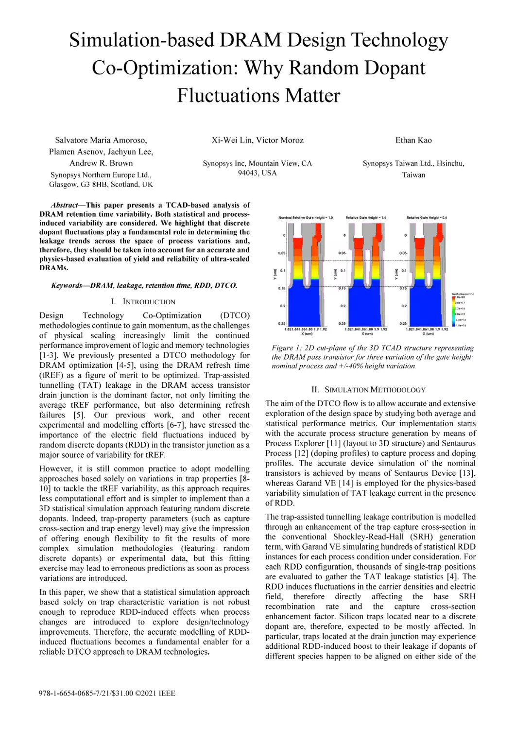
Figure 1: 2D cut-plane of the 3D TCAD structure representing
the DRAM pass transistor for three variation of the gate height:
nominal process and +/-40% height variation
II. SIMULATION METHODOLOGY
The aim of the DTCO flow is to allow accurate and extensive
exploration of the design space by studying both average and
statistical performance metrics. Our implementation starts
with the accurate process structure generation by means of
Process Explorer [11] (layout to 3D structure) and Sentaurus
Process [12] (doping profiles) to capture process and doping
profiles. The accurate device simulation of the nominal
transistors is achieved by means of Sentaurus Device [13],
whereas Garand VE [14] is employed for the physics-based
variability simulation of TAT leakage current in the presence
of RDD.
The trap-assisted tunnelling leakage contribution is modelled
through an enhancement of the trap capture cross-section in
the conventional Shockley-Read-Hall (SRH) generation
term, with Garand VE simulating hundreds of statistical RDD
instances for each process condition under consideration. For
each RDD configuration, thousands of single-trap positions
are evaluated to gather the TAT leakage statistics [4]. The
RDD induces fluctuations in the carrier densities and electric
field, therefore directly affecting the base SRH
recombination rate and the capture cross-section
enhancement factor. Silicon traps located near to a discrete
dopant are, therefore, expected to be mostly affected. In
particular, traps located at the drain junction may experience
additional RDD-induced boost to their leakage if dopants of
different species happen to be aligned on either side of the
ET [eV]
ET std dev [eV]
σT [cm2]
RDD
-0.20
0.05
10-15
No RDD 1
-0.24
0.05
10-14
No RDD 2
-0.29
0.05
5 × 10-14
No RDD 3
-0.31
0.05
10-13
Sim Type
Table 1: Simulation parameters for the case with RDD and for
three cases without RDD: parameters for the cases without
RDD are chosen to fit the RDD simulation results for the
nominal process split (i.e. relative gate height =1.0).
Figure 3: Fitting obtained with three sets of parameters, as
specified in Table I.
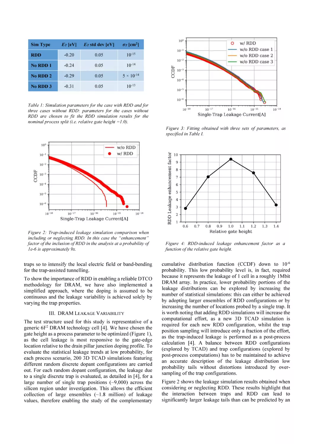
Figure 2: Trap-induced leakage simulation comparison when
including or neglecting RDD. In this case the “enhancement”
factor of the inclusion of RDD in the analysis at a probability of
1e-6 is approximately 9x.
traps so to intensify the local electric field or band-bending
for the trap-assisted tunnelling.
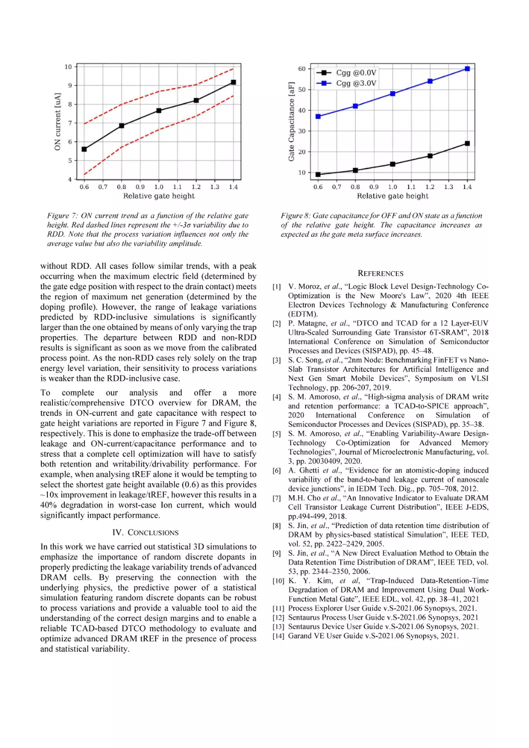
To show the importance of RDD in enabling a reliable DTCO
methodology for DRAM, we have also implemented a
simplified approach, where the doping is assumed to be
continuous and the leakage variability is achieved solely by
varying the trap properties.
III. DRAM LEAKAGE VARIABILITY
The test structure used for this study is representative of a
generic 6F2 DRAM technology cell [4]. We have chosen the
gate height as a process parameter to be optimized (Figure 1),
as the cell leakage is most responsive to the gate-edge
location relative to the drain pillar junction doping profile. To
evaluate the statistical leakage trends at low probability, for
each process scenario, 200 3D TCAD simulations featuring
different random discrete dopant configurations are carried
out. For each random dopant configuration, the leakage due
to a single discrete trap is evaluated, as detailed in [4], for a
large number of single trap positions (~9,000) across the
silicon region under investigation. This allows the efficient
collection of large ensembles (~1.8 million) of leakage
values, therefore enabling the study of the complementary
Figure 4: RDD-induced leakage enhancement factor as a
function of the relative gate height.
cumulative distribution function (CCDF) down to 10-6
probability. This low probability level is, in fact, required
because it represents the leakage of 1 cell in a roughly 1Mbit
DRAM array. In practice, lower probability portions of the
leakage distributions can be explored by increasing the
number of statistical simulations: this can either be achieved
by adopting larger ensembles of RDD configurations or by
increasing the number of locations probed by a single trap. It
is worth noting that adding RDD simulations will increase the
computational effort, as a new 3D TCAD simulation is
required for each new RDD configuration, whilst the trap
position sampling will introduce only a fraction of the effort,
as the trap-induced leakage is performed as a post-process
calculation [4]. A balance between RDD configurations
(explored by TCAD) and trap configurations (explored by
post-process computations) has to be maintained to achieve
an accurate description of the leakage distribution low
probability tails without distortions introduced by oversampling of the trap configurations.
Figure 2 shows the leakage simulation results obtained when
considering or neglecting RDD. These results highlight that
the interaction between traps and RDD can lead to
significantly larger leakage tails than can be predicted by an
Figure 6: Leakage current extracted at 10-6 CCDF probability
for the simulation scenarios reported in Table I across the
space of process variations. The probability level 10-6 is chosen
because it represents the leakage of 1 cell in a roughly 1Mbit
DRAM array.
Figure 5: 3D TCAD simulation without (top) and with (bottom)
random discrete dopants, highlighting one of the extreme
devices with highest leakage. In this case the RDD
configuration brings the effective p-n junction down towards
the bottom of the pillar, with maximum electric field in
proximity to the discrete trap.
approach based on continuous doping. Large leakage tails
will, in turn, degrade bitcell yield (in terms of retention time).
The simulation results for the case without RDD highlight
that the tail is bounded with a factor-of-10 lower leakage than
the RDD case.
Our results show, therefore, that RDD has a non-negligible
impact on the leakage distribution tails. Nevertheless, the
reader may wonder if one could just use a simplified approach
relying solely on the trap energy level and trap capture crosssection as variability parameters, neglecting the random
discrete dopants, yet achieving the same leakage distribution
obtained by RDD-inclusive simulation. Such an approach can
be, indeed, motivated by the reduced computational effort
required to explore solely trap properties variations.
In Figure 3 we show that one could reproduce (in the explored
range of probabilities and for the specific process split) the
RDD+trap-induced leakage variations without the need of
including RDD into the TCAD simulation. In this case, there
are virtually infinite possible combinations of trap energy and
cross-section that are able to fit the RDD+trap-induced
leakage data. In Table 1 we are arbitrarily choosing 3 possible
combinations of cross-section and energy variations that are
within the reasonably physics-based range expected for
Silicon traps. This arbitrary choice already highlights a first
issue affecting a simplified (RDD-free) approach, as
connection with the underlying trap physics is, inevitably lost
and trap properties become merely fitting parameters, which
lowers the simulation prediction quality. This, nonetheless, is
a minor issue when compared to the second predictability
issue related to process variation exploration. To highlight
this, we have performed statistical simulations with and
without RDD across the space of gate height process splits
and measured how the leakage enhancement due to RDD
responds to these process variations. Figure 4 shows the
leakage enhancement factor (LEF), calculated as the ratio
between the leakage with and without RDD at a probability
of 10-6, as a function of the gate height process variation:
,
=
,
≝ 10
≝ 10
The trend is clearly non-linear, and this behaviour can be
understood by considering the gate edge position with respect
to the drain pillar doping. In fact, the closer the gate edge is
to the high doping regions, the higher the impact of random
dopants on enhancing the leakage current (see Figure 5).
However, as the doping increases, the screening length
decreases and, therefore, the RDD-induced electric field
peaks are reduced, thus diminishing the RDD-induced
electric field impact. Based on these results, we can expect
that the arbitrary fitting obtained in Figure 3, cannot
adequately hold true across multiple process splits.
To further confirm this, we have performed statistical
simulations for the three fitting scenarios reported in Table 1
for all process points. Figure 6 shows the leakage current
value at a probability of 10-6, comparing the results with and
Figure 7: ON current trend as a function of the relative gate
height. Red dashed lines represent the +/-3σ variability due to
RDD. Note that the process variation influences not only the
average value but also the variability amplitude.
without RDD. All cases follow similar trends, with a peak
occurring when the maximum electric field (determined by
the gate edge position with respect to the drain contact) meets
the region of maximum net generation (determined by the
doping profile). However, the range of leakage variations
predicted by RDD-inclusive simulations is significantly
larger than the one obtained by means of only varying the trap
properties. The departure between RDD and non-RDD
results is significant as soon as we move from the calibrated
process point. As the non-RDD cases rely solely on the trap
energy level variation, their sensitivity to process variations
is weaker than the RDD-inclusive case.
To complete our analysis and offer a more
realistic/comprehensive DTCO overview for DRAM, the
trends in ON-current and gate capacitance with respect to
gate height variations are reported in Figure 7 and Figure 8,
respectively. This is done to emphasize the trade-off between
leakage and ON-current/capacitance performance and to
stress that a complete cell optimization will have to satisfy
both retention and writability/drivability performance. For
example, when analysing tREF alone it would be tempting to
select the shortest gate height available (0.6) as this provides
~10x improvement in leakage/tREF, however this results in a
40% degradation in worst-case Ion current, which would
significantly impact performance.
IV. CONCLUSIONS
In this work we have carried out statistical 3D simulations to
emphasize the importance of random discrete dopants in
properly predicting the leakage variability trends of advanced
DRAM cells. By preserving the connection with the
underlying physics, the predictive power of a statistical
simulation featuring random discrete dopants can be robust
to process variations and provide a valuable tool to aid the
understanding of the correct design margins and to enable a
reliable TCAD-based DTCO methodology to evaluate and
optimize advanced DRAM tREF in the presence of process
and statistical variability.
Figure 8: Gate capacitance for OFF and ON state as a function
of the relative gate height. The capacitance increases as
expected as the gate meta surface increases.
REFERENCES
[1]
[2]
[3]
[4]
[5]
[6]
[7]
[8]
[9]
[10]
[11]
[12]
[13]
[14]
V. Moroz, et al., “Logic Block Level Design-Technology CoOptimization is the New Moore's Law”, 2020 4th IEEE
Electron Devices Technology & Manufacturing Conference
(EDTM).
P. Matagne, et al., “DTCO and TCAD for a 12 Layer-EUV
Ultra-Scaled Surrounding Gate Transistor 6T-SRAM”, 2018
International Conference on Simulation of Semiconductor
Processes and Devices (SISPAD), pp. 45–48.
S. C. Song, et al., “2nm Node: Benchmarking FinFET vs NanoSlab Transistor Architectures for Artificial Intelligence and
Next Gen Smart Mobile Devices”, Symposium on VLSI
Technology, pp. 206-207, 2019.
S. M. Amoroso, et al., “High-sigma analysis of DRAM write
and retention performance: a TCAD-to-SPICE approach”,
2020 International Conference on Simulation of
Semiconductor Processes and Devices (SISPAD), pp. 35–38.
S. M. Amoroso, et al., “Enabling Variability-Aware DesignTechnology Co-Optimization for Advanced Memory
Technologies”, Journal of Microelectronic Manufacturing, vol.
3, pp. 20030409, 2020.
A. Ghetti et al., “Evidence for an atomistic-doping induced
variability of the band-to-band leakage current of nanoscale
device junctions”, in IEDM Tech. Dig., pp. 705–708, 2012.
M.H. Cho et al., “An Innovative Indicator to Evaluate DRAM
Cell Transistor Leakage Current Distribution”, IEEE J-EDS,
pp.494-499, 2018.
S. Jin, et al., “Prediction of data retention time distribution of
DRAM by physics-based statistical Simulation”, IEEE TED,
vol. 52, pp. 2422–2429, 2005.
S. Jin, et al., “A New Direct Evaluation Method to Obtain the
Data Retention Time Distribution of DRAM”, IEEE TED, vol.
53, pp. 2344–2350, 2006.
K. Y. Kim, et al, “Trap-Induced Data-Retention-Time
Degradation of DRAM and Improvement Using Dual WorkFunction Metal Gate”, IEEE EDL, vol. 42, pp. 38–41, 2021
Process Explorer User Guide v.S-2021.06 Synopsys, 2021.
Sentaurus Process User Guide v.S-2021.06 Synopsys, 2021
Sentaurus Device User Guide v.S-2021.06 Synopsys, 2021.
Garand VE User Guide v.S-2021.06 Synopsys, 2021.