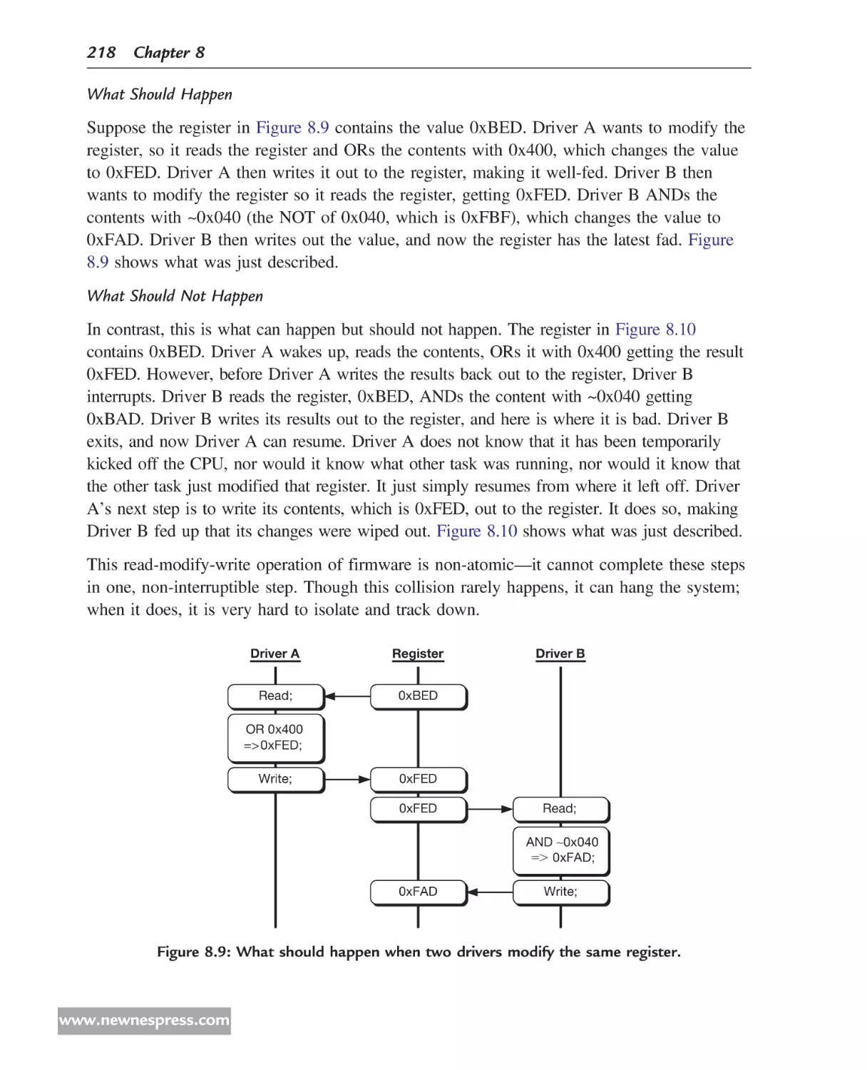
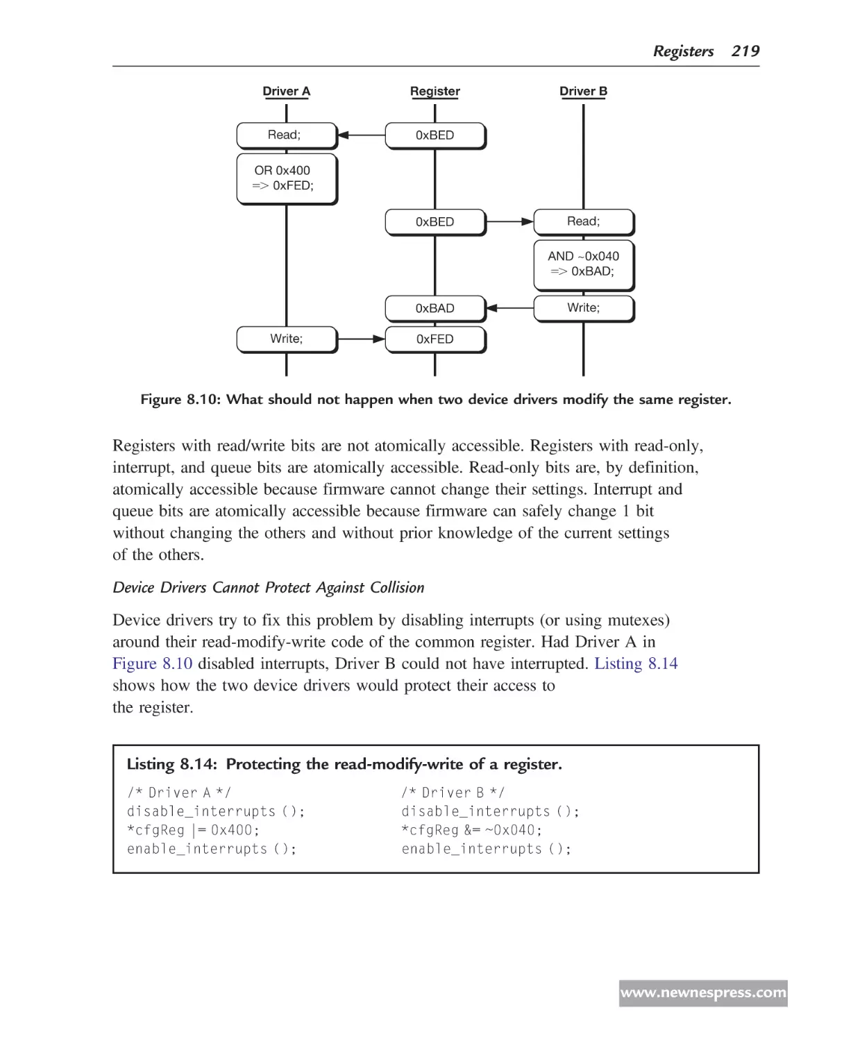
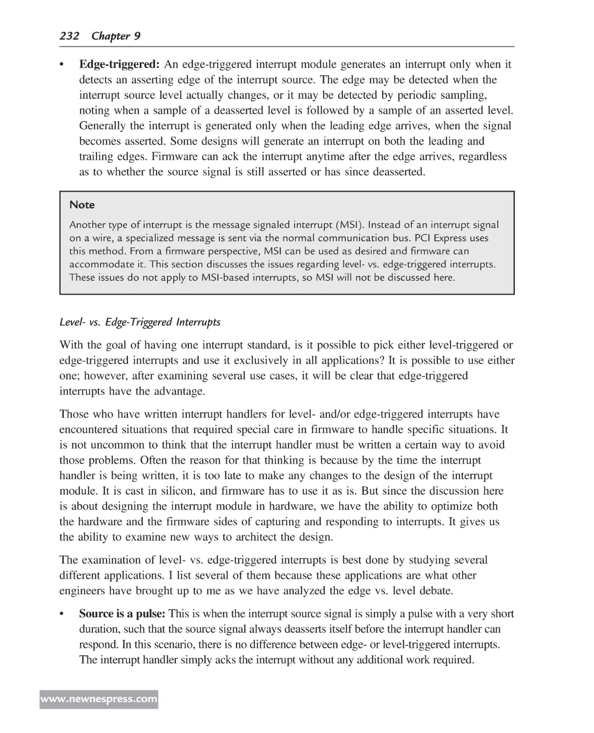
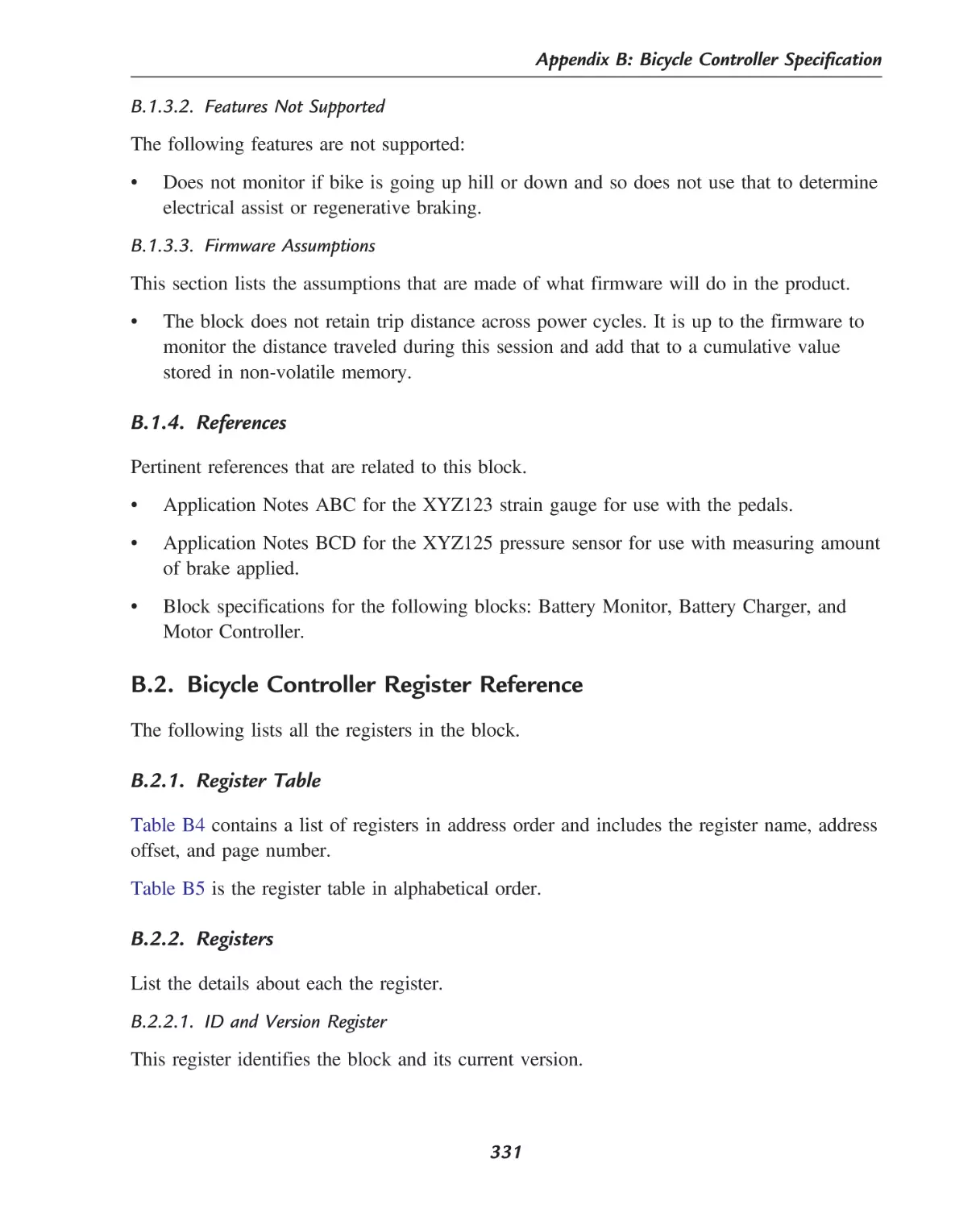
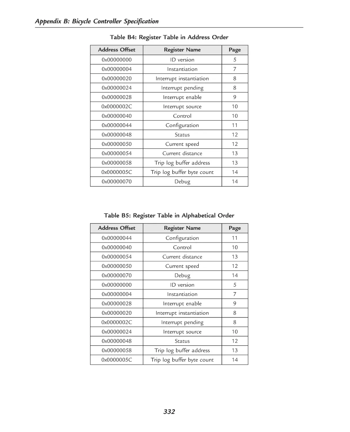
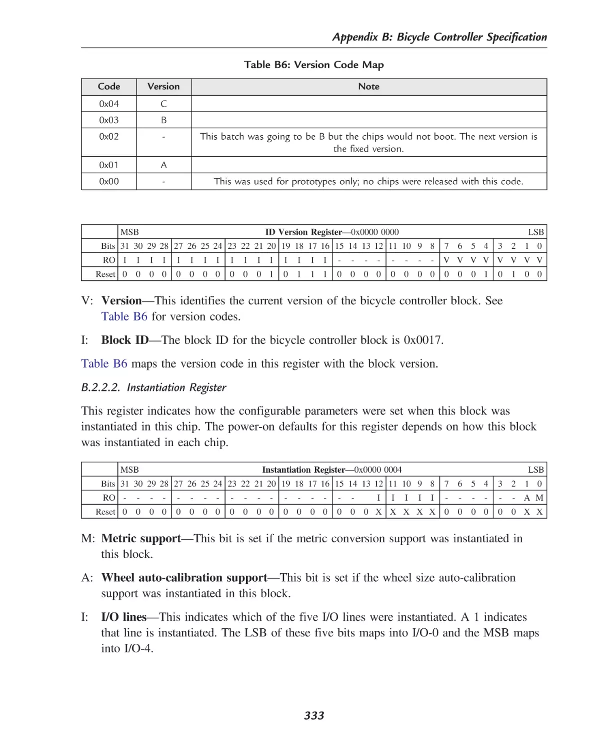
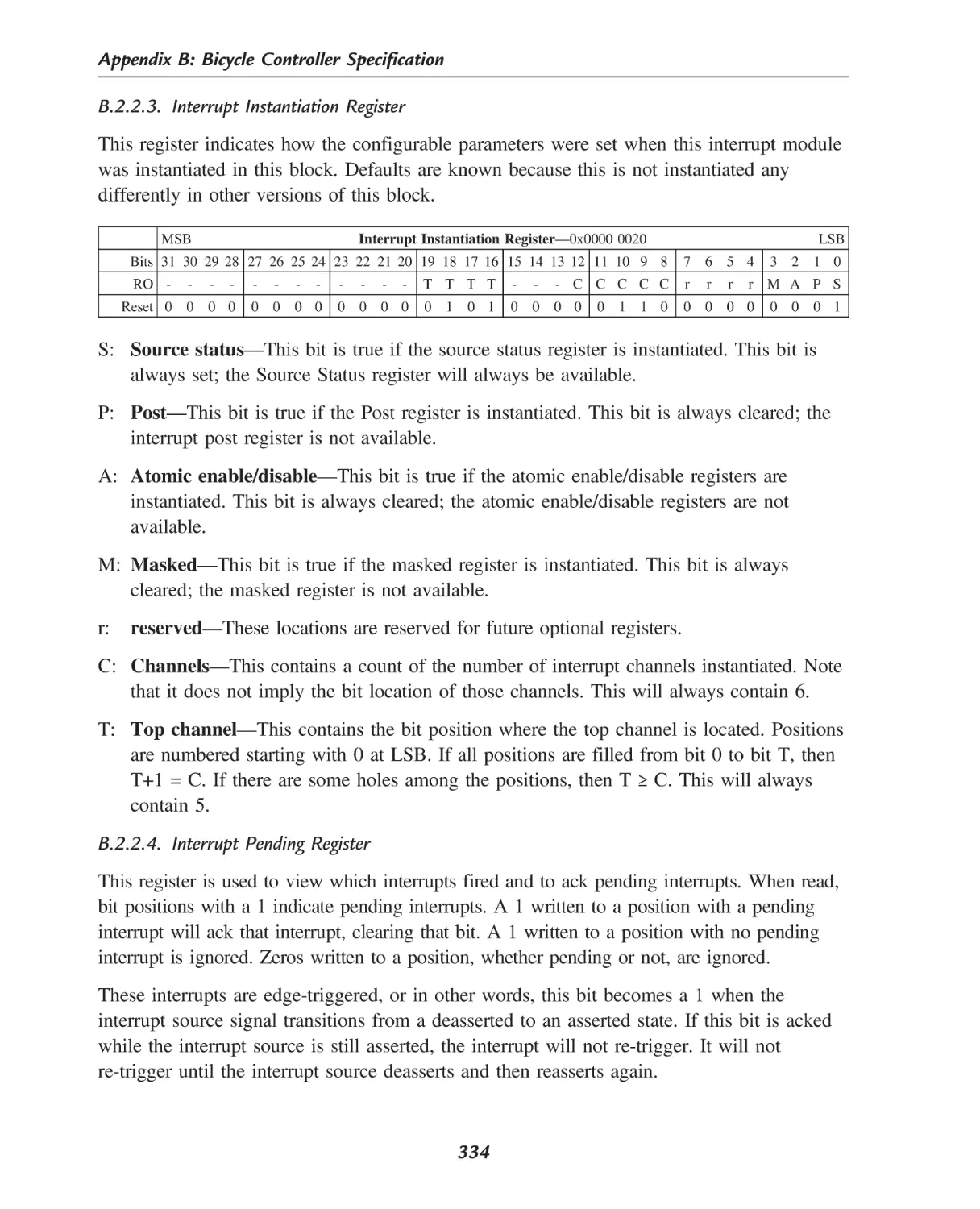
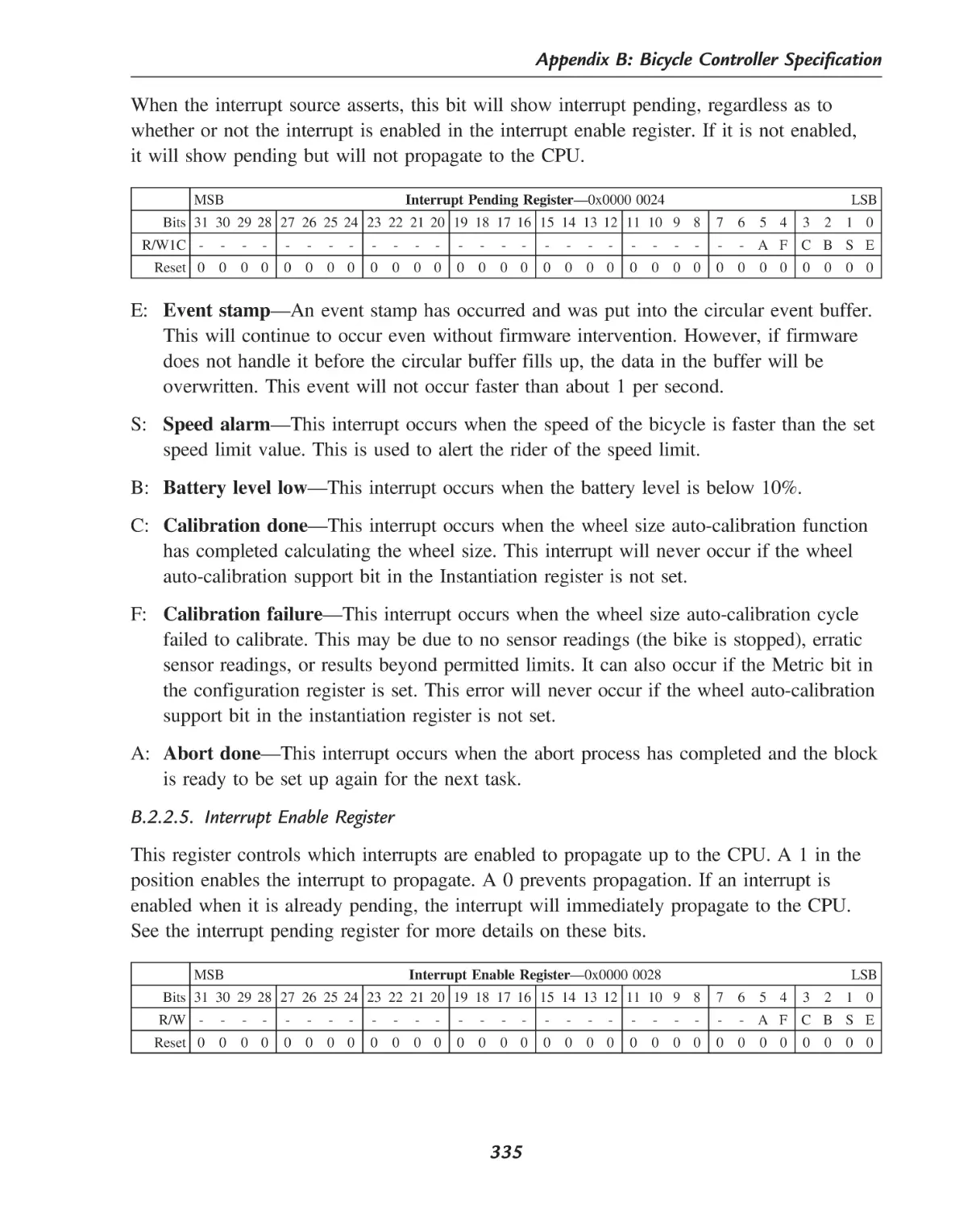
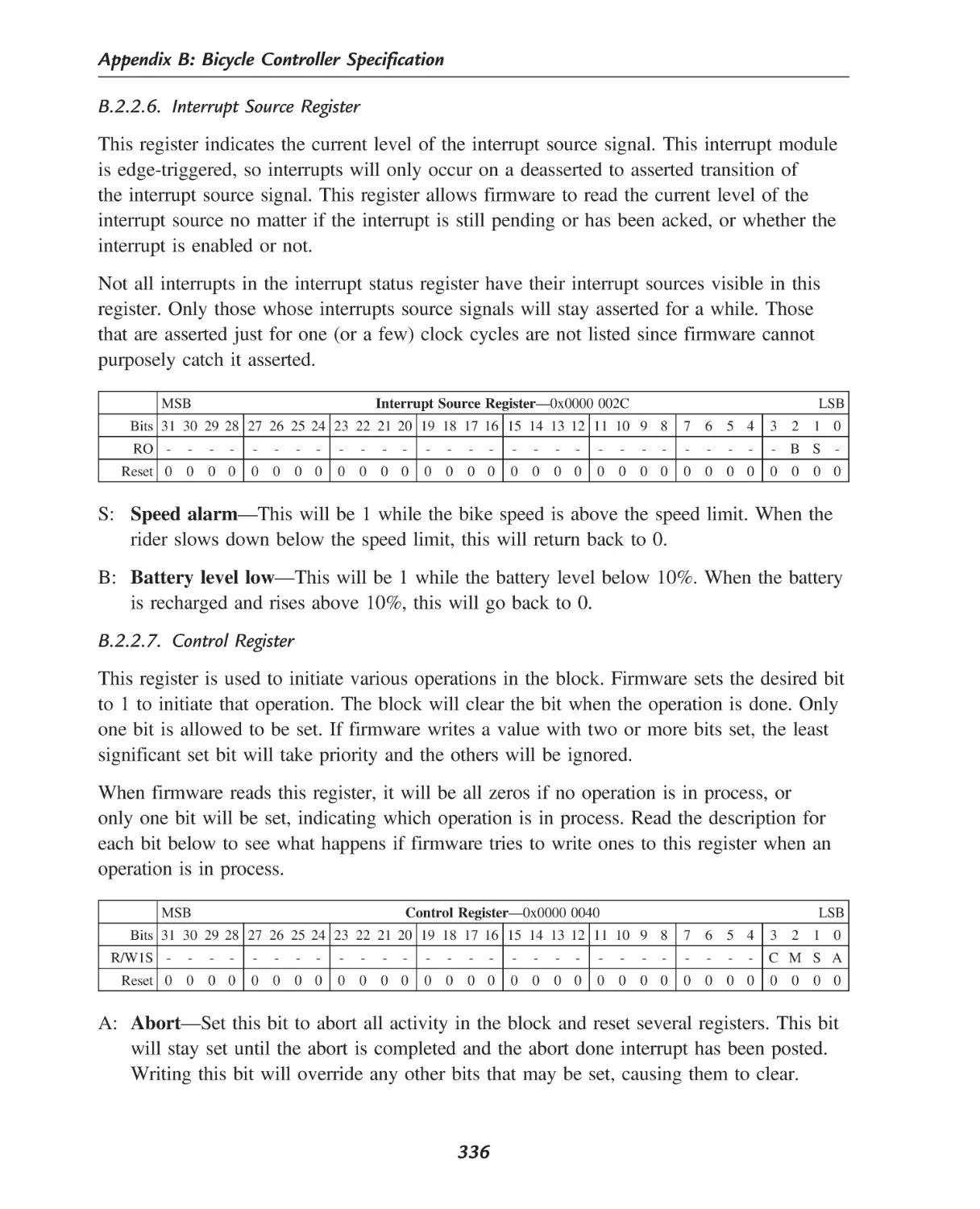
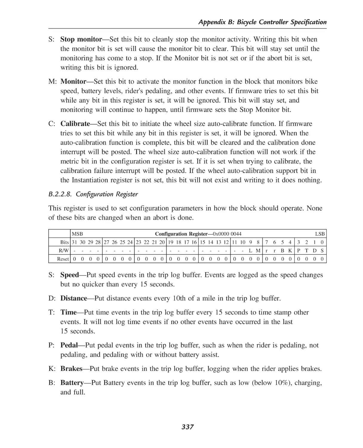
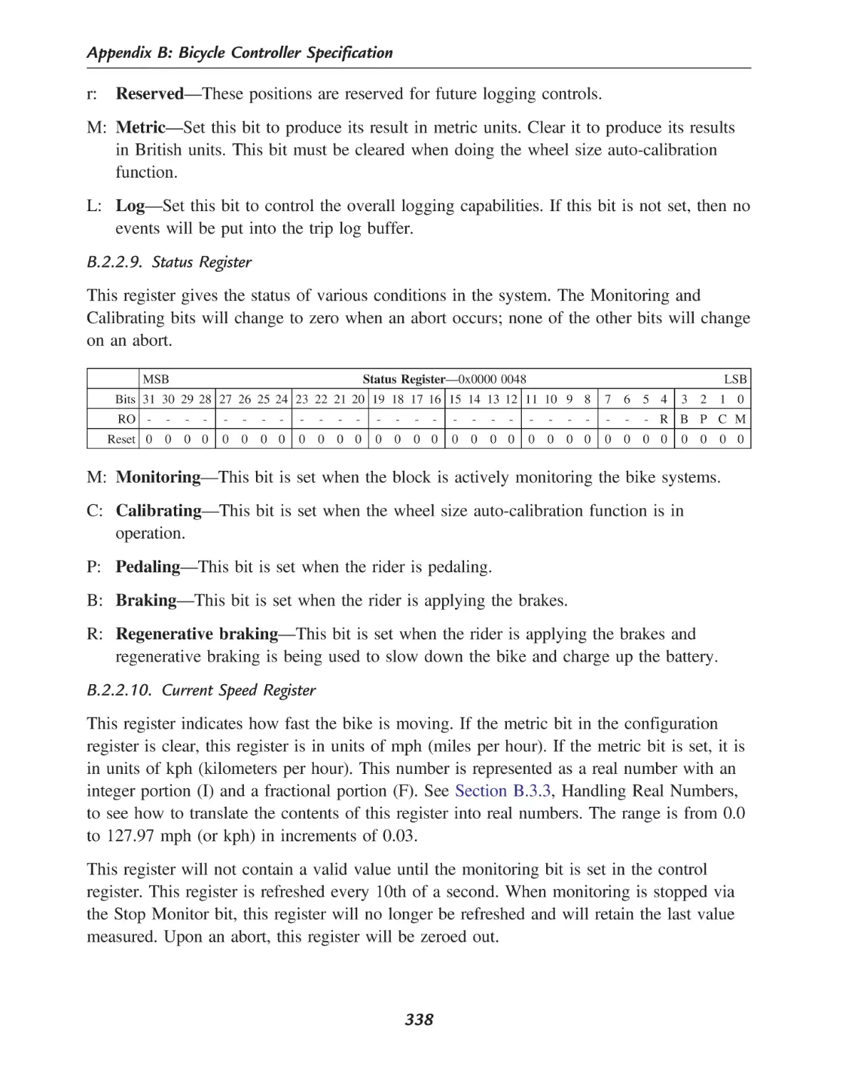
/


Text
Newnes is an imprint of Elsevier
30 Corporate Drive, Suite 400, Burlington, MA 01803, USA
The Boulevard, Langford Lane, Kidlington, Oxford, OX5 1GB, UK
Copyright © 2010 by Elsevier Inc. All rights reserved.
No part of this publication may be reproduced or transmitted in any form or by any means,
electronic or mechanical, including photocopying, recording, or any information storage and
retrieval system, without permission in writing from the publisher. Details on how to seek
permission, further information about the Publisher’s permissions policies and our arrangements
with organizations such as the Copyright Clearance Center and the Copyright Licensing Agency,
can be found at our website: www.elsevier.com/permissions.
This book and the individual contributions contained in it are protected under copyright by
the Publisher (other than as may be noted herein).
Notices
Knowledge and best practice in this field are constantly changing. As new research and experience
broaden our understanding, changes in research methods, professional practices, or medical
treatment may become necessary.
Practitioners and researchers must always rely on their own experience and knowledge in
evaluating and using any information, methods, compounds, or experiments described herein. In
using such information or methods they should be mindful of their own safety and the safety
of others, including parties for whom they have a professional responsibility.
To the fullest extent of the law, neither the Publisher nor the authors, contributors, or editors,
assume any liability for any injury and/or damage to persons or property as a matter of products
liability, negligence or otherwise, or from any use or operation of any methods, products,
instructions, or ideas contained in the material herein.
Library of Congress Cataloging-in-Publication Data
Application Submitted.
British Library Cataloguing-in-Publication Data
A catalogue record for this book is available from the British Library.
ISBN: 978-1-85617-605-7
For information on all Newnes publications
visit our Web site at www.elsevierdirect.com
Typeset by diacriTech, Chennai, India
Printed in the United States of America
08 09 10 10 9 8 7 6 5 4 3 2 1
Preface
You can find books written by hardware engineers teaching hardware engineers how to
design hardware. You can find books written by firmware engineers teaching firmware
engineers how to write firmware. This book is written by a firmware engineer but is
directed primarily to hardware engineers.
Many engineers have experienced problems when trying to get firmware working on
hardware. They are designed generally in isolation from each other and then are expected to
work when brought together. But problems and defects appear. At times it is unknown
where the defect is located—in hardware or firmware, or maybe the documentation.
There is very little written about how to get hardware and firmware to work well together.
This book attempts to fill that niche. It addresses the interface between the hardware and
firmware domains and provides practices that will reduce the time and effort required to
produce an embedded systems product. It covers all aspects of development surrounding the
hardware/firmware interface, including the process of development, the high-level design,
and the detailed design.
A key feature of this book are the 300+ Best Practices that give detailed instructions for
various aspects of the development process and design. These best practices apply perfectly,
but only for a given situation. They should be scrutinized for applicability in a given
situation. Throughout this book, the emphasis is for engineers to develop their own set of
best practices. They may start with these 300, but the set should evolve to be made their
own, as this increases the likelihood of success within their organization.
To help engineers understand the 300+ Best Practices, and to help them create their own
set, Seven Principles are presented that provide overarching guidelines and direction. These
principles, when internalized, will help engineers work in the right direction, even if there is
no specific best practice for that situation. Following the Seven Principles and 300+ Best
Practices will improve the design teams’ ability to produce successful embedded systems
products.
© 2010 by Elsevier Inc. All rights reserved.
x
Preface
Chapter Summaries
The following chapter summaries provide an overview of the book and help the reader to
navigate through the book.
1. Introduction: This chapter establishes the foundation for the book. It discusses various
types of hardware and how they impact the hardware/firmware interface. It defines
principles and best practices, the target audience, and the product life cycle. It also
presents a case study used throughout the book.
2. Principles: This chapter presents the Seven Principles and provides a high-level view
and reasoning for the direction of this book. Understanding these principles is key to
understanding why the best practices are stated as they are.
3. Collaboration: Of key importance to the success of an embedded product is the proper
and sufficient collaboration between hardware and firmware engineers. This chapter
defines roles and processes in such an effort.
4. Planning: Before starting a project, planning must be done to determine and agree what
direction should be taken with the new product. This chapter covers several areas that
should be visited when planning a new project.
5. Documentation: Most engineers assigned to write documentation do not like the task.
And most engineers reading documentation get frustrated with incomplete and incorrect
documentation. This chapter discusses the types of documentation, when to write them,
how to review them, and what types of details to include in them.
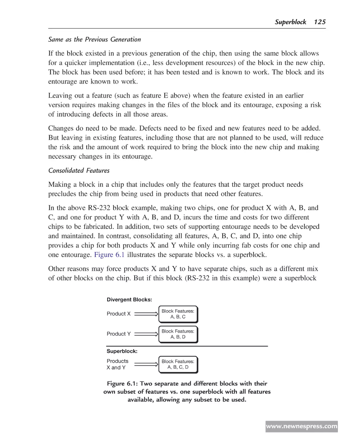
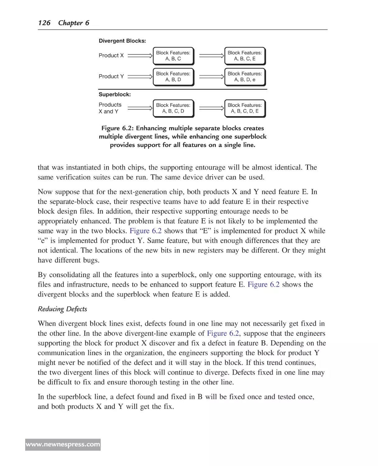
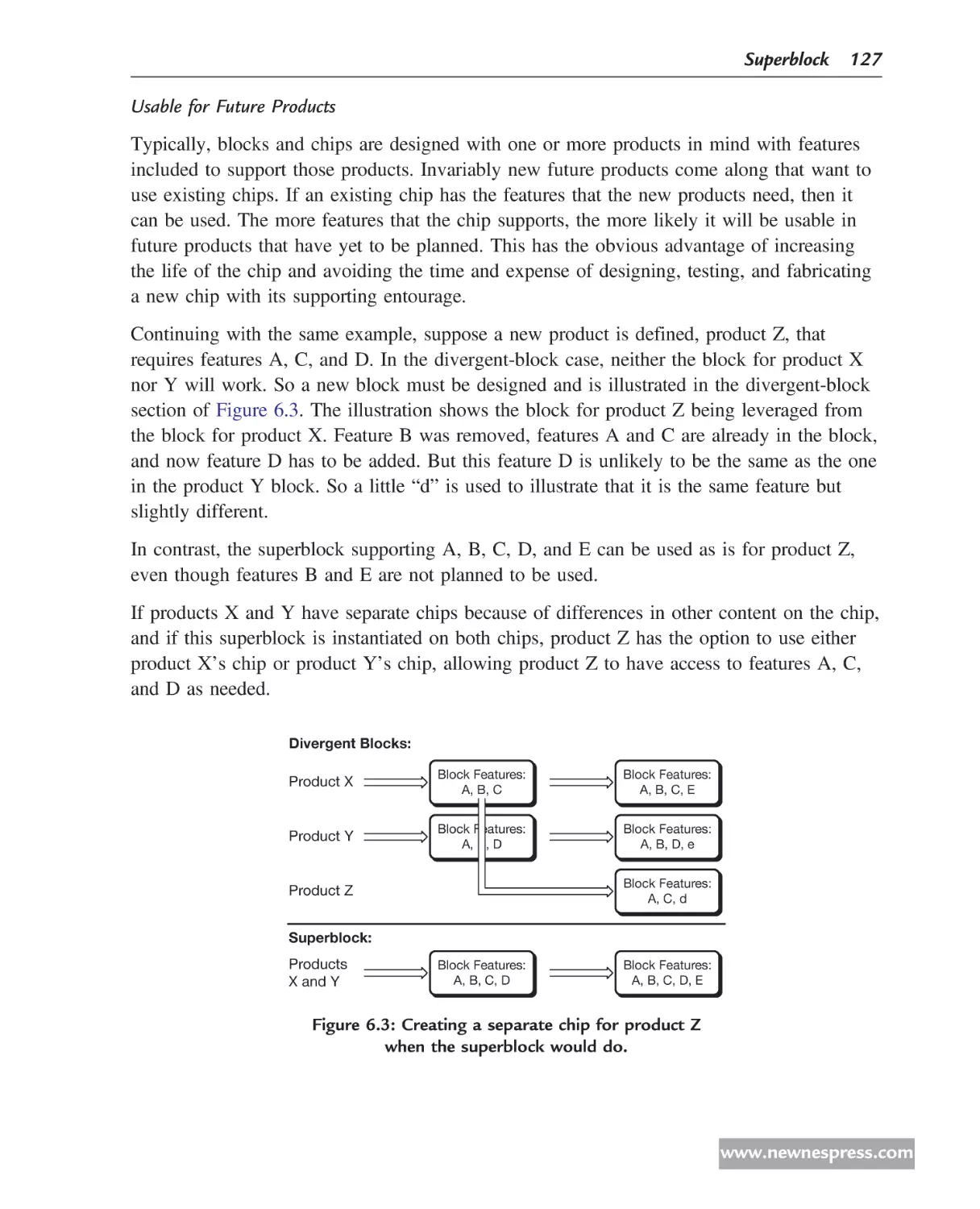
6. Superblock: This chapter introduces the concept of a block that can do everything
within its own domain. It discusses why a superblock is good and how to set it up to be
used where needed. But it also discusses the reality of practical limitations and how to
handle those.
7. Design: Various design aspects are discussed in this chapter, such as events, power-on
sequences, communication, and control.
8. Registers: Registers are the fundamental interface between hardware and firmware. This
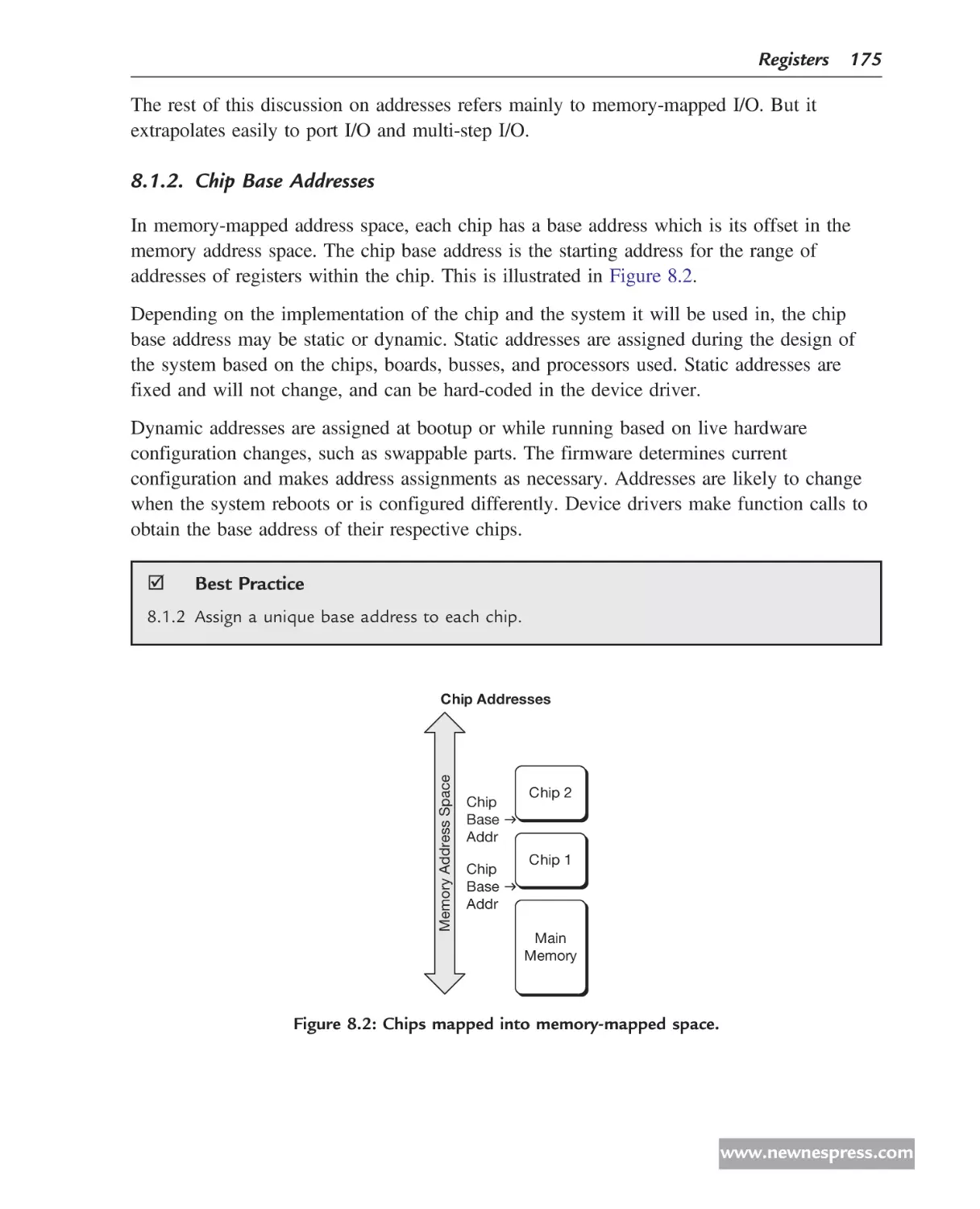
chapter discusses them in great detail, including addresses, bit locations, and types of bits.
9. Interrupts: Given a lack of consistency among interrupt designs used in the industry,
this chapter focuses in great detail how interrupts from hardware into firmware should
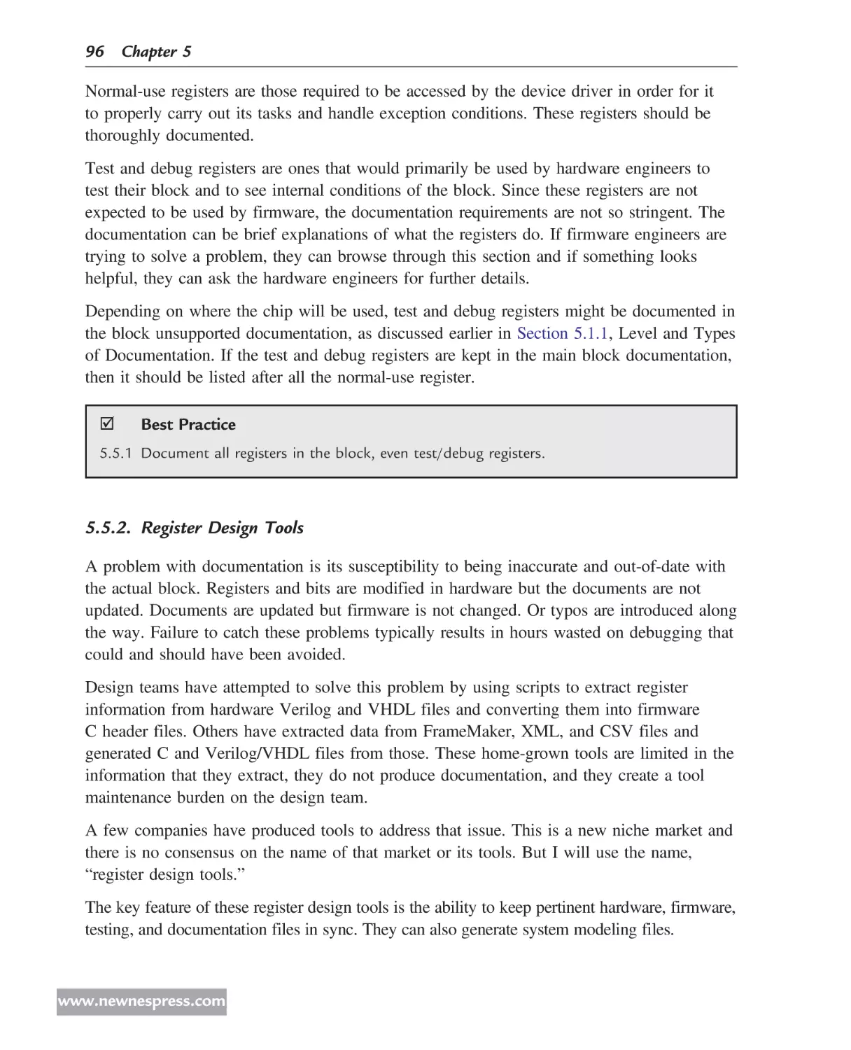
be managed. This chapter also contains a proposal for an interrupt standard and
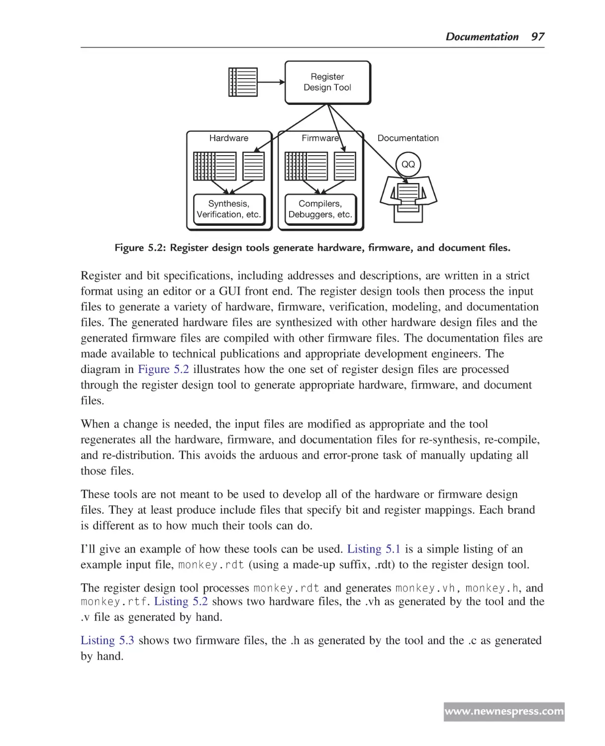
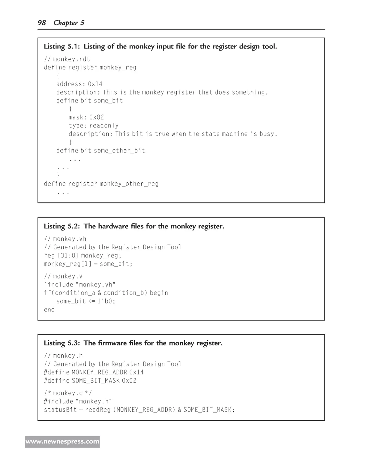
discusses the proposal in detail.
10. Aborts, etc.: Too often very little thought is given to errors and how to recover from
them. This chapter discusses design elements necessary to allow firmware to abort
hardware operations, recover, and resume processing.
© 2010 by Elsevier Inc. All rights reserved.
xi
Preface
11. Hooks: Logic analyzers cannot probe the internals of a chip but knowledge of what is
occurring inside is important when trying to get firmware working on hardware. Having
firmware-accessible hooks inside the chip allows firmware to retrieve information for
engineering analysis. This chapter contains many possible hooks that could be included.
12. Conclusion: This chapter wraps up the book. It also contains a couple of cartoon
illustrations used to help illustrate the concepts in the book.
Appendices
A. Best Practices: This appendix collects all the best practices in the book into
one place.
B. Block Specification: This appendix is a documentation template as explained and
described in Chapter 5, Documentation.
C. Using This Book in a University: This appendix provides suggestions on how to
use this book to teach hardware and firmware engineering students that have to
work together on a project.
D. Glossary: Given that this book addresses two different engineering disciplines,
hardware and firmware engineering, it covers terms from one domain that might
not be understood by the other.
Conventions Used in This Book
The bulk of the text in this book discusses the concept at hand. Interspersed in the text are
one or more of these elements: figures, listings, register maps, best practices, and tales from
the trenches.
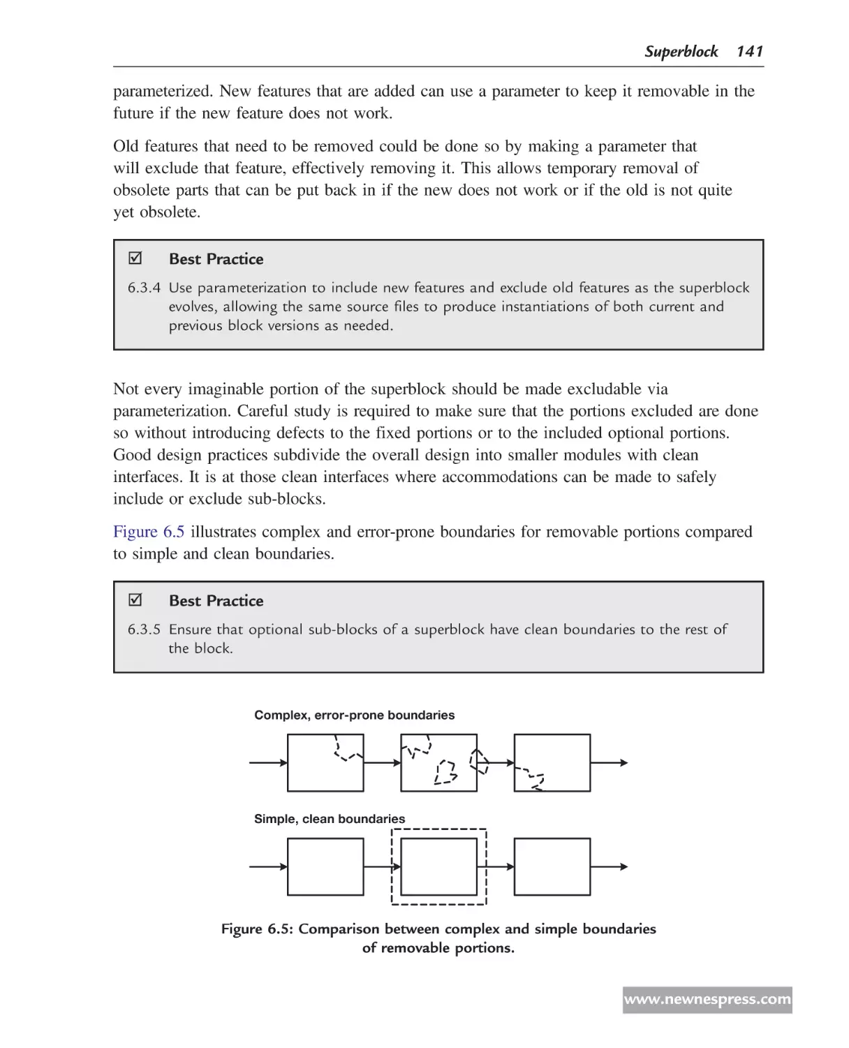
Figures
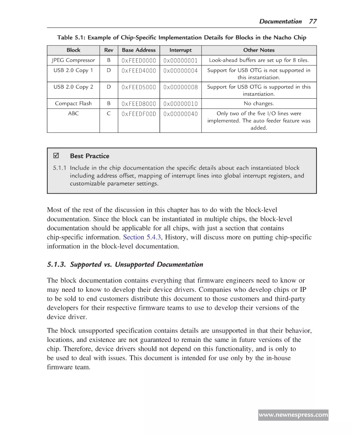
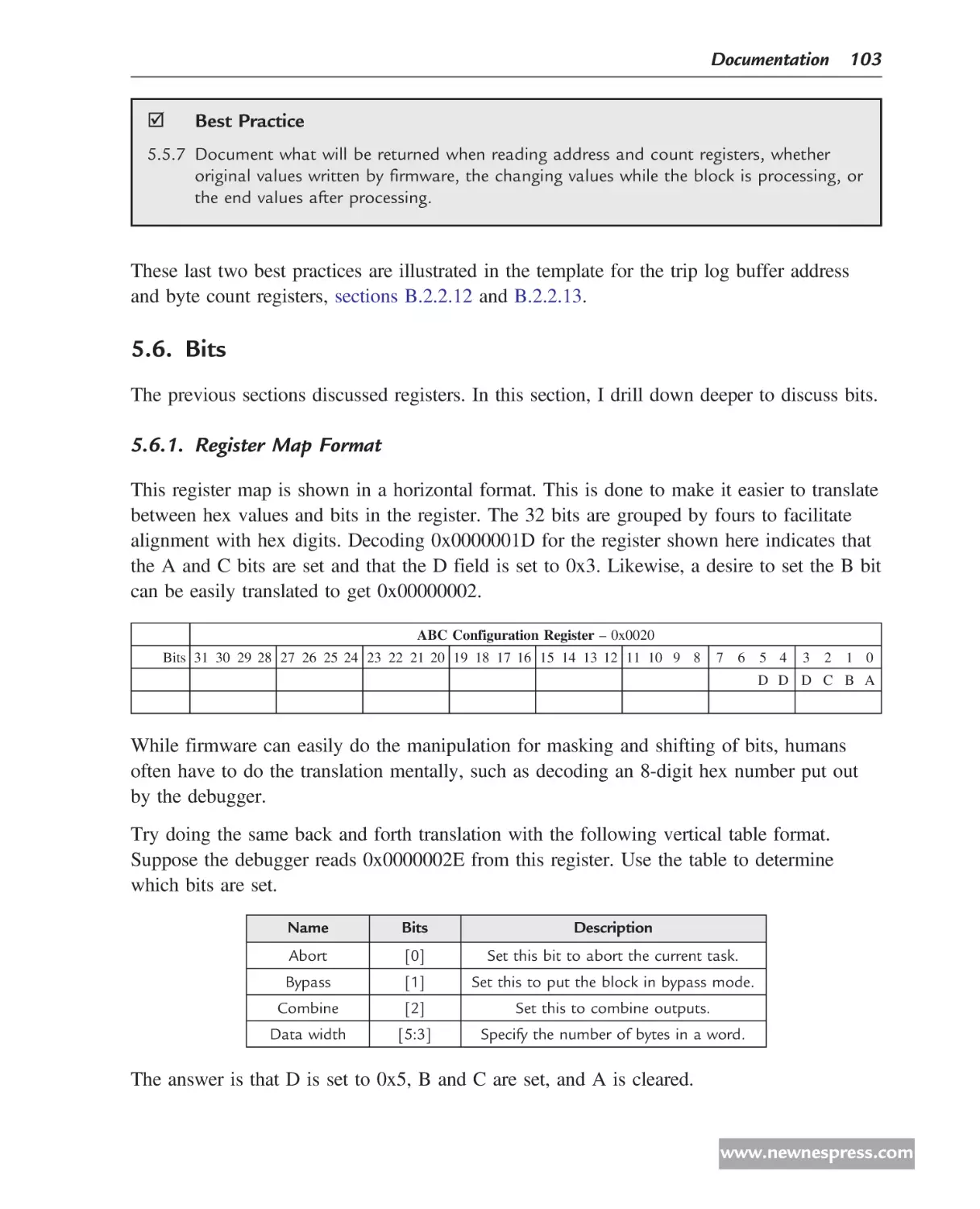
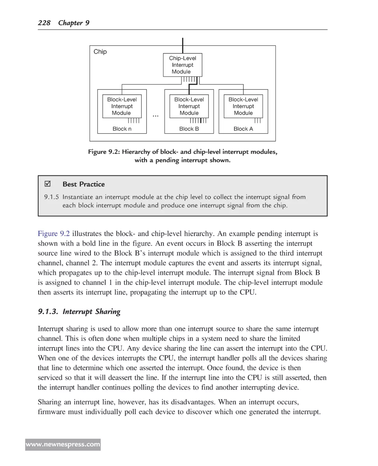
Figure 0.1 is an example figure.
Firmware Listings
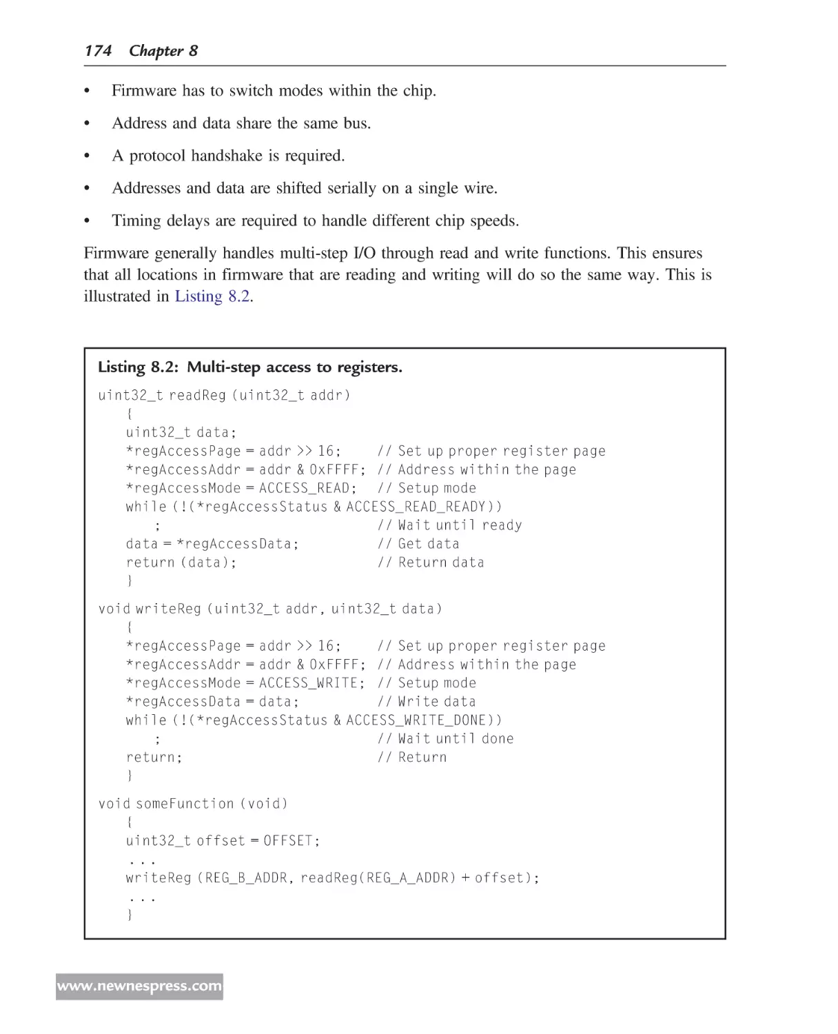
Listing 0.1 shows an example listing of firmware source code written in C.
A
B
C
Figure 0.1: Example figure.
© 2010 by Elsevier Inc. All rights reserved.
xii
Preface
Listing 0.1: Example C code listing.
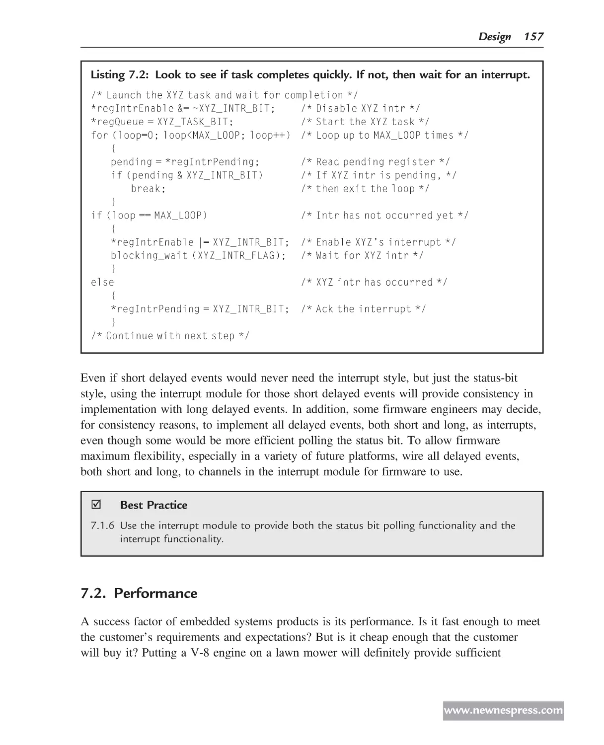
/* Read the current list of pending interrupts */
interrupts = *interruptRegister;
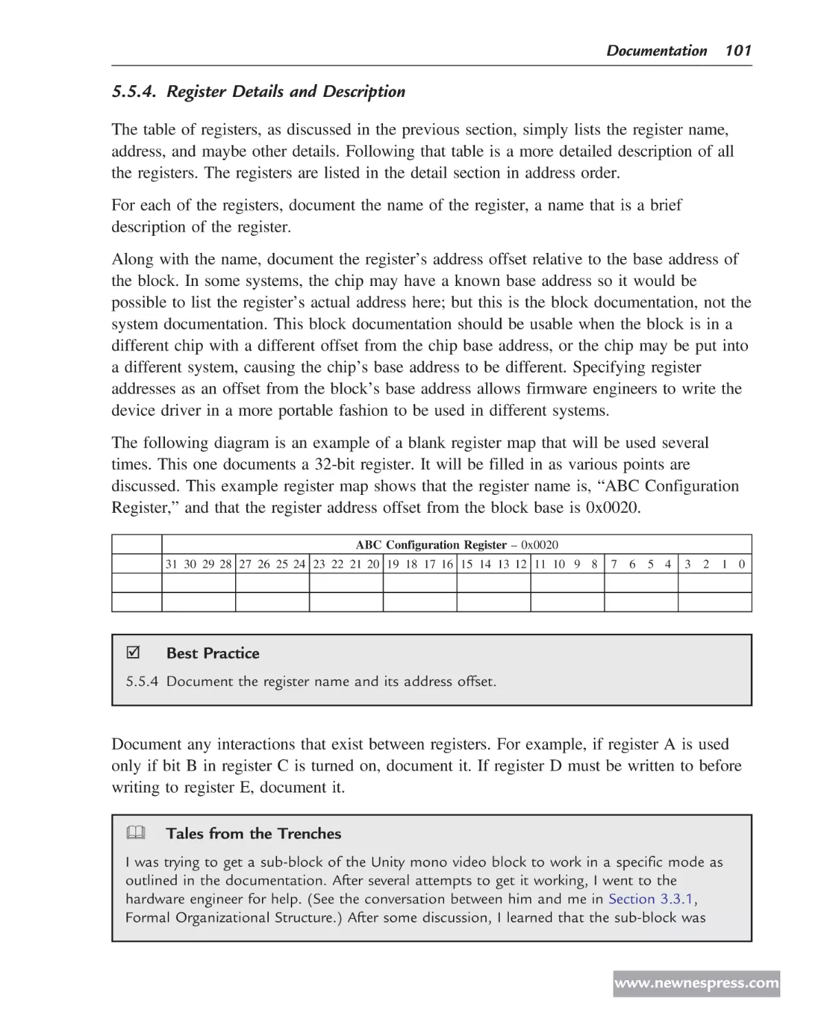
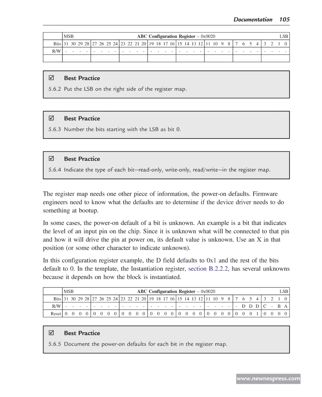
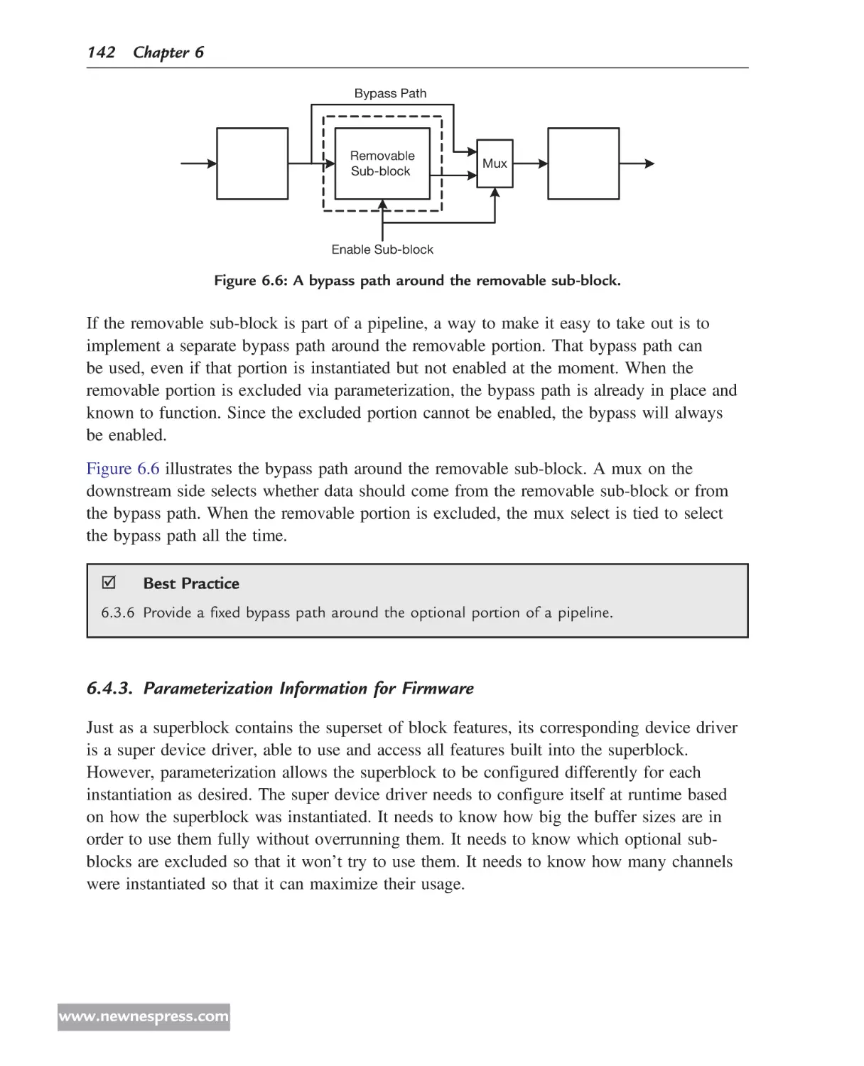
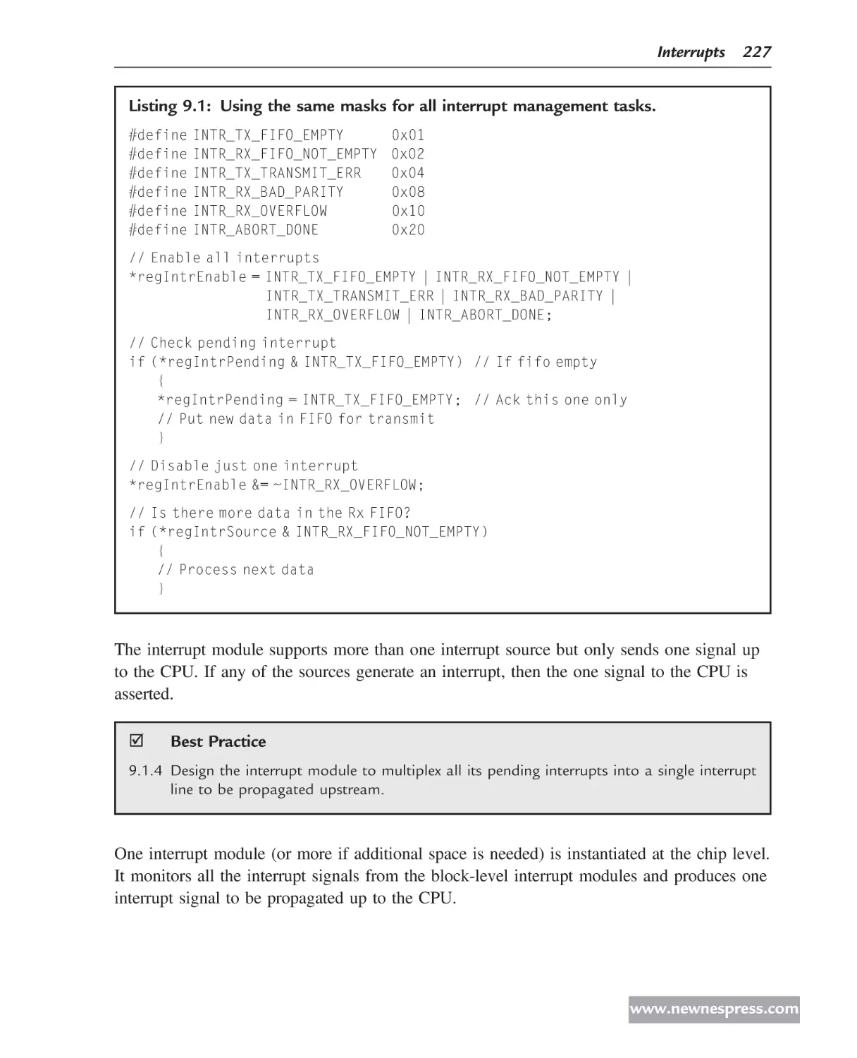
Hardware Circuits
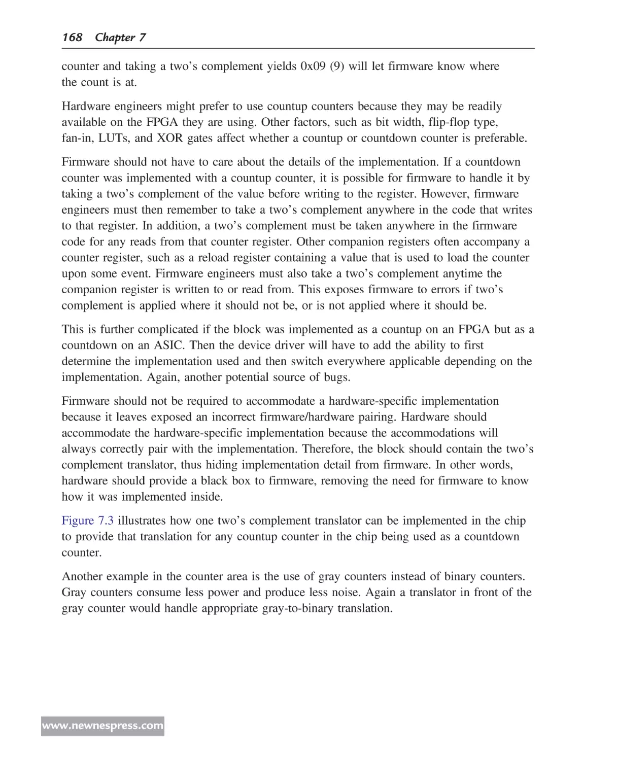
A few hardware circuits are illustrated in the book. Both a schematic drawing and its
equivalent Verilog listing will be given. Figure 0.2 is the schematic and Listing 0.2 is the
corresponding Verilog code for an example circuit.
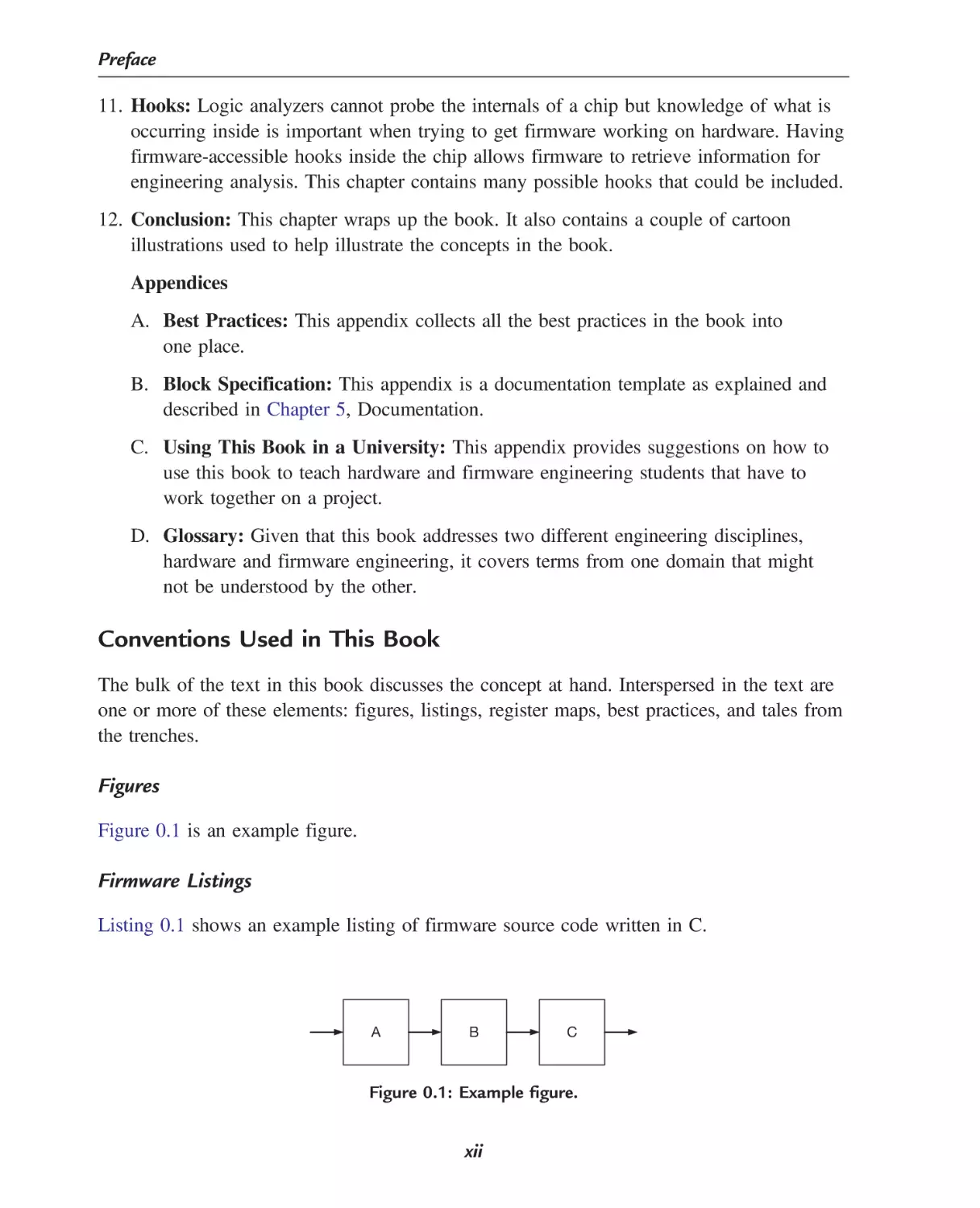
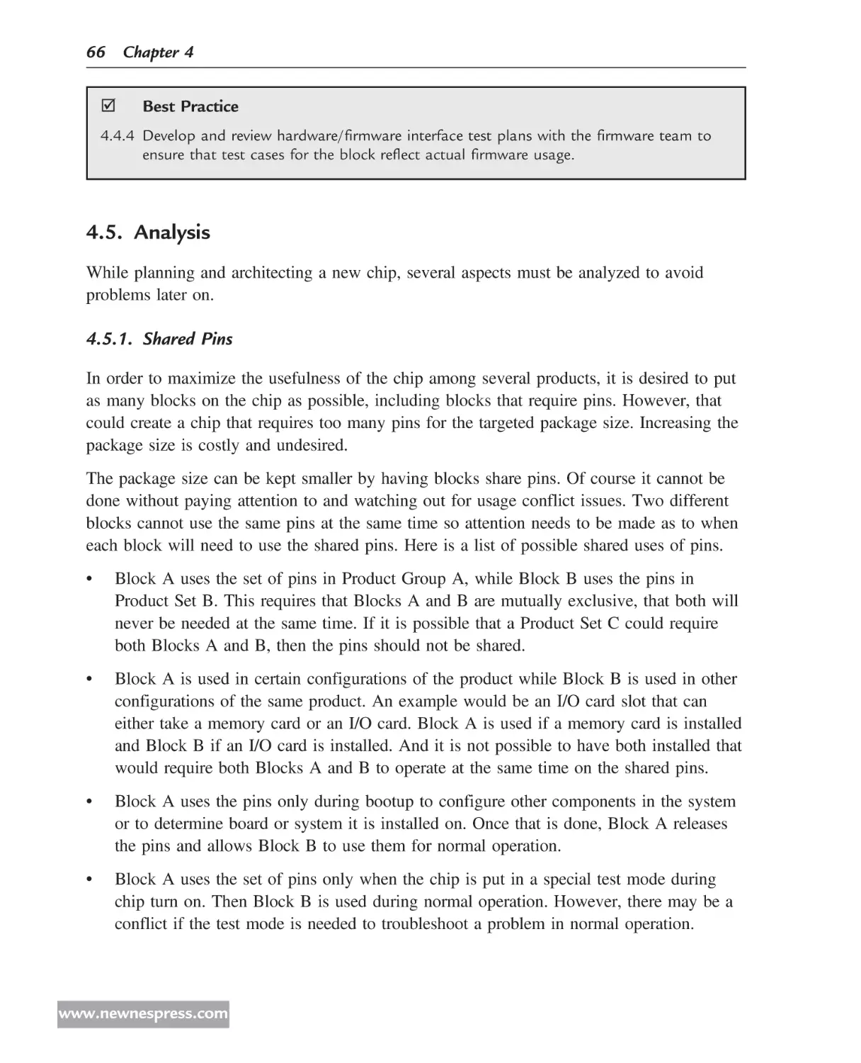
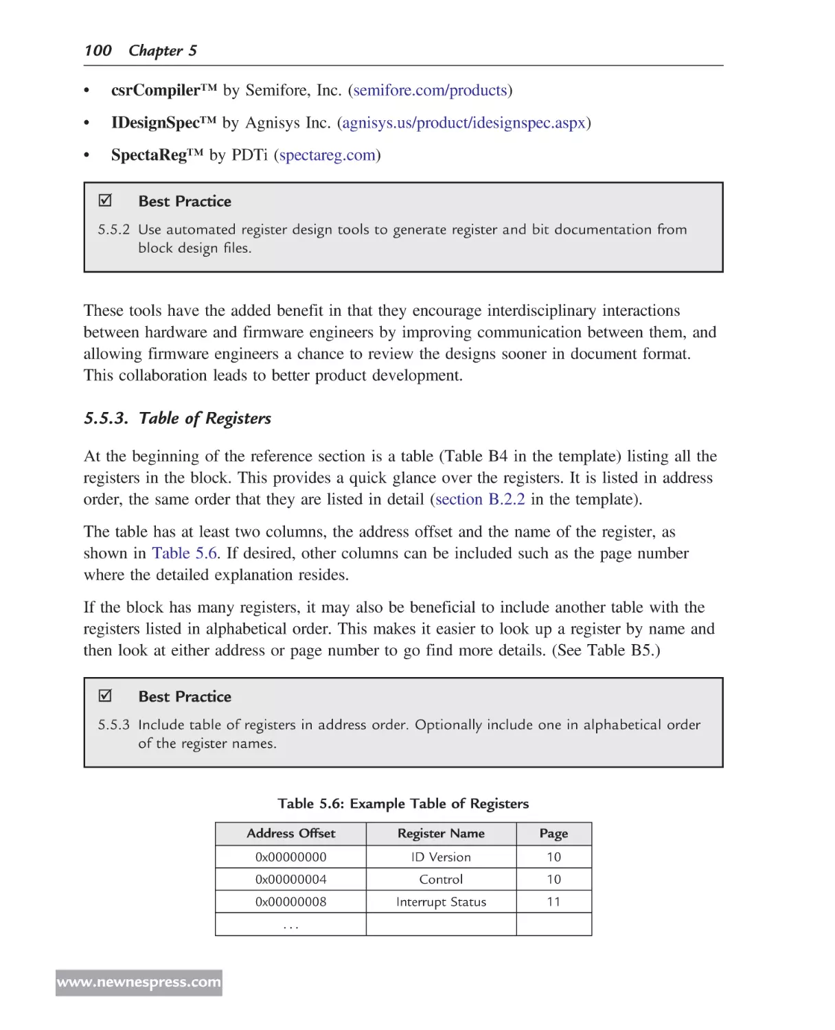
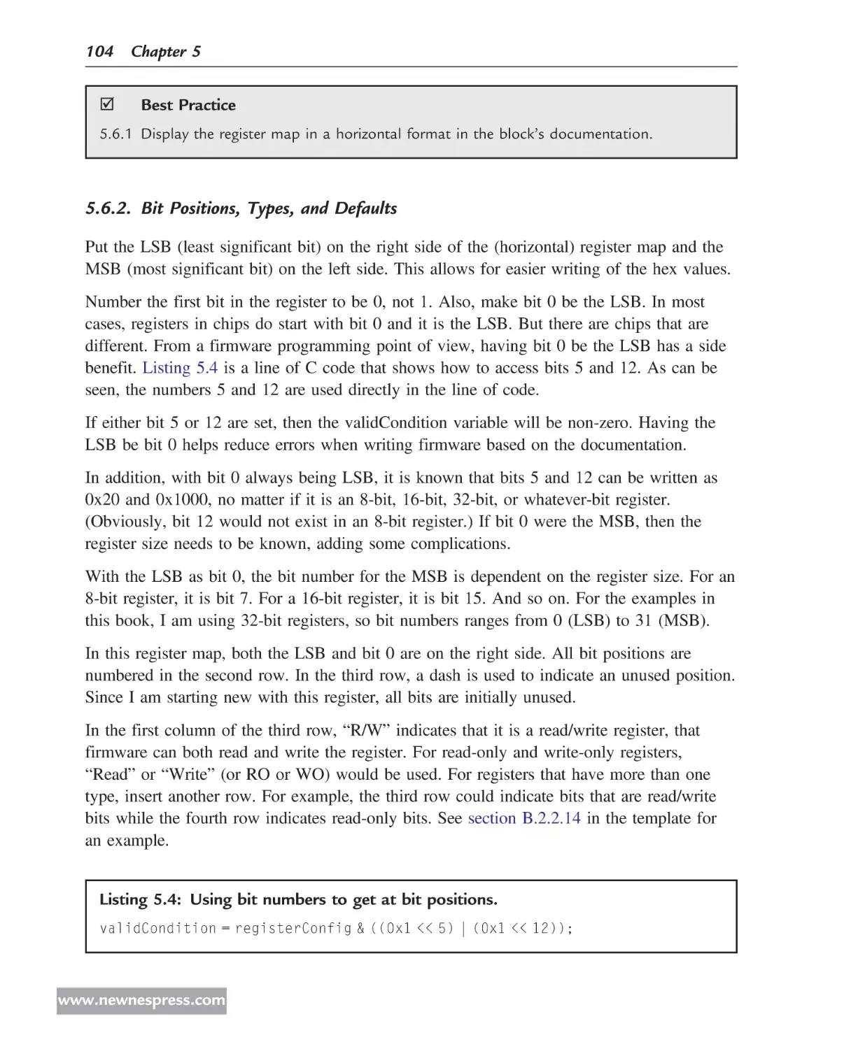
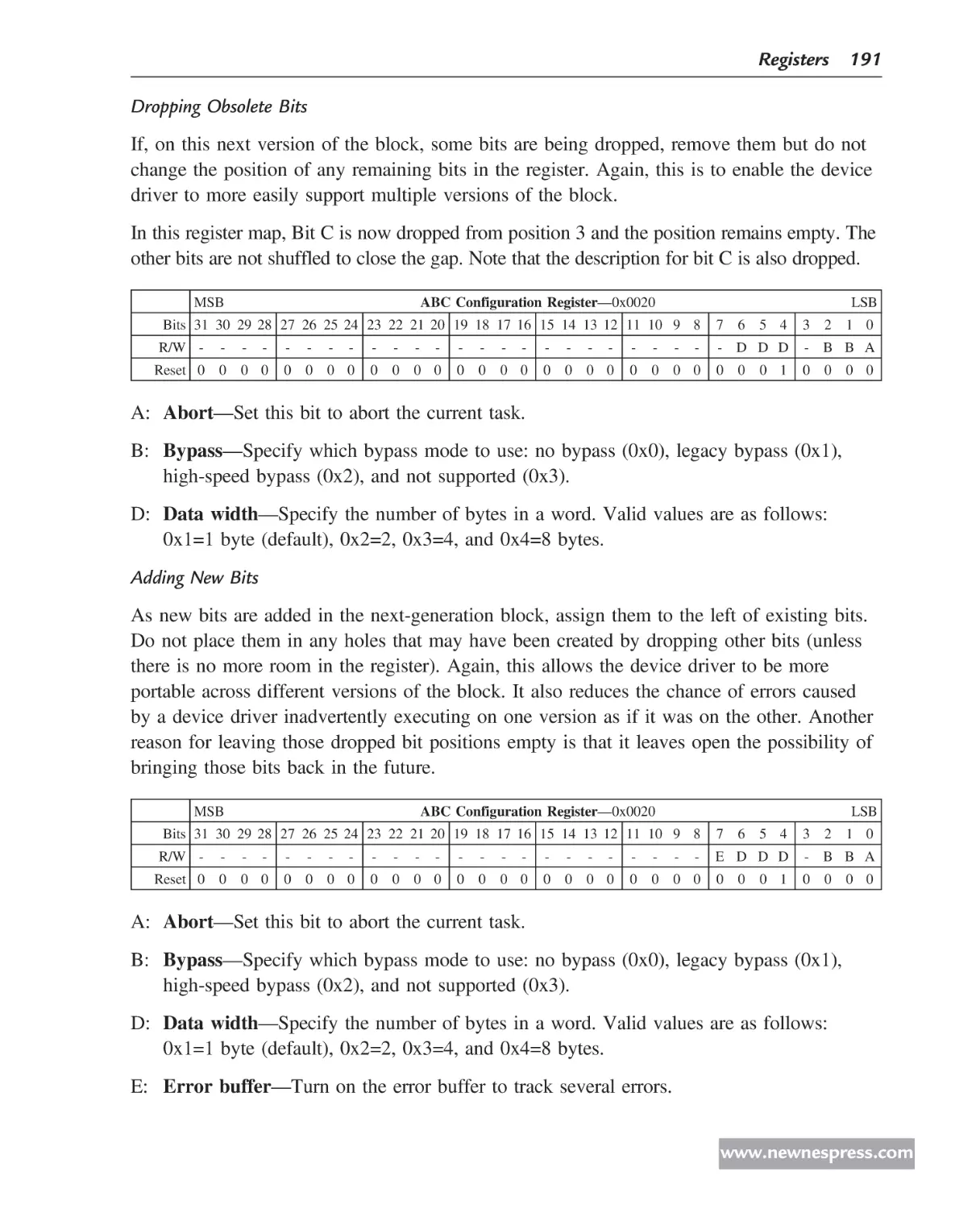
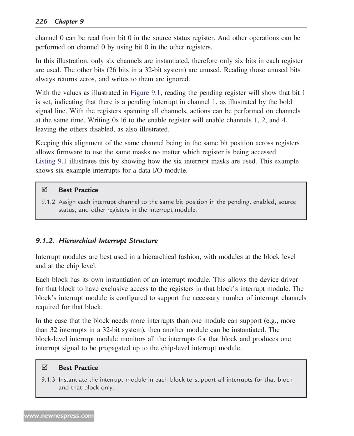
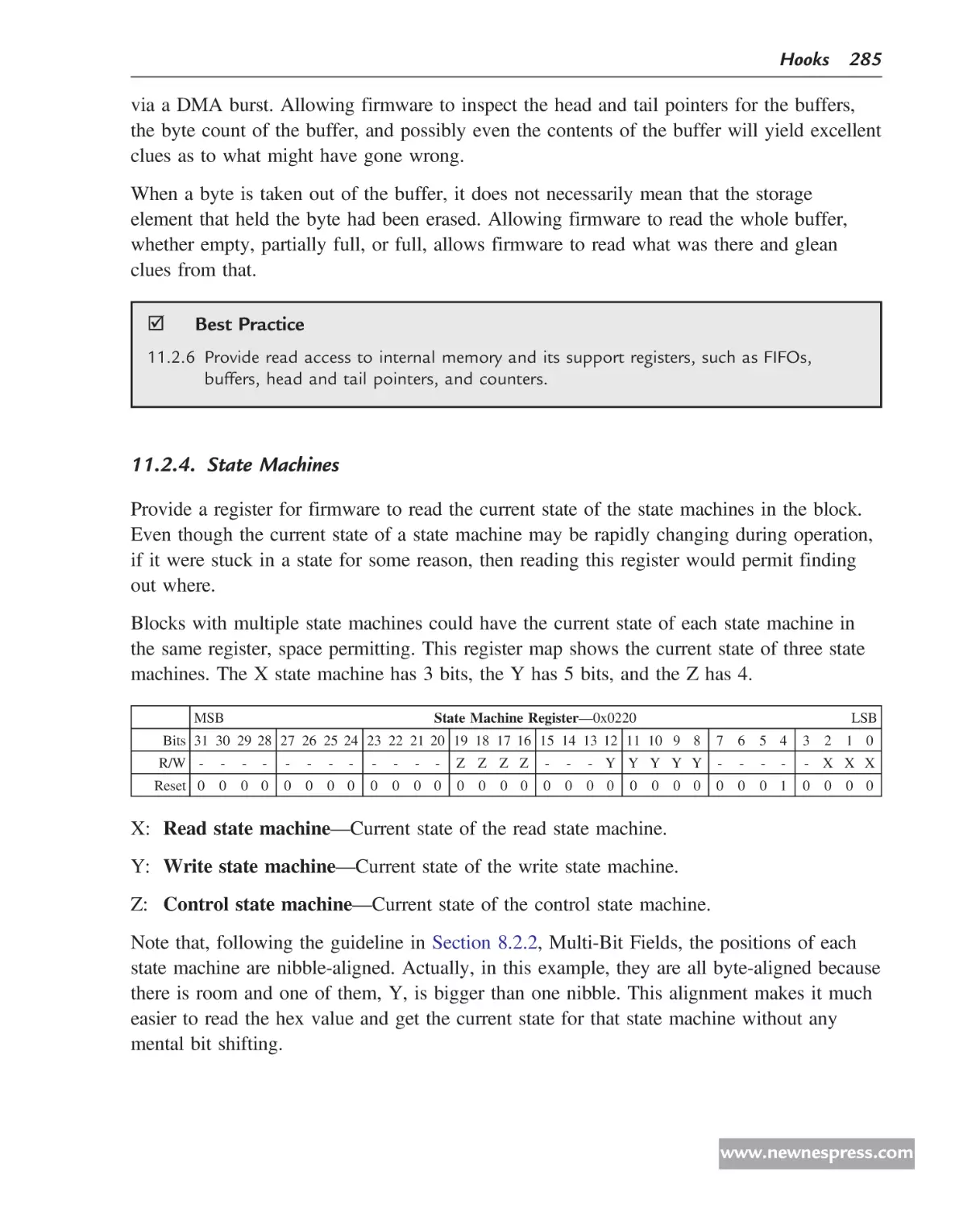
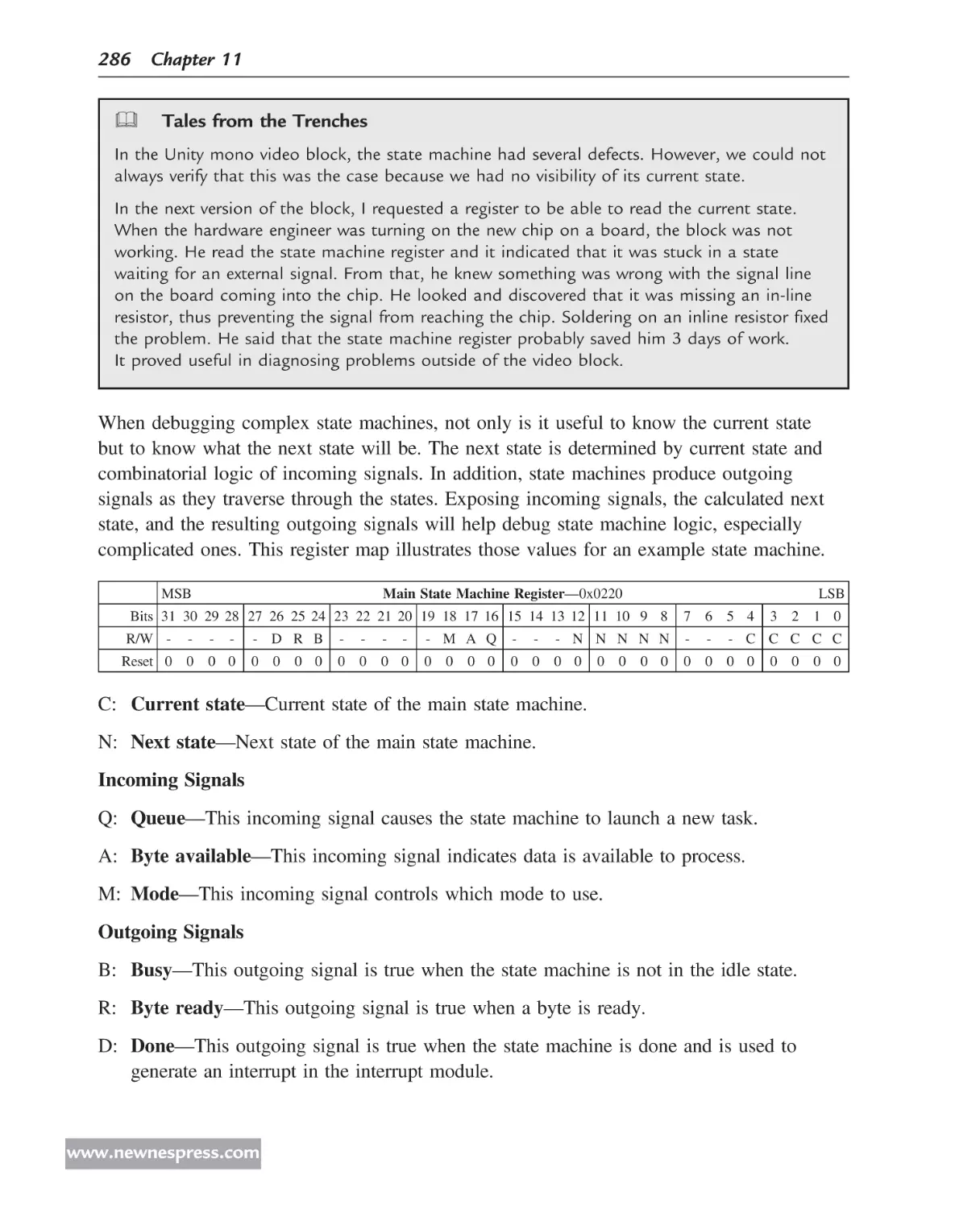
Register Maps
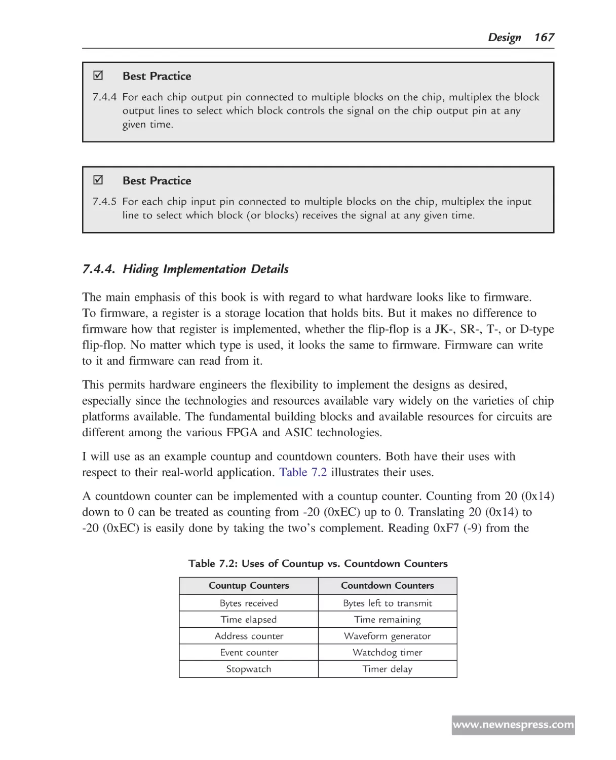
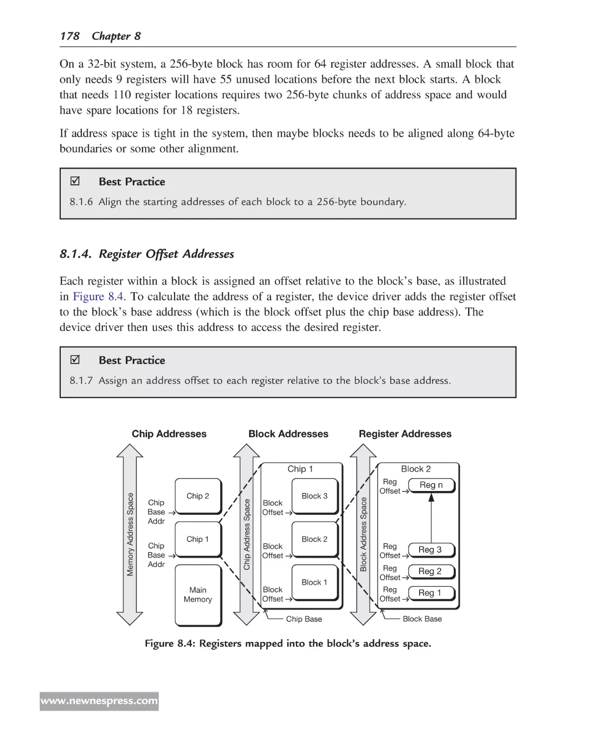
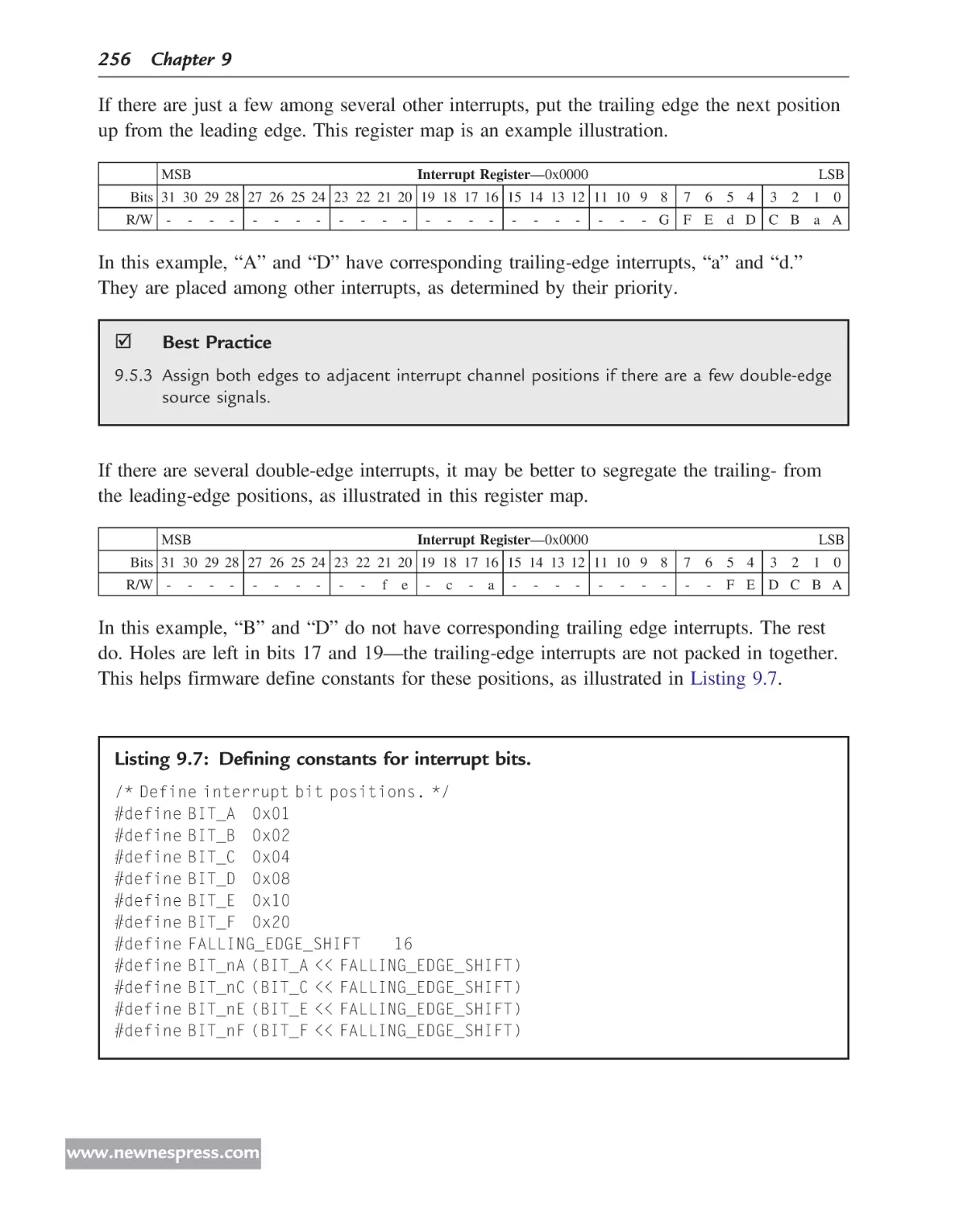
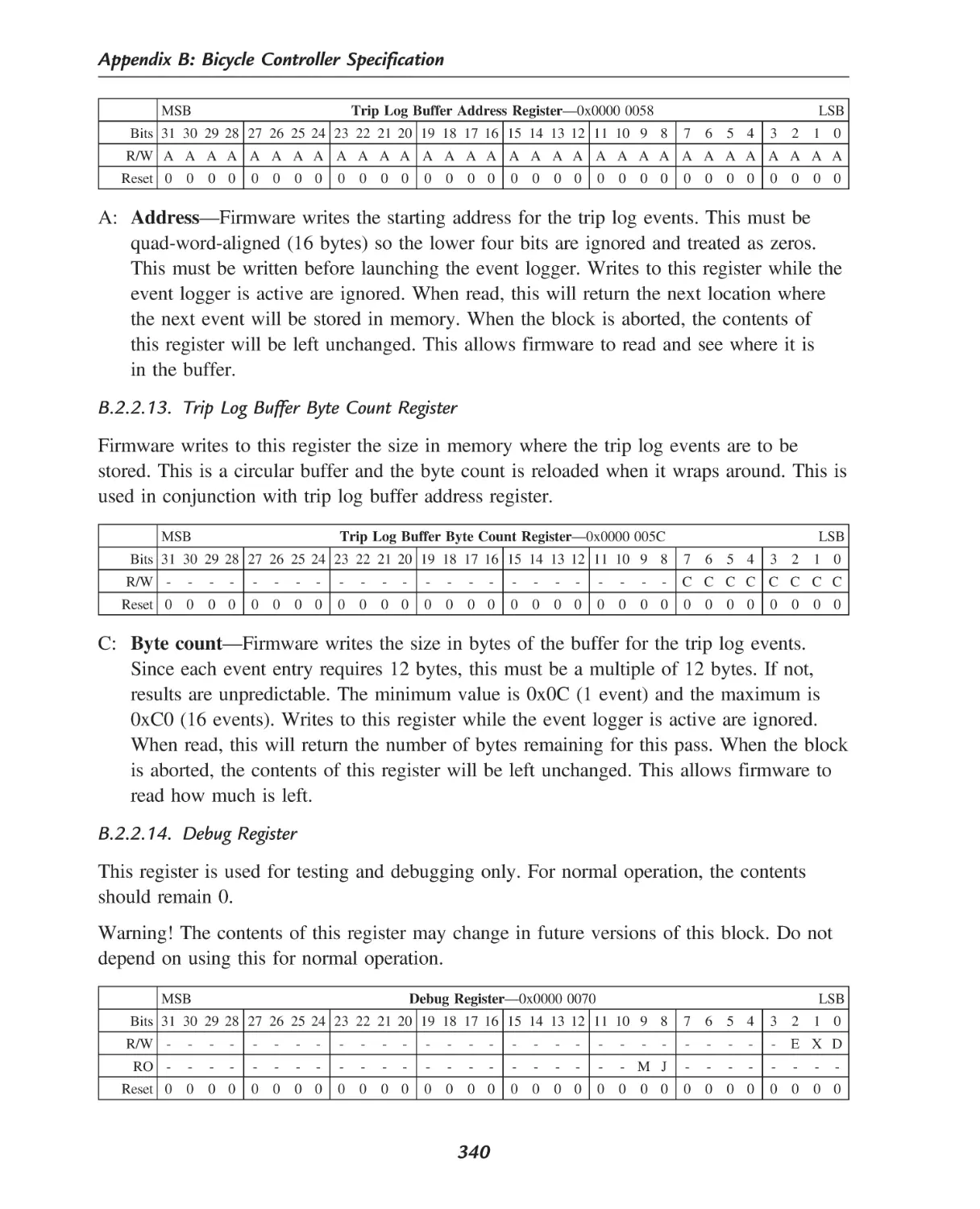
This diagrammatic form is used in discussions about registers, how various bits are mapped
into the register, and the mode of operation and reset values of these bits. A detailed
explanation of this format is given in Chapter 5, Documentation.
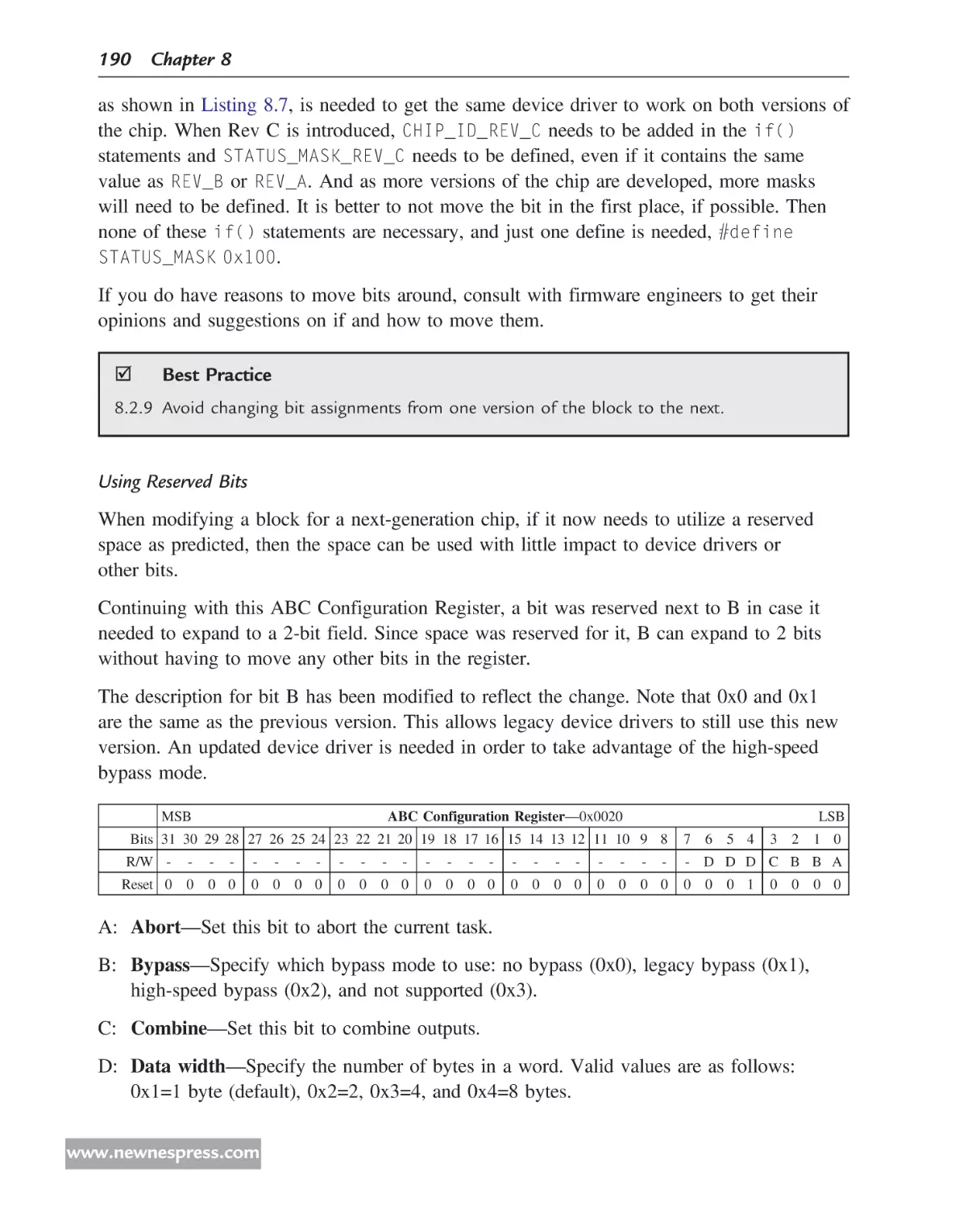
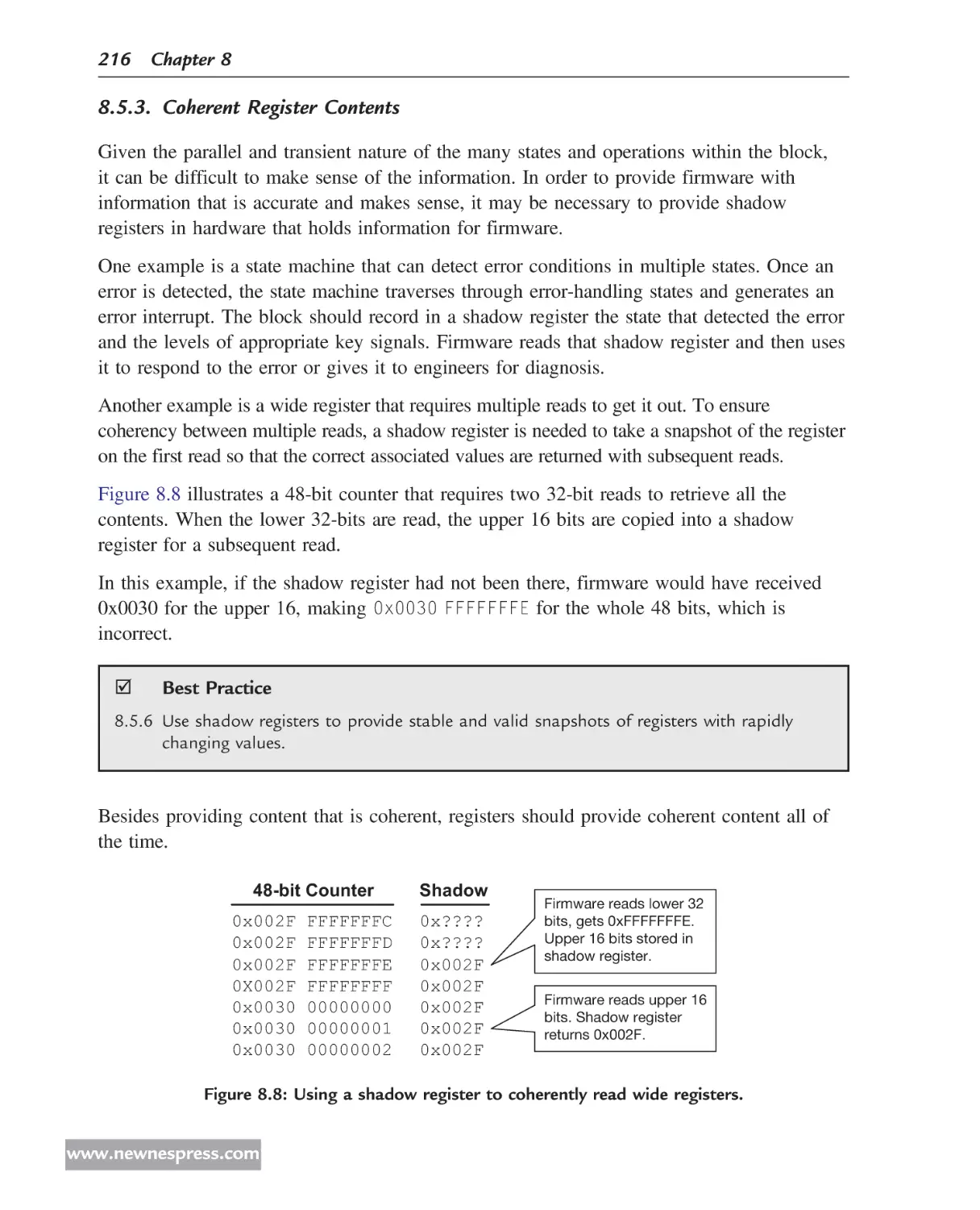
Daily Register – 0x0004
MSB
LSB
Bits 31 30 29 28 27 26 25 24 23 22 21 20 19 18 17 16 15 14 13 12 11 10 9 8
R/W -
-
-
-
Reset 0 0 0 0
-
-
-
-
0 0 0 0
-
-
-
-
0 0 0 0
-
-
-
-
0 0 0 0
-
-
-
-
0 0 0 0
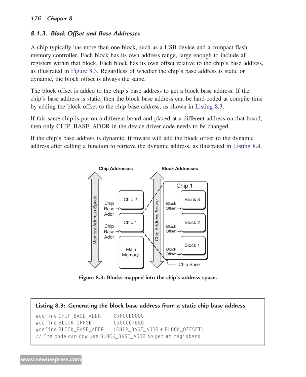
-
-
-
-
0 0 0 0
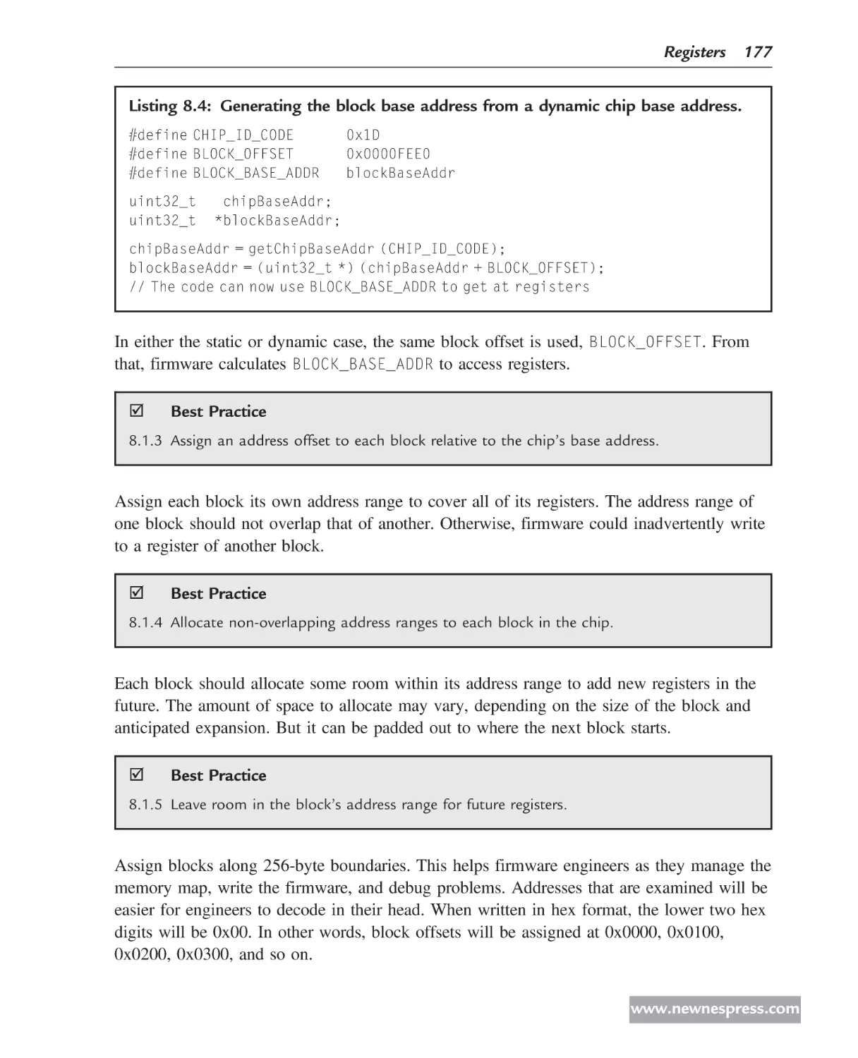
7 6 5 4
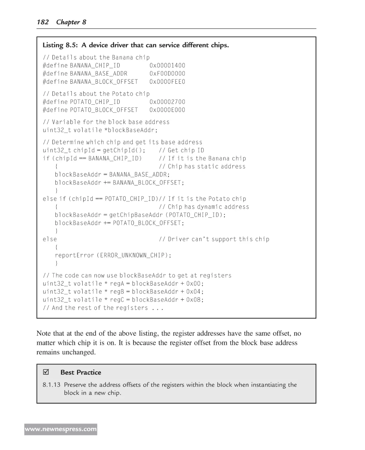
-
-
-
-
0 0 0 0
3 2 1 0
-
C B A
0 0 0 0
A This bit means one thing.
B This bit means another.
C And this bit means something else.
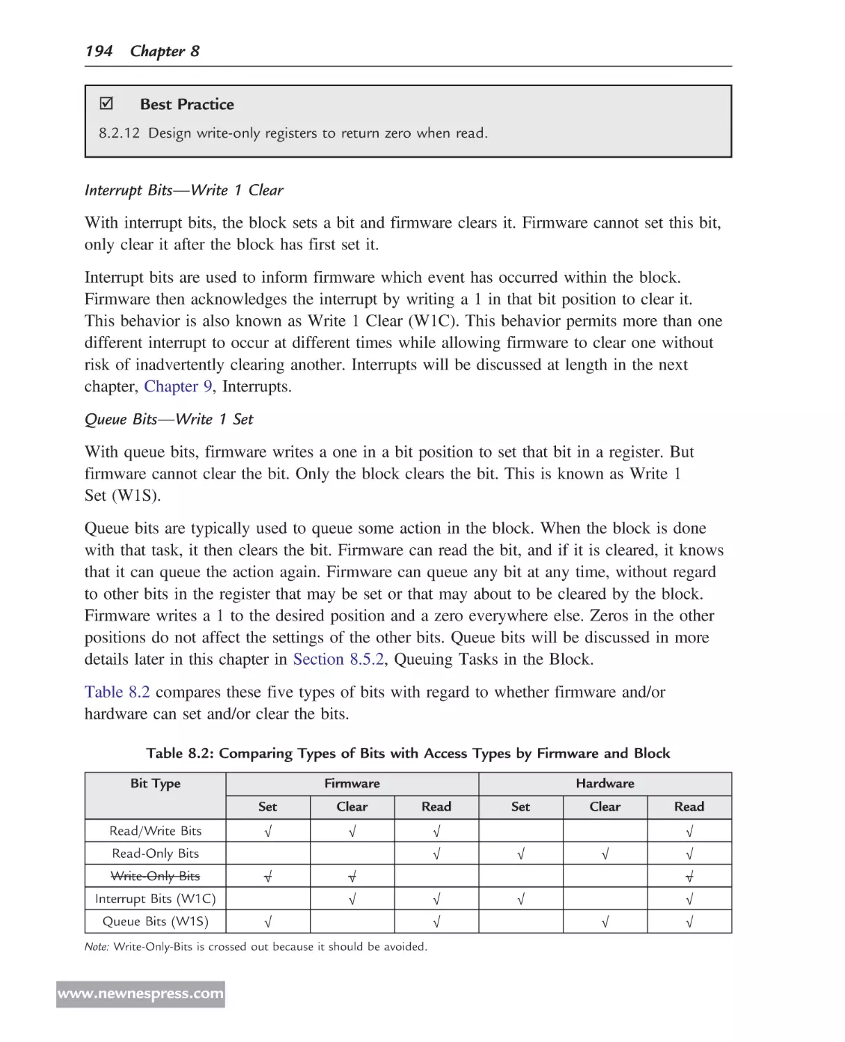
Best Practices
The book contains 300+ Best Practices related to the concepts being taught. In addition to
presentation throughout the book, these practices are collected in Appendix A, thereby
A
C
B
Figure 0.2: Schematic for example circuit.
Listing 0.2: Verilog code for example circuit.
// A simple AND gate.
assign c = a & b;
© 2010 by Elsevier Inc. All rights reserved.
xiii
Preface
providing a concise checklist that can be used during chip design projects. They are also
provided in a spreadsheet available online at the publisher’s website, elsevierdirect.com/
companions, and at the author’s website, garystringham.com/hwfwbook.
Each best practice has an ID number, X.Y.Z, which is used in the body of the book, in
Appendix A, and in the spreadsheet.
þ
Best Practice
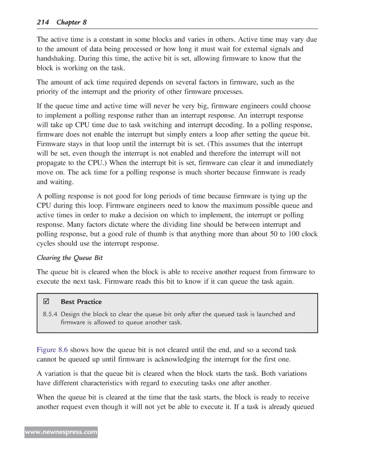
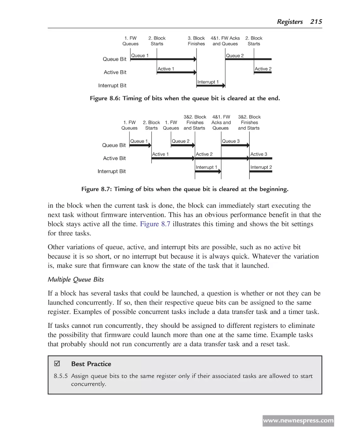
1.1.1 Best Practices of Hardware/Firmware Interface Design.
Like the book, the Excel spreadsheet database is copyrighted material. Purchasers of this
book are entitled (and encouraged) to start with the database and modify it to suit the needs
of their design team, but some restrictions apply. See Appendix A for more details on the
database and its copyright permissions.
þ
Best Practice
1.1.2 Copyright © 2009, Gary Stringham & Associates, LLC. All rights reserved. Do not
distribute beyond your team.
Tales from the Trenches
Scattered throughout this book are real-life stories that help illustrate the impact of the topic
at hand. These are stories from real engineers (mostly me) in the trenches, working away
designing and solving problems. The following is an example tale (not a real one).
&
Tales from the Trenches
I remember hearing a story from a friend of a friend, who heard that an engineer had said
that he heard a manager tell her subordinate that–according to the rumor she had heard–it
was already broken to start with.
Companion Website
This book has a companion website at elsevierdirect.com/companions/9781856176057,
where you will find links to the spreadsheet database for the 300+ Best Practices, the
document template discussed in Chapter 5, Documentation, and other related content. Please
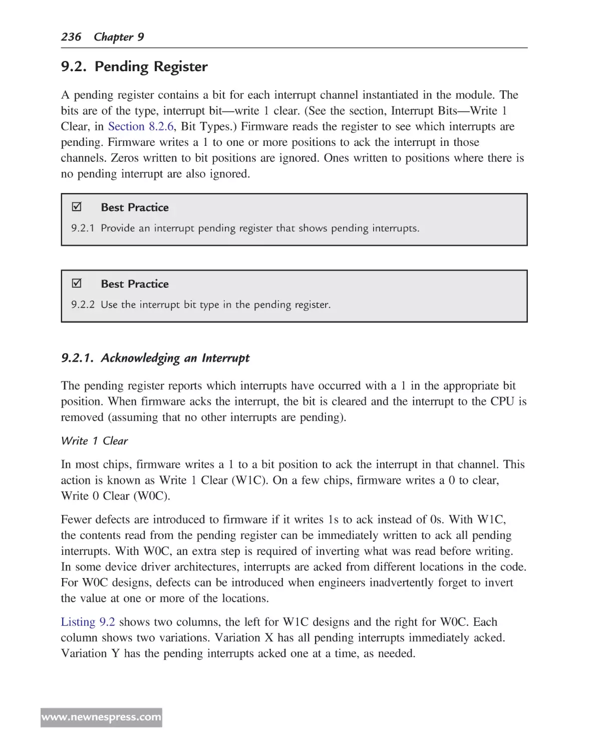
© 2010 by Elsevier Inc. All rights reserved.
xiv
Preface
visit the author’s website at garystringham.com/hwfwbook for the same tools, plus
additional links to his work in this area and details of how to contact him directly.
How to Contact Me
If you have any questions about the content of this book or about your hardware/firmware
interface design, feel free to contact me at gary@garystringham.com.
Acknowledgments
I would like to thank Jack Meador and Mike Merrell, the two unlucky hardware engineers
who had to put up with my constant questions, issues, and requests as we worked through
the project that was the catalyst for this book. They provided valuable insight and help from
within their hardware domain. They, along with other hardware and firmware engineers
within the organization and from other companies, provided much of the input used in
many of the best practices and tales from the trenches in this book.
I would also like to thank my immediate managers at the time, Warren Johnson and Tracy
Sauerwein, and managers above them, Sandy Lieske and Von Hansen. The book is finally
published—your unwarranted support, while tracing my progress from sandy to smooth, was
not in vain.
Me badly english writin’ was greatly improved through the patient tutelage of my technical
writing coach, Joel Saks. He has a gift with words that is way beyond my abilities. In
addition, he was a valuable resource for critical analysis of my concepts, pushing me to
clearly articulate and justify what seemed obvious to me.
I would also like to thank John Blyler, Clive “Max” Maxfield, Jack Meador, Mike Merrell,
Joel Saks, and three others (who wish to remain anonymous) for reviewing all or parts of
my book. Your comments provided valuable input and suggestions, making the book better
than otherwise. Thanks to Mike Merrell for his help with the Verilog code and to Kevin
Falk for drawing the car illustrations. And thanks to the many others who have given me
suggestions and enthusiastic encouragement during the 5 years it took me to complete this
project.
for their patience and
Most of all, I want to thank my wife and children
long suffering as I spent evenings and weekends working on this book instead of making
repairs on the house, driving the children to their activities, and vacationing with the family.
© 2010 by Elsevier Inc. All rights reserved.
xv
CHAPTER 1
Introduction
Hardware and firmware engineering design teams often run into problems and conflicts
when trying to work together. They come from different development environments, have
different toolsets, and use different terminology. Often they are in different locations within
the same company or work for different companies. The two teams have to work together
but often have conflicting differences in procedures and methods. Since their resulting
hardware and firmware work has to integrate successfully to produce a product, it is
imperative that the hardware/firmware interface—including people, technical disciplines,
tools, and technology—be designed properly.
Because of the nature of embedded systems, hardware design will always precede firmware
design. While some tools and techniques are available to permit a more parallel effort, in
the end, the hardware must be created before the firmware team can carry out its final
development and testing efforts. Although a significant amount of effort is expended to
ensure correct design at the hardware/firmware interface, problems will still appear when
hardware and firmware are integrated as a system.
Problems found in firmware are relatively easy to fix compared to problems found in
hardware. Respinning an application-specific integrated circuit (ASIC)1 can take up to
4 months and cost several million dollars, depending on the process node at which the chip
is being developed, such as 90 nm, 65 nm, and so on. So pressure is put on the firmware
teams to try to work around any hardware problems to avoid the delay and cost. As Jack
Ganssle, an embedded systems expert, humorously stated, “Quality is firmware’s
fault—because it is too late to fix it in hardware.”
Chips are expensive and hard to design and build; getting them “right” is a business
necessity. Designing chips for firmware engineers is a key enabler. This book provides a
rigorous study of common sense approaches to chip design based on years of experience in
writing firmware for chips. It captures practical and sensible ideas and applies structure and
1
For the purposes of this book, the term ASIC will also be taken to encompass application-specific standard
products (ASSPs), system on chips (SoCs), and field-programmable gate arrays (FPGAs). (See also the definitions
later in this chapter.)
© 2010 by Elsevier Inc. All rights reserved.
DOI: 10.1016/B978-1-85617-605-7.00003-4.
1
2 Chapter 1
rigor to the design. The goal of the book is to provide principles and best practices that
allow hardware and firmware engineers to improve the development and integration of
embedded systems. This book is most useful during the development phase of the product,
specifically during the development of both the chip and the firmware for a product.
This first chapter provides background into the subject matter and lays the groundwork for
the remainder of the book. The second chapter discusses seven principles of hardware/
firmware interface design. The rest of the book contains over 300 best practices. Obviously
the list of best practices presented here cannot be an exhaustive one in this area. As you
read through the following chapters, you will think about best practices that you use and
will get ideas for others. Write them down so you can apply them to your work and share
them with others.
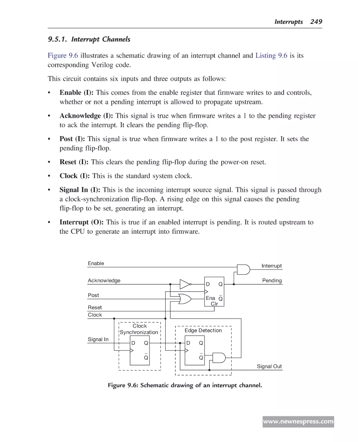
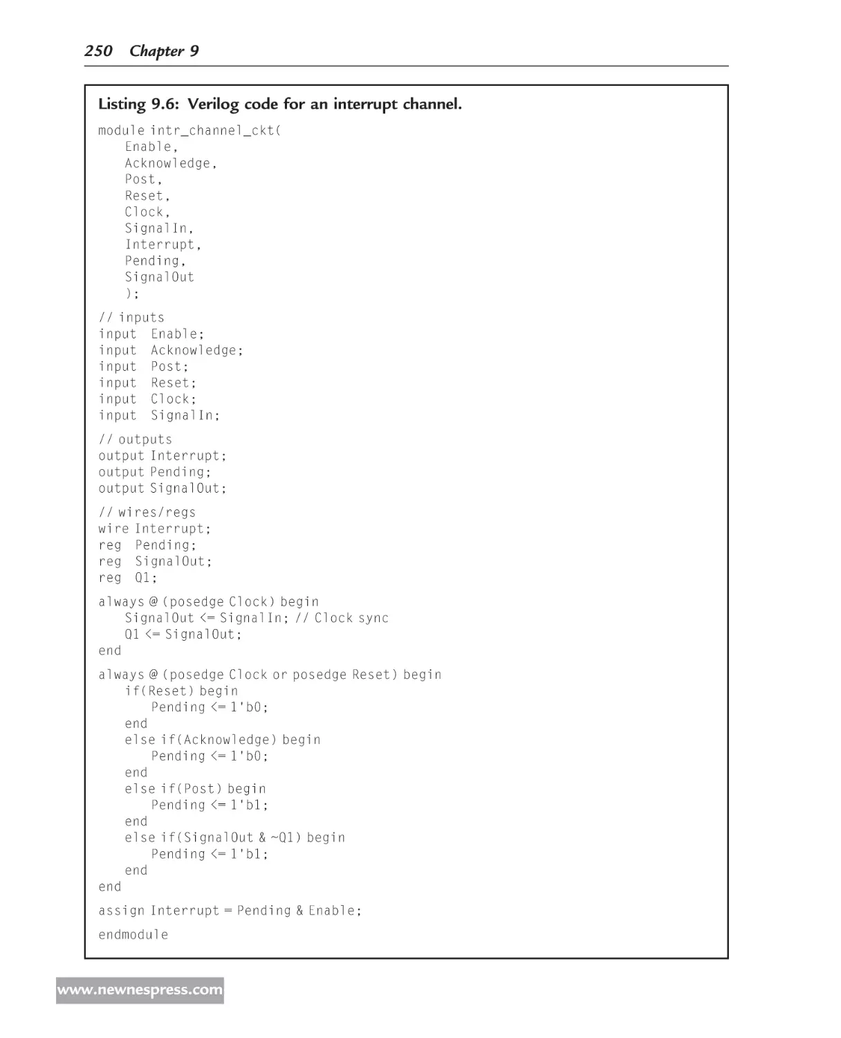
1.1. What Is the Hardware/Firmware Interface?
The hardware/firmware interface is the junction where hardware and firmware meet and
communicate with each other. On the hardware side, it is a collection of addressable
registers that are accessible to firmware via reads and writes. This includes the interrupts
that notify firmware of events. On the firmware side, it is the device drivers or low-level
software that controls the hardware by writing values to registers, interprets the information
read from the registers, and responds to interrupt requests from the hardware. Of course,
there is more to hardware than registers and interrupts, and more to firmware than device
drivers, but this is the interface between the two and where engineers on both sides must be
concerned to achieve successful integration.
The terms “hardware” and “firmware” vary in scope and meaning in the industry, so let’s
define how they are used in this book.
1.1.1. What Are Hardware, Chips, and Blocks?
In the electrical engineering context, the term “hardware” includes all electronic circuits in
an embedded product, including printed circuit boards, passives like resistors and capacitors,
and chips. It can also refer to nonelectrical, mechanical components, such as bolts, spacers,
and housing/enclosures. Meanwhile, the term “chips” includes any devices made from
silicon or other semiconducting materials containing multiple transistors that implement
digital or analog functions. They can be simple, single-function devices or complex,
multi-function devices containing processors, memory, interfaces, and other functional
circuitry.
For the purposes of this book, “hardware” and “chips” refers to just a subset of devices
(such as ASICs and FPGAs): specifically, the components that interact with firmware via
www.newnespress.com
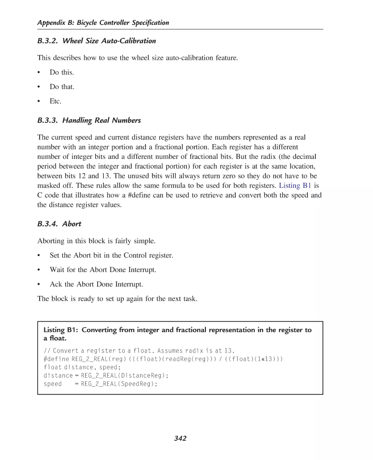
Introduction 3
registers and interrupts. It does not include microprocessors, microcontrollers, or memory.
Furthermore, “hardware” and “chips” are used almost interchangeably in this book; for
example, “The hardware team designs the chips.”
A “chip” will contain one or more functional “blocks,” such as a USB communications
function, an MPEG compressor, and a memory controller. There may be more than one
instantiation (copy) of a particular block, such as two UARTs. Blocks within a chip
typically communicate with each other and with external memory via a shared bus. Each
block is typically designed as an individual unit. When a new chip is designed, it may
comprise a mixture of blocks used in previous designs and new blocks.
Within the scope of “chips,” are several general families of integrated circuits, each with
their own minor differences with regard to the context of this book, but the concepts
generally apply to all.
ASICs
ASICs (application-specific integrated circuits) are designed to be used in a specific product
of a specific brand. It contains a customized mix of standard and/or proprietary blocks.
ASICs are high-volume chips optimized for power, performance, and cost. This means that
there are many different ASICs in use, each with its own hardware and firmware design
teams. These hardware and firmware teams continue to work together as they produce
variations of the ASICs for various product families and multiple generations of the products.
Both of the teams may be working for the company producing the product; alternatively,
one or both of the teams might be working for other companies hired to do the work.
Whatever the case, close coupling between the teams must still be present so as to provide
the hardware team with more opportunities to make changes and improvements because
they can collaborate with the firmware team in advance.
ASSPs
ASSPs (application-specific standard product) are like ASICs except that they are designed
for a specific application area and are sold to more than one customer—hence the name
“standard product.” By contrast, an ASIC is designed and built to order for a specific
customer. ASSPs have only standard functionality, allowing them to be used in a variety of
embedded systems by a variety of companies. This means that one company generates an
ASSP, while potentially many companies generate firmware for that ASSP. Device drivers
are typically needed for a variety of operating systems (OSs) and versions; these device
drivers will be specific to the firmware of the target embedded system. Thus many different
firmware teams from multiple companies are typically involved. The firmware teams
generally do not have ready access to the hardware team that designed the ASSP. There is
no one-to-one relationship as found in ASIC teams.
www.newnespress.com
4 Chapter 1
This puts the burden on the hardware team to try to please many different firmware teams
without being able to collaborate with each and every one. In this scenario, the hardware
team should select one or two firmware teams to partner with to help develop the chip
while it is still in the design phase. This is commonly the case, with the end result that the
company selling the chip has a few device drivers already written that other companies can
use to leverage into their products.
The contents of some ASSPs are standard enough that they are produced by multiple
companies that allow the same device driver to work on any brand. Examples include
EHCI (enhanced host controller interface)-compliant USB (universal serial bus) controllers
and 16550-compatible UARTs (universal asynchronous receiver transmitters). This means
that the registers, bits, and functionality are fairly identical. This allows the same device
driver to run on diverse brands of ASSPs. Maintaining this compatibility restricts the
hardware design team even further by not allowing them much freedom to improve on
other brands.
FPGAs
FPGAs (field-programmable gate arrays) have the flexibility of having their functionality
changed through reprogramming, but they typically use more power, have slower
performance, and cost more per part.
FPGAs can be programmed with a customized mix of content. This custom mix makes it
similar to ASICs in that typically one firmware team is paired with the one hardware team.
However, because FPGAs can be modified in a matter of hours, it is possible for many
versions of the FPGA programming to exist. This requires close collaboration between the
hardware and firmware teams to ensure that the version of firmware paired with the version
of FPGA code will work together.
FPGAs are also used when changes to the design are needed after the product has been
deployed to customers. A new programming file can be distributed and downloaded to the
product.
FPGAs can also be programmed with a standard mix of content. This is similar to ASSPs in
that companies can sell the same package to many customers. This means that there could
be many firmware teams writing device drivers for this standard, FPGA-based content.
Companies use this method to sell small quantities of their designs without incurring the
NRE (nonrecurring engineering) expenses associated with sending the design to a foundry
for fabrication as is the case with non–FPGA-based ASSPs.
References in this book about the time and expense required to respin the chip do not apply
to FPGAs. Firmware cannot tell the difference between an ASIC/ASSP or FPGA, as the
register/interrupt interface is the same.
www.newnespress.com
Introduction 5
SoCs
An SoC (system on chip) is similar to an ASIC and ASSP, but in addition to its mix of
blocks, it also contains one or more processors and possibly some memory. It may be a
customized mix (ASIC + processor) or it may be a standard mix (ASSP + processor).
It may be sent to the foundry for fabrication or it may be programmed into an FPGA.
For the purpose of this book, SoCs are synonymous with ASICs, ASSPs, and FPGAs. The
processor and memory parts of SoCs are not discussed; instead, the focus is on the rest of
the chip—the functional blocks that are accessed by firmware. While firmware is executed
on the processor and resides in and accesses memory, this book is not about how to design
processors or memory.
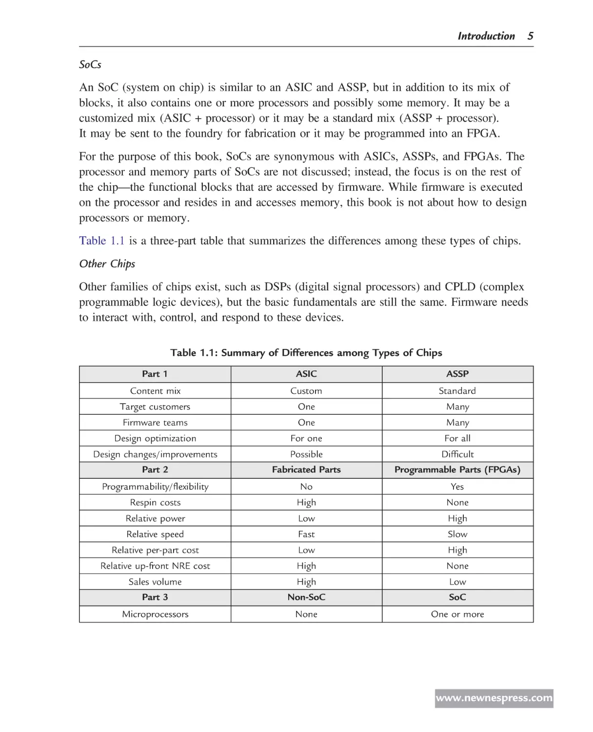
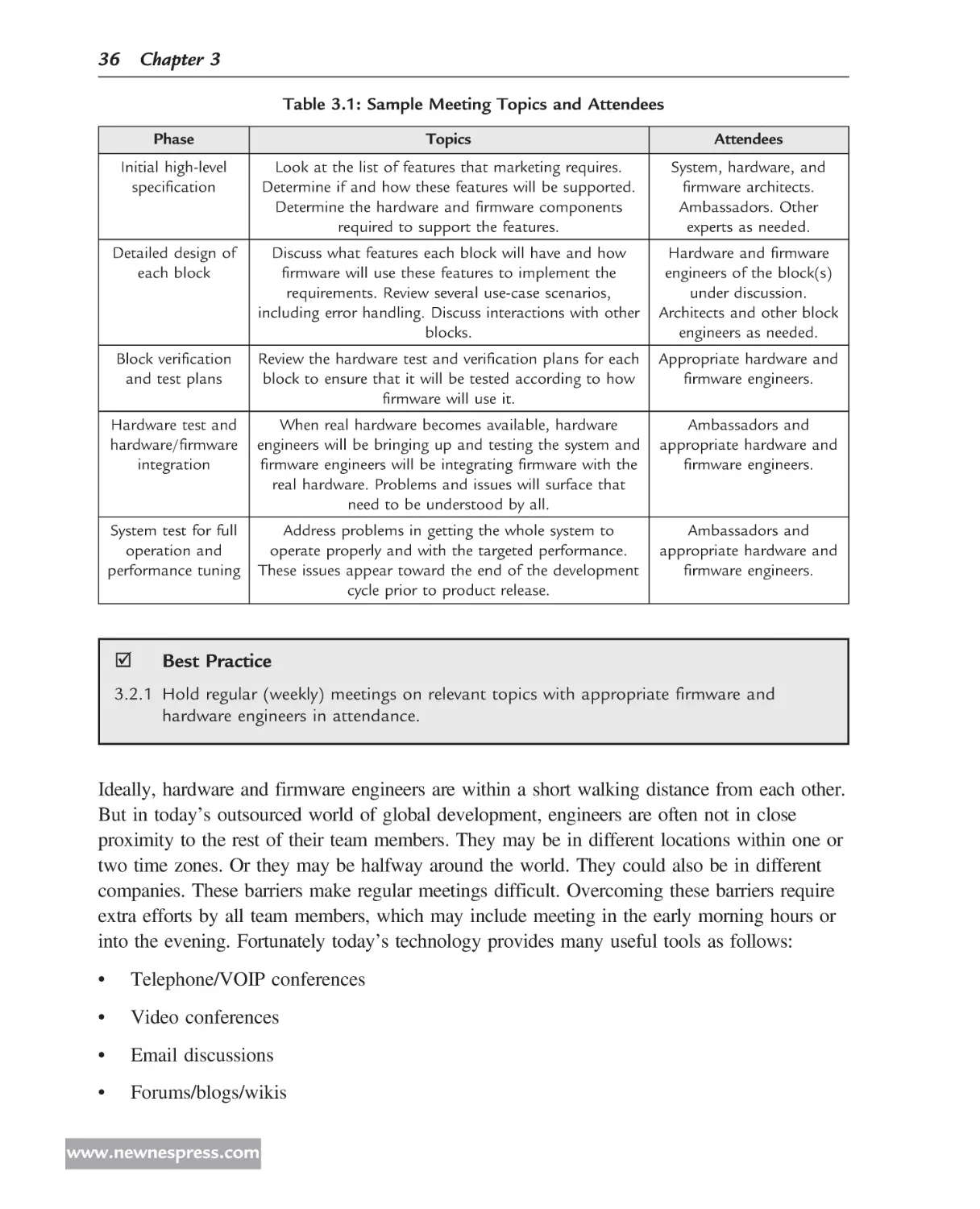
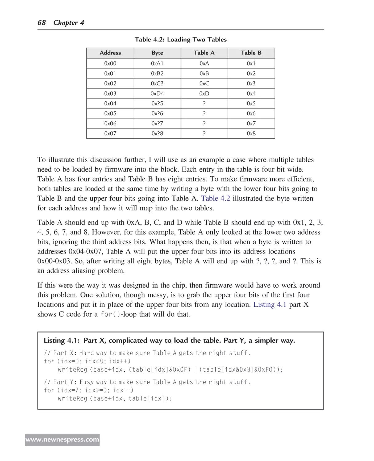
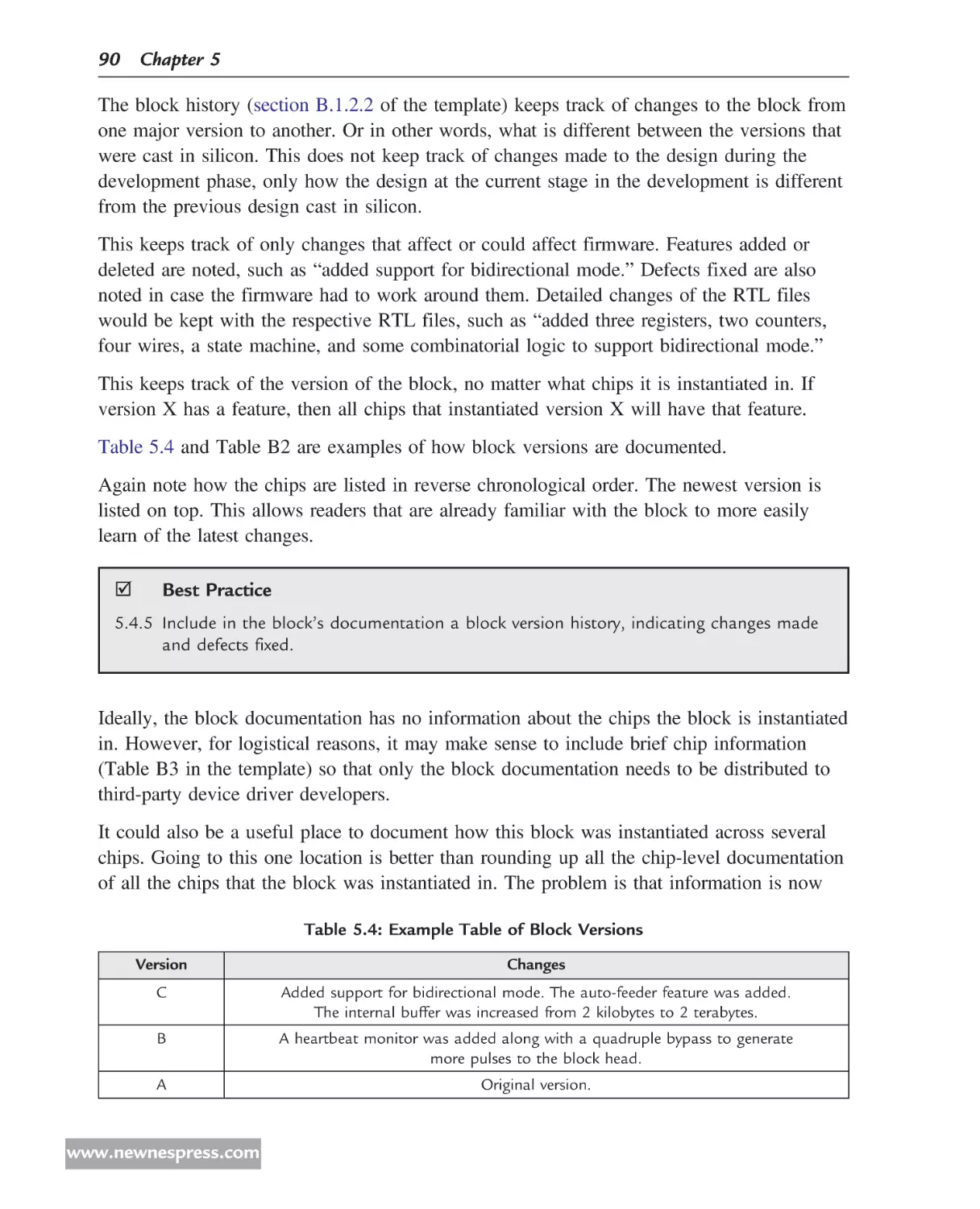
Table 1.1 is a three-part table that summarizes the differences among these types of chips.
Other Chips
Other families of chips exist, such as DSPs (digital signal processors) and CPLD (complex
programmable logic devices), but the basic fundamentals are still the same. Firmware needs
to interact with, control, and respond to these devices.
Table 1.1: Summary of Differences among Types of Chips
Part 1
ASIC
ASSP
Content mix
Custom
Standard
Target customers
One
Many
Firmware teams
One
Many
Design optimization
For one
For all
Design changes/improvements
Possible
Difficult
Part 2
Fabricated Parts
Programmable Parts (FPGAs)
Programmability/flexibility
No
Yes
Respin costs
High
None
Relative power
Low
High
Relative speed
Fast
Slow
Relative per-part cost
Low
High
Relative up-front NRE cost
High
None
Sales volume
High
Low
Part 3
Non-SoC
SoC
Microprocessors
None
One or more
www.newnespress.com
6 Chapter 1
1.1.2. What Are Firmware and Device Drivers?
Firmware is software that is built into an embedded systems product and stored in
nonvolatile memory, such as ROM, EPROM, E2PROM, or FLASH. The memory could be
located on-chip or off-chip. Firmware is also known in the industry as “embedded software”
or “low-level software.” Major firmware components optionally include an operating system
(OS), kernel, device drivers, and application code.
The term “firmware” has other meanings in the industry that are not used here. For
example, to some people, firmware refers to the microcode running in processors that is
executed because of an assembly language instruction. In other sections of the industry,
firmware is the content downloaded into an FPGA to program it. Firmware in this book
does not refer to such microcode or FPGA programming code.
Firmware might contain an OS. This might be an RTOS (real-time operating system). The
OS may be a commercial product, such as Embedded Windows®, Linux®, and VxWorks®,
or it may be developed in-house. Some lightweight embedded systems do not use an OS,
but instead execute the firmware directly.
Device drivers are the specific firmware components that interact with chips. On some
systems this is called the BIOS (basic input/output system) or low-level code. Device
drivers read from and write to registers and respond to interrupts. Applications in firmware
go through device drivers to access the hardware.
The term “driver” has other meanings for hardware engineers, such as current drivers or
buffer drivers. In the computer world, “driver” also refers to software modules installed on
a computer to work with peripheral devices, such as a printer driver. In this book, the term
“driver,” by itself, refers specifically to “device driver.”
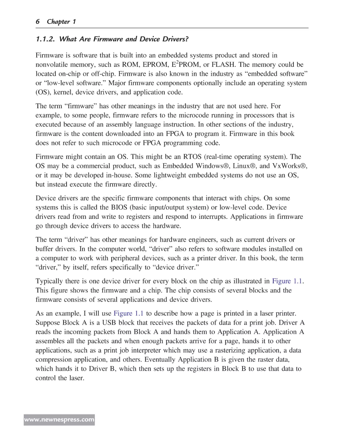
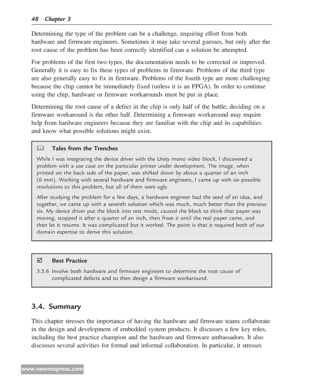
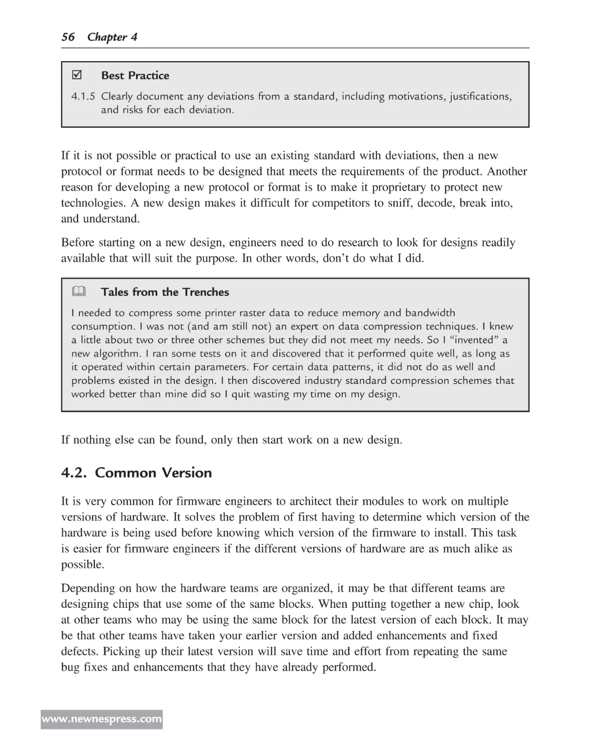
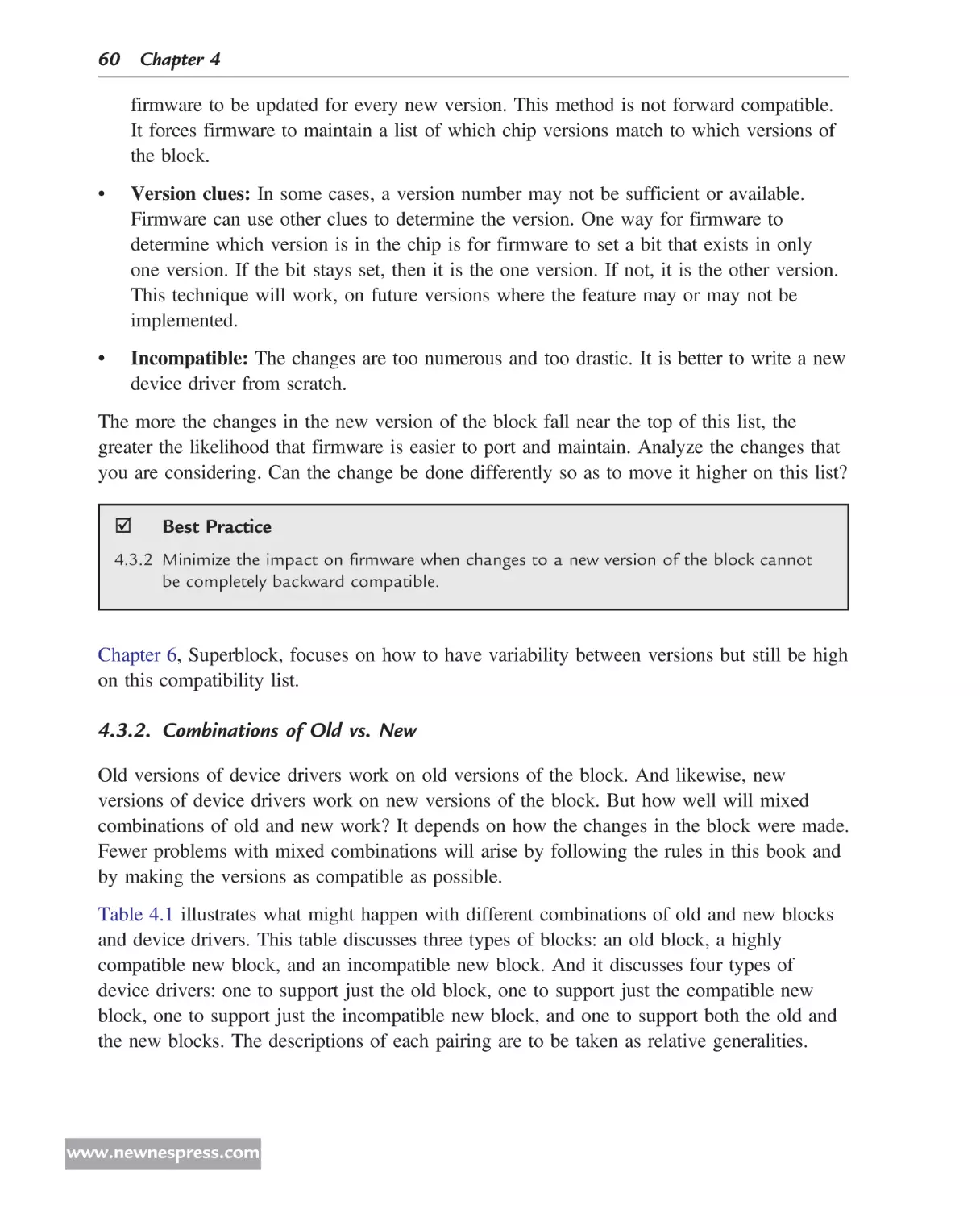
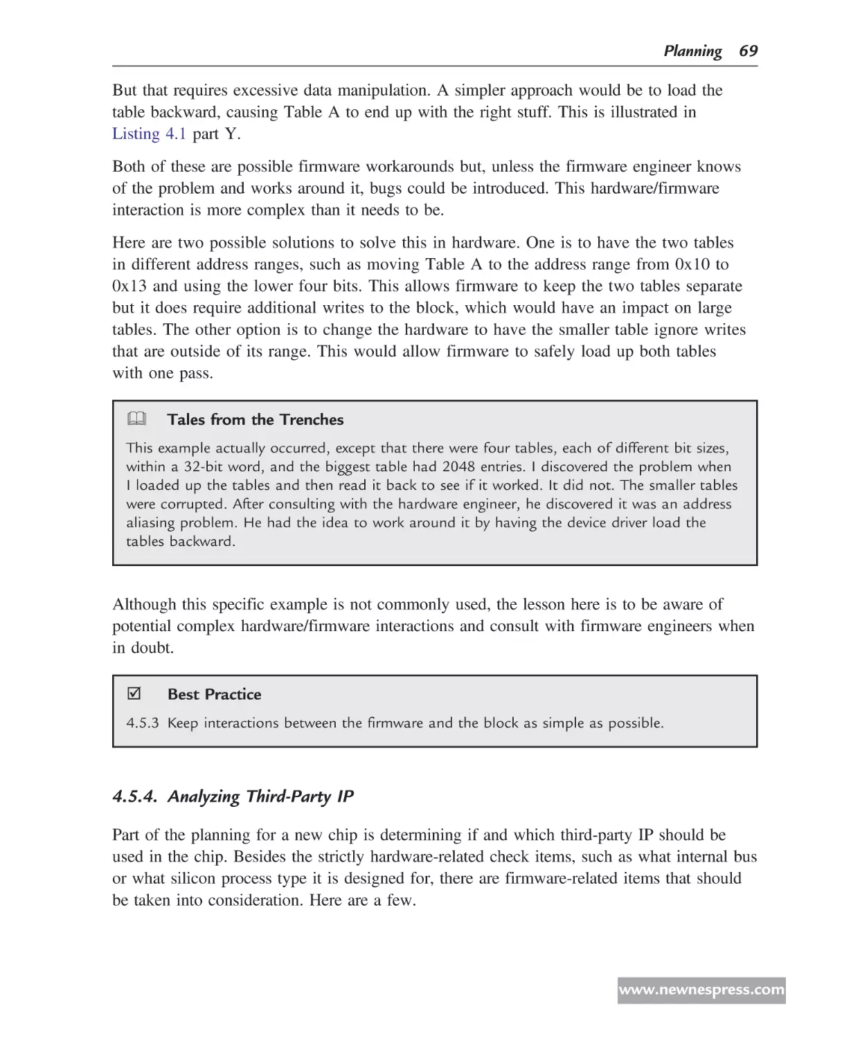
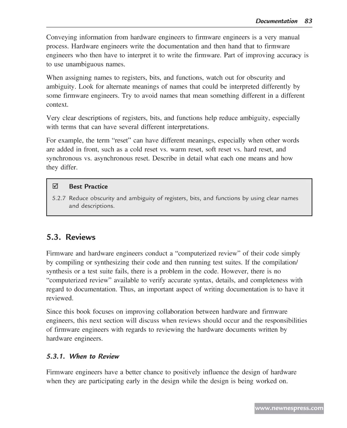
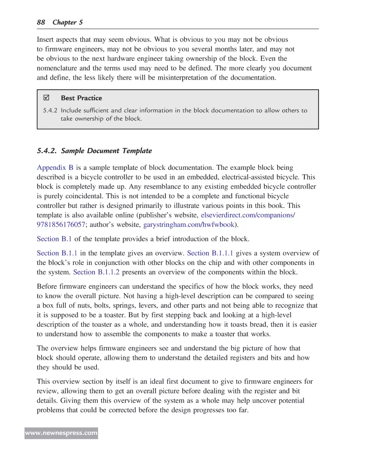
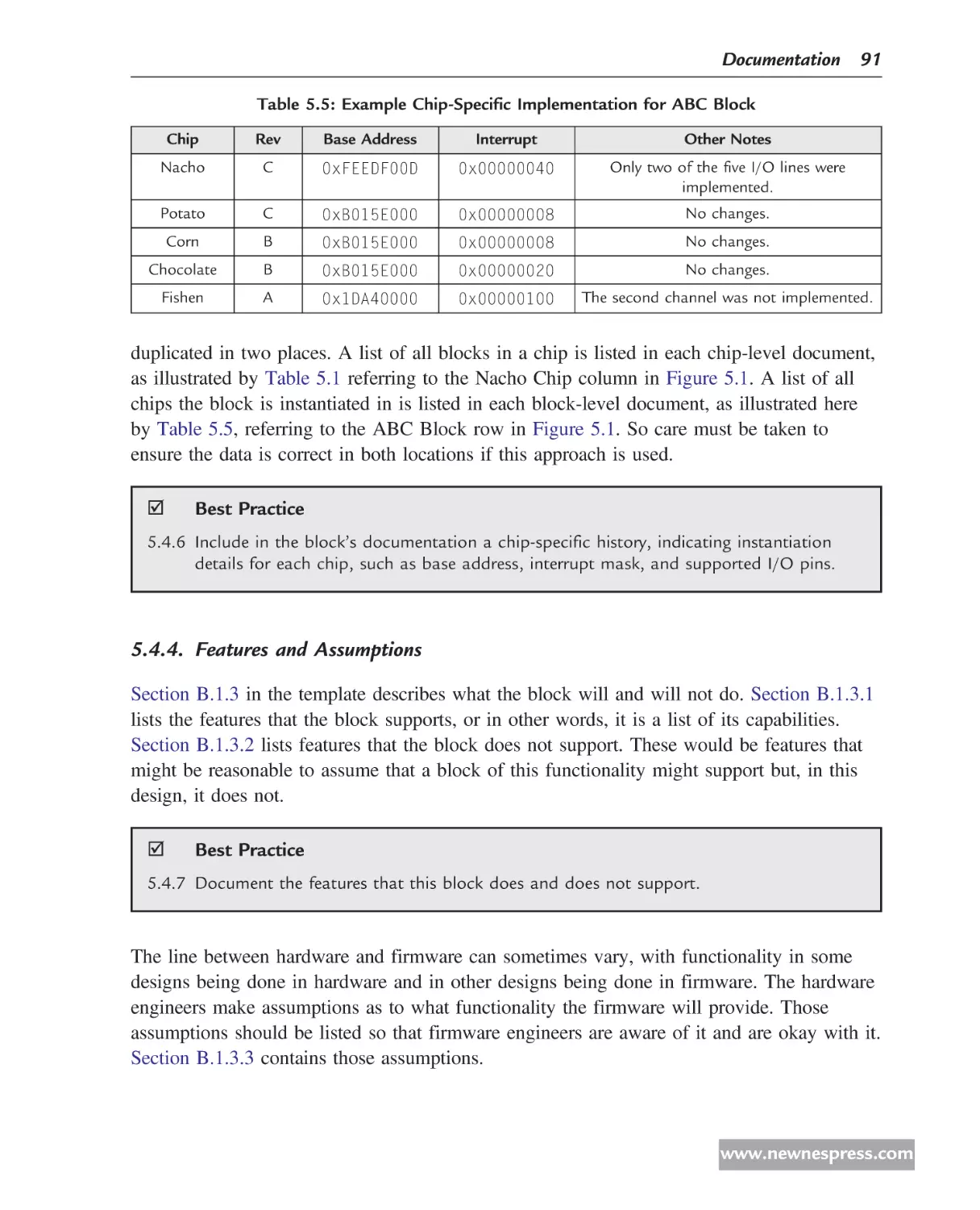
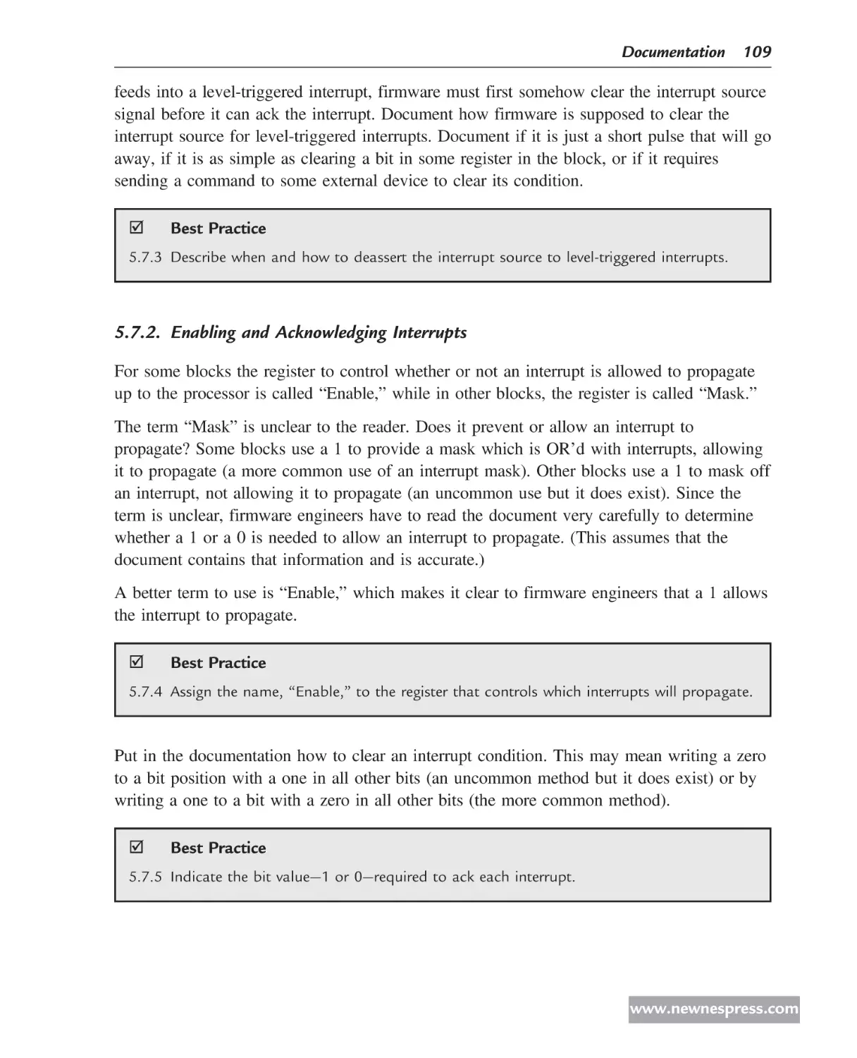
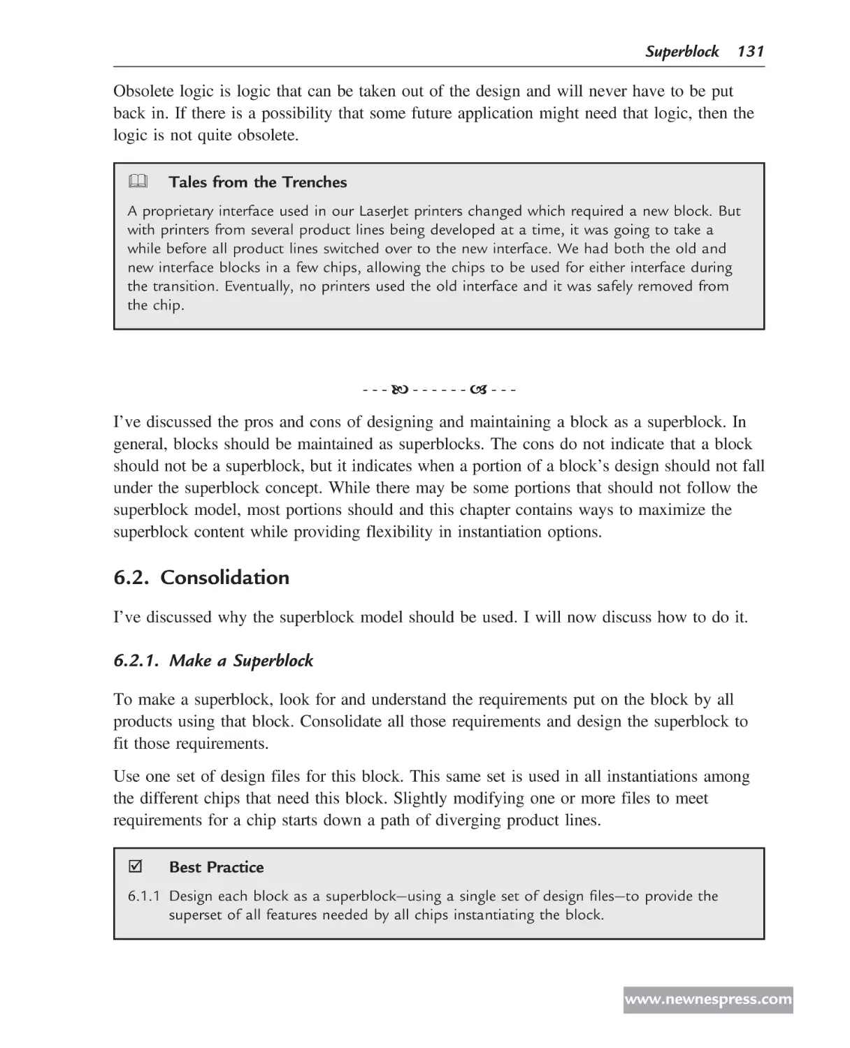
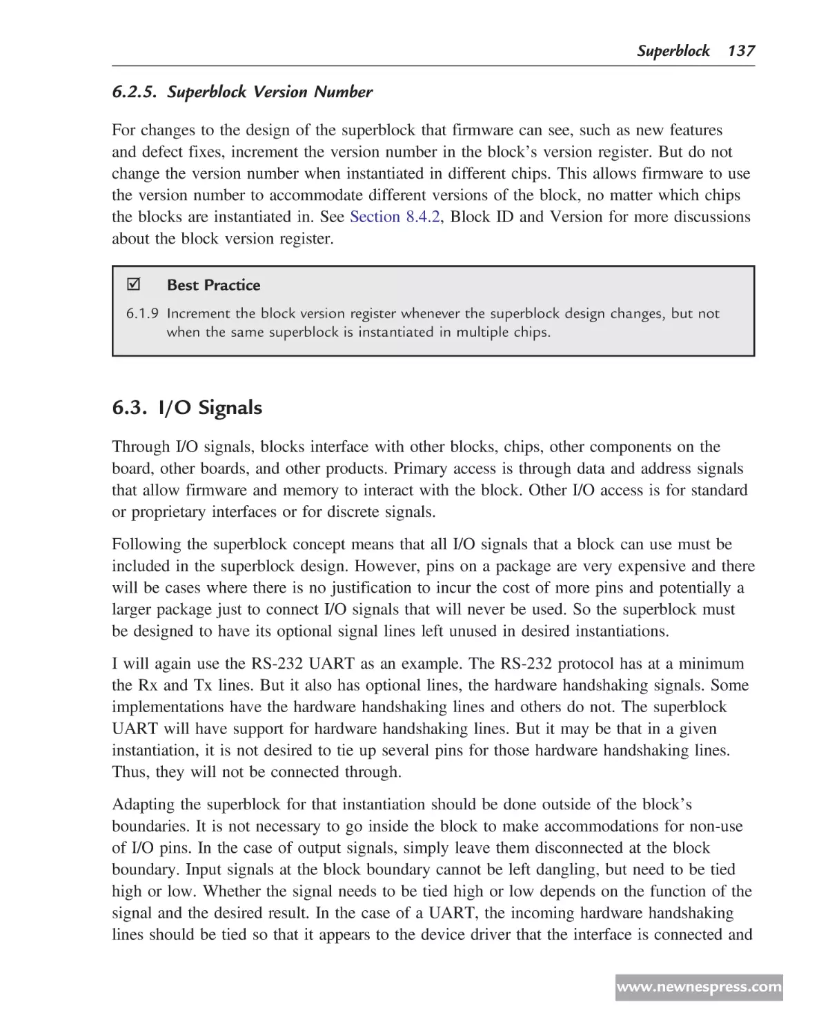
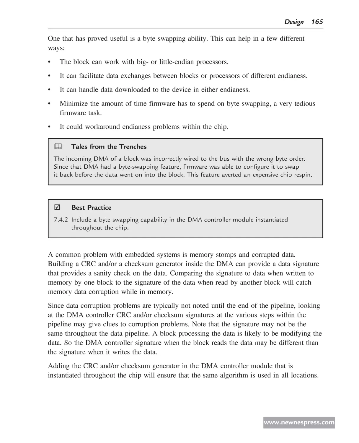
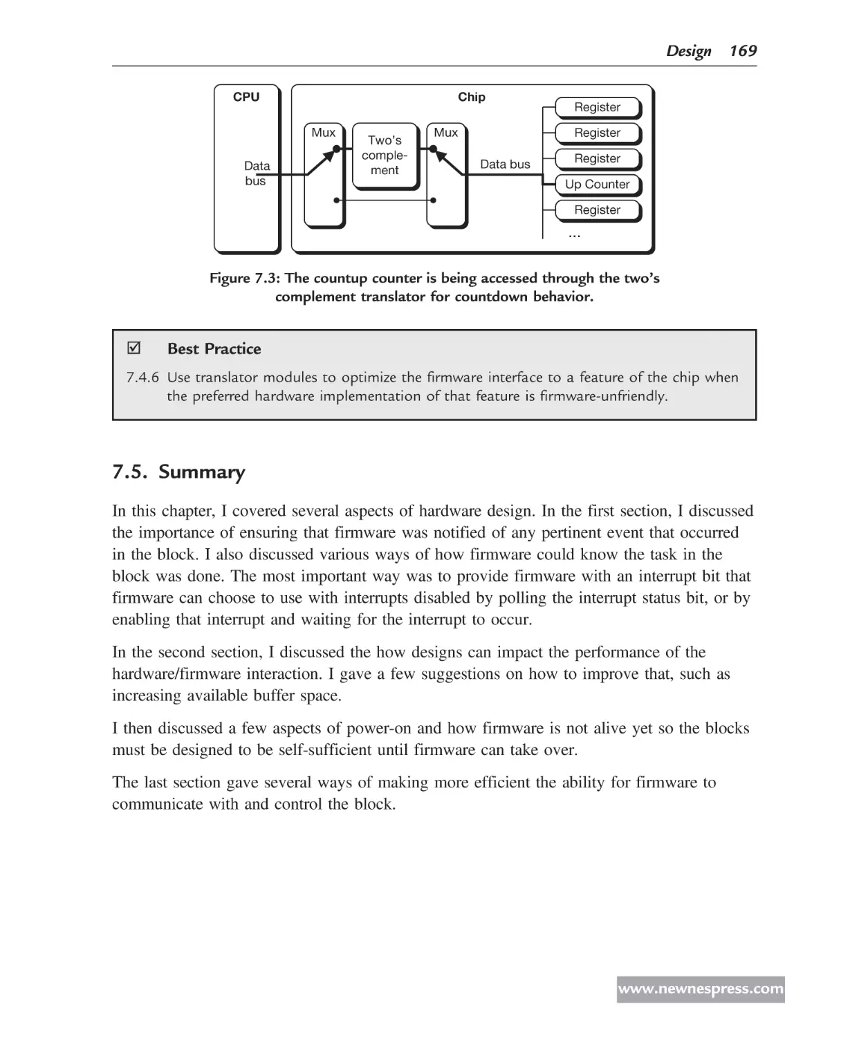
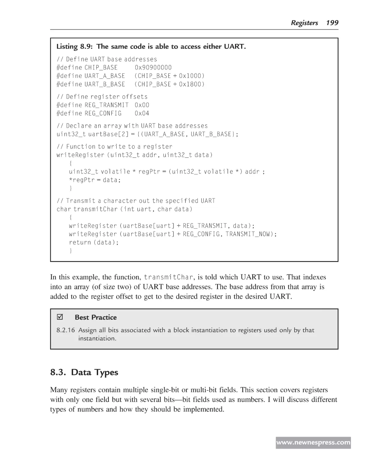
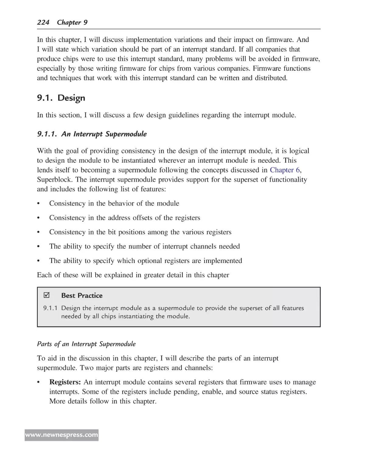
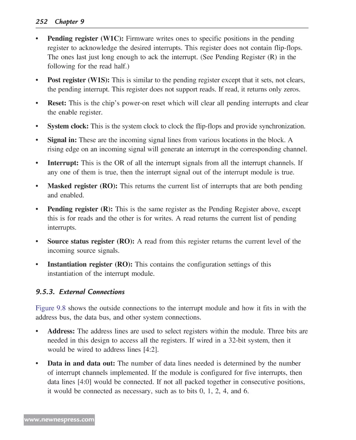
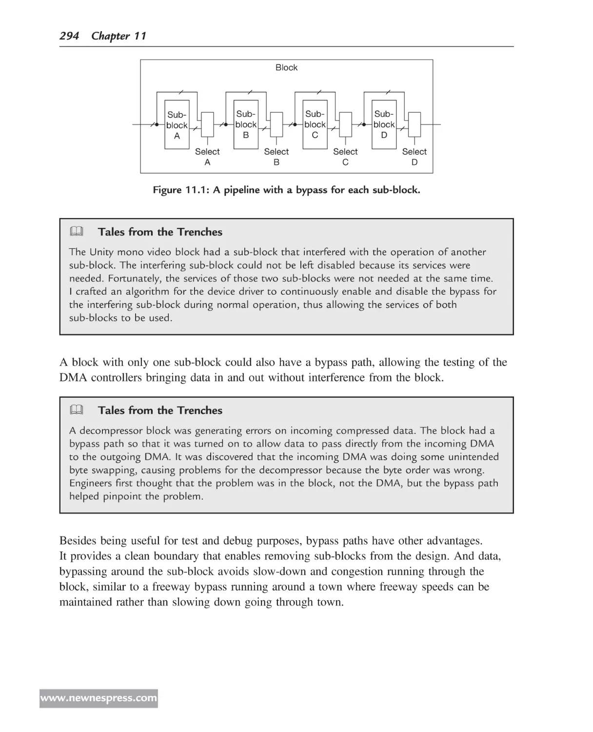
Typically there is one device driver for every block on the chip as illustrated in Figure 1.1.
This figure shows the firmware and a chip. The chip consists of several blocks and the
firmware consists of several applications and device drivers.
As an example, I will use Figure 1.1 to describe how a page is printed in a laser printer.
Suppose Block A is a USB block that receives the packets of data for a print job. Driver A
reads the incoming packets from Block A and hands them to Application A. Application A
assembles all the packets and when enough packets arrive for a page, hands it to other
applications, such as a print job interpreter which may use a rasterizing application, a data
compression application, and others. Eventually Application B is given the raster data,
which hands it to Driver B, which then sets up the registers in Block B to use that data to
control the laser.
www.newnespress.com
Introduction 7
Firmware
Additional Firmware Applications
Application A
Application B
...
Application n
Application Space
Kernel Space
Driver A
Driver B
...
Driver n
Block A
Block B
...
Block n
Chip
Figure 1.1: Relationship between applications and device
drivers in firmware and functional blocks in the chip.
Firmware
Firmware
A
A
D
B
B
Chip
...
B
B
B
Chip
Firmware
Firmware
A
A
A
A
D
D
...
B
B
Chip
...
A
D
D
B
B
A
D
A
D
D
B
Chip
...
B
A
...
D
...
B
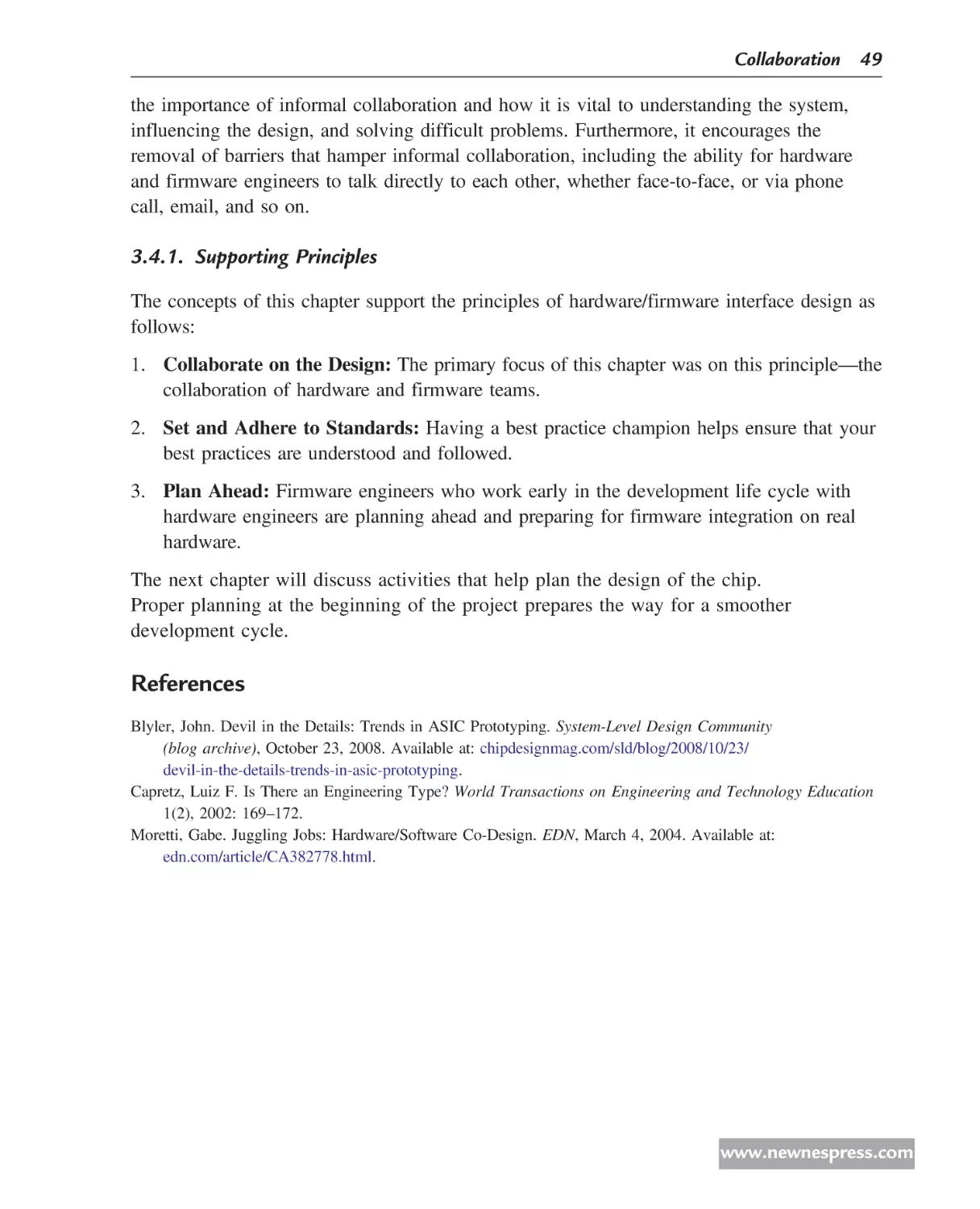
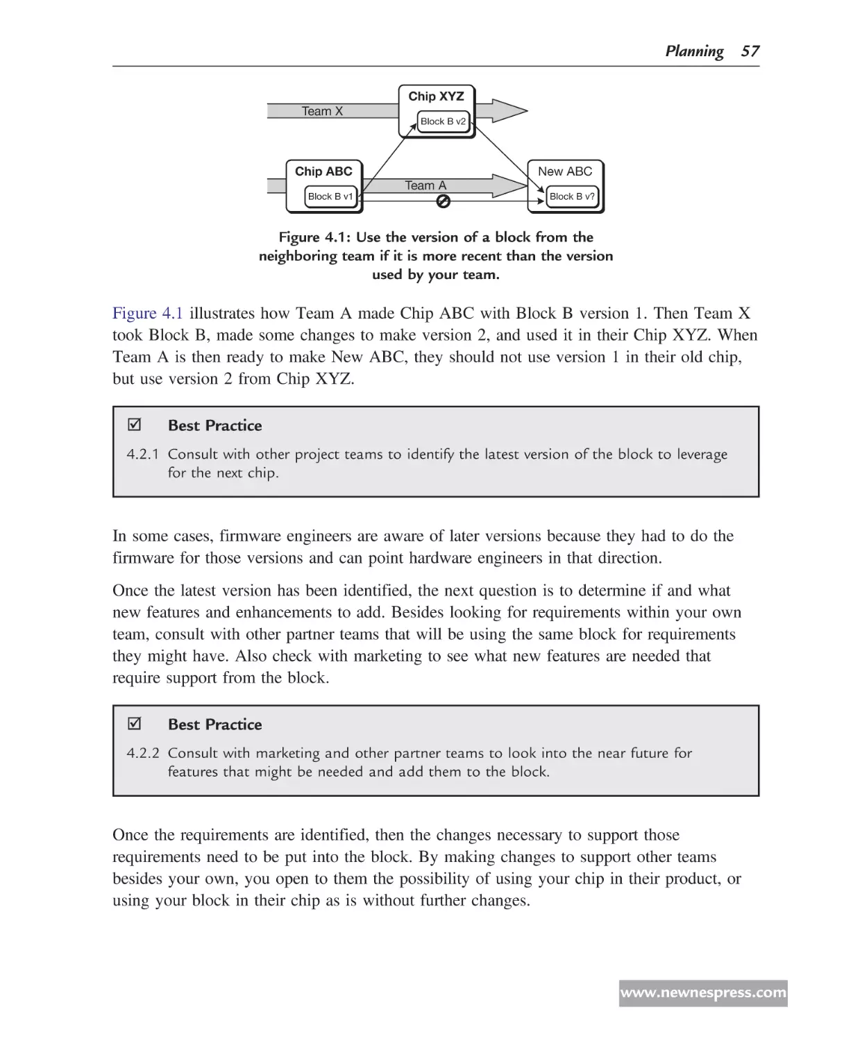
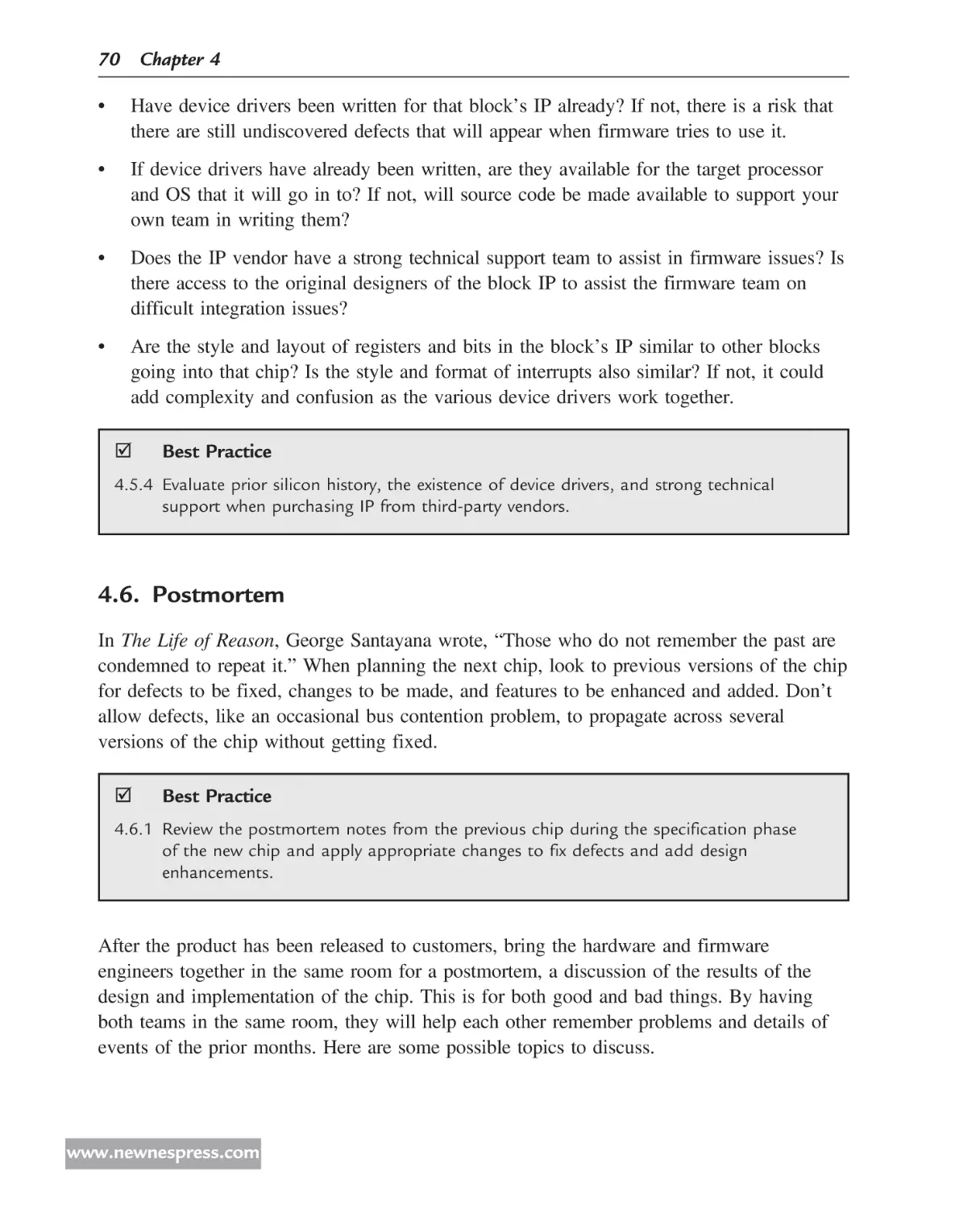
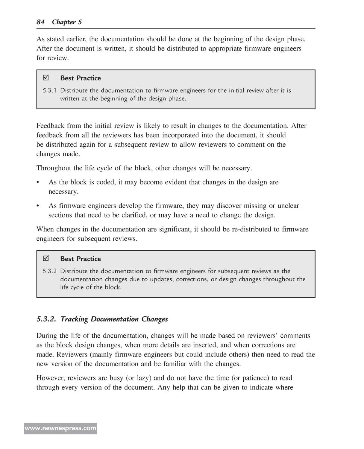
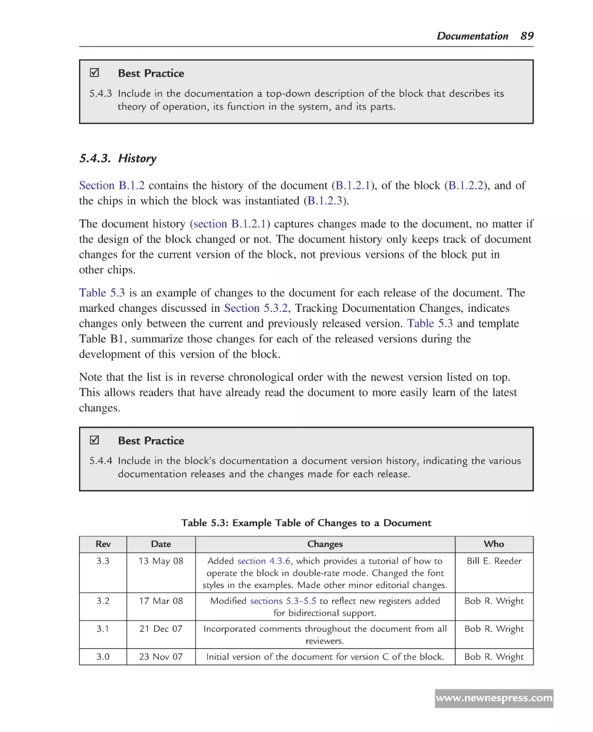
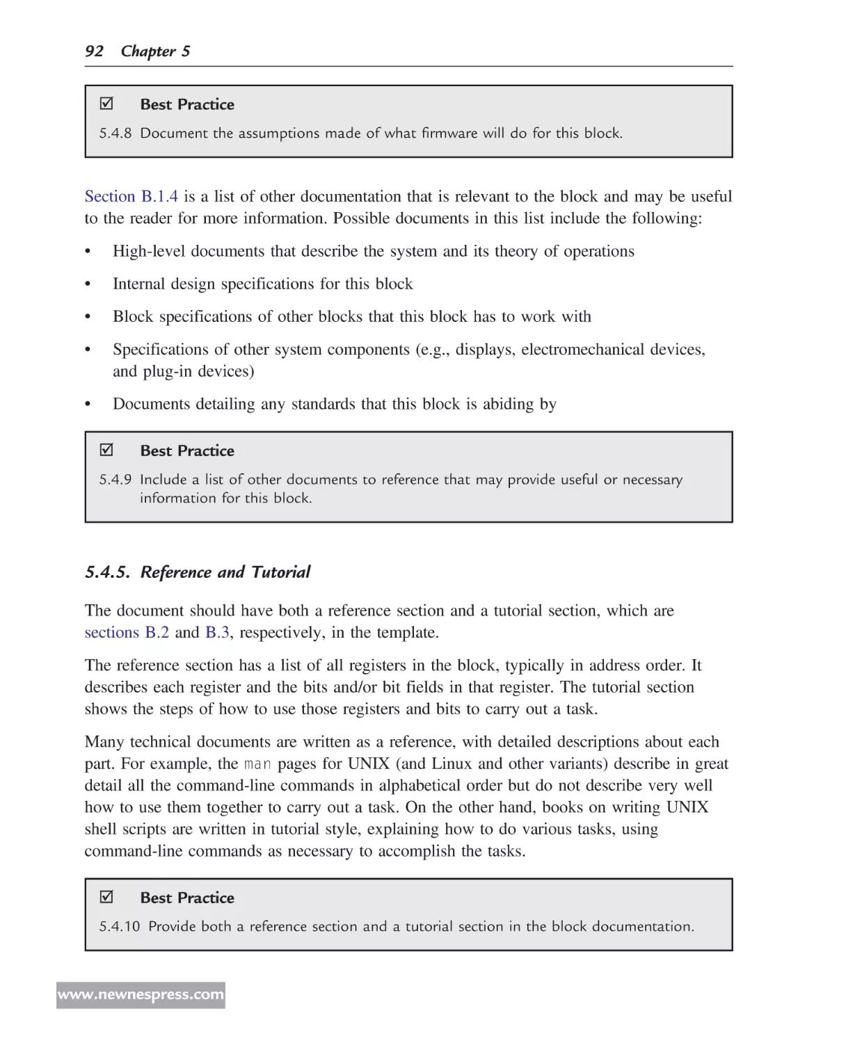
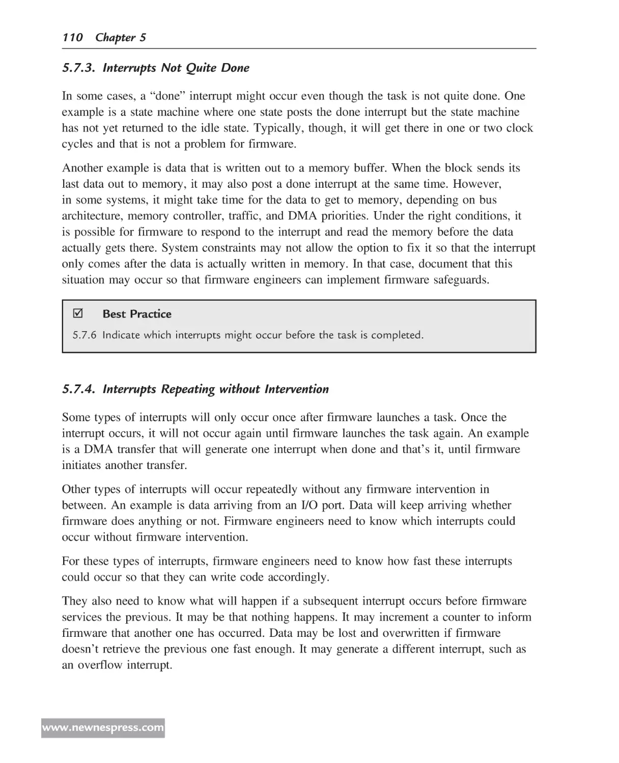
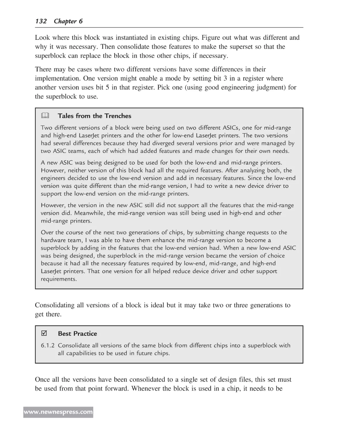
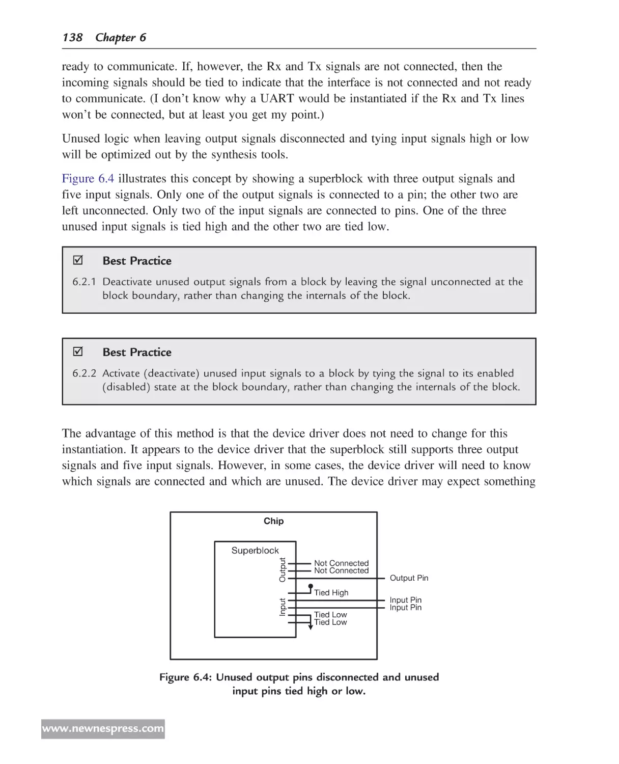
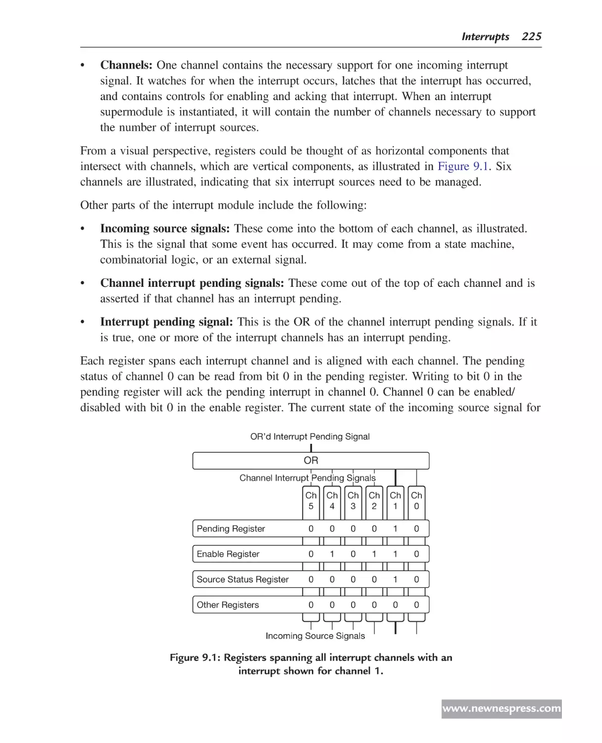
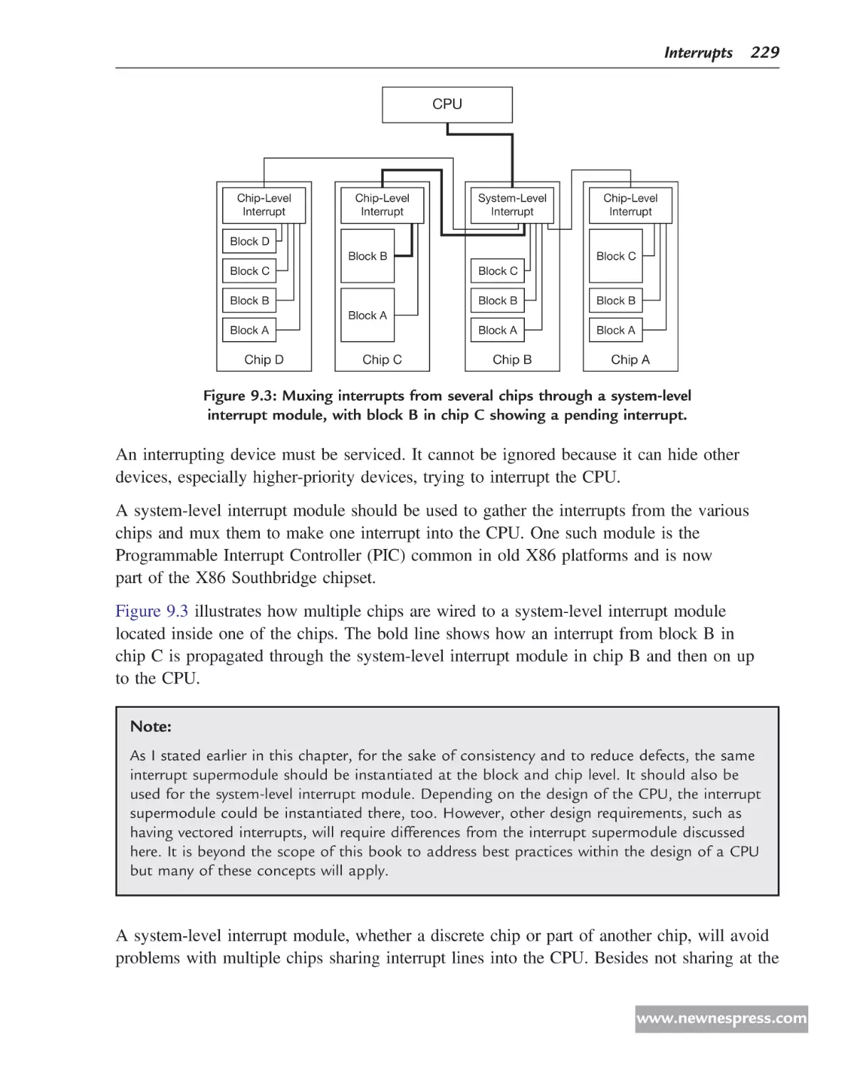
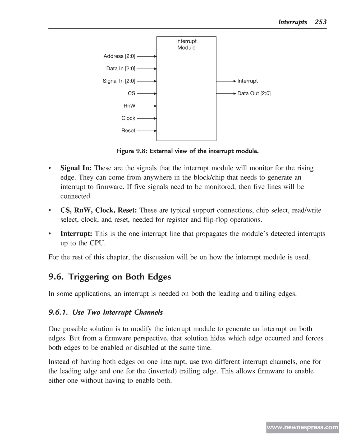
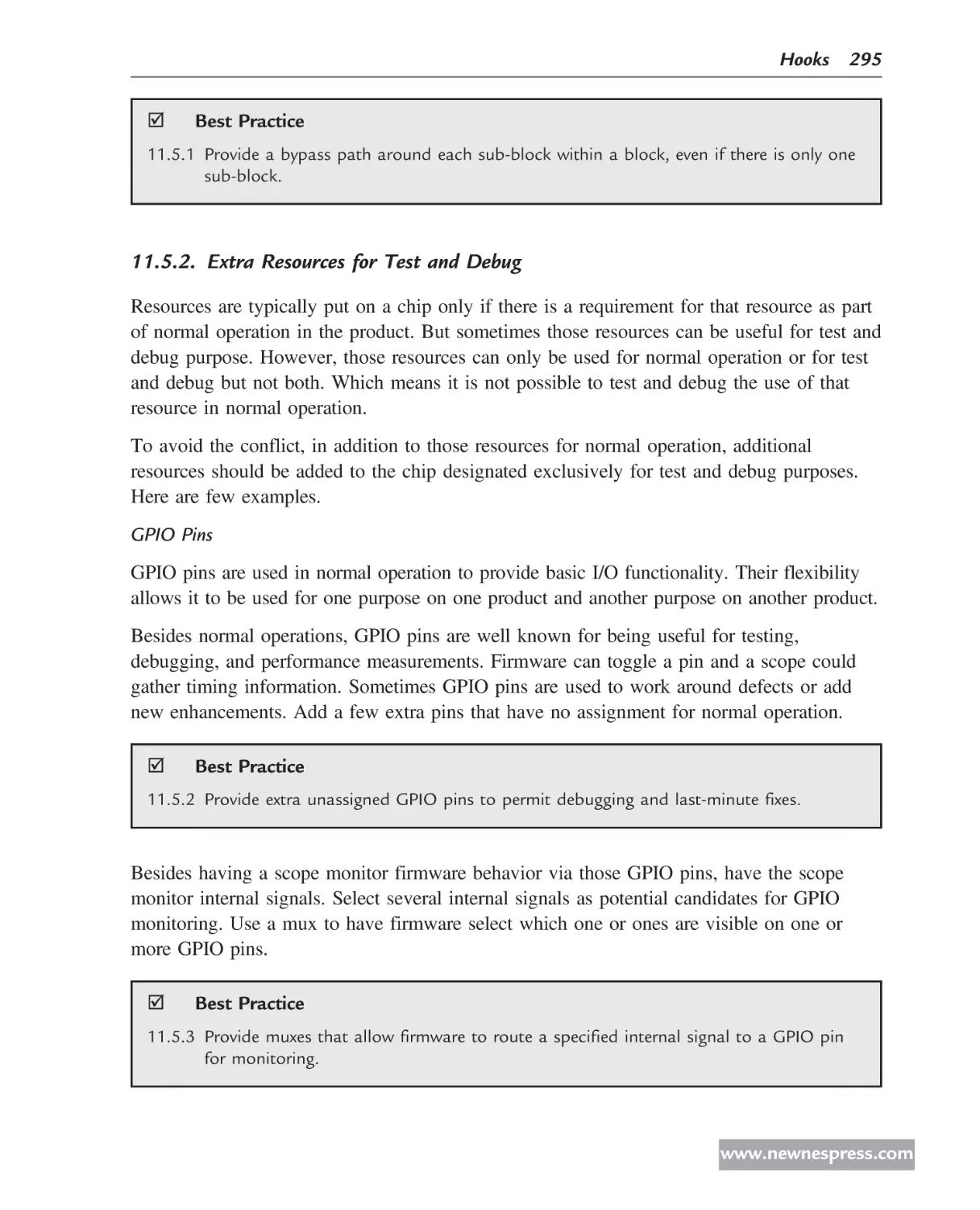
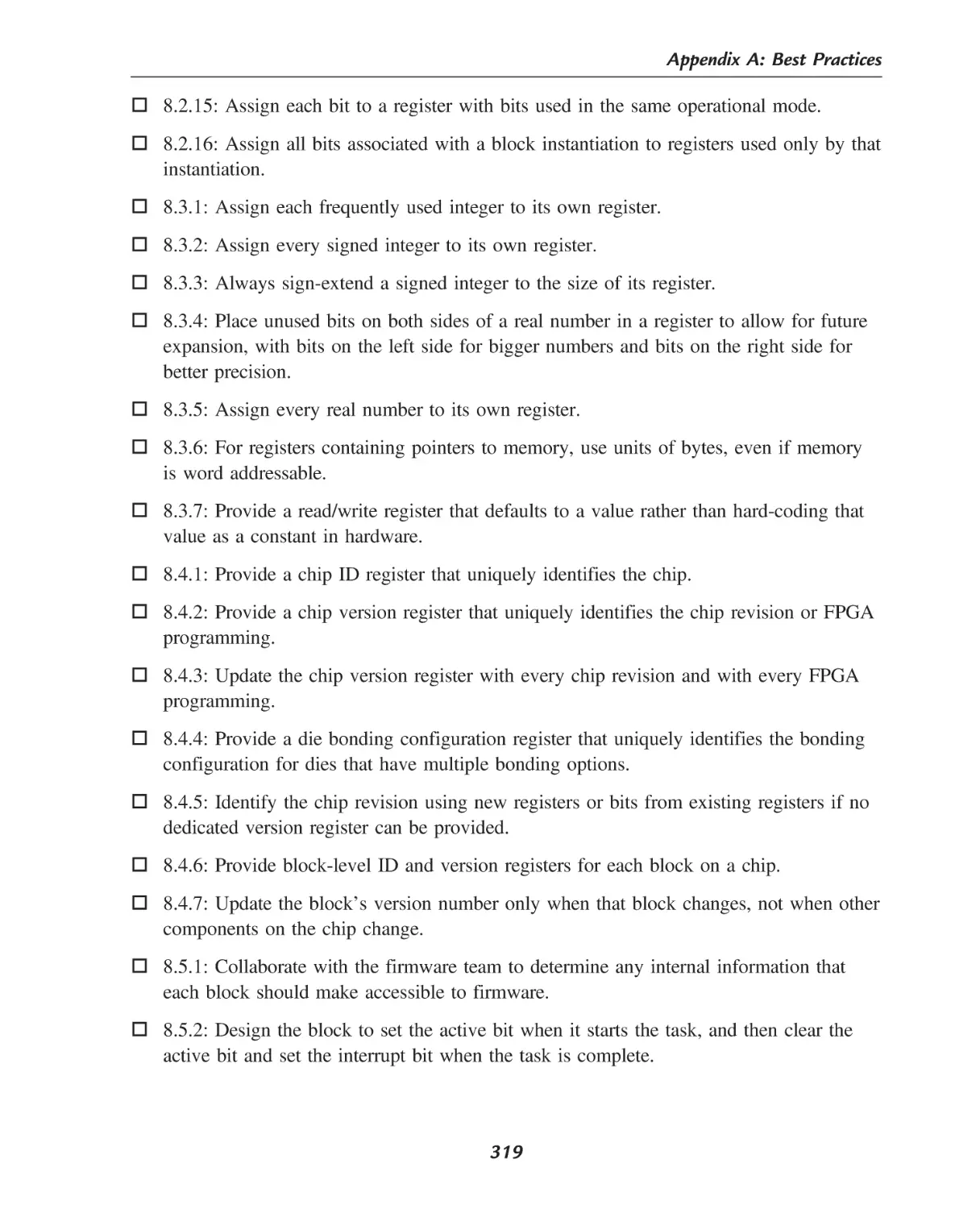
Figure 1.2: Other examples of possible firmware architectures for
applications (A), device drivers (D), and blocks (B).
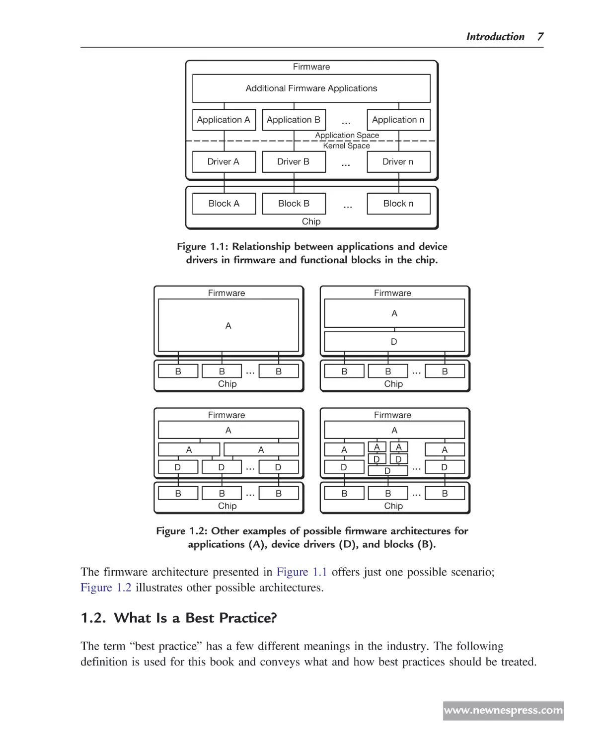
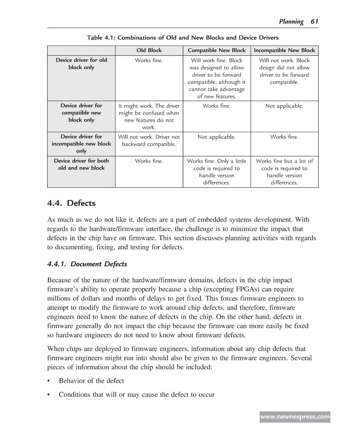
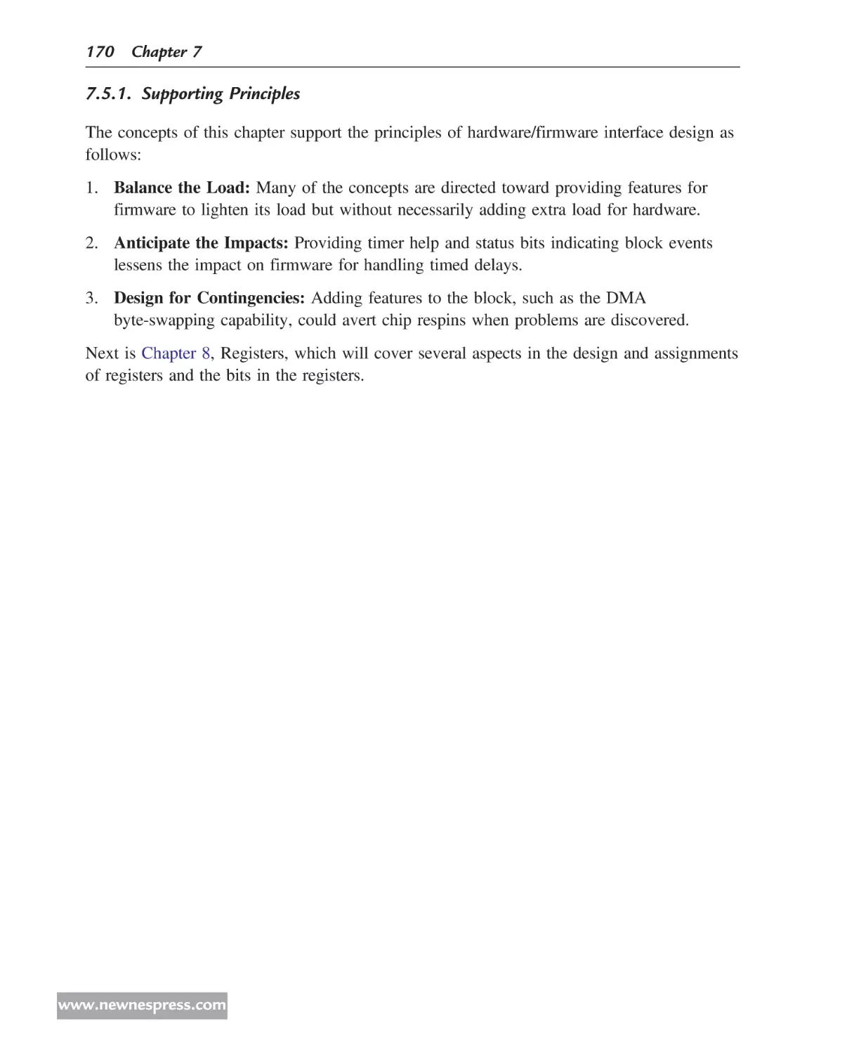
The firmware architecture presented in Figure 1.1 offers just one possible scenario;
Figure 1.2 illustrates other possible architectures.
1.2. What Is a Best Practice?
The term “best practice” has a few different meanings in the industry. The following
definition is used for this book and conveys what and how best practices should be treated.
www.newnespress.com
8 Chapter 1
A “best practice” is the most balanced or optimized way to do something in a given
situation.
An article by Ivar Jacobson, et al., in Dr. Dobb’s Journal states that “A ‘practice’ provides
a way to systematically and verifiably address a particular aspect of a project.” It also says
the following:
•
A practice does not attempt to address the entire problem. Rather, a practice attacks a
particular aspect of the problem.
•
A practice is systematic in that someone can articulate it. It is not a black art. A practice
has a clear beginning and end, and tells a complete story in usable chunks.
•
A practice includes its own verification, providing it with a clear goal and a way of
measuring its success in achieving that goal. Without verification, the practice is not
complete.
The term “best practice” also invokes negative connotations among some. In a recent article
in CIO, Michael Schrage wrote, “Best practice isn’t. Best practice is a fiction, a lie, and a con
job . . . . Never, ever allow [your operations] to be determined by anyone else’s best practices.”
The problem is that too many people forget that a “best practice” applies only in a given
situation and within a certain context. They try to apply a practice in a different situation
without giving it any thought. A wrench is the best tool for turning a bolt but not for
pounding a nail into the wall.
A best practice is not as rigid as a standard. Everybody has to abide by the standard or
things will break. Standards, once set and in place, rarely change. Best practices need to
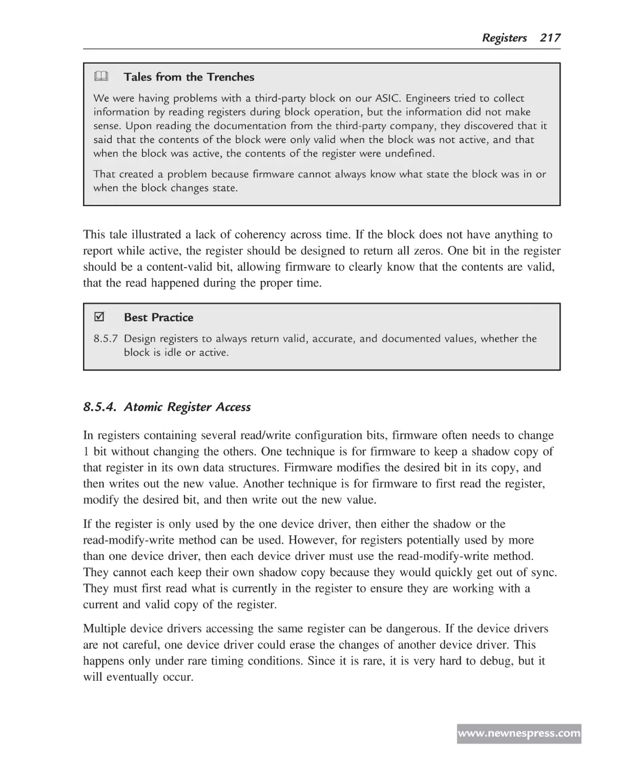
constantly be evaluated and modified as necessary.
Schrage continues, “Effective implementation [of practices] requires companies to constantly
assess the trade-offs between adoption and adaptation.”
For each best practice in this book, I explain why it is a best practice. If the “why” applies
in your situation, then the best practice might apply too. As you go through each best
practice in this book, this is what you should do:
•
Pick and choose the ones you want to use.
•
Modify them if necessary to better fit your situation and organization.
•
Decide together (both hardware and firmware teams) if and how to use them.
•
Broadcast your list to the rest of the engineers in your hardware and firmware teams.
•
Repeat as necessary.
www.newnespress.com
Introduction 9
Included with the purchase of this book is a Microsoft® Excel® spreadsheet database
containing all of the best practices presented in this book.2 This is a good place to start as
you develop your own list of best practices. The list of best practices in this book does not
pretend to be an exhaustive list of all known best practices in this domain. In addition to
what is in this book, look for best practices within your organization or elsewhere as
possible candidates to add to your own list of best practices. Look at lessons learned from
past projects, especially those that were less than successful.
1.2.1. What Is a Principle?
Several times I mention “principles” and “practices” of hardware/firmware interface design.
The terms are not interchangeable.
A “principle” is a fundamental concept that guides what is or is not a best practice.
To better illustrate the differences among principles, practices, and standards, consider the
following example:
•
Standard: “The data bits in an RS-232 start with the least-significant bit first.” This is a
specific design criterion that devices must follow to ensure interoperability. This is not
allowed to change.
•
Principle: “Prepare for Contingencies.” This is a fundamental guideline but has no
specific design action to follow. This will remain true, no matter what the product being
designed is used for.
•
Best Practice: “Make the DMA address readable by firmware as the DMA transfer
progresses.” This is a specific design criterion within the principle of “Prepare for
Contingencies” because it allows firmware to diagnose potential DMA transfer
problems. But there may be conditions under which this practice is not advisable, such
as a chip with a security requirement to not allow reads, thereby preventing rogue
firmware from sniffing DMA transfers. In this case, the best practice does not apply but
the principle, “Prepare for Contingencies,” still remains true.
Over 300 best practices are presented in this book but only seven principles. These seven
principles will be discussed in more detail in Chapter 2, Principles.
2
The best practices spreadsheet is available at the publisher’s website, elsevierdirect.com/companions/
9781856176057, and at the author’s website, garystringham.com/hwfwbook.
www.newnespress.com
10 Chapter 1
1.2.2. Benefits of Principles and Practices
Several benefits exist for implementing and using principles and best practices:
•
Reduce chip respins: A chip respin can incur up to four months of delay and millions
of dollars in cost. Surveys published by John Blyler and Geoffrey Ying in Chip Design
Magazine indicate that 45 to 70% of chip respins are due to functional/logical errors.
Following these best practices will reduce the number of chip respins due to logic
mistakes and functional errors. It also reduces the cascading impact of extra costs
incurred, and loss of engineering productivity waiting for new chips, product release
delays, and reduced market share.
•
Increase product quality: When following these design practices, many errors will
never be introduced into the chip, which increases the quality of the final product. And
the errors that are introduced will more easily be diagnosed and worked around, again
allowing the product to have a better quality than otherwise. Mike Barr wrote that “a
coding standard can help keep bugs out. It’s cheaper and easier to prevent a bug from
creeping into code than it is to find and kill it after it has entered.”
•
Earlier time to market: Avoiding respins of fabrication-based chips is one means
for allowing products to be released to market sooner. In addition, following these
design practices for fabrication-based and FPGA-based chips will allow firmware
engineers to develop their firmware sooner, again allowing the product to be
released sooner.
•
Reduce variations of chip designs: By following best practices regarding design,
features, and performance, each chip designed and produced has the potential of
extending its life by being usable in future products that otherwise would require a new
variation in the design of chip with its associated design, verification, masks, and
testing costs.
1.3. “First Time Right” Also Means . . .
The industry uses a term, “first time right,” to mean that the first run of chips that come
back from fabrication are perfect. This is extremely important since defects that cause
respins have a significant impact on schedule and costs. Wolfgang Rosenstiel states that
“first time right” is the most important goal and it requires that engineers ensure a perfect
design before the production is started. One engineering manager in the industry told me
that he had been given quotas that a certain percentage of his team’s chips have to be “first
time right.”
www.newnespress.com
Introduction 11
Significant effort is put into the design of a chip, from the front to the back end, to reduce
the risk of errors. Many simulations and tests are executed. Design verifications are
carried out. Many products and techniques exist that are designed to help ensure correct
functionality and achieve “first time right.”
But no matter how hard engineers try, it is nearly impossible to make perfect chip designs.
We cannot think of all the possible use cases in advance. We cannot foresee system
interaction problems. We cannot assure that 100% of the defects have been found. Chips do
become better as the designs mature and stabilize but for new designs, it is difficult.
However, by expanding the definition of “first time right” to include more in the case of
imperfect design, we can make “first time right” more achievable. The expansion of the
definition includes other aspects that will aid in that effort, such as creating the chip in such
a way as to make the design:
1. Easier to program.
2. Easier to debug.
3. Easier to work around defects.
This expansion gives firmware engineers a greater probability of making the chip usable in
products in spite of defects that sneak in, thus allowing the chip to be used without a respin.
1.3.1. Easier to Program
Chips can be designed to ease the efforts required by firmware engineers who write the
code to control the chip. By helping firmware engineers do their job, the chip becomes
more usable, especially when it comes to learning about the chip and solving problems that
arise while developing the firmware.
Reviewing the design of the chip with firmware engineers increases the chance that the
design will work with the firmware itself. Improving the documentation will help the
firmware engineers learn and understand the chip. Judicious layout of the register formats
will help the firmware engineers program and control the chip without complicated
interactions. Consistency in how similar functions operate throughout the chip will reduce
errors as existing firmware code is leveraged.
1.3.2. Easier to Debug
Designs frequently have defects and flaws. The challenge is for engineers to be able to
diagnose them when they come across them.
www.newnespress.com
12 Chapter 1
When (not if, but when) defects are found in chips, the first task is to diagnose the root
cause of the defect. It is only after the root cause of the defect is found and clearly
understood that a fix or workaround can be developed and implemented.
Anything that can be done to aid the diagnosis of defects will be of help. Since it is
unknown beforehand where any defects will occur, placing debugging hooks throughout the
chip will increase the likelihood that some will be in the right place when defects are
encountered.
1.3.3. Easier to Work around Defects
Once defects are found and well understood, the next step is to find a way to work around
them. If firmware can be written to work around the defects, it will save the expense and
delay of having to respin the chip.
Working around defects may mean being able to disable or bypass a portion of the block,
use extra registers to allow firmware to peek into the block for possible anomalous
conditions, or use other means to allow firmware to poke a portion of the block.
While using such back-door methods is not preferable, it does give the option of making the
chip functional enough to ship products without incurring an expensive respin.
---b------a--The principles and practices in this book support “first time right” by making the chip easy to
program, to debug, and to work around defects.
Note:
My expansion on the phrase, “first time right,” is not to be used as an excuse for lazy designs
that “should work just fine.” Engineers should still do the best design work they can. By
following the principles and practices in this book, they will have greater success in producing
chips that can be used in products the first time, even though there may be flaws in the
design.
Many of the concepts in the book should be applied to the design of a chip even though it
is not known in advance if they will be required. Applying them will increase the
probability that the chip will succeed the first time. If just one of these concepts saves a
chip from a respin, then all the work to employ the many concepts is worth it to achieve
“first time right.”
www.newnespress.com
Introduction 13
1.4. Target Audience
Since this book addresses the interface between hardware and firmware, the target audience
is the engineers on both sides of the hardware/firmware divide. However, because of the
nature of the business, the hardware engineers produce something that firmware engineers
must use. This means that the bulk of the work on the hardware/firmware interface as
discussed in this book lies primarily on the shoulders of hardware engineers. Firmware
engineers have a role in the design of the chip, but they are not as involved.
1.4.1. Hardware Engineers
Within the hardware engineering community, this book targets more specifically those
working on the front-end of chip design, and in particular, those working on the interface
between the chip and firmware, which is primarily realized in the form of registers and
interrupts.
It is expected that the hardware engineering reader is familiar with basic digital logic and
chip design practices. Examples in this book use Verilog, but only a cursory knowledge of
the language is required. Similarly, only cursory knowledge of C is needed in order to
understand the firmware examples presented in the book.
In particular, this is not a book on Verilog (or VHDL, System C, System Verilog, or other
HDL derivatives or extensions). It does not give specific instructions on how to implement
the concepts; instead, it describes how the chip should present itself to firmware.
1.4.2. Firmware Engineers
Within the firmware engineering community, this book targets those writing the lower-level
code; that is, those portions of code—such as device drivers—tasked with dealing directly
with the hardware. While the bulk of the best practices are implemented by hardware
engineers, it is beneficial for firmware engineers to also know the concepts so they can be
on the same page with respect to the problems being addressed and the methods that will be
agreed upon to address those problems.
It is expected that the firmware engineering reader has some familiarity with firmware
development, can read C code, and has some awareness of the chip development process.
Firmware readers should also be able to read Verilog and VHDL code well enough be
aware of the general concepts of the design, but not necessarily understand all the nuances
of the language and its syntax.
www.newnespress.com
14 Chapter 1
Note:
While it is possible for firmware engineers to read Verilog and VHDL files, they must
remember that in specific contexts, the lines of code are being executed concurrently in
parallel (all at once,) as opposed to firmware code that is executed in serial. Consider the
following example:
X = Y;
Y = X;
In C/C++, both variables will end up containing the original contents of Y. In Verilog/VHDL,
the contents of the variables will be exchanged.
1.4.3. This Book in a University Setting
This book has application in a university setting, such as a senior design project where electrical
engineering students and computer science students have to work together. An example
curriculum and exercise method is available at the publisher’s website, elsevierdirect.com/
companions/9781856176057, and at the author’s website, garystringham.com/hwfwbook.
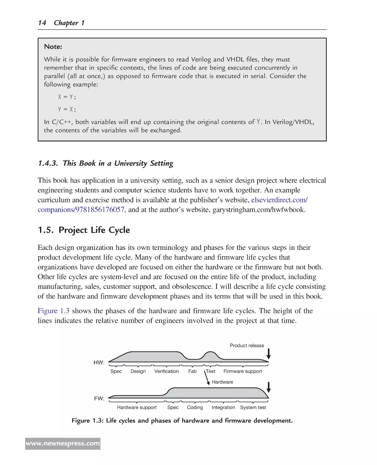
1.5. Project Life Cycle
Each design organization has its own terminology and phases for the various steps in their
product development life cycle. Many of the hardware and firmware life cycles that
organizations have developed are focused on either the hardware or the firmware but not both.
Other life cycles are system-level and are focused on the entire life of the product, including
manufacturing, sales, customer support, and obsolescence. I will describe a life cycle consisting
of the hardware and firmware development phases and its terms that will be used in this book.
Figure 1.3 shows the phases of the hardware and firmware life cycles. The height of the
lines indicates the relative number of engineers involved in the project at that time.
Product release
HW:
Spec
Design
Verification
Fab
Test
Firmware support
Hardware
FW:
Hardware support
Spec
Coding
Integration
System test
Figure 1.3: Life cycles and phases of hardware and firmware development.
www.newnespress.com
Introduction 15
The hardware team is more heavily involved at the beginning with the specification, design,
and verification, while the firmware team is more involved later in the project with the
coding, integration, and system testing. In the beginning, the firmware team supports the
hardware team by collaborating on the design. Near the end, the hardware team supports the
firmware team as they get the hardware and firmware working together as a complete
system.
Tools are available that allow co-development activities where firmware engineers are able
to develop code before hardware is ready. Such tools include co-simulation, virtual
prototypes, and FPGA prototypes.
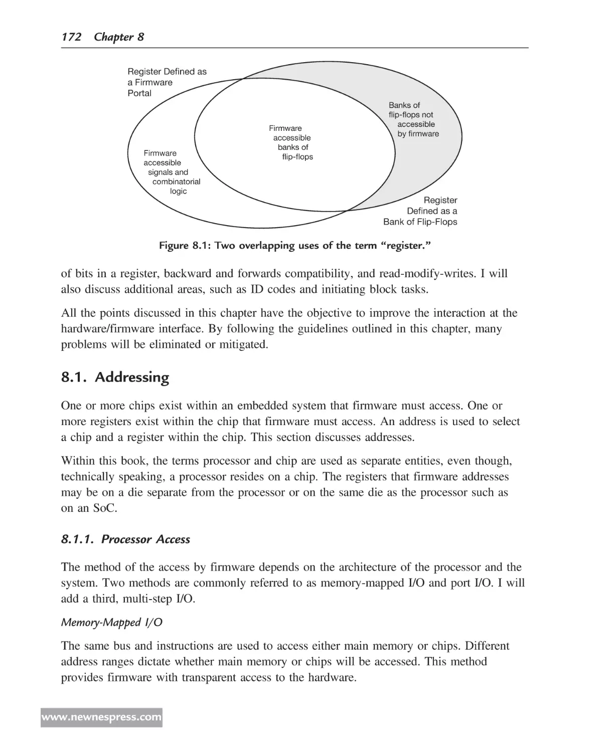
1.6. Case Study
Case studies are useful to learn something via an in-depth examination of an event,
individual, or activity. Some case studies are set up in advance to take detailed notes
throughout the activity. Others examine an unusual event from the past to learn from it.
Consider the following example.
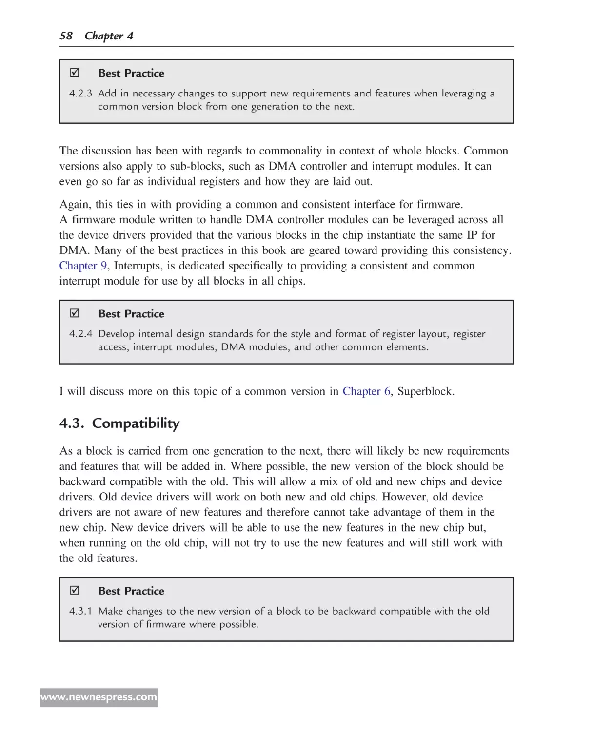
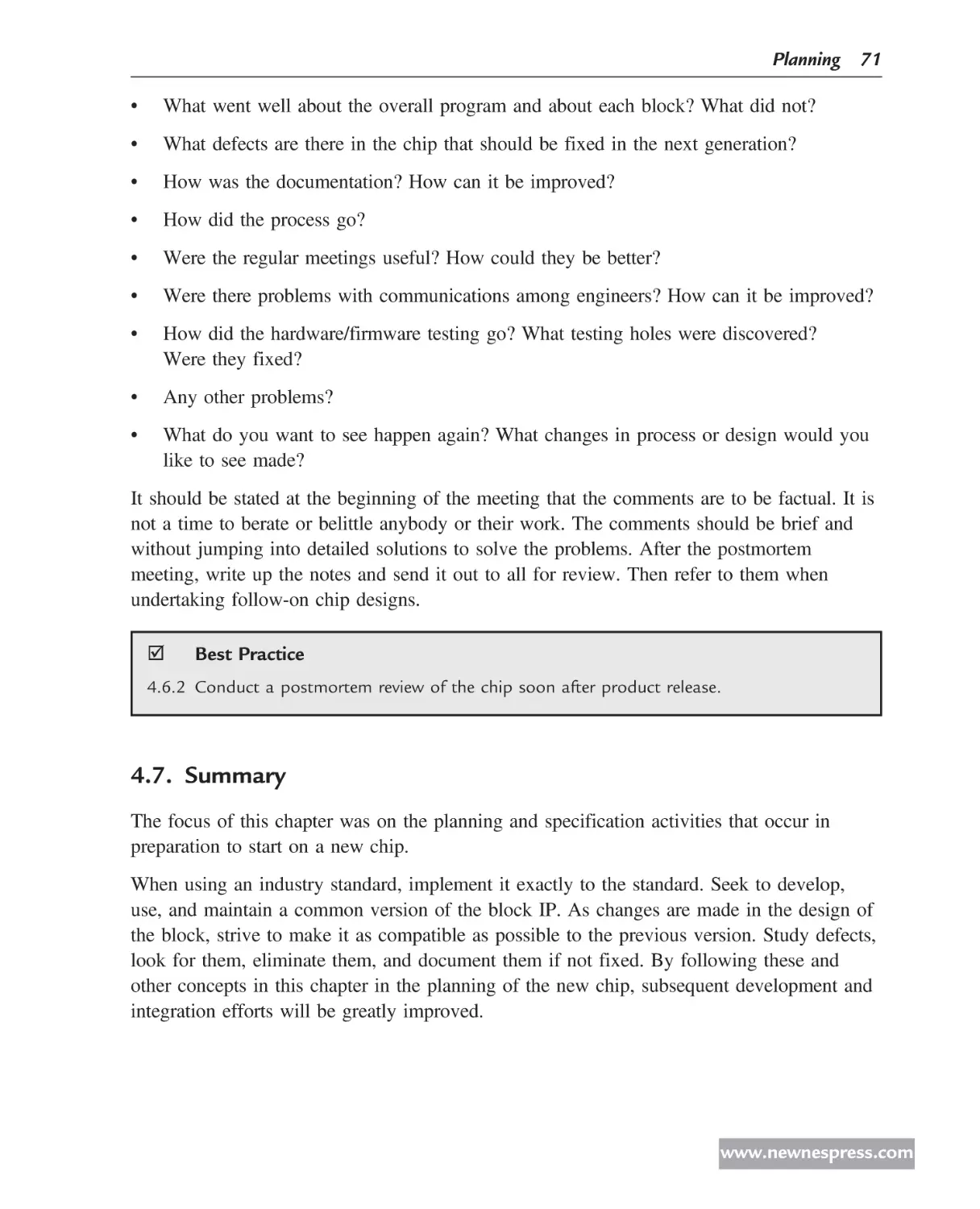
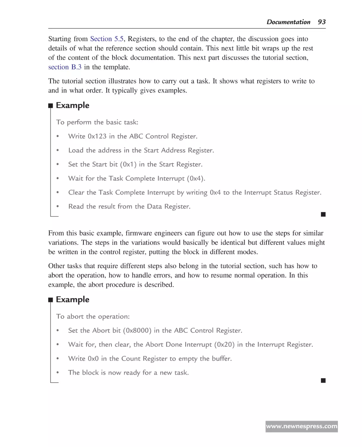
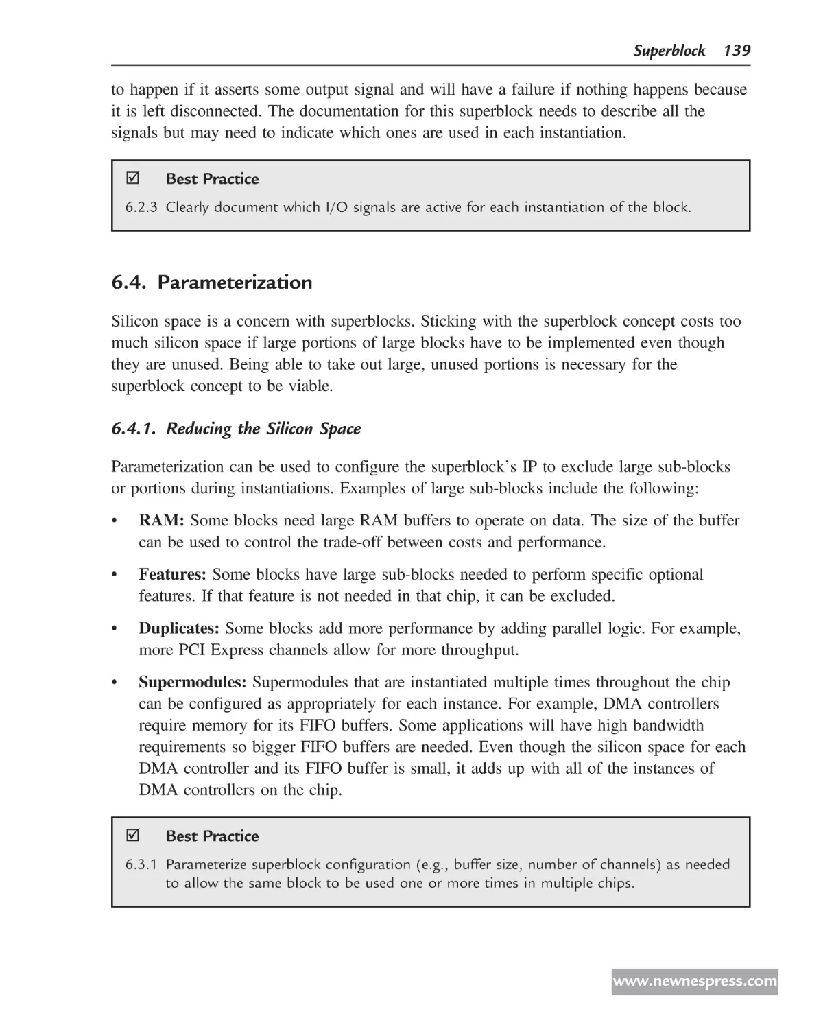
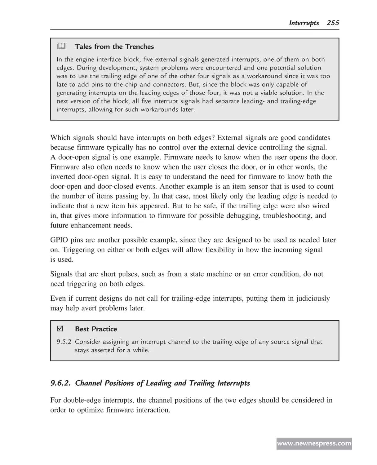
1.6.1. Monochrome Video Block in the Unity ASIC
The Unity ASIC was developed by Hewlett-Packard engineers for use in some of their
LaserJet® printers. It contains several blocks, including standard I/O and data compressors.
One of the blocks is the monochrome (mono) video block for use with HP’s monochrome
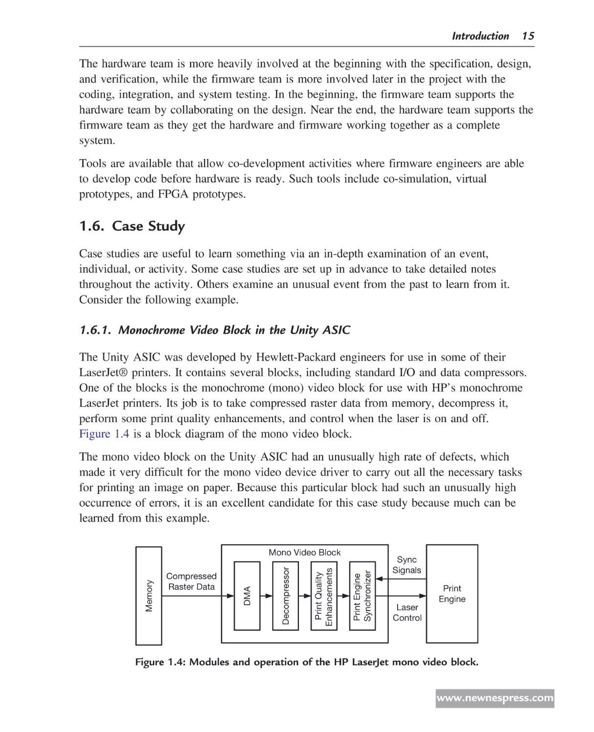
LaserJet printers. Its job is to take compressed raster data from memory, decompress it,
perform some print quality enhancements, and control when the laser is on and off.
Figure 1.4 is a block diagram of the mono video block.
The mono video block on the Unity ASIC had an unusually high rate of defects, which
made it very difficult for the mono video device driver to carry out all the necessary tasks
for printing an image on paper. Because this particular block had such an unusually high
occurrence of errors, it is an excellent candidate for this case study because much can be
learned from this example.
Print Engine
Synchronizer
Print Quality
Enhancements
Decompressor
Compressed
Raster Data
DMA
Memory
Mono Video Block
Sync
Signals
Print
Engine
Laser
Control
Figure 1.4: Modules and operation of the HP LaserJet mono video block.
www.newnespress.com
16 Chapter 1
A
ASIC
B
ASIC
C
ASIC
Unity
ASIC
E
ASIC
Mono
Video
Mono
Video
Mono
Video
Mono
Video
Mono
Video
Leveraged
Good
Leveraged
Leveraged
??
??
Not
Used
Not
Used
Leveraged
Bad
Good
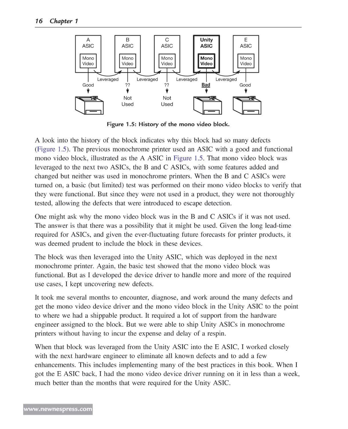
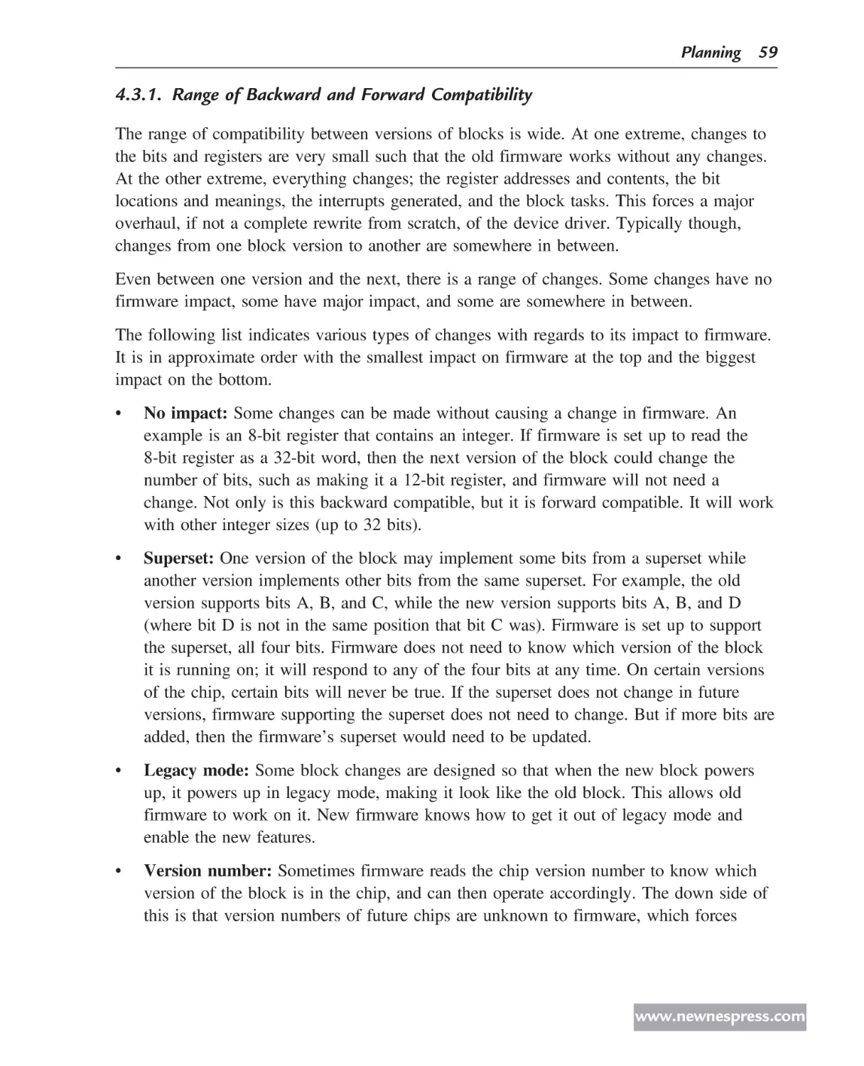
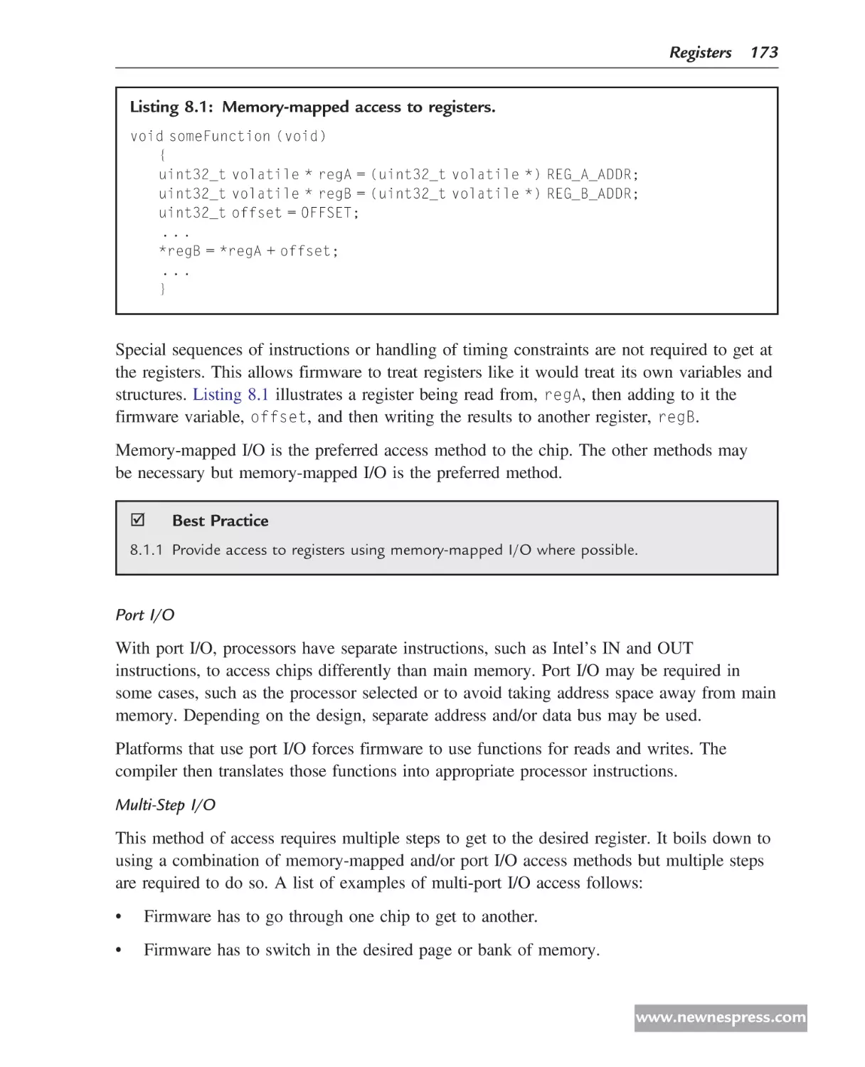
Figure 1.5: History of the mono video block.
A look into the history of the block indicates why this block had so many defects
(Figure 1.5). The previous monochrome printer used an ASIC with a good and functional
mono video block, illustrated as the A ASIC in Figure 1.5. That mono video block was
leveraged to the next two ASICs, the B and C ASICs, with some features added and
changed but neither was used in monochrome printers. When the B and C ASICs were
turned on, a basic (but limited) test was performed on their mono video blocks to verify that
they were functional. But since they were not used in a product, they were not thoroughly
tested, allowing the defects that were introduced to escape detection.
One might ask why the mono video block was in the B and C ASICs if it was not used.
The answer is that there was a possibility that it might be used. Given the long lead-time
required for ASICs, and given the ever-fluctuating future forecasts for printer products, it
was deemed prudent to include the block in these devices.
The block was then leveraged into the Unity ASIC, which was deployed in the next
monochrome printer. Again, the basic test showed that the mono video block was
functional. But as I developed the device driver to handle more and more of the required
use cases, I kept uncovering new defects.
It took me several months to encounter, diagnose, and work around the many defects and
get the mono video device driver and the mono video block in the Unity ASIC to the point
to where we had a shippable product. It required a lot of support from the hardware
engineer assigned to the block. But we were able to ship Unity ASICs in monochrome
printers without having to incur the expense and delay of a respin.
When that block was leveraged from the Unity ASIC into the E ASIC, I worked closely
with the next hardware engineer to eliminate all known defects and to add a few
enhancements. This includes implementing many of the best practices in this book. When I
got the E ASIC back, I had the mono video device driver running on it in less than a week,
much better than the months that were required for the Unity ASIC.
www.newnespress.com
Introduction 17
Many of the best practices and tales from the trenches in this book stem from that mono
video block on the Unity ASIC.
In discussing the many problems of this particular block, let me make it clear that I do not
do so to malign HP engineers. HP is well known for engineering excellence and these
LaserJet hardware engineers are no exception. This particular case is an anomaly and was
the result of a series of events over time. None of the other blocks on the Unity ASIC, nor
any of the blocks on any other HP ASICs that I worked on, had anywhere near the level of
problems exhibited by this Unity mono video block.
The reason I discuss this block is because there is much that can be learned from it. The
lessons learned have been applied to other blocks in subsequent HP ASICs and have proved
beneficial to HP. My experience with that block inspired me to write this book. HP has
graciously allowed me to use this example for, in the words of one manager, “the
betterment of the industry.”
1.6.2. A Case Study of a Good Example?
The Unity mono video block is a case study with many negative examples. What could I
use as a case study of positive examples? That is trickier, because it is difficult for people
to identify good things that avoided problems.
For example, suppose you are driving a car on an icy roadway when another car slides
through an intersection just ahead of you. You slam on your brakes. If your car has an ABS
(automatic braking system), you are likely to keep control of your car and avoid an
accident. How much time and money did you save by not crashing? You avoided going to
the hospital with its associated costs, pain, and recuperation time. You avoided the time and
expense of repairing the car or purchasing a new car. You avoided the disruption in your
life and your work. What is a dollar figure for this? You cannot come up with it. However,
if you had been driving a car without an ABS and crashed, it is easy to tally up the medical
costs, the car repair or replacement costs, and the lost time at work.
Following the principles and practices in this book will help you avoid costly delays and
respins, but you will have a difficult time calculating a dollar amount that you saved. However,
if one day you are able to identify just one best practice that was implemented which avoided
a million-dollar respin, then the effort to implement all of them will have been worth it.
1.7. Summary
Aside from laying the groundwork for this book, this chapter has two important messages.
One is to define the hardware/firmware interface as the junction where the hardware and
the firmware meet. This intersection is often ignored, hence the purpose of this book.
www.newnespress.com
18 Chapter 1
The second important message is the concept of “first time right,” meaning more than just
trying to get a perfect design. It also means putting design practices into place to avoid
defects, putting in hooks to diagnose defects, and making it easy to work around defects.
This chapter also defined several terms in the context of this book, such as “chip,” “best
practice,” and “firmware.” These terms (and others) are also defined in Appendix D,
Glossary.
The next chapter is devoted to the seven principles of hardware/firmware interface design
that will provide the overarching guidance for the best practices described in the remainder
of this book.
References
Barr, Mike. Bug-Killing Standards for Firmware Coding. Embedded.com, March 24, 2009. Available at:
embedded.com/design/opensource/216200567.
Blyler, John. Chip Design Magazine. Devil in the Details: Trends in ASIC Prototyping. Chip Design Magazine,
October 23, 2008. Available at: chipdesignmag.com/sld/blog/2008/10/23/devil-in-the-details-trends-in-asicprototyping.
Ganssle, Jack. Managing Embedded Projects. Tutorial at Embedded Systems Conference. San Francisco, March
2005.
Jacobson, Ivar, Pan-Wei, Ng, and Ian, Spence. Enough of Processes: Let’s Do Practices. Dr. Dobb’s Journal,
May 2007. Available at: ddj.com/architect/198800543.
Rosenstiel, Wolfgang. Hardware/Software Co-Design: Principles and Practices. Edited by Jørgen, Staunstrup
and Wayne, Wolf. Norwell, MA: Kluwer Academic Publishers, 1997.
Schrage, Michael. Making IT Work: Don’t Solve Problems with Best Practices. CIO, February 15, 2003.
Available at: cio.com/article/31713/Making_IT_Work_Don_t_Solve_Problems_With_Best_Practices.
Ying, Geoffrey. Chip Design Magazine. Start at the Top to Reduce Re-Spins for Analog-Digital Chips. Chip
Design Magazine, June/July 2005. Available at: chipdesignmag.com/display.php?articleId=117&issueId=11.
www.newnespress.com
CHAPTER 2
Principles
As I was adding yet another best practice to my collection, I asked myself, “Why is this one
important? Why does it belong?” I thought about it and then answered my own question, “It
supports version independence.” The term “version independence” had just popped into my
head. (I have since replaced it with “compatibility.”) But I realized it was a good way to
describe why many of the best practices belong in the list. Then I realized that it was a
guiding principle and that all of the best practices in the collection were there because of
some fundamental principles that I was following, even though I had not verbalized them.
Just as a brief review from last chapter, “principles” and “practices” are not interchangeable
terms:
•
Practices: The best way to do something in a given situation.
•
Principles: Fundamental concepts that guide what is or is not a best practice.
2.1. Seven Principles of Hardware/Firmware Interface Design
I had already realized that it would be impossible for anyone to remember the few hundred
best practices in the collection, and it occurred to me that a few fundamental and guiding
principles would be much easier to remember. Thus, I analyzed my collection and generated
seven principles of hardware/firmware interface design as follows:
1. Collaborate on the Design.
2. Set and Adhere to Standards.
3. Balance the Load.
4. Design for Compatibility.
5. Anticipate the Impacts.
6. Design for Contingencies.
7. Plan Ahead.
These principles will help you understand why the best practices in this book are included.
© 2010 by Elsevier Inc. All rights reserved.
DOI: 10.1016/B978-1-85617-605-7.00004-6.
19
20 Chapter 2
2.1.1. Collaborate on the Design
Designing and producing an embedded product is a team effort. Hardware engineers cannot
produce the product without the firmware team; likewise, firmware engineers cannot
produce the product without the hardware team. Even though the two groups know that the
other exists, they sometimes don’t communicate with each other very well. Yet it is very
important that the interface where the hardware and firmware meet—the registers and
interrupts—be designed carefully and with input from both sides.
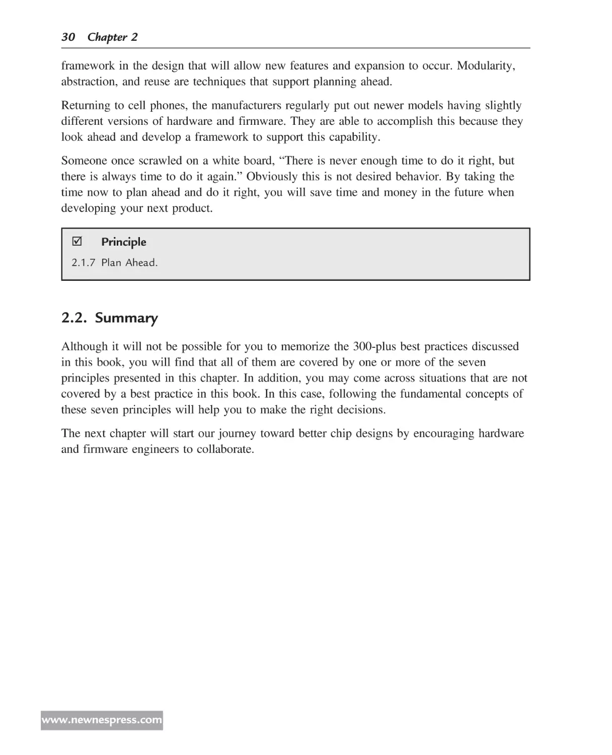
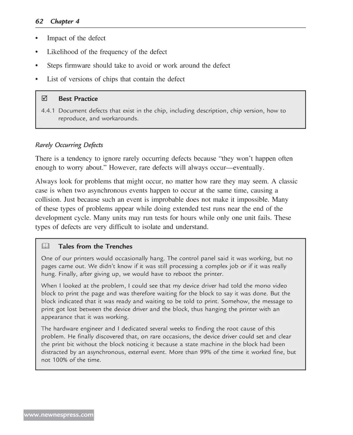
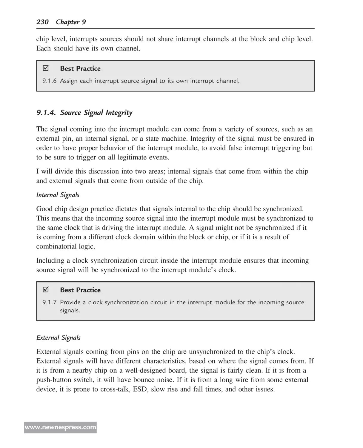
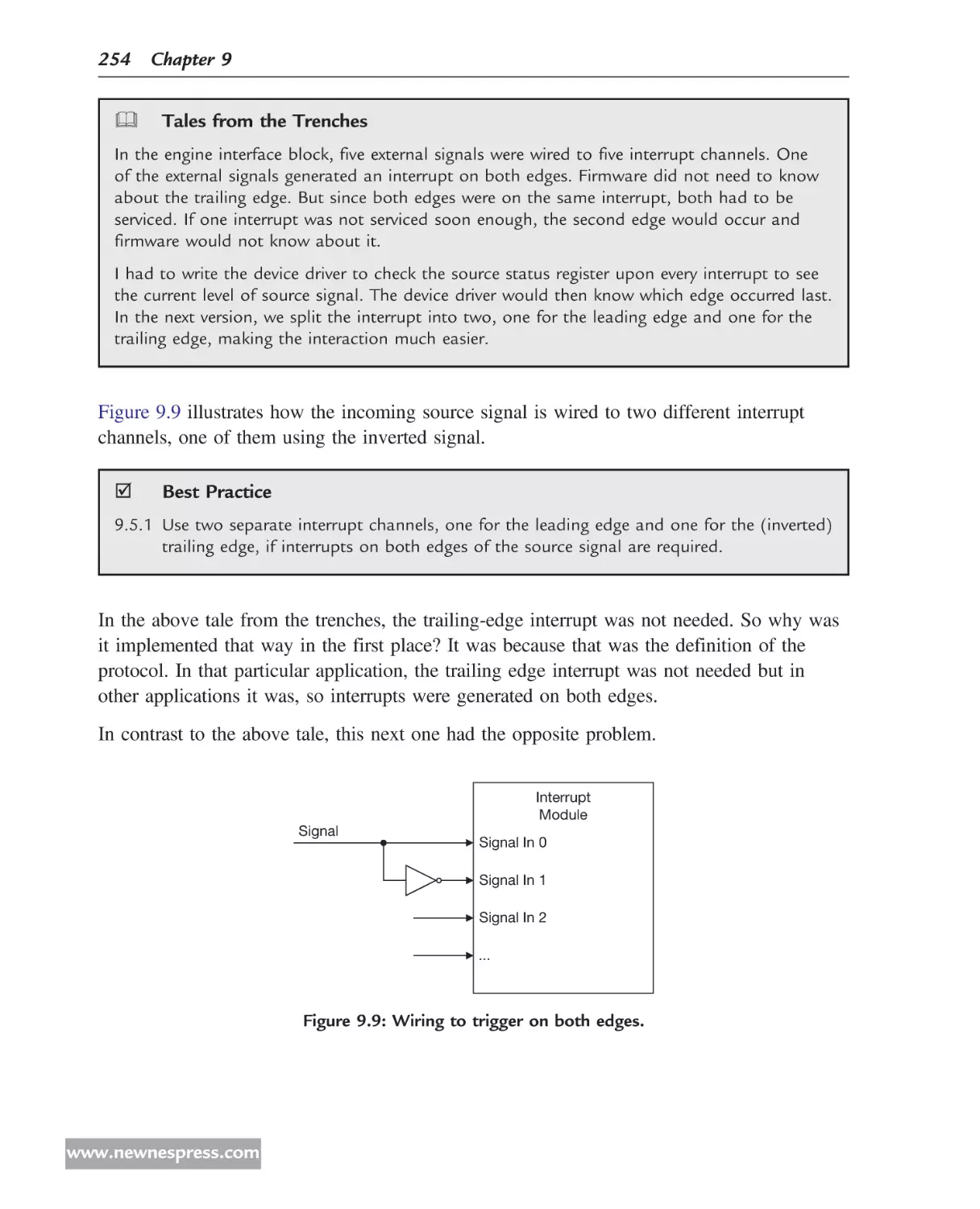
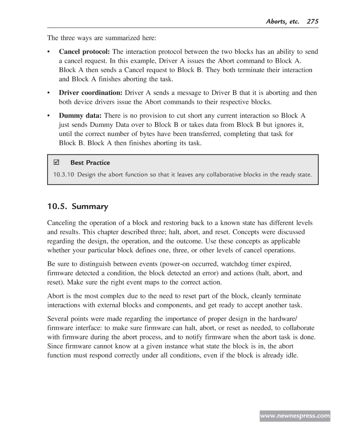
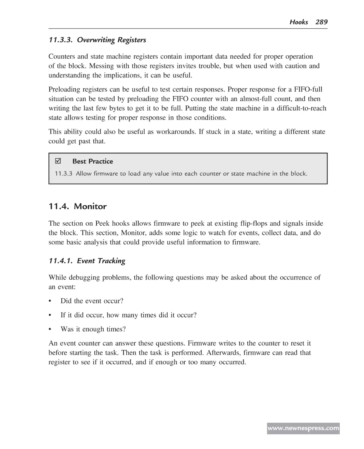
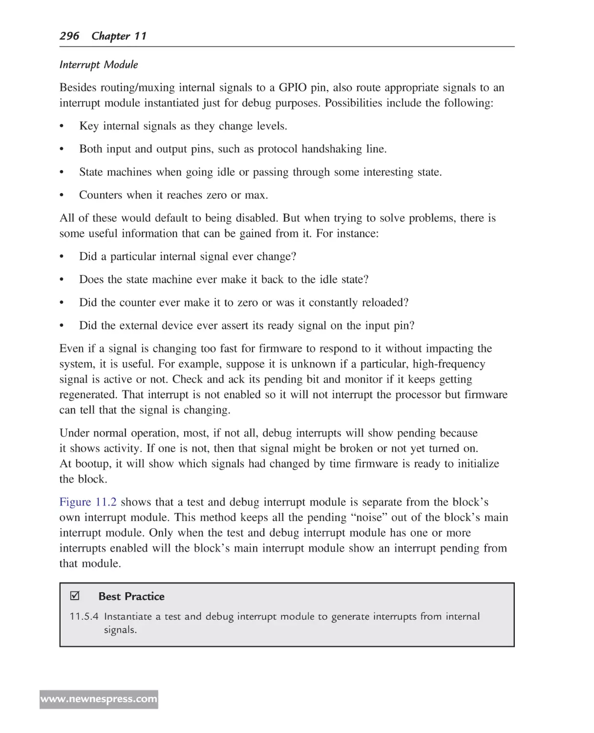
Collaborating implies proactive participation on both sides. Figure 2.1 shows a picture of a
team rowing a boat. Some are rowing on the right side and some on the left. There is a
leader steering the boat and keeping the team rowing in unison. Both sides have to work
and work together. If one side slacks off, it is very difficult for the other side and the leader
to keep the boat going straight.
In order to collaborate, both the hardware and firmware teams should get together to discuss
a design or solve a problem. Collaboration needs to start from the very early stages of
conceptual hardware design all the way to the late stages of final firmware development.
Each side has a different perspective, that is, a view from their own environment, domain,
or angle.
Figure 2.1: Both sides row to keep the boat going straight.
(Photo © iStockphoto.com/Steve Pepple Photography.)
www.newnespress.com
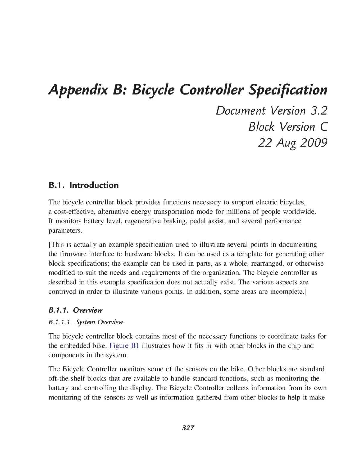
Principles 21
Collaboration helps engineers increase their knowledge of the system as a whole, allowing
them to make better decisions and provide the necessary features in the design. The quality
of the product will be higher because both sides are working from the same agenda and
specification.
Documentation is the most important collaborative tool. It ranges from high-level product
specification down to low-level implementation details. The hardware specification written
by hardware engineers with details about the bits and registers forming the hardware/
firmware interface is the most valuable tool for firmware engineers. They have to have this
to correctly code up the firmware. Of course, it goes without saying that this specification
must be complete and correct.
Software tools are available on the market to assist in collaborative efforts. In some, the
chip specifications are entered and the tool generates a variety of hardware (Verilog,
VHDL . . . ), firmware (C, C++ . . . ), and documentation (*.rtf, *.xls, *.txt . . . ) files.
Other collaborative tools aid parallel development during the hardware design phase,
such as co-simulation, virtual prototypes, FPGA-based prototype boards, and modifying
old products.
Collaboration needs to happen, whether it is achieved by walking over to the desk on the
same floor, or by using email, phone, and video conferencing, or by occasional trips to
another site in the same country or halfway around the world.
This principle, collaboration, is the foundation to all of the other principles. As we shall see,
all of the other principles require some amount of collaboration between the hardware and
firmware teams to be successful.
In this chapter, I will use the following Best-Practice-style box even though these are
principles, not best practices. But this will help reinforce the principle and will be included
in the electronic version of the best practices database.
þ
Principle
2.1.1 Collaborate on the Design.
2.1.2. Set and Adhere to Standards
Standards need to be set and followed within the organization. I group standards into
industry standards and internal standards.
www.newnespress.com
22 Chapter 2
Industry standards exist in many areas, such as ANSI C, POSIX, PCI Express, and JTAG.
Stay true to industry standards. Don’t change them. Changing a standard will break the
protocol, interoperability, and any off-the-shelf components, such as IP, device drivers, and
test suites. For example, USB is widely known and used for connecting devices to
computers. If this standard is adhered to, any USB-enabled device can plug into any
computer and a well-defined behavior will occur (even if it is “unknown USB device
installed”).
Industry standards evolve but still behave in a well-defined manner. USB has evolved,
from 1.1, to 2.0, and now 3.0, but it still has a well-defined behavior when plugging one
version into another.
By internal standards, I mean that you have set standards, rules, and guidelines that
everybody must follow within your organization. Modules are written in a certain fashion,
specific quality checks are performed, and documentation is written in a specified format.
Common practices and methods are defined to promote reuse and avoid the complexity of
multiple, redundant ways of doing the same thing.
In the same way that industry standards allow many companies to produce similar products,
following internal standards allows many engineers to work together and encourages them
to make refinements to the design. It provides consistency among modules, creation of
common test suites and debugging tools, and it spreads expertise among all the engineers.
Look at the standards within your organization. Look for best practices that are being used
and formalize them to make them into standards that everybody abides by. There are many
methods and techniques in the industry that help with this, such as CMMI (capability
maturity model integration, an approach for improving processes; sei.cmu.edu/cmmi), ISO
(International Organization for Standardization, international standards for business,
government, and society; iso.org), and Agile (software development methods promoting
regular inspection and adaptation; agilealliance.org). Adapt and change your internal
standards as necessary. If a change needs to be made, it needs to go through a review and
approval process by all interested parties. Once such a change has been approved, make
sure that it is published within your organization. Apply version numbers if necessary.
There is no such thing as a “customized standard.” Something is either a standard or
customized, but not both. If you break away from a standard, be sure you have a good
reason.
þ
Principle
2.1.2 Set and Adhere to Standards.
www.newnespress.com
Principles 23
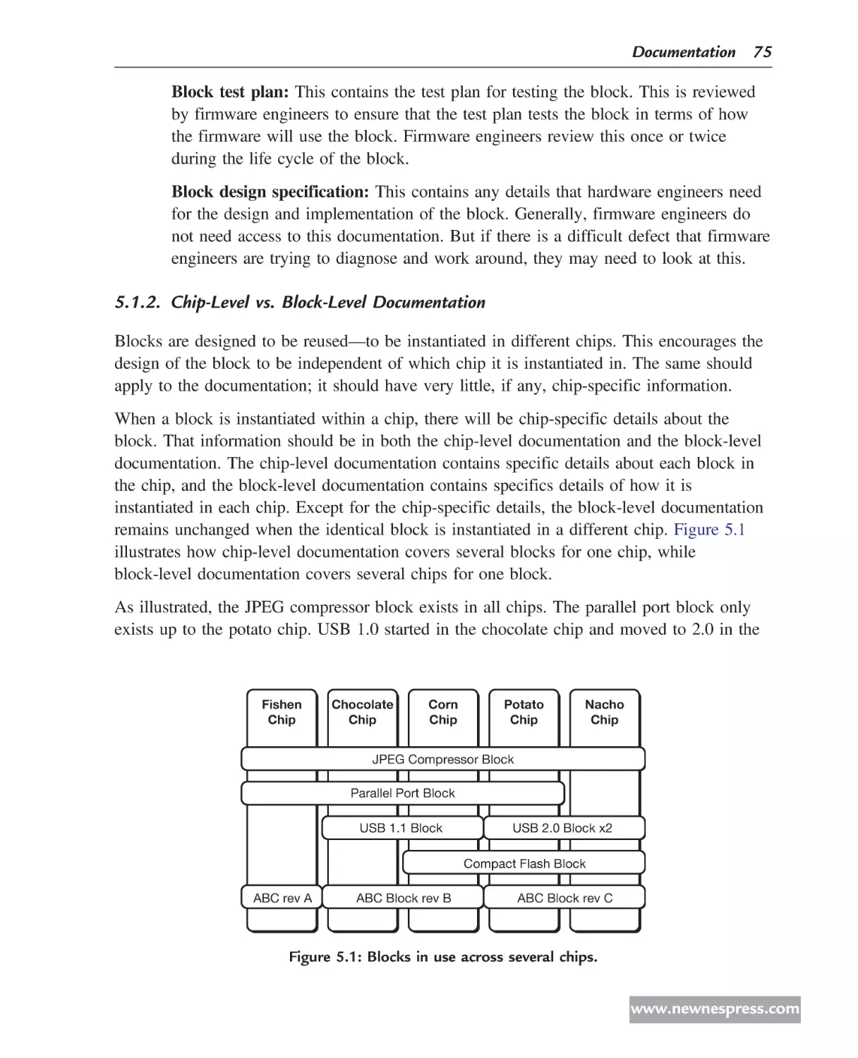
2.1.3. Balance the Load
Hardware and firmware each have their strengths and weaknesses when it comes to
performing tasks. The challenge is to achieve the right balance between the two. What
applies in one embedded system will not necessarily apply in another. Differences exist
in CPU performance, bus architectures, clock speeds, memory, firmware load, and other
parameters.
Proper balance between hardware and firmware depends on the given product and
constraints. It requires studying what the tradeoffs will be for a given situation and adjusting
as necessary.
An embedded system without a proper balance between hardware and firmware may have
bottlenecks, performance issues, and stability problems. If firmware has too much work, it
might be slow responding to hardware and/or it might not be able to keep hardware busy.
Alternatively, hardware might have too big of a load, processing and moving data
excessively, which may impact its ability to keep up with firmware requests. The quality of
the system is also impacted by improper load balancing. The side with the heavier load may
be forced to take shortcuts, fall behind, or lose some work.
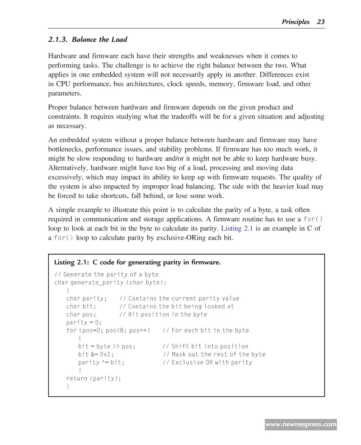
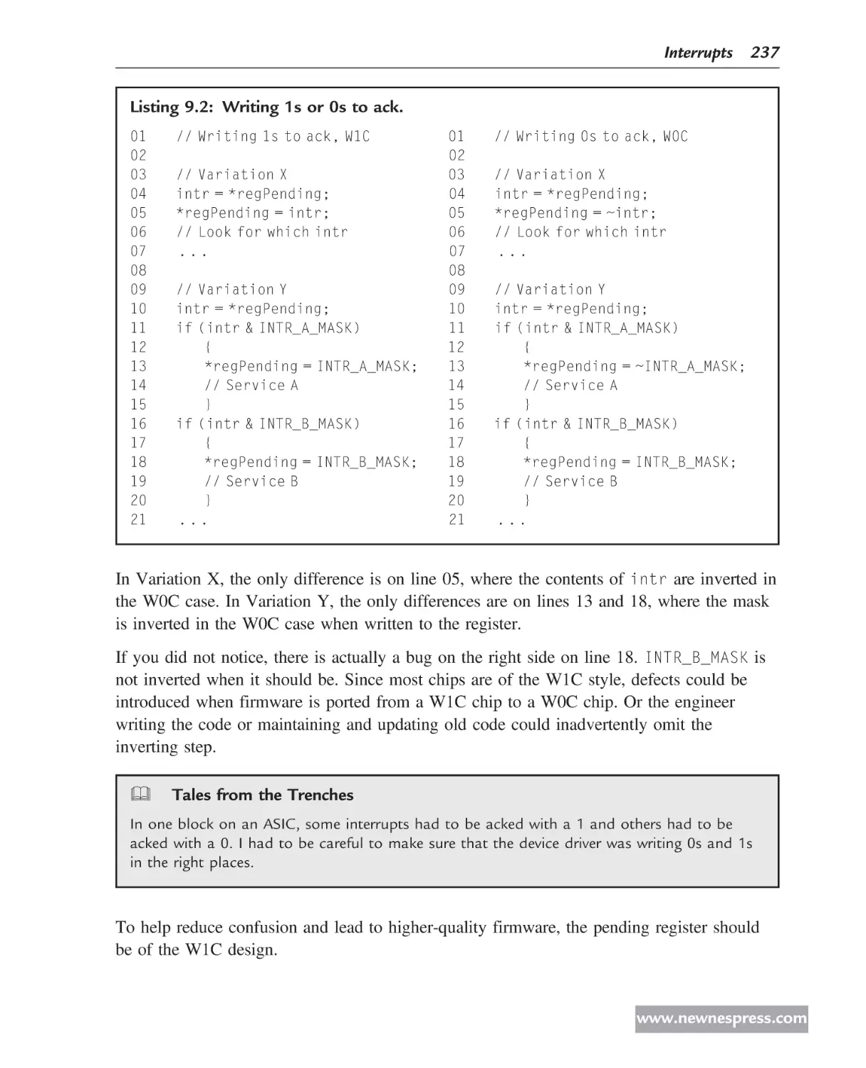
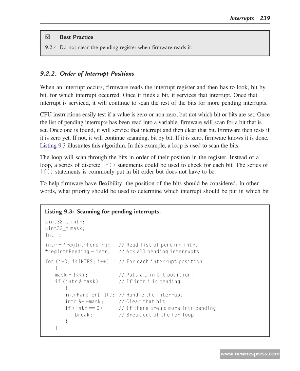
A simple example to illustrate this point is to calculate the parity of a byte, a task often
required in communication and storage applications. A firmware routine has to use a for()
loop to look at each bit in the byte to calculate its parity. Listing 2.1 is an example in C of
a for() loop to calculate parity by exclusive-ORing each bit.
Listing 2.1: C code for generating parity in firmware.
// Generate the parity of a byte
char generate_parity (char byte);
{
char parity;
// Contains the current parity value
char bit;
// Contains the bit being looked at
char pos;
// Bit position in the byte
parity = 0;
for (pos=0; pos<8; pos++)
// For each bit in the byte
{
bit = byte >> pos;
// Shift bit into position
bit &= 0x1;
// Mask out the rest of the byte
parity ^= bit;
// Exclusive OR with parity
}
return (parity);
}
www.newnespress.com
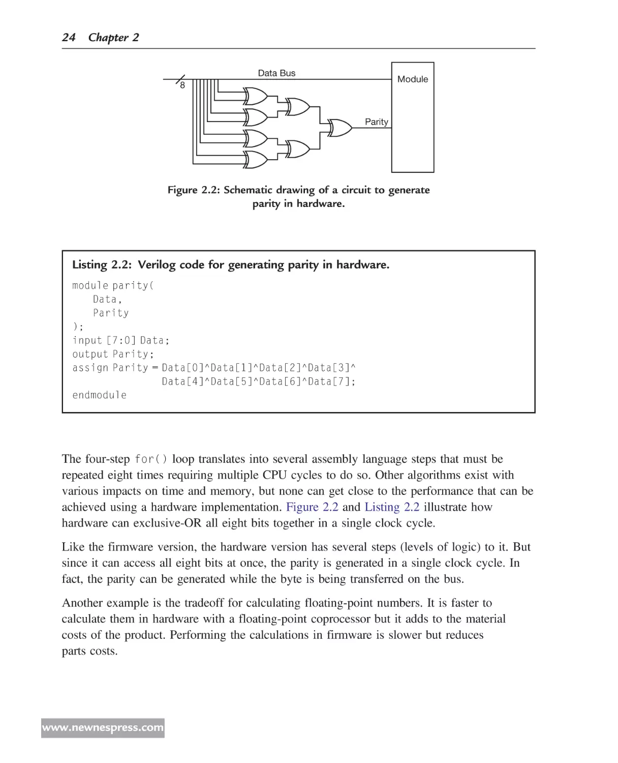
24 Chapter 2
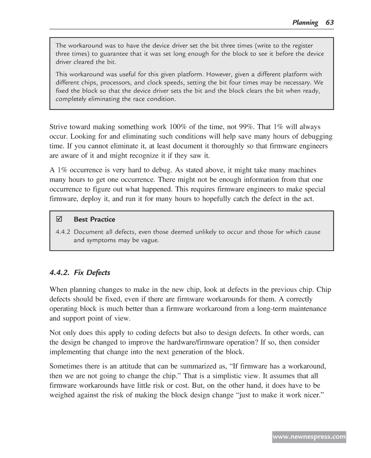
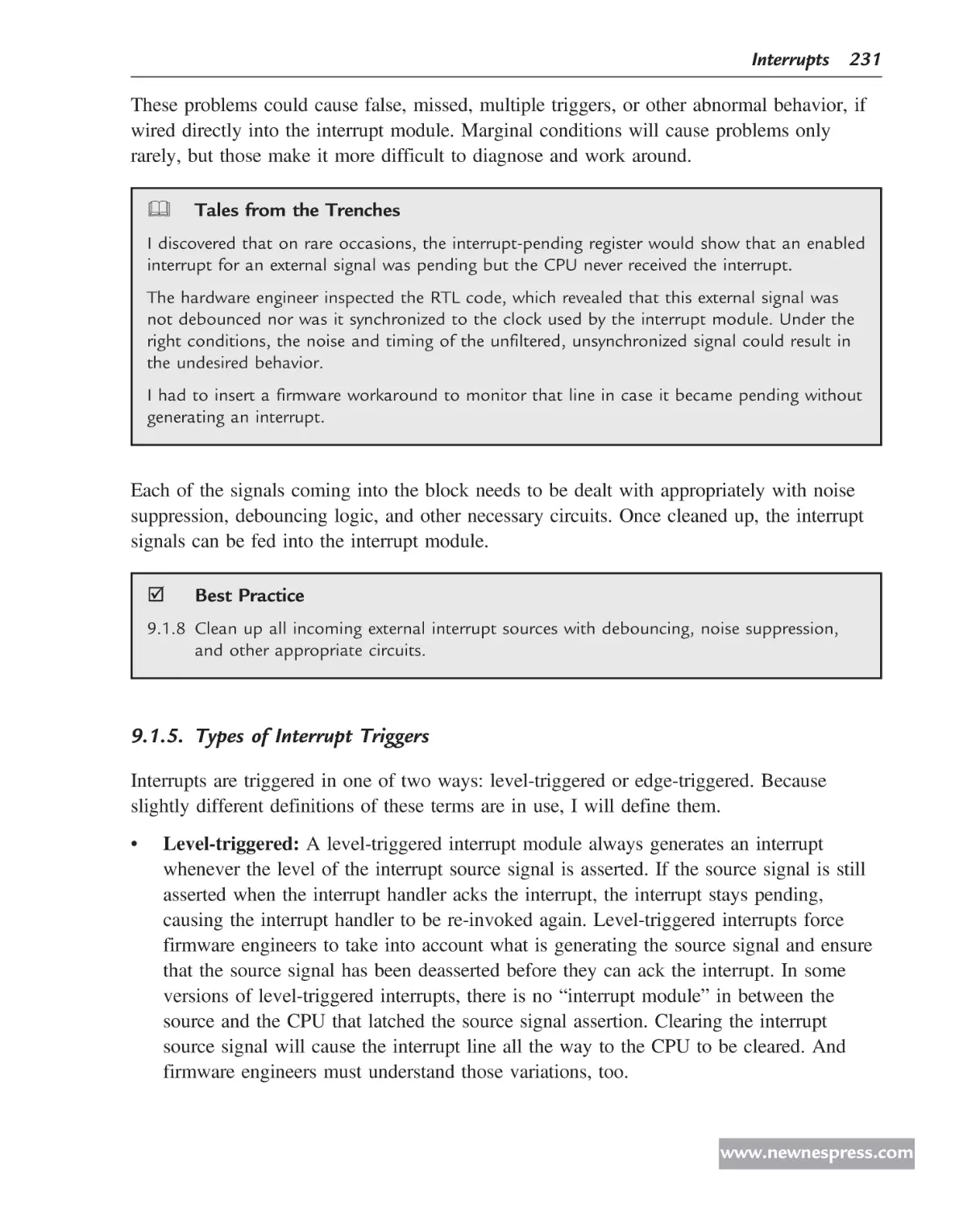
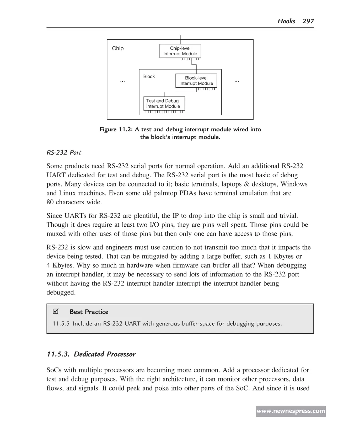
Data Bus
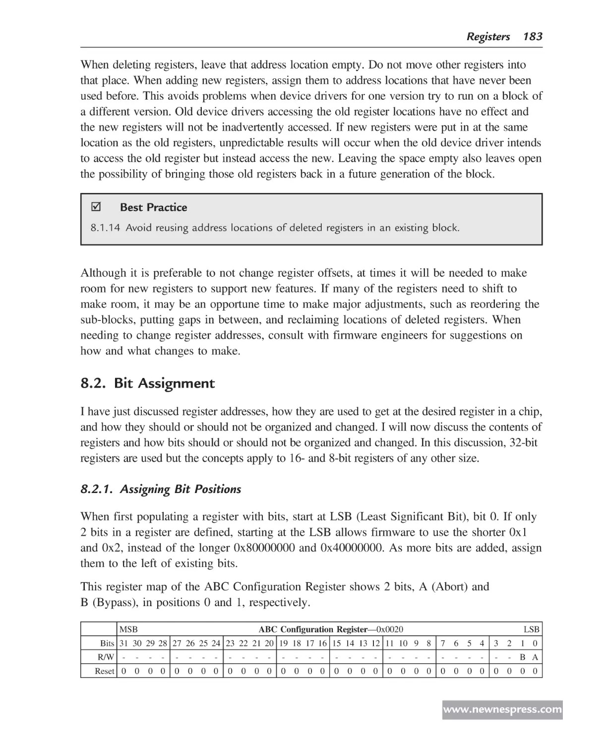
Module
8
Parity
Figure 2.2: Schematic drawing of a circuit to generate
parity in hardware.
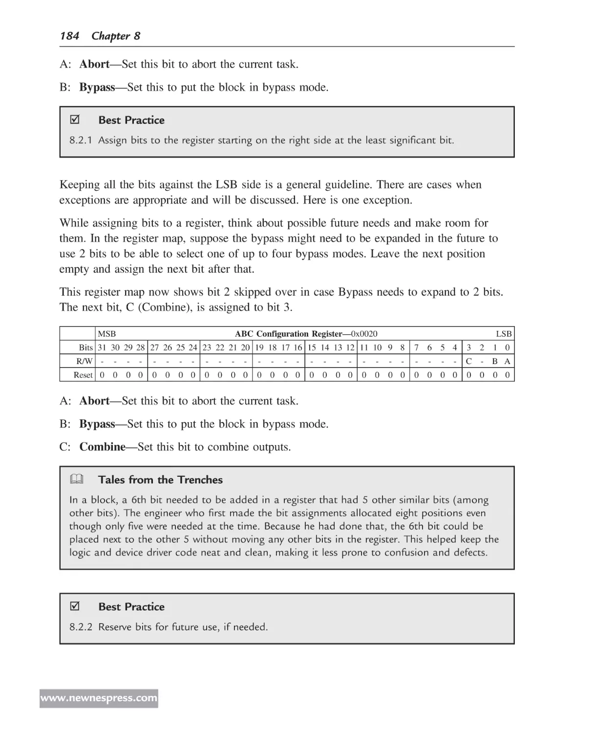
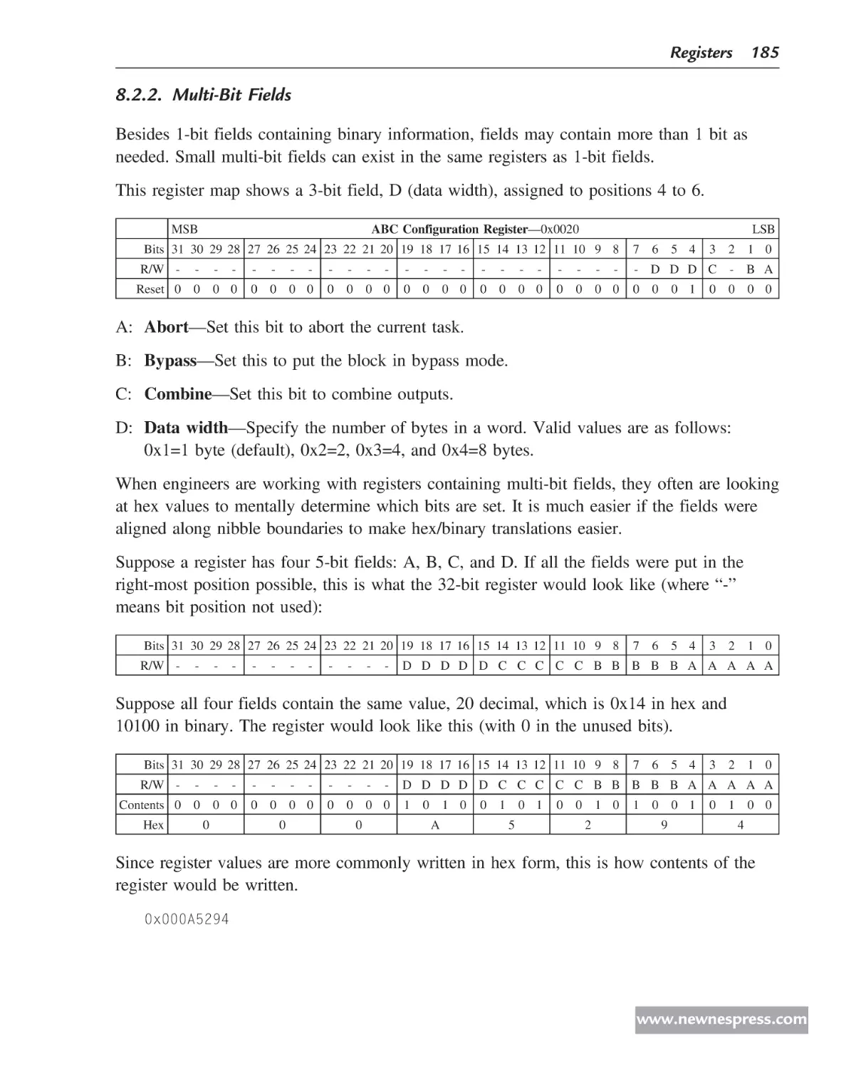
Listing 2.2: Verilog code for generating parity in hardware.
module parity(
Data,
Parity
);
input [7:0] Data;
output Parity;
assign Parity = Data[0]^Data[1]^Data[2]^Data[3]^
Data[4]^Data[5]^Data[6]^Data[7];
endmodule
The four-step for() loop translates into several assembly language steps that must be
repeated eight times requiring multiple CPU cycles to do so. Other algorithms exist with
various impacts on time and memory, but none can get close to the performance that can be
achieved using a hardware implementation. Figure 2.2 and Listing 2.2 illustrate how
hardware can exclusive-OR all eight bits together in a single clock cycle.
Like the firmware version, the hardware version has several steps (levels of logic) to it. But
since it can access all eight bits at once, the parity is generated in a single clock cycle. In
fact, the parity can be generated while the byte is being transferred on the bus.
Another example is the tradeoff for calculating floating-point numbers. It is faster to
calculate them in hardware with a floating-point coprocessor but it adds to the material
costs of the product. Performing the calculations in firmware is slower but reduces
parts costs.
www.newnespress.com
Principles 25
The lesson here is to consider the tradeoffs between the hardware and firmware tasks and to
determine whether the balance needs adjusting. Do the I/O buffers need to be expanded? Do
interrupt priorities need to be adjusted? Are there firmware tasks that could be performed
faster in hardware? Are there hardware tasks that require the flexibility of firmware?
Are there handshaking protocols between hardware and firmware that could be better tuned?
Are there ways to reduce material costs by having firmware do more?
Balancing the load between hardware and firmware requires collaboration between the
hardware and firmware engineers. Engineers understand the load impact associated with a
task in their own domain but may not fully realize how it impacts the other.
A principle of economics applies here—two parties will be more productive if they work
together, but with each working on the tasks that suits them best.
þ
Principle
2.1.3 Balance the Load.
2.1.4. Design for Compatibility
Designing for compatibility means to design in such a way as to facilitate, where possible,
the ability for any version of firmware and any version of hardware to be paired up.
Cell phones are a good example of this. Many, many different models of cell phones exist
but some are very alike. Different phones may have a variety of skins and colors but their
hardware and firmware can be very similar. Cell phones can be upgraded with newer
versions of firmware with new features; meanwhile, different (but similar) models of cell
phones may be equipped with the same firmware.
In some cases, for example, firmware can be set up to support many features and
then—through the use of configuration files, NVRAM settings, compile-time switches, and
so on—only the required features will be enabled. The relevant hardware blocks would be
designed with full support for all features, while the firmware would control which features
are actually used. This allows the same hardware to be installed in different models of the
product while still presenting different features to the outside world.
Designing for compatibility also means that when a new version of hardware is released
with new features, it won’t break when paired with older versions of the device driver,
thereby allowing reuse of the old device driver. This is accomplished by following rules
www.newnespress.com
26 Chapter 2
such as not moving bits and registers around. Compatibility is especially useful when
multiple versions of hardware and firmware are deployed during product development and
among customers. It reduces development time, saves costs, and gets the product out to
customers sooner.
Firmware is becoming more and more expensive; in some cases, developing firmware can
cost more than hardware. Also, it can be difficult to change firmware due to its many
components, layers, and architecture. This increases the importance of striving for
compatibility in hardware so as to minimize changes forced upon firmware.
Pairing any version of firmware with any version of hardware is ideal but not practical all
of the time. However, it is a vision to strive for. Bearing compatibility in mind while
designing from the beginning will lead to decisions that move toward that goal.
þ
Principle
2.1.4 Design for Compatibility.
2.1.5. Anticipate the Impacts
In the game of golf, the golfer selects the club, puts the ball on the tee, looks down the
fairway, checks the wind, lines up the club to the ball, and checks his stance. He is
anticipating the impact of his club on the ball. He does this because he does not want
to miss or slice the ball, sending it into the rough.
Similarly, when creating a new hardware design or changing an existing design, you want
to anticipate the impact on firmware. I chose the word “anticipate” because it implies a
proactive effort. The dictionary lists “foresee” and “prevent” as synonyms. It is not enough
to understand the impact or prepare for the impact; instead, you should anticipate, foresee,
and prevent the impact.
When designing a new block, group bits into registers according to usage; don’t mix
different types of bits in the same register; and limit how many registers need to be
accessed by more than one device driver. When making changes to an existing block, make
the new version of the block work with the old device driver. Do not move bit locations
and register addresses around.
Thus far I have been discussing the avoidance of negative impact. On the flip side, you
want to look for positive impact. For example, providing a DMA with chaining capabilities
or a larger I/O buffer will reduce the firmware load.
www.newnespress.com
Principles 27
&
Tales from the Trenches
New monochrome printers were going to use an older, expensive SoC because there was no time
or budget to develop a cheaper one. An opportunistic engineer took an existing SoC for color
printers and replaced the color video block with the mono video block leaving all else unchanged.
This saved time by avoiding much of the floor planning, timing closures, and verification
activities that are typical with such a chip. Blocks that were no longer needed were left in to
avoid turmoil. Even an ASCII string was left unchanged so that most test suites, simulation
modules, and waveform files could remain unchanged. All pads and pins remained unchanged
with the exception that the mono video block now used some of the pins that the color video
block was using. This made the chip plug compatible on the printed circuit boards.
He used only three to four engineers and had tape out in 2 months (in contrast to the more
usual 15 engineers and 9 months to tape out). When the chip returned from fabrication it
booted in 1 day.
Because the lead engineer restricted all but the minimum change necessary, he had a positive
impact in producing a new and cheaper SoC using significantly less money and time than
normal. This provided a less expensive chip for the new mono printers, thereby saving the
company millions of dollars in future parts costs.
The concept of collaboration is also applicable here because one of the best ways to
determine if and how a hardware change is going to affect firmware is to talk to firmware
engineers. They are best-suited to determine the impact.
Returning to the golf metaphor, the golfer does want to have an impact, but he wants it
where the ball flies straight down the fairway. He may not get a hole in one, but he will be
headed in the right direction with fewer strokes. As you anticipate the impact, your product
development will be in the right direction without wasting time in the rough.
þ
Principle
2.1.5 Anticipate the Impacts.
2.1.6. Design for Contingencies
Why do you carry insurance on your car (beside the fact that in many places the law
requires it)? Why pay the insurance premium? Do you want to collect on it? Are you going
to purposefully get into an accident so you can collect? No. But when you do get into an
accident, you will be glad you have it. You are prepared for that contingency.
www.newnespress.com
28 Chapter 2
Figure 2.3: JetBlue flight 292 landing with the nose gear stuck sideward.
(Top photo is copyrighted by the submitter, Andrewmarino, commons.wikimedia.org/
wiki/Image:JetBlue292Landing.jpg. Reproduced with the permission.
Bottom two photos are in the public domain.)
On September 21, 2005, JetBlue flight 292 with 139 passengers took off from Burbank,
California. Unfortunately, the plane’s nose gear got stuck sideward. After circling Los
Angeles for 3 hours to burn off fuel, the flight crew came in for a successful landing
(msnbc.msn.com/id/9430871; foxnews.com/story/0,2933,170076,00.html). It was amazing
that the nose gear did not collapse. It was rugged. It was designed for contingencies,
although no one anticipated what the gear would be called upon to do. Figure 2.3 shows
the sparks from the plane when landing and how the wheels were ground down.
Designing for contingencies means that you do what you can to prepare for problems that
may appear.
One manager of a young hardware design team told me how his team had informed him
that they had completed their design. The manager then said, “Six months from now, you
www.newnespress.com
Principles 29
are going to get the chip back and it won’t turn on. What are you going to need to debug
that chip?” The team went off, thought about it, and added some test and debug hooks.
When you are trying to get a chip to work, you will need to know what is going on inside.
If you are using a software simulator, you have clear view of every internal signal and
flip-flop. Similarly, if you are working with an in-circuit emulator or JTAG, you have a
good view as to what is going on inside your design. But when you are trying to get
firmware working on a physical chip mounted inside the product, visibility inside the device
is very limited.
Visibility inside the chip can be provided to firmware by adding test and debug hooks in
the device. Adding additional read/write access to internal flip-flops and signals gives
firmware “peek-and-poke” capabilities. It is like having a basic logic analyzer built into the
chip. These added capabilities cost a little in terms of space on the silicon and time required
designing and verifying them, but this is similar to paying insurance. You hope you don’t
have to collect, but if there are problems, you will be very happy that your premiums have
been paid.
Furthermore, test and debug hooks in the chip are not solely for diagnosing and working
around defects in the hardware. They are also very useful for locating and identifying
defects in the firmware.
þ
Principle
2.1.6 Design for Contingencies.
2.1.7. Plan Ahead
People who look to the future toward retirement prepare now by putting away money.
Those who are short-sighted spend their whole paycheck without any thought for the future.
Businesses that plan ahead will take action today to get them to where they want to be 3 to
5 years from now. They don’t focus solely on maximizing this quarter’s results. They do
have to produce good numbers for this quarter, but they don’t lose focus on the future.
Making decisions based solely on current effort and time constraints, without regard to its
impact on the future, is to simply postpone corrective action until later when it will be
difficult and expensive to fix.
Similarly, when designing embedded system products, look ahead and make good decisions
today that will pay off in the future while not sacrificing the current product. Put a
www.newnespress.com
30 Chapter 2
framework in the design that will allow new features and expansion to occur. Modularity,
abstraction, and reuse are techniques that support planning ahead.
Returning to cell phones, the manufacturers regularly put out newer models having slightly
different versions of hardware and firmware. They are able to accomplish this because they
look ahead and develop a framework to support this capability.
Someone once scrawled on a white board, “There is never enough time to do it right, but
there is always time to do it again.” Obviously this is not desired behavior. By taking the
time now to plan ahead and do it right, you will save time and money in the future when
developing your next product.
þ
Principle
2.1.7 Plan Ahead.
2.2. Summary
Although it will not be possible for you to memorize the 300-plus best practices discussed
in this book, you will find that all of them are covered by one or more of the seven
principles presented in this chapter. In addition, you may come across situations that are not
covered by a best practice in this book. In this case, following the fundamental concepts of
these seven principles will help you to make the right decisions.
The next chapter will start our journey toward better chip designs by encouraging hardware
and firmware engineers to collaborate.
www.newnespress.com
CHAPTER 3
Collaboration
Successful projects are the result of well-integrated teams with people working toward a
shared goal. While many teams are necessary, the hardware and firmware teams are central
to the successful development of embedded systems products. However, due to the realities
of their differing development processes, life cycles, organizational structures, vocabularies,
and cultural backgrounds, hardware and firmware engineers often have difficulties working
together while developing the product.
This chapter focuses on improving the ability for hardware and firmware engineers to work
as one team and to collaborate with each other. I will begin by discussing the roles of team
members and the first steps that should be taken when the project commences, and then
I will talk about formal and informal collaboration activities.
While there will be challenges in working together, following these best practices can
dramatically improve the project development effort.
3.1. First Steps
While the number of engineers and the level of their involvement on a given chip will vary
throughout the product development life cycle, identifying all team members and
introducing them to each other are necessary first steps.
3.1.1. Roles
Each organization has its own list of roles and responsibilities with respect to the hardware
and firmware teams. Some roles require more than one person and some people are
assigned more than one role. Let’s consider some of the roles that have hardware/firmware
collaboration responsibilities. You might be using different names for these roles in your
organization but you should be able to understand the intent. Some of these roles have a
best practice associated with them.
© 2010 by Elsevier Inc. All rights reserved.
DOI: 10.1016/B978-1-85617-605-7.00005-8.
31
32 Chapter 3
Traditional Roles
These roles are common in the industry. I describe some of them as they pertain to the
development around the hardware/firmware interface.
•
System engineers: These engineers work with the system as a whole, composed of
both the hardware and firmware components. Organizationally, they may be with the
hardware team, firmware team, or on their own team. While several positions exist at
the system level, I want to point out two of them as follows:
System architects: These engineers design the embedded system product from the top
level, taking into consideration the hardware and software components. They should
review the design with both hardware and firmware architects.
System test developers: These engineers develop tests to test the system as a whole.
They understand how the hardware and firmware components are supposed to work
with each other. In many cases, these are firmware engineers since they also integrate
and test their firmware on the hardware.
•
Hardware engineers: These engineers have several roles in the design of the chips and
boards. I want to point out four of these roles, which may be assigned to the same or
different persons as follows:
Specification writers: As part of writing the hardware specification documents, these
engineers assure that approved requests from firmware engineers for changes and
features are captured in the documents, and that appropriate firmware engineers have
a chance to review any such documents.
Hardware architects: These engineers design the board and chips from the top level.
They should have their high-level designs reviewed by the firmware architects to
assure that firmware can implement the required features.
Front-end chip designers: These engineers design the front end of their respective
block or blocks. They should stay in contact with the corresponding firmware
engineers regarding designs, features, and issues.
Test developers: As part of developing the tests for the blocks and chip, these
engineers confer with firmware engineers to ensure that the tests being developed
reflect the actual firmware usage of the chip.
www.newnespress.com
Collaboration 33
•
Firmware engineers: These engineers have several roles in the firmware development.
I want to point out two of them as follows:
Firmware architects: These engineers design the firmware for the product from
the top level. They need to have their high-level designs reviewed by the hardware
architects to assure that hardware has the necessary features to support the firmware
design.
Device-driver writers: These engineers write the device drivers for their respective
blocks. They should be in contact with the corresponding hardware engineers early in
the specification and design cycle to make sure that the blocks are designed properly.
Collaborative Roles
These roles are not traditional but aid in the collaborative effort between the hardware
and firmware teams. The persons assigned to these roles may have other roles and there
may be more than one person assigned to each role.
•
Best practice champion: This person should be a member of the hardware team since
most of the best practices have to be implemented in that domain. This person leads
the way to promote, inform, and monitor the progress of team members with regards
to carrying out the best practices. Since this is a leadership role (though it may be
informal), this person should have the respect of colleagues. Since the best practices list
is a living document, this person handles requests for additions, changes, and deletions
of the best practices in the list.
þ
Best Practice
3.1.1 Designate a member of the hardware team as best practice champion.
•
Hardware ambassador: This person’s job is to have regular contact with the firmware
team, informing them of progress and issues with respect to the chip development, and
delivering documents for review. This person occasionally sits in on the firmware team’s
meetings and is a resource to the firmware team with respect to addressing any of their
hardware questions and issues, or to direct them to the appropriate member of the
hardware team.
þ
Best Practice
3.1.2 Designate a member of the hardware team as ambassador to the firmware team.
www.newnespress.com
34 Chapter 3
•
Firmware ambassador: This person’s job is to have regular contact with the hardware
team to monitor their progress. This person occasionally sits in on the hardware team’s
meetings and is a resource to the hardware team with respect to addressing any of
their firmware questions and issues or to directing them to the appropriate member of the
firmware team.
þ
Best Practice
3.1.3 Designate a member of the firmware team as ambassador to the hardware team.
The details of these roles listed here are intentionally limited. Existing organizations
will have their roles and respective responsibilities already in place. These roles and
responsibilities may need to be modified to take on the additional hardware/firmware
collaboration tasks outlined here.
3.1.2. Kick-off Activities
Once their roles have been assigned to team members, the next thing to do is to have a
kick-off meeting with both the hardware and firmware teams present. The following is a list
of agenda topics, some of which might require advance preparation and/or a post-meeting
follow-up.
•
Introduce the product.
Highlight its marketing features.
Discuss major product components including relevant industry standards.
Review the development schedule, budget, resource margins, and risk mitigation.
•
Introduce the various team members.
Collect contact information including spheres of responsibilities.
Designate points of contact.
Identify each team’s counterparts in the other team.
Establish contact protocols.
Distribute contact and responsibilities information.
www.newnespress.com
Collaboration 35
•
Discuss project mechanics.
Collect a list of tools needed, especially for hardware/firmware collaboration.
Determine appropriate project-specific email groups, databases, wikis, forums, and
other communication tools.
Set and distribute schedule of meetings.
þ
Best Practice
3.1.4 Hold a project kick-off meeting between hardware and firmware teams giving
introductions and discussing schedules and procedures.
þ
Best Practice
3.1.5 Collect and distribute contact information and spheres of responsibility of hardware
and firmware team members across both teams.
3.2. Formal Collaboration
In this section, I discuss formal collaboration strategies and benefits. In the next section,
I discuss informal collaboration techniques.
Formal collaboration consists of activities that follow established procedures and processes.
These are designed to assure that the right connections are made and that the right
information is being exchanged.
3.2.1. Regular Meetings
Though not enjoyed by all, meetings keep the hardware and firmware teams working
together smoothly. The frequency, scope, and attendees of the meetings will vary through
the life cycle of the project. Table 3.1 lists several example meeting subject matters and
corresponding attendees during the life cycle.
These are just a few examples. You will have other topics that need to be discussed.
Do not force a meeting every week if there is very little to accomplish. Let engineers stay
at their desk and get some work done. When there is a topic that needs some focused
discussion, bring in those appropriate engineers. Ambassadors can represent the rest of their
team for the minor notes and discussions, and then take it back to the appropriate team
members.
www.newnespress.com
36 Chapter 3
Table 3.1: Sample Meeting Topics and Attendees
Phase
Topics
Attendees
Initial high-level
specification
Look at the list of features that marketing requires.
Determine if and how these features will be supported.
Determine the hardware and firmware components
required to support the features.
System, hardware, and
firmware architects.
Ambassadors. Other
experts as needed.
Detailed design of
each block
Discuss what features each block will have and how
firmware will use these features to implement the
requirements. Review several use-case scenarios,
including error handling. Discuss interactions with other
blocks.
Hardware and firmware
engineers of the block(s)
under discussion.
Architects and other block
engineers as needed.
Block verification
and test plans
Review the hardware test and verification plans for each
block to ensure that it will be tested according to how
firmware will use it.
Appropriate hardware and
firmware engineers.
Hardware test and
hardware/firmware
integration
When real hardware becomes available, hardware
engineers will be bringing up and testing the system and
firmware engineers will be integrating firmware with the
real hardware. Problems and issues will surface that
need to be understood by all.
Ambassadors and
appropriate hardware and
firmware engineers.
System test for full
operation and
performance tuning
Address problems in getting the whole system to
operate properly and with the targeted performance.
These issues appear toward the end of the development
cycle prior to product release.
Ambassadors and
appropriate hardware and
firmware engineers.
þ
Best Practice
3.2.1 Hold regular (weekly) meetings on relevant topics with appropriate firmware and
hardware engineers in attendance.
Ideally, hardware and firmware engineers are within a short walking distance from each other.
But in today’s outsourced world of global development, engineers are often not in close
proximity to the rest of their team members. They may be in different locations within one or
two time zones. Or they may be halfway around the world. They could also be in different
companies. These barriers make regular meetings difficult. Overcoming these barriers require
extra efforts by all team members, which may include meeting in the early morning hours or
into the evening. Fortunately today’s technology provides many useful tools as follows:
•
Telephone/VOIP conferences
•
Video conferences
•
Email discussions
•
Forums/blogs/wikis
www.newnespress.com
Collaboration 37
•
Presentations via internet meetings
•
Translation tools
•
Airline travel
þ
Best Practice
3.2.2 Apply extra effort to meet when hardware and firmware teams are in different locations,
such as using emails, teleconferencing, and other means.
3.2.2. Initial Firmware Support
Due to the fact that most of the hardware development effort occurs without the
involvement of firmware engineers, the firmware engineers may not be fully aware of
the current state of the hardware with regards to schedules of upcoming milestones
and checkpoints. Hardware engineers, then, need to notify their firmware engineering
counterparts of upcoming events requiring their assistance.
After the initial kick-off meeting, hardware engineers will be working on the initial high-level
architectural design of the chip, performing basic system tradeoff analysis to balance power,
performance, area, and cost. They need to make sure that the appropriate firmware engineers
are involved in that process to avoid surprises. The firmware ambassador is in a good position
to monitor activity to make sure involvement occurs at the right time.
&
Tales from the Trenches
Along with other firmware engineers, I was invited to a meeting set up by the hardware team
to review the overall plan for the design of a new chip for a next-generation printer family.
The hardware engineers presented their proposal for the chip and the firmware engineers
made their recommendations. The conversation revolved around which blocks should be in
the chip and whether defects in other blocks were worth the risk to fix.
Some of the firmware team comments and requests surprised the hardware team in that they
were not anticipated. At times, the discussion was intense. But the hardware team walked away
with excellent input and an agreement by all parties; they adjusted their plans accordingly.
þ
Best Practice
3.2.3 Start collaboration between hardware and firmware engineers during the initial
high-level hardware design phase.
www.newnespress.com
38 Chapter 3
As the hardware design moves from high-level specification toward block-specific details,
firmware engineers need to stay involved. As specifications and test plans are written, they
should be reviewed by the appropriate firmware engineers. The formal way to encourage
this is to have firmware representation sign off on reviews and checkpoints throughout
the product development life cycle. The firmware ambassador can help make sure the
appropriate firmware engineers are involved for the reviews and signoffs. This will help
keep the firmware team current during the hardware development.
þ
Best Practice
3.2.4 Make sure that the firmware team is represented in the overall design of the chip, the
detailed designs of the blocks, and the plans for testing.
þ
Best Practice
3.2.5 Make sure that the firmware team is represented in reviews and signoffs of hardware
checkpoints throughout the life cycle.
3.2.3. Co-Development Techniques
An inefficient way to develop an embedded systems product is serially—first the hardware
and then the firmware. Unfortunately, in some companies this is still the way things are
being done today. A more efficient manner is to do as much in parallel as possible.
Co-development tools allow firmware to be developed and tested while the hardware is still
being developed and simulated, even before the physical chips arrive back from the fab.
Co-development helps collaboration because it gets hardware and firmware engineers
working together earlier than otherwise. Getting firmware to run on the developing chip
becomes an added bonus with regard to the chip verification phase. Any hardware/firmware
integration issues are discussed by both teams early on. Chip design problems discovered
early can be corrected before it is too late. Co-development techniques include using legacy
hardware, FPGAs, co-simulation, and virtual prototypes.
Legacy Hardware
This works well for chips (or blocks inside chips) that do not change much in the new
design. Hardware engineers can design new boards that use the old chips, allowing the
boards to be put into prototype products for testing. Device drivers for these old blocks
have already been put to use and are thoroughly tested. When the new chips arrive,
changes are made to accommodate the differences and development effort can continue.
www.newnespress.com
Collaboration 39
The problem with using old hardware is that it will not have the new features. In some
cases, firmware stubs can be used to emulate the new features. For first-generation products,
of course, there are no old versions that can be used.
FPGAs
FPGA-based prototype boards allow device drivers to be developed for new blocks or
modified versions of existing blocks. The firmware can run at speed on a real processor.
Errors found in the blocks can be corrected and new versions can be downloaded into the
FPGA within hours. In cases of large ASICs, several FPGAs may be required. FPGAs can
also be paired with legacy hardware to reduce the need to support as much in the FPGAs.
Multiple FPGAs or FPGAs paired with legacy hardware may require temporary address
changes for registers until the physical chip arrives.
FPGAs do have limitations with regards to speed and size. (These limitations are shrinking
as next-generation devices become available.) Resynthesizing RTL to fit in the same
prototype boards can be difficult given fixed pin assignments and partitioning across
multiple FPGAs. In addition, in some cases, RTL code written for ASICs is not necessarily
usable for FPGAs, although this limitation is shrinking too.
Co-Simulation
Co-simulators allow simulated firmware to run on simulated processors controlling
simulated hardware. This technique is possible without first fabricating any hardware. Errors
discovered in the block or device driver can be corrected and the simulation can be
run again. Co-simulation has the advantage of being able to monitor internal signals,
waveforms, and registers that are otherwise hidden on a real chip. Even after chips are back
from the fab, co-simulation can be used to duplicate problems found so that the internal
signals can be inspected.
However, co-simulation requires software models of internal and external behavior. It takes
hours to run a few milliseconds worth of activity, even with a substantial amount of
computing power. This allows only a limited number of test cases to be run. In some cases
simulations are accelerated by using C models parts not specifically being tested.
Virtual Prototypes
Co-simulators are slow because they simulate every gate at every clock edge. Virtual
prototypes take shortcuts by skipping ahead, emulating in C or other techniques. For
example, a count-down counter starting at 1000 and then asserting a signal at count 0, will
not simulate all the gate changes going to 999, 998, 997, and so on. It figures out that after
1000 clock cycles, the signal will assert. It then waits until the rest of the system catches up
to that point in time and then asserts the signal.
www.newnespress.com
40 Chapter 3
Virtual prototypes are completely software based, making it easy to deploy to developers in
remote locations. Changes in the design can be made and re-deployed.
---b------a--Even though limitations exist in these various co-development techniques, the advantages are
clearly apparent to spending the time and money on these activities. Many companies are
developing tools to aid co-development. Gabe Moretti in “Juggling Jobs: Hardware/Software
Co-Design,” discusses several such tools. See also John Blyler, “Devil in the Details: Trends in
ASIC Prototyping.”
Co-development activities lend themselves to getting hardware and firmware teams to work
together sooner. Chip design problems caught early enough will help avoid million-dollar
respins. Firmware developed sooner will allow the product to get to market months earlier
than would otherwise be the case. While there are definite benefits to co-development, there
will still be the need to integrate firmware with real hardware to conduct system testing and
to verify proper performance and behavior.
&
Tales from the Trenches
Two of my fellow firmware engineers were tasked with writing a new USB device driver for a
new USB block on a new ASIC. They were given this task during the design phase of the chip
and were able to use co-development activities. They developed the device drivers on FPGAbased prototype boards; this was a first for our team. They refined the design of both the
device driver and the block.
When the chips came back from the fab, the two team members were successful and
completed the porting and testing on the actual chip in a relatively short period of time.
These results clearly illustrated to us the benefits of co-development.
þ
Best Practice
3.2.6 Use co-development activities, such as virtual prototypes, FPGAs, co-simulation, and old
hardware to get firmware engineers involved in developing code and finding and
resolving problems before the physical chips arrive.
3.2.4. End-Game Hardware Support
After the chips arrive from the fab and are mounted onto boards, hardware engineers bring
up the boards and chips to run their tests and verify basic functionality. They cannot test all
www.newnespress.com
Collaboration 41
aspects of the hardware at this stage because the complete firmware system is required to
get the hardware fully functional. Once the basic tests are done, the hardware is given to the
firmware team for integration with firmware. The hardware engineers often move on to the
next project.
However, hardware engineers still need to keep in touch with firmware engineers to help
them solve problems during system integration and test. This is somewhat ad hoc since
the discovery of problems cannot be scheduled. When problems are found that firmware
engineers cannot solve, hardware engineers may be required to help diagnose and resolve
these problems. The hardware ambassador can help monitor which problems the firmware
team is dealing with and can notify appropriate hardware engineers as necessary. As part of
this process, hardware engineers will also document any problems in the chip design with a
view to fixing them in a future version of the chip.
&
Tales from the Trenches
As I mentioned regarding the Unity mono video block (see Section 1.6, Case Study), I
encountered several defects in the block, many of which required help from the hardware
engineer assigned to that block to diagnose and resolve.
He was very patient with me and did not take it personally every time I found another
problem. He took it as a new challenge to be understood and solved, even though he was
busy working on his next ASIC. His collaborative assistance was instrumental in helping me
successfully get that block to work, not just for that printer, but also for several subsequent
monochrome printers using the same ASIC.
þ
Best Practice
3.2.7 Provide hardware engineering support to firmware engineers through to the end of
firmware development.
3.2.5. Documentation
Imperative to the smooth operation of a collaborative relationship between the hardware and
firmware teams is the flow of important information, and in particular, all necessary
hardware specifications and known hardware defects.
This is a one-way information exchange. Hardware specifications and defect lists are needed
by firmware engineers in order to do their jobs. But firmware specifications and defect lists
are not generally required by hardware engineers. This places the burden on the hardware
www.newnespress.com
42 Chapter 3
team to provide a means for their firmware counterparts to get the desired information
when needed.
In the case of hardware specifications, several methods of storage, distribution, and
management are possible, depending on the needs of the organizations involved; for
example:
•
The firmware engineer may simply walk over or send an email to the hardware engineer
that wrote the specification and ask for a paper or electronic copy.
•
The hardware team may have a centralized storage server or website from whence firmware
engineers can retrieve the desired document. (This server or website may require a
password for each person requiring access.)
•
A central person may be in charge of producing and numbering paper copies and requiring
firmware engineers to sign for the copies they receive.
•
The firmware team, who are part of one company, may submit a formal request for specific
documents to the hardware team who are part of another company.
As we see, many different methods are possible, depending on security needs and
confidentiality of the specifications.
þ
Best Practice
3.2.8 Establish a repository for the hardware team’s high-level and detailed design documents
and provide appropriate access to it for firmware engineers.
Documents, once completed, are not likely to change very much. Having said this, defects
are likely to be discovered—and the corresponding documents updated—throughout the
whole development life cycle, possibly even after the product has been released. Due to the
nature of physical components, defects found in hardware are very difficult to fix as
compared to defects found in firmware.
Defects discovered in the chip before being sent off to the fab have a possibility of being
fixed. But once the chip design is “frozen in silicon,” it is too late to make any changes.
(FPGAs, of course, are much more flexible.) In such a case, the firmware team will
hopefully be able to work around any problems so as to avoid million-dollar chip respins.
In order for firmware to work around the chip’s defects, the firmware team needs to be
aware of all such defects that could possibly impact them. Therefore, the hardware team
needs to provide a way to convey this information to the firmware team. Ideally this would
be in some online, searchable database, especially for teams that are remotely located from
www.newnespress.com
Collaboration 43
one another. Again, depending on the security and confidentiality needs, various
implementations are possible.
þ
Best Practice
3.2.9 Maintain a repository of chip defects that firmware engineers can easily access.
Once firmware engineers have examined the chip defect repository for pertinent defects,
they may not see a need to go back and look again. So when hardware engineers discover
a new defect, they need to “push” this information out to the appropriate firmware engineers
to notify them of the newly detected problem.
Defects may be as simple as an incorrect register address or bit location, which firmware
can easily accommodate. Alternatively, defects may be more severe, requiring firmware to
perform complicated steps to work around them. Or defects may be that some features are
broken and firmware cannot use them.
Letting firmware engineers know about defects as they are discovered will minimize wasted
time by firmware engineers battling against defects that hardware engineers already knew about.
&
Tales from the Trenches
I was asked to join a team consisting of several hardware and firmware engineers to diagnose
a printer ASIC that was having intermittent problems. After 2 months of effort, we determined
that the problem was in a block where the IP was purchased from a third-party vendor. Once
we collected enough data, the IP vendor recognized it as a problem that they had known
about for several months.
They had not told us about the problem because the ASIC had been in use for 6 months with
no apparent problems. But it was an intermittent corner case error that did not occur all the
time. The strange behavior had been observed but it was thought to be due to a defect in a
different block in the ASIC.
The IP vendor apologized and admitted that they should have notified us earlier. Had we been
aware of it sooner, we would have saved several engineering months and tens of thousands of
dollars. Fortunately, we were able to design and implement a firmware workaround to the
problem.
þ
Best Practice
3.2.10 Notify all applicable firmware engineers of chip defects as they are identified.
www.newnespress.com
44 Chapter 3
The hardware team needs to notify the firmware team when they discover hardware defects
that are too late to fix so that the firmware team can work around them. By comparison, the
firmware team does not need to notify the hardware team of firmware defects because there
is nothing that the hardware team can do in the hardware to fix such defects.
3.3. Informal Collaboration
Aside from the tasks and actions to foster formal collaboration, informal collaboration is just
as important. I have spent many hours at the desks of hardware engineers, and they at mine,
discussing various topics (including the latest movies and sports scores). This established a
good working relationship that paid off during product development. Whenever I was stuck,
it was easy to walk over to their desks, call them, or email them with a few questions.
Someone once told me that 75% of the engineers are introverts. (A study by Luiz Capretz
shows 61%.) It is true that, in many cases, engineers are content to stay put at their
computer working away, designing logic, writing code, and solving problems. Initiating
a conversation with someone else may be viewed as a chore, but it needs to happen.
Depending on the personalities involved, the firmware engineer might be an extrovert while
their hardware counterpart is an introvert, or vice versa. So it may be that one will initiate
more conversations than the other. Managers can also play a role to ensure that
conversations are happening.
3.3.1. Formal Organizational Structure
The informal nature that I have described above works very well in informally structured
companies, even if the hardware and firmware teams are in different organizations.
However, in many companies there is a very structured process where one must go up one
management chain and down the other side to get a message to other engineers. I have had
to operate in such circumstances and solving problems in a timely fashion is difficult.
Imagine the following real-world conversation (paraphrased) that actually took place
between myself and a hardware engineer had we been required to go up and down the
management chain.
Me: “I put the block in reverse mode and I can’t get it to work. This is how it is supposed
to work, right?” (Accompanied by a lot of hand-waving in the air.)
Him: “No, it doesn’t work like that, it works like this.” (More hand-waving in the air.)
Me: “How can it work like that? It is missing some information.”
Him: “There is a register with that information.”
www.newnespress.com
Collaboration 45
Me: “What register?”
Him: “The line-size register.”
Me: “Oh, that one? I didn’t know it was being used in this case.”
This type of dialog is very interactive. It cannot be done by writing an email with all the
questions because the next question depends on the answer of the previous question. When
difficult problems exist, it is critical to pull together all pertinent engineers to solve them
quickly.
In some cases, however, the organizational structure must be accommodated. A few
techniques that might help follow:
•
Use email and include all appropriate managers on both teams.
•
Write the email yourself but have your manager send it.
•
Visit with each manager explaining how direct contact is critical for the success of
the project.
•
Appoint a well-respected but capable senior engineer to be a liaison.
•
Accompany the managers as they do the talking, providing clarification and details
as necessary.
•
If approved, contact the other engineer directly but be sure to write up a report and send it
to the relevant managers.
þ
Best Practice
3.3.1 Build bridges between teams to promote informal collaboration between hardware and
firmware engineers.
3.3.2. Hardware Engineers’ Initiative
As hardware engineers go through the specification and design process, there will be times
when they are faced with design options or changes that could impact firmware. Not only
should hardware engineers be aware of how much firmware might need to change, but they
also need to be aware of how many firmware engineers are impacted. If the number of
firmware engineers writing device drivers for the block is small (such as a custom ASIC to
be used by one company), then consult with those firmware engineers with regard to the
proposed changes. If there are many firmware engineers (such as for an ASSP used by
many companies), then changes in the block will have a much greater impact and will affect
www.newnespress.com
46 Chapter 3
many firmware engineers and device drivers. All firmware engineers cannot be consulted,
but a representative number of them should be to obtain their input.
&
Tales from the Trenches
One of my co-workers came to me with a stalled printer, which was leaving paper stopped
inside. Upon investigation, I found a race condition when an interrupt occurred from a CAN
block. An incoming CAN packet was slow getting to memory and the device driver missed it.
I found a firmware workaround to detect and wait for the slow packet, but I also made a
request to the hardware team to fix the race condition.
The hardware engineer assigned to that block determined that the fix required running a
signal from one side of the silicon die to the other, which would have created routing and
timing risks. She came to me and explained what would have to occur in the chip to meet my
request. I could see that it would have added unnecessary complexity and risk to the block,
especially since I had a workaround in firmware that was very robust and not complex. Based
on this, I dropped my request for that fix.
þ
Best Practice
3.3.2 Consult with firmware engineers when contemplating changes to the hardware/firmware
interface.
3.3.3. Firmware Engineers’ Initiative
While the hardware engineers are busy doing the design work, the firmware engineers are
typically working on some other project until the new project’s hardware becomes available.
However, firmware engineers need to take the initiative to visit with their corresponding
hardware counterparts to monitor progress, discuss how each block will be used, and
consider design options. It is while the hardware is still in the design cycle (or sooner) that
the firmware engineers should discuss possible design enhancements, features, and other
changes they would like to see.
þ
Best Practice
3.3.3 Firmware: Initiate contact with the hardware engineer early in the design of the block to
discuss the block, its device driver, and their interactions.
If a firmware engineer has been through a design cycle already and has experience in the
types of problems encountered, that engineer is in a good position to request possible test
www.newnespress.com
Collaboration 47
and debug hooks that would make sense to add to the design of the block. Chapter 11,
Hooks, lists several ideas for test and debug hooks that might give the firmware engineer
ideas on what to request.
þ
Best Practice
3.3.4 Firmware: Discuss with hardware engineers possible test and debug hooks to be added
to the blocks that would assist firmware development. Review the best practices in the
test and debug hook section for ideas.
As firmware engineers design their code, they may come across cumbersome and difficult
interactions that are required to get the code to work on the hardware. For example, a
register containing both interrupt bits and configuration bits require special handling to
avoid inadvertent “acking” (acknowledging) of interrupts or changing configurations.
Another example is requiring a sequence of register reads and writes to access each word in
an internal buffer. Talk to the hardware engineers about the problems and see if a better
solution can be designed.
þ
Best Practice
3.3.5 Firmware: Work with the hardware engineer to find solutions to hardware/firmware
interaction problems when they are discovered.
3.3.4. Collaborative Problem Solving
The firmware engineers are the ones who are primarily involved with integrating hardware
and firmware together and conducting system tests using near-final hardware and firmware.
During this phase, they will occasionally encounter problems that require help from the
hardware engineers. These problems will typically come as one of four generalized types as
follows:
1. The firmware is incorrect because of an incorrect assumption by the firmware engineers as
to the operation(s) of the block.
2. The firmware is incorrect because of erroneous or inadequate hardware documentation.
3. The firmware has a defect.
4. The hardware has a defect.
www.newnespress.com
48 Chapter 3
Determining the type of the problem can be a challenge, requiring effort from both
hardware and firmware engineers. Sometimes it may take several guesses, but only after the
root cause of the problem has been correctly identified can a solution be attempted.
For problems of the first two types, the documentation needs to be corrected or improved.
Generally it is easy to fix these types of problems in firmware. Problems of the third type
are also generally easy to fix in firmware. Problems of the fourth type are more challenging
because the chip cannot be immediately fixed (unless it is an FPGA). In order to continue
using the chip, hardware or firmware workarounds must be put in place.
Determining the root cause of a defect in the chip is only half of the battle; deciding on a
firmware workaround is the other half. Determining a firmware workaround may require
help from hardware engineers because they are familiar with the chip and its capabilities
and know what possible solutions might exist.
&
Tales from the Trenches
While I was integrating the device driver with the Unity mono video block, I discovered a
problem with a use case on the particular printer under development. The image, when
printed on the back side of the paper, was shifted down by about a quarter of an inch
(6 mm). Working with several hardware and firmware engineers, I came up with six possible
resolutions to this problem, but all of them were ugly.
After studying the problem for a few days, a hardware engineer had the seed of an idea, and
together, we came up with a seventh solution which was much, much better than the previous
six. My device driver put the block into test mode, caused the block to think that paper was
moving, stopped it after a quarter of an inch, then froze it until the real paper came, and
then let it resume. It was complicated but it worked. The point is that it required both of our
domain expertise to derive this solution.
þ
Best Practice
3.3.6 Involve both hardware and firmware engineers to determine the root cause of
complicated defects and to then design a firmware workaround.
3.4. Summary
This chapter stresses the importance of having the hardware and firmware teams collaborate
in the design and development of embedded system products. It discusses a few key roles,
including the best practice champion and the hardware and firmware ambassadors. It also
discusses several activities for formal and informal collaboration. In particular, it stresses
www.newnespress.com
Collaboration 49
the importance of informal collaboration and how it is vital to understanding the system,
influencing the design, and solving difficult problems. Furthermore, it encourages the
removal of barriers that hamper informal collaboration, including the ability for hardware
and firmware engineers to talk directly to each other, whether face-to-face, or via phone
call, email, and so on.
3.4.1. Supporting Principles
The concepts of this chapter support the principles of hardware/firmware interface design as
follows:
1. Collaborate on the Design: The primary focus of this chapter was on this principle—the
collaboration of hardware and firmware teams.
2. Set and Adhere to Standards: Having a best practice champion helps ensure that your
best practices are understood and followed.
3. Plan Ahead: Firmware engineers who work early in the development life cycle with
hardware engineers are planning ahead and preparing for firmware integration on real
hardware.
The next chapter will discuss activities that help plan the design of the chip.
Proper planning at the beginning of the project prepares the way for a smoother
development cycle.
References
Blyler, John. Devil in the Details: Trends in ASIC Prototyping. System-Level Design Community
(blog archive), October 23, 2008. Available at: chipdesignmag.com/sld/blog/2008/10/23/
devil-in-the-details-trends-in-asic-prototyping.
Capretz, Luiz F. Is There an Engineering Type? World Transactions on Engineering and Technology Education
1(2), 2002: 169–172.
Moretti, Gabe. Juggling Jobs: Hardware/Software Co-Design. EDN, March 4, 2004. Available at:
edn.com/article/CA382778.html.
www.newnespress.com
CHAPTER 4
Planning
Once the hardware and firmware teams have been identified and have started collaborating,
the next activity is to plan what the requirements and specifications of the chip should be.
Thoughtful planning early in the project sets the stage for the development and integration
of hardware and firmware components into a successful product.
This chapter focuses on various activities and guidelines used to plan the requirements and
specifications of the next chip to be developed. Planning involves looking back into the
past at previous projects to carry forward good aspects and correct bad aspects. It involves
looking forward into the future to determine the desired direction. And it involves looking
sideward at other teams operating on similar projects in parallel to leverage and collaborate
on the projects.
A long-term goal and direction for the product line helps determine the few steps that need
to be taken for this particular chip. The long-term goal may change by the time you are
ready to start on the next chip but unless the change was drastic, you will be headed in the
right general direction.
4.1. Industry Standards
Many standards exist in the industry for a wide variety of interface protocols and data
formats. Some examples include USB, PCI, TCP/IP, I2C, JPEG, and MP3, each of which
serves different needs. Those that are used in a particular application have supporting blocks
placed into chips.
Often hardware architects and engineers wrestle with the decision of if and how to
implement industry standards. Should a new interface or format be designed? Or should an
existing standard be used? If so, to what extent should the standard be implemented? Here
are a few points that will aid in the decision process.
© 2010 by Elsevier Inc. All rights reserved.
DOI: 10.1016/B978-1-85617-605-7.00006-X.
51
52 Chapter 4
4.1.1. Existing Standards
Existing industry standards have many advantages:
•
The design is completed, tested, debugged, and documented.
•
Hardware, IP, software, device drivers, and other components are available “off the shelf.”
•
Debuggers, sniffers, analyzers, documentation, and other support tools already exist.
•
Fewer engineering resources are required to implement them.
•
Expertise exists and is available.
Not only does using an industry standard provide benefit to engineers implementing the
standard, but it also benefits other engineers, both hardware and firmware, who use that
standard in later stages of the product development. Experience has shown that using
standard protocols and formats saves many engineering months during implementation,
development, testing, and debugging. The time spent in a learning curve is avoided when
other engineers know the standard. And if they don’t, books are already written that they
can learn from.
The development process flows smoother when standards are used, just like driving a car.
Traffic flows smoother when drivers stay on their side of the road and stop at red lights.
Drivers who don’t follow those standards literally run into problems.
Even though there are some good reasons to design something new, if possible, use an
industry standard.
þ
Best Practice
4.1.1 Use existing industry standards where possible.
Industry standards are documented and formalized by a standards body. However, many de
facto standards and conventions are in use. Many are in place because of market dominance
by a product that others emulate, such as the “AT” syntax first put in Hayes modems.
Following de facto standards increases the ability to leverage existing work, increases
interoperability, and increases success in the marketplace.
þ
Best Practice
4.1.2 Use a de facto standard, if one exists, in the absence of an official standard.
www.newnespress.com
Planning 53
Some standard blocks go so far as to have an official or de facto standard for its firmware
interface in the layout, order, and position of its registers and bits. Many device drivers
know how to deal with an EHCI-compliant USB host controller. (While there are standards
for USB hosts, there are not for USB devices.) Standard blocks with standard register
interfaces speed up development. Device drivers can generally be purchased for standard
hardware. If there is not an exact fit, new device drivers can be highly leveraged from
existing ones.
4.1.2. Implementing the Standard
Once a standard has been selected, the question is still asked as to how much of it should
be implemented in the block. The degree of implementation falls into one of these four
options:
•
Full standard: In a full implementation of the standard, the block can do anything as
specified by the standard, even though not all of its functionality is planned to be used
in the target product. However, if the plan changes, a fully implemented block will
allow changing how the block is used. An example standard is RS-232 and a full
implementation will have support for hardware handshaking.
•
Standard subset of the standard: Some standards allow and specify how a portion of
the standard can be implemented. This permits partial implementation to reduce the
silicon space or pins needed when the additional functionality is not needed.
An example of a standard subset is an RS-232 block without support for hardware
handshaking.
•
Non-standard subset of the standard: A non-standard subset is when a portion of the
standard is implemented that is not specified by the standard. Engineers implementing
the block decide what portions to implement. This has the advantage of being able to
implement and use a very specific portion. An example of a non-standard subset might
be an RS-232 block that can only transmit but not receive.
•
Derivation of the standard: A derivation of the standard might be implemented if
some things need to be altered to meet certain design goals. Starting with a standard
and then altering it may be better than starting with a whole design from scratch. An
example derivation of the standard might be an RS-232 block that deals with 10-bit
words instead of 8.
To take full advantage of compliance to a standard, blocks should be implemented
using the full standard or a standard subset. Implementing a non-standard subset or a
derivation is not recommended and could cause problems. There are valid reasons for
www.newnespress.com
54 Chapter 4
doing so which are discussed in Section 4.1.3, Deviations or New Creations. But
the following are reasons why the design should comply with the full standard or a
standard subset:
•
Standard device drivers: Standard device drivers are written assuming that the full
standard is implemented in the chip. Even though some features are not being used,
the device driver might access the unused portion as part of its normal startup tasks
before it is aware of which portions to use or not use during normal operation. Using
a standard device driver has the obvious benefit of being already written and tested.
Standard subsets are also well known and device drivers exist which can support that
as well. Depending on the block and the device driver, a particular version of a
device driver may be able to support both the full standard and the standard subset.
If the block implemented a non-standard subset or a derivation, device drivers need
to likewise be modified. This requires implementing a new device driver or
modifying an existing one, both of which are prone to introducing defects and
causing delays.
•
Standard tests and tools: Many standard blocks and device drivers already have
test suites and development tools available on the market. Using what is already
available aids in testing and developing designs for industry standards. Non-standard
subsets and derivations will require that test cases be modified, rewritten, added, and
deleted. It also forces new development tools to be developed, modified, and
maintained. Again, this adds more time to the schedule and risks not being as
thorough.
•
Change in intended usage: Implementing the full standard leaves open the option of
using any part of that standard. It may be that only certain portions of the standard are
planned for the target or future products. However, it is not uncommon for plans to
change due to product requirement changes, to provide necessary performance
improvement, to solve problems encountered, or put in unplanned new products.
Implementing a standard subset still uses standard device drivers, tests, and tools, but
limit the options if changes in the plan are needed.
Aside from intentional changes to a standard, there are unintentional changes (defects)
when the block was not implemented correctly. Or the changes are intentional, either to
save time or gates, but the impact was not well understood, creating problems later.
www.newnespress.com
Planning 55
&
Tales from the Trenches
Tale 1: A standard I2C block in our ASIC was implemented with only the byte-transfer mode.
Block-transfer mode was not implemented, which was fine at first. But later more data needed
to be transferred and it had to be done slowly, 1 byte at a time, resulting in performance
problems. In the next version of the block, block-transfer mode was added in.
Tale 2: Someone in another company told me of a configuration register hardcoded to a
specific IRQ. It worked fine in the target product but had a conflict when the chip was put in
a new product.
Tale 3: One of our ASICs had a JPEG decompressor block that did not respond per the
standard when it saw a certain marker in the compressed data. The workaround was to have
the device driver go through the compressed data, hunt for that marker, and change it to a
different marker. The decompressor was fixed for the next ASIC.
þ
Best Practice
4.1.3 Implement a standard exactly to the specifications of the standard.
þ
Best Practice
4.1.4 Implement the full standard or a standard subset of the standard.
4.1.3. Derivations or New Creations
As much as it would be desirable, there is not always an industry standard that fits the
design requirements of the project at hand. This leaves two options, deriving from an
existing industry standard or designing something new.
Taking an existing standard and deriving from it is an option if the exposure is limited.
Making a USB device with deviations will not work when the device is expected to connect
to many computers. Using deviations to the RS-232 standard to get just two components
within the same system to talk to each other will work as long as other RS-232-based
devices in the industry are not expected to connect in. In addition, deviations made could
eliminate the possibility of using off-the-shelf IP, device drivers, development tools, and
debuggers. If a standard with deviations is used, be sure to document all deviations to help
those who know the standard be able to understand what changes were made. Explain the
motivations and the reasoning why each change was made, and outline any risks that have
been identified.
www.newnespress.com
56 Chapter 4
þ
Best Practice
4.1.5 Clearly document any deviations from a standard, including motivations, justifications,
and risks for each deviation.
If it is not possible or practical to use an existing standard with deviations, then a new
protocol or format needs to be designed that meets the requirements of the product. Another
reason for developing a new protocol or format is to make it proprietary to protect new
technologies. A new design makes it difficult for competitors to sniff, decode, break into,
and understand.
Before starting on a new design, engineers need to do research to look for designs readily
available that will suit the purpose. In other words, don’t do what I did.
&
Tales from the Trenches
I needed to compress some printer raster data to reduce memory and bandwidth
consumption. I was not (and am still not) an expert on data compression techniques. I knew
a little about two or three other schemes but they did not meet my needs. So I “invented” a
new algorithm. I ran some tests on it and discovered that it performed quite well, as long as
it operated within certain parameters. For certain data patterns, it did not do as well and
problems existed in the design. I then discovered industry standard compression schemes that
worked better than mine did so I quit wasting my time on my design.
If nothing else can be found, only then start work on a new design.
4.2. Common Version
It is very common for firmware engineers to architect their modules to work on multiple
versions of hardware. It solves the problem of first having to determine which version of the
hardware is being used before knowing which version of the firmware to install. This task
is easier for firmware engineers if the different versions of hardware are as much alike as
possible.
Depending on how the hardware teams are organized, it may be that different teams are
designing chips that use some of the same blocks. When putting together a new chip, look
at other teams who may be using the same block for the latest version of each block. It may
be that other teams have taken your earlier version and added enhancements and fixed
defects. Picking up their latest version will save time and effort from repeating the same
bug fixes and enhancements that they have already performed.
www.newnespress.com
Planning 57
Chip XYZ
Team X
Block B v2
Chip ABC
New ABC
Team A
Block B v1
Block B v?
Figure 4.1: Use the version of a block from the
neighboring team if it is more recent than the version
used by your team.
Figure 4.1 illustrates how Team A made Chip ABC with Block B version 1. Then Team X
took Block B, made some changes to make version 2, and used it in their Chip XYZ. When
Team A is then ready to make New ABC, they should not use version 1 in their old chip,
but use version 2 from Chip XYZ.
þ
Best Practice
4.2.1 Consult with other project teams to identify the latest version of the block to leverage
for the next chip.
In some cases, firmware engineers are aware of later versions because they had to do the
firmware for those versions and can point hardware engineers in that direction.
Once the latest version has been identified, the next question is to determine if and what
new features and enhancements to add. Besides looking for requirements within your own
team, consult with other partner teams that will be using the same block for requirements
they might have. Also check with marketing to see what new features are needed that
require support from the block.
þ
Best Practice
4.2.2 Consult with marketing and other partner teams to look into the near future for
features that might be needed and add them to the block.
Once the requirements are identified, then the changes necessary to support those
requirements need to be put into the block. By making changes to support other teams
besides your own, you open to them the possibility of using your chip in their product, or
using your block in their chip as is without further changes.
www.newnespress.com
58 Chapter 4
þ
Best Practice
4.2.3 Add in necessary changes to support new requirements and features when leveraging a
common version block from one generation to the next.
The discussion has been with regards to commonality in context of whole blocks. Common
versions also apply to sub-blocks, such as DMA controller and interrupt modules. It can
even go so far as individual registers and how they are laid out.
Again, this ties in with providing a common and consistent interface for firmware.
A firmware module written to handle DMA controller modules can be leveraged across all
the device drivers provided that the various blocks in the chip instantiate the same IP for
DMA. Many of the best practices in this book are geared toward providing this consistency.
Chapter 9, Interrupts, is dedicated specifically to providing a consistent and common
interrupt module for use by all blocks in all chips.
þ
Best Practice
4.2.4 Develop internal design standards for the style and format of register layout, register
access, interrupt modules, DMA modules, and other common elements.
I will discuss more on this topic of a common version in Chapter 6, Superblock.
4.3. Compatibility
As a block is carried from one generation to the next, there will likely be new requirements
and features that will be added in. Where possible, the new version of the block should be
backward compatible with the old. This will allow a mix of old and new chips and device
drivers. Old device drivers will work on both new and old chips. However, old device
drivers are not aware of new features and therefore cannot take advantage of them in the
new chip. New device drivers will be able to use the new features in the new chip but,
when running on the old chip, will not try to use the new features and will still work with
the old features.
þ
Best Practice
4.3.1 Make changes to the new version of a block to be backward compatible with the old
version of firmware where possible.
www.newnespress.com
Planning 59
4.3.1. Range of Backward and Forward Compatibility
The range of compatibility between versions of blocks is wide. At one extreme, changes to
the bits and registers are very small such that the old firmware works without any changes.
At the other extreme, everything changes; the register addresses and contents, the bit
locations and meanings, the interrupts generated, and the block tasks. This forces a major
overhaul, if not a complete rewrite from scratch, of the device driver. Typically though,
changes from one block version to another are somewhere in between.
Even between one version and the next, there is a range of changes. Some changes have no
firmware impact, some have major impact, and some are somewhere in between.
The following list indicates various types of changes with regards to its impact to firmware.
It is in approximate order with the smallest impact on firmware at the top and the biggest
impact on the bottom.
•
No impact: Some changes can be made without causing a change in firmware. An
example is an 8-bit register that contains an integer. If firmware is set up to read the
8-bit register as a 32-bit word, then the next version of the block could change the
number of bits, such as making it a 12-bit register, and firmware will not need a
change. Not only is this backward compatible, but it is forward compatible. It will work
with other integer sizes (up to 32 bits).
•
Superset: One version of the block may implement some bits from a superset while
another version implements other bits from the same superset. For example, the old
version supports bits A, B, and C, while the new version supports bits A, B, and D
(where bit D is not in the same position that bit C was). Firmware is set up to support
the superset, all four bits. Firmware does not need to know which version of the block
it is running on; it will respond to any of the four bits at any time. On certain versions
of the chip, certain bits will never be true. If the superset does not change in future
versions, firmware supporting the superset does not need to change. But if more bits are
added, then the firmware’s superset would need to be updated.
•
Legacy mode: Some block changes are designed so that when the new block powers
up, it powers up in legacy mode, making it look like the old block. This allows old
firmware to work on it. New firmware knows how to get it out of legacy mode and
enable the new features.
•
Version number: Sometimes firmware reads the chip version number to know which
version of the block is in the chip, and can then operate accordingly. The down side of
this is that version numbers of future chips are unknown to firmware, which forces
www.newnespress.com
60 Chapter 4
firmware to be updated for every new version. This method is not forward compatible.
It forces firmware to maintain a list of which chip versions match to which versions of
the block.
•
Version clues: In some cases, a version number may not be sufficient or available.
Firmware can use other clues to determine the version. One way for firmware to
determine which version is in the chip is for firmware to set a bit that exists in only
one version. If the bit stays set, then it is the one version. If not, it is the other version.
This technique will work, on future versions where the feature may or may not be
implemented.
•
Incompatible: The changes are too numerous and too drastic. It is better to write a new
device driver from scratch.
The more the changes in the new version of the block fall near the top of this list, the
greater the likelihood that firmware is easier to port and maintain. Analyze the changes that
you are considering. Can the change be done differently so as to move it higher on this list?
þ
Best Practice
4.3.2 Minimize the impact on firmware when changes to a new version of the block cannot
be completely backward compatible.
Chapter 6, Superblock, focuses on how to have variability between versions but still be high
on this compatibility list.
4.3.2. Combinations of Old vs. New
Old versions of device drivers work on old versions of the block. And likewise, new
versions of device drivers work on new versions of the block. But how well will mixed
combinations of old and new work? It depends on how the changes in the block were made.
Fewer problems with mixed combinations will arise by following the rules in this book and
by making the versions as compatible as possible.
Table 4.1 illustrates what might happen with different combinations of old and new blocks
and device drivers. This table discusses three types of blocks: an old block, a highly
compatible new block, and an incompatible new block. And it discusses four types of
device drivers: one to support just the old block, one to support just the compatible new
block, one to support just the incompatible new block, and one to support both the old and
the new blocks. The descriptions of each pairing are to be taken as relative generalities.
www.newnespress.com
Planning 61
Table 4.1: Combinations of Old and New Blocks and Device Drivers
Old Block
Compatible New Block
Incompatible New Block
Device driver for old
block only
Works fine.
Will work fine. Block
was designed to allow
driver to be forward
compatible, although it
cannot take advantage
of new features.
Will not work. Block
design did not allow
driver to be forward
compatible.
Device driver for
compatible new
block only
It might work. The driver
might be confused when
new features do not
work.
Works fine.
Not applicable.
Device driver for
incompatible new block
only
Will not work. Driver not
backward compatible.
Not applicable.
Works fine.
Device driver for both
old and new block
Works fine.
Works fine. Only a little
code is required to
handle version
differences.
Works fine but a lot of
code is required to
handle version
differences.
4.4. Defects
As much as we do not like it, defects are a part of embedded systems development. With
regards to the hardware/firmware interface, the challenge is to minimize the impact that
defects in the chip have on firmware. This section discusses planning activities with regards
to documenting, fixing, and testing for defects.
4.4.1. Document Defects
Because of the nature of the hardware/firmware domains, defects in the chip impact
firmware’s ability to operate properly because a chip (excepting FPGAs) can require
millions of dollars and months of delays to get fixed. This forces firmware engineers to
attempt to modify the firmware to work around chip defects, and therefore, firmware
engineers need to know the nature of defects in the chip. On the other hand, defects in
firmware generally do not impact the chip because the firmware can more easily be fixed
so hardware engineers do not need to know about firmware defects.
When chips are deployed to firmware engineers, information about any chip defects that
firmware engineers might run into should also be given to the firmware engineers. Several
pieces of information about the chip should be included:
•
Behavior of the defect
•
Conditions that will or may cause the defect to occur
www.newnespress.com
62 Chapter 4
•
Impact of the defect
•
Likelihood of the frequency of the defect
•
Steps firmware should take to avoid or work around the defect
•
List of versions of chips that contain the defect
þ
Best Practice
4.4.1 Document defects that exist in the chip, including description, chip version, how to
reproduce, and workarounds.
Rarely Occurring Defects
There is a tendency to ignore rarely occurring defects because “they won’t happen often
enough to worry about.” However, rare defects will always occur—eventually.
Always look for problems that might occur, no matter how rare they may seem. A classic
case is when two asynchronous events happen to occur at the same time, causing a
collision. Just because such an event is improbable does not make it impossible. Many
of these types of problems appear while doing extended test runs near the end of the
development cycle. Many units may run tests for hours while only one unit fails. These
types of defects are very difficult to isolate and understand.
&
Tales from the Trenches
One of our printers would occasionally hang. The control panel said it was working, but no
pages came out. We didn’t know if it was still processing a complex job or if it was really
hung. Finally, after giving up, we would have to reboot the printer.
When I looked at the problem, I could see that my device driver had told the mono video
block to print the page and was therefore waiting for the block to say it was done. But the
block indicated that it was ready and waiting to be told to print. Somehow, the message to
print got lost between the device driver and the block, thus hanging the printer with an
appearance that it was working.
The hardware engineer and I dedicated several weeks to finding the root cause of this
problem. He finally discovered that, on rare occasions, the device driver could set and clear
the print bit without the block noticing it because a state machine in the block had been
distracted by an asynchronous, external event. More than 99% of the time it worked fine, but
not 100% of the time.
www.newnespress.com
Planning 63
The workaround was to have the device driver set the bit three times (write to the register
three times) to guarantee that it was set long enough for the block to see it before the device
driver cleared the bit.
This workaround was useful for this given platform. However, given a different platform with
different chips, processors, and clock speeds, setting the bit four times may be necessary. We
fixed the block so that the device driver sets the bit and the block clears the bit when ready,
completely eliminating the race condition.
Strive toward making something work 100% of the time, not 99%. That 1% will always
occur. Looking for and eliminating such conditions will help save many hours of debugging
time. If you cannot eliminate it, at least document it thoroughly so that firmware engineers
are aware of it and might recognize it if they saw it.
A 1% occurrence is very hard to debug. As stated above, it might take many machines
many hours to get one occurrence. There might not be enough information from that one
occurrence to figure out what happened. This requires firmware engineers to make special
firmware, deploy it, and run it for many hours to hopefully catch the defect in the act.
þ
Best Practice
4.4.2 Document all defects, even those deemed unlikely to occur and those for which cause
and symptoms may be vague.
4.4.2. Fix Defects
When planning changes to make in the new chip, look at defects in the previous chip. Chip
defects should be fixed, even if there are firmware workarounds for them. A correctly
operating block is much better than a firmware workaround from a long-term maintenance
and support point of view.
Not only does this apply to coding defects but also to design defects. In other words, can
the design be changed to improve the hardware/firmware operation? If so, then consider
implementing that change into the next generation of the block.
Sometimes there is an attitude that can be summarized as, “If firmware has a workaround,
then we are not going to change the chip.” That is a simplistic view. It assumes that all
firmware workarounds have little risk or cost. But, on the other hand, it does have to be
weighed against the risk of making the block design change “just to make it work nicer.”
www.newnespress.com
64 Chapter 4
When planning for the next-generation chip, the high-level chip architects may not be aware
of problems in existing blocks. They may note that the block is working in the current chip,
and therefore it can be leveraged untouched into the new chip. Even if the block defects
were brought to their attention, they might say that since firmware workarounds exist and
are already in place, there is still no need to change the block. However, there is a risk of
quality and a lack of features implicit with firmware workarounds.
The following are several reasons why firmware workarounds are not ideal in the long run.
•
Some workaround function only because the block will be used in specific modes and
conditions, which may be fine for the current product. But if the block were going to be
used outside of those conditions in any future product, then the firmware workaround
will not work.
•
Some workarounds are fairly complex and require a deep knowledge of the firmware
and block to understand it. After time passes, firmware engineers forget details and
move on to other positions, leaving the workaround prone to having new errors
introduced.
•
Some workarounds can never guarantee 100% reliability.
•
Firmware workarounds will never be as fast and responsive to events in the hardware.
•
Hardware engineers making future changes and enhancements to the block may not
know the defect or the basis under which the workaround functions. Making changes
may cause problems.
On the other side of the complexity and risk of firmware workarounds is the complexity
and risk of making the fix in the block. The complexity and risk on both sides should be
weighed. If the firmware workaround is complex and the fix in the block is easy, then the
block should be fixed. Conversely, if the firmware workaround is easy but fixing the block
is risky, then the firmware workaround should be kept.
Firmware and hardware engineers should go over the block defects and firmware
workarounds together to understand the risks and make decisions on what to fix and what
not to fix. For those that do get fixed, be sure to notify appropriate firmware engineers so
they can make necessary changes and take out any firmware workarounds.
All known defects should be documented. This serves to help remind hardware engineers
the nature of the defect when they are ready to fix the block. It also serves to remind
firmware engineers of the details as they support the firmware workarounds.
www.newnespress.com
Planning 65
&
Tales from the Trenches
After completing the mono video device driver for the Unity mono video block, I analyzed
the code and discovered that more than 10% of the lines in the device driver were for
workarounds. Because of the time required to first understand each and every problem and
then come up with functional workarounds, I estimated that about half of my time developing
the device driver was spent in dealing with the defects in the block. That is significant
considering that the device driver took several months to develop.
I worked closely with the hardware engineer to fix all those defects in the next-generation chip.
When the chip came back from the fab, I had the new device driver up and running in 3 days.
þ
Best Practice
4.4.3 Review the list of defects to select those that should be fixed on the next version of
the chip.
4.4.3. Test Plan to Look for Defects
Typically a block can be used in many different ways. When preparing the test plan for a
block, find out how firmware engineers intend to use the block and write the block tests
accordingly. This may be difficult at first if firmware has not written a device driver for this
block yet. But if previous versions of the block and device driver exist, it is easier to see
how firmware uses the block.
Usage by firmware not only includes what bits are set in what registers and in what order
the registers are programmed, but an overall flow of when, how often, and how much it is
used. The block tests should maintain the same values, order, and steps that firmware uses
where possible.
&
Tales from the Trenches
Tale 1: A block was designed to process several chunks of memory, one chained after another.
However, because simulation is slow, only one block was simulated and chaining was not
tested. There was a defect in the chaining operation that was not caught by a test.
Tale 2: A block operation worked fine when tested in the simulator but not on real hardware.
A study of both the device driver and the test case showed that both were writing the same
values to the same registers. However, it was discovered that the device driver was
programming the registers in a different order than the test case and a problem was exposed.
The device driver had to use its order, so a firmware workaround was necessary.
www.newnespress.com
66 Chapter 4
þ
Best Practice
4.4.4 Develop and review hardware/firmware interface test plans with the firmware team to
ensure that test cases for the block reflect actual firmware usage.
4.5. Analysis
While planning and architecting a new chip, several aspects must be analyzed to avoid
problems later on.
4.5.1. Shared Pins
In order to maximize the usefulness of the chip among several products, it is desired to put
as many blocks on the chip as possible, including blocks that require pins. However, that
could create a chip that requires too many pins for the targeted package size. Increasing the
package size is costly and undesired.
The package size can be kept smaller by having blocks share pins. Of course it cannot be
done without paying attention to and watching out for usage conflict issues. Two different
blocks cannot use the same pins at the same time so attention needs to be made as to when
each block will need to use the shared pins. Here is a list of possible shared uses of pins.
•
Block A uses the set of pins in Product Group A, while Block B uses the pins in
Product Set B. This requires that Blocks A and B are mutually exclusive, that both will
never be needed at the same time. If it is possible that a Product Set C could require
both Blocks A and B, then the pins should not be shared.
•
Block A is used in certain configurations of the product while Block B is used in other
configurations of the same product. An example would be an I/O card slot that can
either take a memory card or an I/O card. Block A is used if a memory card is installed
and Block B if an I/O card is installed. And it is not possible to have both installed that
would require both Blocks A and B to operate at the same time on the shared pins.
•
Block A uses the pins only during bootup to configure other components in the system
or to determine board or system it is installed on. Once that is done, Block A releases
the pins and allows Block B to use them for normal operation.
•
Block A uses the set of pins only when the chip is put in a special test mode during
chip turn on. Then Block B is used during normal operation. However, there may be a
conflict if the test mode is needed to troubleshoot a problem in normal operation.
www.newnespress.com
Planning 67
This is an excellent area where hardware engineers should collaborate with the firmware
engineers since they will also be aware of potential conflicts for shared pins.
þ
Best Practice
4.5.1 Avoid functional conflicts of shared pins by assigning them to separate pins if it is
possible that they will be needed at the same time.
4.5.2. Buffer Management
The challenge with buffers in chips is to determine the right tradeoff between larger buffers
with rich management control to improve system performance vs. smaller buffers with
limited management control to reduce silicon space. Just as computers seem to never have
enough hard disk space, so likewise on-chip buffer space never seems to be big enough.
Determining the right size of the buffers requires an analysis of the various use cases. A chip
with a single UART could easily have its eight-byte buffer increased to 128 bytes with very
little impact to silicon. Plus 128 bytes will greatly reduce the frequency of interrupts to
firmware. But doubling DMA buffers from 128 to 256 bytes, especially considering there are
several instantiations of DMA controllers in the chip, will take up too much silicon space. Not
all DMA controllers need the same buffer size. Low-traffic DMA controllers can get away
with less, such as 32 bytes. High-traffic controllers may need more, such as 512 bytes.
Besides buffer sizes, the amount of management control functions should be analyzed.
A variety of interrupts based on buffer full, overflow, empty, timeouts, and other events
provide flexibility to firmware. Being able to inspect buffer contents, find out how full the
buffer is, and read its control registers will help troubleshoot many hardware/firmware
integration problems.
þ
Best Practice
4.5.2 Analyze the design of each I/O block to ensure that it provides the proper buffer
management support for status, control, interrupts, errors, and debug.
4.5.3. Hardware/Firmware Interactions
Some hardware/firmware interactions can be rather complex. Complexity is not good
because it tends to be prone to bugs and hard to maintain. Asking firmware engineers what
they consider to be complex interaction and what they suggest to improve it will help keep
complex interactions minimized.
www.newnespress.com
68 Chapter 4
Table 4.2: Loading Two Tables
Address
Byte
Table A
Table B
0x00
0xA1
0xA
0x1
0x01
0xB2
0xB
0x2
0x02
0xC3
0xC
0x3
0x03
0xD4
0xD
0x4
0x04
0x?5
?
0x5
0x05
0x?6
?
0x6
0x06
0x?7
?
0x7
0x07
0x?8
?
0x8
To illustrate this discussion further, I will use as an example a case where multiple tables
need to be loaded by firmware into the block. Each entry in the table is four-bit wide.
Table A has four entries and Table B has eight entries. To make firmware more efficient,
both tables are loaded at the same time by writing a byte with the lower four bits going to
Table B and the upper four bits going into Table A. Table 4.2 illustrated the byte written
for each address and how it will map into the two tables.
Table A should end up with 0xA, B, C, and D while Table B should end up with 0x1, 2, 3,
4, 5, 6, 7, and 8. However, for this example, Table A only looked at the lower two address
bits, ignoring the third address bits. What happens then, is that when a byte is written to
addresses 0x04-0x07, Table A will put the upper four bits into its address locations
0x00-0x03. So, after writing all eight bytes, Table A will end up with ?, ?, ?, and ?. This is
an address aliasing problem.
If this were the way it was designed in the chip, then firmware would have to work around
this problem. One solution, though messy, is to grab the upper four bits of the first four
locations and put it in place of the upper four bits from any location. Listing 4.1 part X
shows C code for a for()-loop that will do that.
Listing 4.1: Part X, complicated way to load the table. Part Y, a simpler way.
// Part X: Hard way to make sure Table A gets the right stuff.
for (idx=0; idx<8; idx++)
writeReg (base+idx, (table[idx]&0x0F) | (table[idx&0x3]&0xF0));
// Part Y: Easy way to make sure Table A gets the right stuff.
for (idx=7; idx>=0; idx––)
writeReg (base+idx, table[idx]);
www.newnespress.com
Planning 69
But that requires excessive data manipulation. A simpler approach would be to load the
table backward, causing Table A to end up with the right stuff. This is illustrated in
Listing 4.1 part Y.
Both of these are possible firmware workarounds but, unless the firmware engineer knows
of the problem and works around it, bugs could be introduced. This hardware/firmware
interaction is more complex than it needs to be.
Here are two possible solutions to solve this in hardware. One is to have the two tables
in different address ranges, such as moving Table A to the address range from 0x10 to
0x13 and using the lower four bits. This allows firmware to keep the two tables separate
but it does require additional writes to the block, which would have an impact on large
tables. The other option is to change the hardware to have the smaller table ignore writes
that are outside of its range. This would allow firmware to safely load up both tables
with one pass.
&
Tales from the Trenches
This example actually occurred, except that there were four tables, each of different bit sizes,
within a 32-bit word, and the biggest table had 2048 entries. I discovered the problem when
I loaded up the tables and then read it back to see if it worked. It did not. The smaller tables
were corrupted. After consulting with the hardware engineer, he discovered it was an address
aliasing problem. He had the idea to work around it by having the device driver load the
tables backward.
Although this specific example is not commonly used, the lesson here is to be aware of
potential complex hardware/firmware interactions and consult with firmware engineers when
in doubt.
þ
Best Practice
4.5.3 Keep interactions between the firmware and the block as simple as possible.
4.5.4. Analyzing Third-Party IP
Part of the planning for a new chip is determining if and which third-party IP should be
used in the chip. Besides the strictly hardware-related check items, such as what internal bus
or what silicon process type it is designed for, there are firmware-related items that should
be taken into consideration. Here are a few.
www.newnespress.com
70 Chapter 4
•
Have device drivers been written for that block’s IP already? If not, there is a risk that
there are still undiscovered defects that will appear when firmware tries to use it.
•
If device drivers have already been written, are they available for the target processor
and OS that it will go in to? If not, will source code be made available to support your
own team in writing them?
•
Does the IP vendor have a strong technical support team to assist in firmware issues? Is
there access to the original designers of the block IP to assist the firmware team on
difficult integration issues?
•
Are the style and layout of registers and bits in the block’s IP similar to other blocks
going into that chip? Is the style and format of interrupts also similar? If not, it could
add complexity and confusion as the various device drivers work together.
þ
Best Practice
4.5.4 Evaluate prior silicon history, the existence of device drivers, and strong technical
support when purchasing IP from third-party vendors.
4.6. Postmortem
In The Life of Reason, George Santayana wrote, “Those who do not remember the past are
condemned to repeat it.” When planning the next chip, look to previous versions of the chip
for defects to be fixed, changes to be made, and features to be enhanced and added. Don’t
allow defects, like an occasional bus contention problem, to propagate across several
versions of the chip without getting fixed.
þ
Best Practice
4.6.1 Review the postmortem notes from the previous chip during the specification phase
of the new chip and apply appropriate changes to fix defects and add design
enhancements.
After the product has been released to customers, bring the hardware and firmware
engineers together in the same room for a postmortem, a discussion of the results of the
design and implementation of the chip. This is for both good and bad things. By having
both teams in the same room, they will help each other remember problems and details of
events of the prior months. Here are some possible topics to discuss.
www.newnespress.com
Planning 71
•
What went well about the overall program and about each block? What did not?
•
What defects are there in the chip that should be fixed in the next generation?
•
How was the documentation? How can it be improved?
•
How did the process go?
•
Were the regular meetings useful? How could they be better?
•
Were there problems with communications among engineers? How can it be improved?
•
How did the hardware/firmware testing go? What testing holes were discovered?
Were they fixed?
•
Any other problems?
•
What do you want to see happen again? What changes in process or design would you
like to see made?
It should be stated at the beginning of the meeting that the comments are to be factual. It is
not a time to berate or belittle anybody or their work. The comments should be brief and
without jumping into detailed solutions to solve the problems. After the postmortem
meeting, write up the notes and send it out to all for review. Then refer to them when
undertaking follow-on chip designs.
þ
Best Practice
4.6.2 Conduct a postmortem review of the chip soon after product release.
4.7. Summary
The focus of this chapter was on the planning and specification activities that occur in
preparation to start on a new chip.
When using an industry standard, implement it exactly to the standard. Seek to develop,
use, and maintain a common version of the block IP. As changes are made in the design of
the block, strive to make it as compatible as possible to the previous version. Study defects,
look for them, eliminate them, and document them if not fixed. By following these and
other concepts in this chapter in the planning of the new chip, subsequent development and
integration efforts will be greatly improved.
www.newnespress.com
72 Chapter 4
4.7.1. Supporting Principles
The concepts of this chapter support the principles of hardware/firmware interface design as
follows:
1. Set and Adhere to Standards: When using an industry standard, use it with exactness.
2. Balance the Load: Look for firmware workarounds used for previous chips and fix
those defects in future chips to eliminate the workarounds.
3. Design for Compatibility: Strive to make future versions of the block fall higher within
the compatibility range.
The next chapter comprises a discussion on documentation, the importance of it, the types
of documents, and its content.
www.newnespress.com
CHAPTER 5
Documentation
Proper documentation is the most important tool for collaborative development between
hardware and firmware engineers. Firmware engineers need it to write device drivers for the
blocks. Hardware engineers need it to convey their designs to others. Both sides use it as
they develop their respective components. Quality documentation is essential for hardware
and firmware engineers to do their jobs.
Lack of good documentation was the number-one complaint among the firmware engineers
whom I interviewed for this book. The documentation is the primary source of information
for firmware engineers as they develop and debug their code, but it tends to be inaccurate
and incomplete. A few of the engineers interviewed told me that wrong documentation is
worse than no documentation. No documentation basically means that firmware engineers
cannot work. But with wrong documentation, they are working in the wrong direction with
the wrong information, wasting time.
When hardware engineers get their chips back from fabrication and start testing them, they
already know their blocks, and know what they are supposed to do. They have access to the
source code, which reminds them of the locations of bits and registers and how the block is
supposed to work. For portions that do not work as expected, they can refer to the source
code to solve the problems. They might refer to their documentation, but are not dependent
on it. This makes it difficult for them to validate the documentation for accuracy and
completeness.
Without accurate and complete documentation, firmware engineers have difficulty doing
their job. They generally do not have access to the chip’s source file to refer to, and even if
they did, they may not know how to read those files. Depending on the organization of the
teams, firmware engineers may or may not have access to the hardware engineers.
Documentation, therefore, is the best source of information for the chip, and must be as
accurate and complete as possible.
In this chapter, I will discuss document management, reviews, and content. But first, I will
discuss and define types of documents that I will be referring to.
© 2010 by Elsevier Inc. All rights reserved.
DOI: 10.1016/B978-1-85617-605-7.00007-1.
73
74 Chapter 5
5.1. Types
Each company has its own standards, conventions, styles, and procedures for documentation.
They are called by different names, have different sets of contents, and have different
procedures for archival and security. Specifying all aspects of documentation creation,
management, and distribution is beyond the scope of this book. There are aspects of
documentation that pertain to the hardware/firmware interface and those are discussed here.
Because of the variety of documentation types, styles, names, and organizations, I will
define terms that I use in this book. Translate those names to fit your particular
organization. And likewise, translate the best practices to fit your organization.
5.1.1. Level and Types of Documentation
These are the types of documents referred to in this book:
•
Chip level: These documents discuss the chip as a whole, specifying which blocks are
included, how the block are connected, and other chip-level details.
Chip high-level specification: This document is relatively short and contains a
high-level description of the chip and its purpose in the embedded product. It
discusses which blocks are in the chip and how those blocks are set up or modified
for that chip. This document is given to firmware engineers at the beginning of the
chip design phase to allow them to review and comment on the architecture of
the chip.
Chip-level documentation: This document contains specifics that are at the chip
level, not at the block level, such as chip-level interrupt and other global registers.
•
Block level: These documents discuss each block within a chip. Ideally, these describe
the block regardless of which chip it is instantiated in.
Block-level documentation: This is the primary document that firmware engineers
use. Unless otherwise specified, all discussions in this book about documentation
refer to this one. It contains everything firmware engineers need to know to develop
their components. Some companies call it “external reference specification” and
others call it a “programmer’s guide.”
Block unsupported specification: This contains unsupported information that may
be useful when troubleshooting, diagnosing, and working around issues in the chips.
It could include a list of test and debug registers, some state machine diagrams, and
other possibly useful information. See Section 5.1.3, Supported vs. Unsupported
Documentation, for more details.
www.newnespress.com
Documentation 75
Block test plan: This contains the test plan for testing the block. This is reviewed
by firmware engineers to ensure that the test plan tests the block in terms of how
the firmware will use the block. Firmware engineers review this once or twice
during the life cycle of the block.
Block design specification: This contains any details that hardware engineers need
for the design and implementation of the block. Generally, firmware engineers do
not need access to this documentation. But if there is a difficult defect that firmware
engineers are trying to diagnose and work around, they may need to look at this.
5.1.2. Chip-Level vs. Block-Level Documentation
Blocks are designed to be reused—to be instantiated in different chips. This encourages the
design of the block to be independent of which chip it is instantiated in. The same should
apply to the documentation; it should have very little, if any, chip-specific information.
When a block is instantiated within a chip, there will be chip-specific details about the
block. That information should be in both the chip-level documentation and the block-level
documentation. The chip-level documentation contains specific details about each block in
the chip, and the block-level documentation contains specifics details of how it is
instantiated in each chip. Except for the chip-specific details, the block-level documentation
remains unchanged when the identical block is instantiated in a different chip. Figure 5.1
illustrates how chip-level documentation covers several blocks for one chip, while
block-level documentation covers several chips for one block.
As illustrated, the JPEG compressor block exists in all chips. The parallel port block only
exists up to the potato chip. USB 1.0 started in the chocolate chip and moved to 2.0 in the
Fishen
Chip
Chocolate
Chip
Corn
Chip
Potato
Chip
Nacho
Chip
JPEG Compressor Block
Parallel Port Block
USB 1.1 Block
USB 2.0 Block x2
Compact Flash Block
ABC rev A
ABC Block rev B
ABC Block rev C
Figure 5.1: Blocks in use across several chips.
www.newnespress.com
76 Chapter 5
potato chip. And the compact flash block started in the corn chip. The ABC block is shown
to be in all the chips, although there are three different versions.
The chips in Figure 5.1 could be sequential generations of the same chip over time, or
they could be different families of chips being produced at the same time. For example, a
high-end chip might have a parallel port block among others, while a low-end chip being
designed at the same time might not.
Ideally, a block is implemented exactly the same way across all chips. Once firmware
engineers have written the device driver, it will work on all chips that contain that block.
However, that is not the case in the real world. Block designs change as they evolve, as
they are enhanced, and as errors are discovered and corrected. But by documenting the
revisions and in which chips they are used, confusion is minimized.
The chip-level documentation contains the chip-specific information about each block in the
chip. The following list contains examples of some of those items:
1. List which blocks are instantiated in the chip, including blocks with multiple
instantiations.
2. Global registers such as interrupts, power control, reset control, GPIO, and so on.
3. The base address of the chip.
4. For each instantiation of each block:
•
Version of the block instantiated
•
The address offset from the chip base address
•
How the interrupt line (or lines) from the block are mapped into the chip-level
interrupt module
•
Priority levels on the internal bus
•
The settings of customizable parameters used in the instantiation, such as buffer
sizes and number of channels
•
Mapping in the global power, reset, and other applicable registers that control this
block
Table 5.1 illustrates an example table in the chip-level documentation that contains
chip-specific information about each block in the chip.
www.newnespress.com
Documentation 77
Table 5.1: Example of Chip-Specific Implementation Details for Blocks in the Nacho Chip
Block
Rev
Base Address
Interrupt
Other Notes
JPEG Compressor
B
0xFEED0000
0x00000001
Look-ahead buffers are set up for 8 tiles.
USB 2.0 Copy 1
D
0xFEED4000
0x00000004
Support for USB OTG is not supported in
this instantiation.
USB 2.0 Copy 2
D
0xFEED5000
0x00000008
Support for USB OTG is supported in this
instantiation.
Compact Flash
B
0xFEED8000
0x00000010
No changes.
ABC
C
0xFEEDF00D
0x00000040
Only two of the five I/O lines were
implemented. The auto feeder feature was
added.
þ
Best Practice
5.1.1 Include in the chip documentation the specific details about each instantiated block
including address offset, mapping of interrupt lines into global interrupt registers, and
customizable parameter settings.
Most of the rest of the discussion in this chapter has to do with the block-level
documentation. Since the block can be instantiated in multiple chips, the block-level
documentation should be applicable for all chips, with just a section that contains
chip-specific information. Section 5.4.3, History, will discuss more on putting chip-specific
information in the block-level documentation.
5.1.3. Supported vs. Unsupported Documentation
The block documentation contains everything that firmware engineers need to know or
may need to know to develop their device drivers. Companies who develop chips or IP
to be sold to end customers distribute this document to those customers and third-party
developers for their respective firmware teams to use to develop their versions of the
device driver.
The block unsupported specification contains details are unsupported in that their behavior,
locations, and existence are not guaranteed to remain the same in future versions of the
chip. Therefore, device drivers should not depend on this functionality, and is only to
be used to deal with issues. This document is intended for use only by the in-house
firmware team.
www.newnespress.com
78 Chapter 5
Table 5.2: Differences between In-House Usage and Customer/Third-Party Usage
Blocks for In-house Use Only
Blocks for Customer/Third-Party Use
Type of chip
Custom ASIC, SoC, and FPGA IP.
Standard ASSP, SoC, and FPGA IP.
Target product
To be used in company’s own product.
To be sold to other companies for them
to put in their products.
Firmware teams
One team located within the company
(or contracted or outsourced).
Many other teams located in endcustomer companies or third-party
developer companies.
Number of
platforms
Limited to just the one (or very few)
processor and OS that the company is
using in their product family. One device
driver for each block is sufficient.
Used with a variety of processors and
OSs. Each processor/OS combination
will likely need its own device driver for
each block.
Target products
Just for the company’s own product
family.
Used across several end-customers’ own
product families.
Distribution
Has both documents, the block
documentation and the unsupported
specification.
Has only the block documentation.
For chips that are to be sold to customers and third-party developers, only the block
documentation is given to them, not the block unsupported specification. The company
developing that chip may have its own in-house team to generate the first device driver and
to verify functionality. Once they verify the chip, they can then sell it. If that in-house team
discovers a defect in the chip that requires firmware to use a test and debug hook to work
around the issue, then they send a notice to third-party developers with specific instructions
on how to use it but with a warning to not depend on it for the next version of the chip.
Only enough information is given to put in the workaround, not the whole unsupported
specification document.
Table 5.2 compares and contrasts the differences between the in-house teams with
access to both the block documentation and the unsupported specification, and the
customer/third-party teams that only have access to the block documentation.
þ
Best Practice
5.1.2 Distribute the block documentation to all applicable firmware teams, whether located
in-house or with end customers and third-party developers.
þ
Best Practice
5.1.3 Distribute the block unsupported specification only to in-house firmware teams.
www.newnespress.com
Documentation 79
Registers and bits listed in the block unsupported documentation exist in the register and bit
space covered in the block documentation. In some cases it may be possible for firmware
engineers to write device drivers that inadvertently access those registers and bits.
Firmware engineers generally assume that they can safely write either ones or zeros to bit
positions listed as “unused.” And they may write their code to take advantage of that
assumption. If one of those unused positions is really an enable bit for some unsupported
features, then it is not desirable that firmware inadvertently turn it on.
To avoid this situation, bit positions that have unsupported functionality must be so noted in
the block documentation to alert firmware engineers to keep those positions set properly. It
should not explain the purpose of those bits but simply something to the effect, “Use of this
bit is unsupported and must be kept set to zero to avoid undesirable behavior,” or “This bit
is unsupported and may return a 1 when read, which should be ignored.”
This note is needed for all unsupported bits that exist in supported registers, that is, registers
that firmware needs to access for normal operation. It is generally unlikely that unsupported
registers will be inadvertently accessed by normal-operating firmware, and therefore do not
need to be mentioned with a warning in the block documentation, thus helping to keep
hidden the existence and locations of unsupported registers.
þ
Best Practice
5.1.4 Document in the block documentation the unsupported bits in supported registers with
a note to say that they are unsupported and must use zeros when writing and be
ignored when reading.
5.2. Document Management
Several things must be done to manage and develop documents properly. This section will
discuss a few of them.
5.2.1. Document Standards
Develop a standard in the format of the documentation, not only within the one block, but
across all blocks in the chip and across all chips the organization develops. Standards apply
to all aspects of the documentation, such as which sections it contains, the format of register
maps, and reference and tutorials.
Firmware engineers have to write, support, and maintain device drivers across several
blocks and chips. Consistency in the format makes it much easier for firmware engineers to
www.newnespress.com
80 Chapter 5
get the needed information out of the document, which leads to fewer errors in the
firmware.
þ
Best Practice
5.2.1 Develop documentation standards in content and format to be used across the whole
block, across all the blocks in the chip, and across all chips produced by the
organization.
5.2.2. When to Write
The block documentation should be written before implementing the block, at the beginning
of the design phase and before writing code to implement the block. It forces hardware
engineers to think about the interface and usage model of the block. And it gives firmware
engineers a chance to review the design before it is committed.
If co-development is going to be done where firmware engineers can start writing the device
driver and testing it before the chip is in silicon form, then the document has to be ready
early and it has to be accurate.
þ
Best Practice
5.2.2 Write the block documentation at the beginning of the design phase of the block.
Unfortunately, writing the block documentation is not simply a one-time event. What is
finally implemented is not exactly what was originally specified in the first version of the
documentation. Changes are made due to many reasons.
•
Design is an iterative process. Problems with the original intent will cause a change in
design. More problems cause more iteration until a workable design is in place.
•
Better ways of implementation will cause more iteration in the design.
•
When implementing the design in RTL, the hardware engineer does not refer to the
documentation, causing some variation in the implementation.
•
As the block is exercised in the simulator, problems may be found, resulting in more
iteration.
•
The original objectives for the block may change, requiring the block to change.
www.newnespress.com
Documentation 81
•
Co-development activities with firmware could uncover more problems requiring more
changes.
•
The chips being used during development are FPGAs or other PLDs, allowing for
frequent and quick changes in the design.
In order to keep the documentation current with the changes, engineers must make a point
to keep the documentation updated as they’re making changes to the design. If they don’t
make the change in the document as they are making the change in the design, they may
forget that they made a change in the design or forget the exact details of the change. It
requires extra work to keep the document updated during the development but it will pay
off later.
þ
Best Practice
5.2.3 Update the documentation regularly as the design of the block changes.
Once the design of the block is frozen, engineers should make one final pass through the
documentation to ensure that all the details have been updated properly. The engineers
should do this as soon as possible while the details are still fresh in their minds.
þ
Best Practice
5.2.4 Review the documentation soon after the design is frozen to ensure accuracy and
completeness and that it contains all design changes.
5.2.3. Accuracy
Most firmware engineers have had experiences with inaccurate documentation. If something
does not make sense, it must be a documentation problem. If something in the block does
not behave as expected, it must be a documentation problem. At least that is generally what
they assume.
For custom chips, such as ASICs that stay in-house, the readership is small since there are
few firmware engineers that use the chip. For standard products, such as ASSPs, where
there are many potential customers, more rigor must be put in to writing the documentation
and verifying its accuracy. If this is not done, there will be many disgruntled customers.
Since new blocks for a chip are generally leveraged from previous versions of that block or
from other blocks that are similar, the documentation for the new block should also be
www.newnespress.com
82 Chapter 5
leveraged from the block that it comes from. This helps reduce errors that can occur by
typing the same thing twice.
þ
Best Practice
5.2.5 Use the documentation of a leveraged block as the baseline documentation for the new
block.
Using a leveraged documentation is a great start but it is not perfect, especially as registers
and bits are added, deleted, and moved around. Care must be taken to scrutinize the
documentation to find details that need to be changed. The following are common
documentation errors to watch out for.
•
Wrong addresses: This typically happens on leveraged blocks. New features are added
and some features deleted. Their corresponding registers are inserted and deleted, which
occasionally causes some other registers to be shifted around. When dealing with similar
functionality from other blocks, the writer often cuts and pastes the parts from the other
block’s documentation and forgets to adjust the addresses within the new block.
•
Wrong bit positions: Likewise with bits being added, deleted, and shifted within a
register. The writer needs to make sure all the changes make it into the documentation.
•
Wrong bit sense: The documentation says the bit needs to be a one or a zero when it
should be the other way around. This can happen when negative logic is involved, or
when a new bit is added to disable something when bits usually enable something.
•
Old functions still listed: A block was leveraged to a new chip and some functionality
was removed. Or, a block was only partially implemented in a chip. The documentation
needs to be updated to remove those functions.
•
New functions not listed: A block was implemented in a chip with some new functions
added. The documentation needs to be updated to add those new functions.
•
Missing information: The documentation did not contain enough information needed to
allow the firmware engineers to use the block properly.
þ
Best Practice
5.2.6 Correct common documentation errors such as wrong register address, wrong bit
position, old functions still listed, new functions not listed, and missing information.
www.newnespress.com
Documentation 83
Conveying information from hardware engineers to firmware engineers is a very manual
process. Hardware engineers write the documentation and then hand that to firmware
engineers who then have to interpret it to write the firmware. Part of improving accuracy is
to use unambiguous names.
When assigning names to registers, bits, and functions, watch out for obscurity and
ambiguity. Look for alternate meanings of names that could be interpreted differently by
some firmware engineers. Try to avoid names that mean something different in a different
context.
Very clear descriptions of registers, bits, and functions help reduce ambiguity, especially
with terms that can have several different interpretations.
For example, the term “reset” can have different meanings, especially when other words
are added in front, such as a cold reset vs. warm reset, soft reset vs. hard reset, and
synchronous vs. asynchronous reset. Describe in detail what each one means and how
they differ.
þ
Best Practice
5.2.7 Reduce obscurity and ambiguity of registers, bits, and functions by using clear names
and descriptions.
5.3. Reviews
Firmware and hardware engineers conduct a “computerized review” of their code simply
by compiling or synthesizing their code and then running test suites. If the compilation/
synthesis or a test suite fails, there is a problem in the code. However, there is no
“computerized review” available to verify accurate syntax, details, and completeness with
regard to documentation. Thus, an important aspect of writing documentation is to have it
reviewed.
Since this book focuses on improving collaboration between hardware and firmware
engineers, this next section will discuss when reviews should occur and the responsibilities
of firmware engineers with regards to reviewing the hardware documents written by
hardware engineers.
5.3.1. When to Review
Firmware engineers have a better chance to positively influence the design of hardware
when they are participating early in the design while the design is being worked on.
www.newnespress.com
84 Chapter 5
As stated earlier, the documentation should be done at the beginning of the design phase.
After the document is written, it should be distributed to appropriate firmware engineers
for review.
þ
Best Practice
5.3.1 Distribute the documentation to firmware engineers for the initial review after it is
written at the beginning of the design phase.
Feedback from the initial review is likely to result in changes to the documentation. After
feedback from all the reviewers has been incorporated into the document, it should
be distributed again for a subsequent review to allow reviewers to comment on the
changes made.
Throughout the life cycle of the block, other changes will be necessary.
•
As the block is coded, it may become evident that changes in the design are
necessary.
•
As firmware engineers develop the firmware, they may discover missing or unclear
sections that need to be clarified, or may have a need to change the design.
When changes in the documentation are significant, it should be re-distributed to firmware
engineers for subsequent reviews.
þ
Best Practice
5.3.2 Distribute the documentation to firmware engineers for subsequent reviews as the
documentation changes due to updates, corrections, or design changes throughout the
life cycle of the block.
5.3.2. Tracking Documentation Changes
During the life of the documentation, changes will be made based on reviewers’ comments
as the block design changes, when more details are inserted, and when corrections are
made. Reviewers (mainly firmware engineers but could include others) then need to read the
new version of the documentation and be familiar with the changes.
However, reviewers are busy (or lazy) and do not have the time (or patience) to read
through every version of the document. Any help that can be given to indicate where
www.newnespress.com
Documentation 85
changes were made since the last version will help reviewers quickly find and understand
the changes. There are several ways of doing this:
•
Change tracking tool: Turn on the change tracking tool in the word processor. This
will automatically record where changes are made and allow reviewers to quickly jump
to those locations in the documentation. If desired, minor editing changes such as a
change in font and minor word changes could be eliminated, leaving behind more
pertinent changes to be reviewed.
•
Electronic document compare: Use a word processor or other such tool to compare
the new with the older version of the document. This will generate a list of differences
and provide a way to quickly find where changes were made. This one is useful in case
you forgot to turn on the change tracking tool before you started editing. It is also
useful to compare the current document with any one of the several versions back.
•
Manual highlighting: If the changes are few, use the word processor to manually
highlight changes with a different color.
•
Return reviewers’ comments: After incorporating the comments from all reviewers,
return to them their respective comments so they can quickly remind themselves what
their comments were. This allows them to jump to the sections they commented on and
see what changes were made. Their comments may have been handwritten on paper, on
a marked up copy of the document, sent in an email, or edited straight into the
document with the change tracking tool enabled.
The changes marked should only indicate the differences between the current and previous
version of the documentation, not of prior versions. Once a version has been released for
review, remove all markings before starting to make changes for the next version.
þ
Best Practice
5.3.3 Explicitly notate all changes in the documentation between current and previous
versions distributed for reviews.
The changes discussed here are only between the current and previous versions of the
documentation. A history of document changes helps keep track of changes across multiple
versions and is discussed later in Section 5.4.3, History.
5.3.3. Firmware Engineers’ Responsibilities Regarding Reviews
Since documentation is an important communication tool that hardware engineers use to
convey necessary information to firmware engineers, it is important that firmware engineers
www.newnespress.com
86 Chapter 5
review the documentation to make sure the communication is clear. This section is
addressed to firmware engineers.
When you (the firmware engineers) read a document for review, try to understand what the
block is doing. Think about how you would access and control the block. Does it have
everything you need? Do you understand everything that is discussed? This requires detailed
reading and is not easily skimmed over.
As you are reading it, write down any comments you have. If there is anything that you
do not understand and have to ask the hardware engineer questions, that is something
that is not clear in the document and needs to be corrected. If you see any errors or
inconsistencies, note them. Look for and note any issues regarding the design, functionality,
and capabilities of the block.
If you know some necessary detail that is not in the document, insert that detail. By the
time the chip is ready for firmware, you may be off on a different project and somebody
else would have to write the device driver for the block. Getting all the necessary details
in the document will help whoever will be writing the device driver.
If you are reviewing an electronic copy that is markable, make changes and add comments
to the document so that the changes and comments are highlighted and easy to find by the
author. If using a paper copy, use a red pen or other color that will stand out to make it
easy for the author to find changes and comments.
These documents are essentially the specifications of what the block will be and will do.
There are so many details about a block that neither the firmware engineer nor hardware
engineer will remember every detail. Not only does the document remind firmware engineers
of necessary details, it also reminds hardware engineers of what they had agreed upon. It is
as if the document becomes a contract between hardware and firmware engineers.
þ
Best Practice
5.3.4 Firmware: Review the block’s documentation and provide feedback to the hardware
engineers regarding issues on the design, functionality, and documentation.
When you get a document from hardware engineers to review, review it within a timely
fashion, such as within a few days or a week. This will mean setting aside the current work you
are focusing on. But it will be time well spent by catching and correcting problems early on.
The initial review of the document may take some time to read through. Subsequent reviews
will not take as much time, especially if changes are highlighted. Even if, after reviewing a
document, you have no comments, issues, or changes, still notify the authors that you
www.newnespress.com
Documentation 87
reviewed the documentation and found no issues to report. This closes the loop with the
authors, allowing them to finish up.
þ
Best Practice
5.3.5 Firmware: Review the block’s documentation and respond to the hardware engineers in
a timely fashion.
5.4. Content
As has been mentioned, the block documentation is the primary means by which firmware
engineers learn the necessary details to know how to write the device driver to carry out the
necessary tasks in the block. The rest of this chapter will go over many of the content
elements that need to be covered in the documentation.
5.4.1. General Content
In general, the content that needs to be in the document includes the following:
•
A detailed description of the block and each task
•
Why and when each task should be used
•
All registers and bits required to set up the block for each task
•
The order in which registers should be written, if important
•
Any restrictions that limit the valid conditions or values used
þ
Best Practice
5.4.1 Include detailed descriptions of the block that firmware engineers need or might need
to know, such as details of its tasks, its registers and bits, and its limitations.
One way to help decide what to include in the documentation is to imagine taking
ownership of the block, not knowing anything about it. Think about what you would need
to know. In addition to the content mentioned above, think of other items that should be
included in the document.
Aside from the documentation being necessary for firmware engineers, it will be useful for
hardware engineers several months later. A few engineers have commented how the
documentation they wrote helped them recall some of the details of the block months later.
www.newnespress.com
88 Chapter 5
Insert aspects that may seem obvious. What is obvious to you may not be obvious
to firmware engineers, may not be obvious to you several months later, and may not
be obvious to the next hardware engineer taking ownership of the block. Even the
nomenclature and the terms used may need to be defined. The more clearly you document
and define, the less likely there will be misinterpretation of the documentation.
þ
Best Practice
5.4.2 Include sufficient and clear information in the block documentation to allow others to
take ownership of the block.
5.4.2. Sample Document Template
Appendix B is a sample template of block documentation. The example block being
described is a bicycle controller to be used in an embedded, electrical-assisted bicycle. This
block is completely made up. Any resemblance to any existing embedded bicycle controller
is purely coincidental. This is not intended to be a complete and functional bicycle
controller but rather is designed primarily to illustrate various points in this book. This
template is also available online (publisher’s website, elsevierdirect.com/companions/
9781856176057; author’s website, garystringham.com/hwfwbook).
Section B.1 of the template provides a brief introduction of the block.
Section B.1.1 in the template gives an overview. Section B.1.1.1 gives a system overview of
the block’s role in conjunction with other blocks on the chip and with other components in
the system. Section B.1.1.2 presents an overview of the components within the block.
Before firmware engineers can understand the specifics of how the block works, they need
to know the overall picture. Not having a high-level description can be compared to seeing
a box full of nuts, bolts, springs, levers, and other parts and not being able to recognize that
it is supposed to be a toaster. But by first stepping back and looking at a high-level
description of the toaster as a whole, and understanding how it toasts bread, then it is easier
to understand how to assemble the components to make a toaster that works.
The overview helps firmware engineers see and understand the big picture of how that
block should operate, allowing them to understand the detailed registers and bits and how
they should be used.
This overview section by itself is an ideal first document to give to firmware engineers for
review, allowing them to get an overall picture before dealing with the register and bit
details. Giving them this overview of the system as a whole may help uncover potential
problems that could be corrected before the design progresses too far.
www.newnespress.com
Documentation 89
þ
Best Practice
5.4.3 Include in the documentation a top-down description of the block that describes its
theory of operation, its function in the system, and its parts.
5.4.3. History
Section B.1.2 contains the history of the document (B.1.2.1), of the block (B.1.2.2), and of
the chips in which the block was instantiated (B.1.2.3).
The document history (section B.1.2.1) captures changes made to the document, no matter if
the design of the block changed or not. The document history only keeps track of document
changes for the current version of the block, not previous versions of the block put in
other chips.
Table 5.3 is an example of changes to the document for each release of the document. The
marked changes discussed in Section 5.3.2, Tracking Documentation Changes, indicates
changes only between the current and previously released version. Table 5.3 and template
Table B1, summarize those changes for each of the released versions during the
development of this version of the block.
Note that the list is in reverse chronological order with the newest version listed on top.
This allows readers that have already read the document to more easily learn of the latest
changes.
þ
Best Practice
5.4.4 Include in the block’s documentation a document version history, indicating the various
documentation releases and the changes made for each release.
Table 5.3: Example Table of Changes to a Document
Rev
Date
Changes
Who
3.3
13 May 08
Added section 4.3.6, which provides a tutorial of how to
operate the block in double-rate mode. Changed the font
styles in the examples. Made other minor editorial changes.
Bill E. Reeder
3.2
17 Mar 08
Modified sections 5.3–5.5 to reflect new registers added
for bidirectional support.
Bob R. Wright
3.1
21 Dec 07
Incorporated comments throughout the document from all
reviewers.
Bob R. Wright
3.0
23 Nov 07
Initial version of the document for version C of the block.
Bob R. Wright
www.newnespress.com
90 Chapter 5
The block history (section B.1.2.2 of the template) keeps track of changes to the block from
one major version to another. Or in other words, what is different between the versions that
were cast in silicon. This does not keep track of changes made to the design during the
development phase, only how the design at the current stage in the development is different
from the previous design cast in silicon.
This keeps track of only changes that affect or could affect firmware. Features added or
deleted are noted, such as “added support for bidirectional mode.” Defects fixed are also
noted in case the firmware had to work around them. Detailed changes of the RTL files
would be kept with the respective RTL files, such as “added three registers, two counters,
four wires, a state machine, and some combinatorial logic to support bidirectional mode.”
This keeps track of the version of the block, no matter what chips it is instantiated in. If
version X has a feature, then all chips that instantiated version X will have that feature.
Table 5.4 and Table B2 are examples of how block versions are documented.
Again note how the chips are listed in reverse chronological order. The newest version is
listed on top. This allows readers that are already familiar with the block to more easily
learn of the latest changes.
þ
Best Practice
5.4.5 Include in the block’s documentation a block version history, indicating changes made
and defects fixed.
Ideally, the block documentation has no information about the chips the block is instantiated
in. However, for logistical reasons, it may make sense to include brief chip information
(Table B3 in the template) so that only the block documentation needs to be distributed to
third-party device driver developers.
It could also be a useful place to document how this block was instantiated across several
chips. Going to this one location is better than rounding up all the chip-level documentation
of all the chips that the block was instantiated in. The problem is that information is now
Table 5.4: Example Table of Block Versions
Version
Changes
C
Added support for bidirectional mode. The auto-feeder feature was added.
The internal buffer was increased from 2 kilobytes to 2 terabytes.
B
A heartbeat monitor was added along with a quadruple bypass to generate
more pulses to the block head.
A
Original version.
www.newnespress.com
Documentation 91
Table 5.5: Example Chip-Specific Implementation for ABC Block
Chip
Rev
Base Address
Interrupt
Other Notes
Nacho
C
0xFEEDF00D
0x00000040
Only two of the five I/O lines were
implemented.
Potato
C
0xB015E000
0x00000008
No changes.
Corn
B
0xB015E000
0x00000008
No changes.
Chocolate
B
0xB015E000
0x00000020
No changes.
Fishen
A
0x1DA40000
0x00000100
The second channel was not implemented.
duplicated in two places. A list of all blocks in a chip is listed in each chip-level document,
as illustrated by Table 5.1 referring to the Nacho Chip column in Figure 5.1. A list of all
chips the block is instantiated in is listed in each block-level document, as illustrated here
by Table 5.5, referring to the ABC Block row in Figure 5.1. So care must be taken to
ensure the data is correct in both locations if this approach is used.
þ
Best Practice
5.4.6 Include in the block’s documentation a chip-specific history, indicating instantiation
details for each chip, such as base address, interrupt mask, and supported I/O pins.
5.4.4. Features and Assumptions
Section B.1.3 in the template describes what the block will and will not do. Section B.1.3.1
lists the features that the block supports, or in other words, it is a list of its capabilities.
Section B.1.3.2 lists features that the block does not support. These would be features that
might be reasonable to assume that a block of this functionality might support but, in this
design, it does not.
þ
Best Practice
5.4.7 Document the features that this block does and does not support.
The line between hardware and firmware can sometimes vary, with functionality in some
designs being done in hardware and in other designs being done in firmware. The hardware
engineers make assumptions as to what functionality the firmware will provide. Those
assumptions should be listed so that firmware engineers are aware of it and are okay with it.
Section B.1.3.3 contains those assumptions.
www.newnespress.com
92 Chapter 5
þ
Best Practice
5.4.8 Document the assumptions made of what firmware will do for this block.
Section B.1.4 is a list of other documentation that is relevant to the block and may be useful
to the reader for more information. Possible documents in this list include the following:
•
High-level documents that describe the system and its theory of operations
•
Internal design specifications for this block
•
Block specifications of other blocks that this block has to work with
•
Specifications of other system components (e.g., displays, electromechanical devices,
and plug-in devices)
•
Documents detailing any standards that this block is abiding by
þ
Best Practice
5.4.9 Include a list of other documents to reference that may provide useful or necessary
information for this block.
5.4.5. Reference and Tutorial
The document should have both a reference section and a tutorial section, which are
sections B.2 and B.3, respectively, in the template.
The reference section has a list of all registers in the block, typically in address order. It
describes each register and the bits and/or bit fields in that register. The tutorial section
shows the steps of how to use those registers and bits to carry out a task.
Many technical documents are written as a reference, with detailed descriptions about each
part. For example, the man pages for UNIX (and Linux and other variants) describe in great
detail all the command-line commands in alphabetical order but do not describe very well
how to use them together to carry out a task. On the other hand, books on writing UNIX
shell scripts are written in tutorial style, explaining how to do various tasks, using
command-line commands as necessary to accomplish the tasks.
þ
Best Practice
5.4.10 Provide both a reference section and a tutorial section in the block documentation.
www.newnespress.com
Documentation 93
Starting from Section 5.5, Registers, to the end of the chapter, the discussion goes into
details of what the reference section should contain. This next little bit wraps up the rest
of the content of the block documentation. This next part discusses the tutorial section,
section B.3 in the template.
The tutorial section illustrates how to carry out a task. It shows what registers to write to
and in what order. It typically gives examples.
■
Example
To perform the basic task:
•
Write 0x123 in the ABC Control Register.
•
Load the address in the Start Address Register.
•
Set the Start bit (0x1) in the Start Register.
•
Wait for the Task Complete Interrupt (0x4).
•
Clear the Task Complete Interrupt by writing 0x4 to the Interrupt Status Register.
•
Read the result from the Data Register.
■
From this basic example, firmware engineers can figure out how to use the steps for similar
variations. The steps in the variations would basically be identical but different values might
be written in the control register, putting the block in different modes.
Other tasks that require different steps also belong in the tutorial section, such has how to
abort the operation, how to handle errors, and how to resume normal operation. In this
example, the abort procedure is described.
■
Example
To abort the operation:
•
Set the Abort bit (0x8000) in the ABC Control Register.
•
Wait for, then clear, the Abort Done Interrupt (0x20) in the Interrupt Register.
•
Write 0x0 in the Count Register to empty the buffer.
•
The block is now ready for a new task.
■
www.newnespress.com
94 Chapter 5
þ
Best Practice
5.4.11 In the tutorial section, describe the steps necessary to carry out each type of task.
Note how the specific name of each bit and register is mentioned. These are the names of
the respective bits and registers as outlined in the reference section. This ensures that the
example is clear to the reader.
þ
Best Practice
5.4.12 Identify bit fields discussed in the tutorial section by register and bit-field name.
5.4.6. Glossary and Errata
Section B.4 of the template is a glossary of terms that may be unfamiliar or ambiguous to
the reader. Remember that the primary readers of the block documentation are the firmware
engineers. They use a different set of terms and vocabulary, so put in the glossary terms
that may be common for you but not for them.
þ
Best Practice
5.4.13 Define terms that may be unfamiliar in a glossary section.
The block documentation specifies what the block is supposed to do. But defects do end up
in silicon. Some modes may not work, some condition must be met, some action must take
place first, or some values returned will be incorrect.
Ideally, chip defects are detected and fixed before the chip is made into silicon. Firmware
engineers do not need to know about defects that are caught and corrected beforehand. But
they do need to know about defects that are in silicon. Those defects are listed in an errata
section in the block documentation (section B.5 in the sample template).
Some of those defects may have been known before the chip was cast into silicon but was
deemed too risky to fix. Some defects may be discovered after the chip is back from fabrication
while the hardware team is trying to turn it on. And other defects might not be discovered until
late in the development cycle when the product is going through strenuous system testing.
No matter when or where those defects appear, they need to be put in the errata section
when discovered.
www.newnespress.com
Documentation 95
Defects are chip-specific. Defects found in one chip will (should) be fixed in the next chip.
The errata section will identify which chip contains which defects. This example shows a
few defects.
■
Example
Nacho Chip:
•
The block is supposed to be able to handle packet sizes of up to 255 bytes. But
there is a defect at 255. So the max packet size that will work is 254. To work
around the problem, break the packet up into two packets.
•
The link mode is broken and cannot be used.
Chocolate Chip:
•
þ
The abort does not work properly if the last byte is 0x00. To work around this,
hit the abort bit twice.
■
Best Practice
5.4.14 Include an errata section, which describes where and how the block does not work as
specified. Keep this updated, especially with defects found by firmware engineers.
5.5. Registers
The rest of this chapter on documentation is directed towards the reference section of the
block documentation, or in other words, the registers and bits. This section is not just a
matter of listing all registers and bits, but it must also include important little details which
are often left out. These details are required to make this section complete, accurate, and
useful for firmware engineers as they do their jobs.
In the document template, this is section B.2. Examples of the points discussed in the rest
of this chapter are illustrated in no particular order in the template’s section B.2.
5.5.1. Document Registers
List all firmware-accessible registers that exist in the block, even if it is unlikely that
firmware engineers will need them. The time will come when they will need to access one
or more of them to troubleshoot problems. Separate all registers into two groups, normal-use
registers and test/debug registers.
www.newnespress.com
96 Chapter 5
Normal-use registers are those required to be accessed by the device driver in order for it
to properly carry out its tasks and handle exception conditions. These registers should be
thoroughly documented.
Test and debug registers are ones that would primarily be used by hardware engineers to
test their block and to see internal conditions of the block. Since these registers are not
expected to be used by firmware, the documentation requirements are not so stringent. The
documentation can be brief explanations of what the registers do. If firmware engineers are
trying to solve a problem, they can browse through this section and if something looks
helpful, they can ask the hardware engineers for further details.
Depending on where the chip will be used, test and debug registers might be documented in
the block unsupported documentation, as discussed earlier in Section 5.1.1, Level and Types
of Documentation. If the test and debug registers are kept in the main block documentation,
then it should be listed after all the normal-use register.
þ
Best Practice
5.5.1 Document all registers in the block, even test/debug registers.
5.5.2. Register Design Tools
A problem with documentation is its susceptibility to being inaccurate and out-of-date with
the actual block. Registers and bits are modified in hardware but the documents are not
updated. Documents are updated but firmware is not changed. Or typos are introduced along
the way. Failure to catch these problems typically results in hours wasted on debugging that
could and should have been avoided.
Design teams have attempted to solve this problem by using scripts to extract register
information from hardware Verilog and VHDL files and converting them into firmware
C header files. Others have extracted data from FrameMaker, XML, and CSV files and
generated C and Verilog/VHDL files from those. These home-grown tools are limited in the
information that they extract, they do not produce documentation, and they create a tool
maintenance burden on the design team.
A few companies have produced tools to address that issue. This is a new niche market and
there is no consensus on the name of that market or its tools. But I will use the name,
“register design tools.”
The key feature of these register design tools is the ability to keep pertinent hardware, firmware,
testing, and documentation files in sync. They can also generate system modeling files.
www.newnespress.com
Documentation 97
Register
Design Tool
Hardware
Firmware
Documentation
QQ
Synthesis,
Verification, etc.
Compilers,
Debuggers, etc.
Figure 5.2: Register design tools generate hardware, firmware, and document files.
Register and bit specifications, including addresses and descriptions, are written in a strict
format using an editor or a GUI front end. The register design tools then process the input
files to generate a variety of hardware, firmware, verification, modeling, and documentation
files. The generated hardware files are synthesized with other hardware design files and the
generated firmware files are compiled with other firmware files. The documentation files are
made available to technical publications and appropriate development engineers. The
diagram in Figure 5.2 illustrates how the one set of register design files are processed
through the register design tool to generate appropriate hardware, firmware, and document
files.
When a change is needed, the input files are modified as appropriate and the tool
regenerates all the hardware, firmware, and documentation files for re-synthesis, re-compile,
and re-distribution. This avoids the arduous and error-prone task of manually updating all
those files.
These tools are not meant to be used to develop all of the hardware or firmware design
files. They at least produce include files that specify bit and register mappings. Each brand
is different as to how much their tools can do.
I’ll give an example of how these tools can be used. Listing 5.1 is a simple listing of an
example input file, monkey.rdt (using a made-up suffix, .rdt) to the register design tool.
The register design tool processes monkey.rdt and generates monkey.vh, monkey.h, and
monkey.rtf. Listing 5.2 shows two hardware files, the .vh as generated by the tool and the
.v file as generated by hand.
Listing 5.3 shows two firmware files, the .h as generated by the tool and the .c as generated
by hand.
www.newnespress.com
98 Chapter 5
Listing 5.1: Listing of the monkey input file for the register design tool.
// monkey.rdt
define register monkey_reg
{
address: 0x14
description: This is the monkey register that does something.
define bit some_bit
{
mask: 0x02
type: readonly
description: This bit is true when the state machine is busy.
}
define bit some_other_bit
...
...
}
define register monkey_other_reg
...
Listing 5.2: The hardware files for the monkey register.
// monkey.vh
// Generated by the Register Design Tool
reg [31:0] monkey_reg;
monkey_reg[1] = some_bit;
// monkey.v
`include "monkey.vh"
if(condition_a & condition_b) begin
some_bit <= 1'b0;
end
Listing 5.3: The firmware files for the monkey register.
// monkey.h
// Generated by the Register Design Tool
#define MONKEY_REG_ADDR 0x14
#define SOME_BIT_MASK 0x02
/* monkey.c */
#include "monkey.h"
statusBit = readReg (MONKEY_REG_ADDR) & SOME_BIT_MASK;
www.newnespress.com
Documentation 99
The Monkey Block
This section describes the registers in the Monkey Block.
monkey_reg 0x14: This is the monkey register that does something.
This register contains the following bits:
some_bit 0x02 Read-only: This bit is true when the state machine is busy.
some_other_bit …
Figure 5.3: The documentation file for the monkey block.
And Figure 5.3 shows how the documentation file might appear in a word processor.
If, for some reason, we need to move some_bit from 0x02 to 0x08, then monkey.rdt is
modified accordingly, the file is re-processed by the register design tool to regenerate the
.vh, .h, and .rtf. Then the hardware files are re-synthesized, the firmware files are
re-compiled, and the document files re-distributed.
Most of these tools have ways of customizing the output files generated. This permits the
user to control the contents and format of the generated files. This enables the use of these
tools to generate files for use in co-simulators and virtual prototypes.
Although register design tools can capture and generate block documentation (among the
other files), they cannot be used to generate all of the documentation necessary for a block.
The block documentation generated fits only in the reference section (section B.2 of the
document template). It contains only register and bit details, not overviews or tutorials. Even
within the reference section, there are some bits and registers that will require more details
and explanations than the register design tools can handle. The generated documentation
will need to be hand-edited and put in with the rest of the block documentation. If the
register design files are modified and the document file regenerated, care must be taken to
make sure the same hand-edits are done. Though they do have limitations, register design
tools are worth looking into.
As stated earlier, this market niche is new and there is no standard name by which it is
called. So I will name specific brands and companies that are in this niche to help you find
those tools. But recognize that by time you read this book, some of these companies may
have been purchased, some may have closed their doors, and some new companies may
have started. The following list contains register design tools that I am currently aware of:
•
1Team®-Genesis Registers by Atrenta (atrenta.com/solutions/products/1team_genesisregisters.htm)
•
Bitwise™ by Duolog Technologies Ltd. (duolog.com/products/bitwise-register-management)
•
Blueprint™ by Denali Software (denali.com/en/products/blueprint.jsp)
www.newnespress.com
100 Chapter 5
•
csrCompiler™ by Semifore, Inc. (semifore.com/products)
•
IDesignSpec™ by Agnisys Inc. (agnisys.us/product/idesignspec.aspx)
•
SpectaReg™ by PDTi (spectareg.com)
þ
Best Practice
5.5.2 Use automated register design tools to generate register and bit documentation from
block design files.
These tools have the added benefit in that they encourage interdisciplinary interactions
between hardware and firmware engineers by improving communication between them, and
allowing firmware engineers a chance to review the designs sooner in document format.
This collaboration leads to better product development.
5.5.3. Table of Registers
At the beginning of the reference section is a table (Table B4 in the template) listing all the
registers in the block. This provides a quick glance over the registers. It is listed in address
order, the same order that they are listed in detail (section B.2.2 in the template).
The table has at least two columns, the address offset and the name of the register, as
shown in Table 5.6. If desired, other columns can be included such as the page number
where the detailed explanation resides.
If the block has many registers, it may also be beneficial to include another table with the
registers listed in alphabetical order. This makes it easier to look up a register by name and
then look at either address or page number to go find more details. (See Table B5.)
þ
Best Practice
5.5.3 Include table of registers in address order. Optionally include one in alphabetical order
of the register names.
Table 5.6: Example Table of Registers
Address Offset
Register Name
0x00000000
ID Version
10
0x00000004
Control
10
0x00000008
Interrupt Status
11
...
www.newnespress.com
Page
Documentation
101
5.5.4. Register Details and Description
The table of registers, as discussed in the previous section, simply lists the register name,
address, and maybe other details. Following that table is a more detailed description of all
the registers. The registers are listed in the detail section in address order.
For each of the registers, document the name of the register, a name that is a brief
description of the register.
Along with the name, document the register’s address offset relative to the base address of
the block. In some systems, the chip may have a known base address so it would be
possible to list the register’s actual address here; but this is the block documentation, not the
system documentation. This block documentation should be usable when the block is in a
different chip with a different offset from the chip base address, or the chip may be put into
a different system, causing the chip’s base address to be different. Specifying register
addresses as an offset from the block’s base address allows firmware engineers to write the
device driver in a more portable fashion to be used in different systems.
The following diagram is an example of a blank register map that will be used several
times. This one documents a 32-bit register. It will be filled in as various points are
discussed. This example register map shows that the register name is, “ABC Configuration
Register,” and that the register address offset from the block base is 0x0020.
ABC Configuration Register – 0x0020
31 30 29 28 27 26 25 24 23 22 21 20 19 18 17 16 15 14 13 12 11 10 9 8
þ
7 6 5 4
3 2 1 0
Best Practice
5.5.4 Document the register name and its address offset.
Document any interactions that exist between registers. For example, if register A is used
only if bit B in register C is turned on, document it. If register D must be written to before
writing to register E, document it.
&
Tales from the Trenches
I was trying to get a sub-block of the Unity mono video block to work in a specific mode as
outlined in the documentation. After several attempts to get it working, I went to the
hardware engineer for help. (See the conversation between him and me in Section 3.3.1,
Formal Organizational Structure.) After some discussion, I learned that the sub-block was
www.newnespress.com
102 Chapter 5
retrieving some information from a register that was not part of the sub-block, but was
elsewhere in the block. My device driver had not written to that other register yet, so the
sub-block was getting and using garbage data. The documentation for the sub-block did not
indicate the usage of that other register so I did not know to write to it first. I corrected the
device driver and successfully operated that sub-block in that mode.
þ
Best Practice
5.5.5 Document all interactions between registers.
For registers that contain numbers, document what the minimum and maximum values of
those numbers are. Just because a bit field in a register uses six bits, it does not mean that
the maximum value is 63. It could be 50. Specify what happens if firmware tries to write
something outside of those boundaries.
If the register is a count of something, is it a one- or a zero-based count? (Does a value of n
mean n or n+1 items?) What are the units of the count? System clock ticks? Milliseconds?
Data transferred?
þ
Best Practice
5.5.6 Document the units of numbers in the registers, their minimum and maximum values,
and the response for illegal values written to those registers.
Registers that contain address and count values are used to handle large chunks of data. As
the block is processing the data, the block will change the address and count values. Usually,
firmware simply writes those values to the registers then launches the task without needing
to read those registers. But what will be returned if firmware does try to read from those
registers while the block is processing the data? Will it be the address and byte count as
originally written? Will it be the current address and byte count of where the block is
currently processing data?
In this and all other cases where firmware writes values to registers that the block will
change and modify, document what will be returned if firmware were to read those registers
before the block’s task starts processing, while the task is executing, and after the task
is done.
www.newnespress.com
Documentation
þ
103
Best Practice
5.5.7 Document what will be returned when reading address and count registers, whether
original values written by firmware, the changing values while the block is processing, or
the end values after processing.
These last two best practices are illustrated in the template for the trip log buffer address
and byte count registers, sections B.2.2.12 and B.2.2.13.
5.6. Bits
The previous sections discussed registers. In this section, I drill down deeper to discuss bits.
5.6.1. Register Map Format
This register map is shown in a horizontal format. This is done to make it easier to translate
between hex values and bits in the register. The 32 bits are grouped by fours to facilitate
alignment with hex digits. Decoding 0x0000001D for the register shown here indicates that
the A and C bits are set and that the D field is set to 0x3. Likewise, a desire to set the B bit
can be easily translated to get 0x00000002.
ABC Configuration Register – 0x0020
Bits 31 30 29 28 27 26 25 24 23 22 21 20 19 18 17 16 15 14 13 12 11 10 9 8
7 6 5 4
3 2 1 0
D D D C B A
While firmware can easily do the manipulation for masking and shifting of bits, humans
often have to do the translation mentally, such as decoding an 8-digit hex number put out
by the debugger.
Try doing the same back and forth translation with the following vertical table format.
Suppose the debugger reads 0x0000002E from this register. Use the table to determine
which bits are set.
Name
Bits
Description
Abort
[0]
Set this bit to abort the current task.
Bypass
[1]
Set this to put the block in bypass mode.
Combine
[2]
Set this to combine outputs.
Data width
[5:3]
Specify the number of bytes in a word.
The answer is that D is set to 0x5, B and C are set, and A is cleared.
www.newnespress.com
104 Chapter 5
þ
Best Practice
5.6.1 Display the register map in a horizontal format in the block’s documentation.
5.6.2. Bit Positions, Types, and Defaults
Put the LSB (least significant bit) on the right side of the (horizontal) register map and the
MSB (most significant bit) on the left side. This allows for easier writing of the hex values.
Number the first bit in the register to be 0, not 1. Also, make bit 0 be the LSB. In most
cases, registers in chips do start with bit 0 and it is the LSB. But there are chips that are
different. From a firmware programming point of view, having bit 0 be the LSB has a side
benefit. Listing 5.4 is a line of C code that shows how to access bits 5 and 12. As can be
seen, the numbers 5 and 12 are used directly in the line of code.
If either bit 5 or 12 are set, then the validCondition variable will be non-zero. Having the
LSB be bit 0 helps reduce errors when writing firmware based on the documentation.
In addition, with bit 0 always being LSB, it is known that bits 5 and 12 can be written as
0x20 and 0x1000, no matter if it is an 8-bit, 16-bit, 32-bit, or whatever-bit register.
(Obviously, bit 12 would not exist in an 8-bit register.) If bit 0 were the MSB, then the
register size needs to be known, adding some complications.
With the LSB as bit 0, the bit number for the MSB is dependent on the register size. For an
8-bit register, it is bit 7. For a 16-bit register, it is bit 15. And so on. For the examples in
this book, I am using 32-bit registers, so bit numbers ranges from 0 (LSB) to 31 (MSB).
In this register map, both the LSB and bit 0 are on the right side. All bit positions are
numbered in the second row. In the third row, a dash is used to indicate an unused position.
Since I am starting new with this register, all bits are initially unused.
In the first column of the third row, “R/W” indicates that it is a read/write register, that
firmware can both read and write the register. For read-only and write-only registers,
“Read” or “Write” (or RO or WO) would be used. For registers that have more than one
type, insert another row. For example, the third row could indicate bits that are read/write
bits while the fourth row indicates read-only bits. See section B.2.2.14 in the template for
an example.
Listing 5.4: Using bit numbers to get at bit positions.
validCondition = registerConfig & ((0x1 << 5) | (0x1 << 12));
www.newnespress.com
Documentation
ABC Configuration Register – 0x0020
MSB
105
LSB
Bits 31 30 29 28 27 26 25 24 23 22 21 20 19 18 17 16 15 14 13 12 11 10 9 8
7 6 5 4
3 2 1 0
R/W -
-
-
þ
-
-
-
-
-
-
-
-
-
-
-
-
-
-
-
-
-
-
-
-
-
-
-
-
-
-
-
-
-
Best Practice
5.6.2 Put the LSB on the right side of the register map.
þ
Best Practice
5.6.3 Number the bits starting with the LSB as bit 0.
þ
Best Practice
5.6.4 Indicate the type of each bit—read-only, write-only, read/write—in the register map.
The register map needs one other piece of information, the power-on defaults. Firmware
engineers need to know what the defaults are to determine if the device driver needs to do
something at bootup.
In some cases, the power-on default of a bit is unknown. An example is a bit that indicates
the level of an input pin on the chip. Since it is unknown what will be connected to that pin
and how it will drive the pin at power on, its default value is unknown. Use an X in that
position (or some other character to indicate unknown).
In this configuration register example, the D field defaults to 0x1 and the rest of the bits
default to 0. In the template, the Instantiation register, section B.2.2.2, has several unknowns
because it depends on how the block is instantiated.
ABC Configuration Register – 0x0020
MSB
LSB
Bits 31 30 29 28 27 26 25 24 23 22 21 20 19 18 17 16 15 14 13 12 11 10 9 8
R/W -
-
-
-
Reset 0 0 0 0
þ
-
-
-
-
0 0 0 0
-
-
-
-
0 0 0 0
-
-
-
-
0 0 0 0
-
-
-
-
0 0 0 0
-
-
-
-
0 0 0 0
7 6 5 4
3 2 1 0
- D D D C
0 0 0 1
-
B A
0 0 0 0
Best Practice
5.6.5 Document the power-on defaults for each bit in the register map.
www.newnespress.com
106 Chapter 5
5.6.3. Bit Descriptions
Below the register map is a detailed description of each bit, as indicated by each bit’s or
bits’ one-character mnemonic. List the bit descriptions in position order, starting with LSB.
ABC Configuration Register – 0x0020
MSB
LSB
Bits 31 30 29 28 27 26 25 24 23 22 21 20 19 18 17 16 15 14 13 12 11 10 9 8
R/W -
-
Reset 0 0
-
-
0 0
-
-
-
-
0 0 0 0
-
-
-
-
0 0 0 0
-
-
0 0
-
-
0 0
-
-
-
-
0 0 0 0
-
-
-
-
0 0 0 0
7 6 5 4
3 2 1 0
- D D D C 0 0 0 1
B A
0 0 0 0
A: Abort—Set this bit to abort the current task.
B: Bypass—Set this to put the block in bypass mode.
C: Combine—Set this bit to combine outputs.
D: Data width—Specify the number of bytes in a word. Valid values are as follows:
0x1=1 byte (default), 0x2=2, 0x3=4, and 0x4=8 bytes.
þ
Best Practice
5.6.6 Provide a detailed description for each bit under its register map.
þ
Best Practice
5.6.7 Sort the bit descriptions under the register map from the LSB down to the MSB.
5.6.4. Abort Impact
Firmware engineers need to know how an abort will affect bits. Many bits are generally
understood in how they behave in an abort. For example, Interrupt Status and Enable bits
are not changed by an abort (except, of course, the abort-done interrupt). There is no need
to enumerate all of those bits as unaffected by an abort.
Bits that are modified by an abort, and bits that the reader might wonder whether they are
modified by an abort, should be documented regarding whether they are or not.
þ
Best Practice
5.6.8 Document how each bit is affected—or not—by an abort.
www.newnespress.com
Documentation
107
5.6.5. Test and Debug Bits
Test and debug registers are kept in a separate document, the unsupported documentation,
as discussed at the beginning of this chapter. This allows, among other things, to withhold
that information from third-party developers and customers.
However, some test and debug bits might reside in normal registers and therefore should
have some mention in the normal block documentation. But that mention can be in vague
terms, simply listed as notes or warnings, such as in the following examples:
•
This bit is used for testing purposes only and will at times return a 1 but should be
ignored.
•
This bit is used for testing purposes and must always have a 0 written to it. Writing a 1
causes undefined behavior in the block.
This vague description is used in the block documentation. But these bits will be
documented in detail in the unsupported documentation, although because they are not
design for normal use, the documentation requirements are not so stringent. The
unsupported documentation will be made available to firmware engineers, if needed, to use
them to help diagnose and work around chip design flaws.
þ
Best Practice
5.6.9 Explicitly indicate each bit that is reserved for test and debug purposes.
þ
Best Practice
5.6.10 For documents distributed to third-party developers, mark test and debug bits as bits
that should be ignored and always contain zeros, but do not describe what they do.
Because test and debug bits are not designed for normal usage, their purpose and position
can easily be changed with each revision. Where test and debug bits are documented,
whether in the block documentation or the unsupported documentation, a warning should be
included that their location and behavior may change on subsequent revisions, and so they
should not be relied upon.
þ
Best Practice
5.6.11 Provide the warning in the document that the use of test and debug hooks is
unsupported and may change in the next version of the block.
www.newnespress.com
108 Chapter 5
Section B.2.2.14 in the template illustrates these best practices in a debug register.
5.7. Interrupts
Interrupts come in a wide variety of styles and flavors and firmware engineers know that.
Therefore, a lot of details about behavior of the interrupt in the block must be documented.
5.7.1. Edge- vs. Level-Triggered
Interrupt modules responding to interrupt lines are either edge-triggered or level-triggered.
Firmware engineers need to know what type of interrupt it is because the firmware has to
be written differently, depending on the type. For example, in level-triggered interrupts,
firmware must service the interrupting device before it can “ack” (acknowledge) the
interrupt to avoid being re-interrupted for the same interrupt. But in edge-triggered
interrupts, firmware should ack the interrupt first before servicing the device to avoid
missing a new edge.
þ
Best Practice
5.7.1 Document each interrupt as edge- or level-triggered.
Interrupt source signals that are external to the chip are visible or known to the engineers.
As with many logic signals, interrupt source signals can also be active high or active low.
The question when dealing with an interrupt module is if it will trigger with positive or
negative logic. For level-triggered interrupts, will it trigger when the level is high or low?
For edge-triggered interrupts, will it trigger on a rising edge (low-to-high transition) or a
falling edge (high-to-low transition)? Whatever it is, it needs to be documented.
In some cases, an active low signal from an external device is inverted when brought into
the chip. When the external signal is low, a read from a register will show a 1 in that bit.
Make those nuances clear in the documentation.
þ
Best Practice
5.7.2 Document if the interrupt is triggered on the rising or falling edge for edge-triggered
interrupts or the high or low level for level-triggered interrupts.
The interrupt source signal feeding into the interrupt module can be either a short pulse or it
can stay active until cleared by some means. If it feeds into an edge-triggered interrupt, the
interrupt can be acked whether or not the interrupt source signal is still active. But if it
www.newnespress.com
Documentation
109
feeds into a level-triggered interrupt, firmware must first somehow clear the interrupt source
signal before it can ack the interrupt. Document how firmware is supposed to clear the
interrupt source for level-triggered interrupts. Document if it is just a short pulse that will go
away, if it is as simple as clearing a bit in some register in the block, or if it requires
sending a command to some external device to clear its condition.
þ
Best Practice
5.7.3 Describe when and how to deassert the interrupt source to level-triggered interrupts.
5.7.2. Enabling and Acknowledging Interrupts
For some blocks the register to control whether or not an interrupt is allowed to propagate
up to the processor is called “Enable,” while in other blocks, the register is called “Mask.”
The term “Mask” is unclear to the reader. Does it prevent or allow an interrupt to
propagate? Some blocks use a 1 to provide a mask which is OR’d with interrupts, allowing
it to propagate (a more common use of an interrupt mask). Other blocks use a 1 to mask off
an interrupt, not allowing it to propagate (an uncommon use but it does exist). Since the
term is unclear, firmware engineers have to read the document very carefully to determine
whether a 1 or a 0 is needed to allow an interrupt to propagate. (This assumes that the
document contains that information and is accurate.)
A better term to use is “Enable,” which makes it clear to firmware engineers that a 1 allows
the interrupt to propagate.
þ
Best Practice
5.7.4 Assign the name, “Enable,” to the register that controls which interrupts will propagate.
Put in the documentation how to clear an interrupt condition. This may mean writing a zero
to a bit position with a one in all other bits (an uncommon method but it does exist) or by
writing a one to a bit with a zero in all other bits (the more common method).
þ
Best Practice
5.7.5 Indicate the bit value—1 or 0—required to ack each interrupt.
www.newnespress.com
110 Chapter 5
5.7.3. Interrupts Not Quite Done
In some cases, a “done” interrupt might occur even though the task is not quite done. One
example is a state machine where one state posts the done interrupt but the state machine
has not yet returned to the idle state. Typically, though, it will get there in one or two clock
cycles and that is not a problem for firmware.
Another example is data that is written out to a memory buffer. When the block sends its
last data out to memory, it may also post a done interrupt at the same time. However,
in some systems, it might take time for the data to get to memory, depending on bus
architecture, memory controller, traffic, and DMA priorities. Under the right conditions, it
is possible for firmware to respond to the interrupt and read the memory before the data
actually gets there. System constraints may not allow the option to fix it so that the interrupt
only comes after the data is actually written in memory. In that case, document that this
situation may occur so that firmware engineers can implement firmware safeguards.
þ
Best Practice
5.7.6 Indicate which interrupts might occur before the task is completed.
5.7.4. Interrupts Repeating without Intervention
Some types of interrupts will only occur once after firmware launches a task. Once the
interrupt occurs, it will not occur again until firmware launches the task again. An example
is a DMA transfer that will generate one interrupt when done and that’s it, until firmware
initiates another transfer.
Other types of interrupts will occur repeatedly without any firmware intervention in
between. An example is data arriving from an I/O port. Data will keep arriving whether
firmware does anything or not. Firmware engineers need to know which interrupts could
occur without firmware intervention.
For these types of interrupts, firmware engineers need to know how fast these interrupts
could occur so that they can write code accordingly.
They also need to know what will happen if a subsequent interrupt occurs before firmware
services the previous. It may be that nothing happens. It may increment a counter to inform
firmware that another one has occurred. Data may be lost and overwritten if firmware
doesn’t retrieve the previous one fast enough. It may generate a different interrupt, such as
an overflow interrupt.
www.newnespress.com
Documentation
þ
111
Best Practice
5.7.7 Document which interrupts can be generated multiple times without being handled.
þ
Best Practice
5.7.8 Document how quickly an unhandled interrupt could occur again.
þ
Best Practice
5.7.9 Document what would happen if an unhandled interrupt occurred a second time before
firmware serviced the first one (e.g., data loss, an error interrupt).
5.8. Time
The concept of time for hardware is different than firmware. Hardware can keep track
of clock cycles and can do so independent of whatever else is going on in the chip or
elsewhere in the system. Firmware is running on a processor that is typically running at a
different clock frequency than the chip where the block is located. But even then, firmware
does not have a way of monitoring the passage of time, especially since it can be swapped
out when another firmware task needs to run for an unknown period of time.
5.8.1. Ranges of Time
When firmware has to handle delays in time by hardware, firmware engineers need to know
what to expect.
Firmware launches a task in the block by setting a queue bit. But the block may or may not
start on that task immediately. In the documentation for the block, include a note to indicate
how long it will take for the block to start executing the task. It could be similar to one of
the following examples:
•
When the queue bit is set, the block will start the task immediately.
•
When the queue bit is set, the block will start immediately if the port is free. If the port
is not free, the block will wait until it is free, and then start.
•
When the queue bit is set, the block will start the task the next time the external ready
signal is true.
www.newnespress.com
112 Chapter 5
Though not specifically stated, the minimum time for each of these is 0. The maximum and
typical time for the first one is also 0. The maximum for the second may be known if the
engineer knows that a port is only tied up at most X seconds for a packet transfer. The third
is waiting on an external signal, so the maximum time could be forever. Typical times
would be somewhere in between.
þ
Best Practice
5.8.1 Document the minimum, maximum, and typical times for the block to start the task
after its queue bit is set.
Once the task in the block is executing, firmware engineers need to know how long it will
take to complete. Document the minimum, maximum, and typical times of how long the
block will take to complete the task. If specifics cannot be given, then give generalities. The
first example is very specific.
•
When the queue bit is set, the block starts immediately and takes 128 clock cycles to
complete the task.
•
The block takes approximately 1500 clock cycles per 1 Kbyte of data.
•
The time the block takes to complete this task depends on the speed of the handshaking
with the external device.
•
If the block is already idle when the abort bit is set, the abort done interrupt will occur
immediately. If the block is active, then an abort will typically take at least 10 clock
cycles. However, if the outgoing data pipe is stalled waiting for the receiver to take the
data, the block will take up to 20,480 clock cycles before it will timeout and throw
away the data.
For the last example above, firmware engineers know that in most cases, the abort done
interrupt will occur in less than 15 clock cycles; therefore, the firmware can be designed to
loop a few times to see if it will occur then. But if not, then it will take the time to enable
the interrupt, suspend that task, let another task run, wait for the interrupt, service the
interrupt, and resume the task.
þ
Best Practice
5.8.2 Document the minimum, maximum, and typical times for the block to complete the
task, process the abort, or generate other time-delayed events.
www.newnespress.com
Documentation
113
Besides dealing with time delays of hardware tasks initiated by firmware, hardware events
could generate successive interrupts without firmware intervention, such as incoming I/O
data. Firmware may need to respond to the interrupt within a certain time period in order to
avoid data overruns. Document how quickly those events could occur. An example follows.
■
Example
Basic data packets with no payload can come as frequently as every 45 microseconds.
Extended data packets with 16 bytes of payload can come as frequently as every
105 microseconds.
■
þ
Best Practice
5.8.3 Document the minimum and typical times that successive identical hardware events
could occur.
In addition to stating minimum, maximum, and typical, the examples above also indicate
what would cause the variations in timing, such as current state of the block, amount of
data, and external conditions. Be sure to document those, too.
þ
Best Practice
5.8.4 Document the conditions and states that affect the variations of minimum, maximum,
and typical times for each operation.
5.8.2. Unit of Time
A delay is specified in terms of some unit of time. The unit of time may be in terms of
seconds or it may be in terms of some other regularly occurring event, such as a chip clock
cycle.
Suppose that on a chip running at 100 MHz, an event will occur in 10 ms, which is
1 million clock cycles of the chip. If the next generation chip went from 100 MHz to
133 MHz, will that event still take 10 ms or will it now take 7.5 ms? It depends on what
that delay is for.
If it takes 1 million clock cycles to process the data, then it will still take 1 million clock
cycles on the faster chip, so the new time will be 7.5 ms. And in this case, the time should
be specified in units of clock cycles. It will always take 1 million clock cycles to complete,
www.newnespress.com
114 Chapter 5
Table 5.7: Time Measured in Units of Seconds vs. Units of Clock Cycles
Time in Units of Seconds
Time in Units of Clock Cycles
Chip running at 100 MHz
10 ms (1,000,000 clocks)
1,000,000 clocks (10 ms)
Chip running at 133 MHz
10 ms (1,330,000 clocks)
1,000,000 clocks (7.5 ms)
no matter how fast the clock is running on the chip. For the 133 MHz chip, it will take only
7.5 ms.
But if the block must wait 10 ms because of some protocol specification, then it has to still
wait 10 ms in the new chip in the new chip, no matter how fast the clock is. For the
133 MHz chip, it must count 1.33 million clock cycles to maintain a 10 ms delay. Table 5.7
illustrates this distinction.
This distinction is important when porting firmware from one product generation to the
next. The next generation is likely to have a different processor and/or chip, with either or
both running at a different frequency. The same unit of time must be preserved in the port,
whether it is in units of seconds or clock cycles.
Firmware is generally set up to deal with time in units of seconds. As firmware is ported
from one processor/chip set to another, adjustments are made in the support code to keep
seconds accurate. This makes it easy for firmware to delay in units of seconds and have it
portable across products.
On the other hand, it is not easy for firmware to handle time in units of clock cycles. Other
techniques are required to ensure proper delay in the new product, such as tuning the
firmware (not reliable) or have hardware provide support in the form of counters and
interrupts.
The documentation should state very clearly the units of time. For example, “This event will
occur in 10 ms.” Or, “This event will occur in 1 million chip clock cycles, which at
100 MHz will take 10 ms.”
þ
Best Practice
5.8.5 Document the duration of an operation in its primary unit of time, such as seconds or
clock cycles.
5.9. Errors
A college professor taught that 20% of our code is used to handle the normal operation; the
other 80% is for error handling. I have found that generally to be true.
www.newnespress.com
Documentation
115
Not only is most of the hardware and firmware design used for error handling, but most
of the engineers’ time is spent on dealing with errors. It is not only with errors in the
engineers’ own design that causes them to spend that time, but errors elsewhere in the
system that their design catches or that break their design.
Unfortunately, in many cases very little time and effort are put into handling and
documenting errors, resulting in much wasted time when errors do occur. This section will
discuss types of information to put in the documentation to help reduce the time to diagnose
and resolve errors.
5.9.1. Two Types of Errors
From the perspective of firmware engineers writing a device driver for a block, errors that
the block detects generally fall into one of two buckets: errors due to problems within the
device driver and errors due to problems elsewhere in the system.
Errors by the block’s device driver are due to something that the device driver did wrong in
the setup and operation of the block. This would include errors such as the following:
•
Loading an out-of-range value in a register
•
Setting configuration bits in an invalid mode or combination
•
Loading an invalid address pointer to data in memory
•
Not performing steps in the right sequence
Errors due to problems elsewhere in the system are not the fault of the device driver but
must be handled by the device driver when detected by the block. Some of these types of
errors include the following:
•
A delay in the arrival of an event
•
Missing, invalid, or corrupt data in the data stream
•
Error in the operation within the block or within adjacent blocks
Errors due to problems in the device driver are generally easy to fix by correcting the
device driver before releasing the product. But errors detected by the block that are due
to problems elsewhere in the system must be handled by the device driver. And that
error-handling code must be included in the released product.
During the development of the product, when an error is detected but not yet diagnosed,
engineers have to spend time trying to figure out what happened. They do not yet know if it
is a problem in the device driver that can be fixed, or if it is an error that the device driver
needs to handle. The more information engineers have at their disposal, the quicker they can
www.newnespress.com
116 Chapter 5
diagnose and resolve the errors. In Section 7.4.1, Error Information, I discuss how the
hardware can be designed to help provide information when errors occur. Here I will
discuss information that should be in the documentation.
5.9.2. Copious Information about the Errors
I have seen documentation that simply says something to the effect, “The XYZ error bit is
set when an XYZ error occurs.” That is all it says. It does not give any more information
about the error. What is the XYZ error, how did it occur, and how can it be avoided?
Provide copious information, as much as is practical and possible. Some little tidbit within
that abundance of information might be a clue for what went wrong.
Include fairly detailed information on the normal operation of the block. When firmware
engineers understand what normal operation is, it is much easier to recognize and
understand abnormal operation. Identify what types of error conditions the block checks
for when starting or executing normal operations.
þ
Best Practice
5.9.1 Document the details of normal operation and what error checks are performed.
Generally, when the block detects an error condition, it reports that error to firmware by
sending it a message via interrupts or in a status register. Be sure to document all error
messages that the block could send to firmware.
þ
Best Practice
5.9.2 Document all error messages that the block could generate.
Document the reason or reasons why each error occurred. Some errors may have more than
one reason. Document them all.
Write it in terms that the firmware engineer can understand. “The XYZ error occurs when
the internal LMN signal drops before going idle. The LMN signal indicates the presence of
data in the buffer. The buffer may run out of data before the block goes idle because the
incoming DMA was stalled or because the byte count used in the DMA was too small.”
www.newnespress.com
Documentation
&
117
Tales from the Trenches
The Unity mono video block had a decompressor that would occasionally generate a
decompression error. There was just 1 bit which indicated that error, so all that was known
was that there was an error in the decompressor. Why did it occur? Was it a bad setup by my
device driver? An invalid value in a register? An unexpected size? Not enough data? Not
enough memory? Corrupted data? Or what? Since no other information was given, my device
driver could not take further action aside from reporting that it occurred. Nor was there
additional information in the documentation to help understand possible causes as to why
they occurred.
During the development of the product, we were getting several occurrences of this error. We
had to use debuggers and other clues to determine the root cause. At one count, we had
identified six different root causes that resulted in that one error bit being set. Had the
documentation described the details as to why that error was generated, we could have spent
less time diagnosing the problems.
þ
Best Practice
5.9.3 Document in detail all the conditions that could cause each error message.
5.9.3. State of the Block after an Error
Errors can occur any time so it might not be clear if something happened or not. When an
error is detected, does the block immediately stop? Or does it keep processing? If it kept
processing, did it assume some valid mode or could it be processing garbage?
As an example, an I/O block might keep processing data that is flowing through even
though one of them had a bad parity or other error. Or, for more severe errors, such as too
many retries, the block would shut down and not process any more data.
þ
Best Practice
5.9.4 Indicate whether an operation stops or continues in response to a given error.
What state was the block was left in? Did the block reset itself or did it stay put in the bad
state? Did it continue and terminate normally and is back to the idle state?
www.newnespress.com
118 Chapter 5
þ
Best Practice
5.9.5 Describe the state of the block after an error occurs.
What is the state of the data? Was the data left unchanged? Is the data corrupted? Is it
partially transmitted or received? Is it known to be good, is it known to be bad, or is it
unknown if it is good or bad?
þ
Best Practice
5.9.6 Document the state of data—valid or invalid—after the error.
5.9.4. Firmware Steps to Recover
When an error does occur, it needs to be handled. In some cases, normal operation can
resume afterwards, but in other cases it cannot. Again, the firmware engineer needs to know
how to handle each error bit.
This list describes possible actions that firmware might do to recover from errors detected
by the block:
•
Ignore it: This could be for minor problem with which firmware does not need to take
any action. If firmware does not need to take any action on this, then firmware
engineers could disable that interrupt or mask off that bit.
•
Log it: Some errors need no action unless they happen too frequently. By logging it, a
history is kept so that engineers can monitor its frequency.
•
Abort the block: Some state machines are left in an error or other state. Firmware
would need to abort the block to get everything back to a known state.
•
Perform a sequence of steps: Depending on the nature of the recovery process, a series
of steps might be required to get the block back to normal operation mode.
•
Power cycle the device: The block gets into a state that firmware cannot get it out of.
Or it may be that the block interfaces with external blocks, chips, or hardware that
is in a bad state. A power cycle may be required to get all the subsystems back to
normal mode.
www.newnespress.com
Documentation
þ
119
Best Practice
5.9.7 Describe how to recover from each error condition.
5.10. Information
Include any other information that firmware engineers may need to know in order to
develop their device drivers and to diagnose problems that will arise. The following are a
few such types of information to include.
5.10.1. Illegal Configuration
Include what would happen if firmware did something wrong, such as program some
configuration registers in an invalid mode. For example, what would happen if both bits B
and G were set when the block was told to start? What would the block do?
•
Did it go ahead or did it not do anything?
•
Did it assume a mode (e.g., bit B overrides bit G)?
•
Did it go ahead but the results are unpredictable?
•
Could something be clobbered?
•
Would an error bit be set?
þ
Best Practice
5.10.1 Describe how the block responds when configured to an invalid mode.
5.10.2. State Machines
Blocks use state machines to control order, sequence, and timing of events and tasks within
the block. Conditions where state machines cause different behaviors of the block in its
interaction with firmware should be documented. Example questions that need to be
answered include the following:
•
Will a write to a register while the block is busy cause corruption?
•
Will a write during certain states generate an error?
•
Under what conditions will the block generate an error?
www.newnespress.com
120 Chapter 5
•
Does the current state affect whether the block will respond to firmware request
immediately, later, or never?
•
While the state machine is busy with one firmware request, will a second request cause
the first to be aborted, be held until the first is done, or be ignored?
•
If firmware issues two requests at the same time, will one override the other, are they
both executed at the same time by two different state machines, or will an error be
generated?
•
What is the protocol sequence of signals lines on an I/O bus?
Answers to these questions should be documented. Depending on their nature, they could be
answered in paragraph form. But sometimes, it is more precise and detailed to include a
state machine diagram in the documentation.
State machine diagrams are customarily documented in the block design documents, which
describe the internal workings of the block and are used by hardware engineers. These
internal design documents are generally not accessible by firmware engineers. But for those
state machines that do impact firmware interaction, place those diagrams in the block-level
documentation that firmware engineers use.
þ
Best Practice
5.10.2 Document state machines that firmware engineers might need to know about.
5.10.3. How to Abort
If an abort is not as simple as setting 1 bit, then document the procedure. This is needed to
avoid extraneous errors and other problems. It may be something like this:
1. Abort Module A
2. Abort Module B
3. Wait for the Module B Abort Done interrupt
4. Abort Module B again
5. Wait for the Module B Abort Done interrupt again
6. Abort Module C
www.newnespress.com
Documentation
þ
121
Best Practice
5.10.3 Document the steps required to cleanly abort a block.
5.11. Summary
As I stated at the beginning of this chapter, documentation is a very necessary part of
helping firmware engineers develop firmware for the block. There are several reasons why
documentation is beneficial. Documentation helps:
•
New firmware engineers quickly get acquainted with the block.
•
Firmware engineers remind themselves of little details.
•
Firmware engineers familiar with multiple versions of the block keep straight the
differences between the versions.
•
Hardware engineers remind themselves later how they intended to implement the design.
•
Both hardware and firmware engineers remember what they had agreed on for design
aspects of the block.
•
Keep firmware engineers from interrupting hardware engineers too often.
•
Backup engineers cover primary engineers when they are out or have moved on to other
job positions.
&
Tales from the Trenches
The Unity mono video block was fairly complex and the documentation did not contain
sufficient details on its nuances. I had to consult with the hardware engineer frequently to
understand the block. This meant that I had undocumented information in my head that was
required to write the device driver. Since no one else could have quickly stepped in to take
over, I had to change my vacation plans to get the device driver functional before a deadline.
After that incident, I worked closely with the hardware engineers to reduce the complexities of
the block and to improve the documentation for the next-generation chip.
In this chapter I have discussed the importance of having complete and accurate
documentation for the block. I covered several aspects of what the content should be, such
as high-level descriptions, reference and tutorials, registers, interactions, and state machines.
I discussed writing the document early in the design cycle for the block so that firmware
www.newnespress.com
122 Chapter 5
engineers can review it and make comments. I also stressed the importance of keeping the
document updated as the block is being implemented.
To help document variations of blocks across time and chips, I discussed the concept of a
block documentation that contains what the block does regardless of what chip it is in; then
chip-specific implementation, which details how that block is implemented in that chip; and
an errata section which documents errors discovered and how to work around them. I also
discussed a few different types of tables that contain a history of document changes, block
changes, and chip details. I discussed how those tables contained a history of several
versions to help those familiar with some but not all of the past.
5.11.1. Supporting Principles
The concepts of this chapter support the principles of hardware/firmware interface design as
follows:
1. Collaborate on the Design: Documentation is the most important collaborative tool. It
conveys information from hardware engineers necessary for firmware engineers to write
their device drivers.
2. Set and Adhere to Standards: Follow the same standard for all documentation in
terms of format and content to ensure that it contains all the necessary information.
3. Plan Ahead: Write the documentation at the beginning of the project to allow review
and changes before the hardware design has progressed too far.
The next chapter will discuss the superblock concept, a block that contains a superset of
functionality at any subset that the block will need.
www.newnespress.com
CHAPTER 6
Superblock
A “superset” contains everything that a “subset” contains and maybe more. If there are
two or more “subsets,” a “superset” contains everything those “subsets” contain and
maybe more.
A superblock is a block that has a superset of functions and capabilities needed for that
domain, even if only a subset will be used in a given product. The primary advantage is the
ability to reuse the same hardware and firmware design files. Reusing the same files across
current and future chips and products reduces defects and development time, allowing the
products to get to market sooner.
However, there are cost implications in terms of silicon space, package size, and test and
verification efforts. The advantages and disadvantages need to be weighed so that the right
tradeoffs can be made. The disadvantages are primarily in the upfront effort required to
implement a superblock and the incremental silicon space required. But in the long run, it
will pay for itself.
In this chapter I will give reasons why a block should be a superblock and reasons why not.
I will discuss how a superblock can minimize impact on firmware, how it can be scalable to
remove large unused portions, and how to plan for future uses.
6.1. Benefits of a Superblock
Blocks are often designed to handle variations of related tasks. Different products may need
different subsets of those variations. A superblock that can handle all variations can be used
for any product, no matter which subset that product chooses to use.
Table 6.1 shows an example feature list (A through E) for an RS-232 UART block that
needs to be used in both product X and product Y. It shows that product X needs features
A, B, and C and product Y needs features A, B, and D. Neither product X nor Y needs
feature E.
© 2010 by Elsevier Inc. All rights reserved.
DOI: 10.1016/B978-1-85617-605-7.00008-3.
123
124 Chapter 6
Table 6.1: RS-232 Features Needed for Products X and Y
Feature
Description
Product X
Product Y
A
Speeds up to 115,200 baud rate
Yes
Yes
Yes
B
Hardware handshaking
Yes
C
256-byte buffer
Yes
D
Auto speed sensing
E
Automatic software handshaking
Yes
Should there be one chip with features A, B, and C for product X, and one with features
A, B, and D for product Y? Or should one chip be made with features A-D? What
about feature E? Should it be included? The answer depends on many factors such as
application, size, cost, schedule, turmoil, and priority, which engineers need to take into
consideration.
The next several sections will cover reasons for and against a block that supports all
features, A-E, and will discuss how it impacts the block’s supporting entourage.
6.1.1. The Block’s Entourage
A block used in a chip is not designed, developed, debugged, and deployed in isolation.
It is accompanied by many support steps, each with its own set of files and infrastructure
uniquely developed for this one block. For instance:
•
Modeling and stimulus files are required to support this block in virtual prototype and
simulation platforms.
•
Test and verification files are required to support functional, formal, manufacturing, and
system level verification of this block.
•
Device driver files are required to support this block in various processor, OS, and
product platforms.
Making a change in the block could impact the block’s supporting entourage for the
above areas. A change in the block requires ensuring that associated changes are made in
its entourage, and that the correct change is made in the entourage without introducing
defects.
6.1.2. Reasons for Having Unused Logic
The following are several reasons for including block features, even though no plans exist
to use them.
www.newnespress.com
Superblock
125
Same as the Previous Generation
If the block existed in a previous generation of the chip, then using the same block allows
for a quicker implementation (i.e., less development resources) of the block in the new chip.
The block has been used before; it has been tested and is known to work. The block and its
entourage are known to work.
Leaving out a feature (such as feature E above) when the feature existed in an earlier
version requires making changes in the files of the block and its entourage, exposing a risk
of introducing defects in all those areas.
Changes do need to be made. Defects need to be fixed and new features need to be added.
But leaving in existing features, including those that are not planned to be used, will reduce
the risk and the amount of work required to bring the block into the new chip and making
necessary changes in its entourage.
Consolidated Features
Making a block in a chip that includes only the features that the target product needs
precludes the chip from being used in products that need other features.
In the above RS-232 block example, making two chips, one for product X with A, B, and
C, and one for product Y with A, B, and D, incurs the time and costs for two different
chips to be fabricated. In addition, two sets of supporting entourage needs to be developed
and maintained. In contrast, consolidating all features, A, B, C, and D, into one chip
provides a chip for both products X and Y while only incurring fab costs for one chip and
one entourage. Figure 6.1 illustrates the separate blocks vs. a superblock.
Other reasons may force products X and Y to have separate chips, such as a different mix
of other blocks on the chip. But if this block (RS-232 in this example) were a superblock
Divergent Blocks:
Product X
Block Features:
A, B, C
Product Y
Block Features:
A, B, D
Superblock:
Products
X and Y
Block Features:
A, B, C, D
Figure 6.1: Two separate and different blocks with their
own subset of features vs. one superblock with all features
available, allowing any subset to be used.
www.newnespress.com
126 Chapter 6
Divergent Blocks:
Product X
Block Features:
A, B, C
Block Features:
A, B, C, E
Product Y
Block Features:
A, B, D
Block Features:
A, B, D, e
Block Features:
A, B, C, D
Block Features:
A, B, C, D, E
Superblock:
Products
X and Y
Figure 6.2: Enhancing multiple separate blocks creates
multiple divergent lines, while enhancing one superblock
provides support for all features on a single line.
that was instantiated in both chips, the supporting entourage will be almost identical. The
same verification suites can be run. The same device driver can be used.
Now suppose that for the next-generation chip, both products X and Y need feature E. In
the separate-block case, their respective teams have to add feature E in their respective
block design files. In addition, their respective supporting entourage needs to be
appropriately enhanced. The problem is that feature E is not likely to be implemented the
same way in the two blocks. Figure 6.2 shows that “E” is implemented for product X while
“e” is implemented for product Y. Same feature, but with enough differences that they are
not identical. The locations of the new bits in new registers may be different. Or they might
have different bugs.
By consolidating all the features into a superblock, only one supporting entourage, with its
files and infrastructure, needs to be enhanced to support feature E. Figure 6.2 shows the
divergent blocks and the superblock when feature E is added.
Reducing Defects
When divergent block lines exist, defects found in one line may not necessarily get fixed in
the other line. In the above divergent-line example of Figure 6.2, suppose that the engineers
supporting the block for product X discover and fix a defect in feature B. Depending on the
communication lines in the organization, the engineers supporting the block for product Y
might never be notified of the defect and it will stay in the block. If this trend continues,
the two divergent lines of this block will continue to diverge. Defects fixed in one line may
be difficult to fix and ensure thorough testing in the other line.
In the superblock line, a defect found and fixed in B will be fixed once and tested once,
and both products X and Y will get the fix.
www.newnespress.com
Superblock
127
Usable for Future Products
Typically, blocks and chips are designed with one or more products in mind with features
included to support those products. Invariably new future products come along that want to
use existing chips. If an existing chip has the features that the new products need, then it
can be used. The more features that the chip supports, the more likely it will be usable in
future products that have yet to be planned. This has the obvious advantage of increasing
the life of the chip and avoiding the time and expense of designing, testing, and fabricating
a new chip with its supporting entourage.
Continuing with the same example, suppose a new product is defined, product Z, that
requires features A, C, and D. In the divergent-block case, neither the block for product X
nor Y will work. So a new block must be designed and is illustrated in the divergent-block
section of Figure 6.3. The illustration shows the block for product Z being leveraged from
the block for product X. Feature B was removed, features A and C are already in the block,
and now feature D has to be added. But this feature D is unlikely to be the same as the one
in the product Y block. So a little “d” is used to illustrate that it is the same feature but
slightly different.
In contrast, the superblock supporting A, B, C, D, and E can be used as is for product Z,
even though features B and E are not planned to be used.
If products X and Y have separate chips because of differences in other content on the chip,
and if this superblock is instantiated on both chips, product Z has the option to use either
product X’s chip or product Y’s chip, allowing product Z to have access to features A, C,
and D as needed.
Divergent Blocks:
Product X
Block Features:
A, B, C
Block Features:
A, B, C, E
Product Y
Block Features:
A, B, D
Block Features:
A, B, D, e
Block Features:
A, C, d
Product Z
Superblock:
Products
X and Y
Block Features:
A, B, C, D
Block Features:
A, B, C, D, E
Figure 6.3: Creating a separate chip for product Z
when the superblock would do.
www.newnespress.com
128 Chapter 6
If the engineering team for product X needs their own chip, it may be difficult to justify
spending extra time and money to use the superblock. Some future potential product Z is
not their concern, so why incur extra cost to product X’s program?
Scrutinizing the cost savings of one product without taking into account the impact on other
products is a narrowly focused, short-term view. By looking at the big picture, it is easier to
see that if different decisions were made, a better financial picture appears, even though the
one product has to spend a little more.
What is very hard to measure is overall cost across several products, not just in terms of
pennies saved on one chip for one product, but in terms of greater revenue generated across
all products. While some of the concepts in this book add cost to chips themselves,
implementing them will save costs elsewhere in terms of fewer respins, quicker time to
market, and increased life of the chip in other products. The following are tough questions
to answer because there are too many unknowns.
Is it worth adding a few cents to the cost of a product:
•
If it reaches the market 3 months sooner?
•
If it reduces the costs of another product?
•
If it allows creating a new product without making a new ASIC?
•
If it reduces the organization’s operating costs by 10% or 25%?
Besides ASICs, maintaining and using a superblock on FPGAs is also beneficial, especially
as FPGA designs evolve rapidly and deploy frequently during development. Ensuring that
one set of block design files are used for all iterations of an FPGA design ensures that all
FPGA versions have the latest features and bug fixes. This also helps make sure the correct
version of the device drivers is paired with the correct version of the FPGA.
By following the concepts of the book, there will be fewer delays, fewer respins of the
chips, and less need to design new variations of chips. While it will be difficult know how
much each of the implemented best practice saved in future costs, identifying just one that
averted the cost and delay of one respin will prove that adding all of them was worth it.
Accommodate Late Product Changes
Chips and blocks are designed for products to meet their specific feature requirements. In
reality, requirements change. Blocks in the chip that are superblocks are more likely to be
able to accommodate those changes.
Using the above example, suppose that late in the development of Product X, it is decided
that it should now also use feature D. If that block were a superblock, then it would be
fairly easy to add that feature into Product X.
www.newnespress.com
Superblock
&
129
Tales from the Trenches
Late in the development of a LaserJet printer, the laser horizontal sync detector was changed,
for technical reasons, to quit sending horizontal sync pulses earlier than before. Video blocks
in other ASICs had logic to detect when the pulses quit and generate an interrupt but the
video block in this ASIC did not. It took me several experiments of various algorithms over a
3-week period to try to find a viable firmware workaround. I determined one of them to be
the best, even though under “rare” conditions, it would cut the print speed in half.
I implemented the workaround and we started shipping the product.
However, one particular customer bought several of these LaserJet printers for printing under
specific conditions. Those conditions caused this “rare” performance penalty to occur all the
time, impacting the print speed of all the printers they purchased. They were not happy. I had
to spend another 2 weeks to design, develop, and test a new algorithm to fix the customer’s
problem. I changed the workaround to monitor the internal raster data buffer address. As
long as it was changing, I knew the pulses were occurring and consuming raster data. But if it
quit changing, I knew the pulses had quit and I could stop that operation and prepare for the
next printer page. We sent the new firmware to the customer, their printers were upgraded,
and they were happy.
Had the block on the chip been a superblock, containing the pulse cessation detection logic, I
could have accommodated the behavior change within an hour. Instead, it took 5 weeks of
my time, some warranty dollars, and impacted HP’s reputation.
6.1.3. Reasons against Having Unused Logic
The above arguments are in favor of leaving in unused portions of a block when
instantiated on the chip. Following are arguments in favor of taking it out. All the pros
and cons must be evaluated for each case.
Requires Time to Add Them In
It takes time, resources, and expense to add in features if they are not already implemented
and if there are no plans to use them. It takes time to code it and to test it. It takes time to
develop the supporting entourage. If a feature is not implemented yet and it is not needed
yet, do not add it in yet. But by being aware that it might be needed in the future, design
decisions can be made that will ease the addition later if and when it is needed.
For blocks that adhere to an industry standard (RS-232, USB, JPEG, etc.), the complete
standard (or a standard subset) needs to be implemented. Much of the supporting entourage
(virtual prototype models, test vectors, device drivers, etc.) is available off the shelf and it
expects the whole block to be implemented. For more discussion about industry standards,
see Section 4.1.2, Implementing the Standard.
www.newnespress.com
130 Chapter 6
Requires Too Much Silicon Space
The high-volume commodity market is very cost-sensitive. Huge amounts of efforts are
spent to eek out every fraction of a penny from the cost of the product. That translates into
making the chip as small as possible. It is difficult to make a business case to add a few
pennies to the cost of the product “just in case there might be a defect” or “just to keep the
block as is for the next-generation chip.”
If the planned unused portion is big, it does not make much sense to leave it in. But if it is
small, it should be left in. All this requires engineering judgment:
•
How much space is there?
•
What is the potential future benefit if the unused portion is left in?
•
What is the risk in the future if it is taken out?
•
What is the risk of introducing defects when taking it out?
•
What is the priority compared to other unused portions?
Later, in Section 6.4, Parameterization, is a discussion on ways to make a block scalable, to
allow portions to be removed to save silicon space. It can be done in such a manner to
minimize the impact on the block and device drivers, to keep out defects, and to allow
scalable support in future chips.
Consumes Too Much Static Power
Logic left on the silicon, though never used, still consumes power in its static state.
At 65 nm and below, it is a significant problem.
Porting Effort Required
When designs are ported from one platform to another, such as from FPGA to ASIC, it
may be cost-prohibitive to port the portions that will be unused. Some of the supporting
entourage is pertinent to one platform but not the other, so porting unused logic will require
associated entourage changes.
Obsolescence
For logic that will never be used again, removing it will eliminate required maintenance
support. Deciding when to take it out requires a careful assessment of future plans. It is not
enough to say that no new products will use it because there could be cases where the chip
is needed to give old products new life.
www.newnespress.com
Superblock
131
Obsolete logic is logic that can be taken out of the design and will never have to be put
back in. If there is a possibility that some future application might need that logic, then the
logic is not quite obsolete.
&
Tales from the Trenches
A proprietary interface used in our LaserJet printers changed which required a new block. But
with printers from several product lines being developed at a time, it was going to take a
while before all product lines switched over to the new interface. We had both the old and
new interface blocks in a few chips, allowing the chips to be used for either interface during
the transition. Eventually, no printers used the old interface and it was safely removed from
the chip.
---b------a--I’ve discussed the pros and cons of designing and maintaining a block as a superblock. In
general, blocks should be maintained as superblocks. The cons do not indicate that a block
should not be a superblock, but it indicates when a portion of a block’s design should not fall
under the superblock concept. While there may be some portions that should not follow the
superblock model, most portions should and this chapter contains ways to maximize the
superblock content while providing flexibility in instantiation options.
6.2. Consolidation
I’ve discussed why the superblock model should be used. I will now discuss how to do it.
6.2.1. Make a Superblock
To make a superblock, look for and understand the requirements put on the block by all
products using that block. Consolidate all those requirements and design the superblock to
fit those requirements.
Use one set of design files for this block. This same set is used in all instantiations among
the different chips that need this block. Slightly modifying one or more files to meet
requirements for a chip starts down a path of diverging product lines.
þ
Best Practice
6.1.1 Design each block as a superblock—using a single set of design files—to provide the
superset of all features needed by all chips instantiating the block.
www.newnespress.com
132 Chapter 6
Look where this block was instantiated in existing chips. Figure out what was different and
why it was necessary. Then consolidate those features to make the superset so that the
superblock can replace the block in those other chips, if necessary.
There may be cases where two different versions have some differences in their
implementation. One version might enable a mode by setting bit 3 in a register where
another version uses bit 5 in that register. Pick one (using good engineering judgment) for
the superblock to use.
&
Tales from the Trenches
Two different versions of a block were being used on two different ASICs, one for mid-range
and high-end LaserJet printers and the other for low-end LaserJet printers. The two versions
had several differences because they had diverged several versions prior and were managed by
two ASIC teams, each of which had added features and made changes for their own needs.
A new ASIC was being designed to be used for both the low-end and mid-range printers.
However, neither version of this block had all the required features. After analyzing both, the
engineers decided to use the low-end version and add in necessary features. Since the low-end
version was quite different than the mid-range version, I had to write a new device driver to
support the low-end version on the mid-range printers.
However, the version in the new ASIC still did not support all the features that the mid-range
version did. Meanwhile, the mid-range version was still being used in high-end and other
mid-range printers.
Over the course of the next two generations of chips, by submitting change requests to the
hardware team, I was able to have them enhance the mid-range version to become a
superblock by adding in the features that the low-end version had. When a new low-end ASIC
was being designed, the superblock in the mid-range version became the version of choice
because it had all the necessary features required by low-end, mid-range, and high-end
LaserJet printers. That one version for all helped reduce device driver and other support
requirements.
Consolidating all versions of a block is ideal but it may take two or three generations to
get there.
þ
Best Practice
6.1.2 Consolidate all versions of the same block from different chips into a superblock with
all capabilities to be used in future chips.
Once all the versions have been consolidated to a single set of design files, this set must
be used from that point forward. Whenever the block is used in a chip, it needs to be
www.newnespress.com
Superblock
133
instantiated from the one set of design files of that superblock. Don’t make duplicate copies
of the set and use them; otherwise it is prone that the copies start diverging again.
þ
Best Practice
6.1.3 Use the same set of superblock design files to instantiate the block one or more times
in all chips.
6.2.2. Make a Supermodule
A chip consists of one or more blocks. A block consists of one or more modules. Some
modules carry out common functions and are used more than once, whether in just one
block or across many blocks. An example is a DMA controller. One block may need two
DMA controllers, one to read data in from memory and one to write it out to memory.
Other blocks may need four, such as a color printer that needs to read in data for all four
planes for a color page.
Making a common module a supermodule takes advantage of the same benefits of a
superblock. One set of files can be instantiated multiple times where needed. Enhancements
and defect fixes will be propagated to all future instantiations.
þ
Best Practice
6.1.4 Design each module (e.g., DMA, interrupts) as a supermodule with the superset of the
features needed by all blocks instantiating the module.
6.2.3. Evolutionary Design
Designs evolve as they iterate from one generation to the next—changes are made, new
features are added, defects are fixed, and old sections are taken out. Making these changes
to the superblock’s set of design files will ensure that the superblock is current with the
latest design. Often designs are temporarily branched out on their own to during
development and testing to make sure it works. But it should merge back to the main
code before being shipped in a product.
Each new generation of a block often adds new features to support new requirements for
the next generation of products. New features are added in to the superblock so that they
become part of the superblock, working well with the rest of the block.
www.newnespress.com
134 Chapter 6
þ
Best Practice
6.1.5 Add new features to the common superblock rather than creating separate design
branches of the block.
Part of crafting a superblock is to leave in the unused parts that may or may not be needed
in the future. As was discussed in detail earlier in Section 6.1.3, Reasons against Having
Unused Logic, cost and space constraints may not permit leaving in unused parts. But if the
space and risk is low enough, leave it in and it will be there if plans change.
&
Tales from the Trenches
An SoC for LaserJet printers was designed to be used only on portrait-fed printers. (Paper is
fed in portrait orientation with raster line buffers capable of handling U.S. letter paper at
8.5 in wide and international A4 paper at 210 mm wide.) It was stated up front that the SoC
would only be used for portrait printers and it was approved by management. The chip was
made and used as stated.
However, months later, management wanted to expand the use of that SoC into
landscape-fed printers. (Feeding paper in landscape mode with U.S. letter at 11 in wide and
international A4 paper at 297 mm wide.) Since the SoC was designed to handle paper only
8.5 in/210 mm wide, it was unknown if the raster line buffers inside the SoC could handle the
wider 11-in/297-mm paper. After some analysis by several hardware and firmware engineers, it
was determined that the chip could be used in the expanded role.
The reason that this was possible was because the blocks in that SoC were superblocks used
in chips for previous landscape printers and the hardware engineers had not reduced the size
of the buffers. Designing a new SoC for landscape-fed printers was not necessary; the
superblocks thus saved much time and money.
þ
Best Practice
6.1.6 Retain all known low-overhead functionality in a superblock, even if current
requirements do not call for it.
When a feature in a block is being modified and upgraded, depending on the nature of the
changes and the silicon space available, it may be possible to leave the old functionality
in the chip. The old and the new may be completely separate blocks. Or it may be a new
mode that is slightly different than the old. Leaving in the old when adding the new allows
the possibility of using either as needed, or to use the old legacy version if there are defects
in the new. After the new has been proven to work, then the old can be removed.
www.newnespress.com
Superblock
135
Some have commented that this duplication of hardware (old and new) is risky. However,
leaving the old alone reduces turmoil to the design. The old is already mature, known to work,
and has support in the entourage. Turmoil will be induced just by adding the new. Taking out
the old will induce more turmoil. Turmoil must also be induced in the supporting entourage to
take out support for the old. And if the new logic has defects, the old will no longer be there
as a backup plan. So, if possible and if there is space, leave the old logic in the chip.
þ
Best Practice
6.1.7 Leave in old functionality, if possible, until its replacement functionality has been
proven.
Note:
Later in this chapter I will discuss how to leave the old functionality in the design files, and
then use parameterization to take it out for a given instantiation.
6.2.4. Add Future Features
In the software world, there is a line of thinking that says that when designing for a new
product, only the one target product should be taken into account. No functionality should
be added for any possible future products or to make the software more flexible. Additional
design features should be added “tomorrow” (see Beck, 1999). One of the reasons software
can get away with that type of thinking is because they can and are able to change software
rapidly by simply recompiling and re-executing. But hardware does not have that luxury.
Waiting until tomorrow means missing the opportunity to be on this chip. The next
opportunity will cost millions of dollars and come several months later. Now is the time to
consider adding new designs and features.
To help develop new technology, experimental portions could be added to the block with no
intentions of using it in actual products. This provides a useful test bed in the lab for
complicated logic that is not easily simulated or tested in a simulator, virtual prototype, or
FPGA prototype platform. Lessons learned from the experiments can be applied in the next
generation chip when the logic is ready for actual use.
A big concern for adding in experimental logic is the risk it imposes on the rest of the block.
If the experimental portion breaks something in the rest of the block, that becomes a very
expensive experiment. Experimental logic cannot be added to the chip at the expense of
pushing out other features or increasing the cost of the chip and the products that will use it.
www.newnespress.com
136 Chapter 6
However, if the risk is low, if there is room, and if a successful experiment has the potential
for a big payoff, then adding it in could be considered.
Beside experimental designs, there may be opportunities to add logic that will make the chip
more useful for more products. It is not uncommon to have a chip used for more than its
original product targets. New product designs try to use existing chips before incurring the
time and cost to design, develop, simulate, verify, and fab a new chip. Even if only some of
the blocks in the chip were used in the new product, it is cheaper than making a new one.
&
Tales from the Trenches
HP engaged the services of a third-party company to develop an I/O chip (with USB, parallel,
RS-232, PCIe, etc.) for LaserJet printers. The company produced one chip which HP tested
but found problems. A few months later after a respin, a new chip came but it had problems
too. And the third version did as well.
Fortunately for HP, an old HP ASIC had the right set of blocks and could be used in this
application, even though it was more expensive and had other unneeded blocks. So HP
canceled the project with the third-party company, switched to their old chip, and got the
product to the market on time.
When designing a new chip, if there are some extra pins or silicon space, add things that
could help make the chip last longer. For instance:
•
Add more pins to the GPIO port.
•
Put back in some of the removed portions.
•
Add more debug support.
•
Increase on-chip RAM buffers to increase performance.
•
Increase the clock to provide more performance for future, faster products.
If the extras added to the chip allow the chip to be used in just one unplanned product, then
the time and expense of adding those extras will have paid for itself. The time and money
that would have been spent to design a new chip for that product would have been avoided.
Of course, all this needs to be tempered with the realities of costs and schedules. If extras
can be added with little effort, risk, and cost, then it should be done.
þ
Best Practice
6.1.8 Include low-impact, low-risk features in the design of the chip that could be used in
future products or aid future development.
www.newnespress.com
Superblock
137
6.2.5. Superblock Version Number
For changes to the design of the superblock that firmware can see, such as new features
and defect fixes, increment the version number in the block’s version register. But do not
change the version number when instantiated in different chips. This allows firmware to use
the version number to accommodate different versions of the block, no matter which chips
the blocks are instantiated in. See Section 8.4.2, Block ID and Version for more discussions
about the block version register.
þ
Best Practice
6.1.9 Increment the block version register whenever the superblock design changes, but not
when the same superblock is instantiated in multiple chips.
6.3. I/O Signals
Through I/O signals, blocks interface with other blocks, chips, other components on the
board, other boards, and other products. Primary access is through data and address signals
that allow firmware and memory to interact with the block. Other I/O access is for standard
or proprietary interfaces or for discrete signals.
Following the superblock concept means that all I/O signals that a block can use must be
included in the superblock design. However, pins on a package are very expensive and there
will be cases where there is no justification to incur the cost of more pins and potentially a
larger package just to connect I/O signals that will never be used. So the superblock must
be designed to have its optional signal lines left unused in desired instantiations.
I will again use the RS-232 UART as an example. The RS-232 protocol has at a minimum
the Rx and Tx lines. But it also has optional lines, the hardware handshaking signals. Some
implementations have the hardware handshaking lines and others do not. The superblock
UART will have support for hardware handshaking lines. But it may be that in a given
instantiation, it is not desired to tie up several pins for those hardware handshaking lines.
Thus, they will not be connected through.
Adapting the superblock for that instantiation should be done outside of the block’s
boundaries. It is not necessary to go inside the block to make accommodations for non-use
of I/O pins. In the case of output signals, simply leave them disconnected at the block
boundary. Input signals at the block boundary cannot be left dangling, but need to be tied
high or low. Whether the signal needs to be tied high or low depends on the function of the
signal and the desired result. In the case of a UART, the incoming hardware handshaking
lines should be tied so that it appears to the device driver that the interface is connected and
www.newnespress.com
138 Chapter 6
ready to communicate. If, however, the Rx and Tx signals are not connected, then the
incoming signals should be tied to indicate that the interface is not connected and not ready
to communicate. (I don’t know why a UART would be instantiated if the Rx and Tx lines
won’t be connected, but at least you get my point.)
Unused logic when leaving output signals disconnected and tying input signals high or low
will be optimized out by the synthesis tools.
Figure 6.4 illustrates this concept by showing a superblock with three output signals and
five input signals. Only one of the output signals is connected to a pin; the other two are
left unconnected. Only two of the input signals are connected to pins. One of the three
unused input signals is tied high and the other two are tied low.
þ
Best Practice
6.2.1 Deactivate unused output signals from a block by leaving the signal unconnected at the
block boundary, rather than changing the internals of the block.
þ
Best Practice
6.2.2 Activate (deactivate) unused input signals to a block by tying the signal to its enabled
(disabled) state at the block boundary, rather than changing the internals of the block.
The advantage of this method is that the device driver does not need to change for this
instantiation. It appears to the device driver that the superblock still supports three output
signals and five input signals. However, in some cases, the device driver will need to know
which signals are connected and which are unused. The device driver may expect something
Chip
Output
Superblock
Not Connected
Not Connected
Output Pin
Input
Tied High
Input Pin
Input Pin
Tied Low
Tied Low
Figure 6.4: Unused output pins disconnected and unused
input pins tied high or low.
www.newnespress.com
Superblock
139
to happen if it asserts some output signal and will have a failure if nothing happens because
it is left disconnected. The documentation for this superblock needs to describe all the
signals but may need to indicate which ones are used in each instantiation.
þ
Best Practice
6.2.3 Clearly document which I/O signals are active for each instantiation of the block.
6.4. Parameterization
Silicon space is a concern with superblocks. Sticking with the superblock concept costs too
much silicon space if large portions of large blocks have to be implemented even though
they are unused. Being able to take out large, unused portions is necessary for the
superblock concept to be viable.
6.4.1. Reducing the Silicon Space
Parameterization can be used to configure the superblock’s IP to exclude large sub-blocks
or portions during instantiations. Examples of large sub-blocks include the following:
•
RAM: Some blocks need large RAM buffers to operate on data. The size of the buffer
can be used to control the trade-off between costs and performance.
•
Features: Some blocks have large sub-blocks needed to perform specific optional
features. If that feature is not needed in that chip, it can be excluded.
•
Duplicates: Some blocks add more performance by adding parallel logic. For example,
more PCI Express channels allow for more throughput.
•
Supermodules: Supermodules that are instantiated multiple times throughout the chip
can be configured as appropriately for each instance. For example, DMA controllers
require memory for its FIFO buffers. Some applications will have high bandwidth
requirements so bigger FIFO buffers are needed. Even though the silicon space for each
DMA controller and its FIFO buffer is small, it adds up with all of the instances of
DMA controllers on the chip.
þ
Best Practice
6.3.1 Parameterize superblock configuration (e.g., buffer size, number of channels) as needed
to allow the same block to be used one or more times in multiple chips.
www.newnespress.com
140 Chapter 6
Not every change and difference needs to be parameterized. Not every optional portion
needs to be excludable via parameterization—only those that will have the biggest impact
on silicon space. The main reason for a superblock is to have all features available in all
chips. The primary reason for parameterization is to reduce silicon space if there is not
room for the whole superblock. Using parameterization to remove parts of the superblock
will pay for itself later when needing to add that part back in on a future chip.
Parameterization keeps defects down and enables better code leverage and reuse. This has
the same benefit to firmware, also reducing defects and improving leverage and reuse.
þ
Best Practice
6.3.2 Use parameterization only where it will significantly impact the silicon space used.
Look for the biggest gains in silicon space that can be achieved with less effort. If one
block takes up 25% of the silicon space and the block is not going to be used, then it is an
obvious choice to remove, especially if it is easy to remove an entire block.
If a block has a large portion that is optional, that is a potential candidate to exclude via
parameterization.
However, if a superblock is small relative to silicon space, it is not worth it to use
parameterization, even if half of it is optional and can be removed. For example, it is not
worth excluding portions of a 7000-gate UART when only one or two UARTS will be
instantiated on silicon that can hold 10 million gates.
þ
Best Practice
6.3.3 Review each large superblock for large optional sub-blocks to include or exclude using
parameterization.
6.4.2. Minimizing Parameterization Risks
It requires extra time for engineers to add parameterization ability for a superblock—not
only extra time to implement it, but extra tests to ensure it works properly with various
combinations and permutations of the parameters. And this includes the supporting
entourage such as the virtual prototype models and the device drivers.
For a block that has a short life span and is not likely to be used in future chips, it is not
worth the effort. But for blocks with a longer life expectancy, parameterization will help. As
the superblock is modified for a next generation, changes needed at that time could become
www.newnespress.com
Superblock
141
parameterized. New features that are added can use a parameter to keep it removable in the
future if the new feature does not work.
Old features that need to be removed could be done so by making a parameter that
will exclude that feature, effectively removing it. This allows temporary removal of
obsolete parts that can be put back in if the new does not work or if the old is not quite
yet obsolete.
þ
Best Practice
6.3.4 Use parameterization to include new features and exclude old features as the superblock
evolves, allowing the same source files to produce instantiations of both current and
previous block versions as needed.
Not every imaginable portion of the superblock should be made excludable via
parameterization. Careful study is required to make sure that the portions excluded are done
so without introducing defects to the fixed portions or to the included optional portions.
Good design practices subdivide the overall design into smaller modules with clean
interfaces. It is at those clean interfaces where accommodations can be made to safely
include or exclude sub-blocks.
Figure 6.5 illustrates complex and error-prone boundaries for removable portions compared
to simple and clean boundaries.
þ
Best Practice
6.3.5 Ensure that optional sub-blocks of a superblock have clean boundaries to the rest of
the block.
Complex, error-prone boundaries
Simple, clean boundaries
Figure 6.5: Comparison between complex and simple boundaries
of removable portions.
www.newnespress.com
142 Chapter 6
Bypass Path
Removable
Sub-block
Mux
Enable Sub-block
Figure 6.6: A bypass path around the removable sub-block.
If the removable sub-block is part of a pipeline, a way to make it easy to take out is to
implement a separate bypass path around the removable portion. That bypass path can
be used, even if that portion is instantiated but not enabled at the moment. When the
removable portion is excluded via parameterization, the bypass path is already in place and
known to function. Since the excluded portion cannot be enabled, the bypass will always
be enabled.
Figure 6.6 illustrates the bypass path around the removable sub-block. A mux on the
downstream side selects whether data should come from the removable sub-block or from
the bypass path. When the removable portion is excluded, the mux select is tied to select
the bypass path all the time.
þ
Best Practice
6.3.6 Provide a fixed bypass path around the optional portion of a pipeline.
6.4.3. Parameterization Information for Firmware
Just as a superblock contains the superset of block features, its corresponding device driver
is a super device driver, able to use and access all features built into the superblock.
However, parameterization allows the superblock to be configured differently for each
instantiation as desired. The super device driver needs to configure itself at runtime based
on how the superblock was instantiated. It needs to know how big the buffer sizes are in
order to use them fully without overrunning them. It needs to know which optional subblocks are excluded so that it won’t try to use them. It needs to know how many channels
were instantiated so that it can maximize their usage.
www.newnespress.com
Superblock
143
Note:
In Section 5.5.2, Register Design Tools, I talked about using those tools to create the
firmware header files. For a superblock that is being instantiated with some of the optional
portions left out, those tools need to put out just the instantiated subset in the hardware
files, but should put out the full superset for the firmware files to enable the one super device
driver to support all instantiation variations.
Some superblocks may be instantiated more than once on a chip. This requires the super
device driver to create separate instantiations of itself in order to configure each super
device driver instantiation to correspond with each respective superblock instantiation.
To help the super device driver know about the superblock’s instantiation, the superblock
provides a read-only instantiation register. Bits in that register indicate what optional
sub-blocks, features, modes, and so on, are included or excluded. It could indicate
configuration values such as buffer sizes and number of channels. The following is
an example instantiation register that could be in a UART superblock.
UART Instantiation Register—0x0004
MSB
LSB
Bits 31 30 29 28 27 26 25 24 23 22 21 20 19 18 17 16 15 14 13 12 11 10 9 8
7 6 5 4
RO -
-
-
-
-
Reset 0 0 0 0
-
-
-
-
0 0 0 0
-
-
-
-
0 0 0 0
-
-
-
-
0 0 0 0
-
-
B B B B B B
-
-
3 2 1 0
-
- A S H
0 0 X X X X X X 0 0 0 0
0 X X X
H: Hardware handshaking—This bit is set if the hardware handshaking lines are
connected to pins.
S: Software handshaking—This bit is set if the automatic software handshaking sub-block
is included.
A: Auto speed sensing—This bit is set if the automatic speed-sensing logic is included.
B: Buffer size—This indicates how big the Rx and Tx buffers are in units of 8 bytes.
Minimum value is 0x1=8 bytes. Maximum value is 0x20=256 bytes.
Note:
The reset values cannot be documented here because it depends on how each UART was
instantiated.
www.newnespress.com
144 Chapter 6
Note:
I said earlier that a UART, with so few gates, may not be worth using parameters to create
different configurations. If that is the case, then the whole superblock would be instantiated.
But if it will be put on a small chip, then parameterization may be necessary.
þ
Best Practice
6.3.7 Store all parameter values for each instantiation in one or more firmware-readable
instantiation registers.
As the superblock evolves, more configurable parameters may be added. One example is an
existing feature that may become optional in order to save silicon space. Since the feature
already exists, the super device driver knows how to handle it. But if it becomes optional,
and therefore excludible, then the super device driver needs to be able to accommodate its
potential exclusion. Making that feature optional requires adding a new parameter for
instantiation and requires a new bit in the instantiation register.
Because this requires a change in the super device driver, the superblock’s version number
needs to be incremented to indicate a different superblock version, allowing the super device
driver to know about the feature that is now optional.
þ
Best Practice
6.3.8 Increment the block version register as new parameters are added to the superblock.
Using the superblock’s version and instantiation registers, the super device driver has all
the necessary information it needs to know about the block it is dealing with. Since the
instantiation register conveys how the superblock was parameterized, the superblock’s
version number should not be changed for each combination of parameterization used.
þ
Best Practice
6.3.9 Do not change the block version register for different instantiations of the same version
of the superblock.
www.newnespress.com
Superblock
145
6.4.4. Optional vs. Fixed Registers and Bits
When an optional sub-block is excluded via parameterization, the associated registers for the
excluded sub-block should also be excluded. In other words, the registers should behave as
if they did not exist. Writes by firmware to excluded optional registers are ignored and
reads from those registers return zeros. This gives firmware the flexibility to continue to
read and write to those addresses without consequence. Reads from an excluded status
register will return all zeros, signifying that nothing is active, pending, working, or enabled.
Since no bits are set, firmware will not take action to handle anything.
þ
Best Practice
6.3.10 Design optional registers to ignore writes and return zeros when the associated
optional sub-block is excluded.
Excluded optional bits located in fixed registers should likewise ignore writes and return
zeros for reads. Other bits, either fixed bits or included optional bits, in those fixed registers
remain operational.
þ
Best Practice
6.3.11 Design optional bits in fixed registers to ignore writes and return zeros when the
optional bits’ associated optional sub-block is excluded.
Fixed registers and bits should remain in the same address and bit locations no matter
which optional registers and bits are included or excluded. This allows the super device
driver to read and write to those same locations no matter what parameterization settings
were used. Otherwise, the super device driver would have to do some complicated
mapping based on the settings in the instantiation register to figure out where bits and
registers are located.
Some commercial IP vendors advertise as a benefit that when the IP is configured for an
instantiation, the bits that are selected for inclusion will be automatically packed together in
the register such that no holes will exist in between bits. That is a bad idea. It kills the
super device driver because it does not know where the bits are. Separate (non-super) device
drivers must be hand-configured for each instantiation based on how the bit packing was
done for that specific parameterization setting.
www.newnespress.com
146 Chapter 6
All fixed and optional bits and registers must be assigned to some location and not change.
Location of excluded optional bits and registers must be left empty and unused.
þ
Best Practice
6.3.12 Design fixed and optional registers and bits to remain at the same position even when
some optional registers and bits are excluded.
6.5. Summary
I discussed many concepts in regard to turning a block into a superblock. Ideally, the block
on the chip will be able to carry out any one of the related tasks for the block. The ideal
superblock can be put into any chip and used on any product even though only a portion of
the superblock will be used on that product.
I described how a block has a supporting entourage of test and verification suites,
virtual prototype models, and device driver and firmware support. Making just one
version of a block means that only one version of its entourage needs to be developed
and maintained.
Defect fixes and new features added to the superblock are tested once but available for all
future instantiations.
However, not every block can be a fully implemented superblock due to silicon space, pin
count, and cost constraints. So I discussed how to handle unused I/O signals with
disconnects or by tying high or low and letting synthesis take out unused logic. I discussed
how to implement portions of the block using parameterization. I discussed how portions
can be taken out for some chips and added back in for other chips while minimizing the
turmoil in the device drivers.
The importance of planning ahead was discussed. By looking ahead and seeing the general
direction that is being taken, design decisions can be made to save time and money later on.
Not every suggested future feature should be implemented, but being aware of them now
will guide decisions to make them more easily implemented later.
www.newnespress.com
Superblock
147
6.5.1. Supporting Principles
The concepts of this chapter support the principles of hardware/firmware interface design
as follows:
1. Design for Compatibility: A superblock helps ensure compatibility from one chip to
the next, even if they are instantiated with different options.
2. Anticipate the Impacts: A superblock provides a positive impact because a stable and
tested block will be more widely used instead of constantly making changes to
accommodate the needs of the current chip being designed.
3. Plan Ahead: Making a superblock that will work across several families of chips and
products requires looking ahead and seeing what future products will be coming.
The next chapter, Design, will cover several aspects in the design of the chip and how it
can benefit firmware, allowing for smoother hardware/firmware integration into a final
product.
Reference
Beck, Kent. extreme programming eXplained: embrace change. Reading, MA: Addison-Wesley, 2000.
www.newnespress.com
CHAPTER 7
Design
In an embedded system, hardware and firmware each have their respective jobs to do but
must work together as a system. Coordination must occur between hardware and firmware,
especially to keep both working optimally. However, if the system is not balanced,
performance could be impacted if firmware is waiting for hardware to finish something or
if hardware is waiting for firmware to say what to do next.
Firmware has to wait for hardware to complete a task. In the meantime, firmware often
busies itself with other tasks. But if hardware does not generate any kind of task completion
signal, firmware is often left guessing and accommodating a worse-case scenario. On the
other hand, if firmware is too busy to respond to interrupts from hardware, hardware is left
idling and possibly could miss external events it needs to handle.
Timing is not the only aspect, but efficiency across the hardware/firmware interface is
a factor, too. Inefficient designs are prone to defects that need to be detected and resolved.
In this chapter I will discuss several design aspects that will help hardware and firmware
work more efficiently to increase performance and reduce unnecessary waiting.
7.1. Event Notification
When some event occurs in the block that firmware needs to respond to, firmware needs to
be notified. Events in the block result from block tasks that were launched. Launches can be
divided into two categories: external launches and firmware launches.
Events from external launches come as a result of something from outside the block
launching a block task, such as an incoming data packet or a signal from another block.
They come asynchronously; neither the block nor its device driver can anticipate when it
will come. The block is set up to watch for it and generate an interrupt for the device driver
to handle it.
Events from firmware launches come as a result of firmware having launched some task in
the block, such as process some data or send out a packet. Often the hardware engineers
designing the block have a good idea as to how long the task will take. However, that
© 2010 by Elsevier Inc. All rights reserved.
DOI: 10.1016/B978-1-85617-605-7.00009-5.
149
150 Chapter 7
information may not be very useful for firmware. For example, if it is known that a block
task will take 2000 clock cycles, how can firmware use that information? Firmware
engineers do not know what that means for a number of reasons:
•
The CPU and the chip are not necessarily running at the same frequency.
•
Firmware engineers typically do not know how many CPU clock cycles a section of
code takes (unless they are writing in assembly).
•
A CPU with a multiple core or that reorders instructions makes it difficult to calculate.
•
When idle, a CPU could shut itself down, which stops its own clocks.
•
Other system interrupts will stop the current firmware thread from executing
temporarily, and the thread will not know that it occurred.
•
The CPU may be busy working on some other firmware task.
•
I/O reads and writes from the CPU to the chip typically take a few extra clock cycles.
•
The CPU can buffer up I/O reads and writes, so others may be in front.
•
Different CPUs have different read/write characteristics.
So how should firmware know when the task is done? Firmware can only know how much
time passes by reading some counter in the CPU or chip. But firmware is not so concerned
with how much time has passed; it is more concerned about when some event has occurred.
Different methods have been used, each with their own advantages and disadvantages.
Events from external launches always generate an interrupt. But if firmware just launched a
task with a very short time, generating an interrupt right back to firmware might not be
optimal.
Firmware finds out that it can proceed with the next step using one of these four methods:
•
No indication.
•
Timed delay.
•
Status bit.
•
Interrupt.
7.1.1. No Indication
The block does not have a way to notify firmware that the task is complete. This is often used
when the task completion is immediate; or, in other words, synchronous with firmware’s
www.newnespress.com
Design
151
access of the block, such as changing configuration settings or an instantaneous abort. This is
okay because firmware can safely and immediately write something else to the block.
However, when designs evolve and tasks that used to be instantaneous are delayed or take
time to complete, there is the risk that firmware could access the block again before it is
ready.
It is not good design to not indicate to firmware that a task has completed or that an event
has occurred that is not synchronous to firmware’s access to the block. Firmware is left
guessing when it can take the next step and is prone to guess wrong. In the best case,
firmware will know immediately that it guessed wrong and can wait a little longer. But
in the worst case, firmware will not know immediately that it guessed wrong, and its
premature access will have caused problems elsewhere in the system, resulting in a very
difficult defect to diagnose.
Make sure that firmware will be able to know about every event that will occur
asynchronously to its access to the block.
þ
Best Practice
7.1.1 Always provide an indicator to firmware of any event or condition that firmware needs
to know about.
7.1.2. Timed Delay
A timed delay is when firmware needs to wait for a specific amount of time before it can
take the next step.
The method that firmware uses to wait must be portable across generations, types, and speed
of chips and CPUs. Specifying delays in units of clock cycles is difficult for firmware and not
very portable. As mentioned above, telling firmware to wait 2000 clock cycles is difficult.
Specifying delays in units of seconds is portable and firmware generally knows how to
handle that on any given platform. Delays measured in seconds are generally implemented
using one of three implementations: OS timer, CPU busy loop, or hardware timer.
OS Timer
Most OS platforms provide some type of timer delay facility that will invoke a task after a
specified number of ticks. Most systems have a tick size of 1 ms, 10 ms, 100 ms, or other
value within that range. The OS timer works well for long delays: seconds, minutes, hours,
and so on.
www.newnespress.com
152 Chapter 7
Delay for 25 ms
ticks 5 3
0 ms
ticks 5 ??
Timer Done
actual 5 29 ms
10 ms
ticks 5 2
20 ms
ticks 5 1
Delay for 25 ms
ticks 5 3
0 ms
ticks 5 ??
10 ms
ticks 5 2
30 ms
ticks 5 0
Timer Done
actual = 21 ms
20 ms
ticks 5 1
30 ms
ticks 5 0
Figure 7.1: OS time-delay request can occur anywhere within the 10-ms tick window.
Short delays, that require just a few ticks, are prone to problems. If the OS tick were 10 ms,
then asking for a 25-ms delay requires analysis. If that is a minimum of 25 ms, then 3 ticks
are needed and it will generate a 30-ms delay. If 25 ms is a maximum, then 2 ticks are
needed which will generate a delay of 20 ms.
Using 3 ticks to get 30 ms when a 25-ms delay is wanted incurs a penalty of an extra 5 ms,
or a delay time of an extra 20%. However, this assumes that when a 25-ms delay is
requested, it is launched at the beginning of the next 10-ms tick window. But firmware
does not operate that way. The task that wants a 25-ms delay could launch that delay
anywhere within the 10-ms window.
Figure 7.1 illustrates how a timer delay for 3 ticks can result in a delay anywhere from 20
to 30 ms; therefore, a minimum 25-ms delay cannot be guaranteed with a 3-tick delay. So
4 ticks must be requested, which will result in a delay greater than 30 ms and less than
or equal to 40 ms.
The OS timer cannot handle delays less than 1 tick. To induce delays of a shorter amount
of time, the CPU busy loop or a hardware timer must be employed.
CPU Busy Loop
A CPU busy loop involves spinning in a loop, reading a hardware or CPU counter
incrementing at a known speed until the desired time has elapsed. But spinning in a busy
loop ties up the CPU too long, preventing lower-priority tasks from executing. The spinning
task is doing nothing useful besides waiting.
www.newnespress.com
Design
153
Though the spinning loop is undesirable, it may be necessary if a short delay is needed and
no hardware timer support is available.
&
Tales from the Trenches
A team member needed a delay of at least 1 ms for an I2C device driver. The OS timer tick
was at 10 ms, and there was no hardware timer available. However, she did not want to use
a CPU busy loop. Instead, she used the OS timer with 1 tick, inducing a delay up to 10 ms,
which was 9 ms longer than needed. But it avoided the CPU busy loop.
However, 1 tick would only guarantee a delay anywhere between 0 and 10 ms. Depending on
when the timer was installed, there was a 10% chance that the delay would be less than 1 ms.
So she had to set the timer tick to 2 to guarantee a minimum of 1 ms in all cases.
If a hardware timer is available, the CPU busy loop should not be used.
Hardware Timer
A high-resolution hardware timer, such as general-purpose timers, will generate an interrupt
to firmware after the programmed delay. This provides better precision than the OS timer
and does not require tying up the CPU with a busy loop.
As a rule of thumb, the hardware timer should have a resolution of at least 1 μs and should
have enough bits to count up to 10 times the OS tick. If the OS tick were 10 ms, then the
hardware timer should be able to count up to 100 ms. This allows some overlap between
the hardware timer and OS timer. This permits firmware to use the precision of the
hardware timer for delays less than 10 times the OS tick.
In the above example of OS timers, to guarantee a minimum of 25 ms, firmware must
install an OS timer request for 4 ticks, which would yield a delay from 30 to 40 ms. But
with a hardware timer with a 1 μs resolution, the delay would be at most 25.002 ms.
þ
Best Practice
7.1.2 Provide support in the chip—such as a general-purpose timer—that will generate
an interrupt after short delays (less than 100 ms).
7.1.3. Status Bit
The OS timer facility is best suited for long delays. For shorter delays, rather than using a
hardware timer, a better option is to have the block indicate when firmware can take the next step.
www.newnespress.com
154 Chapter 7
This allows the block to generate it sooner or later, depending on the task at hand, and it
takes the burden off of firmware to launch, manage, and respond to other timers.
&
Tales from the Trenches
On the Unity mono video block, firmware was required to wait for a minimum (but short)
amount of time after a reset before writing to any of the registers. There was no status or
interrupt bit to indicate that the minimum time had been met. I ran experiments and
discovered that going six times through a busy loop was enough to induce a long enough
delay before writing to the registers.
About 3 years later, the device driver was ported to a different CPU that ran through the loop
faster. This caused the device driver to write to those registers too soon. But there were no
indications of errors, except that the printer was behaving incorrectly. I was not working on that
project at the time; two other engineers spent months trying to solve it and could not so they
asked for my help. After 2 weeks of looking at the problem, I remembered that obscure little
timing constraint. The solution was simple; I bumped up the loop count to 30. Had there been a
status or interrupt bit to indicate ready, months of engineering resources would have been saved.
The block can indicate task completion in one of two ways, status bit and interrupt. This
section talks about status bits.
A status bit is simply a bit in some register that indicates that the event has occurred. It
could be an active bit that is cleared when the task is done. Or it could be a ready bit that is
set when the block is ready for the next task. Firmware has to read the bit to see what state
it is in. If firmware has to wait for the bit to change, it spins in a polling loop, reading the
bit over and over until it changes. Listing 7.1 shows a typical polling loop.
Obviously, it is not good design to have an infinite loop in firmware. A max counter should
be employed and that is illustrated later in Listing 7.2.
Having firmware poll for the bit to change is best suited if the delay is short.
Listing 7.1: A polling loop used to watch and wait for a bit to get set.
// Poll until the 0x10 bit is set
while (1)
// Loop forever
{
status = *regStatus; // Read the hardware
if (status & 0x10)
// If bit is set,
break;
// then exit the loop
}
www.newnespress.com
Design
þ
155
Best Practice
7.1.3 Use a status bit to indicate completion of tasks guaranteed to complete within an
efficient polling period.
If the bit will change within a few passes of the loop, it is more efficient for the device
driver to poll than to have the firmware system handle the overhead and interrupt as
shown here:
•
The device driver launches a task in the block in the chip. The device driver then
becomes blocked waiting for the interrupt.
•
Since that device driver becomes blocked, it is swapped out and another firmware
process is swapped in.
•
An interrupt occurs and current process is swapped out.
•
The main firmware interrupt handler wakes up, reads the interrupt register, decodes
where the interrupt came from, then calls the device driver’s interrupt handler.
•
The device driver’s interrupt handler wakes up, reads the block’s interrupt register, sets
a flag for itself, and exits.
•
The device driver now becomes unblocked and can move on.
If the delay is long, then firmware should not tie up the CPU by polling but should incur
the overhead and use interrupts.
7.1.4. Interrupts
In general, interrupts are the best way to notify firmware of events because it allows
firmware to stay busy doing other tasks and then know immediately when the event occurs.
þ
Best Practice
7.1.4 Use an interrupt to indicate completion of tasks not guaranteed to complete within an
efficient polling period.
What is an efficient polling period that would determine if a status bit or an interrupt should
be used? That is a difficult question because it depends on the hardware and firmware
platform. If the task takes 10 clock cycles to complete, a status bit is likely the choice. If it
takes 1000, then an interrupt is likely better. What about 100? Where is the boundary?
www.newnespress.com
156 Chapter 7
It is further complicated by events that can sometimes occur quickly and sometimes take a
long time, depending on the task. A good example is the abort task. If the block is already
idle, abort will likely finish within one or two clock cycles. But if the block is busy and has
huge buffers to clean up, it can take a while.
Rather than trying to decide, just wire it to an interrupt channel. Firmware can decide later
if it should enable that interrupt channel or just use the channel’s interrupt pending bit in
the polling loop. Not only does it allow later tuning of where that boundary is, but it also
accommodates variability in delays.
þ
Best Practice
7.1.5 Use an interrupt channel to indicate completion of tasks that sometimes complete
within an efficient polling period.
In Chapter 9, Interrupts, I discuss my preferred style of interrupts. A brief description of
that style is needed here for this discussion:
•
A bit in the Interrupt Pending register contains a 1 when that interrupt is pending.
•
Firmware acks the interrupt by writing a 1 to that bit in that same register.
•
A bit in the Interrupt Enable register control whether or not a pending interrupt in the
corresponding bit in the Interrupt Status register will be allowed to propagate to the CPU.
•
If the interrupt is disabled in the Interrupt Enable register when the interrupt source
asserts, the corresponding bit in the Interrupt Pending register will be set to 1, showing
an interrupt pending, but it will not be allowed to propagate to the CPU.
•
Reading the Interrupt Pending register will show that the interrupt is pending even
though it is disabled in the Interrupt Enable register.
•
Enabling an already-pending interrupt will cause the interrupt to propagate to the CPU.
This behavior for the interrupt module provides a benefit to this status bit vs. interrupt
dilemma. A task’s completion signal is wired to a channel in the interrupt module to generate
an interrupt to firmware. Normal usage is that the interrupt is enabled and firmware wakes up
when the interrupt occurs, thus handling the interrupt case. But firmware has the option to not
enable the interrupt and then poll on the bit in the Interrupt Pending register and wait for it to
assert. Once asserted, the polling loop drops out, acks the interrupt, and moves on.
If the delay is variable, then firmware can leave the interrupt disabled and poll a few loops.
If the bit is not set yet, then enable the interrupt and block waiting for the interrupt to
occur. Listing 7.2 illustrates how firmware can poll and then switch to interrupt mode.
www.newnespress.com
Design
157
Listing 7.2: Look to see if task completes quickly. If not, then wait for an interrupt.
/* Launch the XYZ task and wait for completion */
*regIntrEnable &= ~XYZ_INTR_BIT;
/* Disable XYZ intr */
*regQueue = XYZ_TASK_BIT;
/* Start the XYZ task */
for (loop=0; loop<MAX_LOOP; loop++) /* Loop up to MAX_LOOP times */
{
pending = *regIntrPending;
/* Read pending register */
if (pending & XYZ_INTR_BIT)
/* If XYZ intr is pending, */
break;
/* then exit the loop */
}
if (loop == MAX_LOOP)
/* Intr has not occurred yet */
{
*regIntrEnable |= XYZ_INTR_BIT; /* Enable XYZ’s interrupt */
blocking_wait (XYZ_INTR_FLAG); /* Wait for XYZ intr */
}
else
/* XYZ intr has occurred */
{
*regIntrPending = XYZ_INTR_BIT; /* Ack the interrupt */
}
/* Continue with next step */
Even if short delayed events would never need the interrupt style, but just the status-bit
style, using the interrupt module for those short delayed events will provide consistency in
implementation with long delayed events. In addition, some firmware engineers may decide,
for consistency reasons, to implement all delayed events, both short and long, as interrupts,
even though some would be more efficient polling the status bit. To allow firmware
maximum flexibility, especially in a variety of future platforms, wire all delayed events,
both short and long, to channels in the interrupt module for firmware to use.
þ
Best Practice
7.1.6 Use the interrupt module to provide both the status bit polling functionality and the
interrupt functionality.
7.2. Performance
A success factor of embedded systems products is its performance. Is it fast enough to meet
the customer’s requirements and expectations? But is it cheap enough that the customer
will buy it? Putting a V-8 engine on a lawn mower will definitely provide sufficient
www.newnespress.com
158 Chapter 7
performance; however, it will be too expensive for the consumer. Performance must be
weighed against cost.
The previous section discussed tradeoffs between polling a status bit and waiting for an
interrupt. Interrupts allow firmware to work on something else until the event occurs, and
then be notified immediately when it does occur. But judicious use of interrupts is required
to avoid bogging down the system with interrupts occurring too frequently.
Likewise, other aspects of the hardware/firmware interaction require judicious designs to
ensure optimal performance. This section discusses a few techniques to maximize the
performance at the hardware/firmware interface without incurring too much cost in the
platform.
7.2.1. Increasing the Buffer
Increasing the buffer size for I/O data allows more data to be transferred with fewer
interrupts. But the question is: how big should the buffers be? It depends on the application.
Table 7.1 contains some guidelines.
Table 7.1: Guidelines on Buffer Sizes
System Attribute
Guideline
Data packet size
and burst size
The buffer should be big enough to hold all the bytes of a multi-byte packet or
burst of bytes. The hardware block should be able to handle all bytes in a packet
without requiring mid-packet intervention from the device driver.
Quantity of data
For large quantities of data with high-speed I/O, increasing the buffer size reduces
the frequency and overhead of device driver interrupts. If the device driver is
taking too much time to handle the data, increasing the buffer size
can improve performance.
Operating system
If there is no OS or a very basic one, then a larger buffer size in hardware can help
reduce firmware complexity. Conversely, firmware with proper OS support is more
likely to have separate device drivers, each with its own threads and memory buffers
that can efficiently handle I/O traffic with smaller hardware buffers.
Space on chip
If space availability on the die is constrained, the size of the buffer may be
limited, requiring firmware to take a bigger load.
Synchronicity of
data
If the protocol is such that more data cannot be received without first sending some
sort of synchronization data, then the buffer needs to be only as big as the largest
expected batch of synchronous data. If the data are asynchronous, the buffer should
be sized bigger to accommodate multiple batches that may arrive before the device
driver has a chance to respond.
Buffer location
Memory for smaller buffer sizes can be accommodated on the chip itself
but it is fixed in size. For large and flexible buffer sizes, consider adding
a DMA to access external memory.
www.newnespress.com
Design
159
These and other system requirements may compete against each other in driving the buffer
sizes and will require striking a proper balance.
Increasing the buffer size does require more space on the chip, which must be taken into
consideration. The overall silicon space of the buffer as a percentage of the whole chip is a
factor. Doubling the size of the buffer from 8 bytes to 16 bytes has a small impact on the
chip. But doubling the size of the buffer from 8 Kbytes to 16 Kbytes will impact the space
requirements on the chip.
þ
Best Practice
7.2.1 Size receive and transmit buffers appropriately for efficient communication between
hardware and firmware.
7.2.2. Working Ahead
It may not be just a matter of making the buffer size bigger. Once the buffer fills up,
firmware has to deal with it. But firmware will do so whenever it is allowed, given its
priority compared to other tasks that need to run. After the block fills up one buffer, must
the block wait around until firmware empties that buffer? Or is there another buffer that the
block can start filling up?
If the block can work ahead, it can keep busy. The size and number of buffers dictate how
far ahead the block can work.
The same applies in the other direction. If firmware can queue up a bunch of work for the
block, firmware can forget about it for a little while.
DMA controllers can help by providing chaining capabilities, allowing immediate
continuation from one chunk of memory to the next.
þ
Best Practice
7.2.2 Provide data buffering, queuing, and chaining to maximize data throughput.
Buffers and chaining allow for continuous processing of data from one chunk to the next
assuming that associated settings in configuration registers stay the same. However, if
configuration settings need to change between chunks, the block needs to finish with one
chunk and stop, and then allow firmware to change the settings and start the next chunk.
Stopping between chunks and requiring firmware interaction will not work if the system
requires moving from one chunk to the next in a timely fashion.
www.newnespress.com
160 Chapter 7
An example of this type of system is a LaserJet printer where the raster image for one
page is maintained in several chunks. Once the mechanical gear train starts moving paper
and scanning the laser, it cannot stop. So the block has to move from one chunk to
the next within 50 ns. Firmware cannot step in, set up, and start up the next chunk during
that time.
The solution to this is to double-buffer the necessary configuration registers, or basically
have two sets of registers, the working set, and the hold set. When hardware is working on
one chunk with its configuration settings, firmware can load up the hold register set with
the settings for the next chunk. When hardware is done with the one chunk, it can then
transfer settings from the hold set to the working set and continue with no delay. When the
block transfers from one chunk to the next, it interrupts firmware, notifying it that the hold
register set is empty and can be filled with the settings for the next chunk.
þ
Best Practice
7.2.3 Provide double-buffered registers so that firmware can queue the next task while the
block is still running the current task.
7.2.3. Tuning
When a system is being designed, a lot of study is put into optimizing performance vs.
power consumption. Educated guesses are used to figure out bus priorities, memory
bandwidth, and clock speed. Simulations are used to refine those numbers. But even after a
thorough study, numbers may not be right because of incorrect assumptions or unanticipated
use cases. This causes problems for fabricated chips if those numbers are hard-coded and
need to change.
Some performance aspects in the chip can be designed to allow firmware to tune those
numbers if the default values need to be changed. This could include being able to adjust
bus priorities, DMA transfer sizes, clock speeds of different buses or blocks.
In some cases dynamic changes in the tuning numbers may be desired to alter the behavior
based on conditions. Many battery-powered products do this by switching between being
optimized for battery life or for performance.
þ
Best Practice
7.2.4 Make the chip tunable so that firmware can adjust performance characteristics such as
bus priorities and clock speeds.
www.newnespress.com
Design
161
7.2.4. Margins
Consumers always want the new model of the electronic devices to be faster than the
previous model. To satisfy that demand, it is not uncommon for existing chips to be looked
at for producing faster products. However, it is difficult to know if there will be enough
bandwidth. Existing products are known to work okay, but how much performance leeway
is there? Is it running at 60% or 95%? If it is 95%, then it cannot go much faster.
If the chip were designed with a 10 or 20% performance margin, it will increase its chance
of being usable in the next faster product, thus saving several months and millions of
dollars of designing a new chip just to make it slightly faster.
þ
Best Practice
7.2.5 Maximize performance margins to increase the potential for chip reuse in faster
products.
7.3. Power-On
Power-on initialization requires extra consideration because different hardware and firmware
components are turning on in different states and initializing at different rates.
7.3.1. Power-On Interaction
Hardware typically comes out of power-on reset very quickly. Firmware typically does not.
Firmware takes a long time to boot; it tests memory, installs the OS, installs the device
drivers, and launches the applications. Each device driver and each application has to be
launched serially. Each one starts, initializes its data structures, and opens any connection
ports to other firmware components.
It is not until the device drivers are installed (one at a time) that firmware starts to
communicate with hardware. Each device driver initializes their respective block by
configuring registers and enabling interrupts.
Before one firmware component can interact with another firmware component, both need
to be up and running before they can start talking to each other. This requires some
agreement or protocol between the two. Typically if one block needs to interact with
another block, they wait until their respective device drivers are up and running to
coordinate the interaction. If, however, blocks need to interact at power-on, they must be
able to do so without firmware assistance. Any results (such as success, failure, status) from
www.newnespress.com
162 Chapter 7
that power-on interaction can be reflected in registers that their respective device drivers can
read when they start up.
þ
Best Practice
7.3.1 Design the block such that it does not require firmware interaction immediately at
power-on.
If the two blocks are on different chips on different devices, it is very likely that power will
not be applied to both devices at the same time. An example is a printer that is already on
when the computer turns on. The blocks handling the power-on protocol for the interface
must be able to handle that power-on protocol, even if it already had had its power applied
for some time.
Besides going through the power-on protocol when the remote block powers up even
though the local block has had power for some time, the local block must safely handle the
case when it powers up when the remote block is off. With the remote block off, then any
incoming signals from that remote block must be assumed unstable and incorrect. The local
block must gracefully handle that case. It should also convey that condition to the device
driver when it starts up.
&
Tales from the Trenches
An engine interface block in an ASIC on the printer formatter board communicates with a
print engine via a proprietary protocol that includes a power-on handshaking sequence. Most
of the time, both the formatter and the engine are on the same power supply. But during
early development in the lab, they are often on separate power supplies. When turned on at
different times, the power-on handshaking sequence would fail and the block would cease
further communications.
When the engine interface device driver boots, it reads the status and discovers the
communication error. Fortunately, the proprietary protocol contains a communication reset
capability that the device driver invokes, allowing both sides to try again to get in sync.
þ
Best Practice
7.3.2 Design each block such that is still works at power-on even if its collaborative blocks
are not ready yet.
www.newnespress.com
Design
163
7.3.2. Power-On State of I/O Lines
The power-on state of I/O lines must be in a safe or off state to avoid problems and danger
until firmware can boot up and start safely coordinating the various activities.
The final usage of GPIO lines is typically undefined when the chip is designed; it is
unknown if they will be used as input or output. In order to avoid contention with multiple
devices on the lines, the GPIO lines should default to input. Once firmware is up and
running, it can change appropriate pins to output as needed.
þ
Best Practice
7.3.3 Default GPIO pins to input.
Besides GPIO lines, any other lines controlling external motors, switches, and so on should
wake up in the off and safe state. It then waits until firmware is up and running enough to
put everything in the desired state.
7.3.3. Block-Level Power Control
As devices become more sophisticated, as batteries and power sources become smaller, and
as government regulations become more stringent, power is an ever-increasing issue. There
are many efforts in the industry to make faster and denser chips run with less power.
One area is the ability to power down individual blocks. This may be done by actually
removing power or by stopping the block’s system clock. Powering down individual blocks
is desired when the system is in a power save or quiescent mode, or if the block will not be
used at all in this system, or if the block is not being used at the moment. When firmware
determines that conditions exist to do so, it can remove power from the block.
þ
Best Practice
7.3.4 Provide firmware-accessible power controls for each block.
When power is reapplied to a block, it will go through its power-on sequence, even though
the rest of the chip and any of its collaborative blocks will have already been alive and
operating. This requires the blocks and firmware to handle “re-power-on” cases.
www.newnespress.com
164 Chapter 7
7.4. Communication and Control
Efficient hardware/firmware interface requires access to necessary information and flexibility
in operation control. This section discusses some of those aspects.
7.4.1. Error Information
Section 5.9.2, Copious Information about Errors, discusses how ample information about
error situations, causes, and results should be provided to help diagnose and resolve errors
conditions.
In addition to copious information in the documentation, copious information should also
be provided by the block when the error occurs. This includes current values of addresses,
counters, external and internal signals, and state machines. Present as much relevant and
even marginally relevant information to firmware as possible; it is unknown what little tidbit
of information will give a clue into the problem. Copious information allows the device
driver to make intelligent decisions in its error handling procedure.
&
Tales from the Trenches
In the engine interface block controlling a proprietary communication protocol with the print
engine, a state machine controls the protocol and watches for various error conditions during
the communication. When an error is detected, it transitions to the error state to generate an
error interrupt, and then returns to idle. Firmware is interrupted and told that than an error
occurred. But there was no indication of what the error was.
We enhanced the block and added some extra status bits to an existing register to indicate
which state detected the error. Then when an error occurs, firmware queries the status bit for
the additional information, providing useful error data.
þ
Best Practice
7.4.1 When an error occurs, provide copious status information to firmware, including
internal and external signal levels, state machine states, and counter values.
7.4.2. DMA Features
A distinct advantage of hardware is the ability to do things in parallel. A DMA controller is
transferring data in and out of memory. It can perform some basic tasks on that data without
impacting the data throughput.
www.newnespress.com
Design
165
One that has proved useful is a byte swapping ability. This can help in a few different
ways:
•
The block can work with big- or little-endian processors.
•
It can facilitate data exchanges between blocks or processors of different endianess.
•
It can handle data downloaded to the device in either endianess.
•
Minimize the amount of time firmware has to spend on byte swapping, a very tedious
firmware task.
•
It could workaround endianess problems within the chip.
&
Tales from the Trenches
The incoming DMA of a block was incorrectly wired to the bus with the wrong byte order.
Since that DMA had a byte-swapping feature, firmware was able to configure it to swap
it back before the data went on into the block. This feature averted an expensive chip respin.
þ
Best Practice
7.4.2 Include a byte-swapping capability in the DMA controller module instantiated
throughout the chip.
A common problem with embedded systems is memory stomps and corrupted data.
Building a CRC and/or a checksum generator inside the DMA can provide a data signature
that provides a sanity check on the data. Comparing the signature to data when written to
memory by one block to the signature of the data when read by another block will catch
memory data corruption while in memory.
Since data corruption problems are typically not noted until the end of the pipeline, looking
at the DMA controller CRC and/or checksum signatures at the various steps within the
pipeline may give clues to corruption problems. Note that the signature may not be the
same throughout the data pipeline. A block processing the data is likely to be modifying the
data. So the DMA controller signature when the block reads the data may be different than
the signature when it writes the data.
Adding the CRC and/or checksum generator in the DMA controller module that is
instantiated throughout the chip will ensure that the same algorithm is used in all locations.
www.newnespress.com
166 Chapter 7
þ
Best Practice
7.4.3 Include a CRC and/or a checksum generator in the DMA controller module instantiated
throughout the chip.
7.4.3. Sharing I/O Pins
Given that pins on a package are expensive, it is not uncommon for more than one block to
share pins. Output signals from more than one block to the same output pin must be muxed
since only one block can be allowed to drive the pin.
Input pins that fan to more than one block should also be switched such that only one block
will get the actual signals. This will prevent inadvertent interrupts and responses from
blocks that are supposedly not active. The input signals not currently configured to be
connected to the pin still needs to be configured to an appropriate asserted or deasserted
level, such as deasserted to indicate that the block is not ready for transmission.
Figure 7.2 illustrates this pin sharing between three blocks: A, B, and C. Block A is
currently selected to be connected to the pins. The signal coming out of block A is routed
through the mux to the output pin. The output signals of blocks B and C are not connected
and therefore ignored. The incoming signal is routed through the mux to block A. The input
signal of block B is tied high while not connected to the pin and the input signal of block C
is tied low.
Chip
Block A
Output Mux
Output Pin
Output
Input
Block B
Not connected when
not switched in
Output
Input
Input Mux
Input Pin
Block C
Output
Input
High when not switched in
Low when not switched in
Figure 7.2: Three blocks using the same I/O pins, but only one at a time.
www.newnespress.com
Design
þ
167
Best Practice
7.4.4 For each chip output pin connected to multiple blocks on the chip, multiplex the block
output lines to select which block controls the signal on the chip output pin at any
given time.
þ
Best Practice
7.4.5 For each chip input pin connected to multiple blocks on the chip, multiplex the input
line to select which block (or blocks) receives the signal at any given time.
7.4.4. Hiding Implementation Details
The main emphasis of this book is with regard to what hardware looks like to firmware.
To firmware, a register is a storage location that holds bits. But it makes no difference to
firmware how that register is implemented, whether the flip-flop is a JK-, SR-, T-, or D-type
flip-flop. No matter which type is used, it looks the same to firmware. Firmware can write
to it and firmware can read from it.
This permits hardware engineers the flexibility to implement the designs as desired,
especially since the technologies and resources available vary widely on the varieties of chip
platforms available. The fundamental building blocks and available resources for circuits are
different among the various FPGA and ASIC technologies.
I will use as an example countup and countdown counters. Both have their uses with
respect to their real-world application. Table 7.2 illustrates their uses.
A countdown counter can be implemented with a countup counter. Counting from 20 (0x14)
down to 0 can be treated as counting from -20 (0xEC) up to 0. Translating 20 (0x14) to
-20 (0xEC) is easily done by taking the two’s complement. Reading 0xF7 (-9) from the
Table 7.2: Uses of Countup vs. Countdown Counters
Countup Counters
Countdown Counters
Bytes received
Bytes left to transmit
Time elapsed
Time remaining
Address counter
Waveform generator
Event counter
Watchdog timer
Stopwatch
Timer delay
www.newnespress.com
168 Chapter 7
counter and taking a two’s complement yields 0x09 (9) will let firmware know where
the count is at.
Hardware engineers might prefer to use countup counters because they may be readily
available on the FPGA they are using. Other factors, such as bit width, flip-flop type,
fan-in, LUTs, and XOR gates affect whether a countup or countdown counter is preferable.
Firmware should not have to care about the details of the implementation. If a countdown
counter was implemented with a countup counter, it is possible for firmware to handle it by
taking a two’s complement of the value before writing to the register. However, firmware
engineers must then remember to take a two’s complement anywhere in the code that writes
to that register. In addition, a two’s complement must be taken anywhere in the firmware
code for any reads from that counter register. Other companion registers often accompany a
counter register, such as a reload register containing a value that is used to load the counter
upon some event. Firmware engineers must also take a two’s complement anytime the
companion register is written to or read from. This exposes firmware to errors if two’s
complement is applied where it should not be, or is not applied where it should be.
This is further complicated if the block was implemented as a countup on an FPGA but as a
countdown on an ASIC. Then the device driver will have to add the ability to first
determine the implementation used and then switch everywhere applicable depending on the
implementation. Again, another potential source of bugs.
Firmware should not be required to accommodate a hardware-specific implementation
because it leaves exposed an incorrect firmware/hardware pairing. Hardware should
accommodate the hardware-specific implementation because the accommodations will
always correctly pair with the implementation. Therefore, the block should contain the two’s
complement translator, thus hiding implementation detail from firmware. In other words,
hardware should provide a black box to firmware, removing the need for firmware to know
how it was implemented inside.
Figure 7.3 illustrates how one two’s complement translator can be implemented in the chip
to provide that translation for any countup counter in the chip being used as a countdown
counter.
Another example in the counter area is the use of gray counters instead of binary counters.
Gray counters consume less power and produce less noise. Again a translator in front of the
gray counter would handle appropriate gray-to-binary translation.
www.newnespress.com
Design
CPU
Chip
Mux
Data
bus
Two’s
complement
Mux
169
Register
Register
Data bus
Register
Up Counter
Register
...
Figure 7.3: The countup counter is being accessed through the two’s
complement translator for countdown behavior.
þ
Best Practice
7.4.6 Use translator modules to optimize the firmware interface to a feature of the chip when
the preferred hardware implementation of that feature is firmware-unfriendly.
7.5. Summary
In this chapter, I covered several aspects of hardware design. In the first section, I discussed
the importance of ensuring that firmware was notified of any pertinent event that occurred
in the block. I also discussed various ways of how firmware could know the task in the
block was done. The most important way was to provide firmware with an interrupt bit that
firmware can choose to use with interrupts disabled by polling the interrupt status bit, or by
enabling that interrupt and waiting for the interrupt to occur.
In the second section, I discussed the how designs can impact the performance of the
hardware/firmware interaction. I gave a few suggestions on how to improve that, such as
increasing available buffer space.
I then discussed a few aspects of power-on and how firmware is not alive yet so the blocks
must be designed to be self-sufficient until firmware can take over.
The last section gave several ways of making more efficient the ability for firmware to
communicate with and control the block.
www.newnespress.com
170 Chapter 7
7.5.1. Supporting Principles
The concepts of this chapter support the principles of hardware/firmware interface design as
follows:
1. Balance the Load: Many of the concepts are directed toward providing features for
firmware to lighten its load but without necessarily adding extra load for hardware.
2. Anticipate the Impacts: Providing timer help and status bits indicating block events
lessens the impact on firmware for handling timed delays.
3. Design for Contingencies: Adding features to the block, such as the DMA
byte-swapping capability, could avert chip respins when problems are discovered.
Next is Chapter 8, Registers, which will cover several aspects in the design and assignments
of registers and the bits in the registers.
www.newnespress.com
CHAPTER 8
Registers
Registers are the interface that hardware provides to firmware; this is the primary means
of communication between the two. Firmware reads from and writes to those registers.
Hardware communicates information to firmware by making it available in registers for
firmware to read. Firmware configures hardware and launches tasks in hardware by writing
to registers. More specifically, each hardware block in the chip has a set of registers. Each
block typically has a device driver within firmware that accesses that set of registers.
The term, register, has two slight variations in meaning that overlap each other. One is as
an addressable portal through which firmware accesses hardware. The other is as a bank of
flip-flops. Figure 8.1 illustrates the two types and the overlap.
Most portals have a bank of flip-flops behind them as illustrated in the middle section. An
example is a configuration register where firmware sets or clears bits and the flip-flops
retain those settings.
Some portals do not have a bank of flip-flops but have signals or combinatorial logic
behind them, as illustrated by the left section. An example is a register where firmware
writes a 1 that launches a state machine but no flip-flop is used to hold that 1 when the
write operation is completed.
The shaded section on the right illustrates banks of flip-flops which are internal to the block
and are not accessible to firmware. An example is an internal buffer that holds intermediate
data in the block.
The term, register, as used in this book, is in the context of a firmware-addressable portal.
Or in other words, in Figure 8.1, it is the left and middle sections with the white
background, not the right section with the shaded background.
Another term used in the industry is CSR (control/status register).
This chapter discusses registers in great detail because the reading and writing of registers
is where hardware and firmware meet, and therefore must mesh well together. I will discuss
several aspects of registers, such as register addresses, locations of bits within a register, and
types of bits. I will cover several problematic areas to watch out for, such as mixing types
© 2010 by Elsevier Inc. All rights reserved.
DOI: 10.1016/B978-1-85617-605-7.00010-1.
171
172 Chapter 8
Register Defined as
a Firmware
Portal
Firmware
accessible
signals and
combinatorial
logic
Firmware
accessible
banks of
flip-flops
Banks of
flip-flops not
accessible
by firmware
Register
Defined as a
Bank of Flip-Flops
Figure 8.1: Two overlapping uses of the term “register.”
of bits in a register, backward and forwards compatibility, and read-modify-writes. I will
also discuss additional areas, such as ID codes and initiating block tasks.
All the points discussed in this chapter have the objective to improve the interaction at the
hardware/firmware interface. By following the guidelines outlined in this chapter, many
problems will be eliminated or mitigated.
8.1. Addressing
One or more chips exist within an embedded system that firmware must access. One or
more registers exist within the chip that firmware must access. An address is used to select
a chip and a register within the chip. This section discusses addresses.
Within this book, the terms processor and chip are used as separate entities, even though,
technically speaking, a processor resides on a chip. The registers that firmware addresses
may be on a die separate from the processor or on the same die as the processor such as
on an SoC.
8.1.1. Processor Access
The method of the access by firmware depends on the architecture of the processor and the
system. Two methods are commonly referred to as memory-mapped I/O and port I/O. I will
add a third, multi-step I/O.
Memory-Mapped I/O
The same bus and instructions are used to access either main memory or chips. Different
address ranges dictate whether main memory or chips will be accessed. This method
provides firmware with transparent access to the hardware.
www.newnespress.com
Registers
173
Listing 8.1: Memory-mapped access to registers.
void someFunction (void)
{
uint32_t volatile * regA = (uint32_t volatile *) REG_A_ADDR;
uint32_t volatile * regB = (uint32_t volatile *) REG_B_ADDR;
uint32_t offset = OFFSET;
...
*regB = *regA + offset;
...
}
Special sequences of instructions or handling of timing constraints are not required to get at
the registers. This allows firmware to treat registers like it would treat its own variables and
structures. Listing 8.1 illustrates a register being read from, regA, then adding to it the
firmware variable, offset, and then writing the results to another register, regB.
Memory-mapped I/O is the preferred access method to the chip. The other methods may
be necessary but memory-mapped I/O is the preferred method.
þ
Best Practice
8.1.1 Provide access to registers using memory-mapped I/O where possible.
Port I/O
With port I/O, processors have separate instructions, such as Intel’s IN and OUT
instructions, to access chips differently than main memory. Port I/O may be required in
some cases, such as the processor selected or to avoid taking address space away from main
memory. Depending on the design, separate address and/or data bus may be used.
Platforms that use port I/O forces firmware to use functions for reads and writes. The
compiler then translates those functions into appropriate processor instructions.
Multi-Step I/O
This method of access requires multiple steps to get to the desired register. It boils down to
using a combination of memory-mapped and/or port I/O access methods but multiple steps
are required to do so. A list of examples of multi-port I/O access follows:
•
Firmware has to go through one chip to get to another.
•
Firmware has to switch in the desired page or bank of memory.
www.newnespress.com
174 Chapter 8
•
Firmware has to switch modes within the chip.
•
Address and data share the same bus.
•
A protocol handshake is required.
•
Addresses and data are shifted serially on a single wire.
•
Timing delays are required to handle different chip speeds.
Firmware generally handles multi-step I/O through read and write functions. This ensures
that all locations in firmware that are reading and writing will do so the same way. This is
illustrated in Listing 8.2.
Listing 8.2: Multi-step access to registers.
uint32_t readReg (uint32_t addr)
{
uint32_t data;
*regAccessPage = addr >> 16;
// Set up proper register page
*regAccessAddr = addr & 0xFFFF; // Address within the page
*regAccessMode = ACCESS_READ; // Setup mode
while (!(*regAccessStatus & ACCESS_READ_READY))
;
// Wait until ready
data = *regAccessData;
// Get data
return (data);
// Return data
}
void writeReg (uint32_t addr, uint32_t data)
{
*regAccessPage = addr >> 16;
// Set up proper register page
*regAccessAddr = addr & 0xFFFF; // Address within the page
*regAccessMode = ACCESS_WRITE; // Setup mode
*regAccessData = data;
// Write data
while (!(*regAccessStatus & ACCESS_WRITE_DONE))
;
// Wait until done
return;
// Return
}
void someFunction (void)
{
uint32_t offset = OFFSET;
...
writeReg (REG_B_ADDR, readReg(REG_A_ADDR) + offset);
...
}
www.newnespress.com
Registers
175
The rest of this discussion on addresses refers mainly to memory-mapped I/O. But it
extrapolates easily to port I/O and multi-step I/O.
8.1.2. Chip Base Addresses
In memory-mapped address space, each chip has a base address which is its offset in the
memory address space. The chip base address is the starting address for the range of
addresses of registers within the chip. This is illustrated in Figure 8.2.
Depending on the implementation of the chip and the system it will be used in, the chip
base address may be static or dynamic. Static addresses are assigned during the design of
the system based on the chips, boards, busses, and processors used. Static addresses are
fixed and will not change, and can be hard-coded in the device driver.
Dynamic addresses are assigned at bootup or while running based on live hardware
configuration changes, such as swappable parts. The firmware determines current
configuration and makes address assignments as necessary. Addresses are likely to change
when the system reboots or is configured differently. Device drivers make function calls to
obtain the base address of their respective chips.
þ
Best Practice
8.1.2 Assign a unique base address to each chip.
Memory Address Space
Chip Addresses
Chip
Base
Addr
Chip
Base
Addr
Chip 2
Chip 1
Main
Memory
Figure 8.2: Chips mapped into memory-mapped space.
www.newnespress.com
176 Chapter 8
8.1.3. Block Offset and Base Addresses
A chip typically has more than one block, such as a USB device and a compact flash
memory controller. Each block has its own address range, large enough to include all
registers within that block. Each block has its own offset relative to the chip’s base address,
as illustrated in Figure 8.3. Regardless of whether the chip’s base address is static or
dynamic, the block offset is always the same.
The block offset is added to the chip’s base address to get a block base address. If the
chip’s base address is static, then the block base address can be hard-coded at compile time
by adding the block offset to the chip base address, as shown in Listing 8.3.
If this same chip is put on a different board and placed at a different address on that board,
then only CHIP_BASE_ADDR in the device driver code needs to be changed.
If the chip’s base address is dynamic, firmware will add the block offset to the dynamic
address after calling a function to retrieve the dynamic address, as illustrated in Listing 8.4.
Chip Addresses
Block Addresses
Chip
Base
Addr
Chip
Base
Addr
Chip 2
Chip 1
Chip Address Space
Memory Address Space
Chip 1
Block 3
Block
Offset
Block 2
Block
Offset
Block 1
Main
Memory
Block
Offset
Chip Base
Figure 8.3: Blocks mapped into the chip’s address space.
Listing 8.3: Generating the block base address from a static chip base address.
#define CHIP_BASE_ADDR
0xF00D0000
#define BLOCK_OFFSET
0x0000FEE0
#define BLOCK_BASE_ADDR
(CHIP_BASE_ADDR + BLOCK_OFFSET)
// The code can now use BLOCK_BASE_ADDR to get at registers
www.newnespress.com
Registers
177
Listing 8.4: Generating the block base address from a dynamic chip base address.
#define CHIP_ID_CODE
#define BLOCK_OFFSET
#define BLOCK_BASE_ADDR
uint32_t
uint32_t
0x1D
0x0000FEE0
blockBaseAddr
chipBaseAddr;
*blockBaseAddr;
chipBaseAddr = getChipBaseAddr (CHIP_ID_CODE);
blockBaseAddr = (uint32_t *) (chipBaseAddr + BLOCK_OFFSET);
// The code can now use BLOCK_BASE_ADDR to get at registers
In either the static or dynamic case, the same block offset is used, BLOCK_OFFSET. From
that, firmware calculates BLOCK_BASE_ADDR to access registers.
þ
Best Practice
8.1.3 Assign an address offset to each block relative to the chip’s base address.
Assign each block its own address range to cover all of its registers. The address range of
one block should not overlap that of another. Otherwise, firmware could inadvertently write
to a register of another block.
þ
Best Practice
8.1.4 Allocate non-overlapping address ranges to each block in the chip.
Each block should allocate some room within its address range to add new registers in the
future. The amount of space to allocate may vary, depending on the size of the block and
anticipated expansion. But it can be padded out to where the next block starts.
þ
Best Practice
8.1.5 Leave room in the block’s address range for future registers.
Assign blocks along 256-byte boundaries. This helps firmware engineers as they manage the
memory map, write the firmware, and debug problems. Addresses that are examined will be
easier for engineers to decode in their head. When written in hex format, the lower two hex
digits will be 0x00. In other words, block offsets will be assigned at 0x0000, 0x0100,
0x0200, 0x0300, and so on.
www.newnespress.com
178 Chapter 8
On a 32-bit system, a 256-byte block has room for 64 register addresses. A small block that
only needs 9 registers will have 55 unused locations before the next block starts. A block
that needs 110 register locations requires two 256-byte chunks of address space and would
have spare locations for 18 registers.
If address space is tight in the system, then maybe blocks needs to be aligned along 64-byte
boundaries or some other alignment.
þ
Best Practice
8.1.6 Align the starting addresses of each block to a 256-byte boundary.
8.1.4. Register Offset Addresses
Each register within a block is assigned an offset relative to the block’s base, as illustrated
in Figure 8.4. To calculate the address of a register, the device driver adds the register offset
to the block’s base address (which is the block offset plus the chip base address). The
device driver then uses this address to access the desired register.
þ
Best Practice
8.1.7 Assign an address offset to each register relative to the block’s base address.
Chip Addresses
Block Addresses
Register Addresses
Chip
Base
Addr
Chip 1
Block
Offset
Block 3
Block 2
Block
Offset
Block 1
Main
Memory
Block
Offset
Chip Base
Block 2
Block Address Space
Chip
Base
Addr
Chip 2
Chip Address Space
Memory Address Space
Chip 1
Reg
Offset
Reg n
Reg
Offset
Reg 3
Reg
Offset
Reg 2
Reg
Offset
Reg 1
Block Base
Figure 8.4: Registers mapped into the block’s address space.
www.newnespress.com
Registers
179
8.1.5. Sub-Blocks
A block may have logical subdivisions—sections where natural boundaries exist. Possible
types of sub-blocks follow:
•
Used by multiple blocks: A sub-block that needs to be instantiated multiple times in
multiple blocks, such as a DMA controller.
•
Multiple instantiations: A sub-block that needs to be instantiated multiple times, such
as multiple channels and parallel pipelines.
•
Removable section: A sub-block that could, if not needed, be left out when
instantiated, such as support for a feature that the target product would not need.
•
Multiple design teams: Each engineer or team designs their assigned sub-block with
clear boundaries between them that, when assembled, will constitute the block as a whole.
Each of these sub-blocks should have its own address offset and range. This keeps the
registers together within logical groups. Each sub-block should also have room to grow
and should be aligned on a boundary, such as a 16-byte boundary.
þ
Best Practice
8.1.8 Assign each sub-block its own base address and address range, with room for
expansion.
8.1.6. Bursting
Depending on the architecture of the chip, the CPU, and the system where it will be used,
it may be slow to access non-sequential registers. To overcome that, some architectures
provide a bursting facility which enables several words to be transmitted for sequential
addresses. PCI Express is an example where random address access is much slower than
sequential address access. If bursting might be required for the block, study the grouping
and order of registers that firmware needs to access at the same time.
For example, to start a task, firmware may need to write to the following addresses in the
following order:
•
Address register
•
Count register
•
Control register
•
Start register
www.newnespress.com
180 Chapter 8
Put those four registers in a group of sequential addresses. Those four words can then be
transmitted in one burst. The address of the first register may need to be aligned to some
boundary, such as a quad-word boundary. Other groups of related registers would be
similarly grouped.
þ
Best Practice
8.1.9 Assign a burst-aligned sequence of addresses to related groups of registers if bursting is
needed.
In the above list, the start register is listed last. Be sure to have it last in the address order. This
ensures that the other registers are properly set up before the task in the block is launched.
þ
Best Practice
8.1.10 Assign the start register to the last position in the burst sequence of registers.
8.1.7. Unused Address Locations
Each block is assigned an address range and, most likely, some of the locations in that
range are unused. The block must correctly handle any firmware accesses to any unused
registers. Correct handling means that the block must ignore any writes to unused locations
and return zeros for any reads from unused locations.
Why would firmware access unused locations? One reason may be due to a defect in
firmware that addresses the wrong register. Ignoring writes and returning zeros for reads
reduces side effects of buggy firmware.
Another reason is that the firmware might be designed to access an unused location because
a register exists at that location on a different version of that block. For example, firmware
might read that register to look for any pending conditions. On the version of the block
where that register does not exist, reading the register will return all zeros. Firmware
examines the return value and discovers that none of those conditions are pending and
therefore will not take associated action in response to that. For this reason, it is important
that the block drives zeros onto the data bus for reads and not let the lines float. It would
confuse firmware if random bits in that register are randomly set, causing firmware to take
the associated action when it should not have.
Another reason is that firmware may want to dump all registers or configure all registers by
using a for() loop where it starts at an address and increments that address each time
www.newnespress.com
Registers
181
through the for() loop, accessing all registers in sequence, including any unused register
locations in that range.
The block also needs to watch out for address aliasing. To illustrate with a simple example,
suppose a block is assigned an address range for eight 8-bit registers, from address 0x00 to
0x07. However, the block only needs four registers at 0x00, 0x01, 0x02, and 0x03. For
those four registers, only bits 0 (LSB) and 1 are needed and it would be easy to ignore
bit 2. If bit 2 was ignored, then accessing locations 0x04–0x07 will instead access registers
at 0x00–0x03. This is dangerous when firmware writes to address 0x04 because it will end
up in the register at address 0x00, which could cause an undesirable response.
þ
Best Practice
8.1.11 Design the chip to return zeros for reads from unused address locations.
þ
Best Practice
8.1.12 Design the chip to ignore writes to unused address locations.
8.1.8. Changes in the Next Chip
The discussion to this point on addresses was in context of designing a new block in a new
chip. This section discusses addresses with regard to making changes to the existing
addresses for the next chip.
The static base address of the chip can change with little impact to firmware. (For dynamic
base addresses, firmware is already set up to handle different addresses when necessary.)
Likewise, the block offset within the chip can change. As new blocks are added, deleted,
and changed, block offsets will be changed.
Changing the block base address (because the chip’s base address changed and/or the
block’s offset changed) is typically a one- or two-line firmware change.
However, each register offset within its block should not change on the next version of the
chip. If the register offsets do not change, no register address changes are needed in the
device driver. Porting the device driver to new chips is easier and less prone to problems
when all the register offsets stay the same. This also helps firmware engineers write device
drivers that will work for multiple chip versions. Listing 8.5 is an example of how a device
driver can service different chips.
www.newnespress.com
182 Chapter 8
Listing 8.5: A device driver that can service different chips.
// Details about the Banana chip
#define BANANA_CHIP_ID
0x00001400
#define BANANA_BASE_ADDR
0xF00D0000
#define BANANA_BLOCK_OFFSET
0x0000FEE0
// Details about the Potato chip
#define POTATO_CHIP_ID
0x00002700
#define POTATO_BLOCK_OFFSET
0x0000E000
// Variable for the block base address
uint32_t volatile *blockBaseAddr;
// Determine which chip and get its base address
uint32_t chipId = getChipId();
// Get chip ID
if (chipId == BANANA_CHIP_ID)
// If it is the Banana chip
{
// Chip has static address
blockBaseAddr = BANANA_BASE_ADDR;
blockBaseAddr += BANANA_BLOCK_OFFSET;
}
else if (chipId == POTATO_CHIP_ID)// If it is the Potato chip
{
// Chip has dynamic address
blockBaseAddr = getChipBaseAddr (POTATO_CHIP_ID);
blockBaseAddr += POTATO_BLOCK_OFFSET;
}
else
// Driver can’t support this chip
{
reportError (ERROR_UNKNOWN_CHIP);
}
// The code can now use blockBaseAddr to get at registers
uint32_t volatile * regA = blockBaseAddr + 0x00;
uint32_t volatile * regB = blockBaseAddr + 0x04;
uint32_t volatile * regC = blockBaseAddr + 0x08;
// And the rest of the registers . . .
Note that at the end of the above listing, the register addresses have the same offset, no
matter which chip it is on. It is because the register offset from the block base address
remains unchanged.
þ
Best Practice
8.1.13 Preserve the address offsets of the registers within the block when instantiating the
block in a new chip.
www.newnespress.com
Registers
183
When deleting registers, leave that address location empty. Do not move other registers into
that place. When adding new registers, assign them to address locations that have never been
used before. This avoids problems when device drivers for one version try to run on a block of
a different version. Old device drivers accessing the old register locations have no effect and
the new registers will not be inadvertently accessed. If new registers were put in at the same
location as the old registers, unpredictable results will occur when the old device driver intends
to access the old register but instead access the new. Leaving the space empty also leaves open
the possibility of bringing those old registers back in a future generation of the block.
þ
Best Practice
8.1.14 Avoid reusing address locations of deleted registers in an existing block.
Although it is preferable to not change register offsets, at times it will be needed to make
room for new registers to support new features. If many of the registers need to shift to
make room, it may be an opportune time to make major adjustments, such as reordering the
sub-blocks, putting gaps in between, and reclaiming locations of deleted registers. When
needing to change register addresses, consult with firmware engineers for suggestions on
how and what changes to make.
8.2. Bit Assignment
I have just discussed register addresses, how they are used to get at the desired register in a chip,
and how they should or should not be organized and changed. I will now discuss the contents of
registers and how bits should or should not be organized and changed. In this discussion, 32-bit
registers are used but the concepts apply to 16- and 8-bit registers of any other size.
8.2.1. Assigning Bit Positions
When first populating a register with bits, start at LSB (Least Significant Bit), bit 0. If only
2 bits in a register are defined, starting at the LSB allows firmware to use the shorter 0x1
and 0x2, instead of the longer 0x80000000 and 0x40000000. As more bits are added, assign
them to the left of existing bits.
This register map of the ABC Configuration Register shows 2 bits, A (Abort) and
B (Bypass), in positions 0 and 1, respectively.
ABC Configuration Register—0x0020
MSB
LSB
Bits 31 30 29 28 27 26 25 24 23 22 21 20 19 18 17 16 15 14 13 12 11 10 9 8
R/W -
-
-
-
Reset 0 0 0 0
-
-
-
-
0 0 0 0
-
-
-
-
0 0 0 0
-
-
-
-
0 0 0 0
-
-
-
-
0 0 0 0
-
-
-
-
0 0 0 0
7 6 5 4
-
-
-
-
0 0 0 0
3 2 1 0
-
-
B A
0 0 0 0
www.newnespress.com
184 Chapter 8
A: Abort—Set this bit to abort the current task.
B: Bypass—Set this to put the block in bypass mode.
þ
Best Practice
8.2.1 Assign bits to the register starting on the right side at the least significant bit.
Keeping all the bits against the LSB side is a general guideline. There are cases when
exceptions are appropriate and will be discussed. Here is one exception.
While assigning bits to a register, think about possible future needs and make room for
them. In the register map, suppose the bypass might need to be expanded in the future to
use 2 bits to be able to select one of up to four bypass modes. Leave the next position
empty and assign the next bit after that.
This register map now shows bit 2 skipped over in case Bypass needs to expand to 2 bits.
The next bit, C (Combine), is assigned to bit 3.
ABC Configuration Register—0x0020
MSB
LSB
Bits 31 30 29 28 27 26 25 24 23 22 21 20 19 18 17 16 15 14 13 12 11 10 9 8
R/W -
-
Reset 0 0
-
-
0 0
-
-
-
-
0 0 0 0
-
-
-
-
0 0 0 0
-
-
0 0
-
-
0 0
-
-
-
-
0 0 0 0
-
-
-
-
0 0 0 0
7 6 5 4
3 2 1 0
-
C -
-
-
-
0 0 0 0
B A
0 0 0 0
A: Abort—Set this bit to abort the current task.
B: Bypass—Set this to put the block in bypass mode.
C: Combine—Set this bit to combine outputs.
&
Tales from the Trenches
In a block, a 6th bit needed to be added in a register that had 5 other similar bits (among
other bits). The engineer who first made the bit assignments allocated eight positions even
though only five were needed at the time. Because he had done that, the 6th bit could be
placed next to the other 5 without moving any other bits in the register. This helped keep the
logic and device driver code neat and clean, making it less prone to confusion and defects.
þ
Best Practice
8.2.2 Reserve bits for future use, if needed.
www.newnespress.com
Registers
185
8.2.2. Multi-Bit Fields
Besides 1-bit fields containing binary information, fields may contain more than 1 bit as
needed. Small multi-bit fields can exist in the same registers as 1-bit fields.
This register map shows a 3-bit field, D (data width), assigned to positions 4 to 6.
ABC Configuration Register—0x0020
MSB
LSB
Bits 31 30 29 28 27 26 25 24 23 22 21 20 19 18 17 16 15 14 13 12 11 10 9 8
R/W -
-
-
-
Reset 0 0 0 0
-
-
-
-
0 0 0 0
-
-
-
-
0 0 0 0
-
-
-
-
0 0 0 0
-
-
-
-
0 0 0 0
-
-
-
-
0 0 0 0
7 6 5 4
3 2 1 0
- D D D C
0 0 0 1
-
B A
0 0 0 0
A: Abort—Set this bit to abort the current task.
B: Bypass—Set this to put the block in bypass mode.
C: Combine—Set this bit to combine outputs.
D: Data width—Specify the number of bytes in a word. Valid values are as follows:
0x1=1 byte (default), 0x2=2, 0x3=4, and 0x4=8 bytes.
When engineers are working with registers containing multi-bit fields, they often are looking
at hex values to mentally determine which bits are set. It is much easier if the fields were
aligned along nibble boundaries to make hex/binary translations easier.
Suppose a register has four 5-bit fields: A, B, C, and D. If all the fields were put in the
right-most position possible, this is what the 32-bit register would look like (where “-”
means bit position not used):
Bits 31 30 29 28 27 26 25 24 23 22 21 20 19 18 17 16 15 14 13 12 11 10 9 8
R/W -
-
-
-
-
-
-
-
-
-
-
-
7 6 5 4
3 2 1 0
D D D D D C C C C C B B B B B A A A A A
Suppose all four fields contain the same value, 20 decimal, which is 0x14 in hex and
10100 in binary. The register would look like this (with 0 in the unused bits).
Bits 31 30 29 28 27 26 25 24 23 22 21 20 19 18 17 16 15 14 13 12 11 10 9 8
R/W -
-
-
-
Contents 0 0 0 0
Hex
0
-
-
-
-
-
-
-
-
7 6 5 4
3 2 1 0
D D D D D C C C C C B B B B B A A A A A
0 0 0 0
0 0 0 0
1 0 1 0
0 1 0 1
0 0 1 0
1 0 0 1
0 1 0 0
0
0
A
5
2
9
4
Since register values are more commonly written in hex form, this is how contents of the
register would be written.
0x000A5294
www.newnespress.com
186 Chapter 8
It is very difficult to mentally look at that hex number and see that all four fields contain
the same value. By aligning the four fields along nibble boundaries, the format of the
register would look like this, making it much easier to read and see that all are the same,
especially in hex form.
Bits 31 30 29 28 27 26 25 24 23 22 21 20 19 18 17 16 15 14 13 12 11 10 9 8
7 6 5 4
R/W -
-
-
Contents 0 0
Hex
- D D D D D
-
0 1
0 1 0 0
0 0 0 1
4
1
1
-
- C C C C C
0 1
0 0
4
-
-
- B B B B B
-
3 2 1 0
- A A A A A
0 0 0 1
0 1 0 0
0 0 0 1
0 1 0 0
1
4
1
4
It is now easy to see that all four fields have the same value, 0x14. No mental bit shifting
is required.
Aligning along nibble boundaries makes it easier to read the hex values. Alignment along
byte boundaries can have some benefits in firmware performance. In the above example, not
only are the four fields nibble-aligned, but they are also byte-aligned. Some CPUs have the
ability to quickly read and write bytes within a 32-bit word (or 16- or 64-bit word, etc.).
Although firmware may use the construct ((reg >> 8) & 0xff) to pull the 2nd byte out
(using several assembly instructions), optimizing compilers can use the CPU’s capabilities to
do that in fewer assembly instructions. If alignment were not byte-aligned, the compiler
could not take advantage of the CPU’s byte-wise capabilities.
The number of bits in a bit-field dictates an advantageous alignment. Table 8.1 contains the
alignment details based on the field size.
þ
Best Practice
8.2.3 Place bit fields of 1 bit anywhere as desired in the register.
Table 8.1: Alignment Based on Size of Bit Field
Bit Field Size
www.newnespress.com
Alignment
1
Any bit, anywhere
2
Anywhere within a nibble
3–4
Nibble (4-bit) aligned
5–8
Byte (8-bit) aligned
9–16
16-bit aligned
17–32
32-bit aligned
33–64
64-bit aligned
Registers
þ
187
Best Practice
8.2.4 Place bit fields of 2 bits anywhere within a nibble.
þ
Best Practice
8.2.5 Place bit fields of 3 to 4 bits nibble-aligned, of 5 to 8 bits byte-aligned, of 9 to 16 bits
16-bit aligned, and so on.
8.2.3. Multi-Register Fields
Bit fields that are larger than the register size are accessible to firmware only via multiple
register accesses. Suppose a 21-bit field is needed on an 8-bit chip. Which format should be
used to distribute it across multiple registers?
---BBBBB BBBBBBBB BBBBBBBB -> Right-justified format
BBBBBBBB BBBBBBBB BBBBB--- -> Left-justified format
-BBBBBBB –BBBBBBB –BBBBBBB -> Spread evenly format
From a firmware point of view, right justified is less complicated to assemble. Listing 8.6
shows how it can be assembled into a 32-bit variable.
While the other formats can be similarly assembled, it is more natural to see shifts using 8,
16, and so on. It is more understandable to the reader that registers manipulation is
involved. And often the CPU has optimized ways of manipulating bits in groups of 8.
As noted above, the low-order eight bits are in the register at address 0x00, the next 8 bits
at address 0x01, then the rest at 0x02. If this block is ported to a 32-bit bus, the bits will
already be in the right order when accessed as a uint32_t.
Listing 8.6: Assembling multi-register fields into a bigger integer.
uint8_t volatile
uint8_t volatile
uint8_t volatile
uint32_t myField
*
*
*
=
regA = 0x00;
regB = 0x01;
regC = 0x02;
((uint32_t) *regC) << 16 |
((uint32_t) *regB) << 8 |
((uint32_t) *regA;
www.newnespress.com
188 Chapter 8
Same rules apply when dealing with larger registers, such as putting a 50-bit field into
32-bit registers.
Right-justified also leaves room for expansion to a larger field while leaving the current bits
in their current locations.
þ
Best Practice
8.2.6 Place bit fields with sizes bigger than a register with the less significant bits in the
necessary number of registers and any remaining most significant bits right-justified in
the last register.
8.2.4. Unused Bit Positions
Bit positions in a register that are not used should always return zeros. This is the same as
discussed earlier with regard to unused address locations.
As an example, suppose block version A defines bits G, U, and H in bits 0, 1, and 2,
respectively. Block version B defines bits G, U, and T in bits 0, 1, and 3, respectively.
The device driver will be written to handle all four—G, U, H, and T—as illustrated in this
diagram.
Bits
...
5 4 3 2 1 0
Block version A
...
- -
- H U G
Block version B
...
- -
T - U G
Driver supports
...
- -
T H U G
The device driver is written to process any of these bits when set. Since unused bits always
return zero, then bit 3 in version A will never be set, so bit T will never be processed on
that version. And likewise, bit 2 in version B will never be set, so bit H will never be
processed. Returning zeros in unused bit positions allows the same device driver to be used
on multiple versions of the block without the device driver needing to know which version
it is running on.
þ
Best Practice
8.2.7 Design registers to return zeros for reads from unused bit positions.
The block should also ignore bits written to unused positions. Again, this allows more
flexibility for device drivers. If the device driver wants to set a certain bit that does not exist
on all versions of the block, then it is ignored on blocks that do not support it. If the device
www.newnespress.com
Registers
189
driver needs to know whether or not that version supports it, the device driver can write
a one to that position and then read it back. If it is a one, then that version of the block
supports that bit. If it returns a zero, then that version does not support it and the device
driver can adjust accordingly.
þ
Best Practice
8.2.8 Design registers to ignore writes to unused bit positions.
8.2.5. Changes in the Next Revision
After a block has been released in a chip, changes are often needed in the next revision.
The next few sections talk about how to make those changes with minimal impact to
firmware.
Don’t Rearrange Bits
Leave the bit positions unchanged on the next generation of the block. Since the device
driver often has to work on more than one version of the block, it is less complicated if the
bits do not shift around.
If bits are shifted around, then the device driver has to add code to first determine which
chip is being used. This assumes that the device driver can figure out which version it is
running on. Listing 8.7 shows that code. However, it is just for 1 bit on two different chips.
As more bits and chips have variations, the code becomes more complicated and
error-prone.
It may appear to be simpler to define STATUS_MASK to be 0x100 for Rev A chips and then
change it to 0x040 for Rev B chips, which will then update all places as necessary. But
then the device driver will only work for Rev A or Rev B, but not both. A run-time switch,
Listing 8.7: Determine which mask to use based on the chip.
#define STATUS_MASK_REV_A
#define STATUS_MASK_REV_B
0x100
0x040
if (chipId == CHIP_ID_REV_A)
status_mask = STATUS_MASK_REV_A;
else if (chipId == CHIP_ID_REV_B)
status_mask = STATUS_MASK_REV_B;
else
reportError (ERROR_UNKNOWN_CHIP);
www.newnespress.com
190 Chapter 8
as shown in Listing 8.7, is needed to get the same device driver to work on both versions of
the chip. When Rev C is introduced, CHIP_ID_REV_C needs to be added in the if()
statements and STATUS_MASK_REV_C needs to be defined, even if it contains the same
value as REV_B or REV_A. And as more versions of the chip are developed, more masks
will need to be defined. It is better to not move the bit in the first place, if possible. Then
none of these if() statements are necessary, and just one define is needed, #define
STATUS_MASK 0x100.
If you do have reasons to move bits around, consult with firmware engineers to get their
opinions and suggestions on if and how to move them.
þ
Best Practice
8.2.9 Avoid changing bit assignments from one version of the block to the next.
Using Reserved Bits
When modifying a block for a next-generation chip, if it now needs to utilize a reserved
space as predicted, then the space can be used with little impact to device drivers or
other bits.
Continuing with this ABC Configuration Register, a bit was reserved next to B in case it
needed to expand to a 2-bit field. Since space was reserved for it, B can expand to 2 bits
without having to move any other bits in the register.
The description for bit B has been modified to reflect the change. Note that 0x0 and 0x1
are the same as the previous version. This allows legacy device drivers to still use this new
version. An updated device driver is needed in order to take advantage of the high-speed
bypass mode.
ABC Configuration Register—0x0020
MSB
LSB
Bits 31 30 29 28 27 26 25 24 23 22 21 20 19 18 17 16 15 14 13 12 11 10 9 8
R/W -
-
Reset 0 0
-
-
0 0
-
-
-
-
0 0 0 0
-
-
-
-
0 0 0 0
-
-
0 0
-
-
0 0
-
-
-
-
0 0 0 0
-
-
-
-
0 0 0 0
7 6 5 4
3 2 1 0
- D D D C B B A
0 0 0 1
0 0 0 0
A: Abort—Set this bit to abort the current task.
B: Bypass—Specify which bypass mode to use: no bypass (0x0), legacy bypass (0x1),
high-speed bypass (0x2), and not supported (0x3).
C: Combine—Set this bit to combine outputs.
D: Data width—Specify the number of bytes in a word. Valid values are as follows:
0x1=1 byte (default), 0x2=2, 0x3=4, and 0x4=8 bytes.
www.newnespress.com
Registers
191
Dropping Obsolete Bits
If, on this next version of the block, some bits are being dropped, remove them but do not
change the position of any remaining bits in the register. Again, this is to enable the device
driver to more easily support multiple versions of the block.
In this register map, Bit C is now dropped from position 3 and the position remains empty. The
other bits are not shuffled to close the gap. Note that the description for bit C is also dropped.
ABC Configuration Register—0x0020
MSB
LSB
Bits 31 30 29 28 27 26 25 24 23 22 21 20 19 18 17 16 15 14 13 12 11 10 9 8
R/W -
-
-
-
Reset 0 0 0 0
-
-
-
-
0 0 0 0
-
-
-
-
0 0 0 0
-
-
-
-
0 0 0 0
-
-
-
-
0 0 0 0
-
-
-
7 6 5 4
3 2 1 0
-
- D D D
-
0 0 0 0
0 0 0 1
0 0 0 0
B B A
A: Abort—Set this bit to abort the current task.
B: Bypass—Specify which bypass mode to use: no bypass (0x0), legacy bypass (0x1),
high-speed bypass (0x2), and not supported (0x3).
D: Data width—Specify the number of bytes in a word. Valid values are as follows:
0x1=1 byte (default), 0x2=2, 0x3=4, and 0x4=8 bytes.
Adding New Bits
As new bits are added in the next-generation block, assign them to the left of existing bits.
Do not place them in any holes that may have been created by dropping other bits (unless
there is no more room in the register). Again, this allows the device driver to be more
portable across different versions of the block. It also reduces the chance of errors caused
by a device driver inadvertently executing on one version as if it was on the other. Another
reason for leaving those dropped bit positions empty is that it leaves open the possibility of
bringing those bits back in the future.
ABC Configuration Register—0x0020
MSB
LSB
Bits 31 30 29 28 27 26 25 24 23 22 21 20 19 18 17 16 15 14 13 12 11 10 9 8
7 6 5 4
R/W -
-
E D D D
-
0 0 0 0
0 0 0 1
0 0 0 0
-
-
-
Reset 0 0 0 0
-
-
-
-
0 0 0 0
-
-
-
-
0 0 0 0
-
-
-
-
0 0 0 0
-
-
-
-
0 0 0 0
-
-
-
3 2 1 0
B B A
A: Abort—Set this bit to abort the current task.
B: Bypass—Specify which bypass mode to use: no bypass (0x0), legacy bypass (0x1),
high-speed bypass (0x2), and not supported (0x3).
D: Data width—Specify the number of bytes in a word. Valid values are as follows:
0x1=1 byte (default), 0x2=2, 0x3=4, and 0x4=8 bytes.
E: Error buffer—Turn on the error buffer to track several errors.
www.newnespress.com
192 Chapter 8
þ
Best Practice
8.2.10 Avoid reusing bit positions of deleted bits in an existing register.
8.2.6. Bit Types
I have just discussed how to assign bits within a register. I will now discuss different types
of bits, how they behave, and how they should be assigned among registers.
Read/Write Bits
A common type of bit is the read/write bit. The read and/or write ability of the bit is
documented from the firmware’s perspective. Firmware can read the bit to see its value.
Firmware can change the value of a read/write bit by writing 1’s or 0’s to the bit. The
block, however, can only read the bit; it cannot change the value of the bit (except during
power-on resets).
Common uses of read/write bits include:
•
Control the actions of the block.
•
Configure the behavior of the block.
•
Enable interrupts.
•
Control the level of output pins on the chip.
In all of these uses, firmware writes to read/write bits to configure the block’s behavior.
Read-Only Bits
Another common type of bit is the read-only bit. This means that firmware can read the bit
but cannot change the value of the bit by writing to it. Only the block can change the value
of the bit. Any attempt by firmware to change the value is ignored by the block.
Common uses of read-only bits include:
•
The status of an internal condition such as active, idle, full, empty, or error.
•
The value of an input pin on the chip.
•
The results of a timer/counter.
www.newnespress.com
Registers
193
Write-Only Bits
Write-only bits are rare. It means that firmware can write to it and change its value but
firmware cannot read back what the value is. Since firmware cannot read the register, it
cannot confirm that the register contains what it wrote. If firmware needs to later on
remember the value of what it wrote, it must keep its own copy of what it last wrote.
Obviously, the block can read it and respond to it appropriately.
Reasons are very few to have write-only bits and should be avoided if possible. Here are
two reasons where it might be appropriate:
•
For security purposes, register might be rendered write-only so that rogue firmware
modules cannot read the settings.
•
The register might not have storage elements behind it. Writing to it causes some task
to start, such as a state machine, but there is no need to keep a 1 in a flip-flop. Usually
there is a status register that indicates that the task is now active.
Even if a register is deemed write-only, a read should still work and should return zeros.
&
Tales from the Trenches
I was trying to configure a block to do something. Since accessing that block required
multiple steps, I first tried to verify that the multiple steps worked by writing to three registers
in the block and then reading them back.
The values returned by the read were incorrect. I spent time verifying that the multiple steps
were correct. In the process, I noticed that the documentation labeled those registers as
write-only. At first, I did not believe the documentation because it did not make sense. But
after a while, I decided to believe the documentation. I wanted to see if the multiple steps
worked by getting the block to respond in a manner that was visible by a scope probing one
of the chip’s pins. But the expected results did not occur. I thought maybe the addresses for
those registers were wrong.
After many failed attempts, I consulted with the hardware engineer. The registers were indeed
write-only, the addresses were correct, and the multiple steps were correct. The problem was
that the block functionality was broken.
Had the registers been read/write instead of write-only, much time could have been saved,
leading more quickly to discovering that the block was broken and that it could not be used
at all.
þ
Best Practice
8.2.11 Avoid write-only bits whenever possible; use read/write bits instead.
www.newnespress.com
194 Chapter 8
þ
Best Practice
8.2.12 Design write-only registers to return zero when read.
Interrupt Bits—Write 1 Clear
With interrupt bits, the block sets a bit and firmware clears it. Firmware cannot set this bit,
only clear it after the block has first set it.
Interrupt bits are used to inform firmware which event has occurred within the block.
Firmware then acknowledges the interrupt by writing a 1 in that bit position to clear it.
This behavior is also known as Write 1 Clear (W1C). This behavior permits more than one
different interrupt to occur at different times while allowing firmware to clear one without
risk of inadvertently clearing another. Interrupts will be discussed at length in the next
chapter, Chapter 9, Interrupts.
Queue Bits—Write 1 Set
With queue bits, firmware writes a one in a bit position to set that bit in a register. But
firmware cannot clear the bit. Only the block clears the bit. This is known as Write 1
Set (W1S).
Queue bits are typically used to queue some action in the block. When the block is done
with that task, it then clears the bit. Firmware can read the bit, and if it is cleared, it knows
that it can queue the action again. Firmware can queue any bit at any time, without regard
to other bits in the register that may be set or that may about to be cleared by the block.
Firmware writes a 1 to the desired position and a zero everywhere else. Zeros in the other
positions do not affect the settings of the other bits. Queue bits will be discussed in more
details later in this chapter in Section 8.5.2, Queuing Tasks in the Block.
Table 8.2 compares these five types of bits with regard to whether firmware and/or
hardware can set and/or clear the bits.
Table 8.2: Comparing Types of Bits with Access Types by Firmware and Block
Bit Type
Read/Write Bits
Firmware
Hardware
Set
Clear
Read
√
√
√
√
√
√
Read-Only Bits
Write-Only Bits
√
Interrupt Bits (W1C)
Queue Bits (W1S)
√
Note: Write-Only-Bits is crossed out because it should be avoided.
www.newnespress.com
Set
Clear
Read
√
√
√
√
√
√
√
√
√
√
√
Registers
195
Other types and variations of bits exist. The five discussed here are the most
common.
8.2.7. Bit Types in Registers
Bits should not be grouped into registers without regard to their type. The different types
are handled differently by firmware.
Bits of different writeable types (read/write, interrupt, and queue) should not be mixed in
the same register. It forces firmware engineers to take extra, precautionary steps to make
sure nothing is lost or inadvertently changed. Even if the initial firmware is verified as
correctly written, defects could be introduced by someone not familiar with the register
when they make subsequent maintenance changes or leverage the code.
To illustrate these complexities, I will show what is required if a register contains some
read/write bits and some interrupt bits. Read/write bits are often handled by firmware with
a read-modify-write sequence. Firmware sets bit 3 by reading the current contents of the
register, OR’ing in 0x8, then writing the contents back out to the register. All the other bits
are left the same—but bit 3 is now set.
Interrupt bits are often handled by firmware with a read-write-ack sequence. Firmware
discovers that bit 18 is set, indicating a pending interrupt, by reading the interrupt status
register which contains 0x40000. Firmware then acks that pending interrupt by writing just
that bit, 0x40000, to the register.
Combining these two types of bits in the same register requires extra handling by firmware
to avoid inadvertent changes of the read/write bits and inadvertent acknowledgment of
interrupt bits. Listing 8.8 illustrates the extra handling.
Variations on the above algorithm is needed for read/write bits mixed with queue bits,
interrupt bits mixed with queue bits, and with all three types mixed together in one register.
These algorithms are not intuitive at first glance. Firmware engineers who have not
previously seen mixed registers have to understand the implications of those combinations
before they can start working on an algorithm. As is typical with any algorithm, first
attempts are prone to defects, especially since these are not standard algorithms that are
discussed in college classes or exist in books on algorithms.
Even though firmware can be coded to handle any of these combinations, it does make
firmware prone to defects that should not be there. Assigning these writeable bits to separate
registers eliminates the possibility that firmware can even have those errors.
www.newnespress.com
196 Chapter 8
Listing 8.8: Extra steps required to handle a register with read/write bits and
interrupt bits.
#define REG_A_READ_WRITE_BITS
0x0000007F
#define REG_A_INTERRUPT_BITS
0x001F0000
uint32_t volatile * regA = (uint32_t volatile *) REG_A_ADDR;
uint32_t value;
// Turn on bit 3 in regA
value = *regA;
// Get the current register settings
value &= ~REG_A_INTERRUPT_BITS; // Ignore any pending interrupts
value |= 0x8;
// Set bit 3
*regA = value;
// Write it back out
// Look for any interrupts
value = *regA;
// Get the current register settings
value &= ~REG_A_READ_WRITE_BITS; // Ignore read/write bits
// Look at value and discover that interrupt 18 is pending
// Ack interrupt 18 but no other interrupt that may be pending while
// leaving the read/write bits unchanged
value = *regA;
// Get the current register settings
value &= ~REG_A_INTERRUPT_BITS; // Ignore any pending interrupts
value |= 0x40000; // A 1 to ack interrupt 18
*regA = value;
// Ack intr 18, but leaving r/w bits the same
þ
Best Practice
8.2.13 Do not mix different writeable bit types in any combination in the same register.
Mixing read-only bits in the same register with any one type of writeable bits is safe
because the read-only bits are not affected by any type of write and reading those bits do
not affect the behavior of the writeable bits.
But just because it is safe does not mean it should be done as a general rule. It still helps
reduce confusion in the mind of engineers writing and maintaining the code and reduce the
risk of introducing errors in firmware if read-only bits were kept in their own registers apart
from any writeable bits.
þ
Best Practice
8.2.14 Assign read-only bits to registers with writeable bits only if necessary.
www.newnespress.com
Registers
197
8.2.8. Grouping by Operational Mode
I just discussed grouping bits in registers by types. This section discusses grouping registers
by how they are used, by their operational mode.
A few groups are listed in the following. You might find other groups for your particular
application.
•
Boot up: These registers are accessed only at bootup to configure the block in a manner
that will never change while power is applied. Common uses include operating modes
and timeout values.
•
Regular operation: These registers are used all the time as the block does its job.
Common uses include interrupt registers and data registers.
•
Test and debug: These registers are only used during test and debug and are not
intended to be used as part of normal operation. Common uses include snoop registers
or test hooks.
Bits are assigned bits into appropriate registers in the appropriate group. For example, each
of the above groups are likely to have their own read/write and read-only registers. Bits are
then assigned to one of them based on the operational mode of the bit. Boot up read/write
bits would be assigned to the bootup read/write register. And so on.
Depending on the nature of how the bits are used, there might be little risk in mixing bits of
these different modes in the same register. But from an efficiency perspective, mixing usage
is not efficient. Having to access regular operation bits that are scattered among bootup and
test/debug bits across many registers is not efficient. Grouping them by themselves reduces
the number of register accesses needed during normal operation.
Although the risk is small, there could be inadvertent changing. A bad value intended to
change only regular operation bits could inadvertently change boot-up bits, causing the
block configuration and behavior to change for no apparent reason and to never change
back. This would be very difficult to debug. Unless necessary, do not mix bits according to
their operational mode.
þ
Best Practice
8.2.15 Assign each bit to a register with bits used in the same operational mode.
www.newnespress.com
198 Chapter 8
8.2.9. Multiple Instantiations of a Block
If the chip contains more than one instantiation of a block, bits of each instantiation should
be assigned to separate registers and registers for each instantiation should be in separate
address spaces. This allows multiple threads of the firmware to operate on its own
instantiation of the block without taking extra steps to prevent interfering with other threads.
For example, suppose there are two UARTs (RS-232 serial ports) in the chip. A UART
handles 8-bit characters. Suppose that one 8-bit register is used to write out the character to
be transmitted and another 8-bit register contains some control bits. If we are on a 32-bit
processor, there might be the temptation to combine same functions into the same register in
this fashion.
Offset 31 30 29 28 27 26 25 24 23 22 21 20 19 18 17 16 15 14 13 12 11 10 9 8
7 6 5 4
3 2 1 0
0x00 -
-
-
-
-
-
-
-
-
-
-
-
-
-
-
-
UART 2 Transmit
UART 1 Transmit
0x04 -
-
-
-
-
-
-
-
-
-
-
-
-
-
-
-
UART 2 Configuration
UART 1 Configuration
With this configuration, it is difficult for one thread to write a character in just eight of the
32 bits without inadvertently transmitting or writing over something in the other bits. And
likewise, the control register is prone to being overwritten if both threads collide.
Another disadvantage is that it is cumbersome to make one device driver work for both. For
every register read and write, the device driver first has to determine which UART it is
working on and then do appropriate bit shifting and masking to access either bits 0-7 or
bits 8-15.
A better way to do this is to set up each UART with its own set of registers, each with their
own base address but with the same offset, as illustrated here.
Offset 31 30 29 28 27 26 25 24 23 22 21 20 19 18 17 16 15 14 13 12 11 10 9 8
7 6 5 4
3 2 1 0
0x00 -
-
-
-
-
-
-
-
-
-
-
-
-
-
-
-
-
-
-
-
-
-
-
-
UART Transmit
0x04 -
-
-
-
-
-
-
-
-
-
-
-
-
-
-
-
-
-
-
-
-
-
-
-
UART Configuration
This register map does not indicate whether this is for UART 1 or UART 2. But in the
document, it will specify two different base addresses for the two UART blocks. Adding
the register offset to the desired base address will access the register in the desired block.
The registers in each copy are identical in number, content, and offset. But they are in
different address spaces.
This allows two different threads of the firmware to operate, one for each UART. Since
each copy of the block has its own set of registers, no coordination is needed between the
two threads when accessing registers. It is easy to write one device driver that accesses both
blocks. This is shown in Listing 8.9.
www.newnespress.com
Registers
199
Listing 8.9: The same code is able to access either UART.
// Define UART base addresses
#define CHIP_BASE
0x90900000
#define UART_A_BASE (CHIP_BASE + 0x1000)
#define UART_B_BASE (CHIP_BASE + 0x1800)
// Define register offsets
#define REG_TRANSMIT 0x00
#define REG_CONFIG
0x04
// Declare an array with UART base addresses
uint32_t uartBase[2] = {(UART_A_BASE, UART_B_BASE};
// Function to write to a register
writeRegister (uint32_t addr, uint32_t data)
{
uint32_t volatile * regPtr = (uint32_t volatile *) addr ;
*regPtr = data;
}
// Transmit a character out the specified UART
char transmitChar (int uart, char data)
{
writeRegister (uartBase[uart] + REG_TRANSMIT, data);
writeRegister (uartBase[uart] + REG_CONFIG, TRANSMIT_NOW);
return (data);
}
In this example, the function, transmitChar, is told which UART to use. That indexes
into an array (of size two) of UART base addresses. The base address from that array is
added to the register offset to get to the desired register in the desired UART.
þ
Best Practice
8.2.16 Assign all bits associated with a block instantiation to registers used only by that
instantiation.
8.3. Data Types
Many registers contain multiple single-bit or multi-bit fields. This section covers registers
with only one field but with several bits—bit fields used as numbers. I will discuss different
types of numbers and how they should be implemented.
www.newnespress.com
200 Chapter 8
8.3.1. Integers
Bit fields used as integers should be assigned to their own register, especially if used by
firmware independent of the other bits and if used regularly during operation.
To illustrate, Listing 8.10 shows how firmware adds 2 to the contents of a 12-bit integer.
The first part is when the 12-bit integer is located at bits 8 to 19 in a register with other bits
that must be preserved. The second part is when the 12-bit integer is in a register by itself.
þ
Best Practice
8.3.1 Assign each frequently used integer to its own register.
This best practice says to assign “frequently used integers” in separate registers. This
assumes unsigned integers. Signed integers, whether used frequently or not, should be in
their own registers.
Signed integers use the most significant bit to indicate the sign. When a register with a
signed integer is using fewer bits than the size of the register, the unused bits must return
the same value as the most significant bit of the signed integer. (This assumes, of course,
that the integer is right-justified.) This sign extension ensures that the processor will
interpret the signed number correctly.
A block that has an 8-bit signed number that is read by a 32-bit processor must make sure
the sign is extended across the 24 unused bits. A +2 is 0x02 in an 8-bit register and
0x00000002 in a 32-bit register. A −2 is 0xfe in an 8-bit integer and 0xfffffffe in a
32-bit register. The unused 24 bits are the same as for bit 7 in the 8-bit portion.
Listing 8.10: Accessing a 12-bit integer with and without other bits in the register.
// Add 2 to an integer without changing other bits in the register
contents = *regA;
// Get the register contents
integer = (contents & 0x000FFF00) >> 8;
// Extract the integer
contents &= 0xFFF000FF; // Erase the old integer keeping other bits
integer += 2;
// Add 2 to the integer
integer &= 0xFFF;
// Remove any overflow
contents |= integer << 8; // Put new integer back with the other bits
*regA = contents;
// Write new contents back to the register
// Add 2 to an integer that is by itself in the register
*regA += 2;
// Increment the register contents by 2
www.newnespress.com
Registers
201
According to a best practice specified earlier, all unused bits should return zeros. If that
were done in this case, then a 0xfe read by a 32-bit processor would be 0x000000fe,
which would be interpreted as a decimal 254, not a −2. Firmware can be written to handle
this case so that the correct value, −2, can be obtained but it requires difficult and
error-prone masking and integer size conversions to get it to occur.
In the other direction, when the processor writes 0xfffffffe, the block would simply
ignore the unused bits, correctly putting 0xfe in the 8-bit field.
Rather than thinking of the 24 bits as unused bits, think of them as sign-extended bits. They
don’t need to have a flip-flop behind them—they can just repeat the contents of the flip-flop
for bit 7 across bits 8 to 31. And since those “unused” bits are used, a signed integer must
be in a register by itself. Otherwise, some complicated bit shifting, masking, and type
conversion must be done to make sure the correct signed values are read from and written
to the desired location.
þ
Best Practice
8.3.2 Assign every signed integer to its own register.
þ
Best Practice
8.3.3 Always sign-extend a signed integer to the size of its register.
8.3.2. Real Numbers
Integers have no fractional portion. Real numbers do. (Note: Don’t get real numbers
consisting of an integer portion and a fractional portion confused with floating-point
numbers consisting of a mantissa and an exponent.)
When assigning a real number to a register, one thing that must be decided is how many
significant digits are needed in the fractional portion. In the decimal number, “5.36,” the “5”
is the integer portion and the “36” is the fractional portion with two significant digits. In
this binary number, “101.0110,” the “101” is the integer portion and the “0110” is the
fractional portion with four significant digits.
To represent this binary real number, 101.0110, in a register, 4 bits (bits 0 to 3) are
allocated for the fractional portion. Then at least 3 bits are allocated for the integer portion.
More than 3 bits for the integer portion could be allocated if bigger numbers are needed.
www.newnespress.com
202 Chapter 8
To illustrate the nuances of real numbers in registers, I will use as an example a bicycle
odometer which shows how many miles (1 mi = 1.61 km) the bike has traveled. In this
register map, the real number is defined with 4 bits allocated for the integer portion, I, and
4 bits allocated for the fractional portion, F, as can be seen in this register map. The radix
point (separating the integer from the fractional portion) is between bits 3 and 4.
Bicycle Odometer Register—0x0034
MSB
LSB
Bits 31 30 29 28 27 26 25 24 23 22 21 20 19 18 17 16 15 14 13 12 11 10 9 8
7 6 5 4
3 2 1 0
R/W -
I
F F F F
-
-
-
-
-
-
-
-
-
-
-
-
-
-
-
-
-
-
-
-
-
-
-
I
I
I
In numbers, the radix is shifted to the left/right by dividing/multiplying by BN, where B is
the base and N is the number of digits to shift by. In decimal numbers (base 10), a number
such as 1234.0 can have its radix shifted to the left two digits by dividing by 102, or 100,
yielding 12.34.
The same steps apply with binary numbers (base 2). If the above register contains 01001000
in binary (72 decimal), then shifting the radix to the left by four binary digits yields
0100.1000. To shift a binary radix to the left by four binary digits, divide by 24, or 16. This
then means that the register containing 01001000 represents 72/16 = 4.5.
In the C programming language, raising 2 to the Nth power is easily accomplished by using
1<<N. That is then divided into the value from the register to generate the real number.
Listing 8.11 shows how firmware reads the register as an int, typecasts it to float, then
divides it by 2N using 1<<N.
With this 4-integer/4-fractional value, the max value is 11111111 (255 in decimal) which
when converted (255/24) is 15.9375 mi (25.6489 km). A 4-bit fractional portion has a
precision of 1/16th of a mile, which is 0.0625 mi, which is 330 ft (100 m). The 4-bit
integer portion maxes out at 15.
Suppose that after releasing the bicycle odometer product, the customer feedback said that it
is not good enough; it does not go far enough and it does not have a good enough
precision. The next generation of the block must have better precision and a longer range
value. The integer portion now has 8 bits and the fractional portion has 6 bits. The radix
point has been moved from 4 to 6.
Listing 8.11: Convert a real number in a register to a floating-point number in C.
#define RADIX_POINT
4
// First bit after the radix point
float distance;
distance = ((float) *regDistance) / ((float) (1<<RADIX_POINT));
www.newnespress.com
Registers
Bicycle Odometer Register—0x0034
MSB
203
LSB
Bits 31 30 29 28 27 26 25 24 23 22 21 20 19 18 17 16 15 14 13 12 11 10 9 8
7 6 5 4
3 2 1 0
R/W -
I
F F F F
-
-
-
-
-
-
-
-
-
-
-
-
-
-
-
-
-
I
I
I
I
I
I
I
F F
This now allows for a maximum of almost 256 mi (412 km) with a precision of 1/64th of a
mile, which is 83 ft (25 m).
Firmware needs to be changed to accommodate the different location of the radix point.
In the above Listing 8.11, RADIX_POINT needs to be changed to 6. This requires that
the correct version of firmware be paired with the correct version of the device driver.
If 0x00C0 (192 decimal) were read from the register, the old device driver with
RADIX_POINT at 4 will divide it by 16 and interpret it as 12.0 mi (19.3 km). The new
device driver with RADIX_POINT at 6 will divide it by 64 and interpret it as 3.0 mi
(4.8 km). This register is not designed to allow firmware to be forward and backward
compatible.
A better way to do this is to allocate more bits for the fractional portion, even though not
all would be used by that particular version of the block. Suppose that 8 bits are allocated
for the fractional portion even though only four will be used on the first version. The radix
point is between bits 7 and 8. This is now what the first version would look like.
Bicycle Odometer Register—0x0034
MSB
LSB
Bits 31 30 29 28 27 26 25 24 23 22 21 20 19 18 17 16 15 14 13 12 11 10 9 8
7 6 5 4
3 2 1 0
R/W -
F F F F
-
-
-
-
-
-
-
-
-
-
-
-
-
-
-
-
-
-
-
-
I
I
I
I
-
-
-
For this register, the firmware will be written with RADIX_POINT set at 8, causing it to
divide by 28 = 256. In this first version, though, the fractional portion only has 4 significant
binary digits and is located at bits 4 to 7. The other four (bits 0 to 3) are not used and will
always return zeros. And likewise, the integer portion is only bits 8 to 11, with bits 12 to
31 left unused, always returning zeros. The firmware using this version does not know
that (nor does it need to know that), but it will not return values bigger than 15.9375 mi
(25.6489 km) or have a precision less than 330 ft (100 m) simply because the register will
not give it.
When the second version is made with an 8-bit integer portion and a 6-bit fractional
portion, the register map now looks like this.
Bicycle Odometer Register—0x0034
MSB
LSB
Bits 31 30 29 28 27 26 25 24 23 22 21 20 19 18 17 16 15 14 13 12 11 10 9 8
7 6 5 4
3 2 1 0
R/W -
F F F F
F F
-
-
-
-
-
-
-
-
-
-
-
-
-
-
-
I
I
I
I
I
I
I
I
-
-
The radix point has not moved. It is still at 8. Firmware does not need to change for this
second version. It still uses RADIX_POINT set at 8. But now with this version of the block,
www.newnespress.com
204 Chapter 8
the maximum value that firmware will return is now just less than 256 mi (412 km) with a
precision of 83 ft (25 m).
With the radix point at location 8 in both versions, firmware does not need to know which
version of the block it is running on, allowing firmware to be forward and backward
compatible. It will interpret the register the same way in either version. This reduces
complications and potential defects by not having to do something different depending on
which version it is running on.
When a register is first designed to contain a real number, the radix point must be placed
somewhere to allow maximum expansion on both the integer and fractional portions.
Exactly where that radix point should be depends on the real number that is being
represented. To start with, pick a place and see what the maximum integer portion can be
and what the precision is. If the maximum integer is not big enough, the radix point needs
to be moved to the right. If the precision is not high enough, the radix point needs to be
moved to the left. Adjustments are made until a good balance is achieved between the
maximum integer and the precision.
In the bicycle odometer example with the radix point at location 8, the maximum integer
with 24 bits is 16 million miles (26 million kilometers). That is enough to ride the bike for
35 round trips to the moon and back. That is big enough. With eight bits for the fractional
portion, the precision is 20 ft (6 m). That may not be fine enough if technology for
measuring distance on a bicycle improves.
What if the radix point was moved five places to the left, to location 13? The integer
portion now has 19 bits, which is just over 500,000 mi (800,000 km), only one round trip
to the moon and back, but still big enough. The 13-bit fractional portion generates a
precision of about 8 in (20 cm). That should be a high enough precision to last for many
years. The analysis shows that the radix point at location 13 for the bicycle odometer
register should serve all current and future needs for max size and resolution. Firmware will
then set RADIX_POINT to 13 and the register map for the first version of the block will then
look like this.
Bicycle Odometer Register—0x0034
MSB
LSB
Bits 31 30 29 28 27 26 25 24 23 22 21 20 19 18 17 16 15 14 13 12 11 10 9 8
7 6 5 4
3 2 1 0
R/W -
-
-
þ
-
-
-
-
-
-
-
-
-
-
-
-
-
-
I
I
I
I F
F F F -
-
-
-
-
Best Practice
8.3.4 Place unused bits on both sides of a real number in a register to allow for future
expansion, with bits on the left side for bigger numbers and bits on the right side for
better precision.
www.newnespress.com
-
-
Registers
205
Because unused bits on both sides of a real number are needed in conjunction with the real
number, they should remain unused. In other words, real numbers should be in a register by
themselves.
þ
Best Practice
8.3.5 Assign every real number to its own register.
8.3.3. Pointers
A common use of registers is to contain pointers to memory, such as to the starting
address for the DMA operation. Memory is always addressed at the byte level—even if it
is in a 16-, 32-, or 64-bit system. Addresses to memory in a 32-bit (4-byte) system
progresses by 4s.
0x00000000
0x00000004
0x00000008
0x0000000C
0x00000010
0x00000014
...
Pointer arithmetic in C handles that very nicely. If an address pointer to a 32-bit integer is
incremented by 1, the value is actually incremented by 4. For an array of 32-bit integers,
accessing the 11th element in the array is as simple as adding 10 to the pointer and C will
actually add 40 (or 0x28 in hex). Note that the first element is obtained by adding zero. So
the 11th element is obtained by adding 10. Listing 8.12 illustrates adding 10 to a 32-bit
pointer.
Listing 8.12: Pointer arithmetic automatically taking into account size of element.
uint32_t * memPtr;
// Pointer to a 4-byte word
uint32_t cnt;
// Amount to increment by
memPtr = (uint32_t *) 0xDAD08000; // Addr to first in array
cnt = 10;
printf (“0x%08x + %d = 0x%08x\n”, memPtr, cnt, memPtr+cnt);
// This will yield:
// 0xDAD08000 + 10 = 0xDAD08028
www.newnespress.com
206 Chapter 8
Listing 8.13: Pointer arithmetic to figure out number of 72-byte packets that have
arrived.
someStruct_t * startStructPtr;
someStruct_t * currentStructPtr;
uint32_t packets;
// Pointer to a 72-byte struct
// Number of packets transferred
// startStructPtr is already pointing to the start of the buffer
// The start of the buffer was already written to the block
// After the interrupt let’s see how much has been transferred
// Read the register and convert the value to a struct pointer
currentStructPtr = (someStruct_t *) *regCurrPtr;
packets = currentStructPtr - startStructPtr; // Packets received
printf (“0x%08x—0x%08x = %d packets\n”,
currentStructPtr, startStructPtr, packets);
// This will yield:
// 0xDAD082D0 - 0xDAD08000 = 10 packets
The same will occur with elements of any size. For example, accessing the 11th element of
an array of 72-byte structures by adding 10 to the pointer will cause the pointer to have
720 added.
This pointer arithmetic is handy when calculating sizes of buffers transferred. For example,
suppose that an I/O block transfers packets that are 72 bytes long. Firmware gets an
interrupt that several packets have arrived and have been put in memory. But how many
packets have arrived? Firmware knows the starting address of the buffer in memory. But
firmware will have to read a register in the I/O block to see where the address pointer is
currently pointing to. Firmware can then use pointer arithmetic to figure that out, as
illustrated in Listing 8.13.
In a 32-bit system, the lower two bits are always zero, and therefore could be considered as
irrelevant. The hardware designer might be considering dropping those two bits and shifting
the rest of the address to the right by 2 bits. But that is not a good idea, especially since
pointer arithmetic in C handles everything as byte addresses.
Keep memory address pointers in registers at the byte level, even if the lower bits are
unused. This register map illustrates that for a 32-bit system, bits 0 and 1 are unused.
ABC Address Register—0x0030
MSB
Bits 31 30 29 28 27 26 25 24 23 22 21 20 19 18 17 16 15 14 13 12 11 10 9 8
LSB
7 6 5 4
3 2 1 0
R/W A A A A A A A A A A A A A A A A A A A A A A A A A A A A A A Reset 0 0
0 0
0 0 0 0
0 0 0 0
0 0
A: Address—Starting address of the buffer.
www.newnespress.com
0 0
0 0 0 0
0 0 0 0
0 0 0 0
-
0 0 0 0
Registers
þ
207
Best Practice
8.3.6 For registers containing pointers to memory, use units of bytes, even if memory is word
addressable.
8.3.4. Constants
Some aspects of the design in the block have numerical values that are constants used for
counters, timers, priorities, sizes, locations, and so on. The intent of the design is that those
are constants, which, by definition, should never need to change.
However, as is often the case, some things need tuning after the fact. Instead of making
those constants hard-coded into the hardware out of the reach of firmware, create a
read/write register that has as its power-on default what the constant value should be. If
everything is fine, firmware will not need to change it. But if there was a problem or if
engineers need tune it or run experiments, firmware can write in different values to change
the block’s behavior.
&
Tales from the Trenches
The engine interface between the formatter board and the print engine of a LaserJet printer
uses a proprietary protocol with a constant 10-ms timeout. I requested that the 10-ms
constant be put in a read/write register and it was.
For years, 10-ms timeout worked just fine. But one time, another engineer needed to perform
an analysis and needed to use different values. Because the 10-ms constant was located in a
read/write register, he was able to modify his firmware to put in different values for the
analysis.
þ
Best Practice
8.3.7 Provide a read/write register that defaults to a value rather than hard-coding that value
as a constant in hardware.
8.4. Hardware Identification
Pairing the correct firmware with the correct hardware can be difficult at times. Engineers
must ensure that products in the field that get new firmware upgrades have the correct new
firmware that will work with the old product hardware. In a development lab using
www.newnespress.com
208 Chapter 8
FPGA-based prototypes with frequent updates, new FPGA programming might not be
accompanied by a corresponding upgraded firmware.
This section will discuss ways of helping firmware identify the hardware it is running on.
This information permits the same version of firmware to run on these different versions. In
other words, it provides forward and backward compatibility, where firmware can run on
any known version of hardware.
8.4.1. Chip ID and Version
It is common for chips to have a read-only register that contains an ID code. Typically it
consists of two parts, a vendor code and a device code. This gives a general view of what
the chip is. From the ID code, firmware can know many things about the chip, such as the
blocks it contains and their respective base addresses.
þ
Best Practice
8.4.1 Provide a chip ID register that uniquely identifies the chip.
In addition to an ID register, chips should also have a version register identifying the
version of the chip. This is necessary to help firmware handle subtle differences if the chip
rolls and more than one version of the chip have been sold to customers. This is especially
important when FPGAs are used because many more versions are possible.
Care must be taken to ensure that this version number changes for every spin of the chip,
even for small mask changes, and for every FPGA programming that is distributed.
þ
Best Practice
8.4.2 Provide a chip version register that uniquely identifies the chip revision or FPGA
programming.
þ
Best Practice
8.4.3 Update the chip version register with every chip revision and with every FPGA programming.
Another chip variation used in the industry is to use the same die but with different bonding
options when put in the package. This allows variations in the pins that blocks can access,
including completely disabling blocks by removing all pin access.
www.newnespress.com
Registers
209
Firmware needs to know how the chip is packaged in order to know which blocks are
configured and how. Provide a read-only register that indicates to firmware which bonding
configuration was used for the chip.
þ
Best Practice
8.4.4 Provide a die bonding configuration register that uniquely identifies the bonding
configuration for dies that have multiple bonding options.
If, for some reason, a chip ID register is not provided, provide some means for firmware
to distinguish one version of a chip from another. The following lists ideas on how to
do that:
•
A new read-only register that, when read, no longer returns zeros.
•
A new read/write register that firmware can write ones to and then read it back and the
ones are still there.
•
A new read/write bit in a register that firmware can set then read to see if it is still set.
•
A new read-only bit in a register that is stuck on.
Be sure to document which technique is used to help firmware identify the chip version.
þ
Best Practice
8.4.5 Identify the chip revision using new registers or bits from existing registers if no
dedicated version register can be provided.
8.4.2. Block ID and Version
Taking the chip ID concept down farther, each block within a chip should contain its own
ID and version registers. This allows firmware to base its versions on the block itself, and
not have to decode which chip IDs map into which version of the block, especially when
the same block is instantiated across many chips. This also allows existing device drivers to
work on new chips, even though the new chip has a different chip-level ID and version.
The existing device drivers do not need to be updated simply to add a new chip-level ID
and version to its list.
This block-level ID and version is ideally suited for use on FPGAs, which are, by their
nature, changing quite frequently. A chip-level version number has to change every time
any one of the blocks makes a change. This impacts all device drivers, even those whose
www.newnespress.com
210 Chapter 8
blocks did not change, causing each one to add the new chip-level version to its list. By
using block-level version, only the blocks that changed need to have their respective device
drivers change. This is especially useful if several versions of the FPGA code are being
used throughout the development lab.
In order for the device driver to read the block ID and version registers, it needs to know
where they are, even before knowing the version of the block. So the location of the block
ID and version registers must always be the same in all versions of the block. It should be
at or near the front of the address space for the block, such as offsets 0x0000 and 0x0004.
When a device driver is given a base address for the block, it can check the block ID and
version registers and know what version it is working on.
þ
Best Practice
8.4.6 Provide block-level ID and version registers for each block on a chip.
þ
Best Practice
8.4.7 Update the block’s version number only when that block changes, not when other
components on the chip change.
More was discussed about the block’s version register in Section 6.2.5, Superblock Version
Number.
8.5. Communication and Control
Imperative to proper operation as a system, hardware and firmware must work well together.
This includes support from hardware to give firmware a wide variety of information it may
need to make decisions (communication) and give firmware a wide variety of options for
configuring and launching tasks in hardware (control). This section will discuss several
aspects of communication and control.
8.5.1. Necessary Information
Firmware is best able to make proper decisions if it has necessary information to do so. The
following is a list of some types of information:
•
Current state of the block and I/O signals
•
Performance data
www.newnespress.com
Registers
•
Buffer contents
•
Error information
&
211
Tales from the Trenches
An engineer from a startup company was adding an I2C bus switch to an I2C bus in an
embedded power supply. The switch’s data sheet cautioned that the upstream bus master
should not switch in a downstream bus if the downstream bus was in the middle of a data
transfer. The problem was that when the downstream bus was switched out, the upstream
bus master could not know whether a data transfer was in progress. The bus switch did not
provide any help to know that.
A bus monitor feature in the switch would have solved that problem. The switch could
monitor the state of the downstream bus and know whether data transfers are active. The
upstream bus master queries the switch regarding the current state of the switched-out bus
and, when data transfer stops, then switch in the bus.
A good way to know what kind of information firmware would need is to collaborate with
firmware engineers; ask them what they need to know or would like to know to help
firmware operations.
þ
Best Practice
8.5.1 Collaborate with the firmware team to determine any internal information that each
block should make accessible to firmware.
8.5.2. Queuing Tasks in the Block
Part of the functionality in blocks is to carry out tasks, such as an I/O transfer or data
compression. A task is something that takes several clock cycles to complete. Configuration
registers allow firmware to put the block in certain modes, but those mode and
configuration changes happen immediately. A task takes time to complete, time to process
data, time to wait on interactions with other blocks or devices.
A Task Life Cycle
Firmware initiates a task by writing to a register, monitors the task by reading bits, and
eventually finds out that the task is done. Typically, these steps are accomplished using a
queue bit, an active bit, and an interrupt bit. I will talk about this typical approach and other
variations.
www.newnespress.com
212 Chapter 8
The fundamental purpose of these steps is to ensure that firmware and the block are in sync
with each other and that firmware can know the current condition of the task. This is the
handshaking between firmware and the block.
Four events occur with regard to the block when executing a task. The queue, active, and
interrupt bits are changed during those events as follows.
1. FW queues: Firmware queues the task with the block by writing any necessary
configuration information (such as modes, addresses, and counts) to appropriate
registers, then setting the queue bit.
2. Block starts: The block starts the task and sets the active bit.
3. Block finishes: The block completes the task, clears the queue and active bit, and
generates an interrupt.
4. FW acks: Firmware acknowledges the interrupt and reads any resulting values out of
registers (such as end count, calculated results, and final addresses).
The time between events 1 and 2 is the queue time—the time it takes for the block to start
the task. The time between events 2 and 3 is the active time—the time it takes the block to
complete the task. The time between events 3 and 4 is the ack time—the time it takes for
firmware to ack the interrupt. These events in the life cycle and their relationships with the
queue, active, and interrupt bits are shown in Figure 8.5.
Firmware can monitor the progress of the task by reading the queue, active, and interrupt
bits. If the queue bit is set but the active bit is not set (queue time), then the task is still
pending—the block is currently held off from servicing the task. If the active bit is set
(active time), then the block is currently working on the task. If the interrupt bit is set
(ack time), which implies that the queue and active bits are cleared, then firmware knows
that the task is done.
1. FW
Queues
2. Block
Starts
3. Block
Finishes
4. FW
Acks
Queue Bit
Active Bit
Interrupt Bit
Queue
Time
Active
Time
Ack
Time
Figure 8.5: Bit settings during the life cycle of a task in the block.
www.newnespress.com
Registers
þ
213
Best Practice
8.5.2 Design the block to set the active bit when it starts the task, and then clear the active
bit and set the interrupt bit when the task is complete.
Don’t Use a Read/Write Bit
The discussion on initiating tasks has been in the context of using a queue bit to initiate the
task. A queue bit is set by the firmware and cleared by the block. This method ensures that
the block sees the request one and only one time.
Problems will occur if a read/write bit is used to initiate a task; where firmware not only
sets the bit, but must clear the bit. The problem is that firmware does not know how long to
leave the bit set. If firmware does not leave it on long enough, the block could miss it
because it was busy with something else. If firmware leaves it on too long, the block could
finish the task, see that the bit is on, and start the task again.
&
Tales from the Trenches
See Section 4.4.1, Document Defects, for a tale that applies to this situation.
þ
Best Practice
8.5.3 Provide a queue bit that firmware must set—and only hardware can clear—to initiate a
task in the block.
Timing through the Life Cycle
The timing of this task life cycle sequence depends on the nature of the block. In some
cases, the timing is a constant. In other cases, it varies depending on factors internal and
external to the block.
In some cases, the queue time (from Figure 8.5) is instantaneous (within a few clock
cycles). In other cases, the block must wait for something else to occur before it can start.
For example, a resource that the block needs to use may not yet be available, the block
needs an external event to start, or it may be busy executing the previous task. During this
time, the queue bit is set but not the active bit. This allows firmware to know that the block
received the request but is not yet working on the task.
www.newnespress.com
214 Chapter 8
The active time is a constant in some blocks and varies in others. Active time may vary due
to the amount of data being processed or how long it must wait for external signals and
handshaking. During this time, the active bit is set, allowing firmware to know that the
block is working on the task.
The amount of ack time required depends on several factors in firmware, such as the
priority of the interrupt and the priority of other firmware processes.
If the queue time and active time will never be very big, firmware engineers could choose
to implement a polling response rather than an interrupt response. An interrupt response
will take up CPU time due to task switching and interrupt decoding. In a polling response,
firmware does not enable the interrupt but simply enters a loop after setting the queue bit.
Firmware stays in that loop until the interrupt bit is set. (This assumes that the interrupt
will be set, even though the interrupt is not enabled and therefore the interrupt will not
propagate to the CPU.) When the interrupt bit is set, firmware can clear it and immediately
move on. The ack time for a polling response is much shorter because firmware is ready
and waiting.
A polling response is not good for long periods of time because firmware is tying up the
CPU during this loop. Firmware engineers need to know the maximum possible queue and
active times in order to make a decision on which to implement, the interrupt or polling
response. Many factors dictate where the dividing line should be between interrupt and
polling response, but a good rule of thumb is that anything more than about 50 to 100 clock
cycles should use the interrupt response.
Clearing the Queue Bit
The queue bit is cleared when the block is able to receive another request from firmware to
execute the next task. Firmware reads this bit to know if it can queue the task again.
þ
Best Practice
8.5.4 Design the block to clear the queue bit only after the queued task is launched and
firmware is allowed to queue another task.
Figure 8.6 shows how the queue bit is not cleared until the end, and so a second task
cannot be queued up until firmware is acknowledging the interrupt for the first one.
A variation is that the queue bit is cleared when the block starts the task. Both variations
have different characteristics with regard to executing tasks one after another.
When the queue bit is cleared at the time that the task starts, the block is ready to receive
another request even though it will not yet be able to execute it. If a task is already queued
www.newnespress.com
Registers
1. FW
Queues
Queue Bit
2. Block
Starts
3. Block
Finishes
4&1. FW Acks
and Queues
Queue 1
2. Block
Starts
Queue 2
Active 1
Active Bit
215
Active 2
Interrupt 1
Interrupt Bit
Figure 8.6: Timing of bits when the queue bit is cleared at the end.
1. FW
Queues
Queue Bit
Active Bit
Interrupt Bit
2. Block 1. FW
Starts Queues
Queue 1
3&2. Block
Finishes
and Starts
4&1. FW
Acks and
Queues
Queue 2
Active 1
3&2. Block
Finishes
and Starts
Queue 3
Active 2
Active 3
Interrupt 1
Interrupt 2
Figure 8.7: Timing of bits when the queue bit is cleared at the beginning.
in the block when the current task is done, the block can immediately start executing the
next task without firmware intervention. This has an obvious performance benefit in that the
block stays active all the time. Figure 8.7 illustrates this timing and shows the bit settings
for three tasks.
Other variations of queue, active, and interrupt bits are possible, such as no active bit
because it is so short, or no interrupt but because it is always quick. Whatever the variation
is, make sure that firmware can know the state of the task that it launched.
Multiple Queue Bits
If a block has several tasks that could be launched, a question is whether or not they can be
launched concurrently. If so, then their respective queue bits can be assigned to the same
register. Examples of possible concurrent tasks include a data transfer task and a timer task.
If tasks cannot run concurrently, they should be assigned to different registers to eliminate
the possibility that firmware could launch more than one at the same time. Example tasks
that probably should not run concurrently are a data transfer task and a reset task.
þ
Best Practice
8.5.5 Assign queue bits to the same register only if their associated tasks are allowed to start
concurrently.
www.newnespress.com
216 Chapter 8
8.5.3. Coherent Register Contents
Given the parallel and transient nature of the many states and operations within the block,
it can be difficult to make sense of the information. In order to provide firmware with
information that is accurate and makes sense, it may be necessary to provide shadow
registers in hardware that holds information for firmware.
One example is a state machine that can detect error conditions in multiple states. Once an
error is detected, the state machine traverses through error-handling states and generates an
error interrupt. The block should record in a shadow register the state that detected the error
and the levels of appropriate key signals. Firmware reads that shadow register and then uses
it to respond to the error or gives it to engineers for diagnosis.
Another example is a wide register that requires multiple reads to get it out. To ensure
coherency between multiple reads, a shadow register is needed to take a snapshot of the register
on the first read so that the correct associated values are returned with subsequent reads.
Figure 8.8 illustrates a 48-bit counter that requires two 32-bit reads to retrieve all the
contents. When the lower 32-bits are read, the upper 16 bits are copied into a shadow
register for a subsequent read.
In this example, if the shadow register had not been there, firmware would have received
0x0030 for the upper 16, making 0x0030 FFFFFFFE for the whole 48 bits, which is
incorrect.
þ
Best Practice
8.5.6 Use shadow registers to provide stable and valid snapshots of registers with rapidly
changing values.
Besides providing content that is coherent, registers should provide coherent content all of
the time.
48-bit Counter
0x002F
0x002F
0x002F
0X002F
0x0030
0x0030
0x0030
FFFFFFFC
FFFFFFFD
FFFFFFFE
FFFFFFFF
00000000
00000001
00000002
Shadow
0x????
0x????
0x002F
0x002F
0x002F
0x002F
0x002F
Firmware reads lower 32
bits, gets 0xFFFFFFFE.
Upper 16 bits stored in
shadow register.
Firmware reads upper 16
bits. Shadow register
returns 0x002F.
Figure 8.8: Using a shadow register to coherently read wide registers.
www.newnespress.com
Registers
&
217
Tales from the Trenches
We were having problems with a third-party block on our ASIC. Engineers tried to collect
information by reading registers during block operation, but the information did not make
sense. Upon reading the documentation from the third-party company, they discovered that it
said that the contents of the block were only valid when the block was not active, and that
when the block was active, the contents of the register were undefined.
That created a problem because firmware cannot always know what state the block was in or
when the block changes state.
This tale illustrated a lack of coherency across time. If the block does not have anything to
report while active, the register should be designed to return all zeros. One bit in the register
should be a content-valid bit, allowing firmware to clearly know that the contents are valid,
that the read happened during the proper time.
þ
Best Practice
8.5.7 Design registers to always return valid, accurate, and documented values, whether the
block is idle or active.
8.5.4. Atomic Register Access
In registers containing several read/write configuration bits, firmware often needs to change
1 bit without changing the others. One technique is for firmware to keep a shadow copy of
that register in its own data structures. Firmware modifies the desired bit in its copy, and
then writes out the new value. Another technique is for firmware to first read the register,
modify the desired bit, and then write out the new value.
If the register is only used by the one device driver, then either the shadow or the
read-modify-write method can be used. However, for registers potentially used by more
than one device driver, then each device driver must use the read-modify-write method.
They cannot each keep their own shadow copy because they would quickly get out of sync.
They must first read what is currently in the register to ensure they are working with a
current and valid copy of the register.
Multiple device drivers accessing the same register can be dangerous. If the device drivers
are not careful, one device driver could erase the changes of another device driver. This
happens only under rare timing conditions. Since it is rare, it is very hard to debug, but it
will eventually occur.
www.newnespress.com
218 Chapter 8
What Should Happen
Suppose the register in Figure 8.9 contains the value 0xBED. Driver A wants to modify the
register, so it reads the register and ORs the contents with 0x400, which changes the value
to 0xFED. Driver A then writes it out to the register, making it well-fed. Driver B then
wants to modify the register so it reads the register, getting 0xFED. Driver B ANDs the
contents with ~0x040 (the NOT of 0x040, which is 0xFBF), which changes the value to
0xFAD. Driver B then writes out the value, and now the register has the latest fad. Figure
8.9 shows what was just described.
What Should Not Happen
In contrast, this is what can happen but should not happen. The register in Figure 8.10
contains 0xBED. Driver A wakes up, reads the contents, ORs it with 0x400 getting the result
0xFED. However, before Driver A writes the results back out to the register, Driver B
interrupts. Driver B reads the register, 0xBED, ANDs the content with ~0x040 getting
0xBAD. Driver B writes its results out to the register, and here is where it is bad. Driver B
exits, and now Driver A can resume. Driver A does not know that it has been temporarily
kicked off the CPU, nor would it know what other task was running, nor would it know that
the other task just modified that register. It just simply resumes from where it left off. Driver
A’s next step is to write its contents, which is 0xFED, out to the register. It does so, making
Driver B fed up that its changes were wiped out. Figure 8.10 shows what was just described.
This read-modify-write operation of firmware is non-atomic—it cannot complete these steps
in one, non-interruptible step. Though this collision rarely happens, it can hang the system;
when it does, it is very hard to isolate and track down.
Driver A
Register
Read;
0xBED
Driver B
OR 0x400
=> 0xFED;
Write;
0xFED
0xFED
Read;
AND ∼0x040
5. 0xFAD;
0xFAD
Write;
Figure 8.9: What should happen when two drivers modify the same register.
www.newnespress.com
Registers
Driver A
Register
Read;
0xBED
219
Driver B
OR 0x400
5. 0xFED;
Read;
0xBED
AND ~0x040
5. 0xBAD;
0xBAD
Write;
Write;
0xFED
Figure 8.10: What should not happen when two device drivers modify the same register.
Registers with read/write bits are not atomically accessible. Registers with read-only,
interrupt, and queue bits are atomically accessible. Read-only bits are, by definition,
atomically accessible because firmware cannot change their settings. Interrupt and
queue bits are atomically accessible because firmware can safely change 1 bit
without changing the others and without prior knowledge of the current settings
of the others.
Device Drivers Cannot Protect Against Collision
Device drivers try to fix this problem by disabling interrupts (or using mutexes)
around their read-modify-write code of the common register. Had Driver A in
Figure 8.10 disabled interrupts, Driver B could not have interrupted. Listing 8.14
shows how the two device drivers would protect their access to
the register.
Listing 8.14: Protecting the read-modify-write of a register.
/* Driver A */
disable_interrupts ();
*cfgReg |= 0x400;
enable_interrupts ();
/* Driver B */
disable_interrupts ();
*cfgReg &= ~0x040;
enable_interrupts ();
www.newnespress.com
220 Chapter 8
However, disabling interrupts or using mutexes gives a false sense of security. Errors can be
introduced into the code in many ways:
•
Firmware code is leveraged, copied, and reused, and not necessarily copied from the
right place.
•
The protection must be done the same way in each place, whether disabling interrupts,
using mutexes, or some other scheme.
•
Each and every device driver has to implement this.
•
Each of the different engineers must know how to do it.
•
Engineers new to the code may not be aware of it.
If just one device driver does not disable interrupts when accessing the register, corruption
can still occur. Unfortunately, the device driver that is being impacted is the one that is
playing by the rules, the one that does disable interrupts. The device driver that is doing the
damage is the one that did not play by the rules. In the above Figure 8.10, even if Driver B
had disabled interrupts, Driver A can still overwrite it. Had Driver A disabled interrupts,
Driver B would not have been able to interrupt until Driver A re-enabled interrupts after it
was done.
Disabling interrupts only ensures that your device driver does not overwrite anybody else’s
device driver writes. But it does not ensure that your writes do not get overwritten.
If this situation is suspected, it can be a lengthy process to hunt through all of the code in
all the device drivers to find the one spot that forgot to disable interrupts.
Because avoiding and diagnosing this situation is very difficult, the number of global
registers that require access by multiple device drivers should be minimized.
þ
Best Practice
8.5.8 Avoid read/write registers that more than one device driver will access.
Atomic Registers
However, there are cases where global registers need to be accessed by multiple device
drivers. Two common examples are the chip-level interrupt enable register and GPIO
configuration registers. Fortunately, global registers in the chip can be designed to provide
atomic access, allowing firmware to set or clear any bit as desired while leaving other bits
unchanged. Here is one way of doing it.
www.newnespress.com
Registers
221
Utilize two address locations that point to the same bank of flip-flops: one address for
setting bits and one for clearing bits. The first address behaves as a Read/Write-1-Set,
where firmware writes a one to set the desired bit. The second address behaves as a
Read/Write-1-Clear, where firmware writes a one to clear the desired bit. Firmware can read
from either address and get the same contents.
GPIO Output Register—R/W1S 0x0280, R/W1C 0x0284
MSB
Bits 31 30 29 28 27 26 25 24 23 22 21 20 19 18 17 16 15 14 13 12 11 10 9 8
LSB
7 6 5 4
3 2 1 0
R/W1S -
-
-
-
-
-
-
-
-
-
-
-
-
-
-
-
-
-
-
-
-
-
-
-
-
-
F E D C B A
R/W1C -
-
-
-
-
-
-
-
-
-
-
-
-
-
-
-
-
-
-
-
-
-
-
-
-
-
F E D C B A
Reset 0 0 0 0
0 0 0 0
0 0 0 0
0 0 0 0
0 0 0 0
0 0 0 0
0 0 0 0
0 0 0 0
This register (two addresses but one bank of flip-flops) provides atomic access to firmware.
Firmware does not need to use read-modify-write. But firmware can set or clear bits as
desired without changing other bits and without having prior knowledge of the current
levels of the other bits.
This type of atomic register is used in the PCI Express to Serial ATA Controller by Silicon
Image for their Port Interrupt Enable Set/Clear register. (For SiL3531A Data Sheet,
Document # SiL-DS-0208-C, revision C, 02/02/07, Silicon Image, Inc., see
siliconimage.com/docs/SiI-DS-0208-C.pdf.)
þ
Best Practice
8.5.9 Provide atomic access to registers that more than one device driver will access.
8.6. Summary
This chapter has been about registers, the primary interface between firmware and the block.
Since it is the primary interface, it has the biggest impact in getting firmware and the block
to work together smoothly and efficiently.
Many concepts were given, which, if followed, will improve the interface. Although the
concepts were varied, they share the following common purposes:
•
Keep registers and bits in one block separate from other blocks to avoid collisions with
other device drivers.
•
When making changes to a block, make them such that device drivers can easily
support both the old and the new versions of the block. Having the same device driver
work on both versions reduces complexity, not only in firmware, but also in the
maintenance and support of both the old and new versions of the block.
www.newnespress.com
222 Chapter 8
•
Avoid complex interactions with firmware. Proper design in the block will, not only
help reduce firmware errors, but also prevent some from ever occurring.
•
Provide clear information to status, conditions, and versions. This helps firmware make
decisions on how to handle (or not handle) various conditions and variations.
These purposes will help make decisions when faced with situations not discussed in this
chapter.
8.6.1. Supporting Principles
The concepts of this chapter support the principles of hardware/firmware interface design as
follows:
1. Balance the Load: Several concepts were taught that, just by how the registers were
laid out, would ease the load and complexity for firmware without causing any
additional burden on the hardware.
2. Design for Compatibility: Much of the chapter discussed techniques to allow device
drivers to be forward and backward compatible.
3. Anticipate the Impacts: This chapter discusses being aware of impacts when making
changes to the registers and bits for the next version.
Next is Chapter 9, Interrupts. There are enough issues and nuances associated with
interrupts that they warrant a separate chapter.
www.newnespress.com
CHAPTER 9
Interrupts
The previous chapter discussed registers, which is how firmware invokes action in the
hardware. This chapter is about interrupts, which is how hardware invokes action in
the firmware. Hardware uses interrupts to notify firmware that some event has occurred.
When an interrupt occurs, firmware sets aside its current task and services the interrupt.
Because of the problems and confusion due to the variety of interrupt behaviors in use by
the industry today, I have dedicated a separate chapter to this topic. These problems and
confusion are due to a lack of consistency and clarity in the function and behavior of
interrupts. What one chip calls Enable, another chip calls Mask. It may be that a 1 is written
to “ack” (acknowledge) an interrupt on one chip, whereas a 0 is written on another.
This inconsistency leads to confusion and problems as firmware engineers write device
drivers for different blocks, for different chips, and for chips from different companies.
Leveraging skills and device driver code from one style of behavior to another leads to
firmware defects, some of which are very difficult to debug.
Enforcing the same interrupt behavior in all blocks, in all chips, and across all companies
will greatly reduce problems in firmware. As long as the behavior, whether logical or
esoteric, is consistent throughout, engineers will know the method and understand it and
will be able to leverage firmware code from one device driver to another.
Using a standard implementation has benefits. As an example, electrical engineers know
what a flip-flop is, but because there are a variety of implementations in use, exact details
are not known. But there are standard flip-flop types that are defined and understood, such
as RS, D, and JK flip-flops. Once the type of flip-flop is specified, such as a D flip-flop,
engineers know immediately how it works, its truth table, and how to wire it up. Standard
flip-flops have fixed parts, such as a data and clock input, and it has optional parts, such as
an enable or clear. These are also understood by engineers.
In contrast, an interrupt module can be implemented in many different ways, but no
standard implementation exists.
© 2010 by Elsevier Inc. All rights reserved.
DOI: 10.1016/B978-1-85617-605-7.00011-3.
223
224 Chapter 9
In this chapter, I will discuss implementation variations and their impact on firmware. And
I will state which variation should be part of an interrupt standard. If all companies that
produce chips were to use this interrupt standard, many problems will be avoided in firmware,
especially by those writing firmware for chips from various companies. Firmware functions
and techniques that work with this interrupt standard can be written and distributed.
9.1. Design
In this section, I will discuss a few design guidelines regarding the interrupt module.
9.1.1. An Interrupt Supermodule
With the goal of providing consistency in the design of the interrupt module, it is logical
to design the module to be instantiated wherever an interrupt module is needed. This
lends itself to becoming a supermodule following the concepts discussed in Chapter 6,
Superblock. The interrupt supermodule provides support for the superset of functionality
and includes the following list of features:
•
Consistency in the behavior of the module
•
Consistency in the address offsets of the registers
•
Consistency in the bit positions among the various registers
•
The ability to specify the number of interrupt channels needed
•
The ability to specify which optional registers are implemented
Each of these will be explained in greater detail in this chapter
þ
Best Practice
9.1.1 Design the interrupt module as a supermodule to provide the superset of all features
needed by all chips instantiating the module.
Parts of an Interrupt Supermodule
To aid in the discussion in this chapter, I will describe the parts of an interrupt
supermodule. Two major parts are registers and channels:
•
Registers: An interrupt module contains several registers that firmware uses to manage
interrupts. Some of the registers include pending, enable, and source status registers.
More details follow in this chapter.
www.newnespress.com
Interrupts 225
•
Channels: One channel contains the necessary support for one incoming interrupt
signal. It watches for when the interrupt occurs, latches that the interrupt has occurred,
and contains controls for enabling and acking that interrupt. When an interrupt
supermodule is instantiated, it will contain the number of channels necessary to support
the number of interrupt sources.
From a visual perspective, registers could be thought of as horizontal components that
intersect with channels, which are vertical components, as illustrated in Figure 9.1. Six
channels are illustrated, indicating that six interrupt sources need to be managed.
Other parts of the interrupt module include the following:
•
Incoming source signals: These come into the bottom of each channel, as illustrated.
This is the signal that some event has occurred. It may come from a state machine,
combinatorial logic, or an external signal.
•
Channel interrupt pending signals: These come out of the top of each channel and is
asserted if that channel has an interrupt pending.
•
Interrupt pending signal: This is the OR of the channel interrupt pending signals. If it
is true, one or more of the interrupt channels has an interrupt pending.
Each register spans each interrupt channel and is aligned with each channel. The pending
status of channel 0 can be read from bit 0 in the pending register. Writing to bit 0 in the
pending register will ack the pending interrupt in channel 0. Channel 0 can be enabled/
disabled with bit 0 in the enable register. The current state of the incoming source signal for
OR’d Interrupt Pending Signal
OR
Channel Interrupt Pending Signals
Ch
5
Ch
4
Ch
3
Ch
2
Ch
1
Ch
0
Pending Register
0
0
0
0
1
0
Enable Register
0
1
0
1
1
0
Source Status Register
0
0
0
0
1
0
Other Registers
0
0
0
0
0
0
Incoming Source Signals
Figure 9.1: Registers spanning all interrupt channels with an
interrupt shown for channel 1.
www.newnespress.com
226 Chapter 9
channel 0 can be read from bit 0 in the source status register. And other operations can be
performed on channel 0 by using bit 0 in the other registers.
In this illustration, only six channels are instantiated, therefore only six bits in each register
are used. The other bits (26 bits in a 32-bit system) are unused. Reading those unused bits
always returns zeros, and writes to them are ignored.
With the values as illustrated in Figure 9.1, reading the pending register will show that bit 1
is set, indicating that there is a pending interrupt in channel 1, as illustrated by the bold
signal line. With the registers spanning all channels, actions can be performed on channels
at the same time. Writing 0x16 to the enable register will enable channels 1, 2, and 4,
leaving the others disabled, as also illustrated.
Keeping this alignment of the same channel being in the same bit position across registers
allows firmware to use the same masks no matter which register is being accessed.
Listing 9.1 illustrates this by showing how the six interrupt masks are used. This example
shows six example interrupts for a data I/O module.
þ
Best Practice
9.1.2 Assign each interrupt channel to the same bit position in the pending, enabled, source
status, and other registers in the interrupt module.
9.1.2. Hierarchical Interrupt Structure
Interrupt modules are best used in a hierarchical fashion, with modules at the block level
and at the chip level.
Each block has its own instantiation of an interrupt module. This allows the device driver
for that block to have exclusive access to the registers in that block’s interrupt module. The
block’s interrupt module is configured to support the necessary number of interrupt channels
required for that block.
In the case that the block needs more interrupts than one module can support (e.g., more
than 32 interrupts in a 32-bit system), then another module can be instantiated. The
block-level interrupt module monitors all the interrupts for that block and produces one
interrupt signal to be propagated up to the chip-level interrupt module.
þ
Best Practice
9.1.3 Instantiate the interrupt module in each block to support all interrupts for that block
and that block only.
www.newnespress.com
Interrupts 227
Listing 9.1: Using the same masks for all interrupt management tasks.
#define
#define
#define
#define
#define
#define
INTR_TX_FIFO_EMPTY
INTR_RX_FIFO_NOT_EMPTY
INTR_TX_TRANSMIT_ERR
INTR_RX_BAD_PARITY
INTR_RX_OVERFLOW
INTR_ABORT_DONE
0x01
0x02
0x04
0x08
0x10
0x20
// Enable all interrupts
*regIntrEnable = INTR_TX_FIFO_EMPTY | INTR_RX_FIFO_NOT_EMPTY |
INTR_TX_TRANSMIT_ERR | INTR_RX_BAD_PARITY |
INTR_RX_OVERFLOW | INTR_ABORT_DONE;
// Check pending interrupt
if (*regIntrPending & INTR_TX_FIFO_EMPTY) // If fifo empty
{
*regIntrPending = INTR_TX_FIFO_EMPTY; // Ack this one only
// Put new data in FIFO for transmit
}
// Disable just one interrupt
*regIntrEnable &= ~INTR_RX_OVERFLOW;
// Is there more data in the Rx FIFO?
if (*regIntrSource & INTR_RX_FIFO_NOT_EMPTY)
{
// Process next data
}
The interrupt module supports more than one interrupt source but only sends one signal up
to the CPU. If any of the sources generate an interrupt, then the one signal to the CPU is
asserted.
þ
Best Practice
9.1.4 Design the interrupt module to multiplex all its pending interrupts into a single interrupt
line to be propagated upstream.
One interrupt module (or more if additional space is needed) is instantiated at the chip level.
It monitors all the interrupt signals from the block-level interrupt modules and produces one
interrupt signal to be propagated up to the CPU.
www.newnespress.com
228 Chapter 9
Chip
Chip-Level
Interrupt
Module
Block-Level
Interrupt
Module
Block n
...
Block-Level
Interrupt
Module
Block-Level
Interrupt
Module
Block B
Block A
Figure 9.2: Hierarchy of block- and chip-level interrupt modules,
with a pending interrupt shown.
þ
Best Practice
9.1.5 Instantiate an interrupt module at the chip level to collect the interrupt signal from
each block interrupt module and produce one interrupt signal from the chip.
Figure 9.2 illustrates the block- and chip-level hierarchy. An example pending interrupt is
shown with a bold line in the figure. An event occurs in Block B asserting the interrupt
source line wired to the Block B’s interrupt module which is assigned to the third interrupt
channel, channel 2. The interrupt module captures the event and asserts its interrupt signal,
which propagates up to the chip-level interrupt module. The interrupt signal from Block B
is assigned to channel 1 in the chip-level interrupt module. The chip-level interrupt module
then asserts its interrupt line, propagating the interrupt up to the CPU.
9.1.3. Interrupt Sharing
Interrupt sharing is used to allow more than one interrupt source to share the same interrupt
channel. This is often done when multiple chips in a system need to share the limited
interrupt lines into the CPU. Any device sharing the line can assert the interrupt into the CPU.
When one of the devices interrupts the CPU, the interrupt handler polls all the devices sharing
that line to determine which one asserted the interrupt. Once found, the device is then
serviced so that it will deassert the line. If the interrupt line into the CPU is still asserted, then
the interrupt handler continues polling the devices to find another interrupting device.
Sharing an interrupt line, however, has its disadvantages. When an interrupt occurs,
firmware must individually poll each device to discover which one generated the interrupt.
www.newnespress.com
Interrupts 229
CPU
Chip-Level
Interrupt
Chip-Level
Interrupt
System-Level
Interrupt
Chip-Level
Interrupt
Block D
Block B
Block C
Block C
Block C
Block B
Block B
Block B
Block A
Block A
Block A
Block A
Chip D
Chip C
Chip B
Chip A
Figure 9.3: Muxing interrupts from several chips through a system-level
interrupt module, with block B in chip C showing a pending interrupt.
An interrupting device must be serviced. It cannot be ignored because it can hide other
devices, especially higher-priority devices, trying to interrupt the CPU.
A system-level interrupt module should be used to gather the interrupts from the various
chips and mux them to make one interrupt into the CPU. One such module is the
Programmable Interrupt Controller (PIC) common in old X86 platforms and is now
part of the X86 Southbridge chipset.
Figure 9.3 illustrates how multiple chips are wired to a system-level interrupt module
located inside one of the chips. The bold line shows how an interrupt from block B in
chip C is propagated through the system-level interrupt module in chip B and then on up
to the CPU.
Note:
As I stated earlier in this chapter, for the sake of consistency and to reduce defects, the same
interrupt supermodule should be instantiated at the block and chip level. It should also be
used for the system-level interrupt module. Depending on the design of the CPU, the interrupt
supermodule could be instantiated there, too. However, other design requirements, such as
having vectored interrupts, will require differences from the interrupt supermodule discussed
here. It is beyond the scope of this book to address best practices within the design of a CPU
but many of these concepts will apply.
A system-level interrupt module, whether a discrete chip or part of another chip, will avoid
problems with multiple chips sharing interrupt lines into the CPU. Besides not sharing at the
www.newnespress.com
230 Chapter 9
chip level, interrupts sources should not share interrupt channels at the block and chip level.
Each should have its own channel.
þ
Best Practice
9.1.6 Assign each interrupt source signal to its own interrupt channel.
9.1.4. Source Signal Integrity
The signal coming into the interrupt module can come from a variety of sources, such as an
external pin, an internal signal, or a state machine. Integrity of the signal must be ensured in
order to have proper behavior of the interrupt module, to avoid false interrupt triggering but
to be sure to trigger on all legitimate events.
I will divide this discussion into two areas; internal signals that come from within the chip
and external signals that come from outside of the chip.
Internal Signals
Good chip design practice dictates that signals internal to the chip should be synchronized.
This means that the incoming source signal into the interrupt module must be synchronized to
the same clock that is driving the interrupt module. A signal might not be synchronized if it
is coming from a different clock domain within the block or chip, or if it is a result of
combinatorial logic.
Including a clock synchronization circuit inside the interrupt module ensures that incoming
source signal will be synchronized to the interrupt module’s clock.
þ
Best Practice
9.1.7 Provide a clock synchronization circuit in the interrupt module for the incoming source
signals.
External Signals
External signals coming from pins on the chip are unsynchronized to the chip’s clock.
External signals will have different characteristics, based on where the signal comes from. If
it is from a nearby chip on a well-designed board, the signal is fairly clean. If it is from a
push-button switch, it will have bounce noise. If it is from a long wire from some external
device, it is prone to cross-talk, ESD, slow rise and fall times, and other issues.
www.newnespress.com
Interrupts 231
These problems could cause false, missed, multiple triggers, or other abnormal behavior, if
wired directly into the interrupt module. Marginal conditions will cause problems only
rarely, but those make it more difficult to diagnose and work around.
&
Tales from the Trenches
I discovered that on rare occasions, the interrupt-pending register would show that an enabled
interrupt for an external signal was pending but the CPU never received the interrupt.
The hardware engineer inspected the RTL code, which revealed that this external signal was
not debounced nor was it synchronized to the clock used by the interrupt module. Under the
right conditions, the noise and timing of the unfiltered, unsynchronized signal could result in
the undesired behavior.
I had to insert a firmware workaround to monitor that line in case it became pending without
generating an interrupt.
Each of the signals coming into the block needs to be dealt with appropriately with noise
suppression, debouncing logic, and other necessary circuits. Once cleaned up, the interrupt
signals can be fed into the interrupt module.
þ
Best Practice
9.1.8 Clean up all incoming external interrupt sources with debouncing, noise suppression,
and other appropriate circuits.
9.1.5. Types of Interrupt Triggers
Interrupts are triggered in one of two ways: level-triggered or edge-triggered. Because
slightly different definitions of these terms are in use, I will define them.
•
Level-triggered: A level-triggered interrupt module always generates an interrupt
whenever the level of the interrupt source signal is asserted. If the source signal is still
asserted when the interrupt handler acks the interrupt, the interrupt stays pending,
causing the interrupt handler to be re-invoked again. Level-triggered interrupts force
firmware engineers to take into account what is generating the source signal and ensure
that the source signal has been deasserted before they can ack the interrupt. In some
versions of level-triggered interrupts, there is no “interrupt module” in between the
source and the CPU that latched the source signal assertion. Clearing the interrupt
source signal will cause the interrupt line all the way to the CPU to be cleared. And
firmware engineers must understand those variations, too.
www.newnespress.com
232 Chapter 9
•
Edge-triggered: An edge-triggered interrupt module generates an interrupt only when it
detects an asserting edge of the interrupt source. The edge may be detected when the
interrupt source level actually changes, or it may be detected by periodic sampling,
noting when a sample of a deasserted level is followed by a sample of an asserted level.
Generally the interrupt is generated only when the leading edge arrives, when the signal
becomes asserted. Some designs will generate an interrupt on both the leading and
trailing edges. Firmware can ack the interrupt anytime after the edge arrives, regardless
as to whether the source signal is still asserted or has since deasserted.
Note
Another type of interrupt is the message signaled interrupt (MSI). Instead of an interrupt signal
on a wire, a specialized message is sent via the normal communication bus. PCI Express uses
this method. From a firmware perspective, MSI can be used as desired and firmware can
accommodate it. This section discusses the issues regarding level- vs. edge-triggered interrupts.
These issues do not apply to MSI-based interrupts, so MSI will not be discussed here.
Level- vs. Edge-Triggered Interrupts
With the goal of having one interrupt standard, is it possible to pick either level-triggered or
edge-triggered interrupts and use it exclusively in all applications? It is possible to use either
one; however, after examining several use cases, it will be clear that edge-triggered
interrupts have the advantage.
Those who have written interrupt handlers for level- and/or edge-triggered interrupts have
encountered situations that required special care in firmware to handle specific situations. It
is not uncommon to think that the interrupt handler must be written a certain way to avoid
those problems. Often the reason for that thinking is because by the time the interrupt
handler is being written, it is too late to make any changes to the design of the interrupt
module. It is cast in silicon, and firmware has to use it as is. But since the discussion here
is about designing the interrupt module in hardware, we have the ability to optimize both
the hardware and the firmware sides of capturing and responding to interrupts. It gives us
the ability to examine new ways to architect the design.
The examination of level- vs. edge-triggered interrupts is best done by studying several
different applications. I list several of them because these applications are what other
engineers have brought up to me as we have analyzed the edge vs. level debate.
•
Source is a pulse: This is when the interrupt source signal is simply a pulse with a very short
duration, such that the source signal always deasserts itself before the interrupt handler can
respond. In this scenario, there is no difference between edge- or level-triggered interrupts.
The interrupt handler simply acks the interrupt without any additional work required.
www.newnespress.com
Interrupts 233
•
Source indicates active condition: This is when the source signal indicates that some
condition is now active. It is cleared by firmware. For level-triggered interrupts, the
condition must be cleared before the interrupt is acked. For edge-triggered interrupts,
firmware has the flexibility to ack the interrupt before or after clearing the condition.
•
Source indicates idle condition: This is when the source signal indicates that some
task is complete. Firmware clears the signal by giving the block more work to do. For
level-triggered interrupts, firmware must give the block more work before it can ack the
interrupt. If there is currently no more work to do, firmware must disable that interrupt,
and then re-enable later when there is more work to do. For edge-triggered interrupts,
firmware simply acks the interrupt, whether there is more work to do or not.
•
Repeated event: This source signal indicates that one or more events have occurred,
and a counter or buffer is used to keep track of the number of occurrences. The source signal
deasserts after firmware services each occurrence. With level-triggered interrupts, the handler
can process one, ack the interrupt, and exit. If there are more, the interrupt is still pending
and the handler will be re-invoked. With edge-triggered interrupts, the handler must loop
until it services all occurrences. In this case, level has an advantage with cleaner code.
•
Source from another block: This is a source signal that comes from a different block
controlled by a different device driver. With level-triggered interrupts, the two device
drivers must coordinate. If the interrupt source line will not be deasserted soon, the
interrupt must be disabled to allow other interrupts to occur, and then re-enabled later
after the other block deasserts the source signal. With edge-triggered interrupts, little
coordination is needed—the interrupt can be acked immediately.
•
External source: This is a source signal that comes in from outside the system for
which firmware has no control of the signal. With level-triggered interrupts, when an
interrupt occurs, it must be disabled until the external source signal deasserts itself, and
then be re-enabled. For edge-triggered interrupts, no disable is necessary—the interrupt
is simply acked.
•
Interrupt sharing: Previously I discussed interrupt sharing and how it is not a good
idea. But if it is needed, level-triggered interrupts have the advantage because the
interrupt handler will be re-invoked as long as any device has its interrupt line asserted.
For edge-triggered interrupts, the handler must poll all devices to be sure to catch all
pending interrupts.
•
Interrupt nesting: This is when a higher-priority interrupt occurs while servicing a lowerpriority interrupt. In the level-triggered case, a higher-priority interrupt will be blocked until
the lower-priority interrupt is serviced or disabled. For the edge-triggered case, the interrupt
can be acked immediately, allowing higher-priority interrupts to occur, if necessary.
www.newnespress.com
234 Chapter 9
•
Interrupts during power-on: When a system powers up, interrupt signals are unstable
as the various parts of the system turn on. When firmware is ready to look at interrupt,
it must determine if any pending interrupts are legitimate or due to power-on
fluctuations on the source signals. In the level-triggered case, interrupts must be handled
immediately or disabled. For the edge-triggered case, firmware can ack, allowing
interrupts to be enabled, and then determine how to handle any pending interrupts.
This is not an exhaustive list of applications. But some patterns emerge. For level-triggered
interrupts, several situations exist where the interrupting interrupt must be disabled because
it cannot be acked yet. It must be disabled to allow continuation of other system
functionality. When to re-enable that level-triggered interrupt varies, depending on the
situation. However, interrupts do not need to be disabled for edge-triggered interrupts
because they can always be acked immediately.
Level-triggered interrupts require that the firmware engineer understand the behavior of the
source signal and accommodate the different types. Edge-triggered interrupts do not require
as much understanding. This allows for more consistency in the handling style in the
interrupt handler, which reduces complexity and increases the quality of the firmware.
þ
Best Practice
9.1.9 Make the interrupt module edge triggered.
Which Edge to Trigger On
Which edge should the edge-triggered interrupt trigger on? Before I answer that question,
I need to clarify the naming convention of levels and edges. The reason for this is that
some signals are designed using negative logic, where the 0 and 1 levels mean the
opposite from positive logic.
•
0 vs. 1 level: A 0 level means the voltage level of the signal line is at 0 V. A 1 means
that the voltage level is at some positive voltage level. Actual voltage level depends on
the voltage in the system and the chip technology being used. This is the same for
positive and negative logic.
•
Asserted vs. deasserted levels: The asserted level indicates the signal is true. In
positive logic, it is at a 1; in negative logic, it is at a 0. The deasserted level is opposite.
•
Asserting vs. deasserting edges: An asserting edge is when the level moves from the
deasserted state to the asserted state. For positive logic, that is from 0 to 1. For negative
logic, that is from 1 to 0.
www.newnespress.com
Interrupts 235
Asserted Level
Positive
Logic
1
0 Deasserted Level
Rising
Edges
Leading and
Asserting Edges
Negative
Logic
1 Deasserted Level
Trailing and
Deasserting Edges
Falling
Edges
0
Asserted Level
Figure 9.4: Definition of level and edge terms for positive and negative logic.
•
Leading vs. trailing edges: This is the same as asserting vs. deasserting edges.
•
Rising vs. falling edges: A rising edge is when the signal changes from 0 to 1,
regardless as to whether positive or negative logic is used. A falling edge is when the
signal changes from 1 to 0.
Figure 9.4 is a graphical illustration of these definitions.
It would be cumbersome to require that the edge-triggered interrupt module be instructed as
to whether the incoming source signal is using positive or negative logic, especially since
the module is likely to have a mix of both positive and negative logic source signals.
The interrupt module is also not designed to interrupt on both edges of the signal. (See
Section 9.6, Triggering on Both Edges, for a discussion on triggering on both edges.) For
the sake of consistency and conformity to a standard, the interrupt module should be
designed to interrupt on the rising edge, whenever the signal changes from 0 to 1.
Positive logic signals are wired directly to the interrupt module. Negative logic signals need
to pass through an inverter before going to the interrupt module.
þ
Best Practice
9.1.10 Make the interrupt module rising-edge triggered.
Since these interrupt modules are designed to be hierarchical, the outgoing source signal that is
propagated up to the next interrupt module will also use positive logic—it will change from a 0 to
a 1 when an interrupt becomes pending. It will stay at 1 while one or more interrupts are pending.
þ
Best Practice
9.1.11 Make the interrupt module generate a 1 for the outgoing interrupt signal when one or
more interrupts are pending.
www.newnespress.com
236 Chapter 9
9.2. Pending Register
A pending register contains a bit for each interrupt channel instantiated in the module. The
bits are of the type, interrupt bit—write 1 clear. (See the section, Interrupt Bits—Write 1
Clear, in Section 8.2.6, Bit Types.) Firmware reads the register to see which interrupts are
pending. Firmware writes a 1 to one or more positions to ack the interrupt in those
channels. Zeros written to bit positions are ignored. Ones written to positions where there is
no pending interrupt are also ignored.
þ
Best Practice
9.2.1 Provide an interrupt pending register that shows pending interrupts.
þ
Best Practice
9.2.2 Use the interrupt bit type in the pending register.
9.2.1. Acknowledging an Interrupt
The pending register reports which interrupts have occurred with a 1 in the appropriate bit
position. When firmware acks the interrupt, the bit is cleared and the interrupt to the CPU is
removed (assuming that no other interrupts are pending).
Write 1 Clear
In most chips, firmware writes a 1 to a bit position to ack the interrupt in that channel. This
action is known as Write 1 Clear (W1C). On a few chips, firmware writes a 0 to clear,
Write 0 Clear (W0C).
Fewer defects are introduced to firmware if it writes 1s to ack instead of 0s. With W1C,
the contents read from the pending register can be immediately written to ack all pending
interrupts. With W0C, an extra step is required of inverting what was read before writing.
In some device driver architectures, interrupts are acked from different locations in the code.
For W0C designs, defects can be introduced when engineers inadvertently forget to invert
the value at one or more of the locations.
Listing 9.2 shows two columns, the left for W1C designs and the right for W0C. Each
column shows two variations. Variation X has all pending interrupts immediately acked.
Variation Y has the pending interrupts acked one at a time, as needed.
www.newnespress.com
Interrupts 237
Listing 9.2: Writing 1s or 0s to ack.
01
02
03
04
05
06
07
08
09
10
11
12
13
14
15
16
17
18
19
20
21
// Writing 1s to ack, W1C
// Variation X
intr = *regPending;
*regPending = intr;
// Look for which intr
...
// Variation Y
intr = *regPending;
if (intr & INTR_A_MASK)
{
*regPending = INTR_A_MASK;
// Service A
}
if (intr & INTR_B_MASK)
{
*regPending = INTR_B_MASK;
// Service B
}
...
01
02
03
04
05
06
07
08
09
10
11
12
13
14
15
16
17
18
19
20
21
// Writing 0s to ack, W0C
// Variation X
intr = *regPending;
*regPending = ~intr;
// Look for which intr
...
// Variation Y
intr = *regPending;
if (intr & INTR_A_MASK)
{
*regPending = ~INTR_A_MASK;
// Service A
}
if (intr & INTR_B_MASK)
{
*regPending = INTR_B_MASK;
// Service B
}
...
In Variation X, the only difference is on line 05, where the contents of intr are inverted in
the W0C case. In Variation Y, the only differences are on lines 13 and 18, where the mask
is inverted in the W0C case when written to the register.
If you did not notice, there is actually a bug on the right side on line 18. INTR_B_MASK is
not inverted when it should be. Since most chips are of the W1C style, defects could be
introduced when firmware is ported from a W1C chip to a W0C chip. Or the engineer
writing the code or maintaining and updating old code could inadvertently omit the
inverting step.
&
Tales from the Trenches
In one block on an ASIC, some interrupts had to be acked with a 1 and others had to be
acked with a 0. I had to be careful to make sure that the device driver was writing 0s and 1s
in the right places.
To help reduce confusion and lead to higher-quality firmware, the pending register should
be of the W1C design.
www.newnespress.com
238 Chapter 9
þ
Best Practice
9.2.3 Design the pending register so that a 1 written to a bit position acks the interrupt at
that position.
Read Clear
Another variation for ack is used where the pending register clears (acks) the interrupt itself
as firmware reads the register. It saves time for firmware by not having to clear those bits
with a separate write. That may sound like a good idea, but it is dangerous.
The first read to occur after an interrupt is the only read that will get the list of pending
interrupts. In some firmware architectures, there is a need to read the pending register
multiple times before firmware is ready for interrupts to be acked. Each device driver might
be required to read the global interrupt pending register. Some device drivers are architected
to read its own block pending register multiple times during one interrupt. Firmware logging
code often reads several registers, including the pending register, to generate log traces.
Debuggers often scan the chip reading all its registers. Anytime these logging or debugging
tools read the read-clear pending register, they are at risk for reading and losing pending
interrupts.
An advantage touted for read-clear pending registers is when the CPU and the chip are
across buses, channels, bridges, and tunnels from each other. Some CPUs have a write
buffer that will hold up a write command for a short time. Write buffers and complex bus
architectures slow down how fast the CPU can access the chip. In these systems, there is a
time delay from writing the ack until it actually arrives at the chip so that it can lower the
interrupt line to the CPU.
If interrupt handler waits until its last step to ack the interrupt, it cannot immediately exit
out of the handler because the CPU will still be in interrupt mode since the interrupt line is
still active. The interrupt handler must wait until it knows that the line has been cleared
before it can exit. A common way to solve this problem is for the interrupt handler to read
the pending register right after writing the ack to the pending register. This forces the
handler to block until the read returns. When it does, the handler can safely exit.
A better way to handle this situation is to not wait until the last step to ack the interrupt. In
this edge-triggered system, acking the interrupt can be the second step in the handler, the
first step being to read from the pending register. By the time the handler services the
interrupt with other reads and writes to registers in the block, the interrupt line will be
deasserted and the handler can safely exit without delay.
Because of the dangers of a read-clear architecture, do not use that style to ack interrupts.
www.newnespress.com
Interrupts 239
þ
Best Practice
9.2.4 Do not clear the pending register when firmware reads it.
9.2.2. Order of Interrupt Positions
When an interrupt occurs, firmware reads the interrupt register and then has to look, bit by
bit, for which interrupt occurred. Once it finds a bit, it services that interrupt. Once that
interrupt is serviced, it will continue to scan the rest of the bits for more pending interrupts.
CPU instructions easily test if a value is zero or non-zero, but not which bit or bits are set. Once
the list of pending interrupts has been read into a variable, firmware will scan for a bit that is
set. Once one is found, it will service that interrupt and then clear that bit. Firmware then tests if
it is zero yet. If not, it will continue scanning, bit by bit. If it is zero, firmware knows it is done.
Listing 9.3 illustrates this algorithm. In this example, a loop is used to scan the bits.
The loop will scan through the bits in order of their position in the register. Instead of a
loop, a series of discrete if() statements could be used to check for each bit. The series of
if() statements is commonly put in bit order but does not have to be.
To help firmware have flexibility, the position of the bits should be considered. In other
words, what priority should be used to determine which interrupt should be put in which bit
Listing 9.3: Scanning for pending interrupts.
uint32_t intr;
uint32_t mask;
int i;
intr = *regIntrPending;
*regIntrPending = intr;
// Read list of pending intrs
// Ack all pending interrupts
for (i=0; i<INTRS; i++)
{
mask = 1<<i;
if (intr & mask)
{
intrHandler[i]();
intr &= ~mask;
if (intr == 0)
break;
}
}
// For each interrupt position
// Puts a 1 in bit position i
// If intr i is pending
// Handle the interrupt
// Clear that bit
// If there are no more intr pending
// Break out of the for loop
www.newnespress.com
240 Chapter 9
position? No specific criteria exist, but here are two guidelines than can be applied. You
may have other criteria in your specific application.
•
Frequency: Interrupts that occur most frequently should be first. A frequent interrupt
assigned to position 0 will be caught in the first pass and then, most of the time, no
other bits will be pending so it can quickly jump out of the loop. Catastrophic errors,
since the system is going down anyway, can wait until it scans to the end of the list.
•
Urgency: Interrupts that are urgent need to be serviced first so that they are not blocked
by servicing less urgent interrupts that may also be pending.
The difficult decision is to weigh a frequent, non-urgent interrupt with an infrequent but
urgent interrupt. Analyze what will happen if both are pending at the same time. Can the
urgent interrupt wait for the worse-case service time for the frequent interrupt? If not, then
put the urgent interrupt before the frequent interrupt.
þ
Best Practice
9.2.5 Assign interrupts to interrupt channel positions in the pending register in descending
order of priority, starting at LSB.
9.3. Enable Register
The enable register allows firmware to control which interrupts will be allowed to propagate
to the CPU. It is a regular read/write register that firmware configures as desired.
&
Tales from the Trenches
On one of our ASICs, hardware engineers decided (and firmware engineers approved) that
the chip-level interrupt enable register was not necessary because each block had its own
interrupt enable register. The idea sounded good at first, but in hindsight it was not a good
idea. There were two problems that could have been avoided had there been chip-level enables.
One of the blocks had a new interrupt added and the connection to the enable logic was
omitted. This meant that firmware always had to service that interrupt since it could not be
disabled at the block level or the chip level.
The other problem was that one of the chip-level interrupts was simply routing an interrupt
from an external I2C chip through this chip. Acking an interrupt on that external chip required
writing across the slow, serial I2C bus. Since the pass-through chip could not disable that
external interrupt, the whole system had to stay inside the ISR for about 400 μs until that
serial write was completed and the interrupt acked.
The engineers learned their lesson and put the chip-level interrupt enable register back in.
www.newnespress.com
Interrupts 241
þ
Best Practice
9.3.1 Provide an interrupt enable register that controls which interrupts are propagated to
the CPU.
9.3.1. A 1 Enables the Interrupt
As discussed in Section 5.7.2, Enabling and Acknowledging Interrupts, some chips use the
term, Mask, for the register that controls interrupt propagation. Most chips that use that term
are designed such that a 1 in a bit position allows an interrupt to propagate. However, some
chips are designed such that a 0 allows an interrupt to propagate. This is confusing to
firmware engineers and can lead to defective firmware.
As stated in that section, the term, Enable, is better than Mask. It is more intuitive to the
reader that in the enable register, a 1 is used to enable an interrupt.
It also is more convenient for firmware so that the same constants can be used for managing
interrupts in the pending, enable, and other registers. Listing 9.1 earlier in this chapter
shows the constants used to enable interrupts.
þ
Best Practice
9.3.2 Design the interrupt enable register so that a bit value of 1 allows the interrupt at that
position to propagate.
9.3.2. Enable Controls Interrupt
Two methods are in use that control how the enable controls the interrupt pending
function. One method controls whether the interrupt pending flip-flop is enabled to capture
edges in the source signal. If the interrupt is disabled, edges on the source signal are
ignored. The other method is that the interrupt pending flip-flop is allowed to monitor for
edges in the source signal, generating a pending interrupt signal, but the pending interrupt
signal is not allowed to propagate upstream if disabled. Figure 9.5 illustrates these two
methods.
In the enable-controls-capture method, the pending flip-flop will capture an edge only if it is
enabled. After it is enabled, it will not capture a pending interrupt until the next rising edge
occurs, even if the source signal is already asserted when it becomes enabled. If firmware
wants to service any interrupts that may be asserted before it was enabled, it can read the
source status register to see which ones are asserted.
www.newnespress.com
242 Chapter 9
Enable Controls Capture
Source
Enable
Pending
Flip-Flop
Pending
Enable Controls Propagation
Source
Pending
Flip-Flop
Pending
Enable
Figure 9.5: Two methods of how enable controls interrupts, by controlling
capture or controlling propagation.
In the enable-controls-propagation method, the pending flip-flop will always capture the
rising edge on the source. But it won’t propagate upstream if not enabled. If an interrupt
is pending when firmware enables the interrupt, the interrupt will propagate upstream
immediately, interrupting the CPU. If firmware does not want that to happen, it can first ack
the interrupt before enabling it.
The enable-controls-propagation method has the advantage that firmware, if desired, can
know that an edge has occurred, even though it will not interrupt the CPU when it
happens. This provides more information for firmware. If firmware does not need that
information, it can simply mask it out. Listing 9.4 illustrates how firmware can handle this
situation.
Another advantage of this method is that it will catch interrupts that occurred during bootup
while interrupts are disabled. When firmware is ready to enable them, it can see if any
interrupts occurred and either ack and ignore them or ack and service them.
Of the two methods, the enable-controls-propagation method is preferable because it gives
firmware more information that it can optionally use.
þ
Best Practice
9.3.3 Design the interrupt enable register to control which pending interrupts are propagated,
not which interrupts can become pending.
Listing 9.4: Acking all interrupts but only servicing enabled interrupts.
intr = *regIntrPending;
// Read all pending interrupts
*regIntrPending = intr;
// Ack all pending interrupts
LOG ("All intrs = ", intr); // Log all that are pending
intr &= intrEnabled;
// Remove non-enabled interrupts
// Examine intr to determine which enabled interrupts occurred
www.newnespress.com
Interrupts 243
9.3.3. Default Settings for Enable
Standard practice in the industry is that when chips come out of power-on reset, that all
interrupts are disabled. This is necessary to ensure that the CPU is not interrupted before
firmware has a chance to boot up and get everything ready.
þ
Best Practice
9.3.4 Default all bits in the interrupt enable register to off (disabled).
9.4. Optional Registers
The pending and enable registers are the minimum that is required to have basic
functionality for managing interrupts. This section discusses optional registers that may be
beneficial for firmware to manage interrupts. In the supermodule concept, the existence of
these registers will be specified with parameters when the module is instantiated.
This is not an exhaustive list of all possible optional registers. If engineers have others they
need to add, the concepts taught here could be applied to other optional registers.
9.4.1. Source Status Register
The source status register indicates the current level of the incoming interrupt signal. This
register has been mentioned a few times previously in this chapter. Since the interrupt module
has a clock synchronization circuit built in, this register will reflect the synchronized signal.
This register is useful in several scenarios where the state of the incoming signal may be
useful to know regardless of whether or not the interrupt is currently pending. Here is a
brief list of possible scenarios:
•
Indicate whether the incoming external signal is currently asserted or not.
•
Indicate which external components need service due to edges missed because the
CPU had been reset.
•
If the interrupt was disabled, interrupts pending were acked and ignored. But when
ready to enable interrupts, firmware can check for interrupt sources that are still asserted
and need to be serviced.
•
It can be used when servicing multiple occurrences of an interrupt between services,
such as several incoming data packets located in the FIFO. The handler reads out one
packet and then checks to see if the line is deasserted yet. If not, read another packet
from the FIFO.
www.newnespress.com
244 Chapter 9
•
At the chip-level interrupt module, it can be read to see which block-level modules are
still pending even though interrupts at the chip-level have already been acked.
•
If interrupt sharing were used (not recommended), check to see if other devices are
holding the line asserted once one device has been serviced.
•
For two interrupts, one for each edge of the same signal, the source status register will
indicate which edge occurred last.
þ
Best Practice
9.4.1 Provide an interrupt source status register that indicates the current level of the
incoming source signal.
With all these possible reasons for including the source status register, under what
conditions would it not be needed? Many interrupts are due to events that occur within the
block, such as task done or error detected. They are momentary events rather than a change
of state which will eventually change back. They are short pulses on the interrupt source
signal. In other words, it would be extremely rare for firmware to read the source status
register at the one clock cycle that the source signal is active.
Instead of a short pulse, the signal may be on for several clock cycles, but its asserted level
and its trailing edge is of no value or may be confusing to firmware without in-depth
knowledge of the internal workings of the block.
Other possibilities would be signals that convey information available in other registers. An
example is a Block Active bit in a read-only status register that conveys the state of the
Block Active signal inside the block. When the Block Active signal is cleared, its trailing
edge (inverted) is used to generate a Task Done interrupt. It may be confusing to have the
Block Active signal visible in the source status register for the Task Done interrupt. While
the block is not active, the inverted Block Active signal is still asserted and would show 1
in the source status registers; this would imply that Task Done is till pending, which may
lead to confusion. Since the state of the block is available elsewhere, it is better to not make
that available in the source status register.
For these and other types of uninteresting incoming interrupt source signals, do not make
them visible in the source status register. Just leave those positions unused. If all bits are
unused, then the source status registers does not need to be instantiated.
þ
Best Practice
9.4.2 Leave unused the bit positions in the source status register for uninteresting source signals.
www.newnespress.com
Interrupts 245
9.4.2. Post Register
An interrupt is generated by some event in hardware. An interrupt post register allows
firmware to cause the interrupt to be generated as if the hardware event occurred. Writing a
1 to a bit in the register generates a corresponding interrupt in the interrupt pending register
and is treated like any other interrupt. It propagates up to the CPU (if enabled) causing the
interrupt handlers to be invoked.
This is a write-only register with Write-1-Set (W1S) behavior. Firmware can read the
pending register to verify the results of the write.
Engineers can use this feature to invoke their interrupt handlers in the interrupt handling
context of the operating system. This can be used to test out firmware if generating the
interrupt via hardware is difficult. Or it allows the same code to run, whether invoked by
a hardware or firmware event.
þ
Best Practice
9.4.3 Provide an interrupt post register to allow firmware to trigger interrupts.
9.4.3. Atomic Enable/Disable Registers
As discussed in the section, Atomic Registers, in Section 8.5.4, Atomic Register Access,
global registers that need to be accessed by multiple device drivers should provide atomic
access for setting and clearing bits in those registers.
Interrupt modules instantiated at the chip level may need to be accessed by multiple device
drivers, depending on the architecture of firmware. The enable register is the only read/write
register in the interrupt module that would need to provide atomic access at the chip level.
This is best implemented by adding two registers, the atomic enable register and the atomic
disable register. These registers will not replace the enable register but be in addition to the
enable register. The enable register should remain to provide firmware engineers the option
of using either method.
Reads from any of the three locations (enable, atomic enable, and atomic disable) will return
identical contents—the current list of enabled interrupts.
þ
Best Practice
9.4.4 Provide atomic interrupt enable/disable registers for interrupt modules accessed by
multiple device drivers.
www.newnespress.com
246 Chapter 9
9.4.4. Masked Register
The pending register shows all pending interrupts, regardless as to whether they are enabled
or not. A masked register is a read-only register that returns the pending register ANDed
with the enabled register. In other words, it only shows those interrupts that have occurred
and are enabled.
Firmware can do this ANDing by reading the pending and enable register or by reading the
pending register and using its copy of the enable settings. This masked register is provided
mainly for the convenience of firmware, if desired.
þ
Best Practice
9.4.5 Provide an interrupt masked register that indicates enabled interrupts that are pending.
9.4.5. Instantiation Register
Following the superblock concept, an instantiation register should be added to help firmware
know which optional registers and how many interrupt channels are instantiated. The
following register map shows an example instantiation register.
MSB
R/W -
-
Reset 0 0
LSB
Interrupt Instantiation Register—0x0000
Bits 31 30 29 28 27 26 25 24 23 22 21 20 19 18 17 16 15 14 13 12 11 10 9 8
-
-
0 0
-
-
-
-
0 0 0 0
-
-
-
-
0 0 0 0
T T T T
-
0 0
0 0 0 0
0 0
-
- C C C C C
0 0 0 0
7 6 5 4
r
r
r
3 2 1 0
r M A P S
0 0 0 0
0 0 0 0
S: Source status—This bit is true if the source status register is instantiated.
P: Post—This bit is true if the Post register is instantiated.
A: Atomic enable/disable—This bit is true if the atomic enable/disable registers are
instantiated.
M: Masked—This bit is true if the masked register is instantiated.
r:
reserved—These locations are reserved for future optional registers.
C: Channels—This contains a count of the number of interrupt channels instantiated. Note
that it does not imply the bit location of those channels.
T: Top channel—This contains the bit position where the top channel is located. Positions
are numbered starting with 0 at LSB. If all positions are filled from bit 0 to bit T, then
T+1 = C. If there are some holes among the positions, then T ≥ C.
www.newnespress.com
Interrupts 247
The instantiation register shown here assumes a 32-bit system. In a 16-bit system,
Top Channel would not be included. In an 8-bit system, neither Channels nor
Top Channel would be included. But firmware will still be able to get that
information by writing 0xFF to the enable register, then reading it back and noting
which bits are still set. Reading back 0x57 would indicate that C=5 (five channels)
and T=6 (top channel is in position 6).
þ
Best Practice
9.4.6 Provide an instantiation register indicating instantiated registers and number of
channels.
9.4.6. Addresses of Optional Registers
These optional registers may or may not be instantiated in a given block or chip.
The instantiation register allows firmware to find out which ones are instantiated
so that it knows what it available. Besides knowing which ones are available,
firmware needs to know the addresses of each one. In order for that to be possible,
the addresses of each optional register must be fixed, whether instantiated
or not.
For example, suppose the source status register is at address offset 0x10. The address is an
offset from the base of the interrupt module. For all interrupt modules in the chip, the
source status register will be at offset 0x10.
If the source status register is not implemented, that address location will be left unused. Do
not move any other registers into that location. Moving registers around depending on their
instantiation configuration requires firmware to calculate their location based on some
formula or algorithm. Leaving them in the same location will allow constants to be used for
their offsets, as shown in Listing 9.5.
þ
Best Practice
9.4.7 Reserve an address for each optional register, whether instantiated or not.
www.newnespress.com
248 Chapter 9
Listing 9.5: Determine if the source status register is implemented and access it.
// Interrupt register base and offsets
#define ADDR_INTR_BASE
0xDDOB0380
#define ADDR_INTR_INSTANTIATION
0x00
#define ADDR_INTR_SOURCE_STATUS
0x10
. . . and other registers
// Instantiation bit positions
#define INTR_EXIST_SOURCE_STATUS
. . . and other positions
0x01
// Set up addresses to registers
#define INTR_ADDR(a) (uint32_t *) (ADDR_INTR_BASE + (a))
uint32_t * regInstantiation = INTR_ADDR (ADDR_INTR_INSTANTIATION);
uint32_t * regSourceStatus = INTR_ADDR (ADDR_INTR_SOURCE_STATUS);
. . . and other registers
uint32_t instantiation; // Copy of the instantiation register
uint32_t sourceStatus; // Copy of the source status register
instantiation = *regInstantiation;
// Get instantiation
if (instantiation & INTR_EXIST_SOURCE_STATUS)
{
sourceStatus = *regSourceStatus;
// analyze contents
}
9.5. Interrupt Module Review
Up to this point in this chapter, I have been discussing the internal functionality and design
of an interrupt module. The rest of this chapter will discuss using the interrupt module. But
before I do that, I will give a brief, consolidated summary of the interrupt module.
As a reminder, I stated at the beginning of the chapter how there is no standard in the
industry in the design, functionality, and management of interrupts. As I have discussed the
various concepts of interrupts, I have stated what I think this standard should look like. It is
beyond the scope of this book to propose the exact details of this standard, but it is an
excellent starting place.
I will first review an interrupt channel and then how one or more interrupt channels
are used with registers to make an interrupt module. The specific details of the design
shown here are examples and not intended to state that it should be implemented this way
in the standard.
www.newnespress.com
Interrupts 249
9.5.1. Interrupt Channels
Figure 9.6 illustrates a schematic drawing of an interrupt channel and Listing 9.6 is its
corresponding Verilog code.
This circuit contains six inputs and three outputs as follows:
•
Enable (I): This comes from the enable register that firmware writes to and controls,
whether or not a pending interrupt is allowed to propagate upstream.
•
Acknowledge (I): This signal is true when firmware writes a 1 to the pending register
to ack the interrupt. It clears the pending flip-flop.
•
Post (I): This signal is true when firmware writes a 1 to the post register. It sets the
pending flip-flop.
•
Reset (I): This clears the pending flip-flop during the power-on reset.
•
Clock (I): This is the standard system clock.
•
Signal In (I): This is the incoming interrupt source signal. This signal is passed through
a clock-synchronization flip-flop. A rising edge on this signal causes the pending
flip-flop to be set, generating an interrupt.
•
Interrupt (O): This is true if an enabled interrupt is pending. It is routed upstream to
the CPU to generate an interrupt into firmware.
Enable
Interrupt
Acknowledge
D
Pending
Q
_
Ena Q
Clr
Post
Reset
Clock
Clock
Synchronization
Signal In
D
Q
_
Q
Edge Detection
D
Q
_
Q
Signal Out
Figure 9.6: Schematic drawing of an interrupt channel.
www.newnespress.com
250 Chapter 9
Listing 9.6: Verilog code for an interrupt channel.
module intr_channel_ckt(
Enable,
Acknowledge,
Post,
Reset,
Clock,
SignalIn,
Interrupt,
Pending,
SignalOut
);
// inputs
input Enable;
input Acknowledge;
input Post;
input Reset;
input Clock;
input SignalIn;
// outputs
output Interrupt;
output Pending;
output SignalOut;
// wires/regs
wire Interrupt;
reg Pending;
reg SignalOut;
reg Q1;
always @ (posedge Clock) begin
SignalOut <= SignalIn; // Clock sync
Q1 <= SignalOut;
end
always @ (posedge Clock or posedge Reset) begin
if(Reset) begin
Pending <= 1'b0;
end
else if(Acknowledge) begin
Pending <= 1'b0;
end
else if(Post) begin
Pending <= 1'b1;
end
else if(SignalOut & ~Q1) begin
Pending <= 1'b1;
end
end
assign Interrupt = Pending & Enable;
endmodule
www.newnespress.com
Interrupts 251
•
Pending (O): This is true if an interrupt is pending, regardless as to whether or not it is
enabled. It is readable by firmware.
•
Signal Out (O): This is the synchronized version of Signal In and is made available to
firmware.
9.5.2. Interrupt Module
The interrupt module consists of one or more interrupt channels and several support
registers. Figure 9.7 illustrates this module with three interrupt channels.
The following describes the details of this interrupt module:
•
Interrupt channels: An interrupt module has one or more interrupt channels. The
illustration shows three channels.
•
Interrupt enable (R/W), atomic enable (R/W1S), and atomic disable (R/W1C)
registers: This is one bank of flip-flops accessed through three address portals to
achieve different behavior. Firmware configures the enable registers like any read/write
register. The flip-flops remember the setting to control the enabling of the interrupt.
Firmware writes ones to specific positions in the atomic enable register to set (W1S)
just those bits, leaving the other bits alone. Firmware writes ones to specific positions
in the atomic disable register to clear (W1C) just those bits, leaving the others alone.
The power-on default is 0 for all bits, disabled. Device drivers enable the desired
interrupts when ready.
Interrupt
Channel
Enable (R/W)
Atomic Enable (R/W1S)
Atomic Disable (R/W1C)
Enable
Interrupt
Pending Register
(W1C)
Post Register
(W1S)
Interrupt
Acknowledge
Masked Register
(RO)
Post
Pending
Reset
Reset
Signal Out
System Clock
Clock
Signal In
Signal In
Pending Register
(R)
Source Status
Register (RO)
Instantiation
Register (RO)
Figure 9.7: An interrupt module with three interrupt channels.
www.newnespress.com
252 Chapter 9
•
Pending register (W1C): Firmware writes ones to specific positions in the pending
register to acknowledge the desired interrupts. This register does not contain flip-flops.
The ones last just long enough to ack the interrupt. (See Pending Register (R) in the
following for the read half.)
•
Post register (W1S): This is similar to the pending register except that it sets, not clears,
the pending interrupt. This register does not support reads. If read, it returns only zeros.
•
Reset: This is the chip’s power-on reset which will clear all pending interrupts and clear
the enable register.
•
System clock: This is the system clock to clock the flip-flops and provide synchronization.
•
Signal in: These are the incoming signal lines from various locations in the block. A
rising edge on an incoming signal will generate an interrupt in the corresponding channel.
•
Interrupt: This is the OR of all the interrupt signals from all the interrupt channels. If
any one of them is true, then the interrupt signal out of the interrupt module is true.
•
Masked register (RO): This returns the current list of interrupts that are both pending
and enabled.
•
Pending register (R): This is the same register as the Pending Register above, except
this is for reads and the other is for writes. A read returns the current list of pending
interrupts.
•
Source status register (RO): A read from this register returns the current level of the
incoming source signals.
•
Instantiation register (RO): This contains the configuration settings of this
instantiation of the interrupt module.
9.5.3. External Connections
Figure 9.8 shows the outside connections to the interrupt module and how it fits in with the
address bus, the data bus, and other system connections.
•
Address: The address lines are used to select registers within the module. Three bits are
needed in this design to access all the registers. If wired in a 32-bit system, then it
would be wired to address lines [4:2].
•
Data in and data out: The number of data lines needed is determined by the number
of interrupt channels implemented. If the module is configured for five interrupts, then
data lines [4:0] would be connected. If not all packed together in consecutive positions,
it would be connected as necessary, such as to bits 0, 1, 2, 4, and 6.
www.newnespress.com
Interrupts 253
Interrupt
Module
Address [2:0]
Data In [2:0]
Signal In [2:0]
CS
Interrupt
Data Out [2:0]
RnW
Clock
Reset
Figure 9.8: External view of the interrupt module.
•
Signal In: These are the signals that the interrupt module will monitor for the rising
edge. They can come from anywhere in the block/chip that needs to generate an
interrupt to firmware. If five signals need to be monitored, then five lines will be
connected.
•
CS, RnW, Clock, Reset: These are typical support connections, chip select, read/write
select, clock, and reset, needed for register and flip-flop operations.
•
Interrupt: This is the one interrupt line that propagates the module’s detected interrupts
up to the CPU.
For the rest of this chapter, the discussion will be on how the interrupt module is used.
9.6. Triggering on Both Edges
In some applications, an interrupt is needed on both the leading and trailing edges.
9.6.1. Use Two Interrupt Channels
One possible solution is to modify the interrupt module to generate an interrupt on both
edges. But from a firmware perspective, that solution hides which edge occurred and forces
both edges to be enabled or disabled at the same time.
Instead of having both edges on one interrupt, use two different interrupt channels, one for
the leading edge and one for the (inverted) trailing edge. This allows firmware to enable
either one without having to enable both.
www.newnespress.com
254 Chapter 9
&
Tales from the Trenches
In the engine interface block, five external signals were wired to five interrupt channels. One
of the external signals generated an interrupt on both edges. Firmware did not need to know
about the trailing edge. But since both edges were on the same interrupt, both had to be
serviced. If one interrupt was not serviced soon enough, the second edge would occur and
firmware would not know about it.
I had to write the device driver to check the source status register upon every interrupt to see
the current level of source signal. The device driver would then know which edge occurred last.
In the next version, we split the interrupt into two, one for the leading edge and one for the
trailing edge, making the interaction much easier.
Figure 9.9 illustrates how the incoming source signal is wired to two different interrupt
channels, one of them using the inverted signal.
þ
Best Practice
9.5.1 Use two separate interrupt channels, one for the leading edge and one for the (inverted)
trailing edge, if interrupts on both edges of the source signal are required.
In the above tale from the trenches, the trailing-edge interrupt was not needed. So why was
it implemented that way in the first place? It was because that was the definition of the
protocol. In that particular application, the trailing edge interrupt was not needed but in
other applications it was, so interrupts were generated on both edges.
In contrast to the above tale, this next one had the opposite problem.
Interrupt
Module
Signal
Signal In 0
Signal In 1
Signal In 2
...
Figure 9.9: Wiring to trigger on both edges.
www.newnespress.com
Interrupts 255
&
Tales from the Trenches
In the engine interface block, five external signals generated interrupts, one of them on both
edges. During development, system problems were encountered and one potential solution
was to use the trailing edge of one of the other four signals as a workaround since it was too
late to add pins to the chip and connectors. But, since the block was only capable of
generating interrupts on the leading edges of those four, it was not a viable solution. In the
next version of the block, all five interrupt signals had separate leading- and trailing-edge
interrupts, allowing for such workarounds later.
Which signals should have interrupts on both edges? External signals are good candidates
because firmware typically has no control over the external device controlling the signal.
A door-open signal is one example. Firmware needs to know when the user opens the door.
Firmware also often needs to know when the user closes the door, or in other words, the
inverted door-open signal. It is easy to understand the need for firmware to know both the
door-open and door-closed events. Another example is an item sensor that is used to count
the number of items passing by. In that case, most likely only the leading edge is needed to
indicate that a new item has appeared. But to be safe, if the trailing edge were also wired
in, that gives more information to firmware for possible debugging, troubleshooting, and
future enhancement needs.
GPIO pins are another possible example, since they are designed to be used as needed later
on. Triggering on either or both edges will allow flexibility in how the incoming signal
is used.
Signals that are short pulses, such as from a state machine or an error condition, do not
need triggering on both edges.
Even if current designs do not call for trailing-edge interrupts, putting them in judiciously
may help avert problems later.
þ
Best Practice
9.5.2 Consider assigning an interrupt channel to the trailing edge of any source signal that
stays asserted for a while.
9.6.2. Channel Positions of Leading and Trailing Interrupts
For double-edge interrupts, the channel positions of the two edges should be considered in
order to optimize firmware interaction.
www.newnespress.com
256 Chapter 9
If there are just a few among several other interrupts, put the trailing edge the next position
up from the leading edge. This register map is an example illustration.
MSB
LSB
Interrupt Register—0x0000
Bits 31 30 29 28 27 26 25 24 23 22 21 20 19 18 17 16 15 14 13 12 11 10 9 8
R/W -
-
-
-
-
-
-
-
-
-
-
-
-
-
-
-
-
-
-
-
-
-
7 6 5 4
3 2 1 0
- G F E d D C B a A
In this example, “A” and “D” have corresponding trailing-edge interrupts, “a” and “d.”
They are placed among other interrupts, as determined by their priority.
þ
Best Practice
9.5.3 Assign both edges to adjacent interrupt channel positions if there are a few double-edge
source signals.
If there are several double-edge interrupts, it may be better to segregate the trailing- from
the leading-edge positions, as illustrated in this register map.
MSB
LSB
Interrupt Register—0x0000
Bits 31 30 29 28 27 26 25 24 23 22 21 20 19 18 17 16 15 14 13 12 11 10 9 8
7 6 5 4
R/W -
-
-
-
-
-
-
-
-
-
-
f
e
-
c
-
a
-
-
-
-
-
-
-
-
-
3 2 1 0
F E D C B A
In this example, “B” and “D” do not have corresponding trailing edge interrupts. The rest
do. Holes are left in bits 17 and 19—the trailing-edge interrupts are not packed in together.
This helps firmware define constants for these positions, as illustrated in Listing 9.7.
Listing 9.7: Defining constants for interrupt bits.
/* Define interrupt bit positions. */
#define BIT_A 0x01
#define BIT_B 0x02
#define BIT_C 0x04
#define BIT_D 0x08
#define BIT_E 0x10
#define BIT_F 0x20
#define FALLING_EDGE_SHIFT
16
#define BIT_nA (BIT_A << FALLING_EDGE_SHIFT)
#define BIT_nC (BIT_C << FALLING_EDGE_SHIFT)
#define BIT_nE (BIT_E << FALLING_EDGE_SHIFT)
#define BIT_nF (BIT_F << FALLING_EDGE_SHIFT)
www.newnespress.com
Interrupts 257
The above listing shows that both the leading and trailing edges are in the same interrupt
module. If, by the time trailing edges are added, there is not room to keep the same relative
position, it may be better to use two separate interrupt modules, one for leading-edge
interrupts and one for trailing-edge interrupts, as illustrated with these two register maps.
MSB
LSB
Leading Edge Interrupt Register—0x0000
Bits 31 30 29 28 27 26 25 24 23 22 21 20 19 18 17 16 15 14 13 12 11 10 9 8
7 6 5 4
R/W -
H G F E D C B A
-
-
-
-
-
Z Y X W V U T S R Q P O N M L K J
MSB
I
3 2 1 0
LSB
Trailing Edge Interrupt Register—0x0004
Bits 31 30 29 28 27 26 25 24 23 22 21 20 19 18 17 16 15 14 13 12 11 10 9 8
7 6 5 4
3 2 1 0
R/W -
h g
d
þ
-
-
-
-
-
z y
x w v u
t
s
r q
p o n m
l
k
j
i
f
e
c
b a
Best Practice
9.5.4 Segregate leading-edge from trailing-edge interrupt channels if there are several
double-edge source signals and assign them to the same relative channel positions.
þ
Best Practice
9.5.5 Assign the leading edge group to the lower half of the interrupt channel positions and
the trailing edge group to the upper half if they will fit in the same interrupt module.
Otherwise, use the same channel positions across two interrupt modules, one for each
group.
9.7. Using the Interrupt Module
This last section gives a few guidelines as to when and how to use an interrupt module.
9.7.1. When to Allocate an Interrupt Channel
When an event occurs in the block that firmware needs to respond to, an interrupt must
occur. But the block does not randomly decide when to generate the event. The task that
generated the event was initiated somehow. Block tasks are either initiated externally or by
firmware.
Externally initiated block tasks are when the tasks are launched by something outside of the
block/device-driver pair. It may be a signal from another block on the chip or some I/O
packet arriving on an I/O bus. It may generate an interrupt instantaneously, such as the
www.newnespress.com
258 Chapter 9
assertion of a signal. Or it may require the block to do some work before generating the
interrupt, such as bring in a block of data and compressing it.
Events generated from externally initiated tasks are asynchronous to both the block and
firmware. Neither one is aware if and when it will occur. Therefore, an interrupt channel
should be allocated for this event to notify firmware that it has occurred.
þ
Best Practice
9.6.1 Use an interrupt channel to notify firmware of any externally initiated events.
Firmware-initiated block tasks are when the firmware launches something in the block.
Firmware knows that it launched the task but it may or may not know when it was
completed. Tasks are either completed instantaneously (such as an abort that always
completes in one or two clock cycles) or after some delay (such as a data compression task
that requires several hundred clock cycles to complete). Even if it is known how many
clock cycles a task will take, firmware has no good concept of time, and therefore an
interrupt channel should be allocated for firmware-initiated tasks that will or could take
time to complete.
þ
Best Practice
9.6.2 Use an interrupt channel to indicate completion of firmware-launched hardware tasks
that will not always complete instantaneously.
Interrupts do not need to be allocated for instantaneous firmware-initiated tasks, but only if
it will always be instantaneous. If it might delay under the right conditions, it should have
an interrupt.
Instantaneous means something that will occur within one or two clock cycles, or at least
be so fast that it will be impossible for firmware access the block again before the task is
completed. In other words, firmware does not need to be delayed in order to wait for the
block to finish the task before firmware can safely access the block again.
þ
Best Practice
9.6.3 Do not use an interrupt channel to indicate completion of firmware-launched hardware
tasks that always complete instantaneously.
www.newnespress.com
Interrupts 259
9.7.2. Repeated Interrupts
Interrupts occur either once or repeatedly. Interrupts that occur once require firmware to do
something in order to get it to occur again. An example is a transmit-buffer-empty interrupt.
That interrupt will not occur again until firmware puts more data in the buffer to transmit.
Interrupts that can occur repeatedly are those that can occur without firmware intervention.
An example is a data-packet-received interrupt where data packets are going to arrive
whether firmware does something about it or not.
If repeated interrupts are not serviced by firmware, interrupts and/or data may be lost
without proper hardware support. Some types of support include an interrupt overflow
detector, an interrupt counter, and a buffer to store incoming data. The type of support
needed depends on the application.
&
Tales from the Trenches
In the Unity mono video block, there is a done interrupt and an underrun interrupt. Firmware
had anywhere from 25 to 30 ms to respond to the done interrupt before the next done
interrupt occurred. If firmware did not respond in time, the underrun interrupt occurred.
Normally, everything worked fine. But occasionally some rogue process in firmware would
disable interrupts too long such that the video block interrupt handler could not run. When it
finally did, it read the interrupt pending register and both the done and underrun interrupts
were pending. That meant that the interrupt handler had been held off for at least 25 ms.
Not good! But at least the block detected the problem and generated a different interrupt so
that the video block interrupt handler could respond accordingly.
Support should be provided generously. Firmware may, for the most part, be fast enough to
handle the interrupts as they come. But there are occasional circumstances that force
firmware to delay servicing the interrupt.
þ
Best Practice
9.6.4 Provide additional support, such as a buffer, a FIFO, an interrupt counter, or an
overflow interrupt, for interrupts that could fire rapidly without firmware intervention.
9.7.3. Address Mapping
Hardware will interrupt firmware no matter what context firmware is in. When firmware
gets the interrupt, it needs to quickly service the interrupt. This includes being able to
quickly access the interrupt registers. In some architectures, register address space is limited,
www.newnespress.com
260 Chapter 9
forcing designers to use techniques that will permit more registers than what the address
space permits. One technique is having register pages that are switched in as needed.
Another technique is to use indirection.
When the interrupt handler is invoked, it does not know the current context of registers.
It has to go through extra steps to determine what needs to happen to make the interrupt
registers accessible. And then, when it is completed, switch the context back so it is in the
same state that the interrupted process assumes that it is still in. This design is prone to
having firmware errors.
These problems can be avoided by assigning firmware registers to address locations that are
always accessible.
þ
Best Practice
9.6.5 Place interrupt module registers in an address space that is always visible.
9.8. Summary
I stated at the beginning of this chapter that a major problem at the hardware/firmware
interface is the inconsistency, variety, and limitations of interrupt designs in use today.
There is no industry standard in the design of interrupts.
In this chapter, I discussed design variations with their pros and cons, and made my
recommendation as to which design is better and should be part of a standard interrupt
module. The key highlights to the proposed standard are as follows:
•
Have a pending register that firmware reads to determine pending interrupts and that
firmware writes 1s to ack interrupts.
•
Have an enable register where a 1 allows the interrupt to propagate.
•
Have the interrupt be rising-edge triggered.
•
Make the interrupt module a supermodule that is instantiated at all locations and
configured as appropriate.
Following such a standard leads to code reuse, not only in the RTL code in the chip but
also in firmware code. Hardware and firmware engineers needing to write new RTL or
firmware code will know the standard and know how to implement it. Simply following this
standard will eliminate many errors in both the chip and in firmware. Other errors will be
reduced and easier to find.
www.newnespress.com
Interrupts 261
&
Tales from the Trenches
When enabling interrupts, firmware has to make sure that any pending interrupts are acked to
avoid inadvertently invoking an interrupt handler. In one chip, the device driver had to ack
before enabling the interrupt to prevent the interrupt line from asserting. But in another chip,
the device driver had to wait until after enabling the interrupt before it could ack any pending
interrupts. This subtle difference introduced a firmware defect that required some study before
the firmware engineer realized there was a difference. Had a standard and consistent interrupt
module been used, the firmware engineer would not have spent so much coding and
debugging time supporting the two chips.
9.8.1. Supporting Principles
The concepts of this chapter support the principles of hardware/firmware interface design as
follows:
1. Set and Adhere to Standards: There are too many flavors of interrupts used in the
industry. In this chapter I strongly advocated defining a standard and I specified what it
should look like.
2. Balance the Load: I discussed how edge-triggered interrupts were much easier for
device drivers to handle than level-triggered interrupts.
3. Design for Compatibility: Having a standard for the interrupt module aids
compatibility of interrupt handling code among different blocks and chips.
In this discussion on interrupts, I used several examples, many of which are errors and
aborts. In the next chapter, I will discuss errors and aborts and ways to improve firmware’s
ability to respond to and handle them.
www.newnespress.com
CHAPTER 10
Aborts, etc.
The design for aborting a task in a chip is too often an afterthought. It is not built into the
design up front and is not thoroughly tested. This chapter discusses a few aspects regarding
aborts with regard to its interaction with firmware.
Aborts come in a variety of designs and vary in the depth, extent, purpose, and naming of
their functions. To establish a common base from which to discuss this topic, I will describe
a hierarchy and functionality, and the terminology associated with it that will be used in this
chapter.
10.1. Definitions
In general terms, this chapter is about stopping the block and returning the registers to a
default state. The extent to which that is done varies by level. I define three levels; halt,
abort, and reset. Halt has the smallest impact and reset has the biggest impact to the block.
Figure 10.1 illustrates the relationship among these three levels.
I define these three levels for the purpose of this discussion. Block designs may implement
anywhere from one to four levels. Different names are used as indicated in parentheses in
Table 10.1. The table describes the use, tasks, and outcome for the halt, abort, and reset
functions. For example, it shows how the reset function is used and why hardware and/or
firmware would issue the reset command to invoke the reset task, which results in the reset
outcome. These functions are invoked when the block asserts a signal or when firmware
sets a queue bit in a register.
It is important to distinguish between an event and an action. An event invokes an action.
For example, applying power to the system is a power-on event that invokes the reset
action. A watchdog timer, a button press, or a firmware function are other events that could
invoke the reset action. The block detecting an error is an event that invokes the halt action.
Firmware detecting some condition is an event that invokes the abort action. When trying to
map these concepts into your design, be sure to distinguish between events and actions so
that the right event invokes the right action.
© 2010 by Elsevier Inc. All rights reserved.
DOI: 10.1016/B978-1-85617-605-7.00012-5.
263
264 Chapter 10
Reset: Cancel all tasks and
reset all block registers to their default
Abort: Cancel the task
and reset just the task registers
Halt: Stop task
and clear the active bit
Figure 10.1: Relationship among halt, abort, and reset.
Table 10.1: The Use, Tasks, and Outcomes of Halts, Aborts, and Resets
Function*
Use
Tasks
Outcome
Halt (Stop,
Pause)
The block invokes a halt when
it detects an error, allowing for
firmware to inspect the
registers. Firmware may invoke
this to stop block tasks and
inspect registers. After a halt,
firmware either resumes (if
capable) or aborts the block.
Stops the task that the
block is working on. The
block may take a few
clock cycles to get to a
good stopping place so
that it can resume if
firmware wishes.
The registers are left
unchanged except that
the active (go) bit is
cleared.
Abort (Soft Reset,
Warm Reset)
Firmware issues an abort
command when it needs to
cancel the current task, even if
the current task is not complete.
Firmware can then load the
registers for the next task and
launch it. The block does not
invoke an abort, only firmware.
Cancel the task and
return all state machines
to idle. Gracefully cease
any interaction with
other blocks leaving
them in a ready state.
Put the block in position
to accept new tasks.
The registers associated
with the task are cleared.
The block is ready to
accept another task.
Reset (Hard
Reset, Cold Reset,
Power-on Reset)
The reset is invoked at power
up by power-on circuitry.
Firmware may issue the reset
command to clear problems
that cannot be aborted.
Firmware must then reconfigure
the block after which firmware
can launch a new task.
Abort all operations
regardless of
consequence.
All registers are reset to
their default values.
The block must be
reconfigured, including
re-enabling interrupts.
* Other terms in use appear in parentheses.
The abort function is the most complex of the three functions. Not only does it have
to leave its own block ready for the next task, it must cleanly cease interactions with
collaborative blocks and components so that they can work on the next task too. Most of
this chapter discusses aborts. But I will first discuss halts and resets and then I will discuss
aborts.
www.newnespress.com
Aborts, etc.
265
10.2. Halts
As discussed above, the block should have a halt facility that halts operations and leaves
untouched all registers except for an active or go bit that needs to be cleared.
þ
Best Practice
10.1.1 Provide a halt function in the block that stops the current task, clears the task active
(go) bit, and leaves all other registers and buffers unchanged.
If it makes sense for the given application, firmware should have the ability to invoke
the halt operation. It may be useful for troubleshooting device drivers or for making
changes to configuration values during the middle of operations (which is potentially
dangerous).
Some blocks may be designed so that firmware can resume halted operations right where it
left off. One possible application is a data compression block that is told it has a big chunk
of data to compress even if it really doesn’t yet. Firmware can halt it until more data are
ready, and then tell it to continue.
In other applications, resuming is not feasible or possible. For example, in the case of laser
printers, paper is moving and a mirror moving the laser across a page cannot mechanically
stop in the middle of a page, especially if it has already entered the heated fuser. The laser
and paper must continue to move, even if the rest of the page is left blank.
Once the halt is done, firmware must tell the block to resume operations or abort to clean
up and get ready for the next task.
þ
Best Practice
10.1.2 Provide access to firmware to halt the block.
The difficult thing for firmware engineers writing device drivers for hardware blocks is
that when things go wrong, there is very little visibility into the internal workings of the
block. Any information that the block can provided will help engineers troubleshoot the
problems.
www.newnespress.com
266 Chapter 10
When the block detects an error condition, it should invoke the halt function to stop the task
but leave the registers untouched, allowing engineers to examine them to diagnose the
problem. The following are types of problems that could be detected.
•
The current address and byte count of a DMA controller may indicate if data
transfer started, where it was in the middle of a transfer, or if it was done with
the transfer.
•
An examination of configuration registers will indicate if firmware programmed them
correctly in the first place.
•
An examination of status registers will indicate current settings.
•
An examination of the current state of a state machine will indicate where it was at and
what it was expecting.
•
An examination of internal buffers could yield important information.
Once the examination is done, firmware should abort the block. Trying to resume operation
when an error occurred is not likely to be feasible. Firmware should abort the block to clean
up the problem and launch the next task.
þ
Best Practice
10.1.3 Design the block to halt when an error occurs.
10.3. Resets
The halt function has the smallest impact on the block. The reset function has the largest
impact. It does not attempt to save any register settings, data in buffers, or current state.
It does not attempt to gracefully terminate any interactions with collaborating blocks.
It reboots the block restoring all registers to their default state, marking all buffers as empty,
and sending all state machines to their initial state.
þ
Best Practice
10.2.1 Provide a reset function in the block that stops all tasks and resets all registers,
counters, buffers, and state machines to their default state.
www.newnespress.com
Aborts, etc.
267
Unless required by the block, buffers that are cleared during a reset do not need to be
zeroed out. That could take quite a bit of time for large buffers. But buffers simply need to
be marked as empty by zeroing out the byte count and resetting any pointers back to the
beginning.
Registers, on the other hand, should be reset back to a known and consistent default state.
They should default to inactive, disabled, or idle settings. Especially for registers that
control mechanical devices. A register controlling a stepper motor should default to off,
not full speed ahead.
þ
Best Practice
10.2.2 Design every control register to come out of reset with its bits in a “safe” setting, such
as inactive, disabled, idle, and so on.
The primary purpose of the reset function is to put the block in a known state after power is
applied. This is necessary to put everything in a known state but also to put everything in
an idle state until firmware can boot up and reconfigure it. The power-on circuitry in the
system should be wired to a reset pin in all chips which is wired to reset all blocks within
the chip.
þ
Best Practice
10.2.3 Design the power-on circuitry to invoke the reset function.
The exact nature of the reset function in a block varies depending on the requirements,
conditions, and circumstances of the block. One characteristic is whether the function is
invoked by a synchronous reset, an asynchronous reset, or both. Some designs require an
asynchronous assertion but a synchronous deassertion of the reset signal.
The design of the reset function should allow for firmware to invoke the synchronous or
asynchronous reset, or both if the reset function has both.
þ
Best Practice
10.2.4 Provide access to firmware to invoke synchronous and asynchronous resets.
www.newnespress.com
268 Chapter 10
10.4. Aborts
The halt function has the least impact, the reset function is the most invasive, but the abort
function is the most complex.
10.4.1. The Need for Aborts
But why is an abort necessary? If the block is well designed, it should never need to be
aborted, right? Aborts are necessary for two major reasons, internal errors and external
conditions.
No matter how well designed or tested a new block is, internal errors within the block are
very likely. There may be a malfunction or the block may find itself or be driven into an
unknown state. The design engineer may focus too much on normal functionality, giving
very little thought to error handling. An abort recovers from an internal error allowing the
block to be used again with as little impact to the rest of the system as possible.
Some blocks require several settings, tables, and data to carry out a task. When that task is
done, it is often easier to issue an abort to erase all residual data from the old task to ensure
it does not impact the processing of the next task.
External conditions impact blocks that interact with components outside the block. Blocks
must be able to handle external problems or changes, and aborts may be required to recover
from that. The following lists several external conditions that could cause a block to be
aborted:
•
An external block or component producing data for this block has an error so it stops
producing data. Alternatively, an external block or component consuming this block’s
data has an error that prevents it from consuming any more data.
•
The memory buffer filled up, not allowing the block to accept any additional data.
•
The incoming data has an error or is corrupted.
•
A timeout occurred; interaction with an external component was taking too long.
•
Firmware detected an error or other condition necessitating an abort.
•
The user pushes a button on the device, which required the block to abort its current
operation.
Two Tales from the Trenches are given here to illustrate two contrasting points. In the first,
designing an abort functionality was an afterthought and the block had problems. In the
second, an abort was used as part of normal operations.
www.newnespress.com
Aborts, etc.
&
269
Tales from the Trenches
In a LaserJet printer, the video block reads memory over a bus to get raster data used to
control the laser. The video device driver sets up the bus transaction to transfer large chunks
of data. If the printer has a paper jam or if a user opens a door, the print engine immediately
turns off the laser and stops all motors. If that happens while the video block is in the middle
of a page, the video device driver needs to abort the block because the laser controller will
not be consuming any more raster data.
While I was working on the abort use case for the video device driver, I asked questions to
some hardware engineers and we discovered that the bus used to access memory had no
provision for aborting an active (though stalled) transaction. Fortunately, there was still time
to design that in before sending the design to fabrication. However, a few months later when
the chips were back, a defect in the abort logic was discovered, necessitating a complex
firmware workaround. In this situation, the abort function was not designed up front and the
last-minute inclusion had a defect.
&
Tales from the Trenches
In a LaserJet printer, the laser controller consumes the raster data from the video block until
it reaches the bottom of the page. Because of the variability in paper movement, sizes, and
where the raster line falls, the exact number of raster lines consumed by the laser controller is
not always the same. The laser controller on about 60% of the pages for one particular
product would not consume all the raster lines that the video block had, causing the video
block to stall. When this condition occurred, the video device driver had to abort the video
block.
There was no user-perceptible problem—the page printed fine—so the device driver simply
aborted the video block and set it up for the next page. In this situation, abort was part of
normal operation.
þ
Best Practice
10.3.1 Provide an abort function in the block that stops the current task and resets the
associated task registers and state machines.
A block may have multiple tasks that firmware can invoke, such as a transmit and receive,
and a compression and decompression. Some designs have a series of tasks in a pipe each
of which processes the data as it passes through. Some may be as simple as a pulse
generator that is set up at bootup and left alone. Each of these tasks should be able to be
aborted by firmware.
www.newnespress.com
270 Chapter 10
þ
Best Practice
10.3.2 Provide abort functionality for all tasks in the block.
As stated earlier in this chapter, the block invokes the halt function when it detects an error,
leaving all registers untouched to allow inspection by firmware. The power-on circuitry
invokes the reset function, putting the block in a known state until firmware boots and can
configure it as needed. But the block or the system should not invoke an abort. Aborts
should be done only under firmware control.
þ
Best Practice
10.3.3 Provide access to firmware to abort the block.
10.4.2. Firmware’s Interaction with Aborts
Aborting is very complex. It requires going from any condition back to a known condition.
An abort consists of the following aspects:
•
It requires that all state machines go from any state back to the home/idle state.
•
It requires resetting certain counters and registers.
•
It requires marking buffers as empty.
•
It requires erasing residual data in buffers or memory that could impact the next task.
•
It requires shutting things down in a specific order.
•
It requires being aware of its interaction with surrounding blocks or components not
being reset.
•
And it requires doing anything else needed to get ready for the next task.
•
But it also requires not resetting certain elements such as interrupts enabled and
constants configured at bootup.
Some designs of abort functionality may necessitate firmware involvement, especially when
several components are in a pipeline with data passing through. One on chip I had to abort
the block, abort the DMA controller, wait for the DMA abort done interrupt, and then abort
www.newnespress.com
Aborts, etc.
271
the block again to ensure that all buffers moving data from one stage to another got
completely reset of any data that were still moving while aborting.
Ideally, firmware should only need to set one bit to abort the whole block. However, adding
logic to the abort function to handle complicated abort procedures may add too much risk
that could be avoided with help from firmware.
þ
Best Practice
10.3.4 Keep firmware’s role in the abort process as simple as possible.
Depending on the nature of the block, the time it takes for the abort task to do its work may
or may not be instantaneous. If it is as simple as resetting a few registers and returning the
state machine back to idle, then it is quick. But there are cases where it could take some
time, such as needing to finish the current data transfer with another block.
Since firmware must wait until the abort task is done before it can set the block up for the
next task, it needs to know when the abort task is done. Assign an interrupt channel in the
block’s interrupt module to be an abort done interrupt.
If the abort task will always be instantaneous under all conditions, then no abort done
interrupt is needed. But if the abort task could take some time under certain conditions,
then an abort done interrupt is needed. For example, aborting an active block may take
time because it is in the middle of a data transfer. But aborting an idle block may be
instantaneous. However, firmware does not know if the block is active or idle so it needs
to be prepared for either case.
The interrupt channel, as specified in Chapter 9, Interrupts, provides support for firmware to
handle aborts that are sometimes instantaneous and sometimes not. After issuing an abort,
firmware could leave the abort done interrupt disabled and check for the pending bit to be
set. (Remember that in Chapter 9, I said that the pending bit will be set when the leading
edge arrives even if disabled.) If, after a while, the pending bit does not become set, then
firmware can enable interrupts and switch out to let other work be done while waiting.
Listing 10.1 illustrates how this can work.
þ
Best Practice
10.3.5 Provide an abort-done interrupt if the abort task will not always be instantaneous.
www.newnespress.com
272 Chapter 10
Listing 10.1: Try first to see if abort is instantaneous. If not, then wait for
interrupt.
#define INTR_ABORT_DONE
#define QUEUE_ABORT
#define MAX_ABORT_LOOP
0x10
0x02
10
int abortBlock (void)
{
int i;
*regIntrEnable = ~INTR_ABORT_DONE; // Disable abort done interrupt
*regIntrPending = INTR_ABORT_DONE; // Make sure pending is cleared
*regQueue = QUEUE_ABORT;
// Issue the abort command
for (i=0; i<MAX_ABORT_LOOP; i++)
{
if (*regIntrPending & INTR_ABORT_DONE) // If abort is now done
{
*regIntrPending = INTR_ABORT_DONE;
// Ack pending interrupt
return (OK);
// Return OK
}
}
// If it got this far, it reached the max loop count, so set up
// to wait for the interrupt
*regIntrEnable = INTR_ABORT_DONE; // Enable abort done interrupt
semWait (&semAbortDone);
// Block until abort done intr
return (OK);
// Return OK
}
10.4.3. Abort Behavior
Because aborting can be complicated and the exact steps may vary based on the current
conditions, it is necessary that the block respond to aborts in a known and consistent
manner every time.
The block must respond to the abort command every time firmware issues the command,
even if the block is already in an idle state.
Why would firmware abort an idle block? Firmware cannot know at the very instance if the
block is active or idle. Even if firmware verifies that the active bit is set, the block could
easily go idle before firmware issues the abort command. Firmware must be able to issue an
abort at any time and have the block respond appropriately.
www.newnespress.com
Aborts, etc.
273
Why should the block respond to an abort if it is already idle? It is so that it can clear the
abort queue bit and generate an interrupt for firmware.
&
Tales from the Trenches
When a state machine in the Unity mono video block received an abort command, it moves
to an abort state to reset some bits, clear the abort queue bit, and generate an interrupt to
the device driver. However, the state machine did not check for the abort queue bit while in
the idle state, leaving the abort queue bit set.
When the device driver gave the block the next job, the state machine moved from the idle
state, saw the abort bit, and then promptly aborted the job it was just given. The workaround
was for the device driver to check whether the abort bit was still set. If it was, then the video
block was given a dummy job to flush the abort bit.
The next version of the block was fixed to check for the abort bit in all states.
þ
Best Practice
10.3.6 Design the abort task to respond to an abort command under every condition, even
while the block is idle.
The outcome of the abort task should be the same in all cases. In particular, if an abort task
generates an abort done interrupt upon completion, it must do so in all cases, even if the
abort task was completed instantaneously this time or if the block was already idle. Again,
since firmware cannot know what the exact state the block will be in when it receives the
abort command, firmware has to expect the same behavior all the time. If it were such that
no interrupt was issued if the block was idle, then how does firmware know if it should
wait for an interrupt or not? How long should it wait? What if the abort really is working
but has a big buffer that it needs to finish transferring?
Make sure an interrupt is generated every time.
þ
Best Practice
10.3.7 Design the abort outcome to be the same no matter if the block is busy or idle.
I have just discussed a state machine that responds to an abort, clears the abort queue bit, and
generates an interrupt. There may be several state machines running in the block to help with
their part of the operation. They don’t need to clear the abort queue bit or generate the
interrupt, but they do need to respond by doing any necessary clean up and going back to idle.
www.newnespress.com
274 Chapter 10
þ
Best Practice
10.3.8 Ensure that all states in all the block’s state machines, including all the idle states, will
respond to the abort.
Unfortunately, aborts are not thought of as “normal” operation, the design and testing of the
abort function is not given the same priority as the rest of the block. However, it must be
given the same level of attention as the rest of the block. Otherwise, you will be relying
on a poorly-designed and poorly-tested abort function to keep your well-designed and
well-tested block going in case some defect slips through.
10.4.4. Abort Interactions between Blocks
As with the halt and reset function, the abort function should stay confined within its own
block. Each block implements its own and is controlled by respective device drivers. Abort
is complicated because blocks typically interact with other blocks or components and need
to safely and cleanly abort so that the other blocks are left in a safe, clean, and ready state.
If one block needs to abort while it is collaborating with another block, the first block’s
own abort task should not reset, cancel, or erase anything in the other block. It should abort
only its own block.
þ
Best Practice
10.3.9 Design each block with its own abort function that services just that block.
Figure 10.2 shows three possible ways that one block (Block A) can abort while leaving the
other block (Block B) in a safe and ready state.
Cancel Protocol
Driver Coordination
Driver
A
Abort
Block
B
Driver
B
Driver
A
Abort
Abort
Abort
Block
A
Block
B
Block
A
Dummy
Cancel
Block
A
Abort
Driver
A
Dummy Data
Block
B
Figure 10.2: Three ways to safely abort interactions between two blocks.
www.newnespress.com
Aborts, etc.
275
The three ways are summarized here:
•
Cancel protocol: The interaction protocol between the two blocks has an ability to send
a cancel request. In this example, Driver A issues the Abort command to Block A.
Block A then sends a Cancel request to Block B. They both terminate their interaction
and Block A finishes aborting the task.
•
Driver coordination: Driver A sends a message to Driver B that it is aborting and then
both device drivers issue the Abort commands to their respective blocks.
•
Dummy data: There is no provision to cut short any current interaction so Block A
just sends Dummy Data over to Block B or takes data from Block B but ignores it,
until the correct number of bytes have been transferred, completing that task for
Block B. Block A then finishes aborting its task.
þ
Best Practice
10.3.10 Design the abort function so that it leaves any collaborative blocks in the ready state.
10.5. Summary
Canceling the operation of a block and restoring back to a known state has different levels
and results. This chapter described three; halt, abort, and reset. Concepts were discussed
regarding the design, the operation, and the outcome. Use these concepts as applicable
whether your particular block defines one, three, or other levels of cancel operations.
Be sure to distinguish between events (power-on occurred, watchdog timer expired,
firmware detected a condition, the block detected an error) and actions (halt, abort, and
reset). Make sure the right event maps to the correct action.
Abort is the most complex due to the need to reset part of the block, cleanly terminate
interactions with external blocks and components, and get ready to accept another task.
Several points were made regarding the importance of proper design in the hardware/
firmware interface: to make sure firmware can halt, abort, or reset as needed, to collaborate
with firmware during the abort process, and to notify firmware when the abort task is done.
Since firmware cannot know at a given instance what state the block is in, the abort
function must respond correctly under all conditions, even if the block is already idle.
www.newnespress.com
276 Chapter 10
&
Tales from the Trenches
In the Unity mono video block, the many defects made it very complicated to abort the block.
The function in the device driver to abort the block was 250 lines long and contained some
very complex logic with many cases and situations that had to be dealt with. I was getting
details mixed up in my head while working on it, so I had to document what I was doing.
I first started by adding comments to my code but that was too muddled. So I started to
write a paragraph in the firmware code above the abort function but it was getting too
detailed. I ended up using a word processor to document it. By time I was done, the
document was 11 pages long and had three diagrams and a table. All that just to clearly
explain those 250 lines of code. A few months later, I had to revisit that function and I was
glad I had that document.
On the next version of the block, when all the defects were fixed, the abort function was
reduced to about 10 lines.
10.5.1. Supporting Principles
The concepts of this chapter support the principles of hardware/firmware interface design
as follows:
1. Balance the Load: The abort function should be designed to keep firmware’s
involvement as simple as possible. However, some blocks may have complicated abort
procedures to get the various modules reset in an orderly fashion and it may be less
risky to have firmware help walk through the abort steps.
2. Anticipate the Impacts: When aborting one block, anticipate the impact on other
blocks interacting with the one block so that they are left in a safe and ready state.
3. Design for Contingencies: Things will go wrong in the block. Halts, aborts, and resets
allow firmware to recover the block and keep the system going. The halt function
allows engineers to inspect registers when things go wrong to try to diagnose
the problems.
In the next chapter, I will present several ideas for test and debug hooks that may help
diagnose and work around defects in both the device driver and the block.
www.newnespress.com
CHAPTER 11
Hooks
Try as we might, it is very difficult to consistently make perfect hardware. Defects and
flaws will always exist. The challenge is to be able to understand and resolve them when
we come across them. One of the better ways to do that is to add some test and debugging
hooks in the block to help provide information on the defect.
The term “hook” refers to a mechanism that can be used to reach out or reach in to get
something. In the context of this chapter, hooks in the chip allow firmware to reach in and
get at something it would otherwise not have access to. It is a way of hooking in additional
access to the chip.
Firmware has an advantage because code can be modified, re-compiled, and tested in a
short amount of time. To diagnose defects, a debugger can be attached or debug statements
can be added and compiled in. It is easy to add these debug hooks in firmware. This
flexibility is available even when firmware is running on real hardware.
Silicon-based hardware does not have that luxury. Chips take millions of dollars and months
to manufacture. Before incurring that time and expense, much testing is done to try to find
and eliminate defects. However, simulators are slow, making them difficult to exhaustively
run tests. Virtual prototypes, FPGA prototypes, and JTAG ports are better but still have
limitations. They require extra hardware, run slower, and cannot be done in a buttoned-up
system. Those techniques are valuable and useful in their application but are not within the
scope of this book. This book is focused on the design of chips, not development tools.
In general, hardware engineers have very few chances to get it right. A flaw in the design
that forces a respin can cost millions of dollars and months of delay.
Most of this book discusses techniques, concepts, and best practices that are intended to
keep flaws out of the design. In contrast, this chapter discusses test and debug hooks that
may help in diagnosing and working around flaws that do make it into the design.
Defects are not confined to hardware. Incorrect operation of the block may be due to defects
in firmware because of incorrect settings of registers or due to corrupted data that the block
is trying to process. The easy part is noticing that the block is not operating as it should.
© 2010 by Elsevier Inc. All rights reserved.
DOI: 10.1016/B978-1-85617-605-7.00013-7.
277
278 Chapter 11
The hard part is figuring out why. Debuggers in firmware with test and debug hooks in the
block help collect information for engineers to diagnose the problem. In other words, test
and debug hooks are not solely for dealing with defects in the block, but also defects in the
firmware and system. Once the problem is identified, than a fix or workaround can be
designed. Defects in firmware can be readily fixed. Defects in the block are often worked
around by firmware.
11.1. Designing for Hooks
Since it is unknown where (hardware or firmware) defects will be, hooks need to be in
place in various locations throughout the design in anticipation of possible defects that need
to be addressed.
&
Tales from the Trenches
A manager I met at a conference told me that his young design team announced that they were
done with the design of the chip. He told them that in 6 months when the chip comes back, it
will likely not work. He then asked them what they would need in the chip to figure out why.
They had not thought about that—they had only concentrated on normal operation. So they
went back to their desks and added some extra logic to help the test and debug phase.
But why should valuable silicon space be allocated for test and debug hooks when they
are not needed for normal operation? The same question can be asked with automobile
insurance—why pay for insurance (besides the fact that it is legally required) when you
don’t want anything in return? Because you will be glad you have it when you do get in
an accident.
Test and debug hooks in the chip are insurance. The hooks are planned to not be used—but
are there as a contingency for when something goes wrong. If only 1 out of 10 hooks is
used, and that 1 hook averted a respin, then adding all 10 hooks was worth it. All 10 had to
be added because it cannot be known in advance which one (or ones) will be needed.
Care must be taken to ensure that adding hooks does not add defects to the primary purpose
of the design. Engineers should not have to debug the debug hooks.
Many of the hooks suggested in this chapter take up very little silicon space and are not
very complex, keeping to a minimum the cost of adding and testing them.
þ
Best Practice
11.1.1 Allocate silicon space for test and debug hooks.
www.newnespress.com
Hooks 279
11.1.1. What Hooks to Add
How many test and debug hooks should be added is difficult to say. But use the same
methods that the automobile insurance industry uses, look at past history. Insurance rates
charged for a 16-year-old male with a new driver’s license will be more than the rates for
a 40-year-old female with a clean record. Parts of the block that are new and risky should
have more test and debug hooks than parts that are mature and stable.
Many of the hooks in this chapter came because of defects I’ve encountered over the years.
They are hooks that I had that were helpful, or hooks that I wish I had. Ask yourself where
the problems have been on previous versions of the block. What test and debug hooks
would have been useful?
þ
Best Practice
11.1.2 Design test and debug hooks based on lessons learned from previous hardware
defects.
This is an excellent area to collaborate with firmware engineers. They had to develop
firmware for previous versions without the benefit of simulator or logic analyzers to help
debug. They would have ideas on what types of hooks would have been useful and what
types they would like to see.
þ
Best Practice
11.1.3 Collaborate with firmware engineers on the design of test and debug hooks.
11.1.2. Adding Registers
Access to test and debug hooks is through registers. These registers do not need to follow
the rigorous and formal process that normal registers do. They can come and go as required.
Their bit and address locations can be rearranged. Any use of them by device drivers is
“unsupported” and is not guaranteed to still be valid on the next generation of the block.
The address space for test and debug registers should be behind normal registers in the
block to help keep them separated from the formal registers that must abide by stricter rules.
It will also help keep firmware from accidentally accessing them. If the block’s allocated
address space is tight, debug registers can be assigned into a different page or accessed
indirectly.
www.newnespress.com
280 Chapter 11
þ
Best Practice
11.1.4 Assign test and debug registers to their own address range or page in the block’s
register address space.
11.1.3. Looking for Potential Problem Areas
Potential problem areas should be looked for while designing the block. Analyze what
would happen if the portion of the block being designed did not work as planned. If it
didn’t, is the whole block unusable? Or can it get by without it? If it is broken, how can
firmware work around it?
Thinking about these questions can lead to changing the design to be more flexible. It may
be that an alternative way of doing it is possible or a way of disabling that section and
letting the rest of the block function without it.
Unfortunately, the more flexible the block is, the more combinations and permutations of
modes that need to be tested. Good engineering judgment must be used to weigh risk vs.
ability to test and debug.
þ
Best Practice
11.1.5 Design and document contingency plans to work around defects in blocks and
sub-blocks.
11.1.4. Removing Workarounds
Resolving a defect in a chip may involve using a test and debug hook to make the chip usable
without incurring the time and expense of respinning the chip. Using the test and debug hook is
okay for the current version of the chip but should not be used on the next version.
While firmware workarounds are used to solve the problem, they are not perfect. For instance:
•
Sometimes the workaround is very complex, making future support and changes very
prone to errors, especially when done by someone else.
•
Sometimes the workaround can only be 99.9% reliable and for some reason, there is no
way to plug up that remaining 0.1%.
•
Sometimes it is a performance impact because firmware has to do more work or
because it cannot detect conditions as quickly as the block can.
www.newnespress.com
Hooks 281
•
Sometimes it causes a loss of features. The workaround may have to be simply to never
use that feature. The product can ship without it, but it would have been nice to have it.
•
Sometimes it depends on not using the block in certain modes, which may be fine for
this product but the next generation product may require those modes.
•
Sometimes it depends on test and debug hooks which are “unsupported” and their
existence and behavior is allowed to change on the next version.
If a hook was used to work around a defect in the block’s logic, then fixing the logic will
remove the need to use the hook. When working on the new version, look at defects in the
previous versions and get them fixed so that firmware can quit using the hooks.
If the hook was used to work around a defect in the architecture of the block, then use of
the hook may continue to be needed. In that case, that hook needs to be promoted to be a
standard feature of the block, subject to the formal documentation, design, review, and
testing imposed on normal features.
þ
Best Practice
11.1.6 Fix defects in each new version of the block to eliminate prior workarounds that used
test and debug hooks.
When leveraging from a previous version of the block, consult with firmware engineers for
workarounds used by their device driver that need to be addressed.
11.2. Peek . . .
What follows now for the rest of this chapter is a collection of several ideas for test and
debug hooks. Some will work in your design—others will give you ideas for different
hooks to add. This first section contains hooks that allow firmware to peek at what is going
on inside the block without impacting operations within the block.
11.2.1. Internal Registers
A simple way to give firmware visibility to the insides of the block is to provide
firmware-readable access to all internal registers, i.e., the banks of flip-flops that would
otherwise not be accessible by firmware. Being read by firmware is not needed for the proper
functionality of the block. But if made accessible, firmware can read current conditions.
Internal registers include those used to hold internal signals, conditions, and values. It could also
be those used to hold shadow, working, or modified copies of firmware-accessible registers.
www.newnespress.com
282 Chapter 11
Whether every single internal register is accessible or not depends on the number of internal
registers and the potential benefit to be gained by making them accessible.
þ
Best Practice
11.2.1 Provide read access to all internal registers.
11.2.2. Signals
Back in the old days when hardware was made out of discrete logic parts, it was easy to
debug logic with a logic probe between gates, buffers, flip-flops, and other elements. But
that is not possible with circuits confined on a single silicon chip.
Add a register that contains the current value of several internal signals, ones that would not
normally be made available since they are not needed by firmware for normal operation.
The following lists a few ideas:
•
Busy/active signals.
•
Signals between sections of the block.
•
Signals feeding into and out of state machines.
•
Signals feeding into and being generated by combinatorial logic.
•
Signals used to enable counters.
•
Signals used to control muxes.
•
And any other signals you think might be interesting.
A 32-bit register can show 32 internal signals. If needed, more registers can be added to
show more signals.
Even though internal signals are constantly changing when active, it can still provide clues
to engineers trying to debug problems. If something is stuck, the signals show at what level.
Firmware can do many successive reads to see if a particular signal is changing or not.
&
Tales from the Trenches
A defect was found in a block where signal integrity issues caused extraneous interrupts.
Fortunately an internal signal was made visible to firmware (per a firmware engineer’s request) in
the design of that block. That signal was true if the interrupt was valid. Since that signal was visible
to firmware, it allowed firmware to determine whether the interrupt was valid or extraneous.
www.newnespress.com
Hooks 283
If more than one register is needed to show all the signals in a given set, it may be
necessary to take a snapshot of all the signals at once then read them with the multiple
register reads. This ensures that all the signals in the set are synchronized.
þ
Best Practice
11.2.2 Provide one or more registers that show the levels of key signals internal to the block.
Many blocks interact with other blocks and components through discrete signals other than
the standard address and data bus. Those signals are used for control and handshaking, and
must follow proper protocol in its signaling pattern. Bidirectional signals allow multiple
components to drive the line. Are those I/O signals following proper protocol? Being able to
read I/O signals allows engineers to diagnose I/O protocol problems.
þ
Best Practice
11.2.3 Provide one or more registers that show the current state of key input and output
signal pins.
11.2.3. Memory
Address and counter registers are used to access external or onboard memory. Make
those readable by firmware. During normal operation, they might be rapidly changing.
If successive reads by firmware indicates constant changes, then firmware knows that
the block is not stuck. But if successive reads are the same, then the block is stuck, stalled,
or done. (A stalled bit next to an active bit could also be used to indicate when an active
transfer is stalled.)
þ
Best Practice
11.2.4 Make counter and address registers readable even if they change rapidly.
A DMA controller is often use by blocks to transfer data from memory to the block and from
the block to memory. The DMA controller itself is generally a mature and stable module but the
block it services may not be. Problems may occur while data is being transferred. By reading
the current address location in the DMA address register, firmware engineers can know where
in memory the problems are occurring. DMA controllers with chaining capabilities could yield
information regarding which link in the chain it is currently working on.
www.newnespress.com
284 Chapter 11
Following is a list of useful information that could be read from a DMA controller:
•
Current address pointer
•
Bytes left to transfer in this link in the chain
•
Initial starting address for this link in the chain
•
Initial byte count for this link in the chain
•
Pointer to next link in the chain
Table 11.1 shows how this information can help diagnose data transfer problems.
þ
Best Practice
11.2.5 Provide read access to the parameters of DMA transfers in progress, including the
initial and current data address and byte count, and the pointer to the next buffer in
the DMA chain.
Blocks may have internal memory buffers, such as FIFO’s, circular queues, stacks, and so
on. As the block processes data, bytes will be consumed from buffers, and then produced
and put in buffers as it moves to the next stage in the pipeline or awaits a memory transfer
Table 11.1: Diagnosing DMA Transfer Problems
DMA Register Status
Potential Problem
DMA from Memory
DMA to Memory
Both the address and byte
count registers are unchanged
from what firmware wrote.
The DMA transfer has not started;
this may be due to an incorrect setup
of the DMA registers.
The block has not yet given data
to the DMA controller. The block
may be set up incorrectly.
The address and byte count
registers are one DMA burst
size off.
One burst size from the beginning
indicates that the DMA transfer has
started but the block has not
consumed the data. The block might
not be set up correctly.
One burst size from the end of
the buffer might indicate that a
last byte is stuck somewhere
inside the block.
The address and byte count
registers are somewhere in the
middle of the transfer.
The data read in may have had a
corrupted spot causing the block to
generate an error and quit. The
current address register indicates the
general vicinity where the corrupted
data are in memory.
The block may have terminated
early, stopping it from sending
more data to the DMA
controller. The byte count
indicates how much was
transferred to memory.
The address and byte count
indicate a completed transfer
but the block has not finished.
The block may be expecting more
data than the DMA controller was
programmed to transfer.
The block might have more data
than the DMA controller was
programmed to transfer.
www.newnespress.com
Hooks 285
via a DMA burst. Allowing firmware to inspect the head and tail pointers for the buffers,
the byte count of the buffer, and possibly even the contents of the buffer will yield excellent
clues as to what might have gone wrong.
When a byte is taken out of the buffer, it does not necessarily mean that the storage
element that held the byte had been erased. Allowing firmware to read the whole buffer,
whether empty, partially full, or full, allows firmware to read what was there and glean
clues from that.
þ
Best Practice
11.2.6 Provide read access to internal memory and its support registers, such as FIFOs,
buffers, head and tail pointers, and counters.
11.2.4. State Machines
Provide a register for firmware to read the current state of the state machines in the block.
Even though the current state of a state machine may be rapidly changing during operation,
if it were stuck in a state for some reason, then reading this register would permit finding
out where.
Blocks with multiple state machines could have the current state of each state machine in
the same register, space permitting. This register map shows the current state of three state
machines. The X state machine has 3 bits, the Y has 5 bits, and the Z has 4.
State Machine Register—0x0220
MSB
Bits 31 30 29 28 27 26 25 24 23 22 21 20 19 18 17 16 15 14 13 12 11 10 9 8
R/W -
-
-
-
Reset 0 0 0 0
-
-
-
-
0 0 0 0
-
Z Z Z Z
-
0 0 0 0
-
-
-
0 0 0 0
0 0 0 0
-
- Y Y Y Y Y
0 0 0 0
LSB
7 6 5 4
-
-
-
3 2 1 0
-
- X X X
0 0 0 1
0 0 0 0
X: Read state machine—Current state of the read state machine.
Y: Write state machine—Current state of the write state machine.
Z: Control state machine—Current state of the control state machine.
Note that, following the guideline in Section 8.2.2, Multi-Bit Fields, the positions of each
state machine are nibble-aligned. Actually, in this example, they are all byte-aligned because
there is room and one of them, Y, is bigger than one nibble. This alignment makes it much
easier to read the hex value and get the current state for that state machine without any
mental bit shifting.
www.newnespress.com
286 Chapter 11
&
Tales from the Trenches
In the Unity mono video block, the state machine had several defects. However, we could not
always verify that this was the case because we had no visibility of its current state.
In the next version of the block, I requested a register to be able to read the current state.
When the hardware engineer was turning on the new chip on a board, the block was not
working. He read the state machine register and it indicated that it was stuck in a state
waiting for an external signal. From that, he knew something was wrong with the signal line
on the board coming into the chip. He looked and discovered that it was missing an in-line
resistor, thus preventing the signal from reaching the chip. Soldering on an inline resistor fixed
the problem. He said that the state machine register probably saved him 3 days of work.
It proved useful in diagnosing problems outside of the video block.
When debugging complex state machines, not only is it useful to know the current state
but to know what the next state will be. The next state is determined by current state and
combinatorial logic of incoming signals. In addition, state machines produce outgoing
signals as they traverse through the states. Exposing incoming signals, the calculated next
state, and the resulting outgoing signals will help debug state machine logic, especially
complicated ones. This register map illustrates those values for an example state machine.
Main State Machine Register—0x0220
MSB
Bits 31 30 29 28 27 26 25 24 23 22 21 20 19 18 17 16 15 14 13 12 11 10 9 8
R/W -
-
Reset 0 0
-
- D R B
-
0 0
-
0 0 0 0
0 0 0 0
-
-
-
- M A Q
-
0 0
0 0 0 0
0 0
-
- N N N N N
0 0 0 0
LSB
7 6 5 4
-
-
3 2 1 0
- C C C C C
0 0 0 0
0 0 0 0
C: Current state—Current state of the main state machine.
N: Next state—Next state of the main state machine.
Incoming Signals
Q: Queue—This incoming signal causes the state machine to launch a new task.
A: Byte available—This incoming signal indicates data is available to process.
M: Mode—This incoming signal controls which mode to use.
Outgoing Signals
B: Busy—This outgoing signal is true when the state machine is not in the idle state.
R: Byte ready—This outgoing signal is true when a byte is ready.
D: Done—This outgoing signal is true when the state machine is done and is used to
generate an interrupt in the interrupt module.
www.newnespress.com
Hooks 287
þ
Best Practice
11.2.7 Provide one or more registers with nibble-aligned fields that show the current and next
state and the incoming and outgoing signals of each state machine.
11.3. . . . And Poke
The previous section discussed test and debug hooks that allow firmware to peek inside the
block. They are non-destructive peeks, in that the act of reading does not change the block’s
behavior.
This section discusses test and debug hooks that allow firmware to poke values into the block.
Warning:
These pokes will change the behavior of the block and they can be dangerous. The wrong
value at the wrong time will cause the block to do the wrong thing. But when used with care,
they can aid difficult testing and debugging efforts.
11.3.1. Destructive Reads and Writes
Reads are generally thought of as having no impact to the memory. However, reading from
a FIFO causes data to be removed from the FIFO and the next one made available.
Giving firmware the ability to read from (empty out) and to write to (fill up) a FIFO will
definitely change the behavior of current operations. While that is not desirous in normal
circumstances, it is useful for testing purposes.
Small FIFOs are often used between stages in a pipe. One stage can be tested in isolation of
stages before and/or after by having firmware write test data to the incoming FIFO of that
stage and then read result data from the outgoing FIFO of that stage. Firmware can then
examine the result data for correctness.
&
Tales from the Trenches
The Unity mono video block had some FIFO buffers in a pipeline that were not getting
emptied when an abort was issued. Fortunately, a read port for testing purposes existed in the
middle of the pipeline behind those buffers. I inserted a workaround to read from the port
during the abort process which had the effect of emptying the FIFO buffers, allowing for the
abort process to complete so that the block could be ready to print the next page.
www.newnespress.com
288 Chapter 11
þ
Best Practice
11.3.1 Provide access points in each pipeline for firmware to extract data from and insert
data into the pipeline.
11.3.2. Input and Output Signals
Blocks communicate with other blocks and components through input and output signals.
The other blocks may be on the same silicon or they may be connected through a wiring
harness to another component.
Test hooks for controlling those I/O signals are useful to allow the block to be tested
without having to have the collaborating blocks or components connected or functional.
Firmware can control the signals to test that the block is functioning correctly. Some
signals require a specific waveform for proper operation so a waveform generator can be
implemented to produce it.
These input and output signals hooks are also useful when trying to debug system issues by
dividing the system into sections and testing for proper responses.
&
Tales from the Trenches
A state machine in the Unity mono video block would occasionally get stuck waiting for more
horizontal sync pulses from the laser scanning each raster line. However, at the end of the
page, the laser would stop sending pulses. The abort signal did not work because those
particular states were not looking for it, but only for the next sync pulse.
Fortunately, the block contained an artificial horizontal sync pulse generator for testing
purposes. I modified the device driver so that when the state machine was stuck, the device
driver would switch the block to test mode, have the generator generate a few pulses, and
then switch back out of test mode and get the block ready for the next page. This generator
intended for testing only ended up being used in normal operation.
þ
Best Practice
11.3.2 Provide means to simulate external input and output signals.
www.newnespress.com
Hooks 289
11.3.3. Overwriting Registers
Counters and state machine registers contain important data needed for proper operation
of the block. Messing with those registers invites trouble, but when used with caution and
understanding the implications, it can be useful.
Preloading registers can be useful to test certain responses. Proper response for a FIFO-full
situation can be tested by preloading the FIFO counter with an almost-full count, and then
writing the last few bytes to get it to be full. Putting the state machine in a difficult-to-reach
state allows testing for proper response in those conditions.
This ability could also be useful as workarounds. If stuck in a state, writing a different state
could get past that.
þ
Best Practice
11.3.3 Allow firmware to load any value into each counter or state machine in the block.
11.4. Monitor
The section on Peek hooks allows firmware to peek at existing flip-flops and signals inside
the block. This section, Monitor, adds some logic to watch for events, collect data, and do
some basic analysis that could provide useful information to firmware.
11.4.1. Event Tracking
While debugging problems, the following questions may be asked about the occurrence of
an event:
•
Did the event occur?
•
If it did occur, how many times did it occur?
•
Was it enough times?
An event counter can answer these questions. Firmware writes to the counter to reset it
before starting the task. Then the task is performed. Afterwards, firmware can read that
register to see if it occurred, and if enough or too many occurred.
www.newnespress.com
290 Chapter 11
For example, suppose an external line should pulse 512 times and only 512 times but there
is problem somewhere. Firmware clears the event counter, performs the failing task, and
then reads the counter. The following are possible values and reasons for the failure:
•
0: No pulses occurred. The external line might not be connected properly or the
component driving the line might be operating properly.
•
1: One pulse occurred. A latch grabs the signal but is not getting cleared.
A handshaking pulse is waiting for a response.
•
511: One pulse got lost. An off-by-one problem.
•
512: There were 512 pulses so the problem must be within the block.
•
513: Noise on the line. An off-by-one problem.
•
1242: Significant noise on the line. Maybe it is due to crosstalk. Maybe the input pin is
not being driven and the pin is just floating.
Another use of this event counter is to measure performance. Sometimes an exact rate of
occurrence is unknown and hard to measure. Firmware could reset the counter and then
at some time later, such as 1 second, read it and see how many events occurred during
that time.
þ
Best Practice
11.4.1 Provide firmware-readable and resettable event counters to track key events in the chip.
Knowing where bottlenecks are in the system will help diagnose problems. Is it the block
itself? Is it the data bus? Is it memory? Is another block tying up the bus? It is hard to
know because it is difficult to connect probes inside chips to find out. Summarized in the
following list are a few ideas of probes that could be built into chips to collect data.
•
Bus utilization: Busy counters and idle counters that show what percentage of the time
the bus is busy. Another counter shows how many times one device wants the bus
when it is already busy. These numbers will be very useful to determine bus utilization.
•
Memory bus utilization: Counters to keep track of how often memory is being
accessed. This will be useful to see if the bus is fast enough.
•
Block idle time: An idle time counter keeping track of how much time the block is idle
when it could be doing useful work. Counters indicating how much that block is
accessing the buses and memory.
www.newnespress.com
Hooks 291
•
DMA blockings: Counters monitoring how often each DMA is blocked waiting for
access to the bus. This data could help adjust bus priorities.
•
Shared resource: If there is a shared resource, such as one block that does either
compression or decompression, or two blocks sharing the same DMA controller,
monitor its utilization and how long one is blocking the other.
þ
Best Practice
11.4.2 Provide performance measurement hooks in the chip to collect data.
11.4.2. Timers
Many reasons exist for having timers that will generate an error interrupt if an event does
not occur within a specific time limit. Typically, firmware has to write a timeout value to
the register for the timer to use. Depending on what is being timed, the firmware engineer
does not know what time is typical. So they have to be generous to allow for the worst
possible case. But being too generous could impact system performance.
The information that the firmware engineer learns from this type of timeout is that the event
was early enough or the event was too late. But if the event was early enough, was it barely
early enough or way early enough? For one-shot timers, firmware launches the task then
waits for the event interrupt or timeout interrupt. Firmware then processes it and then
launches another task which restarts the timer.
The hook is to make the one-shot timer stop counting and hold its value when an
early-enough event occurs. When the event occurs, firmware reads the counter and learns
how close the event came to the timeout. The one-shot timer is reset and starts timing again
when firmware launches the next task.
For example, if a one-shot timeout is set for 10 ms, but after much experimentation, it is
learned that a good event always occurs in less than 2 ms, then the timeout could be
adjusted to 3 ms to enable quicker detection and response to bad cases.
þ
Best Practice
11.4.3 Design each one-shot counter (timer) to stop and retain its count when an event
occurs, and allow firmware to read it until firmware writes a new value or the counting
is started again.
www.newnespress.com
292 Chapter 11
In some implementations, the timer is used to ensure that a periodic event keeps occurring.
As long as the event keeps occurring, the periodic timer reloads the start value and
continues counting down. When the periodic event stops occurring, then the timer will
timeout and generate an interrupt.
Firmware cannot precisely read at the point in time to see how far the count got to and the
register cannot stop since it must reload and start counting for the next event. For periodic
timers, use a separate register to keep a snapshot of the timer when the event arrives.
When the next event occurs, another snapshot is taken. As firmware samples the snapshot
register, it can learn what typical values are for when the event arrives compared to the
timeout value.
þ
Best Practice
11.4.4 Save a snapshot of the periodic counter (timer) register value to a separate register
each time an event occurs.
11.4.3. Data Watching
When trying to debug state machines, it may not be sufficient to read the current state.
What path did the state machine take to get to that state?
Add a buffer to store data that tracks the last few states leading up to the current state.
To keep the buffer from filling up while spinning in one state (such as the idle state), add
a counter to count how many clock cycles it was in that state. Table 11.2 illustrates the
data collected of what a state machine trace might look like.
Some state machines would not be complicated enough to warrant space for a tracing
capability. But complicated and high-risk state machines would and could be very useful
to diagnose problems.
Table 11.2: Example Trace of Past Few States Visited
www.newnespress.com
State
Count
1
1
2
1
8
104
5
1
6
23
Hooks 293
þ
Best Practice
11.4.5 Add a simple trace facility for complicated and high-risk state machines.
Some data streams have issues besides simply transferring generic data. Error or control
information may be contained in the middle of the data stream that is handled by the pipe.
A hook can watch for specified data in the data stream and then halt the block when it is
seen. Data to watch could be good data (such as a boundary marker) or bad data (such as
a null data). Once the pipe is halted, firmware can wake up to inspect and alter, and then
resume or abort as needed.
þ
Best Practice
11.4.6 Provide a data transfer breakpoint facility that halts the transfer and interrupts
firmware when specified data criteria are met.
11.5. More Hooks
This last section has a few more hooks to consider.
11.5.1. Bypass Paths
Blocks are often subdivided into sub-blocks with data or signals traversing from one
sub-block to the next. Some sub-blocks are used only part of the time so some means is
used to bypass that sub-block and move to the next. The sub-block may be designed to
have the data or signal pass through it untouched. But a better design is to have a bypass
path around the sub-block. Not only for sub-blocks that are used part of the time but for all
sub-blocks, whether used some of the time or all of the time. Figure 11.1 illustrates several
sub-blocks, each with its own bypass path.
When trying to diagnose problems, having a bypass path around each sub-block allows
testing to be done for each sub-block in isolation from other blocks. Even though some
sub-blocks are required for normal operation, being able to bypass it temporarily will allow
testing and fault isolation.
Bypass paths might be needed to work around defects.
www.newnespress.com
294 Chapter 11
Block
Subblock
B
Subblock
A
Select
A
Subblock
C
Select
B
Subblock
D
Select
C
Select
D
Figure 11.1: A pipeline with a bypass for each sub-block.
&
Tales from the Trenches
The Unity mono video block had a sub-block that interfered with the operation of another
sub-block. The interfering sub-block could not be left disabled because its services were
needed. Fortunately, the services of those two sub-blocks were not needed at the same time.
I crafted an algorithm for the device driver to continuously enable and disable the bypass for
the interfering sub-block during normal operation, thus allowing the services of both
sub-blocks to be used.
A block with only one sub-block could also have a bypass path, allowing the testing of the
DMA controllers bringing data in and out without interference from the block.
&
Tales from the Trenches
A decompressor block was generating errors on incoming compressed data. The block had a
bypass path so that it was turned on to allow data to pass directly from the incoming DMA
to the outgoing DMA. It was discovered that the incoming DMA was doing some unintended
byte swapping, causing problems for the decompressor because the byte order was wrong.
Engineers first thought that the problem was in the block, not the DMA, but the bypass path
helped pinpoint the problem.
Besides being useful for test and debug purposes, bypass paths have other advantages.
It provides a clean boundary that enables removing sub-blocks from the design. And data,
bypassing around the sub-block avoids slow-down and congestion running through the
block, similar to a freeway bypass running around a town where freeway speeds can be
maintained rather than slowing down going through town.
www.newnespress.com
Hooks 295
þ
Best Practice
11.5.1 Provide a bypass path around each sub-block within a block, even if there is only one
sub-block.
11.5.2. Extra Resources for Test and Debug
Resources are typically put on a chip only if there is a requirement for that resource as part
of normal operation in the product. But sometimes those resources can be useful for test and
debug purpose. However, those resources can only be used for normal operation or for test
and debug but not both. Which means it is not possible to test and debug the use of that
resource in normal operation.
To avoid the conflict, in addition to those resources for normal operation, additional
resources should be added to the chip designated exclusively for test and debug purposes.
Here are few examples.
GPIO Pins
GPIO pins are used in normal operation to provide basic I/O functionality. Their flexibility
allows it to be used for one purpose on one product and another purpose on another product.
Besides normal operations, GPIO pins are well known for being useful for testing,
debugging, and performance measurements. Firmware can toggle a pin and a scope could
gather timing information. Sometimes GPIO pins are used to work around defects or add
new enhancements. Add a few extra pins that have no assignment for normal operation.
þ
Best Practice
11.5.2 Provide extra unassigned GPIO pins to permit debugging and last-minute fixes.
Besides having a scope monitor firmware behavior via those GPIO pins, have the scope
monitor internal signals. Select several internal signals as potential candidates for GPIO
monitoring. Use a mux to have firmware select which one or ones are visible on one or
more GPIO pins.
þ
Best Practice
11.5.3 Provide muxes that allow firmware to route a specified internal signal to a GPIO pin
for monitoring.
www.newnespress.com
296 Chapter 11
Interrupt Module
Besides routing/muxing internal signals to a GPIO pin, also route appropriate signals to an
interrupt module instantiated just for debug purposes. Possibilities include the following:
•
Key internal signals as they change levels.
•
Both input and output pins, such as protocol handshaking line.
•
State machines when going idle or passing through some interesting state.
•
Counters when it reaches zero or max.
All of these would default to being disabled. But when trying to solve problems, there is
some useful information that can be gained from it. For instance:
•
Did a particular internal signal ever change?
•
Does the state machine ever make it back to the idle state?
•
Did the counter ever make it to zero or was it constantly reloaded?
•
Did the external device ever assert its ready signal on the input pin?
Even if a signal is changing too fast for firmware to respond to it without impacting the
system, it is useful. For example, suppose it is unknown if a particular, high-frequency
signal is active or not. Check and ack its pending bit and monitor if it keeps getting
regenerated. That interrupt is not enabled so it will not interrupt the processor but firmware
can tell that the signal is changing.
Under normal operation, most, if not all, debug interrupts will show pending because
it shows activity. If one is not, then that signal might be broken or not yet turned on.
At bootup, it will show which signals had changed by time firmware is ready to initialize
the block.
Figure 11.2 shows that a test and debug interrupt module is separate from the block’s
own interrupt module. This method keeps all the pending “noise” out of the block’s main
interrupt module. Only when the test and debug interrupt module has one or more
interrupts enabled will the block’s main interrupt module show an interrupt pending from
that module.
þ
Best Practice
11.5.4 Instantiate a test and debug interrupt module to generate interrupts from internal
signals.
www.newnespress.com
Hooks 297
Chip
...
Chip-level
Interrupt Module
Block
Block-level
Interrupt Module
...
Test and Debug
Interrupt Module
Figure 11.2: A test and debug interrupt module wired into
the block’s interrupt module.
RS-232 Port
Some products need RS-232 serial ports for normal operation. Add an additional RS-232
UART dedicated for test and debug. The RS-232 serial port is the most basic of debug
ports. Many devices can be connected to it; basic terminals, laptops & desktops, Windows
and Linux machines. Even some old palmtop PDAs have terminal emulation that are
80 characters wide.
Since UARTs for RS-232 are plentiful, the IP to drop into the chip is small and trivial.
Though it does require at least two I/O pins, they are pins well spent. Those pins could be
muxed with other uses of those pins but then only one can have access to those pins.
RS-232 is slow and engineers must use caution to not transmit too much that it impacts the
device being tested. That can be mitigated by adding a large buffer, such as 1 Kbytes or
4 Kbytes. Why so much in hardware when firmware can buffer all that? When debugging
an interrupt handler, it may be necessary to send lots of information to the RS-232 port
without having the RS-232 interrupt handler interrupt the interrupt handler being
debugged.
þ
Best Practice
11.5.5 Include an RS-232 UART with generous buffer space for debugging purposes.
11.5.3. Dedicated Processor
SoCs with multiple processors are becoming more common. Add a processor dedicated for
test and debug purposes. With the right architecture, it can monitor other processors, data
flows, and signals. It could peek and poke into other parts of the SoC. And since it is used
www.newnespress.com
298 Chapter 11
solely for that purpose, running debug code on that processor will not impact normal
operation of other processors.
þ
Best Practice
11.5.6 Consider adding a dedicated debugging processor to monitor and poke other
processors within a multiprocessor SoC.
11.6. Summary
Many test and debug hooks were discussed in this chapter. Some will be appropriate for
your designs. You will also get ideas for others you can add. It may seem counterintuitive
to “waste” silicon space for these hooks, but it will be worth it if just one hook allows you
to get your product out the door without delays or respins.
Look for ways to have firmware peek and poke at the internals, to monitor activity, and
provide extra tools. It is a guessing game as to which hooks should be added. But the more
that is included, the more likely that the right tool will be in place when needed.
Since humans are not clairvoyant and cannot predict what defects and issues will appear,
the challenge is to select the right set of hooks to include. Where would problems be likely
to appear? New logic and complicated logic are two areas.
While test and debug hooks can generate some complex firmware workarounds, it can be a
lifesaver to make the block usable.
&
Tales from the Trenches
To get the Unity mono video block going, my device driver had to use four different test and
debug hooks in six different ways in order to get the block functional. Had any one of those
hooks not been in the block, the chip would have been useless; we would have had to spin
the chip at a cost of millions of dollars and weeks of delay in product shipment. Instead,
we were able to come up with firmware workarounds to make the block functional.
In the next generation of that block, every one of those defects was fixed. But we left in all the
test and debug hooks as well as added others. And we ended up using some of them for a
few new defects introduced and discovered.
Should test and debug hooks be taken out? Not unless it does not apply or if they take up
too much silicon space. You never know when they might be needed.
www.newnespress.com
Hooks 299
Although the same rigor is not required for test and debug hooks as with the rest of the
blocks, care must still be exercised to prevent defects in the hooks. It gets cumbersome to
add test and debug hooks for the test and debug hooks.
11.6.1. Supporting Principles
The concepts of this chapter support the principles of hardware/firmware interface design
as follows:
1. Collaborate on the Design: Be sure to work with firmware engineers for ideas on
hooks that may be useful.
2. Design for Contingencies: This is the main message of this chapter, to prepare for
contingencies by including many test and debug hooks throughout the chip.
3. Plan Ahead: It is unknown what defects and issues may arise. Adding these hooks just
in case they might be needed is planning ahead.
The next chapter is directed toward firmware engineers. It has best practices to help them
interface with hardware.
www.newnespress.com
CHAPTER 12
Conclusion
Over 300 best practices are listed in this book. Remember that you are to use them only
if applicable for your situation. Adopt them “as-is,” adapt them as required, and generate
your own.
But in order for your list of best practices to be effective, both the hardware and firmware
engineers must collaborate together to come to an agreement on what that list should be.
Even after you have generated a list, be sure to revisit it periodically to update it as your
development environment evolves over time.
12.1. Key Points
Of all the points made in this book, the most important is collaboration. The hardware and
firmware engineers must collaborate together to get their respective components to work
together. By opening and keeping open the lines of communications between the teams,
many of these issues will be brought up and discussed. The best practices will happen
naturally. If you only remember one thing from this book, remember collaboration, and
everything else will follow.
The most important collaborative tool is documentation. Place high importance on timely,
accurate, and complete documentation. It is the primary reference for the firmware engineers
for developing and debugging device drivers, for diagnosing hardware issues, and for
troubleshooting hardware/firmware interaction problems. You, as a hardware engineer, have
the advantage of being able to look at the RTL code to figure out what the hardware is
doing. Firmware engineers generally do not have that access—they only have the
documentation. Pay attention to the types of questions firmware engineers ask—it is
an indication of areas in the documentation that might need more work. When the first
draft of the documentation is ready, give it to firmware engineers for review and feedback.
As the hardware is being designed, be sure to keep the documentation updated as the
hardware design changes.
Establish and maintain internal standards in your development process, design
methodologies, and coding guidelines. Standards will encourage consistency which will help
© 2010 by Elsevier Inc. All rights reserved.
DOI: 10.1016/B978-1-85617-605-7.00014-9.
301
302 Chapter 12
establish mature processes and designs. As your standards are followed, the quality of your
product will increase.
Remember that designs cannot be perfect. But when there are problems, have the hooks in
place to be able to diagnose and work around the defects. New designs and complicated
designs should have more hooks. These hooks will not be used only for addressing defects
in the block and its device driver alone, but also for system-level issues as all the
components, modules, and pieces are integrated to work as a whole.
12.2. Benefits
Following the concepts in this book has several benefits:
•
The engineering development time will be shortened because defects will be eliminated
or mitigated.
•
The hardware/firmware integration will be smoother because there will be fewer defects
and hooks are available making it easier to diagnose and work around those that are
there.
•
Chips will have fewer respins due to functional problems because defects will be fewer
due to correct-by-design construction and hooks will be available to work around
defects that do make it in.
•
The quality of the product will be improved because the system will be more stable
when released to customers.
•
The shorter development time, smoother integration, and fewer chip respins reduce
development costs. On-time delivery to customers increases market share and revenue.
And higher-quality products reduce warranty costs.
12.3. Seven Principles of Hardware/Firmware Interface Design
The following is a review of the seven principles:
1. The most important of these principles is Collaborate on the Design. Get your
hardware and firmware teams talking to each other, formally and informally, locally and
remotely. It is an area seen lacking many times. If you only concentrate on one
principle, concentrate on this one. As you do so, many of the other principles will
follow naturally and your overall development process and productivity will be greatly
improved.
www.newnespress.com
Conclusion
303
2. Set and Adhere to Standards and abide by them. This is not a time to be
individualistic. The whole development process for this product and subsequent products
will be much more efficient if you set and follow standards. Follow industry standards
to the letter. Change and adapt your internal standards as needed, but make sure
everyone is aware of it.
3. Balance the Load on both hardware & firmware. Adjust their work loads as needed.
Again, one of the best ways to understand loading conditions is for hardware and
firmware engineers to talk to each other.
4. Design for Compatibility to allow you more flexibility in the pairing of a version of
hardware with a version of firmware. This will increase your productivity, especially as
you work on future generations of products.
5. Anticipate the Impacts of your design and any changes to your design that you are
making. Any impact you might be causing should be reviewed by engineers that would
be impacted.
6. Take out an insurance policy by Designing for Contingencies. Include test and debug
hooks in the chip to help diagnose and resolve problems, not only in hardware but also
in firmware.
7. And finally, Plan Ahead. Do things right the first time so you don’t have to do them
again. Set up a direction and framework that will carry you through several generations
of products.
12.4. It Finally Works! Let’s Ship It!
Imagine a car that you have been working on. You encounter problems during the process
but you manage to find ways to solve them or work around them. Finally you have it
working and have a fully-functional car. Figure 12.1 illustrates such a car.
On the outside, the car looks and works great. However, what people don’t see is what is
really going on inside to make the car work great.
Imagine that the driver (device driver or car driver?) has to drive the car down the road,
with its hood up, while reaching under the hood with a long pole to control the throttle. A
lever is installed on the side of the car that will lower brake skids because the brakes do not
work. The airbags are pre-inflated because the sensor does not work. That is okay because
his head has to stick out the window anyway because the hood is up.
www.newnespress.com
304 Chapter 12
Figure 12.1: A car representing an embedded systems product that is finally working
and can be shipped to customers.
An aerosol can horn is duct taped to the side to use as a horn because airbag is already
inflated, making the horn on the steering wheel unusable. Another gas tank is installed on
the roof with the fuel line snaking to the engine because the main tank has a leak. Plus the
fuel line is bigger than designed because the engine needed more gas than expected. A
bigger radiator and fan are installed up front because the engine runs hotter than expected.
A ladder is installed on the door for the driver to get in and out because the brake skid
workaround will not allow doors to open. There is a panicked passenger, scared for having
to ride with that driver in that car. The driver is leaning out of the window to see where to
drive. He has a very jubilant look on his face; a look of great accomplishment. He says,
“It finally works!!! Let’s ship it!!”
This car is illustrated in Figure 12.2.
This car was able to be shipped because there were enough hooks in the hardware and
firmware to get it functional. Although the car is not perfect, it worked, it got the passenger
to the destination, and it can be sold to customers. The next generation car will fix up a lot
of these problems.
www.newnespress.com
Conclusion
305
Figure 12.2: A car humorously illustrating how hooks in the hardware and firmware saved the day;
the car can be shipped to customers.
In the case study of the buggy video processor block, we were able to fix up the firmware
to ship products with it. However, the customer never knew all that was necessary. It
looked like a correctly-functioning printer to the customer. And we did it without having to
incur the expense and delay of respinning the chip.
Hopefully you have learned from this book a few tricks and techniques that you can use in
your work. And hopefully you will succeed in your product development.
www.newnespress.com
Appendix A: Best Practices
This appendix brings together in one place all the best practices throughout this book with
the intent of providing a checklist on a few pages for you to review.
As I have mentioned several times throughout the book, this is not an exhaustive list of best
practices. Some will apply to your design, and some will not. And you will think of others
to add to the list. Use this regularly while designing the chip and you will save some time,
costs, and frustrations later, allowing for the development of the products faster, better,
and cheaper.
Some of these best practices are not very clear if you have not read the associated
background. The item number with each best practice will help you find where it is
discussed in the book.
In the main part of the book, I used checkboxes with a check. Here I am using unchecked
checkboxes so that you can check them as you complete them.
These best practices are also available online in an Excel® spreadsheet. (The best practices
spreadsheet is available at the publisher’s website, elsevierdirect.com/companions/
9781856176057, and at the author’s website, garystringham.com/hwfwbook.)
Copyright Notice
Like the book, the Excel spreadsheet database is copyrighted material. Purchasers of this book
are entitled (and encouraged) to start with that database and modify it to suit the needs of
their design team. The purchaser is allowed to have this database distributed, either in its
original or modified format, within the purchaser’s team and within the corresponding
hardware or firmware team working with the purchaser’s team.
Make a copy of the Excel spreadsheet to keep one unchanged to match this book. But edit
your copy as you see fit. Add columns as desired. Add, delete, and modify the best
practices to fit your organization.
© 2010 by Elsevier Inc. All rights reserved.
307
Appendix A: Best Practices
Chapter 2—Principles
o 2.1.1: Collaborate on the Design.
o 2.1.2: Set and Adhere to Standards.
o 2.1.3: Balance the Load.
o 2.1.4: Design for Compatibility.
o 2.1.5: Anticipate the Impacts.
o 2.1.6: Design for Contingencies.
o 2.1.7: Plan Ahead.
Chapter 3—Collaboration
o 3.1.1: Designate a member of the hardware team as best practice champion.
o 3.1.2: Designate a member of the hardware team as ambassador to the firmware team.
o 3.1.3: Designate a member of the firmware team as ambassador to the hardware team.
o 3.1.4: Hold a project kick-off meeting between hardware and firmware teams giving
introductions and discussing schedules and procedures.
o 3.1.5: Collect and distribute contact information and spheres of responsibility of
hardware and firmware team members across both teams.
o 3.2.1: Hold regular (weekly) meetings on relevant topics with appropriate firmware and
hardware engineers in attendance.
o 3.2.2: Apply extra effort to meet when hardware and firmware teams are in different
locations, such as using emails, teleconferencing, and other means.
o 3.2.3: Start collaboration between hardware and firmware engineers during the initial
high-level hardware design phase.
o 3.2.4: Make sure that the firmware team is represented in the overall design of the chip,
the detailed designs of the blocks, and the plans for testing.
o 3.2.5: Make sure that the firmware team is represented in reviews and signoffs of
hardware checkpoints throughout the life cycle.
o 3.2.6: Use co-development activities, such as virtual prototypes, FPGAs, co-simulation,
and old hardware to get firmware engineers involved in developing code and finding
and resolving problems before the physical chips arrive.
© 2010 by Elsevier Inc. All rights reserved.
308
Appendix A: Best Practices
o 3.2.7: Provide hardware engineering support to firmware engineers through to the end of
firmware development.
o 3.2.8: Establish a repository for the hardware team’s high-level and detailed design
documents and provide appropriate access to it for firmware engineers.
o 3.2.9: Maintain a repository of chip defects that firmware engineers can easily access.
o 3.2.10: Notify all applicable firmware engineers of chip defects as they are identified.
o 3.3.1: Build bridges between teams to promote informal collaboration between hardware
and firmware engineers.
o 3.3.2: Consult with firmware engineers when contemplating changes to the
hardware/firmware interface.
o 3.3.3: Firmware: Initiate contact with the hardware engineer early in the design of the
block to discuss the block, its device driver, and their interactions.
o 3.3.4: Firmware: Discuss with hardware engineers possible test and debug hooks to be
added to the blocks that would assist firmware development. Review the best practices
in the test and debug hook section for ideas.
o 3.3.5: Firmware: Work with the hardware engineer to find solutions to
hardware/firmware interaction problems when they are discovered.
o 3.3.6: Involve both hardware and firmware engineers to determine the root cause of
complicated defects and to then design a firmware workaround.
Chapter 4—Planning
o 4.1.1: Use existing industry standards where possible.
o 4.1.2: Use a de facto standard, if one exists, in the absence of an official standard.
o 4.1.3: Implement a standard exactly to the specifications of the standard.
o 4.1.4: Implement the full standard or a standard subset of the standard.
o 4.1.5: Clearly document any deviations from a standard, including motivations,
justifications, and risks for each deviation.
o 4.2.1: Consult with other project teams to identify the latest version of the block to
leverage for the next chip.
o 4.2.2: Consult with marketing and other partner teams to look into the near future for
features that might be needed and add them to the block.
© 2010 by Elsevier Inc. All rights reserved.
309
Appendix A: Best Practices
o 4.2.3: Add in necessary changes to support new requirements and features when
leveraging a common version block from one generation to the next.
o 4.2.4: Develop internal design standards for the style and format of register layout,
register access, interrupt modules, DMA modules, and other common elements.
o 4.3.1: Make changes to the new version of a block to be backward compatible with the
old version of firmware where possible.
o 4.3.2: Minimize the impact on firmware when changes to a new version of the block
cannot be completely backward compatible.
o 4.4.1: Document defects that exist in the chip, including description, chip version, how
to reproduce, and workarounds.
o 4.4.2: Document all defects, even those deemed unlikely to occur and those for which
cause and symptoms may be vague.
o 4.4.3: Review the list of defects to select those that should be fixed on the next version
of the chip.
o 4.4.4: Develop and review hardware/firmware interface test plans with the firmware
team to ensure that test cases for the block reflect actual firmware usage.
o 4.5.1: Avoid functional conflicts of shared pins by assigning them to separate pins if it
is possible that they will be needed at the same time.
o 4.5.2: Analyze the design of each I/O block to ensure that it provides the proper buffer
management support for status, control, interrupts, errors, and debug.
o 4.5.3: Keep interactions between the firmware and the block as simple as possible.
o 4.5.4: Evaluate prior silicon history, the existence of device drivers, and strong technical
support when purchasing IP from third-party vendors.
o 4.6.1: Review the postmortem notes from the previous chip during the specification
phase of the new chip and apply appropriate changes to fix defects and add design
enhancements.
o 4.6.2: Conduct a postmortem review of the chip soon after product release.
Chapter 5—Documentation
o 5.1.1: Include in the chip documentation the specific details about each instantiated
block including address offset, mapping of interrupt lines into global interrupt registers,
and customizable parameter settings.
© 2010 by Elsevier Inc. All rights reserved.
310
Appendix A: Best Practices
o 5.1.2: Distribute the block documentation to all applicable firmware teams, whether
located in-house or with end customers and third-party developers.
o 5.1.3: Distribute the block unsupported specification only to in-house firmware teams.
o 5.1.4: Document in the block documentation the unsupported bits in supported registers
with a note to say that they are unsupported and must use zeros when writing and be
ignored when reading.
o 5.2.1: Develop documentation standards in content and format to be used across the
whole block, across all the blocks in the chip, and across all chips produced by the
organization.
o 5.2.2: Write the block documentation at the beginning of the design phase of the block.
o 5.2.3: Update the documentation regularly as the design of the block changes.
o 5.2.4: Review the documentation soon after the design is frozen to ensure accuracy and
completeness and that it contains all design changes.
o 5.2.5: Use the documentation of a leveraged block as the baseline documentation for
the new block.
o 5.2.6: Correct common documentation errors such as wrong register address, wrong bit
position, old functions still listed, new functions not listed, and missing information.
o 5.2.7: Reduce obscurity and ambiguity of registers, bits, and functions by using clear
names and descriptions.
o 5.3.1: Distribute the documentation to firmware engineers for the initial review after it is
written at the beginning of the design phase.
o 5.3.2: Distribute the documentation to firmware engineers for subsequent reviews as the
documentation changes due to updates, corrections, or design changes throughout the
life cycle of the block.
o 5.3.3: Explicitly notate all changes in the documentation between current and previous
versions distributed for reviews.
o 5.3.4: Firmware: Review the block’s documentation and provide feedback to the
hardware engineers regarding issues on the design, functionality, and documentation.
o 5.3.5: Firmware: Review the block’s documentation and respond to the hardware
engineers in a timely fashion.
o 5.4.1: Include detailed descriptions of the block that firmware engineers need or might
need to know, such as details of its tasks, its registers and bits, and its limitations.
© 2010 by Elsevier Inc. All rights reserved.
311
Appendix A: Best Practices
o 5.4.2: Include sufficient and clear information in the block documentation to allow
others to take ownership of the block.
o 5.4.3: Include in the documentation a top-down description of the block that describes
its theory of operation, its function in the system, and its parts.
o 5.4.4: Include in the block’s documentation a document version history, indicating the
various documentation releases and the changes made for each release.
o 5.4.5: Include in the block’s documentation a block version history, indicating changes
made and defects fixed.
o 5.4.6: Include in the block’s documentation a chip-specific history, indicating
instantiation details for each chip, such as base address, interrupt mask, and supported
I/O pins.
o 5.4.7: Document the features that this block does and does not support.
o 5.4.8: Document the assumptions made of what firmware will do for this block.
o 5.4.9: Include a list of other documents to reference that may provide useful or
necessary information for this block.
o 5.4.10: Provide both a reference section and a tutorial section in the block
documentation.
o 5.4.11: In the tutorial section, describe the steps necessary to carry out each type
of task.
o 5.4.12: Identify bit fields discussed in the tutorial section by register and bit-field name.
o 5.4.13: Define terms that may be unfamiliar in a glossary section.
o 5.4.14: Include an errata section, which describes where and how the block does not
work as specified. Keep this updated, especially with defects found by firmware
engineers.
o 5.5.1: Document all registers in the block, even test/debug registers.
o 5.5.2: Use automated register design tools to generate register and bit documentation
from block design files.
o 5.5.3: Include table of registers in address order. Optionally include one in alphabetical
order of the register names.
o 5.5.4: Document the register name and its address offset.
o 5.5.5: Document all interactions between registers.
© 2010 by Elsevier Inc. All rights reserved.
312
Appendix A: Best Practices
o 5.5.6: Document the units of numbers in the registers, their minimum and maximum
values, and the response for illegal values written to those registers.
o 5.5.7: Document what will be returned when reading address and count registers,
whether original values written by firmware, the changing values while the block is
processing, or the end values after processing.
o 5.6.1: Display the register map in a horizontal format in the block’s documentation.
o 5.6.2: Put the LSB on the right side of the register map.
o 5.6.3: Number the bits starting with the LSB as bit 0.
o 5.6.4: Indicate the type of each bit—read-only, write-only, read/write—in the
register map.
o 5.6.5: Document the power-on defaults for each bit in the register map.
o 5.6.6: Provide a detailed description for each bit under its register map.
o 5.6.7: Sort the bit descriptions under the register map from the LSB down to the MSB.
o 5.6.8: Document how each bit is affected—or not—by an abort.
o 5.6.9: Explicitly indicate each bit that is reserved for test and debug purposes.
o 5.6.10: For documents distributed to third-party developers, mark test and debug bits as
bits that should be ignored and always contain zeros, but do not describe what they do.
o 5.6.11: Provide the warning in the document that the use of test and debug hooks is
unsupported and may change in the next version of the block.
o 5.7.1: Document each interrupt as edge- or level-triggered.
o 5.7.2: Document if the interrupt is triggered on the rising or falling edge for
edge-triggered interrupts or the high or low level for level-triggered interrupts.
o 5.7.3: Describe when and how to deassert the interrupt source to level-triggered
interrupts.
o 5.7.4: Assign the name, “Enable,” to the register that controls which interrupts will
propagate.
o 5.7.5: Indicate the bit value—1 or 0—required to ack each interrupt.
o 5.7.6: Indicate which interrupts might occur before the task is completed.
o 5.7.7: Document which interrupts can be generated multiple times without being
handled.
© 2010 by Elsevier Inc. All rights reserved.
313
Appendix A: Best Practices
o 5.7.8: Document how quickly an unhandled interrupt could occur again.
o 5.7.9: Document what would happen if an unhandled interrupt occurred a second time
before firmware serviced the first one (e.g., data loss, an error interrupt).
o 5.8.1: Document the minimum, maximum, and typical times for the block to start the
task after its queue bit is set.
o 5.8.2: Document the minimum, maximum, and typical times for the block to complete
the task, process the abort, or generate other time-delayed events.
o 5.8.3: Document the minimum and typical times that successive identical hardware
events could occur.
o 5.8.4: Document the conditions and states that affect the variations of minimum,
maximum, and typical times for each operation.
o 5.8.5: Document the duration of an operation in its primary unit of time, such as
seconds or clock cycles.
o 5.9.1: Document the details of normal operation and what error checks are performed.
o 5.9.2: Document all error messages that the block could generate.
o 5.9.3: Document in detail all the conditions that could cause each error message.
o 5.9.4: Indicate whether an operation stops or continues in response to a given error.
o 5.9.5: Describe the state of the block after an error occurs.
o 5.9.6: Document the state of data—valid or invalid—after the error.
o 5.9.7: Describe how to recover from each error condition.
o 5.10.1: Describe how the block responds when configured to an invalid mode.
o 5.10.2: Document state machines that firmware engineers might need to know about.
o 5.10.3: Document the steps required to cleanly abort a block.
Chapter 6—Superblock
o 6.1.1: Design each block as a superblock—using a single set of design files—to provide
the superset of all features needed by all chips instantiating the block.
o 6.1.2: Consolidate all versions of the same block from different chips into a superblock
with all capabilities to be used in future chips.
© 2010 by Elsevier Inc. All rights reserved.
314
Appendix A: Best Practices
o 6.1.3: Use the same set of superblock design files to instantiate the block one or more
times in all chips.
o 6.1.4: Design each module (e.g., DMA, interrupts) as a supermodule with the superset
of the features needed by all blocks instantiating the module.
o 6.1.5: Add new features to the common superblock rather than creating separate design
branches of the block.
o 6.1.6: Retain all known low-overhead functionality in a superblock, even if current
requirements do not call for it.
o 6.1.7: Leave in old functionality, if possible, until its replacement functionality has
been proven.
o 6.1.8: Include low-impact, low-risk features in the design of the chip that could be used
in future products or aid future development.
o 6.1.9: Increment the block version register whenever the superblock design changes, but
not when the same superblock is instantiated in multiple chips.
o 6.2.1: Deactivate unused output signals from a block by leaving the signal unconnected
at the block boundary, rather than changing the internals of the block.
o 6.2.2: Activate (deactivate) unused input signals to a block by tying the signal to its
enabled (disabled) state at the block boundary, rather than changing the internals of
the block.
o 6.2.3: Clearly document which I/O signals are active for each instantiation of the block.
o 6.3.1: Parameterize superblock configuration (e.g., buffer size, number of channels) as
needed to allow the same block to be used one or more times in multiple chips.
o 6.3.2: Use parameterization only where it will significantly impact the silicon
space used.
o 6.3.3: Review each large superblock for large optional sub-blocks to include or exclude
using parameterization.
o 6.3.4: Use parameterization to include new features and exclude old features as the
superblock evolves, allowing the same source files to produce instantiations of
both current and previous block versions as needed.
o 6.3.5: Ensure that optional sub-blocks of a superblock have clean boundaries to the rest
of the block.
o 6.3.6: Provide a fixed bypass path around the optional portion of a pipeline.
© 2010 by Elsevier Inc. All rights reserved.
315
Appendix A: Best Practices
o 6.3.7: Store all parameter values for each instantiation in one or more firmware-readable
instantiation registers.
o 6.3.8: Increment the block version register as new parameters are added to
the superblock.
o 6.3.9: Do not change the block version register for different instantiations of the same
version of the superblock.
o 6.3.10: Design optional registers to ignore writes and return zeros when the associated
optional sub-block is excluded.
o 6.3.11: Design optional bits in fixed registers to ignore writes and return zeros when the
optional bits’ associated optional sub-block is excluded.
o 6.3.12: Design fixed and optional registers and bits to remain at the same position even
when some optional registers and bits are excluded.
Chapter 7—Design
o 7.1.1: Always provide an indicator to firmware of any event or condition that firmware
needs to know about.
o 7.1.2: Provide support in the chip—such as a general-purpose timer—that will generate
an interrupt after short delays (less than 100 ms).
o 7.1.3: Use a status bit to indicate completion of tasks guaranteed to complete within an
efficient polling period.
o 7.1.4: Use an interrupt to indicate completion of tasks not guaranteed to complete within
an efficient polling period.
o 7.1.5: Use an interrupt channel to indicate completion of tasks that sometimes complete
within an efficient polling period.
o 7.1.6: Use the interrupt module to provide both the status bit polling functionality and
the interrupt functionality.
o 7.2.1: Size receive and transmit buffers appropriately for efficient communication
between hardware and firmware.
o 7.2.2: Provide data buffering, queuing, and chaining to maximize data throughput.
o 7.2.3: Provide double-buffered registers so that firmware can queue the next task while
the block is still running the current task.
© 2010 by Elsevier Inc. All rights reserved.
316
Appendix A: Best Practices
o 7.2.4: Make the chip tunable so that firmware can adjust performance characteristics
such as bus priorities and clock speeds.
o 7.2.5: Maximize performance margins to increase the potential for chip reuse in faster
products.
o 7.3.1: Design the block such that it does not require firmware interaction immediately
at power-on.
o 7.3.2: Design each block such that is still works at power-on even if its collaborative
blocks are not ready yet.
o 7.3.3: Default GPIO pins to input.
o 7.3.4: Provide firmware-accessible power controls for each block.
o 7.4.1: When an error occurs, provide copious status information to firmware, including
internal and external signal levels, state machine states, and counter values.
o 7.4.2: Include a byte-swapping capability in the DMA controller module instantiated
throughout the chip.
o 7.4.3: Include a CRC and/or a checksum generator in the DMA controller module
instantiated throughout the chip.
o 7.4.4: For each chip output pin connected to multiple blocks on the chip, multiplex the
block output lines to select which block controls the signal on the chip output pin at
any given time.
o 7.4.5: For each chip input pin connected to multiple blocks on the chip, multiplex the
input line to select which block (or blocks) receives the signal at any given time.
o 7.4.6: Use translator modules to optimize the firmware interface to a feature of the chip
when the preferred hardware implementation of that feature is firmware-unfriendly.
Chapter 8—Registers
o 8.1.1: Provide access to registers using memory-mapped I/O where possible.
o 8.1.2: Assign a unique base address to each chip.
o 8.1.3: Assign an address offset to each block relative to the chip’s base address.
o 8.1.4: Allocate non-overlapping address ranges to each block in the chip.
o 8.1.5: Leave room in the block’s address range for future registers.
o 8.1.6: Align the starting addresses of each block to a 256-byte boundary.
© 2010 by Elsevier Inc. All rights reserved.
317
Appendix A: Best Practices
o 8.1.7: Assign an address offset to each register relative to the block’s base address.
o 8.1.8: Assign each sub-block its own base address and address range, with room
for expansion.
o 8.1.9: Assign a burst-aligned sequence of addresses to related groups of registers if
bursting is needed.
o 8.1.10: Assign the start register to the last position in the burst sequence of registers.
o 8.1.11: Design the chip to return zeros for reads from unused address locations.
o 8.1.12: Design the chip to ignore writes to unused address locations.
o 8.1.13: Preserve the address offsets of the registers within the block when instantiating
the block in a new chip.
o 8.1.14: Avoid reusing address locations of deleted registers in an existing block.
o 8.2.1: Assign bits to the register starting on the right side at the least significant bit.
o 8.2.2: Reserve bits for future use, if needed.
o 8.2.3: Place bit fields of 1 bit anywhere as desired in the register.
o 8.2.4: Place bit fields of 2 bits anywhere within a nibble.
o 8.2.5: Place bit fields of 3 to 4 bits nibble-aligned, of 5 to 8 bits byte-aligned, of 9 to
16 bits 16-bit aligned, and so on.
o 8.2.6: Place bit fields with sizes bigger than a register with the less significant bits in
the necessary number of registers and any remaining most significant bits right-justified
in the last register.
o 8.2.7: Design registers to return zeros for reads from unused bit positions.
o 8.2.8: Design registers to ignore writes to unused bit positions.
o 8.2.9: Avoid changing bit assignments from one version of the block to the next.
o 8.2.10: Avoid reusing bit positions of deleted bits in an existing register.
o 8.2.11: Avoid write-only bits whenever possible; use read/write bits instead.
o 8.2.12: Design write-only registers to return zero when read.
o 8.2.13: Do not mix different writeable bit types in any combination in the same register.
o 8.2.14: Assign read-only bits to registers with writeable bits only if necessary.
© 2010 by Elsevier Inc. All rights reserved.
318
Appendix A: Best Practices
o 8.2.15: Assign each bit to a register with bits used in the same operational mode.
o 8.2.16: Assign all bits associated with a block instantiation to registers used only by that
instantiation.
o 8.3.1: Assign each frequently used integer to its own register.
o 8.3.2: Assign every signed integer to its own register.
o 8.3.3: Always sign-extend a signed integer to the size of its register.
o 8.3.4: Place unused bits on both sides of a real number in a register to allow for future
expansion, with bits on the left side for bigger numbers and bits on the right side for
better precision.
o 8.3.5: Assign every real number to its own register.
o 8.3.6: For registers containing pointers to memory, use units of bytes, even if memory
is word addressable.
o 8.3.7: Provide a read/write register that defaults to a value rather than hard-coding that
value as a constant in hardware.
o 8.4.1: Provide a chip ID register that uniquely identifies the chip.
o 8.4.2: Provide a chip version register that uniquely identifies the chip revision or FPGA
programming.
o 8.4.3: Update the chip version register with every chip revision and with every FPGA
programming.
o 8.4.4: Provide a die bonding configuration register that uniquely identifies the bonding
configuration for dies that have multiple bonding options.
o 8.4.5: Identify the chip revision using new registers or bits from existing registers if no
dedicated version register can be provided.
o 8.4.6: Provide block-level ID and version registers for each block on a chip.
o 8.4.7: Update the block’s version number only when that block changes, not when other
components on the chip change.
o 8.5.1: Collaborate with the firmware team to determine any internal information that
each block should make accessible to firmware.
o 8.5.2: Design the block to set the active bit when it starts the task, and then clear the
active bit and set the interrupt bit when the task is complete.
© 2010 by Elsevier Inc. All rights reserved.
319
Appendix A: Best Practices
o 8.5.3: Provide a queue bit that firmware must set—and only hardware can clear—to
initiate a task in the block.
o 8.5.4: Design the block to clear the queue bit only after the queued task is launched and
firmware is allowed to queue another task.
o 8.5.5: Assign queue bits to the same register only if their associated tasks are allowed to
start concurrently.
o 8.5.6: Use shadow registers to provide stable and valid snapshots of registers with
rapidly changing values.
o 8.5.7: Design registers to always return valid, accurate, and documented values, whether
the block is idle or active.
o 8.5.8: Avoid read/write registers that more than one device driver will access.
o 8.5.9: Provide atomic access to registers that more than one device driver will access.
Chapter 9—Interrupts
o 9.1.1: Design the interrupt module as a supermodule to provide the superset of all
features needed by all chips instantiating the module.
o 9.1.2: Assign each interrupt channel to the same bit position in the pending, enabled,
source status, and other registers in the interrupt module.
o 9.1.3: Instantiate the interrupt module in each block to support all interrupts for that
block and that block only.
o 9.1.4: Design the interrupt module to multiplex all its pending interrupts into a single
interrupt line to be propagated upstream.
o 9.1.5: Instantiate an interrupt module at the chip level to collect the interrupt signal from
each block interrupt module and produce one interrupt signal from the chip.
o 9.1.6: Assign each interrupt source signal to its own interrupt channel.
o 9.1.7: Provide a clock synchronization circuit in the interrupt module for the incoming
source signals.
o 9.1.8: Clean up all incoming external interrupt sources with debouncing, noise
suppression, and other appropriate circuits.
o 9.1.9: Make the interrupt module edge triggered.
o 9.1.10: Make the interrupt module rising-edge triggered.
© 2010 by Elsevier Inc. All rights reserved.
320
Appendix A: Best Practices
o 9.1.11: Make the interrupt module generate a 1 for the outgoing interrupt signal when
one or more interrupts are pending.
o 9.2.1: Provide an interrupt pending register that shows pending interrupts.
o 9.2.2: Use the interrupt bit type in the pending register.
o 9.2.3: Design the pending register so that a 1 written to a bit position acks the interrupt
at that position.
o 9.2.4: Do not clear the pending register when firmware reads it.
o 9.2.5: Assign interrupts to interrupt channel positions in the pending register in
descending order of priority, starting at LSB.
o 9.3.1: Provide an interrupt enable register that controls which interrupts are propagated
to the CPU.
o 9.3.2: Design the interrupt enable register so that a bit value of 1 allows the interrupt at
that position to propagate.
o 9.3.3: Design the interrupt enable register to control which pending interrupts are
propagated, not which interrupts can become pending.
o 9.3.4: Default all bits in the interrupt enable register to off (disabled).
o 9.4.1: Provide an interrupt source status register that indicates the current level of the
incoming source signal.
o 9.4.2: Leave unused the bit positions in the source status register for uninteresting
source signals.
o 9.4.3: Provide an interrupt post register to allow firmware to trigger interrupts.
o 9.4.4: Provide atomic interrupt enable/disable registers for interrupt modules accessed
by multiple device drivers.
o 9.4.5: Provide an interrupt masked register that indicates enabled interrupts that
are pending.
o 9.4.6: Provide an instantiation register indicating instantiated registers and number
of channels.
o 9.4.7: Reserve an address for each optional register, whether instantiated or not.
o 9.5.1: Use two separate interrupt channels, one for the leading edge and one for the
(inverted) trailing edge, if interrupts on both edges of the source signal are required.
© 2010 by Elsevier Inc. All rights reserved.
321
Appendix A: Best Practices
o 9.5.2: Consider assigning an interrupt channel to the trailing edge of any source signal
that stays asserted for a while.
o 9.5.3: Assign both edges to adjacent interrupt channel positions if there are a few
double-edge source signals.
o 9.5.4: Segregate leading-edge from trailing-edge interrupt channels if there are several
double-edge source signals and assign them to the same relative channel positions.
o 9.5.5: Assign the leading edge group to the lower half of the interrupt channel positions
and the trailing edge group to the upper half if they will fit in the same interrupt
module. Otherwise, use the same channel positions across two interrupt modules, one
for each group.
o 9.6.1: Use an interrupt channel to notify firmware of any externally initiated events.
o 9.6.2: Use an interrupt channel to indicate completion of firmware-launched hardware
tasks that will not always complete instantaneously.
o 9.6.3: Do not use an interrupt channel to indicate completion of firmware-launched
hardware tasks that always complete instantaneously.
o 9.6.4: Provide additional support, such as a buffer, a FIFO, an interrupt counter, or an
overflow interrupt, for interrupts that could fire rapidly without firmware intervention.
o 9.6.5: Place interrupt module registers in an address space that is always visible.
Chapter 10—Aborts, Etc.
o 10.1.1: Provide a halt function in the block that stops the current task, clears the task
active (go) bit, and leaves all other registers and buffers unchanged.
o 10.1.2: Provide access to firmware to halt the block.
o 10.1.3: Design the block to halt when an error occurs.
o 10.2.1: Provide a reset function in the block that stops all tasks and resets all registers,
counters, buffers, and state machines to their default state.
o 10.2.2: Design every control register to come out of reset with its bits in a “safe”
setting, such as inactive, disabled, idle, and so on.
o 10.2.3: Design the power-on circuitry to invoke the reset function.
o 10.2.4: Provide access to firmware to invoke synchronous and asynchronous resets.
© 2010 by Elsevier Inc. All rights reserved.
322
Appendix A: Best Practices
o 10.3.1: Provide an abort function in the block that stops the current task and resets the
associated task registers and state machines.
o 10.3.2: Provide abort functionality for all tasks in the block.
o 10.3.3: Provide access to firmware to abort the block.
o 10.3.4: Keep firmware’s role in the abort process as simple as possible.
o 10.3.5: Provide an abort-done interrupt if the abort task will not always be
instantaneous.
o 10.3.6: Design the abort task to respond to an abort command under every condition,
even while the block is idle.
o 10.3.7: Design the abort outcome to be the same no matter if the block is busy or idle.
o 10.3.8: Ensure that all states in all the block’s state machines, including all the idle
states, will respond to the abort.
o 10.3.9: Design each block with its own abort function that services just that block.
o 10.3.10: Design the abort function so that it leaves any collaborative blocks in
the ready state.
Chapter 11—Hooks
o 11.1.1: Allocate silicon space for test and debug hooks.
o 11.1.2: Design test and debug hooks based on lessons learned from previous hardware
defects.
o 11.1.3: Collaborate with firmware engineers on the design of test and debug hooks.
o 11.1.4: Assign test and debug registers to their own address range or page in the block’s
register address space.
o 11.1.5: Design and document contingency plans to work around defects in blocks and
sub-blocks.
o 11.1.6: Fix defects in each new version of the block to eliminate prior workarounds that
used test and debug hooks.
o 11.2.1: Provide read access to all internal registers.
o 11.2.2: Provide one or more registers that show the levels of key signals internal to
the block.
© 2010 by Elsevier Inc. All rights reserved.
323
Appendix A: Best Practices
o 11.2.3: Provide one or more registers that show the current state of key input and output
signal pins.
o 11.2.4: Make counter and address registers readable even if they change rapidly.
o 11.2.5: Provide read access to the parameters of DMA transfers in progress, including
the initial and current data address and byte count, and the pointer to the next buffer
in the DMA chain.
o 11.2.6: Provide read access to internal memory and its support registers, such as FIFOs,
buffers, head and tail pointers, and counters.
o 11.2.7: Provide one or more registers with nibble-aligned fields that show the current
and next state and the incoming and outgoing signals of each state machine.
o 11.3.1: Provide access points in each pipeline for firmware to extract data from and
insert data into the pipeline.
o 11.3.2: Provide means to simulate external input and output signals.
o 11.3.3: Allow firmware to load any value into each counter or state machine in
the block.
o 11.4.1: Provide firmware-readable and resettable event counters to track key events
in the chip.
o 11.4.2: Provide performance measurement hooks in the chip to collect data.
o 11.4.3: Design each one-shot counter (timer) to stop and retain its count when an event
occurs, and allow firmware to read it until firmware writes a new value or the counting
is started again.
o 11.4.4: Save a snapshot of the periodic counter (timer) register value to a separate
register each time an event occurs.
o 11.4.5: Add a simple trace facility for complicated and high-risk state machines.
o 11.4.6: Provide a data transfer breakpoint facility that halts the transfer and interrupts
firmware when specified data criteria are met.
o 11.5.1: Provide a bypass path around each sub-block within a block, even if there is
only one sub-block.
o 11.5.2: Provide extra unassigned GPIO pins to permit debugging and last-minute fixes.
o 11.5.3: Provide muxes that allow firmware to route a specified internal signal to a GPIO
pin for monitoring.
© 2010 by Elsevier Inc. All rights reserved.
324
Appendix A: Best Practices
o 11.5.4: Instantiate a test and debug interrupt module to generate interrupts from
internal signals.
o 11.5.5: Include an RS-232 UART with generous buffer space for debugging purposes.
o 11.5.6: Consider adding a dedicated debugging processor to monitor and poke other
processors within a multiprocessor SoC.
© 2010 by Elsevier Inc. All rights reserved.
325
Appendix B: Bicycle Controller Specification
Document Version 3.2
Block Version C
22 Aug 2009
B.1. Introduction
The bicycle controller block provides functions necessary to support electric bicycles,
a cost-effective, alternative energy transportation mode for millions of people worldwide.
It monitors battery level, regenerative braking, pedal assist, and several performance
parameters.
[This is actually an example specification used to illustrate several points in documenting
the firmware interface to hardware blocks. It can be used as a template for generating other
block specifications; the example can be used in parts, as a whole, rearranged, or otherwise
modified to suit the needs and requirements of the organization. The bicycle controller as
described in this example specification does not actually exist. The various aspects are
contrived in order to illustrate various points. In addition, some areas are incomplete.]
B.1.1. Overview
B.1.1.1. System Overview
The bicycle controller block contains most of the necessary functions to coordinate tasks for
the embedded bike. Figure B1 illustrates how it fits in with other blocks in the chip and
components in the system.
The Bicycle Controller monitors some of the sensors on the bike. Other blocks are standard
off-the-shelf blocks that are available to handle standard functions, such as monitoring the
battery and controlling the display. The Bicycle Controller collects information from its own
monitoring of the sensors as well as information gathered from other blocks to help it make
© 2010 by Elsevier Inc. All rights reserved.
327
Appendix B: Bicycle Controller Specification
Embedded Bicycle System
Bicycle SoC
Brakes
NVRAM
Wheel
Speed
Sensor
Bicycle
Controller
Pedal
Speed
Sensor
Microprocessor
Battery
Monitor
Strain
Guage
Battery
Charger
Battery
Signal &
Data Bus
Realtime
Clock
LCD
Display
UI
Interface
Buttons
USB
Device
USB
Plug
Motor
Controller
Motor
Figure B1: Overview of an embedded bicycle system.
decisions. It interacts with firmware running on the microprocessor which controls the
whole system.
B.1.1.2. Block Overview
The bicycle controller block monitors events from other blocks in the bicycle SoC and from
external sensors as shown in Figure B2. It monitors the wheel to track the speed and
distance. It monitors the pedals to know when the rider is pedaling and when the rider is
straining and needs an electric boost. It monitors the brakes to know when to engage
regenerative braking to have it recharge the battery. It monitors events from the battery
monitor and charger to know the level and to coordinate with the motor in using or
generating power. It communicates with the microprocessor to receive instruction or to
convey information. The microprocessor monitors button presses on the control panel and
sends appropriate instructions to the various blocks. The microprocessor also retrieves
information from the blocks to display on the LCD display.
B.1.2. History
B.1.2.1. Document History
Table B1 is a reverse-chronological list of changes made to the document since it was first
leveraged from the previous release of this block. This tracks the changes made to the
© 2010 by Elsevier Inc. All rights reserved.
328
Appendix B: Bicycle Controller Specification
Bicycle Controller Block
Wheel
Speedometer
Block
Control
Wheel
Odometer
Pedal Strain
ADC
Pedal Strain
Accumulator
Brake
ADC
Brake
Accumulator
Electrical
Assist
State
Machine
Interrupt
Module
Motor/
Generator
DAC
Battery
DAC
Figure B2: Components inside the bicycle controller block.
Table B1: History of Changes to the Block Documentation
Rev
Date
Changes
Who
3.2
21 Dec 08
Clarified description of the overheat error bit. Corrected the position
of two interrupt bits to match how it is in the chip.
Harry Hardy
3.1
10 Oct 08
Made changes based on feedback from firmware review. Added the
interrupt source register. Clarified programming description and
example for battery monitor.
Harry Hardy
3.0
3 Aug 08
Initial release of this document for version C of the bike controller
block. This document was leveraged from the latest document version
(2.5) of the previous bike controller block version (B). Details about
the wheel-size self-calibration feature were added. Change in the
sampling rate of strain gauge was added.
Harry Hardy
document, which may or may not be associated with a change to the design of the block.
See the next section for changes made to the design of the block.
B.1.2.2. Block History
Table B2 lists the changes that were made in the last several versions of this block, starting
with the most recent version. This only contains changes that impact firmware.
B.1.2.3. Chip-Specific Details
Table B3 indicates how the block was instantiated into the various chips and lists the
pertinent chip-specific details.
© 2010 by Elsevier Inc. All rights reserved.
329
Appendix B: Bicycle Controller Specification
Table B2: History of Changes to This Version of the Block
Version
Changes
C
A different ADC is used for the pedal strain to accommodate a new strain gauge.
The sampling frequency of the brake sensor was increased from 25 to 75 times per second.
A wheel-size self-calibration feature was added.
Added an interrupt source register.
B
An option was added in the controller block to convert speed and distance values to metric units.
The internal clock was changed from 100 MHz to 125 MHz.
A
Original version.
Table B3: Chip-Specific Implementation Details of the Block
Chip
Block Version
Base Address
Interrupt
Buffer Size
Criterion ASIC
C
0xB1CE0000
0x00000008
128
Time Trial SoC
C
0xBAB31000
0x00000040
64
BMX SoC
B
0xB1CE0000
0x00000008
128
Mountain SoC
A
0x0ABE8000
0x00000002
32
Road ASIC
A
0x0BAD0000
0x00000002
32
Notes
Pedal strain input not tied
to pin but tied low.
B.1.3. Features and Assumptions
B.1.3.1. Features Supported
Features of the bicycle controller block follow:
•
Monitor pulse rate of wheel sensor and calculate speed in MPH and distance in miles.
•
Monitor brakes for when and how hard brakes are applied to switch motor over to
generator mode for regenerative braking. Also switch battery controller to charge instead
of draw.
•
Monitor pedal strain gauge and smooth out the pulsing readings into an overall rider
effort applied.
•
Monitor pedal strain and apply electrical assist if strain is too much for the rider.
•
Coordinate with the battery and motor controller blocks.
•
Provide a streaming of speed values to microprocessor for further data analysis and
storage.
•
Provide interrupts to the microcontroller on events such as brakes applied, motor engaged,
generator engaged, battery control signals, speed and distance measurements, and others.
© 2010 by Elsevier Inc. All rights reserved.
330
Appendix B: Bicycle Controller Specification
B.1.3.2. Features Not Supported
The following features are not supported:
•
Does not monitor if bike is going up hill or down and so does not use that to determine
electrical assist or regenerative braking.
B.1.3.3. Firmware Assumptions
This section lists the assumptions that are made of what firmware will do in the product.
•
The block does not retain trip distance across power cycles. It is up to the firmware to
monitor the distance traveled during this session and add that to a cumulative value
stored in non-volatile memory.
B.1.4. References
Pertinent references that are related to this block.
•
Application Notes ABC for the XYZ123 strain gauge for use with the pedals.
•
Application Notes BCD for the XYZ125 pressure sensor for use with measuring amount
of brake applied.
•
Block specifications for the following blocks: Battery Monitor, Battery Charger, and
Motor Controller.
B.2. Bicycle Controller Register Reference
The following lists all the registers in the block.
B.2.1. Register Table
Table B4 contains a list of registers in address order and includes the register name, address
offset, and page number.
Table B5 is the register table in alphabetical order.
B.2.2. Registers
List the details about each the register.
B.2.2.1. ID and Version Register
This register identifies the block and its current version.
© 2010 by Elsevier Inc. All rights reserved.
331
Appendix B: Bicycle Controller Specification
Table B4: Register Table in Address Order
Address Offset
Register Name
Page
0x00000000
ID version
5
0x00000004
Instantiation
7
0x00000020
Interrupt instantiation
8
0x00000024
Interrupt pending
8
0x00000028
Interrupt enable
9
0x0000002C
Interrupt source
10
0x00000040
Control
10
0x00000044
Configuration
11
0x00000048
Status
12
0x00000050
Current speed
12
0x00000054
Current distance
13
0x00000058
Trip log buffer address
13
0x0000005C
Trip log buffer byte count
14
0x00000070
Debug
14
Table B5: Register Table in Alphabetical Order
Address Offset
Register Name
Page
0x00000044
Configuration
11
0x00000040
Control
10
0x00000054
Current distance
13
0x00000050
Current speed
12
0x00000070
Debug
14
0x00000000
ID version
5
0x00000004
Instantiation
7
0x00000028
Interrupt enable
9
0x00000020
Interrupt instantiation
8
0x0000002C
Interrupt pending
8
0x00000024
Interrupt source
10
0x00000048
Status
12
0x00000058
Trip log buffer address
13
0x0000005C
Trip log buffer byte count
14
© 2010 by Elsevier Inc. All rights reserved.
332
Appendix B: Bicycle Controller Specification
Table B6: Version Code Map
Code
Version
0x04
C
0x03
B
0x02
-
0x01
A
0x00
-
Note
This batch was going to be B but the chips would not boot. The next version is
the fixed version.
This was used for prototypes only; no chips were released with this code.
ID Version Register—0x0000 0000
MSB
LSB
Bits 31 30 29 28 27 26 25 24 23 22 21 20 19 18 17 16 15 14 13 12 11 10 9 8
7 6 5 4
RO I
V V V V V V V V
I
I
I
Reset 0 0 0 0
I
I
I
I
0 0 0 0
I
I
I
I
0 0 0 1
I
I
I
I
0 1 1 1
-
-
-
-
0 0 0 0
-
-
-
-
0 0 0 0
0 0 0 1
3 2 1 0
0 1 0 0
V: Version—This identifies the current version of the bicycle controller block. See
Table B6 for version codes.
I:
Block ID—The block ID for the bicycle controller block is 0x0017.
Table B6 maps the version code in this register with the block version.
B.2.2.2. Instantiation Register
This register indicates how the configurable parameters were set when this block was
instantiated in this chip. The power-on defaults for this register depends on how this block
was instantiated in each chip.
Instantiation Register—0x0000 0004
MSB
LSB
Bits 31 30 29 28 27 26 25 24 23 22 21 20 19 18 17 16 15 14 13 12 11 10 9 8
7 6 5 4
3 2 1 0
RO -
-
-
-
-
-
Reset 0 0 0 0
-
-
-
-
0 0 0 0
-
-
-
-
0 0 0 0
-
-
-
-
0 0 0 0
-
-
I
I
I
I
I
-
-
-
0 0 0 X X X X X 0 0 0 0
- A M
0 0 X X
M: Metric support—This bit is set if the metric conversion support was instantiated in
this block.
A: Wheel auto-calibration support—This bit is set if the wheel size auto-calibration
support was instantiated in this block.
I:
I/O lines—This indicates which of the five I/O lines were instantiated. A 1 indicates
that line is instantiated. The LSB of these five bits maps into I/O-0 and the MSB maps
into I/O-4.
© 2010 by Elsevier Inc. All rights reserved.
333
Appendix B: Bicycle Controller Specification
B.2.2.3. Interrupt Instantiation Register
This register indicates how the configurable parameters were set when this interrupt module
was instantiated in this block. Defaults are known because this is not instantiated any
differently in other versions of this block.
Interrupt Instantiation Register—0x0000 0020
MSB
Bits 31 30 29 28 27 26 25 24 23 22 21 20 19 18 17 16 15 14 13 12 11 10 9 8
RO -
-
Reset 0 0
-
-
0 0
-
-
-
-
0 0 0 0
-
-
-
-
0 0 0 0
T T T T
-
0 1
0 0 0 0
0 1
-
- C C C C C
0 1 1 0
LSB
7 6 5 4
r
r
r
3 2 1 0
r M A P S
0 0 0 0
0 0 0 1
S: Source status—This bit is true if the source status register is instantiated. This bit is
always set; the Source Status register will always be available.
P: Post—This bit is true if the Post register is instantiated. This bit is always cleared; the
interrupt post register is not available.
A: Atomic enable/disable—This bit is true if the atomic enable/disable registers are
instantiated. This bit is always cleared; the atomic enable/disable registers are not
available.
M: Masked—This bit is true if the masked register is instantiated. This bit is always
cleared; the masked register is not available.
r:
reserved—These locations are reserved for future optional registers.
C: Channels—This contains a count of the number of interrupt channels instantiated. Note
that it does not imply the bit location of those channels. This will always contain 6.
T: Top channel—This contains the bit position where the top channel is located. Positions
are numbered starting with 0 at LSB. If all positions are filled from bit 0 to bit T, then
T+1 = C. If there are some holes among the positions, then T ≥ C. This will always
contain 5.
B.2.2.4. Interrupt Pending Register
This register is used to view which interrupts fired and to ack pending interrupts. When read,
bit positions with a 1 indicate pending interrupts. A 1 written to a position with a pending
interrupt will ack that interrupt, clearing that bit. A 1 written to a position with no pending
interrupt is ignored. Zeros written to a position, whether pending or not, are ignored.
These interrupts are edge-triggered, or in other words, this bit becomes a 1 when the
interrupt source signal transitions from a deasserted to an asserted state. If this bit is acked
while the interrupt source is still asserted, the interrupt will not re-trigger. It will not
re-trigger until the interrupt source deasserts and then reasserts again.
© 2010 by Elsevier Inc. All rights reserved.
334
Appendix B: Bicycle Controller Specification
When the interrupt source asserts, this bit will show interrupt pending, regardless as to
whether or not the interrupt is enabled in the interrupt enable register. If it is not enabled,
it will show pending but will not propagate to the CPU.
Interrupt Pending Register—0x0000 0024
MSB
LSB
Bits 31 30 29 28 27 26 25 24 23 22 21 20 19 18 17 16 15 14 13 12 11 10 9 8
R/W1C -
-
-
-
Reset 0 0 0 0
-
-
-
-
0 0 0 0
-
-
-
-
0 0 0 0
-
-
-
-
0 0 0 0
-
-
-
-
0 0 0 0
-
-
-
-
0 0 0 0
7 6 5 4
-
3 2 1 0
- A F C B S E
0 0 0 0
0 0 0 0
E: Event stamp—An event stamp has occurred and was put into the circular event buffer.
This will continue to occur even without firmware intervention. However, if firmware
does not handle it before the circular buffer fills up, the data in the buffer will be
overwritten. This event will not occur faster than about 1 per second.
S: Speed alarm—This interrupt occurs when the speed of the bicycle is faster than the set
speed limit value. This is used to alert the rider of the speed limit.
B: Battery level low—This interrupt occurs when the battery level is below 10%.
C: Calibration done—This interrupt occurs when the wheel size auto-calibration function
has completed calculating the wheel size. This interrupt will never occur if the wheel
auto-calibration support bit in the Instantiation register is not set.
F: Calibration failure—This interrupt occurs when the wheel size auto-calibration cycle
failed to calibrate. This may be due to no sensor readings (the bike is stopped), erratic
sensor readings, or results beyond permitted limits. It can also occur if the Metric bit in
the configuration register is set. This error will never occur if the wheel auto-calibration
support bit in the instantiation register is not set.
A: Abort done—This interrupt occurs when the abort process has completed and the block
is ready to be set up again for the next task.
B.2.2.5. Interrupt Enable Register
This register controls which interrupts are enabled to propagate up to the CPU. A 1 in the
position enables the interrupt to propagate. A 0 prevents propagation. If an interrupt is
enabled when it is already pending, the interrupt will immediately propagate to the CPU.
See the interrupt pending register for more details on these bits.
Interrupt Enable Register—0x0000 0028
MSB
LSB
Bits 31 30 29 28 27 26 25 24 23 22 21 20 19 18 17 16 15 14 13 12 11 10 9 8
R/W -
-
-
-
Reset 0 0 0 0
-
-
-
-
0 0 0 0
© 2010 by Elsevier Inc. All rights reserved.
-
-
-
-
0 0 0 0
-
-
-
-
0 0 0 0
335
-
-
-
-
0 0 0 0
-
-
-
-
0 0 0 0
7 6 5 4
-
3 2 1 0
- A F C B S E
0 0 0 0
0 0 0 0
Appendix B: Bicycle Controller Specification
B.2.2.6. Interrupt Source Register
This register indicates the current level of the interrupt source signal. This interrupt module
is edge-triggered, so interrupts will only occur on a deasserted to asserted transition of
the interrupt source signal. This register allows firmware to read the current level of the
interrupt source no matter if the interrupt is still pending or has been acked, or whether the
interrupt is enabled or not.
Not all interrupts in the interrupt status register have their interrupt sources visible in this
register. Only those whose interrupts source signals will stay asserted for a while. Those
that are asserted just for one (or a few) clock cycles are not listed since firmware cannot
purposely catch it asserted.
Interrupt Source Register—0x0000 002C
MSB
LSB
Bits 31 30 29 28 27 26 25 24 23 22 21 20 19 18 17 16 15 14 13 12 11 10 9 8
RO -
-
Reset 0 0
-
-
0 0
-
-
-
-
0 0 0 0
-
-
-
-
0 0 0 0
-
-
0 0
-
-
0 0
-
-
-
-
0 0 0 0
-
-
-
-
0 0 0 0
7 6 5 4
-
-
-
-
0 0 0 0
3 2 1 0
-
B S -
0 0 0 0
S: Speed alarm—This will be 1 while the bike speed is above the speed limit. When the
rider slows down below the speed limit, this will return back to 0.
B: Battery level low—This will be 1 while the battery level below 10%. When the battery
is recharged and rises above 10%, this will go back to 0.
B.2.2.7. Control Register
This register is used to initiate various operations in the block. Firmware sets the desired bit
to 1 to initiate that operation. The block will clear the bit when the operation is done. Only
one bit is allowed to be set. If firmware writes a value with two or more bits set, the least
significant set bit will take priority and the others will be ignored.
When firmware reads this register, it will be all zeros if no operation is in process, or
only one bit will be set, indicating which operation is in process. Read the description for
each bit below to see what happens if firmware tries to write ones to this register when an
operation is in process.
Control Register—0x0000 0040
MSB
LSB
Bits 31 30 29 28 27 26 25 24 23 22 21 20 19 18 17 16 15 14 13 12 11 10 9 8
R/W1S -
-
Reset 0 0
-
-
0 0
-
-
-
-
0 0 0 0
-
-
-
-
0 0 0 0
-
-
0 0
-
-
0 0
-
-
-
-
0 0 0 0
-
-
-
-
0 0 0 0
7 6 5 4
3 2 1 0
-
-
C M S A
0 0 0 0
0 0 0 0
-
-
A: Abort—Set this bit to abort all activity in the block and reset several registers. This bit
will stay set until the abort is completed and the abort done interrupt has been posted.
Writing this bit will override any other bits that may be set, causing them to clear.
© 2010 by Elsevier Inc. All rights reserved.
336
Appendix B: Bicycle Controller Specification
S: Stop monitor—Set this bit to cleanly stop the monitor activity. Writing this bit when
the monitor bit is set will cause the monitor bit to clear. This bit will stay set until the
monitoring has come to a stop. If the Monitor bit is not set or if the abort bit is set,
writing this bit is ignored.
M: Monitor—Set this bit to activate the monitor function in the block that monitors bike
speed, battery levels, rider's pedaling, and other events. If firmware tries to set this bit
while any bit in this register is set, it will be ignored. This bit will stay set, and
monitoring will continue to happen, until firmware sets the Stop Monitor bit.
C: Calibrate—Set this bit to initiate the wheel size auto-calibrate function. If firmware
tries to set this bit while any bit in this register is set, it will be ignored. When the
auto-calibration function is complete, this bit will be cleared and the calibration done
interrupt will be posted. The wheel size auto-calibration function will not work if the
metric bit in the configuration register is set. If it is set when trying to calibrate, the
calibration failure interrupt will be posted. If the wheel auto-calibration support bit in
the Instantiation register is not set, this bit will not exist and writing to it does nothing.
B.2.2.8. Configuration Register
This register is used to set configuration parameters in how the block should operate. None
of these bits are changed when an abort is done.
Configuration Register—0x0000 0044
MSB
LSB
Bits 31 30 29 28 27 26 25 24 23 22 21 20 19 18 17 16 15 14 13 12 11 10 9 8
R/W -
-
-
-
Reset 0 0 0 0
-
-
-
-
0 0 0 0
-
-
-
-
0 0 0 0
-
-
-
-
0 0 0 0
-
-
-
-
0 0 0 0
-
-
7 6 5 4
L M r
0 0 0 0
r
3 2 1 0
B K P T D S
0 0 0 0
0 0 0 0
S: Speed—Put speed events in the trip log buffer. Events are logged as the speed changes
but no quicker than every 15 seconds.
D: Distance—Put distance events every 10th of a mile in the trip log buffer.
T: Time—Put time events in the trip log buffer every 15 seconds to time stamp other
events. It will not log time events if no other events have occurred in the last
15 seconds.
P: Pedal—Put pedal events in the trip log buffer, such as when the rider is pedaling, not
pedaling, and pedaling with or without battery assist.
K: Brakes—Put brake events in the trip log buffer, logging when the rider applies brakes.
B: Battery—Put Battery events in the trip log buffer, such as low (below 10%), charging,
and full.
© 2010 by Elsevier Inc. All rights reserved.
337
Appendix B: Bicycle Controller Specification
r:
Reserved—These positions are reserved for future logging controls.
M: Metric—Set this bit to produce its result in metric units. Clear it to produce its results
in British units. This bit must be cleared when doing the wheel size auto-calibration
function.
L: Log—Set this bit to control the overall logging capabilities. If this bit is not set, then no
events will be put into the trip log buffer.
B.2.2.9. Status Register
This register gives the status of various conditions in the system. The Monitoring and
Calibrating bits will change to zero when an abort occurs; none of the other bits will change
on an abort.
Status Register—0x0000 0048
MSB
LSB
Bits 31 30 29 28 27 26 25 24 23 22 21 20 19 18 17 16 15 14 13 12 11 10 9 8
RO -
-
Reset 0 0
-
-
0 0
-
-
-
-
0 0 0 0
-
-
-
-
0 0 0 0
-
-
0 0
-
-
0 0
-
-
-
-
0 0 0 0
-
-
-
-
0 0 0 0
7 6 5 4
-
-
3 2 1 0
- R B P C M
0 0 0 0
0 0 0 0
M: Monitoring—This bit is set when the block is actively monitoring the bike systems.
C: Calibrating—This bit is set when the wheel size auto-calibration function is in
operation.
P: Pedaling—This bit is set when the rider is pedaling.
B: Braking—This bit is set when the rider is applying the brakes.
R: Regenerative braking—This bit is set when the rider is applying the brakes and
regenerative braking is being used to slow down the bike and charge up the battery.
B.2.2.10. Current Speed Register
This register indicates how fast the bike is moving. If the metric bit in the configuration
register is clear, this register is in units of mph (miles per hour). If the metric bit is set, it is
in units of kph (kilometers per hour). This number is represented as a real number with an
integer portion (I) and a fractional portion (F). See Section B.3.3, Handling Real Numbers,
to see how to translate the contents of this register into real numbers. The range is from 0.0
to 127.97 mph (or kph) in increments of 0.03.
This register will not contain a valid value until the monitoring bit is set in the control
register. This register is refreshed every 10th of a second. When monitoring is stopped via
the Stop Monitor bit, this register will no longer be refreshed and will retain the last value
measured. Upon an abort, this register will be zeroed out.
© 2010 by Elsevier Inc. All rights reserved.
338
Appendix B: Bicycle Controller Specification
Current Speed Register—0x0000 0050
MSB
Bits 31 30 29 28 27 26 25 24 23 22 21 20 19 18 17 16 15 14 13 12 11 10 9 8
RO -
-
-
-
Reset 0 0 0 0
I:
-
-
-
-
0 0 0 0
-
-
-
-
0 0 0 0
I
I
I
I
0 0 0 0
I
I
LSB
7 6 5 4
I F
F F F F
-
0 0 0 0
0 0 0 0
0 0 0 0
-
-
-
3 2 1 0
-
-
-
-
0 0 0 0
Integer portion—This is the integer portion of the current speed.
F: Fractional portion—This is the fractional portion of the current speed.
B.2.2.11. Current Distance Register
This register indicates how far the bike has traveled since the monitoring bit in the control
register has been set. If the metric bit in the configuration register is clear, this register is in
units of miles. If the metric bit is set, it is in units of kilometers. This number is represented
as a real number with an integer portion (I) and a fractional portion (F). See Section B.3.3,
Handling Real Numbers, to see how to translate the contents of this register into real
numbers. The range is from 0.0 to 4095.996 mi (or km) in increments of 0.004 mi or 21 ft
(or, in metric units, 0.004 km or 4 m).
This register will not contain a valid value until the monitoring bit is set in the control
register. This register is refreshed every 10th of a second. When monitoring is stopped via
the stop monitor bit, this register will no longer be refreshed and will retain the last value
measured. Upon an abort, this register will be zeroed out.
Current Distance Register—0x0000 0054
MSB
7 6 5 4
RO -
-
-
-
Reset 0 0 0 0
I:
LSB
Bits 31 30 29 28 27 26 25 24 23 22 21 20 19 18 17 16 15 14 13 12 11 10 9 8
-
-
-
I
0 0 0 0
I
I
I
I
0 0 0 0
I
I
I
I
0 0 0 0
I
I
3 2 1 0
I F
F F F F
F F F -
-
0 0 0 0
0 0 0 0
0 0 0 0
0 0 0 0
-
-
-
Integer portion—This is the integer portion of the current distance.
F: Fractional portion—This is the fractional portion of the current distance.
B.2.2.12. Trip Log Buffer Address Register
Firmware writes to this register the starting address in memory where the trip log events are
to be stored. This is a circular buffer. When the buffer is full, the address and byte count
are reloaded and new events are placed at the beginning of the buffer. Firmware must read
the contents of the buffer before it is overwritten in the next pass. This is used in
conjunction with the trip log buffer byte count register.
© 2010 by Elsevier Inc. All rights reserved.
339
Appendix B: Bicycle Controller Specification
Trip Log Buffer Address Register—0x0000 0058
MSB
LSB
Bits 31 30 29 28 27 26 25 24 23 22 21 20 19 18 17 16 15 14 13 12 11 10 9 8
7 6 5 4
3 2 1 0
R/W A A A A A A A A A A A A A A A A A A A A A A A A A A A A A A A A
Reset 0 0
0 0
0 0 0 0
0 0 0 0
0 0
0 0
0 0 0 0
0 0 0 0
0 0 0 0
0 0 0 0
A: Address—Firmware writes the starting address for the trip log events. This must be
quad-word-aligned (16 bytes) so the lower four bits are ignored and treated as zeros.
This must be written before launching the event logger. Writes to this register while the
event logger is active are ignored. When read, this will return the next location where
the next event will be stored in memory. When the block is aborted, the contents of
this register will be left unchanged. This allows firmware to read and see where it is
in the buffer.
B.2.2.13. Trip Log Buffer Byte Count Register
Firmware writes to this register the size in memory where the trip log events are to be
stored. This is a circular buffer and the byte count is reloaded when it wraps around. This is
used in conjunction with trip log buffer address register.
Trip Log Buffer Byte Count Register—0x0000 005C
MSB
LSB
Bits 31 30 29 28 27 26 25 24 23 22 21 20 19 18 17 16 15 14 13 12 11 10 9 8
7 6 5 4
R/W -
C C C C C C C C
-
Reset 0 0
-
-
0 0
-
-
-
-
0 0 0 0
-
-
-
-
0 0 0 0
-
-
0 0
-
-
0 0
-
-
-
-
0 0 0 0
-
-
-
-
0 0 0 0
0 0 0 0
3 2 1 0
0 0 0 0
C: Byte count—Firmware writes the size in bytes of the buffer for the trip log events.
Since each event entry requires 12 bytes, this must be a multiple of 12 bytes. If not,
results are unpredictable. The minimum value is 0x0C (1 event) and the maximum is
0xC0 (16 events). Writes to this register while the event logger is active are ignored.
When read, this will return the number of bytes remaining for this pass. When the block
is aborted, the contents of this register will be left unchanged. This allows firmware to
read how much is left.
B.2.2.14. Debug Register
This register is used for testing and debugging only. For normal operation, the contents
should remain 0.
Warning! The contents of this register may change in future versions of this block. Do not
depend on using this for normal operation.
Debug Register—0x0000 0070
MSB
LSB
Bits 31 30 29 28 27 26 25 24 23 22 21 20 19 18 17 16 15 14 13 12 11 10 9 8
7 6 5 4
3 2 1 0
R/W -
-
-
-
-
-
-
-
-
-
-
-
-
-
-
-
-
-
-
-
-
-
-
-
-
-
-
-
E X D
RO -
-
-
-
-
-
-
-
-
-
-
-
-
-
-
-
-
-
-
-
-
- M J
-
-
-
-
-
-
Reset 0 0
0 0
0 0 0 0
© 2010 by Elsevier Inc. All rights reserved.
0 0 0 0
0 0
0 0
340
0 0 0 0
-
0 0 0 0
0 0 0 0
-
-
0 0 0 0
Appendix B: Bicycle Controller Specification
D: Debug mode—Set this bit to put the block in debug mode and enable the debug
features.
X: 10X multiplier—Set this bit to cause the speed and distance to measure ten times faster
to help test speed and distance functionality.
E: Debug events—Set this bit to send additional debug tracking events to the trip log
buffer. Since these events are many and frequent, the trip log buffer byte count register
maximum size is increased by 16, or in other words, a maximum of 256 events,
3072 bytes.
J: JustIn signal—This indicates the current state of the JustIn internal signal. Consult with
the block design specification for more details.
M: ModSO signal—This monitors the ModSO internal signal. Consult with the block
design specification for more details.
B.2.2.15. All Other Registers
And similar sections will exist for all the other registers in the block.
B.3. Bicycle Controller Tutorial
This section gives a few examples of how to use the block.
B.3.1. Set Up Block and Monitor Events
This section describes how to configure the block, prepare the trip log buffer, and start
monitoring activity.
•
Allocate memory for the trip log buffer.
•
Write the starting address in the trip log buffer address register.
•
Write the byte count in the trip log buffer byte count register.
•
Enable the desired events (bits 0 to 5) to log and turn on the log bit in the configuration
register.
•
Ack any stray pending interrupts in the interrupt status register.
•
Enable all the interrupts in the interrupt enable register.
•
Then set the monitor bit in the control register.
•
As the event interrupt occurs, the CPU reads events out of the trip log buffer.
© 2010 by Elsevier Inc. All rights reserved.
341
Appendix B: Bicycle Controller Specification
B.3.2. Wheel Size Auto-Calibration
This describes how to use the wheel size auto-calibration feature.
•
Do this.
•
Do that.
•
Etc.
B.3.3. Handling Real Numbers
The current speed and current distance registers have the numbers represented as a real
number with an integer portion and a fractional portion. Each register has a different
number of integer bits and a different number of fractional bits. But the radix (the decimal
period between the integer and fractional portion) for each register is at the same location,
between bits 12 and 13. The unused bits will always return zero so they do not have to be
masked off. These rules allow the same formula to be used for both registers. Listing B1 is
C code that illustrates how a #define can be used to retrieve and convert both the speed and
the distance register values.
B.3.4. Abort
Aborting in this block is fairly simple.
•
Set the Abort bit in the Control register.
•
Wait for the Abort Done Interrupt.
•
Ack the Abort Done Interrupt.
The block is ready to set up again for the next task.
Listing B1: Converting from integer and fractional representation in the register to
a float.
// Convert a register to a float. Assumes radix is at 13.
#define REG_2_REAL(reg) (((float)(readReg(reg))) / ((float)(1«13)))
float distance, speed;
distance = REG_2_REAL(DistanceReg);
speed
= REG_2_REAL(SpeedReg);
© 2010 by Elsevier Inc. All rights reserved.
342
Appendix B: Bicycle Controller Specification
B.4. Glossary
The following are terms that may be vague or unknown beyond the scope of this block.
This is listed in alphabetical order.
•
ADC—Analog to digital convertor.
•
DAC—Digital to analog convertor.
•
Pedal strain accumulator—The strain measurement of a rider pedaling is very up and
down with every stroke. This smoothes out the measurement by averaging the reading
across two strokes.
•
Regenerative braking—The process of putting the motor into the electrical generator
mode to charge the batteries. This can be used to slow down the cyclist when coming to
a stop or to keep the speed down when coasting downhill.
B.5. Defects
This lists all known defect in the block for each chip and what firmware can do to
avoid them.
B.5.1. Criterion ASIC
•
A defect in the reset logic can leave the block in an unknown state. After power up,
reset the block twice to get it into the known state.
© 2010 by Elsevier Inc. All rights reserved.
343
Appendix D: Glossary
This book spans two disciplines, chip design and firmware programming, with each having
its own vocabulary. Some terms in one discipline are unknown in the other. Some terms are
common to both but have different meanings. And within a discipline, common meanings
have different terms. This glossary contains terms and explains how they are used in the
context of this book.
Abort Upon receiving an abort command, a block halts its operation and resets buffers,
counters, and state machines. An abort does not reset configurations registers or clear
memory that was set before the task started. Also known as a “soft reset.”
Ack, Acked, Acking (Acknowledge) Used in the context of interrupts, as in to ack an interrupt.
Application Application in the firmware context is firmware that sits on top of the OS and
goes through device drivers to get at the hardware. In the hardware context, it is used
with ASIC and ASSP to denote hardware functionality specific to a particular purpose.
See ASIC and ASSP.
ASIC (Application-Specific Integrated Circuit) A chip that has been designed for a specific
purpose or application that is typically used in the products of just one company. Unlike
FPGAs, ASICs must be fabricated to get the design on silicon.
ASSP (Application-Specific Standard Product) Like an ASIC, but designed for a standard
application, such as a network or USB chip, that can be used in products by many
companies.
Best Practice The best way to do something in a given situation.
Big-Endian See Endian.
Block A part of a chip that carries out an assigned task. A chip will have one or more
blocks. Each block typically operates independently and may consist of one or more
sub-blocks that all work together to carry out the task.
CAN (Controller Area Network) A two-wire network developed for communications among
modules within an automobile that has since been expanded for other uses.
Chip The hardware component that is soldered on the board and consists of a silicon die in a
package with many pins connecting the die to the board. Technically, a chip is any piece
of silicon mounted on a board, whether it be a CPU with a few hundred pins or a little
eight-pin, dual NAND gate. But for this book it is limited to large-scale chips that are not
© 2010 by Elsevier Inc. All rights reserved.
345
Appendix D: Glossary
CPUs or memory. Examples include ASICs, ASSPs, and FPGAs. Also known as
integrated circuits.
Co-Development The hardware and firmware engineers working together to develop a chip
and associated drivers before the chip is sent to fabrication to be turned into silicon. It
typically means providing ways and means for firmware to test the drivers before silicon
is received. Co-simulation and FPGAs are two forms of co-development.
Co-Simulation The means of running simulated driver code on simulated chip code, typically
simulating down to the gate level for every clock edge. It is typically done before the
chips are available. See Virtual Prototypes.
CPU (Central Processing Unit) The component that executes firmware, which controls the
computer or embedded system. Although it does exist on silicon and in SoCs, and is in
the discussion, it is not the focus for the best practices presented in this book. Used
interchangeably with “microprocessor” and “processor.”
CSR (Control Status Register) See Register.
Device Driver That part of firmware that directly interacts with blocks on a chip. It accesses
the registers and handles the interrupts. There is typically one device driver for each block
on the chip. Also known as “low-level firmware” or “BIOS.”
Die The part made from silicon that has all the circuitry on it. It is mounted in a package that
has pins and is soldered on a board.
Driver See Device Driver. Not to be confused with a current driver on a chip or a windows
driver on a PC.
Embedded Device or Embedded System Any device that contains one or more
microprocessors, zero or more customized chips, and some firmware to control it.
Examples are cell phones, automobiles, and microwave ovens.
Embedded Software The same as firmware. See Firmware.
Endian Refers to the order of bytes in multi-byte words. In a 32-bit word, there are 4 bytes,
bytes 0 to 3. If byte 0 is in the low end of the word (i.e., the least-significant byte), it is
little-endian (3210). If byte 0 is in the high end of the word (i.e., the most-significant
byte), it is big-endian (0123).
Fab (Fabrication) The foundry where chips are made.
Fabricate The multi-week process to make chips out of silicon.
Firmware Software that is inside an embedded system. It may be stored in ROM, flash,
disc, or other such non-volatile memory device. Also known in the industry as
“embedded software.”
First Time Right The notion in the industry of designing a chip such that the first version
that was produced at the fab shop works correctly. If there were defects in the chip that
caused a second version to be made, it failed “first time right.”
FPGA (Field-Programmable Gate Array) A chip that is already fabricated first and then
subsequently programmed with a circuit. It has the ability to be programmed and
© 2010 by Elsevier Inc. All rights reserved.
346
Appendix D: Glossary
reprogrammed. It is programmed and ready to go in a matter of minutes as opposed to
several weeks for fabricated circuits.
Halt Stops operations but does not reset any counters, buffers, or registers. If allowed by the
design, operation can be resumed to continue where it was halted. Also known as “stop.”
Hard Reset This book uses the term, “reset.” See Reset.
Hardware Although hardware includes many aspects such as printed-circuit boards, resistors,
and connectors, the term is used almost exclusively in this book to mean chips,
specifically chips that do specific tasks that are not processors or memory. See also Chip.
Hardware Engineer Although there are other fields of electrical engineering, in this book it
refers to front-end chip designers.
HDL (Hardware Description Language) A language used for the design of chips. Examples
include VHDL and Verilog. (See also RTL.)
Interrupt In this book, it is how the chip notifies firmware that some attention is needed.
Interrupt Channel One channel supports one interrupt source signal and represents one bit in
an interrupt pending and interrupt enable register. Several channels make up an interrupt
module. All enabled and pending interrupts from the interrupt channels are OR’d together
and propagated upstream to the processor.
Interrupt Handler The functions in firmware that respond to interrupts generated by the chip.
It is specialized functions that have to respond quickly and operate under limited
resources.
IP (Intellectual Property) In the context of chips, it refers to the HDL code that describes
a block or module. It is often used in the context of buying IP from another company
to put into chips with other blocks.
ISR (Interrupt Service Routine) See Interrupt Handler.
Little-Endian See Endian.
LSB (Least-Significant Bit) The least important bit in a register. In a register, whether 8 bit,
16 bit, or any other size, it is Bit 0. See also MSB.
Microprocessor See CPU.
Module Used in this book to indicate a portion of a block or firmware. See also Sub-Block.
Mono (Monochrome) Video Block The block in Hewlett-Packard’s LaserJet printers that uses
raster data to control the laser painting the image on the paper. This block in HP’s Unity
ASIC is the subject of the case study in this book.
MSB (Most-Significant Bit) The most important bit in a register. In an 8-bit register, it is
Bit 7. In a 16-bit register, it is Bit 15. And so on. See also LSB.
Power-On Reset The reset that occurs when power is applied. This is functionally identical
to “reset.” See Reset.
Processor See CPU.
Register An addressable portal through which firmware reads from and/or writes to the block.
Although a bank of flip flops internal to the block and not accessible by firmware can
also be called a register, it is not used in that context in this book.
© 2010 by Elsevier Inc. All rights reserved.
347
Appendix D: Glossary
Reset Stops all operations, clears out all memory, resets all state machines, and restores all
registers and modes to their power-on state. A reset may be limited to one block or to the
whole chip. Also known as a “hard reset” and a “power-on reset.”
Respin To again fabricate a chip to correct design flaws.
RTL (Register Transfer Level) A term used to refer to the code that describes the logic
design of chips. (See also HDL.)
Silicon The majority of chips are made on silicon. So the term is often used to refer to actual
chips: “The silicon has arrived from the fab.”
SoC (System on Chip) Refers to chips that have one or more processors along with several
blocks on the same silicon die or FPGA. In some cases, the term PSoC (programmable
system on chip) is used for an FPGA-based implementation.
Soft Reset See Abort.
Stop Used synonymously with “halt.” See Halt.
Sub-Block A part of a block.
Superblock A block that contains a superset of all known capabilities for that block.
Unity ASIC An ASIC designed by Hewlett-Packard for use in their LaserJet printers. See
Mono Video Block.
Verilog A language for specifying the logic design of chips.
VHDL (VHSIC (Very High-Speed Integrated Circuit) Hardware Description
Language) Another language for specifying the logic design of chips.
Virtual Prototypes A software-based simulation of a hardware and firmware system. It is
faster than co-simulation in that shortcuts are taken to not simulate every single gate
change on every single clock edge. See Co-Simulation.
W1C (Write 1 Clear) A register with W1C bits is where firmware writes a 1 to clear the bit.
Writing a zero does nothing.
W1S (Write 1 Set) A register with W1S bits is where firmware writes a 1 to set the bit.
Writing a zero does nothing.
© 2010 by Elsevier Inc. All rights reserved.
348
Index
Note: Entries referencing a figure are italic and followed by an f. Entries referencing tables are italic and followed by a t.
0 level, negative logic, 234
0 value, event counter, 290
1 level, 234
1 value, event counter, 290
1-bit fields, 185
1Team®-Genesis Registers, 99
1242 value, event counter, 290
12-bit integer, 200
16-bit system, 247
32-bit register, 282
32-bit system
instantiation register, 247
register addresses, 178
511 value, event counter, 290
512 value, event counter, 290
513 value, event counter, 290
8-bit signed number, 200
ABC block, 91t
ABC Configuration Register,
183–184
Abort bit
adding new bits, 191
assigning bit positions, 184
bit descriptions, 106
dropping obsolete bits, 191
multi-bit fields, 185
using reserved bits, 190
abort done interrupt, 271–273
aborts, 263–276
behavior of, 272–274
documenting, 120–121
firmware interaction with,
270–272
halts, 265–266
impact of, 106
© 2009 by Elsevier Inc. All rights reserved.
interactions between blocks,
274–275
need for, 268–270
resets, 266–267
terminology, 263–264
accuracy, of documentation, 81–83
acking, 47, 214, 223
overview, 108–109
read clear, 238–239
Write 1 Clear, 236–238
Acknowledge input, interrupt
channel, 249
actions, events and, 263
activating unused input/output
signals, 138
active bit, 154
active condition, 233
active time, 214
address aliasing, 181
address lines, interrupt module, 252
addresses
block offset and base,
176–178
bursting, 179–180
changes in next chip, 181–183
chip base, 175–178
leveraged documentation, 82
mapping, 259–260
of optional registers,
247–248
processor access
memory-mapped I/O,
172–173
multi-step I/O, 173–175
port I/O, 173
register offset, 178
349
sub-blocks, 179
unused locations, 180–181
Agile, 22
algorithms, mixed registers and, 195
alignment, based on size of bit
field, 186t
ambiguity, of names, 83
analysis
buffer management, 67
hardware/firmware
interactions, 67–69
shared pins, 66–67
third-party IP, 69–70
ANDing, 246
anticipating impacts
aborts, 276
design, 170
overview, 26–27, 303
registers, 222
superblocks, 147
applications, 7f
application-specific integrated
circuits (ASICs), 1, 3, 15–17
application-specific standard
products (ASSPs), 3–4
asserted levels, 234
asserting edges, 234
assumptions, in documentation,
91–92
asynchronous reset, 267
“AT” syntax, Hayes modems, 52
Atomic enable/disable bit,
instantiation register, 246
atomic registers
device drivers and collision,
219–220
Index
atomic registers (Cont.)
enable/disable, 245, 251
overview, 217
what should happen, 218
what should not happen,
218–219
audience, target, of book, 13–14
Auto speed sensing bit, 144
automated register design tools,
99–100
back-door methods, 12
backward compatibility, 59–60
balancing load
aborts, 276
design, 170
interrupts, 261
overview, 23–25, 303
planning, 72
registers, 222
base addresses, 175–178
basic input/output system (BIOS), 6
best practice, 7–10
best practice champion, 33
bi-directional signals, 283
binary counters, 168
BIOS (basic input/output system), 6
bit fields, used as integers, 200
bit positions, 79, 82, 104
bits
abort impact, 106
assigning names to, 83
assigning positions, 183–184
assigning to register, 184
block unsupported
documentation, 79
changes in next revision,
189–192
debug, 107–108
defaults, 104–105
descriptions, 106
fixed, 145–146
grouping by operational mode,
197
grouping in registers, 26
interrupt, 194, 196, 236–238
multi-bit fields, 185–187
multiple instantiations of
block, 198–199
multi-register fields, 187–188
© 2009 by Elsevier Inc. All rights reserved.
optional, 145–146
positions, 104–105
queue, 111–112, 194–195,
213–215
read-only, 192, 194t
read/write, 192, 194t, 196,
213
reference section, 92–93
register map format, 103–104
sense, wrong, in
documentation, 82
status, 153–155
test, 107–108
timing of when queue bit is
cleared, 215f
types of, 104–105, 195–196
unused positions, 188–189
write-only, 193–194
Bitwise™, 99
Block Active bit, 244
block design specification, 75
Block finishes event, 212
Block starts event, 212
block tasks
externally initiated, 257–258
firmware-initiated, 258
block test plan, 75
block unsupported specification,
74, 77–78
block version register, 137
block-level documentation, 74–77.
See also documentation
block-level interrupt modules, 226,
228
block-level power control, 163
blocks
abort interactions between,
274–275
aborting, 118
base address, changing, 181
chip, 3
combinations of old and new,
61t
common versions, 56–58
consolidating versions of, 133
design documents, 120
enhancing multiple separate,
126f
firmware architectures for, 7f
history, 90
350
ID and version, 209–210
idle, 272–273
idle time, 290
in-house versus customer/
third-party usage, 78t
instantiating, 132–133
leveraged, 81–82
loading tables into, 68–69
local, 162
monochrome video, in Unity
ASIC, 15–17
multiple instantiations of,
198–199
with multiple state machines,
285
offsets, 176–178
remote, 162
scalability, 130
shared pins, 66–67
sources from other, 233
state of after errors, 117–118
Blueprint™, 99
Blyler, Chip, 40
Boot up registers, 197
Buffer size bit, 144
buffers
increasing, 158–159
management of, 67
reset function, 266–267
size guidelines, 158t
bursting, 179–180
Bus utilization, 290
Busy signal, 286
Bypass bit
adding new bits, 191
assigning bit positions, 184
bit descriptions, 106
dropping obsolete bits, 191
multi-bit fields, 185
using reserved bits, 190
bypass paths, 142f, 293–295
Byte available signal, 286
Byte ready signal, 286
bytes
calculating parity of, 23–24
swapping, 165
.c files, 97–98
C language, 13–14, 23
Cancel protocol, 274f, 275
Index
capability maturity model
integration (CMMI), 22
case study, Unity ASIC, 15–17
cell phones, 25
chaining, 159
change tracking tool, word
processor, 85
channel interrupt pending signals,
225
channels, interrupt
overview, 225, 249–251
positions of leading and
trailing interrupts,
255–257
using two, 253–255
when to allocate, 257–258
Channels bit, 246–247
checksum generator, 165–166
chip high-level specification, 74
chip-level documentation, 74–77.
See also documentation
chip-level interrupt modules, 228,
244
chips
application-specific integrated
circuits, 1, 3
application-specific standard
product, 3–4
base addresses, 175–178
custom, 81
defect repository, 43
defects, 11–12, 61–64
device drivers that service,
182
differences among types of, 5t
field-programmable gate
arrays, 4
ID and version, 208–209
miscellaneous, 5
overview, 2–3
respins, 10
system on chip, 5
CIO, 8
clean boundaries, for removable
portions, 141f
clock connection, interrupt module,
253
clock cycles, units of, 112–114, 151
Clock input, interrupt channel, 249
clock synchronization circuit, 230
© 2009 by Elsevier Inc. All rights reserved.
CMMI (capability maturity model
integration), 22
co-development techniques
co-simulation, 39
FPGAs, 39
legacy hardware, 39
overview, 38
tools for, 15
virtual prototypes, 40–41
coherent register contents, 216–217
collaboration, 31–49
formal
co-development
techniques, 38–41
documentation, 42–44
end-game hardware
support, 41
initial firmware support,
37–38
overview, 35
regular meetings, 35–37
hook, 299
importance of, 301
informal
firmware engineer
initiative, 46–47
formal organizational
structure, 44–45
hardware engineer
initiative, 46
overview, 44
problem solving, 47–49
kick-off activities, 34–35
principle of
documentation, 122
overview, 20–21, 49, 302
roles
collaborative, 33–34
overview, 31
traditional, 32–33
collaborative roles, 33–34
collision, device drivers and,
219–220
Combine bit, 106, 184, 185, 190
comments, reviewer, 85
common modules, 133
common versions, 56–58
communication and control
design
DMA controller, 164–166
351
error information, 164
hiding implementation
details, 167–169
sharing I/O pins,
166–167
registers
atomic register access,
217–221
coherent contents,
216–217
necessary information,
210–211
queuing tasks in block,
211–215
compatibility
combinations of old and new,
60–61
overview, 58, 303
principle of
interrupts, 261
overview, 25–26
planning, 72
registers, 222
range of backward and
forward, 59–60
complement translator, 168–169
complete standard, 129
complex programmable logic
devices (CPLD), 5
complexity
firmware workarounds, 64
hardware/firmware
interactions, 67–69
complicated logic, 135
compression and decompression
task, 269
computerized reviews, 83
concurrent tasks, 215
configuration, illegal, 119
consistency, interrupt supermodule,
224
consolidation
adding future features,
135–137
evolutionary design, 133–135
making superblocks, 131–133
making supermodules, 133
overview, 125–126
version number, 137
constants, 207, 256
Index
contingencies, designing for
aborts, 276
design, 170
hooks, 299
overview, 27–29, 303
superblocks, 147
continuous data processing, 159
control. See communication and
control design
Control state machine, 285
control/status register (CSR), 171
corrupted data, 165
co-simulation, 39
cost
firmware, 26
long-term perspective, 128
superblock, 123
weighed against performance,
157–158
countdown counters, 167–168
countup counters, 167–168, 169f
CPLD (complex programmable
logic devices), 5
CPU
interrupt modules, 227
interrupt sharing, 228
CPU busy loop, 152–153
CRC, 165–166
CS connection, interrupt module,
253
CSR (control/status register), 171
csrCompiler™, 100
Current state, main state machine,
286
custom chips, 81
customer/third-party usage, 78t
customized mix of content,
FPGAs, 4
data corruption, 165
data lines, interrupt module, 252
data transfer breakpoint facility,
293
data types
constants, 207
integers, 200–201
overview, 199
pointers, 205–207
real numbers, 203–205
data watching, hooks, 292–293
© 2009 by Elsevier Inc. All rights reserved.
Data width bit
adding new bits, 191
bit descriptions, 106
dropping obsolete bits, 191
multi-bit fields, 185
using reserved bits, 190
data-packet-received interrupt, 259
de facto standards, 52–53
deactivating unused input/output
signals, 138
deasserted levels, 234
deasserting edges, 234
debug bits, 107–108
debug register, 96, 197, 279–280
debuggers, 277–278
debugging, designing chips for
ease of, 11–12
decompression error, Unity mono
video block, 117
decompression task, 269
dedicated processors, 297–298
defaults, bit, 104–105
defects
chip
diagnosing, 11–12
repository of, 43
documenting, 61–63
fixing, 63–65
hardware team notifying
firmware team of, 44
rarely occurring, 62–63
reducing superblock, 126
test plan to look for, 65–66
working around, 12
deleting registers, 183
derivations of standards, 53, 55–56
descriptions
bit, 106
register, 101–103
design, 1–18, 149–170
See also collaboration;
compatibility;
contingencies,
designing for
best practice, 7–10
chip, reducing variations of, 10
chips, 2–3
communication and control,
164–169
device drivers, defined, 6–7
352
event notification, 149–157
firmware, defined, 6–7
“first time right”, 10–12
hardware, defined, 2–3
key points, 301–302
monochrome video block in
Unity ASIC case study,
15–17
performance, 157–161
phase, documentation and, 80,
84
power-on, 161–163
principles of, 19–30, 302–303
project life cycle, 14–15
target audience of book,
13–14
design files, superblock, 131–132
design tools, register, 96–100
destructive reads and writes,
287–288
details, register, 101–103
device driver files, 124
device drivers
ASSPs, 3
calculating address of
registers, 178
collision and, 219–220
combinations of old and new,
61t
controlling hardware with, 2
defined, 6–7
errors, 115
firmware architectures for, 7f
for hardware blocks, 265
initializing blocks, 161
multiple, accessing same
register, 217–219
polling, 155
reading block-level ID and
version registers, 210
relationship between
functional blocks in chip
and, 7f
servicing different chips, 182
standard, 54
standards, 53
super, 143, 144
unsupported documentation, 77
unused bit positions, 188–189
device-driver programmers, 33
Index
Devil in the Details: Trends in
ASIC Prototyping, 40
die bonding configuration register,
209
digital signal processors (DSPs), 5
discrete signals, 283
distribution, 42
divergent blocks, 125f, 126f
DMA blockings, 291
DMA buffers, 67
DMA controllers
FIFO buffers, 139
memory, 283–284
overview, 164–166
queueing up work, 159
supermodules, 133
document files, 97, 99
documentation, 73–122
assumptions, 91–92
bits, 103–108
as collaborative tool, 21
of defects, 61–64
errata, 94–95
errors, 114–119
features, 91–92
formal collaboration, 42–44
general content, 87–88
glossary, 94–95
history, 89–91
importance of, 301
interrupts, 108–111
levels of, 74–77
management of, 79–83
miscellaneous information,
119–121
overview, 73
reference section, 92–94
registers, 95–103
reviews, 83–87
sample document template,
88–89
supported versus unsupported,
77–79
time, 111–114
tutorial section, 92–94
done interrupts, 110
Done signal, 286
door-open signal, 255
double-edge interrupts, 255–256
Dr. Dobb’s Journal, 8
© 2009 by Elsevier Inc. All rights reserved.
driver coordination, 274f, 275
drivers, defined, 6. See also device
drivers
DSPs (digital signal processors), 5
dummy data, 274f, 275
duplicates, silicon space and, 139
duplication of hardware, 134–135
dynamic base addresses, 175, 177,
181
edge-triggered interrupts, 108–109,
232–234, 238
efficiency, design, 149
electronic circuits, 2
electronic documents, comparing,
85
embedded software. See firmware
Enable bit, 106
Enable input, interrupt channel, 249
enable register
1 value enables interrupt, 241
default settings for, 243
enable controls interrupt,
241–242
overview, 240–241
enable-controls-capture method,
241, 242f
enable-controls-propagation
method, 241–242
enabling interrupts, 109, 241
engineers
firmware
defined, 33
fixing defects, 64
initiative of, 46–47
responsibilities regarding
reviews, 85–87
as target audience of
book, 13–14
hardware
fixing defects, 64
initiative of, 46
overview, 13, 32
system, 32
errata, in documentation, 94–95
Error buffer bit, 191
error-prone boundaries, 141
errors
decompression, Unity mono
video block, 117
353
documentation, 114–119
halts, 266
ignoring, 118
information regarding, in
communication and
control, 164
internal, 268
logging, 118
event notification
interrupts, 155–157
no indication, 150–151
overview, 149–150
status bit, 153–155
timed delay, 151–153
event tracking, 289–291
events, 233, 263
evolutionary design, 133–135
excluded optional bits, in fixed
registers, 145
experimental logic, 135–136
external conditions, aborts, 268
external launches, events from, 149
external reference specification,
74–77
external signals, interrupts,
230–231
external sources, 233
externally initiated block tasks,
257–258
extroverts, 44
falling edges, 235
features
adding future, 135–137
in documentation, 91–92
making optional, 144
silicon space and, 139
feedback, review, 84
field-programmable gate arrays.
See FPGAs
FIFO buffers, 139
FIFOs
destructive reads and writes,
287
source status register and, 243
firmware
See also design
defined, 6–7
development, life cycles and
phases of, 14f
Index
firmware (Cont.)
hardware/firmware
interactions, 67–69
initial support, in formal
collaboration, 37–38
launches, 149–150
parameterization information
for, 142–144
recovering from errors,
118–119
workarounds, 63–64, 280–281
firmware ambassador, 34
firmware architects, 33
firmware engineers
defined, 33
fixing defects, 64
initiative of, 46–47
responsibilities regarding
reviews, 85–87
as target audience of book,
13–14
firmware files, 97–99
firmware-accessible registers, 281
firmware-initiated block tasks, 258
“first time right”
debugging, 11–12
overview, 10–11
programming, 11
working around defects, 12
fixed registers and bits, 145–146
fixing defects, 63–65
flip-flops
interrupt pending, 241–242
portals and, 171
standard, 223
floating-point numbers, 24, 201
for() loop
calculating byte parity, 23–24
registers and, 180–181
formal collaboration
co-development techniques
co-simulation, 39
FPGAs, 39
legacy hardware, 39
overview, 38
virtual prototypes, 40–41
documentation, 42–44
end-game hardware support, 41
initial firmware support,
37–38
© 2009 by Elsevier Inc. All rights reserved.
overview, 35
regular meetings, 35–37
formats
developing new, 56
documentation, 79–80
hex, 177
horizontal, for register map,
103–104
left-justified, 187
right-justified, 187–188
spread evenly, 187
vertical table, 103
forward compatibility, 59–60
FPGAs (field-programmable gate
arrays)
block-level ID and version
registers, 209–210
co-development techniques,
39
maintaining and using
superblocks on, 128
overview, 4
frequent interrupts, 240
front-end chip designers, 32
full implementation of standards,
53
functional blocks in chip, 7f
functions
See also aborts
assigning names to, 83
halts, 265–266
leveraged documentation, 82
reset, 252, 253, 264f, 264t,
266–267
future features, adding, 135–137
future products, and unused logic,
127–128
FW acks event, 212
FW queues event, 212
Ganssle, Jack, 1
general-purpose timers, 153
global registers, 220
glossary, in documentation,
94–95
GPIO configuration registers,
220–221
GPIO lines, 163
GPIO pins, 255, 295
gray counters, 168
354
.h files, 97–99
halts, 265–266
hardware
See also chips
adding future features, 135
defined, 2–3
development, life cycles and
phases of, 14f
end-game support, in formal
collaboration, 41
hardware/firmware
interactions, 67–69
identification
block ID and version,
209–210
chip ID and version,
208–209
overview, 207–208
legacy, 39
hardware ambassador, 33, 41
hardware architects, 32
hardware engineers
fixing defects, 64
initiative of, 46
overview, 13, 32
hardware files, 97–99
Hardware handshaking bit, 144
hardware team, notifying firmware
team of defects, 44
hardware timers, 153
Hayes modems, 52
Hewlett-Packard (HP) Unity ASIC,
15–17
hex format, addresses, 177
hiding implementation details,
167–169
high-level specification, chip, 74
highlighting documentation
changes, 85
high-resolution hardware timers,
153
high-speed bypass mode, 190
history, in documentation, 89–91
hold register set, 160
hooks, 277–299
allowing firmware to peek
inside
internal registers,
281–282
memory, 283–285
Index
signals, 282–283
state machines, 285–287
allowing firmware to poke
values
destructive reads and
writes, 287–288
input and output signals,
288
overwriting registers, 289
allowing monitoring
data watching, 292–293
event tracking, 289–291
timers, 291–292
designing for
adding registers, 279–280
overview, 278–279
potential problem areas,
280
removing workarounds,
280–281
firmware engineer initiative,
47
miscellaneous
bypass paths, 293–295
dedicated processor,
297–298
extra resources, 295–297
overview, 277–278
horizontal format, register map,
103–104
IDesignSpec™, 100
idle blocks, aborting, 272–273
idle condition, 233
if() statements, 190, 239
ignoring errors, 118
illegal configuration, 119
impact of changes on firmware,
59–60. See also anticipating
impacts
implementation details, hiding,
167–169
in-circuit emulator, 29
incoming source signals, interrupt
modules, 225
incompatible changes,
firmware, 60
industry standards
blocks that adhere to, 129
derivations of, 55–56
© 2009 by Elsevier Inc. All rights reserved.
existing, 52–53
implementing, 53–55
new creations, 55–56
overview, 22, 51
informal collaboration
firmware engineer initiative,
46–47
formal organizational
structure, 44–45
hardware engineer initiative,
46
overview, 44
problem solving, 47–49
information exchange, one-way, 42
in-house usage, 78t
initiating tasks, 211
input pins, unused, 138
instantiating blocks, 132–133
instantiation register, 246–247, 252
integers, 200–201
integration, system, 41
intended usage, 54
intentional changes, in standard, 54
interaction
hardware/firmware, 67–69
power-on, 161–162
interface design. See design
internal errors, aborts, 268
internal memory buffers, 284
internal registers, 281–282
internal signals, interrupts, 230
internal standards, 22, 301–302
International Organization for
Standardization (ISO), 22
interrupt bits, 194, 196, 236–238
interrupt channel, 156, 249f
Interrupt Enable register, 156, 251
interrupt handler, 260
interrupt lines, 253
interrupt modules, 157, 226,
228–229, 244, 248–253,
257–260, 296–297
Interrupt output, 249
interrupt pending bit, 156
interrupt pending flip-flop,
241–242
Interrupt Pending register, 156
interrupt pending signal, 225
interrupt post register, 245
interrupt response, 214
355
Interrupt Status bit, 106
interrupts, 223–261
balancing load standard, 261
designing for compatibility,
261
disabling, 220
double-edge, 255–256
edge- versus level-triggered,
108–109
enable register, 240–243
enabling and acknowledging,
109
event notification, 155–157
external connections,
252–253
frequent, 240
hierarchical structure,
226–228
interrupt channels, 249–251
not quite done, 110
optional registers, 243–248
overview, 2, 223–224
pending register, 236–240
repeating without intervention,
110–111
sharing, 228–230
source signal integrity,
230–231
standards, 261
supermodule, 224–226
triggering on both edges,
253–257
types of triggers, 231–235
urgent, 240
using, 257–260
introverts, 44
I/O
card slot, shared pins and, 66
functionality, GPIO pins, 295
lines, power-on state of, 163
memory-mapped, 172–173
multi-step, 173–175
pins, sharing, 166–167
port, 110, 173
signals
hooks, 288
superblocks, 137–139
IP, third-party, 69–70
ISO (International Organization for
Standardization), 22
Index
Jacobson, Ivar, 8
JetBlue flight 292, 28
JTAG, 29
Juggling Jobs: Hardware/Software
Co-Design, 40
kick-off activities, 34–35
landscape-fed printers, 134
LaserJet mono video block, 15f
late product changes, superblocks,
128–129
launches, 149
leading-edge interrupts, 235,
255–257
least significant bit (LSB),
104–105, 183
leeway, performance, 161
left-justified format, 187
legacy hardware, 39
legacy mode, 59
level-triggered interrupts, 108–109,
231, 232–234
leveraged blocks, 81–82
life cycle
project, 14–15
task, 211–213
timing through, 213–214
Life of Reason, The, 70
load, balancing. See balancing
load
local blocks, 162
logging code, firmware, 238
logging errors, 118
logic
See also unused logic
complicated, 135
experimental,
135–136
left on silicon, 130
negative, 234–235
obsolete, 131
positive, 234–235
long delayed events, 157
long-term goals, 51
low-level code, 6
low-level software, 2. See also
firmware
LSB (least significant bit),
104–105, 183
© 2009 by Elsevier Inc. All rights reserved.
man pages, UNIX, 92
management
of documentation, 79–83
hardware specifications for, 42
manually highlighting
documentation changes, 85
margins, performance, 161
market, time to, 10
Masked bit, 246
masked register, 246, 252
masks
defined, 109
determining which to use
based on chip, 189
using for interrupt
management tasks, 227
meetings, formal collaboration,
35–37
memory
done interrupts and, 110
hooks, 283–285
internal buffers, 284
nonvolatile, 6
pointers to, 205
Memory bus utilization, 290
memory stomps, 165
memory-mapped I/O, 172–173
message signaled interrupt (MSI),
232
missing information, in
documentation, 82
mixed registers, 195
Mode signal, 286
modeling files, 124
monitoring tasks, 211
mono video block, Unity, 15–17,
117
Moretti, Gabe, 40
most significant bit (MSB), 104
moving registers, 247
MSB (most significant bit), 104
MSI (message signaled interrupt),
232
multi-bit fields, 185–187, 199
Multiple design teams sub-block,
179
Multiple instantiations sub-block,
179
multiplexing I/O lines, 167
multi-register fields, 187–188
356
multi-step I/O, 173–175
mutexes, 219–220
muxes, 295
muxing interrupts, 229f
names, unambiguous, 83
Negative logic signals, 234–235
nesting, interrupt, 233
new standards, designing, 55–56
Next state, main state machine,
286
next-generation chips, 64
nibble boundaries, aligning fields
along, 185–186
nibble-aligned fields, 287
non-atomically accessible registers,
218
non-destructive peeks, 287
non-standard subsets, 53
nonvolatile memory, 6
normal-use registers, 96, 107
numbers, in register, 102
obscurity, of names, 83
obsolescence
bits, 191
superblocks, 130–131
obsolete logic, 131
offset addresses, register, 178
one-shot timers, 291
one-way information
exchange, 42
on-time delivery, 302
operating systems (OSs), 6
operational mode, 197
optional registers and bits,
145–146
order, of interrupt positions,
239–240
organizational standards, 22
organizational structure, 44–45
OS timer, 151–152
OSs (operating systems), 6
output pins, unused, 138
overwriting registers, 289
parameterization
information for firmware,
142–144
minimizing risks of, 140–142
Index
optional versus fixed registers
and bits, 145–146
reducing silicon space,
139–140
parity, of byte, 23–24
passives, 2
PCI Express, 179
PCI Express to Serial ATA
Controller, 221
pending bit, 271
pending interrupt, 228
Pending output, interrupt channel,
251
pending register, 236–240, 243,
252
performance
increasing buffer, 158–159
margins, 161
overview, 157–158
tuning, 160
working ahead, 159–160
periodic timers, 292
phones, cell, 25
PIC (Programmable Interrupt
Controller), 229
pins, shared, 66–67
planning, 51–72
analysis
buffer management, 67
hardware/firmware
interactions, 67–69
shared pins, 66–67
third-party IP, 69–70
common version, 56–58
compatibility
combinations of old and
new, 60–61
overview, 58
range of backward and
forward, 59–60
defects
documenting, 61–63
fixing, 63–65
test plan to look for,
65–66
industry standards
derivations of, 55–56
existing, 52–53
implementing, 53–55
new creations, 55–56
© 2009 by Elsevier Inc. All rights reserved.
overview, 51
postmortem, 70–71
principle of
collaboration, 49
documentation, 122
hooks, 299
overview, 29–30, 303
superblocks, 147
pointers, 205–207
polling, device driver, 155
polling loop, 154
polling response, 214
Port Interrupt Enable Set/Clear
register, 221
port I/O, 110, 173
portals, 171
porting effort, superblock, 130
portrait-fed printers, 134
positions, bit, 104–105
positive logic signals, 234–235
Post bit, instantiation register,
246
Post input, interrupt channel, 249
post register, 245, 252
postmortems, 70–71
power cycling, 118
power-on
block-level power control, 163
defaults, register map, 105
interaction, 161–162
interrupts during, 234
reset function, 267, 270
state of I/O lines, 163
practices, 8, 19
preloading registers, 289
principles
See also specific principles by
name
defined, 19
of hardware/firmware interface
design, 19–30
overview, 9–10
printers, defect in, 62–63
problem solving, collaborative,
47–49
processor access
memory-mapped I/O, 172–173
multi-step I/O, 173–175
port I/O, 173
processors, dedicated, 297–298
357
product
late changes, 128–129
quality, increasing, 10
Programmable Interrupt Controller
(PIC), 229
programmer’s guide, 74–77
programming, designing chips for
ease of, 11
project life cycle, 14–15
protocol, developing new, 56
prototypes, virtual, 40–41
push-button switch, 230
quality, increasing product, 10
queue bits
clearing, 214–215
multiple, 215
overview, 111–112, 194–195
read/write bits, 213
Queue signal, 286
queue time, 213
queuing tasks in block
life cycle
task, 211–213
timing through, 213–214
queue bits
clearing, 214–215
multiple, 215
read/write bits, 213
quiescent mode, 163
radix point, 204
RAM, 139
rarely occurring defects, 62–63
read state machine, 285
read-clear pending registers,
238–239
read-modify-write method, 195,
217–219
read-only (RO) registers, 104, 246
read-only bits, 192, 194t
read-only instantiation register, 143
reads, destructive, 287–288
read/write (R/W) registers, 104,
207
read/write access, 29
read/write bits, 192, 194t, 196, 213
read-write-ack sequence, 195
ready bits, 154
real numbers, 203–205
Index
real-time operating system
(RTOS), 6
rearranging bits, 189–190
reference section, in
documentation, 92–94
registers, 171–222
See also atomic registers
adding, 183, 279–280
address space, 259–260
addressing, 172–183, 247–248
assigning names to, 83
bit assignment, 183–199
block unsupported
documentation, 79
block version, 137
communication and control,
210–221
CSR, 171
data types, 199–207
debug, 197, 279–280
deleting, 183
description, 101–103
design tools, 96–100, 143
details, 101–103
die bonding configuration,
209
enable, 240–243
firmware-accessible, 281
fixed, 145–146
global, 220
GPIO configuration, 220–221
grouping bits in, 26
hardware identification,
207–210
instantiation, 246–247, 252
internal, 281–282
Interrupt Enable, 156, 251
Interrupt Pending, 156
interrupt post, 245
interrupt supermodule,
224–225
map format, 103–104
mapped into block’s address
space, 178f
masked, 246
mixed, 195
moving, 247
non-atomically accessible, 218
normal-use, 96, 107
offset addresses, 178
© 2009 by Elsevier Inc. All rights reserved.
optional, 145–146
overview, 95–96, 171–172
overwriting, 289
pending, 236–240, 243, 252
Port Interrupt Enable Set/
Clear, 221
post, 245, 252
preloading, 289
read-clear pending, 238–239
read-only, 104, 246
read-only instantiation, 143
read/write, 104, 207
reference section of
documentation, 92–93
reset function, 266–267
shadow, 216
source status, 243–244, 248,
252
start, 180
supported, 79
table of, 100
test, 197, 279–280
version, 208
wide, 216
write-only, 104
Regular operation registers, 197
releasing to market, 10
remote blocks, 162
removable sub-blocks, 141–142,
179
repeated events, 233
repeated interrupts, 110–111, 259
replacement functionality, 135
repository, chip defect, 43
reserved bits, 190, 246
reset function
interrupt module, 252, 253
overview, 266–267
relationship between halts,
aborts, and, 264f
use, tasks, and outcomes of,
264t
Reset input, interrupt channel, 249
respins, chip, 10
resynthesizing RTL, 39
reviewers, 84–85
reviews
firmware engineer
responsibilities regarding,
85–87
358
firmware team representation
in, 38
overview, 83
timing of, 83–84
tracking documentation
changes, 84–85
right-justified format, 187–188
rising edges, 235
RnW connection, interrupt module,
253
RO (read-only) registers, 104, 246
roles
collaborative, 33–34
overview, 31
traditional, 32–33
Rosenstiel, Wolfgang, 10
RS-232 port, 297
RS-232 standard, 55
RS-232 UART, 137
RTL
implementing design in, 80
resynthesizing, 39
RTOS (real-time operating
system), 6
R/W (read/write) registers, 104,
207
Santayana, George, 70
save mode, 163
scalability, blocks, 130
scanning for pending interrupts, 239
Schrage, Michael, 8
seconds, units of, 113–114, 151
shadow registers, 216
shared pins, 66–67
shared resource, 291
sharing
interrupts, 228–230, 233
I/O pins, 166–167
short delayed events, 157
Signal In signal, 249, 252, 253
Signal Out signal, 251
signals, 282–283
signed integers, 200
sign-extended bits, 201
signoffs, 38
silicon space
of buffer, 159
reducing, 139–140
superblocks, 130
Index
single-bit fields, 199
SoCs (system on chip), 5
software, low-level, 2. See also
firmware
Software handshaking bit, 144
software tools, collaboration, 21
source signals
from another block, 233
external source, 233
indicating active condition, 233
indicating idle condition, 233
integrity
external signals, 230–231
internal signals, 230
interrupt nesting, 233
interrupt sharing, 233
interrupts during power-on,
234
as pulse, 232
repeated event, 233
source status bit, 246
source status register, 243–244,
248, 252
specification writers, 32
SpectaReg™, 100
spinning, in loop, 152–153
spread evenly format, 187
stalled bits, 283
standard device drivers, 54
standard mix of content, FPGAs, 4
standard subsets, 53
standard tests, 54
standard tools, 54
standards
collaboration, 49
documentation, 79–80
industry
blocks that adhere to,
129
derivations of, 55–56
existing, 52–53
implementing, 53–55
new creations, 55–56
overview, 51
internal, 301–302
interrupts, 261
overview, 21–22, 303
principle of
documentation, 122
planning, 72
© 2009 by Elsevier Inc. All rights reserved.
versus principles, 9
start register, 180
state machines, 119–120, 285–287
static base addresses, 175–176, 181
static power, superblocks, 130
status bits, 153–155
stimulus files, 124
storage, 42
sub-blocks
addressing, 179
bypass paths, 293–294
common versions, 58
removable, 141–142
subsets, standard, 53
super device drivers, 143, 144
superblocks, 123–147
benefits of
overview, 123–124
supporting entourage,
124
unused logic, 124–131
consolidation
adding future features,
135–137
evolutionary design,
133–135
making superblock,
131–133
making supermodule,
133
version number, 137
I/O signals, 137–139
parameterization
information for firmware,
142–144
minimizing risks,
140–142
optional versus fixed
registers and bits,
145–146
reducing silicon space,
139–140
supermodules
interrupt, 224–226
making, 133
silicon space and, 139
supersets, 59, 123
supported documentation, 77–79
supported registers, 79
swapping bytes, 165
359
synchronous reset, 267
system architects, 32
system clock, interrupt module,
252
system engineers, 32
system integration, 41
system on chip (SoCs), 5
system test developers, 32
system-level interrupt module, 229
system-level life cycles, 14
tables, loading into block, 68–69
target audience of book, 13–14
Task Done interrupt, 244
tasks
See also block tasks; queuing
tasks in block
completion signals, 149
configuration registers, 211
life cycle of, 211–213
test and debug interrupt module,
297f
Test and debug registers, 197
test bits, 107–108
test developers, 32
test files, 124
test plans, 65–66, 75
test register, 96, 197, 279–280
testing, system, 41
tests, standard, 54
third-party IP, 69–70
third-party usage, 78t
time
to market, 10
ranges of, 111–113
superblocks, 129
units of, 113–114
timed delay
CPU busy loop, 152–153
hardware timer, 153
OS timer, 151–152
timers
hardware, 153
hooks, 291–292
OS, 151–152
timing, task life cycle, 213–214
tools, standard, 54
Top channel bit, 246–247
top-down description,
documentation, 89
Index
trace facility, 293
tracking documentation changes,
84–85
traditional roles, 32–33
trailing-edge interrupts, 235,
255–257
translator, complement, 168–169
transmit and receive task, 269
transmit-buffer-empty interrupt,
259
triggers, interrupt
choosing edge to trigger on,
234–235
level- versus edge-triggered
interrupts, 232–234
overview, 231–232
triggering on both edges
channel positions of
leading and trailing
interrupts, 255–257
using two interrupt
channels, 253–255
wiring both edges, 254f
troubleshooting
collaborative, 47–49
device drivers, 265
firmware, 1
hardware, 1
tuning performance, 160
tutorial section, in documentation,
92–94
UARTs (universal asynchronous
receiver transmitters)
multiple instantiations of
block, 198–199
parameters and, 143–144
RS-232, 137
for RS-232, 297
unintentional changes in standard,
54
© 2009 by Elsevier Inc. All rights reserved.
units of clock cycles, 112–114, 151
units of seconds, 113–114, 151
units of time, 113–114
Unity mono video block, 15–17,
117
universal asynchronous receiver
transmitters. See UARTs
university setting, of book, 14
UNIX reference, 92
unsupported documentation, 77–79
unused address locations, 180–181
unused bit positions, 79, 188–189
unused bits, 204–205
unused input pins, 138
unused logic
reasons against having
obsolescence, 130–131
porting effort, 130
silicon space, 130
static power, 130
time, 129
reasons for having
consolidated features,
125–126
future products, 127–128
late product changes,
128–129
overview, 124
previous generation, 125
reducing defects, 126
unused output pins, 138
updating documentation, 81
urgent interrupts, 240
usage, intended, 54
USB standard, 22
Used by multiple blocks sub-block,
179
.v files, 97–98
verification files, 124
Verilog code, 13–14, 24, 250
360
version register, 208
versions
block ID and, 209–210
chip ID and, 208–209
combinations of old and new,
60–61
common, 56–58
number, of chip, 59–60
superblock version number,
137
vertical table format, 103
.vh files, 97–99
VHDL (VHSIC hardware
description language) code, 14
virtual prototypes, 40–41
visibility, inside chip, 29
W0C (Write 0 Clear), 236–237
W1C (Write 1 Clear), 194, 196,
236–238
W1S (Write 1 Set), 194–195,
214–215, 245
warnings, in documentation, 107
wide registers, 216
WO (write-only) registers, 104
word processors, tracking
documentation changes in, 85
workarounds, firmware
fixing chip defects, 63–64
removing, 280–281
working around defects, 12
working register set, 160
Write 1 Clear (W1C), 194, 196,
236–238
Write 1 Set (W1S), 194–195,
214–215, 245
Write state machine, 285
Write 0 Clear (W0C), 236–237
write-only (WO) registers, 104
write-only bits, 193–194
writes, destructive, 287–288