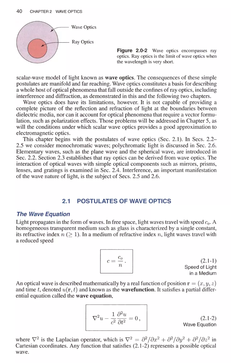
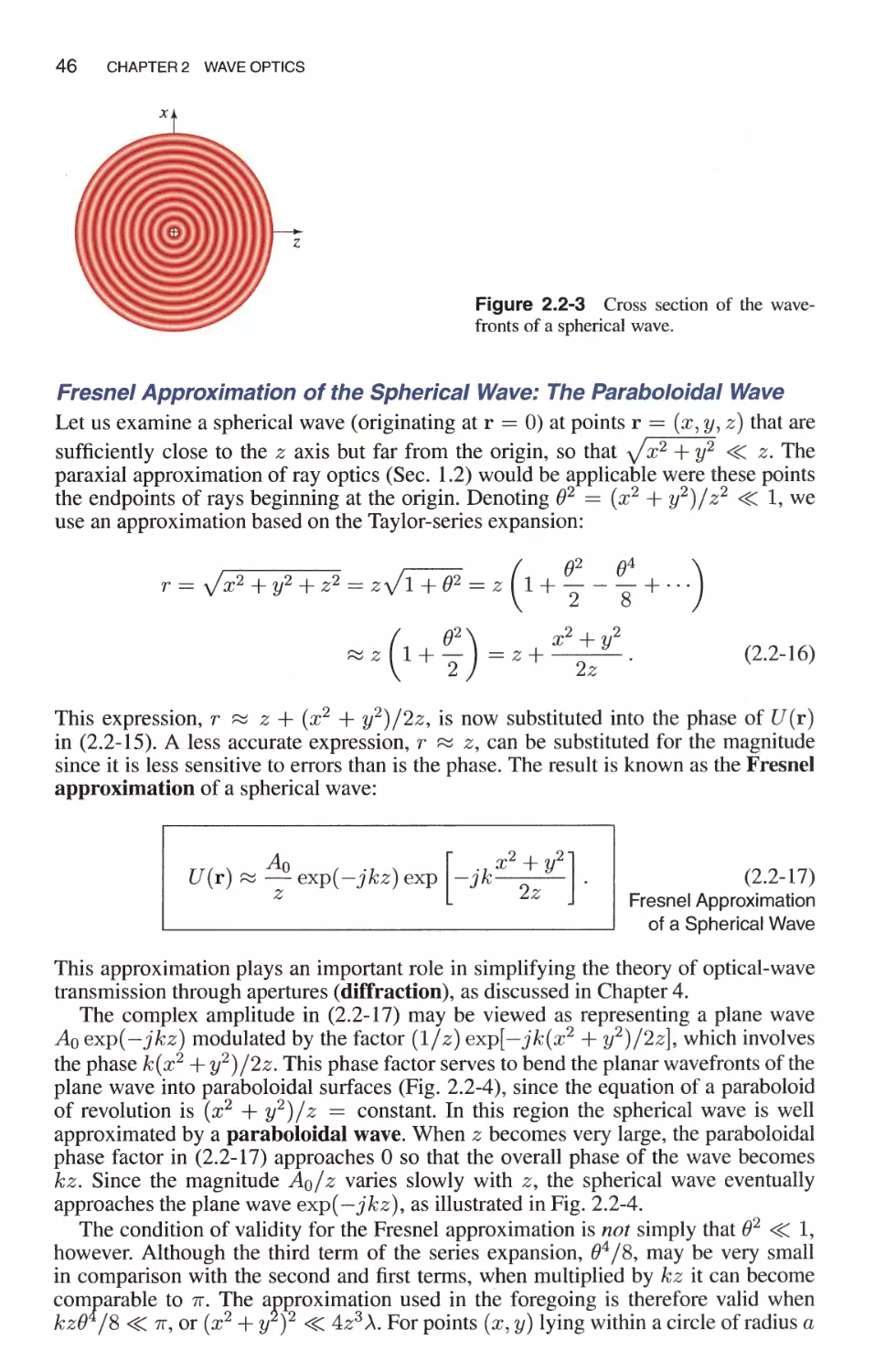
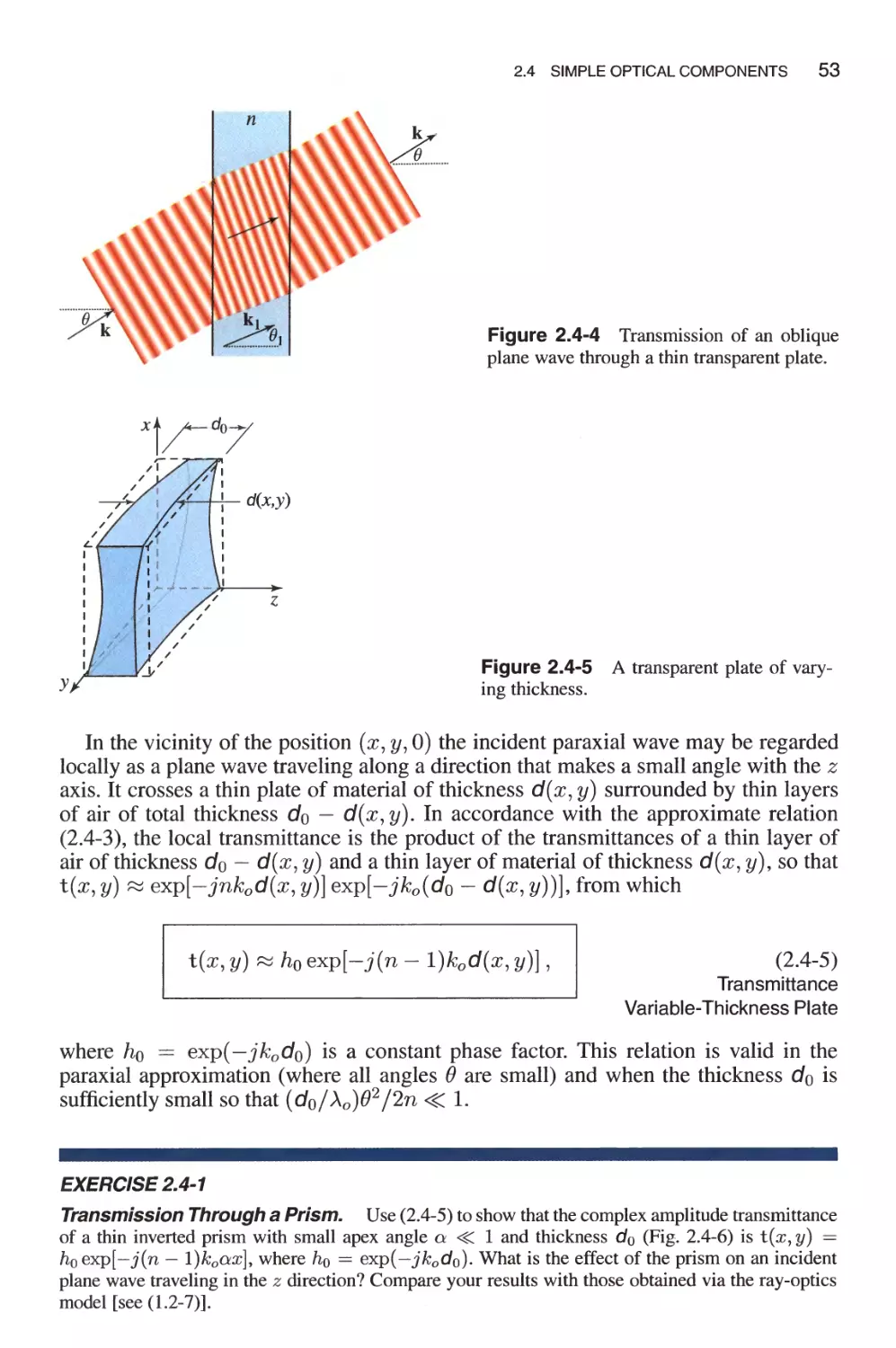
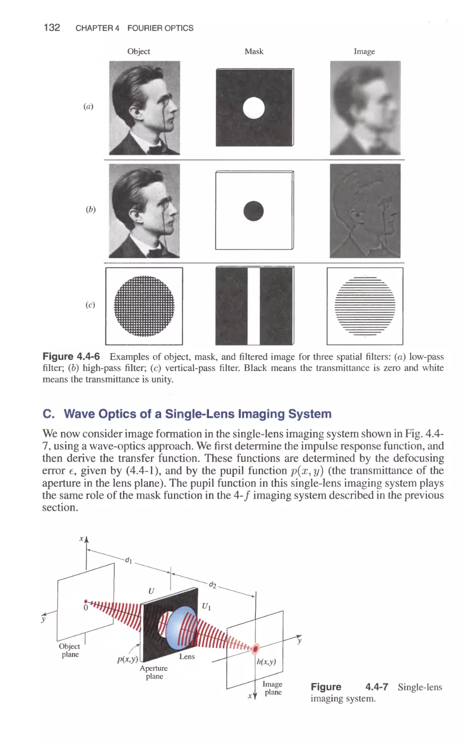
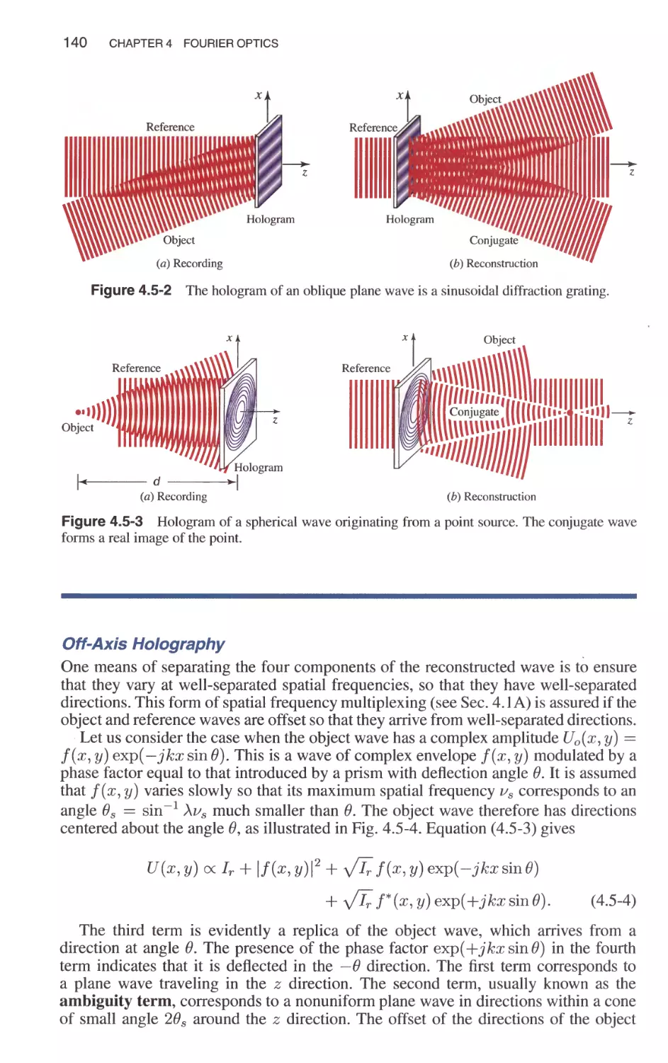
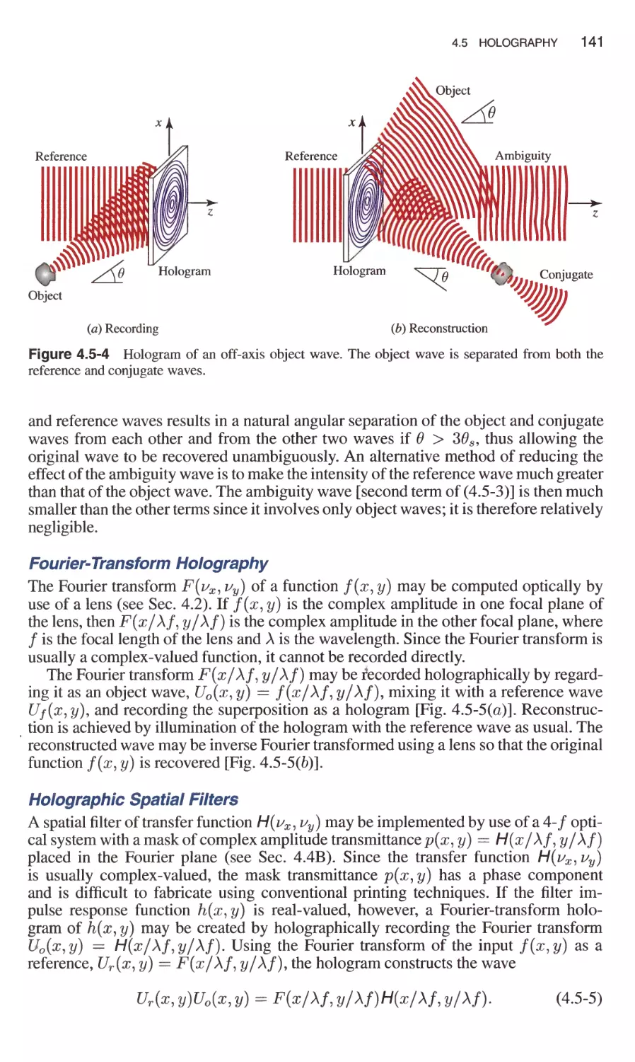
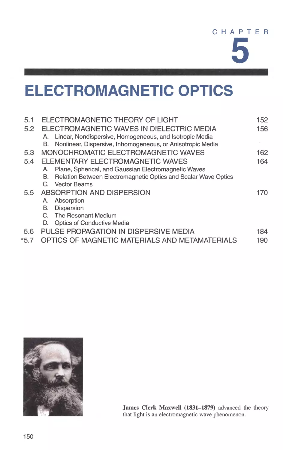
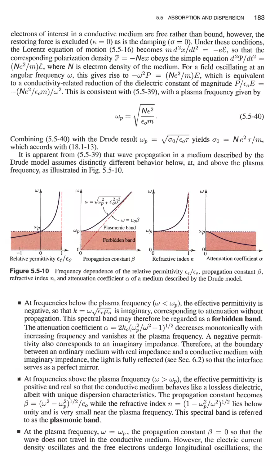
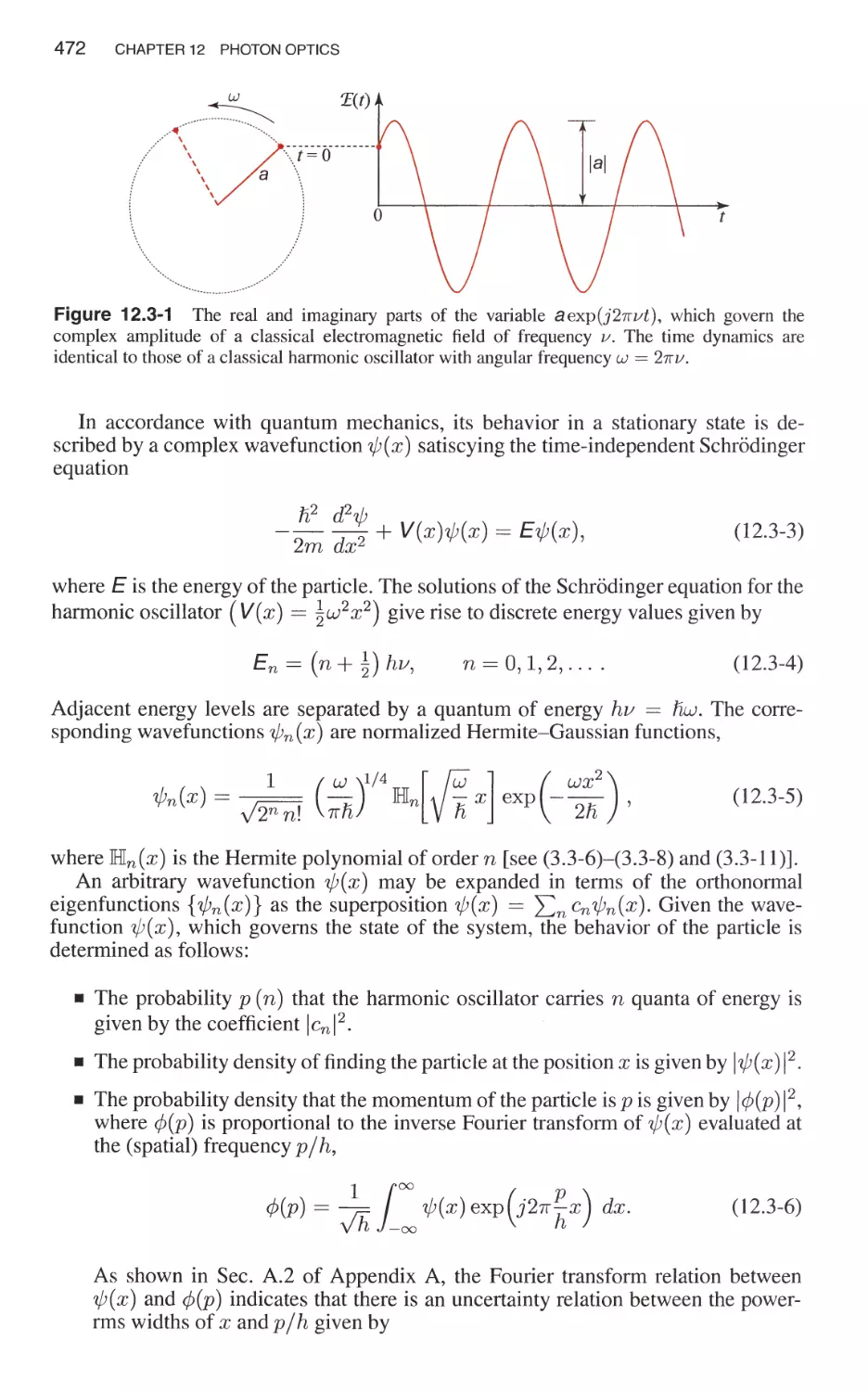
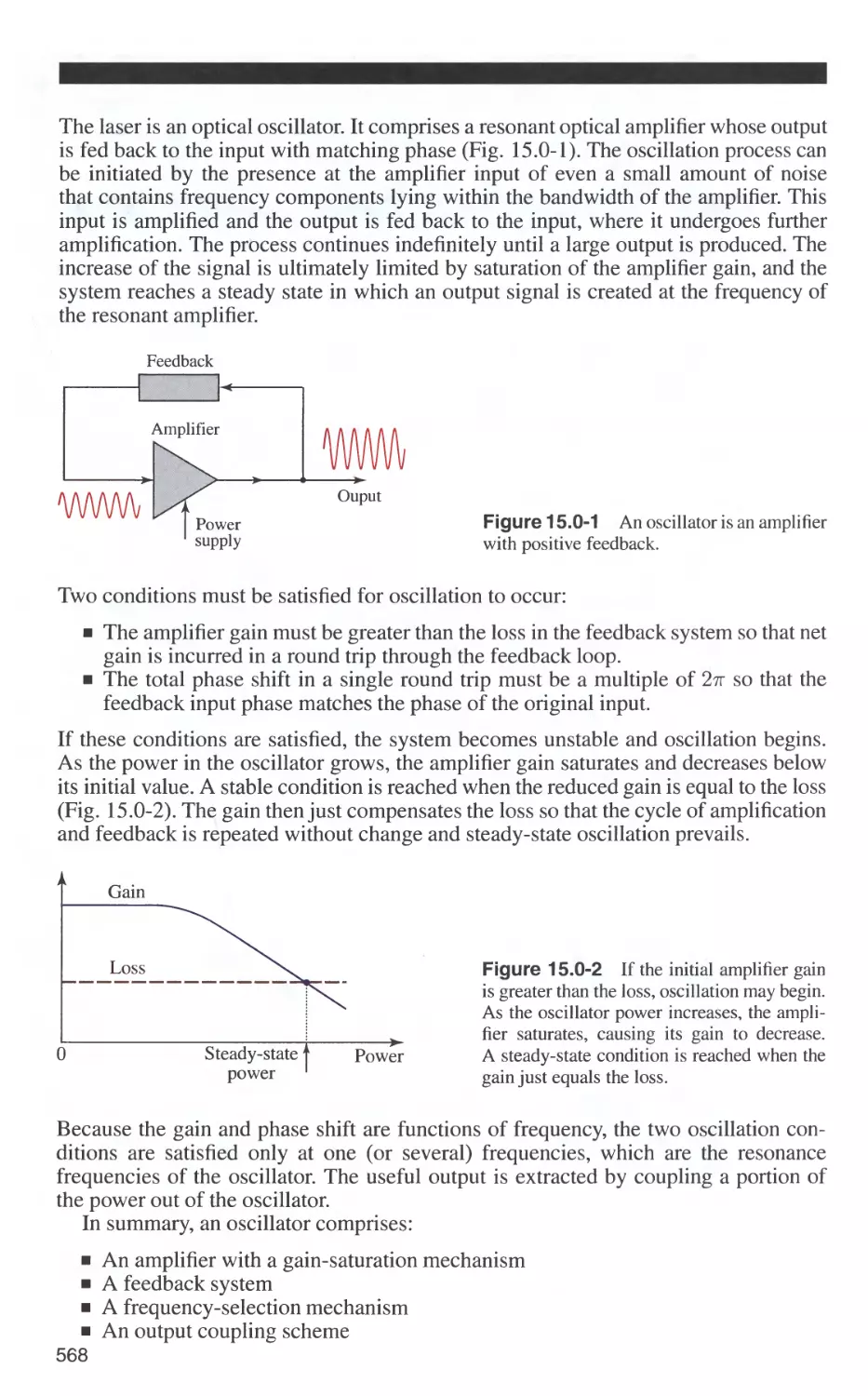
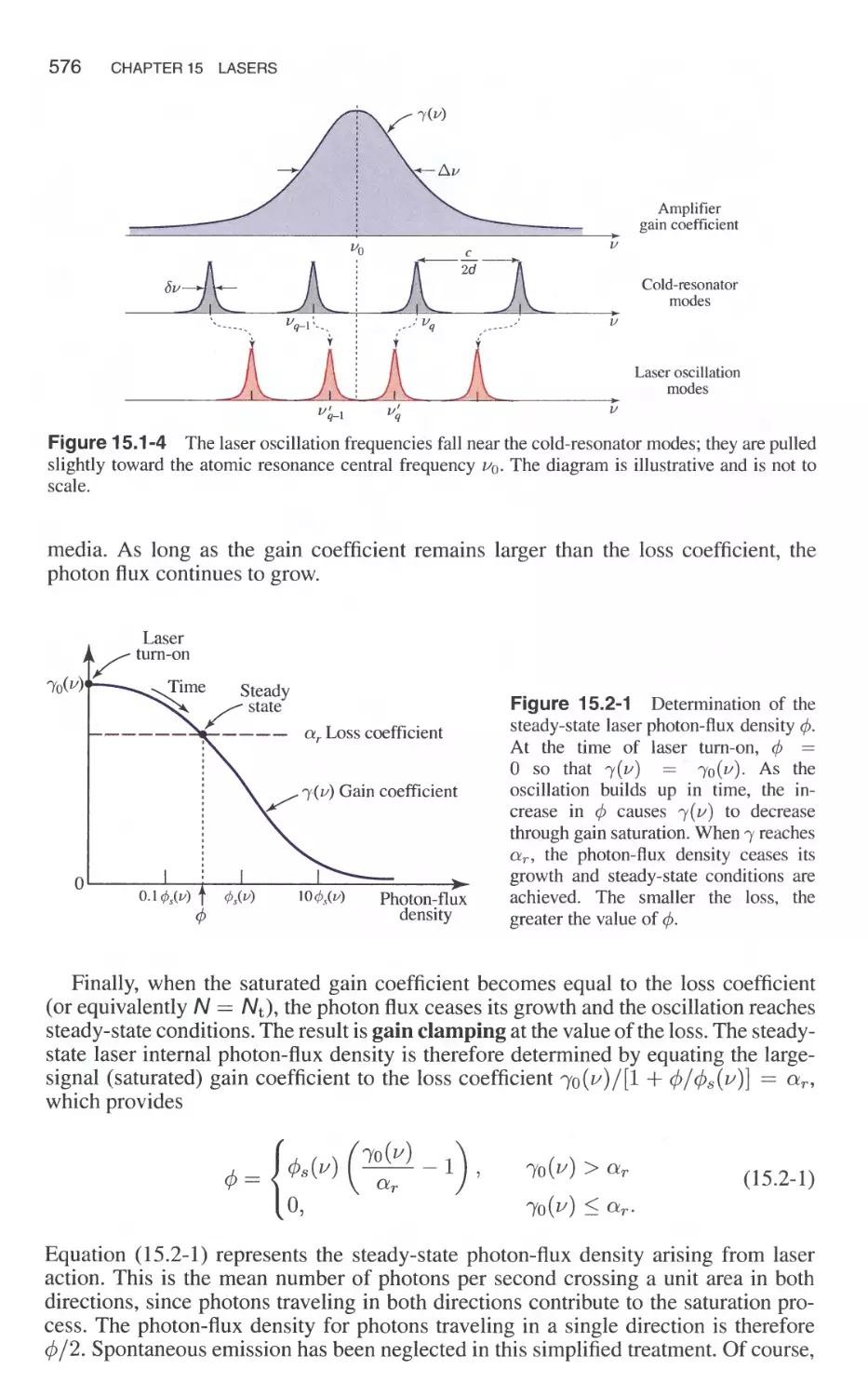
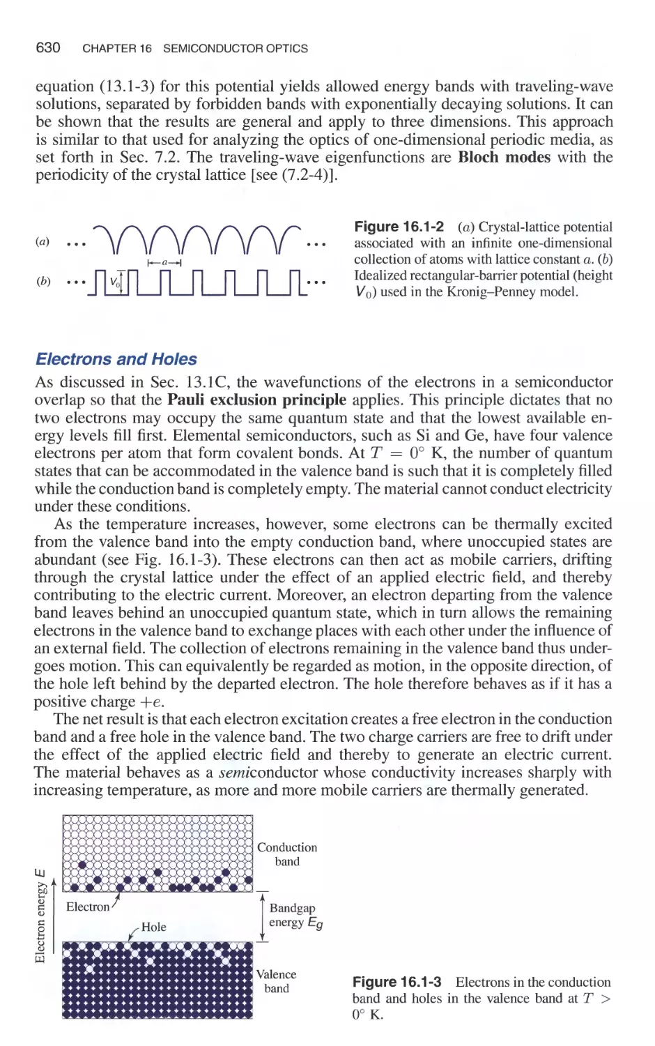
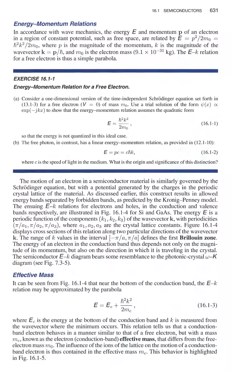
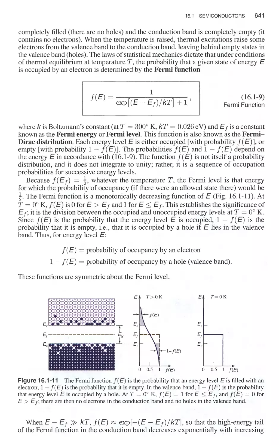
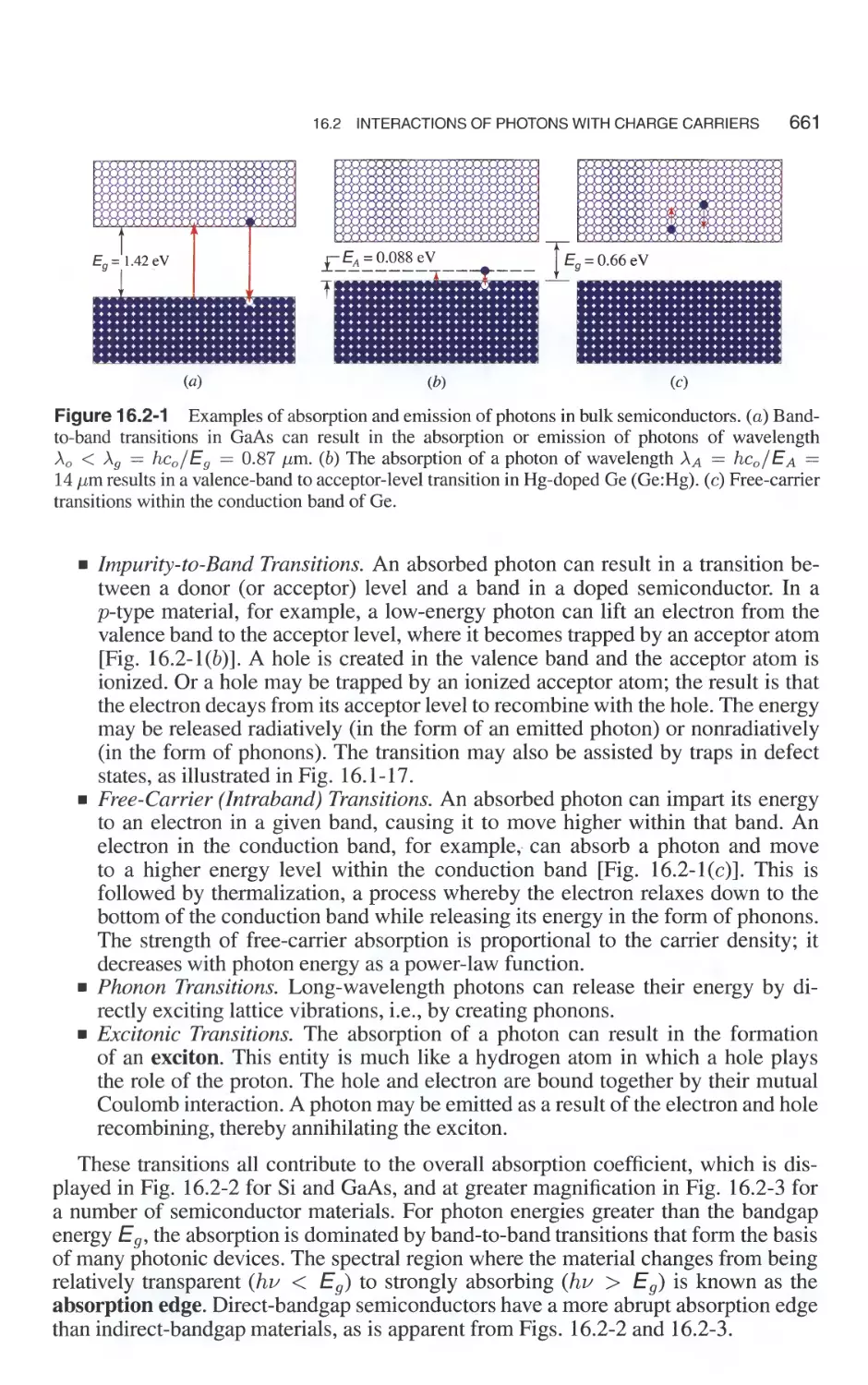
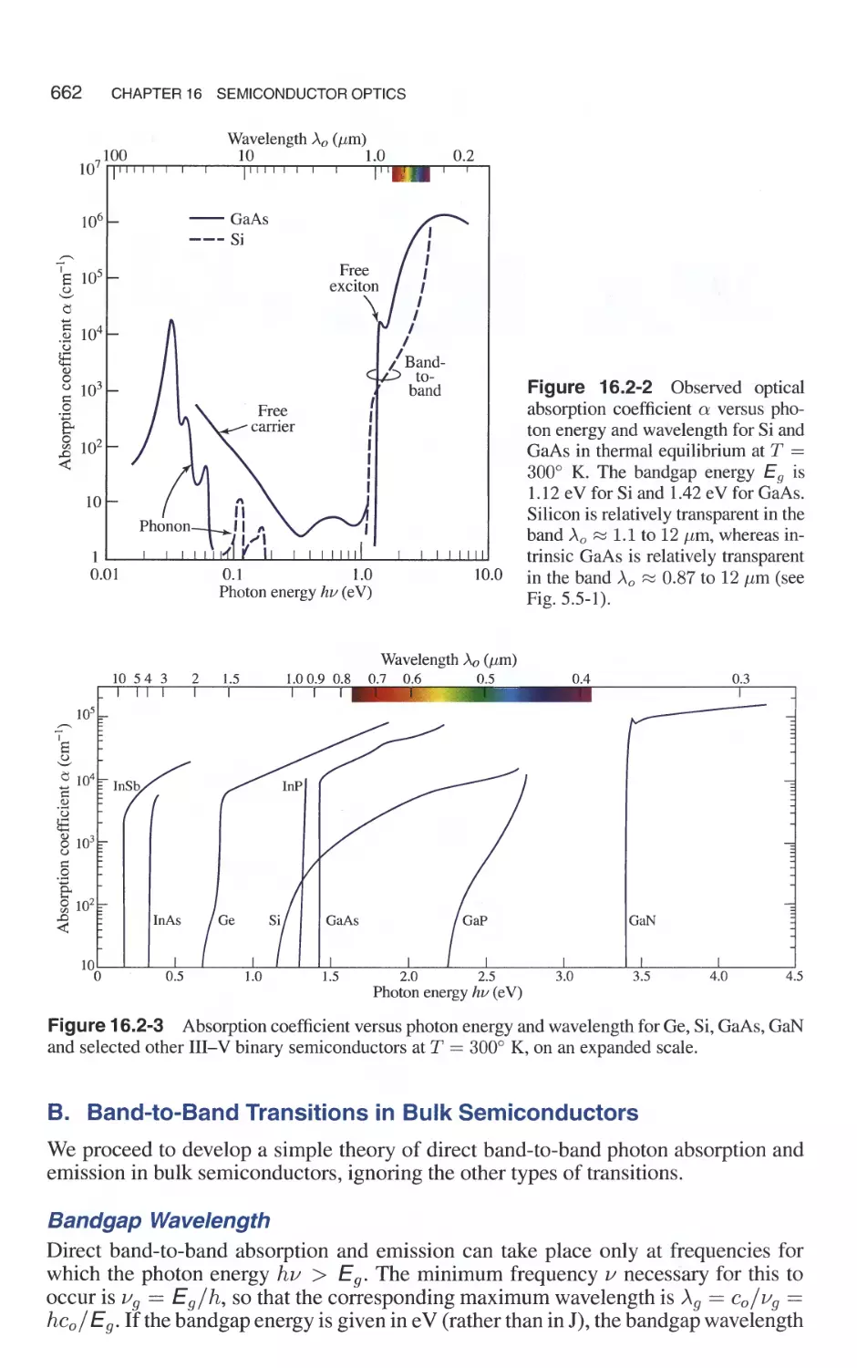
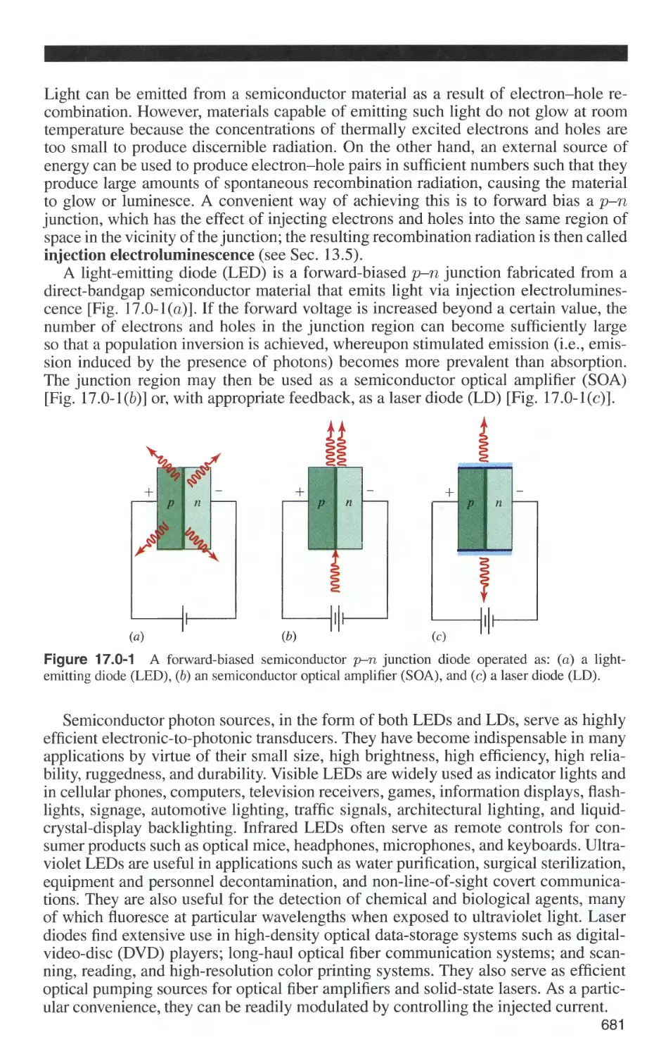
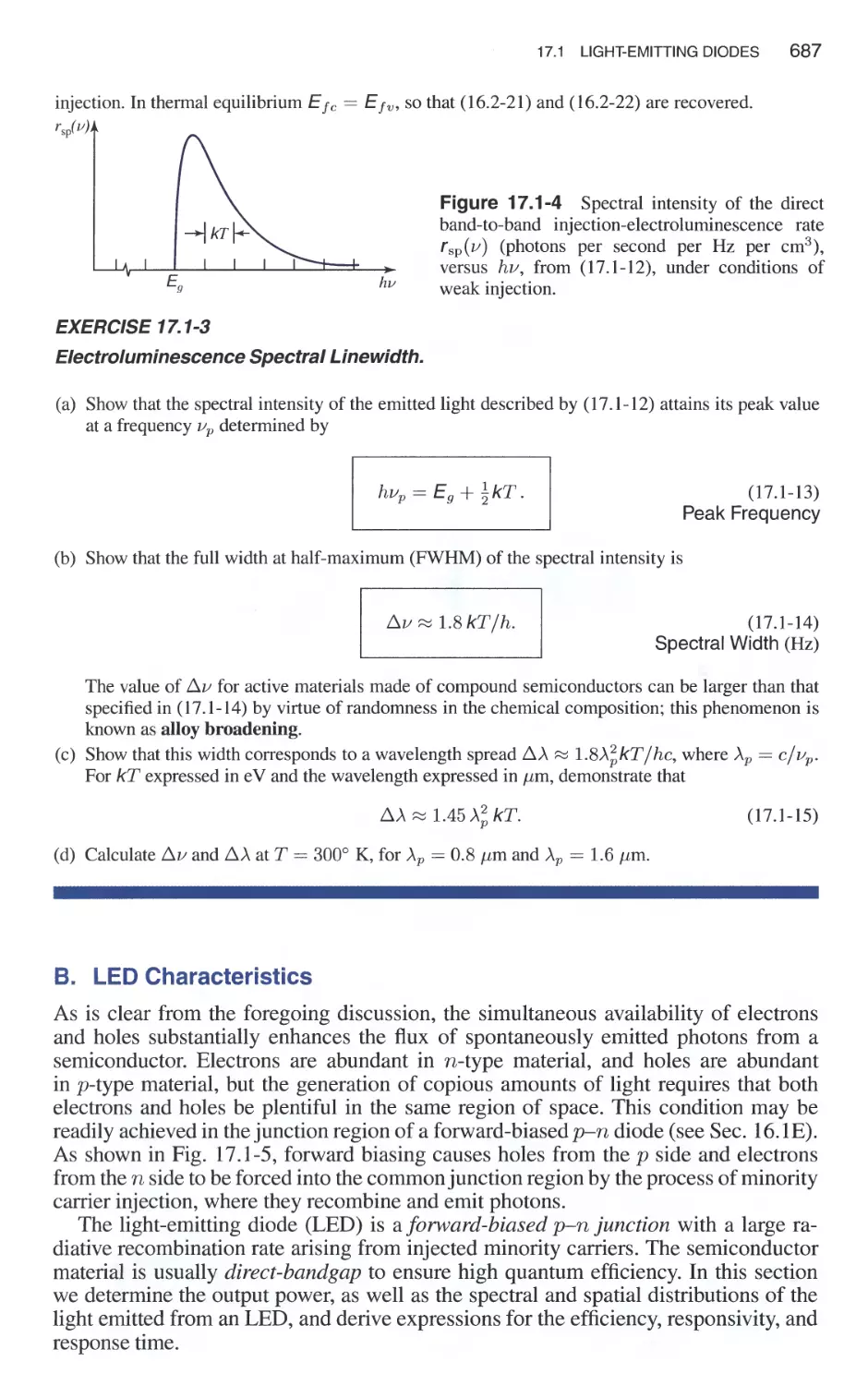
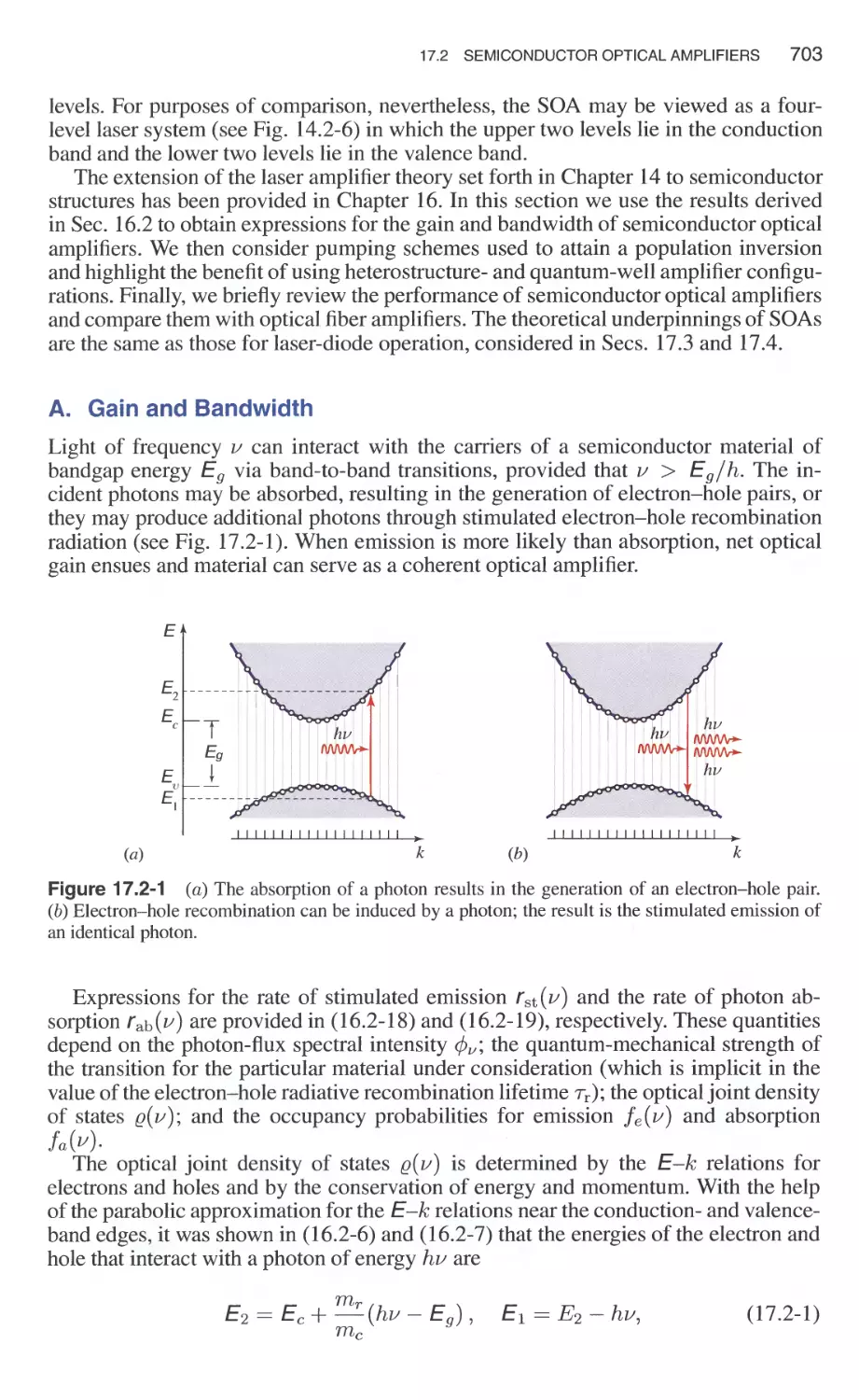
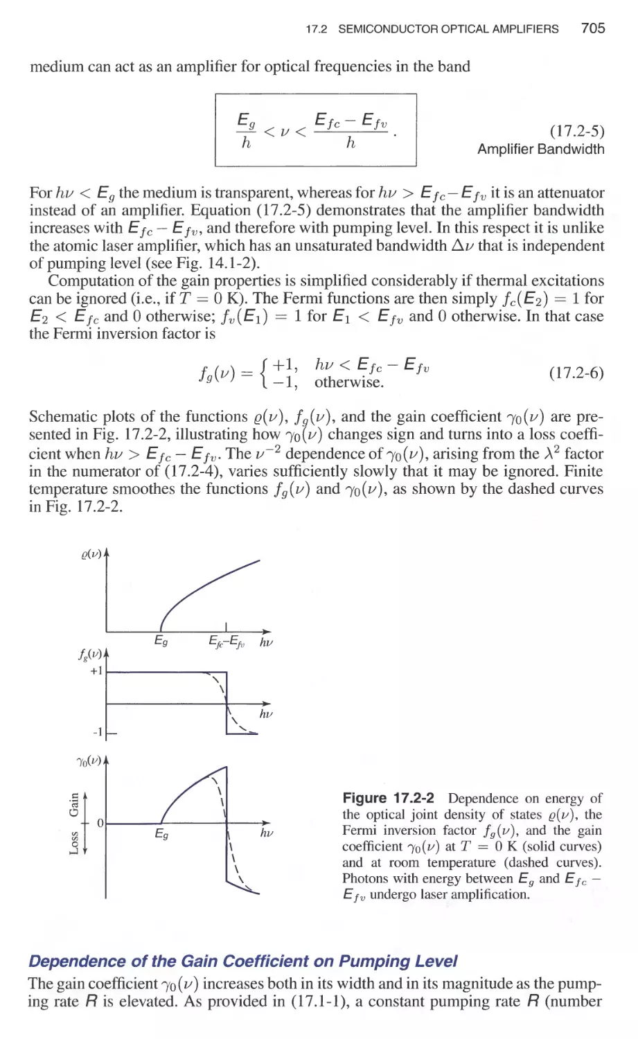
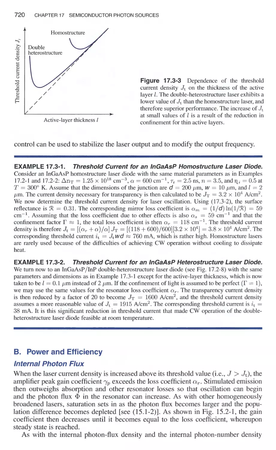
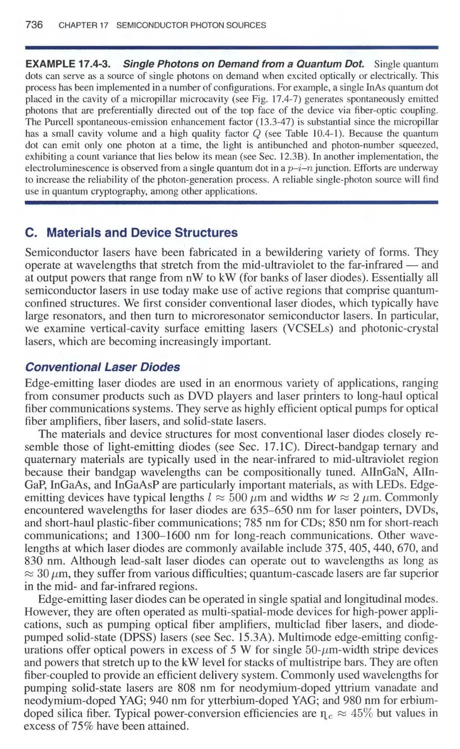
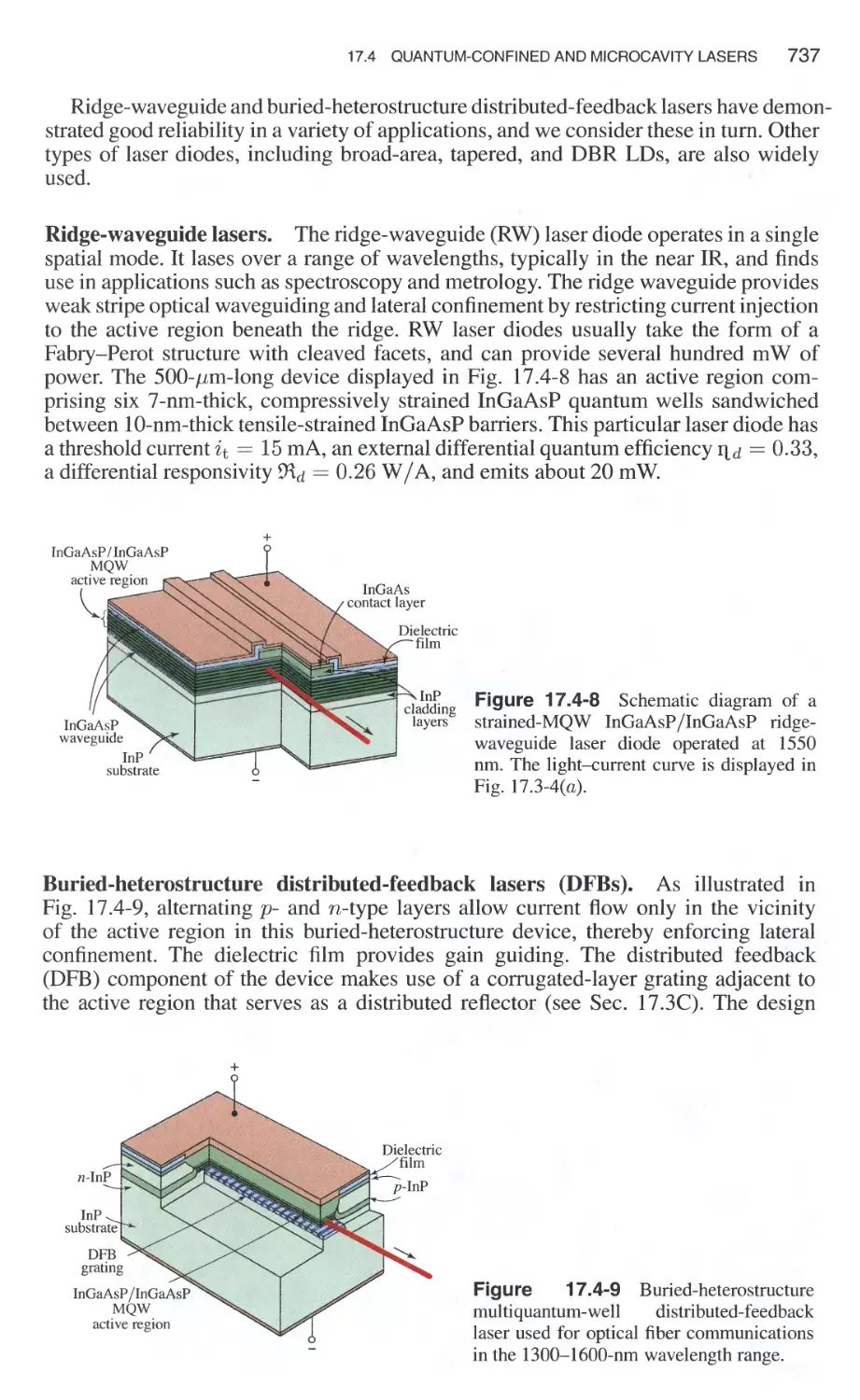
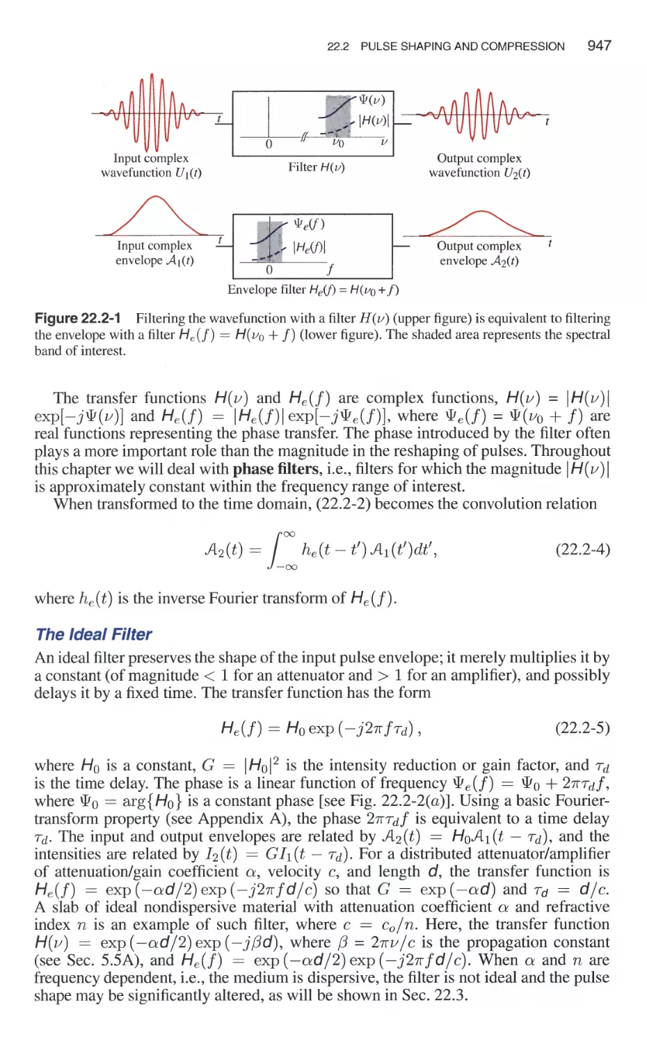
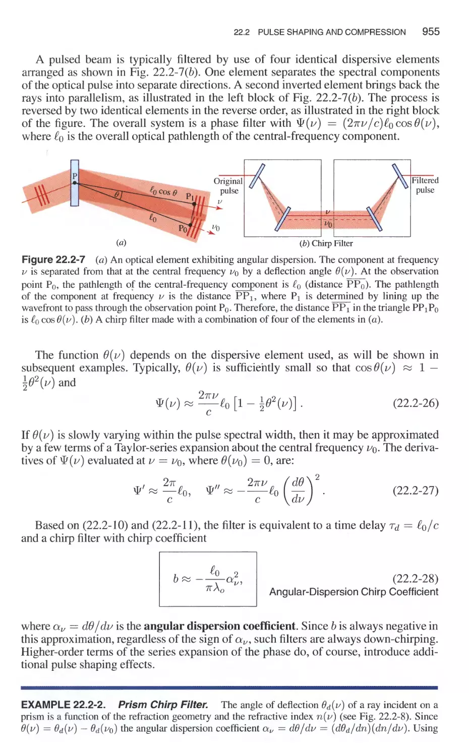
/


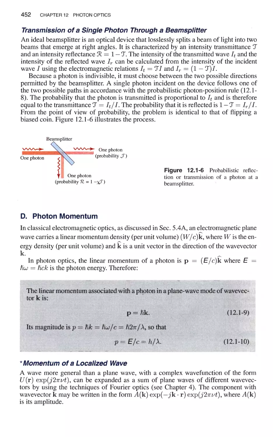


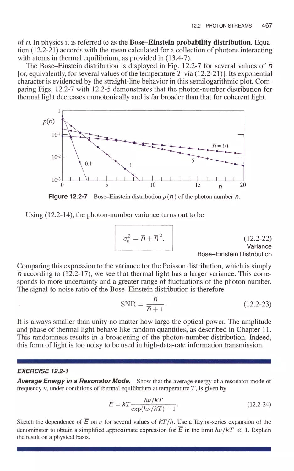


Text
WILEY SERIES IN PURE AND APPLIED OPTICS
Founded by Stanley S. Ballard, University of Florida
EDITOR: Bahaa E. A. Saleh, Boston University
BARRETT AND MYERS · Foundations of Image Science
BEISER · Holographic Scanning
BERGER-SCHUNN · Practical Color Measurement
BOYD. Radiometry and The Detection of Optical Radiation
BUCK. Fundamentals of Optical Fibers, Second Edition
CATHEY · Optical Information Processing and Holography
CHUANG · Physics of Optoelectronic Devices
DEL ONE AND KRAINOV · Fundamentals of Nonlinear Optics of Atomic Gases
DERENIAK AND BOREMAN · Infrared Detectors and Systems
DERENIAK AND CROWE · Optical Radiation Detectors
DE VANY. Master Optical Techniques
ERSOY · Diffraction, Fourier Optics and Imaging
GASKILL · Linear Systems, Fourier Transform, and Optics
GOODMAN · Statistical Optics
HOBBS · Building Electro-Optical Systems: Making It All Work
HUDSON · Infrared System Engineering
IIZUKA · Elements of Photonics, Volume I: In Free Space and Special Media
IIZUKA · Elements of Photonics, Volume II: For Fiber and Integrated Optics
JUDD AND WYSZECKI · Color in Business, Science, and Industry, Third Edition
KAFRI AND GLATT · The Physics of Moire Metrology
KAROW · Fabrication Methods for Precision Optics
KLEIN AND FURTAK · Optics, Second Edition
MALACARA · Optical Shop Testing, Second Edition
MILONNI AND EBERLY · Lasers
NASSAU. The Physics and Chemistry of Color: The Fifteen Causes of Color, Second
Edition
NIETO- VESPERINAS · Scattering and Diffraction in Physical Optics
OSCHE · Optical Detection Theory for Laser Applications
O'SHEA. Elements of Modern Optical Design
OZAKTAS · The Fractional Fourier Transform
SALEH AND TEICH · Fundamentals of Photonics, Second Edition
SCHUBERT AND WILHELMI · Nonlinear Optics and Quantum Electronics
SHEN. The Principles of Nonlinear Optics
UDD. Fiber Optic Sensors: An Introductionfor Engineers and Scientists
UDD · Fiber Optic Smart Structures
VANDERLUGT · Optical Signal Processing
VEST · Holographic Interferometry
VINCENT · Fundamentals of Infrared Detector Operation and Testing
WILLIAMS AND BECKLUND · Introduction to the Optical Transfer Function
WYSZECKI AND STILES · Color Science: Concepts and Methods, Quantitative Data and
Formulae, Second Edition
XU AND STROUD · Acousto-Optic Devices
YAMAMOTO · Coherence, Amplification, and Quantum Effects in Semiconductor Lasers
YARIV AND YEH · Optical Waves in Crystals
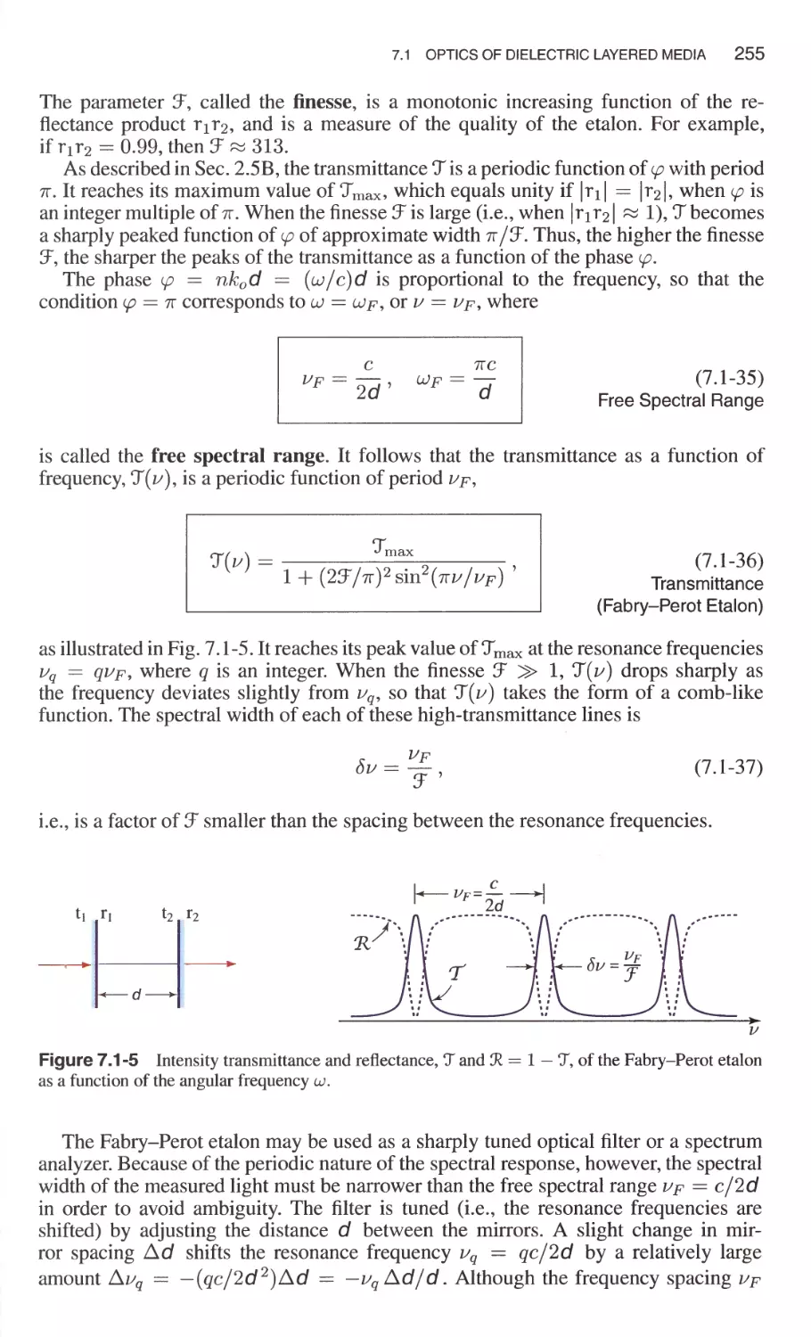
YEH · Optical Waves in Layered Media
YEH. Introduction to Photorefractive Nonlinear Optics
YEH AND GU · Optics of Liquid Crystal Displays
FUNDAMENTALS OF
PHOTONICS
BICENTENNIAL
I B
, t 8 0 7
z! z
=i WILEY =
z, z
; 2 0 0 7 ;
. t I"
BICENTENNIAL
THE WILEY BICENTENNIAL-KNOWLEDGE FOR GENERATIONS
<5 ach generation has its unique needs and aspirations. When Charles Wiley first
opened his small printing shop in lower Manhattan in 1807, it was a generation
of boundless potential searching for an identity. And we were there, helping to
define a new American literary tradition. Over half a century later, in the midst
of the Second Industrial Revolution, it was a generation focused on building the
future. Once again, we were there, supplying the critical scientific, technical, and
engineering knowledge that helped frame the world. Throughout the 20th
Century, and into the new millennium, nations began to reach out beyond their
own borders and a new international community was born. Wiley was there,
expanding its operations around the world to enable a global exchange of ideas,
opinions, and know-how.
For 200 years, Wiley has been an integral part of each generation's journey,
enabling the flow of information and understanding necessary to meet their needs
and fulfill their aspirations. Today, bold new technologies are changing the way
we live and learn. Wiley will be there, providing you the must-have knowledge
you need to imagine new worlds, new possibilities, and new opportunities.
Generations come and go, but you can always count on Wiley to provide you the
knowledge you need, when and where you need it!
W .
WILLIAM &J. PESCE
PRESIDENT AND CHIEF EXECUTIVE CFFICER
L tU
PETER BCCTH WILEY
CHAIRMAN OF THE BOARD
FUNDAMENTALS OF
PHOTONICS
SECOND EDITION
BAHAA E. A. SALEH
Boston University
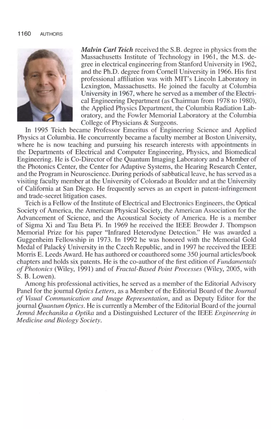
MALVIN CARL TEICH
Boston University
Columbia University
1807
@0WILEY
2007 ;
WILEY-INTERSCIENCE
A John Wiley & Sons, Inc., Publication (ffJ)
Copyright @ 2007 by John Wiley & Sons, Inc. All rights reserved.
Published by John Wiley & Sons, Inc., Hoboken, New Jersey.
Published simultaneously in Canada.
No part of this publication may be reproduced, stored in a retrieval system, or transmitted in any form or by any means,
electronic, mechanical, photocopying, recording, scanning, or otherwise, except as permitted under Section 107 or 108 of
the 1976 United States Copyright Act, without either the prior written permission of the Publisher, or authorization through
payment of the appropriate per-copy fee to the Copyright Clearance Center, Inc., 222 Rosewood Drive, Danvers, MA
01923, (978) 750-8400, fax (978) 750-4470, or on the web at www.copyright.com. Requests to the Publisher for permission
should be addressed to the Permissions Department, John Wiley & Sons, Inc., III River Street, Hoboken, NJ 07030, (20 I)
748-6011, fax (201) 748-6008, or online at http://www.wiley.com/go/permission.
Limit of Liability/Disclaimer of Warranty: While the publisher and author have used their best efforts in preparing this
book, they make no representations or warranties with respect to the accuracy or completeness of the contents of this book
and specifically disclaim any implied warranties of merchantability or fitness for a particular purpose. No warranty may be
created or extended by sales representatives or written sales materials. The advice and strategies contained herein may not
be suitable for your situation. You should consult with a professional where appropriate. Neither the publisher nor author
shall be liable for any loss of profit or any other commercial damages, including but not limited to special, incidental,
consequential, or other damages.
For general information on our other products and services or for technical support, please contact our Customer Care
Department within the United States at (800) 762-2974, outside the United States at (317) 572-3993 or fax (317) 572-4002.
Wiley also publishes its books in a variety of electronic formats. Some content that appears in print may not be available in
electronic format. For information about Wiley products, visit our web site at www.wiley.com.
Wiley Bicentennial Logo: Richard 1. Pacifico
Library of Congress Cataloging-in-Publication Data is available.
ISBN: 978-0-471-35832-9
Printed in the United States of America.
10 9 8 7 6 5 4 3 2
PREFACE TO THE SECOND EDITION
Since the publication of the First Edition in 1991, Fundamentals of Photonics has
been reprinted some 20 times, translated into Czech and Japanese, and used worldwide
as a textbook and reference. During this period, major developments in photonics
have continued apace, and have enabled technologies such as telecommunications
and applications in industry and medicine. The Second Edition reports some of these
developments, while maintaining the size of this single-volume tome within practical
limi ts.
In its new organization, Fundamentals of Photonics continues to serve as a self-
contained and up-to-date introductory-level textbook, featuring a logical blend of the-
ory and applications. Many readers of the First Edition have been pleased with its
abundant and well-illustrated figures. This feature has been enhanced in the Second
Edition by the introduction of full color throughout the book, offering improved clarity
and readability.
While each of the 22 chapters of the First Edition has been thoroughly updated, the
principal feature of the Second Edition is the addition of two new chapters: one on
photonic-crystal optics and another on ultrafast optics. These deal with developments
that have had a substantial and growing impact on photonics over the past decade.
The new chapter on photonic-crystal optics provides a foundation for understand-
ing the optics of layered media, including Bragg gratings, with the help of a matrix
approach. Propagation of light in one-dimensional periodic media is examined using
Bloch modes with matrix and Fourier methods. The concept of the photonic bandgap
is introduced. Light propagation in two- and three-dimensional photonic crystals, and
the associated dispersion relations and bandgap structures, are developed. Sections on
photonic-crystal waveguides, holey fibers, and photonic-crystal resonators have also
been added at appropriate locations in other chapters.
The new chapter on ultrafast optics contains sections on picosecond and femtosec-
ond optical pulses and their characterization, shaping, and compression, as well as their
propagation in optical fibers, in the domain of linear optics. Sections on ultrafast non-
linear optics include pulsed parametric interactions and optical solitons. Methods for
the detection of ultrafast optical pulses using available detectors, which are relatively
slow, are reviewed.
In addition to these two new chapters, the chapter on optical interconnects and
switches has been completely rewritten and supplemented with topics such as wave-
length and time routing and switching, FBGs, WGRs, SOAs, TOADs, and packet
switches. The chapter on optical fiber communications has also been significantly
updated and supplemented with material on WDM networks; it now offers concise
descriptions of topics such as dispersion compensation and management, optical am-
plifiers, and soliton optical communications.
Continuing advances in device-fabrication technology have stimulated the emer-
gence of nanophotonics, which deals with optical processes that take place over
subwavelength (nanometer) spatial scales. Nanophotonic devices and systems include
quantum-confined structures, such as quantum dots, nanoparticles, and nanoscale
periodic structures used to synthesize metamaterials with exotic optical properties
such as negative reflactive index. They also include configurations in which light (or
its interaction with matter) is confined to nanometer-size (rather than micrometer-
size) regions near boundaries, as in surface plasmon optics. Evanescent fields, such
as those produced at a surface where total internal reflection occurs, also exhibit
v
VI PREFACE
such confinement. Evanescent fields are present in the immediate vicinity of sub-
wavelength-size apertures, such as the open tip of a tapered optical fiber. Their use
allows imaging with resolution beyond the diffraction limit and forms the basis of
near-field optics. Many of these emerging areas are described at suitable locations in
the Second Edition.
New sections have been added in the process of updating the various chapters. New
topics introduced in the early chapters include: Laguerre-Gaussian beams; near-field
imaging; the Sellmeier equation; fast and slow light; optics of conductive media and
plasmonics; doubly negative metamaterials; the Poincare sphere and Stokes parame-
ters; polarization mode dispersion; whispering-gallery modes; microresonators; optical
coherence tomography; and photon orbital angular momentum.
In the chapters on laser optics, new topics include: rare-earth and Raman fiber
amplifiers and lasers; EUV, X-ray, and free-electron lasers; and chemical and random
lasers. In the area of optoelectronics, new topics include: gallium nitride-based struc-
tures and devices; superluminescent diodes; organic and white-light LEDs; quantum-
confined lasers; quantum-cascade lasers; microcavity lasers; photonic-crystal lasers;
array detectors; low-noise APDs; SPADs; and QWIPs.
The chapter on nonlinear optics has been supplemented with material on parametric-
interaction tuning curves; quasi-phase-matching devices; two-wave mixing and cross-
phase modulation; THz generation; and other nonlinear optical phenomena associated
with narrow optical pulses, including chirp pulse amplification and supercontinuum
light generation. The chapter on electro-optics now includes a discussion of electroab-
sorption modulators.
Appendix C on modes of linear systems has been expanded and now offers an
overview of the concept of modes as they appear in numerous locations within the
book. Finally, additional exercises and problems have been provided, and these are
now numbered disjointly to avoid confusion.
In this full-color edition, we have used the color code illustrated in the following
chart for most of the illustrations. Light beams and field distributions are colored red
(except when light beams of multiple colors are involved, as in nonlinear optics). Glass
and glass fibers are depicted in light blue. Semiconductors are cast in green, with
various shades representing different doping levels, and metal is indicated by the color
of copper. Energy diagrams are marked in blue and forbidden photonic bandgaps in
pink, as indicated.
Glass
pJ
I
O . I ·
ptica ray
Semiconductor
Optical beam
Energy levels
Dielectric waveguide
<
Optical wave
.0..
Metal
Photonic bandgap
Fiber
Color chart
Organization
In its new incarnation, Fundamentals of Photonics comprises 24 chapters compart-
mentalized into six parts, as depicted in the diagram below. The form of the book
is modular so that it can be used by readers with different needs; it also provides
PREFACE VII
instructors an opportunity to select topics for different courses. Essential material from
one chapter is often briefly summarized in another to make each chapter as self-
contained as possible. For example, at the beginning of Chapter 24 (Optical Fiber
Communications), relevant material from earlier chapters that describe fibers, light
sources, detectors, and amplifiers is briefly reviewed. This places the important features
of the various components at the disposal of the reader before the chapter proceeds with
a discussion of the design and performance of the overall communication system that
makes use of these components.
Fundamentals Wave Propagation Laser Optics Lightwave Devices
1. Ray Optics 7. Photonic-Crystal Optics 13. Photons and Atoms 19. Acousto-Optics
2. Wave Optics 8. Guided-Wave Optics 14. Laser Amplifiers 20. Electro-Optics
3. Beam Optics 9. Fiber Optics 15. Lasers 21. Nonlinear Optics
4. Fourier Optics 10. Resonator Optics 16. Semiconductor Optics 22. Ultrafast Optics
5. Electromagnetic Optics 11. Statistical Optics 17. Semiconductor Sources 23. Interconnects/Switches
6. Polarization Optics 12. Photon Optics 18. Semiconductor Detectors 24. Optical Communications
Optoelectronics
Lightwave Systems
Recognizing the different degrees of mathematical sophistication of the intended
readership, we have endeavored to present difficult concepts in two steps: at an intro-
ductory level providing physical insight and motivation, followed by a more advanced
analysis. This approach is exemplified by the treatment in Chapter 20 (Electro-Optics),
in which the subject is first presented using scalar notation and then treated again using
tensor notation.
Commonly accepted notation and symbols have been used wherever possible. Be-
cause of the broad spectrum of topics covered, however, there are a good number of
symbols that have multiple meanings; a list of symbols and units is provided at the
end of the book to clarify symbol usage. Throughout the book, important equations
are highlighted by boxes to facilitate future retrieval. Sections dealing with material
of a more advanced nature are indicated by asterisks and may be omitted if desired.
Summaries are provided throughout at points where a recapitulation is deemed useful
because of the involved nature of the material.
Each chapter also contains exercises, problem sets, and updated selected reading
lists. Examples of real systems are included to emphasize the concepts governing appli-
cations of current interest, and appendixes summarize the properties of one- and two-
dimensional Fourier transforms, linear-systems theory, and modes of linear systems.
Representative Courses
The chapters of this book may be combined in various ways for use in semester or
quarter courses. Representative examples of such courses are provided below. Some of
these courses may be offered as part of a sequence. Other selections may be made to
suit the particular objectives of instructors and students.
Optics/Photonics
1. Ray Optics
2. Wave Optics
3. Beam Optics
4. Fourier Optics
5. Electromagnetic Optics
6. Polarization Optics
---
- -
7. Photonic Crystals
8. Guided-Wave Optics
9. Fiber Optics
10. Resonator Optics
11. Statistical Optics
12. Photon Optics
13. Photons and Atoms
14. Laser Amplifiers
15. Lasers
16. Semiconductor Optics
17. Sources
18. Detectors
19. Acousto-Optics
20. Electro-Optics
21. Nonlinear Optics
22. Ultrafast Optics
23. Interconnects/Switches :-
24. Optical Communications -
VIII PREFACE
The first six chapters of the book are suitable for an introductory course on Optics or Photonics.
These may be supplemented by Chapter 11, Statistical Optics, to introduce incoherent and partially
coherent light, or by the introductory sections of Chapters 8 and 9, Guided- Wave Optics and Fiber
Optics, which offer applications.
Optical Information Processing
1. Ray Optics 7. Photonic Crystals 13. Photons and Atoms 19. Acousto-Optics
2. Wave Optics 8. Guided-Wave Optics 14. Laser Amplifiers 20. Electro-Optics
3. Beam Optics 9. Fiber Optics 15. Lasers 21. Nonlinear Optics
4. Fourier Optics 10. Resonator Optics 16. Semiconductor Optics 22. Ultrafast Optics
5. Electromagnetic Optics 11. Statistical Optics 17. Sources 23. Interconnects/Switches
6. Polarization Optics 12. Photon Optics 18. Detectors 24. Optical Communications
A course on Optical Information Processing may begin with a background of wave and beam optics,
and cover Fourier Optics (including coherent image formation and processing), along with incoherent
and partially coherent imaging in Statistical Optics. This may be followed by material on devices used
for analog data processing, such as Acousto-Optics, and end with switches and gates (Chapter 23),
which are used for digital data processing.
Guided-Wave Optics
1. Ray Optics 7. Photonic Crystals 13. Photons and Atoms 19. Acousto-Optics
2. Wave Optics 8. Guided-Wave Optics 14. Laser Amplifiers 20. Electro-Optics
3. Beam Optics 9. Fiber Optics 15. Lasers 21. Nonlinear Optics
4. Fourier Optics 10. Resonator Optics 16. Semiconductor Optics 22. Ultrafast Optics
5. Electromagnetic Optics 11. Statistical Optics 17. Sources 23. Interconnects/Switches
6. Polarization Optics 12. Photon Optics 18. Detectors 24. Optical Communications
A course on Guided-Wave Optics may begin with an introduction to wave propagation in layered
and periodic media (Chapter 7, Photonic-Crystal Optics) and follow with the chapters on Guided-
Wave Optics, Fiber Optics, and Resonator Optics. Additional topics may include Electro-Optics and
Optical Interconnects and Stvitches.
Lasers
1. Ray Optics 7. Photonic Crystals 13. Photons and Atoms 19. Acousto-Optics
2. Wave Optics 8. Guided-Wave Optics 14. Laser Amplifiers 20. Electro-Optics
3. Beam Optics 9. Fiber Optics 15. Lasers 21. Nonlinear Optics
4. Fourier Optics 10. Resonator Optics 16. Semiconductor Optics 22. Ultrafast Optics
5. Electromagnetic Optics 11. Statistical Optics 17. Sources 23. Interconnects/Switches
6. Polarization Optics 12. Photon Optics 18. Detectors 24. Optical Communications
A course on Lasers could begin with Beam Optics and Resonator Optics, and follow with the theory
of interaction of light with matter (Chapter 13) and laser amplification and oscillation (Chapters 14
and 15), and include semiconductor LEDs and lasers (Chapters 16 and 17). An introduction to
femtosecond lasers can be provided by including appropriate sections from Ultrafast Optics.
Optoelectronics l
1. Ray Optics 7. Photonic Crystals 13. Photons and Atoms 19. Acousto-Optics
2. Wave Optics 8. Guided-Wave Optics 14. Laser Amplifiers 20. Electro-Optics
3. Beam Optics 9. Fiber Optics 15. Lasers 21. Nonlinear Optics
4. Fourier Optics 10. Resonator Optics 16. Semiconductor Optics 22. Ultrafast Optics
5. Electromagnetic Optics 11. Statistical Optics 17. Sources 23. Interconnects/Switches
6. Polarization Optics 12. Photon Optics 18. Detectors 24. Optical Communications :
The three chapters covering semiconductor optics, sources/amplifiers, and detectors form a suitable
basis for a course on Optoelectronics. This material may be supplemented with optics background
from earlier chapters, and extended to include topics such as liquid-crystal devices (Secs. 6.5 and
PREFACE IX
20.3), semiconductor electroabsorption modulators (Sec. 20.5), and an introduction to the use of
photonic devices for switching and/or communications (Chapters 23 and 24, respectively).
Photonic Devices
1. Ray Optics 7. Photonic Crystals 13. Photons and Atoms 19. Acousto-Optics
2. Wave Optics 8. Guided-Wave Optics 14. Laser Amplifiers 20. Electro-Optics
3. Beam Optics 9. Fiber Optics 15. Lasers 21. Nonlinear Optics
4. Fourier Optics 10. Resonator Optics 16. Semiconductor Optics 22. Ultrafast Optics
5. Electromagnetic Optics 11. Statistical Optics 17. Sources 23. Interconnects/Switches
6. Polarization Optics 12. Photon Optics 18. Detectors 24. Optical Communications
Photonic Devices is another possible topic for a course that combines photonic-crystal and guided-
wave devices with electro-optic, acousto-optic, and nonlinear optical devices, and includes ultrafast
optics and optical interconnects/switches.
Fiber-Optic Communications
1. Ray Optics
2. Wave Optics
3. Beam Optics
4. Fourier Optics
5. Electromagnetic Optics
6. Polarization Optics
7. Photonic Crystals
8. Guided-Wave Optics
9. Fiber Optics
10. Resonator Optics
11. Statistical Optics
12. Photon Optics
13. Photons and Atoms
14. Laser Amplifiers
15. Lasers
16. Semiconductor Optics
17. Sources
18. Detectors
19. Acousto-Optics
20. Electro-Optics
21. Nonlinear Optics
22. Ultrafast Optics
23. Interconnects/Switches
24. Optical Communications :
A course on Fiber-Optic Communications could include optical waveguides and fibers, semiconduc-
tor sources and amplifiers (possibly also Sees. 14.3C and 14.3D on optical-fiber and Raman-fiber
amplifiers), as background material for the chapter on Optical Fiber Communications (Chapter 24).
If fiber-optic networks are to be emphasized, Sec. 23.3 on photonic switches may also be included.
Acknowledgments
We are grateful to many colleagues for providing us with valuable comments about
draft chapters for the Second Edition and for drawing our attention to errors in the
First Edition: Mete Atatiire, Michael Bar, Silvia Carrasco, Thomas Daly, Gianni Di
Giuseppe, Adel EI-Nadi, John Fourkas, Majeed Hayat, Tony Heinz, Erich Ippen, Mar-
tin Jaspan, Gerd Keiser, Jonathan Kane, Paul Kelley, Ted Moustakas, Magued Nasr,
Roy Olivier, Roberto Paiella, Alexander Sergienko, Peter W. E. Smith, Stephen P.
Smith, Kenneth Suslick, and Tommaso Toffoli.
We extend our special thanks to those colleagues who graciously provided us with
in-depth critiques of various chapters: Ayman Abouraddy, Luca Dal Negro, and Paul
Prucnal.
We are indebted to the legions of students and postdoctoral associates who have
posed so many excellent questions that helped us hone our presentation. In particular,
many improvements were initiated by suggestions from Mark Booth, Jasper Cabalu,
Michael Cunha, Darryl Goode, Chris LaFratta, Rui Li, Eric Lynch, Nan Ma, Nishant
Mohan, Julie Praino, Yunjie Tong, and Ranjith Zachariah. We are especially grateful to
Mohammed Saleh, who diligently read much of the manuscript and provided us with
excellent suggestions for improvement throughout.
Wai Yan (Eliza) Wong provided logistical support and a great deal of assistance in
crafting diagrams and figures. Many at Wiley, including George Telecki, our Editor,
and Rachel Witmer have been most helpful, patient, and encouraging. We appreciate
the attentiveness and thoroughness that Melissa Yanuzzi brought to the production pro-
cess. Don DeLand of the Integre Technical Publishing Company provided invaluable
assistance in setting up the Latex style files.
We are most appreciative of the financial support provided by the National Sci-
ence Foundation (NSF), in particular the Center for Subsurface Sensing and Imaging
X PREFACE
Systems (CenSSIS), an NSF-supported Engineering Research Center; the Defense
Advanced Research Projects Agency (DARPA); the National Reconnaisance Office
(NRO); the U.S. Army Research Office (ARO); the David & Lucile Packard Founda-
tion; the Boston University College of Engineering; and the Boston University Photon-
ics Center.
Photo Credits. Most of the portraits were carried forward from the First Edi-
tion with the benefit of permissions provided for all editions. Additional credits are:
Godfrey Kneller 1689 portrait (Newton); Siegfried Bendixen 1828 lithograph (Gauss);
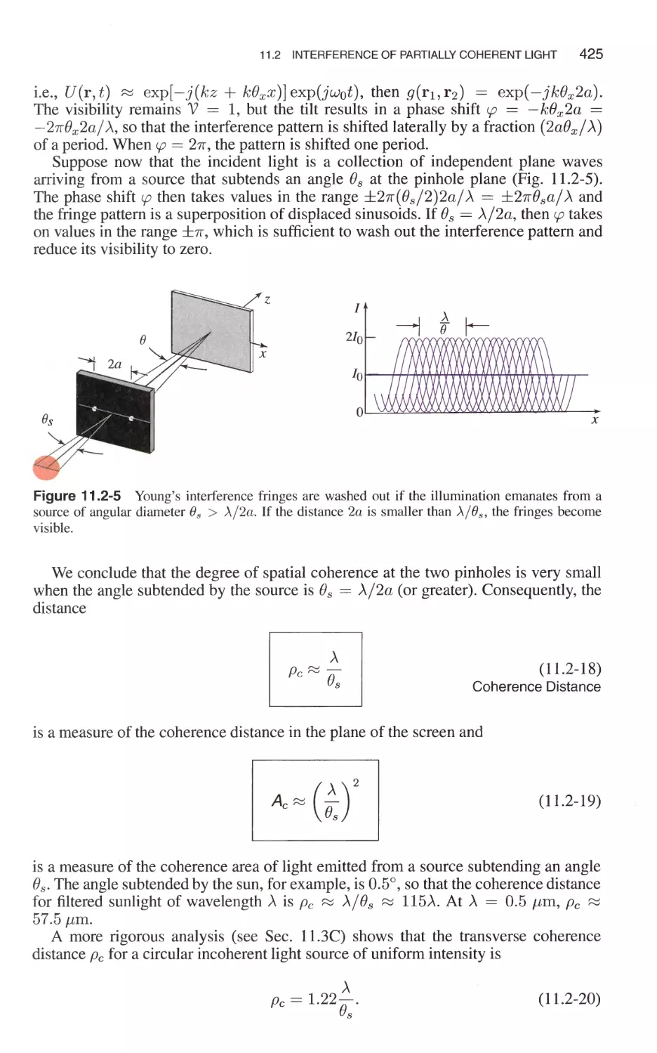
Engraving in the Small Portraits Collection, History of Science Collections, University
of Oklahoma Libraries (Fraunhofer); Stanford University, Courtesy AlP Emilio Segre
Visual Archives (Bloch); Eli Yablonovitch (Yablonovitch); Sajeev John (John); Charles
Kao (Kao); Philip St John Russell (Russell); Ecole Poly technique (Fabry); Observa-
toire des Sciences de l'Univers (Perot); AlP Emilio Segre Visual Archives (Born);
Lagrelius & Westphal 1920 portrait (Bohr); AlP Emilio Segre Visual Archives, Weber
Collection (W. L. Bragg); Linn F. Mollenauer (Mollenauer); Roger H. Stolen (Stolen);
and James P. Gordon (Gordon). In Chapter 23, the Bell Symbol was reproduced with
the permission of BellSouth Intellectual Property Marketing Corporation, the AT&T
logo is displayed with the permission of AT&T, and Lucent Technologies permitted
us use of their logo. Stephen G. Eick kindly provided the image used at the beginning
of Chapter 24. The photographs of Saleh and Teich were provided courtesy of Boston
University.
BAHAA E. A. SALEH
MALVIN CARL TEICH
Boston, Massachusetts
December 19,2006
PREFACE TO THE FIRST EDITION
Optics is an old and venerable subject involving the generation, propagation, and de-
tection of light. Three major developments, which have been achieved in the last thirty
years, are responsible for the rejuvenation of optics and for its increasing importance
in modern technology: the invention of the laser, the fabrication of low-loss optical
fibers, and the introduction of semiconductor optical devices. As a result of these de-
velopments, new disciplines have emerged and new terms describing these disciplines
have come into use: electro-optics, optoelectronics, quantum electronics, quantum
optics, and lightwave technology. Although there is a lack of complete agreement
about the precise usages of these terms, there is a general consensus regarding their
meanIngs.
Photonics
Electro-optics is generally reserved for optical devices in which electrical effects playa
role (lasers, and electro-optic modulators and switches, for example). Optoelectronics,
on the other hand, typically refers to devices and systems that are essentially electronic
in nature but involve light (examples are light-emitting diodes, liquid-crystal display
devices, and array photodetectors). The term quantum electronics is used in connection
with devices and systems that rely principally on the interaction of light with matter
(lasers and nonlinear optical devices used for optical amplification and wave mixing
serve as examples). Studies of the quantum and coherence properties of light lie within
the realm of quantum optics. The term lightwave technology has been used to describe
devices and systems that are used in optical communications and optical signal pro-
cessIng.
In recent years, the term photonics has come into use. This term, which was coined
in analogy with electronics, reflects the growing tie between optics and electronics
forged by the increasing role that semiconductor materials and devices play in optical
systems. Electronics involves the control of electric-charge flow (in vacuum or in
matter); photonics involves the control of photons (in free space or in matter). The
two disciplines clearly overlap since electrons often control the flow of photons and,
conversely, photons control the flow of electrons. The term photonics also reflects the
importance of the photon nature of light in describing the operation of many optical
devices.
Scope
This book provides an introduction to the fundamentals of photonics. The term pho-
tonics is used broadly to encompass all of the aforementioned areas, including the
following:
. The generation of coherent light by lasers, and incoherent light by luminescence
sources such as light-emitting diodes.
. The transmission of light in free space, through conventional optical components
such as lenses, apertures, and imaging systems, and through waveguides such as
optical fibers.
. The modulation, switching, and scanning of light by the use of electrically, acous-
tically, or optically controlled devices.
. The amplification and frequency conversion of light by the use of wave interac-
tions in nonlinear materials.
. The detection of light.
XI
xii PREFACE
These areas have found ever-increasing applications in optical communications, signal
processing, computing, sensing, display, printing, and energy transport.
Approach and Presentation
The underpinnings of photonics are provided in a number of chapters that offer concise
introductions to:
. The four theories of light (each successively more advanced than the preceding):
ray optics, wave optics, electromagnetic optics, and photon optics.
. The theory of interaction of light with matter.
. The theory of semiconductor materials and their optical properties.
These chapters serve as basic building blocks that are used in other chapters to describe
the generation of light (by lasers and light-emitting diodes); the transmission of light
(by optical beams, diffraction, imaging, optical waveguides, and optical fibers); the
modulation and switching of light (by the use of electro-optic, acousto-optic, and
nonlinear-optic devices); and the detection of light (by means of photo detectors). Many
applications and examples of real systems are provided so that the book is a blend
theory and practice. The final chapter is devoted to the study of fiber-optic communica-
tions, which provides an especially rich example in which the generation, transmission,
modulation, and detection of light are all part of a single photonic system used for the
transmission of information.
The theories of light are presented at progressively increasing levels of difficulty.
Thus light is described first as rays, then scalar waves, then electromagnetic waves,
and finally, photons. Each of these descriptions has its domain of applicability. Our
approach is to draw from the simplest theory that adequately describes the phenomenon
or intended application. Ray optics is therefore used to describe imaging systems and
the confinement of light in waveguides and optical resonators. Scalar wave theory
provides a description of optical beams, which are essential for the understanding of
lasers, and of Fourier optics, which is useful for describing coherent optical systems
and holography. Electromagnetic theory provides the basis for the polarization and
dispersion of light, and the optics of guided waves, fibers, and resonators. Photon optics
serves to describe the interactions of light with matter, explaining such processes as
light generation and detection, and light mixing in nonlinear media.
Intended Audience
Fundamentals of Photonics is meant to serve as:
. An introductory textbook for students in electrical engineering or applied physics
at the senior or first-year graduate level.
. A self-contained work for self-study.
. A text for programs of continuing professional development offered by industry,
universities, and professional societies.
The reader is assumed to have a background in engineering or applied physics,
including courses in modern physics, electricity and magnetism, and wave motion.
Some knowledge of linear systems and elementary quantum mechanics is helpful
but not essential. Our intent has been to provide an introduction to photonics that
emphasizes the concepts governing applications of current interest. The book should,
therefore, not be considered as a compendium that encompasses all photonic devices
and systems. Indeed, some areas of photonics are not included at all, and many of the
individual chapters could easily have been expanded into separate monographs.
PREFACE xiii
Problems, Reading Lists, and Appendices
A set of problems is provided at the end of each chapter. Problems are numbered
in accordance with the chapter sections to which they apply. Quite often, problems
deal with ideas or applications not mentioned in the text, analytical derivations, and
numerical computations designed to illustrate the magnitudes of important quantities.
Problems marked with asterisks are of a more advanced nature. A number of exer-
cises also appear within the text of each chapter to help the reader develop a better
understanding of (or to introduce an extension of) the material.
Appendices summarize the properties of one- and two-dimensional Fourier trans-
forms, linear-systems theory, and modes of linear systems (which are important in
polarization devices, optical waveguides, and resonators); these are called upon at
appropriate points throughout the book. Each chapter ends with a reading list that
includes a selection of important books, review articles, and a few classic papers of
special significance.
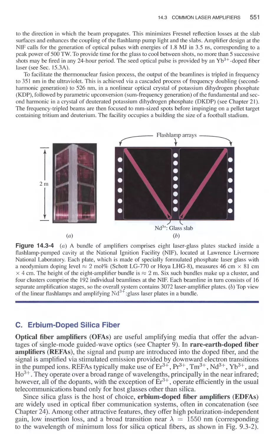
Acknowledgments
We are grateful to many colleagues for reading portions of the text and providing
helpful comments: Govind P. Agrawal, David H. Auston, Rasheed Azzam, Nikolai
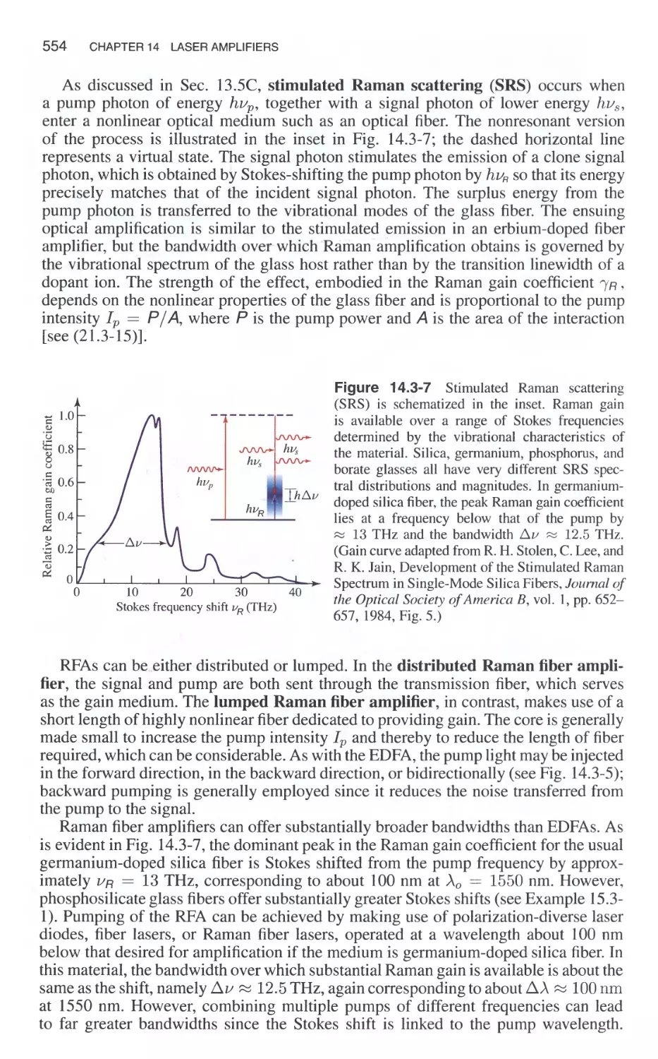
G. Basov, Franco Cerrina, Emmanuel Desurvire, Paul Diament, Eric Fossum, Robert
J. Keyes, Robert H. Kingston, Rodney Loudon, Leonard Mandel, Leon McCaughan,
Richard M. Osgood, Jan Perina, Robert H. Rediker, Arthur L. Schawlow, S. R. Se-
shadri, Henry Stark, Ferrel G. Stremler, John A. Tataronis, Charles H. Townes, Patrick
R. Trischitta, Wen I. Wang, and Edward S. Yang.
We are especially indebted to John Whinnery and Emil Wolf for providing us with
many suggestions that greatly improved the presentation.
Several colleagues used portions of the notes in their classes and provided us with
invaluable feedback. These include Etan Bourkoff at Johns Hopkins University (now
at the University of South Carolina), Mark O. Freeman at the University of Colorado,
George C. Papen at the University of Illinois, and Paul R. Prucnal at Princeton Univer-
sity.
Many of our students and former students contributed to this material in various
ways over the years and we owe them a great debt of thanks: Gaetano L. Aiello,
Mohamad Asi, Richard Campos, Buddy Christyono, Andrew H. Cordes, Andrew
David, Ernesto Fontenla, Evan Goldstein, Matthew E. Hansen, Dean U. Hekel, Conor
Heneghan, Adam Heyman, Bradley M. Jost, David A. Landgraf, Kanghua Lu, Ben
Nathanson, Winslow L. Sargeant, Michael T. Schmidt, Raul E. Sequeira, David Small,
Kraisin Songwatana, Nikola S. Subotic, Jeffrey A. Tobin, and Emily M. True. Our
thanks also go to the legions of unnamed students who, through a combination of
vigilance and the desire to understand the material, found countless errors.
We particularly appreciate the many contributions and help of those students who
were intimately involved with the preparation of this book at its various stages of
completion: Niraj Agrawal, Suzanne Keilson, Todd Larchuk, Guifang Li, and Philip
Tham.
We are grateful for the assistance given to us by a number of colleagues in the course
of collecting the photographs used at the beginnings of the chapters: E. Scott Barr,
Nicolaas Bloembergen, Martin Carey, Marjorie Graham, Margaret Harrison, Ann Kot-
tner, G. Thomas Holmes, John Howard, Theodore H. Maiman, Edward Palik, Martin
Parker, Aleksandr M. Prokhorov, Jarus Quinn, Lesley M. Richmond, Claudia Schuler,
Patrick R. Trischitta, J. Michael Vaughan, and Emil Wolf. Specific photo credits are as
follows: AlP Meggers Gallery of Nobel Laureates (Gabor, Townes, Basov, Prokhorov,
W. L. Bragg); AlP Niels Bohr Library (Rayleigh, Fraunhofer, Maxwell, Planck, Bohr,
Einstein in Chapter 12, W. H. Bragg); Archives de l' Academie des Sciences de Paris
(Fabry); The Astrophysical Journal (Perot); AT&T Bell Laboratories (Shockley, Brat-
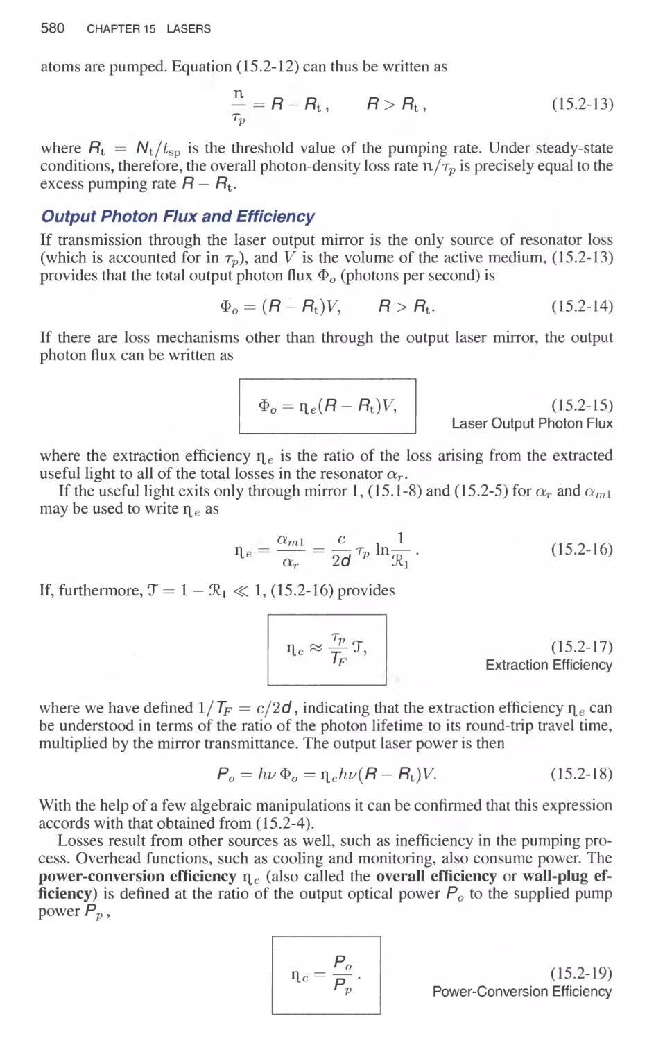
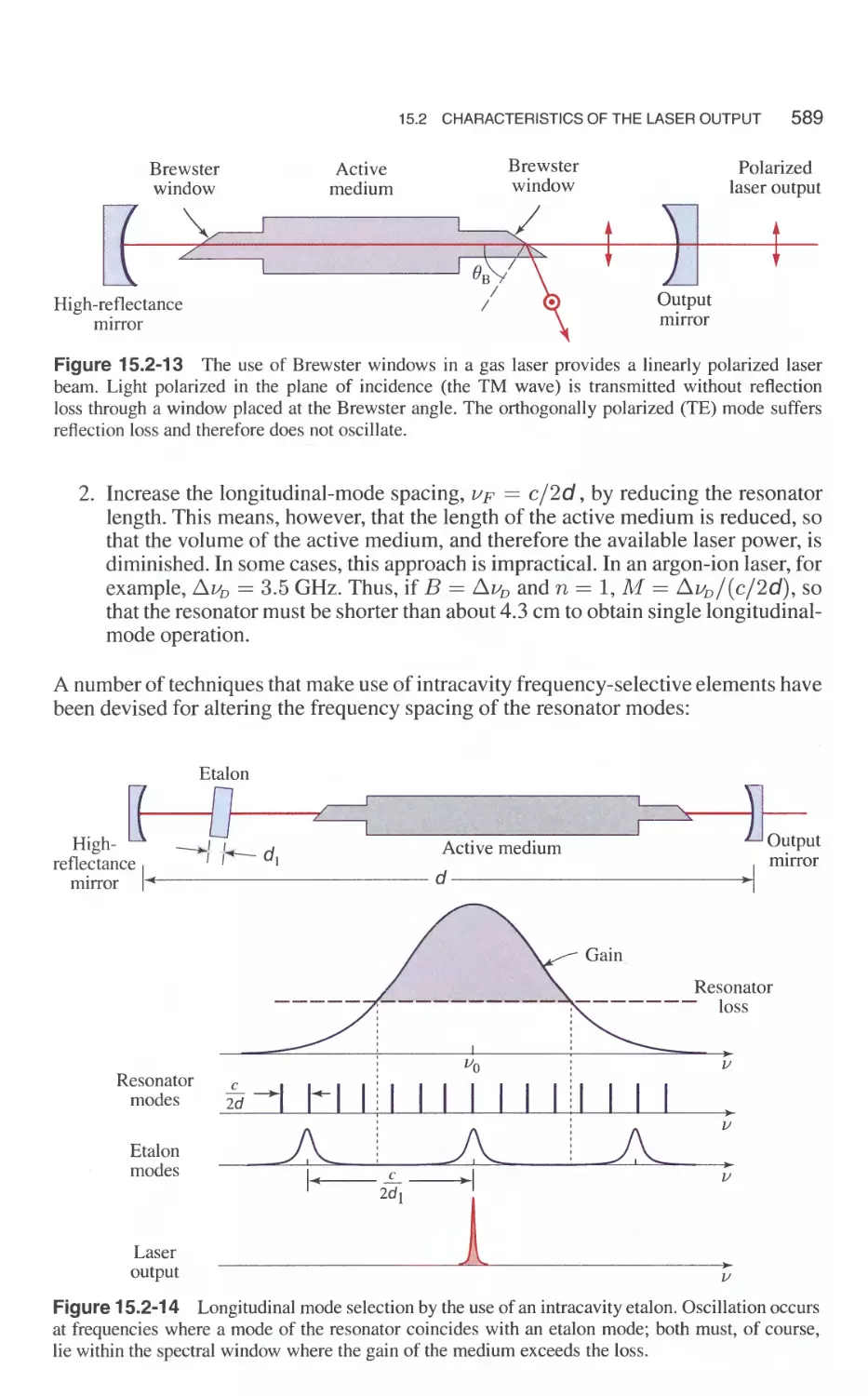
xiv PREFACE
tain, Bardeen); Bettmann Archives (Young, Gauss, Tyndall); Bibliotheque Nationale de
Paris (Fermat, Fourier, Poisson); Burndy Library (Newton, Huygens); Deutsches Mu-
seum (Hertz); ETH Bibliothek (Einstein in Chapter 11); Bruce Fritz (Saleh); Harvard
University (Bloembergen); Heidelberg University (Pockels); Kelvin Museum of the
University of Glasgow (Kerr); Theodore H. Maiman (Maiman); Princeton University
(von Neumann); Smithsonian Institution (Fresnel); Stanford University (Schawlow);
Emil Wolf (Born, Wolt). Corning Incorporated kindly provided the photograph used at
the beginning of Chapter 8. We are grateful to GE for the use of their logotype, which
is a registered trademark of the General Electric Company, at the beginning of Chapter
16. The IBM logo at the beginning of Chapter 16 is being used with special permission
from ffiM. The right-most logotype at the beginning of Chapter 16 was supplied
courtesy of Lincoln Laboratory, Massachusetts Institute of Technology. AT&T Bell
Laboratories kindly permitted us use of the diagram at the beginning of Chapter 22.
We greatly appreciate the continued support provided to us by the National Sci-
ence Foundation, the Center for Telecommunications Research, and the Joint Services
Electronics Program through the Columbia Radiation Laboratory.
Finally, we extend our sincere thanks to our editors, George Telecki and Bea Shube,
for their guidance and suggestions throughout the course of preparation of this book.
BAHAA E. A. SALEH
Madison, Wisconsin
MALVIN CARL TEICH
New York, New York
April 3, 1991
CONTENTS
PREFACE TO THE SECOND EDITION
v
PREFACE TO THE FIRST EDITION
xi
1 RAY OPTICS 1
1.1 Postulates of Ray Optics 3
1.2 Simple Optical Components 6
1.3 Graded-Index Optics 17
1.4 Matrix Optics 24
Reading List 34
Problems 35
2 WAVE OPTICS 38
2.1 Postulates of Wave Optics 40
2.2 Monochromatic Waves 41
*2.3 Relation Between Wave Optics and Ray Optics 49
2.4 Simple Optical Components 50
2.5 Interference 58
2.6 Polychromatic and Pulsed Light 66
Reading List 72
Problems 73
3 BEAM OPTICS 74
3.1 The Gaussian Beam 75
3.2 Transmission Through Optical Components 86
3.3 Hermite-Gaussian Beams 94
*3.4 Laguerre-Gaussian and Bessel Beams 97
Reading List 100
Problems 100
4 FOURIER OPTICS 102
4.1 Propagation of Light in Free Space 105
4.2 Optical Fourier Transform 116
4.3 Diffraction of Light 121
4.4 Image Formation 127
4.5 Holography 138
Reading List 145
Problems 147
xv
XVI CONTENTS
5 ELECTROMAGNETIC OPTICS 150
5.1 Electromagnetic Theory of Light 152
5.2 Electromagnetic Waves in Dielectric Media 156
5.3 Monochromatic Electromagnetic Waves 162
5.4 Elementary Electromagnetic Waves 164
5.5 Absorption and Dispersion 170
5.6 Pulse Propagation in Dispersive Media 184
*5.7 Optics of Magnetic Materials and Metamaterials 190
Reading List 193
Problems 195
6 POLARIZATION OPTICS 197
6.1 Polarization of Light 199
6.2 Reflection and Refraction 209
6.3 Optics of Anisotropic Media 215
6.4 Optical Activity and Magneto-Optics 228
6.5 Optics of Liquid Crystals 232
6.6 Polarization Devices 235
Reading List 239
Problems 240
7 PHOTONIC-CRYSTAL OPTICS 243
7.1 Optics of Dielectric Layered Media 246
7.2 One-Dimensional Photonic Crystals 265
7.3 Two- and Three-Dimensional Photonic Crystals 279
Reading List 286
Problems 288
8 GUIDED-WAVE OPTICS 289
8.1 Planar-Mirror Waveguides 291
8.2 Planar Dielectric Waveguides 299
8.3 Two-Dimensional Waveguides 308
8.4 Photonic-Crystal Waveguides 311
8.5 Optical Coupling in Waveguides 313
8.6 Sub-Wavelength Metal Waveguides (Plasmonics) 321
Reading List 322
Problems 323
9 FIBER OPTICS 325
9.1 Guided Rays 327
9.2 Guided Waves 331
9.3 Attenuation and Dispersion 348
9.4 Holey and Photonic-Crystal Fibers 359
Reading List 362
Problems 363
10 RESONATOR OPTICS 365
10.1 Planar-Mirror Resonators 367
10.2 Spherical-Mirror Resonators 378
10.3 Two- and Three-Dimensional Resonators 390
10.4 Microresonators 394
Reading List 400
Problems 400
CONTENTS XVII
11 STATISTICAL OPTICS 403
11.1 Statistical Properties of Random Light 405
11.2 Interference of Partially Coherent Light 419
* 11.3 Transmission of Partially Coherent Light Through Optical Systems 427
11.4 Partial Polarization 436
Reading List 440
Problems 442
12 PHOTON OPTICS
12.1 The Photon
12.2 Photon Streams
* 12.3 Quantum States of Light
Reading List
Problems
13 PHOTONS AND ATOMS
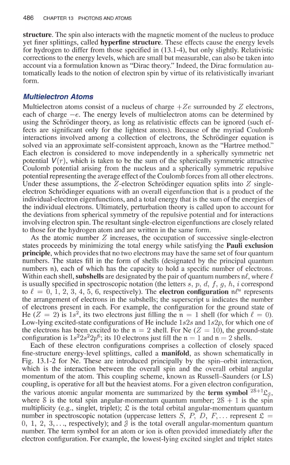
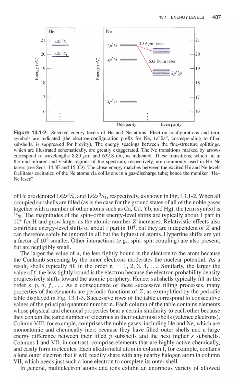
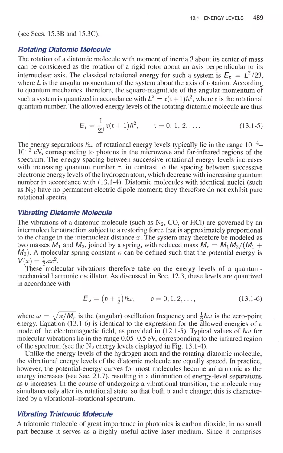
13.1 Energy Levels
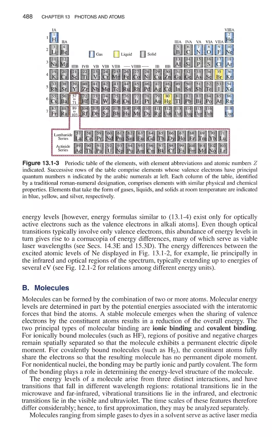
13.2 Occupation of Energy Levels
13.3 Interactions of Photons with Atoms
13.4 Thermal Light
13.5 Luminescence and Light Scattering
Reading List
Problems
14 LASER AMPLIFIERS
14.1 Theory of Laser Amplification
14.2 Amplifier Pumping
14.3 Common Laser Amplifiers
14.4 Amplifier Nonlinearity
* 14.5 Amplifier Noise
Reading List
Problems
15 LASERS
15.1 Theory of Laser Oscillation
15.2 Characteristics of the Laser Output
15.3 Common Lasers
15.4 Pulsed Lasers
Reading List
Problems
16 SEMICONDUCTOR OPTICS
444
446
458
471
476
478
482
483
499
501
517
522
528
530
532
535
539
547
556
562
564
565
567
569
575
590
605
621
624
16.1 Semiconductors
16.2 Interactions of Photons with Charge Carriers
Reading List
Problems
627
629
660
675
677
xviii CONTENTS
17 SEMICONDUCTOR PHOTON SOURCES 680
17.1 Light-Emitting Diodes 682
17.2 Semiconductor Optical Amplifiers 702
17.3 Laser Diodes 716
17.4 Quantum-Confined and Microcavity Lasers 728
Reading List 741
Problems 745
18 SEMICONDUCTOR PHOTON DETECTORS 748
18.1 Photodetectors 749
18.2 Photoconductors 758
18.3 Photodiodes 762
18.4 Avalanche Photodiodes 767
18.5 Array Detectors 775
18.6 Noise in Photodetectors 777
Reading List 798
Problems 800
19 ACOUSTO-OPTICS 804
19.1 Interaction of Light and Sound 806
19.2 Acousto-Optic Devices 819
* 19.3 Acousto-Optics of Anisotropic Media 828
Reading List 832
Problems 832
20 ELECTRO-OPTICS 834
20.1 Principles of Electro-Optics 836
*20.2 Electro-Optics of Anisotropic Media 849
20.3 Electro-Optics of Liquid Crystals 856
*20.4 Photorefractivity 863
20.5 Electroabsorption 868
Reading List 869
Problems 871
21 NONLINEAR OPTICS 873
21.1 Nonlinear Optical Media 875
21.2 Second-Order Nonlinear Optics 879
21.3 Third-Order Nonlinear Optics 894
*21.4 Second-Order Nonlinear Optics: Coupled-Wave Theory 905
*21.5 Third-Order Nonlinear Optics: Coupled-Wave Theory 917
*21.6 Anisotropic Nonlinear Media 924
*21.7 Dispersive Nonlinear Media 927
Reading List 932
Problems 934
22 ULTRAFAST OPTICS 936
22.1 Pulse Characteristics 937
22.2 Pulse Shaping and Compression 946
22.3 Pulse Propagation in Optical Fibers 960
CONTENTS XIX
22.4 Ultrafast Linear Optics 973
22.5 Ultrafast Nonlinear Optics 984
22.6 Pulse Detection 999
Reading List 1011
Problems 1013
23 OPTICAL INTERCONNECTS AND SWITCHES
23.1 Optical Interconnects
23.2 Passive Optical Routers
23.3 Photonic Switches
23.4 Optical Gates
Reading List
Problems
1016
1018
1030
1038
1058
1069
1071
24 OPTICAL FIBER COMMUNICATIONS
24.1 Fiber-Optic Components
24.2 Optical Fiber Communication Systems
24.3 Modulation and Multiplexing
24.4 Fiber-Optic Networks
24.5 Coherent Optical Communications
Reading List
Problems
1072
1074
1084
1101
1106
1112
1118
1120
A FOURIER TRANSFORM
A.1 One-Dimensional Fourier Transform
A.2 Time Duration and Spectral Width
A.3 Two-Dimensional Fourier Transform
Reading List
1122
1122
1124
1128
1131
B LINEAR SYSTEMS
8.1 One-Dimensional Linear Systems
8.2 Two-Dimensional Linear Systems
Reading List
1132
1132
1135
1136
C MODES OF LINEAR SYSTEMS
1137
SYMBOLS AND UNITS
1142
AUTHORS
1159
INDEX
1161
FUNDAMENTALS OF
PHOTONICS
CHAPTER
.
..
1.1 POSTULATES OF RAY OPTICS
1.2 SIMPLE OPTICAL COMPONENTS
A. Mirrors
B. Planar Boundaries
C. Spherical Boundaries and Lenses
D. Light Guides
1.3 GRADED-INDEX OPTICS
A. The Ray Equation
B. Graded-Index Optical Components
*C. The Eikonal Equation
1.4 MATRIX OPTICS
A. The Ray-Transfer Matrix
B. Matrices of Simple Optical Components
C. Matrices of Cascaded Optical Components
D. Periodic Optical Systems
3
6
17
24
.,.,
,
t
-
,
..
Sir Isaac Newton (1642-1727) set forth a
theory of optics in which light emissions con-
sist of collections of corpuscles that propagate
rectilinear! y.
Pierre de Fermat (160]-1665) enunciated the
principle that light travels along the path of
least time.
Light can be described as an electromagnetic wave phenomenon governed by the
same theoretical principles that govern all other forms of electromagnetic radiation,
such as radio waves and X-rays. This conception of light is called electromagnetic
optics. Electromagnetic radiation propagates in the form of two mutually coupled
vector waves, an electric-field wave and a magnetic-field wave. Nevertheless, it is
possible to describe many optical phenomena using a simplified scalar wave theory
in which light is described by a single scalar wavefunction. This approximate way of
treating light is called scalar wave optics, or simply wave optics.
When light waves propagate through and around objects whose dimensions are
much greater than the wavelength of the light, the wave nature is not readily discerned
and the behavior of light can be adequately described by rays obeying a set of geomet-
rical rules. This model of light is called ray optics. From a mathematical perspective,
ray optics is the limit of wave optics when the wavelength is infinitesimally small.
Thus, electromagnetic optics encompasses wave optics, which, in turn, encompasses
ray optics, as illustrated in Fig. 1.0-1. Ray optics and wave optics are approximate theo-
ries that derive their validity from their successes in producing results that approximate
those based on the more rigorous electromagnetic theory.
Quantum Optics
Ray Optics
Figure 1.0-1 The theory of quantum optics
provides an explanation of virtually all optical phe-
nomena. The electromagnetic theory of light (elec-
tromagnetic optics) provides the most complete
treatment of light within the confines of classical
optics. Wave optics is a scalar approximation of
electromagnetic optics. Ray optics is the limit of
wave optics when the wavelength is very short.
Electromagnetic
Optics
Wave Optics
Although electromagnetic optics provides the most complete treatment of light
within the confines of classical optics, certain optical phenomena are characteristically
quantum mechanical in nature and cannot be explained classically. These phenomena
are described by a quantum version of electromagnetic theory known as quantum
electrodynamics. For optical phenomena, this theory is also referred to as quantum
optics.
Historically, the theories of optics developed roughly in the following sequence:
(1) ray optics > (2) wave optics > (3) electromagnetic optics > (4) quantum optics.
These models are progressively more complex and sophisticated, and were devel-
oped successively to provide explanations for the outcomes of increasingly subtle and
precise optical experiments. The optimal choice of a model is the simplest one that
satisfactorily describes a particular phenomenon, but it is sometimes difficult to know
a priori which model will achieve this. Fortunately, however, experience often provides
a good guide.
For pedagogical reasons, the initia] chapters in this book follow the historical order
indicated above. Each model of light begins with a set of postulates (provided without
proof), from which a large body of results are generated. The postulates of each model
are shown to arise in special cases of the next-higher-Ievel model. In this chapter we
begin with ray optics.
2
1.1 POSTULATES OF RAY OPTICS 3
This Chapter
Ray optics is the simplest theory of light. Light is described by rays that travel in
different optical media in accordance with a set of geometrical rules. Ray optics is
therefore also called geometrical optics. Ray optics is an approximate theory. Al-
though it adequately describes most of our daily experiences with light, there are many
phenomena that ray optics does not adequately describe (as amply attested to by the
remaining chapters of this book).
Ray optics is concerned with the location and direction of light rays. It is therefore
useful in studying image formation the collection of rays from each point of an
object and their redirection by an optical component onto a corresponding point of
an image. Ray optics permits us to determine conditions under which light is guided
within a given medium, such as a glass fiber. In isotropic media, optical rays point in
the direction of the flow of optical energy. Ray bundles can be constructed in which the
density of rays is proportional to the density of light energy. When light is generated
isotropically from a point source, for example, the energy associated with the rays in a
given cone is proportional to the solid angle of the cone. Rays may be traced through
an optical system to determine the optical energy crossing a given area.
This chapter begins with a set of postulates from which the simple rules that govern
the propagation of light rays through optical media are derived. In Sec. 1.2 these
rules are applied to simple optical components such as mirrors and planar or spher-
ical boundaries between different optical media. Ray propagation in inhomogeneous
(graded-index) optical media is examined in Sec. 1.3. Graded-index optics is the basis
of a technology that has become an important part of modem optics.
Optical components are often centered about an optical axis, about which the rays
travel at small inclinations. Such rays are called paraxial rays. This assumption is
the basis of paraxial optics. The change in the position and inclination of a paraxial
ray as it travels through an optical system can be efficiently described by the use of a
2 x 2-matrix algebra. Section 1.4 is devoted to this algebraic tool, called matrix optics.
.
1.1 POSTULATES OF RAY OPTICS
Postulates of Ray Optics
. Light travels in the form of rays. The rays are emitted by light sources and can
be observed when they reach an optical detector.
. An optical medium is characterized by a quantity n > 1, called the refractive
index. The refractive index n Co c where Co is the speed of light in free space
and c is the speed of light in the medium. Therefore, the time taken by light to
travel a distance d is d c nd CO. It is proportional to the product nd, which
is known as the optical pathlength.
. In an inhomogeneous medium the refractive index n r is a function of the
position r x, y, z . The optical path length along a given path between two
points A and B is therefore
Optical pathlength
B
n r ds,
A
(1.1-1)
where ds is the differential element of length along the path. The time taken by
light to travel from A to B is proportional to the optical pathlength.
4 CHAPTER 1 RAY OPTICS
.
. Fermat's Principle. Optical rays traveling between two points, A and B, fol-
Iowa path such that the time of travel (or the optical pathlength) between the
two points is an extremum relative to neighboring paths. This is expressed
mathematically as
B
8 n r ds 0,
A
(1.1-2)
where the symbol 8, which is read "the variation of," signifies that the optical
pathlength is either minimized or maximized, or is a point of inflection. It is,
however, usually a minimum, in which case:
Light rays travel along the path of least time.
Sometimes the minimum time is shared by more than one path, which are then
all followed simultaneously by the rays. An example in which the pathlength is
maximized is provided in Probe 1.1-2.
In this chapter we use the postulates of ray optics to determine the rules governing
the propagation of light rays, their reflection and refraction at the boundaries between
different media, and their transmission through various optical components. A wealth
of results applicable to numerous optical systems are obtained without the need for any
other assumptions or rules regarding the nature of light.
Propagation in a Homogeneous Medium
In a homogeneous medium the refractive index is the same everywhere, and so is the
speed of light. The path of minimum time, required by Fermat's principle, is therefore
also the path of minimum distance. The principle of the path of minimum distance
is known as Hero's principle. The path of minimum distance between two points is
a straight line so that in a homogeneous medium, light rays travel in straight lines
(Fig. 1. 1- 1 ).
,
--
Figure 1.1-1 Light rays travel in straight lines. Shadows are perfect projections of stops.
1.1 POSTULATES OF RAY OPTICS 5
Reflection from a Mirror
Mirrors are made of certain highly polished metallic surfaces, or metallic or dielectric
films deposited on a substrate such as glass. Light reflects from mirrors in accordance
with the law of reflection:
The reflected ray lies in the plane of incidence; the angle of reflection equals the
angle of incidence.
The plane of incidence is the plane formed by the incident ray and the normal to the
mirror at the point of incidence. The angles of incidence and reflection, 8 and 8', are
defined in Fig. 1.1-2(a). To prove the law of reflection we simply use Hero's principle.
Examine a ray that travels from point A to point C after reflection from the planar
mirror in Fig. 1.1-2(b) . A cc ordi ng to Hero's principle, for a mirror of infinitesimal
thic knes s, th e distanc e A B + BC must be minimum. If C' is a mirror image of C, then
BC BC', so that AB + BC' must be a minimum. This occurs when ABC' is a
straight line, i.e., when B coincides with B' so that 8 8'.
Plane of
incidence
Mirror
Mirror
c
c'
Reflected
ray
,
,
,
,
,
,
,
,
,
,
,
,
,
,
,
",
" "
" ,
" "
" ,
,
B ' ., ,
" ,
., "
" ,
,
., ,
,
,
,
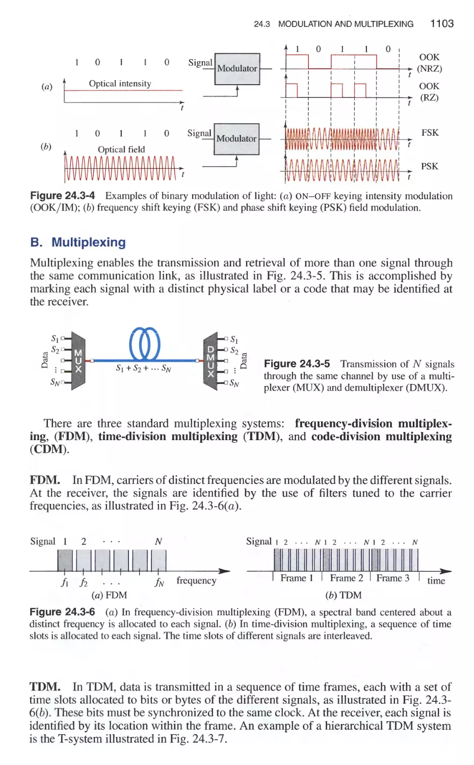
,
,
,
'" ,
()' " ,,'
() ........_'.1 B
...-
......
...-
......
-
Normal
to mirror
()'
()
A
Incident
ray
(a)
(b)
Figure 1.1-2 (a) Reflection from the surface of a curved mirror. (b) Geometrical construction to
prove the law of reflection.
Reflection and Refraction at the Boundary Between Two Media
At the boundary between two media of refractive indexes n1 and n2 an incident ray is
split into two a reflected ray and a refracted (or transmitted) ray (Fig. 1.1-3). The
reflected ray obeys the law of reflection. The refracted ray obeys the law of refraction:
The refracted ray lies in the plane of incidence; the angle of refraction 8 2 is
related to the angle of incidence 8 1 by Snell's law,
nl sin 8 1 n2 sin 8 2 .
(1.1-3)
Snell's law
The proportion in which the light is reflected and refracted is not described by ray
.
optIcs.
6 CHAPTER 1 RAY OPTICS
Reflected
ray
!
--
Nonnal to
boundary
OJ
OJ
Refracted
I
'2 ray
Incident
ray
,
Plane of
incidence
n2
nl
Figure 1.1-3 Reflection and refraction at the boundary between two media.
EXERCISE 1.1-1
Proof of Snell's Law. The proof of Snell's law is an exercise in the ap plic ation of Fermat's
principle. Referring to Fig. 1.1-4, we seek to minimize the optical pathlength nlAB +n2BC between
points A and C. We therefore have the following optimization problem: Minimize nl d 1 see ()l +
n2 d 2 see f)2 with respect to the angles f)l and f)2, subject to the condition d 1 tan f)l + d 2 tan f)2 d.
Show that the solution of this constrained minimization problem yields Snell's law.
n} n2
d 2 C
-- ---- ----------.
O}
°2
B
d.
d}
}\ -----------------
Figure 1.1-4 Construction to prove Snell's law.
The three simple rules propagation in straight lines and the laws of reflection and
refraction are applied in Sec. 1.2 to several geometrical configurations of mirrors
and transparent optical components, without further recourse to Fermat's principle.
1.2 SIMPLE OPTICAL COMPONENTS
A. Mirrors
Planar Mirrors
A planar mirror reflects the rays originating from a point PI such that the reflected rays
appear to originate from a point P2 behind the mirror, called the image (Fig. 1.2-1).
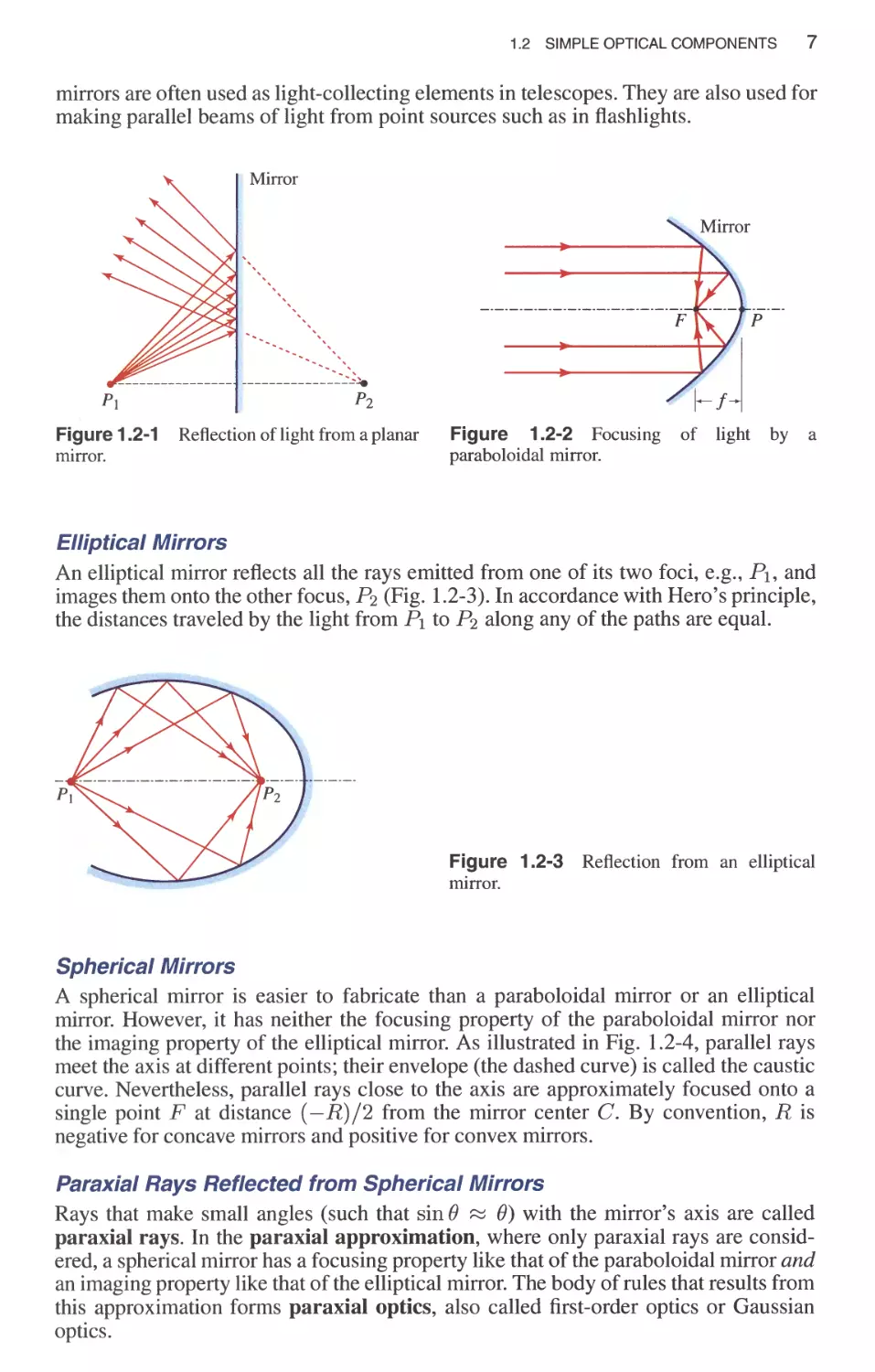
Paraboloidal Mirrors
The surface of a paraboloidal mirror is a paraboloid of revolution. It has the useful
property of focusi ng a ll incident rays parallel to its axis to a single point called the fo-
cus. The distance P F f defined in Fig. 1.2-2 is called the focal length. Paraboloidal
.
1.2 SIMPLE OPTICAL COMPONENTS 7
mirrors are often used as light-collecting elements in telescopes. They are also used for
making parallel beams of light from point sources such as in flashlights.
Mirror
PI
Pz
"
"
"
"
"
"
"
"
"
"
"
"
"
"
"
"
"
"
"
"
, "
" "
" "
---------------- --------------
Figure 1.2-1 Reflection of light from a planar Figure 1.2-2 Focusing of light by a
mIrror. paraboloidal mirror.
Elliptical Mirrors
An elliptical mirror reflects all the rays emitted from one of its two foci, e.g., PI, and
images them onto the other focus, P 2 (Fig. 1.2-3). In accordance with Hero's principle,
the distances traveled by the light from PI to P 2 along any of the paths are equal.
Figure 1.2-3 Reflection from an elliptical
mIrror.
Spherical Mirrors
A spherical mirror is easier to fabricate than a paraboloidal mirror or an elliptical
mirror. However, it has neither the focusing property of the paraboloidal mirror nor
the imaging property of the elliptical mirror. As illustrated in Fig. 1.2-4, parallel rays
meet the axis at different points; their envelope (the dashed curve) is called the caustic
curve. Nevertheless, parallel rays close to the axis are approximately focused onto a
single point F at distance (- R) /2 from the mirror center C. By convention, R is
negative for concave mirrors and positive for convex mirrors.
Paraxial Rays Reflected from Spherical Mirrors
Rays that make small angles (such that sin () () with the mirror's axis are called
paraxial rays. In the paraxial approximation, where only paraxial rays are consid-
ered, a spherical mirror has a focusing property like that of the paraboloidal mirror and
an imaging property like that of the elliptical mirror. The body of rules that results from
this approximation forms paraxial optics, also called first-order optics or Gaussian
optics.
8 CHAPTER 1 RAY OPTICS
"
"
z
"
"
,
,
,
,
I
I
I
,
,
I
I
,
,
\
\
\
,
,
,
,
...
...
c
z
------
------
Spherical
mIrror
,
,
I
I
,
\
\
\
\
\
,
,
,
...
...
------
"
"--- -;-RH
Figure 1.2-4 Reflection of parallel rays
from a concave spherical mirror.
(-2 R ) I ( R)
Figure 1.2-5 A spherical mirror approxi-
mates a paraboloidal mirror for paraxial rays.
A spherical mirror of radius R therefore acts like a paraboloidal mirror of focal
length f == R/2. This is in fact plausible since at points near the axis, a parabola can
be approximated by a circle with radius equal to the parabola's radius of curvature
(Fig. 1.2-5).
All paraxial rays originating from each point on the axis of a spherical mirror are
reflected and focused onto a single corresponding point on the axis. This can be seen
(Fig. 1.2-6) by examining a ray emitted at an angle ()l from a point PI at a distance ZI
away from a concave mirror of radius R, and reflecting at angle ( -()2) to meet the axis
at a point P 2 that is a distance Z2 away from the mirror. The angle ()2 is negative since
the ray is traveling downward. Since the three angles of a triangle add to 180 0 , we have
()I == ()o - () and (-()2) == ()o + (), so that ( -()2) + ()I == 2()o. If ()o is sufficiently small,
the approximation tan ()o ()o may be used, so that ()o Y / ( - R), from which
2y
( -( 2 ) + 0 1 (- R) ,
(1.2-1)
where y is the height of the point at which the reflection occurs. Recall that R is
negative since the mirror is concave. Similarly, if ()I and ()2 are small, ()l Y / Zl
and (-()2) == y/Z2' so that (1.2-1) yields y/Zl + y/Z2 2y/( -R), whereupon
1 1
-+-
ZI Z2
2
(- R) .
(1.2-2)
z
T
y
1
-..;(
z
Zl
(-R)
Z2 (-R)/2
o
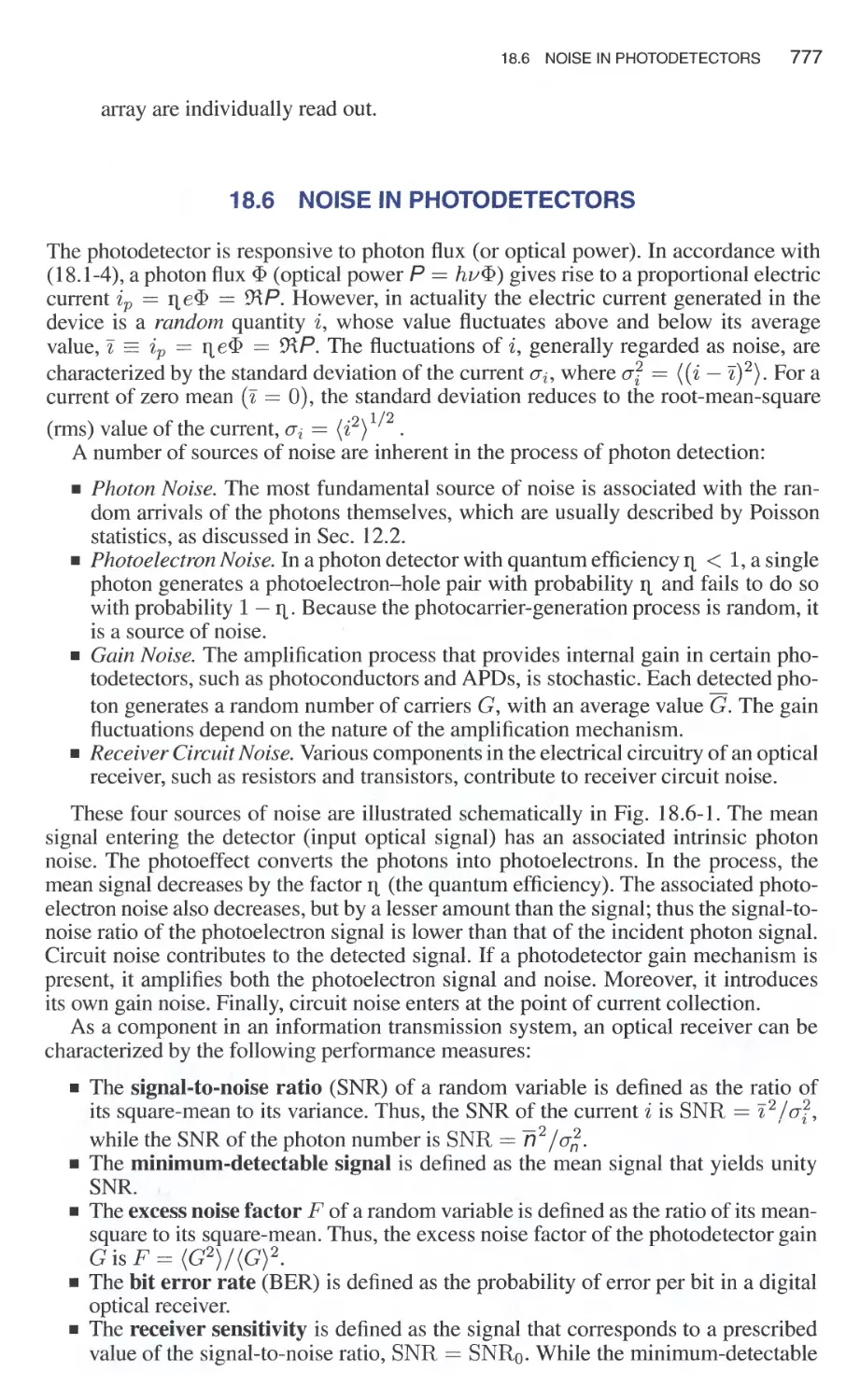
Figure 1.2-6 Reflection of paraxial rays from a concave spherical mirror of radius R < O.
1.2 SIMPLE OPTICAL COMPONENTS 9
This relation holds regardless of y (i.e., regardless of 0 1 ) as long as the approxima-
tion is valid. This means that all paraxial rays originating from point PI arrive at P2.
The distances ZI and Z2 are measured in a coordinate system in which the z axis points
to the left. Points of negative z therefore lie to the right of the mirror.
According to (1.2-2), rays that are emitted from a point very far out on the z axis
ZI ()() are focused to a point F at a distance Z2 R 2. This means that within
the paraxial approximation, all rays coming from infinity (parallel to the axis of the
mirror) are focused to a point at a distance f from the mirror, which is known as its
focal length:
f
, R'
, )
2
,
(1.2-3)
Focal Length
Spherical Mirror
Equation (1.2-2) is usually written in the form
1 1
+
Zl Z2
1
f'
( 1.2 -4 )
Imaging Equation
(Paraxial Rays)
which is known as the imaging equation. Both the incident and the reflected rays must
be paraxial for this equation to hold.
EXERCISE 1.2-1
Image Formation by a Spherical Mirror. Show that within the paraxial approximation, rays
originating from a point PI (y!, Zl) are reflected to a point P 2 (Y2, Z2), where Zl and Z2 satisfy
(1.2-4) and Y2 YIZ2/ Zl (Fig. 1.2-7). This means that rays from each point in the plane Z Zl
meet at a single corresponding point in the plane Z Z2, so that the mirror acts as an image-formation
system with magnification Z2/ Z1 . Negative magnification means that the image is inverted.
y
P I =(y I' Z I)
c
z
Pz=(yz, zz)
Figure 1.2-7 Image formation by a
spherical mirror. Four particular rays are
illustrated.
B. Planar Boundaries
The relation between the angles of refraction and incidence, O 2 and 0 1 , at a planar
boundary between two media of refractive indexes nl and n2 is governed by Snel]'s
law (1.1-3). This relation is plotted in Fig. 1.2-8 for two cases:
. External Refraction nl < n2 . When the ray is incident from the medium of
smaller refractive index, O 2 < 0 1 and the refracted ray bends away from the
boundary.
1 0 CHAPTER 1 RAY OPTICS
. Internal Refraction ni > n2 . If the incident ray is in a medium of higher
refractive index, ()2 > ()I and the refracted ray bends toward the boundary.
n I
n 2
n}
n z
°e
90°
n 2 /n}= 2/3
O 2
00
I
Oe
OJ
3/2
External refraction
Internal refraction
0 1 90°
Figure 1.2-8 Relation between the angles of refraction and incidence.
The refracted rays bend in such a way as to minimize the optical pathlength, i.e.,
to increase the pathlength in the lower-index medium at the expense of pathlength in
the higher-index medium. In both cases, when the angles are small (i.e., the rays are
paraxial), the relation between ()2 and ()I is approximately linear, nl()1 n2()2, or
()2 nl n2 ()I.
Total Internal Reflection
For internal refraction ni > n2 , the angle of refraction is greater than the angle of
incidence, ()2 > ()I, so that as ()I increases, ()2 reaches 90 0 first (see Fig. 1.2-8). This
occurs when ()I ()e (the critical angle), with ni sin ()e n2 sin 7r 2 n2, so that
()e
· -1 n2
SIn .
nl
( 1.2-5)
Critical Angle
When ()I > ()e, Snells' law (1.1-3) cannot be satisfied and refraction does not occur.
The incident ray is totally reflected as if the surface were a perfect mirror [Fig. 1.2-
9(a)]. The phenomenon of total internal reflection is the basis of many optical de-
vices and systems, such as reflecting prisms [see Fig. 1.2-9(b)] and optical fibers (see
Sec. 1.2D). It can be shown using electromagnetic optics (Fresnel's equations in Chap-
ter 6) that all of the energy is carried by the reflected light so that the process of total
internal reflection is highly efficient.
n 1 n 2
o
o
n 1
ocr
n 2 = 1
(a) (b) (c)
Figure 1.2-9 (a) Total internal reflection at a planar boundary. (b) The reflecting prism. If n] > 2
and n2 1 (air), then Oe < 45°; since 0 1 45°, the ray is totally reflected. (c) Rays are guided by
total internal reflection from the internal surface of an optical fiber.
1.2 SIMPLE OPTICAL COMPONENTS 11
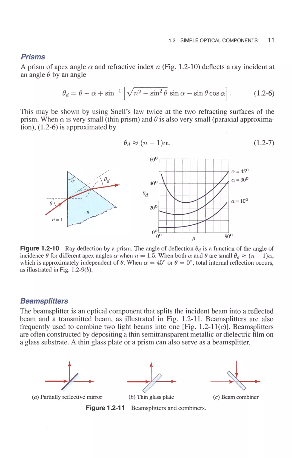
Prisms
A prism of apex angle a and refractive index n (Fig. 1.2-1 0) deflects a ray incident at
an angle e by an angle
e d e Q + sin- 1
n 2 sin 2 e sin Q sin e cos Q .
(1.2-6)
This may be shown by using Snell's law twice at the two refracting surfaces of the
prism. When Q is very small (thin prism) and e is also very small (paraxial approxima-
tion), (1.2-6) is approximated by
L
ed n 1 Q.
(1.2-7)
60°
40°
Q' = 45°
Q' = 30°
,
,
,
,
,
,
(}d
(}d
()
Q = 10°
20°
n
n=l
0°
0°
()
90°
Figure 1.2-1 0 Ray deflection by a prism. The angle of deflection ()d is a function of the angle of
incidence () for different apex angles a when n 1.5. When both a and () are small ()d (n l)a,
which is approximately independent of (). When a 45° or () 0°, total internal reflection occurs,
as illustrated in Fig. ] .2-9(b).
Beamsplitters
The beamsplitter is an optical component that splits the incident beam into a reflected
beam and a transmitted beam, as illustrated in Fig. 1.2-11. Beamsplitters are also
frequently used to combine two light beams into one [Fig. t.2-11(e)]. Beamsplitters
are often constructed by depositing a thin semitransparent metallic or dielectric film on
a glass substrate. A thin glass plate or a prism can also serve as a beamsplitter.
(a) Partially reflective mirror
( b) Thin glass plate
(c) Beam combiner
Figure 1.2-11 Beamsplitters and combiners.
12 CHAPTER 1 RAY OPTICS
c. Spherical Boundaries and Lenses
We now examine the refraction of rays from a spherical boundary of radius R between
two media of refractive indexes nl and n2. By convention, R is positive for a convex
boundary and negative for a concave boundary. The results are obtained by applying
Snell's law, which relates the angles of incidence and refraction relative to the normal
to the surface, defined by the radius vector from the center e. These angles are to
be distinguished from the angles ()I and ()2, which are defined relative to the z axis.
Considering only paraxial rays making small angles with the axis of the system so that
sin () () and tan () (), the following properties may be shown to hold:
. A ray making an angle ()I with the z axis and meeting the boundary at a point of
height y where it makes an angle ()o with the radius vector [see Fig. 1.2-12(a)]
changes direction at the boundary so that the refracted ray makes an angle ()2
with the z axis and an angle ()3 with the radius vector. The angle of incidence is
therefore 0 1 + ()2 while the angle of refraction is ()3, so that
nl
()2 ()I
n2
n2 n 1 y
n2 R'
( 1.2-8)
,
R
,
,
(a)
OJ
( -(2)
y
- - - - - - - - - - - - - - - - - --
PI C P 2
n j n 2
z
\
\
,
,
y
PI =(YJ,zl)
- - - - -
--. - - - - - - - ..
C
(b)
o
- -
P 2 = (Y2' Z2)
Z
Z
Figure 1.2-12 Refraction at a convex spherical boundary (R > 0).
. All paraxial rays originating from a point PI Y1 , Zl in the z Zl plane meet
at a point P 2 Y2, Z2 in the z Z2 plane, where
Zl Z2 R
and
nl Z2
Yl.
n2 Zl
(1.2-1 0)
Y2
1.2 SIMPLE OPTICAL COMPONENTS 13
The Z ZI and Z Z2 planes are said to be conjugate planes. Every point
in the first plane has a corresponding point (image) in the second with magnifi-
cation nl n2 Z2 ZI . Again, negative magnification means that the image is
inverted. By convention PI is measured in a coordinate system pointing to the left
and P2 in a coordinate system pointing to the right (e.g., if P 2 lies to the left of
the boundary, then Z2 would be negative).
The similarities between these properties and those of the spherical mirror are evi-
dent. It is important to remember that the image formation properties described above
are approximate. They hold only for paraxial rays. Rays of large angles do not obey
these paraxial laws; the deviation results in image distortion called aberration.
EXERCISE 1.2-2
Image Formation. Derive (1.2-8). Prove that paraxial rays originating from PI pass through P 2
when (1.2-9) and (1.2-1 0) are satisfied.
EXERCISE 1.2-3
Aberration-Free Imaging Surface. Determine the equation of a convex aspherical (nonspheri-
cal) surface between media of refractive indexes nl and n2 such that all rays (not necessarily paraxial)
from an axial point PI at a distance Zl to the left of the surface are imaged onto an axial point P2 at
a distance Z2 to the right of the surface [Fig. 1.2-12(a)]. Hint: In accordance with Fermat's principle
the optical pathlengths between the two points must be equal for all paths.
Lenses
A spherical lens is bounded by two spherical surfaces. It is, therefore, defined com-
pletely by the radii R 1 and R 2 of its two surfaces, its thickness , and the refractive
index n of the material (Fig. 1.2-13). A glass lens in air can be regarded as a combina-
tion of two spherical boundaries, air-to-glass and glass-to-air.
,
.,
,
" ,
" \
,
" \
( ) " \ I
-R2/" \ "
,
,
,
,
,
,
,
,
,
,
,
,
,
,
,
,
,
,
,
,
,
/
/
,
,
,
,
,
,
,
,
R I ,,/
,
,
,
,
,
,
,
,
,
,
,
,
,
,
, "
','
,
"
"
, \
, \
I ,
I
I
/
/
,
"
Figure 1.2-13 A biconvex spherical lens.
A ray crossing the first surface at height y and angle 8 1 with the Z axis [Fig. 1.2-
14(a)] is traced by applying (1.2-8) at the first surface to obtain the inclination angle
8 of the refracted ray, which we extend until it meets the second surface. We then use
(1.2-8) once more with 8 replacing 8 1 to obtain the inclination angle ()2 of the ray after
refraction from the second surface. The results are in general complicated. When the
lens is thin, however, it can be assumed that the incident ray emerges from the lens
at about the same height y at which it enters. Under this assumption, the following
relations follow:
14 CHAPTER 1 RAY OPTICS
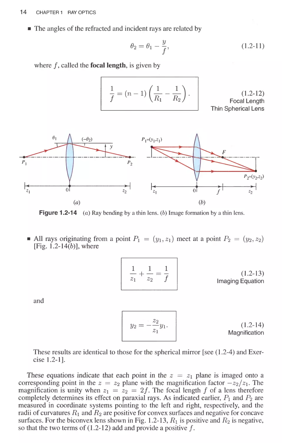
. The angles of the refracted and incident rays are related by
()2 ()I
Y
f'
(1.2-11)
where f, called the focal length, is given by
1
f
1
RI
1
R 2
n
1
.
(1.2-12)
Focal Length
Thin Spherical Lens
OJ
( -(}2)
P 1 =(y 1 ,Z 1 )
y
- - - - - - - - - - - - -
.
- -
F
PJ
P2
P 2=(Y2'Z2)
Zl
o
Z2
ZJ
o
f
Z2
(a)
(b)
Figure 1.2-14 (a) Ray bending by a thin lens. (b) Image formation by a thin lens.
. All rays originating from a point PI
[Fig. 1.2-14(b)], where
YI, ZI meet at a point P 2
Y2, Z2
1 1
+
Zl Z2
1
f
(1.2-13)
Imaging Equation
and
Y2
Z2
Yl-
Zl
(1.2-14)
Magnification
These results are identical to those for the spherical mirror [see (1.2-4) and Exer-
cise 1.2-1].
These equations indicate that each point in the Z Zl plane is imaged onto a
corresponding point in the Z Z2 plane with the magnification factor Z2 ZI. The
magnification is unity when Zl Z2 2f. The focal length f of a lens therefore
completely determines its effect on paraxial rays. As indicated earlier, PI and P 2 are
measured in coordinate systems pointing to the left and right, respectively, and the
radii of curvatures RI and R 2 are positive for convex surfaces and negative for concave
surfaces. For the biconvex lens shown in Fig. 1.2-13, RI is positive and R 2 is negative,
so that the two terms of (.1.2-12) add and provide a positive f.
1.2 SIMPLE OPTICAL COMPONENTS 15
EXERCISE 1.2-4
Proof of the Thin Lens Formulas. Using (1.2-8), along with the definition of the focal length
given in (1.2-12), prove (1.2-11) and (1.2-13).
It is emphasized once again that the foregoing relations hold only for paraxial rays.
The presence of nonparaxial rays results in aberrations, as illustrated in Fig. 1.2-15.
f
Figure 1.2-15 Nonparaxial rays do not meet
at the paraxial focus. The dashed envelope of the
refracted rays is called the caustic curve.
D. Light Guides
Light may be guided from one location to another by use of a set of lenses or mirrors,
as illustrated schematically in Fig. 1.2-16. Since refractive elements (such as lenses)
are usually partially reflective and since mirrors are partially absorptive, the cumula-
tive loss of optical power will be significant when the number of guiding elements
is large. Components in which these effects are minimized can be fabricated (e.g.,
antireflection-coated lenses), but the system is generally cumbersome and costly.
(a) = ---------- ---------- - -
(b) - - ----------- ---------- ----------- ------
) --- - -- ---
Figure 1.2-16 Guiding light: (a) lenses; (b) mirrors; (c) total internal reflection.
An ideal mechanism for guiding light is that of total internal reflection at the bound-
ary between two media of different refractive indexes. Rays are reflected repeatedly
without undergoing refraction. Glass fibers of high chemical purity are used to guide
light for tens of kilometers with relatively low loss of optical power.
An optical fiber is a light conduit made of two concentric glass (or plastic) cylinders
(Fig. 1.2-17). The inner, called the core, has a refractive index nl, and the outer, called
16 CHAPTER 1 RAY OPTICS
the cladding, has a slightly smaller refractive index, n2 < nl. Light rays traveling in
the core are totally re fl ected from the cladding if their angle of incidence is greate r
than the critical angle, () > (}c sin- 1 n2 nl . The rays making an an gl e () 90 ° ()
with the optical axis are therefore confined in the fiber core if () < (}c, where (}c
90° (}c cos- 1 n2 nl . Optical fibers are used in optical communication systems
(see Chapters 9 and 24). Some important properties of optical fibers are derived in
Exercise 1.2-5.
Cladding
Core
n2
nl
-
- - -- -
Figure 1.2-17 The optical fiber. Light rays are guided by multiple total internal reflections. Here
-
() represents the angle measured from the axis of the optical fiber so that its complement () 90° ()
is the angle of incidence at the dielectric interface.
EXERCISE 1.2-5
Numerical Aperture and Angle of Acceptance of an Optical Fiber. An optical fiber is
illuminated by light from a source (e.g., a light-emitting diode, LED). The refractive indexes of the
core and cladding of the fiber are nl and n2, respectively, and the refractive index of air is 1 (Fig. 1.2-
18). Show that the half-angle ()a of the cone of rays accepted by the fiber (transmitted through the
fiber without undergoing refraction at the cladding) is given by
NA
sin ()a
n 2
1
2
n 2 ·
(1.2-15)
Numerical Aperture
Optical Fiber
The angle () a is called the acceptance angle and the parameter N A sin () a is known as the numerical
aperture of the fiber. Calculate the numerical aperture and acceptance angle for a silica-glass fiber
with nl 1.475 and n2 1.460.
Air
Cladding n2
Core n I
-
-
- - - -
- - - - -
()a
n2
Figure 1.2-18 Acceptance angle of an optical fiber.
Trapping of Light in Media of High Refractive Index
It is often difficult for light originating inside a medium of large refractive index to
be extracted into air, especially if the surfaces of the medium are parallel. This occurs
since certain rays undergo multiple total internal reflections without ever refracting into
air. The principle is illustrated in Exercise 1.2-6.
1.3 GRADED-INDEX OPTICS 17
EXERCISE 1.2-6
Light Trapped in a Light-Emitting Diode.
(a) Assume that light is generated in all directions inside a material of refractive index n cut in the
shape of a parallelepiped (Fig. 1.2-19). The material is surrounded by air with unity refractive
index. This process occurs in light-emitting diodes (see Chapter 17). What is the angle of the
cone of light rays (inside the material) that will emerge from each face? What happens to the
other rays? What is the numerical value of this angle for GaAs (n 3.6)?
I
Figure 1.2-19 Trapping of light in a paral-
lelepiped of high refractive index.
(b) Assume that when light is generated isotropically the amount of optical power associated with
the rays in a given cone is proportional to the solid angle of the cone. Show that the ratio of
the optical power that is extracted from the material to the total generated optical power is
3 1 1 1/n2, provided that n > 2. What is the numerical value of this ratio for GaAs?
1.3 GRADED-INDEX OPTICS
A graded-index (GRIN) material has a refractive index that varies with position in
accordance with a continuous function n r . These materials are often fabricated by
adding impurities (dopants) of controlled concentrations. In a GRIN medium the opti-
cal rays follow curved trajectories, instead of straight lines. By appropriate choice of
n r , a GRIN plate can have the same effect on light rays as a conventional optical
component, such as a prism or lens.
A. The Ray Equation
To determine the trajectories of light rays in an inhomogeneous medium with refractive
index n r , we use Fermat's principle,
B
8 n r ds 0,
A
(1.3-1)
where ds is a differential length along the ray trajectory between A and B. If the
trajectory is described by the function x s , y s , and z s , where s is the length of the
trajectory (Fig. 1.3-1), then using the calculus of variations it can be shown t that x s ,
t This derivation is beyond the scope of this book; see, e.g., R. Weinstock, Calculus of Variations, Dover,
1974.
18 CHAPTER 1 RAY OPTICS
Y ( s ), and z ( s) must satisfy three partial differential equations,
d ( dX ) an
- n- ==-
ds ds ax '
d ( dY ) an
ds n ds == oy '
d ( dZ ) an
ds n ds == oz .
(1.3-2)
By defining the vector r(s), whose components are x(s), y(s), and z(s), (1.3-2) may
be written in the compact vector form
d ( dr )
ds n ds == V n,
(1.3-3)
Ray Equation
where Vn, the gradient of n, is a vector with Cartesian components an/ax, on/oy,
and an/oz. Equation (1.3-3) is known as the ray equation.
yt
B
A
Figure 1.3-1 The ray trajectory is described
parametrically by three functions x( s), y( s), and
z(s), or by two functions x(z) and y(z).
One approach to solving the ray equa tion is to describe the traje ctory by two func-
tions x(z) and y(z), write ds == dz -J l + (dx/dz)2 + (dy/dz)2, and substitute in
(1.3-3) to obtain two partial differential equations for x(z) and y(z). The algebra is
generally not trivial, but it simplifies considerably when the paraxial approximation is
used.
The Paraxial Ray Equation
In the paraxial approximation, the trajectory is almost parallel to the z axis, so that
ds dz (Fig. 1.3-2). The ray equations (1.3-2) then simplify to
d ( dX ) an
dz n dz ax '
d ( dY ) an
dz n dz oy .
( 1.3-4)
Paraxial
Ray Equations
Given n == n(x, y, z), these two partial differential equations may be solved for the
trajectory x(z) and y(z).
In the limiting case of a homogeneous medium for which n is independent of x, y, z,
(1.3-4) gives d 2 x/dz 2 == 0 and d 2 y/dz 2 == 0, from which it follows that x and yare
linear functions of z, so that the trajectories are straight lines. More interesting cases
will be examined subsequently.
1.3 GRADED-INDEX OPTICS 19
y
z
Figure 1.3-2 Trajectory of a paraxial ray in a graded-index medium.
B. Graded-Index Optical Components
Graded-Index Slab
Consider a slab of material whose refractive index n n y is uniform in the x and
z directions but varies continuously in the y direction (Fig. 1.3-3). The trajectories of
paraxial rays in the y z plane are described by the paraxial ray equation
d dy
dz n dz
dn
dy'
(1.3-5)
from which
d 2 y
dz 2
1 dn y
n y dy
.
(1.3-6)
Given n y and initial conditions (y and dy dz at z 0), (1.3-6) can be solved for the
function y z , which describes the ray trajectories.
y
y+L\y
y
O(y + L\y)
O(y)
--
- -
dn
n(y)+ d L\y
n(y) Y
z
Refractive index
Figure 1.3-3 Refraction in a graded-index slab.
D Derivation of the Paraxial Ray Equation in a Graded-Index Slab Using Snell's Law.
Equation (1.3-6) may also be derived by the direct use of Snell's law (Fig. 1.3-3). Let O(y) dyJdz
be the angle that the ray makes with the z axis at the position (y, z). After traveling through a layer
of thickness y the ray changes its angle to O(y + y). The two angles are related by Snell's law
where 0, as defined in Fig. 1.3-3, is the complement of the angle of incidence (refraction):
n(y) cos O(y) n(y + y) cos O(y + y)
dn dO.
cosO(y) (1.3-7)
where we have applied the expansion f (y + y) f (y) + (df J dy) y to the functions f (y) n(y)
and f(y) cosO(y). In the limit y ) 0, after eliminating the term in ( y)2, we obtain the
differential equation
dn dO
dy
(1.3-8)
For paraxial rays 0 is very small so that tan 0 O. Substituting 0
( 1.3-6).
dy J dz in (1.3-8), we obtain
.
20 CHAPTER 1 RAY OPTICS
EXAMPLE 1.3-1. Slab with Parabolic Index Profile. An important particular distribution
for the graded refractive index is
n 2 (y) n6 1 O?y2.
( 1.3-9)
This is a symmetric function of y that has its maximum value at y 0 (Fig. 1.3-4). A glass slab with
this profile is known by the trade name SELFOC. Usually, a is chosen to be sufficiently small so that
a 2 y2 « 1 for all y of interest. Under this condition, n(y) no 1 a 2 y2 no(l a2y2); i.e.,
n(y) is a parabolic distribution. Also, because n(y) no «::: no, the fractional change of the refractive
index is very small. Taking the derivative of (1.3-9), the right-hand side of (1.3-6) is (l/n)dn/dy
(no/n)2a 2 y Q2y, so that (1.3-6) becomes
d 2 y
Q2y.
dz 2
(1.3-10)
The solutions of this equation are harmonic functions with period 2n / Q. Assuming an initial position
y(O) Yo and an initial slope dy/dz Bo at z 0 inside the GRIN medium,
(}o ·
Yo CDS Q'Z + SIn Q'Z,
Q'
y(z)
(1.3-11)
from which the slope of the trajectory is
B(z)
dy
dz
yoa sin QZ + Bo cos az.
(1.3-12)
The ray oscillates about the center of the slab with a period ( distance) 2n / Q known as the pitch, as
illustrated in Fig. 1.3-4.
y
r
27r
a
y
Yo
0 0
z
no n(y)
Figure 1.3-4 Trajectory of a ray in a GRIN slab of parabolic index profile (SELFOC).
The maximum excursion of the ray is Ymax Y5 + (Bo/a)2 and the maximum angle is Bmax
aYmax. The validity of this approximate analysis is ensured if (}max « 1. If 2Ymax is smaller than
the thickness of the slab, the ray remains confined and the slab serves as a light guide. Figure 1.3- 5
shows the trajectories of a number of rays transmitted through a SELFOC slab. Note that all rays
have the same pitch. This GRIN slab may be used as a lens, as demonstrated in Exercise 1.3- I .
z
7r
Q'
d
-i
Figure 1.3-5 Trajectories of rays from an external point source in a SELFOC slab.
1.3 GRADED-INDEX OPTICS 21
EXERCISE 1.3-1
The GRIN Slab as a Lens. Show that a SELFOC slab of length d < 7r /2a and refractive index
given by (1.3-9) acts as a cylindrical lens (a lens with focusing power in the y-z plane) of focal length
nod a sin a
(1.3-13)
Show that the principal point (defined in Fig. 1.3-6) lies at a distance from the slab edge AH
(l/noa) tan(ad/2). Sketch the ray trajectories in the special cases d 7r /a and 7r /2a.
Y
f
Yo
----------- -
I "'" ""
"'"
""
I ..... ""
I
I
I
A F
z
H
r-
d
Figure 1.3-6 The SELFOC slab used as
a lens; F is the focal point and H is the
principal point.
Graded-Index Fibers
A graded-index fiber is a glass cylinder with a refractive index n that varies as a
function of the radial distance from its axis. In the paraxial approximation, the ray
trajectories are governed by the paraxial ray equations (1.3-4). Consider, for example,
the distribution
n 2
n 2 1
o
a? x 2 + y2
.
(1.3-14)
Substituting (1.3-14) into (1.3-4) and assuming that Q2 x 2 + y2 «1 for all x and y
of interest, we obtain
d 2 x
r"..J
r"..J
dz 2
Q 2 X
,
tPy
r"..J
r"..J
dz 2
Q2y.
(1.3-15)
Both x and yare therefore harmonic functions of z with period 27r Q. The initial
positions Xo, Yo and angles (B xo dx dz and Byo dy dz at z 0 determine the
amplitudes and phases of these harmonic functions. Because of the circular symmetry,
there is no loss of generality in choosing Xy O. The solution of (1.3-15) is then
Bxo .
x z Sinaz
a
Byo .
SIn az + Yo CDS az.
a
(1.3-16)
y z
If Bxo 0, Le., the incident ray lies in a meridional plane (a plane passing through
the axis of the cylinder, in this case the y z plane), the ray continues to lie in that plane
following a sinusoidal trajectory similar to that in the GRIN slab [Fig. 1.3-7(a)].
On the other hand, if Byo 0, and Bxo ayo, then
x z
.
Yo SIn az
( 1.3-17)
y z
Yo CDS az,
22 CHAPTER 1 RAY OPTICS
(a)
27r
Q
()o
-
- .... ..... -
- -
-
z
\
Yo
-
-
,
,
- -
,
,
-
-
/
,
/-
,
.,v (\
/
- , - --".-
, z
., ., J
(b)
I \
\
Figure 1.3-7 (a) Meridional and (b) helical rays in a graded-index fiber with parabolic index
profile.
so that the ray follows a helical trajectory lying on the surface of a cylinder of radius
Yo [Fig. 1.3- 7 (b)]. In both cases the ray remains confined within the fiber, so that the
fiber serves as a light guide. Other helical patterns are generated with different incident
rays.
Graded-index fibers and their use in optical communications are discussed in Chap-
ters 9 and 24.
EXERCISE 1.3-2
Numerical Aperture of the Graded-Index Fiber. Consider a graded-index fiber with the index
profile provided in (1.3-] 4) and radius a. A ray is incident from air into the fiber at its center, which
then makes an angle (}o with the fiber axis in the medium (see Fig. 1.3-8). Show, in the paraxial
approximation, that the numerical aperture is
NA sin (}a noaa,
( 1.3-18)
Numerical Aperture
Graded-Index Fiber
where () a is the maximum acceptance angle for which the ray trajectory is confined within the fiber.
Compare this to the numerical aperture of a step-index fiber such as the one discussed in Exercise 1.2-
5. To make the comparison fair, t ake the refr active indexes of the core and cladding of the step- index
fiber to be nl no and n2 no V I a 2 a 2 no (1 !a 2 a 2 ), respectively.
y
T
(}a eo a
-1-
- - - - - - I
e a eo z
Figure 1.3-8 Acceptance angle of a graded-index optical fiber.
1.3 GRADED-INDEX OPTICS 23
*c. The Eikonal Equation
The ray trajectories are often characterized by the surfaces to which they are normal.
Let 8 r be a scalar function such that its equilevel surfaces, 8 r constant, are
everywhere normal to the rays (Fig. 1.3-9). If 8 r is known, the ray trajectories can
readily be constructed since the normal to the equilevel surfaces at a position r is in the
direction of the gradient vector \7 8 r . The function 8 r , called the eikonal, is akin
to the potential function V r in electrostatics; the role of the optical rays is played by
the lines of electric field E \7V.
Rays
,.
S(r) = constant
Figure 1.3-9 Ray trajectories are normal to the surfaces
of constant S(r).
To satisfy Fermat's principle (which is the main postulate of ray optics) the eikonal
8 r must satisfy a partial differential equation known as the eikonal equation,
08 2
ax
+
08 2
ay
08 2
az
n 2
,
(1.3-19)
+
which is usually written in the vector form
\78 2
n 2
,
(1.3-20)
Eikonal Equation
where \7 8 2 \7 8 · \7 8. The proof of the eikonal equation from Fermat's principle
is a mathematical exercise that lies beyond the scope of this book. t Fermat's principle
(and the ray equation) can also be shown to follow from the eikonal equation. There-
fore, either the eikonal equation or Fermat's principle may be regarded as the principal
postulate of ray optics.
Integrating the eikonal equation (1.3-20) along a ray trajectory between points A
and B gives
B
8 rB
8 rA
\7 8 ds
B
n ds optical pathlength between A and B.
A
A
(1.3-21)
This means that the difference 8 r B 8 r A represents the optical pathlength be-
tween A and B. In the electrostatics analogy, the optical pathlength plays the role of
the potential difference.
To determine the ray trajectories in an inhomogeneous medium of refractive index
n r , we can either solve the ray equation (1.3-3), as we have done earlier, or solve the
eikonal equation for 8 r , from which we calculate the gradient \7 8.
t See, e.g., M. Born and E. Wolf, Principles of Optics, Cambridge University Press, 7th expanded and corrected
ed. 2002.
24 CHAPTER 1 RAY OPTICS
If the medium is homogeneous, i.e., n r is constant, the magnitude of \7 S is
constant, so that the wavefront normals (rays) must be straight lines. The surfaces
S r constant may be parallel planes or concentric spheres, as illustrated in Fig. 1.3-
10.
S(r) = constant
Rays
/
-
Rays
-
Figure 1.3-10 Rays and surfaces of constant S(r) in a homogeneous medium.
The eikonal equation is revisited from the point-of-view of the relation between ray
optics and wave optics in Sec. 2.3.
1.4 MATRIX OPTICS
Matrix optics is a technique for tracing paraxial rays. The rays are assumed to travel
only within a single plane, so that the formalism is applicable to systems with planar
geometry and to meridional rays in circularly symmetric systems.
A ray is described by its position and its angle with respect to the optical axis. These
variables are altered as the ray travels through the system. In the paraxial approxima-
tion, the position and angle at the input and output planes of an optical system are
related by two linear algebraic equations. As a result, the optical system is described
by a 2 x 2 matrix called the ray transfer matrix.
The convenience of using matrix methods lies in the fact that the ray-transfer matrix
of a cascade of optical components (or systems) is a product of the ray-transfer matrices
of the individual components (or systems). Matrix optics therefore provides a formal
mechanism for describing complex optical systems in the paraxial approximation.
A. The Ray-Transfer Matrix
Consider a circularly symmetric optical system formed by a succession of refracting
and reflecting surfaces all centered about the same axis (optical axis). The z axis lies
along the optical axis and points in the general direction in which the rays travel.
Consider rays in a plane containing the optical axes, say the y z plane. We proceed
to trace a ray as it travels through the system, i.e., as it crosses the transverse planes
at different axial distances. A ray crossing the transverse plane at z is completely
characterized by the coordinate of y of its crossing point and the angle () (Fig. 1.4-
1 ).
An optical system is a set of optical components placed between two transverse
planes at Zl and Z2, referred to as the input and output planes, respectively. The system
is characterized completely by its effect on an incoming ray of arbitrary position and
1.4 MATRIX OPTICS 25
y
Ray
e
z
Figure 1.4-1 A ray is charac-
terized by its coordinate y and its
angle ().
Optical
.
aXIs
Input
(YI, ( 1 )
Optical system
Output
(Y2, (2)
Y
Input
plane
° 1
Output
plane
°2 Figure 1.4-2 A ray enters an
YI
Yz optical system at location Zl with
Optical
position Yl and angle ()l and leaves
Zl Zz .
z aXIs at position Y2 and angle ()2.
direction Yl, 0 1 . It steers the ray so that it has new position and direction Y2, O 2 at
the output plane (Fig. 1.4-2).
In the paraxial approximation, when all angles are sufficiently small so that sin 0
0, the relation between Y2, O 2 and YI, Ol is linear and can generally be written in
the form
Y2 AYl + BO I
O 2 CYl + 001,
( 1.4- 1 )
(1.4-2)
where A, B, C, and 0 are real numbers. Equations (1.4-1) and (1.4-2) may be conve-
niently written in matrix form as
Y2
O 2
A B
C 0
Yl
Ol ·
(1.4-3)
The matrix M, whose elements are A, B, C, and 0, characterizes the optical system
completely since it permits Y2, O 2 to be determined for any Yl, Ol . It is known as the
ray-transfer matrix. As will be seen in the examples provided in Sec. 1.4B, angles
that turn out to be negative point downward from the z axis in their direction of travel.
Radii that turn out to be negative indicate concave surfaces whereas those that are
positive indicate convex surfaces.
EXERCISE 1.4-1
Special Forms of the Ray- Transfer Matrix. Consider the following situations in which one of
the four elements of the ray-transfer matrix vanishes:
(a) Show that if A 0, all rays that enter the system at the same angle leave at the same position, so
that parallel rays in the input are focused to a single point at the output.
(b) What are the special features of each of the systems for which B 0, C 0, or 0 O?
26 CHAPTER 1 RAY OPTICS
B. Matrices of Simple Optical Components
Free-Space Propagation
Since rays travel along straight lines in a medium of uniform refractive index such as
free space, a ray traversing a distance d is altered in accordance with Y2 YI + 0 1 d
and O 2 0 1 . The ray-transfer matrix is therefore
M
1 d
o 1 ·
(1.4-4)
d
Refraction at a Planar Boundary
At a planar boundary between two media of refractive indexes nl and n2, the ray
angle changes in accordance with Snell's law nl sin 0 1 n2 sin O 2 . In the paraxial
approximation, nlOl n202. The position of the ray is not altered, Y2 Yl. The
ray-transfer matrix is
nl n2
I
M
1 0
o nl ·
n2
(1.4-5)
Refraction at a Spherical Boundary
The relation between 0 1 and O 2 for paraxial rays refracted at a spherical boundary
between two media is provided in (1.2-8). The ray height is not altered, Y2 Yl. The
ray-transfer matrix is
R
n} n 2
1 0
(n2- n l) nl ·
n2 R n2
( 1.4-6)
M
Convex: R > 0; concave: R< 0
Transmission Through a Thin Lens
The relation between 0 1 and O 2 for paraxial rays transmitted through a thin lens of focal
length f is given in (1.2-11). Since the height remains unchanged Y2 Yl, we have
1
1
-
f
o
1 ·
(1.4-7)
f
M
Convex: f> 0; concave: f < 0
Reflection from a Planar Mirror
Upon reflection from a planar mirror, the ray position is not altered, Y2 Yl. Adopting
the convention that the z axis points in the general direction of travel of the rays, i.e.,
toward the mirror for the incident rays and away from it for the reflected rays, we
1.4 MATRIX OPTICS 27
conclude that ()2 ()l. The ray-transfer matrix is therefore the identity matrix
z
z
M
1 0
o 1 ·
( 1.4-8)
Reflection from a Spherical Mirror
Using (1.2-1), and the convention that the z axis follows the general direction of the
rays as they reflect from mirrors, we similarly obtain
(-R)
M
1
2
R
o
1 ·
( 1.4-9)
Concave: R < 0; convex: R > 0
Note the similarity between the ray-transfer matrices of a spherical mirror (1.4-9) and
a thin lens (1.4-7). A mirror with radius of curvature R bends rays in a manner that is
identical to that of a thin lens with focal length f R 2.
C. Matrices of Cascaded Optical Components
A cascade of N optical components or systems whose ray-transfer matrices are
M 1 , M 2 , . . . , MN is equivalent to a single optical system of ray-transfer matrix
). M 1
). M 2
>- . . .
). MN
>-
M MN · · · M 2 M 1 .
( 1.4-1 0)
Note the order of matrix multiplication: The matrix of the system that is crossed by the
rays is first placed to the right, so that it operates on the column matrix of the incident
ray first. A sequence of matrix multiplications is not, in general, commutative, although
. . ..
It IS aSSocIative.
EXERCISE 1.4-2
A Set of Parallel Transparent Plates. Consider a set of N parallel planar transparent plates of
refractive indexes nI, n2,.. · nN and thicknesses d 1 , d 2 ,. . . d N , placed in air (n 1) normal to the
z axis. Using induction, show that the ray-transfer matrix is
I n 1 n2
. . .
nN
1
h
z
M
o 1
( 1.4-11 )
d} d 2 d N
Note that the order in which the plates are placed does not affect the overall ray-transfer matrix. What
is the ray-transfer matrix of an inhomogeneous transparent plate of thickness do and refractive index
n(z)?
28 CHAPTER 1 RAY OPTICS
EXERCISE 1.4-3
A Gap Followed by a Thin Lens. Show that the ray-transfer matrix of a distance d of free
space followed by a lens of focal length 1 is
f
1
1
-
f
1
d
d ·
-
f
( 1.4-12)
M
d I
EXERCISE 1.4-4
Imaging with a Thin Lens. Derive an expression for the ray-transfer matrix of a system com-
prised of free space/thin lens/free space, as shown in Fig. 1.4-3. Show that if the imaging condition
(1/ d 1 + 1/ d 2 1/ f) is satisfied, all rays originating from a single point in the input plane reach the
output plane at the single point Y2, regardless of their angles. Also show that if d 2 f, all parallel
incident rays are focused by the lens onto a single point in the output plane.
f
d 1 I--c
d 2
Figure 1.4-3 Single-lens imaging system.
EXERCISE 1.4-5
Imaging with a Thick Lens. Consider a glass lens of refractive index n, thickness d, and two
spherical surfaces of equal radii R (Fig. 1.4-4). Determine the ray-transfer matrix of the system
between the two planes at distances d l and d 2 from the vertices of the lens. The lens is placed in air
(refractive index 1). Show that the system is an imaging system (i.e., the input and output planes
are conjugate) if
1 1
+
1
f
or
1 2 ,
81 8 2
(1.4-13)
Zl Z2
where
ZI d l + h,
Z2 d 2 + h,
81 ZI f
82 Z2 f
(1.4-14)
(1.4-15)
and
h
(n l)fd
nR
(1.4-16)
n Id
n R
.
( 1.4-17)
1
f
R
The points F I and F 2 are known as the front and back focal points, respectively. The points PI and
P 2 are known as the first and second principal points, respectively. Show the importance of these
points by tracing the trajectories of rays that are incident parallel to the optical axis.
1.4 MATRIX OPTICS 29
......c:
d
Sl
f
n
.
FI
.
PI
.
P2
f ......c
.
F2
S2
d 1
h ......
h
d 2
Z2
ZI
Figure 1.4-4 Imaging with a thick lens. PI and P 2 are the principal points and FI and F 2 are the
focal points.
.
D. Periodic Optical Systems
A periodic optica] system is a cascade of identical unit systems. An example is a
sequence of equally spaced identical relay lenses used to guide light, as shown in
Fig. 1.2-16( a). Another example is the reflection of light between two mirrors that
form an optical resonator (see Sec. 10.2A); in that case, the ray repeatedly traverses
the same unit system (a round trip of reflections). Even a homogeneous medium, such
as a glass fiber, may be considered as a periodic system if it is divided into contiguous
identical segments of equal length. We proceed to formulate a general theory of ray
propagation in periodic optical systems using matrix methods.
Difference Equation for the Ray Position
A periodic system is composed of a cascade of identical unit systems (stages), each
with a ray-transfer matrix A, B, G, D , as shown in Fig. 1.4-5. A ray enters the system
with initial position Yo and slope ()o. To determine the position and slope Ym, ()m of
the ray at the exit of the mth stage, we apply the ABGD matrix m times,
Yrn
()m
A B m Yo
G D ()o'
( 1.4-18)
We can also iteratively apply the relations
Ym+l AYm + B()m
()m+l GYm + D()m
(1.4-19)
(1.4-20)
to determine (Yl, ()l from Yo, ()o , then Y2, ()2 from Yl, ()l , and so on, using a
software routine.
Yo
° 0
A B Yl
C D OJ
1
A B
C D
. ..
A B
C D
A B Y m A B
C D Om C D
Ym+l
Om + I
2
m-l
m
m+ 1
Figure 1.4-5 A cascade of identical optical systems.
It is of interest to derive equations that govern the dynamics of the position Ym,
m 0,1, . . . , irrespective of the angle ()m. This is achieved by eliminating ()m from
30 CHAPTER 1 RAY OPTICS
(1.4-19) and (1.4-20). From (1.4-19)
Om
Ym+ 1 AYm
B
.
( 1.4- 21 )
Replacing m with m + 1 in (1.4-21) yields
AYm+ 1
B
Substituting (1.4-21) and (1.4-22) into (1.4-20) gives
Om+l
Yrn+2
.
(1.4-22)
Ym+2 2bYm+l F2Ym,
(1.4-23)
Recurrence Relation
for Ray Position
where
b
A+D
2
AD BC
det M ,
(1.4-24)
(1.4-25)
F 2
and det M is the determinant of M.
Equation (1.4-23) is a linear difference equation governing the ray position Ym. It
can be solved iteratively by computing Y2 from Yo and Yl, then Y3 from Yl and Y2, and
so on. The quantity Yl may be computed from Yo and 0 0 by use of (1.4-19) with m O.
It is useful, however, to derive an explicit expression for Ym by solving the difference
equation (1.4-23). As with linear differential equations, a solution satisfying a linear
difference equation and the initial conditions is a unique solution. It is therefore appro-
priate to make a judicious guess for the solution of (1.4-23). We use a trial solution of
the geometric form
Ym Yohm,
(1.4-26)
where h is a constant. Substituting (1.4-26) into (1.4-23) immediately shows that the
trial solution is suitable provided that h satisfies the quadratic algebraic equation
h 2 2bh + F 2 0,
(1.4-27)
from which
h b -X j p2 b 2 .
( 1.4-28)
The results can be presented in a more compact form by defining the variable
<p cos- 1 b F ,
(1.4-29)
so that b F cos <p, F2 b 2 F sin <p, and therefore h F cos <p -X j sin <p
F exp -xj<p , whereupon (1.4-26) becomes Ym yoFm exp -xjm<p .
A general solution may be constructed from the two solutions with positive and
negative signs by forming their linear combination. The sum of the two exponential
functions can always be written as a harmonic (circular) function, so that
Ym Ymax Fm sin m<p + <Po ,
(1.4-30)
1.4 MATRIX OPTICS 31
where Ymax and 'Po are constants to be determined from the initial conditions Yo and
Yl. In particular, setting m 0 we obtain Ymax Yo sin 'Po.
The parameter F is related to the determinant of the ray-transfer matrix of the unit
system by F det M . It can be shown that regardless of the unit system, det M
ni n2, where ni and n2 are the refractive indexes of the initial and final sections
of the unIt system. This general result is easily verified for the ray-transfer matrices
of all the optical components considered in this section. Since the determinant of a
product of two matrices is the product of their determinants, it follows that the relation
det M ni n2 is applicable to any cascade of these optical components. For exam-
ple, if det M 1 ni n2 and det M 2 n2 n3, then det M 2 M I n2 n3 nl n2
ni n3. In most applications the first and last stages are air (n 1) ni n2, so that
det M 1 and F 1, in which case the solution for the ray position is
. , ,
Ym Ymax SIn, m'P + 'Po) ·
( 1.4- 31 )
Ray Position
Periodic System
We shall assume henceforth that F 1. The corresponding solution for the ray angle
is obtained by use of the relation ()m Ym+1 A Ym B, which is derived from
(1.4-19).
Condition for a Harmonic Trajectory
For Ym to be a harmonic (instead of hyperbolic) function, 'P cos- I b must be real.
This requires that
b < 1
(1.4-32)
Stability Condition
or
If, instead, b > 1, 'P is then imaginary and the solution is a hyperbolic function (cosh
or sinh), which increases without bound, as illustrated in Fig. 1.4-6(a). A harmonic
solution ensures that Ym is bounded for all m, with a maximum value of Ymax. The
bound b < 1 therefore provides a condition of stability (boundedness) of the ray
trajectory.
Since Ym and Ym+1 are both harmonic functions, so too is the ray angle corre-
sponding to (1.4-31), by virtue of (1.4-21) and trigonometric identities. Thus, ()m
()max sin m<p + 'PI , where the constants ()max and 'PI are determined by the initial
conditions. The maximum angle ()max must be sufficiently small so that the paraxial
approximation, which underlies this analysis, is applicable.
Condition for a Periodic Trajectory
The harmonic function (1.4- 31) is periodic in m if it is possible to find an integer s such
that Ym+s Ym for all m. The smallest integer is the period. The ray then retraces its
path after s stages. This condition is satisfied if S'P 21fq, where q is an integer.
Thus, the necessary and su ffi cient condition for a periodic traj ec t or y is that 'P 21f is a
is periodic with period s 11 stages. This case is illustrated in FIg. 1.4-6(b). Periodic
optical systems will be revisited in Chapter 7.
32 CHAPTER 1 RAY OPTICS
Ym
(a)
o
10
20
m
Ym
(b)
m
Ym
(c)
10
m
Figure 1.4-6 Examples of trajectories in periodic optical systems: (a) unstable trajectory (b >
1); (b) stable and periodic trajectory (<.p 67r /11; period 11 stages); (c) stable but nonperiodic
trajectory (<.p 1.5).
< Summary
<
: A paraxial ray (Omax « 1) traveling through a cascade of identical unit optical
-.
: systems, each with a ray-transfer matrix with elements A, B, C, D such that
. AD BC 1, follows a harmonic (and therefore bounded) trajectory if the
-.
j.
-.
; at th e m th stage is then Ym Ymax sin mcp + CPo , m 0, 1, 2, . . ., where
I
f
: positions Yo and Yl .. Ayo + BOo, where (}o is the initial ray inclination. The
: ray angles are related to the positions by Om Ym+1 AYm B and follow a
; harmonic function Om Oroax sin m<p + CPI . The ray trajectory is periodic with I
; period s if cp 21r is a rational number q s.
--
EXAMPLE 1.4-1. A Sequence of Equally Spaced Identical Lenses. A set of identical
lenses of focal length 1 separated by distance d, as shown in Fig. 1.4-7, may be used to relay light
between two locations. The unit system, a distance of d of free space followed by a lens, has a
ray-transfer matrix given by (1.4-12); A 1, B d, C 1/ I, D 1 d/ I. The parameter
b ! (A + D) 1 d /2/ and the determinant is unity. The condition for a stable ray trajectory,
Ibl < 1 or 1 < b < 1, is therefore
o < d < 41,
(1.4-33)
so that the spacing between the lenses must be smaller than four times the focal length. Under this
condition the positions of paraxial rays obey the harmonic function
Ym Ymax sin( m<.p + <.po),
<.p cos- 1 1
d
.
21
( 1.4-34)
1- - - - - - - - - - - r - .. - ... - - - ... - - ..... - - - - - - - - - ... ..
: jf : jf : jf :
I I
I
I
I
I
I
I
I
I
I
I I
1- _ _ _ _ _ _ _ _ _ _ I
- --- --- -
..-----------
J..
d +
d +
d
Figure 1.4-7 A periodic sequence of lenses.
1.4 MATRIX OPTICS 33
When d 2f, 'P n /2, and 'P /21r , so that the trajectory of an arbitrary ray is periodic with
period equal to four stages. When d f, 'P 7r /3, and 'P /2n t, so that the ray trajectory is
periodic and retraces itself each six stages. These cases are illustrated in Fig. 1.4-8.
(a)
d I
(b)
1 --< d I
Figure 1.4-8 Examples of stable ray trajectories in a periodic lens system: (a) d 2f; (b) d f.
EXERCISE 1.4-6
A Periodic Set of Pairs of Different Lenses. Examine the trajectories of paraxial rays through
a periodic system comprising a sequence of lens pairs with alternating focal lengths fl and f2, as
shown in Fig. 1.4-9. Show that the ray trajectory is bounded (stable) if
o < 1
d
2fl
1
d
2f2
< 1.
( 1.4-35)
r lr 1r 1 - -
II 1 2 II 1 2 II 1 2
II
I I I II
II
I I I II
I
I I I II II
I I I II
II
I I I II
l
I - I -f
d .c d d 4l1li( d d d ..
Figure 1.4-9 A periodic sequence of lens pairs.
EXERCISE 1.4-7
An Optical Resonator. Paraxial rays are reflected repeatedly between two spherical mirrors of
radii R 1 and R 2 separated by a distance d (Fig. 1.4-10). Regarding this as a periodic system whose
unit system is a single round trip between the mirrors, determine the condition of stability for the ray
trajectory. Optical resonators will be studied in detail in Chapter 10.
----- .-------
-
,,; --...
... ... .....
,
-
,
,
....
....
....
....
....
"
"
"
"
"", R2
.....
'"
.....
.,
,
,
,
, ,
, ,
" RI "
, ,
,
,
,
,
,
,
,
,
,
,
"
....
"
....
"
"
,
"
"
\
\
\
\
,
,
,
,
,
I
I
I
I Z
,
,
,
,
,
,
I
I
I
I
,
,
,
,
,
,
,
,
,
,
Figure 1.4-1 0 The optical resonator as a
periodic optical system.
'"
,
,
,
,
,
I
I
I
I
I
I
I
,
,
: Yo
I
I
I
,
,
,
\ Y2
\
\
\
\
"
"
,
"
"
"
"
"
"
"
"
,
-01
-
,
,
,
,
"
"
"
"
"
"
"
d
....
"
'"
'"
....
'"
'" ,
.......... -... ...-
...
..._-....... "....._----.-- ...
"
'"
....
.....
....
34 CHAPTER 1 RAY OPTICS
READING LIST
General
F. L. Pedrotti, L. M. Pedrotti, and L. S. Pedrotti, Introduction to Optics, Prentice Hall, 3rd ed. 2006.
K. K. Sharma, Optics: Principles and Applications, Academic Press, 2006.
A. Walther, The Ray and Wave Theory of Lenses, Cambridge University Press, 1995, paperback 00.
2006.
K. D. Moeller, Optics: Learning by Computing with Examples Using Maple, MathCad, Mathematica,
and MATLAB, Springer-Verlag, 2nd ed. 2006.
T.-C. Poon and T. Kim, Engineering Optics with MATLAB, World Scientific, 2006.
A. Siciliano, Optics: Problems and Solutions, World Scientific, 2006.
G. Chartier, Introduction to Optics, Springer- Verlag, 2005.
J. Strong, Concepts of Classical Optics, Freeman, 1958; Dover, paperback ed. 2004.
G. Brooker, Modem Classical Optics, Oxford University Press, 2003.
M. Born and E. Wolf, Principles of Optics, Cambridge University Press, 7th expanded and corrected
ed. 2002.
E. Hecht, Optics , Addison-Wesley, 4th ed. 2002.
M. Mansuripur, Classical Optics and Its Applications, Cambridge University Press, 2002.
M. P. Keating Geometric, Physical, and Visual Optics, Butterworth-Heinemann, 2nd ed. 2002.
M. Young, Optics and Lasers Including Fibers and Optical Waveguides, Springer-Verlag, 1977, 5th
ed. 2000.
J. R. Meyer-Arendt, Introduction to Classical and Modem Optics, Prentice Hall, 1972, 4th ed. 1995.
J. W. Blaker and W. M. Rosenblum, Optics An Introduction for Students of Engineering, Macmillan,
1993.
D. T. Moore, ed., Selected Papers on Gradient-Index Optics, SPIE Optical Engineering Press (Mile-
stone Series Volume 67), 1993.
F. A. Jenkins and H. E. White, Fundamentals of Optics, McGraw-Hill, 1937, 4th revised ed. 1991.
P. P. Banerjee and T.-C. Poon, Principles of Applied Optics, Aksen Associates, 1991.
R. D. Guenther, Modern Optics, Wiley, 1990.
E. Hecht and A. Zajac, Optics, Addison-Wesley, 1974, 2nd ed. 1990.
W. T. Welford, Optics, Oxford University Press, 1976, 3rd ed. 1988.
R. W. Wood, Physical Optics, Macmillan, 3rd ed. 1934; Optical Society of America, 1988.
M. V. Klein and T. E. Furtak, Optics, Wiley, 1982, 2nd ed. 1986.
E. W. Marchand, Gradient-Index Optics, Academic Press, 1978.
F. P. Carlson, Introduction to Applied Optics for Engineers, Academic Press, 1977.
R. W. Ditchburn, Light, Academic Press, 3rd ed. 1976.
E. Hecht, Schaum's Outline of Optics, McGraw-Hili, paperback ed. 1974.
B. B. Rossi, Optics, Addison-Wesley, 1957, reprinted 1965.
J. M. Stone, Radiation and Optics, McGraw-Hili, 1963.
A. Sommerfeld, Lectures on Theoretical Physics: Optics, Academic Press, paperback ed. 1954.
Geometrical Optics
Yu. A. Kravtsov, Geometrical Optics in Engineering Physics, Alpha Science, 2005.
J. E. Greivenkamp, Field Guide to Geometrical Optics, SPIE Optical Engineering Press, 2004.
K. B. Wolf, Geometric Optics on Phase Space, Springer-Verlag, 2004.
M. Katz, Introduction to Geometrical Optics, World Scientific, 2002.
R. Ditteon, Modern Geometrical Optics, Wiley, 1998.
F. Colombini and N. Lerner, eds., Geometrical Optics and Related Topics, Birkhauser, 1997.
P. Mouroulis and J. Macdonald, Geometrical Optics and Optical Design, Oxford University Press,
1997 .
D. S. Loshin, The Geometrical Optics Workbook, Butterworth-Heinemann, 1991.
G. A. Fry, Geometrical Optics, Chilton, 1969, reprinted 1981.
PROBLEMS 35
W. T. Welford and R. Winston, The Optics of Non imaging Concentrators, Academic Press, 1978
O. N. Stavroudis, The Optics of Rays, Wavefronts, and Caustics, Academic Press, 1972.
H.-G. Zimmer, Geometrical Optics, Springer-Verlag, 1970.
A. Nussbaum, Geometric Optics: An Introduction, Addison-Wesley, 1968.
R. K. Luneburg and M. Herzberger, Mathematical Theory of Optics, University of California Press,
1964, reprinted 1966.
Optical System Design
H. Gross, ed., Handbook of Optical Systems, Wiley, 2005.
D. Malacara and Z. Malacara, Handbook of Optical Design, Marcel Dekker, 1994, 2nd ed. 2004.
R. E. Fischer and B. Tadic-Galeb, Optical System Design, McGraw-Hill, 2000.
W. J. Smith, Modern Optical Engineering: The Design of Optical Systems, McGraw-Hill, 1966, 3rd
ed.2000.
A. Nussbaum, Optical System Design, Prentice Hall, 1998.
D. C. O'Shea, Elements of Modern Optical Design, Wiley, 1985.
R. Kingslake, Optical System Design, Academic Press, 1983.
L. Levi, Applied Optics: A Guide to Optical System Design, Wiley, Volume 1, 1968; Volume 2, 1980.
Matrix Optics
A. Gerrard and J. M. Burch, Introduction to Matrix Methods in Optics, Wiley, 1975; Dover, paperback
ed. 1994.
J. W. Blaker, Geometric Optics: The Matrix Theory, Marcel Dekker, 1971.
W. Brouwer, Matrix Methods in Optical Instrument Design, Benjamin, 1964.
Popular and Historical
R. J. Weiss, A Brief History of Light and Those that Lit the Way, World Scientific, 1996.
A. R. Hall, All was Light: An Introduction to Newton's Opticks, Clarendon Press/Oxford University
Press, 1993.
R. Kingslake, A History of the Photographic Lens, Academic Press, 1989.
M. I. Sobel, Light, University of Chicago Press, 1987.
A. I. Sabra, Theories of Light from Descartes to Newton, Cambridge University Press, 1981.
I. Newton, Opticks or a Treatise of the Reflections, Refractions, Inflections & Colours of Light, 4th
ed. 1704; Dover, reissued [979.
A. C. S. van Heel and C. H. F. Velze, What is Light?, McGraw-Hill, 1968, reprinted 1978.
V. Ronchi, The Nature of Light: An Historical Survey, Harvard University Press, 1970.
S. Tolansky, Revolution in Optics, Penguin, 1968.
S. Tolansky, Curiosities of Light Rays and Light Waves, Elsevier, 1965. "-
W. H. Bragg, Universe of Light, Dover, paperback ed. 1959.
E. Riichardt, Light, Visible and Invisible, University of Michigan Press, 1958.
PROBLEMS
1.1-2 Fermat's Principle with Maximum Time. Consider the elliptical mirror shown in Fig. PI. 1-
2(a), whos e foci are denoted A and B. Geomet rical p roper ties of the ellipse dictate that the
pathlength AP B is identical to the pathlengths AP' B and AP" B for adjacent points on the
ellipse.
(a) Now consider another mirror with a radius of curvature smaller than that of the ell iptical
mirror, but tangent to it at P, as displayed in Fig. P 1.1- 2( b). Show that the path AP B
followed by the light ray in traveling b etwee n poi nts A an d B is a path of maximum time,
i.e., is greater than the adjacent paths AQ' Band AQ" B.
(b) Finally, consider a mirror that crosses the ellipse, b ut is ta n gent t o it at P, as i llustrated
in Fig. P1.1-2(c). Show that the possible ray paths AQ' B, APB, and AQ" B exhibit a
point of inflection.
36 CHAPTER 1 RAY OPTICS
----------------.
...-
......
-'"
.'"
............-
...
...
..
..
..
..
..
..
..
..
..
..
..
..
..
..
..
! A
.
,..
" ....
, ........
" ....
" ........
, ........
" ....
" ........
" ....
....
" .... ,
" ...."
, ....,
.... ,
, ,,-....
, ,....
, ,
" ,
,
......-.----. ----.---.-..
- .__ _.._ . ..a. __.
-"". w P -. .- -...
-- .. ...... -- ..- ... ...
.. -,. .. ..
-. ..... -.. ..... -..
... ...... ... .. ..
"" ..... """"... .- -..
.. ..... ...... ,. .. .. ..
.. ...- '1IIiI
"411 "'.. ...
...... ... ....
..... ... ..
1IiII.... .. _ ..
".. ... ...
.., . ..
.. - ... # "I-
... . .. , ..
.. .. . ..
.. . .. .
1IIi . -. . -.
... #I 'II . ..
.. . , . ..
.. . .. . .
.. . .. . .
B \ fA B \ lAB
. . . . .
.----------------------------.-- ..---...... ---- ------------------------.---... -...-........ ---- -------------..-.--------..---- ---,.....
.. . I. .
I . " ,.... I
.. . .. '\ .... .... ..
. . . . .
.. . . " ,.... ..
.. . . . "........ ..
.. " . . , .... .... .
. -. . .. .
.. I .. " ".... .
.. .. .. " '\ .... .... ..
. ... . . .
.. ... . .. '\ .... .
.. .. .. '\ .... ..
.. .." ... .... ..
... ..... '\ .... ..
.. -.. .
... .' -.."" , .-
...... ,-...." .. , --
.., .411 .... " _ .....
""", .... ,,"..
.. I .......... -.",,'" ......
Q ._ eo..,"._
..... ..... ..,...
"-.. J."'''' -.L" J.-'"
-. .... ---, .-.,
P QH I P Q"
P'
,
,," ,
, ,
,," ,
, ,
,,' ,
, ,
" ,
, ,
, ,
,
,
,
,
,
......-.
I
.
.
.
I
.
"
..
"
"
..
...
p
pit
1.2-7
(a) (b) (c)
Figure P1.1-2 (a) Reflection from an elliptical mirror. (b) Reflection from an inscribed
tangential mirror with greater curvature. (c) Reflection from a tangential mirror with
curvature changing from concave to convex.
Transmission through Planar Plates.
(a) Use Snell's law to show that a ray entering a planar plate of thickness d and refractive
index nl (placed in air; n 1) emerges parallel to its initial direction. The ray need not
be paraxial. Derive an expression for the lateral displacement of the ray as a function of
the angle of incidence O. Explain your results in terms of Fermat's principle.
(b ) If the plate instead comprises a stack of N parallel layers stacked against each other
wi th thicknesses d 1 , d 2, . . . , d N and refractive indexes n 1 , n2, . . . , n N, show that the
transmitted ray is parallel to the incident ray. If Om is the angle of the ray in the mth
layer, show that n m sin (}m sin (), m 1, 2, . . . .
Lens in Water. Determine the focal length f of a biconvex lens with radii 20 em and 30 em
and refractive index n 1.5. What is the focal length when the lens is immersed in water
(n )?
Numerical Aperture of a Cladless Fiber. Determine the numerical aperture and the accep-
tance angle of an optical fiber if the refractive index of the core is nl 1.46 and the cladding
is stripped out (replaced with air n2 1).
Fiber Coupling Spheres. Tiny glass balls are often used as lenses to couple light into and
out of optical fibers. The fiber end is located at a distance f from the sphere. For a sphere of
radius a 1 mm and refractive index n 1.8, determine f such that a ray parallel to the
optical axis at a distance y O. 7 mm is focused onto the fiber, as illustrated in Fig. P 1.2-1 O.
f
1.2-8
1.2-9
1.2-1 0
2a
..
y
\.
\. /"
/'
- -
-
-
-
- -
Lens
Fiber
Figure P1.2-1 0 Focusing light into an optical fiber with a spherical glass ball.
1.2-11 Extraction of Light from a High-Refractive-Index Medium. Assume that light is gener-
ated isotropically in all directions inside a material of refractive index n 3. 7 cut in the
shape of a parallelepiped and placed in air (n 1) (see Exercise 1.2-6).
(a) If a reflective material acting as a perfect mirror is coated on all sides except the front
side, determine the percentage of light that may be extracted from the front side.
(b) If another transparent material of refractive index n 1.4 is placed on the front side,
would that help extract some of the trapped light?
1.3-3 Axially Graded Plate. A plate of thickness d is oriented normal to the z axis. The refractive
index n(z) is graded in the z direction. Show that a ray entering the plate from air at an
incidence angle (}o in the y-z plane makes an angle (}(z) at position z in the medium given
by n(z) sin O(z) sin (}o. Show that the ray emerges into air parallel to the original incident
ray. Hint: You may use the results of Prob. 1.2-7. Show that the ray position y(z) inside the
plate obeys the differential equation (dyjdz)2 (n 2 j sin 2 0 1)-1.
1.3-4 Ray Trajectories in GRIN Fibers. Consider a graded-index optical fiber with cylindrical
symmetry about the z axis and refractive index n(p), p x 2 + y2. Let (p, 4J, z) be the
position vector in a cylindrical coordinate system. Rewrite the paraxial ray equations, (1.3-
4), in a cylindrical system and derive differential equations for p and 4J as functions of z.
PROBLEMS 37
1.4-8 Ray-Transfer Matrix of a Lens System. Determine the ray-transfer matrix for an optical
system made of a thin convex lens of focal length f and a thin concave lens of focal length
f separated by a distance f. Discuss the imaging properties of this composite lens.
1.4-9 Ray-Transfer Matrix of a GRIN Plate. Determine the ray-transfer matrix of a SELFOC
plate [i.e., a graded-index material with parabolic refractive index n(y) no (1 ex2y2)]
of thickness d.
1.4-10 The GRIN Plate as a Periodic System. Consider the trajectories of paraxial rays inside
a SELFOC plate normal to the z axis. This system may be regarded as a periodic system
made of a sequence of identical contiguous plates, each of thickness d. Using the result of
Probe 1.4-9, determine the stability condition of the ray trajectory. Is this condition dependent
on the choice of d?
1.4-1 ] Recurrence Relation for a Planar-Mirror Resonator. Consider a planar-mirror optical
resonator, with mirror separation d, as a periodic optical system. Determine the unit ray-
transfer matrix for this system, demonstrating that b 1 and F 1. Show that there is then
only a single root to the quadratic equation (1.4-27) so that the ray position must then take
the form ex + m{3, where ex and {3 are constants.
1.4-12 4 x 4 Ray-Transfer Matrix for Skewed Rays. Matrix methods may be generalized to
describe skewed paraxial rays in circularly symmetric systems, and to astigmatic (non-
circularly symmetric) systems. A ray crossing the plane z 0 is generally characterized by
four variables the coordinates (x, y) of its position in the plane, and the angles (Ox, ()y )
that its projections in the x-z and y-z planes make with the z axis. The emerging ray is
also characterized by four variables linearly related to the initial four variables. The optical
system may then be characterized completely, within the paraxial approximation, by a 4 x 4
matrix.
x
(a) Determine the 4 x 4 ray-transfer matrix of a distance d in free
space.
(b) Determine the 4 x 4 ray-transfer matrix of a thin cylindrical lens
with focal length f oriented in the y direction. The cylindrical lens
has focal length f for rays in the y-z plane, and no focusing power
for rays in the x-z plane.
z
\
y
CHAPTER
2.1
2.2
POSTULATES OF WAVE OPTICS
MONOCHROMATIC WAVES
A. Complex Representation and the Helmholtz Equation
B. Elementary Waves
C. Paraxial Waves
RELATION BETWEEN WAVE OPTICS AND RAY OPTICS
SIMPLE OPTICAL COMPONENTS
A. Reflection and Refraction
B. Transmission Through Optical Components
C. Graded-Index Optical Components
INTERFERENCE
A. Interference of Two Waves
B. Multiple-Wave Interference
POLYCHROMATIC AND PULSED LIGHT
A. Temporal and Spectral Description
B. Light Beating
40
41
*2.3
2.4
49
50
2.5
58
2.6
66
t "
t
.-
.
"
,
.
...
"
.
. .
.
.
'"
..
,
"
.
"
Christiaan Huygens (1629-1695) advanced
several new concepts concerning the propaga-
tion of light waves.
Thomas Young (1773-1829) championed the
wave theory of light and discovered the princi-
ple of optical interference.
38
Light propagates in the form of waves. In free space, light waves travel with a constant
speed, Co 3.0 x 10 8 m s (30 cm/ns or 0.3 mm/ps or 0.3 /-lmlfs). As illustrated in
Fig. 2.0-1, the range of optical wavelengths contains three regions: infrared (0.76 to
300 /-lm), visible (390 to 760 nm), and ultraviolet (10 to 390 nm). The corres onding
range of optical frequencies stretches from 1 THz in the far-infrared to 3 x 10 6 Hz in
the extreme ultraviolet.
-5 8 \D 00 8 8 o-5s
0 t" C\ 0
COEf")
. ('f"') ('f"') C""I
N N 0 ....-.4 ....... CJ) C
s::
- - --...... ... . - ::k:JI:-- -. - - - . s::'-""
(1)"-"" - . ... ... -
OJ
. , . ,
OJ OJ
;> > > > > ;>
e=
...... ::> ::J ::>
. z :E
z
Frequency I
N N
f X I X
f....c c.. UJ
...... CL>,...... > . ,
........
ex:
.
U'.:I ::>
· ...-4
.>
.
I
Wavelength
(in vacuum)
e
e
c
- ,
......
. ,
Q.) s::
CJ)
..c:: "tj OJ OJ OJ
0
OJ ::s . ,
b.O - , 0
- , . .
s:: 0 . ...-4
(1) 0 >
. ,
OJ",......., 0 ('.1 f'. f'. ('.1 V') 0
\D ('.1 C\ f'. 0\ V') C\
t' \0 V') V') ('f"')
Figure 2.0-1 Optical frequencies and wavelengths. The infrared (IR) region of the spectrum
comprises the near infrared (NIR), mid infrared (MIR), and far infrared (FIR) bands while the
ultraviolet (UV) region comprises the near ultraviolet (NUV), mid ultraviolet (MUV), far ultraviolet
(FUV), and extreme ultraviolet (EUV or XUV) bands. Radiation in the EUV band is also known
as soft X-rays (SXR). The vacuum ultraviolet (VUV) consists of the and EUV bands. The
infrared, visible, and ultraviolet regions are all termed "optical" since they make use of similar types
of components (e.g., lenses and mirrors).
The wave theory of light encompasses the ray theory (Fig. 2.0-2). Strictly speaking,
ray optics is the limit of wave optics when the wavelength is infinitesimally short.
However, the wavelength need not actually be zero for the ray-optics theory to be
useful. As long as the light waves propagate through and around objects whose dimen-
sions are much greater than the wavelength, the ray theory suffices for describing most
optical phenomena. Because the wavelength of visible light is much shorter than the
dimensions of the usual objects encountered in our daily lives, the manifestations of
the wave nature of light are not apparent without careful observation.
This Chapter
In this chapter, light is described by a scalar function, called the wave function, that
obeys a second-order differential equation known as the wave equation. A discussion
of the physical significance of the wave function is deferred to Chapter 5, where we
consider electromagnetic optics; we will see that the wave function represents any of
the components of the electric or magnetic fields. The wave equation, and a relation
between the optical power density and the wavefunction, constitute the postulates of the
39
40 CHAPTER 2 WAVE OPTICS
Wave Optics
Ray Optics
Figure 2.0-2 Wave optics encompasses ray
optics. Ray optics is the limit of wave optics when
the wavelength is very short.
scalar-wave model of light known as wave optics. The consequences of these simple
postulates are manifold and far reaching. Wave optics constitutes a basis for describing
a whole host of optical phenomena that fall outside the confines of ray optics, including
interference and diffraction, as demonstrated in this and the following two chapters.
Wave optics does have its limitations, however. It is not capable of providing a
complete picture of the reflection and refraction of light at the boundaries between
dielectric media, nor can it account for optical phenomena that require a vector formu-
lation, such as polarization effects. Those problems will be addressed in Chapter 5, as
will the conditions under which scalar wave optics provides a good approximation to
electromagnetic optics.
This chapter begins with the postulates of wave optics (Sec. 2.1). In Secs. 2.2
2.5 we consider monochromatic waves; polychromatic light is discussed in Sec. 2.6.
Elementary waves, such as the plane wave and the spherical wave, are introduced in
Sec. 2.2. Section 2.3 establishes that ray optics can be derived from wave optics. The
interaction of optical waves with simple optical components such as mirrors, prisms,
lenses, and gratings is examined in Sec. 2.4. Interference, an important manifestation
of the wave nature of light, is the subject of Sees. 2.5 and 2.6.
2.1 POSTULATES OF WAVE OPTICS
The Wave Equation
Light propagates in the form of waves. In free space, light waves travel with speed Co. A
homogeneous transparent medium such as glass is characterized by a single constant,
its refractive index n ( > 1). In a medium of refractive index n, light waves travel with
a reduced speed
Co
.
(2.1-1 )
Speed of Light
in a Medium
C
n
An optical wave is described mathematically by a real function of position r x, y, z
and time t, denoted u r, t and known as the wavefunction. It satisfies a partial differ-
ential equation called the wave equation,
yr 2 u
1 8 2 u
c 2 8t 2
0,
(2.1-2)
Wave Equation
where V'2 is the Laplacian operator, which is V'2 8 2 8x 2 + 8 2 8y2 + 8 2 8z2 in
Cartesian coordinates. Any function that satisfies (2.1-2) represents a possible optical
wave.
2.2 MONOCHROMATIC WAVES 41
Because the wave equation is linear, the principle of superposition applies: if
U1 r, t and U2 r, t represent possible optical waves, then u r, t U1 r, t +U2 r, t
also represents a possible optical wave.
At the boundary between two different media, the wavefunction changes in a way
that depends on their refractive indexes. However, the. laws that govern this change
depend on the physical significance assigned to the wavefunction which, as will be
seen in Chapter 5, is an electromagnetic-field component. The underlying physical
origin of the refractive index derives from electromagnetic optics (Sec. 5.5B).
The wave equation is also approximately applicable for media with refractive in-
dexes that are position dependent, provided that the variation is slow within distances
of the order of a wavelength. The medium is then said to be locally homogeneous.
For such media, n in (2.1-1) and c in (2.1-2) are simply replaced by the appropriate
position-dependent functions n rand c r , respectively.
Intensity, Power, and Energy
The optical intensity I r, t , defined as the optical power per unit area (units of
,vatts cm 2 ), is proportional to the average of the squared wavefunction:
I r,t
2u 2 r,t .
(2.1-3)
Optical Intensity
The operation · denotes averaging over a time interval much longer than the time of
an optical cycle, but much shorter than any other time of interest (such as the duration
of a pulse of light). The duration of an optical cycle is extremely short: 2 x 10- 15 S
2 fs for light of wavelength 600 nm, as an example. This concept is further elucidated
in Sec. 2.6.
Although the physical significance of the wavefunction u r, t has not been explic-
itly specified, (2.1-3) represents its connection with a physically measurable quantity
the optical intensity. There is some arbitrariness in the definition of the wavefunction
and its relation to the intensity. For example, (2.1-3) could have been written without
the factor 2 and the wavefunction scaled by a factor 2, in which case the intensity
would remain the same. The choice of the factor 2 in (2.1- 3) will later prove convenient,
however.
The optical power P t (units of watts) flowing into an area A normal to the direc-
tion of propagation of light is the integrated intensity
Pt
I r,t dA.
A
(2.1-4 )
The optical energy (units of joules) collected in a given time interval is the integral of
the optical power over the time interval.
2.2 MONOCHROMATIC WAVES
A monochromatic wave is represented by a wavefunction with harmonic time depen-
dence,
u r,t
a r cas 21fvt + f{J r ,
(2.2-1)
42 CHAPTER 2 WAVE OPTICS
as illustrated in Fig. 2.2-1 (a), where
a(r) == amplitude
cp(r) == phase
v == frequency (cycles/s or Hz)
w == 27rv == angular frequency (radians/s or S-l)
T == l/v == 27r / W == period (s).
Both the amplitude and phase are generally position dependent, but the wavefunction
is a harmonic function of time with frequency v at all positions. Optical waves have
frequencies that lie in the range 3 x 10¹¹ to 3 X 10 16 Hz, as depicted in Fig. 2.0-1.
u(t)
Im{ U}
Im{U}
a
Re{ U}
Re{U}
t
................. .................
w w
Figure 2.2-1 Representations of a monochromatic wave at a fixed position r: (a) the wave-function
u(t) is a harmonic function of time; (b) the complex amplitude U = aexp(jcp) is a fixed phasor;
(c) the complex wavefunction U(t) = U exp(j27rvt) is a phasor rotating with angular velocity w =
27rV radians/so
A. Complex Representation and the Helmholtz Equation
Complex Wavefunction
It is convenient to represent the real wavefunction u(r, t) in (2.2-1) in terms of a
complex function
U(r, t) == a(r) exp[jcp(r)] exp(j27rvt) ,
(2.2-2)
so that
u(r, t) == Re{U(r, t)} == [U(r, t) + U*(r, t)] ,
(2.2-3)
where the symbol * signifies complex conjugation. The function U(r, t), known as the
complex wavefunction, describes the wave completely; the wavefunction u(r, t) is
simply its real part. Like the wavefunction u(r, t), the complex wavefunction U(r, t)
must also satisfy the wave equation
'\J2U _ fj2U = o.
c 2 8t 2
(2.2-4)
Wave Equation
The two functions satisfy the same boundary conditions.
2.2 MONOCHROMATIC WAVES 43
Complex Amplitude
Equation (2.2-2) may be written in the form
U r,t
U r exp j27rvt ,
(2.2-5)
where the time-independent factor U r a r exp jep r is referred to as the com-
plex amplitude of the wave. The wavefunction u r, t is therefore related to the com-
plex amplitude by
u r, t Re U r exp j27rvt j27rvt .
(2.2-6)
At a given position r, the complex amplitude Uris a complex variable [depicted
in Fig. 2.2-I(b)] whose magnitude U r a r is the amplitude of the wave and
whose argument arg U r ep r is the phase. The complex wavefunction U r, t ,
shown in Fig. 2.2-1 (c), is represented graphically by a phasor that rotates with angular
velocity w 27rv radians/so Its initial value at t 0 is the complex amplitude U r .
The Helmholtz Equation
Substituting U r, t U r exp j27rvt from (2.2-5) into the wave equation (2.2-4)
leads to a differential equation for the complex amplitude U r :
\J2U + k 2 U 0 ,
(2.2-7)
Helmholtz Equation
which is known as the Helmholtz equation, where
k
27rV
w
c
c
(2.2-8)
Wavenumber
is referred to as the wavenumber. Different solutions are obtained from different
boundary conditions.
Optical Intensity
The optical intensity is determined by inserting (2.2-1) into (2.1- 3):
2u 2 r, t
2a 2 r cos 2 27rvt + ep r
U r 2 1 + cos 2 27rvt + ep r
.
(2.2-9)
Averaging (2.2-9) over a time longer than an optical period, 1 v, causes the second
term of (2.2-9) to vanish, whereupon
Ir
U r 2.
(2.2-1 0)
Optical Intensity
The optical intensity of a monochromatic wave is the absolute square of its
complex amplitude.
The intensity of a monochromatic wave does not vary with time.
44 CHAPTER 2 WAVE OPTICS
Wavefronts
The wavefronts are the surfaces of equal phase, <p r constant. The constants are
often taken to be multiples of 21r so that <p r 21rq, where q is an integer. The
wavefront normal at position r is parallel to the gradient vector \7 <p r (a vector that
has components 8<p 8x, 8<p 8y, and 8<p 8z in a Cartesian coordinate system). It
represents the direction at which the rate of change of the phase is maximum.
::
-.
..
-:
::
Summary
. A monochromatic wave of frequency v is described by a complex wavefunction
U r, t U r exp j27rvt , which satisfies the wave equation.
, . The complex amplitude U r satisfies the Helmholtz equation; its magnitude
U r and argument arg U r are the amplitude and phase of the wave,
respectively. The optical intensity is I r . U r 2.. The wavefronts are the
surfaces of constant phase, <p r .. arg . U r 27rq (q integer).
. . The wavefunction u r, t is the real part of the complex wavefunction, u r, t
Re U r, t . The wavefunction also satisfies the wave equation.
.
;
-,
:i
,
,
, , ,
B. Elementary Waves
The simplest solutions of the Helmholtz equation in a homogeneous medium are the
plane wave and the spherical wave.
The Plane Wave
The plane wave has complex amplitude
Ur
Aexp
jk.r
Aexp
j kxx + ky y + k z Z
,
(2.2-11)
where A is a complex constant called the complex envelope and k k x , ky, k z
is called the wavevector. Subs tit uting (2.2-11) into the Helmholtz equation (2.2-7)
wavenumber k.
Since the phase of the wave is arg U r arg A k · r, the surfaces of constant
phase (wavefronts) obey k. r kxx + kyY + kzz 21rq + arg A with q integer. This
is the equation describing parallel planes perpendicular to the wavevector k (hence the
name "plane wave"). Consecutive planes are separated by a distance A 21r k, so that
A
c
,
(2.2-12)
Wavelength
v
where A is called the wavelength. The plane wave has a constant intensity I r A 2
everywhere in space so that it carries infinite power. This wave is clearly an idealization
since it exists everywhere and at all times.
If the z axis is taken along the direction of the wavevector k, then U r
A exp j kz and the corresponding wavefunction obtained from (2.2-6) is
.
u r, t
A cos 21rvt kz + arg A
A cos 21rV t z c + arg A .
(2.2-13)
2.2 MONOCHROMATIC WAVES 45
The wavefunction is therefore periodic in time with period 1 v, and periodic in space
with period 21r k, which is equal to the wavelength A (see Fig. 2.2-2). Since the phase
of the complex wavefunction, arg U r, t 21rV t z C + arg A , varies with
time and position as a function of the variable t z C (see Fig. 2.2-2), C is called the
phase velocity of the wave.
x
A I .....
u(x, z, tl)
u(x, Z, t)
1/ v l .....c
z
x
u(x, Z, t2)
t
z
Figure 2.2-2 A plane wave traveling in the z direction is a periodic function of z with spatial
period A and a periodic function of t with temporal period 1/v.
In a medium of refractive index n, the wave has phase velocity C Co nand
wavelength A C v Co nv, so that A AD n where AD CO v is the wavelength
in free space. Thus, for a given frequency v, the wavelength in the medium is reduced
relative to that in free space by the factor n. As a consequence, the wavenumber
k 21r A is increased relative to that in free space ko 21r AD by the factor n.
As a monochromatic wave propagates through media of different refractive in-
dexes itsfrequency remains the same, but its velocity, wavelength, and wavenum-
ber are altered:
,
A
AD
Co
,
k nko .
(2.2-14)
c
n
n
The wavelengths displayed in Fig. 2.0-1 are in free space n 1.
The Spherical Wave
Another simple solution of the Helmholtz equation (in spherical coordinates) is the
spherical wave
Ur
Ao
exp jkr,
(2.2-15)
r
where r is the distance from the origin, k 21rV C W c is the wavenumber, and
Ao is a constant. The intensity I r Ao 2 r 2 is inversely proportional to the square
of the distance. Taking arg Ao 0 for simplicity, the wavefronts are the surfaces
kr 21rq or r qA, where q is an integer. These are concentric spheres separated by
a radial distance A 21r k that advance radially at the phase velocity c (Fig. 2.2-3).
A spherical wave originating at the position ro has a complex amplitude U r
Ao r ro exp jk r ro . Its wavefronts are spheres centered about rOe A wave
with complex amplitude U r Ao r exp + j kr is a spherical wave traveling
inwardly (toward the origin) instead of outwardly (away from the origin).
46 CHAPTER 2 WAVE OPTICS
x
z
Figure 2.2-3 Cross section of the wave-
fronts of a spherical wave.
Fresnel Approximation of the Spherical Wave: The Paraboloidal Wave
Let us examine a spherical wave (originating at r 0) at points r x, y, z that are
sufficiently close to the z axis but far from the origin, so that x 2 + y2 « z. The
paraxial approximation of ray optics (Sec. 1.2) would be applicable were these points
the endpoints of rays beginning at the origin. Denoting ()2 x 2 + y2 z2« 1, we
use an approximation based on the Taylor-series expansion:
()4
+ . . .
8
r
x 2 + y2 + z2 Z 1 + ()2
()2
Z 1 +
2
x2 + y2
z+
2z
z
()2
1+
2
.
(2.2-16)
This expression, r z + x 2 + y2 2z, is now substituted into the phase of U r
in (2.2-15). A less accurate expression, r z, can be substituted for the magnitude
since it is less sensitive to errors than is the phase. The result is known as the Fresnel
approximation of a spherical wave:
z
jkz exp
. x2 + y2
Ur
Ao
exp
.
(2.2-17)
Fresnel Approximation
of a Spherical Wave
This approximation plays an important role in simplifying the theory of optical-wave
transmission through apertures (diffraction), as discussed in Chapter 4.
The complex amplitude in (2.2-17) may be viewed as representing a plane wave
Ao exp jkz modulated by the factor 1 z exp jk x 2 + y2 2z, which involves
the phase k x 2 + y2 2z. This phase factor serves to bend the planar wavefronts of the
plane wave into paraboloidal surfaces (Fig. 2.2-4), since the equation of a paraboloid
of revolution is x 2 + y2 Z constant. In this region the spherical wave is well
approximated by a paraboloidal wave. When z becomes very large, the paraboloidal
phase factor in (2.2-17) approaches 0 so that the overall phase of the wave becomes
kz. Since the magnitude Ao z varies slowly with z, the spherical wave eventually
approaches the plane wave exp j kz , as illustrated in Fig. 2.2-4.
The condition of validity for the Fresnel approximation is not simply that ()2 « 1,
however. Although the third term of the series expansion, ()4 8, may be very small
in comparison with the second and first terms, when multiplied by kz it can become
com arable to 1r. The a Qroximation used in the foregoing is therefore valid when
kz() 8« 1r, or x 2 + y 2« 4z3 A. For points x, y lying within a circle of radius a
2.2 MONOCHROMATIC WAVES 47
x
:::::: Parapoloidal
.A...
r
z
Figure 2.2-4 A spherical wave may
be approximated at points near the z
axis and sufficiently far from the origin
by a paraboloidal wave. For points very
far from the origin, the spherical wave
approaches a plane wave.
\....
y
::::: Planar
Spherical
centered about the z axis, the validity condition is thus a 4 « 4z3 A or
N 0 2
F m « 1
4 '
(2.2-18)
where Om a z is the maximum angle and
N F
a 2
AZ
(2.2-19)
Fresnel Number
is known as the Fresnel number.
EXERCISE 2.2-1
Validity of the Fresnel Approximation. Determine the radius of a circle within which a spher-
ical wave of wavelength A G33 nm, originating at a distance 1 m away, may be approximated by a
paraboloidal wave. Determine the maximum angle (}m and the Fresnel number N F .
c. Paraxial Waves
A wave is said to be paraxial if its wavefront normals are paraxial rays. One way of
constructing a paraxial wave is to start with a plane wave A exp j kz , regard it as a
"carrier" wave, and modify or ''"modulate'' its complex envelope A, making it a slowly
varying function of position, A r , so that the complex amplitude of the modulated
wave becomes
Ur
A r exp j kz .
(2.2-20)
The variation of the envelope A r and its derivative with position z must be slow
within the distance of a wavelength A 27r k so that the wave approximately main-
tains its underlying plane-wave nature.
The wavefunction of a paraxial wave, u r, tAr cos 27rvt kz + arg A r ,
is sketched in Fig. 2.2-5(a) as a function of z at t 0 and x y O. It is a sinusoidal
function of z with amplitude A 0,0, z and phase arg A 0,0, z , both of which
vary slowly with z. Since the phase arg A x, y, z changes little within the distance
of a wavelength, the planar wavefronts kz 27rq of the carrier plane wave bend only
slightly, so that their normals form paraxial rays [Fig. 2.2-5(b)].
48 CHAPTER 2 WAVE OPTICS
x
Wavefronts /
c
Rays
u(O,O,z)
AI
"
IAI
...-
- -
-
....
"....
........
--
z
z
...-
...-
.,,"
'"
....'"
.... -
- --
..",.
(a)
(b)
Figure 2.2-5 (a) Wavefunction of a paraxial wave at point on the z axis as a function of the axial
distance z. (b) The wave fronts and wavefront normals of a paraxial wave in the x-z plane.
The Paraxial Helmholtz Equation
For the paraxial wave (2.2-20) to satisfy the Helmholtz equation (2.2-7), the complex
envelope A r must satisfy another partial differential equation that is obtained by
substituting (2.2-20) into (2.2-7). The assumption that A r varies slowly with respect
to z signifies that within a distance /}.z A, the change /}.A is much smaller than A
itself, i.e., A « A. This inequality of complex variables applies to the magnitudes
of the real and imaginary parts separately. Since A 8A 8z z 8A 8z A, it
follows that 8A 8z A A Ak 27r, so that
8A
(2.2-21)
The derivative 8A 8z itself must also vary slowly within the distance A, so that
8 2 A 8z2 « k 8A 8z, which provides
8 2 A
(2.2- 22)
Substituting (2.2-20) into (2.2-7), and neglecting 8 2 A 8z2 in comparison with k 8A 8z
or k 2 A, leads to a partial differential equation for the complex envelope A r :
V T 2 A
J 8z
0,
(2.2- 23)
Paraxial Helmholtz Equation
where V'} 8 2 8x 2 + 8 2 8y2 is the transverse Laplacian operator.
Equation (2.2-23) is the slowly varying envelope approximation of the Helmholtz
equation. We shall simply call it the paraxial Helmholtz equation. It bears some
similarity to the Schrodinger equation of quantum physics [see (13.1-1)]. The simplest
solution of the paraxial Helmholtz equation is the paraboloidal wave (Exercise 2.2-2),
which is the paraxial approximation of a spherical wave. One of the most interesting
and useful solutions, however, is the Gaussian beam, to which Chapter 3 is devoted.
EXERCISE 2.2-2
The Paraboloidal Wave and the Gaussian Beam. Verify that a paraboloidal wave with
the complex envelope A(r) (Ao/z)exp[ jk(x 2 + y2)/2z] [see (2.2-17)] satisfies the paraxial
Helmholtz equation (2.2-23). Show that the wave with complex envelope A(r) [Al/q(Z)] exp[ jk(x 2 +
2.3 RELATION BETWEEN WAVE OPTICS AND RAY OPTICS 49
y2) /2q( Z ) ], where q( z ) z + j Zo and Zo is a constant, also satisfies the paraxial Helmholtz equation.
This wave, caned the Gaussian beam, is the subject of Chapter 3. Sketch the intensity of the Gaussian
beam in the plane z O.
.
*2.3 RELATION BETWEEN WAVE OPTICS AND RAY OPTICS
We proceed to show that ray optics emerges as the limit of wave optics when the
wavelength Ao O. Consider a monochromatic wave of free-space wavelength Ao
in a medium with refractive index n r that varies sufficiently slowly with position
so that the medium may be regarded as locally homogeneous. We write the complex
amplitude in (2.2-5) in the form
Ur
a r exp j ko 8 r ,
(2.3-1 )
where a r is its magnitude, k o 8 r is its phase, and ko 27r Ao is the free-space
wavenumber. We assume that a r varies sufficiently slowly with r that it may be
regarded as constant within the distance of a wavelength Ao.
The wavefronts are the surfaces 8 r constant and the wavefront normals point
in the direction of the gradient vector \7 8. In the neighborhood of a given position ro,
the wave can be locally regarded as a plane wave with amplitude a ro and wavevector
k with magnitude k n ro ko and direction parallel to the gradient vector \7 8 at rOe A
different neighborhood exhibits a local plane wave of different amplitude and different
wavevectof.
In ray optics it was shown that the optical rays are normal to the equilevel sur-
faces of a function 8 r called the eikonal (see Sec. 1.3C). We therefore associate
the local wavevectors (wavefront normals) in wave optics with the ray of ray optics
and recognize that the function 8 r , which is proportional to the phase of the wave,
is nothing but the eikonal of ray optics (Fig. 2.3-1). This association has a formal
mathematical basis, as will be demonstrated shortly. With this analogy, ray optics can
serve to determine the approximate effects of optical components on the wavefront
normals, as illustrated in Fig. 2.3-].
(a)
.....
({C:-
..
(b)
Figure 2.3-1 (a) The rays of ray optics are orthogonal to the wavefronts of wave optics (see also
Fig. 1.3-1 0). (b) The effect of a lens on rays and wavefronts.
.
The Eikonal Equation
Substituting (2.3-1) into the Helmholtz equation (2.2-7) provides
k n 2 \78 2 a + V 2 a jko 2 \78. Va + a V 2 8
0,
(2.3-2)
where a a rand 8 8 r . The real and imaginary parts of the left-hand side
of (2.3-2) must both vanish. Equating the real part to zero and using ko 27r Ao, we
50 CHAPTER 2 WAVE OPTICS
obtain
vs 2
n 2 +
Ao 2 V 2 Q
27r Q
.
(2.3-3)
The assumption that Q varies slowly over the distance Ao means that A V2Q Q « 1,
so that the second term of the right-hand side may be neglected in the limit Ao 0,
whereupon
vs 2 n 2 .
(2.3-4)
Eikonal Equation
This is the eikonal equation (1.3-20), which may be regarded as the main postulate of
ray optics (Fermat's principle can be derived from the eikonal equation and vice versa).
Thus, the scalar function S r , which is proportional to the phase in wave optics, is
the eikonal of ray optics. This is also consistent with the observation that in ray optics
S rB S rA equals the optical path length between the points rA and rB.
The eikonal equation is the limit of the Helmholtz equation when Ao ) O. Given
n r we may use the eikonal equation to determine Sr. By equating the imaginary
part of (2.3-2) to zero, we obtain a relation between Q and S, thereby permitting us to
determine the wavefunction.
2.4 SIMPLE OPTICAL COMPONENTS
In this section we examine the effects of optical components, such as mirrors, trans-
parent plates, prisms, and lenses, on optical waves.
A. Reflection and Refraction
Reflection from a Planar Mirror
A plane wave of wavevector k 1 is incident onto a planar mirror located in free space
in the z 0 plane. A reflected plane wave of wavevector k 2 is created. The angles
of incidence and reflection are 0 1 and O 2 , as illustrated in Fig. 2.4- L. The sum of the
two waves satisfies the Helmholtz equation if the wavenumber is the same, i.e., if
k 1 k 2 ko. Certain boundary conditions must be satisfied at the surface of the
mirror. Since these conditions are the same at all points x, y , it is necessary that the
wavefronts of the two waves match, i.e.,
k 1 · r k 2 · r
for all r
x,y,O .
(2.4-1 )
Substituting r x,y,O , k 1 kosinOl,O,kocoSOl , and k 2 kosin02,O,
ko cos O 2 into (2.4-1), we obtain kox sin 0 1 kox sin (}2, from which (}l (}2, so
that the angles of incidence and reflection must be equal. Thus, the law of reflection of
optical rays is applicable to the wavevectors of plane waves.
Reflection and Refraction at a Planar Dielectric Boundary
We now consider a plane wave of wavevector k 1 incident on a planar boundary between
two homogeneous media of refractive indexes nl and n2. The boundary lies in the
2.4 SIMPLE OPTICAL COMPONENTS 51
x
k2
(}2
.....................
Z
....................
,
Figure 2.4-1 Reflection of a plane wave from
a planar mirror. Phase matching at the surface of
the mirror requires that the angles of incidence and
reflection be equal.
6 1
k 1
z 0 plane (Fig. 2.4-2). Refracted and reflected plane waves of wavevectors k 2
and k3 emerge. The combination of the three waves satisfies the Helmholtz equation
everywhere if each of the waves has the appropriate wavenumber in the medium in
which it propagates (k 1 k3 nlko and k 2 n2 k O).
x
nl n2
k2
()
..................
...
Figure 2.4-2 Refraction of a plane wave at a
dielectric boundary. Match ing th e wavefronts at
the boundary: the distance PI P 2 for the incident
wave, Al/ sinO! Ao/n! sinOl, equals that for
the refracted wave, A2/ sin O 2 Ao/n2 sin O 2 ,
from which Snell's law follows.
z
...................
(}l
k J
Since the boundary conditions are invariant to x and y, it is necessary that the
wavefronts of the three waves match, i.e.,
k 1 · r k 2 · r k3 · r
for all r
x,y,O .
(2.4-2)
Since k 1 nlko sin (}l, 0, nlko cos (}l , k3 nlko sin {}3, 0, nlko cos (}3 , and
k 2 n2ko sin {}2, 0, n2 k o cos 8 2 , where 8 1 , 8 2 , and 8 3 are the angles of incidence,
refraction, and reflection, respectively, it follows from (2.4-2) that (}l (}3 and
nl sin (}l n2 sin 8 2 . These are the laws of reflection and refraction (Snell's law)
of ray optics, now applicable to the wavevectors.
It is not possible to determine the amplitudes of the reflected and refracted waves
using scalar wave optics since the boundary conditions are not completely specified in
this theory. This will be achieved in Sec. 6.2 using electromagnetic optics (Chapters 5
and 6).
B. Transmission Through Optical Components
We now proceed to examine the transmission of optical waves through transparent
optical components such as plates, prisms, and lenses. The effect of reflection at the
surfaces of these components will be ignored, since it cannot be properly accounted
for using the scalar wave theory of light. Nor can the effect of absorption in the
material, which is relegated to Sec. 5.5. The principal emphasis here is on the phase
shift introduced by these components and on the associated wavefront bending.
52 CHAPTER 2 WAVE OPTICS
Transmission Through a Transparent Plate
Consider first the transmission of a plane wave through a transparent plate of refractive
index n and thickness d surrounded by free space. The surfaces of the plate are the
planes Z 0 and z d and the incident wave travels in the z direction (Fig. 2.4-3).
Let U x, y, z be the complex amplitude of the wave. Since external and internal reflec-
tions are ignored, U x, y, z is assumed to be continuous at the boundaries. The ratio
t x, Y U x, y, dUx, y, 0 therefore represents the complex amplitude trans-
mittance of the plate; it permits us to determine U x, y, d for arbitrary U x, y, 0 at
the input. The effect of reflection is considered in Sec. 6.2 and the effect of multiple
internal reflections within the plate is examined in Sec. 10.].
Ao
A
Figure 2.4-3 Transmission of a plane
wave through a transparent plate.
Once inside the plate, the wave continues to propagate as a plane wave with
wavenumber nko, so that U x, y, z is proportional to exp jnkoz. Thus, the ratio
U x, y, dUx, y, 0 exp jnkod, so that
t : x, y: exp : j nko d: .
(2.4-3)
Transmittance
Transparent Plate
The plate is seen to introduce a phase shift nkod 27r d A .
If the incident plane wave makes an angle () with respect to the z axis and has
wavevector k (Fig. 2.4-4), the refracted and transmitted waves are also plane waves
with wavevectors k 1 and k and angles (}1 and (), respectively, where (}1 and () are related
by Snell's law: sin () n sin 0 1 . The complex amplitude U x, y, z inside the plate is
now proportional to exp jk 1 . r exp jnk o z COS 0 1 + x sin 0 1 , so that the
complex amplitude transmittance of the plate U x, y, dUx, y, 0 is
t x,y
exp jnkod cos 0 1 .
(2.4-4)
If the angle of incidence () is small (i.e., if the incident w ave is paraxial), then
exp jnkod exp jko(}2d 2n . If the plate is sufficiently thin, and the angle () is suffi-
ciently small such that ko(}2d 2n« 27r [or d Ao (}2 2n« 1], then the transmittance
of the plate may be approximated by (2.4-3). Under these conditions the transmittance
of the plate is approximately independent of the angle ().
Thin Transparent Plate of Varying Thickness
We now determine the amplitude transmittance of a thin transparent plate whose thick-
ness d x, y varies smoothly as a function of x and y, assuming that the incident wave
is an arbitrary paraxial wave. The plate lies between the planes z 0 and z do,
which are regarded as the boundaries encasing the optical component (Fig. 2.4-5).
2.4 SIMPLE OPTICAL COMPONENTS 53
n
.....................
...................
()
k
Figure 2.4-4 Transmission of an oblique
plane wave through a thin transparent plate.
x
,- -
/1 I
/
I
/
I
L I d(x,y)
I
I
/ I
/
/ I
L I
I I
I I I I
I I I
I I .,l__-
I /
I Z
.I I /
I I /
I /
I
I /
I /
I /
I ' :...y/
Y
Figure 2.4-5 A transparent plate of vary-
ing thickness.
In the vicinity of the position x, y, 0 the incident paraxial wave may be regarded
locally as a plane wave traveling along a direction that makes a small angle with the z
axis. It crosses a thin plate of material of thickness d x, y surrounded by thin layers
of air of tota] thickness do d x, y . In accordance with the approximate relation
(2.4-3), the local transmittance is the product of the transmittances of a thin layer of
air of thickness do d x, y and a thin layer of material of thickness d x, y , so that
t x, y exp jnkod x, y exp jko do d x, y , from which
t x, Y ho exp
.
J n
1 ko d x, y ,
(2.4-5)
Transmittance
Variable-Thickness Plate
where ho exp jkod o is a constant phase factor. This relation is valid in the
paraxial approximation (where all angles () are small) and when the thickness do is
sufficiently small so that do Ao ()2 2n« 1.
EXERCISE 2.4-1
Transmission Through a Prism. Use (2.4-5) to show that the complex amplitude transmittance
of a thin inverted prism with small apex angle a « 1 and thickness do (Fig. 2.4-6) is t( x, y )
ko exp[ j(n l)k o ax], where ho exp( jkod o ). What is the effect of the prism on an incident
plane wave traveling in the z direction? Compare your results with those obtained via the ray-optics
model [see (1.2-7)].
54 CHAPTER 2 WAVE OPTICS
x
do
Q
o
z
Figure 2.4-6 Transmission of a plane
wave through a thin prism.
Thin Lens
The general expression (2.4-5) for the complex amplitude transmittance of a thin trans-
parent plate of variable thickness is now applied to the planoconvex thin lens shown in
Fig. 2.4- 7. Since the lens is t he cap of a sph ere of radius R, the thickness at the point
x, y is d x, y do PQ do R QC, or
d x,y
do
R
R2
x2 + y2
.
(2.4-6)
This expression may be simplified by considering onl points for which x and yare
sufficiently small in comparison with R so that x 2 + y «R 2 . In that case
R2
x2 + y2
R
1
x2 + y2
1
x2 + y2
2R2
,
(2.4-7)
where we have used the same Taylor-series expansion that led to the Fresnel approx-
imation of a spherical wave in (2.2-17). Using this approximation in (2.4-6) then
provides
d x, y do
x2 + y2
2R
.
(2.4-8)
Finally, substitution into (2.4-5) yields
I , h
t\x, YJ 0 exp
... x2 + y2 -
,
(2.4-9)
Transmittance
Thin Lens
-
-
where
f
R
n 1
(2.4-1 0)
is the focal length of the lens (see Sec. 1.2C) and ho exp jnkod o is another
constant phase factor that is usually of no significance.
Since the lens imparts a phase proportional to x 2 + y2 to the incident plane wave, it
transforms the planar wavefronts into wavefronts of a paraboloidal wave centered at a
distance f from the lens, as demonstrated in Exercise 2.4-3.
2.4 SIMPLE OPTICAL COMPONENTS 55
x
..
..
.-
..
,.
.
,
d(x,y)
P Q
c
z
..
..
..
..
do ..
Figure 2.4-7 A planoconvex lens.
EXERCISE 2.4-2
Double-Convex Lens. Show that the complex amplitude transmittance of the double-convex
lens (also called a spherical lens) shown in Fig. 2.4-8 is given by (2.4-9) with
(n
1)
1
Rl
1
R 2
.
(2.4-11)
1
f
You may prove this either by using the general formula (2.4-5) or by regarding the double-convex lens
as a cascade of two planoconvex lenses. Recall that, by convention, the radius of a convex/concave
surface is positive/negative, so that R] is positive and R 2 is negative for the lens displayed in Fig. 2.4-
8. The parameter f is recognized as the focal length of the lens [see (1.2-12)].
R 2 _-'''--- .--
",-
--
--
---
---
---
---
---
-- ....
---
---
--....
_....-
--
----------.... R ]
_....-
Figure 2.4-8 A double-convex lens.
EXERCISE 2.4-3
Focusing of a Plane Wave by a Thin Lens. Show that when a plane wave is transmitted
through a thin lens of focal length f in a direction parallel to the axis of the lens, it is converted
into a paraboloidal wave (the Fresnel approximation of a spherical wave) centered about a point at a
distance f from the lens, as illustrated in Fig. 2.4-9. What is the effect of the lens on a plane wave
incident at a small angle B?
,.
z
.
.
......
,
f
Figure 2.4-9 A thin lens transforms a
plane wave into a paraboloidal wave.
EXERCISE 2.4-4
Imaging Property of a Lens. Show that a paraboloidal wave centered at the point PI (Fig. 2.4-
1 0) is converted by a lens of focal length f into a paraboloidal wave centered about P 2 , where 1/ ZI +
1/ Z2 1/ f (this is known as the imaging equation).
· z
.....
Zl
.
.
......
.
Z2
Figure 2.4-10 A lens transforms a
paraboloidal wave into another paraboloidal
wave. The two waves are centered at
distances that satisfy the imaging equation.
56 CHAPTER 2 WAVE OPTICS
Diffraction Gratings
A diffraction grating is an optical component that serves to periodically modulate
the phase or amplitude of an incident wave. It can be made of a transparent plate with
periodically varying thickness or periodically graded refractive index (see Sec. 2.4C).
Repetitive arrays of diffracting elements such as apertures, obstacles, or absorbing
elements (see Sec. 4.3) can also be used for this purpose. A reflection diffraction
grating is often fabricated from a periodically ruled thin film of aluminum that has
been evaporated onto a glass substrate.
Consider a diffraction grating made of a thin transparent plate placed in the z 0
plane whose thickness varies periodically in the x direction with period A (Fig. 2.4-
11). As will be demonstrated in Exercise 2.4-5, this plate converts an incident plane
wave of wavelength A A, traveling at a small angle (}i with respect to the z axis, into
several plane waves at small angles with respect to the z axis:
Oq
A
(2.4-12)
Grating Equation
where q 0,1:1, ::f:2, . . . , is called the diffraction order. Successive diffracted waves
are separated by an angle () A A, as shown schematically in Fig. 2.4-11.
1...i \" LLL"""'"
. . . . t . . t 1 1 1 1 1 I I
....t4t.. ,.t.
'........,
· . t , I I I I I
Figure 2.4-11 A thin transparent plate
with periodically varying thickness serves
as a diffraction grating. It splits an incident
plane wave into multiple plane waves travel-
ing in different directions.
EXERCISE 2.4-5
Transmission Through a Diffraction Grating.
(a) The thickness of a thin transparent plate varies sinusoidally in the x direction, d(x, y) do [1 +
cos(27rx/ A)], as illustrated in Fig. 2.4-11. Show that the complex amplitude transmittance is
t(x, y) ho exp[ j (n l)kod o cos(27rx/ A)] where ho exp[ j (n + l)kod o ].
(b) Show that an incident plane wave traveling at a small angle Oi with respect to the z direction is
transmitted in the form of a sum of plane waves traveling at angles Oq given by (2.4-12). Hint:
Expand the periodic function t( x, y) in a Fourier series.
Equation (2.4-12) is valid only in the paraxial approximation (when all angles are
small). This approximation is applicable when the period A is much greater than the
wavelength A. A more general analysis of thin diffraction gratings, without the use
of the paraxial approximation, shows that the incident plane wave is converted into
several plane waves at angles Oq satisfying t
sin () q
. A
(2.4-13)
t See, e.g., E. Hecht and A. Zajac, Optics, Addison-Wesley, 2nd ed. 1990.
2.4 SIMPLE OPTICAL COMPONENTS 57
Diffraction gratings are used as filters and spectrum analyzers. Since the angles
Oq depend on the wavelength A (and therefore on the frequency v), an incident poly-
chromatic wave is separated by the grating into its spectral components (Fig. 2.4-12).
Diffraction gratings have found numerous applications in spectroscopy.
R
R
G
B
R+G+B
R+G+B
.
B
G
R
Figure 2.4-12 A diffraction grating directs two
waves of different wavelengths, '\1 and '\2, into
two different directions, (}1 and (}2. It therefore
serves as a spectrum analyzer or a spectrometer.
..
C. Graded-Index Optical Components
The effect of a prism, lens, or diffraction grating on an incident optical wave lies in the
phase shift it imparts, which serves to bend the wavefront in some prescribed manner.
This phase shift is controlled by the variation in the thickness of the material with the
transverse distance from the optical axis (linearly, quadratically, or periodically, in the
cases of a prism, lens, and diffraction grating, respectively). The same phase shift may
instead be introduced by a transparent planar plate of fixed thickness but with varying
refractive index. This is a result of the fact that the thickness and refractive index appear
as a product in (2.4-3).
The complex amplitude transmittance of a thin transparent planar plate of thickness
do and graded refractive index n x, y is, from (2.4-3),
t : x, y: exp: j n : x, y: ko do: .
(2.4-14)
Transmittance
Graded-Index Thin Plate
By selecting the appropriate variation of n x, y with x and y, the action of any
constant-index thin optical component can be reproduced, as demonstrated in Exer-
cise 2.4-6.
EXERCISE 2.4-6
Graded-Index Lens. Show that a thin plate of unifonn thickness do (Fig. 2.4-13) and quadrati-
cally graded refractive index n(x, y) no [1 a2(x2 + y2)], with ado « 1, acts as a lens of focal
length f 1/n o d o a. 2 (see Exercise 1.3-1).
.
Figure 2.4-13 A graded-index plate acts
as a lens.
58 CHAPTER 2 WAVE OPTICS
2.5 INTERFERENCE
When two or more optical waves are simultaneously present in the same region of
space and time, the total wavefunction is the sum of the individual wavefunctions. This
basic principle of superposition follows from the linearity of the wave equation. For
monochromatic waves of the same frequency, the superposition principle carries over
to the complex amplitudes, which follows from the linearity of the Helmholtz equation.
The superposition principle does not apply to the optical intensity since the intensity
of the sum of two or more waves is not necessarily the sum of their intensities. The
disparity is associated with interference. The phenomenon of interference cannot be
explained on the basis of ray optics since it is dependent on the phase relationship
between the superposed waves.
In this section we examine the interference between two or more monochromatic
waves of the same frequency. The interference of waves of different frequencies is
discussed in Sec. 2.6.
A. Interference of Two Waves
When two monochromatic waves with complex amplitudes U 1 rand U 2 r are super-
posed, the result is a monochromatic wave of the same frequency that has a complex
amplitude
Ur
U 1 r + U 2 r .
(2.5-1 )
In accordance with (2.2-10), the intensities of the constituent waves are II
1 2 U 2 2, while the intensity of the total wave is
U 1 2 and
U 1 + U 2 2
U 1 2 + U 2 2 + U;U 2 + U 1 U;.
(2.5-2)
I
U 2
The explicit dependence on r has been omitted for convenience. Substituting
U 1
II exp j'Pl
and
U 2
1 2 exp j'P2
(2.5- 3)
into (2.5-2), where 'PI and 'P2 are the phases of the two waves, we obtain
1 II + 1 2 + 2 II 1 2 COS 'P ,
(2.5-4)
Interference Equation
with
'P 'P2 'PI ·
(2.5-5)
This relation, called the interference equation, can also be understood in terms of
the geometry of the phasor diagram displayed in Fig. 2.5-1(a), which demonstrates that
the magnitude of the phasor U is sensitive not only to the magnitudes of the constituent
phasors but also to the phase difference 'P.
It is clear, therefore, that the intensity of the sum of the two waves is not the
sum of their intensities [Fig. 2.5-1(b)]; an additional term, attributed to interference
between the two waves, is present in (2.5-4). This term may be positive or negative,
corresponding to constructive or destructive interference, respectively. If II 1 2 1 0 ,
for example, then (2.5-4) yields I 210 1 + COS'P 41 0 cos 2 'P 2 , so that for
'P 0, I 41 0 (i.e., the total intensity is four times the intensity of each of the
2.5 INTERFERENCE 59
1
(a)
U2
C{J
I] + 12
------ - -- - - - - -- - -- ---.
(b)
C{JI
UI
C{J2
I I I I
-47r -27r 0 27r 47r
C{J
Figure 2.5-1 (a) Phasor diagram for the superposition of two waves of intensities II and 1 2 and
phase difference <P <P2 <Pl. (b) Dependence of the total intensity I on the phase difference <po
superposed waves). For cp 7r, on the other hand, the superposed waves cancel one
another and the total intensity 1 O. Complete cancellation of the intensity in a region
of space is generally not possible unless the intensities of the constituent superposed
waves are equal. When cp 7r 2 or 37r 2, the interference term vanishes and 1 21 0 ;
for these special phase relationships the total intensity is the sum of the constituent
intensities. The strong dependence of the intensity I on the phase difference cp permits
us to measure phase differences by detecting light intensity. This principle is used in
numerous optical systems.
Interference is accompanied by a spatial redistribution of the optical intensity with-
out a violation of power conservation. For example, the two waves may have uniform
intensities II and 1 2 in a particular plane, but as a result of a position-dependent phase
difference cp, the total intensity can be smaller than II + /2 at some positions and larger
at others, with the total power (integral of the intensity) conserved.
Interference is not observed under ordinary lighting conditions since the random
fluctuations of the phases CPl and CP2 cause the phase difference cP to assume random
values that are uniformly distributed between 0 and 27r, so that cos cp averages to 0 and
the interference term washes out. Light with such randomness is said to be partially
coherent and Chapter 11 is devoted to its study. We limit ourselves here to the study of
coherent light.
Interferometers
Consider the superposition of two plane waves, each of intensity /0, propagating in the
z direction, and assume that one wave is delayed by a distance d with respect to the
other so that U 1 /0 exp jkz and U 2 10 exp jk z d. The intensity
1 of the sum of these two waves can be determined by substituting II 1 2 10 and
cp kd 27rd A into the interference equation (2.5-4),
d
1
210 1 + cos
.
(2.5-6)
The dependence of / on the delay d is sketched in Fig. 2.5-2. When the delay is an
integer multiple of A, complete constructive interference occurs and the total intensity
1 410. On the other hand, when d is an odd integer multiple of A 2, complete
destructive interference occurs and 1 O. The average intensity is the sum of the two
intensities, i.e., 210.
An interferometer is an optical instrument that splits a wave into two waves us-
ing a beamsplitter, delays them by unequal distances, redirects them using mirrors,
recombines them using another (or the same) beamsplitter, and detects the intensity of
their superposition. Three important examples are illustrated in Fig. 2.5-3: the Mach
Zehnder interferometer, the Michelson interferometer, and the Sagnac interfer-
ometer.
60 CHAPTER 2 WAVE OPTICS
I
41 0
21 0
,\
2,\
3,\
d
Figure 2.5-2 Dependence of the intensity I of
the superposition of two waves, each of intensity
1 0 , on the delay distance d. When the delay
distance is a multiple of '\, the interference is
constructive; when it is an odd multiple of '\/2,
the interference is destructive.
Uo
-------..
-------..
-i\.
1 1
"'-
U2 ' I I VI '
(a) Mach-Zehnder t t
VI
-------..
Uo U
-------.. ....--
-------..
-------..
U2
....--
U;
....--
(b) Michelson
Ull 1 U2
Uo
-------..
U;
1---
1---
Figure 2.5-3 Interferometers: A wave U o
is split into two waves U 1 and U 2 (they are
shown as shaded light and dark for ease of vi-
sualization but are actually congruent). After
traveling through different paths, the waves
are recombined into a superposition wave
U = U 1 + U 2 whose intensity is recorded.
The waves are split and recombined using
beamsplitters. In the Sagnac interferometer
the two waves travel through the same path,
but in opposite directions.
f 1 =
1---
U
-------..
(c) Sagnac
Ull 1 U2
Since the intensity I is sensitive to the phase c.p == 27rd / A == 27rnd / AO ==
27rnvd / Co, where d is the difference between the distances traveled by the two
waves, the interferometer can be used to measure small changes in the distance
d, the refractive index n, or the wavelength Ao (or frequency v). For example, if
d / Ao == 10 4 , a change of the refractive index of only !::::.n == 10- 4 corresponds to an
easily observable phase change !::::.c.p == 27r. The phase c.p also changes by a full 27r if d
changes by a wavelength A. An incremental change of the frequency v == c/ d has
the same effect.
Interferometers have numerous applications. These include the determination of
distance in metrological applications such as strain measurement and surface profil-
ing; refractive-index measurements; and spectrometry for the analysis polychromatic
light (see Sec. 11.2B). In the Sagnac interferometer the optical paths are identical but
opposite in direction, so that rotation of the interferometer results in a phase shift c.p
proportional to the angular velocity of rotation. This system can therefore be used as
a gyroscope. Because of its precision, optical interferometry is also being co-opted to
detect the passage of gravitational waves.
Finally, we demonstrate that energy conservation in an interferometer requires that
the phases of the waves reflected and transmitted at a beamsplitter differ by 7r /2. Each
of the interferometers considered in Fig. 2.5-3 has an output wave U == U 1 + U 2 that
exits from one side of the beamsplitter and also another output wave U' == Uf + U
that exits from the opposite side. Energy conservation dictates that the sum of the
intensities of these two waves must equal the intensity of the incident wave, so that
if one output wave has high intensity by virtue of constructive interference, the other
2.5 INTERFERENCE 61
must have low intensity by virtue of destructive interference. This complementarity can
only be achieved if the phase differences <p and <p', associated with the components of
output waves U and U', respectively, differ by 7r. Since the components of U and the
components of U' experience the same pathlength differences, and the same numbers
of reflections from mirrors, the 7f phase difference must be attributable to different
phases introduced by the beamsplitter upon reflection and transmission. Examination
of the three interferometers in Fig. 2.5-3 reveals that for one output wave, each of the
components is transmitted through the beamsplitter once and reflected from it once,
so that no phase difference is introduced. However, for the other output wave, one
component is transmitted twice and the other is reflected twice, thereby introducing
the phase difference of 7f. It follows that the phases of the reflected and transmitted
waves at a beamsplitter differ by 7r 2. This important property of the beamsplitter is
described in more detail in Sec. 7.1 (see Example 7.1-2).
Interference of Two Oblique Plane Waves
Consider now the interference of two plane waves of equal intensities: one propagating
in the z direction, U 1 10 exp j kz ; the other propagating at an angle () with
respect to the z axis, in the x z plane, U 2 10 exp j k cos () z + k sin () x , as
illustrated in Fig. 2.5-4. At the z 0 plane the two waves have a phase difference
<p k Sill () x, for which the interference equation (2.5-4) yields a total intensity
I
210 1 + cos k sin () x
.
(2.5-7)
This pattern varies sinusoidally with x, with period 27r k sin () ,X sin (), as shown in
Fig. 2.5-4. If () 30° , for example, the period is 2'x. This suggests a method of printing
a sinusoidal pattern of high resolution for use as a diffraction grating. It also suggests
a method of monitoring the angle of arrival () of a wave by mixing it with a reference
wave and recording the resultant intensity distribution. As discussed in Sec. 4.5, this is
the principle that lies behind holography.
\\\\\\\,\\\,\
\\\\\,\\\,\\
\,\\\,\\\\\\,\\\ "\"\,\\\\
Figure 2.5-4 The interference of two
plane waves traveling at an angle () with
respect to each other results in a sinusoidal
intensity pattern in the x direction with period
AI sin ().
EXERCISE 2.5-1
Interference of a Plane Wave and a Spherical Wave. A plane wave traveling along the
z direction with complex alnplitude Al exp( jkz), and a spherical wave centered at z 0 and
approximated by the paraboloidal wave of complex amplitude (A 2 Iz) exp( jkz) exp[ jk(x 2 +
y2) /2z] [see (2.2-17)], interfere in the z d plane. Derive an expression for the total intensity
lex, y, d). Assuming that the two waves have the same intensities at the z d plane, verify that the
locus of points of zero intensity is a set of concentric rings, as illustrated in Fig. 2.5-5.
62 CHAPTER 2 WAVE OPTICS
x
x
z
y
Figure 2.5-5 The interference of a plane
wave and a spherical wave creates a pattern of
concentric rings (iHustrated at the plane z ==
d).
EXERCISE 2.5-2
Interference of Two Spherical Waves. Two pherical waves of equal intensity 1 0 , originating
at the points (-a, 0, 0) and (a, 0, 0), interfere in the plane z == d as iHustratcd in Fig. 2.5-6. This
double-pinhole sy ten1 is similar to that used by Thomas Young in his celebrated double-slit exper-
iment in which he demonstrated interference. Use the paraboloidal approxiInation for the spherical
waves to how that the intensity at the plane z == d is
( 2 7rXe )
I(x,y,d) 21o l+cos '
(2.5-8)
where the angle subtended by the centers of the two waves at the observation plane is e 2a/ d. The
intensity pattern is periodic with period 'A/e.
A
--., (J I
z
--.,'
(JA=1T .....:=-
'" ... . .'
2a ...., ..... I
.. ./ /1
d
x
.
.
1 · t1 \j\ ·
T 2G ; u:: } J iJ) i jjj]jj!!!!\;IIII!!I) I
.. jI, !11I1/j'1111111I/J
.. /
.,
.
d .
e
x
Figure 2.5-6 [nterference of two spherical waves of equal intensities originating at the points PI
and P2. The two waves can be obtained by permitting a plane wave to impinge on two pinholes in a
screen. The light intensity at an observation plane a large distance d froIn the pinholes take the form
of a sinusoidal interference pattern, with period 'A/(J, along the direction of the line connecting the
pinholes.
B. Multiple-Wave Interference
The superposition of I monochromatic waves of the same frequency, with cOlnplex
amplitudes VI, V 2 , . . . , VAl gives rise to a wave whose frequency renlains the same
and whose complex amplitude is given by U == U 1 + U 2 + . . . + U AI. Knowledge of
the intensities of the individual waves, 1 1 ,1 2 , . . . , I A !, is not sufficient to determine the
total intensity I == I UI 2 since the relative phases must also be known. The role played
by the phase is dralnatical1y illustrated in the foHowing exanlple .
2.5 INTERFERENCE 63
Interference of M Waves with Equal Amplitudes and Equal Phase
Differences
We first examine the interference of !!vI waves with complex amplitudes
Urn
10 exp j m 1 <p ,
m 1, 2, . . . , it! .
(2.5-9)
The waves have equal intensities 1 0 , and phase difference <p between successive waves,
as illustrated in Fig. 2.5-7(a). To derive an expression for the intensity of the super-
position, it is convenient to introduce the quantity h exp j<p whereupon Urn
10 h m - 1 . The complex amplitude of the superposed wave is then
u
10 1 + h + h 2 + · · · + hM-l
h M
h
o 1
exp jMcp
. ,
exp J cp
(2.5-1 0)
o 1
which has the corresponding intensity
I
U 2
exp
10
exp
jM<p 2
j<p 2
exp j<p 2
,
(2.5-11)
whence
I
02.
sin <p 2
(2.5-12)
Interference of M Waves
UM
I
-
l ..........
27r
-Ji
I
J
,<{J
Wo
.
.
.
.
.
- .
.
I -- - ----- - ---- - ------ - -
.
.
.
.
.
27r
M
t..c
V3
VI V2
o 27r
M
27r
47r
67r
<(J
Figure 2.5-7 (a) The sum of !vI phasors of equal magnitudes and equal phase differences. (b) The
intensity I as a function of <p. The peak intensity occurs when all the phasors are aligned; it is then
-
M times greater than the mean intensity I MIo. In this example M 5.
The intensity I is evidently strongly dependent on the phase difference <p, as illus-
trated in Fig. 2.5-7(b) for M 5. When <p 21fq, where q is an integer, all the phasors
are aligned so that the amplitude of the total wave is M times that of an individual
component, and the intensity reaches its peak v a lue of M2Io. The m ean intensity
is the same as the result obtained in the absence of interference. The peak intensity is
therefore M times greater than the mean intensity. The sensitivity of the intensity to the
64 CHAPTER 2 WAVE OPTICS
phase is therefore dramatic for large M. At its peak value, the intensity is magnified
by a factor M over the mean but it decreases sharply as the phase difference <p deviates
slightly from 27fq. In particular, when <p 27f M the intensity becomes zero. It is
instructive to compare Fig. 2.5-7(b) for M 5 with Fig. 2.5-2 for Al 2.
EXERCISE 2.5-3
Bragg Reflection. Consider light reflected at an angle () from M parallel reflecting planes
separated by a distance A, as shown in Fig. 2.5-8. Assume that only a small fraction of the light
is reflected from each plane, so that the amplitudes of the M reflected waves are approximately
equal. Show that the reflected waves have a phase difference c.p k(2A sin ()) and that the angle () at
which the intensity of the total reflected light is maximum satisfies
sin ()
A
2A ·
(2.5-13)
Bragg Angle
This equation defines the Bragg angle (). Such reflections are encountered when light is reflected
from a multilayer structure (see Sec. 7.1) or when X-ray waves are reflected from atomic planes in
crystalline structures. It also occurs when light is reflected from a periodic structure created by an
acoustic wave (see Chapter 19). An exact treatment of Bragg reflection is provided in Sec. 7.1C.
VI
V2
.
12..M
.
.U
M
,
, '\
."
A
Figure 2.5-8 Reflection of a plane wave from
AJ parallel planes separated from each other
by a distance A. The reflected waves interfere
constructively and yield maximum intensity when
the angle () is the Bragg angle. Note that () is
defined with respect to the parallel planes.
()
Interference of an Infinite Number of Waves of Progressively Smaller
Amplitudes and Equal Phase Differences
We now examine the superposition of an infinite number of waves with equal phase
differences and with amplitudes that decrease at a geometric rate:
U 1
10 , U 2
hUt, U 3
hU2
h 2 U t ,
. . . ,
(2.5-14)
.
where h h eJ<P, h < 1, and 10 is the intensity of the initial wave. The amplitude of
the mth wave is smaller than that of the mIst wave by the factor h and the phase
differs by <po The phasor diagram is shown in Fig. 2.5-9(a).
The superposition wave has a complex amplitude
U U t + U 2 + U 3 + · · ·
10 1 + h + h 2 + · · ·
2.5 INTERFERENCE 65
I
Imax
.
<pI
I
I
VI
U2
<P
U3 <P
"
"
P=2
27r
'F
I
'F = 10
o
27r
47r
<P
Figure 2.5-9 (a) The sum of an infinite number of phasors whose magnitudes are successively
reduced at a geometric rate and whose phase differences cp are equal. (b) Dependence of the intensity
I on the phase difference cp for two values of :F. Peak values occur at cp 27rq. The full width at half
maximum of each peak is approximately 27r /:F when :F » 1. The sharpness of the peaks increases
with increasing :F.
10
1 h
10
h e jep ·
(2.5-15)
1
The total intensity is then
10
h e jep 2
1
1
10
2
h COscp +
h 2 · 2 '
SIn cp
(2.5-16)
1
u 2
from which
1
10
h 2 + 4 h sin 2 cp 2 ·
(2.5-17)
I
It is convenient to write this equation in the form
1
I max.
1 + 2:7 7r 2 sin 2 cp 2 '
I max.
10
1 h 2'
(2.5-18)
I ntensity of an I nfin ite
Number of Waves
where the quantity
1f h
1 h
(2.5-19)
Finesse
is a parameter known as the finesse.
The intensity 1 is a periodic function of cp with period 21f, as illustrated in Fig. 2.5-
9(b). It reaches its maximum value Imax. when cp 27rq, where q is an integer. This
occurs when the phasors align to form a straight line. (This result is not unlike that
displayed in Fig. 2.5-7(b) for the interference of M waves of equal amplitudes and
equal phase differences.) en the finesse :7 is large (Le., the factor h is close to 1),
I becomes a sharply peaked function of cp. Consider values of cp near the cp 0 peak,
66 CHAPTER 2 WAVE OPTICS
as a representative example. For cp «1, sin cp 2 cp 2 whereupon (2.5-18) can be
wri tten as
1 + 1"' 1r 2cp2
(2.5- 20)
The intensity I then decreases to half its peak value when cp
width at half maximum ( HM) of the peak becomes
1f 1"', so that the full
21r
cp .
1"'
(2.5-21)
Width of Interference Pattern
In the regime 1"' » 1, we then have cp « 21f and the assumption that cp 1 is
applicable. The finesse 1"' is the ratio of the period 21f to the HM of the peaks in
the interference pattern. It is therefore a measure of the sharpness of the interference
function, i.e., the sensitivity of the intensity to deviations of <p from the values 27rq
corresponding to the peaks.
A useful device based on this principle is the Fabry Perot interferometer. It consists
of two parallel mirrors within which light undergoes multiple reflections. In the course
of each round trip, the light suffers a fixed amplitude reduction h r , arising from
losses at the mirrors, and a phase shift <p k2d 41rvd C 21rV C 2d associated
with the propagation, where d is the mirror separation. The total light intensity depends
on the phase shift cp in accordance with (2.5-18), attaining maxima when cp 2 is an
integer multiple of 1f. The proportionality of the phase shift cp to the optical frequency
v shows that the intensity transmission of the Fabry Perot device will exhibit peaks
separated in frequency by c 2d. The width of these peaks will be c 2d 1"', where the
finesse :f is governed by the loss via (2.5-19). The Fabry Perot interferometer, which
also serves as a spectrum analyzer, is considered further in Sec. 7.1 B. It is commonly
used as a resonator for lasers, as discussed in Secs. 10.1 and 15.1A.
2.6 POLYCHROMATIC AND PULSED LIGHT
Since the wavefunction of monochromatic light is a harmonic function of time extend-
ing over all time (from 00 to (0), it is an idealization that cannot be met in reality.
This section is devoted to waves of arbitrary time dependence, including optical pulses
of finite time duration. Such waves are polychromatic rather than monochromatic. A
more detailed introduction to the optics of pulsed light is provided in Chapter 22.
A. Temporal and Spectral Description
Although a polychromatic wave is described by a wavefunction u r, t with nonhar-
monic time dependence, it may be expanded as a superposition of harmonic func-
tions, each of which represents a monochromatic wave. Since we already know how
monochromatic waves propagate in free space and through various optical components,
we can determine the effect of optical systems on polychromatic light by using the
principle of superposition.
Fourier methods permit the expansion of an arbitrary function of time u t , repre-
senting the wavefunction u r, t at a fixed position r, as a superposition integral of
2.6 POLYCHROMATIC AND PULSED LIGHT 67
harmonic functions of different frequencies, amplitudes, and phases:
..
ex)
u t
v v exp j27rvt dv,
(2.6-1)
-00
where v v is determined by carrying out the Fourier transform
00
vv
u t exp j27rvt dt.
(2.6-2)
-00
A review of the Fourier transform and its properties is presented in Sec. A.I of
Appendix A. The expansion in (2.6-1) extends over positive and negative frequencies.
However, since u t is real, v v v* v (see Sec. A.l). Thus, the negative-
frequency components are not independent; they are simply conjugated versions of the
corresponding positive-frequency components.
Complex Representation
It is convenient to represent the rea] function u t in (2.6-1) by a complex function
ex)
Ut
2
v v exp j27rvt dv
(2.6-3)
o
that includes only the positive-frequency components (multiplied by a factor of 2), and
suppresses aU the negative frequencies. The Fourier transform of U t is therefore a
function V v 2v v for v > 0, and 0 for v < o.
The real function u t can be determined from its complex representation U t by
simply taking the real part,
u t
Re U t
(2.6-4)
The complex function U t is known as the complex analytic signal. The validity of
(2.6-4) can be verified b y breaking the integral in (2.6-1) into two parts, with limits
whereas the second is given by
o
00
v v exp j27rvt dv
v v exp j27rvt dv
-ex)
o
00
v* v exp j27rvt dv
o
The first step above reflects a simple change of variable from v to v, while the second
step uses the symmetry relation v v v* v . The net result is that u t can be
4).
As a simple example, the complex representation of the real harmonic function
u t cos wt is the complex harmonic function U t exp jwt . This is the
complex representation introduced in Sec. 2.2A for monochromatic waves. In fact,
the complex representation of a polychromatic wave, as described in this section, is
simply a superposition of the complex representations of each of its monochromatic
Fourier components.
68 CHAPTER 2 WAVE OPTICS
The complex analytic signa] corresponding to the wavefunction u r, t is called
the complex wavefunction U r, t . Since each of its Fourier components satisfies the
wave equation, so too does the complex wavefunction U r, t ,
v 2 u
1 a 2 u
c 2 8t 2
o.
(2.6-6)
Wave Equation
Figure 2.6-1 shows the magnitudes of the Fourier transforms of the wavefunction
u r, t and the complex wavefunction U r, t . In this illustration the optical wave
is quasi-monochromatic, i.e., it has Fourier components with frequencies confined
within a narrow band of width f:,.v surrounding a central frequency vo, such that
f:,.v « Vo.
Iv(r, v)1
IV(r, v)1
---------.------- --
(a)
(b)
__ _e._ae..._ __..____ ___________________
-vo 0 Vo v 0 Vo v
Figure 2.6-1 (a) The magnitude Iv(r, v)1 of the Fourier transform of the wavefunction u(r, t).
(b) The magnitude I V (r, v) I of the Fourier transform of the corresponding complex wavefunction
U(r, t).
Intensity of a Polychromatic Wave
The optical intensity is related to the wavefunction by (2.1-3):
Ir,t 2u 2 r,t
2
2
+ U* r, t
U 2 r, t + U*2 r, t + U r, t U* r, t .
(2.6-7)
For a quasi-monochromatic wave with central frequency va and spectral width D..v «
va, the average · is taken over a time interval much longer than the time of an
optical cycle 1 va but much shorter than 1 D..v (see Sec. 2.1). Since U r, t is given
by (2.6-4), the term U 2 in (2.6-7) has components oscillating at frequencies 2vo.
Similarly, the components of U*2 oscillate at frequencies 2vo. These terms are
therefore washed out by the averaging operation. The third term, however, contains
only frequency differences, which are of the order of f:,.v «:: va. It therefore varies
slowly and is unaffected by the time-averaging operation. Thus, the third term in (2.6-
7) survives and the light intensity becomes
I r,t
2
U r, t
.
(2.6-8)
Optical Intensity
The optical intensity of a quasi-monochromatic wave is the absolute square of its
complex wavefunction.
2.6 POLYCHROMATIC AND PULSED LIGHT 69
The simplicity of this result is, in fact, the rationale for introducing the concept of the
complex wavefunction.
Pulsed Plane Wave
The simplest example of pulsed light is a pulsed plane wave. The complex wavefunc-
tion has the form
U r,t
A t
z
C
exp j27fvo t
z
C
,
(2.6-9)
where the complex envelope A t is a time-varying function and Vo is the central
optical frequency. The monochromatic plane wave is a special case of (2.6-9) for which
A t is constant, i.e., U r, t A exp j27fvo t z c A exp jkoz exp jwot ,
where ko Wo c and Wo 27rvo.
Since U r, t in (2.6-9) is a function of t z c it satisfies the wave equation (2.6-6)
regardless of the form of the function A · (provided that d 2 A dt 2 exists). This can be
verified by direct substitution.
If A t is of finite duration 7, then at any fixed position z the wave lasts for a
time period 7, and at any fixed time t it extends over a distance C7. It is therefore a
wavepacket of fixed extent traveling in the z direction (Fig. 2.6-2). As an example, a
pulse of duration 7 1 ps extends over a distance C7 0.3 mm in free space.
The Fourier transform of the complex wavefunction in (2.6-9) is
V r,v
.
A v Vo exp j27fvZ C ,
(2.6-10)
where A v is the Fourier transform of At. This may be shown by use of the fre-
quency translation property of the Fourier transform (see Sec. A.I of Appendix A).
The complex envelope A t is often slowly varying in comparison with an optical
cycle, so that its Fourier transform A v has a spectral width llv much smaller than the
central frequency Yo. The spectral width llv is inversely proportional to the temporal
width 7. In particular, if A t is Gaussian, then its Fourier transform A v is also
Gaussian. If the temporal and spectral widths are defined as the power-rms widths, then
their product equals 1 47r (see Sec. A.2 of Appendix A). For example, if 7 1 ps,
then llv 80 GHz. If the central frequency Vo is 5 X 10 14 Hz (corresponding to
Ao 0.6 MID), then llv Vo 1.6 X 10- 4 , so that the light is quasi-monochromatic.
Fig. 2.6-2 illustrates the temporal, spatial, and spectra] characteristics of the pulsed
plane wave in terms of the wavefunction.
IA(t) I
at t
,
,
,
"
CT
IA(v) I
I V(v) I
....
"
"
"
T
"
,
,
,
...c
,
o "
z
V
V
"
,
,
t
at t + T
.....
"
,
,
"
o
cT '
, z
"
,
....
, ' 0 1/ 0 1/0 V
....
(a) (b) (c) (d)
Figure 2.6-2 Temporal, spatial, and spectral characteristics of a pulsed plane wave. (a) The
wavefunction at a fixed position has duration T. (b) The wavefunction as a function of position at
times t and t + T. The pulse travels with speed C and occupies a distance CT. (c) The magnitude
IA(v)1 of the Fourier transform of the complex envelope. (d) The magnitude IV(v)1 of the Fourier
transform of the complex wavefunction is centered at Vo.
70 CHAPTER 2 WAVE OPTICS
The propagation of a pulsed plane wave through a medium with frequency-
dependent refractive index (i.e., with a frequency-dependent speed of light C Co n)
is discussed in Sec. 5.5B while Chapter 22 covers other aspects of pulsed optics.
B. Light Beating
The dependence of the intensity of a polychromatic wave on time may be attributed
to interference among the monochromatic components that constitute the wave. This
concept is now demonstrated by means of two examples: interference between two
monochromatic waves and interference among a finite number of monochromatic
waves.
Interference of Two Monochromatic Waves with Different Frequencies
An optical wave composed of two monochromatic waves of frequencies VI and V2 and
intensities II and 1 2 has a complex wavefunction at some point in space
Ut
II exp j27rVIt + 1 2 exp j 27rV 2 t ,
(2.6-11 )
where the phases are taken to be zero and the r dependence has been suppressed for
convenience. The intensity of the total wave is determined by use of the interference
equation (2.5-4),
I t
II + 1 2 + 2 1 1 1 2 cas 27r V2 vI t .
(2.6-12)
The intensity therefore varies sinusoidally at the difference frequency v2 vI, which
is known as the beat frequency. This phenomenon goes by a number of names: light
beating, optical mixing, photomixing, and optical heterodyning.
Equation (2.6-12) is analogous to (2.5-7), which describes the spatial interference
of two waves of the same frequency traveling in different directions. This can be
understood in terms of the phasor diagram in Fig. 2.5-1. The two phasors U 1 and U 2
rotate at angular frequencies WI 27rVI and W2 27rV2, so that the difference angle
<P <P2 <PI 27r V2 VI t, in accord with (2.6-] 2). Waves of different frequencies
traveling in different directions exhibit spatiotemporal interference.
In electronics, beating or mixing is said to occur when the sum of two sinusoidal
signals is detected by a nonlinear (e.g., quadratic) device called a mixer.. producing
signals at the difference and sum frequencies. This device is used in heterodyne radio
receivers. In optics, photodetectors are responsive to the optical intensity (see Chap-
ter 18), which, in accordance with (2.6-8), is proportional to the absolute square of the
complex wavefunction. Optical detectors are therefore sensitive only to the difference
frequency.
Much as (2.5- 7) provides the basis for determining the direction of a wave via the
spatial interference pattern at a screen, (2.6-12) provides a way of determining the
frequency of an optical wave by measuring the temporal interference pattern at the
output of a photodetector. The use of optical beating in optical heterodyne receivers is
discussed in Sec. 24.5. Other forms of optical mixing make use of nonlinear media to
generate optical-frequency differences and sums, as described in Chapter 21.
EXERCISE 2.6-1
Optical Doppler Radar. As a result of the Doppler effect, a monochromatic optical wave of
frequency v, reflected from an object moving with a velocity component v along the line of sight
from an observer, undergoes a frequency shift l::1v i:(2v Ie) v, depending on whether the object is
2.6 POLYCHROMATIC AND PULSED LIGHT 71
moving toward (+) or away ( ) from the observer. Assuming that the original and reflected waves
are superimposed, derive an expression for the intensity of the resultant wave. Suggest a method for
measuring the velocity of a target using such an arrangement. If one of the mirrors of a Michelson
interferometer [(Fig. 2.5-3(b)] moves with velocity i:v, use (2.5-6) to show that the beat frequency is
i:(2v / c) v.
Interference of M Monochromatic Waves with Equal Intensities and
Equally Spaced Frequencies
The interference of a large number of monochromatic waves with equal intensities,
equal phases, and equally spaced frequencies can result in the generation of brief pulses
of light. Consider an odd number of waves, AI 2L + 1, each with intensity fo and
zero phase, and with frequencies
L, . . . , 0, . . . L ,
(2.6-13)
V q Vo + qVF,
q
centered about frequency Vo and spaced by frequency VF « yo. At a given position,
the total wave has a complex wavefunction
L
Ut
fo exp j27r Vo + qVF t .
q -L
(2.6-14)
This represents the sum of itI phasors of equal magnitudes and successive phases that
differ by cp 27rVFt. Results for the intensity are immediately available from the
analysis carried out in Sec. 2.5B, which is mathematically identical to the case at hand.
Referring to (2.5-12) and Fig. 2.5-7, and using the substitution cp 27ft T F with
T F 1 VF, the total intensity is
I t
U t 2
.
(2.6-15)
!(t)
-
MI
T F -I
I V(lI) I
VF
] 2...M
-
I -- - ----- - ----- -------- - --
-I I .... T F
M
Figure 2.6-3 Time dependence of the optical intensity I{t) of a polychromatic wave comprising
A! monochromatic waves of equal intensities, equal phases, and successive frequencies that differ
by VF. The intensity I(t) is a periodic train of pulses of period T F l/VF with a peak that is Al
-
times greater than the mean I. The duration of each pulse is Al times shorter than the period. In this
example 1\1 5. These graphs should be compared with those in Fig. 2.5-7. The magnitude of the
Fourier transform IV(v)1 is shown in the lower graph.
t
Vo
v
"As illustrated in Fig. 2.6-3, the intensity I t is a periodic sequence of optical pulses
with period T F , peak intensity 111 2 1 0 , and mean intensity I AIIo. The peak intensity
is therefore !vI times greater than the mean intensity. The duration of each pulse is
approximately T F AI so that the pulses become very short when AI is large. If VF
1 GHz, for example, then T F 1 TIS; for A-l 1000, pulses of I-ps duration are
generated.
72 CHAPTER 2 WAVE OPTICS
This example provides a dramatic demonstration of how it! monochromatic waves
can conspire to produce a train of very short optical pulses. We shall see in Sec. 15.4D
that the modes of a laser can be phase locked in the fashion described above to produce
sequences of ultrashort laser pulses.
READING LIST
Books on Wave Optics and Interferometry
See also the general reading list in Chapter 1.
J. R. Pierce, Almost All About Waves, MIT Press, 1974; Dover, reissued 2006.
H. J. Pain, The Physics of Vibrations and Waves, Wiley, 6th ed. 2005.
R. H. Webb, Elementary Wave Optics, Academic Press, 1969; Dover, 2005
P. Hariharan, Optical Interferometry, Academic Press, 2nd ed. 2003.
M. Mansuripur, Classical Optics and Its Applications, Cambridge University Press, 2002.
S. G. Lipson, H. Lipson, and D. S. Tannhauser, Optical Physics, Cambridge University Press 3rd ed.
1998.
S. A. Akhmanov and S. Yu. Nikitin, Physical Optics, Oxford University Press, 1997.
A. R. Mickelson, Physical Optics, Van Nostrand Reinhold, 1992.
J. M. Vaughan, The Fabry-Perot Interferometer, Adam Hilger 1989.
H. D. Young, Fundan1entals of Waves, Optics, and Moden1 Physics, McGraw-Hill, paperback 2nd
ed. 1976.
S. Tolansky, An Introduction to Interferometry, Wiley, 2nd ed. 1973.
M. Fran on, N. Krauzman, J. P. Matieu and M. May, Experilnents in Physical Optics, Gordon and
Breach, 1970.
M. Fran on, Optical Interferometry, Academic Press, 1966.
Books on Spectroscopy
J. M. Hollas, Modern Spectroscopy, Wiley, 4th ed. 2004.
J. Kauppinen and J. Partanen, Fourier Transforms in Spectroscopy, Wiley-VCH, 2001.
A. A. Christy, Y. Ozaki, and V. G. Gregoriou, Modern Fourier Transforl1l Illfrared Spectroscopy,
Elsevier, 2001.
D. L. Pavia, G. M. Lampman, and G. S. Kriz, Introduction to Spectr()scopy Brooks/Cole, paperback
3rd ed. 2000.
B. C. Smith, Fundalnentals of Fourier Transform Infrared Spectroscopy, CRC Press, 1996.
Books on Diffraction Gratings
C. Palmer, Diffraction Grating Handbook, Richardson Grating Laboratory (Newport Corporation/Spectra-
Physics, Irvine, CA) 4th ed. 2000.
E. G. Loewen and E. Popov, Diffraction Gratings and Application, , Marcel Dekker, 1997.
Popular and Historical
J. Z. Buchwald, The Rise of the Wave Theory of Light: Optical Theory and Experi1nent in the Early
Nineteenth Century, University of Chicago Press, paperback ed. 1989.
W. E. Kock, Sound Waves and Light Waves, Doubleday/Anchor, 1965.
C. Huygens, Treatise on Light, 1690, University of Chicago Press, 1945.
Articles
T. E. Bell, Waiting for Gravity, IEEE Spectrum, vol. 43, no. 7, pp. 40-46 2006.
G. W. Kamerman, ed., Selected Papers on Laser Radar, SPIE Optical Engineering Press (Milestone
Series Volume 133), 1997.
D. Maystre, ed., Selected Papers 011 Diffraction Gratings, SPIE Optical Engineering Press (Milestone
Series Volume 83), 1993.
P. Hariharan, ed., Selected Papers on Interferolnetry, SPIE Optical Engineering Press (Milestone
Series Volume 28), 1991.
PROBLEMS 73
PROBLEMS
,
2.2-3 Spherical Waves. Use a spherical coordinate system to verify that the complex amplitude of
the spherical wave (2.2-15) satisfies the Helmholtz equation (2.2-7).
2.2-4 Intensity of a Spherical Wave. Derive an expression for the intensity I of a spherical wave
at a distance r from its center in terms of the optical power P. What is the intensity r 1 ill
for P 100 W?
2.2-5 Cylindrical Waves. Derive expressions for the complex amplitude and intensity of a
monochromatic wave whose wavefronts are cylinders centered about the y axis.
2.2-6 Paraxial Helmholtz Equation. Derive the paraxial Helmholtz equation (2.2-23) using the
approximations in (2.2-21) and (2.2-22).
2.2-7 Conjugate Waves. Compare a monochromatic wave with complex amplitude U(r) to a
monochromatic wave of the same frequency but with complex amplitude U*(r), with respect
to intensity, wavefronts, and wavefront normals. Use the plane wave U(r) A exp[ jk(x +
y)1 2] and the spherical wave U(r) (Air) exp( jkr) as examples.
2.3-1 Wave in a GRIN Slab. Sketch the wavefronts of a wave traveling in the graded-index
SELFOC slab described in Example 1.3-1.
2.4- 7 Reflection of a Spherical Wave from a Planar Mirror. A spherical wave is reflected from
a planar mirror sufficiently far from the wave origin so that the Fresnel approximation is sat-
isfied. By regarding the spherical wave locally as a plane wave with slowly varying direction,
use the law of reflection of plane waves to determine the nature of the reflected wave.
2.4-8 Optical Path Length. A plane wave travels in a direction normal to a thin plate made of
N thin parallel layers of thicknesses d q and refractive indexes nq, q 1, 2, . . . N. If all
reflections are ignored, determine the complex amplitude transmittance of the plate. If the
plate is replaced with a distance d of free space, what should d be so that the same complex
amplitude transmittance is obtained? Show that this distance is the optical path length defined
in Sec. 1.1.
2.4-9 Diffraction Grating. Repeat Exercise 2.4-5 for a thin transparent plate whose thickness
d(x, y) is a square (instead of sinusoidal) periodic function of x of period A » A. Show
that the angle () between the diffracted waves is still given by () AlA. If a plane wave
is incident in a direction normal to the grating, determine the amplitudes of the different
diffracted plane waves.
2.4-1 0 Reflectance of a Spherical Mirror. Show that the complex amplitude reflectance r( x, y)
(the ratio of the complex amplitudes of the reflected and incident waves) of a thin spherical
mirror of radius R is given by r(x, y) ho exp[ jk o (x 2 + y2)1 R], where ho is a constant.
Compare this to the complex amplitude transmittance of a lens of focal length f R12.
2.5-4 Standing Waves. Derive an expression for the intensity I of the superposition of two plane
waves of wavelength A traveling in opposite directions along the z axis. Sketch I versus z.
2.5-5 Fringe Visibility. The visibility of an interference pattern such as that described by (2.5-4)
and plotted in Fig. 2.5-1 is defined as the ratio V (Imax Imin)/(Imax + I min ), where
Imax and I min are the maximum and minimum values of I. Derive an expression for V as
a function of the ratio II 11 2 of the two interfering waves and determine the ratio III 1 2 for
which the visibility is maximum.
2.5-6 Michelson Interferometer. If one of the mirrors of the Michelson interferometer [Fig. 2.5-
3(b)] is misaligned by a small angle (), describe the shape of the interference pattern in the
detector plane. What happens to this pattern as the other mirror moves?
2.6-2 Pulsed Spherical Wave.
(a) Show that a pulsed spherical wave has a complex wavefunction of the form U(r, t)
(l/r)a(t rlc), where a(t) is an arbitrary function.
(b) An ultrashort optical pulse has a complex wavefunction with central frequency corre-
sponding to a wavelength Ao 585 nm and a Gaussian envelope of RMS width of
at 6 fs (1 fs 10- 15 s). How many optical cycles are contained within the pulse
width? If the pulse propagates in free space as a spherical wave initiated at the origin at
t 0, describe the spatial distribution of the intensity as a function of the radial distance
at time tIps.
CHAPTER
-
.
3.1
THE GAUSSIAN BEAM
A. Complex Amplitude
B. Properties
C. Beam Quality
TRANSMISSION THROUGH OPTICAL COMPONENTS
A. Transmission Through a Thin Lens
B. Beam Shaping
C. Reflection from a Spherical Mirror
*0. Transmission Through an Arbitrary Optical System
HERMITE GAUSSIAN BEAMS
LAGUERRE GAUSSIAN AND BESSEL BEAMS
75
3.2
86
3.3
*3.4
94
97
.
..
\
"
.... ..
If.
, """
,
.
" ..
.....
"'\.'
....r.... .
\!, .
.
"
\\-,
.
...
..
.
.
.
.
"
-
-
.
,
.... ..
.
,
.. .
\
J
" .. ..
'J
..
. ..,-,
.. .., .
,
.
. .
".
.
-- ..A
,..
"'\. '
.
.
.
,
.. .....
-.. .I
y
r: ,
-
...
lit '
'- +...
.
.
.
,-'
-""
. 1
, ..
,
-
":.,.
\'-
A
..... '"<to...".,
The Gaussian be,lm t,lkes the n£lme of the cele-
br£lted Germ£ln m£lthem£ltician Carl Friedrich
Gauss (1777-1855).
Lord Rayleigh (John William Strutt)
(1842-1919) contributed to many areas of
optics. The depth of focus of the Gaussian
beam is named in his honor.
74
Can light be spatially confined and transported in free space without angular spread?
Although the wave nature of light precludes the possibility of such idealized transport,
light can, in fact, be confined in the form of beams that come as close as possible to
spatially localized and nondiverging waves.
The two extremes of angular and spatial confinement are the plane wave and the
spherical wave. The wavefront normals (rays) of a plane wave coincide with the di-
rection of travel of the wave so that there is no angular spread, but the energy extends
spatially over all of space. The spherical wave, in contrast, originates from a single
spatial point, but has wavefront normals (rays) that diverge in all angular directions.
Waves whose wavefront normals make small angles with the z axis are called parax-
ial waves. They must satisfy the paraxial Helmholtz equation, which was derived in
Sec. 2.2C. The Gaussian beam is an important solution of this equation that exhibits
the characteristics of an optical beam, as attested to by the following features. The
beam power is principally concentrated within a small cylinder that surrounds the
beam axis. The intensity distribution in any transverse plane is a circularly symmetric
Gaussian function centered about the beam axis. The width of this function is mini-
mum at the beam waist and gradually becomes larger as the distance from the waist
increases in both directions. The wavefronts are approximately planar near the beam
waist, gradually curve as the distance from the waist increases, and ultimately become
approximately spherical far from the waist. The angular divergence of the wavefront
normals assumes the minimum value permitted by the wave equation for a given beam
width. The wavefront normals are therefore much like a thin pencil of rays. Under ideal
conditions, the light from many types of lasers takes the form of a Gaussian beam.
This Chapter
An expression for the complex amplitude of the Gaussian beam is set forth in Sec. 3.1
and a detailed discussion of its physical properties (intensity, power, beam width, beam
divergence, depth of focus, and phase) is provided therein. The shaping of Gaussian
beams (focusing, relaying, collimating, and expanding) by the use of various optical
components is the subject of Sec. 3.2. In Sec. 3.3 we introduce a more general family
of optical beams called Hermite Gaussian beams, of which the simple Gaussian beam
is a member. Finally, in Sec. 3.4, Laguerre Gaussian and Bessel beams are discussed.
3.1 THE GAUSSIAN BEAM
A. Complex Amplitude
The concept of paraxial waves was introduced in Sec. 2.2C. A paraxial wave is a plane
wave traveling along the z direction e- jkz (with wavenumber k 21r A and wave-
length A), modulated by a complex envelope A r that is a slowly varying function of
position (see Fig. 2.2-5), so that its complex amplitude is
Ur
A r exp jkz.
(3.1-1)
The envelope is taken to be approximately constant within a neighborhood of size A, so
that the wave locally maintains its plane-wave nature but exhibits wavefront normals
that are paraxial rays.
In order that the complex amplitude U r satisfy the Helmholtz equation, \72U +
k 2 U 0, the complex envelope A r must satisfy the paraxial Helmholtz equa-
75
76 CHAPTER 3 BEAM OPTICS
tion (2.2-23)
\7 T 2 A
J 8z
0,
(3.1-2)
where \7} {)2 ox 2 + {)2 {)y2 is the transverse Laplacian operator. A simple solution
to the paraxial Helmholtz equation yields the paraboloidal wave (see Exercise 2.2-2),
for which
exp
2
"k P
J 2z '
p2 x2 + y2 ,
(3.1-3)
Ar
Al
z
where Al is a constant. The paraboloidal wave is the paraxial approximation of the
spherical wave UrAl r exp j kr when x and yare much smaller than z (see
Sec. 2.2B).
Another solution of the paraxial Helmholtz equation leads to the Gaussian beam.
It is obtained from the paraboloidal wave by use of a simple transformation. Since
the complex envelope of the paraboloidal wave (3.1- 3) is a solution of the paraxial
Helmholtz equation (3.1-2), so too is a shifted version of it, with z replacing z
where ( is a constant:
Ar
Al
q Z
exp
2
2q z
,
q z
z .
(3.1-4)
This represents a paraboloidal wave centered about the point z ( instead of about
z O. Equation (3.1-4) remains a solution of (3.1-2) even when is complex, but
the solution acquires dramatically different properties. In particular, when is purely
imaginary, say (, jzo where Zo is real, (3.1-4) yields the complex envelope of the
Gaussian beam
Ar
Al
q Z
exp
2
2q z
,
q z
z + j Zo.
(3.1-5)
Complex
Envelope
The quantity q z is called the q-parameter of the beam and the parameter Zo is known
as the Rayleigh range.
To separate the amplitude and phase of this complex envelope, we write the complex
function 1 q z 1 z + j Zo in terms of its real and imaginary parts by defining two
new real functions, R z and W z , such that
1
q z
1
Rz
" A
J 1r T2 Z ·
(3.1-6)
It will be shown subsequently that W z and R z are measures of the beam width
and wavefront radius of curvature, respectively. Expressions for T z and R z as
functions of z and Zo are provided in (3.1-8) and (3.1-9). Substituting (3.1-6) into (3.1-
5) and using (3.1-1) leads directly to an expression for the complex amplitude U r of
3.1 THE GAUSSIAN BEAM 77
the Gaussian beam:
exp
2
P
TV2 Z
exp
jkz
2
Ok P
J 2R z
+j( z
(3.1-7)
Complex
Amplitude
Ur
W o
v z
W o 1+
z
2
(3.1-8)
Rz
Zo
Zo 2
Z 1 +
z
(3.1-9)
( z
z
tan- I
Zo
(3.1-10)
W o
'\zo
.
(3.1-11)
Beam Parameters
7r
A new constant Ao Al jzo has been defined for convenience.
The expression for the complex amplitude of the Gaussian beam provided above is
centra] to this chapter. It is described by two independent parameters, Ao and zo, which
are determined from the boundary conditions. All other parameters are related to the
Zo and the wavelength ,\ by (3.1-8) to (3.1-11). The significance of these parameters
will become clear in the sequel.
B. Properties
Equations (3.1-7) to (3.1-11) will now be used to determine the properties of the
Gaussian beam.
Intensity
The optical intensity 1 r U r 2 is a function of the axial and radial positions, z
and P x 2 + y2 , respectively
1 P,Z
tV o
10
Wz
2
exp
2p 2
TV2 Z
,
(3.1-12)
where 10 Ao 2. At any value of z the intensity is a Gaussian function of the
radial distance p hence the appellation "Gaussian beam." The Gaussian function
has its peak on the z axis, at p 0, and decreases monotonically as p increases. The
beam width W z of the Gaussian distribution increases with the axial distance z as
illustrated in Fig. 3.1-1.
On the beam axis p 0 the intensity in (3.1-12) reduces to
2
10,z
o T T Z
10
1 + z Zo 2 '
(3.1-13)
78 CHAPTER 3 BEAM OPTICS
y
y
y
...
X
.
X
X
1/10
1/10
1/10
.-
o Wo X 0 Wo X 0 Wo X
Figure 3.1-1 The normalized beam intensity 1/10 as a function of the radial distance p at different
axial distances: (a) z 0; (b) z Zo; (c) z 2zo.
which has its maximum value 10 at Z ° and decays gradually with increasing z,
reaching half its peak value at z ::f:zo (Fig. 3.1-2). When z » zo, I 0, z
Ioz5 z2, so that the intensity decreases with distance in accordance with an inverse-
square law, as for spherical and paraboloidal waves. Overall, the beam center z
0, p ° is the location of the greatest intensity: I 0, 0 10.
1/10
1
.------- 0.5
.
.
.
I
.
I
----------
I
I
I
.
.
I
I
- 0 z
Figure 3.1-2 The normalized beam intensity 1/10 at points on the beam axis (p 0) as a function
of distance along the beam axis., z.
Power
The total optical power carried by the beam is the integral of the optical intensity over
any transverse plane (say at position z),
ex)
p
Ip,z 27rpdp,
(3.1-14)
o
which yields
p
(3.1-15)
The beam power is thus half the peak intensity multiplied by the beam area. The result
is independent of z, as expected. Since optical beams are often described by their power
3.1 THE GAUSSIAN BEAM 79
P, it is useful to express 10 in terms of P via (3.1-15), whereupon (3.1-12) can be
rewritten in the form
2P [ 2 p2 ]
I(p, z) = 7rW 2 (z) exp - W2(z) .
(3.1-16)
Beam Intensity
The ratio of the power carried within a circle of radius Po in the transverse plane to
the total power, at position z, is
1 (PO [ 2 P6 ]
p Jo I(p, z) 27rpdp = 1 - exp - W2(z) .
(3.1-17)
The power contained within a circle of radius Po == W (z) is therefore approximately
86% of the total power. About 99% of the power is contained within a circle of radius
1.5 W(z).
Beam Width
At any transverse plane, the beam intensity assumes its peak value on the beam axis,
and decreases by the factor 1/ e 2 0.135 at the radial distance p == W (z). Since 86%
of the power is carried within a circle of radius W (z ), we regard W (z) as the beam
radius (or beam width). The RMS width of the intensity distribution, on the other hand,
is a == ! W (z) (see Appendix A, Sec. A.2, for the different definitions of width).
The dependence of the beam width on z is governed by (3.1-8),
W(z) = W o 1 + ( y.
(3.1-18)
Beam Width
(Beam Radius)
It assumes its minimum value, W o , at the plane z == O. This is the beam waist and
W o is thus known as the waist radius. The waist diameter 2W o is also called the spot
size. The beam width increases monotonically with z, and assumes the value .J2w o at
z == ::f:zo (Fig. 3.1-3).
-
........................
--
--
........................
--
---
.......................
---
--
............ ;";"
........................ -' ..,.., e
W(z)
--
--
--
--
--
---
--
--
---
-3Z0 -2Z0 -Zo 0 Zo 2Z0 3Z0 Z
Figure 3.1-3 The beam width W(z) assumes its minimum value W o at the beam waist (z == 0),
reaches V2W o at z == :!:zo, and increases linearly with z for large z.
80 CHAPTER 3 BEAM OPTICS
Beam Divergence
For z » Zo the first term of (3.1-18) may be neglected, which results in the linear
relation
W o
W(z) -z == eoz.
Zo
(3.1-19)
As illustrated in Fig. 3.1-3, the beam then diverges as a cone of half-angle
W o A
eo == - ==
Zo 7rW o '
(3.1-20)
where we have made use of (3.1-11). Approximately 86% of the beam power is con-
fined within this cone, as indicated following (3.1-17).
Rewriting (3.1-20) in terms of the spot size, the angular divergence of the beam
becomes
4 A
2()o == - -.
7r 2W o
(3.1-21)
Divergence Angle
The divergence angle is directly proportional to the wavelength A and inversely propor-
tional to the spot size 2W o . Squeezing the spot size (beam-waist diameter) therefore
leads to increased beam divergence. It is clear that a highly directional beam is con-
structed by making use of a short wavelength and a thick beam waist.
Depth of Focus
Since the beam has its minimum width at z == 0, as shown in Fig. 3.1-3, it achieves
its best focus at the plane z == O. In either direction, the beam gradually grows "out
of focus." The axial distance within which the beam width is no greater than a factor
J2 times its minimum value, so that its area is within a factor of 2 of the minimum,
is known as the depth of focus or confocal parameter (Fig. 3.1-4). It is evident from
(3.1-18) and (3.1-11) that the depth of focus is twice the Rayleigh range:
27rWc?
2zo == A .
(3.1-22)
Depth of Focus
--- - ] : = -_c:= ::: ::: --------- - -- J - wo
I __ I _ ---- I __ I
-2Zo _= ------------- 0 --------_______z 2Zo
_-- _------------------- I ( 2zo >1 -------------------______
--- ---
z
Figure 3.1-4 Depth of focus of a Gaussian beam.
The depth of focus is therefore directly proportional to the area of the beam at its
waist, 7r WJ, and inversely proportional to the wavelength, A. A beam focused to a
3.1 THE GAUSSIAN BEAM 81
small spot size thus has a short depth of focus; locating the plane of focus thus requires
increased accuracy. Small spot size and long depth of focus can be simultaneously
attained only for short wavelengths. As an example, at Ao == 633 nm (a common He-
Ne laser-line wavelength), a spot size 2W o == 2 cm corresponds to a depth of focus
2zo 1 km. A much smaller spot size of 20 J-lm corresponds to a much shorter depth
of focus of 1 mm.
Phase
The phase of the Gaussian beam is, from (3.1- 7),
k p 2
cp(p, z) = kz - ((z) + 2R(z) '
(3.1-23)
On the beam axis (p == 0) the phase comprises two components:
<p(0, z) == kz - ((z).
(3.1-24)
The first, kz, is the phase of a plane wave. The second represents a phase retardation
((z) given by (3.1-10), which ranges from -7r/2 at z == -00 to +7r/2 at z == 00, as
illustrated in Fig. 3.1-5. This phase retardation corresponds to an excess delay of the
wavefront in relation to a plane wave or a spherical wave (see also Fig. 3.1-8). The
total accumulated excess retardation as the wave travels from z == -00 to z == 00 is 7r.
This phenomenon is known as the Gouy effect. t
- 2Z 0
(z)
n/2
n/4
,
.
-3Z 0
2zo
3Z 0
z
Figure 3.1-5 The function (( z) represents the phase retardation of the Gaussian beam relative to
a uniform plane wave at points on the beam axis.
Wavefronts
The third component in (3.1-23) is responsible for wavefront bending. It represents the
deviation of the phase at off-axis points in a given transverse plane from that at the axial
point. The surfaces of constant phase satisfy k[z + p2/2R(z)] - ((z) == 27rq. Since
((z) and R(z) are relatively slowly varying functions, they are effectively constant at
points within the beam width on each wavefront. We may therefore write z + p2 /2R
qA + (A/27r, where R == R(z) and ( == ((z). This is the equation of a paraboloidal
surface with radius of curvature R. Thus, R(z), plotted in Fig. 3.1-6, is the radius of
curvature of the wavefront at position z along the beam axis.
As illustrated in Fig. 3.1-6, the radius of curvature R( z) is infinite at z == 0, so
that the wavefronts are planar, i.e., they have no curvature. The radius decreases to
a minimum value of 2zo at z == Zo, where the wavefront has the greatest curvature
(Fig. 3.1-7). The radius of curvature subsequently increases as z increases further until
R(z) z for z » zoo The wavefronts are then approximately the same as those of a
t See, for example, A. E. Siegman, Lasers, University Science, 1986.
82 CHAPTER 3 BEAM OPTICS
R(z)
2Z0
Zo
2zo
3Zo
z
-3Zo
-2Zo
Figure 3.1-6 The radius of curvature R( z) of the wavefronts of a Gaussian beam as a function of
position along the beam axis. The dashed line is the radius of curvature of a spherical wave.
-2Zo
xi
o
2Zo
z
Figure 3.1-7 Wavefronts of a Gaussian beam.
spherical wave. The pattern of the wavefronts is identical for negative z, except for a
change in sign (Fig. 3.1-8). We have adopted the convention that a diverging wavefront
has a positive radius of curvature whereas a converging wavefront has a negative radius
of curvature.
(a)
...
z
(b)
z
z
Figure 3.1-8 Wavefronts of (a) a uniform
plane wave; (b) a spherical wave; (c) a Gaus-
sian beam. At points near the beam center,
the Gaussian beam resembles a plane wave. '
At large z the beam behaves like a spherical
wave except that its phase is retarded by
7r /2 (a quarter of the distance between two
adjacent wavefronts).
. . . . .
. . . . .
. . . . .
. . . . .
. . . . .
. . . . .
. . . , .
. . .
(c)
Parameters Required to Characterize a Gaussian Beam
Assuming that the wavelength A is known, how many parameters are required to
describe a plane wave, a spherical wave, and a Gaussian beam? The plane wave is
3.1 THE GAUSSIAN BEAM 83
completely specified by its complex amplitude and direction. The spherical wave is
specified by its complex amplitude and the location of its origin. The Gaussian beam,
in contrast, requires more parameters for its characterization - its peak amplitude
[determined by Ao in (3.1-7)], its direction (the beam axis), the location of its waist,
and one additional parameter, such as the waist radius W o or the Rayleigh range zoo
Thus, if the beam peak amplitude and the axis are known, two additional parameters
are required for full specification.
If the complex q-parameter, q( z) == z + j zo, is known, the distance to the beam
. waist z and the Rayleigh range Zo are readily identified as the real and imaginary parts
thereof. As an example, if q(z) is 3 + j4 cm at some point on the beam axis, we infer
that the beam waist lies at a distance z == 3 cm to the left of that point and that the depth
of focus is 2zo == 8 cm. The waist radius W o may then be determined via (3.1-11). The
quantity q(z) is therefore sufficient for characterizing a Gaussian beam of known peak
amplitude and beam axis. Given q( z) at a single point, the linear dependence of q on
z permits it to be determined at all points: if q( z) == ql and q( z + d) == q2, then
q2 == ql + d. Using the example provided immediately above, at z == 13 cm it is
evident that q == 13 + j4.
If the beam width W (z) and the radius of curvature R( z) are known at an arbitrary
point on the beam axis, the beam can be fully identified by solving (3.1-8), (3.1-9), and
(3.1-11) for z, zo, and WOe Alternatively, the beam can be identified by determining
q(z) from W(z) and R(z) using (3.1-6).
Summary: Properties of the Gaussian Beam at Special Locations
. At the location z == Zo. At an axial distance Zo from the beam waist, the wave
has the following properties:
- The intensity on the beam axis is ! the peak intensity.
- The beam width is a factor of vI2 greater than the width at the beam waist,
and the beam area is larger by a factor of 2.
- The phase on the beam axis is retarded by an angle 1r / 4 relative to the
phase of a plane wave.
- The radius of curvature of the wavefront achieves its minimum value, R ==
2zo, so that the wavefront has the greatest curvature.
. Near the beam center. At locations for which Iz( « Zo and p W o , the
quantity exp[-p2 /W 2 (z)] exp( _p2 /W6) 1, so that the beam intensity,
which is proportional to the square of this quantity, is approximately constant.
Also, R(z) z5/ z and «z) 0, so that the phase k[z + p2 /2R(z)] kz(l +
p2 / 2z 5) kz, by virtue of (3.1-11) when Zo A. The Gaussian beam may
therefore be approximated near its center by a plane wave.
. Far from the beam waist. At transverse locations within the waist rad us (p <
W o ), but far from the beam waist (z :» zo), the wave behaves approximately
like a spherical wave. In this domain W (z) Woz / Zo » W o and p < W o , so
that exp[ - p2 /W 2 (z)] 1 and the beam intensity is approximately uniform.
Since R(z) z in this regime, the wavefronts are approximately spherical.
Thus, except for the Gouy phase retardation «z) 1r/2, the complex ampli-
tude of the Gaussian beam approaches that of the paraboloidal wave, which in
turn approaches that of the spherical wave in the paraxial approximation.
84 CHAPTER 3 BEAM OPTICS
EXERCISE 3.1-1
Parameters of a Gaussian Laser Beam. A l-mW He-Ne laser produces a Gaussian beam at
a wavelength of A = 633 nm with a spot size 2fV o = 0.1 mm.
(a) Determine the angular divergence of the beam, its depth of focus, and its diameter at z = 3.5 X
10 5 km (approximately the distance to the moon).
(b) What is the radius of curvature of the wavefront at z = 0, z = Zo, and z = 2zo?
(c) What is the optical intensity (in W/cm 2 ) at the beam center (z = 0, p = 0) and at the axial point
z = zo? Compare this with the intensity at z = Zo of a 100- W spherical wave produced by a
small isotropically emitting light source located at z = o.
EXERCISE 3.1-2
Validity of the Paraxial Approximation for a Gaussian Beam. The complex envelope
A(r) of a Gaussian beam is an exact solution of the paraxial Helmholtz equation (3.1-2), but its
corresponding complex amplitude U(r) = A(r) exp( -jkz) is only an approximate solution of the
Helmholtz equation (2.2-7). This is because the paraxial Helmholtz equation is itself approximate.
The approximation is satisfactory if the condition (2.2-21) is satisfied. Show that if the divergence
angle eo of a Gaussian beam is small (eo « 1), the necessary condition (2.2-21) for the validity of
the paraxial Helmholtz equation is indeed satisfied.
EXERCISE 3.1-3
[Determination of a Beam with Given Width and Curvature. Consider a Gaussian beam
whose width TiT and radius of curvature R are known at a particular point on the beam axis (Fig. 3.1-
9). Show that the beam waist is located to the left at a distance
R
z=
1 + (AR/7r V2)2
(3.1-25)
and that the waist radius is
W o =
V I + (7r TT2 / AR)2
T T
(3.1-26)
;;
;;
;;
;;
;;
w
[% R
---........
--
--
Ie :- -------.1
Figure 3.1-9 Given TV and R, determine z and TV o .
EXERCISE 3.1-4
Determination of the Width and Curvature at One Point Given the Width and Curva-
ture at Another Point. Assume that the width and radius of curvature of a Gaussian beam of
wavelength A = 1 J-Lm at some point on the beam axis are fTl = 1 mm and Rl = 1 m, respectively
(Fig. 3.1-10). Determine the beam width Vl T 2 and radius of curvature R 2 at a distance d = 10 em to
the right.
......
......
.........
--- --- WI W2
-_....--
Rl R2
--....... ---
---
--
-;
Figure 3.1-10 Given fV 1 , Rl and d, determine V2 and
R 2 .
3.1 THE GAUSSIAN BEAM 85
EXERCISE 3.1-5
Identification of a Beam with Known Curvatures at Two Points. A Gaussian beam has
radii of curvature Rl and R 2 at two points on the beam axis separated by a distance d, as illustrated
in Fig. 3.1-11. Verify that the location of the beam center and its depth of focus may be determined
from the relations
-d(R 2 - d)
Zl ==
R 2 - Rl - 2d
2 -d (R 1 + d)(R 2 - d)(R 2 - Rl - d)
Zo ==
(R 2 - Rl - 2d)2
(3.1-27)
(3.1-28)
W o = J >';0 .
_ 2
--
_..----
.1
---
--
--
----
---
R2
r:-; I
Figure 3.1-11 Given R 1 , R 2 , and d, determine Zl, Z2, Zo,
and Woo
C. Beam Quality
The Gaussian beam is an idealization that is only approximately met, even in well-
designed laser systems. A measure of the quality of an optical beam is the deviation
of its profile from Gaussian form. For a beam of waist diameter 2ff l m and angular
divergence 20m, a useful numerical measure of the beam quality is provided by the M 2 _
factor, which is defined as the ratio of the waist-diameter-divergence product, 2 V m .
20m (usually measured in units of mm.mrad), to that expected for a Gaussian beam,
which is 21V o .20 0 == 4)../7r. Thus,
M 2 == 2 V m . 20m
4)../7r .
(3.1-29)
If the two beams have the same waist diameter, the M 2 -factor is simply the ratio of
their angular divergences,
M 2 == Om/O O ,
(3.1-30)
where 0 0 == )../7r1V o == )../7rW m [see (3.1-21)]. Since the Gaussian beam enjoys the
smallest possible divergence angle of all beams with the same waist diameter, M 2 > 1.
The specification of the M 2 -factor of an optical beam thus signifies a divergence angle
that is M 2 times greater than that of a Gaussian beam of the same waist diameter.
Optical beams produced by commonly available Helium-Neon lasers usually ex-
hibit M 2 < 1.1. For ion lasers, M 2 is typically in the range 1.1-1.3. Collimated
TEMoo diode-laser beams usually exhibit M 2 1.1-1.7, whereas high-energy mul-
timode lasers display M 2 factors as high as 3 or 4.
For an optical beam that is approximately Gaussian, the M 2 -factor may be de-
termined by making use of a charge-coupled device (CCD) camera to measure the
86 CHAPTER 3 BEAM OPTICS
intensity profile of the beam at various locations along the axis of the beam. The
beam is focused, by a high-quality lens with a long focal length and large P#, to
a size that is roughly the same as that of the CCD array. First, the beam center is
located by finding the plane at which the spot size is minimized; the waist diameter
2TV m is then measured. The axial distance from the beam center to the plane at which
the beam diameter increases by a factor of V2 provides the Rayleigh range Zm. An
estimate of the a ngular divergence 2e m is obtained by using the Gaussian-beam relation
em == V >"'/1rZm, which is obtained from (3.1-11) and (3.1-20). Finally, the M 2 -factor
is computed by means of (3.1-29).
3.2 TRANSMISSION THROUGH OPTICAL COMPONENTS
We proceed now to a discussion of the effects of various optical components on a
Gaussian beam. We demonstrate that if a Gaussian beam is transmitted through a set
of circularly symmetric optical components aligned with the beam axis, the Gaussian
beam remains a Gaussian beam, provided that the overall system maintains the parax-
ial nature of the wave. The beam is reshaped, however - its waist and curvature are
altered. The results of this section are of importance in the design of optical instruments
that rely on Gaussian beams.
A. Transmission Through a Thin Lens
The complex amplitude transmittance of a thin lens of focal length f is proportional
to exp(jkp2/2f) [see (2.4-9)]. When a Gaussian beam traverses such a component,
its complex amplitude, given in (3.1-7), is multiplied by this phase factor. As a result,
although the beam width is not altered (TTT' == T T)'I the wavefront is.
To be specific consider a Gaussian beam centered at Z == 0, with waist radius lV o ,
transmitted through a thin lens located at position z, as illustrated in Fig. 3.2-1. The
phase of the incident wave at the plane of the lens is kz + k p 2 /2R - (, as prescribed by
(3.1-23), where R == R(z) and ( == ((z) are given in (3.1-9) and (3.1-10), respectively.
The phase of the emerging wave therefore becomes
p2 p2 p2
kz + k 2R - ( - k 21 = kz + k 2R' - (,
(3.2-1)
where
1
R'
1 1
---
R f
(3.2-2)
We conclude that the transmitted wave is itself a Gaussian beam with width Ml' == IT!
and radius of curvature R', where R' satisfies the imaging equation 1/ R -1 / R' == 1/ f.
The sign of R is positive since the wavefront of the incident beam is diverging whereas
the opposite is true of R'.
The parameters of the emerging beam are determined by referring to the outcome
of Exercise 3.1-3, in which the parameters of a Gaussian beam are determined from its
width and curvature at a given point. Equation (3.1-26) provides that the waist radius
IS
T T
TV ==
V I + (7rW 2 /AR,)2
(3.2-3)
3.2 TRANSMISSION THROUGH OPTICAL COMPONENTS 87
z
.1.
z
z
Figure 3.2-1 Transmission of a Gaussian beam through a thin lens.
whereas (3.1-25) provides that the beam center is located at a distance from the lens
given by
R'
- z' ==
1 + (,XR' /7rW2)2 .
(3.2-4)
The minus sign in (3.2- 4) indicates that the beam waist lies to the right of the lens.
Substituting W == Wo V I + (z/zO)2 and R == z[I + (zO/z)2] from (3.1-8) and (3.1-9)
into (3.2-2) to (3.2-4) yields a set of formulas that relate the unprimed parameters of
the Gaussian beam incident on the lens to the primed parameters of the Gaussian beam
that emerges from the lens, as represented in Fig. 3.2-1:
Waist radius W == MW o (3.2-5)
Waist location (z' - f) == M 2 (z - f) (3.2-6)
Depth of focus 2zb == M2( 2z 0) (3.2-7)
Divergence angle 20 = 20 0 (3.2-8)
M
Magnification M== M r (3.2-9)
v I + r 2
Zo M r == f (3.2-9a)
r== z - f' z-f
Parameter
Transformation
by a Lens
The magnification factor M evidently plays an important role. The waist radius is
magnified by M, the depth of focus is magnified by M 2 , and the divergence angle is
minified by M.
Limit of Ray Optics
Consider the limiting case in which (z - f) » Zo, so that the lens is well outside the
depth of focus of the incident beam (Fig. 3.2-2). The beam may then be approximated
by a spherical wave, and, in accordance with (3.2-9) and (3.2-9a), r « 1 so that
M Mr. In this case (3.2-5)-(3.2-9a) reduce to
W MW o
111
-+- -
z, z f
(3.2-10)
(3.2-11)
88 CHAPTER 3 BEAM OPTICS
f
M M r ==
z-f
(3.2-12)
Equations (3.2-10)-(3.2-12) are precisely the relations provided by ray optics for the
location and size of a patch of light of diameter 2W o located at a distance z to the left of
a thin lens (see Sec. 1.2C). Indeed, the magnification factor M r is identically that based
on ray optics. Since (3.2-9) provides that M < M r , the maximum Gaussian-beam
magnification attainable is the ray-optics limit Mr. As r 2 increases, the magnification
is reduced and the deviation from ray optics widens. Equations (3.2-10)-(3.2-12) also
correspond to the results obtained from wave optics for the focusing of a spherical
wave in the paraxial approximation (see Sec. 2.4B).
z -T- z' 1
Figure 3.2-2 Beam imaging in the
ray-optics limit.
B. Beam Shaping
A lens, or sequence of lenses, may be used to reshape a Gaussian beam without
compromising its Gaussian nature. Of course, graded-index components can serve this
purpose as well.
Beam Focusing
For a lens placed at the waist of a Gaussian beam, as illustrated in Fig. 3.2-3, the
appropriate parameter-transformation formulas are obtained by simply substituting
z == 0 in (3.2-5) to (3.2-9a). The transmitted beam is then focused to a waist radius
W at a distance z' given by
H/:' _ W o
o - V I + (zo/ f)2
, f
z ==
- 1 + (f / zo) 2 .
(3.2-13)
(3.2-14)
In the special case when the depth of focus of the incident beam 2zo is much longer
than the focal length f of the lens, as illustrated in Fig. 3.2-4, (3.2-13) reduces to
W6 (f / zo)W o . Using Zo == 7rWc? / A from (3.1-11), along with (3.1-20), then leads
to the simple result
, A
W o f == Oof
7rW o
z' f.
(3.2-15)
(3.2-16)
3.2 TRANSMISSION THROUGH OPTICAL COMPONENTS 89
Zo z' ---.J
2w o l I
1-1-1
Figure 3.2-3 Focusing a Gaussian
beam with a lens at the beam waist.
The transmitted beam is then focused in the focal plane of the lens as would be expected
for a collimated beam of parallel rays impinging on the lens. This result emerges
because, at its waist, the incident Gaussian beam is well approximated by a plane wave.
Wave optics provides that the focused waist radius W6 is directly proportional to the
wavelength and the focal length, and inversely proportional to the radius of the incident
beam. The spot size expected from ray optics is, of course, zero, a result that is indeed
obtained from the wave-optics formulas as A o.
Zo » f
Figure 3.2-4 Focusing a colli-
mated beam.
In many applications, such as laser scanning, laser printing, compact-disc (CD)
burning, and laser fusion, it is desired to generate the smallest possible spot size. It
is clear from (3.2-15) that this is achieved by making use of the shortest possible
wavelength, the thickest incident beam, and the shortest focal-length lens. Since the
lens must intercept the incident beam, its diameter D should be at least 2W o . Taking
D == 2W o , and making use of (3.2-15), the diameter of the focused spot is given by
, 4
2W o -AF#
7r
f
F# == D '
(3.2-17)
Focused Spot Size
where F # is the F-number of the lens. A microscope objective with small F-number
is often used for this purpose. A caveat is in order: since (3.2-15) and (3.2-16) are
approximate their validity must always be confirmed before use.
EXERCISE 3.2-1
Beam Relaying. A Gaussian beam of radius W o and wavelength A is repeatedly focused by a
sequence of identical lenses, each of focal length 1 and separated by a distance d (Fig. 3.2-5). The
focused waist radius is equal to the incident waist radius, i.e., W = Woo Using (3.2-6), (3.2-9), and
(3.2-9a) show that this condition can arise only if the inequality d < 41 is satisfied. Note that this is
the same as the ray-confinement condition for a sequence of lenses derived in Example 1.4-1 using
ray optics.
90 CHAPTER 3 BEAM OPTICS
....
1\
fl\
d -+-1
J\ J\
/\
z
Figure 3.2-5 Beam relaying.
EXERCISE 3.2-2
Beam Collimation. A Gaussian beam is transmitted through a thin lens of focal length I.
(a) Show that the locations of the waists of the incident and transmitted beams, z and z', respectively,
are related by
z' z / I - 1
- -1 =
I (z/ I - 1)2 + (zo/I)2 .
(3.2-18)
This relation is plotted in Fig. 3.2-6.
-2
,
-]
1
Zo
, -=0
,I
\ 0.25
2
-1
1
Figure 3.2-6 Relation between the waist
locations of the incident and transmitted
beams.
(b) The beam is collimated by making the location of the new waist z' as distant as possible from
the lens. This is achieved by using the smallest possible ratio zo/ I (short depth of focus and
long focal length). For a given ratio zo/ I, show that the optimal value of z for collimation is
z = I + zoo
(c) Given A = 1 /-Lm, Zo = 1 cm, and I = 50 cm, determine the optimal value of z for collimation,
and the corresponding magnification M, distance z', and width W of the collimated beam.
EXERCISE 3.2-3
Beam Expansion. A Gaussian beam may be expanded and collimated by using two lenses of
focal lengths 11 and 12, as illustrated in Fig. 3.2-7. Parameters of the initial beam (W o , zo) are
modified by the first lens to (W ', zg) and subsequently altered by the second lens to (W , zb). The
first lens, which has a short focal length, serves to reduce the depth of focus 2zg of the beam. This
prepares it for collimation by the second lens, which has a long focal length. The system functions as
an inverse Keplerian telescope.
3.2 TRANSMISSION THROUGH OPTICAL COMPONENTS 91
I
z d--.J c
Zl I+- Z2 ---.t
Z'
I
2W O
2 '
o
Figure 3.2-7 Beam expansion using a two-lens system.
(a) Assuming that 11 « z and z - 11 » Zo, use the results of Exercise 3.2-2 to determine the optical
distance d between the lenses such that the distance z' to the waist of the final beam is as large
as possible.
(b) Determine an expression for the overall magnification M == W /W o of the system.
C. Reflection from a Spherical Mirror
We now examine the reflection of a Gaussian beam from a spherical mirror. The
complex amplitude reflectance of the mirror is proportional to exp( - j k p 2 / R) (see
Prob. 2.4-10), where by convention R > 0 for convex mirrors and R < 0 for concave
mirrors. The action of the mirror on a Gaussian beam of width WI and radius of
curvature R I is therefore to reflect the beam and to modify its phase by the factor
-k p 2 / R, while leaving the beam width unaltered. The reflected beam therefore re-
mains Gaussian, with parameters W 2 and R 2 given by
W 2 == WI
1 1 2
R 2 == R I + R .
Equation (3.2-20) is identical to (3.2-2) provided f - R/2. Thus, the Gaussian
beam is modified in precisely the same way as it is by a lens, except for a reversal of
the direction of propagation.
Three special cases, illustrated in Fig. 3.2-8, are of interest:
(3.2-19)
(3.2-20)
I
---
..---
...
......
......
'----
......
.........
..........
-------; --
--
---
... -...............
,,---
....
........
(a)
(b)
(c)
Figure 3.2-8 Reflection of a Gaussian beam with radius of curvature R 1 from a mirror with radius
of curvature R: (a) R == 00; (b) R 1 == 00; (c) R 1 == - R. The dashed curves show the effects of
replacing the mirror by a lens of focal length I == - R/2.
92 CHAPTER 3 BEAM OPTICS
. If the mirror is planar, i.e., R == 00, then R 2 == R 1 , so that the mirror reverses the
direction of the beam without altering its curvature, as illustrated in Fig. 3 .2-8( a).
. If Rl == 00, i.e., if the beam waist lies on the mirror, then R 2 == R/2. If the
mirror is concave (R < 0), R 2 < 0 so that the reflected beam acquires a negative
curvature and the wavefronts converge. The mirror then focuses the beam to a
smaller spot size, as illustrated in Fig. 3.2-8(b).
. If Rl == - R, Le., if the incident beam has the same curvature as the mirror, then
R 2 == R. The wavefronts of both the incident and reflected waves then coincide
with the mirror and the wave retraces its path as shown in Fig. 3 .2-8( c). This is
expected since the wavefront normals are also normal to the mirror so that the
mirror reflects the wave back onto itself. In the illustration in Fig. 3.2-8(c) the
mirror is concave (R < 0); the incident wave is diverging (R 1 > 0) and the
reflected wave is converging (R 2 < 0).
EXERCISE 3.2-4
Variable-Reflectance Mirrors. A spherical mirror of radius R has a variable intensity re-
flectance characterized by (p) == Ir(p)12 == exp( -2 p 2 /W ), which is a Gaussian function of the
radial distance p. The reflectance is unity on axis and falls by a factor 1/ e 2 when p == W m" Determine
the effect of the mirror on a Gaussian beam with radius of curvature R I and beam width WI at the
mIrror.
*D. Transmission Through an Arbitrary Optical System
In the paraxial ray-optics approximation, an optical system is completely characterized
by the 2 x 2 ray-transfer matrix relating the position and inclination of the transmitted
ray to those of the incident ray (see Sec. 1.4). We now consider how an arbitrary
paraxial optical system, characterized by a matrix M of elements (A, B, C, D), modifies
a Gaussian beam (Fig. 3.2-9).
[ :]
Figure 3.2-9 Modification of a
Gaussian beam by an arbitrary
paraxial system described by an
ABCD matrix.
The ABCD Law
The q-parameters, ql and q2, of the incident and transmitted Gaussian beams at the
input and output planes of a paraxial optical system described by the (A, B, C, D)
matrix are related by
Aql + B
q2 == Cql + D.
(3.2-21)
The ABCD Law
3.2 TRANSMISSION THROUGH OPTICAL COMPONENTS 93
Because the complex q parameter identifies the width T and radius of curvature R of
the Gaussian beam (see Exercise 3.1-3), this simple expression, called the ABCD law,
governs the effect of an arbitrary paraxial system on a Gaussian beam. The ABCD
law will be established by verification in special cases; its generality will ultimately be
proved by induction.
Transmission Through Free Space
When the optical system is a distance d of free space (or of any homogeneous
medium), the elements of the ray-transfer matrix M are A == 1, B == d, C == 0,
D == 1 [see (1.4-4)]. Since it has been established earlier that q == z + j Zo in free space,
the q-parameter is modified by the optical system in accordance with q2 == ql + d.
This is, in fact, is equal to (1 . ql + d) / (0 . ql + 1) so that the ABCD law is seen to
apply.
Transmission Through a Thin Optical Component
An arbitrary thin optical component does not affect the ray position so that
Y2 == YI,
(3.2-22)
but does alter the inclination angle in accordance with
()2 == CYI + D()l,
(3.2-23)
as illustrated in Fig. 3.2-10. Thus, A == 1 and B == 0, but C and D are arbitrary.
However, in all of the thin optical components described in Sec. 1.4B, D == nl/n2. By
virtue of the vanishing thickness of the component, the beam width does not change,
I.e.,
W 2 == WI.
(3.2-24)
Moreover, if the beams at the input and output planes of the component are ap-
proximated by spherical waves of radii RI and R 2 , respectively, then in the paraxial
approximation, when ()l and ()2 are small, ()l YI/ RI and e 2 Y2/ R 2 . Substituting
these expressions into (3.2-23), with the help of (3.2-22) we obtain
1 D
-==C+-.
R 2 RI
(3.2-25)
Using (3.1-6), which is the expression for q as a function of Rand W, and noting that
D == nl/n2 == A2/ AI, (3.2-24) and (3.2-25) can be combined into a single equation,
1 D
-==C+-,
q2 ql
(3.2- 26)
from which q2 == (1 . ql + 0) / (Cql + D), so that the ABC D law again applies.
Invariance of the ABCD Law to Cascading
If the ABCD law is applicable to each of two optical systems with matrices M i
(Ai, B i , C i , D i ), i == 1,2, it must also apply to a system comprising their cascade (a
system with matrix M == M 2 M 1 ). This may be shown by straightforward substitution.
94 CHAPTER 3 BEAM OPTICS
Rl
/-
-- --:--=-\\
_-:::--- Yl
----
-::::--
....-:- ()
.- I
R2
( ----
H- -_ _
Y ----
2 --_ -_
----
--.:::::---
- - :-..
() 2 ::::: ::::: -- .....
Optical
component
z
Figure 3.2-10 Modification of a Gaussian beam by a thin optical component.
Genemfflyof eABCDLaw
Since the ABCD law applies to thin optical components as well as to propagation
in a homogeneous medium, it also applies to any combination thereof. All of the
paraxial optical systems of interest are combinations of propagation in homogeneous
media and thin optical components such as thin lenses and mirrors. It is therefore
apparent that the ABCD law is applicable to all of these systems. Furthermore, since
an inhomogeneous continuously varying medium may be regarded as a cascade of
incremental thin elements followed by incremental distances, we conclude that the
ABCD law applies to these systems as well, provided that all rays (wavefront normals)
remain paraxial.
EXERCISE 3.2-5
Transmission of a Gaussian Beam Through a Transparent Plate. Use the ABCD law to
examine the transmission of a Gaussian beam from air, through a transparent plate of refractive index
n and thickness d, and again into air. Assume that the beam axis is normal to the plate.
3.3 HERMITE-GAUSSIAN BEAMS
The Gaussian beam is not the only beam-like solution of the paraxial Helmholtz equa-
tion (3.1-2). Of particular interest are solutions that exhibit non-Gaussian intensity
distributions but share the paraboloidal wave fronts of the Gaussian beam. Such beams
have the salutary feature of being able to match the curvatures of spherical mirrors of
large radius, such as those that form an optical resonator, and reflect between them
without being altered. Such self-reproducing waves are called the modes of the res-
onator. The optics of resonators is discussed in Chapter 9.
Consider a Gaussian beam of complex envelope [see (3.1-5)]
Al [ . x 2 + y2 ]
Ac(x, y, z) = q(z) exp -Jk 2q(z) ,
(3.3-1)
where q( z) == z + j zoo Expressions for the beam width W (z) and the wavefront radius
of curvature R(z) are provided in (3.1-8) and (3.1-9), respectively. Now consider a
second wave whose complex envelope is a modulated version of the Gaussian beam,
A(x,y,z) = X[J2 w Z) ] 1J[J2 z) ] exp[jZ(z)] Ac(x,y,z),
(3.3-2)
3.3 HERMITE-GAUSSIAN BEAMS 95
where X(.), }j (.), and Z(.) are real functions. This wave, should it be shown to exist,
has the following two properties:
1. The phase is the same as that of the underlying Gaussian wave, except for an
excess phase Z(z) that is independent of x and y. If Z(z) is a slowly varying
function of z, both waves have paraboloidal wavefronts with the same radius
of curvature R( z). These two waves are therefore focused by thin lenses and
mirrors in precisely the same manner.
2. The magnitude
[ X ] [ Y ] [ W o ] [ X2 + y2 ]
AoX V2 V(z) 11 V2 TV (z) W(z) exp - W2(Z) ·
(3.3-3)
where Ao == At/jzo, is a function of X/f T(Z) and y/TTT(Z) whose widths in
the x and y directions vary with z in accordance with the same scaling factor
fT T (z ). As z increases, the intensity distribution in the transverse plane remains
fixed, except for a magnification factor TV (z). This distribution is a Gaussian
function modulated in the x and y directions by the functions X 2 ( .) and }j 2 ( . ),
respectively.
The modulated wave therefore represents a beam of non-Gaussian intensity distri-
bution, but it shares the same wavefronts and angular divergence as the underlying
Gaussian wave.
The existence of this wave is assured if three real functions X(.), }j (.), and Z(z) can
be found such that (3.3-2) satisfies the paraxial Helmholtz equation (3.1-2). Substitut-
ing (3.3-2) into (3.1-2).. using the fact that Ac itself satisfies (3.1-2), and defining two
new variables u == V2 x/TV (z) and v == V2 y /W (z), we obtain
1 ( 82X 8X ) 1 ( 8 2 }j 8}j ) T2 8Z_
X au 2 - 2'11 au + 11 av2 - 2v av + kH (z) az - O.
(3.3-4)
Since the left-hand side of this equation is the sum of three terms, each of which is a
function of a single independent variable, u, v, and z, respectively, each of these terms
must be constant. Equating the first term to the constant - 2!-Ll and the second to - 2!-L2,
the third must be equal to 2(!-Ll + !-L2). This technique of "separation of variables" per-
mits us to reduce the partial differential equation (3.3-4) into three ordinary differential
equations, for X ( u), }j ( v), and Z( z), respectively:
1 d 2 X dX
- 2 du 2 + u du == !-LIX
1 d 2 }j d}j
- 2 dv 2 + v dv == !-L2}j
Zo [1+ ( )2] =Ml+M2.
(3.3-5a)
(3.3-5b)
(3.3-5c)
where we have used the expression fT7(Z) given in (3.1-8) and (3.1-11).
Equation (3.3-5a) represents an eigenvalue problem whose eigenvalues are !-Ll == l,
where l == 0,1,2,... and whose eigenfunctions are the Hermite polynomials X(u) ==
IHIl( u), l == 0, 1,2, . . .. These polynomials are defined by the recurrence relation
IHIl+l (u) == 2u IHIl (u) - 2l IHI l - 1 (u)
(3.3-6)
96 CHAPTER 3 BEAM OPTICS
with
IHIo ( u) == 1,
IHI1(U) == 2u.
(3.3-7)
Thus,
IHI2(U) == 4u 2 - 2,
IHI3 (u) == 8u 3 - 12u,
(3.3-8)
Similarly, the solutions of (3.3-5b) are JL2 == m and (v) == IHIm(v), where m ==
0,1,2, . ... There is therefore a family of solutions labeled by the indexes (l, m).
Substituting JL1 == land JL2 == m in (3.3-5c), and integrating, we obtain
Z(z) == (l + m) «(z),
(3.3-9)
where «(z) == tan- 1 (z/ zo). The excess phase Z(z) thus varies slowly between -(l +
m) 7r /2 and +(l + m) 7r /2, as z varies between -00 and 00 (see (3.1-10) and Fig. 3.1-
5).
Complex Amplitude
Finally, substitution into (3.3-2) yields an expression for the complex envelope of the
beam labeled by the indexes (l, m). Rearranging terms and multiplying by exp( -jkz)
provides the complex amplitude
[ W o ] [ V2 x ] [ V2 y ]
Ul,m(X, y, z)= Al,m W(z) Gl W(z) G m W(z)
x exp [-jkZ - jk X;R 2 + j(l + m + 1) ((z)]
(3.3-10)
Hermite-
Gaussian
Beam
where
Gl(U) = JHIl(U) ex p ( ; 2),
l == 0,1,2,...
(3.3-11)
is known as the Hermite-Gaussian function of order l, and Al m is a constant.
,
Since IHIo( u) == 1, the Hermite-Gaussian function of order 0 is simply the Gaussian
function. Continuing to higher order, <G 1 (u) == 2u exp( -u 2 /2) is an odd function,
G 2 (u) == (4u 2 - 2) exp( -u 2 /2) is even, <G 3 (u) == (8u 3 - 12u) exp(-u 2 /2) is odd,
and so on. These functions are displayed schematically in Fig. 3.3-1.
Go( u) t
Gl(U)
G2(U)
G3(U)
U
U
u
Figure 3.3-1 Low-order Hermite-Gaussian functions: (a) G o ( u); (b) G 1 (u); (c) G 2 (u); (d) G 3 (u).
3.4 LAGUERRE-GAUSSIAN AND BESSEL BEAMS 97
An optical wavc \vith conlplex anlplitude given by (3.3-10) is known as the
Hernlite-Gaussian bean1 of order (1. Ill). The Hennite-Gaussian beanl of order
(0.0) is the silllple Gaussian bealll.
Intensity Distribution
The optical intensity of the (1. In) Hernlite-Gaussian beam 1 1 . n1 == IUI.11I1:2 is given by
[ fTT ] :2 [ 0 ] [ 0 ]
.) () .) V.!...r ,) V L. Y
hilI (.r. !J. ) = 1 A , . III 1- Ie (-:; ) <G, II' ( .:; ) <G II n- ( .:; ) .
(3.3-12)
Figure 3.3-2 illustrates the dependence of the intensity on the nonnalized transverse
distances II == J2.r/1\ (:) and I' == J2 Ij/1TT(z) for several values of 1 and Ill. Beams
of higher order have larger widths than those of lower order as is evident from Fig. 3.3-
1. Regardless of the order however the width of the beanl is proportional to 1 T T (z) so
that as -: increases the spatial extent of the intensity pattern is magni fled by the factor
1T (:)/1\ o hut otherwise nlaintains its profile. The only circularly symmetric 1l1elllber
alllong the falllily of I-Iernlite-Gaussian beanls is the eleJllentary Gaussian beanl itself.
(0.0) (0.1) (0.2) (1,1) (1,2) (2,2)
Figure 3.3-2 Intensity distrihutions of several lo\v-order Hernlite-Gaussian bealns in the
transverse plane. The order (1. Ill) is indicated in each case.
EXERCISE 3.3-1
The Donut Beam. Consider a wave that is a superposition of two Hennite-Gaussian bealns of
orders (1.0) and (0. I) \vith equal intensities. The two beanls have independent and randOlll phases
so that their intensities add with no interference. Show that the total intensity is described by a donut-
shaped circularly synlnletric function. Assunling that H () = 1 mIn. detennine the radius of the circle
of peak intensity and the radii of the two circles of 1/(''2 times the peak intensity at the beanl waist.
*3.4 LAGUERRE-GAUSSIAN AND BESSEL BEAMS
Laguerre-Gaussian Beams
The Hernlite-Gaussian beallls fornl a cOlllplete set of solutions to the paraxial
l-Ielnlholtz equation. Any other solution can be written as a superposition of these
beanls. An alternate conlplete set of solutions, known as Laguerre-Gaussian beams,
is obtained by writing the paraxial Helmholtz equation in cylindrical coordindte
(p. 6. :) and then using the separation-of-variables technique in p and 9, rather than in
.1' and .lJ.
98 CHAPTER 3 BEAM OPTICS
The complex amplitude of the Laguerre-Gaussian beam is
UI,m(P, 4Y, z) = Al,m [ :;:) ] ( z) Y L ( :;(2Z) ) ex p ( - :zJ
x eXp[-jkZ-jk 2 Z) -j Z 4Y+j(Z+2m+l)((Z)], (3.4-1)
where IL ( .) is the generalized Laguerre polynomial function, t and fV (z ), R( z ), (( z ),
and Wo are given by (3.1-8)-(3.1-11). The lowest-order Laguerre-Gaussian beam (l ==
m == 0) is again the Gaussian beam.
The intensity of the Laguerre-Gaussian beam is a function of p and z, so that it is
circularly symmetric. For l f= 0, the beam has zero intensity at the center (p == 0) and
an annular intensity pattern. The phase has the same dependence on p and z as the
Gaussian beam, but has an additional term proportional to the azimuthal angle cp, and
also a Gouy phase that is greater by the factor (l + 2m + 1). Because of the linear
dependence of the phase on cp (for l f= 0) the wavefront tilts helically as the wave
travels in the z direction, as illustrated in Fig. 3.4-1. Beams with such spiral phase are
of interest since they carry orbital angular momentum (see Secs. 5.1 and 12.1D) that
can impart torque to the illuminated system.
y
y
x
x
--Y---t
z
(a) Intensity
(b) Wavefront
Figure 3.4-1 Intensity distribution and wavefront of a Laguerre-Gaussian beam with I == 1.
Bessel Beams and Bessel-Gaussian Beams
In the search for beam-like waves, it is natural to attempt to construct waves whose
wavefronts are planar but whose intensity distributions are nonuniform in the trans-
verse plane. Consider, for example, a wave with complex amplitude
U (r) == A(x, y) e- j {3z.
(3.4-2)
In order that this wave satisfy the Helmholtz equation (2.2-7), V' 2 U + k 2 U == 0, the
quantity A( x, y) must satisfy
V' A + k A == 0,
(3.4-3)
t The generalized Laguerre polynomials are defined by Rodrigues' formula lL (x)
(x-lex 1m!) (d m Idxm)(xl+me- X ). For example, lLb(x) = 1; lL?(x) = 1 - x; lL (x) = 1 - 2x + x 2 /2.
3.4 LAGUERRE-GAUSSIAN AND BESSEL BEAMS 99
where k + {32 == k 2 and \7 == 8 2 /8x 2 + 8 2 /8 y 2 is the transverse Laplacian operator.
Equation (3.4-3), known as the two-dimensional Helmholtz equation, may be solved
by employing the method of separation of variables. Using polar coordinates (x ==
P cos cp, Y == P sin cp), the result turns out to be
A(x, y) == Am Jrn(kTP) e jm 4>,
m == 0, :1::1, :1::2,...,
(3.4-4)
where J rn ( .) is the Bessel function of the first kind and mth order, and Am is a constant.
Solutions of (3.4-4) that are singular at P == 0 are not included.
For m == 0, the wave has a complex amplitude
U(r) == Ao JO(kTP) e- j {3z
(3.4-5)
and therefore has planar wavefronts. The w vefront normals (rays) are all parallel to the
z axis. The intensity distribution I(p, cp, z) == IAoI2J5(kTP) is circularly symmetric,
varies with P as illustrated in Fig. 3.4-2, and is independent of z, so that there is no
spread of the optical power. This wave is called the Bessel beam.
p
z
Figure 3.4-2 The intensity distribu-
tion of the Bessel beam in the transverse
plane is independent of z; the beam does
not diverge.
It is useful to compare the Bessel beam with the Gaussian beam. Whereas the
complex amplitude of the Bessel beam is an exact solution of the Helmholtz equation,
the complex amplitude of the Gaussian beam is only an approximate solution thereof
(its complex envelope is an exact solution of the paraxial Helmholtz equation). The
intensity distributions of these two beams are compared graphically in Fig. 3.4-3. It is
apparent that the asymptotic behavior of these distributions in the limit of large radial
distances is significantly different. The intensity of the Gaussian beam decreases expo-
nentially with P as exp[ - 2p 2 /W 2 (z)]. The intensity of the Bessel beam, on the other
hand, decreases as J5(k T P) (2/1rk T P) cos 2 (kTP - 1r/4), which is an oscillatory
function superimposed on a slow inverse-power-Iaw decay with p. As a consequence,
the transverse RMS width of the Gaussian beam, (J" == W(z), is finite, while the
transverse RMS width of the Bessel beam is infinite for all z (see Appendix A, Sec. A.2
for the definition ofRMS width), and the beam carries infinite power. Evidently there is
a tradeoff between minimum beam size and divergence; although the divergence of the
Bessel beam is zero, its RMS width is infinite. Whereas the generation of Bessel beams
requires special schemes, t Gaussian beams are the modes of spherical resonators and
are therefore created naturally by lasers that make use of such resonators.
Yet another class of beams are Bessel-Gaussian beams,:!: which are Bessel beams
modulated by a Gaussian function of the radial coordinate p. The Gaussian serves as a
windowing function that accelerates the slow radial decay of the Bessel beam.
t See P. w. Milonni and J. H. Eberly, Lasers, Wiley, 1988, Sec. 14.14.
:f: See F. Gori, G. Guattari, and C. Padovani, Bessel-Gauss Beams, Optics Communications, vol. 64, pp. 491-
495, 1987.
100 CHAPTER 3 BEAM OPTICS
I
Figure 3.4-3 Comparison of the ra-
dial intensity distributions of a Gaussian
beam and a Bessel beam. Parameters are
selected such that the peak intensities
and 1/ e 2 widths are identical in both
P cases.
READING LIST
Books
See also the books on lasers in Chapter 15.
F. M. Dickey, S. C. Holswade, and D. L. Shealy, Laser Beam Shaping Applications, CRC Press, 2006.
F. M. Dickey and S. C. Holswade, eds., Laser Bealn Shaping: Theory and Techniques, Marcel Dekker,
2000.
P. F. Goldsmith, Quasioptical Systems: Gaussian Beam Quasioptical Propagation and Applications,
Wiley, 1998.
A. N. Oraevskiy, Gaussian Beams and Optical Resonators, Nova Science, 1996.
J. A. Arnaud, Beam and Fiber Optics, Academic Press, 1976.
Articles
Special issue on propagation and scattering of beam fields, Journal of the Optical Society of America
A, vol. 3, no. 4, 1986.
H. Kogelnik and T. Li, Laser Beams and Resonators, Proceedings of the IEEE, vol. 54, pp. 1312-
1329, 1966.
G. D. Boyd and J. P. Gordon, Confocal Multimode Resonator for Millimeter Through Optical Wave-
length Masers, Bell System Technical Journal, vol. 40, pp. 489-508, 1961.
A. G. Fox and T. Li, Resonant Modes in a Maser Interferometer, Bell Systenl Technical Journal.
vol. 40, pp. 453-488, 1961.
PROBLEMS
3.1-6 Beam Parameters. The light emitted from aNd: YAG laser at a wavelength of 1.06 J-Lm is
a Gaussian beam of ] - W optical power and beam divergence 2()u == 1 mrad. Determine the
beam waist radius, the depth of focus, the maximum intensity, and the intensity on the beam
axis at a distance z == 100 em from the beam waist.
3.1-7 Beam Identification by Two Widths. A Gaussian beam of wavelength Ao == 10.6 /-Lm
(emitted by a CO 2 laser) has widths UTI == 1.699 mm and IT2 == 3.380 mm at two points
separated by a distance d == 10 cm. Determine the location of the waist and the waist radius.
3.1-8 The Elliptic Gaussian Beam. The paraxial Helmholtz equation admits a Gaussian beam with
intensity I(x, y. 0) == IAo/2 exp[-2(x 2 /W x + y2 /W y)] in the z == 0 plane, with the beam
waist radii rox and TTOy in the x and y directions, respectively. The contours of constant
intensity are therefore ellipses instead of circles. Write expressions for the beam depth of
focus, angular divergence, and radii of curvature in the x and y directions, as functions of
Vox, VOy, and the wavelength A. If TV ox == 2W oy , sketch the shape of the beam spot in the
z == 0 plane and in the far field (z much greater than the depths of focus in both transverse
directions).
3.2-6 Beam Focusing. An argon-ion laser produces a Gaussian beam of wavelength A == 488 nm
with waist radius W o == 0.5 mm. Design a single-lens optical system for focusing the light to
PROBLEMS 101
a spot of diameter 100 /-Lm. What is the shortest focal-length lens that may be used?
3.2-7 Spot Size. A Gaussian beam of Rayleigh range Zo == 50 cm and wavelength A == 488 nm is
converted into a Gaussian beam of waist radius W using a lens of focal length f == 5 cm at
a distance z from its waist, as illustrated in Fig. 3.2-2. Write a computer program to plot W
as a function of z. Verify that in the limit z - f» Zo, (3.2-10) and (3.2-12) hold; and that in
the limit z « Zo, (3.2-13) holds.
3.2-8 Beam Refraction. A Gaussian beam is incident from air (n == 1) into a medium with a
planar boundary and refractive index n == 1.5. The beam axis is normal to the boundary and
the beam waist lies at the boundary. Sketch the transmitted beam. If the angular divergence
of the beam in air is 1 mrad, what is the angular divergence in the medium?
*3.2-9 Transmission of a Gaussian Beam Through a Graded-Index Slab. The ABCD matrix of
a SELFOC graded-index slab with quadratic refractive index (see Sec. 1.3B) n(y) no(1 -
a2y2) and length disA == cosad, B == (lja) sin ad, C == -asinad, D == casad
for paraxial rays along the z direction. A Gaussian beam of wavelength Ao, waist radius W o
in free space, and axis in the z direction enters the slab at its waist. Use the ABCD law to
determine an expression for the beam width in the y direction as a function of d. Sketch the
shape of the beam as it travels through the medium.
3.3-2 Power Confinement in Hermite-Gaussian Beams. Determine the ratio of the power con-
tained within a circle of radius W (z) in the transverse plane to the total power in the Hermite-
Gaussian beams of orders (0,0), (1,0), (0, 1), and (1, 1). What is the ratio of the power
contained within a circle of radius 1 W(z) to the total power for the (0,0) and (1, 1)
Hermite-Gaussian beams?
3.3-3 Superposition of1\vo Beams. Sketch the intensity of a superposition of the (1,0) and (0,1)
Hermite-Gaussian beams assuming that the complex coefficients A 1 ,o and A o ,1 in (3.3-10)
are equal.
3.3-4 Axial Phase. Consider the Hermite-Gaussian beams of all orders (l, m) with Rayleigh range
Zo == 30 cm in a medium of refractive index n == 1. Determine the frequencies within the
band v == 10 14 :i: 2 X 10 9 Hz for which the phase retardation between the planes z == - Zo
and z == Zo is an integer multiple of 7r on the beam axis. These frequencies are the modes of
a resonator comprising two spherical mirrors placed at the z == :i:zo planes as described in
Sec. 10.2D.
CHAPTER
4.1 PROPAGATION OF LIGHT IN FREE SPACE
A. Spatial Harmonic Functions and Plane Waves
B. Transfer Function of Free Space
C. Impulse Response Function of Free Space
D. Huygens Fresnel Principle
4.2 OPTICAL FOURIER TRANSFORM
A. Fourier Transform in the Far Field
B. Fourier Transform Using a Lens
4.3 DIFFRACTION OF LIGHT
A. Fraunhofer Diffraction
* B. Fresnel Diffraction
4.4 IMAGE FORMATION
A. Ray-Optics of a Single-Lens Imaging System
B. Wave-Optics of a 4-f Imaging System
C. Wave Optics of a Single-Lens Imaging System
D. Near-Field Imaging
4.5 HOLOGRAPHY
105
116
121
127
138
....
..
,
II.
..
Josef yon Fraunhofer (1787-
1826) developed the diffrac-
tion grating and contributed to
our understanding of diffrac-
tion. His epitaph reads Approx-
imavit sidera (he brought the
stars closer).
Jean-Baptiste Joseph Fourier
(1768-1830) demonstrated that
periodic functions could be
constructed from sums of sinu-
soids. Harmonic analysis is the
basis of Fourier optics; it has
many applications.
Dennis Gabor (1900-1979)
invented holography and con-
tributed to its development. He
made the first hologram in
1947 and received the Nobel
Prize in 1971 for carrying out
this body of work.
102
Fourier optics provides a description of the propagation of light waves based on har-
monic analysis (the Fourier transform) and linear systems. The methods of harmonic
analysis have proven to be useful in describing signals and systems in many disciplines.
Harmonic analysis is based on the expansion of an arbitrary function of time f t
as a superposition (a sum or an integral) of harmonic functions of time of different
frequencies (see Appendix A, Sec. A.I). The harmonic function F v exp j27rvt ,
which has frequency v and complex amplitude F v , is the building block of the
theory. Several of these functions, each with its own value of F v , are added to
construct the function f t , as illustrated in Fig. 4.0-1. The complex amplitude F v , as
a function of frequency, is called the Fourier transform of ft. This approach is useful
for the description of linear systems (see Appendix B, Sec. B.l). If the response of the
system to each harmonic function is known, the response to an arbitrary input function
is readily determined by the use of harmonic analysis at the input and superposition at
the output.
j(t)
t +
+
+ . . .
t
t
t
Figure 4.0-1 An arbitrary function f(t) may be analyzed as a sum of harmonic functions of
different frequencies and complex amplitudes.
An arbitrary complex function f x, y of the two variables x and y, representing
the spatial coordinates in a plane, may similarly be written as a superposition of har-
monic functions of x and y, each of the form F vx' v y exp j27r VxX + vyy "where
F v x , v y is the complex amplitude and V x and v y are the spatial frequencies (cycles
per unit length; typically cycles/mm) in the x and y directions, respectively.t The
harmonic function F Vx v y exp j27r VxX + vyy is the two-dimensiona] building
block of the theory. It can be used to generate an arbitrary function of two variables
f x, y , as illustrated in Fig. 4.0-2 (see Appendix A, Sec. A.3).
v
..
I
I
,
,
-
"
..
+
+
+ ...
x
.
fix, y)
Figure 4.0-2 An arbitrary function f(x, y) may be analyzed as a sum of harmonic functions of
different spatial frequencies and complex amplitudes, drawn here schematically as graded blue lines.
The plane wave U x y, z A exp j kxx + kyY + kzz plays an important
role in wave optics. The coefficients k x , ky, k z are components of the wavevector
k and .i 1 is a complex constant. At points in an arbitrary plane, U x, y, z is a spatial
harmonic function. In the z 0 plane, for example, U x, y, 0 is the harmonic function
f .E Y A exp j27r VxX + vyy , where V x kx 27r and v y ky 27r are the
t The spatial harmonic function is defined with a minus sign in the exponent, in contrast to the plus sign used
in the definition of the tenlporal harmonic function (see Appendix A, Sec. A.3). These signs match those of a
forward-traveling plane wave.
103
1 04 CHAPTER 4 FOURIER OPTICS
spatial frequencies (cycles/mm) and kx and ky are the spatial angular frequencies (ra-
dians/mm). There is a one-to-one correspondence between the plane wave U x, y, z
and the spatial harmonic function f x, y U x , y, 0 sinc e kx and ky are sufficient
will be subsequently explained, kx and ky may not be greater than w c; i.e. the spatial
frequencies V x and v y may not exceed the inverse wavelength 1 A. Since an arbitrary
function f x, y can be analyzed as a superposition of harmonic functions, an arbitrary
traveling wave U x, y, z may be analyzed as a sum of plane waves (Fig. 4.0-3). The
plane wave is the building block used to construct a wave of arbitrary complexity.
Furthermore, if it is known how a linear optical system modifies plane waves, the
principle of superposition can be used to determine the effect of the system on an
arbitrary wave.
=
z
z
Figure 4.0-3 The principle of Fourier optics: an
arbitrary wave in free space can be analyzed as a
superposition of plane waves.
Because of the important role Fourier analysis plays in describing linear systems,
it is useful to describe the propagation of light through linear optical components,
including free space, using a linear-systems approach. The complex amplitudes in two
planes normal to the optic z axis are regarded as the input and output of the system
(Fig. 4.0-4). A linear system may be characterized by either its impulse response
function (the response of the system to an impulse, or a point, at the input) or by
its transfer function (the response to spatial harmonic functions), as described in
Appendix B.
y
Input
plane z = 0
x
U(X,y,z)
x
Figure 4.0-4 The transmission of an
optical wave U (x, y, z) through an opti-
cal system between an input plane z
o and an output plane z d. This
is regarded as a linear system whose
input and output are the functions of
f(x,y) U(x,y,O) and g(x,y)
U(x, y, d), respectively.
f(x,y)
Optical
system
g( x,y )
Y
Output
plane z = d
This Chapter
The chapter begins with a Fourier description of the propagation of light in free space
(Sec. 4.1). The transfer function and impulse response function of the free-space prop-
agation system are determined. In Sec. 4.2 we show that a lens may perform the
operation of the spatial Fourier transform. The transmission of light through apertures
is discussed in Sec. 4.3; this is a Fourier-optics approach to the diffraction of light, a
subject usually presented in introductory textbooks from the perspective of the Huy-
gens principle. Section 4.4 is devoted to image formation and spatial filtering. Finally,
an introduction to holography the recording and reconstruction of optical waves, is
presented in Sec. 4.5. Knowledge of the basic properties of the Fourier transform
and linear systems in one and two dimensions (reviewed in Appendixes A and B) is
necessary for understanding this chapter.
4.1 PROPAGATION OF LIGHT IN FREE SPACE 1 05
4.1 PROPAGATION OF LIGHT IN FREE SPACE
A. Spatial Harmonic Functions and Plane Waves
Consider a plane wave of complex amplitude U x, y, z A exp j kxx+kyy+kzz
with wavevector k k x , ky, k z , wavelength ,x, wavenumber k k + k + k;
27r A, and complex envelope A. The vector k makes angles ()x sin- 1 kx k and
()y SiIl- 1 ky k with the y z and x z planes, respectively, as illustrated in Fig. 4.1-
I. Thus, if ()x 0, there is no component of k in the x direction. The complex
amplitude in the z 0 plane, U x, y, 0 , is a spatia] harmonic function f x, Y
A exp j21f VxX + vyy with spatial frequencies V x kx 21f and v y ky 21f (the
spatial frequency v k 21f is specified in cycles/mm, whereas the optical frequency
v kc 27r is specified in cycles/see or Hz, as discussed in Sec. 2.2). The angles of the
wavevector are therefore related to the spatial frequencies of the harmonic function by
()x
· -1 \
SIn /\V x ,
()y
· -1 \
SIn /\V y .
(4.1-1 )
Spatial Frequencies and Angles
Recognizing Ax 1 V x and Ay 1 v y as the periods of the harmonic functions
in the x and y directions (mm/cycle), we see that the angles ()x sin- 1 ,X Ax and
()y sin -1 A Ay are governed by the ratios of the wavelength of light to the period
of the harmonic function in each direction. These geometrical relations follow from
matching the wavefronts of the wave to the periodic pattern of the harmonic function
in the z 0 plane, as illustrated in Fig. 4.1-1.
"
"..' k
"
.
-
x
xt
kx
,
"
,
"
Plane
wave
,
"
,,'
"",
kv
..,
Ax = l/vx
Ox = in-I AVx
Harmonic
function f(x,y)
Figure 4.1-1 A harmonic function of spatial frequencies I/x and I/y at the plane z 0 is consistent
with a plane wave traveling at angles ()x sin- 1 AI/x and ()y sin- 1 AI/ y .
k z
...
......
...
...
......
......
"',
z
-
4.,
If kx « k and ky « k, so that the wavevector k is paraxial, the angles ()x and ()y
are small (sin ()x ()x and sin ()y ()y) and
()x 'xv:r, ()y AV y .
(4.1-2)
Spatial Frequencies and Angles
(Paraxial Approximation)
The angles of inclination of the wavevector are then directly proportional to the spatial
frequencies of the corresponding harmonic function. Apparently, there is a one-to-one
correspondence between the plane wave U x, y, z and the harmonic function f x, y .
1 06 CHAPTER 4 FOURIER OPTICS
Given one, the other can be readily determined, provided the wavelength A is known:
the harmonic function f x, y is obtained by sampling at the Z 0 plane, f x, y
U x, y, 0 . Given the harmonic function f x, y , on the other hand, the wave U x, y, Z
is constructed by using the relation U x, y, z f x, y exp jkzz with
k z :f: k 2 k k ,
k 27r A.
(4.1-3)
is real. This condition implies that AV x < 1 and AV y < 1, so that the angles ex and
By defined by (4.1-1) exist. The + and signs in (4.1- 3) represent waves traveling in
the forward and backward directions, respectively. We shall be concerned with forward
waves only.
SpanalSpecualAnalys
When a plane wave of unity amplitude traveling in the z direction is transmitted
through a thin optical element with complex amplitude transmittance f x, y
exp j27r VxX + lI. Y the wave is modulated by the harmonic function, so that
U x, y, 0 f x, y . The incident wave is then converted into a plane wave with a
wavevector at angles ex sin- 1 AV x and e y sin- 1 AV y (see Fig. 4.1-2). The element
thus acts much as a prism, bending the wave upward in this illustration. If the complex
amplitude transmittance is f x, y exp +j27f VxX + vyy , the wave is converted
into a plane wave whose wavevector makes angles ex and e y with the z axis, so the
wave is bent downward instead.
x
A
A
k
() x = sin- 1 Avx
z
Ax = Il v x
f(x,y)
Figure 4.1-2 A thin element whose complex amplitude transmittance is a harmonic function of
spatial frequency V x (period Ax Ilv x ) bends a plane wave of wavelength A by an angle Ox
sin- 1 AV x sin- 1 (A/Ax). The blue color is used to indicate that the element is a phase grating
(changing only the phase of the wave).
The wave-deflection property of an optical element with harmonic-function trans-
mittance may be understood as an interference phenomenon. In a direction making an
angle ex, two points on the element separated by a the period A 1 v x , have a relative
pathlength difference of A sin ex 1 V x AV x A, i.e., equal to a wavelength. Hence,
all segments separated by a period interfere constructively in this direction.
If the transmittance of the optical element f x, y is the sum of several harmonic
functions of different spatial frequencies, the transmitted optical wave is also the sum
of an equal number of plane waves dispersed into different directions; each spatial
frequency is mapped into a corresponding direction, in accordance with (4.1-1). The
amplitude of each wave is proportional to the amplitude of the corresponding harmonic
component of f x, y ·
4.1 PROPAGATION OF LIGHT IN FREE SPACE 1 07
Examples.
. A com pl ex amplitude transmittance of the form f x, Y cas 27rll x x
ponents traveling at angles:!: sin- 1 AlIx , i.e., in both the upward and downward
directions.
. An element with a transmittance that varies as 1 + cas 27rll y Y behaves as a
diffraction grating (see Exercise 2.4-5); the incident wave is bent into right and
left components, and a portion of it travels straight through.
. An element with transmittance 1 x, y 1L cas 27rll x x , where 1L x is the unit
step function [ 1L x 1 if x > 0, and 1L x 0 if x < 0], represents a
periodic set of slits, wherein 1 x, Y 1, in an opaque screen [I x, yO].
This periodic function may be analyzed in a Fourier series as a sum of harmonic
functions of frequencies 0, :1:lI x , :1:2v x ,..., corresponding to waves at angles
0,:1: sin- 1 AlIx, :!: sin- 1 2AlI x , . . ., with amplitudes proportional to the coefficients
of the Fourier series. At these angles, the waves transmitted through the slits
interfere constructively.
More generally, if f x, Y is a superposition integral of harmonic functions,
00
f X,Y
F V x , v y exp j27r lIxX + lIyY dll x dll y ,
( 4.1-4 )
-00
with frequencies lI x , lIy and amplitudes F lI x , v y , the transmitted wave U x, Y, z is
the superposition of plane waves,
00
U x,y,Z
F lI x , lIy exp j 27rll x x + 27rv y y exp jkzz dv x dv y ,
-00
( 4.1-5)
with complex envelopes F lI x , v y where k z k 2 k k 27r A- 2 lI; lI .
Note that F lI x , v y is the Fourier transform of f x, Y (see Appendix A, Sec. A.3.
Since an arbitrary function may be Fourier analyzed as a superposition integral of
the form (4.1-4), the light transmitted through a thin optical element of arbitrary trans-
mittance may be written as a superposition of plane waves (see Fig. 4.1-3), provided
x
z
Figure 4.1-3 A thin optical element
of amplitude transmittance I(x, y) de-
composes an incident plane wave into
many plane waves. The plane wave
traveling at the angles Ox sin -1 AV x
and Oy sin -1 AV y has a complex en-
velope F(v x , v y ), the Fourier transform
of I(x, y).
y
f(x,y)
This process of "spatial spectral analysis" is akin to the angular dispersion of differ-
ent temporal-frequency components (wavelengths) provided by a prism. Free-space
1 08 CHAPTER 4 FOURIER OPTICS
propagation serves as a natural "spatial prism," sensitive to the spatial rather than
temporal frequencies of the optical wave.
Amplitude Modulation
Consider a transparency with complex amplitude transmittance 10 x, y . If the Fourier
transfonn Fo v x , v y extends over widths :i:: vx and :i: Vy in the x and y directions,
the transparency wilJ defle c t an incident plane wave by angles ()x and By in the range
:i:: sin -1 A vx and:i:: sin 1 A vy , respectively.
Consider a second transparency of complex amplitude transmittance I x, Y
10 x, y exp j27r vxox + vyoy , where 10 x, y is slowly varying compared to
exp j27r VxoX + vyoy so that vx Vxo and Vy vyo. We may regard
1 x, y as an amplitude-modulated function with a carrier frequency Vxo and vyo and
modulation function 10 x, y . The Fourier transfonn of I x, y is Fo V x Vxo, v y
vyo , in accordance with the frequency-shifting property of the Fourier transform (see
Appendix A). The transparency will deflect a plane wave to directions centered about
the angles B xO sin -1 Avxo and Byo sin -1 Avyo (Fig. 4.1-4). This can also be readily
seen by regarding 1 x, y as a transparency of transmittance 10 x, y in contact with
a grating or prism of transmittance exp j27r VxOX + vyoy that provides the angular
deflection ()xo and Byo.
x
x
j
,,"
" " ,.
\ sin- 1 AlIxQ
....
z
z
,
y
;
y
!o(x,y) exp(-j27rllxQx)
Figure 4.1-4 Deflection of light by the transparencies fo(x, y) and fo(x, y) exp( j27rll x ox). The
"carrier" harmonic function exp( j21fll x ox) acts as a prism that deflects the wave by an angle ()xo
· -1 \
SIn /\lI x o.
This idea may be used to record two images 11 x, y and 12 x, y on the same
transparency using the spatial-frequency multiplexing scheme I x, y 11 X, Y
exp j27r vxlX + VylY + 12 x, y exp j27r vx2X + V y 2Y . The two images may
be easily separated by illuminating the transparency with a plane wave, whereupon the
two images are deflected at different angles and are thus separated. This principle will
prove useful in holography (Sec. 4.5), where it is often desired to separate two images
recorded on the same transparency.
Frequency Modulation
We now examine the transmission of a plane wave through a transparency comprising a
"collage" of several regions, the transmittance of each of which is a harmonic function
of some spatial frequency, as illustrated in Fig. 4.1-5. If the dimensions of each region
are much greater than the period, each region acts as a grating or prism that deflects
the wave in some direction, so that different portions of the incident wavefront are
deflected into different directions. This principle may be used to create maps of optical
interconnections.
A transparency may also have a harmonic transmittance with a spatial frequency
that varies continuously and slowly with position (in comparison with A), much as the
4.1 PROPAGATION OF LIGHT IN FREE SPACE 1 09
-.-...-.-.-.-..-.-.-.---.-. ..
.
Figure 4.1-5 Deflection of light by a trans-
parency made of several hannonic functions
(phase gratings) of different spatial frequen-
.
Cles.
.
,
.
.
-------..------------...-.---------. -
frequency of a frequency-modulated (PM) signal varies slowly with time. Consider,
for example, the phase function f x, y exp j27r<jJ x, y , where <jJ x, y is a
continuous slowly varying function of x and y. In the neighborhood of a point Xo, Yo ,
we may use the Taylor-series expansion <jJ x, y <jJ Xo, Yo + x Xo V x + Y Yo v y ,
where the derivatives V x 8<jJ 8x and v y 8<jJ 8y are evaluated at the position
xo, Yo · The local variation of f x, y with x and y is therefore proportional to the
quantityexp j27r VxX + vyy , which is a harmonic function with spatial frequencies
V x a<jJ ax and v y 8<jJ 8y. Since the derivatives 8<jJ 8x vary with x and y, so
do the spatial frequencies. The transparency f x, y exp j27r<jJ x, y therefore
deflects the portion of the wave at the position x, y by the position-dependent angles
()x sin- 1 Aa<jJ 8x and ()y sin- 1 A8<jJ 8y .
EXAMPLE 4.1-1. Scanning. A thin transparency with complex amplitude transmittance
f(x, y) exp(j7rx 2 /Af) introduces a phase shift 27r4;(x, y) where 4;(x, y) x 2 /2Af, so that
the wave is deflected at the position (x, y) by the angles Ox sin- 1 (Ao4;/ox) sin- 1 ( xl I)
and Oy O. If Ix / II 1, Ox x I I and the deflection angle ex is directly proportional to
the transverse distance x. This transparency may be used to deflect a narrow beam of light. If the
transparency is moved at a uniform speed, the beam is deflected by a linearly increasing angle as
illustrated in Fig. 4.1-6.
x
t
" \ I - ---.
II ! -ox
;
-
.
--- - --- ----
.
.
.
.
.
.
.
.
.
/
-
/' -.
./ ..
-. - -----------------
-
---
I
/
/
z
./
.//
/-//
//
//
f
Figure 4.1-6 Using a frequency-
modulated transparency to scan an optical
beam.
Figure 4.1-7 A transparency with transmit-
tance f ( x, y ) exp (j 7rX 2 I AI) bends the wave
at position x by an angle ex x / f so that it acts
as a cylindrical lens with focal length f.
EXAMPLE 4.1-2. Imaging. If the transparency in Example 4.1-1 is illuminated by a plane
wave, each part of the wave is deflected by a different angle and as a result the wavefront is altered.
The local wavevector at position x bends by an angle x I I so that all wavevectors meet at a
single point on the optical axis a distance I from the transparency, as illustrated in Fig. 4.1-7.
The transparency acts as a cylindrical lens with a focal length f. Similarly, a transparency with the
transmittance I(x, y) exp[f7r(x 2 + y2)/ AI] acts as a spherical lens with focal length I. Indeed,
this is the expression for the amplitude transmittance of a thin lens [see (2.4-9)].
11 0 CHAPTER 4 FOURIER OPTICS
EXERCISE 4.1-1
Binary-Plate Cylindrical Lens. Use harmonic analysis near the position x to show that a trans-
parency with complex amplitude transmittance equal to the binary function
f(x,y)
x 2
,
( 4.1-6)
where ti( x) is the unit step function [ti( x) 1 if x > 0, and ti( x) 0 if x < 0], acts as a cylindrical
lens with multiple focal lengths equal to 00, -3=f, -3=f /2, ....
x
-
-
f
z
Figure 4.1-8 Binary plate as a cylindrical
lens with multiple foci.
Fresnel Zone Plate
A two-dimensional generalization of the binary plate in Exercise 4.1-1 is a circularly
symmetric transparency of complex amplitude transmittance
x2 + y2
f x,y
( 4.1- 7)
known as the Fresnel zone plate. It is a set of ring apertures of increasing radii,
decreasing widths, and equal areas (see Fig. 4.1-9). The structure serves as a spherical
lens with multiple focal lengths. A ray incident at each point is split into multiple
rays, and the transmitted rays meet at multiple foci with focal lengths :l=f, :l=f 2, . . . ,
together with a component transmitted without deflection.
The operation of the Fresnel zone plate may also be described as an interference
effect (see Sec. 2.5B). The center of the mth ring has a radius Pm at the mth peak
of the cosine function, i.e., 1rp Af m21r. At a focal point z f, the distance
Rm to the mth ring is given by R f2 + P , so that Rm f2 + 2mAf.
If f is sufficiently large so that the angles subtended by the rings are small, then
Rm f +mA. Thus, the waves transmitted through consecutive rings have pathlengths
differing by a wavelength, so that they interfere constructively at the focal point. A
similar argument applies for the other foci.
x
I
I
,
.
Rm
I
I
. !
I
L
r
f
z
Figure 4.1-9 The Fresnel zone plate.
4.1 PROPAGATION OF LIGHT IN FREE SPACE 111
B. Transfer Function of Free Space
We now examine the propagation of a monochromatic optical wave of wavelength A
and complex amplitude U (x, y, z) in the free space between the planes z == 0 and
z == d, called the input and output planes, respectively (see Fig. 4.1-10). Given the
complex amplitude of the wave at the input plane, f(x, y) == U(x, y, 0), we shall
determine the complex amplitude at the output plane, g(x, y) == U(x, y, d).
U(x,y,z)
g(x,y)
o
d Z
-L I
h
H
/
y
Figure 4.1-10 Propagation of light between two planes is regarded as a linear system whose input
and output are the complex amplitudes of the wave in the two planes.
We regard f (x, y) and g( x, y) as the input and output of a linear system. The system
is linear since the Helmholtz equation, which U (x, y, z) must satisfy, is linear. The
system is shift-invariant because of the invariance of free space to displacement of
the coordinate system. A linear shift-invariant system is characterized by its impulse
response function h(x, y) or by its transfer function H(v x , v y ), as explained in Ap-
pendix B, Sec. B.2. We now proceed to determine expressions for these functions.
The transfer function H(v x , v y ) is the factor by which an input spatial harmonic
function of frequencies V x and v y is multiplied to yield the output harmonic function.
We therefore consider a harmonic input function f(x, y) == A exp[-j27f(v x x + vyY)].
As explained earlier, this corresponds to a plane wave U(x, y, z) == A exp[-j(kxx +
kyY + kzz)] where kx == 27fv x , ky == 27fv y , and
k = V k2 - k 2 - k 2 = 21f V >..-2 - v 2 - v 2
z x Y x y.
(4.1-8)
The output g(x, y) == Aexp[-j(kxx + kyy + kzd)], so that we can write H(v x , v y ) ==
g(x, y)/ f(x, y) == exp( -jkzd), from which
H(vx,v y ) = ex p ( -j21fd V >..-2 - v; - v ) .
(4.1-9)
Transfer Function
of Free Space
The transfer function H(v x , v y ) is therefore a circularly symmetric complex function of
the spatial frequencies V x and v y . Its magnitude and phase are sketched in Fig. 4.1-11.
For spatial frequencies for which v; + v; < A -2 (i.e., frequencies lying within a
circle of radius 1/A.) the magnitude IH(v x , vy)1 == 1 and the phase arg{H(v x , v y )} is a
function of V x and v y . A harmonic function with such frequencies therefore undergoes
a spatial phase shift as it propagates, but its ma nitude is not altered.
At higher spatial frequencies, v; + v; > A. - , the quantity under the square root in
(4.1-9) is negative so that the exponent is real and the transfer function exp[ - 27fd(v; +
112 CHAPTER 4 FOURIER OPTICS
IH IA
1
Harmonic
function
I
Plane wave
1
Vx
I
I
I
I
A
-- 2d 2
x
1
l/x
:
,t
I A-I
Vy
Shifted
harmonic
function
-arg {H}
I
I
I
I
I
2nd/ AI
I
I
I
I
I
I
I
Vx
d
A-I Vy
Vx
Figure 4.1-11 Magnitude and phase of the transfer function H(v x , v y ) for free-space propagation
between two planes separated by a distance d.
sharply when the spatial fre uency slightly exceeds A -1 , as illustrated in Fig. 4.1-11.
We may therefore regard A- as the cutoff spatial frequency (the spatial bandwidth) of
the system. Thus,
the spatial bandwidth of light propagation in free space is approximately
A -1 cycles/mm.
Features contained in spatial frequencies greater than A -1 (corresponding to details
of size finer than A) cannot be transmitted by an optical wave of wavelength A over
distances much greater than A.
Fresnel ApproximaUon
The expression for the transfer function in (4.1-9) may be simplified if the input func-
tion f x, y contains only spatial frequencies that are much smaller than the cutoff
light then make s mall angles ()x AI/x and ()y AI/ y corresponding to paraxial rays.
the phase factor in (4.1-9) is
1/2
x
1/2
Y
d
1
()2
21rd A- 2
t The sign in (4.1-3) was used since the + sign would have resulted in an exponentially growing function,
which is physically unacceptable since the system is passive.
4.1 PROPAGATION OF LIGHT IN FREE SPACE 113
d ()2 ()4
.
(4.1-10)
. . .
Neglecting the third and higher terms of this expansion, (4.1-9) may be approximated
by
H ' ' H - · d (2 2' -
,l/x, l/y) 0 exp _J7r A ....l/x + l/y) _ '
(4.1-11)
Transfer Function of Free Space
(Fresnel Approximation)
where Ho exp j kd . In this approximation, the phase is a quadratic function of
l/x and l/y, as illustrated in Fig. 4.1-12. This approximation is known as the Fresnel
approximation.
H
-rarg {H} A
1 L
,
A-I
1/y
I
A-I
Vy
Figure 4.1-12 The transfer function of free-space propagation for low spatial frequencies (much
less than 1/ A cycles/nun) has a constant magnitude and a quadratic phase.
The condition of validity of the Fresnel approximation is that the third term in (4.1-
1 0) is much smaller than 7r for all (). This is equivalent to
()4d
(4.1-12)
If a is the largest radial distance in the output plane, the largest angle ()m a d, and
(4.1-12) may be written in the form [see (2.2-18)]
()2
(4.1-13)
Fresnel Approximation
Condition of Validity
.....
-
-...
-
--- a
--
--------r----- Om
z
d
NF
a 2
Ad'
(4.1-14)
Fresnel Number
1 cm, d 100 cm, and A
4 5 x 10 3. In this case the
where N F is the Fresnel number. For example, if a
0.5 /-Lm, then Om 10 2 radian, N F 200, and N F ()2
Fresnel approximation is applicable.
114 CHAPTER 4 FOURIER OPTICS
Input Output Relation
Given the input function f x, y , the output function 9 x, Y may be determined as
follows: (1) we determine the Fourier transform
(X)
F lI x , lIy
f x, y exp j27r lIxX + lIyY dx dy,
( 4.1-(5)
-(X)
which represents the complex envelopes of the plane-wave components in the input
plane; (2) the product H lIx,l/y F l/x, lIy gives the complex envelopes of the plane-
wave components in the output plane; and (3) the complex amplitude in the output
plane is the sum of the contributions of these plane waves,
(X)
9 x,y
H lI x , lIy F l/x, lIy exp j27r lIxX + lIyy dllxdll y .
( 4.1-16)
-(X)
Using the Fresnel approximation for H lI x , lIy , which is given by (4.1-11), we have
00
9 x,y
Ho
F l/x, lIy
exp j27r lIxX + l/yY dll x dll y
-00
(4. ] -17)
Equations (4.1-1 7) and (4.1-] 5) serve to relate the output function 9 x, Y to the input
function f x, y ·
c. Impulse Response Function of Free Space
The impulse response function h x, y of the system of free-space propagation is the
response 9 x, Y when the input f x, Y is a point at the origin 0,0. It is the inverse
Fourier transform of the transfer function H l/x, lIy . Using the results of Sec. A.3 and
Table A.2-1 of Appendix A, together with k 27r A, the inverse Fourier transform of
(4.1-11) turns out to be
h : x, y: ho exp
- . x2 + y2 -
,
( 4.1-18)
Impulse Response Function
Free Space (Fresnel Approximation)
-
-
where ho j Ad exp j kd . This function is proportional to the complex ampli-
tude at the z d plane of a paraboloidal wave centered about the origin 0,0 [see
(2.2-17)]. Thus, each point in the input plane generates a paraboloidal wave; all such
waves are superimposed at the output plane.
Free-Space Propagation as a Convolution
An alternative procedure for relating complex amplitudes f x, y and 9 x, Y is to
regard f x, y as a superposition of different points (delta functions), each producing a
paraboloidal wave. The wave originating at the point x', y' has an amplitude f x', y'
4.1 PROPAGATION OF LIGHT IN FREE SPACE 115
and is centered about x', y' so that it generates a wave with amplitude f x', y' h X
x' , y y' at the point x, y in the output plane. The sum of these contributions is the
two-dimensional convolution
00
9 x,y
f x', y' h x
I
x,y
y' dx' dy',
(4.1-19)
-00
which, in the Fresnel approximation, becomes
(X)
9 x,y
ho
f x', y' exp
.
J1r
x
x' 2 + y
Ad
y' 2
dx' dy',
(4.1-20)
-(X)
where ho j Ad exp jkd.
In summary: within the Fresnel approximation, there are two approaches to deter-
mining the complex amplitude 9 x, y in the output plane, given the complex amplitude
f x, y in the input plane: (1) Equation (4.1-20) is based on a space-domain approach
in which the input wave is expanded in terms of paraboloidal elementary waves; and
(2) Equation (4.1-17) is a frequency-domain approach in which the input wave is
expanded as a sum of plane waves.
EXERCISE 4.1-2
Gaussian Beams Revisited. If the function f(x, y) Aexp[ (x 2 + y2)/W ] represents the
complex amplitude of an optical wave U(x, y, z) in the plane z 0, show that U(x, y, z) is the
Gaussian beam discussed in Chapter 3, (3.1-7). Use both the space- and frequency-domain methods.
D. Huygens Fresnel Principle
The Huygens Fresnel principle states that each point on a wavefront generates a
spherical wave (Fig. 4.1-13). The envelope of these secondary waves constitutes a new
wavefront. Their superposition constitutes the wave in another plane. The system's
impulse response function for propagation between the planes z 0 and z d is
1
h x, y ex: exp j kr ,
r
r
x 2 + y2 + d 2 .
(4.1-21)
x+
Spherical wave
(
. IIII
..."
I
....
z
Figure 4.1-13 The Huygens-
Fresnel principle. Each point on
a wavefront generates a spherical
wave.
In the paraxial approximation, the spherical wave given by (4.1-21) is approximated
by the paraboloidal wave in (4.1-18) (see Sec. 2.2B). Our derivation of the impulse
response function is therefore consistent with the Huygens Fresnel principle
o
y
Wavefront
Wavefront
116 CHAPTER 4 FOURIER OPTICS
4.2 OPTICAL FOURIER TRANSFORM
As has been shown in Sec. 4.1, the propagation of light in free space is described
conveniently by Fourier analysis. If the complex amplitude of a monochromatic wave
of wavelength .A in the z 0 plane is a function f x, y composed of harmonic
components of different spatial frequencies, each harmonic component corresponds
to a plane wave: the plane wave traveling at angles ()x sin- 1 .AV x , ()y sin- 1 >..v y
corresponds to the components with spatial frequencies V x and v y and has an ampli-
tude F v x , v y , the Fourier transform of f x, y . This suggests that light can be used
to compute the Fourier transform of a two-dimensional function f x, y , simply by
making a transparency with amplitude transmittance f x, y through which a uniform
plane wave of unity magnitude is transmitted.
Because each of the plane waves has an infinite extent and therefore overlaps with
the other plane waves, however, it is necessary to find a method of separating these
waves. It will be shown that at a sufficiently long distance, only a single plane wave
contributes to the total amplitude at each point in the output plane, so that the Fourier
components are eventually separated naturally. A more practical approach is to use a
lens to focus each of the plane waves into a single point, as described subsequently.
A. Fourier Transform in the Far Field
We now proceed to show that if the propagation distance d is sufficiently long, the
only plane wave that contributes to the complex amplitude at a point x, y in the
output plane is the wave with direction making angles ()x x d and ()y y d with
the optical axis (see Fig. 4.2-1). This is the wave with wavevector components kx
x d k and ky y d k and amplitude F v x , v y with V x x >"d and v y x .Ad.
The complex amplitudes 9 x, y and f x, y of the wave at the z d and z 0 planes
are related by
(4.2-1)
Free-Space Propagation as Fourier
Transform (Fraunhofer Approximation)
where F v x , v y is the Fourier transform of f x, y and ho j .Ad exp jkd.
Contributions of all other waves cancel out as a result of destructive interference. This
approximation is known as the Fraunhofer approximation.
x y
-
-.
b
:t
o
..... ---__ Ox
-
--
-
f( x,y)
........
......
......
......
......
......
......
......
......
Oy ---___-
......
........
......
......
......
---
-- --
--
y
--
--
---
--
a
l x,y )
z
g(x,y)
Figure 4.2-1 When the distance d is sufficiently long, the complex amplitude at point (x, y) in
the z d plane is proportional to the complex amplitude of the plane-wave component with angles
Ox xjd AV x and Oy yjd AV y , i.e., to the Fourier transform F(v x , v y ) of f(x, y), with
V x xj Ad and v y yj Ad.
4.2 OPTICAL FOURIER TRANSFORM 117
As noted in the following proofs, the conditions of validity of Fraunhofer approxi-
.
matlon are:
(4.2-2)
Fraunhofer Approximation
Condition of Validity
N F a 2 / Ad, N b 2 / Ad
The Fraunhofer approximation is therefore valid whenever the Fresnel numbers N F
and N are small. The Fraunhofer approximation is more difficult to satisfy than the
Fresnel approximation" which requires that NF()?'n 4« 1 [see (4.1-13)]. Since ()m « 1
in the paraxial approximation, it is possible to satisfy the Fresnel condition NF()'?n 4«
1 for Fresnel numbers N F not necessarily « 1.
N F 1 and N « 1,
D Proofs of the Fourier Transform Property of Free-Space Propagation in the Fraunhofer
Approximation. We begin with the relation between g(x, y) and f(x, y) in (4.1-20). The phase in the
argument of the exponent is (7r / Ad) [(x X')2 + (y y')2] (7r / Ad) [(x 2 +y2) + (X,2 +y'2) 2(xx' +
yy')]. If f (x , y) is confined to a small area of radius b, and if the distance d is sufficiently large so
that the Fresnel number N b 2 / Ad is small. then the phase factor (7r / Ad) (X,2 + y'2) < 7r(b 2 / Ad)
is negligible and (4.1-20) may be approximated by
00
g(;r,y)
hoexp
. x2 + y2
J7r Ad
. xx' + yy'
dx' dy'.
(4.2-3)
-00
The factors x / Ad and y / Ad may be regarded as the frequencies V x x / Ad and v y y / Ad, so that
g(x,y)
hoexp
. x2 + y2
J7r Ad
x Y
F Ad ' Ad '
(4.2-4)
where F(v x , v y ) is the Fourier transform of f(x, y). The phase factor given by exp[ j7r(x 2 +
y2)/Ad] in (4.2-4) may also be neglected and (4.2-1) obtained if we also limit our interest to points
in the output plane within a circle of radius a centered about the z-axis so that 7r(X2 + y2)/Ad <
7ra 2 / Ad « 7r. This is applicable when the Fresnel number N F a 2 / Ad « 1.
Another proof is based on (4.1-17). which expresses the complex amplitude g(x, y) as an integral
of plane waves of different frequencies. If d is sufficiently large so that the phase in the integrand is
much greater than 27r, it can be shown using the method of stationary phase t that only one value of
V x contributes to the integral. This is the value for which the derivative of the phase 7r Adv; 27rv x x
with respect to V x vanishes; i.e., V x x / Ad. Similarly, the only value of v y that contributes to the
integral is v y y / Ad. This proves the assertion that only one plane wave contributes to the far field
at a given point. .
EXERCISE 4.2-1
Conditions of Validity of the Fresnel and Fraunhofer Approximations: A Comparison.
Demonstrate that the Fraunhofer approximation is more restrictive than the Fresnel approximation
by taking A 0.5 /-Lm, and assuming that the object points lie within a circular aperture of radius
b 1 em and the observation points lie within a circular aperture of radius a 2 cm. Determine
the range of distances d between the object plane and the observation plane for which each of these
approximations is applicable.
t See, e.g., M. Born and E. Wolf, Principles of Optics, Cambridge University Press, 7th expanded and corrected
ed. 2002, Appendix III.
118 CHAPTER 4 FOURIER OPTICS
Summary
In the Fraunhofer approximation, the complex amplitude 9 x, y of a wave of
wavelength A in the z d plane is proportional to the Fourier transform
F V x , v y of the complex amplitude ! x, y in the z 0 plane, evaluated at
the spatial frequencies V x x Ad and v y . y Ad. The approximation is valid if
I x, y at the input plane is confined to a circle of radius b satisfying b 2 Ad« 1,
.
and at points in the output plane within a circle of radius a satisfying a 2 Ad« 1. '
00'-
..,. .. - -... -. .
"". .. - -..
.
,
.
B. Fourier Transform Using a Lens
The plane-wave components that constitute a wave may also be separated by use of a
lens. A thin spherical lens transforms a plane wave into a paraboloidal wave focused
to a point in the lens focal plane (see Sec. 2.4 and Exercise 2.4-3). If the plane wave
arrives at small angles Ox and 0Y' the paraboloidal wave is centered about the point
Oxf,Oyf , where! is the focal length (see Fig. 4.2-2). The lens therefore maps each
direction Ox,Oy into a single point Ox I, Oyl in the focal plane and thus separates
the contributions of the different plane waves.
Ox
.. x = Ox!
z
Figure 4.2-2 Focusing of a plane
wave into a point. A direction
( Ox, 0 y ) is mapped into a point
(x,y) (Oxf,Oyf). (see Exer-
cise 2.4-3.)
",
*"""'"
l-c
!
Focal
plane
In reference to the optical system shown in Fig. 4.2-3, let I x, y be the complex
amplitude of the optical wave in the z 0 plane. Light is decomposed into plane
waves, with the wave traveling at small angles Ox AV x and Oy >..v y having
a complex amplitude proportional to the Fourier transform F v x , v y . This wave is
focused by the lens into a point x, y in the focal plane where x Oxl >"Iv x
and y Oy! >..fv y . The complex amplitude at point x, y in the output plane is
therefore proportional to the Fourier transform of I x, y evaluated at V x x >"i and
v y y >"1, so that
x y
>"1 ' >"i
9 x, y DC F
.
(4.2-5)
To determine the proportionality factor in (4.2-5), we analyze the input function
I x, y into its Fourier components and trace the plane wave corresponding to each
component through the optical system. We then superpose the contributions of these
waves at the output plane to obtain 9 x, Y . Assuming that these waves are paraxial
and using the Fresnel approximation, we obtain:
9 x,y
h z exp
. x 2 + y2 d
f
x y
,
(4.2-6)
4.2 OPTICAL FOURIER TRANSFORM 119
x
!(x,y) ,
(Ox. Oy )
-, .1"
g(x,y)
y
tHHH
j f
Poi
III ..... (x,y) = (Ox/' Oy/)
-
11111 1 ..
"'" ....
z
l:::.
f
Focal plane
d
z=o
Figure 4.2-3 Focusing of the plane waves associated with the harmonic Fourier components of the
input function f(x, y) into points in the foca] plane. The amplitude of the plane wave with direction
(Ox,Oy) (AV x , AV y ) is proportional to the Fourier transform F(v x , v y ) and is focused at the point
(x, y) (Oxf,Oyf) (Afv x , Afv y ).
where hl Hoho j Af exp j k d + f . Thus, the coefficient of proportionality
in (4.2-5) contains a phase factor that is a quadratic function of x and y.
Since h l 1 Af it follows from (4.2-6) that the optical intensity at the output
plane is
1 x Y
Af 2
2
I x,y
.
(4.2-7)
The intensity of light at the output plane (the back focal plane of the lens) is therefore
proportional to the squared absolute value of the Fourier transform of the complex
amplitude of the wave at the input plane, regardless of the distance d.
The phase factor in (4.2-6) vanishes if d f, so that
9 x,y
x y
,
(4.2-8)
Fourier- Transform
Property of a Lens
where hl j >..f exp j2kf. In this geometry, known as the 2-1 system (see
Fig. 4.2-4), the complex amplitudes at the front and back focal planes of the lens are
related by a Fourier transform, both magnitude and phase.
x
f (x, y)
z
Figure 4.2-4 The 2- f system. The
Fourier component of f ( x, y ) with
spatial frequencies V x and v y gener-
ates a plane wave at angles 0 x
AV x and Oy AV y and is focused
by the lens to the point ( x, y )
(fOx, fOy) (Afv x , Afv y ) so that
g( x, y) is proportional to the Fourier
transform F(x/ Af, y/ Af).
",,,,'"
- Ox I...c
Focal
plane
f
tc
f
120 CHAPTER 4 FOURIER OPTICS
Summary
The complex amplitude of light at a point x, y in the back focal plane of a lens of
focal length f is proportional to the Fourier transform of the complex amplitude in
the front focal plane evaluated at the frequencies V x x AI, v y Af. This relation
is valid in the Fresnel approximation. Without the lens, the Fourier transformation
is obtained only in the Fraunhofer approximation, which is more restrictive.
D *Proof of the Fourier Transform Property of the Lens in the Fresnel Approximation. The
proof takes the following four steps.
1. The plane wave with angles Ox AV x and Oy AV y has a complex amplitude U(x, y, 0)
F(v x , v y ) exp[ j27r(v x x + vyy)] in the z 0 plane and U(x, y, d) H(v x , vy)F(v x , v y )
exp[ j27r(v x x + vyY)] in the z d plane, immediately before crossing the lens, where
H(v x , v y ) Ho exp[j7rAd(v; + v;)] is the transfer function of a distance d of free space and
Ho exp( jkd).
2. Upon crossing the lens, the complex amplitude is multiplied by the lens phase factor
exp[j7r(x 2 + y2)/Af] [the phase factor exp( jk ), where is the width of the lens, has
been ignored]. Thus,
. x2 + y2
x exp j7r Ad v; + v; F(v x , v y ) exp [ j27r(v x x + vyY)] .
This expression is simplified by writing 2v x X+X 2 /Af (X2 2v x Afx)/Af [(x XO)2
x5]/ Af, with Xo Avxf; a similar relation for y is written with Yo Avyf, so that
U(X,y, d + )
(4.2-9)
XO)2 + (y
Af
YO)2
U(X, y, d + )
,
(4.2-10)
where
A(v x , v y ) Ho exp j7r A( d f) v; + v; F(v x , v y ). (4.2-11)
Equation (4.2-10) is recognized as the complex amplitude of a paraboloidal wave converging
toward the point (xo, Yo) in the lens focal plane, z d + D. + f.
3. We now examine the propagation in the free space between the lens and the output plane to
determine U(x, y, d + + f). We apply (4.1-20) to (4.2-10), use the relation exp[j27r(x
xo)x' / Af] dx' Af8(x xo), and obtain
U(x, y, d + + f) h O (Af)2 A(v x , v y )8(x xo)8(y Yo) (4.2-12)
where ho (j / Af) exp( jkf). Indeed, the plane wave is focused into a single point at Xo
Avxf and Yo Avyf.
4. The last step is to integrate over all the plane waves (all V x and v y ). By virtue of the sifting
property of the delta function, 8(x xo) 8(x Afv x ) (1/ Af)8(v x x / Af), this integral
gives g(x, y) hoA(x/ Af, y/ Af). Substituting from (4.2-11) we finally obtain (4.2-6). .
EXERCISE 4.2-2
The Inverse Fourier Transform. In the single-lens optical system depicted in Fig. 4.2-4, the
field distribution in the front focal plane (z 2f) is a scaled version of the Fourier transform of the
field distribution in the back focal plane (z 0). Verify that if the coordinate system in the front
focal plane is inverted, i.e., (x, y) ) ( x, y), then the resultant field distribution yields the inverse
Fourier transform.
4.3 DIFFRACTION OF LIGHT 121
4.3 DIFFRACTION OF LIGHT
When an optical wave is transmitted through an aperture in an opaque screen and
travels some distance in free space, its intensity distribution is called the diffraction
pattern. If light were treated as rays, the diffraction pattern would be a shadow of the
aperture. Because of the wave nature of light, however, the diffraction pattern may
deviate slightly or substantially from the aperture shadow, depending on the distance
between the aperture and observation plane, the wavelength, and the dimensions of
the aperture. An example is illustrated in Fig. 4.3-1. It is difficult to determine exactly
the manner in which the screen modifies the incident wave, but the propagation in
free space beyond the aperture is always governed by the laws described earlier in this
chapter.
Figure 4.3-1 Diffraction patterns of the teeth of a
saw. (From M. Cagnet, M. Fran on, and J. C. Thrierr,
Atlas of Optical Phenomena, Springer-Verlag, 1962.)
The simplest theory of diffraction is based on the assumption that the incident wave
is transmitted without change at points within the aperture, but is reduced to zero at
points on the back side of the opaque part of the screen. If U x, y and f x, yare
the complex amplitudes of the wave immediately to the left and right of the screen
(Fig. 4.3-2), respectively, then in accordance with this assumption,
f x,y
U x, y p x, y ,
(4.3-1)
where
p x,y
1 inside the aperture
0, outside the aperture
(4.3-2)
is called the aperture function.
x
U(x,y)
d
z
Figure 4.3-2 A wave U(x, y) is
transmitted through an aperture of
amplitude transmittance p(x, y), gen-
erating a wave of complex am-
plitude f(x, y) U(x, y)p(x, y).
After propagation a distance d in
free space, the complex amplitude is
g(x, y) and the diffraction pattern is
the intensity I(x, y) Ig(x, y)12.
Observation
plane
f(x,y)
y
Aperture
plane
g( x,y )
Given f x, y , the complex amplitude 9 x, y at an observation plane a distance d
from the screen may be determined using the methods described in Sees. 4.1 and 4.2.
The diffraction pattern I x, y 9 x, Y 2 is known as Fraunhofer diffraction or
122 CHAPTER 4 FOURIER OPTICS
Fresnel diffraction, depending on whether free-space propagation is described using
the Fraunhofer approximation or the Fresnel approximation, respectively.
Although this approach gives reasonably accurate results in most cases, it is not
exact. The validity and self-consistency of the assumption that the complex amplitude
f x, y vanishes at points outside the aperture on the back of the screen are question-
able since the transmitted wave propagates in all directions and therefore reaches those
points as well. A theory of diffraction based on the exact solution of the Helmholtz
equation under the boundary conditions imposed by the aperture is mathematically
difficult. Only a few geometrical structures have yielded exact solutions. However,
different theories of diffraction have been developed using a variety of assumptions,
leading to results with varying accuracies. Rigorous diffraction theory is beyond the
scope of this book.
A. Fraunhofer Diffraction
Fraunhofer diffraction is the theory of transmission of light through apertures, as-
suming that the incident wave is multiplied by the aperture function and that the
Fraunhofer approximation determines the propagation of light in the free space beyond
the aperture. The Fraunhofer approximation is valid if the propagation distance d
between the aperture and observation planes is sufficiently large so that the Fresnel
number N b 2 >"d« 1, where b is the largest radial distance within the aperture.
Assuming that the incident wave is a plane wave of intensity Ii traveling in the
z direction so that U x, Y Ii , then f x, Y Ii P x, Y . In the Fraunhofer
approximation [see (4.2-1)],
9 x, Y
x y
(4.3-3)
where
CX)
p 1/x, 1/y
P x, Y exp j27r 1/ x X + 1/yy dx dy
(4.3-4)
-CX)
is the Fourier transform of p x, y and ko
pattern is therefore
j >"d exp j kd . The diffraction
Ii X Y
P
>"d 2 Ad ' Ad
2
I x,y
.
(4.3-5)
In summary: the Fraunhofer diffraction pattern at the point x, y is proportional
to the squared magnitude of the Fourier transform of the aperture function p x, y
evaluated at the spatial frequencies 1/x x >"d and 1/y y >"d.
EXERCISE 4.3-1
Fraunhofer Diffraction from a Rectangular Aperture. Verify that the Fraunhofer diffraction
pattern from a rectangular aperture, of height and width Dx and Dy respectively, observed at a
distance d is
I(x,y)
· 2 DxX · 2 DyY
(4.3-6)
where Io(DxDyjAd)2 Ii is the peak intensity and sinc(x) sin(7rx)j(7rx). Verify that the first
4.3 DIFFRACTION OF LIGHT 123
zeros of this pattern occur at x :tAd / Dx and y :tAd / Dy, so that the angular divergence of the
diffracted light is given by
Ox
A
Dx'
Oy
A
Dy
.
( 4.3-7)
If Dy < Dx, the diffraction pattern is wider in the y direction than in the x direction, as illustrated in
Fig. 4.3-3.
Diffraction
pattern
z
x
Dx
m
I
..",
,
,
..",
..",
,
...............,
..... Oy
1(0, y)
Aperture
...
y
d
Dy
o
y
Figure 4.3-3 Fraunhofer diffraction from a rectangular aperture. The central lobe of the pattern
has half-angular widths Ox A/ Dx and Oy A/ Dy.
EXERCISE 4.3-2
Fraunhofer Diffraction from a Circular Aperture. Verify that the Fraunhofer diffraction
pattern from a circular aperture of diameter D (Fig. 4.3-4) is
2
o 7r Dp/ Ad '
where 10 (7r D 2 / 4Ad)2 Ii is the peak intensity and J 1 (.) is the Bessel function of order 1. The
Fourier transform of circularly symmetric functions is discussed in Appendix A, Sec. A.3. The
circularly symmetric pattern (4.3-8), known as the Airy pattern, consists of a central disk surrounded
by rings. Verify that the radius of the central disk, known as the Airy disk, is Ps 1.22Ad / D and
subtends an angle
x 2 + y2,
( 4.3-8)
l(x,y)
p
o
A
1.22 .
D
(4.3-9)
Airy Disk Half Angle
Diffraction
pattern
z
.......,
x
I(p)
Aperture
..",
..",
..",
..",
..",
..",
..",
..",
..",
,
,
..... ..... ..... ..... " 0
-
y
d
D---1 I----
ops
p
Figure 4.3-4 The Fraunhofer diffraction pattern from a circular aperture produces the Airy pattern
with the radius of the central disk subtending an angle 0 1.22A/ D.
124 CHAPTER 4 FOURIER OPTICS
The Fraunhofer approximation is valid for distances d that are usually extremely
large. They are satisfied in applications of long-distance free-space optical communi-
cation such as laser radar (lidar) and satellite communication. However, as shown in
Sec. 4.2B, if a lens of focal length / is used to focus the diffracted light, the intensity
pattern in the focal plane is proportional to the squared magnitude of the Fourier
transform of P x, Y evaluated at lJ x x)../ and lJ y Y Af. The observed pattern
is therefore identical to that obtained from (4.3-5), with the distance d replaced by the
focal length /.
EXERCISE 4.3-3
Spot Size of a Focused Optical Beam. A beam of light is focused using a lens of focal length
f with a circular aperture of diameter D (Fig. 4.3-5). If the beam is approximated by a plane wave at
points within the aperture, verify that the pattern of the focused spot is
1(x,y)
x2 + y2,
(4.3-10)
P
o 7rDp/Af
where 10 is the peak intensity. Compare the radius of the focused spot
Ps
f
1.22A D '
(4.3-1])
to the spot size obtained when a Gaussian beam of waist radius Vo is focused by an ideal lens of
infinite aperture [see (3.2-15)].
x
Aperture
f
Diffraction
pattern
Lens
-
y
-----.. ,
... ...
.....
y
D
Figure 4.3-5 Focusing of a
plane wave transmitted through a
circular aperture of diameter D.
* B. Fresnel Diffraction
The theory of Fresnel diffraction is based on the assumption that the incident wave is
multiplied by the aperture function P x, y and propagates in free space in accordance
with the Fresnel approximation. If the incident wave is a plane wave traveling in the
z-direction with intensity Ii, the complex amplitude immediately after the aperture is
/ x, Y liP x, Y . Using (4.1-20), the diffraction pattern I x, y 9 x, Y 2 at a
distance d is
00 2
1- P x', y' x x' 2 + y y' 2 dx' dy'
I x,y 1, .
Ad 2 exp J1r )"d .
-00
(4.3-12)
4.3 DIFFRACTION OF LIGHT 125
It is convenient to normalize all distances using Ad as a unit of distance, so that
X x Ad and X' x' Ad are the normalized distances (and similarly for y
and y'). Equation (4.3-12) then gives
(X)
2
I X,Y
Ii
p X', y' exp j7r X X' 2 + y y' 2 dX'dY' .
-ex::>
(4.3-13)
The integral in (4.3-13) is the convolution of p X, Y and exp j7r X 2 + y 2 .
The real and imaginary parts of exp j1f X 2 , COS 7r X 2 and sin 7r X 2 , are plotted in
Fig. 4.3-6. They oscillate at an increasing frequency and their first lobes lie in the
intervals X < 1 2 and X < 1, respectively. The total area under the function
exp j7r X 2 is 1, with the main contribution to the area coming from the first few
lobes, since subsequent lobes cancel out. If a is the radius of the aperture, the radius
of the normalized function p X, Y is a Ad . The result of the convolution, which
depends on the relative size of the two functions, is therefore governed by the Fresnel
number N F a 2 Ad.
COS 7rX2
)
sin 7rX2
1
-1
2
3 X
-3
-2 -1
3 X
-3 -2
)
-1
-)-
Figure 4.3-6 The real and imaginary parts of exp( j7r X 2 ).
If the Fresnel number is large, the normalized width of the aperture a Ad is much
greater than the width of the main lobe, and the convolution yields approximately
the wider function p X, Y . Under this condition the Fresnel diffraction pattern is a
shadow of the aperture, as would be expected from ray optics. Note that ray optics
is applicable in the limit A 0, which corresponds to the limit NF 00. In the
opposite limit, when NF is small, the Fraunhofer approximation becomes applicable
and the Fraunhofer diffraction pattern is obtained.
EXAMPLE 4.3-1. Fresnel Diffraction from a Slit. Assume that the aperture is a slit of width
D 2 a, so that p(x, y) 1 when Ixl < a, and 0 elsewhere. The normalized coordinate X
xl J >"d and
P(X, Y)
1,
N F
(4.3-14)
0, elsewhere,
where N F a 2 />"d is the Fresnel number. Substituting into (4.3-13), we obtain I(X, Y)
Iilg(X)12, where
g(X)
VNF
exp j7r(X X')2 dX'
-VNF
X+VNF
exp( j7r X'2) dX'.
(4.3-15)
X-VNF
126 CHAPTER 4 FOURIER OPTICS
This integral is usually written in terms of the Fresnel integrals
x
7ra 2
cas do
2
x
7ra 2
sin d(
2
(4.3-16)
C(x)
Sex)
o
o
which are available in the standard computer mathematical libraries.
The complex function g( X) may also be evaluated us ing Fourier-transform techniques. Since g( x)
is the convolution of a rectangular function of width V NF and exp( j7r X 2 ), its Fourier transform
G(v x ) ex: sinc( N F v x ) exp(j7rV;) (see Table A.2-1 in Appendix A). Thus_ g(X) may be computed
by determining the inverse Fourier transform of G(v x ). If N F » 1, the width of sinc( N F v x )
is muc h n arrower than the width of the first lobe of exp(j7rv;) (see Fig. 4.3-6) so that G(v x )
sinc( V NF v x ) and g(X) is the rectangular function representing the aperture shadow.
The diffraction pattern from a slit is plotted in Fig. 4.3-7 for different Fresnel numbers corre-
sponding to different distances d from the aperture. At very small distances (very large N F )- the
diffraction pattern is a perfect shadow of the slit. As the distance increases (N F decreases), the wave
nature of light is exhibited in the form of small oscillations around the edges of the aperture (see also
the diffraction pattern in Fig. 4.3-1). For very small N F , the Fraunhofer pattern described by (4.3-6)
is obtained. This is a sine function with the first zero subtending an angle AI D A/2a.
xi.
A
2a
-----
---
------
--
----
--
---
---
--
---
------
(a)
2a
.... - -
... -- ...
.-c....
- .... ...
-- .....
t t
NF= 10 I
----
--
----
---
--
---
--
z
0.5
---- N 01
------ - F = ·
---
----
- .
x xi. x
..t
NF= 10 NF= I NF=0.5
NF=O.I
..--------
(b)
2a
--------
--...--
----...... ---.
- -
. . .
211
- -
...... ...--..
..,,....--
Figure 4.3-7 Fresnel diffraction from a slit of width D 20-. (a) Shaded area is the geometrical
shadow of the aperture. The dashed line is the width of the Fraunhofer diffracted beam. (b) Diffraction
pattern at four axial positions marked by the arrows in (a) and corresponding to the Fresnel numbers
N F 10, 1, 0.5, and 0.1. The shaded area represents the geometrical shadow of the slit. The dashed
lines at Ixl (AI D)d represent the width of the Fraunhofer pattern in the far field. Where the dashed
lines coincide with the edges of the geometrical shadow, the Fresnel number N F a 2 I Ad 0.5.
EXAMPLE 4.3-2. Fresnel Diffraction from a Gaussian Aperture. If the aperture func-
tion p(x, y) is the Gaussian function p(x, y) exp[ (x 2 + y2)IV{/5], the Fresnel diffraction equa-
tion (4.3-12) may be evaluated exactly by finding the convolution of exp[ (x 2 + y2)/1V"c?] with
ho exp[ j7r(.r 2 + y2) I Ad] using, for example, Fourier transform techniques (see Appendix A). The
resultant diffraction pattern is
I(x,y)
{V o
Ii
fT( d)
2
exp
x2 + y2
,
(4.3-17)
where Tf T2 ( d) {fT 5 + 06 d 2 and 0 0 AI7r UTo.
The diffraction pattern is a Gaussian function of 1/c 2 half-width TI T (d). For small d, IT(d)
Vo; but as d increases, 1TT( d) increases and approaches 1fT( d) od when d is sufficiently large for
4.4 IMAGE FORMATION 127
the Fraunhofer approximation to be applicable, so that the angle subtended by the Fraunhofer diffrac-
tion pattern is Bo. These results are illustrated i n Fig. 4.3-8, which is analogous to the illustration in
Fig. 4.3-7 for diffraction from a slit. The wave diffracted from a Gaussian aperture is the Gaussian
beam described in detail in Chapter 3.
xi
e - A
0- 7rWo _---
---
-
----
---
-
--.
---
----
---
--
----
----
(a)
2W o
-
NF= 10 1
0.5
--- Z
--
---
--
---
--
----
---- N 01
--------- P = .
----
---.
xi xi
x
x
Np=O.l
Np=IO NF=1
NF = 0.5
(b)
2W o
. . .
2a
- - -
Figure 4.3-8 Fresnel diffraction pattern for a Gaussian aperture of radius W o at distances d such
that the parameter (7r /2)lfTJ / Ad, which is analogous to the Fresnel number N F in Fig. 4.3-7, is 10, 1,
0.5, and 0.1. These values correspond to W( d)/W o 1.001, 1.118, 1.414, and 5.099, respectively.
The diffraction pattern is Gaussian at all distances.
Summary
In the order of increasing distance from the aperture, the diffraction pattern is:
1. A shadow of the aperture.
2. A Fresnel diffraction pattern, which is the convolution of the normalized
aperture function with exp j7r X 2 + y2 .
3. A Fraunhofer diffraction pattern, which is the squared-absolute value of
the Fourier transform of the aperture function. The far field has an angular
divergence proportional to AD, where D is the diameter of the aperture.
4.4 IMAGE FORMATION
An ideal image formation system is an optical system that replicates the distribution
of light in one plane, the object plane, into another, the image plane. Since the optical
transmission process is never perfect, the image is never an exact replica of the object.
Aside from image magnification, there is also blur resulting from imperfect focusing
and from the diffraction of optical waves. This section is devoted to the description
of image formation systems and their fidelity. Methods of linear systems, such as
the impulse response function and the transfer function (Appendix B), are used to
characterize image formation. A simple ray-optics approach is presented first, then a
treatment based on wave optics is subsequently developed.
128 CHAPTER 4 FOURIER OPTICS
- A. Ray-Optics of a Single-Lens Imaging System
Consider an imaging system using a lens of focal length f at distances d 1 and d 2 from
the object and image planes, respectively, as shown in Fig. 4.4-1. When 1 d 1 + 1 d 2
1 f, the system is focused so that paraxial rays emitted from each point in the object
plane reach a single corresponding point in the image plane. Within the ray theory of
light, the imaging is "ideal," with each point of the object producing a single point of
the image. The impulse response function of the system is an impulse function.
Lens
Object
Image
... .....
f ...
d 2
Figure 4.4-1 Rays in a focused
imaging system.
d 1
f
Suppose now that the system is not in focus, as illustrated in Fig. 4.4-2, and assume
that the focusing error is
E
1 1
+
d 1 d 2
1
f.
(4.4-1)
Focusing Error
A point in the object plane generates a patch of light in the image plane that is a shadow
of the lens aperture. The distribution of this patch is the system's impulse response
function. For simplicity, we shall consider an object point lying on the optical axis and
determine the distribution of light h x, y it generates in the image plane.
x
I
I
I
I
Ps I
I
. '- ...... I
........
h(x, y)
P
..........
..
I
I
I
hex, y) I
I
- ....,,----.
.
Ps
y
d20
d2 ....
x
d)
...
(a)
(b)
Figure 4.4-2 (a) Rays in a defocused imaging system. (b) The impulse response function of an
imaging system with a circular aperture of diameter D is a circle of radius Ps Ed 2 D /2.. where E is
the focusing error.
Assume that the plane of the focused image lies at a distance d 20 satisfying the
imaging equation 1 d 20 + 1 d 1 1 f. The shadow of a point on the edge of the
aperture at a radial distance p is a point in the image plane with radial distance Ps
where the ratio Ps P d 20 d 2 d 20 1 d 2 d 20 1 d 2 1 f 1 d l
1 d 2 1 d 2 f fd 2 . If P x, y is the aperture function, also called the pupil
.
4.4 IMAGE FORMATION 129
function [p x, y 1 for points inside the aperture, and 0 elsewhere], then h x, y is
a scaled version of p x, y magnified by a factor Ps P Ed 2 , so that
x Y
Ed 2 ' Ed 2
h x, Y DC P
.
(4.4-2)
Impulse Response Function
(Ray-Optics)
As an example, a circular aperture of diameter D corresponds to an impulse re-
sponse function confined to a circle of radius
Ps
1
Ed 2 D,
2
(4.4-3)
Blur Spot Radius
as illustrated in Fig. 4.4-2. The radius Ps of this "blur spot" is an inverse measure of re-
solving power and image quality. A small value of Ps means that the system is capable
of resolving fine details. Since Ps is proportional to the aperture diameter D, the image
quality may be improved by use of a small aperture. A small aperture corresponds
to a reduced sensitivity of the system to focusing errors, so that it corresponds to an
increased "depth of focus."
B. Wave-Optics of a 4-f Imaging System
Consider now the two-lens imaging system illustrated in Fig. 4.4-3. This system, called
the 4-1 system, serves as a focused imaging system with unity magnification, as can be
easily verified by ray tracing.
I .....
x
f
+
f
.....
f
+
f
p(X,y)
x
Object plane Fourier plane Image plane
Figure 4.4-3 The 4- f imaging system. If an inverted coordinate system is used in the image plane,
the magnification is unity.
The analysis of wave propagation through this system becomes simple if we rec-
ognize it as a cascade of two Fourier-transforming subsystems. The first subsystem
(between the object plane and the Fourier plane) performs a Fourier transform, and the
second (between the Fourier plane and the image plane) performs an inverse Fourier
transform since the coordinate system in the image plane is inverted (see Exercise 4.2-
2). As a result, in the absence of an aperture the image is a perfect replica of the object.
Let f x, y be the complex amplitude transmittance of a transparency placed in the
object plane and illuminated by a plane wave exp j kz traveling in the z direction,
as illustrated in Fig. 4.4-4, and let 9 x, Y be the complex amplitude in the image plane.
The first lens system analyzes f x, y into its spatial Fourier transform and separates
130 CHAPTER 4 FOURIER OPTICS
its Fourier components so that each point in the Fourier plane corresponds to a single
spatial frequency. These components are then recombined by the second lens system
and the object distribution is perfectly reconstructed.
Lens -.-
y
--
-
-....-
Z
Fourier plane
x
.::'.':.
-
g(x, y)
"'"
..........-.
Lens
..
: .
...........
.
--
.
--- - - --=... f{x, y)
-
."
.
.
y
f
f
Image
x plane
,
.
. .i_I-.
--
.\
.--
t
,
.
....
.,
.._0-
- --
--
-;.. ,.-
Plane
wave
Object f
plane
Figure 4.4-4 The 4- 1 imaging system performs a Fourier transform followed by an inverse Fourier
transform, so that the image is a perfect replica of the object.
The 4- f imaging system can be used as a spatial filter in which the image 9 x, y is a
filtered version of the object f x, y . Since the Fourier components of f x, yare avail-
able in the Fourier plane, a mask may be used to adjust them selectively, blocking some
components and transmitting others, as illustrated in Fig. 4.4-5. The Fourier component
of f x, y at the spatial frequency l/x, l/y is located in the Fourier plane at the point
x Afl/x, y Afl/y. To implement a filter of transfer function H l/x, l/y , the complex
amplitude transmittance p x, y of the mask must be proportional to H x Af, y Af .
Thus, the transfer function of the filter realized by a mask of transmittance p x, y is
H V x , l/y
P Afl/x, Afl/y ,
(4.4-4)
Transfer Function
4-1 System
where we have ignored the phase factor j exp j2kf associated with each Fourier
transform operation [the argument of h z in (4.2-8)]. The Fourier transforms G l/x, v y
and F l/x, l/y of 9 x, y and f x, yare related by G l/x, l/y H l/x, v y F l/x, l/y .
This is a rather simple result. The transfer function has the same shape as the pupil
function. The corresponding impulse response function h x, y is the inverse Fourier
transform of H l/x, l/y ,
h x,y
1
x Y
Af ' Af
,
(4.4-5)
Impulse Response Function
4-1 System
where P l/x, l/y is the Fourier transform of p x, y .
4.4 IMAGE FORMATION 131
g(x, y)
Lens
y
--
...-
-....-
Z
Mask
- - _l p(x,y)
...-
x
Lens
-
--
,
.... .... '-.... f(x, y)
-
y
f
f
f
Image
x plane
-
-
Fourier I
plane
Plane
wave
-
Object
plane
-
f --
Figure 4.4-5 Spatial filtering. The transparencies in the object and Fourier planes have complex
amplitude transmittances f(x, y) and p(x, y). A plane wave traveling in the z direction is modulated
by the object transparency, Fourier transformed by the first lens, multiplied by the transmittance
of the mask in the Fourier plane, and inverse Fourier transformed by the second lens. As a result,
the complex ampJitude in the image plane g(x, y) is a filtered version of f(x, y). The system has a
transfer function H(v x , v y ) p(Afv x , >..fv y ).
Examples of Spatial Filters
. The ideal circularly symmetric l ow -pass filter has a transfer function H v x , v y
are smaller than the cutoff frequency V s and blocks higher frequencies. This filter
is implemented by a mask in the form of a circular aperture of diameter D, with
D 2 vsAf. For example, if D 2 em, A 1 /L m , and f 100 cm, the cutoff
frequency (spatial bandwidth) V s D 2AI 10 lines/mm. This filter eliminates
spatial frequencies that are greater than 1 0 lines/mm, so that the smallest size of
discernible detail in the filtered image is approximately 0.1 mm.
. The high-pass filter is the complement of the low-pass filter. It blocks low fre-
quencies and transmits high frequencies. The mask is a clear transparency with
an opaque central circle. The filter output is high at regions of large rate of
change and small at regions of smooth or slow variation of the object. The filter
is therefore useful for edge enhancement in image-processing applications.
. The vertical-pass filter blocks horizontal frequencies and transmits vertical fre-
quencies. Only variations in the x direction are transmitted. If the mask is a
vertical slit of width D, the highest transmitted frequency is v y D 2 Af.
Examples of these filters and their effects on images are illustrated in Fig. 4.4-6.
132 CHAPTER 4 FOURIER OPTICS
Object
Mask
Image
-
-
-1
(a)
;
(b)
\
-
-
(c)
.........
.............
...............
.................
...................
.....................
.....................
.......................
.......................
.......................
.......................
.......................
.......................
.......................
.......................
.......................
.....................
.....................
...................
.................
...............
.............
.........
Figure 4.4-6 Examples of object, mask, and filtered image for three spatia] filters: (a) low-pass
filter; (b) high-pass filter; (c) vertical-pass filter. Black means the transmittance is zero and white
means the transmittance is unity.
c. Wave Optics of a Single-Lens Imaging System
We now consider image formation in the single-lens imaging system shown in Fig. 4.4-
7, using a wave-optics approach. We first determine the impulse response function, and
then derive the transfer function. These functions are determined by the defocusing
error E, given by (4.4-1), and by the pupil function p x, y (the transmittance of the
aperture in the lens plane). The pupil function in this single-lens imaging system plays
the same role of the mask function in the 4- f imaging system described in the previous
section.
x
d]
v
--
J
VI
o
y
p(x,y)
Aperture
plane
Lens
Object
plane
y
h( x,y )
x
Image
plane
Figure 4.4-7 Single-lens
imaging system.
4.4 IMAGE FORMATION 133
Impulse Response Function
To determine the impulse response function we consider an object composed of a single
point (an impulse) on the optical axis at the point 0,0 , and follow the emitted optical
wave as it travels to the image plane. The resultant complex amplitude is the impulse
response function h x, y .
An impulse in the object plane produces in the aperture plane a spherical wave
approximated by [see (4.1-18)]
U x, y hI exp
. x2 + y2
(4.4-6)
where hI j >"d i exp jkd l . Upon crossing the aperture and the lens, U x, y is
multiplied by the pupil function p x, y and the lens quadratic phase factor exp j k x 2 +
y2 2 f , becoming
U I X, Y
U x,y exp
. x2 + y2
p x, y .
(4.4-7)
The resultant field U I x, y then propagates in free space a distance d 2 . In accordance
with (4.1-20) it produces the impulse response function
(X)
h x,y
h 2
U I I
1 X , Y exp
.
J1r
x
x' 2 + Y
>"d 2
I 2
(4.4-8)
-(X)
where h 2 j >"d 2 exp j kd 2 . Substituting from (4.4-6) and (4.4-7) into (4.4-8)
and casting the integrals as a Fourier transform, we obtain
h x,y
h I h2 ex P
. x 2 + y2 x Y
,
(4.4-9)
where P v x , v y is the Fourier transform of the function
PI x, Y
p x,y exp
. x2 + y2
J1rE >.. '
(4.4-10)
Generalized Pupil Function
known as the generalized pupil function. The factor f. is the focusing error given by
(4.4-1).
For a high-quality imaging system, the impulse response function is a narrow func-
tion, extending only over a small range of values of x and y. If the phase factor
7r x 2 + y2 >"d 2 in (4.4-9) is much smaller than 1 for all x and y within this range, it
can be neglected, so that
x
h x,y
>"d 2 ' >"d 2
,
( 4.4-11 )
Impulse Response Function
134 CHAPTER 4 FOURIER OPTICS
where ho hI h 2 is a constant of magnitude 1 >"d l 1 >"d 2 . It follows that the
system's impulse response function is proportional to the Fourier transform of the
generalized pupil function PI x, Y evaluated at V x x >"d 2 and v y y >..d 2 .
If the system is focused EO, then PI x, Y P x, Y , and
x
>"d 2 ' >"d 2
,
(4.4-12)
where P v x , v y is the Fourier transform of P x, Y . This result is similar to the corre-
sponding result in (4.4-5) for the 4- f system.
EXAMPLE 4.4-1. Impulse Response Function of a Focused Imaging System with
a Circular Aperture. If the aperture is a circle of diameter D so that p( x, y ) 1 if P
x 2 + y2 < D 1 2 .. and zero otherwise, then the impulse response function is
h(x,y)
x2 + y2 ,
( 4.4-13)
w Dp/ )"d 2
P
and Ih(O,O)1 (wD 2 /4)..2d 1 d 2 ). This is a circularly symmetric function whose cross section is
shown in Fig. 4.4-8. It drops to zero at a radius
d
Ps
(4.4-14)
and oscillates slightly before it vanishes. The radius Ps is therefore a measure of the size of the blur
circle. If the system is focused at 00, d 1 00, d 2 f, and
Ps 1.22)"F#,
(4.4-15)
Spot Radius
where F # f 1 D is the lens F-number. Thus, systems of smaller F # (larger apertures) have better
image quality. This assumes, of course, that the larger lens does not introduce geometrical aberrations.
x
d}
d2
h(x,y)
U
U I
o
y
D
h{x,y)
o
..
,-
p
Ps = ] .22).. d2
D
x
Figure 4.4-8 Impulse response function of an imaging system with a circular aperture
4.4 IMAGE FORMATION 135
Transfer Function
The transfer function of a linear system can only be defined when the system is shift
invariant (see Appendix B). Evidently, the single-lens imaging system is not shift
invariant since a shift of a point in the object plane is accompanied by a different
shift AI in the image plane, where AI == -d 2 / d 1 is the magnification.
The image is different from the object in two ways. First, the image is a magnified
replica of the object, i.e., the point (x, y) of the object is located at a new point
(M x, My) in the image. Second, every point is smeared into a patch as a result of
defocusing or diffraction. We can therefore think of image formation as a cascade
of two systems - a system of ideal magnification followed by a system of blur, as
depicted in Fig. 4.4-9. By its nature, the magnification system is shift variant. For points
near the optical axis, the blur system is approximately shift invariant and therefore can
be described by a transfer function.
(a)
x
(b)
I Magnification I
Blur
.
Figure 4.4-9 The imaging system in (a) is regarded in (b) as a combination of an ideal imaging
system with only magnification, followed by shift-invariant blur in which each point is blurred into a
patch with a distribution equal to the impulse response function.
The transfer function H(v x , v y ) of the blur system is determined by obtaining the
Fourier transform of the impulse response function h( x, y) in (4.4-11). The result is
H(v x , v y ) PI (Ad 2 v x , Ad 2 v y ),
( 4.4-16)
Transfer Function
where PI (x, y) is the generalized pupil function and we have ignored a constant phase
factor exp( - j kd 1 ) exp( - j kd 2 ). If the system is focused, then
H(v x , v y ) p(Ad 2 v x , Ad 2 v y ),
( 4.4-17)
where p( x, y) is the pupil function. This result is identical to that obtained for the 4- f
imaging system [see (4.4-4)]. If the aperture is a circle of diameter D, for example,
then the transfer function is constant within a circle of radius vs, where
D
V s == 2Ad 2 '
(4.4-18)
and vanishes elsewhere, as illustrated in Fig. 4.4-10.
136 CHAPTER 4 FOURIER OPTICS
x
dl
v
-
d2
H(v x , v y )
y
,
VI
o
.
D
,
.'
h (x, y)
lJ x
lJ
lJ s Y
x
Figure 4.4-1 0 Transfer function of a focused imaging system with a circular aperture of diameter
D. The system has a spatia] bandwidth V s D /2Ad 2 . ·
If the lens is focused at infinity, i.e., d 2 f,
V s
1
2A.F# '
(4.4-19)
Spatial Bandwidth
where F# f D is the lens F-number. For example, for an F-2lens (F# f D
2) and for A. 0.5 /-Lm, V s 500 lines/mm. The frequency V s is the spatial bandwidth,
i.e., the highest spatial frequency that the imaging system can transmit.
D. Near-Field Imaging
It was shown in Sec. 4.1 B that the spatial bandwidth of light propagating in free space,
at a wavelength ,x, is ,x -1 cycles mm. Fourier components of the object distribution
with spatial frequencies greater than ,x -1 lead to evanescent waves that decay rapidly
and diminish at distances from the object plane of the order of a wavelength, so that
object features smaller than a wavelength cannot be transmitted. Moreover, it was
shown in Sec. 4.4C that an imaging system using a lens with a specified F# has an
impulse response function whose radius is 1.22A.F#, so that points separated by a
distance smaller than 1.22'xF# cannot be discriminated [see Fig. 4.4-11(a)]. Another
imaging modality that makes use of a laser beam focused by a lens to scan an object, as
illustrated in Fig. 4.4-11(b), behaves similarly. The resolution of this system is dictated
by the size of the focused spot, which has a radius of 1.22'xF #, as was shown in Exam-
ple 4.4-1. In both of these cases, therefore.. object details whose dimensions are much
smaller than a wavelength are washed out in the scanned image. This fundamental limit
on the resolution of image-formation systems is often referred to as the diffraction
limit.
The diffraction limit may be circumvented, however. Light can be localized to a
spot with dimensions much smaller than a wavelength within a single plane. The
difficulty is that the evanescent waves fully decay at a short distance away from that
plane, whereupon the spot diverges and acquires a size exceeding the wavelength.
At yet greater distances, the wave ultimately becomes a spherical wave. Hence, the
diffraction limit can be circumvented if the object is brought to the very vicinity of the
sub-wavelength spot, where it is illuminated before the beam waist grows. This may
be implemented in a scanning configuration by passing the illumination beam through
an aperture of diameter much smaller than a wavelength, as depicted in Fig. 4.4-11(c).
4.4 IMAGE FORMATION 137
r ft
f.\
,
--
Aperture
AT
Impulse _
response "'I
AT
Focused
spot
Lens
L
.
I.,.
Illumination
Object
Image
Illumination
Object
(a)
(b)
(c)
Figure 4.4-11 In a single-lens imaging system, the sub-wavelength spatial details of an object
are washed out in an image formed (a) by a single lens, or (b) by a focused laser scanning system.
(c) A scanning imaging system that uses illumination transmitted through a sub-wavelength aperture
preserves the subwavelength details of the object provided that the object plane is placed at a sub-
wavelength distance from the aperture plane.
The object is placed at a sub-wavelength distance from the aperture (usually less than
half the diameter of the aperture) so that the beam illuminates a sub-wavelength-size
area of the object. Upon transmission through the object, the traveling components
of the wave form a spherical wave whose amplitude is proportional to the object
transmittance at the location of the spot illumination. The resolution of this imaging
system is therefore of the order of the aperture size, which is much smaller than the
wavelength. An image is constructed by raster-scanning the illuminated aperture across
the object and recording the optical response via a conventional far-field imaging
system. The technique is known as near-field optical imaging or scanning near-field
optical microscopy (SNOM). It falls within the domain of nanophotonics since the
imaging takes place over a subwavelength (nanometer) spatial scale.
SNOM is typically implemented by sending the illumination light through an optical
fiber with an aluminum-coated tapered tip, as illustrated in Fig. 4.4-12. The light
is guided through the fiber by total internal reflection. As the diameter of the fiber
decreases, the light is guided by reflection from the metallic surface, which acts like
a conical mirror. As the fiber diameter grows yet smaller in the region of the tip, the
wave can no longer be guided (see Sec. 8.]) and becomes evanescent. The distribution
of the illumination wave at, and beyond, the end of the tip is complex and must be
determined numerically. Aperture diameters and spatial resolutions of the order of tens
of nanometers are achieved in SNOM with visible light. Since the tip of the fiber scans
the object at a distance of only a few nanometers, an elaborate feedback system must be
employed to maintain the distance for a specimen of arbitrary topography. Applications
of SNOM include non-destructive characterization of inorganic, organic, composite,
and biological materials and nanostructures.
. Metal
I coating
Incident
light
Object
T
A
t 1
Glass fiber
Tapered
fiber tip
Figure 4.4-12 An optical fiber with a ta-
pered metal-coated tip for near-field imaging.
138 CHAPTER 4 FOURIER OPTICS
4.5 HOLOGRAPHY
Holography involves the recording and reconstruction of optical waves. A hologram
is a transparency that contains a coded record of the optical wave, including its am-
plitude and phase properties. Consider a monochromatic optical wave whose complex
amplitude in some plane, say the z 0 plane, is U o x, y . If, somehow, a thin optical
element (call it a transparency) with complex amplitude transmittance t x, y equal
to U o x, y were able to be made, it would provide a complete record of the wave.
The wave could then be reconstructed simply by illuminating the transparency with a
uniform plane wave of unit amplitude traveling in the z direction. The transmitted wave
would have a complex amplitude in the z 0 plane U x, y 1 · t x, Y U o x, Y .
The original wave would then be reproduced at all points in the z 0 plane, and
therefore reconstructed everywhere in the space z > O.
As an example, we know that a uniform plane wave traveling at an angle ()
with respect to the z axis in the x z plane has a complex amplitude U o x, y
exp j kx sin (). A record of this wave would be a transparency with complex
amplitude transmittance t x, y exp j kx sin () . Such a transparency acts as a
prism that bends an incident plane wave exp jkz by an angle () (see Sec. 2.4B),
thus reproducing the original wave.
The question is how to make a transparency t x, y from the original wave U 0 x, y .
One key impediment is that optical detectors, including the photographic emulsions
used to make transparencies, are responsive to the optical intensity, U o x, y 2, and
are therefore insensitive to the phase arg U o x, y . Phase information is obviously
important and cannot be disregarded, however. For example, if the phase of the oblique
wave U o x, y exp j kx sin () were not recorded, neither would the direction of
travel of the wave. To record the phase of U o x, y , a code must be found that trans-
forms phase into intensity. The recorded information could then be optically decoded
in order to reconstruct the wave.
.
The Holographic Code
The holographic code is based on mixing the original wave (hereafter called the object
wave) U o with a known reference wave U r and recording their interference pattern
in the z 0 plane. The intensity of the sum of the two waves is photographically
recorded and a transparency of complex amplitude transmittance t, proportional to the
intensity, is made [Fig. 4.5-I(a)]. The transmittance is therefore given by
t ex: U o + U r 2 U r 2 + U o 2 + U;U o + UrU;,
Ir + 10 + U;U o + UrU;,
Ir + 10 + 2 IrIo cas arg U r
arg U o ,
(4.5-1)
where Ir and 10 are, respectively, the intensities of the reference wave and the object
wave in the z 0 plane.
The transparency, called a hologram, clearly carries coded information pertinent
to the magnitude and phase of the wave U o . In fact, as an interference pattern the
transmittance t is highly sensitive to the difference between the phases of the two
waves, as was shown in Sec. 2.5 (the temporal analog to holography is heterodyning,
discussed in Sec. 2.6). As indicated above, ordinary photography is responsive only to
the intensity of the incident wave and therefore records no phase information.
To decode the information in the hologram and reconstruct the object wave, the
reference wave U r is again used to illuminate the hologram [Fig. 4.5-1(b)]. The result
is a wave with complex amplitude
U tU r ex: UrIr + UrIo + IrUo + U;U;
(4.5-2)
4.5 HOLOGRAPHY 139
z
x
Object
x
Object
(a) Recording
Reference
Reference
Z
Hologram
Hologram
(b) Reconstruction
Figure 4.5-1 (a) A hologram is a transparency on which the interference pattern between the
original wave (object wave) and a reference wave is recorded. (b) The original wave is reconstructed
by illuminating the hologram with the reference wave.
in the hologram plane z O. The third term on the right-hand side is the original wave
multiplied by the intensity Ir of the reference wave. If Ir is uniform (independent of x
and y), this term constitutes the desired reconstructed wave. But it must be separated
from the other three terms. The fourth term is a conjugated version of the original wave
modulated by U;. The first two terms represent the reference wave, modulated by the
sum of the intensities of the two waves.
If the reference wave is selected to be a uniform plane wave propagating along
the z axis Ir exp j kz , then in the z 0 plane U f x, y Ir is a constant
independent of x and y. Dividing (4.5-2) by U r Ir gives
U x, y ex Ir + 10 x, y + Ir U o x, y + Ir U; x, y ·
(4.5-3)
Reconstructed Wave
in Plane of Hologram
The significance of the various terms in (4.5-3), and the methods of extracting the
original wave (the third term), are clarified by means of a number of examples.
. EXAMPLE 4.5-1. Hologram of an Oblique Plane Wave. If the object wave is an oblique
plane wave a t ang le 0 [Fig. 4.5-2(a)], Uo (x, y ) 10 exp( jkx sin 0), then (4.5-3) gives U(x, y) ex:
Ir + 10 + V IrIo exp( jkxsinO) + V IrIo exp( jkx sin 0). Since the first two terms are constant,
they correspond to a wave propagating in the z direction (the continuance of the reference wave). The
third term corresponds to the original object wave, whereas the fourth term represents the conjugate
wave, a plane wave traveling at an angle O. The object wave is therefore separable from the other
waves. In fact, this hologram is nothing but a recording of the interference pattern formed from two
oblique plane waves at an angle 0 (Sec. 2.5A). It serves as a sinusoidal diffraction grating that splits
an incident reference wave into three waves at angles 0, 0, and 0 [see Fig. 4.5-2(b) and Sec. 2.4B].
EXAMPLE 4.5-2. Hologram of a Point Source. Here the object wave is a spherical wave
originating at the point ro (0, 0, d), as illustrated in Fig. 4.5-3, so that Uo(x, y) ex: exp( jklr
rol)/Ir rol, where r (x, y, 0). The first term of (4.5-3) corresponds to a plane wave traveling
in the z direction, whereas the third is proportional to the amplitude of the original spherical wave
originating at (0, 0, d). The fourth term is proportional to the amplitude of the conjugate wave
U (x, y) ex: exp(jklr roD/lr rol, which is a converging spherical wave centered at the point
(0, 0, d). The second term is proportional to l/lr rol2 and its corresponding wave therefore travels
in the z direction with very small angular spread since its intensity varies slowly in the transverse
plane.
140 CHAPTER 4 FOURIER OPTICS
x
x
Object
z
Reference
Reference
\ \ \ \ \ \ \ \
\\ \\ \\'
z
-f44 1 t.
.tt....Cf.. " )
ft.f t ,.......
,'......4fl "
'44ft .t,,1
Hologram
Hologram
Object
(a) Recording
Conjugate
(b) Reconstruction
Figure 4.5-2 The hologram of an oblique plane wave is a sinusoidal diffraction grating.
.
x
x
Object
.'1)
Object
Reference
Reference
z
III.... ...111
Z
Hologram
d
(a) Recording
(b) Reconstruction
Figure 4.5-3 Hologram of a spherical wave originating from a point source. The conjugate wave
forms a real image of the point.
Off-Axis Holography
.
One means of separating the four components of the reconstructed wave is to ensure
that they vary at well-separated spatial frequencies, so that they have well-separated
directions. This form of spatial frequency multiplexing (see Sec. 4.1 A) is assured if the
object and reference waves are offset so that they arrive from well-separated directions.
. Let us consider the case when the object wave has a complex amplitude U o x, y
f x, y exp j kx sin e . This is a wave of complex envelope f x, y modulated by a
phase factor equal to that introduced by a prism with deflection angle e. It is assumed
that f x, y varies slowly so that its maximum spatial frequency V s corresponds to an
angle Os sin- l AV s much smaller than e. The object wave therefore has directions
centered about the angle e, as illustrated in Fig. 4.5-4. Equation (4.5-3) gives
u x, y ex: Ir + f x, y 2 + Ir f x, y exp jkx sin ()
+ Ir f* x, y exp +jkx sin () ·
(4.5-4)
The third term is evidently a replica of the object wave, which arrives from a
direction at angle e. The presence of the phase factor exp + j kx sin 0 in the fourth
term indicates that it is deflected in the e direction. The first term corresponds to
a plane wave traveling in the z direction. The second term, usually known as the
ambiguity term, corresponds to a nonuniform plane wave in directions within a cone
of small angle 2() s around the z direction. The offset of the directions of the object
4.5 HOLOGRAPHY 141
z
Object
x
x
Reference
Ambiguity
Reference
.
.. . ..
.... .
. . .....-
......-.-
ff..".-
"f, -
Z
Hologram
Hologram
()
Conjugate
Object
(a) Recording
(b) Reconstruction
Figure 4.5-4 Hologram of an off-axis object wave. The object wave is separated from both the
reference and conjugate waves.
and reference waves results in a natural angular separation of the object and conjugate
waves from each other and from the other two waves if () > 3()s, thus allowing the
original wave to be recovered unambiguously. An alternative method of reducing the
effect of the ambiguity wave is to make the intensity of the reference wave much greater
than that of the object wave. The ambiguity wave [second term of (4.5-3)] is then much
smaller than the other terms since it involves only object waves; it is therefore relatively
negligible.
Fourier- Transform Holography
The Fourier transform F v x , v y of a function / x, y may be computed optically by
use of a lens (see Sec. 4.2). If / x, y is the complex amplitude in one focal plane of
the lens, then F x >.../, y >.../ is the complex amplitude in the other focal plane, where
/ is the focal length of the lens and>'" is the wavelength. Since the Fourier transform is
usually a complex-valued function, it cannot be recorded directly.
The Fourier transform F x >.../, y >.../ may be recorded holographically by regard-
ing it as an object wave, U o x, y / x >.../, y >.../ , mixing it with a reference wave
Uf x, y , and recording the superposition as a hologram [Fig. 4.5-5(a)]. Reconstruc-
. tion is achieved by illumination of the hologram with the reference wave as usual. The
reconstructed wave may be inverse Fourier transformed using a lens so that the original
function / x, y is recovered [Fig. 4.5-5(b)].
Holographic Spatial Filters
A spatial filter of transfer function H v x , v y may be implemented by use of a 4- / opti-
cal system with a mask of complex amplitude transmittance p x, y H x >.../, y >.../
placed in the Fourier plane (see Sec. 4.4B). Since the transfer function H v x , v y
is usually complex-valued, the mask transmittance p x, y has a phase component
and is difficult to fabricate using conventional printing techniques. If the filter im-
pulse response function h x, y is real-valued, however, a Fourier-transform holo-
gram of h x, y may be created by holographically recording the Fourier transform
U o x, y H x >.../, y >...f . Using the Fourier transform of the input / x, y as a
reference, U r x, y F x >.../, y >.../ , the hologram constructs the wave
U r x,y U o x,y
F x >...f, y >...f H x >...f, y >.../ ·
(4.5-5)
142 CHAPTER 4 FOURIER OPTICS
F
,
,
,
F* "
',,-
Hologram
f
(a) Recording (b) Reconstruction
Figure 4.5-5 (a) Hologram of a wave whose complex amplitude represents the Fourier transform
of a function I(x, y). (b) Reconstruction of I(x, y) by use of a Fourier-transform lens.
U r
U r
F
------
Hologram
f
The inverse Fourier transform of the reconstructed object wave, obtained with a lens
of focal length I as illustrated in Fig. 4.5-6(b), therefore yields a complex amplitude
9 x, y with a Fourier transform G v x , v y H v x , v y F v x , v y . Thus, 9 x, y is the
convolution of I x, y with h x, y . The overall system, known as the Vander I..Iugt
filter, performs the operation of convolution, which is the basis of spatial filtering.
------
"
"
"
"
,
',,-
Hologram
g(x,y)
f(x,y)
(a) Recording (b) Reconstruction
Figure 4.5-6 The Vander Lugt holographic filter. (a) A hologram of the Fourier transform of
hex, y) is recorded. (b) The Fourier transform of I(x, y) is transmitted through the hologram and
inverse Fourier transformed by a lens. The result is a function g(x, y) proportional to the convolution
of I ( x, y) and h ( x, y ). The overall process provides a spatial filter with impulse response function
hex, y).
U r
Hologram
h(x,y)
If the conjugate wave U r x, Y U; x, y F x AI, y AI H* x AI, y AI is, in-
stead, inverse Fourier transformed, the correlation, instead of the convolution, of the
functions I x, y and h x, y is obtained. The operation of correlation is useful in
image-processing applications, including pattern recognition.
The Holographic Apparatus
An essential condition for the successful fabrication of a hologram is the availability
of a monochromatic light source with minimal phase fluctuations. The presence of
phase fluctuations results in the random shifting of the interference pattern and the
washing out of the hologram. For this reason, a coherent light source (usually a laser)
is a necessary part of the apparatus. The coherence requirements for the interference
of light waves are discussed in Chapter 1 O.
4.5 HOLOGRAPHY 143
Figure 4.5-7 illustrates a typical experimental configuration used to record a holo-
gram and reconstruct the optical wave scattered from the surface of a physical object.
Using a beamsplitter, laser light is split into two portions; one is used as the reference
wave, whereas the other is scattered from the object to form the object wave. The
optical path difference between the two waves should be as small as possible to ensure
that the two beams maintain a nonrandom phase difference [the term arg U r
arg U o in (4.5-1)].
Laser ".
Laser
Reference
Reference
'"
'"
Object
....
......-
",
""".
""".
",
-
-
..
Hologram
t ''III
-._ 'II
..
I..
........ -
--
-
--
-
Object
Hologram
(a) Recording
(b) Reconstruction
Figure 4.5-7 Holographic recording and reconstruction.
Since the interference pattern forming the hologram is composed of fine lines sep-
arated by distances of the order of A sin (), where () is the angular offset between
the reference and object waves, the photographic film must be of high resolution
and the system must not vibrate during the exposure. The larger (), the smaller the
distances between the hologram lines, and the more stringent these requirements are.
The object wave is reconstructed when the recorded hologram is illuminated with the
reference wave, so that a viewer see the object as if it were actually there, with its
three-dimensional character preserved.
Volume Holography
It has been assumed so far that the hologram is a thin planar transparency on which the
interference pattern of the object and reference waves is recorded. We now consider
recording the hologram in a relatively thick medium and show that this offers an
advantage. Consider the simple case when the object and reference waves are plane
waves with wavevectors k r and ko. The recording medium extends between the planes
z 0 and z , as illustrated in Fig. 4.5-8. The interference pattern is now a function
of x, y, and z:
I x,y,z
2
Ir exp jk r . r + 10 exp jko. r
Ir + 10 + 2 IrIo cos ko · r k r · r
Ir + 10 + 2 IrIo cos kg · r , (4.5-6)
where kg ko k r . This is a sinusoidal pattern of period A 27r kg and with the
surfaces of constant intensity normal to the vector kg.
For example, if the reference wave points in the z direction and the object wave
makes an angle () with the z axis, kg 2k sin () 2 and the period is
A
A
2 sin () 2
(4.5-7)
144 CHAPTER 4 FOURIER OPTICS
()
,
\ , , " " " " " , " "" , ,
. , , , , , \ , , ,. \ \ \ \ \ \
, \" \", \\\ ,
, ", \\\\\ ", I'
,:," , \\\\\\,::", J
\\ \ \\\\\ ,',\ \'
kg
k r
()/2
-072
.,.,.--
.,.,."'"
.,.,....
x
r
-- . --
1
A
z
ko
A
Figure 4.5-8 Interference pattern when the reference and object waves are plane waves. Since
I k r I I ko I 27r / A and I kg I 27r / A, from the geometry of the vector diagram 27r / A
2(27r / A) sine () /2), so that A A/2 sine () /2).
I
as illustrated in Fig. 4.5-8.
If recorded in emulsion, this pattern serves as a thick diffraction grating, a volume
hologram. The vector kg is called the grating vector. When illuminated with the
reference wave as illustrated in Fig. 4.5-9, the parallel planes of the grating reflect the
wave only when the Bragg condition sin <p A 2A is satisfied, where <p is the angle
between the planes of the grating and the incident reference wave (see Exercise (2.5-
3)). In our case <p () 2, so that sin () 2 A 2A. In view of (4.5-7), the Bragg
condition is indeed satisfied, so that the reference wave is indeed reflected. As evident
from the geometry, the reflected wave is an extension of the object wave, so that the
reconstruction process is successful.
x
A
z
(J/2
A
Figure 4.5-9 The reference wave is Bragg reflected from the thick hologram and the object wave
is reconstructed.
Suppose now that the hologram is illuminated with a reference wave of different
wavelength A'. Evidently, the Bragg condition, sin () 2 A' 2A, will not be satisfied
and the wave will not be reflected. It follows that the object wave is reconstructed only
if the wavelength of the reconstruction source matches that of the recording source.
If light with a broad spectrum (white light) is used as a reconstruction source, only
the "correct" wavelength would be reflected and the reconstruction process would be
successful.
Although the recording process must be done with monochromatic light, the re-
construction can be achieved with white light. This provides a clear advantage in
many applications of holography. Other geometries for recording a reconstruction of a
volume hologram are illustrated in Fig. 4.5-1 O.
Another type of hologram that may be viewed with white light is the rainbow
hologram. This hologram is recorded through a narrow slit so that the reconstructed
READING LIST 145
· J:.J
O"{)
Reference
Reference
.""
.""
--
-
,.".
",
\,
· G
O'O
",
",
", Reference
",
Reference
",
.",.
",
",
",
--
- -
-
-
-
-
.»
GC
(a) Transmission hologram (b) Reflection hologram
Figure 4.5-10 Two geometries for recording and reconstruction of a volume hologram. (a) This
hologram is recorded with the reference and object waves arriving from the same side, and is
reconstructed by use of a reversed reference wave; the reconstructed wave is a conjugate wave
traveling in a direction opposite to the original object wave. (b) A reflection hologram is recorded
with the reference and object waves arriving from opposite sides; the object wave is reconstructed by
reflection from the grating.
",
--
- -
-
-
--
-
--
-
· J: \
O'O
image, of course, also appears as if seen through a slit. However, if the wavelength of
reconstruction differs from the recording wavelength, the reconstructed wave will ap-
pear to be coming from a displaced slit since a magnification effect will be introduced.
If white light is used for reconstruction, the reconstructed wave appears as the object
seen through many displaced slits, each with a different wavelength (color). The result
is a rainbow of images seen through parallel slits. Each slit displays the object with
parallax effect in the direction of the slit, but not in the orthogonal direction. Rainbow
holograms have many commercial uses as displays.
READING LIST
Fourier Optics and Optical Signal Processing
J. W. Goodman, Introduction to Fourier Optics, Roberts, 3rd ed. 2005.
E. G. Steward, Fourier Optics: An Introduction, Halsted Press, 2nd ed. 1987; Dover, reissued 2004.
W. Lauterbom and T. Kurz, Coherent Optics: Fundamentals and Applications Springer- Verlag, 2nd
ed. 2003.
E. L. O'Neill, Introduction to Statistical Optics, Addison-Wesley, 1963; Dover, reissued 2003.
M. A. Abushagur and H. Caulfield, eds., Selected Papers on Fourier Optics, SPIE Optical Engineering
Press (Milestone Series Volume 105), 1995.
P. W. Hooijmans, Coherent Optical System Design, Wiley, 1994.
F. T. Yu and S. Yin, eds., Selected Papers on Coherent OpticaL Processing, SPIE Optical Engineering
Press (Milestone Series Volume 52), 1992.
G. Reynolds, 1. B. DeVelis, G. B. Parrent, and B. J. Thompson, The New Physical Optics Notebook:
Tutorials in Fourier Optics, SPIE Optical Engineering Press, 1989.
J. L. Homer, ed., Optical Signal Processing, Academic Press, 1987.
A. Papoulis, Systems and Transforms with Applications in Optics, McGraw-Hill, 1968; Krieger,
reissued ] 986.
F. T. S. Yu, White-Light Optical Signal Processing, Wiley, 1985.
146 CHAPTER 4 FOURIER OPTICS
P. M. Duffieux, Fourier Transform and Its Applications to Optics, Wiley, 2nd ed. 1983.
H. Stark, ed., Applications of Optical Fourier Transforms, Academic Press, 1982.
J. D. Gaskill, Linear Systems, Fourier Transforms and Optics, Wiley, 1978.
F. P. Carlson, Introduction to Applied Optics for Engineers, Academic Press, 1977.
G. Harbum, C. A. Taylor, and T. R. Welberry, Atlas of Optical Transforms, Cornell University Press,
1975.
W. T. Cathey, Optical Information Processing and Holography, Wiley, 1974.
H. S. Lipson, ed., Optical Transforms, Academic Press, 1972.
M. Cagnet, M. Fran on, and S. Mallick, Atlas of Optical Phenomena, Springer-Verlag, reprinted with
supplement 1971.
L. Mertz, Transformations in Optics, Wiley, 1965.
M. Cagnet, M. Fran on, and J. C. Thrierr, Atlas of Optical Phenomena, Springer-Verlag, 1962.
Diffraction
o. K. Ersoy.. Diffraction, Fourier Optics, and Imaging, Wiley, 2007.
M. Nieto- Vesperinas, Scattering and Diffraction in Physical Optics, World Scientific, 2nd ed. 2006.
A. Sommerfeld, Mathematical Theory of Diffraction, Mathematische Annalen, 1896; Birkhauser,
2004.
D. C. 0' Shea, T. J. Suleski, A. D. Kathman, and D. W. Prather, Diffractive Optics: Design, Fabrica-
tion, and Test, SPIE Optical Engineering Press, 2003.
J. M. Cowley, Diffraction Physics, Elsevier, 3rd revised ed. 1995.
H. M. Nussenzveig, Diffraction Effects in Semiclassical Scattering, Cambridge University Press,
1992.
K. E. Oughstun, ed., Selected Papers on Scalar Wave Diffraction, SPIE Optical Engineering Press
(Milestone Series Volume 51), 1992.
S. Solimeno, B. Crosignani, and P. Di Porto, Guiding, Diffraction, and Confinement of Optical
Radiation, Academic Press, 1986.
M. Fran on, Diffraction: Coherence in Optics, Pergamon, ] 966.
.
Imaging
L. Novotny and B. Hecht, Principles of Nano-Optics, Cambridge University Press, 2006.
H. Barrett and K. Myers, Foundations of Image Science, Wiley, 2003.
D. Courjon, Near-Field Microscopy and Near-Field Optics, Imperial College Press, 2003.
C. S. Williams and O. A. Becklund, Introduction to the Optical Transfer Function, Wiley, 1989; SPIE
Optical Engineering Press, 2002.
S. Kawata, ed., Near-Field Optics and Surface Plasmon Polaritons, Springer, 2001.
F. de Fomel, Evanescent Waves: From Newtonian Optics to Atomic Optics, Springer- Verlag, 2001.
M. Gu, Advanced Optical Imaging Theory, Springer-Verlag, 1999.
H. P. Herzig, ed., Micro-Optics: Elements, Systems and Applications, Taylor & Francis, 1997.
M. Kufner and S. Kufner, Micro-Optics and Lithography, VUB Press, 1997.
J. Fillard, Near Field Optics and Nanoscopy, World Scientific, 1996.
M. Fran on, Optical Image Formation and Processing, Academic Press, 1979.
J. C. Dainty and R. Shaw, Image Science: Principles, Analysis and Evaluation Of Photographic-Type
Imaging Processes, Academic Press, 1974.
K. R. Barnes, The Optical Transfer Function, Elsevier, 1971.
Holography
G. Saxby, Practical Holography, Institute of Physics, 3rd ed. 2004.
U. Schnars and W. Jueptner, Digital Holography: Digital Hologram Recording, Numerical Recon-
struction, and Related Techniques, Springer-Verlag, 2004.
L. Yaroslavsky, Digital Holography and Digital Image Processing: Principles, Methods, Algorithms,
Kluwer, 2004.
P. Hariharan, Basics of Holography, Cambridge University Press, 2002.
PROBLEMS 147
H. I. Bjelkhagen and HooJ. Caulfield, eds., Selected Papers on Fundamental Techniques in Hologra-
phy, SPIE Optical Engineering Press (Milestone Series Volume 171), 2001.
J. E. Kasper and S. A. FeUer, Complete Book of Holograms: How They Work and How to Make Them,
Wiley, 1987; Dover, reissued 200 1.
R. S. Sirohi and K. D. Hinsch, eds., Selected Papers on Holographic Interferometry Principles and
Techniques, SPIE Optical Engineering Press (Milestone Series Volume 144), 1998.
P. Hariharan, Optical Holography: Principles, Techniques and Applications, Cambridge University
Press, 2nd ed. 1996.
V. A. Soifer and M. V. Golub, Laser Beam Mode Selection by Computer Generated Holograms, CRC
Press, 1994.
H. M. Smith, Principles of Holography, Wiley, 2nd ed. 1975, reprinted 1988.
W. Schumann, J.-P. Zurcher, and D. Cuche, Holography and Deformation Analysis, Springer-Verlag,
1985.
N. Abramson, The Making and Evaluation of Holograms, Academic Press, 1981.
Yu. I. Ostrovsky, M. M. Butusov, and G. V. Ostrovskaya, Interferometry by Holography, Springer-
Verlag, 1980.
L. M. Soroko, Holography and Coherent Optics, Plenum, 1980.
H. J. Caulfield, ed., Handbook of Optical Holography, Academic Press, 1979.
W. Schumann and M. Dubas, Holographic Interferometry, Springer-Verlag, 1979.
C. M. Vest, Holographic Interferometry, Springer-Verlag, 1979.
R. J. Collier, C. B. Burckhardt, and L. H. Lin, Optical Holography, Academic Press, paperback ed.
1977 .
M. Fran on, Holography, Academic Press, 1974.
H. J. Caulfield and L. Sun, The Applications of Holography, Wiley, 1970.
PROBLEMS
.
Correspondence Between Harmonic Functions and Plane Waves. The complex ampli-
tudes of a monochromatic wave of wavelength A in the z 0 and z d planes are f ( x, y )
and g(x, y), respectively. Assuming that d 10 4 A, use harmonic analysis to detennine
g(x, y) in the following cases:
(a) f(x, y) 1;
(b) f(x, y) exp[( j7r I .A) (x + y)];
(c) f(x, y) cos(7rxI2A);
(d) f(x,y) cos 2 (7ry/2A);
(e) f(x, y) Lm rect[(xl10.A) 2m], m 0, :f:1, :f:2, . . . , where rect(x) 1 if Ixl <
and 0, otherwise.
Describe the physical nature of the wave in each case.
In Probe 4. ] - 3, if f (x, y) is a circularly symmetric function with a maximum spatial frequency
of 200 lines/mm, determine the angle of the cone within which the wave directions are
confined. Assume that A 633 nm.
Logarithmic Interconnection Map. A transparency of amplitude transmittance t(x, y)
exp[ j27r4;(x)] is illuminated with a uniform plane wave of wavelength A 1 /-Lm. The
transmitted light is focused by an adjacent lens of focal length f 100 cm. What must 4;(x)
be so that the ray that hits the transparency at position x is deflected and focused to a position
x' In(x) for all x > O? (Note that x and x' are measured in millimeters.) If the lens
is removed, how should 4;( x) be modified so that the system perfonns the same function?
This system may be used to perform a logarithmic coordinate transformation, as discussed in
Chapter 21.
Proof of the Lens Fourier-Transform Property.
(a) Show that the convolution of f(x) and exp( j7rX 2 lAd) may be obtained in three steps:
multiply f(x) by exp( j7rX 2 I Ad); evaluate the Fourier transform of the product at the
4.1-3
4.1-4
4.1-5
4.2-3
148 CHAPTER 4 FOURIER OPTICS
frequency l/x X I Ad; and multiply the result by exp( j7fX 2 I Ad).
(b) The Fourier transform system in Fig. 4.2-4 is a cascade of three systems propagation a
distance f in free space, transmission through a lens of focal length f, and propagation a
distance f in free space. Noting that propagation a distance d in free space is equivalent
to convolution with exp( j7fX 2 lAd) [see (4.1-20)], and using the result in (a), derive
the lens' Fourier transform equation (4.2-8). For simplicity ignore the y dependence.
4.2-4 Fourier Transform of the Line Functions. A transparency of amplitude transmittance
t(x, y) is illuminated with a plane wave of wavelength A 1 {lm and focused with a lens of
focal length f 100 cm. Sketch the intensity distribution in the plane of the transparency
and in the lens focal plane in the following cases (all distances are measured in mm):
(a) t(x, y) 8(x y);
(b) t(x, y) 8(x + a) + 8(x a), a 1 mm;
(c) t(x, y) 8(x + a) + j8(x a), a 1 mm,
where 8(.) is the delta function (see Appendix A, Sec. A.I).
4.2-5 Design of an Optical Fourier-Transform System. A lens is used to display the Fourier
transform of a two-dimensional function with spatial frequencies between 20 and 200 lines/mm.
If the wavelength of light is A 488 nm, what should be the focal length of the lens so that
the highest and lowest spatial frequencies are separated by a distance of 9 cm in the Fourier
plane?
4.3-4 Fraunhofer Diffraction from a Diffraction Grating. Derive an expression for the Fraun-
hofer diffraction pattern for an aperture made of M 2£ + 1 parallel slits of infinitesimal
widths separated by equal distances a lOA,
L
p(x,y)
8(x ma).
(4.5-8)
m=-L
Sketch the pattern as a function of the observation angle e x I d, where d is the observation
distance.
4.3-5 Fraunhofer Diffraction with an Oblique Incident Wave. The diffraction pattern from
an aperture with aperture function p(x, y) is proportional to IP(xIAd, yIAd)12, where
pel/x, l/y) is the Fourier transform of p(x, y) and d is the distance between the aperture and
observation planes. What is the diffraction pattern when the direction of the incident wave
makes a small angle ex « 1, with the z-axis in the x-z plane?
*4.3-6 Fresnel Diffraction from Two Pinholes. Show that the Fresnel diffraction pattern from two
pinholes separated by a distance 2a, Le.,p(x, y) [8(x a)+8(x+a)]8(y), at an observation
distance d is the periodic pattern, lex, y) (2/Ad)2 cos 2 (27faxIAd).
*4.3-7 Relation Between Fresnel and Fraunhofer Diffraction. Show that the Fresnel diffraction
pattern of the aperture function p(x, y) is equal to the Fraunhofer diffraction pattern of the
aperture function p(x, y) exp[ j7f(X2 + y2)IAd].
4.4-1 Blurring a Sinusoidal Grating. An object f (x, y ) cos 2 (27fx I a) is imaged by a defocused
single-lens imaging system whose impulse response function hex, y) 1 within a square of
width D, and 0 elsewhere. Derive an expression for the distribution of the image g(x, 0)
in the x direction. Derive an expression for the contrast of the image in terms of the ratio
Dla. The contrast (max min)/(max+min), where max and min are the maximum
and minimum values of g(x, 0).
4.4-2 Image of a Phase Object. An imaging system has an impulse response function hex, y)
rect( x )8 (y ). If the input wave is
f(x,y)
. 7r
exp J 2
7r
.
exp J 2
for x > 0
(4.5-9)
for x < 0,
determine and sketch the intensity Ig(x, y)12 of the output wave g(x, y). Verify that even
though the intensity of the input wave If (x, y ) 1 2 1, the intensity of the output wave is not
uniform.
PROBLEMS 149
4.4-3 Optical Spatial Filtering. Consider the spatial filtering system shown in Fig. 4.4-5 with
f 1000 mm. The system is illuminated with a uniform plane wave of unit amplitude
and wavelength A 10- 3 mm. The input transparency has amplitude transmittance f(x, y)
and the mask has amplitude transmittance p(x, y). Write an expression relating the complex
amplitude g(x, y) of light in the image plane to f(x, y) and p(x, y). Assuming that all
distances are measured in mm, sketch g(x, 0) in the following cases:
(a) f(x, y) 8(x 5) and p(x, y) rect(x);
(b) f(x, y) rect(x) and p(x, y) sinc(x).
Determine p(x, y) such that g(x, y) V}I(x, y), where V} {)2 j8x2 + 8 2 j8y2 is the
transverse Laplacian operator.
4.4-4 Optical Cross-Correlation. Show how a spatial filter may be used to perform the operation
of cross-correlation (defined in Appendix A) between two images described by the real-
valued functions II (x, y) and I2(x, y). Under what conditions would the complex amplitude
transmittances of the masks and transparencies used be real-valued?
*4.4-5 Impulse Response Function of a Severely Defocused System. Using wave optics, show
that the impulse response function of a severely defocused imaging system (one for which
the defocusing error f is very large) may be approximated by h(x, y) p(x/fd 2 , Y/fd 2 ),
where p(x, y) is the pupil function. Hint: Use the method of stationary phase described on
page 117 (second proof) to evaluate the integral that results from the use of (4.4-11) and
(4.4-10). Note that this is the same result predicted by the ray theory of light [see (4.4-2)].
4.4-6 1Wo-Point Resolution.
(a) Consider the single-lens imaging system discussed in Sec. 4.4C. Assuming a square
aperture of width D, unit magnification, and perfect focus, write an expression for the
impulse response function h(x, y).
(b) Determine the response of the system to an object consisting of two points separated by
a distance b, Le.,
I(x, y) 8(x)8(y) + 8(x b)8(y).
(4.5-10)
4.4- 7
(c) If Ad 2 j D 0.1 mm, sketch the magnitude of the image g(x, 0) as a function of x when
the points are separated by a distance b 0.5, 1, and 2 mm. What is the minimum
separation between the two points such that the image remains discernible as two spots
instead of a single spot, i.e., has two peaks?
Ring Aperture.
(a) A focused single-lens imaging system, with magnification M 1 and focal length I
100 cm has an aperture in the form of a ring
1, a < x 2 + y2 < b,
0, otherwise,
p(x,y)
( 4.5-11 )
4.5-1
where a 5 mm and b 6 mm. Determine the transfer function H ( V x , v y ) of the system
and sketch its cross section H(v x , 0). The wavelength A 1 J-Lm.
(b) If the image plane is now moved closer to the lens so that its distance from the lens
becomes d 2 25 cm, with the distance between the object plane and the lens d 1 as in
(a), use the ray-optics approximation to determine the impulse response function of the
imaging system h(x, y) and sketch h(x, 0).
Holography with a Spherical Reference Wave. The choice of a uniform plane wave as
a reference wave is not essential to holography; other waves can be used. Assuming that
the reference wave is a spherical wave centered about the point (0,0, d), determine the
hologram pattern and examine the reconstructed wave when:
(a) the object wave is a plane wave traveling at an angle ()x;
(b) the object wave is a spherical wave centered at ( xo,O, d 1 ).
Approximate spherical waves by paraboloidal waves.
Optical Correlation. A transparency with an amplitude transmittance given by I (x, y )
11 (x a, y) + f2(X + a, y) is Fourier transformed by a lens and the intensity is recorded on
a transparency (hologram). The hologram is subsequently illuminated with a reference wave
and the reconstructed wave is Fourier transformed with a lens to generate the function 9 ( x, y ).
Derive an expression relating g(x, y) to 11 (x, y) and I2(x, y). Show how the correlation of
the two functions 11 (x, y) and I2(x, y) may be determined with this system.
4.5-2
CHAPTER
5.1 ELECTROMAGNETIC THEORY OF LIGHT
5.2 ELECTROMAGNETIC WAVES IN DIELECTRIC MEDIA
A. Linear, Nondispersive, Homogeneous, and Isotropic Media
B. Nonlinear, Dispersive, Inhomogeneous, or Anisotropic Media
5.3 MONOCHROMATIC ELECTROMAGNETIC WAVES
5.4 ELEMENTARY ELECTROMAGNETIC WAVES
A. Plane, Spherical, and Gaussian Electromagnetic Waves
B. Relation Between Electromagnetic Optics and Scalar Wave Optics
C. Vector Beams
5.5 ABSORPTION AND DISPERSION
A. Absorption
B. Dispersion
C. The Resonant Medium
D. Optics of Conductive Media
5.6 PULSE PROPAGATION IN DISPERSIVE MEDIA
*5.7 OPTICS OF MAGNETIC MATERIALS AND METAMATERIALS
152
156
,
162
164
170
184
190
...
( *
..
t ,
t
..
.
.....
......
". ,
. ...
.J __ '\. a,
.
... \.
I
"
.
,.
<:1
_.
.-
-- .--.:
"'"'" ..-
-" ,--.. I
James Clerk Maxwell (1831-1879) advanced the theory
that light is an electromagnetic wave phenomenon.
- "
-" -
150
It is apparent from the results presented in Chapters 2-4 that wave optics has a far
greater reach than ray optics. Remarkably, both approaches provide similar results for
many simple optical phenomena involving paraxial waves, such as the focusing of light
by a lens and the behavior of light in graded-index media and periodic systems. But it
is clear that wave optics offers something that ray optics cannot: the ability to explain
phenomena such as interference and diffraction, which involve phase, and therefore lie
hopelessly beyond the reach of a simple construct like ray optics. In spite of its many
successes, however, wave optics, like ray optics, is unable to quantitatively account for
some simple observations in an optics experiment, such as the division of light at a
beamsplitter. The fraction of light reflected (and transmitted) turns out to depend on
the polarization of the incident light, which means that the light must be treated in the
context of a vector, rather than a scalar, theory. That's where electromagnetic optics
enters the picture. In common with radio waves and X-rays, as shown in Fig. 5.0-1,
light is an electromagnetic phenomenon that is described by a vector wave theory. Elec-
tromagnetic radiation propagates in the form of two mutually coupled vector waves, an
electric-field wave and a magnetic-field wave. From this perspective, the wave-optics
approach described in Chapter 2, and developed in Chapters 3 and 4, is merely a scalar
approximation to the more complete electromagnetic theory.
N
N
::r::
:E
N
::r::
c
N
::r::
N
::r::
N
::r::
N
::r::
N
Frequency
..
..
..
.
.
,
.
m
,....,. 1
N I.Ij 00 .......
("f') \C 0\ ....... ....... N
0 0 0 0 0 0 0
.-..4 ..... ..... .-.. .-.4 ....... ......
rJ:J C1)
S ....... >
...J ::r:: ::r:: ::r:: Cd .D X rays 'Y rays
...J :E ::r:: s . --'I
1-c t t 00
> > en . .....
E-c >
N
("f') ("f') b 9'
b b
0 0
......-4 ......-4 ....... ......... .....
I.
-- I I I
Hz
..
I
I
I
I
s
I
I
I
I
S I
S I
I
..
I
S
::l
I
I
I
I
S
s::
S
Wavelength
(in vacuum)
..
,
..
-
Radiowave Microwave
Optical
Figure 5.0-1 The electromagnetic spectrum from low frequencies (long wavelengths) to high
frequencies (short wavelengths). The optical region, shown as shaded, is displayed in greater detail
in Fig. 2.0-1.
Electromagnetic optics thus encompasses wave optics, which in turn reduces to
ray optics in the limit of short wavelengths as shown in Chapter 2. This hierarchy
is displayed in Fig. 5.0-2.
Electromagnetic
Optics
Wave Optics
Figure 5.0-2 Electromagnetic optics is a vector
theory comprising an electric field and a magnetic
field that vary in time and space. Wave optics is
an approximation to electromagnetic optics that relies
on the wavefunction, a scalar function of time and
space. Ray optics is the limit of wave optics when the
wavelength is very short.
"'
...
Ray Optics
151
152 CHAPTER 5 ELECTROMAGNETIC OPTICS
Optical frequencies occupy a band of the electromagnetic spectrum that extends
from the infrared through the visible to the ultraviolet, as shown in Fig. 5.0-1. The range
of wavelengths generally considered to lie in the optical domain extends from 1 0 nm
to 300 Mm (as is shown in greater detail in Fig. 2.0-1). Because these wavelengths
are substantially shorter than those of radiowaves, or even microwaves, the techniques
involved in their generation, transmission, and detection have traditionally been rather
distinct. In recent years, however, the march toward miniaturization has served to
blur these differences: wavelength-size lasers and optical waveguides, as well as tiny
photodetectors, are now commonplace.
This Chapter
This chapter offers a brief review of those aspects of electromagnetic theory that are of
paramount importance in optics. The fundamental theoretical construct Maxwell's
equations is set forth in Sec. 5.1. The behavior of optical electromagnetic waves
in dielectric media is examined in Sec. 5.2. Together, these sections layout the (un-
damentals of electromagnetic optics and provide the set of rules that govern the re-
maining sections of the chapter. These rules simplify considerably for the special case
of monochromatic light, as discussed in Sec. 5.3. Elementary electromagnetic waves
(plane waves, spherical waves, and Gaussian beams), introduced in Sec. 5.4, provide
important examples that are often encountered in practice. Finally, Sec. 5.5 is devoted
to a study of the propagation of light in dispersive media, which exhibit wavelength-
dependent absorption and refraction as real media do. This topic will be revisited in
Chapter 22.
Chapter 6, which is based upon the theory of electromagnetic optics presented in this
chapter, deals explicitly with the polarization of light and the interaction of polarized
light with dielectric and anisotropic media, particularly liquid crystals. The material
set forth here also forms the basis for the expositions provided in Chapters 8 11,
which consider the optics of layered and periodic media, guided-wave optics, fiber
optics, resonator optics, and statistical optics, respectively. Chapter 21 is devoted to
the electromagnetic optics of nonlinear media.
5.1 ELECTROMAGNETIC THEORY OF LIGHT
An electromagnetic field is described by two related vector fields that are functions of
position and time: the electric field £ r, t and the magnetic field r, t . In general,
therefore, six scalar functions of position and time are required to describe light in
free space. Fortunately, these six functions are interrelated since they must satisfy the
celebrated set of coupled partial differential equations known as Maxwell's equations.
Maxwell's Equations in Free Space
The electric- and magnetic-field vectors in free space satisfy Maxwell's equations:
\7.£
\7 .
a£
Eo at
8
Mo 8t
o
(5.1-1)
\7x1i
\7x£
0,
(5.1-2)
(5.1-3)
(5.1-4)
Maxwell's Equations
(Free Space)
5.1 ELECTROMAGNETIC THEORY OF LIGHT 153
where the constants Eo 1 367r X 10- 9 F/m and J-Lo 47r x 10- 7 HIm (MKS
units) are, respectively, the Electric permittivity and the magnetic permeability of
free space. The vector operators V. and V x represent the divergence and curl, respec-
tively. t
The Wave Equation
A necessary condition for £ and to satisfy Maxwell's equations is that each of their
components satisfy the wave equation
V 2 u
1 8 2 u
c 2 8t 2
o
o.
(5.1-5)
Wave Equation
(Free Space)
Here
1
3 X 10 8 m/s
(5.1-6)
Speed of Light
(Free Space)
Co
Eo J-Lo
is the speed of light in vacuum, and the scalar function u r, t represents any of the
three components G x , G y , G z of £ or the three components 9-C x , 9-C y , 9-C z of .
The wave equation may be derived from Maxwell's equations by applying the curl
operation V x to (5.1-2), making use of the vector identity V x V x £ V V. £
V 2 £, and then using (5.1-1) and (5.1-3) to show that each component of £ satisfies
the wave equation. A similar procedure is followed for . Since Maxwell's equations
and the wave equation are linear, the principle of superposition applies: if two sets of
electric and magnetic fields are solutions to these equations separately, their sum is
also a solution.
The connection between electromagnetic optics and wave optics is now evident. The
wave equation (2.1-2), which is the basis of wave optics, is embedded in the structure
of electromagnetic theory; the speed of light is related to the electromagnetic constants
Eo and J-Lo by (5.1-6); and the scalar wavefunction u r, t in Chapter 2 represents any of
I
the six components of the electric- and magnetic-field vectors. Electromagnetic optics
reduces to wave optics in problems for which the vector nature of the electromagnetic
fields is not of essence. As we shall see in this and the following chapters, the vector
character of light underlies polarization phenomena and governs the amount of light
reflected or transmitted through boundaries between different media, and therefore
detennines the characteristics of light propagation in waveguides, layered media, and
optical resonators.
Maxwell's Equations in a Medium
In a medium in which there are no free electric charges or currents, two additional
vector fields are required the electric flux density (also called the electric displace-
ment) 1) r, t and the magnetic flux density 23 r, t . The four fields, £, , 1), and
1J, are related by Maxwell's equations in a source-free medium:
t In a Cartesian coordinate system V · [: 8Ex/8x + 8Ey/8y + 8Ez/8z whereas \7 x [: is a vector with
Cartesian components (8Ez/8y 8E y /8z), (8Ex/8z 8Ez/8x), and (8Ey/8x 8Ex/8y).
154 CHAPTER 5 ELECTROMAGNETIC OPTICS
Vx£
aTI
at
ap,
at
(5.1-7)
Vx1{
V.TI
v.
o
o.
(5.1-8)
(5.1-9)
(5.1-10)
Maxwell's Equations
(Source-Free Medium)
The relationship between the electric flux density TI and the electric field £ depends
on the electric properties of the medium, which are characterized by the polarization
density P. In a dielectric medium, the polarization density is the macroscopic sum of
the electric dipole moments induced by the electric field. Similarly, the relation be-
tween the magnetic flux density P, and the magnetic field 1{ depends on the magnetic
properties of the medium, embodied in the magnetization density M, which is defined
analogously to the polarization density. The equations relating the flux densities and
the fields are
1) to£ + P
13 J.101{ + /loM.
(5.1-11)
(5.1-12)
The vector fields P and M are in turn related to the externally applied electric and
magnetic fields £ and 1{ by relationships that depend on the electric and magnetic
character of the medium, respectively, as will be described in Sec. 5.2. Equations
relating P and £, as well as M and 1{, are established once the medium is specified.
When these latter equations are substituted into Maxwell's equations in a source-free
medium, the flux densities disappear.
In free space, P M 0, so that TI toG and 13 J.101{ whereupon (5.1-7)
(5.1-10) reduce to the free-space Maxwell's equations, (5.1-1) (5.1-4).
Boundary Conditions
In a homogeneous medium, all components of the fields £, 1{, TI, and 13 are con-
tinuous functions of position. At the boundary between two dielectric media, in the
absence of free electric charges and currents, the tangential components of the electric
and magnetic fields £ and 1{, and the normal components of the electric and magnetic
flux densities TI and p" must be continuous (Fig. 5.1-1).
Dielectric
£
-
-
:J{
v
Dielectric
'B
f O
Dielectric
Perfect conductor
Figure 5.1-1 Boundary conditions at: (a) the interface between two dielectric media; (b) the
interface between a perfect conductor and a dielectric material.
At the boundary between a dielectric medium and a perfectly conductive medium,
the tangential components of the electric field vector must vanish. Since a perfect
mirror is made of a perfectly conductive material (a metal), the component of the
5.1 ELECTROMAGNETIC THEORY OF LIGHT 155
electric field parallel to the surface of the mirror must be zero. This requires that at
normal incidence the electric fields of the reflected and incident waves must have equal
magnitudes and a phase shift of 7f so that their sum adds up to zero.
These boundary conditions are an integral part of Maxwell's equations. They are
used to determine the reflectance and transmittance of waves at various boundaries
(see Sec. 6.2), and the propagation of waves in periodic structures (see Sec. 7.1) and
waveguides (see Sec. 8.2).
Intensity, Power, and Energy
The flow of electromagnetic power is governed by the vector
S £ x 1-C,
(5.1-13)
which is known as the Poynting vector. The direction of power flow is along the di-
rection of the Poynting vector, i.e., orthogonal to both £ and j{. The optical intensity
I r, t (power flow across a unit area normal to the vector S) t is the magnitude of the
time-averaged Poynting vector S . The average is taken over times that are long in
comparison with an optical cycle, but short compared to other times of interest. The
wave-optics equivalent is given in (2.1-3).
Using the vector identity \7. £ x j{ \7 x £ · j{ \7 x j{ · £, together with
Maxwell's equations (5.1-7) (5.1-8) and (5.1-11) (5.1-12), we obtain
a 1 2 1 2 ap aM
at
\7. S
(5.1-14)
.
The first and second terms in parentheses in (5.1-14) represent the energy densities
(per unit volume) stored in the electric and magnetic fields, respectively. The third and
fourth terms represent the power densities delivered to the material's electric and mag-
netic dipoles. Equation (5.1-14), known as the Poynting theorem, therefore represents
conservation of energy: the power flow escaping from the surface of an incremental
volume equals the time rate of change of the energy stored inside the volume.
Momentum
An electromagnetic wave carries linear momentum, which results in radiation pressure
on objects from which the wave reflects or scatters. In free space, the linear momentum
densjty (per unit volume) is a vector
.
Eo£ X 13
c 2
(5.1-15)
Linear Momentum Density
proportional to the Poynting vector S. The average momentum in a cylinder of length
c and unit area is (S c 2 · C S c. This momentum crosses the unit area in a
unit time, so that the average rate (per unit time) of momentum flow across a unit area
oriented perpendicular to the direction of S is S c.
An electromagnetic wave may also carry angular momentum and may therefore
exert torque on an object. The average rate of angular momentum transported by an
electromagnetic field is r x S c. For example, the Laguerre Gaussian beams intro-
duced in Sec. 3.4 have helical wavefronts; the Poynting vector then has an azimuthal
component, which leads to an orbital angular momentum.
t For a discussion of this interpretation, see M. Born and E. Wolf, Principles of Optics, Cambridge University
Press, 7th expanded and corrected ed. 2002, pp. 7-10.
156 CHAPTER 5 ELECTROMAGNETIC OPTICS
5.2 ELECTROMAGNETIC WAVES IN DIELECTRIC MEDIA
The character of the medium is embodied in the relation between the polarization and
magnetization densities, P and M, on the one hand, and the electric and magnetic
fields, £ and j{, on the other; these are known as the constitutive relation. In most
media, the constitutive relation separates into a pair of constitutive relations, one be-
tween P and E, and another between M and j{. The former describes the dielectric
properties of the medium, whereas the latter describes its magnetic properties. With
the notable exceptions of Sec. 5.7 and Sec. 6.4, the principal emphasis in this book is
on the dielectric properties. We therefore direct our attention to the P-E relations for
various dielectric media; the M-j{ relations for magnetic media obey similar relations
under similar conditions.
It is useful to regard the P-E constitutive relation as arising from a system in which
E is the input and P is the output or response (Fig. 5.2-1). Note that E E r, t and
P P r, t are functions of both position and time.
£(r,t)
P(r,t)
Medium
Figure 5.2-1 In response to an applied electric
field £, the dielectric medium creates a polariza-
tion density P.
Definitions
. A dielectric medium is said to be linear if the vector field P r, t is linearly
related to the vector field E r, t . The principle of superposition then applies.
. The medium is said to be nondispersive if its response is instantaneous, i.e., if
P at time t is detennined by £ at the same time t and not by prior values of
E Nondispersiveness is clearly an idealization since all physical systems, no
matter how rapidly they may respond, do have a response time that is finite.
. The medium is said to be homogeneous if the relation between P and £ is
independent of the position r.
. The medium is said to be isotropic if the relation between the vectors P and E
is independent of the direction of the vector E, so that the medium exhibits the
same behavior from all directions. The vectors P and E. must then be parallel.
. The medium is said to be spatially nondispersive if the relation between P and
E is local, i.e., if P at each position r is influenced only by E at the same
position r. The medium is assumed to be spatially nondispersive throughout
this chapter (optically active media, considered in Sec. 6.4A, are spatially dis-
persive).
A. Linear, Nondispersive, Homogeneous, and Isotropic Media
Let us first consider the simplest case of linear, nondispersive, homogeneous, and
isotropic dielectric media. The vectors P and E at every position and time are then
parallel and proportional, so that
P Eo X £,
(5.2-1)
where the scalar constant X is called the electric susceptibility (Fig. 5.2-2).
5.2 ELECTROMAGNETIC WAVES IN DIELECTRIC MEDIA 157
£,
p
x
Figure 5.2-2 A linear, nondispersive, homoge-
neous, and isotropic medium is fully characterized
by a single constant, the electric susceptibility x.
Substituting (5.2-1) in (5.1-11) shows that 1) and £ are also parallel and propor-
tional,
1) f£,
(5.2-2)
where the scalar quantity
E Eo 1 + X
(5.2-3)
is defined as the electric permittivity of the medium. The relative permittivity E Eo
1 + X is also called the dielectric constant of the medium.
Under similar conditions, the magnetic relation can be written in the form
23 f-l'J{ ,
(5.2-4)
where Jj is the magnetic permeability of the medium.
With the relations (5.2-2) and (5.2-4), Maxwell's equations in (5.1-7) (5.1-10) relate
oniy the two vector fields £ r, t and 'J{ r, t , simplifying to
Vx'J{ o£
E ot
Vx£ 0'J{
f-l ot
V.£ 0
V.'J{ o.
(5.2-5)
(5.2-6)
(5.2-7)
(5.2-8)
Maxwell's Equations
(Linear, Nondispersive, Homogeneous,
Isotropic, Source-Free Medium)
It is apparent that (5.2-5) (5.2-8) are identical in form to the free-space Maxwell's
equations in (5.1-1) (5.1-4) except that f replaces Eo and f-l replaces f-lo. Each compo-
nent of £ and 'J{ therefore satisfies the wave equation
V 2 u
1 02U
c 2 ot 2
0,
(5.2-9)
Wave Equation
(In a Medium)
where the speed of light in the medium is denoted c:
1
.
(5.2-10)
Speed of Light
(In a Medium)
c
.
Ef-l
158 CHAPTER 5 ELECTROMAGNETIC OPTICS
The ratio of the speed of light in free space to that in the medium, Co c, is defined
as the refractive index n:
Co
€ /-L
c
,
(5.2-11)
Refractive Index
n
Eo /-Lo
where (5.1-6) provides
1
.
(5.2-12)
Co
Eo/-Lo
For a nonmagnetic material, /-L /-Lo and
,
E
1 + x,
(5.2-13)
Refractive Index
(Nonmagnetic Media)
n
Eo
so that the refractive index is the square root of the dielectric constant. These relations
provide another point of connection with scalar wave optics (Sec. 2.1), as discussed
further in Sec. 5.4B.
Finally, the Poynting theorem (5.1-14) based on Maxwell's equations (5.2-5) and
(5.2-6) takes the form of a continuity equation
aw
at
(5.2-14)
v.s
where
w
IE £2 + 111. 2
2 2
(5.2-15)
is the energy density stored in the medium.
B. Nonlinear, Dispersive, Inhomogeneous, or Anisotropic Media
We now consider nonmagnetic dielectric media for which one or more of the properties
of linearity, nondispersiveness, homogeneity, and isotropy are not satisfied.
Inhomogeneous Media
We first consider an inhomogeneous dielectric (such as a graded-index medium) that
is linear, nondispersive, and isotropic. The simple proportionalities, P EoX£ and
1) E£, remain intact, but the coefficients X and E become functions of position:
X X rand E E r (Fig. 5.2-3). The refractive index therefore also becomes
position dependent so that n n r .
£(r)
x(r)
P(r)
Figure 5.2-3 An inhomogeneous (but linear,
nondispersive, and isotropic) medium is character-
ized by a position dependent susceptibility x(r).
5.2 ELECTROMAGNETIC WAVES IN DIELECTRIC MEDIA 159
Beginning with Maxwell's equations, (5.1-7) (5.1-10), and noting that E E r is
position dependent, we apply the curl operation V x to both sides of (5.1-8). We then
use (5.1-7) to write
Eo V' X 'V x £'
E \ J
1 f)2£
c 2 f)t 2 ·
o
(5.2-16)
Wave Equation
(Inhomogeneous Medium)
The magnetic field satisfies a different equation:
V X Eo V X j{
E
1 f)2j{
c 2 f)t 2 ·
o
(5.2-17)
Wave Equation
(Inhomogeneous Medium)
Equation (5.2-16) may also be written in the form
f)2£
?toE f)t 2
o.
(5.2-18)
1
V 2 £ + V VE. £
E
The validity of (5.2-18) can be demonstrated by employing the following procedure.
Use the identity V x V' x £ V V · £ V 2 £, valid for a rectilinear coordinate
system. Invoke (5.1-9), which yields V · E£ 0, together with the identity V · E£
E"V · £ + VE. £, which provides V' · £ 1 E VE. £. Finally, substitute in (5.2-16)
to obtain (5.2-18).
For media with gradually varying dielectric properties, i.e., when E r varies suf-
ficiently slowly so that it can be assumed constant within distances of the order of a
wavelength, the second term on the left-hand side of (5.2-18) is negligible in compari-
son with the first, so that
V 2 £
1
c 2 r
f)2£
2 0,
f)t
(5.2-19)
where c r 1 ?toE Co n r is spatially varying and n r E r Eo is the
refractive index at position r. This relation was invoked without proof in Chapter 2,
but it is clearly an approximate consequence of Maxwell's equations.
For a homogeneous dielectric medium of refractive index n perturbed by a slowly
varying spatially dependent change n, it is often useful to write (5.2-19) in the form
1 f)2£
rv
c 2 f)t 2
s,
s
V 2 c:
f)2 p
?to f)t 2 '
p
2Eon n£,
(5.2-20)
where c Co n is the speed of light in the homogenous medium. Thus, £ satisfies the
wave equation with a radiation source S created by a perturbation of the polarization
density P, which in turn is proportional to n and £ itself. These equations may be
verified by expanding the term 1 c 2 r in (5.2-19) as n+ n 2 c n2+2n n c
and bringing the perturbation term to the right-hand side of the equation. The term p
is the perturbation in P, as can be shown by noting that P EoXC: Eo E Eo 1 c:
Eo n 2 1 C:, so that p Eo n 2 1 £ 2Eon n£.
160 CHAPTER 5 ELECTROMAGNETIC OPTICS
Anisotropic Media
The relation between the vectors P and £ in an anisotropic dielectric medium depends
on the direction of the vector £; the requirement that the two vectors remain parallel
is not maintained. If the medium is linear, nondispersive, and homogeneous, each
component of P is a linear combination of the three components of £:
Pi
foXijGj,
(5.2-21)
.
J
where the indexes i, j 1, 2, 3 denote the x, y, and z components, respectively.
The dielectric properties of the medium are then described by a 3 x 3 array of
constants Xij , which are elements of what is called the electric susceptibility tensor
X (Fig. 5.2-4). A similar relation between 1) and £ applies:
1)i
fij £ j ,
( .2-22)
.
J
where fij are the elements of the electric permittivity tensor €.
£1
XII
X I2
X I 3
X 21
X 22
X 23
X 31
X 32
X 33
PI
£2
Figure 5.2-4 An anisotropic (but linear, ho-
mogeneous, and nondispersive) medium is char-
acterized by nine constants, the elements of the
susceptibility tensor Xij. Each component of P is
a weighted superposition of the three components
of £.
).-
P2
£3
P3
The optical properties of anisotropic media are examined in Chapter 6. The relation
between t and j{ t for anisotropic magnetic media takes a form similar to that of
(5.2-22), under similar assumptions.
Dispersive Media
The relation between the vectors P and £ in a dispersive dielectric medium is dynamic
rather than instantaneous. The vector £ t may be thought of as an input that induces
the bound electrons in the atoms of the medium to oscillate, which then collectively
give rise to the polarization-density vector P t as the output. The presence of a time
delay between the output and the input indicates that the system possesses memory.
Only when this time is short in comparison with other times of interest can the response
be regarded as instantaneous, in which case the medium is approximately nondisper-
.
Slve.
For dispersive media that are linear, homogeneous, and isotropic, the dynamic rela-
tion between P t and £ t may be described by a linear differential equation such as
that associated with a driven harmonic oscillator: al d 2 P dt 2 + a2 dP dt + a3 P £,
where aI, a2, and a3 are constants. A simple analysis along these lines (see Sec. 5.5C)
provides a physical rationale for the presence of dispersion (and absorption).
More generally, the linear-systems approach provided in Appendix B may be used
to investigate an arbitrary linear system, which is characterized by its response to an
impulse (impulse response function). An electric-field impulse of magnitude 8 t ap-
plied at time t 0 induces a time-dispersed polarization density of magnitude foX t ,
where X t is a scalar function of time with finite duration that begins at t O. Since
the medium is linear, an arbitrary electric field £ t then induces a polarization density
5.2 ELECTROMAGNETIC WAVES IN DIELECTRIC MEDIA 161
Figure 5.2-5 In a dispersive (but linear, homoge-
neous, and isotropic) medium the relation between P(t)
and £(t) is governed by a dynamic linear system
described by an impulse response function Eo x( t) that
corresponds to a frequency dependent susceptibility
X(v).
x(t)
P{t)
E(t)
that is a superposition of the effects of £ t' for all t' < t, so that the polarization
density can be expressed as a convolution, as defined in Appendix A:
00
Pt
Eo
x t t' £ t' dt'.
(5.2-23)
-00
This dielectric medium is completely described by its impulse response function
Eo X t .
Alternatively, a dynamic linear system may be described by its transfer function,
which governs the response to harmonic inputs. The transfer function is the Fourier
transform of the impulse response function (see Appendix B). In the example at hand,
the transfer function at frequency lJ is EoX lJ , where X lJ is the Fourier transform
of x t so that it is a frequency-dependent susceptibility (Fig. 5.2-5). This concept is
discussed further in Sees. 5.3 and 5.5.
For magnetic media under similar assumptions, the relation between M t and 1{ t
is analogous to (5.2-23).
Nonlinear Media
A nonlinear dielectric medium is defined as one in which the relation between P and £
is nonlinear, in which case the wave equation as written in (5.2-9) is not applicable.
Rather, Maxwell's equations can be used to derive a nonlinear wave equation that
electromagnetic waves obey in a such a medium.
We first derive a general wave equation valid for homogeneous and isotropic non-
magnetic media. Operating on Maxwell's equation (5.1-8) with the curl operator V x ,
and using the relation Mo1{ from (5.2-4) together with (5.1-7), we obtain V x V x
£ M o ( 2 1) ot 2 . Making use of the vector identity V x V x £ V V. £ V 2 £
and the relation 1) Eo£ + P from (5.1-11) then yields
0 2 £
EoMo ot 2
02p
Mo ot 2 ·
(5.2-24)
.
V V.£
V 2 £
For homogeneous and isotropic media 1) E£; thus \7 · 1) 0 from (5.1-9) is
equivalent to V · £ O. Substituting this, along with EoMo 1 c from (5.1-6), into
(5.2-24) therefore provides
V 2 £
1 0 2 £
c 2 ot 2
o
02p
Mo ot 2 ·
(5.2-25)
Wave Equation
(Homogeneous and Isotropic Medium)
Equation (5.2-25) is applicable for all homogeneous and isotropic dielectric media:
nonlinear or linear, nondispersive or dispersive.
Now, if the medium is nonlinear, nondispersive, and nonmagnetic, the polarization
density P can be written as a memory less nonlinear function of £, say P W £ ,
valid at every position and time. (The simplest example of such a function is P
162 CHAPTER 5 ELECTROMAGNETIC OPTICS
al £ + a2 £2, where al and a2 are constants.) Under these conditions (5.2-25) becomes
a nonlinear partial differential equation for the electric-field vector £ r, t :
V 2 £
1 {)2£
c 2 {)t 2
o
{)2\lJ £
J-to {)t 2
.
(5.2-26)
The principle of superposition is no longer applicable by virtue of the nonlinear nature
of this wave equation. Nonlinear magnetic materials may be similarly described.
Most dielectric media are approximately linear unless the optical intensity is sub-
stantial, as in the case of focused laser beams. Nonlinear optics is discussed in Chap-
ter 21.
5.3 MONOCHROMATIC ELECTROMAGNETIC WAVES
,
For the special case of monochromatic electromagnetic waves in an optical medium,
all components of the electric and magnetic fields are harmonic functions of time with
the same frequency v and corresponding angular frequency w 21fv. Adopting the
complex representation used in Sec. 2.2A, these six real field components may be
expressed as
£ r, t
j{ r, t
Re E r exp jwt
Re H r exp jwt ,
(5.3-1)
where E rand H r represent electric- and magnetic-field complex-amplitude vec-
tors, respectively. Analogous complex-amplitude vectors P, D, M, and B are similarly
associated with the real vectors P, 1:>, M, and 13, respectively.
Maxwell's Equations in a Medium
Inserting (5.3-1) into Maxwell's equations (5.1-7) (5.1-10), and using the relation
() {)t e jwt jw e jwt for monochromatic waves of angular frequency w, yields a et
of equations obeyed by the field complex-amplitude vectors:
VxH
VxE
V.D
V.B
jwD
jwB
o
o.
(5.3-2)
(5.3-3)
(5.3-4)
(5.3-5)
Maxwell's Equations
(Source-Free Medium;
Monochromatic Fields)
Similarly, (5.1-11) and (5.1-12) give rise to
D foE + P
B J-toH + J-toM.
(5.3-6)
(5.3-7)
Intensity and Power
As indicated in Sec. 5.1, the flow of electromagnetic power is governed by the time
average of the Poynting vector S £ x j{. Casting this expression in terms of complex
5.3 MONOCHROMATIC ELECTROMAGNETIC WAVES 163
amplitudes yields
s
Re Eei wt x Re He jwt
! Ee jwt + E*e- jwt x! He jwt + H*e- jwt
2 2
(5.3-8)
The terms containing the factors e j2wt and e- j2wt oscillate at optical frequencies and
are therefore washed out by the averaging process, which is slow in comparison with
an optical cycle. Thus,
s
! E x H* + E* x H
4
1 S + S*
2
Re S ,
(5.3-9)
where the vector
S
! E x H*
2
(5.3-10)
Complex Poynting Vector
may be regarded as a complex Poynting vector. The optical intensity is the magnitude
of the vector Re S .
Linear, Nondispersive, Homogeneous, and Isotropic Media
For monochromatic waves, the relations provided in (5.2-2) and (5.2-4) become the
material equations
D fE
and
B p,H,
(5.3-11)
so that Maxwell's equations, (5.3-2) (5.3-5), depend solely on the interrelated complex-
amplitude vectors E and H:
\lxH
\lxE
\l.E
\l.H
jWfE
jwp,H
o
o.
(5.3-] 2)
(5.3-13)
(5.3-14)
(5.3-15)
Maxwell's Equations
(Linear, Nondispersive, Homogeneous,
Isotropic, Source-Free Medium;
Monochromatic Light)
Substituting the electric fJnd magnetic fields E and j{ given in (5.3-1) into the wave
equation (5.2-9) yields the Helmholtz equation
\l2U + k 2 U 0,
k nko W Ep' (5.3-16)
Helmholtz Equation
where the scalar function U U r represents the complex amplitude of any of the
three components (Ex, Ey, Ez) of E or three components (Hx, Hy, Hz) of H; and
where n E Eo P, P,o , ko W Co, and c Co n. In the context of wave optics,
the Helmholtz equation in (2.2- 7) was written in terms of the complex amplitude U r
of the real wavefunction u r, t .
164 CHAPTER 5 ELECTROMAGNETIC OPTICS
Inhomogeneous Media
In an inhomogeneous nonmagnetic medium, Maxwell's equations (5.3-12) (5.3-15)
remain applicable, but the electric permittivity of the medium becomes position de-
pendent, E E r . For locally homogeneous media in which E r varies slowly with
respect to the wavelength, the Helmholtz equation (5.3-16) remains approximately
valid, subject to the substitutions k n r ko and n r
Dispersive Media
In a dispersive dielectric medium, P t and £ t are connected by the dynamic relation
provided in (5.2-23). To determine the corresponding relation between the complex-
amplitude vectors P and E, we substitute (5.3-1) into (5.2-23), which gives rise to
..
P ' ' E
EOX,V i
(5.3-17)
#
where
00
xv
x t exp j27fvt dt
(5.3-18)
-00
is the Fourier transform of x t . Equation (5.3-17) can also be directly inferred from
(5.2-23) by invoking the convolution theorem: convolution in the time domain cor-
responds to multiplication in the frequency domain (see Sees. A.l and B.l of Ap-
pendixes A and B, respectively), and recognizing E and P as the components of £
and P of frequency v. The function EoX V may therefore be regarded as the transfer
function of the linear system that relates P t to £ t .
The relation between 1) and £ is similar,
D EvE
(5.3-19)
where
E 1/
Eo 1 + X v ·
(5.3-20)
Therefore, in dispersive media the susceptibility X and the permittivity E are
frequency-dependent and, in general, complex-valued quantities. The Helmholtz
equation (5.3-16) is thus readily adapted for use in dispersive nonmagnetic media
by taking
k W E V Mo.
(5.3-21 )
When X v and E v are approximately constant within the frequency band of interest,
the medium may be treated as approximately nondispersive. The implications of the
complex-valued nature of X and k in dispersive media are discussed further in Sec. 5.5.
5.4 ELEMENTARY ELECTROMAGNETIC WAVES
A. Plane, Spherical, and Gaussian Electromagnetic Waves
We now examine three elementary solutions to Maxwell's equations that are of sub-
stantial importance in optics: plane waves and spherical waves, which were discussed
5.4 ELEMENTARY ELECTROMAGNETIC WAVES 165
in Sec. 2.2B in the context of wave optics, and the Gaussian beam, which was stud-
ied in Chapter 3 using the wave-optics formalism. The medium is assumed to be
linear, homogeneous, nondispersive, and isotropic, and the waves are assumed to be
monochromatic.
The Transverse Electromagnetic (TEM) Plane Wave
Consider a monochromatic electromagnetic wave whose magnetic- and electric-field
complex-amplitude vectors are plane waves with wavevector k (see Sec. 2.2B) so that
Hr
Er
Hoexp jk. r
Eo exp jk · r ,
(5.4-1)
(5.4-2)
where the complex envelopes Ho and Eo are constant vectors. All components of H r
and E r satisfy the Helmholtz equation provided that the magnitude of k is k nko,
where n is the refractive index of the medium.
We now examine the conditions that must be obeyed by Ho and Eo in order that
Maxwell's equations be satisfied. Substituting (5.4-1) and (5.4-2) into Maxwell's equa-
tions (5.3-12) and (5.3-13), respectively, leads to
,
k x Ho W E Eo
k x Eo W JL Ho.
(5.4-3)
(5.4-4)
The other two Maxwell's equations, (5.3-14) and (5.3-15), are satisfied identically
since the divergence of a uniform plane wave is zero.
It follows from (5.4-3) that E must be perpendicular to both k and H and from
(5.4-4) that H must be perpendicular to both k and E. Thus, E, H, and k are mutually
orthogonal, as illustrated in Fig. 5.4-1. Since E and H lie in a plane normal to the
direction of propagation k, the wave is called a transverse electromagnetic (TEM)
wave.
'E
k
"--Wave fronts
Figure 5.4-1 The TEM plane wave. The vectors
E, H, and k are mutually orthogonal. The wave-
fronts (surfaces of constant phase) are normal to
k.
H
In accordance with (5.4-3), the magnitudes Ho and Eo are related by Ho
WE k Eo. Similarly, (5.4-4) yields Ho k WJL Eo. For these two equations to
be consistent, we must have WE k k WJL, or k W f JL W C nw Co nko.
This is, in fact, the same condition required in order that the wave satisfy the Helmholtz
.
equatIon.
The ratio between the amplitudes of the electric and magnetic fields is Eo Ho
WJL k CJL JL f. This quantity is known as the impedance of the medium,
1}
Eo
Ho
JL
.
(5.4-5)
Impedance
E
166 CHAPTER 5 ELECTROMAGNETIC OPTICS
For nonmagnetic media JL JLo, whereupon 'f}
the impedance of free space Tjo via
JLo E may be defined in terms of
Tj
Tjo
,
(5.4-6)
Impedance
(Nonmagnetic Media)
n
where
JLo 1207r 377 O.
Eo
(5.4-7)
'f}o
The complex Poynting vector S 1 E x H* [see (5.3-1 0)] is parallel to the wavevec-
tor k, so th at the power flows along a irection normal to the wavefronts. Its magnitude
I
Eo 2
2Tj
.
(5.4-8)
Intensity
The intensity of a TEM wave is thus seen to be proportional to the absolute-square of
the complex envelope of the electric field. As an example, an intensity of 10 W/cm 2 in
free space corresponds to an electric field of 87 V/cm. Note the similarity between
(5.4-8) and the relation I U 2, which was defined for scalar waves in Sec. 2.2A.
Equation (5.2-15) provides that the time-averaged energy density W W of the
plane wave is
W I E 2
2 E 0 ,
(5.4-9)
The intensity in (5.4-8) and the time-averaged energy density in (5.4-9) are therefore
related by
I cW,
(5.4-10)
indicating that the time-averaged power density flow I results from the transport of the
time-averaged energy density at the velocity of light c. This is readily visualized by
considering a cylinder of area A and length c whose axis lies parallel to the direction
of propagation. The energy stored in the cylinder, cAW, is transported across the area
in one second, confirming that the intensity (power per unit area) is I cW.
The linear momentum density (per unit volume) transported by a plane wave is
""""
1 c 2 S 1 c 2 I k W c k.
The Spherical Wave
An oscillating electric dipole radiates a wave with features that resemble the scalar
spherical wave discussed in Sec. 2.2B. This electromagnetic wave is readily con-
structed from an auxiliary vector field A r , known as the vector potential, which
is often used to facilitate the solution of Maxwell's equations in electromagnetics. For
the case at hand we set
Ar
AoU r X,
(5.4-11)
5.4 ELEMENTARY ELECTROMAGNETIC WAVES 167
where Ao is a constant and x is a unit vector in the x direction. The quantity U r
represents a scalar spherical wave with the origin at r 0:
1
exp jkr.
r
(5.4-12)
Ur
Because U r satisfies the Helmholtz equation, as was established in Sec. 2.2B, A r
will also satisfy the Helmholtz equation \72 A + k 2 A o.
We now define the magnetic field in terms of the curl of this vector
1
\7 x A,
Jl
and determine the corresponding electric field from Maxwell's equation (5.3-12)
H
(5.4-13)
E
1
\7 x H.
.
JW€
(5.4-14)
The form of (5.4-13) and (5.4-14) ensures that \7 · E 0 and \7 · H 0, as
required by (5.3-14) and (5.3-15), since the divergence of the curl of any vector field
vanishes. Because A r satisfies the Helmholtz equation, it can readily be shown that
the remaining Maxwell's equation, \7 x E jWJlH, is also satisfied. Thus, (5.4-11)
to (5.4-14) define a valid electromagnetic wave that satisfies Maxwell's equations.
To obtain explicit expressions for E and H, the curl operations in (5.4-13) and
(5.4-14) must be carried out. This is conveniently accomplished by making use of the
spherical coordinate system r, f), 4> defined in Fig. 5.4-2(a). For points at distances
from the origin much greater than a wavelength (r » A or kr » 21r), the complex-
amplitude vectors may be approximated by
E r Eo sin f) U r e
(5.4-15)
(5.4-16)
H r Ho sin f) U r cJ>,
where Ho jk Jl Ao, Eo TJHo, f) cos 1 x r , and e and cJ> are unit vectors
in spherical coordinates. The wavefronts are therefore spherical and the electric and
magnetic fields are orthogonal to one another and to the radial direction r, as illustrated
in Fig. 5.4-2(b). Unlike the scalar spherical wave, however, the magnitude of this vector
wave varies as sin f). At points near the z axis and far from the origin, f) 7f 2 and
4> 1r 2, so that the wavefront normals are nearly parallel to the z axis (corresponding
to paraxial rays) and sin f) 1.
In a Cartesian coordinate system, e sin f) x + cos () cos 4> y + cas () sin 4> Z
x + x z y z y + x z Z x + x z z, so that
E r Eo
"""'" x"".....,
x+ z Ur,
z
(5.4-17)
where Uris the paraxial approximation of the spherical wave, namely the paraboloidal
wave discussed in Sec. 2.2B. For sufficiently large values of z, the term x z in (5.4-
17) may also be neglected, whereupon
E r EoU r x
H r Ho U r y.
(5.4-18)
(5.4-19)
Under this approximation U r approaches 1 z e- jkz , so that a TEM plane wave
ultimately emerges.
168 CHAPTER 5 ELECTROMAGNETIC OPTICS
x
x
Wavefront "
,
\
\
\
\
-- -- H
E H E
\
\ H
\
\
\
" Z
" \
"
" \
" E
" H
H E
E
......
/ "
"
I "
I A "
r /'
I / "
I /. A ,
I ct» \
\
/- -- -- --
\
,
\
,
r \
,
\
, ,
J
J
/ Z
I <P "'"
I '"
"
I ",
.",,-
-- --
- ----
(a) (b)
Figure 5.4-2 (a) Spherical coordinate system. (b) Electric- and magnetic-field vectors and
wavefronts of the electromagnetic field, at distances r » , radiated by an oscillating electric dipole.
The Gaussian Beam
It was demonstrated in Sec. 3.1 that a scalar Gaussian beam is readily obtained from
a paraboloidal wave (the paraxial approximation to a spherical wave) by replacing the
coordinate z by z + j zo, where Zo is a real constant.
The same transformation applied to the corresponding electromagnetic wave leads
to the electromagnetic Gaussian beam. Replacing z in (5.4-17) by z + j Zo yields
"'" x "'"
x+ . z Ur,
Z + JZo
Er
Eo
(5.4-20)
where U r now represents the scalar complex amplitude of a Gaussian beam provided
in (3.1-7). The wavefronts of the Gaussian beam are illustrated in Fig. 5.4-3(a) (these
are also shown in Fig. 3.1-7) whereas the E-field lines determined from (5.4-20) are
displayed in Fig. 5.4-3(b). In this case, the direction of the E field is not spatially
uniform.
x
(a)
- 2z 0
-ZO
o
Zo
2Z0 z
(b)
z
Figure 5.4-3 (a) Wavefronts of the scalar Gaussian beam U(r) in the x-z plane. (b) Electric-field
lines of the electromagnetic Gaussian beam in the x-z plane. (Adapted from H. A. Haus, Waves and
Fields in Optoelectronics, Prentice Hall, 1984, Fig. 5.3a.)
5.4 ELEMENTARY ELECTROMAGNETIC WAVES 169
B. Relation Between Electromagnetic Optics and Scalar Wave Optics
The paraxial scalar wave, defined in Sec. 2.2C, has wavefront normals that form small
angles with respect to the axial coordinate z. The wavefronts behave locally as plane
waves while the complex envelope and direction of propagation vary slowly with z.
This notion is also applicable to electromagnetic waves in linear isotropic media. A
paraxial electromagnetic wave is locally approximated by a TEM plane wave. At each
point, the vectors E and H lie in a plane that is tangential to the wavefront surfaces and
normal to the wavevector k (Fig. 5.4-4). The optical power flows along the direction
E x H, which is parallel to k and approximately parallel to the coordinate z.
E
k
(
,
z
H
Figure 5.4-4 Paraxial electromagnetic wave.
A paraxial scalar wave of intensity I U 2 [see (2.2-10)] may be associated with
a paraxial electromagnetic wave of the same intensity I E 2 2'T} [see (5.4-8)] by
setting the complex amplitude to U E 2'T} and matching the wavefronts. As
attested to by the extensive development provided in Chapters 2--4, the scalar-wave
description of light provides a very good approximation for solving a great many
problems involving the interference, diffraction, propagation, and imaging of paraxial
waves. The Gaussian beam with small divergence angle, considered in Chapter 3,
provides a case in point. Most features of such beams, such as their intensity, focusing
by a lens, reflection from a mirror, and interference, are addressed satisfactorily within
the context of scalar wave optics. Of course, when polarization comes into play, wave
optics is mute and we must appeal to electromagnetic optics.
It is of interest to note that U (as defined above) and E do not satisfy the same
boundary conditions. For an electric field tangential to the boundary between two
dielectric media, for example, E is continuous (Fig. 5.1-1), but U E 2'T} is dis-
continuous since 'f} changes value at the boundary. Thus, problems involving reflection
and refraction at boundaries cannot be addressed completely within the scalar wave
theory, although the matching of phase that leads to the law of reflection and Snell's
law is adequately carried out within its confines (Sec. 2.4). Indeed, calculations of
reflectance and transmittance at a boundary depend on the polarization state of the
light and therefore require electromagnetic optics (see Sec. 6.2). Similarly, problems
involving the transmission of light through dielectric waveguides require an analysis
.
based on electromagnetic theory, as discussed in Chapters 8 and 9.
c. Vector Beams
Maxwell's equations in the paraxial approximation admit other cylindrically symmetric
.
beam solutions for which the direction of the electric field vector is spatially nonuni-
form. One example is a beam for which the electric field is aligned in an azimuthal
orientati9n with respect to the beam axis [see Fig. 5.4-5(a)], i.e.,
Er
U p, z exp jkz $.
(5.4-21)
170 CHAPTER 5 ELECTROMAGNETIC OPTICS
The scalar function U p, z turns out to be the Bessel Gauss solution to the Helmholtz
equation, as discussed in Sec. 3.4. This beam vanishes on-axis (p 0) and has a
donut-like spatial distribution. The beam diverges in the axial direction and the spot
size increases, much like the Gaussian beam. t
Yet another cylindrically-symmetric beam has an azimuthally oriented magnetic
field vector, so that the electric field vector is radial, as illustrated schematically in
Fig. 5.4-5(b). It also has a spatial distribution with an on-axis null. The distribution of
the vector field of this beam is similar to the electromagnetic field radiated by a dipole
oriented along the beam axis.
It has been shown that a vector beam with radial electric field vector may be focused
by a lens of large numerical aperture to a spot of significantly smaller size than is pos-
sible with a conventional scalar Gaussian beam.:f: Clearly, there are useful applications
for such beams in high-resolution microscopy.
y
y
- --
r
\
"
"-...
-..
, E
.k' "-
,
1
"
,
E
.
,
......c.----
[
.
\x
"
-x
.,
.
J.
-,
. 1 .
,,", ,
(a)
(b)
Figure 5.4-5 Vector beams with cylindrical symmetry. (a) Electric-field vectors oriented in the
azimuthal direction. (b) Electric-field vectors oriented in the radial direction. The shading indicates
the spatial distribution of the optical intensity in the transverse plane.
5.5 ABSORPTION AND DISPERSION
In this section, we consider absorption and dispersion in nonmagnetic media.
A. Absorption
The dielectric media considered thus far have been assumed to be fully transparent, i.e.,
not to absorb light. Glass is such a material in the visible region of the optical spectrum
but it is, in fact, absorptive in the ultraviolet and infrared regions. Transmissive optical
components in those bands are fabricated from other materials: examples are quartz
and magnesium fluoride in the ultraviolet; and germanium and barium fluoride in the
infrared. Fig. 5.5-1 illustrates the spectral windows within which some commonly
encountered optical materials are transparent (see Sec. 13.1 C for further discussion).
In this section, we adopt a phenomenological approach to the absorption of light in
linear media. Consider a complex electric susceptibility
X X' + jx",
(5.5-1)
t D. G. Hall, Vector-Beam Solutions of Maxwell's Wave Equation, Optics Letters, vol. 21, pp. 9-J I, 1996.
t R. Dorn, S. Quabis, and G. Leuchs, Sharper Focus for a Radially Polarized Light Beam, Physical Review
Letters, vol. 91, 233901, 2003.
5.5 ABSORPTION AND DISPERSION
171
00
Q
=:
o
..J
Magnesium fluoride MgF2
Calcium fluoride CaF2
Barium fluoride BaF2
Quartz S i 02
UV fused silica Si02
IR fused silica Si02
Glass (BK-7)
00
00
00
<
..J
00
o
u
;J
Q
Z
o
U
t-4
00
Silicon Si
Germanium Ge
...
II!.
Gallium arsenide GaAs
Zinc sulfide ZnS
Zinc selenide ZnSe
Cadmium telluride CdTe
0.1
0.2 0.3 0.4 0.5 0.7 1 2 3 4 5 7 10
Wavelength (Jim)
Figure 5.5-1 Spectral bands within which selected optical materials transmit light.
20
corresponding to a complex electric permittivity E Eo 1 + X and a complex dielectric
constant E Eo 1 + X . For monochromatic light, the Helmholtz equation (5.3-16)
for the complex amplitude U r remains valid, \72U + k 2 U 0, but the wavenumber
k itself becomes complex-valued:
k W EJ-Lo ko 1 + X ko 1 + X' + j X" ,
(5.5-2)
where ko W Co is the wavenumber in free space.
Writing k in terms of rea] and imaginary parts, k (3
related to the susceptibility components X' and X":
(3
ko 1 + X' + j X" ·
(5.5-3)
As a result of the imaginary part of k, a plane wave with complex amplitude U
A exp j kz traveling through such a medium in the z-direction undergoes a change
which corresponds to absorption in the medium, the envelope A of the original plane
recognized as the absorption coefficient (also called the attenuation coefficient or
extinction coefficient) of the medium. This simple exponential decay formula for the
seen in Sec. 14.1 A that certain media, such as those used in lasers, can exhibit a < 0,
in which case 'Y a is called the gain coefficient and the medium amplifies rather
than attenuates light.
Since the parameter (3 is the rate at which the phase changes with z, it represents
the propagation constant of the wave. The medium therefore has an effective refractive
172 CHAPTER 5 ELECTROMAGNETIC OPTICS
index n defined by
j3 nko,
(5.5-4)
and the wave travels with a phase velocity c Co n.
Substituting (5.5-4) into (5.5-3) therefore relates the refractive index n and the
absorption coefficient ex to the real and imaginary parts of the susceptibility X' and
X":
1 ex
.
n
E Eo
1 + X' + j X" ·
(5.5-5)
Absorption Coefficient
and Refractive Index
Note that the square root in (5.5-5) provides two complex numbers with opposite signs
(phase difference of 7r). The sign is selected such that if X" is negative, i.e., the medium
is absorbing, then ex is positive, i.e., the wave is attenuated. If 1 + X' is positive, then
the complex number 1 + X' + jx" is in the fourth quadrant, and its square root can be in
either the second or the fourth quadrant. By selecting the value in the fourth quadrant,
we ensure that ex is positive and n is then also positive. Similarly, if 1 + X' is negative,
then 1 + X' + j X" is in the third quadrant and its square root is selected to be in the
fourth quadrant so that both ex and n are positive. The impedance associated with the
complex susceptibility X, which is also complex, is given by
1}
JLo
E
1}o
l+X
.
(5.5-6)
Impedance
In general, therefore, X, k, E, and 1} are complex quantities while ex, (3, and n are real.
Weakly Absorbing Media
In a weakly absorbing medium, X" « 1 + X' so th at
that
1 + X' + j X"
1 + X' . It follows from (5.5-5)
n
1 + X'
ko II
x.
n
(5.5-7)
ex
(5.5-8)
Weakly Absorbing Medium
Under these circumstances, the refractive index is determined by the real part of
the susceptibility and the absorption coefficient is proportional to the imaginary part
thereof. In an absorptive medium X" is negative so that ex is positive whereas in an
amplifying medium X" is positive and ex is negative.
EXERCISE 5.5-1
Dilute Absorbing Medium. A nonabsorptive medium of refractive index no serves as host to
a dilute suspension of impurities characterized by susceptibility X X' + j X", where X' « 1 and
5.5 ABSORPTION AND DISPERSION 173
x" « 1. Determine the overall susceptibility of the medium and demonstrate that the refractive index
and absorption coefficient are given approximately by
x'
n no+-
2no
ko X"
Q --.
no
(5.5-9)
(5.5-10)
Strongly Absorbing Media
In a strongly abs orbing medium, I X" I » 1 1 + x'I , so that (5.5-5) yields n - ja/2ko
vjx" == J jJ (-X") == :f: (I- j) J (-X")' whereupon
n J (- X")/2
a 2ko J ( -X")/2.
(5.5-11)
(5.5-12)
Strongly Absorbing Medium
Since X" is negative for an absorbing medium, the plus sign of the square root was
selected to ensure that a is positive, and this yields a positive value for n as well.
B. Dispersion
Dispersive media are characterized by a frequency-dependent (and therefore wavelength-
dependent) susceptibility X(v), electric permittivity E(V), refractive index n(v), and
speed co/n(v). Since the angle of refraction in Snell's law depends on refractive
index, which is wavelength dependent, optical components fabricated from dispersive
materials, such as prisms and lenses, bend light of different wavelengths by different
angles. This accounts for the wavelength-resolving capabilities of refracting surfaces
and for the wavelength-dependent focusing power of lenses (and the attendant chro-
matic aberration in imaging systems). Polychromatic light is therefore refracted into a
range of directions. These effects are illustrated schematically in Fig. 5.5-2.
White
/
R
G
B White
/\
><
(1)
] :
I.
c.= :: :
(1) '. .
p:: :: :
White
B G R
R
G
B
B G R
Wavelength
Figure 5.5-2 Optical components fabricated from dispersive materials refract waves of different
wavelengths by different angles (B == blue, G == green, R == red).
Moreover, by virtue of the frequency-dependent speed of light in a dispersive
medium, each of the frequency components comprising a short pulse of light ex-
periences a different time delay. If the propagation distance through a medium is
substantial, as is often the case in an optical fiber, for example, a brief light pulse at the
174 CHAPTER 5 ELECTROMAGNETIC OPTICS
Original
pulse
Delayed & broadened
pulse
R B
o
Dispersive Medium
t
o
t
Figure 5.5-3 A dispersive medium serves to broaden a pulse of light because the different
frequency components that constitute the pulse travel at different velocities. In this illustration,
the low-frequency component (long wavelength, denoted R) travels faster than the high-frequency
component (short wavelength, denoted B) and therefore arrives earlier.
input will be substantially dispersed in time so that its width at the output is increased,
as illustrated in Fig. 5.5-3.
The wavelength dependence of the refractive index of some common optical mate-
rials is displayed in Fig. 5.5-4.
2.5 '-- --- AS2S3 glass
SrTi03
-
<U AgCI
"0 2
s:::
.-
<U MgO
> CsBr
.- Quartz
u
ro BK7 0 Calcite
1.5 F. Silica e C aF 2
4
Ge
3.5
Si
e
GaAs
3
s:::
.-
<U
>
.-
u
2.5
<U
o
ZnSe
2
o
e
e
LiNb03
BBO
-
G
KTP
c=:
C KDP
1.5
o
e
1
0.1 1 10
Wavelength <Jlm)
Figure 5.5-4 Wavelength dependence of the refractive index of selected optical materials,
including glasses, crystals, and semiconductors.
5.5 ABSORPTION AND DISPERSION 175
Measures of Dispersion
Material dispersion can be quantified in a number of different ways. For glass optical
components and broad-spectrum light that covers the visible band (white light), a
commonly used measure is the Abbe number V nd 1 np nc, where np,
nd, and nc are the refractive indexes of the glass at three standard wavelengths: blue at
486.1 nm, yellow at 587.6 nm, and red at 656.3 nm, respectively. For flint glass V 38
whereas for fused silica V 68.
On the other hand, if dispersion in the vicinity of a particular wavelength Ao is
of interest, an often used measure is the magnitude of the derivative dn dAo at that
wavelength. This measure is appropriate for prisms, for example, in which the ray
deflection angle (}d is a function of n [see (1.2-6)]. The angular dispersion d(}d dAo
d(}d dn dn dAo is then a product of the material dispersion factor, dn dAo, and
another factor, d(}d dn, that depends on the geometry of the prism and the refractive
index of the material of which it is made.
The effect of material dispersion on the propagation of brief pulses of light is
governed not only by the refractive index n and its first derivative dn dAo, but also
by the second derivative d 2 n dA , as will be elucidated in Sec. 5..6 and Sec. 22.3.
Absorption and Dispersion: The Kramers Kronig Relations
Absorption and dispersion are intimately related. Indeed, a dispersive material, i.e.,
a material whose refractive index is wavelength dependent, must be absorptive and
must exhibit an absorption coefficient that is also wavelength dependent. The relation
between the absorption coefficient and the refractive index is a result of the Kramers
Kronig relations, which relate the real and imaginary parts of the susceptibility of a
medium, X' v and X" v :
x'v 2 00 sX" S
s2 2 ds (5.5-13)
7r 0 v
X" v 2 00 vx ' s (5.5-14)
v 2 2 ds.
7r 0 s Kramers Kronig Relations
Given the real or the imaginary component of X v for all v, these powerful formulas
allow the complementary component to be determined for all v. The Kramers Kronig
relations connecting X" v and X' v translate into relations between the absorption
coefficient Q v and the refractive index n v by virtue of (5.5-5), which relates Q and
n to X" and X'.
The Kramers Kronig relations are a special Hilbert-transform pair, as can be under-
stood from linear systems theory [see Sec. B.I of Appendix B]. They are applicable
for all linear, shift-invariant, causal systems with real impulse response functions. The
linear system at hand is the polarization-density response of a medium P t to an
applied electric field £ t set forth in (5.2-23). Since £ t and P t are real, so too
is the impulse response function EoX t . As a consequence, its Fourier transform, the
transfer function EoX V , exhibits Hermitian symmetry: X v X* v [see Sec. A.l
of Appendix A]. This system therefore obeys all of the conditions required for the
Kramers Kronig relations to apply. The real and imaginary parts of the transfer func-
tion EoX V are therefore related by (B.1-6) and (B.1-7) and, in particular, by (5.5-13)
and (5.5-14).
176 CHAPTER 5 ELECTROMAGNETIC OPTICS
c. The Resonant Medium
We now set forth a simple classical microscopic theory that leads to a complex suscep-
tibility and provides an underlying rationale for the presence of frequency-dependent
absorption and dispersion in an optical medium. The approach is known as the Lorentz
oscillator model. A more thorough discussion of the interaction of light and matter is
provided in Chapter 13.
Consider a dielectric medium such as a collection of resonant atoms, in which the
dynamic relation between the polarization density P t and the electric field £ t ,
considered for a single polarization, is described by a linear second-order ordinary
differential equation of the form
W5€oXo £,
(5.5-15)
Resonant Dielectric Medium
where 0", Wo, and XO are constants.
An equation of this form emerges when the motion of a bound charge associated
with a resonant atom is modeled phenomenologically as a classical harmonic oscillator,
in which the displacement of the charge x t and the applied force :.r t are related by
d 2 X dx 2
:.r
.
(5.5-16)
m
Here m is the mass of the bound charge, Wo K m is its resonance angular fre-
quency, K is the elastic constant of the restoring force, and 0" is the damping coefficient.
If the dipole moment associated with each individual atom is p ex, the po-
larization density of the medium as a whole is related to the displacement by P
Np Nex, where e is the electronic charge and N is the number of atoms per unit
volume of the medium. The electric field and force are related by [, :.r e . The
quantities P and £ are therefore proportional to x and :.r, respectively, and comparison
of (5.5-15) and (5.5-16) provides
Ne 2
Xo 2 .
€omwo
(5.5-17)
The applied electric field can thus be thought of as inducing a time-dependent electric
dipole moment in each atom, as portrayed in Fig. 5.5-5, and hence a time-dependent
polarization density in the medium as a whole.
£[
t
.
.+
.
-
. + .
Figure 5.5-5 A time-varying electric field f, applied to
a Lorentz-oscillator atom induces a time-varying dipole
moment p that contributes to the overall polarization density
P.
-
The medium is completely characterized by its impulse response function foX t ,
an exponentially decaying harmonic function, or equivalently by its transfer function
foX V , which is obtained by solving (5.5-15) one frequency at a time, as follows.
5.5 ABSORPTION AND DISPERSION 177
Substituting £ t
yields
Re Eexp jwt and P t
Re P exp jwt into (5.5-15)
w 2 + jCJw + W5 P w5 E oXoE,
(5.5-18)
from which P Eo XoW6 w6
EoX v E, and substituting w
susceptibility,
w 2 + jcrw E. Writing this relation in the form P
21I"v, yields an expression for the frequency-dependent
( "
X\v)
Xo 2
V o
2
o
v 2 + jv v '
(5.5-19)
Susceptibility
(Resonant Medium)
where Vo Wo 21I" is the resonance frequency and v
The real and imaginary parts of X v , denoted X' v
therefore given by
() 21I".
and X" v respectively, are
I
X V
Xo 2
Vo
v5 v5 v 2
v 2 2 + v v 2
v5 v v
2 ·
v 2 + v v 2
(5.5-20)
x" v
Xo 2
V o
(5.5-21)
These equations are plotted in Fig. 5.5-6.
x'(v)
-x"(v)
1/
XoQ
lI
lIo
Xo
II
lIo
II
Figure 5.5-6 Real and imaginary parts of the susceptibility of a resonant dielectric medium. The
real part X' (1/) is positive below resonance, zero at resonance, and negative above resonance. The
imaginary part X" (1/) is negative so that X"(I/) is positive everywhere and has a peak value XoQ at
1/ I/o, where Q 1/0/ /).1/. The illustration portrays results for Q 10.
At frequencies well below resonance v« Vo , X' v XO and X" v 0, so that
the low-frequency susceptibility is simply Xo. At frequencies well above resonance
v » Vo , X' v X" v 0 so that the medium behaves like free space. Precisely
at resonance v Vo , X' Vo 0 and X" Vo reaches its peak value of XoQ,
where Q Vo v. The resonance frequency Vo is usually much greater than v
so that Q » 1. Thus, the magnitude of the peak value of X" v , which is xoQ, is
much larger than the magnitude of the low-frequency value of X' v , which is Xo.
The maximum and minimum values of X' v are ::f:Xo Q 2 =F 1 Q and occur at
frequencies Vo 1 =F 1 Q, respectively. For large Q, X' swings between positive and
negative values with a magnitude approximately equal to xoQ 2, i.e., one half of the
178 CHAPTER 5 ELECTROMAGNETIC OPTICS
peak value of X". The signs of X' and X" determine the phase of \':, which simply
determines the angle between the phasors P and E.
The behavior of x(v) in the vicinity of resonance (v rv vo) is often of particular
interest. In this region, we may use the approximation (v6 - v 2 ) == (vo + v)(vo - v)
2vo (vo - v) in the real part of the denominator of (5.5-19), and replace v with Vo in
the imaginary part thereof, to obtain
vo/2
X(v rv va) Xa (va _ v) + jtlv/2 '
(5.5-22)
from which
(5.5-24)
Susceptibility
(Near Resonance)
The function X" (v) in (5.5-23), known as the Lorentzian function, drops to half its
peak value when I v - Vo I == v /2. The parameter v therefore represents the full-
width half-maximum (FWHM) value of X"(V).
The behavior of X (v) far from resonance is also of interest. In the limit I (v - vo) I »
6v, the susceptibility given in (5.5-19) is approximately real,
II vo v 1
X (v) -Xa 4 (va - v)2 + (tlv/2)2
v - Vo
X' (v) 2 tlv X" (v).
(5.5-23)
2
X(v) Xo 2 0 2 '
V -v
o
(5.5-25)
Susceptibility
(Far from Resonance)
so that the medium exhibits negligible absorption.
The absorption coefficient and the refractive index of a resonant medium may be
<:feterrnined by substituting the expressions for X' (v) and X" (v), e.g., (5.5-23) and
(5.5-24) into (5.5-5). Each of these parameters generally depends on both y/(V) and
x" (v). However, in the special case for which the resonant atoms are embedded in a
nondispersive host medium of refractive index no, and are sufficiently dilute so that
x" (v) and X'(V) are both« 1, this dependence is much simpler, namely, the refractive
index and the absorption coefficient are dependent on X' and X", respectively. Using
the results of Exercise 5.5-1, it can be shown that these parameters are related by:
( 27rv ) II
a(v) - - X (v)
noco
X' ( v )
n(v) no+ .
2no
(5.5-26)
(5.5-27)
The dependence of these quantities on v is illustrated in Fig. 5.5-7.
Media with Multiple Resonances
A typical dielectric medium contains multiple resonances corresponding to different
lattice and electronic vibrations. The overall susceptibility arises from a superposition
5.5 ABSORPTION AND DISPERSION 179
Q(I/)
n(l/)
/:).1/
Xo/ 2n o
-f---------
--------- -no
I/o
1/
»
1/
Figure 5.5-7 Absorption coefficient a(v) and refractive index n(v) of a dielectric medium of
refractive index no containing a dilute concentration of atoms of resonance frequency Vo.
of contributions from these resonances. Whereas the imaginary part of the suscep-
tibility is confined to frequencies near the resonance, the real part contributes at all
frequencies near and below resonance, as shown in Fig. 5.5-6. This is exhibited in
the frequency dependence of the absorption coefficient and the refractive index, as
illustrated in Fig. 5.5-8. Absorption and dispersion are strongest near the resonance
frequencies. Away from the resonance frequencies, the refractive index is constant and
the medium is approximately nondispersive and nonabsorptive. Each resonance does,
however, contribute a constant value to the refractive index at all frequencies below its
resonance frequency.
c:::--
.9
e. E
o.
(/) U
.D
«ti-<
CI)
o
u
v
VI
V2
V 3
Figure 5.5-8 Frequency dependence
of absorption coefficient a(v) and re-
fractive index n( v) for a medium with
three resonances.
V
Other complex processes can also contribute to the absorption coefficient and the re-
fractive index of a material, so that different patterns of frequency dependence emerge.
Figure 5.5-9 shows an example of the wavelength dependence of the absorption co-
efficient and refractive index for a dielectric material that is essentially transparent at
visible wavelengths. The illustration shows a decreasing refractive index with increas-
ing wavelength in the visible region by virtue of a nearby ultraviolet resonance. The
material is therefore more dispersive at shorter visible wavelengths where the rate of
decrease of the index is greatest. This behavior is not unlike that exhibited in Fig. 5.5-1
and Fig. 5.5-4 for various real dielectric materials.
The Sellmeier Equation
In a medium with multiple resonances, labeled i == 1,2,..., the susceptibility is
approximately given by a sum of terms, each of the form of (5.5-25), for frequencies
far from any of the resonances. Using the relation between the refractive index and the
real susceptibility provided in (5.2-13), n 2 == 1 + x, the dependence of n on frequency
180 CHAPTER 5 ELECTROMAGNETIC OPTICS
Ultraviolet : Infrared
1:01
'.;;;1
I>
Absorption
coefficient Q
)..0
Figure 5.5-9 Typical wavelength de-
pendence of the absorption coefficient
and refractive index for a dielectric
medium exhibiting resonant absorption
in the ultraviolet and infrared bands,
concomitant with low absorption in the
visible band. Note that the abscissa is
wavelength rather than frequency.
1
0.01
I
0.1
I
1
I
10
I
100
I
)..0 (/lm)
and wavelength assumes a form known as the Sellmeier equation:
2 '"'" v '"'" .x 2
n 1 + XOi 2 2 == 1 + XOi .x2 _ .x .
v. - V
i i
(5.5-28)
Sellmeier Equation
Table 5.5-1 provides the Sellmeier equations for a few selected materials, extracted
from measured data using a least-squares fitting algorithm. The Sellmeier equation pro-
vides a good description of the refractive index for most optically transparent materials.
Table 5.5-1 Sellmeier equations for the wavelength dependence of the refractive indexes for
selected materials at room temperature. The quantities no and ne indicate the ordinary and
extraordinary indexes of refraction, respectively, for anisotropic materials (see Sec. 6.3). The range
of wavelengths. where the results are valid is indicated in the rightmost column.
Material Sellmeier Equation Wavelength
(Wavelength ..\ in /-Lm) Range (/-Lm)
Fused silica 2 0.6962..\ 2 0.4079'\ 2 0.8975..\ 2 0.21-3.71
n == 1 + ..\2 _ (0.06840)2 + ..\2 _ (0.1162)2 + ..\2 - (9.8962)2
Si 2 10.6684..\2 0.0030,\2 1.5413..\2 1.36-11
n == 1 + ,\2 _ (0.3015)2 + ..\2 _ (1.1347)2 + ,\2 - (1104.0)2
GaAs 2 7.4969..\2 1.9347..\2 1.4-11
n == 3.5 + ..\2 _ (0.4082)2 + ..\2 _ (37.17)2
BBO n 2 == 2.7359 0.01878 - 0.01354,\2 0.22-1.06
o + ..\2 - 0.01822
2 0.01224 2
ne == 2.3753 +..\2 0 0 - 0.01516..\
- . 1667
KDP 2 1.2566..\2 33.8991..\2 0.4-1.06
no == 1 + ..\2 _ (0.09191)2 + ..\2 - (33.3752)2
2 1.1311..\2 5.7568..\2
n -1+ +
e - ..\2 _ (0.09026)2 ..\2 - (28.4913)2
LiNb0 3 2 2.5112..\2 7.1333,\2 0.4-3.1
no == 2.3920 + ..\2 _ (0.217)2 + ..\2 _ (16.502)2
2 2.2565..\2 14.503,\2
n == 2.3247 + +
e ..\2 _ (0.210)2 ,\2 - (25.915)2
5.5 ABSORPTION AND DISPERSION 181
At wavelengths for which A « Ai the ith term becomes approximately proportional to
A 2 , and for A » Ai it becomes approximately constant. As an example, the dispersion
in fused silica, illustrated in Example 5.6-1, is well described by three resonances. For
some materials the Sellmeier equation is conveniently approximated by a power series.
D. Optics of Conductive Media
Conductive materials such as metals, semiconductors, doped dielectrics, and ionized
gases have free electric charges and an associated electric current density (J. In such
media, the first of the source-free Maxwell's equations, (5.1-7), must be modified by
including the current density (J along with the displacement current density (1) /8t, so
that
(1)
V' x 1( == 8t + (J.
(5.5-29)
The other three Maxwell's equations remain the same. For a monochromatic wave of
angular frequency w, this equation takes the form
V' x H == jwD + J,
(5.5-30)
which is a modified version of (5.3-2).
For a medium with linear dielectric properties, D == EE == Eo(l + X)E. Similarly,
for a medium with linear conductive properties and conductivity a, the electric current
density is proportional to the electric field,
J == aE,
(5.5-31)
which is a form of Ohm's law [see (18.1-13) and (18.1-14)]. The right-hand side of
(5.5-30) then becomes (jwE + a)E == jw( E + a / jw )E, so that
V' x H == jWEeE,
(5.5-32)
where the effective electric permittivity Ee is
a
Ee == E + -:- .
JW
(5.5-33)
Effective Permittivity
The effective permittivity Ee is a complex frequency-dependent parameter that repre-
sents a combination of the dielectric and conductive properties of the medium. Since
the second term in (5.5-33) varies inversely with frequency, the contribution of the
conductive component diminishes as the frequency increases.
Moreover, since (5.5-32) takes the same form as the analogous equation for a dielec-
tric medium, the laws of wave propagation derived in Sees. 5.3-5.5 are applicable even
in the presence of conductivity. Thus, the wavenumber in (5.5-2) and (5.5-3) b ecome s
k == {3 - j 10, == w vEeJ-Lo , and the impedance in (5.5-6) becomes 'fJ == V J-Lo/ Ee ,
while the reG-active index n and the attenuat ion co efficient 0, in (5.5-5) are determined
from the complex equation n- ja/2ko == V Ee/Eo. When a /w » E, conducti ve effect s
dominate and Ee a / jw. We then have n-ja/ 2k o v a / jWE o and 'fJ vj wJ-Lo/a,
from which we obtain
182 CHAPTER 5 ELECTROMAGNETIC OPTICS
n Ja/2WE o
Q J 2wJ-L o a
'f} (1 + j) J wJ-Lo/2a,
(5.5-34)
(5.5-35)
(5.5-36)
Conductive Medium
where we have made use of the relation ko == W / Co == w . The optical intensity
is attenuated by a factor e- 1 at a depth d p == 1/ Q == 1/ y 2wJ-L o a , which is known as
the penetration depth or skin depth. t Both d p and n vary as 1/ VW.
For metals, a is very large and therefore so is Q, indicating that optical waves
are significantly attenuated as they cross the surface of the material. However, the
impedance'f} is very small, so these materials are highly reflective (see Exercise 6.2-2).
EXAMPLE 5.5-1. Penetration Depth and Refractive Index of Copper. Copper has a
conductivity of a == 0.58 x 10 8 (O-m)-l, so that the penetration depth is a scant d p == 1.9 nm at a
wavelength Ao == 1 /-lID. In accordance with (5.5-34) and (5.5-35), the refractive index is related to
the penetration depth via n == a1J o d p , which, for the case at hand, turns out to be n == 41.6.
The Drude Model
Since the relation between (J and £ is dynamic, the conductivity a must be frequency
dependent with a finite bandwidth. Treating the conduction electrons as independent
particles in an ideal gas that move freely between scattering events, the Drude model
prescribes a frequency-dependent conductivity
ao
a==
1 + jWT '
where ao is the low-frequency conductivity and T is a relaxation time. It then follows
from (5.5-33) that
(5.5-37)
ao
Ee == E + .
jw(l + jWT)
(5.5-38)
For W » I/T, (5.5-38) provides Ee E - ao/w 2 T. It is apparent that the conductivity
then reduces the real part of the permittivity of the medium, acting like a negative con-
tribution to the dielectric constant, with a functional form that is inversely proportional
to the square of the frequency. In particular, if the medium has free-space-like dielectric
properties with E == EO, the effective permittivity can be written as
Ee = EO(l- : ).
(5.5-39)
where w p == J ao/ EoT is known as the plasma frequency.
A simple classical microscopic theory provides an underlying rationale for the re-
sults of the Drude model. The construct is similar to that of the Lorentz model; since the
t The penetration depth is sometimes defined as the distance over which the field, rather than the intensity, is
attenuated by a factor e -1 .
5.5 ABSORPTION AND DISPERSION 183
electrons of interest in a conductive medium are free rather than bound, however, the
restoring force is excluded (K == 0) as is the damping ({J == 0). Under these conditions,
the Lorentz equation of motion (5.5-16) becomes md 2 x/dt 2 == -e£, so that the
corresponding polarization density P == - Nex obeys the simple equation d 2p / dt 2 ==
(Ne 2 /m)£, where N is electron density of the medium. For a field oscillating at an
angular frequency w, this gives rise to -w 2 P == (Ne 2 /m)E, which is equivalent
to a conductivity-related reduction of the dielectric constant of magnitude P / EoE ==
- (Ne 2 / Eom) / w 2 . This is consistent with (5.5-39), with a plasma frequency given by
- [f£ e 2
w p - - .
Eom
(5.5-40)
Combining (5.5-40) with the Drude result w p == J ao/Eor yields ao Ne 2 r/m,
which accords with (18.1-13).
It is apparent from (5.5-39) that wave propagation in a medium described by the
Drude model assumes distinctly different behavior below, at, and above the plasma
frequency, as illustrated in Fig. 5.5-10.
W
I
I
I
I
I
I
I
I
I
I
-........--..-.1
1
I
I
W
W
W
-1 0 1
Relative permittivity Ee / Eo
/ 2 2 2
w =VW p + c o !3 //
'"
"/
/
// W = co!3
/
// Plasmonic band
wp -----7---------------------
/
// Forbidden band
/
:/
00
Propagation constant !3
I
I
I
I
I
I
I
I
I
wp - --I
I
I
I
I
00 1
Refracti ve index n
o
o
Attenuation coefficient a
Figure 5.5-10 Frequency dependence of the relative permittivity Ee/Eo, propagation constant {3,
refractive index n, and attenuation coefficient Q of a medium described by the Drude model.
. At frequencies below the plasma frequency (w < w p ), the effective permittivity is
negative, so that k == W vEeMo is imaginary, corresponding to attenuation without
propagation. This spectral band may therefore be regarded as a forbidden band.
The attenuation coefficient Q == 2ko(w /w2 _1)1/2 decreases monotonically with
increasing frequency and vanishes at the plasma frequency. A negative permit-
tivity also corresponds to an imaginary impedance. Therefore, at the boundary
between an ordinary medium with real impedance and a conductive medium with
imaginary impedance, the light is fully reflected (see Sec. 6.2) so that the interface
serves as a perfect mirror.
. At frequencies above the plasma frequency (w > w p ), the effective permittivity is
positive and real so that the conductive medium behaves like a lossless dielectric,
albeit with unique dispersion characteristics. The propagation constant becomes
(3 == (w 2 - w )1/2 /c o while the refractive index n == (1 - w /w2)1/2 lies below
unity and is very small near the plasma frequency. This spectral band is referred
to as the plasmonic band.
· At the plasma frequency, w == w p , the propagation constant (3 == 0 so that the
wave does not travel in the conductive medium. However, the electric current
density oscillates and the free electrons undergo longitudinal oscillations; the
184 CHAPTER 5 ELECTROMAGNETIC OPTICS
quantum quasi-particle associated with these oscillations is called a plasmon
(much as a photon is associated with an optical field, as discussed in Chapter 12).
In most metals, the plasma frequency lies in the ultraviolet so that they are reflective
and shiny in the visible band. Some metals, such as copper, have a plasma frequency in
the visible band so that they reflect only a portion of the visible spectrum and therefore
have a distinct color. In doped semiconductors, the plasma frequency is usually in the
infrared.
5.6 PULSE PROPAGATION IN DISPERSIVE MEDIA
The propagation of pulses of light in dispersive media is important in many applications
including optical fiber communication systems, as will be discussed in detail in Chap-
ters 9 and 24. As indicated above, a dispersive medium is characterized by a frequency-
dependent refractive index and absorption coefficient, so that monochromatic waves of
different frequencies travel through the medium with different velocities and undergo
different attenuations. Since a pulse of light comprises a sum of many monochro-
matic waves, each of which is modified differently, the pulse is delayed and broadened
(dispersed in time); in general its shape is also altered. In this section we provide a
simplified analysis of these effects; a detailed description is deferred to Chapter 22.
Group Velocity
Consider a pulsed plane wave traveling in the z direction through a lossless disper-
sive medium with refractive index n(w). Following the example set forth in Sec. 2.6,
assume that the initial complex wavefunction at z == 0 is U(O, t) == A(t) exp(jwot),
where Wo is the central angular frequency and A(t) is the complex envelope of the
wave. It will be shown below that if the dispersion is weak, i.e., if n varies slowly
within the spectral bandwidth of the wave, then the complex wavefunction at a distance
z is approximately U(z, t) == A(t - z/v) exp[jwo(t - z / c)], where c == co/n(wo) is the
speed of light in the medium at the central frequency, and v is the velocity at which the
envelope travels (see Fig. 5.6-1). The parameter v, called the group velocity, is given
by
! = (3' = d(3
v dw'
(5.6-1)
Group Velocity
where (3 == wn (w ) / Co is the frequency-dependent propagation constant and the deriva-
tive in (5.6-1), which is often denoted (3', is evaluated at the central frequency WOo The
group velocity is a characteristic of the dispersive medium, and generally varies with
the central frequency. The corresponding time delay Td == z/v is called the group
delay.
Since the phase factor exp[jwo(t - z/c)] is a function of t - z/c, the speed of
light c, given by 1/ c == (3 (wo) / Wo, is often called the phase velocity. In an ideal
(nondispersive) medium, (3(w) == w/c whereupon v == c and the group and phase
velocities are identical.
D Derivation of the Formula for the Group Velocity. The proof of (5.6-1) relies on a Fourier de-
composition of the envelope A (t) into its constituent harmonic functions. A component of frequency
0, assumed to have a Fourier amplitude A(O), corresponds to a monochromatic wave of frequency
5.6 PULSE PROPAGATION IN DISPERSIVE MEDIA 185
w == Wo + 0 traveling with propagation constant {3(wo + 0). This component of the pulsed plane
wave therefore travels as A(O) exp{ -j[{3(wo + O)]z} exp[j(wo + O)t]. If {3(w) varies slowly near
the central frequency wo, it may be approximately linearized via a two-term Taylor series expansion:
{3(wo +0) {3(wo) +0 d{3/dw == wo/c+O/v. The 0 component of the complex wavefunction may
therefore be approximated by A(O) exp[jO(t-z/v)] exp[jwo(t-z/c)]. It follows that, upon traveling
a distance z, the envelope of the Fourier component A(O) exp(jOt) becomes A(O) exp[jO(t - z/v)]
for every value of 0; thus the pulse envelope A(t) becomes A(t - z/v). The pulse therefore travels
at the group velocity v == 1/(d{3/dw), in accordance with (5.6-1). .
Pulse at z = 0
I
o
\
Weakly dispersive medium
I
z
1-
A(t) expUwot)
\/
Pulse at z
\ A(t-z/v) expUwo(t-z/c)]
z/v
t
Figure 5.6-1 An optical pulse traveling in a dispersive medium that is weak enough so that
its group velocity is frequency independent. The envelope travels with group velocity v while the
underlying wave travels with phase velocity c.
Since the index of refraction of most materials is typically measured and tabulated
as a function of optical wavelength rather than frequency, it is convenient to express the
group velocity v in terms of n(A). Using the relations (3 == wn(Ao)/ Co == 27rn(Ao) / Ao
and Ao == 27rc o /w in (5.6-1), along with the chain rule d(3/dw == (d(3/dA) (dA/dw),
provides
Co
V ==-
N
dn
N = n - Ao dAo .
(5.6-2)
Group Velocity and
Group Index
The parameter N is often called the group index.
Group Velocity Dispersion (GVD)
Since the group velocity v == 1/ ( d(3 / dw) is itself often frequency dependent, different
frequency components of the pulse undergo different delays Td == z/v. As a result,
the pulse spreads in time. This phenomenon is known as group velocity dispersion
(GVD). To estimate the spread associated with GVD it suffices to note that, upon
traveling a distance z, two identic a] pulses of central frequencies v and v + 8v suffer a
differential group delay
dTd d ( Z )
8T == - 8v == - - 8v == Dv z8v,
dv dv v
(5.6-3)
where the quantity
Dv = ( ) == 27r(3"
dv v
(5.6-4)
Dispersion Coefficient
186 CHAPTER 5 ELECTROMAGNETIC OPTICS
is called the dispersion coefficient and {3" d 2 {3 / dw 2 l w o. This effect is actually
associated with the higher-order terms in the Taylor series expansion of (3( w) that were
neglected in the derivation of the group velocity carried out above; a more complete
treatment will be provided in Chapter 22.
If the pulse has an initial spectral width a v (Hz), in accordance with (5.6-3) a good
estimate of its temporal spread is then provided by
(5.6-5)
Pulse Spread
The dispersion coefficient Dv is a measure of the pulse-time broadening per unit
distance per unit spectral width (s/m-Hz). This temporal broadening process is illus-
trated schematically in Fig. 5.6-2. If the refractive index is specified in terms of the
wavelength, n(Ao), then (5.6-2) and (5.6-4) give
aT == IDvlav z .
A 3 d 2 n
Dv == --f d '2 .
Co Ao
(5.6-6)
Dispersion Coefficient
(s/m-Hz)
t
z
t
Z = Z2
.
t
Dispersive medium
I .
o Zl Z2 Z
Figure 5.6-2 An optical pulse traveling in a dispersive medium is broadened at a rate proportional
to the product of the dispersion coefficient Dv, the spectral width a v, and the distance traveled z.
It is also common to define a dispersion coefficient D,\ in terms of the wave-
length t instead of the frequency. Using D,\ dA == Dv dv yields D,\ == Dv dv / dAo ==
Dv (-c o / A ), which leads directly to
(5.6-7)
Dispersion Coefficient
(s/m-nm)
In analogy with (5.6-5), for a source of spectral width a,\ the temporal broadening of a
pulse of light is
D).. = _ >'0 d2 .
Co dAo
(5.6-8)
Pulse Spread
As discussed in Sec. 9.3, Sec. 24.1, and Sec. 22.3, in fiber-optics applications D,\
is usually specified in units of pslkm-nm: the pulse broadening is measured in pi-
coseconds, the length of the medium in kilometers, and the source spectral width in
nanometers.
aT == ID,\ la,\z.
t An alternative definition of the dispersion coefficient, M = - D).., is also widely used in the literature.
5.6 PULSE PROPAGATION IN DISPERSIVE MEDIA 187
Normal and Anomalous Dispersion
Although the sign of the dispersion coefficient Dv (or D,\) does not affect the pulse-
broadening rate, it does affect the phase of the complex envelope of the optical pulse.
As such, the sign can play an important role in pulse propagation through media
consisting of cascades of materials with different dispersion properties, as examined
in Chapter 22. If Dv > 0 (D,\ < 0), the medium is said to exhibit normal dispersion.
In this case, the travel time for higher-frequency components is greater than the travel
time for lower-frequency components so that shorter-wavelength components of the
pulse arrive later than longer-wavelength components, as illustrated schematically in
Fig. 5.6-3. If Dv < 0 (D,\ > 0), the medium is said to exhibit anomalous disper-
sion, in which case the shorter-wavelength components travel faster and arrive earlier.
Most glasses exhibit normal dispersion in the visible region of the spectrum; at longer
wavelengths, however, the dispersion often becomes anomalous.
I \
{3''J> 0, DvI> 0, D.xp::: 0
Nonnal Dispersion ,.
Anomalous Dispersion
,
t
{3'T< 0, Dv r < 0, D AI> 0
Figure 5.6-3 Propagation of an optical pulse through media with normal and anomalous
dispersion. In a medium with norma] dispersion the shorter-wavelength components of the pulse
(B) arrive later that those with longer wavelength (R). A medium with anomalous dispersion exhibits
the opposite behavior. The pulses are said to be chirped since the instantaneous frequency is time
varyIng.
Single-Resonance Medium
The group velocity and dispersion coefficient for an optical pulse propagating through
a single-resonance medium is determined by substituting (5.5-20) and (5.5-21) into
(5.5-5) and making use of (5.6-2) and (5.6-7). To illustrate the behavior of the pulse in
this medium, the wavelength dependence of the refractive index n, the group index N,
and the dispersion coefficient D,\, are plotted in Fig. 5.6-4 as a function of normalized
wavelength A/ Ao, for a medium with parameters XO == 0.05 and v /vo == 0.1.
In the vicinity of the resonance (shaded area in figure), n varies sufficiently rapidly
with wavelength that the parameters Nand D,\, which are defined on the basis of
a Taylor series approximation comprising a few terms, cease to be meaningful. Away
from the resonance, on both sides thereof, the refractive index decreases monotonically
with increasing wavelength and exhibits points of inflection (indicated by dots). The
first derivative of the refractive index achieves local maxima at these locations so that
the group index N attains its maximum values there. Moreover, the second derivative
vanishes at these points so that the dispersion coefficient changes sign. As the wave-
length approaches the resonance wavelength from below, the dispersion changes from
anomalous to normal; the reverse is true as the wavelength approaches resonance from
above, as is evident in Fig. 5.6-4.
188 CHAPTER 5 ELECTROMAGNETIC OPTICS
1.2
1.1
..;= ><
cu 1.0
tl::"'O
0.9
0.8
1.8
o.: " 1.4
:::J><
OCU
'-''''0 1.0
Os::
-
0.6
c<lO
s::Q 5
o .....
.V;
.u 0
.- t+-o 5
Q 8 -
U_ 1O
0.5 0.6 0.7 0.8 0.9 1.0 1.1 1.2 1.3 1.4
Normalized wavelength AI AO
Figure 5.6-4 Wavelength dependence of
the optical parameters associated with a
single-resonance medium plotted as a func-
tion of the wavelength normalized to the
wavelength at the resonance frequency,
A / AO: the refractive index n == Co / c (dots
indicate points of inflection), the group
index N == co/v (dots indicate maxima),
and the dispersion coefficient D.x (dots
indicate zeros). The parameters Nand D.x
1.5 are not meaningful near resonance (shaded
area) .
Fast and Slow Light in Resonant Media
As is evident in Fig. 5.6-4, in a resonant medium the refractive index n and the group
index N undergo rapid changes near the resonance frequency, and may be substantially
greater or smaller than unity. Consequently, the phase velocity C == coin and the group
velocity v == coiN may be significantly less than, or greater than, the velocity of
light in free space, Co. The group index, and hence the group velocity, may even be
negative. This raises the question of a potential conflict with causality and the special
theory of relativity, which provides that information cannot be transmitted at a velocity
greater than Co. It turns out that there is no such conflict since neither the group velocity
nor the phase velocity corresponds to the information velocity, which is the speed at
which information is transmitted between two points. The information velocity may be
determined by tracing the propagation of a nonanalytic point on the pulse, for example,
the onset of a rectangular pulse. It cannot exceed Co.
The concepts of phase and group velocity were considered earlier in the context
of an optical pulse traveling in a weakly dispersive medium, i.e., a medium with
propagation constant {3( w) that is approximately linear in the vicinity of the central
frequency of the pulse, woo After traveling a distance z, the pulse is delayed by a time
z I v and is modulated by a phase factor exp( - jwoz I c). This phase, which travels at
the phase velocity c, carries no information. It is the group velocity v that governs
the time of "arrival" of the pulse. Since, in this approximation, the pulse envelope
maintains its shape as it travels (Fig. 5.6-1), the group velocity is a good approximation
of the information velocity. In the resonant medium, this occurs at wavelengths far from
resonance, where the group index is greater than unity and the group velocity is less
than co.
At frequencies closer to resonance, higher-order dispersion terms become appre-
ciable. In the presence of second-order dispersion (GVD), but negligible higher-order
dispersion, a Gaussian pulse, for example, remains Gaussian, albeit with an increased
width; its peak travels at the group velocity v. However, since the Gaussian pulse has
a continuous profile and infinite support (i.e., extends over all time), the velocity at
which the peak travels is not necessarily the information velocity; indeed, it can be
greater than the free-space speed of light.
In the immediate vicinity of resonance, where the group velocity can be significantly
greater than Co and can even be negative (Fig. 5.6-4), higher-order dispersion terms
must be considered. The pulse shape can then be significantly altered and the group
velocity can no longer be considered as a possible information velocity. For sufficiently
short distances, however, the pulse may travel without a significant alteration in shape,
5.6 PULSE PROPAGATION IN DISPERSIVE MEDIA 189
and this may occur at a group velocity significantly higher than CO. The pulse can also
travel at a negative group velocity, signifying that a point on the pulse, identified by
a peak for example, arrives at the end of the medium before the corresponding point
on the input pulse even enters the medium! In the opposite limit of slow light, certain
special resonance media permit the group velocity of light to be made exceedingly
small so that a light pulse may be substantially slowed or even halted. It should be
emphasized, however, that in none of these situations does the information velocity
exceed CO.
Since fast- and slow-light phenomena can only be observed near resonance, where
the absorption coefficient is large (and frequency dependent), a mechanism for optical
amplification is necessary, and nonlinear effects are often exploited to enhance this
phenomenon.
EXAMPLE 5.6-1. Dispersion in a Multi-Resonance Medium: Fused Silica. In the
region between 0.21 and 3.71 /-lm, the wavelength dependence of the refractive index n for fused
silica at room temperature is well characterized by the Sellmeier equation (5.5-28). Expressing all
wavelengths in /-lm, this is achieved using three resonance wavelengths at Al = 0.06840 /-lm, A2 =
0.1162 /-lm, and A3 = 9.8962 /-lm, with weights XOI = 0.6962, X02 = 0.4079, and X03 = 0.8975,
respectively. Expressions for the group index N and the dispersion coefficient D A are readily derived
from this equation by means of (5.6-2) and (5.6-7). The results of this calculation in the 600-1600-nm
wavelength range are presented in Fig. 5.6-5.
1.48
1.47
a)
"'0
.5 1.46
a)
.
.....
u
cl:: 1.45
a)
1.44
40
0
.....
s::
a) -40
.u
t;::--
c+-o E
a) s:: -80
o I
.9 -120
0..
8. -- -160
v.J
a
-200
0.6 0.7
D)..
Anomalous
Normal dispersion dispersion
0.8 0.9 1 1.1 1.2 .3 1.4 1.5 1.6
Wavelength Ao (/lm)
Figure 5.6-5 Wavelength depen-
dence of optical parameters for fused
silica calculated on the basis of the
Sellmeier equation (5.5-28): the re-
fractive index n = colc (dot indi-
cates point of inflection), the group
index N = Co I v (dot indicates min-
imum), and the dispersion coefficient
D A (dot indicates zero).
The refractive index n is seen to decrease monotonically with increasing wavelength, and to
exhibit a point of inflection at Ao = 1.276 /-lm. At this wavelength, the group index N is minimum
so that the group velocity v = Co I N is maximum. Since the dispersion coefficient D).. is proportional
to the second derivative of n with respect to Ao, it vanishes at this wavelength. Zero dispersion
coefficient signifies minimal pulse broadening. At wavelengths shorter than 1.276 /-lm, D).. < 0 and
the medium exhibits normal dispersion whereas at longer wavelengths, D).. > 0 and the dispersion is
anomalous. The presence of a zero-dispersion wavelength offers significant advantages in the design
of optical fiber communications systems in which optical pulses carry information, as will become
evident in Secs. 9.3, 24.1, and 22.3. The silica-glass fibers used in such systems are doped and exhibit
zero dispersion close to 1.312 /-lm.
190 CHAPTER 5 ELECTROMAGNETIC OPTICS
*5.7 OPTICS OF MAGNETIC MATERIALS AND METAMATERIALS
In this section we consider wave propagation in media that exhibit absorption and
dispersion in both their dielectric and magnetic properties; these are media for which
E and J-L are complex and frequency dependent.
A monochromatic plane wave with wavevector k has electric and magnetic fields
given by E(r) == Eo exp( -jk . r) and H(r) == Ho exp( -jk . r), respectively. These
fields obey (5.4-3) and (5.4-4), reproduced here for convenience:
k x Ho == -WE Eo
k x Eo == W J-LHo.
(5.7-1)
(5.7-2)
The associated wavenumber and impedance are, respectively,
k == w ,
(5.7-3)
and
Eo WJ-L
1] == Ho == k .
(5.7-4)
If both E and J-L are real, then k == nko, where the refractive index
{ff J-L
n == -- == co .
Eo J-Lo
(5.7-5)
When E and J-L are complex, following (5.5-5) we write k in the form nko - j !a, so
that
I nko - j a = wR-,
(5.7-6)
where the real numbers '!1 and a are the refractive index and the attenuation coefficient,
respectively. The imaginary parts of E and J-L therefore contribute to the attenuation
coefficient a. The dispersion properties of the medium are described by the frequency
dependences of nand a. These quantities are in turn controlled by the frequency
dependences of the permittivity E == E(V) and permeability J-L == J-L(v), which are
governed by the dynamics of the electric and magnetic responses of the medium at
the atomic and molecular levels. For example, a simple dielectric material obeys the
resonant-medium model described in Sec. 5.5C.
A new class of artificially structured composite materials, called metamaterials,
has recently emerged (see Chapter 7). These materials are fabricated by using ele-
ments patterned on a macroscopic scale, in place of the atoms or molecules that form
patterns in natural materials. The electromagnetic properties of metamaterials can be
engineered so that they exhibit tailor-made electric and magnetic parameters E(V) and
J-L (v), and therefore prescribed dispersion properties. Metamaterials typically consist
of matrices of conductive wires or lattices and ring-like metal loops. Such structures
exhibit resonant-like behavior similar to that discussed in Sec. 5.5C. A doubly periodic
array of pairs of parallel gold nanorods, for example, exhibits a negative refractive
5.7 OPTICS OF MAGNETIC MATERIALS AND METAMATERIALS 191
index in the near infrared, with n -0.3 at A == 1.5 Mm. In this case, the negative-
index behavior results from the plasmon resonances in the pairs of nanorods for both
the electric and the magnetic components of the field. t
Doubly Negative Metamaterials
Dielectric and magnetic materials with complex E and M support diverse forms of
wave propagation, depending on the values of the real and imaginary components of
these complex parameters. The signs of the real parts of these coefficients also playa
crucial role (for absorbing media the imaginary parts are always positive, as dictated
by causality). An unusual situation arises when both E and M are real and negative
since, in the this case, a self-consistent and physically realizable solution of Maxwell's
equations gives rise to a negative refractive index. Such materials are said to be doubly
negative.
For doubly negative materials with real E and M, i.e., E == -lEI and M == -IMI, (5.7-1)
and (5.7-2) become
k x Ho == w lEI Eo
k x Eo == -w IMI Ho,
(5.7-7)
(5.7-8)
respectively. The sign reversal in (5.7-7) and (5.7-8) [compare with (5.7-1) and (5.7-2)
for an ordinary material with positive real E and M] is tantamount to exchanging the
roJes of the electric and magnetic fields. As a result, Eo, Ho, and k form a left-handed
set of vectors in a doubly negative material, whereas in ordinary materials they form
a right-handed set. This has profound implications since the complex Poynting vector
S == !Eo x Ho is then anti-parallel to the wavevector k. This means that the wavefront
travels in a direction opposite to the flow of electromagnetic energy. Figures 5.7-1 (a)
and (b) illustrate the directions of flow of the power and wavefronts in normal and
doubly negative materials, respectively.
E
E
k
k
s
s
H
H
(a) Ordinary material (b) Doubly negative material
Figure 5.7-1 (a) Plane wave in an ordinary (doubly positive) material. The vectors E, H, and
k form a right-handed set and the wavefronts travel in the same direction as the power flow. (b)
Plane wave in a doubly negative material. The vectors E, H, and k form a left-handed set and the
wavefronts travel in a direction opposite to that of the power flow.
An example is provided by a plane electromagnetic wave traveling along the z
axis in a doubly negative material, with E and H pointing in the x and y directions,
respectively:
E == Eo exp( -jkz) x
H == Ho exp( -jkz) y.
(5.7-9)
(5.7-10)
t See v. M. Shalaev, w. Cai, u. K. Chettiar, H.-K. Yuan, A. K. Sarychev, v. P. Drachev, and A. V. Kildishev,
Negative Index of Refraction in Optical Metamaterials, Optics Letters, vol. 30, pp. 3356-3358, 2005.
192 CHAPTER 5 ELECTROMAGNETIC OPTICS
Th e Poy nting vector S == EoHoz == (IE o I/2'l])z. Since the wave impedance 'l] ==
V I/-lI/IEI in (5.7-4) is positive, as can be verified by use of (5.7-7), the Poynting vector
points in the +z direction so that the wavevector k must be in the -z direction. We
conclude that the wavenumber k in (5.7-9) and (5.7-10) is negative. This peculiar
situation corresponds to selecting the negative sign for the square root in (5.7-6), which
results in a negative refractive index:
n == -co V IEII/-lI.
(5.7-11)
The prospects for E and /-l both being real and negative at some frequency are
remote. For example, if both parameters are described by a resonant model, such as
that considered in Sec. 5.5C, then throughout the frequency range over which the real
part is negative, the imaginary part cannot be zero.
Fortunately, the condition of reality and negativity of E and /-l is sufficient but not
necessary for left-handedness, and thus for negative index. Left-handedness can in fact
be exhibited in conjunction with absorption, i.e., in materials with complex E and /-l. It
can be shown that if the real parts of both E and /-l are negative, the materia] is indeed
left-handed even in the presence of absorption (nonvanishing imaginary part).t For
example, if E and /-l are both described by resonant models, then above both resonance
frequencies a band of frequencies exists where this condition is met (see Fig. 5.5-6).
For such materials, the wave is attenuated and its amplitude decays in the direction of
the energy flow (direction of the Poynting vector S).
Furthermore, requiring the real parts of both E and /-l to be negative again turns out
to be sufficient but not necessary for achieving a negative refractive index. The class of
left-handed media transcends doubly negative materials. The definitive necessary and
sufficient condition for left-handedness is:!:
(I E I - Re{ E } ) (I /-ll - Re{ /-l }) > 1m { E } 1m {/-l } .
(5.7-12)
Materials for which both parameters are real, but only one is negative, do not satisfy
(5.7-12) and therefore cannot be left-handed, but they do support attenuated waves as
can be seen by using (5.7-6). Nor do media for which one of the material parameters,
E or /-l, is real and positive, whatever the real and imaginary values of the other. It is
clear, then, that nonmagnetic materials cannot be left-handed.
Optics of Negative-Index Materials
Many ordinary optical phenomena behave quite differently in negative-index media. A
simple example is provided by the refraction of light, which follows Snell's law at the
boundary between two dielectric media, nl sin (}l == n2 sin {}2. If one of the media, say
medium 2, has a negative refractive index, this law takes the form
nl sin (}l == -l n 21 sin {}2
(5.7-13)
Since nl and (}l are positive, the angle of refraction (}2 must be negative, and the
refracted and incident rays both lie on same side of the normal to the boundary. The
two forms of Snell's law are illustrated in Figs. 5.7-2(a) and (b), respectively.
As a result, the optics of planar boundaries and lenses is altered significantly. For
example a convex lens of negative-index material behaves like a concave lens, and
vice-versa. More peculiarly, a planar boundary between positive- and negative-index
t See, for example, M. W. McCall, A. Lakhtakia, and W. S. Weiglhofer, The Negative Index of Refraction
Demystified, European Journal of Physics, vol. 23, pp. 353-359, 2002.
t Ibid.
READING LIST 193
nl>O
n2>O
nl>O
n2<O
,.
:fF. ,.
,&
,
.,.
. "
- _'" if
J.
".r
-.
(a)
(b)
Figure 5.7-2 (a) Refraction at the boundary between positive-index media. The directions of 8 2
and k 2 are the same. (b) Refraction at the boundary between positive- and negative-index media. The
directions of 8 2 and k 2 are opposite.
materials acts like a lens, as illustrated in Fig. 5.7-3 for the special case of a negative-
index material n == -1 in free space (n == 1). Moreover, each of the two boundaries
of a negative-index slab has focusing power, so that a second image is created beyond
the slab. Moreover, this system has been shown to offer the remarkable property of
unity transmittance for plane waves at any inclination, regardless of polarization. *
From a Fourier-optics viewpoint, as discussed in Sec. 4.4, this means that all spatial
frequencies of an image are transmitted through the slab, including evanescent waves.
The slab, in principle, acts as an "ideal lens" that transmits information beyond the
diffraction limit.
.
" '#'.
n2 =-1 }Ji
-.,.
n3 = 1
nl = 1
...
,.,
....
," '. oj"
4'
'f
;\
....
Figure 5.7-3 Focusing of rays by a negative-index slab in free space. Each boundary acts as a lens
so that images are formed both inside and outside the slab.
READING LIST
General
See also the general reading list in Chapter 1.
W. H. Hayt, Jr. and J. A. Buck, Engineering Electromagnetics, McGraw-Hill, 1958, 7th ed. 2006.
M. N. O. Sadiku, Elements of Electromagnetics, Oxford University Press, 4th ed. 2006.
J. A. Kong, Electromagnetic Wave Theory, Wiley, 2nd ed. 1990; EMW Publishing, 2005.
* See J. B. Pendry, Negative Refraction Makes a Perfect Lens, Physical Review Letters, vol. 85, pp. 3966-3969,
2000.
194 CHAPTER 5 ELECTROMAGNETIC OPTICS
V. Lucarini, J. J. Saarinen, K.-E. Peiponen, and E. M. Vartiainen, Kramers-Kronig Relations in
Optical Materials Research, Springer-Verlag, 2005.
N. Narayana Rao, Elements of Engineering Electromagnetics, Prentice Hall, 1977. 6th ed. 2004.
N. Ida, Engineering Electromagnetics, Springer-Verlag, 2nd ed. 2004.
P. Lorrain, D. R. Corson, and F. Lorrain, Fundamentals of Electromagnetic Phenomena, Freeman,
2000.
J. D. Jackson, Classical Electrodynamics, Wiley, 3rd ed. 1998.
L. D. Landau and E. M. Lifshitz, The Classical Theory of Fields, Butterworth-Heinemann, 4th
revised ed. 1997.
S. Ramo, J. R. Whinnery, and T. Van Duzer, Fields and Waves in Communication Electronics, Wiley,
3rd ed. 1994.
D. H. Staelin, A. W. Morgenthaler, and J. A. Kong, Electromagnetic Waves. Prentice Hall, 1994.
V. V. Sarwate, Electromagnetic Fields and Waves, Wiley, 1993.
F. A. Hopf and G. I. Stegeman, Applied Classical Electrodynamics, Wiley, 1985; Krieger, reissued
1992.
E. E. Kriezis, D. P. Chrissoulidis. and A. G. Papagiannakis, Electromagnetics and Optics. World
Scientific, 1992.
D. K. Cheng, Field and Wave Electromagnetics, Addison-Wesley, 1983, 2nd ed. 1989.
H. A. Haus and J. R. Melcher, Electromagnetic Fields and Energy, Prentice Hall, 1989.
H. A. Haus, Waves and Fields in Optoelectronics, Prentice Hall, 1984.
L. D. Landau, E. M. Lifshitz, and L. P. Pitaevskii. Electrodynamics of Continuous Media. Pergamon.
2nd revised ed. 1984.
Optical Constants
M. Bass, E. W. Van Stryland, D. R. Williams, and W. L. Wolfe, eds., Handbook of Optics, McGraw-
Hill, 2nd ed. 1995.
W. L. Wolfe and G. J. Zissis, eds., The Infrared Handbook, Environmental Research Institute of
Michigan. 1993.
E. D. Palik, ed., Handbook of Optical Constants of Solids II, Academic Press, 1991.
W. D. Kingery, H. K. Bowen, and D. R. Uhlmann, Introduction to Ceramics, Wiley, 2nd ed. 1976.
Plasmons
M. L. Brongersma and P. G. Kik, eds., Suiface Plasmon Nanophotonics, Springer-Verlag, 2006.
J. Tominaga and D. P. Tsai, eds., Optical Nanotechnologies: The Manipulation of Suiface and Local
Plasmons, Springer-Verlag, 2003.
S. Jutamulia, ed., Selected Papers on Near-Field Optics, SPIE Optical Engineering Press (Milestone
Series Volume 172), 2002.
S. Kawata, M. Ohtsu, and M. Irie, eds., Near-Field Optics and Suiface Plasmon Polaritons, Springer-
Verlag, 2001.
D. Pines, Elementary Excitations in Solids: Lectures on Phonons, Electrons, and Plasmons, West-
view, paperback ed. 1999.
A. Liebsch, Electronic Excitations at Metal Suifaces, Springer-Verlag, 1997.
H. Raether, Suiface Plasmons on Smooth and Rough Suifaces and on Gratings, Springer-Verlag,
1988.
Fast and Slow Light
P. W. Milonni, Fast Light, Slow Light and Left-Handed Light. Institute of Physics, 2005.
M. Stenner, D. J. Gauthier, and M. A. Neifeld, Fast Causal Information Transmission in a Medium
with a Slow Group Velocity, Physical Review Letters, vol. 94, 053902, 2005.
N. Brunner, V. Scarani, M. Wegmiiller, M. Legre, and N. Gisin, Direct Measurement of Superluminal
Group Velocity and Signal Velocity in an Optical Fiber. Physical Review Letters. vol. 93, 203902.
2004.
R. W. Boyd and D. Gauthier, Slow" and 'Fast" Light, in Progress in Optics, vol. 43, pp. 497-530,
E. Wolf, ed., Elsevier, 2002.
PROBLEMS 195
R. Y. Chiao and A. M. Steinberg, Tunneling Times and Superluminality, in Progress in Optics, vol. 37,
pp. 347-406, E. Wolf, ed., Elsevier, 1997.
K. E. Oughstun and G. C. Sherman, Electromagnetic Pulse Propagation in Causal Dielectrics,
Springer-Verlag, 1994, corrected ed. 1997.
L. Brillouin, Wave Propagation and Group Velocity, Academic Press, 1960.
Doubly Negative Materials
G. V. Eleftheriades and K. G. Balmain, eds., Negative-Refraction Metamaterials: Fundamental Prin-
ciples and Applications, Wiley, 2005.
J. B. Pendry and D. R. Smith, Reversing Light with Negative Refraction, Physics Today, vol. 57,
no. 6,pp. 37-43,2004.
M. W. McCall, A. Lakhtakia, and W. S. Weiglhofer, The Negative [ndex of Refraction Demystified,
European Journal of Physics, vol. 23, pp. 353-359, 2002.
J. B. Pendry, Negative Refraction Makes a Perfect Lens, Physical Review Letters, vol. 85, pp. 3966-
3969, 2000.
V. G. Veselago, The Electrodynamics of Substances with Simultaneously Negative Values of f and J-L,
Soviet Physics-Uspekhi, vol. 10, pp. 509-514, 1968.
PROBLEMS
5. 1-1 An Electromagnetic Wave. An electromagnetic wave in free space has an electric-field
vector E = J(t - z/co)x, where x is a unit vector in the x direction, and f(t) =
exp( -t 2 /7 2 ) exp(j27rV o t), where 7 is a constant. Describe the physical nature of this
wave and determine an expression for the magnetic-field vector.
5.2-1 Dielectric Media. Identify the media described by the following equations, regarding lin-
earity, dispersiveness, spatial dispersiveness, and homogeneity. Assume that all media are
isotropic.
(a) P = EoX£ - a'\l x £,
(b) P + ap2 = foE,
(c) al 82P/8t 2 + a2 8P/8t + P = foX£,
(d) P = Eo {a] + a2 exp[-(x 2 + y2)]}£,
where X, a, aI, and a2 are constants.
5.3-1 Traveling Standing Wave. The electric-field complex-amplitude vector for a monochro-
matic wave of wavelength Ao traveling in free space is E(r) = Eo sin{3y exp( -j{3z) x.
(a) Determine a relation between (3 and Ao.
(b) Derive an expression for the magnetic-field complex-amplitude vector H(r).
(c) Determine the direction of the flow of optical power.
(d) This wave may be regarded as the sum of two TEM plane waves. Determine their direc-
tions of propagation.
5.4-1 Electric Field of Focused Light.
(a) 1 W of optical power is focused uniformly on a flat target of size 0.1 x 0.1 mm 2 placed
in free space. Determine the peak value of the electric field Eo (V 1m). Assume that the
optical wave is approximated as a TEM plane wave within the area of the target.
(b) Determine the electric field at the center of a Gaussian beam (a point on the beam axis
at the beam waist) if the beam power is 1 Wand the beam waist radius W o = 0.1 mm.
Refer to Sec. 3.1.
5.5-2 Amplitude-Modulated Wave in a Dispersive Medium. An amplitude-modulated wave
whose complex wavefunction takes the form A(t) = [1 + m cos(27rf st)] exp(j27rv o t) at
z = 0, where fs « vo, travels a distance z through a dispersive medium of propagation
constant (3(v) and negligible attenuation. If (3(vo) = {30, (3(vo - fs) = {3t, and (3(vo + fs) =
{32, derive an expression for the complex envelope of the transmitted wave as a function of
{30, {3}, {32, and z. Show that at certain distances z the wave is amplitude modulated with no
phase modulation.
196 CHAPTER 5 ELECTROMAGNETIC OPTICS
5.6-1 Group Velocity Dispersion in a Medium Described by the Sellmeier Equation.
(a) Derive expressions for the group index N and the group velocity dispersion coefficient
D A for a medium whose refractive index is described by the Sellmeier equation (5.5-28).
(b) Use a computer to plot the wavelength dependence of n, N, and D A for fused silica in
the region between 0.25 and 3.5 /-lm. Make use of the parameters provided in Table 5.5-1
(and Example 5.6-1). Verify the curves provided in Fig. 5.6-5.
(c) Construct a similar collection of plots for GaAs in the region between 1.5 and 10.5 J-Lm.
As indicated in Table 5.5-1, GaAs is characterized by a 3-term Sellmeier equation with
resonance wavelengths 0 J-Lm, 0.4082 J-Lm, and 37.17 J-Lm, whose weights are 3.5, 7.4969,
and 1.9347, respectively, in the wavelength region between 1.4 and 11 J-Lm at room
temperature. Compare and contrast the behavior of the dispersion properties of fused
silica and GaAs.
5.6-2 Refractive Index of Air. The refractive index of air can be precisely measured with the
help of a Michelson interferometer and a tunable light source. At atmospheric pressure and a
temperature of 20° C, the refractive index of air differs from unity by n - 1 == 2.672 X 10- 4
at a wavelength of 0.76 J-Lm, by n - 1 == 2.669 X 10- 4 at a wavelength of 0.8] J-Lm, and by
n - 1 == 2.665 X 10- 4 at a wavelength of 0.86 J-Lm.
(a) Using a quadratic fit to these data, determine the wavelength dependence of the group
velocity.
(b) Obtain an expression for the dispersion coefficient D A in ps/km-nm and compare your
result with that for a silica optical fiber.
5.6-3 Group Velocity in a Metal. Show that for a medium described by the Orude model, (5.5-39),
the product of the phase velocity and the group velocity is equal to c .
CHAPTER
6
POLARIZATION OPTICS
6.1 POLARIZATION OF LIGHT
A. Polarization
B. Matrix Representation
6.2 REFLECTION AND REFRACTION
6.3 OPTICS OF ANISOTROPIC MEDIA
A. Refractive Indexes
B. Propagation Along a Principal Axis
C. Propagation in an Arbitrary Direction
D. Dispersion Relation, Rays, Wavefronts, and Energy Transport
E. Double Refraction
6.4 OPTICAL ACTIVITY AND MAGNETO-OPTICS
A. Optical Activity
B. Magneto-Optics: The Faraday Effect
6.5 OPTICS OF LIQUID CRYSTALS
6.6 POLARIZATION DEVICES
A. Polarizers
B. Wave Retarders
C. Polarization Rotators
D. Nonreciprocal Polarization Devices
199
209
215
228
232
235
f
"' .
"...
--
"
I. "-
Augustin Jean Fresnel (1788-1827) advanced a theory
of light in which waves exhibit transverse vibrations. The
equations describing the partial reflection and refraction of
light are named in his honor. Fresnel also made important
contributions to the theory of light diffraction.
197
The polarization of light at a fixed position is determined by the time course of the
electric-field vector £(r, t). In a simple medium, this vector lies in a plane tangential
to the wavefront at that position. For monochromatic light, any two orthogonal compo-
nents of the complex-amplitude vector E(r) in that plane vary sinusoidally with time,
with amplitudes and phases that are generally different, so that the endpoint of the
vector E( r) traces an ellipse. Since the wavefront generally has different directions at
different positions, the plane, the orientation, and the shape of the ellipse also vary with
position, as illustrated in Fig. 6.0-1 (a).
For a plane wave, however, the wavefronts are parallel transverse planes and the
polarization ellipses are the same everywhere, as illustrated in Fig. 6.0-1 (b), although
the field vectors are not necessarily parallel at any given time. The plane wave is
therefore described by a single ellipse, and is said to be elliptically polarized. The
orientation and ellipticity of the polarization ellipse determine the state of polarization
of the plane wave, whereas the size of the ellipse is determined by the optical intensity.
When the ellipse degenerates into a straight line or becomes a circle, the wave is said
to be linearly polarized or circularly polarized, respectively.
y
y
(a)
Wavefronts
z
(b)
----
Wavefronts
Figure 6.0-1 Time course of the electric field vector of monochromatic light at several positions:
(a) arbitrary wave; (b) plane wave or paraxial wave traveling in the z direction.
In paraxial optics, light propagates along directions that lie within a narrow cone
centered about the optical axis (the z axis). Waves are approximately transverse electro-
magnetic (TEM) and the electric-field vectors therefore lie approximately in transverse
planes, and have negligible axial components. From the perspective of polarization,
paraxial waves may be approximated by plane waves and described by a single polar-
ization ellipse (or circle or line).
Polarization plays an important role in the interaction of light with matter as attested
to by the following examples:
. The amount of light reflected at the boundary between two materials depends on
the polarization of the incident wave.
. The amount of light absorbed by certain materials is polarization dependent.
. Light scattering from matter is generally polarization sensitive.
. The refractive index of anisotropic materials depends on the polarization. Waves
with different polarizations travel at different velocities and undergo different
phase shifts, so that the polarization ellipse is modified as the wave advances
(e.g., linearly polarized light can be transformed into circularly polarized light).
This property is used in the design of many optical devices.
198
6.1 POLARIZATION OF LIGHT 199
. The polarization plane of linearly polarized light is rotated by passage through
certain media, including those that are opticalJy active, liquid crystals, and certain
substances in the presence of an external magnetic field.
This Chapter
This chapter is devoted to a description of elementary polarization phenomena and a
number of their applications. Elliptically polarized light is introduced in Sec. 6.1 using
a matrix formalism that is convenient for describing polarization devices. Sec. 6.2
describes the effect of polarization on the reflection and refraction of light at the
boundaries between dielectric media. The propagation of light through anisotropic
media (crystals), optically active media, and liquid crystals are the subjects of Secs. 6.3,
6.4, and 6.5, respectively. Finally, basic polarization devices (polarizers, retarders, and
rotators) are discussed in Sec. 6.6.
6.1 POLARIZATION OF LIGHT
A. Polarization
Consider a monochromatic plane wave of frequency v and angular frequency w == 27rV
traveling in the z direction with velocity c. The electric field lies in the x-y plane and
is generally descri bed by
£ (z, t) = Re { A exp [j W (t - : )]} ,
(6.1-1)
where the complex envelope
A == Axx + AyY,
(6.1-2)
is a vector with complex components Ax and Ay. To describe the polarization of this
wave, we trace the endpoint of the vector £ (z, t) at each position z as a function of
time.
Polarization Ellipse
Expressing Ax and A in terms of their magnitudes and phases, Ax == ax exp(jc.px)
and Ay == a y exp(jc.py), and substituting into (6.1-2) and (6.1-1) we obtain
£(z, t) == £xx + £yY,
(6.1-3)
where
C x = ax cas [w (t - : ) + 'Px ]
c y = a y cas [w (t - : ) + 'Py ]
(6.1-4a)
(6 .1-4b )
are the x and y components of the electric-field vector £(z, t). The components £x and
£y are periodic functions of t - z / c that oscillate at frequency v. Equations (6.1-4) are
the parametric equations of the ellipse
£2 £2 £ £
+ - 2 cos c.p x y == sin 2 c.p,
ax a y axa y
(6.1-5)
200 CHAPTER 6 POLARIZATION OPTICS
where c.p == c.py - c.px is the phase difference.
At a fixed value of z, the tip of the electric-field vector rotates periodically in the
x-y plane, tracing out this ellipse. At a fixed time t, the locus of the tip of the electric-
field vector follows a helical trajectory in space that lies on the surface of an elliptical
cylinder (see Fig. 6.1-1). The electric field rotates as the wave advances, repeating its
motion periodically for each distance corresponding to a wavelength A == c/v.
y y
Ie
A
-I
I
I
T -7 \
I
,
I
,
" \ b) Z
x
(a)
Figure 6.1-1 (a) Rotation of the endpoint of the electric-field vector in the x-y plane at a fixed
position z. (b) Snapshot of the trajectory of the endpoint of the electric-field vector at a fixed time t.
The state of polarization of the wave is determined by the orientation and shape of
the polarization ellipse, which is characterized by the two angles defined in Fig. 6.1-2:
the angle W determines the direction of the major axis, whereas the angle X determines
the ellipticity, namely the ratio of the minor to major axes of the ellipse b / a. These
angles depend on the ratio of the magnitudes r == Qy / U x , and on the phase difference
c.p == c.py - c.px , in accordance with the following relations:
x
2r
tan 2W == 2 cas c.p ,
l-r
. 2r.
SIn 2x == 1 2 SIn c.p ,
+r
U y
r== -
Qx
(6.1-6)
c.p == c.py - c.px. (6.1-7)
ax--j
Figure 6.1-2 Polarization
ellipse.
Equations (6.1-6) and (6.1-7) may be derived by finding the angle W that achieves a
transformation of the coordinate system of Ex and Ey in (6.1-5) such that the rotated
ellipse has no cross term. The size of the ellipse is determined by the intensity of the
wave, which is proportional to IAxl2 + IAyl2 == u; + u .
Linearly Polarized Light
If one of the components vanishes (u x == 0, for example), the light is linearly po-
larized (LP) in the direction of the other component (the y direction). The wave
is also linearly polarized if the phase difference c.p == 0 or 7r, since (6.1-4) gives
Ey == ::i::( Qy/ ux)Ex, which is the equation of a straight line of slope ::i::u y / U x (the
+ and - signs correspond to c.p == 0 or 7r, respectively). In these cases the elliptical
cylinder in Fig. 6.1-1(b) collapses into a plane as illustrated in Fig. 6.1-3. The wave is
therefore also said to have planar polarization. If U x == Qy, for example, the plane of
polarization makes an angle 45° with the x axis. If U x == 0, the plane of polarization is
the y-z plane.
(a)
6.1 POLARIZATION OF LIGHT 201
(b)
x z
Plane of polarization
Figure 6.1-3 Linearly polarized light (also called plane polarized light). (a) Time course at a fixed
position z. (b) A snapshot (fixed time t).
Circularly Polarized Light
If c.p == 7r/2 and ax == Qy == ao, (6.1-4) gives Ex == ao cos[w(t - z/c) + c.px] and
Ey == =Faosin[w(t - z/c) + c.px], from which E; + E == aB, which is the equation
of a circle. The elliptical cylinder in Fig. 6.1-1 (b) becomes a circular cylinder and
the wave is said to be circularly polarized. In the case c.p == +7r /2, the electric field
at a fixed position z rotates in a clockwise direction when viewed from the direction
toward which the wave is approaching. The light is then said to be right circularly
polarized (RCP). The case c.p == -7r /2 corresponds to counterclockwise rotation and
left circularly polarized (LCP) light. t In the right circular case, a snapshot of the
lines traced by the endpoints of the electric-field vectors at different positions is a
right-handed helix (like a right-handed screw pointing in the direction of the wave), as
illustrated in Fig. 6.1-4. For left circular polarization, a left-handed helix is followed.
y
(a)
y
z
y
z
(b)
Figure 6.1-4 Trajectories of the endpoint of the electric-field vector of a circularly polarized plane
wave. (a) Time course at a fixed position z. (b) A snapshot at a fixed time t. The sense of rotation in
(a) is opposite that in (b) because the traveling wave depends on t - z/c.
Poincare Sphere and Stokes Parameters
As indicated above, the state of polarization of a light wave can be described by two
real parameters: the magnitude ratio r == a y / Qx and the phase difference c.p == c.py - c.px.
These are sometimes lumped into a single complex number r exp(jc.p), called the com-
plex polarization ratio. Alternatively, we may characterize the state of polarization
t This convention is used in most optics textbooks. The opposite designation is often used in the engineering
literature: in the case of right (left) circularly polarized light, the electric-field vector at a fixed position rotates
counterclockwise (clockwise) when viewed from the direction toward which the wave is approaching.
202 CHAPTER 6 POLARIZATION OPTICS
by the two angles wand X, which represent the orientation and ellipticity of the
polarization ellipse, respectively, as defined in Fig. 6.1-2.
The Poincare sphere (see Fig. 6.1-5) is a geometrical construct in which the state
of polarization is represented by a point on the surface of a sphere of unit radius, with
coordinates r 1, () 90° 2X, <p 2W in a spherical coordinate system. Each
point on the sphere represents a polarization state. For example, points on the equator
(X 0°) represent states of linear polarization, with the two points 21}J 0° and
2W 180° representing linear polarization along the x and y axes, respectively. The
north and south poles (2X 900) represent right-handed and left-handed circular
polarization, respectiv.ely. Other points on the sphere represent states of elliptical po-
larization.
y
U3
U3 RCP
,
,
,
,
,
,
,
,
, ,
, ,
, ,
,
,
x
LP: 90°
.. .
-
LP: 135°
..
LP: 45°
Polarization
ellipse
2
U2
U2
LP: 0°
Poincare
sphere
LCP
...
(a)
(b)
Figure 6.1-5 (a) The orientation and ellipticity of the polarization ellipse are represented
geometrically as a point on the Poincare sphere. (b) Points on the Poincare sphere representing
linearly polarized (LP) light at various angles with the x direction, as well as right-circularly polarized
(RCP) and left-circularly polarized (LCP) light.
The two real quantities r, cp , or equivalently the angles X, W , describe the state
of polarization but contain no information about the intensity of the wave. Another
representation that does contain such information is the Stokes vector. This is a
set of four re a l numbers 80, 81, 82, 83 , called the Stokes parameters. The first
three, 81, 82, 83 , are the Cartesian coordinates of the point on the Poincare sphere,
U1 , U2, U3 cos 2X cas 2W, cos 2X sin 2W, sin 2X , multiplied by 80, so that
81 80 cas 2X cas 211J
82 80 cas 2X sin 2W
83 80 sin 2X.
(6.1-8a)
(6.1-8b)
(6.1-8c)
Using (6.1-6) and (6.1-7), together with a few trigonometric identities, the Stokes
parameters in (6.1-8) may be expressed in terms of the field parameters ax, a y , cp ,
and in terms of the components of the complex envelope Ax, Ay , as:
80
81
82
83
a 2 + a 2
x y
a 2 a 2
x y
2a x a y cas cp
2a x Oy sin cp
Ax 2 + Ay 2
2 Re," A * A '
x Y
A * A
21m,.. x y.. .
Ax 2
(6.1-9a)
( 6.1-9b )
(6.1-9c)
(6.1-9d)
Stokes Parameters
6.1 POLARIZATION OF LIGHT 203
Since si + s + s S6, only three of the four components of the Stokes vector
are independent; they completely define the intensity and the state of polarization of
the light. A generalization of the Stokes parameters suitable for describing partially
coherent light is presented in Sec. 11.4.
We conclude that there are three equivalent representations for describing the state
of polarization of an optical field: (1) the polarization ellipse, (2) the Poincare sphere,
and (3) the Stokes vector. Yet another equivalent representation, the Jones vector, is
introduced in the following section.
B. Matrix Representation
The Jones Vector
As indicated above, a monochromatic plane wave of frequency v traveling in the z
direction is completely characterized by the complex envelopes Ax ax exp jcpx
and Ay ayexp jcpy of the x and y components of the electric-field vector. These
complex quantities may be written in the form of a column matrix known as the Jones
vector:
Ax
A ·
y
(6.1-10)
J
Given J, we can determine the total intensity of the wave, I Ax 2 + Ay 2 21],
and use the ratio r a y ax Ay Ax and the phase difference cp Cpy CPx
arg Ay arg Ax to determine the orientation and shape of the polarization ellipse,
as well as the Poincare sphere and the Stokes parameters.
The Jones vectors for some special polarization states are provided in Table 6.1-1.
The intensity in each case has been normalized so that Ax 2 + Ay 2 1 and the phase
of the x component is taken to be CPx O.
Table 6.1-1 Jones vectors of linearly polarized (LP) and right- and left-circularly polarized (RCP,
LCP) light.
y
y
LP in x direction
1
o
LP at angle e
cose
sine
x
x
y
y
x
1
2
1
.
J
RCP
1 1
.
2 J
LCP
x
OrlhogonalPomrizaUons
Two polarization states represented by the Jones vectors J 1 and J 2 are said to be
orthogonal if the inner product between J 1 and J 2 is zero. The inner product is defined
by
J 1, J 2
A 1x A;x + AlyA;y,
(6.1-11 )
where A 1x and A 1y are the elements of J 1 and A 2x and A 2y are the elements of J 2 .
An example of orthogonal Jones vectors are the linearly polarized waves in the x and
204 CHAPTER 6 POLARIZATION OPTICS
y directions, or any other pair of orthogonal directions. Another example is provided
by right and left circularly polarized waves.
Expansion of Arbitrary Polarization as a Superposition of Two
Orthogonal Polarizations
An arbitrary Jones vector J can always be analyzed as a weighted superposition of
two orthogonal Jones vectors, say J I and J 2, that form the expansion basis; thus J
QI J 1 + Q2 J 2. If J 1 and J 2 are normalized such that J I, J 1 J 2 , J 2 1, the
expansion coefficients are the inner products QI J , J I and Q2 J , J 2 .
EXAMPLE 6.1-1. Expansions in Linearly Polarized and Circularly Polarized Bases.
Using the x and y linearly polarized vectors and as an expansion basis, the expansion
coefficients for a Jones vector of components Ax and Ay with lAx 1 2 + lAy 1 2 1 are, by definition,
(Xl Ax and (X2 Ay. The same polarization state may be expanded in other bases.
. In a basis of linearly polarized vectors at angles 45° and 135°, Le., J 1
and J 2
1
(Ax + Ay), A 135
2
A45
Ax).
(6.1-12)
2 y
are used as an
expansion basis, the coefficients (Xl and Q2 are:
2 x
1 .
(Ax + JAy).
2
(6.1-13)
A R
jAy), A L
For example, a linearly polarized wave with a plane of polarization that makes an angle () with
the x axis (i.e., Ax cos () and Ay sin ()) is equivalent to a superposition of right and
left circularly polarized waves with coefficients e- j () and e j (), respectively. A linearly
polarized wave therefore equals a weighted sum of right and left circularly polarized waves.
EXERCISE 6. 1-1
Measurement of the Stokes Parameters. Show that the Stokes parameters defined in (6.1-9)
for light with Jones vector components Ax and Ay are given by
So lAx 1 2 + lAy 1 2 ( 6.1-14a)
Sl I Ax 1 2 IAyl2 (6.1-14b)
82 IA4512 IA13512 (6.l-14c)
S3 IARI2 IAL 1 2 , ( 6.1-14d)
where A45 and A 135 are the coefficients of expansion in a basis of linearly polarized vectors at angles
45° and 135° as in (6.1-12), and A R and A L are the coefficients of expansion in a basis of the right
and left circularly polarized waves set forth in (6.1-13). Suggest a method of measuring the Stokes
parameters of light with arbitrary polarization.
6.1 POLARIZATION OF LIGHT 205
Matrix Representation of Polarization Devices
Consider the transmission of a plane wave of arbitrary polarization through an optical
system that maintains the plane-wave nature of the wave, but alters its polarization, as
illustrated schematically in Fig. 6.1-6. The system is assumed to be linear, so that the
principle of superposition of optical fields is obeyed. Two examples of such systems are
the reflection of light from a planar boundary between two media, and the transmission
of light through a plate with anisotropic optical properties.
Optical
system
Figure 6.1-6 An optical system that alters
the polarization of a plane wave.
The complex envelopes of the two electric-field components of the input (incident)
wave, A 1x and A 1y , and those of the output (transmitted or reflected) wave, A 2x and
A 2y , are in general related by the weighted superpositions
A 2x TIIAlx + T l2 A 1y
A 2y T 2l A 1x + T 22 A 1y ,
(6.1-15)
where T 11 , T 12 , T 21 , and T 22 are constants describing the device. Equations (6.1-15)
are general relations that all linear optical polarization devices must satisfy.
The linear relations in (6.1-15) may conveniently be written in matrix notation by
defining a 2 x 2 matrix T with elements T 11 , T12, T 21 , and T 22 so that
A 2x
A 2y
TII T l2
T 21 T 22
A 1x
A 1y ·
( 6.1-16)
If the input and output waves are described by the Jones vectors J I and J 2 , respectively,
then (6.1-16) may be written in the compact matrix form
J 2 TJ 1 .
(6.1-17)
The matrix T, called the Jones matrix, describes the optical system, whereas the
vectors J I and J 2 describe the input and output waves.
The structure of the Jones matrix T of a given optical system determines its effect
on the polarization state and intensity of the wave. The following is a compilation of
the Jones matrices of some systems with simple characteristics. Physical devices that
have such characteristics will be discussed subsequently in this chapter.
Linear polarizers. The system represented by the Jones matrix
T
... -
1 0
o 0
(6.1-18)
Linear Polarizer
Along x Direction
.. -
transforms a wave of components A lx, A ly into a wave of components A lx, 0 by
eliminating the y component, thereby yielding a wave polarized along the x direction,
206 CHAPTER 6 POLARIZATION OPTICS
as illustrated in Fig. 6.1-7. The system is a linear polarizer with its transmission axis
pointing in the x direction.
y
-
..
.-
x
,
,
."
.-
Linearly polarized
light
Figure 6.1-7 The linear polarizer. The lines in
the polarizer represent the field direction that is
permitted to pass.
.-
Polarizer
Wave retarders. The system represented by the matrix
T
- -
1 0
o e- jr
(6.1-19)
Wave-Retarder
(Fast Axis Along x Direction)
- -
transforms a wave with field components A 1x , A 1y into another with components
A 1x , e- Jr A 1y , thereby delaying the y component by a phase r while leaving the x
· component unchanged. It is therefore called a wave retarder. The x and y axes are
called the fast and slow axes of the retarder, respectively.
The simple application of matrix algebra permits the results illustrated in Fig. 6.1-8
to be understood:
F
F
x
I
I
I
x
I
I
I '
1r/2
y -
/
/
7T
/
S/
y
/
S/
F
F
x
I
I
I
x
I
I
I
y
/
S/
Tf/2
,
/
'Tr
,
/
,
y
s'
(a) Quarter-wave retarder (b) Half-wave retarder
Figure 6.1-8 Operations of quarter-wave (Tf /2) and half-wave (Tf) retarders on several particular
states of polarization are shown in (a) and (b), respectively. F and S represent the fast and slow axes
of the retarder, respectively.
6.1 POLARIZATION OF LIGHT 207
. When r 7r 2, the retarder (called a quarter-wave retarder) converts the
1
· , an d
-J
converts the right circularly polarized wave into the linearly polarized wave
J
1
1 ·
. When r 7r, the retarder (called a half-wave retarder) converts the linearly
plane of polarization by 90°. The half-wave retarder converts the right circularly
polarized wave into the left circularly polarized wave ]..
J J
Polarization rotators. While a wave retarder can transform a wave with one form
of polarization into another" a polarization rotator always maintains the linear polar-
ization of a wave but rotates the plane of polarization by a particular angle. The Jones
.
matrIx
T
-
cos ()
t;in ()
-
Sill fJ
cos ()
-
-
(6.1-20)
Polarization Rotator
SIn 1
of a linearly polarized wave by an angle ().
Cascaded Polarization Devices
The action of cascaded optical systems on polarized light may be conveniently deter-
mined by using conventional matrix multiplication formulas. A system characterized
by the Jones matrix T] followed by another characterized by T 2 are equivalent to
a single system characterized by the product matrix T T2Tl. The matrix of the
system through which light is first transmitted must stand to the right in the matrix
product since it is the first to affect the input Jones vector.
EXERCISE 6. 1-2
Cascaded Wave Retarders. Show that two cascaded quarter-wave retarders with parallel fast
axes are equivalent to a half-wave retarder. What is the result if the fast axes are orthogonal?
Coordinate Transformation
The elements of the Jones vectors and Jones matrices are dependent on the choice of
the coordinate system. However, if these elements are known in one coordinate system,
they can be determined in another coordinate system by using matrix methods. If J is
the Jones vector in the x y coordinate system, then in a new coordinate system x' y',
with the x' direction making an angle () with the x direction, the Jones vector J' is
given by
J' R () J,
(6.1-21)
208 CHAPTER 6 POLARIZATION OPTICS
where R () is the matrix
,. y
y\
\
\
\
\
\
,
x
,
-' () '
",,-,
-
-
CDS () sin ()
sin () co'S () ·
...".
"",
"
"
R'()'
, )
\ X
\
\
\
\
\
\
\
\
-
-
(6.1-22)
Coordinate
Transformation
This can be verified by relating the components of the electric field in the two coordi-
nate systems.
The Jones matrix T, which represents an optical system, is similarly transformed
into T', in accordance with the matrix relations
T' R () TR e
T R () T' R ()
(6.] -23)
(6.] -24)
where R () is given by (6.1-22) with () replacing e. The matrix R () is the in-
verse of R () so that R () R () is a unit matrix. Equation (6.1-23) can be obtained
by using the relation J 2 T J 1 and the transformation J R () J 2 R () T J 1.
Since J 1 R () J , we have J R () T R () J ; since J T' J , (6.1-23)
follows.
EXERCISE 6. 1-3
Jones Matrix of a Polarizer. Show that the Jones matrix of a linear polarizer with a transmission
axis making an angle () with the x axis is
T
- cos 2 ()
Sill () cas ()
-
sin e cos e
· 2 ()
SIll
.
(6.1-25)
Linear Polarizer
at Angle ()
-
-
Derive (6.1-25) using (6. ] -18), (6.1-22), and (6.] -24).
Normal Modes
The normal modes of a polarization system are the states of polarization that are not
changed when the wave is transmitted through the system (see Appendix C). These
states have Jones vectors satisfying
T J J..lJ ,
(6.1-26)
where J--l is constant. The normal modes are therefore the eigenvectors of the Jones
matrix T, and the values of J-l. are the corresponding eigenvalues. Since the matrix
T is of size 2 x 2 there are only two independent normal modes, T J 1 J--l1J 1 and
T J 2 J..l2 J 2. If the matrix T is a Hermitian.. Le., if T 12 T 21 , the normal modes are
orthogonal: J 1, J 2 O. The normal modes are usually used as an expansion basis so
that an arbitrary input wave J may be expanded as a superposition of normal modes:
J a 1 J 1 + a2J2. The response of the system may then be easily evaluated since
TJ T a1J 1 + a2 J 2 a1TJ 1 + a2TJ2 alJ..l1J 1 + a2J--l2J2 (see Appendix C).
6.2 REFLECTION AND REFRACTION 209
EXERCISE 6. 1-4
Normal Modes of Simple Polarization Systems.
(a) Show that the norma] modes of the linear polarizer are linearly polarized waves.
(b) Show that the norma] modes of the wave retarder are linearly polarized waves.
(c) Show that the normal modes of the polarization rotator are right and left circularly polarized
waves.
What are the eigenvalues of the systems described above?
6.2 REFLECTION AND REFRACTION
In this section we examine the reflection and refraction of a monochromatic plane wave
of arbitrary polarization incident at a planar boundary between two dielectric media.
The media are assumed to be linear, homogeneous, and isotropic with impedances 1]1
and 1]2, and refractive indexes n1 and n2. The incident, refracted, and reflected waves
are labeled with the subscripts 1, 2, and 3, respectively, as illustrated in Fig. 6.2-1.
As shown in Sec. 2.4A, the wavefronts of these waves are matched at the boundary if
the angles of reflection and incidence are equal, ()3 ()1, and if the angles of refraction
and incidence satisfy Snel]'s law,
nIsin ()1 n2 sin ()2 ·
(6.2-1 )
To relate the amplitudes and polarizations of the three waves, we associate with
each wave an x y coordinate system in a plane normal to the direction of propagation
(Fig. 6.2-1). The electric-field envelopes of these waves are described by the Jones
vectors
J 1
A 1x
A 1y ,
J 2
A 2x
A 2y ,
J 3
A 3x
A 3y ·
(6.2-2)
We proceed to determine the relations between J 2 and J 1 and between J 3 and J 1.
These relations are written in the form of matrices J 2 tJ 1 and J 3 r J 1, where t
and rare 2 x 2 Jones matrices describing the transmission and reflection of the wave,
respectively.
The elements of the transmission and reflection matrices may be determined by
imposing the boundary conditions required by electromagnetic theory, namely the
continuity at the boundary of the tangential components of E and H and the normal
components of D and B. The electric field associated with each wave is orthogonal to
the magnetic field; the ratio of their envelopes is the characteristic impedance, which
is 1]1 for the incident and reflected waves and 1]2 for the transmitted wave. The result
is a set of equations that are solved to obtain relations between the components of the
electric fields of the three waves.
The algebra involved is reduced substantially if we observe that the two normal
modes for this system are linearly polarized waves with polarizations along the x and y
directions. This may be proved if we show that an incident, a reflected, and a refracted
wave with their electric field vectors pointing in the x direction are self-consistent
with the boundary conditions, and similarly for three waves linearly polarized in the y
direction. This is indeed the case. The x and y polarized waves are therefore uncoupled.
21 0 CHAPTER 6 POLARIZATION OPTICS
Reflected x
wave x
y
k3 C\e
e\{ :'o1e
()3 ()2
Plane of
incidence
y
· Oe \
\ e
x ()t
kl
nl
n2
Figure 6.2-1 Reflection and refraction at the boundary between two die1ectric media.
The x-polarized mode is called the transverse electric (TE) polarization or the or-
thogonal polarization, since the electric fields are orthogonal to the plane of incidence.
The y-polarized mode is called the transverse magnetic (TM) polarization since the
magnetic field is orthogonal to the plane of incidence, or the parallel polarization since
the electric fields are parallel to the plane of incidence. The orthogonal and parallel
polarizations are also called the s (for the German senkrecht, meaning "perpendicular")
and p (for "parallel") polarizations, respectively. The y axes in Fig. 6.2-1 are arbitrarily
defined such that their components parallel to the boundary between the dielectrics all
point in the same direction.
The independence of the x and y polarizations implies that the Jones matrices t and
r are diagonal,
t
t x
o
o
t '
y
r
Tx 0
o Ty
(6.2-3)
so that
E 2x txElx,
E 3x TxElx,
E 2y tyEly
E 3y T yEly ·
(6.2-4)
(6.2-5)
The coefficients t x and t y are the complex amplitude transmittances for the TE and
TM polarizations, respectively; T x and T yare the analogous complex amplitude re-
flectances.
Applying the boundary conditions (i.e., equating the tangential components of the
electric fields and the tangential components of the magnetic fields at both sides of the
boundary) in each of the TE and TM cases, we obtain the following expressions for the
reflection and transmission coefficients:
Tx
rJ2 see B 2 rJl sec Bl
rJ2 sec B 2 + rJl see Bl '
rJ2 cas B 2 rJl cas Bl
'l}2 cas B 2 + 'l}l cas (}l '
t x
1 + Tx,
(6.2-6)
TE Polarization
Ty
t y
+ r y .
\ ) cas B 2
(6.2-7)
TM Polarization
Reflection & Transmission
The characteristic impedance 'l} J1 E is complex if E and or J-l are complex, as
is the case for lossy or conductive media. For nonlossy, nonmagnetic, dielectric media,
rJ rJo n is real, where rJo J-lo Eo and n is the refractive index. In this case,
6.2 REFLECTION AND REFRACTION 211
the reflection and transmission coefficients in (6.2-6) and (6.2-7) yield the following
equations, known as the Fresnel equations:
ry
nl eos (}l n2 eos (}2
nl eos (}l + n2 eos (}2 '
nl see (}l n2 see (}2
nl see (}1 + n2 see (}2 '
t x
1 + r x ,
(6.2-8)
TE Polarization
r x
t y
+ r y .
\ ) eos (}2
(6.2-9)
TM Polarization
Fresnel Equations
Given nl, n2, and (}l, the reflection coefficients can be determined the Fresnel
equations by first determining (}2 using Snell's law, (6.2-1), from which
eos (}2
1 sin 2 (}2
1
2 · 2 ()
n 1 n2 SIn 1.
(6.2-10)
Since the quantities under the square-root signs in (6.2-10) can be negative, the re-
flection and transmission coefficients are in general complex. The magnitudes r x and
r y , and the phase shifts C{Jx arg r x and C{Jy arg r y , are plotted in Figs. 6.2-2
to 6.2-5 for the two polarizations, as functions of the angle of incidence (}l. Plots are
provided for external reflection nl < n2 as well as for internal reflection nl > n2 .
TE Polarization
The dependence of the reflection coefficient r x on (}l for the TE-polarized wave is
given by (6.2-8):
External reflection nl < n2. The reflection coefficient r x is always real and nega-
tive, corresponding to a phase shift C{Jx 7r. The magnitude r x n2 n 1 n 1 + n2
at (}l 0 (normal incidence) and increases to unity at (}1 90° (grazing incidence),
as shown in Fig. 6.2-2.
I
0)
---
OJ
Irxl
o
n)
n2
7r
I I I . I I
Figure 6.2-2 Magnitude and phase of the re-
flection coefficient as a function of the angle
of incidence for external reflection of the TE-
polarized wave (n2/nl 1.5).
<Px
00
()t
90°
Internal reflection nl > n2. For small (}l the reflection coefficient is real and
positive. Its magnitude is nl n2 nl + n2 when (}l 0°, and increases grad-
ually to a value of unity, which is attained when (}l equals the critical angle (}e
sin- 1 n2 nl . For (}l > () e, the magnitude of r x remains at unity, which corresponds
to total internal reflection. This may be shown by using (6.2-10) to write t eos (}2
t The choice of the minus sign for the square root is consistent with the derivation that leads to the Fresnel
equation.
212 CHAPTER 6 POLARIZATION OPTICS
1 sin 2 ()1 sin 2 0 e j sin201 sin 2 0 e 1, and substituting into (6.2-8). To-
tal internal reflection is accompanied by a phase shift C{Jx arg r x given by
t C{Jx
an
2
cos 2 () e
cos 2 {)1
1
(6.2-11)
TE-Reflection
Phase Shift
The phase shift C{Jx increases from 0 at 0 1 () e to 7r at ()1 90°, as illustrated in
Fig. 6.2-3. This phase plays an important role in dielectric waveguides (see Sec. 8.2).
I
(}J
--- ---
(}l
(}2
I rxl
f-
I
I
I
I
- t
I
I
I
I
t
--
o
7r
I
nl
n2
I
I
Figure 6.2-3 Magnitude and phase of the re-
flection coefficient as a function of the angle
of incidence for internal reflection of the TE-
polarized wave (nl/n2 1.5).
c.px
I
I
I
00
()c
() 90°
J
TM Polarization
Similarly, the dependence of the reflection coefficient r y on 0 1 for the TM-polarized
wave is provided by (6.2-9):
External reflection nl < n2. The reflection coefficient r y is always real. It as-
sumes a negative value of nl n2 n1 + n2 at 0 1 0 (normal incidence). Its
magnitude then decreases until it vanishes when n1 see ()1 n2 see ()2, at an angle
{)1 {)B, known as the Brewster angle:
{)B tan -1 n2 n1
(6.2-12)
Brewster Angle
(see Probe 6.2-5 for other properties of the Brewster angle). For {)1 > {)B, ry reverses
sign (C{Jy goes from 7r to 0) and its magnitude gradually increases until it approaches
unity at {)1 90°. The absence of reflection of the TM wave at the Brewster angle is
useful for making polarizers (see Sec. 6.6).
1
nl
n2
/r)
-
(}l
......
(}l
- -- - (}2
o
7r
c.py
Figure 6.2-4 Magnitude and phase of the re-
flection coefficient as a function of the angle
of incidence for external reflection of the TM-
polarized wave (n2/nl 1.5).
00
()B
90°
OJ
6.2 REFLECTION AND REFRACTION 213
Internal reflection nl > n2. At ()1 0°, r y is positive and has magnitude nl
n2 nl + n2 . As ()l increases, the magnitude decreases until it vanishes at the Brew-
ster angle ()B tan -1 n2 nl . As ()1 increases beyond ()B, r y becomes negative and
its magnitude increases until it reaches unity at the critical angle () c. For ()1 > () c the
wave undergoes total internal reflection accompanied by a phase shift CPy arg r y
given by
I
tan CPy
2
1
sin 2 ()c
cos 2 ()c
cos 2 () 1
1 .
(6.2-13)
TM-Reflection
Phase Shift
At normal incidence, evidently, the reflection coefficient is r
whether the reflection is TE or TM, or external or internal.
1
nl n2 nl +n2 ,
o
t
I
.
I
I
I
, I
, I :
I I
01
---
01
--
I r I
y
nl
n2
7r
I
I
<;?y
Figure 6.2-5 Magnitude and phase of the re-
flection coefficient as a function of the angle
of incidence for internal reflection of the TM-
polarized wave (nl/n2 1.5).
[
00
(}B () c
() 90°
1
EXERCISE 6.2-1
Brewster Windows. At what angle is a TM-polarized beam of light transmitted through a glass
plate of refractive index n 1.5 placed in air (n 1) without suffering reflection losses at either
surface? Such plates, known as Brewster windows (Fig. 6.2-6), are used in lasers, as described in
Sec. 15.2D.
(}o ----
--
Figure 6.2-6 The Brewster window transmits
TM-polarized light with no reflection loss.
Power Reflectance and Transmittance
The reflection and transmission coefficients rand t represent ratios of complex ampli-
tudes. The power reflectance J( and power transmittance 'J are defined as the ratios of
power flow (along a direction normal to the boundary) of the reflected and transmitted
waves to that of the incident wave. Because the reflected and incident waves propagate
in the same medium and make the same angle with the normal to the surface, it follows
214 CHAPTER 6 POLARIZATION OPTICS
that
T 2.
(6.2-14)
For both TE and TM polarizations, and for both external and internal reflection, the
power reflectance at norma] incidence is therefore
nl n2
nl + n2
2
.
(6.2-15)
Power Reflectance
at Normal I ncidence
At the boundary between glass n 1.5 and air n 1, for example, 0.04,
so that 4% of the light is reflected at normal incidence. At the boundary between GaAs
n 3.6 and air n 1, 0.32, so that 32% of the light is reflected at normal
incidence. However, at oblique angles the reflectance can be much greater or much
smaller than 32%, as illustrated in Fig. 6.2-7.
n 1 n 3.6
1
()
Q)
t.>
s:::
u
0.5
Q)
t.-.4
Q)
o
TE
-------
TM
-
00
20°
40°
60°
80° ()
Figure 6.2-7 Power reflectance ofTE- and TM-polarization plane waves at the boundary between
air (n 1) and GaAs (n 3.6), as a function of the angle of incidence ().
The power transmittance 'J' is determined by invoking the conservation of power, so
that in the absence of absorption loss the transmittance is simply
'J' 1 .
(6.2-16)
It is important to note, however, that 'J' is generally not equal to t 2 since the power
travels at different angles and with different impedances in the two media. For a wave
traveling at an angle 0 in a medium of refractive index n, the power flow in the direction
normal to the boundary is (, 2 2'l} cos () (, 2 21]0 n cos (). It follows that
n2 cos O 2 2
t .
nl cos Ol
(6.2-17)
'J'
Reflectance from a plate. The power reflectance at normal incidence from a plate
with two surfaces is described by 1 + 'J"2 since the power reflected from the far
surface involves a double transmission through the near surface. For a glass plate
in air, the overall reflectance is 1 + 'J2 0.04 1 + 0.96 2 0.077, so that
about 7.7% of the incident light power is reflected. However, this calculation does
not include interference effects, which are washed out when the light is incoherent
(see Sec.II.2), nor does it account for multiple reflections inside the plate. Optical
transmission and reflectance from multiple boundaries in layered media are described
in detail in Sec. 7 .1.
6.3 OPTICS OF ANISOTROPIC MEDIA 215
EXERCISE 6.2-2
Reflectance of a Conductive Medium. The equations for the reflection coefficients set forth
in (6.2-6) and (6.2-7) can be used to determine the intensity reflectance at the boundary between a
dielectric medium and a conductive medium.
(a) Show that 1 if the conductivity of the conductive medium a is infinite.
(b ) Show that at normal incidence, and for a » foW, the relation 1 2 2f o W / a, known as
the Hagen-Rubens relation, emerges. Use this relation to determine the reflectance of copper
at the wavelengths Ao 1.06 J.Lm and 10.6 J.Lm. Assume that the conductivity of copper is
a 0.58 x 10 8 (O-m)-l.
(c) Show that if the conductive medium is described by the Drude model, (5.5-39), then 1 at
frequencies below the plasma frequency.
6.3 OPTICS OF ANISOTROPIC MEDIA
A dielectric medium is said to be anisotropic if its macroscopic optical properties
depend on direction. The macroscopic properties of a material are, of course, ultimately
governed by its microscopic properties: the shape and orientation of the individual
molecules and the organization of their centers in space. Optical materials have dif-
ferent kinds of positional and orientational types of order, which may be described as
follows (see Fig. 6.3-1):
Isotropic
Anisotropic
,'-,'/
-
, - \, -
\ " I - , - "
" "
- \ I , ' I \
'" -- "
/ " "' 1 \ /,'
."", I '
""" /'
, I
/ "
Gas, liquid, amorphous solid
-
.
-
-
-
-
-
.
-
-
-
- -
- -
. -
-
-
- -
-
Polycrystalline
Crystalline
Liquid crystal
Figure 6.3-1 Positional and orientational order in different types of materials.
. If the molecules are located at totally random positions in space, and are them-
selves isotropic or oriented along random directions, the medium is isotropic.
Gases, liquids, and amorphous solids follow this prescription.
. If the structure takes the form of disjointed crystalline grains that are randomly
oriented with respect to each other, the material is said to be polycrystalline.
The individual grains are, in general, anisotropic, but their averaged macroscopic
behavior is isotropic.
. If the molecules are organized in space according to a regular periodic pattern and
they are oriented in the same direction, as in crystals, the medium is, in general,
anisotropic.
216 CHAPTER 6 POLARIZATION OPTICS
. If the molecules are anisotropic and their orientations are not totally random, the
medium is anisotropic, even if their positions are totally random. This is the case
for liquid crystals, which have orientational order but lack complete positional
order.
A. Refractive Indexes
Permittivity Tensor
In a linear anisotropic dielectric medium (a crystal, for example), each component
of the electric flux density D is a linear combination of the three components of the
electric field,
D i
EijEj ·
(6.3-1 )
.
J
The indexes i, j 1, 2, 3 refer to the x, y, and z components, respectively, as described
in Sec. 5.2B. The dielectric properties of the medium are therefore characterized by a
3 x 3 array of nine coefficients, Eij , that form the electric permittivity tensor €,
which is a tensor of second rank. The material equation (6.3-1) is usually written in
the symbolic form
D €E.
(6.3-2)
For most dielectric media, the electric permittivity tensor is symmetric, i.e., Eij
Eji. This means that the relation between the vectors D and E is reciprocal, Le., their
ratio remains the same if their directions are exchanged. This symmetry is obeyed
for dielectric nonmagnetic materials that do not exhibit optical activity, and in the
absence of an external magnetic field (see Sec. 6.4). With this symmetry, the medium
is characterized by only six independent numbers in an arbitrary coordinate system.
For crystals of certain symmetries, even fewer coefficients suffice since some vanish
and some are related.
Geometrical Representation of Vectors and Tensors
A vector, such as the electric field E, for example, describes a physical variable
with magnitude and direction. It is represented geometrically by an arrow pointing in
that particular direction, whose length is proportional to the magnitude of the vector
[Fig. 6.3-2(a)]. A vector, which is a tensor of first rank, is represented numerically
by three numbers: its projections on the three axes of a particular coordinate system.
Though these components depend on the choice of the coordinate system, the magni-
tude and direction of the vector in physical space are independent of the choice of the
coordinate system. A scalar, which is described by a single number, is a tensor of zero
rank.
"
"
,
,
(a)
(b)
Figure 6.3-2 Geometrical representation of (a)
a vector and ( b) a symmetric second-rank tensor.
6.3 OPTICS OF ANISOTROPIC MEDIA 217
A second-rank tensor is a rule that relates two vectors. In a given coordinate system,
it is represented nUl11erically by nine numbers. Changing the coordinate system yields
a different set of nine numbers, but the physical nature of the rule is unchanged. A
useful geometrical representation [Fig. 6.3-2(b)] of a symmetric second-rank tensor
(the dielectric tensor €, for example), is a quadratic surface (an ellipsoid) defined by
EijXiXj 1,
(6.3-3)
. .
'lJ
which is known as the quadric representation. This surface is invariant to the choice
of the coordinate system; if the coordinate system is rotated, both Xi and Eij are altered
but the ellipsoid remains intact in physical space. The ellipsoid has six degrees of
freedom and carries all information about the symmetric second-rank tensor. In the
principal coordinate system, Eij is diagonal and the ellipsoid assumes a particularly
simple form:
2 2 2 1
EIX I + E2 X 2 + E3 X 3 ·
(6.3-4 )
Its principal axes are those of the tensor, and its axes have half-lengths 1 EI , 1 E2 ,
and 1 E3.
Principal Axes and Principal Refractive Indexes
The elements of the permittivity tensor depend on how the coordinate system is chosen
relative to the crystal structure. However, a coordinate system can always be found for
which the off-diagonal elements of Eij vanish, so that
DI EIEl,
D 2 E2 E 2,
D3 E3 E 3,
(6.3-5)
where EI EJI, E2 E22, and E3 E33. According to (6.3-1), E and D are parallel
along these particular directions so that if, for example, E points in the x direction,
then so too must D. This coordinate system defines the principal axes and principal
planes of the crystal. Throughout the remainder of this chapter, the coordinate system
X, y, z, which is equivalently denoted Xl, X2, X3, is assumed to lie along the principal
axes of the crystal. This choice simplifies all analyses without loss of generality. The
permittivities E I, E2'1 and E3 correspond to refractive indexes
nl
E 1 Eo ,
n2
E2 Eo,
n3
E3 Eo ,
(6.3-6)
respectively, where Eo is the permittivity of free space; these are known as the principal
refractive indexes.
Biaxial, Uniaxial, and Isotropic Crystals
Crystals in which the three principal refractive indexes are different are termed biaxial.
For crystals with certain symmetries, namely a single axis of threefold, fourfold, or
sixfold symmetry, two of the refractive indexes are equal nl n2 and the crystal
is called uniaxial. In this case, the indexes are usually denoted nl n2 no and
n3 ne, which are known as the ordinary and extraordinary indexes, respectively,
for reasons that will become clear shortly. The crystal is said to be positive uniaxial if
ne > no, and negative uniaxial if ne < no. The z axis of a uniaxial crystal is called
the optic axis. In certain crystals with even greater symmetry (those with cubic unit
cells, for example), all three indexes are equal and the medium is optically isotropic.
218 CHAPTER 6 POLARIZATION OPTICS
Impermeability Tensor
The relation D €E can be inverted and written in the form E € -1 D, where €-1
is the inverse of the tensor €. It is also useful to define the electric impermeability
tensor 11 Eo€-1 (not to be confused with the impedance of the medium 7]), so that
EoE 11 D. Since € is symmetric, so too is 11. Both tensors, € and 11, share the same
principal axes. In the princi al coordinate system, 11 is diagonal with principal values
Eo El 1 ni, Eo E2 1 n2' and Eo E3 1 n . Either tensor, € or 11, fully describes
the optical properties of the crystal.
Index Ellipsoid
The index ellipsoid (also called the optical indicatrix) is the quadric representation
of the electric impermeability tensor 11 Eo€-I:
llij XiXj 1,
i,j 1,2,3.
(6.3-7)
. .
'lJ
If the principal axes were to be used as the coordinate system, we would obtain
x 2 X2 x 2
1 + 2 + 3
n 2 n 2 n 2
123
1 ,
( 6.3-8)
I ndex Ellipsoid
with principal values 1 n!, 1 n , and 1 n , and axes of half-lengths nl, n2, and n3.
The optical properties of the crystal (the directions of the principal axes and the
values of the principal refractive indexes) are therefore completely described by the
index ellipsoid (Fig. 6.3-3). For a uniaxial crystal, the index ellipsoid reduces to an
ellipsoid of revolution; for an isotropic medium it becomes a sphere.
X3
n3
I "".
. 11*
/
.....
"
,
,
I n2 X2
nl
Figure 6.3-3 The index ellipsoid. The coor-
dinates (Xl, X2, X3) are the principal axes while
( nl , n2, n3) are the principal refractive indexes of
the crystal.
Xl
B. Propagation Along a Principal Axis
The rules that govern the propagation of light in crystals under general conditions are
rather complex. However, they become relatively simple if the light is a plane wave
traveling along one of the principal axes of the crystal. We begin with this case.
Normal Modes
Let x y z be a coordinate system that coincides with the principal axes of a crystal.
A plane wave traveling in the z direction and linearly polarized along the x direction
[Fig. 6.3-4(a)] travels with phase velocity Co nl (wavenumber k nlko) without
changing its polarization. The reason for this is that the electric field has only one
,
6.3 OPTICS OF ANISOTROPIC MEDIA 219
component, EI pointed along the x direction, so that D is also in the x direction with
DI tIEl; the wave equation derived from Maxwell's equations therefore provides a
velocity of light given by 1 Mot I Co nl. Similarly, a plane wave traveling in the z
direction and linearly polarized along the y direction [Fig. 6.3-4(b)] travels with phase
velocity Co n2, thereby experiencing a refractive index n2. Thus, the normal modes for
propagation in the z direction are linearly polarized waves in the x and y directions.
These waves are said to be normal modes because their velocities and polarizations
are maintained as they propagate (see Appendix C). Other cases in which the wave
propagates along one of the principal axes and is linearly polarized along another are
treated similarly [Fig. 6.3-4(c)].
z
z
z
H
k
H
k
E
k
H
y
y
y
(a)
(b)
(c)
Figure 6.3-4 A wave traveling along a principal axis and polarized along another principal axis
has phase velocity coin!, c o ln2, or c o ln3, when the electric field vector points in the x, y, or z
directions, respectively. (a) k n!ko; (b) k n2ko; (c) k n3ko.
Polarization Along an Arbitrary Direction
We now consider a wave traveling along one principal axis (the z axis, for example)
that is linearly polarized along an arbitrary direction in the x y plane. This case is
addressed by analyzing the wave as a sum of the normal modes, namely the linearly
polarized waves in the x and y directions. These two components travel with different
phase velocities, Co nl and Co n2, respectively. They therefore undergo different phase
shifts, <.px nlkod and <.py n2k o d, respectively, after propagating a distance d.
Their phase retardation is thus cp Cpy CPx n2 nl kod. Recombination of
the two components yields an elliptically polarized wave, as explained in Sec. 6.1 and
illustrated in Fig. 6.3-5. Such a crystal can therefore serve as a wave retarder, a device
in which two orthogonal polarizations travel at different phase velocities so that one is
retarded with respect to the other (see Fig. 6.1-8).
y
y
x
y
x
/
z
+
z
/
/
z
(a) (b) (c)
Figure 6.3-5 A linearly polarized wave at 45° in the z 0 plane (a) is analyzed as a superposition
of two linearly polarized components in the x and y directions (normal modes), which travel at
velocities coin! and c o ln2 [(b) and (c), respectively]. As a result of phase retardation, the wave is
converted from plane polarization to elliptical polarization (a). It is therefore clear that the initial
linearly polarized wave is not a normal mode of the system.
220 CHAPTER 6 POLARIZATION OPTICS
c. Propagation in an Arbitrary Direction
We now consider the general case of a plane wave traveling in an anisotropic crystal
in an arbitrary direction defined by the unit vector u. We demonstrate that the two
normal modes are linearly polarized waves. The refractive indexes na and nb, and the
directions of polarization of these modes, may be determined by use of a procedure
based on the index ellipsoid:
Index-Ellipsoid Construction for Determining Normal Modes
Figure 6.3-6 illustrates a geometrical construction for determining the polariza-
tions and refractive indexes na and nb of the normal modes of a wave traveling in
the direction of the unit vector u in an anisotropic material characterized by the
index ellipsoid:
x 2 x 2 x 2
1 + 2 + 3
n 2 n 2 n 2
123
1.
X3
Index n3
ellipse
n a ..\.
, ,
.,
,
,
, .
r "
" Da
, .
, "\
"-
u
"
-.
n2
X2
":;.
"):---:
Xl
Index
ellipsoid
Figure 6.3-6 Determination of the normal
modes from the index ellipsoid.
. Draw a plane passing through the origin of the index ellipsoid, normal to n.
The intersection of the plane with the ellipsoid is an ellipse called the index
ellipse.
. The half-lengths of the major and minor axes of the index ellipse are the
refractive indexes na and nb of the two normal modes.
. The directions of the major and minor axes of the index ellipse are the
directions of the vectors Da and Db for the normal modes. These directions
are orthogonal.
. The vectors Ea and Eb may be determined from Da and Db with the help of
(6.3-5).
,
D Proof of the Index-Ellipsoid Construction for Determining the Normal Modes. To determine
the normal modes (see Sec. 6.1B) for a plane wave traveling in the direction ii, we cast Maxwell's
equations (5.3-2)-(5.3-5), and the material equation D €E given in (6.3-2), as an eigenvalue
problem. Since all fields are assumed to vary with the position r as exp( jk. r), where k kii,
Maxwell's equations (5.4-3) and (5.4-4) reduce to
k x H wD
k x E wJ.LoH
(6.3-9)
(6.3-10)
6.3 OPTICS OF ANISOTROPIC MEDIA 221
Substituting (6.3-10) into (6.3-9) leads to
w 2 JLoD .
(6.3-11 )
k x (k x E)
Using E €-1 D, we obtain
w 2 JLoD .
(6.3-12)
k x (k x € -1 D )
This is an eigenvalue equation that D must satisfy. Working with D is convenient since we know that
it lies in a plane normal to the wave direction fi.
We now simplify (6.3-12) by using 11 Eo€-l, k kfi, n k/ko, and k w 2 JLoEo to obtain
1
2 D.
n
(6.3-13)
fi x (fi x 11 D)
The operation ii x (fi x l1D) may be interpreted as a projection of the vector l1D onto a plane
normal to fi. We may therefore rewrite (6.3-13) in the form
1
2 D,
n
(6.3-14)
Pul1 D
where Puis an operator representing projection. Equation (6.3-14) is an eigenvalue equation for the
operator P ul1 , with eigenvalue 1/n2 and eigenvector D. The two eigenvalues, l/n and l/n , and
two corresponding eigenvectors, Da and Db, represent the two normal modes.
The eigenvalue problem (6.3-]4) has a simple geometrical interpretation. The tensor 11 is
represented geometrically by its quadric representation, the index ellipsoid. The operator P u 11
represents projection onto a plane normal to u. Solving the eigenvalue problem in (6.3-14) is thus
equivalent to finding the principal axes of the ellipse formed by the intersection of the plane normal
to fi with the index ellipsoid. This is precisely the construction set forth in Fig. 6.3-6 for determining
the normal modes. .
Special Case: Uniaxial Crystals
In uniaxial crystals (n} n2 no and n3 ne) the index ellipsoid of Fig. 6.3-6 is an
ellipsoid of revolution. For a wave whose direction of travel u forms an angle e with
the optic axis, the index ellipse has half-lengths no and n () , where
cos 2 e sin 2 e
+
n 2 n 2
o e
1
2 ' e '
n ... )
,
(6.3-15)
Refractive Index
of Extraordinary Wave
so that the normal modes have refractive indexes nb no and na n () . The first
mode, called the ordinary wave, has a refractive index no regardless of (). In accor-
dance with the ellipse shown in Fig. 6.3-7, the second mode, called the extraordinary
wave, has a refractive index n e that varies from no when () 0°, to ne when () 90° .
The vector D of the ordinary wave is normal to the plane defined by the optic axis (z
axis) and the direction of wave propagation k, and the vectors E and D are parallel.
The extraordinary wave, on the other hand, has a vector D that is normal to k and lies
in the k z plane, and E is not parallel to D, as shown in Fig. 6.3-7.
D. Dispersion Relation, Rays, Wavefronts, and Energy Transport
We now examine other properties of waves in anisotropic media including the disper-
sion relation (the relation between wand k).
222 CHAPTER 6 POLARIZATION OPTICS
.
I
!o
I
I ne
I
/
/
/
/
""
.,,'"
.-----
----
--
.
E,Dj
-
!H
I
I
.
I
.
I
.
I
k
.
--
.... --
---
."
."
/
,/
/
/
I
I
I
I
\
\
,
,
,
"
.........
........
..............
.....
---
D
E
I
.
I
.
I
.
!e
I
.
-0
I
-
I
.
I
e wave
U en I e
. ...... .
....... I
><
o I
k
no
n( B)
t
(
I
,.
,
f
o wave
Figure 6.3-7 Variation of the refractive index n( B) of the extraordinary wave with () (the angle
between the direction of propagation and the optic axis) in a uniaxial crystal, and directions of the
electromagnetic fields of the ordinary (0) and extraordinary (e) waves. The circle with a dot at the
center located at the origin signifies that the direction of the vector is out of the plane of the paper,
toward the reader.
The optical wave is characterized by the wave vector k, the field vectors E, D, H,
and B, and the complex Poynting vector S ! E x H* (direction of power flow).
These vectors are related by (6.3-9) and (6.3-1 0). It follows from (6.3-9) that D is
normal to both k and H. Equation (6.3-10) similarly indicates that H is normal to both
k and E. These geometrical conditions are illustrated in Fig. 6.3-8, which also shows
the complex Poynting vector S, which is orthogonal to both E and H. Thus, D, E, k,
and S lie in one plane to which Hand B are normal. In this plane D 1.. k and S 1.. E;
but D is not necessarily parallel to E, and S is not necessarily parallel to k.
D
1
I
o.
EI
0" I
.J
..
I
0"
I
I
I
I
I
I
I
I
H,B
I
.
I"
/
,
k '
I
I
I
I
s:
Figure 6.3-8 The vectors D, E, k, and S
all lie in one plane to which Hand Bare
normal. D 1.. k and E 1.. S.
/
Using the relation D €E in (6.3-11), we obtain
k x k x E +w 2 J-Lo€E o.
(6.3-16)
This vector equation, which E must satisfy, translates to three linear homogeneous
equations for the components E 1 , E 2 , and E3 along the principal axes, written in the
matrix form
n 2 k 2 k 2
1 0 2
k 2 k l
k3 k l
k5 k 1 k 2
n k ki
k3 k 2
klk3
k5 k2 k 3
n k ki
EI
E 2
k E3
o
o ,
o
(6.3-17)
where k 1 , k 2 , k3 are the components of k, ko w Co, and nl, n2, n3 are the
principal refractive indexes given by (6.3-6). The condition for these equations to
have a nontrivial solution is obtained by setting the determinant of the matrix to zero.
The result is an equation that relates w to k 1 , k 2 , and k3 and that takes the form
w w k 1 , k 2 , k3 , where w k 1 , k 2 , k3 is a nonlinear function. This relation, known
as the dispersion relation, is the equation of a surface in the k l , k 2 , k3 space, known
6.3 OPTICS OF ANISOTROPIC MEDIA 223
as the normal surface or the k surface. The intersection of the direction u with the k
surface determines the vector k whose magnitude k nw Co provides the refractive
index n. There are two intersections corresponding to the two normal modes associated
with each direction.
The k surface is a centrosymmetric surface comprising two sheets, each correspond-
ing to a solution (a normal mode). It can be shown that the k surface intersects each
of the principal planes in an ellipse and a circle, as illustrated in Fig. 6.3-9. For biaxial
crystals nl < n2 < n3 , the two sheets meet at four points, defining two optic axes.
In the uniaxial case (nl n2 no, n3 n e ), the two sheets become a sphere and an
ellipsoid of revolution that meet at only two points, thereby defining a single optic axis
(the z axis). In the isotropic case nl n2 n3 n, the two sheets degenerate into
a single sphere.
k]/k o
Q n2
l. n1
:Ie
""" rl-t · ...
./8 " 1
""
k]/k o
k]/k o
UrJ:J
. .-01 _
...... ..........
o no
. .........
. ::--
n
.
....
"
"
. -
"
L nl
."
..
n?t
..
.
.'
.
:: no
ne
: .
k 2 / ko
.
y
y
..
k 2 / ko
n
k 2 / ko
.
,
-- -- -
n -.
n]
k/ko
..
.-
no
:;'_._""
n.
-
. -.'-.' . -
k/ko
ne
k 1/ ko
(a) Biaxia]
(b) Uniaxial
(c) Isotropic
Figure 6.3-9 One octant of the k surface for (a) a biaxial crystal (nl < n2 < n3); (b) a uniaxial
crystal (nl n2 no, n3 n e ); and (c) an isotropic crystal (nl n2 n3 n).
The intersection of the direction u
a wavenumber k that satisfies
Ul, U2, U3 with the k surface corresponds to
U k 2
J
k 2 n k 2
J 0
1.
(6.3-18)
j 1,2,3
This is a fourth-order equation in k (or second order in k 2 ). It has four solutions, -:tk a
and -i:k b , of which only the two positive values are meaningful, since the negative
. values represent a reversed direction of propagation. The problem is therefore solved:
the wavenumbers of the normal modes are ka and kb and the refractive indexes are
na ka ko and nb kb ko.
To determine the directions of polarization of the two normal modes, we determine
the components k l , k 2 , k3 ku 1, kU2, kU3 and the elements of the matrix in (6.3-
17) for each of the two wavenumbers k ka and k kb. We then solve two of the
three equations in (6.3-17) to determine the ratios El E3 and E 2 E 3 , from which we
determine the direction of the corresponding electric field E.
The nature of waves in anisotropic media is best explained by examining the k
surface w w k 1 , k 2 , k3 obtained by equating the determinant of the matrix in (6.3-
17) to zero, as illustrated in Fig. 6.3-9. The variation of the phase velocity c w k
with the direction u can be determined from the k surface: the distance from the origin
to the k surface in the direction of u is inversely proportional to the phase velocity.
The group velocity may also be determined from the k surface. In analogy with the
group velocity v dw dk that governs the propagation of light pulses (wavepack-
ets), as discussed in Sec. 5.6, the group velocity for rays (localized beams or spatial
224 CHAPTER 6 POLARIZATION OPTICS
wavepackets) is the vector v \7 kW k , the gradient of w with respect to k. Since
the k surface is the surface w k 1 , k 2 , k3 constant, v must be normal to the k
surface. Thus, rays travel along directions normal to the k surface. The wavefronts are
perpendicular to the wavevector k since the phase of the wave is k · r. The wavefront
normals are therefore parallel to the wavevector k.
The complex Poynting vector S ! E x H* is also normal to the k surface. This can
be demonstrated by choosing a value or wand considering two vectors k and k + k
that lie on the k surface. By taking the differential of (6.3-9) and (6.3-10), and using
certain vector identities, it can be shown that k · S 0, so that S is normal to the k
surface. Consequently, S is also parallel to the group velocity vector v.
If the k surface is a sphere, as it is for isotropic media, the vectors v, S., and k are
all parallel, indicating that rays are parallel to the wavevector k and energy flows in
the same direction, as illustrated in Fig. 6.3-10(a). On the other hand, if the k surface
is not normal to the wavevector k, as illustrated in Fig. 6.3-1 O(b), the rays and the
direction of energy transport are not orthogonal to the wavefronts. Rays then have the
"extraordinary" property of traveling at an oblique angle to their wavefronts [Fig. 6.3-
1 O(b )].
k
,
s
Ray
k surface
s
Ray
Wavefronts
Wavefronts
k surface
k
o
o
(a) Ordinary
(b) Extraordinary
Figure 6.3-10 Rays and wavefronts for (a) a spherical k surface, and (b) a nonspherical k surface.
Special Case: Uniaxial Crystals
In uniaxial crystals (n} n2 no and n3
w w k 1 , k 2 , k3 simplifies to
n e ), the equation of the k surface
k 2 + k 2 k 2
1 2 + 3
n 2 n 2
e 0
k 2
n 2 k 2
o 0
k 2
o
O.
(6.3-19)
This equation has two solutions: a sphere, corresponding to the leftmost factor being
zero:
k no ko,
(6.3-20)
and an ellipsoid of revolution, corresponding to the rightmost factor being zero:
k 2 + k 2 k 2
1 2 2 + k .
n n
e 0
(6.3-21 )
Because of symmetry about the z axis (optic axis), there is no loss of generality in
assuming that the vector k lies in the y z plane. Its direction is then characterized by
6.3 OPTICS OF ANISOTROPIC MEDIA 225
kJI ko
nn
n( 0)
k/k o
no
ne k Ik
2 0
Figure 6.3-11 Intersection of the k
surfaces with the y-z plane for a positive
uniaxial crystal (n e > no).
the angle () it makes with the optic axis. It is thus convenient to draw the k-surfaces
only in the y z plane, as a circle and an ellipse, as shown in Fig. 6.3-11.
Given the direction ii of the vector k, the wavenumber k is determined by finding
the intersection with the k surfaces. The two solutions define the two normal modes,
the ordinary and extraordinary waves. The ordinary wave has wavenumber k noko
regardless of the direction of u, whereas the extraordinary wave has wavenumber
n () ko, where n e is given by (6.3-15), thereby confirming earlier results obtained
from the index-ellipsoid geometrical construction. The directions of the rays, wave-
fronts, energy flow, and field vectors E and D for the ordinary and extraordinary waves
in a uniaxial crystal are illustrated in Fig. 6.3-12.
E,D
k
kJ/ ko
D
E
kJ/ ko
no
no
s
o
E, D k/k o
E
o
H
no k 2 /k o
ne k 2 / ko
(a) Ordinary (b) Extraordinary
Figure 6.3-12 The normal modes for a plane wave traveling in a direction k that makes an angle
o with the optic axis z of a uniaxial crystal are: (a) An ordinary wave of refractive index no polarized
in a direction normal to the k-z plane. (b) An extraordinary wave of refractive index n(O) [given by
(6.3-15)] polarized in the k-z plane along a direction tangential to the ellipse (the k surface) at the
point of its intersection with k. This wave is "extraordinary" in the following ways: D is not parallel
to E but both lie in the k-z plane and S is not parallel to k so that power does not flow along the
direction of k; the rays are therefore not normal to the wavefronts so that the wave travels "'sideways."
E. Double Refraction
Refraction of Plane Waves
We now examine the refraction of a plane wave at the boundary between an isotropic
medium (say air, n 1) and an anisotropic medium (a crystal). The key principle
226 CHAPTER 6 POLARIZATION OPTICS
that governs the refraction of waves for this configuration is that the wavefronts of the
incident and refracted waves must be matched at the boundary. Because the anisotropic
medium supports two modes with distinctly different phase velocities, and therefore
different indexes of refraction, an incident wave gives rise to two refracted waves
with different directions and different polarizations. The effect is known as double
refraction or birefringence.
The phase-matching condition requires that Snell's law be obeyed, i.e.,
ko sin ()1 k sin (),
(6.3-22)
where ()1 and () are the angles of incidence and refraction, respectively. In an anisotropic
medium, however, the wavenumber k n () ko is itself a function of (), so that
sin ()1 n ()a + () sin (),
(6.3-23)
where ()a is the angle between the optic axis and the normal to the surface, so that ()a +()
is the angle the refracted ray makes with the optic axis. Equation (6.3-23) is a modified
version of Snell's law. To solve (6.3-22), we draw the intersection of the k surface with
the plane of incidence and search for an angle () for which (6.3-22) is satisfied. Two
solutions, corresponding to the two normal modes, are expected. The polarization state
of the incident light governs the distribution of energy among the two refracted waves.
Take, for example, a uniaxial crystal and a plane of incidence parallel to the optic
axis. The k surfaces intersect the plane of incidence in a circle and an ellipse (Fig. 6.3-
13). The two refracted waves that satisfy the phase-matching condition are determined
by satisfying (6.3-23):
. An ordinary wave of orthogonal polarization (TE) at an angle () ()o for which
sin ()1 no sin () 0 ;
(6.3-24)
. An extraordinary wave of parallel polarization (TM) at an angle () ()e, for which
sin ()1 n ()a + ()e sin ()e ,
(6.3-25)
where n () is given by (6.3-15).
k surface
( crystal)
,
, I
, I
k surface
( air)
Extraordinary
wave
Q
.
/c
v..-r. .,
/$
Q
.
:l'c
v .,
/$'
Ordinary
wave
I
kl
I
I
I
,
Be
,
,
I ,
I \
..
'"
Crystal
Air
(h '
I
I
I
..... J
I k · () k . I
I 0 sin I 0 sin () I I
Figure 6.3-13 Determination of the angles of refraction by matching projections of the k vectors
in air and in a uniaxial crystal.
If the incident wave carries the two polarizations, the two refracted waves will emerge,
as shown in Fig. 6.3-13.
6.3 OPTICS OF ANISOTROPIC MEDIA 227
Refraction of Rays
The analysis immediately above dealt with the refraction of plane waves. The refraction
of rays is different in an anisotropic medium, since rays do not necessarily travel in
directions normal to the wavefronts. In air, before entering the crystal, the wavefronts
are normal to the rays. The refracted wave must have a wavevector that satisfies the
phase-matching condition, so that Snell's law (6.3-23) is applicable, with the angle of
refraction () determining the direction of k. However, since the direction of k is not the
direction of the ray, Snell's law is not applicable to rays in anisotropic media.
--9 Pf l c
, is
"
I
S I Os
I
k
Extraordina ry ()
s
ray
· Ordinary
ray
k
k surface
""
...
Crystal
"
Air
Figure 6.3-14 Double refraction at normal incidence.
An example that dramatizes the deviation from Snell's law is that of normal in-
cidence into a uniaxial crystal whose optic axis is neither parallel nor perpendicular
to the crystal boundary. The incident wave has a k vector normal to the boundary.
To ensure phase matching, the refracted waves must also have wavevectors in the same
direction. Intersections with the k surface yield two points corresponding to two waves.
The ordinary ray is parallel to k. But the extraordinary ray points in the direction of
the normal to the k surface, at an angle () s with the normal to the crystal boundary,
as illustrated in Fig. 6.3-14. Thus, normal incidence creates oblique refraction. The
principle of phase matching is maintained, however: wavefronts of both refracted rays
are parallel to the crystal boundary and to the wavefront of the incident ray.
When light rays are transmitted through a plate of anisotropic material as described
above, the two rays refracted at the first surface refract again at the second surface,
creating two laterally separated rays with orthogonal polarizations, as illustrated in
Fig. 6.3-15.
Extraordinary ray
-
- - -:"'c ?J. \s
- - - 09\\
Ordinary ray
Figure 6.3-15 Double refraction through an anisotropic plate. The plate serves as a polarizing
beamspli tter.
228 CHAPTER 6 POLARIZATION OPTICS
6.4 OPTICAL ACTIVITY AND MAGNETO-OPTICS
A. Optical Activity
Certain materials act as natural polarization rotators, a property known as optical ac-
tivity. Their normal modes are waves that are circularly, rather than linearly polarized;
waves with right- and left-circular polarizations travel at different phase velocities.
We demonstrate below that an optically active medium with right- and left-circular-
polarization phase velocities Co n+ and Co n- acts as a polarization rotator with an
angle of rotation 1f n- n+ d Ao that is proportional to the thickness of the medium
d. The rotatory power (rotation angle per unit length) of the optically active medium
is therefore
p
1f (
,
n+) .
(6.4-1)
Rotatory Power
The direction in which the polarization plane rotates is the same as that of the circularly
polarized component with the greater phase velocity (smaller refractive index). If n+ <
n_, p is positive and the rotation is in the same direction as the electric field vector of
the right circularly polarized wave [clockwise when viewed from the direction toward
which the wave is approaching, as illustrated in Fig. 6.4-1(a)]. Such materials are said
to be dextrorotatory, whereas those for which n+ > n- are termed levorotatory.
D Derivation of the Rotatory Power. Equation (6.4-1) may be derived by decomposing the
incident linearly polarized wave into a sum of right and left circularly polarized components of equal
amplitudes (see Exercise 6.1 B),
cas ()
sin ()
J
1
. ,
J
(6.4-2)
where () is the initial angle of the plane of polarization. After propagating a distance d through the
medium, the phase shifts encountered by the right and left circularly polarized waves are <P+
21rn+ d / AD and <P- 21rn_ d / AD, respectively, resulting in a Jones vector
1 -j(J -jlp+ 1 + lej(J e- jlp -
2 e e j 2
.
-J'Po
e
cos(()
sin (()
<P /2)
,
<P /2)
(6.4-3)
1
.
J
where <Po !(<p+ + <p-) and <p <p- <p+ 21r(n_ n+)d /Ao. This Jones vector represents a
linearly polarized wave with the plane of polarization rotated by an angle <p /2 7r( n- n+) d / AD,
as provided in (6.4-1). .
Optical activity occurs in materials with an intrinsically helical structure. Examples
include selenium, tellurium, tellurium oxide (Te02), quartz (a-Si0 2 ), and cinnabar
(HgS). Optically active liquids consist of so-called chiral molecules, which come in
distinct left- and right-handed mirror-image forms. Many organic compounds, such as
amino acids and sugars, exhibit optical activity. Almost all amino acids are levorota-
tory, whereas common sugars come in both forms: dextrose (d-glucose) and levulose
(fructose) are dextrorotatory and levorotatory, respectively, as their names imply. The
rotatory power and sense of rotation for solutions of such substances are therefore
sensitive to both the concentration and structure of the solute. A saccharimeter is used
to determine the optical activity of sugar solutions, from which the sugar concentration
is calculated.
6.4 OPTICAL ACTIVITY AND MAGNETO-OPTICS 229
k
k
.....c
"
,
',R L
.......,
'\
',R L
- -1- --- - -1- ---
n#- n:t-
I I
I I
I I
I /
/ ,/
/ ,
(a) Forward wave
(b) Backward wave
Figure 6.4-1 (a) The rotation of the plane of polarization by an optically active medium results
from the difference in the velocities for the two circular polarizations. In this illustration, the right
circularly polarized wave (R) is faster than the left circularly polarized wave (L), i.e., n+ < n_, so
that p is positive and the material is dextrorotatory. (b) If the wave in (a) is reflected after traversing
the medium, the plane of polarization rotates in the opposite direction so that the wave retraces itself.
Material Equations
A time-varying magnetic flux density B applied to an optically active structure induces
a circulating current, by virtue of its helical character, that sets up an electric dipole
moment (and hence a polarization) proportional to jwB \7 x E. The optically
active medium is therefore spatially dispersive; i.e., the relation between D rand
E r is not local. Drat position r is determined not only by E r , but also by
E r' at points r' in the immediate vicinity of r, since it is dependent on the spatial
derivatives contained in \7 x E r . For a plane wave, we have ErE exp jk · r
and \7 x E jk x E, so that the dielectric permittivity tensor is dependent on the
wavevector k. Spatial dispersiveness is analogous to temporal dispersiveness, which
has its origin in the noninstantaneous response of the medium (see Sec. 5.2). While the
permittivity of a medium exhibiting temporal dispersion depends on the frequency w,
that of a medium exhibiting spatial dispersion depends on the wavevector k.
An optically active medium is described by the k-dependent material equation
D EE + j Eo k x E,
(6.4-4)
where is a quantity (called a pseudoscalar) that changes sign depending on the
handedness of the coordinate system. This relation is a first-order approximation of
the k dependence of the permittivity tensor, under appropriate symmetry conditions. t
The first term represents the response of an isotropic dielectric medium whereas the
second term accounts for the optical activity, as will be shown subsequently. This D- E
relation is often written in the form
D EE + j Eo G x E,
(6.4-5)
where G k is known as the gyration vector. In such media the vector D is clearly
not parallel to E since the vector G x E in (6.4-5) is perpendicular to E.
Normal Modes of the Optically Active Medium
We proceed to show that the two normal modes of the medium described by (6.4-5) are
circularly polarized waves, and we determine the velocities Co n+ and Co n- in terms
of the constant G k.
t See, for example, L. D. Landau, E. M. Lifshitz, and L. P. Pitaevskii, Electrodynamics of Continuous Media,
Pergamon, 2nd revised ed. 1984, Chapter 12.
230 CHAPTER 6 POLARIZATION OPTICS
We assume that the wave propagates in the z direction, so that k 0,0, k and
thus G 0,0, G . Equation (6.4-5) may then be written in matrix form as
D]
D 2
D3
n 2
Eo jG
o
jG 0
'f72 0
o n 2
EI
E 2
E3
( 6.4-6)
where n 2 E Eo. The diagonal elements in (6.4-6) correspond to propagation in an
isotropic medium with refractive index n, whereas the off-diagonal elements, propor-
tional to G, represent the optical activity.
To prove that the normal modes are circularly polarized, consider the two circularly
polarized waves with electric-field vectors E Eo, jEo, 0 . The + and signs
correspond to right and left circularly polarized waves, respectively. Substitution in
(6.4-6) yields D Do, :f:jDo, 0 , where Do Eo n 2 :f: G Eo. It follows that D
Eon E, where
n
71 2 :f: G .
(6.4- 7)
.
Hence, for either of the two circularly polarized waves the vector D is parallel to
the vector E. Equation (6.3-11) is satisfied if the wavenumber k n ko. Thus., the
right and left circularly polarized waves propagate without changing their state of
polarization, with refractive indexes n+ and n_, respectively. They are therefore the
normal modes for this medium.
EXERCISE 6.4-1
Rotatory Power of an Optically Active Medium. Show that if G « n. the rotatory power of
an opticaIIy active medium (rotation of the polarization plane per unit length) is approximately given
by
p';::j
7rG
Aon ·
(6.4-8)
The rotatory power is strongly dependent on the wavelength. Since G is proportional
to k, as indicated by (6.4-5)., it is inversely proportional to the wavelength Ao. Thu ,
the rotatory power in (6.4-8) is inversely proportional to A . Moreover, the refractive
index n is itself wavelength dependent. By way of example, the rotatory power p of
quartz is 31 deg/mm at Ao 500 nm and 22 deg/mm at Ao GOO nm: for silver
thiogallate AgGaS 2 ' p is 700 deg/mm at 490 nm and 5UO deg/mm at 500 nm.
B. Magneto-Optics: The Faraday Effect
Many materials act as polarization rotators in the presence of a static magnetic field,
a property known as the Faraday effect. The angle of rotation is then proportional to
the thickness of the material, and the rotatory power p (rotation angle per unit length)
is proportional to the component of the magnetic flux density B in the direction of the
.
wave propagation,
p 9JB,
(6.4-9)
6.4 OPTICAL ACTIVITY AND MAGNETO-OPTICS 231
where Q1 is called the Verdet constant.
The sense of rotation is governed by the direction of the magnetic field: for Q1 > 0,
the rotation is in the direction of a right-handed screw pointing in the direction of
the magnetic field [Fig. 6.4-2(a)]. In contrast to optical activity, however, the sense of
rotation does not reverse with the reversal of the direction of propagation of the wave.
Thus, when a wave travels through a Faraday rotator and then reflects back onto itself,
traveling once more through the rotator in the opposite direction, it undergoes twice
the rotation [Fig. 6.4-2(b)]. Materials that exhibit the Faraday effect include glasses, yt-
B
B
.....
,
,
,
,
\
\
\
,
,
,
I
/
,
I
/
./
I
I
I I
I I
I J
I I
I /
--- --. -1- .., ... --
(a) Forward wave
(b) Backward wave
Figure 6.4-2 (a) Polarization rotation in a medium exhibiting the Faraday effect. (b) The sense of
rotation is invariant to the direction of travel of the wave.
trium iron garnet (YIG), terbium gallium garnet (TGG), and terbium aluminum garnet
(TbAIG). The Verdet constant of TbAIG is Q1 1.16 min Oe-cm at Ao 500 nm.
Thin films of these ferrimagnetic materials are used to make compact devices.
Material Equations
In magneto-optic materials, the electric permittivity tensor € is altered by the appli-
cation of a static magnetic field H, so that € € H . This effect originates from the
interaction of the static magnetic field with the motion of the electrons in the material in
response to an optical electric field E. For the Faraday effect, in particular, the material
equation is
D EE + jEoG x E
(6.4-10)
with
G 'YB.
(6.4-11)
Here, B JlH is the static magnetic flux density, and 'Y is a constant of the medium
known as the magnetogyration coefficient.
Equation (6.4-1 0) is identical to (6.4-5) so that the vector G 'Y B in Faraday
rotators plays the role of the gyration vector G k in optically active media. For
the Faraday effect, however, G does not depend on k, so that reversing the direction
of propagation does not reverse the sense of rotation of the plane of polarization. This
property is useful for constructing optical isolators, as explained in Sec. 6.6C.
With this analogy, and using (6.4-8), we conclude that the rotatory power of the
Faraday medium is p 'irG Aon 'ir'Y B Aon, from which the Verdet constant
(rotatory power per unit magnetic flux density) is seen to be
Q1
'ir'Y
Aon ·
(6.4-12)
The Verdet constant is clearly a function of the wavelength Ao.
232 CHAPTER 6 POLARIZATION OPTICS
6.5 OPTICS OF LIQUID CRYSTALS
Liquid Crystals
A liquid crystal comprises a collection of elongated organic molecules that are typ-
ically cigar-shaped. The molecules lack positional order (like liquids) but possess
orientational order (like crystals). There are three types (phases) of liquid crystals,
as illustrated in Fig. 6.5-1:
h
/
/
(
I
I
I
I
I
.
I
I
'/
/I
I
I
I
I
I
/
/
v/
(a) Nematic
(b) Smectic
(c) Cholesteric
Figure 6.5-1 Molecular organizations of different types of liquid crystals.
. In nematic liquid crystals the orientations of the molecules tend to be the same
but their positions are totally random.
. In smectic liquid crystals the orientations of the molecules are the same, but their
centers are stacked in parallel layers within which they have random positions;
they therefore have positional order only in one dimension.
. The cholesteric liquid crystal is a distorted form of its nematic cousin in which
the orientations undergo helical rotation about an axis.
Liquid crystallinity is a fluid state of matter. The molecules are able to change orien-
tation when subjected to a force. When a thin layer of liquid crystal is placed between
two parallel glass plates that are rubbed together, for example, the molecules orient
themselves along the direction of rubbing.
isted nematic liquid crystals are nematic liquid crystals on which a twist (sim-
ilar to the twist that exists naturally in the cholesteric phase) is externally imposed.
This can be achieved, for example, by placing a thin layer of nematic liquid crystal
between two glass plates that are polished in perpendicular directions, as schematized
in Fig. 6.5-2. This section is devoted to a discussion of the optical properties of twisted
nematic liquid crystals, which are widely used in photonics, e.g., for liquid-crystal
displays. The electro-optic properties of twisted nematic liquid crystals, and their use
as optical modulators and switches, are described in Chapter 20.
--
s::
o
. ......
u
(1)
.
"'C
OJ)
c:
. ......
..s:::
VJ
. ......
. .
o
--
--
--
--
.O'{\.
se c \\!
· 0 u.\
\ c;\\\1):t::)
\>0\\"
Figure 6.5-2 Molecular orientations of the
twisted nematic liquid crystal.
6.5 OPTICS OF LIQUID CRYSTALS 233
Optical Properties of Twisted Nematic Liquid Crystals
The twisted nematic liquid crystal is an optically inhomogeneous and anisotropic
medium that acts locally as a uniaxial crystal, with the optic axis parallel to the
elongated direction. The optical properties are conveniently analyzed by considering
the material to be divided into thin layers perpendicular to the axis of twist, each of
which acts as a uniaxial crystal; the optic axis is taken to rotate gradually, in a helical
fashion, along the axis of twist (Fig. 6.5-3). The cumulative effects of these layers
on the transmitted wave is then calculated. We show that, under certain conditions,
the twisted nematic liquid crystal acts as a polarization rotator in which the plane of
polarization rotates in alignment with the molecular twist.
x
e P!ic
/ aXIS
I
/
,
-- --- ------ ----------
-..------------
Z
I
o
------ - ---- ---------------------
y
Figure 6.5-3 Propagation of light in a twisted nematic liquid crystal. In this diagram the angle of
twi st is 90° .
Consider the propagation of light along the axis of twist (the z axis) of a twisted
nematic liquid crystal and assume that the twist angle () varies linearly with z,
e az,
(6.5-1 )
where a is the twist coefficient (degrees per unit length). The optic axis is therefore
parallel to the x y plane and makes an angle e with the x direction. The ordinary and
extraordinary refractive indexes are no and ne, respectively (typically, ne > no), and
the phase-retardation coefficient (retardation per unit length) is
{3
ne no ko.
(6.5-2)
The liquid crystal cell is completely characterized by the twist coefficient a and the
retardation coefficient {3.
In practice, {3 a so that many cycles of phase retardation are introduced before
the optic axis rotates appreciably. We show below that if this condition is satisfied,
and the incident wave at z 0 is linearly polarized in the x direction, then the wave
maintains its linearly polarized state but the plane of polarization rotates in alignment
with the molecular twist, so that the angle of rotation is () az and the total rotation
in a crystal of length d is the angle of twist ad. The liquid crystal cell then serves
as a polarization rotator with rotatory power a. The polarization-rotation property of
the twisted nematic liquid crystal is useful for making display devices, as explained in
Sec. 20.3.
234 CHAPTER 6 POLARIZATION OPTICS
D Proof that the 1\visted Nematic Liquid Crystal Acts as a Polarization Rotator. We proceed
to show that the twisted nematic liquid crystal acts as a polarization rotator if (3 » a. We divide the
overall width of the cell d into N incremental layers of equal widths z d / N. The mth layer..
located at the distance Z Zm m z, m 1, 2, . . . , N, is a wave retarder whose slow axis (the
optic axis) makes an angle Om m O with the x axis, where O Q z. It therefore has a Jones
matrix [see (6.1-24)]
Tm R( Om) Tr R(Om)'
(6.5-3)
where
..
Tr
exp( jneko z)
o
o
exp( jnoko z)
(6.5-4)
is the Jones matrix of a wave retarder whose axis is along the x direction and R( 0) is the coordinate
rotation matrix in (6.1-22).
It is convenient to rewrite T r in terms of the phase-retardation coefficient (3 (ne no)ko,
o
exp (j(3 z/2) ,
(6.5-5)
Tr
exp Jc.p z 0
where c.p (no + ne)ko/2. Since multiplying the Jones vector by a constant phase factor does not
affect the state of polarization, we simply ignore the prefactor exp( jc.p z) in (6.5-5).
The overall Jones matrix of the device is the product
1
1
T
Tm
R( Om) Tr R(Om).
( 6.5-6)
m=N m=N
Using (6.5-3) and noting that R(Om) R( Om-I) R(Om Om-I) R( O), we obtain
T R( ()N) [TrR( ())]N-l Tr R(Ol). (6.5-7)
Substituting from (6.5-5) and (6.1-22), we obtain
Tr R( O)
exp ( j(3 z/2)
o
o
exp (j(3 z/2)
cas Q; Z
sin Q Z
sin Q Z
CDS Q Z ·
( 6.5-8)
Using (6.5-7) and (6.5-8), the Jones matrix T of the device can, in principle, be determined in terms
of the parameters a, (3, and d N z.
For a « (3, we may assume that the incremental rotation matrix R( O) is approximately the
identity matrix, whereupon
T R( ON) [Tr]N R(OI)
o
exp (j(3 z/2)
N
j (3N z /2)
o
o
exp (j (3N z /2) ,
( 6.5-9)
R(
so that
o
exp (j (3d /2) ·
(6.5-10)
T
This Jones matrix represents a wave retarder of retardation (3d with the slow axis along the x
direction, followed by a polarization rotator with rotation angle ad. If the original wave is linearly
polarized along the x direction, the wave retarder imparts only a phase shift; the device then simply
rotates the polarization by an angle ad equal to the twist angle. A wave linearly polarized along the
y direction is .rotated by the same angle. .
6.6 POLARIZATION DEVICES 235
6.6 POLARIZATION DEVICES
This section offers a brief description of a number of devices that are used to modify
the state of polarization of light. The basic principles underlying the operation of these
devices have been set forth earlier in this chapter.
A. Polarizers
A linear polarizer is a device that transmits the component of the electric field that lies
along the direction of its transmission axis while blocking the orthogonal component.
The blocking action may be achieved by selective absorption, selective reflection from
isotropic media, or selective reflection/refraction in anisotropic media.
Polarization by Selective Absorption (Dichroism)
The absorption of light by certain anisotropic media, called dichroic materials, de-
pends on the direction of the incident electric field (Fig. 6.6-1). These materials gener-
ally have anisotropic molecular structures whose response is sensitive to the direction
of the electric field. The most common dichroic materia] is Polaroid H-sheet, invented
in 1938 and still in common use. It is fabricated from a sheet of iodine-impregnated
polyvinyl alcohol that is heated and stretched in a particular direction. The analogous
device in the infrared is the wire-grid polarizer, which comprises a planar configura-
tion of closely spaced fine wires stretched in a single direction. The component of the
incident electric field in the direction of the wires is absorbed whereas the component
perpendicular to the wires passes through.
1.0
Maximum
0.8
Q)
u
s:: 0.6
ro
.....
.....
f- oE
(f'J 0.4
s::
ro
0.2
Polarizer 0 0 0 400 600 800 1000 1200
Wavelength (run)
Figure 6.6-1 Power transmittances of a typical dichroic polarizer with the plane of polarization of
the light aligned for maximum and minimum transmittance, as indicated.
Polarization by Selective Reflection
The reflectance of light at the boundary between two isotropic dielectric materials is
dependent on its polarization, as discussed in Sec. 6.2. At the Brewster angle of inci-
dence, in particular, the reflectance of TM-polarized light vanishes so that it is totally
refracted (Fig. 6.2-4). At this angle, therefore, only TE-polarized light is reflected, so
that the reflector serves as a polarizer.
Polarization by Selective Refraction (Polarizing Beamsplitters)
When light enters an anisotropic crystal, the ordinary and extraordinary waves refract
at different angles and gradually separate from each other (see Sec. 6.3E and Fig. 6.3-
15). This provides an effective means for obtaining polarized light from unpolarized
236 CHAPTER 6 POLARIZATION OPTICS
TE
TE
TM
Figure 6.6-2 Brewster-angle polarizer.
light, and it is commonly used. These devices usually consist of two cemented prisms
comprising anisotropic (uniaxial) materials, often with different orientations, as il-
lustrated by the examples in Fig. 6.6-3. These prisms therefore serve as polarizing
beamsplitters.
Opt}c @
aXIs
Optic
axis @
Optic t::\
axis \!I
0"
Optic .
.
aXIs
...........
.........
-. ..... ...
......
......
.... . 0
0>
.. -;..- "'. .. . -. .. . .,....
.........
.........
........
.::::::-.0
..
> ....
.JI'''. ....
.........
.........
.. ........
.. ........
... ......
.. ..
e
o ... '" u: u 0
.. .. -:-
. .
o
.
. e
o
.... .
...... ...
...... ..
...... .
.... ..
..... ....
.. ..:
..
o 0
- - - --
Opt}c @
aXIs .
..
o .. o ono_rno ........ It''''''': I no.._.... .
Optic
.
aXIs
(a) Wollaston prism (b) Rochon prism (c) Glan-Thompson prism
Figure 6.6-3 Polarizing beam splitters. The directions and polarizations of the waves that exit differ
for the three prisms. In this illustration, the crystals are negative uniaxial (e.g., calcite). The Glan-
Thompson device has the merit of providing a large angular separation between the emerging waves.
B. Wave Retarders
A wave retarder serves to convert a wave with one form of polarization into another
form. It is characterized by its retardation r and its fast and slow axes (see Sec. 6.1B).
The normal modes are linearly polarized waves polarized along the directions of the
axes. The velocities of the two waves differ so that transmission through the retarder
imparts a relative phase shift r to these modes.
Wave retarders are often constructed from anisotropic crystals in the form of plates.
As explained in Sec. 6.3B, when light travels along a principal axis of a crystal (say
the z axis), the normal modes are linearly polarized waves pointing along the two
other principal axes (the x and y axes). These modes experience the principal refractive
indexes nl and n2, and thus travel at velocities Co nl and Co n2, respectively. If nl <
n2, the x axis is the fast axis. If the plate has thickness d, the phase retardation is
r n2 nl kod 27f n2 nl d Ao. The retardation is thus directly proportional
to the thickness d of the plate and inversely proportional to the wavelength Ao (note,
however, that n2 nl is itself wavelength dependent).
The refractive indexes of a thin sheet of mica, for example, are 1.599 and 1.594 at
Ao 633 nm, so that r d 15.87f rad/mm. A sheet of thickness 63.3 J.Lm yields
r 7f and thus serves as a half-wave retarder.
238 CHAPTER 6 POLARIZATION OPTICS
D. Nonreciprocal Polarization Devices
A device whose effect on the polarization state is invariant to reversal of the direction
of propagation is said to be reciprocal. If a wave is transmitted through such a device
in one direction and the emerging wave is retransmitted in the opposite direction, then
it retraces the changes in the polarization state and arrives at the input in the very
same initial polarization state. Devices that do not have this directional invariance
are called nonreciprocal. All of the polarization systems described in this chapter
are reciprocal, with the exception of the Faraday rotator (see Sec. 6.4B). A number
of useful nonreciprocal polarization devices are obtained by combining the Faraday
rotator with other reciprocal polarization components.
Optical Isolator
An optical isolator is a device that transmits light in only one direction, thereby
acting as a "one-way valve." Optical isolators are useful for preventing reflected light
from returning back to the source. Such feedback can have deleterious effects on the
operation of certain devices, such as semiconductor lasers.
An opticaJ isolator is constructed by placing a Faraday rotator between two po-
larizers whose axes make a 45° angle with respect to each other. The magnetic flux
density applied to the rotator is adjusted so that it rotates the polarization by 45°
in the direction of a right-handed screw pointing in the z direction [Fig. 6.6-5(a)].
Light traveling through the system in the forward direction (from left to right) thus
crosses polarizer A, rotates 45°, and is thence transmitted through polarizer B. Linearly
polarized light with the polarization plane at 45° but traveling through the system in the
backward direction [from right to left in Fig. 6.6-5(b)] successfully crosses polarizer B.
However, on passing through the Faraday rotator, the plane of polarization rotates an
additional 45° and is therefore blocked by polarizer A. Since the backward light might
be generated by reflection of the forward wave from subsequent surfaces, the isolator
serves to protect its source from reflected light.
Note that the Faraday rotator is a necessary component of the optical isolator. An
optically active, or liquid-crystal, polarization rotator cannot be used in its place. In
those reciprocal components, the sense of rotation is such that the polarization of the
reflected wave retraces that of the incident wave so that the light would be transmitted
back through the polarizers to the source.
45°
45°
i
Transmitted
1 450 45°
wave
x
jJ 45°
Polarizer B
45° x
Incident
wave y Faraday Polarizer B
rotator 5°
Polarizer A
y Faraday
rotator
(a) Polarizer A (b)
45°
Figure 6.6-5 An optical isolator that makes use of a Faraday rotator transmits light in one
direction. (a) A wave traveling in the forward direction is transmitted. (b) A wave traveling in the
backward ( or reverse) direction is blocked.
Faraday-rotator isolators constructed from yttrium iron garnet (YIG) or terbium
gallium garnet (TGG) offer attenuations of the backward wave of up to 90 dB, over
a relatively wide wavelength range. Thin films of these materials placed in permanent
magnetic fields are used to make very compact optical isolators.
READING LIST 239
Nonreciprocal Polarization Rotation
A combination of a 45° Faraday rotator followed by a half-wave retarder is another
useful nonreciprocal device. As illustrated in Fig. 6.6-6(a), the state of polarization
of a forward linearly polarized wave, with the plane of polarization oriented at 22.5°
with the fast axis of the retarder, maintains its state of polarization upon transmission
through the device (since it undergoes 45° rotation by the Faraday rotator, followed by
45° rotation by the retarder). However, for a wave traveling in the reverse direction,
the plane of polarization is rotated by 45° + 45° 90°, as can be readily seen in
Fig. 6.6-6(b). The device may therefore be used in combination with a polarizing
beamsplitter to direct the backward wave away from the source of the forward wave
and to access it independently. The system can be useful in implementing nonreciprocal
interconnects, such as optical circulators, as described in Sec. 23.1.
22.5°
..
..
..
....
..
.-
.-
22.5°
45°
-
.-
.-
.
.-
.
B
45°
Retarder
7r
Faraday
rotator
45°
Retarder
'iT
(a)
(b)
Faraday
rotator
Figure 6.6-6 A nonreciprocal device that maintains the polarization state of a linearly polarized
forward wave (a), but rotates the plane of polarization of the backward wave (b) by 90°.
READING LIST
General
See also the general reading lists in Chapters 1 and 5.
J. N. Damask, Polarization Optics in Telecommunications, Springer-Verlag, 2004.
D. H. Goldstein, Polarized Light, Marcel Dekker, 2nd ed. 2003.
A. Yariv and P. Yeh, Optical Waves in Crystals: Propagation and Control of Laser Radiation, Wiley,
reprinted 2003.
J. F. Nye, Physical Properties of Crystals: Their Representation by Tensors and Matrices, Oxford
University Press, 1957, reprinted with corrections and new material, 2001.
S. Sugano and N. Kojima, eds., Magneto-Optics, Springer-Verlag, 2000.
C. Brosseau, Fundamentals of Polarized Light: A Statistical Optics Approach, Wiley, 1998.
D. Clarke and J. F. Grainger, Polarized Light and Optical Measurement, Pergamon, 1971, reprinted
1996.
S. Huard, Polarization of Light, Wiley, 1996.
E. Collett, Polarized Light: Fundamentals and Applications, Marcel Dekker, 1993.
D. S. Kliger, J. W. Lewis, and C. E. Randall, Polarized Light in Optics and Spectroscopy, Academic
Press, 1990.
R. M. A. Azzam and N. M. Bashara, Ellipsometry and Polarized Light, North-Holland, 1977,
reprinted 1989.
P. Gay, An Introduction to Crystal Optics, Longmans, 1967, paperback ed. 1982.
240 CHAPTER 6 POLARIZATION OPTICS
B. A. Robson, The Theory of Polarization Phenomena, Clarendon, 1974.
W. A. Shurcliff, Polarized Light: Production and Use, Harvard University Press, 1962, reprinted
1966.
L. Velluz, M. Le Grand, and M. Grosjean, Optical Circular Dichroism: Principles, Measurements,
and Applications., Academic Press, 1965.
W. A. Shurcliff and S. S. Ballard, Polarized Light, Van Nostrand, 1964.
Books on Liquid Crystals
P. Oswald and P. Pieranski, Nematic and Cholesteric Liquid Crystals: Concepts and Physical Prop-
erties Illustrated by Experiments, CRC Pressrraylor & Francis, 2005.
L. Vicari, Optical Applications of Liquid Crystals, Institute of Physics, 2003.
P. J. Collings, Liquid Crystals: Nature's Delicate Phase of Matter, Princeton University Press, 2nd
ed. 2002.
P. Yeh and C. Gu, Optics of Liquid Crystal Displays, Wiley, 1999.
V. G. Chigrinov, Liquid Crystal Devices: Physics and Applications, Artech House, 1999.
P. G. de Gennes, The Physics of Liquid Crystals., Clarendon Press, 1974; Oxford University Press,
2nd ed. 1995.
S. Chandrasekhar, Liquid Crystals, Cambridge University Press, 2nd ed. 1992.
J. L. Ericksen and D. Kinderlehrer, eds., Theory and Applications of Liquid Crystals, Springer-Verlag,
1987 .
L. M. Blinov, Electro-Optical and Magneto-Optical Properties of Liquid Crystals, Wiley, 1983.
W. H. de Jeu, Physical Properties of Liquid Crystalline Materials, Gordon and Breach, 1980.
G. Meier, E. Sackmann, and J. G. Grabmaier, Applications of Liquid Crystals, Springer-Verlag, 1975.
Articles
K. Ando, W. Challener, R. Gambino, and M. Levy, eds., Magneto-Optical Materials for Photon-
ics and Recording, Materials Research Society Symposium Proceedings Volume 834, Materials
Research Society, 2005.
M. Mansuripur, The Faraday Effect, Optics & Photonics News, vol. 10, no. ] 1, pp. 32-36, 1999.
B. H. Billings, ed., Selected Papers on Applications of Polarized Light, SPIE Optical Engineering
Press (Milestone Series Volume 57), 1992.
S. D. Jacobs, ed., Selected Papers on Liquid Crystals for Optics., SPIE Optical Engineering Press
(Milestone Series Volume 46), 1992.
B. H. Billings, ed., Selected Papers on Polarization, SPIE Optical Engineering Press (Milestone
Series Volume 23), 1990.
A. Lakhtakia, ed., Selected Papers on Natural Optical Activity, SPIE Optical Engineering Press
(Milestone Series Volume 15)., 1990.
V. L. Ginzburg, On Crystal Optics with Spatial Dispersion, in Physics Reports, vol. 194, pp. 245-251,
1990.
J. M. Bennett and H. E. Bennett, Polarization, in Handbook of Optics, W. G. Driscoll, ed., McGraw-
Hill, 1978.
W. Swindell, ed., Benchmark Papers in Optics: Polarized Light, Dowden, Hutchinson & Ross, 1975.
v. M. Agranovich and V. L. Ginzburg, Crystal Optics with Spatial Dispersion, in Progress in Optics,
vol. 9, E. Wolf, ed., North-Holland, 197].
PROBLEMS
6.1-5 Orthogonal Polarizations. Show that if two elliptically polarized states are orthogonal, the
major axes of their ellipses are perpendicular and the senses of rotation are opposite.
6.1-6 Rotating a Polarization Rotator. Show that the Jones matrix of a polarization rotator is
invariant to rotation of the coordinate system.
PROBLEMS 241
6.1-7 Half-Wave Retarder. Consider linearly polarized light passed through a half-wave retarder.
If the polarization plane makes an angle () with the fast axis of the retarder, show that the
transmitted light is linearly polarized at an angle (), i.e., it is rotated by an angle 2(). Why is
the half-wave retarder not equivalent to a polarization rotator?
6.1-8 Wave Retarders in Tandem. Write the Jones matrices for:
(a) A 7r /2 wave retarder with the fast axis along the x direction.
(b) A 7r wave retarder with the fast axis at 45° to the x direction.
(c) A 7r /2 wave retarder with the fast axis along the y direction.
If these three retarders are placed in tandem, with (c) following (b) following (a). show that
the resulting device introduces a 90° rotation. What happens if the order of the three retarders
is reversed?
6.1-9 Reflection of Circularly Polarized Light. Show that circularly polarized light changes
handedness (right becomes left, and vice versa) upon reflection from a mirror.
6.1-10 Anti-Glare Screen. A self-luminous object is viewed through a glass window. An anti-glare
screen is used to eliminate glare caused by reflection of background light from the window
surfaces. Show that such a screen may be made of a combination of a linear polarizer and
a quarter-wave retarder whose axes are at 45° with respect to the transmission axis of the
polarizer. Can the screen be regarded as an optical isolator?
6.2-3 Derivation of Fresnel Equations. Derive the reflection equation (6.2-6), which is used to
derive the Fresnel equation (6.2-8) for TE polarization. How would you go about obtaining
the reflection coefficient if the incident light took the form of a beam rather than a plane
wave?
6.2-4 Reflectance of Glass. A plane wave is incident from air (n 1) onto a glass plate (n 1.5)
at an angle of incidence of 45 0 . Determine the power reflectances of the TE and TM waves.
What is the average reflectance for unpolarized light (light carrying TE and TM waves of
equal intensities)?
6.2-5 Refraction at the Brewster Angle. Use the condition nl see ()l n2 see O 2 and Snell's
law, nl sin 0 1 n2 in O 2 , to derive (6.2-12) for the Brewster angle. Also show that at the
Brewster angle, 0 1 + O 2 90° 'I so that the directions of the reflected and refracted waves are
orthogonal, and hence the electric field of the refracted TM wave is parallel to the direction
of the reflected wave. The reflection of light may be regarded as a scattering process in
which the refracted wave acts as a source of radiation generating the reflected wave. At the
Brewster angle, this source oscillates in a direction parallel to the direction of propagation of
the reflected wave, so that radiation cannot occur and no TM light is reflected.
6.2-6 Retardation Associated with Total Internal Reflection. Determine the phase retardation
between the TE and TM waves that is introduced by total internal reflection at the boundary
between glass (n 1.5) and air (n 1) at an angle of incidence 0 1.2 0e, where Oe is the
critical angle.
6.2- 7 Goos-Hanchen Shift. Consider two TE plane waves undergoing total internal reflection at
angles 0 and 0 + dO, where dO is an incremental angle. If the phase retardation introduced
between the reflected waves is written in the form d<p dO, find an expression for the
coefficient . Sketch the interference patterns of the two incident waves and the two reflected
waves and verify that they are shifted by a lateral distance proportional to . When the
incident wave is a beam (composed of many plane-wave components), the reflected beam
is displaced laterally by a distance proportional to . This is known as the Goos-Ranchen
effect.
6.2-8 Reflection from an Absorptive Medium. Use Maxwell's equations and appropriate bound-
ary conditions to show that the complex amplitude reflectance at the boundary between free
space and a medium with refractive index n and absorption coefficient Q, at normal incidence,
is r [(n jac/2w) l]/[(n jac/2w) + 1].
6.3-1 Maximum Retardation in Quartz. Quartz is a positive uniaxial crystal with ne 1.553
and no ] .544. (a) Determine the retardation per mm at Ao 633 nDl when the crystal is
oriented such that retardation is maximized. (b) At what thickness( es) does the crystal act as
a quarter-wave retarder?
6.3-2 Maximum Extraordinary Effect. Determine the direction of propagation in quartz (ne
1.553 and no 1.544) at which the angle between the wavevector k and the Poynting vector
S (which is also the direction of ray propagation) is maximum.
242 CHAPTER 6 POLARIZATION OPTICS
6.3-3 Double Refraction. An unpolarized plane wave is incident from free space onto a quartz
crystal (n e 1.553 and no 1.544) at an angle of incidence 30°. The optic axis lies in the
plane of incidence and is perpendicular to the direction of the incident wave before it enters
the crystal. Determine the directions of the wavevectors and the rays of the two refracted
components.
6.3-4 Lateral Shift in Double Refraction. What is the optimum geometry for maximizing the
lateral shift between the refracted ordinary and extraordinary beams in a positive uniaxial
crystal? Indicate all pertinent angles and directions.
6.3-5 Transmission Through a LiNb0 3 Plate. Examine the transmission of an unpolarized He-
Ne laser beam (Ao 633 nm) normally incident on a LiNb0 3 plate (ne 2.29, no 2.20)
of thickness 1 cm, cut such that its optic axis makes an angle 45° with the normal to the plate.
Determine the lateral shift at the output of the plate and the retardation between the ordinary
and extraordinary beams.
*6.3-6 Conical Refraction. When the wavevector k points along an optic axis of a biaxial crystal
an unusual situation occurs. The two sheets of the k surface meet and the surface can be
approximated by a conical surface. Consider a ray normally incident on the surface of a
biaxial crystal for which one of its optic axes is also normal to the surface. Show that multiple
refraction occurs with the refracted rays forming a cone. This effect is known as conical
refraction. What happens when the conical rays refract from the parallel surface of the crystal
into air?
6.6-1 Circular Dichroism. Certain materials have different absorption coefficients for right and
left circularly polarized light, a property known as circular dichroism. Determine the Jones
matrix for a device that converts light with any state of polarization into right circularly
polarized light.
6.6-2 Polarization Rotation by a Sequence of Linear Polarizers. A wave that is linearly po-
larized in the x direction is transmitted through a sequence of N linear polarizers whose
transmission axes are inclined by angles mB (m 1,2, . . . , N; B 7r /2N) with respect
to the x axis. Show that the transmitted light is linearly polarized in the y direction but its
amplitude is reduced by the factor cos N B. What happens in the limit N > oo? Hint: Use
Jones matrices and note that
R[(m + l)B] R( mB) R(B),
where R( B) is the coordinate transformation matrix.
CHAPTER
..
7.1 OPTICS OF DIELECTRIC LAYERED MEDIA 246
A. Matrix Theory of Multilayer Optics
B. Fabry Perot Etalon
C. Bragg Grating
7.2 ONE-DIMENSIONAL PHOTONIC CRYSTALS 265
A. Bloch Modes
B. Matrix Optics of Periodic Media
C. Fourier Optics of Periodic Media
D. Boundaries Between Periodic and Homogeneous Media
7.3 TWO- AND THREE-DIMENSIONAL PHOTONIC CRYSTALS 279
A. Two-Dimensional Photonic Crystals
B. Three-Dimensional Photonic Crystals
(
....
..
,
,
.
..
\..
,
. '
...
11
.
Felix Bloch (J905-1983) de-
veloped a theory that describes
electron waves in the periodic
structure of solids.
Eli Yablonovitch (born 1946)
coinvented the concept of the
photonic bandgap; he made the
first photonic bandgap crystal.
Sajeev John (born 1957) in-
voked the notion of photon lo-
calization and was a coinventor
of the photonic bandgap idea.
243
The propagation of light in homogeneous media and its reflection and refraction at the
boundaries between different media are a principal concern of optics, as described
in the earlier chapters of this book. Photonic devices often comprise multiple lay-
ers of different materials arranged, for example, to suppress or enhance reflectance
or to alter the spectral or the polarization characteristics of light. Multilayered and
stratified media are also found in natural physical and biological systems and are
responsible for the distinct colors of some insects and butterfly wings. Multilayered
media can also be periodic, Le., comprise identical dielectric structures replicated in
a one-, two-, or three-dimensional periodic arrangement, as illustrated in Fig. 7 .0-1.
One-dimensional periodic structures include stacks of identical parallel planar multi-
layer segments. These are often used as gratings that reflect optical waves incident at
certain angles, or as filters that selectively reflect waves of certain frequencies. Two-
dimensional periodic structures include sets of parallel rods as well as sets of parallel
cylindrical holes, such as those used to modify the characteristics of optical fibers
known as holey fibers (see Chapter 9). Three-dimensional periodic structures comprise
arrays of cubes, spheres, or holes of various shapes, organized in lattice structures
much like those found in natural crystals.
....
.....
....
..
-....
.....
'.
ID 2D 3D
Figure 7.0-1 Periodic photonic structures in one-dimensional (1 D), two-dimensional (2D), and
three-dimensional (3D) configurations.
Optical waves, which are inherently periodic, interact with periodic media in a
unique way, particularly when the scale of the periodicity is of the same order as that
of the wavelength. For example, spectral bands emerge in which light waves cannot
propagate through the medium without severe attenuation. Waves with frequencies
lying within these forbidden bands, called photonic bandgaps, behave in a manner
akin to total internal reflection, but applicable for all directions. The dissolution of
the transmitted wave is a result of destructive interference among the waves scattered
by elements of the periodic structure in the forward direction. Remarkably, this effect
extends over finite spectral bands, rather than for just single frequencies.
This phenomenon is analogous to the electronic properties of crystalline solids such
as semiconductors. The periodic wave associated with an electron travels in a periodic
crystal lattice, and energy bandgaps are commonly found. Because of this analogy,
the photonic periodic structures have come to be called photonic crystals. Photonic
crystals have found many applications, including use as special filters, waveguides,
and resonators, and many more applications are in the offing.
An electromagnetic-optics analysis is usually required to describe the optical prop-
erties of inhomogeneous media such as multilayered and periodic media. For inhomo-
geneous dielectric media, as we know from Sec. 5.2B, the permittivity E r is spatially
varying and the wave equation takes the general forms of (5.2-16) and (5.2-17). For a
harmonic wave of angular frequency w, this leads to generalized Helmholtz equations
244
CHAPTER 7 PHOTONIC-CRYSTAL OPTICS 245
for the electric and the magnetic fields expressed as
11r \7x \7xE
w 2
2 E,
Co
W 2
2 H
Co
(7.0-1)
\7x 11r \7xH
(7.0-2)
Generalized
Helmholtz Equations
where 11 r Eo E r is the electric impermeability (see Sec. 6.3A). One of these
equations ITIay be solved for either the electric or the magnetic field.. and the other
field may be directly determined by use of Maxwell's equations. Note that (7.0-1) and
(7.0-2) are cast in the form of an eigenvalue problem: a differential operator applied on
the field function equals a constant multiplied by the field function. The eigenvalues
are w 2 c and the eigenfunctions provide the spatial distributions of the lTIodes of the
propagating field (see Appendix C). For reasons to be explained in Sec. sec7n-2c and
Sec. sec7n-3, we work with the magnetic field equation (7.0-2) instead of the electric
field equation (7.0- J ).
For nlultilayered media, E r is piecewise constant, i.e., it is uniform within any
given layer but changes from one layer to another. Wave propagation can then be
studied by using the known properties of optical waves in homogeneous media.. to-
gether with the appropriate boundary conditions that dictate the laws of reflection and
. .
transmISSIon.
Periodic dielectric media are characterized by periodic values of E rand 11 r .
This periodicity ilnposes certain conditions on the optical wave. For example" the
propagation constant deviates from simply proportionality to the angular frequency
w, as is the case for a homogeneous medium. While the modes of propagation in a
homogeneous medium are plane waves of the form exp jk. r , the modes of the
periodic Inediunl, known as Bloch modes, are traveling waves modulated by standing
waves.
This Chapter
Previous chapters have focused on the optics of thin optical components that are well
separated, such as thin lenses, planar gratings, and image-bearing films across which
the light travels. This chapter addresses the optics of bulk media comprising multiple
dielectric layers and periodic 1 D, 2D, and 3D photonic structures. Section 7.1, in which
ID layered media are considered, serves as a prelude to periodic media and photonic
crystals. A matrix approach offers a systematic treatment of the multiple reflections
that occur at the multiple boundaries of the medium. Section 7.2 introduces photonic
crystals in their silnplest fornl 1 D periodic structures. Matrix methods are adopted
to determine the dispersion relation and the band structure. An alternative approach,
based on a Fourier-series representation of the periodic functions associated with the
medium and the wave, is also presented. These results are generalized in Sec. 7.3 to
two- and three-dimensional photonic crystals.
Throughout this chapter, the various media are assumed to be isotropic, and there-
fore described by a scalar permittivity E, although reflection and refraction at bound-
aries have inherent polarization-sensitive characteristics.
Photonic Crystals in Other Chapters
By virtue of their omnidirectional reflection property, photonic crystals can be used
as "perfect" dielectric mirrors. A slab of homogeneous medium embedded in a pho-
tonic crystal may be used to guide light by multiple reflections from the boundaries.
246 CHAPTER 7 PHOTONIC-CRYSTAL OPTICS
Applications to optical waveguides are described in Sec. 8.4. Similarly, light may be
guided through an optical fiber with a homogeneous core embedded in a cladding of the
same material, but with cylindrical holes parallel to the fiber axis. Such "holey" fibers,
described in Sec. 9.4, have a number of salutatory features not present in ordinary
optical fibers. A cavity burrowed in a photonic crystal may function as an optical
resonator since it has perfectly reflecting walls at frequencies within the photonic
bandgap. Photonic-crystal microresonators will be described briefly in Secs. 10.4D
and 17.4C.
7.1 OPTICS OF DIELECTRIC LAYERED MEDIA
A. Matrix Theory of Multilayer Optics
A plane wave normally incident on a layered medium undergoes reflections and trans-
missions at the layer boundaries, which in turn undergo their own reflections and
transmissions in an unending process, as illustrated in Fig. 7.1-1(a). The complex am-
plitudes of the transmitted and reflected waves may be determined by use of the Fresnel
equations at each boundary (see Sec. 6.2); the overall transmittance and reflectance of
the medium can, in principle, be calculated by superposition of these individual waves.
This technique was used in Sec. 2.5B to determine the transmittance of the Fabry-Perot
interferometer.
(a)
(-) (-)
VI V z
(b) « « «
) .. )
vt) (+)
V z
Figure 7.1-1 (a) Reflections of a
single wave from the boundaries of a
multilayered medium. (b) In each layer,
the forward waves are lumped into a
.. forward collected wave U( +), and the
backward waves are lumped into a back-
ward collected wave U( - ) .
When the number of layers is large, tracking the infinite number of "micro" re-
flections and transmissions can be tedious. An alternative "macro" approach is based
on the recognition that within each layer there are two types of waves: forward waves
traveling to the right, and backward waves traveling to the left. The sums of these waves
add up to a single forward collected wave U( +) and a single backward collected wave
U( -) at any point, as illustrated in Fig. 7 .1-1 (b). Determining the wave propagation in
a layered medium is then equivalent to determining the amplitudes of this pair of waves
everywhere. The complex amplitudes of the four waves on the two sides of a boundary
may be related by imposing the appropriate boundary conditions, or by simply using
the Fresnel equations of reflection and transmission.
Wave- Transfer Matrix
Tracking the complex amplitudes of the forward and backward waves through the
boundaries of a multilayered medium is facilitated by use of matrix methods. Consider
two arbitrary planes within a given optical system, denoted plane 1 and plane 2. The
amplitudes of the forward and backward collected waves at plane 1, uf +) and uf - ) ,
7.1 OPTICS OF DIELECTRIC LAYERED MEDIA 247
respectively, are represented by a column matrix of dimension 2, and similarly for
plane 2. These two column matrices are related by the matrix equation
V +) vi+)
M u:(+) A B U(+)
2 1 (7 . 1-1)
u:( ) .
C D
(-) (-)
VI V 2 2
The matrix M, whose elements are A, B, C, and D, is called the wave-transfer
matrix (or transmission matrix). It depends on the optical properties of the layered
medium between the two planes.
A multilayered medium is conveniently divided into a concaten48ation of basic
elements described by known wave-transfer matrices, say M 1 , M 2 ,..., MN. The am-
plitudes of the forward and backward collected waves at the two ends of the overall
medium are then related by a single matrix that is the matrix product,
M)
M2
MN +-
M MN · · · M 2 M 1 ,
(7.1-2)
where the elements 1, 2, . . . , N are numbered from left to right as shown in the figure.
The wave-transfer matrix cascade formula provided in (7 .1- 2) is identical to the ray-
transfer matrix cascade formula given in (1.4-1 0), and it proves equally useful:
Scattering Matrix
An alternative to the wave-transfer matrix that relates the four complex amplitudes
,
often used to describe transmission lines, microwave circuits, and scattering systems.
In this case, the outgoing waves are expressed in terms of the incoming waves,
vj+)
vi+}
s u:( + )
2
(-) U(-)
VI
1
t12 T21
T12 t21
u(+)
1
u:( - ) ,
2
(7 .1- 3 )
(-)
V2
where the elements of the S matrix are denoted t 12, T21, T12, and t21. Unlike the wave-
transfer matrix, these elements have direct physical significance. The quantities t12 and
T12 are the forward amplitude transmittance and reflectance (i.e., the transmittance and
reflectance of a wave incident from the left), respectively, while t21 and T21 are the
amplitude transmittance and reflectance in the backward direction (i.e., a wave coming
from the right), respectively. The subscript 12, for example, signifies that the light is
incide n t from medium I into medium 2. This can b e easily verified b y noting th a t if
b · u: (+) u: (-) d U (-) TT(-)
we 0 taln 2 T21 2 an 1 t21 U 2.
A distinct advantage of the S-matrix formalism is that its elements are directly
related to the physical parameters of the system. On the other hand, a disadvantage
is that the S matrix of a cascade of elements is not the product of the S matrices of the
constituent elements. A useful systematic procedure for analyzing a cascaded system
248 CHAPTER 7 PHOTONIC-CRYSTAL OPTICS
therefore draws on both the wave-transfer and scattering matrix approaches: we use
the handy multiplication formula of the M matrices and then convert to the S matrix to
determine the overall transmittance and reflectance of the cascaded system.
EXAMPLE 7.1-1. Propagation Through a Homogeneous Medium. For a homogeneous
layer of width d and refractive index n, the complex amplitudes of the collected waves at the planes
indicated by the arrows are related by UJ+) e-j<pUi+) and ui-) e-j<PUJ-), where <p nkod,
so that in this case the wave-transfer matrix and the scattering matrix are:
t . I
I I
, I
I I
I exp( j<p) 0 exp( j<p) 0
I n nkod.
M ,5
I I ,<p
I I 0 exp(j<p ) 0 exp( j<p)
I I
I I (7 .1-4 )
I I
r d .. I
Relation between Scattering Matrix and Wave- Transfer Matrix
The elements of the M and S matrices are related by manipulating the defining equa-
tions (7.1-1) and (7.1-3), whereupon the following conversion equations emerge:
M
A B
C D
1
t21
t 12 t21 T12 T21
T12
r21
1
,
(7 .1- 5)
s
t12
T12
T21
t21
1 AD
D
BC B
C 1.
(7.1-6)
Conversion
Relations
These equations are not valid in the limiting cases when t21 0 or D O.
, Summary
- Matrix wave optics offers a systematic procedure for determining the amplitude
transmittance and reflectance of a stack of dielectric layers with prescribed thick-
nesses and refractive indexes:
".
:?
",
The stack is divided into a cascade of elements encompassing boundaries with
homogeneous layers between them.
1-..
,.
. The M matrix is determined for each element. This may be achieved by using
the Fresnel formulas for transmission and reflection to determine its S matrix, ,
and then using the conversion relation (7.1-5) to calculate the corresponding M
matrix.
. The M matrix for the full stack of elements is obtained by simply multiplying
the M matrices for the individual elements, in accordance with the wave-transfer
matrix formula provided in (7.1-2).
i . Finally, the S matrix for the full stack is determined by conversion from the
overall M matrix via (7.1-6). The elements of the S matrix then directly yield
the amplitude transmittance and reflectance for the full stack of dielectric layers.
"
:
::
.
:"
"
..
::
)
7.1 OPTICS OF DIELECTRIC LAYERED MEDIA 249
Two Cascaded Systems: Airy's Formulas.
Matrix methods may be used to derive explicit expressions for elements of the scatter-
ing matrix of a composite system in terms of elements of the scattering matrices of the
constituent systems. Consider a wave transmitted through a system described by an S
matrix with elements t12, r21, r12, and t21, followed by another system with S matrix
elements t23, r32, r23, and t32. By multiplying the two associated M matrices, and then
converting the result to an S matrix, the following formulas for the overall forward
transmittance and reflectance can be derived:
t13
t 12 t23
1 r 21 r 23 '
r13
t 1 2 t 21 r23
r12 +
1 r21 r23
.
(7 .1- 7)
If the two cascaded systems are mediated by propagation through a homogeneous
medium, as illustrated in Fig. 7 .1- 2, then by use of the wave-transmission matrix in
(7.1-4), with the phase <p nkod, where d is the propagation distance and n is the
refractive index of the medium, the following formulas for the overall transmittance
and reflectance, known as the Airy's formulas, may be derived:
t13
( . ,
t12 t 23 exp, J<P)
1 r21 r23 exp: j2<P:'
r13
t 12 t21 r23 exp: j2<p :
r12 + , . , .
1 r21 r23 exp, J2<pJ
(7.1-8)
Airy's
Formulas
t l 2 f21
fl2 t 21
t23 f32
f23 t 32
..... d .
.
.
.
ui+) .. --
.
. \
)
U r U t
Ul+
Figure 7 .1-2 Transmission of a
plane wave through a cascade of
two separated systems.
U-
I
Ud+)
The Airy's formulas may also be derived by tracking the multiple transmissions
and reflections undergone by an incident wave between the two systems and adding
up their amplitudes, as portrayed in Fig. 7.1-2. A plane wave of complex amplitu de
t12Ui, which reflects back and forth between the two subsystems producing additional
of the over all transmitted wa v e U t is re l at ed to th e t otal intern al a mplitude U ( +)
is the round-trip multiplication factor, the overall amplitude transmittance t13 yields
the Airy's formula in (7.1-8).
Conservation Relations for Lossless Media
If the medium between planes 1 and 2 is nonlossy, then the incoming and outgoing
optical powers must be equal. Furthermore, if the media at the input and output planes
have the same impedance and refractive index, then these powers are represented by
250 CHAPTER 7 PHOTONIC-CRYSTAL OPTICS
,
(0,1), and (1, 1), the conservation formula above yields three equations that relate the
elements of the S matrix. These equations can be used to prove the following formulas:
t12
t21
t , r12
t 12 t;l
r21 r ,
t 2 + r 2 1,
(7.] -9)
(7.1-10)
*
r12 r 21 .
Equations (7 .1-9) relate the magni tudes of the elements of the 5 matrix for lossless
media whose input and output planes see the same refractive index, whereas (7.1-1 0)
relates their arguments.
The formulas in (7.1-9) and (7.1-10) translate to the following relations among the
elements of the M matrix:
D A, C B, A 2 8 2
det M C a * A D * t t d t M
12 21 , e
1.
(7 .1-11 )
(7.1-12)
1,
These results can be derived by substituting the conservation relations for lossless
media, (7 .1-9) and (7 .1-1 0), into the conversion relations between the wave-transfer
and scattering matrices, (7. 1- 5) and (7 .1-6).
Lossless Reciprocal Systems
For lossless systems with reciprocal symmetry, namely systems whose transmis-
sion/reflection in the forward and backward directions are identical, we have t21
t12 t and r21 r12 r. In this case, (7.1-9) and (7.1-] 0) yield
t 2 +r 2 1 t
r
t r * arg t
arg r
:1:1f 2
(7 . 1 - 13)
indicating that the phases associated with transmission and reflection differ by 1f 2.
Under these conditions, the elements of the M matrix satisfy the following relations:
A
D* B C*
, ,
A 2
a 2
1 , det M
1.
(7 . 1- 14 )
The Sand M matrices then take the simple form
S
t r
r t '
M
1 t* r t
r* t* 1 t '
(7.1-15)
Lossless Reciprocal System
and the system is described by two complex numbers t and r related by (7.1-13).
EXAMPLE 7.1-2. Partially Reflective Mirror (Beamsplitter). A 10ssJess partially reflec-
tive mirror placed in a homogeneous medium is a reciprocal system with an S matrix given by
(7.1-15). Assuming that the phase arg{t} O then (7.1-13) dictates that a.rg{r} 7r/2, so that
r jlrl. Using the + sign, a model for the scattering matrix of the beamsplitter is:
S
It I jlrl
jlrl It I '
Itl 2 + Irl 2
1.
(7 .1-16)
7.1 OPTICS OF DIELECTRIC LAYERED MEDIA 251
The corresponding M matrix is:
n n
M
1
It I
1
jlrl
jlrl
1
.
(7 .1-17)
An ideal mirror has an S matrix given by (7.1-16) with ITI 1 and It I O. In this limiting case,
(7.1-17) is not applicable and the M matrix does not provide an appropriate representation since the
two sides of the perfect mirror are isolated and independent.
EXAMPLE 7.1-3. Single Dielectric Boundary. In this example, the system comprises a
single boundary. In accordance with the Fresnel equations (see Sec. 6.2), the transmittance and
reflectance at a boundary between two media of refractive indexes nl and n2 are defined by the
S matrix
S
t 1 2
T12
r21
t 21
1 2nl
n1 + n2 n1 n2
n2 n1
2n2
.
(7.1-18)
Substitution into (7. I -5) yields the M matrix
n} n2
M
1 n2 + n1 n2 n1
2n2 n2 nl n2 + nl
.
(7.1-19)
EXAMPLE 7.1-4. Propagation Followed by a Boundary. The M matrix of a homoge-
neous layer of width d followed by a boundary is given by the M matrix for the boundary, (7 .1-19),
multiplied by the M matrix for the homogeneous layer, (7.1-4):
I
I n) n2
I
I (n2 + nl) e- jcp nl) e jcP
: M 1 (n2 nlkod ·
(7.1-20)
I <P
I 2n2 (n2 nl) e- jcp (n2 + nl) e jcp ,
I
I
I
d I
EXAMPLE 7.1-5. Propagation Followed by Transmission Through a Slab. This sys-
tem comprises a cascade of two subsystems, both of the type considered in Example 7 .1-4. In the first
system the light travels from a medium of index nl to a medium of index n2, whereas in the second
system the light travels from a medium of index n2 to a medium of index nl. By virtue of (7.1-2),
the overall M matrix is a product of the constituent M matrices, with the matrix multiplication taking
place in reverse order:
I
I
I n)
I
I
I
I
I
I
M
1 (nl + n2) e- jCP2
4nln2 (nl n2) e- jCP2
(n2 + nl) e- jCP1
x
(n2 nl)e- jCP1
(nl n2) e jCP2
(nl + n2) e jCP2
(n2 nl) e jCP1
(n2 + nl) e jCP1 ·
(7.1-21)
n2 n)
d)
... d24
Here <PI nlkod l and <P2 n2k o d 2 , where d l and d 2 are the widths of the two regions,
respectively. Elements of the matrix M, which are given by
A
D*
1
1 2 .
(nl + n2) e- JCP2
4nln2
1 2 2 ·
n l ) e- JCP2
(n2 nl)2 e jCP2
.
-J<{)l
e ,
(7.1-22)
t*
B
C*
r
. .
e J <{)2 eJ «) 1
,
(7 .1-23)
-
t
satisfy the properties of a reciprocal and lossless system, as described by (7.1-14).
252 CHAPTER 7 PHOTONIC-CRYSTAL OPTICS
From (7.1-22) and (7.1-23) we can determine expressions for t and r. Thus,
. 4nl n2 exp( j<P2)
exp J<Pl ·
t
(7.1-24)
This expression can also be directly derived by regarding the system as a combination of two bound-
aries mediated by propagation through a distance in a medium, and using the Airy's formula (7.1-8)
with t 12 t32 2nl/(nl + n2), t21 t 23 2n2/(nl + n2), r12 T32 T21 T23
(nl n2)/(nl + n2).
EXERCISE 7.1-1
Quarter-Wave Film as an Anti-Reflection Coating. Specially designed thin films are often
used to reduce or eliminate reflection at the boundary between two media of different refractive
indexes. Consider a thin film of refractive index n2 and thickness d sandwiched between media
of refractive indexes nl and n3. Derive an expression for the B element of the M matrix for this
multilay er m edium. Show that light incident from medium 1 has zero reflectance if d A/4 and
n2 yl n ln3, where A Ao/n2-
.
n]
n2
n3
n2 = v n l n 3
d = '\/4
Figure 7.1-3 Anti-reflection coating.
Off-Axis Waves in Layered Media
When an oblique wave is incident on a layered medium, the transmitted and reflected
waves, along with their reflections and transmissions in turn, bounce back and forth
between the layers, as illustrated by its real part as shown in Fig. 7.1-4(a). The laws of
reflection and refraction ensure that, within the same layer, all of the forward waves are
parallel, and all of the backward waves are parallel. Moreover, within any given layer
the forward and backward waves travel at the same angle, when measured from the + z
and z directions, respectively.
--.
--
----
.
(a)
-
....
(b)
(-)
VI
(-)
.... V 2
-
-
Figure 7.1-4 (a) Reflections of
a single incident oblique wave from
the boundaries of a multilayered
medium. (b) In each layer, the
forward waves are lumped into a
collected forward wave, and the
backward waves are lumped into a
collected backward wave.
-
)II--
(+)
VI
(+)
V2
The "macro" approach that was used earlier for normally incident waves is sitni-
larly applicable for oblique waves. The distinction is that the Fresnel transmittances
7.1 OPTICS OF DIELECTRIC LAYERED MEDIA 253
and reflectances at a boundary, t12, T21, T12, and t21, are angle-dependent as well as
polarization-dependent (see Sec. 6.2).
The simplest example is propagation a distance d through a homogeneous medium
of refractive index n, at an angle () measured from the z axis. The wave-transfer
matrix M is then given by (7 .1-4), where the phase is now <p nko d cos (). Two other
examples are presented below.
EXAMPLE 7.1-6. Single Boundary: Oblique TE Wave. A wave transmitted through a
planar boundary between media of refractive indexes nl and n2 at angles (}l and (}2, satisfying Snell's
law (nl sin (}l n2 sin (}2), is described by an S matrix determined from the Fresnel equations (6.2-8)
and (6.2-9), and its correspondingM matrix:
nl n2 2a12rit - "'"
t 12 T21 1 n2 n1
S (7 .1- 25)
-.; """'-' ,.,..." 2a2l n2 ,
T12 t 21 n1 + n2 n1 n2
(}l ()2
(}l (}2
A B ,."""", ,.."." ,.,...... ,.....""
1 nl + n2 n2 nl
M
(7.1-26)
2a2l n2 - "..,."., ,.."." - .
C D n2 n1 n1 + n2
These expressions are applicable for both TE and TM polarized waves with the following defini-
tions:
TE:
TM:
nl cos (}l ,
nl sec (}1,
"'-'
"..,.",
n1
"'-'
n1
n2
"'-'
n2
n2 cos (}2,
n2 sec (}2 ,
a12
a12
a21 1,
cos (}ll cos (}2
1 I a2l ·
EXAMPLE 7.1-7. Propagation Followed by Transmission Through a Slab: Off-Axis
Wave. This example deals with an oblique wave traveling through the system described in Exam-
ple 7.1-5: a slab of thickness d 2 and refractive index n2 in a medium of refractive index nl. The wave
travels a distance d l in the surrounding medium before it crosses into the slab. The wave-transfer
matrix for an oblique wave is a generalization of the on-axis result:
d
nl n2 nl
(nl + n2) e- j <P2 (nl n2) e jCP2
M 1
.
4nln2 (nl n2) e- j <P2 (nl + n2) e jCP2
------_\_-- OJ
---- --....... (n2 + nl) e-j<PI (n2 nl) ej<Pl
() (7.1-27)
(}2 x
nl) e-j<Pl (n2 + nl) ej<Pl ,
(n2
where <PI nlkod l COS(}1 and <P2 n2kod2cOS(}2, and, as in Example 7.1-6, ni ni COS(}l
and n2 n2 cos ()2 for the TE polarization, and nl nl sec ()l and n2 n2 sec ()2 for the TM
polarization.
The expression for the matrix M in (7.1-27) is identical to that provided in (7.1-21), which
describes the on-axis system, except that the parameters n}, n2, <pI, and <P2 are replaced by the
angle- and polarization-dependent parameters ni and n2, and by the angle-dependent parameters <PI
and <P2. Note that the factors aI2 and a21, which appear in (7.1-26) at each boundary, cancel out since
a12a2l 1: With these substitutions, the expression (7.1-24) for the on-axis transmittance developed
in Example 7.1-5 is generalized to the off-axis, polarization-dependent case,
exp( Jc.pl
(ni + n2)2 (ni n2)2 exp( j 2 <P2).
(7.1-28)
t
254 CHAPTER 7 PHOTONIC-CRYSTAL OPTICS
B. Fabry Perot Etalon
The Fabry Perot etalon was introduced in Sec. 2.5B as an interferometer made of two
parallel highly reflective mirrors that transmit light only at a set of specific uniformly
spaced frequencies, which depend on the optical pathlength between the mirrors. It
is used both as a filter and as a spectrum analyzer, and is controlled by varying the
pathlength, e.g., by moving one of the mirrors. It is also used as an optical resonator,
as discussed in Sec. 10.1. In this section, we examine this multilayer device using the
matrix methods developed in this chapter.
Mirror Fabry Perot Eta/on
Consider two lossless partially reflective mirrors with amplitude transmittances tl and
t2, and amplitude reflectances rl and r2, separated by a distance d filled with a medium
of refractive index n. The overall system is described by the matrix product
M
1 t*
1
r* t *
1 1
rl tl
1 tl
.
exp J C{J
o
o
.
exp J C{J
1 t*
2
r* t *
2 2
r2 t2
1 t2 '
(7.1-29)
where <p nkod. Since the system is lossless and reciprocal, M takes the simplified
form provided in (7 .1-15) and the amplitude transmittance t is therefore the inverse of
the D element of M, so that
tl t2 exp
rl r2 exp
1
.
JC{J
j2C{J
.
(7.1-30)
t
This relation may also be derived by direct use of the Airy's formula (7.1-8).
As a result, the intensity transmittance of the etalon is
t 1 t2 2
T t 2
1 rlr2 exp j2<p 2.
(7 . 1- 3 I )
This expression is similar to (2.5-16) for the intensity of an infinite number of waves
with equal phase differences, and with amplitudes that decrease at a geometric rate, as
described in Sec.2.5B. Assuming that arg rl r2 0, this expression can be written in
the form t
T
Tmax
1 + 2 7r 2 sin 2 <p ,
(7.1-32)
where
t 1 t2 2
1 rl r2 2
1 rl 2 1 r2 2
1 rl r2 2
(7.1-33)
Tmax
and
7r rlr2
1 rl r2
.
(7 .1- 34 )
Finesse
t This expression reproduces (2.5-18) if cp is replaced by the round-trip phase 2cp.
7.1 OPTICS OF DIELECTRIC LAYERED MEDIA 255
The parameter :7, called the finesse, is a monotonic increasing function of the re-
flectance product Tl T2, and is a measure of the quality of the etalon. For example,
if fl T2 0.99, then 3=' 313.
As described in Sec. 2.5B, the transmittance 'J is a periodic function of <p with period
7r. It reaches its maximum value of 'J mroo which equals unity if Tl T2 , when <p is
an integer multiple of 7r. When the finesse is large (i.e., when Tl T2 1), 'J becomes
a sharply peaked function of <p of approximate width 7f 3='. Thus, the higher the finesse
:7, the sharper the peaks of the transmittance as a function of the phase <p.
The phase <p nkod w c d is proportional to the frequency, so that the
condition <p 7f corresponds to w Wp, or v Vp, where
Vp
c
2d '
7fC
d
(7.1-35)
Free Spectral Range
Wp
is called the free spectral range. It follows that the transmittance as a function of
frequency, 'J v , is a periodic function of period Vp,
'Iv
'J max
1 + 2:7 7f 2 sin 2 7fV vp ,
(7 .1- 36)
Transmittance
(Fabry Perot Etalon)
as illustrated in Fig. 7 .1- 5. It reaches its peak value of 'I max at the resonance frequencies
v q qvp, where q is an integer. When the finesse :7 » 1, 'J v drops sharply as
the frequency deviates slightly from v q , so that 'J v takes the form of a comb-like
function. The spectral width of each of these high-transmittance lines is
v
vp
'
(7.1-37)
i.e., is a factor of 3=' smaller than the spacing between the resonance frequencies.
C
1/F=
2d
t) rl
t 2 f2
---..
'III
,. ..
....
T
....----..
.,.- ......
,
, ,
, I
I I
. I
· 1/F'
uV = :F
.----
--
,
.
.
.
.
.-----.-.
-- ......
, ,
, ,
, I
, I
. .
I .
. .
. .
. .
I .
I I
. .
..
. .
. .
. .
. .
. .
. .
I'
. .
. .
. .
. .
I .
. .
I'
d
....
1/
Figure 7 .1-5 Intensity transmittance and reflectance, T and :R 1 'J, of the Fabry-Perot etalon
as a function of the angular frequency w.
The Fabry Perot etalon may be used as a sharply tuned optical filter or a spectrum
analyzer. Because of the periodic nature of the spectral response, however, the spectral
width of the measured light must be narrower than the free spectral range vp c 2d
in order to avoid ambiguity. The filter is tuned (i.e., the resonance frequencies are
shifted) by adjusting the distance d between the mirrors. A slight change in mir-
ror spacing d shifts the resonance frequency v q qc 2d by a relatively large
amount Vq qc 2d 2 d v q d d. Although the frequency spacing Vp
256 CHAPTER 7 PHOTONIC-CRYSTAL OPTICS
also changes, it is by the far smaller amount vF d d. As an example, a mirror
separation d 1.5 em leads to a free spectral range VF 10 GHz when n 1. For
a typical optical frequency of v 10 14 Hz, corresponding to q 10 4 , a change of d
by a factor of 10- 4 ( d 1.5 Mm) translates the peak frequency by Vq 10 GHz,
whereas the free spectral range is altered by only 1 MHz, becoming 9.999 GHz.
Applications of the Fabry Perot etalon as a resonator are described in Sec. 10.1.
The Dielectric-Slab as a Fabry Perot Etalon
Based on (7 .1-24), the transmittance of a dielectric slab of width d and refractive index
n2 in a medium of refractive index n 1 is
4nln2exp jep
nl + n2 2 nl n2 2 exp j2<p'
(7.1 38)
t
where <p n2k o d. This expression reproduces (7.1-30), which applies to the Fabry
Perot etalon, if we substitute tl t2 4nl n2 nl + n2 and Tl f2 nl n2 2 nl +
n2 2. It follows that the expressions for the intensity transmittance of the mirror etalon,
(7.1-32) and (7.1-36), are applicable to the dielectric slab. Using (7.1-34), the finesse
of the slab is given by
7r n ni
4 n 1 n2
.
(7.1-39)
Large values of are not normally obtained in slab etalons. For example, for nl
1.5 (the refractive index of Si0 2 ) and n2 3.5 (the refractive index of Si), 3=' 1.68.
As illustrated in Fig. 7 .1-6, the frequency dependence of 'I in this case does not exhibit
the sharp peaks seen in etalons with highly reflective mirrors, as displayed in Fig. 7.1-5.
To obtain higher values of the surfaces of the slab must be coated to enhance internal
reflection.
1
o
I \ I \ I \
I \ ' \ I \
I \ I \ I \
I \ \ I \
I \ I \ I \
I \ I \ I \
I \ I \ I \
" " " ,
, , , '-
n2 n}
0.5
'R
nl
d --.I
l/F
l/
Figure 7.1-6 Frequency dependence of the intensity transmittance and reflectance, 'J and 1(,
respectively, of a slab with refractive index n2 3.5 (the refractive index of Si) in a medium with
refractive index nl 1.5 (the refractive index of Si0 2 ).
Off-Axis Transmittance of the Fabry Perot Etalon
For an oblique wave traveling at an angle () with the axis of a mirror e ta lon, the ampli-
tude transmittance is given by (7 .1- 30) with the phase ep replaced by (p' nko d cos ().
It follows that the intensity transmittance in (7.1-36) is generalized to
Tv
Tmax
1 + 2 7r 2 sin 2 7rcos() v vF '
(7.1-40)
7.1 OPTICS OF DIELECTRIC LAYERED MEDIA 257
in the off-axis case.
Maximum transmittance occurs at frequencies for which
v q V F see () , q 1, 2, . . . , V F C 2 d. (7 .1-41 )
Resonance
Condition
If the finesse of the etalon is large, transmission occurs at these frequencies and is
almost completely blocked at all other frequencies. The plot of this relation provided
in Fig. 7 .1- 7 (c) shows that at each angle () only a set of discrete frequencies are
transmitted. Likewise, a wave at frequency v is transmitted at only a set of angles,
so that a cone of incident broad-spectrum (white) light creates a set of concentric rings
spread like a rainbow, as illustrated in Fig. 7 .1-7 (b). For incident light with a spectral
width smaller than the free spectral range VF, each frequency component corresponds
to one and only one angle, so that the etalon can be used as a spectrum analyzer.
\
erGO
80°
70°
60°
50°
40°
30°
20°
10°
0°
o
d
-
....
....
..
, .
-
--JI"'"
1
\
'-
"\
\
-
. 1
,
.
\ 1
.
-- -..-------..
,..----
....---
_.........
.-...-
-....
.
:a
-------- -
-
()
""
..--
-
.'
.
..
d r-
1
234
(c)
5vj V :F
(a)
(b)
Figure 7.1-7 (a) An off-axis wave transmitted through a mirror Fabry-Perot etalon. (b) White
light from a point source transmitted through the etalon creates a set of concentric rings of different
frequencies (colors). (c) Frequencies and angles that satisfy the condition of peak transmittance, as
set forth in (7. 1-41 ).
c. Bragg Grating
The Bragg grating was introduced in Exercise 2.5- 3 as a set of uniformly spaced
parallel partially reflective planar mirrors. Such a structure has angular and frequency
selectivity that is useful in many applications. In this section, we generalize the defini-
tion of the Bragg grating to include a set of N uniformly spaced identical multilayer
segments, and develop a theory for light reflection based on matrix wave optics.
Simplified Theory
The reflectance of the Bragg grating was determined in Exercise 2.5-3 under two
assumptions: (1) the mirrors are weakly reflective so that the incident wave is not
depleted as it propagates, and (2) secondary reflections (Le., reflections of the reflected
waves) are negligible. In this approximation, the reflectance 1{N of an N -mirror grating
is related to the reflectance R of a single mirror by the relation t
1{N
sin 2 <p
(7 .1-42)
t Note that in Exercise 2.5-3 <p denotes the phase between successive phasors, while here that phase is denoted
2<p since it represents a round-trip phase.
258 CHAPTER 7 PHOTONIC-CRYSTAL OPTICS
As described in Sec. 2.5B, the factor sin 2 N <pI sin 2 <P represents the intensity of the
sum of N phasors of unit amplitude and phase difference 2<p. This function has a peak
value of N 2 when the Bragg condition is satisfied, i.e., when 2<p equals q27r, where
q == 0, 1, 2, . . .. It drops away from these values sharply, with a width that is inversely
proportional to N. In this simplified model, the intensity of the total reflected wave is,
at most, a factor of N 2 greater than the intensity of the wave reflected from a single
segment.
For a Bragg grating comprising partially reflective mirrors separated from each
other by a distance A and a round-trip phase 2<p == 2kA cas (), where () is the angle
of incidence. Therefore, maximum reflection occurs when 2kA cos () == 2q7r or
A W13 V13
cosf) == q- == q- == q-,
2A W v
(7.1-43)
Bragg Condition
where
C
V13 == 2A '
7rC
W13 == A '
(7.1-44 )
Bragg Frequency
is the Bragg frequency.
90°
or
80°
70°
-J I-- A
60°
o
z
50° ___________
40°
30°
20°
10°
0°
o
2 3 4 5 vjv'B
Figure 7.1-8 Locus of frequencies v and angles ()
at which the Bragg condition is satisfied. For example,
if v == 1.5 v , then () == 48.2°. This corresponds to a
Bragg angle () == 41.8° (measured from the plane of
the grating.)
At normal incidence «() == 0°), peak reflectance occurs at frequencies that are integer
multiples of the Bragg frequency, i.e., v == qV13. At angular frequencies v < V13, the
Bragg condition cannot be satisfied at any angle. At frequencies V13 < v < 2V13,
the Bragg condition is satisfied at one angle () == cos- 1 ('x/2A) == cos- 1 (V13/ V ). The
complement of this angle, f)13 == 7r /2 - f), is the Bragg angle [see (2.5-13) and Fig. 2.5-
8],
()13 == sin- 1 ('x/2A).
(7.1-45)
Bragg Angle
At angular frequencies v > 2V13, the Bragg condition is satisfied at more than one
angle. Figure 7.1-8 illustrates the spectral and angular dependence of reflections from
a Bragg grating, based on the simplified theory.
7.1 OPTICS OF DIELECTRIC LAYERED MEDIA 259
Matrix Theory
We now use the matrix approach introduced in the previous section to develop an
exact theory of Bragg reflection that includes multiple transmissions and reflections,
as well as depletion of the incident wave. It turns out that the collaborative effects
of the reflections, and the reflections of reflections, can lead to enhancement of the
total reflected wave, and a phenomenon whereby total reflection occurs not only at
single frequencies that are multiples of Vp> cos f), but over extended spectral bands
surrounding these frequencies!
Consider a grating comprising a stack of N identical generic segments (Fig. 7 .1-9),
each described by a unimodular wave-transfer matrix Mo satisfying the conservation
relations for a lossless, reciprocal system, so that
Mo
1 t* T t
T* t* 1 t '
(7.1-46)
where t and r are complex amplitude transmittance and reflectance satisfying the
conditions set forth in (7.] -13), and 'J' t 2 and T 2 are the corresponding
intensity transmittance and reflectance.
-----
Mo Mo Mo
-----
Mo
1
2
N-l
N
Figure 7.1-9 Bragg grating made of N segments, each of which is described by a matrix Mo
In accordan ce with (7.1-2), the wave-transfer matrix M for the N segments is simply
M W NMo W N-II,
(7 .1-4 7)
where
WN
sin N <I>
sin <I> '
(7 .1-48)
cos <I>
Re 1 t ,
(7 .1-49)
and I is the identity matrix. Equation (7 .1-47) may be proved by induction (i.e., show
that this relation is valid for N segments if it is valid for N 1 segments; this may be
done by direct substitution and use of trigonometric identities).
Since the N -segment system is also lossless and reciprocal, its matrix may be
written in the form
M N
o
1 t*
N
r* t*
N N
TN tN
1 tN
,
(7.1-50)
260 CHAPTER 7 PHOTONIC-CRYSTAL OPTICS
where tN and rN are the N-segment amplitude transmittance and reflectance, re-
spectively. Substituting from (7.1-46) and (7.1-50) into (7.1-47), and comparing the
diagonal and off-diagonal elements of the matrices on both sides of the equation, leads
to
1
tN
rN
tN
Nt
r
WN-.
t
WN-l
(7 .1- 51 )
(7.1-52)
These two equations define tN and rN in terms of t and r.
The intensity transmittance TN tN 2 is obtained by taking the squared absolute
value of (7.1-52) and using the relation 1 T,
TN
T
T + w1 1
.
T
(7 .1- 53)
It follows that the intensity reflectance N 1 TN is given by
N
WJv
1 + W ·
(7.1-54)
Bragg-Grating
Reflectance
- . . -
- .=:':'. -" -.-
- - - . . - - - -- --- - ..- - - -. - - - - - - - -- - - -. - . - "".... -. ...-
- - -. - -"':"'_----.- - ---- -""- - -- ------- --- - -
_:...- - .--_.:...:;.:. -- - .- -- . - . ......;...... - - - =-- .- - - - - - - --
... .
- - --
Summary
The reflectance N of a medium made of N identical segments is related to the
single-segment reflectance by a nonlinear relation, (7.1-54), which contains
a factor q, N resulting from the interference effects associated with collective ·
j reflections from the N segments of the grating. Defined by (7 .1-48), q, N depends '
: on the number of segments N and another parameter , which is related to the :
, single-segment complex amplitude transmittance t by (7.1-49).
-
. -t.
The dependence of N on , described by (7.1-54), takes simpler forms in certain
limits. If the single-segment reflectance is very small, Le., « 1, and if w1 is not too
large so that w1 « 1, then (7 .1- 54) may be approximated by:
N W7v
sin 2 <I>
(7 .1- 55)
This relation is now similar in form to the approximate relation (7.1-42), with <I> playing
the role of the phase <po
In the opposite limit for which w1 » 1, the reflectance N w1 1 + w1 .
This nonlinear relation between N and exhibits saturation and is typical of systems
with feedback, which in this case results from multiple internal reflections at the seg-
ment boundaries. Ultimately, if WJv 1, then N approaches its maximum value
of unity, so that the N -segment device acts as perfect mirror even though the single
segment is only partially reflective. A large interference factor W N accelerates the rise
of N to unity as increases.
The interference factor W N, which depends on <I> cos- 1 Re 1 t via (7 .1-48),
follows two distinct regimes: i) a normal regime for which <I> is real and the grating ex-
hibits partial reflection/transmission (including zero reflection, or total transmission),
7.1 OPTICS OF DIELECTRIC LAYERED MEDIA 261
and ii) an anomalous regime for which cI> is complex and \If N can be extremely large,
corresponding to total reflection.
Partial- and Zero-Reflection Regime
This regime is defined by the condition Re 1 t :( 1, which ensures that <I>
cos- 1 Re 1 t is real. In this case, N depends on 9{ and \If N in accordance with
(7.1-48) and (7.1-54). Maximum reflectance occurs when \If N has its maximum value
of N. In this case, N N2 1 + N2 . Therefore, N cannot exactly equal
unity unless 1, exactly. For example, for N 10, if 0.5, then the maximum
value of N 0.99.
Zero reflectance, or total transmittance, is possible.. even if the reflectance R of the
individual segment is substantial. This occurs when \If N 0, i.e., when sin N <I> 0,
or <I> q7r N for q 0,1, . . . , N 1. The N frequencies at which this complete trans-
parency occurs are resonance frequencies of the grating. The phenomenon represents
some form of tunneling through the individually reflective segments.
Total-Reflection Regime
In this regime, Re 1 t cos <I> > 1 so that <I> is a complex variable <I> <I>R +
j<I>I. Using the identity cos cI>R + j<I>I cos <I>R cosh <I>I j sin <I>R sinh <I>I, and
equating the real and imaginary parts of both sides of (7 .1-49), we obtain sin <I>R 0
so that <:PR m7r and cos cI>R + 1, or 1, when m is an even or odd integer,
respectively, which results in
cosh <I>I
Re 1 t .
(7.1-56)
Total-Reflection Regime
The factor \If N sin N <I> sin cI> then becomes
\IlN
sinh N <I> I
:f:: ,
sinh <I>I
(7.1-57)
Total-Reflection Regime
where the :f:: sign is the sign of the factor cos N m7r cos m7r . Since sinh · increases
exponentially with N for large N, \II N can be much greater than N. In this case,
in accordance with (7 .1- 54), the reflectance N 1 and the grating acts as a total
reflector. The forward waves become evanescent and do not penetrate the multisegment
medium, much as occurs with total internal reflection.
Because <I> depends on t, which depends on the frequency v, the two regimes
correspond to distinct spectral bands, as illustrated in the following examples. The
spectral bands associated with the total-reflection regime are called stop bands since
they represent bands within which light transmission is almost completely blocked.
The other regime corresponds to passbands. Total transmission (zero reflection) occurs
at specific resonance frequencies within the passbands.
EXAMPLE 7.1-8. Stack of Partially Reflective Mirrors. Consider a grating made of a stack
of N identical partially reflective mirrors (beamsplitters) that are mutually separated by a distance A
and embedded in a homogeneous medium of refractive index n, as illustrated in Fig. 7.1-10(a). A
single segment comprises a distance A in a homogeneous medium, followed by a partially reflective
mirror of amplitude transmittance t and amplitude reflectance T.
262 CHAPTER 7 PHOTONIC-CRYSTAL OPTICS
The wave-transfer matrix Mo for this segment is determined by multiplying the matrix in (7.1-17)
by the matrix in (7.1-4):
.
-Jc.p
e
jlrle-j<p
jlrlej<p
Mo
1
It I
.
eJc.p
,
cP
nkoA
7rV /vp"
(7.1-58)
where Vp, c/2A is the Bragg frequency. This provides t Itlej<p, and therefore 4> via
1
1
cosh 4>1 for I cos cpl > Itl. (7.1-60)
The relationships between 4> and cp, and between 4>1 and cp, are nonlinear and unusual, as illus-
trated in Fig. 7.1-10(b). The corresponding dependence of the intensity reflectance N on cp is shown
in Fig. 7.1-10(c). In the normal regime (indicated by the shaded regions), 4> is real and the reflectance
exhibits multiple peaks with zeros between. None of the peaks approaches unity, despite the fact that
\l1 N reaches a maximum value of N 10.
The situation is quite different in the total-reflection regime (unshaded regions), where 4> is
complex. The factor W N reaches a value 3000 at the center of the band (cp 7r) when Itl 2 0.5.
These regions represent ranges of cp where total reflection occurs ( N 1). Since cp is proportional
to the frequency v, Fig. 7 .1-1 O( c) is actually a display of the spectral reflectance, and the unshaded
regions correspond to the stop bands.
7r
cos 4>
for
I cos cpl < It I,
(7.1-59)
"
,
\
,...
,
,
I
,
4>
3
I A I "
--....
4>.
4>
I
I
I
I
I
I
I
I
I
\.. .A J. J \..
i 2 3 ...r N
(a)
.....,
"
,
\
cI>
(b)
4>.
00
1
,... .....
,
,
I
,
"
"
,
\
7r
2n <pV Rrvj v 13
(1) .....-4 N M
U "'0
(c) s:: s:: s:: s::
(:) 0.5 .D .D .D
Cl.t
(1)
0 0 0
.....
(1) CI) CJ'.) CJ'.)
o
o
V13
2V13
v
Figure 7.1-10 (a) Bragg grating made of N 10 identical mirrors, each with an intensity
reflectance Irl 2 0.5. (b) Dependence of <I> on the inter-mirror phase delay cp nkoA. Within
the shaded regions, 4> is complex and its imaginary part 4>1 is represented by the dashed curves. (c)
Reflectance as a function of frequency (in units of the Bragg frequency Vp, c/2A) . Within the
stop bands, the reflectance is approximately unity.
EXAMPLE 7.1-9. Dielectric Bragg Grating. A grating is made of N identical dielectric
layers of refractive index n2, each of width d 2 , buried in a medium of refractive index nl and
separated by a distance d I, as illustrated in Fig. 7 .1-11. This multi segment system is a stack of
N identical double layers, each of the type described in Example 7.1- 5. The A 1 jt* element of the
wave-transfer matrix Mo is given by (7.1-22), from which
1
Re -
t
2
nl + n2
nln2
cos CPI CP2 ) ,
4nI n 2
(7 .1-61 )
where CPI nikod l and CP2 n2k o d 2 are the phases introduced by the two layers of a segment. This
result can be used in conjunction with (7.1-48), (7.1-49), (7.1-54), (7.1-56), and (7.1-57) to determine
the reflectance of the grating.
The spectral dependence of the reflectance can be computed as a function of v by noting that
CPI + CP2 ko(nid l + n2 d 2) 7rv/vp" where Vp, (c o /n)/2A, and n (nIdI + n2d2)/A is
7.1 OPTICS OF DIELECTRIC LAYERED MEDIA 263
the average refractive index. The Bragg frequency Vp, is the frequency at which the single-segment
round-trip phase 2ko(nl d 1 + n2d2) 27r. The phase difference <PI <P2 (,7rV /vp" with (,
(nIdI n2 d 2)/(n 1 d l + n2 d 2), is also proportional to the frequency. Figure 7.1-11(b) provides an
example of the spectral reflectance as a function of v.
n l n) n 2 d. d 2 A n 1 I
--.J
/ / I /
. 1
C'1
'\j
cu '\j
u s::
s=
c ft t\S A ft
.,.D t\S A
C\j
.l:J
(:)0.5
0..
0
cu 0
'= en .....,
en
cu
" 1.
°
"- 4- "-
... y .... 0 2v'B 3v'B
1 2 N v'B v
Figure 7.1-11 Intensity reflectance as a function of frequency for a dielectric Bragg grating made
of N 10 segments, each of which has two layers of thickness d l d 2 and refractive indexes
nl 1.5 and n2 3.5. The grating is placed in a medium with matching refractive index nl.
The reflectance is approximately unity within the shaded stop bands centered about multiples of
Vp, cj2A, where c coin and n is the mean refractive index.
EXAMPLE 7.1-10. Dielectric Bragg Grating: Oblique Incidence. The results in Exam-
ple 7 .1-9 may be generalized to oblique waves with angle of incidence ()l in medium 1, corresponding
to angle ()2 in layer 2, where nl sin ()l n2 sin ()2. In this case, (7.1-61) becomes
( ,...., ,...., ) 2
nl + n2 "'-'
nln2
1
Re -
t
( ,...,., ,...,., ) 2
n2 nl
4ih n2
cos( <PI
<P2 ) ,
(7.1-62)
where <PI nlkod l cos ()l and <P2 n2k o d 2 cos ()2; nl nl cos ()l and n2 n2 cas ()2
for TE polarization; and n1 nl sec ()l and n2 n2 sec ()2 for TM polarization. This re-
lation may be used to compute the spectral reflectance at any angle of incidence. Figure 7.1-
12 illustrates the dependence of the intensity reflectance RN on frequency and the angle of
incidence for both TE and TM polarization for a high- contrast grating. The range of angles over
which unity reflectance obtains increases with increasing refractive-index contrast ratio n2/nl'
I
0
1
Q) TM
CJ
s::: 0.5
Cd
CJ
Q) 0
t+: 30°
Q) I
TE
0.5
0.5
o
1
0.5
o
1
0.5
o
I
0.5
o
1
0.5
o
o
0°
TM
60°
TE
TM
70°
TE
V'B
2v'B
v
3v'B
Figure 7.1-12 Spectral dependence of the reflectance for the 10-segment dielectric Bragg
grating shown in Fig. 7 .1-11 at several angles of incidence ()l and for TE and TM polarization.
264 CHAPTER 7 PHOTONIC-CRYSTAL OPTICS
Bragg Grating in an Unmatched Medium
In the previous analysis, the Bragg grating was assumed to be made of N identical
segments. If each segment is made of multiple dielectric layers, this requires that
grating be placed in a matched medium, i.e., a medium with a refractive index equal
to that of the front layer, so that the incident light undergoes no additional reflection
at the front boundary, and reflects at the back boundary as if it were entering another
layer of the grating. The device described in Example 7 .1-9 meets this condition.
In most applications, the grating is placed in an unmatched medium, such as air,
and boundary effects must be accounted for. This may be accomplished by writing the
wave-transfer matrix M of the composite system, including all boundaries, and finding
the corresponding scattering matrix S by use of the conversion relation. The reflectance
of the composite system may be readily determined from S.
the front layer, then the overall wave transfer function takes the form
M MeM -lMi'
(7.1-63)
where M i is the wave-transfer matrix of the entrance boundary, and Me is the wave-
transfer matrix of the Nth segment with a boundary into the unmatched medium.
EXAMPLE 7.1-11. Reflectance of a Dielectric Bragg Grating in an Unmatched
Medium. An N -segment Bragg grating is made of alternating layers of refractive indexes n]
and n2, and widths d 1 and d 2 , placed in a medium of refractive index no. We wish to determine the
reflectance for a wave incident at an angle 0 0 in the external medium corresponding to angles Ol and
O 2 in the first and second layer of each segment, as determined by Snell's law (n! sin 0 1 n2 sin ( 2 ).
In this case, (7.1-63) may be used with the following wave-transfer matrices: (1) M i represents
a boundary between media of refractive indexes no and nl, as described in Example 7.1-6; (2)
Mo represents a single segment of the grating, as described in Example 7.1-7; (3) Me represents
propagation a distance d 1 in a medium with refractive index n] followed by a slab of width d 2
and refractive index n2, with boundary into a medium of refractive index no. Once the M matrix is
determined, we use the conversion relation (7 .1-6) to determine the corresponding scattering matrix
S. The overall reflectance is the element Tl2 in (7.1-4).
I
do)
u
c
Crj
u O . 5
cu
r=
cu
0
1
v/v'B = 0.9
TE
--------------
-------------------.---------
v/v'B = 0.9
TE
TM
TM
cu
u
c
50.5
u
Q)
r=
cu
0
1
V/lI'B = I
TE
-------------------- --
TE
TM
V/v'B = 0.97-1.18
TM
I
I
I
I
I
I
I
I
v/v'B = 1.2
TE
.--
.,
,
,
,
TE:
,
I
,
I
,
,
I
, ,
v/v'B = 1.2
---
,
,
,
cu '
u :
C : TM
0.5 I
cu :
r= ,
cu '
A "
0° 1 0° 20° 30° 40° 50° 60° 70° 80° 90° 0° I 0° 20° 30° 40° 50° 60° 70° 80° 90°
o 8
(a) Grating in matched medium (b) Grating in air
Figure 7.1-13 Intensity reflectance as a function of the angle of incidence 0 at fixed frequencies
for the grating described in Fig. 7.1-11. (a) Grating is placed in a matched medium (n nl). (b)
Grating is placed in air (n 1). In air, the grating has unity reflectance at all angles, for both TE and
TM polarizations, at frequencies in the band O.97v13 to 1.18 V13.
7.2 ONE-DIMENSIONAL PHOTONIC CRYSTALS 265
7.2 ONE-DIMENSIONAL PHOTONIC CRYSTALS
One-dimensional (lD) photonic crystals are dielectric structures whose optical prop-
erties vary periodically in one direction, called the axis of periodicity, and are constant
in the orthogonal directions. These structures exhibit unique optical properties, par-
ticularly when the period is of the same order of magnitude as the wavelength. If the
axis of periodicity is taken to be the z direction, then optical parameters such as the
permittivity E z and the impermeability 11 z Eo E Z are periodic functions of z,
satisfying
11z+A
11 z ,
(7.2-1)
for all z, where A is the period. Wave propagation in such periodic media may be
studied by solving the generalized Helmholtz equations (7.0-2), for periodic 11 z .
For an on-axis wave traveling along the z axis and polarized in the x direction, the
electric and the magnetic field components Ex and Hy are functions of z, independent
of x and y, so that (7.0- 2) becomes
w 2
2 Hy.
Co
(7.2-2)
d d
For an off-axis wave, i.e., a wave traveling in an arbitrary direction in the x z plane,
the generalized Helmholtz equation has a more complex form. For example, for a TM-
polarized off-axis wave, the magnetic field points in the y direction and (7.0-2) gives:
8 8 8 2
w 2
2 Hy.
Co
(7.2-3)
Note that (7.2-2) and (7.2-3) are cast in the form of an eigenvalue problem from which
the modes Hy x, z can be determined. ·
Before embarking on finding solutions to these eigenvalue problems, we first exam-
ine the conditions imposed on the propagating modes by the translational symmetry
associated with the periodicity.
A. Bloch Modes
Consider first a homogeneous medium, which is invariant to an arbitrary translation of
the coordinate system. For this medium, an optical mode is a wave that is unaltered by
such a translation; it changes only by a multiplicative constant of unity magnitude (a
phase factor). The plane wave exp jkz is such a mode since, upon translation by a
distance d, it becomes exp jk z + d exp jkd exp jkz. The phase factor
exp j kd is the eigenvalue of the translation operation, as discussed in Appendix C.
On-Axis Bloch Modes
Consider now a J D periodic medium, which is invariant to translation by the distance
A along the axis of periodicity. Its optical modes are waves that maintain their form
upon such translation, changing only by a phase factor. These modes must have the
form
x
. -..,..
..... .n
Uz
PK z exp j K z ,
(7.2-4)
Bloch Mode
.. ....c .
- .....
1
z
266 CHAPTER 7 PHOTONIC-CRYSTAL OPTICS
where U represents any of the field components Ex, Ey, Hx, or Hy; K is a constant,
and PK (z) is a periodic function of period A. This form satisfies the condition that a
translation A alters the wave by only a phase factor exp( - j K A) since the periodic
function is unaltered by such translation. This optical wave is known as a Bloch mode,
and the parameter K, which specifies the mode and its associated periodic function
PK(Z), is called the Bloch wavenumber.
The Bloch mode is thus a plane wave exp( - j K z) with propagation constant K,
modulated by a periodic function PK(Z), which has the character of a standing wave, as
illustrated by its real part displayed in Fig. 7.2-1 (a). Since a periodic function of period
A can be expanded in a Fourier series as a superposition of harmonic functions of the
form exp( -jmg z), m == 0, :i::l, :i::2,. . ., with
9 == 27r I A,
(7.2-5)
it follows that the Bloch wave is a superposition of plane waves of multiple spatial
frequencies K +mg . The fundamental spatial frequency 9 of the periodic structure and
its harmonics mg, added to the Bloch wavenumber K, constitute the spatial spectrum
of the Bloch wave, as shown in Fig. 7.2-1(b). The spatial frequency shift introduced by
the periodic medium is analogous to the temporal frequency (Doppler) shift introduced
by reflection from a moving object.
Standing
A ---+j,._ / wave _
." L/ ."
" "
" "
"
(a)
K-g K K+g
(b) Spatial frequency
Figure 7.2-1 (a) The Bloch mode. (b) Its spatial spectrum.
z
Two modes with Bloch wavenumbers K and K' == K + 9 are equivalent since
they correspond to the same phase factor, exp( - j K' A) == exp( - j K A) exp( - j27r) ==
exp( - j KA). This is also evident since the factor exp( - j 9 z) is itself periodic and can
be lumped with the periodic function PK (z). Therefore, for a complete specification of
all modes, we need only consider values of K in a spatial-frequency interval of width
9 == 27r/A. The interval [-g 12, 9 12] == [-7r/A,7r/A], known as the first Brillouin
zone, is a commonly used construct.
Off-Axis Bloch Modes
Off-axis optical modes traveling at some angles in the x-z plane assume the Bloch
form
xt
"""--- .........
U(x,y,z) ==PK(z)exp(-jKz)exp(-jkxx). (7.2-6)
z Off-Axis
Bloch Mode
The uniformity of the medium in the x direction constrains the x dependence of the
optical mode to the harmonic form exp( - j kxx), posing no other restriction on the
transverse component kx of the wavevector. At a location where the refractive index
\
7.2 ONE-DIMENSIONAL PHOTONIC CRYSTALS 267
is n, kx nko sin (), where () is the inclination angle of the wave with respect to the
z axis. As the wave travels through the various layers of the inhomogeneous medium,
this angle changes, but in view of Snell's law, n sin () and kx are unaltered.
Normal-to-Axis Bloch Modes
When the angle of incidence in the densest medium is greater than the critical angle,
the modes do not travel along the axis of periodicity (the z direction). Rather, they are
normal-to-axis modes traveling along the lateral x direction that take the Bloch form
(7.2-6) with K 0,
x
where Po z
periodicity.
(7.2-7)
Normal-to-Axis
Bloch Mode
is a periodic function representing a standing wave along the axis of
u x,y,z
Po z exp
j kxx ,
---+-
Z
Eigenvalue Problem, Dispersion Relation, and Photonic Bandgaps
Now that we have established the mathematical form of the modes, as imposed by the
translational symmetry of the periodic medium, the next step is to solve the eigenvalue
problem described by the generalized Helmholtz equation. For a mode with a Bloch
wavenumber K, the eigenvalues w 2 c provide a discrete set of frequencies w. These
values are used to construct the w K dispersion relation. The eigenfunctions help us
determine the Bloch periodic functions PK z for each of the values of w associated
with each K.
The w K relation is a periodic multivalued function of K with period g, the funda-
mental spatial frequency of the periodic structure; it is often plotted over the Brillouin
zone 9 2 < k < 9 2 , as illustrated schematically in Fig. 7.2-2(a). When visualized
as a monotonically increasing function of k, it appears as a continuous function with
discrete jumps at values of K equal to integer multiples of 9 2. These discontinuities
correspond to the photonic bandgaps, which are spectral bands not crossed by the
dispersion lines, so that no propagating modes exist.
The origin of the discontinuities in the dispersion relation lies in the special sym-
metry that emerges when k 9 2, i.e., when the period of the traveling wave equals
exactly half a period of the periodic medium. Consider the two modes with k g 2
and Bloch periodic functions PK z P-i:.g/2 Z . Since these modes travel with the
same wavenumber, but in opposite directions, i.e. see inverted versions of the medium,
P-g/2 z Pg/2 z. But these two modes are in fact one and the same, because their
Bloch wavenumbers differ by g. It therefore follows that at the edge of a Brillouin
zone, there are two Bloch periodic functions that are inverted versions of one another.
Since the medium is inhomogeneous or piecewise homogeneous within a unit cell,
these two distinct functions interact with the medium differently, and therefore have
two distinct eigenvalues, i.e., distinct values of w. This explains the discontinuity that
emerges as the continuous w K line crosses the boundary of the Brillouin zone. A
similar argument explains the discontinuities that occur when K equals other integer
multiples of 9 2.
The variational principle (see Appendix C) is helpful in pointing out certain features
of these eigenfunctions. Based on this principle, the eigenfunctions of a Hermitian op-
erator are orthogonal distributions that minimize the variational energy. The variational
energy associated with the linear operator £ in the eigenvalue equation (7.0-2) is Ev
H, \7 x 11 r V' x H. D r 2 f r dr, so that minimization of Ev is achieved
268 CHAPTER 7 PHOTONIC-CRYSTAL OPTICS
by distributions for which higher displacement fields D r are located at positions of
lower 1 f r , i.e. higher refractive index. For example, if the periodic medium is made
of two alternating dielectric layers, as illustrated in Fig. 7 .2- 2(b), then at a discontinuity
the eigenfunction of the lower frequency concentrates its displacement field in the layer
with the greater refractive index, whereas the eigenfunction of the higher frequency has
an inverted distribution for which the displacement field is concentrated in the layer
with the lower refractive index.
I
I
I
I
I
I
--....-
I "
I "
I "
I "
I '...
J '-_
I
I
I
I __ .
I ,",
I " "
: ""
I ,,'
--
I
Brillouin zone :
I
I
I
-- - I
" I ......
" I " I
" I "" :
" I "" I
-' I ' t
,- ......
w
A
n 1 n 2
I
I
I
I
,--r--.....
I ......,
I "
I ,
I "
I "
I ,
I '"
_!g 0
z
-
I ...,
, "
I "
I "
I
I
B "
iI
/ . .
II ·
. u__..
i
.
.
.
.
.
.
.
.
I
.
.
.
.
: "..-......
: /'
: /
. /
: /
. - "
.
.
.
.
.
.
.
:, /
. /
:, /
., /
: ,,,
. .......
z
I
I
: Bandgap 1
,
/ :
, / .
.
' - .- " .
.
.
.
.
.
.
.
.
.
.
.
.
,
,
, /.
-
.
.
.
.
.
.
.
.
.
.
.
A : --"'''''' : "
I " I -
I '" ,,"
I ',I,'
I " I ,
I " I '
, ,
A ".-....."
!g 9
z
K
Figure 7.2-2 (a) The dispersion relation is a multi valued periodic function with period 9 27r / A
and discontinuities at k equals integer multiples of 9/2. (b) Bloch functions at the points A and B at
the edge of the Brillouin zone for an alternating dielectric-layer periodic medium with n2 > nl.
The challenging problem now is the solution of the eigenvalue problem associated
with the Helmholtz equation. There are two approaches:
. The first approach is based on expanding the periodic function 11 z of the medium
and the periodic function PK z of the Bloch mode in Fourier series and con-
verting the Helmholtz differential equation into a set of algebraic equation cast
in the form of a matrix eigenvalue problem, which are solved numerically. This
approach is called the Fourier Optics approach.
. The second approach is applicable to layered (piecewise homogeneous) media
with planar boundaries. Instead of solving the Helmholtz equation, we make
direct use of the laws of propagation and reflection/refraction at boundaries, which
are known consequences of Maxwell's equations. We then use the matrix methods
developed for multilayer media in Sec. 7 .IA and applied to Bragg gratings in Sec.
7 .1 C. This Matrix Optics approach leads to a 2 x 2 matrix eigenvalue problem
from which the dispersion relation and the Bloch modes are determined.
The matrix-optics approach is discussed next, and the Fourier-optics approach is
examined in Sec. 7.2C.
B. Matrix Optics of Periodic Media
.
A one-dimensional periodic medium comprises identical segments, called unit cells,
that are repeated periodically along one direction (the z axis) and separated by the
period A (Fig. 7.2-3). Each unit cell contains a succession of lossless dielectric layers
or partially reflective mirrors in some order, forming a reciprocal system represented
by a generic unimodular wave- transfer matrix
Mo
1 t* r t
r* t* 1 t '
(7.2-8)
where t and r are complex amplitude transmittance and reflectance satisfying the con-
ditions set forth in (7 .1-15), and 'J' t 2 and 9( r 2 are the corresponding intensity
7.2 ONE-DIMENSIONAL PHOTONIC CRYSTALS 269
transmittance and reflectance. The medium is a Bragg grating, like that described in
Sec. 7.1 C, with an infinite number of segments. A wave traveling through the medium
undergoes multiple transmissions and reflections that add up to one forward and one
backward wave at every plane. We now use the matrix method developed in Sec. 7.1A
to determine the Bloch modes.
(+) u( + )
U
nl m+ I
. . .
Mo
Mo
Mo
Mo
Mo .. ·
L
J
(-)
U m
I
mA
(-)
U m + l
,
(m+ l)A
1
I
Z
Figure 7.2-3 Wave-transfer ma-
trix representation of a periodic
medium.
initial position z mA of unit cell m. Knowing these amplitudes, the amplitudes
elsewhere within the cel] can be determined by straightforward application of the
appropriate wave-transfer matrices, as described in Sec. 7 .1. We therefore direct our
next. These dynamics are described by the recurrence relations
u(+)
m+l
(-)
U m + 1
Mo
U +)
U - ) ,
(7.2-9)
which can be used to determine the amplitudes at a particular cell if the amplitudes at
the previous cell are known.
Eigenvalue Problem and Bloch Modes
By definition, the modes of the periodic medium are self-reproducing waves, for which
u(+)
m+ 1
u(-)
m+l
u(+)
_jq, m
m
1,2,...;
(7.2-10)
after transmission through a distance A (in this case a unit cell), the magnitudes of
the forward and backward waves remain unchanged and the phases are altered by a
common shift <I>, called the Bloch phase. The corresponding Bloch wavenumber is
K <I> A, so that
<I> KA.
(7.2-11 )
Bloch Phase
the self-reproduction condition (7 .2-10) can be cast as an eigenvalue problem. This is
accomplished by using (7 .2-9) with m 0 to write (7.2-10) in the form
Mo
u:(+)
o
u:( -)
o
u:( +)
-jq, 0
o
(7.2-12)
270 CHAPTER 7 PHOTONIC-CRYSTAL OPTICS
This is an eigenvalue problem for the 2 x 2 unit-cell matrix Mo. The factor e- j i1> is the
The eigenvalues are determined by equating the determinant of the matrix Mo
e- j i1>I to zer o. Noting that t 2 + r 2 1, the solution to the ensuing quadratic equation
cas <I>
1
Re
t
.
(7.2-13)
Equation (7 .2-13) is identical to (7 .1-49) for the Bragg grating. This is gratifying
inasmuch as the periodic medium at hand is an extended Bragg grating with an infinite
number of segments.
Since Mo is a 2 x 2 matrix, it has two eigenvalues. Hence, only two of the mul-
tiple solutions of (7 .2-13) are independent. Since the cas-I. function is even, the
two solutions within the interval 7f, 7f have equal magnitudes and opposite signs.
They correspond to Bloch modes traveling in the forward and backward directions.
Other solutions obtained by adding multiples of 27f are not independent since they are
irrelevant to the phase factor e- j i1> .
The associated eigenvectors of Mo are therefore
u.( +)
o ex
u.( - )
o
r t
e-j<l> 1 t* ,
(7.2-14)
as can be ascertained by operating on the right-hand side of (7 .2-14) with the Mo
matrix; the result is again the right-hand side of (7.2-14) to within a constant.
The periodic function PK z associated with the Bloch wave can be determined by
initial layer in the unit cell is a homogeneous medium of refractive index nl and width
d 1 , then the wave at distance z into this layer is
PK z e- jKz
(7.2-15)
Using (7 .2-14) and (7 .2-11), (7 .2-15) then provides
PK z ex re-jnlkoz + e- jKA 1 ejnlkoz e jKz , 0 < z < d I -
(7 .2-16)
The waves in (7 .2-16) may be propagated further into the subsequent layers within the
cell by using the appropriate M matrices.
Dispersion Relation and Photonic Band Structure
The dispersion relation is an equation relating the Bloch wavenumber K and the
angular frequency w. Equation (7.2-13), which provides the eigenvalues exp jif>
of the unit-cell matrix, is the progenitor of the dispersion relation for the ID periodic
medium. The phase if> K A is proportional to K, and t t w is related to w
through the phase delay associated with propagation through the unit cell, so that (7 .2-
13), written in the form
cas
9
Re
1
tw
II)
(7 .2-17)
Dispersion Relation
7.2 ONE-DIMENSIONAL PHOTONIC CRYSTALS 271
is the w K dispersion relation. Here, 9 21r A is the fundamental spatial frequency
of the periodic medium.
The function cos 21r K 9 is a periodic function of K of period 9 21r A, so that
for a given w, (7.2-17) has multiple solutions. However, solutions separated by the pe-
riod 9 are not independent since they lead to identical Bloch waves. It is therefore com-
mon to limit the domain of the dispersion relation to a period with values of K in the
interval 9 2, 9 2 or 1r A,1r A, which is the Brillouin zone. This corresponds
precisely to limiting the phase cI> to the interval 1r, 1r . Also, since cos 21r K 9 is
an even function of K, at each value w there are two independent values of K of
equal magnitudes and opposite signs within the Brillouin zone. They correspond to
independent Bloch modes traveling in the forward and backward directions.
The dispersion relation exhibits multiple spectral bands classified into two regimes:
. Propagation regime. Spectral bands within which K is real correspond to prop-
agating modes. Defined by the condition Re 1 t w < 1, these bands are
numbered, 1, 2, . .., starting with the lowest-frequency band.
. Photonic bandgap regime. Spectral bands within which K is complex corre-
spond to evanescent waves that are rapidly attenuated. Defined by the condition
Re 1 t w > 1, these bands correspond to the stop bands of the diffraction
grating discussed in Sec. 7.1C. They are also called photonic bandgaps (PBG)
or forbidden gaps since propagating modes do not exist.
The dispersion relation is often plotted with K measured in units of 9 21r A,
the fundamental spatial frequency of the periodic structure, whereas w is measured
in units of the Bragg frequency w 1rC A, where C Co nand n is the average
refractive index of the periodic medium. The ratio w 9 2 c, which is the slope
of the dispersion relation w cK for propagation in a homogeneous medium with the
average refractive index.
EXAMPLE 7.2-1. Periodic Stack of Partially Reflective Mirrors. The dispersion relation
for a wave traveling along the axis of a periodic stack of identical partially reflective lossless mirrors
with intensity reflectance Irl 2 and intensity transmittance Itl 2 1 Ir1 2 , separated by a distance A,
is determined directly from Example 7.1-8. Using the results obtained there, namely t Itle jcp with
c.p nkoA (wlc)A, in conjunction with (7.2-13), provides the dispersion relation
K
cas 27r
9
1
W
7r
Wp,
,
(7.2-18)
where 9 27r 1 A, and w
C7r / A is the Bragg frequency. This result is plotted in Fig. 7.2-4.
W
--
-.
.
.
..
.
-.
--
-
--
.-
--
-
A
-
--
-
--
W'B ::. Photonic badgap
...
..
....
.. _.
-.. .-
Photonic bandgap":: <...
.. .
. ..
- .
.- ..
.- .
. .
..-
.
z
3
2w'B
..
.-
..
..
.
-.
..
..
.
..
.
-.
.
9.
.
-.
.
..
.
.-
.
.-
.-
..
2
..
..
..
..
.
Figure 7 .2-4 Dispersion diagram of a pe-
riodic set of mirrors, each with intensity
transmittance Itl 2 0.5, separated by a
distance A. Here, w 7rcl A and 9
27r 1 A. The dotted straight lines represent
propagation in a homogeneous medium for
which w 1 K w (g 12) c.
o Photonic bandgap........ ........
-g/2 0
w .c K "-y.......
-.
..
.
-.
.
.
.
.
1
.
....
K g/2
272 CHAPTER 7 PHOTONIC-CRYSTAL OPTICS
The photonic bandgaps, which correspond to frequency regions where (7.2-18) does not admit
a real solution, are centered at W'B, 2w'B, .... These frequency regions do not permit propagating
modes; rather, they correspond to the stop bands that exhibit unity reflectance in Fig. 7 .1-1 O. In this
system, the onset of the lowest photonic bandgap is at w o.
EXAMPLE 7.2-2. Alternating Dielectric Layers. A periodic medium comprises alternating
dielectric layers of refractive indexes nl and n2, with corresponding widths d 1 and d 2, and period
A d 1 + d 2. This system is the dielectric Bragg grating described in Example 7.1-9 with N 00.
For a wave traveling along the axis of periodicity, Re{l/t} Re{A} is given by (7.1-61). Using
the relations 'PI + 'P2 k o (nl d l + n2 d 2) 1fWIW'B and 'PI 'P2 (,1fWI W 'B, where W'B
( Co In) ( 1f I A) is the Bragg frequency, n ( n 1 d 1 + n2 d 2) I A is the average refractive index and
(, (nIdI n2 d 2)/(n 1 d 1 + n2 d 2), (7.2-13) provides the dispersion relation
K
COS 27r
9
1 W
COS 7r
t 12 t 21 W'B
IT1212 cos 7f(, W
Wp,
,
(7.2-19)
where t12t21 4nln2/(nl + n2)2 and IT1212 (n2 nl)2/(nl + n2)2.
An example of this dispersion relation is plotted in Fig. 7.2-5 for dielectric materials with nl 1.5
and n2 3.5, and d 1 d 2 . As with the periodic stack of partially reflective mirrors considered in
Example 7.2-1, the photonic bandgaps are centered at the frequencies W'B and its multiples, and occur
at either the center of the Brillouin zone (K 0) or at its edge (K 9 12). In this case, however, the
frequency region surrounding W 0 admits propagating modes instead of a forbidden gap. Dielectric
materials with lower contrast have bandgaps of smaller width, but the bandgaps exist no matter how
small the contrast.
.
..
..
..
..
-.
-.
..
.
n} n 2
/
Aj.--
W
.
.
.
.
.-
..
..
.
..
..
.-
. .
-.. ..
-. ...
.::: :::. Photonic bandgap
... ...
.. -.
.... "- --. .-.. . -. ..
. -
.. e.
.. -.
. -
.. ..
.. -.
..
III
d l d 2
z
2w'B
-.
"
-.
. - . .,
.....
WI rC K ..:
..-
" ...
...
..
..
..
.....
.
..
.
o
-g/2
o
K g/2
Figure 7.2-5 Dispersion diagram of an
alternating-layer periodic dielectric medium
with nl 1.5 and n2 3.5, and d 1 d 2 .
Here, W'B 1fC o l An and 9 21f I A. The
dotted straight lines represent propagation in
a homogeneous medium of mean refractive
index n, so that W I K W'B I (g 12)
coin c.
,. -. - - - - - . - ,. .
.-
.-
W'B .: . Photonic bandgap
..
...
..
..
.
-.
.
-.
..
-.
..
..
.
-.
.
..
Phase and Group Velocities
The propagation constant K corresponds to a phase velocity w K and an effective
refractive index neff coK w. The group velocity v dw dK, which governs
pulse propagation in the medium, is associated with an effective group index Neff
codK dw (see Sec.5.6). These indexes can be determined at any point on the w K
dispersion curve by finding the slope dw dK, and the ratio w K, i.e., the slope of
a line joining the point with the origin. Figure 7 .2-6 is a schematic illustration of a
dispersion relation of an alternating-layer dielectric periodic medium, together with
the effective index and group index, at frequencies extending over two photonic bands
with a photonic bandgap in-between.
At low frequencies within the first photonic band, neff is approximately equal to
the average refractive index n. This is expected since at long wavelengths the material
7.2 ONE-DIMENSIONAL PHOTONIC CRYSTALS 273
.
.
.
.
.
.
.
.
.
.
.
.
.
.
.
w
-
.
.
.
.
.
. - .
.
.
,.
.
.
.
.
.
.
.
WtcrCK ,...
.
.
.
41
- - ..
Photonic bandgap
.
.
.
.
.
.
.
-
.
.
.
.
.
.
.
At Iii""""
.
.
.
.
"
.
.
.
I
o
o
g/2
g
K
-
n
neff
-
n
Neff
Figure 7 .2-6 Frequency dependence of the effective refractive index neff, which determines the
phase velocity, and the effective group index Neff, which determines the group velocity.
behaves as a homogeneous medium with the average refractive index. With increase of
frequency, neff increases above ii, reaching its highest value at the band edge. At the
bottom of the second band, neff is smaller than fi but increases at higher frequencies,
approaching ii in the middle of the band.
This drop of neff from a value above average just below the bandgap to a value
below average just above the bandgap is attributed to the significantly different spatial
distributions of the corresponding Bloch modes, which are orthogonal. The mode at
the top of the lower band, has greater energy in the dielectric layers with the higher
refractive index, so that its effective index is greater than the average. For the mode at
the bottom of the upper band, greater energy is localized in the layers with the lower
refractive index, and the effective index is therefore lower than the average.
The frequency dependence of the effective group index follows a different pattern,
as shown in Fig. 7 .2-6. As the edges of the bandgap are approached, from below or
above, this index increases substantially, so that the group velocity is much smaller,
i.e., optical pulses are very slows near the edges of the bandgap.
Off-Axis Dispersion Relation and Band Structure
The dispersion relation for off-axis waves may be determined by using the same equa-
tion, cos K A Re 1 t w , where Re 1 t w now depends on the angles of
incidence within the layers of each segment and on the state of polarization (TE or TM).
For example, for a periodic medium made of alternating dielectric layers, Re 1 t w
takes the more general form in (7.1-62).
Since the same transverse component kx of the wavevector determines the angles of
incidence at the two layers (k x n1ko sin 0 1 n2ko sin ( 2 ), it is more convenient to
express the dispersion relation as a function of k x , in the form of a three-dimensional
surface w w K, kx . Every value of kx yields a dispersion diagram with bands and
bandgaps similar to those of Fig. 7 .2-5.
A simpler representation of the w K, kx 3D surface is the projected dispersion
diagram, which displays in a two-dimensional plot of the edges of the bands and
bandgaps at each value of k x , for both TE and TM polarizations, as illustrated in
Fig. 7 .2- 7. This figure is constructed by determining the ranges of angular frequencies
over which photonic bands and bandgaps exist in the dispersion diagram for a particular
value of k x , and then projecting these onto corresponding vertical lines at that value of
kx in the projected dispersion diagram. The loci of all such vertical lines for the bands
at different values of kx correspond to the shaded (green) areas displayed in Fig. 7.2-7;
the unshaded (white) areas represent the bandgaps.
In this diagram, each angle of incidence is represented by a straight line passing
through the origin. For example, the incidence angle 0 1 in layer 1 corresponds to the
line kx w Cl sin 0 1 , i.e., w Cl sin 0 1 k x , where Cl Co nl. The line w
C1kx, called the light line corresponds to 0 1 90°. Similar lines may be drawn for
274 CHAPTER 7 PHOTONIC-CRYSTAL OPTICS
W'B
..
..
.
.
.
..
.
.
..
..
..
.
.
.
..
..
TM polarization TE polarization
90 . 0 \ ,I I I I :
\ ' I I , .. 90 °
. \ I I ° *
.. .. () B 40 0 \ I 60 :
I 40 °.:
. \ I. / _
-. \ \ 20 0 I I 0 0 20° I /:
\\ \ , I I I / i
.. , I I.
-. , \ \ I I , :*
e.. \ \ ' I I .
- \ I I.
-.\ \ ' I I I , /.:
\ \ ' I " w=c 1 k X
\ \ I ,
\ \ , I , '/.
I
\ I :
o \' I I 7 :
o. \ \ I I ,':
/ :
\ I I /:
.., \, I I /:
-.. \ \, I I /:-
.-\ I I /:
...' \ I " /:
. .
\, \, I I I':
... -.) \, I , '.:
.. \ , I '
..... \ I /:.
.. \' I I,: .-
.... \, 11/:* ...
.. \ "1/: .*
.... \, "1: .-*
... \\ III: .*
.... \ It ....
.
.
.
x
n} n 2
/ /
IA
W
___
Z
2w'B
.
.
..
..
.
..
.
.
.
.
I
0)
t-+--
°2
.
*
.
.
.
.
.
.
-
.
.
*
.
.
.
.
.
Figure 7.2-7 Projected dispersion diagram
for an alternating-layer periodic dielectric
medium with nl 1.5, n2 3.5, and
d l d 2 A/2. Here, W'13 'lrC o / An and
9 2'1r / A. Photonic bands are shaded (green).
The dashed lines represent fixed angles of
incidence 0 1 in layer I, including the Brewster
angle OB 66.8°. Points within the region
bounded by the light lines W CI kx and
g W C2kx represent normal-to-axis waves.
.
.
.
*
...."
.. w=c2 k x
0g
kx
kx
the incidence angles in medium 2; Fig. 7.2-7 shows only the light line W C2kx,
assuming that n2 > nI, i.e., C2 < CI. Points in the region bounded by the two light lines
represent normal-to- axis modes, which travel in the lateral direction by undergoing
total reflection in the denser medium (medium 2).
The question arises as to whether there exists a frequency range over which prop-
agation is forbidden at all angles of incidence (}I and (}2 and for both polarizations?
This could occur if the forbidden gaps at all values of kx between the lines kx 0
and kx W C2, and for both polarizations, were to align in such a way as to create a
common or photonic bandgap. This is clearly not the case in the example in Fig. 7 .2-
7. It turns out that this is not possible; complete photonic band gaps cannot exist within
ID periodic structures. However, they can occur in 2D and 3D periodic structures, as
we shall see in Sec. 7.3.
Indeed, there is one special case in which a photonic bandgap cannot occur at all,
and that is an oblique TM wave propagating at the Brewster angle () B tan -1 n2 nl
in layer 1. As shown in Fig. 7 .2- 7, the line at the Brewster angle does not pass through
a gap. This is not surprising since at this angle, the reflectance of a unit cell is zero, and
the forward and backward waves are uncoupled so that the collective effect that leads
to total reflection is absent.
c. Fourier Optics of Periodic Media
The matrix analysis of periodic media presented in the previous section is applicable
to layered (i.e., piecewise homogeneous) media. A more general approach, applicable
for arbitrary periodic media, including continuous media, is based on a Fourier-series
representation of periodic functions and conversion of the Helmholtz equation into a
set of algebraic equations whose solution provides the dispersion relation and the Bloch
modes. This approach can also be generalized to 2D and 3D periodic media, as will be
shown in Sec. 7.3.
A wave traveling along the axis of a ID periodic medium (the z axis) and polarized
in the x direction is described by the generalized Helmholtz equation (7.2-2). Since
11 z is periodic with period A, it can be expanded in a Fourier series,
CX)
11 z
11£ exp j£g z ,
(7.2-20)
f -CX)
7.2 ONE-DIMENSIONAL PHOTONIC CRYSTALS 275
where 9 27f A is the spatial frequency (rad/mm) of the periodic structure and 11£ is
the Fourier coefficient representing the £th harmonic. The impermeability 11 z is real.,
so that 11-/ 11£ ·
The periodic portion of the Bloch wave PK z in (7 .2-4) may also be expanded in a
Fourier series,
CX)
PK Z
C m exp
.
Jmg z
(7 .2- 21 )
Tn -CX)
whereupon the Bloch wave representation of the magnetic field may be written as
CX)
Hy Z
C m exp j K + mg z .
(7.2-22)
Tn - CX)
For brevity, the dependence of the Fourier coefficients C m on the Bloch wavenumber
K is suppressed. Substituting these expansions into the Helmholtz equation (7.2-2) and
equating harmonic terms of the same spatial frequency, we obtain
CX)
w 2
2 Cm, FmP
Co
K + mg K + £g 11m-P
(7.2-23)
F mf Cp
f -CX)
where m 0, ::1:1, ::1:2, . . . .
The differential equation (7.2-2) has now been converted into a set of linear equa-
tions (7.2-23) for the unknown Fourier coefficients C m . These equations may be
cast in the form of a matrix eigenvalue problem. For each K, the eigenvalues w 2 c
correspond to multiple values of w, from which the w K dispersion relation may
be constructed. The eigenvectors are sets of C m coefficients, which determine the
periodic function PK z of the Bloch mode for each K.
Posed as an eigenvalue problem for a matrix F with elements F mP, this set of
coupled equations may be solved using standard numerical techniques. Since 11m-f
l1£-m' the matrix F is Hermitian, i.e., FmP FPm. Note that if we were to use the
electric-field Helmholtz equation instead of the magnetic-field Helmholtz equation
(7 .2- 2), we would obtain another matrix representation of the eigenvalue problem, but
the matrix would be non-Hermitian, and therefore more difficult to solve. This is why
we elected to work with the Helmholtz equation for the magnetic field. t
Approximate Solution of the Eigenvalue Problem
In (7.2-23), the harmonics of the optical wave are coupled via the harmonics of the
periodic medium. An optical-wave harmonic of spatial frequency K + £g mixes with
a medium harmonic of spatial frequency m £ 9 and contributes to the optical-wave
hannonic of spatial frequency K + £g + m £ 9 K + mg .
The conditions under which strong coupling emerges can be determined by separat-
ing out the mth term in (7.2-23), which leads to
K+fg
nw Co 2
C m
l1'rn-f
Pim 110
m
0, ::1:1, ::i:2,...,
(7.2-24)
t It can be shown that the differential operator in the generalized Helmholtz equation, (7.0-2), is a Hermitian
operator, but that for the electric field is non-Hermitian
276 CHAPTER 7 PHOTONIC-CRYSTAL OPTICS
where n 1 110 is an average refractive index of the medium. Strong coupling
between the mth harmonic of the wave and other harmonics exists if the denominator
in (7.2-24) is small, i.e.,
wn Co K + my .
(7.2-25)
This equation represents a resonance condition for interaction between the harmonics.
It can also be regarded as a phase matching condition.
Figure 7.2-8 is a plot of (7.2-25) as an equality. For each value of m, the w K
relation is a V-shaped curve. The intersection points of these curves represent common
values of wand K at which (7 .2- 25) is simultaneously satisfied for two harmonics. The
intersections between the m 0 curve (dashed) and the curves for m 1, m 2,
. . ., are marked by filled circles; they correspond to the lowest-order bandgaps 1, 2,
an integer multiple of the Bragg frequency WT> Co n 9 2 or WT> 27r 1/p,
Co n 2A. This corresponds to the Bragg wavelength AT> 2A in the medium, and
therefore to total reflection. Unmarked intersections in Fig. 7.2-8 are not independent
since each of these has the same W as a marked intersection, and a value of K differing
by a reciprocal lattice constant 9 .
w
m= 1
. .
. .
. .
. .
. .
. ' . .. - -- ' . .
.
.
.
Figure 7.2-8 Plot of (7.2-25), as an
equality, for various values of m. The
m 0 curve is indicated as dashed.
Strong coupling between the harmonics
of the optical wave and those of the
medium occurs at the intersection points
1, 2,. . . , which correspond to the lowest-
order bandgaps.
m=-3
-
W1J
m=O
"
,
.
.
.
.
m -2
o
19
2
g
19
2
2g K
The lowest-order bandgap occurs at the intersection of the m 0 and m 1
curves (point 1 in Fig. 7.2-8). In this case, only the coefficients Co and C- 1 are strongly
coupled, so that (7.2-24) yields two coupled equations
Co
111 'K
110 w 2 n 2
gK
Co
(7 .2- 26)
C- 1
11i K K 9
110 w 2 n 2 C K
2 Co,
9
(7.2-27)
where 11-1 TJi · These equations are self-consistent if
2
11 1 K 2 K
116
9 2
-2
2 n
w 2
Co
K 2
-2
2 n
w 2
Co
K
9 2 .
(7.2-28)
Dispersion
Relation
A plot of this equation (Fig. 7 .2-9) yields the w K dispersion relation near the edge of
the bandgap, where the equation is valid. For K
W:f: Wp, 1:f:: 111 110,
(7.2-29)
7.2 ONE-DIMENSIONAL PHOTONIC CRYSTALS 277
representing the edges of the first photonic bandgap. The center of the bandgap is at
the Bragg frequency Wp, Co fi g 2 'If A Co fi . The ratio of the gap width
to the midgap frequency, which is called the gap-midgap ratio, grows with increasing
impermeability contrast ratio 111 110.
W
---.... t
".... ,
"
, , I
" ',I
, ,,,
" '4IIIt '
......
.
..
I ....,
,
I "
I ,
I "
,
I
Bandgap 2
W+
........
" I
, I
" I
" I
....., I
...
W'B nnnnnn.non..- Bandgap 1
W . ....
- I ....,.... I
I', I
I " I "
I ',I,'
I 'I"
I " I ,,"
I , I '
, ,
!g
g
K
Figure 7.2-9 Dispersion relation in the vicinity of
photonic bandgaps.
A similar procedure can be followed to determine the spectral width of higher-order
bandgaps. The width of the mth bandgap is determined by a formula identical to (7 .2-
29), but the ratio 11m 110 replaces Tll Tlo, so that higher bandgaps are governed by
higher spatial harmonics of the periodic function 11 z .
Off-Axis Waves
The dispersion relation for off-axis waves may be determined by use of the same
Fourier expansion technique. For a TM-polarized off- axis wave traveling in an ar-
bitrary direction in the x z plane, the Helmholtz equation is given by (7.2-3). The
Bloch wave is a generalization of (7.2-22) obtained via (7.2-6),
00
Hy Z
C m exp j K + mg z exp j kxx .
(7.2-30)
m -00
C ing out calculations similar to the on-axis case, leads to the following set of
algebraic equations for the C m coefficients:
00
w 2
2 Cm, Fmt
Co
K +£g K + mg + k; 11m-t.
(7.2-31)
F mi Ct
i -00
Equation (7.2-31) is a generalization of (7.2-23) for the off-axis wave. The dispersion
relation may be determined by solving this matrix eigenvalue problem for the set of
frequencies w associated with each pair of values of K and kx.
..
D. Boundaries Between Periodic and Homogeneous Media
The study of light wave propagation in periodic media has so far been limited to deter-
mining the dispersion relation and its associated band structure, as well as estimating
the phase and group velocity of such waves. By definition, the periodic medium extend
indefinitely in all directions. The next step is to examine reflection and transmission
at boundaries between periodic and homogeneous media. We first examine reflection
from a single boundary and subsequently consider a slab of periodic medium embed-
ded in a homogeneous medium. Other configurations made of homogeneous structures
such slabs or holes embedded in extended periodic media are described in Sec. 9.4 and
Sec. 10.4D.
278 CHAPTER 7 PHOTONIC-CRYSTAL OPTICS
Omnidirectional Reflection at a Single Boundary
We examine the reflection and transmission of an optical wave at the boundary between
a semi-infinite homogeneous medium and a semi-infinite one-dimensional periodic
medium, as portrayed in Fig. 7 .2-1 O. We demonstrate that, under certain conditions and
within a specified range of angular frequencies, the periodic medium acts as a perfect
mirror, totally reflecting waves incident from any direction and with any polarization!
Wave transmission and reflection at the boundary between two media is governed
by the phase-matching condition. At the boundary between two homogeneous media,
for example, the transverse components of the wavevector kx must be the same on
both sides of the boundary. Since kx k sin () W Co n sin (), this condition means
that the product n sin () is invariant. This is the origin of Snel]'s law of refraction, as
explained in Sec. 2.4A.
Similarly, for a wave incident from a homogeneous medium into a one-dimensional
periodic medium, kx must remain the same. Thus, if the incident wave has angular
frequency wand angle of incidence (), we have kx w Co n sin (), where n is the
refractive index of the homogeneous medium. Knowing kx and w. we can use the
dispersion relation w w K, kx for the periodic medium at the appropriate polariza-
tion to determine the Bloch wavenumber K. If the angular frequency w lies within
a forbidden gap at this value of k x , the incident wave will not propagate into the
periodic medium but will, instead, be totally reflected. This process is repeated for
all frequencies, angles of incidence, and polarizations of the incident wave.
We now consider the possibility that the boundary acts as an omnidirectional reflec-
tor (a perfect mirror). For this purpose, we use the projected dispersion diagram, which
displays the bandgaps for each value of k x , as illustrated in the example provided in
Fig. 7 .2-10. On the same diagram, we delineate by a red dashed line the w kx region
that can be accessed by waves entering from the homogeneous medium. This region is
defined by the equation kx w Co n sin (), which dictates that kx < w Co n or w >
Co n k x ; it is thus bounded by the line w Co n k x , or w W13 fi n kx 9 2 ,
known as the light line. This line corresponds to an angle () 90° in the surrounding
medium.
Figure 7 .2-1 0 reproduces Fig. 7 .2- 7 with the light lines added, and the permissible
w kx regions within the light lines highlighted. Waves incident from the homogeneous
medium at all angles, and both polarizations, are represented by points within this
region; points outside this region are not accessible by waves incident from the homo-
geneous medium regardless of their angle of incidence or polarization. The spectral
band bounded by the angular frequencies WI and W2, as defined in Fig. 7 .2-10, is of
particular interest inasmuch as all w kx points lying in this band are within a photonic
bandgap. In this spectral band, therefore, no incident wave, regardless of its angle or
polarization, can be matched with a propagating wave in the periodic medium the
boundary then acts as a perfect omnidirectional reflector. Also illustrated in Fig. 7 .2-1 0
is a second spectral band, at higher angular frequencies, that behaves in the same way.
Slab of Periodic Material in a Homogeneous Medium
A slab of I D periodic material embedded in a homogeneous medium is nothing but a
1 D Bragg grating with a finite number of segments. Reflection and transmission from
the Bragg grating has already been examined in Sec. 7.1 C.
One would expect that a Bragg grating with a large, but finite, number of seg-
ments N captures the basic properties of a periodic medium made of the same unit
cell. This is in fact the case since the passbands and stop bands of the grating are
mathematically identical to the photonic bands and bandgaps of the extended periodic
medium. However, the spectral transmittance and reflectance of the Bragg grating,
which exhibit oscillatory properties sensitive to the size of the grating and the presence
of its boundaries, do not have their counterparts in the extended periodic structure.
7.3 TWQ- AND THREE-DIMENSIONAL PHOTONIC CRYSTALS 279
o
g
TM polarization
"
.
.
.
.
.
-------
.
.
.
.
TE polarization
/
--------!WI=ICok x
.
.
.
.
.
x
In] 7 2 I A j.-
W
.
.
.
.
.
.
.
.
.
,
.
.
.
.
n
2w'B
()
z
.
.
.
.
.
.
.
,
.
.
-Id
1
-+- J.-
d 2
.
. .
. .
. .
. .
.
.
W'B
,
"
-..- - - ...,...... -.: W 2
. *
. .
· I
· -- ---: Wt
. .
. .
.
. .
. .,
. .
. .
. .
. .
. .
. .
kx
o kx
g
Figure 7.2-10 Projected dispersion di-
agram for an alternating-layer dielectric
medium with ni 1.5, n2 3.5, and
d 1 d 2 A/2. The dotted lines (red)
are light lines for a homogeneous medium
with refractive index n 1. In the spectral
band between WI and W2, the medium acts
as a perfect omnidirectional reflector for all
polarizations. A similar band is shown at
higher angular frequencies.
.
. .
. .
. .
. .
. .
. .
. .
. .
. .
". .
. .
. .
Likewise, the phase and group velocities and the associated effective refractive in-
dexes determined from the dispersion relation in the extended periodic medium do not
have direct counterparts in the finite-size Bragg grating. Nevertheless, such parameters
can be defined for a grating by determining the complex amplitude transmittance t w
and matching it with an effective homogeneous medium of the same total thickness d
such that arg tN w Co neff d . An effective group index Neff neff+wdneff dw is
then determined [see (5.6-2)]. The dependence of these effective indexes on frequency
is different from that shown in Fig. 7 .2-6 for the extended periodic medium in that
it exhibits oscillations within the passbands. However, for sufficiently large N, say
greater than 1 00, these oscillations are washed out and the effective indexes become
nearly the same as those of the extended periodic medium.
Another configuration of interest is a slab of homogeneous medium embedded in
a periodic medium. In this configuration, the light may be trapped in the slab by
omnidirectional reflection from the surrounding periodic medium, so that the slab
becomes an optical waveguide. This configuration is discussed in Sec. 8.4.
7.3 TWO- AND THREE-DIMENSIONAL PHOTONIC CRYSTALS
The concepts introduced in Sec. 7.2 for the study of optical-wave propagation in ID
periodic media can be readily generalized to 2D and 3D structures. These include
Bloch waves as the modes of the periodic medium and w K dispersion relations with
photonic bands and bandgaps. In contrast to ID structures, 2D photonic crystals have
2D-complete photonic bandgaps, i.e., common bandgaps for waves of both polarization
traveling in any direction in the plane of periodicity. However, 3D-complete photonic
bandgaps, i.e., common bandgaps for all directions and polarizations, can be achieved
only in 3D photonic crystals. The mathematical treatment of 2D and 3D periodic media
is more elaborate and the visualization of the dispersion diagrams is more difficult
because of the additional degrees of freedom involved, but the concepts are essentially
the same as those encountered for 1 D periodic media. This section begins with a simple
treatment of 2D structures followed by a more detailed 3D treatment.
280 CHAPTER 7 PHOTONIC-CRYSTAL OPTICS
A. Two-Dimensional Photonic Crystals
2D Periodic Structures
Consider a 2D periodic structure such as a set of identical parallel rods, tubes, or veins
embedded in a homogeneous host medium [Fig. 7.3-1(a)] and organized at the points
of a rectangular lattice, as illustrated in Fig. 7 .3-1 (b). The impermeability 11 x, y
Eo E x, y is periodic in the transverse directions, x and y, and uniform in the axial
direction z. If a1 and a2 are the periods in the x and y directions, then 11 x, Y satisfies
the translational symmetry relation
11 x + m1 a 1, Y + m2 a 2
11 x, Y ,
(7.3-1)
for all integers mI and m2. This periodic function is represented as a 2D Fourier series,
CX) CX)
11 x,y
11£1,£2 exp j£1g IX exp j£2g 2 X ,
(7.3-2)
i l -CX) £2 -CX)
where 9 I 27f aI and 9 2 27r a2 are fundamental spatial frequencies (radians/mm)
in the x and y directions, and £lg 1 and £2g 2 are their harmonics. The coefficients 11£1'£2
depend on the actual profile of the periodic function, e.g., the size of the rods.
The 2D Fourier transform of the periodic function is composed of points (delta
functions) on a rectilinear lattice, as shown in Fig. 7.3-1 (c). This Fourier-domain lattice
is known to solid-state physicists as the reciprocal lattice.
at are the optical modes of a medium with such symmetry? The answer is a
simple generalization of the 1 D case given in (7 .2-4). For waves traveling in a direction
parallel to the x y plane, the modes are 2D Bloch waves,
u x,y
PKx,Ky x, Y exp jKxx exp jKyy,
(7.3-3)
where PKx,Ky x, Y is a periodic function with the same periods as the medium. The
wave is specified by a pair of Bloch wavenumbers K x, Ky. Another wave with Bloch
wavenumbers Kx + g1, Ky + g2 is not a new mode. As shown in Fig. 7.3-1(c) a
complete set of modes in the Fourier plane has Bloch wavenumbers located at points
in a rectangle defined by 9 I 2 < K x 9 1 2 and 9 2 2 < K y 9 2 2, which
is the first Brillouin zone.
Other symmetries may be used to reduce the set of independent Bloch wavevectors
within the Brillouin zone. When all symmetries are included, the result is an area called
the irreducible Brillouin zone. For example, the rotational symmetry inherent in the
square lattice results in an irreducible Brillouin zone in the form of a triangle, as shown
in Fig 7.3-1(d).
2D Skew-Periodic Structures
An example of another class of 2D periodic structures is a set of parallel cylindrical
holes placed at the points of a triangular lattice, as illustrated in Fig. 7.3-2(a). Since the
lattice points are skewed (not aligned with x and y axis), we use two primitive vectors
aI and a2 [Fig. 7.3-2(b)] to generate the lattice via the lattice vector R mIaI +
m2 a 2, where mI and m2 are integers. We also define a position vector r T x, Y so
that the periodic function E r T E x, y satisfies the translational symmetry relation
E r T + R E r T (the subscript "T" indicates transverse).
The 2D Fourier series of such a function is a set of points on a reciprocal lattice
defined by the vectors gI and g2, which are orthogonal to a1 and a2, respectively,
and have magnitudes 9 1 27f a1 sin 0 and 9 2 27r a2 sin 0, where 0 is the angle
between a1 and a2. The 2D reciprocal lattice is also a triangular lattice generated by
7.3 TWO- AND THREE-DIMENSIONAL PHOTONIC CRYSTALS 281
y
ky
.. ...
.. ..
, ..
.. ..
I' ..
.. ..
, ..
,
.. ...
.. ...
, ...
I' ..
.. ..
v
- ,.-....
M
C"-I
..
...
...
..
..
..
..
..
..
..
..
..
..
..
...
..
..
..
..
..
..
..
..
..
...
..
,
..
,
,
,
..
..
..
..
..
,
,
,
kx
x
,
..
,
,
I'
,
..
..
I'
..
I'
,
,
...
..
..
..
...
..
..
..
..
..
..
-:(.-
x
r
- ".
.:- .
-
I'
,
,
I'
..
,
,
,
,
,
,
..
,
x
( a) 20 periodic structure
at
-
(b) Lattice
g2
( c) Reciprocal lattice
y
(d) Irreducible
Brillouin zone
Figure 7.3-1 (a) A 20 periodic structure comprising parallel rods. (b) The rectangular lattice at
which the rods are placed. (c) The 20 Fourier transform of the lattice points is another set of points
forming a reciprocal lattice with periods 9 1 27r / al and 9 2 27r / a2. The shaded (yellow) area
is the Brillouin zone. (d) For a square lattice (al a2 a), the irreducible Brillouin zone is the
triangle rMX.
{
I
\
,
.
\
\
I
I
.
I
x
ky
y
,
M K
\
\
\
\
\
\
\
\
I
I
,
,
I
,
,
,
\
\
\
r
\
,
(
I
I
.
y
(d) Irreducible
Brillouin zone
Figure 7.3-2 (a) A 20 periodic structure comprising parallel cylindrical holes. (b) The triangular
lattice at which the holes are placed. In this diagram the magnitudes al a2 a and () 120 0 .
(c) Reciprocal lattice; the shaded (yellow) area is the Brillouin zone, a hexagon. (d) The irreducible
Brillouin zone is the triangle rMK.
x
( a) 20 periodic structure
(b) Lattice
( c) Reciprocal lattice
the vector G fIg l +£2g2, where f 1 and £2 are integers, as illustrated in Fig. 7.3-2(c).
For waves traveling in a direction parallel to the x y plane, the Bloch modes are
U r T
PK r T exp j K T · r T ,
(7 .3-4 )
where K T Kx, Ky is the Bloch wavevector and PKT r T is a 2D periodic function
on the same lattice. Two Bloch modes with Bloch wavevectors K T and K T + G are
equivalent. To cover a complete set of Bloch wavevectors, we therefore need only
consider vectors within the Brillouin zone shown in Fig. 7.3-2(c).
The dispersion relation can be determined by ensuring that the Bloch wave in (7 .3- 3)
or (7.3-4) satisfies the generalized Helmholtz equation. The calculations are facilitated
by use of a Fourier series approach, as was done in the ID case and as will be described
(in a more general form) in the 3D case.
EXAMPLE 7.3-1. Cylindrical Holes on a Triangular Lattice. A 20 photonic crystal com-
prises a homogeneous medium (n 3.6) with air-filled cylindrical holes of radius 0.48a organized at
the points of a triangular lattice with lattice constant a. The calculated dispersion relation, shown in
Fig. 7.3-3, forTE and TM waves traveling in the plane of periodicity (k z 0) exhibits a 2D-complete
282 CHAPTER 7 PHOTONIC-CRYSTAL OPTICS
photonic bandgap at frequencies near the angular frequency Wo == 7rC o / a. t As in the 1 D case, the gap
can be made wider by use of materials with greater refractive-index contrast. Indeed, most geometries
exhibit photonic bandgaps if the materials used have sufficiently high contrast.
o:
TE I'
t.- ' <!
/'1
M K
(f)
o
cW
TM \ :;g:s;;.' I I
/<. ---
w
KT
K
KT
r
Figure 7.3-3 Calculated band structure of a 2D photonic crystal made of a homogeneous medium
(n == 3.6) with air-filled cylindrical holes of radius O.48a organized at the points of a triangular lattice
with lattice constant a. The abscissa spans Bloch wavevectors defined by points on the periphery of
the irreducible Brillouin zone, the rMK triangle. The ordinate is plotted in units of Wo == 7rC o / a. The
wave travels in the plane of periodicity and has TE polarization (left) and TM polarization (right).
This photonic-crystal structure finds use as a "holey" optical fiber, which has a number of salutary
properties (see Sec. 9.4).
For an oblique wave traveling at an angle with respect to the x-y plane, the Bloch
wave in (7.3-4) becomes
U(r T ) ==PK(rT)exp(-jK T .rT)exp(-jkzz),
(7.3-5)
where k z is a constant. The band structure then takes the form of a set of surfaces of
w == w(K T , k z ).
A 3D-complete photonic bandgap is a range of frequencies w crossed by none of
these surfaces, i.e., values of w that are not obtained by any combination of real K T
and k z . While a 2D-complete photonic bandgap exists for k z == 0, as illustrated by the
example in Fig. 7.3-3, a photonic bandgap for all off-axis waves is not attainable in 2D
periodic structures.
B. Three-Dimensional Photonic Crystals
Crystal Structure
A 3D photonic crystal is generated by placement of duplicates of a basic dielectric
structure, such as a sphere or a cube, at points of a 3D lattice generated by the lattice
vectors R == mial +m2a2+m3a3, where ml, m2, and m3 are integers, and aI, a2, and
t See S. G. Johnson and J. D. Joannopoulos, Block-Iterative Frequency-Domain Methods for Maxwell's
Equations in a Planewave Basis, Optics Express, vol. 8, pp. 173-190,2001.
7.3 TWO- AND THREE-DIMENSIONAL PHOTONIC CRYSTALS 283
a3 are primitive vectors defining the lattice unit cell. The overall structure is periodic
and its physical properties, such as the permittivity E r and the impermeability 11 r
Eo E r , are invariant to translation by R, e.g.,
11 r ,
(7.3-6)
11r+R
for all positions r. This periodic functions may therefore be expanded in a 3D Fourier
.
senes,
11 G exp j G · r ,
(7.3-7)
11 r
G
where G £lgl + £2g2 + £3g3 is a vector defined by the primitive vectors gl, g2,
and g3 of another lattice, the reciprocal lattice, and £1, £2, and £3, are integers. The g
vectors are related to the a vectors via
,
g3
27r a1 x a2
al · a2 x a3
,
(7.3-8)
gl
27r a2 x a3
a 1 · a2 x a3
27r a3 x a 1
al · a2 x a3
,
g2
so that gl · a1 27r , gl · a2 0 , and gl · a3 0, Le., gl is orthogonal to a2 and a3
aQd its length is inversely proportional to a1. Similar properties apply to g2 and g3. It
can also be shown that G · R 21r ·
If aI, a2, and a3 are mutually orthogonal, then gl, g2, and g3 are also mutually
orthogonal and the magnitudes 9 1 27r aI, 9 2 21r a2, and 9 3 27r a3 are the
spatial frequencies associated with the periodicities in the three directions, respectively.
An example of a 3D crystal lattice and its corresponding reciprocal lattice is shown in
Fig. 7 .3-4.
"
,. --
-
---
z
k z
L
z
,
. --
--
...
, I
... -- .........
_----- -.. --------.1\
.. . "'y
. ------_ . ------- I
: .7 ---fII\---'" :
I I
I I I
I I I
I I I
I I I
I I I
I I I
I . I
. I I
I I
I I
I I
I I
I I
I #' -_ I
" -
"---- I ---", k
kx .' ' " y
WK
&,:
, --
--
, 0-
,
-
-
'0 T
-
: - ". "' \ - .,-
I: 0
I
I
I
I .
I
-
.
-- I
.\
I Y X
-
"
. I .
h I
X _L
-
--
- -
---
"
---- I
...
(a) 3D periodic structure
(b) Lattice
( c) Reciprocal lattice
(d) Irreducible
Brillouin zone
Figure 7.3-4 (a) A 3D periodic structure comprising dielectric spheres. (b) The spheres are
placed at the points of a diamond (face-centered cubic) lattice for which al (aj 2)(x + y),
a2 (aj 2)(y+z), and a3 (aj 2)(x+z), where a is the lattice constant. (c) The corresponding
reciprocal lattice is a body-centered cubic lattice with a Brillouin zone indicated by the shaded
volume, known as a Wigner-Seitz cell. (d) The irreducible Brillouin zone is the polyhedron whose
comer points are marked by the crystallographic symbols rXULKW.
Bloch Modes
The modes of a 3D periodic medium are waves that maintain their shape upon trans-
lation by a lattice vector R, changing only by a multiplicative constant of unity mag-
nitude. These modes have the Bloch form PK r exp jK. r where PK r is a 3D
periodic function, with the periodicity described by the same lattice vector R; K is the
Bloch wavevector; and e is a unit vector in the direction of polarization. The Bloch
mode is a traveling plane wave exp jK. r modulated by a periodic function PK r ·
284 CHAPTER 7 PHOTONIC-CRYSTAL OPTICS
Translation by R results in multiplication by a phase factor exp jK. R , which
depends on K.
Two modes with Bloch wavevectors K and K' K + G are equivalent since
exp j K' · R exp j K. R , i.e., translation by R is equivalent to multiplication by
the same phase factor. This is because exp jG. R exp j27r 1. Therefore,
for the complete specification of all modes, we need only consider values of K within
a finite volume of the reciprocal lattice, the Brillouin zone. The Brillouin zone is the
volume of points that are closer to one specific reciprocal lattice point (the origin of the
zone, denoted r) than to any other lattice point. Other symmetries of the lattice permit
further reduction of that volume to the irreducible Brillouin zone, as illustrated by the
example in Fig. 7.3-4.
Photonic Band Structure
To determine the w K dispersion relation for a 3D periodic medium, we begin with
the eigenvalue problem described by the generalized Helmholtz equation (7.0-2). One
approach for solving this problem is to generalize the Fourier method that was intro-
duced in Sec. 7.2C for ID periodic structures. By expanding the periodic functions
11 rand PK r in Fourier series, the differential equation (7.0-2) is converted into a
set of algebraic equations leading to a matrix eigenvalue problem that can be solved
numerically using matrix methods. As discussed at the end of Sec. 7.2C, we work with
the magnetic field to ensure Hermiticity of the matrix representation.
Expanding the periodic function PK r in the Bloch wave into a 3D Fourier series
PK r
GG exp j G · r ,
(7.3-9)
G
we write the magnetic field vector in the Bloch form
Hr
PK r exp j K · r e
GG exp j K + G · r e.
(7.3-10)
G
.
For notational simplicity, the dependence of the Fourier coefficients GG on the Bloch
wavevector K is not explicitly indicated. Substituting (7 .3- 7) and (7 .3-1 0) into (7 .0-
2), using the relation V x exp jK. r e j K x e exp jK. r , and equating
harmonic terms of the same spatial frequency yields
w 2
2 GG e ·
Co
(7.3-11)
K + G x K + G' x e 11G-G' GG'
G'
Forming a dot product with e on both sides, and using the vector identity A. B x C
B x A · C leads to
w 2
C G FGG '
2 '
Co
K+G x e · K+G' x e 11G-G'. (7.3-12)
F GG' GG'
G'
The Helmholtz differential equation has now been converted into a set of linear
equations for the Fourier coefficients GG · Since 11 z is real, 11G-G' 11 ' -G' and
the matrix F GG' is Hermitian. Hence, (7.3-12) represents an eigenvalue problem for
a Hermitian matrix. For each Bloch wavevector K, the eigenvalues w 2 c provide
multiple values of w, which are used to construct the w K diagram and the photonic
band structure. The eigenvectors GG determine the periodic function PK r of the
Bloch wave.
7.3 TWO- AND THREE-DIMENSIONAL PHOTONIC CRYSTALS 285
Examples
Spherical holes on a diamond lattice. An example of a 3D photonic crystal that
has been shown to exhibit a complete 3D photonic bandgap comprises air spheres
embedded in a high-index material at the points of a diamond lattice (see Fig. 7.3-4).
The radius of the air spheres is sufficiently large so that the spheres overlap, thereby
creating intersecting veins. The calculated band structure shown in Fig. 7 .3-5 has a rel-
atively wide complete 3D photonic bandgap between the two lowest bands. t Photonic
crystals using spherical holes in silicon have been fabricated by growing silicon inside
the voids of an opal template of close-packed silica spheres that are connected by small
"necks" formed during sintering, followed by removal of the silica template. t
w
Complete photonic
bandgap
wo
o
X U
L
r
K
X
w
Figure 7.3-5 Calculated band structure of
a 3D photonic crystal with a diamond lattice
of lattice constant a. The structure comprises
air spheres of radius 0.325 a embedded in
a homogeneous material of refractive index
n 3.6. The gap extends from approxi-
K mately Wo 1fC o / a to 1.32 W0 0
Yablanovite. The first experimental observation of a 3D complete photonic bandgap
was made by Eli Yablonovitch in 1991 using a variant of the diamond lattice structure,
now known as the Yablonovite. This slanted-pore structure is fabricated by drilling
a periodic array of cylindrical holes at specified angles in a dielectric slab. Three
holes are drilled at each point of a 20 triangular lattice at the surface of the slab;
the directions of the holes are parallel to three of the axes of the diamond lattice, as
shown in Fig. 7.3-6(a). This structure has a complete gap with a gap-midgap ratio of
0.19 when the refractive index is n 3.6.
Woodpile. Another 3D photonic-crystal structure, which is simpler to fabricate, is
made of a 10 periodic stack of alternating layers, each of which is itself a 20 photonic
crystal. For example, the woodpile structure illustrated in Fig. 7 .3-6(b) uses layers
of parallel logs with a stacking sequence that repeats itself every four layers. The
orientation of the logs in adjacent layers is rotated 90°, and the logs are shifted by
half the pitch every two layers. The resulting structure has a face-centered-tetragonal
lattice symmetry. Fabricated using silicon technology, at a minimum feature size of
180 nm this structure manifested a complete 30 photonic bandgap in the wavelength
range.A 1.35 1.95 /-L m . *
t See s. G. Johnson and J. D. Joannopoulos, Block-Iterative Frequency-Domain Methods for Maxwell's
Equations in a Planewave Basis, Optics Express, vol. 8, pp. 173-190, 2001.
t See A. Blanco et aI., Large-Scale Synthesis of a Silicon Photonic Crystal with a Complete Three-dimensional
Bandgap Near 1.5 Micrometres, Nature, vol. 405, pp. 437 0, 2000.
* See J. G. Fleming and S.-Y. Lin, Three-Dimensional Photonic Crystal with a Stop Band from 1.35 to 1.95
J..Lm, Optics Letters, vol. 24, pp. 49-51, 1999.
286 CHAPTER 7 PHOTONIC-CRYSTAL OPTICS
(a) Yablanovite
---....
b
'-
(b) Woodpile
(c) Holes and poles
Figure 7.3-6 (a) The Yablonovite photonic crystal is fabricated by drilling cylindrical holes
through a dielectric slab. At each point of a 2D triangular lattice at the surface, three holes are
drilled along directions that make an angle of 35° with the normal and are separated azimuthally by
120°. (b) The woodpile photonic crystal comprises alternating layers of parallel rods, with adjacent
layers oriented at 90°. (c) The holes-and-poles structure is made of alternating layers of 2D periodic
structures: a layer of parallel cylindrical holes on a hexagonal lattice, followed by a layer of parallel
rods lined up to fit between the holes.
Holes and poles. Yet another example is the holes-and-poles structure illustrated in
Fig. 7.3-6(c). Here, two complementary types of 2D-periodic photonic-crystal slabs
are used: dielectric rods in air and air holes in a dielectric. Fabricated in silicon,
this structure exhibited a stop-band for all tilt angles in the wavelength range A ==
1.15-1.6 JLm t
Both the holes-and-poles structure and the woodpile structure offer the opportunity
of introducing arbitrary point defects, such as a missing hole or rod, which provide
means for fabricating devices such as photonic crystal waveguides (see Sec. 8.5),
photonic-crystal nano-resonators (see Sec. 10.4D), and specially controlled light emit-
ters:/: (see Chapter 17). Indeed, the ability to insert a defect at will is the most valuable
feature of 2D and 3D photonic structures since ID periodic media serve admirably as
omnidirectional reflectors.
READING LIST
Books on Layered and Periodic Media
s. Visnovsky, Optics in Magnetic Multilayers and Nanostructures, CRC Press, 2006.
O. Stenzel, The Physics of Thin Film Optical Spectra: An Introduction, Springer-Verlag, 2005.
P. Yeh, Optical Waves in Layered Media, Wiley, 2005.
L. Brillouin, Wave Propagation in Periodic Structures: Electric Filters and Crystal Lattices, Dover,
2nd ed. 1953, reprinted 2003.
M. Neviere and E. Popov, Light Propagation in Periodic Media: Differential Theory and Design,
Marcel Dekker, 2003.
M. Born and E. Wolf, Principles of Optics, Cambridge University Press, 7th expanded and corrected
ed. 2002, Sec. 1.6.
R. Kashyap, Fiber Bragg Gratings, Academic Press, 1999.
W. C. Chew, Waves and Fields in Inhomogeneous Media, Van Nostrand Reinhold, 1990.
A. Yariv and P. Yeh, Optical Waves in Crystals: Propagation and Control of Laser Radiation, Wiley,
1985.
t See M. Qi, et el., A Three-Dimensional Optical Photonic Crystal with Designed Point Defects, Nature,
vol. 429, pp. 538-542, 2004.
t See S. P. Ogawa, M. Imada, S. Yoshimoto, M. Okano, and S. Noda, Control of Light Emission by 3D
Photonic Crystals, Science, vol. 305, pp. 227-229, 2004.
READING LIST 287
Books on Photonic Crystals
K. Yasumoto, ed., Electromagnetic Theory and Applications for Photonic Crystals, CRC Press, 2006.
J.-M. Lourtioz, H. Benisty, V. Berger, J.-M. Gerard, D. Maystre, and A. Tchelnokov, Photonic Crys-
tals: Towards Nanoscale Photonic Devices, Springer-Verlag, 2005.
K. Sakoda, Optical Properties of Photonic Crystals, Springer-Verlag, 2nd ed. 2005.
K. Busch, S. Lolkes, R. B. Wehrspohn, and H. FoIl, eds., Photonic Crystals: Advances in Design,
Fabrication, and Characterization, Wiley, 2004.
K. Inoue and K. Ohtaka, eds., Photonic Crystals: Physics, Fabrication and Applications, Springer-
Verlag, 2004.
S. Noda and T. Baba, eds., Roadmap on Photonic Crystals, Kluwer, 2003.
V. Kochergin, Omnidirectional Optical Filters, Kluwer, 2003.
R. E. Slusher and B. J. Eggleton, eds., Nonlinear Photonic Crystals, Springer-Verlag, 2003.
S. G. Johnson and J. D. Joannopoulos, Photonic Crystals: The Road from Theory to Practice,
Springer- Verlag, 2002.
C. M. Soukoulis, ed., Photonic Band Gap Materials, Kluwer, 1996.
J. D. Joannopoulos, R. D. Meade, and J. N. Winn, Photonic Crystals: Molding the Flow of Light,
Princeton University Press, 1995.
M. Senechal, Quasicrystals and Geometry, Cambridge University Press, 1995.
Articles
Issue .on nanophotonics, IEEE Journal of Selected Topics in Quantum Electronics, vol. 12, no. 6,
2006.
A. Adibi, S.- Y. Lin, and A. Scherer, eds., Photonic crystal materials and devices III, SPIE Proceed-
ings, vol. 5733, 2005.
A. Adibi, A. Scherer, and S.- Y. Lin, eds., Photonic crystal materials and devices II, SPIE Proceedings,
vol. 5360, 2004.
S. P. Ogawa, M. Imada, S. Yoshimoto, M. Okano, and S. Noda, Control of Light Emission by 3D
Photonic Crystals, Science, vol. 305, pp. 227-229, 2004.
M. Qi, E. Lidorikis, P. T. Rakich, S. G. Johnson, J. D. Joannopoulos, E. P. Ippen, and H. I. Smith,
A Three-Dimensional Optical Photonic Crystal with Designed Point Defects, Nature, vol. 429,
pp. 538-542, 2004.
A. Adibi, A. Scherer, and S.- Y. Lin, eds., Photonic crystal materials and devices I, SPIE Proceedings,
vol. 5000, 2003.
E. Yablonovitch, Photonic Crystals: Semiconductors of Light, Scientific American, vol. 285, no. 6,
pp. 47-55, 2001.
M. Deopura, C. K. Ullal, B. Temelkuran, and Y. Fink, Dielectric Omnidirectional Visible Reflector,
Optics Letters, vol. 26, pp. 1197-1199, 2001.
Focus issue on photonic bandgap calculations, Optics Express, vol. 8, no. 3, 2001.
S. G. Johnson and J. D. Joannopoulos, Block-Iterative Frequency-Domain Methods for Maxwell's
Equations in a Planewave Basis, Optics Express, vol. 8, pp. 173-190, 2001.
M. Muller, R. Zentel, T. Maka, S. G. Romanov, and C. M. Sotomayor Torres, Photonic Crystal Films
with High Refractive Index Contrast, Advanced Materials, vol. 12, pp. 1499-1503, 2000.
A. Blanco, E. Chomski, S. Grabtchak, M. Ibisate, S. John, S. W. Leonard, C. Lopez, F. Meseguer,
H. Miguez, J. P. Mondia, G. A. Ozin, O. Toader, and H. M. van Driel, Large-Scale Synthesis of
a Silicon Photonic Crystal with a Complete Three-dimensional Bandgap Near 1.5 Micrometres,
Nature, vol. 405, pp. 437-440, 2000.
Y Fink, J. N. Winn, S. Fan, C. Chen, J. Michel, J. D. Joannopoulos, and E. L. Thomas, A Dielectric
Omnidirectional Reflector, Science, vol. 282, pp. 1679-1682, 1998.
J. M. Bendickson, J. P. Dowling, and M. Scalora, Analytic Expressions for the Electromagnetic Mode
Density in Finite, One-Dimensional, Photonic Band-Gap Structures, Physical Review E, vol. 53,
pp.4107-4121,1996.
P. R. Villeneuve and M. Piche, Photonic Bandgaps in Periodic Dielectric Structures, Progress in
Quantum Electronics, vol. 18, pp. 153-200, 1994.
S. John, Localization of Light, Physics Today, vol. 44, no. 5, pp. 32-40, 1991.
288 CHAPTER 7 PHOTONIC-CRYSTAL OPTICS
E. Yablonovitch, T. J. Gmitter, and K. M. Leung, Photonic Band Structures: The Face-Centered Cubic
Case Employing Non-Spherical Atoms, Physical Review Letters, vol. 67, pp. 2295-2298, 1991.
E. Yablonovitch and T. J. Gmitter, Photonic Band Structure: The Face-Centered-Cubic Case, Journal
of the Optical Society of America A, vol. 7, pp. 1792-1800, 1990.
S. John, Strong Localization of Photons in Certain Disordered Dielectric Superlattices, Physical
Review Letters, vol. 58, pp. 2486-2489, 1987.
E. Yablonovitch, Inhibited Spontaneous Emission in Solid-State Physics and Electronics, Physical
Review Letters, vol. 58, pp. 2059-2062, 1987.
PROBLEMS
7 .1-2 Beamsplitter Slab. A dielectric lossless slab of refractive index n and width d, oriented at
45° with respect to an incident beam, is used as a beamsplitter. Derive expressions for the
transmittance and reflectance and sketch their spectral dependence for TE and TM polariza-
tion.
7.1-3 Air Gap in Glass. Determine the transmittance through a thin planar air gap of width d
A/2 in glass of refractive index n. Assume (a) normal incidence, and (b) a TE wave incident
at an angle greater than the critical angle. Can the wave penetrate (tunnel) through the gap?
7 .1-4 Multilayer Device in an Unmatched Medium. The complex amplitude reflectance of a
multilayer device is r m when it is placed in a medium with refractive index nl matching its
front layer. If the device is instead placed in a medium with refractive index n, show that the
amplitude reflectance is r (rb + r m )/(l + rbrm), where rb (n nl)/(n + nl) is the
reflectance of the new boundary. Determine r in each of the following limiting cases: rb 0,
rb 1, r m 0, and r m 1.
7.1-5 Quarter-Wave Film: Angular Dependence of Reflectance. Consider the quarter-wave an-
tireflection coating described in Exercise 7 .1-1. Derive an expression for the reflectance as a
function of the angle of incidence.
7 .1-6 Quarter-Wave and Half-Wave Stacks. Derive expressions for the reflectance of a stack of
N double layers of dielectric materials of equal optical thickness, nl d l n2d2, equal to
Ao/4 and Ao/2.
7 .1- 7 GaAsl AlAs Bragg Grating Reflector. A Bragg grating reflector comprises N units of al-
ternating layers of GaAs (nl 3.57) and AlAs (n2 2.94) of widths d l and d 2 equal to
a quarter wavelength in each medium. The grating is placed in an extended GaAs medium.
Calculate and plot the transmittance and reflectance of the grating as functions of N, for
N 1, 2, . . . , 10, at a frequency equal to the Bragg frequency.
7.1-8 Bragg Grating: Angular and Spectral Dependence of Reflectance. Write a computer
program based on matrix algebra to determine the wave-transfer matrix and the reflectance
of an N-Iayer alternating-layer dielectric Bragg grating. Use your program to verify the
graphs presented in Fig. 7 .1-12 and Fig. 7 .1-13 for the spectral and angular dependence of
the reflectance, respectively.
7.2-1 Gap-Midgap Ratio. Using a Fourier optics approach, determine the Bragg frequency and
the gap-midgap ratio for the lowest bandgap of aID periodic structure comprising a stack
of dielectric layers of equal optical thickness, with nl 1.5 and n2 3.5, and period
A 2 J-Lm. Assume that the wave travels along the axis of periodicity. Repeat the process for
nl 3.4 and n2 3.6. Compare your results.
7.2-2 OfT-Axis Wave in ID Periodic Medium. Derive equations analogous to those provided
in (7.2-24)-(7.2-28) for an off-axis wave traveling through a ID periodic medium with a
transverse wavevector kx.
7.2-3 Normal-to-Axis Wave in a ID Periodic Medium. Use the results of Prob. 7.2-2 to show
that there are no bandgaps for a wave traveling along the lateral direction of aID periodic
medium, Le., for K O.
7 .2-4 Omnidirectional Reflector. A periodic stack of double layers of dielectric materials with
nl d l n2 d 2, n2 2nl and A d l + d 2 is to be used as an omnidirectional reflector in
air. Plot the projected dispersion relation showing the light line for air (a diagram similar to
Fig. 7.2-10). Determine the frequency range (in units of W13) for omnidirectional reflection.
C HAP T E R
e
.
GUIDED-WAVE OPTICS
8.1 PLANAR-MIRROR WAVEGUIDES 291
8.2 PLANAR DIELECTRIC WAVEGUIDES 299
A. Waveguide Modes
B. Field Distributions
C. Dispersion Relation and Group Velocities
8.3 TWO-DIMENSIONAL WAVEGUIDES 308
8.4 PHOTONIC-CRYSTAL WAVEGUIDES 311
8.5 OPTICAL COUPLING IN WAVEGUIDES 313
A. Input Couplers
B. Coupled Waveguides
C. Periodic Waveguides
8.6 SUB-WAVELENGTH METAL WAVEGUIDES (PLASMONICS) 321
"
1-.
1:'
'..
.
'-' "\.
."
. '100.'
'-
John Tyndall (1820-1893) was the first to demonstrate total
internal reflection, the basis of guided-wave optics.
289
In traditional optical instruments and systems, light is transmitted between different
locations in the form of beams that are collimated, relayed, focused, and scanned by
mirrors, lenses, and prisms. The beams diffract and broaden as they propagate though
they can be refocused by the use of lenses and mirrors. However, the bulk optical
components that comprise such systems are often large and unwieldy, and objects in
the paths of the beams can obstruct or scatter them.
In many circumstances it is advantageous to transmit optical beams through di-
electric conduits rather than through free space. The technology for achieving this
is known as guided-wave optics. It was initially developed to provide long-distance
light transmission without the necessity of using relay lenses. This technology now has
many important applications. A few examples are: carrying light over long distances
for lightwave communications, biomedical imaging where light must reach awkward
locations, and connecting components within miniaturized optical and optoelectronic
devices and systems.
The underlying principle of optical confinement is simple. A medium of refractive
index nl, embedded in a medium of lower refractive index n2 < nl, acts as a light
"trap" within which optical rays remain confined by multiple total internal reflections at
the boundaries. Because this effect facilitates the confinement of light generated inside
a medium of high refractive index [see Exercise (1.2-6)], it can be exploited in making
light conduits - guides that transport light from one location to another. An optical
waveguide is a light conduit consisting of a slab, strip, or cylinder of dielectric material
embedded in another dielectric material of lower refractive index (Fig. 8.0-1). The
light is transported through the inner medium without radiating into the surrounding
medium. The most widely used of these waveguides is the optical fiber, comprising
two concentric cylinders of low-loss dielectric material such as glass (see Chapter 9).
I
L
Figure 8.0-1 Optical waveguides.
(
Integrated optics is the technology of combining, on a single substrate ("chip"),
various optical devices and components useful for generating, focusing, splitting, com-
bining, isolating, polarizing, coupling, switching, modulating, and detecting light. Op-
tical waveguides provide the links among these components. Such chips (Fig. 8.0-2)
are optical versions of electronic integrated circuits. Integrated optics has, as its goal,
the miniaturization of optics in much the same way that integrated circuits have served
to miniaturize electronics.
This Chapter
The basic theory of optical waveguides is presented in this and the following chapter.
In this chapter, we consider rectangular waveguides, which are used extensively in
integrated optics. Chapter 9 deals with cylindrical waveguides, i.e., optical fibers. If
reflectors are placed at the two ends of a short waveguide, the result is a structure
that traps and stores light - an optical resonator. These devices, which are essential
to lasers, are described in Chapter 10. Other integrated-optic components and devices
(such as semiconductor lasers, detectors, modulators, and switches) are considered in
290
8.1 PLANAR-MIRROR WAVEGUIDES 291
Modulator
Fiber
Figure 8.0-2 Example of an
integrated-optic device used as
an optical receiver/transmitter. Re-
ceived light is coupled into a
waveguide and directed to a pho-
todiode where it is detected. Light
from a laser is guided, modulated,
and coupled into a fiber for trans-
mISSIon.
Laser
Substrate
Photodiode
the chapters that deal specifically with those components and devices. Optical fiber
communication systems are discussed in detail in Chapter 24.
8.1 PLANAR-MIRROR WAVEGUIDES
We begin by examining wave propagation in a waveguide comprising two parallel
infinite planar mirrors separated by a distance d (Fig. 8.1-1). The mirrors are assumed
to reflect light without loss. A ray of light, say in the y-z plane, making an angle ()
with the mirrors reflects and bounces between them without loss of energy. The ray is
thus guided along the z direction.
This waveguide appears to provide a perfect conduit for light rays. It is not used
in practical applications, however, principally because of the difficulty and cost of
fabricating low-loss mirrors. Nevertheless, we study this simple example in detail
because it provides a valuable pedagogical introduction to the dielectric waveguide,
which we examine in Sec. 8.2, and to the optical resonator, which is the subject of
Chapter 10.
y
x
Mirrors
1-\-
_\
1
d
z
Figure 8.1-1 Planar-mirror
waveguide.
T
Waveguide Modes
The ray-optics picture of light being guided by multiple reflections cannot explain a
number of important effects that require the use of electromagnetic theory. A simple
approach for carrying out an electromagnetic analysis is to associate with each optical
ray a transverse electromagnetic (TEM) plane wave. The total electromagnetic field is
then the sum of these plane waves.
Consider a monochromatic TEM plane wave of wavelength A == Aol n, wavenumber
k == nk o , and phase velocity c == coin, where n is the refractive index of the medium
between the mirrors. The wave is polarized in the x direction and its wavevector lies in
the y-z plane at an angle () with the z axis (Fig. 8.1-1). Like the optical ray, the wave
reflects from the upper mirror, travels at an angle -(), reflects from the lower mirror,
and travels once more at an angle (), and so on. Since the electric-field vector is parallel
292 CHAPTER 8 GUIDED-WAVE OPTICS
to the mirror, each reflection is accompanied by a phase shift 1r for a perfect mirror,
but the amplitude and polarization are not changed. The 1r phase shift ensures that the
sum of each wave and its own reflection vanishes so that the total field is zero at the
mirrors. At each point within the waveguide we have TEM waves traveling upward at
an angle 0 and others traveling downward at an angle 0; all waves are polarized in
the x direction.
We now impose a self-consistency condition by requiring that as the wave eflects
twice, it reproduces itself [see Fig. 8.1-2(a)], so that we have only_t wo d istinct plane
waves. Fields that satisfy this condition are called the modes (or eigenfunctions) of
the waveguide (see Appendix C). Modes are fields that maintain the same transverse
distribution and polarization at all locations along the waveguide axis. We shall see
that self-consistency guarantees this shape invariance. In connection with Fig. 8.1-2,
the phase shift <p encountered by the original wave in traveling from A to B must be
equal to, or differ by an integer multiple of 21r, from that encountered when the wave
reflects, travels from A to C, and reflect s on ce more. Acco unt ing for a phase shift of
1r at each reflection, w e h av e <p 21r AC A 21r 21r AB A 21rq, where q
0, 1, 2, . . ., so that 21r AC AB A 21r q + 1 . The geometry po rtr ayed in Fig. 8.1-
2(a), together with the identity cos 2x 1 2 sin 2 x, provides AC AB 2d sin 0,
where d is the distance between the mirrors. Thus, 21r 2d sin 0 A 21r q + 1 so that
27r
21r m,
m
1,2,....
(8.1-1)
where m q + 1. The self-consistency condition is therefore satisfied only for certain
bounce angles 0 Om satisfying
sin Om
A
m 2d'
m
1,2,....
(8.1-2)
Bounce Angles
Each integer m corresponds to a bounce angle Om, and the corresponding field is called
the mth mode. The m 1 mode has the smallest angle, 0 1 sin- 1 A 2d ; modes
with larger m are composed of more oblique plane-wave components.
y
".
't B
,( \
,('\\ \ \
( '\ \ \ \
,\' \ \ \ \ \
,( \ \ \ \ \\ \ \
A '0\ \ \ \ \ \ \ \ \
... '\ . \ \. \ ...
,\
OriginaJ
wave
.
A
...
d
c
Z
Twice-
reflected
wave
, , , , , , i , j j , . , , ,. &. 1
"""""""""""fTfTlfl"""l""""""'"
,tit t t,t,t,t,t,t,t,tN,t,t t t,t,t,t,t,H t t tat t t,t,t,t,t,t,t,t,t,t,t,t t t,t,tN,t,t,t t
, , , , 'f1J T' """"
(a) (b)
Figure 8.1-2 (a) Condition of self-consistency: as a wave reflects twice it duplicates itself. (b) At
angles for which self-consistency is satisfied, the two waves interfere and create a pattern that does
not change with z.
When the self-consistency condition is satisfied, the phases of the upward and down-
ward plane waves at points on the z axis differ by half the round-trip phase shift q1r,
8.1 PLANAR-MIRROR WAVEGUIDES 293
q 0,1, . . . , or m 1 7f, m 1,2, . . . , so that they add for odd m and subtract for
even m.
Since the y component of the propagation constant is given by ky nko sin 0, it is
quantized to the values k ym nko sin Om 27f A sin Om. Using (8.1-2), we obtain
k ym
7r
m d ,
m
1,2,3..., (8.1-3)
Wavevector
Transverse Component
so that the k ym are spaced by 7f d. Equation (8.1-3) states that the phase shift en-
countered when a wave travels a distance 2d (one round trip) in the y direction, with
propagation constant k ym , must be a multiple of 27f.
Propagation Constants
A guided wave is composed of two distinct plane waves traveling in the y Z plane
at angles :f:O with the z axis. Their wavevectors have components 0, ky, k z and
0, ky, k z . Their sum or difference therefore varies with z as exp jkzz, so that
the propagation constant of the guided wave is {3 k z k cos O. Thus, {3 is quantized
to the values!3m kcosO m , from which!3?:n, k 2 1 sin 2 Om . Using (8.1-2), we
obtain
{3 k 2
m 2 7f2
d 2 ·
(8.1-4 )
Propagation Constants
Higher-order (more oblique) modes travel with smaller propagation constants. The
values of Om, k ym , and (3m for the different modes are illustrated in Fig. 8.1-3.
sinO
]
ky = nko sin 0
nko
---_......... --.._- -----..............................
M
0 0
......... .-.-._-----
I
I
I
I
I
I
I
I
I
I
I
I
I
I
I
OM
I
----- I--
I I
---- -,-- T-
I I I
--- -I -- - m
nko
f)m
13m
k ym
..-.-.. .........----- -,............... --
I
)"/2d I
I I
.-.-. - -- I I
I I I
I I I
I I I I
- I I I I
I I I I I
I I I I I
I I I
0
Om
el e2 e3
1rld
1r /2 0
/3 = nko cos f)
Figure 8.1-3 The bounce angles Om and the wavevector components of the modes of a planar-
mirror waveguide (indicated by dots). The transverse components k ym k sin Om are spaced
uniformly at multiples of 1f / d, but the bounce angles Om and the propagation constants (3m are not
equally spaced Mode m 1 has the smallest bounce angle and the largest propagation constant.
294 CHAPTER 8 GUIDED-WAVE OPTICS
Field Distributions
The complex amplitude of the total field in the waveguide is the superposition of
the two bounci n g TEM plane waves . If Am exp j kymY j {3mz is the upw ard
0, the two waves differ by a phase shift m 1 1f]. There are therefore symmet-
ric modes, for which the two plane-wave components are added, and antisymmetric
modes, for which they are subtracted. The total field turns out to be Ex Y, z
2Am cos kymY exp j {3mz for odd modes and 2j Am sin kymY exp j (3mz for
even modes.
Using (8.1-3) we write the complex amplitude of the electric field in the form
Ex Y, z
UmU m Y exp j{3m z ,
(8.1-5)
where
2 y
Urn Y
(8.1-6)
2. Y
d SIn m 1f d '
m
2, 4, 6, . . . ,
with am 2d Am and j 2d Am' for odd m and even m, respectively. The functions
U m Y have been normalized to satisfy
d/2
u y dy 1.
-dj2
(8.1-7)
Thus, am is the amplitude of mode m. It can be shown that the functions U m Y also
satisfy
d/2
U m Y UI Y dy 0,
-dj2
i.e., they are orthogonal in the d 2, d 2 interval.
The transverse distributions U m yare plotted in Fig. 8.1-4. Each mode can be
viewed as a standing wave in the y direction, traveling in the z direction. Modes of
large m vary in the transverse plane at a greater rate ky and travel with a smaller
propagation constant {3. The field vanishes at y ::I:d 2 for all modes, so that the
boundary conditions at the surface of the mirrors are always satisfied.
l i- m,
(8.1-8)
o
. .
--
y
Mirrors
Figure 8.1-4 Field distributions
of the modes of a planar-mirror
waveguide.
d
-
2
- -
./"
z
d
--
2
Since we assumed at the outset that the bouncing TEM plane wave is polarized in
the x direction, the total electric field is also in the x direction and the guided wave
is a transverse-electric (TE) wave. Transverse magnetic (TM) waves are analyzed in a
similar fashion as will be seen subsequently.
8.1 PLANAR-MIRROR WAVEGUIDES 295
EXERCISE 8.1-1
Optical Power. Show that the optical power flow in the z direction associated with the TE mode
Ex(Y, z) amum(y) exp( jf3m z ) is (la m I 2 /2'rJ) cos Om, where 'rJ 'rJo/n and'rJo J-to/Eo is the
impedance of free space.
Number of Modes
Since sin ()m mA 2d, m 1,2, . . ., and taking sin ()m < 1, the maximum allowed
value of m is the greatest integer smaller than 1 A 2d ,
2d
(8.1-9)
Number of Modes
The symbol . denotes that 2d A is reduced to the nearest integer. As examples, when
2d A 0.9, 1, and 1.1, we have M 0, 0, and 1, respectively. Thus, M is the
number of modes of the waveguide. Light can be transmitted through the waveguide
in one, two, or many modes. The actual number of modes that carry optical power
depends on the source of excitation, but the maximum number is M.
The number of modes increases with increasing ratio of the mirror separation to the
wavelength. Under conditions such that 2d A < 1, corresponding to d < A 2, M is
seen to be 0, which indicates that the self-consistency condition cannot be met and the
waveguide cannot support any modes. The wavelength Ae 2d is called the cutoff
wavelength of the waveguide. It is the longest wavelength that can be guided by the
structure. It corresponds to the cutoff frequency
1/c
C
2d'
(8.1-10)
Cutoff Frequency
or the cutoff angular frequency We 27fV e 7fC d, the lowest frequency of light
that can be guided by the waveguide. If 1 < 2d A < 2 (Le., d < A < 2d or 1/e <
1/ < 2v e ), only one mode is allowed. The structure is then said to be a single-mode
waveguide. If d 5 {lm, for example, the waveguide has a cutoff wavelength Ae
10 J-Lm; it supports a single mode for 5 J-Lm < A < 10 J-Lm, and more modes for A <
5 J-Lm. Equation (8.1-9) can also be written in terms of the frequency v, M . v V e
W We, so that the number of modes increases by unity when the angular frequency W is
incremented by We, as illustrated in Fig. 8.1-5(a).
Dispersion Relation
The relation between the propagation constant (3 and the angular frequency W is an
important characteristic of the waveguide, known as the dispersion relation. For a
homogeneous medium, the dispersion relation is simply W c(3. For mode m of a
planar-mirror waveguide, (3m and ware related by (8.1-4) so that
(3
W C 2 m 2 'Jr2 d 2 .
(8.1-11 )
296 CHAPTER 8 GUIDED-WAVE OPTICS
This relation may be written in terms of the cutoff angular frequency We 27fll e
7f C d as
,
(3m
W
A 1
2
2 We
m 2.
W
(8.1-12)
Dispersion Relation
c
As shown in Fig. 8.1-5(b) for m 1,2, . . ., the propagation constant {3 for mode m is
zero at angular frequency W mw e , increases monotonically with angular frequency,
and ultimately approaches the linear relation {3 w c for sufficiently large values of
{3.
w
w
w
,.---
m=5
4
3
2
I
I
I
I
I
I
I
I
I
I
I
I
I
I
I
1
I
C
-- _.-__.-
..,._.. ..
----------
m=5
4
3
2
1
-----
----------------
-_..
3w c
2w c
we
, ., .. -... ...... - .....- ........
-----
_.-_..... .. ..,.- ... -
Light line
w = c/3
-'----
°0 1 2 3 4 5 6 0
Number of modes M Propagation constant {3
(a) (b)
Figure 8.1-5 (a) Number of modes M as a function of angular frequency w. Modes are not
permitted for angular frequencies below the cutoff, W c wc/ d. M increments by unity as w increases
by Wc. (b) Dispersion relation. A forbidden band exists for angular frequencies below Wc. (c) Group
velocities of the modes as a function of angular frequency.
- -.-----._----------------------- ------
-,-,'" Forbidden band
-----------------.----- ------
o
Group velocity v
(e)
Group Velocities
In a medium with a given w-{3 dispersion relation, a pulse of light (wavepacket) that
has an angular frequency centered at w travels with a velocity v dw d{3, known as
the group velocity (see Sec. 5.6). Taking the derivative of (8.1-12) and assuming that
c is independent of w (i.e., ignoring dispersion in the waveguide material), we obtain
2{3m d{3m dw 2w c 2 , so that dw d{3m c 2 (3m W c 2 k cos Om W C COS Om, from
which the group velocity of mode m is
v rn
c COS Om
c 1
2
2 We
m 2.
W
(8.1-13)
Group Velocity
It follows that more oblique modes travel with smaller group velocities since they are
delayed by the longer paths of the zigzagging process. The dependence of the group
velocity on angular frequency is illustrated in Fig. 8.1-5(c), which shows that for each
mode, the group velocity increases monotonically from 0 to c as the angular frequency
increases above the mode cutoff frequency.
Equation (8.1-13) may also be obtained geometrically by examining the plane wave
as it bounces between the mirrors and determining the distance advanced in the z
8.1 PLANAR-MIRROR WAVEGUIDES 297
direction and the time taken by the zigzagging process. For the trip from the bottom
mirror to the top mirror (Fig. 8.1-6) we have
v = dis.tance = d cot () = c cos () .
tIme d csc () / c
(8.1-14)
/
Figure 8.1-6 A plane wave
bouncing at an angle () advances in
the z direction by a distance d cot ()
in a time d csc () / c. The velocity is
c cos ().
T
d
1
()
I.. d cot () · I
TM Modes
Only TE modes (electric field in the x direction) have been considered to this point.
TM modes (magnetic field in the x direction) can also be supported by the mirror
waveguide. They can be studied by means of a TEM plane wave with the magnetic
field in the x direction, traveling at an angle () and reflecting from the two mirrors
(Fig. 8.1-7). The electric-field complex amplitude then has components in the y and
z directions. Since the z component is parallel to the mirror, it behaves precisely like
the x component of the TE mode (i.e., it undergoes a phase shift 7r at each reflection
and vanishes at the mirrors). When the self-consistency condition is applied to this
component the result is mathematically identical to that of the TE case. The angles (),
the transverse wavevector components ky, and the propagation constants {3 of the TM
modes associated with this component are identical to those of the TE modes. There
are M . 2d/ A TM modes (and a total of 2M modes) supported by the waveguide.
y
x/
y
TE
TM
Figure 8.1-7 TE and TM polarized guided waves.
The z component of the electric-field complex amplitude of mode m, as previously,
is the sum of an upward plane wave Am exp( -jkymY) exp( -j{3mz) and a downward
plane wave e j (m-l)7r Am exp(j kymY) exp( - j {3mz), with equal amplitudes and phase
shift (m - 1)7r, so that
am cos (m1f ) exp( -jj3mz), m = 1,3,5,...
Clm sin (m1f ) exp( -jj3mz), m = 2,4,6,...,
Ez(Y,z) ==
(8.1-15)
where am == V2d Am and j V2d Am for odd and even m, respectively. Since the
electric-field vector of a TEM plane wave is normal to its direction of propagation, it
298 CHAPTER 8 GUIDED-WAVE OPTICS
makes an angle 'IT /2 + Om with the z axis for the upward wave, and 7r /2 - Om for the
downward wave.
The Y components of the electric field of these waves are
Am cot Om exp( - j kymY) exp( - j (3mz) and e jm1f Am cot Om exp(j kymY) exp( - j (3mz),
(8.1-16)
so that
Ey(Y, z)
Clm cot 8m cos (m1f ) exp( -j,Bm Z ) , m = 1,3,5,...
Clm cot 8m sin (m1f ) exp( -j,Bmz), m = 2,4,6,. ...
(8.1-17)
Satisfaction of the boundary conditions is assured because Ez (y, z) vanishes at the
mirrors. The magnetic field component Hx(Y, z) may be similarly determined by not-
ing that the ratio of the electric to the magnetic fields of a TEM wave is the impedance
of the medium 1]. The resultant fields Ey(Y, z), Ez(Y, z), and Hx(Y, z) do, of course,
satisfy Maxwell's equations.
Multimode Fields
For light to be guided by the mirrors, it is not necessary that it have the distribution
of one of the modes. In fact, a field satisfying the boundary conditions (vanishing at
the mirrors) but otherwise having an arbitrary distribution in the transverse plane can
be guided by the waveguide. The optical power, however, is then divided among the
modes. Since different modes travel with different propagation constants and different
group velocities, the transverse distribution of the field will alter as it travels through
the waveguide. Fig. 8.1-8 illustrates how the transverse distribution of a single mode
is invariant to propagation, whereas the multi mode distribution varies with z (the
illustration is for the intensity distribution).
(a)
(b)
(c)
y
z
y
z
y
z
Figure 8.1-8 Variation of the intensity distribution in the transverse direction y at different axial
distances z. (a) The electric-field complex amplitude in mode 1 is E(y, z) == Ul (y) exp( -j{31Z),
where Ul (y) == /2/ d cos( 7rY / d). The intensity does not vary with z. (b) The complex amplitude
in mode 2 is E(y, z) == U2(y) exp( -j{32Z), where U2(y) == /2/d sin(27ry/d). The intensity
does not vary with z. (c) The complex amplitude in a mixture of modes 1 and 2, E(y, z) ==
Ul (y) exp( -j{31Z) + U2(y) exp( -j{32Z). Since {31 =1= {32, the intensity distribution changes with z.
8.2 PLANAR DIELECTRIC WAVEGUIDES 299
An arbitrary field polarized in the x direction and satisfying the boundary conditions
can be written as a weighted superposition of the TE modes,
M
Ex(Y, z) == L amum(y) exp( -j(3m z ),
m=O
(8.1-18)
where am, the superposition weights, are the amplitudes of the different modes.
EXERCISE 8.1-2
Optical Power in a Multimode Field. Show that the optical power flow in the z direction
associated with the multimode field in (8.1-18) is the sum of the powers (I am 1 2 /2'T]) cos em carried
by each of the modes.
8.2 PLANAR DIELECTRIC WAVEGUIDES
A planar dielectric waveguide is a slab of dielectric material surrounded by media of
lower refractive indexes. The light is guided inside the slab by total internal reflection.
In thin-film devices the slab is called the "film" and the upper and lower media are
called the "cover" and the "substrate," respectively. The inner medium and outer media
may also be called the "core" and the "cladding" of the waveguide, respectively. In this
section we study the propagation of light in a symmetric planar dielectric waveguide
made of a slab of width d and refractive index nl surrounded by a cladding of smaller
refractive index n2, as illustrated in Fig. 8.2-1. All materials are assumed to be lossless.
y
x
d
2:
o nl
d
-2: n2
n2
z
Figure 8.2-1 Planar dielectric
( slab) waveguide. Rays making an
angle e < Be == cos-1(n2/nl) are
guided by total internal reflection.
Guided ray
Unguided ray
Light rays making angles () with the z axis, in the y-z plane, undergo multiple
total internal reflections at the slab boundaries, provided that () is smaller than the
complement of the critical angle ()c == 1T /2 - sin- 1 (n2/nl) == cos- 1 (n2/nl) [see (1.2-
5) and Figs. 6.2-3 and 6.2-5]. They travel in the z direction by bouncing between the
slab surfaces without loss of power. Rays making larger angles refract, losing a portion
of their power at each reflection, and eventually vanish.
To determine the waveguide modes, a formal approach may be pursued by develop-
ing solutions to Maxwell's equations in the inner and outer media with the appropriate
boundary conditions imposed (see Prob. 8.2-6). We shall instead write the solution in
terms of TEM plane waves bouncing between the surfaces of the slab. By imposing the
300 CHAPTER 8 GUIDED-WAVE OPTICS
self-consistency condition, we determine the bounce angles of the waveguide modes
from which the propagation constants, field distributions, and group velocities are
determined. The analysis is analogous to that used in the previous section for the
planar-mirror waveguide.
A. Waveguide Modes
Assume that the field in the slab is in the form of a monochromatic TEM plane wave
of wavelength A == Aoln1 bouncing back and forth at an angle () smaller than the
complementary critical angle () c. The wave travels with a phase velocity C1 == coin 1,
has a wavenumber n1 ko, and has wavevector components kx == 0, ky == n1 ko sin (), and
k z == n1ko cas (). To determine the modes we impose the self-consistency condition that
a wave reproduces itself after each round trip.
In one round trip, the twice-reflected wave lags behind the original wave by a
- -
distance AC - AB == 2d sin (), as in Fig. 8.1-2. There is also a phase CPr introduced by
each internal reflection at the dielectric boundary (see Sec. 6.2). For self-consistency,
the phase shift between the two waves must be zero or a multiple of 27r,
27r .
T 2d SIn () - 2cpr == 27rm,
m == 0,1,2, . . .
(8.2-1 )
or
2k y d - 2cpr == 27rm.
(8.2-2)
The only difference between this condition and the corresponding condition in the
mirror waveguide, (8.1-1) and (8.1-3), is that the phase shift 7r introduced by the mirror
is replaced here by the phase shift CPr introduced at the dielectric boundary.
10
RHS
LHS ,)
m=O \ 1
\
\
\
\
\
,
2
3
4
5
6
7
8
o
o
I r-
2d
sin fie
sinO
Figure 8.2-2 Graphical solution of (8.2-4) to determine the bounce angles Om of the modes of a
planar dielectric waveguide. The RHS and LHS of (8.2-4) are plotted versus sin (). The intersection
points, marked by filled circles, determine sin ()m. Each branch of the tan or cot function in the LHS
corresponds to a mode. In this plot sin e c = 8(A/2d) and the number of modes is !vI = 9. The open
circles mark sin ()m = mA/2d, which provide the bounce angles of the modes of a planar-mirror
waveguide of the same dimensions.
The reflection phase shift CPr is a function of the angle (). It also depends on the
polarization of the incident wave, TE or TM. In the TE case (the electric field is in the
8.2 PLANAR DIELECTRIC WAVEGUIDES 301
x direction), substituting ()l == 7r /2 - () and ()c == 7r /2 - ()c in (6.2-11) gives
CPr
tan - ==
2
sin 2 Bc
-1
sin 2 ()
(8.2-3)
so that CPr varies from 7r to 0 as () varies from 0 to () c. Rewriting (8.2-1) in the form
tan(7rdsinB/'\ - m7r/2) == tan(cpr/2) and using (8.2-3), we obtain
( d. 7r )
tan 7r ,\ SIn () - m"2
sin 2 ()c
- 1.
sin 2 ()
(8.2-4)
Self-Consistency Condition
(TE Modes)
This is a transcendental equation in one variable, sin B. Its solutions yield the bounce
angles ()m of the modes. A graphic solution is instructive. The right- and left-hand sides
of (8.2-4) are plotted in Fig. 8.2-2 as functions of sin (). Solutions are given by the
intersection points. The right-hand side (RHS), tan( CPr/2), is a monotonic decreasing
function of sin () that reaches 0 when sin () == sin Bc. The left-hand side (LHS) generates
two families of curves, tan( (7rd / ,\) sin ()] and cot (( 7rd / ,\) sin ()], when m is even and
odd, respectively. The intersection points determine the angles ()m of the modes. The
bounce angles of the modes of a mirror waveguide of mirror separation d may be
obtained from this diagram by using CPr == 7r or, equivalently, tan( CPr/2) == 00. For
comparison, these angles are marked by open circles.
The angles ()m lie between 0 and ()c . They correspond to wavevectors with compo-
nents (0, nik o sin ()m, nlko cos ()m). The z components are the propagation constants
!3m == nlko cos ()m.
(8.2-5)
Propagation Constants
Since cos()m lies between 1 and cos ()c == n2/nl,!3m lies between n2ko and nlko, as
illustrated in Fig. 8.2-3.
ky
n]ko
n]ko k z =!3
Figure 8.2-3 The bounce angles ()m
and the corresponding components k z
and ky of the wavevector of the waveg-
uide modes are indicated by_dots. The
angles ()m lie between 0 and ()c, and the
propagation constants !3m lie between
n2ko and nl ko. These results should be
compared with those shown in Fig. 8.1-3
for the planar-mirror waveguide.
n2 k o
n]kosinOc
302 CHAPTER 8 GUIDED-WAVE OPTICS
The bounce angles {}m and the propagation constants (3m of TM modes can be found
by using the same equation (8.2-1), but with the phase shift <{Jr given by (6.2-13).
Similar results are obtained.
Number of Modes
To determine the number of TE modes supported by the dielectric waveguide we
examine the diagram in Fig. 8.2-2. The abscissa is divided into equal intervals of width
A 2d, each of which contain s a mode marked by a filled circle. This extends over
angles for which sin {} < sin {} e. The number of TE modes is therefore the smallest
integer greater than sin {} e A 2 d , so that
sin {} e
(8.2-6)
The symbol · d enotes that sin {}e -A 2d is increased to the nearest integer. For
example, if sin {}e A 2d 0.9, 1, or 1.1, then M 1, 2, and 2, respectively.
Substituting cos Be n2 nl into (8.2-6), we obtain
M '
Ao '
(8.2-7)
Number of TE Modes
where
NA
,-
<1 n 2 n 2 2
V 1
(8.2-8)
Numerical Aperture
is the numerical aperture of the waveguide (the NA is the sine of the angle of accep-
tance of rays from air into the slab; see Exercise 1.2-5). A similar expression can be
obtai n ed for the TM modes. If d Ao 10, nl 1.47, and n2 1.46, for example,
then {}e 6.7°, NA 0.171, and M 4 TE modes.
en A 2 d > sin {} c or 2 d Ao NA < 1, only one mode is allowed. The waveguide
is then a single-mode waveguide. This occurs when the slab is sufficiently thin or the
wavelength is sufficiently long. Unlike the mirror waveguide, the dielectric waveguide
has no absolute cutoff wavelength (or cutoff frequency). In a dielectric waveguide
there is at least one TE mode, since the fundamental mode m 0 is always allowed.
Each of the modes m 1, 2, . . . has its own cutoff wavelength, however.
Stated in terms of frequency, the condition for single-mode operation is that 1/ > 1/e,
or W > We, where the mode cutoff frequency is
1/ e Wel 21r
1 Co
NA 2d ·
(8.2-9)
Mode Cutoff Frequency
The number of modes is then M · 1/ 1/e W We, which is the relation illustrated in
Fig. 8.2-4. M is incremented by unity as W increases by We. Identical expressions for
the number of TM modes are obtained via a similar derivation.
8.2 PLANAR DIELECTRIC WAVEGUIDES 303
W
3wc
2w c
00 1 2 3 4 5 6
Number of modes M
Figure 8.2-4 Number of TE modes
as a function of frequency. Compare
with Fig. 8.1-5(a) for the planar-mirror
waveguide. There is no forbidden band
in the case at hand.
We
EXAMPLE 8.2-1. Modes in an AIGaAs Waveguide. A waveguide is made by sandwiching
a layer of AlxGal-xAs between two layers of AlyGal-yAs. By changing the concentrations of x, y
of AI in these compounds their refractive indexes are controlled. If x and y are chosen such that at an
operating wavelength AD 0.9 /-lm, nl 3.5, and nl n2 0.05, then for a thickness d 10 /-lm
there are Al 14 TE modes. For d < O. 76 /-lm, only a single mode is allowed.
B. Field Distributions
We now determine the field distributions of the TE modes.
Internal Field
The field inside the slab is composed of two TEM plane waves traveling at angles Om
and em with the z axis with wavevectorcomponents 0, :f::nlko sin em, nlko cos Om .
They have the same amplitude and phase shift m7r (half that of a round trip) at
the center of the slab. The electric-field complex amplitude is therefore Ex y, z
am U m Y exp j {3m z , where {3m nl ko cos Om is the propagation constant, am is a
constant,
27r sin em 0, 2, 4, . . .
cos A Y , m
d d
Urn Y ex <y< 2' (8.2-1 0)
sin em 2
. 27r 1,3,5,...,
SIn A y , m
and A Ao nl- Note that although the field is harmonic, it does not vanish at the
slab boundary. As m increases, sin em increases, so that higher-order modes vary more
rapidly with y.
External Field
The external field must match the internal field at all boundary points y :f::d 2. It
must therefore vary with z as exp j {3m z . Substituting Ex y, z am U m Y exp j {3mz
into the Helmholtz equation \72 + n k; Ex y, z 0, we obtain
d 2 u m
dy2
2
'Ym Um
0,
(8.2-11)
304 CHAPTER 8 GUIDED-WAVE OPTICS
where
1' {3 n k ·
(8.2-12)
Since!3m > n2 k o for guided modes (See Fig. 8.2-3), 1' > 0, so that (8.2-11) is
satisfied by the exponential functions exp l'mY and exp l'mY . Since the field must
decay away from the slab, we choose exp l'mY in the upper medium and exp l'mY
in the lower medium
Urn Y ex
exp l'mY, Y > d 2
exp l'mY, Y < d 2.
(8.2-13)
The decay rate l'm is known as the extinction coefficient. T he wave is said to be an
evanescent wave. Substituting {3m nlko cos ()m and cos Be n2 nl into (8.2-12),
we obtain
,
l'rn
n2 k o A
COs 2 ()m
cos 2 () c
1 .
(8.2-14)
Extinction Coefficient
As the mode number m increases, ()m increases, and l'm decreases. Higher-order modes
therefore penetrate deeper into the cover and substrate.
To determine the proportionality constants in (8.2-10) and (8.2-13), we match the
internal and external fields at Y d 2 and use the normalization
(X)
U Y dy 1.
(8.2-15)
(X)
This gives an expression for U m Y valid for all y. These functions are illustrated in
Fig. 8.2-5. As in the mirror waveguide, all of the U m yare orthogonal, i.e.,
(X)
Urn Y Ul Y dy 0,
l =J m.
(8.2-16)
-(X)
y
m=O
1
2
3
8
d
2
o
z
d
-
2
Figure 8.2-5 Field distributions for TE guided modes in a dielectric waveguide. These results
should be compared with those shown in Fig. 8.1-4 for the planar-mirror waveguide.
8.2 PLANAR DIELECTRIC WAVEGUIDES 305
An arbitrary TE field in the dielectric waveguide can be written as a superposition
of these modes:
Ex y, z
amU m y exp j{3mz,
(8.2-17)
Tn
where am is the amplitude of mode m.
EXERCISE 8.2-1
Confinement Factor. The power confinement factor is the ratio of power in the slab to the total
power
0 00 u (y) dy ·
Derive an expression for r m as a function of the angle 8m and the ratio d / A. Demonstrate that the
lowest-order mode (smallest 8m) has the highest power confinement factor.
r m
(8.2-18)
The field distributions of the TM modes may be similarly determined (Fig. 8.2-
6). Since it is parallel to the slab boundary, the z component of the electric field
behaves similarly to the x component of the TE electric field. The analysis may start
by determining Ez y, z . Using the properties of the constituent TEM waves, the other
components Ey y, z and Hx y, z may readily be determined, as was done for mirror
waveguides. Alternatively, Maxwell's equations may be used to determine these fields.
y
TM
. V IV'" ,
--
-
. . . _ T
z
y
TE
J'
/'
.,
E
z
H
Figure 8.2-6 TE and TM modes in a dielectric planar waveguide.
The field distribution of the lowest-order TE mode (m 0) is similar in shape to
that of the Gaussian beam (see Chapter 3). However, unlike the Gaussian beam, guided
light does not spread in the transverse direction as it propagates in the axial direction
(see Fig. 8.2-7). In a waveguide, the tendency of light to diffract is compensated by
the guiding action of the medium.
---
---
--- .... --- .-
_..-.----
---
-.
-.
z
- - ---- --. -.
---
---
"'_-1 A WI 1f!I Un'" .. . .- 'Y. 111M . I!M..... ,
Z
---
--
---
-
(a)
(b)
Figure 8.2-7 (a) Gaussian beam in a homogeneous medium. (b) Guided mode in a dielectric
waveguide.
306 CHAPTER 8 GUIDED-WAVE OPTICS
c. Dispersion Relation and Group Velocities
The dispersion relation (w versus (3) is ob ta ined by w ri ting the self-consistency equa-
w 2
c 2
1
{32
2cpr + 27rm.
(8.2-19)
2d
Since cos B {3 W Cl and cos Be n2 nl Cl C2, (8.2-3) becomes
t 2 CPr
an 2
{32 W 2
2 2 {3 2.
W C l
(8.2-20)
Substituting (8.2-20) into (8.2-19) we obtain
{32 W 2
2 2 r:l2.
W C l fJ
(8.2-21)
Dispersion
Relation
2
W 2
C 2
1
{32
7r
m 2
This relation may be plotted by rewriting it in parametric form,
n 2
1
n 2
1
n 2
2
n 2
2
m + tan- l
7r
We
n 2
n 2
1
n
n 2
W
,
(3
nw Co,
(8.2-22)
in terms of the effective refractive index n defined in (8.2-22), where We 27r
Co 2dNA is the mode-cutoff angular frequency. As shown in the schematic plot in
Fig. 8.2-8(a), the dispersion relations for the different modes lie between the lines
W c2{3 and W cl{3, the light lines representing propagation in homogeneous
media with the refractive indexes of the surrounding medium and the slab, respectively.
As the frequency increases above the mode cutoff frequency, the dispersion relation
moves from the light line of the surrounding medium toward the light line of the slab,
i.e., the effective refractive index n increases from n2 to nl. This effect is indicative
of a stronger confinement of waves of shorter wavelength in the medium of higher
refractive index.
The group velocity is obtained from the dispersion relation by determining the slope
v dw d{3 for each of the guided modes. The dependence of the group velocity on the
angular frequency is illustrated schematically in Fig. 8.2-8(b). As the angular frequency
increases above the mode cutoff frequency for each mode, the group velocity decreases
from its maximum value C2, reaches a minimum value slightly below Cl, and then
asymptotically returns back toward Cl. The group velocities of the allowed modes thus
range from C2 to a value slightly below Cl.
In propagating through a multimode waveguide, optical pulses spread in time since
the modes have different velocities, an effect called modal dispersion. [n a single-
mode waveguide, an optical pulse spreads as a result of the dependence of the group ve-
locity on frequency. This effect is called group velocity dispersion (GVD). As shown
in Sec. 5.6, GVD occurs in homogeneous materials by virtue of the frequency depen-
dence of the refractive index of the material. Moreover, GVD occurs in waveguides
even in the absence of material dispersion. It is then a consequence of the frequency
dependence of the propagation coefficients, which are determined by the dependence
of wave confinement on wavelength. As illustrated in Fig. 8.2-8(b), each mode has
8.2 PLANAR DIELECTRIC WAVEGUIDES 307
o
o Propagation constant f3
(a)
W
W
4wc
m=3
I
.
.
.
.
.
.
.
.
.
4we
Light line /
W = C2{1
3wc
,
.
,
,
.
m=3
3wc
.
.
.
.
I
.
I
.
2wc
.
,
.
,
.
#
.
,
#
,
,
,
,
,
,
.
,
,
,
,
,
,
2we
.
.
.
.
.
I
I
I
.
.
,
.
.
,
,
#
,
,
,
1#
,
,
#
#
,
Light line
W = CI{3
2
1
I
.
.
.
.
.
.
.
We
We
o
.
.
.
.
.
.
.
.
,
#
o
CI
C2 Group velocity V
(b)
Figure 8.2-8 Schematic representations of (a) the dispersion relation for the different TE modes,
m 0, 1,2, . . .; and (b) the frequency dependence of the group velocity, which is the derivative of
the dispersion relation, v dw / d{3.
a particular angular frequency at which the group velocity changes slowly with fre-
quency (the point at which v reaches its minimum value so that its derivative with
respect to w is zero). At this frequency, the GVD coefficient is zero and pulse spreading
is negligible.
An approximate expression for the group velocity may be obtained by taking the
total derivative of (8.2-19) with respect to (3,
2d 2w dw
2ky c d(3
2(3
(8.2-23)
Substituting dw d(3 v, ky W Cl
new parameters
sin (), and ky (3 tan (), and introducing the
l:1z
O<pr
0(3 ,
l:17
Ocpr
ow '
(8.2-24)
we obtain
v
d cot () + l:1z
d csc () Cl + l:1 7 ·
(8.2-25)
As we recall from (8.1-14) and Fig. 8.1-6 for the planar-mirror waveguide, d cot () is
the distance traveled in the z direction as a ray travels once between the two boundaries.
This takes a time d csc () Cl. The ratio d cot () d csc () Cl Cl COS () yields the
group velocity for the mirror waveguide. The expression (8.2-25) for the group velocity
in a dielectric waveguide indicates that the ray travels an additional distance l:1z
o<pr 0(3, a trip that lasts a time l:17 o<pr ow. We can think of this as an effective
penetration of the ray into the cladding, or as an effective lateral shift of the ray, as
shown in Fig. 8.2-9. The penetration of a ray undergoing total internal reflection is
known as the Goos Hanchen effect (see Probe 6.2-7). Using (8.2-24) it can be shown
that l:1z l:1 7 W (3 Cl COS () .
308 CHAPTER 8 GUIDED-WAVE OPTICS
... L1 z
C;
6CJ
I
I
I
,
I
I
I
I
I
I
-
Figure 8.2-9 A ray model that replaces the
reflection phase shift with an additional distance
z traversed at velocity Cl / cos e.
I dcot()
EXERCISE 8.2-2
The Asymmetric Planar Waveguide. Examine the TE field in an asymmetric planar waveg-
uide consisting of a dielectric slab of width d and refractive index nl placed on a substrate of lower
refractive index n2 and covered with a medium of refractive index n3 < n2 < nl, as illustrated in
Fig. 8.2-10.
(a) Determine an expression for the maximum inclination angle e of plane waves undergoing total
internal reflection, and the corresponding numerical aperture NA of the waveguide.
(b) Write an expression for the self-consistency condition, similar to (8.2-4).
(c) Determine an approximate expression for the number of modes M (valid when M is very large).
n3
d n}
n2
............. - " yo
Figure 8.2-10 Asymmetric planar
waveguide.
8.3
TWO-DIMENSIONAL WAVEGUIDES
The planar-mirror waveguide and the planar dielectric waveguide studied in the pre-
ceding two sections confine light in one transverse direction (the y direction) while
guiding it along the z direction. Two-dimensional waveguides confine light in the
two transverse directions (the x and y directions). The principle of operation and the
underlying modal structure of two-dimensional waveguides is basically the same as
planar waveguides; only the mathematical description is lengthier. This section is a
brief description of the nature of modes in two-dimensional waveguides. Details can
be found in specialized books. Chapter 9 is devoted to an important example of two-
dimensional waveguides, the cylindrical dielectric waveguide used in optical fibers.
Rectangular Mirror Waveguide
The simplest generalization of the planar waveguide is the rectangular waveguide
(Fig. 8.3-1). If the walls of the waveguide are mirrors, then, as in the planar case,
light is guided by multiple reflections at all angles. For simplicity, we assume that the
cross section of the waveguide is a square of width d. If a plane wave of wavevector
k x , ky, k z and its multiple reflections are to exist self-consistently inside the waveg-
8.3 TWO-DIMENSIONAL WAVEGUIDES 309
uide, it must satisfy the conditions:
2kx d 21rm x ,
2k y d 21rmy,
m x 1, 2, . . .
my 1, 2, . . . ,
(8.3-1 )
which are obvious generalizations of (8.1-3).
ky
y
Ilk o -----r-----1------r-----1------r-----1------:
. . I I I I
I I I I I I
---- ---- -- ----- -----t-----1------!
I I I I I I I
I . I I . I I
. I I I I I I
I 'I I I I
---- ---- ---- ---- ----t----- ------t d
I I I . I I I
, I I I . I I
, I I . I I I
I I . I I I
---- ---- ---- ---- ---- ----1------i
'?r Id I I I I . I I
II I I . I I . I
I I I I I I I
---- ---- ---- ---- ---- --- 1------:
I I . I I .
I I I I I I
I I I I I I
I I I I I I I
---- ---- ---- ---- ---- ----" ----I
I I I f I I I
I I I f I I I
, I I I I I I
I I I I I I I
---- ---- ---- ---- ---- ---- - ---i
I I I I I I I
. . I . I f I
I I I I I I .
o I I I I I I I
o 1r/d nko
I
I
,
!
I
I
I
I
I
Mirror
d
x
kx
Figure 8.3-1 Modes of a rect-
angular mirror waveguide are char-
acterized by a finite number of
discrete values of kx and ky repre-
sented by dots.
The propagation c on stant {3 k z can be determined by kx and ky by using the
discrete values, yielding a finite number of modes. Each mode is identified by two
indexes m x and my (instead of on e index m). All positive integer values of m x and my
The number of modes M can be easily determined by counting the number of dots
within a quarter circle of radius nko in the kx versusk y diagram (Fig. 8.3-1). If this
number is large, it may be approximated by the ratio of the area 1r nko 2 4 to the area
of a unit cell 1r d 2,
M 1r
4
2d 2
A
.
(8.3-2)
Since there are two polarizations per mode, the total number of modes is actually 2M.
Comparing this to the number of modes in a one-dimensional mirror waveguide, M
2d A, we see that increase of the dimensionality yields approximately the square of the
number of modes. The number of modes is a measure of the degrees of freedom. en
we add a second dimension we simply multiply the number of degrees of freedom.
The field distributions associated with these modes are generalizations of those in
the planar case. Patterns such as those in Fig. 8.1-4 are obtained in each of the x and y
directions depending on the mode indexes m x and my.
Rectangular Dielectric Waveguide
A dielectric cylinder of refractive index nl with square cross section of width d is
embedded in a medium of slightly lower refractive index n2. The waveguide nodes can
be determined using a similar t h eory. Comp o nents of th e w avev ec tor k x , ky, k z must
and ky lie in the area shown in Fig. 8.3-2. The values of kx and ky for the different
modes can be obtained from a self-consistency condition in which the phase shifts at
the dielectric boundary are included, as was done in the planar case.
310 CHAPTER 8 GUIDED-WAVE OPTICS
y
ky
nlko
-
nl kosin.Bc I
---.----.r:-
I I
I I I
I I I
.: . I .
----T----i----- ----
/d I I I I
'Ti I I I I
II .:.:.: . : .
- -r--- -- - r
. I I I I
I I I I .
- .: . I . :. : .
. I I
----T---- ---- ----,----- ---
e: .: .:.:. :.
I I : I I I
I. I I
_ __+__ , L- - - - -
.. .. .:. I. I. _
I. I.
I I I . I I
. I : I I :
---.t---.ii--ifr-ii-i-it-- it--1i-
I I I I I
I I I I I :
O I I I I I .
I. I I
o 7r/d
n2
nl
d
x
d
Figure 8.3-2 Geometry of a
rectangular dielectric waveguide.
The values of kx and ky for the
waveguide modes are marked by
dots.
n I ko kx
Unlike the mirror waveguide, kx and ky of the modes are not uniformly spaced.
However, two consecutive values of kx (or ky) are separated by an average value
of 7r d (the same as for the mirror waveguide). The number of modes can there-
fore be approximated by counting the number of dots in the inner circle in the kx
versusk y diagram of F ig. 8.3-2, assuming an average spacing of 7r d. The result is
M 7r 4 nlko sinO c 2 7r d 2, from which
!vI 7r
4
2d 2
Ao
NA 2
,
(8.3-3)
Number of TE Modes
where NA n n is the numerical aperture. The approximation is satisfactory
when M is large. There is also an identical number M of TM modes. The number of
modes is roughly the square of that for the planar dielectric waveguide (8.2-7).
Geometries of Channel Waveguides
Useful geometries for waveguides include the strip, the embedded-strip, the rib or
ridge, and the strip-loaded waveguides illustrated in Fig. 8.3-3. The exact analysis for
some of these geometries is not easy, and approximations are usually used. The reader
is referred to specialized books for further information about this topic.
Embedded strip
Strip
Rib or ridge
Strip loaded
Figure 8.3-3 Various waveguide geometries. The darker the shading, the higher the refractive
index.
The waveguide may be fabricated in different configurations, as illustrated in
Fig. 8.3-4 for the embedded-strip geometry. S bends are used to offset the propagation
axis. The Y branch plays the role of a beam splitter or combiner. Two Y branches may
be used to make a Mach Zehnder interferometer. Two waveguides in close proximity,
or intersecting, can exchange power and may be used as directional couplers, as we
shall see in the next section.
8.4 PHOTONIC-CRYSTAL WAVEGUIDES 311
Straight S Bend Y branch Mach-Zehnder Directional coupler Intersection
Figure 8.3-4 Different configurations for waveguides.
Materials
The most advanced technology for fabricating waveguides is Ti:LiNb0 3 . An embedded-
strip waveguide is fabricated by diffusing titanium into a lithium niobate substrate
to increase its refractive index in the region of the strip. GaAs strip waveguides
are made by using layers of GaAs and AIGaAs of lower refractive index. Another
semiconductor material that has recently gained importance in waveguides is InP.
Glass waveguides are made by ion exchange. Polymer waveguides are also emerging
as a viable technology.
Waveguides can also be fabricated using silicon-on-insulator (Si-Si0 2 or SOl), and
silicon and oxide etching tools, which are standards in the industry. This technology
is also called silica-on-silicon. Since the refractive index of silica is rv 3.5 and
that of silica is less than 1.5, this combination of materials exhibits a large index-of-
refraction difference n. A typical SOl may take the form of a silicon rib waveguide
(see Fig. 8.3-3) on top of a layer of silica, serving as a cladding, with a silicon sub-
strate underneath. Silicon processing and fabrication has been well developed by the
microelectronics industry, and compatibility with CMOS fabrication technology is an
important advantage.
Ti
Si
Silica
Si substrate
Figure 8.3-5 LiNb0 3 and silica-on-
silicon waveguides.
LiNb03
The ability to modulate the refractive index is an important requirement for materi-
als used in integrated-optic devices, such as light modulators and switches, as we shall
see in Chapters 20 and 23.
8.4 PHOTONIC-CRYSTAL WAVEGUIDES
Bragg-Grating Waveguide
We have seen so far that light may be guided by bouncing between two parallel reflec-
tors e.g., planar mirrors as described in Sec. 8.1; or planar dielectric boundaries,
at which the light undergoes total internal reflection, as described in Sec. 8.2. Alter-
natively, Bragg grating reflectors (BGR) may be used (see Sec. 7.1 C), as illustrated in
Fig. 8.4-1. The BGR is a stack of alternating dielectric layers that has special angle- and
312 CHAPTER 8 GUIDED-WAVE OPTICS
frequency-dependent reflectance. For a given angle, the reflectance is close to unity at
frequencies within a stop band. Similarly, at a given frequency, the reflectance is close
to unity within a range of angles, but omnidirectional reflection is also possible. Thus,
a wave with a given frequency can be guided through the waveguide by repeated reflec-
tions within a range of bounce angles. Within this angular range, the self-consistency
condition is satisfied at a discrete set of angles, each corresponding to a propagating
mode. The field distribution of a propagating mode is confined principally to the slab;
decaying (evanescent) tails reach into the adjacent grating layers, as illustrated in
Fig. 8.4-1.
.
.
J..,.".-oq . --... """ ,"",.,.. ""' f _ J I Ii..... "L. - .. - ,..,... 'L 1t:L."..k "".. - ,,-
.
y
Waveguide
BGR
BGR
.
.
Figure 8.4-1 Planar waveguide made
of a dielectric slab sandwiched between
two Bragg-grating reflectors (BGR).
Bragg-Grating Waveguide as a Photonic Crystal with a Defect Layer
If the upper and lower gratings of a Bragg-grating waveguide are identical, and the slab
thickness is comparable to the thickness of the periodic layers constituting the gratings,
then the entire medium may be regarded as a ID periodic structure, i.e., a ID photonic
crystal, but with a defect. For example, the device shown in Fig. 8.4-1 is periodic
everywhere except for the slab, which is a layer of different thickness and or different
refractive index; the slab may therefore be viewed as a "defective" layer. As described
in Sec. 7 .2, a perfect photonic crystal has a dispersion relation, or energy band diagram,
containing bandgaps within which no propagating modes exist. In the presence of the
"defective" layer, however, a mode whose frequency lies within the bandgap may exist,
but it is confined primarily within the layer. Such a mode corresponds to a frequency in
the dispersion diagram that lies within the photonic bandgap, as illustrated in Fig. 8.4-
2. Such a frequency is the analog of a defect energy level that lies within the bandgap
of a semiconductor crystal.
w
Defect level :=J:..
Photonic bandgap
o
K
Figure 8.4-2 Dispersion diagram of a photonic
crystal with a defect layer.
2D Photonic-Crystal Waveguides
Waveguides may also be created by introducing a path of defects in a 2D photonic
crystal. In the example illustrated in Fig. 8.4-3(a), a 2D photonic crystal comprising a
set of parallel cylindrical holes, placed in a dielectric material at the points of a periodic
8.5 OPTICAL COUPLING IN WAVEGUIDES 313
triangular lattice, exhibits a complete photonic bandgap for waves traveling along di-
rections parallel to the plane of periodicity (normal to the cylindrical holes). The defect
waveguide takes the form of a line of absent holes. A wave entering the waveguide at
frequencies within the photonic bandgap does not leak into the surrounding periodic
media so that the light is guided through the waveguide. A typical profile of the field
distribution is illustrated in Fig. 8.4-3(a).
-
-
x
o
00
,.
-....
/
1//)
-- /
17 /
I
./
...-
)
/?
\
/; /"
"\ Z
I
- )
eee
oo. Cv
-.. .. -- .--- - . - _.,.:,- . . . ..&I -..-
(a)
Figure 8.4-3 (a) Propagating mode in a photonic-crystaJ waveguide. (b) L-shaped photonic-crystal
waveguide.
Moreover, because of the omnidirectional nature of the photonic bandgap, light may
be guided through photonic-crystal waveguides with sharp bends and corners without
losing energy into the surrounding medium, as illustrated by the L -shaped waveguide
configuration shown in Fig. 8.4-3(b). Such behavior is not possible with conventional
dielectric waveguides based on total internal reflection.
8.5 OPTICAL COUPLING IN WAVEGUIDES
A. Input Couplers
Mode Excitation
As indicated in previous sections, light propagates in a waveguide in the form of modes.
The complex amplitude of the optical field is generally a superposition of these modes,
E y,z
amu m y exp j{3mz,
(8.5-1 )
m
where am is the amplitude, U m Y is the transverse distribution (assumed to be real),
and {3m is the propagation constant of mode m.
The amplitudes of the different modes depend on the nature of the light source used
to excite the waveguide. If the source has a distribution that is a perfect match to a spe-
cific mode, only that mode will be excited. In general, a source of arbitrary distribution
s y excites different modes at different levels. The fraction of power transferred from
the source to mode m depends on the degree of similarity between s y and U m Y .
To establish this, we write s y as an expansion (a weighted superposition) of the
orthogonal functions U m Y ,
s y
am Urn y ,
(8.5-2)
m
314 CHAPTER 8 GUIDED-WAVE OPTICS
where the coefficient al, which represents the amplitude of the excited mode l, is
00
al
S Y Ul Y dy.
(8.5- 3)
-00
This expression can be derived by multiplying both sides of (8.5-2) by Ul Y , inte gr at-
for l =I m along with the normalization condition. The coefficient al represents the
degree of similarity (or correlation) between the source distribution s y and the mode
distribution Ul y .
Input Couplers
Light may be coupled into a waveguide by directly focusing it at one end (Fig. 8.5-1).
To excite a given mode, the transverse distribution of the incident light s y should
match that of the mode. The polarization of the incident light must also match that of
the desired mode. Because of the small dimensions of the waveguide slab, focusing
and alignment are usually difficult and coupling using this method is inefficient.
Lens
)'
- --- - ---- - - J.-..- - ........
n'J
....
s(y)
1
um(y)
....
z
n)
Figure 8.5-1 Coupling an opti-
cal beam into an optical waveguide.
In a multimode waveguide, the amount of coupling can be assessed by using a
ray-optics ap p roach (Fig. 8.5-2). The guided rays within the waveguide are confined
to an angle f)e cos- 1 n2 nl . Because of refraction at the input to the w a veg-
uide, this corresponds to an external angle (Ja satisfying NA sin (Ja nl sin (Je
nl 1 n2 nl 2 nr n ' where NA is the numerical aperture of the waveg-
uide (see Exercise 1.2-5). For maximum coupling efficiency the incident light should
be focused within the angle f)a.
-
Oc
n2
--- ._-_._------- ---- -----_. - ------- --
n}
Figure 8.5-2 Focusing rays into
a multimode waveguide.
Light may also be coupled from a semiconductor source (a light-emitting diode
or a laser diode) into a waveguide by simply aligning the ends of the source and the
waveguide, leaving a small space that is selected for maximum coupling (Fig. 8.5-3).
In light-emitting diodes, light originates from a semiconductor junction region and is
emitted in all directions. In a laser diode, the emitted light is confined in a waveg-
uide of its own (light-emitting diodes and laser diodes are described in Chapter 17).
Other methods of coupling light into waveguides include the use of prisms, diffraction
gratings, and other waveguides, as discussed below.
8.5 OPTICAL COUPLING IN WAVEGUIDES 315
-.....-
Waveguide
. -....
LED or
Figure 8.5-3 End butt coupling
from a light-emitting diode or laser
diode into a waveguide.
--
Light emitting
.
regIon
laser diode
Prism and Grating Side Couplers
Can optical power be coupled into a guided mode of a waveguide by use of a source
wave entering from the side at some angle ()i in the cladding, as shown in Fig. 8.5-4(a)?
The condition for such coupling is that the axial component of the wavevector of the
incident wave, n2ko cas ()i, equals the propagation constant (3m of the guided mode.
Since (3m > n2 k o (see Fig. 8.5-4), it is not possible to achieve the required phase
matching condition (3m n2 k o cas ()i. The axial component of the wavevector of the
incident wave is simply too small. However, the problem may be alleviated by use of a
prism or a grating.
As illustrated in Fig. 8.5-4(b), a prism of refractive index np > n2 is placed at a
short distance d p from the waveguide slab. The incident wave is refracted into the
prism where it undergoes total internal reflection at an angle ()p. The incident and
reflected waves form a wave traveling in the z direction with propagation constant
(3p np ko cas ()p. The transverse field distribution extends into the space separating
the prism and the slab, as an evanescent wave that decays exponentially. If the distance
d p is sufficiently small, the wave is coupled into a mode of the slab waveguide with
a matching propagation constant (3m (3p np ko cas ()p. Since np > n2, phase
matching is possible, and if an appropriate interaction distance is selected, significant
power can be coupled into the waveguide. The operation may also be reversed to make
an output coupler, extracting light from the slab waveguide into free space.
The grating [Fig. 8.5-4(c)] addresses the phase-matching problem by modifying
the wavevector of the incoming wave. A grating with period A modulates the incom-
ing wave by phase factors 27rq Az, where q :1:1, :1:2, . ... These are equivalent
to changes of the axial component of the wavevector by factors 27rq A. The phase
matching condition can now be satisfied if n2 ko cas ()i + 27rq A (3m, with q 1,
for example. The grating may even be designed to enhance the q 1 component.
(a)
n2
nl
n2
Op
{3m
(b) Prism coupler
Figure 8.5-4 Prism and grating side couplers.
Prism
Incident
wave
Incident
wave
np
Incident
wave
d p
Grating
(3m
(c) Grating coupler
B. Coupled Waveguides
If two waveguides are sufficiently close such that their fields overlap, light can be
coupled from one into the other. Optical power can then be transferred between the
316 CHAPTER 8 GUIDED-WAVE OPTICS
waveguides, an effect that can be used to make optical couplers and switches. The
basic principle of waveguide coupling is presented here; couplers and switches are
discussed in Chapters 23 and 24.
Consider two parallel planar waveguides made of two slabs of widths d, separation
.
2a, and refractive indexes nl and n2, embedded in a medium of refraction index n that
is slightly smaller than nl and n2, as illustrated in Fig. 8.5-5. Each of the waveguides
is assumed to be single-mode. The separation between the waveguides is such that the
optical field outside the slab of one waveguide (in the absence of the other) overlaps
slightly with the slab of the other waveguide.
y
n
T
II)
2a
n
1
d
d
T
z
Figure 8.5-5 Coupling between
two parallel planar waveguides. At
Zl light is mostly in waveguide 1,
at Z2 it is divided equally between
the two waveguides, and at Z3 it is
mostly in waveguide 2.
n
-
-
f-c
Z2
1..0
Z3
..,
ZI
The formal approach to studying the propagation of light in this structure is to
write Maxwell's equations for the different regions and use the boundary conditions
to determine the modes of the overall system. These modes are different from those
of each of the waveguides in isolation. An exact analysis is not easy and is beyond
the scope of this book. For weak coupling, however, a simplified approximate theory,
known as coupled-mode theory, is often satisfactory.
Coupled- mode theory assumes that the mode of each waveguide is determined
as if the other waveguide were absent. In the presence of both waveguides, the
modes are taken to remain approximately unchanged, say Ul y exp j{3lz and
U2 y exp j{32Z. Coupling is assumed to modify only the amplitudes of these
modes without affecting either their transverse spatial distributions or their propagation
constants. The amplitudes of the modes of waveguides 1 and 2 are therefore functions
of z, al Z , and a2 Z . The theory is directed toward determining al Z and a2 Z
under appropriate boundary conditions.
Coupling can be regarded as a scattering effect. The field of waveguide 1 is scattered
from waveguide 2, creating a source of light that changes the amplitude of the field in
waveguide 2. The field of waveguide 2 has a similar effect on waveguide 1. An analysis
of this mutual interaction leads to two coupled differential equations that govern the
variation of the amplitudes al Z and a2 Z .
It can be shown (see the derivation at the end of this section) that the amplitudes
al z and a2 z are governed by two coupled first-order differential equations
dal
dz
da2
dz
je 21 exp j {3 z a2 z
(8.5-4a)
je 12 exp j (3 z al Z ,
(8.5-4b)
Coupled-Mode
Equations
8.5 OPTICAL COUPLING IN WAVEGUIDES 317
where
D.{3 {3I {32
(8.5-5)
is the phase mismatch per unit length and
k 2 a+d
1 n 2 n 2
e 2I 0 Ul Y U2 Y dy,
-
2 2 {3I
a (8.5-6)
k 2
a
1 n 2 n 2
e I2 0 U2 Y UI Y dy
-
2 1 {32
-a-d
are coupling coefficients. We see from (8.5-4) that the rate of variation of al is pro-
portional to a2, and vice versa. The coefficient of proportionality is the product of the
coupling coefficient and the phase mismatch factor exp j D.{3 z .
The coupled-mode equations may be solved by multiplying both sides of (8.5-4a)
by exp jD.{3z, taking the derivative with respect to z, substituting from (8.5-4b),
and solving the resultant second-order differential equation in al z . The result is:
al Z
A z al 0 + B z a2 0
C z al 0 + D z a2 0 ,
a2 z
(8.5-7 a)
(8.5-7b)
where
Az D* z j D.{3 z .D.{3 . (8.5-8a)
exp 2 cas, z SIll, Z
Bz e 2I .D.{3z . (8.5-8b)
exp J 2 SIll, Z
.
J,
Cz e I2 .D.{3z . (8.5-8c)
exp J 2 SIll, Z
.
J,
are elements of a transmission matrix T that relates the output and input fields and
,2
D.{3
2
2
+ e 2 ,
e
e I2 e 2I ·
(8.5-9)
If we assume that no light enters waveguide 2 so that a2 0
powers PI z ex al z 2 and P 2 z ex a2 z 2 are
0, then the optical
D.{3
2,
2
sin 2 , z
(8.5-10a)
PI Z
PIO
COS 2 ,z +
P 2 Z
PIO
e 2I 2 . 2
2 SIll ,z.
,
(8.5-10b)
Thus, power is exchanged periodically between the two waveguides, as illustrated in
Fig. 8.5-6(a). The period is 7r ,.
318 CHAPTER 8 GUIDED-WAVE OPTICS
{32, and {3 0, the two
e, e I2 e 21 e, and
When the waveguides are identical, i.e., ni n2, (3I
guided waves are said to be phase matched. In this case, 'Y
the transmission matrix takes the simpler form
Az
Cz
Bz
Dz
cas ez
j sin ez
j sin ez
cas ez
.
(8.5-11)
T
Equations (8.5-10) then simplify to
PI Z
P 2 Z
PI 0 cas 2 ez
PI 0 sin 2 ez.
(8.5-12a)
(8.5-12b)
The exchange of power between the waveguides can then be complete, as illustrated in
Fig. 8.5-6(b).
PI (0)
Waveguide 1
Waveguide 1
PI (0)
Waveguide 2
Waveguide 2
,
PI(O) ,
\
, /
"-...1
/,
I \
I \
I \
p] (z)
, ,
,/ \
, /
"-...1
" Pl(Z) "
,/ \ ,/ \
, /
"'-.J1
-
Pl(O)
\
\
\
, Lo
I \
I \
I \
-
P2(Z) \ I \ I \ P2(Z)
\ I \ I
\ u l I \.. k l \
00 0 I ,
z 0 Lo z
(a) (b)
Figure 8.5-6 Periodic exchange of power between waveguides I and 2: (a) Phase mismatched
case; (b) Phase matched case.
We thus have a device capable of coupling any desired fraction of optical power
from one waveguide into another. At a distance z Lo 7r 2e, called the coupling
length or the transfer distance, the power is transferred completely from waveguide I
into waveguide 2 [Fig. 8.5-7(a)]. At a distance Lo 2, half the power is transferred, so
that the device acts as a 3-dB coupler, i.e., a 50/50 beamsplitter [Fig. 8.5-7(b)].
P
P
P
Y Lo
"
P/2
(a)
(b)
P/2
Figure 8.5-7 Optical couplers: (a) switching power from one waveguide to another; (b) a 3-dB
coupler.
8.5 OPTICAL COUPLING IN WAVEGUIDES 319
Switching by Control of Phase Mismatch
A waveguide coupler of fixed length, Lo 1f 2e for example, changes its power-
transfer ratio if a small phase mismatch /:).{3 is introduced. Using (8.5-1 Ob) and (8.5-9),
the power-transfer ratio 'J P 2 Lo PI 0 may be written as a function of /:).{3,
'J
1f2 1
sinc 2
4 2
/:).{3 Lo 2
1+
,
(8.5-13)
Power- Transfer
Ratio
7r
where sinc x sin 1fX 1fX. Figure 8.5-8 illustrates the dependence of the power-
transfer ratio 'J on the mismatch parameter /:).{3 Lo. The ratio achieves a maximum
value of unity at /:).{3 Lo 0, decreases with increasing /:).{3 Lo, and then vanishes
when /:).{3 Lo 3 7r.
l
o
· fIIIIIt
ro
I--t
I--t
rJ'.J
s:::
ro
I--t
I--t
Q)
o
0 0
Figure 8.5-8 Dependence of the power transfer
ratio T P 2 ( Lo ) / P 1 (0) on the phase mismatch
parameter D..(3 Lo. The waveguide length is chosen
such that for D..(3 0 (the phase-matched case),
maximum power is transferred to waveguide 2,
i.e., T 1.
-Y31f
Phase mismatch D..{3Lo
The dependence of the transferred power on the phase mismatch can be utilized in
making electrically activated directional couplers. If the mismatch /:).{3 Lo is switched
between 0 and 3 1f, the light is switched from waveguide 2 to waveguide 1. Electrical
control of /:).{3 can be achieved if the material of the waveguides is electro-optic (i.e.,
if its refractive index can be altered by applying an electric field). Such devices will be
examined in Chapters 20 and 23 in connection with electro-optic switches.
D *Derivation of the Coupled Wave Equations. We proceed to derive the differential equations
(8.5-4) that govern the amplitudes al(z) and a2(z) of the coupled modes. When the two waveguides
are not interacting they carry optical fields whose complex amplitudes are of the form
El (y, z)
E 2 (y, z)
al Ul (y) exp( j (3lZ)
a2 u 2(Y) exp( j(32Z).
(8.5-14a)
(8.5-14b)
The amplitudes a land a2 are then constant. In the presence of coupling, we assume that the am-
plitudes al and a2 become functions of z but the transverse functions Ul(Y) and U2(Y), and the
propagation constants {3l and {32, are not altered. The amplitudes al and a2 are assumed to be slowly
varying functions of z in comparison with the distance {3-1 (the inverse of the propagation constant,
(3l or (32), which is of the order of magnitude of the wavelength of light.
The presence of waveguide 2 is regarded as a perturbation of the medium outside waveguide 1 in
the form of a slab of refractive index n2 n and width d at a distance 2a. The excess refractive index
(n2 n) and the field E 2 correspond to an excess polarization density P (f2 f)E 2 fo(n
n 2 )E2' which creates a source of optical radiation into waveguide I [see (5.2-25)] Sl ILo82p / 8t 2
320 CHAPTER 8 GUIDED-WAVE OPTICS
with complex amplitude
8 1 JL o w 2 P JL o W 2 £o n n 2 E 2
k k 2 E 2 .
n n 2 k E2
(8.5-15)
Here £2 and £ are the electric permittivities associated with the refractive indexes n2 and n, respec-
tively, and k 2 n2ko. This source is present only in the slab of waveguide 2.
To determine the effect of such a source on the field in waveguide I, we write the Helmholtz
equation in the presence of a source as
k k 2 E 2 .
(8.5-16a)
\72 El + k El
8 1
We similarly write the Helmholtz equation for the wave in waveguide 2 with a source generated as a
result of the field in waveguide 1,
k k 2 El'
(8.5-16b)
\72 E 2 + k E2
8 2
where k 1 nl ko. Equations (8.5-16) are two coupled partial different equations that we solve to
determine El and E 2 . This type of perturbation analysis is valid only for weakly coupled waveguides.
We now write El (y, z) al (z) el (y, z) and E 2 (y, z) a2(z) e2(Y, z), where el (y, z)
ul(y)exp( j{31Z) and e2(Y,z) u2(y)exp( j{32 Z ) and note that el and e2 must satisfy the
Helmholtz equations,
\7 2e l + kiel 0
\72 e2 + k e2 0,
(8.5-17a)
(8.5-17b)
where k l
k l k 2
nlko and k 2 n2ko for points inside the slabs of waveguides 1 and 2, respectively, and
nko elsewhere. Substituting El aiel into (8.5-16a), we obtain
d2al
dz 2 el
dal del
2
dz dz
k 2 2 k 2
U2 e2 ·
(8.5-18)
Noting that al varies slowly, whereas el varies rapidly with z, we neglect the first term of (8.5-
18) in comparison with the second. The ratio between these terms is [(dw /dz)el]/[2wdel/dz]
[(d\II /dz)el]/[2w( j{3lel)] j(dw /W)/2{3l dz where \II dal/dz. The approximation is valid if
d\II /\II « (3l dz, i.e., if the variation in a 1 (z) is slow in comparison with the length (31 1 .
We proceed by substituting el Ul exp( j{31Z) and e2 U2 exp( j/32Z) into (8.5-18). Ne-
glecting the first term leads to
dal .
k k 2 a2 U2(Y) e- j {32 Z .
(8.5-19)
Multiplying both sides of (8.5-19) by Ul (y), integrating with respect to y, and using the fact that
ui (y) is normalized so that its integral is unity, we finally obtain
dal -j{31 Z
dz e
where e 2l is given by (8.5-6). A similar equation is obtained by repeating the procedure for waveg-
uide 2. These equations yield the coupled differential equations (8.5-4). .
j e 21 a 2 ( z) e - j {32 Z ,
(8.5-20)
c. Periodic Waveguides
The analysis of light propagation in two coupled parallel planar waveguides may,
in principle, be generalized to multiple waveguides, although the resultant coupled
equations are difficult to solve. In the limit of a large number of parallel identical slabs
separated by equal distances, the theory of light propagation in periodic media, which is
8.6 SUB-WAVELENGTH METAL WAVEGUIDES (PLASMONICS) 321
presented in Sec. 7.2, may be readily applied. It is instructive to compare the dispersion
diagram for light propagation in a slab dielectric waveguide, as shown in Fig. 8.2-8( a),
to that for light propagation in a periodic dielectric medium comprising a collection
of parallel dielectric slabs, as shown in Fig. 7.2-7. These diagrams are reproduced in
Fig. 8.5-9 for comparison.
t
d=
t
nz
W
..
t
3we
2we
We
o
o
Propagation constant {3 = k z
(a)
nz
n}
A
t
W
t
2w1J
.......
o.
o
o
.
..
W1J
......
W=C1 3
o
9
Propagation constant {3 = k z
(b)
Figure 8.5-9 Dispersion diagram of (a) slab waveguide with cutoff angular frequency We
(7r/d)(c o /NA); (b) periodic waveguide with Bragg angular frequency Wp, = (7r/A)(c o /n).
In the single-slab waveguide, light travels in modes, each with a dispersion line lying
in the region between the light lines w == cl{3 and w == c2{3. At any frequency, there is
at least one mode. In the periodic waveguide, the dispersion lines broaden into bands
separated by photonic bandgaps. Here, we assume that the modes travel in a direction
parallel to the layers (the z direction in Fig. 8.5-9, which corresponds to the x direction
in Fig. 7.2-7), so that the bands also lie in the region between the light lines.
8.6 SUB-WAVELENGTH METAL WAVEGUIDES (PLASMONICS)
As shown in earlier sections of this chapter, it is difficult to confine an optical wave
to dimensions much smaller than a wavelength (see also Sec. 4.4D). In the mirror
waveguide described in Sec. 8.1, for example, a wave of wavelength A cannot be guided
if the mirror separation d is smaller than A/2 (since the wave frequency would then be
smaller than the cutoff frequency c/2d). In the slab dielectric waveguide described in
Sec. 8.2, if the width d is reduced below A/2, only a single mode can be supported,
and if d is reduced further, there is substantial leakage of the guided wave into the
cladding. Light can, however, be confined and guided at the sub-wavelength scale by
the use of sub-wavelength metallic structures, such as thin films and metallic particles
buried in dielectric media. This approach has become feasible in recent years as a
result of advances in nanotechnology (nanostructures and nanoparticles), and the field
is known as plasmonics.
322 CHAPTER 8 GUIDED-WAVE OPTICS
The propagation of light in a bulk metal was described in Sec. 5.5D. It was shown
that at frequencies below the plasma frequency, the optical wave decays with an at-
tenuation coefficient that decreases as the frequency increases, and vanishes at the
plasma frequency; the free electrons then undergo longitudinal oscillations associated
with plasmons. Clearly, bulk metals cannot confine and guide optical waves. At a
metal-dielectric interface, however, Maxwell's equations admit solutions in the form
of charge-density waves coupled with optical waves, generally referred to as surface
plasmon polaritons (SPPs). The conduction electrons oscillate in the longitudinal
direction and the electromagnetic field is confined to sub-wavelength dimensions near
the surface of the metal. These coupled waves can be excited at frequencies below
the plasma frequency and become most localized at the plasma frequency. SPPs allow
light to be controlled and manipulated at the nanometer spatial scale, while retaining
the high temporal frequency associated with optical waves.
Waveguides based on SPPs can, for example, be implemented by using a dielectric
slab surrounded by metallic claddings. The width of the slab must be sufficiently small
for the confined SPP waves at the claddings to overlap, thereby permitting the coupled
SPP waves to be guided. The dispersion relation for such a structure may be obtained
by matching the boundary conditions at the dielectric-metal interfaces using, e.g., the
Drude model for the metal (see Sec. 5.5D). For sufficiently small slab thicknesses, large
propagation constants can be achieved even for frequencies far below the bulk-metal
plasma frequency. These plasmonic waveguides are made of metal/insulator/metal
(MIM) heterostructures of submicrometer dimensions. Modes at near-infrared wave-
lengths can be localized at the nanometer scale, but the propagation length is limited.
Another class of plasmonic waveguides with subwavelength mode size makes use
of arrays of metallic nanoparticles that are sufficiently close so that their localized
plasmonic fields overlap. Such metamaterials (see Sec. 5.7) admit guided modes of
submicrometer size at frequencies of the individual particle plasmons or at the inter-
particle gap resonance.
Plasmonics seeks to couple the domains of highly integrated electronics (with di-
mensions < 100 nm) and optical-frequency photonics (with bandwidths> 100 THz).
It is envisioned to have a number of valuable applications in nano-optics, including
intrachip interconnects; the transmission of light through objects that are ordinarily
opaque (as a result of plasmon excitations at nanosize holes in the material); the cre-
ation of distributed point sources of light generated at the surfaces of metallic-coated
nanosize objects; and devices such as nanoantennas, nanoresonators, and nanowaveg-
uides that are analogous to electrical circuit elements but operate in the visible region
of the spectrum. Biosensing applications, based on the sensitivity of plasmon excita-
tions to the properties of a dielectric medium surrounding a metallic nanostructure,
include measurements of the thickness of colloidal films as weB as the screening and
quantifying of protein binding events.
READING LIST
Books
C.-L. Chen, Foundations for Guided Wave Optics, Wiley, 2006.
K. Iga and Y. Kokobun, eds., Encyclopedic Handbook of Integrated Optics, CRC Press, 2006.
A. Sharma, ed., Guided Wave Optics, Anshan, 2006.
K. Okamoto, Fundamentals of Optical Waveguides, Elsevier, 2nd ed. 2005.
B. P. Pal, ed., Guided Wave Optical Components and Devices: Basics, Technology, and Applications,
Academic Press, 2005.
G. T. Reed and A. P. Knights, Silicon Photonics, Wiley, 2004.
PROBLEMS 323
G. Lifante, Integrated Photonics: Fundamentals, Wiley, 2003.
C. Pollock and M. Lipson, Integrated Photonics, Kluwer, 2003.
A. A. Barybin and V. A. Dmitriev, Modern Electrodynamics and Coupled-Mode Theory: Application
to Guided- Wave Optics, Rinton Press, 2002.
R. G. Hunsperger, Integrated Optics: Theory and Technology, Springer-Verlag, 1982, 5th ed. 2002.
K. Iizuka, Elements of Photonics, Volume 2: For Fiber and Integrated Optics, Wiley, 2002.
R. W. Waynant and J. K. Lowell, Electronic and Photonic Circuits and Devices, IEEE Press, 1998.
W. B. Leigh, Devices for Optoelectronics, Marcel Dekker, 1996.
L. A. Coldren and S. W. Corzine, Diode Lasers and Photonic Integrated Circuits, Wiley, 1995.
H. P. Zappe, Introduction to Semiconductor Integrated Optics, Artech, 1995.
R. G. Hunsperger ed. Photonic Devices and Systems Marcel Dekker, 1994.
Y. Suematsu and A. R. Adams, eds., Handbook of Semiconductor Lasers and Photonic Integrated
Circuits, Chapman & Hall, English ed. 1994.
O. Wada, ed., Optoelectronic Integration: Physics, Technology, and Applications, Kluwer, 1994.
K. 1. Ebeling, Integrated Optoelectronics: Waveguide Optics, Photonics, Semiconductors, Springer-
Verlag, 1993.
A. R. Mickelson, Guided Wave Optics, Springer-Verlag, 1993.
L. A. Hornak, ed., Polymers for Lightwave and Integrated Optics: Technology and Applications,
Marcel Dekker, 1992.
J. E. Midwinter and Y. L. Guo, Optoelectronics and Lightwave Technology, Wiley, 1992.
R. Syms and J. Cozens, Optical Guided Waves and Devices, McGraw-Hill, 1992.
M. Young, Optics and Lasers: Including Fibers and Optical Waveguides, Springer-Verlag, 4th revised
ed. 1992.
D. Marcuse, Theory of Dielectric Optical Waveguides, Academic Press, 1974, 2nd ed. 1991.
T. Tamir, ed., Guided- Wave Optoelectronics, Springer-Verlag, 2nd ed. 1990.
D. Marcuse, Light Transmission Optics Van Nostrand Reinhold 1972 2nd ed. 1982; Krieger reis-
sued 1989.
H. Nishihara, M. Haruna, and T. Suhara, Optical Integrated Circuits, McGraw-Hill, 1989.
S. Solimeno, B. Crosignani, and P. Di Porto, Guiding, Diffraction, and Confinement of Optical
Radiation, Academic Press, 1986.
Articles
Issue on nanophotonics, IEEE Journal of Selected Topics in Quantum Electronics, vol. 12, no. 6,
2006.
M. Paniccia and S. Koehl, The Silicon Solution, IEEE Spectrum, vol. 42, no. 10, pp. 38-43, 2005.
Issue on integrated optics and optoelectronics, Part II, IEEE Journal of Selected Topics in Quantum
Electronics, vol. 11, no. 2, 2005.
Issue on integrated optics and optoelectronics, Part I, IEEE Journal of Selected Topics in Quantum
Electronics, vol. 11, no. 1, 2005.
Special issue on integrated optics, Applied Physics B: Lasers and Optics, vol. 73, no. 5-6, 2001.
Millennium issue, IEEE Journal of Selected Topics in Quantum Electronics, vol. 6, no. 6, 2000.
Issue on integrated optics and optoelectronics, IEEE Journal of Selected Topics in Quantum Elec-
tronics, vol. 6, no. 1, 2000.
D. G. Hall, ed., Selected Papers on Coupled Mode Theory in Guided- Wave Optics, SPIE Optical
Engineering Press (Milestone Series Volume 84), 1993.
PROBLEMS
8.1-3 Field Distribution.
(a) Demonstrate that a single TEM plane wave Ex(Y, z)=A exp( -jkyY) exp( -j{3z) cannot
satisfy the boundary conditions, Ex (-T-.d /2, z) == 0 at all z, in the mirror waveguide
il1ustrated in Fig. 8.1-1.
324 CHAPTER 8 GUIDED-WAVE OPTICS
(b) Show that the sum of two TEM plane waves written as Ex(Y, z) == Al exp( -jkyIY)
exp( -j{3IZ) + A 2 exp( -jk y2 Y) exp( -j{32Z) does not satisfy the boundary conditions if
Al == :l::A 2 , {3I == {32, and k yl == -k y2 == m7r / d where m == 1,2, . . ..
8.1-4 Modal Dispersion. Light of wavelength Ao == 0.633 J-Lm is transmitted through a mirror
waveguide of mirror separation d == 10 J-Lm and n == 1. Determine the number ofTE and TM
modes. Determine the group velocities of the fastest and the slowest mode. If a narrow pulse
of light is carried by all modes for a distance 1 m in the waveguide, how much does the pulse
spread as a result of the differences of the group velocities?
8.2-3 Parameters of a Dielectric Waveguide. Light of free-space wavelength Ao == 0.87 J-LID is
guided by a thin planar film of width d == 2 J-Lm and refractive index ni == 1.6 surrounded by
a medium of refractive index n2 == 1.4.
(a) Determine the critical angle ()e and its complement ()e, the numerical aperture NA, and
the maximum acceptance angle for light originating in air (n == 1).
(b) Determine the number of TE modes.
(c) Determine the bounce angle () and the group velocity v of the m == 0 TE mode.
8.2-4 Effect of Cladding. Repeat Prob. 8.2-3 if the thin film is suspended in air (n2 == 1). Compare
the results.
8.2-5 Field Distribution. The transverse distribution U m (y) of the electric-field complex amplitude
of a TE mode in a slab waveguide is given by (8.2-10) and (8.2-13). Derive an expression for
the ratio of the proportionality constants. Plot the distribution of the m == a TE mode for a
slab waveguide with parameters ni == 1.48, n2 == 1.46, d == 0.5 J-Lm, and Ao == 0.85 J-Lm, and
determine its confinement factor (percentage of power in the slab).
8.2-6 Derivation of the Field Distributions Using Maxwell's Equations. Assuming that the
electric field in a symmetric dielectric waveguide is harmonic within the slab and exponential
outside the slab and has a propagation constant {3 in both media, we may write Ex (y, z) ==
u(y) e- j {3z, where ...
{ ACOS(k y y + <p),
u(y) == Bexp(-,y),
B exp(,y),
-d/2 < Y < d/2,
y > d /2,
y < d /2.
For the Helmholtz equation to be satisfied, k + {32 == ni k and _,2 + (32 == n k .
Use Maxwell's equations to derive expressions for Hy(Y, z) and Hz(y, z). Show that the
boundary conditions are satisfied if {3, " and ky take the values (3m, ,m, and k ym derived in
the text and verify the self-consistency condition (8.2-4).
8.2-7 Single-Mode Waveguide. What is the largest thickness d of a planar symmetric dielectric
waveguide with refractive indexes ni == 1.50 and n2 == 1.46 for which there is only one TE
mode at Ao == 1.3 J-Lm? What is the number of modes if a waveguide with this thickness is
used at Ao == 0.85 J-Lm instead?
8.2-8 Mode Cutoff. Show that the cutoff condition for TE mode m > a in a symmetric slab
waveguide with ni n2 is approximately A 8nl n d 2 /m2, where n == ni - n2.
8.2-9 TM Modes. Derive an expression for the bounce angles of the TM modes similar to (8.2-4).
Use a computer to generate a plot similar to Fig. 8.2-2 for TM modes in a waveguide with
sinO e == 0.3 and A/2d == 0.1. What is the number ofTM modes?
8.3-1 Modes of a Rectangular Dielectric Waveguide. A rectangular dielectric waveguide has a
square cross section of area 10- 2 mm 2 and numerical aperture NA == 0.1. Use (8.3-3) to plot
the number of TE modes as a function of frequency v. Compare your results with Fig. 8.2-4.
8.4-1 Coupling Coefficient Between Two Slabs.
(a) Use (8.5-6) to determine the coupling coefficient between two identical slab waveguides
of width d == 0.5 J-Lm, spacing 2a == 1.0 J-Lm, refractive indexes ni == n2 == 1.48, in a
medium of refractive index n == 1.46, at Ao == 0.85 J-Lm. Assume that both waveguides
are operating in the m == 0 TE mode and use the results of Prob. 8.2-5 to determine the
transverse distributions.
(b) Determine the length of the waveguides so that the device acts as a 3-dB coupler.
C HAP T E R
.
FIBER OPTICS
9.1 GUIDED RAYS 327
A. Step-Index Fibers
B. Graded-Index Fibers
9.2 GUIDED WAVES 331
A. Step-Index Fibers
B. Single-Mode Fibers
*C. Quasi-Plane Waves in Step- and Graded-Index Fibers
9.3 ATTENUATION AND DISPERSION 348
A. Attenuation
B. Dispersion
9.4 HOLEY AND PHOTONIC-CRYSTAL FIBERS 359
v ....
,
'"
Charles Kao (born 1933) promulgated the
concept of using low-loss optical fibers in
practical telecommunications systems.
Philip St John Russell (born 1953) invented
the photonic-crystal fiber in 1991; it has found
use in many applications.
325
An optical fiber is a cylindrical dielectric waveguide made of a low-loss material, such
as silica glass. It has a central core in which the light is guided, embedded in an outer
cladding of slightly lower refractive index (Fig. 9.0-1). Light rays incident on the
core-cladding boundary at angles greater than the critical angle undergo total internal
reflection and are guided through the core without refraction into the cladding. Rays
at greater inclination to the fiber axis lose part of their power into the cladding at each
reflection and are not guided.
1
a
--- f - -
. .
t
b
__l__
C(( )))
Cladding
Core
n2 < n I
fll
Figure 9.0-1 An optical fiber is a cylindrical dielectric waveguide with an inner core and an outer
cladding.
Remarkable technological advances in the fabrication of optical fibers over the past
two decades allow light to be guided through 1 km of glass fiber with a loss as low
as 0.15 dB ( 3.4%) at the wavelength of maximum transparency. Because of
this low loss, optical fibers long ago replaced copper coaxial cables as the preferred
transmission medium for terrestrial and sub-oceanic voice and data communications.
In this chapter we introduce the principles of light transmission in optical fibers.
These principles are essentially the same as those applicable to planar dielectric waveg-
uides (Chapter 8); the most notable distinction is that optical fibers have cylindrical
geometry. In both types of waveguide, light propagates in the form of modes. Each
mode travels along the axis of the waveguide with a distinct propagation constant
and group velocity, maintaining its transverse spatial distribution and polarization.
In a planar dielectric waveguide, each mode is described as the sum of the multiple
reflections of a TEM wave bouncing within the slab, in the direction of an optical ray
at a certain bounce angle. This approach is approximately applicable to cylindrical
waveguides as well. When the core diameter is small, only a single mode is supported
and the fiber is said to be a single-mode fiber.
Fibers with large core diameters are multimode fibers. One of the difficulties as-
sociated with the propagation of light in a multimode fiber arises from the differences
among the group velocities of the modes. This results in a spread of travel times and
results in the broadening of a light pulse as it travels through the fiber. This effect,
called modal dispersion, limits how often adjacent pulses can be launched without
resulting in pulse overlap at the far end of the fiber. Modal dispersion therefore limits
the speed at which multi mode optical fiber communications systems can operate.
Modal dispersion can be reduced by grading the refractive index of the fiber core
from a maximum value at its center to a minimum value at the core-cladding boundary.
The fiber is then called a graded-index fiber, or GRIN fiber, whereas conventional
fibers with constant refractive indexes in the core and the cladding are known as step-
index fibers. In a graded-index fiber the travel velocity increases with radial distance
from the core axis (since the refractive index decreases). Although rays of greater
inclination to the fiber axis must travel farther, they thus travel faster. This permits
the travel times of the different modes to be equalized.
In summary, optical fibers are classified as step-index or graded-index, and multi-
mode or single-mode, as illustrated in Fig. 9.0-2.
326
9.1 GUIDED RAYS 327
Step- Index MMF
n2
SMF
n2
- -----
-----
n]
GRIN MMF
n2
n]
Figure 9.0-2 Geometry, refractive-index profile, and typical rays in a step-index multimode fiber
(MMF), a single-mode fiber (SMF), and a graded-index multimode fiber (GRIN MMF).
This Chapter
This chapter begins with ray-optics descriptions of step-index and graded-index fibers
(Sec. 9.1). An electromagnetic-optics approach, emphasizing the nature of optical
modes and single-mode propagation, follows in Sec. 9.2. The opticaJ properties of
the fiber material (usually fused silica), including attenuation and material dispersion,
as well as modal, waveguide, and polarization-mode dispersion, are discussed in
Sec. 9.3. Since fibers are usually used to transmit information in the form of optical
pulses, a brief introduction to pulse propagation in fibers is also provided in Sec. 9.3.
Holey and photonic-crystal fibers, which have more complex refractive-index profiles,
and unusual dispersion characteristics, are introduced in Sec. 9.4. We return to this
topic in Chapters 22 and 24, which are devoted to ultrafast optics and optical fiber
communications systems, respectively.
9.1 GUIDED RAYS
A. Step-Index Fibers
A step-index fiber is a cylindrical dielectric waveguide specified by the refractive
indexes of its core and cladding, nl and n2, respectively, and their radii a and b
(see Fig. 9.0-1). Examples of standard core-to-cladding diameter ratios (in units of
/-lm/ /-lm) are 2a/2b == 8/125,50/125,62.5/125,85/125, and 100/140. The refractive
indexes of the core and cladding differ only slightly, so that the fractional refractive-
index change is small:
2 2
A == n 1 - n 2 nl - n2
u « 1.
- 2ni nl
(9.1-1)
Most fibers used in currently implemented optical communication systems are made
of fused silica glass (Si0 2 ) of high chemical purity. Slight changes in the refractive
index are effected by adding low concentrations of doping materials (e.g., titanium,
germanium, boron). The refractive index nl ranges from 1.44 to 1.46, depending on
the wavelength, and typically lies between 0.001 and 0.02.
328 CHAPTER 9 FIBER OPTICS
An optical ray in a step-index fiber is guided by total internal reflections within the
fiber core if its angle of incidence at the core-cladding boundary is greater than the
critical angle ()c == sin-1(n2/nl), and remains so as the ray bounces.
Meridional Rays
Meridional rays, which are rays confined to planes that pass through the fiber axis, have
a particularly simple guiding condition, as shown in Fig. 9.1-1. These rays intersect
the fiber axis and reflect in the same plane without changing their angle of incidence,
behaving as if they were in a planar waveguide. Meridional rays are guided if the angle
() they make with the fiber axis is smaller than the complement of the critical angle,
i.e., if() < ()c == 1T/2 - ()c == cos-1(n2/nl). Since nl n2, ()c is usually small and the
guided rays are approximately paraxial.
Figure 9.1-1 The trajectory of a meridional ray lies in a plane that passes through the fiber axis.
The ray is guided if () < Be == cos- 1 (n2/nl).
Skewed Rays
An arbitrary ray is identified by its plane of incidence, which is a plane parallel to the
fiber axis through which the ray passes, and by the angle with that axis, as illustrated
in Fig. 9.1-2. The plane of incidence intersects the core-cladding cylindrical boundary
at an angle cp with respect to the normal to the boundary and lies at a distance R from
the fiber axis. The ray is identified by its angle () with the fiber axis and by the angle
<p of its plane. When <p f= 0 (R f= 0) the ray is said to be skewed. For meridional rays
<p == 0 and R == O.
A skewed ray reflects repeatedly into planes that make the same angle <p with the
core-cladding boundary; it follows a helical trajectory confined within a cylindrical
shell of inner and outer radii R and a, respectively, as illustrated in Fig. 9.1-2. The
projection of the trajectory onto the transverse (x-y) plane is a regular polygon that is
not necessarily closed. The condition for a skewed ray to always undergo total internal
reflection is that its angle with the z axis be smaller than the complementary critical
angle, i.e., () < () c.
yt
(
Figure 9.1-2 A skewed ray lies in a plane offset from the fiber axis by a distance R. The ray is
identified by the angles () and cjJ. It follows a helical trajectory confined within a cylindrical shell with
inner and outer radii R and a, respectively. The projection of the rayon the transverse plane is a
regular polygon that is not necessarily closed.
9.1 GUIDED RAYS 329
Numerical Aperture
A ray incident from air into the fiber becomes a guided ray if, upon refraction into
the core, it makes an angle () with the fiber axis that is smaller than () c. As shown
in Fig. 9.1-3(a), if Snell's law is applied at the air-core boundary, the angle ()a in
- -
air corresponding to the angle ()c in the co re is obt ained from 1 . sin Ba == n1 si n Bc,
which leads to sin()a == n1 V I - cos 2 ()c == n1 V I - (n2/n1)2 == v ni - n (see
Exercise 1.2-5). The acceptance angle of the fiber is therefore
()a == sin -1 NA,
(9.1-2)
where the numerical aperture (NA) of the fiber is given by
NA = J n - n n 1 V2Ll
(9.1-3)
Numerical Aperture
since n1 - n2 == nl and n1 + n2 2n1.
The acceptance angle ()a of the fiber determines the cone of external rays that are
guided by the fiber. Rays incident at angles greater than B a are refracted into the
fiber but are guided only for a short distance since they do not undergo total internal
reflection. The numerical aperture therefore describes the light-gathering capacity of
the fiber, as illustrated in Fig. 9.1-3(b).
When the guided rays arrive at the terminus of the fiber, they are refracted back
into a cone of angle ()a. The acceptance angle is thus a crucial design parameter for
coupling light into and out of a fiber.
(a)
(b)
=>t==:
5 f:=><><><><><2K
Figure 9.1-3 (a) The acceptance angle ()a of a fiber. Rays within the acceptance cone are guided
by total internal reflection. The numerical aperture NA == sin ()a. The angles ()a and ()e are typically
quite small; they are exaggerated here for clarity. (b) The light-gathering capacity of a large NA fiber
is greater than that of a small NA fiber.
EXAMPLE 9.1-1. Cladded and Uncladded Fibers. In a silica-glass fiber with nl == 1.46
and == (nl-n2)/nl == 0.01, the complementary critical angle Be == cos-1(n2/nl) == 8.1°, and the
acceptance angle ()a == 11.9°, corresponding to a numerical aperture NA == 0.206. By comparison,
330 CHAPTER 9 FIBER OPTICS
a fiber with silica-glass core (n! = 1.46) and a cladding with a much smaller refractive index n2 =
1.064 has Be = 43.2°, ()a = 90°, and NA = 1. Rays incident from all directions are guided since they
eflect within a cone of angle Be = 43.2° inside the core. Likewise, for an uncladded fiber (n2 = 1),
() e = 46.8°, and rays incident from air at any angle are also refracted into guided rays. Although
its light-gathering capacity is high, the uncladded fiber is generally not suitable for use as an optical
waveguide because of the large number of modes it supports, as will be explained subsequently.
B. Graded-Index Fibers
Index grading is an ingenious method for reducing the pulse spreading caused by
differences in the group velocities of the modes in a multimode fiber. The core of a
graded-index (GRIN) fiber has a refractive index that varies; it is highest in the center of
the fiber and decreases gradually to its lowest value where the core meets the cladding.
The phase velocity of light is therefore minimum at the center and increases gradually
with radial distance. Rays of the most axial mode thus travel the shortest distance,
but they do so at the smallest phase velocity. Rays of the most oblique mode zigzag
at a greater angle and travel a longer distance, but mostly in a medium where the
phase velocity is high. The disparities in distances are thus compensated by opposite
disparities in the phase velocities. As a consequence, the differences in the travel times
associated with a light pulse are reduced. In this section we examine the propagation
of light in GRIN fibers.
The core refractive index of a GRIN fiber is a function n( r) of the radial position r.
As illustrated in Fig. 9.1-4, the largest value of n(r) is at the core center, n(O) == nl,
while the smallest value occurs at the core radius, n( a) == n2. The cladding refractive
index is maintained constant at n2.
Cladding
--------------------------- --Q -------
Core
n 2 n 1 n
Figure 9.1-4 Geometry and refractive-
index profile of a graded-index optical fiber.
A versatile refractive-index profile that exhibits this generic behavior is described
as the power-law function
n 2 (r) = ni [1 - 2 c r tl] ,
r < a,
(9.1-4 )
where
2 2
n - n nl - n2
A == 1 2 '"'-'
u 2 '"'-'
2n 1 nl
(9.1-5)
The grade profile parameter p determines the steepness of the profile. As illustrated
in Fig. 9.1-5, n 2 (r) is a linear function of r for p == 1 and a quadratic function for p ==
2 The quantity n 2 (r) becomes increasingly steep as p becomes larger, and ultimately
approaches a step function for p --t 00. The step-index fiber is thus a special case of
the GRIN fiber.
9.2 GUIDED WAVES 331
Core
n 2 n 2
1
Figure 9.1-5 Power-law refractive-index
profile n2 ( r) for various values of p.
Cladding
--------------------------- --Q -------
The transmission of light rays through a GRIN medium with parabolic-index profile
was discussed in Sec. 1.3. Rays in meridional planes follow oscillatory planar trajec-
tories, whereas skewed rays follow helical trajectories with the turning points forming
cylindrical caustic surfaces, as illustrated in Fig. 9.1-6. Guided rays are confined within
the core and do not reach the cladding.
(a)
I I
I I
I I
----
.
Or[ Rf a r
----
(b)
Figure 9.1-6 Guided rays in the core of a GRIN fiber. (a) A meridional ray confined to a
meridional plane inside a cylinder of radius Ro. (b) A skewed ray follows a helical trajectory confined
within two cylindrical shells of radii rl and Rlo
The numerical aperture of a GRIN optical fiber may be determined by identifying
the largest angle of the incident ray that is guided within the GRIN core without
reaching the cladding. For meridional rays in a GRIN fiber with parabolic profile, the
numerical aperture is given by (9.1-3) (see Exercise 1.3-2).
9.2 GUIDED WAVES
We now proceed to develop an electromagnetic-optics theory of light propagation in
fibers. We seek to determine the electric and magnetic fields of guided waves by using
Maxwell's equations and the boundary conditions imposed by the cylindrical dielectric
core and cladding. As in all waveguides, there are certain special solutions, called
modes (see Appendix C), each of which has a distinct propagation constant, a char-
acteristic field distribution in the transverse plane, and two independent polarization
states. Since an exact solution is rather difficult, a number of approximations will be
used.
332 CHAPTER 9 FIBER OPTICS
Helmholtz Equation
The optical fiber is a dielectric medium with refractive index n( r). In a step-index fiber,
n(r) == nl in the core (r < a) and n(r) == n2 in the cladding (r > a). In a GRIN fiber,
n(r) is a continuous function in the core and has a constant value n(r) == n2 in the
cladding. In either case, we assume that the outer radius b of the cladding is sufficiently
large so that it can be taken to be infinite when considering guided light in the core and
near the core-cladding boundary.
Each of the components of the monochromatic electric and magnetic fields obeys
the Helmholtz equation, \12U + n2(r)k U == 0, where ko == 21r/Ao. This equation
is obeyed exactly in each of the two regions of the step-index fiber, and is obeyed
approximately within the core of the GRIN fiber if n( r) varies slowly within a wave-
length (see Sec. 5.3). In a cylindrical coordinate system (see Fig. 9.2-1) the Helmholtz
equation is written as
[J2U 1 [JU 1 [J2U [J2U
8r 2 + r 8r + r 2 84J2 + 8z2 + n 2 k;U = 0,
(9.2-1)
where U == U(r, 1, z). The guided modes are waves traveling in the z direction with
propagation constant (3, so that the z dependence of U is of the form e- j {3z. They are
periodic in the angle 1 with period 21r, so that they take the harmonic form e-jl<p, where
[ is an integer. Substituting
U(r, 1, z) == u(r)e- jl <P e -j{3z,
[ == 0, ::!:1, ::!:2, . . .
(9.2-2)
into (9.2-1) leads to an ordinary differential equation for the radial profile u( r ):
d 2 u 1 du ( 2 2 2 [2 )
- + -- + n (r)k - (3 - - u == o.
dr 2 r dr 0 r 2
(9.2-3)
x
Er
'" --...." Z \ "',--....,
/ / I '
E " I Ez \
<P I r I I
I ,
, I
I I
, I
\'..... ",,,,//'
I
I
I
/
",///
z
Figure 9.2-1 Cylindrical coordinate system.
A. Step-Index Fibers
As we found in Sec. 8.2B, the wave is guided (or bound) if the propagation constant is
smaller than the wavenumber in the core ((3 < nl ko) and greater than the wavenumber
in the cladding ((3 > n2ko). It is therefore convenient to define
kf == nik - (32
(9.2-4a)
and
ry2 == (3 2 _ n 2 k 2
I 2 0'
(9 .2-4b )
9.2 GUIDED WAVES 333
so that for guided waves k} and ')'2 are positive and k T and')' are real. Equation (9.2-3)
may then be written in the core and cladding separately:
d 2 u 1 du ( Z2 )
dr 2 + r dr + k - r 2 u = 0,
d 2 u 1 du ( Z2 )
- + -- - ')'2 + _ u == 0,
dr 2 r dr r 2
r < a (core),
(9.2-5a)
r > a (cladding).
(9.2-5b)
Equations (9.2-5) are well-known differential equations whose solutions are the
family of Bessel functions. Excluding functions that approach 00 at r == 0 in the core,
or r ---t 00 in the cladding, we obtain the bounded solutions:
u ( r) ex: { Jl ( kTr ) ,
Kl ( ')'r ) ,
r < a (core)
r > a (cladding),
(9.2-6)
where Jl (x) is the Bessel function of the first kind and order Z, and Kl (x) is the
modified Bessel function of the second kind and order Z. The function Jl (x) oscillates
like the sine or cosine function but with a decaying amplitude. The function Kl (x)
decays exponentially at large x. Two examples of the radial distribution u(r) are
displayed in Fig. 9.2-2.
u(r)
1/=01
u(r)
1/= 3\
0 0
a
r
00
Figure 9.2-2 Examples of the radial distribution u(r) provided in (9.2-6) for I == 0 and I == 3. The
shaded and un shaded areas represent the fiber core and cladding, respectively. The parameters k T and
" and the two proportionality constants in (9.2-6), have been selected such that u(r) is continuous
and has a continuous derivative at r == a. Larger values of k T and ,lead to a greater number of
oscillations in u( r ).
The parameters k T and')' determine the rate of change of u( r) in the core and in the
cladding, respectively. A large value of k T means more oscillation of the radial distri-
bution in the core. A large value of ')' means more rapid decay and smaller penetration
of the wave into the cladding. As can be seen from (9.2-4), the sum of the squares of
k T and')' is a constant,
k 2 + '"'1/2 == ( n2 _ n 2 ) k2 == ( NA ) 2 . k 2
T I 1 2 0 0'
(9.2-7)
so that as k T increases, ')' decreases and the field penetrates deeper into the cladding.
For those values of k T that exceed NA . ko, the quantity')' becomes imaginary and the
wave ceases to be bound to the core.
334 CHAPTER 9 FIBER OPTICS
Fiber V Parameter
It is convenient to normalize k T and 'Y by defining the quantities
x == kTa,
Y == 'Ya.
(9.2-8)
In view of (9.2-7),
X 2 + y 2 == V 2 ,
(9.2-9)
where V == NA . koa, from which
a
V = 2n Ao NA.
(9.2-10)
V Parameter
It is important to keep in mind that for the wave to be guided, X must be smaller than
V.
As we shall see shortly, V is an important parameter that governs the number of
modes of the fiber and their propagation constants. It is called the fiber parameter or
the V parameter. It is directly proportional to the radius-to-wavelength ratio aj .Ao, and
to the numerical aperture NA. Equation (9.2-10) is not unlike (8.2-7) for the number
of TE modes in a planar dielectric waveguide.
Modes
We now consider the boundary conditions. We begin by writing the axial components
of the electric- and magnetic-field complex amplitudes, Ez and Hz, in the form of
(9.2-2). The condition that these components must be continuous at the core-cladding
boundary r == a establishes a relation between the coefficients of proportionality in
(9.2-6), so that we have only one unknown for Ez and one unknown for Hz. With the
help of Maxwell's equations, jWE o n 2 E == V' x Hand - jWJ.1oH == \7 x E [see (5.3-12)
and (5.3-13)], the remaining four components, E4J, H4J, Er, and Hr, are determined in
terms of Ez and Hz. Continuity of 4J and H4J at r == a yields two additional equations.
One equation relates the two unknown coefficients of proportionality in Ez and Hz; the
other provides a condition that the propagation constant (3 must satisfy. This condition,
called the characteristic equation or dispersion relation, is an equation for (3 with
the ratio aj.Ao and the fiber indexes nl, n2 as known parameters.
For each azimuthal index l, the characteristic equation has multiple solutions yield-
ing discrete propagation constants (3zm, m == 1,2,..., each solution representing a
mode. The corresponding values of k T and 'Y, which govern the spatial distributions
in the core and in the cladding, respectively, are determined by using (9.2-4) and
are denoted k Tlm and 'YZm. A mode is therefore described by the indexes land m,
characterizing its azimuthal and radial distributions, respectively. The function u( r)
depends on both land m; l == 0 corresponds to meridional rays. Moreover, there are
two independent configurations of the E and H vectors for each mode, corresponding
to the two states of polarization. The classification and labeling of these configurations
are generally quite involved (details are provided in specialized books in the reading
Ii s t) .
Characteristic Equation (Weakly Guiding Fiber)
Most fibers are weakly guiding (i.e., nl n2 or « 1) so that the guided rays are
paraxial, i.e., approximately parallel to the fiber axis. The longitudinal components of
the electric and magnetic fields are then far weaker than the transverse components and
9.2 GUIDED WAVES 335
the guided waves are approximately transverse electromagnetic (TEM) in nature. The
linear polarization in the x and y directions then form orthogonal states of polarization.
The linearly polarized (l, m) mode is usually denoted as the LPz m mode. The two
polarizations of mode (l, m) travel with the same propagation constant and have the
same spatial distribution.
For weakly guiding fibers the characteristic equation obtained using the procedure
outlined earlier turns out to be approximately equivalent to the conditions that the
scalar function u(r) in (9.2-6) is continuous and has a continuous derivative at r == a.
These two conditions are satisfied if
(kTa)J{(kTa)
Jz(kTa)
('Ya)K{ ("fa)
Kz ("fa)
(9.2-11)
The derivatives J{ and K{ of the Bessel functions satisfy the identities
, (x)
Jz (x) == ::I:: JZ=Fl (x) l
x
, Kz(x)
Kz (x) == - KZ=Fl (x) l .
x
(9.2-12)
(9.2-13)
Substituting these identities into (9.2-11) and using the normalized parameters X ==
kTa and Y == "fa leads to the characteristic equation
X Jl::l::1 (X) = ::I:: Y Kl::l::1 ( Y) Y = .J V 2 _ X 2 .
Jz ( X) Kz (Y) ,
(9.2-14)
Characteristic
Equation
Given V and l, the characteristic equation contains a single unknown variable X.
Note that J-z(x) == (-l)zJ z (x) and K-z(x) == Kz(x), so that the equation remains
unchanged if l is replaced by -l.
The characteristic equation may be solved graphically by plotting its right- and left-
hand sides (RHS and LHS, respectively) versus X and finding the intersections. As
illustrated in Fig. 9.2-3 for l == 0, the LHS has multiple branches whereas the RHS
decreases monotonically with increasing X until it vanishes at X == V (Y == 0). There
are therefore multiple intersections in the interval 0 < X < V. Each intersection
point corresponds to a fiber mode with a distinct value of X. These values are denoted
X Zm , m == 1,2,..., Alz in order of increasing X. Once the X Zm are found, (9.2-8),
(9.2-4), and (9.2-6) allow us to determine the corresponding transverse propagation
constants k TZm , the decay parameters 'YIm, the propagation constants (JZm, and the radial
distribution functions uzm(r). The graph in Fig. 9.2-3 is similar in character to that in
Fig. 8.2-2, which governs the modes of a planar dielectric waveguide.
Each mode has a distinct radial distribution. As examples, the two radial distribu-
tions u(r) illustrated in Fig. 9.2-2 correspond to the LP ol mode (l == 0, m == 1) in
a fiber with V == 5, and the LP34 mode (l == 3, m == 4) in a fiber with V == 25,
respectively. Since the (l, m) and (-l, m) modes have the same propagation constant,
it is of interest to examine the spatial distribution of their equal-weight superposition.
The complex amplitude of the sum is proportional to uzm(r) cos lcp exp( - j (JZmz). The
intensity, which is proportional to ufm (r) cos 2 lcp, is illustrated in Fig. 9.2-4 for the
LP ol and LP 34 modes (the same modes for which u(r) is displayed in Fig. 9.2-2).
336 CHAPTER 9 FIBER OPTICS
--------
1": ,
,
I
I
I
I
I
,
,
,
I
....----------
LHS = XJ.(X)
.J>- Jo(X)
Ii
,
....--1....__
, --
I -_
, --
I
I
I
I
I
I
I
I
I
I
I
RHS = YKd Y ) ,
Ko(Y)
----:-J y= J V 2 _X 2
, "
: "
I '
8 V X
o
Figure 9.2-3 Graphical construction for solving the characteristic equation (9.2-14). The left- and
right-hand sides are plotted as functions of X. The intersection points are the solutions. The LHS has
multiple branches intersecting the abscissa at the roots of Jl 1 (X). The RHS intersects each branch
once and meets the abscissa at X = V. The number of modes therefore equals the number of roots of
Jl 1 (X) that are smaller than V. In this plot 1 = 0, V = 10, and either the - or + signs in (9.2-14)
may be used.
(a)
(b)
Figure 9.2-4 Intensity distributions of (a) the
LP o1 and (b) the LP 34 modes in the transverse
plane, assuming an azimuthal dependence of the
form cos lcjJ. The distribution of the fundamental
LP ol mode is similar to that of the Gaussian beam
discussed in Chapter 3.
Mode Cutoff
It is evident from the graphical construction in Fig. 9.2-3 that as V increases, the
number of intersections (modes) increases since the LHS of the characteristic equa-
tion (9.2-14) is independent of V, whereas the RHS moves to the right as V increases.
Considering the minus signs in the characteristic equation, branches of the LHS in-
tersect the abscissa when J Z - I (X) == O. These roots are denoted xZ m , m == 1, 2, . . ..
The number of modes J\;[z is therefore equal to the number of roots of JZ- I (X) that are
smaller than V. The (l, m) mode is allowed if V > XZm. The mode reaches its cutoff
point when V == XZm. As V decreases, the (l, m - 1) mode also reaches its cutoff point
when a new root is reached, and so on. The smallest root of JZ- I (X) is XOI == 0 for
l == 0 and the next smallest is XII == 2.405 for l == 1. The numerical values of some of
these roots are provided in Table 9.2-1.
Table 9.2-1 Cutoff V parameter for low-order LP lm modes. a
l\m
o
1
1
2
3.832
5.520
3
7.0]6
8.654
o
2.405
aThe cutoffs of the I = 0 modes occur at the roots of J -1 (X) = - J 1 (X). The I = 1
modes are cut off at the roots of Jo (X), and so on.
When V < 2.405, all modes with the exception of the fundamental LP OI mode are
cut off. The fiber then operates as a single-mode waveguide. The condition for single-
9.2 GUIDED WAVES 337
mode operation is therefore
v < 2.405.
(9.2-15)
Single-Mode Condition
Since V is proportional to the optical frequency [see (9.2- L 0)], the cutoff condition for
the fundamental mode provided in (9.2-15) yields a corresponding cutoff frequency:
/ 1 Co
V e == We 2n == -
NA 2.61a
(9.2-16)
Cutoff Frequency
By comparison, in accordance with (8.2-9), the cutoff frequency of the lowest-order
mode in a dielectric slab waveguide of width d is V e == (l/NA) (c o /2d).
Number of Modes
A plot of the number of modes M z as a function of V therefore takes the form of
a staircase function that increases by unity at each of the roots XZ m of the Bessel
function JZ- 1 (X). A composite count of the total number of modes M (for all values
of l), as a function of V, is provided in Fig. 9.2-5. Each root must be counted twice
since, for each mode of azimuthal index l > 0, there is a corresponding mode -l
that is identical except for opposite polarity of the angle cP (corresponding to rays with
helical trajectories of opposite senses), as can be seen by using the plus signs in the
characteristic equation. Moreover, each mode has two states of polarization and must
therefore be counted twice.
10
8
I
Figure 9.2-5 Total number of modes M versus
the fiber parameter V == 27r(aj Ao)NA. Included
in the count are the two helical polarities for
each mode with I > 0 and the two polarizations
per mode. For V < 2.405, there is only a
single mode, the fundamental LP 01 mode with
two polarizations. The dashed curve is the relation
1\;1 == 4 V 2 j 7r 2 + 2, which provides an approximate
formula for the number of modes when V » 1.
6
V
4
2
o
o 10 20 30 40 50
Number of modes M
Number of Modes (Fibers with Large V Parameter)
For fibers with large V parameters, there are a large number of roots of Jz(X) in the
interval 0 < X < V. Since Jz(X) (2/nX)1/2cos[X - (l + ) ] when X» 1, its
roots xZ m are approximately given by xZ m == (l + ) + (2m - 1) . Thus, xZ m ==
(l + 2m - ) , so that when m is large the cutoff points of modes (l, m), which are
the roots of JZ:f:l (X), are
XZ m (l + 2m - :i: 1) (l + 2m) ,
l == 0, 1, . . . ; m» 1. (9.2-17)
338 CHAPTER 9 FIBER OPTICS
For fixed l, these roots are spaced uniformly at a distance 7r, so that the number
of roots !VIz satisfies (l + 2Mz) == V, from which M z V/7r - l/2. Thus, M z
decreases linearly with increasing l, beginning with Mz V /7r for l == 0 and ending
at M z == 0 when l == lmax, where lmax == 2 V /7r, as illustrated in Fig. 9.2-6. Thus, the
total number of modes is M E :o x Mz == E mo x ( V / 7r - l /2). Since the number of
terms in this sum is assumed to be large, it may be readily evaluated by approximating
it as the area of the unshaded triangle in Fig. 9.2-6: AI (2 V / 7r ) ( V / 7r) == V 2 / 7r 2 .
Accommodating the two degrees of freedom for positive and negative l, and the two
polarizations for each index (l, m), finally leads to
4 2
M 2"V .
7r
(9.2-18)
Number of Modes (V» 1)
Note that (9.2-18) is valid only for large V. This approximate number of modes is
compared with the exact number, obtained from the characteristic equation, in Fig. 9.2-
5.
1
2V/1r
. . . . . . . . .
. . . . . . . . .
. . . . . . . .
.. . . . . . . . 1 = 2(V/1r- m)
. . . . . . it
. . Ii
. . . .
Figure 9.2-6 The indexes of guided modes
extend from m == 1 to m V /7r - 1/2 and from
1 == 0 to 1 2 V / 7r, as displayed by the unshaded
area.
o
o
V/1r m
The expression for the number of modes M for the circular waveguide given in
(9.2-18), M (4a/ Ao)2(NA)2, is analogous to the expression provided in (8.3-3) for
the waveguide of rectangular cross section, M (7r / 4) (2d / Ao)2(NA)2.
EXAMPLE 9.2-1. Approximate Numbe r of Mo des. A silica fiber with nl == 1.452 and
l:1 == 0.01 has a numerical aperture NA == J ni - n nl yl2 0.205. If Ao == 0.85 /-Lm and
the core radius a == 25 /-LID, then V == 27r ( a / Ao ) N A 37.9. There are therefore approximately
M 4 V 2 / 7r 2 585 modes. If the cladding is stripped away so that the core is in direct contact with
air, n2 == 1 and NA == 1, whereupon V == 184.8 and more than 13,800 modes are allowed.
Propagation Constants (Fibers with Large V Parameter)
As indicated earlier, the propagation constants can be determined by solving the char-
acteristic equation (9.2-14) for the X Zm and using (9.2-4a) and (9.2-8) to obtain {JZm ==
(ni k - X;m/ a 2 )1/2. A number of approximate formulas for X Zm applicable in certain
limits are available in the literature, but there are no explicit exact formulas.
If V » 1, the crudest approximation is to assume that the X Zm are equal to the
cutoff values XZm. This is equivalent to assuming that the branches in Fig. 9.2-3 are
9.2 GUIDED WAVES 339
approximately vertical lines, so that X Zm XZm. Since V » 1, the majority of the
roots would then be large so that the approximation in (9.2-17) may be used to obtain
{JZm
2
2 2 ( ) 2 7r
n 1 ko - l + 2m .
4a
(9.2-19)
Since
]I.[ V 2 = (NA)2. a 2 k 2 (2n2 ) k2a2
7r2 7r 2 0 7r 2 1 0'
(9.2-20)
(9.2-19) and (9.2-20) yield
J (1+2m)2
{JZm n1 k o 1 - 2 .
AI
(9.2-21)
Because is small, we may use the approximation V I + 8 1 + 812 for /81 « 1 to
obtain
[ (l+2m)2 ]
{JZm n1 k o 1 - AI .
(9.2-22)
Propagation Constants (V» 1)
I == 0, 1, . . . , viM
m == 1,2, . . . , (JM - I)
Since l + 2m varies between 2 and 2 V 1 7r == VM (see Fig. 9.2-6), (JZm varies
approximately between n1ko and n1ko(1 - ) n2ko, as illustrated in Fig. 9.2-7.
131m k
n l 0
n2 k o
1M
I
. . . . . . . .
. . . . . . . . .
. . . . . . . . .
.. .. .
Figure 9.2-7 Approximate propagation con-
stants {3lm of the modes of a fiber with large V
parameter, as functions of the mode indexes I and
m.
m
Group Velocities (Fibers with Large V Parameter)
To determine the group velocity, VZm == dw 1 d{JZm, of the (l, m) mode we express {JZm as
anexplicitfunctionofwbysubstitutingn1ko == WlC1 andAf == (4/7r2)(2nI )k a2 ==
(8/7r2)a2w2 /cI into (9.2-22) and assume that C1 and are independent of w. The
derivative dw 1 d{Jzm provides
[ (l+2m)2 ] -1
VZm C1 1 + M
(9.2-23)
340 CHAPTER 9 FIBER OPTICS
Since « 1, the approximate expansion (1 + 8)-1 1 - 8 for 181 « 1, then leads to
[ (l+2m)2 ]
VIm Cl 1 - M .
(9.2-24)
Group Velocities (V» 1)
Because the minimum and maximum values of (l + 2m) are 2 and m, respectively,
and since AI » 1, the group velocity varies approximately between C1 and C1 (1- ) ==
Cl (n2/ nl). Thus, the group velocities of the low-order modes are approximately equal
to the phase velocity of the core material, whereas those of the high-order modes are
smaller.
The fractional group-velocity change between the fastest and the slowest mode is
roughly equal to , the fractional refractive index change of the fiber. Fibers with large
, although endowed with a large NA and therefore large light-gathering capacity,
also have a large number of modes, large modal dispersion, and consequently high
pulse-spreading rates. These effects are particularly severe if the cladding is removed
altogether.
B. Single-Mode Fibers
As discussed earlier, a fiber with core radius a and numerical aperture NA operates
as a single-mode fiber in the fundamental LP ol mode if V == 27r(a/Ao)NA < 2.405.
Single-mode operation is therefore achieved via a small core diameter and small nu-
merical aperture (in which case n2 is close to nl), or by operating at a sufficiently low
optical frequency [below the cutoff frequency V c == (1/NA)(c o /2.61a)].
The fundamental mode has a bell-shaped spatial distribution similar to the Gaussian
[see Fig. 9.2-2 for l == 0 and 9 .2-4( a)]. It provides the highest confinement of light
power within the core.
EXAMPLE 9.2-2. Single-Mode Operation. A silica-glass fiber with nl = 1.447 and =
0.01 (NA = 0.205) operates at Ao = 1.3 /-LID as a single-mode fiber if V = 27r(a/Ao)NA <
2.405, i.e., if the core diameter 2a < 4.86 /-LID. If is reduced to 0.0025, single-mode operation is
maintained for a diameter 2a < 9.72 /-LID.
The dependence of the effective refractive index n == (3/ ko on the V parameter
for the fundamental mode is shown in Fig. 9.2-8(a), and the corresponding dispersion
relation (w versus (3) is illustrated in Fig. 9.2-8(b). As the V parameter increases, i.e.,
the frequency increases or the fiber diameter increases, the effective refractive index n
increases from n2 to nl. This is expected since the mode is more confined in the core
at shorter wavelengths.
There are numerous advantages of using single-mode fibers in lightwave communi-
cation systems. As explained earlier, the modes of a multimode fiber travel at different
group velocities so that a short-duration pulse of multi mode light suffers a range of
delays and therefore spreads in time. Quantitative measures of modal dispersion are
examined in Sec. 9.3B. In a single-mode fiber, on the other hand, there is only one mode
with one group velocity, so that a short pulse of light arrives without delay distortion.
As explained in Sec. 9.3B, pulse spreading in single-mode fibers does result from other
dispersive mechanisms, but these are significantly smaller than modal dispersion.
Moreover, as shown in Sec. 9.3A, the rate of power attenuation is lower in a single-
mode fiber than in a multimode fiber. This, together with the smaller rate of pulse
9.2 GUIDED WAVES 341
n-n2
n l -n2 n = n l
1 ............................................... ... ... ....
w
.
.....
....
Light line ........
W = c2 a ....
fJ ..
...
--...... .
.
... ..-
... .... \
. ..
.. .-
. ..
..- ....
........ ........... Light line
:....... W = cl!3
..
...
o
o
(a)
(b)
o ............. ........!!.. . .. ....... ............
o
v
10
{JOl
Figure 9.2-8 Schematic illustrations of the propagation characteristics of the fundamental LP ol
mode. (a) Effective refractive index n == !3/ko as a function of the V parameter. (b) Dispersion
relation (w versus !30l).
spreading, permits substantially higher data rates to be transmitted over single-mode
fibers than over multi mode fibers. This topic is considered further in Chapters 22 and
24.
Another difficulty with multimode fibers stems from the random interference of
the modes. As a result of uncontrollable imperfections, strains, and temperature fluc-
tuations, each mode undergoes a random phase shift so that the sum of the complex
amplitudes of the modes exhibits an intensity that is random in time and space. This
randomness is known as modal noise or speckle. This effect is similar to the fading of
radio signals resulting from multiple-path transmission. In a single-mode fiber there is
only one path and therefore no modal noise.
Polarization-Maintaining Fibers
In a fiber with circular cross section, each mode has two independent states of polariza-
tion with the same propagation constant. Thus, the fundamental LP ol mode in a single-
mode weakly guiding fiber may be polarized in the x or y direction; the two orthogonal
polarizations have the same propagation constant and the same group velocity.
In principle, there should be no exchange of power between the two polarization
components. If the power of the light source is delivered exclusively into one polariza-
tion, the power should remain in that polarization. In practice, however, slight random
imperfections and uncontrollable strains in the fiber result in random power transfer
between the two polarizations. Such coupling is facilitated because the two polar-
izations have the same propagation constant and their phases are therefore matched.
Thus, linearly polarized light at the fiber input is generally transformed into elliptically
polarized light at the fiber output. In spite of the fact that the total optical power remains
fixed (see Fig. 9.2-9), the ellipticity of the received light fluctuates randomly with time
as a result of fluctuations in the material strain and temperature, and of the source
wavelength. The randomization of the power division between the two polarization
components poses no difficulty if the object is solely to transmit light power, provided
that the total power is collected.
However, in many areas where fiber optics is used, e.g., integrated-optic devices,
optical sensors based on interferometric techniques, and coherent optical communi-
cations, the fiber must transmit the complex amplitude (magnitude and phase) of a
specific polarization. Polarization-maintaining fibers are required for such applications.
To construct a polarization-maintaining fiber, the circular symmetry of the conventional
fiber must be abandoned, such as by using fibers with elliptical cross section or stress-
induced anisotropy of the refractive index. This eliminates the polarization degeneracy,
thereby making the propagation constants of the two polarizations different. The intro-
duction of such phase mismatch serves to reduce the coupling efficiency.
342 CHAPTER 9 FIBER OPTICS
Polarization C())
L
(a) t
) Polarization-maintaing fiber $ )
t t
L (C))
)
(b) t t
) 47 Conventional fiber )
t t
Figure 9.2-9 (a) Ideal polarization-maintaining fiber. (b) Random transfer of power between two
polarizations.
*c. Quasi-Plane Waves in Step- and Graded-Index Fibers
The modes of the graded-index fiber are determined by writing the Helmholtz equa-
tion (9.2-1) with n == n( r), solving for the spatial distributions of the field components,
and using Maxwell's equations and the boundary conditions to obtain the characteristic
equation, as was done for the step-index case. This procedure is difficult, in general.
In this section we use instead an approximate approach based on picturing the field
distribution as a quasi-plane wave traveling within the core, approximately along the
trajectory of the optical ray. A quasi-plane wave is a wave that is locally identical
to a plane wave, but changes its direction and amplitude slowly as it travels. This
approach permits us to maintain the simplicity of rays optics but at the same time
retain the phase associated with the wave, so that the self-consistency condition to
determine the propagation constants of the guided modes can be used (as was done
for the planar dielectric waveguide in Sec. 8.2). This approximate technique, called the
WKB (Wentzel-Kramers-Brillouin) method, is applicable only to fibers with a large
number of modes (large V parameter).
Quasi-Plane Waves
Consider a solution of the Helmholtz equation (9.2-1) that takes the form of a quasi-
plane wave (see Sec. 2.3)
U(r) == a(r) exp [-jkoS(r)] ,
(9.2-25)
where a( r) and S( r) are real functions of position that are slowly varying in compari-
son with the wavelength Ao == 27r / ko. It is known from (2.3-4) that S( r) approximately
satisfies the eikonal equation IV SI 2 n 2 , and that the rays travel in the direction of
the gradient VS. If we take koS(r) == kos(r) + Zcp + (3z, where s(r) is a slowly
varying function of r, the eikonal equation gives
( dS ) 2 2 Z2 2 2
ko dr + (3 + r 2 == n (r) ko.
(9.2-26)
The local spatial frequency of the wave in the radial direction is the partial derivative
of the phase koS(r) with respect to r,
ds
k r == ko dr '
(9.2- 27)
9.2 GUIDED WAVES 343
so that (9.2-25) becomes
U(r) = a(r) ex p ( -j Lrkrdr) e- jltP e- j {3z
(9.2-28)
Quasi-Plane Wave
and (9.2-26) gives
k; = n 2 (r) k _ {32 _ Z: .
r
(9.2- 29)
Defining keJ> == Zir so that exp( -jZ1) == exp( -jkeJ>r1), and k z == (3, (9.2-29) yields
k; + k + k; == n 2 (r) k . The quasi-plane wave therefore has a local wavevector k
with magnitude n(r)k o and cylindrical-coordinate components (k r , keJ>, k z ). Since n(r)
and keJ> are functions of r, k r is also generally position dependent. The direction of k
changes slowly with r (see Fig. 9.2- L 0), following a helical trajectory similar to that of
the skewed ray shown earlier in Fig. 9 .1-6(b).
x
y
(a)
Figure 9.2-10 (a) The wavevector k == (k r , kc/J, k z ) in a cylindrical coordinate system. (b) Quasi-
plane wave following the direction of a ray.
To establish the region of the core within which the wave is bound, we determine
the values of r for which k r is real, or k; > O. For a given Z and (3 we plot k; ==
[n 2 (r) k - Z2/r 2 - (32] as a function of r. The term n 2 (r) k is first plotted as a
function of r [thick solid curve in Fig. 9.2-11(a)]. The term Z2/r 2 is then subtracted,
yielding the dashed curve. The value of (32 is marked by the thin solid vertical line.
It follows that k; is represented by the difference between the dashed curve and the
thin solid line, i.e., by the shaded area. Regions where k; is positive and negative are
indicated by + and - signs, respectively."
For the step-index fiber, we have n(r) == nl for r < a, and n(r) == n2 for r > a.
In this case the quasi-plane wave is guided in the core by reflecting from the core-
cladding boundary at r == a. As illustrated in Fig. 9.2-11 (a), the region of confinement
is then rl < r < a, where
2 2 z2 2
n l ko - 2" - (3 == O.
r l
(9.2-30)
The wave bounces back and forth helically like the skewed ray illustrated in Fig. 9.1-2.
In the cladding (r > a), and near the center of the core (r < rl), k; is negative so that
344 CHAPTER 9 FIBER OPTICS
k r is imaginary; the wave therefore decays exponentially in these regions Note that rz
depends on (3. For large (3 (or large l), rz is large so that the wave is confined to a thin
cy lindrical shell near the boundary of the core.
For the graded-index fiber illustrated in Fig. 9.2-11(b), k r is real in the region rz <
r < Rz, where rz and Rz are the roots of the equation
n 2 (r) k - l: - (32 = o.
r
(9.2-31 )
It follows that the wave is essentially confined within a cylindrical shell of radii rz and
Rz, just as for the helical ray trajectory shown in Fig. 9.1-6(b).
r
r
I
I
I
I
a -----
rl
2 k 2
n (r) 0
I
,
1
I
a - ---(
,
,
,
,
RZ-------
,
\
\
\
+ ,
I
k-
k 2
r
n2(r)k - P / ?
n 2 (r)k;- P/r 2
k 2
r
rz
,
,,"
-- -
o
o
11 {32 ni n (32 ni
(a) Step-index (b) Graded-index
Figure 9.2-11 Dependence of n 2 (r) k , n 2 (r) k - [2/r2, and k; == n 2 (r) k - [2/r2 - {32 on
the position r. At any r, k; is the width of the shaded area with the + and - signs denoting positive
and negative values of k;, respectively. (a) Step-index fiber: k; is positive in the region rl < r < a.
(b) Graded-index fiber: k; is positive in the region rl < r < Rl.
Modes
The modes of the fiber are determined by imposing the self-consistency condition that
the wave reproduce itself after one helical period of travel between rz and Rz and
back. The azimuthal path length corresponding to an angle 21T must correspond to a
multiple of 21T phase shift, i.e., k4J21Tr == 21Tl; l == 0, ::i:l, ::i:2, . . .. This condition is
evidently satisfied since k4J == l / r. Furthermore, the radial round-trip path length must
correspond to a phase shift equal to an integer multiple of 21T:
l Rl
2 k r dr == 21Tm,
rl
m == I, 2, . . . , M z ,
(9.2-32)
where Rz == a for the step-index fiber. This condition, which is analogous to the
self-consistency condition (8.2-2) for planar waveguides, provides the characteristic
equation from which the propagation constants (3zm of the modes are determined. These
values are indicated schematically in Fig. 9.2-12; the mode m == I has the largest value
of (3 (approximately nlko) whereas m == Alz has the smallest value (approximately
n2 k o ).
9.2 GUIDED WAVES 345
r
n 2 (r) _[2/ r2
a
n2(r)k
2 k 2
n2 0
Figure 9.2-12 The propagation constants and confinement regions of the fiber modes. Each curve
corresponds to an index I, which stretches from 0 to 6 in this plot. Each mode (corresponding to a
certain value of m) is marked schematically by two dots connected by a dashed vertical line. The
ordinates of the dots mark the radii rl and Rl of the cylindrical shell within which the mode is
confined. Values on the abscissa are the squared propagation constants of the modes, {32.
00
2 2
nl ko
{32
Number of Modes
The total number of modes can be determined by adding the number of modes Mz for
[ == 0, 1, . . . , lmax. We consider this computation using a different procedure, however.
We first determine the number q{3 of modes with propagation constants greater than
a given value (3. For each l, the number of modes J\;I z ({3) with propagation constant
greater than (3 is the number of multiples of 27r the integral in (9.2-32) yields, i.e.,
1 1 Rl l 1 Rl J l2
Afz({3) == - k r dr == - n2(r)k - 2" - {32 dr,
7r 7r r
(9.2-33)
where rz and Rz are the radii of confinement corresponding to the propagation constant
{3 as given by (9.2-31). Clearly, rz and Rz depend on {3, and Rz == a for the step-index
fiber.
The total number of modes with propagation constant greater than {3 is therefore
zmax ({3)
q{3 == 4 l: lv/z ((3) ,
z=o
(9.2-34)
where lmax({3) is the maximum value of l that yields a bound mode with propagation
constants greater than (3, i.e., for which the peak value of the function n 2 (r) k _[2 / r 2
is greater than {32. The grand total mode count AI is q{3 for {3 == n2ko. The factor
of 4 in (9.2-34) accommodates the two possible polarizations and the two possible
polarities of the angle 1, corresponding to positive and negative helical trajectories for
each ([, m). If the number of modes is sufficiently large, we can replace the summation
in (9.2-34) by an integral, whereupon
{Zmax ({3)
q{3 ';::;j 4 } 0 AIL (fJ) dl.
(9.2-35)
For fibers with power-law refractive-index profiles, we insert (9.1-4) into (9.2-33),
346 CHAPTER 9 FIBER OPTICS
and thence into (9.2-35). Evaluation of the integral then yields
p+2
M [ 1 - ((3/n 1 k o )2 ] p
q{3 2
(9.2-36)
with
AI P n 2 k 2 a 2 t:J.. = P V 2
p+2 1 0 p+2 2 '
where == (nl - n2)/nl and V == 27r(a/Ao)NA is the fiber V parameter. Since
q{3 fYf at (3 == n2 k o, M is indeed the total number of modes.
For step-index fibers (p (0), (9.2-36) and (9.2-37) become
(9.2-37)
M [ 1 - ((3/n 1 k o )2 ]
q{3 2
(9.2-38)
and
(9.2-39)
Number of Modes
(Step-Index)
respectively. This expression for M is nearly the same as that set forth in (9.2-18), M
4 V 2 /7r 2 0.41 V 2 , which was obtained in Sec. 9.2 using a different approximation.
1
M _V 2
2 '
Propagation Constants
The propagation constant (3q for mode q is obtained by inverting (9.2-36),
/ ( q ) P/(P+2)
/3q nlkoy 1 - 2 M t:J.. ,
where the index q{3 has been replaced by q, and (3 replaced by (3q. Since « 1, the
approximation v I + 8 1 + 8 (applicable for 181 « 1) can be applied to (9.2-40),
yielding
q == 1, 2, . . . , AI,
(9.2-40)
[ ( q ) P / (p+ 2) ]
(3q nlko 1 - AI .
(9.2-41)
Propagation Constants
The propagation constant (3q therefore decreases from nlko (for q == 1) to n2ko (for
q == fYI), as illustrated in Fig. 9.2-13.
For the step-index fiber (p (0), (9.2-40) reduces to
(9.2-42)
Propagation Constants
(Step-Index Fiber)
This expression is identical to (9.2-22) if the index q == 1, 2, . . . , M is replaced by
(l + 2m) 2 , with l == 0, 1, . . . , VM; m == 1, 2, . . . , (VM - l).
/3q n 1 ko ( 1 - :1 t:J..) .
9.2 GUIDED WAVES 347
....
nlko
....
VJ
t::
o
t)
t::
.g n2 k o
C\S
blJ
C\S
o
ct 0
M
....
n lko
....
VJ
t::
o
t)
t::
.g n2 k o
C\S
blJ
C\S
e
Graded-index fiber
(p = 2)
Step- index fiber
Mode index q
o Mode index q M
Figure 9.2-13 Dependence of the propagation constants {3q on the mode index q == 1,2,..., M
for a step-index fiber (p ---+ 00) and for an optimal graded-index fiber (p == 2).
Group Velocities
To determine the group velocity v q == dw / d{3q, we write {3q as a function of w by sub-
stituting (9.2-37) into (9.2-41), substituting n1ko == w / C1 into the result, and evaluating
v q == (d{3q / dw ) -1. With the help of the approximation (1 + 8) -1 1 - 8 (valid for
181 « 1), and assuming that C1 and are independent of w (i.e., ignoring material
dispersion), we obtain
[ p - 2 ( q ) P/(P+2) ]
v C1 1 - - .
q p+2 M
(9.2-43)
Group Velocities
For the step-index fiber (p ---+ (0), (9.2-43) yields
V q Cl ( 1 - :1 Ll ) ,
(9.2-44 )
which reproduces (9.2-24). The group velocity thus varies from approximately C1 to
C1 (1 - ), as illustrated in Fig. 9.2-14(a).
Optima/Index Profile
Equation (9.2-43) indicates that the grade profile parameter p == 2 yields a group
velocity v q C1 for all q, so that all modes travel at approximately the same velocity
C1. This highlights the advantage of the graded-index fiber for multimode transmission.
To determine the group velocity with better accuracy, we return to the derivation of
v q from (9.2-4 0) for p == 2. Carrying the Taylor-series expansion to three terms instead
of two, i.e., V I + 8 1 + 8 - 82, gives rise to
v C1 ( 1-.!L Ll2 ) .
q AI 2
(9.2-45)
G roup Velocities
(Graded-Index, p == 2)
Thus, the group velocities vary from approximately C1 at q == 1 to approximately
C1 (1 - 2 /2) at q == AI. Comparison with the results for the step-index fiber is
provided in Fig. 9.2-14. The group-velocity difference for the parabolically graded
fiber is f:,. 2 /2, which is substantially smaller than the group-velocity difference f:,. for
the step-index fiber. Under ideal conditions, the graded-index fiber therefore reduces
the group-velocity difference by a factor /2, thus realizing its intended purpose of
.
348 CHAPTER 9 FIBER OPTICS
equalizing the modal velocities. However, since the analysis leading to (9.2-45) is
based on a number of approximations, this improvement factor is only a rough estimate
- indeed it is not fully attained in practice.
\::r<
>.
.....
.u ci
o
Q)
:>
::3
o
I-<
o
. ci (l - )
\::r<
>.
.E cI
o
Q)
:>
::3
o
I-<
o
Graded-index fiber
(p = 2)
Step-index fiber
: CI (1 - 2/2)
o Mode index q M 0 Mode index q M
Figure 9.2-14 Group velocities v q of the modes of a step-index fiber (p ---+ (0) and an optimal
graded-index fiber (p == 2).
The number of modes M in a graded-index fiber with grade profile parameter p is
specified by (9.2-37). For p == 2, this becomes
}.f V 2 .
4
(9.2-46)
Number of Modes
(Graded-Index, p == 2)
Comparing this with the result for the step-index fiber provided in (9.2-39), AI
V 2 /2, reveals that the number of modes in an optimal graded-index fiber is roughly
half that in a step-index fiber with the same parameters nl, n2, and a.
9.3 ATTENUATION AND DISPERSION
Attenuation and dispersion limit the performance of the optical-fiber medium as a data-
transmission channel. Attenuation, associated with losses of various kinds, limits the
magnitude of the optical power transmitted. Dispersion, which is responsible for the
temporal spread of optical pulses, limits the rate at which such data-carrying pulses
may be transmitted.
A. Attenuation
Attenuation Coefficient
The power of a light beam traveling through an optical fiber decreases exponentially
with distance as a result of absorption and scattering. The associated attenuation co-
efficient is conventionally defined in units of decibels per kilometer (dB /km) and is
denoted by the symbol cx,
1 1
cx == L 101og 10 'J '
(9.3-1)
where'J == P( L) / P(O) is the power transmission ratio (ratio of transmitted to incident
power) for a fiber of length L km. The conversion of a ratio to dB units is illustrated in
9.3 ATTENUATION AND DISPERSION 349
10
3
'"
'"
"'-
------ --- -- s
I "
-f-
I ,
dB
o
0.1
Ratio 0.5
1
Figure 9.3-1 The dB value of a ratio. For
example, 3 dB is equivalent to a ratio of 0.5; 10 dB
corresponds to 'J == 0.1; and 20 dB corresponds to
'J == 0.01.
Fig. 9.3-1. An attenuation of 3 dB/lan, for example, corresponds to a power transmis-
sion of'J == 0.5 through a fiber of length L == 1 km.
For light traveling through a cascade of lossy systems, the overall transmission ratio
is the product of the constituent transmission ratios. By virtue of the logarithm in (9.3-
1), the overall loss in dB therefore becomes the sum of the constituent dB losses. For
a propagation distance of z km, the loss is exz dB. The associated power transmission
ratio, which is obtained by inverting (9.3-1), is then
P(z) == 10-£xz/10 e- 0 . 23 £xz
P(O) ,
ex in dB /km.
(9.3-2)
Equation (9.3-2) applies when the quantity ex is specified in units of dB/km. However,
that if the attenuation coefficient is specified in units of km -1, rather than in units of
dB /km, then
P(z)/P(O) == e- az ,
Q in km- 1 ,
(9.3-3)
where Q 0.23 ex. The attenuation coefficient Q is usually specified in units of cm- 1
for components other than optical fibers, in which case the power attenuation is de-
scribed by (9.3-3) with z in cm.
Absorption
The attenuation coefficient ex of fused silica (Si0 2 ) is strongly dependent on wave-
length, as illustrated in Fig. 9.3-2. This material has two strong absorption bands: a
mid-infrared absorption band resulting from vibrational transitions and an ultraviolet
absorption band arising from electronic and molecular transitions. The tails of these
bands form a window in the near infrared region of the spectrum in which there is little
intrinsic absorption.
Scattering
Rayleigh scattering is another intrinsic effect that contributes to the attenuation of
light in glass. The random localized variations of the molecular positions in the glass
itself create random inhomogeneities in the refractive index that act as tiny scattering
centers. The amplitude of the scattered field is proportional to w 2 , where w is the
angular frequency of the light. t The scattered intensity is therefore proportional to w 4 ,
or to 1/ A , so that short wavelengths are scattered more than long wavelengths. Blue
light is therefore scattered more than red (a similar effect, the scattering of sunlight
from atmospheric molecules, is the reason the sky appears blue).
t The scattering medium creates a polarization density T, which corresponds to a source of radiation
proportional to d 2 T / dt 2 = -w 2 T; see (5.2-25).
350 CHAPTER 9 FIBER OPTICS
S 3
---
1:: 1
(1)
.-
t)
E
(1)
8 0.5
t::
.g 0.3
C\S
::j
0.2
<
0.1
0.6
,
,
, .
" Rayleigh
" I scattering
"
,
,
,
" UV absorption
', band tail
,
,
,
I',
0.8 1.0 1.2 1.4
Wavelength >"0 (/Lm)
I
[nfrared /
absorption
I
I
OH
absorption
1.6
1.8
Figure 9.3-2 Attenuation coefficient ex of silica glass versus wavelength Ao. There is a local
minimum at 1.3 /-Lm (ex 0.3 dB/km) and an absolute minimum at 1.55 /-Lm (ex 0.15 dB/km).
The functional form of Rayleigh scattering, which decreases with wavelength as
1/ .A , is known as Rayleigh's inverse fourth-power law. In the visible region of the
spectrum, Rayleigh scattering is a more significant source of loss than is the tail of the
ultraviolet absorption band, as shown in Fig. 9.3-2. However, Rayleigh loss becomes
negligible in comparison with infrared absorption for wavelengths greater than 1.6 /-LID.
We conclude that the transparent window in silica glass is bounded by Rayleigh scat-
tering on the short-wavelength side and by infrared absorption on the long-wavelength
side (indicated by the dashed curves in Fig. 9.3-2). Lightwave communication systems
are deliberately designed to operate in this window.
Extrinsic Effects
Aside from these intrinsic effects there are extrinsic absorption bands that result from
the presence of impurities, principally metallic ions and OH radicals associated with
water vapor dissolved in the glass. Most metal impurities can be readily removed but
OH impurities are somewhat more difficult to eliminate. Only recently have specialty
fibers with significantly reduced OH absorption become available. In general, wave-
lengths at which glass fibers are used for lightwave communication are selected to
avoid the OH absorption bands.
Light-scattering losses may also be accentuated when dopants are added, as they
often are for purposes of index grading. The attenuation coefficient for guided light in
glass fibers depends on the absorption and scattering in the core and cladding materials.
Each mode has a different penetration depth into the cladding, causing the rays to travel
different effective distances and rendering the attenuation coefficient mode dependent.
It is generally higher for higher-order modes. Single-mode fibers therefore typically
have smaller attenuation coefficients than multimode fibers (Fig. 9.3-3). Losses are
also introduced by small random variations in the geometry of the fiber and by bends.
Alternates to Silica Glass
A number of materials other than silica glass are being examined for potential use in
mid-infrared optical fiber systems. These include heavy-metal fluoride glasses, heavy-
metal germanate glasses, and chalcogenide glasses. The infrared absorption band is
located further into the infrared for these materials than it is for silica glass so that
longer-wavelength operation, with its attendant reduced Rayleigh scattering (which
.
9.3 ATTENUATION AND DISPERSION 351
(j
I
I
I
I
I
I
I
E 3
"'d
'-'
1.0 1.2 1.4
Wavelength >"0 (J-Lm)
Figure 9.3-3 Ranges of attenuation coefficients for silica-glass single-mode fibers (SMF) and
multimode fibers (MMF).
t:
(I)
.u
b:
(I)
8 0.5
t:
o
. 0.3
:3
t:
0.2
<
0.1
0.6
""
""
,
,
,
""
,
,
Supressed /'........,
OH absorption ................ I
...........j
0.8
1.6
1.8
decreases as 1 / .A ), is possible. In particular, the optical attenuation for heavy-metal
fluoride glass fibers is predicted to be about 10 times smaller than for silica fibers,
reaching a minimum of 0.01 dB/km at .Ao 2.5 /-Lm. However, extrinsic loss
mechanisms currently dominate fiber loss and these materials are generally far less
durable than silica glass. Although quantum-cascade lasers offer room-temperature
operation in the mid infrared, high-efficiency photodetectors are generally not available
in this spectral region.
B. Dispersion
When a short pulse of light travels through an optical fiber, its power is "dispersed"
in time so that the pulse spreads into a wider time interval. There are five principal
sources of dispersion in optical fibers:
. Modal dispersion
. Material dispersion
. Waveguide dispersion
. Polarization-mode dispersion
. Nonlinear dispersion
The combined contributions of these effects to the spread of pulses in time are not
necessarily additive, as will be subsequently shown.
Modal Dispersion
Modal dispersion occurs in multimode fibers as a result of the differences in the group
velocities of the various modes. A single impulse of light entering an M -mode fiber
at z == 0 spreads into !vI pulses whose differential delay increases as a function of
z. For a fiber of length L, the time delays engendered by the different velocities are
Tq == L/v q , q == 1, . . . , J\;I, where v q is the group velocity of mode q. If Vrnin and V rnax
are the smallest and largest group velocities, respectively, the received pulse spreads
over a time interval L/Vrnin - L/v rnax . Since the modes are usually not excited equally,
the overalJ shape of the received pulse generally has a smooth envelope, as illustrated
in Fig. 9.3-4. An estimate of the overall pulse duration (assuming a triangular envelope
and using the FWHM definition of the width) is aT == (L/Vrnin - L/v rnax ), which
represents the modal-dispersion response time of the fiber.
352 CHAPTER 9 FIBER OPTICS
L
o t
o t
a4n\
I A, .
o t
. z
Figure 9.3-4 Pulse spreading caused by modal dispersion.
In a step-index fiber with a large number of modes, Vrnin Cl (1 - ) and V rnax Cl
[see Sec. 9.2C and Fig. 9.2-14(a)]. Since (1 - )-l 1 + for « 1, the response
time turns out to be a fraction / 2 of the delay time L / Cl :
(9.3-4)
Response Time
(Multimode Step-Index)
Modal dispersion is far smaller in graded-index (GRIN) fibers than in step-index
fibers since the group velocities are equalized and the differences between the delay
times of the modes, Tq == L/v q , are reduced. It was shown in Sec. 9.2C and in Fig. 9.2-
14(b) that a graded-index fiber with an optimal index profile and a large number of
modes has V rnax Cl and Vrnin cl(l - 2/2). The response time in this case is
therefore a factor of /2 smaller than that in a step-index fiber:
L
aT - . - .
Cl 2
L 2
aT - . - .
Cl 4
(9.3-5)
Response Time
(Graded-Index)
EXAMPLE 9.3-1. Multimode Pulse Broadening Rate. In a step-index fiber with l::J. == 0.01
and n == 1.46, pulses spread at a rate of approximately a T / L == l::J./2Cl == n 1 l::J./2c o 24 ns/km. In
a IOO-Ian fiber, therefore, an impulse spreads to a width of 2.4 MS. If the same fiber is optimally
index graded, the pulse broadening rate is approximately n 1 l::J. 2 /4c o 122 ps/km, a substantial
reduction.
The pulse broadening arising from modal dispersion is proportional to the fiber
length L in both step-index and GRIN fibers. Because of mode coupling, however,
this dependence does not necessarily apply for fibers longer than a certain critical
length. Coupling occurs between modes that have approximately the same propagation
constants as a result of small imperfections in the fiber, such as random irregularities
at its surface or inhomogeneities in its refractive index. This permits optical power to
be exchanged between the modes. Under certain conditions, the response time aT of
mode-coupled fibers is proportional to L for small fiber lengths and to VI when a
critical length is exceeded, whereupon the pulses are broadened at a reduced rate. t
Material Dispersion
Glass is a dispersive medium, i.e., its refractive index is a function of wavelength.
As discussed in Sec. 5.6, an optical pulse travels in a dispersive medium of refractive
t See, e.g., J. E. Midwinter, Optical Fibers for Transmission, Wiley, 1979; Krieger, reissued 1992.
9.3 ATTENUATION AND DISPERSION 353
index n with a group velocity v == c o / N, where N == n - >"'0 dn/ d>"'o. Since the
pulse is a wavepacket, comprising a collection of components of different wavelengths,
each traveling at a different group velocity, its width spreads. The temporal duration
of an optical impulse of spectral width a,\ (nm), after traveling a distance L through a
dispersive material, is aT == I ( d / d>"'o) (L / v ) I a,\ == I ( d / d>"'o) (LN / co) I a,\. This leads to
a response time [see (5.6-2), (5.6-7), and (5.6-8)]
aT == ID'\la,\L,
(9.3-6)
Response Time
(Material Dispersion)
where the material dispersion coefficient D,\ is
>"'0 d 2 n
D,\ == -- d '2 .
Co Ao
(9.3-7)
The response time increases linearly with the distance L. Usually, L is measured in
lan, aT in ps, and a,\ in nm, so that D,\ has units of ps/km-nm. This type of dispersion
is called material dispersion.
The wavelength dependence of the dispersion coefficient D,\ for a silica-glass fiber
is displayed in Fig. 9.3-5. At wavelengths shorter than 1.3 /-LID the dispersion coefficient
is negative, so that wavepackets of long wavelength travel faster than those of short
wavelength. At a wavelength >"'0 == 0.87 /-lm, for example, the dispersion coefficient
D,\ is approximately -80 ps/km-nm. At >"'0 == 1.55 /-lm, on the other hand, D,\ + 17
ps/km-nm. At >"'0 1.312 /-Lm the dispersion coefficient vanishes, so that aT in (9.3-6)
vanishes. A more precise expression for aT that incorporates the spread of the spectral
width a,\ about >"'0 == 1.312 /-LID yields a very small, but nonzero, width.
40
--
e
t:
CI:J
-40
o
No al di persio:n Anomalous
. ... '.....!' .... ...,;.."::.......I.::: ...::::::::::::[::::::::I::::::::::]:::::::::::I r:"::::::::
..! .. :......... ::::: ::: ]:: :.:: :::::: r :::::::::: ....::: ::: ::: I: :::: ::: ::1: ::: ::: ::: :1::::::::: ::1 :::: ::: :::
_ooj -----umu-1 m - __m -- oot 00 "_m_ -oo-t-- mm m--1 m mmm _(moomoo_ mmmu--t-- m - mm -1--m-- m__
..-.::::
Q
t= -80
.
u
-120
(1)
o
u
6 -160
.
CI:J
I-t
(1)
-200
o
0.6 0.7 0.8 0.9 1 1.1 1.2 1.3 1.4 1.5 1.6
Wavelength '\0 (JLm)
Figure 9.3-5 Dispersion coefficient D).. for a silica-glass fiber as a function of wavelength Ao. The
result is similar to, but distinct from, that of fused silica (see Fig. 5.6-5).
EXAMPLE 9.3-2. Pulse Broadening Associated with Material Dispersion. The dis-
persion coefficient D).. for a silica-glass fiber is approximately -80 pslkm-nm at Ao = 0.87 /-Lm.
For a source of spectrallinewidth a).. = 50 nm (generated by an LED, for example) the pulse-
spread rate in a single-mode fiber with no other sources of dispersion is ID)..la).. = 4 ns/km. An
.\
354 CHAPTER 9 FIBER OPTICS
impulse of light traveling a distance L == 100 krn in the fiber is therefore broadened to a width
aT == IDAlaAL == 0.4 MS. The response time of the fiber is thus aT == 0.4 MS. As another example,
an impulse with narrower spectrallinewidth a A == 2 nrn (generated by a laser diode, for example),
operating near 1.3 Mrn where the dispersion coefficient is I ps/km-nm, spreads at a rate of only
2 ps/km. In this case, therefore, a IOO-km fiber has a substantially shorter response time, aT == 0.2 ns.
Combined Material and Modal Dispersion
The effect of material dispersion on pulse broadening in multimode fibers may be
determined by returning to the original equations for the propagation constants {3q of
the modes and determining the group velocities v q == (d{3q/ dw )-1 with n1 and n2 given
as functions of w. Consider, for example, the propagation constants of a graded-index
fiber with a large number of modes, which are given by (9.2-41) and (9.2-37). Although
n1 and n2 are dependent on w, it is reasonable to assume that the ratio == (n1 -
n2)/n1 is approximately independent of w. Using this approximation and evaluating
v q == (d{3q/ dw )-1, we obtain
r-...I Co [ P - 2 ( q ) p/(p+2) ]
Vr-...I-l- -
q N 1 P + 2 M '
(9.3-8)
where N 1 == (d/ dw) (wn1) == n1 - Ao( dn1/ dAo) is the group index of the core material.
Under this approximation, the earlier expression (9.2-43) for v q remains intact, except
that the refractive index n1 is replaced with the group index N 1 . For a step-index fiber
(p (0), the group velocities of the modes vary from c o /N 1 to (c o /N 1 )(1 - ), so
that the resp<;>nse time is
aT
L
(co/N l ) 2
(9.3-9)
Response Time
(Multimode Step-Index,
Material Dispersion)
This expression should be compared with (9.3-4), which is applicable in the absence
of material dispersion.
EXERCISE 9.3-1
Optimal Grade Profile Parameter. Use (9.2-41) and (9.2-37) to derive the following expression
for the group velocity v q when both nl and are wavelength dependent:
Co [ P - 2 - P s ( q ) p / (p+ 2) ]
v -l- -
q N 1 P + 2 M '
with Ps == 2(nl/Nl)(W/ ) d /dw. What is the optimal value of the grade profile parameter p for
minimizing modal dispersion?
q == 1, 2, . . . , AI
(9.3-10)
Waveguide Dispersion
The group velocities of the modes in a waveguide depend on the wavelength even if
material dispersion is negligible. This dependence, known as waveguide dispersion,
9.3 ATTENUATION AND DISPERSION 355
results from the dependence of the field distribution in the fiber on the ratio of the core
radius to the wavelength (a / .Ao). The relative portions of optical power in the core and
cladding thus depend on .Ao. Since the phase velocities in the core and cladding differ,
the group velocity of the mode is altered. Waveguide dispersion is particularly impor-
tant in single-mode fibers where modal dispersion is not present, and at wavelengths
for which material dispersion is small (near .Ao == 1.3 /-lID in silica glass), since it then
dominates.
As discussed in Sec. 9.2A, the group velocity v == (d(3 / dw ) -1 and the propagation
constant (3 are determined from the characteristic equation, which is governed by the
fiber V parameter, V == 27r(a/ .Ao)NA == (a. NA/co)w. In the absence of material
dispersion (i.e., when NA is independent of w), V is directly proportional to w, so that
1
d(3
dw
d(3 dV
--
dV dw
a . NA d(3
Co dV.
(9.3-11)
v
The pulse broadening associated with a source of spectral width a.x is related to the
time delay L/v by aT == I (d/d.Ao)(L/v) la.x. Thus,
aT == IDwla.x L ,
(9.3-12)
where the waveguide dispersion coefficient Dw is given by
Dw = d o ( ) = - : ( ) .
(9.3-13)
Substituting (9.3-11) into (9.3-13) leads to
( 1 ) V2 J2(3
Dw = - 27rc o dV 2 '
(9.3-14)
Thus, the group velocity is inversely proportional to d(3/ d V and the waveguide
dispersion coefficient is proportional to V 2 d 2 (3/ d V 2 . The dependence of (3 on V is
displayed in Fig. 9.2-8(a) for the fundamental LP 01 mode. Since (3 varies nonlinearly
with V, the waveguide dispersion coefficient Dw is itself a function of V and is there-
fore also a function of the wavelength. t The dependence of Dw on .Ao may be controlled
by altering the radius of the core or, for graded-index fibers, the index grading profile.
Combined Material and Waveguide Dispersion
The combined effects of material dispersion and waveguide dispersion (which we refer
to as chromatic dispersion) may be determined by including the wavelength depen-
dence of the refractive indexes, nl and n2 and therefore NA, when determining d(3/ dw
from the characteristic equation. Although generally smaller than material dispersion,
waveguide dispersion does shift the wavelength at which the total chromatic dispersion
. ..
IS mInImum.
Since chromatic dispersion limits the performance of single-mode fibers, more ad-
vanced fiber designs aim at reducing this effect by using graded-index cores with
refractive-index profiles selected such that the wavelength at which waveguide dis-
persion compensates material dispersion is shifted to the wavelength at which the
fiber is to be used. Dispersion-shifted fibers have been successfully fabricated by
using a linearly tapered core refractive index and a reduced core radius, as illustrated
in Fig. 9.3-6(a). This technique can be used to shift the zero-chromatic-dispersion
t For further details on this ,topic, see the reading list, particularly the articles by Gloge.
356 CHAPTER 9 FIBER OPTICS
wavelength from 1.3 /-LID to 1.55 /-LID, where the fiber has its lowest attenuation. Other
grading profiles have been developed for which the chromatic dispersion vanishes at
two wavelengths and is reduced for intermediate wavelengths. These fibers, called
dispersion-flattened, have been implemented by using a quadruple-clad layered grad-
ing, as illustrated in Fig. 9 .3-6(b). Note, however, that the process of index grading
itself introduces losses since dopants are used.
Fibers with other refractive index profiles may be engineered such that the combined
material and waveguide dispersion coefficient is proportional to that of a conventional
step-index fiber but has the opposite sign. This can be achieved over an extended
wavelength band, as illustrated in Fig. 9.3-6(c). The pulse spread introduced by a
conventional fiber can then be reversed by concatenating the two types of fiber. A
fiber with a reversed dispersion coefficient is known as a dispersion compensating
fiber (DCF). A short segment of the DCF may be used to compensate the dispersion
introduced by a long segment of conventional fiber.
(a) DSF
d======
- [; --- .
n
s:: .....
o s::
._ (I)
Cl) .-
u
&b:J 0
. 8
o u
,
,
,
,
,
,
( -:---
,
,
,
,
,
,
o
o
M
......
o
......
o
o
V)
......
8 >"0 (om)
\Ci
......
(
} - -----
- ------
, - ----
s:: .....
o s::
._ (I)
fJ:J .-
u
&b:J 0
fJ:J (I)
.- 0
o u
,
,
,
,
,
,
,
,
,
,
,
,
(b) DFF
.
n
>"0 (om)
...... ...... ......
--------------
o
s:: .....
o s::
._ (I)
fJ:J .-
u
&b:J
fJ:J (I)
.- 0
o u
-----
(c) DCF
'/
.
n
o
o
V)
......
8 >"0 (om)
\Ci
......
Figure 9.3-6 Refractive-index profiles with schematic wavelength dependences of the material
dispersion coefficient (dashed curves) and the combined material and waveguide dispersion
coefficients (solid curves) for (a) dispersion-shifted fiber (DSF), (b) dispersion-flattened fiber (DFF),
and (c) dispersion-compensating fiber (DCF).
Polarization Mode Dispersion (PMD)
As indicated earlier, the fundamental spatial mode (LP ol ) of an optical fiber has two
polarization modes, say linearly polarized in the x and y directions. If the fiber has
perfect circular symmetry about its axis, and its material is perfectly isotropic, then the
two polarization modes are degenerate, i.e., they travel with the same velocity. How-
ever, fibers exposed to real environmental conditions exhibit a small birefringence that
9.3 ATTENUATION AND DISPERSION 357
varies randomly along their length. This is caused by slight variations in the refractive
indexes and fiber cross-section ellipticity. Although the effects of such inhomogeneities
and anisotropies on the polarization modes, and on the dispersion of optical pulses, are
generally difficult to assess, we consider these effects in terms of simple models.
Consider first a fiber modeled as a homogeneous anisotropic medium with principal
axes in the x and y directions and principal refractive indexes n x and ny. The third
principal axis lies, of course, along the fiber axis (the z direction). The fiber material is
assumed to be dispersive so that n x and ny are frequency dependent, but the principal
axes are taken to be frequency independent within the spectral band of interest. If the
input pulse is linearly polarized in the x direction, over a length of fiber L, it will
undergo a group delay 7x == NxL / co; if it is linearly polarized in the y direction, the
group delay will be 7y == NyL / CO. Here, N x and Ny are the group indexes associated
with n x and ny (see Sec. 5.6). A pulse in a polarization state that includes both linear
polarizations will undergo a differential group delay (DGD) 87 == 17y - 7x I given by
87 == NL/co,
(9.3-15)
Differential Group Delay
where N == IN y - Nxl. Upon propagation, therefore, the pulse will split into two
orthogonally polarized components whose centers will separate in time as the pulses
travel (see Fig. 9.3-7). The DGD corresponds to polarization mode dispersion (PMD)
that increases linearly with the fiber length at the rate N / Co, which is usually ex-
pressed in units of ps/km.
o
t
J
o Tx Ty t
Figure 9.3-7 Differential group delay (DGD)
associated with polarization mode dispersion
(PMD).
Since a long fiber is typically exposed to environmental and structural factors that
vary along its axis, the simple model considered above is often inadequate. Under these
conditions, a more realistic model comprises a sequence of short homogeneous fiber
segments, each with its own principal axes and principal indexes. The principal axes
are taken to be slightly misaligned (rotated) from one segment to the next. Such a
cascaded system is generally described by a 2 x 2 Jones matrix T, which is a product
of the Jones matrices of the individual segments (see Sec. 6.1B). The polarization
modes of the combined system are the eigenvectors of T and are not necessarily
linearly polarized modes. If the fiber is taken to be lossless, the matrix T is unitary. Its
eigenvalues are then phase factors exp(j<pl) and exp(j<p2), which may be written in
the form exp(jnlkoL) and exp(jn2koL), where nl and n2 are the effective refractive
indexes of the two polarization modes and L is the fiber length. The propagation of
light through such a length of fiber may then be determined by analyzing the input
wave into components along the two polarization modes; these components travel with
effective refractive indexes n land n2.
Since the fiber is dispersive, T is frequency dependent and so too are the indexes nl
and n2 of the modes, as well as their corresponding group indexes N l and N 2 . An input
pulse with a polarization state that is the same as that of the fiber's first polarization
mode travels with an effective group index N l . Similarly, if the pulse is in the second
polarization mode, it travels with an effective group index N 2 . However, an input pulse
358 CHAPTER 9 FIBER OPTICS
with a component in each of the fiber's polarization modes suffers DGD, as provided
in (9.3-15), with N == IN l - N 2 1.
A statistical model describing the random variations in the magnitude and orienta-
tion of birefringence along the length of the fiber leads to an expression of the RMS
value of the pulse broadening associated with DGD. This turns out to be proportional
to VI instead of L,
apMD == DpMDVI,
(9.3-16)
Polarization-Mode Dispersion
where D pMD is a dispersion parameter typically ranging from 0.1 to ] ps/ vlkm .
Aside from DGD, higher-order dispersion effects are also present. Each of the
polarization modes is spread by group-velocity dispersion (GVD) with dispersion co-
efficients proportional to the second derivative of its refractive index (see Sec. 5.6).
Another higher-order effect relates to the coupled nature of the spectral and polar-
ization properties of the system. Since the matrix T is frequency dependent, not only
are the eigenvalues (i.e., the principal indexes nl and n2) frequency dependent, but
so too are the eigenvectors (i.e., the polarization modes). If the pulse spectral width
is sufficiently narrow (i.e., the pulse is not too short), we may approximately use the
polarization modes at the central frequency. For ultrashort pulses, however, a more
detailed nalysis that includes a combined polarization and spectral description of the
system is required. Polarization states may be found such that the group delays are
frequency insensitive so that their associated GVD is minimal. However, these are not
eigenvectors of the Jones matrix so that the input and output polarization states are not
the same. t
EXERCISE 9.3-2
Differential Group Delay in a Two-Segment Fiber. Consider the propagation of an optical
pulse through a fiber of length 1 Ian comprising two segments of equal length. Each segment is
a single-mode anisotropic fiber with principal group indexes N x == 1.462 and Ny == 1.463. The
corresponding group velocity dispersion coefficients are Dx == Dy == 20 pslkm-nm. The principal
axes of one segment are at an angle of 45° with respect to the other, as illustrated in Fig. 9.3-8.
(a) If the input pulse has a width of 100 ps and is linearly polarized at 45° with respect to the fiber
x and y directions, sketch the temporal profile of the pulse at the output end of the fiber. Assume
that the pulse source has a spectrallinewidth of 50 nm.
(b) Determine the polarization modes of the full fiber and determine the temporal profile of the output
pulse if the input pulse is in one of the polarization modes.
YI
y' ,
I
, ,: x'
..: ?o
'......
x
Figure 9.3-8 Two-segment birefringent fiber.
t For more details on this topic, see C. D. Poole and R. E. Wagner, Phenomenological Approach to Polarization
Dispersion in Long Single-Mode Fibers, Electronics Letters, vol. 22, pp. 1029-1030, 1986.
9.4 HOLEY AND PHOTONIC-CRYSTAL FIBERS 359
Nonlinear Dispersion
Yet another dispersion effect occurs when the intensity of light in the core of the
fiber is sufficiently high, since the refractive index then becomes intensity dependent
and the material exhibits nonlinear behavior. Since the phase is proportional to the
refractive index, the high-intensity portions of an optical pulse undergo phase shifts
different from the low-intensity portions, resulting in instantaneous frequencies shifted
by different amounts. This nonlinear effect, called self-phase modulation (SPM),
contributes to pulse dispersion. Under certain conditions, SPM can compensate the
group velocity dispersion (GVD) associated with material dispersion, and the pulse
can travel without altering its temporal profile. Such a guided wave is known as a
soliton. Nonlinear optics is introduced in Chapter 21 and optical solitons are discussed
in Chapter 22.
Summary
The propagation of pulses in optical fibers is governed by attenuation and several
types of dispersion. Figure 9.3-9 provides a schematic illustration in which the
profiles of pulses traveling through different types of fibers are compared.
. In a multimode fiber (MMF), modal dispersion dominates and the width of the
pulse received at the terminus of the fiber. It is governed by the disparity in the
group delays of the individual modes.
. In a single-mode fiber (SMF), there is no modal dispersion and the transmission
of optical pulses is limited by combined material and waveguide dispersion
(called chromatic dispersion) The width of the output pulse is governed by
group velocity dispersion (GVD).
. Material dispersion is usually much stronger than waveguide dispersion. How-
ever, at wavelengths where material dispersion is small, waveguide dispersion
becomes important. Fibers with special index profiles may then be used to
alter the chromatic dispersion characteristics, creating dispersion-flattened,
dispersion-shifted, and dispersion-compensating fibers.
. Pulse propagation in long single-mode fibers for which chromatic dispersion
is negligible is dominated by polarization mode dispersion (PMD). Small
anisotropic changes in the fiber, caused, for example, by environmental con-
ditions, alter the polarization modes so that the input pulse travels in two .
polarization modes with different group indexes. This differential group delay
(DGD) results in a small pulse spread.
. Under certain conditions an intense pulse, called an optical soliton, can render
a fiber nonlinear and travel through it without broadening. This results from
a balance between material dispersion and self-phase modulation (the depen-
dence of the refractive index on the light intensity), as discussed in Chapter 22.
9.4 HOLEY AND PHOTONIC-CRYSTAL FIBERS
A holey fiber is a pure silica-glass fiber that contains multiple cylindrical air holes
parallel to, and along the length of, its axis. The holes are organized in a regular
periodic pattern. As illustrated in Fig. 9.4-1, the core is defined by a defect, or fault,
360 CHAPTER 9 FIBER OPTICS
(C))
I
o
o
t
MMF
illt '
7 aT
, n . _ ".
'min 'max t
(a)
(())
o
t
SMF
I
o
- aT .
t
(b)
(())
I
o
-L
t
(c)
o
t
SMF with PMD
Soliton
-
'0
C())
'0
(d)
I
o t Nonlinear SMF 0 t
Figure 9.3-9 Broadening of a short optical pulse after transmission through different types of
fibers. (a) Modal dispersion in a multimode fiber (MMF). (b) Material and waveguide dispersion in a
single-mode fiber (SMF). (c) Polarization mode dispersion (PMD) in a SMF. (d) Soliton transmission
in a nonlinear SMF.
in the periodic structure, such as a missing hole, a hole of a different size, or an extra
hole. The holes are characterized by the spacing between their centers, A, and their
diameters, d. The quantity A, which is also called the pitch, is typically in the range
1-10 /Jm. It is not necessary to include dopants in the glass.
A
d ----I t+-
(a)
CfSllRcW5NdP
(J(I(IQODDOO
0000
(b)
,W o
ooD<?QQ
°oo 08
<bo oo@8
. . .
. . . . . . . .
. . . . . . . . .
. . . . . . . . . .
. . . . . . . . . . . .
. . . . . . . . . . . . .
. . . .. -,.....
.....,) .....
. . . . ......... ....
. . . . . . . . . . . . .
. . . . . . . . . . . .
. . . . . . . . . . .
. . . . . . . . . .
. . . . . . .
(c)
Figure 9.4-1 Various forms of holey fibers. (a) Solid core (dotted circle) surrounded by a cladding
of the same material but suffused with a periodic array of cylindrical air holes whose diameters are
much smaller than a wavelength. The average refractive index of the cladding is lower than that of
the core. (b) Photonic-crystal holey fiber with cladding that contains a periodic array of large air holes
and a solid core (dotted circle). (c) Photonic-crystal holey fiber with cladding that contains a periodic
array of large air holes and a core that is an air hole of a different size (dotted circle).
Holey fibers guide optical waves via one of two mechanisms: effective-index guid-
ance and photonic-bandgap guidance, which we consider in turn below.
9.4 HOLEY AND PHOTONIC-CRYSTAL FIBERS 361
Effective-Index Guidance
If the hole diameter is much smaller than the wavelength of light (d « A), then the
periodic cladding behaves approximately as a homogeneous medium whose effective
refractive index n2 is equal to the average refractive index of the holey material [see
Fig. 9.4-1(a)]. Waveguiding is then achieved by making use of a solid core with index
nl > n2, so that the light is guided by total internal reflection as with conventional
fibers. In this configuration, the holes serve merely as distributed "negative dopants"
that reduce the refractive index of the cladding below that of the solid core. The
holes can therefore be randomly, rather than periodically, arrayed and they need not
be axially continuous.
If the size of the holes is not much smaller than the wavelength, then the ho-
ley cladding must be treated as a two-dimensional periodic medium. The effective
refractive index n2 is then equal to the average refractive index, weighted by the
optical intensity distribution in the medium, and is therefore strongly dependent on the
wavelength as well as on the size and the geometry of the holes. Since waves of shorter
wavelength are more confined in the medium of higher refractive index, the effective
refractive index of the cladding n2 (A) is a decreasing function of the wavelength. A
similar effect occurs in a I D photonic crystal, for which the effective refractive index
is an increasing function of frequency at frequencies in the lowest photonic band (see
Fig. 7.2-6). The holey fiber is therefore endowed with strong waveguide dispersion,
which can be an extremely useful feature.
One consequence of the waveguide dispersion is that the holey fiber may operate as
a single-mode structure over a broad range of wavelengths, possibly stretching from
the infrared to the ultraviolet. t This property, called en dless singl e-mode guidance,
results when the fiber V parameter, V == (27raj A) J ni - n (A), is approximately
independent of A. This c ondition ari ses when the effective index n2 (A) decreases with
A in such a way that J ni - n (A) ex A. For a conventional fiber, in contrast, V is
inversely proportional to A so that single-mode behavior at a particular wavelength
(V < 2.405) morphs into multi mode behavior for a sufficiently lower wavelength such
that V increases above 2.405.
Another interesting feature is the feasibility of large mode-area (LMA) single-
mode operation. Optical fibers with large mode areas are useful for applications requir-
ing high power delivery. In a conventional fiber the condition of single-mode operation
(V == 27r( aj Ao)NA < 2.405) can be met for a large core diameter 2a by use of a small
numerical aperture. Similarly, the guided mode size can be increased in holey fibers
by having a larger hole-to-hole spacing A (thus resulting in a larger core diameter) and
using holes with smaller diameter d (creating a lower numerical aperture and allowing
the field to penetrate farther into the cladding). Dramatic increases in mode area for
relatively small changes in the hole size are obtained and mode areas that are several
order of magnitudes greater than in conventional fibers have been reported.
Photonic-Bandgap Guidance
The cladding of a holey fiber may be regarded as a two-dimensional photonic crys-
tal. The triangular-hole microstructure shown in Fig. 9.4-1(b), for example, has a
dispersion diagram with photonic bandgaps, as shown in Fig. 7.3-3 and discussed
in Sec. 7.3A. If the optical frequency lies within the photonic bandgap, propagation
through the cladding is prohibited and the fiber serves as a photonic-crystal waveguide
(see Sec. 8.5).
A photonic-crystal fiber (PCF) may have a solid or hollow core, as illustrated in
Fig. 9.4-1(b) and (c), respectively. Fibers with a hollow core are novel since they cannot
t See T. A. Birks, J. C. Knight, and P. St. J. Russell, Endlessly Single-Mode Photonic Crystal Fibre, Optics
Letters, vol. 22, pp. 961-963, 1997.
362 CHAPTER 9 FIBER OPTICS
operate by effective-index guidance; i.e., guidance cannot be based on total internal
reflection. A guided wave traveling in an air-core PCF suffers lower losses and reduced
nonlinear effects, and can carry increased amounts of optical power. As a result, PCFs
offer many unique design possibilities. Dispersion flattening over broad wavelength
ranges can be achieved as can dispersion shifting to wavelengths lower than the zero-
material-dispersion wavelength. Powerful fiber lasers that operate over a broad range
of wavelengths can be constructed. A whole raft of other applications are also possible,
such as analyzing gases by introducing them into the fiber core.
READING LIST
Books
See also the books on optical waveguides in Chapter 8.
C. DeCusatis and C. J. Sher DeCusatis, Fiber Optic Essentials, Elsevier, 2005.
J. Hecht, Understanding Fiber Optics, Prentice Hall, 5th ed. 2005.
F. Zolla, G. Renversez, A. Nicolet, B. Kuhlmey, S. Guenneau, and D. Felbacq, Foundations of
Photonic Crystal Fibres, Imperial College Press (London), 2005.
A. Galtarossa and C. R. Menyuk, eds., Polarization Mode Dispersion, Springer-Verlag, 2005.
R. P. Khare, Fiber Optics and Optoelectronics, Oxford University Press, 2004.
J. A. Buck, Fundamentals of Optical Fibers, Wiley, 1995, 2nd ed. 2004.
J. Hecht, City of Light: The Story of Fiber Optics, Oxford University Press, 2004.
A. Bjarklev, J. Broeng, and A. S. Bjarklev, Photonic Crystal Fibers, Springer-Verlag, 2003.
J. K. Petersen, Fiber Optics Illustrated Dictionary, CRC Press, 2003.
I. Kaminow and T. Li, eds. Optical Fiber Telecommunications IVA: Components, Academic Press,
2002.
C. Manolatou and H. A. Haus, Passive Components for Dense Optical Integration, Kluwer, 2002.
D. R. Goff and K. S. Hansen. eds., Fiber Optic Reference Guide: A Practical Guide to the Technology,
Focal, 3rd ed. 2002.
R. Tricker, Optoelectronics and Fiber Optic Technology, Newnes, 2002.
R. J. Bates, Basic Fiberoptics Technologies, McGraw-Hill, 2001.
J. Crisp, Introduction to Fiber Optics, Newnes, 2nd ed. 2001.
A. Othonos and K. Kalli, Fiber Bragg Gratings: Fundamentals and Applications in Telecommunica-
tions and Sensing, Artech, 1999. .
A. Ghatak and K. Thyagarajan, An Introduction to Fiber Optics, Cambridge University Press, 1998.
J. S. Sanghera and I. D. Aggarwal, eds., Infrared Fiber Optics, CRC Press, 1998.
J. P. Powers, An Introduction to Fiber Optic Systems, Irwin, 2nd ed. 1997.
M. H. Weik, Fiber Optics Standard Dictionary, Chapman & Hall, 3rd ed. 1997.
A. Kumar, Antenna Design with Fiber Optics, Artech House, 1996.
J. L. Miller and E. Friedman, Photonics Rules of Thumb: Optics, Electro-Optics, Fiber Optics, and
Lasers, McGraw-Hill, 1996.
C.-L. Chen, Elements of Optoelectronics and Fiber Optics, Irwin, 1995.
R. B. Dyott, Elliptical Fiber Waveguides, Artech House, 1995.
N. Kashima, Passive Optical Components for Optical Fiber Transmission, Artech, 1995.
S. G. Krivoshlykov, Quantum-Theoretical Formalism for Inhomogeneous Graded-Index Waveguides,
Akademie- Verlag, 1994.
G. Cancellieri, Single-Mode Optical Fiber Measurement: Characterization and Sensing, Artech
House, 1993.
J. E. Midwinter, Optical Fibers for Transmission, Wiley, 1979; Krieger, reissued 1992.
K. Chang, ed., Fiber and Electro-Optical Components, Wiley, 1991.
P. K. Cheo, Fiber Optics and Optoelectronics, Prentice Hall, 1985, 2nd ed. 1990.
PROBLEMS 363
P. Diament, Wave Transmission and Fiber Optics, Macmillan, 1989.
D. Marcuse, Light Transmission Optics, Van Nostrand Reinhold, 1972, 2nd ed. 1982; Krieger, reis-
sued 1989.
C. K. Kao, Optical Fiber Systems: Technology, Design, and Applications, McGraw-Hill, 1982,
reprinted 1986.
D. Marcuse, PrincipLes of Optical Fiber Measurements, Academic Press, 1981.
Articles
M. Bayindir, A. F. Abouraddy, o. Shapira, J. Viens, D. Saygin-Hinczewski, F. Sorin, J. Arnold,
1. D. Joannopoulos, and Y. Fink, Kilometer-Long Ordered Nanophotonic Devices by Preform-to-
Fiber Fabrication, IEEE Journal of SeLected Topics in Quantum Electronics, vol. 12, pp. 1202-
1213, 2006.
P. Russell, Photonic Crystal Fibers, Science, vol. 299, pp. 358-362, 2003.
Issue on novel and specialty fibers, IEEE Journal of Selected Topics in Quantum Electronics, vol. 7,
no. 3, 2001.
Millennium issue, IEEE Journal of Selected Topics in Quantum ELectronics, vol. 6, no. 6, 2000.
J. P. Gordon and H. Kogelnik, PMD Fundamentals: Polarization Mode Dispersion in Optical Fibers,
Proceedings of the National Academy of Sciences (USA), vol. 97, pp. 4541-4550, 2000.
Issue on fiber-optic passive components, IEEE JournaL of Selected Topics in Quantum Electronics,
vol. 5, no. 5, 1999.
T. A. Birks, J. C. Knight, and P. St. J. Russell, Endlessly Single-Mode Photonic Crystal Fibre, Optics
Letters, vol. 22, pp. 961-963, 1997.
P. J. B. Clarricoats, Optical Fibre Waveguides-A Review, in Progress in Optics, vol. 14, E. Wolf,
ed., North-Holland, 1977.
D. Gloge, Weakly Guiding Fibers, Applied Optics, vol. 10, pp. 2252-2258, 1971.
D. Gloge, Dispersion in Weakly Guiding Fibers, Applied Optics, vol. 10, pp. 2442-2445, 1971.
PROBLEMS
9.1-1 Coupling Efficiency.
(a) A source emits light with optical power Po and a distribution 1(0) == (1/ 7r ) Po cos 0,
where 1(0) is the power per unit solid angle in the direction making an angle 0 with the
axis of a fiber. Show that the power collected by the fiber is P == (NA)2 Po, so that the
coupling efficiency is (NA)2, where NA is the numerical aperture of the fiber.
(b) If the source is a planar light-emitting diode of refractive index ns bonded to the fiber, and
the fiber cross-sectional area is larger than the LED emitting area, calculate the numerical
aperture of the fiber and the coupling efficiency when nl == 1.46, n2 == 1.455, and
ns == 3.5.
9.1-2 Numerical Aperture of a Graded-Index Fiber. Compare the numerical apertures of a step-
index fiber with nl == 1.45 and == 0.01 and a graded-index fiber with nl == 1.45, ==
0.01, and a parabolic refractive-index profile (p == 2). (See Exercise 1.3-2.)
9.2-1 Modes. A step-index fiber has radius a == 5 J-Lm, core refractive index nl == 1.45, and
fractional refractive-index change == 0.002. Determine the shortest wavelength Ac for
which the fiber is a single-mode waveguide. If the wavelength is changed to Ac/2, identify
the indexes (1, m) of all the guided modes.
9.2-2 Modal Dispersion. A step-index fiber of numerical aperture NA == 0.16, core radius a ==
45 J-Lm, and core refractive index nl == 1.45 is used at Ao == 1.3 J-Lm, where material
dispersion is negligible. If a light pulse of very short duration enters the fiber at t == 0 and
travels a distance of 1 lan, sketch the shape of the received pulse:
(a) Using ray optics and assuming that only meridional rays are allowed.
(b) Using wave optics and assuming that only meridiona] (1 == 0) modes are allowed.
9.2-3 Propagation Constants and Group Velocities. A step-index fiber with refractive indexes
nl == 1.444 and n2 == 1.443 operates at Ao == 1.55 J-Lm. Determine the core radius at which
364 CHAPTER 9 FIBER OPTICS
the fiber V parameter is 10. Use Fig. 9.2-3 to estimate the propagation constants of all the
guided modes with I == O. If the core radius is now changed so that V == 4, use Fig. 9.2-8(a)
to determine the phase velocity, the propagation constant, and the group velocity of the LP 01
mode. Ignore the effect of material dispersion.
9.2-4 Propagation Constants and Wavevector (Step-Index Fiber). A step-index fiber of radius
a == 20 /-Lm and refractive indexes nl == 1.47 and n2 == 1.46 operates at Ao == 1.55 /-Lm.
Using the quasi-plane wave theory and considering only guided modes with azimuthal index
I == 1:
(a) Determine the smallest and largest propagation constants.
(b) For the mode with the smallest propagation constant, determine the radii of the cylindri-
cal shell within which the wave is confined, and the components of the wavevector k at
r == 5 /-Lm.
9.2-5 Propagation Constants and Wavevector (Graded-Index Fiber). Carry out the same calcu-
lations as in Prob. 9.2-4, but for a graded-index fiber with parabolic refractive-index profile
(p == 2).
9.3-3 Scattering Loss. At Ao == 820 nm the absorption loss of a fiber is 0.25 dB/km and the
scattering loss is 2.25 dB/kIn. If the fiber is used instead at Ao == 600 nm, and calorimetric
measurements of the heat generated by light absorption give a loss of 2 dB /km, estimate the
total attenuation at Ao == 600 nm.
9.3-4 Modal Dispersion in Step-Index Fibers. Determine the core radius of a multi mode step-
index fiber with a numerical aperture N A == 0.1 if the number of modes lvI == 5000 when the
wavelength is 0.87 /-Lm. If the core refractive index nl == 1.445, the group index N 1 == 1.456,
and is approximately independent of wavelength, determine the modal-dispersion response
time aT for a 2-km-Iong fiber.
9.3-5 Modal Dispersion in Graded-Index Fibers. Consider a graded-index fiber with a/ Ao == 10,
nl == 1.45, == 0.01, and power-law profile with index p. Determine the number of modes
AI, and the modal-dispersion pulse-broadening rate a T / L, for p == 1.9, 2, 2.1, and 00.
9.3-6 Pulse Propagation. A pulse of initial temporal width 70 is transmitted through a graded-
index fiber of length L km and power-law refractive-index profile with index p. The peak
refractive index nl is wavelength-dependent with D). == -(Ao/c o ) d2nl/dA , l::J. is approx-
imately independent of wavelength, a). is the spectral width of the source, and Ao is the
operating wavelength. Discuss the effect of increasing each of the following parameters on
the temporal width of the received pulse: L, 70, p, ID).I, a)., and Ao.
RESONATOR OPTICS
10.1 PLANAR-MIRROR RESONATORS
A. Resonator Modes
B. Off-Axis Resonator Modes
10.2 SPHERICAL-MIRROR RESONATORS
A. Ray Confinement
B. Gaussian Modes
C. Resonance Frequencies
D. Hermite-Gaussian Modes
*E. Finite Apertures and Diffraction Loss
10.3 TWO- AND THREE-DIMENSIONAL RESONATORS
A. Two-Dimensional Rectangular Resonators
B. Circular Resonators and Whispering-Gallery Modes
C. Three-Dimensional Rectangular Cavity Resonators
10.4 MICRORESONATORS
A. Rectangular Microresonators
B. Micropillar, Microdisk, and Microtoroid Microresonators
C. Microsphere Microcavities
D. Photonic-Crystal Microcavities
CHAPTER
10
367
378
390
394
Charles Fabry Alfred Perot
(1867-1945) (1863-1925)
Fabry and Perot constructed an optical resonator for use as an interferometer. Now known as the
Fabry-Perot etalon, it is used extensively in lasers.
365
An optical resonator is the optical counterpart of an electronic resonant circuit. It
confines and stores light at resonance frequencies determined by its configuration. It
may be viewed as an optical transmission system that incorporates feedback: light
circulates or is repeatedly reflected within the resonator. Various optical resonator
configurations are depicted in Fig. 10.0-1. The simplest of these, the Fabry-Perot
resonator, comprises two parallel planar mirrors; light is repeatedly reflected between
them while experiencing little loss. Other mirror configurations include spherical mir-
rors, ring arrangements, and rectangular two- and three-dimensional cavities. Fiber-
ring resonators and integrated-optic-ring resonators are also widely used.
Dielectric resonators make use of total internal reflection at the boundary between
two low-loss dielectric materials in lieu of mirrors. The confined rays skim around the
inside rim of the resonator with an angle of incidence that is always greater than the
critical angle, preventing them from refracting out of the resonator. In microdisks, mi-
crotoroids, and microspheres, light circulates by reflecting at near-grazing incidence,
in what are known as whispering-gallery modes. Periodic dielectric structures such as
distributed Bragg reflectors (DBRs) play the role of mirrors in conventional Fabry-
Perot resonators, providing feedback in structures such as the micropillar resonator.
Two-dimensional photonic crystals with a defect are also used to make microcavities.
)' II(
)'
Planar-mirror
Spherical-mirror
Ring-mirror
Rectangular
cavity
, /
Fiber-ring
P:::
o
Integrated-optic-ring
Jc:-
',I
tt
---------
Microdisk
P:::
o
,AY
Microtoroid
Microsphere
Micropillar
Photonic-crystal
Figure 10.0-1 Storage of light in optical resonators via: multiple reflections from mirrors;
propagation though closed-loop optical fibers and integrated-optic waveguides; whispering-gallery
mode reflections near the surface of disks, toroids, and spheres; reflections from periodic structures
such as Bragg gratings; and defects in photonic crystals.
The optical resonator is characterized by two key parameters:
. Modal volume V, which is the volume occupied by the confined optical mode.
. Quality factor Q, which is proportional to the storage time in units of optical
period.
These parameters represent the degrees of spatial and temporal light confinement in the
resonator. Improvement of spatial confinement has been achieved by the development
366
10.1 PLANAR-MIRROR RESONATORS 367
of microresonators of various geometries, while enhancement of temporal confinement
has been realized by making use of low-loss materials and low-leakage configurations.
Because of their frequency selectivity, optical resonators serve as optical filters or
spectrum analyzers, as discussed in Chapter 7. Their most important use, however,
is as a "container" within which laser light can be generated and built up. The laser
comprises a medium that amplifies light inside an optical resonator; the resonator
determines, in part, the frequency and spatial distribution of the laser beam produced.
Because resonators have the capability of storing energy, they can also be used to
generate pulses of laser energy. Lasers are discussed in Chapters 15 and 17; the material
contained in this chapter is essential to their understanding.
This Chapter
Several theoretical approaches considered in previous chapters are useful for describ-
ing the operation of optical resonators:
. The simplest approach is based on Ray Optics (Chapter 1). Optical rays are traced
as they repeatedly reflect within the resonator and geometrical conditions are
established that assure that the rays are confined.
. Wave Optics (Chapter 2) is used to determine the modes of the resonator, i.e., the
resonance frequencies and wavefunctions of the optical waves that are permitted
to exist self-consistently within the resonator.
. The study of Beam Optics (Chapter 3) is useful for understanding the behavior of
spherical-mirror resonators; the modes of a resonator with spherical mirrors are
Gaussian and Hermite-Gaussian optical beams.
. Fourier Optics and the theory of light propagation and diffraction (Chapter 4)
determine how the finite sizes of the resonator mirrors affect resonator loss and
the spatial characteristics of the modes.
. Photonic-Crystal Optics and the optics of multilayer media (Chapter 7) is impor-
tant for optical resonators, since they often make use of multiple dielectric layers
and periodic media (e.g., distributed Bragg reflectors and photonic crystals) in
lieu of mirrors.
. The analysis of resonator modes is similar to that used in Guided- Wave Optics
(Chapter 8) to determine the modes of planar-mirror and dielectric waveguides
since the optical resonator may be regarded as an optical waveguide with reflec-
tors at both ends - the propagating light is thus repeatedly reflected and confined
with little leakage.
The optical resonator evidently provides an excellent venue for applying the dif-
ferent theories of light presented in earlier chapters. We begin with a study of planar-
mirror resonators in Sec. 10.1 and spherical-mirror resonators in Sec. 10.2. We then
introduce two- and three-dimensional resonators in Sec. 10.3 and consider microres-
onators in Sec. 10.4.
10.1 PLANAR-MIRROR RESONATORS
A. Resonator Modes
In this section we examine the modes of an optical resonator constructed from two
parallel, highly reflective, flat mirrors separated by a distance d (Fig. 10.1-1). This
simple one-dimensional resonator is known as a Fabry-Perot etalon. We first consider
an idealized version in which the mirrors are lossless; the effect of losses is included
subsequently.
368 CHAPTER 10 RESONATOR OPTICS
(a) (b)
/ «
d
)1
/ «
d
-/
Figure 10.1-1 Two-mirror planar resonator (Fabry-Perot etalon). (a) Light rays perpendicular to
the mirrors reflect back and forth without escaping. (b) Rays that are only slightly inclined eventually
escape. Rays also escape if the mirrors are not perfectly parallel.
Resonator Modes as Standing Waves
As discussed in Sees. 2.2, 5.3, and 5.4, a monochromatic wave of frequency v has a
wave function
u ( r, t) == Re {U ( r) exp (j 27r vt )} ,
(10.1-1)
representing a transverse component of the electric field. The complex amplitude U (r)
satisfies the Helmholtz equation, \72U(r) + k 2 U(r) == 0, where k == 27rv/c is the
wavenumber and c is the speed of light in the medium. The resonator modes are the
solutions to the Helmholtz equation under the appropriate boundary conditions. For the
lossless planar-mirror resonator, the transverse components of the electric field vanish
at the mirror surfaces (see Sec. 5.1), so that U(r) == 0 at the planes Z == 0 and Z == d
in Fig. 10.1-2.
The standing wave U (r) == A sin kz, where A is a constant, satisfies the Helmholtz
equation and vanishes at Z == 0 and Z == d if k satisfies the condition kd == q7r, where
q is an integer. This restricts k to the values
7r
kq == q d '
so that the modes have complex amplitudes
U(r) == Aqsinkqz,
q== 1,2,...,
(10.1-2)
(10.1-3)
where the Aq are constants. Negative values of q do not constitute independent modes
since sin k_qz == - sin kqz. Furthermore, the value q == 0 is associated with a mode
that carries no energy since ko == 0 and sin koz == O. The modes of the resonator
are therefore the standing waves Aq sin kqz, where the positive integer q == 1,2,...
is called the mode number. An arbitrary wave inside the resonator can be written in
terms of a superposition of the resonator modes:
U(r) == L Aq sin kqz. (10.1-4)
It follows from (10.1-2) that the assocPated frequencies v == ck/27r are restricted to
the discrete values
c
v q == q 2d '
which are the resonance frequencies of the resonator. As illustrated in Fig. 10.1-3
adjacent resonance frequencies are separated by a constant frequency difference
q== 1,2,...,
(10.1-5)
c
Vp == 2d .
(10.1-6)
Frequency Spacing
of Resonator Modes
10.1 PLANAR-MIRROR RESONATORS 369
-.1 A
z
z=o
A/2 -.1
z=d
Figure 10.1-2 (a) Complex amplitude of an
ideal planar-mirror resonator mode. Since 14 half-
wavelengths match the length of the resonator in
this illustration, the mode number q = d/ (>-"/2) =
14. (b) Intensity distribution.
The associated resonance wavelengths are Aq == clv q == 2d I q. The round-trip distance
traversed at resonance must therefore precisely equal an integer number of wave-
lengths:
2d == qAq,
q== 1,2,....
(10.1-7)
It is important to keep in mind that c coin is the speed of light in the medium
between the two mirrors, and that the Aq represent wavelengths within that medium.
d---1
-+J I d
I
0
Resonator
4 VF= 2
(a)
v q v q+ I
v
r- VF= 2 -1
I I
.
v3 v
(b)
vI
V2
Resonant frequencies
Figure 10.1-3 The adjacent resonance frequencies of a planar-mirror resonator are separated by
VF = c/2d = c o /2nd, as illustrated by two examples: (a) A 30-cm long resonator (d = 30 em) with
air between the mirrors (n = 1) has a frequency spacing between modes given by v F = 500 MHz.
(a) A much shorter resonator with d = 3 /-Lm has v F = 50 THz, so that the first mode has a frequency
corresponding to a wavelength of 6 /-LID and there are only two modes within the 700-900-nm optical
band, which occupies a frequency range of 95 THz.
Resonator Modes as Traveling Waves
Alternatively, the resonator modes can be determined by following a wave as it travels
back and forth between the two mirrors [Fig. 10.1-4(a)]. A mode is a wave that repro-
duces itself after a single round trip (see Appendix C). The phase shift imparted by a
single round trip of propagation (a distance 2d), c.p == k2d == 41TVd I c, must therefore
be a multiple of 21T:
c.p == k2d == q21T,
q == 1, 2, . . . .
(10.1-8)
This result is not altered by an additional phase shift of 21T, which can be imparted
by reflections at the two mirrors (see Sec. 6.2). As expected, we therefore obtain
kd == q1T, as in (10.1-2), and the same resonance frequencies as set forth in (10.1-
5). Equation (10.1-8) may be viewed as a condition of positive feedback in the system
370 CHAPTER 10 RESONATOR OPTICS
Ve -J<P
Mirror 1 Mirror 2
VI e -j<p
cr5tI127r
p Va
Va VI V2
. . ) ...
(tg,27r
(a) (b) (c)
Figure 10.1-4 (a) A wave reflects back and forth between the resonator mirrors, suffering a phase
shift cp on each round trip. (b) Block diagram of an optical feedback system with a phase delay cpo
(c) Phasor diagram representing the sum U == U o + U 1 + . . . for cp =I q27r and for cp == q27r.
displayed in Fig. 1 0.1-4(b); this requires that the output of the system be fed back in
phase with the input.
We now demonstrate that only self-reproducing waves, or combinations thereof, can
exist within the resonator under steady-state conditions. Consider a monochromatic
plane wave of complex amplitude U o at point P traveling to the right along the axis of
the resonator [see Fig. 10.1-4(a)]. The wave is reflected from mirror 2 and propagates
back to mirror 1 where it is again reflected. Its amplitude at P then becomes U 1 . Yet
another round trip results in a wave of complex amplitude U 2 , and so on ad infinitum.
Because the original wave U o is monochromatic, it is "eternal." Indeed, all of the partial
waves, U o , U 1 , U 2 , . .. are monochromatic and perpetually coexist. Moreover, their
magnitudes are identical because it has been assumed that there is no loss associated
with reflection and propagation. The total wave U is therefore represented by the sum
of an infinite number of phasors of equal magnitude,
U == U o + U 1 + U 2 + . . . ,
(10.1-9)
as shown in Fig. 10.1-4(c).
The phase difference of two consecutive phasors imparted by a single round trip of
propagation is c.p == k2 d. If the magnitude of the initial phasor is infinitesimal, the
magnitude of each of these phasors must also be infinitesimal. The magnitude of the
sum of this infinite number of infinitesimal phasors is itself infinitesimal unless they
are aligned, i.e., unless c.p == q27r, as illustrated at the bottom of Fig. 10.1-4(c). Thus,
an infinitesimal initial wave can result in the buildup of finite power in the resonator,
but only if <p == q27r.
Traveling-Wave Resonators
In a traveling-wave resonator, an optical mode travels in one direction along a closed
path representing a round trip and retraces itself without reversing direction. Examples
are the ring resonator and the bow-tie resonator illustrated in Fig. 10.1-5. The reso-
nance frequencies of the modes may be obtained by equating the round-trip phase shift
to 27r. Each of the set of modes traveling in the clockwise direction has a corresponding
mode of the same resonance frequency traveling in the counterclockwise direction, and
the matching modes are said to be degenerate.
EXERCISE 10.1-1
Resonance Frequencies of a Traveling-Wave Resonator. Derive expressions for the res-
onance frequencies v q and their frequency spacing Vp for the three-mirror ring resonator and the
10.1 PLANAR-MIRROR RESONATORS 371
four-mirror bow-tie resonator shown in Fig. 10.1-5. Assume that each mirror reflection introduces a
phase shift of 7r.
T
d
1
(a) Ring resonator (b) Bow-tie resonator
Figure 10.1-5 Traveling-wave resonators. (a) Three-mirror ring resonator. (b) Four-mirror bow-tie
resonator.
Density of Modes
The number of modes per unit frequency is the inverse of the frequency spacing be-
tween modes, i.e., 1/ Vp == 2d / c in each of the two orthogonal polarizations. The
density of modes M(v), which is the number of modes per unit frequency per unit
length of the resonator, is therefore
4
M(v)==-.
c
(10.1-10)
Density of Modes
(1 D Resonator)
The number of modes in a resonator of length d , in the frequency interval v, is thus
( 4/ c) d D:.v. This represents the number of degrees of freedom for the optical waves
existing in the resonator, i.e., the number of independent ways in which these waves
may be arranged.
Losses and Resonance Spectral Width
The strict condition on the frequencies of optical waves that are permitted to exist
inside a resonator is relaxed when the resonator has losses. Consider again Fig. 10.1-
4(a) and follow the initial wave inside the resonator, Uo, in its excursions between
the two mirrors. As discussed above, the result is the infinite sum of phasors shown in
Fig. 10. I -4(c) and the phase difference imparted by propagation through a single round
trip is
c.p == 2kd == 47rvd / c .
(10.1-11)
Reflection at the two mirrors can impart an additional phase shift, usually 27r.
However, in the presence of loss the phasors are not all of equal magnitude. Two
successive phasors are related by a complex round-trip amplitude attenuation factor
h == Irle-j<p resulting from losses associated with the two mirror reflections and the
absorption in the medium (the corresponding intensity attenuation factor for a round
trip is Irl 2 with Irl < 1). Thus, U 1 == hUo and, in fact, U 2 is related to U 1 by this same
complex factor h, as are all consecutive phasor pairs. The net result is the superposition
of an infinite number of waves, each distinguished from the previous one by a constant
phase shift and an amplitude that is geometrically reduced. It is readily seen that U ==
U o + U 1 + U 2 +. . . == U o + hUo + h 2 U O +. . . == Uo(l + h + h 2 +. . .) == Uo/(l- h).
372 CHAPTER 10 RESONATOR OPTICS
The net result, U == U o / (1 - h), is easily understood in terms of the simple feedback
configuration pictured in Fig. 10.1-4(b).
The intensity of the light in the resonator is therefore given by
I = IUl 2 = IU o l 2
11 -lrle- jcp I 2
10
1 + Irl 2 - 21rl cos cp'
(10.1-12)
which can be written as
I == Imax
1 + (2'Y/7r)2 sin 2 (cp/2) ,
1 == 10
max (1 _ Irl)2 .
(10.1-13)
Here 10 == I U o 1 2 is the intensity of the initial wave and
9"= 1fJfTT
l-Irl
(10.1-14)
finesse
is the finesse of the resonator.
The treatment offered above is nearly identical to that provided earlier in Sec. 2.5B,
where the complex round-trip amplitude attenuation factor was chosen to be h ==
Ihle+ jcp . In the current context we instead select this factor to be h == Irle-jk ==
Irle-jcp by dint of the fact that successive phasors arise from the delay of the wave
as it bounces between the mirrors. This distinction is superficial, however, and has no
bearing on the results.
Indeed, (10.1-13) is identical to (2.5-18), which is plotted in Fig. 2.5-9(b). The
intensity I ( c.p) is a periodic function of c.p with period 27r. For large , I ( c.p) has
sharp peaks centered about the values c.p == q27r, which correspond to the alignment
of all phasors. The peaks have a full width at half maximum (FWHM) described by
D,.c.p 27r / , in accordance with (2.5-20).
The internal resonator intensity I ( c.p) in (10.1-13) can alternately be expressed as a
function of the optical frequency of an internal monochromatic wave, I(v), by virtue
of (10.1-11), which shows that c.p == 47rvd / c. This function then takes the form
I == 1m ax
1 + (2 /7r)2 sin 2 (7rV/Vp) ,
I _ 10
max - (1 _ Irl)2 ,
(10.1-15)
with Vp == c/2d. This result is displayed in Fig. 10.1-6 and indeed it mirrors that
depicted in Fig. 2.5-9. The maximum internal intensity I == Imax is attained when the
second term in the denominator is zero, i.e., at the resonance frequencies
v == V q == qvp,
q== 1,2,....
(10.1-16)
The minimum intensity, attained at the midpoints between the resonances, is
Imax
I min = 1 + (29" /1f)2 '
(10.1-17)
10.1 PLANAR-MIRROR RESONATORS 373
I
C
vF=-
(a) 2d
A
v
I
(b)
v
Figure 10.1-6 (a) In the steady state,
a lossless resonator (3=' == 00) sustains
light waves only at the precise resonance
frequencies v q . (b) A lossy resonator
best sustains waves in the immediate
vicinity of the resonance frequencies,
but it can sustain waves at other frequen-
cies as well.
VF
T
v
When the finesse is large ( » 1), it is clear that the spectral response of the
resonator is sharply peaked about the resonance frequencies and Iminl Imax is small. In
that case, the FWHM of the resonance peaks is 8v vp/ since 8v == (c/47rd) <p
and <p 27r I in accordance with (2.5-20). This simple result provides the rationale
for the definition of the finesse given in (10.1-14).
In short, the spectral response of the Fabry-Perot optical resonator is characterized
by two parameters:
. The frequency spacing vp between adjacent resonator modes:
c
vp == 2d .
(10.1-18)
Frequency Spacing
. The spectral width 8v of the individua] resonator modes:
vp
8v .
(10.1-19)
Spectral Width
Equation (10.1-19) is valid in the usual case when » 1. The spectral width 8v
is inversely proportional to the finesse . As the loss increases, decreases and
8 v therefore increases.
Sources of Resonator Loss
The two principal sources of loss in optical resonators are:
. Losses arising from imperfect reflection at the mirrors. There are two underlying
sources of reduced reflection: (1) a partially transmitting mirror is often deliber-
ately used in a resonator to permit laser light generated in the resonator to escape
through it; and (2) the finite size of the mirrors causes a fraction of the light
to leak around them and thereby to be lost. This latter effect also modifies the
spatial distribution of the reflected wave by truncating it to the size of the mirror.
The reflected light produces a diffraction pattern at the opposite mirror that is
again truncated. Such diffraction loss may be regarded as an effective reduction
of the mirror reflectance. Further details regarding diffraction loss are provided in
Sec. 10.2E.
. Losses attributable to absorption and scattering that occurs in the medium be-
tween the mirrors. The round-trip power attenuation factor associated with these
374 CHAPTER 10 RESONATOR OPTICS
effects is exp ( - 2a s d ), where as is the loss coefficient of the medium associated
with absorption and scattering.
For mirrors of reflectances 9(1 == Ir112 and 9(2 == Ir212, the wave intensity decreases
by the factor 9(19<2 as a result of the two reflections associated with a single round trip.
These are referred to as "lumped losses" since they occur only at the discrete locations
where the mirrors are located. Accounting also for the "distributed losses" that take
place within the intervening medium yields a round-trip intensity attenuation factor
Irl 2 == 9(19(2 exp( -2a s d),
(10.1-20)
which is usually written in the form
Irl 2 == exp( -2a r d),
(10.1-21)
where a r is an effective overall distributed-loss coefficient. Equating (10.1-20) and
(10.1-21), and taking the natural logarithm of both sides, allows a r to be written in
terms of the distributed and lumped loss parameters, as and 9<19(2, respectively:
1 1
a r = as + 2d In l 2 .
(10.1-22)
Loss Coefficient
This can also be written as
a r == as + amI + a m 2,
(10.1-23)
where the quantities
1 1
aml = 2d In l '
1 1
a m 2 = 2d In 2
(10.1-24)
represent the effective distributed-loss coefficients associated with mirrors 1 and 2,
respectively.
These loss coefficients can be cast in a simpler form for mirrors of high reflectance.
If 9<1 1, then In(l/9<I) == -In(9<I) == -In(l - (1 - 9(1)] 1 - 9(1, where we have
used the Taylor-series approximation In(l - ) - , which is valid for I I « 1.
This allows us to write
aml
1 - 9<1
2d
(10.1-25)
Similarly, if 9<2 1, we have a m 2 (1-9<2) /2d . If, furthermore, 9<1 == 9(2 == 9( 1,
then
a r as +
1- 9(
d
(10.1-26)
The finesse :r can be expressed as a function of the effective loss coefficient a r by
substituting (10.1-21) in (10.1-14). The result is
9=' == 1T exp( -ard /2)
1 - exp( -ard) ,
(10.1-27)
10.1 PLANAR-MIRROR RESONATORS 375
which is plotted in Fig. 10.1-7. It is clear that the finesse decreases as the loss increases.
If the loss factor ard « 1, then exp( -ard) 1 - ard , whereupon
7r
f1::" r-..; _
Jr-..;.
ard
(10.1-28)
Finesse and
Loss Factor
This demonstrates that the finesse is inversely proportional to the loss factor a r d in
this limit.
200
(1.)
C/'.)
C/'.)
(1.)
s:::
100
o
0.01
1
Figure 10.1-7 Finesse of an opti-
cal resonator versus the loss factor
Or d, where Or is the effective overall
distributed-loss coefficient. The round-
trip intensity attenuation factor ITI2
exp( -2o r d).
EXERCISE 10.1-2
Resonator Modes and Spectral Width. Determine the frequency spacing, and spectral width,
of the modes of a Fabry-Perot resonator whose mirrors have reflectances 0.98 and 0.99 and are
separated by a distance d = 100 em. Assume that the medium has refractive index n = 1 and
negligible losses. Is the approximation used to derive (10.1-28) appropriate in this case?
Photon Lifetime
The relationship between the resonance linewidth and resonator loss may be viewed
as a manifestation of the time-frequency uncertainty relation, as we now demonstrate.
Substituting (10.1-18) and (10.1-28) in (10.1-19), we obtain
8v c/2d == car .
7r/a r d 27r
(10.1-29)
Because a r is the loss per unit length, car represents the loss per unit time. Defining
the characteristic decay time
1
Tp == -
car
(10.1-30)
376 CHAPTER 10 RESONATOR OPTICS
as the resonator lifetime or photon lifetime, we obtain
1
8v == .
27rT p
(10.1-31)
The time-frequency uncertainty product is therefore 8v . Tp 1/27r. Resonance-
line broadening may therefore be considered to be a consequence of optical-energy
decay arising from resonator losses. An electric field that decays as exp( -t/2Tp),
corresponding to an energy that decays as exp( -t/Tp), has a Fourier transform that
is proportional to 1/(1 + j47rVT p ), which has a (FWHM) spectral width 8v == 1/27rTp.
Quality Factor Q
The quality factor Q is often used to characterize electrical resonance circuits and
microwave resonators. This parameter is defined as
Q = 21f stored energy .
energy loss per cycle
(10.1-32)
Large values of Q are associated with low-loss resonators. A series RLC circuit has
resonance frequency Va 1/27r vLC and quality factor Q == 27rvaL/ R, where R,
L, and C are the resistance, inductance, and capacitance of the resonance circuit,
respectively.
The quality factor of an optical resonator is determined by observing that stored
energy is lost at the rate car (per unit time), which is equivalent to the rate car / Va (per
cycle), so that
Q = 21f
car / Va
27rVa
(10.1-33)
car
Since 8v == ca r /27r,
Q == Va
8v .
( 10.1- 34)
By virtue of (10.1-33), the quality factor is related to the resonator lifetime (photon
lifetime) Tp == 1/ car via
Q == 27rVaTp.
(10.1-35)
Finally, combining (10.1-19) and (10.1-34) leads to a relationship between Q and the
finesse of the resonator:
Q == Va .
Vp
(10.1-36)
Since optical resonator frequencies Va are typically much greater than the mode spacing
Vp, we have Q » . Moreover, the quality factor of an optical resonator is typically
far greater than that of a resonator at microwave frequencies.
10.1 PLANAR-MIRROR RESONATORS 377
Summary
. Two parameters are convenient for characterizing the losses in an optical
resonator: the loss coefficient a r (em -1) and the photon lifetime Tp == 1/ CQr
(s).
. Two dimensionless parameters characterize the quality of an optical res-
onator of length d operated at frequency Vo: the finesse 3=' == 7r / a"d and
the quality factor Q == 27rVQT p .
. Two frequencies describe the spectral characteristics of an optical resonator:
the frequency spacing between the modes Vp == c/2d, known as the free
spectral range, and the spectral width 8v == Vp /3='.
B. Off-Axis Resonator Modes
An optical resonator with perfectly parallel planar mirrors of infinite dimensions can
also support oblique, or off-axis, modes. A plane wave traveling at an angle () with
respect to the axis of the resonator (the z direction) bounces back and forth between
the mirrors [see Fig. 10.1-8(a)] as a guided wave traveling in the transverse direction
(the x direction). Such guided waves were described in Sec. 8.1.
The boundary conditions at the mirrors dictate that the axial component of the
propagation constant, k z == k cas (), is an integer multiple of 7r / d. However, no such
condition is imposed on the transverse component kx since the resonator is open in the
x direction. The condition k cas () == q7r / d, where q is an integer, can be written in the
form
v == q v F sec () ,
q== 1,2,...,
(10.1-37)
where Vp == c/2d. This relation, which is plotted in Fig 10.1-8(b), is equivalent
to the self-consistency condition for guided modes in planar-mirror waveguides (see
Sec. 8.1). It is also identical to the condition (7.1-41) for the peak transmittance of an
oblique wave through a Fabry-Perot etalon. As illustrated in Fig I 0.I-8( c), at a given
frequency v, there are modes at a discrete set of angles ()q that satisfy the condition
cas()q == qvp/v. These are the bounce angles of the guided modes of a waveguide.
Also, at any fixed angle (), the modal frequencies are v q == qvp / cas (), as illustrated
in Fig 1 0.1-8( d). The larger the inclination angle, the greater the spacing between the
modal frequencies.
xi
90°
O oo
70°
60°
50°
40°
30°
20°
10°
d
(a)
0°
o
234
(b)
51//1/F
' <'.:::=:
1/ F'jSec ()
1--1 I-
)
1/
(c)
(d)
Figure 10.1-8 (a) Off-axis mode in a planar-mirror resonator. (b) Relation between mode angles
and resonance frequencies. (c) Off-axis modes at a fixed frequency 1/ > 1/F. (d) Resonance
frequencies of an off-axis mode of prescribed angle ().
378 CHAPTER 10 RESONATOR OPTICS
10.2 SPHERICAL-MIRROR RESONATORS
The planar-mirror resonator configuration discussed in the preceding section is highly
sensitive to misalignment. If the mirrors are not perfectly parallel, or the rays are not
perfectly normal to the mirror surfaces, they undergo a sequence of lateral displace-
ments that eventually causes them to wander out of the resonator (see Fig. 10.] -1).
Spherical-mirror resonators, in contrast, provide a more stable configuration for the
confinement of light that renders them less sensitive to misalignment under appropriate
geometrical conditions.
A spherical-mirror resonator is constructed from two spherical mirrors of radii Rl
and R 2 , separated by a distance d (Fig. 10.2-1). A line connecting the centers of
the mirrors defines the optical axis (z axis), about which the system exhibits circular
symmetry. Each of the mirrors can be concave (R < 0) or convex (R > 0). The planar-
mirror resonator is a special case for which Rl == R 2 == 00. Making use of the results
set forth in Sec. 1.4D, we first examine the conditions required for ray confinement.
Then, using the results derived in Chapter 3, we determine the resonator modes and
resonance frequencies. Finally, we briefly discuss the implications of finite mirror size.
z
Figure 10.2-1 Geometry of a spherical-mirror
resonator. In this illustration both mirrors are
concave (their radii of curvature are negative).
A. Ray Confinement
We begin with ray optics to determine the conditions of confinement for light rays in
a spherical-mirror resonator. We consider only meridional rays (rays lying in a plane
that passes through the optical axis) and limit our consideration to paraxial rays (rays
that make small angles with the optic axis). The matrix -optics methods introduced in
Sec. 1.4, which are valid only for meridional and paraxial rays in a circularly symmetric
system, are thus suitable for studying the trajectories of these rays as they travel inside
the resonator.
A resonator is a periodic optical system, since a ray travels through the same system
after a round trip of two reflections. We may therefore make use of the analysis of
periodic optical systems presented in Sec. 1.4D. Let Ym and em be the position and
inclination of an optical ray after m round trips, as illustrated in Fig. 10.2-2. Given Ym
and em, we determine Ym+l and e m + 1 by tracing the ray through the system.
For paraxial rays, where all angles are small, the relation between (Ym+ 1, e m + 1) and
(Ym, em) is linear and can be written in matrix form as
[ Ym+l ] == [ A B ] [ Ym ] .
e m + 1 C 0 em
(10.2-1)
Beginning at the bottom-left of Fig. 10.2-2 with Yo and eo, the round-trip ray-transfer
matrix for the ray pattern depicted in Fig. 10.2-2 is
[ g] = [ 1 ] [ ][ 1 ] [ ].
(10.2-2)
10.2 SPHERICAL-MIRROR RESONATORS 379
Rl
R2
--..
Z
Figure 10.2-2 The position and inclina-
tion of a ray after m round trips are rep-
resented by Ym and ()m, respectively, where
m == 0, 1, 2, . . .. In this diagram, ()1 < 0 since
the ray is directed downward. Angles are
exaggerated for the purposes of illustration;
all rays are paraxial so that sin () tan ()
() and the propagation distance of all rays
between the mirrors is d .
This cascade of ray-transfer matrices represents, from right to left [see (1.4-4) and
(1.4-9)]:
. Propagation a distance d through free space
. Reflection from a mirror of radius R 2
. Propagation a distance d through free space
. Reflection from a mirror of radius R 1
As shown in Sec. 1.4D, the solution of the difference e uation (10.2-1) is Ym ==
YmaxFm sin(mcp + CPo), where F 2 == AD - BC, cp == cos- (bl F), b == (A + 0)/2,
and Ymax and CPo are constants to be determined from the initial position and inclination
of the ray. For the case at hand F == 1, so that
Ym == Ymax sin (mcp + CPo),
(10.2-3)
cp == cos- 1 b,
b=2(1+ :J (l+ :2 )-1.
(10.2-4)
The solution (10.2-3) is harmonic, and therefore bounded, provided cp == cos- 1 b is
real. This is ensured if Ibl < 1, i.e., if -1 < b < 1, so that
o < (1 + :J (1 + :2 ) < 1.
(10.2-5)
It is convenient to write this condition in terms of the quantities 91 == 1 + d / R 1 and
92 == 1 + d / R 2 , which are known as the 9 parameters:
o < 91 92 < 1.
(10.2-6)
Confinement Condition
The resonator is said to be stable when this condition is satisfied. This result also
emerges from wave optics, as will be demonstrated subsequently [see (10.2-17)].
When the confinement condition (10.2-6) is not satisfied, cp is imaginary so that Ym
in (10.2-3) becomes a hyperbolic sine function of m that increases without bound. The
resonator is then said to be unstable. At the boundary of the confinement condition
(when the inequalities are equalities), the resonator is said to be conditionally stable.
A useful graphical representation of the confinement condition (Fig. 10.2-3) identi-
fies each combination (91,92) of the two 9 parameters of a resonator as a point in a 92
versus 91 diagram. The left inequality in (10.2-6) is equivalent to {91 > 0 and 92 >
0; or 91 < 0 and 92 < O} so that all stable points (91, 92) must lie in the first or third
380 CHAPTER 10 RESONATOR OPTICS
quadrants. The right inequality in (10.2-6) signifies that stable points (91, 92) must lie
in a region bounded by the hyperbola 91 92 == 1. The unshaded area in Fig. 10.2-
3 represents the region for which both inequalities are satisfied, indicating that the
resonator is stable.
g2
1
(a) Planar
(Rl = R2 = 00)
(b) Symmetric
confocal
d (Rl = R2 = -cf)
,
, , I
I
, , I
, , I
, I (><)
, , I (c) Symmetric
, I
, I
, concentric
, ,
0 1 2 gl (Rl = R2 = -d/2)
(d) Confocal/planar
(Rl = d. R2 = 00)
b
-1
,
,
,
,
,
,
,
,
,
,
,
,
,
,
c ---------
,
,
,
,
,
,
,
,
,
'V "
#,,
/.s
:v '
C:, /'o
, "
" '"
,
,
(e) Concave/convex t---
(Rl <O,R2>O) :::=---\
Figure 10.2-3 Resonator stability diagram. A spherical-mirror resonator is stable if the parameters
91 == 1 + d / R 1 and 92 == 1 + d / R 2 lie in the unshaded regions, which are bounded by the lines
91 == 0 and 92 == 0, and the hyperbola 92 == 1/91, R is negative for a concave mirror and positive for
a convex mirror. Commonly used resonator configurations are indicated by letters and sketched at the
right. All symmetric resonators lie along the line 92 == 91.
Symmetric resonators, by definition, have identical mirrors (R 1 == R 2 == R) so that
91 == 92 == 9. Resonators in this class are thus represented in Fig. 10.2-3 by points
lying along the line 92 == 91. The condition of stability then becomes 9 2 < 1, or
-1 < 1 + d/ R < 1, which implies
d
o < < 2.
(-R)
(10.2-7)
Confinement Condition
(Symmetric Resonator)
To satisfy (10.2-7) a stable symmetric resonator must use concave mirrors (R < 0)
whose radii are greater than half the resonator length. Three examples within this class
are of special interest: d / ( - R) == 0, 1, and 2, corresponding to planar, confocal, and
concentric resonators, respectively.
In the symmetric confocal resonator, (- R) == d so that the center of curvature
of each mirror lies on the other. Thus, b == -1 and cP == 7f so that the ray position
in (10.2-3) is prescribed to be Ym == Ymax sin(m7f + CPo), Le., Ym == (-1)myo. Rays
initiated at position Yo, at any inclination, are thus imaged to position Y1 == -Yo, and
then reimaged again to position Y2 == Yo, and so on, repeatedly. Each ray thus retraces
itself after two round trips (Fig. 10.2-4). All paraxial rays are therefore confined,
10.2 SPHERICAL-MIRROR RESONATORS 381
whatever their original position and inclination. This is a substantial improvement in
comparison with the planar-mirror resonator, for which only rays of zero inclination
retrace themselves as schematized in Fig. 10.1-1.
YI
, '\. , '\. , '\.
I \ I \ I \
Y" Y" Y"
Yo
1 , 3 n , 5 4' ,
, , ,
, , : '. : '.
, ,
, , ! \. , \
, , !
, ,
, ,
, , , ,
, , , , , ,
, ,I '. , , /
, , \,
\ \ ,I
'h ,I , Y
, "
Yo \ ,' Y2 \ ,' 4 \ ,'
Figure 10.2-4 All paraxial rays in a symmetric confocal resonator retrace themselves after two
round trips, whatever their original position and inclination. Angles are exaggerated in this drawing
for purposes of illustration.
Summary
The confinement condition for paraxial rays in a spheric aI-mirror resonator, com-
prising mirrors of radii R 1 and R 2 separated by a di tance d, is 0 < 9192 <
1, where 91 == 1 + d / R 1 and 92== 1 + d / R 2 . The confinement condition
for symmetric resonators is 0 < d / (- R) < 2; this condition governs planar,
symmetric confocal, and symmetric concentric mirror configurations.
EXERCISE 10.2-1
Maximum Resonator Length for Confined Rays. A resonator is constructed using concave
mirrors of radii 50 cm and 100 cm. Determine the maximum resonator length for which rays satisfy
the confinement condition.
B. Gaussian Modes
Although the ray-optics approach considered in the preceding section is useful for de-
termining the geometrical conditions under which rays are confined, it cannot provide
information about the resonance frequencies and spatial intensity distributions of the
resonator modes. For those quantities we must appeal to wave optics. We now proceed
to show that Gaussian beams are solutions of the paraxial Helmholtz equation for the
boundary conditions imposed by a pair of spherical mirrors in a resonator configura-
tion. More generally, we demonstrate that Hermite-Gaussian beams are modes of the
spherical-mirror resonator. In the course of our analysis, we obtain expressions for the
resonance frequencies and spatial intensity distributions of the resonator modes.
Gaussian Beams
As discussed in Chapter 3, the Gaussian beam is a circularly symmetric wave whose
energy is confined about its axis (the z axis) and whose wavefront normals are paraxial
rays (Fig. 10.2-5). In accordance with (3.1-12), at an axial distance z from the beam
382 CHAPTER 10 RESONATOR OPTICS
waist, the beam intensitl I varies in the transverse x-y plane as the Gaussian distribu-
tion I == Io[Wo/W(z)] exp[-2(x 2 + y2)/W 2 (z)]. Its width is given by (3.1-8):
W (z) = Wo 1 + ( y ,
(10.2-8)
where Zo is the distance, known as the Rayleigh range, at which the beam wavefronts
are most curved. The beam width (radius) W(z) increases in both directions from
its minimum value W o at the beam waist (z == 0). The radius of curvature of the
wavefronts, given by (3.1-9),
R(z) = z [1 + ( r]
(10.2-9)
decreases from 00 at z == 0, to a minimum value at z Zo, and thereafter grows
linearly with z for large z. For z > 0, the wave diverges and R(z) > 0; for z < 0,
the wave converges and R(z) < O. The Rayleigh range Zo is related to the beam waist
radius W o by (3.1-11):
7r T{l;2
o
Zo == A .
(10.2-10)
The depth of focus is 2zo, i.e., twice the Rayleigh range.
Beam
radius
z
Figure 10.2-5 Gaussian beam wavefronts (solid curves) and beam width (dashed curve).
The Gaussian Beam /s a Mode of the Spherical-Mirror Resonator
A Gaussian beam reflected from a spherical mirror will retrace the incident beam if
the radius of curvature of its wavefront is the same as that of the mirror radius (see
Sec. 3.2C). Hence, if the radii of curvature of the wavefronts of a Gaussian beam, at
planes separated by a distance d , match the radii of two mirrors separated by the same
distance d, a beam incident on the first mirror will reflect and retrace itself to the
second mirror, where it once again will reflect and retrace itself back to the first mir-
ror, and so on. The beam can then exist self-consistently within that spherical-mirror
resonator, satisfying the Helmholtz equation and the boundary conditions imposed by
the mirrors. Provided that the phase also retraces itself, as discussed in Sec. 10.2C, the
Gaussian beam is then said to be a mode of the spherical-mirror resonator.
We now proceed to determine the Gaussian beam that matches a spherical-mirror
resonator, whose mirrors have radii of curvature Rl and R 2 and are separated by the
distance d . The task is illustrated in Fig. 10.2-6 for the special case when both mirrors
are concave (R 1 < 0 and R 2 < 0).
10.2 SPHERICAL-MIRROR RESONATORS 383
......
......
I (
d
Zl
o
Z2
z
Figure 10.2-6 Fitting a Gaussian beam to two mirrors separated by a distance d . Their radii of
curvature are Rl and R 2 . Both mirrors are taken to be concave so that Rl and R 2 are negative, as is
Zl.
The Z axis is defined by the centers of the mirrors. The center of the beam, which is
yet to be determined, is assumed to be located at the origin Z == 0; mirrors Rl and R 2
are located at positions Zl and
Z2 == Zl + d,
(10.2-11)
respectively. A negative value for Zl indicates that the center of the beam lies to the
right of mirror I; a positive value indicates that it lies to the left. The values of Zl and
Z2 are determined by matching the radius of curvature of the beam, R( z) == Z + z6 / z,
to the radii Rl at Zl and R 2 at Z2. Careful attention must be paid to the signs. If both
mirrors are concave, they have negative radii. But the beam radius of curvature was
defined to be positive for Z > 0 (at mirror 2) and negative for Z < 0 (at mirror 1). We
therefore equate Rl == R(Zl), but -R 2 == R(Z2), to obtain
Rl == Zl + Z5/ Z 1
-R 2 == Z2 + z5/ Z2.
(10.2-12)
(10.2-13)
Solving (10.2-11), (10.2-12), and (10.2-13) for Zl, Z2, and Zo leads to
- d (R 2 + d)
Z l - Z 2 == Zl + d ,
- R 2 + Rl + 2d '
2 - d (R 1 + d) (R 2 + d) (R 2 + R 1 + d )
Zo == (R 2 + Rl + 2d)2 '
which accord with (3.1-27) and (3.1-28) (if R 2 is replaced with - R 2 ).
Having determined the location of the beam center and the depth of focus 2 zo, ev -
erything about the beam is known (see Sec. 3.1B). The waist radius is W o == V >"'zo/7r,
and the beam radii at the mirrors are
(10.2-14)
(10.2-15)
Wi=W o l+( ; Y,
i == 1,2.
(10.2-16)
In order that the solution (10.2-14)-(10.2-15) indeed represents a Gaussian beam,
Zo must be real. An imaginary value of Zo would signify that the Gaussian beam is a
paraboloidal wave, which is an unconfined solution of the paraxial Helmholtz equation
(see Sec. 3.IA). Using (10.2-15), it is not difficult to show that the condition z5 > 0 is
384 CHAPTER 10 RESONATOR OPTICS
equivalent to
0 < (1+ :J (l+ :2 ) < 1.
(10.2-17)
This is precisely the confinement condition derived from ray optics as set forth in
(10.2-5).
EXERCISE 10.2-2
A Piano-Concave Resonator. When mirror 1 is planar (R 1 = 00), determine the confinement
condition and the depth of focus, as well as the beam width at the waist and at each of the mirrors, as
a function of d/IR 2 1.
Gaussian Mode of a Symmetric Spherical-Mirror Resonator
The results provided in (10.2-11)-(10.2-15) simplify considerably for symmetric res-
onators with concave mirrors. Substituting RI == R 2 == -IRI into (10.2-14) provides
ZI == -d /2 and Z2 == d /2. The beam center thus lies at the center of the resonator, and
Z o = d V21RI 1
2 d '
H/; o 2 = Ad V 21RI 1
27r d '
W 2 == vv: 2 == >... d / 7r
I 2 J (d/IRI)[2-(d/IRI)].
(10.2-18)
(10.2-19)
(10.2-20)
The confinement condition (10.2-17) becomes
d
o < _ I I < 2.
- R -
(10.2-21)
Given a resonator of fixed mirror separation d , we now examine the effect of in-
creasing mirror curvature on the beam radius at the waist Wo, and at the mirrors WI ==
W 2 . (Increasing curvature corresponds to increasing d /IRI since the radius of curva-
ture diminishes as the curvature increases.) The results are illustrated in Fig. 10.2-7.
For a planar-mirror resonator, d /IRI == 0, so that W o and WI are infinite, correspond-
ing to a plane wave rather than a Gaussian beam. As d/IRI increases, W o decreases
until it vanishes for the concentric resonator (d /IRI == 2); at this point WI == W 2 == 00
and W o == O. In this limit, the resonator supports a spherical wave instead of a Gaussian
beam.
The width of the beam at the mirrors attains its minimum value, WI == W 2
J >"'d/7r, when d/IRI == 1, i.e., for the symmetric confocal resonator. In this case
Zo == d /2,
W o == J >"'d/27r,
VI == W 2 == J2w o .
(10.2-22)
(10.2-23)
(10.2-24)
Beam
radius
2 /¥
/¥
WI =W 2
o
1
d/IRI
10.2 SPHERICAL-MIRROR RESONATORS 385
2
Figure 10.2-7 The beam width at the waist,
W o , and at the mirrors, WI == W 2 , for a symmetric
spherical- mirror resonator with concave mirrors,
as a function of the ratio d fiRI. The planar-mirror
resonator corresponds to d flRI == O. Symmetric
confocal and concentric resonators correspond to
d flRI == 1 and d flRI == 2, respectively.
The depth of focus 2zo is then equal to the length of the resonator d, as shown in
Fig. 10.2-8. This explains why the parameter 2zo is sometimes called the confocal
parameter. A long resonator has a long depth of focus. The waist radius is proportional
to the square root of the mirror spacing. A Gaussian beam at Ao == 633 nm (a Re-
Ne-laser wavelen gth) in a resonator with d == 100 em, for example, has a waist radius
W o == J Ad/21T == 0.32 mm, whereas a 25-cm-Iong resonator supports a Gaussian
beam with a waist radius that is half as big at the same wavelength: 0.16 mm. The
width of the beam at each of the mirrors is greater than it is at the waist by a factor of
)2.
rror 1
------- i ·
Mirror
T
.J2w o
z
d=2Zo
.
Figure 10.2-8 Gaussian beam in a symmetric confocal resonator with concave mirrors. The depth
of focus 2zo equals the length of the resonator d . The beam width at the mirrors is a factor of J2
greater than that at the waist.
c. Resonance Frequencies
As indicated in Sec. 10.2B, a Gaussian beam is a mode of the spherical-mirror res-
onator provided that the wavefront normals reflect back onto themselves, always re-
tracing the same path, and that the phase retraces itself as well.
The phase of a Gaussian beam, in accordance with (3.1-23), is
k p 2
<p(p, z) = kz - ((z) + 2R(z) ,
(10.2-25)
where ((z) == tan- 1 (z/zo) and p2 == x 2 + y2. At points on the optical axis (p == 0),
cp(O, z) == kz - ((z), so that the phase retardation relative to a plane wave is ((z). At
the locations of the mirrors, Zl and Z2, we therefore have
cp(O, Zl) == kZ 1 - ((Zl),
cp(O, Z2) == kZ 2 - ((Z2).
(10.2-26)
(10.2-27)
386 CHAPTER 10 RESONATOR OPTICS
Because the mirror surface coincides with the wavefronts, all points on each mirror
share the same phase. As the beam propagates from mirror 1 to mirror 2, its phase
changes by
cp(O, Z2) - cp(O, Zl) == k(Z2 - Zl) - [((Z2) - ((Zl)]
==kd- (,
(10.2-28)
where
( == ((Z2) - ((Zl).
(10.2-29)
As the traveling wave completes a round trip between the two mirrors, therefore, its
phase changes by 2kd - 2 (.
In order that the beam truly retrace itself, the round-trip phase change must be
zero or a multiple of ::i::27r, i.e., 2kd - 2 ( == 27rq, q == 0, ::i::l, ::i::2, . ... Using the
substitutions k == 27rV / c and Vp == c/2d, the frequencies v q that satisfy this condition
are
(
v q == qvp + - Vp.
7r
(10.2-30)
Resonance Frequencies
Gaussian Modes
The frequency spacing of adjacent modes is therefore Vp == c/2d, which is identical to
the result obtained in Sec. 10.IA for the planar-mirror resonator. For spherical-mirror
resonators, this frequency spacing is evidently independent of the curvatures of the
mirrors. The second term in (10.2-30), which does depend on the mirror curvatures,
simply represents a displacement of all resonance frequencies.
EXERCISE 10.2-3
Resonance Frequencies of a Confocal Resonator. A symmetric confocal resonator has a
length d = 30 em, and the medium has refractive index n = 1. Determine the frequency spacing Vp
and the displacement frequency ( ( /7r) lip. Determine all resonance frequencies that lie within the
band 5 x 10 14 ::f: 2 X 10 9 Hz.
D. Hermite-Gaussian Modes
In Sec. 3.3 it was shown that the Gaussian beam is not the only beam-like solution
of the paraxial Helmholtz equation. The family of Hermite-Gaussian beams also pro-
vides solutions. Although a Hermite-Gaussian beam of order (l, m) has an amplitude
distribution that differs from that of the Gaussian beam, their wavefronts are identical.
As a result, the design of a resonator that "matches" a given beam (or the design of a
beam that "fits" a given resonator) is the same as for the Gaussian beam, whatever the
values of (l, m). It follows that all members of the family of Hermite-Gaussian beams
represent modes of the spherical-mirror resonator.
The resonance frequencies of the (l, m) mode do, however, depend on the indexes
(l, m). This is because of the dependence of the Gouy phase shift on land m. As is
evident from (3.3-10), the phase of the (l, m) mode on the beam axis is
cp(O, z) == kz - (l + m + l)((z).
(10.2-31)
10.2 SPHERICAL-MIRROR RESONATORS 387
Again, the phase shift encountered by a traveling wave undergoing a single round trip
through a resonator of length d must be set equal to zero or an integer multiple of ::l:27r
in order that the beam retrace itself. Thus,
2kd - 2(l + m + 1) ( == 27rq,
q == 0, ::l:1, ::l:2,...,
(10.2-32)
where, as previously, ( == ((Z2) - ((Zl) and Zl, Z2 represent the positions of the two
mirrors. With k == 27rv / c and Vp == c/2d, this yields the resonance frequencies
(
Vl m q == qvp + (l + m + 1) - Vp.
, , 7r
(10.2-33)
Resonance Frequencies
Hermite-Gaussian Modes
Modes of different q, but the same (l, m), have identical intensity distributions [see
(3.3-12)]. They are known as longitudinal or axial modes. The indexes (l,m) label
different spatial dependences on the transverse coordinates x, y; these therefore repre-
sent different transverse modes, as illustrated in Fig. 3.3-2.
Equation (10.2-33) dictates that the resonance frequencies of the Hermite-Gaussian
modes satisfy the following properties:
. Longitudinal modes corresponding to a given transverse mode have resonance
frequencies spaced by Vp == c/2d since Vl,m,q+l - Vl,m,q == Vp. This result is
the same as that obtained for the (0,0) Gaussian mode and for the planar-mirror
resonator.
. All transverse modes, for which the sum of the indexes l + m is the same, have
the same resonance frequencies.
. Two transverse modes (l, m), (l', m') corresponding to the same longitudinal
mode q have resonance frequencies spaced by
Vl,m,q - Vl',m',q = [(i + m) - (i' + m')] ( VF.
(10.2-34)
This expression determines the frequency shift between the sets of longitudinal
modes of indexes (l, m) and (l', m').
EXERCISE 10.2-4
Resonance Frequencies of the Symmetric Confocal Resonator. Show that for a symmet-
ric confocal resonator, the longitudinal modes associated with different transverse modes are either
the same, or are displaced by VF /2, as illustrated in Fig. 10.2-9.
j+vF+I
(l m)
v
(I', m)
v
Figure 10.2-9 In a symmetric confocal res-
onator, the longitudinal modes associated with two
transverse modes of indexes (l, m) and (l', m') are
either aligned or displaced by half a longitudinal
mode spacing.
v
388 CHAPTER 10 RESONATOR OPTICS
*E. Finite Apertures and Diffraction Loss
Since Gaussian and Hermite-Gaussian beams have infinite transverse extent whereas
the resonator mirrors are of finite extent, a portion of the optical power leaks around
the mirrors and escapes from the resonator on each pass. An estimate of the power loss
may be obtained by calculating the fractional power of the beam that is not intercepted
by the mirror. If the beam is Gaussian with width Wand the mirror is circular with
radius a == 2W, for example, a small fraction, exp( -2a 2 jW 2 ) 3.35 X 10- 4 , of
the beam power escapes on each pass [see (3.1-17)], the remainder being reflected (or
transmitted through the mirror). Higher-order transverse modes suffer greater losses
since they have greater spatial extent in the transverse plane.
When the mirror radius a is smaller than 2W, the losses are greater. The Gaussian
and Hermite-Gaussian beams then no longer provide good approximations for the res-
onator modes. The problem of determining the modes of a spherical-mirror resonator
with finite-size mirrors is difficult. A wave is a mode if it retraces its amplitude (to
within a multiplicative constant) and reproduces its phase (to within an integer multiple
of 27r) after completing a round trip through the resonator. One oft-used method for
determining the modes involves following a wave repeatedly as it bounces through the
resonator, thereby determining its amplitude and phase, much as we determined the
position and inclination of a ray bouncing within a resonator. After many round trips
this process converges to one of the modes.
If U 1 (x, y) is the complex amplitude of a wave immediately to the right of mirror 1
in Fig. 10.2-10, and if U 2 (x, y) is the complex amplitude after one round trip of travel
through the resonator, then U 1 (x, y) is a mode provided that U 2 (x, y) == J-lU l (x, y) and
provided that arg{J-l} is an integer multiple of 27r (i.e., J-L is real and positive). After
a single round trip, the mode intensity is attenuated by the factor J-L2, and the phase
is reproduced. The methods of Fourier optics (Chapter 4) may be used to determine
U 2 (x, y) from U1(x, y). These quantities may be regarded as the output and input,
respectively, of a linear system (see Appendix B) characterized by an impulse response
function h(x, y; x', y'), so that
00
U 2 (x,y) = 11 h(x,Yi X ',y')U 1 (x',y')dx'dy'.
-00
(10.2-35)
If the impulse response function h is known, the modes can be determined by
solving the eigenvalue problem described by the integral equation (see Appendix C)
00
11 hex, Yi x', y') U(x', y') dx' dy' = J-L U(x, y).
-00
(10.2-36)
The solutions determine the eigenfunctions Ul,m (x, y), and the eigenvalues J-Ll,m, la-
beled by the indexes (l, m). The eigenfunctions are the modes and the eigenvalues are
the round-trip multiplicative factors. The squared magnitude lJ-Ll,mI 2 is the round-trip
intensity reduction factor for the (l, m) mode. Clearly, when the mirrors are infinite
in size and the paraxial approximation is satisfied, the modes reduce to the family of
Hermite-Gaussian beams discussed earlier.
It remains to determine h(x, y; x', y') and to solve the integral equation (10.2-36).
A single pass inside the resonator involves traveling a distance d, truncation by the
mirror aperture, and reflection by the mirror. The remaining pass, needed to comprise
Mirror ] Mirror 2
V2 T
2a
VI 1
I c d -I
10.2 SPHERICAL-MIRROR RESONATORS 389
Figure 10.2-10 Propagation of a wave through
a spherical-mirror resonator. The complex ampli-
tude U 1 (x, y) corresponds to a mode if it repro-
duces itself after a round trip, i.e., if U 2 (x, y) ==
JLU! (x, y) and arg{JL} == q27r.
a single round trip, is similar. The impulse response function h( x, y; x' , y') can then
be determined by applying the theory of Fresnel diffraction (Sec. 4.3B). In general,
however, the modes and their associated losses can be determined only by numerically
solving the integral equation (10.2-36). An iterative numerical solution begins with an
initial guess U 1 , from which U 2 is computed and passed through the system one more
round trip, and so on until the process converges.
This technique has been used to determine the losses associated with the various
modes of a spherical-mirror resonator with circular mirror apertures of radius a. The
results are illustrated in Fig. 10.2-11 for a symmetric confocal resonator. The loss is
governed by a single parameter, the Fresnel number N F == a 2 j .Ad . This is because the
Fresnel number governs Fresnel diffraction between the two mirrors, as discussed in
Sec. 4.3B. For the symmetric confocal reson ator d escribed by (10.2-23) and (10.2-24),
the beam width at the mirrors is W == V .Ad j 7r, so that .Ad == 7r W 2 , from which
the Fresnel number is readily determined to be N F == a 2 j 7r W 2 . N F is therefore
proportional to the ratio a 2 jW 2 ; a higher Fresnel number corresponds to a smaller
loss. From Fig. 10.2-11 we find that the loss per pass of the lowest-order symmetric-
confocal-resonator mode (l, m) == (0,0) is about 0.1 % when N F 0.94. This Fresnel
number corresponds to ajW == 1.72. If the beam were Gaussian with width W,
the percentage of power contained outside a circle of radius a == 1.72W would be
exp( -2a 2 jW 2 ) 0.27%. This is larger than the 0.1 % loss per pass for the actual
resonator mode. Higher-order modes suffer from greater losses because of their greater
spatial extent.
d
100
T
2a
1
.. ....
" ...........
"
" ",
"-
" " "
" "
\. "
\. \. '\.
" \ (1,0) " 2, 0)
,(0,0)
\..
'\. I\.
\. \.
1\ \
\
'-'10
en
en
0..
Q)
0..
en
en
o
0.1
0.5 1.0 1.4
Fresnel number NF = a 2 / >"d
Figure 10.2-11 Percent diffraction loss per pass (half a round trip) as a function of the Fresnel
number N F == a 2 / >"d for the (0,0), (1,0), and (2,0) modes in a symmetric confocal resonator.
(Adapted from A. E. Siegman, Lasers, University Science, 1986, Fig. 19.19 left.)
390 CHAPTER 10 RESONATOR OPTICS
10.3 TWO- AND THREE-DIMENSIONAL RESONATORS
A. Two-Dimensional Rectangular Resonators
A two-dimensional (2D) planar-mirror resonator is constructed from two orthogonal
pairs of parallel mirrors, e.g., a pair normal to the z axis and another pair normal to the
y axis. Light is confined in the z-y plane by a sequence of ray reflections, as illustrated
in Fig. 10.3-1(a).
T
(a) d
1
(b)
! 1
I
Figure 10.3-1 A two-dimensional planar-mirror resonator: (a) ray pattern; (b) standing-wave
pattern with mode numbers qy = 3 and qz = 2.
The boundary conditions establish the resonator modes, much as for the one-
dimensional Fabry-Perot resonator. If the mirror spacing is d , then for standing waves
the components of the wavevector k == (ky, k z ) are restricted to the values
7r
ky == qy(j'
7r
k z == qz d ' qy == 1, 2, . . . , qz == 1, 2, . . . ,
(10.3-1)
where qy and qz are mode numbers for the y and z directions, respectively. These
conditions are a generalization of (10.1-2). Each pair of integers (qy, qz) represents a
resonator mode U(r) ex: sin(q1{7ryjd) sin(q z 7rzjd), as illustrated in Fig. 10.3-I(b).
The lowest-order mode is (1,1) since the modes (qy,O) and (0, qz) have zero ampli-
tude, i.e., U(r) == O. Modes are conveniently represented by dots that indicate their
values of ky and k z on a periodic lattice of spacing 7r j d (Fig. 10.3-2).
ky J
. . . . . . . . . . . . .
. . . . . . . . . . . . .
............. 7r
· · · · · · · · · · . T d
. . .. ........
· · · · .. ... k = 27rV
. . C
. . . . . . . .
. . . . . . . . .
00
k z
Figure 10.3-2 Dots denote the endpoints of the
wavevectors k = (ky, k z ) for modes in a two-
dimensional resonator.
The wavenumber k of a mode is the distance of the dot from the origin. The associ-
ated frequency of the mode is v == ck j27r. The frequencies of the resonator modes are
thus determined from
k 2 = k; + k; = ( 2:V Y ,
(10.3-2)
10.3 TWO- AND THREE-DIMENSIONAL RESONATORS 391
so that
V q = VF J q + q; , qy, qz = 1,2,. ..,
c
Vp == 2d '
(10.3-3)
Resonance
Frequencies
where q == (qy, qz).
The number of modes in a given frequency band, VI < V < V2, is established
by drawing two circles, of radii k i == 27rVI / c and k 2 == 27rV2/ c in the k diagram of
Fig. 10.3-2, and counting the number of dots that lie within the annulus. This procedure
converts the allowed values of the vector k into allowed values of the frequency v.
EXERCISE 10.3-1
Density of Modes in a Two-Dimensional Resonator.
(a) Determine an approximate expression for the number of modes in a two-dimensional resonator
with frequencies lying between 0 and v, assuming that 21rv / C » 1r / d, Le., d » >-"/2, and
allowing for two orthogonal polarizations per mode.
(b) Show that the number of modes per unit area lying within the frequency interval between v and
v + dv is M(v)dv, where the density of modes M(v) (modes per unit area per unit frequency) at
frequency v is given by
M(v) = 4 v .
C
(10.3-4)
Density of Modes
(20 Resonator)
The resonator modes described thus far in this section are in-plane modes, traveling
in the plane of the 2D resonator (the y-z plane). Off-plane modes have a propagation
constant with a component in the orthogonal direction (the x direction). These are
guided modes traveling along the axis of a 2D waveguide such as that described in
Sec. 8.3. Whereas the ky and k z components of the wavevector take discrete values
dictated by the boundary conditions, the kx component takes continuous values since
the 2D resonator is open in the x direction.
B. Circular Resonators and Whispering-Gallery Modes
Light may be confined in a two-dimensional circular resonator by repeated reflections
from the circular boundary. As illustrated in Fig. 10.3-3, a ray that self-reproduces after
N reflections traces a path with round-trip pathlength Nd, where d == 2a sin( 7r / N) and
a is the radius. For a traveling-wave mode, the resonance frequencies are determined by
equating the round-trip pathlength to an integer number of wavelengths, as in (10.1-7).
Ignoring the phase shift associated with each reflection, this leads to Nd == q>... == qc/v,
i.e., to resonant frequencies v q == qc/ Nd, where q == 1, 2, . . .. The spacing between
these frequencies is therefore Vp == c/ Nd.
For N == 2, we have Vp == c/2d == c/4a, which is identical to (10.1-5). Similarly,
N == 3 yields Vp == c/3d == c/3v13 a, which coincides with the result for the three-
mirror resonator (Exercise 10.1-1). In the limit N 00, the pathlength Nd approaches
the cylindrical circumference 27ra and the corresponding spacing of the resonance
392 CHAPTER 10 RESONATOR OPTICS
frequencies becomes
c
Vp == -.
27ra
(10.3-5)
Spacing of Resonance Frequencies
The rays then hug the interior boundary of the resonator, reflecting at near-grazing
incidence, as illustrated in Fig. 10.3-3. Such optical modes are known as whispering-
gallery modes (WGM). The optical modes then behave similarly to acoustic modes in
the familiar acoustical whispering gallery, so-named because of the ease with which an
acoustic whisper can bounce along the convex surface of a church dome or gallery.
,
,
,
, ,
" ,,,.'
" ,( , '
f "''' \: ,,,...-''-
J,",,- a
7r/N
Mirror resonator
Dielectric resonator
Figure 10.3-3 Reflections in a
circular resonator.
Two-dimensional resonators with other cross sections are also used. For example,
the circular cross section can be squeezed into a stadium-shaped structure. This oblong
configuration supports bow-tie modes [see Fig. 10.1-5(b)] in which the ray executes a
round-trip path comprising localized reflections from the four locations on the perime-
ter of the resonator that match the curvature of a conventional spherical-mirror confocal
resonator (see Sec. 10.2A).
C. Three-Dimensional Rectangular Cavity Resonators
A three-dimensional (3D) planar-mirror resonator is constructed from three pairs of
parallel mirrors forming the walls of a closed rectangular box of dimensions d x ,
d y , and d z . The structure is a three-dimensional resonator, as depicted in Fig. 10.3-
4(a). Standing-wave solutions within the resonator require that the components of the
wavevector k == (k x , ky, k z ) are discretized to obey
7r
kx = qx d x '
7r
ky == qYd'
y
7r
k z = qz d z '
qx, qy, qz == 1, 2, . . . ,
(10.3-6)
where qx, qy, and qz are positive integers representing the respective mode numbers.
Each mode q, which is characterized by the three integers (qx, qy, qz), is represented
by a dot in (k x , ky, kz)-space. The spacing between these dots in a given direction is
inversely proportional to the width of the resonator along that direction. Figure 10.3-
4(b) illustrates the concept of the k-space for a cubic resonator with d x == d y == d z ==
d.
The values of the wavenumbers k, and the corresponding resonance frequencies v,
satisfy
k 2 = k; + k; + k; = ( 2:V Y .
(10.3-7)
I
d
1
II d
10.3 TWO- AND THREE-DIMENSIONAL RESONATORS 393
k z
---
k= 27rv
7r c
I ---+J d j.-
....-/
/ ./ ../ ./ ./
./ VI V
.../' ../ .:;:. f..-:::? ,.-::::
1 ...."J .... Y ../
V /' V V v......
../ ...- ? l:::;:?
7r I--' ...-/
d /' v- v- V"
./ ..::::::> r:::;:;::::::>
T ...,.."J /' .... /' ....-/ \
V v v...... v...... ...,..
.../' /.... {
.... .... y
v....v....v
....-/
kx
(a) (b)
Figure 10.3-4 (a) Waves in a three-dimensional cubic resonator (d x == d y == d z == d). (b) The
endpoints of the wavevectors (kx, ky, k z ) of the modes in a three-dimensional resonator are marked
by dots. The wavenumber k of a mode is the distance from the origin to the dot. Each point in k-space
occupies a volume (7r / d )3. All modes of frequency smaller than v lie inside the positive octant of a
sphere of radius k == 27r V / c.
The surface of constant frequency v is a sphere of radius k == 27fv / c. The resonance
frequencies are determined from (10.3-6) and (10.3-7):
_ J 22 + 22 + 22
v q - qx v px qy v Fy qz v pz ,
qx, qy, qz == 1, 2, . . . ,
(10.3-8)
Resonance
Frequencies
where
c
VPx == 2d x '
c
Vpy == 2d '
y
c
Vpz == -
2d z
(10.3-9)
are frequency spacings that are inversely proportional to the resonator widths in the x,
y, and z direction, respectively. For resonators whose dimensions are much greater than
a wavelength, the frequency spacing is much smaller than the optical frequency. For
example, for d == 1 cm and n == 1, Vp == 15 GHz. This is not so for microresonators,
however, as will be discussed in Sec. 10.4.
Density of Modes
When all dimensions of the resonator are much greater than a wavelength, the fre-
quency spacing Vp == c/2d is small, and it is analytically difficult to enumerate the
modes. In this case, it is useful to resort to a continuous approximation and introduce
the concept of density of modes, the validity of which depends on the relative values
of the bandwidth of interest and the frequency interval between successive modes.
The number of modes lying in the frequency interval between 0 and v corresponds
to the number of points lying in the volume of the positive octant of a sphere of radius
k in the k diagram [Fig. 10.3-4(b)]. The number of modes in the positive octant of
a sphere of radius k is 2(l)( 7fk3)/(7f/d)3 == (k 3 /37f2)d 3 . The initial factor of 2
accounts for the two possible polarizations of each mode, whereas the denominator
(7f / d)3 represents the volume in k space per point. Since k == 27fV / c, the number of
394 CHAPTER 10 RESONATOR OPTICS
modes lying between 0 and v is [(27rv/C)3/37r 2 ]d 3 == (87rv 3 /3c 3 )d 3 . The number of
modes in the incremental frequency interval lying between v and v + f1v is therefore
given by (d/ dv) [(87rv 3 /3c 3 )d 3]f1v == (87rv 2 / c 3 )d 3 f1v.
The density of modes M(v), i.e., the number of modes per unit volume of the
resonator, per unit bandwidth surrounding the frequency v, is therefore
(10.3-10)
Density of Modes
(3D Resonator)
This formula was first derived by Rayleigh and Jeans in connection with the spectrum
of blackbody radiation (see Sec. 13.4B). The quantity M(v) is a quadratically increas-
ing function of frequency so that the number of modes within a fixed bandwidth f1v
increases with the frequency v in the manner indicated in Fig. 10.3-5. At v == 3 X 10 14
(Ao == 1 /-Lm), M(v) == 0.08modes/cm 3 -Hz. Within a frequency band of width 1 GHz,
there are therefore 8 x 10 7 modes/cm 3 . The number of modes per unit volume
within an arbitrary frequency interval VI < V < V2 is simply the integral J 2 M(v) dv.
M(v) = 87f 2 .
C
IIIIII!III III III
v
M(v)
Figure 10.3-5 (a) The frequency
spacing between adjacent modes de-
creases as the frequency increases.
(b) The density of modes M(v) for a
three-dimensional optical resonator is
a quadratically increasing function of
frequency.
v
The density of modes in two and three dimensions were derived on the basis of
square and cubic geometry, respectively. Nevertheless, the results are applicable for
arbitrary geometries, provided that the resonator dimensions are large in comparison
with the wavelength.
It is, perhaps, worthy of mention at this juncture that the enumeration of the elec-
tromagnetic modes considered here is mathematically identical to the calculation of
the allowed quantum states of electrons confined within perfectly reflecting walls. This
latter model is of importance in determining the density of allowed electron states as a
function of energy in semiconductor materials (see Sec. 16.1C).
10.4 MICRORESONATORS
Microresonators are resonators in which one or more of the spatial dimensions as-
sumes the size of a few wavelengths of light or smaller. The term microcavity res-
onator, or microcavity for short, is usually reserved for a microresonator that has
small dimensions in all spatial directions, so that the modes exhibit large spacings
in all directions of k-space and the resonance frequencies are sparse. However, these
terms are often used interchangeably.
The absence of resonance modes in extended spectral bands can inhibit the emission
of light from sources placed within a microcavity. At the same time, the emission of
10.4 MICRORESONATORS 395
light into particular modes of a high-Q, small-volume microcavity can be enhanced
relative to emission into ordinary optical modes, as described in Sec. 13.3E. These
effects can be important in the operation of microcavity lasers (see Sec. 17.4B).
Microresonators can be fabricated using dielectric materials configured in various
geometries, such as (1) micropillars with Bragg-grating reflectors; (2) microdisks and
microspheres in which light reflects near the surface in whispering-gallery modes; (3)
microtoroids, which resemble small fiber rings; and (4) 2D photonic crystals containing
light-trapping defects that function as microcavities. These technologies have had two
principal design objectives:
. The reduction of the modal volume V, which is defined as the spatial integral of
the optical energy density E £2 of the mode, normalized to its maximum value.
. The enhancement of the quality factor Q.
Typical modal volumes and quality factors for these structures are summarized in
Table 10.4-1.
Table 10.4-1 Normalized modal volume VI)..3 and quality factor Q for various microresonators.
VI )..3
Q
Micropillar Microdisk
5 5
10 3 10 4
Microtoroid
10 3
10 8
Microsphere
10 3
Photonic-Crystal
10 10
1
10 4
An exact analysis of the resonator modes of dielectric microresonators requires
the full electromagnetic theory. The Helmholtz equation is solved in a coordinate
system suitable for the geometry of the structure, and appropriate boundary conditions
are applied to the electric and magnetic fields at the planar, cylindrical, or spherical
boundaries. The solution yields the resonance frequencies of the modes and their spa-
tial distributions, which may be used to determine the modal volume for each mode.
Since the analysis is complex for all practical geometries, numerical solutions are often
necessary.
In the next section, we describe some of the properties of a simple rectangular (box)
microresonator whose walls are made of perfect mirrors. A simple analysis of the
modes of such a structure provides the resonance frequencies and the spatial distri-
butions of the modes. High-Q microresonators do not make use of mirrors because of
their relatively high losses, and the box structure is also not among the geometries
typically used in practical microresonators. Nevertheless, the analysis is useful for
elucidating the relation between the resonance frequencies and the dimensions of the
resonator, and for illustrating the frequency dependence of the density of modes for
boxes with different aspect ratios.
A. Rectangular Microresonators
The simplest microresonator structure is a rectangular (box) resonator made of planar
parallel mirrors. The modes are then sinusoidal standing waves in all three directions
and the resonance frequencies are given by (10.3-8). When the dimensions of the box
are small, only the lowest order modes lie within the optical band. For a cubic resonator,
the resonance frequencies are provided in Table 10.4-2 in units of Vp == c/2d. As an
example, if d == 1 /-Lm and the medium has refractive index n == 1.5, we obtain VF ==
100 THz. The frequencies of the lowest-order modes then correspond to the free-space
wavelengths Ao == 2.13,1.73,1.34,1.22,1.06,1.00, and 0.87jLm, which are widely
spaced.
396 CHAPTER 10 RESONATOR OPTICS
Table 10.4-2 Resonance frequencies for the lowest-order modes of a cubic microcavity resonator.
Mode (qx qy qz)(a) (011)(3)
Frequency (units of vp) 1.41
(111)(1)
1.73
(012)(6)
2.24
(112)(3)
2.45
(022)(3)
2.83
(122)(3)
3
(222) (1)
3.46
a Superscripts in parentheses indicate the modal degeneracy, i.e., the number of modes of the same resonance
frequency. As an example, three modes have the same resonance frequency 1.41vp: (011), (101), and (110).
If the resonator has a mixture of dimensions both small and large, as with a box
of large aspect ratio, the modes are placed at the points of an anisotropic grid in k-
space [see Fig. lO.3-4{b)]. The grid is finely divided along the directions of the large
dimensions and coarsely divided along the directions of the small dimensions. Mode
counting may then be implemented by use of a continuous approximation only in
those directions for which the grid is fine. The resultant modal density is displayed
in Fig. 10.4-1 for various cases.
zt
d sl y
Y d
M(v)
o
vF
2VF
(a)
3VF v
zt
.. y
ds
Yd s
zt
ds«l
M(v
_ M(v)
t")
c
. -
NO
ON
8 s;:: N
- N _ N N
oN C:
S:! 0 S:! S:!
"-" --- NN
....: ON
N N N
:::, :::,
o
v
-
o
s
2VF
(b)
v 0
2VF
(c)
vF
vF
Figure 10.4-1 Modal density M(v) for rectangular microresonators with (a) one, (b) two, and
(c) three sides of small dimension d s « d. The frequency spacing associated with the small
dimension is VF == c/2d s . When all dimensions are small, as in (c), the resonance frequencies are
discrete and their values are those provided in Table 10.4-2 for the cubic microcavity resonator. The
result shown in (b) represents a combination of discrete modes associated with a 2D microresonator
and continuous modes associated with a ID large resonator, which has a uniform modal density [see
(10.1-10)]. The result provided in (a) illustrates a combination of discrete modes associated with a I D
microresonator and a continuum of modes associated with a 2D large resonator, which has a modal
density that is linearly proportional to frequency [see (10.3-4)].
B. Micropillar, Microdisk, and Microtoroid Microresonators
Dielectric microresonators have been fabricated in a number of configurations, includ-
ing micropillars, microdisks, and microtoroids, as illustrated in Fig. 10.4-2. Light is
confined in these structures by total internal reflection (see Fig. 10.3-3).
The micropillar, or micropost, resonator is a cylinder of high-refractive-index ma-
terial sandwiched between dielectric layers comprising distributed Bragg-grating re-
flectors (DBRs), as illustrated in Fig. 10.4-2{a). Light is confined in the axial direction
by reflection from the DBRs, as in a Fabry-Perot resonator; light is confined in the
10.4 MICRORESONATORS 397
0::
o
t
Dis k
----------------- ---- - -
Silica
".- toroid
0::
o
-.
Silicon
chip -..."
Silicon
- _____ pillar
(a) Micropillar
(b) Microdisk
(c) Microtoroid
Figure 10.4-2 Micropillar, microdisk and microtoroid resonators.
lateral direction by total internal reflection from the walls of the cylinder. Micropillars
are typically fabricated from compound semiconductors via conventional lithographic
and etching processes; DBR layers are often made of AIAsjGaAs or AIGaAsjGaAs.
The pillar itself can contain an active region such as a multi quantum-well structure that
provides optical gain when pumped (see Sec. 17.4).
The microdisk cavity displayed in Fig. 1 0.4-2(b) is a circular resonator in which
light travels at near-grazing incidence in whispering-gallery modes and is confined
by total internal reflection from the circular boundary (see Sec. 10.3B). Micropillar
and microdisk sizes usually range from a few J-lm to tens of J-lm and their quality
factors Q are substantially larger than those of mirror resonators since their losses are
significantly lower (see Table 10.4-1). Still, their performance is limited by the surface
quality of the material since the light travels near the boundary.
The toroidal dielectric microresonator illustrated in Fig. 10.4-2(c) is much like a
fiber-ring resonator, in which the resonator modes are circulating guided waves. These
microresonators are usually fabricated from silica and are supported on a silicon chip
by a silicon pillar. The toroid is formed by surface tension while the material is in a
molten state; the outer boundary thus assumes a near atomic-scale surface finish and
has significantly lower scattering losses than the microdisk resonator. Silica toroidal
microresonators-on-a-chip exhibit exceptionally high values of the quality factor, Q >
10 8 (see Table 10.4-1).
c. Microsphere Microcavities
Dielectric spheres are used as three-dimensional optical microcavities. Certain modes
are guided along trajectories (orbits) that are tightly confined near a great circle of the
sphere, resulting in whispering-gallery modes.
The modes of a dielectric sphere may be determined by solving the Helmholtz equa-
tion (5.3-16) for the electric and magnetic field vectors, together with the appropriate
boundary conditions. These modes are similar to the wavefunctions of an electron in a
hydrogen atom (see Sec. 13.1 A) because of the spherical symmetry of both problems,
but there are also differences in view of the vector nature of the electromagnetic field.
The electric and magnetic vector fields are directly related to a scalar potentia] func-
tion U that satisfies the Helmholtz equation. t For a sphere of radius a and refractive
index n in air, the separation of variables method in a spherical coordinate system
(r, B, 1) results in a solution of the form
U(r, B, 1) ex: Vi Jf+l/2(nkor) P (cosB) exp(::l::jm1), r < a, (10.4-1)
t For a detailed mathematical description, see, for example, A. N. Oraevsky, Whispering-Gallery Waves,
Kvantovaya Elektronika (Quantum Electronics), vol. 32, pp. 377-400, 2002.
398 CHAPTER 10 RESONATOR OPTICS
<X vr .fj 1/2(nkor) p;. (cos 0) exp(::I::jmct», r > a, (10.4-2)
where Jl(.) is the Bessel function of the first kind of order £, S) 1) (.) is the Hankel
function of the first kind of order £, P[n (.) is the adjoint Legendre function, and m and
£ are nonnegative integers. The boundary conditions at r = a yield a characteristic
equation that provides a discrete set of values for ko, corresponding to the resonance
frequencies. These are indexed by a third integer n. In addition, there are two polariza-
tion modes - an E mode for which Hr = 0 and an H mode for which Er = O.
The modes are generally oscillatory functions of r, (), and c/J characterized by the
radial, polar, and azimuthal mode numbers n, £, and m, respectively. There are n
maxima in the radial direction within the sphere. The number of field maxima in the
azimuthal direction is 2£, while the number of field maxima in the polar direction
(between the two poles) is £ - m + 1.
The fundamental mode (n = 1, m = £) has a single peak in the radial direction
within the sphere, and a single peak in the polar direction at () = 7r /2. For large m == £,
the modes are highly confined near the equator. This is because pi ( cos ()) sin i ()
vanishes rapidly at angles slightly different from () = 7r /2, and Jl( nkor) is small
everywhere within the sphere except for a sharp peak near r = a. The mode therefore
represents an optical beam traveling along the equator, as shown in Fig. 10.4-3(a),
much like the whispering-gallery modes of the disk resonator displayed in Fig. 10.3-3.
For sufficiently large £ = m, the resonance frequencies of these modes are approxi-
mately equal to Vi £ c/27ra. This is to be expected since the angular mode number £
is close to the number of wavelengths that comprise the optical length of the equator.
The whispering-gallery mode may be viewed from a ray-optics perspective in terms
of quasi-plane waves with wavevectors parallel to the local rays (see Sec. 2.3 and
Fig. 9.2-10) that zigz ag near th e equator, as shown in Fig. 10.4- 3(b). The wavevector k
has magnitude k = J £ ( £ + 1) / a and azimuthal component k4J = m/ a. The inclination
angle of the zigzagging rays is smallest ( 1/ Vi) for the fundamental mode m = £,
while the m = 0 mode has a 90° inclination.
t
\
t
(a)
A B .
a r
(b)
Figure 10.4-3 (a) Whispering-gallery mode in a microsphere resonator. (q) Ray mode] of the
whispering-gallery mode.
Microspheres fabricated from low-loss fused silica have been used as optical res-
onators with ultrahigh values of Q. Like the toroidal resonator depicted in Fig. 10.4-
2(c), the shape and surface finish of the sphere are determined by the surface tension in
the molten state during fabrication; the result is near atomic perfection in the surface
finish. The reduced surface scattering losses lead to remarkably high quality factors,
Q > 10 10 (see Table 10.4-1). Optical power may be coupled into the sphere via an
optical fiber that is locally stripped of its cladding, as illustrated in Fig. 10.4-4.
10.4 MICRORESONATORS 399
Fiber
\
Microsphere
./
Figure 10.4-4 Coupling optical power from an
optical fiber into a microsphere resonator.
D. Photonic-Crystal Microcavities
As described in Chapter 7, photonic crystals are periodic dielectric structures exhibit-
ing photonic bandgaps, i.e., spectral bands within which light cannot propagate. The
Bragg grating reflector (BGR) is an example of a ID photonic crystal that serves as
a reflector for frequencies within a photonic bandgap. For example, the micropillar
resonator shown in Fig. 10.4-2(a) uses BGRs in lieu of mirrors. If the height of the
microresonator equals one or just a few periods of the BGR, as illustrated in Fig. 10.4-
5(a), the structure may also be regarded as an extended photonic crystal with the cavity
acting as a defect in the crystal structure. The resonator is then called a photonic-
crystal resonator.
This concept is also applicable to 2D photonic crystals. As schematized in Fig. 10.4-
5(b), a defect in the 2D periodic crystal structure is a local alteration such as a missing
hole in a periodic array of air holes drilled in a slab. For wavelengths that fall within
the photonic-crystal bandgap, the periodic structure surrounding the defect does not
support light propagation, so that light is trapped within the defect, much like electrons
or holes are trapped by a defect in a semiconductor crystal. The defect then serves
as a microcavity resonator. Stated differently, the defect produces new resonance fre-
quencies that lie within the bandgap and correspond to optical modes that have spatial
distributions centered within the microcavity and that decay rapidly in the surrounding
photonic crystal.
Two-dimensional photonic crystals are fabricated by using e-beam lithography and
reactive ion etching in semiconductor materials. Microcavities of dimensions close to
a period of the photonic crystal, which can be of the order of a wavelength of light,
can support modal volumes as small as A 3 . In comparison with other technologies,
photonic-crystal microcavities have the smallest modal volume (see Table 10.4-1). The
quality factors Q can also be as high as 10 4 .
.....
,
'--
,
'-
,
.....
""
Photonic
crystal
Microcavity
Microcavity
Photonic
crystal
000000
0000000
o 000000
00 000000
000 0000
0000 0000
0000 0000
000000000
00000000
0000000
000000
...
..
,
..
'"
...
"
...
...
(a) (b)
Figure 10.4-5 Photonic-crystal microresonators. (a) The micropillar resonator as a ID photonic
crystal in which the microresonator acts as a defect. (b) A 2D photonic-crystal resonator may be
fabricated by drilling holes in a dielectric slab at the points of a planar hexagonal lattice; a missing
hole serves as the microcavity.
400 CHAPTER 10 RESONATOR OPTICS
READING LIST
Books
See also the books on lasers in Chapter 15.
N. Hodgson and H. Weber, Laser Resonators and Beam Propagation: Fundamentals, Advanced
Concepts and Applications, Springer-Verlag, 2nd ed. 2005.
K. J. Vahala, ed., Optical Microcavities, World Scientific, 2004.
K. Stalifinas and V. J. Sanchez-Morcillo, Transverse Patterns in Nonlinear Optical Resonators,
Springer- Verlag, 2003.
R. K. Chang and A. J. Campillo, eds., Optical Processes in Microcavities, World Scientific, 1996.
A. N. Oraevskiy, Gaussian Beams and Optical Resonators, Nova, 1996.
Yu. Anan'ev, Laser Resonators and the Beam Divergence Problem, Taylor & Francis, 1992.
J. M. Vaughan, The Fabry-Perot Interferometer, Adam Hilger, 1989.
G. Hernandez, Fabry-Perot Interferometers, Cambridge University Press, paperback ed. 1988.
A. E. Siegman, Lasers, University Science, 1986.
L. A. Weinstein, Open Resonators and Open Waveguides, Golem Press, 1969.
Articles
Issue on microresonators, IEEE Journal of Selected Topics in Quantum Electronics, vol. 12, no. I,
2006.
K. J. Vahala, Optical Microcavities, Nature, vol. 424, pp. 839-846, 2003.
Millennium issue, IEEE JournaL of Selected Topics in Quantum Electronics, vol. 6, no. 6, 2000.
J. U. Nackel and A. D. Stone, Ray and Wave Chaos in Asymmetric Resonant Optical Cavities, Nature,
vol. 385, pp. 45-47, 1997.
Y. Yamamoto and R. E. Slusher, Optical Processes in Microcavities, Physics Today, vol. 46, no. 6,
pp.66-73,1993.
H. Yokoyama, Physics and Device Applications of Optical Microcavities, Science, vol. 256, pp. 66-
70, 1992.
A. E. Siegman, Unstable Optical Resonators, Applied Optics, vol. 13, pp. 353-367, 1974.
H. Kogelnik and T. Li, Laser Beams and Resonators, Applied Optics, vol. 5, pp. 1550-1567, 1966
(published simultaneously in Proceedings of the IEEE, vol. 54, pp. 1312-1329, 1966).
A. G. Fox and T. Li, Resonant Modes in a Maser Interferometer, Bell System Technical Journal,
vol. 40, pp. 453-488, 1961.
G. D. Boyd and J. P. Gordon, Confocal Multimode Resonator for Millimeter Through Optical Wave-
length Masers, Bell System Technical Journal, vol. 40, pp. 489-508, 1961.
PROBLEMS
10.1-3 Resonance Frequencies of a Resonator with an Etalon.
(a) Determine the spacing between adjacent resonance frequencies in a resonator con-
structed of two parallel planar mirrors separated by a distance d = 15 em in air (n = 1).
(b) A transparent plate of thickness d 1 = 2.5 em and refractive index n = 1.5 is placed
inside the resonator and is tilted slightly to prevent light reflected from the plate from
reaching the mirrors. Determine the spacing between the resonance frequencies of the
resonator.
10.1-4 Mirrorless Resonators. Semiconductor lasers are often fabricated from crystals whose
surfaces are cleaved along crystal planes. These surfaces act as reflectors and therefore
serve as the resonator mirrors. An expression for the intensity reflectance is provided in
(6.2-15). Consider a crystal placed in air (n = 1) whose refractive index n = 3.6 and loss
coefficient Os = 1 em -1. The light reflects between two parallel surfaces separated by a
distance d = 0.2 mm. Determine the spacing between resonance frequencies VF, the overall
distributed loss coefficient Or, the finesse , the spectral width 8v, and the quality factor
PROBLEMS 401
Q. Assuming that the free-space wavelength of the generated light is 1.55 /-Lm, estimate the
longitudinal mode number q.
10.1-5 Fabry-Perot Etalon with Bragg Grating Reflectors. A Fabry-Perot etalon is made by
sandwiching a layer of GaAs between two of the GaAs/ AlAs Bragg grating reflectors
described in Prob. 7.1-7. Determine the finesse of the resonator and quality factor Q.
Determine the transmittance of a Bragg grating reflector comprised of N == 10 alternating
layers of GaAs (nl == 3.6) and AlAs (n2 == 3.2) of widths d l and d 2 equal to a quarter
wavelength in each medium. Assume that the light is incident from an extended GaAs
medium.
10.1-6 Resonator Spectral Response. The transmittance of a symmetric Fabry-Perot resonator
was measured by using light from a tunable monochromatic light source. The transmittance
versus frequency exhibits periodic peaks of period 150 MHz, each of width (FWHM)
5 MHz. Assuming that the medium within the resonator mirrors is a gas with n == 1,
determine the length and finesse of the resonator. Assuming further that the only source
of loss is associated with the mirrors, find their reflectances.
10.1- 7 Optical Energy Decay Time. How much time does it take for the optical energy stored in
a resonator of finesse == 100, length d == 50 em, and refractive index n == 1, to decay to
one-half of its initial value?
10.2-5 Stability of Spherical-Mirror Resonators.
(a) Can a resonator with two convex mirrors ever be stable?
(b) Can a resonator with one convex and one concave mirror ever be stable?
10.2-6 A Planar-Mirror Resonator Containing a Lens. A lens of focal length f is placed inside
a planar-mirror resonator constructed of two flat mirrors separated by a distance d . The lens
is located at a distance d /2 from each of the mirrors.
(a) Determine the ray-transfer matrix for a ray that begins at one of the mirrors and travels
a round trip inside the resonator.
(b) Determine the condition of stability of the resonator.
(c) Under stable conditions sketch the Gaussian beam that fits this resonator.
10.2-7 Self-Reproducing Rays in a Symmetric Resonator. Consider a symmetric resonator using
two concave mirrors of radii R separated by a distance d == 3IRI/2. After how many round
trips through the resonator will a ray retrace its path?
10.2-8 Ray Position in Unstable Resonators. Show that for an unstable resonator the ray position
after m roun d trips is given by Y m == Q I hI + Q2h'2, where QI and Q2 are constants. Here
hI == b + yl b 2 -1, h 2 == b - yl b 2 - 1, and b == 2(1 + d/R I )(1 + d/R 2 ) - 1. Hint: Use
the results in Sec. 1.4D.
10.2-9 Ray Position in Unstable Symmetric Resonators. Verify that a symmetric resonator using
two concave mirrors of radii R == -30 cm separated by a distance d == 65 em is unstable.
Find the position YI of a ray that begins at one of the mirrors, at position Yo == 0 with an
angle (}o == 0.1 0 , and undergoes one round trip. If the mirrors have 5-cm-diameter apertures,
after how many round trips does the ray leave the resonator? Write a computer program to
plot Ym, m == 2, 3, . . ., for d == 50 em and d == 65 em. You may use the results of
Prob. 10.2-8.
10.2-10 Gaussian- Beam Standing Waves. Consider a wave formed by the sum of two identical
Gaussian beams propagating in the + z and - z directions. Show that the result is a standing
wave. Using the boundary conditions at two ideal mirrors placed such that they coincide
with the wavefronts, derive the resonance frequencies (10.2-30).
10.2-11 Gaussian Beam in a Symmetric Confocal Resonator. A symmetric confocal resonator
with mirror spacing d == 16 em, mirror reflectances 0.995, and n == 1 is used in a laser
operating at Ao == 1 /-Lm.
(a) Find the radii of curvature of the mirrors.
(b) Find the waist of the (0,0) (Gaussian) mode.
(c) Sketch the intensity distribution of the (1,0) modes at one of the mirrors and determine
the distance between its two peaks.
(d) Determine the resonance frequencies of the (0,0) and (1,0) modes.
(e) Assuming that losses arise only from imperfect mirror reflectances, determine the dis-
tributed resonator loss coefficient Qr.
402
CHAPTER 10 RESONATOR OPTICS
.
* 10.2-12 Diffraction Loss in a Symmetric Confocal Resonator. The percent diffraction loss per
pass for the different low-order modes of a symmetric confocal resonator is given in
Fig. 10.2-11, as a function of the Fresnel number N F a 2 / Ad (where d is the mirror
spacing and a is the radius of the mirror aperture). Using the parameters provided in
Probe 10.2-11, determine the mirror radius for which the loss per pass of the (1,0) mode is
1%.
10.3-2 Number of Modes in Resonators of Different Dimensions. Consider light of wavelength
Ao 1.06 pm and spectral width v 120 GHz. How many modes have frequencies
within this linewidth in the following resonators (n 1 ):
(a) A one-dimensional resonator of length d 10 em?
(b) A 10 em x 10 em two..,dimensional resonator?
( c ) A 10 em x 10 em x 10 em three-dimensional resonator?
CHAPTER
11.1 STATISTICAL PROPERTIES OF RANDOM LIGHT 405
A. Optical Intensity
B. Temporal Coherence and Spectrum
C. Spatial Coherence
D. Longitudinal Coherence
11.2 INTERFERENCE OF PARTIALLY COHERENT LIGHT 419
A. Interference of Two Partially Coherent Waves
B. Interference and Temporal Coherence
C. Interference and Spatial Coherence
k11.3 TRANSMISSION OF PARTIALLY COHERENT LIGHT THROUGH
OPTICAL SYSTEMS 427
A. Propagation of Partially Coherent Light
B. Image Formation with Incoherent Light
C. Gain of Spatial Coherence by Propagation
11.4 PARTIAL POLARIZATION 436
II -L ...
. '
. I
(.., .
. .
. .
. J. .
....
,',
I
. - II
. "
-.:.. :." ......:..:O'.;-:O' II . .
",
.."
..
'4 '."'..oo '. ..
, "
. -.
. ."
"
"
, .
. .
'.
. .
, .
. ':.' .:. ..
.
. ,
[T
I ,
.
. ,
."
. .
]" I l _ r .I
'.
.'
.-
I
I .'
.
-
., ,
.
,
,"
'. .
'.
,
""
.-
"
"
-
,
_ u
.
. . . .
'.
-
..... . .
"
Max Born (1882-1970) Emil Wolf (born 1922)
The book Principles of Optics. first published in 1959 by Max Born and Emil Wolf, drew attention
to the importance of coherence in optics. Emil Wolf is responsible for many advances in the theory
of optical coherence.
403
Statistical optics is the study of the properties of random light. Randoillness in light
arises because of unpredictable fluctuations of the light source or of the medium
through which light propagates. Natural light, e.g., light radiated by a hot object, is
random because it is a superposition of emissions from a very large number of atoms
radiating independently and at different frequencies and phases. Randomness in light
may also be a result of scattering from rough surfaces, diffused glass, or turbulent
fluids, which impart random variations to the optical wavefront. The study of the
random fluctuations of light is also known as the theory of optical coherence.
In the preceding chapters it was assumed that light is deterministic or I.l. co herent." An
example of coherent light is the monochromatic wave u r, t Re U r exp jwt ,
for which the complex amplitude Uris a deterministic complex function, e.g.,
U r A exp j kr r in the case of a spherical wave l Fig. 11.0-1 (a)]. The
dependence of the wavefunction on time and position is perfectly periodic and
predictable. On the other hand, for random light, the dependence of the wavefunction
on time and position [Fig. 11.0-1 (b)] is not totally predictable and cannot generally be
described without resorting to statistical methods.
Time
dependence
t
t
\
..\
Wavefronts
-"
"7
,.
"
(a)
(b)
Figure 11.0...1 TilDe dependence and wavefronts of (a) a monochronlatic spherical wave, which is
an example of coherent light; (b) random light.
How can we extract from the fluctuations of a random optical wave SOll1e meaningful
measures that characterize it and distinguish it from other random waves? Examine, for
instance, the three random optical waves whose wavefunctions at SOll1e position vary
with time as in Fig. 11.0-2. It is apparent that wave (b) is more I.l.intense" than wave (a)
and that the envelope of wave ( c) fluctuates '"'faster" than the envelopes of the other two
waves.
I
. I I
I . I
.1 III. II I
11111111111 1I11' ltllllll'ljllll
1'111 1 """11"" "'1'" II'! t
.
I I I
I
I I
111111 Id 11 111111 III
Illf'II'IIIII'IIIIIIII"'III II! II t
illdl.ILI Illd .lllldLLlill
I , I I , I I I I ' II' I r " 'I '" I I ' II I I ' , , 'I t
(a)
(b)
(c)
Figure 11.0...2 TilDe dependence of the wavefunctions of three rand0l11 waves.
404
11.1 STATISTICAL PROPERTIES OF RANDOM LIGHT 405
To translate these casual qualitative observations into quantitative measures, we
use the concept of statistical averaging to define a number of nonrandom measures.
Because the random function u r, t satisfies certain laws (the wave equation and
boundary conditions) its statistical averages must also satisfy certain laws. The theory
of optical coherence deals with the definitions of these statistical averages, with the
laws that govern them, and with measures by which light is classified as coherent,
incoherent, or, in general, partially coherent.
This Chapter
This chapter is an introduction to the theory of partial coherence. Familiarity with the
theory of random fields (random functions of many variables space and time) is
necessary for a full understanding of the theory of optical coherence. However, the
ideas presented in this chapter are limited in scope, so that knowledge of the concept
of statistical averaging is sufficient.
In Sec. 11.1 we define two statistical averages used to describe random light: the op-
tical intensity and the mutual coherence function. Temporal and spatial coherence are
delineated, and the connection between temporal coherence and monochromaticity is
established. The examples of partially coherent light provided in Sec. 11.1 demonstrate
that spatially coherent light need not be temporally coherent, and that monochromatic
light need not be spatially coherent. One of the basic manifestations of the coherence
of light is its ability to produce visible interference fringes. Sec. 11.2 is devoted to the
laws of interference of random light. The transmission of partially coherent light in
free space and through different optical systems, including image-formation systems,
is the subject of Sec. 11.3. A brief introduction to the theory of polarization of random
light (partial polarization) is provided in Sec. 11.4.
.
11.1 STATISTICAL PROPERTIES OF RANDOM LIGHT
An arbitrary optical wave is described by a wavefunction u r, t Re U, r, t ,
where U r, t is the complex wavefunction. For example, U r, t may take the form
U r exp jwt for monochromatic light, or it may be a sum of many similar functions
of different v for polychromatic light (see Sec. 2.6A for a discussion of the complex
wavefunction). For random light, both functions, u r, t and U r, t , are random and
are characterized by a number of statistical averages introduced in this section.
A. Optical Intensity
The intensity I r, t of coherent (deterministic) light is the absolute square of the
complex wavefunction U r, t ,
I r,t
2
U r, t .
(11.1-1)
(see Sec. 2.2A and Sec. 2.6A). For monochromatic deterministic light the intensity is
independent of time, but for pulsed light it is time varying.
For random light, U r, t is a random function of time and position. The intensity
U r, t 2 is therefore also random. The average intensity is then defined as
I r,t
U r t 2
,
(11.1-2)
Average Intensity
406 CHAPTER 11 STATISTICAL OPTICS
where the symbol · now denotes an ensemble average over many realizations of the
random function. This means that the wave is produced repeatedly under the same con-
ditions, with each trial yielding a different wavefunction, and the average intensity at
each time and position is determined. When there is no ambiguity we shall simply call
I r, t the intensity of light (with the word average implied). The quantity U r, t 2 is
called the random or instantaneous intensity. For deterministic light, the averaging
operation is unnecessary since all trials produce the same wavefunction, so that (11. ] -
2) is equivalent to (11.1-1).
The average intensity may be time independent or may be a function of time, as
illustrated in Figs. 11.1-1 (a) and (b), respectively. The former case applies when the
optical wave is statistically stationary; that is, its statistical averages are invariant
to time. The instantaneous intensity U r, t 2 fluctuates randomly with time, but its
average is constant. We will denote it, in this case, by I r . Stationarity does not
necessarily mean constancy. It means constancy of the average properties. An example
of stationary random light is that from an ordinary incandescent lamp heated by a
constant electric current. The average intensity I r is a function of distance from the
lamp, but it does not vary with time. However, the random intensity U r, t 2 fluctuates
with both position and time, as illustrated in Fig. 11.1-1 (a).
I U(r, t)1 2
I U(r, t)1 2
t
t
I(r, t)
I(r, t)
t
t
(a) Stationary
(b) N on station ary
Figure 11.1-1 (a) A statistically stationary wave has an average intensity that does not vary with
time. (b) A statistically nonstationary wave has a time-varying intensity. These plots represent, e.g.,
the intensity of light from an incandescent lamp driven by a constant electric current in (a) and a
pulse of electric current in (b).
When the light is stationary, the statistical averaging operation in (11.1- 2) can usu-
ally be determined by time averaging over a long time duration (instead of averaging
over many realizations of the wave), whereupon
Ir
1
lim
T > 00 2 T - T
T
U r t 2 dt.
,
(11.1-3)
B. Temporal Coherence and Spectrum
Consider the fluctuations of stationary light at a fixed position r as a function of time.
The stationary random function U r, t has a constant intensity I r U r, t 2 .
For brevity, we drop the r dependence (since r is fixed), so that U r, t U t and
I r I.
The random fluctuations of U t are characterized by a time scale representing the
"memory" of the random function. Fluctuations at points separated by a time interval
longer than the memory time are independent, so that the process "forgets" itself.
The function appears to be smooth within its memory time, but "rough" and "erratic"
11.1 STATISTICAL PROPERTIES OF RANDOM LIGHT 407
when examined over longer time scales (see Fig. 11.0-2). A quantitative measure of
this temporal behavior is established by defining a statistical average known as the
autocorrelation function. This function describes the extent to which the wavefunction
fluctuates in unison at two instants of time separated by a given time delay, so that it
establishes the time scale of the process that underlies the generation of the wavefunc-
.
tlon.
Temporal Coherence Function
The autocorrelation function o( a stationary complex random function U t is the
average of the product of U* t and U t + T as a function of the time delay T
GT
U* t U t + T
( 11.1-4 )
Temporal Coherence Function
or
GT
. 1
11m
T > 00 2 T
T
U* t U t + T dt
-T
(] 1.1- 5)
(see Sec. A.I in Appendix A).
To understand the significance of the definition in (11.1-4), consider the case in
which the average value of the complex wavefunction U t O. This is applicable
when the phase of the phasor U t is equally likely to have any value between 0 and
27r, as illustrated in Fig. 11.1- 2. The phase of the product U* t U t + T is the angle
between phasors U t and U t + T . If U t and U t + Tare uncorrelated, the angle
between their phasors varies randomly between 0 and 27r. The phasor U* t U t + T
then has a totally uncertain angle, so that it is equally likely to take any direction,
making its average, the autocorrelation function G T , vanish. On the other hand if,
for a given T, U t and U t + T are correlated, their phasors will maintain some
relationship. Their fluctuations are then linked together so that the product phasor
U* t U t + T has a preferred direction and its average G T will not vanish.
Im{U(t)}
Re{U(t)}
Figure 11.1-2 Variation of the phasor U(t)
with time when its argument is uniformly dis-
tributed between 0 and 2w. The average values
of its real and imaginary parts are zero, so that
(U(t)) O.
In the language of optical coherence theory, the autocorrelation function G T is
known as the temporal coherence function. It is easy to show that G T is a function
with Hermitian symmetry, G T G* T , and that the intensity I, defined by (1 1.1-
2), is equal to G T when T 0,
I GO.
( 11.1-6)
408 CHAPTER 11 STATISTICAL OPTICS
Degree of Temporal Coherence
The temporal coherence function G T carries information about both the intensity
I G 0 and the degree of correlation (coherence) of stationary light. A measure of
coherence that is insensitive to the intensity is provided by the normalized autocorre-
lation function,
9 7
GT
GO
U* t U t + T
U* t U t
,
(11.1 - 7)
Complex Degree of
Temporal Coherence
which is called the complex degree of temporal coherence. Its absolute value cannot
exceed unity,
o < 9 T < 1.
(11.1-8)
The value of 9 T is a measure of the degree of correlation between U t and U t+
T . When the light is deterministic and monochromatic, i.e., UtA exp jwot ,
where A is constant, (11.1- 7) gives
9 T
.
exp JW07 ,
(11.1-9)
so that 9 T 1 for all T. The variables U t and U t + T are then completely
correlated for all time delays T . Usually, 9 T drops from its largest value 9 0 1
as T increases and the fluctuations become uncorrelated for sufficiently large T.
Coherence Time
If 9 T decreases monotonically with time delay, the value Tc at which it drops to a
the fluctuations known as the coherence time (see Fig. 11.1-3).
u(t) Tc-ll-
I I I I I
II I
Ig( T) I
I
I I
Ig( T) I
1
u(t)
I I
1 4 Ie 1 -4t(
I I.
LILII.,Ld Ill.d.ltlLILLIIiI
11111"" 1'11'1" I" r 'I" 1'1" 1'1'11 t
Ie
III Jllldlllllll""11I11111.11111
"""1'11" 11"'"1 1 11111 ' '' III t
TC
o
T
o
T
(a)
(b)
Figure 11.1-3 Illustrative examples of the wavefunction, the magnitude of the complex degree of
temporal coherence Ig( T) I, and the coherence time Te for an optical field with (a) short coherence time
and (b) long coherence time. The amplitude and phase of the wavefunction vary randomly with time
constants approximately equal to the coherence time. In both cases the coherence time Ie is greater
than the duration of an optical cycle. Within the coherence time, the wave is rather predictable and can
be approximated as a sinusoid. However, given the amplitude and phase of the wave at a particular
time, one cannot predict the amplitude and phase at times beyond the coherence time.
For T < Tc the fluctuations are "strongly" correlated whereas for T > Tc they are
"weakly" correlated. In general, Tc is the width of the function 9 T . Although the
definition of the width of a function is rather arbitrary (see Sec. A.2 of Appendix A),
11.1 STATISTICAL PROPERTIES OF RANDOM LIGHT 409
the power-equivalent width
00
Tc
9 T 2 dT
(11.1-1 0)
Coherence Time
-00
is commonly used as the definition of coherence time [see (A.2-8) and note that 9 0
1]. The coherence time of monochromatic light is infinite since 9 T 1 everywhere.
EXERCISE 11.1-1
Coherence Time. Verify that the fonowing expressions for the complex degree of temporal
coherence are consistent with the definition of 7c given in (11.1-10):
exp
17/
( exponential)
Tc
g(T)
(11.1-11)
7rT 2
2T 2
c
exp
(Gaussian)
By what factor does Ig( T) I drop as 7 increases from 0 to 7c in each case?
Light for which the coherence time Tc is much longer than the differences of the time
delays encountered in the optical system of interest is effectively completely coherent.
Thus, light is effectively coherent if the distance CT c is much greater than all optical
path-length differences encountered. The distance
l c CT c
(] 1.1-12)
Coherence Length
is known as the coherence length.
Power Spectral Density
To determine the average spectrum of random light, we carry out a Fourier decompo-
sition of the random function U t . The amplitude of the component with frequency v
is the Fourier transform (see Appendix A)
00
Vv
U t exp j27rvt dt.
(11.1-13)
-00
The average energy per unit area of those components with frequencies in the interval
between v and v + dv is V V 2 dv, so that V v 2 represents the energy spectral
density of the light (energy per unit area per unit frequency). Note that the complex
wave function U t has been defined so that V v 0 for negative v (see Sec. 2.6A).
Since a truly stationary function U t is eternal and carries infinite energy, we
consider instead the povver spectral density. We first determine the energy spectral
density of the function U t observed over a window of time width T by finding the
truncated Fourier transform
V T V
T/2
U t exp j27rvt dt
-T/2
(11.1-14)
41 0 CHAPTER 11 STATISTICAL OPTICS
and then determine the energy spectral density V T v 2 . The power spectral density
is the energy per unit time 1 T V T V 2 . We can now extend the time window to
infinity by taking the limit T > 00. The result
Sv
1 2
T > ex:>
,
(11.1-15)
is called the power spectral density. It is nonzero only for positive frequencies. Be-
cause U t was defined such that U t 2 represents power per unit area, or intensity
(W/cm 2 , S v dv represents the average power per unit area carried by frequencies
between v and v + dv, so that S v actually represents the intensity spectral density
(W/cm 2 -Hz). It is often referred to simply as the spectral density or the spectrum.
The total average intensity is the integral
ex:>
I
S v dv.
( 11.1-16)
o
The autocorrelation function G T , defined by (11.1-4), and the spectral density
S v defined by (11.1-15) can be shown to form a Fourier transform pair (see
Probe 11.1-5),
ex:>
Sv
G T exp j21TvT dT.
(1 ] .1-17)
Power Spectral Density
-(X)
This relation is known as the Wiener Khinchin theorem.
An optical wave representing a color image, such as that illustrated in Fig. 11.1-4,
has a spectrum that varies with position r; each spectral profile shown corresponds to
a perceived color.
>.
. .....
..
.'
..::. .. ',I :. .! .
. '. .. - . " . . :....... .
] .
I
.. . . .
. ,
. ..
. ..
. ':. . .. ,
. .'
. -
, -
"
-
,:} -.-
...
=
a. --
"1 .
I .
'oO - .
. -
r:.I'J
t::
(],)
"1;
. .
L
r-
. l
. .r::;: l. I r
0'" .._:- ,
:'.' oO...: 1"1
. '" .
.. L _
.' . 1-
, ,
.\.
,.'
.'
I "
-, r
-:..
.t;.
. - . - .
.'c
- . .
, . .
. .
. . I
, ,
,
'.
,
.... .
','
, -
, -
I I I
400 500 600 700
Wavelength (nm)
L
>.
.........
.
r:.I'J
C
(1)
. 1
ro
u
(],)
Uj
. ,
Red
, .
. -
. .
...
"
--
. .
"
.
"
-
. . ,
.... . ::. .. . . .
-. . . .j-:
.... . ", ,,,, .:. .,.:
.. . 1 . . .;..:.. .
.. .....-,
. . - ..
'. -" '. .'. .;'" .' ..:....-:::.. (, : :''-:.' . : ,> -..:.. '.: .
. :.. . .:..;'.. . .'. . -
-: .. . " .. .. .
& .oO ",.
.' .
. ','
"
....
- . .
- .
I -r
. oOoO. r :. ',:' ...f'! I
. .:
. ,
..... .
. .
, .
.-
"11:
I .
=s.
. ,
J-
L
[
. t
ro
u
(1)
CI1
400 500 600 700
Wavelength (nm)
--
.
. -
. ..'. . 'oO "'L
.,.-- - . . '.
I . .' ...
.- - . . .. .
. _:. '. . . :..r"........ '" '. .
-- - - ". '..'.
'f
.n -
f, ..
...t
[
,-;!
o
,
.. .
-. '-
..=-
-
-. .
. i
I
>--
. ......
.
. .. '3 .. - -
. . ,.,,;
.:. .... I.
. '.
r .
UJ
c::
(1)
.
Green. "
-<
- -- --.
- -
I .-
..
._...
'Lr-...
}f,
.,
:i-- .'
. - . r . '.'
.
. .
-0
<: ..".
- --
- Co . .
:.... . . :..:;. :. :.
.. ," .
. . ..
.. . .
.,
. . .
. . . .
.-..:. ........
. ....
-{
.'.
. . .
.. - '.
.' .
...... .. . .
..'
-,
;.r.
. '. ..Ii. .
"
"
. 1
ro
$.....
U
(1)
CI1
400 500 600 700
Wavelength (nlTI)
"
." ....
- .
- -[
:"r
':."
\
Blue
. .::, r :-.
.'
. ., .
.. . r
.. .
.... .
- .. .
- . .. . '.. - - - .
. . .;.... .... -
.. . , .-. . ."I. -- - .
...........
.. . ..."11
. "'.
n...; .?,.
,.' .: '.
. :. . .. .:
'.' .... -
. - . -. : ':.. -r. .". I '. . .
- - . . ...... & :.'::
. .
,
.
.. ..
- .' . .
- .
.' .'
....
.... . .
. . ';. ,:-; ;,'.. -. ., .. . . . .
, .'
. .
....
.
. .
1 '..
...:
." ..
.'.
-
- ..
.'
.' .
. .
. .,
. . - .
... . ... .'. ..
... ........... .. ..
'.
Figure 11.1-4 Variation of the spectral density as a function of wavelength at three positions in a
color image (Dahlias, Henri Matisse).
11.1 STATISTICAL PROPERTIES OF RANDOM LIGHT 411
Spectral Width
The spectrulll of light is often confined to a narrow band centered about a central
frequency Va. The spectral width, or linewidth, of light is the width v of the spectral
density S v . Because of the Fourier-transform relation between S v and G T , their
widths are inversely related. A light source of broad spectrum has a short coher-
ence time, whereas a light source with narrow linewidth has a long coherence time,
as illustrated in Fig. 11.1-5. In the limiting case of monochromatic light, G T
I exp jwoT , so that the corresponding intensity spectral density S v I 6 v Va
contains only a single frequency component, Va. Thus, Tc 00 and v O. The
coherence time of a light source can be increased by using an optical filter to reduce
its spectral width. The resultant gain of coherence comes at the expense of losing light
energy.
I
I
g( T) I
1
S(v)
ll( t)
I
TC --i l -c
I I I I
(a)
I I I I I I I I I I I j I I I I I I i I I I i I I I I I
"'1 11 '111 I 11"'1' "1'11'1'1'1 t
... Tc
.......
6v
T
o
o
Va
V
II I
I g( T) I
1
S(v)
ll(t)
.1
Tc I ....
I I.
(b)
j I I I I i I I I j I I j I . I I I I I I I I I J j I
1'111 1 '11" 1"'."1111111" 'I t
I
TC
..... 8 v
T
o
o
Va
V
Figure 11.1-5 Two random waves, the magnitudes of their complex degree of temporal coherence,
and their spectral densities.
There are severa] definitions for the spectral width. The most common is the full
width of the function S v at half its maximum value (FWHM). The relation between
the coherence time and the spectral width depends on the spectral profile, as indicated
in Table 1 ] .1-] (see also Appendix A, Sec. A.2).
.
Table 11.1-1 Relation between spectral width and coherence time.
Spectral Density
Rectangular
Lorentzian
Gaussian
r"'V
r"'V
2ln 2/1r 0.66
r"'V
r"....I
Spectral Width l/F\\THM
1
1 0.32
.
Tc
1TTr
Tc
Tc
Tc
Another convenient definition of the spectral width is
CXJ 2
Sv dv
Vc 0 (11.1-18)
00 .
S2 V dv
0
412 CHAPTER 11 STATISTICAL OPTICS
By this definition it can be shown that
tJ.V c
1
(] 1.1-19)
Spectral Width
,
Tc
regardless of the spectral profile (see Exercise 11.1- 2). If S v is a rectangular function
extending over a frequency interval from Va B 2 to Va + B 2, for example, then ( 11.1-
18) yields tJ.v c B. The two definitions of bandwidth, tJ.v c and tJ.VFWHM tJ.v,
differ by a factor that ranges from 1 7r 0.32 to 1 for the profiles listed in Table] 1.1-
1.
EXERCISE 11. 1-2
Relation Between Spectral Width and Coherence Time. Show that the coherence time Te
defined by (11.1-1 0) is related to the spectral width v e defined in (11.1-18) by the simple inverse
relation Te 1/ ve. Hint: Use the definition of ve and Te, the Fourier transform relation between
S(v) and G(T), and Parseval's theorem [see (A. 1-7) in Appendix A].
Representative spectral bandwidths for different light sources, and their associated
coherence times and coherence lengths lc CT c , are provided in Table 11.1- 2.
Table 11.1-2 Spectral widths of a number of light sources together with their coherence times and
coherence lengths in free space.
Source
ve (Hz)
3.74 x 10 14
1.5 X 10 13
5 X 10¹¹
1.5 X 10 9
1 x 10 6
Te 1/ ve Ie CT e
Filtered sunlight (A o 0.4-0.8/lID)
Light-emitting diode (Ao 1 /lm, Ao 50 nm)
Low-pressure sodium lamp
Multimode He-Ne laser (A o 633 nm)
Single-mode He-Ne laser (Ao 633 nm)
2.67 fs
67 fs
2 ps
0.67 os
1 JLS
800 nm
20 /lID
600 /ln1
20 em
300m
EXAMPLE 11.1-1. A Wave Comprising a Random Sequence of Wavepackets. Light
emitted from an incoherent source may be modeled as a sequence of wavepackets emitted at random
times (Fig. 11.1-6). Each wavepacket has a random phase since it is emitted by a different atom.
u(t)
I g( T) I
I Tc
A
A
A
A
A
TC
A
A
A
i , , . .
, , , '
I i'..i, IA,. i'i...
, r' , ., t , ,. I""
, III ,i, I, . J" I. 1" A, .
1'" '1 11 ' "'" " '"
t
o
T
Figure 11.1-6 Light comprised of wavepackets emitted at random times has a coherence time
equal to the duration of a wavepacket.
11.1 STATISTICAL PROPERTIES OF RANDOM LIGHT 413
The wavepackets may be sinusoidal with an exponentially decaying envelope, for example, so that
a wavepacket emitted at t 0 has a complex wavefunction (at a given position)
t
Up(t)
Apexp
0,
exp(jwot), t > 0
Tc
(1 1.1-20)
t < O.
The emission times are totally random, and the random independent phases of the different emissions
are included in Ap. The statistical properties of the total field may be determined by performing
the necessary averaging operations using the rules of mathematical statistics. The result yields a
complex degree of coherence given by g(T) exp( ITI/Tc) exp(jwoT) whose magnitude is a
double-sided exponential function. The corresponding power spectral density is Lorentzian, S(v)
( v/21r)/[(v vo)2 + ( V/2)2], where v l/1rTc (see Table A.2-1 in Appendix A). The
coherence time Tc in this case is exactly the width of a wavepacket. The statement that this light
is correlated within the coherence time therefore means that it is correlated within the duration of an
individual wavepacket.
C. Spatial Coherence
Mutual Coherence Function
An important descriptor of the spatial and temporal fluctuations of the random function
U r, t is the cross-correlation function of U rl, t and U r2, t at pairs of positions
rl and r2.
Grl,r2,T
U* rl, t U r2, t + T .
(11.1-21)
Mutual Coherence Function
This function of the time delay T is known as the mutual coherence function. Its
normalized form,
9 rl,r2,T
G r}, r2, T
,
(11.1-22)
Complex Degree of Coherence
is called the complex degree of coherence. When the two points coincide so that
rl r2 r, (11.1- 21) and (11.1- 22) reproduce the temporal coherence function
and the complex degree of temporal coherence defined in (11.1-4) and (11.1-7) at the
position r. Ultimately, when T 0, the intensity I r G r, r, 0 at the position r.
The complex degree of coherence g rl, r2, T is the cross-correlation coefficient of
the random variables U* rl, t and U r2, t + T . Its absolute value is bounded between
zero and unity,
o < 9 rl,r2,T < 1.
(11.1-23)
It is therefore considered a measure of the degree of correlation between the fluctua-
tions at rl and those at r2 at a time T later.
When the two phasors U rl, t and U r2, t fluctuate independently and their
phases are totally random (each having equally probable phase between 0 and 27r),
9 rl, r2, T 0 since the average of the product U* rl, t U r2, t + T van-
ishes. The light fluctuations at the two points are then uncorrelated. The other limit,
414 CHAPTER 11 STATISTICAL OPTICS
9 rl, r2, T 1, applies when the light fluctuations at rl, and at r2 a time T later, are
fully correlated. Note that 9 rl, r2, 0 is not necessarily unity; however, by definition
gr,r,O 1.
The dependence of 9 rl, r2, T on time delay and on the positions characterizes
the temporal and spatial coherence of light. Two examples of the dependence of
9 rl, r2, T on the distance rl r2 and the time delay T are illustrated in Fig. 11.1-
7.
Ig(rl, r2, 7)1
Ig(rl, r2, 7)1
.
- --.
. ..
.. -
. .
I
I
I
I
I
I
I .
.
- .-::
-0
-0 . Jot ____ __ ..
I -. .:. 0 .-.- -« ---. -- . . ... '''-'''';'
I ... ",,'
. . .
..". --
..
--- Irl - r21
.
.. ..... ..
-"-' '-
-''"Iii;
.
1: .. ..
o 0
I ...
o
I 0 .
.--
- 0
. .
- - .. -
........ .. ....... ... .. .......
.-
>
.
_......00-
o .....
.
. .
.-
o
-.",
Irl - r21
"'."..-
I ....
',:.' ""
I ::...
..- -
....0...
. ,-
I -:. "
, .: "
.,
""
.0
T
T
"
, - .
.-.--..-... ..
...- - ..
,
,
(a)
(b)
Figure 11.1-7 Two examples of Ig(rt, r2, 7)1 as a function of the separation Irt r21 and the time
delay 7. In (a) the maximum correlation for a given Irt r21 occurs at 7 O. In (b) the maximum
correlation occurs at Irt r21 CT.
The temporal and spatial fluctuations of light are intimately related since light prop-
agates in waves and the complex wavefunction U r, t must satisfy the wave equation.
This imposes certain conditions on the mutual coherence function (see Exercise 11.1-
3). To illustrate this point, consider, for example, a plane wave of random light traveling
in the z direction in a homogeneous and nondispersive medium with velocity c. Fluctu-
ations at the points rIO, 0, Zl and r2 0,0, Z2 are completely correlated when
the time delay is T TO Z2 Zl C, so that 9 rl, r2, TO 1. As a function of T,
9 rl, r2, T has a peak at T TO, as illustrated in Fig. 11.1-7 (b). This example will
be discussed again in Sec. II.ID.
EXERCISE 11. 1-3
Differential Equations Governing the Mutual Coherence Function. In free space, U (r, t)
must satisfy the wave equation, \12U (1/c 2 )8 2 U /8t 2 O. Use the definition (11.1-21) to show
that the mutual coherence function G (rt, r2, 7) satisfies the two partial differential equations
\1 G
18 2 G
c 2 8T 2
18 2 G
c 2 8T 2
o
(l1.1-24a)
\1 G
0,
(11.1-24b)
where \1 and \1 are the Laplacian operators with respect to rt and r2, respectively.
Mutual Intensity
The spatial correlation of light may be assessed by examining the dependence of the
mutual coherence function on position for a fixed time delay T. In many situations the
11.1 STATISTICAL PROPERTIES OF RANDOM LIGHT 415
point T 0 is the most appropriate, as in the example in Fig. 11.1-7 (a). However, this
need not always be the case, as in the example in Fig. ] 1.1-7(b). The mutual coherence
function at T 0,
G rl, r2, 0
U* rl, t U r2, t ,
( 11.1- 25)
is known as the mutual intensity and is denoted by G rl, r2 for simplicity. The
diagonal values of the mutual intensity rl r2 r provide the intensity I r
G r, r .
When the optical path differences encountered in an optical system are much shorter
than the coherence length Ie CT e , the light may be considered to effectively possess
complete temporal coherence, so that the mutual coherence function is a harmonic
function of time:
G rl, r2, T
G rl, r2 exp jwoT ,
(11.1- 26)
where Vo is the central frequency. In this case the light is said to be quasi-monochromatic
and the mutual intensity G rl, r2 describes the spatial coherence completely.
The complex degree of coherence 9 rl, r2, 0 is similarly denoted by 9 rl, r2 .
Thus,
9 rl,r2
G rl, r2
(11.1-27)
Normalized Mutual Intensity
is the normalized mutual intensity. The magnitude 9 rl, r2 is bounded between
zero and unity and is regarded as a measure of the degree of spatial coherence
(when the time delay T is zero). If the complex wavefunction U r, t is deterministic,
9 rl, r2 1 for all rl and r2, so that the light is completely correlated everywhere.
Coherence Area
The spatial coherence of quasi-monochromatic light in a given plane in the vicinity of
a given position r2 is described by 9 rl, r2 as a function of the distance rl r2 .
This function is unity when rl r2 and drops as rl r2 increases (but it need not be
monotonic). The area scanned by the point rl within which the function 9 rl, r2 is
It represents the spatial extent of 9 rl, r2 as a function of rl for fixed r2, as illustrated
in Fig. 11.1-8. In the ideal limit of coherent light the coherence area is infinite.
The coherence area is an important parameter that characterizes random light. This
parameter must be considered in relation to other pertinent dimensions of the optical
system. For example, if the area of coherence is greater than the size of the aperture
through which light is transmitted, so that 9 rl, r2 1 at all points of interest, the
light may be regarded as coherent, as if the coherence area were infinite. Similarly,
if the coherence area is smaller than the resolution of the optical system, it can be
regarded as infinitesimal, i.e., 9 rl, r2 0 for practically all rl -# r2. In this limit the
light is said to be incoherent.
Light radiated from an extended radiating hot surface has an area of coherence on
the order of A 2 , where A is the central wavelength, so that for most practical cases it
may be regarded as incoherent. Thus, complete coherence and incoherence are only
idealizations representing the two limits of partial coherence.
416 CHAPTER 11 STATISTICAL OPTICS
" .
. ..
-... .:;.
1
Ac
Ig(rl, rz)1
Ig(rl, rz)1
.
...; .;... /
.._\.....0.', ,a_
. . ";.::: .' ':<::..;.:.;:' "..
...._ .. -";. ..... ......
..; . ..;,.:,:.;:-
'. ""
- -
. ... ,- " I'
.- . :' ,':"'..."' -;f.;f .
.:::::',
,- "
..... .
..
."
;t
:-.:.... ..
.. ....... ...... . ..
.. .. ...... .
. .... .
.......:. . .
,.
.
;.' .
1
r2
:r2
3.::..
-:..-"..... .
:.i::. .
. .........
Ac
o
o
(a)
(b)
Figure 11.1-8 Two illustrative examples of the magnitude of the normalized mutual intensity as a
function of rl in the vicinity of a fixed point r2. The coherence area in (a) is smaller than that in (b).
Cross-Spectral Density
The mutual coherence function G rl, r2, T describes the spatial correlation at each
time delay T. The time delay T 0 is selected to define the mutual intensity
G rl, r2 G rl, r2, 0 , which is suitable for describing the spatial coherence
of quasi-monochromatic light. A useful alternative is to describe coherence in the
frequency domain by examining the spatial correlation at a fixed frequency. The cross-
spectral density (or the cross-power spectrum) is defined as the Fourier transform of
G rl, r2, T with respect to T:
c:x:)
S rl,r2,V
G rl, r2, T exp j27rVT dT.
( 11.1- 28)
Cross-Spectral Density
- c:x:)
When rl r2 r, the cross-spectral density becomes the power-spectral density
S v at position r, as defined in (11.1-17).
The normalized cross-spectral density is defined by
S rl,r2,V
,
S rl,rl,V S r2,r2,V
S rl,r2,V
(11.1-29)
and its magnitude can be shown to be bounded between zero and unity, so that it serves
as a measure of the degree of spatial coherence at the frequency v. It represents the
degree of correlation of the fluctuation components of frequency v at positions rl and
r2.
In certain cases, the cross-spectral density factors into a product of one function of
position and another of frequency, S rl, r2, v G rl, r2 S v , so that the spatial and
spectral properties are separable. The light is then said to be cross-spectrally pure. The
mutual coherence function must then also factor into a product of a function of position
and another of time, G rl, r2, T G rl, r2 9 T , where 9 T is the inverse Fourier
transform of s v . If the factorization parts are selected such that s v dv 1, then
G rl, r2 G rl, r2, 0 , so that G rl, r2 is nothing but the mutual intensity. Cross-
spectrally pure light has two important properties:
1. At a single position r, S r, r, v G r, r S v IrS v . The spectrum has
the same profiles at all positions. If the light represents a visible image, it would
appear to have the same color everywhere but with varying brightness.
11.1 STATISTICAL PROPERTIES OF RANDOM LIGHT 417
2. The normalized cross-spectral density
S rl,r2,V
G rl, r2
G rl, rl G r2, r2
9 rl,r2
(11.1-30)
is independent of frequency. In this case the normalized mutual intensity
9 rl, r2 describes spatial coherence at all frequencies.
D. Longitudinal Coherence
In this section the concept of longitudinal coherence is introduced by taking examples
of random waves with fixed wavefronts, such as planar and spherical waves.
Partially Coherent Plane Wave
Consider a plane wave
U r,t
z
exp jwo t
Z
(11.1-31)
a t
c
c
traveling in the z direction in a homogeneous medium with velocity c. As shown in
Sec. 2.6A, U r, t satisfies the wave equation for an arbitrary function at. If a t is
a random function, U r, t represents partially coherent light. The mutual coherence
function defined in (11.1- 21) is
Z2
Zl
Z2
Zl
G rl, r2, T
G a T
.
exp JWo T
,
(11.1-32)
c
c
where Zl and Z2 are the z components of rl and r2 and GaT a * tat + T is
the autocorrelation function of at, assumed to be independent of t.
The intensity I r G r, r , 0 G a 0 is constant everywhere in space. Tem-
poral coherence is characterized by the time function G r, r, T G a T exp jwoT ,
which is independent of position. The complex degree of coherence is 9 r, r, T
ga T exp jwoT , where 9a T GaT G a 0 . The width of ga T 9 r, r, T ,
defined by an expression similar to (11.1-1 0), is the coherence time Tc. It is the same
at all positions.
The power spectral density is the Fourier transform of G r, r, T with respect to T.
From (11.1-32), S v is seen to be equal to the Fourier transform of GaT shifted by a
frequency Vo (in accordance with the frequency shift property of the Fourier transform
defined in Appendix A, Sec. A.I. The wave therefore has the same power spectral
density everywhere in space.
The spatial coherence properties are described by
G rl, r2, 0
G a
Zl
Z2 . Zl
exp J Wo
Z2
(11.1-33)
c
c
and its nonnalized version
9 rl,r2,O
Zl Z2 . Zl Z2
9a exp JWo
(11.1-34)
c
c
If the two points rl and r2 lie in the same transverse plane, i.e., Zl Z2, then
9 rl, r2, 0 9a 0 1. This means that fluctuations at points on a wavefront
(a plane normal to the z axis) are completely correlated; the coherence area in any
transverse plane is infinite (Fig. 11.1-9). On the other hand, fluctuations at two points
418 CHAPTER 11 STATISTICAL OPTICS
fc = CTC
I
Ig( T) I
S(v)
...... T C
8v
U ncorrelated
Figure 11.1-9 The fluctuations of a partially coherent plane wave at points on any wavefront
(transverse plane) are completely correlated, whereas those at points on wavefronts separated by an
axial distance greater than the coherence length Ie CT e are approximately uncorrelated.
. .
z
.
.
T
o
o
lIa
II
Correlated
separated by an axial distance Z2 Zl such that Z2 Zl C > Te, or Z2 Zl > le,
where lc eT c is the coherence length, are approximately uncorrelated.
In summary: the partially coherent plane wave is spatially coherent within each
transverse plane, but partially coherent in the axial direction. The axial (longitudinal)
spatial coherence of the wave has a one-to-one correspondence with the temporal
coherence. The ratio of the coherence length lc eT c to the maximum optical path
difference lmax in the system governs the role played by coherence. If le » lmax, the
wave is effectively completely coherent. The coherence lengths of a number of light
sources are listed in Table 11.1-2.
Partially Coherent Spherical Wave
A partially coherent spherical wave is described by the complex wavefunction (see
Sec. 2.2B and Sec. 2.6A)
1
a t
r
r
exp jwo t
r
e
,
(11.1-35)
U r, t
C
where a t is a random function. The corresponding mutual coherence function is
r2 rl
e
T
.
exp JWo T
r2 rl
C
G rl, r2, T
,
(11.1-36)
rlr2
withG a T a* t a t+T .
The intensity I r G a 0 r 2 varies in accordance with an inverse-square law.
The coherence time Te is the width of the function 9a T G a T G a 0 . It is the
same everywhere in space. So is the power spectral density. For T 0, fluctuations
at all points on a wavefront (a sphere) are completely correlated, whereas fluctuations
at points on two wavefronts separated by the radial distance r2 rl» lc eT c are
uncorrelated (see Fig. 11.1-10).
An arbitrary partially coherent wave transmitted through a pinhole generates a par-
tially coherent spherical wave. This process therefore imparts spatial coherence to the
incoming wave (points on any sphere centered about the pinhole become completely
correlated). However, the wave remains temporally partially coherent. Points at differ-
ent distances from the pinhole are only partially correlated. The pinhole imparts spatial
coherence but not temporal coherence to the wave.
Suppose now that an optical filter of very narrow spectral width is placed at the
pinhole, so that the transmitted wave becomes approximately monochromatic. The
wave will then have complete temporal, as well as spatial, coherence. Temporal co-
herence is introduced by the narrowband filter, whereas spatial coherence is imparted
11.2 INTERFERENCE OF PARTIALLY COHERENT LIGHT 419
..)
cf(C
\(c
Uncorrelated
wavefronts
Figure 11.1-1 0 A partially coherent spherical
wave has complete spatia] coherence at all points
on a wavefront but not at points wi th different
radial distances.
by the pinhole, which acts as a spatial filter. The price for obtaining this ideal wave
is, of course, the loss of optical energy introduced by the temporal and spatial filtering
processes.
11.2 INTERFERENCE OF PARTIALLY COHERENT LIGHT
The interference of coherent light was discussed in Sec. 2.5. This section is devoted to
the interference of partially coherent light.
A. Interference of Two Partially Coherent Waves
The statistical properties of two partially coherent waves U 1 and U 2 are described not
only by their own mutual coherence functions but also by a measure of the degree to
which their fluctuations are correlated. At a given position r and time t, the intensities
of the two waves are I] U] 2 and 1 2 U 2 2 , whereas their cross-correlation is
described by the statistical average G 12 U;U 2 , and its normalized version
UtU 2
1 1 1 2
912
.
(11.2-1 )
When the two waves are superposed, the average intensity of their sum is
U 1 + U 2 2 U 1 2
II + 1 2 + G 12 + G 2
+ U 2 2 + U{U 2 + U 1 U;
II + 1 2 + 2 Re G 12
I
II + 1 2 + 2 1 1 1 2 Re 912 ,
(11.2-2)
from which
I I] + 1 2 + 2 1 1 1 2 912 cas cp,
(11.2-3)
Interference Equation
where cp arg 912 is the phase of 912. The third term on the right-hand side of
(11.2- 3) represents optical interference.
There are two illlportant limits:
1. For two cOlnJ}letely correlated waves with 912 exp jcp and 912 1, we re-
cover the interference formula (2.5-4 ) for two coherent waves of phase difference
cp.
420 CHAPTER 11 STATISTICAL OPTICS
2. For two uncorrelated waves with 912 0, we have I II + 1 2 so that there is
no interference.
In the general case, the normalized intensity I versus the phase cp assumes the form
of a sinusoidal pattern, as shown in Fig. 11.2-1. The strength of the interference is
measured by the visibility V (also called the modulation depth or the contrast of the
interference pattern):
V
I max I min
Imax + I min '
(11.2-4)
where Imax and I min are, respectively, the maximum and minimum values that 1 takes
as cp is varied. Since cos cp stretches between 1 and 1, inserting (11.2-3) into (11.2-4)
yields
V
2 1112
II + 1 2
912 ·
(11.2-5)
The visibility is therefore proportional to the absolute value of the normalized cross-
correlation 912 . In the special case when II 1 2 , we have
V
912 ·
(11.2-6)
Visibility
2
I
21 0
1
I g 12
'P
Figure 11.2-1 Normalized intensity I / 21 0
of the sum of two partially coherent waves
of equal intensities (II 1 2 1 0 ), as a
function of the phase <p of their normalized
cross-correlation 912. This sinusoidal pattern
has visibility V 19121.
o
I I I
I I I
I I I
- -- - - -- , - r- I - -
I I I
, I I
I I I
, I I
f I I
I I I
- - --
-27r 0 27r
The interference equation (11.2- 3) will now be considered in a number of specific
contexts to illustrate the effects that temporal and spatial coherence have on the inter-
ference of partially coherent light.
B. Interference and Temporal Coherence
Consider a partially coherent wave U t with intensity 10 and complex degree of
temporal coherence 9 T U* t U t + T 10. If U t is added to a replica of itself
delayed by the time T, U t + T , what is the intensity I of the superposition?
Usingtheinterferenceformula(II.2-2)withU I U t ,U 2 U t+T ,II 1 2
10, and 912 U;U 2 fo U* t U t + T 10 9 T , we obtain
1 210 1 + Re 9 T
210 1 + 9 T COS cp T ,
( 11.2- 7)
where cp T arg 9 T . It is thus apparent that the ability of a \'vave to interfere with
a tbne delayed replica of itself is governed by its cOlnplex degree of telnporal coherence
at that tilne de lay.
11.2 INTERFERENCE OF PARTIALLY COHERENT LIGHT 421
Implementing the addition of a wave with a time-delayed replica of itself may be
achieved by using a beamsplitter to generate two identical waves, one of which is made
to traverse a longer optical path than the other, and then recombining them at another
(or the same) beamsplitter. This can be effected, for example, with the help of a Mach
Zehnder or a Michelson interferometer (see Fig. 2.5-3).
Consider, as an example, the partially coherent plane wave introduced in Sec. 11.1D
[see (11.1-31)], whose complex degree of temporal coherence is 9 T ga T
exp jwoT . The spectral width of the wave is l:1v c 1 Tc, where Tc (the width of
ga T ) is the coherence time. Substituting this into (11.2-7), we obtain
1 21 0 1 + 9a T COS WOT + CPa T
,
(11.2-8)
where CPa T arg ga T ·
The relation between 1 and T, which is known as an interferogram, is illustrated
in Fig. ] 1.2-2. Assuming that l:1v c 1 Tc« Yo, the functions ga T and CPa T vary
slowly in comparison with the period 1 yo. The visibility of this interferogram in the
vicinity of a particular time delay T is V 9 T ga T . It has a peak value of
unity near T 0 and vanishes for T » Tc, i.e., when the optical path difference is
much greater than the coherence length lc CTc. For the Michelson interferometer
illustrated in Fig. 11.2-2, T 2 d 2 d 1 c. Interference occurs only when the optical
path difference is smaller than the coherence length.
-
dl
2
)I..
I
21 0
" '"
/ '21 9 121
v
d2
/
,
l
1
,
...... .
,
,
I
o
, /
VI +U2
o
T
2(d2 - dl)/C
Figure 11.2-2 The normalized intensity 1 /210, as a function of the time delay T, when a partially
coherent plane wave is introduced into a Michelson interferometer. The visibility determines the
magnitude of the complex degree of temporal coherence.
The magnitude of the complex degree of temporal coherence of a wave, 9 T ,
may therefore be measured by monitoring the visibility of the interference pattern as a
function of time delay. The phase of 9 T may be measured by observing the locations
of the peaks of the pattern.
Fourier- Transform Spectroscopy
It is revealing to write (11.2- 7) in terms of the power spectral density of the wave S v .
Using the Fourier-transform relation between G T and S v ,
GT
log T
00
S v exp j27rVT dv,
(11.2-9)
o
substituting into (11.2-7), and noting that S v
obtain
dv 1 0 , we
00
I 2
S v 1 + cos 27fVT dv.
(11.2-10)
o
422 CHAPTER 11 STATISTICAL OPTICS
This equation can be interpreted as a weighted superposition of interferograms pro-
duced by each of the monochromatic components of the wave. Each component v
produces an interferogram with period 1 v and unity visibility, but the composite
interferogram exhibits reduced visibility by virtue of the different periods.
Equation (11.2-1 0) suggests that the spectral density S v of a light source can be
determined by measuring the interferogram I versus T and then inverting the result by
means of Fourier-transform methods. This technique is known as Fourier-transform
spectroscopy.
Optical Coherence Tomography
Optical coherence tomography (OCT) is an interferometric technique for profiling
a multilayered medium, i.e., for measuring the reflectance and depth of each of its
boundaries. It makes use of a partially coherent light source of short coherence length
and a Michelson interferometer. As illustrated in Fig. 11.2-3, a replica of the original
wave, delayed by a movable mirror, is superposed with a collection of waves reflected
from the multiple sample boundaries. Information about the sample profile is carried by
the interferogram, which is the intensity measured at the detector as the movable mirror
is translated. By virtue of the short coherence length of the source, the interferogram
comprises sets of fringes centered at path delays of the movable mirror that match those
of the reflecting boundaries.
Movable
.
mIrror
d
__a 0
---
.....
1 2 3
.
, .
- .
-
..... ..
.... ,
oJ
.....
-
;;::
--
Sample
.,
2
. .
I
21 0
1
r}
r2
r3
Detector
o
o
'L
72
T)
I
Figure 11.2-3 Optical coherence tomography.
Let U t T be the wave reflected from the movable mirror, with its associated
time delay T d Co, and let riU t Ti, i 1,2, . . ., be the waves reflected from
the boundaries of the sample, where T i represents the amplitude reflectance at the ith
boundary; the associated time delays are designated Ti. For a symmetric beamsplitter,
the average intensity is then I T U t T + i ri U t Ti 2 , which may be
written in normalized form as
I 210 1 +
TiRe 9 T Ti +
TiT; Re 9 Tj Ti ,
(] 1.2-11)
.
'l
. .
'lJ
since the complex degree of temporal coherence of the source is characterized by
9 T U* t U t + T U* t U t .
The second term on the right-hand side of (11.2-11) is of paramount importance
since it represents interference between the reference wave from the movable mirror
and each of the waves reflected from the sample boundaries. The third term represents
interference terms associated with multiple reflections from the sample; since these
terms are independent of the path delay of the movable mirror, T d c, they may be
regarded as background contributions and ignored.
11.2 INTERFERENCE OF PARTIALLY COHERENT LIGHT 423
For a light source of central frequency Vo, we have 9 T ga T exp jWOT , where
the width of ga T is the coherence time Tc. Equation (11.2-11) then becomes
I 210 1 +
rig a T Ti COS Wo T Ti + cP a T Ti ,
(11.2-12)
.
where cpa T arg 9a T . If the source is of short coherence length, the function
ga T is narrow. As illustrated in Fig. 11.2-3, the reflection from each sample boundary
then generates a distinct set of interference fringes of brief duration Tc, centered about
its corresponding time delay. Measurement of the OCT interferogram therefore permits
the reflectance at each boundary, as well as the width of each of the sample layers, to
be determined. "
Optical coherence tomography has proven to be an effective imaging technique in
clinical medicine as well as in engineering.
c. Interference and Spatial Coherence
The effect of spatial coherence on interference is demonstrated by considering the
Young's double-pinhole interference experiment, discussed in Exercise 2.5-2 for co-
herent light. A partially coherent optical wave U r, t illuminates an opaque screen
with two pinholes located at positions rl and r2. The wave has mutual coherence
function G rl, r2, T U* rl, t U r2, t + T and complex degree of coherence
9 rl, r2, T . The intensities at the pinholes are assumed to be equal.
Light is diffracted in the form of two spherical waves centered at the pinholes.
The two waves interfere, and the intensity I of their sum is observed at a point r
in the observation plane a distance d from the screen sufficiently large so that the
paraboloidal approximation is applicable. In Cartesian coordinates (Fig. 11.2-4) rl
a, 0, 0 , r2 a, 0,0 , and r x, 0, d . The intensity is observed as a function of
x. An important geometrical parameter is the angle e 2a d subtended by the two
pinholes.
A
()
2a
, Z
l "
; \ .
\ \ .
I I \
I , 'r
,
.
.
. .
.
.
, \; ,
,
I
21 0
2
Ig(rl' r2)1
I -' \ _
, '1:' -
x
.E
1 - - - - - -
"
d
.
J ,
"
o
o
x
Figure 11.2-4 Young's double-pinhole interferometer. The incident wave is quasi-monochromatic
and the nonnalized mutual intensity at the pinholes is g(rl' r2). The normalized intensity 1/210 in
the observation plane at a large distance is a sinusoidal function of x with period Ale and visibility
V Ig(rl, r2)1.
In the paraboloidal (Fresnel) approximation [see (2.2-17)], the two diffracted spher-
424 CHAPTER 11 STATISTICAL OPTICS
ical waves are approximately related to U r, t by
r r1
e
d + x + a 2 2d
U 1 r, t ex: U r1, t
U r1, t
(II.2-13a)
e
U 2 r, t ex: U r2, t
r
r2
U r2, t
d+ x
a 2 2d
, (11.2-13b)
e
e
and have approximately equal intensities, 1 1
correlation between the two waves at r is
1 2
10. The normalized cross-
912
U{ r, t U 2 r, t
10
9 r1, r2, Tx ,
(11.2-14)
where
Tx
r r1 r r2
e
x+a 2 x a 2
2dc
2ax
de
()
x
e
(11.2-15)
is the difference in the time delays encountered by the two waves.
Substituting (11.2-14) into the interference formula (11 .2- 3) gives rise to an ob-
served intensity I I x :
I f'
\.x)
21 0 1 + 9 :r1, r2, Tx: cos <Px: ,
(11.2-16)
where <Px arg 9 r1, r2, Tx . This equation describes the pattern of observed inten-
sity as a function of position x in the observation plane, in terms of the magnitude and
phase of the complex degree of coherence at the pinholes at time delay Tx ()x e.
Quasi-Monochromatic Light
If the light is quasi-monochromatic with central frequency Vo
9 r1, r2, T 9 r1, r2 exp jwoT , then (11.2-16) gives
Wo 27r, i.e., if
21T()
Ix
210 1 + Vcos
,
(11.2-17)
where A C va, V 9 r1, r2 , Tx ex C, and <p arg 9 r1, r2 . The inter-
ference fringe pattern is therefore sinusoidal with spatial period A e and visibility V.
In analogy with the temporal case, the visibility of the interference pattern equals the
magnitude of the complex degree of spatial coherence at the two pinholes (Fig. 11.2-4).
The locations of the peaks depend on the phase <po
Interference with Light from an Extended Source
If the incident wave in Young's interferometer is a coherent plane wave traveling in the
z direction, U r, t exp jkz exp jwot , then 9 r1, r2 1, so that 9 rl, r2
1, and arg 9 r1 r2 O. The interference pattern therefore has unity visibility and a
peak at x O. But if the illumination is, instead, a tilted plane wave arriving from
a direction in the x z plane making a small angle ()x with respect to the z axis,
11.2 INTERFERENCE OF PARTIALLY COHERENT LIGHT 425
i.e., U r, t exp j kz + kOxx exp jwot , then 9 rl, r2 exp jkO x 2a.
The visibility remains V 1, but the tilt results in a phase shift cp kO x 2a
27rO x 2a A, so that the interference pattern is shifted laterally by a fraction 2aO x A
of a period. When cp 27r, the pattern is shifted one period.
Suppose now that the incident light is a collection of independent plane waves
arriving from a source that subtends an angle Os at the pinhole plane (Fig. 11.2-5).
The phase shift cp then takes values in the range ::l:27r Os 2 2a A ::l:27rO sa A and
the fringe pattern is a superposition of displaced sinusoids. If Os A 2a, then cp takes
on values in the range ::l:7r, which is sufficient to wash out the interference pattern and
reduce its visibility to zero.
z
I
Os
.
. --e
o
A
e
()
21 0
x
10
- Ac'
.. --
. .
.
x
Figure 11.2-5 Young's interference fringes are washed out if the illumination emanates from a
source of angular diameter Os > A/2a. If the distance 2a is smaller than A/Os, the fringes become
visible.
We conclude that the degree of spatial coherence at the two pinholes is very small
when the angle subtended by the source is Os A 2a (or greater). Consequently, the
distance
A
Pc
Os
( 11.2-18)
Coherence Distance
is a measure of the coherence distance in the plane of the screen and
Ac
A 2
Os
(11.2-19)
is a measure of the coherence area of light emitted from a source subtending an angle
Os. The angle subtended by the sun, for example, is 0.5 0 , so that the coherence distance
for filtered sunlight of wavelength A is Pc A Os 115A. At A 0.5 /-Lill, Pc
57.5/-L ill .
A more rigorous analysis (see Sec. ] 1.3C) shows that the transverse coherence
distance Pc for a circular incoherent light source of uniform intensity is
Pc
A
1.22
Os
.
(11.2-20)
426 CHAPTER 11 STATISTICAL OPTICS
Effect of Spectral Width on Interference
Finally, we examine the effect of the spectral width on interference in the Young's
double-pinhole interferometer. The power spectral density of the incident wave is as-
sumed to be a narrow function of width vc centered about Va, and vc « Va. The
complex degree of coherence then has the form
9 rl,r2,T
.
ga rl, r2, T exp JWOT ,
(11.2-21)
where ga rl, r2, I is a slowly varying function of I (in comparison with the period
1 va). Substituting (11.2-21) into (11.2-16), we obtain
Ix
21a 1 + V x cos
21f()
x + <{Jx
A
,
( 11.2-22)
where V x ga rl, r2, IX , <{Jx arg ga rl, r2, IX , Tx ()x c, and A C Va.
Thus, the interference pattern is sinusoidal with period A () but with a varying
visibility V x and varying phase 'Px equal to the magnitude and phase of the complex
degree of coherence at the two pinholes, respectively, evaluated at the time delay
IX ()x c. If ga rl, r2, T 1 at I 0, decreases with increasing I, and vanishes
for I » Ie, the visibility V x 1 and x 0, decreases with increasing x, and vanishes
for x » Xc Clc (). The interference pattern is then visible over a distance
lc
()'
Xc
(] 1.2-23)
where lc Clc is the coherence length and () is the angle subtended by the two pinholes
(Fig. 11.2-6).
Observation
plane
I
-
A
e
, fc
, I
.. \
, Xc =
I,
21 0
Ox;= a ,
l --c
d ,
I
-
2a I A
£ -...- 2 e
e
1
e
d
Incident
wave
Screen
o
o
X
Figure 11.2-6 The visibility of Young's interference fringes at position x is the magnitude of the
complex degree of coherence at the pinholes at a time delay Tx ex/c. For spatiaIly coherent light
the number of observable fringes is the ratio of the coherence length to the central wavelength, or the
ratio of the central frequency to the spectrallinewidth.
The number of ob s ervable fringes is thus Xc A () lc A CT c A Va vc.
It equals the ratio lc A of the coherence length to the central wavelength, or the ratio
Va v c of the central frequency to the linewidth. Clearly, if 9 rl, r2, 0 < 1, i.e.,
if the source is not spatially coherent, the visibility will be further reduced and even
fewer fringes wilJ be observable.
11.3 TRANSMISSION OF PARTIALLY COHERENT LIGHT THROUGH OPTICAL SYSTEMS 427
*11.3 TRANSMISSION OF PARTIALLY COHERENT LIGHT THROUGH
OPTICAL SYSTEMS
The transmission of coherent light through thin optical components, through apertures,
and through free space was discussed in Chapters 2 and 4. In this section we pursue
the same goal for quasi-monochromatic partially coherent light. We assume that the
spectral width is sufficiently small so that the coherence length le CT e C ve
is much greater than the differences of optical path lengths in the system. The mutual
coherence function may then be approximated by G rl, r2, T G rl, r2 exp jWoT ,
where G rl, r2 is the mutual intensity and Vo is the central frequency.
It is noted at the outset that the transmission laws that apply to the deterministic
function U r , which represents coherent light, apply also to the random function
U r , which represents partially coherent light. However, for partially coherent light
our interest is in the laws that govern statistical averages: the intensity I r and the
mutual intensity G rl, r2 .
A. Propagation of Partially Coherent Light
Transmission Through Thin Optical Components
en a partially coherent wave is transmitted through a thin optical component char-
acterized by an amplitude transmittance t x, y the incident and transmitted waves are
related by U 2 r t r U 1 r , where r x, y is the position in the plane of the
component (see Fig. 11.3-1). Using the definition of the mutual intensity, G rl, r2
U* rl U r2 , we obtain
G 2 rl, r2
t* rl t r2 G 1 rl,r2 ,
(11.3-1)
where G 1 rl, r2 and G 2 rl, r2 are the mutual intensities of the incident and trans-
mitted light, respectively.
f2
r] .
.
U 1 (r)
Uz(r)
Figure 11.3-1 The absolute value of the degree
of spatial coherence is not altered by transmission
through a thin optical component.
..,
Since the intensity at position r equals the mutual intensity at rl r2 r,
1 2 r
t r 2 II r .
(11.3-2)
The normalized mutual intensities defined by (11.1-27) therefore satisfy
92 r1,r2
91 r1, r2 ·
(11.3-3)
Although transmission through a thin optical component may change the intensity
of partially coherent light, it does not alter the magnitude of its degree of spatial
coherence. Naturally, if the complex amplitude transmittance of the component itself
were random, the coherence of the transmitted light would be altered.
428 CHAPTER 11 STATISTICAL OPTICS
Transmission Through an Arbitrary Optical System
We next consider an arbitrary optical system one that includes propagation in free
space or transmission through thick optical components. It was shown in Chapter 4
that the complex amplitude U 2 r at a point r x, y in the output plane of such a
system is generally a weighted superposition integral comprising contributions from
the complex amplitudes U 1 r at points r' x' y' in the input plane (see Fig. 11.3-
2),
u 2 r
h r; r' U 1 r' dr',
(11.3-4)
where h r; r' is the impulse response function of the system. The integral in (11.3-4)
is a double integral with respect to r' x' , y' extending over the entire input plane.
x
U(X,y,z)
,
,
her, r'
U2(r)
VI(r)
Input
plane
Optical
system
y
Output
plane
y
Figure 11.3-2 An optical system is characterized by its impulse response function h(r; r').
To translate this relation between the random functions U 2 rand U 1 r into a
relation between their mutual intensities, we substitute (11.3-4) into the definition
G 2 rl, r2 U; rl U 2 r2 and use the definition GIrl, r2 U; rl U 1 r2
to obtain
G 2 rl, r2
h * I h I G I I d I d '
rl;r 1 r2;r 2 1 r 1 ,r 2 r 1 r 2 .
(11.3-5)
Mutual Intensity
If the mutual intensity G 1 rl, r2 of the input light and the impulse response function
h r; r' of the system are known, the mutual intensity of the output light G 2 rl, r2
can be determined by carrying out the integrals in (11.3-5).
The intensity of the output light is obtained by using the definition 1 2 r G 2 r, r ,
which reduces (11.3-5) to
1 2 r
h * I h ' G I I d I d '
r;r 1 r;r 2 1 r 1 ,r 2 r 1 r2-
(J 1.3-6)
I mage Intensity
To determine the intensity of the output light, we must know the mutual intensity of the
input light. Kno)ivledge of the input intensity II r by itself is generally not sufficient to
deternline the output intensity 1 2 r .
11.3 TRANSMISSION OF PARTIALLY COHERENT LIGHT THROUGH OPTICAL SYSTEMS 429
B. Image Formation with Incoherent Light
We now consider the special case when the input light is incoherent. The mutual
intensity G 1 rl, r2 vanishes when r2 is only slightly separated from rl so that the
coherence distance is much smaller than other pertinent dimensions in the system (for
example, the resolution distance of an imaging system). The mutual intensity may then
be written in the form G 1 rl, r2 II rl II r2 9 rl r2, where 9 rl r2 is a
very narrow function. When G 1 rl, r2 appears under the integral in (11.3-5) or (11.3-
6) it is convenient to replace 9 rl r2 with a delta function, 9 rl r2 ab rl r2,
where a 9 r dr is the area under 9 r , so that
G 1 rl, r2 a II rl II r2 b rl r2.
( 11.3-7)
Since the mutual intensity must remain finite and b 0 > 00, this equation is clearly
not generally accurate. It is valid only for the purpose of evaluating integrals such as
in (11.3-6). Substituting (11.3-7) into (11.3-6), the delta function reduces the double
integral into a single integral and we obtain
1 2 r
I 1 r' hi r; r' dr',
(11.3-8)
Imaging Equation
(Incoherent Illumination)
where
hi r; r'
a h r; r' 2 .
(11.3-9)
Impulse Response Function
(Incoherent Illumination)
Under these conditions, the relation between the intensities at the input and output
planes describes a linear system of impulse response function hi r; r' , also called the
point-spread function. When the input light is completely incoherent, therefore, the
intensity of the light at each point r in the output plane is a weighted superposition of
contributions from intensities at many points r' of the input plane; interference does
not occur and the intensities simply add (Fig. 11.3-3). This is to be contrasted with the
completely coherent system, for which the complex amplitudes rather than intensities
are related by a superposition integral, as in (11.3-4).
UI(r)
U2(r)
(a)
her, r'x)
II (r)
/2(r)
Figure 11.3-3 (a) The complex ampli-
tudes of light at the input and output planes
of an optical system illuminated by coherent
light are related by a linear system with
impulse response function h(r; r'). (b) The
intensities of light at the input and output
planes of an optical system illuminated by
incoherent light are related by a linear system
with impulse response function hi(r; r')
alh(r; r') 1 2 .
(b)
hI (r, r'x)
430 CHAPTER 11 STATISTICAL OPTICS
In certain optical systems the impulse response function h r; r' is a function of
r r', say h r r'. The system is then said to be shift variant or isoplanatic (see
Appendix B). In this case hi r; r' hi r r'. The integrals in (11.3-4) and (11.3-8)
are then two-dimensional convolutions and the systems can be described by trans-
fer functions H V x , v y and Hi v x , v y , which are the Fourier transforms of h r
h x, y and hi r hi x, y , respectively.
As an example, we apply the relations above to an imaging system. It was shown in
Sec. 4.4C that with coherent illumination, the impulse response function of the single-
lens focused imaging system illustrated in Fig. 11.3-4 in the Fresnel approximation
.
IS
h r ex P
x Y
Ad 2 ' Ad 2
,
( 11.3-1 0)
where P v x , v y is the Fourier transform of the pupil function p x, y and d 2 is the
distance from the lens to the image plane. The pupil function is unity within the
aperture and zero elsewhere.
x
dl
p(X,y)
- c:f
j
y
Lens
Object
plane
Lens
y
....
Aperture
Image
plane X
Figure 11.3-4 A single-lens imaging system.
When the illumination is quasi-monochromatic and spatially incoherent, the intensi-
ties of light at the object and image plane are linearly related by a system with impulse
response function
2
hi r
uhr 2 exP
x Y
Ad 2 ' Ad 2
,
(11.3-11 )
where A is the wavelength corresponding to the central frequency Va.
EXAMPLE 11.3-1. Imaging System with a Circular Aperture. If the aperture is a circle
of radius a, the pupil function p( x, y) 1 for x, y inside the circle, and 0 elsewhere. Its Fourier
transform is
P(v x , v y )
aJ 1 (21rv p a)
,
V p
2 + 2
V x v y ,
( 11.3-12)
V p
11.3 TRANSMISSION OF PARTIALLY COHERENT LIGHT THROUGH OPTICAL SYSTEMS 431
where J 1 (.) is the Bessel function (see Appendix A, Sec. A.3). The impulse response function of the
coherent system is obtained by substituting into (11.1-36),
J 1 (27rv s p)
h(x,y) ex:
x2 + y2 ,
(11.3-13)
,
p
7rV s P
where
V s
B
2A'
B
2a
d 2 ·
(11.3-14)
For incoherent illumination, the impulse response function is therefore
i x,y ex: ·
7rV s P
(11.3-]5)
The response functions h(x, y) and hi(x, y) are illustrated in Fig. 11.3-5. Both functions reach
their first zero when 27rv s p 3.832, or p Ps 3.832j27rv s 3.832>...j7rB, from which
A
Ps 1.22 B ·
(11.3-16)
Two-Point Resolution
Thus, the image of a point (impulse) in the input plane is a patch of intensity hi (x, y) and radius
Ps. When the input distribution is composed of two points (impulses) separated by a distance Ps, the
image of one point vanishes at the center of the image of the other point. The distance Psis therefore
a measure of the resolution of the imaging system.
<U h(p) hi(P)
00
0 00 1 1
c
dS 0
.....-( 1.22>"'F #
I
<U U
00
d eB
8 00 00
t I Ps P
P
H(vp) Hi(V p)
1 1
00
t:
o 1
r:J'1.
u >"'F#
cd c
cE
00 Vs up 00 2vs up
(a) Coherent (b) Incoherent
Figure 11.3-5 Impulse response functions and transfer functions of a single-lens focused
diffraction-limited imaging system with a circular aperture and F-number F# under (a) coherent
and (b) incoherent illumination.
The transfer functions of linear systems (see Appendix B) with the impulse response functions
h(x, y) and hi(x, y) are the Fourier transforms (see Appendix A),
1, v p < V s
H(vx,v y ) (11.3-17)
0, otherwise,
432 CHAPTER 11 STATISTICAL OPTICS
and
2 v
COS -1 P
1f 2v s
2
v p
2v s
1
v p
2v s
, V p < 2v s
Hi(V x , V y )
(11.3-18)
0,
otherwise,
where v p v; + V;. Both functions have been normalized such that their values at v p 0
are 1. These functions are illustrated in Fig. 11.3-5. For coherent illumination, the transfer function
is flat and has a cutoff frequency V s () /2A lines/mm. For incoherent illumination, the transfer
function drops approximately linearly with the spatial frequency and has a cutoff frequency 2v s
() j A lines/mm.
If the object is placed at infinity, i.e., d 1 00, then d 2
angle () 2aj f is then the inverse of the lens F-number, F#
2v s are related to the lens F-number by
f, the focal length of the lens. The
f /2a. The cutoff frequencies V s and
Cutoff frequency
(lines/mm)
, 1
2AF#
(coherent illumination)
<
(11.3-19)
1
'- AF #
(incoherent ill umination).
One should not draw the false conclusion that incoherent illumination is superior to coherent
illumination since it has twice the spatial bandwidth. The transfer functions of the two systems should
not be compared directly since one describes imaging of the complex amplitude, whereas the other
describes imaging of the intensity.
C. Gain of Spatial Coherence by Propagation
Equation (11.3- 5) describes the change of the mutual intensity when the light prop-
agates through an optical system of impulse response function h r; r' . When the input
light is incoherent, the mutual intensity GIrl, r2 may be replaced by all rl II r2
b rl r2 and substituted in the double integral in (11.3-5) to obtain the single integral,
G 2 rI, r2
a h* rI;r h r2;r II r dr.
(11.3-20)
Mutual Intensity
It is evident that the received light is no longer incoherent. In general, light gains
spatial coherence by the mere act of propagation. This is not surprising. Although
light fluctuations at different points of the input plane are uncorrelated, the radiation
from each point spreads and overlaps with that from the neighboring points. The light
reaching two points in the output plane comes from many points of the input plane,
some of which are common (see Fig. (11.3-6)). These common contributions create
partial correlation between fluctuations at the output points.
This is not unlike the transmission of an uncorrelated time signal (white noise)
through a low-pass filter. The filter smooths the function and reduces its spectra] band-
width, so that its coherence time increases and it is no longer uncorrelated. The prop-
agation of light through an optical system is a form of spatial filtering that cuts the
spatial bandwidth and therefore increases the coherence area.
11.3 TRANSMISSION OF PARTIALLY COHERENT LIGHT THROUGH OPTICAL SYSTEMS 433
I
/
/
/
/ 2
I
Figure 11.3-6 Gain of coherence by propaga-
tion is a result of the spreading of light. Although
the light is completely uncorrelated at the source,
the light fluctuations at points 1 and 2 share a
common origin, the shaded area, and are therefore
partially correlated.
Incoherent
source
Van Cittert Zernike Theorem
There is a mathematical similarity between the gain of coherence of initially inco-
herent light propagating through an optical system, and the change of the amplitude
of coherent light traveling through the same system. In reference to (11.3-20), if the
observation point rI is fixed, for example at the origin 0, and the mutual intensity
G 2 0, r2 is examined as a function of r2, then
G 2 0, r2
a h* 0; r h r2; r II r dr.
(11.3-21)
Defining U 2 r2 G 2 0, r2 and U I r
in the familiar form
uh* 0, r II r , (11.3-21) may be written
U 2 r2
h r2; r U I r dr,
(1].3-22)
which is exactly the integral (11.3-4) that governs the propagation of coherent light.
Thus, the observed mutual intensity G 0, r2 at the output of an optical system whose
input is incoherent is mathematically identical to the observed complex amplitude if
a coherent wave of complex amplitude U I r ah* 0; r II r were the input to the
same system.
As an example, suppose that the incoherent input wave has uniform intensity and
extends over an aperture p r p r 1 within the aperture, and zero elsewhere],
i.e., II r p r ; and assume that the optical system is free space; i.e., h r'; r
exp j k r' r r' r . The mutual intensity G 2 0, r2 is then identical to the
amplitude U 2 r2 obtained when a coherent wave with input amplitude U I r
ah* 0; r p r up r exp j kr r is transmitted through the same system. This is a
spherical wave converging to the point 0 in the output plane and transmitted through
the aperture.
This similarity between the diffraction of coherent light and the gain of spatial
coherence of incoherent light traveling through the same system is known as the
Van Cittert Zernike theorem.
Gain of Coherence in Free Space
Consider the optical system of free-space propagation between two parallel planes sep-
arated by a distance d (Fig. 11.3-7). Light in the input plane is quasi-monochromatic,
spatially incoherent, and has intensity I x, y extending over a finite area. The distance
d is sufficiently large so that for points of interest in the output plane the Fraunhofer
approximation is valid. Under these conditions the impulse response function of the
optical system is described by the Fraunhofer diffraction formula [see (4.2-3)]
h r. r'
,
hoexp
. x2 + y2
J1r Ad
. xx' + yy'
exp
,
(11.3-23)
434 CHAPTER 11 STATISTICAL OPTICS
where r x, y, d and r' x' , y', 0 are the coordinates of points in the output and
input planes, respectively, and ho j Ad exp j27rd A is a constant.
x
.
(X2' Y2)
x
./
(Xl, YI)
.
,
..
; . '
, (x, Y) ..
.
z
.
. .
. .
- .'" Source
Y
Y
Observation
plane
d
Figure 11.3-7 Radiation from an incoherent source in free space.
To determine the mutual coherence function G Xl, YI, X2, Y2 at two points Xl, YI
and X2, Y2 in the output plane, we substitute (11.3-23) into (11.3-20) and obtain
00
G Xl, YI, X2, Y2
27r
.
al
YI Y I x, y dx dy ,
-00
where al
determine
I x, Y ,
(11.3-24)
a ho 2 a A 2 d 2 is another constant. Given I x, Y , one can easily
G Xl, YI, X2, Y2 in terms of the two-dimensional Fourier transform of
CX)
J v x , v y
exp j27r VxX + vyy I x, y dx dy
( 11.3-25)
-CX)
evaluated at V x X2 Xl Ad and v y Y2 YI Ad. The magnitude of the
corresponding normalized mutual intensity is
X2 Xl Y2 YI
Ad ' Ad
J 0, 0 .
(I 1.3-26)
9 Xl, YI, X2, Y2
J
This Fourier transform relation between the intensity profile of an incoherent source
and the degree of spatial coherence of its far field is similar to the Fourier transform
relation between the amplitude of coherent light at the input and output planes (see
Sec. 4.2A). The similarity is expected in view of the Van Cittert Zernike theorem.
The implications of (11.3-26) are profound. If the area of the source, i.e., the spatial
extent of I x, Y , is small, its Fourier transform J v x , v y is wide, so that the mutual
intensity in the output plane extends over a wide area and the area of coherence in
the output plane is large. In the extreme limit in which light in the input plane origi-
nates from a point, the area of coherence is infinite and the radiated field is spatially
completely coherent. This confirms our earlier discussions in Sec. 1 I .1 D regarding the
coherence of spherical waves. On the other hand, if the input coherent light originates
from a large extended source, the propagated light has a small area of coherence.
11.3 TRANSMISSION OF PARTIALLY COHERENT LIGHT THROUGH OPTICAL SYSTEMS 435
EXAMPLE 11.3-2. Radiation from an Incoherent Circular Source. For input light with
unifonn intensity lex, y) /0 confined to a circular aperture of radius a, (11.3-26) yields
Ig(xl, Yl, X2, Y2)1
2 J 1 ( 7r pO s / A)
7rpOs/ A
,
(11.3-27)
where p (X2 Xl)2 + (Y2 Yl)2 is the distance between the two points, Os 2a/d is the angle
subtended by the source, and J 1 ( .) is the Bessel function. This relation is plotted in Fig. 11.3-8. The
Bessel function reaches its first zero when its argument is 3.832. We can therefore define the area of
coherence as a circle of radius Pc 3.832(A/7rO s ), so that
A
pc
(11.3-28)
Coherence Distance
A similar result, (11.2-18), was obtained using a less rigorous analysis. The area of coherence is
inversely proportional to 0;. An incoherent light source of wavelength A 0.6 pm and radius 1 cm
observed at a distance dIDO m, for example, has a coherence distance pc 3.7 mm.
y
P -. 1
I 9 I
1
A
Pc = 1.22 Os
2
,
,
, ,
, ,
" ,
" ,
" ,
.,,,' ,
, ,
Incoherent ,,,,,, ,,'
, ,
" ,
" ,
, ,
source "," ,,'
,
,
." ,
,
,
,
,
Os
x
o
o
-....1
2a
d
Pc
P
Figure 11.3-8 The magnitude of the degree of spatial coherence of light radiated from an
incoherent circular light source subtending an angle Os, as a function of the separation p.
Measurement of the Angular Diameter of Stars: The Michelson Stellar
Interferometer
Equation (] 1.3-28) is the basis of a method for measuring the angular diameters of
stars. If the star is regarded as an incoherent disk of diameter 2a with uniform bril-
liance, then at an observation plane a distance d away from the star, the coherence
function drops to 0 when the separation between the two observation points reaches
Pc 1.22A Os. Measuring Pc for a given A permits us to determine the angular
diameter Os 2a d.
As an example, taking the angular diameter of the sun to be 0.5°, Os 8.7 x
10- 3 radians, and assuming that the intensity is uniform, we obtain Pc 140A. For
A 0.5 /-lID, Pc 70 /-lID. To observe interference fringes in a Young's double-slit
apparatus, the holes would have to be separated by a distance smaller than 70 /-lID.
Stars of smaller angular diameter have correspondingly larger areas of coherence. For
example, the first star whose angular diameter was measured using this technique (a-
Orion) has an angular diameter Os 22.6 x 10- 8 , so that for A 0.57 /-lID, Pc 3.1 ffi.
A Young's interferometer can be modified to accommodate such large slit separations
by using movable mirrors, as shown in Fig. 11.3-9.
436 CHAPTER 11 STATISTICAL OPTICS
...
x
I
I
I
I
I
Ml
Screen
I
Figure 11.3-9 Michelson stellar in-
terferometer. The angular diameter of a
star is estimated by measuring the mu-
tual intensity at two points with variable
separation P using Young's double-slit
interferometer. The distance p between
mirrors M 1 and ltI 2 is varied and the
visibility of the interference fringes is
measured. When p Pc 1.22)"'/()s,
the visibility O.
I
I
p
I
I
I
I
I
I
M2
I
.
11.4 PARTIAL POLARIZATION
As we have seen in Chapter 6, the scalar theory of light is often inadequate and a vector
theory that includes the polarization of light is necessary. This section provides a brief
discussion of the statistical theory of random light, including the effects of polarization.
The theory of partial polarization is based on characterizing the components of
the optical field vector by correlations and cross-correlations similar to those defined
earlier in this chapter.
To simplify the presentation, we shall not be concerned with spatial effects. We
therefore limit ourselves to light described by a transverse electromagnetic (TEM)
plane wave traveling in the z direction. The electric-field vector has two components in
the x and y directions with complex wavefunctions U x t and U y t that are generally
random. Each function is characterized by its autocorrelation function (the temporal
coherence function),
G xx T
G yy T
U; t U x t + T
U; t U y t + T .
(11.4-1 )
(11.4-2)
An additional descriptor of the wave is the cross-correlation function of U x t and
U y t ,
G xy T
u; t U y t + T .
(11.4-3)
The normalized function
gxy T
(11.4-4)
is the cross-correlation coefficient of U x t and U y t + T . It satisfies the inequality
o < gxy T < 1. When the two components are uncorrelated at all times, gxy T
0; when they are completely correlated at all times, gxy T 1.
The spectral properties are, in general, tied to the polarization properties and the
autocorrelation and cross-correlation functions can have different dependences on T.
However, for quasimonochromatic light, all dependences on T in (11.4-1) to (11.4-
4) are approximately of the form exp jWoT , so that the polarization properties are
described by the values at T O. The three numbers G xx 0 , G yy 0 , and G xy 0 ,
hereafter denoted G xx , G yy , and G xy , are then used to describe the polarization of the
wave. Note that G xx Ix and G yy Iy are real numbers that represent the intensities
of the x and y components, but G xy is complex and G yx G;y, as can easily be
verified from the definition.
11.4 PARTIAL POLARIZATION 437
Coherency Matrix
It is convenient to write the four variables G xx , G xy , G yx , and G yy in the form of a
2 x 2 Hermitian matrix
G
G xx G xy
G yx G yy
(11.4-5)
called the coherency matrix. The diagonal elements are the intensities Ix and Iy, and
the off-d ia onaI elements are the cross-correlations. The trace of the matrix, Tr G
Ix + Iy I, is the total intensity.
U x
U'
y
defined in terms of the complex wavefunctions and complex amplitudes (instead of in
terms of the complex envelopes as in Sec. 6.1B),
The coherency matrix may also be written in terms of the Jones vector, J
J*Jt
U*
x
U x U y
U;U x
U;U x
U;U y
U;U y
G,
(11.4-6)
U*
y
where t denotes the transpose of a matrix, and U x and U y denote U x t and U y t ,
respectively.
The Jones vector is transformed by polarization devices, such as polarizers and
retarders, in accordance with the rule J' T J [see (6.1-17)], where T is the Jones
matrix representing the device [see (6.1-18) to (6.1-25)]. The coherency matrix is
therefore transformed in accordance with G' T* J* TJ t T* J* JtTt
T* J* Jt Tt, so that
G' T*GTt.
( 11.4-7)
We thus have a formalism for determining the effect of polarization devices on the
coherency matrix of partially polarized light.
Stokes Parameters and Poincare Sphere Representation
The Stokes parameters were defined in Sec. 6.1 A for coherent light as a set of four real
parameters related to the products of the x and y components of the complex envelope
[see (6.1-9)]. This definition is readily generalized to partially coherent light as an
average of these products:
80 U x 2 + u: 2 G xx + G yy (11.4-8a)
y
81 U x 2 U 2 G xx G yy (11.4-8b)
y
82 2Re U;U y 2Re G xy (11.4-8c)
83 21m U;U y 21m G xy · (11.4-8d)
Stokes Parameters
Thus, the Stokes parameters are directly related to elements of the coherency matrix
G. The first parameter, 80, is simply the sum of the diagonal elements, which is the
-
total intensity I. The second, 81, is the difference of the diagonal elements, i.e., the
438 CHAPTER 11 STATISTICAL OPTICS
difference between the intensities of the two polarization components. The third and
fourth, 82 and 83, are proportional to the real and imaginary parts of the off-diagonal
element, i.e., the cross-correlation function. Using these relations, it can be readily
shown that the inequality G xy 2 < GxxG yy leads to the condition 8I + 8 + 8 < 86.
For coherent light, these inequalities become equalities.
The state of polarization of partially polarized light may be represented geometri-
cally on the Poincare sphere as a point with Cartesian coordinates 81 80,82 80,83 80 .
Since 8I + 8 + 8 < 86, such a point lies inside, or on, the surface of the sphere.
To understand the significance of the coherency matrix and the Stokes parameters,
we next examine two limiting cases.
Unpolarized Light
-
Light of intensity I is said to be u npol a rized if its tw o components have the same
then
G
- -
1 - 1 0
1 ·
... -
(11.4-9)
Unpolarized Light
By use of (11.4-7) and (6. I -22), it can be shown that (11.4-9) is invariant to rotation of
the coordinate system, so that two components always have equal intensities and are
uncorrelated. Unpolarized light therefore has an electric field vector that is statistically
isotropic; it is equally likely to have any direction in the x y plane, as illustrated in
Fig.ll.4-1(a).
RCP
---..
.,.. .....
, "
, "
, ,
I ,
I
I ,
, ,
, ,
, ,
. .
I I
. .
. ,
, ,
, ,
, I
, I
, I
, ,
" ,
" ,
.... ""
...... ....
------
Polarized
Partially
po larizea
Un o1arized
-
(a) Unpolarized (b) Partially polarized (c) Polarized (RCP)
(d) Poincare sphere
Figure 11.4-1 Fluctuations of the electric field vector for (a) unpolarized light; (b) partially
polarized light; (c) polarized light with circular polarization; (d) Poincare-sphere representation.
When passed through a polarizer, unpolarized light becomes linearly polarized, but
larized light since it only introduces a phase shift between two components that have a
totally random phase to begin with. Similarly, unpolarized light transmitted through a
polarization rotator remains unpolarized. These effects may be shown formally by use
of (11.4-7) and (11.4-9) together with (6.1-18), (6.2-14), and (6.1- 20). _
The Stokes parameters describing unpolarized light are 80,81,82,83 1,0,0,0
as can be readily shown by use of (11.4-8) and (11.4-9). The corresponding representa-
tion on the Poincare sphere is a point with cartesian coordinates 81 80,82 80, S3 So
0, 0, 0 , i.e., is located at the very origin of the sphere.
11.4 PARTIAL POLARIZATION 439
Polarized Light
If the cross-correlation coefficient 9xy G xy IxIy has unit magnitude, 9xy 1,
the two components of the optical field are perfectly correlated and the light is said to
be completely polarized (or simply polarized). The coherency matrix then takes the
form
G
Ix
.
IxIyeJ<P
Iy
,
(11.4-10)
.
I 1 e -J<P
x y
where <p is the argument of 9xy. Defining U x
Ix and U y
I e J <P
y ,
G
U;U x U;U y
U;U x U;U y
J*Jt
,
(11.4-11 )
where J is a Jones matrix with components U x and U y . Thus, G has the same form
as the coherency matrix of a coherent wave. Using the Jones vectors provided in Ta-
ble 6.1- ], we can determine the coherency matrices for different states of polarization.
Two examples are:
r- -
- 1 0
o
-
-
1 -
-I
2
1
.
J
.
J
1
in the x directi on
polarized
-
-
-
-
The Stokes parameters corresponding to (11.4-11) satisfy the relation 8I+8 +8
86, so that polarized light is represented by a point on the surface, rather than inside,
the Poincare sphere.
It is instructive to examine the distinction between unpolarized light and circularly
polarized light. In both cases the intensities of the x and y components are equal
Ix Iy . For circularly polarized light the two components are completely corre-
lated, but for unpolarized light they are uncorrelated. Circularly polarized light may be
transformed into linearly polarized light by the use of a wave retarder, but unpolarized
light remains unpolarized upon passage through such a device. Circularly polarized
light is represented by a point at the north or south poles of the Poincare sphere, while
unpolarized light is represented by a point at the origin.
Degree of Polarization
Partial polarization is a general state of random polarization that lies between the
two ideal limits of unpolarized and polarized light. One measure of the degree of
polarization is defined in terms of the determinant and the trace of the coherency
matrix:
JP>
1
4 det G
TrG 2
(11.4-12)
1
4
IxIy
Ix + Iy 2
1
2
9xy ·
( 11.4-13)
This measure is meaningful because of the following considerations:
440 CHAPTER 11 STATISTICAL OPTICS
. It satisfies the inequality 0 < IP' < 1.
. For polarized light, IP' has its highest value of 1, as can easily be seen by substitut-
ing 9xy 1 into (11.4-13). For unpolarized light it has its lowest value JP> 0,
since Ix Iy and gxy O.
. It is invariant to rotation of the coordinate system (since the determinant and the
trace of a matrix are invariant to unitary transformations).
. The degree of polarization in (11.4-13) may also be expressed in terms of the
Stokes parameters as:
JP>
S2 + S2 + S2
123
So
,
( 11.4- 14)
so that in the Poincare sphere representation, it is equal to the distance from the
origin of the sphere.
. It can be shown (Exercise 11.4-1) that a partially polarized wave can always be-
regarded as a mixture of two uncorrelated waves: a completely polarized wave and
an unpolarized wave, with the ratio of the intensity of the polarized component to
the total intensity equal to the degree of polarization IP'.
EXERCISE 11.4-1
Partially Polarized Light. Show that the superposition of unpolarized light of intensity (Ix +
Iy)(l IP'), and linearly polarized light with intensity (Ix + Iy)IP', where IP' is given by {I 1.4-13),
yields light whose x and y components have intensities Ix and Iy and normalized cross-correlation
I 9 xy I.
READING LIST
General
A. A. Kokhanovsky, Polarization Optics of Random Media, Springer-Verlag, 2003.
E. L. O'Neill, Introduction to Statistical Optics, Addison-Wesley, 1963; Dover, reissued 2003.
W. Lauterborn and T. Kurz, Coherent Optics: Fundamentals and Applications, Springer, 2nd ed.
2003.
M. Born and E. Wolf, Principles of Optics, Cambridge University Press, 7th expanded and corrected
ed. 2002, Chapter 10.
B. R. Frieden, Probability, Statistical Optics, and Data Testing: A Problem Solving Approach,
Springer-Verlag, 1983, 3rd ed. 2001.
J. W. Goodman, Statistical Optics, Wiley, 1985, paperback ed. 2000.
H. E. Rowe, Electromagnetic Propagation in Multi-Mode Random Media, Wiley, 1999.
C. Brosseau, Fundamentals of Polarized Light: A Statistical Optics Approach, Wiley, 1998.
L. Mandel and E. Wolf, Optical Coherence and Quantum Optics, Cambridge University Press, 1995.
H. Lefevre, The Fiber-Optic Gyroscope, Artech, 1993.
G. Reynolds, J. B. DeVelis, G. B. Parrent, and B. J. Thompson, The New Physical Optics Notebook:
Tutorials in Fourier Optics, SPIE Optical Engineering Press, 1989.
J. Perina, Coherence of Light, Reidel, 1971, 2nd ed. 1985.
J. C. Dainty, ed., Laser Speckle and Related Phenomena, Springer-Verlag, 1975, 2nd ed. 1984.
READING LIST 441
A. S. Marathay, Elements of Optical Coherence Theory, Wiley, 1982.
B. E. A. Saleh, Photoelectron Statistics with Applications to Spectroscopy and Optical Communica-
tion, Springer-Verlag, 1978.
B. Crosignani, P. Di Porto, and M. Bertolotti, Statistical Properties of Scattered Light, Academic
Press, 1975.
M. J. Beran and G. B. Parrent, Jr., Theory of Partial Coherence, Prentice Hall, 1964; SPIE Optical
Engineering Press, reissued 1974.
R. Hanbury-Brown, The Intensity Interferometer: Its Application to Astronomy, Taylor & Francis,
1974.
G.1. Troup, Optical Coherence Theory, Methuen, 1967.
Books on Random Functions
A. Papoulis and S. U. Pillai, Probability, Random Variables, and Stochastic Processes, McGraw-Hill,
1965, 4th ed. 2002.
E. Parzen, Stochastic Processes, Holden-Day, 1962; Society for Industrial and Applied Mathematics
(SIAM), reissued 1999.
E. Parzen, Modern Probability Theory and Its Applications, Wiley, 1960, paperback ed. 1992.
C. W. Helstrom, Probability and Stochastic Processes for Engineers and Scientists, Macmillan, 2nd.
ed. [991.
W. B. Davenport, Jr., and W. L. Root, An Introduction to the Theory of Random Signals and Noise,
McGraw-HilI, 1958; IEEE Press, reissued 1987.
E. Vanmarcke, Random Fields, MIT Press, 1983.
1. B. Thomas, An Introduction to Applied Probability and Random Processes, Wiley, 1971.
Books on Optical Coherence Tomography
M. E. Brezinski, Optical Coherence Tomography: Principles and Applications, Academic Press,
2006.
W. Drexler, ed., Optical Coherence Tomography and Coherence Techniques, Volume 2, Progress in
Biomedical Optics and Imaging, SPIE Optical Engineering Press, 2005.
W. Drexler, ed., Optical Coherence Tomography and Coherence Techniques, Volume 1, Progress in
Biomedical Optics and Imaging, SPIE Optical Engineering Press, 2003.
B. E. Bouma and G. J. Teamey, eds., Handbook of Optical Coherence Tomography, Marcel Dekker,
2002.
Articles
P. H. Tomlins and R. K. Wang, Theory, Developments and Applications of Optical Coherence To-
mography, Journal of Physics D: Applied Physics, vol. 38, pp. 2519-2535, 2005.
A. F. Fercher, W. Drexler, C. K. Hitzenberger, and T. Lasser, Optical Coherence Tomography
Principles and Applications, Reports on Progress in Physics, vol. 66, pp. 239-303, 2003.
L. Mandel and E. Wolf, eds., Selected Papers on Coherence and Fluctuations of Light (1850-1966),
SPIE Optical Engineering Press (Milestone Series Volume 19), 1990.
R. B. Smith, ed., Selected Papers on Fiber Optic Gyroscopes, SPIE Optical Engineering Press (Mile-
stone Series Volume 8), 1989.
Feature issues on applications of coherence and statistical optics, Journal of the Optical Society of
America, no. 7, 1986 and no. 8, 1986.
F. T. S. Yu, Principles of Optical Processing with Partially Coherent Light, in Progress in Optics,
vol. 23, E. Wolf, ed., North-Holland, 1986.
W. J. Tango and R. Q. Twiss, Michelson Stellar Interferometry, in Progress in Optics, vol. 17, E. Wolf,
ed., North-Holland, 1980.
G. O. Reynolds and J. B. DeVelis, Review of Optical Coherence Effects in Instrument Design, SPIE
Proceedings, vol. 194, pp. 2-33, 1979.
H. P. Baltes, J. Geist, and A. Walther, Radiometry and Coherence, in Inverse Source Problems in
Optics, H. P. Baltes, ed., Springer-Verlag, 1978.
E. Wolf, Coherence and Radiometry, Journal of the Optical Society of America, vol. 68, pp. 6-17,
1978.
442 CHAPTER 11 STATISTICAL OPTICS
L. Mandel and E. Wolf, eds., Selected Papers on Coherence and Fluctuations of Light, Volumes I
and 2, Dover, 1970.
B. J. Thompson, Image Fonnation with Partially Coherent Light, in Progress in Optics, vol. 7,
E. Wolf, ed., North-Holland, 1969.
L. Mandel and E. Wolf, Coherence Properties of Optical Fields, Reviews of Modem Physics, vol. 37,
pp. 231-287, 1965.
PROBLEMS
11.1-4 Lorentzian Spectrum. A light-emitting diode (LED) emits light of Lorentzian spectrum
with a linewidth v (FWHM) 10 13 Hz centered about a frequency corresponding to a
wavelength Ao O. 7 pm. Determine the linewidth Ao (in units of nm), the coherence
time Tc, and the coherence length lco What is the maximum time delay within which the
magnitude of the complex degree of temporal coherence Ig( 7) I is greater than 0.5?
11.1- 5 Proof of the Wiener-Khinchin Theorem. Use the definitions in (11.1-4), (] 1.1-14), and
(11.1-] 5) to prove that the spectral density S(v) is the Fourier transfonn of the autocorre-
lation function G ( T). Prove that the intensity 1 is the integral of the power spectral density
S(v).
11. ] -6 Mutual Intensity. The mutual intensity of an optical wave at points on the x axis is given
by
G(X1, X2)
10 exp
(x 2 + x 2 )
1 2 ex p
IV: 2
o
(Xl X2)2
P
,
where 1 0 , W o , and Pc are constants. Sketch the intensity distribution as a function of x. De-
rive an expression for the normalized mutual intensity g( Xl, X2) and sketch it as a function
of Xl X2. What is the physical meaning of the parameters 1 0 , W o , and Pc?
11.1- 7 Mutual Coherence Function. An optical wave has a mutual coherence function at points
on the X axis,
G(X1, X2, T)
exp
exp[j27rU(X1, X2, )7] exp
(Xl X2)2
p
,
7rT 2
27 2
c
where u(xl, X2) 5 x 10 14 S- 1 for Xl + X2 > 0, and 6 x 10 14 S- 1 for Xl + X2 < 0, Pc
1 mm, and Tc 1 ps. Detennine the intensity, the power spectral density, the coherence
length, and the coherence distance in the transverse plane. Which of these quantities is
position dependent? If this wave were recorded on color film, what would the recorded
image look like?
11.1-8 Coherence Length. Show that light of narrow spectral width has a coherence length lc
A 2 / A, where A is the linewidth in wavelength units. Show that for light of broad uniform
spectrum extending between the wavelengths Amin and Amax 2A m in, the coherence length
lc Amax.
11.1-9 Effect of Spectral Width on Spatial Coherence. A point source at the origin (0, 0, 0) of
a Cartesian coordinate system emits light with a Lorentzian spectrum and coherence time
Tc 10 ps. Determine an expression for the normalized mutual intensity of the light at the
points (0,0, d) and (x, 0, d), where d 10 em. Sketch the magnitude of the normalized
mutual intensity as a function of x.
11.1-10 Gaussian Mutual Intensity. An optical wave in free space has a mutual coherence function
G(r1, r2, T) J(rl r2) exp(jwor).
(a) Show that the function J(r) must satisfy the Helmholtz equation \J2J + k J 0,
where ko wo/ c.
(b) An approximate solution of the Helmholtz equation is the Gaussian-beam solution
J(r)
1
q(z) exp
jk o (X2 + y2)
2q(z)
exp( jkoz),
PROBLEMS 443
where q(z) z + jzo and Zo is a constant. This solution has been studied extensively
in Chapter 3 in connection with Gaussian beams. Determine an expression for the
coherence area near the z axis and show that it increases with I z I, so that the wave
gains coherence with propagation away from the origin.
11.2-1 Effect of Spectral Width on Fringe Visibility. Light from a sodium lamp of Lorentzian
spectrallinewidth v 5 x 10¹¹ Hz is used in a Michelson interferometer. Determine the
maximum path-length difference for which the visibility of the interferogram V > .
11.2-2 Number of Observable Fringes in Young's Interferometer. Determine the number of
observable fringes in Young's interferometer if each of the sources in Table 11.1-2 is used.
Assume full spatial coherence in all cases.
11.2-3 Spectrum of a Superposition of Two Waves. An optical wave is a superposition of two
waves Ul(t) and U 2 (t) with identical spectra Sl(V) S2(V), which are Gaussian with
spectral width v and central frequency Vo. The waves are not necessarily uncorrelated.
Determine an expression for the power spectral density S(v) of the superposition U(t)
Ul(t) + U 2 (t). Explore the possibility that S(v) is also Gaussian, with a shifted central
frequency VI -I Vo. If this were possible, our faith in using the Doppler shift as a method to
determine the velocity of stars would be shaken, since frequency shifts could originate from
something other than the Doppler effect.
* 11.3-1 Partially Coherent Gaussian Beam. A quasi-monochromatic light wave of wavelength
A travels in free space in the z direction. Its intensity in the z 0 plane is a Gaussian
function l(x) 10 exp( 2X2/TVJ) and its normalized mutual intensity is also a Gaus-
sian function g(Xb X2) exp[ (Xl X2)2 / p ]. Show that the intensity at a distance z
satisfying conditions of the Fraunhofer approximation is also a Gaussian function lz(x) ex:
exp[ 2X2 /W 2 (z)] and derive an expression for the beam width W (z) as a function of z and
the parameters W o , Pc, and A. Discuss the effect of spatial coherence on beam divergence.
* 11.3-2 Fourier-Transform Lens. Quasi-monochromatic spatially incoherent light of uniform in-
tensity illuminates a transparency of intensity transmittance f (x, y) and the emerging light
is transmitted between the front and back focal planes of a lens. Determine an expression
for the intensity of the observed light. Compare your results with the case of coherent light
in which the lens performs the Fourier transform (see Sec. 4.2).
*11.3-3 Light from Two-Point Incoherent Source. A spatially incoherent quasi-monochromatic
source of light emits only at two points separated by a distance 2a. Determine an expression
for the normalized mutual intensity at a distance d from the source (use the Fraunhofer
approximation) .
* 11.3-4 Coherence of Light Transmitted Through a Fourier-Transform Optical System. Light
from a quasi-monochromatic spatially incoherent source with uniform intensity is transmit-
ted through a thin slit of width 2a and travels between the front and back focal planes of a
lens. Determine an expression for the normalized mutual intensity in the back focal plane.
11.4-2 Partially Polarized Light. The intensities of the two components of a partially polarized
wave are Ix ly !, and the argument of the cross-correlation coefficient gxy is 7r /2.
(a) Plot the degree of polarization IP versus the magnitude of the cross-correlation coeffi-
cient Igxy I.
(b) Determine the coherency matrix if IP 0, 0.5, and 1, and describe the nature of the
light in each case.
(c) If the light is transmitted through a polarizer with its axis in the X direction, what is the
intensity of the light transmitted?
CHAPTER
12.1 THE PHOTON
A. Photon Energy
B. Photon Polarization
C. Photon Position
D. Photon Momentum
E. Photon Interference
F. Photon Time
12.2 PHOTON STREAMS
A. Mean Photon Flux
B. Randomness of Photon Flow
C. Photon-Number Statistics
D. Random Partitioning of Photon Streams
*12.3 QUANTUM STATES OF LIGHT
A. Coherent-State Light
B. Squeezed-State Light
446
458
471
..
-,
," " "
- "
-'.' .
4.' .' .
..J-'- -.. .
.. .
"
.
" ,
r'
=
-3.-
I' ,':JI
,....
- ."
..
-
,
.. ,
"
. ,
I
,.,
"
",
,
.. .
,- ."
.
4
. . . I
. '
,
...
. ,
,.,
,
.
'00
" ,
.. <I'
I .. .
Max Planck (1858-1947) suggested that the
emission and absorption of light by matter
takes the form of quanta of energy.
Albert Einstein (1879-1955) advanced the
hypothesis that light itself comprises quanta of
energy.
444
Electromagnetic optics (Chapter 5) provides the most complete treatment of light
within the confines of classical optics. It encompasses wave optics, which in turn
encompasses ray optics (Fig. 12.0-1). Although classical electromagnetic theory is
capable of providing explanations for a great many effects in optics, as attested to
by the earlier chapters in this book, it nevertheless fails to account for certain optical
phenomena. This failure, which became evident at the beginning of the last century,
ultimately led to the formulation of a quantum electromagnetic theory known as
quantum electrodynamics. For optical phenomena, this theory is also referred to as
quantum optics. Quantum electrodynamics (QED) is today accepted as a theory that
is useful for explaining almost all known optical phenomena.
Quantum Optics
Electromagnetic
Optics
Wave Optics
Ray Optics
Figure 12.0-1 The theory of quantum optics
provides an explanation for virtually all optical
phenomena. It is more general than electromag-
netic optics, which was shown earlier to encom-
pass wave optics and ray optics.
In the framework of QED, the electric and magnetic fields E and H are mathemat-
ically treated as operators in a Hilbert space, rather than simply as vectors. They are
assumed to satisfy certain operator equations and commutation relations that govern
their time dynamics and their interdependence. The equations of QED describe the
interactions of electromagnetic fields with matter in the same way that Maxwell's
equations are used in classical electrodynamics. QED leads to results that are char-
acteristically quantum in nature and cannot be explained classically. However, in spite
of its vast successes, QED is not the final arbiter of all optical effects. That distinction
currently belongs to electroweak theory, which combines quantum electrodynamics
with the theory of weak interactions. The electroweak theory successfully explains
unexpected (parity nonconserving) small rotations of the plane of polarization of light
upon passage through certain materials. t There is hope that a combination of the elec-
troweak theory with the theories of strong and gravitational interactions will ultimately
lead to a general unified theory that accommodates all of the forces known in nature.
This Chapter
The formal treatment of QED is beyond the scope of this book. Nevertheless, it is
possible to describe many of the quantum properties of light and its interaction with
matter by supplementing electromagnetic optics with a few simple relationships drawn
from QED that embody the corpuscularity, localization, and fluctuations of quantum
fields and energy. This set of rules, which we call photon optics, permits us to deal
with optical phenomena that lie beyond the reach of classical theory, yet retain classical
optics as a limiting case. However, photon optics is not intended to be a theory capable
of providing an explanation for all of the effects that can be explained by quantum
optics.
In Sec. 12.1 we introduce the concept of the photon and examine its properties. We
use electromagnetic optics as a point of departure, imposing a number of rules that
t See, for example, P. A. Vetter, D. M. Meekhof, P. K. Majumder, S. K. Lamoreaux, and E. N. Fortson, Precise
Test of Electroweak Theory from a New Measurement of Parity Nonconservation in Atomic Thallium, Physical
Review Letters, vol. 74, pp. 2658-2661, 1995.
445
446 CHAPTER 12 PHOTON OPTICS
govern the behavior of photon energy, momentum, polarization, position, time, and
interference. These rules take the form of deceptively simple relationships that have far-
reaching consequences. This is followed, in Sec. 12.2, by a discussion of the properties
of collections of photons and photon streams. The number of photons emitted by a
light source in a given time interval is almost always random, exhibiting statistical
properties that depend on the nature of the source. The photon-number statistics for
several important optical sources, including lasers and thermal radiators, are set forth.
The effect of simple optical components (such as beamsplitters and filters) on the
randomness of a photon stream is also studied. In Sec. 12.3 we use quantum optics
to study the random fluctuations of the magnitude and phase of the electromagnetic
field. We provide a brief introduction to coherent, squeezed, and twin-beam light. The
interactions of photons with atoms and semiconductors are described in Chapters 13
and 16, respectively.
12.1 THE PHOTON
From a quantum perspective, light consists of particles called photons. A photon car-
ries electromagnetic energy and momentum, as well as an intrinsic angular momentum
(or spin) associated with its polarization properties. It can also carry orbital angular
momentum. The photon has zero rest mass and travels at the speed of light in vacuum
co; its speed in matter is reduced to c < CO. A photon also has a wavelike character
that determines its localization properties in space and time, and the rules by which it
interferes and diffracts.
The notion of the photon initially grew out of an attempt by Max Planck in 1900 to
resolve a long-standing riddle concerning the spectrum of blackbody radiation (this
topic is discussed in Chapter 13). He finally achieved this goal by quantizing the
allowed energy values of each of the electromagnetic modes in a cavity from which
radiation was emanating. In 1905, Albert Einstein extended the notion of quantiza-
tion by considered the light itself to be a collection of photons. This enabled him to
successfully explain the photoelectric effect (this topic is discussed in Chapter 18).
The concept of the photon and the rules of photon optics are introduced by consid-
ering light inside an optical resonator (cavity). This is a convenient choice because it
restricts the space under consideration to a simple geometry. However, the presence of
the resonator turns out not to be an important restriction in the argument; the results
can be shown to be independent of its presence.
Electromagnetic-Optics Theory of Light in a Resonator
In accordance with electromagnetic optics, light inside a lossless resonator of volume
V is completely characterized by an electromagnetic field that takes the form of a su-
perposition of discrete orthogonal modes of different spatial distributions, different fre-
quencies, and different polarizations. The electric field vector is G r, t Re E r, t ,
where
E r, t
Aq U q r exp j27rv q t e q .
(12.1-1 )
q
The qth mode has complex envelope Aq, frequency v q , polarization along the direction
of the unit vector e q , and a spatia] distribution characterized by the complex function
U q r , which is normalized such that v U q r 2 dr 1. The expansion functions
U q r , exp j27rv q t , and e q are not unique; other choices are possible including the
use of polychromatic modes.
12.1 THE PHOTON 447
In a cubic resonator of dimension d, a convenient choice of the spatial expansion
functions is the set of standing waves
2 3/2
.
d SIn
7r 7r
.
qx d x SIn qy d Y
7r
.
SIn qz d Z ,
(12.1-2)
U q r
where qx, qy, and qz are integers denoted collectively by the index q qx, qy, qz [see
Sec. 10.3 and Fig. 12.1-1(a)]. In accordance with (5.4-9), the energy density of mode
Eq
1 f A 2 U. r 2 dr
2 q q
v
1 A 2
2"f q ,
(12.1-3)
where V is the modal volume. In classical electromagnetic theory, the energy Eq can
assume an arbitrary nonnegative value, no matter how small. The total energy is the
sum of the energies in all modes.
3
5
6
I 4
I 5
I
I hVI 2
I
'Mode 1 4 3
I
I hV2
Mode 2
t 3
1
2
f Q) 1
J 0
f
2 h V 3
I
)---------
--
/ 1
/
/ 1
/.
/
/ Mode 3 0
/-- 0 0
/
./
(a)
(b)
Mode 1
Mode 2
Mode 3
Figure 12.1-1 (a) Three modes of different frequencies and directions in a cubic resonator.
(b) Allowed energies of three modes of frequencies VI, V2, and V3. The solid circles represent the
number of photons in each mode: modes 1, 2, and 3 contain 2, 0, and 3 photons, respectively.
Photon-Optics Theory of Light in a Resonator
The electromagnetic-optics theory described above is maintained in photon optics, but
a restriction is placed on the energy that each mode is permitted to carry. Rather than
assuming a continuous range, the modal energy is restricted to discrete values separated
from each other by a fixed energy. The energy of a mode is quantized with only integral
units of this fixed energy permitted. Each unit of energy is carried by one photon and
the mode may carry an arbitrary number of photons.
- iII!':- '-f.YIi ----"'. ' - -- -*..- ,," . $S'i. r. -'!; i:.'&- : otr.;;. ::: --.--- ---:-ow :: -":::_:::::..:-:_ £1t i -3;;."3:!: W ! -: :-:-: - : .wt .:- - *" . .
;s
'"
. Light in a resonator comprises a ser';or.modes each cQntalning an iIitegratnumber I
of identical photons. Charact ristics of the mQde &\lcb a:S \ts, Jreq!Jency spati ] i
- . - -
di5tribution, direction of propagation, and polarization., are assigned'.to the photon. ;
.
.
: _ n _n ....u n__-:""__-:"'.u___n.'....,_ _ .n nn ._. ",,......, -.,.. - 7' - '- - - ' -=- - - _n - - _nn - - _nn_ _ _""_ n _ _ . _nn - -""-- 1-
.. * ._ .v;:. ..5_ ......... .. ...... ........VA........ '"v..... :.. .. "Ie .......... ... A *"....: *:: *"' ffi .: .. : . ... .: ;. . ..:.:... . .: . 'S:: :\..-s: ; '% .A. ..- .:..:.:..: : ::'" »xC-:v _" =::: -"......: x-..-...:. . .. i:! .. t: : ... .. . ...:''"''''- ..
...:=:.-.y...Vt/'".. ...."I(..... 6"JII.. ..-.'v,-"''''=,....,.-)I\.v .. ....- ..- ,..... ('.. .... . ..... ,,-"" ...... .....".... ...................?N .....v...................... ....... ...."r.-.. ....,p . ... .... ;"x.(.? A " ....... ....-.r..,::. ,........_....y.....+-..-:-.+.. -y-............................ .. ........_..... 'V" ..v..."""'"_...............,.. ..............v...... )1"....... r.. ..........."""G"' )% :.;..--w... .. V""- . . q ............
448 CHAPTER 12 PHOTON OPTICS
A. Photon Energy
Photon optics provides that the energy of an electromagnetic mode is quantized to
discrete levels separated by the energy of a photon (Fig. 12.1-1). The energy of a photon
in a mode of frequency v is
E hv fiuJ,
(12.1-4)
Photon Energy
where h 6.63 x 10- 34 J-s is Planck's constant and Ii h 27r. Energy may be
added to, or taken from this mode only in units of hv.
called the zero-point energy. When it carries n photons, therefore, the mode has total
energy
En
n 0, 1, 2, . . . .
(12.1-5)
In most experiments the zero-point energy is not directly observable because only
energy differences [for example, E 2 E 1 in (12.1-5)] are measured. However, the
presence of the zero-point energy is manifested in subtle ways when matter is exposed
to static fields. It also plays a crucial role in the process of spontaneous emission from
an atom, as discussed in Chapter 13.
The order of magnitude of photon energy is readily estimated. An infrared photon
of wavelength Ao 1 /--lm in free space has a frequency 3 x 10 14 Hz by virtue of the
relation Aov Co. Its energy is thus hv 1.99 x 10- 19 J 1.99 X 10- 19 1.6 X
10- 19 eV 1.24 eV (electron volts); this is the same as the kinetic energy imparted to
an electron when it accelerates through a potential difference of 1.24 V. The conversion
formula between wavelength pm and photon energy (e V) is therefore simply
E eV
1.24
.
Ao /--lm
(12.1-6)
Another example is provided by a microwave photon with a wavelength of 1 cm; the
photon energy is therefore 10 4 times smaller, namely hv 1.24 x 10- 4 eVe
The reciprocal wavelength is frequently used as a unit of energy, often in chemistry.
It is specified in em -1 and is determined by expressing the wavelength in cm and
simply taking the inverse. Thus, 1 cm- I corresponds to 1.24 10000 eV and 1 eV cor-
responds to 8068.1 em-I. Conversions among photon frequency, wavelength, energy,
and reciprocal wavelength are illustrated in Fig. 12.1- 2.
Because photons of higher frequency carry larger energy, the particle nature of light
becomes increasingly important as the frequency of the radiation increases. Wavelike
effects such as diffraction and interference become more difficult to discern as the
wavelength becomes shorter. X-rays and gamma-rays almost always behave like col-
lections of particles, in contrast to radio waves, which almost always behave like waves.
The frequency of light in the optical region is such that both particle-like and wavelike
behavior occur, thus spurring the need for photon optics.
B. Photon Polarization
As indicated earlier, light is characterized by a set of modes of different frequen-
cies, directions, and polarizations, each occupied by a number of photons. For each
monochromatic plane wave traveling in some direction, there are two polarization
modes. The polarization of a photon is that of the mode it occupies For example,
the photon may be linearly polarized in the x direction, or right circularly polarized.
12.1 THE PHOTON 449
L ,:)
. ". - -
. ," ...-......-.
::.....-
\ 10 nm
Wavelength AO
100 nm
10 rn
100 rn
Imrn
lern
Ii] .l i :( "rl ( )NI( ts
10 em ---.......
PII( ),I'() It s
. '
. ."
- . .
.....
Frequency v
..- ;-
:I'"
"
1
1111111
.
w.:
1 1 I I I I ..
I
=
.:.
." :: I 1
. . .
. . . -. -..
I
J:PP
1 I 1 .
:j:
I
100 meV >-
;:;x t1)
S
'"
N
10 - 20 II
- -
1 O 'meV'
.. '.. ..... I
- . -
l ' THz .
. .
. . .: :oX
'. ... ....... m
. ,.,,"' ... I
100 GHz ..1Q:..QHz
.' ...:.... ",'. :.:,.
*
St
:l-
S!!
v
1 GHz
1 PHz j J.l)Q ta ;:.
10 THz
j
eV 100 eV
Energy
I"
J
E = hv
" 10-1-7
..-
cm- I
10 6
.
.
:
.:.
.-, '.,-,.-.'.
.
:-10 pe V
.
10 eV I eV
I t
J
i
1 0- 18 j 10-:l- Q
-"
1 J
l:;,':rneV
n
1&
rl'....
10(J-:.peV
'iI .
i .
,
i 10- 22
$I;
-
.,. 4) "
:,"j 10 "
.... '.
i { . .......-
..
tB
10- 24
10 5
10 4
10 3
10 2
10
1
10- 1
Figure 12.1-2 Relationships among photon wavelength .Ao, frequency v, and energy E (specified
in units of eV, J, and reciprocal wavelength 1/.Ao in em-I). A photon of free-space wavelength .Ao
1 pm has frequency v 300 THz and energy E 1.24 eV = 1.99 x 10- 19 J = 10 4 em-I. The
domains of photonics and electronics are indicated.
Since the polarization modes of free space are degenerate, they are not unique. One
may use modes with linear polarization in the x and y directions, linear polarization in
two other orthogonal directions, say x' and y', or right- and left-circular polarizations.
The choice of a particular set is a matter of convenience. A problem arises when a pho-
ton occupying a given mode (say linear polarization in the x direction) is to be observed
in a different set of modes (say linear polarization in the x' and y' directions). Since the
photon energy cannot be split between the two modes, a probabilistic interpretation is
necessary.
In classical electromagnetic optics, the state of polarization of a plane wave is
described by a Jones vector, whose components Ax, Ay are the components of the
complex envelope in the x and y directions (see Sec. 6.1A). The very same wave may
also be represented in a different coordinate system x', y' , e.g., one that makes a 45°
angle with the initial coordinate system, by a Jones vector with components
(12.1-7)
Ay ,
Ay'
Ax'
as described in Sec. 6.1B. Therefore, a wave that is linearly polarized in the x direction
is described by a Jones vector with components Ao,O in the x y coordinate system,
where Ao is the c om plex e nvelope. In the x', y' coordinate system, the Jones vector
.'-.
"
... In photon optics, the state ofpolarization ofa;sing'e photon is described by a Jones
.. vector with complex components. ... Ax, Ay ., nonnaJized'such that. Ax 2 + Ay2 ",. .
:.. 1. l1e coefficients Ax apd A y are interpreted a& complex; probability amplitudes,
and their squared magnitudes .Ax. 2 and A y .... 2 represent the probabilities that the.
photon is observed in the x and. y linear polarization modes, respectively.
:!":x 't"' -.-... -
The components Ax, Ay are transformed from one coordinate system to another
like ordinary Jones vectors, and the new components represent complex probability
amplitudes in the new modes. Thus, a single photon may exist, probabilistically, in
more than one mode. This concept is illustrated by the following examples.
Linearly Polarized Photons
A photon is linearly polarized in the x direction. In terms of the x y linearly polarized
modes, the photon is described by a Jones vector with components 1,0. In a set
450 CHAPTER 12 PHOTON OPTICS
o f l in ea rly polarized modes in the x' and y' directions at 45°, these components are
x X x' \XX x
- - - - y' - -
....... .." .......
-' -' -'
-' " "
/ /45 /
\ \ "" / 45°
, I
I , I I
I I I I I
/ I + I
I I I
I Z I Z , , Z
I I I
, I , I , I
\ I \ I \ I
/ " /
/ " , /
"- ,/ ./ ,/
" Y , )' ... '"
..... - -
- - - -
One x-polarized photon
One x'-polarized photon
(probability )
One y' -polarized photon
(probability )
Figure 12.1-3 A photon in the x linear polarization mode is the same as a photon in a superposition
of the x' linear polarization mode and the y' linear polarization mode with probability each.
EXAMPLE 12.1-1. Transmission of Linearly Polarized Photon Through Polarizer.
Consider the transmission of a photon that is linearly polarized in the x direction through a linear
polarizer with a transmission axis along the x' direction at an angle e, as illustrated in Fig. 12.1-
4). The polarizer transmits light that is linearly polarized in the x' direction but blocks light in
the orthogonal direction y'. To determine the probability that the photon is transmitted through the
polarizer, we write the Jones vector of the photon polarization state in the x'-y' coordinate system
as (cos e, sin e) [see (6.1-21) and (6.1-22)]. The probability of observing the photon in the mode
with x' linear polarization is therefore cos 2 e so that this represents the probability of passage of the
photon through the polarizer: p (e) cos 2 e. The probability that the photon is blocked is therefore
1 p (e) sin 2 e. It is known from classical polarization optics that the intensity transmittance of
a polarizer in this same configuration is cos 2 e (see Sec. 6.IB). This tells us that the probability of
transmission of a single photon is identical to the classical transmittance, namely p (e) 'J (e).
x
p(e)
1
00
7r
2
7r e
Figure 12.1-4 Probability of a
linearly polarized photon passing
through a polarizer. The axis of
the polarizer is at an angle e with
respect to the photon polarization.
Polarizer
Circularly Polarized Photons
where the + and signs corresponding to right- and left-handed polarizations,
respectively. This description is based on an T y coordinate system, Le., linearly
polarized modes. Therefore" the probability of the photon passing through a linear
case, regardless of the direction of the linear polarizer. The circularly polarized photon
may be regarded as equivalent to the probabilistic superposition of a photon with linear
12.1 THE PHOTON 451
Right- and left-circular polarizations may also be used as modes (as a coordinate
system). In this description, a linearly polarized photon may be regarded as a proba-
bilistic superposition of right- and left-circularly polarized photons, each with proba-
bility !, as illustrated in Fig. 12.1-5.
x
x
x
OR
z
z
z
One LP photon One RCP photon One LCP photon
(probability ) (probability )
Figure 12.1-5 A linearly polarized photon is equivalent to the superposition of a right- and a
left-circularly polarized photon, each with probability .
c. Photon Position
Associated with each photon of frequency v is a wave described by the complex
wavefunction U r exp j27rvt of the mode. However, when a photon impinges on a
detector of small area dA located normal to the direction of propagation at the position
r, its indivisibility causes it to be either wholly detected or not detected at all. The
location at which the photon is registered is not precisely determined. It is governed
by the optical intensity I r ex U r 2, in accordance with the following probabilistic
law:
.
.:'.
:-. :
'The probability- p , ,,: dA Qf opse:rving a'pbeton :at:' a'fPQi!it r :wit h il1 an: incretpental I
:: area dA, 'atany,time, is proportional to' the: local qpticul intensity, /" 'P';,' ,OG; : :U:" r:,>"2"" i
'.' " .' . '. . , " . "., ".. . -. :
:
.-:
: " " p · 't' :dA rx': I "r,'u': dA.
.:-.:.
: 'Photon Position
..
...n....,..._. ..,..- ..... ... ...."' _ 'U """""'.'_ ' ' - ... ,.---..,--- . . :'O««i:.. '--- -'- ......_..n '._ -.. ,.-",., ... .' ' ".""--.-' "" '. -"""'" m
lli*"'"'" '.' .....,.,... ;:« .-....... . . . . ....,'....'., .,' " -" . ."" 'v-OOOOO; ""' .. . ... ...-:«. ""''t'!: ' '_=:_- ,
-.-. :-. .. . _- _. -_ _ _.. _ __-:-_.. (oo .:!)o i"« -j. . ...:......................': ....' ...-.:y.:. ........_..._.... ... ............... ... . . ... .. . -x: "-"i...".......... ...
....
.; .;. :-:.::
,
""1
it
-----_-..:-:.-;--- - --"-.-.ILI'W'..----- -h............................--h.--.--..-_-.........-..... __............._.........-........h................'II'>I".r....................._............ !(QtIC ..... _-:..........................""........................_......_....-:"Iol'.AI""..'IoI'Io.":.I'V ..,.._. ... .. ............",.... ....r .. -"-'"A.A.. .J'i.."\IU'!!____""....-......___ *
.........-.--.-..: ..._......-,.-y-.--....r..'.. .. .---y--.-....-.-_-... ,--....;.A-...-.....--___'""'--.--.._-.,.-.-."".-.....--...-.......T-"o.'......".'WIIro.'to......-.- .-.- .. - - l"... ..-...,. ..........V'II....-...v"."'VI/VW"IoI"........,........:'V'V'II....-- ..":... . .. 4. _ .. rI'If"_. .... .._ ":...-__- -..-."'Ir_.... ..;111,.,,-........--"'-"""--.&.....-..... ..
The photon is therefore more likely to be found at those locations where the intensity
is high. A photon in a mode described by a standing wave with the intensity distribution
I x, y, z ex sin 2 7rZ d , where 0 < z < d , for example, is most likely to be detected
at z d 2, but will never be detected at z 0 or Z d. In contrast to waves, which
are extended in space, and particles, which are localized, optical photons behave as
extended and localized entities. This behavior is called wave particle duality. The
localized nature of photons becomes evident when they are detected.
EXERCISE 12. 1-1
Photons in a Gaussian Beam.
(a) Consider a single photon described by a Gaussian beam (the TEMo,o mode of a spherical-mirror
resonator; see Sees. 3.1B, 5.4A, and 10.2B). What is the probability of detecting the photon at a
point within a circle whose radius is the waist radius of the beam, W o ? Recall that at the waist
(z 0), I(p, z 0) ex exp( 2 p 2/W5), where p is the radial coordinate.
(b ) If the beam carries a large number n of independent photons, estimate the average number of
photons that lie within this circle.
452 CHAPTER 12 PHOTON OPTICS
Transmission of a Single Photon Through a Beamsplitter
An ideal beamsplitter is an optical device that losslessly splits a beam of light into two
beams that emerge at right angles. It is characterized by an intensity transmittance 'I
and an intensity reflectance 1 'I. The intensity of the transmitted wave It and the
intensity of the reflected wave Ir can be calculated from the intensity of the incident
wave I using the electromagnetic relations It 'II and Ir 1 'J I.
Because a photon is indivisible, it must choose between the two possible directions
permitted by the beamsplitter. A single photon incident on the device follows one of
the two possible paths in accordance with the probabilistic photon-position rule (12.1-
8). The probability that the photon is transmitted is proportional to It and is therefore
equal to the transmittance 'J It I. The probability that it is reflected is 1 'I Ir I.
From the point of view of probability, the problem is identical to that of flipping a
biased coin. Figure 12.1-6 illustrates the process.
Beamsplitter
- - -
....... - - -
- -
One photon
One photon
(probability R = 1 -)(1)
Figure 12.1-6 Probabilistic reflec-
tion or transmission of a photon at a
beamsplitter.
D. Photon Momentum
In classical electromagnetic optics, as discussed in Sec. 5.4A, an electromagnetic plane
wave carries a linear momentum density (per unit volume) W c k, where W is the en-
ergy density (per unit volume) and k is a unit vector in the direction of the wavevector
k.
In photon optics, the linear momentum of a photon is p
fiw tick is the photon energy. Therefore:
E c k where E
'ti '
.. i>
,,;,x.:.:.
.'\ v
..:....:..; '. If"r
TheJinear momentum associated with a,ph9toh in a plane-wave mode of wavevec-
k . e)..:.
tor':: IS:-
.
; Its magnitude is p c: 1ik .., ' w.c ' ... h21r , so that
,
>
.
=.='!-!
p ' ... lik.
( 12.1-9)
_ p o:. - . ",' E -.. p . -. - h '---'
. . ....v - - A.
(12.1-10)
: :.
''''''''''''''''''.A.' ..'OW".. 2,..........
G99G"'"..'ii: . v.-....*-_.-
* Momentum of a Localized Wave
A wave more general than a plane wave, with a complex wavefunction of the form
U r exp j27rvt , can be expanded as a sum of plane waves of different wavevec-
tors by using the techniques of Fourier optics (see Chapter 4). The component with
wavevector k may be written in the form A k exp jk · r exp j27rvt , where A k
is its amplitude.
12.1 THE PHOTON 453
.: _ . WQ(-._._.A .----: . x....-.c--:«<-.. ""'V:..,:: .ww,x iK<: -X"
,"< j..:y v,:..w.-y:."...-.:-:-:.'l*-:
"
&.
"!
j..
f
.:
.
i The momentum of a photon described 'by an arbitrary complex wa efiInction: t
>
;
, .U.':r':. }{pj21f1lt,O is uncertain. It base. the 'value. I
i
,
""
:.:
;
:
i-'
.",
:.
"
.:':
;
:..:
P . .. ti ....:.:;.: k; .'.. :
',' ,".: . :'::: ,
.
. .-.
_0'-
(1'2.1. 11)
. .. ,-. .... -,"-
plane-wave Fourier component of U.,.; ;:.' .with wavevectork. ".'
.. .
:.-
,-
,
. '"'" .'.'" ( :!C 1&1 ' - - -- --- .nn. .
:. . r.,... .-. "'". .- ".- "._ .'. . ,."..uu.".. ...nn .'" '.., .
: .... .... .. . '. .. - ...... ... .. .. :'(?-,;........... .. .. . ______ .. .. .= ..'\0: .. ...... ..... ........ ;,;; -..y .... . ... .... ..:-;; _________ ... .. ... ..... ...... .. .... .........- ... ..... .. .. .......... .. ... ............ ...... ..
:s: . »Jo . , .J\N' 'VY'I....... YoI'."'V'Io.-v__vv- .."y., .. ,\: ..vv .....ru"""".,\:""... ;,0 .... ... "". I . . ._ .._ ... :.y",'V.. _ . . . ... ...._...r ",...Vtt'ir.. ..V .-':r ...... .....y._ ......... ...._._._ ""''V''oo"':.r"v ."";'.Y..Y....V v. .. '\:_Y' ..V..Y#'N'_Y'If'I.:.... .._...:I...:.".Y. V_.Y. ..,..y. . . ....u :A....9,A..
If f x, y U x, y, 0 is the complex amplitude at the z 0 plane, the plane-wave
Fourier component with wavevector k k x , ky, k z has an amplitude A k
F kx 27r, ky 21T , where F v x , v y is the two-dimensional Fourier transform of
f x, y (see Chapter 4). Because the functions f x, y and F v x , v y form a Fourier
transform pair, their widths are inversely related and satisfy the duration bandwidth
relation (see Appendix A, (A.2-6)). The uncertainty relation between the position of
the photon and the direction of its momentum is established because the position of
the photon at the z 0 plane is probabilistic ally determined by U r 2 f x, Y 2 ,
and the direction of its momentum is probabilistic ally determined by A k 2
F kx 27r, ky 27r 2. Thus if, at the plane z 0, a x is the positional uncertainty in the
x direction, and a() sin- 1 akx k A 27r akx is the angular unc e rtainty about the
to axa() > A 47r.
A plane-wave photon has a known momentum (fixed direction and magnitude), so
that (I() 0, but its position is totally uncertain ax 00; it is equally likely to be
detected anywhere in the z 0 plane. When a plane-wave photon passes through an
aperture, its position becomes localized at the expense of a spread in the direction of
its momentum. The position momentum uncertainty therefore parallels the theory of
diffraction described in Chapter 4. At the other extreme from the plane wave is the
spherical-wave photon. It is well localized in position (at the center of the wave), but
its momentum has a direction that is totally uncertain.
Radiation Pressure
Because a photon carries momentum, and momentum is conserved, the atom emitting
the photon experiences a recoil of magnitude hv c. Moreover, the momentum associ-
ated with a photon can be transferred to objects of finite mass, giving rise to a force and
causing mechanical motion. As an example, light beams can be used to deflect atomic
beams traveling perpendicularly to the photons. The term radiation pressure is often
used to describe this phenomenon (pressure force/area).
.
EXERCISE 12.1-2
Photon-Momentum Recoil. Calculate the recoil velocity imparted to a 198Hg atom that has
emitted a photon of energy 4.88 eV. Compare this with the root-mean-square thermal velocity v of
the atom at a temperature of T 300 0 K (obtained by setting the average kinetic energy equal to the
average thermal energy, mv2 kT, where k 1.38 x 10- 23 J /K is Boltzmann's constant).
.
454 CHAPTER 12 PHOTON OPTICS
Photon Spin Angular Momentum
Photons possess intrinsic spin angular momentum associated with the circularly polar-
ized states. The magnitude of the photon spin is quantized to two values,
n,
(12.1-12)
Photon Spin
where the plus (minus) signs are associated with right-handed (left-handed) circular
polarization, respectively; the spin vector is parallel (antiparallel) to the linear momen-
tum vector or the wavevector. Linearly polarized photons have an equal probability of
exhibiting parallel and antiparalle] spin.
In the same way that photons can transfer linear momentum to an object, circularly
polarized photons can exert a torque on an object. For example, a circularly polarized
photon will exert a torque on a half-wave plate.
Photon Orbital Angular Momentum
Aside from the spin angular momentum associated with circular polarization, an elec-
tromagnetic wave may carry angular momentum by virtue of its spatial distribution. For
example, the Laguerre Gaussian beam described by the wavefunction Ul,m P, cjJ, z in
(3.4-1), which has an azimuthal phase dependence exp jlcjJ and a helical wavefront,
has an angular momentum (for l i- 0) that is independent of its state of polarization. To
distinguish it from the spin angular momentum, this is referred to as orbital angular
momentum. A photon in such a spatial mode possesses an orbital angular momentum
L In.
Another example is provided by a photon in a whispering-gallery mode (WGM) of
a cylindrical resonator (Sec. 10.3B). In the context of ray optics, the mode is described
by a ray tracing the circular boundary of the resonator. In the context of wave optics,
the wavelength satisfies the resonance condition 27ra qA, where a is the radius of the
circle and q 1,2, . . .. The photon linear momentum is p nk fi27r A qfi a,
and its angular momentum is therefore ap qn. Similarly, a photon in a WGM mode
of a microsphere resonator (Sec. 10.4C) of radius a has an angular momentum L £fi,
where the integer £ is associated with the resonance wavelength for an optical path
tracing a great circle. This number may be regarded as an angular-momentum quantum
number similar to that used to describe a hydrogen atom (see Sec. 13.1A).
E. Photon Interference
Young's double-pinhole interference experiment is generally invoked to demonstrate
the wave nature of light (see Exercise 2.5-2). In fact, Young'ts experiment can be
carried out even when there is only a single photon in the apparatus at a given time.
The outcome of this experiment can be understood in the context of photon optics
by using the photon-position rule. The intensity at the observation plane is calculated
using electromagnetic (wave) optics and the result is converted to a probability density
function that specifies the random position of the detected photon. The interference
arises from phase differences associated with the two possible paths.
Consider a plane wave illuminating a screen with two pinholes, as shown in
Fig. 12.1- 7. On the other side of the screen, this generates two spherical waves that
interfere at the observation plane. In the paraboloidal-wave approximation, these give
rise to a sinusoidal intensity given by (see Exercise 2.5-2)
I x 210
27rx()
,
(12.1-13)
12.1 THE PHOTON 455
where fo is the intensity of each of the waves at the observation plane, A is the wave-
length, and e is the angle subtended by the two pinholes at the observation plane
(Fig. 12.1-7). The line that joins the holes defines the x axis. The result in (12.1-13)
describes the intensity pattern that is experimentally observed when the incident light
is strong.
r-
A
e
x
,
,
\ \ {
\
z
Single
photon
..-
.
l
,
\
.
.
,
1 ,
,
\
X
,
,
.-
---
, "
. .
\
,
.,' ,
,
, ,
.,
., ., , I"IIIIIIIIIf-
,
., ,
, ,
,
,
I
",
, I
, I
,
,
------
-
-
2a
,
"."
"
.('
"
d
I
,
Screen
Observation Probability
plane
Figure 12.1-7 Young's double-pinhole experiment with a single photon. The interference pattern
I (x) determines the probability density of detecting the photon at position x.
Now if only a single photon is present in the apparatus, the probability of detecting
it at position x is proportional to I x , in accordance with (12.1-8). It is most likely
to be detected at those values of x for which I x is a maximum. It will never be
detected at values for which I x O. If a histogram of the locations of the detected
photon is constructed by repeating the experiment many times, as Taylor did in 1909,
the classical interference pattern obtained by carrying out the experiment once with a
strong beam of light emerges. The interference pattern thus represents the probability
distribution of the position at which the photon is observed.
The occurrence of the interference results from the extended nature of the photon,
which permits it to pass through both holes of the apparatus. This gives it knowledge
of the entire geometry of the experiment when it reaches the observation plane, where
it is detected as a single entity. If one of the holes were to be covered, the interference
pattern would disappear because the photon was forced to pass through the other hole,
depriving it of knowledge of the whole apparatus.
EXERCISE 12. 1-3
Single Photon in a Mach Zehnder Interferometer. Consider a plane wave of light of
wavelength A that is split into two parts at a beamsplitter (see Sec. 12.1C) and recombined in a Mach-
Zehnder interferometer, as shown in Fig. 12.1-8 [see also Fig. 2.5-3(a)]. If the wave contains only a
single photon, plot the probability of finding it at the detector as a function of d / A (for 0 < d / A < 1),
where d is the difference between the two optical paths of the light. Assume that the mirrors and
beamsplitters are perfectly flat and lossless, and that the beamsplitters have 'J 1( . Where
might the photon be located when the probability of finding it at the detector is not unity?
456 CHAPTER 12 PHOTON OPTICS
Photon
Detector
Figure 12.1-8 Single photon in a
Mach-Zehnder interferometer.
F. Photon Time
The modal expansion provided in (12.1-1) represents monochromatic (single-frequency)
modes that are "eternal" harmonic functions of time. A photon in a monochromatic
mode is equally likely to be detected at any time. However, as indicated previously, a
modal expansion of the radiation inside (or outside) a resonator is not unique. A more
general expansion may be made in terms of polychromatic modes (time-localized
wavepackets, for example). The probability of detecting the photon described by the
complex wavefunction U r, t (see Sec. 2.6A) at any position, in the incremental time
interval between t and t + dt, is proportional to I r, t dt ex U r, t 2 dt.
The photon-position rule presented in (12.1-8) may therefore be generalized to
include photon time localization:
: _ -,"=><>",""c"",", _ -n _ n" _ - _ n _ . _ . .........,,, _ . ---.-'-""""""'''1;;'':: -..;. :t:;......",, _ ..... ::: :'"-_ _.: _ _. """: _._- _ _ -..- :""""'.:-- - .,.'"... _"C.o.-:: ""' -""".- '_-.'.:.-'-.'.:.'- .:.: - -_ : ! '-"".:. ;: "'::""""" '!o-":!- :'"" _ m:i!!!SS:-'Qf!: "'.*<?f :_ . ::_"....::_ -._ ..::.:,.............'" ),....._....................-...... ............,"""""--.--..'LC&- ... _- - ......v..,,,,,,,,,.,-,, '-""" """Ii!II:"''''''''''''''''''-''''' _ LI' ' ' ' MAII l t . . _ 'I'I'- _ """""' ""-
,, --- ¥'!" _':1t'(:j-:":"_ 7"..of'".__-"""\i."""' __T _""'. __""£.:_ -"-'nY_._._ __n_ _u __;' ;IIro. __ 4)¥'0- __ __......___.___ .yw._ _____ ____ _'\.________ _..,.__________ _ _ _ _ ___ _ _ __ __ ______ __... : _n______ ..."IM]P'. ______ .. __n__ ___........:=_g.:=n ..:. ......._ ___ M'"'_ I!I.Pi...u __ _.. ___ __ .._____._ _..:101:;,:.c',.3.-...:
,.
-5-
.-
1;
-:
:
-.;
:
'!!
:
:<;
x:
«
;.Go
x
.
'"
....-
"
-
.P.
x
":>(
,..
:
7&
'-
.
;
-<
:.:-
.
YO
-....
:No
:
v:
i:':
;
-
::
-.".
'¥.
';(,:
;::
-- "i
.-1
-
:.:::
' -:3f:::$ .&t'::'&:::WS::- . ::
_-_. " __:.'I.."'_Yl. :..'\I\..V"_ ;;:''\t '-'" :---......y.-
:Th I1fQod:nility ,, f:pb$-e fog .-:phQfQfi;,at ;i,;pQliit r within tile incremental area dA
::- a "'- :' n - -:.-:':a d t:t' n .-' n - - "- g - ., .: *'k:: e :." . . ;:n- -r e '--:- m --:'-':':---'- /:S: n ':' -:"-:' : -.1:- :-:+ :: ' e ::. " .-:..' m ' :. --."'::*- e -'-" f - - .- y .....:-.....- a -,.n.:.' I . '. d . .:.. :. t : .':: o .. ::...:-':. I :: . J -:: o ."-.:"" W -::' '.':' m :.::: g .,.:;: tl -' ro """:' e ...... t . 1 s '" :. proportl "' o - n --' al to - - th .. . e .'
. - u. -. .y-' . Lll L.l;1 :' - . v . .:UU' U 1J.: ..,::-.' ,.[!-':: -.' '-.- -.- I' ',:", ::'., ." '-' -. - - - .
.:--:.- ,,:-:' . - ,:'_:; -.:. '. - :',:' .: ..:,- _,' __:,-:. -..: n: :.:,. :'. .:::'." . '. :::,...:.:_: .::: :.: :::. ',.- _ :..:. .:.:.-.. - __: n __. . __ __.' ':.._' _ _ .'- _ :;:. :.-: _',' _...... .:.;'.' _'.'.'.'... .-.:-::......-. - '.'..- _.- '. _...-.,:. _..._:.,..., ..- .._ : :.'.. _:::""",:",_",: . "'_:'..-._ :.:.:.... ..:, :...... -:... .:.:.-.- ...:'. .:- _..:. ., ':'.. ---. _.'. - -"_ _.' .. . ..,:. .-: _ . .- -. - .. .. - _.-' .- _.' .
-- --
-. "0-.. ._._. '_' _._'
iHtenSity:ef'the)mooe: at rFand- so that
--
- _-..- - - _.-:.O-'-: ' '_0,.- _. _. __- - - _' _. - - r . .. - .:. -_ - . . . _ __' _ _ _-_' - _- 0_:._- __-_. __'_-. _-. _ __- __- __- __-_. __' _ _ . _-.-. _ _ -r _ _ _.. -_ -_-, _- -r _-__- _- __ _ _ _ .-. .-. __-_..-. __-,-_' _-,- _ _- _-, __ __' __ __ _. _.-_' __' __-, _. _. .-, .-, _.-_ _-
- - -
. .
.'
.
.-.'
- .
.. ...-
:::,: P :-'.;:::-: --."-: -:. ::. : -::: d :- '!: . p4;: --/+y:::: 1 .'. .:..: -':.' r ::'-:':-{_.- :4j>:: :. -- ::./:--: .--. ...:/11:4; :?J;;;.-t:;-::- /' r -:-.-":::': .....::: t "'::;'....: . :--A-' d - -.-.-?t::,. :. :;
-'-' - -.' .' L--:'_, Ii.-' -'. --:a:();- \:iA., - '.' ... ,Ii- - '- - _ . .-.-.::-. /(;£:6 . .. U:"; ..-___ . :.. ..:-..: . ar1.,._ . if) .'" .
'_ ';. .:.: _' ...::: ".:_;- _ .,":= ,_, ....:_.- ..... ._".,'.:.' :.:--.-. ._":'_'_".' :'_'_ :'.. .... ... .._.-. :.' ..: y __ ... >, ..... ;_: '_ _.n n _ __ '_." _ _._ n.. _ :... _." n n . ___::.. ....- _ _ :::_-'.'/ .. .:;",.... _ ' _. '_:. :.: . . :._ _ _ .. _, _'. .. ._
- -
- .. -
, .
(. .- ,- ;-.
- -
. .
:. -.
-
- -
_ ___ __ _ r _ _- r'_ _ _ -_ .. _- -__r__ ___ - ____ __ _.-,_-_-__ ______ _ _ _ _ __ _ .. --"-.- _ -....... - -.-. -_..- ._...__. _ ._-_-.-._._._ --._.,:-..'" -'Y'-.......... ----...... --.. .-'_'__' ..--- _ -_' .' _--__._._'----- ---- -_- -_'_'. ---r - - --_.-_.._...-_.-_._'-.-- _- -- _-. "_' - - -._......--- - --_ -- - -_ - _'- - --,
(12. t: l4)
:Photon Position and>Time
-.-."",:,:...:- :...:;:...:_ _-n_-.- , - " "j::- :>- ----r..""'---- - --------<'--"'*-""""-'--': : ...o-.,;x:-x='. ......, . -... ......- --.....-.. -_....- .:>-"- :;;;,:,:-.-.<>:.i-- .".-...;;,. "',*---.-- ,.-;;w.:-:.:-... :-::-. .--:, ..--a:-.-.-:.--- .-..- . .. . ... ............... ?". ...... -. - . ..... :... i:tt -'" "-W .;JS... .. _...> -I --. . ""-
.........._...- ._ v..."C1 _ ..;: - _..................-_ ...'I..'\l'"_ ...w . y;-;;: ;;:w:-....--------....--y-...-...--..--..-..--..-.._..._...___..______.. . ......_.._...__..._..._._____..._..._..... _ ___"4i._.__"' ....._.... _..._.......... ...;..-_.- .....-_J' .....x._.._-_.._._.:_ ..... -...-x......,- v ;:, -.:'". ... Y'" _,"; _ -.. _ _._ ...4. 1".._........_ ".._- _ _ _ _.... .. ,.._ r _ '\I("_. _-_-_ .... ... ..,...
__ ___.. ______ ______ ___ _ ....--..... --_,..... ___ _ ___ __ _ _ __.._ __ ___ ______ __ _____ ____"'______________ ___"'I0:"Io.__ _..,.__ _..... 0£10. _....................",.. "V"to...--...........u' '_"\A. _ ____ "'" ..-v .. _ -..-.. .............-- '...... ._
t" '9'... -...... .. ;r..
."'I- ...I_.........:_..-"'(
Time Energy Uncertainty
The time during which a photon in a monochromatic mode of frequency v may be
detected is totally uncertain, whereas the value of its frequency v (and its energy hv) is
absolutely certain. On the other hand, a photon in a wavepacket mode with an intensity
function I t of duration at must be localized within this time. Bounding the photon
time in this way engenders an uncertainty in its frequency (and energy) as a result of the
properties of the Fourier transform. The result is a polychromatic photon. Suppressing
the r dependence for simplicity, the frequency uncertainty is readily determined by
Fourier expanding U t in terms of its harmonic components,
CX)
Ut
v v exp j27rvt dv,
(12.1-15)
-CX)
where V v is the Fourier transform of U t (see Sec. A.I, Appendix A). The width a v
of V v 2 represents the spectral width. If a t is the S width of the function U t 2
(namely the power-rms w idth), then at and a v must s at isfy the duration bandwidth
for the definitions of at and a v that lead to this uncertainty relation).
12.1 THE PHOTON 457
The energy of the photon fiw cannot then be specified to an accuracy better than
(IE naw. It follows that the energy uncertainty of a photon, and the time during
which it may be detected, must satisfy
n
(12.1-16)
Time Energy Uncertainty
which is known as the time energy uncertainty relation. This relation is analogous
to that between position and wavenumber (momentum), which sets a limit on the
precision with which the posi tio n and momentum of a photon c an be si multaneously
specified. The average energy E of this polychromatic photon is E hv !fj;j.
To summarize: a monochromatic photon a v 0 has an eternal duration within
which it can be observed at > (X) . In contrast, a photon associated with an optical
wavepacket is localized in time and is therefore polychromatic with a corresponding
energy uncertainty. Thus, a wavepacket photon can be viewed as a confined traveling
packet of energy.
EXERCISE 12. 1-4
Single Photon in a Gaussian Wavepacket. Consider a plane-wave wavepacket (see Sec. 2.6A)
containing a single photon traveling in the z direction, with complex wavefunction
U(r, t)
z
(12. 1-1 7)
Q t
-
c
where
aCt)
exp
t 2
47 2
exp(j27rV o t).
( 12.1-18)
(a) Show that the uncertainties in its time and z position are at T and a z cat, respectively.
(b) Show that the uncertainties in its energy and momentum satisfy the minimum uncertainty rela-
.
tlons
,
aE at n/2
a z a p n/2.
(12.1-19)
(12.1-20)
Equation (12.1-20) is the minimum-uncertainty limit of the Heisenberg position-momentum
uncertainty relation [see (A.2-7) in Appendix A].
Electromagnetic radiation may 'be described as a sum of modes, e.g., monochro-
.
, matic uniform plane waves of tQe fo.rm
:-.
:
-,
;.
->
.-.
-:.
:.:
.
.-
.
,
:
-.-
:-:
.:
,
.-.
-
_-:
o':
.-
,:
.:.
==:
:,
.-
-:
-:
: Summary
.
:::
:
.:-
mfiI -- [
..
tWj'.
:;
jf
E r, t uuuu
Aq €XP . jkq ..r- c exp .j21tl/qt ., €q.
(1-2.1 21)
q
-.",- -:
.;0
:-.'
. .
:.'P:.. "$:' _ o' . ..:...:,;. .- : ,,'\,
. «...:-r..-:Jo:-:-. ....:-0......,.. -:---......",...
,on
::.:. .:"
.: :::::
458 CHAPTER 12 PHOTON OPTICS
-
Each plane wave ,has: fwo, orth gon.al polarization states (e..g.., vertical/horizontaJ
: linearly PQlaci eQ, {ightll ft' ir ulat y p()larized) ,xepresented by the vectors e q ..
,. When the .energy of a mode ;is measured, the result is an integer (in general,
, random) number of energy quanta: (photons). Each of the photons associated with
,. the mode q has the fQIIDwjrtg pFQpeFtj $:
<'. Energy E . ' " hV q
. MomentUrhp ..; .. ..hkq
. Spin S .'. .. " ::I:h, if it is cireul(irly P91 lJ:i. eQ
. The photon is equ y lik ly to berfo,:!ndanywhere in space, and at any time,
since the wavefunction of the mode isa monochromatic plane wave
,"The choice of modes;' is hot Wlique..- A modal expansion in terms of non-
; m:onochromatic (quasi...m()qQ brQma:tic), UQQ-pla{le waves, is also possible:
-.:
:.
.:.
.:.
-' :
E '. ,-
r . ._
- - --
- --
. -...
. -
. .r ,: t «. <0
." ..' "A q U q " r te q -.
- - -- ,
. . ,
-q
(12.1-22)
-,
-
.-
: The photons associated, with the,.c.mode q then have the following properties:
': . Photon position and time" are: t.pvemed by the complex wavefunction U q . r, t . .
.... The PfpbaQ\Iity oK q ( dug, ' pb9to in the in«remental time between t and t +
. dt, in an incremental area.dA at position r., is proportional to U q r, t . 2 dA dt..
- .
. If U q r, t ,has a finite- time < uration 'at, i.e., if the photon is localized in time,
: then the photon energy hJ/q.has'an uncertainty hall > h 41rO"t.
, . If Uq'r,. t has {l.:fi.piw $pa;ti J xtt;nt !A tbe transverse z . . 0 plane, i.e.,
... if the photon is localized in ihe x direction, for example, then the direction
. of photon momentum is uncertain.. The spread in photon momentum can be
..... determined by' analyzing [fq' p? t.t ltSa StUn of plane waves, the wave with
, wavevectorkcortesPQnding to ,photon momentum fik. Spatial localization of
, the photon in the transverse plane results in an increase in uncertainty of the
.' photon-momentum directiort
,---,
12.2 PHOTON STREAMS
In Sec. 12.1 we concentrated on the properties and behavior of single photons. We
now consider the properties of collections of photons. As a result of the processes by
which photons are created (e.g., emissions from atoms; see Chapter 13), the number of
photons occupying any mode is generally random. The probability distribution obeyed
by the photon number is governed by the quantum state of the light (see Sec. 12.3).
Photon streams often contain numerous propagating modes, each carrying a random
number of photons.
If an experiment is carried out in which a weak stream of photons falls on a light-
sensitive surface, the photons are registered (detected) at random localized instants of
time and at random points in space, in accordance with (I 2.1-14). This space time
process can be discerned by viewing a barely illuminated object with the naked dark-
adapted eye.
The temporal pattern of such photon registrations can be highlighted by examining
the temporal and spatial behavior separately. Consider the use of a detector with good
12.2 PHOTON STREAMS 459
temporal resolution that integrates light over a finite area A, as illustrated in Fig. 12.2-1.
Equation (12.1-14) tells us that the probability of detecting a photon in the incremental
time interval between t and t + dt is then proportional to the optical power at time t:
P t A I r, t dA. The photons are registered at random times.
_.. ..'1......-.......".".,,,....1'.--... -. ...........,..,.."., .... . .. _7 -........,._..I'.-... . _._--....-#'.AJ'!.._..-_..A1'._....-\
.-
Figure 12.2-1 Photon registrations at
random localized instants of time for a
detector that integrates light over an area
A.
Light
t
Detector
m. n -- ... _ _' 'CI(lJ1)JJ II:I l !:Il 't'I.I:I.I HI\) J_' _ : . i!-l!_ : :: :;J )": . .
;:.. ""
Oscilloscope
On the other hand, the spatial pattern of photon registrations is readily manifested
by making use of a detector with good spatial resolution that integrates over a fixed
exposure time T (e.g., photographic film). In accordance with (12.1-14), the prob-
ability of observing a photon in an incremental area dA surrounding the point r is
grainy photographic image of Max Planck provided in Fig. 12.2-2. This image was
obtained by rephotographing, under very low light conditions, the picture of Max
Planck presented on page 444. Each white dot in the photograph represents a random
photon registration; the density of these registrations follows the local intensity.
.. 1
-
- ....,...
- . .
... '
. . .....
.
. ..
,..; J 0( >
,\-...
,.
l
.
, .
.....
).<t _
. ,10
- ..
-01 .
.. fl
. .
Figure 12.2-2 The random photon registrations
have a spatial density that follows the local optical
intensity. This image of Max Planck under illumi-
nation with a sparse stream of photons should be
compared with the photograph on page 444 taken
with high-intensity light.
A. Mean Photon Flux
We begin by introducing a number of definitions that relate the mean flow of photons to
classical electromagnetic intensity, power, and energy. These definitions are inspired by
(12.1-14), which governs the position and time at which a single photon is observed.
We then discuss randomness in the photon flux and the photon-number statistics for
different sources of light. Finally, we consider the random partitioning of a photon
stream by a beamsplitter or detector.
460 CHAPTER 12 PHOTON OPTICS
Mean Photon-Flux Density
Monochromatic light of frequency v and classical intensity I r (watts cm 2 ) carries a
mean photon-flux density
q;r
I r
hv
.
(12.2-1)
Mean Photon-Flux Density
Since each photon carries energy hv, this equation provides a straightforward con-
version from a classical measure (units of energy s-crn 2 ) into a quantum me a sure
(units of photons s-crn 2 ). For quasi-monochromatic light of central frequency v, all
photons have approximately the same energy hv, so that the mean photon-flux density
is approximately
q; r
Ir
.
hv
(12.2-2)
Typical values of q; r for some common sources of light are provided in Table 12.2-
1. It is clear from these numbers that trillions of photons rain down on each square
centimeter of us each second.
Table 12.2-1
Mean photon-flux density for various sources of light.
Source
Mean Photon-Flux Density (photons/s-cm 2 )
10 6
10 8
10 10
10 12
10 14
10 22
Starlight
Moonlight
Twilight
Indoor light
Sunlight
Laser light a
a A lO-mW He-Ne laser beam at Ao 633 nm focused to a 20-j.Lm-diameter spot.
Mean Photon Flux
The mean photon flux 'l> (units of photons s) is obtained by integrating the mean
photon-flux density over a specified area,
'l>
cP r dA
A
P
hv '
(12.2-3)
Mean Photon Flux
where hv is again the average energy of a photon, and the optical power (watts) is
p
I r dA.
A
(12.2-4 )
As an example, 1 nW of optical power, at a wavelength Ao 0.2 /-lrn, delivers to an
object an average photon flux 'l> 10 9 photons per second. Roughly speaking, one
12.2 PHOTON STREAMS 461
photon therefore strikes the object every nanosecond, i.e.,
1 nW at Ao 0.2/Lill 1 photon ns.
(12.2-5)
A photon of wavelength Ao 1 /-lill carries one- fifth of the energy, in which case 1 n W
corresponds to an average of 5 photons ns.
Mean Number of Photons
The mean number of photons n detected in the area A and in the time interval T
is obtained by multiplying the mean photon flux 'l> in (12.2-3) by the time duration,
whereupon
n 'l>T
E
h v '
(12.2-6)
Mean Photon Number
where E PT is the optical energy Uoules).
To summarize: The relations between the classical and quantum measures are:
Classical
Optical intensity I r
Optical power P
Optical energy E
Quantum
Photon-flux density cP r
Photon flux 'l>
Photon number n
I r hv
P hv
E hv
Spectral Densities of Photon Flux
For polychromatic light of nonnegligible bandwidth, it is useful to define spectral
densities of the classical intensity, power, and energy, and their quantum counterparts:
the spectral photon-flux density, spectral photon flux, and spectral photon number:
Classical
Quantum
W cm 2 -Hz
W Hz
J Hz
cPv
q>v
nv
Iv hv
Pv hv
Ev hv
(photons s-cm 2 -Hz)
(photons s- Hz)
(photons Hz)
Iv
Pv
Ev
For example, P v dv represents the optical power in the frequency range v to v + dv
whereas 'l>v dv indicates the flux of photons whose frequencies lie between v and v +
dv.
Time- Varying Light
If the light intensity is time varying, the photon- flux density in (12.2-1) is a function of
time,
I r,t
hv
cP r, t
.
(12.2-7)
Mean Photon-Flux
Density
462 CHAPTER 12 PHOTON OPTICS
The photon flux and optical power are then also functions of time,
cI> t
cp r, t dA
A
Pt
h v '
( 12.2-8)
Mean Photon Flux
where
Pt
I r, t dA.
A
( 12.2-9)
Consequently, the mean number of photons registered in a time interval between t 0
and t T, which is obtained by integrating the photon flux, also varies with time:
n
T
cI> t dt
E
h v '
(12.2-10)
Mean Photon Number
o
where
E
T
P t dt
T
I r, t dA dt
o A
(12.2-11 )
o
is the optical energy (intensity integrated over time and area).
B. Randomness of Photon Flow
When the classical intensity I r, t is constant, the time of arrival and position of regis-
tration of a single photon is governed by (12.1-14), which provides that the probability
density of detecting that photon at the space time point r, t is proportional to I r, t .
The classical electromagnetic intensity I r, t governs the behavior of photon streams
as well as single photons, but the interpretation ascribed to I r, t differs:
For photon streams, the classical intensity I r, t deterlnines the lnean photon-
flux density cp r, t . The properties of the light source deternline the fluctuations
in cp r, t .
Consider a detector that integrates over space, such as that illustrated in Fig. 12.2-1.
If the intensity I is cons ta nt in time, then so too is the power P. T he mean photon-flux
density is then cp I hv and the mean photon flux is cI> P hv. However, the times
at which the photons are detected are random, their statistical behavior determined by
the source, as illustrated in Fig. 12.2-3(a). For example, at AD 1 /-lID, an optical
power PIn W carries an average of <I> 5 photons/ns, or 0.005 photons every
picosecond. Of course, only integral numbers of photons may be detected. An average
of 0.005 photons/ps means that if 10 5 time intervals are examined, each of duration
TIps, most will be empty (no photons will be registered), about 500 intervals will
contain one photon, and very few intervals will contain two or more photons.
If the optical power P t does vary with time, the mean density of photon detections
follows the func ti on P t , as schematically illustrated in Fig. 12.2-3(b). The mean flux
<I> t P t hv, which accommodates the fact that there are more photon arrivals
when the power is large than when it is small. This variation is in addition to the
fluctuations in photon occurrence times associated with the source.
The image of Max Planck in Fig. 12.2-2 illustrates the same behavior in the spatial
domain. The locations of the detected photons generally follow the classical intensity
12.2 PHOTON STREAMS 463
P(t) P(t)
. I
. 1 $.-4 t1)
(]) .;j
.;: o
o o
o
t t
Photon Photon
arrivals arrivals
t t
(a) (b)
Figure 12.2-3 (a) Constant optical power and the corresponding random photon arrival times.
(b) Time-varying optical power and the corresponding random photon arrival times.
distribution, with a high density of photons where the intensity is large and a low pho-
ton density where the intensity is small. But there is considerable graininess (noise) in
the image, corresponding to the fluctuations in photon occurrence positions associated
with the source of illumination. These fluctuations are most discernible when the mean
photon-flux density is small, as in the case of Fig. 12.2-2. When the mean photon-flux
density becomes large everywhere in the image, as in the picture of Max Planck on
page 444, the graininess disappears and the classical intensity distribution is recovered.
c. Photon-Number Statistics
An understanding of photon-number statistics is important for applications such as
reducing noise in weak images and optimizing optical information transmission. In an
optical fiber communications system, for example, information is carried in the form
of pulses of light (see Chapter 24). Only the mean number of photons per pulse is
controlled at the source. The actual number of photons emitted is unpredictable and
varies from pulse to pulse, resulting in errors in the transmission of information.
The statistical distribution of the number of photons depends on the nature of the
light source and must generally be treated by use of the quantum theory of light, as
described briefly in Sec. 12.3. However, under certain conditions, the arrival of photons
may be regarded as the independent occurrences of a sequence of random events at a
rate equal to the photon flux, which is proportional to the optical power. The optical
power may be deterministic (as in coherent light) or a time-varying random process
(as in partially coherent light). For partially coherent light (see Chapter 11), the power
fluctuations are correlated, so that the arrival of photons no longer forms a sequence of
independent events; the photon statistics are then significantly altered.
Coherent Light
Coherent l ig ht has a constant optical power P. The corresponding mean photon flux
tI> P hv (photons/s) is also constant, but the actual times of registration of the
photons are random, as shown in Fig. 12.2-3(a) and Fig. 12.2-4. Given a time interval
of duration T, let th e number of detec te d photons be n. We already know that the
mean value of n is n tI> T PT hv. We seek an expression for the probability
distribution p n , i.e., the probability p 0 of detecting no photons, the probability
p 1 of detecting one photon, and so on.
An expression for the probability distribution p n can be derived under the as-
sumption that the registrations of photons are statistically independent. The result is
the Poisson distribution
n n I n '
exp I. )
n!
In';
p \ )
,
n
0,1,2,....
(12.2-12)
Poisson Distribution
464 CHAPTER 12 PHOTON OPTICS
n=9 n=8 n=7 n = ] 1
T T T T t
Figure 12.2-4 Random arrival of photons in a light beam of constant power P within during
intervals of duration T. Although the optical power is constant, the number n of photons arriving
within each interval is random.
This result, known as the Poisson distribution, is displayed on a semilogarithmic
plot in Fig. 12.2-5 for several values of the mean n . The curves become progressively
broader as n increases.
1
p(n)
10-]
10- 2
10- 3
o
5
10
15
20
n
Figure 12.2-5 Poisson distribution p (n) of the photon number n.
D Derivation of the Poisson Distribution. Divide the time interval T into a large number N of
subintervals of sufficiently small duration T j N each, such that each interval carries one photon with
probability p == n j N and no photons with probability 1 - p. The probability of finding n independent
photons in the N intervals, like the flips of a biased coin, then follows the binomial distribution.
N! n N-n
p(n)== n!(N-n)! P (l-p) ,
TIN -1 r-
N!
n!(N-n)!
( y (1- r-n
o
I.
T
N
) I
t
In the limit as N -7 00, N!j(N - n)! N n -7 1, and [1- ( n jn)]N-n --t exp(- n ), which yields
(12.2-12). .
Mean and Variance
Two important parameters characterize any random number n: its mean value,
ex)
n == Lnp(n),
n=O
(12.2-13)
and its variance
ex)
a; == L(n - n )2p (n),
n=O
(12.2-14)
12.2 PHOTON STREAMS 465
which is the average of the squared deviation from the mean. The standard deviation
an (the square root o f the variance) is a measure of the width of the distribution.
The quantities p n , n, and an are collectively called the photon-number statistics.
Although the function p n contains more information than just its mean and variance,
these are useful measures.
It is not difficult to show [by use of (1 2. 2-12) in (12.2-13) and (12.2-14)] that the
mean of the Poisson distribution is indeed n and its variance is equal to its mean:
"..2 n
un ·
(12.2-15)
Variance
Poisson Distribution
For example, when n 100, an 10; thus, the presence of 100 photons is accompa-
nied by an inaccuracy of about ::l:10 photons.
The Poisson photon-number distribution is applicable for an ideal laser emitting
a beam of monochromatic coherent light in a single mode (see Chapter 15). This
distribution corresponds to a quantum state of light known as the coherent state (see
Sec. 12.3A). This distribution also provides an excellent approximation for the photon
statistics of many other light sources, including multimode thermal light.
Signal-to..Noise Ratio
The randomness of the number of photons constitutes a fundamental source of noise
that we have to cont en d with when using light to transmit a signal. Representing the
mean of the signal as n, and its noise by the root mean square value an, a useful measure
of the performance of light as an information-carrying medium is the signal-to-noise
ratio (SNR). The SNR of the random number n is defined as
n 2
2 ·
an
(12.2-16)
SNR
(mean)2
.
varIance
For the Poisson distribution
SNR n,
(12.2-17)
Signal-to-Noise Ratio
Poisson Distribution
so that the signal-to-noise ratio increases linearly with the mean number of photon
counts.
Although the SNR is a useful measure of the randomness of a signal, in some
applications it is necessary to know the probability distrib u tion itself. For example, if
one communicates by sending a mean number of photons n 20, according to (12.2-
12) the probability that no photons are received is p 0 2 x 10- 9 . This represents
a probability of error in the transmission of information. This topic is addressed in
Chapter 24.
Thermal Light
When the photon arrival times are not independent, as is the case for thermal light,
the photon number statistics can obey distributions other than the Poisson. Consider an
optical resonator whose walls are maintained at temperature T (OK), so that photons
are emitted into the modes of the resonator. In accordance with the laws of statistical
mechanics, under conditions of thermal equilibrium the probability of occupancy of
energy level En in a mode satisfies the Boltzmann probability distribution
466 CHAPTER 12 PHOTON OPTICS
P En ex: exp
En
kT
,
(12.2-18)
Boltzmann Distribution
where k is Boltzmann's constant k 1.38 x 10- 23 J OK). The origin of this
distribution is discussed in more detail in Sec. 13.2.
In thermal equilibrium, the energy associated with each mode is random. Higher
energies are relatively less probable than lower energies, as provided by this sim-
ple exponential law with parameter kT. The Boltzmann distribution is sketched in
Fig. 12.2-6 with temperature as a parameter. The smaller the value of kT, the less
likely it is that higher energies will be observed. At room temperature T 300° K ,
we have kT 0.026 e V, which is equivalent to 208 em -1. If we consider a collection
.
.
y- T 2 > T]
n
En
.
.
.
.
2
E 2
TI
1
E 1
/
Figure 12.2-6 Boltzmann prob-
ability distribution P( En) versus
energy En for two values of the
temperature T.
o
Eo
PeEn)
.
of photons in a resonator mode of frequency v as a gas in thermal equilibrium at
temperature T, it follows from the Boltz m ann distribution (12.2-18) and the photon-
n photons is
p n ex: exp
exp
hv
kT
n
nhv
kT
,
n 0,1,2,....
(12.2-19)
Using the condition that the probability distribution must sum to unity, i.e., c: 0 p n
1, the norm al ization constant is determined to be 1 exp hv kT . The zero-point
accordance with the discussion in Sec. 12.1A.
The probability distribution is most simply written in terms of its mean n as
p n
1
n+1
n
n+1
n
,
(12.2-20)
Bose Einstein Distribution
where
n
1
exp hv kT
1 '
(12.2-21 )
as determined from (12.2-13). In the parlance of probability theory, this distribution is
called the geometric distribution since p n is a geometrically decreasing function
12.2 PHOTON STREAMS 467
of n. In physics it is referred to as the Bose Einstein probability distribution. Equa-
tion (12.2- 21) accords with the mean calculated for a collection of photons interacting
with atoms in thermal equilibrium, as provided in (13.4-7).
The Bose Einstein distribution is displayed in Fig. 12.2-7 for several values of n
[or, equivalently, for several values of the temperature T via (12.2-21)]. Its exponential
character is evidenced by the straight-line behavior in this semilogarithmic plot. Com-
paring Figs. ] 2.2-7 with 12.2-5 demonstrates that the photon-number distribution for
thennallight decreases monotonically and is far broader than that for coherent light.
1
10-]
-
n = 10
pen)
10- 2
5
1
10- 3
o
5
10
15
n
20
Figure 12.2-7 Bose-Einstein distribution p (n) of the photon number n.
Using (12.2-14), the photon-number variance turns out to be
a; n+ n 2 .
(12.2-22)
Variance
Bose Einstein Distribution
C omparing this expression to the variance for the Poisson distribution, which is simply
n according to (12.2-17), we see that thermal light has a larger variance. This corre-
sponds to more uncertainty and a greater range of fluctuations of the photon number.
The signal-to-noise ratio of the Bose Ein st e in dis tribution is therefore
n+l
.
(12.2-23)
It is always smaller than unity no matter how large the optical power. The amplitude
and phase of thermal light behave like random quantities, as described in Chapter 11.
This randomness results in a broadening of the photon-number distribution. Indeed,
this form of light is too noisy to be used in high-data-rate infonnation transmission.
I
EXERCISE 12.2-1
A verage Energy in a Resonator Mode. Show that the average energy of a resonator mode of
frequency v, under conditions of thermal equilibrium at temperature T, is given by
E
exp(hv / kT)
.
(12.2-24)
1
Sketch the dependence of E on v for several values of kT jh. Us e a Taylor-series expansion of the
denominator to obtain a simplified approximate expression for E in the limit hv j kT « 1. Explain
the result on a physical basis.
468 CHAPTER 12 PHOTON OPTICS
* Other Sources of Light
As indicated earlier, for certain light sources the photon arrivals can be regarded as a
sequence of independent events, arriving at a rate proportional to the optical power.
For coherent light, the optical power P is deterministic, and the photon number obeys
the Poisson distribution p n wne- w n!, where
1
I r, t dAdt.
hv 0 A
T
hv 0
(12.2-25)
w
The quantity w, which is the integrated photon flux (nor m alized integrated optical
power), is a constant representing the mean photon number n.
For light sources in which the intensity I r, t itself fluctuates randomly in time
and or space, the optical power P t also undergoes random fluctuations [see Fig. 12.2-
3(b)], and its integral w is thus also random. As a result, not only is the photon number
random but so is its mean w. Because of this added source of randomness, the photon-
number statistics for partially coherent light differ from the Poisson distribution. If
the fluctuations in the mean photon number ware described by a probability density
function p w , the unconditional probability distribution for partially coherent light
is obtained by averaging the conditional Poisson distribution p n w wne- w n!
over all permitted values of w, weighted by its probability density p w . The resultant
photon-number distribution is then given by
p n
00 wne- w
p w dw,
n!
(12.2-26)
Mandel's Formula
o
which is known as Mandel's formula. Equation (12.2-26) is also referred to as the dou-
bly stochastic Poisson counting distribution because of the two sources of randomness
that contribute to it: the photons themselves (which locally behave in Poisson fashion)
and the intensity fluctuations arising from the noncoherent nature of the light (which
must be specified).
Note that this theory of photon statistics is applicable only to a certain class of light
called classical light; a more general theory based on a quantum description of the state
of light is described briefly in Sec. 12.3.
The photon-number mean and variance for partially coherent light, which can be
derived using (12.2-13) and (12.2-14) in conjunction with (12.2-26), are
(12.2-27)
n w
and
"..2 n + 2
Un o-w ,
(12.2-28)
respectively. Here 0-;" signifies the variance of w. Note that the variance of the photon
number is the sum of two contributions: the first term is the basic contribution of the
Poisson distribution whereas the second is an additional contribution arising from the
classical fluctuations of the optical power.
In one important example, the fluctuations of the normalized integrated optical
power w obey the exponential probability density function
1
exp
w
, w > 0
pw
(12.2-29)
w
0,
w
w < o.
12.2 PHOTON STREAMS 469
This distribution is appropriate for quasi-monochromatic spatially coherent light, when
the real and imaginary components of the complex amplitude of the field are indepen-
dent and have Gaussian probability distributions. It is applicable when the spectral
width is sufficiently small so that the coherence time Tc is much greater than the
counting time T, and the coherence area Ac is much larger than the area of the detector
A (see Chapter 11).
The photon-number distribution p n that corresponds to (12.2-29) can be obtained
by substituting it into (12.2-26) and evaluating the integral. The result turns out to
be the Bose Einstein distribution given in (12.2-20). The Gaussian-distributed optical
field therefore has photon statistics identical to those of single-mode thermal light.
When the area A and the time T are not small, the statistics are modified; they describe
multimode thermal light (see Probs. 12.2-6 12.2-8).
D. Random Partitioning of Photon Streams
A photon stream is said to be partitioned when it is subjected to the removal of some
of its photons. The photons removed may be either diverted or destroyed. The process
is called random partitioning when they are diverted and random selection when they
are destroyed. There are numerous ways in which this can occur. Perhaps the simplest
example of random partitioning is provided by an ideallossless beamsplitter. Photons
are randomly selected to join either of the two emerging streams (see Fig. 12.2-8). An
example of random selection is provided by the action of an optical absorption filter
on a light beam. Photons are randomly selected either to pass through the filter or to be
destroyed (and converted into heat).
Lossless
beamsplitter
. I . I I . I
I I . I I I I
I I . I I . I
I I I I I . I
I I . . I I I
I I I I I I I
I I I I I . I
I I I I I . I Figure 12.2-8 Random . .
I I . I I . . partltlon-
I . I I I . I
I I . I I I I
I I I I . I I ing of photons by a beamsplitter.
.
.
We restrict our treatment to situations in which the possibility of each photon being
removed behaves in accordance with an independent random (Bernoulli) trial. In terms
of the beamsplitter, this is satisfied if a photon stream impinges on only one of the input
ports (Fig. 12.2-8). This eliminates the possibility of interlerence, which in general
invalidates the independent-trial assumption. Although the results derived below are
couched in terms of random partitioning, they apply equally well to random selection.
Consider a lossless beamsplitter with transmittance 'I and reflectance J( 1 T.
In electromagnetic optics, the intensity of the transmitted wave It is related to the
intensity of the incident wave I by It T I. The result of a single photon impinging
on a beamsplitter was examined in Sec. 12.1 C; it was shown that the probability of
transmission is equal to the transmittance 'I. We now proceed to calculate the outcome
w hen a photon stream of mean flux <P is incident, so that a mean number of photons
n <P T strikes the beamsplitter in the time interval T. In accordance with (12.2-6),
the mean number of photons in a beam is proportional to the optical energy. The mean
number o f transmitted and reflected photons in this time must therefore be Tn and
1 Tn, respectively.
We now consider a more general question: What happens to the photon-number
statistics p n of the photon stream on partitioning by a beamsplitter?
A single photon falling on the beamsplitter is transmitted with probability T and
reflected with probability 1 'I (see Fig. 12.1-6). If the incident beam contains precisely
470 CHAPTER 12 PHOTON OPTICS
n photons, the probability p m that m photons are transmitted is the same as that of
flipping a coin n times, where the probability of achieving a head (being transmitted)
is 'I. From elementary probability theory we know that the outcome is the binomial
distribution
pm
n 'Jm 1 'I n-m
m '
m 0, 1, . . . , n ,
(12.2-30)
where; n! m! n m!. The mean number of transmitted photons is easily
shown to be
m 'In .
(12.2-31)
The variance for the binomial distribution is given by
a 2 'I 1 'I n
m
1 'I m.
(12.2-32)
Because of the symmetry of the problem, the results for the refl ec ted beam are obtained
immediately. As the average nu mber o f t ran smi tt ed photons m increases, the signal-
intensities, the photons will be partitioned between the two streams in good accord
with 'I and 1 'I, indicating that the laws of classical optics are recovered.
The expressions provided above are useful because they permit us to calculate the
effect of a beamsplitter on photons obeying arbitrary photon-number statistics. The
solution is obtained by recognizing that in these cases the number of photons n at the
input to the beamsplitter is random rather than fixed. Let the probability that there are
exactly n photons present be Po n . If we treat the photons as independent events, the
photon-number probability distribution in the transmitted stream will be a weighted
sum of binomial distributions, with n taking on the random value n. The weighting
is in accordance with the probability that n photons were present. The probability
of finding m photons transmitted through the beamsplitter, when the input photon-
number distribution is P 0 n , is therefore given by p m n p m n Po n ,
where P m n ; 'Jm 1 'I n-m is the binomial distribution. Explicitly, then,
00
n
m
pm
'Jm 1
'J n-mpo n .
(12.2-33)
Photon-Number Statistics
Under Random Partitioning
n m
When Po n is the Poisson distribution (coherent light) or the Bose Einstein dis-
tribution (single-mode thermal light), the results turn out to be quite simple: p m
has exactly the same form for the photon-number distribution as Po n . Both of these
distributions retain their form under random partitioning. Thus, single-mode laser light
transmitted through a beamsplitter remains Poisson and thermal light remains Bose
Einstein, but of course the photon-number mean is reduced by the factor J. Light with
a deterministic number of photons (see Sec. 12.3B), on the other hand, does not retain
its form under random partitioning, and this unfortunate property is responsible for its
lack of robustness.
The signal-to-noise ratio of m is easily calculated for photon streams that have
undergone partitioning or selection. For coherent light and single-mode thermal light,
the results are, respectively,
12.3 QUANTUM STATES OF LIGHT 471
SNR
T n
Tn
Tn+l
coherent light
(12.2-34)
thermal light.
(12.2-35)
Since T < 1 it is clear that random partitioning decreases the signal-to-noise ratio.
Another way of stating this is that random partitioning introduces noise. The effect is
most severe for deterministic photon-number light.
The same results are also applicable to the detection of photons. If every photon has
an independent chance of being detected, then out of n incident photons, m photons
would be detected where P m is related to Po n by (12.2-33). We will find this
result useful in the theory of photon detection (Chapter 18).
*12.3 QUANTUM STATES OF LIGHT
The number of photons in an electromagnetic mode is generally a random quantity.
In this section it will be shown that in the context of quantum optics the electric field
itself is also generally random. Consider a monochromatic plane-wave electromagnetic
mode in a volume V, described by the electric field £ r, t Re E r, t , where
E r, t
A exp jk · r exp j27rvt e.
(12.3-1)
According to classical electromagnetic optics, as provided in (12.1-3), the energy of
hv a 2, thereby allowing a 2 to be interpreted as the energy of the mode in units of
photon number. The electric field may then be written as
E r, t
2hv
jk · r exp j27rvt e,
(12.3-2)
.
where the complex variable a determines the complex amplitude of the field.
In classical electromagnetic optics, a exp j27rvt is a rotating phasor whose pro-
jection on the real axis determines the sinusoidal electric field (see Fig. 12.3-1). The
real and imaginary parts of a x + j p, which are x Re a and p 1m a
respectively, are termed the quadrature components of the phasor a because they are
a quarter cycle 90° out of phase with each other. They determine the amplitude
and phase of the sine wave that represents the temporal variation of the electric field.
The rotating phasor a exp j27rvt also describes the motion of a harmonic oscillator;
the real component x is proportional to position and the imaginary component p to
momentum. From a mathematical point of view, then, a classical monochromatic mode
of the electromagnetic field and a classical harmonic oscillator behave identically.
A parallel argument can be constructed to show that a quantum monochromatic
electromagnetic mode and a one-dimensional quantum-mechanical harmonic oscillator
have identical behavior. To facilitate the comparison, we review the quantum theory of
a simple harmonic oscillator before proceeding.
Quantum Theory of the Harmonic Oscillator
where is the elastic constant, represents a harmonic oscillator of total energy
4 72 CHAPTER 12 PHOTON OPTICS
T(t)
w
---....----.
.- --.
.
."
........
..
, ., \
..
.... \
..
..' \
.-' \
:- \
: \
.
: \
: \
.
I
I
I
I
I
I
I
.
I
.
I
.
.
I
.
.
.
,
..
.
.
.
.
..
I
..
I
.
I
..
..
...
........
......
- .
--. ....-
-....-.--..-
- ----_-.-._-----
......
..
..
..
...
..
..
..
..
I
.
'1... t == 0
lal
.
.
,
,
.
.
I
.
I
I
.
I
I
I
I
I
I
I
I
.
I
I
I
I
.
.
.
.
"
.
.
"
"
.
"
..
..
..
..
..
..
.
..
..
..........
o
t
Figure 12.3-1 The real and imaginary parts of the variable aexp(j27rvt), which govern the
complex amplitude of a classical electromagnetic field of frequency v. The time dynamics are
identical to those of a classical harmonic oscillator with angular frequency w 27rv.
In accordance with quantum mechanics, its behavior in a stationary state is de-
scribed by a complex wavefunction 'l/J x satiscying the time-independent Schr6dinger
equation
fi2 d 2 'l/J
2m x
E'l/J x ,
(12.3-3)
where E is the energy of th e particle. The solutions of the Schr6dinger equation for the
En
n + ! hv
2 '
n 0,1,2, . .. .
(12.3-4)
Adjacent energy levels are separated by a quantum of energy hv fiw. The corre-
sponding wavefunctions 'l/Jn x are normalized Hermite Gaussian functions,
2 n n!
7fn
w
n x exp
wx 2
W 1/4
lH[n
'ljJ n X
1
2n
,
(12.3-5)
where lH[n X is the Hermite polynomial of order n [see (3.3-6) (3.3-8) and (3.3-11)].
An arbitrary wavefunction 'l/J x may be expanded in terms of the orthonormal
eigenfunctions 'ljJn x as the superposition 'l/J x n en 'l/Jn x . Given the wave-
function 'l/J x , which governs the state of the system, the behavior of the particle is
determined as follows:
. The probability p n that the harmonic oscillator carries n quanta of energy is
given by the coefficient c n 2.
. The probability density of finding the particle at the position x is given by 'ljJ x 2 .
. The probability density that the momentum of the particle is p is given by cp p 2 ,
where cp p is proportional to the inverse Fourier transform of 'l/J x evaluated at
the (spatial) frequency p h,
1
h -00
00
x exp
dx.
(12.3-6)
cpp
As shown in Sec. A.2 of Appendix A, the Fourier transform relation between
'l/J x and cjJ p indicates that there is an uncertainty relation between the power-
rms widths of x and p h given by
12.3 QUANTUM STATES OF LIGHT 4 73
ax a p 1
>
h 47r
n
or
(12.3-7)
.
This relation is the well-known Heisenberg position momentum uncertainty relation.
Analogy Between an Optical Mode and a Harmonic Oscillator
The energy of an electromagnetic mode is hv a 2 hv x 2 + p2 . The analogy with a
x
1 2hw w x
1 2hw p.
(12.3-8)
and
p
as the energy of a harmonic oscillator. Because the analogy is complete, we conclude
that the energy of a quantum electromagnetic mode, like that of a quantum-mechanical
the use of proper scaling normalization factors, the behavior of the position x and
momentum p of the harmonic oscillator also describe the quadrature components of
the electromagnetic field, x and p.
:---:-:,.). -_-.-_"1.""_- -_._.......""..,.- "-:-",:-:-:..:-..--_............._-_......_--.r. =-",:-":...-- .:'-X-" :- ._......- ;)."" :-" : "'''''''--::-.'''''''''''-'''''",,"_'''''G_*. . xv.. .JQI :-. .:''-'--X-;;-:--'''':--:!(- -;''' .-:-.M. '''X....x-x .- :::.:....... ;:" :_ _; ..v.. -:-- ___.......... . - .-. . ....._.-:-::..,x-;..;-...... -:-: "'":-........;.....-..II.I-_-.,.: ;...""Jo. ......... -.-x.:" ..,,..v:-:: .
_ n _. :."\,;....-_-_.. _ .....:':OO' :.."I.r-:-:- ..".."...-r........-_.. .y_-.......__._._......._ -.-.-_-_.r-_-. _.. .__..... -..."...-_....-.r---....._.."10"110. . .i:i:-:: . -....... .........._.-.)o: :.."I."I."I.-_.r- ...... ......r._._..._.__y. :- -- -.Y.-.-.-.-....--w- '-._....._._.._.". '.Y ", #,.r ,;. ,,&;
.I'C.::-..:::;.",=-. :$" ....... -.. .............-.. . ...:.._ ._._ ..... .-_:.-.:....,,-...:. . ._. -.:; :,.;,. .-.-.I'..-.-. _- _ _ -:_ .:.r.:.-::;- . """,--:-; ._ :!O_- -._-._-._. . .._.. .... : _ .:.-...... .y-:. : .. :3:- .. .£ :-,;;. .;'-..IJ._ ;:;;'':''''-::: -: ":»c--::
- -- - _n _n ;as
<:>
=
fi
w
X<:
:7$:
oX
x.:
="'=
:IX
%:
$
-,..
::[
Xi:
'::
0::-<:
...'\0
$"
:
*
:.
..,.-
«-
;:;>
«:
M
;ig:
=%
X<:
-x
'*
X<:
:lit
X<:
;t.2
z:
i
i
.
«:
».
.-
"X-
<0
,x
»
%
*
'0<
-...
ey.
»
I
x
*
:oc
S8:
;,
«
x-
!»
x
eo:
0$:
:::.
g
«
N
a
»
"'"
..Mo.
.
:E;,w:
n.: v
-
,.-
::!-
:;::.
:..
--. .- . -.
( ....' 1 ;..... 2 . '.' $ ';':':' ,. ,. .. ." . 1 "::. ::
. .' .-....,...:,....... . ','
.,.... :.:' .:..::..: ..' '. . ,. .... : :
.-. . .-. .-.:.:.- .:..- .-. ,. . .-' :.: Z
eo:
J'Jo
x.
:<-
%
-:
«.=.
c-;.o.::.
oj' ...
ft]
i
.of!':
-,..--X:
X"X<:
-,x
--$;
:.
:»
t:
oQo
::0:
:x>:i
x:..-:x
.;.
>;
It
.;.
:-:
._. ",
wx-
::
'-::E
""
:f
...
...
:tc
-
@3:
::_
:
.".
.....
... ...j...
j
II
:
..
::-'i'-?"
i
:-:
.""''':,.-;:11
,,_4-
<:x:;:
5:___
<::>..::;:
.:
--.
.'
.j
*
:»
ooj-
ci
:
..
w=:
(t:«-
...
=-
$ :=x: ::x: di
. ..... ... . .,. .,. ..M. "*.", . . .. .. . .:: .. . .... ._-.............., "': <:- - .......... ! . '<'JOO""-":" """"" ."' -W"' "' -- -"""""""'''Jo:<=r' '''''I:I:'''-* ''''''- - .''''''''''''''':> '''''''''''''-- _.'''''''''''''>:o.. ' '' X'<.><""1"0' 000>. "on---.'
, . .... ..... , ..., '" . ...% ' ..............""'" . - =-:-,,,,,,,,.aK-:t:, _,:> ""''Io,,,,,,,,,";' ... """"' :.#v .-.-.-........ ......... ........ -:-, ... . ' . .o;,:; :o:. ....-""-.. "',;;,, ''':'-''''''' ,:,-«,....... 'Io.. ...-... '..---"""".-..' -' .-:-:»'."Jo_"'._"" . . @ '. . . .". _v:'!:.... -...'-:'''''
.;-.-. "' ».- . ..... . .. ,n '- u__'... .... .uu.:-.."'" .... .-. ..-.. ...:.c-;. . ... ....:w:.. ..W.".. -- t' . .r_______u-_: . .... . .--... .. . :=:.: ......,;:.:': ....".. .... ...... ..... :m... .. !o:.::I. . .c.:. Q»..- . .: _.:X _c...... _uu.. _ .... .f' ..". ..... . .J_ . . .. *
.- ...
:i-.....:
.: . ..
::-:
:-.:
' -
:-;:f.
;
-:
-.:.:.
.-:--
.'
-.:;.-
: :
=r::
. .
;,.
.-.
-.::::
:=;:
:: ::
..........
.:.::.".. -
.
...
.
..i":
:.-::::-
:::;.
. :
::,,:
:
Properties
A ,:.......:=-:: e "'- :, 1 :' ::: e : '-' C "+ o :- m '- a . g - . ne .". t -::-::' l ::' C " ':::, m "' o . ." d . , '::, 0 , '- f ':":: ;':- e . q "'.:-' U . :: p' n . " . J ..':::.';" :.,: :: ; : I : } S :'--';' ::' . ' :e 1; ' :)2.. y ,. :"'.::: . a ......'. : O ' -..; " m .:. .. ::"':'. lt " .:':: :: ' e '-':'."v .;,:t:l- a ':. :,,-r e -: . '- , . n :'" ,. t . l '.. O ':':.":: n '. .'., .:':
.fill . -' U 1 -. 'v :1.1) - \.;;;..": 1/::: :: UvL) '.I::':1UvU .:'E1.. -..., . . '. : : , :' 1 A VY ,.:y: 1:-U ' '
::'-' :'_ ._ "..-, -." _-. .--." '. -. -_" .- _- __':- _' .:._-.. ."'. -:....-..._..: ,_. :.:.-... -" ..- .- ..... . .. :.:..::: :_'." -:; . "....:."_.._. :.'::: .:_:. :.: :;.:.:-:.:.: :_: ._.. _.: :.._ - .:.... .. .. _ :_- _....._ ....:. : ': .::.....: ....": : :- __. : . .: ... :.: .-.....r= _'_"'_" - _- .:.."....- . :::_____.: :.r..._:.....:....-:. __:-:._:. .:....:..: :....:. _-_"_ _. .... -:
- - ".' - - - . .... .. ... .,.,_ . . .. .... ... '. ""'r. ..... ....... ... . . . ..... .. ... .. ... .". ...." ...,,,. ... .." . . ... . .. "" ".... . .... ..
1/;,: .'X .: that governs th utlcertainties0ftJm; Jl4dIatBre.:comp()neRts X andp of tflg.
electtoma netic field. as "'well as: "the :: ,statistics of ,.'th0i;number of, ":llo;fonsm the
. " . ,',' - g . '. ." _', ',' .-. . -.'. . ,'_'_ " _' ','. . ' . .'..'. '.' '. . '"n....'.-...'.. .".' .- .. n...- '. .....'... '.-" n .-.-..... '. . '.. -. .. .... .'..... "".' .' . ','.'..- -. '.. -.'-.".
'. . *:C::=j: ., .
od ::;.-::' :;' ;:...: 9:- ...-..f-:;, ..:x.::. ..'....
mo' :e.. . . --..»
'.
II ::" .: T .. ;. e '.. .: : o . b :: a ' b - '. il '- " l .. ty :.,. P : " n :' ".., t . : : h ."g::' t :".:.. th :' e :: .--: m ':." /:\. d ..':::: : e '; ':..:;.. c :.:, () '-' ::':: n ....,_..'f.t a '-'-'.:.; : n "<: s ':'-:'.t :" P :..:;?h:;n O ':::::..'.:n : S ...:"::: t :.. . s :.'..:. g '..: ..- l 't. ifd!ii ' ; . Y :: ii"""2) . W :"'::':' :p r .'-',. .
II P 1 1 . " ."- v. '.. ., L 'J;;. . ,. '''1:. . !1v .- H. ... ... ,.Y;::v.I:J..;.l} :. u n -,;' .11 .W
' -.-..- .. '. . _ '., ':...,., ,.. n. .,.: '. -' . :., -:. -. . . .' -,- .-:', ':. ;. n: '., ...... '-"':"-.":.) :':.' ::' -: .:.. :.-' :,:,,'_:":.:'. '.. -. ,.:' ,:.,.. :. ..'. ::-,: .', ,'.,.- -. . :,' ':.:.: ':.,: :.'::' . .' .:..-". .-.,.: .:.:- ,.:: .-'-' ,>' .,. '. -'.':' .:1:1 : L:, '.' -::' -.:-., .... .::,. :..:..: -._,-,'=-.- ....
th Cn are coefficients 'of the e pansion fjJ".X': m.. mmns; '€If' the::eigenfunctiofls
" 1/i . .. :.' ' x ':', ; : 1 . e ,. .-.. x , .. .. .:. . 0 :: W ".'} ' . ;: ,..'" x , "'.'-:. -' ::;.:::.. :;:::Sx.::. .-.,;. : .:.::.:.: ;.4 j t t:".n. , ».;,:;: $x -,:_:"::".,, ,:,:.:::::: -,:
.. .:. n . .-' . -'.. . ..r. . . --'.' -. - -- n " .- . n . -' . - -...;,... :::-::.: : ". .:y-:".. . ::=z:::.......:" ....... .. .i:r::-:-:", "'!."..vID* .- .:..;..-." :.:.:-;.V«..... ..'-Y: :t: ili. =::::::=: :z. :'!o
.: ':- -., :. :', ::'. , . it -:..". .. . ". . ..: - .': . . n .. ,.' .:: " .' ., '. ,., '. .::: .. :.::..' -::::'%:': -:-y..:?':;::: B: ;;::: ,. :.:;:: :': : ::«fu *' ....-?- :, ;: f)
-. :. ..:.; - _ -. _ .- : . .. '.-. ..- . ." .r . :..: . mxx9:.:-:-- j:>: m. ..:X._.. : =*w. - -::-. .: :« ..»
-.: '. . -. _ __ -: ..",- : .-'. "'.", .""..." .... ...".." ._.,,,"".,r-;';;' ..."..... ;:- '-"" J!:.", ..
.: . - ..... _ r=i-..:" ::..-=: :=- ;.'.: :_ y :=-:....,, =::s.x... x.».. .:.::,, m x:..u:....:-;,:.= .:
, P Y Y g D
; =
"" -- .. -: . -'.' '. ,.' ., ..' -, -. .,.. . .' .. , .' .'" ....... ... .. . . . ., . . . .' . . .. ...... . . . .. .. ' , . .. . ..... . . ..;
: ::: ._ . .' .- _'.:. .. . . ..- " " . . r._ -_. . . _' _' .r . . .... __. . .:.. .. _. _.:.. .- ._....... _. : r : . . _:._:. . .:._.: _..._..: . " . . ._. .:. ._. . ". . " ." . r. . : : . .. . _.- ....-..- . .: .." ,, ..::...... .':' ..". " ..." .: . .:._' .:. ._. .._._. :. . " .:,,, . :.:'-'.'..- _._ ..- ".. ".. . :=' .:. r. :. ._, .:' '_. ...-;:, r:.:.:.:.:_:.:.-
" g ..iven b y 1/J ...x, ... pp:n4!', 1:j: . '!" t S tiv ly,wl1y " !ft(::' '. and :fk' .,:.. '";art1 :tela lby
=:;'..' , -- .' .. '.'. . 'r' .. .. =". . " " .."".. ..' ,
»- .. . -' - - .... -.: .. _ . .. .. - ". :- -)X'X+. _.........,,-..;, :.. .-;,:-;.-:. .....« '- r. . r.:. ..::-: .. :--:-: : :.(. .... -.: ..: 'Y . ....:.- .:.;: . .-(.:.;
. .: :- -:.X- .:-:..;:..: -:- ...... :"'.." :-:-: x-: ,y.:. »:"'''-J. .:i: h"
' ,. '. . . . "i"" - i!-_.:" . : ... ""... -. ,,-
. "..... .:." . "= . ,' . : . -:' . :: . .' . =: . ,>:-0:( . _ . , . _ .
:. . "._.,,- ..... :."v;: ::::::
"':
........_ ...=::;;;;,:rz...._. _.. "_"._K --:: -5-j.,,. .. ._..
:_ ..: .;::" v".;: :-':-""_..;: ." .". ..:..:.i: v...-:+:""" ':"'V.-V':---::-:"ij."
:,-:.- :s.;: - - "»: ...:::::: . 5;;..- :: _....-.............
:-- .......- - -:-:.. ..- :---.- !.f,: :-i=i.:.X< :- .... .r i: ».....-.. .{ »£; :...y......:--:--
:0000 .,. . .. . . ...... . . 00 - ." -:--.. .. ".." .. . .........."..,.::............. -.". . .....r .v::." ...:.c,..:..:'.".:::.:...v.... ,..:'.;"':v-....::.:.":..:r.....:
. xJ'J"-:."....... ..."._ "x-:.... ,or.. . : .*:-:",-:-x- :..: ...... .......:
,:. ':n..: 1 ;. :. . xx..«f;.; .;::-.': :':: ::%- <: ::::::-=:: ..;: :f. :.:::;:<; "*
. .-. *.--." .....- ...."v.._y._.-x-.. "'tt..._" ....*.._._
. . » . . .. - _ ' . '-.- .-:;. ..v..':":-;';:;' . :-Y"+: -:+: :"',",,:-:.....--:X.:_ J"h: "X"'".-i:;.."....v"" .......
", - -::: : -& :: - - - - - ,,-.5:
1t 4j ' ,'- ::;: p ' . .......:. '.,.:.' . . . ....:: '. 1/J ::::..::'.:;" ': .:V .;::: "ov' p . '::.:: .': .' !J .::::. ::' : -:.:: r..V:-' ." :. i!...:v::,..
. '-' . .'.... ..' ., -. ' . - A U:A.. . -. . u".:., ,
.-3 .' . . ". .: .. .. ..:: ::: . :on ,.:.' .., : :. '.. .. . : .:. . 'n . ,. . :. .. ., ::. . ': ... .: ..': ..: . :.. .:, , .,:.. . : .
-:, .-::......' .':-'.' .,. "'..n:':: . . ? -:.. :'.... -...:,;'-' .....: ..:. w. . -. .._ .::. -.' <.. .:'.. ':"-' -,,' . .-. .:.::' . .-. .. "',...
'-'. ,',' .' '. ... : . :.00: :;;':8:: , :: -:::::::. ::: " :. .:
_. - . :'-
--'-- -.-..-..:.
-
:.;:
.:..
1
; :
::--.....
.
,..
..,
:
:.::.
. .-;..
.'"
N-.-
:..j:
.:
.
../=
:
.
,"
......:.-
Y.
..
.. .
-:- ..
.".-;"
::"
;=-;..-:
......."':-.:
.""..,. .c'" .... :. . '"' , .
: .: :v .:==: ....
:.:: -". -"..- - . .- .:'. r --; -_-. " .,",<-: _. :.:'. _-_._:.:_-_-:..:. _-_
I 'This equation is, derived &om,'(J: ;...) 9) ,yu:&e [0£ tDe ,transfonnaliQft; (l2..3..8j: and
11 .. . . t - '-. .:. th t t . h - t } .,. .- - . 1M . '- :':: :.:. 2 ','. ....,. .'. . d '.....- ::. ;p .. :. . '"', .-: :..:. .:2':: .........,....,.... .,..... ..... : ,'_',U ",.._-... ,.-..,.-.,:,.:., .., ....
; ::.l1Q_:-.m g .. a... e In e gr ..... as '.':";::.' X.':;" ,a.n;,:.. :':::..:'.'.: '1.i 'i'" imnSJJ e'um
::::'E _ ..' .'_ ' ... .' :: . .... .'-' : :J);
--. -.." . -.- .- .. . - .-.-
:-: :;:.
:v:.
_.
. ... :There is an ltnce:naint (r J tif)n twe u $e.)1Qw x nn$:,:}¥iU f m JiJJaJ11t@mte:
'.,com p onents g iven 'b Y ' . ," " ". "o/ : . ,.«:...'" <t it' '!e .' '..,c.
% .' .: . . .-. x &%:"¥ [':..;,.;,.-"'" . * 7
:'2-:' .... !2..x__....:"%!, .-. '::,;:-:,
..... . . . . , . . ;,. . . .. . .?:... . r ::-;... M... ...._.....
.. ...v_ ". .........:.-.x--"'..'QV-
.-.... ....".. --.......
r:".;: . ... ... :=;-* -.:-::
:.i: . -.. .-.. . ..... . .... ..... .. .-. . :::;'":
::.. . . _ . . .: -:.=.::::_
.: :x:;:. .
::-':"% ...A...
" :.;:::.. .;-:-= '
." ...:.:.:-:-:. .
: . .-) .-:"""'....:"(-.
. ._,,::: :-?..- I'
.,. .. > ...;".., ::ii. : : w:.>:::
-." .. '. ' .. -:: .;;J:: .
.:.(£ . 0:. 1' :::...::' '. .:. . :.'.. :. :. ":' ':
.,, .. .....::, x ' .. ':'... ": .:.': . .... .: .,... 4 .::;:' : :
-. - -' - . .-..,... .
. ..... ;.... . . ..-... ;;: : :;
".:.i: X,j.
-:t: -.
:$
..":
u
.
,-n
,.
t
.:-:.:
.. .
.",..
.
:::::
, (J a. .lQ)
.-:.,:.v.:_. X":y. " __
::;".--"'-:"...".-:-;':.. . ..
.'QeadrafurelJncertainty
-:.-
.
.
.:..:
;..v.
-
.-
..
-3.:
:;:.;
-::::
..
.;:
...k
.y;'v
-,-"..
..-..
.:
: ::.
: "
'.
". . .-,.. .. .. . .. .'. ". ..".. . .. . . ....- .r.. ..... " .. r.... .... ... . . . . .,J'I.......r ..r. .
_. _ _ _ . _. r " . __ .
{:
..
._w
-:
. ,.
.Y.
. ...
.y#
"..
m
.."...
....
...."rv
'..,
...-;-:-
. -:)
):<::
'...
-:.,,
::":1:.=
:.
.;,...;,.
:ioi:i-X
$.=>
.:-
.:
),i-;;'
. ......
,
.,,"' "
Yo""
:)):." ,,. ..... "...... ; - . .." .....
.. n..».« -:K-- .. . n...', . .
." ". ..:. ..". . , ..
... .....-..." .:..ot.- . .. .._... ..... . ... ."W
._._."""-r.'1I-' ".. r..... r
. - : .:: - --. -
8 .':.:: 0 ' ,:.: .:::} t -,.- ha .-:-:- t --. th ::: e - s ': e '-. CO --- ':' m "':.:: P .'- on -' :: e '::: -:" n '" ts - .' '. :. C ':.:."':' a ' . n ' :"'-':'- n :::" ", 0 ::., . t ' .--:: b ':. ';s*' h :.:' --' e :'. ..':')' : e ". ' te '.....:,.:i+m:: . n .n:.n.. e .... A __.' : nn ill:...'....,:..,.,......: :'I+.n.:i6A. O .- :-...::i:-': . s :."':' l ':. y "'.':'.':':. . w '..: : ": I . .. t .. :;t;,::. ?i , ,...,
. .: ., ',-.-.. ,. " . ..:' ..;u::L tJ..... ,..,u ..' . . , J..-Ll:: -' '. .:\iJ;,::,--:o ..: W:t.aJ.::l _' u= ',:-- -' ... 11 .ua::::U ...n"':.
._.. -' - .". . .._ _._ ._, . ._" .-.". _; ._." ..:_;. ._._. :. .;_. ..' ; :_ . . .:,;.:. :.:_:' .:_:." .". ... _..: . . . . .".. ... .. ...: .. .._ ._ ....-.. ... ... -.r .r .;_:.;_." ;.. .r.. . .:. ;..':. ;. _:_ . .."." .:.. . _.;. -. .:'.:' .:....'_ :.-.. ,,- .: .. .. . -_. -. . .. . .. -_. '_ . ._- _-. :. .:.
:trary precision.. '" w,. ..
474 CHAPTER 12 PHOTON OPTICS
A. Coherent-State Light
is Gaussian (see Sec. A.2 of Appendix A). In that case
'ljJ x ex exp
x
2
Qx ,
(12.3-11)
whereupon its Fourier transform is also Gaussian, so that
cjJ p ex exp
p
2
a p .
(12.3-12)
Here, ax and Qp are arbitrary values that represent the means of x and p, respectively.
The quadrature uncertainties, determined from 'ljJ X 2 and cjJ p 2, are then given by
ax a p
1
-
2 ·
(I 2.3-13)
Under these conditions the electromagnetic field is said to be in a coherent state.
The one-standard-deviation range of uncertainty in the quadrature components x and
p , as well as in the complex amplitude a and in the electric field £ t , are illustrated in
Fig. 12.3-2 for coherent-state light. The squared-magnitude c n 2 of the c oefficient of
th e e xpansion of 'ljJ x in the Hermite Gaussian basis equals n n exp n n!, where
tus in electromagnetic optics, in the context of quantum optics coherent light is not
deterministic.
2a p 1
I
'E(t) 1
x
20- - 1
x
:\ =:.: -=-:.:-=-=::::::.::::.- - -
w
- -- ----------------
p ,
t
Figure 12.3-2 Uncertainties for the coherent state. Representative values of £(t) ex: aexp(j21rvt)
are drawn by choosing several arbitrary points within the uncertainty circle. The coefficient of
proportionality is chosen to be unity.
The uncertainty of the coherent state is most pronounced when ax and Qp are small.
The time behavior of the electric field is illustrated in Fig. 12.3-3 in the limit when
ax Qp O. This corresponds to the case when the mode contains zero photons and
B. Squeezed-State Light
.
Quadrature-Squeezed Light
Although the uncertainty product a x a p cannot be reduced below its minimum value
12.3 QUANTUM STATES OF LIGHT 475
XA
'E( t)
._....,.. _ . .. .. , ...,............,...""""""'"."'I'I"'1II ............. . _............. ......... ...... . ........ ........._ _ ........ ........ _ ..... ..... ...... ....... ............
------------------------- ". -
.... _0 _ .
- -" ---------------- .-:
. I
II
><
p
t
- -
--- ----------------------
0"
..._.....-. .-.....-.....-...........- ---------------------------
2u p 1
Figure 12.3-3 Representative uncertainties for the vacuum state.
light, which is distinctly nonclassical, is said to be quadrature squeezed. For example,
a state for which 'ljJ X is a Gaussian function with a (stretched) width ax s 2 (s > 1)
corresponds to a Gaussian cp p with a (squeezed) width a p 1 2s. The product a x a p
into an ellipse, as shown in Fig. 12.3-4.
The asymmetry in the uncertainties of the two quadrature components is manifested
in the time course of the electric field by periodic occurrences of increased uncertainty
followed, each quarter cycle later, by occurrences of decreased uncertainty. If the field
were to be measured only at those times when its uncertainty is minimal, its noise
would be reduced below that of the coherent state. The selection of those times may be
achieved by heterodyning the squeezed field with a coherent optical field of appropriate
phase (see Sec. 24.5). Because of its reduced noisiness, squeezed light has found a
niche in precision measurements. It is not robust in the face of losses, however.
X4
'£(1) l/s
2a x == 1/
-
- -- ---
......==...a......===.=.__
w
_______________________ .1
o.
--------------------- j
,
t
{/2a p =S
p\\
Figure 12.3-4 Representative uncertainties for a quadrature-squeezed state.
Photon-Number-Squeezed Light
Quadrature-squeezed light exhibits an uncertainty in one of its quadrature components
that is reduced relative to that of the coherent state. Another form of nonclassical light
is photon-number-squeezed or sub-Poisson light. It has a photon-numb er variance
that is "squeezed" below the coherent-state (Poisson) value, so that a < n. Photon-
number fluctuations obeying this relation are nonclassical since (12.2-28) cannot be
satisfied. Like quadrature-squeezed light, it enjoys some applications in precision mea-
surements and is adversely affected by the presence of losses. Photon-number squeezed
light can be generated by placing a quantum dot in a specially designed microcavity
(see Example 17.4-3) or by making use of twin-beam light, as described below.
An electromagnetic mode described by the harmonic oscillator eigenstate 'ljJ x
'ljJno X provides the quintessential description of photon-number-squeezed light. This
is called a number state because p n C n 2 1 for n n 0, while all other
476 CHAPTER 12 PHOTON OPTICS
coefficients vanish (c n == 0 for n -I- no). The number of photons carried by the mode
is deterministic; it is precisely no. The mean photon number is obviously n == no and
the variance is zero (since there are no photon-number fluctuations). The case no == 1
corresponds to the presence of precisely one photon. Many other states also exhibit
photon-number squeezing.
The uncertainties associated with number-state light are illustrated in Fig. 12.3-5.
Although the quadrature components, as well as the phasor magnitude and phase, are
all uncertain, the photon number is absolutely certain.
T(t)
t
Figure 12.3-5 Representative uncertainties for the number state. This state is photon-number
squeezed but not quadrature squeezed.
Twin-Beam Light
The question naturally arises as to whether photon-number-squeezed light can be gen-
erated by manipulating coherent-state light in some manner. A first thought might be to
monitor the photons from a coherent source in successive time intervals, and then to use
the photons only in those time intervals where the desired photon number is observed.
Unfortunately, this approach is generally doomed to failure because the very act of
observing the photons annihilates them, rendering them unavailable for the purposes
at hand.
With the help of nonlinear optics and twin-beam light, however, coherent light can
indeed be selectively manipulated to generate photon-number-squeezed light. Photons
can be generated in correlated pairs by means of spontaneous parametric downconver-
sion, a nonlinear-optical process in which some fraction of the photons incident on a
crysta] are split into pairs of photons, while conserving energy and momentum (see
Secs. 21.2C and 21.4C). Since the same number of photons is generated in each of the
twin beams, the joint photon-number distribution has a width that is squeezed below its
classical value and the light generated in this way can be viewed as two-mode photon-
number-squeezed. Given such twin-beam light, information can be garnered from one
of the beams by making measurements on it. Although the photons from this beam are
annihilated in the measurement process, the information can nevertheless be used to
control the photon number (as well as other features) of the surviving twin beam.
READING LIST
Books on Quantum Optics and Quantum Mechanics
M. Fox, Quantum Optics: An Introduction, Oxford University Press, 2006.
W. Vogel and D.-G. Welsch, Quantum Optics, Akademie-Verlag, 1994; Wiley-VCH, 3rd ed. 2006.
J. R. Klauder and E. C. G. Sudarshan, Fundamentals of Quantum Optics, Benjamin, 1968; Dover,
reissued 2006.
READING LIST 477
D. F. Walls and G. J. Milburn, Quantum Optics, Springer-Verlag, 1995, paperback 2nd ed. 2006.
V. Vedral, Introduction to Quantum Information Science, Oxford University Press, 2006.
R. P. Feynman, QED: The Strange Theory of Light and Matter, Princeton University Press, 1985,
reissued 2006.
R. P. Feynman, R. B. Leighton, and M. Sands, The Feynman Lectures on Physics, Volume 3, Quantum
Mechanics, 1965 and Volume 1, Mainly Mechanics, Radiation, and Heat, 1963, Addison-Wesley,
2nd ed. 2006.
A. V. Sergienko, ed., Quantum Communications and Cryptography, Taylor & Francis, 2006.
M. Planck, Planck's Columbia Lectures: Abridged and Unabridged Versions, with commentary by
W. Vlasak, Adaptive Enterprises, 2005.
Z. Ficek and S. Swain, Quantum Inteiference and Coherence: Theory and Experiments, Springer-
Verlag, 2005.
C. C. Gerry and P. L. Knight, Introductory Quantum Optics, Cambridge University Press, 2005.
H. Paul, Introduction to Quantum Optics: From Light Quanta to Quantum Teleportation, Cambridge
University Press, 2004.
H.-A. Bachor and T. C. Ralph, A Guide to Experiments in Quantum Optics, Wiley- VCH, paperback
2nd ed. 2004.
H. J. Carmichael, Statistical Methods in Quantum Optics 1: Master Equations and Fokker-Planck
Equations, Springer-Verlag, 2003.
M. A. Nielsen and I. L. Chuang, Quantum Computation and Quantum Information, Cambridge
University Press, 2002.
R. Baierlein, Newton to Einstein: The Trail of Light, Cambridge University Press, paperback ed. 2001.
J. Kim, S. Somani, and Y. Yamamoto, Nonclassical Light from Semiconductor Lasers and LEDs,
Springer-Verlag, 2001.
W. Schleich, Quantum Optics in Phase Space, Wiley-VCH, 2001.
R. Loudon, The Quantum Theory of Light, Oxford University Press, 3rd ed. 2000.
Y. Yamamoto, F. Tassone, and H. Cao, Semiconductor Cavity Quantum Electrodynamics, Springer-
Verlag, 2000.
C. A. Mead, Collective Electrodynamics: Quantum Foundations of Electromagnetism, MIT Press,
2000.
P. Meystre and M. Sargent HI, Elements of Quantum Optics, Springer-Verlag, 3rd ed. 1999.
Y. Yamamoto and A. Imamoglu, Mesoscopic Quantum Optics, Wiley, 1999.
R. P. Feynman, Quantum Electrodynamics, Benjamin, 1962; Addison-Wesley, 1998.
V. Perinova, A. Luks, and J. Perina, Phase in Optics, World Scientific, 1998.
S. M. Barnett and P. M. Radmore, Methods in Theoretical Quantum Optics, Clarendon, 1997.
M. O. Scully and M. S. Zubairy, Quantum Optics, Cambridge University Press, 1997.
L. Mandel and E. Wolf, Optical Coherence and Quantum Optics, Cambridge University Press, 1995.
J. Perina, Quantum Statistics of Linear and Nonlinear Optical Phenomena, Reidel, 2nd ed. 1991.
W. H. Louisell, Quantum Statistical Properties of Radiation, Wiley, 1973, reprinted 1990.
E. R. Pike and H. Walther, eds., Photons and Quantum Fluctuations, Adam Hilger, 1988.
J. Penna, Coherence of Light, Reidel, 1971, 2nd ed. 1985.
W. Heitler, The Quantum Theory of Radiation, Clarendon, 3rd ed. 1954; Dover, reissued 1984.
E. Goldin, Waves and Photons: An Introduction to Quantum Optics, Wiley, 1982.
H. Haken, Light: Waves, Photons, Atoms, Volume 1, North-Holland, 1981.
B. Saleh, Photoelectron Statistics, Springer-Verlag, 1978.
W. H. Louisell, Radiation and Noise in Quantum Electronics, McGraw-Hill, 1964; Krieger, reissued
1977.
D. ter Haar, The Old Quantum Theory, Pergamon, 1967; contains English translations of key early
papers by Planck, Einstein, Rutherford, and Bohr.
C. DeWitt, A. Blandin, and C. Cohen-Tannoudji, eds., Quantum Optics and Electronics, Gordon and
Breach, 1965.
478 CHAPTER 12 PHOTON OPTICS
Books on Statistical and Thermal Physics
S. Blundell and K. Blundell, Concepts in Thermal Physics, Oxford University Press, paperback ed.
2006.
M. Plischke and B. Bergersen, Equilibrium Statistical Physics, World Scientific, 3rd ed. 2006.
C. Kittel, Elementary Statistical Physics, Wiley, 1958; Dover, reissued 2004.
F. Reif, Customized Complete Statistical Physics: Berkeley Physics Course, Volume 5, McGraw-Hill,
1998.
Articles
R. J. Glauber, One Hundred Years of Light Quanta, in K. Grandin, ed., The Nobel Prizes 2005, Nobel
Foundation, 2006, pp. 75-98.
V. Jacques, E. Wu, T. Toury, F. Treussart, A. Aspect, P. Grangier, and J.-F. Roch, Single-Photon
Wavefront-Splitting Interference: An Illustration of the Light Quantum in Action, The European
Physical Journal D, vol. 35, pp. 561-565, 2005.
Special issue on trends in quantum optics, Journal of Optics B, vol. 6, no. 3, 2004.
C. Roychoudhuri and R. Roy, eds., The Nature of Light: What is a Photon?, OPN Trends (Optics &
Photonics News), vol. 3, no. 1, 2003.
D. V. Regelman, U. Mizrahi, D. Gershoni, E. Ehrenfreund, W. V. Schoenfeld, and P. M. Petroff,
Semiconductor Quantum Dot: A Quantum Light Source of Multicolor Photons with Tunable
Statistics, Physical Review Letters, vol. 87, 257401, 2001.
G. S. Agarwal, ed., Selected Papers on Fundamentals of Quantum Optics, SPIE Optical Engineering
Press (Milestone Series Volume 103), 1995.
L. Mandel and E. Wolf, eds., Selected Papers on Coherence and Fluctuations of Light (1850-1966),
SPIE Optical Engineering Press (Milestone Series Volume 19), 1990.
M. C. Teich and B. E. A. Saleh, Squeezed and Antibunched Light, Physics Today, vol. 43, no. 6,
pp. 26-34, 1990.
M. C. Teich and B. E. A. Saleh, Squeezed States of Light, Quantum Optics, vol. 1, pp. 153-191,
1989.
M. C. Teich and B. E. A. Saleh, Photon Bunching and Antibunching, in Progress in Optics, vol. 26,
pp. 1-104, E. Wolf, ed., North-Holland, 1988.
Special issue on squeezed states of the electromagnetic field, Journal of the Optical Society of
America B, vol. 4, no. 10, 1987.
Special issue on squeezed light, Journal of Modern Optics, vol. 34, no. 6/7, 1987.
Special issue on quantum-limited imaging and image processing, Journal of the Optical Society of
America A, vol. 3, no. 12, L986.
M. C. Teich and B. E. A. Saleh, Observation of Sub-Poisson Franck-Hertz Light at 253.7 nm, Journal
of the Optical Society of America B, vol. 2, pp. 275-282, 1985.
E. Wolf, Einstein's Researches on the Nature of Light, Optics News, vol. 5, no. 1, pp. 24-39, 1979.
S. Weinberg, Light as a Fundamental Particle, Physics Today, vol. 28, no. 6, pp. 32-37, 1975.
L. Mandel and E. Wolf, eds., Selected Papers on Coherence and Fluctuations of Light, Volumes 1
and 2, Dover, 1970.
L. Mandel and E. Wolf, Coherence Properties of Optical Fields, Reviews of Modern Physics, vol. 37,
pp. 231-287, 1965.
L. Mandel, Fluctuations of Light Beams, in Progress in Optics, vol. 2, E. Wolf, ed., North-Holland,
1963.
PROBLEMS
12.1-5 Photon Energy.
(a) What voltage should be applied to accelerate an electron from zero velocity in order
that it acquire the same energy as a photon of wavelength Ao == 0.87 /Jm?
PROBLEMS 479
(b) A photon of wavelength 1.06 J-Lm is combined with a photon of wavelength 10.6 J-Lm
to create a photon whose energy is the sum of the energies of the two photons. What is
the wavelength of the resultant photon? Photon interactions of this type are discussed
in Chapter 21.
12.1-6 Position of a Single Photon at a Screen. Consider a monochromatic light beam of wave-
length Ao falling on an infini te scree n in the plane z == 0, with an intensity I (p ) ==
10 exp( -pi Po), where p == y x2 + y2. Assume that the intensity of the source is reduced
to a level at which only a single photon strikes the screen.
(a) Find the probability that the photon strikes the screen within a radius Po of the origin.
(b) If the beam contains exactly 10 6 photons, how many photons strike within a circle of
radius Po on average?
12.1- 7 Momentum of a Free Photon. Compare the total momentum of the photons in a 10-J laser
pulse with that of a I-g mass moving at a velocity of 1 cm/s and with an electron moving at
a velocity c o /10.
*12.1-8 Momentum of a Photon in a Gaussian Beam.
(a) What is the probability that the momentum vector of a photon associated with a Gaus-
sian beam of waist radius W o lies within the beam divergence angle eo? Refer to Sec. 3.1
for definitions.
(b) Does the relation p == E I Co hold in this case?
12.1-9 Levitation by Light Pressure. Consider an isolated hydrogen atom of mass 1.66 x
10- 27 kg.
(a) Find the gravitational force on this hydrogen atom near the surface of the earth (assume
that at sea level the gravitational acceleration constant 9 == 9.8 m/s 2 ).
(b) Let an upwardly directed laser beam emitting l-eV photons be focused in such a way
that the ful1 momentum of each of its photons is transferred to the atom. Find the average
upward force on the atom provided by one photon striking each second.
(c) Find the number of photons that must strike the atom per second, and the corresponding
optical power, for it not to fall under the effect of gravity, given idealized conditions in
vacuum.
(d) How many photons per second would be required to keep the atom from falling if it
were perfectly reflecting?
*12.1-10 Single Photon in a Fabry-Perot Resonator. Consider a Fabry-Perot resonator of length
d == 1 em containing nonabsorbing material of refractive index n == 1.5 and perfectly
reflecting mirrors. Assume that there is exactly one photon in the mode described by the
standing wave sin(10 5 7rxld).
(a) Determine the photon wavelength and energy (in eV).
(b) Estimate the uncertainty in the photon's position and momentum (magnitude and direc-
tion). Compare with the value obtained from the relation a x a p == n/2.
12.1-11 Single-Photon Beating (Time Interference). Consider a detector illuminated by a poly-
chromatic plane wave consisting of two monochromatic waves that are superposed and
traveling in the same direction. The constituent waves have complex wavefunctions given
by
U 1 (t) == J[; exp(j 27rV l t )
and
U 2 (t) == .Ji; exp(j 27rV 2 t ),
with frequencies VI and V2 and intensities II and 1 2 , respectively. According to wave optics
(see Sec. 2.6B), the intensity of this wave is given by I(t) == II + 1 2 + 2 VII 1 2 eos[27r(V2-
Vl)t]. Assume that the two constituent plane waves have equal intensities (II == 1 2 ) and
that the wave is sufficiently weak so that only a single polychromatic photon reaches the
detector during the time interval T == 1 I I V2 - vII.
(a) Plot the probability density p (t) for the detection time of the photon for 0 < t <
1 I I V2 - vII. At what time instant during T is the probability density zero that the photon
wi II be detected?
(b) An attempt to discover from which of the two constituent waves the photon comes
entails an energy measurement to a precision better than
aE < hlv2 - vII.
480 CHAPTER 12 PHOTON OPTICS
Use the time-energy uncertainty relation to show that the time required for such a
measurement is of the order of the beat-frequency period. The very process of mea-
surement thus washes out the interference and thereby precludes the interference from
being observed.
12.1-12 Photon Momentum Exchange at a Beamsplitter. Consider a single photon, in a mode
described by a plane wave, impinging on a lossless beamsplitter. What is the momentum
vector of the photon before it impinges on the mirror? What are the possible values of the
photon's momentum vector, and the probabilities of observing these values, after passage
through the beamsplitter?
12.2- 2 Photon Flux. Show that the power of a monochromatic optical beam that carries an average
of one photon per optical cycle is inversely proportional to the squared wavelength.
12.2-3 The Poisson Distribution. Verify that the Poisson probability distribution given by (12.2-
12) is normalized to unity and has mean n and variance a == n .
12.2-4 Photon Statistics of a Coherent Gaussian Beam. Assume that a 100-pW He-Ne single-
mode laser emits light at 633 nm in a TEMo,o Gaussian beam (see Chapter 3).
(a) What is the mean number of photons crossing a circle of radius equal to the waist radius
of the beam W o in a time T == 100 ns?
(b) What is the root-mean-square value of the number of photon counts in (a)?
(c) What is the probability that no photons are counted in (a)?
12.2-5 The Bose-Einstein Distribution.
(a) Verify that the Bose-Einstein probability distribution given by (12.2-20) is normalized
and has a mean n and variance a == n + n 2.
(b) If a beam of photons obeying Bose-Einstein statistics contains an average of == 1
photon per nanosecond, what is the probability that zero photons will be detected in a
20- ns time interval?
*12.2-6 The Negative-Binomial Distribution. It is well known in the literature of probability
theory that the sum of M identically distributed random variables, each with a geometric
(Bose-Einstein) distribution, obeys the negative binomial distribution
( n + M - 1 ) ( n jM)n
p (n) == n (1 + njM)n+M .
Verify that the negative-binomial distribution reduces to the Bose-Einstein distribution for
M == 1 and to the Poisson distribution as M 00.
* 12.2- 7 Photon Statistics for MuItimode Thermal Light in a Cavity. Consider M modes of
thermal radiation sufficiently close to each other in frequency that each can be considered
to be occupied in accordance with a Bose-Einstein distribution of the same mean photon
number Ij[exp(hv j kT) - 1]. Show that the variance of the total number of photons n is
related to its mean by
-2
2 - n
an==n+ M '
indicating that multi mode thermal light has less variance than does single-mode thermal
light. The presence of the multiple modes provides averaging, thereby reducing the noisiness
of the light.
* 12.2-8 Photon Statistics for a Beam of MuItimode Thermal Light. A multimode thermal light
source that carries M identical modes, each with exponentially distributed (random) inte-
grated rate, has an overall probability density p (w) describable by the gamma distribution
( ) M ( )
1 M M-l Mw
p (w) == (M _ I)! (w) w exp - (w) ,
w > O.
Use Mandel's formula (12.2-26) to show that the resulting photon-number distribution
assumes the form of the negative-binomial distribution defined in Probe 12.2-6.
* 12.2-9 Mean and Variance of the Doubly Stochastic Poisson Distribution. Prove (12.2-27) and
( 12.2-28).
PROBLEMS 481
* 12.2-10 Random Partitioning of Coherent Light.
(a) Use (12.2-33) to show that the photon-number distribution of randomly partitioned
coherent light retains its Poisson form.
(b) Show explicitly that the mean photon number for light reflected from a lossless beam-
splitter is (1 - 'T) n .
(c) Prove (L2.2-34) for coherent light.
12.2- L I Random Partitioning of Single-Mode Thermal Light.
(a) Use (12.2-33) to show that the photon-number distribution of randomly partitioned
single-mode thermal light retains its Bose-Einstein form.
(b) Show explicitly that the mean photon number for light reflected from a lossless beam-
splitter is (1 - 'T) n .
(c) Prove (12.2-35) for single-mode thermal light.
*12.2-12 Exponential Decay of Mean Photon Number in an Absorber.
(a) Consider an absorptive material of thickness d and absorption coefficient a (cm- 1 ).
If the average number of photons that enters the material is n o, write a differential
equation to find the average number of photons n (x) at position x, where x is the depth
into the material (0 < x < d).
(b) Solve the differential equation. State the reason that your result is the exponential decay
law obtained from electromagnetic optics (Sec. 5.5A).
(c) Write an expression for the photon-number distribution, p (n), at an arbitrary position
x in the absorber, when coherent light is incident on it.
(d) What is the probability that a single photon incident on the absorber survives passage
through it?
* 12.3-1 Statistics of the Binomial Photon-Number Distribution. The binomial probability distri-
bution is written as
( ) M! n ( ) M-n
p n = (M-n)!n! p 1-p .
It describes the counting statistics for certain sources of photon-number-squeezed light.
(a) Indicate a possible mechanism for converting number-state light into light described by
binomial photon statistics.
(b) Prove that the binomial probability distribution is normalized to unity.
(c) Find the count mean n and the count variance a of the binomial probability distribution
in terms of its two parameters, p and M.
(d) Find an expression for the SNR in terms of n and p. Evaluate it for the limiting cases
p 0 and p 1. To what kinds of light do these two limits correspond?
*12.3-2 Noisiness of a Hypothetical Photon Source. Consider a hypothetical light source that
produces a photon stream with a photon-number distribution that is discrete-uniform, given
by
p(n)= { 2n 1 '
0,
0 < n < 2 n
otherwise.
(a) Verify that the distribution is normalized to unity and has mean n . Calculate the photon-
number variance a and the signal-to-noise ratio (SNR) and compare them with those
for the Bose-Einstein and Poisson distributions of the same mean.
(b) In terms of SNR, would this source be quieter or noisier than an ideal single-mode laser
when n < 2? When n = 2? When n > 2?
( c) By what factor is the SNR for this light larger than that for single-mode thermal light?
Useful formulas:
. ( . + 1 )
1+2+3+...+ ) .=))
2 '
12+22+3 2 +...+j2= j(j+1)(2j+1) .
6
CHAPTER
13
PHOTONS AND ATOMS
13.1 ENERGY LEVELS 483
A. Atoms
B. Molecules
C. Solids
13.2 OCCUPATION OF ENERGY LEVELS 499
A. Boltzmann Distribution
B. Fermi-Dirac Distribution
13.3 INTERACTIONS OF PHOTONS WITH ATOMS 501
A. Interaction of Single-Mode Light with an Atom
B. Spontaneous Emission
C. Stimulated Emission and Absorption
D. Line Broadening
*E. Enhanced Spontaneous Emission
*F. Laser Cooling and Trapping of Atoms
13.4 THERMAL LIGHT 517
A. Thermal Equilibrium Between Photons and Atoms
B. Blackbody Radiation Spectrum
13.5 LUMINESCENCE AND LIGHT SCATTERING 522
A. Forms of Luminescence
B. Photoluminescence
C. Light Scattering
"_,,"r_ ,
c ,,' ", .
...-
, \"
.l' ';;.;' ;:,"',..':,'
.. .. c -c 't. >-
iI1'
)'i )
If
'\
iI "-1"1 ·
r
..
. .", .< .
.>
'\:
. ":",
Niels Bohr
(1885-1962)
Albert Einstein
(1879-1955)
Bohr and Einstein laid the theoretical foundations for describing the interaction of light with matter.
482
Light interacts with matter because matter contains electric charges. The time-varying
electric field of light exerts forces on the electric charges and dipoles in atoms,
molecules, and solids, causing them to vibrate so that they undergo acceleration.
Vibrating electric charges absorb and emit light.
Atoms, molecules, and solids have specific allowed energy levels and bands that
are determined by the rules of quantum mechanics. A photon may interact with an
atom if its energy matches the difference between two atomic energy levels. If the
atom is initially in the lower energy level, the photon may impart its energy to the
atom and thereby raise it to the higher level; the photon is then said to be absorbed (or
annihilated). Alternatively, if the atom is in the higher energy level, the photon may
stimulate the atom to undergo a transition to the lower level, resulting in the emission
(or creation) of a second photon whose energy is equal to the difference between the
atomic energy levels. Under appropriate circumstances, stimulated emission can lead
to the generation of laser light.
Thermal excitations cause the atoms of matter to constantly undergo upward and
downward transitions among their allowed energy levels via the absorption and emis-
sion of photons. For blackbodies in thermal equilibrium, under steady-state conditions,
the resulting collection of photons and atoms produces thermal light. All blackbodies
whose temperatures lie above absolute zero radiate thermal light, which has a distribu-
tion of frequencies known as the blackbody radiation spectrum. As the temperature of
the object increases, the higher atomic energy levels become increasingly populated,
causing the peak of the blackbody radiation spectrum to shift toward higher frequencies
(shorter wavelengths).
Photon emissions may also be instigated by external sources of energy other than
thermal excitations. Exposure to ultraviolet radiation, sound waves, electric current,
and chemical reactions can cause atoms to emit light called luminescence. Yet other
processes can also result in the emission of light; examples include charged particles
traveling faster than the velocity of light in a medium (Cherenkov radiation) and the
deceleration of charged particles as they penetrate matter (Bremsstrahlung).
A photon incident on a material can also have its direction and energy altered via
light scattering, a process that can serve to elucidate the internal energy levels of the
material, such as those associated with molecular vibrations.
The application of the laws set forth in this chapter to the operation of laser ampli-
fiers and oscillators is considered in Chapters 14 and 15, respectively.
This Chapter
The purpose of this chapter is to introduce the laws that govern the interaction of
light with matter. These laws are responsible for the generation of laser, thermal, and
luminescence light. The chapter begins with a brief review of the generic energy levels
associated with different types of matter (Sec. 13.1), and the occupation of these energy
levels (Sec. 13.2). In Sec. 13.3 we discuss the absorption and emission of photons
by an atom. The interaction of many photons with many atoms, under conditions of
steady state and thermal equilibrium, is considered in Sec. 13.4. Finally, an elementary
description of luminescence light and light scattering is provided in Sec. 13.5.
13.1 ENERGY LEVELS
The atoms of matter may exist in relative isolation, as in the case of a dilute atomic gas,
or they may interact with neighboring atoms to form molecules, liquids, and solids. The
483
484 CHAPTER 13 PHOTONS AND ATOMS
constituents of matter obey the laws of quantum mechanics.
The behavior of a single nonrelativistic particle of mass m (an electron, for exam-
ple), subject to a potential V(r, t), is governed by a complex wavefunction w(r, t) that
satisfies the Schrodinger equation
h 2 2 . 8w(r, t)
-- V \]fer, t) + VCr, t)\]f(r, t) = -In 8 .
2m t
(13.1-1)
The potential characterizes the environment of the particle, including contributions
from externally applied optical fields. The partial differential equation displayed in
(13.1-1) thus has a great variety of solutions, depending on the form of V (r, t). Systems
that comprise multiple particles, such as atoms, molecules, liquids, and solids, obey
a more complex version of this equation in which the potential contains terms that
accommodate interactions among the particles. Equation (13.1-1) is mathematically
similar to the paraxial Helmholtz equation of wave optics (2.2-23) and to the slowly
varying envelope equation of ultrafast optics (22.1-24).
The Born postulate of quantum mechanics specifies that the probability of finding
the particle within an incremental volume dV surrounding the position r, within the
time interval between t and t + dt, is
p(r, t) dV dt == Iw(r, t) 1 2 dV dt.
(13.1-2)
Equation (13.1-2) resembles (12.1-14) for the probability of finding a photon within an
incremental area and time.
In the absence of a time-varying potential, the allowed energy levels E of the
particle are determined by using the technique of separation of variables. This leads to
a solution of (13.1-1) of the form w(r, t) == 'ljJ(r) exp[j(E/h)t], where 'ljJ(r) satisfies
the time-independent Schrodinger equation
h 2
--V 2 'ljJ(r) + V(r)'ljJ(r) == E'ljJ(r).
2m
(13.1-3)
Equation (13.1-3), which is similar to the Helmholtz equation (2.2-7), may be regarded
as an eigenvalue problem for which the allowed values of the energy E are the eigen-
values, while the solutions 'ljJ(r) are the eigenfunctions.
Systems of multiple particles obey a generalized form of (13.1-3). The solutions
provide the allowed values of the energy of the system, E. These values can be discrete
(as for an atom), or continuous (as for a free particle), or comprise sets of densely
packed discrete levels called bands (as for a semiconductor). The presence of thermal
excitation or an external field, such as light illuminating the material, can induce the
system to move from one of its energy levels to another. It is by such means that the
system exchanges energy with the outside world.
In the following sections we schematically illustrate typical energy-level structures
for selected atoms, molecules, and solids.
A. Atoms
Atomic energy levels are established by the potential energies of the electrons in the
presence of the atomic nucleus and the other electrons, as well as by forces involving
the orbital and spin angular momenta, which are usually much weaker than the inter-
actions involving charges. Many atoms and ions are used as active laser media (see
Sec. 15.3).
13.1 ENERGY LEVELS 485
Hydrogen
The energy levels of a hydrogen-like atom comprising a nucleus of charge +Ze and a
single electron of charge -e and mass m, where Z is the atomic number, are deter-
mined by inserting the Coulomb potential, V(r) -Ze 2 /r, in the time-independent
Schrodinger equation (13.1-3). Since V( r) is a function of the radial coordinate alone,
the Laplacian may be written in spherical coordinates whereupon the partial differential
equation splits into three ordinary differential equations via separation of variables.
This enables us to solve the eigenvalue problem. The eigenvalues comprise an infinite
number of discrete energy levels with values
M r Z 2 e 4 1
E -- -
n - ( 41fE o)2 2fi 2 n 2 '
n 1,2,3, . . . ,
( 13.1-4)
where the reduced mass of the atom M r replaces the electron mass m to accommodate
the finite mass of the nucleus. The energy levels in (13.1-4), which are characterized
by a single quantum number n called the principal quantum number, are displayed
in Fig. 13.1-1 for Hand C 5 +. These levels can also be obtained by equating the
eV eV
H C 5 +
14 00 504
4
12 3 I 432
18.2-nm laser
,,-.... 10 2 t 360 CO
......
II II
N N
'-' 8 288 ';:
;;>-.
OJ) Figure 13.1-1 Energy levels of hydrogen
I-<
Il) Il)
= = (Z = 1; left ordinate) and C 5 + (a hydrogen-
6 216
like atom with Z = 6; right ordinate). The
4 144 n - 3 to n - 2 transition, indicated by
an arrow, corresponds to the C 5 + extrerne-
ultraviolet laser transition at 18.2 nrn, as
2 72 discussed in Sec. 15.3C. The arbitrary zero
n = 1 of energy is taken to coincide with the n = 1
0 0 level.
Coulomb force of attraction to the centrifugal force required to keep the electron
in a circular orbit, while assuming that the electron orbital angular momentum is
quantized to inte¥er multiples of fi. The radii of these Bohr orbits turn out to be
r n (41fEo) n 2 fi /mZe 2 , n 1,2,3,...; the radius of the n 1 orbit is denoted
rl. This is the basis of Bohr theory, which is part of the "old quantum theory."
The eigenfunctions of the Schrodinger equation take the f9rm of products of three
functions, 'l/JnRm (r, e, cjJ) IR nR ( r) eRm (e) <Pm (cjJ), where n 1, 2, 3, . . . is the prin-
cipal quantum number; £ 0,1, 2, . . . , n - 1 is called the azimuthal quantum
number; and m 0, ::t1, ::t2, . . . ,::t£ is called the magnetic quantum number.
Here, IRnR(r) represent associated Laguerre functions (these are closely related to the
generalized Laguerre polynomials discussed in the footnote on page 98), eRm (e) are
associated Legendre functions, and the <Pm (cjJ) are phase functions. These solutions are
similar to those for the spherical microcavity, as discussed in Sec. 10.4C.
Incorporating the intrinsic spin of the electron requires an additional quantum num-
ber known as the spin quantum number: s ::t . The interaction of the electron spin
with its orbital angular momentum, which is referred to as the spin-orbit interaction,
serves to split the energy levels into closely spaced, but distinct, components called fine
486 CHAPTER 13 PHOTONS AND ATOMS
structure. The spin also interacts with the magnetic moment of the nucleus to produce
yet finer splittings, called hyperfine structure. These effects cause the energy levels
for hydrogen to differ from those specified in (13.1-4), but only slightly. Relativistic
corrections to the energy levels, which are small but measurable, can also be taken into
account via a formulation known as "Dirac theory." Indeed, the Dirac formulation au-
tomatically leads to the notion of electron spin by virtue of its relativistically invariant
form.
Multielectron Atoms
Multielectron atoms consist of a nucleus of charge +Ze surrounded by Z electrons,
each of charge -e. The energy levels of multielectron atoms can be determined by
using the Schrodinger theory, as long as relativistic effects can be ignored (such ef-
fects are significant only for the lightest atoms). Because of the myriad Coulomb
interactions involved among a collection of electrons, the Schrodinger equation is
solved via an approximate self-consistent approach, known as the "Hartree method."
Each electron is considered to move independently in a spherically symmetric net
potential V (r), which is taken to be the sum of the spherically symmetric attractive
Coulomb potential arising from the nucleus and a spherically symmetric repulsive
potential representing the average effect of the Coulomb forces from all other electrons.
Under these assumptions, the Z -electron Schrodinger equation splits into Z single-
electron Schrodinger equations with an overall eigenfunction that is a product of the
individual-electron eigenfunctions, and a total energy that is the sum of the energies of
the individual electrons. Ultimately, perturbation theory is called upon to account for
the deviations from spherical symmetry of the repulsive potential and for interactions
involving electron spin. The resultant single-electron eigenfunctions are closely related
to those for the hydrogen atom and are written in the same form.
As the atomic number Z increases, the occupation of successive single-electron
states proceeds by minimizing the total energy while satisfying the Pauli exclusion
principle, which provides that no two electrons may have the same set of four quantum
numbers. The states fill in the form of shells (designated by the principal quantum
numbers n), each of which has the capacity to hold a specific number of electrons.
Within each shell, subshells are designated by the pair of quantum numbers nR, where R
is usually specified in spectroscopic notation (the letters s, p, d, f, g, h, i correspond
to R == 0, 1, 2, 3, 4, 5, 6, respectively). The electron configuration nRu represents
the arrangement of electrons in the subshells; the superscript u indicates the number
of electrons present in each. For example, the configuration for the ground state of
He (Z == 2) is ls 2 , its two electrons just filling the n == 1 shell (for which R == 0).
Low-lying excited-state configurations of He include ls2s and ls2p, for which one of
the electrons has been excited to the n == 2 shell. For Ne (Z == 10), the ground-state
configuration is ls 2 2s 2 2 p 6; its 10 electrons just fill the n == 1 and n == 2 shells.
Each of these electron configurations comprises a collection of closely spaced
fine-structure energy-level splittings, called a manifold, as shown schematically in
Fig. 13.1-2 for Ne. These are introduced principally by the spin-orbit interaction,
which is the interaction between the overall spin and the overall orbital angular
momentum of the atom. This coupling scheme, known as Russell-Saunders (or LS)
coupling, is operative for all but the heaviest atoms. For a given electron configuration,
the various atomic angular momenta are summarized by the term symbol 2S+1£8,
where 8 is the total spin angular-momentum quantum number; 28 + 1 is the spin
multiplicity (e.g., singlet, triplet); £ is the total orbital angular-momentum quantum
number in spectroscopic notation (uppercase letters S, P, D, F,... represent £ ==
0, 1, 2, 3,..., respectively); and a is the total overall angular-momentum quantum
number. The term symbol for an atom or ion is often provided immediately after the
electron configuration. For example, the lowest-lying excited singlet and triplet states
13.1 ENERGY LEVELS 487
He Ne
21 Is2s ISO 21
2p 5 5s 3.3 9-!lID laser
20 Is2s 3 S) 20
--- --- 2p 5 4s
> >
(l) (l)
'--" '-'
:>-. 19 :>-. 19
OJ) OJ) 2p 5 3p
I-< I-<
(l) (l)
!::: !:::
18 18
17 17
2p 5 3s
16 16
Odd parity Even parity
Figure 13.1-2 Selected energy levels of He and Ne atoms. Electron configurations and term
symbols are indicated (the electron-configuration prefix for Ne, 18 2 28 2 , corresponding to filled
subshells, is suppressed for brevity). The energy spacings between the fine-structure splittings,
which are illustrated schematically, are greatly exaggerated. The Ne transitions marked by arrows
correspond to wavelengths 3.39 /-LID and 632.8 nm, as indicated. These transitions, which lie in
the mid-infrared and visible regions of the spectrum, respectively, are commonly used in He-Ne
lasers (see Secs. 14.3E and 15.30). The close energy matches between the excited He and Ne levels
facilitates excitation of the Ne atoms via collisions in a gas-discharge tube; hence the moniker "He-
Ne laser."
of He are denoted 1828 1 8 0 and 1828 3 8 1 , respectively, as shown in Fig. 13.1-2. When all
occupied subshells are filled (as is the case for the ground states of all of the noble gases
together with a number of other atoms such as Ca, Cd, Yb, and Hg), the term symbol is
18 0 . The magnitudes of the spin-orbit energy-level shifts are typically about 1 part in
10 4 for H and grow larger as the atomic number Z increases. Relativistic effects also
contribute energy-level shifts of about 1 part in 10 4 , but they are independent of Z and
can therefore safely be ignored in all but the lightest of atoms. H yperfine shifts are yet
a factor of 10 3 smaller. Other interactions (e.g., spin-spin coupling) are also present,
but are negligibly small.
The larger the value of n, the less tightly bound is the electron to the atom because
the Coulomb screening by the inner electrons moderates the nuclear potential. As a
result, shells typically fill in the order n == 1, 2, 3, 4, . . .. Similarly, the larger the
value of R, the less tightly bound is the electron because the electron probability density
progressively shifts toward the atomic periphery. Hence, subshells typically fill in the
order 8, p, d, f, . . .. As a consequence of these successive filling processes, many
properties of the elements are periodic functions of Z, as exemplified by the periodic
table displayed in Fig. 13.1-3. Successive rows of the table correspond to consecutive
values of the principal quantum number n. Each column of the table contains elements
whose physical and chemical properties bear a certain similarity to each other because
they contain the same number of electrons in their outermost shells (valence electrons).
Column VIII, for example, comprises the noble gases, including He and Ne, which are
monoatomic and chemically inert because they have filled outer shells and a large
energy difference between their filled p subshells and the next higher 8 subshells.
Columns I and VII, in contrast, comprise elements that are highly active chemically,
and easily form molecules. Each alkali-metal atom in column I, for example, contains
a lone outer electron that it will readily share with any nearby halogen atom in column
VII, which needs just such a lone electron to complete its outer shell.
In general, multielectron atoms and ions exhibit an enormous variety of allowed
488 CHAPTER 13 PHOTONS AND ATOMS
VIllA
IlIA IVA VA VIA VIlA [ ej
D Gas D Liquid [] Solid t ] t .11 H II j[ j
M
3 M8I IIIB IVB VB VIB VIIB - VIIIB - IB lIB W W LQJ
.. 19'! . 2 . : . ' ... 2 . 4; .. : . ' . . \ . 28; . "' . 29 . .
4 LKJ I[!j W [Qd IMdI ll!U [ill l1kJ lK!J
5 m j lr7jl 1
155 56 57 72i ! 73 '117 ' [ 75 1 r 6 1 r 7 i 1 78 11 79 1 f80l t 81 ] rszl l 83 j 1 84 11 85 1 M
6 J= B 71 'Hf':.Ta tW:Re'Ps; il r ; ".Pt:Au l!!gJTllf!!) Bi' Po' At
18l . . . 88; 89 i;I04 . . . . [JO 11 . 1 . O:H I07 . . . L08 . . ... . . HJ 09 .' ... . 111 IOH II I 11:HIII r t ffil rml fTI8l
7Pr; Rai 103, JDb$ '.'J3I1. s,MtDs R. ." uti JJut lJu.
IA
[!!J 'I'
I'
H IIA
2 [ i &:J
c
: lm J I f
Figure 13.1-3 Periodic table of the elements, with element abbreviations and atomic numbers Z
indicated. Successive rows of the table comprise elements whose valence electrons have principal
quantum numbers n indicated by the arabic numerals at left. Each column of the table, identified
by a traditional roman-numeral designation, comprises elements with similar physical and chemical
properties. Elements that take the form of gases, liquids, and solids at room temperature are indicated
in blue, yellow, and silver, respectively.
energy levels [however, energy formulas similar to (13.1-4) exist on]y for optically
active electrons such as the valence electrons in alkali atoms]. Even though optical
transitions typically involve only valence electrons, this abundance of energy levels in
turn gives rise to a cornucopia of energy differences, many of which serve as viable
laser wavelengths (see Secs. 14.3E and 15.3D). The energy differences between the
excited atomic levels of Ne displayed in Fig. 13.1-2, for example, lie principally in
the infrared and optical regions of the spectrum, typically extending up to energies of
several e V (see Fig. 12.1-2 for relations among different energy units).
B. Molecules
Molecules can be formed by the combination of two or more atoms. Molecular energy
levels are determined in part by the potential energies associated with the interatomic
forces that bind the atoms. A stable molecule emerges when the sharing of valence
electrons by the constituent atoms results in a reduction of the overall energy. The
two principal types of molecular binding are ionic binding and covalent binding.
For ionic ally bound molecules (such as HF), regions of positive and negative charges
remain spatially separated so that the molecule exhibits a permanent electric dipole
moment. For covalently bound molecules (such as H 2 ), the constituent atoms fully
share the electrons so that the resulting molecule has no permanent dipole moment.
For nonidentical nuclei, the bonding may be partly ionic and partly covalent. The form
of the bonding plays a role in determining the energy-level structure of the molecule.
The energy levels of a molecule arise from three distinct interactions, and have
transitions that fall in different wavelength regions: rotational transitions lie in the
microwave and far-infrared, vibrational transitions lie in the infrared, and electronic
transitions lie in the visible and ultraviolet. The time scales of these features therefore
differ considerably; hence, to first approximation, they may be analyzed separately.
Molecules ranging from simple gases to dyes in a solvent serve as active laser media
13.1 ENERGY LEVELS 489
(see Secs. 15.3B and 15.3C).
Rotating Diatomic Molecule
The rotation of a diatomic molecule with moment of inertia J about its center of mass
can be considered as the rotation of a rigid rotor about an axis perpendicular to its
internuclear axis. The classical rotational energy for such a system is E-c == L 2 /2J,
where L is the angular momentum of the system about the axis of rotation. According
to quantum mechanics, therefore, the square-magnitude of the angular momentum of
such a system is quantized in accordance with L 2 == t( t + 1) ti 2 , where t is the rotational
quantum number. The allowed energy levels of the rotating diatomic molecule are thus
1 2
E-c == 2J t(t + 1)ti ,
t == 0, 1, 2, . . . .
(13.1-5)
The energy separations tiw of rotational energy levels typically lie in the range 10- 4 -
10- 2 eV, corresponding to photons in the microwave and far-infrared regions of the
spectrum. The energy spacing between successive rotational energy levels increases
with increasing quantum number t, in contrast to the spacing between successive
electronic energy levels of the hydrogen atom, which decrease with increasing quantum
number in accordance with (13.1-4). Diatomic molecules with identical nuclei (such
as N 2 ) have no permanent electric dipole moment; they therefore do not exhibit pure
rotational spectra.
Vibrating Diatomic Molecule
The vibrations of a diatomic molecule (such as N 2 , CO, or HCI) are governed by an
intermolecular attraction subject to a restoring force that is approximately proportional
to the change in the internuclear distance x. The system may therefore be modeled as
two masses M 1 and M 2 , joined by a spring, with reduced mass M r == MIM2/(Ml +
M 2 ). A molecular spring constant /'1; can be defined such that the potential energy is
V ( x) == ! /'1;X 2 .
These molecular vibrations therefore take on the energy levels of a quantum-
mechanical harmonic oscillator. As discussed in Sec. 12.3, these levels are quantized
in accordance with
ED == (0 + !)tiw,
o == 0,1,2, . . . ,
(13.1-6)
where w == vi /'1;/ M r is the (angular) oscillation frequency and !tiw is the zero-point
energy. Equation (13.1-6) is identical to the expression for the allowed energies of a
mode of the electromagnetic field, as provided in (12.1-5). Typical values of tiw for
molecular vibrations lie in the range 0.05-0.5 e V, corresponding to the infrared region
of the spectrum (see the N 2 energy levels displayed in Fig. 13.1-4).
Unlike the energy levels of the hydrogen atom and the rotating diatomic molecule,
the vibrational energy levels of the diatomic molecule are equally spaced. In practice,
however, the potential-energy curves for most molecules become anharmonic as the
energy increases (see Sec. 21.7), resulting in a diminution of energy-level separations
as 0 increases. In the course of undergoing a vibrational transition, the molecule may
simultaneously alter its rotational state, so that both 0 and t change; this is character-
ized by a vibrational-rotational spectrum.
Vibrating Triatomic Molecule
A triatomic molecule of great importance in photonics is carbon dioxide, in no small
part because it serves as a highly useful active laser medium. Since it comprises
490 CHAPTER 13 PHOTONS AND ATOMS
eV CO 2 eV
N 2
(050)
0.4 04
(200) (040)
0.3 tJ=1 (001) 0.3
>-> (030)
bI}
<l)
10.6-Jlm laser
0.2 (100) 0.2
0.1 (010) 0.1
tJ=O (000) (000) (000)
0 Symmetric Asymmetric Symmetric Bending 0
stretch stretch stretch
-- --
Figure 13.1-4 Lowest vibrational energy levels of the N 2 and CO 2 molecules (the zero of energy is
arbitrarily chosen at t1 == 0). The transitions indicated by arrows represent energy exchanges between
different normal modes, and correspond to Ao == 10.6 J-LID and Ao == 9. 6 J-LID as indicated. These
transitions are used in CO 2 lasers (see Sees. 14.3E and I5.3D). Each CO 2 vibrational level has a
manifold of finely spaced associated rotational energy levels (not shown).
three atoms and is linear, the CO 2 molecule may undergo independent vibrations of
three kinds, as illustrated in Fig. 13.1-4: asymmetric stretch (AS), symmetric stretch
(SS), and bending (B). Each of these normal modes has the features of a quantum-
mechanical harmonic oscillator, with its own spring constant and hence its own value
of hw. The allowed energy levels of the molecule are thus characterized by a sum
of three terms, each of the form (13.1-6), corresponding to the three modal quantum
numbers (tJl, tJ2, tJ3) that characterize the vibrations (see Fig. 13.1-4). As with diatomic
molecules, each vibrational level is split into many closely spaced rotational levels (not
shown), whose energies are given approximately by (13.1-5).
Dye Molecule
Organic dyes are large and complex molecules. As a result, they may undergo elec-
tronic, vibrational, and rotational transitions, and typically have a vast array of energy
levels. Levels exist in both singlet (S) and triplet (T) states (see Sec. 13.1 A). Singlet
states have an excited electron whose spin lies antiparallel to that of the remainder of
the dye molecule; triplet states have parallel spins.
The differences between energy levels correspond to wavelengths that cover broad
regions of the optical and ultraviolet. Figure 13.1-5 provides a schematic illustration
of a portion of the energy-level structure for Rhodamine-6G, which becomes an ion
when dissolved in a solvent such as water or alcohol. This particular dye is sometimes
used as a lasing medium in the yellow region of the spectrum. The organic dye laser is
briefly discussed in Sec. 15.3C.
c. Solids
The molecules (or atoms) of solids lie in close proximity to each other and typically
coalesce into a periodic arrangement comprising a crystal lattice. The strength of the
forces holding the atoms together is roughly of the same magnitude as the forces that
bind atoms into molecules. Consequently, the energy levels of solids are determined
not only by the potentials associated with individual atoms, but also by the potentials
13.1 ENERGY LEVELS 491
5
..--...,
>-
Q)
'-"
Sl
3
ec
eH
eN
eO
Dye
\ ./
T 2 \.
" ,# 4
>-.
bJ)
$.-<
Q)
t::
\ ./
T . ,,#
1 . #
' '
2
1
Figure 13.1-5 Structure of the Rhodamine-
60 lon, which has the chemical formula
C2sH31N20j. At left is a schematic illustra-
tion of a laser transition between two singlet
manifolds with slightly different configura-
tions, as indicated by their horizontal offset.
Vi brationa] and rotational energy levels are
represented by thick and thin lines, respec-
tively.
Laser
So
o
Singlet
states
Triplet
states
associated with neighboring lattice atoms. Noncrystalline solids, such as glasses and
plastics, have orderly structures like those of crystals, but over a short range.
Three principal types of binding occur in ordinary solids: ionic, covalent, and metal-
lic. Ionic solids (such as CaF 2 ) comprise a crystalline array of positive and negative
ions with spherically symmetric closed shells. Since there are no free electrons to
carry current, these materials are insulators. They are generally transparent in the
visible region of the spectrum since their bandgaps usually lie in the ultraviolet (see
Fig. 5.5-1). Covalent solids, like covalently bound molecules, consist of atoms bound
by shared valence electrons. They are often insulators and can be transparent (such as
diamond) or opaque (such as graphite) in the visible region. Covalent solids can be
semiconductors (such GaAs), which are opaque in the visible and transparent in the
infrared (see Fig. 5.5-1). Metallic solids have valence electrons that are all shared by
all of the positive ions, and move in their combined potential. The ability of the elec-
trons to wander at will through metallic crystals is responsible for their high electrical
conductivity. Metals strongly reflect light and are opaque in the visible.
It is instructive to examine how the energy levels of an isolated atom are modified
as it comes into close contact with neighboring atoms in the course of forming a
crystal lattice. Isolated atoms and molecules (e.g., those in gases) exhibit discrete
energy levels (see Figs. 13.1-1-13.1-5). Each individual atom in a collection of such
identical isolated atoms has an identical set of discrete energy levels. As these atoms
are brought into proximity to form a solid, exchange interactions (arising from the
quantum-mechanical requirement of indistinguishability for identical particles), along
with the presence of fields of varying strengths from neighboring atoms, become in-
creasingly important. The initially sharp energy levels associated with the valence
electrons of isolated atoms gradually broaden into collections of numerous densely
spaced energy levels that form energy bands. This process is illustrated in Fig. 13.1-
6, where electron energy levels are illustrated schematically for two isolated atoms
(a), for a molecule containing two such atoms (b), and for a rudimentary ID lattice
comprising five such atoms (c). The lowest-lying energy levels remain sharp because
the electrons in the inner subshells are shielded from the influence of nearby atoms
while the sharp energy levels associated with the outer atomic electrons become bands
as the atoms enter into close proximity.
This picture is elaborated in Fig. 13.1-7, where we schematically compare the en-
492 CHAPTER 13 PHOTONS AND ATOMS
(a)
-v
-y--
(b)
Figure 13.1-6 Schematic energy levels
for: (a) two isolated atoms; (b) the same two
atoms having formed a diatomic molecule;
and (c) five identical atoms having formed a
rudimentary 1 D crystal.
(c)
ergy levels of an isolated atom and three different kinds of solids comprising lattices of
such atoms: a metal, a semiconductor, and an insulator. The lowest-lying energy levels
of these solids, denoted by the electron configurations Is, 2s, and 2p, resemble those
of the isolated atom because the inner electrons are shielded from interatomic forces.
In contrast, the discrete higher energies of the atomic valence electrons, denoted 38
and 3p, are split into densely packed energy bands in the solids. The lowest-lying
unoccupied, or partially occupied, energy band is called the conduction band while
the highest-lying fully occupied energy band is known as the valence band. These
two bands are separated by a forbidden band, with an energy extent E 9 known as the
bandgap energy. As with electrons in individual atoms, the Pauli exclusion principle
applies to the electrons in solids so that the lowest-lying energy bands are occupied
firs 1.
Vacuum level
3p
3s
- - --,
2p
>-.
Q)
s:::
pJ
2s
Is
Isolated
atom
Figure 13.1-7 Broadening of the discrete energy levels of an isolated atom into energy bands when
atoms in close proximity form a solid. Fully occupied bands are darkly shaded, unoccupied bands are
lightly shaded, and partially occupied bands are both lightly and darkly shaded The forbidden band
is shown as white. Typical values of the conductivity a for metals, semiconductors, and insulators are
10 8 (!1-m)-l, 10- 4 -10 5 (!1-m)-l, and 10- 10 (!1-m)-l, respectively, at room temperature.
Metal
Semiconductor
Insulator
Metals have a partially occupied conduction band at all temperatures (light and
shaded region in Fig. 13.1-7). The availability of many unoccupied states in this band is
responsible for their high electrical conductivity (see Sec. 5.5D). Metals comprise the
great preponderance of elements in the periodic table (see Fig. 13.1-3). Semimetals, on
the other hand, have overlapping valence and conduction bands.
Intrinsic semiconductors have an occupied valence band (dark shading) and an un-
occupied conduction band (light shading) at T == 0° K. Since there are no available free
13.1 ENERGY LEVELS 493
states in the valence band, and no electrons in the conduction band, the conductivity
of an ideal intrinsic semiconductor is zero at T == 0 0 K. As the temperature of the
semiconductor rises above absolute zero, an increasing number of electrons from the
valence band gain sufficient thermal energy to enter the conduction band, and thereby
contribute to the conductivity of the material.
Insulators also have a fully occupied valence band and an unoccupied conduction
band. They are distinguished from semiconductors by their larger bandgap energy (typ-
ically E 9 > 3 e V). As an example, the bandgap energy for silicon (a semiconductor) is
Eg 1.1 eV whereas that for diamond (an insulator) is Eg 5.5 eV. Fewer electrons
in insulators have the requisite thermal energy to surmount the bandgap energy and
contribute to the conductivity of the material. It should be pointed out, however, that
issues such as the degree of band overlap also play a role in determining whether a
material is a metal, semiconductor, or insulator.
Solid-state materials playa host of important roles in photonics. Metals are highly
reflective in the visible and infrared regions of the spectrum; they are often used to
fabricate optical components such as mirrors. Many types of laser amplifiers and lasers
are based on doped dielectric materials. Doped semiconductors, in the form of p-n
junctions, heterostructures, and quantum wells, are also widely used as active laser
media and detectors.
We proceed to examine the energy levels of some representative doped dielectric
media and semiconductor materials used as active laser media.
Doped Dielectric Media
Ionic or covalent solids that are insulating and transparent in a particular region of the
spectrum are called transparent dielectric media. Provided they have suitable optical,
thermal, and mechanical properties, such materials often serve as hosts for active laser
ions. The optical properties of these host materials were considered in Sec. 5.5C in the
context of the Lorentz oscillator model. Although this model is classical, it is adequate
for characterizing the host material since the material is transparent in the wavelength
region of interest (its resonances lie outside that region). The resonances of the dopant
ions, in contrast, must be established via quantum-mechanical calculations or, as is
more often the case in practice, empirically. Transition-metal and lanthanide-metal ions
are the most common dopants.
The extent to which the energy levels of the active laser ions are affected by the
host medium is determined principally by how well their optically active electrons
are shielded from neighboring lattice atoms. It will become clear that the energy lev-
els of transition-metal ions are substantially modified by crystal-field effects whereas
those of lanthanide-metal (rare-earth) ions are scarcely affected. By way of example,
we consider the energy levels of four well-known laser systems: Cr 3 +:AI 2 0 3 (ruby),
Cr 3 +:BeAI 2 04 (alexandrite), Nd3+:Y3AIs012 (Nd 3 +:YAG), and Nd 3 +:glass.
Transition-metal dOfant ions. The most commonly used transition-metal dopant
ions for lasers are Cr + and Ti 3 +. The electron configurations and term symbols for
these elements, and their trivalent ions, are provided in Table 13.1-1. Ni 2 + and C0 2 +
are also often used as dopants.
We examine the energy levels of two dielectric media doped with Cr 3 +, namely
ruby and alexandrite (Fig. 13.1-8). Ruby is celebrated because it was used to make the
first laser, whereas alexandrite has received considerable attention because its output
is tunable over a range of wavelengths. The energy levels of Ti:sapphire, an important
transition-ion laser material, will be considered in Sec. 15.3A.
Ruby (Cr 3 +:AI 2 0 3 ) is chromium aluminum oxide. It is a dielectric medium with
refractive index n 1.76 that is composed principally of sapphire (A1 2 0 3 , also
known as aluminum oxide, alumina, and corundum), in which a small fraction of
494 CHAPTER 13 PHOTONS AND ATOMS
Table 13.1-1 Important transition-metal and lanthanide-metal (rare-earth) dopants for solid-state
lasers: Electron configurations a and term symbols.
Atom Ion
Atomic Number Z Element Configuration Term Ion Configurati on Term
Transition metals
22 Ti 3d 2 48 2 3P2 Ti 3 + 3d 1 2D 3 / 2
24 Cr 3d 5 48 1 78 3 Cr 3 + 3d 3 4P3/2
Lanthanide metals
60 Nd 4f4 68 2 5]4 Nd 3 + 4f3 4]9/2
68 Er 4f12 68 2 3H 6 Er 3 + 4fll 4]15/2
70 Yb 4f14 68 2 ISO Yb 3 + 4f13 2P7/2
aBy convention, the electron configurations for filled subs hells are omitted; this includes those for the 58 2 5p 6
filled subshells in the n = 5 shell of the lanthanides.
the A13+ ions (rv 0.05%) are replaced by Cr 3 + ions. Alexandrite (Cr 3 +:BeAI 2 0 4 ) is
formed by doping a small amount of chromium oxide (rv 0.1 %) into a chrysobery I host
(BeA1 2 0 4 ). This material has a refractive index that is close to that of ruby, n 1.74;
however chrysoberyl is biaxial whereas sapphire is uniaxial.
Cr 3 +: Al 2 0 3 (Ruby)
-4
4F
1 - 3
,,-.....
,,-..... >
> 4F 2 _ Q)
Q) '-'
'-'
- 2 OJJ
OJJ $.-<
$.-< 2£ Q)
Q)
w
694-nm - 1
laser
4A2 0
Cr 3 +: BeAl 2 0 4 (Alexandrite) -
-
4T
2 -
2£
tunable
laser
680-nm ! -
laser
4A "" -'"
2
4
3
2
1
o
Figure 13.1-8 Selected energy levels and energy bands for Cr 3 + :A1 2 0 3 (ruby) and Cr 3 + :BeAI 2 0 4
(alexandrite). The red arrows represent laser transitions. Each laser emits light at a characteristic fixed
wavelength. However alexandrite lases over a substantial range of additional wavelengths. The dark-
to-light shading of the lower laser band in alexandrite indicates a decrease in its relative occupancy.
Since the 3d electrons of the Cr 3 + ions in both materials are exposed to neigh-
boring ions, the energy levels of these materials are determined in large part by the
surrounding crystal fields and therefore depend substantially on the host material. In
particular, each chromium ion is surrounded by oxygen atoms in a configuration that
subjects it to a significant spatially varying potential. Best represented in the context
of crystal-field theory (or ligand-field theory), this potential, along with that of the
Cr 3 + nucleus, determines the energy levels of ruby and alexandrite via the Schrodinger
equation. As a consequence, the energy levels of transition-metal ions in a dielectric
host are generally designated by group-theoretical symbols rather than term symbols
13.1 ENERGY LEVELS 495
The resultant energies are a mixture of discrete levels and energy bands, some
of which are shown, along with their group-theoretical symbols, in Fig. 13.1-8. The
energy levels of the two materials are quite distinct even though they share the same
dopant. In particular, the 4A 2 energy band in alexandrite comprises a collection of
vibronic states that result from coupling between the electronic energy levels and
the lattice vibrations of the crystal; indeed, these states are not unlike those of a dye
molecule (see Fig. 13.1-5). Consequently, alexandrite lases over a substantial range of
wavelengths that is not available in ruby (see Sees. 14.3E and 15.3D). Nevertheless,
both materials lase at particular characteristic wavelengths that are not too far apart
(694 and 680 nm, for ruby and alexandrite, respectively).
Lanthanide-metal dopant ions. The lanthanides, comprising the series from 58Ce
to 71 Lu, reside in row 6 of the periodic table (see Fig. 13.1-3). These elements are
often called rare earths because they were long ago thought to be rare (they are not).
Successive lanthanide elements are constructed by adding electrons to the 4f subshell,
which lies within the filled 58 2 5 p 6 and 68 2 subshells. The lanthanides usually exist as
trivalent cations; the configuration of their valence electrons takes the form 4fu, with
u varying from 1 (Ce 3 +) to 14 (Lu 3 +).
Nd 3 +, Er 3 +, and Yb 3 + are particularly important dopants for laser amplifiers and
oscillators. Nd 3 +:glass and Er3+:silica fiber are widely used as laser am lifiers, as will
be highlighted in Sees. 14.3B and 14.3C, respectively. Nd 3 +:YAG, Nd +:YV0 4 , and
Yb 3 +:silica fiber often serve as laser oscillators, as discussed in Sec. 15.3A. Among
the other lanthanides, Tm 3 + and H03+ are also extensively used as active laser ions.
3.0
3.0
Nd 3 +: Y AG
Nd 3 +: Glass
2.5
2.5
-
2.0
2.0
---
>
Q)
'-'
4F 3n T
1.064-jLm
laser
41 1ln
41 91
1.5
---
>
Q)
'-'
OJ)
Q)
c
W
b/J
Q)
c
[.iJ
4F 3n T
1.053-jLm
laser
41un
4 19 / 2
1.5
1.0
1.0
0.5
0.5
o
o
Figure 13.1-9 Selected energy levels of Nd 3 + in YAG and Nd 3 + in glass. The arrows indicate the
principal near-infrared laser transition, which has a wavelength 1.064 /-LID in YAG and 1.053 /-LID in
phosphate glass. The energy-level fine structure differs in the two materials (see, e.g., Fig. 15.3-2),
but this cannot be resolved in the figure.
The behavior of trivalent lanthanide ions in a dielectric host and in isolation is rather
similar. This results from the fact that the 4f electrons are well shielded from external
effects of the lattice by the filled 58 and 5p subshells (see Table 13.1-1). This is in sharp
contrast to the behavior of transition-metal ions. Thus, unlike ruby and alexandrite,
rare-earth-ion energy levels are essentially independent of the host material. This is
illustrated in Fig. 13.1-9 for two hosts that are quite different: Nd 3 + in YAG and Nd 3 +
in glass. The principal near-infrared laser transition in the two materials, corresponding
496 CHAPTER 13 PHOTONS AND ATOMS
to the energy differences between the 4F 3 / 2 and 41 11 / 2 levels, are remarkably close to
each other: 1.064 /-lID for Nd 3 +:YAG and 1.053 /-lID for Nd 3 +:glass. Although the fine-
structure manifolds resulting from crystal-field splittings differ in the two materials,
this feature plays a relatively minor role and cannot be resolved in the figure.
Actinide-metal dopant ions. The actinides, which are sometimes also gathered un-
der the rubric of the rare earths, are constructed by incrementing the number of elec-
trons in the 5 f subshell, which lies deep within the filled 78 2 subshell. The chemical
behavior of the actinides is similar to that of their lanthanide homologs (see Fig. 13.1-
3). Although lasers have been constructed from actinide-metal ions in dielectric hosts
(e.g., U 3 +:CaF 2 ), these efforts are generally impeded by the radioactivity of these
elements.
Semiconductors
Semiconductors find widespread use in photonics. They are used as sources such as
light-emitting diodes and laser diodes, and as detectors, and play many other important
roles as well. We provide a brief introduction to the energy levels of bulk semiconduc-
tors, quantum wells, quantum wires, and quantum dots. A more extensive exposition
relating to the energy levels of semiconductors is provided in Chapter 16.
Bulk semiconductors. The binary semiconductor GaAs was early on found to be
useful in photonics. This material takes the form of a zincblende structure comprising
two face-centered-cubic lattices, one of Ga atoms and the other of As atoms, displaced
from each other by the length of a body diagonal (Fig. 13.1-10). Four molecules of
GaAs are present in the conventional cell, which is a cube. Each atom is surrounded by
four atoms of the opposite type, equally spaced and located at the corners of a regular
tetrahedron.
Semiconductors have many closely spaced allowed electron energy levels that
take the form of bands, as displayed in Fig. 13.1-10 for GaAs. The bandgap energy
E 9' which is the energy separating the valence and conduction bands, is 1.42 e V at
room temperature. The Ga and As (3d) core levels are quite sharp, as is apparent
GaAs
5
Conduction band Eg
- 1
Laser 1.42 eV
T
o
Valence band
",-...,
>
Q.)
'-'
-5
O/J
$.-<
Q.)
-10
Ga
-20
- 30
-40
-50
.
.
.
Core levels
As
.
.
.
GGa
I) As
Figure 13.1-10 The semiconductor GaAs
takes the form of a zincblende crystal struc-
ture comprising two face-centered-cubic lat-
tices, one of Ga and the other of As. The
higher energy levels are closely spaced and
form bands. The zero of energy is (arbitrarily)
defined at the top edge of the valence band.
The GaAs laser diode operates on the elec-
tron transition between the conduction and
valence bands, in the near-infrared region of
the spectrum (see Chapter 17).
13.1 ENERGY LEVELS 497
in Fig. 13.1-10. The valence band of GaAs is formed from the 48 and 4p levels
(as illustrated schematically in Fig. 13.1-7). The properties of semiconductors are
examined in greater detail in Chapter 16.
Quantum wells. Crystal-growth techniques, such as molecular-beam epitaxy and
vapor-phase epitaxy, can be used to grow materials with specially designed band struc-
tures. In semiconductor quantum-well structures, the energy bandgap is engineered to
vary with position in a specified manner, leading to materials with unique electronic
and optical properties. An example is the multiquantum-well structure illustrated in
Fig. 13.1-11. It consists of ultrathin (2- to 15- nm) layers of GaAs alternating with
thin (20-nm) layers of AIGaAs. The bandgap of the GaAs is smaller than that of
the AIGaAs. For motion perpendicular to the layer, the allowed energy levels for
electrons in the conduction band, and for holes in the valence band, are discrete and
well separated, like those of the square-well potential in quantum mechanics (see
Exercise 16.1-5); the lowest energy levels are shown schematically in each of the
quantum wells. The AIGaAs barrier regions can also be made ultrathin « 1 nm),
in which case the electrons in adjacent wells can readily couple to each other via
quantum-mechanical tunneling and the discrete energy levels broaden into miniature
bands called minibands. The material is then called a superlattice structure because
the minibands arise from a lattice that is "super to" (i.e., larger than) the spacing of the
natural atomic lattice structure.
<l)
Conduction band
GaAs AIGaAs
Valence band
o 20 40 60 80 100 120 Distance (nm)
Figure 13.1-11 Quantized energies in a single-crystal AIGaAsjGaAs multiquantum-well struc-
ture. The well widths can be periodic or arbitrary (as shown).
Quantum wires. A semiconductor material that takes the form of a thin wire sur-
rounded by a material of wider bandgap is known as a quantum wire. The wire acts as
a potential well that narrowly confines electrons (and holes) in the two lateral directions
but not in the direction along the axis of the wire. Quantum wires are readily made
from 111- V and II-VI materials, such as InP and CdSe, respectively; they can have
rectangular or circular cross section. N anotubes and nanowires, fabricated from a vast
array of materials, can behave as quantum wires. In particular, carbon nanotubes,
cylindrical carbon molecules with diameters of one or a few nm, display remarkable
properties. The carbon molecules organize themselves into thin hollow ropes held
together by van der Waals forces. Single- or multi walled nanotubes exhibit unique
optical, mechanical, and electrical properties. They can behave as semiconductors or
highly conductive metals, depending on their precise structure. There are a multitude
of uses for carbon nanotubes in photonics, ranging from filaments for incandescent
light sources to photovoltaic detectors.
498 CHAPTER 13 PHOTONS AND ATOMS
Quantum dots. Also known as nanocrystals and quantum boxes, quantum dots
are semiconductor particles whose dimensions usually range from 1 nm to 10 nm,
but can extend to several /-lm. They can be fabricated from many different kinds of
semiconductors and in many geometrical shapes (e.g., cubes, spheres, and pyramids),
and are usually embedded in larger-bandgap semiconductor materials or in glasses and
polymers. They are sometimes fabricated as disk-shaped structures using molecular-
beam epitaxy or chemical-vapor deposition, in which case the electrons are restricted to
motion in a plane, exhibiting 2D atomic-like shell structures not unlike those associated
with the toroidal resonators considered in Sec. 10.4B. They can also be created by
electron-beam lithography, where a pattern is etched onto a semiconductor chip and
conducting metal is deposited onto the pattern. Quantum dots can be readily grown in
a beaker using wet chemistry; colloidal nanocrystals are supplied in liquid suspension
or dispersed in a plastic composite.
The sizes of quantum dots, and thus the number of atoms they contain, can be varied
over a broad range. The number of electrons can be as small as just a few or as large as
millions; a 10-nm cube of GaAs contains some 40,000 atoms. All electrons belong to
the dot as a whole; the energy levels are those of its excitons, namely the electron-hole
pairs generated within, and confined to, the dot. As with atoms, a series of sharp energy
levels results from tight electron confinement; indeed, quantum dots are often referred
to as artificial atoms.
Unlike atoms, however, a quantum dot fabricated from a given material has the
unusual property that its energy levels are strongly dependent on its size. The color of
light elicited from a CdSe quantum dot by photoexcitation, for example, can be grad-
ually tuned from the red region of the spectrum for a 5-nm-diameter dot, to the violet
region for a l.5-nm-diameter dot; the trend is illustrated in Fig. 13.1-12. The emitted
Figure 13.1-12 Photoluminescence from
colloidal CdSe quantum dots (with oleyl amine
surface capping molecules) dispersed in n-
hexane, in response to ultraviolet excitation at
Ao = 365 nm. Quantum confinement effects al-
low the emission color to be tuned with particle
size (courtesy Dong-Kyun Seo, Arizona State
University).
photon energy increases as the dot size decreases because greater energy is required to
confine the semiconductor excitation to a smaller volume. The photoexcitation wave-
length is arbitrary, as long as it is to the blue of the emission wavelength. Quantum
dots fabricated from InP luminesce in the near infrared, whereas those fabricated from
InAs emit across the 1300-1600-nm silica-fiber-based telecommunications window.
Photoexcited Si quantum dots also emit over a broad spectral range, extending from
the infrared to the visible (see Sec. 17.4A). Quantum dots can also been fabricated
from organic compounds.
Quantum dots overcoated with a semiconductor of higher-bandgap are known as
"core-shell quantum dots," whereas those overcoated with multiple semiconductors of
alternating higher and lower bandgaps are known as "quantum-well-quantum dots."
Such overcoatings can substantially improve the tunability and photoluminescence
efficiency of the nanostructure. Ordered arrangements of quantum dots, known as
quantum-dot solids, can be grown by a number of methods, including the self-
assembly of spherical nanocrystals into a close-packed configuration. In the same way
that tunneling can occur in multiquantum-well superlattices, so too can it occur in
quantum-dot solids known as nanocrystal superlattices.
13.2 OCCUPATION OF ENERGY LEVELS 499
Quantum-dot structures are sometimes large enough to be connected to electrodes,
in which case they can serve as miniature photonic devices. By constructing arrays of
quantum dots of different sizes in specially designed configurations, they can sustain
currents and operate over broad, or specially chosen, wavelength ranges. Quantum dots
are useful as spectral tags in biological, commercial, and military applications, as well
as in the detection of counterfeiting. They also find use in a broad array of applications
such as efficient lasers, broadband light-emitting diodes, single-photon sources, mem-
ory elements, photodetectors, solar cells, flat-panel displays, and absorbers in materials
where it is desirable to filter out ultraviolet light.
13.2 OCCUPATION OF ENERGY LEVELS
As indicated earlier, each atom or molecule in a collection continuously undergoes ran-
dom transitions among its different energy levels. These transitions are characterized
by the rules of statistical physics. Temperature is the principal determinant of both the
average behavior and the fluctuations in energy-level occupancy.
A. Boltzmann Distribution
Consider a collection of distinguishable objects, such as atoms or molecules that form a
dilute gas. Each atom is in one of its allowed energy levels E 1, E 2, . . .. If the system is
in thermal equilibrium at temperature T (i.e., the atoms are kept in contact with a heat
bath maintained at temperature T and their motion reaches a steady state in which the
fluctuations are, on average, invariant to time), the probability P ( Em) that an arbitrary
atom is in energy level Em is given by the Boltzmann distribution
P(Ern) ex exp(-Em/kT),
m == 1,2,3, . . . ,
(13.2-1)
where k is the Boltzmann constant. The coefficient of proportionality is chosen such
that Lm P( Em) == 1. The occupation probability P( Em) is an exponentially decreas-
ing function of Em, as displayed in Fig. 13.2-1.
\
Em
Em
\
\
\
\
\
E3
E 2
E3
E 2
'-
'-
El
El
"
"-
........
........
"
'/////////////// /
Energy levels Occupation P(Em)
Figure 13.2-1 The Boltzmann distribution provides the probability that energy level Em of an
arbitrary atom is occupied; it is an exponentially decreasing function of Em.
The origin of Boltzmann distribution can be understood by considering a system
of many identical entities that share a fixed total energy E. The entities are isolated
500 CHAPTER 13 PHOTONS AND ATOMS
from their surroundings but are in thermal equilibrium, exchanging energy among
themselves via a bath at temperature T. The divisions of energy are taken to be dis-
tinguishable if they involve different energy states, and aU possible divisions of the
total energy are assumed to occur with equal probability. If one of the entities takes a
large share of the total energy, less is available for the remaining constituents so there
are fewer possible divisions. Consequently, large energies are less probable than small
energies. A quantitative description is provided by considering two entities. Because
they are independent, the probability of finding one with energy E 1 and the other with
energy E 2 is the product P ( E 1) P ( E 2). If the sum of the energies of the two entities is
fixed at the value E 1 + E 2 , then P( E 1 )P( E 1 ) must be a function of (E1 + E 2 ), which
uniquely specifies an exponential function. The equipartition energy kT for the two
degrees of freedom associated with a harmonic mode leads directly to the Boltzmann
distribution.
Consider the Boltzmann distribution in the context of a large number of atoms N. If
N m is the number of atoms occupying energy level Em, the fraction Nm/N P(Em).
If N 1 atoms occupy level 1 and N 2 atoms occupy a higher level 2, the population ratio
IS, on average,
N 2 = cx p ( - E2 - E1 ) .
N 1 kT
(13.2-2)
This quantity depends on the temperature T. At T == 0° K, all atoms are in the lowest
energy level (ground state). As the temperature increases the populations of the higher
energy levels grow. Under equilibrium conditions, the average population of a given
energy level is always greater than that of a higher-lying level. This condition need not
hold under nonequilibrium conditions, however, when a higher energy level can have
a greater average population than a lower energy level. This state of affairs, known as
a population inversion, provides the basis for laser action (see Chapters 14 and 15).
It was assumed in the foregoing that there is a unique way in which an atom can find
itself in one of its energy levels. It is sometimes the case, however, that several different
states can correspond to the same energy (e.g., different states of angular momentum).
To account for such degeneracies, (13.2-2) can be written in a more general form:
N 2 = 92 cx p ( - E2 - E1 ) .
N 1 91 kT
(13.2-3)
The degeneracy parameters 92 and 91 represent the numbers of states corresponding
to the energy levels E 2 and E 1, respectively.
B. Fermi-Dirac Distribution
Quantum systems with overlapping wavefunctions, such as multielectron atoms and
semiconductors, are subject to the Pauli exclusion principle. A state may then be
occupied by at most one electron; the number of electrons N m in state m is either
o or 1. The probability of occupancy of a state of energy E is then described by the
Fermi-Dirac distribution (or Fermi function),
f(E) = exp[(E - f)/kT] + 1 '
(13.2-4 )
where E f is known as the Fermi energy. This quantity has a maximum value of
unity, indicating that the state of energy level E is definitely occupied. It decreases
monotonically with increasing E, assuming a value of at the Fermi energy E == E f.
13.3 INTERACTIONS OF PHOTONS WITH ATOMS 501
E
Boltzmann
P(Em)
Ef
Fermi-Dirac
f(E)
o
1/2
1
Figure 13.2-2 The Fermi-Dirac distribu-
tion f (E) is well approximated by the Boltz-
mann distribution P(Em) when E» Ef.
It is important to recognize that f (E) is neither a probability density function nor
a probability distribution function, but rather a distribution (sequence) of probabilities
for different values of E, each of which stretches between 0 and 1. Nevertheless, when
E » E f (and E » kT) the Fermi function behaves like the Boltzmann probability
distribution,
P(E) ex exp(-EjkT),
(13.2-5)
as is evident from (13.2-4). The Fermi-Dirac and Boltzmann distributions are com-
pared in Fig. 13.2-2. Since in general E » E f for atomic electrons in outer subshells,
energy levels involving optical transitions are often characterized by the Boltzmann
distribution. The Fermi function is discussed in further detail in Chapter 16.
13.3 INTERACTIONS OF PHOTONS WITH ATOMS
A. Interaction of Single-Mode Light with an Atom
As is known from atomic theory, an atom may emit (create) or absorb (annihilate)
a photon by undergoing downward or upward transitions between its energy levels,
conserving energy in the process. The laws that govern these processes are described
in this section. The interactions of photons with electrons and holes in semiconductors
is considered in Sec. 16.2.
Interaction Between an Atom and an Electromagnetic Mode
Consider the energy levels E 1 and E 2 of an atom placed in an optical resonator of
volume V that can sustain a number of electromagnetic modes. We are particularly
interested in the interaction between the atom and the photons of a prescribed radiation
mode of frequency v vo, where hvo == E 2 - E 1, since photons of this energy match
the atomic energy-level difference. Such interactions are formally studied by the use of
quantum electrodynamics. The key results are presented below, without proof. Three
forms of interaction are possible - spontaneous emission, absorption, and stimulated
emISSIon.
Spontaneous Emission
If the atom is initially in the upper energy level, it may decay spontaneously to the
lower energy level and release its energy in the form of a photon (Fig. 13.3-1). The
photon energy hv is added to the energy of the electromagnetic mode. The process is
502 CHAPTER 13 PHOTONS AND ATOMS
called spontaneous emission because the transition is independent of the number of
photons that may already be in the mode.
2
hv
Figure 13.3-1 Spontaneous emission of a pho-
ton into the mode of frequency v by an atomic
transition from energy l vel 2 to energy level ].
The photon energy hv E 2 - El.
1
In a cavity of volume V, the probability density (per second), or rate, for this
spontaneous transition depends on v in a way that characterizes that atomic transition,
c
Psp == V a(v).
(13.3-1)
Spontaneous Emission
into a Prescribed Mode
The function a(v) is a function of v centered about the atomic resonance frequency
Vo; it is known as the transition cross section. The significance of this desi nation
will become apparent subsequently, but it is clear that it has dimensions of cm (since
Psp has dimensions of S-I). In principle, a(v) can be determined from the Schrodinger
equation; the calculations are usually sufficiently complex, however, that a(v) is usu-
ally determined experimentally. Equation (13.3-1) applies separately to every mode,
with a cross section given by
a == a max cos 2 B,
(13.3-2)
where B is the angle between the dipole moment of the atom and the field direction of
the mode; the maximum cross section a max is attained when the dipole moment and
field are aligned.
N(t)
1
Ps p
t
Figure 13.3-2 Spontaneous emission into
a single mode results in an exponential de-
crease of the number of excited atoms with
time constant 1/ Psp.
N(O)
The term "probability density" signifies that the probability of an emission taking
place in an incremental time interval between t and t + 6.t is simply Psp 6.t. Because
it is a probability density, Psp can have a numerical value greater than 1 S-l, although,
of course, Psp6.t must always be smaller than 1. Thus, if there are a large number N
of such atoms, a fraction of approximately 6.N == (Psp 6.t)N atoms will undergo the
transition within the time interval 6.t. We can therefore write dN / dt == -Psp N, so
that the number of atoms N(t) == N(O) exp( -Pspt) decays exponentially with time
constant l/psp, as illustrated in Fig. 13.3-2.
13.3 INTERACTIONS OF PHOTONS WITH ATOMS 503
Absorption
If the atom is initially in the lower energy level and the radiation mode contains a
photon, the photon may be annihilated and the atom concomitantly raised to the upper
energy level (Fig. ] 3.3-3). This process, which is induced by the photon, is called
absorption. It can occur only when the mode contains a photon.
2
1
I
.
Figure 13.3-3 Absorption of a photon of en-
ergy hv leads to an upward transition of the atom
from energy level 1 to energy level 2.
hv
The probability density for the absorption of a photon from a given mode of fre-
quency v, in a cavity of volume V, is governed by the same law that governs sponta-
neous emission into that mode,
C
Pab == V a (v).
(13.3-3)
However, if there are n photons in the mode, the probability density that the atom
absorbs one photon is n times greater since the events are mutually exclusive, i.e.,
C
P ab == n - a(v).
V
( 13 .3 -4 )
Absorption of One Photon
from a Mode with n Photons
Stimulated Emission
Finally, if the atom is in the upper energy level and the mode contains a photon, the
atom may be induced to emit another photon into the same mode. This process is
known as stimulated emission. It is the inverse of absorption. The presence of a photon
in a mode of specified frequency, propagation direction, and polarization stimulates
the emission of a duplicate ("clone") photon with precisely the same characteristics
as the original (Fig. 13.3-4). This photon amplification process is the phenomenon
that underlies the operation of laser amplifiers and lasers, as will be elucidated in
subsequent chapters.
2
hv
hv
hv
Figure 13.3-4 Stimulated emission is a process
whereby a photon of energy hv stimulates the
atom to emit a clone photon as it undergoes a
downward transition.
1
The probability density Pst that this process occurs in a cavity of volume V is
governed by the same law that governs spontaneous emission and absorption:
C
Pst == V a(v).
(13.3-5)
504 CHAPTER 13 PHOTONS AND ATOMS
If the mode originally carries n photons, the probability density that the atom is stim-
ulated to emit an additional photon is, as in the case of absorption,
c
Pst == n V a(v).
(13.3-6)
Stimulated Emission of
One Photon into a
Mode with n Photons
Since Pst == P ab , we make use of a common notation, Wi, to represent the probability
density of stimulated emission and absorption.
Inasmuch as spontaneous emission is present in addition to stimulated emission,
the overall probability density that the atom emits a photon into the mode is given
by Psp + Pst == (n + l)(c/V)a(v). From a quantum electrodynamic point of view,
spontaneous emission may be regarded as stimulated emission induced by the zero-
point fluctuations associated with the mode (see Sec. 12.1A). Because the zero-point
energy is not applicable for absorption, Pab is proportional to n rather than to (n + 1).
The three possible interactions between an atom and a cavity radiation mode (spon-
taneous emission, absorption, and stimulated emission) obey the fundamental relations
set forth above. These should be regarded as the laws that govern photon-atom inter-
actions, supplementing the rules of photon optics provided in Chapter 12.
We now proceed to discuss the character and consequences of these rather simple
relations in some detail.
The Lineshape Function
The transition cross section a(v) characterizes the interaction of the atom with the
radiation. Its area,
s = l°Oa(v) dv,
(13.3-7)
which has units of cm 2 -Hz, is called the transition strength or oscillator strength
and represents the strength of the interaction. Its shape governs the relative magni-
tude of the interaction with photons of different frequencies. The shape (profile) of
a(v) is readily separated from its strength by defining a normalized function g(v) ==
a(v)/ S, known as the lineshape function, which has units of Hz-l and unity area:
Jo oo g(v) dv == 1. The transition cross section can then be written in terms of its strength
and profile as
a(v) == Sg(v).
(13.3-8)
The lineshape function g(v) is centered about the resonance frequency Yo, where
a(v) is largest, and drops sharply as v deviates from Yo. Transitions are therefore most
likely for photons of frequency v Yo. The width of the function g(v) is known as
the transition linewidth. The linewidth v is usually defined as the full width of the
function g(v) at half its maximum value (FWHM) (see Sec. A.2 of Appendix A). Since
the area of g(v) is unity, its width is inversely proportional to its central value:
v ex l/g(vo).
(13.3-9)
It is also useful to define a peak transition cross section at the resonance frequency,
ao == a(vo). The function a(v) is then characterized by its height ao, width v, area
S, and profile g(v), as illustrated in Fig. 13.3-5.
13.3 INTERACTIONS OF PHOTONS WITH ATOMS 505
a(v)
Area = S
ao
g(v)
vo
v
vo
v
Figure 13.3-5 The transition cross section a(v) and the lineshape function g(v).
B. Spontaneous Emission
Total Spontaneous Emission into All Modes
Equation (13.3-1) provides the probability density Psp for spontaneous emission into a
specific mode of frequency v (without regard to whether the mode contains photons).
As indicated in (10.3-10), the density of modes for a three-dimensional cavity increases
quadratically as M(v) == 81TV 2 / c 3 . This quantity approximates the number of modes of
frequency v, per unit volume of the cavity per unit bandwidth, provided that the number
of modes is sufficiently large so that a continuous approximation for their number may
be used. An atom may spontaneously emit one photon of frequency v into any of these
modes, as shown schematically in Fig. 13.3-6.
.
Atom
'////////////////
Optical modes
Figure 13.3-6 An atom may spontaneously emit a photon into anyone (but only one) of the many
optical modes with frequencies v Yo.
The probability density for spontaneous emission into all modes is therefore given
by the probability density for spontaneous emission into each mode, weighted by
the modal density. Since modes at each frequency have an isotropic distribution of
directions, each with two polarizations, we must determine the average transition cross
section a (v). If B is the angle between the dipole moment of the atom and the field
direction, (13.3-2) leads to
a (v) == la max ,
(13.3-10)
since (cos 2 B) == l, where (.) represents an average in 3D space. The overall
spontaneous-emission probability density therefore becomes
P sp = 1 00 [ a (v)] [VM(v)] dv = c l °Oa (v) M(v) dv.
(13.3-11)
506 CHAPTER 13 PHOTONS AND ATOMS
Because the function a (v) is sharply peaked, it is narrow in comparison with the
quadratic function M(v). Since a (v) is centered about vo, M(v) is essentially constant
with a value M(vo), and can thus be removed from the integral. The probability density
of spontaneous emission of one photon into any mode is therefore given by
- 81T S
P sp == M(vo) cS == '
where A == c/vo is the wavelength of the light in the medium and S == Io oo a (v) dv. We
define a time constant t sp , known as the spontaneous lifetime of the 2 1 transition,
such that l/t sp P sp == M(vo) cS . Thus,
(13.3-] 2)
1
P sp == - ,
t sp
(13.3-13)
Spontaneous Emission of
One Photon into Any Mode
which is independent of the cavity volume V. This permits us to express S as
_ A 2
S==
81Tt sp ,
(13.3-14)
which enables the transition strength to be determined from an experimental measure-
ment of the spontaneous lifetime t sp .
Equation (13.3-14) is useful because an analytical calculation of S would require
intimate knowledge about the quantum-mechanical behavior of the system, which
is not always available. Typically, t sp 10- 8 s for atomic transitions such as the
first excited state of atomic hydrogen; however, t sp can vary over a large range, from
subpicoseconds to minutes.
EXERCISE 13.3-1
Frequency of Spontaneously Emitted Photons. Show that the probability density for an
excited atom spontaneously emitting a photon of frequency between v and v + dv is P p(v) dv ==
(l/isp)g(v) dv. Explain why the spectrum of spontaneous emission from an atom is proportional to
its lineshape function g(v) after a large number of photons have been emitted.
Relation Between Transition Cross Section and Spontaneous Lifetime
Using (13.3-14) and the relation a (v) == Sg (v) shows that the average transition cross
section is related to the spontaneous lifetime and the lineshape function via
(13.3-15)
Average Transition
Cross Section
The average transition cross section at the central frequency vo is therefore
A 2
a (v) == g(v).
81Tt sp
A 2
a o a (vo) == g(vo).
81Tt sp
(13.3-16)
13.3 INTERACTIONS OF PHOTONS WITH ATOMS 507
Because g(vo) is inversely proportional to v, in accordance with (13.3-9), the peak
transition cross section a o is inversely proportional to the linewidth v, for a given
value of t sp . The transition cross section a for stimulated emission into a particular
mode, and the associated peak transition cross section ao, obey relations identical
to those provided in (] 3.3-15) and (13.3-16), except that the effective spontaneous
emission time is reduced by virtue of (13.3-2) and (13.3-10). For simplicity, we shall
henceforth not always distinguish between t sp for spontaneous emission and its effec-
tive value for stimulated emission.
c. Stimulated Emission and Absorption
Transitions Induced by Monochromatic Light
We now consider the interaction of single-mode light with an atom when a stream of
photons impinges on it, rather than when it is in a resonator of volume V as considered
above. Let monochromatic light of frequency v, intensity I, and mean photon-flux
density (photons/cm 2 -s)
fjJ=
hv
(13.3-17)
interact with an atom whose resonance frequency is yo. We wish to determine the
probability densities for stimulated emission and absorption, Wi P ab == Pst, in this
configuration.
The number of photons n involved in the interaction process is determined by
constructing a volume in the form of a cylinder of base area A, height c, and volume
V == cA. The axis of the cylinder is parallel to k, the direction of propagation of the
light. The photon flux that crosses the cylinder base is <I> == cj;A (photons/s). Because
photons travel at the speed of light c, all of the photons within the volume of the
cylinder cross its base within one second. It follows that, at any time, the cylinder
contains n == cj;A == cj; V / c photons so that
c
cj;==n-
V.
(13.3-18)
To determine Wi, we substitute (13.3-18) into (13.3-4) to obtain
Wi == cj; a(v).
(13.3-19)
It is apparent that a (v) is the coefficient of proportionality between the probability
density of an induced transition and the photon-flux density. The name "transition cross
section" is thus apt: cj; is the photon flux per cm 2 , a(v) is the effective cross-sectional
area of the atom (cm 2 ), and cj; a(v) is the photon flux "captured" by the atom for the
purpose of absorption or stimulated emission.
Whereas the spontaneous emission rate is enhanced by the many modes into which
an atom can decay, stimulated emission involves decay only into modes that contain
photons. Its rate is enhanced by the possible presence of a large number of photons in
few modes.
Transitions Induced by Broadband Light
Consider now an atom in a cavity of volume V containing multimode polychromatic
light of spectral energy density (}( v ) (energy per unit bandwidth per unit volume) that
508 CHAPTER 13 PHOTONS AND ATOMS
is broadband in comparison with the atomic linewidth. The average number of photons
in the frequency band from v to v + dv is {]( v) V dv j hv; each of these has a probability
density (cjV)a(v) of initiating an atomic transition, so that the overall probability of
absorption or stimulated emission is
Wi = roo e(v)V [ a(v) ] dv.
Jo hv V
(13.3-20)
Since the radiation is broadband, the function {]( v) varies slowly in comparison with
the sharply peaked transition cross section a(v). We can therefore replace {](v)jhv
under the integral with {]( vo) j hvo, which leads to
W . - {](vo) 1 00 ( ) d - {](vo) S
- c avv- c.
hvo 0 hvo
(13.3-21)
Using (13.3-14), we therefore have
A 3
Wi == {](vo),
81T ht sp
(13.3-22)
where A == cjvo is the wavelength in the medium at the central frequency vo. Defining
_ A 3
n == 81Th {](vo),
(13.3-23)
which represents the mean number of photons per mode, allows us to write (13.3-22)
in the convenient form
n
Wi == - .
t sp
(13.3-24 )
The interpretation of n as the mean number of photons per mode follows from the
form of the ratio
Wi A 3 {](vo) 1
Psp 81Tht sp M(vo)cS
{] ( vo ) .
hvoM(vo) ,
(13.3-25)
the quantity {]( vo) j hvo represents the mean number of photons per unit volume in the
vicinity of the frequency Vo while M(vo) is the number of modes per unit volume in
the vicinity of Vo. The probability density Wi is thus a factor of n greater than that for
spontaneous emission, since each mode contains an average of n photons.
Einstein Coefficients
Although Einstein did not have knowledge of (13.3-22), he carried out an important
analysis of the energy exchange between atoms and radiation that permitted him to
obtain general expressions for the probability densities of spontaneous and stimulated
transitions. Assuming that the atoms interacted with broadband radiation of spectral
energy density {]( v ), under conditions of thermal equilibrium, he obtained the follow-
. .
Ing expressIons:
13.3 INTERACTIONS OF PHOTONS WITH ATOMS 509
P sp == A
Wi == Iffig( Vo).
(13.3-26)
(13.3-27)
Einstein's Postulates
The constants A and Iffi are known as the Einstein A and Iffi coefficients.
Comparison with (13.3-13) and (13.3-22) reveals that the A and Iffi coefficients are
A==
t sp
A 3
Iffi==
87f ht sp
(13.3-28)
(13.3-29)
which are associated with spontaneous and stimulated transitions, respectively. The
ratio is given by
Iffi A 3
A 87fh .
(13.3-30)
The relation between the A. and Iffi coefficients is a result of the microscopic (rather than
macroscopic) probability laws of interaction between an atom and the photons of each
mode. We shall present an analysis similar to that provided by Einstein in Sec. 13.4.
EXAMPLE 13.3-1. Comparison Between Rates of Spontaneous and Stimulated
Emission. Whereas the rate of spontaneous emission for an atom in the upper state is constant at
A == 1/tsp, the rate of stimulated emission in the presence of broadband light, ]ffiQ(vo), is proportional
to the spectral energy density of the light, Q(vo). The two rates are equal when Q(vo) == A/]ffi ==
87r h I A 2 ; for larger values of the spectral energy density, the rate of stimulated emission exceeds
that of spontaneous emission. If A == 1 J1m, for example, A/]ffi == 1.66 x 10- 14 J 1m3 -Hz. This
corresponds to an intensity spectral density cQ(vo) :::::: 5 x 10- 6 W 1m 2 -Hz in free space. Thus, for
a linewidth /j,v == 10 7 Hz, the optical intensity at which the stimulated emission rate equals the
spontaneous emission rate is 50 W 1m2 or 5 m W I em 2 .
Summary
An atomic transition may be considered in terms of its resonance frequency Vo ==
(E 2 - E1)/h, spontaneous lifetime t sp , and lineshape function g(v), which has
linewidth l::1v. The average transition cross section is
_ A 2
a (v) == Sg(v) == 8 g(v).
7ft sp
(13-3-15)
510 CHAPTER 13 PHOTONS AND ATOMS
Spontaneous Emission
. If the atom is in the upper level and in a cavity of volume V, the probability
density (per second) of emitting spontaneously into one prescribed mode of
frequency v is
C
Psp == V a(V).
(13-3-1)
. The probability density of spontaneous emission into any of the available
modes is
87rS
P sp == V
1
(13-3-13)
t sp
. The probability density of emitting into modes lying only in the frequency
band between v and v + dv is P sp dv == (l/tsp)g(v) dv.
Stimulated Emission and Absorption
. If the atom in the cavity is in the upper level and a radiation mode contains
n photons of frequency v, the probability density of emitting a photon into
that mode is
C
Wi == n V a(v).
(13-3-6)
If the atom is instead in the lower level, and a mode contains n photons,
the probability of absorption of a photon from that mode is also given by
(13.3-6).
. If instead of being in a cavity, the atom is illuminated by a monochromatic
beam of light of frequency v, with mean photon-flux density cP (photons per
second per unit area), the probability density of stimulated emission (if the
atom is in the upper level) or absorption (if the atom is in the lower level) i
Wi == cP a(v).
(13-3-19)
. If the light illuminating the atom is polychromatic, but narrowband in com-
parison with the atomic linewidth, and has a mean photon-flux spectral den-
sity cPv (photons per second per unit area per unit frequency), the probability
density of stimulated emission/absorption is
Wi == J cPv a(v) dv.
(13.3-31)
. If the light illuminating the atom has a spectral energy density g(v) that is
broadband in comparison with the atomic linewidth, the probability density
of stimulated emission/absorption is
Wi == :IEg(vo),
( 13-3-27)
where :IE == A 3 / 87r ht sp is the Einstein JB coefficient.
In all of these formulas, C == Co / n is the velocity of light and A == Ao / n is the
wavelength of light in the atomic medium, and n is the refractive index.
13.3 INTERACTIONS OF PHOTONS WITH ATOMS 511
D. Line Broadening
Because the lineshape function g(v) plays an important role in atom-photon interac-
tions, we devote this subsection to a brief discussion of its origin. The same lineshape
function applies for spontaneous emission, absorption, and stimulated emission.
Lifetime Broadening
Atoms can undergo transitions between energy levels by both radiative and nonradia-
tive processes. Radiative transitions result in photon absorption and emission. Non-
radiative transitions permit energy transfer by mechanisms such as lattice vibrations,
inelastic collisions among the constituent atoms, and inelastic collisions with the walls
of the vessel. Each atomic energy level has a lifetime T, which is the inverse of the rate
at which its population decays, radiatively or nonradiatively, to all lower levels.
The lifetime T2 of energy level 2 shown in Fig. 13.3-1 represents the inverse of the
rate at which the population of that level decays to level 1 and to all other lower energy
levels (none of which are shown in the figure), by either radiative or nonradiative
means. Since 1/ t sp is the radiative decay rate from level 2 to levell, the overall decay
rate 1/T2 must be greater, i.e., I/T2 > l/t sp , corresponding to a shorter decay time,
T2 < t sp . The lifetime Tl of level 1 is defined similarly. Clearly, if level 1 is the lowest
allowed energy level (the ground state), Tl == 00.
Lifetime broadening is, in essence, a Fourier transform effect. The lifetime T of
an energy level is related to the time uncertainty of the occupation of that level. As
shown in Sec. A.l of Appendix A, the Fourier transform of an exponentially decaying
harmonic function of time e- t / 2T ej27rvot, which has an energy that decays as e- t / T ,
with time constant T, is proportional to 1/[1 + j47r(v - VO)T]. The full width at half-
maximum (FWHM) of the absolute square of this Lorentzian function of frequency is
l::1v == 1/27rT. This spectral uncertainty corresponds to an energy uncertainty l::1E ==
hl::1v == h/27rT. An energy level with lifetime T therefore has an energy spread l::1E ==
h/27rT, provided that we can model the decay process as a simple exponential. In this
picture, spontaneous emission can be viewed in terms of a damped harmonic oscillator,
which generates an exponentially decaying harmonic function, as embodied in the
Lorentz oscillator model presented in Sec. 5.5C.
Thus, if the energy spreads of levels 1 and 2 are l::1E 1 == h/27rTI and l::1E 2 ==
h/27rT2, respectively, the spread in the energy difference corresponding to the transi-
tion between the two levels is
h ( l 1 ) hI
l::1E == l::1E 1 + l::1E 2 == - - + - == - - ,
27r Tl T2 27r T
( 13.3-32)
where T is the transition lifetime and T- 1 == (T 1 1 + T21). The corresponding spread of
the transition frequency, which is called the lifetime-broadening linewidth, is therefore
l::1v == ( + ) .
27r Tl T2
(13.3-33)
Lifetime-Broadening
Linewidth
(E 2 - E 1 )/h, and the lineshape
This spread is centered about the frequency va
function has a Lorentzian profile:
g(v) = b.v /2n
(v - vO)2 + (l::1v /2)2 .
(13.3-34)
Lorentzian
Lineshape Function
512 CHAPTER 13 PHOTONS AND ATOMS
More generally, the lifetime broadening associated with an atom or a collection
of atoms may be modeled as follows. Each of the photons emitted in a transition
represents a wavepacket of central frequency Vo (the transition resonance frequency),
with an exponentially decaying envelope of decay time 27, which corresponds to an
energy decay time equal to the transition lifetime 7. As illustrated in Fig. 13.3-7, the
radiated light is taken to be a sequence of such wavepackets emitted at random times.
As discussed in Example 11.1-1, this corresponds to random (partially coherent) light
with a spectral intensity that is described precisely by the Lorentzian function given in
(13.3-34), with v == 1/27r7.
a
a
--+-1 27
a a a a
g(v)
a
111111.. III/IU.I.II, .1.11111 .. i III,U,III,I 111111111111.
I' , , ' , , ' " , , , 'l'n T ' , 'IT" I , , ' " , , , 'I'I'P , 'II fl' , i j I , ' , , ' ' t
o
Vo
v
Figure 13.3-7 Wavepacket emissions at random times from a lifetime-broadened atomic system
with transition lifetime 7. The light emitted has a Lorentzian spectral intensity of width l/ == 1/21f7.
The value of the Lorentzian lineshape function at the central frequency Vo is g(vo) ==
2/ 7r v, so that the peak transition cross section, given by (13.3-16), becomes
A 2 1
ao == - .
27r 27rtsp v
(13.3-35)
The largest transition cross section occurs under ideal conditions when the decay is
entirely radiative so that 72 == t sp and 1/71 == 0 (which is the case when level 1 is the
ground state from which no decay is possible). Then v == 1/27rt sp so that
A 2
ao == 27r '
(13.3-36)
indicating that the peak cross section is of the order of one square wavelength. When
level 1 is not the ground state, or when nonradiative transitions are significant, v can
be » l/t sp in which case a o can be significantly smaller than A 2 /27r. For example, for
optical transitions in the range A == 0.1 to 10 /-L m , A 2 /27r 10- 11 to 10- 7 cm 2 ,
whereas typical observed values of ao fall in the range 10- 20 to 10- 11 cm 2 (see
Table 14.3-1).
Collision Broadening
Collisions in which energy is exchanged, called inelastic collisions, result in transitions
between atomic energy levels. This affects the decay rates and lifetimes of all levels
involved and modifies the linewidth of the radiated field considered above.
Collisions that do not involve an exchange of energy, called elastic collisions, also
modify the linewidth of the radiated field. Elastic collisions impart random phase shifts
to the wavefunction associated with the energy level, which in turn results in a random
phase shift of the radiated field at each collision time. As illustrated in Fig. 13.3-8, a
sine wave whose phase is modified by a random shift at random times (collision times)
exhibits spectral broadening. The spectrum of such a randomly dephased function can
13.3 INTERACTIONS OF PHOTONS WITH ATOMS 513
.
t
Figure 13.3-8 A sine wave interrupted at the rate feol by random phase jumps has a Lorentzian
spectrum of width v = feol/7r.
t
Collision times
I
I
I
I
.
be determined using the theory of random processes. The result is again Lorentzian,
with a width v == feol/7r, where feol is the collision rate (mean number of collisions
per second).t The Lorentzian lineshape function that accommodates lifetime and col-
lision broadening has an overalllinewidth that is the sum of the individuallinewidths,
1 ( 1 1 )
v == - - + - + 2feol .
27r 71 72
(13.3-37)
Inhomogeneous Broadening
Lifetime broadening and collision broadening are examples of homogeneous broad-
ening, in which all of the atoms of a medium are taken to be identical and to have
identical lineshape functions. Under some conditions, however, the different atoms
constituting a medium have different lineshape functions or different center frequen-
cies. [n that case we can define an average lineshape function
9 ( v) == (g j3 ( v ) ) ,
(13.3-38)
where (.) represents an average with respect to the variable (3, which is used to label
those atoms with lineshape function 9 (3 (v). The average lineshape function is obtained
by weighting g{3(v) by the fraction of the atomic population endowed with the property
(3, as pictured in Fig. 13.3-9.
Vo
Figure 13.3-9 The average lineshape
function for an inhomogeneously broadened
collection of atoms.
v
A particular inhomogeneous broadening mechanism is Doppler broadening. As a
result of the Doppler effect, an atom moving with velocity v along a given direction
exhibits a spectrum that is shifted by the frequency :::l:: ( v / c) Vo when viewed along
that direction, where Vo is its central frequency. The shift is in the direction of higher
frequency (+ sign) if the atom is moving toward the observer, and in the direction of
t See, e.g., A. E. Siegman, Lasers, University Science, 1986, Sec. 3.2.
514 CHAPTER 13 PHOTONS AND ATOMS
lower frequency (- sign) if it is moving away. For an arbitrary direction of observation,
the frequency shift is ::l::(vlI/c)vo, where VII is the component of velocity parallel to the
direction of observation. Since a collection of atoms in a gas exhibits a distribution of
velocities, as depicted in Fig. 13.3-10, the light they emit exhibits a range of frequen-
cies, which results in Doppler broadening.
Direction
l1li( .
of observatIon
2
3 1
Figure 13.3-10 The frequency radiated by
an atom depends on the direction of atomic
motion relative to the direction of observa-
tion. Radiation from atom I has a higher
frequency than that from atoms 3 and 4.
Radiation from atom 2 has a lower frequency.
4
For Doppler broadening, the velocity V therefore plays the role of the parameter /3
and g (v) == (gv(v)). As illustrated in Fig. 13.3-11, if p(v) dv is the probability that
the velocity of a given atom lies between V and V + dv, the overall inhomogeneous
Doppler-broadened lineshape function is
g (v)= l:g(v-vo )p(V)dV.
(J 3.3-39)
---+-1 Vo
,
,
,
,
I
I
I
I
I
I
I
I
I
,
,
,
,
,
"
g(v-vo*)
o
Velocity v
o
Vo
v
Figure 13.3-11 Velocity distribution and average lineshape function for a Doppler-broadened
atomic system.
EXERCISE 13.3-2
Doppler-Broadened Lineshape Function.
(a) A collection of atoms in a gas has a component of velocity v along a particular direction that
obeys the Gaussian probability density function
p(v) = (Jv ex p ( - ;(J ) ,
where aJ == kT / M and M is the atomic mass. If each atom has a Lorentzian naturallineshape
function of width v and central frequency Yo, derive an expression for the average lineshape
function 9 (v).
(13.3-40)
13.3 INTERACTIONS OF PHOTONS WITH ATOMS 515
(b) Show that if v « voav / c, 9 (v) may be approximated by the Gaussian lineshape function
_ 1 [ (v - vo) 2 ]
9 (v) == V2ii aD exp - 2aE '
(13.3-41)
where
(TD = Vo : = J .
The full-width half-maximum (FWHM) Doppler linewidth VD is then
VD == V81n 2 aD :::::: 2.35 aD.
(13.3-42)
(] 3.3-43)
(c) Compute the Doppler linewidth for the Ao == 632.8 nnl transition in Ne and for the Ao == 10.6 J1ill
transition in CO 2 at room temperature, assuming that v « voav / c. These transitions are used
in He-Ne and CO 2 gas lasers, respectively.
(d) Show that the maximum value of the transition cross section for the Gaussian lineshape function
in (13.3-41) is
(To = ). 2 J 41n 2 1 0.94 ). 2 1 .
87r 7r t sp VD 87r t sp VD
Compare with (13.3-35) for the Lorentzian lineshape function.
(13.3-44 )
Many atom-photon interactions exhibit broadening that is intermediate between
purely homogeneous and purely inhomogeneous. Such mixed broadening can be mod-
eled by an intermediate lineshape function such as the Voight profile.
*E. Enhanced Spontaneous Emission
All of the results presented thus far in Sec. 13.3 are predicated on the assumption that
v » bv, i.e., that the atomic linewidth v is far greater than the width of an electro-
magnetic mode bv. This condition is usually, but not always, obeyed. In the opposite
limit, when the atomic linewidth is far smaller than the width of an electromagnetic
mode (Fig. 13.3-12), an enhancement of the spontaneous emission probability density
can be achieved, particularly in high-Q microcavities, as we proceed to demonstrate.
The enhancement of spontaneous emission is desirable for the operation of certain
photon sources, as discussed in Sec. ] 7.4.
p(v)
2Q
7r V q
v
8VF
Figure 13.3-12 Spontaneous emISSIon
from an atom with normalized lineshape
function g(v) into a broader normalized
Lorentzian cavity mode p(v). The lineshape-
function and cavity-mode center frequencies
are designated by Vo and v q , respectively,
while their widths are specified by v and
8v. We consider the case where Vo == v q and
v « 8v.
Vq v
g(V)
V
Vo v
Consider the spontaneous emission of an atom with resonance frequency Vo into
an electromagnetic mode with center frequency v q == Vo in the regime v « bv, as
516 CHAPTER 13 PHOTONS AND ATOMS
portrayed in Fig. 13.3-12. In accordance with (13.3-11), when the dipole moment of
the atom is aligned with the field direction of the mode, the probability density for
spontaneous emission into a single cavity mode p(v) is given by
1 00 C C 3A 2 1 00
ps;ax == V amax(V) p(v) dv V 8 p(vo) g(v) dv,
o n4 p 0
(13.3-45)
since amax(v) == 3 a (v) and a (v) == A 2 g(v)j8nt sp , as provided in (13.3-10) and
(13.3-15), respectively. Inasmuch as the lineshape function g(v) is normalized, and the
height of the normalized Lorentzian lineshape function of the cavity mode is 2Q j nv q ,
where Q == vqjflv, we obtain
P max _ 1 3CA 2 2Q _ 1 3 A 3 Q
sp ------. - .
t sp 8nV nV q t sp 4n V
(13.3-46)
The net result is an enhancement of the spontaneous emission probability density
relative to that in free space by a quantity known as the Purcell factor:
pmax 3 A 3
sp Q
Psp == 4n 2 V .
( 13.3-47)
Purcell Factor
The Purcell factor in (13.3-47) exhibits the following features:
. The factor of 3 is a result of the alignment of the dipole moment of the atom and
the field direction of the mode.
. The quantity A 3 jV, which is the ratio of the cubed wavelength to the cavity
volume, is substantially enhanced in a microcavity.
. A high value of Q, i.e., a sharp cavity mode, enhances the Purcell factor; however,
as Q increases, flv == vqjQ decreases, so that ultimately the condition v « flv
is violated.
As Vo deviates from v q , the height of the cavity mode at Vo becomes smaller and the en-
hancement of spontaneous emission ultimately becomes a suppression of spontaneous
emISSIon.
*F. Laser Cooling and Trapping of Atoms
It is often desirable to slow neutral atoms (laser cooling) and to trap them in a confined
region of space (atom trapping). Ultracold atoms offer unparalleled accuracy for
atomic clocks. Laser cooling and trapping can be achieved by arranging laser beams in
such a way that they selectively impart photon momentum to a beam of atoms with
well-regulated velocities (see Sec. 12.1D). Cooled and trapped atoms are essential
components of atom optics, a field of research concerned with the manipulation of
matter waves. Structured light waves often serve as atom-optical components; as in
ordinary wave optics, reflection, refraction, diffraction, interference, and scattering of
the matter waves are all observed. Matter-wave interferometry promises exceptionally
sensitive measurements of local gravity anomalies. Cooled and trapped atoms are also
important for the production of Bose-Einstein condensates (BECs), collections of
atoms that are sufficiently slow and dense that their atomic wavefunctions overlap.
One of the simplest schemes for laser cooling relies on photons from a laser beam of
narrow linewidth, with a center frequency tuned slightly below the atomic line center,
13.4 THERMAL LIGHT 517
interacting with a beam of atoms moving toward the laser beam. After absorption by
atoms whose Doppler-shifted frequency matches the photon frequency, an atom can
return to the ground state via either stimulated or spontaneous emission. If it returns
by stimulated emission, the momentum of the emitted photon is the same as that of
the absorbed photon, leaving the atom with no net change of momentum. If it returns
by spontaneous emission, on the other hand, the direction of the photon emission is
random so that repeated absorptions and emissions result in a net decrease of the atomic
momentum in the direction pointing toward the laser beam. The result is a decrease in
the velocity of those atoms, as shown schematically in Fig. 13.3-13. Ultimately, the
change of atomic momentum (and therefore velocity) results in the atoms moving out
of resonance with the laser beam, which can be compensated by sweeping the laser-
beam frequency.
rfJ
E
o
.....
ro
t+-o
o
<l)
.D
E
;::::S
Z
Velocity v
Figure 13.3-13 Velocity distribution of a
beam of atoms (dashed curve) and the laser-
cooled distribution (solid curve).
Multiple laser beams can be used to construct an optical trap in which large numbers
of neutral atoms can be confined to a small volume of space. The trapped atoms can
be rapidly moved about simply by redirecting the laser beam. For trapping to occur,
the kinetic energy of the collection of atoms must be sufficiently low so that the atoms
cannot jump out of the trap. The use of cooling and trapping techniques can lead to
temperatures in the J-lK range for neutral atoms (corresponding to atomic velocities of
the order of cmls), many orders of magnitude below the hundreds of mK temperatures
offered by ordinary cryogenic cooling. Even lower temperatures can be attained by
means of "evaporative cooling," in which the trap depth is lowered so that atoms with
energies exceeding it escape, leaving behind less energetic atoms; and via ""subrecoil
cooling," in which the atomic-momentum spread is driven below the single-photon
recoil momentum, and maintained at that level for long periods of time by virtue of the
Levy statistics of the momentum random walk.
13.4 THERMAL LIGHT
Under conditions of thermal equilibrium, and in the absence of other external energy
sources, a universal form of radiation known as thermal light is emitted from black-
bodies (these objects are so-named because they absorb all of the light incident on
them). In this section we determine the properties of thermal light by examining the
interactions among a collection of photons and atoms in thermal equilibrium, in terms
of the processes of spontaneous emission, absorption, and stimulated emission. We
also show how the thermal light emitted from an object can be used to image it.
A. Thermal Equilibrium Between Photons and Atoms
A macroscopic rate-equation approach that balances spontaneous emission, absorption,
and stimulated emission, under conditions of thermal equilibrium, leads to the spectral
518 CHAPTER 13 PHOTONS AND ATOMS
intensity of thermal light. The point of departure for our analysis is (13.3-13) and
(13.3-24), which govern spontaneous emission and induced transitions in the presence
of broadband light, respectively. Consider a cavity of unit volume whose walls have a
large number of atoms with two energy levels, denoted 1 and 2, that are separated by an
energy difference hv. The cavity, which is at temperature T, supports broadband radi-
ation. Let N 1 (t) and N 2 (t) represent the numbers of atoms per unit volume occupying
energy levels 1 and 2, at time t, respectively. Since some of the atoms are initially in
level 2, as ensured by the finite temperature, spontaneous emission creates radiation in
the cavity. This radiation in turn can induce absorption and stimulated emission. The
three processes coexist and it is assumed that steady-state (equilibrium) conditions are
attained. We assume that an average of n photons occupies each of the radiation modes
whose frequencies lie within the atomic linewidth, as established in (13.3-24).
We first consider spontaneous emission alone. The probability that a single atom
in the upper level undergoes spontaneous emission into any of the modes, within the
time increment from t to t + t, is Psp t tjtsp. There are N 2 (t) such atoms
so that the av rage number of emitted photons within t is N2(t) tjtsp. This is also
the number of atoms that depart from level 2 during the time interval t. Hence, the
(negative) rate of increase of N 2 (t) arising from spontaneous emission is obtained from
the differential equation
dN 2
dt
N 2
( 13.4- 1 )
t sp
The solution, N 2 (t) N 2 (O) exp( -tjt sp ), is an exponentially decaying function of
time, as displayed in Fig. 13.4-1. Given sufficient time, the number of atoms in the
upper level N 2 decays to zero with time constant t sp . The energy is carried off by the
spontaneously emitted photons.
N z (t)
N z (0)
Figure 13.4-1 Decay of the upper-level
population caused by spontaneous emission
t alone.
We now incorporate absorption and stimulated emISSIon, which contribute to
changes in the populations. Since there are N 1 atoms capable of absorption, the rate of
increase of the population of atoms in the upper energy level arising from absorption
is, based on (13.3-24),
dN 2 N w. n N 1
dt 1 t .
sp
(13.4-2)
Similarly, stimulated emission gives rise to a (negative) rate of increase of atoms in the
upper state, expressed as
dN 2 = -N 2 W i = _ nN 2
dt t sp
(13.4-3)
13.4 THERMAL LIGHT 519
The rates of atomic absorption and stimulated emission are proportional to n , the
average number of photons in each mode.
Combining (13.4-]), (13.4-2), and (13.4-3) to accommodate spontaneous emission,
absorption, and stimulated emission together, yields the rate equation
dN 2 N 2 n N 1 n N 2
- == -- +
dt t sp t sp t sp
(13.4-4)
Rate Equation
This equation ignores transitions into or out of level 2 that arise from other effects, such
as interactions with other energy levels, nonradiative transitions, and external sources
of excitation. Steady-state demands that dN 2 / dt == 0, which leads to
N 2
N 1
n
1 + n .
(13.4-5)
Clearly, N 2 / N 1 < 1. If we now make use of the fact that the atoms are in thermal
equilibrium, (13.2-2) dictates that their populations obey the Boltzmann distribution:
z = ex p ( - E\;El ) = ex p ( - :; ).
Substituting (13.4-6) into (13.4-5) leads to a mean number of photons per mode near
the frequency v that is given by
(13.4-6)
1
n==
exp(hv / kT) - 1 .
( 13.4-7)
The foregoing derivation is predicated on the interaction of two energy levels cou-
pled by absorption, as well as by stimulated and spontaneous emission, at a frequency
near v. The applicability of (13.4-7) is, however, far broader. This may be understood
by considering a cavity whose walls are made of solid materials that possess a contin-
uum of energy levels at all energy separations, and therefore an values of v. Atoms in
the walls spontaneously emit into the cavity. The emitted light subsequently interacts
with the atoms, giving rise to absorption and stimulated emission. If the walls are
maintained at temperature T, the combined system of atoms and radiation reaches
thermal equilibrium.
Equation (13.4-7) is identical to (12.2-21) - the expression for the mean photon
number in a mode of thermal light for which the occupation of the modal energy levels
follows the distribution p( n) ex: exp( - n hv / kT). This indicates a self-consistency in
our analysis. Photons interacting with atoms in thermal equilibrium at temperature T
are themselves in thermal equilibrium at the same temperature T (see Sec. 12.2C). A
collection of such photons is often termed a "photon gas."
B. Blackbody Radiation Spectrum
Based on the discussion provided in Sec. 13.4A, the average energy E of a radiation
mode is simply n hv, where n is given by (13.4-7), so that
E == hv
exp(hv / kT) - 1 .
(13.4-8)
Average Energy of a
Mode in Thermal Equilibrium
520 CHAPTER 13 PHOTONS AND ATOMS
E
°kT
10h
kT
h
10 kT v
h
Figure 13.4-2 Semilogarithmic plot of the av-
erage energy E of an electromagnetic mode in
thermal equilibrium at temperature T, as a func-
tion of the mode frequency v. At T == 300 0 K,
kT /h == 6.25 THz, which corresponds to a
wavelength of 48 J1m.
The dependence of E on v, which is identical to that given in (12.2-24), is portrayed in
Fig. 13.4-2. Multiplying the average energy per mode E by the modal density M(v) ==
81TV 2 / c 3 provided in (10.3-10) gives rise to a spectral energy density {}( v) == M (v) E
(energy per unit bandwidth per unit cavity volume) that takes the form
81Thv 3 1
e(v) = c3 exp(hvjkT) - 1 .
(13.4-9)
Spectral Energy Density
for Blackbody Radiation
This formula, which is known as the blackbody radiation spectrum, is plotted in
Fig. 13.4-3 as a function of frequency. Its dependence on temperature is illustrated in
Fig. 13.4-4. The total power radiated by a blackbody increases steeply with tempera-
ture, as T 4 , a result known as the Stefan-Boltzmann law.
The spectrum of blackbody radiation played an important role in the discovery
E
kT
Wavelength Ao (/-lID)
1 0 2 10
10- 22
10 15 10 16
Frequency v (Hz)
Figure 13.4-4 Dependence of the spectral en-
ergy density (}(v) on frequency, plotted on double-
logarithmic coordinates for several different tem-
peratures.
-..
rr.
E
V3 10- 15
I
'-'
00
M(v)
v
10- 16
"-:e'
ell
.£ 10- 17
VJ
s::
Q)
10- 18
e.o
Q)
E 10- 19
c;
....
.....
10- 20
0..
CI)
o
o
g(v)
v
10- 21
10- 23
00 v
Figure 13.4-3 Frequency depen-
dence of the energy per mode E, the
density of modes M(v), and the spec-
tral energy density (}(v) == M(v) E , on
double-linear coordinates.
10- 24
10 12
13.4 THERMAL LIGHT 521
of the quantum (photon) nature of light (see Chapter 12). Based on classical elec-
tromagnetic theory, the modal density for a three-dimensional cavity was known to
be a quadratic function of v, namely M(v) == 87rV 2 /c 3 (see Sec. 10.3C). However,
the law of equipartition of energy in classical statistical mechanics specified that the
average energy per mode must be constant at E == kT, independent of the modal
frequency. This yielded an expression for g(v), known as the Rayleigh-Jeans formula
for blackbody radiation, which failed to agree with experiment. Moreover, its integral
diverged. In 1900, Max Planck observed that it was possible to obtain a theoretical
expression for the blackbody spectrum that agreed with experiment by quantizing the
energy of each mode. Planck's calculation led to the expression for E given in (13.4-8).
Indeed, the Rayleigh-Jeans formula is recovered in the limit of sma}] photon energy:
for hv « kT, we have exp(hv / kT) 1 + hv / kT whereupon (13.4-8) reverts to the
classical equipartition formula E kT so that g(v) 87rv 2 kT /c 3 .
EXERCISE 13.4-1
Frequency of Maximum Blackbody Energy Density. Using the blackbody radiation law
g(v), show that the frequency v p at which the spectral energy density is maximum satisfies the
equation 3(1 - e- X ) == x, where T == hvpl kT. Find x approximately and determine v p at T ==
300 0 K.
Thermography
The blackbody spectral energy-density formula (13.4-9) is useful for generating maps
(images) of the temperature distribution of thermal objects. This is achieved by using a
camera that is sensitive in the wavelength region of the object's thermal emissions (see
Fig. 13.4-4). Hot objects, such as the sun, emit most strongly in the visible region,
whereas objects of moderate temperature, such as the earth and humans, typically
radiate in the mid-infrared region. Cold objects radiate in the far-infrared. The imag-
ing of thermal objects by means of their self-radiation is known as thermography.
Thermographic cameras contain an array of photodetectors sensitive in a particular
region of the spectrum (see Sec. 18.5). The technique is often used in the wavelength
region 0.7 /-Lm Ao 300 /-Lm, corresponding to 12° K T 5200° K. Although
thermography is facilitated at higher temperatures because of the T 4 dependence of the
total radiated power, the representative images in Fig. 13.4-5 illustrate the broad range
of temperatures that can be accessed.
Thermography is used to garner information about objects and scenes that exhibit
temperature variations. Different local temperatures are typically displayed as false
colors. The technique finds use in industrial applications, such as monitoring the over-
40°C 50 60 70 80 90 100 110 22°C 24 26 28 30 32 34 36
I I I I I I I I I I I I I I I I
1115 0 K 1136 0 K 1160 0 K
Figure 13.4-5 Representative thermographic images in different temperature regions. (a)
Industrial-systems analysis. (b) Search and rescue. (c) Cosmology.
522 CHAPTER 13 PHOTONS AND ATOMS
heating of circuit boards and the evolution of oil spills. It is of assistance in search-
and-rescue missions of humans and animals, even when they are concealed in dense
foliage at night. Thermography is also used in clinical medicine since skin-surface
temperature is a diagnostic for blood-flow blockages and tumors. Environmental ap-
plications include fire-fighting and forestry. The technique is invaluable in astronomy
and cosmology since it allows astronomical objects, such as cooler red stars and red
giants, to be imaged in the near infrared; planets, comets, and asteroids to be seen in the
mid-infrared; and central galactic regions and emissions from cold dust to be imaged
in the far-infrared.
13.5 LUMINESCENCE AND LIGHT SCATTERING
Thermal excitation is not the only external source of energy that can raise an atomic
or molecular system to a higher energy level and result in the emission of light. Other
sources of excitation, such as electron impact and sound waves, can also cause light
to be emitted as the system decays back to its ground state. Excitation in the form of
one or more photons can also result in the emission of light via photoluminescence.
Nonthermal radiators are known as luminescent radiators and the radiation process
is called luminescence.
While photoluminescence involves the absorption and subsequent emission of pho-
tons, light can also scatter from an atomic or molecular system in a resonant or nonres-
onant manner. Various forms of linear and nonlinear scattering, such as Rayleigh and
Raman scattering, respectively, play important roles in photonics.
A. Forms of Luminescence
The form of the luminescence is classified according to the source of excitation as
indicated by the following examples (Fig. 13.5-1).
Cathodoluminescence. Cathodoluminescence is light emitted from a material as a
result of excitation by energetic electrons. Examples are the images at the face of a
cathode-ray tube or an image intensifier, which are induced in phosphors at the screen
by the electrons. Cathodoluminescence is frequently used for assaying the composition
of a material since the depth of penetration into the sample can be modified by chang-
ing the electron energy and different components give rise to emission at different
wavelengths.
Sonoluminescence. Sonoluminescence is the emission of light from a liquid induced
by acoustic cavitation: the formation, growth, and collapse of bubbles in a liquid irradi-
ated with high-intensity sound or ultrasound. The light consists of picosecond-duration
flashes emitted when the collapsing bubbles reach minimum size. Sonoluminescence
is observed from clouds of bubbles and, under certain circumstances, from isolated
bubbles. It is possible to generate single-bubble sonoluminescence flashes with a stable
period and position.
Chemiluminescence. Chemiluminescence is the emission of light via a chemical
reaction. It is observed under those relatively rare circumstances when the reaction
between two or more chemicals releases sufficient energy to populate the excited
state of a reaction product. Lightsticks, for example, glow when the seal between two
compartments containing chemicals is broken and they are permitted to mix. The color
13.5 LUMINESCENCE AND LIGHT SCATTERING 523
of the emitted light is determined by the dye incorporated in the chemical mixture.
Lightsticks are used for illumination in underwater and military environments.
Bioluminescence. Bioluminescence is chemiluminescence produced by living or-
ganisms such as fireflies and glowworms. It provides a means of communication,
and some organisms such as fireflies synchronize their flashes. Many deep-sea marine
organisms naturally produce bioluminescence, often in the blue region of the spectrum
where seawater is transparent. Biologists often attach bioluminescent proteins fromjel-
lyfish to the genes of other species to permit genetic expression to be tracked optically.
Electroluminescence. Electroluminescence is light resulting from the application of
an electric field to a material. An important example is injection electroluminescence,
which occurs when electric current is injected into a forward-biased semiconductor
junction such as that in a light-emitting diode (LED), as discussed in Chapter 17.
The combination of injected electrons from the conduction band with holes from the
valence band results in the emission of photons.
Photoluminescence. Photoluminescence is light emitted by a sample following the
absorption of optical photons. An example is the glow emitted by some materials after
exposure to ultraviolet light. Photoluminescence, which is discussed in greater detail
in the next section, is a useful tool for investigating the properties of semiconductor
materials. The light is termed radioluminescence when the photons are in the X-ray
or gamma-ray regIon.
'1
"
..
""'-
,,-
- .}
.....
.
". ."'
, ""
(a) Cathodoluminescence
(b) Sonoluminescence
(c) Chemiluminescence
..
(d) Bioluminescence
(e) Electroluminescence
if) Photoluminescence
Figure 13.5-1 (a) Cathodoluminescence from a mineral sample reveals the presence of zoned
calcite and saddle dolomite in boxwork breccia. The edge dimension is 1.3 mm and the electron
energy is 22 keY (courtesy Charles M. Onasch, Bowling Green State University). (b) Multibubble
sonoluminescence created by an ultrasonic horn immersed in liquid (courtesy Kenneth S. Suslick,
University of Illinois at Urbana-Champaign). (c) Chemiluminescence from a lightstick. (d) The deep-
sea scyphomedusa AtoUa vanhoeffeni (diameter 3 em) is abundant throughout the world and pro-
duces bioluminescence when disturbed (courtesy Edith A. Widder, Ocean Research & Conservation
Association). (e) The electric field across a pair of parallel wires held at different potentials elicits
electroluminescence from a powdered material coating them. (f) Photoluminescence from colloidal
CdSe quantum dots dispersed in hexane following illumination by ultraviolet light; see Fig. 13.1-12
(courtesy Dong-Kyun Seo, Arizona State University).
524 CHAPTER 13 PHOTONS AND ATOMS
If the radiative transitions are spin-allowed, i.e., if they take place between two
states with equal multiplicity (singlet ---t singlet or triplet ---t triplet; see Fig. 13.1-5, for
example), the luminescence process is called fluorescence. Luminescence from spin-
forbidden transitions (e.g., triplet ---t singlet) is called phosphorescence. Fluorescence
lifetimes are usually relatively short (often 0.1 to 20 ns), so that the luminescence pho-
ton is promptly emitted following excitation. This is in contrast to phosphorescence,
in which the "forbidden" nature of the transition results in longer lifetimes (often
1 ms to 10 s) and therefore substantial delay between excitation and emission. The
amplification of fluorescence by stimulated emission forms the basis of laser action
(see Chapters 14 and 15).
B. Photoluminescence
Photoluminescence occurs when a system is excited to a higher energy level by absorb-
ing a photon, and then spontaneously decays to a lower energy level, emitting a photon
in the process. To conserve energy, the emitted photon cannot have more energy than
the exciting photon. Several examples of transitions that lead to photoluminescence
are depicted schematically in Fig. 13.5-2. Nonradiative downward transitions can be
part of the process, as shown by the dashed lines in (b) and (c). Ultraviolet light can
be converted to visible light by this mechanism. The excited electron can be stored in
an intermediate state (e.g., a trap) for an extended period of time, resulting in delayed
luminescence. Intermediate downward nonradiative transitions, followed by upward
nonradiative transitions, can also occur, as shown in (d). In another variation on this
theme, called "quantum cutting," the absorption of an ultraviolet photon is followed by
the emission of two visible photons. Photoluminescence occurs in all forms of matter.
+
I
I
I
I
I I
--.L-L
(a)
(b)
(c)
(d)
Figure 13.5-2 Various forms of single-photon photoluminescence.
Multiphoton Photoluminescence
Photoluminescence can also occur when a system is excited to a higher energy level by
the absorption of more than one photon, followed by a subsequent spontaneous decay
to a lower energy level and the concomitant emission of a photon. The exciting photons
can have the same, or different, energies and the emitted photon can have an energy
greater than one of the exciting photons.
Multiphoton fluorescence. Two or more photons of the same energy may conspire
to raise the system to a higher energy level, where it undergoes photoluminescence
(fluorescence), as shown schematically in Figs. 13.5-3(a) and (b). Two-photon fluo-
rescence, illustrated in Fig. 13.5-3(a), is the basis of an imaging technique known as
two-photon laser scanning fluorescence microscopy (TPLSM). A fluorescent probe
(fluorophore), linked to specific locations in a specimen, absorbs a pair of photons that
13.5 LUMINESCENCE AND LIGHT SCATTERING 525
arrive in its vicinity, each with energy hVl, and then emits a single fluorescence photon
with energy hV2 (> hVl ), which is detected. As shown in Sec. 12.2C, the probability
of observing two independently arriving photons at a given position and time is the
square of observing a single such photon. Thus, by virtue of (12.1-14), the two-photon
absorption rate at position r and time t, along with the emitted fluorescence-photon
rate, behaves as a quadratic function of the incident intensity, i.e., is proportional to
1 2 ( r, t).
(c)
Figure 13.5-3 (a) Two-photon fluorescence. (b) Three-photon fluorescence. (c) Upconversion
fluorescence. Nonradiative relaxation is presumed to take part in the decay in all cases. Other
scenarios also occur.
hV l
hV l
hV l
hV 2 hV 2
hV l
hV l
(a) (b)
hV 2 hV 3
The advantage of TPLSM derives in large part from this quadratic dependence: a
focused excitation beam results in absorption localized to the immediate vicinity of
the focal point since two-photon absorption occurs preferentially where the intensity
is greatest. In comparison with ordinary (single-photon) microscopy, the region from
which fluorescence is observed is thus sharpened, yielding enhanced resolution; there
is also a reduction of the background light arising from out-of-focus fluorescence. Yet
another advantage of TPLSM in the domain of biology is the double wavelength of the
excitation since longer wavelengths penetrate more deeply into biological tissue. To
ensure that the peak intensity is sufficiently high to engender two-photon absorption,
and that the average intensity is sufficiently low to avoid damage to delicate tissue,
the excitation is often provided by a mode-locked laser that generates ultrashort (fem-
tosecond) optical pulses with high peak power but low average power. Multiphoton
laser scanning fluorescence microscopy operates in much the same way, except that
k independent photons, rather than two, conspire to effect each absorption, so that the
emitted fluorescence-photon rate varies as 1 k (r, t).
Three-dimensional multi photon microlithography. A similar approach is used to
fabricate micro-objects. A lens delivers high-power optical pulses to a particular lo-
cation in a specially designed transparent polymeric material. The light has sufficient
intensity to effect multiphoton polymerization only in the vicinity of the focal region; it
reaches that region without affecting the intervening material. Moving the focal point
of the lens about allows any desired three-dimensional microstructure to be written. In
practice, the strong thresholding behavior of the polymerization nonlinearity increases
the resolution yet further.
Upconversion fluorescence. Multiphoton photoluminescence can also occur when
the two photons that conspire to excite the system are of different energies, as illus-
trated in Fig. 13.5-3(c). This scheme is useful for the conversion of infrared photons to
visible ones. An infrared photon of low energy (hVl) teams up with an auxiliary photon
(hV2) to excite a system such as a single ion, which then produces a luminescence
photon at the sum energy (hV3 == hVl + hV2).
526 CHAPTER 13 PHOTONS AND ATOMS
Upconversion fluorescence via sequential absorption can be observed most easily
in materials containing traps that can store the electron elevated by the first photon for
a time sufficient for the second photon to arrive and boost the system to its upper
state. Phosphors doped with rare-earth ions such as Er 3 + are often used. In some
materials, the traps can be charged to their intermediate state in minutes by exposing
the material to daylight or fluorescent light, which provides the auxiliary photons of
energy hV2. An infrared signal photon of energy hVl then releases an electron from
the trap, and the result is the emission of a visible luminescence photon of energy
h(Vl + V2). Upconversion fluorescence can also occur via a more complex process,
such as collective emission from two nearby ions that have both been excited.
Practical devices often take the form of a small reflective or transmissive card with
an active area about 5 cm x 5 cm, known as an infrared sensor card. The upcon-
verting powder is laminated between a pair of stiff transparent plastic sheets to form
the card. The upconverting powder can also be dispersed in a block of polymer for
three-dimensional viewing. Although the conversion efficiency is typically quite small,
these devices are nevertheless useful for visually viewing the spatial distribution of
an infrared beam, such as that produced by an infrared laser. The relative spectral
sensitivity and emission spectral intensity of a commercially available card are shown
in Fig. 13.5-4.
Visible
emISSIon
Infrared
sensitivity
400
800
1000 1200
Wavelength (nm)
1400
1600
Figure 13.5-4 Infrared spectral sen-
sitivity and relative spectral intensity
of the visible upconversion-fluorescence
emission from a commercially available
infrared sensor card.
c. Light Scattering
Photoluminescence, as considered in Sec. 13.5B, involves the resonant absorption of a
photon via a transition between the ground state and a real excited state; the subsequent
relaxation of the excited state back to the ground state results in the emission of a
luminescence photon. Absorption and subsequent re-emission from the real upper state
are the defining characteristics of luminescence, fluorescence, and phosphorescence.
Light scattering processes can involve transitions that occur via virtual states. Since
these can be nonresonant interactions, light can be scattered over a broad range of
frequencies. We consider in turn three scattering processes of importance in photonics:
Rayleigh, Raman, and Brillouin scattering (see Fig. 13.5-5). Scattering is inherent
and unavoidable under many circumstances but it can also prove useful for providing
information about the characteristics of materials and for creating useful light sources.
Rayleigh scattering. Rayleigh scattering is a process whereby a material causes an
incident photon to change direction. It entails an energy-conserving (elastic) interaction
so that the scattered photon has the same energy as the incident photon, as schematized
in Fig. 13.5-5(a). Rayleigh scattering occurs in gases, liquids, and solids. It is engen-
dered by variations in a medium, such as the random refractive-index inhomogeneities
13.5 LUMINESCENCE AND LIGHT SCATTERING 527
hV I hV I hV I hvs hV I hVA hV I
hVR
hVR
hvs
hVB
(a) (b) (c) (d)
Figure 13.5-5 Several forms of light scattering: (a) Rayleigh, (b) Raman (Stokes), (c) Raman
(anti-Stokes), and (d) Brillouin. Dashed horizontal lines indicate virtual states and therefore
nonresonant scattering.
in glass (see Sec. 9.3A), or by the presence of particles whose sizes are much smaller
than the wavelength of light, such as electrons, atoms, molecules, and nanoparticles.
The scattered intensity is proportional to v 4 , and therefore to 1 / A , where v and Ao are
the frequency and wavelength of the illumination, respectively. Short wavelengths thus
undergo greater scattering than long wavelengths; Rayleigh scattering is responsible
for the blue color of the sky. Scattering from spherical particles larger than Ao/10 is
known as Mie scattering; this process does not depend strongly on the wavelength of
the illumination and is responsible for the white glare around lights in the presence of
mist and fog.
Raman scattering. Raman scattering is a process by means of which a photon
of frequency hVl, following an interaction with a material, emerges either at a lower
frequency hv s == hVl - hV R (Stokes scattering) or at a higher frequency hV A ==
hVl + hV R (anti-Stokes scattering), as displayed in Figs. 13.5-5(b) and (c), respectively.
Raman scattering occurs in gases, liquids, and solids. Unlike Rayleigh scattering, Ra-
man scattering is inelastic; the alteration of photon frequency is brought about by an
exchange of energy hV R with a rotational and/or vibrational mode of a molecule or
solid. In Stokes scattering, the photon imparts energy to the material system, whereas
the reverse occurs in anti-Stokes scattering. The spectrum of light scattered from
a material thus generally contains a Rayleigh-scattered component, at the incident
frequency, together with red-shifted and blue-shifted sidebands corresponding to in-
elastically scattered Stokes and anti-Stokes components, respectively. Although the
sideband power is typically weak for nonresonant interactions, lying about 10- 7 below
that of the incident light, Raman scattering is useful for characterizing materials. In
crystalline materials, the vibrational spectrum is generally discrete and the Raman lines
are narrow. Glasses, in contrast, have broad vibrational spectra that in turn give rise to
broad Raman spectra. Brillouin scattering, portrayed in Fig. 13.5-5(d), is similar to
Raman scattering except that the exchange of energy hV B takes place with acoustic,
rather than vibrational, modes of the medium.
Stimulated Raman scattering. Stimulated Raman scattering (SRS) can take place
when a signal photon enters a nonlinear optical medium together with a pump photon
of higher frequency (see inset in Fig. 14.3-7). The signal photon stimulates the emis-
sion of a second signal photon, which is obtained by Stokes-shifting the pump photon
so that its frequency precisely matches that of the input signal photon. The surplus
energy of the pump photon is transferred to the vibrational modes of the medium. The
process bears some similarity to stimulated emission, but the Raman interaction is a
parametric third-order nonlinear optical process (see Sec. 21.3B).
528 CHAPTER 13 PHOTONS AND ATOMS
Stimulated Raman scattering is useful for making optical amplifiers (see Sec. 14.3D)
and lasers (see Sec. lS.3A). Raman amplification and lasing have the distinct merit that
the bandwidth over which they can be realized is governed by the vibrational spectrum
of the material rather than by the linewidth of a stimulated-emission transition. The
vibrational spectrum of glass is particularly broad, so that a length of optical fiber can
serve as an optical amplifier or laser over a bandwidth of hundreds of nm. Raman
optical amplifiers and Raman fiber lasers find widespread use in dense wavelength-
division-multiplexed optical fiber communication systems (see Sec. 24.3C).
SRS is also useful as a spectroscopic tool since it can reveal the underlying vibra-
tional characteristics of a material. The sensitivity of Raman-based spectroscopy can be
enhanced by making use of coherent anti-Stokes Raman scattering (CARS), which
uses two pump lasers whose frequency difference is resonant with the vibrational
frequency of the material under investigation, thereby increasing the efficiency of wave
mIxIng.
In another important application, optical fibers can be used to generate broadband
light with the help of Raman processes. A pump gives rise to Raman-scattered spon-
taneous emission that is amplified via stimulated Raman scattering as the light propa-
gates through the fiber. For an optical fiber of sufficient length, and a pump of sufficient
strength, the resulting Raman spectrum initiates yet further Raman frequency conver-
sion, resulting in the production of broadband (supercontinuum) light (see Sec. 22.5C).
Stabilization of the process can be achieved by making use of a resonator. Stimulated
Brillouin scattering is similar except that acoustic vibrations, rather than molecular
vibrations, are involved.
READING LIST
Books on Atomic, Molecular, and Condensed-Matter Physics
See also the reading lists in Chapters ] 4, 15, and 16.
S. Haroche and J.-M. Raimond, Exploring the Quantum, Oxford University Press, 2006.
M. Plischke and B. Bergersen, Equilibrium Statistical Physics, World Scientific, 3rd ed. 2006.
W. Demtroder, Molecular Physics: Theoretical Principles and Experimental Methods, Wiley- VCH,
2005.
C. L. Tang, Fundamentals of Quantum Mechanics: For Solid State Electronics and Optics, Cambridge
University Press, 2005.
G. Liu and B. Jacquier, eds., Spectroscopic Properties of Rare Earths in Optical Materials, Springer-
Verlag, 2005.
R. P. Feynman, R. B. Leighton, and M. Sands, The Feynman Lectures on Physics, Volume 3, Quantum
Mechanics, 1965 and Volume 1, Mainly Mechanics, Radiation, and Heat, 1963, Addison-Wesley,
2nd ed. 2005.
W. A. Harrison, Elementary Electronic Structure, World Scientific, 2004.
C. Cohen- Tannoudji, Atoms in Electromagnetic Fields, World Scientific, 2nd ed. 2004.
C. J. Foot, Atomic Physics, Oxford University Press, 2004.
C. Kittel, Elementary Statistical Physics, Wiley, 1958; Dover, reissued 2004.
H. A. Lorentz, The Theory of Electrons and its Applications to the Phenolnena of Light and Radiant
Heat, Teubner, 1906; Dover, reissued 2004.
B. Henderson and R. H. Bartram, Crystal-Field Engineering of Solid-State Laser Materials, Cam-
bridge University Press, 2000.
I. N. Levine, Quantum Chemistry, Prentice Hall, 5th ed. 1999.
D. M. Roundhill and J. P. Fackler, Jr., eds., Optoelectronic Properties of Inorganic Compounds,
Plenum, 1999.
F. Reif, Complete Statistical Physics, Volume 5, Berkeley Physics Course, McGraw-Hill, 1998.
READING LIST 529
R. C. Powell, Physics of Solid-State Laser Materials, Springer-Verlag, 1998.
C. Cohen- Tannoudji, J. Dupont-Roc, and G. Grynberg, Atom-Photon Interactions: Basic Processes
and Applications, Wiley, 1992, paperback ed. 1998.
D. Suter, The Physics of Laser-Atom Interactions, Cambridge University Press, 1997.
F.-H. Kan and F. Gan, Laser Materials, World Scientific, 1995.
H. Yokoyama and K. Ujihara, eds., Spontaneous Emission and Laser Oscillation in Microcavities,
CRC Press, 1995.
S. G. Lipson, H. Lipson, and D. S. Tannhauser, Optical Physics, Cambridge University Press, paper-
back ed. 1995.
C. A. Morrison, Crystal Fields for Transition-Metal Ions in Laser Host Materials, Springer-Verlag,
1992.
D. C. Harris and M. D. Bertolucci, Symmetry and Spectroscopy: An Introduction to Vibrational and
Electronic Spectroscopy, Oxford University Press, 1978; Dover, reissued 1989.
M. Born Atomic Physics, Blackie & Son, 1935, 8th ed. 1969; Dover, reissued 1989.
V. S. Letokhov, ed. Laser Spectroscopy of Highly Vibrationally Excited Molecules, Adam Hilger,
1989.
L. Allen and J. H. Eberly, Optical Resonance and Two-Level Atoms, Wiley, 1975; Dover, reissued
1987.
R. Eisberg and R. Resnick, Quantum Physics of Atoms, Molecules, Solids, Nuclei, and Particles,
Wiley, 2nd ed. 1985.
R. G. Breene, Jr.. Theories of Spectral Line Shape, Wiley, 1981.
C. Kittel and H. Kroemer, Thermal Physics, Freeman, 2nd ed. 1980.
D. ter Haar, The Old Quantum Theory, Pergamon, 1967. (Contains English translations of key early
papers by Planck, Einstein, Rutherford, and Bohr.)
G. Herzberg, Electronic Spectra and Electronic Structure of Polyatomic Molecules, Van Nostrand
Reinhold, 1966.
D. L. Livesey, Atomic and Nuclear Physics, Blaisdell, 1966.
J. C. Slater, Quantum Theory of Atomic Structure, Volume 1, McGraw-Hill, 1960.
P. A. M. Dirac, The Principles of Quantum Mechanics, Oxford University Press, 4th ed. 1958.
L. D. Landau and E. M. Lifshitz, Quantum Mechanics, Addison-Wesley, 1958.
G. Herzberg, Molecular Spectra and Molecular Structure Volume 1 Spectra of Diatomic Molecules,
Van Nostrand Reinhold, 2nd ed. 1950.
G. Herzberg, Atomic Spectra and Atomic Structure, Prentice Hall, 1937; Dover, reissued 1944.
E. U. Condon and G. H. Shortley, The Theory of Atomic Spectra, Cambridge University Press, 1935.
Books on Laser Cooling and Trapping
V. Letokhov, Laser Control of Atoms and Molecules, Oxford University Press, 2007.
A. Ashkin, Optical Trapping and Manipulation of Neutral Particles Using Lasers: A Reprint Volume
with Commentaries, World Scientific, 2006.
F. Bardou, J.-P. Bouchaud A. Aspect, and C. Cohen- Tannoudji, Levy Statistics and Laser Cooling:
How Rare Events Bring Atoms to Rest, Cambridge University Press, 2002.
H. J. Metcalf and P. van der Straten, Laser Cooling and Trapping, Springer-Verlag, 1999.
Books on Thermography, Luminescence, and Scattering
J. R. Lakowicz, Principles of Fluorescence Spectroscopy, Springer, 3rd ed. 2006.
F. R. Young, Sonoluminescence, CRC Press, 2005.
A. Tsuji, M. Maeda, M. Matsumoto, L. J. Kricka, and P. E. Stanley, eds., Bioluminescence and Chemi-
luminescence: Progress and Perspectives (Proceedings of the 13th International Symposium),
World Scientific, 2005.
O. Breitenstein and M. Langenkamp, Lock-in Thermography: Basics and Use for Functional Diag-
nostics of Electronic Components, Springer-Verlag, 2003.
J.-C. Krupa and N. A. Kulagin, eds., Physics of Laser Crystals, Kluwer, 2003.
D. A. Long, The Raman Effect: A Unified Treatment of the Theory of Raman Scattering by Molecules,
Wiley, 2002.
530 CHAPTER 13 PHOTONS AND ATOMS
M. J. Damzen, V. I. Vlad, V. Babin, and A. Mocofanescu, Stilnulated Brillouin Scattering: Funda-
mentals and Applications, Institute of Physics, 2002.
A. D. Wheelon, Electromagnetic Scintillation. Cambridge University Press, 200 I.
B. J. Berne and R. Pecora, Dynamic Light Scattering: With Applications to Chelnistry, Biology, and
Physics, Wiley, 1976; Dover, reissued 2000.
C. F. Bohren and D. R. Huffman, Absorption and Scattering of Light by Slnall Particles, Wiley, 1983;
paperback ed. 1998.
C. S. Johnson, Jr. and D. A. Gabriel, Laser Light Scattering, Chapter 5 of Spectroscopy ill Biochem-
istry (Volume II), T. E. Bell, ed., CRC Press, 1981; Dover, reissued 1995.
Articles
F. W. Wise, ed., Selected Papers 011 Semiconductor Quantunl Dots, SPIE Optical Engineering Press
(Milestone Series Volume 180), 2005.
T. Baldacchini, C. N. LaFratta, R. A. Farrer, M. C. Teich, B. E. A. Saleh, M. J. Naughton. and
J. T. Fourkas, Acrylic-Based Resin with Favorable Properties for Three-Dimensional Two-Photon
Polymerization, Journal of Applied Physics, vol. 95, pp. 6072-6076, 2004.
B. R. Masters, ed., Selected Papers on Multiphoton Excitation Microscopy, SPIE Optical Engineering
Press (Milestone Series Volume 175), 2003.
Millennium issue, IEEE Journal of Selected Topics in Quantum Electronics. vol. 6. no. 6. 2000.
M. J. Weber, ed., Selected Papers on Phosphors, Light Emitting Diodes, and Scintillators: Appli-
cations of Photoluminescence, Cathodolulninescence, Electrolunlinescence, and Radiolumines-
cence, SPIE Optical Engineering Press (Milestone Series Volume 151), 1998.
S. J. Tans, M. H. Devoret, H. Dai, A. Thess, R. E. Smalley, L. J. Geerligs, and C. Dekker, Individual
Single-Wall Carbon Nanotubes as Quantum Wires, Nature, vol. 386, pp. 474--477, 1997.
R. C. Ashoori, Electrons In Artifical Atoms, Nature, vol. 379, pp. 413--419, 1996.
S. J. Putterman, Sonoluminescence: Sound Into Light, Scientific Anlerican, vol. 272, no. 2, pp. 46-51,
1995.
M. Kerker, ed.. Selected Papers on Light Scattering, SPIE Optical Engineering Press (Milestone
Series Volume 4), 1988.
J. H. van Vleck and D. L. Huber, Absorption, Emission, and Linebreadths: A Semihistorical Perspec-
tive, Reviews of Modern Physics, vol. 49, pp. 939-959, 1977.
V. F. Weisskopf, How Light Interacts with Matter, Scientific American, vol. 219, no. 3, pp. 60-71,
1968.
E. M. Purcell, Spontaneous Emission Probabilities at Radio Frequencies, Proceedings of the Amer-
ican Physical Society, Cambridge, MA, April 25-27, 1946, Abstract B 10, (Physical Review,
vol. 69, p. 681, June 1946).
M. Goppert-Mayer, Uber Elementarakte mit zwei Quantenspriingen. Annalen der Physik. vol. 9.
pp. 273-294, 1931.
A. Einstein, Zur Quantentheorie der Strahlung, Physikalische Zeitschrift, vol. 18, pp. 121-] 28, 1917
[Translation: On the Quantum Theory of Radiation, in D. ter Haar, The Old Quantum Theory,
Pergamon, 1967].
PROBLEMS
13.3-3 Comparison of Stimulated and Spontaneous Emission. An atom with two energy levels
corresponding to a transition with characteristics: Ao = 0.7 /-Lill, t sp = 3 illS, lI = 50 GHz,
and Lorentzian lineshape, is placed in a resonator of volume V = 100 cln 3 and refractive in-
dex n = 1. Two radiation modes (one at the center frequency lIo and the other at lIO+ lI) are
excited with 1000 photons each. Determine the probability density for stimulated emission
(or absorption). If N 2 such atoms are excited to energy level 2, determine the time constant
for the decay of N 2 due to stimulated and spontaneous emission. How many photons (rather
than 1000) should be present so that the decay rate due to stimulated emission equals that
due to spontaneous emission?
PROBLEMS 531
13.3-4 Spontaneous Emission into Prescribed Modes.
(a) Consider a I-J-Lm 3 cubic cavity containing a medium of refractive index n = 1. What
are the mode numbers (ql, q2, q3) of the lowest- and next-higher-frequency modes (see
Chapter 10)? Show that these frequencies are 260 and 367 THz.
(b) Con ider a single excited atom in the cavity when it contains zero photons. Let Psp1
be the probability density (S-l) that the atom spontaneously emits a photon into the
(2, 1, 1) mode, and let Psp2 be the probability density that the atom spontaneously emits
a photon with frequency 367 THz. Determine the ratio Psp2/ Psp1.
13.4-2 Rate Equations for Broadband Radiation. A resonator of unit volume contains atoms
having two energy levels, labeled I and 2, corresponding to a transition of resonance fre-
quency Vo and linewidth v. There are N 1 and N 2 atoms in the lower and upper levels,
1 and 2, respectively, and a total of n photons in each of the modes within a broad band
surrounding Vo. Photons are lost from the resonator at a rate 1/ Tp as a result of imperfect
reflection at the cavity walls. Assuming that there are no nonradiative transitions between
levels 2 and 1, write the rate equations for N 2 and n .
13.4-3 Inhibited Spontaneous Emission. Consider a hypothetical two-dimensional blackbody
radiator (e.g., a square plate of area A) in thermal equilibrium at temperature T.
(a) Determine the density of modes M(v) and the spectral energy density (i.e., the energy
in the frequency range between v and v + dv per unit area) of the emitted radiation f2(v)
(see Sec. 10.3).
(b) Find the probability density of spontaneous emission P.. p for an atom located in a cavity
that permits radiation only in two dimensions. Such a cavity may be made, for example,
by using photonic-crystal omnidirectional reflectors above and below a slab.
13.4-4 Comparison of Stimulated and Spontaneous Emission in Blackbody Radiation. Find
the temperature of a thermal-equilibrium blackbody cavity emitting a spectral energy den-
sity f2(v), when the rates of stimulated and spontaneous emission from the atoms in the
cavity walls are equal at Ao = 1 J-Lill.
13.4-5 Wien's Law. Derive an expression for the spectral energy density f2.x(A) [the energy per
unit volume in the wavelength region between A and A + dA is f2.x(A) dA]. Show that the
wavelength Ap at which the spectral energy density is maximum satisfies the equation 5(1-
e- Y ) = y, where y = he/ ApkT, demonstrating that the relationship ApT = constant
(Wien's law) is satisfied. Find ApT approximately. Show that Ap -# e/v p , where v p is the
frequency at which the blackbody energy density f2( v) is maximum (see Exercise 13.4-1).
Explain.
] 3.4-6 Spectral Energy Density of One-Dimensional Blackbody Radiation. Consider a hypo-
thetical one-dimensional blackbody radiator of length L in thermal equilibrium at tempera-
ture T.
(a) Determine the density of modes M(v) (number of modes per unit frequency per unit
length) in one dimension.
(b) Using the average density E of a mode of frequency v, determine the spectral energy
density (i.e., the energy in the frequency range between v and v + dv per unit length)
of the blackbody radiation f2( v). Sketch f2( v) versus v.
13.4-7 Stefan-Boltzmann Law. Use the spectral energy density for blackbody radiation provided
in (13.4-9) to confirm that the total power radiated by a blackbody is proportional to T 4 ,
in accord with the Stefan-Boltzmann law. Determine the proportionality constant. Hint:
J o oo x 3 dx/(e X - 1) = 7f4/15.
* 13.5-1 Statistics of Cathodoluminescence Light. Consider a beam of electrons impinging on the
phosphor of a cathode-ray tube. Let m be the mean number of electrons striking a unit area
of the phosphor in unit time. If the number m of electrons arriving in a fixed time is random
with a Poisson distribution and the number of photons emitted per electron is also Poisson
distributed, but with mean G , find the overall distribution p(n) of the emitted cathodolu-
minescence photons. The result is known as the Neyman type-A distribution. Determine
expressions for the mean n and the variance a . Hint: Use conditional probability.
CHAPTER
1
LASER AMPLIFIERS
14.1 THEORY OF LASER AMPLIFICATION 535
A. Gain and Bandwidth
B. Phase Shift
14.2 AMPLIFIER PUMPING 539
A. Rate Equations
B. Pumping Schemes
14.3 COMMON LASER AMPLIFIERS 547
A. Ruby
B. Neodymium-Doped Glass
c. Erbium-Doped Silica Fiber
D. Raman Fiber Amplifiers
E. Tabulation of Selected Laser Transitions
14.4 AMPLIFIER NONLINEARITY 556
A. Saturated Gain in Homogeneously Broadened Media
*B. Saturated Gain in In homogeneously Broadened Media
* 14.5 AMPLIFIER NOISE 562
,
,
Charles H. Townes Nikolai G. Basov Aleksandr M. Prokhorov
(born 1915) (1922-2001) (1916-2002)
Townes, Basov, and Prokhorov developed the principle of Light Amplification by Stimulated
Emission of Radiation (LASER). They received the Nobel Prize for this work in 1964.
532
A coherent optical amplifier is a device that increases the amplitude of an optical
field while maintaining its phase. If the optical field at the input to such an amplifier is
monochromatic, the output will also be monochromatic with the same frequency. The
output amplitude is increased relative to the input while the phase remains unchanged
or is shifted by a fixed amount. [n contrast, an incoherent optical amplifier increases
the intensity of an optical wave without preserving its phase.
Coherent optical amplifiers are important in a number of applications; examples in-
clude the amplification of weak optical pulses such as those that have traveled through
a long length of optical fiber and the production of highly intense optical pulses such as
those required for laser-fusion applications. Furthermore, it is important to understand
the principles underlying the operation of optical amplifiers as a prelude to the analysis
of optical oscillators (lasers) in Chapter 15.
The underlying principle for achieving the coherent amplification of light is light
amplification by stimulated emission of radiation, known by the acronym LASER.
Stimulated emission (see Sec. 13.3) allows a photon in a given mode to induce an
atom whose electron is in an upper energy level to undergo a transition to a lower
energy level and, in the process, to emit a clone photon into the same mode as the
initial photon. A clone photon has the same frequency, direction, and polarization as
the initial photon. These two photons in turn serve to stimulate the emission of two
additional photons, and so on, while preserving these properties. The result is coherent
light amplification. Because stimulated emission occurs only when the photon energy
is nearly equal to the atomic-transition energy difference, the process is restricted to a
band of frequencies determined by the atomic linewidth.
Laser amplification differs in a number of respects from electronic amplification.
Electronic amplifiers rely on devices in which small changes in an injected electric
current or applied voltage result in large changes in the rate of flow of charge carriers,
such as electrons and holes in a semiconductor field-effect transistor (PET) or bipolar
junction transistor. Tuned electronic amplifiers make use of resonant circuits (e.g.,
a capacitor and an inductor) or resonators (metal cavities) to limit the gain of the
amplifier to the band of frequencies of interest. In contrast, atomic, molecular, and
solid-state laser amplifiers rely on differences in their allowed energy levels to provide
the principal frequency selection. These entities act as natural resonators that select the
frequency of operation and bandwidth of the device. Optical cavities (resonators) are
often used to provide auxiliary frequency tuning.
Light transmitted through matter in thermal equilibrium is attenuated. This is be-
cause absorption by the large population of atoms in the lower energy level is more
prevalent than stimulated emission by the smaller population of atoms in the upper
level. An essential ingredient for achieving laser amplification is the presence of a
greater number of atoms in the upper energy level than in the lower level. This is a
nonequilibrium situation, as is understood from Sec. 13.2. Achieving such a population
inversion requires a source of power to excite (pump) the atoms to the higher energy
level, as illustrated in Fig. 14.0-1. Although the presentation throughout this chapter
is couched in terms of "atoms" and "atomic levels," these appellations are to be more
broadly understood as "active medium" and "laser energy levels," respectively.
The properties of an ideal optical or electronic coherent amplifier are displayed
schematically in Fig. 14.0-2(a). It is a linear system that increases the amplitude of
the input signal by a fixed factor, the amplifier gain. A sinusoidal input leads to a
sinusoidal output at the same frequency, but with larger amplitude. The gain of the
ideal amplifier is constant for all frequencies within the amplifier spectral bandwidth.
The amplifier may impart to the input signal a phase shift that varies linearly with
frequency, corresponding to a time delay at the output with respect to the input (see
Sec. B.l of Appendix B).
533
t
[77<.: .:..:: : ..:. :... . .f:; I
..:.. '.= :. :.. ':..:: .:-:.. .., :....
.. ..
......... .
. .. . .. .- -. .. . .... ... .
. .: . ..':.. '.. : :.:.:.. .. ... .;0.. '. . .:
534 CHAPTER 14 LASER AMPLIFIERS
Pump
Input
photons
..
Input Ideal amplifier
(a)
. . . . . .
"""t
Input Real amplifier
(b)
. . . . . .
"""t
Atoms
Output
photons
..
Output
! ! ! ! ! !
"""t
Output
! ! ! ! ! !
"""t
Figure 14.0-1 The laser amplifier.
An external power source (the pump)
excites the active medium (represented
by a collection of atoms), producing a
population inversion. Photons interact
with the atoms. When stimulated emis-
sion is more prevalent than absorption.
the medium acts as a coherent amplifier.
Gain
// v o V
/
/
Gain
A hase
-. )a
\ /v. V
_/ 0
Q)
....."'0
:::I :::I
o...
"50..
OE
ro
Input amplitude
Q)
....."'0
:::I :::I
o...
"50..
OE
ro
Input amplitude
Figure 14.0-2 (a) An ideal amplifier is linear. It increases the amplitude of a signal (whose
frequencies lies within its bandwidth) by a constant gain factor, possibly introducing a linear phase
shift. (b) A real amplifier typically has a gain and phase shift that are functions of frequency,
as illustrated. For large values of the input, the output signal saturates and the amplifier exhibits
nonl ineari ty.
Real coherent amplifiers deliver a gain and phase shift that are frequency depen-
dent, typically in the manner illustrated in Fig. 14.0-2(b). The gain and phase shift
determine the amplifier's transfer function. For a sufficiently large input amplitude,
real amplifiers generally exhibit saturation, a form of nonlinear behavior in which the
output amplitude does not increase in proportion to the input amplitude. Saturation
introduces harmonic components into the output, provided that the amplifier bandwidth
is sufficiently broad to pass them. Real amplifiers also introduce noise, so that a random
fluctuating component is present at the output, regardless of the input.
An amplifier may therefore be characterized by the following features:
. Gain
. Bandwidth
. Phase shift
. Power source
. Nonlinearity and gain saturation
. Noise
This Chapter
In this chapter, we discuss the features listed above, in turn. In Sec. 14.1 the theory of
laser amplification is developed, leading to expressions for the amplifier gain, spectral
bandwidth, and phase shift. The mechanisms by means of which a power source pumps
the active medium and achieves a population inversion are examined in Sec. 14.2.
Examples of important laser amplifiers are considered in Sec. 14.3. Sees. 14.4 and
14.5 are devoted to nonlinearity and noise in the amplification process, respectively.
This chapter relies on the material presented in Chapter 13, particularly Sec. 13.3.
14.1 THEORY OF LASER AMPLIFICATION 535
14.1 THEORY OF LASER AMPLIFICATION
A monochromatic optical plane wave traveling in the z direction with frequency
v, electric field E(z) == Re{ E(z) exp(j27fvt)}, complex amplitude E(z), intensity
I(z) == IE(z) 1 2 /21], and photon-flux density e/;(z) == I(z) / hv (photons per second per
unit area) will interact with an atomic medium, provided that the atoms of the medium
have two energy levels whose energy difference nearly matches the photon energy
hv. The numbers of atoms per unit volume in the lower and upper energy levels are
denoted N 1 and N 2 , respectively. The wave is amplified with a gain coefficient --y(v)
(per unit length) and undergoes a phase shift <p(v) (per unit length). We proceed to
determine expressions for --y(v) and <p(v). Positive --y(v) corresponds to amplification;
negative --y (v) corresponds to attenuation.
A. Gain and Bandwidth
Three forms of photon-atom interaction take place (see Sec. ] 3.3). If the atom is in the
lower energy level, the photon may be absorbed, whereas if it is in the upper energy
level, a clone photon may be emitted by the process of stimulated emission. These
two processes lead to attenuation and amplification, respectively. The third form of
interaction, spontaneous emission, in which an atom in the upper energy level emits
a photon independently of the presence of other photons, is responsible for amplifier
noise (see Sec. 14.5).
The probability density (8- 1 ) that an unexcited atom absorbs a single photon is,
according to (13.3-19) and (13.3-] 5),
Wi == e/; a(v),
(14.1-1)
where a(v) == ()..2/87ft sp ) g(v) is the transition cross section at the frequency v, g(v)
is the normalized lineshape function, t sp is the spontaneous lifetime, and ).. is the
wavelength of light in the medium. The probability density for stimulated emission
is the same as that for absorption.
Gain Coefficient
The average density of absorbed photons (number of photons per unit time per unit
volume) is N1W i . Similarly, the average density of clone photons generated as a result
of stimulated emission is N 2 W i . The net number of photons gained per second per unit
volume is therefore NW i , where N == N 2 - N 1 is the population density difference.
For convenience, N is simply referred to as the population difference. If N is positive,
a population inversion exists, in which case the medium can act as an amplifier and
the photon-flux density can increase. If it is negative, the medium acts as an attenuator
and the photon-flux density decreases. If N == 0, the medium is transparent.
Since the incident photons travel in the z direction, the stimulated-emission photons
also travel in this direction, as illustrated in Fig. ] 4. ] -1. An external pump providing a
population inversion (N > 0) then causes the photon-flux density e/;(z) to increase with
z. Because emitted photons stimulate further emissions, the growth at any position z is
proportional to the population at that position; e/;( z) thus increases exponentially.
To demonstrate this process explicitly, consider an incremental cylinder of length
dz and unit area, as shown in Fig. 14.1-1. If e/;(z) and e/;(z) + de/;(z) are the photon-flux
densities entering and exiting the incremental cylinder, respectively, then de/; ( z) must
be the photon-flux density emitted from within the cylinder. This incremental number
of photons per unit area per unit time, de/; ( z), is simply the number of photons gained
per unit time per unit volume, NW i , multiplied by the thickness of cylinder dz:
de/; == NW i dz.
(14.1-2)
536 CHAPTER 14 LASER AMPLIFIERS
Input
light
.
4J
Output
light
I
o
z+dz
Figure 14.1-1 The photon-flux density ej; (photons/cm 2 -s) entering an incremental cylinder
containing excited atoms grows to ej; + dej; after traveling a distance dz.
With the help of (14.1-1), (14.1-2) can be written in the form of a differential equation,
d ) = (v) </J(z),
(14.1-3)
where
,\2
ry(v) == Na(v) == N g(v).
87rt sp
( 14.1-4 )
Gain Coefficient
The coefficient ry(v) represents the net gain in the photon-flux density per unit length
of the medium. The solution of (14.1- 3) is the exponentially increasing function
4;(z) == 4;(0) exp[ry(v) z].
(14.1-5)
Since the optical intensity I (z) == hvcjJ( z), (14.] -5) can also be written in terms of I as
I ( z) == 1(0) exp [ry ( v) z].
(14.1-6)
Thus, ry( v) also represents the gain in the intensity per unit length of the medium.
The amplifier gain coefficient ry (v) is seen to be proportional to the population
difference N == N 2 - N 1 . Although N was taken to be positive in the example provided
above, the derivation is valid whatever the sign of N. In the absence of a population
inversion, N is negative (N 2 < N 1 ) and so is the gain coefficient. The medium will
then attenuate (rather than amplify) light traveling in the z direction, in accordance
with the exponentially decreasing function 4;(z) == 4;(0) exp[-a(v) z], where the
attenuation coefficient a(v) == -ry(v) == -N a(v). A medium in thermal equilibrium
therefore cannot provide laser amplification.
Gain
For an interaction region of total length d (see Fig. 14.1-1), the overall gain of the
laser amplifier G(v) is defined as the ratio of the photon-flux density at the output to
the photon-flux density at the input, G(v) == 4;( d) /4;(0), so that
G ( v) == exp [ry ( v) d ] .
(14.1-7)
Amplifier Gain
14.1 THEORY OF LASER AMPLIFICATION 537
Bandwidth
The dependence of the gain coefficient --y( v) on the frequency of the incident light v
is contained in its proportionality to the lineshape function g(v), as given in (14.1-4).
The latter is a function of width v centered about the atomic resonance frequency
va == (E 2 - E1)/h, where E 2 and El are the atomic energies. The laser amplifier is
therefore a resonant device, with a resonance frequency and bandwidth determined by
the lineshape function of the atomic transition. This is because stimulated emission and
absorption are governed by the atomic transition. The linewidth v is measured either
in units of frequency (Hz) or in units of wavelength (nm). These linewidths are related
by A == 1 (co/v)1 == +(co/v2) v == (A /Co) v. Thus, a linewidth v == 1 THz at
Ao == 0.6 J-Lm corresponds to A == 1.2 nm.
If the lineshape function is Lorentzian, for example, (13.3-34) provides
g(v) = b.v/2n
(v - vO)2 + ( v /2)2 .
(14.1-8)
The gain coefficient is then also Lorentzian with the same width, i.e.,
( V/2)2
,,(v) = ,,(vo) (v _ vo)2 + (b.v /2)2 '
as illustrated in Fig. 14.1-2, where --y(vo) == N(A 2 /47r2tsp v) is the gain coefficient at
the central frequency va.
(] 4.1-9)
"i(v)
7{v o )
o
o
V o
v
Fig u re 14.1-2 Gain coefficient ,,( v)
of a Lorentzian-lineshape resonant laser
amplifier.
EXERCISE 14.1-1
Attenuation and Gain in a Ruby Laser Amplifier.
(a) Consider a ruby crystal with two energy levels separated by an energy difference corresponding to
a free-space wavelength Ao == 694.3 nn1, with a Lorentzian lineshape of width /j,v == 330 GHz.
The spontaneous lifetime is t sp == 3 Ins and the refractive index of ruby is n == 1.76. If N 1 +
N 2 == N a == 10 22 cm- 3 , determine the population difference N == N 2 - N 1 and the attenuation
coefficient at the line center a(vo) under conditions of thermal equilibrium at T == 300 0 K (so
that the Boltzmann distribution discussed in Sec. 13.2 is obeyed).
(b) What value should the population difference N assume to achieve a gain coefficient ''(va) ==
0.5 em- 1 at the central frequency?
(c) How long should the crystal be to provide an overal] gain of 4 at the central frequency when
''(va) == 0.5 em-I?
538 CHAPTER 14 LASER AMPLIFIERS
B. Phase Shift
Because the gain of the resonant medium is frequency dependent, the medium is
dispersive (see Sec. 5.5) and a frequency-dependent phase shift must be associated
with its gain. The phase shift imparted by the laser amplifier can be determined by
considering the interaction of light with matter in terms of the electric field rather than
the photon-flux density or the intensity, as we have done in the foregoing.
We proceed with an alternative approach, in which the mathematical properties of
a causal system are used to determine the phase shift. For homogeneously broadened
media, the phase-shift coefficient <p(v) (phase shift per unit length of the amplifier
medium) is related to the gain coefficient --y( v) by the Hilbert transform (see Sec. B.l
of Appendix B), so that knowledge of --y(v) at all frequencies uniquely determines
<p(v).
The optical intensity and the complex amplitude of the field are related by 1 (z) ==
IE(z)1 2 /21]. Since 1(z) == 1(0) exp[--y(v) z] in accordance with (14.1-6), the field
complex amplitude obeys the relation
E ( z) == E ( 0) exp [ --y ( v) z ] exp [ - j <p (v) z] ,
(14.1-10)
where <p(v) is the phase-shift coefficient. The field complex amplitude evaluated at
z + z is therefore
E(z + z) == E(O) exp[!--y(v) (z + z)] exp [-j<p(v) (z + z)]
== E ( z) exp [ --y (v) z ] exp [ - j <p (v) z]
E(z) [1 + --y(v) z - j<p(v) zJ ' (14.1-11)
where we have made use of a Taylor-series approximation for the exponential func-
tions. The incremental change in the electric field, E(z) == E(z + z) - E(z),
therefore satisfies the equation
E(z)
t::.z = E(z)[ I'(v) - jcp(v)] .
(14.1-12)
This incremental amplifier may be regarded as a linear system whose input and output
are E(z) and E(z)/ z, respectively, and whose transfer function is
H(v) == --y(v) - j<p(v).
(14.1-13)
Because this incremental amplifier represents a physical system, it must be causal.
But the real and imaginary parts of the transfer function of a linear causal system are
related by the Hilbert transform (see Sec. B.l of Appendix B). It follows that -<p(v) is
the Hilbert transform of ! --y (v) so that the amplifier phase shift function is determined
by its gain coefficient.
A simple example is provided by the Lorentzian atomic lineshape function with
narrow width v « Yo, for which the gain coefficient --y(v) is given by (14.1-9). The
corresponding phase shift coefficient <p(v) is provided in (B.I-13) of Sec. B.l,
v - Vo
<p(v) == v --y(v).
(14.1-14)
Phase-Shift Coefficient
(Lorentzian Lineshape)
14.2 AMPLIFIER PUMPING 539
The Lorentzian gain and phase-shift coefficients are plotted in Fig. 14.1-3 as functions
of frequency. At resonance, the gain coefficient is maximum and the phase-shift coef-
ficient is zero. The phase-shift coefficient is negative for frequencies below resonance
and positive for frequencies above resonance.
ry(v)
flv
v o
v
<p(v)
vo
v
Figure 14.1-3 Gain coefficient ,,(v)
and phase-shift coefficient <p(v) for a
laser amplifier with a Lorentzian line-
shape function.
14.2 AMPLIFIER PUMPING
Like other amplifiers, laser amplifiers require an external source of power to provide
the energy required to augment the input signal. The pump supplies this power via
mechanisms that excite the electrons in the atoms, causing them to move from lower
to higher atomic energy levels. To achieve amplification, the pump must provide a
population inversion (N == N 2 - N 1 > 0) on the transition of interest. However, the
mechanics of pumping often involves the use of ancillary energy levels. For example,
the pumping of atoms from level 1 into level 2, to achieve amplification on the 2---+ 1
transition, might be most readily accomplished by pumping the atoms from level 1
into level 3 and then by relying on natural processes of decay from level 3 to populate
level 2.
The pumping may be achieved optically (e.g., with a flashlamp or laser), electrically
(e.g., through a gas discharge, an electron beam, an ion beam, or by means of injected
charge carriers), or chemically (e.g., with a flame or via a chemical reaction that leaves
the products in an excited state). For continuous-wave (CW) operation, the rates of
excitation and decay of the various energy levels participating in the process must be
balanced to maintain a steady-state inverted population on the 2---+ 1 transition.
A. Rate Equations
The equations that describe the rates of change of the population densities N 1 and
N 2 as a result of pumping, as well as radiative and nonradiative transitions, are called
rate equations. They are not unlike the equations presented in Sec. 13.4, but selective
external pumping is now part of the process so that thermal equilibrium conditions no
longer prevail.
540 CHAPTER 14 LASER AMPLIFIERS
Consider the schematic energy-level diagram of Fig. 14.2-1. We focus on levels 1
and 2, which have overall lifetimes 71 and 72, respectively, permitting transitions to
lower levels. The lifetime of level 2 has two contributions - one associated with decay
from 2 to 1 (721), and the other (720) associated with decay from 2 to all other lower
levels. When several modes of decay are possible, the overall transition rate is a sum of
the component transition rates. Since the rates are inversely proportional to the decay
times, the reciprocals of the decay times must be added:
-1 -1 -1
7 2 == 7 21 + 7 20 .
(14.2-1 )
Multiple modes of decay therefore shorten the overall lifetime (i.e., they render the
decay more rapid). Aside from the radiative spontaneous emission component (of time
constant t sp ) in 721, a nonradiative contribution 7nr may also be present (arising, for
example, from a collision of the atom with the wall of the container, thereby resulting
in a depopulation), so that
-1 t -I -1
7 21 == sp + 7nr .
(14.2-2)
If an unpumped system like that illustrated in Fig. 14.2-1 is allowed to reach steady
state, the population densities N 1 and N 2 will vanish by virtue of all of the electrons
having ultimately decayed to lower energy levels.
CD
CD
I
1
1
1 7 1
Y
I I I
1 I 1
7 21 :
(' )
72
1 I 1
t S p 1 I T I
Y Y nr :
1
17 20
I
Y
Figure 14.2-1 Energy levels 1 and 2 and
their decay times.
Steady-state populations of levels 1 and 2 can be maintained, however, if the energy
levels above level 2 are continuously excited by pumping and ultimately populate
level 2, as shown in the more realistic energy-level diagram of Fig. l4.2-2. Pumping
serves to bring atoms whose electrons are in levels other than 1 and 2 out of level 1
and into level 2, at rates Rl and R 2 (per unit volume per second), respectively, as
shown in simplified form in Fig. 14.2-3. As a result, levels I and 2 can achieve nonzero
steady-state populations.
We now proceed to write the rate equations for this system both in the absence and
in the presence of amplifier radiation (the radiation resonant with the 2 ] transition).
Rate Equations in the Absence of Amplifier Radiation
The rates of increase of the population densities of levels 2 and 1 arising from pumping
and decay are, respectively,
dN 2 = R 2 _ N 2
dt 72
dN l = -R l _ N l + N 2 .
dt 71 721
(14.2-3)
( 14.2 -4 )
14.2 AMPLIFIER PUMPING 541
R 2 V@ I I
R 2 . .
7 21 . .
. .
72
Ry CD f_ .
I .
.
I .
. I
I t 7 20
I
Y 7 1
Figure 14.2-2 Energy levels I and 2, together
with surrounding higher and lower energy levels,
in the presence of pumping.
Figure 14.2-3 Energy levels 1 and 2 and
their decay times. By means of pumping, the
population density of level 2 is increased at the
rate R 2 while that of level I is decreased at the
rate RI.
Under steady-state conditions (dN 1 /dt == dN 2 /dt == 0), (14.2-3) and (14.2-4) can be
solved for N] and N 2 , and the population difference N == N 2 - N 1 can be determined.
The result is
No == R272 ( 1 - 71 ) + R 1 7 1 ,
721
(14.2-5)
Steady-State Population Difference
(Absence of Amplifier Radiation)
where the symbol No represents the steady-state population difference N in the absence
of amplifier radiation.
In accordance with (14.1-4), a large gain coefficient requires a large population
difference, i.e., a large positive value of No. Equation (14.2-5) shows that this may
be achieved by:
. Large R 1 and R 2 .
. Long 72 (but t sp , which contributes to 72 through 721, must be sufficiently short
so as to make the radiative transition rate large, as will be seen subsequently).
. Short 7] ifR 1 < (72/721)R2.
The physical reasons underlying these conditions make good sense. The upper level
should be pumped strongly and decay slowly so that it retains its population. The lower
level should depump strongly so that it quickly disposes of its population. Ideally, it
is desirable to have 721 t sp « 720 so that 72 t sp , and 71 « t sp . Under these
conditions, (] 4.2-5) simplifies to
No R 2 t sp + R]71.
( 14.2-6)
In the absence of depumping (R 1 == 0), or when R 1 « (t sp /71)R 2 , this result further
simplifies to
No R 2 t sp .
(14.2-7)
EXERCISE 14.2-1
Optical Pumping.
Assume that RI == 0 and that R 2 is realized by exciting atoms from the ground state E == 0
to level 2 using photons of frequency E2/h absorbed with a transition probability W. Assume that
542 CHAPTER 14 LASER AMPLIFIERS
T2 t sp and T1 « t sp so that in steady state N 1 0 and No R 2 t sp . If N a is the total population
of levels 0, I, and 2, show that R 2 (N a - 2N o ) W, so that the population difference is No
Nat sp W /(1 + 2t sp W).
Rate Equations in the Presence of Amplifier Radiation
The presence of radiation near the resonance frequency Vo enables transitions between
levels 2 and 1 to take place via stimulated emission as well as absorption. These
processes are characterized by the probability density Wi == q; a(v), as provided in
(14.1-1) and illustrated in Fig. 14.2-4. The rate equations (14.2-3) and (14.2-4) must
then be extended to include this source of population loss and gain in both levels:
dN 2 N 2
- == R 2 - - - N 2 W. + N 1 W.
dt T2
dN l N 1 N 2
- == -R 1 - - + - + N 2 Wi - N l Wi .
dt Tl T21
(14.2-8)
( 14.2-9)
The population density of level 2 is decreased by stimulated emission from level 2 to
level 1 and increased by absorption from level 1 to level 2. The spontaneous emission
contribution is contained in T21.
y(j)
;yCD
. .
I I
TZI I I
W.- l I I
I
" t I
I
I I
TZ
Figure 14.2-4 The population densities
N 1 and N 2 (cm- 3 -s- 1 ) of atoms in en-
ergy levels 1 and 2 are determined by
three processes: decay (at rates 1/T1 and
1/T2' respectively, which includes the effects
of spontaneous emission), depumping and
pumping (at rates Rl and R 2 , respectively)
and absorption and stimulated emission (at
rate Wi with corresponding time constant
w; 1 ).
I
I
I
Y Tl
I
I
I
, Tzo
Under steady-state conditions (dN I /dt == dN 2 /dt == 0), (14.2-8) and (14.2-9) are
readily solved for N 1 and N 2 , and for the population difference N == N 2 - N 1 . The
result is
N == No
1 + Ts Wi '
(14.2-10)
Steady-State Population Difference
(Presence of Amplifier Radiation)
where No is the steady-state population difference in the absence of amplifier radiation,
given by (14.2-5). The characteristic time Ts, which is always positive since T2 < T21,
is given by
Ts == T2 + Tl ( 1 _ T2 ) .
T21
(14.2-11)
Saturation Time Constant
14.2 AMPLIFIER PUMPING 543
In the absence of amplifier radiation, Wi == 0 so that (14.2-10) provides N ==
No, as expected. Because Ts is positive, the steady-state population difference in the
presence of amplifier radiation always has a smaller absolute value than in its absence,
i.e., I NI < I No I. If the radiation is sufficiently weak so that Ts Wi « 1 (the small-
signal approximation), we may take N No. As the amplifier radiation becomes
stronger, Wi increases and ultimately N 0 regardless of the initial sign of No, as
shown in Fig. 14.2-5. This arises because stimulated emission and absorption dominate
the interaction when Wi is very large and they have equal probability densities. It is
apparent that even very strong radiation cannot convert a negative population difference
into a positive one, nor vice versa. The quantity Ts plays the role of a saturation time
constant, as is evident from Fig. 14.2-5.
N
u
c
No
4-.
:a
c
.9 N
--D ------------------
::; 2
0..
o
p..
0.1
Ts Ts
10
Ts
w.
I
Figure 14.2-5 Depletion of the steady-state
population difference N == N 2 - N 1 as the
rate of absorption and stimulated emission Wi
increases. When Wi == 1/7s, N is reduced by a
factor of 2 from its value when Wi == o.
o
EXERCISE 14.2-2
Saturation Time Constant. Show that if t sp « 7nr (the nonradiative part of the lifetime 721 of
the 2 I transition), t sp « 720, and t sp » 71, then 7s t sp .
B. Pumping Schemes
We now proceed to examine specific (four-level and three-level) pumping schemes that
are used in practice to achieve a population inversion. The object of these arrangements
is to make use of an excitation process that increases the number of atoms populated
in level 2 while decreasing the number populated in level 1.
Four-Level Pumping
In this arrangement, shown in Fig. 14.2-6, level 1 lies above the ground state (which
is designated as the lowest energy level 0). In thermal equilibrium, level 1 will be
virtually unpopulated provided that El » kT, a situation that is, of course, desirable.
Pumping is accomplished by making use of an energy level (or collection of energy
levels) that lies above level 2; we designate this as level 3. The 3 2 transition has
a short lifetime (decay occurs rapidly) so that there is little population accumulation
in level 3. For reasons that are made clear in Prob. 14.2-4, two-level pumping is not
possible so level 2 is pumped through level 3 rather than directly. Level 2 is long-
lived, so that it accumulates population, whereas level 1 is short-lived so that it sheds
population; a population inversion is thereby established between levels 2 and 1. All
told, four energy levels are involved in the process but the optical interaction of interest
takes place between levels 2 and 1.
544 CHAPTER 14 LASER AMPLIFIERS
I
I
Rapid I
I
decay : 7 32
G) Short-lived level
Pump
R
Laser
W- 1
1
@ Long-lived level
I I
72
I
7 21 I
I
I
Rapid :
T 1
decay :
I
t
CD Short-lived level
720
T @ Ground state
Figure 14.2-6 Energy levels and decay rates for a four-level system. The four levels are drawn
from a multitude of levels (not shown). It is assumed that the rate of pumping into level 3, and out of
level 0, are the same.
An external source of energy (e.g., photons with frequency E3/h) pumps atoms
from level 0 to level 3 at a rate R. If the decay from level 3 to level 2 is sufficiently rapid,
it may be taken to be instantaneous, in which case pumping to level 3 is equivalent to
pumping level 2 at the rate R 2 == R. The situation is then the same as that shown
in Fig. 14.2-4 and the expressions in (14.2-10) and (14.2-11) apply. However, in this
configuration atoms are neither pumped into nor out of levell, so that R 1 == O. Thus, in
the absence of amplifier radiation (Wi == cjJ == 0), the steady-state population difference
is given by (14.2-5) with R 1 == 0, i.e.,
No == RT2 ( 1- ) .
T21
(14.2-12)
In most four-level systems, the nonradiative decay component in the 2---41 transition is
negligible (t sp « Tnr) and T20 » t sp » T1 (see Exercise 14.2-2), so that
No Rt sp ,
Ts t sp ,
(14.2-13)
(14.2-14)
and therefore
Rt sp
N
1 + t sp Wi .
Implicit in the preceding derivation is the assumption that the pumping rate R is
independent of the population difference N == N 2 - N 1 . This is not always the case,
however, because the population densities of the ground state and level 3, N g and N 3
respectively, are related to N 1 and N 2 by
( 14.2-15)
N g + N 1 + N 2 + N 3 == N a ,
(14.2-16)
where the total atomic density in the system, N a , is a constant. If the pumping involves
a transition between the ground state and level 3 with transition probability W, then
R == (N g - N 3 ) W. If levels 1 and 3 are short-lived, then N 1 N 3 0, whereupon
N g + N 2 N a so that N g N a - N 2 N a - N.
Under these conditions, the pumping rate can be approximated as
R (N a - N) W,
(14.2-17)
14.2 AMPLIFIER PUMPING 545
which reveals that the pumping rate is a linearly decreasing function of the population
difference N and is thus clearly not independent of it. This arises because the popula-
tion inversion established between levels 2 and 1 reduces the number of atoms available
to be pumped. Substituting (14.2-17) into (14.2-15), and reorganizing terms, leads to
N tspNaW .
1 + t sp W + t sp Wi
( 14.2-18)
Finally, the population difference can be written in the generic form of (14.2-10),
N == No
1 + Ts Wi '
(14.2-19)
but where now No and Ts, rather than being expressed as (14.2-13) and (14.2-14), are
given by
N tspNa W
o
1 + t sp W
( 14.2-20)
and
t sp
Ts .
1 + t sp W
(14.2-21)
For weak pumping (W « l/t sp ), No tspN a W is proportional to the pumping tran-
sition probability density W, and Ts t sp , so that (14.2-13) and (14.2-14) reemerge.
However, as the pumping strength increases, No decreases and ultimately saturates,
while Ts decreases.
Three-Level Pumping
A three-level pumping arrangement, in contrast, makes use of the ground state (E 1 ==
0) as the lower laser level 1, as depicted in Fig. 14.2-7. Again, an auxiliary third level
(designated 3) is involved and the 3 2 decay is rapid so that there is no buildup of
population in level 3. The 3 1 decay is slow (T32 « T31) so that the pumping serves
to populate level 2, the upper laser level, which is long-lived and therefore accumulates
population. Atoms are pumped from level 1 to level 3 (e.g., by absorbing light at the
frequency E3/h) at a rate R; fast (nonradiative) decay effectively pumps level 2 at the
rate R 2 == R. The thermally excited population of level 2 is assumed to be negligible.
It is not difficult to see that under rapid 3 2 decay, the three-level system displayed
in Fig. 14.2-7 is a special case of the system shown in Fig. 14.2-4 (provided that R is
independent of N) with the parameters
Rl == R 2 == R,
T1 == 00,
72 == T21.
( 14.2-22)
To avoid algebraic problems in connection with the value T1 == 00, rather than substi-
tuting these special values into (14.2-10) and (14.2-11), we return to the original rate
equations (14.2-8) and (14.2-9). In steady state, both of these equations provide the
same result:
N 2
o == R - - - N 2 Wi + N 1 Wi .
T21
(14.2-23)
546 CHAPTER 14 LASER AMPLIFIERS
I
I
Rapid I
decay : 732
G) Short-lived level
Pump
R
Laser
@ Long-lived level
I
I
: 721
I
I
CD Ground state
Figure 14.2-7 Energy levels and decay rate for a three-level system. A multitude of other energy
levels exist, but they are not germane to the considerations at hand. It is assumed that the rate of
pumping into level 3 is the same as the rate of pumping out of level 1.
It is not possible to determine both N 1 and N 2 from a single equation relating them.
However, knowledge of the total atomic density N a in the system (in levels 1,2, and
3) provides an auxiliary condition that does permit N 1 and N 2 to be determined. Since
T32 is very short, level 3 retains a negligible steady-state population; all of the atoms
that are raised to it immediately decay to level 2. Thus,
N 1 + N 2 == N a ,
(14.2-24 )
which enables us to solve (14.2-23) for N 1 and N 2 and thereby to determine the
population difference N == N 2 - N 1 and the saturation time Ts. The result may be
cast in the usual form of (14.2-10), N == N o /(l + Ts Wi), where now
No == 2RT21 - N a
Ts == 2T21 .
(14.2-25)
( 14.2-26)
When nonradiative decay from level 2 to level 1 is negligible (t sp « Tnr), T21 may be
replaced by t sp , whereupon
No 2Rt sp - N a
Ts 2t sp .
( 14.2-27)
( 14.2-28)
It is of interest to compare these equations with the analogous results (] 4.2-13) and
(14.2-14) for a four-level pumping scheme. Attaining a population inversion (N > 0
and therefore No > 0) in the three-level system requires a pumping rate R > N a /2t sp .
Thus, just to make the population density N 2 equal to N 1 (i.e., No == 0) requires
a substantial pump power density, given by E3Na/2tsp. The large population in the
ground state (which is the lowest laser level) is an inherent obstacle to achieving a
population inversion in a three-level system that is avoided in a four-level system (in
which level 1 is normally empty since T1 is short). The saturation time constant Ts t sp
for the four-level pumping scheme is half that for the three-level scheme. And again,
as shown in Prob. 14.2-4, a steady-state population inversion cannot be achieved by
means of direct optical pumping between levels 1 and 2.
The dependence of the pumping rate R on the population difference N can be
included in the analysis of the three-level system by writing R == (N 1 - N 3 ) W,
N 3 0, and N 1 == (Na - N), from which R (Na - N)W. Substituting this
in the principal equation N == (2Rt sp - N a ) / (1 + 2t sp Wi), and reorganizing terms,
we can write the population difference in the usual form,
N == No
1 + Ts Wi '
(14.2-29)
14.3 COMMON LASER AMPLIFIERS 547
but now with
N _ N a ( t sp W - 1)
0-
1 + t sp W
(14.2-30)
and
Ts ==
2t sp
1 + t sp W .
(14.2-31)
As in the four-level scheme, No and Ts saturate as the pumping transition probability
W increases.
EXERCISE 14.2-3
Pumping Power in Three- and Four-Level Systems.
(a) Determine the pumping transition probability W required to achieve a zero population difference
in a three- and a four-level laser amplifier.
(b) If the pumping transition probability W = 2/t sp in the three-level system, and W = 1/2t sp in
the four-level system show that No = N a /3. Compare the pumping powers required to achieve
this population difference.
Pumping Methods
As indicated earlier, pumping may be achieved by many methods, including the use
of electrical, optical, and chemical means (see Sec. 13.5A for a discussion of various
forms of luminescence). A number of common methods of electrical and optical pump-
ing are illustrated schematically in Fig. 14.2-8. Nuclear pumping makes use of a stream
of high-energy particles or gamma rays derived from a nuclear reactor or radioisotope.
It is important to recognize that Rl and R 2 represent the numbers of atoms per
unit time per unit volume for which pumping is successfully achieved. The pumping
process can be quite inefficient. In optical pumping, for example, many of the photons
supplied by the pump can fail to raise the atoms to the upper laser level and are
therefore lost.
14.3 COMMON LASER AMPLIFIERS
Laser amplification can take place in a great variety of materials. The energy-level
diagrams for a number of representative atoms, ions, molecules, and solids that ex-
hibit laser action are displayed in Sec. 13.1. Practical laser systems usually involve
many interacting energy levels that influence the population densities associated with
the transition of interest, N 1 and N 2 , as illustrated in Fig. 14.2-2. Nevertheless, the
essential principles of laser-amplifier operation may be codified in terms of three- and
four-level systems.
548 CHAPTER 14 LASER AMPLIFIERS
(a)
Anode
.>: :..:. :..: ...: .G s::." :.. -: ::.":"0
. . . .- ... ". .. . .. . .: ......"...... ..
(d) :(] 0
Er 3 +:Silica fiber
Laser Lens
diode
(b)
" . :. :.:.. ... . 6 s" .:. .":'..: ::":
... .:. ". ". . .. . .:.: ... .. .. .
(e):(])
Laser-diode Lens
arra y
I
Nd3+:YV04 rod
ROd FlaShlamp
(c) ()
Figure 14.2-8 Examples of electrical and optical pumping. (a) Direct current (dc) is often used
to pump gas lasers. The current may be passed either along the laser axis, creating a longitudinal
discharge, or transverse to it. (b) Radio-frequency (RF) discharge currents are also used for pumping
gas lasers. (c) Xe flashlamps or Kr CW arc lamps are useful for optically pumping ruby and rare-earth
solid-state lasers. (d) Semiconductor laser diodes are often used for pumping Er 3 + :silica fiber laser
amplifiers. (e) An array of laser diodes is generally used to optically pump Nd 3 +:YV0 4 lasers.
This is illustrated by three laser-amplifier systems: the three-level ruby laser ampli-
fier, the four-level neodymium-doped glass laser amplifier, and the three-level erbium-
doped silica-fiber laser amplifier. These are discussed in turn. Although most lasers
operate on the basis of a four-level pumping scheme, ruby and Er 3 + -doped silica fiber
are exceptions. We also consider an important amplifier that operates on the basis of
stimulated Raman scattering. All of the laser amplifiers discussed here also operate as
laser oscillators (see Sec. 15.3A).
Most laser amplifiers are used as power amplifiers; this form of amplifier is de-
signed to increase the power of a high-quality, but low-power, laser oscillator. How-
ever, some laser amplifiers, such as erbium-doped silica fiber, are also used in optical
fiber communication systems as in-line amplifiers (optical repeaters) and as optical
preamplifiers, designed to boost a signal prior to photodetection (see Sec. 24.1 C).
Semiconductor optical amplifiers are described in Sec. 17.2. Laser amplifiers are often
operated in the saturation regime (Sec. 14.4).
A. Ruby
Ruby (Cr 3 +:A1 2 0 3 ) is sapphire (A1 2 0 3 ), in which chromium ions (Cr 3 +) replace a
small percentage of the aluminum ions (see Sec. 13.1 C). Ruby is the first material in
which laser action was observed (see page 567 of Chapter 15). It serves as a didactic
example since this laser amplifier is rarely used today. As with most materials, laser
action can take place on a variety of transitions. The energy levels pertinent to the
well-known red ruby-laser transition, labeled with their group-theoretical symbols, are
displayed in Fig. 14.3-1. It is a three-level system. Levell is the ground state. Level 2
comprises a pair of closely spaced discrete levels; these levels are not resolved in
Fig. 14.3-1 - the lower of the two levels, known as R 1 , corresponds to the famous
red laser transition at Ao == 694.3 nm. Level 3 comprises two broad bands centered
about 550 nm (green) and 400 nm (violet); these absorption bands are responsible for
the reddish color of the material as light passes through it.
As illustrated in Fig. 14.3-2, a ruby rod may be optically pumped from level I to
level 3 by surrounding it with a helical flash lamp or by enclosing it, together with a
14.3 COMMON LASER AMPLIFIERS 549
---
>
(])
'-'
c +: Al 2 0 3 (Ruby) -
4p
1 -
G) 1,,\
4F
2 I
-
2£
@
Pump 694-nm -
laser
4A CD
2
4
3
co
(])
s:::
2
1
Figure 14.3-1 Relevant energy levels for
the 2E 4A 2 red ruby-laser transition at
694.3 nm. The three interacting levels are
indicated by encircled numbers.
o
linear flashlamp, within a reflecting cylinder of elliptical cross section (see Fig. l.2-3).
The flashlamp emits white light, a fraction of which is absorbed by level 3, which is
quite broad, resulting in the excitation of the Cr 3 + ions to level 3. Excited Cr 3 + ions
rapidly decay from level 3 to level 2 (732 is of the order of ps). They remain in level 2
for a substantial time since the spontaneous lifetime for the 2 ] transition is relatively
long (t sp 3 ms), complying with the three-level laser scheme shown in Fig. 14.2-7.
Nonradiative decay is negligible (721 t sp ). The transition has a homogeneously
broadened linewidth v 330 GHz that arises principally from elastic collisions
with lattice phonons. The characteristics of the ruby-laser transition and the ruby-laser
oscillator are provided in Tables 14.3-1 and 15.3-1, respectively.
Ruby rod '\
Flashlamp
"""\. v \
Input
photons
Ouput
photons
Flashlamp
1:
...
'--- Ruby rod
citor
Elliptical/
mIrror
Power
supply
(a)
(b)
Figure 14.3-2 Ruby laser-amplifier configurations. (a) Geometry used for the first laser oscillator
built by Maiman in 1960 (see page 567 of Chapter 15). (b) High-efficiency pumping geometry using
a linear flashlamp in a reflecting elliptical cylinder.
B. Neodymium-Doped Glass
Nd 3 +:glass amplifiers can be made in very large sizes and can therefore be used to
generate extremely powerful optical pulses, albeit at low duty cycle because of the
limited thermal conductivity of glass. Glass can be fabricated with high optical quality
and retains its optical finish. Moreover, it has the merit of being isotropic and readily
doped in a homogeneous fashion.
550 CHAPTER 14 LASER AMPLIFIERS
The four-level neodymium-doped glass-laser amplifier plays a central role at the Na-
tional Ignition Facility (NIF), located at the Lawrence Livermore National Laboratory
(LLNL) in Livermore, California (see Example 14.3-1). The energy levels relevant
to the Ao == 1.053 J-LID transition for the particular phosphate laser glass used at the
NIF are displayed in Fig. 14.3-3. Also shown in this figure is the spectrum of the Xe
flashlamp light used to pump this amplifier.
3.0
Flashlamp
3.0
Nd 3 +: Glass
2.5
2.5
2.0
---
>
Q)
"-"
1.5
OJ)
Q)
c::
1.0
I I
0.5 0.5 1.0 .
Relative spectral
intensity
0
G)
4 F 3 @T
1.053-JLm
laser
4 CD I
/ll/2
2.0
---
>
Q)
"-"
1.5
OJ)
Q)
c::
1.0
Pump
0.5
@
4/9/2
o
Figure 14.3-3 Left: Spectral profile of the broadband Xe flashlamp emission used to pump the
neodymium-doped glass laser amplifiers at the National Ignition Facility (NIF). Right: Relevant
energy levels for the 4F 3 / 2 41 11 / 2 laser transition at 1.053 J1ID in neodymium-doped phosphate
glass (Schott LG-770). The four interacting energy levels are indicated by encircled numbers.
Level 1 has an energy that is 0.24 e V above the ground state. This is substantially
larger than the thermal energy at room temperature, kT 0.026 eV, so that the
thermal population of the lower laser level is negligible. Level 3 is a collection of four
absorption bands, each about 30 nm wide, centered at 805, 745,585, and 520 nm; these
bands are responsible for the purple color of the material when viewed in transmission.
The excited ions decay rapidly from level 3 to level 2 and then remain in level 2 for
a substantial time (t sp == 375 J-Ls). Since 71 is very short ( 300 ps), the energy-level
structure of Nd 3 +:glass falls within the four-level laser scheme displayed in Fig. 14.2-
6. The 2---+ 1 transition is inhomogeneously broadened as a result of the amorphous
nature of the glass, which presents a different environment at each ionic location.
This material therefore has a large room-temperature linewidth, v 7 THz. Other
features of the 2---+ 1 transition in this material are detailed in Table 14.3-1. The gain
is substantially greater than that of ruby by virtue of its four-level character. The
characteristics of a small Nd 3 +:glass laser oscillator are given in Table 15.3-1.
EXAMPLE 14.3-1. Neodymium-Doped Glass Laser Amplifiers at the Nationallgni-
tion Facility. Neodymium-doped glass amplifiers are widely used in experiments designed to
achieve the ignition of controlled thermonuclear fusion, such as those carried out at the NIF and at the
Laser MegaJoule (LMJ) project in France. Both the NIF and LMJ laser systems employ a design that
comprises four clusters of laser amplifiers, each of which consists of 6 amplifier bundles. Each bundle
in turn contains 8 amplifying laser-glass plates stacked inside a flashlamp-pumped cavity, as shown in
Fig. 14.3-4. The use of square beams allows the individual laser-glass amplifiers to be tightly packed
into a compact configuration, thereby reducing the size and cost of the system. Although the laser
aperture is square, the laser glass plates are rectangular since they are mounted at Brewster's angle
14.3 COMMON LASER AMPLIFIERS 551
to the direction in which the beam propagates. This minimizes Fresnel reflection losses at the slab
surfaces and enhances the coupling of the flashlamp pump light and the slabs. Amplifier design at the
NIF calls for the generation of optical pulses with energies of 1.8 MJ in 3.5 ns corresponding to a
peak power of 500 TW. To provide time for the glass to cool between shots, no more than 5 successive
shots may be fired in any 24-hour period. The seed optical pulse is provided by an Yb 3 + -doped fiber
laser (see Sec. 15.3A).
To facilitate the thermonuclear fusion process, the output of the beamlines is tripled in frequency
to 351 nm in the ultraviolet. This is achieved via a cascaded process of frequency doubling (second-
harmonic generation) to 526 nm in a nonlinear optical crystal of potassium dihydrogen phosphate
(KDP), followed by parametric upconversion (sum-frequency generation) of the fundamental and sec-
ond harmonic in a crystal of deuterated potassium dihydrogen phosphate (DKDP) (see Chapter 21).
The frequency-tripled beams are then focused to mm-sized spots before impinging on a pellet target
containing tritium and deuterium. The facility occupies a building the size of a football stadium.
,- FlaShla p arrays
. .
.
2m I .
.
. .
...
Nd 3 +: Glass slab
(a) (b)
Figure 14.3-4 (a) A bundle of amplifiers comprises eight laser-glass plates stacked inside a
flashlamp-pumped cavity at the National Ignition Facility (NIF) located at Lawrence Livermore
National Laboratory. Each plate, which is made of specially formulated phosphate laser glass with
a neodymium doping level:::::: 2 mol% (Schott LG-770 or Hoya LHG-8), measures 46 cm x 81 cm
x 4 cm. The height of the eight-amplifier bundle is :::::: 2 m. Six such bundles make up a cluster, and
four clusters comprise the 192 individual beamlines at the NIF. Each beamline in turn consists of 16
separate amplification stages so the overall system contains 3072 laser-amplifier plates. (b) Top view
of the linear flashlamps and amplifying Nd 3 + :glass laser plates in a bundle.
c. Erbium-Doped Silica Fiber
Optical fiber amplifiers (OFAs) are useful amplifying media that offer the advan-
tages of single-mode guided-wave optics (see Chapter 9). In rare-earth-doped fiber
amplifiers (REFAs), the signal and pump are introduced into the doped fiber, and the
signal is amplified via stimulated emission provided by downward electron transitions
in the pumped ions. REFAs typically make use of Er 3 + , Pr 3 +, Tm 3 +, Nd 3 +, Yb 3 +, and
Ho 3 +. They operate over a broad range of wavelengths, principally in the near infrared;
however, al1 of the dopants, with the exception of Er 3 + , operate efficiently in the usual
telecommunications band only for host glasses other than silica.
Since silica glass is the host of choice, erbium-doped fiber amplifiers (EDFAs)
are widely used in optical fiber communication systems, often in concatenation (see
Chapter 24). Among other attractive features, they offer high polarization-independent
gain, low insertion loss, and a broad transition near A == 1550 nm (corresponding
to the wavelength of minimum loss for silica optical fibers, as shown in Fig. 9.3-2).
552 CHAPTER 14 LASER AMPLIFIERS
Pumping is achieved by longitudinally coupling light into the amplifying medium from
strained quantum-well InGaAs laser diodes operating at Ao == 980 nm. As shown in
Fig. 14.3-5, the pump light may be injected in the same direction as the signal (the
forward direction), in the opposite direction from the signal (the backward direction),
or in both directions (bidirectional). Although more complex, the latter configuration
is preferred since it provides a relatively uniform distribution of pump power along the
length of the amplifying fiber, which serves to increase efficiency and reduce noise.
Double-clad fiber configurations can be used to avoid nonlinear optical effects in
the fiber core when the pump power is high, as is usually the case in fiber laser
oscillators (see Fig. 15.3-5). Ytterbium or thulium are sometimes used as codopants
with erbium; codoping offers various benefits such as extending the wavelength of
operation and permitting greater optical power to be attained by offering an energy-
transfer mechanism and preventing erbium-ion clustering.
Gain fiber
Gain fiber
Gain fiber
)
(a)
(b)
(c)
Figure 14.3-5 Longitudinal pumping of a fiber laser amplifier. The pumping may be (a) in the
forward direction; (b) in the backward direction; or (c) bidirectional. Er 3 +: silica-fiber amplifiers
are often pumped by strained [nGaAs laser diodes operated at Ao == 980 nm. Raman silica fiber
amplifiers, discussed in Sec. 14.3D, can also be pumped by InGaAsP laser diodes operated at a
wavelength about 100 nm below that desired for amplification; however, Raman fiber laser pumping
IS common.
As illustrated in Fig. 14.3-6, the 980-nm pumped Er 3 +: silica fiber system operates
at a wavelength in the vicinity of A == 1550 nm on the 4[13/2 4[15/2 fluorescence
line. It behaves as a three-level system at T == 300° K and as a four-level system
when cooled to T == 77° K. Since Er 3 + is a lanthanide-metal ion, the material in
which the ions are embedded plays a minima] role in determining the energy levels.
The broadening is a mixture of homogeneous (phonon mediated) and inhomogeneous
(arising from local field variations in the glass); this leads to a wavelength-dependent
gain profile that requires gain equalization for some applications. Salutary features
of the laser transition include a long excited-state spontaneous lifetime, the absence
of intermediate energy levels between the ground state and the excited state, and the
absence of excited-state absorption.
These properties allow gains in excess of 50 dB to be achieved in EDFAs with
tens of m W of pump power. As a particular example, a gain of 30 dB is obtained
by launching 5 rn W of pump power at 980 nm into a roughly 50-m length of
fiber containing 300 pprn Er203. The best gain efficiencies are 10 dB/mW.
Moreover, signal output powers in excess of 100 W can be generated since the output
power increases in proportion to the pump power. The available bandwidth is A
40 nrn, corresponding to v 5.3 THz, which accommodates the C (conventional)
band that extends from about 1530 to 1565 nm (see Sec. 24.1A). The L (long) band,
which stretches from about 1565 to 1625 nm, is also readily accommodated although
the optimization parameters of the EDFAs are not the same in the two bands. The
large gain-bandwidth product offered by these amplifiers make them highly suitable
for use in wavelength-division multiplexing (WDM) systems (see Sec. 24.3). Various
characteristics of the Er 3 +: silica-fiber laser amplifier are provided in Table 14.3-1. The
introduction of feedback readily converts amplification into oscillation, as discussed in
Sec. 15.3A.
14.3 COMMON LASER AMPLIFIERS 553
2.0
Er 3 +: Silica fiber
- 1.5
--
>
cu
'--"
4/ 1112
G)
4/1312
1.55-JLm
laser
4 CD I
1 1512
- 1.0
o
Figure 14.3-6 Schematic of energy-level
manifolds for the Er 3 +: silica fiber 11 13 / 2 ----7
41 15 / 2 laser transition in the vicinity of 1550
nm. The erbium-doped silica-fiber system
behaves as a three-level laser at T = 300 0 K.
The three interacting levels are indicated by
encircled numbers. The system can also be
made to behave as a four-level laser in the
vicinity of 2.9 /-LID on the 11 11 / 2 ----7 41 13 / 2
transition.
Ol)
cu
c::
Pump
- 0.5
The 4[13/2 --+ 41 15 / 2 laser transition can also be directly pumped at 1.48 /-Lill by light
from InGaAsP laser diodes. This quasi-two-Ievel pumping scheme is less efficient than
the three-level scheme implemented at 980 nm since the gain per unit pump power is
lower and the noise is higher in the latter case. However, the pump transition linewidth
and saturation signal power are greater at 1.48 /-Lill so that pumping at this wavelength
is sometimes used for higher power amplifiers. In some configurations, EDFAs are
simultaneously pumped at both wavelengths.
With respect to other rare-earth-doped fiber amplifiers, good performance can be
obtained from Tm 3 + -doped fluoride or multicomponent-silicate glass REFAs operat-
ing in the 1460-1530-nm S-band wavelength range, from Pr 3 + -doped REFAs in the
1300-nm region, and from Yb 3 +:silica fiber REFAs operating in the 1050-1120-nm
wavelength range. Other classes of optical amplifiers in common usage are Raman
fiber amplifiers (RFAs), discussed in Sec. 14.3D, and semiconductor optical amplifiers
(SOAs), studied in Sec. 17.2. The relative merits of these three classes of amplifiers
are examined in Sees. 17.2D and 24.1 C.
Summary
The Er 3 +: silica fiber amplifier is widely used by virtue of its many salutary
features:
. High gain
. High output power
. Broad bandwidth
. Polarization insensitivity
. High efficiency
. Low insertion loss
. Low noise
D. Raman Fiber Amplifiers
Erbium-doped fiber amplifiers, and rare-earth-doped fiber amplifiers in general, are not
the only form of optical fiber amplifiers. OFAs also operate on the basis of principles
other than stimulated emission. An important version of the OFA, known as the Raman
fiber amplifier (RFA), relies on stimulated Raman scattering.
554 CHAPTER 14 LASER AMPLIFIERS
As discussed in Sec. 13.5C, stimulated Raman scattering (SRS) occurs when
a pump photon of energy hv p , together with a signal photon of lower energy hv s ,
enter a nonlinear optical medium such as an optical fiber. The nonresonant version
of the process is illustrated in the inset in Fig. 14.3-7; the dashed horizontal line
represents a virtual state. The signal photon stimulates the emission of a clone signal
photon, which is obtained by Stokes-shifting the pump photon by hV R so that its energy
precisely matches that of the incident signal photon. The surplus energy from the
pump photon is transferred to the vibrational modes of the glass fiber. The ensuing
optical amplification is similar to the stimulated emission in an erbium-doped fiber
amplifier, but the bandwidth over which Raman amplification obtains is governed by
the vibrational spectrum of the glass host rather than by the transition linewidth of a
dopant ion. The strength of the effect, embodied in the Raman gain coefficient R ..
depends on the nonlinear properties of the glass fiber and is proportional to the pump
intensity Ip == P / A, where P is the pump power and A is the area of the interaction
[see (21.3-15)].
C 1.0
<l)
.u
0.8
o
u
c
.@ 0.6
00
c
ro
0.4
<l)
.b 0.2
ro
a)
0
o
- J -- ---
hv s
hv p
Ih!J.v
hV R
10 20 30 40
Stokes frequency shift v R (THz)
Figure 14.3-7 Stimulated Raman scattering
(SRS) is schematized in the inset. Raman gain
is available over a range of Stokes frequencies
determined by the vibrational characteristics of
the material. Silica, germanium, phosphorus, and
borate glasses all have very different SRS spec-
tral distributions and magnitudes. In germanium-
doped silica fiber, the peak Raman gain coefficient
lies at a frequency below that of the pump by
13 THz and the bandwidth v 12.5 THz.
(Gain curve adapted from R. H. Stolen, C. Lee, and
R. K. Jain, Development of the Stimulated Raman
Spectrum in Single-Mode Silica Fibers, Journal of
the Optical Society of America B.. vol. 1, pp. 652-
657, 1984, Fig. 5.)
RFAs can be either distributed or lumped. In the distributed Raman fiber ampli-
fier, the signal and pump are both sent through the transmission fiber, which serves
as the gain medium. The lumped Raman fiber amplifier, in contrast, makes use of a
short length of highly nonlinear fiber dedicated to providing gain. The core is generally
made small to increase the pump intensity Ip and thereby to reduce the length of fiber
required, which can be considerable. As with the EDFA, the pump light may be injected
in the forward direction, in the backward direction, or bidirectionally (see Fig. 14.3-5);
backward pumping is generally employed since it reduces the noise transferred from
the pump to the signal.
Raman fiber amplifiers can offer substantially broader bandwidths than EDFAs. As
is evident in Fig. 14.3-7, the dominant peak in the Raman gain coefficient for the usual
germanium-doped silica fiber is Stokes shifted from the pump frequency by approx-
imately VR == 13 THz, corresponding to about 100 nm at Ao == 1550 nm. However..
phosphosilicate glass fibers offer substantially greater Stokes shifts (see Example 15.3-
1). Pumping of the RFA can be achieved by making use of polarization-diverse laser
diodes, fiber lasers, or Raman fiber lasers, operated at a wavelength about 100 nm
below that desired for amplification if the medium is germanium-doped silica fiber. In
this material, the bandwidth over which substantial Raman gain is available is about the
same as the shift, namely v 12.5 THz, again corresponding to about A 100 nrn
at 1550 nm. However, combining multiple pumps of different frequencies can lead
to far greater bandwidths since the Stokes shift is linked to the pump wavelength.
14.3 COMMON LASER AMPLIFIERS 555
In principle, Raman amplification can be employed over the entire region of fiber
transparency.
Raman fiber amplifiers offer gains approaching 20 dB. The RFA gain efficiency in
germanium-doped silica fiber is 0.02 dB/mW, which is to be compared with a gain
efficiency 10 dB/mW for an EDFA. Thus, the pump power for achieving useful
levels of Raman gain in such a distributed amplifier is typically hundreds of m W, far
greater than that required for an EDFA. In lumped Raman amplifiers, where safety
risks are not of concern, pump powers in excess of ] W can be used. Unlike EDFAs,
polarization-diverse pumping is required since the Raman gain is maximized when
the signal and pump beams have the same polarization. Although RFA efficiencies are
substantially lower than those offered by EDFAs, they can be measurably enhanced by
the use of dispersion-compensating fiber and are sometimes used in conjunction with
EDFAs. The use of dispersion compensation, along with the availability of high-power
laser-diode arrays, make RFAs competitive as optical fiber amplifiers, particularly as
the requirements for bandwidth continue to increase toward the long-distance trans-
mission of many tens of THz.
Summary
The Raman fiber amplifier enjoys both advantages and disadvantages in compar-
ison with the erbium-doped fiber amplifier:
Advantages of the RFA relative to the EDFA:
. Wider bandwidth
. Bandwidth extendable by use of multiple pumps
. Operation over a broad range of wavelengths
. Arbitrary fiber host
. Compatible with existing links
Disadvantages of the RFA relative to the EDFA:
. Smaller gain
. Greater pump power and lower efficiency
. Longer fiber lengths
. Sensitivity to signal polarization
A comparison of the performance of optical fiber amplifiers and semiconductor optical
amplifiers is provided in Secs. 17.2D and 24.1 C.
E. Tabulation of Selected Laser Transitions
The most commonly used laser amplifiers are those discussed in Secs. 14.3B and
14.3C. However, laser amplification is also provided by gases, dyes, free-electron
systems, and semiconductors. Table 14.3-1 provides the wavelengths, cross sections,
spontaneous lifetimes, linewidths, and refractive indexes for a number of represen-
tative laser transitions. Although the maser principle can be implemented from the
microwave to the X-ray region, the entries in Table 14.3-1 highlight transitions in the
visible and infrared. The values of ao, t sp , and v vary over a broad range.
556 CHAPTER 14 LASER AMPLIFIERS
Table 14.3-1 Characteristics of common laser transitions.
Transition Transition Spontaneous Transition Refractive
Wavelength a Cross Section Lifetime Linewidth b Index
Laser Medium Ao (nm) 0"0 (cm 2 ) t sp l/ n
C 5 + 18.2 5 x 10- 16 12 ps I THz I 1
ArF Excimer 193 3 x 10- 16 10 ns 10 THz [ 1
Ar+ 515 3 x 10- 12 10 ns 3.5 GHz I 1
Rhodamine-6G dye 560-640 2 x 10- 16 5 ns 40 THz H/I 1.40
He-Ne 633 3 x 10- 13 150 ns 1.5 GHz I 1
Cr 3 + :A1 2 0 3 694 2 x 10- 20 3ms 330 GHz H 1.76
Cr 3 + :BeAI 2 0 4 700-820 1 x 10- 20 260 J-LS 25 THz H 1.74
Ti 3 + :A1 2 0 3 700-1050 3 x 10- 19 3.9 J-LS 100 THz H 1.76
Yb 3 +:YAG 1030 2 x 10- 20 1 ms 1 THz H 1.82
Nd 3 + :Glass (phosphate) 1053 4 x 10- 20 370 J-LS 7THz I 1.50
Nd 3 +:YAG 1064 3 x 10- 19 230 J-LS 150 GHz H 1.82
Nd 3 +:YV0 4 1064 8 x 10- 19 100 J-LS 210 GHz H 2.0
InGaAspr 1300-1600 2 x 10- 16 2.5 ns 10 THz H 3.54
Er 3 + :Silica fiber 1550 6 x 10- 21 10ms 5THz Hn 1.46
CO 2 10 600 3 X 10- 18 3s 60 MHz I 1
aThe free-space wavelength shown in the table represents the most commonly used transition in each laser
medium. The He-Ne gas laser system, for example, is most often used on the red-orange line at 0.633 J-LID, but it is
also extensively used at 0.543, 1.15, and 3.39 J-LID (it also has laser transitions at hundreds of other wavelengths).
bYalues reported for gases such as C02 are typical for low-pressure operation (the atomic linewidth in a gas
depends on its pressure because of the presence of collision broadening, which is homogeneous). H and I indicate
line broadening dominated by homogeneous and inhomogeneous mechanisms, respectively.
cYalues are for Ino.72GaO.28Aso.6P0.4 assuming an injected carrier concentration n = 1.8 x 10 18 cm -3 (see
Examples 17.2- 1-17.2-3).
14.4 AMPLIFIER NONLINEARITY
A. Saturated Gain in Homogeneously Broadened Media
Gain Coefficient
It has been established that the gain coefficient --y( v) of a laser medium depends on the
population difference N [see (14.1-4)], which in turn is governed by the pumping level
[see (14.2-15)]; that N also depends on the transition rate Wi [see (14.2-10)]; and that
Wi in turn depends on the radiation photon-flux density cP [see (14.1-1)]. It follows
that the gain coefficient of a laser medium is dependent on the photon-flux density that
is to be amplified. This is the origin of gain saturation and laser amplifier nonlinearity,
as we now show.
Substituting (14.1-1) into (14.2-10) provides
N == No
1 + cPlcPs(v)
(14.4-1)
where
1 A 2 Ts
ljJ ( ) = Tsa(v) = -- g(v).
s V 81T t sp
(14.4-2)
Saturation
Photon-Flux Density
14.4 AMPLIFIER NONLINEARITY 557
This represents the dependence of the population difference N on the photon-flux den-
sity cP. Now, substituting (14.4-1) into the expression for the gain coefficient (14.1-4)
leads directly to the saturated gain coefficient for homogeneously broadened media:
"Yo (v)
I'(v) = 1 + cjJ/4Js(v) ,
( 14.4-3)
Saturated
Gain Coefficient
where
A 2
"Yo (v ) == No a(v) == No g(v) .
87rt sp
(14.4-4)
Small-Signal
Gain Coefficient
The gain coefficient is a decreasing function of the photon-flux density cP, as illustrated
in Fig. 14.4-1. The quantity cPs(v) == l/T s a(v) represents the photon-flux density at
which the gain coefficient decreases to half its maximum value; it is therefore called
the saturation photon-flux density. When Ts t sp the interpretation of cPs(v) is
straightforward: roughJy one photon can be emitted during each spontaneous emission
time into each transition cross-sectional area [a(v) cPs(v) t sp == 1].
'"'/( v)
'"Yo (v)
1
0.5
o
10- 2 1 0- 1
1
10
c/J
c/JS<v)
Figure 14.4-1 Dependence of the
normalized saturated gain coefficient
,(v)/,o(v) on the normalized photon-
flux density cP/cPs(v). When cP equals its
saturation value cPs (v), the gain coeffi-
cient is reduced to half its unsaturated
value.
EXERCISE 14.4-1
Saturation Photon-Flux Density for Ruby. Determine the saturation photon-flux density, and
the corresponding saturation intensity, for the Ao == 694.3-nm ruby laser transition at v == Yo. Use the
parameters provided in Table 14.3-1. Assume that Ts 2t sp , in accordance with (14.2-28).
EXERCISE 14.4-2
Spectral Broadening of a Saturated Amplifier. Consider a homogeneously broadened am-
plifying medium with a Lorentzian lineshape of width /j,y [see (14.1-8)]. Show that for a photon-flux
density cP, the amplifier gain coefficient ,(v) assumes a Lorentzian lineshape with width
!:::,. y s == !:::,. y
1+ cP .
cPs (vo)
( 14.4-5)
Linewidth of
Saturated Amplifier
558 CHAPTER 14 LASER AMPLIFIERS
Gain
coefficien0
Vo
v
Figure 14.4-2 Gain coefficient re-
duction and bandwidth increase result-
ing from saturation when 4> == 24>s(vo).
This demonstrates that gain saturation is accompanied by an increase in bandwidth, corresponding to
reduced frequency selectivity, as illustrated in Fig. 14.4-2.
Gain
Having determined the effect of saturation on the gain coefficient (gain per unit length),
we embark on determining the behavior of the saturated gain for a homogeneously
broadened laser amplifier of length d [Fig. 14.4-3(a)]. For simplicity, we suppress the
frequency dependencies of "Y(v) and cPs(v) and use the symbols "Y and cPs instead.
If the photon-flux density at position z is cP(z), then in accordance with (14.4-3) the
gain coefficient at that position is also a function of z. We know from (14.1-3) that
the incremental increase of photon-flux density at the position z is dcP == "YcP dz, which
leads to the differential equation
dcP "YocP
dz 1 + cP / cP s .
(14.4-6)
Rewriting this equation as (1/ cP + 1/ cPs) dcP == "Yo dz, and integrating, we obtain
1 cP(z) cP(z) - cP(O) _
n <p(0) + <Ps - 'Yo Z .
(14.4-7)
The relation between the photon-flux densities at the input and output, cP(O) and cP( d),
respectively, is therefore
[In(Y) + Y] == [In(X) + X] + "Yod ,
( 14.4-8)
where X == cP(O) / cPs and Y == cP( d) / cPs are the input and output photon-flux densities
normalized to the saturation photon-flux density, respectively.
It is useful to examine the solution for the gain G == cP( d ) / cP( 0) == Y / X in two
limiting cases:
1. If both X and Yare much smaller than unity (i.e., the photon-flux densities are
much smaller than the saturation photon-flux density), then X and Yare negligi-
ble in comparison with In(X) and In(Y), whereupon we obtain the approximate
relation In(Y) In(X) + "Yod , from which
Y X exp("Yod).
( 14.4-9)
14.4 AMPLIFIER NONLINEARITY 559
In this case the relation between Y and X is linear, with a gain G == Y / X
exp( "Yod) [leftmost dashed curve in Fig. 14.4-3(b)]. This accords with (14.1-7),
which was obtained under the small-signal approximation, valid when the gain
coefficient is independent of the photon-flux density, i.e., "Y "Yo.
2. When X » 1, we can neglect In(X) in comparison with X, and In(Y) In
comparison with Y, whereupon
Y X + "Yo d
or
cP( d) cP(O) + "YocPs d
Nod
cP(O) + - .
Ts
(14.4-10)
(14.4-11)
Under these heavily saturated conditions, the atoms of the medium are "busy"
emitting a constant photon-flux density Nod / Ts. Incoming input photons there-
fore simply leak through to the output, augmented by a constant photon-flux
density that is independent of the amplifier input.
For intermediate values of X and Y, (14.4-8) must be solved numerically. A plot
of the solution is shown as the solid curve in Fig. 14.4-3(b). The linear input-output
relationship obtained for X « 1, and the saturated relationship for X » 1, are evident
as limiting cases of the numerical solution. The gain G == Y / X for "Yo d == 2 is plotted
in Fig. 14.4-3(c). It achieves its maximum value exp( "Yo d) for small values of the input
photon-flux density (X « 1), and decreases toward unity as X 00.
12
I I
Amplifier
.............
8
--e-
II
;:....
y = X exp( 'Yod)
,
I
,
I
,
,
,
,
,
,
,
,
,
,
,
I.
.1
I Output
E
0..
E 4
o
d
(a)
2 4
Input X = 4;(O)/4;s
(b)
---------------- exp('Yod)
6
,-.
o
.............
4
--e-
c::
.
(:)
2
6
1 ---------------------------
o
0.01 0.1 1
Input X = </J(O)/4;s
(c)
10
Figure 14.4-3 (a) A nonlinear (saturated) amplifier. (b) Relation between the normalized output
photon-flux density Y == cjJ(d)/cjJs and the normalized input photon-flux density X == cjJ(O)/cjJs. For
X « 1, the gain Y/ X exp( !'ad). For X » 1, we obtain Y X + !'ad. A numerical solution
of (14.4-8) is indicated by the solid curve. (c) Gain as a function of the input normalized photon-flux
density X in an amplifier of length d with !'ad == 2.
Saturable Absorbers
If the gain coefficient "Yo is negative, i.e., if the population is normal rather than inverted
(No < 0), the medium provides attenuation rather than amplification. The attenuation
coefficient a(v) == -"Y(v) also suffers from saturation, in accordance with the relation
a(v) == ao(v)/[l + cP/cPs(v)]. This indicates that there is less absorption for large val-
ues of the photon-flux density. A material exhibiting this property is called a saturable
absorber.
560 CHAPTER 14 LASER AMPLIFIERS
The relation between the output and input photon-flux densities, cjJ( d) and cjJ(O),
for an absorber of length d is governed by (J 4.4-8) with negative '"Yo. The overall
transmittance of the absorber Y / X == cjJ( d ) / cjJ( 0) is presented as a function of X ==
cjJ( 0) / cjJs as the solid curve of Fig. 14.4-4. The transmittance increases with increasing
cjJ(O), ultimately reaching a limiting value of unity. This effect occurs because the
population difference N 0, so that there is no net absorption.
I « d ./
5' 0.8
.............
"6'
0.6
II
><:
-.........
0.4
Q)
u
is
. 0.2
en
C\S
$-0
0
0.1
- exp( 1'00)
Input Saturable absorber Output
I 10
Input X = </J(O)/</Js
Figure 14.4-4 The transmittance of a saturable absorber Y / X == c/J( d) / c/J(O) versus the
normalized photon-flux density X == c/J(O)/c/Js, for "rod == -2. The transmittance increases with
increasing input photon-flux density.
*B. Saturated Gain in Inhomogeneously Broadened Media
Gain Coefficient
An inhomogeneously broadened medium comprises a collection of atoms with dif-
ferent properties. As discussed in Sec. 13.3D, the subset of atoms labeled (3 has a
homogeneously broadened lineshape function g{3(v). The overall inhomogeneous av-
erage lineshape function of the medium is described by g (v) == (g{3(v)), where (.)
represents an average with respect to (3.
Because the small-signal gain coefficient '"Yo (v ) is proportional to g(v), as provided
in (14.4-4), different subsets (3 of atoms have different gain coefficients '"Yo{3 (v). The
average small-signal gain coefficient is therefore
A 2
'"Y o (v) == No g (v).
87rt sp
( 14.4-12)
Solving for the saturated gain coefficient is more subtle, however, because the sat-
uration photon-flux density cjJs(v), being inversely proportional to g(v) as provided in
(14.4-2), is itself dependent on the subset of atoms (3. An average gain coefficient may
be defined by using (14.4-3) and (14.4-2),
'"Y (v) == ('"Y{3(v)),
( 14.4-13 )
where
'"YO{3 (v)
')' (v) = 1 + 4Y/4Ys (v)
== b g{3(v)
1 + cjJa 2 g{3(v) ,
with b == N O (A 2 /87rt sp ) and a 2 == (A 2 /87r) ( Ts/t sp ). Evaluating the average of (14.4-
14) requires care because the average of a ratio is not equal to the ratio of the averages.
( 14.4- J 4)
14.4 AMPLIFIER NONLINEARITY 561
Doppler-Broadened Medium
Although all of the atoms in a Doppler-broadened medium share a g(v) of identical
shape, the center frequency of the subset {3 is shifted by an amount v{3 proportional to
the velocity v (3 of the subset. If g( v) is Lorentzian with width v, (14.1-8) provides
g(v) == ( v /27f)/[(v - vO)2 + ( v /2)2] and g{3(v) == g(v - v(3). Substituting g{3(v)
into (14.4-14) provides
b( v/27f)
'"'/(3 ( v) = (v _ v (3 - vo) 2 + (b. v s / 2) 2 '
(14.4-15)
where
vs == v
1+ cP
cP s ( va )
( 14.4-16)
and
2a 2 ,,\2 Ts 2
<jJ-;l(vO) = b. _ 8 - t
7f V 7f sp 7f V
,,\2 Ts
== -- g(vo).
87f t sp
(14.4-17)
Equation (14.4-16) was obtained for the homogeneously broadened saturated amplifier
considered in Exercise 14.4-2 [see (14.4-5)]. It is evident that the subset of atoms with
velocity v (3 has a saturated gain coefficient 'Y{3(v) with a Lorentzian shape of width
vs that increases as the photon-flux density becomes larger.
The average of'Y{3(v) in (14.4-13) is readily obtained since the shifts v{3 follow a
zero-mean Gaussian probability density function p (v{3) == (27fa )-1/2 exp( -vffi/2a )
with standard deviation aD (see Exercise 13.3-2). Thus, 'Y (v) == ('Y{3(v)) is given by
,",/ (v) = I: '"'/(3 (v)p(v(3) dV(3.
(14.4-18)
If p (v{3) is much broader than 'Y{3(v) (i.e., the Doppler broadening is much wider than
vs), we may regard the broad function p(v{3) as constant and remove it from the
integral when evaluating 'Y (vo). Setting v == va and v{3 == 0 in the exponential provides
_ bp(O)
'"'/(vo) = JI + 2<jJ a 2 /7rb.v
'Yo
J l + cP / cPs (va) ,
(14.4-19)
where the average small-signal gain coefficient 'Yo is
,,\2 1
'Yo == No 8 t
7f sp J 27fa;
(14.4-20)
Equation (14.4-] 9) provides an expression for the average saturated gain coefficient
of a Doppler broadened medium at the central frequency va, as a function of the
photon-flux density cP at v == va. The gain coefficient saturates as cP increases in accor-
dance with a square-root law. The gain coefficient in an inhomogeneously broadened
medium therefore saturates more slowly than the gain coefficient in a homogeneously
broadened medium [see (14.4-3)], as illustrated in Fig. 14.4-5.
562 CHAPTER 14 LASER AMPLIFIERS
1
7(V o )
1"0
0.5
o
10- 2
10- 1
10
10 2 c/J
c/J s
Figure 14.4-5 Comparison of gain
saturation in homogeneously and inho-
mogeneously broadened media.
Hole Burning
When a large flux density of monochromatic photons at frequency VI is applied to an
inhomogeneously broadened medium, the gain saturates only for those atoms whose
lineshape function overlaps VI. Other atoms simply do not interact with the photons and
remain unsaturated. When the saturated medium is probed by a weak monochromatic
light source of varying frequency v, the profile of the gain coefficient therefore exhibits
a hole centered around VI, as illustrated in Fig. 14.4-6. This phenomenon is known as
hole burning. Since the gain coefficient 'Y (3 (v) of the subset of atoms with velocity v (3
has a Lorentzian shape with width vs given by (14.4-16), it follows that the width
of the hole is vs. As the flux density of saturating photons at VI increases, both the
depth and the width of the hole increase.
E
o
u
it:
(1)
o
u
°a
c
lIO
A
VI
II
Figure 14.4-6 The gain coefficient
of an inhomogeneously broadened
medium is locally saturated by a large
flux density of monochromatic photons
at frequency VI.
.
II
*14.5 AMPLIFIER NOISE
The resonant medium that provides amplification via stimulated emission also gener-
ates spontaneous emission. The light arising from the latter process, which is indepen-
dent of the input to the amplifier, represents a fundamental source of laser amplifier
noise. Whereas the amplified signal has a specific frequency, direction, and polariza-
tion, the noise associated with amplified spontaneous emission (ASE) is broadband,
multidirectional, and unpolarized. As a consequence, it is possible to filter out some
of this noise by following the amplifier with a narrowband optical filter, a collection
aperture, and a polarizer.
The probability density (per second) that an atom in the upper laser level sponta-
neously emits a photon of frequency between V and v + dv is (see Exercise 13.3-1):
1
Psp(v) dv == - g(v) dv.
t sp
( 14.5-1)
14.5 AMPLIFIER NOISE 563
The probability density of spontaneously emitting a photon of any frequency is, of
course, P sp == l/t sp . If N 2 is the atomic density in the upper energy level, the average
spontaneously emitted photon density is N 2 P sp (v). The average spontaneously emit-
ted power per unit volume per unit frequency is therefore hvN2Psp(v). This power
density is emitted uniformly in all directions and is equally divided between the two
polarizations. If the amplifier output is collected from a solid angle dO., as illustrated
in Fig. 14.5-1, and from only one of the polarizations, it contains only a fraction
dO. /47f of the spontaneously emitted power. Furthermore, if a filter is used to limit the
collected photons to a narrow frequency band of width B centered about the amplified
signal frequency v, the number of photons added by spontaneous emission from an
incremental volume of unit area and length dz is sp(v) dz, where
1 dO.
sp(v) == N 2 - g(v)B-
t sp 87f
( 14.5-2)
is the noise photon-flux density per unit length.
Input
photon flux
Spontaneous
photon flux
Filter and
polarizer
Output
photon flux
d )__
---
'\J\.MMJ'+
e.:: :: - -
---
---
T-
Noise
photon flux
Figure 14.5-1 Spontaneous emission is a source of amplifier noise. It is broadband, radiated in all
directions, and unpolarized. Optics can be used at the output of the amplifier to limit the spontaneous
emission noise to a narrow optical band, solid angle do', and a single polarization.
In determining the noise photon-flux density contributed by the amplifier, the
photon-flux density per unit length should not be simply multiplied by the length of
the amplifier. This is because the spontaneous-emission noise is itself amplified by
the medium; spontaneous-emission noise generated near the input end of the amplifier
provides a greater contribution than noise generated near the output end. One way to
accommodate the spontaneous-emission noise is to replace the differential equation
governing the growth of photon-flux density (14.1-3) by
dcjJ
dz == --y(v)cjJ + sp (v).
(14.5-3)
Equation (14.5-3) incorporates the photon-flux density arising from both the amplified
signal and the amplified-spontaneous-emission noise.
EXERCISE 14.5-1
Amplified Spontaneous Emission (ASE).
(a) Use (14.5-3) to show that, in the absence of any input signal, spontaneous emission produces a
photon-flux density at the output of an unsaturated amplifier [I'(v) I'o(v)] of length d that can
be expressed as <p ( d) == <Psp { exp [1'0 (v) d] - I}, where <Psp == sp (v) /1'0 (v).
564 CHAPTER 14 LASER AMPLIFIERS
(b) Since both sp(v) and T'o(v) are proportional to g(v), cfJs p is independent of g(v) so that the fre-
quency dependence of cfJ( d) is governed by the factor {exp[T'o(v)d] -I}. If T'o(v) is Lorentzian
with width v, i.e., T'o(v) = T'o(vo)( v/2)2 /[(v -vO)2 + ( V/2)2], show that the width of the
factor {exp[T'o(v)d] -I} is smaller than v, i.e., that the amplification of spontaneous emission
is accompanied by spectral narrowing.
In the course of amplification, the photon-number statistics (see Sec. 12.2C) of the
incoming light are altered. A coherent signal presented to the input of the amplifier
exhibits Poisson photon-number statistics, with a variance a equal to the mean sig-
nal photon number n s. The ASE photons, on the other hand, exhibit Bose-Einstein
statistics with a SE == n ASE + n SE and are therefore considerably noisier than Poisson
statistics. The photon-number statistics of the light after amplification, comprising both
signal and spontaneous-emission contributions, obey a probability law intermediate
between the two. If the counting time is short and the emerging light is linearly polar-
ized, these statistics can be well approximated by the Laguerre-polynomial photon-
number distribution (see Probe 14.5-3), which has a variance given by
a; == n s + ( n ASE + n SE) + 2 n S n ASE .
( 14.5 -4 )
These photon-number fluctuations contain contributions from the signal and the spon-
taneous emission individually, as well as a cross-term contribution.
READING LIST
Books
See also the reading list in Chapter 15.
c. Headley and G. P. Agrawal, eds., Raman Amplification in Fiber Optical Communication Systems,
Elsevier, 2005.
M. N. Islam, ed., Raman Amplifiers for Telecommunications, Volume 1: Physical Principles,
Springer- Verlag, 2004.
M. N. Islam, ed., Raman Amplifiers for Telecommunications, Volume 2: Sub-Systems and Systems,
Springer-Verlag, 2004.
E. Desurvire, D. Bayart, B. Desthieux, and S. Bigo, Erbium-Doped Fiber Amplifiers: Device and
System Developments, Wiley, 2002.
M. J. F. Digonnet, ed., Rare-Earth-Doped Fiber Lasers and Amplifiers, Marcel Dekker, 2nd ed. 2001.
P. C. Becker, N. A. Olsson, and J. R. Simpson, Erbium-Doped Fiber Amplifiers: Fundamentals and
Technology, Academic Press, 1999.
S. Sudo, Y. Ohishi, K. Fujiura, T. Kanamori, M. Yamada, and M. Shimizu, Optical Fiber Amplifiers:
Materials, Devices, and Application Technologies, Artech, 1997.
E. Desurvire, Erbium-Doped Fiber Amplifiers: Principles and Applications Wiley, 1994.
S. Shimada and H. Ishio, eds., Optical Amplifiers and Their Applications, Wiley, 1994.
A. Bjarklev, Optical Fiber Amplifiers: Design and System Applications, Artech, 1993.
Articles
C. Bibeau, M. A. Rhodes, and L. J. Atherton, Innovative Technology Enables a New Architecture for
the World's Largest Laser, Photonics Spectra, vol. 40, no. 6, pp. 50-60, 2006.
Issue on fiber amplifiers and lasers, IEEE Journal of Selected Topics in Quantum Electronics, vol. 7,
no. 1, 2001.
Millennium issue, IEEE Journal of Selected Topics in Quantum Electronics, vol. 6, no. 6, 2000.
J. H. Campbell and T. I. Suratwala, Nd-Doped Phosphate Glasses for High-Energy/High-Peak-Power
Lasers, Journal of Non-Crystalline Solids, vol. 263/264, pp. 318-341, 2000.
PROBLEMS 565
T. Li and M. C. Teich, Photon Point Process for Traveling-Wave Laser Amplifiers, IEEE Journal of
Quantum Electronics, vol. 29, pp. 2568-2578, 1993.
M. J. Digonnet, ed., Selected Papers on Rare Earth-Doped Fiber Laser Sources and Amplifiers, SPIE
Optical Engineering Press (Milestone Series Volume 37), 1992.
PROBLEMS
14.1-2 Amplifier Gain and Rod Length. A commercially available ruby laser amplifier using a
15-cm-Iong rod has a small-signal gain of 12. What is the small-signal gain of a 20-cm-Iong
rod? Neglect gain saturation effects.
14.1-3 Laser Amplifier Gain and Population Difference. A 15-cm-Iong rod of Nd 3 +:glass used
as a laser amplifier has a total small-signal gain of 10 at Ao == 1.06 J-Lm. Use the data in
Table 14.3-1 to determine the population difference N (Nd 3 + ions per em 3 ) required to
achieve this gain.
14.1-4 Amplification of a Broadband Signal. The transition between two energy levels exhibits
a Lorentzian lineshape of central frequency Vo == 5 X 10 14 with a linewidth v == 1 THz.
The population is inverted so that the maximum gain coefficient 1'(vo) == 0.1 em-I. The
medium has an additional loss coefficient as == 0.05 em-I, which is independent of v.
Estimate the loss or gain encountered by a light wave in I cm if it has a uniform power
spectral density centered about Vo with a bandwidth 2 v.
14.2-4 The Two-Level Pumping System. Write the rate equations for a two-level system, showing
that a steady-state population inversion cannot be achieved by using direct optical pumping
between levels 1 and 2.
14.2-5 Two Laser Lines. Consider an atomic system with four levels: 0 (ground state), 1, 2, and
3. Two pumps are applied: between the ground state and level 3 at a rate R 3 , and between
the ground state and level 2 at a rate R 2 . Population inversion can occur between levels 3
and 1 and/or between levels 2 and 1 (as in a four-level laser). Assuming that decay from
level 3 to level 2 is not possible, and that decay from levels 3 and 2 to the ground state are
negligible, write the rate equations for levels 1, 2, and 3 in terms of the lifetimes 71, 731,
and 721. Determine the steady-state populations N 1 , N 2 , and N 3 and examine the possibility
of simultaneous population inversions between levels 3 and 1, and between levels 2 and 1.
Show that the presence of radiation at the 2 1 transition reduces the population difference
for the 3 1 transition.
14.4-3 Significance of the Saturation Photon-Flux Density. In the general two-level atomic
system of Fig. 14.2-3, 72 represents the lifetime of level 2 in the absence of stimulated
emission. In the presence of stimulated emission, the rate of decay from level 2 increases
and the effective lifetime decreases. Find the photon-flux density q; at which the lifetime
decreases to half its value. How is that photon-flux density related to the saturation photon-
flux density q;s?
14.4-4 Saturation Optical Intensity. Determine the saturation photon-flux density q;s(vo) and the
corresponding saturation optical intensity 1s(vo), for the homogeneously broadened ruby
and Nd 3 + :YAG laser transitions listed in Table 14.3-1.
14.4-5 Growth of the Photon-Flux Density in a Saturated Amplifier. The growth of the photon-
flux density q;(z) in a laser amplifier is described by (14.4-7). Plot q;(z)/q;s versus 1'oz for
q;( 0) / q;s == 0.05. Identify the onset of saturation in this amplifier.
14.4-6 Resonant Absorption of a Medium in Thermal Equilibrium. A unity refractive-index
medium of volume 1 em 3 contains N a == 10 23 atoms in thermal equilibrium. The ground
state is energy level 1; level 2 has energy 2.48 eV above the ground state (Ao == 0.5 J-Lm). The
transition between these two levels is characterized by a spontaneous lifetime t sp == 1 ms,
and a Lorentzian lineshape of width v == 1 GHz. Consider two temperatures, Tl and T 2 ,
such that kT l == 0.026 eV and kT 2 == 0.26 eV.
(a) Determine the populations N 1 and N 2 .
(b) Determine the number of photons emitted spontaneously every second.
(c) Determine the attenuation coefficient of this medium at Ao == 0.5 J-Lm assuming that the
566 CHAPTER 14 LASER AMPLIFIERS
incident photon flux is small.
(d) Sketch the dependence of the attenuation coefficient on frequency, indicating on the
sketch the important parameters.
(e) Find the value of photon-flux density at which the attenuation coefficient decreases by
a factor of 2 (i.e., the saturation photon-flux density).
(f) Sketch the dependence of the transmitted photon-flux density cP( d) on the incident
photon-flux density cP(O) for v == va and v == va + v when cP(O)/cPs « 1.
14.4-7 Gain in a Saturated Amplifying Medium. Consider a homogeneously broadened laser
amplifying medium of length d == 10 em and a saturation photon flux density cPs ==
4 X 10 18 photons/em 2 -so It is known that a photon-flux density at the input cP(O) ==
4 X 10 15 photons/em 2 -s produces a photon-flux density at the output cP( d) == 4 X
10 16 photons/em 2 -so
(a) Determine the small-signal gain of the system Go.
(b) Determine the small-signal gain coefficient 1'0.
(c) What is the photon-flux density at which the gain coefficient decreases by a factor of 5?
(d) Determine the gain coefficient when the input photon-flux density is cP(O) == 4 X
10 19 photons/em 2 -so Under these conditions, is the gain of the system greater than,
less than, or the same as the small-signal gain determined in (a)?
*14.5-2 Ratio of Signal Power to ASE Power. An unsaturated laser amplifier of length d and gain
coefficient I'o(v) amplifies an input signal cPs(O) of frequency v and introduces amplified
spontaneous emission (ASE) at a rate sp (per unit length). The amplified signal photon-
flux density is cPs( d) and the ASE at the output is cPASE. Sketch the dependence of the ratio
cPs( d) / cPASE on the product of the amplifier gain coefficient and length, I'o(v)d.
*14.5-3 Photon-Number Distribution for Amplified Coherent Light. A linearly polarized su-
perposition of interfering thermal and coherent light serves as a suitable model for the
light emerging from a laser amplifier. This superposition is known to have random energy
fluctuations w that obey the noncentral-chi-square probability distribution,
( ) 1 ( w+ws ) [ 2 ]
p W == - exp - fa
W ASE WA SE W ASE'
provided that the measurement time is sufficiently short. tHere 10 denotes the modified
Bessel function of order zero, W ASE is the mean energy of the ASE, and Ws is the (constant)
energy of the amplified coherent signal.
(a) Calculate the mean and variance of w.
(b) Use (12.2-27) and (12.2-28) to determine the photon-number mean n and variance a ,
confirming the validity of (14.5-4).
(c) Use (12.2-26) to show that the photon-number distribution is given by
( ) _ n SE ( _ ns ) L ( _ n s/ n ASE )
pn - - n 1 exp - n - ,
(1 + n ASE) + 1 + n ASE 1 + n ASE
where Ln represents the Laguerre polynomial
n ( n ) Xk
Ln (-x) == L k k! '
k=O
and n sand n ASE are the mean signal and amplified-spontaneous-emission photon
numbers, respectively.
(d) Plotp(n) for n s/ n == 0,0.5,0.8, and 1, when n == 5, demonstrating that it reduces
to the Bose-Einstein distribution for n s /71 == 0 and to the Poisson distribution for
n s/ n ==1.
t See, for example, B. E. A. Saleh, Photoelectron Statistics, Springer-Verlag, 1978.
C HAP T E R
15
LASERS
15.1 THEORY OF lASER OSCillATION
A. Optical Amplification and Feedback
B. Conditions for Laser Oscillation
15.2 CHARACTERISTICS OF THE lASER OUTPUT
A. Power
B. Spectral Distribution
C. Spatial Distribution and Polarization
D. Mode Selection
15.3 COMMON lASERS
A. Solid-State Lasers
B. Gas Lasers
C. Other Lasers
D. Tabulation of Selected Characteristics
15.4 PULSED lASERS
A. Methods of Pulsing Lasers
* B. Analysis of Transient Effects
*C. Q-Switching
D. Mode Locking
569
575
590
605
to
Arthur L. Schawlow Theodore H. Maiman
(1921-1999) (born 1927)
In 1958 Arthur Schawlow, together with Charles Townes, showed how to extend the principle of the
maser to the optical region of the spectrum. Schawlow shared the 1981 Nobel Prize with Nicolaas
Bloembergen. Theodore Maiman achieved the first successful operation of the ruby laser in 1960.
567
The laser is an optical oscillator. It comprises a resonant optical amplifier whose output
is fed back to the input with matching phase (Fig. 15.0-1). The oscillation process can
be initiated by the presence at the amplifier input of even a small amount of noise
that contains frequency components lying within the bandwidth of the amplifier. This
input is amplified and the output is fed back to the input, where it undergoes further
amplification. The process continues indefinitely until a large output is produced. The
increase of the signal is ultimately limited by saturation of the amplifier gain, and the
system reaches a steady state in which an output signal is created at the frequency of
the resonant amplifier.
Feedback
Amplifier
WVWv
'W\f\M
Ouput
Power
supply
Figure 15.0-1 An oscillator is an amplifier
with positive feedback.
Two conditions must be satisfied for oscillation to occur:
. The amplifier gain must be greater than the loss in the feedback system so that net
gain is incurred in a round trip through the feedback loop.
. The total phase shift in a single round trip must be a multiple of 27r so that the
feedback input phase matches the phase of the original input.
If these conditions are satisfied, the system becomes unstable and oscillation begins.
As the power in the oscillator grows, the amplifier gain saturates and decreases below
its initial value. A stable condition is reached when the reduced gain is equal to the loss
(Fig. 15.0-2). The gain then just compensates the loss so that the cycle of amplification
and feedback is repeated without change and steady-state oscillation prevails.
Gain
Loss
o Steady-state
power
Power
Figure 15.0-2 If the initial amplifier gain
is greater than the loss, oscillation may begin.
As the oscillator power increases the ampli-
fier saturates, causing its gain to decrease.
A steady-state condition is reached when the
gain just equals the loss.
Because the gain and phase shift are functions of frequency, the two oscillation con-
ditions are satisfied only at one (or several) frequencies, which are the resonance
frequencies of the oscillator. The useful output is extracted by coupling a portion of
the power out of the oscillator.
In summary, an oscillator comprises:
. An amplifier with a gain-saturation mechanism
. A feedback system
. A frequency-selection mechanism
. An output coupling scheme
568
15.1 THEORY OF lASER OSCillATION 569
The laser is an optical oscillator (Fig. 15.0-3) in which the amplifier is the pumped
active medium considered in Secs. 14.1 and 14.2. Gain saturation is a basic property
of laser amplifiers, as discussed in Sec. 14.4. Feedback is engendered by placing the
active medium in an optical resonator, which reflects the light back and forth between
its mirrors, as discussed in Chapter 10. Frequency selection is jointly achieved by
the resonant amplifier and the resonator, which admits only certain modes. Output
coupling is accomplished by making one of the resonator mirrors partially transmitting.
Mirror
/ Active mediu m
, I
Partially
trans!lli tting
mIrror
Laser
output
I -
d
) I
Figure 15.0-3 A laser consists of an optical amplifier (comprising an active medium) placed
within an optical resonator. The output is extracted through a partially transmitting mirror.
Lasers take an enormous variety of forms and are used in myriad scientific and
technical applications including interferometry, spectroscopy, imaging, lithography,
metrology, communications, lidar (light detection and ranging), atomic cooling, and
materials processing. Needless to say, they are invaluable for fundamental studies
in photonics, as well as in all branches of science, engineering, and medicine. The
precursor to the laser was the maser, an acronym for microwave amplification by
stimulated emission of radiation. The maser jlaser principle also holds promise for
waves other than electromagnetic radiation. The saser, for example, is an acoustic
version of the laser that emits a beam of phonons, offering sound amplification by
stimulated emission of radiation.
This Chapter
This chapter provides an introduction to the operation of lasers. In Sec. 15.1 the be-
havior of the laser amplifier and the laser resonator are summarized, and oscillation
conditions are derived. The properties of the light emitted by lasers, such as power,
spectral distribution, spatial distribution, and polarization, are considered in Sec. 15.2.
Common lasers are discussed in Sec. 15.3, and Sec. 15.4 is devoted to the operation of
pulsed lasers.
15.1 THEORY OF lASER OSCillATION
We begin this section with a summary of the properties of the two basic components of
the laser - the amplifier and the resonator. Although these topics have been discussed
in detail in Chapters 14 and 10, respectively, they are reviewed here for convenience.
A. Optical Amplification and Feedback
Laser Amplification
The laser amplifier is a narrowband coherent amplifier of light. Amplification is
achieved by stimulated emission from an atomic or molecular system with a transition
whose population is inverted (i.e., the upper energy level is more populated than
570 CHAPTER15 LASERS
the lower). The amplifier bandwidth is determined by the linewidth of the atomic
transition, or by an inhomogeneous broadening mechanism such as the Doppler effect
in gas lasers.
The laser amplifier is a distributed-gain device characterized by its gain coefficient
(gain per unit length) 'Y(v), which governs the rate at which the photon-flux density cP
(or the optical intensity I == hv cP) increases. When the photon-flux density cP is small,
the gain coefficient is
A 2
'Yo (v) == No a(v) == No g(v),
87Tt sp
(15.1-1)
Small-Signal
Gain Coefficient
where
No = equilibrium population density difference (density of atoms in the upper en-
ergy state minus that in the lower state); No increases with increasing pump-
ing rate
a(v) = (A2/87Tt sp )g(v) == transition cross section
t sp = spontaneous lifetime
9 (v) = transition lineshape
A = Ao/n == wavelength in the medium, where n == refractive index
As the photon-flux density increases, the amplifier enters a region of nonlinear
operation. It saturates and its gain decreases. The amplification process then depletes
the initial population difference No, reducing it to N == No/[l + cP/cPs(v)] for a
homogeneously broadened medium, where
cPs(v) = [Ts a(v)]-l = saturation photon-flux density
Ts = saturation time constant, which depends on the decay times of the energy
levels involved; in an ideal four-level pumping scheme, Ts t sp , whereas
in an ideal three-level pumping scheme, Ts == 2t sp
The gain coefficient of the saturated amplifier is therefore reduced to 'Y(v) == Na(v),
so that for homogeneous broadening
(15.1-2)
Satu rated
Gain Coefficient
The laser amplification process also introduces a phase shift. When the lineshape is
Lorentzian with linewidth v, g( v) == ( v /27T) / [(v - vO)2 + ( v /2)2], the amplifier
phase shift per unit length is
'Yo (v)
I'(v) = 1 + c/;Ns(v) .
(15.1-3)
Phase-Shift Coefficient
(Lorentzian Lineshape)
This phase shift is in addition to that introduced by the medium hosting the laser
atoms. The gain and phase-shift coefficients for an amplifier with Lorentzian lineshape
function are illustrated in Fig. 15.1-1.
v - Vo
cp(v) == v 'Y(v).
15.1 THEORY OF lASER OSCillATION 571
Gain
coefficient
-y(v)
v
Phase-shift
coefficient
<p'(v)
Va
V
Figure 15.1-1 Spectral dependence
of the gain and phase-shift coefficients
for an optical amplifier with Lorentzian
lineshape function.
Feedback and Loss: The Optical Resonator
Optical feedback is achieved by placing the active medium in an optical resonator. A
Fabry-Perot resonator, comprising two mirrors separated by a distance d, contains the
medium (refractive index n) in which the active atoms of the amplifier reside. Travel
through the medium introduces a phase shift per unit length equal to the wavenumber
k == 27rV .
C
( 15 .1-4 )
Phase-Shift Coefficient
The resonator also contributes to losses in the system. Absorption and scattering
of light in the medium introduces a distributed loss characterized by the attenuation
coefficient as (loss per unit length). In traveling a round trip through a resonator of
length d, the photon-flux density is reduced by the factor 9(19(2 exp( -2a s d), where
9( 1 and 9(2 are the reftectances of the two mirrors. The overall loss in one round trip
can therefore be described by a total effective distributed loss coefficient a r , where
exp(-2a r d) == 9(19(2 ex p(-2a s d),
(15.1-5)
so that
a r == as + amI + a m 2
1 1
Cl:ml = 2d In 1
1 1
Cl: m 2 = 2d In 2 '
(15.1-6)
Loss Coefficient
where amI and a m 2 represent the contributions of mirrors 1 and 2, respectively. The
contribution from both mirrors is
1 1
Cl: m = Cl:ml + Cl: m 2 = 2d In I 2 .
(15.1-7)
Since a r represents the total loss of energy (or number of photons) per unit length, arC
572 CHAPTER15 LASERS
represents the loss of photons per second. Thus,
1
Tp == -
Qr C
(15.1-8)
represents the photon lifetime.
The resonator sustains only frequencies that correspond to a round-trip phase shift
that is a multiple of 21T. For a resonator devoid of active atoms (i.e., a "cold" resonator),
the round-trip phase shift is simply k2d == 21TVd I C == q21T, corresponding to modes of
frequencies
V q == qvp,
q== 1,2,...,
(15.]-9)
where Vp == c/2d is the resonator mode spacing and c == coin is the speed of light
in the medium (Fig. 15.1-2). The (full width at half maximum) spectral width of these
resonator modes is
Vp
6v -
1"
(15.1-10)
where 1" is the finesse of the resonator (see Sec. 1 O.lA). When the resonator losses are
small and the finesse is large,
1T
1" - d == 21TTp Vp.
Qr
(15.1-11)
I ' c I
V F = 2d
v -1
q
l/q
l/q + 1
v
Figure 15.1-2 Resonator modes are separated by the frequency l/F == c/2d and have linewidths
bl/ == l/F / == 1/21rTp.
B. Conditions for Laser Oscillation
Two conditions must be satisfied for the laser to oscillate (lase). The gain condition
determines the minimum population difference, and therefore the pumping threshold,
required for lasing. The phase condition determines the frequency (or frequencies) at
which oscillation takes place.
Gain Condition: Laser Threshold
The initiation of laser oscillation requires that the small-signal gain coefficient be
greater than the loss coefficient,
--Yo ( v) > Qr,
(15.1-12)
Threshold Gain Condition
15.1 THEORY OF lASER OSCillATION 573
or, equivalently, that the gain be greater than the loss. In accordance with (IS .1-1),
the small-signal gain coefficient '"Yo (v) is proportional to the equilibrium population
density difference No, which in turn is known from Chapter 14 to increase with the
pumping rate R. Indeed, {IS. 1-1) may be used to translate (I 5.1-12) into a condition
on the population difference, i.e., No == '"Yo(v)/a(v) > Qr/a(v). Thus,
No > Nt ,
(15.1-13)
where the quantity
Qr
Nt = a(v)
(15.1-14)
is called the threshold population difference. Nt, which is proportional to Qr, deter-
mines the minimum pumping rate Rt for the initiation of laser oscillation.
Using (15.1-8), Qr may alternatively be written in terms of the photon lifetime,
Qr == 1/ CT p , whereupon (IS .1-14) takes the form
1
N t == .
CT p a(v)
{IS. 1-15)
The threshold population density difference is therefore directly proportional to Qr
and inversely proportional to Tp. Higher loss (shorter photon lifetime) requires more
vigorous pumping to achieve lasing.
Finally, use of the standard formula for the transition cross section, a( v) ==
(A 2 /87rt sp )g(v), leads to yet another expression for the threshold population dif-
ference,
(15.1-16)
Threshold
Population Difference
from which it is clear that Nt is a function of the frequency v. The threshold is lowest,
and therefore lasing is most readily achieved, at the frequency where the lineshape
function is greatest, i.e., at its central frequency v == yo. For a Lorentzian lineshape
function, g(vo) == 2/7r v, so that the minimum population difference for oscillation
at the central frequency Vo turns out to be
Nt = 87r t sp
A 2 C Tp g(v) ,
Nt = 27r 27r /:lv t sp .
A 2 C T.
P
(IS. I -17)
It is directly proportional to the linewidth v.
If, furthermore, the transition is limited by lifetime broadening with a decay time
t sp , v assumes the value 1/27rt sp (see Sec. 13.3D), whereupon (IS. I -17) simplifies
to
27r
Nt == '2
/\ CT p
27rQr
A 2 .
(15.1-18)
This formula shows that the minimum threshold population difference required to
achieve oscillation is a simple function of the wavelength A and the photon lifetime
Tp. It is clear that laser oscillation becomes more difficult to achieve as the wavelength
decreases. As a numerical example, if Ao == 1 J-Lm, Tp == 1 ns, and the refractive index
n == 1, we obtain Nt 2.1 X 10 7 cm- 3 .
574 CHAPTER15 LASERS
EXERCISE 15.1-1
Threshold of a Ruby Laser.
(a) At the line center of the Ao == 694.3-nm transition, the absorption coefficient of ruby in thermal
equilibrium (i.e., without pumping) at T == 300 0 K is a(vo) -'(va) 0.2 em-I. If the
concentration of Cr 3 + ions responsible for the transition is N a == 1.58 X 10 19 cm- 3 , determine
the transition cross section ao == a(vo).
(b) A ruby laser makes use of a 10-cm-Iong ruby rod (refractive index n == 1. 76) of cross-sectional
area 1 cm 2 and operates on this transition at Ao == 694.3 nm. Both of its ends are polished
and coated so that each has a reflectance of 80%. Assuming that there are no scattering or other
extraneous losses, determine the resonator loss coefficient a r and the resonator photon lifetime
Tp.
(c) As the laser is pumped, ,(vo) increases from its initial thermal equilibrium value of -0.2 cnl- I
and changes sign, thereby providing gain. Determine the threshold population difference Nt for
laser oscillation.
Phase Condition: Laser Frequencies
The second condition of oscillation requires that the phase shift imparted to a light
wave completing a round trip within the resonator must be a multiple of 21T, i.e.,
2kd + 2cp(v)d == 21TQ,
Q== 1,2,....
(15.1-19)
If the contribution arising from the active laser atoms [2cp(v)d] is small, dividing (15.1-
19) by 2d gives the cold-resonator result obtained earlier, v == v q == q( c/2d).
In the presence of the active medium, when 2cp(v) d contributes, the solution of
(15.1-19) gives rise to a set of oscillation frequencies v that are slightly displaced from
the cold-resonator frequencies v q . It turns out that the cold-resonator modal frequencies
are all pulled slightly toward the central frequency of the atomic transition, as shown
below.
* Frequency Pulling
U sing the relation k == 21TV / c, and the phase-shift coefficient for the Lorentzian
lineshape function provided in (15.1-3), the phase-shift condition (15.1-19) provides
c v - Vo
v+- --y(v)==v q .
21T V
(15.1-20)
This equation can be solved for the oscillation frequency v == v corresponding to
each cold-resonator mode v q . Because the equation is nonlinear, a graphical solution is
useful. The left-hand side of (J 5.1-20) is designated 'ljJ(v) and plotted in Fig. 15.1-3 (it
is the sum of a straight line representing v plus the Lorentzian phase-shift coefficient
shown schematically in Fig. 15.1-1). The value of v == v that makes 'ljJ(v) == v q is
graphically determined. It is apparent from the figure that the cold-resonator modes v q
are always frequency-pulled toward the central frequency of the resonant medium Yo.
An approximate analytical solution of (15.1-20) can also be obtained. We write
(15.1-20) in the form
c V-Yo
v==v q -- --y(v).
21T V
(15.1-21)
15.2 CHARACTERISTICS OF THE LASER OUTPUT 575
'ljJ( V)
V q ---------------------------------------
Central frequency of
atomic transition
/
/
/
/
V q _ I ------------------------/: -
Oscillation
frequency
Cold-resonator
/ mode
v q _] v _] V o v v q v
Figure 15.1-3 The left-hand side of (15.1-20), 'ljJ(v), plotted as a function of v. The frequency v
for which 'ljJ(v) == v q is the solution of (15.1-20). Each "cold" resonator frequency v q corresponds
to a "hot" resonator frequency v , which is shifted in the direction of the atomic resonance central
frequency Va.
When v == v v q , the second term of (15.1-21) is small, whereupon v may be
replaced with v q without much loss of accuracy. Thus,
, C v q - va )
v q == v q - - '"'((v q ,
21r V
(15.1-22)
which is an explicit expression for the oscillation frequency v as a function of the cold-
resonator frequency v q . Furthermore, under steady-state conditions, the gain equals the
loss so that '"'((v q ) == Qr 1rj'J'd == (21rjc)bv, where bv is the spectral width of the
cold resonator modes. Substituting this relation into (15.1-22) leads to
, ( ) bv
v q v q - v q - va v .
(15.1-23)
Laser Frequencies
The cold-resonator frequency v q is therefore pulled toward the atomic resonance fre-
quency va by a fraction bv j v of its original distance from the central frequency
(v q - va), as shown in Fig. 15.1-4. The sharper the resonator mode (the smaller the
value of by), the less significant the pulling effect. In contrast, the narrower the atomic
resonance linewidth (the smaller the value of v), the more effective the pulling.
15.2 CHARACTERISTICS OF THE LASER OUTPUT
A. Power
Internal Photon-Flux Density
A laser pumped above the threshold (No> Nt) exhibits a small-signal gain coefficient
'"'(o(v) that is greater than the loss coefficient Qr, as shown in (15.1-12). Laser oscil-
lation may then begin, provided that the phase condition (15.1-19) is satisfied. As the
photon- flux density q; inside the resonator increases (Fig. 15.2-1), the gain coefficient
'"'((v) begins to decrease in accordance with (15.1-2) for homogeneously broadened
8V* AVO JCfdJl
.,,____. V q _ I ._, , ,' V q ----- ,'
1111
V _I v
576 CHAPTER15 LASERS
)I
v
Amplifier
gain coefficient
Cold-resonator
modes
)I
v
Laser oscillation
modes
)I
v
Figure 15.1-4 The laser oscillation frequencies fall near the cold-resonator modes; they are pulled
slightly toward the atomic resonance central frequency va. The diagram is illustrative and is not to
scale.
media. As long as the gain coefficient remains larger than the loss coefficient, the
photon flux continues to grow.
Qr Loss coefficient
/,(v) Gain coefficient
o
Photon-flux
density
Figure 15.2-1 Determination of the
steady-state laser photon-flux density cjJ.
At the time of laser turn-on, cjJ ==
o so that ')'(v) == ')'o(v). As the
oscillation builds up in time, the in-
crease in cjJ causes ')'( v) to decrease
through gain saturation. When')' reaches
Qr, the photon-flux density ceases its
growth and steady-state conditions are
achieved. The smaller the loss, the
greater the val ue of cjJ.
Finally, when the saturated gain coefficient becomes equal to the loss coefficient
(or equivalently N == Nt), the photon flux ceases its growth and the oscillation reaches
steady-state conditions. The result is gain clamping at the value of the loss. The steady-
state laser internal photon-flux density is therefore determined by equating the large-
signal (saturated) gain coefficient to the loss coefficient --yo(v)/[l + c/J/c/Js(v)] == Qr,
which provides
c/J == { <ps(V) ( -r::) - 1) ,
0,
--Yo ( v) > Qr
--Yo ( v) < Qr.
(15.2-1 )
Equation (15.2-1) represents the steady-state photon-flux density arising from laser
action. This is the mean number of photons per second crossing a unit area in both
directions, since photons traveling in both directions contribute to the saturation pro-
cess. The photon-flux density for photons traveling in a single direction is therefore
c/J/2. Spontaneous emission has been neglected in this simplified treatment. Of course,
15.2 CHARACTERISTICS OF THE LASER OUTPUT 577
(15.2-1) represents the mean photon-flux density; there are random fluctuations about
this mean as discussed in Sec. 12.2.
Since 'Yo (v) == No a(v) and Qr == Nt a(v), (15.2-1) may be written in the form
cP == { q)S(V) ( -1) ,
0,
No > Nt
No < Nt.
(15.2-2)
Steady-State Internal
Photon-Flux Density
Below threshold, the laser photon-flux density is zero; any increase in the pumping
rate is manifested as an increase in the spontaneous-emission photon flux, but there
is no sustained oscillation. Above threshold, the steady-state internal laser photon-flux
density is directly proportional to the initial population difference No, and therefore
increases with the pumping rate R [see (14.2-13) and (14.2-27)]. If No is twice the
threshold value Nt, the photon-flux density is precisely equal to the saturation value
cPs(v), which is the photon-flux density at which the gain coefficient decreases to half
its maximum value. Both the population difference N and the photon-flux density cP
are shown as functions No in Fig. 15.2-2.
N
cp
C Q)
o u
. '3 N -- - -- - - - - -- - -
...... '""' t I
::J , :
0-.;::: I
0.- :
"Cj :
I
I
I
Nt No
. Pumping rate
>.
......
c.u;
cPs -------------------------- I
..r:::><: :
p..::J :
p;: :
I
I
o :
o Nt 2N t No
.. Pumping rate
Figure 15.2-2 Steady-state values of the population difference N, and the laser internal photon-
flux density cP, as functions of No (the population difference in the absence of radiation; No increases
with the pumping rate R). Laser oscillation occurs when No exceeds Nt; the steady-state value of
N then saturates, clamping at the value Nt Uust as T'o(v) is clamped at ar]. Above threshold, cP is
proportional to No - Nt.
Output Photon-Flux Density
Only a portion of the steady-state internal photon-flux density determined by (15.2-2)
leaves the resonator in the form of useful light. The output photon-flux density cPo is
that part of the internal photon-flux density that propagates toward mirror 1 (cPj2) and
is transmitted by it. If the transmittance of mirror 1 is 'J, the output photon-flux density
IS
q)o = 'J' q) .
2
(15.2-3)
The corresponding optical intensity of the laser output 10 is
I _ hv'JcP
o - 2 '
( 15 .2 -4 )
and the laser output power is Po == loA, where A is the cross-sectional area of the laser
beam. These equations, together with (15.2-2), permit the output power of the laser to
be explicitly calculated in terms of cPs(v), No, Nt, 'J, and A.
578 CHAPTER15 LASERS
Optimization of the Output Photon-Flux Density
The useful photon-flux density at the laser output diminishes the internal photon-flux
density and therefore contributes to the losses of the laser oscillator. Any attempt to in-
crease the fraction of photons allowed to escape from the resonator (in the expectation
of increasing the useful light output) results in increased losses so that the steady-state
photon-flux density inside the resonator decreases. The net result may therefore be a
decrease, rather than an increase, in the useful light output.
We proceed to show that there is an optical transmittance 'I (0 < 'I < 1) that
maximizes the laser output intensity. The output photon-flux density cPo == T cP/2 is a
product of the mirror's transmittance 'I and the internal photon-flux density cP/2. As
'I is increased, cP decreases as a result of the greater losses. At one extreme, when
'I == 0, the oscillator has the least loss (cP is maximum), but there is no laser output
whatever (cPo == 0). At the other extreme, when the mirror is removed so that T == 1,
the increased losses make Qr > 'Yo (v) (Nt> No), thereby preventing laser oscillation.
In this case cP == 0, so that again cPo == O. The optimal value of T lies somewhere
between these two extremes.
To determine it, we must obtain an explicit relation between cPo and 'I. We assume
that mirror 1, with a reflectance 9(1 and a transmittance 'I == 1 - 9(1, transmits the
useful light. The loss coefficient Qr is written as a function of 'I by substituting in
(15.1-6) the loss coefficient due to mirror 1,
1 1 1
amI = 2d In 9(1 = - 2d In(l - 'J),
(15.2-5)
to obtain
1
Qr == Qs + Qm2 - 2d In(l - 'I),
(15.2-6)
where the loss coefficient due to mirror 2 is
1 1
a m 2 = 2d In 9(2 .
(15.2-7)
We now use (15.2-1), (15.2-3), and (15.2-6) to obtain an equation for the transmitted
photon-flux density cPo as a function of the mirror transmittance
cPo = !cPs'J [ L _ I Ol _ 'J) - 1] ,
go == 2'Yo(v)d, L == 2(Qs + Qm2)d,
(15.2-8)
which is plotted in Fig. 15.2-3. Note that the transmitted photon-flux density is directly
related to the small-signal gain coefficient. The optical transmittance Top is found by
setting the derivative of cPo with respect to 'I equal to zero. When 'I « 1 we Cdn make
use of the approximation In( 1 - 'I) -'I to obtain
'loP VgO L - L.
( 15.2-9)
Internal Photon-Number Density
The steady-state number of photons per unit volume inside the resonator n is related to
the steady-state internal photon-flux density cP (for photons traveling in both directions)
15.2 CHARACTERISTICS OF THE LASER OUTPUT 579
0.2
I--e:
--0--
(]):3
N
.-.......
-:3
E 0.1
$.-.(])
Ocr:,
Z
o
o
0.1 0.2 0.3
Mirror transmittance T
Figure 15.2-3 Dependence of the trans-
mitted steady-state photon-flux density cPo on
the mirror transmittance T. For the purposes
of this illustration, the gain factor go = 2')'0 d
has been chosen to be 0.5 and the loss factor
L = 2( as + a m 2) d is 0.02 (2%). The optical
transmittance Top turns out to be 0.08.
by the simple relation
cP
n== -.
c
(15.2-10)
This is readily visualized by considering a cylinder of area A, length c, and volume
cA (c is the velocity of light in the medium), whose axis lies parallel to the axis
of the resonator. For a resonator containing n photons per unit volume, the cylinder
contains cAn photons. These photons travel in both directions, parallel to the axis of
the resonator, half of them crossing the base of the cylinder in each second. Since the
base of the cylinder also receives an equal number of photons from the other side,
however, the photon-flux density (photons per second per unit area in both directions)
is cP == 2( cAn)/ A == cn, from which (15.2-10) follows.
The photon-number density corresponding to the steady-state internal photon-flux
density in (15.2-2) is
n = ns ( : - 1) ,
No > Nt ,
(15.2-11)
Steady-State
Photon-Number Density
where ns == cPs (v) / c is the photon-number density saturation value. Using the relations
cPs(v) == [Ts a(v )]-1 , Qr == --y(v), Qr == 1/ CT p , and --y(v) == N a(v) == Nt a(v), (15.2-
11) may be written in the form
( Tp
n== No-N t )-,
Ts
No > Nt .
(15.2-12)
Steady-State
Photon-Number Density
This relation admits a simple and direction interpretation: (No - Nt) is the population
difference (per unit volume) in excess of threshold, and (No - Nt)/Ts represents the
rate at which photons are generated which, by virtue of steady-state operation, is equal
to the rate at which photons are lost, n/Tp. The fraction Tp/Ts is the ratio of the rate at
which photons are emitted to the rate at which they are lost.
Under ideal pumping conditions in a four-level laser system, (14.2-13) and (14.2-
14) provide that Ts t sp and No Rt sp , where R is the rate (s-l-cm- 3 ) at which
580 CHAPTER15 LASERS
atoms are pumped. Equation (15.2-12) can thus be written as
n
- == R - Rt ,
Tp
R > Rt ,
(15.2-13)
where Rt == Nt/t sp is the threshold value of the pumping rate. Under steady-state
conditions, therefore, the overall photon-density loss rate n/ Tp is precisely equal to the
excess pumping rate R - Rt.
Output Photon Flux and Efficiency
If transmission through the laser output mirror is the only source of resonator loss
(which is accounted for in T p ), and V is the volume of the active medium, (15.2-13)
provides that the total output photon flux 0 (photons per second) is
o == (R - Rt)V,
R > Rt.
( 15.2-14)
If there are loss mechanisms other than through the output laser mirror, the output
photon flux can be written as
o == Ile(R - Rt)V,
(15.2-15)
Laser Output Photon Flux
where the extraction efficiency Ile is the ratio of the loss arising from the extracted
useful light to all of the total losses in the resonator Qr.
If the useful light exits only through mirror 1, (15.1-8) and (15.2-5) for Qr and QmI
may be used to write Ile as
QmI C 1
Ile = aT = 2d Tp In 9(l .
If, furthermore, 'J == 1 - I « 1, (15.2-16) provides
(15.2-16)
Tp
Ile T F 'J",
(15.2-17)
Extraction Efficiency
where we have defined 1/ T F == c/2d, indicating that the extraction efficiency Ile can
be understood in terms of the ratio of the photon lifetime to its round-trip travel time,
multiplied by the mirror transmittance. The output laser power is then
Po == hv o == Ilehv(R - Rt)V.
(15.2-18)
With the help of a few algebraic manipulations it can be confirmed that this expression
accords with that obtained from (15.2-4).
Losses result from other sources as well, such as inefficiency in the pumping pro-
cess. Overhead functions, such as cooling and monitoring, also consume power. The
power-conversion efficiency Ilc (also called the overall efficiency or wall-plug ef-
ficiency) is defined at the ratio of the output optical power Po to the supplied pump
power P p ,
Po
Ilc == P .
p
(15.2-19)
Power-Conversion Efficiency
15.2 CHARACTERISTICS OF THE LASER OUTPUT 581
Representative values of Ilc for various types of lasers are provided in Table 15.3-1.
Because the laser output power increases linearly with pump power above threshold, in
accordance with (15.2-18), the differential power-conversion efficiency (also called
the slope efficiency) is another oft-used measure of performance:
dPo
Its == dP .
p
(15.2-20)
Slope Efficiency
The slope efficiency Ils is generally larger than the power-conversion efficiency Ilc-
B. Spectral Distribution
The spectral distribution of the generated laser light is determined both by the atomic
lineshape of the active medium (including whether it is homogeneous or inhomoge-
neously broadened) and by the resonator modes. This is illustrated in the two condi-
tions for laser oscillations:
1. The gain condition requiring that the initial gain coefficient of the amplifier be
greater than the loss coefficient ['"Yo (v) > Qr] is satisfied for all oscillation fre-
quencies lying within a continuous spectral band of width B centered about the
atomic resonance frequency Yo, as illustrated in Fig. 15.2-4(a). The bandwidth
B increases with the atomic linewidth v and the ratio '"Yo (vo) / Qr; the precise
relation depends on the shape of the function '"Yo (v)_
2. The phase condition requires that the oscillation frequency be one of the res-
onator modal frequencies v q (assuming, for simplicity, that mode pulling is neg-
ligible). The FWHM linewidth of each mode is 6v VF / [Fig. 15.2-4(b)].
Gain !'o(v)
tJ.v
(a)
Loss a --- -----
r
Vo v
I v F
Resonator
modes
(b) v
1 UW Allowed
.. modes
vI v 2 ... v M V
Figure 15.2-4 (a) Laser oscillation can occur only at frequencies for which the gain coefficient
is greater than the loss coefficient (filled-in region). (b) Oscillation can occur only within bv of the
resonator modal frequencies (which are represented as lines for simplicity of illustration)
582 CHAPTER15 LASERS
It follows that only a finite number of oscillation frequencies (VI, V2, . . . , VAl) are
possible. The number of possible laser oscillation modes is therefore
B
M -
,
VF
(15.2-21)
Number of
Possible Laser Modes
where VF == c/2d is the approximate spacing between adjacent modes However,
of these it! possible modes, the number of modes that actually carry optical power
depends on the nature of the atomic line broadening mechanism. It will be shown
below that for an inhomogeneously broadened medium all itI modes oscillate (albeit
at different powers), whereas for a homogeneously broadened medium these modes
engage in some degree of competition, making it more difficult for as many modes to
oscillate simultaneously.
The approximate FWHM linewidth of each laser mode might be expected to be
flv, but it turns out to be far smaller than this. It is limited by the so-called Schawlow-
Townes linewidth, which decreases inversely as the optical power. Almost all lasers
have linewidths far greater than the Schawlow- Townes limit as a result of extraneous
effects such as acoustic and thermal fluctuations of the resonator mirrors, but the limit
can be approached in carefully controlled experiments.
EXERCISE 15.2-1
Number of Modes in a Gas Laser. A Doppler-broadened gas laser has a gain coefficient with
a Gaussian spectral profile (see Sec. 13.3D and Exercise 13.3-2) given by T'o(v) == T'o(vo) exp[-(v-
vO)2 /2a ], where VD == (8 In 2)1/2aD is the FWHM linewidth.
(a) Derive an expression for the allowed oscillation band B as a function of VD and the ratio
T'o(vo)/a n where a r is the resonator loss coefficient.
(b) A He-Ne laser has a Doppler linewidth VD == 1.5 GHz and a midband gain coefficient T'o(vo) ==
2 x 10- 3 em-I. The length of the laser resonator is d == 100 cm, and the reflectances of the
mirrors are 100% and 97% (all other resonator losses are negligible). Assuming that the refractive
index n == 1, determine the number of laser modes AI.
Homogeneously Broadened Medium
Immediately after being turned on, all laser modes for which the initial gain is greater
than the loss begin to grow [Fig. 15.2-5(a). Photon-flux densities cPl, cP2, . . . , cPlvl are
created in the M modes. Modes whose frequencies lie closest to the transition central
frequency Vo grow most quickly and acquire the highest photon-flux densities. These
photons interact with the medium and reduce the gain by depleting the population
difference. The saturated gain is
( ) _ 'Yo (v)
'Y V - M '
1 + E j =1 cPj/cPs(Vj)
(15.2-22)
where cPs(Vj) is the saturation photon-flux density associated with mode j. The validity
of (15.2-22) may be verified by carrying out an analysis similar to that which led to
(14.4-3). The saturated gain is shown in Fig. 15.2-5(b).
Because the gain coefficient is reduced uniformly, for modes sufficiently distant
from the line center the loss becomes greater than the gain; these modes lose power
15.2 CHARACTERISTICS OF THE LASER OUTPUT 583
Vo
V o
"
ro(V)/ \
I \
I \
I \
-- _.
- .
I VO :
v
"
ro(V)/ \
I \
I \
I \
----/. \----
/ r(V)
/ '"
--'" ---
.
I I I I I
V 1 V2". V M
(a)
.
. I II .
.
(b)
(c)
Figure 15.2-5 Growth of oscillation in an ideal homogeneously broadened medium. (a) Immedi-
ately following laser turn-on, all modal frequencies VI, V2, . . . , VAl, for whi h the gain coefficient
exceeds the loss coefficient, begin to grow, with the central modes growing at the highest rate.
(b) After a short time the gain saturates so that the central modes continue to grow while the peripheral
modes, for which the loss has become greater than the gain, are attenuated and eventually vanish.
(c) In the absence of spatial hole burning, only a single mode survives.
while the more central modes continue to grow, albeit at a slower rate. Ultimately, only
a single surviving mode (or two modes in the symmetrical case) maintains a gain equal
to the loss, with the loss exceeding the gain for all other modes. Under ideal steady-
state conditions, the power in this preferred mode remains stable, while laser oscillation
at all other modes vanishes [Fig. 15.2-5(c)]. The surviving mode has the frequency
lying closest to Vo; values of the gain for its competitors lie below the loss line. Given
the frequency of the surviving mode, its photon-flux density may be determined by
means of (15.2-2).
In practice, however, homogeneously broadened lasers do indeed oscillate on mul-
tiple modes because the different modes occupy different spatial portions of the active
medium. When oscillation on the most central mode in Fig. 15.2-5 is established,
the gain coefficient can stilJ exceed the loss coefficient at those locations where the
standing-wave electric field of the most-central mode vanishes. This phenomenon is
called spatial hole burning. It allows another mode, whose peak fields are located
near the energy nulls of the central mode, the opportunity to lase as well.
Inhomogeneously Broadened Medium
In an inhomogeneously broadened medium, the gain ')Io (v) represents the composite
envelope of gains of different species of atoms (see Sec. 13.3D), as shown in Fig. 15.2-
6.
-,....
""-
Va
v
Figure 15.2-6 The lineshape of an inhomogeneously broadened medium is a composite of numer-
ous constituent atomic lineshapes, associated with different properties or different environments
The situation immediately after laser turn-on is the same as in the homogeneously
broadened medium. Modes for which the gain is larger than the loss begin to grow
584 CHAPTER15 LASERS
and the gain decreases. If the spacing between the modes is larger than the width v
of the constituent atomic lineshape functions, different modes interact with different
atoms. Atoms whose lineshapes fail to coincide with any of the modes are ignorant of
the presence of photons in the resonator. Their population difference is therefore not
affected and the gain they provide remains the small-signal (unsaturated) gain. Atoms
whose frequencies coincide with modes deplete their inverted population and their gain
saturates, creating "holes" in the gain spectral profile [Fig. 15.2-7(a)]. This process
is known as spectral hole burning. The width of a spectral hole increases with the
photon-flux density in accordance with the square-root law vs == v(l + cP/ cPs)1/2
obtained in (14.4-16).
;Y{V)
(b)
Figure 15.2-7 (a) Laser oscillation occurs in an inhomogeneously broadened medium by each
mode independently burning a hole in the overall spectral gain profile. The gain provided by the
medium to one mode does not influence the gain it provides to other modes. The central modes gamer
contributions from more atoms, and therefore carry more photons than do the peripheral modes.
(b) Spectrum of a typical inhomogeneously broadened multimode gas laser.
A
V q _ 1 V q V q + 1 V
(a)
..
v
2Cd
v
This process of saturation by hole burning progresses independently for the differ-
ent modes until the gain is equal to the loss for each mode in steady state. Modes
do not compete because they draw power from different, rather than shared, atoms.
Many modes oscillate independently, with the central modes burning deeper holes and
growing larger, as illustrated in Fig. 15.2-7(a). The spectrum of a typical multimode
inhomogeneously broadened gas laser is shown in Fig. 15 .2-7 (b). The number of modes
is typically larger than that in homogeneously broadened media since spatial hole
burning generally sustains fewer modes than spectral hole burning.
* Spectral Hole Burning in a Doppler-Broadened Medium
The lineshape of a gas at temperature T arises from the collection of Doppler-
shifted emissions from the individual atoms, which move at different velocities
(see Sec. 13.3D and Exercise 13.3-2). A stationary atom interacts with radiation
of frequency va. An atom moving with velocity v toward the direction of propagation
of the radiation interacts with radiation of frequency va (1 + v / c), whereas an atom
moving away from the direction of propagation of the radiation interacts with radiation
of frequency Yo (1 - vi c). Because a radiation mode of frequency Y q travels in both
directions as it bounces back and forth between the mirrors of the resonator, it interacts
with atoms of two velocity classes: those traveling with velocity + v and those traveling
with velocity - v, such that v q - va == ::l:vo v / c. It follows that the mode v q saturates
15.2 CHARACTERISTICS OF THE LASER OUTPUT 585
the populations of atoms on both sides of the central frequency and bums two holes in
the gain profile, as shown in Fig. 15.2-8. If v q == vo, of course, only a single hole is
burned in the center of the profile.
1o( v) --.....,/
,
,
V o
Jl
v
Figure 15.2-8 Hole burning in a
Doppler-broadened medium. A probe
wave at frequency v q saturates those
atomic populations with velocities V ==
:t:.c(vq/vo - 1) on both sides of the
central frequency, burning two holes in
the gain profile.
V q
v
The steady-state power of a mode increases with the depth of the hole(s) in the
gain profile. As the frequency v q moves toward Vo from either side, the depth of the
holes increases, as does the power in the mode. As the modal frequency v q begins to
approach vo, however, the mode begins to interact with only a single group of atoms
instead of two, so that the two holes collapse into one. This decrease in the number of
available active atoms when v q == Vo causes the power of the mode to decrease slightly.
Thus, the power in a mode, plotted as a function of its frequency v q , takes the form of
a bell-shaped curve with a central depression, known as the Lamb dip, at its center
(Fig. ] 5.2-9).
Gain 'Yo (v)
Loss a ---
r
Resonator .
modes
c
2d
! '1
I V
: q
I I
i
V o
v
v
Power of
mode q
V o
v
q
Figure 15.2-9 Power in a single laser mode of frequency v q in a Doppler-broadened medium
whose gain coefficient is centered about va. Rather than providing maximum power at v q == va, it
exhibits the Lamb dip.
586 CHAPTER15 LASERS
c. Spatial Distribution and Polarization
Spatial Distribution
The spatial distribution of the emitted laser depends on the geometry of the resonator
and on the shape of the active medium. In the laser theory developed to this point we
have ignored transverse spatial effects by assuming that the resonator is constructed of
two parallel planar mirrors of infinite extent and that the space between them is filled
with the active medium. In this idealized geometry the laser output is a plane wave
propagating along the axis of the resonator. But as is evident from Chapter 10, this
planar-mirror resonator is highly sensitive to misalignment.
Laser resonators usually have spherical mirrors. As indicated in Sec. 10.2, the
spherical-mirror resonator supports a Gaussian beam (which was studied in detail in
Chapter 3). A laser using a spherical-mirror resonator may therefore give rise to an
output that takes the form of a Gaussian beam.
It was also shown (in Sec. 10.2D) that the spherical-mirror resonator supports a
hierarchy of transverse electric and magnetic modes denoted TEl\l l ,m,q. Each pair of
indexes (l, m) defines a transverse mode with an associated spatial distribution. The
(0, 0) transverse mode is the Gaussian beam (Fig. 15.2-10). Modes of a higher land
m form Hermite-Gaussian beams (see Sec. 3.3 and Fig. 3.3-2). For a given (l, m), the
index q defines a number of longitudinal (axial) modes of the same spatial distribution
but of different frequencies v q (which are always separated by the longitudinal-mode
spacing Vp == c/2d, regardless of land m). The resonance frequencies of two sets
of longitudinal modes belonging to two different transverse modes are, in general,
displaced with respect to each other by some fraction of the mode spacing Vp [see
(10.2-34 ).]
x,y
Sph.erical
mIrror
Spherical
mirror
Laser
intensity
Figure 15.2-10 The laser output for the (0,0) transverse mode of a spherical-mirror resonator
takes the form of a Gaussian beam.
Because of their different spatial distributions, different transverse modes undergo
different gains and losses. The (0,0) Gaussian mode, for example, is the most confined
about the optical axis and therefore suffers the least diffraction loss at the boundaries
of the mirrors. The (1,1) mode vanishes at points on the optical axis (see Fig. 3.3-
2); thus if the laser mirror were blocked by a small central obstruction, the (1,1) mode
would be completely unaffected, whereas the (0, 0) mode would suffer significant loss.
Higher-order modes occupy a larger volume and therefore can have larger gain. This
disparity between the losses and/or gains of different transverse modes in different
geometries determines their competitive edge in contributing to the laser oscillation, as
Fig. 15.2-1] illustrates.
In a homogeneously broadened laser, the strongest mode tends to suppress the gain
for the other modes, but spatial hole burning can permit a few longitudinal modes
to oscillate. Transverse modes can have substantially different spatial distributions so
that they can readily oscillate simultaneously. A mode whose energy is concentrated
in a given transverse spatial region saturates the atomic gain in that region, thereby
15.2 CHARACTERISTICS OF THE LASER OUTPUT 587
Laser
output
TEMO,O
(O,O) modes
)0
v
TEM 1,1
v
Figure 15.2-11 The gains and losses for two transverse modes, say (0,0) and (1, 1), usually differ
because of their different spatial distributions. A mode can contribute to the output if it lies in the
spectral band (of width B) within which the gain coefficient exceeds the loss coefficient. The allowed
longitudinal modes associated with each transverse mode are shown.
burning a spatial hole there. Two transverse modes that do not spatially overlap can
coexist without competition because they draw their energy from different atoms.
Partial spatial overlap between different transverse modes and atomic migrations (as in
gases) allow for mode competition.
Lasers are often designed to operate on a single transverse mode; this is usually the
(0,0) Gaussian mode because it has the smallest beam diameter and can be focused
to the smallest spot size (see Chapter 3). Oscillation on higher-order modes can be
desirable, on the other hand, for purposes such as generating large optical power.
Polarization
Each (I, m, q) mode has two degrees of freedom, corresponding to two independent
orthogonal polarizations. These two polarizations are regarded as two independent
modes. Because of the circular symmetry of the spherical-mirror resonator, the two
polarization modes of the same I and m have the same spatial distributions. If the
resonator and the active medium provide equal gains and losses for both polarizations,
the laser will oscillate on the two modes simultaneously, independently, and with the
same intensity. The laser output is then unpolarized (see Sec. 11.4).
Unstable Resonators
Although our discussion has focused on laser configurations that make use of stable
resonators (see Fig. 10.2-3), the use of unstable resonators offers a number of advan-
tages in the operation of high-power lasers. These include (1) a greater portion of the
gain medium contributing to the laser output power as a result of the availability of a
larger modal volume; (2) higher output powers attained from operation on the lowest-
order transverse mode, rather than on higher-order transverse modes as in the case
of stable resonators; and (3) high output power with minimal optical damage to the
resonator mirrors, as a result of the use of purely reflective optics that permits the laser
light to spill out around the mirror edges (this configuration also permits the optics to
be water-cooled and thereby to tolerate high optical powers without damage).
D. Mode Selection
A multimode laser may be operated on a single mode by making use of an element
inside the resonator to provide loss sufficient to prevent oscillation of the undesired
modes.
588 CHAPTER15 LASERS
Selection of the Laser Line
An active medium with multiple transitions (atomic lines) whose populations are in-
verted by the pumping mechanism will produce a multiline laser output. A particular
line may be selected for oscillation by placing a prism inside the resonator, as shown
schematically in Fig. 15.2-12. The prism is adjusted such that only light of the desired
wavelength strikes the highly reflecting mirror at normal incidence and can therefore be
reflected back to complete the feedback process. By rotating the prism, one wavelength
at a time may be selected. Argon-ion lasers, as an example, often contain a rotatable
prism in the resonator to allow the choice of one of six common laser lines, stretching
from 488 nm in the blue to 514.5 nm in the blue-green. A prism can only be used
to select a line if the other lines are well separated from it. It cannot be used, for
example, to select one longitudinal mode; adjacent modes are so closely spaced that
the dispersive refraction provided by the prism cannot distinguish them.
High-reflectance P .
mirror nsm
Output
mIrror
/':
/
/,
Unwanted line
Figure 15.2-12 A particular atomic line may be selected by the use of a prism placed inside the
resonator. A transverse mode may be selected by means of a spatial aperture of carefully chosen
shape and size.
Active medium
I
I
Aperture
Laser
output
Selection of a Transverse Mode
Different transverse modes have different spatial distributions, so that an aperture of
controllable shape placed inside the resonator may be used to selectively attenuate
undesired modes (Fig. 15.2-12). The laser mirrors may also be designed to favor a
particular transverse mode.
Selection of a Polarization
A polarizer may be used to convert unpolarized light into polarized light. It is ad-
vantageous, however, to place the polarizer inside the resonator rather than outside
it. An external polarizer wastes half the output power generated by the laser. The
light transmitted by the external polarizer can also suffer from noise arising from the
fluctuation of power between the two polarization modes (mode hopping). An internal
polarizer creates high losses for one polarization so that oscillation in its corresponding
mode never begins. The atomic gain is therefore provided totally to the surviving
polarization. An internal polarizer is usually implemented with the help of Brewster
windows (see Sec. 6.2 and Exercise 6.2-1), as illustrated in Fig. ] 5.2-13.
Se cUonofaLongffudmalMode
The selection of a single longitudinal mode is also possible. The number of longitudinal
modes in an inhomogeneously broadened laser (e.g., a Doppler broadened gas laser)
is the number of resonator modes contained in a frequency band B within which the
atomic gain is greater than the loss (see Fig. 15.2-4). There are two alternatives for
operating a laser in a single longitudinal mode:
1. Increase the loss sufficiently so that only the mode with the largest gain oscillates.
This means, however, that the surviving mode would itself be weak.
15.2 CHARACTERISTICS OF THE LASER OUTPUT 589
Brewster
window
Active
medium
Brewster
window
Polarized
laser output
High-r flectance
mIrror
Output
mIrror
Figure 15.2-13 The use of Brewster windows in a gas laser provides a linearly polarized laser
beam. Light polarized in the plane of incidence (the TM wave) is transmitted without reflection
loss through a window placed at the Brewster angle. The orthogonally polarized (TE) mode suffers
reflection loss and therefore does not oscillate.
2. Increase the longitudinal-mode spacing, VF == c/2d, by reducing the resonator
length. This means, however, that the length of the active medium is reduced, so
that the volume of the active medium, and therefore the available laser power, is
diminished. In some cases, this approach is impractical. In an argon-ion laser, for
example, VD == 3.5 GHz. Thus, if B == VD and n == 1, M == vD/(c/2d), so
that the resonator must be shorter than about 4.3 cm to obtain single longitudinal-
mode operation.
A number of techniques that make use of intracavity frequency-selective elements have
been devised for altering the frequency spacing of the resonator modes:
High- IT
reflectance I
mirror I(
Etalon
o
-..1 '"'1-- d
1 I I
>
u t
.1 mirror
/
Active medium
d
Resonator
loss
Resonator
modes
lIo
II
c
2d
A
) 1
1
A
II
Etalon
modes
A
I e
c
2dl
)
II
Laser
output
)
II
Figure 15.2-14 Longitudinal mode selection by the use of an intracavity etalon Oscillation occurs
at frequencies where a mode of the resonator coincides with an etalon mode; both must, of course,
lie within the spectral window where the gain of the medium exceeds the loss.
590 CHAPTER15 LASERS
. An intracavity tilted etalon (Fabry-Perot resonator) whose mirror separation d 1
is much shorter (thinner) than the laser resonator may be used for mode selection
(Fig. 15.2-14). Modes of the etalon have a large spacing c/2d 1 > B, so that
only one etalon mode can fit within the laser amplifier bandwidth. The etalon is
designed so that one of its modes coincides with the resonator longitudinal mode
exhibiting the highest gain (or any other desired mode). The etalon may be fine-
tuned by means of a slight rotation, by changing its temperature, or by slightly
changing its width d 1 with the help of a piezoelectric (or other) transducer. The
etalon is slightly tilted with respect to the resonator axis to prevent reflections
from its surfaces from reaching the resonator mirrors and thereby creating unde-
sired additional resonances. The etalon is usually temperature stabilized to assure
frequency stability.
. Multiple-mirror resonators can also be used for mode selection. Several configu-
rations are illustrated in Fig. 15.2-15. Mode selection may be achieved by means
of two coupled resonators of different lengths [Fig. 15.2-15(a)]. The resonator
in Fig. 15.2-15(b) consists of two coupled cavities, each with its own gain - in
essence, two coupled lasers. This is the configuration used for the C 3 (cleaved-
coupled-cavity) semiconductor laser discussed in Chapter 17. Another technique
makes use of a resonator coupled with an interferometer [Fig. 15.2-15(c)]. The
theory of coupled resonators and coupled resonator/interferometers is not ad-
dressed here.
(a)
(b)
l-----i
Figure 15.2-15 Longitudinal mode selec-
tion by use of (a) two coupled resonators
(one passive and one active); (b) two coupled
active resonators; (c) a coupled resonator-
interferometer.
(c)
1
15.3 COMMON LASERS
Laser amplification and oscillation is ubiquitous; it occurs in an enormous variety
of media, including solids (crystals, glasses, fibers, powders), gases (atomic, ionic,
molecular, excimeric), and liquids (organic-dye solutions). Plasmas support laser ac-
tion in the extreme-ultraviolet and X -ray regions. The energy levels of an electron in a
magnetic field act as an active medium for the free-electron laser. We present several
examples of lasers in these various categories.
Lasers have sizes that range from nm, to the size of a football field, to the ex-
tent of an astronomical body. The maser principle extends over an enormous span
of electromagnetic frequencies, more than 18 orders of magnitude from I GHz in the
microwave to 100 PHz in the X-ray. Laser spectral linewidths reach more than 12
orders of magnitude, from Hz to THz. And lasers generate pulses with durations from
fs to CW - and with peak output powers that extend some 27 orders of magnitude,
from p W to PW.
15.3 COMMON LASERS 591
A. Solid-State Lasers
The energy-level diagrams of several solid-state laser materials (ruby, alexandrite,
Nd 3 +:YAG, and Nd 3 +:glass) were displayed in Sec. 13.1 C (see Figs. 13.1-8 and
13.1-9) and the operation of several solid-state laser amplifiers (ruby, N d 3 + :glass, and
Er 3 + :silica fiber) was discussed in Sec. 14.3 (see Figs. 14.3-1, 14.3-3, and 14.3-6,
respectively). The characteristics of the principal laser transitions in these, and other,
active media have been summarized in Table 14.3-1.
When placed in an optical resonator that provides feedback, all of these solid-state
materials behave as laser oscillators. There are many varieties of solid-state lasers
since dozens of transparent dielectric media are commonly used as host materials for
many different kinds of active dopant ions. Crystalline hosts include oxides, garnets,
fluorides, and vanadates, the most common examples of which are Al 2 0 3 (sapphire),
Y 3Al5012 (yttrium aluminum garnet or YAG), Gd3Ga5012 (gadolinium gallium garnet
or GGG), YLiF 4 (yttrium lithium fluoride or YLF), and YVO.t (yttrium vanadate, also
known as yttrium orthovanadate). Many different glass hosts are also in wide use; these
include silicate-based compositions (such as noncrystalline Si0 2 , which is fused silica)
and phosphate-based compositions, which are favored for high-power and pulsed-laser
applications (see Sec. 14.3B for an example).
Comparing the characteristics of lasers that use crystalline and glass hosts reveals
that the former typically offer narrower linewidths (and correspondingly lower laser
thresholds), lower doping levels, increased resistance to solarization (darkening caused
by the ultraviolet component of flashlamp light), and higher thermal conductivities. On
the other hand, glass hosts have a number of distinct merits: they are isotropic, easily
fabricated with high optical quality and homogeneous doping, they retain their optical
finishes, and are readily grown in large sizes (see Sec. 14.3B). Because they are poor
conductors of heat, however, glass lasers are principally used in systems that operate
at very high powers and low duty cycles. Line-broadening behavior and level lifetimes
of solid-state lasers are often controlled by the vibrational characteristics of the host
medium; crystalline hosts typically give rise to homogeneous broadening whereas glass
hosts lead to inhomogeneous broadening (see Sec. 13.30).
The lion's share of dopant ions used as active laser media in host crystals are
transition-metal and lanthanide-metal (rare-earth) ions, but actinide-metal ions are
also occasionally employed (see Fig. 13.1-3). The dopant ions are generally dispersed
throughout the host and act as independent radiators, much as organic-dye ions behave
in a solvent. The dopant concentration typically lies in the vicinity of 1 %; however, it
can be as small as 0.01% or as large as 50%, depending on the dopant, host material,
and application. To minimize strain, a host material is generally chosen so that the
active dopant ion is comparable in atomic size to the substituted atom.
Of this vast array of combinations, the most commonly encountered solid-state
lasers are Nd 3 +:yV0 4 , Nd 3 +:YAG, Yb 3 +:YAG, Ti 3 +:sapphire, Er 3 +:silica fiber, and
Yb 3 +:silica fiber, and we consider these in turn. Many other important solid-state lasers
also belong to the family of rare-earth-doped dielectrics. These include Er 3 +: YAG,
H0 3 +:YAG, Tm 3 +:YAG, and thulium-doped optical fiber. As discussed in Sec. 13.1C,
the energy levels of the rare-earth ions (but not their fine structure) are essentially
independent of the host material because the 4f electrons are well shielded from the
lattice by the filled 58 and 5p subshells (see Table 13.1-1). Despite the fact that it
was the first material to be crafted into a laser (see page 567), ruby is rarely used.
Alexandrite finds occasional use in dermatologic applications.
Solid-state lasers that are optically pumped by laser diodes (or banks of laser diodes)
are known as diode-pumped solid-state (OPSS) lasers. These devices convert the rel-
atively broadband, multimode output of laser diodes into the narrowband, single-mode
output of solid-state lasers. They are compact and highly efficient devices, and offer a
substantial variety of wavelengths. Frequency doubling, tripling, and quadrupling (see
592 CHAPTER15 LASERS
Chapter 21) is often used to convert the emission into visible and ultraviolet light at
many more wavelengths. Solid-state lasers find wide application in industry, medicine,
and research.
Neodymium-Doped Yttrium Vanadate
Nd 3 +:YV0 4 is a dielectric medium with refractive index n 2.0. The host material is
transparent over a broad range of wavelengths from 0.3 to 2.5 /-Lm. The energy levels
relevant to lasing are illustrated in Fig. 15.3-1. Optical pumping by a semiconductor
laser diode at Ao == 808 nm populates the 4F s / 2 level at 1.53 e V. Banks of laser diodes
deliver high pump powers, as shown schematically in Fig. 14.2-8( d).
The 4F 3 / 2 4[11/2 transition is responsible for laser action at 1.064 /-Lill, which
is the principal transition of this medium. However, the 4F 3 / 2 4[13/2 and 4F 3 / 2
4[9/2 transitions also support laser action at 1.34 /-Lill and at 914 nm, respectively, the
latter as a quasi-three-Ievel system. This material is distinguished from neodymium-
doped glass (see Fig. 13.] -9) by its higher refractive index, homogeneous broadening,
and smaller transition linewidth (see Table 14.3-1). As a four-level system, the laser
threshold is substantially lower than that of ruby. Frequency-doubled Nd 3 +: YV0 4 laser
light at 532 nm is often used to pump the Ti:sapphire laser (see Fig. 15.3-4).lntracavity
frequency doubling of the 4F 3 / 2 4[9/2 laser light generates blue light at 457 nm.
2.0
Nd 3 +:YV0 4
...-.,
>
(1)
'-"
4F512
G) 4F312
1.064- /-Lm
Pump laser
1.5
1.0
;>.
blJ
1-<
(1)
t:
4/ 1312
PlJ
8 1JJp
'V8
I}/Jj (
Nd 3 +:YV0 4
0.5
@
4/ 91
4/ 1112
CD
o
1.064 Mill
(a)
(b)
Figure 15.3-1 (a) Selected energy levels of Nd 3 +:yV0 4 . The red arrow indicates the principal
laser transition, which has a wavelength of 1.064 /-LID in the near infrared. The four interacting
energy levels are indicated by encircled numbers. (b) Configuration of a Nd 3 +: YV0 4 laser with an
intracavity frequency-doubling lithium-triborate (LBO) crystal that generates light at )..0/2 == 532
nm (see Sec. 21.2A).
Neodymium-Doped Yttrium Aluminum Garnet
Developed in the 1960s, Nd 3 +: YAG, whose energy levels are displayed in Fig. 13.1-9,
is one of the most widely used of all solid-state laser materials. Because the optically
active 4f electrons are shielded from the host, its energy levels are similar to those of
neodymium-doped glass and neodymium-doped yttrium vanadate (see Figs. 13.1-9 and
15.3-1, respectively). N d 3 +: YAG lasers often incorporate intracavity doubling crystals,
15.3 COMMON LASERS 593
as shown in Fig. 15.3-1 for Nd 3 +:yV0 4 . Although it can be pumped by flashlamp,
Nd 3 +:YAG is most conveniently pumped by a laser diode at 808 nm, providing a
compact battery-powered source of near-infrared or green light. Crystals with lengths
as short as a few hundred J-Lm can serve as efficient single-frequency thin-disk lasers.
The most common laser line offered by Nd 3 +:YAG is at Ao == 1.06415 J-Lm in the
near infrared. The fine-structure levels of the three manifolds associated with this laser
transition are displayed in Fig. 15.3-2. This particular laser line arises from a transition
between the upper fine-structure level in the 4P3/2 manifold at 1.4269 e V and the third-
from-bottom fine-structure level in the 4[11/2 manifold at 0.2616 eV. When frequency
doubled, this transition provides the familiar green emission line at 532 nm.
0.12 4/ 11 / 2 0.34 4 F 3/2 1.50
4/ 9 /2
0.10 0.32 1.48 Figure 15.3-2 Fine structure of
- -
the three manifolds associated with
near-infrared Nd 3 +: YAG laser tran-
- 0.08 - 0.30 1.46 sitions in the vicinity of 1.06 /-Lm
>' (see Fig. 13.1-9): (a) ground state
;>-. - 0.06 - 0.28 1.44 41 9 / 2 ; (b) lower laser level 41 11 / 2 ;
e!J
v (c) upper laser level 4P3/2' The num-
s::
- 0.04 - 0.26 1.42 bers of distinct levels in the three
manifolds are (23+1)/2 == 5,6, and
- 0.02 - 0.24 1.40 2 respectively. The specific energies
depend on the host material - the
0 0 0 levels are substantially smeared in
(a) (b) (c) glass hosts.
The number of distinct fine-structure levels within each manifold is determined
by 9/2, where 9 == 28 + 1. The quantity 9 is the degeneracy parameter and 8
is the total overall angular momentum quantum number, which is contained in the
term symbol 2S+ l 'ca, as discussed in Sec. 13.1 A. Figure 15.3-2 reveals that transitions
among the different fine-structure levels within the upper and lower laser manifolds
offer a multitude of possible laser wavelengths that span the range from 1.052 to 1.122
J-Lm. In particular, lasing can be achieved at Ao == 1.12238 J-Lm via a transition between
the lower of the two levels in the 4P3/2 manifold at 1.4165 e V and the highest of the
levels in the 4[11/2 manifold at 0.3117 e V. This represents the longest wavelength that
can be attained by a transition between these manifolds. When frequency doubled,
this yields yellow-green light at Ao == 561 nm. Nd 3 +:YAG can also be operated
as a quasi-three-Ievellaser on the 4P3/2 4[9/2 transition, generating laser light at
946 nm; intracavity frequency doubling then provides blue light at 473 nm. Specially
designed photonic crystals can be used as filters to suppress oscillation on the dominant
transition. Other possibilities abound since laser action can take place on many of these
transitions.
The principal disadvantages of Nd 3 +:YAG relative to Nd 3 +:YV0 4 are its narrower
4P5/2 absorption band (rendering it more sensitive to wavelength variations in the
pump laser diode), higher threshold, lower slope efficiency, and unpolarized output.
Nevertheless, Nd 3 +:YAG continues to be the workhorse of diode-pumped solid-state
lasers.
Ytterbium-Doped Yttrium Aluminum Garnet
Yb 3 +:YAG thin-disk lasers make use of a 940-nm laser-diode pump (Fig. 15.3-3).
High-efficiency absorption of the pump light is achieved by passing it through the
active medium multiple times with the help of suitably designed optics. Large gain is
594 CHAPTER15 LASERS
2.0
Yb 3 +:y AG
- 1.5
732
Q)
F5n 1
>
Q) 1.0
'-" -
>. Laser-diode pump
bJ)
""'"
Q) Mirror
t:
LI.:j Pump 1. 03 O-fJ,m
laser
- 0.5
2p CD '
7/2
Retro -
reflector
o
(a)
(b)
Figure 15.3-3 (a) Energy levels pertinent to the ytterbium-doped YAG laser transition at Ao ==
1.030 fJ,m. (b) Schematic of a single-frequency, single-mode Yb 3 +: YAG thin-disk laser. The pump
light is passed through the active medium some 25 times by an optical system that includes a parabolic
mirror and a retroreflector. High gain is achieved by using Yb 3 + doping levels 25%.
attained by using high Yb 3 + doping levels. Since the pump wavelength Ao == 940 nm is
close to the laser wavelength Ao == 1030 nm, the thermal load per pump photon is small
so that little heat is generated in the crystal. Furthermore, the thin-disk configuration
allows the residual heat to be removed effectively by heat-sink mounting, thereby
permitting the TEMoo spatial mode to be maintained. Despite the fact that ytterbium-
doped YAG is a quasi-three-Ievel system, thin-disk lasers can generate hundreds of
watts of CW optical power at 1.030 J-Lm. When doubled, this laser provides a strong
source of green light at 515 nm; it can therefore replace the Ar+ laser, a far more
cumbersome device, in many applications.
Titanium-Doped Sapphire
The Ti 3 + : sapphire laser is widely used because it is tunable over a substantial range of
wavelengths. Another of its merits is that it can be mode-locked to provide ultrashort
pulses (see Sec. 15.40). As the crystal grows, a small fraction of the Al ions in sapphire
( 1 %) are replaced by Ti ions. Like ruby, the material is principalJy sapphire and
therefore has a refractive index n 1.76. Optical pumping is usually provided by a
frequency-doubled Nd 3 +:YV0 4 or Nd 3 +:YAG laser at 532 nm (see Fig. 15.3-1); by an
Ar+ -ion laser or a frequency-doubled Yb 3 +:YAG laser at 515 nm (see Fig. 15.3-3); or
by direct pumping with a green laser diode.
Each titanium ion, which has a single 3d 1 active electron (see Table 13.1-1), is
surrounded by six oxygen atoms at an octahedral site. This ion is therefore subjected
to significant crystal-field and orbital interactions. As with other transition-metal ions
in dielectric hosts, the titanium-doped sapphire energy levels displayed in Fig. 15.3-
4 are designated by group-theoretical, rather than by term symbols (see Sec. 13.1 C).
Moreover, the electronic energy levels are strongly coupled to the lattice vibrations.,
resulting in broad bands of vibronic states. Stimulated emission is thus accompanied
by the simultaneous emission of one or more phonons. The occupancy of the '4f 2 band
follows a Boltzmann distribution so that its upper reaches are essentially unoccupied
and the system behaves as a four-level laser, as shown in Fig. ] 5.3-4(a).
The laser transition indicated by a red arrow in Fig. 15 .3-4( a) can be tuned over a
15.3 COMMON LASERS 595
few tens of nm by making use of a rotatable birefringent filter installed at Brewster's
angle within the cavity [Fig. 15.3-4(b)], which acts as a bandpass filter for the polarized
intracavity beam. Greater changes in wavelength are effected by adjusting the internal
optics since the cavity group-velocity dispersion changes with wavelength. All-in-all,
a broad range of wavelenfths, from 700 nm in the red to 1050 nm in the near infrared,
can be accessed. The Ti + :A1 2 0 3 laser can provide 5 W of optical power when
operated CW and, when mode locked, can generate a sequence of 10-fs, 50 nJ pulses,
with a repetition rate of 80 MHz and a peak power 1 MW.
Ti 3 +: Al 2 0 3 (Ti : Sapphire)
3.0
2.5
2£ 732
-.. G) @T
>
(1)
'-"
;>.
bJ)
Tunable
(1) laser
c::
UJ
Pump
CD
;(
@ 2T
2
(a)
2.0
1.5
1.0
.
Pump
Ti:Sapphire
0.5
o
(b)
Figure 15.3-4 (a) Selected energy bands of Ti 3 +:AI 2 0 3 . The red arrow indicates the principal
laser transition of this vibronic system, which is tunable between 700 and 1050 nm. Dark-to-
light shading in the bands indicates a decrease in relative occupancy. (b) Schematic diagram of a
Ti 3 + :A1 2 0 3 mode-locked laser. The two prisms within the dashed box provide intracavity dispersion
compensation. Wavelength tuning over tens of nm is achieved by means of a rotatable birefringent
filter (BRF) that acts as a bandpass filter for the polarized intracavity beam; tuning over a larger range
is effected by adjusting one of the prisms. The green pump light is often provided by a frequency-
doubled Nd 3 +: YV0 4 laser, such as that illustrated in Fig. 15.3-1.
Because of the importance of lattice vibrations in the tunability of this laser,
titanium-doped sapphire is described as a phonon-terminated or vibronic laser.
The alexandrite laser (see Fig. 13.1-8) also falls in this class, as does the dye laser
(see Sec. 15.3C), since molecular vibrations play the same role as lattice vibrations.
In general, a vibronic transition indicates a simultaneous change in the electronic and
vibrational states of a system.
Fiber Lasers
With suitable feedback, rare-earth-doped fibers operate as highly efficient fiber lasers
from the visible to the mid infrared. A simplified schematic that illustrates the use
of diode-laser pumping and fiber Bragg-grating reflectors is displayed in Fig. 15.3-
5( a). Double-clad fiber configurations are widely used to avoid the nonlinear effects
attendant to concentrating high pump power in a small fiber core [Fig. ] 5.3-5(b)].
Ytterbium-doped multiclad silica fiber lasers offer particularly good performance.
The laser-diode pump energy is delivered to the active medium via multimode fibers
that are spliced to a coil of multiclad fiber. Feedback is provided by fiber Bragg
596 CHAPTER15 LASERS
Gain fiber
(a)
FBG
»»»»»
FBG
)rf))))
-
-
(b)
Outer Cladding
Inner Cladding!
Outer core
Inner Core
Figure 15.3-5 (a) Simplified schematic of a laser-diode-pumped fiber laser with fiber Bragg
gratings (FBG) as reflectors. Pumping often involves multiple broad-area multi mode laser diodes
whose light is coupled into the outer core of the fiber via multimode couplers, in both the forward
and backward directions. A single-mode inner core fosters single-trans verse-mode oscillation. Fiber-
laser operation has been achieved in many other configurations. (b) Concentric double-clad fiber
configuration. Other double-clad configurations are designed to provide increased overlap between
the inner core and the skew rays of the outer core (see Fig. 9.1-2). For example, the inner core may be
shifted off-center (toward the edge of the outer core), or the outer core may be rectangular, hexagonal,
octagonal, or D-shaped.
gratings. Output powers well in excess of 1 kW CW are available in the 1070-1080-
nm wavelength range, with a FWHM linewidth 1 THz. The light exits via a single-
mode fiber whose core diameter is several J-Lm. Beam quality is excellent (M 2 < 1.1),
as is the overall efficiency (Ilc > 25%). Linear polarization, reduced linewidth, and a
wider wavelength range can be obtained at reduced power levels. On the other side
of the coin, substantially greater optical power can be obtained by operating in a
multimode configuration; powers up to 50 kW are available for applications such as
welding, cutting, and drilling.
Erbium-doped silica fiber lasers offer hundreds of watts of CW power in the 1550-
1570-nm wavelength range, with FWHM linewidths < 400 GHz. Beam quality is near
diffraction-limited (M 2 < 1.1) and the overall efficiency Ilc > 10%. These diode-
laser pumped devices are compact and air-cooled, and can operate with random, linear,
or circular polarization. Operation over an enhanced wavelength range, from 1530 to
1620 nm, is possible when the optical power is reduced to tens of watts.
At yet longer wavelengths, in the 1.8-2.1-J-Lm range, thulium-doped fiber lasers
provide optical powers of 150 W with FWHM linewidths 75 GHz. Typical overall
efficiencies are Ilc 5% and beam quality is excellent (M 2 < 1.05). Again, linear
polarization can be obtained at reduced optical powers. When operated at 1.94 J-Lm, the
thulium-laser output matches the water-absorption wavelength of soft tissue, so this
laser is useful in clinical medicine.
Doped fiber lasers are used in a broad range of applications that stretch from materi-
als processing, to surgery, to seeding the glass laser amplifiers at the National Ignition
Facility (see Sec. 14.3B). Fiber lasers can also be operated at large average powers
in Q-switched and mode-locked configurations (see Sec. 15.4). Moreover, photonic-
bandgap fiber lasers can be configured so that the light emerges radially from the
full circumferential surface of the fiber, rather than axially; this configuration promises
new forms of imaging and display. t A comparison of the performance of fiber lasers
and laser diodes is provided in Sec. 17.3C.
t See o. Shapira, K. Kuriki, N. D. Orf, A. F. Abouraddy, G. Benoit, J. F. Viens, A. Rodriguez, M. Ibanescu,
J. D. Joannopoulos, Y. Fink, and M. M. Brewster, Surface-Emitting Fiber Lasers, Optics Express, vol. 14,
pp.3929-3935,2006.
15.3 COMMON LASERS 597
Raman Fiber Lasers
Raman fiber lasers (RFLs) operate on the basis of stimulated Raman scattering (SRS),
a process initially considered in Sec. 13.5C and revisited in connection with Raman
fiber amplifiers (RFAs) in Sec. 14.3D. Stimulated Raman scattering is illustrated in
Fig. ] 4.3-7: A signal photon of energy hv s stimulates the emission of a clone signal
photon that is obtained by Stokes-shifting the pump photon by the Raman vibrational
energy hV R so that the energy of the clone photon precisely matches the energy of the
initial signal photon. The optical gain of a RFA is governed by the Raman gain coef-
ficient 'YR [see (2] .3-15)] and its bandwidth is determined by the vibrational spectrum
of the glass host (see Sec. 14.3D and Fig. 14.3-7).
Just as a rare-earth-doped fiber amplifier is converted into a fiber laser by the intro-
duction of optical feedback, as shown in Fig. 15.3-5, so too is a Raman fiber amplifier
converted into a Raman fiber laser (RFL). Fiber Bragg gratings (FBGs) serve as re-
flectors and comprise the resonator, fostering oscillation at those frequencies where
their reflectance is large (see Sec. 7.1 C). The oscillation frequency v is shifted from
the pump frequency v p by the Stokes frequency V R , which can take on any value within
the vibrational spectrum of the glass host, as illustrated in Fig. 14.3-7.
A unique feature of the Raman interaction is that the Stokes shift is linked to the
pump wavelength. As a consequence, the Stokes-shifted RFL oscillation frequency
generated with a resonator comprising a particular pair of fiber Bragg gratings, say
FBG I, can itself serve as a pump for the same fiber. As shown in Fig. 15.3-6(a), this
second pump, which has reduced frequency Vpl == v p - V R , can then create a second-
order Stokes-shifted oscillation, established at the frequency of maximum reflectance
V p 2 of a second pair of fiber Bragg gratings, FBG2. The cascade can continue, using
nested pairs of FBGs, until terminated by use of an output coupler that directs light out
of the fiber at the desired frequency. Raman fiber lasers comprising multiple orders of
Stokes shifts, which are known as cascaded Raman fiber lasers, thus offer a greatly
expanded range of possible wavelengths.
(a)
hvp
---- -------
. . .
hVp2
---
hv
h .
Figure 15.3-6 (a) Cascaded
Stokes shifts of multiple orders.
(b) Schematic of a Raman
phosphosilicate- fiber laser. The
double-clad Yb 3 + :silica fiber
pump laser is itself pumped by
a laser-diode array. Numbers
under the FBGs represent intensity
reflectances at the specified
wavelengths (in nm).
h .'
Double-clad
Yb 3 +:silica fiber
Phosphosilicate fiber
(b)
( c- FBG FBG v p
») ») -
1064 1064
100% 20%
1 c Pump laser _ I c
FBG 1 FBG2
») »)
1239 1484
100% 100%
FBG2 FBG 1 v
») ») -
1484 1239
50% 100%
Raman wavelength shifter -I
The RFL is a high-power, single-mode source that is useful in many applications,
including materials processing, clinical medicine, and optical fiber communications.
598 CHAPTER15 LASERS
RFLs are particularly useful for pumping Raman fiber amplifiers in dense wavelength-
division-multiplexed (DWDM) systems and for the remote pumping of erbium-doped
fiber amplifiers. Its most attractive feature is that oscillation can be achieved over a
broad range of wavelengths by suitably choosing the pump wavelength, fiber material,
and fiber Bragg gratings. Indeed, under appropriate conditions the RFL can directly
serve as an RFA by injecting the signal to be amplified.
EXAMPLE 15.3-1. Raman Phosphosilicate-Fiber Laser. A Raman fiber laser can be
constructed by using a double-clad ytterbium-doped fiber laser, which emits in the 1050-1120-nm
region, as a pump for a l-km length of phosphosilicate-fiber Raman wavelength shifter, as depicted
in Fig. 15.3-6(b). The Yb 3 + :silica-fiber pump laser, which is itself pumped by a laser-diode array
operating in the vicinity of 960 nm, emits single-mode light that can be coupled into the single-
mode Raman wavelength shifter far more efficiently than can multimode light from a laser-diode
array. As a specific example, assume we wish to convert ytterbium-laser pump light at 1064 nm to a
longer wavelength, say 1484 nm, so that the Raman fiber laser is suitable for pumping a Raman fiber
amplifier (see Sec. 14.3D). Since we wish to translate the wavelength over a rather large range of 80
THz, we make use of phosphosilicate fiber, which has a large Stokes shift, VR 40 THz, enabling
us to make the conversion using only two Stokes orders. Alternatively, we could use germanium-
doped silica fiber, but this would require six Stokes orders since the Stokes shift for this material is
far smaller, VR 13 THz, as is evident in Fig. 14.3-7. As shown in Fig. 15.3-6(b), a first pair of
fiber Bragg gratings, FBG 1, is used to shift the 1064-nm pump light down by 40 THz in frequency
to 1239 nm, while a second pair, FBG2, shifts the light down yet another 40 THz in frequency to
the desired wavelength of 1484 nm. The FBG 1 pair have reflectances of 100%, while the reflectance
of one member of the FGB2 pair is reduced to 50% to couple light at 1484 nm out of the RFL. A
compact RFL, such as that shown in Fig. 15.3-6(b), can deliver tens of watts of CW optical power,
with a bandwidth of a few nm, at any desired wavelength in the 1200- I 700-nm range. The overall
efficiency of the ytterbium-doped fiber pump laser is 25% while the slope efficiency of the Raman
wavelength converter is roughly 0.25 W /W.
Although bulk Raman lasers were demonstrated long ago, the fiber version of this
device has brought Raman technology to the fore for several reasons. Fibers offer long
lengths and therefore large gains, they can support large intensities in a single-mode
core, they are efficiently pumped by diode-pumped solid-state lasers" and they readily
accommodate multiple fiber Bragg gratings. Stimulated Brillouin scattering can be
used in an analogous way to make Brillouin fiber lasers.
As a final note, we emphasize that the Raman laser operates on the basis of Raman
gain rather than stimulated emission. As such, it does not make use of a population
inversion and it therefore differs from the usual laser in an fundamental way. It should
also be pointed out that lasing without inversion (LWI) can be achieved within the
energy-level structure of a conventional laser medium by using an external optical field
to create an additional path from the lower to the upper energy level, via an auxiliary
energy level. Under appropriate circumstances, the presence of the two paths can result
in destructive quantum interference, and consequently the elimination of absorption.
Random Lasers
As discussed in Secs. 15.1 and 15.2, the oscillation frequencies of conventional lasers
are determined by the Fabry-Perot resonator modes together with the gain profile of
the active-medium resonant transition. The output light, transmitted through a partially
reflecting exit mirror, typically has a narrow spectrum, strong directionality, and a high
degree of temporal and spatial coherence. Scattering from the laser medium introduces
loss and is assiduously avoided.
When scattering in the active medium is very strong, however, it itself can provide
feedback. Random lasers operate on the basis of feedback provided by multiple scatter-
ing within a disordered gain medium, which serves as a closed 3D cavity. Photons trav-
15.3 COMMON LASERS 599
eling within the medium can be viewed as executing a random walk in 3D [Fig. 15.3-
7(a)]. Because strong scattering is associated with disordered media, lasers that operate
on this principle are known as random lasers. They are also called powder lasers
or plasers. In distinction to conventional lasers, the radiation scattered back to any
location in the active medium has a random phase. The feedback is thus incoherent and
intensity-based, rather than coherent and field-based. Inasmuch as resonant feedback
is absent in such random lasers, the central oscillation frequency is governed by the
active-medium gain profile. Substantial gain can be achieved because of the large
overall path length in the active medium engendered by the multiple scattering. The
stronger the scattering, the greater the feedback and hence the lower the laser threshold.
Feedback via scattering appears to play an important role in astronomical maser action,
such as that observed from molecular clouds of H 2 0, OH, and SiO. Scattering is
appealing for providing feedback in the X-ray region, where specular reflection is
difficult to achieve.
100 nm
(a)
(b)
Figure 15.3-7 (a) A random laser relies on incoherent and nonresonant feedback provided by
multiple scattering as well as a long path length within the gain medium. In recurrent scattering
(illustrated schematically as loops), the field can repeatedly retrace one or more local paths that
collectively serve as a local cavity, thereby providing coherent and resonant feedback. (b) Close-
packed ZnO nanocrystallites serve as both the active medium and the scattering feedback elements
in a microrandom laser.
The hallmark of random lasers is the absence of directionality and spatial coherence
of the emitted light. Indeed, the spatial emission lasing pattern from the face of a
cuvette containing the powdered active medium often resembles that of a surface-
emitting LED [see Fig. 17 .1-12( a)]. However, random lasers share many properties
in common with conventional lasers, including their diversity. They can be pumped
optically, electrically, or by electron beam. Lasing can take place over a broad range of
wavelengths, from the infrared to the ultraviolet. The sizes of active regions can stretch
from microcavities with volumes of the order of 1 J-Lm 3 to macroscopic devices with
cm 3 volumes.
When ground into powders, conventional solid-state laser materials such as ruby,
Nd 3 +:YAG, Nd 3 +:glass, Ti 3 +:sapphire, and GaAs function as random lasers. In many
powders, the gain and scattering media are one-and-the-same, but this need not be
the case. For example, rhodamine 6G dye molecules serve well as an active medium
while Al 2 0 3 microparticles function as a scattering medium, when both are placed in
a solution of methanol. Random-laser active media encompass inorganic dielectrics,
polymers, liquids, dye solutions, dye-doped liquid crystals, disordered semiconductor
nanostructures, and even biological tissues.
If the constituent particles of the active medium are sufficiently large and regularly
shaped so that they support resonator modes, they can behave instead as random col-
lections of individual microlasers, each with its own emission direction. Alternatively,
a local configuration of scatterers can support resonances. If the scattering is recurrent
600 CHAPTER15 LASERS
[see Fig. 15.3-7(a)], and the optical amplification exceeds the losses along the return
paths, the latter can serve as a cavity. The ensuing laser emission is then sharply peaked
at these fortuitous cavity-mode frequencies. Since different regions of the random
medium support different collections of return paths, the oscillation frequencies depend
on the particular region of the material being pumped. Such lasers are called coher-
ent random lasers because of their coherent feedback and spatially random cavity
configurations; they are similar to collections of microlasers with random emission
directions.
Clusters of scatterers can be used to fabricate individual microrandom lasers, in
which light is confined to a volume of the order of a cubic wavelength by strong
scattering rather than by reflection. Other forms of microcavity lasers are considered
in Sec. 17.4B.
EXAMPLE 15.3-2. ZnO Microrandom Laser. A closely packed collection several thousand
ZnO nanocrystallites [see Fig. l5.3-7(b)], each of the order of tens of nm in diameter can coalesce
into a microcluster 1 /-Lm in diameter. The nanocrystallites serve as both the gain medium and the
scattering feedback elements of a microrandom laser. The emission wavelength Ao 380 nm lies
near the bandgap wavelength of ZnO. Because the optical confinement arises from scattering rather
than from reflection at the surface of the microcluster, such microlasers need not have regular shapes
and smooth surfaces.
B. Gas Lasers
Atomic and Ionic Lasers
Atomic and ionic gas lasers, such as He-Ne, Ar+, and Kr+, produce the beautiful
multicolored beams that have been a staple of optics laboratories for decades (see
Table 15.3-1). The Kr+ -ion laser, in particular, produces hundreds of milliwatts of
optical power at wavelengths ranging from Ao == 350 nm in the near-ultraviolet to
676 nm in the red. It can be operated simultaneously on a number of lines to produce
"white laser light." Many other monoatomic species, and their ions, also serve as
active laser media and operate at innumerable wavelengths in the near infrared and
visible regions. Nevertheless, atomic and ionic gas lasers are now used principally
for specialized applications; diode-pumped solid-state lasers and laser diodes have
superior performance, can be more readily tuned, and are physically more robust.
Molecular Lasers
Molecular gas lasers such as the CO 2 laser (see Table 15.3-1 and Fig. 13.1-4), which
lases in the vicinity of Ao == 9.6 and 10.6 /-Lm in the mid-infrared region, can produce
thousands of watts of CW power with high efficiency, and has applications such as
cutting, welding, scribing, engraving, and marking. A favorite in the far-infrared is
methanol, which lases at Ao == 119 and 124 /-Lm as well as at myriad other wavelengths.
Indeed, most molecular transitions in the infrared region can be made to lase; even
simple water vapor (H 2 0) lases at many wavelengths in the far infrared, as shown in
Table 15.3-1.
Excimer Lasers
Excimer lasers are important in the ultraviolet region of the spectrum. The term
excimer, which is a contraction of the phrase "excited dimer," is a short-lived molecule
that contain two atoms in an electronic excited state; the term exciplex is often used
in place of excimer when the atoms are not identical. Noble-gas halides, such as
XeCI, form exciplexes because the chemical behavior of an excited noble gas atom
15.3 COMMON LASERS 601
is similar to that of an alkali atom, which readily reacts with a halogen (see Fig. 13.1-
3). When the exciplex returns to the ground state, its components dissociate and the
individual atoms often repel each other. The lower laser level is therefore unpopulated,
providing a built-in population inversion. Examples of excimer and exciplex lasers,
along with their principal wavelengths of operation, are: F 2 (153 nm), ArF (193 nm),
KrF (248 nm), XeCI (308 nm), and XeF (351 nm) [see Table 15.3-1]. Laser pulses
from XeCI, for example, can be generated by passing an electric discharge through
a gas mixture of Xe and C1 2 . Short-wavelength light is not absorbed deeply in most
materials, which renders excimer lasers useful for cutting sharply and without the
production of heat. This, plus their substantial energy per pulse, makes them useful for
applications such as microlithography, micromachining, photochemistry, and refractive
surgery. Semiconductor-chip fabrication using light at Ao == 193 nm in the FUV is
standard.
Chemical Lasers
Chemiluminescence, the emission of light via a chemical reaction, is observed when
the reaction between two or more substances releases sufficient energy to populate the
excited state of a reaction product (see Sec. 13.5A). Chemical lasers, which comprise
mixtures of gases, are self-pumped in the sense that the pump energy derives from a
chemical reaction in the active medium itself. The HF laser, which operates principally
in the 2.7-3.1-fLm wavelength range, is perhaps the best known among this class of
lasers. A mixture of H 2 and F 2 gases is subjected to an electric discharge, which
results in the production of an HF molecule in an excited vibrational state, denoted
HF*. This molecule emits an infrared photon and dissociates. Its components in turn
react with the H 2 and F 2 gases to create other vibrationally excited molecules, creating
a chain reaction of sorts. Chemical lasers can generate high power and are of interest
principally for military applications.
EXAMPLE 15.3-3. Deuterium Fluoride Chemical Laser at White Sands. The most
notorious chemical laser, perhaps, is the U.S. Army's Mid-Infrared Advanced Chemical Laser
(MIRACL), located at the White Sands Missile Range in New Mexico. This formidable device burns
ethylene (C 2 H 4 ) with nitrogen trifluoride (NF 3 ). The resulting free fluorine atoms combine with
injected deuterium gas to form vibrationally excited deuterium fluoride molecules, DF*. The photon
emission, molecular dissociation, and creation of new vibrationally excited molecules is similar to
that of the HF laser. However, the DF device lases on multiple lines in the 3.5-4.0-p,m wavelength
range, which is absorbed far less by the atmosphere than the light emitted by the HF laser. This laser
produces megawatt levels of CW radiation, over durations 1 minute, in the form of a beam with a
diameter 4 em.
c. Other Lasers
Dye Lasers
Organic dye lasers played a central role in photonics in years past because of their
ability to be tuned over a substantial range of wavelengths. The active medium of a
dye laser is generally a solution of an organic dye compound in alcohol or water, with
a concentration 10- 4 M, although the dye molecules can alternatively be imbedded
in a polymer, glass, or crystalline host to form a solid-state dye laser. Dye lasers
typically behave as a four-level system (see Fig. 13.1-5). Polymethine dyes provide
oscillation in the red and near infrared (0.7-1.5 J-Lm), xanthene dyes lase in the visible
(500-700 nm), coumarin dyes lase in the blue-green (400-500 nm), and scintillator
dyes lase in the ultraviolet « 400 nm). Rhodamine-6G, the quintessential example,
602 CHAPTER15 LASERS
can be tuned over the wavelength range 560-640 nm.
Unfortunately, dye lasers require high maintenance, in no small part because the
chemical life of the dye in the solvent is relatively short. As a result, diode-pumped
solid-state lasers (see Sec. 15.3A) have by-and-Iarge replaced the dye laser, except in
the most specialized of applications. The diode-pumped solid-state Ti 3 +:A1 2 0 3 laser,
for example, offers broader tunability than the typical dye laser in the vicinity of Ao ==
800 nm, and requires little maintenance. Frequency doubling the Ti:sapphire laser leads
to a useful band of tunable radiation in the vicinity of 400 nm. Tunability near 600 nm,
in the gap between 400 and 800 nm, can be achieved by frequency-doubling the output
of an optical parametric oscillator operating in the 1-2-Mm wavelength region (see
Secs. 21.2C and 21.4C).
Extreme-Ultraviolet and X-Ray Lasers
Achieving laser action in the extreme-ultraviolet (EUV) and X-ray regions of the elec-
tromagnetic spectrum is a challenging enterprise because of the difficulty of achieving
a population inversion at these short wavelengths. According to (15.1-16), for a fixed
value of t sp , the threshold population difference Nt ex l/Tp A 2 g(v) so that the thresh-
old pump power density ex l/Tp A 3 g(v). When Doppler broadening prevails, as is
generally the case in EUV active laser media, (13.3-42) reveals that g(v) ex A, which
leads to a threshold pump power density proportional to l/Tp A 4 . It therefore becomes
increasingly difficult to attain threshold as A decreases toward the EUV and X-ray
regIons.
Another aspect of the challenge has to do with optical components in this wave-
length region, which have traditionally been difficult to construct. This is both because
the absorption coefficient is large (which decreases Tp and thus further increases Nt)
and the refractive index is close to unity in most materials. Nevertheless, two ap-
proaches have proved successful:
. Grazing-Incidence Optics. Since EUV frequencies are well above the plasma
frequency, metals exhibit a refractive index that lies just below unity (see Fig. 5.5-
10 and Sec. 5.5D). Thus, total internal reflection can be achieved and metals can
serve as mirrors. This is possible only at grazing incidence, however, because the
small refractive-index contrast requires a large angle of incidence (the situation is
analogous to that at the boundary of the core and cladding of an optical fiber).
. Multilayer Optics. The construction of multilayer-optical devices is not as
straightforward as in the visible region since the refractive index is close to
unity in the EUV region and it does not vary appreciably from one material to
another. Nevertheless, high-reflectance multilayer mirrors can be fabricated with
tolerable losses by using a large numbers of layers (see Sec. 7.1). For example,
multilayer mirrors comprising tens of alternating layers of Si and Mo can provide
reflectances > 70% in the EUV. Multilayer optics can also be incorporated in
zone-plate structures.
X-ray laser action was first achieved in a dramatic experiment carried out by re-
searchers at the Lawrence Livermore National Laboratory (LLNL) in 1980. An un-
derground nuclear detonation was used to create X-rays, which in turn pumped the
atoms in an assembly of metal rods. The X-ray laser pulse was generated before the
detonation vaporized the apparatus.
Nowadays, coherent EUV and X-ray radiation is typically generated via recom-
bination in a hot ionized-atom plasma. A downward electron transition in a highly
ionized atom produces a high-energy photon that in turn induces the emission of a
clone photon from a nearby ion via stimulated emission. Pumping in such systems is
typically achieved by focusing a highly intense laser beam onto a solid target. Short
pump pulses are generally used to attain high intensities. Most extreme-ultraviolet
15.3 COMMON LASERS 603
lasers and soft X-ray lasers operate on the basis of this principle. Devices such as these
generate amplified stimulated emission (ASE) [see Sec. 14.5] rather than radiation
emerging from a resonator since it is difficult to arrange for optical feedback at these
short wavelengths. Spatial coherence can be imparted by propagation (see Sec. 11.3C).
An illustrative example of an EUV laser is provided by a plasma of ionized carbon.
In an experiment carried out in the mid-1980s, a 10.6- Mm-wavelength CO 2 laser pulse,
of 50-ns duration and 300-1 energy, was focused onto a solid carbon disk. The infrared-
laser pump pulse generated sufficient heat to strip all of the electrons from some of the
carbon atoms, thereby creating a plasma of ionized carbon, which was radially confined
by the use of a magnetic field. The cooling of the plasma at the tennination of the pump
pulse led to the capture of electrons in the n == 3 shells, and simultaneously to a dearth
of electrons in the n == 2 shells because of fast radiative decay to the ground state. The
net result was a collection of hydrogen-like C 5 + ions with a population inversion (see
Fig. 13.1-1).
As expected from (13.1-4), the decay of an electron from the n == 3 to the n == 2
shell (the 3d 2p transition has the largest cross section) will be accompanied by the
emission of a photon of energy
A1rLj2e4 ( 1 1 )
E = ( 41fE o)2 2/1,2 2 2 - 3 2 .
(15.3-1)
With Lj == 6 this corresponds to an EUV photon of energy 68 e V and wavelength Ao ==
18.2 nm. In the ionized-carbon experiment, a spontaneously emitted photon (t sp 12
ps) initiated the stimulated emission of EUV photons from other ions, resulting in
amplified spontaneous emission. The single-pass gain-coefficient/length product ryd
was 6 so that, in accordance with (14.1-7), the gain was G e 6 . The output was
a 20-ns pulse of EUV (soft X-ray) ASE with a power of 100 kW, an energy of 2 mJ,
and a divergence of 5 mrad. Similar results were obtained by using a Nd 3 +:glass-Iaser
pump operated at 1.06 Mm.
Active media in EUV lasers of current interest are, for the most part, highly ionized
atoms that are Ne-like, Ni-like, and Pd-like. Lasers have been created from dozens of
such ionic species. A common pumping configuration makes use of a cylindrical lens
that focuses the pump light onto the target, generating a column of plasma that serves
as a length of active region. Pumping is usually provided by a Ti 3 +:sapphire laser or
by the fundamental, second, or third hannonic of a Nd 3 +:glass laser (see Secs. 15.3A
and 14.3B). The use of sequential pump pulses enhances the population inversion,
which improves efficiency and permits laser operation in the saturated-gain regime.
Delivering the main pump pulse at grazing incidence increases absorption and reduces
the required pump energy. The Ni-like Ag 19 + EUV laser considered in Example 15.3-
4 illustrates the operation of this type of laser.
EXAMPLE 15.3-4. Nickel-Like Silver-Ion EUV Laser. The Ni-like AgI9+ -ion EUV laser
operates on the 4d ISO 4p IP I transition. Pumping with a 4-ps-duration prepulse of 1.5 J, followed
1.2 ns later by a 4-ps-duration main pump pulse of 10.5 J, yields an EUV ASE pulse of 25 j1J at
Ao = 13.9 nm. The gain coefficient is 35 cm- I and the gain-coefficient/length product is 1'd 13.6.
The divergence is 6 mrad.
Focusing a highly intense pump laser beam onto a solid target is not the only way to
attain laser action in the EUV region. A population inversion can also be achieved by
directly exciting the active medium with a brief, strong electrical pulse that creates a hot
plasma. The capillary-discharge X-ray laser makes use of an active medium flowing
through (or coated on the inside ot) a capillary that is a few mm in diameter and tens of
cm in length. Such current-pumped devices typically offer greater repetition rates and
greater spatial coherence than laser-pumped devices. However, their principal merit
604 CHAPTER15 LASERS
lies in their relatively small size; indeed, such lasers are informally known as "tabletop
X-ray lasers."
Ionization of the active medium can also be achieved directly via field effects and
multiphoton processes. The production of a population inversion then results from the
collisional excitation of ions initiated by the emitted electrons, rather than by ther-
malized particles in the heated plasma. Such optical-field-ionization lasers produce
a cold, dense collection of ionized atoms surrounded by a hot electron distribution. In
principal, it is also possible to construct inner-shell photopumped lasers, in which the
inner-shell electrons of neutral atoms are ionized. Although the lifetimes of inner-shell
vacancies are very short as a result of fast radiative decay from higher energy levels
and from Auger transitions, the techniques of ultrafast optics may well be useful for
facilitating such pumping (see Chapter 22).
Substantial advances have also been made in the generation of coherent X-rays
by means of high-harmonic generation (HHG). High-order harmonics can be gen-
erated via an extreme nonlinear interaction between intense fsec laser pulses and the
molecules of a gas. If the laser field is sufficiently strong, it can ionize the gas molecule
and accelerate the liberated valence electrons away from the ion. High-order harmonic
light is generated as the field reverses and the oscillating electrons return to the ion.
This approach typically produces ultrashort pulses in the 5-30-nm wavelength range
with significant average power. Free-electron lasers (FELs) provide yet another means
for generating coherent EUV and X-ray radiation (see below), but FELs are available
only at large-scale synchrotron facilities.
EUV and X-ray laser applications include nanolithography for semiconductor in-
tegrated circuits, nanopatteming, nanoimaging, plasma diagnostics, and the dynamic
imaging and holography of biological and other structures.
Free-Electron Lasers
The free-electron laser (FEL) makes use of a magnetic wiggler field produced by
a periodic assembly of magnets of alternating polarity, known as an undulator. The
active medium is a relativistic electron beam moving in the wiggler field (Fig. 15.3-8).
As the electrons traverse the magnet structure, they undergo oscillations and radiate
coherently. Despite the appellation "free-electron laser," the electrons are not truly free
since their motion is affected by the wiggler field.
U ndulator
Electron
beam
Electron
beam
Figure 15.3-8 Schematic of a typical FEL in the optical region. The undulator generates a periodic
transverse wiggler field. The undulator period A is a few centimeters; it contains roughly 100 periods
and has a total length of a few meters. The resonator mirrors surround the undulator and have a
separation d that is about twice its length. The peak magnetic field in the undulator is typically a few
kilogauss. The electron beam is guided into the undulator by bending magnets. The electron-beam
current ranges from a few amperes to a few kiloamperes and the electron energy can vary from a few
Me V to several Ge V; a typical value is 50 MeV. The radius of the electron beam is roughly 1 mm
while the optical-beam waist is about 3 mm. The electron-beam pulse duration can vary from ps to
MS. The temporal structure of the radiation follows that of the electron beam.
15.4 PULSED LASERS 605
The FEL emission can be tuned over a broad range of wavelengths by modifying
the electron-beam energy, the strength of the magnetic field, and the undulator period.
Depending on design, PELs emit at wavelengths that stretch from the mm-wave region
to the extreme ultraviolet. Since they operate in a vacuum, high peak powers can be
attained without incurring material damage and encountering thermal lensing effects.
The forthcoming generation of FELs will be dedicated to the production of coherent
hard X-ray radiation with wavelengths as short as Ao 1 A = 0.1 nm. The first
FEL of this class, the 1-km-long Linac Coherent Light Source (LCLS) at the Stanford
Linear Accelerator Center (SLAC), will accelerate bunches of roughly 10 10 electrons
to generate bunches of 10 12 photons in 100-fs pulses at Ao == 1.5 A. Several FELs
operating at shorter wavelengths are slated to come online by 2015.
D. Tabulation of Selected Characteristics
In Table 15.3-1 we provide a list, in order of increasing wavelength, of representative
characteristics of some well-known lasers. The broad range of transition wavelengths,
overall efficiencies, and power outputs for the different lasers is noteworthy.
The transition cross section, spontaneous lifetime, and atomic linewidth for a num-
ber of these laser transitions are listed in Table 14.3-1. The linewidth of the laser output
is generally many orders of magnitude smaller than the atomic linewidths specified in
Table 14.3-1; this is because of the additional frequency selectivity imposed by the
optical resonator. Some laser systems cannot sustain a continuous population inversion
and therefore operate only in a pulsed mode.
15.4 PULSED LASERS
It is sometimes desirable to operate lasers in a pulsed mode since the optical power
can be greatly increased when the output pulse has a limited duration. Lasers can be
made to emit optical pulses with durations as short as femtoseconds; the durations can
be further compressed to the attosecond regime by making use of nonlinear-optical
techniques. Maximum pulse-repetition rates extend from hours for some EUV lasers to
more than 100 GHz. Maximum pulse energies reach from fJ to MJ, more than 20 orders
of magnitude, while peak powers extend to more than 10 MW and peak intensities
reach 10 TW / cm 2 . Some lasers must be operated in a pulsed mode since CW operation
cannot be sustained, as is evident in Table 15.3-1.
A. Methods of Pulsing Lasers
The most direct method of obtaining pulsed light from a laser is to use a continuous-
wave (CW) laser in conjunction with an external switch or modulator that transmits
the light only during selected short time intervals. This simple method has two distinct
disadvantages, however. First, the scheme is inefficient since it blocks (and therefore
wastes the light) energy during the off-time of the pulse train. Second, the peak power
of the pulses cannot exceed the steady power of the CW source, as illustrated in
Fig. 15.4-1(a).
More efficient pulsing schemes are based on turning the laser itself on and off by
means of an internal modulation process, designed so that energy is stored during the
off-time and released during the on-time. Energy may be stored either in the resonator,
in the form of light that is periodically permitted to escape, or in the atomic system, in
the form of a population inversion that is released periodically by allowing the system
to oscillate. These schemes permit short laser pulses to be generated with peak powers
606 CHAPTER15 LASERS
Table 15.3-1 Typical characteristics and parameters for a number of well-known lasers made of
different forms of matter, a in order of increasing wavelength.
Single Mode Approximate
Transition (S) or CW OveralJ Output Energy-
Wavelength Multimode or Efficiency Power or Level
Laser Medium Ao (M) Pulsed b Ilc(%)C Energyd Diagram
Ag19+ (p) 13.9 nm M Pulsed 0.0002 25 pJ
C 5 + (p) 18.2 nm M Pulsed 0.0005 2mJ Fig. 13.]-1
ArF Excimer (g) 193 nm M Pulsed 1. 200 mJ
KrF Excimer (g) 248 nm M Pulsed l. 500 mJ
He-Cd (g) 442 nm S/M CW 0.1 100 mW
Ar + (g) 515 nm S/M CW 0.05 lOW
Rhodamine-6G (1) 560-640 nm S/M CW 0.005 100 mW Fig. 13.1-5
He-Ne (g) 633 nm S/M CW 0.05 ]OmW Fig. 13.1-2
Kr + (g) 647 nm S/M CW 0.01 lW
Ruby (s) 694 nm M CW 0.1 5W Fig. 14.3-1
Alexandrite (s) 700-820 nm M CW 0.1 lW Fig. 13.]-8
Ti:Sapphire (s) 700-1050 nm S/M CW 0.01 5W Fig. 15.3-4
Yb 3 +:YAG (s) 1030 nm S/M CW 5. 100W Fig. 15.3-3
Nd 3 + :Glass (s) 1053 nm M Pulsed l. 50J Fig. 14.3-3
Nd 3 +:YAG (s) 1064 nm S/M CW 5. 50W Fig. 13.1-9
Nd 3 +:YV0 4 (s) 1064 nm S/M CW 10. 30W Fig. 15.3-1
Yb 3 + :Silica fiber (s) 1075 nm S/M CW 20. 1500 W
Er 3 + :Silica fiber (s) 1550 nm S/M CW ] o. 100W Fig. 14.3-6
Till 3 + : Fluoride fiber (s) 1.8-2.1 /-Lm S/M CW 5. 150W
He-Ne (g) 3.39 /-Lill S/M CW 0.05 20mW Fig. 13.]-2
CO 2 (g) 10.6 /-Lill S/M CW ] O. 500W Fig. 13.]-4
H 2 0 (g) 28 /-Lill S/M CW 0.02 100 mW
FEL at UCSB 60 /-Lill-2.5 mm M Pulsed 0.5 5 m]
H 2 0 (g) 118.7/-L ill S/M CW 0.01 50mW
CH 3 0H (g) 118.9 /-Lill S/M CW 0.02 100 mW
HCN (g) 336.8 /-Lill S/M CW 0.01 20mW
aGas (g), solid (s), liquid (1), plasma (p).
bLasers designated "cw" can, of course, be operated in a pulsed mode; lasers designated "pulsed" are usually
operated in that mode.
cThe power-conversion efficiency Ilc (also called the overall efficiency and wall-plug efficiency) is the ratio of
output light power to input electrical power (for pulsed lasers, the ratio of output light energy to input electrical
energy). Values reported have substantial uncertainty since in some cases they include the electrical power
consumed for overhead functions such as cooling and monitoring. Laser diodes exhibit the highest efficiencies,
readily exceeding 50%, as discussed in Sec. 17 AC.
d The output power (for CW systems) and output energy per pulse (for pulsed systems) vary over a substantial
range, in part because of the wide range of pulse durations; representative values are provided.
far in excess of the constant power deliverable by CW lasers, as illustrated in Fig. 15.4-
1 (b).
Four common methods used for the internal modulation of laser light are: gain
switching, Q-switching, cavity dumping, and mode locking. These are considered in
turn.
Gain Switching
Gain switching is a rather direct approach in which the gain is controlled by turning
the laser pump on and off (Fig. 15.4-2). In the flashlamp-pumped pulsed ruby laser,
15.4 PULSED LASERS 607
Modulator
Modulator
IT I
I TI
IT I
I [g]TI
t
Peak power
Peak power
Jl ---- Dx power
)
t
___ Average
power
)
t
(a) (b)
Figure 15.4-1 Comparison of pulsed laser outputs achievable with (a) an external modulator, and
(b) an internal modulator.
for example, the pump (flashlamp) is switched on periodically for brief periods of time
by a sequence of electrical pulses. During the on-times, the gain coefficient exceeds
the loss coefficient and laser light is produced. Most pulsed semiconductor lasers are
gain switched because it is easy to modulate the electric current used for pumping,
as discussed in Chapter 17. The laser-pulse rise and fall times achievable with gain
switching are determined in Sec. 15.4B.
! Pump
Pump
IT I
I TI
Gain
Loss --
Laser
output
t
Figure 15.4-2 Gain switching.
Q-Switching
In Q-switching, the laser output is turned off by increasing the resonator loss (spoiling
the resonator quality factor Q) periodically with the help of a modulated absorber
inside the resonator (Fig. 15.4-3). Thus, Q-switching is loss switching. Because the
pump continues to deliver the constant power at all times, energy is stored in the atoms
in the form of an accumulated population difference during the off (high-loss)-times.
When the losses are reduced during the on-times, the large accumulated population
difference is released, generating intense (usually short) pulses of light. An analysis of
this method is provided in Sec. 15.4C.
Loss
--1 ,...--, r---' ,--- -.
I I I I I I I I
I I I I I I I I
I I I I I I I I
_J L L LI
I [g] TI
Gain
IT I
Modulated
absorber
.
t
Laser .--.0
output
o n (l
t
Figure 15.4-3 Q-switching.
608 CHAPTER15 LASERS
Cavity Dumping
Cavity dumping is a technique based on storing photons (rather than a population
difference) in the resonator during the off-times, and releasing them during the on-
times. It differs from Q-switching in that the resonator loss is modulated by altering
the mirror transmittance (see Fig. 15.4-4). The system operates like a bucket into which
water is poured from a hose at a constant rate. After a period of time of accumulating
water, the bottom of the bucket is suddenly removed so that the water is "dumped." The
bucket bottom is subsequently returned and the process repeated. A constant flow of
water is therefore converted into a pulsed flow. For the cavity-dumped laser, of course,
the bucket represents the resonator, the water hose represents the constant pump, and
the bucket bottom represents the laser output mirror. The leakage of light from the
resonator, including useful light, is not permitted during the off-times. This results
in negligible resonator losses, thereby increasing the optical power inside the laser
resonator. Photons are stored in the resonator and cannot escape. The mirror is suddenly
removed altogether (e.g., by rotating it out of alignment), increasing its transmittance to
100% during the on-times. As the accumulated photons leave the resonator, the sudden
increase in the loss arrests the oscillation. The result is a strong pulse of laser light.
The analysis for cavity dumping is not provided here inasmuch as it is closely related
to that of Q-switching. This is because the variation of the gain and loss with time are
similar, as may be seen by comparing Fig. 15.4-4 with Fig. 15.4-3.
Mirror
transmittance
r-
I TI
1 1 I r , II I-I
Gain I I I I I I I I
I I I I II I I
Loss __I ,-__J L___ 1__-' L
IT I
.
t
Laser
output
t
Figure 15.4-4 Cavity dumping. One of the mirrors is removed altogether to dump the stored
photons as useful light.
Mode Locking
The three pulse-generation approaches discussed above are based on the transient
dynamics of a laser medium. Mode locking differs from these approaches in that it
is a dynamic steady-state process. It is the most important technique for generating
trains of ultrashort laser pulses. Pulsed laser action is attained by coupling together the
modes of a laser and locking their phases to each other. An example is provided by the
longitudinal modes of a multimode laser, which oscillate at frequencies that are equally
separated by the intermodal frequency c/2d. When the phases of these components
are locked together, they behave like the Fourier components of a periodic function,
and therefore form a periodic pulse train. The coupling of the modes is achieved by
periodically modulating the losses inside the resonator. Mode locking is examined in
Sec. 15.4D.
*8. Analysis of Transient Effects
An analytical description of the operation of pulsed lasers requires an understanding
of the dynamics of the laser oscillation process, i.e., the time course of laser oscillation
15.4 PULSED LASERS 609
onset and termination. The steady-state solutions presented earlier in the chapter are
inadequate for this purpose. The lasing process is governed by two variables: the
number of photons per unit volume in the resonator, n( t), and the atomic population
difference per unit volume, N(t) == N 2 (t) - N1(t); both are functions of the time t.
Rate Equation for the Photon-Number Density
The photon-number density n is governed by the rate equation
dn n
-==--+NW i .
dt Tp
(15.4-1)
The first term represents photon loss arising from leakage from the resonator, at a rate
given by the inverse photon lifetime I/Tp. The second term represents net photon gain,
at a rate NW i , arising from stimulated emission and absorption. Wi == cjJa(v) ==
en a (v) is the probability density for induced absorption/emission. Spontaneous emis-
sion is assumed to be small. With the help of the relation Nt == a r / a(v) == 1/ CT p a(v),
where Nt is the threshold population difference [see (15.1-15)], we write a(v)
l/cTp Nt, from which
n
Wi = Nt Tp .
(15.4-2)
Substituting this into (15.4-1) provides a simple differential equation for the photon
number density n,
dn n N n
- == -- + -- .
dt Tp Nt Tp
(15.4-3)
Photon-Number
Rate Equation
As long as N > Nt, dn/dt will be positive and n will increase. When steady state
(dn/dt == 0) is reached, N == Nt.
Rate Equation for the Population Difference
The dynamics of the population difference N(t) depends on the pumping configu-
ration. A three-level pumping scheme (see Sec. 14.2B) is analyzed here. The rate
equation for the population of the upper energy level of the transition is, according
to (14.2-8),
dN 2 N 2
- == R - - - W. ( N 2 - N l )
dt t sp 'I, ,
(15.4-4 )
where it is assumed that T2 == t sp . The pumping rate R is assumed to be independent
of the population difference N. Denoting the total atomic number density N 2 + N 1 by
Na,sothatN 1 == (N a -N)/2andN 2 == (N a +N)/2,weobtainadifferentialequation
for the population difference N == N 2 - N 1 ,
dN No N
-==----2W i N
dt t sp t sp ,
(15.4-5)
610 CHAPTER15 LASERS
where the small-signal population difference No == 2Rt sp - N a [see (14.2-27)]. Sub-
stituting the relation Wi == n/ NtTp obtained above into (15.4-5) then yields
(15.4-6)
Population-Difference Rate Equation
(Three-Level System)
The third tenn on the right-hand side of (15.4-6) is twice the second term on the right-
hand side of (15.4-3), and of opposite sign. This reflects the fact that the generation
of one photon by an induced transition reduces the population of level 2 by one atom
while increasing the population of level 1 by one atom, thereby decreasing the popula-
tion difference by two atoms.
Equations (15.4-3) and (15.4-6) are coupled nonlinear differential equations whose
solution determines the transient behavior of the photon number density n(t) and the
population difference N(t). Setting dN/dt == 0 and dn/dt == 0 leads to N == Nt and
n == (No - N t )( T p /2t sp ). These are indeed the steady-state values of Nand n obtained
previously, as is evident from (15.2-12) with Ts == 2t sp , as provided by (14.2-28) for a
three-level pumping scheme.
dN No N N n
- == - - - - 2--.
dt t sp t sp Nt Tp
EXERCISE 15.4-1
Population-Difference Rate Equation for a Four-Level System. Obtain the population-
difference rate equation for a four-level system for which 71 « t sp . Explain the absence of the factor
of 2 that appears in (15.4-6).
Gain Switching
Gain switching is accomplished by turning the pumping rate R on and off; this in turn
is equivalent to modulating the small-signal population difference No == 2Rt sp - N a .
A schematic illustration of the typical time evolution of the population difference N (t)
and the photon-number density n(t), as the laser is pulsed by varying No, is provided
in Fig. 15.4-5. The following regimes are evident in the process:
N Ob -----
No(t) Pump
N(t) Population
Loss
N ------ - ----------------
t I
I
I
N Oa I
I I
I I
I
N(t)
o t}
i I -£ n(t . ) P . hot . on-number density
Tp I I
(NOb-Nt)'it - - T
sp I I
I I
I I
I I
I I
I I
I I
t 2
.
t
\
.
t
Figure 15.4-5 Variation of the population difference N(t) and the photon-number density n(t)
with time, as a square pump results in No suddenly increasing from a low value N oa to a high value
Nab, and then decreasing back to a low value N oa .
15.4 PULSED LASERS 611
. For t < 0, the population difference N(t) == N oa lies below the threshold Nt and
oscillation cannot occur.
. The pump is turned on at t == 0, which increases No from a value N oa below
threshold to a value N Ob above threshold in step-function fashion. The population
difference N(t) begins to increase as a result. As long as N(t) < Nt, however,
the photon-number density n == O. In this region (15.4-6) therefore becomes
dN/dt == (No - N)/t sp , indicating that N(t) grows exponentially toward its
equilibrium value N Ob with time constant t sp .
. Once N(t) crosses the threshold Nt, at t == tI, laser oscillation begins and n(t)
increases. The population inversion then begins to deplete so that the rate of
increase of N(t) slows. As n(t) becomes larger, the depletion becomes more
effective so that N(t) begins to decay toward Nt. N(t) finally reaches Nt, at
which time n( t) reaches its steady-state value.
. The pump is turned off at time t == t2, which reduces No to its initial value N oa .
N(t) and n(t) decay to the values N Oa and 0, respectively.
The actual profile of the buildup and decay of n(t) is obtained by numerically
solving (15.4-3) and (15.4-6). The precise shape of the solution depends on t sp , Tp,
N b as well as on N Oa and N Ob (see Probe 15.4-4).
*c. Q-Switching
Q-switched laser pulsing is achieved by switching the resonator loss coefficient a r
from a large value during the off-time to a small value during the on-time. This may be
accomplished in any number of ways, such as by placing a modulator that periodically
introduces large losses in the resonator. Since the lasing threshold population difference
Nt is proportional to the resonator loss coefficient a r [see (15.1-14) and (15.1-6)],
the result of switching a r is to decrease Nt from a high value N ta to a low value
N tb , as illustrated in Fig. 15.4-6. In Q-switching, therefore, Nt is modulated while No
remains fixed, whereas in gain switching No is modulated while Nt remains fixed (see
Fig. 15.4-5). The population and photon-number densities behave as follows:
N ta
,-------,
I I
I I
,------ Nt
I
I
I
I
_J
Nj
t; : t j
-r 1\/ n(t)
D
Loss
No Pump
N tb
N(t) opul tion
InVerSIOn
o
}\2
t
n(t) Photon-
number
density
)0
t
Figure 15.4-6 Operation of a Q-switched laser. Variation of the population threshold Nt (which is
proportional to the resonator loss), the pump parameter No, the population difference N(t), and the
photon number n(t).
. At t == 0, the pump is turned on so that No follows a step function. The loss
is maintained at a level that is sufficiently high (Nt == N ta > No) so that laser
oscillation cannot begin. The population difference N ( t) therefore builds up (with
time constant t sp ). Although the medium is now a high-gain amplifier, the loss is
sufficiently large so that oscillation is prevented.
612 CHAPTER15 LASERS
. At t == tl, the loss is suddenly decreased so that Nt diminishes to a value N tb <
No. Oscillation therefore begins and the photon-number density rises sharply.
The presence of the radiation causes a depletion of the population inversion (gain
saturation) so that N(t) begins to decrease. When N(t) falls below N tb , the loss
again exceeds that gain, resulting in a rapid decrease of the photon-number density
(with a time constant of the order of the photon lifetime T p ).
. At t == t2, the loss is reinstated, insuring the availability of a long period of
population-inversion buildup to prepare for the next pulse. The process is repeated
periodically so that a periodic optical pulse train is generated.
We now undertake an analysis to determine the peak power, energy, duration, and
shape of the optical pulse generated by a Q-switched laser in the steady pulsed state.
We rely on the two basic rate equations (15.4-3) and (15.4-6) forn(t) and N(t), respec-
tively, which we solve during the on-time ti to tf indicated in Fig. 15.4-6. The problem
can, of course, be solved numerically. However, it simplifies sufficiently to permit an
analytical solution if we assume that the first two terms of (15.4-6) are negligible. This
assumption is suitable if both the pumping and the spontaneous emission are negligible
in comparison with the effects of induced transitions during the short time interval from
ti to t f. This approximation turns out to be reasonable if the duration of the generated
optical pulse is much shorter than t sp . When this is the case, (15.4-3) and (15.4-6)
become
dn ( !i _ 1 ) n
dt Nt Tp
dN N n
- == -2- -.
dt Nt Tp
(15.4-7)
(15.4-8)
These are two coupled differential equations in n( t) and N (t) with initial conditions
n == 0 and N == N i at t == ti. Throughout the time interval from ti to tf, Nt is fixed at
its low value N tb .
Dividing (15.4-7) by (15.4-8), we obtain a single differential equation relating n
and N,
dn ( Nt _ 1 )
dN 2 N '
(15.4-9)
which we integrate to obtain
n Nt In(N) - N + constant.
(15.4-10)
Using the initial condition n == 0 when N == N i finally leads to
1 N 1
n -N t In- - - ( N - N. )
2 N i 2 '1, .
( 15 .4-11 )
15.4 PULSED LASERS 613
EXAMPLE 15.4-1. Q-Switched Neodymium-Doped-YAG Microchip Laser. A slice of
Nd 3 +: YAG is brought together with a saturable absorber and an intracavity frequency-doubling
crystal to form a I-mm-Iong cavity. When pumped with 1 W of light from a fiber-coupled 808-
nm laser diode, this microchip laser generates Q-switched optical pulses at 532-nm. Each pulse has
an energy of 30 j1J and a duration of 250 ps. The repetition rate is 10 kHz and the average power
is 300 mW.
Pulse Power
According to (15.2-10) and (15.2-3), the internal photon-flux density (comprising both
directions) is given by rp == nc, whereas the external photon-flux density emerging
from mirror I (which has transmittance 'J) is CPo == 'Jnc. Assuming that the photon-
flux density is uniform over the cross-sectional area A of the emerging beam, the
corresponding optical output power is
1 C
Po == hv A CPo == "2 hv c 'J An == hv 'J 2 d V n ,
where V == Ad is the volume of the resonator. According to (15.2-17), if'J « 1,
the fraction of the resonator loss that contributes to useful light at the output is Il e
'J( c/2d )Tp, so that we obtain
(15.4-12)
nV
Po==Ile hv -.
Tp
(15.4-13)
Equation (15.4-13) is easily interpreted since the factor n V /Tp is the number of pho-
tons lost from the resonator per unit time.
Peak Pulse Power
As discussed earlier and illustrated in Fig. 15.4-6, n reaches its peak value np when
N == Nt == N tb . This is corroborated by setting dn/ dt == 0 in (15.4-7), which leads
immediately to N == Nt. Substituting this into (15.4-11) therefore provides
1 ( Nt Nt Nt )
np == "2 Ni 1 + N. In N. - N. .
z z z
(15.4-14 )
Using this result in conjunction with (15.4-12) gives the peak power
c
P p == hv'J 2d Vn p .
When N i » Nt, as must be the case for pulses of large peak power, N t / N i « 1,
whereupon (15.4-14) gives
(15.4-15)
np Ni.
(15.4-16)
The peak photon-number density is then equal to one-half the initial population density
difference. In this case, the peak power assumes the particularly simple form
1 C
P "2 hv 'J 2d VN i .
(15.4-17)
Peak Pulse Power
614 CHAPTER15 LASERS
Pulse Energy
The pulse energy is given by
l t f
E == Podt,
ti
(15.4-18)
which, in accordance with (15.4-12), can be written as
C {t f C (N f dt
E = hv'J 2d V 1t; n(t) dt = hv'J 2d V 1N; n(t) dN dN.
(15.4-19)
Inserting (15.4-8) in (15.4-19), we obtain
C {N i dN
E = !hv'J 2d VN t Tp 1N! N '
(15.4-20)
which integrates to
1 C N i
E = 2 hv 'J 2d VN t Tp In N f .
(15.4-21)
The final population difference N f is determined by setting n == a and N == N f in
(15.4-11), which provides
N i Ni-N f
In N f = Nt .
(15.4-22)
Substituting this into (15.4-21) gives
1 C
E == "2 hv 'J 2d VT p (N i - N f ).
(15.4-23)
Q-Switched
Pulse Energy
When N i » N f, E hv 'J( c/2d) V Tp N i , as expected. It remains to solve (15.4-
22) for N f . One approach is to rewrite it in the form Y exp( -Y) == X exp( -X),
where X == Nil Nt and Y == Nfl Nt. Given X == Nil Nt, we can easily solve for Y
numerically or by using the graph provided in Fig. 15.4-7.
Xe- X
Xl X 2 Y 2
Y I
Figure 15.4-7 Graphical construction for
determining N f from N i , where X == Nil Nt
and Y == NfiN t . For X == Xl the
ordinate represents the value X I exp ( - X I).
Since the corresponding solution Yi obeys
Y I exp( -Y I ) == Xl exp( -Xl), it must have
the same value of the ordinate.
X
15.4 PULSED LASERS 615
Pulse Duration
A rough estimate of the pulse duration is the ratio of the pulse energy to the peak pulse
power. Using (15.4-14), (15.4-15), and (15.4-23), we obtain
Nil Nt - Nfl Nt
Tpul se == Tp Nil Nt - In( Nil Nt) - 1 .
(15.4-24)
Pulse Duration
When N i » Nt and N i » N f, we have Tpul se Tp.
Pulse Shape
The optical pulse shape, along with all of the pulse characteristics described above,
can be determined by numerically integrating (15.4-7) and (15.4-8). Examples of the
resulting pulse shapes are shown in Fig. 15.4-8.
n(t)
Nt
3
1
2
o
2
4
6
t
Tp
Figure 15.4-8 Typical Q-switched
pulse shapes obtained from numerical
integration of the approximate rate equa-
tions. The photon-number density n( t)
is normalized to the threshold popula-
tion difference Nt = N tb and the time t
is normalized to the photon lifetime Tp.
The pulse narrows and achieves a higher
peak value as the ratio Nil Nt increases.
In the limit Nil Nt » 1, the peak value
of n(t) approaches N i .
EXERCISE 15.4-2
Pulsed Ruby Laser. Consider the ruby laser discussed in Exercise 15.1-1. If the laser is now
Q-switched so that at the end of the pumping cycle (at t = t i in Fig. 15.4-6) the population difference
N i = 6Nt, use Fig. 15.4-8 to estimate the shape of the laser pulse, its duration, peak power, and total
energy.
D. Mode Locking
A laser can oscillate on many longitudinal modes, with frequencies that are equally
separated by the Fabry-Perot intermodal spacing Vp == c/2d. Although these modes
normally oscillate independently (they are then called free-running modes), external
means can be used to couple them and lock their phases together. The modes can then
616 CHAPTER15 LASERS
be regarded as the components of a Fourier-series expansion of a periodic function of
time of period T p == 1 I Vp == 2 d I c, which constitute a periodic pulse train. This is the
approach taken in Sec. 2.6B, where we considered the interference of AI monochro-
matic waves with equal intensities and equally spaced frequencies. We discuss in turn
the properties of a mode-locked pulse train and methods of achieving mode locking,
and then provide several examples of mode-locked lasers.
Properties of a Mode-Locked Pulse Train
If each of the laser modes is approximated by a uniform plane wave propagating in the
z direction with a velocity c == coin, we may write the total complex wavefunction of
the field in the form of a sum:
U(z, t) = L Aq exp [j21fv q (t - : )] ,
q
(15.4-25)
where
V q == Va + qvp,
q == 0, ::i:1, ::i:2, . . .
(15.4-26)
is the frequency of mode q, and Aq is its complex envelope. For convenience we assume
that the q == 0 mode coincides with the central frequency Va of the atomic lineshape.
The magnitudes IAql may be determined from knowledge of the spectral profile of the
gain and the resonator loss (see Sec. 15.2B). Since the modes interact with different
groups of atoms in an inhomogeneously broadened medium, their phases arg{ Aq} are
random and statistically independent.
Substituting (15.4-26) into (15.4-25) provides
U(z, t) = A (t - : ) exp [j21fvo (t - : )] ,
(15.4-27)
where the complex envelope A(t) is the function
'"' ( jq 27rt )
A(t) = L.." Aq exp T p
q
(15.4-28)
and
T p = = 2d .
Vp c
(15.4-29)
The complex envelope A(t) in (15.4-28) is a periodic function of the period T p , and
A(t - zlc) is a periodic function of z of period cT p == 2d. If the magnitudes and
phases of the complex coefficients Aq are properly chosen, A( t) may be made to take
the form of periodic narrow pulses.
Consider, for example, M modes (q == 0, ::i:1, . . . , ::i:S, so that M == 2S + 1), whose
complex coefficients are all equal, Aq == A, q == 0, ::i:1, . . . , ::i:S. Then
S ( jq 27rt ) S xS+1 _ x-s xS+ _ x-s-
A(t) == A L exp == A L x q == A == A 1. _1.
T p x-I X2 - X 2
q=-S q=-S
(15.4-30)
15.4 PULSED LASERS 617
where x == exp(j21ftl T p ) (see Sec. 2.6B for more details). After a few algebraic
manipulations, A(t) can be cast in the form
A(t) = A sin(M1ftjT F ) .
sin( 1ftl T p )
(15.4-31)
The optical intensity is then given by I(t, z) == IA(t - zlc)12 or
I(t, z) = IAI2 sin 2 [M1f(t - zjc)jT F ] ,
sin 2 [1f (t - z I c) I T p ]
(15.4-32)
which, as illustrated in Fig. 15.4-9, is a periodic function of time.
-
MI
I I(
T F
) I
Intensity
-
1--
t
Figure 15.4-9 Intensity of the periodic pulse train resulting from the sum of Af laser modes of
equal magnitudes and phases. Each pulse has a duration that is 1\11 times smaller than the period T p
and a peak intensity that is AI times greater than the mean intensity.
The shape of the mode-locked laser pulse train is therefore dependent on the number
of modes AI, which is proportional to the atomic linewidth v. If A[ vlvp, then
Tpul se == TplM II v. The pulse duration Tpul se is therefore inversely proportional
to the atomic linewidth v. Because v can be quite large, very narrow mode-locked
laser pulses can generated. The ratio between the peak and mean intensities is equal to
the number of modes it[, which can also be quite large.
The period of the pulse train is T p == 2 d I c. This is just the time for a single round
trip of reflection within the resonator. Indeed, the light in a mode-locked laser can be
regarded as a single narrow pulse of photons reflecting back and forth between the
mirrors of the resonator (see Fig. 15.4-10). At each reflection from the output mirror,
a fraction of the photons is transmitted in the fonn of a pulse of light. The transmitted
pulses are separated by the distance c(2dlc) == 2d and have a spatial width dpul se ==
CTpul se == 2d1M.
A summary of the properties of the mode-locked laser pulse train is provided in
Table 15.4-1.
Table 15.4-1 Characteristic properties of a mode-locked pulse train.
T p == 2d T p 1
Temporal period Pulse duration T pulse == 1\11 == v
c
2d 2d
Spatial period Pulse length dpulse == AI
Mean intensity I Peak intensity I p == fYf I
618 CHAPTER15 LASERS
d pulse I Z
:
!
j. I
2d I
-I
I . d -I
Figure 15.4-10 The mode-locked laser pulse reflects back and forth between the mirrors of the
resonator. Each time it reaches the output mirror it transmits a short optical pulse. The transmitted
pulses are separated by the distance 2d and travel with velocity c. The switch opens only when the
pulse reaches it and only for the duration of the pulse. The periodic pulse train is therefore unaffected
by the presence of the switch. Other wave patterns, however, suffer losses and are not permitted to
oscillate.
As a particular example, we consider a Nd 3 +:glass laser operating at Ao == 1.05 Mm
(see Table 14.3-1). It has a refractive index n == 1.5 and a linewidth t:::..v == 7 THz.
Thus, the pulse duration Tpul se == 1/ t:::..v 140 fs and the pulse length dpulse 42 Mm.
If the resonator has a length d == 15 em, the mode separation is Vp == c/2d == 1 GHz,
which means that M == t:::..v / Vp == 7000 modes. The peak intensity is therefore 7000
times greater than the average intensity. In media with broad linewidths, mode locking
is generally more advantageous than Q-switching for obtaining short pulses. Gas lasers
generally have narrow atomic linewidths, on the other hand, so that ultrashort pulses
cannot be obtained by mode locking.
Although the formulas provided above were derived for the special case in which the
modes have equal amplitudes and phases, calculations based on more realistic behavior
provide similar results.
EXERCISE 15.4-3
Demonstration of Pulsing by Mode Locking. Write a computer program to plot the intensity
I(t) = IA(t)/2 of a wave whose envelope A(t) is given by the sum in (15.4-28). Assume that the
number of modes AI = 11 and use the following choices for the complex coefficients Aq:
(a) Equal magnitudes and the same phase (this should reproduce the results of the foregoing exam-
pie) .
(b) Magnitudes that obey the Gaussian spectral profile I Aq I = exp [ - ( q /5) 2 ] and the same phase.
(c) Equal magnitudes but with random phases (obtain the phases by using a random number gener-
ator to produce a random variable uniformly distributed between 0 and 21T).
Methods of Mode Locking
We have found thus far that if a large number M of modes are locked in phase, they
form a giant narrow pulse of photons that reflects back and forth between the mirrors
of the resonator. The spatial length of the pulse is a factor of M smaller than twice the
resonator length. The question that remains is how the modes can be locked together
so that they have the same phase. This can be accomplished with the help of an active
or passive modulator (switch) placed inside the resonator. We consider active mode
locking and passive mode locking in turn.
Suppose that an optical switch controlled by an external applied signal (e.g., an
acousto-optic or electro-optic switch, as discussed in Chapters 19 and 20) is placed
inside the resonator, which blocks the light at all times, except when the pulse is about
to cross it, whereupon it opens for the duration of the pulse (Fig. 15.4-10). Since the
pulse itself is permitted to pass, it is not affected by the presence of the switch and
15.4 PULSED LASERS 619
the pulse train continues uninterrupted. In the absence of phase locking, the individual
modes have different phases that are determined by the random conditions at the onset
of their oscillation. If the phases happen, by accident, to take on equal values, the sum
of the modes will form a giant pulse that would not be affected by the presence of the
switch. Any other combination of phases would form a field distribution that is totally
or partially blocked by the switch, which adds to the losses of the system. Therefore,
in the presence of the switch, only when the modes have equal phases can lasing occur.
The laser waits for the "lucky accident" of such phases, but once the oscillations start,
they continue to be locked.
The problem can also be examined mathematically. An optical field must satisfy the
wave equation with the boundary conditions imposed by the presence of the switch.
The multimode optical field of (15.4-25) does indeed satisfy the wave equation for any
combination of phases. The case of equal phases also satisfies the boundary conditions
imposed by the switch; therefore, it must be a unique solution.
A passive switch such as a saturable absorber may also be used to achieve mode
locking. A saturable absorber (see Sec. 14.4A) is a medium whose absorption co-
efficient decreases as the intensity of the light passing through it increases; it thus
transmits intense pulses with relatively little absorption while absorbing weak ones.
Oscillation can therefore occur only when the phases of the different modes are related
to each other in such a way that they form an intense pulse that can then pass through
the switch. Semiconductor saturable-absorber mirrors (SESAMs), which are saturable
absorbers operating in reflection, are in widespread use; the more intense the light,
the greater the reflection provided by these devices. SESAMs can accommodate wave-
lengths in the range from 800 to 1600 nm, pulse durations from fs to ns, and power
levels from m W to hundreds of W. Saturable absorbers can also produce Q-switched
modelocking, in which the laser emits collections of modelocked pulses within a Q-
switching envelope.
Passive mode locking can also be implemented by means of Kerr-lens mode lock-
ing, which relies on a nonlinear-optical phenomenon in which the refractive index of
a material changes with optical intensity (see Sec. 21.3). A Kerr medium, such as the
gain medium itself, or a material placed within the laser cavity, acts as a lens with a
focal length inversely proportional to the intensity (see Exercise 21.3-2). By placing
an aperture at a judicious position within the cavity, the Kerr lens reduces the area
of the laser mode for high intensities so that the light passes through the aperture.
Alternatively, the reduced modal area in the gain medium can be used to increase its
overlap with the strongly focused pump beam, thereby increasing the effective gain.
The Kerr-lens approach is inherently broadband because of the parametric nature of
the process. The rapid recovery inherent in passive mode locking generally leads to
shorter optical pulses than can be achieved with active mode locking. Passive and
active switches are used for the mode locking of inhomogeneously and homogeneously
broadened media alike.
Examples of Mode-Locked Lasers
Table 15.4-2 provides a list, in order of increasing observed pulse duration, of pulse
durations available using various mode-locked laser media. A broad range of pulse
durations is represented. The observed pulse durations, which for a given medium can
vary greatly, depend on the method used to achieve mode locking and can be limited
by nonlinearities and dispersion in the medium.
With the ability to tune the center wavelength over the range 700-1050 nm, and
with individual pulses as short as 10- fs duration, the mode-locked laser of choice is
often Ti:sapphire. A commercial version of this laser readily delivers 50-nJ pulses of
duration 10 fs and peak power 1 MW, at a repetition rate of 80 MHz. Substantially
better performance is available in the laboratory. Further reductions in pulse duration
620 CHAPTER15 LASERS
can be achieved by using pulse-compression techniques (see Sec. 22.2A). It should
also be mentioned, perhaps, that the spectral bandwidth of this laser, v, can be easily
constrained to provide ps-duration mode-locked pulses. Aside from their importance in
photonics research, mode-locked lasers find use in many applications, including time-
resolved measurements, imaging, metrology, communications, materials processing,
and clinical medicine.
Table 15.4-2 Typical pulse durations for a number of mode-locked lasers subject to homogeneous
(H) and inhomogeneous (I) broadening.
Calculated
Laser Transition Pulse Duration Observed
Medium Linewidth a 6.v Tpul se == 1/6.v Pulse Duration
Ti 3 +:Ab 0 3 H 100 THz 10 fs 10 fs
Rhodamine-6G dye H/I 40 THz 25 fs 27 fs
Nd 3 + :Glass (phosphate) I 7THz 140 fs 150 fs
Er 3 + :Silica fiber HII 5THz 200 fs 200 fs
Nd 3 +:YAG H 150 GHz 7 ps 7 ps
Ar+ I 3.5 GHz 286 ps 150 ps
He-Ne I 1.5 GHz 667 ps 600 ps
CO 2 I 60 MHz 16 ns 20 ns
aThe transition linewidths D"v are drawn from Table 14.3-1.
EXAMPLE 15.4-2. Mode-Locking in an Ytterbium-Doped Fiber Laser. A passively
mode-locked ytterbium-doped silica fiber laser operated at Ao == 1070 nm produces an average
power of 10 W in the form of pulses with energy 200 nJ and peak power 40 k W. This laser generates
mode-locked pulses that are 5 ps in duration at a repetition rate of 50 MHz. Since 6.v == 5 THz,
the pulse duration is substantially greater than the expected value, Tpul se == 1/6.v == 200 fs. The
discrepancy arises because of group velocity dispersion, which imparts broadening and chirping to
a pulse traveling through an optical medium (see Fig. 5.6-3). The normal dispersion in a silica fiber
near Ao == 1 J-Lm (Fig. 5.6-5) can be canceled by introducing anomalous dispersion via a fiber Bragg
grating or a photonic-crystal fiber, reducing the observed pulse duration to 200 fs.
The power level available from a mode-locked Ti:sapphire laser is sufficient to allow
harmonic generation and other nonlinear wavelength-shifting techniques to be em-
ployed (see Chapter 21), thereby providing a source of mode-locked pulses at shorter
wavelengths. In particular, second-harmonic generation produces pulses in the range
350-525 nm whereas third-hannonic generation reaches the range 230-350 nm. Mode-
locked operation can be extended beyond Ao == 1 Mm in the infrared by making use
of Raman fiber lasers or the nonlinear-optical process of parametric downconversion
(see Sec. 21.4C). The Ti:sapphire mode-locked laser oscillator serves as a source for
a synchronously pumped optical parametric oscillator that employs a nonlinear optical
crystal such as LBO or a periodically poled crystal. This generates modelocked signal
and idler outputs that offer wavelength coverage in the range 1.0-3.3 Mm.
READING LIST 621
READING LIST
Books on Lasers
See also the reading list in Chapter 14 and the books on optoelectronics in Chapter 17.
W. Koechner, Solid-State Laser Engineering, Springer-Verlag, 6th ed. 2006.
R. S. Quimby, Photonics and Lasers: An Introduction, Wiley, 2006.
A. Yariv and P. Yeh, Photonics: Optical Electronics in Modern Communications, Oxford University
Press, 6th ed. 2006.
Y. B. Band, Light and Matter: Electromagnetism, Optics, Spectroscopy and Lasers, Wiley, 2006.
M. A. Noginov, Solid-State Random Lasers, Springer-Verlag, 2005.
C. Rulliere, ed., Femtosecond Laser Pulses: Principles and Experiments, Springer, 1998, 2nd ed.
2005.
W. T. Silfvast, Laser Fundamentals, Cambridge University Press, 2nd ed. 2004.
O. Svelto, Principles of Lasers, Springer-Verlag, 4th ed. 2004.
D. Meschede, Optics, Light and Lasers: The Practical Approach to Modem Aspects of Photonics and
Laser Physics, Wiley-VCH, 2004.
E. L. Saldin, E. A. Schneidmiller, and M. V. Yurkov, The Physics of Free Electron Lasers, Springer-
Verlag, 2000.
F. Ciocci, G. Dattoli, A. Torre, and A. Renieri, Insertion Devices for Synchrotron Radiation and Free
Electron Laser, World Scientific, 2000.
M. 1. Weber, Handbook of Laser Wavelengths, CRC Press, 1999.
A. A. Kaminskii, Crystalline Lasers: Physical Processes and Operating Schemes, CRC Press, 1996.
J. T. Verdeyen, Laser Electronics, Prentice Hall, 3rd ed. 1995.
F. J. Duarte, ed., Tunable Lasers Handbook, Academic Press, 1995.
H. Yokoyama and K. Ujihara, eds., Spontaneous Emission and Laser Oscillation in Microcavities,
CRC Press, 1995.
M. Elitzur, Astronomical Masers, Kluwer, 1992.
F. P. Schafer, ed., Dye Lasers, Springer-Verlag, 3rd ed. 1990.
N. G. Basov, A. S. Bashkin, V. I. Igoshin, A. N. Oraevsky, and A. A. Shcheglov, Chemical Lasers,
Springer-Verlag, 1990.
P. Luchini and H. Motz, Undulators and Free-electron Lasers, Oxford University Press, 1990.
P. W. Milonni and J. H. Eberly, Lasers, Wiley, 1988.
P. K. Cheo, ed., Handbook of Molecular Lasers, Marcel Dekker, 1987.
A. E. Siegman, Lasers, University Science, 1986.
K. Shimoda, Introduction to Laser Physics, Springer-Verlag, 2nd ed. 1986.
C. K. Rhodes, ed., Excimer Lasers, Springer-Verlag, 2nd ed. 1984.
Books and Articles on UV and X-Ray Lasers
P. Jaegle, Coherent Sources of xu V Radiation: Soft X-Ray Lasers and High-Order Harmonic Gener-
ation, Springer-Verlag, 2006.
J. J. Rocca, H. C. Kapteyn, D. T. Atwood, M. M. Murnane, C. S. Menoni, and E. H. Anderson,
Tabletop Lasers in the Extreme Ultraviolet, Optics & Photonics News, vol. 17, no. 11, pp. 30-38,
2006.
D. M. Paganin, Coherent X-Ray Optics, Oxford University Press, 2006.
Feature section on extreme ultraviolet coherent sources and applications, IEEE Journal of Quantum
Electronics, vol. 42, no. 1, 2006.
A. Weith, M. A. Larotonda, Y. Wang, B. M. Luther, D. Alessi, M. C. Marconi, J. J. Rocca, and
J. Dunn, Continuous High-Repetition-Rate Operation of Collisional Soft-X-Ray Lasers With
Solid Targets, Optics Letters, vol. 31, pp. 1994-1996, 2006.
J. Zhang, ed., X-Ray Lasers 2004 (Institute of Physics Conference Series), Taylor & Francis, 2005.
H. C. Kapteyn, M. M. Murnane, and I. P. Christov, Extreme Nonlinear Optics: Coherent X Rays from
Lasers, Physics Today, vol. 58, no. 3, pp. 39-44, 2005.
Y Shvyd'ko, X-Ray Optics: High-Energy-Resolution Applications, Springer-Verlag, 2004.
622 CHAPTER15 LASERS
Issue on short wavelength and EUV lasers, IEEE Journal of Selected Topics in Quantum Electronics,
vol. 10, no. 6, 2004.
J. J. Rocca, J. Dunn, and S. Suckewer, eds., X-Ray Lasers 2002 (AlP Conference Proceedings 641),
American Institute of Physics, 2002.
D. Attwood, Soft X-Rays and Extreme Ultraviolet Radiation: Principles and Applications, Cambridge
University Press, 1999.
I. C. E. Turcu and J. B. Dance, X-Rays From Laser Plasmas: Generation and Applications, Wiley,
1999.
Issue on short wavelength lasers and applications, IEEE Journal of Selected Topics in Quantum
Electronics, vol. 5, no. 6, 1999.
P. Rullhusen, X. Artru, and P. Dhez, Novel Radiation Sources Using Relativistic Electrons: From
Infrared to X-Rays, World Scientific, 1998.
W. W. Duley, UV Lasers: Effects and Applications in Materials Science, Cambridge University Press,
1996.
R. W. Waynant and M. N. Ediger, eds., Selected Papers on U VU and X-Ray Lasers, SPIE Optical
Engineering Press (Milestone Series Volume 71), 1993.
R. C. Elton, X-Ray Lasers, Academic Press, 1990.
D. L. Matthews and M. D. Rosen, Soft X-Ray Lasers, Scientific American, vol. 259, no. 6, pp. 86-91,
1988.
D. L. Matthews, P. L. Hagelstein, M. D. Rosen, M. J. Eckart, N. M. Ceglio, A. U. Hazi, H. Medecki,
B. J. MacGowan, J. E. Trebes, B. L. Whitten, E. M. Campbell, C. W. Hatcher, A. M. Hawryluk,
R. L. Kauffman, L. D. Pleasance, G. Rambach, J. H. Scofield, G. Stone, and T. A. Weaver,
Demonstration of a Soft X-Ray Amplifier, Physical Review Letters, vol. 54, pp. 110-113, 1985.
S. Suckewer, C. H. Skinner, H. Milchberg, C. Keane, and D. Voorhees, Amplification of Stimulated
Soft X-Ray Emission in a Confined Plasma Column, Physical Review Letters, vol. 55, pp. 1753-
1756, 1985.
Articles
Feature issue on fiber lasers, Journal of the Optical Society of America B, vol. 24, no. 8, 2007.
A. J. Kent, R. N. Kini, N. M. Stanton, M. Henini, B. A. Glavin, V. A. Kochelap, and T. L. Linnik,
Acoustic Phonon Emission from a Weakly Coupled Superlattice Under Vertical Electron Trans-
port: Observation of Phonon Resonance, Physical Review Letters, vol. 96, 215504, 2006.
H. Cao, Review on Latest Developments in Random Lasers with Coherent Feedback, Journal of
Physics A: Mathematical and General, vol. 38, pp. 10497-10535, 2005.
H. Cao, Random Lasers: Development, Features and Applications, Optics & Photonics News, vol. 16,
no. l,pp. 24-29, 2005.
Issue on solid-state lasers, IEEE Journal of Selected Topics in Quantum Electronics, vol. 11, no. 3,
2005.
M. Claussen, Astronomical Masers, Science, vol. 306, pp. 235-236, 2004.
R. L. Walsworth, The Maser at 50, Science, vol. 306, pp. 236-237, 2004.
U. Keller, Recent Developments in Compact Ultrafast Lasers, Nature, vol. 424, pp. 831-838, 2003.
V. V. Ter-Mikirtychev, ed., Selected Papers on Tunable Solid-State Lasers, SPIE Optical Engineering
Press (Milestone Series Volume 173), 2002.
W. B. Colson, E. D. Johnson, M. J. Kelley, and H. A. Schwettman, Putting Free-Electron Lasers to
Work, Physics Today, vol. 55, no. 1, pp. 35-41, 2002.
Millennium issue, IEEE Journal of Selected Topics in Quantum Electronics, vol. 6, no. 6, 2000.
N. S. Kim, M. Prabhu, C. Li, J. Song, and K-i. Ueda, 1239/1484 nm Cascaded Phosphosilicate
Raman Fiber Laser with CW Output Power of 1.36 W at 1484 nm Pumped by CW Vb-Doped
Double-Clad Fiber Laser at 1064 nm and Spectral Continuum Generation, Optics Communica-
tions, vol. 176, pp. 219-222, 2000.
M. S. Feld and K. An, The Single-Atom Laser, Scientific American, vol. 279, no. 1, pp. 56-63, 1998.
M. Elitzur, Masers in the Sky, Scientific American, vol. 272, no. 2, pp. 68-74, 1995.
M. D. Perry and G. Mourou, Terawatt to Petawatt Subpicosecond Lasers, Science, vol. 264, pp. 917-
924, 1994.
READING LIST 623
W. T. Silfvast, ed., Selected Papers on Fundamentals of Lasers, SPIE Optical Engineering Press
(Milestone Series Volume 70), 1993.
M. J. Mumma, D. Buhl, G. Chin, D. Deming, F. Espenak, and T. Kostiuk, Discovery of Natural
Gain Amplification in the 10 Mill CO 2 Laser Bands on Mars: A Natural Laser, Science, vol. 212,
pp. 45-49, 1981.
Historical
J. Hecht, Beam: The Race to Make the Laser, Oxford University Press, 2005.
M. Bertolotti, The History of the Laser, Taylor & Francis, 2004.
Millennium issue, IEEE Journal of Selected Topics in Quantum Electronics, vol. 6, no. 6, 2000.
J. Hecht, ed., Laser Pioneer Interviews, High Tech Publications, 1985.
A. Kastler, Birth of the Maser and Laser, Nature, vol. 316, pp. 307-309, 1985.
Special issue: "Twenty-Five Years of the Laser," Optica Acta (Journal of Modern Optics), vol. 32,
no. 9/10, 1985.
Centennial issue, IEEE Journal of Quantum Electronics, vol. QE-20, no. 6, 1984.
C. H. Townes, Science, Technology, and Invention: Their Progress and Interactions, Proceedings of
the National Academy of Sciences (USA), vol. 80, pp. 7679-7683, 1983.
A. L. Schawlow, Spectroscopy in a New Light (Nobel lecture), Reviews of Modern Physics, vol. 54,
pp. 697-707, 1982.
D. 0' Shea and D. C. Peckham, Lasers: Selected Reprints, American Association of Physics Teachers,
1982.
D. C. 0' Shea and D. C. Peckham, Resource Letter L-1: Lasers, American Journal of Physics, vol. 49,
pp. 915-925, 1981.
A. L. Schawlow, Maser and Laser, IEEE Transactions on Electron Devices, vol. ED-23, pp. 773-779,
1976.
A. L. Schawlow, From Maser to Laser, in Impact of Basic Research on Technology, B. Kursunoglu
and A. Perlmutter, eds., Plenum, 1973.
w. E. Lamb, Jr., Physical Concepts in the Development of the Maser and Laser, in Impact of Basic
Research on Technology, B. Kursunoglu and A. Perlmutter, eds., Plenum, 1973.
A. Kastler, Optical Methods for Studying Hertzian Resonances, in Nobel Lectures in Physics, 1963-
1970, Elsevier, 1972.
C. H. Townes, Production of Coherent Radiation by Atoms and Molecules, in Nobel Lectures in
Physics, 1963-1970, Elsevier, 1972.
N. G. Basov, Semiconductor Lasers, in Nobel Lectures in Physics, 1963-1970, Elsevier, 1972.
A. M. Prokhorov, Quantum Electronics, in Nobel Lectures in Physics, 1963-1970, Elsevier, 1972.
F. S. Barnes, ed., Laser Theory, IEEE Press Reprint Series, IEEE Press, 1972.
R. H. Stolen, E. P. Ippen, and A. R. Tynes, Raman Oscillation in Glass Optical Waveguide, Applied
Physics Letters, vol. 20, pp. 62-65, 1972.
A. L. Schawlow, ed., Lasers and Light-Readings from Scientific American, Freeman, 1969.
C. H. Townes, Quantum Electronics and Surprise in the Development of Technology, Science,
vol. 159, pp. 699-703, 1968.
v. S. Letokhov, Generation of Light by a Scattering Medium with Negative Resonance Absorption,
Soviet Physics-JETP, vol. 26, pp. 835-840, 1968 [Zhurnal Eksperimental 'noi i Teoreticheskoi
Fiziki, vol. 53, pp. 1442-1452, 1967].
J. Weber, ed., Lasers: Selected Reprints with Editorial Comment, Gordon and Breach, 1967.
B. A. Lengyel, Evolution of Masers and Lasers, American Journal of Physics, vol. 34, pp. 903-913,
1966.
C. Cohen- Tannoudji and A. Kastler, Optical Pumping, in Progress in Optics, vol. 5, E. Wolf, ed.,
North-Holland, 1966.
W. E. Lamb, Jr., Theory of an Optical Maser, Physical Review, vol. 134, pp. A1429-A1450, 1964.
A. Yariv and J. P. Gordon, The Laser, Proceedings of the IEEE, vol. 51, pp. 4-29,1963.
T. H. Maiman, Stimulated Optical Radiation in Ruby, Nature, vol. 187, pp. 493-494, 1960.
A. L. Schawlow and C. H. Townes, Infrared and Optical Masers, Physical Review, vol. 112, pp. 1940-
1949, 1958.
624 CHAPTER15 LASERS
R. H. Dicke, Molecular Amplification and Generation Systems and Methods, U.S. Patent 2,851,652,
September 9, 1958.
J. P. Gordon, H. J. Zeiger, and C. H. Townes, The Maser-New Type of Microwave Amplifier,
Frequency Standard, and Spectrometer, Physical Review, vol. 99, pp. 1264-1274, 1955.
N. G. Basov and A. M. Prokhorov, Possible Methods of Obtaining Active Molecules for a Molec-
ular Oscillator, Soviet Physics-JETP, vol. 1, pp. 184-185, 1955 [Zhurnal Eksperimental'noi i
Teoreticheskoi Fiziki, vol. 28, pp. 249-250, 1955].
V. A. Fabrikant, The Emission Mechanism of Gas Discharges, Trudi Vsyesoyuznogo Elektrotekhnich-
eskogo lnstituta (Reports of the All-Union Electrotechnical Institute, Moscow), vol. 41, Elektron-
nie i lonnie Pribori (Electron and Ion Devices), pp. 236-296, 1940.
PROBLEMS
15.2-2 Number of Longitudinal Modes. An Ar+ -ion laser has a resonator of length 100 cm. The
refractive index n = 1.
(a) Determine the frequency spacing Vp between the resonator modes.
(b) Determine the number of longitudinal modes that the laser can sustain if the FWHM
Doppler-broadened linewidth is 6.VD = 3.5 GHz and the loss coefficient is half the
peak small-signal gain coefficient.
(c) What would the resonator length d have to be to achieve operation on a single longitu-
dinal mode? What would that length be for a CO 2 laser that has a much smaller Doppler
linewidth !J.VD = 60 MHz under the same conditions?
15.2-3 Frequency Drift of the Laser Modes. A He-Ne laser has the following characteristics:
(1) A resonator with 97% and 100% mirror reflectances and negligible internal losses; (2) a
Doppler-broadened atomic transition with Doppler linewidth 6.VD = 1.5 GHz; and (3) a
small-signal peak gain coefficient 'ro(vo) = 2.5 X 10- 3 em-I. While the laser is running, the
frequencies of its longitudinal modes drift with time as a result of small thermally induced
changes in the length of the resonator. Find the allowable range of resonator lengths such
that the laser will always oscillate in one or two (but not more) longitudinal modes. The
refractive index n = 1.
15.2-4 Mode Control Using an Etalon. A Doppler-broadened gas laser operates at 515 nm in a
resonator with two mirrors separated by a distance of 50 cm. The photon lifetime is 0.33 ns.
The spectral window within which oscillation can occur is of width B = 1.5 GHz. The
refractive index n = 1. To select a single mode, the light is passed into an etalon (a passive
Fabry-Perot resonator) whose mirrors are separated by the distance d and its finesse is .
The etalon acts as a filter. Suggest suitable values of d and :J'. Is it better to place the etalon
inside or outside the laser resonator?
15.2-5 Modal Powers in a Multimode Laser. A He-Ne laser operating at Ao = 632.8 nm
produces 50 mW of multimode power at its output. It has an inhomogeneously broadened
gain profile with a Doppler linewidth 6.VD = 1.5 G Hz and the refractive index n = 1. The
resonator is 30 cm long.
(a) If the maximum small-signal gain coefficient is twice the loss coefficient, determine the
number of longitudinal modes of the laser.
(b) If the mirrors are adjusted to maximize the intensity of the strongest mode, estimate its
power.
15.2-6 Output of a Single-Mode Gas Laser. Consider a 10-cm-long gas laser operating at the
center of the 600-nm line in a single longitudinal and single transverse mode. The mirror
reflectances are 9(1 = 99% and 9(2 = 100%. The refractive index n = 1 and the effective
area of the output beam is 1 mm 2 . The small-signal gain coefficient l'o(vo) = 0.1 em- 1
and the saturation photon-flux density CPs = 1.43 X 10 19 photonsjem 2 -so
(a) Determine the distributed loss coefficients, amI and a m 2, associated with each of the
mirrors separately. Assuming that as = 0, find the resonator loss coefficient a r .
(b) Find the photon lifetime Tp.
(c) Determine the output photon flux density CPo and the output power Po.
PROBLEMS 625
15.2- 7 Transmittance of a Laser Resonator. Monochromatic light from a tunable optical source
is transmitted through the optical resonator of an unpumped gas laser. The observed trans-
mittance, as a function of frequency, is shown in Fig. P 15 .2-7.
200MHz
5x 10 14 Hz
Figure P15.2-7 Transmittance of a laser resonator.
v
(a) Determine the resonator length, the photon lifetime, and the threshold gain coefficient
of the laser. Assume that the refractive index n = 1.
(b) Assuming that the central frequency of the laser transition is 5 x 10 14 Hz, sketch
the transmittance versus frequency if the laser is now pumped but the pumping is not
sufficient for laser oscillation to occur.
15.2-8 Rate Equations in a Four-Level Laser. Consider a four-level laser with an active volume
V = 1 em 3 . The population densities of the upper and lower laser levels are N 2 and N 1 and
N = N 2 - N 1 . The pumping rate is such that the steady-state population difference N in
the absence of the stimulated emission and absorption is No. The photon-number density is
n and the photon lifetime is 7 p . Write the rate equations for N 2 , N 1 , N, and n in terms of
No, the transition cross section a(v), and the times t sp , 71, 72, 721, and 7 p . Determine the
steady-state values of Nand n.
15.3-1 Operation of an Ytterbium-Doped YAG Laser. Yb 3 +: YAG is a rare-earth-doped dielec-
tric material that lases at Ao = 1.030 Mm on the 2F 5 / 2 2F 7 / 2 transition (see Tables 13.1-1,
14.3-1, 15.3-1, and Fig. 15.3-3). This three-level laser is usually optically pumped with an
InGaAs laser diode.
( a) The pump band (level 3) has a central energy of 1. 31915 e V and a width of 0.02475
eV. Determine the wavelength of the desired laser-diode pump and the width of the
absorption band in nm.
(b) At the central frequency of the laser transition vo, the peak transition cross section
ao a(vo) = 2 x 10- 20 cm 2 . Given that the Yb 3 + -ion doping density is set at N a =
1.4 X 10 20 em -3, determine the absorption and gain coefficients of the material at the
center of the line, a(vo) -""'((vo). Assume that the material is in thermal equilibrium
at T = 300 0 K (i.e., there is no pumping).
(c) Consider a laser rod constructed from this material with a length of 6 cm and a diameter
of 2 mm. One of its ends is polished to a reflectance of 80% (9(1 = 0.8) while the other
is polished to unity reflectance (9(2 = 1.0). Assuming that there is no scattering, and
that there are no other extraneous losses, determine the resonator loss coefficient a r and
the resonator photon lifetime 7 p .
(d) As the laser is pumped, the gain coefficient ""'((vo) increases from its initial negative
value at thermal equilibrium and changes sign, thereby providing gain. Determine the
threshold population difference Nt for laser oscillation.
(e) Why is it advantageous to have the energy of level 3 close to that of level 2?
(f) How might the operation of the laser change if yttrium vanadate (YV0 4 ) were substi-
tuted for YAG (Y 3A15012) as the host materia]?
15.3-2 Threshold Population Difference for an Ar+ -Ion Laser. An Ar + -ion laser has a I-m-Iong
resonator with 98% and 100% mirror reflectances. Other loss mechanisms are negligible.
The atomic transition has a central wavelength Ao = 515 nm, spontaneous lifetime t sp =
10 ns, and linewidth A = 0.003 nm. The lower energy level has a very short lifetime and
hence zero population. The diameter of the oscillating mode is 1 mm. Determine
(a) the photon lifetime
626 CHAPTER15 LASERS
(b) the threshold population difference for laser action.
15.3-3 Spontaneous Lifetime of an EUV Transition. A visible laser transition at Ao = 500 nm
has a spontaneous lifetime t sp = 10 ns. Estimate the spontaneous lifetime for an EUV laser
transition at Ao = 18.2 nm, assuming that the transition strength S is the same in both cases.
Compare your result with that provided in Table 14.3-1.
* 15.4-4 Transients in a Gain-Switched Laser.
(a) Introduce the new variables X = n/Tp, Y = N / Nt, and the normalized time s = t/Tp,
to demonstrate that the rate equations (J 5.4-3) and (15.4-6) take the form
dX T
- = -X + X}
ds
dY
ds = a(Y o - Y) - 2XY,
where a = Tp/t sp and Yo = No/Nt.
(b) Write a computer program to solve these two equations for both switching on and
switching off. Assume that Yo is switched from 0 to 2 to turn the laser on, and from 2
to 0 to turn it off. Assume further that an initially very small photon flux corresponding
to X = 10- 5 starts the oscillation at t = O. Speculate on the possible origin of this
flux. Determine the switching transient times for a = 10- 3 , 1, and 10 3 . Comment on
the significance of your results.
*15.4-5 Q-Switched Ruby Laser Power. A Q-switched ruby laser makes use of a 15-cm-long rod
of cross-sectional area 1 cm 2 placed in a resonator of length 20 cm. The mirrors have
reflectances 9(1 = 0.95 and 9( = 0.7. The Cr 3 + density is 1.58 x 10 19 atoms/cm 3 , and
the transition cross section a(vo) = 2 x 10- 20 cm 2 . The laser is pumped to an initial
population of 10 19 atoms/cm 3 in the upper state with negligible population in the lower
state. The pump band (level 3) is centered at 450 nm and the decay from level 3 to level 2
is fast. The lifetime of level 2 is 3 ms.
(a) How much pump power is required to maintain the population in level 2 at 10 19 cm- 3 ?
(b) How much power is spontaneously radiated before the Q-switch is operated?
(c) Determine the peak power, energy, and duration of the Q-switched pulse.
* 15.4-6 Operation of a Cavity-Dumped Laser. Sketch the variation of the threshold population
difference Nt (which is proportional to the loss), the population difference N(t), the internal
photon number density n(t), and the external photon flux density cjJo(t), during two cycles
of operation of a pulsed cavity-dumped laser.
15.4- 7 Mode Locking with Lorentzian Amplitudes. Assume that the envelopes of the modes of
a mode-locked laser are
A = JP ( V/2)2
q (qvp)2 + ( v /2)2 '
q = -00, . . . , 00,
and the phases are equal. Determine expressions for the following parameters of the gener-
ated pulse train:
(a) Mean power
(b) Peak power
(c) Pulse duration (FWHM)
15.4-8 Second-Harmonic Generation. Crystals with nonlinear optical properties are often used
for second-harmonic generation, as explained in Chapter 21. In this process, two photons
of frequency v are converted into a single photon of frequency 2v. Assume that such a
crystal is placed inside a laser resonator with an active medium providing gain at frequency
v. The frequencies v and 2v correspond to two modes of the resonator. If the rate of
second-harmonic conversion is (n (s-1_m- 3 ) and the rate of photon production by the
laser process (net effect of stimulated emission and absorption) is n (S-1_ n1 -3), where (
and are constants, write the rate equations for the photon number densities nand n2 at
the frequencies v and 2v. Assume that the photon lifetimes at v and 2v are Tp and T p 2,
respectively. Determine the steady-state values of nand n2.
CHAPTER
16
SEMICONDUCTOR OPTICS
16.1 SEMICONDUCTORS 629
A. Energy Bands and Charge Carriers
B. Semiconductor Materials
C. Electron and Hole Concentrations
D. Generation, Recombination, and Injection
E. Junctions
F. Heterojunctions
G. Quantum-Confined Structures
16.2 INTERACTIONS OF PHOTONS WITH CHARGE CARRIERS 660
A. Photon Interactions in Bulk Semiconductors
B. Band-to-Band Transitions in Bulk Semiconductors
C. Absorption, Emission, and Gain in Bulk Semiconductors
D. Photon Interactions in Quantum-Confined Structures
E. Refractive Index
o
".
.
.
'.
\'
--/
... '..1,.
*
......... '.,"1
;, '11
I
.; ...
J
,
..,.:
....
. .. 11 '\--
. :"'..,..,1
.' . l' ;...."\.
"-' \
. " '
, """ ."
William P. Shockley (1910-1989), seated, John Bardeen (1908-1991), center, and \Valter H.
Brattain (1902-1987), right, shared the Nobel Prize in 1956 for demonstrating that semiconductor
devices could be used to achieve amplification.
627
Photonics is the technology of controlling the flow of photons, much as electronics is
the technology of controlling the flow of charge carriers (electrons and holes). These
two technologies join together in semiconductor optoelectronics: photons generate
mobile charge carriers, and charge carriers generate and control the flow of photons.
Semiconductor optoelectronic devices serve as photon sources (light-emitting diodes
and laser diodes), amplifiers, detectors, waveguides, modulators, sensors, and nonlin-
ear optical elements. The compatibility of semiconductor optoelectronic devices and
electronic devices has fostered the development of both fields.
Semiconductor materials absorb and emit photons by undergoing transitions among
allowed energy levels. Although the basic rules that govern these interactions are the
same as those set forth in Sec. 13.3, semiconductors have a number of unique features
(see Sec. 13.1 C):
. A semiconductor material cannot be viewed as a collection of non interacting
atoms, each with its own individual energy levels. Because of the proximity of
the atoms in the crystal lattice, the energy levels belong to the system as a whole.
. Collections of closely spaced energy levels form energy bands. In the absence of
external excitation, at T == 0° K, these bands are either fully occupied by electrons
or totally unoccupied. The lowest-lying unoccupied energy band is called the
conduction band while the highest-lying fully occupied energy band is known
as the valence band. These two bands are separated by a forbidden band, with
bandgap energy Eg.
. An external energy source (whether thermal, optical, or electronic) can impart
energy to an electron in the valence band, causing it to cross the forbidden band
and enter the conduction band. This transition leaves a vacancy (hole) behind in
the valence band. In the inverse process, electron-hole recombination, an electron
decays from the conduction band to fill an empty state in the valence band (pro-
vided that one is accessible), generating a photon and/or phonons in the process.
Thus, photons interact with both types of charge carriers, electrons and holes.
Two processes are fundamental to the operation of almost all semiconductor opto-
electronic devices:
1. The absorption of a photon can create an electron-hole pair. Mobile charge
carriers resulting from the absorption of a photon alter the electrical properties
of the semiconductor. This process is the basis of operation of photoconductive
photodetectors.
2. The recombination of an electron and a hole can result in the emission of a
photon. This process is responsible for the operation of semiconductor photon
sources. Spontaneous radiative electron-hole recombination gives rise to photon
generation in the light-emitting diode. Stimulated electron-hole recombination
is responsible for the generation of photons in a laser diode.
This Chapter
The reader is expected to be familiar with the basic principles of semiconductor
physics. In Sec. 16.1 we offer a review of semiconductors and their properties,
particularly those that are important in semiconductor optoelectronics. Section 16.2
provides an introduction to the optical properties of semiconductors. A simplified
theory of absorption, spontaneous emission, and stimulated emission, patterned on the
theory of radiative atomic transitions developed in Sec. 13.3, is presented.
This and the following two chapters are to be regarded as a unit. Chapter 17 deals
with the operation of semiconductor sources such as the light-emitting diode and the
628
16.1 SEMICONDUCTORS 629
laser diode. Chapter 18 is devoted to semiconductor detectors.
16.1 SEMICONDUCTORS
As discussed in Sec. 13.1C, a semiconductor is a crystalline or amorphous solid whose
electrical conductivity is typically intermediate between that of a metal and that of an
insulator. Its conductivity can be significantly altered by modifying the temperature
or doping concentration of the material, or by illuminating it with light. The band
structure of semiconductors, and the ability to form junctions and heterostructures,
offer unique properties. Quantum-confined semiconductor structures further extend
the range of available properties. Electronic semiconductor devices are principally
fabricated from silicon (Si), while optoelectronic semiconductor devices often make
use of ternary or quaternary semiconductor compounds such as InGaAsP and AllnGaN
(see Sec. 16.1B).
A. Energy Bands and Charge Carriers
Energy Bands in Semiconductors
The atoms comprising solid-state materials have sufficiently strong interatomic inter-
actions that they cannot be treated as individual entities (see Sec. 13.1 C). Their conduc-
tion electrons are not bound to individual atoms; rather, they belong to the collection
of atoms as a whole. The solution of the Schr6dinger equation for the electron energy,
in the periodic potential created by the collection of atoms in the crystal lattice, results
in a splitting of the atomic energy levels and the formation of energy bands. Each
band contains a large number of densely packed discrete energy levels that is well
approximated as a continuum. As illustrated in Fig. 16.1-1, the valence and conduction
bands are separated by the bandgap energy E 9' which plays an important role in
determining the electrical and optical properties of the material.
Si
GaAs
5
5
>-..
(])
c::
Valence band
. ductioh ban ' t Eg
1.42 eV
T 0
Conduction band
..............u... ". . ." t Eg
1.12 eV 0
T
,,-..,
>
<l)
'-"
,,-..,
>
(])
'-"
-5
>-..
(])
c::
Valence band
-5
-10
-10
-15
-15
Fig u re 16.1-1 Energy bands in Si and GaAs. The bandgap energy E g, which separates the valence
and conduction bands, is 1.12 e V for Si and 1.42 e V for GaAs at room temperature.
The origin of the bandgap may be illustrated by means of the Kronig-Penney
model. In this simple theory the crystal-lattice potential, a one-dimensional version
of which is depicted in Fig. 16.1-2(a), is approximated by a ID periodic rectangular-
barrier potential, as shown in Fig. 16.1- 2(b). The solution of the associated Schr6dinger
630 CHAPTER 16 SEMICONDUCTOR OPTICS
equation (13.1-3) for this potential yields allowed energy bands with traveling-wave
solutions, separated by forbidden bands with exponentially decaying solutions. It can
be shown that the results are general and apply to three dimensions. This approach
is similar to that used for analyzing the optics of one-dimensional periodic media, as
set forth in Sec. 7.2. The traveling-wave eigenfunctions are Bloch modes with the
periodicity of the crystal lattice [see (7.2-4)].
I-- a--l
Figure 16.1-2 (a) Crystal-lattice potential
associated with an infinite one-dimensional
collection of atoms with lattice constant a. (b)
Idealized rectangular-barrier potential (height
V 0) used in the Kronig-Penney model.
(a) ... ,(\(\(\(\(\( ...
(b) . . .
Electrons and Holes
As discussed in Sec. 13.1C, the wavefunctions of the electrons in a semiconductor
overlap so that the Pauli exclusion principle applies. This principle dictates that no
two electrons may occupy the same quantum state and that the lowest available en-
ergy levels fill first. Elemental semiconductors, such as Si and Ge, have four valence
electrons per atom that form covalent bonds. At T == 0° K, the number of quantum
states that can be accommodated in the valence band is such that it is completely filled
while the conduction band is completely empty. The material cannot conduct electricity
under these conditions.
As the temperature increases, however, some electrons can be thermally excited
from the valence band into the empty conduction band, where unoccupied states are
abundant (see Fig. 16.1-3). These electrons can then act as mobile carriers, drifting
through the crystal lattice under the effect of an applied electric field, and thereby
contributing to the electric current. Moreover, an electron departing from the valence
band leaves behind an unoccupied quantum state, which in turn allows the remaining
electrons in the valence band to exchange places with each other under the influence of
an external field. The collection of electrons remaining in the valence band thus under-
goes motion. This can equivalently be regarded as motion, in the opposite direction, of
the hole left behind by the departed electron. The hole therefore behaves as if it has a
positive charge +e.
The net result is that each electron excitation creates a free electron in the conduction
band and a free hole in the valence band. The two charge carriers are free to drift under
the effect of the applied electric field and thereby to generate an electric current.
The material behaves as a semiconductor whose conductivity increases sharply with
increasing temperature, as more and more mobile carriers are thermally generated.
lJ.J
>-..
ep
<l)
<l)
o
;....
.....
u
(])
.
. .
. . . . . .
. . . . ... .. .
.,i
Conduction
band
! Bandgap
_ energy Eg
; ;.; ; ;.;.; ;.; ; ; ;e; ;e; ;.; ;. ; ;e;.;
. . . ... . . . ... .. . . . ... . . .. . .
.. ...... ........ ..
· · ... · · · · · · · · · · · · · · · · · · · · Valence
........................
· · · · · · · · · · · · · · · · · · · · · · · · band
........................
........................
........................
Electron
Hole
Figure 16.1-3 Electrons in the conduction
band and holes in the valence band at T >
0° K.
16.1 SEMICONDUCTORS 631
Energy-Momentum Relations
In accordance with wave mechanics, the energy E and momentum p of an electron
in a region of constant potential, such as free space, are related by E == p2/2mo ==
n 2 k 2 12mo, where p is the magnitude of the momentum, k is the magnitude of the
wavevector k == pin, and mo is the electron mass (9.1 x 10- 31 kg). The E-k relation
for a free electron is thus a simple parabola.
EXERCISE 16.1-1
Energy-Momentum Relation for a Free Electron.
(a) Consider a one-dimensional version of the time-independent Schrodinger equation set forth in
(13.1-3) for a free electron (V == 0) of mass mo. Use a trial solution of the form 'ljJ(x) ex:
exp( - j kx) to show that the energy-momentum relation assumes the quadratic form
fi 2 k 2
E==-
2mo '
(16.1-1)
so that the energy is not quantized in this ideal case.
(b) The free photon, in contrast, has a linear energy-momentum relation, as provided in (12.1-10):
E == pc == cfik,
(16.1-2)
where c is the speed of light in the medium. What is the origin and significance of this distinction?
The motion of an electron in a semiconductor material is similarly governed by the
Schrodinger equation, but with a potential generated by the charges in the periodic
crystal lattice of the material. As discussed earlier, this construct results in allowed
energy bands separated by forbidden bands, as predicted by the Kronig-Penney model.
The ensuing E-k relations for electrons and holes, in the conduction and valence
bands respectively, are illustrated in Fig. 16.1-4 for Si and GaAs. The energy E is a
periodic function of the components (k 1 , k 2 , k 3 ) of the wavevector k, with periodicities
Crrla1,7rla2,7rla3), where a1,a2,a3 are the crystal lattice constants. Figure 16.1-4
displays cross sections of this relation along two particular directions of the wavevector
k. The range of k values in the interval [-7r I a, 7r I a] defines the first Brillouin zone.
The energy of an electron in the conduction band thus depends not only on the magni-
tude of its momentum, but also on the direction in which it is traveling in the crystal.
The semiconductor E-k diagram bears some resemblance to the photonic-crystal w-K
diagram (see Fig. 7.3-5).
Effective Mass
It can be seen from Fig. 16.1-4 that near the bottom of the conduction band, the E-k
relation may be approximated by the parabola
n 2 k 2
E == Ec + - ,
2mc
(16.1-3)
where E c is the energy at the bottom of the conduction band and k is measured from
the wavevector where the minimum occurs. This relation tells us that a conduction-
band electron behaves in a manner similar to that of a free electron, but with a mass
mc, known as the electron (conduction-band) effective mass, that differs from the free-
electron mass mo. The influence of the ions of the lattice on the motion of a conduction-
band electron is thus contained in the effective mass mc. This behavior is highlighted
in Fig. 16.1-5.
632 CHAPTER 16 SEMICONDUCTOR OPTICS
E
E
-
--------
- EC-------
t Eg= 1.12 eV
:;;;;;;;;;;;;;;;;;;;;;;;; Ev
..........................
..........................
..........................
..........................
..........................
..........................
..........................
..........................
. .. ......... .......... .......... .. .... ...... .... .. .. ....
Eg= 1.42eV
k
k
Ev ;;;;;;;;;;;;;;;;;;;;;;;;
..........................
..........................
..........................
..........................
.........................
.........................
..........................
..........................
... .. .. .. .... . .. .. .... ........ .. .. .. .. .. .. .. ....
Si
(
[Ill]
.
[ 100]
GaAs
(
[Ill]
.
[ 100]
Figure 16.1-4 Cross section of the E-k function for Si and GaAs along two crystal directions:
[111] toward the left and [100] toward the right.
Eg = 1.12 e V
Eg= 1.42eV
k
E
-- -
'I' ,. ",.- T T T .... .....- T ". T
..........................
.........................<
.........................<
..........................
..........................
..........................
..........................
..........................
..........................
k
..........................
..........................
..........................
..........................
..........................
..........................
..........................
..........................
..........................
Si GaAs
Figure 16.1-5 The E-k diagrams for Si and GaAs are well approximated by parabolas at the
bottom of the conduction band and at the top of the valence band.
Similarly, near the top of the valence band, we have
h 2 k 2
E==E --
v 2 '
mv
( 16.1-4)
where Ev == Ec - Eg is the energy at the top of the valence band and mv is the hole
(valence-band) effective mass, as portrayed in Fig. 16.1-5. The influence of the lattice
ions on the motion of a valence-band hole is captured by the effective mass mv. The
effective mass depends on the crystal structure of the material and the direction of travel
with respect to the lattice since the interatomic spacing varies with crystallographic
direction. It also depends on the particular band under consideration. Indeed, several
parabolas of different curvature often coexist near the top of the valence band; these
correspond to so-called heavy holes, light holes, and holes associated with the split-off
band. Typical ratios of the averaged effective masses to the mass of the free electron
mo are provided in Table 16.1-1 for Si, GaAs, and GaN.
Table 16.1-1 Typical values of electron and hole effective
masses in selected semiconductor materials.
mc/mo mv/mo
Si 0.98 0.49
GaAs 0.07 0.50
GaN 0.20 0.80
16.1 SEMICONDUCTORS 633
Direct- and Indirect-Bandgap Semiconductors
Semiconductors for which the conduction-band minimum energy and the valence-
band maximum energy correspond to the same value of the wavenumber k (same
momentum) are called direct-bandgap materials. Semiconductors for which this is not
the case are known as indirect-bandgap materials. As is evident in Fig. 16.1-5, GaAs
is a direct-bandgap semiconductor whereas Si is an indirect-bandgap semiconductor.
The distinction is important because a transition between the bottom of the conduction
band and the top of the valence band in an indirect-bandgap semiconductor must
accommodate a substantial change in the momentum of the electron. It will be shown
subsequently that direct-bandgap semiconductors such as GaAs are efficient photon
emitters, whereas indirect-bandgap semiconductors such as Si cannot serve as efficient
light emitters under ordinary circumstances.
B. Semiconductor Materials
Figure 16.1-6 reproduces the section of the periodic table that comprises most of the
elements important in semiconductor electronics and photonics. Both elemental and
compound semiconductors play crucial roles in these technologies.
II III IV V VI
2 rn rn
3 /r:fJ l rJ r ] r . 1 1
4 M 1 [G l fG r:rs; t 1
J48l [491 . 49 .. ' k501 . . . .; f5il f521
5 Ltg] 1ThJ
6 1 1 ]
D Gas
D Liquid
[] Solid
Figure 16.1-6 Section of the periodic table relating to semiconductors. Elements indicated in blue,
yellow, and silver take the form of gases, liquids, and solids, respectively, at room temperature. The
full periodic table is displayed in Fig. 13.1-3.
We proceed to discuss elemental, binary, ternary, and quaternary semiconductors in
turn, and then consider doped semiconductors.
Elemental
Semiconductors
Silicon (Si) and gennanium (Ge) are important elemental
semiconductors in column IV of the periodic table. Virtually
all commercial electronic integrated circuits and devices are
fabricated using Si. Both Si and Ge also find widespread use in
photonics, principally as photodetectors. These materials have
traditionally not been used for the fabrication of light emitters
because of their indirect bandgaps. However, some forms of
Si are viable as light emitters and silicon photonics has come
to the fore. The basic properties of Si and Ge are provided in
Table 16.1-2.
634 CHAPTER 16 SEMICONDUCTOR OPTICS
Binary 111- V
Semiconductors
Ternary III-V
Semiconductors
Compounds fonned by combining an element in column III,
such as aluminum (AI), gallium (Ga), or indium (In), with
an element in column V, such as nitrogen (N), phosphorus
(P), arsenic (As), or antimony (Sb), are important semicon-
ductors in photonics. These 12 III-V compounds are listed in
Table 16.1-2, along with their crystal structure (zincblende or
wurtzite), bandgap type (direct or indirect), bandgap energy
Eg, and bandgap wavelength >"g == hcal Eg (the free-space
wavelength of a photon of energy Eg). The bandgap energies
and lattice constants of these compounds are also displayed in
Fig. 16.1-7. Photon sources (light-emitting diodes and lasers)
N and detectors can be readily fabricated from many of these
p binary compounds. The first of the binary semiconductors to
find use in photonics was gallium arsenide (GaAs), which is
also sometimes used as an alternative to Si for fast electronic
devices and circuits. Gallium nitride (GaN) plays a central
role in photonics by virtue of its near-ultraviolet bandgap
wavelength; it is also important in electronics because of
its ability to withstand high temperatures. AIN, which is an
insulator, has the highest bandgap of all 111- V compounds and
emits photons at the shortest wavelength, in the mid-ultraviolet
regIon.
Compounds formed from two elements of column III with
one element from column V (or one from column III with
two from column V) are important ternary semiconductors.
(AlxGal-x)As, for example, is a compound with properties
that interpolate between those of AlAs and GaAs, depending
on the compositional mixing ratio x (the fraction of Ga atoms
in GaAs that are replaced by Al atoms). The bandgap energy
E 9 for this material varies between 1.42 e V for GaAs and
2.16 e V for AlAs, as x varies between 0 and 1 along the
line connecting GaAs and AlAs in Fig. 16.1-7(a). Because
this line is essentially vertical, AlxGal-xAs is lattice matched
to GaAs; a layer of arbitrary composition of this material can
therefore be grown on a layer of different composition without
straining the lattice. Other useful 111- V ternary compounds,
such as Ga(Asl-xP x), are also represented in the bandgap-
energy versus lattice-constant diagram displayed in Fig. 16.1-
7(a). (InxGal-x)As is widely used for photon sources
and detectors in the near-infrared region of the spectrum.
Similarly, (AlxGal-x)N and (InxGal-x)N are important
ternary semiconductors for photonic devices that operate in the
ultraviolet, violet, blue, and green regions of the spectrum, as
can be deduced from Fig. 16.1-7 (b). In the domain of electron-
ics, (InxGal-x)As/InP heterojunction bipolar transistors can
be switched at speeds approaching 1 THz; indeed, various 111-
V compounds can be used to fabricate ultrafast transistors that
emit light.
16.1 SEMICONDUCTORS 635
These compounds are formed by mixing two elements from
column III with two elements from column V (or three
from column III with one from column V). Quaternary
semiconductors offer more flexibility for fabricating materials
with desired properties than do ternary semiconductors by
virtue of an additional degree of freedom. An example is
provided by Inl-xGaxAsl-yPy, whose bandgap energy
varies between 0.36 eV (InAs) and 2.26 eV (GaP) as the
compositional mixing ratios x and y vary between 0 and 1. The
lattice constant usually varies linearly with the mixing ratio
(Vegard's law). The stippled area in Fig. 16.1-7(a) indicates
the range of bandgap energies and lattice constants spanned
by this compound. For mixing ratios x and y that satisfy y ==
2.16(1 - x), Inl-xGaxAsl-yP y can be lattice matched to InP,
which can therefore serve as a convenient template (substrate).
This quaternary compound is used for fabricating light-
emitting diodes, laser diodes, and photodetectors, particularly
in the vicinity of the 1550-nm optical fiber communications
wavelength (see Chapters 17, 18, and 24). Another example is
provided by (AlxInyGal_x_y)P, for which GaAs serves as
a template; this compound offers high-brightness emission in
the red, orange, and yellow spectral regions [see shaded region
in Fig. 16.1-7(a)]. Yet another important quaternary material is
the III-nitride compound (AlxInyGal-x-y)N, which serves
the green, blue, violet, and ultraviolet spectral regions in the
same way [see Fig. 16.1-7(b)]. Convenient templates for the
Ill-nitrides are sapphire and SiC.
Column IV elements can also be alloyed to form compound semiconductors. The
binary alloy silicon carbide (SiC), also known as carborundum, has an indirect bandgap
and is useful for fabricating ultraviolet photodetectors and as a template for 111-
nitride compounds. Silicon germanium (Si1-xGe x ) enjoys a variety of applications in
electronics and photonics, including use as an infrared photodetector material. Ternary
and quaternary column-IV semiconductor compounds include Sil-x-yGexCy and
Sil-x-y-zGexCySnz, respectively.
Binary II-VI materials, i.e., compounds formed from elements in column II (e.g.,
Zn, Cd, Hg) and column VI (e.g., S, Se, Te) of the periodic table are also useful
semiconductors. This family includes ZnS, ZnSe, ZnTe, CdS, CdSe, CdTe, HgS, HgSe,
and HgTe, as shown in Fig. 16.1-8. All of these materials have a zincblende structure
and all are direct-bandgap semiconductors; the exceptions are HgSe and HgTe, which
are semimetals with small negative bandgaps. A particular merit of ZnSe, is that it can
be deposited on a GaAs substrate with a relatively low defect density since the lattice
constants of the two materials are similar. Moreover, HgTe and CdTe are nearly lattice
matched, so the ternary semiconductor HgxCd 1 - x Te can be grown without strain on a
CdTe substrate. This material system is widely used for fabricating photon detectors,
as are other II-VI compounds (see Chapter 18). Unlike the III-V alloys, the II-VI
compounds are widely found in nature, but photon sources fabricated from these mate-
rials currently suffer from limited lifetimes. Nevertheless, binary II-VI semiconductor
materials are readily fashioned into quantum dots with tunable photoluminescence
emission wavelength (see, for example, Fig. 13.1-12). Ternary IV-VI semiconductor
compounds, such as PbxSnl- x Te and PbxSnl-xSe, have also been used as infrared
photodetectors and laser diodes. However, these alloys have slower response times
because of their large dielectric constants. They also have high thermal coefficients of
expansion, so cycling between room and cryogenic temperatures can be problematic.
Quaternary III-V
Senliconductors
636 CHAPTER 16 SEMICONDUCTOR OPTICS
Zincblende and
Diamond Table 16.1-2 Selected elemental and III-V binary semiconductors
along with their crystal structures, bandgap types, bandgap energies, and
GOa bandgap wavelengths.
-As
Crystal Bandgap Bandgap Bandgap
Structure a Type b EnergyC Wavelength d
Material (D/ZIW) (lID) E 9 (e V) Ag (11m)
Si D I 1.12 1.11
Ge D I 0.66 1.88
Wurtzite AIN W D 6.20 0.200
AlP Z I 2.45 0.506
GOa AlAs Z I 2.16 0.574
GN AISb Z I 1.58 0.785
GaN W D 3.39 0.366
GaP Z I 2.26 0.549
GaAs Z D 1.42 0.873
GaSb Z D 0.73 1.70
InN W D 0.65 1.91
InP Z D 1.35 0.919
InAs Z D 0.36 3.44
InSb Z D 0.17 7.29
aThe crystal structure listed indicates the most commonly used form of the material: D = Diamond, Z =
Zincblende, W = Wurtzite, as displayed at left. The zincblende structure comprises two interpenetrating face-
centered-cubic lattices, one for each element, displaced from each other by i of the body diagonal. The diamond
lattice is the same as zincblende except that all atoms are identical. The Brillouin zone for these structures is
illustrated in Fig. 7.3-4. The wurtzite structure consists of two hexagonal close-packed lattices, one for each
element, displaced from each other along the three-fold c axis by of its length. All atoms are tetrahedrally
bonded with their neighbors.
b I = Indirect bandgap; D = Direct bandgap.
CData are provided at T = 300 0 K.
dThe bandgap wavelength )..g is related to the bandgap energy E 9 by )..g = hco / E g; when the bandgap energy is
expressed in eV and the bandgap wavelength is expressed in /-Lm, this relation becomes )..g 1.24/ Eg.
Doped Semiconductors
The electrical and optical properties of semiconductors can be modified substantially
by the controlled introduction into the material of small amounts of specially chosen
impurities called dopants. The introduction of these impurities can alter the concen-
tration of mobile charge carriers by many orders of magnitude. Dopants with excess
valence electrons, called donors, replacing a small proportion of the normal atoms in
the crystal lattice, create a predominance of mobile electrons. The material is then said
to be an n-type semiconductor. Thus, atoms from column V (e.g., P or As) replacing
column-IV atoms in an elemental semiconductor (e.g., Si or Ge), or atoms from column
VI (e.g., Se or Te) replacing column- V atoms in a 111- V binary semiconductor (e.g.,
As or Sb), produce an n-type material. Similarly, a p-type semiconductor is made
by using dopants with a deficiency of valence electrons, called acceptors. The result is
then a predominance of mobile holes. Column IV atoms in an elemental semiconductor
replaced with column-III atoms (e.g., B or In), or column-III atoms in a III-V binary
semiconductor replaced with column-II atoms (e.g., Zn or Cd), yield p-type material.
Column- IV atoms act as donors for column III and as acceptors for column V, and
therefore can be used to produce an excess of both electrons and holes in 111- V mate-
rials. Of course, the charge neutrality of the material is not altered by the introduction
of dopants.
16.1 SEMICONDUCTORS 637
2.5 t'".. bJ!.' 0.5 AIN
.. .. 6
I ..
"--->'.,
0..'. ..
C\S " -.1' 0.6
o ,. I
2.0 ',..... : 5
',. . E
>' 0.7 -3 >'
0> 4
Jnl.5 0.8 ...-.:::
...c I..LJO>
biJ
:>.. 1.0 s::: :>.. SiC
OJ.) OJ.)
'- Q) '- 3 .
. Si
s::: :> s:::
1.0 1.2 ro
0..,
ro 0.., ro
OJ.) ro OJ.) 2
"'0 OJ.) "'0
s::: "'0 s:::
ro . 2.0 s::: ro
Ge ro
0.5
3.0
10
0 0
5.4 5.6 5.8 6.0 6.2 6.4 6.6 3.0 3.1 3.2 3.3 3.4
Lattice constant (A) Lattice constant (A)
(a) (b)
3.5
0.2
E
:::t
0.3
...-.:::
...c
bJ.)
0.4 ]
:>
0.5
0.6
OJ.)
"'0
s:::
ro
1.0
InN
2.0
10
3.6
Figure 16.1-7 Bandgap energies, bandgap wavelengths, and lattice constants for Si, Ge, SiC,
and 12 III-V binary compounds. Solid and dashed curves represent direct-bandgap and indirect-
bandgap compositions, respectively. A material may have a direct bandgap for one mixing ratio and
an indirect bandgap for a different mixing ratio. Ternary materials are represented along the line
that joins two binary compounds. A quaternary compound is represented by the area formed by its
binary components. (a) Inl-xGaxAsl-YP y is represented by the stippled area with vertices at InP,
InAs, GaAs, and GaP, while (AlxGal- x )ylnl-YP is represented by the shaded area with vertices at
AlP, InP, and GaP. Both are important quaternary compounds, the former in the near infrared and
the latter in the visible. AlxGal-xAs is represented by points along the line connecting GaAs and
AlAs. As x varies from 0 to 1, the point moves along the line from GaAs and AlAs. Since this line
is nearly vertical, AlxGal-xAs is lattice matched to GaAs. (b) Although the III-nitride compound
InxGal-xN can, in principle, be compositionally tuned to accommodate the entire visible spectrum,
this material becomes increasingly difficult to grow as the composition of In becomes appreciable.
InxGal-xN is principally used in the green, blue, and violet spectral regions, while AlxGal-xN and
AlxlnyGal_x_yN serve the ultraviolet region. All compositions of these III-Nitride compounds are
direct-bandgap semiconductors.
3.5
3.0 0.4
>' 2.5 E
\ 0.5 3
\ 0>
\
0> \ 0.6 """ Figure 16.1-8
I..LJ 2.0 \ ...c Bandgap energies, bandgap
:>.. \ biJ
OJ.) \ 0.7 s::: wavelengths, and lattice constants for various
'- \
\
s::: 1.5 \ Q)
\ :> 11- VI semiconductors (HgSe and HgTe are
0.., \ \ l.0 ro
ro \
J.) 1.0 \ \ 1.2 semimetals with small negative bandgaps).
\ \ 0..,
s::: \ \ ro
ro \ \ OJ.) HgTe and CdTe are nearly lattice matched,
t:C \ \ 2.0 "'0
0.5 \ \ s:::
\ \ ro as evidenced by the vertical line connect-
\ \ t:C
\ \
\ \ 10 ing them, so that the ternary semiconductor
0.0 \ \
\ \
HgSe HgTe \ Hg x Cd 1 - x Te can be grown without strain
5.4 5.6 5.8 6.0 6.2 6.4 6.6 on a CdTe template. It is an important mid-
Lattice constant (A) infrared photodetector material.
Undoped semiconductors (i.e., semiconductors devoid of intentional doping) are
referred to as intrinsic materials, whereas doped semiconductors are called extrinsic
materials. The concentrations of mobile electrons and holes are equal in an intrinsic
semiconductor, n == p == ni, where the intrinsic concentration ni grows with in-
creasing temperature at an exponential rate. On the other hand, the concentration of
mobile electrons in an n-type semiconductor (majority carriers) is far greater than
the concentration of holes (minority carriers), i.e., n » p. The opposite is true in
638 CHAPTER 16 SEMICONDUCTOR OPTICS
a p-type semiconductor, where holes are the majority carriers, and p » n. A doped
semiconductor at room temperature typically has a majority-carrier concentration that
is approximately equal to the doping concentration.
Single-ion implantation techniques can be used to fabricate semiconductor materials
in which the number of dopant atoms, and their positions, are precisely controlled.
The resulting materials exhibit properties that are more deterministic than those with
random numbers of dopant atoms, which is useful in certain applications.
EXAMPLE 16.1-1. Donor-Electron Ionization Energy. Consider a germanium crystal of
dielectric constant E/ Eo = 16 (see Table 16.2-1), doped with arsenic donor atoms. The electron
effective mass me = 0.2 mo, where mo is the free electron mass. The donor electron moves in the
field of the singly charged arsenic ion (As+), and has energy levels similar to those of an electron in
the hydrogen atom. Choosing n = 1 and Z = 1 in (13.1-4), and replacing Eo by E, and M r by me, to
accommodate the polarization density and crystal lattice of the semiconductor material, respectively,
the energy of the donor electron is given by
( 1 ) 2 4
ED = _ _ mee
41TE 21i 2 .
(16.1-5)
Since the energy of the electron in the ground state of hydrogen is -13.6 eV (indicating that it is
13.6 eV below ionization), the energy of the arsenic donor electron is ED = -(me/mO)(Eo/E)2 x
13.6 eV -0.01 eV. The donor electron thus resides in the forbidden band, at a level 0.01 eV
below the conduction band. However, since the thermal energy kT 0.026 eV at T = 300 0 K,
essentially all of the donors are ionized at room temperature and the donor electrons are elevated to
the conduction band. The material thus has a conduction-band donor concentration that matches the
impurity concentration.
Organic Semiconductors
Organic semiconductors are increasingly employed in a wide variety of fields. This in-
cludes photonics, where they are used to fabricate photovoltaic devices, light-emitting
diodes, and displays. Although they offer neither the speed nor small size of con-
ventional semiconductor structures, they can be inexpensively fabricated in the form
of thin sheets, making low-cost, mechanically flexible optoelectronic components a
reality. These materials come in a virtually unlimited array of variations that can be
engineered to suit specific requirements and some can be printed on a suitable substrate
using inkjet technology.
Organic semiconductors come in two principal varieties, as illustrated schematically
in Fig. 16.1-9:
1. Small organic molecules such as pentacene, which consists of five linearly joined
benzene rings [Fig. 16.1-9( a)].
2. Conjugated polymer chains such as polyacetylene, comprising hundreds or thou-
sands of carbon atoms [Fig. 16.1-9(b)].
A hallmark of these amorphous materials, tenned conjugation, is their alternating
single and double carbon-carbon bonds. Although the double-bond electrons shown in
Figs. 16.1-9( a) and (b) are portrayed as belonging to particular atoms, these electrons
are actually delocalized and shared among multiple atoms, or along a segment of poly-
mer comprising roughly 10 repeat units. The molecule, or polymer segment, behaves
as a single system in which the allowed electron states form bands.
In its undoped state, the valence band of a conjugated polymer chain is typically
full, and its conduction band empty, so that it behaves as an insulator. However, as
16.1 SEMICONDUCTORS 639
(a)
r-- Electron
(b) ... ... (c) ...
0- Sodium ion
Figure 16.1-9 Organic semiconductors are available in two principal varieties: (a) small organic
molecules such as pentacene, and (b) conjugated polymer chains such as polyacetylene. (c) Doping
polyacetylene with sodium donors yields an n-type material, while doping with iodine acceptors
yields a p-type material. Each line represents a bond between two carbon atoms; double lines
represent double bonds. Hydrogen bonds are omitted for simplicity. A wide variety of organic
molecules and polymers are used in electronics and photonics.
illustrated in Fig. 16.1-9( c), dopants such as sodium and iodine act as donors and
acceptors, respectively, providing n-type and p-type variants. Small organic molecules
are often conductive in their pure state.
C. Electron and Hole Concentrations
Determining the concentration of carriers (electrons and holes) as a function of energy
requires knowledge of two features, which we consider in turn:
. The density of allowed energy levels (density of states)
. The probability that each of these levels is occupied
Density of States
The quantum state of an electron in a semiconductor material is characterized by its
energy E, its vector k [the magnitude of which is approximately related to E by (16.1-
3) or (16.1-4)], and its spin. The state is described by a wavefunction that satisfies
certain boundary conditions.
An electron near the conduction band edge may be approximately described as a
particle of mass me confined to a three-dimensional cubic box (of dimension d) with
perfectly reflecting walls, i.e., a three-dimensional infinite rectangular potential well.
The standing-wave solutions require that the components of the vector k == (k x , ky, k z )
assume the discrete values k == (ql7r 1 d, q2 7r 1 d, q3 7r 1 d), where the respective mode
numbers (ql, Q2, Q3) are positive integers. This result is a three-dimensional general-
ization of the one-dimensional infinite square well (see Exercise 16.1-5). The tip of
the vector k must lie on the points of a lattice whose cubic unit cell has dimension
7r / d. There are therefore (d 1 7r)3 points per unit volume in k-space. The number of
states whose vectors k have magnitudes between 0 and k is determined by counting
the number of points lying within the positive octant of a sphere of radius k [with
volume (! )47rk 3 /3 == 7rk 3 /6]. Because of the two possible values of the electron
spin, each point in k-space corresponds to two states. There are therefore approxi-
mately 2(7rk 3 /6)/(7r Id)3 == (k 3 /37r 2 )d 3 such points in the volume d 3 and (k 3 /37r 2 )
points per unit volume. It follows that the number of states with electron wavenumbers
between k and k + k, per unit volume, is g(k) k == [(dldk)(k 3 /37r2)] k ==
(k 2 /7r2) k, so that the density of states is
k 2
g( k) == 2 .
7r
(16.1-6)
Density of States
This derivation is identical to that used for counting the number of modes that can be
supported in a three-dimensional electromagnetic resonator (see Sec. 10.3). In the case
of electromagnetic modes there are two degrees of freedom associated with the field
640 CHAPTER 16 SEMICONDUCTOR OPTICS
polarization (i.e., two photon spin values), whereas in the semiconductor case there
are two spin values associated with the electron state. In resonator optics the allowed
electromagnetic solutions for k were converted into allowed frequencies via the linear
frequency-wavenumber relation v == ckj27r. In semiconductor physics, on the other
hand, the allowed solutions for k are converted into allowed energies via the quadratic
energy-wavenumber relations given in (16.1-3) and (16.1-4).
If (}e(E) E represents the number of conduction-band energy levels (per unit
volume) lying between E and E + E, then, because of the one-to-one correspondence
between E and k governed by (16.1-3), the densities (}e( E) and (}(k) must be related by
(}e (E) dE == (}( k) dk. Thus, the density of allowed energies in the conduction band is
(}e (E) == (}( k) j (dE j dk). Similarly, the density of allowed energies in the valence band
is (}v(E) == (}(k)j(dEjdk), where E is given by (16.1-4). The approximate quadratic
E-k relations (16.1-3) and (16.1-4), which are valid near the edges of the conduction
band and valence band, respectively, are used to evaluate the derivative dE j dk for each
band. The result that obtains is
(16.1-8)
Density of States
Near Band Edges
The square-root relation is a result of the quadratic energy-wavenumber formulas for
electrons and holes near the band edges. The dependence of the density of states on
energy is illustrated in Fig. 16.1-10. It is zero at the band edge, and increases away
from it at a rate that depends on the effective masses of the electrons and holes. The
values of me and mv provided in Table 16.1-] are actually averaged values suitable for
calculating the density of states.
( 2m e)3/2
t!c(E) = 27r 2 ti 3 J E - En E > Ec
( 2m v)3/2
t!v(E) = 27r 2 ti 3 J Ev - E, E < Ev.
(16.1-7)
E
Ec
II
---- - - - - t------- j---
- - - - - - - - - - - - - - - - - - - - -
E
f2c(E)
Ec--------Ec
Ev
Ev----u-Ev
f2 v< E)
Density of states
(a) (b) (c)
Figure 16.1-10 (a) Cross section of the E-k diagram (e.g., in the direction of the k 1 component,
with k 2 and k3 fixed). (b) Allowed energy levels (at all k). (c) Density of states near the edges of the
conduction and valence bands. The quantity (2c( E) dE is the number of quantum states with energy
between E and E +dE, per unit volume, in the conduction band. The quantity (2v (E) has an analogous
interpretation for the valence band.
k
Probability of Occupancy
In the absence of thermal excitation (at T == 0° K), all electrons occupy the lowest
possible energy levels, subject to the Pauli exclusion principle. The valence band is then
16.1 SEMICONDUCTORS 641
completely filled (there are no holes) and the conduction band is completely empty (it
contains no electrons). When the temperature is raised, thermal excitations raise some
electrons from the valence band to the conduction band, leaving behind empty states in
the valence band (holes). The laws of statistical mechanics dictate that under conditions
of thermal equilibrium at temperature T, the probability that a given state of energy E
is occupied by an electron is determined by the Fermi function
f (E) = 1 ,
exp [ (E - E f ) / kT] + 1
(16.1-9)
Fermi Function
where k is Boltzmann's constant (at T == 300° K, kT == 0.026 e V) and E f is a constant
known as the Fermi energy or Fermi level. This function is also known as the Fermi-
Dirac distribution. Each energy level E is either occupied [with probability f (E)], or
empty [with probability 1 - f(E)]. The probabilities f(E) and 1 - f(E) depend on
the energy E in accordance with (16.1-9). The function f( E) is not itself a probability
distribution, and it does not integrate to unity; rather, it is a sequence of occupation
probabilities for successive energy levels.
Because f(Ef) == , whatever the temperature T, the Fermi level is that energy
for which the probability of occupancy (if there were an allowed state there) would be
!. The Fermi function is a monotonically decreasing function of E (Fig. 16.1-11). At
T == 0° K, f (E) is 0 for E > E f and 1 for E < E f. This establishes the significance of
E f; it is the division between the occupied and unoccupied energy levels at T == 0° K.
Since f (E) is the probability that the energy level E is occupied, 1 - f (E) is the
probability that it is empty, i.e., that it is occupied by a hole if E lies in the valence
band. Thus, for energy level E:
f (E) == probability of occupancy by an electron
1 - f( E) == probability of occupancy by a hole (valence band).
These functions are symmetric about the Fermi level.
Ec T
Ej----------------- Eg
E - -- -.l
1 . ....... + 1'1';:-. +.....;-.."x..
.+ ... ...J'...:_.. ..
. . ..+ . . + . . . . . . . . . . . J'. . .
.. ....................
..+.+..........+.+..+...
.++++........++.........
..++.++..+..+++.+..+....
......++.+.......+..+...
....+..+....+.......+...
E
E T= 0 K
T>OK
Ec -
Ej
Ev
- -'I
I
I
k-l- f(E)
I
E-
v
I
o 0.5
-
o 0.5 1 f(E)
1 f(E)
Figure 16.1-11 The Fermi function f (E) is the probability that an energy level E is filled with an
electron; 1 - f (E) is the probability that it is empty. In the valence band, 1 - f (E) is the probability
that energy level E is occupied by a hole. At T == 0° K, f (E) == 1 for E < E f, and f (E) == 0 for
E > E f; there are then no electrons in the conduction band and no holes in the valence band
When E - E f » kT, f (E) exp [ - (E - E f ) / kT], so that the high-energy tail
of the Fermi function in the conduction band decreases exponentially with increasing
642 CHAPTER 16 SEMICONDUCTOR OPTICS
energy. The Fermi function is then proportional to the Boltzmann distribution, which
describes the exponential energy dependence of the fraction of a population of atoms
excited to a given energy level (see Sec. 13.2). By symmetry, when E < E f and
E f - E » kT, 1 - f (E) exp [ - ( E f - E) / kT]; the probability of occupancy by
holes in the valence band then decreases exponentially as the energy decreases well
below the Fermi level.
Thermal-Equilibrium Carrier Concentrations
Let n(E) t::,.E and p(E) t::,.E be the number of electrons and holes per unit volume,
respectively, with energy lying between E and E + t::,.E. The densities n(E) and
p (E) can be obtained by multiplying the densities of states at energy level E by the
probabilities of occupancy of the level by electrons or holes, so that
n (E) == (}e ( E) f ( E) ,
p (E) == (}v ( E) [1 - f ( E) ] .
(16.1-10)
The concentrations (populations per unit volume) of electrons and holes, nand p, are
then obtained from the integrals
n = ('XJ n(E) dE,
lEe
l Ev
P = -00 p(E) dE.
(16.1-11)
In an intrinsic (pure) semiconductor at any temperature, n == p because thermal
excitations always create electrons and holes in pairs. The Fermi level must therefore
be placed at an energy value such that n == p. In materials for which mv == me,
the functions n(E) and p(E) are also symmetric, so that Ef must lie precisely in the
middle of the bandgap (Fig. 16.1-12). In most intrinsic semiconductors, the Fermi level
does indeed lie near the middle of the bandgap.
Ec
Ej -----------------
E ":e;' M ' . . . .. .. . . .,... .
v .:+X+++X: :::A:+:( +:
+ + .+ + + + + + + +-: + + + + + + + + :e: + + .
++ ++++++++++++++++++++.
++++++++++++++++++++++++.
++++++++++++++++++++++++.
++++++++++++++++++++++++.
++++++++++++++++++++++++.
++++++++++++++++++++++++.
L. . . .....44 .......44
E
Ec
Ej
Ev
Carrier concentration
Figure 16.1-12 The concentrations of electrons and holes, n( E) and p( E), as a function of energy
E, for an intrinsic semiconductor. The total concentrations of electrons and holes are nand p,
respecti vel y.
The energy-band diagrams, Fermi functions, and equilibrium concentrations of elec-
trons and holes for n-type and p-type doped semiconductors are illustrated in Figs.
16.1-13 and 16.1-14, respectively. Donor electrons occupy an energy ED slightly be-
low the conduction-band edge so that they are easily raised to it. If ED == 0.01 eV, for
example, at room temperature (kT == 0.026 e V) most donor electrons will be thermally
excited into the conduction band (see Example 16.1-1). As a result, the Fermi level
[the energy at which f(Ef) == ] will lie above the middle of the bandgap. For a
p-type semiconductor, the acceptor energy level lies at an energy E A just above the
valence-band edge so that the Fermi level will lie below the middle of the bandgap.
16.1 SEMICONDUCTORS 643
Our attention has been directed to the mobile carriers in doped semiconductors. These
materials are, of course, electrically neutral, as assured by the fixed donor and acceptor
ions, so that n + N A == P + N D , where N A and N D are, respectively, the number of
ionized acceptors and donors per unit volume.
-
EDT ---- - Dono level -----
E
:;;;;J{ :;++:;)t++; ; ;;
.++++++++++++++++++)(++++
.++++++++++++++++++++++++
.++++++++++++++++++++++++
.++++++++++++++++++++++++
.++++++++++++++++++++++++
.++++++++++++++++++++++++
.+++ ++++++++++++++++++++
.++++++++++++++++++++++++
..... ............to..a........................to.......... J
E
E
Ef
Ev
n(E)
Ec
o
1 f(E)
Carrier concentration
Figure 16.1-13 Energy-band diagram, Fermi function f(E), and concentrations of mobile
electrons and holes, n( E) and p( E), respectively, in an n-type semiconductor.
E E 1- ____ Acceptor eve ____
A T :. c .; x_:..... .,,1A. . ..., "":.":.":..... e;."":."":.
. ...: ..: :e:x::. (::
. +:« + + X + + + X + + + +...;
· )(;It; + + + X + + + + + + + + + ...+ X + +
::+::::::+:::::::)(:::+:::
.++++++++++++++++++++++++
.++++++++++++++++++++++++
.++++++++++++++++++++++++
E
E
p(E)
Ef
Ev
o 1 f( E) Carrier concentration
Figure 16.1-14 Energy-band diagram. Fermi function f(E), and concentrations of mobile
electrons and holes, n( E) and p( E), respectively, in a p-type semiconductor.
EXERCISE 16.1-2
Exponential Approximation of the Fermi Function. When E - Ef » kT, the Fermi
function f(E) may be approximated by an exponential function. Similarly, when E f - E » kT,
1 - f(E) may be approximated by an exponential function. These conditions apply when the Fermi
level lies within the bandgap, but away from its edges by an energy of at least several times kT (at
room temperature kT 0.026 eV whereas Eg == 1.12 eV in Si and 1.42 eV in GaAs). Using these
approximations, which apply for both intrinsic and doped semiconductors, show that (16. 1-11) gives
n = Ncex p ( - Ec:r Ej )
p = Nvex p ( _ E j ;;;, Ev )
np = NcNvex p ( - :; ),
where N e == 2(21rmekT /h2)3/2 and N v == 2(21rmvkT /h 2 )3/2. Verify that if E f is closer to the
conduction band and mv == me, then n > p, whereas if it is closer to the valence band, then p > n.
(16.1-12)
(16.1-13)
(16.1-14 )
644 CHAPTER 16 SEMICONDUCTOR OPTICS
Law of Mass Action
Equation (16.1-14) reveals that, in thermal equilibrium, the product
_ ( 27rkT ) 3 3/2 ( E g )
np - 4 h 2 (mcmv) exp - kT
(16.1-15)
is independent of the location of the Fermi level E f within the bandgap and the semi-
conductor doping level, provided that the exponential approximation to the Fermi
function is valid. The constancy of the concentration product is called the law of mass
action. For an intrinsic semiconductor, n == p n i. Combining this latter relation
with (16.1-14) then leads to
(16.1-16)
Intrinsic
Carrier Concentration
revealing that the intrinsic concentration of electrons and holes increases with temper-
ature T at an exponential rate. The law of mass action may therefore be written in the
form
ni J NcN v ex p ( - 2 ) ,
2
np == n i .
( 16.1-17)
Law of Mass Action
The values of n i for different materials vary because of differences in the bandgap
energies and effective masses. The room-temperature intrinsic carrier concentrations
for Si, GaAs, and GaN are provided in Table 16.1-3.
Table 16.1-3
Intrinsic carrier concentrations at T = 300 0 K.a
Material
ni (cm- 3 )
1.5 x 10 10
1.8 X 10 6
1.9 X 10- 10
Si
GaAs
GaN
a Substitution of the values of me and mv provided in Table 16.1-1, and the value
for E 9 given in Table 16.l-2, into (16.1-16), does not yield the listed values of n i
because of the sensitivity of the formula to the precise values of the parameters.
The law of mass action is useful for determining the concentrations of electrons and
holes in doped semiconductors. A moderately doped n-type material, for example, has
a concentration of electrons n that is essentially equal to the donor concentration N D.
Using the law of mass action, the hole concentration is then p == n / N D . Knowledge
of nand p allows the Fermi level to be determined via (16.1-11). As long as the
Fermi level lies within the bandgap, at an energy greater than several times kT from its
edges, the approximate relations in (16.1-12) and (16.1-13) can be used to determine it
direct! y.
If the Fermi level lies inside the conduction (or valence) band, the material is re-
ferred to as a degenerate semiconductor. In that case, the exponential approximation
of the Fenni function cannot be used, so that np i=- n . The carrier concentrations
must then be obtained by numerical solution. Under conditions of very heavy doping,
the donor (acceptor) impurity band actually merges with the conduction (valence) band
to become what is known as the band tail. This results in an effective decrease of the
bandgap.
16.1 SEMICONDUCTORS 645
Quasi-Equilibrium Carrier Concentrations
The occupancy probabilities and carrier concentrations considered above are applica-
ble only for a semiconductor in thermal equilibrium. They are not valid when thennal
equilibrium is disturbed. There are, nevertheless, situations in which the conduction-
band electrons are in thennal equilibrium among themselves, as are the valence-band
holes, but the electrons and holes are not in mutual thermal equilibrium. This can occur,
for example, when an external electric current or photon flux induces band-to-band
transitions at too high a rate for interband equilibrium to be achieved. This situation,
which is known as quasi-equilibrium, arises when the relaxation (decay) times for
transitions within each of the bands are much shorter than the relaxation time between
the two bands. Typically, the intraband relaxation time < 10- 12 s, whereas the radiative
electron-hole recombination time 10- 9 s.
Under these circumstances, it is appropriate to use a separate Fermi function for
each band; the two associated Fermi levels, denoted E fe and E fv, are known as quasi-
Fermi levels (Fig. 16.1-15). When E fe and E fv lie well inside the conduction and
valence bands, respectively, the concentration of both electrons and holes can be quite
large.
E
E ==_E
c t
Eg
Ev 11( .M 11;J8+. ;e;...«e;.;.1'1I;.;"..;e;-. - - - - - - -- -- -- -- -- -- - -- -- -- -- -- -- -- - - ---; -- - -- -- -- -- Ev
,..... ..+++ .....+...lI+ ..++ ... ..+.--E - Eju -., p(E)
+ ++++++ .. ..+.+++w ...... tv I
+. .. + + + )( + + + + + .. + + .. . .. .
:::::::+:::::::::e:::::::: I
::::::::::::::::::::::::: I
++++++++++++++++++++++++.
....... .................................................
E
E
-.,
I
r - - - - - - - - - - - - - - - - - - - - - - - - - - - - - - - - - - Ec
I
o
1 fc(E)
o
1 IV< E)
Carrier
concentration
.......
Figure 16.1-15 A semiconductor in quasi-equilibrium. The probability that a particular
conduction-band energy level E is occupied by an electron is fc( E), a Fermi function with Fermi
level Efc. The probability that a valence-band energy level E is occupied by a hole is 1 - Iv (E),
where Iv (E) is a Fermi function with Fermi level E fv. The concentrations of electrons and holes are
n(E) and p(E), respectively. Both can be large.
EXERCISE 16.1-3
Determination of the Quasi-Fermi Levels Given the Electron and Hole Concentrations.
(a) Given the concentrations of electrons n and holes p in a semiconductor at T = 0° K, use (16.1-
10) and (16. 1-11) to show that the quasi-Fermi levels are
E fe = Ee + (37r 2 )2/3 n 2 / 3
2mc
E fv = Ev - (37r2)2/3 p2/3.
2mv
(16.1-18a)
(16.l-18b)
(b) Show that these equations are approximately applicable for an arbitrary temperature T if nand
p are sufficiently large so that E fc - Ec » kT and Ev - E fv » kT, i.e., if the quasi-Fermi
levels lie deep within the conduction and valence bands.
646 CHAPTER 16 SEMICONDUCTOR OPTICS
D. Generation, Recombination, and Injection
Generation and Recombination in Thermal Equilibrium
The thermal excitation of electrons from the valence band into the conduction band
results in the electron-hole generation (Fig. 16.1-16). Thennal equilibrium requires
that this generation process be accompanied by a simultaneous reverse process of deex-
citation. This process, called electron-hole recombination, occurs when an electron
decays from the conduction band to fill a hole in the valence band (Fig. 16.1-16). The
energy released by the electron may take the form of an emitted photon, in which case
the process is called radiative recombination.
Ec
.
. .
. . . . . .
. . . . .. . .. .
Generation 1 Recombinat"
Ion
Ev ; ;-; ..... 11 ... ; ..; ; ; +- +... ;-; ;- ; ;- -;--;:
+ + + +... + + + +.. + + + +-+ + + +- .+ + + .
::::(:::::::::::::::::::::
++++++++++++++++++++++++.
++.+++++++++++++++++++++.
+++++.++++++++++++++++++.
++++++++++++++++++++++++.
++++++++++++++++++++++++.
Figure 16.1-16 Electron-hole generation
and recombination.
Nonradiative recombination can occur via a number of independent competing
processes, including the transfer of energy to lattice vibrations (creating one or more
phonons) or to another free electron (Auger process). Recombination may also take
place at surfaces and indirectly via traps or defect centers, which are energy levels
associated with impurities or defects associated with grain boundaries, dislocations, or
other lattice imperfections that lie within the forbidden band. An impurity or defect
state can act as a recombination center if it is capable of trapping both an electron and
a hole, thereby increasing their probability of recombining (Fig. 16.1-17). Impurity-
assisted recombination may be radiative or nonradiative.
Ec
.
. . . . . .
. .. . .. .
Trap
Ev ;;e;; ;- -; e;;;;e; ;- -; ce;;e;; ;--; --;:
, + + II. · + + +-. e: + + + .-+ + · +- + + + ·
::)(:::::::+::::::::+::::
++++++++++++++++++++++++.
++++++++++++++++++++++++.
++++++++++++++++++++++++.
++++++++++++++++++++++++.
++++++++++++++++++++.+++.
Figure 16.1-17 Electron-hole recombina-
tion via a trap.
Because it takes both an electron and a hole for a recombination to occur, the rate
of recombination is proportional to the product of the concentration of electrons and
holes, i.e.,
rate of recombination == rnp,
(16.1-19)
where the recombination coefficient r (cm 3 /s) depends on the characteristics of the
material, including its composition and defect density, and on temperature; it also
depends relatively weakly on the doping level.
16.1 SEMICONDUCTORS 647
The equilibrium concentrations of electrons and holes no and Po are established
when the generation and recombination rates are in balance. In the steady state, the
rate of recombination must equal the rate of generation. If Go is the rate of thermal
electron-hole generation at a given temperature, then, in thermal equilibrium,
Go == rnopo.
(16.1-20)
The product of the electron and hole concentrations nopo == Go/r is approximately
the same whether the material is n-type, p-type, or intrinsic. Thus, n1 == Go/r, which
leads directly to the law of mass action nopo == n 1. This law is therefore seen to
be a consequence of the balance between generation and recombination in thermal
equilibrium.
Electron-Hole Injection
A semiconductor in thermal equilibrium with carrier concentrations no and Po has
equal rates of generation and recombination, Go == rnopo. Now let additional
electron-hole pairs be generated at a steady rate R (pairs per unit volume per unit
time) by means of an external (nonthermal) injection mechanism, such as light falling
on the material. A new steady state will be reached in which the concentrations are
n == no + n and P == Po + p. It is clear, however, that n == P since the electrons
and holes are created in pairs. Equating the new rates of generation and recombination,
we obtain
Go + R == rnp.
Substituting Go == rnopo into (16.1-21) leads to
R == r(np-nopo) == r (no n + po n + n2) == r n(no+po+ n), (16.1-22) .
(16.1-21)
which we write in the form
R == n
,
T
(16.1-23)
with
1
T==
r [ (no + Po) + n] .
(16.1- 24)
For an injection rate such that n « no + Po,
(16.1-25)
Excess-Carrier
Recombination Lifetime
In an n-type material, where no » Po, the recombination lifetime T l/rno is
inversely proportional to the electron concentration. Similarly, for a p-type material
where Po » no, we obtain T l/rpo. This simple formulation is not applicable
when traps play an important role in the process.
The parameter T may be regarded as the electron-hole recombination lifetime of
the injected excess electron-hole pairs. This is readily understood by noting that the
injected-carrier concentration is governed by the rate equation
1
T .
r(no + Po)
d( n) == R _ n
dt T '
(16.1-26)
648 CHAPTER 16 SEMICONDUCTOR OPTICS
which is similar to (14.2-3). In the steady state, d( n)/dt == 0 whereupon (16.1-23),
which is like (14.2-13), is recovered. If the source of injection is suddenly removed
(R becomes 0) at the time to, then n decays exponentially with time constant T, i.e.,
n(t) == n(to) exp[-(t - to)/T]. In the presence of strong injection, on the other
hand, T is itself a function of n, as evident from (16.1-24), so that the rate equation
is nonlinear and the decay is no longer exponential.
If the injection rate R is known, the steady-state injected concentration may be
detennined from
n == RT,
(16.1-27)
permitting the total concentrations n == no + n and P == Po + n to be determined.
Furthermore, if quasi-equilibrium is assumed, (16.1-11) may be used to detennine the
quasi-Fermi levels. Quasi-equilibrium is not inconsistent with the balance of gener-
ation and recombination assumed in the analysis above; it simply requires that the
intraband equilibrium time be short in comparison with the recombination time T.
This type of analysis will prove useful in developing theories of the semiconductor
light-emitting diode and the semiconductor laser diode, which are based on enhancing
light emission by means of carrier injection, as will become clear in Chapter 17.
EXERCISE 16.1-4
Electron-Hole Pair Injection in GaAs. Assume that electron-hole pairs are injected into n-
type GaAs (E g === 1.42 eV, me 0.07 mo, mv 0.50 mo) at a rate R === 10 23 /cm 3 -s. The thermal
equilibrium concentration of electrons is no === 10 16 I cm 3 . If the recombination coefficient r ===
10- 11 cm 3 Is and T === 300° K, determine:
(a) The equilibrium concentration of holes Po.
(b) The recombination lifetime T.
(c) The steady-state excess concentration n.
(d) The separation between the quasi-Ferrni levels E fe - E fv, assuming that T === 0° K.
Internal Quantum Efficiency
The internal quantum efficiency It i of a semiconductor material is defined as the
ratio of the radiative electron-hole recombination coefficient to the total (radiative
and nonradiative) recombination coefficient. This parameter is important because it
determines the efficiency of light generation in a semiconductor material. The total
rate of recombination is given by (16.1-19). If the recombination coefficient r is split
into a sum of radiative and nonradiative parts, r == rr + r nr , the internal quantum
efficiency is
rr rr
Iti == - == .
r rr+r nr
(16.1-28)
The internal quantum efficiency may also be written in terms of the recombination
lifetimes since T is inversely proportional to r [see (16.1-25)]. Defining the radiative
and nonradiative lifetimes Tr and Tnr, respectively, leads to
1 1 1
-==-+-.
T Tr Tnr
(16.1-29)
16.1 SEMICONDUCTORS 649
The internal quantum efficiency is then r r / r == (1/ Tr ) / (1/ T ), or
T Tnr
Iti == - == .
Tr Tr + T nr
(16.1-30)
Internal
Quantum Efficiency
The radiative recombination lifetime Tr governs the rate of photon absorption and
emission, as explained in Sec. 16.2C. Its value depends on the carrier concentrations
and the material parameter rr. For low to moderate injection rates,
1
Tr ,
rr(no + Po)
(16.1-31)
in accordance with (16.1-25). The nonradiative recombination lifetime is governed by a
similar equation. However, if nonradiative recombination takes place via defect centers
in the forbidden band, T nr is more sensitive to the concentration of these centers than
to the electron and hole concentrations.
Typical values for recombination coefficients and lifetimes are listed in Table 16.1-
4. Order-of-magnitude values are given for the radiative recombination coefficients
rr; the radiative, nonradiative, and overall recombination lifetimes, Tr, Tnr, and T,
respectively; and the internal quantum efficiencies It i.
Table 16.1-4 Representative values for radiative recombination coefficients r r, recombination
lifetimes, and internal quantum efficiencies Ili, for representative semiconductors. a
Materia] rr (cm 3 Is) Tr Tnr T Ili
Si 10- 15 10 ms 100 ns lOO ns 10- 5
GaAs 10- 10 100 ns 100 ns 50 ns 0.5
GaN b 10- 8 20 ns O. 1 ns O. 1 ns 0.005
a Assuming n-type material with a carrier concentration no = 10 17 / cm 3 and defect centers with a concentration
10 15 /cm 3 , at T = 300 0 K.
b As a matter of practice, InGaN is used; this increases the internal quantum efficiency to Ili 0.3.
The radiative lifetime for bulk Si is orders of magnitude longer than its overall
lifetime, principally because of its indirect bandgap. This results in a small internal
quantum efficiency. For GaAs and GaN, on the other hand, the decay is largely via
radiative transitions (these materials have a direct bandgap), and consequently the
internal quantum efficiency is large. Direct-bandgap materials are therefore useful for
fabricating light-emitting structures, whereas indirect-bandgap materials generally are
not.
E. Junctions
Juxtapositions of differently doped regions of a single semiconductor material are
called homojunctions. An important example is the p-n junction, which is discussed
in this section. Junctions between different semiconductor materials are called hetero-
junctions. These are discussed subsequently.
650 CHAPTER 16 SEMICONDUCTOR OPTICS
The p-n Junction
The p-n junction is a homojunction between a p-type and an n-type semiconductor. It
acts as a diode, which can serve in electronics as a rectifier, logic gate, voltage regulator
(Zener diode), or tuner (varactor diode); and in optoelectronics as a light-emitting diode
(LED), laser diode (LD), photodetector, or solar cell.
A p-n junction consists of a p-type and an n-type section of the same semicon-
ductor materials in metallurgical contact. The p-type region has an abundance of holes
(majority carriers) and few mobile electrons (minority carriers); the n-type region has
an abundance of mobile electrons and few holes (Fig. 16.1-18). Both charge carriers
are in continuous random thennal motion in all directions.
....- ....-1....- 0
p-type l f n-type
t"
;>. I I
. . . .
<l)
s::
<l)
s:: Ej ------------
0
l- .. ... .... .... . ..... ... . . .
..... .. . . .. ...
u . . ...:... ...
<l)
. !
I- .....
!-
o
u
p
n
------------
.
Position
Figure 16.1-18 Energy levels and
carrier concentrations for a p-type and
an n-type semiconductor before contact.
n
------------
p
When the two regions are brought into contact (Fig. 16.1-19), the following se-
quence of events takes place:
. Electrons and holes diffuse from areas of high concentration toward areas of low
concentration. Thus, electrons diffuse from the n-region into the p-region, leaving
behind positively charged ionized donor atoms. In the p-region the electrons re-
combine with the abundant holes. Similarly, holes diffuse from the p-region into
the n-region, leaving behind negatively charged ionized acceptor atoms. In the
n-region the holes recombine with the abundant mobile electrons. This diffusion
process does not continue indefinitely, however, because it causes a disruption of
the charge balance in the two regions.
. As a result, a narrow region on both sides of the junction becomes nearly depleted
of mobile charge carriers. This region is called the depletion layer. It contains
only the fixed charges (positive ions on the n-side and negative ions on the p-
side). The thickness of the depletion layer in each region is inversely proportional
to the concentration of dopants in the region.
. The fixed charges create an electric field in the depletion layer that points from the
n-side toward the p-side of the junction. This built-in field obstructs the diffusion
of further mobile carriers through the junction region.
. An equilibrium condition is established that results in a net built-in potential dif-
ference V o between the two sides of the depletion layer, with the n-side exhibiting
a higher potential than the p-side.
. The built - in potential provides a lower potential energy for an electron on the
n-side relative to the p-side. As a result, the energy bands bend as shown in Fig.
16.1 SEMICONDUCTORS 651
Depletion layer
p
- -- +++
: -- ++++
- - + + n
-- -- +++ +
--- + +
1( Electric field
>--.
b1)
;....
(])
(])
o
;....
....
u
(])
fIJ
. .
.
X
Figure 16.1-19 A p-n junction in
thermal equilibrium at T > 0° K. The
depletion-layer, energy-band diagram,
and concentrations (on a logarithmic
scale) of mobile electrons n(x) and
holes p (x) are shown as functions of
the position x. The built-in potential
difference Va corresponds to an energy
e va, where e is the magnitude of the
electron charge.
. . .
6 1
.-
;... ....
I-
o
u
p(x) n(x)
x--------
----------'"
16.1-19. In thermal equilibrium there is only a single Fermi function for the entire
structure so that the Fermi levels in the p- and n-regions must align.
. No net current flows across the junction. The currents associated with diffusion
and built-in field (drift current) cancel for both the electrons and holes.
The Biased p-n Junction
An externally applied potential will alter the potential difference between the p- and n-
regions. This in turn will modify the flow of majority carriers, so that the junction can
be used as a "gate." If the junction is forward biased by applying a positive voltage
V to the p-region (Fig. 16.1-20), its potential is increased with respect to the n-region,
so that an electric field is produced in a direction opposite to that of the built-in field.
The presence of the external bias voltage causes a departure from equilibrium and a
misalignment of the Fermi levels in the p- and n-regions, as well as in the depletion
layer. The presence of two Fermi levels in the depletion layer, E fe and E fv, represents
a state of quasi-equilibrium.
p
(
+
I
n
>...
CD
1-4
Q)
s::
Q)
s::
o
.b
u
Q)
· · · · ..£ .. ......._...._.. .J
eV ---------- EJc
E/ v --------- r _ c
..:- ...... ... . ...: t e(V o - V)
. . ..
s::
.9
1-4.....
Q)ro
-8
ro s::
u8
s::
o
u
p(x) n(x)
Excess /'). I / - - /)..; Exces s --
electron: _ L:: holes
Figure 16.1-20 Energy-band diagram
and carrier concentrations for a forward-
biased p-n junction.
x
652 CHAPTER 16 SEMICONDUCTOR OPTICS
The net effect of the forward bias is to reduce the height of the potential-energy hill
by an amount e V. The majority carrier current turns out to increase by an exponential
factor exp( e V I kT) so that the net current becomes i == is exp( e VI kT) - is, where is
is a constant. The excess majority carrier holes and electrons that enter the n- and p-
regions, respectively, become minority carriers and recombine with the local majority
carriers. Their concentration therefore decreases with distance from the junction as
shown in Fig. 16.1-20. This process is known as minority carrier injection.
If the junction is reverse biased by applying a negative voltage V to the p-region,
the height of the potential-energy hill is augmented by e V. This impedes the flow of
majority carriers. The corresponding current is multiplied by the exponential factor
exp( e VI kT), where V is negative; i.e., it is reduced. The net result for the current is
i == is exp( e V I kT) - is, so that a small current of magnitude is flows in the reverse
direction when IVI » kTle.
A p-n junction therefore acts as a diode with a current-voltage (i-V) characteristic
i = is [ex p ( ) - 1] ,
(16.1-32)
Ideal Diode
Characteristic
as illustrated in Fig. 16.1-21. The ideal diode characteristic in (16.1-32) is known as
the Shockley equation.
v
v )
Is
+
+
o
o v
(a)
(b)
(c)
Figure 16.1-21 (a) Voltage and current in a p-n junction. (b) Circuit representation of the p-n
junction diode. (c) Current-voltage characteristic of the ideal p-n junction diode.
The response of a p-n junction to a dynamic (ac) applied voltage is determined
by solving the set of differential equations governing the processes of electron and
hole diffusion, drift (under the influence of the built-in and external electric fields),
and recombination. These effects are important for determining the speed at which
the diode can be operated. They may be conveniently modeled by two capacitances,
a junction capacitance and diffusion capacitance, in parallel with an ideal diode. The
junction capacitance accounts for the time necessary to change the fixed positive and
negative charges stored in the depletion layer when the applied v oltage c hanges. The
thickness l of the depletion layer turns out to be proportional to vi Vo - V ; it therefore
increases under reverse-bias conditions (negative V) and decreases under forward-bias
conditions (positive V). The junction capacitance C == f Ail (where A is the area of the
junction) is therefore inversely proportional to vi Vo - V . The junction capacitance of
a reverse-biased diode is smaller (and the RC response time is therefore shorter) than
that of a forward-biased diode. The dependence of C on V is used to make voltage-
variable capacitors (varactors).
Minority carrier injection in a forward-biased diode is described by the diffusion
capacitance, which depends on the minority carrier lifetime and the operating current.
16.1 SEMICONDUCTORS 653
The p-i-n Junction Diode
A p-i-n junction diode is made by inserting a layer of intrinsic (or lightly doped)
semiconductor material between a p-type region and an n-type region (Fig. 16.1-22).
Because the depletion layer extends into each side of a junction by a distance inversely
proportional to the doping concentration, the depletion layer of the p-i junction pene-
trates deeply into the i-region. Similarly, the depletion layer of the i-n junction extends
well into the i-region. As a result, the p-i-n diode can behave like a p-n junction with
a depletion layer that encompasses the entire intrinsic region. The electron energy,
density of fixed charges, and the electric field in a p-i-n junction diode in thermal
equilibrium are illustrated in Fig. 16.1-22. One advantage of using a diode with a large
depletion layer is its small junction capacitance and its consequent fast response. For
this reason, p-i-n diodes are often favored over p-n diodes for use as semiconductor
photodetectors. The large depletion layer also permits an increased fraction of the
incident light to be captured, thereby increasing the photodetection efficiency (see Sec.
18.3B).
Depletion layer
/ /L' X-
I p . I n
o
...
Electric field
Electron
energy
.,;,.
.. . I
.. Ec
Ev
G
..
x
Fixed-charge
density
G
I
I I
!i
I I
I I
I I
I I
I I
I I
I I
I I
I I
\
..
x
Figure 16.1-22 Electron energy,
fixed-charge density, and electric field
magnitude for a p-i-n junction diode in
thermal equilibrium.
Electric-
field magnitude
F. Heterojunctions
Junctions between different semiconductor materials are known as heterojunctions.
Optical sources and detectors make extensive use of heterojunctions in their designs;
they are used not only as active regions but also as contact layers and waveguid-
ing regions. The electron affinities of the materials determine the alignments of the
conduction- and valence-band edges. It is often advantageous to lattice match the semi-
conductor materials and to make use of graded junctions rather than abrupt ones. The
juxtaposition of different semiconductors can have manifold advantages in photonics:
. Junctions between materials of different bandgap create localized jumps in the
energy-band diagram. A potential-energy discontinuity provides a barrier that
can be useful in preventing selected charge carriers from entering regions where
they are undesired. This property may be used in a p-n junction, for example, to
reduce the proportion of current carried by minority carriers, and thus to increase
injection efficiency (see Fig. 16.1-23).
654 CHAPTER 16 SEMICONDUCTOR OPTICS
r
r p 1/
n
p
.. .._..
>.
t ..- . ... .. -----. t
g Eg, Eml _____
1------
"I
>.
OJ)
(l)
c
(l)
c
o
.......
u
(l)
@
l
. .
- - - -
- .. - -
. . . . --_.-
o
Figure 16.1-23 The p-p-n double heterojunc-
tion structure. The middle layer is of narrower
bandgap than the outer layers. In equilibrium, the
Fermi levels align so that the edge of the conduc-
tion band drops sharply at the p-p junction and the
edge of the valence band drops sharply at the p-n
junction. The conduction- and valence-band dis-
Eg3 continuities are known as band offsets. When the
! device is forward biased, these jumps act as barri-
ers that confine the injected minority carriers to the
region of lower bandgap. Electrons injected from
the n-region, for example, are prevented from
diffusing beyond the barrier at the p-p junction.
Similarly, holes injected from the p-region are
not permitted to diffuse beyond the energy barrier
at the p-n junction. This double-heterostructure
configuration therefore forces electrons and holes
to occupy a narrow common region. This sub-
stantially increases the efficiency of light-emitting
diodes, semiconductor optical amplifiers, and laser
diodes (see Chapter 17).
. Discontinuities in the energy-band diagram created by two heterojunctions can
be useful for confining charge carriers to a desired region of space. For example,
a layer of narrow-bandgap material can be sandwiched between two layers of
a wider bandgap material, as shown in the p-p-n structure illustrated in Fig.
16.1-23 (which consists of a p-p heterojunction and a p-n heterojunction). This
double-heterostructure (DH) configuration is used effectively in the fabrica-
tion of LEDs, semiconductor optical amplifiers, and laser diodes, as explained
in Chapter 17.
. Heterojunctions are useful for creating energy-band discontinuities that accelerate
carriers at specific locations. The additional kinetic energy suddenly imparted to a
carrier can be useful for selectively enhancing the probability of impact ionization
in a multilayer avalanche photodiode (see Sec. 18.4A).
. Semiconductors of different bandgap type (direct and indirect) can be used in the
same device to select regions of the structure where light is emitted. Only semi-
conductors of the direct-bandgap type can efficiently emit light (see Sec. 16.2).
. Semiconductors of different bandgap can be used in the same device to select
regions of the structure where light is absorbed. Semiconductor materials whose
bandgap energy is larger than the photon energy incident on them will be trans-
parent, acting as a window layer.
. Heterojunctions of materials with different refractive indexes can be used to create
photonic structures and optical waveguides that confine and direct photons, as
discussed in Chapters 7 and 8.
G. Quantum-Confined Structures
Heterostructures of thin layers of semiconductor materials can be grown epitaxially,
i.e., as layers of one semiconductor material over another, by using techniques such
as molecular-beam epitaxy (MBE); liquid-phase epitaxy (LPE); and vapor-phase epi-
taxy (YPE), of which common variants are metal-organic chemical vapor deposition
(MOCYD) and hydride vapor-phase epitaxy (HYPE). Homoepitaxy is the growth of
16.1 SEMICONDUCTORS 655
materials that have the same composition as the substrate whereas heteroepitaxy is the
growth of materials on a substrate of different composition, whether lattice-matched or
not. MBE makes use of molecular beams of the constituent elements that are caused
to impinge on an appropriately prepared substrate in a high-vacuum environment, LPE
uses the cooling of a saturated solution containing the constituents in contact with
the substrate, and VPE uses gases in a reactor. The compositions and dopings of
the individual layers, which can be made as thin as monolayers, are determined by
manipulating the arrival rates of the molecules and the temperature of the substrate
surface.
When the layer thickness is comparable to, or smaller than, the de Broglie wave-
length of a thermalized electron, the quantized energy of an electron resident in the
layer must be accommodated, in which case the energy-momentum relation for a
bulk semiconductor material is no longer applicable. The de Broglie wavelength is
expressed as 7\ == hip, where h is Planck's constant and p is the electron momen-
tum (7\ 50 nm for GaAs). Three structures offer substantial advantages for use
in photonics: quantum wells, quantum wires, and quantum dots (see Sec. I3.1C).
The appropriate energy-momentum relations for these structures are derived below.
Applications of these structures are deferred to Chapters 17 and 18.
Quantum Wells
A quantum-well structure, displayed in Fig. 16.1-24, is a double heterostructure con-
sisting of an ultrathin (;S 50 nm) layer of semiconductor material whose bandgap is
smaller than that of the surrounding material. An example is provided by a thin layer of
GaAs surrounded by AIGaAs (see Fig. 13.1-11). The sandwich forms ID conduction-
and valence-band rectangular potential wells within which electrons and holes are
confined: electrons in the conduction-band well and holes in the valence-band well.
A sufficiently deep potential well can be approximated as an infinite rectangular
potential well (see Fig. 16.1-25). The energy levels Eq of a particle of mass m (me
for electrons and mv for holes) confined to a one-dimensional infinite rectangular well
of full width d are determined by solving the time-independent Schrodinger equation
(13.1-3). As shown in Exercise 16.1-5, the energy levels turn out to be
h 2 (q7r I d)2
E q ==
2m '
q == 1,2,3,....
(16.1-33)
As an example, the first three allowed energy levels of an electron in an infinitely deep
GaAs well (me == 0.07 mo) of width d == 10 nm are Eq == 54, 216, and 486 meV,
respectively (recall that kT == 26 me V at T == 300 0 K). The smaller the width of the
well, the larger the separation between adjacent energy levels.
EXERCISE 16.1-5
Energy Levels of a Quantum Well. Solve the Schrodinger equation (13.1-3) to determine the
allowed energies of an electron of mass m in an infinitely deep one-dimensional rectangular potentia]
well [V(x) == 0 for 0 < x < d and V(x) == 00 otherwise], confirming that Eq == fi2(q7r/d)2/2m,
q == 1,2,3, . .. , as illustrated in Fig. 16.1-25(a). Compare these energies with those for the particular
finite square quantum well shown in Fig. 16.1-25(b).
656 CHAPTER 16 SEMICONDUCTOR OPTICS
dl
r, "u 1 E
E
1
lE2
E...L r ..
Li.
t
z y
x
(a)
Eg
)
x
k
(b)
(c)
Figure 16.1-24 (a) Geometry of the quantum-well structure. (b) Energy-level diagram for
electrons and holes in a quantum well. (c) Cross section of the E-k relation in the direction of k 2 or
k3. The energy subbands are labeled by their quantum number ql == 1,2,.. .. The E-k relation for
bulk semiconductor is indicated by the dashed curves.
fi2
E4 = 78.9
md
.
.4" . .4
.
fi2
E3 = 44.
md
fi2
E 2 = 19.7
md
fi2
E} = 4.9
md
-d/2
d/2
(a)
Continuum
fi2
32.0
md '\.
fi2
25.9
md
V o
E3 = 0.81 V o
fi2
11.9
md
fi2
3.2
md_ d / 2
E 2 = 0.37 V o
El = 0.10 Va
d/2
(b)
Figure 16.1-25 Energy levels of (a) a one-dimensional infinite rectangular potential well, and
(b) a finite square quantum well with an energy depth Va == 321i2/md 2 .
However, semiconductor quantum wells are actually three-dimensional constructs.
In the quantum-well structure shown in Fig. 16.1-24, electrons (and holes) are confined
in the x direction to within a distance d 1 (the well thickness), but they extend over
much larger dimensions (d 2 , d 3 » d 1 ) in the plane of the confining layer. Thus, in the
y-z plane, they behave as if they were in bulk semiconductor.
The electron energy-momentum relation is
n 2 k 2 h 2 k 2 h 2 k 2
E == Ec + --1. + + ----1. ,
2mc 2mc 2mc
(16.1-34)
where k 1 == ql7rjd 1 , k 2 == q27rjd2, k3 == Q37rjd3, and Ql, Q2, Q3 == 1,2,3,.... Since
16.1 SEMICONDUCTORS 657
d 1 « d 2 , d 3 , the parameter k 1 takes on well-separated discrete values, whereas k 2
and k3 have finely spaced discrete values that may be approximated as a continuum. It
follows that the energy-momentum relation for electrons in the conduction band of a
quantum well is given by
fi 2 k 2
E == Ee + Eql + - ,
2me
ql == 1, 2, 3, . . . ,
(16.1- 35)
where k is the magnitude of a two-dimensional k == (k 2 , k 3 ) vector in the y-z plane.
Each quantum number ql corresponds to a subband whose lowest energy is Ee + Eql.
Similar relations apply for the valence band.
The energy-momentum relation for a bulk semiconductor is given by (16.1-3),
where k is the magnitude of a three-dimensional vector k == ( k 1 , k 2 , k 3 ). The key
distinction is that for the quantum well, k 1 takes on well-separated, discrete values. As
a result, the density of states associated with a quantum-well structure differs from that
associated with bulk material, for which the density of states is detennined from the
magnitude of the three-dimensional vector with components k 1 == ql n I d, k 2 == q2 n I d,
and k3 == q3n I d for d 1 == d 2 == d 3 == d. The result is g(k) == k 2 /n 2 per unit volume
[see (16.1-6)], which yields the density of conduction-band states [see (16.1-7) and Fig
16.1-10]
J2 m /2
t!c(E) = 7r 2 n} ..j E - Ec,
E> O.
(16.1-36)
In a quantum-well structure the density of states is obtained from the magnitude of
the two-dimensional vector (k 2 , k 3 ). For each quantum number ql the density of states
is therefore g(k) == kin states per unit area in the y-z plane, and therefore klnd 1
per unit volume. The densities ge(E) and g(k) are related by ge(E) dE == g(k) dk ==
(klnd 1 ) dk. Finally, using the E-k relation (16.1-35) we obtain dE/dk == n 2 klm e ,
from which
{ me
ge( E) == nn 2 d 1 '
0,
E > Ee + Eql
ql == 1, 2, 3, . . . .
(16.1-37)
E < Ee + E q1 ,
Thus, for each quantum number ql, the density of states per unit volume is constant
when E > Ee + Eql. The overall density of states is the sum of the densities for
all values of ql, so that it exhibits the staircase distribution shown in Fig. 16.1-26.
Each step of the staircase corresponds to a different quantum number ql and may be
regarded as a subband within the conduction band (Fig. 16.1-24). The bottoms of these
subbands move progressively higher for higher quantum numbers. It can be shown by
substituting E == Ee + Eql in (16.1-36), and by using (16.1-33), that at E == Ee + Eql
the quantum-well density of states is the same as that for the bulk material. The density
of states in the valence band has a similar staircase distribution.
In contrast with bulk semiconductor, the quantum-well structure exhibits a substan-
tial density of states at its lowest allowed conduction-band energy level and at its
highest allowed valence-band energy level. This property has an important effect on
the optical characteristics of the material, as discussed in Sec. 17.2D.
Multiquantum Wells and Superlattices
Multilayered structures comprising alternating semiconductor materials are known as
multiquantum-well (MQW) structures (see Fig. 16.1-27). They can be fabricated so
that the energy bandgap varies with position in any desired way (see, e.g., Fig. 13.1-11).
658 CHAPTER 16 SEMICONDUCTOR OPTICS
dl
E
I
E g1
_J
---------------- 1
t ql=
l
----- -- 1 --------
.".""
------f-- -------Ec ----
E E 1
-------------------
-------------------
------ -------------
,
ql =2 ,,'
, Bulk
...----
.
x
Density of states {!(E)
Figure 16.1-26 Density of states for a quantum-well structure (solid curve) and for a bulk
semiconductor (dashed curve).
A MQW structure can have any number of layers, from just a few to hundreds. As an
example, a MQW structure with 100 layers, each of thickness 10 nm and containing
some 40 atomic planes, has an overall thickness 1 Mm. As discussed in Sec. 13.1C,
if the energy barriers between adjacent wells are sufficiently thin so that electrons can
readily tunnel through, the discrete energy levels broaden into minibands, in which
case the multiquantum-well structure is referred to as a superlattice structure. The
transition from MQW subbands to superlattice minibands is analogous to the transition
from discrete energy levels in an atom to energy bands in a solid as the atoms are
brought into closer proximity and permitted to interact (see Figs. 13.1-6 and 13.1-7).
Quantum wells and superlattices can also be created by spatially varying the doping of
a material, thereby creating space-charge fields that fonn potential barriers.
GaAs
Figure 16.1-27 A MQW structure fabricated from alternating
layers of materials of different bandgaps, such as AIGaAs
and GaAs. These particular materials are often used to illus-
trate multiquantum-well structures because they can be lattice
matched over a broad range of compositions [see Fig. 16.1-
7(a)], which minimizes the strain between the two lattices,
and because of their large difference in bandgap energies [see
Table 16.1-2], which provides substantial carrier confinement.
Other combinations of MQW materials commonly used in pho-
tonics include AUnAs /InGaAs, AUnGaP /InGaP, GaN /InGaN,
and AlxGal-xN / AlyGal_yN.
AIGaAs
Biased Multiquantum-Well Structures
The energy-band diagrams of unbiased and biased multiquantum-well and superlattice
structures are schematized in Fig. 16.1-28. The electric field causes the wells to become
canted and alters the energy levels. In superlattice structures, the discrete energy levels
smear into minibands. Multiquantum-well structures find use in a wide variety of
photonic devices, such as active regions in light-emitting diodes, semiconductor optical
amplifiers, and laser diodes (see Secs. 17.1 C, 17.2D, and 17.4, respectively). They also
serve as photo detectors (see Sec. 18.2C) and modulators (see Sec. 20.5).
16.1 SEMICONDUCTORS 659
(a)
I .
Miniband
Minigap
.. - -
-.....111
(c)
Figure 16.1-28 Energy-band diagrams of MQW and superlattice structures fabricated from
alternating layers of materials with different bandgaps, such as AIGaAs and GaAs. (a) Unbiased
MQW structure. (b) Biased MQW structure. (c) Biased superlattice structure with mini bands and
mlnlgap.
Quantum Wires
A semiconductor material that takes the form of a thin wire surrounded by a material
of wider bandgap is called a quantum-wire structure (Fig. 16.1-29). The wire acts as
a potential well that narrowly confines electrons (and holes) in two directions, x and
y. Assuming that the wire has a rectangular cross section of area d 1 d 2 , the energy-
momentum relation in the conduction band is
h 2 k 2
E == Ee + Eql + E q2 + - ,
2me
(16.1-38)
where
E _ ti?(ql1f/dd 2
ql - 2 '
me
E _ /1,2(q2 1f / d 2)2
q2 - 2 '
me
Ql,Q2==1,2,3,... (16.1-39)
and k is the vector component in the z direction (along the axis of the wire).
z
x
E
E
E
E
,
,
,
,
,
,
"'-
"--
,
,
,
,
,
,
,
Ec
Ec --...
Ec
Ec
Ev
Ev ---___
Ev
...
...
.....
Ev
Bulk
Quantum well
Quantum wire
Quantum dot
Figure 16.1-29 The density of states in different confinement configurations. The conduction and
valence bands split into overlapping subbands that become successively narrower as the electron
motion is restricted in a greater number of dimensions.
660 CHAPTER 16 SEMICONDUCTOR OPTICS
Each pair of quantum numbers (ql, q2) is associated with an energy subband that
has a density of states {}( k) == 1/ TI per unit length of the wire and therefore 1/ Tld 1 d 2
per unit volume. The corresponding quantum-wire density of states (per unit volume),
as a function of energy, is
(}e( E) ==
(1/ d 1 d 2 ) ( / J2 TIn)
vi E - Ee - Eql - E q2 '
0,
E > Ee + Eql + E q2
otherwise,
ql, q2 == 1,2,3,.... (16.1-40)
These are decreasing functions of energy, as illustrated in Fig. 16.1-29.
Quantum Dots
In a quantum-dot structure, the electrons are narrowly confined in all three directions
within a region that we take to be a box of volume d 1 d 2 d 3 . The energy is therefore
quantized to
E == Ee + Eql + E q2 + E q3 ,
(1 6. 1-41)
where
E _ n 2 (ql 7r jdd 2
ql - 2 '
me
E _ n 2 (q2 7r jd 2 )2
q2 - 2 '
me
ql , q2, q3 == 1, 2, 3, . . . .
E _ n2(q37rjd 3 )2
q3 - 2 '
me
(16.1-42)
The allowed energy levels are discrete and well separated so that the density of states
is represented by a sequence of delta functions at the allowed energies, as illustrated
in Fig. 16.1-29. Quantum dots are often called artificial atoms (see Sec. 13.1C). Even
though they contain enormous numbers of strongly interacting natural atoms, the dis-
crete energy levels of the quantum dot can, in principle, be chosen at will by proper
design.
16.2 INTERACTIONS OF PHOTONS WITH CHARGE CARRIERS
We proceed to consider some of the basic optical properties of semiconductors, with
an emphasis on the processes of absorption and emission important in the operation of
photonic devices. This domain of study is known as semiconductor optics.
A. Photon Interactions in Bulk Semiconductors
A number of mechanisms can lead to the absorption and emission of photons in bulk
semiconductors. The most important of these are:
. Band-to-Band (Interband) Transitions. An absorbed photon can result in an elec-
tron in the valence band making an upward transition to the conduction band,
thereby creating an electron-hole pair [Fig. 16.2-1(a)]. Electron-hole recombi-
nation can result in the emission of a photon. Band-to-band transitions may be
assisted by one or more phonons. A phonon is a quantum of the lattice vibrations
associated with molecular or acoustic vibrations of the atoms in a material.
t.
Eg = 1.42 eV
if
T..... ....... ... T ... ... ..,. ... ... .... ..
.++++++++++++++++++ +++++
.++++++++++++++++++++++++
.++++++++++++++++++++++++
.++++++++++++++++++++++++
.++++++++++++++++++++++++
.++++++++++++++++++++++++
.++++++++++++++++++++++++
(a)
16.2 INTERACTIONS OF PHOTONS WITH CHARGE CARRIERS 661
I _EA 0.088 eV. __-,-___ TE g = 0.66 eV
!:;;;;;;;;+;;;++++;; +;++; :;+;;;;;;;;;;;;;;;;;;;;;;
I .++++++++++++++++++++++++ .++++++++++++++++++++++++
.++++++++++++++++++++++++ .++++++++++++++++++++++++
.++++++++++++++++++++++++ .++++++++++++++++++++++++
.++++++++++++++++++++++++ .+++++.++++++++++++++++++
.++++++++++++++++++++++++ .++++++++++++++++++++++++
.++++++++++++++++++++++++ .++++++++++++++++++++++++
.++++++++++++++++++++++++ .++++++++++++++++++++++++
.++++++++++++++++++++++++ ,++++++++++++++++++++++++
(b)
(c)
Figure 16.2-1 Examples of absorption and emission of photons in bulk semiconductors. (a) Band-
to-band transitions in GaAs can result in the absorption or emission of photons of wavelength
Aa < Ag == hcal Eg == 0.87 J-Lm. (b) The absorption of a photon of wavelength AA == hcal E A ==
14 J-Lm results in a valence-band to acceptor-level transition in Hg-doped Ge (Ge:Hg). (c) Free-carrier
transitions within the conduction band of Ge.
. Impurity-to-Band Transitions. An absorbed photon can result in a transition be-
tween a donor (or acceptor) level and a band in a doped semiconductor. In a
p-type material, for example, a low-energy photon can lift an electron from the
valence band to the acceptor level, where it becomes trapped by an acceptor atom
[Fig. 16.2-1 (b)]. A hole is created in the valence band and the acceptor atom is
ionized. Or a hole may be trapped by an ionized acceptor atom; the result is that
the electron decays from its acceptor level to recombine with the hole. The energy
may be released radiatively (in the form of an emitted photon) or nonradiatively
(in the form of phonons). The transition may also be assisted by traps in defect
states, as illustrated in Fig. 16.1-17.
. Free-Carrier (Intraband) Transitions. An absorbed photon can impart its energy
to an electron in a given band, causing it to move higher within that band. An
electron in the conduction band, for example, can absorb a photon and move
to a higher energy level within the conduction band [Fig. 16.2-1 ( c)]. This is
followed by thermalization, a process whereby the electron relaxes down to the
bottom of the conduction band while releasing its energy in the fonn of phonons.
The strength of free-carrier absorption is proportional to the carrier density; it
decreases with photon energy as a power-law function.
. Phonon Transitions. Long-wavelength photons can release their energy by di-
rectly exciting lattice vibrations, i.e., by creating phonons.
. Excitonic Transitions. The absorption of a photon can result in the formation
of an exciton. This entity is much like a hydrogen atom in which a hole plays
the role of the proton. The hole and electron are bound together by their mutual
Coulomb interaction. A photon may be emitted as a result of the electron and hole
recombining, thereby annihilating the exciton.
These transitions all contribute to the overall absorption coefficient, which is dis-
played in Fig. 16.2-2 for Si and GaAs, and at greater magnification in Fig. 16.2-3 for
a number of semiconductor materials. For photon energies greater than the bandgap
energy Eg, the absorption is dominated by band-to-band transitions that form the basis
of many photonic devices. The spectral region where the material changes from being
relatively transparent (hv < Eg) to strongly absorbing (hv > Eg) is known as the
absorption edge. Direct-bandgap semiconductors have a more abrupt absorption edge
than indirect-bandgap materials, as is apparent from Figs. 16.2-2 and 16.2-3.
662 CHAPTER 16 SEMICONDUCTOR OPTICS
7 100
10
Wavelength Ao (J-Lm)
10 1.0
0.2
10 6
- GaAs
- - - Si
,
,
I
I
I
I
I
I
I
I
L Band-
to-
band
.....
10 4
'(3
S
<l)
o
u 103
C
.9
.....
10 2
<r:
,-....
Ie 10 5
u
'-'
d
1
0.01
0.1 1.0
Photon energy hv (e V)
10.0
Figure 16.2-2 Observed optical
absorption coefficient a versus pho-
ton energy and wavelength for Si and
GaAs in thermal equilibrium at T ==
300 0 K. The bandgap energy Egis
1.12 eV for Si and 1.42 eV for GaAs.
Silicon is relatively transparent in the
band Ao 1.1 to 12 Mm, whereas in-
trinsic GaAs is relatively transparent
in the band Ao 0.87 to 12 Mm (see
Fig. 5.5-1).
10
Wavelength Ao (J-Lm)
1.0 0.9 0.8 0 7 0 6 0 5
I I J
0.4
0.3
10 5
(j 10 4
.....
s::
<l)
'u
S
8 10 3
U
s::
.9
e.
10 2
<r:
GaN
,-....
I
e
u
'-'
10
o
0.5
1.0
1.5
3.0
3.5
4.0
4.5
2.0 2.5
Photon energy hv (e V)
Figure 16.2-3 Absorption coefficient versus photon energy and wavelength for Ge, Si, GaAs, GaN
and selected other 111- V binary semiconductors at T == 300 0 K, on an expanded scale.
B. Band-to-Band Transitions in Bulk Semiconductors
We proceed to develop a simple theory of direct band-to-band photon absorption and
emission in bulk semiconductors, ignoring the other types of transitions.
Bandgap Wavelength
Direct band-to-band absorption and emission can take place only at frequencies for
which the photon energy hv > Eg. The minimum frequency v necessary for this to
occur is v 9 == E 9 I h, so that the corresponding maximum wavelength is >"g == Co I v 9 ==
hcol Eg. If the bandgap energy is given in eV (rather than in J), the bandgap wavelength
16.2 INTERACTIONS OF PHOTONS WITH CHARGE CARRIERS 663
Ag == hcal eEg in Mill turns out to be
(16.2-1)
Bandgap Wavelength
Ag (J1m) and Eg (eV)
The quantity Ag is known as the bandgap wavelength (or cutoff wavelength).
The bandgap wavelength Ag, and its associated bandgap energy Eg, are provided in
Table 16.1-2, and in Figs. 16.1-7 and 16.1-8, for a number of semiconductor materials
of importance in photonics. 111- V ternary and quaternary semiconductors of different
compositions span a substantial range of bandgap wavelengths, from the mid-infrared
to the mid-ultraviolet, as is evident in Fig. 16.2-4.
\ r-...; 1.24
/\ 9 r-...; E .
9
10 5 3 2 1.5 1.00.90.8 0.7 0.6 0.5
I I
0.4
0.3
0.2 )..g (JLm)
InN I
InN
A1Xfu::: r ,N
I :
Inl_xGa x Asl_yP y
InP
InP
AlP
InAs
GaAs
InAs GaAs
GaSb GaAs
IGe ISi
o
0.5
1.0
1.5
2.0
2.5
3.0
3.5
4.0
4.5
5.0
5.5
6.0 Eg(eV)
Figure 16.2-4 Bandgap wavelength Ag, and corresponding bandgap energy Eg, for selected
elemental and 111- V binary, ternary, and quaternary semiconductor materials. Successive rows,
starting at the top, represent AlInGaN, AIGaN, InGaN, InGaAsP, AlInGaP, InGaP, GaAsP, AIGaAs,
InGaAs, and GaAsSb. The shaded regions indicate compositions for which the materials are direct-
bandgap semiconductors.
Conditions for Absorption and Emission
Electron excitation from the valence to the conduction band may be induced by the
absorption of a photon of appropriate energy (hv > Eg or A < Ag). An electron-hole
pair is generated [Fig. 16.2-5(a)]. This adds to the concentration of mobile charge
carriers and increases the conductivity of the material. The material behaves as a
photoconductor with a conductivity proportional to the photon flux. This effect is used
to detect light, as discussed in Chapter 18.
Electron deexcitation from the conduction to the valence band (electron-hole re-
combination) may result in the spontaneous emission of a photon of energy hv > E 9
[Fig. 16.2-5(b)], or in the stimulated emission of a photon [Fig. 16.2-5(c)], provided
that a photon of energy hv > Egis initially present (see Sec. 13.3). Spontaneous
emission is the underlying phenomenon on which the light-emitting diode is based,
as will be seen in Sec. 17.1. Stimulated emission is responsible for the operation of
semiconductor optical amplifiers and laser diodes, as will be seen in Secs. 17.2, 17.3,
and 17.4.
The conditions under which absorption and emission take place are summarized as
follows:
664 CHAPTER 16 SEMICONDUCTOR OPTICS
t
II
II IhV
Iff!
:
E
E
E 2 _____mm__m_
1111111111111111111 )
k
(a)
I I I I I I I I I I I I I I I I I I I )
k
(b)
1111111111111111111 )
k
(c)
Figure 16.2-5 (a) The absorption of a photon results in the generation of an electron-hole pair.
This process is used in the photodetection of light. (b) The recombination of an electron-hole pair
results in the spontaneous emission of a photon. Light-emitting diodes (LEDs) operate on this basis.
(c) Electron-hole recombination can be induced by a photon. The result is the stimulated emission
of an identical photon. This is the unded ying process responsible for the operation of semiconductor
laser diodes.
. Conservation of Energy. The absorption or emission of a photon of energy hv
requires that the energies of the two states involved in the interaction (say E 1
and E 2 in the valence band and conduction band, respectively, as depicted in
Fig. 16.2-5) be separated by hv. Thus, for photon emission to occur by electron-
hole recombination, for example, an electron occupying an energy level E 2 must
interact with a hole occupying an energy level E 1, such that energy is conserved,
1.e.,
E 2 - E I == hv.
(16.2-2)
. Conservation of Momentum. Momentum must also be conserved in the process of
photon emissionl absorption, so that P2 - PI == hv I c == hi A, or k 2 - k I == 27r / A.
The photon-momentum magnitude hi A is, however, very small in comparison
with the range of momentum values that electrons and holes can assume. The
semiconductor E-k diagram extends to values of k of the order 27r / a, where
the lattice constant a is much smaller than the wavelength A, so that 27r I A «
27r I a. The momenta of the electron and the hole participating in the interaction
must therefore be approximately equal. This condition, k 2 k I , is called the k-
selection rule. Transitions that obey this rule are represented in the E-k diagram
(Fig. 16.2-5) by vertical lines, indicating that the change in k is negligible on the
scale of the diagram.
. Energies and Momenta of the Electron and Hole with Which a Photon Interacts.
As is apparent from Fig. 16.2-5, conservation of energy and momentum require
that a photon of frequency v interact with electrons and holes of specific energies
and momenta determined by the semiconductor E-k relation. Using (16.1-3) and
(16.1-4) to approximate this relation for a direct-bandgap semiconductor by two
parabolas, and writing Ec - Ev == Eg, (16.2-2) may be written in the form
fi 2 k 2 fi 2 k 2
E 2 - E I == - + Eg + - == hv,
2mv 2mc
(16.2-3)
from which
k 2 = 2;r (hv - Eg),
(16.2-4)
16.2 INTERACTIONS OF PHOTONS WITH CHARGE CARRIERS 665
where
1 1 1
-==-+-.
m r mv me
(16.2-5)
Substituting (16.2-4) into (16.1-3) provides that the energy levels E 1 and E 2 with
which the photon interacts are
m r
E 2 == Ee + - (hv - Eg)
me
m r )
E 1 == Ev - - (hv - Eg == E 2 - hv.
mv
( 16.2-6)
(16.2-7)
In the special case when me == mv, we obtain E 2 == Ee+ (hv- Eg), as required
by symmetry.
. Optical Joint Density of States. We now determine the density of states g(v) with
which a photon of energy hv interacts under conditions of energy and momentum
conservation in a direct-bandgap semiconductor. This quantity incorporates the
density of states in both the conduction and valence bands and is called the
optical joint density of states. The one-to-one correspondence between E 2 and
v embodied in (16.2-6) permits us to readily relate g(v) to the density of states
ge(E 2 ) in the conduction band by use of the incremental relation ge(E 2 ) dE 2 ==
g(v) dv, from which g(v) == (dE2/dv)ge(E2)' so that
hm r
g(v) == - ge(E 2 ).
me
( 16.2-8)
Using (16.1-7) and (16.2-6), we finally obtain the number of states per unit vol-
ume per unit frequency:
(2mr )3/2
Q(V) = 7r!i 2 J hv - Eg ,
hv > Eg,
( 16.2-9)
Optical Joint
Density of States
which is illustrated in Fig. 16.2-6. The one-to-one correspondence between E 1
and v in (16.2-7), together with gv (E 1) from (16.1-8), results in an expression for
g(v) identical to (16.2-9).
g{v)
Eg
hv
Figure 16.2-6 The density of states with which
a photon of energy hv interacts increases with
hv - Eg in accordance with a square-root law.
. Photon Emission Is Unlikely in an Indirect-Bandgap Semiconductor. Radiative
electron-hole recombination is unlikely in an indirect-bandgap semiconductor.
This is because transitions from near the bottom of the conduction band to near the
top of the valence band (where electrons and holes, respectively, are most likely
666 CHAPTER 16 SEMICONDUCTOR OPTICS
to reside) requires an exchange of momentum that cannot be accommodated by
the emitted photon. Momentum may be conserved, however, by the participation
of phonons in the interaction. Phonons can carry relatively large momenta but
typically have small energies ( 0.01-0.1 e V; see Fig. 16.2-2), so their transitions
appear horizontal on the E-k diagram (see Fig. 16.2-7). The net result is that
momentum is conserved, but the k-selection rule is violated. Because phonon-
assisted emission involves the participation of three bodies (electron, photon, and
phonon), the probability of its occurrence is quite low. Thus, Si, which is an
indirect-bandgap semiconductor, has a substantially lower radiative recombina-
tion coefficient than does GaAs, which is a direct-bandgap semiconductor (see
Table 16.1-4). Silicon is therefore not an efficient light emitter, whereas GaAs is.
E
'1 1 11
I I
Figure 16.2-7 Photon emISSIon in an
indirect-bandgap semiconductor. The recom-
bination of an electron near the bottom of
the conduction band with a hole near the top
of the valence band requires the exchange
of energy and momentum. The energy may
be carried off by a photon, but one or
more phonons are also required to conserve
momentum. This type of multi particle inter-
action is therefore unlikely.
k
. Photon Absorption Is Not Unlikely in an Indirect-Bandgap Semiconductor. Al-
though photon absorption also requires energy and momentum conservation in an
indirect-bandgap semiconductor, this is readily achieved by means of a two-step
process (Fig. 16.2-8). The electron is first excited to a high energy level within the
conduction band by a k-conserving vertical transition. It then quickly relaxes to
the bottom of the conduction band by a process called thermalization in which its
momentum is transferred to phonons. The generated hole behaves similarly. Since
the process occurs sequentially, it does not require the simultaneous presence
of three bodies and is thus not unlikely. Silicon is therefore an efficient photon
detector, as is GaAs.
EI
I
Photon I
absorption
hv I I
II
IA
Thennalization I
II
Figure 16.2-8 Photon absorption in an
indirect-bandgap semiconductor via a ver-
tical (k-conserving) transition. The photon
generates an excited electron in the con-
duction band, leaving behind a hole in the
valence band. The electron and hole then
undergo fast transitions - to the lowest and
highest possible levels in the conduction and
valence bands, respectively, releasing their
energy in the form of phonons. Since the
process is sequential it is not unlikely.
k
c. Absorption, Emission, and Gain in Bulk Semiconductors
We now proceed to determine the probability densities of a photon of energy hv
being emitted or absorbed by a bulk semiconductor material in a direct band-to-band
16.2 INTERACTIONS OF PHOTONS WITH CHARGE CARRIERS 667
transition. Conservation of energy and momentum, in the form of (16.2-4), (16.2-
6), and (16.2-7), determines the energies Eland E 2 , and the momentum hk, of the
electrons and holes with which the photon may interact. Three factors detennine these
probability densities, as discussed below:
1. Occupancy probabilities
2. Transition probabilities
3. Optical joint density of states
Occupancy Probabilities
The occupancy conditions for photon emission and absorption by means of transitions
between the discrete energy levels E 2 and E 1 are stated as follows:
Emission condition: A conduction-band state of energy E 2 is filled (with an electron)
and a valence-band state of energy E 1 is empty (i.e., filled with a hole).
Absorption condition: A conduction-band state of energy E 2 is empty and a valence-
band state of energy E 1 is filled.
The probabilities that these occupancy conditions are satisfied for various values of
E 2 and E 1 are detennined from the appropriate Fermi functions fc( E) and fv (E) asso-
ciated with the conduction and valence bands of a semiconductor in quasi-equilibrium.
Thus, the probability fe (v) that the emission condition is satisfied for a photon of
energy hv is the product of the probabilities that the upper state is filled and that the
lower state is empty (these are independent events), i.e.,
fe(v) == fc(E 2 ) [1 - fv(E1)J.
(16.2-10)
The energies E 1 and E 2 are related to v by (16.2-6) and (16.2-7). Similarly, the
probability fa (v) that the absorption condition is satisfied is
fa (v) == [1 - fc(E 2 )] fv(E1).
(16.2-11)
EXERCISE 16.2-1
Requirement for the Photon Emission Rate to Exceed the Absorption Rate.
(a) For a bulk semiconductor in thermal equilibrium, show that !e(v) is always smaller than !a(v)
so that the rate of photon emission cannot exceed the rate of photon absorption.
(b) For a semiconductor in quasi -equilibrium (E f e -I- E f v), with radiative transitions occurring
between a conduction-band state of energy E 2 and a valence-band state of energy E 1 with the
same value of k, show that emission is more likely than absorption if the separation between the
quasi-Fermi levels is larger than the photon energy, i.e., if
E fe - E fv > hv.
(16.2-12)
Condition for Net Emission
What does this condition imply about the locations of E fe relative to Ee, and E fv relative to Ev?
668 CHAPTER 16 SEMICONDUCTOR OPTICS
Transition Probabilities
Satisfying the emission/absorption occupancy condition does not assure that the
emission/absorption actually takes place. These processes are governed by the proba-
bilistic laws of interaction between photons and atomic systems examined at length in
Secs. 13.3A-13.3C (see also Exercise 13.3-1). As they relate to semiconductors, these
laws are generally expressed in terms of emission into (or absorption from) a narrow
band of frequencies between v and v + dv:
Summary
A radiative transition between two discrete energy levels Eland E 2 is charac-
terized by a transition cross section a(v) == ()..2/8T1t sp )g(v), where v is the fre-
quency, t sp is the spontaneous lifetime, and 9 (v) is the lineshape function [which
has linewidth f1v centered about the transition frequency vo == (E 2 - E1)/h
and has unity area]. In semiconductors, the radiative electron-hole recombination
lifetime Tr, which was discussed in Sec. 16.1D, plays the role of t sp so that
.x 2
a(v) == _ 8 g(v) .
TlTr
(16.2-13)
. If the occupancy condition for emission is satisfied, the probability density
(per unit time) for the spontaneous emission of a photon into any of the
available radiation modes in the narrow frequency band between v and v+dv
IS
1
Psp(v) dv == - g(v) dv.
Tr
(16.2-14)
. If the occupancy condition for emission is satisfied and a mean spectral
photon-flux density cPv (photons per unit time per unit area per unit fre-
quency) at frequency v is present, the probability density (per unit time)
for the stimulated emission of one photon into the narrow frequency band
between v and v + dv is
)..2
Wi (v) dv == 4Jv a(v) dv == q;v- g(v) dv.
8T1T r
(16.2-15)
. If the occupancy condition for absorption is satisfied and a mean spectral
photon- flux density cPv at frequency v is present, the probability density for
the absorption of one photon from the narrow frequency band between v and
v + dv is also given by (16.2-15).
Since each transition has a different central frequency vo, and since we are consid-
ering a collection of such transitions, we explicitly label the centra] frequency of the
transition by writing g(v) as gvo(v). In semiconductors the homogeneously broadened
lineshape function gvo (v) associated with a pair of energy levels generally has its origin
in electron-phonon collision broadening. It therefore typically exhibits a Lorentzian
lineshape [see (13.3-34) and (13.3-37)] with width f1v l/TI T 2 , where the electron-
phonon collision time T 2 is of the order of picoseconds. If T 2 == 1 ps, for example,
then f1v == 318 GHz, corresponding to an energy width hf1v 1.3 meV. The
radiative lifetime broadening of the levels is negligible in comparison with collisional
broadening.
16.2 INTERACTIONS OF PHOTONS WITH CHARGE CARRIERS 669
Overall Emission and Absorption Transition Rates
For a pair of energy levels separated by E 2 - El == hVa, the rates of spontaneous
emission, stimulated emission, and absorption of photons of energy hv (in units of
photonsjs-Hz-cm 3 of the semiconductor material), at the frequency v, are obtained as
follows: The appropriate transition probability density Psp(v) or Wi (v) [as provided in
(16.2-14) or (16.2-15)] is multiplied by the appropriate occupation probability fe (va)
or fa (va ) [as given in (16.2-10) or (16.2-11)], and by the density of states that can
interact with the photon g(va) [as set forth in (16.2-9)]. The overall transition rate for
all allowed frequencies is then calculated by integrating over Va.
The rate of spontaneous emission at frequency v, for example, is given by
fsp(V) = J [(I/Tr)gvO(v)) !e(VO) l?(vo) dvo.
(16.2-16)
When the collision-broadened width f1v is substantially less than the width of the
product fe(va)g(va), which is the usual situation, gva(v) may be approximated by
b(v - va), whereupon the transition rate simplifies to rsp(v) == (ljTr)g(v)fe(v). The
rates of stimulated emission and absorption are obtained in a similar fashion, which
leads to the following formulas:
1
rsp(v) == - O(v)fe(v)
Tr
.x 2
rst(v) == cPv- O(v)fe(v)
87rT r
.x 2
rab(V) == cPv- g(v)fa(v).
87rT r
(16.2-17)
(16.2-18)
(16.2-19)
Emission and
Absorption Rates
These equations, together with (16.2-9)-(16.2-11), permit the rates of spontaneous
emission, stimulated emission, and absorption arising from direct band-to-band transi-
tions (photonsjs-Hz-cm 3 ) to be calculated in the presence of a mean spectral photon-
flux density cPv (photonsjs-Hz-cm 2 ). The products g(v)fe(v) and g(v)fa(v) are anal-
ogous to the products of the lineshape function and atomic number densities in the
upper and lower levels, g(v)N 2 and g(v)N 1 , respectively, used in Chapters 13-15 to
study emission and absorption in atomic systems.
The determination of the occupancy probabilities fe(v) and fa(v) requires knowl-
edge of the quasi-Fermi levels E fe and E fv. It is via the control of these two parameters
(by the application of an external bias to a p-n junction, for example) that the emission
and absorption rates are modified to produce semiconductor photonic devices that carry
out different functions. Equation (16.2-17) is the basic result that describes the opera-
tion of the light-emitting diode (LED), a semiconductor source based on spontaneous
emission (see Sec. 17.1). Equation (16.2-18) is applicable to semiconductor optical
amplifiers and laser diodes, which operate on the basis of stimulated emission (see
Sees. 17.2-17.4). Equation (16.2-19) is appropriate for semiconductor detectors that
function by means of photon absorption (see Sec. 18.1B).
Spontaneous-Emission Spectral Intensity in Thermal Equilibrium
A semiconductor in thermal equilibrium has only a single Fermi function so that (16.2-
10) becomes fe(v) == f(E 2 )[1 - f(El)]. If the Fermi level lies within the bandgap,
away from the band edges by at least several times kT, use may be made of the
670 CHAPTER 16 SEMICONDUCTOR OPTICS
exponential approximations to the Fermi functions, f ( E 2) exp [ - ( E 2 - E f ) / kT]
nd 1- f(El) exp[-(E f - E1)/kT], whereuponfe(v) exp[-(E 2 - E1)/kT],
I.e.,
fe(v) ex p ( - z; ) .
(16.2-20)
Substituting (16.2-9) for Q(v) and (16.2-20) for fe(v) into (16.2-17) therefore provides
( hv - E )
fsp(V) Do J hv - Eg exp - kT 9 ,
hv > Eg,
(16.2-21)
where
_ (2m r )3/2 ( _ E g )
Do - 7rn2Tr exp kT
(16.2-22)
is a parameter that increases with temperature at an exponential rate.
The spontaneous emission rate (16.2-21), which is plotted versus hv in Fig. 16.2-9,
comprises two factors: a function associated with the density of states that increases
as the square-root of hv - Eg, and an exponentially decreasing function of hv - Eg
arising from the Fermi function. The spontaneous emission rate can be increased by
augmenting fe(v). In accordance with (16.2-10), this can be achieved by purposely
causing the material to depart from thermal equilibrium in such a way that fc(E2) is
made large and fv(E 1 ) is made small. This assures an abundance of both electrons
and holes, which is the desired condition for the operation of an LED, as discussed in
Sec. 1 7 .1.
r sp ( v)
Figure 16.2-9 Spectral intensity of
the direct band-to-band spontaneous
emission rate rsp(v) (photons/s-Hz-
cm 3 ) from a semiconductor in thermal
equilibrium, as a function of hv. The
spectrum has a low-frequency cutoff at
v == E 9 / h and extends over a range
hv of frequencies of approximate width
2kT/h.
Eg
Gain Coefficient in Quasi-Equilibrium
The net gain coefficient "Yo (v) corresponding to the rates of stimulated emission and
absorption in (16.2-18) and (16.2-19) is determined by taking a cylinder of unit area
and incremental length dz, and assuming that a mean spectral photon-flux density is
directed along its axis (see Fig. 14.1-1). If cPv(z) and cPv(z) + dcPv(z) are the mean
spectral photon-flux densities entering and leaving the cylinder, respectively, dcpv(z)
must be the mean spectral photon-flux density emitted from within the cylinder. The
16.2 INTERACTIONS OF PHOTONS WITH CHARGE CARRIERS 671
incremental number of photons, per unit time per unit frequency per unit area, is
simply the number of photons gained, per unit time per unit frequency per unit volume
[rst(v) - rab(V)], multiplied by the thickness of the cylinder dz. Hence, dcPv(z) ==
[rst(v) - rab(V)] dz. Substituting the rates set forth in (16.2-18) and (16.2-19) leads to
dq;;(z) = 8 A2 e(v) [fe(v) - fa(v)] q;v(z) = 1'o(v) q;v(z).
Z 7rTr
(16.2-23)
The net gain coefficient is therefore
.x 2
fio(V) == _ 8 g(v) fg(v),
7rTr
(16.2-24)
Gain Coefficient
where the Fermi inversion factor fg(v) is given by
fg(v) fe(v) - fa (V) == fe(E 2 ) - fv(E 1 ),
(16.2-25)
as may be seen from (16.2-10) and (16.2-11), with Eland E 2 related to v by (16.2-
6) and (16.2-7). Comparing (16.2-24) with (14.1-4) reveals that g(v) fg(v) in the
semiconductor system plays the role of Ng(v) in the atomic system. Using (16.2-9),
the gain coefficient may be cast in the fonn
with
fio(v) == Dl V hv - Eg fg(v), hv > Eg
J2 m /2.x2
Dl == h 2
Tr
(16.2-26a)
(16.2-26b)
The sign and spectral form of the Fermi inversion factor fg(v) are governed by the
quasi-Fermi levels E fe and E fv, which in turn depend on the state of excitation of
the carriers in the semiconductor. As shown in Exercise 16.2-1, this factor is positive
(corresponding to a population inversion and net gain) only when E fe - E fv > hv.
When the semiconductor is pumped to a sufficiently high level by means of an external
source of power, this condition may be satisfied and net gain achieved, as we shall
see in Sec. 17.2. This is the physics underlying the operation of semiconductor optical
amplifiers and laser diodes.
Absorption Coefficient in Thermal Equilibrium
A semiconductor in thermal equilibrium has only a single Fermi level E f == E fe ==
E fv, so that
1
fc(E) = fv(E) = f(E) = exp[(E _ Ef)/kT] + 1 . (16.2-27)
The factor fg(v) == fe(E 2 ) - fv(E 1 ) == f(E 2 ) - f(El) < 0, and therefore the gain
coefficient fiO(V) is always negative [since E 2 > El and f(E) decreases monotonically
with E]. This is true whatever the location of the Fermi level E f. Thus, a semiconduc-
tor in thermal equilibrium, whether it be intrinsic or doped, always attenuates light.
The attenuation (absorption) coefficient, a(v) == -fio(V), is therefore
a(v) == Dl V hv - Eg [f(E 1 ) - f(E 2 )] ,
(16.2-28)
Absorption Coefficient
672 CHAPTER 16 SEMICONDUCTOR OPTICS
where E 2 and E 1 are given by (16.2-6) and (16.2-7), respectively, and D 1 is given by
(16.2-26b).
If E f lies within the bandgap but away from the band edges by an energy of at least
several times kT, then f(E 1 ) 1 and f(E 2 ) 0 so that [f(E 1 ) - f(E 2 )] 1. In
that case, the direct band-to-band contribution to the absorption coefficient is
V2 c2m /2 1
a(v) Tr (hv)2 J hv - Ego
(16.2-29)
Equation (16.2-29) is plotted in Fig. 16.2-10 for GaAs, using the following parameters:
n == 3.6, me == 0.07 mo, mv == 0.50 mo, mo == 9.1 X 10- 31 kg, a doping level such
that Tr == 0.4 ns (this differs from that given in Table 16.1-4 because of the difference
in doping level), Eg == 1.42 eV, and a temperature such that [f(E 1 ) - f(E 2 )] 1. As
the temperature increases, f (E 1) - f ( E 2) decreases below unity and the absorption
coefficient set forth in (16.2-28) is reduced.
10 4 2
Wavelength Ao (/-lm)
1 0.5
0.4
--
.....
'S
0.5xl0 4
"S'
'-"
(j
o 1
(hv- Eg) (eV)
2
Figure 16.2-10 Calculated absorp-
tion coefficient a(v) (cm- 1 ) resulting
from direct band-to-band transitions,
as a function of the photon energy
hv (eV) and wavelength Ao (J1m), for
GaAs. This curve should be compared
with the experimental result shown in
Fig. 16.2-3, which includes all absorp-
tion mechanisms.
o
-1
In accordance with (16.2-29), absorption near the band edg e in a direct-bandgap
semiconductor should follow the functional form J hv - Eg. However, the sharp
onset of absorption at hv == Egis an idealization. As is evident in Fig. 16.2-3, direct-
bandgap semiconductors generally exhibit an exponential absorption tail, known as
the Urbach tail, with a characteristic width kT that extends slightly into the for-
bidden band. This is associated with thennal and static disorder in the crystal arising
from several factors, including phonon-assisted absorption, randomness in the doping
distribution, and variations in material composition. Absorption near the band edge
in indirect-bandgap semiconductors (e.g., Ge, Si, and GaP in Fig. 16.2-3) generally
follows the functional form (hv - Eg)2 rather than the square-root relation applicable
for direct-bandgap semiconductors.
EXERCISE 16.2-2
Wavelength of Maximum Band-to-Band Absorption. Use (16.2-29) to determine the (free-
space) wavelength Ap at which the absorption coefficient of a semiconductor in thermal equilibrium
is maximum. Calculate the value of Ap for GaAs. Note that this result applies only to absorption by
direct band-to-band transitions.
16.2 INTERACTIONS OF PHOTONS WITH CHARGE CARRIERS 673
D. Photon Interactions in Quantum-Confined Structures
Multiquantum-well and superlattice structures were considered in Sec. 16.1G. The
photon interactions in these structures bear considerable resemblance to those for bulk
semiconductors (see Sec. 16.2A). Several mechanisms play important roles in absorp-
tion and emission in quantum-confined structures:
. Interband (band-to-band) transitions
. Excitonic transitions
. Intersubband transitions
. Miniband transitions
These are illustrated in Fig. 16.2-11 and discussed below.
....
Id'tr
I I
I iloJ I
o .
---
(a)
(b)
(c)
(d)
Figure 16.2-11 Photon absorption and emission in multiquantum-well structures. (a) Interband
transitions. (b) Excitonic transitions. (c) Intersubband transitions. (d) Miniband transitions in a
superlattice structure.
. Interband Transitions. Interband emission and absorption takes place between
states in the valence and conduction bands [Fig. 16.2-11 (a)], much as in bulk
semiconductors. Because of quantum confinement, however, the optical joint den-
sity of states (16.2-9) must be replaced by (17.2-11). lnterband transitions are
responsible for the operation of MQW light-emitting diodes, superluminescent
diodes, and laser diodes (see Figs. 17.1-20, 17.2-11, and 17 .4-8, respectively), as
well as MQW electroabsorption modulators (see Fig. 20.5-2).
. Excitonic Transitions. The ID carrier confinement associated with MQW struc-
tures results in an increase in the exciton binding energy. This leads to strong
excitonic transitions, even at T == 300 0 K, as schematized in Fig. 16.2-11 (b).
Excitonic transitions play an important role in many quantum-confined devices,
including MQW electroabsorption modulators (see Fig. 20.5-2).
. Intersubband Transitions. Transitions that take place between energy levels within
a single band of a MQW structure [Fig. 16.2-11(c)] are known as intersub-
band transitions. Devices that operates on the basis of these intraband transi-
tions include the quantum-well quantum cascade laser [see Fig. 17.4-6(a)] and
the quantum-well infrared photodetector (see Fig. 18.2-3). In the latter device,
the absorption of a photon causes a transition from a bound energy level to the
continuum. The picosecond carrier dynamics of intersubband systems offer very
large bandwidths.
. Miniband Transitions. In superlattices, the discrete MQW energy levels broaden
into minibands that are separated by minigaps. Such miniband transitions
[Fig. 16.2-11 (d)] play a crucial role in the operation of superlattice quantum
cascade lasers [see Fig. 17.4-6(b)]. Such transitions, as well as intersubband
transitions, exhibit fast relaxation and large nonlinearities, and therefore offer
promise for applications such as all-optical switching and demultiplexing.
674 CHAPTER 16 SEMICONDUCTOR OPTICS
E. Refractive Index
The ability to control the refractive index of a semiconductor is important in the design
of many photonic devices, particularly those that make use of optical waveguides,
integrated optics, and laser diodes. Semiconductor materials are dispersive, so that
the refractive index is dependent on the wavelength. Indeed, the refractive index is
related to the absorption coefficient a(v) inasmuch as the real and imaginary parts
of the susceptibility must satisfy the Kramers-Kronig relations (see Sec. 5.5B and
Sec. B.1 of Appendix B). The group index and refractive index for GaAs, calculated
from the Sellmeier equation discussed in Sec. 5.5C, are displayed in Fig. 16.2-12. The
refractive index depends on temperature and doping level. The refractive indexes of
3.8
><
Q)
"0
.s 3.7
Q)
:>
. ""'"'
U 3.6
ro
Q)
3.5
,
'......
................-
n .------
3.4
1
234
Wavelength Ao (/-lill)
Figure 16.2-12 Refractive index nand
group index N for GaAs as a function of
the wavelength Ao. The results are calculated
from the Sellmeier equation provided in Ta-
ble 5.5-1.
selected elemental and binary bulk semiconductors, under specific conditions and near
the bandgap wavelength, are provided in Table 16.2-1.
Table 16.2-1 Refractive indexes of selected semi-
conductor materials. a
Material
Refracti ve Index
Elemental semiconductors
Ge
Si
4.0
3.5
111- V binary semiconductors
AIN
AlP
AlAs
AISb
GaN
GaP
GaAs
GaSb
InN
InP
InAs
InSb
2.2
3.0
3.2
3.8
2.5
3.3
3.6
4.0
3.0
3.5
3.8
4.2
aResults reported are for photon energies near the bandgap
energy of the material (hv Eg) and at T = 300 0 K. The
refractive indexes of ternary and quaternary semiconductors
can be approximated by linear interpolation between the
refractive indexes of their components.
READING LIST 675
READING LIST
Books on Semiconductor Physics, Devices, and Optics
See also the reading lists in Chapters 17 and] 8.
S. M. Sze and K. K. Ng, Physics of Semiconductor Devices, Wiley, 3rd ed. 2006.
S. S. Islam, Semiconductor Physics and Devices, Oxford University Press, 2006.
D. A. Neamen, An Introduction to Semiconductor Devices, McGraw-Hill, 2006.
S. Kasap and P. Capper, eds., Springer Handbook of Electronic and Photonic Materials, Springer-
Verlag, 2006.
L. J. Olafsen, R. M. Biefeld, M. C. Wanke, and A. W. Saxler, eds., Progress in Semiconductor Ma-
terials V-Novel Materials and Electronic and Optoelectronic Applications, Materials Research
Society Symposium Proceedings Volume 891, Materials Research Society, 2006.
M. Kuball, T. H. Myers, J. M. Redwing, and T. Mukai, eds., GaN, AIN, InN and Related Materials,
Materials Research Society Symposium Proceedings Volume 892, Materials Research Society,
2006.
A. Moliton, Optoelectronics of Molecules and Polymers, Springer-Verlag, 2006.
B. G. Streetman and S. Banerjee, Solid State Electronic Devices, Prentice Hall, 6th ed. 2005.
C. F. Klingshirn, Semiconductor Optics, Springer-Verlag, 1997, 2nd ed. 2005.
S. O. Kasap, Principles of Electronic Materials and Devices, McGraw-Hill, 3rd ed. 2005.
W. Barford, Electronic and Optical Properties of Conjugated Polymers, Oxford University Press,
2005.
P. Wiirfel, Physics of Solar Cells: From Principles to New Concepts, Wiley-VCH, 2005.
C. Kittel, Introduction to Solid State Physics, Wiley, 8th ed. 2004.
K. Seeger, Semiconductor Physics: An Introduction, Springer-Verlag, 9th ed. 2004.
H. Haug and S. W. Koch, Quantum Theory of the Optical and Electronic Properties of Semiconduc-
tors, World Scientific, 4th ed. 2004.
J. Singh, Electronic and Optoelectronic Properties of Semiconductor Structures, Cambridge Univer-
sity Press, 2003.
P. T. Landsberg, Recombination in Semiconductors, Cambridge University Press, paperback ed. 2003.
Y. Toyozawa, Optical Processes in Solids, Cambridge University Press, paperback ed. 2003.
P. K. Basu, Theory of Optical Processes in Semiconductors: Bulk and Microstructures, Oxford Uni-
versity Press, paperback ed. 2003.
K. K. Ng, Complete Guide to Semiconductor Devices, Wiley-IEEE, 2nd ed. 2002.
W. Schafer and M. Wegener, Semiconductor Optics and Transport Phenomena, Springer-Verlag,
2002.
S. M. Sze, Semiconductor Devices: Physics and Technology, Wiley, 2nd ed. 2001.
M. Fox, Optical Properties of Solids, Oxford University Press, 2001.
K. A. Jackson and W. Schroter, eds., Handbook of Semiconductor Technology, Wiley-VCH, 2000.
K. F. Brennan, The Physics of Semiconductors with Applications to Optoelectronic Devices, Cam-
bridge University Press, 1999.
K. Hess, Advanced Theory of Semiconductor Devices, Wiley-IEEE, 1999.
M. Fukuda, Optical Semiconductor Devices, Wiley, 1999.
S. Adachi, Optical Properties of Crystalline and Amorphous Semiconductors: Materials and Funda-
mental Principles, Kluwer, 1999.
W. W. Chow and S. W. Koch, Semiconductor-Laser Fundamentals: Physics of the Gain Materials,
Springer-Verlag, 1999.
H. Morko , Nitride Semiconductors and Devices, Springer-Verlag, 1999.
M. Pope and C. E. Swenberg, Electronic Processes in Organic Crystals and Polymers, Oxford Uni-
versi ty Press, 2nd ed. 1999.
R. K. Willardson and E. R. Weber, eds., Semiconductors and Semimetals, Volume 57, Gallium Nitride
(GaN) II, J. I. Pankove and T. D. Moustakas, eds., Academic Press, 1999.
R. K. Willardson and E. R. Weber, eds., Semiconductors and Semimetals, Volume 50, Gallium Nitride
(CaN) I, J. I. Pankove and T. D. Moustakas, eds., Academic Press, 1998.
676 CHAPTER 16 SEMICONDUCTOR OPTICS
S. R. Rotman, ed., Wide-Gap Luminescent Materials: Theory and Applications, Kluwer, 5th ed. 1997.
E. F. Schubert, ed., Delta-Doping of Semiconductors, Cambridge University Press, 1996.
E. F. Schubert, Doping in III-V Semiconductors, Cambridge University Press, 1993.
N. Peyghambarian, S. W. Koch, and A. Mysyrowicz, Introduction to Semiconductor Optics, Prentice
Hall, 1993.
R. Eisberg and R. Resnick, Quantum Physics of Atoms, Molecules, Solids, Nuclei, and Particles,
Wiley, 2nd ed. 1985.
J. M. Ziman, Principles of the Theory of Solids, Cambridge University Press, paperback ed. 1979.
H. C. Casey, Jr., and M. B. Panish, Heterostructure Lasers, Part A, Fundamental Principles, Aca-
demic Press, 1978.
N. W. Ashcroft and N. D. Mermin, Solid State Physics, Holt, Rinehart and Winston, 1976.
A. van der Ziel, Solid State Physical Electronics, Prentice Hall, 3rd ed. 1976.
J. I. Pankove, Optical Processes in Semiconductors, Prentice Hall, 1971; Dover, reissued 1975.
Books on Quantum-Confined Materials and Nanostructures
R. Paiella, ed., Intersubband Transitions in Quantum Structures, McGraw-Hill, 2006.
S. Y. Ren, Electronic States in Crystals of Finite Size: Quantum Confinement of Bloch Waves,
Springer- Verlag, 2006.
M. Grundmann, The Physics of Semiconductors: An Introduction Including Devices and Nanophysics,
Springer- Verlag, 2006.
M. J. O'Connell, ed., Carbon Nanotubes, CRC Press, 2006.
L. Novotny and B. Hecht, Principles of Nano-Optics, Cambridge University Press, 2006.
C. N. R. Rao and A. Govindaraj, Nanotubes and Nanowires, Royal Society of Chemistry, 2005.
E. L. Ivchenko, Optical Spectroscopy of Semiconductor Nanostructures, Alpha Science, 2005.
P. N. Prasad, Nanophotonics, Wiley, 2004.
H. Kalt and M. Hetterich, eds., Optics of Semiconductors and Their Nanostructures, Springer-Verlag,
2004.
T. Steiner, ed., Semiconductor Nanostructures for Optoelectronic Applications, Artech, 2004.
Y. Masumoto and T. Takagahara, eds., Semiconductor Quantum Dots: Physics, Spectroscopy and
Applications, Springer-Verlag, 2002.
P. Harrison, Quantum Wells, Wires and Dots: Theoretical and Computational Physics of Semicon-
ductor Nanostructures, Wiley, 2000.
F. T. Vasko and A. V. Kuznetsov, Electronic States and Optical Transitions in Semiconductor Het-
erostructures, Springer-Verlag, 1999.
V. Mitin, V. Kochelap, and M. A. Stroscio, Quantum Heterostructures: Microelectronics and Opto-
electronics, Cambridge University Press, 1999.
R. Willardson and E. R. Weber, eds., Semiconductors and Semimetals, Volume 62, Intersubband
Transitions in Quantum Wells: Physics and Device Applications I, H. C. Liu and F. Capasso, eds.,
Academic Press, 1999.
R. K. Willardson and E. R. Weber, eds., Semiconductors and Semimetals, Volume 66, Intersubband
Transitions in Quantum Wells: Physics and Device Applications II, H. C. Liu and F. Capasso, eds.,
Academic Press, 1999.
J. T. Londergan, J. P. Carini, and D. P. Murdock, Binding and Scattering in Two-Dimensional Systems:
Application to Quantum Wires, Waveguides and Photonic Crystals, Springer-Verlag, 1999.
S. V. Gaponenko, Optical Properties of Semiconductor Nanocrystals, Cambridge University Press,
1998.
T. Ruf, Phonon Raman-Scattering in Semiconductors, Quantum Wells and Superlattices: Basic Re-
sults and Applications, Springer-Verlag, 1998.
H. Yokoyama and K. Ujihara, eds., Spontaneous Emission and Laser Oscillation in Microcavities,
CRC Press, 1995.
L. Banyai and S. W. Koch, Semiconductor Quantum Dots, World Scientific, 1993.
Articles
Issue on optoelectronic materials and processing and nanostructures, IEEE Journal of Selected Topics
in Quantum Electronics, vol. 11, no. 6, 2005.
PROBLEMS 677
T. Shinada, S. Okamoto, T. Kobayashi, and I. Ohdomari, Enhancing Semiconductor Device Perfor-
mance Using Ordered Dopant Arrays, Nature, vol. 437, pp. 1128-1131,2005.
G. Malliaras and R. Friend, An Organic Electronics Primer, Physics Today, vol. 58, no. 5, pp. 53-58,
2005.
G. P. Collins, Next Stretch for Plastic Electronics, Scientific American, vol. 291, no. 2, pp. 74-81,
2004.
J. Wu, W. Walukiewicz, K. M. Yu, J. W. Ager III, S. X. Li, E. E. Haller, H. Lu, and W. J. Schaff,
Universal Bandgap Bowing in Group-III Nitride Alloys, Solid State Communications, vol. 127,
pp. 411-414,2003.
Issue on optoelectronic materials and processing, IEEE Journal of Selected Topics in Quantum Elec-
tronics, vol. 8, no. 4, 2002.
Issue on nanostructures and quantum dots, IEEE Journal of Selected Topics in Quantum Electronics,
vol. 8, no. 5, 2002.
D. Gammon and D. G. Steel, Optical Studies of Single Quantum Dots, Physics Today, vol. 55, no. 10,
pp. 36-41, 2002.
Issue on organics for photonics, IEEE Journal of Selected Topics in Quantum Electronics, vol. 7,
no. 5, 2001.
Millennium issue, IEEE Journal of Selected Topics in Quantum Electronics, vol. 6, no. 6, 2000.
Issue on nanostructures and quantum dots, IEEE Journal of Selected Topics in Quantum Electronics,
vol. 6, no. 3, 2000.
Issue on organic electroluminescence, IEEE Journal of Selected Topics in Quantum Electronics,
vol. 4, no. I, 1998.
M. Riordan and L. Hoddeson, The Origins of the pn Junction, IEEE Spectrum, vol. 34, no. 6, pp. 46-
51, 1997.
D. A. B. Miller, Optoelectronic Applications of Quantum Wells, Optics & Photonics News, vol. 1,
no.2,pp. 7-15,1990.
S. Schmitt-Rink, D. S. Chemla, and D. A. B. Miller, Linear and Nonlinear Optical Properties of
Semiconductor Quantum Wells, Advances in Physics, vol. 38, pp. 89-188, 1989.
L. Esaki, A Bird's-Eye View on the Evolution of Semiconductor Superlattices and Quantum Wells,
IEEE Journal of Quantum Electronics, vol. QE-22, pp. 1611-1624, 1986.
PROBLEMS
16.1-6 Donor-Electron Ionization Energies and Radii. Estimate the donor electron ionization
energies ED and Bohr radii Tl for the semiconductor materials listed below (see Sec. 13.1A
and Example 16.1-1). Comment, in each case, on the role of thermal excitations and the use
of the bulk dielectric constants in your calculations.
(a) A silicon crystal, with electron effective mass mc = 0.98 mo (see Table 16.1-1) and
dielectric constant E/Eo = 12.3 (see Table 16.2-1).
(b) A gallium arsenide crystal, with electron effective mass mc = 0.07 mo (see Table 16.1-
1) and dielectric constant E/ Eo = 13 (see Table 16.2-1).
(c) A gallium nitride crystal, with electron effective mass mc = 0.20 mo (see Table 16.1-1)
and dielectric constant E/ Eo = 6.25 (see Table 16.2-1).
(d) A sample of Na+ -doped polyacetylene, an n-type conjugated polymer semiconductor,
with electron effective mass mc = mo and dielectric constant E/ Eo = 3. Organic light-
emitting diodes operate on the basis of recombination radiation from bound excitons.
16 1-7 Fermi Level of an Intrinsic Semiconductor. Given the expressions (16.1-12) and (16.1-
13) for the thermal equilibrium carrier concentrations in the conduction and valence bands:
(a) Determine an expression for the Fermi level E f of an intrinsic semiconductor and show
that it falls exactly in the middle of the bandgap only when the effective mass of the
electrons mc is precisely equal to the effective mass of the holes mc'
678 CHAPTER 16 SEMICONDUCTOR OPTICS
(b) Determine an expression for the Fermi level of a doped semiconductor as a function of
the doping level and the Fermi level determined in (a).
16.1-8 Electron-Hole Recombination Under Strong Injection. Consider electron-hole recombi-
nation under conditions of strong carrier-pair injection such that the recombination lifetime
can be approximated by T = 1/ r n, where r is the recombination coefficient of the
material and n is the injection-generated excess carrier concentration. Assuming that the
source of injection R is set to zero at t = to, find an analytical expression for n(t),
demonstrating that it exhibits power-law rather than exponential behavior.
16.1-9 Bowing Parameters for Ternary Semiconductors. The lattice constant of a ternary semi-
conductor alloy, say AxB1-xC, typically varies linearly with the composition x, in ac-
cordance with Vegard's law. The bandgap energy Eg, on the other hand, usually varies
nonlinearly with x so that a plot of bandgap energy versuslattice constant exhibits a bowed
shape. This relation is usually modeled by the quadratic equation
E BC(X) = E cx + E: c (1 - x) - bx(l - x),
where b is called the bowing parameter. Use the curves provided in Figs. 16.1-7 and
16.1-8 to determine the bowing parameters for AlxGa1_xAs, GaAs1-xPx, AlxGa1- x N,
InxGa1-xN, Alxln1_ x N, and Hg x Cd 1 - x Te. What significance does the bowing parameter
have with respect to lattice matching of the ternary compound to a substrate?
* 16.1-10 Energy Levels in a GaAsl AIGaAs Quantum Well.
(a) Draw the energy-band diagram of a single-crystal multiquantum-well structure of
GaAs/AIGaAs to scale on the energy axis when the AIGaAs has the composition
Alo.3Gao.7As. The bandgap of GaAs, Eg(GaAs), is l.42 eV; the bandgap of AIGaAs
increases above that of GaAs by 12.47 me V for each 1 % increase in the Al
composition. Because of the inherent characteristics of these two materials, the depth
of the GaAs conduction-band quantum well is about 60% of the total conduction-plus-
valence band quantum-well depths.
(b) Assume that a GaAs conduction-band well has depth as determined in (a) above and
precisely the same energy levels as the finite square well shown in Fig. 16.1-25(b), for
which (m va d 2 /2fi2) 1/2 = 4, where va is the depth of the well. Find the total width d
of the GaAs conduction-band well. The effective mass of an electron in the conduction
band of GaAs is me 0.07 mo = 0.64 X 10- 31 kg.
16.2-3 Validity of the Approximation for Absorption/Emission Rates. The derivation of the rate
of spontaneous emission made use of the approximation gvo (v) 8 (v - vo) in the course
of evaluating the integral
rsp(v) = J [ r 9 VO (V)] fe(vo) g(vo) dvo.
(a) Demonstrate that this approximation is satisfactory for GaAs by plotting the functions
gvo(v), !e(VO), and Q(vo) at T = 300 0 K and comparing their widths. GaAs is colli-
sionally lifetime broadened with T 2 1 ps.
(b) Repeat (a) for the rate of absorption in thermal equilibrium.
16.2-4 Peak Spontaneous Emission Rate in Thermal Equilibrium.
(a) Determine the photon energy hv p at which the direct band-to-band spontaneous emis-
sion rate from a semiconductor material in thermal equilibrium achieves its maximum
value when the Fermi level lies within the bandgap and away from the band edges by at
least several times kT.
(b) Show that this peak rate (photons per sec per Hz per cm 3 ) is given by
Do 2(m r )3/2 ( Eg )
rsp(v p ) = M:: ill = ,;e fi2 ill exp -- k .
y 2e e 7r Tr T
(c) What is the effect of doping on this result?
(d) Assuming that Tr = 0.4 ns, me = 0.07 mo, mv = 0.50 mo, and Eg = 1.42 eV, find the
peak rate in GaAs at T = 300 0 K.
PROBLEMS 679
16.2-5 Radiative Recombination Rate in Thermal Equilibrium.
(a) Show that the direct band-to-band spontaneous emission rate integrated over all emis-
sion frequencies (photons per sec per cm 3 ) is given by
1 ( v ) dv = D -fiT ( kT ) 3/2 = (m r )3/2 ( kT ) 3/2 ex p( - E 9 )
sp 0 2h M 2 3/21:::3 kT '
o v n n
provided that the Fermi level is within the semiconductor energy gap and away from
the band edges. Note: Io oo x 1 / 2 e-J-Lx dx = (-fiT /2)J1-3/2.
(b) Compare this with the approximate integrated rate obtained by multiplying the peak
rate obtained in Prob. 16.2-4 by the approximate frequency width 2kT / h shown in
Fig. ] 6.2-9.
(c ) Using (16.1-15), set the phenomenological equilibrium radiative recombination rate
rrnp = rrn (photons per second per cm 3 ) introduced in Sec. 16.1D equal to the
direct band-to-band result derived in (a) to obtain the expression for the radiative re-
combination coefficient
V2 n 3 / 2 fi3 1
rr =
(me + mv)3/2 (kT)3/2 Tr .
(d) Use the result in (c) to find the value of r r for GaAs at T = 300 0 K using me =
0.07 mo, mv = 0.5 mo, and Tr = 0.4 ns. Compare this with the value provided in
Table 16.1-4 (rr 10- 10 cm 3 /s).
CHAPTER
17
SEMICONDUCTOR PHOTON
SOURCES
17.1 LIGHT-EMITTING DIODES
A. Injection Electroluminescence
8. LED Characteristics
C. Materials and Device Structures
17.2 SEMICONDUCTOR OPTICAL AMPLIFIERS
A. Gain and Bandwidth
B. Pumping
C. Heterostructures
D. Quantum-Well Structures
E. Superluminescent Diodes
17.3 LASER DIODES
A. Amplification, Feedback, and Oscillation
B. Power and Efficiency
C. Spectral and Spatial Characteristics
17.4 QUANTUM-CONFINED AND MICROCAVITY LASERS
A. Quantum-Confined Lasers
B. Microcavity Lasers
C. Materials and Device Structures
682
702
716
728
--
---
- ---
-
-
-
-
-
-
-
-
- -
-.... -
- - -...-
---
-., -
The operation of semiconductor laser diodes was reported nearly simultaneously in 1962 by
independent research teams from the General Electric Corporation, IBM Corporation, and Lincoln
Laboratory of the Massachusetts Institute of Technology.,
680
Light can be emitted from a semiconductor material as a result of electron-hole re-
combination. However, materials capable of emitting such light do not glow at room
temperature because the concentrations of thermally excited electrons and holes are
too small to produce discernible radiation. On the other hand, an external source of
energy can be used to produce electron-hole pairs in sufficient numbers such that they
produce large amounts of spontaneous recombination radiation, causing the material
to glow or luminesce. A convenient way of achieving this is to forward bias a p-n
junction, which has the effect of injecting electrons and holes into the same region of
space in the vicinity of the junction; the resulting recombination radiation is then called
injection electroluminescence (see Sec. 13.5).
A light-emitting diode (LED) is a forward-biased p-n junction fabricated from a
direct-bandgap semiconductor material that emits light via injection electrolumines-
cence [Fig. 17.0-1 (a)]. If the forward voltage is increased beyond a certain value, the
number of electrons and holes in the junction region can become sufficiently large
so that a population inversion is achieved, whereupon stimulated emission (i.e., emis-
sion induced by the presence of photons) becomes more prevalent than absorption.
The junction region may then be used as a semiconductor optical amplifier (SOA)
[Fig. 17.0-1(b)] or, with appropriate feedback, as a laser diode (LD) [Fig. 17.0-1(c)].
'i ,
+ +
p n p n p n
k"J
,
(a) (b) II (c) II
Figure 17.0-1 A forward-biased semiconductor p-n junction diode operated as: (a) a light-
emitting diode (LED), (b) an semiconductor optical amplifier (SOA), and (c) a laser diode (LD).
Semiconductor photon sources, in the form of both LEDs and LDs, serve as highly
efficient electronic-to-photonic transducers. They have become indispensable in many
applications by virtue of their small size, high brightness, high efficiency, high relia-
bility, ruggedness, and durability. Visible LEDs are widely used as indicator lights and
in cellular phones, computers, television receivers, games, information displays, flash-
lights, signage, automotive lighting, traffic signals, architectural lighting, and liquid-
crystal-display backlighting. Infrared LEDs often serve as remote controls for con-
sumer products such as optical mice, headphones, microphones, and keyboards. Ultra-
violet LEDs are useful in applications such as water purification, surgical sterilization,
equipment and personnel decontamination, and non-line-of-sight covert communica-
tions. They are also useful for the detection of chemical and biological agents, many
of which fluoresce at particular wavelengths when exposed to ultraviolet light. Laser
diodes find extensive use in high-density optical data-storage systems such as digital-
video-disc (DVD) players; long-haul optical fiber communication systems; and scan-
ning, reading, and high-resolution color printing systems. They also serve as efficient
optical pumping sources for optical fiber amplifiers and solid-state lasers. As a partic-
ular convenience, they can be readily modulated by controlling the injected current.
681
682 CHAPTER 17 SEMICONDUCTOR PHOTON SOURCES
This Chapter
This chapter is devoted to the study of light-emitting diodes (Sec. 17.1), semiconductor
optical amplifiers (Sec. 17.2), laser diodes (Sec. 17.3), and quantum-confined and mi-
crocavity lasers (Sec. 17.4). As background, we draw broadly on the material presented
in Chapter 16. The theoretical treatments of semiconductor optical amplifiers and laser-
diode oscillators closely parallel the analyses of laser amplifiers and laser oscillators
provided in Chapters 14 and 15, respectively.
17.1 LIGHT-EMITTING DIODES
Electroluminescence, first observed in 1907, is a phenomenon in which light is emitted
by a material that is subjected to an electric field (see Sec. 13.5). Injection electrolu-
minescence underlies the operation of light-emitting diodes, highly efficient devices
capable of emitting light of any color. LEDs have become enormously important in a
number of areas of photonics. We discuss the theory of injection electroluminescence
in Sec. 17.1A, the characteristics of light-emitting diodes in Sec. 17.1B, and typical
materials and device structures in Sec. 17.1 C.
A. Injection Electroluminescence
Electroluminescence in Thermal Equilibrium
Electron-hole radiative recombination results in the emission of light from a semicon-
ductor material. At room temperature the concentration of thermally excited electrons
and holes is so small, however, that the generated photon flux is very small.
EXAMPLE 17.1-1. Photon Emission from GaAs in Thermal Equilibrium. At room
temperature, the intrinsic concentration of electrons and holes in GaAs is n1 1.8 x 10 6 cm- 3 (see
Table 16.1-3). Since the radiative electron-hole recombination coefficient rr 10- 10 cm 3 /s (as
specified in Table 16.1-4 for certain conditions), the electroluminescence rate rrnp = rrn
324 photons/cm 3 -s, as discussed in Sec. 16.1D. Using the bandgap energy for GaAs, Eg =
1.42 eV = 1.42 x 1.6 x 10- 19 J, this emission rate corresponds to an optical power density
= 324 x 1.42 x 1.6 x 10- 19 7.4 X 10- 17 W/cm 3 . A 2-J1m layer of GaAs therefore produces an
intensity I 1.5 X 10- 20 W/cm 2 , which is negligible. Light emitted from a layer of GaAs thicker
than about 2 J1m suffers reabsorption.
If thermal equilibrium conditions are maintained, this intensity cannot be apprecia-
bly increased (or decreased) by doping the material. In accordance with the law of
mass action provided in (16.1-17), the product np is fixed at n 1 if the material is not
too heavily doped so that the recombination rate rrnp == rrn1 depends on the doping
level only through rr. An abundance of electrons and holes is required for a large
recombination rate; in an n-type semiconductor n is large but p is small, whereas the
converse is true in a p-type semiconductor.
Electroluminescence in the Presence of Carrier Injection
The photon emission rate can be appreciably increased by using external means to
increase excess electron-hole pairs in the material. This may be accomplished, for
example, by illuminating the material with light, but it is typically achieved by forward
biasing a p-n junction diode, which serves to inject carrier pairs into the junction
region. This process is illustrated in Fig. 16.1-20 and will be explained further in
17.1 LIGHT-EMITTING DIODES 683
Sec. 17.IB. The photon emission rate may be calculated from the electron-hole pair
injection rate R (pairs/cm 3 -s), where R plays the role of the laser pumping rate (see
Sec. 14.2). The photon flux <I> (photons per second), generated within a volume V of
the semiconductor material, is directly proportional to the carrier-pair injection rate
(see Fig. 17.1-1).
(rate R)
Figure 17.1-1 Spontaneous photon emis-
sion resulting from electron-hole radiative
recombination, as might occur in a forward-
biased p-n junction.
Injected carriers
Denoting the equilibrium concentrations of electrons and holes in the absence of
pumping as no and Po, respectively, we use n == no + n and P == Po + P
to represent the steady-state carrier concentrations in the presence of pumping (see
Sec. 16.1D). The excess electron concentration n is precisely equal to the excess hole
concentration P because electrons and holes are produced in pairs. It is assumed that
the excess electron-hole pairs recombine at a rate 1/ T, where T is the overall (radiative
and nonradiative) electron-hole recombination time. Under steady-state conditions, the
generation (pumping) rate must precisely balance the recombination (decay) rate, so
that R == n/ T. Thus, the steady-state excess-carrier concentration is proportional to
the pumping rate, i.e.,
n == RT.
(17.1-1)
For carrier injection rates that are sufficiently low, as explained in Sec. 16.1D, we
have T l/r(no + Po) where r is the (radiative and nonradiative) recombination
coefficient, so that R r n (no + Po).
Only radiative recombinations generate photons, however, and the internal quantum
efficiency Ili == rr/r == T /Tr, defined in (16.1-28) and (16.1-30), accounts for the fact
that only a fraction of the recombinations are radiative in nature. The injection of RV
carrier pairs per second therefore leads to the generation of a photon flux <I> == Il i RV
photons/s, i.e.,
V n
<I> == Ili RV == Ili
T
V n
(17.1-2)
Tr
The interna] photon flux <I> is proportional to the carrier-pair injection rate Rand
therefore to the steady-state concentration of excess electron-hole pairs n.
The internal quantum efficiency Il i plays a crucial role in determining the per-
formance of this electron-to-photon transducer. Direct-bandgap semiconductors are
usually used to make LEDs (and laser diodes) because Ili is substantially larger than
for indirect-bandgap semiconductors (e.g., at room temperature Ili 0.5 for GaAs,
whereas Ili 10- 5 for Si, as shown in Table 16.1-4). The internal efficiency Ili
depends on the doping, temperature, and defect concentration of the material.
684 CHAPTER 17 SEMICONDUCTOR PHOTON SOURCES
EXAMPLE 17.1-2. Injection Electroluminescence Emission from GaAs. Under cer-
tain conditions, T = 50 ns and Iti = 0.5 for GaAs (see Table 16.1-4), so that a steady-state
excess concentration of injected electron-hole pairs n = 10 17 em -3 will give rise to a photon
flux concentration Iti n/T 10 24 photons/cm 3 -s. This corresponds to an optical power density
2.3 x 10 5 W/cm 3 for photons at the bandgap energy Eg = 1.42 eVe A 2-J1m-thick slab of GaAs
therefore produces an optical intensity of 46 W Icm 2 , which is a factor of 10 21 greater than the
thermal equilibrium value calculated in Example 17.1-1. Under these conditions the power emitted
from a device of area 200 J1m x 10 J1m is 0.9 mW.
Spectral Intensity of Electroluminescence Photons
The spectral intensity of injection electroluminescence light may be determined by
using the direct band-to-band emission theory developed in Sec. 16.2. The rate of
spontaneous emission rsp(v) (number of photons per second per Hz per unit volume),
as provided in (16.2-17), is
1
rsp(v) == -g(v)!e(v),
Tr
(17.1-3)
where Tr is the radiative electron-hole recombination lifetime. The optical joint density
of states for interaction with photons of frequency v, as given in (16.2-9), is
(2mr )3/2
e(v) = nn 2 J hv - Eg,
(1 7 . 1-4)
where m r is related to the effective masses of the holes and electrons by l/mr ==
l/mv + l/me [as given in (16.2-5)], and Eg is the bandgap energy. The emission
condition [as given in (16.2-10)] provides
!e(V) == !e(E2)[1 - !v(E 1 )],
(17.1-5)
which is the probability that a conduction-band state of energy
E 2 == Ee + m r (hv - Eg)
me
( 1 7.1-6)
is filled and a valence-band state of energy
El == E 2 - hv
( 1 7 .1- 7)
is empty, as provided in (16.2-6) and (16.2-7) and illustrated in Fig. 17.1-2. Equa-
tions (17.1-6) and (17.1- 7) guarantee that energy and momentum are conserved. The
Fermi functions fe(E) == l/{exp[(E - Efe)/kT] + I} and fv(E) == l/{exp[(E-
E fv)/ kT] + I} that appear in (17.1-5), with quasi-Fermi levels E fe and E fv, apply to
the conduction and valence bands, respectively, under conditions of quasi-equilibrium.
The semiconductor parameters Eg, Tr, mv, and me, and the temperature T, deter-
mine the spectral distribution rsp(v), given the quasi-Fenni levels E fe and E fv. These
in turn are determined from the concentrations of electrons and holes given in (16.1-10)
and (16.1-11),
17.1 LIGHT-EMITTING DIODES 685
E ---------
2
--------1
Ec -------r----
Eg
Ev _______t____ ...
. . . .
. . . .
El --------- . --.--.,....-- ·
hv
Figure 17.1-2 The spontaneous emission
of a photon resulting from the recombination
of an electron of energy E 2 with a hole
of energy El == E 2 - hv. The transition
is represented by a vertical arrow because
the momentum carried away by the photon,
hv / c, is negligible on the scale of the figure.
. k
rOO Qc(E)fc(E) dE = n = no + b.n;
lEe
l Ev
-00 Qv(E)[l - fv(E)] dE = P = Po + b.n.
(17.1-8)
The densities of states near the conduction- and valence-band edges are, respectively,
as per (16.1-7) and (16.1-8),
( 2m e)3/2
Qc(E) = 2fi3 J E - Ec;
27r
( 2m v)3/2
Qv(E) = 2fi3 J Ev - E,
27r
(17.1-9)
where no and Po are the concentrations of electrons and holes in thermal equilibrium
(in the absence of injection), and n == RT is the steady-state injected-carrier con-
centration. For sufficiently weak injection, such that the Fermi levels lie within the
bandgap and away from the band edges by several kT, the Fermi functions may be
approximated by their exponential tails. The spontaneous photon flux (integrated over
all frequencies) is then obtained from the spontaneous emission rate r sp (v) by
<I> == V 1 00 r ( v ) dv = V(m r )3/2 ( kT ) 3/2 e x p( Efe - E fv - E g ) ( 17.1-10 )
sp M 2 3/2 3 kT'
o v 7r It Tr
as is readily extrapolated from Prob. 16.2-5.
Increasing the pumping level R causes n to increase, which in turn moves E fe
toward (or further into) the conduction band, and E fv toward (or further into) the
valence band. This results in an increase in the probability fe( E 2 ) of finding the
conduction-band state of energy E 2 filled with an electron, and the probability 1 -
fv(El) of finding the valence-band state of energy El empty (filled with a hole).
The net result is that the emission-condition probability fe(v) == fe(E 2 )[1 - fv(E 1 )]
increases with R, thereby enhancing the spontaneous emission rate given in (17.1-3)
and the spontaneous photon flux <I> given above.
EXERCISE 17.1-1
Quasi-Fermi Levels of a Pumped Semiconductor.
(a) Under ideal conditions at T == 0° K, when there is no thermal electron-hole pair generation
[see Fig. 17.1-3(a)], show that the quasi-Fermi levels are related to the concentrations of injected
686 CHAPTER 17 SEMICONDUCTOR PHOTON SOURCES
electron-hole pairs n by
E fe = Ee + (37r 2 )2/3.-£. ( n)2/3
2me
(17.1-11a)
E = E - ( 31T2 ) 2/3 ( n ) 2/3
fv v 2 '
mv
(17.1-11b)
so that
E - E = E + ( 31T2 ) 2/3 ( n ) 2/3
fe fv 9 2 '
m r
(17.1-11c)
where n » no, Po. Under these conditions all n electrons occupy the lowest allowed energy
levels in the conduction band, and all p holes occupy the highest allowed levels in the valence
band. Compare with the results of Exercise 16.1-3.
(b) Sketch the functions !e(v) and rsp(v) for two values of n. Given the effect of temperature
on the Fermi functions, as illustrated in Fig. 17 .1-3(b), determine the effect of increasing the
temperature on r sp (v).
E
E,
Ej
\
I
fc(E)
fA E)
------.----- ----- E fc
EI
.....
. .
----. E
fv
.....
- ---:-------
----E
.. fv
fv(E)
fv(E)
.
k
)
k
(a)
(b)
Figure 17.1-3 Energy bands and Fermi functions for a semiconductor in quasi-equilibrium (a) at
T = 0° K, and (b) at T > 0° K.
EXERCISE 17.1-2
Spectral Intensity of Injection Electroluminescence under Weak Injection. For suffi-
ciently weak injection, such that Ee - E fe » kT and E fv - Ev » kT, the Fermi functions may be
approximated by their exponential tails. Show that the luminescence rate can then be expressed as
( hv - E )
rsp(v) = D V hv - Eg exp - kT 9 ,
hv > Eg,
(1 7 .1-12a)
where
D (2mr)3/2 ( Efe-Efv-Eg )
= exp
1Tn2 kT
( 17 .1-12b )
is an exponentially increasing function of the separation between the quasi-Fermi levels E fe - E fv.
The spectral intensity of the spontaneous emission rate is shown in Fig. 17.1-4; it has precisely the
same shape as the thermal-equilibrium spectral intensity shown in Fig. 16.2-9, but its magnitude is
increased by the factor D / Do = exp [( E f e - E f v) / kT], which can be very large in a presence of
17.1 LIGHT-EMITTING DIODES 687
injection. In thermal equilibrium E fe = E fv, so that (16.2-21) and (16.2-22) are recovered.
r sp( v)
Figure 17.1-4 Spectral intensity of the direct
band-to-band injection-electroluminescence rate
rsp(v) (photons per second per Hz per cm 3 ),
versus hv, from (17.1-12), under conditions of
weak injection.
hv
EXERCISE 17.1-3
Electroluminescence Spectral Linewidth.
(a) Show that the spectral intensity of the emitted light described by (17.1-12) attains its peak value
at a frequency v p determined by
hv p = Eg + kT.
(17.1-13)
Peak Frequency
(b) Show that the full width at half-maximum (FWHM) of the spectral intensity is
v 1.8 kT /h.
(17.1-14)
Spectral Width (Hz)
The value of v for active materials made of compound semiconductors can be larger than that
specified in (17.1-14) by virtue of randomness in the chemical composition; this phenomenon is
known as alloy broadening.
(c) Show that this width corresponds to a wavelength spread A 1.8A kT /hc, where Ap = c/v p .
For kT expressed in e V and the wavelength expressed in J-Lm, demonstrate that
A 1.45 A kT.
(d) Calculate v and A at T = 300 0 K, for Ap = 0.8 J-Lm and Ap = 1.6 J-Lm.
(17.1-15)
B. LED Characteristics
As is clear from the foregoing discussion, the simultaneous availability of electrons
and holes substantially enhances the flux of spontaneously emitted photons from a
semiconductor. Electrons are abundant in n-type material, and holes are abundant
in p-type material, but the generation of copious amounts of light requires that both
electrons and holes be plentiful in the same region of space. This condition may be
readily achieved in the junction region of a forward-biased p-n diode (see Sec. 16.1E).
As shown in Fig. 17.1-5, forward biasing causes holes from the p side and electrons
from the n side to be forced into the common junction region by the process of minority
carrier injection, where they recombine and emit photons.
The light-emitting diode (LED) is a forward-biased p-n junction with a large ra-
diative recombination rate arising from injected minority carriers. The semiconductor
material is usually direct-bandgap to ensure high quantum efficiency. In this section
we determine the output power, as well as the spectral and spatial distributions of the
light emitted from an LED, and derive expressions for the efficiency, responsivity, and
response time.
688 CHAPTER 17 SEMICONDUCTOR PHOTON SOURCES
Internal Photon Flux and Internal Efficiency
A schematic representation of a simple p-n homojunction diode is provided in
Fig. 17.1-6. An injected DC current i leads to an increase in the steady-state carrier
concentrations n, which in turn result in radiative recombination in the active-region
volume V.
p
n
+V
>-..
ep
<l)
c::
<l)
c::
o
....
u
<l)
.
. .. .
--- - - 1 -- E
y.. ..... · \I :. .... .. Ie
!! hv eV
· ...... .....:". ..... ... .... 1
· ....!...:. · , .-:,, .,. .:. ..; - - - - - --
.. . .
Ejv-
.. .
.
.
Position
Figure 17.1-5 Energy-band diagram of a heavily doped p-n junction that is strongly forward
biased by an applied voltage V (compare with the less strongly forward-biased energy-band diagram
in Fig. 16.1-20). The dashed lines represent the quasi-Fermi levels, which are separated as a result
of the bias. The simultaneous abundance of electrons and holes within the junction region results in
strong electron-hole radiative recombination (injection electroluminescence).
Since the total number of carriers per second passing through the junction region is
i / e, where e is the magnitude of the electronic charge, the carrier injection (pumping)
rate (carriers per second per cm 3 ) is simply
R == i/e
V.
(17.1-16)
Equation (17.1-1) provides that n
concentration
RT, which results in a steady-state carrier
n == (i/e)T .
V
( 1 7.1-1 7)
In accordance with (17.1-2), the internal photon flux <I> is then Il i RV, which, using
(17.1-3), gives
<I>==Ili-.
e
(17.1-18)
Internal Photon Flux
This simple and intuitively appealing formula governs the production of photons by
electrons in an LED: a fraction Il i of the injected electron flux i / e (electrons per
17.1 LIGHT-EMITTING DIODES 689
p
I
I
I
I
I
I
I
/,-
l-+-I
Figure 17.1-6 A simple forward-biased
LED. The photons are emitted spontaneously
from the junction region.
n
+
second) is converted into photon flux. The internal quantum efficiency Ili is therefore
simply the ratio of the generated photon flux to the injected electron flux.
The internal photon flux can be enhanced by making use of LEDs with double-
heterostructure configurations (Sec. 16.1F), and, in particular, multiquantum-well
(MQW) active regions (Sec. 16.1G). The benefit obtains because double heterostruc-
tures engender higher carrier concentrations, which enhances radiative recombination
(the radiative lifetime Tr is reduced) and thereby increases the internal quantum
efficiency Ili [see (16.1-30), (16.1-31), and (17.1-18)]. To maximize Ili, the het-
erostructure confinement layers should be lattice matched to the active region.
Narrow quantum wells confine carriers even more tightly, further enhancing Ili. The
number of quantum wells used in a device is frequently limited because of difficulties
in populating all of them. To achieve good performance, it is important to make use
of materials of the highest crystal quality, which minimizes defect concentrations,
and to avoid the presence of surfaces to which both carrier types have access, which
minimizes nonradiative recombination.
Extraction Efficiency
The photon flux generated in the junction is radiated uniformly in all directions; how-
ever, the flux that emerges from the device depends on the direction of emission. This is
readily illustrated by considering the photon flux transmitted through a planar material
along three possible ray directions, denoted A, B, and C in the geometry of Fig. 17.1-7:
p n
II
Be
A
B
Figure 17.1-7 Not all light generated in an
LED with a planar surface is able to emerge.
Ray A is partly reflected. Ray B suffers more
reflection. Ray C lies outside the critical
angle and therefore undergoes total internal
reflection, so that it is trapped in the structure.
690 CHAPTER 17 SEMICONDUCTOR PHOTON SOURCES
. The photon flux traveling in the direction of ray A is attenuated by the factor
III == exp( -all),
(17.1-19)
where a is the absorption coefficient of the n-type material and II is the distance
from the junction to the surface of the device. Furthermore, for normal incidence,
reflection at the semiconductor-air boundary permits only a fraction of the light,
(n-1)2 4n
Il.2 = 1 - (n + 1)2 = (n + 1)2 '
(17.1-20)
to be transmitted, where n is the refractive index of the semiconductor material
[see Fresnel's equations (6.2-15)]. For GaAs, n == 3.6, so that Il2 == 0.68. The
overall transmittance for the photon flux traveling in the direction of ray A is
therefore IlA == IllIl2.
. The photon flux traveling in the direction of ray B has farther to travel and
therefore suffers a larger absorption; it also has greater reflection losses. Thus,
IlB < IlA.
. The photon flux emitted along directions lying outside a cone of (critical) angle
ee == sin-l(l/n), such as illustrated by ray C, suffers total internal reflection in
an ideal material and is not transmitted [see (1.2-5)]. The area of the spherical cap
atop this cone is A == J c 27rr sin e r de == 27rr 2 (1 - cas e e) while the area of the
entire sphere is 47rr 2 . Thus, the fraction of the emitted light that lies within the
solid angle subtended by this cone is A/ 47rr 2 , so that
Il.3 = !(1 - cosec) = ! (1 - \/1 - l/n 2 ) 1/4n 2 .
(17.1-21)
For a material with refractive index n == 3.6, as an example, only 1.9% of the
total generated photon flux can be transmitted. For a parallelepiped of refractive
index n > j2, the ratio of isotropically radiated light energy that can emerge, to
the total generated light energy, is 3[1- (1-1/n2)1/2], as shown in Exercise 1.2-
6. However, some fraction of the photons emitted outside the critical angle can
be absorbed and reemitted within this angle, so that in practice, Il3 may assume
a value larger than that specified by (17.1-21). Loss and Fresnel reflection must
also be incorporated for these rays.
The efficiency with which the internal photons can be extracted from the LED structure
is known as the extraction efficiency Il e. Antireflection coatings (see Exercise 7.1-1)
can be used to reduce Fresnel reflection and thereby increase Il e.
EXERCISE 17.1-4
Extraction of Light from a Planar-Surface LED.
(a) Derive (17.1-21).
(b) Determine the critical angles for light escaping into air from: GaAs (n = 3.6), GaN (n = 2.5),
and a transparent polymer (n = 1.5). Calculate the fraction of light that can be extracted in the
three cases if absorption and Fresnel reflection are ignored.
(c) What is the enhancement in the fraction of extracted light that can be achieved if a planar GaAs
LED is coated with a transparent polymer of refractive index n = 1.5, assuming that absorption
and Fresnel reflection at the semiconductor-polymer boundary are ignored?
17.1 LIGHT-EMITTING DIODES 691
(d) Determine the polymer refractive index that would maximize the fraction of light emitted from
the LED into air if absorption is ignored but Fresnel reflection at the semiconductor-polymer and
polymer-air interfaces is accommodated.
The extraction efficiency can be enhanced in a multitude of ways. One approach is
to select a geometry that allows a greater fraction of the light to escape. A spherical
dome surrounding a point source at its center, for example, permits all rays to escape,
although they remain subject to Fresnel reflection. Several other geometries offer en-
hanced extraction efficiencies in comparison with the parallelepiped, as illustrated in
Fig. 17.1-8: hemispherical domes, cylindrical structures (which have an escape ring
along the perimeter in addition to the escape cone toward the top surface), inverted
cones, and truncated inverted pyramids. However, geometries that entail complex pro-
cessing steps are often avoided in practice because of increased manufacturing costs.
Simple planar-surface-emitting LEDs are suitable when the intended viewing angle
deviates little from the normal or when the light is coupled into an optical fiber, as for
telecommunications applications.
I
/
:' ;<
K:- I ;0
J V
Figure 17.1-8 LED die geometries that offer enhanced extraction efficiencies relative to the
parallelepiped.
An alternative approach is to roughen the planar surface, or otherwise impart a
texture to it. This enhances the extraction efficiency by permitting rays beyond the
critical angle to escape via scattering, as illustrated in Fig. 17.1-9. Indeed, a textured
surface appears automatically under certain growth conditions.
p n
Figure 17.1-9 An LED with a roughened
planar surface permits rays beyond the crit-
ical angle to escape, thereby increasing the
extraction efficiency Ile.
Top-emitting LEDs often make use of current-spreading layers (also referred to as
window layers), which are transparent conductive semiconductor layers that spread
the region of light emission beyond that surrounding the electrical contact. Current-
blocking layers, which prevent current from entering the active region below the top
contact, can also be used to control the light emission. The contact geometry can be
designed to maximize light transmission.
692 CHAPTER 17 SEMICONDUCTOR PHOTON SOURCES
A whole host of other techniques are also used to enhance the extraction efficiency.
These include the use of reflective and transparent contacts, transparent substrates, and
distributed Bragg reflectors (see Chapter 7) between the active layer and an absorbing
substrate to reflect the light back toward the desired direction of emission. When the
substrate is transparent, another favored technique is the use of flip-chip packaging,
which allows light to be extracted through the substrate rather than through the top
surface of the device.
The LED extraction efficiency can also be enhanced by guiding light to the surface
of the device via a 2D photonic crystal (see Sec. 7.3A), comprising a regular array of
100-250-nm diameter holes formed in the current-spreading layer.
Yet another approach for increasing the extraction efficiency from an LED makes
use of a microresonator (see Secs. 10.1B and 10.4). A pair of mirrors (e.g., distributed
Bragg reflectors) confines the light within a wavelength-sized region in one dimension.
As illustrated in Fig. 17.1-10, this substantially narrows the angular confinement of the
light so that a large fraction of it is emitted into a resonant mode whose angular extent
falls principally within the extraction cone (see Sec. 10.1). A photonic-crystal structure
can also be incorporated into a microresonator LED to guide much of the residual
light toward the surface of the device, thereby increasing Il e yet further. The use of
microresonators for enhancing the properties of photon sources is discussed further in
Sec. 17.4B.
Source
Extraction
_! one
Figure 17.1-10 A plane-parallel-mirror
microresonator LED. Two closel y spaced
reflectors (one at left with a reflectance of
100% and one at right with a reflectance of,
say, 50%) form a wavelength-size cavity that
confines the light, funneling a large portion
of it into a spatial region that lies within the
extraction cone.
MQdified
emISSIon
Spatial Pattern of Emitted Light
The far-field radiation pattern for light emitted into air from a planar surface-emitting
LED is similar to that of a Lambertian radiator. The intensity varies as cas e, where e
is the angle from the emission-plane normal; the intensity decreases to half its value at
e == 60°. This pattern arises as a result of Snell's law: light rays bend away from the
normal as they exit the semiconductor-air interface.
f--'
,
"-. .-.
, ," ''-.''
_ LED
" ' chip
Figure 17.1-11 Epoxy-encapsulated LED. Encapsulation
protects the semiconductor chip, increases light extraction by
reducing refractive-index mismatch, and serves as a lens to
shape the beam.
LEDs are often encapsulated in transparent epoxy lenses for a number of purposes
(Fig. 17.1-11). Lenses of different shapes alter the emission pattern in different ways,
as illustrated schematically for hemispherical and parabolic lenses in Fig. 17.1-12.
Epoxy lenses can also enhance the extraction efficiency Ile. A lens with a refractive
index close to that of the semiconductor optimizes the extraction of light from the
semiconductor into the epoxy. The shape of the lens can then be tailored so as to
17.1 LIGHT-EMITTING DIODES 693
maximize the extraction of light at the epoxy-air interface. Epoxy materials usually
have refractive indexes that are intermediate between those of semiconductors and air
and, in practice, yield a factor of 2-3 enhancement in light extraction.
+
Junction
+
+
(a) (b) (c)
Figure 17.1-12 Radiation patterns of surface-emitting LEDs: (a) Lambertian spatial pattern in the
absence of a lens; (b) spatial pattern with a hemispherical lens; (c) spatial pattern with a parabolic
lens.
The radiation pattern from edge-emitting LEDs and laser diodes is usually quite
narrow and can often be empirically described by the function coss e, with s > 1. If
s == 10, for example, the intensity decreases to half its value at e 21 0 .
Output Photon Flux and External Efficiency
The output photon flux <1>0 (also called the external photon flux) is related to the
internal photon flux by
<1>0 == lle<1> == llelli- ,
e
(1 7 .1- 22)
where the internal efficiency II i relates the internal photon flux to the injected electron
flux, and the extraction efficiency II e specifies how much of the internal photon flux is
transmitted out of the structure. A single quantum efficiency that accommodates both
of these processes is the external efficiency II ex:
llex II ell i.
(1 7 .1- 23 )
External Efficiency
The output photon flux in (17.1-22) can therefore be written as
<1> 0 == II ex - ,
e
(1 7.1-24)
External Photon Flux
so that the external efficiency llex is simply the ratio of the external photon flux <1>0 to
the injected electron flux i / e. Because the pumping rate generally varies locally within
the junction region, so too does the generated photon flux. The LED output optical
power Po is directly related to the output photon flux since each photon has energy hv:
Po == hvcp 0 == II ex hv - .
e
(17.1- 25)
Output Power
694 CHAPTER 17 SEMICONDUCTOR PHOTON SOURCES
The internal efficiency It i for LEDs ranges between 50% and just about 100%, while
the extraction efficiency Ite for properly designed devices can stretch up to 50%. The
external efficiency Itex of LEDs is thus typically below 50%.
As discussed in Sec. 15.2A, another measure of performance is the power-conversion
efficiency (or wall-plug efficiency), which is defined at the ratio of the emitted optical
power Po to the applied electrical power,
Po hv
It c i V == It ex e V '
(17.1-26)
where V is the voltage drop across the device. For hv eV, as is the case for some
commonly encountered LEDs, we obtain Itc Itex.
Responsivity
The responsivity 9\ of an LED is defined as the ratio of the emitted optical power Po
to the injected current i, i.e., 9\ == Po/i. Using (17.1-25), we obtain
9l = o = hv.ipo = IJ.ex hv .
e
(17.1-27)
The responsivity in W/A, when Ao is expressed in Mm, is then
1.24
9l = IJ.ex .
(17.1-28)
LED Responsivity
(W j A; Ao in J-Lill)
For example, if Ao == 1.24 Mm, then 9\ == Itex W / A; if It ex were unity, the maximum
optical power that could be produced by an injection current of 1 mA would be 1 m W.
Thus, for Itex == at Ao == 1.24 Mm, we have 9\ == mW/mA.
In accordance with (17.1-25), the LED output power Po is proportional to the
injected current i. In practice, however, this relationship is valid only over a re-
stricted range. For the particular device whose light-current characteristics is shown in
Fig. 17.1-13, the emitted optical power is proportional to the injection (drive) current
only when the latter is less than about 20 mA. In this range, the responsivity has a
constant value of about 0.3 mW/mA, as detennined from the slope of the curve. For
larger drive currents, saturation causes the proportionality to fail; the responsivity then
declines with increasing drive current. Since Ao == 0.420 Mm for this LED, (17.1-28)
reveals that it has an external efficiency Itex == 0.10.
,,-...,
12
8
"-"
Figure 17.1-13 Optical power at the out-
put of an LED versus injection (drive) cur-
rent. This MQW InGaNjGaN LED emits in
the violet region of the spectrum, at Ao ==
420 nm; the device structure is exhibited in
Fig. 17.1-20.
QC 10
;....
<l)
8
o
0...
6
.
g. 4
.......
::3
& 2
::3
o
17.1 LIGHT-EMITTING DIODES 695
Spectral Distribution
The spectral intensity rsp(v) of light spontaneously emitted from a semiconductor in
quasi-equilibrium has been determined, as a function of the concentration of injected
carriers n, in Exercises 17.1-2 and 17.1-3. This theory is applicable to the electro-
luminescence light emitted from an LED in which quasi-equilibrium conditions are
established by injecting current into a p-n junction.
Under conditions of weak pumping, such that the quasi-Fermi levels lie within the
bandgap and are at least a few kT away from the band edges, the spectral intensity
achieves its peak value at the frequency v p == (Eg + kT/2)/h (see Exercise 17.1-3).
In accordance with (17.1-14) and (17.1-15), the FWHM of the spectral intensity is
v 1.SkT/h ( v == 10 THz for T == 300 0 K), which is independent of v. When
expressed in terms of wavelength, however, the width does depend on A,
A 1.45 A; kT,
(17.1-29)
Spectral Width (J1m)
where kT is specified in eV, the wavelength is specified in Mm, and Ap == c/v p .
The dependence of A on A is apparent in Fig. 17.1-14, which illustrates the
observed wavelength spectral intensities for a selection of LEDs operating in the ultra-
violet (indicated as magenta) and visible regions of the spectrum. AIN has the largest
III-nitride bandgap, producing light at 210 nm; AIGaN is typically employed in the
mid and near ultraviolet; InGaN is the material of choice in the violet, blue, and green;
and AllnGaP usually serves the yellow, orange, and red. Typical spectral intensities
for LEDs that operate in the near infrared are displayed in Fig. PI7.1-5; these devices
are generally fabricated from InGaAsP. The spectral width increases roughly as A , in
accordance with (17.1-29). However, alloy broadening can result in a further increase
in the spectral width, as is evident in the spectrum for the green LED. If Ap == 1 Mm at
T == 300 0 K, for example, (17.1-29) provides A 36 nm.
0.2
0.3
0.4 0.5 0.6
Wavelength Ao (/Lm)
0.7
Figure 17.1-14 Spectral inten-
sities versus wavelength for LEDs
that operate in the ultraviolet and
visible regions of the spectrum.
The peak intensities are all normal-
ized to the same value. Results for
LEDs operating in the infrared are
presented in Fig. P17.1-5.
Response Time
The response time of LEDs used for illumination is usually limited by the RC time
constant of the device because the junction area, and therefore the capacitance, is
large. The response time of communication-system LEDs, in contrast, is generally
limited principally by the lifetime T of the injected minority carriers that are respon-
sible for radiative recombination. For a sufficiently small injection rate R, the injec-
tion/recombination process can be described by a first-order linear differential equation
(see Sec. 16.1D), and therefore by the response to sinusoidal signals. An experimental
determination of the highest frequency at which an LED can be effectively modulated
696 CHAPTER 17 SEMICONDUCTOR PHOTON SOURCES
is easily obtained by measuring the output light power in response to sinusoidal electric
currents of different frequencies. If the injected current assumes the form i == io +
i l cos(Dt), where i l is sufficiently small so that the emitted optical power P varies
linearly with the injected current, the emitted optical power behaves as P == Po +
PI cos(Dt + cp).
The associated transfer function, which is defined as H(D) == (PI/i l ) exp(jcp),
assumes the form
H(D) = 1 + jDT '
(17.1-30)
which is characteristic of a resistor-capacitor circuit. The rise time of the LED is
T (seconds) and its 3-dB bandwidth is B == 1/21rT (Hz). A larger bandwidth B is
therefore attained by decreasing the rise time T, which comprises contributions from
both the radiative lifetime Tr and the nonradiative lifetime T nr through the relation
l/T == l/Tr + l/Tnr. However, reducing Tnr results in an undesirable reduction of
the internal quantum efficiency It i == T / Tr. It may therefore be desirable to maximize
the internal quantum efficiency-bandwidth product ItiB == 1/21rTr rather than the
bandwidth alone. This requires a reduction of only the radiative lifetime Tr, without
a reduction of Tnr, which may be achieved by careful choice of the semiconductor
material and doping level. Typical rise times of LEDs are in the range I to 50 ns,
corresponding to bandwidths as large as hundreds of MHz.
Electronic Circuitry
An LED is usually driven by a current source, as illustrated schematically in Fig.
17.1-15(a), often implemented by means of a constant-voltage source in series with
a resistor, as shown in Fig. 17.1-15(b). The emitted light is readily modulated by
simply modulating the injected current. Analog and digital modulation are portrayed
in Figs. 17 .1-15(c) and 17 .1-15(d), respectively. The performance of LED drivers may
be improved by adding circuitry that regulates bias current, matches impedance, and
provides nonlinear compensation to limit the maximum current. Fluctuations in the
intensity of the emitted light may be stabilized by monitoring it with a photodetector,
whose output is used as a feedback signal to control the injected current.
<>-1
Input
signal
Data
Enable
(a)
(b)
(c)
(d)
Figure 17.1-15 Various circuits can be used as LED drivers. These include (a) an ideal DC current
source; (b) a DC current source provided by a constant-voltage source in series with a resistor; (c)
transistor control of the current injected into the LED to provide analog modulation of the emitted
light; and (d) transistor switching of the current injected into the LED to provide digital modulation
of the emitted light.
For architectural lighting applications, a number of LEDs of a particular color are
typically connected in series and driven by a pulse-width-modulated (PWM) current
provided by a drive transistor. The light level is determined by the average current
passing through the LEDs, which in turn is governed by the duty cycle of the PWM
17.1 LIGHT-EMITTING DIODES 697
current. Banks of LEDs of different colors (e.g., red, green, and blue) are used to
generate light of an arbitrary color, including white. An addressable microprocessor
can be used to control the relative light levels generated by the different-color LEDs,
enabling the overall color and intensity of the light to vary with time and position in an
arbitrary manner. Collections of such lighting units can be concatenated into a lighting
network.
c. Materials and Device Structures
Photonics was revolutionized in the 1950s by the growth of single-crystal binary 111- V
semiconductors, compounds that do not occur in nature. Many of these alloys have
direct bandgaps and therefore yield large values of the internal quantum efficiency.
Photon sources fabricated from 111- V materials also offer long lifetimes, unlike those
that make use of 11- VI alloys. In 1962, GaAs was the first such material to be fabricated
in the form of an LED and an LD (see p. 680).
Today's LED industry is built around ternary and quaternary 111- V material systems,
particularly InGaAsP, AllnGaP, and AllnGaN. High-brightness light is readily gener-
ated at all colors of the rainbow, from the ultraviolet to the infrared (see Figs. 17.1-14
and 17.1-16).
..;
- "
-::il!:..
.{ .::: .; .
.: t:: "
........
Figure 17.1-16 LED traffic signal based
on 111- V materials.
'.' ';
. ,:.'.':
LEDs may be constructed either in surface-emitting or edge-emitting configurations
(Fig. 17.1-17). The surface-emitting LED emits light from a face of the device that is
parallel to the plane of the active region. The edge-emitting LED emits light from the
edge of the active region.
(a)
(b)
Figure 17.1-17 (a) Surface-emitting LED, (b) Edge-emitting LED,
We proceed to provide a brief description of the principal classes of 111- V materials,
along with schematic illustrations of several representative LED device structures.
GaAs
The first 111- V material to play an important role in photonics was GaAs. This binary
direct-bandgap semiconductor was used to fabricate the first laser diode in 1962, with
an emission wavelength Ao == 0.873 Mm near its bandgap wavelength Ag. The GaAs
698 CHAPTER 17 SEMICONDUCTOR PHOTON SOURCES
LED was a byproduct of the development of the GaAs LD. Shortly thereafter, sev-
eral other binary direct-bandgap 111- V semiconductors, grown by vapor-phase epitaxy
(VPE) and liquid-phase epitaxy (LPE), were also shown to exhibit electrolumines-
cence and lasing near their bandgap wavelengths: GaSb (A g == 1.70 Mm), InP (A g ==
0.919 Mm), InAs (A g == 3.44 Mm), and InSb (A g == 7.29 Mm).
GaAsP
The bandgap wavelength of the ternary semiconductor GaAsl-xP x moves into the
visible as the mole-fraction of phosphorus increases, offering emission in the red region
of the spectrum [see Fig. 16.1-7(a)]. Although the bandgap changes to indirect in
the red, emission in the orange, yellow, and green can nevertheless be achieved by
using nitrogen-doped versions of these materials, GaAsP:N and GaP:N. The nitrogen
impurities (zinc and oxygen co-dopants are sometimes used in place of nitrogen) are
incorporated into the material at sharply localized positions so that they are able to
accommodate the substantial momentum changes associated with indirect transitions.
However, the external efficiencies of GaAsP LEDs are typically small (0.02-0.5%),
in part because of a lattice-constant mismatch with the GaAs substrate. Nevertheless,
LEDs made of GaAs, GaAsP, GaAsP:N, and GaP:N are inexpensive to fabricate and
thus continue to be used in low-brightness applications such as remote controls for
consumer appliances and indicator lamps.
In GaAsP
An admixture of indium reduces the bandgap of GaAsP. The quaternary semiconductor
Inl-xGaxAsl-YP Y is a versatile alloy that is widely used in the near-infrared region
of the spectrum. Its bandgap is compositionally tunable over a substantial range of
wavelengths [0.549 Mm (GaP) < Ag < 3.44 Mm (InAs)], and lattice matching to
an InP substrate can be maintained if the compositional mixing ratios x and y are
judiciously chosen [see stippled area in Fig. 16.1-7(a)]. Only a portion of this range
enjoys the benefit of a direct bandgap, however. InGaAsP is used to fabricate LEDs
for short-haul, modest-bit-rate communications systems operating near Ao == 1330 nm
(see Fig. 17.1-18). Long-haul high-bit-rate communication systems generally operate
in the vicinity of Ao == 1550 nm and make use of laser diodes rather than LEDs since
it is far easier to couple the highly collimated light emitted by an LD into a single-
mode fiber (see Chapter 24). Low-cost InxGal-xAs LEDs are used in a broad range
of consumer applications.
InGaAsP
active region
Figure 17.1-18 Saul-Lee-Burrus-type surface-
emitting InGaAsP LED designed for use in an
optical fiber communication system operating at
a wavelength of 1.3 J-Lm. The active region is
lattice matched to the InP substrate; the device is
mounted upside down in the package (flip-chip
packaging) so the light emerges through the sub-
strate. An integrated lens collimates the light for
enhanced coupling to a fiber. The light-emitting
region is a single surface for communication-
systems LEDs.
+
Dielectric
film
I.. -
- - "'.'-.. I
InGaASP""-- .
contact \. InP
layer confinement
layers
17.1 LIGHT-EMITTING DIODES 699
AIGaAs
Just as adding phosphorus to GaAs increases its bandgap, so too does the addition of
aluminum. Like GaAsl-xP x, the ternary alloy AlxGal-xAs is a direct-bandgap ma-
terial in the red and near-infrared regions of the spectrum that can be compositionally
tuned. Unlike GaAsP, however, it has the merit that lattice matching to GaAs is main-
tained for all mole fractions of aluminum [see Fig. 16.1-7(a)], so that the material can
serve as a high-brightness source in the red. Since AlxGal-xAsjGaAs multiquantum-
well structures tend to suffer from nonunifonn carrier distributions in the active region,
LEDs are often fabricated using a double-heterostructure configuration of the form
AlxGal-xAs/AlyGal-yAs, in which the compositions of the barriers and well differ.
An unattractive feature of this material is limited device lifetime associated with the
oxidation and corrosion of the material over time, when the aluminum content is
sufficiently high.
AllnGaP
The quaternary semiconductor (AlxGal-x)ylnl-YP is a direct-bandgap material over a
substantial range of the near infrared and the longer reaches of the visible spectrum [see
shaded area in Fig. 16.1-7 (a)]. Lattice matching to GaAs is attained for compositions
in the range (AlxGal-x)O.5Ino.5P. The lattice-matched ternary compound Ino.5Gao.5P
has a bandgap wavelength of 650 nm, which is useful for applications such as laser
pointers and digital-video-disc (DVD) players. AllnGaP is the material of choice for
high-brightness applications, such as traffic lights and signage, in the red, orange,
yellow-orange (amber), and yellow. Quantum efficiency is enhanced by using wafer-
bonded transparent GaP substrates in place of GaAs, multiquantum-well (MQW) ac-
tive regions, and resonant-cavity (RC) configurations, which offer decreased band-
width and directed emission patterns. AllnGaPlInGaP LEDs are often used in plastic-
fiber communications systems that operate in the 600-650-nm region (see Fig. 17.1-
19).
AlInGaP /InGaP
MQW .
active region ...L
II
;;11
GaAs
contact layer
+
(\
J
Figure 17.1-19 Surface-emitting AlInGaPlInGaP
650-nm MQW RC LED for use in short-haul, plastic-
fiber communications. A top-emitting structure is used
because of the opacity of the GaAs substrate in this
device. The distributed Bragg reflectors are made
of AIAs/AIGaAs layers with an aluminum content
that is sufficiently large so that the 650-nm light is
transmitted. A lens enhances coupling of the light to
a fiber.
GaAs ) / '" "-.. AlInGaP
substrate AlAs / AIGaAs confinement
Bragg reflectors layers
GaN
GaN is a binary direct-bandgap semiconductor with a bandgap wavelength >"g
0.366 Mm that falls in the near-ultraviolet region of the spectrum. Although it is a
relative newcomer to photonics, GaN is arguably one of the most important. It may be
grown by MBE, MOCVD, or HVPE. Although electroluminescence from this material
was first observed in 1971, it was not until 1992 that the first GaN p-n homojunction
700 CHAPTER 17 SEMICONDUCTOR PHOTON SOURCES
LED was fabricated. The material is typically grown on a sapphire substrate, which
has a substantial lattice mismatch with GaN. Unlike the arsenide and phosphide 111-
V compounds, however, GaN can tolerate a large dislocation concentration so that the
mismatch turns out to be of small import. GaN is the progenitor of the highly important
compounds InGaN, AIGaN, and AllnGaN,just as GaAs was the progenitor oflnGaAsP
and AllnGaP.
InGaN
The ternary semiconductor InxGal-xN is a direct-bandgap material with a bandgap
wavelength that spans the region 366 nm (GaN) < Ag < 1.61 Mm (InN). However, it is
difficult to grow InGaN with a large InN content since clusters of InN form during the
growth process. This phenomenon is responsible for the substantial alloy broadening of
the green LED spectrum portrayed in Fig. 17.1-14. InGaN is the material of choice for
high-brightness LEDs in the wavelength range 366 nm < Ag < 580 nm, comprising
the near-ultraviolet, violet, blue, and green regions of the spectrum [see Fig. 16.1-7 (b)].
This III-nitride alloy is thus complementary to AllnGaP, which accommodates the
red, orange, and yellow regions. As with AllnGaP, the quantum efficiency is enhanced
by making use of GaNlInGaN MQW structures, as illustrated in Fig. 17.1-20. The
number of quantum wells is often limited to 3-5 because of limits on the ability to
populate them as a result of the hole diffusion length. The substrate is usually GaN on
sapphire. Performance can also be enhanced by the use of resonant-cavity devices. Yet
another configuration of interest comprises arrays of quantum dots that self-assemble
on growth.
GaNlInGaN
MQW J-.,
active region
z z z
° "" ° ""
° < ° .50
z z z
0""0""0 :a
.50.50.5 °
°
<
z
°
AlGaN
confinement
layers
+
Figure 17.1-20 Surface-emitting GaNjlnGaN MQW LED operating at Ao = 420 nm in the violet
spectral region. The active region comprises 5-nm GaN barriers and four 2.5-nm InxGal-xN wells
(for simplicity, the effects of the characteristic intrinsic electric fields of III-nitride semiconductors
are not shown). The light is extracted through the substrate of GaN on sapphire, which is transparent
at 420 nm.
AIGaN
AlxGal-xN is also a ternary III-nitride direct-bandgap semiconductor, but its bandgap
wavelength falls in the range 200 nm (AIN) < Ag < 366 nm (GaN) [see Fig. 16.1-7(b)],
covering the mid- and near-ultraviolet regions (200 nm < Ao < 390 nm). One of the
difficulties in making devices operate efficiently at the shorter wavelengths has been the
decrease in the p-type conductivity as the AIN concentration increases, which results
in a dearth of holes available for recombination in the active region. Nevertheless, AIN
LEDs that emit at 210 nm have been successfully operated.
17.1 LIGHT-EMITTING DIODES 701
As with InGaN, the LED quantum efficiency is enhanced by making use of
double-heterostructure, quantum-well, or MQW active regions with layers of the form
AlxGal-xN/AlyGal-yN. Templates of AIGaNj AINjsapphire serve as transparent
lattice-matched substrates for ultraviolet AIGaN-based emitters. The use of GaN as a
substrate is avoided because of its absorption at wavelengths below 366 nm.
AllnGaN
It is clear from the foregoing that the ternary III-nitride compounds InGaN and AIGaN
are highly suitable for fabricating sources that stretch across the visible and ultraviolet
regions of the spectrum. However, the quaternary semiconductor (AlxInyGal-x-y)N
has the merit that it can be lattice matched to a GaN template for appropriate values
of x and y [see Fig. 16.1-7(b)], thereby increasing the quantum efficiency. This lattice
matching is analogous to that of AllnGaP to GaAs and of InGaAsP to InP. AllnGaN
LEDs with lattice matching to a GaN substrate are used over a wavelength range
ranging from 366 nm, the wavelength of GaN, to about 250 nm, the wavelength of
AllnN that is lattice matched to GaN. AllnGaNjlnGaNj AllnGaN quantum wells serve
as active regions. The inclusion of indium in AIGaN also yields an enhancement in
internal quantum efficiency. AllnGaN can also serve as a transparent contact layer.
White-Light LEDs
Appropriate combinations of red, green, and blue light are perceived as white. Two
principal approaches are used for generating white light from LEDs. Blue and near-
ultraviolet LEDs fabricated from III-nitrides can be used to illuminate phosphors,
which then generate various other colors via photoluminescence (see Sec. 13.5B and
Fig. 17.1-21). Alternatively, the light generated by LEDs of different compositions can
be combined to yield light of various colors. Although the internal quantum efficiency
in the green is typically lower than that in other spectral regions, the latter approach
can be used to produce white light with excellent color rendering. LEDs are replacing
incandescent lighting in the home and workplace, and are increasingly being used in
architectural venues. The LED is superior to the incandescent lightbulb by virtue of
its higher wall-plug efficiency and luminous efficacy, longer lifetime, lower cost, and
compact configuration.
.
Figure 17.1-21 White light emission from a
III-nitride blue semiconductor LED containing a
phosphor.
.
Organic LEDs
Organic light-emitting diodes can be fabricated from small organic molecules or con-
jugated polymer chains (see Sec. 16.1B). Arrays of pixelated organic LEDs can be
fabricated in the form of thin light-emitting plastic sheets that generate diffuse light
over large areas. These serve as inexpensive, flexible, rollable, high-efficiency self-
luminous displays. These devices can be used in digital cameras, cellular phones, com-
puter monitors, television receivers, as well as in architectural lighting. They are less
complex and thinner than liquid-crystal displays (LCDs), which require backlighting.
Indeed, organic light emitters can serve as the source of backlighting for LCDs.
Small-molecule organic light-emitting diodes, called OLEDs, are efficient gen-
erators of electroluminescence in the red, green, and blue. Two thin ( lOO-nm)
organic-semiconductor films are juxtaposed to form an organic heterostructure. As
702 CHAPTER 17 SEMICONDUCTOR PHOTON SOURCES
shown in Fig. 17.1-22, this structure is sandwiched between two inorganic electrodes,
an anode that injects holes and one or more cathodes that inject electrons. The injected
carriers are transported to the heterojunction (active region), forming bound excitons
that generate spontaneous emission upon recombination. Different heterostructure ma-
terials yield different recombination-radiation wavelengths, so several heterostructures
can be patterned on a substrate to provide a multicolor OLED. The active region can
instead be infused with a fluorescent dopant to create blue light, and phosphorescent
dopants to create green and red light, thereby increasing the internal quantum efficiency
by making use of both singlet and triplet excitons (see Sec. 13.5B). White organic
light-emitting diodes (WOLEDs) fabricated in this manner have nearly unity internal
quantum efficiency and well-balanced color rendition.
Glass
substrate
!
Figure 17.1-22 Typical OLED structure. Cal-
cium and indium tin oxide are commonly used as
the cathode and transparent anode materials, re-
spectively. Exciton recombination radiation emit-
ted at the organic heterojunction exits through
the transparent anode and glass substrate. Organic
semiconductors used to fabricate OLEDs include
hole-transporting TPD (triphenyl diamine deriva-
tive) and electron-transporting Alq3 (aluminum
tris[8-hydroxyquinoline]). Luminescent dopants
can be infused into the active regions to enhance
the internal quantum efficiency and to create
white light.
Polymer light-emitting diodes, called PLEDs, are similar in construction to
OLEDs except that they typically have an n-type active region into which holes are
injected by a p-type organic layer. PPV (polyphenylene vinylene) is often used for
making PLEDs. These devices are generally easier to fabricate, and have greater
efficiencies than OLEDs, but they offer a more limited range of colors. The desirable
features of small-molecule and large-molecule polymeric organic materials can be
brought together in molecules known as phosphorescent dendrimers. These are large
molecular balls containing a heavy-metal ion core, such as Ir(2-phenylpyridine)3,
which facilitates exciton radiative recombination; layers of branching-ring structures
are bonded around it. Such hybrid devices provide bright, high-resolution, multicolor
Images.
17.2 SEMICONDUCTOR OPTICAL AMPLIFIERS
The principle underlying the operation of a semiconductor optical amplifier (SOA),
also known as a semiconductor laser amplifier, is the same as that for other laser
amplifiers: the creation of a population inversion that renders stimulated emission more
prevalent than absorption. The population inversion is usually achieved by electric-
current injection in some form of a p-n junction diode; a forward bias voltage causes
carrier pairs to be injected into the junction region, where they recombine by means of
stimulated emission.
However, the theory of the SOA is somewhat more complex than that presented in
Chapter 14 for other laser amplifiers, inasmuch as the transitions take place between
bands of closely spaced energy levels rather than between well-separated discrete
17.2 SEMICONDUCTOR OPTICAL AMPLIFIERS 703
levels. For purposes of comparison, nevertheless, the SOA may be viewed as a four-
level laser system (see Fig. 14.2-6) in which the upper two levels lie in the conduction
band and the lower two levels lie in the valence band.
The extension of the laser amplifier theory set forth in Chapter 14 to semiconductor
structures has been provided in Chapter 16. In this section we use the results derived
in Sec. 16.2 to obtain expressions for the gain and bandwidth of semiconductor optical
amplifiers. We then consider pumping schemes used to attain a population inversion
and highlight the benefit of using heterostructure- and quantum-well amplifier configu-
rations. Finally, we briefly review the performance of semiconductor optical amplifiers
and compare them with optical fiber amplifiers. The theoretical underpinnings of SOAs
are the same as those for laser-diode operation, considered in Secs. 17.3 and 17.4.
A. Gain and Bandwidth
Light of frequency v can interact with the carriers of a semiconductor material of
bandgap energy Eg via band-to-band transitions, provided that v > Eg/h. The in-
cident photons may be absorbed, resulting in the generation of electron-hole pairs, or
they may produce additional photons through stimulated electron-hole recombination
radiation (see Fig. 17.2-1). When emission is more likely than absorption, net optical
gain ensues and material can serve as a coherent optical amplifier.
E
E 2
E T
c
E g
E
v
El
(a)
h hv
v
hv
hv
I
I I I I I I I I I I I I I I I I I I I )
k
I I I I I I I I I I I I I I II I I I )
(b) k
Figure 17.2-1 (a) The absorption of a photon results in the generation of an electron-hole pair.
(b) Electron-hole recombination can be induced by a photon; the result is the stimulated emission of
an identical photon.
Expressions for the rate of stimulated emission fst(V) and the rate of photon ab-
sorption f ab (v) are provided in (16.2-18) and (16.2-19), respectively. These quantities
depend on the photon-flux spectral intensity CPv; the quantum-mechanical strength of
the transition for the particular material under consideration (which is implicit in the
value of the electron-hole radiative recombination lifetime Tr); the optical joint density
of states Q(v); and the occupancy probabilities for emission fe(v) and absorption
fa(v).
The optical joint density of states Q( v) is determined by the E-k relations for
electrons and holes and by the conservation of energy and momentum. With the help
of the parabolic approximation for the E-k relations near the conduction- and valence-
band edges, it was shown in (16.2-6) and (16.2-7) that the energies of the electron and
hole that interact with a photon of energy hv are
E 2 == Ee + m r (hv - Eg) , El == E 2 - hv,
me
(17.2-1)
704 CHAPTER 17 SEMICONDUCTOR PHOTON SOURCES
respectively, where me and mv are their effective masses and l/m r == lime + l/mv.
The resulting optical joint density of states that interacts with a photon of energy hv
was determined to be [see (16.2-9)]
(2m r )3/2
e(v) = 7rn 2 .J hv - Eg, hv > Ego
(17.2-2)
It is apparent that Q( v) increases as the square root of photon energy above the bandgap.
The occupancy probabilities fe(v) and fa(v) are determined by the pumping rate
through the quasi-Fermi levels E fe and E fv. The quantity fe(v) is the probability that
a conduction-band state of energy E 2 is filled with an electron and a valence-band
state of energy E 1 is filled with a hole. The quantity fa (v), on the other hand, is the
probability that a conduction-band state of energy E 2 is empty and a valence-band
state of energy El is filled with an electron. The Fermi inversion factor [see (16.2-25)]
fg(v) == fe(v) - fa(v) == fe(E 2 ) - fv(E 1 )
(17.2-3)
represents the degree of population inversion. The quantity fg (v) depends on both the
Fermi function for the conduction band, fe(E) == l/{exp[(E - Efe)/kT] + I}, and
the Fermi function for the valence band, fv (E) == 1 I { exp[ (E - E fv) I kT] + I}. It
is a function of temperature and of the quasi-Fermi levels E fe and E fv, which in turn
are determined by the pumping rate. Because a complete population inversion can in
principle be achieved in a semiconductor optical amplifier [fg(v) == 1], it behaves like
a four-level system.
The results provided above were combined in (16.2-24) to provide an expression for
the net gain coefficient, '"YO (v) == [rst(v) - (ab(v)]I<pv,
.A 2
'"YO (v) == - Q(v) fg(v).
81fT r
(17.2-4)
Gain Coefficient
Comparing (17.2-4) with (14.1-4), it is apparent that the quantity Q(v)fg(v) in the
semiconductor optical amplifier plays the role of Ng(v) in other laser amplifiers, and
that a(v) '"YO (v ) I n.
Amplifier Bandwidth
In accordance with (17.2-3) and (17.2-4), a semiconductor medium provides net optical
gain at the frequency v when fe(E 2 ) > fv(E 1 ). Conversely, net attenuation ensues
when fe(E 2 ) < fv(E 1 ). Thus, a semiconductor material in thermal equilibrium (un-
doped or doped) cannot provide net gain whatever its temperature; this is because the
conduction- and valence-band Fermi levels coincide (E fe == E fv == E f ). External
pumping is required to separate the Fermi levels of the two bands in order to achieve
amplification.
The condition fe(E 2 ) > fv(E 1 ) is equivalent to the requirement that the photon
energy be smaller than the separation between the quasi-Fermi levels, i.e., hv <
E fe - Efv, as demonstrated in Exercise 16.2-1. Of course, the photon energy must
be larger than the bandgap energy (hv > E g) in order that laser amplification occur by
means of band-to-band transitions. Thus, if the pumping rate is sufficiently large that
the separation between the two quasi-Fermi levels exceeds the bandgap energy Eg, the
17.2 SEMICONDUCTOR OPTICAL AMPLIFIERS 705
medium can act as an amplifier for optical frequencies in the band
E g E f e - E f v
-<v<
h h
(17.2-5)
Amplifier Bandwidth
For hv < E 9 the medium is transparent, whereas for hv > E fe - E fv it is an attenuator
instead of an amplifier. Equation (17.2-5) demonstrates that the amplifier bandwidth
increases with E fe - E fv, and therefore with pumping level. In this respect it is unlike
the atomic laser amplifier, which has an unsaturated bandwidth /:::1v that is independent
of pumping level (see Fig. 14.1-2).
Computation of the gain properties is simplified considerably if thermal excitations
can be ignored (i.e., if T == 0 K). The Fermi functions are then simply fe(E 2 ) == 1 for
E 2 < E fe and 0 otherwise; fv(E 1 ) == 1 for El < E fv and 0 otherwise. In that case
the Fermi inversion factor is
f (v) == { +1,
9 -1
,
hv < E fe - E fv
otherwise.
(17.2-6)
Schematic plots of the functions Q( v ), f 9 (v), and the gain coefficient '"Yo (v) are pre-
sented in Fig. 17.2-2, illustrating how '"Yo (v) changes sign and turns into a loss coeffi-
cient when hv > E fe - E fv. The v- 2 dependence of '"Yo (v), arising from the .A 2 factor
in the numerator of (17.2-4), varies sufficiently slowly that it may be ignored. Finite
temperature smoothes the functions fg(v) and '"Yo (v), as shown by the dashed curves
in Fig. 17.2-2.
(leV)
fl v )
+1
E g Efc-Eju hv
'\
\
-
, hv
......
-I -
"Yo(v)
hv
Figure 17.2-2 Dependence on energy of
the optical joint density of states Q(v), the
Fermi inversion factor fg(v), and the gain
coefficient /'o(v) at T = 0 K (solid curves)
and at room temperature (dashed curves).
Photons with energy between E 9 and E fe -
E fv undergo laser amplification.
t 0
Dependence of the Gain Coefficient on Pumping Level
The gain coefficient '"Yo (v) increases both in its width and in its magnitude as the pump-
ing rate R is elevated. As provided in (17.1-1), a constant pumping rate R (number
706 CHAPTER 17 SEMICONDUCTOR PHOTON SOURCES
of injected excess electron-hole pairs per cm 3 per second) establishes a steady-state
concentration of injected electron-hole pairs in accordance with n == P == RT,
where T is the electron-hole recombination lifetime (which includes both radiative
and nonradiative contributions). Knowledge of the steady-state total concentrations of
electrons and holes, n == no + n and P == Po + n, respectively, permits the Fermi
levels E fe and E fv to be determined via (17.1-8). Once the Fermi levels are known,
the computation of the gain coefficient can proceed using (17.2-4). The dependence of
'"Yo (v) on n and thereby on R, is illustrated in Example 17.2-1.
EXAMPLE 17.2-1. Gain Coefficient for an InGaAsP SOA. A sample of the quaternary
material Ino.72Gao.28Aso.6Po.4, with bandgap energy E 9 == 0.95 e V, is operated as a semiconductor
optical amplifier at a wavelength of Ao == 1300 nm at T == 300 0 K. The sample is undoped but
has residual concentrations of 2 x 10 17 cm- 3 donors and acceptors, and a radiative electron-hole
recombination lifetime Tr 2.5 ns. The effective masses of the electrons and holes are me 0.06 mo
and mv 0.4 mo, respectively, and the refractive index n 3.5. Given the steady-state injected-
carrier concentration n (which is controlled by the injection rate R and the overall recombination
time T), the gain coefficient /'0 (v) may be computed from (17.2-4) in conjunction with (17.1-8). As
illustrated in Fig. 17.2-3, both the amplifier bandwidth and the peak value of the gain coefficient "Yp
increase with n. The energy at which the peak occurs also increases with n, as expected from
the behavior shown in Fig. 17.2-2. Furthermore, the minimum energy at which amplification occurs
decreases slightly with increasing n as a result of band-tail states, which reduce the bandgap energy.
At the largest value of n shown ( n == 1.8 x 10 18 cm- 3 ), photons with energies falling between
0.91 and 0.97 eV undergo amplification. This corresponds to a full amplifier bandwidth of 14.5 THz,
and a wavelength range of 80 nm. A more suitable measure is the bandwidth at the full-width at
half maximum (FWHM) of the gain profile, also called the 3-dB gain bandwidth, which is 10 THz,
corresponding to about 50 nm at Ao == 1300 nm (see Table 14.3-1 for a comparison with other laser
transitions). The calculated peak gain coefficient /,p == 270 cm- 1 at this value of n is large in
comparison with most atomic laser amplifiers.
200
..--,.
I
8
-3
E 200
Q)
.u
S
Q)
o
u
t::
. 100
..:..::
ro
Q)
0..
300
-...
18 100
-3
'S'
'1:
0
.u
S
Q)
o
u
.s -100
ro
o
-200
o
1.0
1.5
.6.n (10 18 cm- 3 )
2.0
(a) 0.90 0.92 0.94 0.96 hv (eV) (b)
Figure 17.2-3 (a) Calculated gain coefficient /'o(v) for an InGaAsP SOA versus photon energy
hv, with the injected-carrier concentration n as a parameter (T == 300 0 K). The band of frequencies
over which amplification occurs (centered near 1300 nm) increases with increasing n. At the
largest value of n shown, the FWHM amplifier bandwidth is 10 THz, corresponding to 0.04 eV
in energy and 50 nm in wavelength. (Adapted from N. K. Dutta, Calculated Absorption, Emission,
and Gain in Ino.72Gao.28Aso.6Po.4, Journal of Applied Physics, vol. 51, pp. 6095-6100, 1980, Fig. 8.)
(b) Calculated peak gain coefficient /,p as a function of n. At the largest value of n, the peak
gain coefficient 270 cm- 1 . (Adapted from N. K. Dutta and R. J. Nelson, The Case for Auger
Recombination in In1-xGaxAsyP1-Y' Journal of Applied Physics, vol. 53, pp. 74-92, 1982, Fig. 17.)
17.2 SEMICONDUCTOR OPTICAL AMPLIFIERS 707
The onset of gain saturation in semiconductor optical amplifiers is not unlike that
of other homogeneously broadened laser amplifiers, as considered in Sec. 14.4. The
relatively large semiconductor transition cross section (see Table 14.3-1) implies a
small saturation photon-flux density [<Ps l/Tr a(v)] and therefore a reduced gain
coefficient [see (14.4-2) and (14.4-3)]. This in turn limits the overall gain that an SOA
can provide.
In common with other optical amplifiers, SOAs suffer from amplified spontaneous
emission noise (see Sec. 14.5); however, they are also affected by noise associated with
temperature and carrier fluctuations.
Approximate Peak Gain Coefficient
The complex dependence of the gain coefficient on the injected-carrier concentra-
tion makes the analysis of the semiconductor amplifier (and laser) somewhat difficult.
Because of this, it is customary to adopt an empirical approach in which the peak
gain coefficient "Yp is assumed to be linearly related to n for values of n near
the operating point. As the example in Fig. 17 .2-3(b) illustrates, the approximation
is reasonable when "Yp is large. The dependence of the peak gain coefficient "Yp on n
may then be modeled by the linear relation
(17.2-7)
Peak Gain Coefficient
(Linear Approximation)
which is illustrated in Fig. 17.2-4. The parameters 0: and nT are chosen to satisfy
the following limits:
. When n == 0, "Yp == -0:, where 0: represents the absorption coefficient of the
semiconductor in the absence of current injection.
. When n == nT, "Yp == O. Thus, nT is the injected-carrier concentration at
which emission and absorption just balance so that the medium is transparent.
p a ( :n: - 1 ) ,
p
s:::
. u s:::
S '@
C
o
C)
s::: C/)
.- C/)
ro 0
OJ)
ro
// nT
/
/
/
-Q /
n
Figure 17.2-4 Peak value of the gain coeffi-
cient "!p as a function of injected-carrier concen-
tration n for the approximate linear model. The
quantity Q represents the attenuation coefficient in
the absence of injection, whereas nT represents
the injected-carrier concentration at which emis-
sion and absorption just balance each other. The
solid portion of the straight line matches the more
realistic calculation considered in the preceding
subsection.
/
o
EXAMPLE 17.2-2. Approximate Peak Gain Coefficient for an InGaAsP SOA. The
peak gain coefficient "!p versus n for InGaAsP presented in Fig. 17 .2-3(b) may be approximately
fit by a linear relation that takes the form of (17.2-7), with the parameters nT 1.25 x 10 18 cm- 3
and Q == 600 cm- 1 . For n == 1.4 nT == 1.75 x 10 18 cm- 3 , the linear model yields a peak gain
coefficient "!p == 240 cm -1. For an InGaAsP crystal of length d == 350 pm, this corresponds to a
total gain of exp( ,,!pd) 4447 or 36.5 dB. In practice, this value is reduced by gain saturation, as
discussed above, as well as by coupling losses, which are typically 3 to 5 dB per facet.
708 CHAPTER 17 SEMICONDUCTOR PHOTON SOURCES
Increasing the injected-carrier concentration from below to above the transparency
value nT results in the semiconductor changing from a strong absorber of light
[fg(v) < 0] into a high-gain amplifier of light [fg(v) > 0]. The very same large
transition probability that makes the semiconductor a good absorber also makes it a
good amplifier, as may be understood by comparing (16.2-18) and (16.2-19).
B. Pumping
Optical Pumping
Pumping may be achieved by the use of external light, as depicted in Fig. 17.2-5,
provided that its photon energy is sufficiently large (> E g). Pump photons are absorbed
by the semiconductor, resulting in the generation of carrier pairs. The generated elec-
trons and holes decay to the bottom of the conduction band and the top of the valence
band, respectively. If the intraband relaxation time is much shorter than the interband
relaxation time, as is usually the case, a steady-state population inversion between the
bands may be established, as discussed in Sec. 14.2.
Pump
photon
I . I Output signal
nput sIgna 1\n1\I\A.Jo.- h t
1\I\I\I\A.Jo.- 'vvvv P oons
photon 'vvvv
I I I I I I I I I I I I I I I I I I I )
k
Figure 17.2-5 Optical pumping of a semi-
conductor optical amplifier.
Current Pumping
A more practical scheme for pumping a semiconductor optical amplifier is by means of
electron-hole injection in a heavily doped p-n junction - a diode. As with the LED
(see Sec. 17.1) the junction is forward biased so that minority carriers are injected
into the junction region (electrons into the p-type region and holes into the n-type
region). Figure 17.1-5 shows the energy-band diagram of a forward-biased heavily
doped p-n junction. The conduction-band and valence-band quasi-Fermi levels, E fe
and E fv, lie within the conduction and valence bands, respectively, and a state of quasi-
equilibrium exists within the junction region. The quasi-Fermi levels are sufficiently
well separated so that a population inversion is achieved and net gain may be obtained
over the bandwidth E 9 < hv < E fe - E fv within the active region. The thickness l of
the active region is an important parameter of the diode that is determined principally
by the diffusion lengths of the minority carriers at both sides of the junction. Typical
values of l for InGaAsP are 1-3 Mm.
If an electric current i is injected through an area A == wd, where wand dare
the width and height of the device, respectively, into a volume lA (as portrayed in Fig.
17.2-6), then the steady-state carrier injection rate is R == i / elA == J / el per second
per unit volume, where J == i / A is the injected current density. The resulting injected-
carrier concentration is then
T T
n == T R == - i == - J.
elA el
(17.2-8)
17.2 SEMICONDUCTOR OPTICAL AMPLIFIERS 709
Output
photons
1 l
+
p
n
Input
photons
Figure 17.2-6 Geometry of a simple semi-
conductor optical amplifier. Charge carriers
travel perpendicularly to the p-n junction,
whereas photons travel in the plane of the
junction.
The injected-carrier concentration is therefore directly proportional to the injected
current density so that the results shown in Figs. 17.2-3 and 17.2-4 with n as a
parameter may just as well have J as a parameter. In particular, it follows from (17.2-
7) and (17.2-8) that within the linear approximation implicit in (17.2- 7), the peak gain
coefficient is linearly related to the injected current density J, i.e.,
p a ( - 1 ).
(17.2-9)
Peak Gain Coefficient
The transparency current density J T is given by
el
J T == - nT,
ItiTr
(17.2-10)
Transparency Current Density
where It i == T / Tr again represents the internal quantum efficiency.
When J == 0, the peak gain coefficient "Yp == -Q becomes the attenuation co-
efficient, as is apparent in Fig. 17.2-7. When J == J T , "Yp == 0 and the material
is transparent and neither amplifies nor attenuates. Net gain can be achieved only
when the injected current density J exceeds its transparency value J T . Note that J T
is directly proportional to the junction thickness I so that a lower transparency current
density J T is achieved by using a narrower active-region thickness. This is an important
consideration in the design of semiconductor optical amplifiers (and lasers).
EXAMPLE 17.2-3. Gain of an InGaAsP SOA. An InGaAsP semiconductor optical amplifier
operates at 300 0 K and has the following parameters: Tr == 2.5 ns, Il i == 0.5, nT == 1.25 x 10 18
cm -3, and Q == 600 cm -1. The junction has thickness l == 2 pm, length d == 200 pm, and width
w == 10 pm. Using (17.2-10), the current density that just makes the semiconductor transparent
is J T == 3.2 X 10 4 A/cm 2 . A slightly larger current density J == 3.5 X 10 4 A/cm 2 provides a
peak gain coefficient 'Yp 56 cm- 1 as is clear from (17.2-9). This gives rise to an amplifier gain
G == exp(')'pd) == exp(1.12) 3. However, since the junction area A == wd == 2 x 10- 5 cm 2 , a
rather large injection current i == J A == 700 mA is required to produce this current density.
710 CHAPTER 17 SEMICONDUCTOR PHOTON SOURCES
s:::
. s:::
C) .-
.- C\S
0
Q)
o
C) 00
s::: 00
.- 0
...J
C\S
Q)
o
/
/ J T
/
/
/
/
Current density J
Figure 17.2-7 Peak optical gain
coefficient 1p as a function of cur-
rent density J for the approximate
linear model. When J = J T the
material is transparent and exhibits
neither gain nor loss.
-Q
Motivation for Heterostructures
If the thickness I of the active region in Example 17.2-3 were reduced from 2 Mm to,
say, 0.1 Mm, the current density J T would be reduced by a factor of 20, to the more
reasonable value 1600 A/cm 2 . Because proportionately less volume would have to be
pumped, the amplifier could then provide the same gain with a lower injected current
density. Such a reduction in the thickness of the active region poses a potential problem,
however, because the diffusion lengths of the electrons and holes in InGaAsP are
several Mm and the carriers would tend to diffuse out of this smaller region. However,
it is possible to confine carriers to an active region whose thickness is smaller than
their diffusion lengths by making use of a heterostructure device, as discussed in
Sec. 17.2C. Indeed, light can simultaneously be confined in such a structure, providing
an additional advantage.
c. Heterostructures
As is apparent from (17.2-9) and (17.2-10), the diode-laser peak amplifier gain co-
efficient ryp varies inversely with the thickness I of the active region. It is therefore
advantageous to use the smallest thickness possible. The active region is defined by
the diffusion distances of minority carriers on both sides of the junction. The concept
of the double heterostructure is to form heterojunction potential barriers on both sides
of the p-n junction to provide a potential well that limits the distance over which
minority carriers may diffuse. The junction barriers define a region of space within
which minority carriers are confined, allowing active regions of thickness I as small as
0.1 Mm to be achieved. Yet thinner confinement regions, 0.01 Mm, can be attained
by making use of quantum-well devices, as will be discussed in Sec. 17.2D.
Electromagnetic confinement of the amplified optical beam can be achieved simul-
taneously if the material of the active layer is selected such that its refractive index is
slightly greater than that of the two surrounding layers, in which case the structure acts
as an optical waveguide (see Sec. 8.2).
The double-heterostructure design therefore calls for three layers of different lattice-
matched materials, as illustrated in Fig. 17.2-8:
Layer 1: p-type, energy gap E g1 , refractive index n1
Layer 2: p-type, energy gap E g2 , refractive index n2
Layer 3: n-type, energy gap E g3 , refractive index n3
The semiconductor materials are selected such that E g1 and Eg3 are greater than E g2 ,
which achieves carrier confinement, while n2 is greater than n1 and n3, which achieves
light confinement. The active layer (layer 2) is made quite thin (0.1 to 0.2 Mm) to
minimize the transparency current density J T and thereby to maximize the peak gain
coefficient ryp. Stimulated emission takes place in the p-n junction between layers 2
and 3.
17.2 SEMICONDUCTOR OPTICAL AMPLIFIERS 711
V
+
E T Barrier {
E g )
1 --- -
f
E g2
l
t
Eg3
t
----T
eV
t
11 )
11)
112
113
Figure 17.2-8 Energy-band diagram and
refractive index as functions of position for a
double-heterostructure semiconductor optical
amplifier.
In summary, the double-heterostructure design offers the following advantages:
. Increased amplifier gain, for a given injected current density, as a result of de-
creased active-layer thickness, in accordance with (17.2-9) and (17.2-10). Injected
minority carriers are confined within the thin active layer between the two hetero-
junction barriers and are prevented from diffusing to the surrounding layers.
. Increased amplifier gain resulting from the confinement of photons within the
active layer as a result of its larger refractive index. The active medium acts as an
optical waveguide.
. Reduced loss, resulting from the inability of layers 1 and 3 to absorb the guided
photons because the bandgaps of these layers, E g1 and E g3 , are larger than the
photon energy (hv == E g2 < E g1 , E g2 ).
Two examples of double-heterostructure semiconductor optical amplifiers follow:
. In GaAsP / InP Double-Heterostructure Laser Diode Amplifier. The active layer,
In1-xGaxAs1-yPy, is surrounded by layers of InP. The composition parameters x
and yare selected so that the materials are lattice matched. Operation is thereby
restricted to a range of values of x and y for which E g2 corresponds to the band
1.1-1.7 Mm.
. GaAsjAlGaAs Double-Heterostructure Laser Diode Amplifier. The active layer
(layer 2) is fabricated from GaAs (E g2 == 1.42 eV, n2 == 3.6). The surround-
ing layers (1 and 3) are fabricated from AlxGa1-xAs with Eg > 1.43 eV and
n < 3.6 (by 5-10%). This amplifier typically operates within the 0.82-0.88-
Mm wavelength band when the AIGaAs composition parameter is in the range
x == 0.35-0.5.
D. Quantum-Well Structures
As discussed in Sec. 17.2C, heterostructures offer a reduced thickness of the active
layer within which carriers and photons are confined. This in turn provides increased
amplifier gain and reduced amplifier loss. When the thickness of the active layer is
reduced yet further, say to 5-10 nm (which is smaller than the de Broglie wavelength
of a thermalized electron), quantum effects playa key role. Since the active layer in
712 CHAPTER 17 SEMICONDUCTOR PHOTON SOURCES
a double heterostructure has a bandgap energy smaller than that of the surrounding
layers, the structure then acts as a quantum well (see Sec. 16.1 G), and is referred to as
a quantum-well device.
The band structure and energy-momentum (E-k) relations of a quantum well are
different from those of a bulk material. The conduction band is split into a number
of subbands, labeled by the quantum number q == 1,2,. . ., each with its own energy-
momentum relation and density of states. The bottoms of these subbands have energies
Ee + Eq, where Eq == fi2(q1f /1)2 /2me, q == 1,2,..., are the energies of an electron
of effective mass me in a one-dimensional quantum well of thickness I (see Figs. 16.1-
24 and 16.1-26; ql and d 1 in Chapter 16 correspond to q and I here). Each subband
has a parabolic E-k relation and a constant density of states that is independent of
energy. The overall density of states in the conduction band, (}e ( E), therefore assumes
a staircase distribution [see (16.1-37)] with steps at energies E e + E q, q == 1, 2, . . .. The
valence band has similar subbands at energies Ev - E , where E == fi2(q1f /1)2 /2mv
are the energies of a hole of effective mass mv in a quantum well of thickness I.
The interactions of photons with electrons and holes in a quantum well take the
form of energy- and momentum-conserving transitions between the conduction and
valence bands. The transitions must also conserve the quantum number q, as illustrated
in Fig. 17.2-9; they obey rules similar to those that govern transitions between the
conduction and valence bands in bulk semiconductors. The expressions for the transi-
tion probabilities and gain coefficient in the bulk material (see Sec. 16.2) apply to the
quantum-well structure if we simply replace the bandgap energy E 9 with the energy
gap between the subbands, Egq == Eg + Eq + E , and use a constant density of states
rather than one that varies as the square root of energy. The total gain coefficient is the
sum of the gain coefficients provided by all of the subbands (q == 1, 2, . . .).
E
g(v)
------ -f- q= 1
E 2 t
---- - -----
i Ec ---(----T--
E g2 E E
91 E' 9
j E ___L____l__
___v - -T
E2 q= 1
______ _l___
//
.
,
(a)
)0
k
(b)
//
/
I'
!
Eg E g1
,
E g2 hv
Figure 17.2-9 (a) E-k relations of different subbands. (b) Optical joint density of states for a
quantum-well structure (staircase curve) and for a bulk semiconductor (dashed curve). The first jump
occurs at energy Egl == Eg + El + E (where El and E are, respectively, the lowest energies of an
electron and a hole in the quantum well).
Density of States
Consider transitions between the two subbands of quantum number q. To satisfy the
conservation of energy and momentum, a photon of energy hv interacts with states
of energies E == Ee + Eq + (mr/me)(hv - Egq) in the upper subband and E - hv
17.2 SEMICONDUCTOR OPTICAL AMPLIFIERS 713
in the lower. The optical joint density of states g( v) is related to ge (E) by g( v)
(dE/dv) ge(E) == (hmr/me) ge(E). It follows from (16.1-37) that
{ hmr me 2m r ,
, hv > Eg + Eq + E q
g(v) == me 7rn 2 1 == hi
0, otherwise.
(17.2-11)
Including transitions between all subbands q == 1, 2, . . ., we arrive at a g( v) that has
a staircase distribution with steps at the energy gaps between subbands of the same
quantum number (Fig. 17.2-9).
Gain Coefficient
The gain coefficient of the device is given by the usual expression [see (16.2-24)]
A 2
'"Yo (v) == _ 8 g(v) fg(v) ,
7rTr
(17.2-12)
where the Fermi inversion factor fg(v) depends on the quasi-Fermi levels and temper-
ature, and is the same for bulk and quantum-well lasers. The density of states g(v),
however, differs in the two cases, as we have shown. The frequency dependences of
g(v), fg(v), and their product are illustrated in Fig. 17.2-10 for quantum-well and bulk
double-heterostructure configurations. The quantum-well structure has a smaller peak
gain coefficient and a narrower gain profile.
g(v) /'
Bulk / '-
/' QW
/
/
I
fgCv) Eg E9l hv
+1
hv
-1
'Yo(v)
c:: 'Ym /
. I
d
0
C/:J
C/:J
0
hv
\
Figure 17.2-10 Density of states Q(v),
Fermi inversion factor fg(v), and gain coeffi-
cient 1'0 (v) in quantum-well (solid) and bulk
(dashed) structures.
It is assumed in the construction of Fig. 17.2-10 that only a single step of the
staircase function g(v) occurs at an energy smaller than E fe - Efv. This is the case
714 CHAPTER 17 SEMICONDUCTOR PHOTON SOURCES
under usual injection conditions. The maximum gain m may then be determined by
substituting f 9 (v) == 1 and Q( v) == 2m r / hI in (17.2-12), which yields
A 2 m r
m == 2Trhi .
(17.2-13)
Relation Between Gain Coefficient and Current Density
By increasing the injected current density J, the concentration of excess electrons and
holes n is increased and, therefore, so is the separation between the quasi-Fermi
levels E fe - E fv. The effect of this increase on the gain coefficient o (v) may be
assessed by examining the diagrams in Fig. ] 7.2-10. For sufficiently small J there is
no gain. When J is such that E fe - E fv just exceeds the gap E gl between the q == 1
subbands, the medium provides gain. The peak gain coefficient increases sharply and
saturates at the value m. An increase of J increases the gain spectral width but not its
peak value. If J is increased yet further, to the point where E fe - E fv exceeds the gap
E g2 between the q == 2 subbands, the peak gain coefficient undergoes another jump,
and so on. The gain profile can therefore be quite broad, providing the possibility of a
wide tuning range for such devices.
Materials and Device Structures
The structure of a semiconductor optical amplifier resembles that of a laser diode
operated above transparency but below the threshold of oscillation (see Sec. 17.3).
Semiconductor optical amplifiers can be made to operate in any region of the optical
spectrum by judiciously choosing the semiconductor material. The center wavelength,
bandwidth, and gain depend both on the material and on the structure of the device.
SOAs designed for optical transmission applications in the near infrared are usually
fabricated from InGaAsP, InGaAs, or InP. In the 1300-1600-nm telecommunications
band, achievable bandwidths are A 50 nlli, corresponding to v 10 THz at
AD == 1300 nm (see Example 17.2-1). This is broader than the bandwidths offered by
EDFAs and similar to those provided by RFAs (see Secs. 14.3C and 14.3D). Quantum-
well SOAs offer a substantial reduction in the drive current required to achieve trans-
parency but otherwise behave similarly to bulk devices. Bandwidths for quantum-dot
SOAs can stretch up to nearly 200 nm, corresponding to v 25 THz at AD == 1550
nm.
The gain of an SOA is usually limited to 15 dB because of gain saturation and
insertion losses of 3-5 dB per facet (see Example 17.2-2). Saturation leads to inter-
channel and intersymbol interference, rendering SOAs unsuitable for use in DWDM
communication systems (see Sec. 24.3C). Furthermore, the short semiconductor re-
combination time (see Table 14.3-1) leaves the SOA susceptible to high-frequency
noise that might reside in the pumping current and optical signal, leading to noise
figures 8-10 dB as opposed to 3 dB for EDFAs. It is important to note that if an SOA
is to be operated as a broadband single-pass device (i.e., as a traveling-wave amplifier),
the facet reflectances must be reduced to a minimum. Failure to do so can lead to
multiple reflections and a gain profile that is modulated by the resonator modes; this
can also result in oscillation, which, of course, obviates the possibility of controllable
amplification. Techniques for reducing reflectances include the use of antireflection
coatings and tilted waveguides.
As a result of the issues discussed above, optical-transmission applications of SOAs
have, for the most part, been limited to metropolitan optical networks where low gain
suffices to overcome losses associated with multiple optical add-drop nodes. SOAs
hold greater appeal for applications such as nonlinear optical elements and optical
switches (see Sec. 23.3C), as well as for wavelength conversion.
17.2 SEMICONDUCTOR OPTICAL AMPLIFIERS 715
EXAMPLE 17.2-4. Waveguide Amplifiers. Multiquantum-well semiconductor optical am-
plifiers can be constructed in the form of optical waveguides, providing operation in fundamental
optical modes at increased output saturation powers, and employing direct butt coupling to single-
mode fibers. Such devices have relatively low losses and a small optical confinement factor. As an
example, a 1550-nm InGaAsP /lnP quantum-well amplifier with a length of 1 cm provides a fiber-to-
fiber gain of 13 dB. t
Comparison of SOAs and OFAs
The semiconductor optical amplifier enjoys advantages and disadvantages with respect
to optical fiber amplifiers such as the erbium-doped fiber amplifier and the Raman fiber
amplifier:
Advantages:
. Central wavelength selectable by choice of material
. Compatible with integrated optoelectronic circuits
. Electrical pumping
. Small size
. Low cost
Disadvantages:
. Low gain
. Low saturated output power
. High noise
. Substantial interchannel and intersymbol interference
. Sensitivity to thermal effects from heat dissipation
. Sensitivity to facet reflections
. Sensitivity to signal polarization
. Control of transverse-mode characteristics
. High insertion loss
. Incompatibility with fiber geometry
On balance, the performance of the SOA is generally inferior to that of the EDFA and
the RFA, and its use is generally restricted to special applications (see Sec. 24.1 C). The
relative merits of EDFAs and RFAs have been considered in Sec. 14.3D.
E. Superluminescent Diodes
Superluminescent diodes (SLDs) are semiconductor laser diodes with sufficiently
strong current injection so that stimulated emission outweighs spontaneous emission.
SLDs differ from SOAs in that no optical signal is presented to the device. Rather, the
emission is amplified spontaneous emission (ASE) produced by the device itself (see
Sec. 14.5).
An example of an SLD is the multiquantum-well InGaAsP jlnP structure displayed
in Fig. 17.2-11. The optical output power of an SLD is generally greater than that of
an LED but less than that of an LD (see Fig. 17.3-5); the optical spectrum is typically
narrower than that of an LED but broader than that of an LD (see Fig. 17.3-7). As
with the semiconductor optica] amplifier, it is important to minimize optical feedback
to avoid lasing. This may be achieved in any number of ways, such as by using a stripe
t See P. W. Juodawlkis, J. J. Plant, R. K. Huang, L. J. Missaggia, and J. P. Donnelly, High-Power 1.5-J-Lm
InGaAsP-InP Slab-Coupled Optical Waveguide Amplifier, IEEE Photonics Technology Letters, vol. 17, pp. 279-
281, 2005.
716 CHAPTER 17 SEMICONDUCTOR PHOTON SOURCES
contact that injects current only over a portion of the device, by using a tapered-stripe
geometry, or by antireflection-coating or tilting the facets of the device.
+
InP
cladding
layers
Figure 17.2-11 MQW InGaAsPjInP su-
perluminescent diode. SLDs generate light
with substantial optical power and a band-
width intermediate between that of an LED
and an LD. It is important to minimize
feedback so that laser oscillation does not
occur. One way of achieving this is to use
a stripe contact that injects current only over
a portion of the device.
Superluminescent diodes find use in applications where the long coherence time
of laser light is troublesome because of randomly occurring interferences. Examples
of such applications include interferometric instrumentation such as optical coherence
tomography (see Sec. 11.2B), fiber-optic gyroscopy, and certain fiber-optic sensors.
Optical fiber amplifiers are also sometimes used as sources of superluminescence light.
17.3 LASER DIODES
In this section we consider the general characteristics of laser diodes, which take many
forms. Quantum-confined and microcavity semiconductor lasers are considered further
in Sec. 17.4.
A. Amplification, Feedback, and Oscillation
A laser diode is a semiconductor optical amplifier that is endowed with a path for
optical feedback. As discussed in the preceding section, a semiconductor optical am-
plifier is a forward-biased heavily doped p-n junction fabricated from a direct-bandgap
semiconductor material. The injected current is sufficiently large to provide optical
gain. The optical feedback is provided by mirrors, which are usually implemented by
cleaving the semiconductor material along its crystal planes. The sharp refractive index
difference between the crystal and the surrounding air causes the cleaved surfaces to
act as reflectors. Thus, the semiconductor crystal acts both as a gain medium and as
a Fabry-Perot optical resonator, as illustrated in Fig. 17.3-1. Provided that the gain
coefficient is sufficiently large, the feedback converts the optical amplifier into an
optical oscillator, i.e., a laser. The device is called a laser diode or a diode laser (it is
also sometimes referred to as a semiconductor injection laser).
The laser diode (LD) bears considerable similarity to the light-emitting diode (LED)
discussed in Sec. 17.1. In both devices, the source of energy is an electric current
injected into a p-n junction. However, the light emitted from an LED is generated by
spontaneous emission, whereas the light from an LD arises from stimulated emission.
Laser diodes have a number of advantages with respect to other types of lasers:
high power, high efficiency, small size, compatibility with electronic components, and
ease of pumping and modulation by electric current injection. However, their broader
bandwidths and lower coherence can be detriInental in certain applications. Laser
diodes have manifold uses, as discussed subsequently.
17.3 LASER DIODES 717
Cleaved
surface
TI
+
d
p
n
""
Area A
"
Cleaved
surface
Figure 17.3-1 A laser diode is a forward-biased
p-n junction with two parallel surfaces that act as
reflectors.
We begin our consideration of the conditions required for laser oscillation and the
properties of the emitted light with a brief summary of the basic results that describe
the semiconductor optical amplifier and the optical resonator.
Laser Amplification
The gain coefficient '"Yo (v) of a semiconductor optical amplifier has a peak value '"Yp
that is approximately proportional to the injected-carrier concentration, which in turn
is proportional to the injected current density J. Thus, as provided in (17.2-9) and
(17.2-10), and as illustrated in Fig. 17.2-7,
p ex ( - 1) ,
el
J T == - nT ,
ItiTr
(17.3-1)
where Tr is the radiative electron-hole recombination lifetime, It i == T / Tr is the internal
quantum efficiency, l is the thickness of the active region, a is the thermal-equilibrium
absorption coefficient, and nT and J T are the injected-carrier concentration and
current density required to just make the semiconductor transparent.
Feedback
The feedback is often obtained by cleaving the crystal planes normal to the plane of
the junction, or by polishing two parallel surfaces of the crystal. The active region of
the p-n junction illustrated in Fig. 17.3-1 then also serves as a planar-mirror optical
resonator of length d and cross-sectional area lw. Semiconductor materials typically
have large refractive indexes, so that the power reflectance at the semiconductor-air
interface
9(== ( n-l ) 2
n+l
(17.3-2)
is substantial [see (6.2-15) and Table 16.2-1]. Thus, if the gain of the medium is
sufficiently large, the refractive-index discontinuity can itself serve as an adequate
reflective surface and no external mirrors are necessary. For GaAs, for example, n ==
3.6, so that (17.3-2) yields 9( == 0.32.
718 CHAPTER 17 SEMICONDUCTOR PHOTON SOURCES
Resonator Losses
The principal source of resonator loss arises from the partial reflection at the surface
of the crystal. This loss constitutes the transmitted useful laser light. For a resonator of
length d , the reflection loss coefficient is [see (10.1-22)]
am = amI + a m 2 = ;d In( 9( 1 19(2 )
(17.3-3)
if the two surfaces have the same reflectances 9(1 == 9(2 == 9(, then am == (1/ d) In(I/9().
The total loss coefficient is
aT == as + am,
( 17.3 -4 )
where as represents other sources of loss, including free-carrier absorption in the semi-
conductor material (see Fig. 16.2-2) and scattering from optical inhomogeneities. The
9uantity as increas s as the concentra ion of i purities and interfacial imrerfections
In heterostructures Increase. It can attaIn values In the range 10 to 100 cm - .
Of course, the term -a in the expression for the gain coefficient (17.3-1), corre-
sponding to absorption in the material, also contributes substantially to the losses. This
contribution is accounted for, however, in the net peak gain coefficient "Yp given by
(17.3-1). This is apparent from the expression for "Yo (v) given in (16.2-24), which is
proportional to I g (v) == Ie (v) - I a (v) (i.e., to stimulated emission less absorption).
Another important contribution to the loss results from the spread of optical energy
outside the active layer of the amplifier (in the direction perpendicular to the junction
plane). This can be especially detrimental if the thickness of the active layer I is
small. The light then propagates through a thin amplifying layer (the active region)
surrounded by a lossy medium so that large losses are likely. This problem may be
alleviated by the use of a double heterostructure (see Sec. 17.2C and Fig. 17.2-8), in
which the middle layer is fabricated from a material of elevated refractive index that
acts as a waveguide confining the optical energy.
Losses caused by optical spread may be phenomenologically accounted for by defin-
ing a confinement factor r to represent the fraction of the optical energy lying within
the active region (Fig. 17.3-2). Assuming that the energy outside the active region is
totally wasted, r is therefore the factor by which the gain coefficient is reduced, or
equivalently, the factor by which the loss coefficient is increased. Equation (17.3-4)
must therefore be modified to reflect this increase, so that
1
aT == r (a s + am).
(17.3-5)
There are three types of simple laser-diode structures based on the mechanism used
to confine the carriers or light in the lateral direction (i.e., in the junction plane): broad-
area (in which there is no mechanism for lateral confinement), gain-guided (in which
lateral variations of the gain are used for confinement), and index-guided (in which
lateral refractive-index variations are used for confinement).
Gain Condition: Laser Threshold
The laser oscillation condition is that the gain exceed the loss, "Yp > aT' as indicated in
(15.1-12). The threshold gain coefficient is therefore aT. Setting "Yp == aT and J == J t
17.3 LASER DIODES 719
T
l
l
d
p
n
p
n
1
Refractive
index
I I
I I
I I
I I
I I
-
I I
I I
I I
I I
I I
x
I I
I I
I I
.
x
H
I I
I I
I I
I I
I I
I I
I I
I I
I I
A
.
x
I I
I I
.
x
(a)
.
x
A
.
x
(b)
Figure 17.3-2 Spatial spread of the laser light in the direction perpendicular to the plane of the
junction for: (a) homostructure, and (b) heterostructure lasers.
in (17.3-1) corresponds to a threshold injected current density J t given by
T _ aT + a T
Jt - JT ,
a
(17.3-6)
Th reshold Cu rrent Density
where the transparency current density,
el
J T == - nT ,
Il i Tr
(17.3-7)
Transparency Current Density
is the current density that just makes the medium transparent. The threshold current
density is larger than the transparency current density by the factor (aT + a) / a, which
is 1 when a » aT. Since the current i == J A, where A == wd is the cross-sectional
area of the active region, we can define iT == JTA and it == JtA, corresponding
to the currents required to achieve transparency of the medium and laser-oscillation
threshold, respectively.
The threshold current density J t is a key parameter in characterizing the laser-diode
performance; smaller values of J t indicate superior performance. In accordance with
(17.3-6) and (17.3-7), J t is minimized by maximizing the internal quantum efficiency
Ili; and by minimizing the resonator loss coefficient aT' the transparency injected-
carrier concentration nT, and the active-region thickness l. As l is reduced beyond a
certain point, however, the loss coefficient aT becomes larger because the confinement
factor r decreases [see (17.3-5)]. Consequently, J t decreases with decreasing l until it
reaches a minimum value, beyond which any further reduction causes J t to increase
(see Fig. 17.3-3). In double-heterostructure lasers, however, the confinement factor
remains near unity for lower values of l because the active layer behaves as an optical
waveguide (see Fig. 17.3-2). The result is a lower minimum value of J t , as shown in
Fig. 17.3-3, and therefore superior performance. The reduction in J t is illustrated in
the following examples.
Because the parameters nT and a in (17.3-1) are temperature dependent, so too
are the threshold current density J t and the frequency of peak gain. Temperature
720 CHAPTER 17 SEMICONDUCTOR PHOTON SOURCES
Homostructure
....
.c- Double
.-
heterostructure
(J)
'"d
.....
s:::
u
'"d
-
o
..c::
rF.J
(J)
..c::
Active-layer thickness I
Figure 17.3-3 Dependence of the threshold
current density J t on the thickness of the active
layer l. The double-heterostructure laser exhibits a
lower value of J t than the homo structure laser, and
therefore superior performance. The increase of J t
at small values of l is a result of the reduction in
confinement for thin active layers.
control can be used to stabilize the laser output and to modify the output frequency.
EXAMPLE 17.3-1. Threshold Current for an InGaAsP Homostructure Laser Diode.
Consider an InGaAsP homostructure laser diode with the same material parameters as in Examples
17.2-1 and 17.2-2: nT = 1.25 x 10 18 cm- 3 , a = 600 cm- 1 , Tr = 2.5 ns, n = 3.5, and Ili = 0.5 at
T = 300 0 K. Assume that the dimensions of the junction are d = 200 pm, W = 10 pm, and l = 2
pm. The current density necessary for transparency is then calculated to be J T = 3.2 X 10 4 A/cm 2 .
We now determine the threshold current density for laser oscillation. Using (17.3-2), the surface
reflectance is 1< = 0.31. The corresponding mirror loss coefficient is am = (l/d) In(l/1<) = 59
cm -1. Assuming that the loss coefficient due to other effects is also as = 59 cm -1 and that the
confinement factor r 1, the total loss coefficient is then a r = 118 cm- 1 . The threshold current
density is therefore J t = [(ar + a)/a] J T = [(118 + 600)/600][3.2 x 10 4 ] = 3.8 X 10 4 A/cm 2 . The
corresponding threshold current it = J t wd 760 mA, which is rather high. Homostructure lasers
are rarely used because of the difficulties of achieving CW operation without cooling to dissipate
heat.
EXAMPLE 17.3-2. Threshold Current for an InGaAsP Heterostructure Laser Diode.
We turn now to an InGaAsP /lnP double-heterostructure laser diode (see Fig. 17.2-8) with the same
parameters and dimensions as in Example 17.3-1 except for the active-layer thickness, which is now
taken to be l = 0.1 pm instead of 2 pm. If the confinement of light is assumed to be perfect (f = 1),
we may use the same values for the resonator loss coefficient a r . The transparency current density
is then reduced by a factor of 20 to become J T = 1600 A/cm 2 , and the threshold current density
assumes a more reasonable value of J t = 1915 A/cm 2 . The corresponding threshold current is it =
38 mA. It is this significant reduction in threshold current that made CW operation of the double-
heterostructure laser diode feasible at room temperature.
B. Power and Efficiency
Internal Photon Flux
When the laser current density is increased above its threshold value (i.e., J > J t ), the
amplifier peak gain coefficient "Yp exceeds the loss coefficient aT. Stimulated emission
then outweighs absorption and other resonator losses so that oscillation can begin
and the photon flux <I> in the resonator can increase. As with other homogeneously
broadened lasers, saturation sets in as the photon flux becomes larger and the popu-
lation difference becomes depleted [see (15.1-2)]. As shown in Fig. 15.2-1, the gain
coefficient then decreases until it becomes equal to the loss coefficient, whereupon
steady state is reached.
As with the internal photon-flux density and the internal photon-number density
17.3 LASER DIODES 721
considered for other types of lasers [see (15.2-2) and (15.2-13)], the steady-state inter-
nal photon flux <I> is proportional to the difference between the pumping rate R and the
threshold pumping rate Rt. Since R ex i and Rt ex it, in accordance with (17.2-8), <I>
may be written as
{ - t
<I> == Iti e '
0,
i > it
i < it.
(17.3-8)
Steady-State
Internal Photon Flux
Thus, the steady-state laser internal photon flux (photons/ s generated within the active
region) is equal to the electron flux (injected electrons / s) in excess of that required for
threshold, multiplied by the internal quantum efficiency It i.
The internal laser power above threshold is simply related to the internal photon flux
<I> by the relation P == hv<I>, so that we obtain
( ) 1.24
P = Il i i-it --;:-'
(17.3-9)
Internal Laser Power
Ao (11 m ), P (W), i (A)
where .Ao is expressed in /-Lm, i in amperes, and P in watts.
Output Photon Flux and Efficiency
The laser output photon flux <I>o is the product of the internal photon flux <I> and the
extraction efficiency It e [see (15.2-16)], which is the ratio of the loss associated with
the useful light transmitted through the mirrors to the total resonator loss a r . If only
the light transmitted through mirror 1 is used, then It e == amI / a r ; on the other hand, if
the light transmitted through both mirrors is used, then It e == am / a r . In the latter case,
if both mirrors have the same reflectance 9(, we obtain Ite == [(1/ d) In(I/9()]/ are The
laser output photon flux is therefore given by
- t
<I>o == IteIti .
e
(17.3-10)
Laser Output Photon Flux
The proportionality between the laser output photon flux and the injected electron
flux above threshold set forth in (17.3-10) is governed by a quantity known as the
external differential quantum efficiency,
I Ild = Ilelli .
(17.3-11)
External Differential
Quantum Efficiency
The quantity Itd thus represents the rate of change of the output photon flux with
respect to the injected electron flux above threshold:
d<I>o
Itd == d(i/e) .
(17.3-12)
722 CHAPTER 17 SEMICONDUCTOR PHOTON SOURCES
The laser output power above threshold is Po == hviJ? 0 == Il d (i - it) (hv j e ), which
is written more simply as
( ) 1.24
Po == Ild i-it T'
o
(17.3-13)
Laser Output Power
Ao (pm), Po (W), i (A)
when Ao is expressed in Mm. This relationship is called the light-current curve. The
slope of this curve above threshold is known as the differential responsivity of the
laser, which is usually specified in units of W / A:
9{ == dPo == 1.24
d di Ild Ao .
[Ao (MID), Po (W), i (A)]
(17.3-]4)
Light-current curves for two laser diodes are displayed as the solid curves in
Fig. 17.3-4: (a) a gain-guided MQW InGaAsP jlnGaAsP device operating at 1550 nm;
and (b) a MQW GaN jlnGaN device operating at 405 nm. The theoretical fits provided
by (17.3-13) are shown as dashed curves.
28
S
24
20
o
0.. 16
c;
.g 12
0..
o
'5 8
0..
'5 4
o
;
,
,
,
Ideal "
,
,
,
,
,
,
,
,
,
I.
I.
56
S
48
40
o
0.. 32
c;
.g 24
0..
o
'5 16
0..
'5 8
o
,
,
Ideal "
,
,
,
I.
GaN jlnGaN
o 0 40 80 120 160 200 0 0 20 40 60 80 100
Drive current i (mA) Drive current i (mA)
(a) (b)
Figure 17.3-4 Measured (solid) and ideal (dashed) light-current curves for: (a) a gain-guided
MQW InGaAsP jlnGaAsP laser diode operated at a wavelength of 1550 nm in the near infrared
(the device structure is exhibited in Fig. 17.4-8); (b) a MQW GaNjlnGaN laser diode operated at a
wavelength of 405 nm in the violet. Nonlinearities, which are not accounted for by the simple theory,
cause the optical output power to saturate.
The parameters associated with these laser diodes are readily extracted by making use
of (17.3-13) and (17.3-14); their values are presented in Table 17.3-1. Although the
external differential quantum efficiency Il d is nearly identical for both devices, the
differential responsivity 9{d is about a factor of four greater for the GaN jlnGaN device
by virtue of its shorter operating wavelength, as is readily understood from (17.3-14).
Table 17.3-1 Laser-diode operating parameters extracted from the infrared and violet light-current
curves displayed in Figs. 17.3-4(a) and (b), respectively.
Material
Ao (nm)
InGaAsP jlnGaAsP
GaN jlnGaN
1550
405
it (mA)
15
35
9\d (W/A)
0.26
1.0
Ild
0.33
0.33
17.3 LASER DIODES 723
The power-conversion efficiency (or wall-plug efficiency) ltc is defined as the
ratio of the emitted laser light power to the electrical input power iV, where V is
the forward-bias voltage applied to the diode. Since Po == ltd( i-it) (hv / e), we have
( it ) hv
ltc == ltd 1 - i e V .
(17.3-15)
Power Conversion
Efficiency
For operation well above threshold, so that i » it, and for e V hv, we obtain
ltc ltd. Laser diodes can exhibit power-conversion efficiencies in excess of 50%,
which is well above that for other types of lasers (see Table 15.3-1). The electrical
power that is not transformed into light is transformed into heat. Because laser diodes
do, in fact, generate substantial amounts of heat they are usually mounted on heat sinks,
which help to dissipate the heat and stabilize the temperature.
EXAMPLE 17.3-3. Comparison of Efficiencies for Multiquantum-Well and Double-
Heterostructure InGaAsP Laser Diodes. Consider once again Example 17.3-2 for the
InGaAsP /lnP double-heterostructure laser diode with 1l.i == 0.5, am == 59 cm- 1 , a r == 118
cm- 1 , and it == 38 mA. If the light from both output faces is used, the extraction efficiency is
1l.e == am/ar == 0.5, while the external differential quantum efficiency is 1l.d == 1l.e1l.i == 0.25. At
Ao == 1300 nm, the differential responsivity of this laser is 91: d == dP 0/ di == 0.24 W / A. If, for
example, i == 50 mA, we have i-it == 12 mA and Po == 12 x 0.24 == 2.9 mW. Comparison of these
numbers with those reported in Fig. 17.3-4(a) and Table 17.3-1 for aMQW InGaAsP/lnGaAsP laser
diode operated at 1550 nm reveals that the MQW laser has a lower threshold current and a higher
external differential quantum efficiency than the double-heterostructure laser, as expected.
Summary
There are four efficiencies associated with the laser diode:
. The internal quantum efficiency It i == r r / r == T / Tn which accounts for the
fact that only a fraction of the electron-hole recombinations are radiative.
. The extraction efficiency lte, which accounts for the fact that only a portion
of the light lost from the cavity is useful.
. The external differential quantum efficiency ltd == Ilelti, which accounts for
both of the above effects.
. The power-conversion (wall-plug) efficiency ltc, which is the ratio of the
emitted optical power to the electrical power supplied to the device.
The differentia] responsivity 9{d (W / A) is also a useful measure of performance. I
Comparison of LED, SLD, and LD Efficiencies and Powers
It is of interest to compare the efficiencies and optical powers associated with LEDs,
SLDs, and LDs. When operated below threshold, laser diodes produce spontaneous
emission and behave as light-emitting diodes (see Sec. 17.1). Indeed, the presence of
spontaneous emission can be discerned at low currents in LD light-current curves.
The four efficiencies attendant to LD operation have been highlighted in the sum-
mary above. There are also four efficiencies associated with LEDs, as discussed in
Sec. 17.1. These are the internal quantum efficiency It i, which accounts for the fact
724 CHAPTER 17 SEMICONDUCTOR PHOTON SOURCES
that only a fraction of the electron-hole recombinations are radiative in nature; the
transmittance efficiency Il e, which accounts for the fact that only a small fraction of
the light generated in the junction region can escape from the high-index medium;
the external efficiency Ilex == IliIle, which accounts for both of these effects; and the
power-conversion efficiency Ilc. The responsivity 9{ is also used as a measure of LED
performance.
There is a one-to-one correspondence between the quantities Ili, Ile, and Ilc for the
LED and the LD. Furthermore, there is a correspondence between Ilex and Ild, 9{ and
9{d, and i and (i - it). The superior performance of the laser results from the fact
that Ile for the LD is greater than that for the LED. This stems from the fact that the
laser operates on the basis of stimulated emission, which causes the laser light to be
concentrated in particular modes so that it can be more readily extracted. The net result
is that a laser diode operated above threshold has a value of Il d that is larger than the
value of Ilex for an LED.
Superluminescent laser diodes (SLDs), which are operated with injection that is suf-
ficiently strong so that stimulated emission dominates spontaneous emission, exhibit
behavior intermediate between that of LEDs and LDs. As discussed in Sec. 17.2E,
feedback is frustrated in these devices to avert lasing.
To forge a comparison among the performance of these three classes of devices,
light-current curves for a light-emitting diode, superluminescent diode, and laser diode
are provided in Fig. 17.3-5. All are MQW InGaAsP /InP structures operating at a
wavelength of 1600 nm. The responsivities and efficiencies of the LD are substantially
greater than those of the other two devices. Moreover, as is apparent in the inset, the
light-current curve of the SLD characteristically bends upward whereas the LED curve
bends downward as a result of saturation.
24
E
'-'"
QC 20
I-<
(l)
8.. 16
u
"& 12
o
E
So 8
=='
o
28
Fig u re 17 .3-5 Light-current curves
for a light-emitting diode (LED), su-
perluminescent diode (SLD), and laser
diode (LD). All three devices are
InGaAsP /InP MQW structures operated
at a wavelength of 1600 nm. The inset
provides an expanded view of the LED
and SLD curves.
. . ....
LED , _ ,..':
- - -' ;,.,,,
4
SLD
00
C. Spectral and Spatial Characteristics
Spectral Characteristics
The spectral intensity of laser light is governed by three factors, as described in Sec.
15.2B:
1. The bandwidth B over which the active medium small-signa] gain coefficient
o ( v) is greater than the loss coefficient aT.
17.3 LASER DIODES 725
2. The homogeneous or inhomogeneous nature of the line-broadening mechanism
(see Sec. 13.3D).
3. The resonator modes, in particular the approximate frequency spacing between
the longitudinal modes Vp == c/2d, where d is the resonator length.
Semiconductor laser diodes, in particular, are characterized by the following three
features:
1. The spectral width of the gain coefficient is relatively large because transitions
occur between two energy bands rather than between two discrete energy levels.
2. Intraband processes are very fast so that semiconductors tend to be homoge-
neously broadened. Nevertheless, spatial hole burning permits the simultaneous
oscillation of many longitudinal modes (see Sec. 15.2B). Spatial hole burning
is particularly prevalent in short cavities in which there are few standing-wave
cycles. This permits the fields of different longitudinal modes, which are dis-
tributed along the resonator axis, to overlap less, thereby allowing partial spatial
hole burning to occur.
3. The semiconductor resonator length d is significantly smaller than that of most
other types of lasers. The frequency spacing of adjacent resonator modes Vp ==
c/2d is therefore relatively large. Nevertheless, many such modes can generally
fit within the broad bandwidth B over which the small-signal gain exceeds the
loss [the number of possible laser modes is M == B/vp, in accordance with
(15.2-21)].
EXAMPLE 17.3-4. Number of Longitudinal Modes in an InGaAsP Laser Diode.
An InGaAsP crystal (n == 3.5) of length d == 400 pm has resonator modes spaced by Vp ==
c/2d == c o /2nd 107 GHz. Near the central wavelength Ao == 1300 nm, this frequency
spacing corresponds to a free-space wavelength spacing Ap, where Ap / Ao == Vp Iv, so that
Ap == AoVp /v == A /2nd 0.6 nm. If the spectral width B == 1.2 THz (corresponding to a
wavelength width A == 7 nm), then approximately II longitudinal modes may oscillate. A typical
spectral-intensity pattern consisting of a single transverse mode and about 11 longitudinal modes is
illustrated in Fig. 17.3-6. The linewidth of individual longitudinal modes is typically of the order of
tens of MHz for index-guided lasers and a few GHz for gain-guided lasers. The overall spectral width
of light emitted by laser diodes is greater than that of most other lasers (see Table 14.3-1). To reduce
the number of modes to one, the resonator length d would have to be reduced so that B == c/2d,
requiring a cavity of length d 36 pm.
AF=0.6nm
I I
I I
I I
I
1290
1300
1310 Wavelength Ao (nm)
Figure 17.3-6 Spectral intensity of a 1300-nm InGaAsP index-guided buried-heterostructure laser
This distribution is considerably narrower, and differs in shape, from that of a Ao 1300-nm
InGaAsP LED (see Fig. P 17.1-5). The number of modes decreases as the injection current increases;
the mode closest to the gain maximum increases in power while the side peaks saturate. (Adapted
from R. J. Nelson, R. B. Wilson, P. D. Wright, P. A. Barnes, and N. K. Dutta, CW Electrooptical
Properties of InGaAsP (A == 1.3 pm) Buried-Heterostructure Lasers, IEEE Journal of Quantum
Electronics, vol. QE-17, pp. 202-207, Fig. 6 @1981 IEEE.)
726 CHAPTER 17 SEMICONDUCTOR PHOTON SOURCES
Comparison of LED, SLD, and LD Spectra/Intensities
The spectral intensities for an InGaAsP /lnP light-emitting diode, superluminescent
diode, and laser diode are compared in Fig. 17.3-7. The spectral narrowing associated
with stimulation emission is evident in the SLD curve, and even more so in the LD
curve.
LD
I ,
I ,
I ,
I ,
i SLD
I '
I '
I '
I '
I '
I' ,
Y ,
'I
/: ,
/ ' : t\
I " LED
/ ': \ "-
, I ,...
""". : "........-
" '.
1.4
1.5
1.6
1.7
1.8 Ao (J.Lm)
Fig u re 17 .3-7 Normalized spectral
intensities for a light -emitting diode
(LED), superluminescent diode (SLD),
and laser diode (LD). All three devices
are InGaAsP /lnP structures operating at
a wavelength of 1600 nm. The LED has
a broad spectrum, the LD has a narrow
spectrum, and the SLD lies between.
Spatia/ Characteristics
As with other lasers, oscillation in laser diodes takes the form of transverse and longi-
tudinal modes. In Sec. 15.2C, the indexes (l, m) were used to characterize the spatial
distributions in the transverse direction, while the index q was used to represent varia-
tion along the direction of wave propagation or temporal behavior. In most other types
of lasers, the laser beam resides totally within the active medium so that the spatial
distributions of the different modes are determined by the shapes of the mirrors and
their separations. For circularly symmetric systems, the transverse modes can be rep-
resented in terms of Hermite-Gaussian or Laguerre-Gaussian beams (see Sec. 10.2D).
However, the situation is different in semiconductor lasers since the laser beam extends
outside the active layer. The transverse modes are therefore modes of the dielectric
waveguide created by the different layers of the laser diode.
The transverse modes can be determined by using the theory presented in Sec. 8.3
for an optical waveguide with rectangular cross section of dimensions I and w. If I / .Ao
is sufficiently small, the waveguide will admit only a single mode in the transverse
direction perpendicular to the junction plane. However, w is usually larger than .Ao, so
that the waveguide will support several modes in the direction parallel to the plane of
the junction, as illustrated in Fig. 17.3-8. Modes in the direction parallel to the junction
plane are called lateral modes. The larger the ratio W / .Ao, the greater the number of
lateral modes possible.
Figure 17.3-8 Schematic illustration of optical-intensity spatial distributions for the laser
waveguide modes (l, m) = (1, 1), (1,2), and (1,3).
17.3 LASER DIODES 727
Far-Field Radiation Pattern
A laser diode with an active layer of dimensions land w emits light with far-field
angular divergence Ao/l (radians) in the plane perpendicular to the junction and
Ao/W in the plane parallel to the junction, as illustrated in Fig. 17.3-9. This is
similar to the results for a Gaussian beam of diameter 2W o , provided in (3.1-21), for
which the divergence angle is () (2/ 7r ) (Ao / 2 W o ) == Ao / 7r W o when () « 1. The
angular divergence determines the far-field radiation pattern, as discussed in Sec. 4.3.
Because of the small size of its active layer, the laser diode is characterized by an
angular divergence larger than that of most other lasers. As an example, for l == 2 /-Lm,
W == 10 /-Lm, and Ao == 800 nm, the divergence angles are calculated to be 23° and
5°. Light from a single-transverse-mode laser diode, for which w is smaller, has an
even larger angular divergence. The spatial distribution of the far-field light within the
radiation cone depends on the number of transverse modes and on their optical powers.
The highly asymmetric elliptical distribution of laser-diode light can make collimating
it tricky.
Figure 17.3-9 Angular distribution of the
optical beam emitted from a laser diode.
Single-Mode Operation
Because higher-order lateral modes have a wider spatial spread, they are less confined;
their loss coefficient Qr is therefore greater than that for lower-order modes. Conse-
quently, some of the highest-order modes will fail to satisfy the oscillation conditions;
others will oscillate at a lower power than the fundamental (lowest-order) mode. To
achieve high-power single-spatial-mode operation, the number of waveguide modes
must be reduced by decreasing the dimensions of the active-layer cross section (l
and w), so that it acts as a single-mode waveguide. The attendant reduction of the
junction area also has the effect of reducing the threshold current. Higher-order lateral
modes may be eliminated by making use of gain-guided or index-guided laser-diode
configurations.
Operation on a single longitudinal mode, which produces a single-frequency output,
may be achieved by reducing the length d of the resonator so that the frequency spacing
between adjacent longitudinal modes exceeds the spectral width of the amplifying
medium. Single-mode operation may also be attained by making use of multiple-mirror
resonators, as discussed in Sec. 15.2D and illustrated in Fig. 15.2-15.
Another approach for achieving single-frequency operation involves the use of dis-
tributed reflectors in place of the cleaved crystal surfaces that serve as lumped mirrors
in the Fabry-Perot configuration. When feedback of this type is provided, the surfaces
of the crystal are antireflection coated to minimize reflections. For example, frequency-
selective reflectors such as Bragg gratings can be placed in the plane of the junction
728 CHAPTER 17 SEMICONDUCTOR PHOTON SOURCES
[Fig. 17.3-1 O( a)]. As discussed in Secs. 2.4 Band 7.1 C, a Bragg grating reflects light
when the grating period A satisfies A == q>"/2, where q is an integer. The device
portrayed in Fig. 17.3-1 O( a) is called a distributed Bragg reflector laser or, more
simply, a DBR laser. Alternatively, a DBR grating placed below or above the active
region can also serve as a distributed reflector, as illustrated in Fig. 17.3-1 O(b).
Yet another method for providing feedback makes use of a corrugation between the
active and guiding layers, as shown in Fig. 17.3-10(c); this results in a periodic refrac-
tive index and therefore a grating. Structures of this kind are known as distributed-
feedback lasers or, for short, DFB lasers. This class of lasers offers narrow spec-
tral widths and large modulation bandwidths. They are widely used as sources for
optical fiber communications systems in the 1300-1600-nm wavelength range (see
Sec. 17.4C).
DBR
grating
DBR
grating
\. '
MQW
active region
MQW
acti ve region
(a)
(b)
(c)
Figure 17.3-10 (a) Schematic diagram of a distributed Bragg reflector (DBR) multiquantum-well
laser diode with DBR mirrors outside the active region. (b) Diagram of a distributed feedback (DFB)
multiquantum-welliaser diode with a DBR structure that resides below the active region and serves as
a distributed reflector. (c) Structure for a distributed feedback (DFB) muitiquantum-welliaser diode
with a corrugation between the active and guiding layers that acts as a distributed reflector.
17.4 QUANTUM-CONFINED AND MICROCAVITY LASERS
A. Quantum-Confined Lasers
Quantum-confined lasers, in which carriers are confined to dimensions smaller than
the de Broglie wavelength of a thermalized electron ( 50 nm in GaAs), offer excel-
lent performance and are the most common of all semiconductor laser diodes. Con-
finement in 1, 2, and 3 dimensions corresponds to quantum-well, quantum-wire, and
quantum-dot configurations, respectively, as depicted in Fig. 17.4-1. Several examples
of quantum-well and multiquantum-well LDs, SLDs, LEDs, and SOAs arose earlier.
As the dimensionality of a semiconductor structure decreases, the gain-coefficient
curves typically increase in height and decrease in width, offering lower threshold cur-
rents, higher external differential quantum efficiencies, and narrower laser linewidths.
At the same time, however, the volume of the interaction region decreases with di-
mensionality, which leads to reduced output power for quantum-wire and quantum-dot
lasers.
In this section, we discuss quantum-well, quantum-wire, and quantum-dot semi-
conductor lasers in turn. We then turn to quantum-cascade lasers, which are specially
designed unipolar multiquantum-well devices that generate substantial optical power
in the infrared spectral region.
Quantum-Well Lasers
The quantum-well device portrayed in Fig. 17.4-1 (a) offers far better performance than
the double-heterostructure device, as discussed in Secs. 17.2 and 17.3. The benefit
accrues from the small thickness of a single quantum well, which is typically < 10
17.4 QUANTUM-CONFINED AND MICROCAVITY LASERS 729
t
t
+
.
Bragg
reflectors
)
f - 0 . yj
r --. _u -v
\
Quantum-wire
active region
(b)
Confinement
c rs
Quantum-well
active region
(a)
Quantum-dot
active region
(c)
Figure 17.4-1 Schematic representation of quantum-confined lasers in (a) quantum-well, (b)
quantum-wire, and (c) quantum-dot configurations. Charge carriers are restricted to the active region
by the confinement layers and Bragg reflectors serve as mirrors.
nm; this is to be compared with 100 nm for a DR laser diode and about 2 Mm for
an old-fashioned homojunction laser diode.
The dependences of the peak gain coefficient ryp on the current density J for SQW
and bulk DR semiconductor lasers are compared in Fig. 17.4-2. The quantum-well
laser has a far smaller value of J T , the current density required for transparency,
although its gain saturates at a lower level.
.......
s:::
Q)
.-
C) 2'Ym
S
Q)
o
C)
s:::
. '"'1m
OJ.)
C\S
Q)
p...
in
in
Current density i
Figure 17.4-2 Peak gain coefficient 'Yp versus current density J for single-quantum-well (SQW)
and bulk double-heterostructure (DR) semiconductor lasers. The peak gain coefficient for the SQW
laser increases sharply and then saturates at multiples of the maximum gain '"'1m [see (17.2-13)].
The QW laser offers the following salutary features in comparison with its double-
heterostructure counterpart:
. Smaller threshold current density
. Larger external differential quantum efficiency
. Larger power-conversion efficiency
. Narrower width of the gain coefficient
. Smaller linewidth of the laser modes
. Faster response allowing greater modulation frequencies
. Reduced dependence on temperature
Multiquantum-Well Lasers
The multiquantum-well (MQW) laser (Fig. 17.4-3) offers a greater gain coefficient
than the single quantum-well (SQW) laser. Indeed, the gain coefficient of a MQW
laser with N -wells is N times that of each of its wells. To effect a fair comparison of
the performance of the two devices, however, the pumping should be the same in both.
730 CHAPTER 17 SEMICONDUCTOR PHOTON SOURCES
Consider a single quantum well injected with an excess carrier density n and a peak
gain coefficient ryp.
In a MQW structure, each of the N wells would be injected with only n/ N
carriers. Because of the nonlinear dependence of the gain on n, however, the gain
coefficient of each well is rypjN, where may be smaller or greater than I, de-
pending on the operating conditions. The total gain provided by the MQW laser is
then N ( rypj N) == ryp. It turns out that the SQW is typically superior at low current
densities, whereas the MQW usually performs better at high current densities, but by a
factor smaller than N.
Multiquanturp.- well
actIve regIon
Figure 17.4-3 Schematic of the active
region of a multiquantum-well laser. The
confinement layers restrict charge carriers to
the quantum-well region.
Confinement
layers
Strained-Layer Lasers
The introduction of strain can provide a salutatory effect on the performance of laser
diodes, in spite of the fact that the notion is counterintuitive. Strained-layer lasers can
have superior properties, and can operate at wavelengths other than those accessible
by means of compositional tuning. Quantum-confined strained-layer lasers have been
fabricated from 111- V semiconductor materials in various configurations. Rather than
being lattice-matched to the confining layers, the active region is deliberately chosen
to have a different lattice constant. If sufficiently thin, it can accommodate its atomic
spacings to those of the surrounding layers, and in the process become strained (if
the active region is too thick it will not properly accommodate and the material will
contain dislocations). The InGaAs active layer in an AIGaAsjlnGaAs strained-layer
quantum-well laser, for example, has a lattice constant that is significantly greater than
that of its AIGaAs confining layers. The thin InGaAs layer therefore experiences a
biaxial compression in the plane of the layer, while its atomic spacings are increased
above their nominal values in the direction perpendicular to the layer.
The compressive strain alters the band structure in three significant ways: (I) it
increases the bandgap Eg; (2) it removes the degeneracy at k == 0 between the heavy
and light hole bands; and (3) it makes the valence bands anisotropic so that the highest
band has a light effective mass in the direction parallel to the plane of the layer while
it has a heavy effective mass in the perpendicular direction.
This behavior can significantly improve the performance of lasers. First, the laser
wavelength is altered by virtue of the dependence of E 9 on the strain. Second, the laser
threshold current density can be reduced by the presence of the strain. Achieving a
population inversion requires that the separation of the quasi-Fermi levels be greater
than the bandgap energy, i.e., E fc - E fv > Eg [see (16.2-12)]. The reduced hole
mass allows E fv to more readily descend into the valence band, thereby permitting
this condition to be satisfied at lower values of injection current.
Quantum-Wire and Multiquantum-Wire Lasers
Quantum wires (see Sec. 16.IG) can also serve as the active region of a semiconductor
laser, as illustrated in Fig. 17.4-I(b). Multiquantum-wire lasers comprise arrays of
quantum wires, as portrayed in Fig. 17.4-4. In principle, multiquantum-wire lasers
offer narrower linewidths than quantum-well lasers by virtue of their tighter carrier
17.4 QUANTUM-CONFINED AND MICROCAVITY LASERS 731
confinement. However, the fabrication of 111- V quantum-wire structures lags well be-
hind that of quantum-well structures, in part because of the difficulty of creating a
sufficiently dense collection of wires, and hence so too does their performance.
.
Cladding
Multiquantum-wire
active region
Figure 17.4-4 Schematic of the active
region of a multiquantum-wire laser. Light is
ordinarily emitted in all directions although
laser emission can be restricted to the end
faces by making use of a suitable resonator.
EXAMPLE 17.4-1. Performance of Multiquantum-Wire and Quantum-Well Lasers.
A collection of five i-mm-Iong, 23-nm-wide, InGaAsP active-layer quantum wires, clad with InP and
spaced 80 nm apart, operates as a room-temperature CW multiquantum-wire laser at a wavelength
Ao 1550 nm. The threshold current, threshold current density, external differential quantum
efficiency, and power-conversion efficiency are determined to be it == 140 mA, J t == 800 A/cm 2 ,
Ild == 40%, and Ilc == 2%, respectively. t As a result of the small volume of the active region and
the substantial optical losses, however, the performance of this multi quantum-wire laser turns out
to be inferior to that of a quantum-well laser fabricated from the same chip, which has operating
parameters it == 100 mA, J t == 500 A/cm 2 , Ild == 50%, and Ilc == 6%.
Quantum-Dot and Multiquantum-Dot Lasers
Quantum dots, also called quantum boxes and sometimes referred to as nanocrys-
tals, usually take the form of cubes, spheres, or pyramids. They typically have dimen-
sions in the range 1-10 nm (a lO-nm cube of GaAs contains some 40000 atoms). The
carriers may be confined by cladding the dots with a semiconductor of larger bandgap
or by embedding them in glass or polymer. Figure 17.4-1(c) depicts a quantum-dot
laser.
The energy levels of a quantum dot are those of its excitons. Although the levels
are sharp as a result of tight carrier confinement, the energies depend strongly on the
size of the dot. As is dramatically illustrated in Fig. 13.1-12, the photoluminescence-
photon energy increases as the dot size decreases because of the greater energy required
to confine the semiconductor excitation to a smaller volume (see Sec. 13.1 C). This
tunability is a salutary feature of using quantum dots as an active laser medium. A
collection of quantum dots that contribute in concert can give rise to a useful level of
optical power. Since quantum dots often self-assemble into ordered arrangements, it is
not difficult to construct a multiquantum-dot laser with an active region that contains
many quantum dots, as depicted in Fig. 17.4-5.
Multiquantum-dot structures offer a good deal of design flexibility; they can, for
example, emit broadband light or serve as optical amplifiers.
t See H. Yagi, T. Sano, K. Ohira, D. Plumwongrot, T. Maruyama, A. Haque, S. Tamura, and S. Arai,
GalnAsP flnP Partially Strain-Compensated Multiple-Quantum- Wire Lasers Fabricated by Dry Etching and
Regrowth Processes, Japanese Journal of Applied Physics, vol. 43, pp. 3401-3409, 2004.
732 CHAPTER 17 SEMICONDUCTOR PHOTON SOURCES
Multiquantum-dot
active region
Cladding
Figure 17.4-5 Schematic of the active re-
gion of a multi quantum-dot laser, which often
consists of multiple layers. Each layer con-
tains self-assembled multiple quantum dots.
The typical dimensions of self-assembled
quantum dots fall in the 10-50 nm range.
EXAMPLE 17.4-2. Quantum-Dot Silicon Photonics. The confinement of carriers in a
quantum dot results in a reduction of their positional uncertainty x. Since x k > , in
accordance with (A.2-6) of Appendix A, this is accompanied by a concomitant increase in the
wavenumber uncertainty k. The increase in k obviates the need for a phonon to take part
in radiative recombination. The use of quantum-dot structures in this context is analogous to
incorporating nitrogen impurities at sharply localized positions in indirect-bandgap GaP to make
GaP:N LEDs a reality (see Sec. 17.1 C). Considering quantum-confinement effects as well, the
small size of the quantum dot therefore endows indirect-bandgap semiconductors with an internal
quantum efficiency that is substantially greater than that of their bulk-material counterparts. Also,
surface passivation enhances the radiative rate via induced surface-localized excitons. As a result,
light emission from silicon nanoparticles, as well as from porous silicon and germanium, becomes
practical. Efforts are underway to demonstrate lasing in silicon nanostructures.
Quantum-Cascade Lasers
All of the semiconductor lasers discussed to this point operate via radiative electron-
hole recombination. The production of light is a two-carrier, single-photon affair: the
combination of an electron in the conduction band with a hole in the valence band
generates a photon. The quantum cascade laser (QCL), in contrast, makes use of
only a single carrier, the electron, but each electron generates multiple photons. The
QCL is therefore unipolar rather than bipolar. Quantum-cascade lasers are constructed
from a concatenated series of quantum wells, designed and biased in such a way that
an electron injected into the conduction band undergoes a cascade of light-emitting
intersubband transitions as it transits the device. The QCL is, perhaps, the epitome of
band -structure engineering.
Quantum cascade lasers are generally constructed with either quantum-well active
regions or superlattice active regions. As illustrated in Fig. 17 .4-6( a), the quantum-
well version consists of a sequence of stages, each comprising an n-type electron
injector and an intrinsic quantum-well active region. The injector contains a collection
of wells of varying widths and thin barriers that form a superlattice, with an energy-
level structure consisting of minibands separated by minigaps (see Sec. 13.1C). The
number of states in a miniband is the same as the number of quantum wells. In the
presence of bias, the electrons are injected via resonant tunneling from the bottom
(ground state) of a miniband, denoted level 3, into the upper laser level in the quantum-
well active region, denoted level 2. A photon of frequency v == E21/h is emitted via
stimulated emission on the 2----t 1 intersubband transition, as indicated by the red arrow
(see Sec. 16.2D). The electron then decays via phonon scattering to level 0, whereupon
it enters the miniband in the next stage via resonant tunneling. The process is repeated
in that stage and another photon is emitted. A typical QCL contains 20-100 stages,
so that a substantial number of photons is generated for each electron that transits the
device.
Because it makes use of intersubband transitions, the operation of a quantum-well
17.4 QUANTUM-CONFINED AND MICROCAVITY LASERS 733
...
...
I Injector
Acti ve
I njector
Acti ve
Miniband
3
Miniband
3
(a)
(b)
Figure 17.4-6 Schematic diagram of: (a) two stages of a QCL with a quantum-well active region,
and (b) two stages of a QCL with a super lattice active region. QCLs usually contain from 20 to 100
stages; the overall length of a typical device is 1.-3 mm and its width ranges from 5 to 20 11m.
Quantum-cascade lasers are often made of AlInAsJlnGaAs quantum wells that are lattice-matched
to an InP substrate, or of AIGaAsjGaAs quantum wells, using MBE or MOCVD. Other material
systems of interest include AIAsSbjlnGaAs, AIGaNjGaN, and SiGe.
QCL closely resembles that of an atomic laser. As is evident in Fig. 17 .4-6( a), level 2 is
not aligned with a miniband of the succeeding stage, so that it has a relatively long life-
time (72 1 ps) and therefore accumulates population. Level I, in contrast, does not
sustain population since decay to level 0 takes place via a fast nonradiative transition
and subsequent tunneling into the succeeding stage (71 0.1 ps). The quantum-well
active region thus behaves as a four-level laser system in which a population inversion
is achieved on the 2---+ 1 transition (see Sec. 14.2B).
The superlattice QCL shown in Fig. 17 .4-6(b) differs from the quantum-well QCL
in that stimulated emission takes place between the bottom and top of two minibands
in an active region which, in this case, comprises a superlattice (see Sec. 16.2D). The
laser frequency is thus established by the height of the minigap separating the two
minibands. This structure is generally more suitable for generating coherent light at
longer wavelengths (Ao > 10 Mm) since the alignment between the injector and active
region is less critical. Moreover, higher drive currents can be used and a population
inversion is more readily achieved because of fast relaxation in the lower laser-level
miniband. Yet another design for the QCL active region is the so-called bound-to-
continuum scheme, where the laser action involves transitions from a discrete upper
state to a superlattice miniband. This design combines the efficient electron injection
into the upper laser level of quantum-well QCLs with the fast depopulation of the
lower laser level of superlattice QCLs, thereby reducing the threshold and increasing
the power.
QCLs can be operated over an enormous range of wavelengths, from 2-70 Mm in the
mid and far infrared regions, by appropriate choice of well thicknesses, which in turn
determine the subband and miniband energy levels (see Exercise 16.1-5). External-
cavity feedback, in conjunction with a rotatable grating (see Sec. 15.2D), offers less
coarse wavelength tuning over a region comprising about 10% of the center wavelength
( 1 Mm at a center wavelength of 10 Mm). Fine wavelength tuning ( 0.1 Mm
at a 10-Mm center wavelength) can be achieved by changing the injection current
and/ or temperature, which modify the effective refractive index - this in turn changes
734 CHAPTER 17 SEMICONDUCTOR PHOTON SOURCES
the optical path length of the cavity and thus the emission wavelength. Single-mode
operation is attained by endowing the device with a distributed-feedback element.
Mid-infrared QCLs operate at room temperature and emit mW to hundreds ofmW
of CW coherent radiation. t High external quantum efficiency and low threshold is
achieved because a single carrier produces many photons and the devices can tolerate
high currents since they need not be made of low-bandgap materials. QCLs can be
modulated at high speeds and can be modelocked to produce optical pulses of a few ps
duration. They can also be operated as THz sources, yielding tens of m W CW when
cooled. QCL devices have been operated at wavelengths as long as 150 Mm in the far
infrared (v == 2 THz).
A variety of other QCL designs have been developed, including superlattice devices
in which the injector region is eliminated; devices in which the light is guided in
surface-plasmon modes so that long-wavelength operation can be achieved without the
need for thick dielectric waveguides; devices that simultaneously operate at multiple
wavelengths; devices that generate supercontinuum emission by endowing the active
regions in different stages with different quantum-well thicknesses; and Raman-laser
devices that are injection-pumped by a quantum-cascade laser integrated into the same
structure.
The development of the QCL, in conjunction with room-temperature mid-infrared
detectors such as HgCdTe photovoltaic arrays and VOx microbolometer arrays (see
Sec. 18.5), has opened the door to a plethora of new scientific, industrial, and military
applications in the mid and far infrared. Since these bands correspond to vibrational-
rotational transitions in molecular species (see Sec. 13.1B), applications include trace-
gas analysis, chemical sensing, isotopic analysis, and infrared spectroscopy. QCLs also
appear to be suitable for eye-safe mid-infrared optical wireless communications.
B. Microcavity Lasers
The quantum confinement considered in Sec. 17.4A relates to the confinement of
carriers to a spatial region of the order of the de Broglie wavelength of an electron
(for a thermalized electron in GaAs, "A 50 nm). The microcavity lasers considered
in this section, in contrast, involve the confinement of photons to a spatial region of the
order of the optical wavelength (Ao 1 Mm » "A). Microresonators are resonators in
which one or more of the spatial dimensions is the size of a few wavelengths of light
or smaller, d A. Microcavities are usually thought of as having small dimensions in
all spatial directions; however, these two terms have come to be used interchangeably.
Photon confinement and carrier confinement are independent features of photonic
devices. It is therefore possible to have a microcavity laser whose active region is
not subject to quantum confinement (e.g., a microcavity containing a simple p-n ho-
mojunction active region), or a large-resonator laser whose active region is subject
to quantum confinement (e.g., a quantum-cascade laser). In practice, however, most
microcavity lasers make use of quantum-confined structures for their active regions.
Several representative examples of microcavity lasers are discussed in Sec. 17.4C.
Microresonator lasers in which the light is confined to wavelength-sized regions
in various dimensions are exemplified by the micropillar, microdisk, and microsphere
structures illustrated in Fig. 17.4-7. These, and other, microresonators have been de-
scribed in Sees. 10.4B and 10.4C.
In laser diodes with large resonators (d » A), the modes exhibit small spacings in
all directions of k-space and the density of allowed resonance frequencies M(v) can be
determined via a continuous approximation (see Sec. 10.3). The overall spontaneous
t Although conventional lead-salt laser diodes can operate at wavelengths as long as 30 J-Lm, they suffer
from a number of difficulties that do not afflict QCLs: (1) power levels are limited to the mW range, (2) emission
wavelengths are tunable only over a relatively narrow band, and (3) they require cooling.
17.4 QUANTUM-CONFINED AND MICROCAVITY LASERS 735
!X
o
,----- ,AtIP
.....-' 2D photonic crystal
Microdisk
!X -
,
o
'"
,
Micropillar
...........-
Figure 17.4-7 Microresonator
lasers confine light within
wavelength-sized regions in various
dimensions. The defect in the 2D
photonic crystal creates a cavity
that traps the light. The analogous
quantum-confined structures are the
quantum well, quantum wire, and
quantum dot.
tt
.....-
r
Microtoroid Microsphere
)
emission probability density (S-l) depends on the modal density M(v) of the frequency
space into which the atom can emit, as specified by (13.3-11). In large-resonator lasers,
as in free space, the modal density assumes the quadratic form M(v) == 87rV 2 jc 3 ,
in accordance with (10.3-10). This offers a great number of modes for spontaneous
emission; however, spontaneous emission into modes other than the laser mode repre-
sents wasted energy after stimulated emission is initiated in a particular mode. Indeed,
for a typical edge-emitting laser diode, the fraction (3 of spontaneous emission that
contributes to a given laser mode is generally minuscule ((3 10- 5 ). The current
injected into a large-resonator laser at threshold is thus principally replenishing the
wasted spontaneous emission rather than contributing to the stimulated emission.
However, the modal density M(v) can be substantially reduced by making use of
a microcavity, as discussed in Sec. 10.4. The allowed modes of microresonators can
exhibit large spacings in one or more directions of k-space, so that modes can be absent
over extended spectral bands. The reduction is most dramatic in microcavities that have
large spacings in all directions of k-space, which results in a discrete collection of
modes (see Fig. 10.4-1). The opportunity to alter the modal environment is important
in connection with spontaneous emission. Placing a source in this environment inhibits
spontaneous emission into modes that do not exist, redirecting it into available modes.
The emission of light into particular modes of a high-Q, small-volume microcavity can
be enhanced relative to emission into ordinary optical modes via the Purcell effect, as
described in Sec. 13.3E. Microcavity lasers are designed to take maximum advantage
of opportunities for inhibition and enhancement. The modification of the modal density
offered by a microcavity can increase the spontaneous-emission coupling coefficient (3
by several orders of magnitude, thereby reducing the laser-diode threshold current it
by a commensurate amount (e.g., from the mA to the /-LA domain).
Although semiconductor microcavity lasers are the most prevalent, they can also be
made of materials such as organic dyes, rare-earth-doped silica, and organic polymers.
Summary
Microcavity lasers offer a number of desirable features in comparison with their
conventional counterparts:
. Reduced size
. Reduced laser threshold
. Reduced spectral width
. Reduced spatial width
. Increased efficiency
Their small sizes means that they operate at low powers, however.
736 CHAPTER 17 SEMICONDUCTOR PHOTON SOURCES
EXAMPLE 17.4-3. Single Photons on Demand from a Quantum Dot. Single quantum
dots can serve as a source of single photons on demand when excited optically or electrically. This
process has been implemented in a number of configurations. For example, a single InAs quantum dot
placed in the cavity of a micropillar microcavity (see Fig. 17.4-7) generates spontaneously emitted
photons that are preferentially directed out of the top face of the device via fiber-optic coupling.
The Purcell spontaneous-emission enhancement factor (13.3-47) is substantial since the micropillar
has a small cavity volume and a high quality factor Q (see Table 10.4-1). Because the quantum
dot can emit only one photon at a time, the light is antibunched and photon-number squeezed,
exhibiting a count variance that lies below its mean (see Sec. 12.3B). In another implementation, the
electroluminescence is observed from a single quantum dot in a p-i-n junction. Efforts are underway
to increase the reliability of the photon-generation process. A reliable single-photon source will find
use in quantum cryptography, among other applications.
c. Materials and Device Structures
Semiconductor lasers have been fabricated in a bewildering variety of forms. They
operate at wavelengths that stretch from the mid-ultraviolet to the far-infrared - and
at output powers that range from n W to kW (for banks of laser diodes). Essentially all
semiconductor lasers in use today make use of active regions that comprise quantum-
confined structures. We first consider conventional laser diodes, which typically have
large resonators, and then turn to microresonator semiconductor lasers. In particular,
we examine vertical-cavity surface emitting lasers (VCSELs) and photonic-crystal
lasers, which are becoming increasingly important.
Conventional Laser Diodes
Edge-emitting laser diodes are used in an enormous variety of applications, ranging
from consumer products such as DVD players and laser printers to long-haul optical
fiber communications systems. They serve as highly efficient optical pumps for optical
fiber amplifiers, fiber lasers, and solid-state lasers.
The materials and device structures for most conventional laser diodes closely re-
semble those of light-emitting diodes (see Sec. 17.1 C). Direct-bandgap ternary and
quaternary materials are typically used in the near-infrared to mid-ultraviolet region
because their bandgap wavelengths can be compositionally tuned. AllnGaN, AIln-
GaP, InGaAs, and InGaAsP are particularly important materials, as with LEDs. Edge-
emitting devices have typical lengths I 500 Mm and widths w 2 Mm. Commonly
encountered wavelengths for laser diodes are 635-650 nm for laser pointers, DVDs,
and short-haul plastic-fiber communications; 785 nm for CDs; 850 nm for short-reach
communications; and 1300-1600 nm for long-reach communications. Other wave-
lengths at which laser diodes are commonly available include 375, 405, 440, 670, and
830 nm. Although lead-salt laser diodes can operate out to wavelengths as long as
30 Mm, they suffer from various difficulties; quantum-cascade lasers are far superior
in the mid- and far-infrared regions.
Edge-emitting laser diodes can be operated in single spatial and longitudinal modes.
However, they are often operated as multi-spatial-mode devices for high-power appli-
cations, such as pumping optical fiber amplifiers, multiclad fiber lasers, and diode-
pumped solid-state (DPSS) lasers (see Sec. 15.3A). Multimode edge-emitting config-
urations offer optical powers in excess of 5 W for single 50-Mm-width stripe devices
and powers that stretch up to the kW level for stacks of multistripe bars. They are often
fiber-coupled to provide an efficient delivery system. Commonly used wavelengths for
pumping solid-state lasers are 808 nm for neodymium-doped yttrium vanadate and
neodymium-doped YAG; 940 nm for ytterbium-doped YAG; and 980 nm for erbium-
doped silica fiber. Typical power-conversion efficiencies are Ilc 45% but values in
excess of 75% have been attained.
17.4 QUANTUM-CONFINED AND MICROCAVITY LASERS 737
Ridge-waveguide and buried-heterostructure distributed-feedback lasers have demon-
strated good reliability in a variety of applications, and we consider these in turn. Other
types of laser diodes, including broad-area, tapered, and OBR LOs, are also widely
used.
Ridge-waveguide lasers. The ridge-waveguide (RW) laser diode operates in a single
spatial mode. It lases over a range of wavelengths, typically in the near IR, and finds
use in applications such as spectroscopy and metrology. The ridge waveguide provides
weak stripe optical waveguiding and lateral confinement by restricting current injection
to the active region beneath the ridge. RW laser diodes usually take the form of a
Fabry-Perot structure with cleaved facets, and can provide several hundred m W of
power. The 500-fLm-Iong device displayed in Fig. 17.4-8 has an active region com-
prising six 7-nm-thick, compressively strained InGaAsP quantum wells sandwiched
between 10-nm-thick tensile-strained InGaAsP barriers. This particular laser diode has
a threshold current it == 15 mA, an external differential quantum efficiency Il d == 0.33,
a differential responsivity 9{d == 0.26 W / A, and emits about 20 m W.
+
InGaAsP / InGaAsP
MQW
active region
( InGaAs
\.... contact layer
l .. D" I .
' lfil nc
"' .., ,," --:::::::.--" - .:::::;;
iii5
' --" ,
,,-' - - InP
! e a I J C\ g
substrate
Figure 17.4-8 Schematic diagram of a
strained-MQW InGaAsP jInGaAsP ridge-
waveguide laser diode operated at 1550
nm. The light-current curve is displayed in
Fig. 17.3-4(a).
Buried-heterostructure distributed-feedback lasers (DFBs). As illustrated in
Fig. 17.4-9, alternating p- and n-type layers allow current flow only in the vicinity
of the active region in this buried-heterostructure device, thereby enforcing lateral
confinement. The dielectric film provides gain guiding. The distributed feedback
(OFB) component of the device makes use of a corrugated-layer grating adjacent to
the active region that serves as a distributed reflector (see Sec. 17.3C). The design
+
InGaAsP jlnGaAsP
MQW
active region
Figure 17.4-9 Buried-heterostructure
mul tiquantum- well distri buted- feedback
laser used for optical fiber communications
in the 1300-1600-nm wavelength range.
738 CHAPTER 17 SEMICONDUCTOR PHOTON SOURCES
of this laser is compatible with on-chip integration. Lasers such as these offer ample
gain at modest current levels, and provide output powers in excess of 1 W in a single
spatial mode. Typical values of the threshold current and differential responsivity are
it < 10 mA and 9{d 0.4 W j A, respectively. These edge-emitting devices offer
narrow spectral widths, which is critical for the efficient operation of 1300-1600-nm
wavelength-division-multiplexed (WDM) communication systems.
Vertical-Cavity Surface-Emitting Lasers
The most common microresonator lasers are vertical-cavity surface-emitting lasers
(VeSELs); these devices are designed so that the light emerges from the top face of a
1 D planar microresonator. VeSELs typically operate in the visible and near- IR regions
and can be fabricated with a broad range of diameters, stretching down to 1 /-Lm.
An example of a large-area VeSEL is displayed in Fig. 17.4-10. This device has a
multiquantum-well GaAsjInGaAs active region and operates at a wavelength of 995
nm. The light is repeatedly reflected through the active region by highly reflective
distributed Bragg reflectors (DBRs). A key feature in the operation of a high-efficiency
VeSEL is the dielectric film, which localizes carrier injection and laterally confines
the optical mode.
+
AIGaAs / GaAs
Bragg reflectors
Dielectric
film AlAs
confinement
layers
GaAs/lnGaAs MQW
active region
AIGaAs / GaAs
Bragg reflectors
.
GaAs
substrate
!
(a)
(h)
Figure 17.4-10 (a) Schematic diagram of a large-area (320-pm diameter) multiquantum-well
GaAsjlnGaAs VCSEL operating at a wavelength of 995 nm. (b) Etched mesa showing the p
contact, p-type DBR, and active region. (Adapted from M. Miller, M. Grabherr, R. King, R. Jager,
R. Michalzik, and K. J. Ebeling, Improved Output Performance of High-Power VCSELs, IEEE
Journal of Selected Topics in Quantum Electronics, vol. 7, pp. 210-216, Fig. 2 @2001 IEEE.)
The spectral intensity, optical power, and angular distribution generated by this laser
are illustrated in Fig. 17.4-11.
Because the thickness of the active region is only tens of nll, the single-pass gain is
typically low (a fraction of 1 %). High gain coefficient and high mirror reflectivities are
thus mandatory; a typical VeSEL DBR mirror contains dozens of layers. Moreover,
special care must be taken to avoid heating. Thresholds of small-area VeSEL devices
fall in the /-LA region and power-conversion efficiencies reach Ilc 70%.
Although the active regions are usually multiquantum wells, VeSELs have also
been fabricated with multiquantum-dot active regions, as illustrated in Fig. 17.4-12.
VeSELs assume an enormous variety of forms, and can incorporate auxiliary features
such as photonic crystals for latera] mode control, coupled cavities, and integrated
modulators that extend direct-modulation speeds toward 40 Gbit/s, as portrayed in
Fig. 17.4-13.
Most importantly, VeSELs offer high packing densities on a wafer scale and are
readily fabricated in the form of dense arrays. As an early example, an array of about
C 1.0
.U;
5 0.8
-0
"@
.b 0.6
u
(l)
0..
0.4
.:::
] 0.2
(l)
0::
o
991
17.4 QUANTUM-CONFINED AND MICROCAVITY LASERS 739
10
QC
0.8
(l)
8. 0.6
>.
."';::: 0.8
Cf)
t::
(l)
.5 0.6
(l)
>
..g 0.4
Q)
0.2
1.0
"@
.g 0.4
0..
o
0.2
0..
o 0
2 20
993 995 997 999
Wavelength Au CJLm)
Figure 17.4-11 Spectral intensity, optical power, and angular distribution of the multi quantum-
well GaAsjlnGaAs VCSEL shown in Fig. 17.4-10. The threshold current it = 1.1 A for this
large-area device. (Adapted from M. Miner, M. Grabherr, R. King, R. Jager, R. Michalzik, and
K. J. Ebeling, Improved Output Performance of High-Power VCSELs, IEEE Journal of Selected
Topics in Quantunl Electronics, vol. 7, pp. 210-216, Figs. 8, 5, and 9 @2001 IEEE.)
t
.-----J
GaAs/ AIO +
Bragg reflectors
G
AIGaAs
Cladding layers
GaAs
substrate
GaAs
confinement
layers
InGaAs / GaAs
MQD active region
Figure 17.4-12 VCSEL with a
quantum-dot active region.
GaAs / InGaAs
MQW
_ active region
AlGaAs / GaAs :!t
Bragg reflectors GaAs / InGaAs
"'-- + MQW structure
T / -/+
Moiulator . __ . GaAUd aAs
t . ' c . tive region
T --- ---- ...
tIJI!'!:::.:: - - - - .....
4
VeSEL rwf1. . .
1 [ "> / 1"- - -- u - _; ::f riC
AlAs substrate
confinement layers
AIGaAs / GaAs
Bragg reflectors
"--
-
GaAs
substrate
AlAs
confinement layers
(a)
+
(b)
Figure 17.4-13 Variations on the theme of VCSELs. (a) VCSEL with photonic crystal for lateral
mode control (b) VCSEL with monolithic ally integrated electroabsorption modulator.
1 million electrically pumped tiny vertical-cavity cylindrical InGaAs quantum-well
veSELs (diameter 211m, height 5.5 11m), with lasing wavelengths in the vicinity
of 970 nm, was fabricated on a single l-cm 2 chip of GaAs. These particular devices
had thresholds it 100 I1A, for T == 300 0 K ew operation. A scanning electron mi-
crograph of a small portion of this array is displayed in Fig. 17.4-14. VeSEL arrays can
be fabricated with elements that have a pre specified distribution of laser frequencies.
740 CHAPTER 17 SEMICONDUCTOR PHOTON SOURCES
.'
Figure 17.4-14 Scanning electron micrographs
of an early array of electrically pumped vertical-
cavity Ino.2Gao.8As quantum-well lasers with di-
ameters between 1 and 5 pm on a GaAs chip.
The microresonators comprise AIAsjGaAs Bragg
reflectors. (a) AlAs has been preferentially etched
away from the Bragg reflectors in these devices,
highlighting the GaAs disks, which are supported
by the residual AlAs at the device centers. (b) Top
view of a small portion of the array. Circular out-
put beams provide easy coupling to optical fibers
(courtesy Jack L. Jewell, Picolight Incorporated).
O!iic
". "L- .
I-'
...
.-
-
"-
-
.t "
(a)
(b)
Photonic-Crystal Microcavity Lasers
Microcavities consisting of defects in 2D photonic crystals, together with miniature
quantum-confined sources of emission, offer the possibility of wavelength-size thresh-
oldless lasers and laser arrays. Such devices have wavelengths and defect-mode radia-
tion patterns that are tunable, and they offer high direct-modulation rates. The radiation
source can be a quantum well or a quantum dot.
Individual devices as well as coherently coupled arrays of such devices have been
demonstrated, as illustrated in Figs. 17.4-15 (a) and (b), respectively. The device por-
trayed in Fig. 17.4-15(a) is a single-mode, photonic-bandgap laser that operates at
room temperature. t It is electrically pumped via a sub-micron-size post and has a
threshold current of 260 JLA. The active region comprises six strain-compensated In-
GaAsP quantum wells and lasing takes place at .Ao == 1520 nm. The structure produces
2 n W of power at a current of mA and its differential responsivity is estimated to be
9{ 10- 5 . The quality factor and modal volume are Q 2500 and V 6 X 10- 2 JLm 3 ,
respectively.
When the emission linewidth v is smaller than the width of an electromagnetic
mode 6v, spontaneous emission in high-Q microcavities can be enhanced via the
Purcell effect (see Sec. 13.3E and Fig. 13.3-12). The Purcell factor for this device
was determined to be (3/47r 2 )(.A 3 /V)Q 400.
InP
confinement
layers
I I t -
:=- i
. =- =-J
- '!a --
InP ___ -:=: 2 i. "!!!"",!! -ea...- o--
f " - . ... -.. · ./':.
con mement _,.... -::: ::;;---...
layers -- I !".:!!-- : --.: : l
,. .-- -
InGaAs L ::::rr
contact -.;:-=--= I G A
----=_-= ).. n a s
layers InGaAsP/lnGaAsP - -= ntact
MQW ! I layers
active region InP + Dielectric
substrate film
InGaAsP / InGaAsP
MQW
active region
(a)
(b)
Figure 17.4-15 (a) InGaAsPjInGaAsP multiquantum-well photonic-crystallaser. The TnP post
has a height of 1 pm and serves as an electrical contact. (b) Array of coherently coupled quantum-
well photonic-crystallasers.
The nW-Ievel output powers of individual devices can be substantially increased
by using arrays of coupled microcavities. The device illustrated in Fig. 17 .4-15(b) is
t H.-G. Park, S.-H. Kim, S.-H. Kwon, Y.-G. Ju, J.-K. Yang, J.-H. Baek, S.-B. Kim, and Y.-H. Lee, Electrically
Driven Single-Cell Photonic Crystal Laser, Science, vol. 305, pp. 1444-1447 (2004).
READING LIST 741
a photonic-crystal microcavity-array laser (also called a nanocavity-array laser),
with four InGaAsPlInP quantum wells, and an emission wavelength Ao == 1534 nm.:\:
Each of the 9 x 9 == 81 cavities that forms the array occupies an area of 1.5 fLm 2 and
the array area is 15 fLm 2 .
The device is optically pumped by a pulsed 808-nm diode laser focused to a spot
size similar to that of the array. The threshold peak pump power of the coupled-cavity
array is 2.5 mW and the spontaneous-emission coupling coefficient (3 0.1. A
single-mode peak output power of 12 fLW was observed. The laser threshold increases
with the number of coupled cavities, but the efficiency of the device rises more rapidly.
Very high modulation rates are possible with such devices.
READING LIST
Books and Articles on Laser Amplifiers and Lasers
See also the reading lists in Chapters 14 and 15.
Books and Articles on Semiconductor Physics, Devices, and Nanostructures
See the reading list in Chapter 16.
Books on LEDs and Laser Diodes
E. F. Schubert, Light-Emitting Diodes, Cambridge University Press, 2nd ed. 2006.
K. Mullen and U. Scherf, eds., Organic Light Emitting Devices: Synthesis, Properties and Applica-
tions, Wi ley- VCH, 2006.
R. R. Alfano, ed., The Supercontinuum Laser Source, Springer-Verlag, 1989, 2nd ed. 2006.
Z. H. Kafafi, ed., Organic Electroluminescence, CRC Press, 2005.
D. Sands, Diode Lasers, Institute of Physics, 2005.
J. Ohtsubo, Semiconductor Lasers: Stability, Instability and Chaos, Springer-Verlag, 2005.
T. Numai, Fundamentals of Semiconductor Lasers, Springer-Verlag, 2004.
T. Suhara, Semiconductor Laser Fundamentals, Marcel Dekker, 2004.
C. Ye, Tunable External Cavity Diode Lasers, World Scientific, 2004.
H. K. Choi, ed., Long- Wavelength Infrared Semiconductor Lasers, Wiley, 2004.
H. Zappe, Laser Diode Microsystems, Springer-Verlag, 2004.
M. S. Shur and A. Zukauskas, eds., UV Solid-State Light Emitters and Detectors, NATO Science
Series II: Mathematics, Physics and Chemistry, Volume 144, Springer-Verlag, 2004.
J. Shinar, ed., Organic Light-Emitting Devices: A Survey, Springer-Verlag, 2004.
W. P. Risk, T. R. Gosnell, and A. V. Nurmikko, Compact Blue-Green Lasers, Cambridge University
Press, 2003.
I. T. Sorokina and K. L. Vodopyanov, eds., Solid-State Mid-Infrared Laser Sources, Springer-Verlag,
2003.
S. F. Yu, Analysis and Design of Vertical Cavity Suiface Emitting Lasers, Wiley, 2003.
H. Ghafouri-Shiraz, Distributed Feedback Laser Diodes and Optical Tunable Filters, Wiley, 2003.
H. Li and K. Iga, eds., Vertical-Cavity Suiface-Emitting Laser Devices, Springer-Verlag, 2003.
E. Gehrig and O. Hess, Spatio- Temporal Dynamics and Quantum Fluctuations in Semiconductor
Lasers, Springer-Verlag, 2003.
V. M. Ustinov, A. E. Zhukov, A. Yu. Egorov, and N. A. Maleev, Quantum Dot Lasers, Oxford
University Press, 2003.
A. Zukauskas, M. S. Shur, and R. Gaska, Introduction to Solid-State Lighting, Wiley, 2002.
J. Kim, S. Somani, and Y. Yamamoto, Nonclassical Light from Semiconductor Lasers and LEDs,
Springer-Verlag, 2001.
:j: H. Altug and 1. Vuckovic, Photonic Crystal Nanocavity Array Laser, Optics Express, vol. 13, pp. 8819-8828,
2006.
742 CHAPTER 17 SEMICONDUCTOR PHOTON SOURCES
S. Nakamura, S. Pearton, and G. Fasol, The Blue Laser Diode: The Complete Story, Springer-Verlag,
2nd ed. 2000.
S. Nakamura and S. F. Chichibu, eds., Introduction to Nitride Semiconductor Blue Lasers and Light
Emitting Diodes, Taylor & Francis, 2000.
R. Diehl, ed., High-Power Diode Lasers: Fundamentals, Technology, Applications, Springer-Verlag,
2000.
E. Kapon, ed., Semiconductor Lasers, Academic Press, 1999.
C. Wilmsen, H. Temkin, and L. A. Coldren, eds., Vertical-Cavity Suiface-Emitting Lasers: Design,
Fabrication, Characterization, and Applications, Cambridge University Press, 1999.
J. Carroll, J. Whiteaway, and D. Plumb, Distributed Feedback Semiconductor Lasers, Institution of
Engineering and Technology (London), 1998.
J. P. Loehr, Physics of Strained Quantum Well Lasers, Kluwer, 1998.
M.-C. Amann and J. Buus, Tunable Laser Diodes, Artech, 1998.
G. Morthier and P. Vankwikelberge, Handbook of Distributed Feedback Laser Diodes, Artech, 1997.
W. W. Chow, S. W. Koch, and M. Sargent III, Semiconductor-Laser Physics, Springer-Verlag, 1994,
corrected ed. 1997.
R. K. Willardson and E. R. Weber, eds., Semiconductors and Semimetals, Volume 48, High-
Brightness Light Emitting Diodes, G. B. Stringfellow and M. G. Craford, eds., Academic Press,
1997.
L. A. Coldren and S. W. Corzine, Diode Lasers and Photonic Integrated Circuits, Wiley, 1995.
T. Ikegami, S. Sudo, and Y. Sakai, Frequency Stabilization of Semiconductor Laser Diodes, Artech,
1995.
D. Botez and D. R. Scifres, eds., Diode Laser Arrays, Cambridge University Press, 1994.
N. W. Carlson, Monolithic Diode-Laser Arrays, Springer-Verlag, 1994.
K. Suto and J.-I. Nishizawa, Semiconductor Raman Lasers, Artech, 1994.
G. P. Agrawal and N. K. Dutta, Semiconductor Lasers, Van Nostrand Reinhold, 2nd ed. 1993.
M. Ohtsu, Highly Coherent Semiconductor Lasers, Artech, 1992.
Y. Yamamoto, ed., Coherence, Amplification, and Quantum Effects in Semiconductor Lasers, Wiley,
1991.
R. K. Willardson and A. C. Beer, eds., Semiconductors and Semimetals, Volume 22, Lightwave Com-
munications Technology, W. T. Tsang, ed., Part B, Semiconductor Injection Lasers, I, Academic
Press, 1985.
R. K. Willardson and A. C. Beer, eds., Semiconductors and Semimetals, Volume 22, Lightwave
Communications Technology, W. T. Tsang, ed., Part C, Semiconductor Injection Lasers, II and
Light Emitting Diodes, Academic Press, 1985.
H. C. Casey, Jr., and M. B. Panish, Heterostructure Lasers, Part B, Materials and Operating Charac-
teristics, Academic Press, 1978.
Books on Optoelectronics
A. Krier, ed., Mid-infrared Semiconductor Optoelectronics, Springer-Verlag, 2006.
J. P. Dakin and R. G. W. Brown, eds., Handbook of Optoelectronics, Volumes 1 and 2, CRC Press,
2006.
J.-M. Liu, Photonic Devices, Cambridge University Press, 2005.
M. A. Parker, Physics of Optoelectronics, Taylor & Francis, 2005.
M. Razeghi and M. Henini, eds., Optoelectronic Devices: III-Nitrides, Elsevier, 2005.
J. Piprek, Semiconductor Optoelectronic Devices: Introduction to Physics and Simulation, Academic
Press 2003.
T. P. Pearsall, Photonics Essentials: An Introduction with Experiments, McGraw-Hill 2003.
E. Rosencher and B. Vinter, Optoelectronics, Cambridge University Press, 2002.
S. O. Kasap, Optoelectronics and Photonics: Principles and Practices, Prentice Hall, 2001.
J. Wilson and J. F. B. Hawkes, Optoelectronics, Prentice Hall, 3rd ed. 1998.
P. Bhattacharya, Semiconductor Optoelectronic Devices, Prentice Hall, 2nd ed. 1996.
S. L. Chuang, Physics of Optoelectronic Devices, Wiley 1995.
J. Gowar, Optical Communication Systems (Optoelectronics), Prentice Hall, 2nd ed. 1993.
READING LIST 743
Books and Articles on Silicon Photonics
R. J. Walters, J. Kalkman, A. Polman, H. A. Atwater, M. J. A. de Dood, Photoluminescence Quantum
Efficiency of Dense Silicon Nanocrystal Ensembles in Si0 2 , Physical Review B, vol. 73, 132302,
2006.
M. Makarova, J. Vuckovic, H. Sanda, and Y. Nishi, Silicon-Based Photonic Crystal Nanocavity Light
Emitters, Applied Physics Letters, vol. 89, 221101, 2006.
B. Jalali, "'. Raghunathan D. Dimitropoulos, and O. Boyraz, Raman-Based Silicon Photonics, IEEE
Journal of Selected Topics in Quantum Electronics, vol. 12, pp. 412-421, 2006.
M. Paniccia and S. Koehl, The Silicon Solution, IEEE Spectrum, vol. 42, no. 10, pp. 38-43, 2005.
L. Pavesi and D. J. Lockwood, eds., Silicon Photonics, Springer-Verlag, 2004.
G. T. Reed and A. P. Knights, Silicon Photonics: An Introduction, Wiley, 2004.
L. Pavesi, S. Gaponenko, and L. Dal Negro, eds., Towards the First Silicon Laser, NATO Science
Series II: Mathematics, Physics and Chemistry, Volume 93, Kluwer, 2003.
L. Pavesi, L. Dal Negro, C. Mazzoleni, G. Franz<), and F. Priolo, Optical Gain in Silicon Nanocrystals,
Nature, vol. 408, pp. 440-444, 2000.
H. Zimmermann, Integrated Silicon Optoelectronics, Springer-Verlag, 2000.
Issue on silicon-based optoelectronics, IEEE Journal of Selected Topics in Quantum Electronics,
vol. 4, no. 6, 1998.
Articles
Issue on nanophotonics, IEEE Journal of Selected Topics in Quantum Electronics, vol. 12, no. 6,
2006.
Y. Sun, N. C. Giebink, H. Kanno, B. Ma, M. E. Thompson, and S. R. Forrest, Management of
Singlet and Triplet Excitons for Efficient White Organic Light-Emitting Devices, Nature, vol. 440,
pp.908-912,2006.
1. Faist, Continuous-Wave, Room-Temperature Quantum Cascade Lasers, Optics & Photonics News,
vol. 17, no. 5, pp. 32-36, 2006.
N. Holonyak, Jr. and M. Feng, The Transistor Laser, IEEE Spectrum, vol. 43, no. 2, pp. 50-55, 2006.
H. Altug, D. Englund, and J. Vuckovic, Ultrafast Photonic Crystal Nanocavity Laser, Nature Physics,
vol. 2, pp. 484-488, 2006.
N. Narendran, The Solid-State Lighting Revolution, Physics World, vol. 18, no. 7, pp. 25-29, 2005.
P. T. Snee, Y. Chan, D. G. Nocera, and M. G. Bawendi, Whispering-Gallery-Mode Lasing from
a Semiconductor NanocrystaljMicrosphere Resonator Composite, Advanced Materials, vol. 17,
pp. 1131-1136,2005.
Issue on semiconductor lasers, IEEE Journal of Selected Topics in Quantum Electronics, vol. 11,
no. 5, 2005.
Issue on organic light-emitting diodes, IEEE Journal of Selected Topics in Quantum Electronics,
vol. 10, no. 1, 2004.
W. E. Howard, Better Displays with Organic Films, Scientific American, vol. 290, no. 2, pp. 76-81,
2004.
H.-G. Park, S.-H. Kim, S.-H. Kwon, Y.-G. Ju, J.-K. Yang, J.-H. Baek, S.-B. Kim, and Y.-H. Lee,
Electrically Driven Single-Cell Photonic Crystal Laser, Science, vol. 305, pp. 1444-1447 (2004).
Issue on semiconductor lasers, IEEE Journal of Selected Topics in Quantum Electronics, vol. 9, no. 5,
2003.
Feature issue on mid-infrared quantum-cascade lasers, IEEE Journal of Quantum Electronics, vol. 38,
no. 6, 2002.
Issue on high-efficiency light-emitting diodes, IEEE Journal of Selected Topics in Quantum Electron-
ics, vol. 8, no. 2, 2002.
F. Capasso, C. Gmachl, D. L. Sivco, and A. Y. Cho, Quantum Cascade Lasers, Physics Today, vol. 55,
no. 5,pp. 34-40, 2002.
M. G. Craford, N. Holonyak, Jr., and F. A. Kish, Jr., In Pursuit of the Ultimate Lamp, Scientific
American, vol. 284, no. 2, pp. 62-67, 2001.
Issue on semiconductor lasers, IEEE Journal of Selected Topics in Quantum Electronics, vol. 7, no. 2,
2001.
744 CHAPTER 17 SEMICONDUCTOR PHOTON SOURCES
M. H. Huang, S. Mao, H. Feick, H. Van, Y. Wu, H. Kind, E. Weber, R. Russo, and P. Yang, Room-
Temperature Ultraviolet Nanowire Nanolasers, Science, vol. 292, pp. 1897-1899, 2001.
P. Michler, A. Kiraz, C. Becher, W. V. Schoenfeld, P. M. Petroff, L. Zhang, E. Hu, and A. Imamoglu,
A Quantum Dot Single-Photon Turnstile Device, Science, vol. 290, pp. 2282-2285, 2000.
Millennium issue, IEEE Journal of Selected Topics in Quantum Electronics, vol. 6, no. 6, 2000.
Issue on semiconductor lasers, IEEE Journal of Selected Topics in Quantum Electronics, vol. 5, no. 3,
1999.
O. Painter, R. K. Lee, A. Scherer, A. Yariv, J. D. O'Brien, P. D. Dapkus, and I. Kim, Two-Dimensional
Photonic Band-Gap Defect Mode Laser, Science, vol. 284, pp. 1819-1821, 1999.
C. J. Chang-Hasnain, VCSELs: Advances and Future Prospects, Optics & Photonics News, vol. 9,
no. 5,pp. 34-39, 1998.
G. R. Little, ed., Selected Papers on Fundamentals of Optoelectronics, SPIE Optical Engineering
Press (Milestone Series Volume 90), 1994.
J. J. Coleman, ed., Selected Papers on Semiconductor Diode Lasers, SPIE Optical Engineering Press
(Milestone Series Volume 50), 1992.
J. Jewell, Surface-Emitting Lasers: A New Breed, Physics World, vol. 3, no. 7, pp. 28-30, 1990.
F. Capasso and S. Datta, Quantum Electron Devices, Physics Today, vol. 43, no. 2, pp. 74-82, 1990.
R. H. Saul, T. P. Lee, and C. A. Burrus, Light-Emitting-Diode Device Design, in R. K. Willardson
and A. C. Beer, eds., Semiconductors and Semimetals, Volume 22, Lightwave Communications
Technology, W. T. Tsang, ed., Part C, Semiconductor Injection Lasers, II and Light Emitting
Diodes, Academic Press, 1985.
Historical
Zh. I. Alferov, Double Heterostructure Concept and its Applications in Physics, Electronics and
Technology, in G. Ekspong, ed., Nobel Lectures, Physics 1996-2000, World Scientific, 2002.
H. Kroemer, Quasi-Electric Fields and Band Offsets: Teaching Electrons New Tricks, in G. Ekspong,
ed., Nobel Lectures, Physics 1996-2000, World Scientific, 2002.
J. Faist, F. Capasso, D. L. Sivco, C. Sirtori, A. L. Hutchinson, and A. Y. Cho, Quantum Cascade
Laser, Science, vol. 264, pp. 553-556, 1994.
J. L. Jewell, A. Scherer, S. L. McCall, Y. H. Lee, S. Walker, J. P. Harbison, and L. T. Florez, Low-
Threshold Electrically Pumped Vertical-Cavity Surface-Emitting Microlasers, Electronics Letters,
vol. 25, pp. 1123-1124, 1989.
R. D. Dupuis, An Introduction to the Development of the Semiconductor Laser, IEEE Journal of
Quantum Electronics, vol. QE-23, pp. 651-657, 1987.
N. G. Basov, Quantum Electronics at the P. N. Lebedev Physics Institute of the Academy of Sciences
of the USSR (FIAN), Soviet Physics-Uspekhi, vol. 29, pp. 179-185, 1986 [Uspekhi Pizicheskikh
Nauk, vol. 148, pp. 313-324, 1986].
J. K. Butler, ed., Semiconductor Injection Lasers, IEEE Press, 1980.
E. E. Loebner, Subhistories of the Light Emitting Diode, IEEE Transactions on Electron Devices,
vol. ED-23, pp. 675-699, 1976.
N. G. Basov, Semiconductor Lasers, in Nobel Lectures in Physics, 1963-1970, Elsevier, 1972.
R. F. Kazarinov and R. A. Suris, Amplification of Electromagnetic Waves in a Semiconductor Super-
lattice, Soviet Physics-Semiconductors, vol. 5, pp. 707-709, 197].
L. Esaki and R. Tsu, Superlattice and Negative Differential Conductivity in Semiconductors, IBM
Journal of Research and Development, vol. 14, pp. 61-65, 1970.
J. I. Pankove and J. E. Berkeyheiser, A Light Source Modulated at Microwave Frequencies, Proceed-
ings of the IRE, vol. 50, pp. 1976-1977, 1962.
T. M. Quist, R. H. Rediker, R. J. Keyes, W. E. Krag, B. Lax, A. L. McWhorter, and H. J. Zeiger,
Semiconductor Maser of GaAs, Applied Physics Letters, vol. 1, pp. 91-92, 1962.
N. Holonyak, Jr., and S. F. Bevacqua, Coherent (Visible) Light Emission from Ga(As1-xP x) Junc-
tions, Applied Physics Letters, vol. 1, pp. 82-83, 1962.
M. I. Nathan, W. P. Dumke, G. Bums, F. H. Dill, Jr., and G. Lasher, Stimulated Emission of Radiation
from GaAs p-n Junctions, Applied Physics Letters, vol. 1, pp. 62-64, 1962.
R. N. Hall, G. E. Fenner, J. D. Kingsley, T. J. Soltys, and R. o. Carlson, Coherent Light Emission
from GaAs Junctions, Physical Review Letters, vol. 9, pp. 366-368, 1962.
PROBLEMS 745
R. J. Keyes and T. M. Quist, Recombination Radiation Emitted by Gallium Arsenide, Proceedings of
the IRE, vol. 50, pp. 1822-1823, 1962.
N. G. Basov, O. N. Krokhin, and Yu. M. Popov, Production of Negative-Temperature States in p-
n Junctions of Degenerate Semiconductors, Soviet Physics-JETP, vol. 13, pp. 1320-1321, 1961
[Zhurnal Eksperimental'noi i Teoreticheskoi Fiziki, vol. 40, pp. 1879-1880, 1961].
M. G. A. Bernard and G. Duraffourg, Laser Conditions in Semiconductors, Physica Status Solidi,
vol. 1, pp. 699-703, 1961.
John von Neumann, in unpublished calculations sent to Edward Teller in September 1953, showed
that it was possible, in principle, to upset the equilibrium concentration of carriers in a semi-
conductor and thereby obtain light amplification by stimulated emission, e.g., via the recombi-
nation of electrons and holes injected into a p-n junction [see J. von Neumann, Notes on the
Photon-Disequilibrium-Amplification Scheme (JvN), Sept. 16, 1953, IEEE Journal of Quantum
Electronics, vol. QE-23, pp. 658-673, 1987].
H. J. Round, A Note on Carborundum, Electrical World, vol. 49, p. 309, 1907.
PROBLEMS
17.1-5 LED Spectral Widths. Consider seven of the LED spectra shown in Figs. 17.1-14 and
P17.1-5, namely those centered at Ao == 0.37, 0.53, 0.64, 0.91, 1.30, 1.93, and 2.25 pm.
Graphically estimate the spectral widths (FWHM) in units ofnm, Hz, and eV. Compare your
estimates with the results calculated from the formulas given in Exercise 17.1-3. Estimate
the alloy broadening in the LED spectrum centered at Ao == 0.53 pm in units of nm, Hz,
and e V.
Figure P17.1-5 Spectral intensities
versus wavelength for InGaAsP LEDs
operating in the near-infrared region of
the spectrum. The peak intensities are
all normalized to the same value. The
spectral width generally increases as A '
in accordance with (17.1-29).
0.8 1.0 1.2 1.4 1.6 1.8 2.0 2.2 2.4
Wavelength Ao (/lID)
17.1-6 External Efficiency of an LED. Derive an expression for It e, the efficiency for the extrac-
tion of internal unpolarized light from an LED, that includes the angular dependence of
Fresnel reflection at the semiconductor-air boundary (see Sec. 6.2).
17.1- 7 Coupling Light from an LED into an Optical Fiber. Calculate the fraction of optical
power emitted from an LED that is accepted by a step-index optical fiber of numerical
aperture NA == 0.1 in air and core refractive index 1.46 (see Sec. 9.1). Assume that the
LED has a planar surface, a refractive index n == 3.6, and an angular dependence of optical
power that is proportional to cos 4 (B). Assume further that the LED is bonded to the core of
the fiber and that the emission area is smaller than the fiber core.
17.2-1 Bandwidth of a Semiconductor Optical Amplifier. Use the data in Fig. 17.2-3(a) to plot
the full bandwidth of the InGaAsP amplifier against the injected-carrier concentration n.
Find an approximate linear formula for this bandwidth as a function of n and plot the
amplifier gain coefficient versus bandwidth.
17.2-2 Peak Gain Coefficient of a Semiconductor Optical Amplifier at T == 0° K.
(a) Show that the peak value IP of the gain coefficient IO(v) at T == 0° K is located at
v == (E jc - Ejv)/h.
(b) Obtain an analytical expression for the peak gain coefficient IP as a function of the
injected-carrier concentration n at T == 0° K.
746 CHAPTER 17 SEMICONDUCTOR PHOTON SOURCES
(c) Plot 'Yp versus n for an InGaAsP amplifier (Ao = 1300 nm, n = 3.5, Tr = 2.5 ns,
me = 0.06 mo, mv = 0.4 mo) for values of n in the range of 1 x 10 18 to 2 X 10 18
cm -3.
(d) Compare the results with the data provided in Fig. 17.2-3b.
* 17 2-3 Gain Coefficient of a GaAs Semiconductor Optical Amplifier. A room-temperature (T =
300° K) p-type GaAs SOA (E g 1.40 eV, me = 0.07 mo, mv = 0.50 mo), with refractive
index n = 3.6, is doped (Po = 1.2 x 10¹⁸) such that the radiative recombination lifetime
Tr 2 ns.
(a) Given the steady-state injected-carrier concentration n (which is controlled by the
injection rate R and the overall recombination time T), use (17.2-2)-(17.2-4) to compute
the gain coefficient ')'0 (v) versus the photon energy hv, assuming that T = 0° K.
(b) Carry out the same calculation using a computer, assuming that T = 300° K.
(c) Plot the peak gain coefficient as a function of n for both cases.
(d) Determine the loss coefficient Q and the transparency concentration nT using the
linear approximation model.
(e) Plot the full amplifier bandwidth (in Hz, nm, and e V) as a function of n for both cases.
(0 Compare your results with the gain coefficient and peak gain coefficient curves shown
in Fig. PI7.2-3.
--.
"7
E 300
u
"-"
200
Q)
°u
S
Q)
o
u 100
s:::
"a
o
--.
"7
5 300
"-"
......
s:::
Q)
.u 200
Q)
o
u
s:::
"a 100
OJJ
ro
Q)
P-;
o
1.38
o
1040 1042
1.44 hv (eV)
(a)
0.5 1.0 1.5
n (l0 18 cm- 3 )
(b)
2.0
Figure P17.2-3 Gain coefficient and peak gain coefficient of a GaAs SOA. (Adapted from
M. B. Panish, Heterostructure Injection Lasers, Proceedings of the IEEE, vol. 64, pp. 1512-1540,
Fig. 4 @1976 IEEE.)
17.2-4 Bandgap Reduction Arising from Band-Tail States. The bandgap reduction E 9 arising
from band-tail states in InGaAsP and GaAs can be empirically expressed as
Eg(eV) (-1.6 X 10- 8 ) (p1/3 + n 1 / 3 ) ,
where nand p are the carrier concentrations (cm- 3 ) provided by doping, carrier injection,
or both.
(a) For p-type InGaAsP and GaAs, determine the concentration p that reduces the bandgap
by approximately 0.02 e V.
(b) For undoped InGaAsP and GaAs, determine the injected-carrier density n that re-
duces the bandgap by approximately 0.02 e V. Assume that n i is negligible.
(c) Compute Eg+ Eg and compare the result with the energy at which the gain coefficient
in Fig. PI7.2-3(a) is zero on the low-frequency side.
17.2-5 Amplifier Gain and Bandwidth. GaAs has an intrinsic carrier concentration n i = 1.8 X
10 6 cm- 3 , a recombination lifetime T = 50 ns, a bandgap energy E 9 = 1.42 e V, an effective
electron mass me = 0.07 mo, and an effective hole mass mv = 0.50 mo. Assume that
T = 0° K.
PROBLEMS 747
(a) Determine the center frequency, bandwidth, and peak net gain within the bandwidth for
a GaAs amplifier of length d = 200 pm, width w = 10 pm, and thickness l = 2 pm,
when 1 mA of current is passed through the device.
(b) Determine the number of voice messages that can be supported by the bandwidth
determined above, given that each message occupies a bandwidth of 4 kHz.
(c) Determine the bit rate that can be passed through the amplifier given that each voice
channel requires 64 kbits/s.
17.2-6 Transition Cross Section. Determine the transition cross section a(v) for GaAs as a func-
tion of n at T = 0° K. The probability density for stimulated emission or absorption is
cpa(v), where cp is the photon-flux density. Why is the transition cross section less useful for
semiconductor optical amplifiers than for other laser amplifiers?
*17.2-7 Gain Profile. Consider a 1550-nm InGaAsP amplifier (n = 3.5) of the configuration shown
in Fig. 17.2-6, with identical antireflection coatings on its input and output facets. Calculate
the maximum reflectivity of each of the facets that can be tolerated if it is desired to maintain
the variations in the gain profile arising from the frequency dependence of the Fabry-Perot
transmittance to less than 10% [see (7.1-32)].
17.3-1 Dependence of Output Power on Refractive Index. Identify the terms in the output photon
flux <Po given in (] 7.3-10) that depend on the refractive index of the crystal.
17.3- 2 Longitudinal Modes. A current is injected into an InGaAsP diode of bandgap energy E 9 =
0.91 e V and refractive index n = 3.5 such that the difference in Fermi levels is E f c - E f v =
0.96 e V. If the resonator is of length d = 250 pm and has no losses, determine the maximum
number of longitudinal modes that can oscillate.
17.3-3 Minimum Gain Required for Lasing. A 500-pm-Iong InGaAsP crystal operates at a
wavelength where its refractive index n = 3.5. Neglecting scattering and other losses,
determine the gain coefficient required to barely compensate for reflection losses at the
crystal boundaries.
*17.3-4 Modal Spacings with a Wavelength-Dependent Refractive Index. The frequency sepa-
ration of the modes of a laser diode is complicated by the fact that the refractive index is
wavelength dependent [i.e., n = n(Ao)]. A laser diode of length 430 pm oscillates at a
central wavelength Ac = 650 nm. Within the emission bandwidth n( Ao) may be assumed to
be linearly dependent on Ao [i.e., n(Ao) = no - a(Ao - Ac), where no = n(Ac) = 3.4 and
a = dn/dAo].
(a) The separation between the laser modes with wavelength near Ac was observed to be
A 0.12 nm. Explain why this does not correspond to the usual modal spacing
vp = c/2d.
(b) Find an estimate of a.
(c) Explain the phenomenon of mode pulling in a gas laser and compare it with the effect
described above in semiconductor lasers.
CHAPTER
18
SEMICONDUCTOR PHOTON
DETECTORS
18.1
18.2
18.3
18.4
18.5
18.6
PHOTODETECTORS
A. External and Internal Photoeffects
B. General Properties
PHOTOCONDUCTORS
A. Intrinsic Materials
B. Extrinsic Materials
C. Heterostructures
PHOTODIODES
A. The p-n Photodiode
B. The p-i-n Photodiode
C. Heterostructures
AVALANCHE PHOTODIODES
A. Principles of Operation
B. Gain and Responsivity
C. Response Time
D. Single-Photon Avalanche Diodes (SPADs)
ARRAY DETECTORS
NOISE IN PHOTODETECTORS
A. Photoelectron Noise
B. Gain Noise
C. Circuit Noise
D. Signal-to-Noise Ratio and Receiver Sensitivity
E. Bit Error Rate and Receiver Sensitivity
749
758
762
767
775
777
"
It -...\ "
.....;
,...
,I'
..
",-,
Heinrich Hertz (1857-1894) discovered the
photoelectric effect in 1887; its origin was
explained by Einstein in 1905.
748
Simeon Denis Poisson (1781-1840) devel-
oped the fundamental probability distribution
that describes photodetector noise.
A photodetector is a device that measures photon flux or optical power by converting
the energy of the absorbed photons into a measurable form. Two principal classes of
photodetectors are in common use, photoelectric detectors and thermal detectors:
1. The operation of photoelectric detectors is based on the photoelectric effect,
also called the photoeffect. The absorption of photons by a material causes
electrons to transition to higher energy levels, resulting in mobile charge car-
riers. Under the effect of an electric field, these carriers move and produce a
measurable electric current. The photoeffect takes two forms: external and in-
ternal. The external photoeffect involves photoelectric emission, in which the
photogenerated electrons escape from the material as free electrons. The internal
photoeffect involves photoconductivity, in which the excited carriers remain
within the material and serve to increase its conductivity.
2. Thermal detectors operate by converting photon energy into heat. As a result of
the time required to effect a temperature change, thermal detectors are generally
inefficient and slow in comparison with photoelectric detectors. However, recent
advances in manufacturing and miniaturization have dramatically improved the
performance of thermal array detectors and they are now viable contenders for
imaging applications in the mid-infrared region.
This Chapter
This chapter is devoted to a study of various photoelectric detectors that find use
in photonics. We begin in Sec. 18.1 with a discussion of the external and internal
photoeffects. and we set forth several important general properties of photodetectors,
including quantum efficiency, responsivity, and response time. In Secs. 18.2, 18.3, and
18.4, we direct our attention to three types of semiconductor photo detectors that rely
on the internal photoeffect: photoconductors, photodiodes, and avalanche photodiodes,
respectively. Array detectors, which produce electronic versions of optical images, are
considered in Sec. 18.5.
To assess the performance of semiconductor photo detectors in various applications,
it is important to understand their noise properties, and these are set forth in Sec. 18.6.
Noise in the output circuit of a photoelectric detector arises from several sources:
the photon character of the light itself (photon noise), the conversion of photons to
photocarriers (photoelectron noise), the generation of secondary carriers by internal
amplification (gain noise), as well as receiver circuit noise. A brief discussion of the
performance of analog and digital optical receivers is also provided.
18.1 PHOTODETECTORS
A. External and Internal Photoeffects
Photoelectron Emission
If the energy of a photon illuminating a material in vacuum is sufficiently large, the
excited electron can escape over the potential barrier of the surface of the material and
be liberated into the vacuum as a free electron. This process, called photoelectron
emission, is illustrated in Fig. 18.1-1 (a) for a metal. An incident photon of energy
hv releases a free electron from within the partially filled conduction band. Energy
conservation requires that electrons emitted from below the Fermi level, where they
749
750 CHAPTER 18 SEMICONDUCTOR PHOTON DETECTORS
are plentiful, have a maximum kinetic energy
Emax == hv - w,
(18.1-1)
where the photoelectric work function W is the energy difference between the vacuum
level and the Fermi level of the metal. Equation (18.1-1) is known as Einstein's photo-
emission equation. Only if the electron initially lies at the Fermi level can it receive the
maximum kinetic energy specified in (18.1-1); the removal of a deeper-lying electron
requires additional energy to transport it to the Fermi level, thereby reducing the kinetic
energy of the liberated electron. The lowest work function for a metal (Cs) is about 2
e V, so that optical detectors based on the external photoeffect from pure metals are
useful in the visible and ultraviolet regions of the spectrum.
Free 4 t
elect ron I Next higher band
Photon
Vacuum
Free f
electron
Photon Conduction band
'V\J\J\IL.f,- ..
hv
Vacuum
rrr
+w
____E !!l!} !. E g !
+
hv
W
Fermilevel 1
.--4 r :. ; . :._---:--.. --
Conduction band
.
Valence band
(a) Metal
(b) Semiconductor
Figure 18.1-1 Photoelectric emission (a) from a metal, and (b) from an intrinsic semiconductor.
The bandgap energy and electron affinity of the material are denoted E 9 and X, respectively, and W is
the photoelectric work function. All three of these quantities are usually specified in e V.
Photoelectric emission from an intrinsic semiconductor is portrayed schematically
in Fig. 18.1-1 (b). Photoelectrons are usually released from the valence band, where
electrons are plentiful. The formula analogous to (18.1-1) is
Emax == hv - W == hv - (Eg + X),
(18.1-2)
where Eg is the bandgap energy and X is the electron affinity of the material (the
energy difference between the vacuum level and the bottom of the conduction band).
The energy Eg + X can be as small as 1.4 eV for certain materials (e.g., the multialkali
compound NaKCsSb, which forms the basis for the so-called S-20-type photocath-
ode), so that semiconductor photoemissive detectors can operate in the near infrared,
as well as in the visible and ultraviolet regions of the spectrum.
Furthermore, negative-electron-affinity (NEA) semiconductors have been devel-
oped in which the conduction-band edge lies above the vacuum level in the bulk of
the material, so that hv need only exceed Eg for photoemission to occur (a thin n-
type or metallic layer deposited on p-type material can cause the bands to bend at the
surface of the material so that the bottom of the conduction band does indeed lie below
the vacuum level). NEA detectors, such as Cs-coated GaAs, are therefore responsive
to slightly longer near-infrared wavelengths, and also exhibit improved quantum ef-
ficiency and reduced dark current. Photocathodes constructed from inhomogeneous
materials or oxides, such as the S-I-type photocathode, can also be used in the near
infrared, but only up to wavelengths of::::;j 1 /-Lm.
In their simplest form, photodetectors based on photoelectric emission take the form
of vacuum tubes called vacuum photodiodes or phototubes. Electrons are emitted
18.1 PHOTODETECTORS 751
from the surface of a photoemissive material called the photocathode and travel to an
electrode (anode), which is maintained at a higher electric potential. The photocathode
can be opaque and operate in reflection mode [Fig. I8.I-2(a)], or semitransparent and
operate in transmission mode [Fig. I8.I-2(b)]. As a result of the electron transport
between the cathode and anode, a current proportional to the photon flux, known as
the photocurrent, is created in the circuit. The photoemitted electrons may also create
a cascade of electrons via the process of secondary emission. This occurs when the
photoelectrons impact other specially placed semiconductor or cesiated-oxide surfaces
in the tube, called dynodes, which are maintained at successively higher potentials.
The result is an amplification of the generated photocurrent by a factor as high as 10 8 .
This useful device, illustrated in Fig. I8.I-2(b), is known as a photomultiplier tube
(PMT). A PMT can be used to detect and count individual photons while offering a
large dynamic range; however, it is bulky and requires a high-voltage supply.
An imaging device that makes use of this principle is the micro channel plate. It
consists of an array of millions of capillaries (of internal diameter 10 Mm) created
in a glass plate of thickness 1 mm. Both faces of the plate are coated with thin
metal films that act as electrodes, across which a voltage is applied [Fig. I8.I-2(e)].
The interior walls of each capillary are coated with a material that emits secondary
electrons so it behaves as a continuous dynode, multiplying the photocurrent generated
at that position [Fig. 18.1- 2( d)]. The local photon flux in a faint image can therefore be
converted into a substantial electron flux that can be directly measured. Furthermore,
the electron flux can be reconverted into an (amplified) optical image by using a
phosphor coating as the rear electrode that produces light via cathodoluminescence
(see Sec. I3.5A); this combination is called an image intensifier.
R L
Dynodes
hv
(a)
-v
-=-
(b)
-v
-=-
Imaging
/'" photocathode
Capillaries
-=-
(c)
(d)
-v
Figure 18.1-2 (a) Vacuum photodiode with a photocathode operated in reflection mode. (b)
Electron multiplication in a photomultiplier tube with a semitransparent photocathode operated in
transmission mode. ( c) Cutaway view of microchannel plate. (d) Electron multiplication in a single
capillary of a microchannel plate.
752 CHAPTER 18 SEMICONDUCTOR PHOTON DETECTORS
Photoconductivity
Most modem photo detectors operate on the basis of the internal photoeffect, in which
the photoexcited carriers (electrons and holes) remain within the sample. Detectors
based on photoconductivity rely directly on the light-induced increase in the electrical
conductivity of a material. The absorption of a photon by an intrinsic semiconductor,
for example, results in the generation of a free electron excited from the valence band
to the conduction band (Fig. 18.1-3). Concurrently, a hole is generated in the valence
band. The application of an electric field to the material results in the transport of both
electrons and holes through the material and, as a consequence, the production of an
electric current in the electrical circuit.
Photon
hv
Eleeu@D
e .
t'::;. ._.
I hv
-4
Hole
.....T
E g
L
Figure 18.1-3 Electron-hole photogeneration
in a semiconductor.
The semiconductor photodiode detector is a p-n junction structure that is also based
on the internal photoeffect. Photons absorbed in the depletion layer generate electrons
and holes, which are subjected to the local electric field within that layer. The two
carriers drift in opposite directions. This transport process induces an electric current
in the external circuit.
Some photodetectors incorporate internal gain mechanisms so that the photocurrent
can be amplified by carrier multiplication within the detector and thus make the signal
more easily detectable. If the depletion-layer electric field in a photodiode is increased
sufficiently by applying a large reverse bias across the junction, the electrons and holes
generated may themselves acquire sufficient energy to liberate additional electrons and
holes within this layer by a process called impact ionization. Devices in which this
internal amplification process occurs are known as avalanche photodiodes (APDs). An
APD can be used as an alternative to (or in conjunction with) a laser amplifier (see
Chapters 14 and 17), in which the optical signal is amplified before detection. Each of
these amplification mechanisms introduces its own form of noise, however.
Semiconductor photoelectric detectors with gain therefore involve the following
three basic processes:
1. Generation: Absorbed photons generate free carriers.
2. Transport: An applied electric field causes these carriers to move, resulting in
the circuit current.
3. Gain: In avalanche photodiodes, large electric fields impart sufficient energy to
the carriers so that they in turn free additional carriers by impact ionization. This
internal amplification process enhances the responsivity of the detector.
B. General Properties
Certain general features are associated with all semiconductor photodetectors. Before
studying the details of specific photo detectors of interest in photonics, we examine the
quantum efficiency, responsivity, and response time of photoelectric detectors from a
general perspective.
18.1 PHOTODETECTORS 753
Semiconductor photon detectors and semiconductor photon sources are inverse de-
vices. Detectors serve to convert a photon flux at the input of the device to an electric
current at its output; sources do the opposite. The same materials are often used in
fabricating both types of devices (see Chapter 16). Indeed, all of the performance
measures discussed in this section have their counterparts in sources (see Chapter 17).
Quantum Efficiency
The quantum efficiency Il (0 < Il < 1) of a photodetector is the probability that a
single photon incident on the device will generate a photocarrier pair that contributes to
the detector current. When many photons are incident, as is usually the case, Il becomes
the flux of generated electron-hole pairs that contribute to the detector current divided
by the flux of incident photons.
Not all incident photons produce electron-hole pairs because not all of them are
absorbed. As illustrated in Fig. 18.1-4, some of the photons are reflected at the surface
of the detector while others fail to be absorbed because the material does not have suffi-
cient depth (the rate of photon absorption in a semiconductor material was considered
in Sec. 16.2C). Furthermore, some electron-hole pairs produced near the surface of
the detector quickly recombine because of the abundance of recombination centers at
surfaces, and are therefore not available to contribute to the detector current.
The quantum efficiency can therefore be written as
Il == (1 - 9() ( [1 - exp ( - ad)] ,
(18.1-3)
Quantum Efficiency
where 9( is the optical power reflectance at the surface, ( the fraction of electron-hole
pairs that successfully contribute to the detector current, a the absorption coefficient
of the material (cm- I ) discussed in Sec. 16.2C, and d the photo detector depth. Equa-
tion (18.1-3) is a product of three factors:
. The first factor, (1 - 9(), represents the effect of reflection at the surface of
the device. Reflection can be reduced, for example, by the use of antireflection
coatings. Some definitions of the quantum efficiency Il exclude reflection at the
surface, which must then be considered separately.
. The second factor ( is the fraction of electron-hole pairs that successfully avoid
recombination at the material surface and contribute to the useful photo current.
Surface recombination can be reduced by careful material growth and device
design.
. The third factor, fad e- ax dx/ fo oo e- ax dx == [1 - exp( -ad )], represents the
fraction of the photon flux absorbed in the bulk of the material. The device should
have a value of d that is sufficiently large so this factor is maximized.
Of course, additional loss occurs if the light is not properly focused onto the active
region of the detector.
Dependence of quantum efficiency on wavelength. The quantum efficiency Il is a
function of wavelength, principally because the absorption coefficient a is wavelength
dependent (see Fig. 16.2-3). The characteristics of the semiconductor material thus
determine the spectral window within which Il is large. For sufficiently large values
of the free-space wavelength .Ao, Il is small because absorption cannot occur when
.Ao > .Ag == hc o / Eg (the photon energy is then smaller than the bandgap energy and the
material is transparent). The bandgap wavelength .Ag is thus the long-wavelength limit
of the semiconductor material. Representative values of E 9 and .Ag are presented in
Table 16.1-2 and displayed in Figs. 16.1-7 and 16.1-8 for most semiconductor materials
754 CHAPTER 18 SEMICONDUCTOR PHOTON DETECTORS
Incident
photon flux <I>
Photons hv
T
d
1
Photosensitive
region
x
------- - -----------
l/a
1
Reflected
photon flux
Transmitted
photon flux
Figure 18.1-4 Effect
of surface reflection and
incomplete absorption
on the detector quantum
efficiency It.
x
of interest in photonics. For sufficiently small values of .Ao, It also decreases because
most photons are then absorbed near the surface of the device (e.g., for a == 10 4 cm- 1 ,
most of the light is absorbed within a distance 1/ a == 1 /-Lm). The recombination
lifetime is quite short near the surface, so that the photocarriers recombine before being
collected.
Resonant-cavity photodetectors. The quantum efficiency It may be enhanced by
constructing a detector configuration in which the light can interact with the photosen-
sitive material on multiple passes. This is equivalent to increasing the photodetector
depth d, which increases the absorption and reduces the transmitted photon flux. This
may be achieved in practice by placing the photodetector inside a resonant cavity,
which traps the light and thus increases the quantum efficiency.
Responsivity
The responsivity of a photo detector relates the electric current ip flowing in the de-
vice circuit to the optical power P incident on it. If every photon were to generate a
photocarrier pair in the device, a photon flux <I> (photons per second) would produce
an electron flux <I> (electrons per second) in the photo detector circuit, corresponding to
a short-circuit electric current ip == e<I>. Thus, an optical power P == hv<I> (watts) at
frequency v would give rise to an electric current ip == e P / hv.
However, since the fraction of photons producing detected electrons is It rather than
unity, the electric current is
. IteP
p == Ite<I> == - P.
hv
( 18.1-4 )
The proportionality factor between the electric current and the optical power,
ip/ P, has units of A/W and is called the photo detector responsivity:
9\= Ile =Il '
hv 1.24
(18.1-5)
Photodetector Responsivity
(AjW; Ao in pm)
It is important to distinguish the photodetector responsivity (A/W) from the light-
emitting-diode responsivity (W/A) defined in (17.1-28).
The responsivity is linearly proportional to both the quantum efficiency It and the
free-space wavelength .Ao, as is evident from (18.1-5) and Fig. 18.1-5. An appreciation
for the order of magnitude of the responsivity is gained by setting It == 1 and .Ao == 1.24
/-Lm in (18.1-5), whereupon == 1 A/W == 1 nA/nW.
18.1 PHOTODETECTORS 755
1.2
1.0
1.0
-
$ 0.8
C
.;;
.;;; 0.6
t::
o
0..
0.4
0.2
>.
0.8 g
Q)
.u
it:
0.6 E
::3
E
ro
0.4 8
0.2
Figure 18.1-5 Responsivity 9{ (A/W)
versus wavelength Ao, with the quantum
efficiency Il as a parameter. For 11. == 1,
9{ == 1 A/W at Ao == 1.24 11m.
o
0.8
1.0 1.2 1.4
Wavelength Ao (Mm)
1.6
The proportionality of 9{ to .Ao arises because the responsivity is defined on the
basis of optical power, whereas most photodetectors generate currents proportional to
the photon flux <I>. For a given photon flux <I> == P / hv == P.A o / hc o (corresponding
to a given photodetector current i p ), the product P.A o is fixed so that an increase
in .Ao requires a commensurate decrease in P, thereby leading to an increase in the
responsivity. Indeed, some thermal detectors are responsive to optical power rather
than to photon flux, causing 9{ to be independent of .Ao.
The region over which 9{ increases with .Ao is limited, however, inasmuch the wave-
length dependence of Il comes into play at both long and short wavelengths. The
responsivity can also be degraded if the detector is presented with an excessively large
optical power. This condition, known as detector saturation, limits the linear dynamic
range of the detector, which is the range over which it responds to the incident optical
power in a linear fashion.
Devices with gain. The formulas presented above are predicated on the assumption
that each photocarrier pair produces a charge e in the photodetector circuit. However,
many devices produce a charge q in the circuit that differs from e. Such devices are
said to exhibit gain. The gain G is defined as the average number of circuit electrons
generated per photocarrier pair,
G q/e.
(18.1-6)
It can be either greater than or less than unity, as will be seen subsequently.
In the presence of gain, the formulas for the photocurrent and responsivity presented
in (18.1-4) and (18.1-5), respectively, must be modified. Substituting q == Ge for e in
these equations yields, respectively,
. Il GeP
zp == Il q<I> == Il Ge<I> ==
hv
(18.1-7)
Photocurrent with Gain
and
9t = l\.Ge = l\.G .
hv 1.24
(18.1-8)
Responsivity with Gain
(AjW; Ao in 11m)
The device gain G is to be distinguished from the photodetector efficiency Il, which
is the probability that an incident photon produces a detectable photocarrier pair. Other
756 CHAPTER 18 SEMICONDUCTOR PHOTON DETECTORS
useful measures of photodetector behavior, such as signal-to-noise ratio and receiver
sensitivity, await discussion of detector noise properties presented in Sec. 18.6.
Response Time
Transit-time spread. A constant electric field E presented to a semiconductor (or
metal) causes its free charge carriers to accelerate. In the course of doing so, they
encounter frequent collisions with lattice ions moving about their equilibrium positions
via thermal motion, as well as imperfections in the crystal lattice associated with
impurity ions. These collisions cause the carriers to suffer random decelerations; the
result is motion at an average velocity rather than at a constant acceleration. The mean
velocity of a carrier is given by V == aTeol, where a == eE/m is the acceleration
imparted by the electric field and Teol is the mean time between collisions, which serves
as a relaxation time. The result is that the carrier drifts in the direction of the electric
field with a mean drift velocity v == eTeoIE/m, which is conventionally written in the
form
v == JLE,
(18.1-9)
where JL == eTeol/m is the carrier mobility.
The carrier motion in the photodetector creates a current in its external circuit. To
determine the magnitude of the current i(t), consider an electron-hole pair generated
(by photon absorption, for example) at an arbitrary position x in a semiconductor
material of length w, to which a voltage V is applied, as shown in Fig. 18.1-6(a).
We restrict out attention to motion in the x direction and use an energy argument. If a
carrier of charge Q (a hole of charge Q == e or an electron of charge Q == -e) moves
a distance dx in the time dt, under the influence of an electric field of magnitude
E == V / w, the work done is -Q E dx == -Q(V / w) dx. This work must equal the
energy provided by the external circuit, i(t)V dt. Thus, i(t)V dt == -Q(V/w) dx,
from which i(t) == -(Q/w)(dx/dt) == -(Q/w)v(t). A carrier moving with a drift
velocity v( t) in the x direction therefore creates a current in the external circuit given
by Ramo's theorem:
i(t) = - Q v(t).
w
(18.1-10)
Ramo's Theorem
Assuming that the hole moves with velocity Vh to the left, and the electron moves
with velocity v e to the right, (18.1-10) tells us that the hole current i h == -e( -Vh)/W
and the electron current ie == -( -e)ve/w, as illustrated in Fig. 18.1-6(b). Each carrier
contributes to the current as long as it is moving. If the carriers continue their motion
until they reach the edges of the material, the hole moves for a time X/Vh and the
electron moves for a time (w - x)/v e [see Fig. 18.1-6(a)]. In semiconductors, v e
is generally larger than Vh so that the fuH width of the response is X/Vh. The finite
duration of the current is known as transit-time spread; it is an important limiting
factor for the speed of operation of all semiconductor photodetectors.
One might be inclined to argue that the charge generated in an external circuit
should be 2e when a photon generates an electron-hole pair in a photodetector material,
since there are two charge carriers. In fact, the charge generated is e, as is shown by
calculating the total charge q induced in the external circuit as the sum of the areas
under ie and i h :
Vh X v e W-x ( X W-x )
q == e-- + e- == e - + == e.
W Vh W v e W W
(18.1-11)
18.1 PHOTODETECTORS 757
v i(t)
;(t)
t
V e
x W
evh/w eve/w
(W-X)/V e
x
ieCt)
uu____u_u_u_u__ (w-x) /V e '
[h(t)
X/V h
X/V h
t
(a)
(b)
Figure 18.1-6 (a) An electron-hole pair is generated at the position x. The hole drifts to the left
with velocity Vh and the electron drifts to the right with velocity V e . The process terminates when the
carriers reach the edges of the material. (b) Hole current ih(t), electron current ie(t), and total current
i(t) induced in the circuit. The total charge induced in the circuit per carrier pair is e.
This result is independent of the position x at which the electron-hole pair was created.
The transit-time spread is even more severe if the electron-hole pairs are generated
uniformly throughout the material, as shown in Fig. 18.] -7. For Vh < V e , the full width
of the transit-time spread is then W / Vh rather than x / Vh. This occurs because uniform
illumination produces carrier pairs everywhere, including at x == w, which is the point
at which the holes have the farthest to travel before being able to recombine at x == o.
iJz(t) ii t ) i(t)
Ne(Ve+vh)lw
Nevelw
+ .
.
.
.
.
.
"
.
.
Nevhlw Nevhlw -...: -
.
.
f
..
0 wlv h t 0 wive t o wiVe wlV h t
Figure 18.1-7 Hole current i h (t), electron current ie (t), and total current i( t) induced in the circuit
for electron-hole generation by N photons uniformly distributed between 0 and W (see Prob. 18.1-4).
The tail in the total current results from the motion of the holes. The total current i(t) can be viewed
as the impulse response function (see Appendix B, Sec. B.l) for a uniformly illuminated detector
subject to transit-time spread.
In summary, Ramo's theorem demonstrates that the charge delivered to the external
circuit by carrier motion in the photodetector material is not provided instantaneously,
but rather occupies an extended time. It is as if the motion of the charged carriers in
the material pulls charge slowly from the wire on one side of the device and pushes it
slowly into the wire on the other side, so that each charge passing through the external
circuit is spread out in time.
Ohm's law. In the presence of a uniform charge density (}, rather than a single
point charge Q, the total charge in the photodetector material is (}Aw, where A is
758 CHAPTER 18 SEMICONDUCTOR PHOTON DETECTORS
the cross-sectional area [see Fig. 18.1-6(a)]. Equation (18.]-10) then yields i(t)
-(QAwlw)v(t) == -QAv(t), so that the current density in the x direction is J(t) ==
-i(t)1 A == Qv(t). The well-known vector form of this equation is
(J==QV.
(18.1-12)
Current Density
Combining (18.1-12) with (18.1-9) yields J == a E, where a is the conductivity of the
medium,
a == Q J1 == eQ Teoll m == N e 2 Teoll m,
(18.1-13)
where N is the number of carriers per unit volume (see Sec. 5.5D). More generally, the
conductivity is a tensor u and the vector version of this equation is Ohm's law:
(J == u£ .
(18.1-14)
Ohm's Law
For charge carried by a homogeneous conductive material with cross-sectional area A
and length w, J == aE can be written as i == (aAlw)Ew == (aAlw)V == GV ==
V I R, where G and R are the conductance and resistance of the material, respectively.
In this configuration, Ohm's law takes its beloved form
V == iR .
(18.1-15)
RC time constant. The resistance R and capacitance C of the photodetector, along
with that of its circuitry, give rise to another response time known as the RC time
constant, T RC == RC. The combination of resistance and capacitance serves to integrate
the current at the output of the detector, and thereby to lengthen the impulse response
function. The impulse response function in the presence of transit-time and simple
RC time-constant spread is determined by convolving the current i(t) displayed in
Fig. 18.1-7 with the exponential function (II RC) exp( -tl RC) (see Sec. B.l).
It is worthy of note that photodetectors of different types may exhibit other specific
limitations on their speeds of response, which we consider on a case-by-case basis. As
a final point, we mention that photo detectors of a given material and structure often
exhibit a fixed gain-bandwidth product. Increasing the gain results in a decrease of the
bandwidth, and vice versa. This trade-off between sensitivity and frequency response
is associated with the time required for the gain process to take place.
18.2 PHOTOCONDUCTORS
When photons are absorbed by a semiconductor, mobile charge carriers are generated
(ideally an electron-hole pair for every absorbed photon). The electrical conductivity
of the material a increases in proportion to the photon flux <I>. An electric field applied
to the material by an external voltage source causes the electrons and holes to be
transported. This in turn results in a measurable electric current in the circuit, as
illustrated in Fig. 18.2-1 (a). Photoconductive detectors operate by registering either
the photo current ip, which is proportional to the photon flux <I>, or the voltage drop
across a load resistor R placed in series with the circuit.
18.2 PHOTOCONDUCTORS 759
A. Intrinsic Materials
If the photon energy is greater than the bandgap of the semiconductor, photons are
absorbed by virtue of band-to-band transitions. A photoconductive device may take the
form of a slab or a thin film. The anode and cathode contacts are often interdigitated
on the same surface of the material to maximize the light reaching the material while
minimizing the transit time (see Fig. 18.2-1(b)). Light can also be admitted from the
bottom of the device if the insulating substrate has a sufficiently large bandgap so that
it is not absorptive.
v
lp
Insulator
Photons
A
I (
w
-I
(a)
(b)
Figure 18.2-1 (a) The photoconductive detector. Photogenerated carrier pairs move in response
to the applied voltage V, generating a photocurrent ip proportional to the incident photon flux <I>. (b)
The interdigitated electrode structure is designed to maximize the light reaching the semiconductor
while minimizing the carrier transit time (thereby maximizing the bandwidth of the device).
The increase in conductivity arising from a photon flux <I> (photons per second)
illuminating a semiconductor volume w A (see Fig. 18.2-1) is calculated as follows. A
fraction q of the incident photon flux is absorbed and gives rise to excess electron-
hole pairs. The pair-production rate R (per unit volume) is thus R == q <I> / w A. If T
is the excess-carrier recombination lifetime, electrons are lost at the rate n/ T where
n is the electron concentration (see Chapter 16). Under steady-state conditions both
rates are equal, R == 6.n/ T, so that 6.n == q T<I> / w A. The increase in the carrier
concentration 6.n is accompanied by an increase in the charge density (} == e6.n,
and thence, in accordance with (18.1-13), by an increase in the conductivity 6.a
(} M == e nM, so that
A == q eT(Me + Mh) ffi
ua W A 'J!,
(18.2-1)
where Me and Mh are the electron and hole mobilities, respectively. In accordance with
(18.2-1), the increase in conductivity is proportional to the photon flux.
Ohm's law (18.1-14) dictates that the photogenerated current density is given by
J p == a E. Combining this with (18.2-1) and (18.1-9), which provides V e == MeE
and Vh == MhE, gives J p == [qeT(v e + vh)/wA] <I>, which corresponds to an electric
current ip == AJ p == [q eT( v e + Vh) / w] <I>. If Vh « v e, and the formula is cast in terms
of the electron transit time across the sample Te == W / V e , we obtain
ip q(T/Te)e<I>.
(18.2-2)
Comparison with (18.1-7) shows that the ratio T / Te in (18.2-2) corresponds to the
detector gain G, for reasons we now proceed to elucidate.
760 CHAPTER 18 SEMICONDUCTOR PHOTON DETECTORS
Gain
The responsivity of a photoconductor with gain is given by (18.1-8). Simply viewed,
the device exhibits internal gain because the recombination lifetime and transit time
generally differ. Suppose that electrons travel faster than holes (see Fig. 18.2-1) and
that the recombination lifetime is very long. As the electron and hole are transported
to opposite sides of the photoconductor, the electron completes its trip sooner than the
hole. The requirement of current continuity forces the external circuit to immediately
provide another electron, which enters the device from the wire at the left. This new
electron moves quickly toward the right, again completing its trip before the hole
reaches the left edge. This process continues until the electron recombines with the
hole.
A single photon absorption can therefore result in an electron passing through the
external circuit many times. The expected number of trips that the electron makes
before the process terminates is
G==TITe,
(18.2-3)
where T is the excess-carrier recombination lifetime and Te W Iv e is the electron
transit time across the sample. The charge delivered to the circuit by a single electron-
hole pair is then q == Ge > e so that the device exhibits gain.
At the other extreme, the recombination lifetime may be sufficiently short such that
the carriers recombine before reaching the edge of the material. This can occur if there
is a ready availability of carriers of the opposite type for recombination. In that case
T < Te and the gain is less than unity so that, on average, each carrier pair contributes
only a fraction of the electronic charge e to the circuit. Charge is, of course, conserved
and the many carrier pairs present deliver an integral number of electronic charges to
the circuit.
The photoconductor gain G == T I Te can therefore be interpreted as the fraction of
the sample length traversed by the average excited carrier before it undergoes recombi-
nation. The transit time Te is determined from the length of the device and the applied
voltage via (18.1-9) and Te == wive; typical values of w == 1 mm and V e == 10 7
cm/s yield Te 10- 8 s. The recombination lifetime T can range from 10- 13 s to many
seconds, depending on the photoconductor material and doping [see (16.1-24)]. Thus,
G can assume a broad range of values, stretching from below unity to well above unity,
depending on the parameters of the material, the size of the device, and the applied
voltage. However, the gain of a photoconductor generally cannot exceed 10 6 because
of the restrictions imposed by space-charge-limited current flow, impact ionization,
and dielectric breakdown.
Spectral Response
The spectral sensitivity of photoconductors is governed principally by the wavelength
dependence of Il, as discussed in Sec. 18.IB. Different semiconductors have different
long-wavelength limits (see, for example, Table 16.1-2). Elemental, binary, and ternary
semiconductors can be used in the photoconductive mode. Photoconductive detectors
(in contrast to photoemissive detectors) operate into the infrared region on band-to-
band transitions. However, operation at wavelengths beyond about 2 /-Lm generally
requires that the devices be cooled to minimize the thermal excitation of electrons
into the conduction band in these low-gap materials.
Response Time
The response time of a photoconductive detector is, of course, constrained by the
transit-time and RC time-constant considerations discussed in Sec. 18.1 B. The carrier-
transport response time is approximately equal to the recombination time T, so that
18.2 PHOTOCONDUCTORS 761
the carrier-transport bandwidth B is inversely proportional to T. Since the gain G is
directly proportional to T in accordance with (18.2-3), increasing T serves to increase
the gain, which is desirable, but concomitantly decreases the bandwidth, which is
undesirable. The gain-bandwidth product G B thus turns out to be roughly independent
of T; typical values of GB extend up to 10 9 .
B. Extrinsic Materials
Photoconductivity can be achieved at longer wavelengths by making use of doped
semiconductors. Mobile charge carriers can be generated via photon absorption by
dopants with energy levels lying within the forbidden gap. The process can occur in
one of two ways: (1) an incident photon interacts with a bound electron at a donor
site, frees it to the conduction band, and leaves behind a bound hole; or (2) an incident
photon interacts with a bound hole at an acceptor site, frees it to the valence band, and
leaves behind a bound electron, as illustrated in Fig. 16.2-1 (b). Donor and acceptor
levels in the bandgap of doped semiconductors can have very low activation energies
E A , and therefore quite substantial long-wavelength limits AA == hco/EA. These
detectors must be cooled to avoid thermal excitation; liquid He at 4 0 K is often used.
Representative values of E A and AA are provided in Table 18.2-1 for a number of
extrinsic semiconductors.
Table 18.2-1 Selected extrinsic semiconductor materials with their activation
energies and long-wavelength limits.
Semiconductor: Dopant
Ge:Hg
Ge:Cu
Ge:Zn
Ge:Ga
Si:B
E A (e V)
0.088
0.041
0.033
0.010
0.044
AA (/-lm)
14
30
38
115
23
The spectral responses of several extrinsic semiconductor materials are illustrated in
Fig. 18.2-2. The responsivity increases approximately linearly with Ao, in accordance
with (18.1-8), peaks slightly below the long-wavelength limit AA, and falls off rapidly
beyond it. The quantum efficiency for these detectors can be quite high (e.g., Il 0.5
for Ge:Cu), although the gain may be low under usual operating conditions (e.g., G
0.03 for Ge:Hg).
c-
";;
"Vi
t::
o
0..
r/J
Q)
I-;
Q)
.:::
Q)
Ge:Hg
Ge:Cu
Ge:Zn
Ge:Ga Ge:Ga (stressed)
2
4
20 40
Wavelength Ao (Mill)
100
200
Figure 18.2-2 Relative responsivity versus wavelength Ao (pm) for five different doped-Ge
extrinsic materials used as infrared photoconductive detectors.
762 CHAPTER 18 SEMICONDUCTOR PHOTON DETECTORS
c. Heterostructures
Properly configured heterostructures can serve as useful photoconductive detectors. An
example is the quantum-well infrared photodetector (QWIP). An incident infrared
photon releases the electron occupying a bound energy level in a quantum-well to the
continuum, thereby creating a mobile charge carrier that increases the conductivity of
the material (see Fig. 18.2- 3).
Figure 18.2-3 Generation of mobile charge carriers by
absorption of photons in a QWIP. The device is configured
such that there is a single energy level in each well,
corresponding to sensitivity in a particular spectral band. The
detector illustrated comprises AIGaAs barriers and n-type
GaAs quantum wells, providing the electrons that occupy
the energy levels. QWIPs fabricated from III-V compound
semiconductors offer high responsivity from mid- to far-
infrared wavelengths (Ao 4-20 JLm) and high speeds, but
require cooling.
The quantum-dot infrared photodetector (QDIP), a variation on this theme, can also
be used for multiwavelength infrared detection via intersubband transitions.
18.3 PHOTO DIODES
A. The p-n Photodiode
As with photoconductors, photodiode detectors rely on photogenerated charge carri-
ers for their operation. A photodiode is a p-n junction (see Sec. 16.1E) whose reverse
current increases when it absorbs photons. Although p-n and p-i-n photodiodes are
generally faster than photoconductors, they do not exhibit gain.
Consider a reverse-biased p-n junction under illumination, as depicted in Fig. 18.3-
1. Photons are absorbed everywhere with absorption coefficient a. Whenever a photon
is absorbed, an electron-hole pair is generated. But only where an electric field is
present can the charge carriers be transported in a particular direction. Since a p-n
junction can support an electric field only in the depletion layer, this is the region in
which it is desirable to generate photocarriers.
Photons
;; 2kJ 2 3 L
0 V
P n
I(
Electric field E
Figure 18.3-1 Photons illuminating an idealized reverse-biased p-n photodiode detector. The drift
and diffusion regions are indicated by 1 and 2, respectively.
18.3 PHOTODIODES 763
There are, however, three possible locations where electron-hole pairs can be gen-
erated:
1. Electrons and holes generated in the depletion layer (region 1) quickly drift in
opposite directions under the influence of the strong electric field. Since the
electric field always points in the n-tp direction, electrons move to the n side
and holes to the p side. As a result, the photocurrent created in the external circuit
is always in the reverse direction (from the n to the p region). Each carrier pair
generates in the external circuit an electric current pulse of area e (G == 1) since
recombination does not take place in the depleted region.
2. Electrons and holes generated away from the depletion layer (region 3) cannot
be transported because of the absence of an electric field. They wander randomly
until they are annihilated by recombination. They do not contribute a signa] to
the external electric current.
3. Electron-hole pairs generated outside the depletion layer, but in its vicinity (re-
gion 2), have a chance of entering the depletion layer by random diffusion. An
electron coming from the p side is quickly transported across the junction and
therefore contributes a charge e to the external circuit. A hole coming from the
n side has a similar effect.
Photodiodes have been fabricated from many of the semiconductor materials listed
in Table 16.1-2, as well as from binary, ternary, and quaternary compound semiconduc-
tors such as SiC, InGaAs, and InGaAsP. Devices are sometimes constructed in such a
way that the light impinges normally on the p-n junction region instead of parallel
to it. In that case the additional carrier diffusion current in the depletion region acts
to enhance It, but this is counterbalanced by the decreased thickness of the material,
which acts to reduce It.
Response Time
The transit time of carriers drifting across the depletion layer (w d/ V e for electrons
and W d/ v h for holes) and the RC time response play a role in the response time of
photodiode detectors, as discussed in Sec. I8.1B. The resulting circuit current is shown
in Fig. 18.l-6(b) for an electron-hole pair generated at the position x, and in Fig. 18.1-7
for uniform electron-hole pair generation.
In photodiodes there is an additional contribution to the response time arising from
diffusion. Carriers generated outside the depletion layer, but sufficiently close to it,
take time to diffuse into it. This is a relatively slow process in comparison with drift.
The maximum times allowed for this process are the carrier lifetimes (T p for electrons
in the p region and Tn for holes in the n region). The effect of diffusion time can be
decreased by using a p-i-n diode, as will be seen subsequently.
Nevertheless, photodiodes are generally faster than photoconductors because the
strong field in the depletion region imparts a large velocity to the photogenerated
carriers. Furthermore, photodiodes are not affected by many of the trapping effects
associated with photoconductors.
Bias
As an electronic device, the photodiode has an i-V relation given by
i = is [ exp ( : ) - 1] - ip ,
(18.3-1)
as illustrated in Fig. 18.3-2. This is the usua] i-V relation of a p-njunction [see (16.1-
32)] with an added photocurrent -i p proportional to the photon flux.
764 CHAPTER 18 SEMICONDUCTOR PHOTON DETECTORS
<1>
v
's
v
ip 1
+
<1>=0
Ip
<1»0
Figure 18.3-2 Generic photodiode and its i-V relation.
There are three classical modes of photodiode operation: open-circuit (photo-
voltaic), short-circuit, and reverse-biased (photoconductive). In the open-circuit mode
(Fig. 18.3-3), the light generates electron-hole pairs in the depletion region. The
additional electrons freed on the n side of the layer recombine with holes on the p
side, and vice versa. The net result is an increase in the electric field, which produces
a photovoltage across the device that increases with increasing photon flux <I>.
This mode of operation is used, for example, in solar cells. The responsivity of a
photovoltaic photodiode is measured in V /W rather than A/W. The short-circuit
(V == 0) mode is illustrated in Fig. 18.3-4. The short-circuit current is simply
the photocurrent ip. Finally, a photodiode may be operated in its reverse-biased or
"photoconductive" mode, as shown in Fig. 18.3-5(a). If a series load resistor is inserted
in the circuit, the operating conditions are those illustrated in Fig. 18.3-5(b).
+
<1>
<1>
o
0 0
is <1>=0 V is <1>=0 V
! ! -lpl
<1>1 <1>1
-I ')
p
<1>2
<1>2
Figure 18.3-3 Photovoltaic operation of a
photodiode.
Figure 18.3-4 Short-circuit operation of a
photodiode.
Photodiodes are usually operated in the strongly reverse-biased mode for the fol-
lowing reasons:
. A strong reverse bias creates a strong electric field in the junction that increases
the drift velocity of the carriers, thereby reducing transit time.
. A strong reverse bias increases the width of the depletion layer, thereby reducing
the junction capacitance and improving the response time.
. The increased width of the depletion layer leads to a larger photosensitive area,
making it easier to collect more light.
18.3 PHOTODIODES 765
<I> R L
i
VB VB
-VB -VB
V , V
! ! ,
,
-VB/R L
(a) (b)
Figure 18.3-5 Reverse-biased operation of a photodiode (a) without a load resistor, and (b) with
a load resistor. The operating point lies on the dashed line.
B. The p-i-n Photodiode
As a detector, the p-i-n photodiode has a number of advantages over the p-n pho-
todiode. A p-i-n diode is a p-n junction with an intrinsic (usually lightly doped)
layer sandwiched between the p and n layers (see Sec. 16.1E). It may be operated
under the various bias conditions discussed in the preceding section. The energy-band
diagram, charge distribution, and electric field distribution for a reverse-biased p-i-n
diode are illustrated in Fig. 18.3-6. This structure serves to extend the width of the
region supporting an electric field, in effect widening the depletion layer.
./
r n 0
r p
Electron
energy
I.
I.
I
..
I".
i.
,.
I
lEe
Ev
X
I
Fixed-charge H i
density _ '
Electric t
field I \
I
+
I
I
I
I
I
I
I
I
I
pin
) x
) x
Figure 18.3-6 The p-i-n photodiode structure, energy-band diagram, charge distribution, and
electric-field distribution. The device can be illuminated either perpendicularly to, or parallel to, the
junction.
Photodiodes with a p-i-n structure offer the following advantages:
. Increasing the width of the depletion layer of the device (where the generated
carriers can be transported by drift) increases the area available for capturing light.
. Increasing the width of the depletion layer reduces the junction capacitance and
thereby the RC time constant. On the other hand, the transit time increases with
the width of the depletion layer.
. Reducing the ratio between the diffusion length and the drift length of the device
results in a greater proportion of the generated current being carried by the faster
drift process.
766 CHAPTER 18 SEMICONDUCTOR PHOTON DETECTORS
The responsivity of two commercially available p-i-n photodiodes is compared
with that of an ideal device (Il == 1) in Fig. 18.3-7. The maximum responsivity is
at a wavelength that is shorter than the bandgap wavelength. This is because Si is an
indirect-bandgap material. The photon-absorption transitions therefore typically take
place from the valence-band to conduction-band states that typically lie well above the
conduction-band edge (see Fig. 16.2-8).
1.0
0.2
Ideal Si
photodiode
0.8
<X::
"-"
:>..
. 0.6
.(/j
s:::
o
0.4
(1)
0:::
o
0.5 1.0 Ag
Wavelength Ao (/-Lm)
Figure 18.3-7 Responsivity versus
wavelength (pm) for ideal and com-
mercially available silicon p-i-n pho-
todiodes. The quantum efficiency of
a carefully constructed antireflection-
coated silicon device can approach
unity.
c. Heterostructures
Heterostructure photodiodes, formed from two semiconductors of different bandgaps,
can exhibit advantages over p-n junctions fabricated from a single material. A hetero-
junction comprising a large-bandgap material (E g > hv), for example, can make use of
its transparency to minimize optical absorption outside the depletion region. The large-
bandgap material is then called a window layer. The use of different materials also
offers devices with a great deal of flexibility. Several material systems are of particular
interest (see Figs. 16.1-7 and 16.1-8):
. AlxGal-xAs/GaAs (AIGaAs lattice matched to a GaAs substrate) is useful in the
wavelength range 0.7 to 0.87 Mm.
. InxGal-xAs/InP (InGaAs lattice matched to an InP substrate) can be composi-
tionally tuned over the wavelength range 1300-] 600 nm, which is of interest for
optical fiber communications (see Sec. 24.1D). A typical InGaAs p-i-n photode-
tector operating at 1550 nm has a quantum efficiency Il 0.75 and a responsivity
9{ 0.9 A/W.
. HgxCd 1 - x Te/CdTe is a material that is highly useful in the mid-infrared region
of the spectrum. This is because HgTe and CdTe have nearly the same lattice
parameter and can therefore be lattice matched at nearly all compositions. This
material offers a compositionally tunable bandgap that operates in the wavelength
range between 3 and 17 Mm. Applications include night vision, thermal imaging,
and long-wavelength lightwave communications.
. Quaternaries, such as Inl-xGaxAsl-yPy/InP and Gal_xAlxAsySb1_y/GaSb,
which are useful over the range 0.92 to 1.7 Mm, are of interest because the fourth
element provides an additional degree of freedom that allows lattice matching to
be achieved for different compositionally determined values of Eg.
Schottky-Barrier Photodiodes
Metal-semiconductor photodiodes (also called Schottky-barrier photodiodes) are
formed from metal-semiconductor heterojunctions. A thin semitransparent metallic
film is used in place of the p-type (or n-type) layer in the p-n junction photodiode. The
thin film is sometimes made of a metal-semiconductor alloy that behaves like a metal.
18.4 AVALANCHE PHOTODIODES 767
The Schottky-barrier structure and its energy-band diagram are shown schematically
in Fig. 18.3-8.
Ev
Metal
Semiconductor
(b)
(a)
Figure 18.3-8 (a) Structure and (b) energy-band diagram of a Schottky-barrier photodiode formed
by depositing a metal on an n-type semiconductor. These photodetectors are responsive to photon
energies greater than the Schottky barrier height, hv > W - X. Schottky photodiodes can be fabricated
from many materials, such as Au on n-type Si (which operates in the visible) and platinum silicide
(PtSi) on p-type Si (which operates over a range of wavelengths stretching from the ultraviolet to the
infrared).
Schottky-barrier photodiodes are useful for a number of reasons:
. Not all semiconductors can be prepared in both p-type and n-type forms; Schottky
devices are of particular use in these material systems.
. Semiconductors used for the detection of visible and ultraviolet light with a pho-
ton energy well above the bandgap energy have a large absorption coefficient.
This gives rise to substantial surface recombination and a reduction of quantum
efficiency. The metal-semiconductor junction has a depletion layer present im-
mediatel y at the surface, thus eliminating surface recombination.
. The response speed of p-n and p-i-n junction photodiodes is in part limited by
the slow diffusion current associated with photocarriers generated close to, but
outside of, the depletion layer. One way of decreasing this unwanted absorption
is to decrease the thickness of one of the junction layers. However, this should
be achieved without substantially increasing the series resistance of the device
because such an increase has the undesired effect of reducing the speed by increas-
ing the RC time constant. The Schottky-barrier structure achieves this because
of the low resistance of the metal. Furthermore, Schottky-barrier structures are
majority-carrier devices and therefore have inherently fast responses and large
operating bandwidths. Response times in the picosecond regime, corresponding
to bandwidths 100 GHz, are readily available.
Representative responsivity curves for several p-i-n and Schottky-barrier photodi-
odes are displayed in Fig. 18.3-9.
18.4 AVALANCHE PHOTODIODES
An avalanche photodiode (APD) operates by converting each detected photon into
a cascade of moving carrier pairs. Weak light is then able to elicit a current that is
sufficiently large so that it can be detected by the electronics following the APD. The
device is configured as a strongly reverse-biased photodiode in which the junction
electric field is large. The charge carriers can therefore acquire sufficient energy to
excite new carriers by the process of impact ionization.
768 CHAPTER 18 SEMICONDUCTOR PHOTON DETECTORS
1.0
---
<
"-'
,
\
\
\
\
\
,
,
,
.>
.
\/l
s:::
o
0.-
\/l
Q)
0.1
0.0
0.5
1.0 1.5
Wavelength,&o (/Lm)
Figure 18.3-9 Responsivity 9{ versus wavelength Ao (/Lm) for a number of p-i-n (solid) and
Schottky-barrier (dashed) photodiodes. For ternary and quaternary devices, the wavelength of
maximum response depends on composition. Response times in the tens of ps, corresponding to
bandwidths 50 GHz, are generally available.
A. Principles of Operation
The history of a typical electron-hole pair in the depletion region of an APD is depicted
in Fig. 18.4-1. A photon is absorbed at point 1, creating an electron-hole pair (an
electron in the conduction band and a hole in the valence band). The electron acceler-
ates under the influence of the strong electric field, thereby increasing its energy with
respect to the bottom of the conduction band. The acceleration process is constantly
interrupted by random collisions with the lattice in which the electron loses some of
its acquired energy. These competing processes cause the electron to reach an average
saturation velocity. Should the electron be lucky and acquire an energy larger than E 9
at any time during the process, it has an opportunity to generate a second electron-hole
pair by impact ionization (say at point 2). The two electrons then accelerate under the
effect of the field, and each of them may be the source for a further impact ionization.
The holes generated at points 1 and 2 also accelerate, moving toward the left. Each of
these also has a chance of creating an impact ionization should they acquire sufficient
energy, thereby generating a hole-initiated electron-hole pair (e.g., at point 3).
>...
ep
(l)
s::
(l)
s::
o
;.....
....
()
(l)
Ec
Figure 18.4-1 Schematic represen-
tation of the multiplication process in
an APD.
x
18.4 AVALANCHE PHOTODIODES 769
Ionization Coefficients
The abilities of electrons and holes to impact ionize are characterized by the ionization
coefficients a e and ah. These quantities represent ionization probabilities per unit
length (cm- 1 ); the inverse coefficients 1/ a e and 1/ ah represent average distances be-
tween consecutive ionizations. The ionization coefficients increase with the depletion-
layer electric field (since it provides the acceleration) and decrease with increasing
device temperature (since the increased frequency of collisions diminishes the opportu-
nity a carrier has of gaining sufficient energy to ionize). The simplified theory presented
below assumes that a e and ah are constants. However, it can be advantageous for
the purposes of noise reduction to design devices in which the ionization coefficients
depend on position and carrier history in particular ways, as discussed in Sec. 18.6B.
An important parameter for characterizing the performance of an APD is the ion-
ization ratio, which is defined as the ratio of the ionization coefficients,
k == ah .
a e
(18.4-1 )
When holes do not ionize appreciably (i.e., when ah « a e so that k « 1), most of the
ionization is achieved by electrons. The avalanching process then proceeds principally
from left to right (i.e., from the p side to the n side of the device) in Fig. 18.4-1. It
terminates some time later when all of the electrons arrive at the n side of the depletion
layer. On the other hand, if electrons and holes both ionize appreciably (k 1),
those holes moving to the left create electrons that move to the right, which in turn
generate further holes moving to the left, in a possibly unending circulation. Although
this feedback process increases the gain of the device (the total generated charge in the
circuit per photocarrier pair q / e), it is nevertheless undesirable for several reasons:
. It is time consuming and therefore reduces the device bandwidth
. It is random and therefore increases the device noise
. It can be unstable, thereby causing avalanche breakdown
It is therefore desirable to fabricate APDs from materials that permit only one type
of carrier (either electrons or holes) to impact ionize. If electrons have the higher ion-
ization coefficient, for example, optimal behavior is achieved by injecting the electron
of a photocarrier pair at the p-type edge of the depletion layer and by using a material
whose value of k is as small as possible. If holes are injected, the hole of a photocarrier
pair should be injected at the n-type edge of the depletion layer and k should be as large
as possible. The ideal case of single-carrier multiplication is achieved when k == 0 or
00.
Design
As with any photodiode, the geometry of an APD should maximize photon absorption,
for example by taking the form of a p-i-n structure. On the other hand, the multi-
plication region should be thin to minimize the possibility of localized uncontrolled
avalanches (instabilities or microplasmas) being produced by the strong electric field.
Greater electric-field uniformity can be achieved in a thin region.
These two conflicting requirements call for an APD design in which the absorption
and multiplication regions are separate. Structures of this kind are known as separate-
absorption-multiplication APD (SAM APD) devices. Their operation is most readily
understood by considering a device with k 0 (e.g., Si). Photons are absorbed in
a large intrinsic or lightly doped region. The photoelectrons drift across this region
under the influence of a moderate electric field, and then enter a thin multiplication
layer with a strong electric field where avalanching occurs. The reach-through APD
structure illustrated in Fig. 18.4-2 accomplishes this. Photon absorption occurs in the
770 CHAPTER 18 SEMICONDUCTOR PHOTON DETECTORS
wide 7r region. Electrons drift through the 7r region into a thin p-n + junction, where
they experience a sufficiently strong electric field to cause avalanching. The reverse-
bias voltage applied across the device is large enough for the depletion layer to reach
through the p and 7r regions into the p+ contact layer.
ff'
7r
m
.
cd rJj
..c: c
u
x
u
. t:: "'d
-
u
.
-
\
J
)
x
Figure 18.4-2 Reach-through
p+ -7f-p-n+ APD structure. The
7f region is very lightly doped p-
type material The p + and n +
regions are heavily doped.
B. Gain and Responsivity
As a prelude to determining the gain of an APD in which both kinds of carriers
cause multiplication, we first consider the simpler problem of single-carrier (electron)
multiplication (ah == 0, k == 0). Let Je(x) be the electric current density carried by
electrons at location x, as shown in Fig. 18.4-3. Within a distance dx, on the average,
the current is incremented by the factor
dJe(x) == aeJe(x) dx,
(18.4-2)
from which we obtain the differential equation
dJ e ( )
dx == aeJ e x ,
(18.4-3)
whose solution is the exponential function J e (x)
Je(w)j Je(O) is therefore
Je(O) exp(aex). The gain G ==
G == exp(aew).
(18.4-4)
The electric current density increases exponentially with the product of the ionization
coefficient a e and the multiplication layer width w. The result is similar to that for a
laser amplifier [see (14.1- 7)].
The double-carrier multiplication problem requires knowledge of both the electron
current density J e (x) and the hole current density J h (x). It is assumed that only elec-
trons are injected into the multiplication region. Since hole ionizations also produce
electrons, however, the growth of J e ( x) is governed by the differential equation
= cxeJe(x) + cxhJh(X).
(18.4-5)
18.4 AVALANCHE PHOTODIODES 771
Ji w )
I
/
/
./
./
./
"
Ji x ) ,..'"
...'"
--"
----
-
,.
JiO)
,.
I
°
x
w
Figure 18.4-3 Exponential growth of the elec-
tric current density in a single-carrier APD.
As a result of charge neutrality, dJejdx == -dJhjdx, so that the sum Je(x) + Jh(x)
must remain constant for all x under steady-state conditions. This is clear from Fig.
18.4-4; the total number of charge carriers crossing any plane is the same regardless of
position.
r I
Injected C : i
electron
CD -c
I 2 I
I I
I 3 I .
!: .4 x
@--
(I)
Figure 18.4-4 Constancy of the sum of the electron and hole current densities across a plane at
any x. By way of illustration, four impact ionizations and five electrons-plus-holes crossing every
plane are illustrated.
Since it is assumed that no holes are injected at x == W, J h (W) == 0, so that
Je(x) + Jh(x) == Je(W),
(18.4-6)
as shown in Fig. 18.4-5. The hole current density Jh(x) can therefore be eliminated in
(18.4-5) to obtain
= (Ct e - Cth)Je(X) + CthJe(W).
(18.4-7)
This first-order differential equation is readily solved for the gain G == Je(w)j Je(O).
For Qe -# Qh, the result is G == (Qe - Qh)j {Qe exp[-(Qe - Qh) w] - Qh}, from which
we obtain
1-k
G==
exp [-(1 - k)Qew] - k .
(18.4-8)
APD Gain
772 CHAPTER 18 SEMICONDUCTOR PHOTON DETECTORS
The single-carrier multiplication result for the gain (18.4-4), with its exponential
growth, is recovered when k == O. When k == 00, the gain remains unity since
only electrons are injected and electrons do not multiply. For k == 1, (18.4-8) is
indeterminate and the gain must be obtained directly from (18.4-7); the result is then
G == 1 f (1 - D:e w). An instability is reached when D:e W == 1. The dependence of the
gain on D:e W for several values of the ionization ratio k is illustrated in Fig. 18.4-6.
The responsivity 9{ is obtained by using (18.4-8) in the general relation (18.1-8).
JeC w )
--__ Jh(x)
--
..............
............
.....
.....
"-
"
,
,
Je(O)
o
W x
Figure 18.4-5 Growth of the electron and hole
currents as a result of avalanche multiplication.
G
k3=O.5
1
o
1
2
DeW
Figure 18.4-6 Growth of the gain G with
multiplication-layer width for several values of
the ionization ratio k, assuming pure electron
injection.
The materials of interest are closely related to those used for p-i-n photodiodes (see
Fig. 18.3-9), with the additional proviso that they should have the lowest (for electron
injection) or highest (for hole injection) possible value of the ionization ratio k. Silicon
APDs have ionization rates in the range k 0.1-0.2, but Si devices with k as low
as 0.006 can be fabricated, providing excellent performance in the wavelength region
700-900 nm. InGaAs APDs are often used at telecommunications wavelengths (1300-
1600 nm), in spite of their higher values of k, because the t offer high responsivities
(see Fig. 18.3-9) and moderate noise. Electric fields 10 V fern, corresponding to
tens of volts across the device, initiate the avalanche mechanism. As the reverse-bias
voltage increases, so too does the gain and dark current, as is evident in Fig. 18.4-7.
EXAMPLE 18.4-1. Gain in an InGaAs APD. Because they provide internal gain, InGaAs
avalanche photodiodes are widely used as photodetectors for optical fiber communication systems
operating in the 1300-1600-nm telecommunications band (see Sec. 24.1D). These devices are
generally operated between the punchthrough and breakdown voltages. Optimal gains are G 10
and typical dark currents are 10- 11 A. Devices fabricated from II-VI materials (e.g., HgCdTe)
and IV-VI materials (e.g., PbSnTe) find use at longer wavelengths.
10- 4
10- 6
$
10- 8
t:
::3
U
10- 10
10- 12
10
18.4 AVALANCHE PHOTODIODES 773
.
: Punchthrough
: voltage
f
r.
I:
I:
1 :
Dark current I :
/:
;I' ·
.;'
Figure 18.4-7 Current-voltage
characteristic for an InGaAs SAM
APD. The device is operated at a
reverse-bias voltage that lies between
the punchthrough voltage and the
breakdown voltage.
.;'
"
---
--
Breakdown:
voltage:
20
Reverse-bias voltage (V)
30
c. Response Time
Aside from the usual transit, diffusion, and RC effects that govern the response time of
photodiodes, APDs suffer from an additional multiplication time called the avalanche
buildup time. The response time of a two-carrier-multiplication APD is illustrated in
Fig. 18.4-8 by following the history of a photoelectron generated at the edge of the
absorption region (point 1). The electron drifts with a saturation velocity V e , reaching
the multiplication region (point 2) after a transit time W d/ v e . Within the multiplication
region the electron also travels with a velocity v e . Through impact ionization it creates
electron-hole pairs, say at points 3 and 4, generating two additional electron-hole
pairs. The holes travel in the opposite direction with their saturation velocity v h. The
holes can also cause impact ionizations resulting in electron-hole pairs as shown,
for example, at points 5 and 6. The resulting carriers can themselves cause impact
ionizations, sustaining the feedback loop. The process is terminated when the last hole
leaves the multiplication region (at point 7) and crosses the drift region to point 8. The
total time T required for the entire process (between points 1 and 8) is the sum of the
transit times (from I to 2 and from 7 to 8) and the multiplication time denoted Tm,
Wd Wd
T == - + - + Tm.
V e Vh
(18.4-9)
Because of the randomness of the multiplication process, the multiplication time T m
is random. In the special case k == 0 (no hole multiplication) the maximum value of
T m is readily seen from Fig. 18.4-8 to be
W m w m
Tm == - + - .
v e Vh
(18.4-10)
For a large gain G, and for electron injection with 0 < k < 1, an order of magnitude
of the average value of Tm is obtained by increasing the first term of (18.4-10) by the
factor Gk,
Tm
Gkw m w m
+-.
v e Vh
( 18.4-11 )
A more accurate theory is rather complex.
774 CHAPTER 18 SEMICONDUCTOR PHOTON DETECTORS
hv
Absorption
region
Multiplication
region
I ( W d -I (
wdl1
V e 1 unmmnnnm____mmm_
W m ---+I
Hole
current ih(t)
Electron
current ieCt)
Tm
x
3
4
5
6
7
3
4
5
6
7
T
-I
eVe
W d + W m
W d
V h
1 -I 1-
8 eVil
W d + W m
t
(a) (b)
Figure 18.4-8 (a) Tracing the course of the avalanche buildup time in an APD with the help of a
position-time graph. The blue lines represent electrons, and the green lines represent holes. Electrons
move to the right with velocity v e and holes move to the left with velocity Vh. Electron-hole pairs
are produced in the multiplication region. The carriers cease moving when they reach the edge of
the material. (b) Hole current ih(t) and electron current ie(t) induced in the circuit. Each carrier pair
induces a charge e in the circuit. The total induced charge q, which is the area under the ie(t) + ih(t)
versus t curve, is Ge. This figure is a generalization of Fig. 18.1-6, which applies for a single electron-
hole pair.
EXAMPLE 18.4-2. Avalanche Buildup Time in a Silicon APD. Consider a Si APD with
Wd == 50 pm, w 7n == 0.5 pm, v e == 10 7 cmls, Vh == 5 X 10 6 cmls, G == 100, and k == 0.1.
Equation (18.4-10) yields T7n == 5 + 10 == 15 ps, whereupon (18.4-9) gives T == 1020 ps == 1.02 ns.
On the other hand, (18.4-11) yields T7n == 60 ps, so that (18.4-9) provides T == 1065 ps == 1.07 ns. For
ap-i-n photodiode with the same values of Wd, V e , and Vh, the transit time is Wd/Ve + Wd/Vh 1
ns. These results do not differ greatly because T 7n is quite low in a silicon device.
D. Single-Photon Avalanche Diodes (SPADs)
The ability to detect and count individual photons is important in many applications
(e.g., imaging, satellite laser ranging, and deep-space laser communications). The use
of photon counting mitigates against gain noise and circuit noise because the detector
response is binarized. Photon counting can be achieved by using a single-photon
avalanche photodetector (SPAD), also known as a Geiger-mode avalanche pho-
todiode. This device is an APD biased in such a way that the arrival of a single photon
precipitates avalanche breakdown, thereby creating a large current pulse that signifies
the arrival of a photon. Each current pulse must be quenched to prepare for the arrival
of a subsequent photon. This may be carried out either by passive or active means; the
latter approach is more complex but provides a substantially greater maximum photon
detection rate.
Silicon SPADs operate in the visible and near-infrared spectral regions (.Ao == 400-
18.5 ARRAY DETECTORS 775
1000 nm) and offer high efficiency (Il 75%), low dark-count rates ( 75 counts/s),
and sub-nanosecond timing resolution ( 100 ps). In the optical fiber communications
band (.Ao == 1300-1600 nm), InGaAsjlnP heterostructures are the devices of choice,
but performance is far less impressive than at shorter wavelengths: typical parameters
are It 20%, dark count rate 5000 counts/s, timing resolution 500 ps. Ge and
Si-Ge are also occasionally used in this region. At yet longer wavelengths (.Ao <
4 Mm), devices relying on an InAsSb absorption layer together with an AIGaAsSb
multiplication layer, on a GaSb substrate, have been used. Devices fabricated from
GaN and SiC have found use in the ultraviolet. SiC has the particular merit that it can
tolerate high temperatures and hostile environments. In all cases, SPADs are subject to
a tradeoff between efficiency and bandwidth.
Photon counting can also be achieved by making use of superconducting single-
photon detectors (SSPDs), which are broadband, low-noise, and fast although they
require cooling. The arrival of a photon locally creates a nonsuperconducting hotspot
that gives rise to a response signaling the occurrence of an event.
18.5 ARRAY DETECTORS
An individual photodetector registers the photon flux striking it as a function of time.
In contrast, an array containing a large number of photodetectors can simultaneously
register the photon fluxes (as functions of time) from many spatial points. Array
detectors therefore permit electronic versions of optical images to be formed. One
type of array detector, the microchannel plate [see Fig. 18.1-2(c)], has already been
discussed.
Modern microelectronics technology permits the fabrication of many types of ar-
rays. These contain large numbers of photo detector elements, known as pixels, that are
made of photoconductors, photodiodes, avalanche photodiodes, or thermal detectors
such as bolometers. A 2D array of photosensitive elements designed to record an
electronic version of an image at the focal plane of an imaging system is known as
a focal-plane array (FPA). In a hybrid focal-plane array, the signal collection and
processing circuitry lies in a layer directly beneath the array of photosensitive elements.
Two principal forms of readout circuitry are used to transport the photodetector
signals: charge-coupled device (CCD) technology and complementary metal-oxide-
semiconductor (CMOS) technology.
Materials and Structures
Array detectors take many forms, as indicated by the following examples:
. Microbolometer arrays are often used in thermal imaging cameras. Incident pho-
tons cause an increase in the temperature of the illuminated elements; the ac-
companying change in resistance is recorded by external circuitry. These devices
operate at ambient temperature and have come to the fore in recent years as their
resolution and sensitivity have improved dramatically. Vanadium oxide (VOx)
microbolometer arrays offer hundreds of thousands of pixels, each 25 Mm in
size, and are sensitive in the mid-infrared region. These devices find extensive use
in military and commercial applications.
. Photoconductive arrays are typically used in the mid-infrared region. A photon
whose energy is greater than the bandgap energy in a semiconductor such as InSb
or HgCdTe creates an electron-hole pair that contributes to the conductivity of
the material.
. Arrays of extrinsic semiconductors, such as Ge:Ga, are useful for making pho-
toconductive FPAs that are sensitive in the far-infrared. A photon places a donor
776 CHAPTER 18 SEMICONDUCTOR PHOTON DETECTORS
electron into the conduction band (or a receptor hole into the valence band)., so
that it contributes to the conductivity.
. Quantum-well infrared photodetectors (QWIPs) are used in megapixel focal-
plane arrays. A photon provides sufficient energy to lift an electron out of
a quantum well so that it contributes to the conductivity. Long-wavelength
infrared (LWIR) and mid-wavelength infrared (MWIR) images are provided by
GaAs/AIGaAs and GaAs/InGaAs/AIGaAs elements, respectively. Narrowband
spectral filters can be used to provide hundreds of wavelength bands.
. Arrays fabricated from compound-semiconductor p-i-n photodiodes, such as
InGaAs and HgCdTe, are used in the visible and infrared. A photon whose energy
is greater than the bandgap energy creates an electron-hole pair that contributes
to the diode current.
. Schottky-barrier photodiode elements fabricated from metal-semiconductor junc-
tions are used in highly versatile FPA cameras. A photon whose energy is greater
than the Schottky barrier creates an electron-hole pair that contributes to the diode
current. PtSi can be used for imaging in many spectral regions since it is sensitive
to a broad band of wavelengths stretching from the near-ultraviolet to about 6 /-Lm
in the mid-infrared. In spite of the fact that it has low quantum efficiency in the
infrared, PtSi is widely used since it is easily manufactured and highly stable.
. Avalanche-photodiode detectors fabricated from p-n junctions with multiplica-
tion regions have been crafted into array detectors. A photon whose energy is
greater than the bandgap energy creates an electron-hole pair that enters a high-
field semiconductor region providing gain. The resulting sub-nanosecond electri-
cal pulse has an amplitude of several volts, which is sufficient to directly trigger
the digital CMOS circuit, thereby obviating the need for analog-to-digital conver-
SIon.
. Single-photon avalanche detectors (SPADs) fabricated from reverse-biased p-n
junctions make use of multiplication regions operated in the Geiger mode. A
photon whose energy is greater than the bandgap energy creates an electron-hole
pair that enters the high-field semiconductor region, thereby causing avalanche
breakdown and the concomitant generation of a large current pulse.
. Photosensitive arrays can also be operated as heterodyne detectors; conversion
gain is provided by a local oscillator (see Sec. 24.5).
Readout Circuitry
Two principal forms of readout circuitry are used to transport the photodetector sig-
nals to the camera display or output: charge-coupled device (CCD) technology and
complementary metal-oxide-semiconductor (CMOS) technology:
1. CCD technology. A CCD operates by transferring the charge produced by a
particular detector element to a buried CCD channel at a specified time. The
charge is then sequentially transferred, via this channel, from one detector posi-
tion to another until it is transported to one corner of the chip, where it is read
out. Many electrode structures and clocking schemes have been developed for
periodically reading out the charge accumulated by each element and generating
the electronic data stream that represents the image.
2. CMOS technology. Complementary metal-oxide-semiconductor (CMOS) is
a widely used manufacturing technology for fabricating electronic devices
and integrated circuits. Because it consumes little power and is relatively
inexpensive, this technology has spurred the mass production of FPAs. Each
element in the detector is linked to several metal-oxide-semiconductor field-
effect transistors (MOSFETs) that amplify and read out the detector signal.
Unlike the sequential read-out used in CCDs, the detector elements in a CMOS
18.6 NOISE IN PHOTODETECTORS 777
array are individually read out.
18.6 NOISE IN PHOTODETECTORS
The photodetector is responsive to photon flux (or optical power). In accordance with
(18.1-4), a photon flux <I> (optical power P == hv<I» gives rise to a proportional electric
current ip == It e<I> == P. However, in actuality the electric current generated in the
device is a random quantity i, whose value fluctuates above and below its average
value, z ip == It e<I> == P. The fluctuations of i, generally regarded as noise, are
characterized by the standard deviation of the current ai, where a; == (( i - z) 2 ). For a
current of zero mean (z == 0), the standard deviation reduces to the root-mean-square
(rms) value of the current, ai == (i 2 ) 1/2 .
A number of sources of noise are inherent in the process of photon detection:
. Photon Noise. The most fundamental source of noise is associated with the ran-
dom arrivals of the photons themselves, which are usually described by Poisson
statistics, as discussed in Sec. 12.2.
. Photoelectron Noise. In a photon detector with quantum efficiency It < 1, a single
photon generates a photoelectron-hole pair with probability It and fails to do so
with probability 1 - It. Because the photocarrier-generation process is random, it
is a source of noise.
. Gain Noise. The amplification process that provides internal gain in certain pho-
todetectors, such as photoconductors and APDs, is stochastic. Each detected pho-
ton generates a random number of carriers G, with an average value G. The gain
fluctuations depend on the nature of the amplification mechanism.
. Receiver Circuit Noise. Various components in the electrical circuitry of an optical
receiver, such as resistors and transistors, contribute to receiver circuit noise.
These four sources of noise are illustrated schematically in Fig. 18.6-1. The mean
signal entering the detector (input optical signal) has an associated intrinsic photon
noise. The photoeffect converts the photons into photoelectrons. In the process, the
mean signal decreases by the factor It (the quantum efficiency). The associated photo-
electron noise also decreases, but by a lesser amount than the signal; thus the signal-to-
noise ratio of the photoelectron signal is lower than that of the incident photon signal.
Circuit noise contributes to the detected signal. If a photo detector gain mechanism is
present, it amplifies both the photoelectron signal and noise. Moreover, it introduces
its own gain noise. Finally, circuit noise enters at the point of current collection.
As a component in an information transmission system, an optical receiver can be
characterized by the following performance measures:
. The signal-to-noise ratio (SNR) of a random variable is defined as the ratio of
its square-mean to its variance. Thus, the SNR of the current i is SNR == Z2 / a;,
while the SNR of the photon number is SNR == n 2 / a; .
. The minimum-detectable signal is defined as the mean signal that yields unity
SNR.
. The excess noise factor F of a random variable is defined as the ratio of its mean-
square to its square-mean. Thus, the excess noise factor of the photodetector gain
GisF== (G 2 )/(G)2.
. The bit error rate (BER) is defined as the probability of error per bit in a digital
optical receiver.
. The receiver sensitivity is defined as the signal that corresponds to a prescribed
value of the signal-to-noise ratio, SNR == SNRo. While the minimum-detectable
778 CHAPTER 18 SEMICONDUCTOR PHOTON DETECTORS
Photon
r ?iS , \. . .
Photoelectron Circuit
nOise \ / nOise
, . ,. . .. ... ,. :';. .... ..::
.:.": : ":.. . ->* . ,¥-.... :
Photon
nOise
Gain
noise
,.,
I.
i' < ..
,
..
Input
optical
signal
Detected
signal
Input
optical
signal
Gain
Photoeffect and
current collection
Detected
signal
Photoeffect
t
Current
collection
(a)
(b)
Figure 18.6-1 Input and detected signals along with various sources of noise for (a) a
photodetector without gain, such as a p-i-n photodiode; and (b) a photodetector with gain such
as an avalanche photodiode.
signal corresponds to a receiver sensitivity that provides SNR o == 1, a higher
value of SNR o is often specified to ensure a given level of accuracy (e.g., SNR o ==
10-10 3 corresponding to 10-30 dB). For a digital system, the receiver sensitivity
is defined as the minimum optical energy (or corresponding mean number of
photons) per bit required to achieve a prescribed bit error rate, which is often
set at BER == 10- 9 .
We begin by deriving expressions for the signal-to-noise ratio for optical detectors
with these four sources of noise. Other sources of noise that we do not explicitly con-
sider include background noise and dark-current noise. Background noise is photon
noise associated with light from extraneous optical sources that reach the detector
(these include sources other than the signal of interest, such as sunlight and starlight).
Background noise is particularly deleterious in detection systems that operate in the
mid- and far-infrared spectral regions because of the copious thermal radiation emitted
at these wavelengths by objects at room temperature (see Fig. 13.4-4). Photodetectors
also generate dark-current noise, which, as the name implies, is present even in the
absence of light. Dark-current noise results from random electron-hole pairs generated
thermally or by tunneling. Also ignored are leakage currents and 1/ f noise.
A. Photoelectron Noise
Photon Noise
As described in Sec. 12.2, the photon flux associated with a fixed optical power P
is inherently uncertain. The mean photon flux is <I> == P / hv (photons/s), but this
quantity fluctuates randomly in accordance with a probability law that depends on
the nature of the light source. The number of photons n counted in a time interval T
is thus random with mean n == <I> T. For light from an ideal laser, or from a thermal
source of spectral width much greater than 1/ T, the photon number obeys the Poisson
probability distribution, for which cr; == n . Hence, the fluctuations associated with an
average of 100 photons result in an actual number of photons that lies approximately
within the range 100 ::!: 10.
18.6 NOISE IN PHOTODETECTORS 779
The photon-number signal-to-noise ratio SNR == n 2 / a; is therefore
SNR == n ,
( 18 .6-1 )
Photon-Number
Signal-to-Noise Ratio
and the minimum-detectable photon number is n == 1 photon. If the observation time
T == 1 J1s and the wavelength AD == 1.24 J1m, this is equivalent to a minimum-
detectable power of 0.16 pW. The receiver sensitivity for SNR o == 10 3 (30 dB) is
1000 photons. If the time interval T == 10 ns, this is equivalent to a sensitivity of 1011
photons/s or an optical power sensitivity of 16 n W at AD == 1.24 J1m.
Photoelectron Noise
A photon incident on a photodetector of quantum efficiency It generates a photoevent
(i.e., creates a photoelectron-hole pair or liberates a photoelectron) with probability
It, or fails to do so with probability 1 - It. Photoevents are assumed to be selected at
random from the photon stream. An incident mean photon flux <I> (photons/s) therefore
results in a mean photoelectron flux It <I> (photoelectrons/s). The number of photoelec-
trons m detected in the time interval T is a random variable with mean
m==Itn,
(18.6-2)
where n == <I> T is the mean number of incident photons in the same time interval T. If
the photon number is distributed in Poisson fashion, so too is the photoelectron number,
as can be ascertained by using a parallel argument to that developed in Sec. 12.2D. It
follows that the photoelectron-number variance is equal to m , so that
2 - -
am == m == Itn.
(18.6-3)
It is clear that the photoelectron noise is not additive with the photon noise.
The underlying randomness inherent in the photon number, which constitutes a
fundamental source of noise with which we must contend when using light to transmit
a signal, therefore gives rise to a photoelectron-number signal-to-noise ratio
SNR == m == It n .
(18.6-4 )
Photoelectron-Number
Signal-to-Noise Ratio
The minimum-detectable photoelectron number is m == It n == 1 photoelectron, corre-
sponding to l/It photons. The receiver sensitivity for SNR o == 10 3 is 1000 photoelec-
trons or 1000/It photons.
Photocurrent Noise
We now examine the properties of the electric current i(t) induced in a circuit by
a random photoelectron flux with mean It <I>. The treatment we provide includes the
effects of photon noise, photoelectron noise, and the characteristic time response of
the detector and circuitry (filtering). Every photoelectron-hole pair generates a pulse
of electric current with charge (area) e and time duration Tp in the external circuit of
the photodetector (Fig. 18.6-2). A photon stream incident on a photo detector therefore
results in a stream of current pulses which add together to constitute the photocurrent
i(t). The randomness of the photon stream is transformed into a fluctuating electric
780 CHAPTER 18 SEMICONDUCTOR PHOTON DETECTORS
current. If the incident photons are Poisson distributed, these fluctuations are known
as shot noise. More generally, for detectors with gain C, the generated charge in each
pulse is q == Ce.
Photons
.. .., , .".. ,
I I I I I I
I I I I I
I I I I I I
I I I I I I
I I I I I I
I I I I I I
. ., . , . ... . )
I I I I I I I I I I t
Tp A: eae
I I I I I I I I I I
: :: : : : ::: : t
I I I I I I I I I I
I I I I I I I I I I
I I I I I I I I I I
I I I I I I I I 1
1 I I I I I I I
- --' , " , :
I I
I I
I I
I I
I I
t
. .
)
Photoelectrons
Current pulses
Electric current
(shot noise) i(t)
)
t
Figure 18.6-2 The photocurrent induced in a photodetector circuit comprises a superposition
of current pulses, each associated with a detected photon. The individual pulses illustrated are
exponentially decaying step functions but they can assume an arbitrary shape (see, e.g., Figs. 18.1-
6(b) and 18.1-7).
Before providing an analytical derivation of the properties of the photocurrent i(t),
we first consider the problem from a simplified perspective. Consider a photon flux <P
incident on a photoelectric detector of quantum efficiency It. Let the random number
m of photoelectrons counted within a characteristic time interval T == 1/2B (the
resolution time of the circuit) generate a photo current i(t), where t is the instant of
time immediately following the interval T. For rectangular current pulses of duration
T, the current and photoelectron-number random variables are related by i == (e/ T)m.
The photo current mean and variance are therefore given by
e_
z==-m
T
2 ( e ) 2 2
a i == T am'
(18.6-5)
(18.6-6)
where m == Il <P T == Il <P /2B is the mean number of photoelectrons collected in
the time interval T == 1/ 2B. Substituting a == m for the Poisson law yields the
photocurrent mean and variance:
z == ell <P
(18.6-7)
Photocurrent Mean
a; == 2e'iB.
(18.6-8)
Photocurrent Variance
It follows that the signal-to-noise ratio of the photoelectric current, SNR == Z2 / a;, is
SNR == == Il <P == m .
2eB 2B
( 18.6-9)
Photocurrent
Signal-to-Noise Ratio
18.6 NOISE IN PHOTODETECTORS 781
The current SNR is directly proportional to the photon flux <P and inversely propor-
tional to the electrical bandwidth of the circuit B. The result is identical to that for the
photoelectron-number signal-to-noise ratio m , as expected, since the circuit introduces
no added randomness.
EXAMPLE 18.6-1. SNR and Receiver Sensitivity. For 'i == 10 nA and B == 100 MHz,
CTi 0.57 nA, corresponding to a signal-to-noise ratio SNR == 310 or 25 dB. An average of 310
photoelectrons are detected in every time interval T == 1/2B == 5 ns. The minimum-detectable
photon flux is <I> == 2B lIt, and the receiver sensitivity for SNR o == 10 3 is <I> == 1000 . (2B lIt) ==
2 x 10¹¹ lIt photons/so
D Derivation of the Photocurrent Mean and Variance. We now proceed to prove (18.6-7) and
(18.6-8) in the general case. Assume that a photoevent generated at t == 0 produces an electric pulse
h(t), of area e, in the external circuit. A photoevent generated at time t 1 then produces a displaced
pulse, h(t - t 1 ). Divide the time axis into incremental time intervals flt so that the probability p that
a photoevent occurs within an interval is P == It <I>flt. The electric current i at time t is written as
i(t) == L Xl h(t - ltlt),
l
( 18.6-10)
where Xi assumes the value 1 with probability p, and 0 with probability 1 - p. The variables {Xl}
are independent. The mean value of Xl is 0 x (1 - p) + 1 x p == p. Its mean-square value is
(Xl) == 0 2 x (1 - p) + 1 2 x P == p. The mean of the product XlX k is p2 if l i- k, and p if l == k.
The mean and mean-square values of i(t) are now determined via
'i == (i) == LP h(t - ltlt)
l
( 18.6-11 )
(i 2 ) == L L (XlX k ) h(t - ltlt) h(t - ktlt)
l k
== L Lp2 h(t -ltlt) h(t - kflt) + LPh 2 (t -ltlt).
l=j:k l
( 18.6-12)
Substituting p == It <I> tlt, and taking the limit tlt -+ 0 so that the summations become integrals,
(18.6-11) and (18.6-12) yield, respectively,
1: = Il <f> 1= h(t) dt = ell <f>
(i 2 ) = (ell <f>? + Il <f> 1=h 2 (t) dt.
( 18.6-13)
( 18.6-14 )
It follows that
aT = {i 2 ) - (i? = Il <f> 1= h 2 (t) dt.
(18.6-15)
Defining
1 1 00 frOO h 2 (t) dt
B == - h 2 (t) dt == 0
2e 2 0 2 [Jo oo h ( t) dt] 2 ,
we finally obtain (18.6-7) and (18.6-8).
(18.6-16)
.
The parameter B defined by (18.6-16) represents the device/circuit bandwidth. This
is readily verified by noting that the Fourier transform of h( t) is its transfer function
782 CHAPTER 18 SEMICONDUCTOR PHOTON DETECTORS
H(v). The area under h(t) is simply H(O) == e. In accordance with Parseval's theorem
[see (A.I-7)], the area under h 2 (t) is equal to the area under the symmetric function
I H ( v) 1 2 , so that
roo H(v) 2
B = Jo H(O) dv.
(18.6-17)
The quantity B is therefore the power-equivalent spectral width of the function IH(v)1
(Le., the bandwidth of the device/circuit combination), in accordance with (A.2-10).
As an example, if H(v) == 1 for -V c < v < V c and 0 elsewhere, (18.6-17) yields
B == V c .
These relations are applicable for all photoelectric detection devices without gain
(e.g., phototubes and junction photodiodes). Use of the formulas requires knowledge of
the bandwidth of the device, biasing circuit, and amplifier; B is determined by inserting
the transfer function of the overall system into (18.6-17).
B. Gain Noise
The photocurrent mean and variance for a device with fixed (deterministic) gain G is
determined by replacing e with q == Ge in (18.6-7) and (18.6-8), which leads to
eGIl P
"i == eGIl q> ==
hv
a; == 2eG"iB == 2e 2 G 2 Il Bq>.
(18.6-18)
(18.6-19)
The signal-to-noise ratio, in accordance with (18.6-9), becomes
"i Ilq>-
SNR == == - == m.
2eG B 2B
(18.6-20)
It is independent of G because the deterministic gain introduces no additional random-
ness; the mean current "i and its RMS value ai are both multiplied by the same factor
G.
Photoelectrons
. . . . . )
t
G 3 G s
G 1 G 2
Randomly G 4
multiplied
photoelectrons
...
'"t
Figure 18.6-3 Each photoevent in
a photodetector with gain generates a
random number G l of carriers, each of
which gives rise to an electrical current
pulse of area eG l. The total electric
current in the detector circuit i( t) is the
superposition of these pulses.
Electric
current i(t)
. I(t)
!
{
,
t
This simple result does not apply when the gain itself is random, as is the case in a
photomultiplier tube, photoconductor, and avalanche photodiode. The derivation of the
18.6 NOISE IN PHOTODETECTORS 783
photocurrent mean and variance given in the previous section must then be modified.
In particular, the electric current (18.6-10) should then be written as
i(t) == L Xl G l h(t - l t),
l
( 18.6- 21 )
where, as before, Xl takes the value 1 with probability p == Il q> t, and 0 with probabil-
ity 1 - p. Included now are the independent random numbers G l representing the gain
imparted to a photocarrier generated in the lth time slot, as illustrated in Fig. 18.6-3.
If the random variable G l has mean value (G) == G , and a mean-square value (G 2 ),
an analysis similar to that set forth in (18.6-10)-(18.6-17) yields
z == eGIl q>
(18.6-22)
Photocu rrent Mean
(Random Gain)
2 --
a. == 2eGzBF
'I, ,
( 18.6-23)
Photocurrent Variance
(Random Gain)
where the excess noise factor F is defined as
(G 2 )
F = (G)2 .
(18.6-24)
Excess Noise Factor
The excess noise factor is related to the variance of the gain ab by F == 1 + ab / (G) 2 .
In the special case of deterministic gain, ab == 0 and F == 1, whereupon (18.6-23)
reduces to (18.6-19). When the gain is random, ab > 0 and F > 1; both of these
quantities increase with the severity of the gain fluctuations. The resulting electric
current i then exhibits fluctuations that are greater than those of shot noise.
In the presence of random gain, the current signal-to-noise ratio Z2 / a; becomes
(18.6-25)
Signal-to-Noise Ratio
(Random Gain)
where m is the mean number of photoelectrons collected in the time T == 1/ 2B. This
is smaller than the deterministic-gain SNR by the factor F; the reduction is associated
with the randomness of the gain.
SNR ==
2eG B F
z
Il <P /2B
F
m
F'
EXAMPLE 18.6-2. Excess Noise Factor for a Photomultiplier Tube. A photomultiplier
tube operates on the basis of electron multiplication, via secondary electron emission at its dynodes.
For a typical device, the gain randomness associated with this process yields an excess noise factor
F 1.2. Since F = 1 + a /(G)2, the gain SNR = l/(F - 1) 5. If the PMT has a mean gain
G = 10 8 , the standard deviation of the gain fluctuations is ac = 10 8 / V5.
784 CHAPTER 18 SEMICONDUCTOR PHOTON DETECTORS
Excess Noise Factor for an APD
When photoelectrons are injected at the edge of a uniform multiplication region in a
conventional APD, the gain G of the device is given by (18.4-8). It depends on the
electron ionization coefficient a e and the ionization ratio k == ah/ ae, as well as on the
width of the multiplication region w. The use of a similar (but more complex) analysis,
incorporating the randomness associated with the gain process, leads to an expression
for the mean-square gain (G 2 ), and therefore for the excess noise factor F in (18.6-
24). This more general derivation gives rise to an expression for the mean gain G that
is identical to that given in (18.4-8).
Calculations shown that the excess noise factor F is then related to the mean gain
and ionization ratio by
F = kG + (1 - k) (2 - ) .
(18.6-26)
Excess Noise Factor
(Conventional APD)
A plot of this formula is presented in Fig. 18.6-4 with k as a parameter.
1000
k.
S 100
.......
u
(l)
(/J
.0
I
(/J
(/J
(l)
u
><
10
2
1
1
10
100
1000
-
Mean gain G
Figure 18.6-4 Excess noise factor F for a conventional APD with a uniform multiplication region,
under electron injection, as a function of the mean gain G , for different values of the ionization ratio
k. For hole injection, l/k replaces k.
Equation (18.6-26) is valid when electrons are injected at the edge of the multiplication
region, but both electrons and holes have the capacity to initiate impact ionizations. If
only holes are injected, the same expression applies, provided that k is replaced by l/k.
Gain noise is minimized by injecting the carrier with the higher ionization coefficient,
and by fabricating a structure with the lowest possible value of k if electrons are
injected, or the highest possible value of k if holes are injected. Thus, the ionization
coefficients for the two carriers should be as different as possible. Equation (18.6-
26) is said to be valid under conditions of single-carrier-initiated double-carrier
multiplication since both types of carrier have the capacity to impact ionize, even
when only one type is injected. If electrons and holes are injected simultaneously, the
overall result is the sum of the two partial results.
18.6 NOISE IN PHOTODETECTORS 785
The gain noise introduced by a conventional APD arises from two sources: the
randomness in the locations at which ionizations occur, and the feedback process
associated with the fact that both kinds of carrier can produce impact ionizations.
The first of these sources of noise is present even when only one kind of carrier can
multiply; it gives rise to a minimum excess noise factor F == 2 at large values of the
- -
mean gain G, as is apparent by setting k == 0 and letting G become large in (18.6-26).
The second source of noise, the feedback process, is potentially more detrimental since
it can result in a far larger increase in F.
EXAMPLE 18.6-3. Excess Noise Factor for a Silicon APD. A Si APD that makes use of
electron injection has a mean gain G == 100 and an ionization ratio k == 0.1. Equation (18.6-26)
yields F == 11.8 so that the mean value of the detected current is increased by a factor of 100, while
the signal-to-noise ratio is reduced by a factor of 11.8. In the presence of circuit noise, however, the
use of an APD can serve to increase the overall SNR, as will be shown subsequently.
APDs with History-Dependent Ionization Coefficients
A newly generated carrier can cause an impact ionization only after traveling a suf-
ficient distance through the multiplication region so that it can accumulate sufficient
energy from the field. This distance is called the dead space. The ionization coeffi-
cients are therefore not truly independent of location and carrier history, as assumed in
the theory for the conventional APD. The dead space serves to organize the locations at
which impact ionizations can occur. This in turn enhances the orderliness of the carrier-
generation process and leads to a reduction in gain noise. This is particularly true when
the multiplication region is very thin (w < 400 nm) and the number of multiplications
is small.
A further reduction in the noise can be achieved if the carrier energy is suitably
controlled:
. Initial-energy effects. Carriers traversing an appropriately designed field gradient
before entering the multiplication region can gamer substantial kinetic energy,
thereby reducing the initial dead space in the multiplication region and further
regularizing the impact ionizations.
. Impact-ionization threshold-energy effects. A device can be designed such that
a carrier traversing the multiplication region encounters a sudden change in the
ionization threshold energy as it crosses from a layer of one material into a layer
of another. A carrier with insufficient energy in the first layer can result in an
ionization when it enters the second layer.
The localization of impact ionizations in such specially designed multilayer struc-
tures yields devices with high gain, low noise, and low dark current. An example of
an energy-band diagram for such a device, under reverse-bias conditions, is displayed
in Fig. ] 8.6-5. Two thin multiplication layers, with relatively low threshold energy,
surround a layer with higher threshold energy. Impact ionization is enhanced at the
edges of the twin multiplication layers and is suppressed in the central region, which
imparts energy to the carriers in transit. The materials are chosen so that hole-induced
ionizations are discouraged.
A theory of APD noise that accommodates these effects has been developed. t It
takes the form of recurrence relations for the first and second moments, and the prob-
ability distribution, of the numbers of electrons and holes. These random variables are
t See M. M. Hayat, G.-H. Kwon, S. Wang, J. C. Campbell, B. E. A. Saleh, and M. C. Teich, Boundary
Effects on Multiplication Noise in Thin Heterostructure Avalanche Photodiodes: Theory and Experiment, IEEE
Transactions on Electron Devices, vol. 49, pp. 2114-2123, 2002.
786 CHAPTER 18 SEMICONDUCTOR PHOTON DETECTORS
hv
Figure 18.6-5 Energy-band diagram of
a low-noise heterostructure APD under
reverse- bias condi ti ons.
deterministically related to the random gain. The recurrence relations are formulated
in such a way as to accommodate dead space, as well as initial-energy and impact-
ionization threshold-energy effects. Numerical solutions provide the mean gain and
excess noise factor for arbitrary values of dead space and multiplication-region width.
The theory properly predicts the measurements reported in Example] 8.6-4.
EXAMPLE 18.6-4. Excess Noise Factor for a Very Thin GaAs APD. A thin heterostruc-
ture APD similar to that displayed in Fig. 18.6-5 has a multiplication region comprising two 50-nm
layers of GaAs surrounding an 85-nm layer of Alo.6Gao.4As. The measured excess noise factor is
F 2.5 at a mean gain of G = 20. The theoretical excess oise factor predicted by (18.6-26) for a
bulk GaAs homojunction APD (k 0.75) is F 15.5 at G = 20 (see Fig. 18.6-4). The measured
noisiness of the heterostructure device is thus substantially lower than that predicted by the bulk
theory, which ignores dead space as well as initial-energy and impact-ionization threshold-energy
effects. These effects are evidently important for reducing gain noise and must be accommodated
when modeling thin-multiplication-region APDs. Other heterostructure configu rat ions, such as a
centered-well configuration, can exhibit even lower values of F at small values of G.
C. Circuit Noise
Yet additional noise is introduced by the electronic circuitry associated with an optical
receiver. Circuit noise results from the thermal motion of charged carriers in resistors
and other dissipative elements (thermal noise), and from fluctuations of charge carriers
in transistors used in the receiver amplifier.
Thermal Noise
Thermal noise (also called Johnson noise or Nyquist noise) arises from the random
motions of mobile carriers in resistive electrical materials at finite temperatures; these
motions give rise to a random electric current i(t) even in the absence of an external
electrical power source. The thermal electric current in a resistance R is a random
function i(t) whose mean value (i(t)) == O. The variance of the current a}, which is the
same as the mean-square value since the mean vanishes, increases with the temperature
T.
Using an argument based on statistical mechanics, which is presented in the next
section, it can be shown that a resistance R at temperature T exhibits a random electric
current i (t) characterized by a power spectral density (see Sec. 11.1 B)
4 hf
Si(f) = Rexp(hf/kT) -1 '
(18.6-27)
where f is the frequency. In the region f « kT / h, which is of principal interest since
18.6 NOISE IN PHOTODETECTORS 787
kT / h == 6.24 THz at room temperature, exp (h f / kT) 1 + h f / kT so that
Si (f) 4kT / R.
(18.6-28)
The variance of the electric current is the integral of the power spectral density over all
frequencies within the bandwidth B of the circuit, i.e.,
(JT = l B Si(J) df.
(18.6-29)
For B « kT / h, we obtain
a-; 4kTB/R.
(18.6-30)
Thermal Noise Current Variance
(Resistance R)
Thus, as shown in Fig. 18.6-6, a resistor R at temperature T in a circuit of bandwidth
B behaves as a noiseless resistor in parallel with a source of noise current with zero
mean and an RMS value (Ji determined by (18.6-30).
R
(J".
I
Figure 18.6-6 A resistance R at temperature T
is equivalent to a noiseless resistor in parallel with
a noise current source with variance a; = (i 2 )
4kT B / R, where B is the circuit bandwidth.
EXAMPLE 18.6-5. Thermal Noise in a Resistor. A l-kO resistor at T = 300 0 K, in a
circuit of bandwidth B = 100 MHz, exhibits an RMS thermal noise current ai 41 nA.
D *Derivation of the Power Spectral Density of Thermal Noise. We derive (18.6-27) by demon-
strating that the electrical power associated with the thermal noise in a resistance is identical to the
electromagnetic power radiated by a one-dimensional blackbody. The factor h f / [exp ( h f / kT) - 1]
in (18.6-27) is recognized as the mean energy E of an electromagnetic mode of frequency f (the
symbol v is reserved for optical frequencies) in thermal equilibrium at temperature T [see (13.4-8)].
Equation (18.6-27) may therefore be written as Si(f)R = 4E. The electrical power dissipated by
a noise current i passing through a resistance R is (i 2 )R = a; R, so that Si(f)R represents the
electrical power density (per Hz) dissipa ted by the noise current i(t) through R.
We now proceed to demonstrate that 4E is the power density radiated by a one-dimensional black-
body. As discussed in Sec. 13.4B, an atomic system in thermal equilibrium with the electromagnetic
modes in a cavity radiates a spectral energy density (}(v) = M(v) E , where M(v) = 87rV 2 /C 3 is the
three-dimensional density of modes, and the spectral intensity density is C{}( v). Although the charge
carriers in a resistor move in all directions, only motion in the direction of the circuit current flow
contributes. The density of modes in a single dimension is (f) 4/c modes/m-Hz [see (10.1-10)]
so that the corresponding energy density is (}(f) = M(f)E = 4E/c and the radiated power density
is c{}(f) = 4 E as promised. .
788 CHAPTER 18 SEMICONDUCTOR PHOTON DETECTORS
Circuit-Noise Parameter: Resistance-Limited and Amplifier-Limited
Optical Receivers
It is convenient to lump the various sources of circuit noise (thermal noise in resistors
as well as noise in transistors and other circuit devices) into a single random current
source i r at the receiver input that produces the same total noise at the receiver output
(Fig. 18.6-7). The mean value of i r is zero while its variance a; depends on tempera-
ture, receiver bandwidth, circuit parameters, and device type.
<I>
<I>
Noiseless
circuit
Noisy
circuit
Figure 18.6-7 A noisy receiver circuit can be replaced by a noiseless receiver circuit and a single
random current source with RMS value a r at its input.
Furthermore, it is convenient to define a dimensionless circuit-noise parameter
a r T a r
a - -
q - - 2Be '
( 18.6- 3 1 )
where B is the receiver bandwidth and T == 1/2B is the receiver resolution time. Since
a r is the RMS value of the noise current, a r / e is the RMS electron flux (electrons/s)
arising from circuit noise, and a q == (a r / e ) T therefore represents the RMS number
of circuit-noise electrons collected in the time T. The circuit-noise parameter a q is
a figure of merit that characterizes the quality of the optical receiver circuit, as will
become apparent in Sec. 18.6D.
An optical receiver comprising a photodiode in series with a load resistor R L ,
followed by an amplifier, is illustrated in Fig. 18.6-8. This simple receiver is said to
be resistance limited if the circuit-noise current arising from thermal noise in the load
resistor substantially exceeds contributions from other sources of noise. The amplifier
may then be regarded as noiseless and the circuit-noise mean-square current is simply
a; == 4kT B / R L . The circuit-noise parameter defined by (18.6-31) is therefore
{kT
(Jq=V '
(18.6-32)
which is inversely proportional to the square-root of the bandwidth B.
EXAMPLE 18.6-6. Circuit-Noise Parameter. At room temperature, a resistance R L = 50 0
in a circuit of bandwidth B = 100 MHz generates a random current of RMS value a r = 0.18 /-LA.
This corresponds to a circuit-noise parameter a q 5700.
A receiver using a well-designed low-noise amplifier can yield a lower circuit-
noise parameter than a resistance-limited receiver. Consider a receiver using an FET
18.6 NOISE IN PHOTODETECTORS 789
To noiseless
amplifier
R L
Figure 18.6-8 Resistance-limited optical re-
ceIver.
amplifier. If the noise arising from the high input resistance of the amplifier can be
neglected, the receiver is limited by thermal noise in the channel between the FET
source and drain. With the use of an equalizer to boost the high frequencies attenuated
by the capacitive input impedance of the circuit, the circuit-noise parameter at room
temperature, for typical circuit component values, turns out to be
VB
(J"q 100 (B in Hz) .
(18.6-33)
Circuit-Noise Parameter
(FET Amplifier Receiver)
For example, if B == 100 MHz, then (J" q == 100. This is significantly smaller than the
circuit-noise parameter associated with a 50-0 resistance-limited amplifier of the same
bandwidth. The circuit-noise parameter (J"q increases with B because of the effect of
the equalizer. t
A receiver that makes use of a bipolar transistor amplifier, on the other hand, has a
circuit-noise parameter (J"q that is independent of the bandwidth B over a wide range
of frequencies. For bandwidths between 100 MHz and 2 GHz, (J"q is typically 500,
provided that appropriate transistors are used and that they are optimally biased.
D. Signal-to-Noise Ratio and Receiver Sensitivity
The simplest measure of quality of reception is the signal-to-noise ratio. The SNR of
the current at the input to the noiseless circuit represented in Fig. 18.6-7 is the ratio of
the square of the mean current to the sum of the variances of the constituent sources of
nOIse:
-2
'l
SNR == -
2eG"iBF + (J";
( eGIl <P ) 2
-2 .
2e 2 G IlB<pF + (J";
(18.6-34 )
Signal-to-Noise Ratio
for an Optical Receiver
The first term in the denominators represents photoelectron and gain noise [see (18.6-
23)], whereas the second term represents circuit noise. For a detector without gain,
G == 1 and F == 1. The noiseless circuit does not alter the signal-to-noise ratio even if
it provides amplification.
t For further details, see S. D. Personick, Optical Fiber Transmission Systems, Plenum, 1981, Sec. 3.4; note
that the parameter a q is equivalent to Z /2 in this reference.
790 CHAPTER 18 SEMICONDUCTOR PHOTON DETECTORS
EXERCISE 18.6-1
Signal-to-Noise Ratio of the Resistance-Limited Optical Receiver. Assume that the opti-
cal receiver shown in Fig. 18.6-8 makes use of an ideal p-i-n photodiode (q = 1) and the resistance
R L = 50 0 at T = 300 0 K. The bandwidth is B = 100 MHz. At what value of photon flux <I> is the
photoelectron-noise current variance equal to the resistor thermal-noise current variance? What is the
corresponding optical power at Ao = 1550 nrn?
It is useful to write the SNR in (18.6-34) in terms of the mean number of detected
photons m in the resolution time of the receiver T == 1/ 2B,
- ffi T Il<P
m == Il 'J! == 2B '
(18.6-35)
and the circuit noise-parameter (J"q == (J"r/2Be. The resulting expression is
C 2 m 2
SNR ==
-2
C F m + (J"
(18.6-36)
Signal-to-Noise Ratio
for an Optical Receiver
Equation (18.6-36) has a simple interpretation. The numerator is the square of the
mean number of multiplied photoelectrons detected in the receiver resolution time T ==
1/2B. The denominator is the sum of the variances of the number of photoelectrons
and the number of circuit-noise electrons collected in T. For a photodiode without gain
C == F == 1, whereupon (18.6-36) reduces to
-2
m
SNR == - 2 .
m+(J"q
(18.6-37)
Signal-to-Noise Ratio
(Optical Receiver in Absence of Gain)
The relative magnitudes of m and (J" determine the relative importance of photoelec-
tron noise and circuit noise. The manner in which the parameter (J" q characterizes the
circuit's performance as an optical receiver is now apparent. For example, if (J"q == 100,
then circuit noise dominates photoelectron noise provided that the mean number of
photoelectrons recorded per resolution time lies below 10000.
We proceed now to examine the dependence of the SNR on photon flux <P, circuit
bandwidth B, receiver circuit-noise parameter (J"q, and gain C. This will allow us
to determine when the use of an APD is beneficial and will permit us to select an
appropriate optical preamplifier for a given photon flux. In undertaking this parametric
study, we rely on the expressions for the SNR provided in (18.6-34), (18.6-36), and
(18.6-37).
Dependence of the SNR on Photon Flux
The dependence of the SNR on m == Il <P /2B provides an indication of how the SNR
varies with the photon flux <P. Consider first a photodiode without gain, in which case
(18.6-37) applies. Two limiting cases are of interest:
18.6 NOISE IN PHOTODETECTORS 791
1. Circuit-noise limit. If <P is sufficiently small, such that m « (J" (<P « 2B(J" /f}J,
the photon noise is negligible and circuit noise dominates, yielding
-2
m
SNR 2 .
(J"q
(18.6-38)
2. Photon-noise limit. If the photon flux <P is sufficiently large, such that m » (J"
(<1> » 2B(J" /Il), the circuit-noise term can be neglected, whereupon
SNR m .
(18.6-39)
For small m , therefore, the SNR is proportional to m 2 and thereby to <p 2 , whereas
for large m it is proportional to m and thereby to <P, as illustrated in Fig. 18.6-9. For
all levels of light the SNR increases with increasing incident photon flux <P; more light
improves receiver performance.
SNR
10 5
m
Figure 18.6-9 Signal-to-noise ratio (SNR)
as a function of the mean number of photo-
electrons per receiver resolution time, m ==
11. <I> /2B, for a photodiode at two values of the
circuit-noise parameter a q.
10 3
10
10
When the Use of an APD Provides an Advantage
We now compare two receivers that are identical in all respects except that one exhibits
no gain, while the other exhibits gain G together with an excess noise factor F (e.g., an
APD). For sufficiently small m (or photon flux <P), circuit noise dominates. Amplifying
the photocurrent above the level of the circuit noise should then improve the SNR. The
APD receiver would then be superior. For sufficiently large m (or photon flux), circuit
noise is negligible. Amplifying the photocurrent then introduces gain noise, thereby
reducing the SNR. The photodiode receiver would then be superior. Comparing (18.6-
36) and (18.6-37) shows that the SNR of the APD receiver is greater than that of the
photodiode receiver when m < cr (1-1/ G 2) / (F -1). For G » 1, the APD provides
an advantage when m < (J" / (F - 1). If this condition is not satisfied, the use of an
APD compromises, rather than enhances, receiver performance. When (J" q is very small,
for example, it is evident from (18.6-36) that the APD SNR == m / F is inferior to the
photodiode SNR == m . The SNR is plotted as a function of m for the two receivers in
Fig. 18.6-10.
Dependence of the SNR on APD Gain
The use of an APD is beneficial for a sufficiently small photon flux, m < (J" / (F - 1).
The optimal gain of the APD is determined by making use of (18.6-36):
-2
SNR = -2 G m
G F + (J" / m
(18.6-40)
792 CHAPTER 18 SEMICONDUCTOR PHOTON DETECTORS
SNR
10 5
10 3
10
10
m
Figure 18.6-10 SNR versus m == 11 <I> /2B for a
photodiode receiver (so lid curve) and for an APD
receiver with mean gain G == 100 and excess noise
factor F == 2 (dashed curve) obtained from (18.6-
36). The circuit-noise parameter (J" q == 100 in both
cases. For small photon flux (circuit-noise-limited
case), the APD yields a higher SNR than the
photodiode. For large photon flux (photon-noise
limited case), the photodiode receiver is superior
to the APD receiver. The transition between the
two regions occurs at m (J" /(F - 1) == 10 4 .
The excess noise factor F is itself a function of G, as is clear from (18.6-26) for a thick
APD. Substitution yields
G 2 m
SNR == -3 -2 - ,
kG + (1 - k)(2G - G) + a / m
(18.6-41)
where k is the APD carrier ionization ratio. This expression is plotted in Fig. 18.6-11
for m == 1000 and a q == 500. For the single-carrier multiplication APD (k == 0), the
SNR increases with gain and eventually saturates. For the double-carrier multiplication
APD (k > 0), the SNR also increases with increasing gain, but it reaches a maximum
at an optimal value of the gain, beyond which it decreases as a result of the sharp
increase in gain noise. In general, there is thus an optimal choice of APD gain.
SNR
10 3
10 2
10
1
1
kJ=O
10 3 G
Figure 18.6-11 De pen dence of the SNR
on the APD mean gain G for different ioniza-
tion ratios k when m == 1000 and (J"q == 500.
10
10 2
Dependence of the SNR on Receiver Bandwidth
The relation between the SNR and the bandwidth B is implicit in (18.6-34). It is
governed by the dependence of the circuit-noise current variance a; on B. Consider
three receivers:
1. The resistance-limited receiver exhibits a; ex B [see (18.6-30)] so that
SNR ex 1/ B.
(18.6-42)
2. The FET amplifier receiver obeys a q ex B 1 / 2 [see (18.6-33)] so that aT ==
2eBa q ex B3/2. This indicates that the dependence of the SNR on B in (18.6-34)
18.6 NOISE IN PHOTODETECTORS 793
assumes the form
SNR ex l/(B + sB 3 ),
(18.6-43)
where s is a constant.
3. The bipolar-transistor amplifier has a circuit-noise parameter a q that is approx-
imately independent of B. Thus, a r ex B, so that (18.6-34) take the form
SNR ex l/(B + s'B 2 ),
(18.6-44 )
where s' is a constant.
These relations are illustrated schematically in Fig. 18.6-12. The SNR always de-
creases with increasing b. For sufficiently small bandwidths, all three receivers exhibit
an SNR that varies as 1/ B. For large bandwidths, the SNR of the FET and bipolar
transistor-amplifier receivers declines more sharply with bandwidth.
SNR
B.
JPol ar t
ral1Sistor
Figure 18.6-12 Double-logarithmic plot of the
dependence of SNR on bandwidth B for three
types of receivers.
B
Receiver Sensitivity
The receiver sensitivity is the minimum photon flux <1>0, with its corresponding op-
tical power Po == hv<1>o and corresponding mean number of photoelectrons m o ==
Il fPo/2B, required to achieve a prescribed value of signal-to-noise ratio SNRo. The
quantity m o can be determined by solving (18.6-36) for SNR == SNRo. We shall
consider only the unity-gain receiver, leaving the more general solution as an exercise.
Solving the quadratic equation (18.6-37) for m o, we obtain
m o = [SNR o + J SNR?o + 4(J SNRo ] .
(18.6-45)
Two limiting cases emerge:
Photon-noise limit (a « SNRo): m 0 == SN R o
Circuit-noise limit (a » SNRo): m o == J SNR o a q .
(18.6-46)
(18.6-47)
Receiver Sensitivity
794 CHAPTER 18 SEMICONDUCTOR PHOTON DETECTORS
EXAMPLE 18.6-7. Receiver Sensitivity. We assume that SNR o == 10 4 , which corresponds
to an acceptable signal-to-noise ratio of 40 dB. If the receiver circuit-noise parameter a q « 50,
the receiver is photon-noise limited and its sensitivity is m 0 == 10000 photoelectrons per receiver
resolution time. In the more likely situation for which a q » 50, the receiver sensitivity 100 a q. If
a q == 500, for example, the sensitivity is m o == 50000, which corresponds to 2B m o == 10 5 B pho-
toelectrons/s. The optical power sensitivity Po == 2B m ohv lIt == 10 5 Bhv lIt is directly proportional
to the bandwidth. If B == 100 MHz and It == 0.8, then at Ao == 1550 nm the receiver sensitivity is
Po 1.6 J-LW.
When using (18.6-45) to determine the receiver sensitivity, it should be kept in mind
that the circuit-noise parameter (J" q is, in general, a function of the bandwidth B, in
accordance with:
Resistance-limited receiver: (J" q ex 1/ VB
FET amplifier: (J" q ex VB
Bipolar-transistor amplifier: (J" q independent of B
For these receivers, the sensitivity m 0 depends on bandwidth B as illustrated in Fig.
18.6-13. The optimal choice of receiver therefore depends in part on the bandwidth B.
o
IE
>.
+->
:
.
s::
Q)
V)
Bipolar
transistor
Figure 18.6-13 Double-logarithmic plot
of receiver sensitivity mo (the minimum
mean number of photoelectrons per reso-
lution time T == 1/2B guaranteeing a
minimum signal-to-noise ratio SNRo) as a
function of bandwidth B for three types of
receivers. The curves approach the photon-
noise limit at values of B for which a «
SNR o /4. In the photon-noise limit (i.e., when
circuit noise is negligible), m o == SNR o in all
cases.
Photon-noise limit
B
EXERCISE 18.6-2
Sensitivity of the APD Receiver. Derive n expression analogous to (18.6-45) for the sensitiv-
ity of a receiver incorporating an APD of gain G and excess noise factor F. Show that in the limit of
negligible circuit noise, the receiver sensitivity reduces to
m o == F . SNRo.
( 18.6-48)
18.6 NOISE IN PHOTODETECTORS 795
E. Bit Error Rate and Receiver Sensitivity
The sensitivity of an analog receiver was defined in Sec. 18.6D as the minimum power
of the received light (or the corresponding photon flux) necessary to achieve a pre-
scribed signal-to-noise ratio SNRo. We now turn to the sensitivity of a digital com-
munications receiver. For a binary ON-OFF keying system, the sensitivity is defined as
the minimum optical energy (or the corresponding mean number of photons) per bit
necessary to achieve a prescribed bit error rate (BER). We first determine the sensitivity
of the ideal detector and then consider the effects of circuit noise and detector gain
nOIse.
Sensitivity of the Ideal Optical Receiver
Assume that bits" 1" and "0" of an ON-OFF keying system are represented by the pres-
ence and absence of optical energy, respectively, as described in Chapter 24. During bit
"1" an average of n photons is received. During bit "0" no photons are received. If the
two bits are equally likely, the overall average number of photons per bit is n a == ! n .
Since the actual number of detected photons is random, errors in bit identificatIon
occur. For light generated by laser diodes, the probability of detecting n photons obeys
] 0 ] ] 0 100 I
1
\
\
\
\
\
\
\
\
\
Transmitted
bits
Received
photons
I
I
I
I
e:
e:
e:
e:
I
f
e
e
e
e
.
P:::
CO
e :
I
f
I
];0] 001001:
Reproduced
bits
(a)
Error
(b)
10- 9
o
10 ria
Figure 18.6-14 (a) Schematic illustrating errors that result from randomness in the photon
number. (b) Bit error rate (BER) versus mean number of photons per bit n a in an ON-OFF keying
system with an ideal receiver.
the Poisson distribution p( n) == n n exp ( - n ) / n! when an average of n photons has
been transmitted (see Sec. 12.2). The receiver decides that" 1" has been transmitted if
it detects one or more photons. The probability PI of mistaking" 1" for "0" is therefore
equal to the probability of detecting no photons, i.e., PI == P (0) == exp( - n ). When
bit "0" is transmitted, there are no photons; the receiver decides correctly that bit "0"
has been transmitted, so that Po == O. The bit error rate is the average of the two error
probabilities, BER == !(PI + Po), from which
BER == ! exp( - n ) == ! exp( -2 n a).
(18.6-49)
Figure 18.6-14 portrays a semilogarithmic plot of this relation.
The receiver sensitivity is defined as the average number of photons per bit required
to achieve a certain value of the BER. In particular, for BER == 10- 9 , a value that is
often chosen, (18.6-49) provides n a 10 photons per bit. We conclude that:
The receiver sensitivity (for bit error rate BER == 10- 9 ) of an optical digital
communication system using an ideal receiver is 10 photons per bit.
796 CHAPTER 18 SEMICONDUCTOR PHOTON DETECTORS
EXERCISE 18.6-3
Effect of Quantum Efficiency and Background Noise on Receiver Sensitivity.
(a) Show that for a receiver using a detector with quantum efficiency Il, but that is otherwise ideal,
B ER = exp ( - 2Il n a), so that the sensi ti vi ty is 11 a = 10/ Il photons per bit, corresponding to
m a = Il 11 a = 10 photoelectrons per bit.
(b) Assuming that bits "I" and "0" correspond to mean photon numbers n l = n + n B and n o = n B,
where n is the mean number of signal photons and n B is the mean of a Poisson-distributed
background photon flux that is independent of the signal, determine an expression for the BER
as a function of n and n B. Plot the BER versus n a = n for several values of n B. Determine
the receiver sensitivity n a as a function of n B from this plot. [Hint: The sum of two random
numbers, each with a Poisson probability distribution, is also Poisson distributed.]
The ideal receiver sensitivity of 10 photons per bit is applicable only for light with a
Poisson photon-number distribution. The sensitivity can be improved, in principle, by
the use of photon-number-squeezed light (see Sec. 12.3B).
Sensitivity of a Receiver with Circuit Noise and Gain Noise
As explained in Sec. 18.6A, a photodiode transforms an average fraction q of the
received photons into photoelectron-hole pairs, each of which contributes a charge e
to the electric current in the external circuit. The total charge accumulated in the bit
time interval T is m (units of electrons). This number is random and has a Poisson
distribution with mean m == q n and variance m .
Additional noise is introduced by the photodiode circuit in the form of a random
electric current iT of Gaussian probability distribution with zero mean and variance a; .
Within the bit time interval T, the accumulated charge q == iT Tie (units of electrons)
has an RMS value a q == aT Tie. The parameter a q , called the circuit-noise parameter,
depends on the receiver bandwidth B as described in Sec. 18.6C.
The total accumulated charge per bit s == m + q (units of electrons) is the sum of a
Poisson random variable m and an independent Gaussian random variable q. Its mean
is the sum of the means,
M==m==qn,
(18.6-50)
while its variance is the sum of the variances,
(J"2 == m + a;.
( 18.6- 51 )
For m sufficiently large, the Poisson distribution may be approximated by a Gaussian
so that the overall distribution may be approximated by a Gaussian distribution with
mean M and variance a 2 . We adopt this approximation in the present analysis.
For an avalanche photodiode (APD) of gain G, the mean number of photoelectrons
is amplified by a factor G but additional noise is introduced in the amplification pro-
cess. The mean of the total collected charge per bit s (units of electrons) is
M == mG
(18.6-52)
while the variance is
a 2 == m G 2 F + a2
q ,
(18.6-53)
18.6 NOISE IN PHOTODETECTORS 797
where F == (G 2 ) / (G)2 is the excess-noise factor of the APD (see Sec. 18.6B).
The receiver measures the charge s accumulated in each bit (by use of an integrator,
for example) and compares it to a prescribed threshold {J. If s > {J, bit" 1" is selected;
otherwise, bit "0" is selected. The probabilities of error PI and Pa are determined by
examining two Gaussian probability distributions of s that have
mean /-La == 0, variance a6 == a
mean /-L I == m G, variance ai == m G 2 F + a
for bit "0"
for bit "I".
(18.6-54)
The probability Pa of mistaking "0" for "1" is the integral of a Gaussian probability
distribution p( s) with mean /-La and variance a6 from s == {J to s == 00. The probability
PI of mistaking" 1" for "0" is the integral of a Gaussian probability distribution with
mean /-LI and variance af from s == -00 to s == {J. The threshold {J is selected such
that the average probability of error, BER == ! (p a + PI), is minimized.
This type of analysis is the basis of the conventional theory of binary detection in the
presence of Gaussian noise. If /-La and a6, and /-L I and ai, are the means and variances
associated with two Gaussian variables representing bits "0" and" 1", respectively, and
if ao and al are much smaller than /-LI - /-La, the bit error rate for an optimal-threshold
receiver is given approximately by
BER ![1 - erf(Q/J2)].
( 18.6-55)
Here
Q == /-LI - /-La
aa + al
( 18.6-56)
and the error function erf( z) is defined as
2 (Z
erf(z) Vi Jo exp( _x 2 ) dx.
(18.6-57)
Since a BER of 10- 9 corresponds to Q 6, we have
(18.6-58)
Condition for BER == 10- 9
(Gaussian Approximation)
Substituting (18.6-54) into (18.6-58), defining m a == ! m as the mean number of
photoelectrons detected per bit, and carrying out a bit of algebra yields
/-L 1 - /-La 6 ( a a + al).
m a 18F + 6a q / G .
(18.6-59)
Equation (18.6-59) relates the receiver sensitivity, in terms of the mean number of pho-
toelectrons per bit m a required to make the BER == 10- 9 , to the receiver parameters
G, F, and a q .
When the APD gain is sufficiently large such that 3GF » a q , the second (circuit-
noise) term on the right-hand side of (18.6-59) is negligible, whereupon
m a 18F.
(18.6-60)
APD Receiver Sensitivity
(Absence of Circuit Noise)
798 CHAPTER 18 SEMICONDUCTOR PHOTON DETECTORS
Table 18.6-1 Typical sensitivities (mean number of photons per bit) of several optical receivers
operating at bit rates in the range of 1 Mb/s to 2.5 Gb/s.
Receiver
Receiver Sensitivity (photons/bit)
10
125
215
500
6000
Photon-limited ideal detector
Si APD
Er 3 + -doped silica-fiber preamplifierjlnGaAs p-i-n photodiode
InGaAs APD
p-i-n photodiode
According to these calculations, a receiver that has negligible circuit noise, and makes
use of a photodiode with no gain (G == 1 and F == 1), exhibits a receiver sensitivity
of m a == 18 photoelectrons per bit. This result differs from the 10 photoelectrons
per bit established earlier for this ideal receiver (see Exercise 18.6-3). The reason for
the discrepancy is that the use of the Gaussian distribution in place of the Poisson is
inappropriate for these small count numbers. Typical sensitivities of several receivers
are provided in Table 18.6-1. The actual values depend on the receiver circuit-noise
parameter (J" q, which in turn depends on the bit rate Bo 1/ T.
READING LIST
Books
See also the reading lists in Chapters 16 and 17.
W. Becker, Advanced Time-Correlated Single Photon Counting Techniques, Springer-Verlag, 2005.
M. S. Shur and A. Zukauskas, eds., UV Solid-State Light Emitters and Detectors, NATO Science
Series II: Mathematics, Physics and Chemistry, Volume 144, Springer-Verlag, 2004.
M. Johnson, Photodetection and Measurement: Maximizing Performance in Optical Systems,
McGraw-Hill, 2003.
G. R. asche, Optical Detection Theory for Laser Applications, Wiley, 2002.
M.Henini and M. Razeghi, eds., Handbook of Infrared Detection Technologies, Elsevier, 2002.
A. R. Jha, Infrared Technology: Applications to Electro-Optics, Photonic Devices, and Sensors,
Wiley, 2000.
S. B. Howell, Handbook of CCD Astronomy, Cambridge University Press, 2000.
I. S. Glass, Handbook of Infrared Astronomy, Cambridge University Press, 2000.
S. Donati, Photodetectors: Devices, Circuits, and Applications, Prentice Hall, ] 999.
M. A. Trishenkov, Detection of Low-Level Optical Signals: Photodetectors, Focal Plane Arrays and
Systems, Springer-Verlag, 1997.
K. K. Choi, The Physics of Quantum Well Infrared Photodetectors, World Scientific, 1997.
E. L. Dereniak and G. D. Boreman, Infrared Detectors and Systems, Wiley, 1996.
R. H. Kingston, Optical Sources, Detectors, and Systems: Fundamentals and Applications, Academic
Press, 1995.
G. H. Rieke, Detection of Light: From the Ultraviolet to the Submillimeter, Cambridge University
Press, 1994.
M. O. Manasreh, Semiconductor Quantum Wells and Superlattices for Long- Wavelength Infrared
Detectors, Artech, 1993.
R. H. Bube, Photoelectronic Properties of Semiconductors, Cambridge University Press, paperback
ed. 1992.
N. V. Joshi, Photoconductivity: Art, Science, and Technology, Marcel Dekker, ] 990.
J. D. Vincent, Fundamentals of Infrared Detector Operation and Testing, Wiley, 1990.
P. N. J. Dennis, Photodetectors, Springer-Verlag, 1986.
READING LIST 799
A. van der Ziel, Noise in Solid State Devices and Circuits, Wiley, 1986.
R. K. Willardson and A. C. Beer, eds., Semiconductors and Semimetals, Volume 22, Lightwave
Communications Technology, W. T. Tsang, ed., Part D, Photodetectors, Academic Press, 1985.
E. L. Dereniak and D. G. Crowe, Optical Radiation Detectors, Wiley, 1984.
M. J. Buckingham, Noise in Electron Devices and Systems, Wiley, 1983.
R. W. Boyd, Radiometry and the Detection of Optical Radiation, Wiley, 1983.
R. 1. Keyes, ed., Optical and Infrared Detectors, Volume 19, Topics in Applied Physics, Springer-
Verlag, 2nd ed. 1980.
B. E. A. Saleh, Photoelectron Statistics, Springer-Verlag, 1978.
A. Rose, Concepts in Photoconductivity and Allied Problems, Wiley, 1963; Krieger, reissued 1978.
R. K. Willardson and A. C. Beer, eds., Semiconductors and Semimetals, Volume 12, Infrared Detec-
tors II, Academic Press, 1977.
R. D. Hudson, Jr. and J. W. Hudson, eds., Benchmark Papers in Optics/2: Infrared Detectors, Dow-
den, Hutchinson & Ross, 1975.
R. K. Willardson and A. C. Beer, eds., Semiconductors and Semimetals, Volume 5, Infrared Detec-
tors, Academic Press, 1970.
A. H. Sommer, Photoemissive Materials: Preparation, Properties and Uses, Wiley, 1968; Krieger,
reissued 1980.
Articles
Special issue on photodetectors, IEEE Lasers & Electro-Optics Society News, vol. 20, no. 5, 2006.
D. A. Ramirez, M. M. Hayat, G. Karve, J. C. Campbell, S. N. Torres, B. E. A. Saleh, and M. C. Teich,
Detection Efficiencies and Generalized Breakdown Probabilities for Nanosecond-Gated Near In-
frared Single-Photon Avalanche Photodiodes, IEEE Journal of Quantum Electronics, vol. 42,
pp. 137-145, 2006.
P. L. Richards and C. R. McCreight, Infrared Detectors for Astrophysics, Physics Today, vol. 58,
no. 2,pp.41-47, 2005.
A. Rogalski, HgCdTe Infrared Detector Material: History, Status and Outlook, Reports on Progress
in Physics, vol. 68, pp. 2267-2336, 2005.
J. Piotrowski and A. Rogalski, Uncooled Long Wavelength Infrared Photon Detectors, Infrared
Physics and Technology, vol. 46, pp. 115-131, 2004.
A. Rogalski, ed., Selected Papers on Infrared Detectors: Developments, SPIE Optical Engineering
Press (Milestone Series Volume 179), 2004.
Issue on photodetectors and imaging, IEEE Journal of Selected Topics in Quantum Electronics,
vol. 10, no. 4, 2004.
M. G. Kang, ed., Selected Papers on CCD and CMOS Imagers, SPIE Optical Engineering Press
(Milestone Series Volume 177), 2003.
B. F. Aull, A. H. Loomis, D. J. Young, R. M. Heinrichs, B. J. Felton, P. J. Daniels, and D. J. Lan-
ders, Geiger-Mode Avalanche Photodiodes for Three-Dimensional Imaging, Lincoln Laboratory
Journal, vol. 13, no. 2,pp. 335-350, 2002.
M. M. Hayat, O.-H. Kwon, S. Wang, J. C. Campbell, B. E. A. Saleh, and M. C. Teich, Boundary
Effects on Multiplication Noise in Thin Heterostructure Avalanche Photodiodes: Theory and
Experiment, IEEE Transactions on Electron Devices, vol. 49, pp. 2114-2123, 2002.
M. C. Teich and B. E. A. Saleh, Branching Processes in Quantum Electronics, IEEE Journal of
Selected Topics in Quantum Electronics, vol. 6, pp. 1450-1457,2000.
P. Yuan, S. Wang, X. Sun, X. G. Zheng, A. L. Holmes, Jr., and J. C. Campbell, Avalanche Photo-
diodes with an Impact-Ionization-Engineered Multiplication Region, IEEE Photonics Technology
Letters, vol. 12, pp. 1370-1372,2000.
Millennium issue, IEEE Journal of Selected Topics in Quantum Electronics, vol. 6, no. 6, 2000.
A. Smith, ed., Selected Papers on Photon Counting Detectors, SPIE Optical Engineering Press (Mile-
stone Series Volume 143), 1998.
A. Rogalski, ed., Selected Papers on Semiconductor Infrared Detectors, SPIE Optical Engineering
Press (Milestone Series Volume 66), 1992.
N. V. Joshi, ed., Selected Papers on Photoconductivity, SPIE Optical Engineering Press (Milestone
Series Volume 56), 1992.
800 CHAPTER 18 SEMICONDUCTOR PHOTON DETECTORS
M. M. Hayat, B. E. A. Saleh, and M. C. Teich, Effect of Dead Space on Gain and Noise of Double-
Carrier-Multiplication Avalanche Photodiodes, IEEE Transactions on Electron Devices, vol. 39,
pp. 546-552, 1992.
M. C. Teich, K. Matsuo, and B. E. A. Saleh, Excess Noise Factors for Conventional and Superlat-
tice Avalanche Photodiodes and Photomultiplier Tubes, IEEE Journal of Quantum Electronics,
vol. QE-22, pp. 1184-1193, 1986.
N. Sclar, Properties of Doped Silicon and Germanium Infrared Detectors, Progress in Quantum
Electronics, vol. 9, pp. 149-257, 1984.
R. Chin, N. Holonyak, Jr., G. E. Stillman, J. Y. Tang, and K. Hess, Impact Ionization in Multilayered
Heterojunction Structures, Electronics Letters, vol. 16, pp. 467-469, 1980.
P. R. Bratt, Impurity Germanium and Silicon Infrared Detectors, in Semiconductors and Semimetals,
Volume 12, Infrared Detectors II, R. K. Willardson and A. C. Beer, eds., Academic Press, 1977,
pp. 33-142.
H. Melchior, Demodulation and Photodetection Techniques, in F. T. Arecchi and E. o. Schulz-
Dubois, eds., Laser Handbook, Volume 1, North-Holland, 1972, pp. 725-835.
W. E. Spicer and F. Wooten, Photoemission and Photomultipliers, Proceedings of the IEEE, vol. 51,
pp. 1119-1126, 1963.
W. Shockley and J. R. Pierce, A Theory of Noise for Electron Multipliers, Proceedings of the IRE,
vol. 26, pp. 321-332,1938.
PROBLEMS
18.1-1 Effect of Reflectance on Quantum Efficiency. Determine the factor 1- in the expression
for the quantum efficiency, under normal and 45° incidence, for an unpolarized light beam
incident from air onto Si, GaAs, and InSb (see Sec. 6.2 and Table 16.2-1).
18.1-2 Responsivity. Find the maximum responsivity of an ideal (unity quantum efficiency and
unity gain) semiconductor photodetector made of (a) Si; (b) GaAs; (c) InSb.
18.1- 3 Transit Time. Referring to Fig. 18.1-6, assume that a photon generates an electron-hole pair
at the position x == W /3, that v e == 3Vh (in semiconductors V e is generally larger than Vh),
and that the carriers recombine at the contacts. For each carrier, find the magnitudes of the
currents, i h and ie, and the durations of the currents, Th and Te. Express your results in terms
of e, W, and v e . Verify that the total charge induced in the circuit is e. For v e == 6 X 10 7
cm/s and W == 10 11m, sketch the time course of the currents.
18.1-4 Current Response with Uniform Illumination. Consider a semiconductor material (as in
Fig. 18.1-6) exposed to an impulse of light at t == 0 that generates N electron-hole pairs
uniformly distributed between 0 and w. Let the electron and hole velocities in the material
be v e and Vh, respectively. Show that the hole current can be written a
{ Nev Nevh
. - t+
h(t) == w 2 w
0,
w
o<t<-
- - Vh
elsewhere,
while the electron current is
{ Nev; Neve
ie (t) == - w2 t + w
0,
and that the total current is therefore
w
O<t<-
- - v e
elsewhere,
{ Ne [(Vh + v e ) - (v + v;)t] ,
i(t) == w
N eVh [ _ ]
1 w t ,
w
w
O<t<-
- - v e
W W
-<t<-.
v e - - Vh
The various currents are illustrated in Fig. 18.1-7. Verify that the electrons and holes each
contribute a charge N e/2 to the external circuit so that the total charge generated is N e
PROBLEMS 801
* 18.1-5 Two-Photon Detectors. Consider a beam of photons of energy hv and photon flux density cjJ
(photons/cm 2 -s) incident on a semiconductor detector with bandgap hv < E 9 < 2hv, such
that one photon cannot provide sufficient energy to raise an electron from the valence band
to the conduction band. Nevertheless, two photons can occasionally conspire to jointly give
up their energy to the electron. Assume that the current density induced in such a detector
is given by J p = (cjJ2, where ( is a constant. Show that the responsivity (AIW) is given by
91 = [(/(hco)2]A P / A for the two-photon detector, where P is the optical power and A is
the detector area illuminated. Explain physically the proportionality to A6 and P / A.
18.2-1 Photoconductor Circuit. A photoconductive detector is often connected in series with a
load resistor R and a DC voltage source V, and the voltage V p across the load resistor is
measured. If the conductance of the detector is proportional to the optical power P, sketch
the dependence of V p on P. Under what conditions is this dependence linear?
18.2-2 Photoconductivity. The concentration of charge carriers in a sample of intrinsic Si is nj =
1.5 x 10 10 cm- 3 and the recombination lifetime T = 10 j1S. If the material is illuminated
with light, and an optical power density of 1 mW/cm 3 at Ao = 1 j1m is absorbed by the
material, determine the percentage increase in its conductivity. The quantum efficiency It =
1
2.
18.3-1 Quantum Efficiency of a Photodiode Detector. For a particular p-i-n photodiode, a pulse
of light containing 6 x 10 12 incident photons at wavelength Ao = 1550 nm gives rise to, on
average, 2 x 10 12 electrons collected at the terminals of the device. Determine the quantum
efficiency It and the responsivity 91 of the photodiode at this wavelength.
18.4-1 Quantum Efficiency of an APD. A conventional APD with gain G = 20 operates at a
wavelength Ao = 1550 nm. If its responsivity at this wavelength is 91 = 12 A1W, calculate
its quantum efficiency It. What is the photocurrent at the output of the device if a photon
flux c]) = 10 10 photons/s, at this same wavelength, is incident on it?
18.4-2 Gain of an APD. Show that an APD with ionization ratio k = 1, such as germanium, has a
gain given by G = 1/(1- D:e w), where D:e is the electron ionization coefficient and w is the
width of the multiplication layer. [Note: Equation (18.4-8) does not give a proper answer
for the gain when k = 1.]
] 8.5-] Excess Noise Factor for a Single-Carrier APD. Show that an APD with pure electron
injection and no hole multiplication (k = 0) has an excess noise factor F 2 for all
appreciable val ues of the gain. Use (18.4-8) to show that the mean gain is then G =
exp( D:e w). Calculate the responsivity of an Si APD for photons with energy equal to the
bandgap energy Eg, assuming that the quantum efficiency It = 0.8 and the gain G = 70.
Find the excess noise factor for a double-carrier-multiplication Si APD when k = 0.01.
Compare it with the value F 2 obtained in the single-carrier-multiplication limit.
*18.5-2 Gain of a Multilayer APD. Use the Bernoulli probability law to show that the mean gain
of a single-carrier-multiplication multilayer APD, such as that displayed in Fig. 18.6-5, is
G = (1 + p)l, where P is the probability of impact ionization at each stage and 1 is the
number of stages. Show that the result reduces to that of the conventional APD when P 0
and 1 00.
*18.5-3 Excess Noise Factor for a One-Stage Photomultiplier Tube. Derive an expression for
the excess noise factor F of a one-stage photomultiplier tube assuming that the number of
secondary emission electrons per incident primary electron is Poisson distributed with mean
8.
* 18.5-4 Excess Noise Factor for a Photoconductive Detector. The gain of a photoconductive
detector was shown in Sec. 18.2 to be G = T / Te, where T is the electron-hole recombination
lifetime and Te is the electron transit time across the sample. Actually, G is random because
T can be thought of as random. Show that an exponential probability density function for the
random recombination lifetime, P( T) = (l/T) exp( -T /T), results in an excess noise factor
F = 2, confirming that photoconductor generation-recombination (GR) noise degrades
the SNR by a factor of 2.
18.5-5 Bandwidth of an RC Circuit. Using the definition of bandwidth provided in (18.6-16),
show that a circuit of impulse response function h(t) = efT) exp( -tiT) has a bandwidth
B = 1/4T. What is the bandwidth of an RC circuit? Determine the thermal noise current
for a resistance R = 1 kO at T = 300 0 K connected to a capacitance C = 5 pF.
18.5-6 Signal-to-Noise Ratio of an APD Receiver. By what factor does the signal-to-noise ratio of
802 CHAPTER 18 SEMICONDUCTOR PHOTON DETECTORS
a receiver using an APD of mean gain G 100 change if the ionization ratio k is increased
fr om k 0.1 to 0.2? Assume that circuit noise is negligible. Show that if the m ean gain
G » 1 and » 2(1 k)/k, the SNR is approximately inversely proportional to G.
18.5-7 Noise in an APD Receiver. An optical re ce iver using an APD has the following parameters:
quantum efficiency Il 0.8; mean gain G 100; ionization ratio k 0.5; load resistance
R L 1 kO; bandwidth B 100 kHz; dark and leakage current 1 nA. An optical signal
of power 10 nW at Ao 0.87 J-lm is received. Determine the RMS values of the different
noise currents, and the SNR. Assume that the dark and leakage current has a noise variance
that obeys the same law as photocurrent noise and that the receiver is resistance limited.
18.5-8 Optimal Gain in an APD. A receiver using a p-i-n photodiode has a ratio of circuit-noise
variance to photoelectron-noise variance of 100. If an APD with ionization ratio k 0.2 is
used instead, determine the optimal mean gain for maximizing the signal-to-noise ratio and
the corresponding improvement in signal-to-noise ratio.
18.5-9 Receiver Sensitivity. Determine the receiver sensitivity (Le., optical power required to
achieve a SNR 103) for a photodetector of quantum efficiency Il 0.8 at Ao 1300
nm in a circuit of bandwidth B 100 MHz when there is no circuit noise. The receiver
measures the electric current i.
18.5-10 Noise Comparison of Three Photodetectors. Consider three photodetectors in series with
a 50-0 load resistor at 77° K (liquid nitrogen temperature) that are to be used with a I-J-lm
wavelength optical system that has a bandwidth of 1 GHz: (a) a p-i-n photodiode w ith
quantum efficiency Il 0.9; (b) an APD with quantum efficiency Il 0.6, gain G
100, and ionization ratio k 0; (c) a 1 0-stage photomultiplier tube (PMT) wit h quantum
efficiency Il 0.3, overall mean gain G 4 10, and overall gain variance a'b G 2 / 4.
(a) For each detector, find the photocurrent SNR when the detector is illuminated by a
photon flux of 10 10 S-l.
(b) Which devices render the signal detectable?
18.5-11 Dependence of Receiver Sensitivity on Wavelength. The receiver sensitivity of an ideal
receiver (with unity quantum efficiency and no circuit noise) operating at a wavelength 870
nm is 76 dBm. What is the sensitivity at 1300 nm if the receiver is operated at the same
data rate?
18.5-12 Bit Error Rates. A quantum-limited p-i-n photodiode (no noise other than photon noise)
of quantum efficiency Il 1 mistakes a present Ao 870 nm optical signal of power P (bit
1) for an absent signal (bit 0) with probability 10- 10 . What is the probability of error under
each of the following new conditions?
(a) The wavelength is Ao 1300 nm.
(b) Original conditions, but now the power is doubled.
(c) Original conditions, but the efficiency is now Il 0.5.
(d) Original conditions but an ideal APD with Il 1 and gain G 100 (no gain noise) is
used.
(e) As in (d), but the APD has an excess noise factor F 2 instead.
18.5-13 Sensitivity of an AM Receiver. A detector with responsivity 91 ( ), bandwidth B, and
negligible circuit noise measures a modulated optical power P(t) Po + Ps cos(21f ft)
with f < B. If Po » Ps, derive an expression for the minimum modulation power Ps
that is measurable with signal-to-noise ratio SNR o 30 dB. What is the effect of the
background power Po on the minimum observable signal P s ?
18.5-14 Sensitivity of a Photon-Counting Receiver. A photodetector of quantum efficiency Il
0.5 counts photoelectrons received in successive time intervals of duration T 1 tIs.
Determine the receiver sensitivity (mean number of photons required to achieve SNR
103) assuming a Poisson photon-number distribution. Assuming that the wavelength of the
light is Ao 870 nm, what is the corresponding optical power? If this optical power is
received, what is the probability that the detector registers zero counts?
* 18.5-15 A Single-Dynode Photomultiplier Thbe. Consider a photomultiplier tube with quantum
efficiency Il 1 and only one dynode. Incident on the cathode is light from a hypothetical
photon source that gives rise to a probability of observing n photons in the counting time
PROBLEMS 803
T 1.3 ns, which is given by
p(n)
, n 0, 1
0, otherwise.
When one electron strikes the dynode, either two or three secondary electrons are emitted
and these proceed to the anode. The gain distribution P( G) is given by
P(G)
1
-
3 '
2
-
3 '
G
G
2
3
0, otherwise.
Thus, it is twice as likely that three electrons are produced as two.
(a) Calculate the SNR of the input photon number and compare the result with that of a
Poisson photon number of the same mean.
(b) Find the probability distribution for the photoelectron number p ( m) and the SNR of
the photoelectron number.
(c) Find the mean gain (G) and the mean-square gain (G 2 ).
(d) Find the excess noise factor F.
(e) Find the mean anode current 'l in a circuit of bandwidth B 1/2T.
(t) Find the responsivity of this photomultiplier tube if the wavelength of the light is Ao
1550 nm.
(g) Explain why (18.6-23) for a; is not applicable.
. .
CHAPTER
19
ACOUSTO-OPTICS
19.1 INTERACTION OF LIGHT AND SOUND
A. Bragg Diffraction
*B. Coupled-Wave Theory
C. Bragg Diffraction of Beams
19.2 ACOUSTO-OPTIC DEVICES
A. Modulators
B. Scanners
C. Space Switches
D. Filters, Frequency Shifters, and Isolators
*19.3 ACOUSTO-OPTICS OF ANISOTROPIC MEDIA
806
819
828
.....
Ii
.,
..
;, . .
, \'
,, ' d ..
Sir William Henry Bragg (1862-1942, left) and Sir William Lawrence Bragg (1890-1971, right),
a father-and-son team, were awarded the Nobel Prize in 1915 for their studies of the diffraction of
light from periodic structures, such as those created by sound.
804
The refractive index of an optical medium is altered by the presence of sound. Sound
therefore modifies the effect of the medium on light; i.e., sound can control light (Fig.
19.0-1). Many useful devices make use of this acousto-optic effect; these include opti-
cal modulators, switches, deflectors, filters, isolators, frequency shifters, and spectrum
analyzers.
Sound
Light
----...
----...
Figure 19.0-1 Sound modifies the effect
of an optical medium on light.
-
Medium
Sound is a dynamic strain involving molecular vibrations that take the form of
waves which travel at a velocity characteristic of the medium (the velocity of sound).
As an example, a harmonic plane wave of compressions and rarefactions in a gas is
pictured in Fig. 19.0-2. In those regions where the medium is compressed, the density
is higher and the refractive index is larger; where the medium is rarefied, its density and
refractive index are smaller. In solids, sound involves vibrations of the molecules about
their equilibrium positions, which alter the optical polarizability and consequently the
refractive index.
Rarefaction
Compression
xt
x
1-,
A
T
1-
A
IT
Figure 19.0-2 Variation of the refractive
index accompanying a harmonic sound wave.
The pattern has a period A, the wavelength of
sound, and travels with the velocity of sound.
Refractive index
An acoustic wave creates a perturbation of the refractive index in the form of a wave.
The medium becomes a dynamic graded-index medium - an inhomogeneous medium
with a time-varying stratified refractive index. The theory of acousto-optics deals with
the perturbation of the refractive index caused by sound, and with the propagation of
light through this perturbed time-varying inhomogeneous medium.
The propagation of light in static (as opposed to time-varying) inhomogeneous
(graded-index) media was discussed at several points in Chapters 1 and 2 (Sec. 1.3 and
Sec. 2.4C). Since optical frequencies are much greater than acoustic frequencies, the
variations of the refractive index in a medium perturbed by sound are usually very slow
in comparison with an optical period. There are therefore two significantly different
time scales for light and sound. As a consequence, it is possible to use an adiabatic
approach in which the optical propagation problem is solved separately at every instant
of time during the relatively slow course of the acoustic cycle, always treating the
material as if it were a static (frozen) inhomogeneous medium. In this quasi-stationary
805
806 CHAPTER 19 ACOUSTO-OPTICS
approximation, acousto-optics b"ecomes the optics of an inhomogeneous medium (usu-
ally periodic) that is controlled by sound.
The simplest form of interaction of light and sound is the partial reflection of an
optical plane wave from the stratified parallel planes representing the refractive-index
variations created by an acoustic plane wave (Fig. 19.0-3). A set of parallel reflectors
separated by the wavelength of sound A will reflect light if the angle of incidence ()
satisfies the Bragg condition for constructive interference,
. () A
SIn == 2A '
( 19.0-1 )
Bragg Condition
where A is the wavelength of light in the medium (see Exercise 2.5-3). This form
of light-sound interaction is known as Bragg diffraction, Bragg reflection, or Bragg
scattering. The device that effects it is known as a Bragg reflector, a Bragg deflector,
or a Bragg cell.
xt
Diffracted light
Incident light
8 I
":':"-r
\8
z
A
T
Sound Transmitted
light
Figure 19.0-3 Bragg diffraction: an
acoustic plane wave acts as a partial reflector
of light (a beamsplitter) when the angle of
incidence () satisfies the Bragg condition.
This Chapter
Bragg cells have found numerous applications in photonics. This chapter is devoted
to their properties. In Sec. 19.1, a simple theory of the optics of Bragg reflectors is
presented for linear, nondispersive media. Anisotropic properties of the medium and
the polarized nature of light and sound are ignored. Although the theory is based on
wave optics, a simple quantum interpretation of the results is provided. In Sec. 19.2,
the use of Bragg cells for light modulation and scanning is discussed. Section 19.3
provides a brief introduction to anisotropic and polarization effects in acousto-optics.
19.1 INTERACTION OF LIGHT AND SOUND
The effect of a scalar acoustic wave on a scalar optical wave is described in this section.
We first consider optical and acoustic plane waves, and subsequently examine the
interaction of optical and acoustic beams.
A. Bragg Diffraction
Consider an acoustic plane wave traveling in the x direction in a medium with velocity
v s , frequency f, and wavelength A == v s / f. The strain (relative displacement) at
19.1 INTERACTION OF LIGHT AND SOUND 807
position x and time t is
s x, t
So cas flt qx,
(19.1-1)
where So is the amplitude, fl 27T f is the angular frequency, and q
wavenumber. The acoustic intensity (W m 2 ) is
27T A is the
I 1 3 S 2
s "2[!V s 0'
(19.1-2)
where [! is the mass density of the medium.
The medium is assumed to be optically transparent and the refractive index in the
absence of sound is n. The strain s x, t creates a proportional perturbation of the
refractive index, analogous to the Pockels effect in (20.1-4),
1 3
"2pn s x, t ,
(19.1-3)
/}.n x, t
where P is a phenomenological dimensionless coefficient known as the photoelastic
constant (or strain-optic coefficient). The minus sign indicates that positive strain
(dilation) leads to a reduction of the refractive index. As a consequence, the medium
has a time-varying inhomogeneous refractive index in the form of a wave
n x, t
n /}. no cas flt qx,
(19.1-4)
with amplitude
A 1 3 8
uno "2pn o.
(19.1-5)
Substituting from (19.1-2) into (19.1-5), we find that the change of the refractive index
is proportional to the square root of the acoustic intensity,
/}. no
(19.1-6)
where
]v(
p 2 n 6
[!V
(19.1-7)
is a material parameter representing the effectiveness of sound in altering the refractive
index. The quantity M is a figure of merit for the strength of the acousto-optic effect
in the material.
EXAMPLE 19.1-1. Acousto-optic Effect Figure of Merit. In extra-dense flint glass {}
6.3x 10 3 kg/m 3 , V s 3.1 km/s, n 1.92, p 0.25, sothatM 1.67x 10- 14 m 2 /W. An acoustic
wave of intensity 10 W /cm 2 creates a refractive-index wave of amplitude no 2.89 x 10- 5 .
808 CHAPTER 19 ACOUSTO-OPTICS
Consider now an optical plane wave traveling in this medium with frequency V,
angular frequency w 27rv, free-space wavelength Ao Co v, wavelength in the
unperturbed medium A Ao n corresponding to a wavenumber k nw Co, and
wavevector k lying in the x z plane and making an angle e with the z axis, as illus-
trated in Fig. 19.1-1.
x
q
L
2
o
k
() .
()
k r
.-...........
-;. ..... -JI r-' -
....
-..--
. _ U_&"_ _ _ I I
-..... Ir 'I I
i.... . ...- L ..... - . -
.. t"........ - -..
.
1. I: - -, I .::. ...- -r 'I I') - """'
. ,
. _ L. ,
r
- - 'L.1 'I ..'1 ____ - ..I
.... -:- _ 'I n
. . -
- -
"J
- ....... . - .I
- .,
:..,-
_ - _ r
.. -
",'.
- _- L
r
L
z
.... _. u
L
-
.....-.- -
'" .
L
- _ ...... _ - ,. --""""'---8 M - ..... . T L - -
2
_ _ .J'o_ _ ..l._ r__. _ .....,__. . . I.........
..............
L inrf) Ltf,inrf)
Figure 19.1-1 Reflections from layers of an inhomogeneous medium.
Because the acoustic frequency f is typically much smaller than the optical fre-
quency v (by at least five orders of magnitude), an adiabatic approach for studying
light sound interaction may be adopted: We regard the refractive index as a static
"frozen" sinusoidal function
nx
n no cos qx cp,
(19.1-8)
where cp is a fixed phase; we determine the reflected light from this inhomogeneous
(graded-index) medium and track its slow variation with time by taking cp 0.t.
To determine the amplitude of the reflected wave we divide the medium into in-
cremental planar layers orthogonal to the x axis. The incident optical plane wave is
partially reflected at each layer because of the refractive-index change. We assume
that the reflectance is sufficiently small so that the transmitted light from one layer
approximately maintains its original magnitude (i.e., is not depleted) as it penetrates
through the following layers of the medium.
If r dr dx x is the incremental complex amplitude reflectance of a layer
of incremental width x at position x, the total complex amplitude reflectance for an
overall length L (see Fig. 19.1-1) is the sum of all incremental reflectances,
r
L/2
- L /2 dx
(19.1-9)
The phase factor e j2kx sin () is included since the reflected wave at a position x is ad-
vanced by a distance 2x sin 0, corresponding to a phase shift 2kx sin 0, relative to the
reflected wave at x O. The wave numbers for the incident and reflected waves are
taken to be the same.
Using (19.1-8), we write
dr
dx
dr dn
dn dx
dr
cp,
(19.1-10)
where the derivative dr dn, which may be obtained from the Fresnel equations of
reflection as will be shown later, is not dependent on x. We now substitute (19.1-
10) into (19.1-9), and use complex notation to write sin qx cp ej(qx-<p)
19.1 INTERACTION OF LIGHT AND SOUND 809
e-j(qx-<p) 2j, thereby obtaining
1£
2 e j (2k sin 8-q)x dx
_1£
2
1.£
2
e j (2k sin 8+q)x dx, (19.1-11)
-1.£
2
r
where
ro
1 dr
(19.1-12)
Performing the integrals in (19.1-11) and substituting rp nt, we obtain
r r++r_,
(19.1-13)
where
- -
:!:jro sinc SIn =F q e:1::jOt
\ )27r
- -
(19.1-14)
Amplitude Reflectance
r:t
and sinc x sin 7rX 7rX.
For reasons to become clear shortly, the terms r + and r _ are called the upshifted
and downshifted reflections, respectively. The upshifted reflectance r + has its maxi-
mum value when 2k sin () q, whereas the downshifted reflection is maximum when
2k sin () q. If L is sufficiently large, these maxima are sharp, so that any slight de-
viation from the angles () :!: sin -1 q 2k makes the corresponding term negligible.
Thus, only one of these two terms may be significant at a time, depending on the angle
(). We first consider the upshifted condition, 2k sin () q, for which the downshifted
reflection is negligible, and comment on the downshifted case subsequently.
Bragg Condition
The sinc function in (19.1-14) has its maximum value of 1.0 when its argument is zero,
i.e., when q 2k sin () for upshifted reflection. This occurs when () Bp" where
()py sin -1 q 2k is the Bragg angle. Since q 27r A and k 27r A,
sin (}p,
A
2A.
(19.1-15)
Bragg Angle
The Bragg angle is the angle for which the incremental reflections from planes sep-
arated by an acoustic wavelength A have a phase shift of 27r so that they interfere
constructively [see Exercise 2.5- 3 and (7 .1-45)].
EXAMPLE 19.1-2. Bragg Angle. An acousto-optic cell is made of flint glass in which the
sound velocity is V s 3 km/s and the refractive index is n 1.95. The Bragg angle for reflection
of an optical wave of free-space wavelength Ao 633 nm (A Ao/n 325 nm) from a sound
wave of frequency 1 100 MHz (A V S / 1 30 Mm) is ()'B 5.4 mrad 0.31 0 . This angle
is internal (i.e., inside the medium). If the cell is placed in air, ()'B corresponds to an external angle
() n()p> 0.61 0 . A sound wave of 10 times greater frequency (1 1 GHz) corresponds to a
Bragg angle ()'B 3.1 0 .
81 0 CHAPTER 19 ACOUSTO-OPTICS
The Bragg condition can also be stated as a simple relation between the wavevectors
of the sound wave and the optical waves. If q q, 0, 0 , k k sin (), 0, k cos () ,
and k r k sin (), 0, k cos () are the components of the wavevectors of the sound
wave, the incident light wave, and the reflected light wave, respectively, the condition
q 2k sin ()p> is equivalent to the vector relation
k r k + q,
(19.1-16)
illustrated by the vector diagram in Fig. 19.1-2.
Incident
light
Diffracted
light
,
"
,
,
\
,
,
k r
-
() /
\ ()
()
-------- ......--- --...-._-
, e
,
,
,
,
,
.. 27r
A "
,
,
, I
.......,
I
,
,
I
k
,
,
I
q : 27f
_ J
: A
I
.
.
,
,
- - -
---
Sound
,
,
,
I
,
,
T
_ _... . ... .... _ _ J".-....
.
Figure 19.1-2 The Bragg condition sin ()p, q/2k is equivalent to the vector relation k r k+ q.
Tolerance in the Bragg Condition
The dependence of the complex amplitude reflectance on the angle () is governed by
the symmetric function sine q 2k sin () L 27r sine sin () sin ()p> 2L A in
(19.1-14). This function reaches its peak value when () ()p> and drops sharply when
() differs slightly from ()p>. When sin () sin ()p> A 2£ the sine function reaches
its first zero and the reflectance vanishes (Fig. 19.1- 3). Because ()p> is usually very
small, sin () (), and the reflectance vanishes at an angular deviation from the Bragg
angle of approximately () ()p> A 2£. Since L is typically much greater than ,x,
this is an extremely small angular width. This sharp reduction of the reflectance for
slight deviations from the Bragg angle occurs as a result of the destructive interference
between the incremental reflections from the sound wave.
Incident Diffracted
light light N
-- T
.-
. - .
- (l)
... u
, s::
() ( , () ro
"'-'
- - u
(1)
I A
, r;::
Q.) 2L
I
I I
I I
I I
I I
I I
T I I
I I
I I
... . .- Sound 0 BB e
.... ... . - ...
..... -....... -. . - . ...
. ." . - -.
Figure 19.1-3 Dependence of the reflectance Irl 2 on the angle (). Maximum reflection occurs at
the Bragg angle ()p, sin- 1 (A/2A).
19.1 INTERACTION OF LIGHT AND SOUND 811
Doppler Shift
In accordance with (19.1-14), the complex amplitude reflectance r + is proportional to
exp jOt. Since the angular frequency of the incident light is w [i.e., E ex: exp jwt ,
the reflected wave Er r +E ex: exp j w + 0 t has angular frequency
w r W + O.
( 19 .1-1 7)
Doppler Shift
The process of reflection is therefore accompanied by a frequency shift equal to the
frequency of sound. This can almost be thought of as a Doppler shift (see Exercise 2 6-
1 and Sec. I3.3D). The incident light is reflected from surfaces that move with a
velocity VS. Its Doppler-shifted angular frequency is therefore W r W 1 + 2v s sin () c ,
where V s sin () is the component of velocity of these surfaces in the direction of the
incident and the reflected waves. Using the relations sin () A 2A, V S Af2 27r, and
c AW 27r, (19.1-17) is reproduced. The Doppler shift equals the sound frequency.
Because 0 « w, the frequencies of the incident and reflected waves are approx-
imately equal (with an error typically smaller than 1 part in 105). The wavelengths
of the two waves are therefore also approximately equal. In writing (19.1-9) we have
implicitly used this assumption by using the same wavenumber k for the two waves.
Also, in drawing the vector diagram in Fig. 19.1-2 it was assumed that the vectors k r
and k have approximately the same length nw CO.
Peak Reflectance
The reflectance r + 2 is the ratio of the intensity of the reflected optical wave to
that of the incident optical wave. At the Bragg angle () () , (19.1-14) gives ro 2.
Substituting from (19.1-12),
dr 2
1 n 2 q2 L 2 .
4 0 dn
(19.1-18)
An expression for the derivative dr dn may be obtained by use of the Fresnel
equations (see Sec. 6.2) to determine the incremental complex amplitude reflectance
r in terms of the incremental refractive-index change n between two adjacent
layers. For TE (orthogonal) polarization, (6.2-8) is used with nl n + n, n2 n,
()l 90° (), and Snell's law nl sin ()l n2 sin ()2 is used to determine ()2. When
terms of second order in n are neglected, the result is r n 2n sin 2 () so that
dr 1
dn 2n sin 2 () ·
(19.1-19)
Equation (6.2-9) is similarly used for the TM (parallel) polarization, yielding
dr cas 2()
dn 2n sin 2 () ·
(19.1-20)
In most acousto-optic devices () is very small, so that cas 2() 1, making (19.1-19)
approximately applicable to both polarizations.
Substituting for ro from (19.1-19) into (19.1-18) and using the Bragg condition
q 2k sin () 47rn sin () Ao , we obtain
7r 2
A 2
o
L
sin ()
2
n6.
(19.1-21)
812 CHAPTER 19 ACOUSTO-OPTICS
Using (19.1-6), we conclude that the reflectance
9{
1T 2
2A
L
sine
2
MIs
(J 9.1-22)
Reflectance
is proportional to the intensity of the acoustic wave Is, to the material parameter Jv(
defined in (19.1- 7) and to the square of the oblique distance L sin () of penetration of
light through the acoustic wave.
Substituting sine A 2A into (19.1-22), we obtain
L 2 A 2
Ao
(19.1-23)
Thus, the reflectance is inversely proportional to A (or directly proportional to w 4 ).
The dependence of the efficiency of scattering on the fourth power of the optical
frequency is typical of light-scattering phenomena.
The proportionality between the reflectance and the sound intensity poses a prob-
lem. As the sound intensity increases, would eventually exceed unity, and the re-
flected light would be more intense than the incident light! This unacceptable result is
a consequence of violating the assumptions of this approximate theory. It was assumed
that the incremental reflection from each layer is too small to deplete the transmitted
wave which reflects from subsequent layers. Clearly, this assumption does not hold
when the sound wave is intense. In reality, a saturation process occurs, ensuring that 9{
does not exceed unity. A more careful analysis (see Sec. 19.1B), in which depletion
of the incident optical wave is included, leads to the following expression for the
reflectance:
e sin 2 ,
(19.1-24)
where is the approximate expression (19.1-22) and e is the exact expression. This
relation is illustrated in Fig. 19.1-4. Evidently, when « 1, sin , so that
e 9(.
1
(l)
u
cd
U
(l)
(l)
00
,
/
-------r-----
Sound intensity Is
Figure 19.1-4 Dependence of the re-
flectance e of the Bragg reflector on the
intensity of sound Is. When Is is small1t e
, which is a linear function of Is.
EXAMPLE 19.1-3. Reflectance of a Bragg Reflector. A Bragg cell is made of extra-dense
flint glass with material parameter]v( 1.67 x 10- 14 m 2 /W (see Example 19.1-1). If AD 633 nm
(wavelength of the He-Ne laser), the sound intensity Is 10 W jcm 2 , and the length of penetration
19.1 INTERACTION OF LIGHT AND SOUND 813
of the light through the sound is Lj sin () 1 mm, then 0.0206 and e 0.0205, so that
approximately 2% of the light is reflected. If the sound intensity is increased to 100 W jcm 2 , then
0.206 and e 0.192 so that the reflectance increases to 19%.
Downshifted Bragg Diffraction
Another possible geometry for Bragg diffraction is that for which 2k sin () q. This
is satisfied when the angle () is negative; i.e., the incident optical wave makes an acute
angle with the sound wave as illustrated in Fig. 19.1- 5. In this case, the downshifted
reflectance r _ in (19.1-14) has its maximum value, whereas the upshifted reflectance
r + is negligible. The complex amplitude reflectance is then given by
jroe- jOt .
( 19 .1- 25)
r_
In this geometry, the frequency of the reflected wave is downshifted, so that
W s W f2
(19.1-26)
and the wavevectors of the light and sound waves satisfy the relation
ks k q,
(19.1-27)
illustrated in Fig. 19.1-5. Equation (19.1-27) is a phase-matching condition, ensuring
that the reflections of light add in phase. The frequency downshift in (19.1- 26) is
consistent with the Doppler shift since the light and sound waves travel in the same
directi on.
x
Transmitted light
\
\
\
\
,
,
k r
()
()
e
()
--- --------
, e
,
,
,
"'-
"-
' 27r
A "
"
, I
"
......,
I
I
,
,
k
,
,
,
I
-q
· 21r
J
:A
I
I
.
,
r
y
A1-
Incident light T
-- ,
. . ' . ....
,
,
I
I
Sound Diffracted light
.. ..... ..,..... .-,.. . . . -. ..-..... ..
.. .-.,. ... -.-...- ......
Figure 19.1-5 Geometry of downshifted reflection of light from sound. The frequency of the
reflected wave is downshifted.
Quantum Interpretation
In accordance with the quantum theory of light (see Chapter 12), an optical wave of
angular frequency wand wavevector k is viewed as a stream of photons, each of energy
mu and momentum lik. An acoustic wave of angular frequency f2 and wavevector q is
similarly regarded as a stream of acoustic quanta, called phonons, each of energy hf2
and momentum hq.
Interaction of light and sound occurs when a photon combines with a phonon to
generate a new photon of the sum energy and momentum. An incident photon of
frequency wand wavevector k interacts with a phonon of frequency f2 and wavevec-
tor q to generate a new photon of frequency W r and wavevector k, as illustrated in
814 CHAPTER 19 ACOUSTO-OPTICS
Fig. 19.1-6. Conservation of energy and momentum require that liw r liw + fifl and
fik r fik + fiq, from which the Doppler shift formula W r W + n and the Bragg
condition, k r k + q, are recovered.
Photon fiw
Photon fiw r
Phonon fin <
"
"
Figure 19.1-6 Bragg diffraction: a photon
combines with a phonon to generate a new
photon of different frequency and momen-
tum.
*8. Coupled-Wave Theory
Bragg Diffraction as a Scattering Process
As described in Sec. 5.2B, light propagation through a homogeneous medium with a
slowly varying inhomogeneous refractive-index perturbation n is described by the
wave equation
\72£
1 8 2 £
r-....I
,-...",.;
c 2 8t 2
s,
(19.1-28)
where
82 p
J-lo 8t 2
8 2
(19.1-29)
s
is a radiation source proportional to the second derivative of the product n£ [see
(5.2-20)]. For Bragg diffraction the perturbation Lln is created by the sound wave, so
that the scattering source is dependent on both the acoustic field and the optical field
£, which includes both the incident and scattered fields.
One approximate method of solving this scattering problem, called the first Born
approximation, uses the assumption that the scattering source S is created by the
incident field (rather than by the actual field). Once we know the scattering source,
we can solve the wave equation for the scattered field.
Assuming that the incident light is a plane wave
£ Re A exp j wt k · r
(19.1-30)
and the perturbation caused by the acoustic wave is a plane wave
Ll no cos flt q · r ,
(19.1-31)
Lln
we substitute into (19.1-29), and reorder the terms of the product n£ to obtain
no
n
k; Re A exp j W r t k r · r
+ k; Re A exp j w s t ks. r
,
S
(19.1-32)
where W r W + fl, k r k + q, k r W r c; and W s w fl, ks k q,
ks W s c. We thus have two sources of light of frequencies w ::I:: fl, and wavevectors
k::l::q, that may emit an upshifted or downshifted Bragg-reflected plane wave. Upshifted
reflection occurs if the geometry is such that the magnitude of the vector k + q equals
19.1 INTERACTION OF LIGHT AND SOUND 815
W r C W c, as can be easily seen from the vector diagram in Fig. 19.1-2. Downshifted
reflection occurs if the vector k q has magnitude W s c W c, as illustrated in Fig.
19.1-5. Obviously, these two conditions may not be met simultaneously.
We have thus independently proved the Bragg condition and Doppler-shift formula
using a scattering approach. Equation (19.1-32) indicates that the intensity of the emit-
ted light is proportional to w; w 4 , so that the efficiency of scattering is inversely
proportional to the fourth power of the wavelength. This analysis can be pursued
further to derive an expression for the reflectance by determining the intensity of the
wave emitted by the scattering source (see Probe 19.1-2).
Coupled- Wave Equations
To go beyond the first Born approximation, we must include the contribution made
by the scattered field to the source S. Assuming that the geometry is that of upshifted
Bragg diffraction, the field £ is composed of the incident and Bragg-reflected waves:
£ Re E exp jwt + Re Er exp jwrt . With the help of the relation n
nocos Ot q. r , (19.1-29) gives
S Re S exp jwt + Sr exp jwrt + terms of other frequencies,
(19.1-33)
where
r,
n
Sr
S
(19.1- 34)
n
Com aring terms of equal frequencies on both sides of the wave equation, \72 £
1 C f)2 £ f) 2 t S, we obtain two coupled Helmholtz equations for the incident
wave and the Bragg-reflected wave,
S,
\72 + k2 E
r r
\72 + k 2 E
Sr.
(19.1-35)
These equations, together with (19.1- 34), may be solved to determine E and Er.
Consider, for example, the case of small-angle reflection (() « 1), so that the two
waves travel approximately in the z direction. Assuming that k k r , the fields E and
Er are described by E A exp j kz and Er Ar exp j kz , where A and Ar
are slowly varying functions of z. Using the slowly varying envelope approximation
(see Sec. 2.2C), \72 + k 2 Aexp jkz j2k dA dz exp jkz, (19.1-34) and
(19.1-35) yield
dA
dz
dAr
dz
.1 A
J2'Y r
(19.1-36a)
.1 A
J 2 'Y ,
(19.1- 36b )
where
(19.1-37)
'Y
n
If the cell extends between z 0 and z d, we use the boundary condition
Ar 0 0, and find that equations (19.1- 36) have the harmonic solution
A 0 cas 'Y z
2
Az
(19.1-38a)
816 CHAPTER 19 ACOUSTO-OPTICS
Ar Z
. A 0 · fiZ
J SIn ·
2
(] 9 .1- 3 8b )
These equations describe the rise of the reflected wave and the fall of the incident wave,
as illustrated in Fig. 19.1- 7. The reflectance 9(e Ar d 2 A 0 2 is therefore given
by 9(e sin 2 fi d 2 , so that 9(e sin 2 9(, where 9( fid 2 2. Using (19.1-37),
reflectance in (19.1-21) with d L sin 8.
Incident ... . .. 11 Reflected
,.
light light
....
- z
-
c c-'"
I
IA 1 2
I
I
I
I
I
I t/1}
I "'"
"'"
..--
..
"","'"
"'"
t/1}
o
d
z
Figure 19.1-7 Variation of the intensity of
the incident optical wave ( solid curve) and the
intensity of the Bragg-reflected wave (dashed
curve) as functions of the distance traveled
through the acoustic wave.
1Arl2
I "
I " ,
I '
"
I -....
c. Bragg Diffraction of Beams
It has been shown so far that an optical plane wave of wavevector k interacts with an
acoustic plane wave of wavevector q to produce an optical plane wave of wavevector
k r k+q, provided that the Bragg condition is satisfied (i.e., the angle between k and
q is such that the magnitude k r k + q k 2?T A). Interaction between a beam of
light and a beam of sound can be understood if the beam is regarded as a superposition
of plane waves traveling in different directions, each with its own wavevector (see the
introduction to Chapter 4).
Diffraction of an Optical Beam from an Acoustic Plane Wave
Consider an optical beam of width D interacting with an acoustic plane wave. In
accordance with Fourier optics (see Sec. 4.3A), the optical beam can be decomposed
into plane waves with directions occupying a cone of half-angle
88
A
D
.
(19.1-39)
There is some arbitrariness in the definition of the diameter D and the angle 88, and a
multiplicative factor in (19.1-39) is taken to be ] .0. If the beam profile is rectangular of
width D, the angular width from the peak to the first zero of the Fraunhofer diffraction
pattern is 88 A D; for a circular beam of diameter D, 88 1.22A D; for a Gaussian
beam of waist diameter D 2W o ,88 A ?TWo 2?T A D 0.64A D [see (3.1-
20)]. For simplicity, we shall use (19.1- 39).
Although there is only one wavevector q, there are many wavevectors k (aU of the
same length 2?T A) within a cone of angle 88. As Fig. 19.1-8 illustrates, there is only
one direction of k for which the Bragg condition is satisfied. The reflected wave is then
a plane wave with only one wavevector k r .
19.1 INTERACTION OF LIGHT AND SOUND 817
Incident
light
Diffracted
light
..
....-..-
-
k r
-
b8
'
() -. -
-
J'II . J;:
, .
....-
..
.
lJ
-
\
8 q
e-- r ----
.'. = ''', , ,
.. '. :'.. .";: k I
! ..
118
. .
- .-.
I
I
I
I
-
Figure 19.1-8 Diffraction of an optical beam from an acoustic plane wave. There is only one
plane-wave component of the incident light beam that satisfies the Bragg condition. The diffracted
light is a plane wave.
Diffraction of an Optical Beam from an Acoustic Beam
Suppose now that the acoustic wave itself is a beam of width D s. If the sound fre-
quency is sufficiently high so that the wavelength is much smaller than the width of
the medium, sound propagates as an unguided (free-space) wave and has properties
analogous to those of optical beams, with angular divergence
80s
A
Ds
.
( 19. 1-40)
This is equivalent to many plane waves with directions lying within the divergence
angle.
The reflection of an optical beam from this acoustic beam can be determined by
finding matching pairs of optical and acoustic plane waves satisfying the Bragg condi-
tion. The sum of the reflected waves constitutes the reflected optica] beam. There are
many vectors k (all of the same length 21f A) and many vectors q (all of the same
length 27r A); only the pairs of vectors that form an isosceles triangle contribute, as
illustrated in Fig. 19.1-9.
80
\ .,'
..--
...,.,. ,
.
...,-"""'- .
',n .
-- t
---- ---------
l
.
.""--
"'-
. " .........
) ""'-.
"'"'-
88
"\
\
\
\
\
/
Diffracted
light
..,..,-
Incident
light
--
"..
".. .
()
(}
80
80s
...
88 s -,- =
,,,,..J),,.....
I
'.
I
I
I
I
I
Figure 19.1-9 Diffraction of an optical beam from a sound beam.
If the acoustic-beam divergence is greater than the optical-beam divergence (80 s
80) and if the central directions of the two beams satisfy the Bragg condition, every
incident optical plane wave finds an acoustic match and the reflected light beam has the
same angular divergence as the incident optical beam 8e. The distribution of acoustic
energy in the sound beam can thus be monitored as a function of direction, by using a
probe light beam of much narrower divergence and measuring the reflected light as the
angle of incidence is varied.
818 CHAPTER 19 ACOUSTO-OPTICS
Diffraction of an Optical Plane Wave from a Thin Acoustic Beam:
Raman Hath Diffraction
Since a thin acoustic beam comprises plane waves traveling in many directions, it can
diffract light at angles that are significantly different from the Bragg angle correspond-
ing to the beam's principal direction. Consider, for example, the geometry in Fig. 19.1-
lOin which the incident optical plane wave is perpendicular to the main direction of
a thin acoustic beam. The Bragg condition is satisfied if the reflected wavevector k r
makes angles :f:8, where
. 8
SIn
2
A
2A.
( 19 .1-41 )
If 8 is small, sin 8 2 8 2 and
A
8 .
A
( 19 .1-42)
The incident beam is therefore deflected into either of the two directions making angles
:f:8, depending on whether the acoustic beam is traveling upward or downward. For an
acoustic standing-wave beam the optical wave is deflected in both directions.
:
Diffracted
light
. - - , ' , - ',.....
.- .
. , - . J " ..
. .
k r
e q
k
()
-q
k'
r
Incident
light
..Y
..'
-' ....
\ e
.,
-
-
-
.
or _
_ t: ':.
.'
l ()
- - ... \
"'--
.-
,..
Figure 19.1-10 An optical plane wave incident nonnally on a thin-beam acoustic standing wave
is partially deflected into two directions making angles ::f:A / A.
The angle 8 A A is the angle by which a diffraction grating of period A deflects an
incident plane wave (see Exercise 2.4-5). The thin acoustic beam in fact modulates the
refractive index, creating a periodic pattern of period A confined to a thin planar layer.
The medium therefore acts as a thin diffraction grating. This phase grating diffracts
light also into higher diffraction orders, as illustrated in Fig. 19.1-11 (a).
The higher-order diffracted waves generated by the phase grating at angles ::f:28,
:f:38, . . . may also be interpreted using a quantum picture of light sound interaction.
One incident photon combines with two phonons (acoustic quantum particles) to form
a photon of the second-order reflected wave. Conservation of momentum requires that
k r k ::f: 2q. This condition is satisfied for the geometry in Fig. 19.1-11(b). The
second-order reflected light is frequently shifted to W r W :f: 20. Similar interpreta-
tions apply to higher orders of diffraction.
The acousto-optic interaction of light with a perpendicular thin sound beam is
known as Raman Nath or Debye Sears scattering of light by sound. t
t For further details, see, e.g., M. Born and E. Wolf, Principles of Optics, Cambridge University Press, 7th
expanded and corrected ed. 2002, Chapter 12.
19.2 ACOUSTO-OPTIC DEVICES 819
Ds
Diffracted
light
J-
\ e
k r
\0
q
Incident
light
-.....-
e ---
q
...- ()
_ I 1"'-'J r......
- -- y y - r T - -
- . ., ,
k
.
- ' -
:- .'. .-.. '....:..r :..-. . .
(a)
(b)
Figure 19.1-11 (a) A thin acoustic beam acts as a diffraction grating. (b) Conservation-of-
momentum diagram for second-order acousto-optic diffraction.
19.2 ACQUSTO-OPTIC DEVICES
A. Modulators
The intensity of the reflected light in a Bragg cell is proportional to the intensity
of sound, if the sound intensity is sufficiently weak. Using an electrically controlled
acoustic transducer [Fig. 19.2-1 (a)], the intensity of the reflected light can be varied
proportionally. The device can be used as a linear analog modulator of light.
As the acoustic power increases, however, saturation occurs and almost total reflec-
tion can be achieved (see Fig. 19.1-4). The modulator then serves as an optical switch,
which, by switching the sound on and off, turns the reflected light on and off, and the
transmitted light off and on, as illustrated in Fig. 19 .2-1 (b).
...c:: ..c:
...c::
b.O >. bJ)
bJ)
. .
..
.. ...-.4 .
VJ ......, VJ
I:: I:: . .... C I::
VJ
0..> 0..> 0..> I:: 0..> (l)
"'C 0..> "'C """""
C 0 C
. 0..> .
o .. I:: u .
C C . I::
t 0..> t t--I t
-. '. -..-,..'
- -
...c::
bJ)
.
---" """""
.
0..> VJ
I::
o 0..>
0..> C
.....
t
.. "0
-..... "..-- .
.....
.... ..... .....
-o.Q
0..> .
VJ
I::
. (l)
E """""
c
VJ ....-01:
I::
ro...c::
b.O
· ..-4
t
......
>.
"'C .
I:: rJ'J
::s c
o 0..>
cnE
. ......
"'0 .
VJ
::s c
o 0..>
cnc
· ..-4
t
t
(a) (b)
Figure 19.2-1 (a) An acousto-optic modulator. The intensity of the reflected light is proportional
to the intensity of sound. (b) An acousto-optic switch.
Modulation Bandwidth
The bandwidth of the modulator is the maximum frequency at which it can efficiently
modulate. When the amplitude of an acoustic wave of frequency fa is varied as a func-
tion of time by amplitude modulation with a signal of bandwidth B, the acoustic wave
is no longer a single-frequency harmonic function; it has frequency components within
a band fa:l:B centered about the frequency fa (Fig. 19.2-2). How does monochromatic
light interact with this multifrequency acoustic wave and what is the maximum value
of B that can be handled by the acousto-optic modulator?
820 CHAPTER 19 ACOUSTO-OPTICS
/
I
I
S
::3
I-<
+-'
U
d)
0...
r./)
2B
,
o
fo f
Figure 19.2-2 The waveform of
an amplitude-modulated acoustic signal
and its spectrum.
When both the incident optical wave and the acoustic wave are plane waves, the
component of sound of frequency f corresponds to a Bragg angle,
. -1'\ . -1 f'\ ,\
e == SIn - == SIn - - f
2A 2v s 2v s
(assumed to be small). For a fixed angle of incidence e, an incident monochromatic
optical plane wave of wavelength ,\ interacts with one and only one harmonic com-
ponent of the acoustic wave, the component with frequency f satisfying (19.2-1), as
illustrated in Fig. 19.2-3. The reflected wave is then monochromatic with frequency
v + f. Although the acoustic wave is modulated, the reflected optical wave is not.
Evidently, under this idealized condition the bandwidth of the modulator is zero!
(19.2-1)
27ff
Vs
}===- I f L ¥ _
m 1 Vs
27rf,
Vs 0
________L____
Figure 19.2-3 Interaction of an optical plane wave with a modulated (multiple frequency) acoustic
plane wave. Only one frequency component of sound reflects the light wave. The reflected wave is
monochromatic and not modulated.
To achieve modulation with a bandwidth B, each of the acoustic frequency com-
ponents within the band fa ::l: B must interact with the incident light wave. A more
tolerant situation is therefore necessary. Suppose that the incident light is a beam of
width D and angular divergence be == AI D and assume that the modulated sound
wave is planar. Each frequency component of sound interacts with the optical plane
wave that has the matching Bragg angle (Fig. 19.2-4). The frequency band fa ::l: B is
matched by an optical beam of angular divergence
8() (21f/v s )B = B.
27rj'\ V s
The bandwidth of the modulator is therefore
B == V s 6 e == v s
,\ D'
(19.2-2)
(19.2-3)
or
1
B == T '
T== D
,
V s
(19.2-4)
Bandwidth
19.2 ACOUSTO-OPTIC DEVICES 821
where T is the transit time of sound across the waist of the light beam. This is an
expected result since it takes time T to change the amplitude of the sound wave at all
points in the light-sound interaction region, so that the maximum rate of modulation is
1/ T Hz. To increase the bandwidth of the modulator, the light beam should be focused
to a small diameter.
Incident
light
Diffracted
light
-...........
-
- T
T t t 7r (to + B)
i]l.fo S l
t; (fo B) r
-
.... ....
B - -_
-
t
8B
-
,B
I
I
I
Figure 19.2-4 Interaction of an optical beam of angular divergence 8e with an acoustic plane wave
of frequency in the band f 0 =:t B. There are many parallel q vectors of different lengths each matching
a direction of the incident light.
EXERCISE 19.2-1
Parameters of Acousto-Optic Modulators. Determine the Bragg angle and the maximum
bandwidth of the following acousto-optic modulators:
Modulator 1
Material: Fused quartz (n == 1.46, V s == 6 km/s)
Sound: Frequency f == 50 MHz
Light: He-Ne laser, wavelength Ao == 633 nm, angular divergence 8e == 1 mrad
Modulator 2
Material: Tellurium (n == 4.8, V s == 2.2 km/s)
Sound: Frequency f == 100 MHz
Light: CO 2 laser, wavelength Ao == 10.6 /Lm, and beam width D == 1 mm
B. Scanners
The acousto-optic cell can be used as a scanner of light. The basic idea lies in the linear
relation between the angle of deflection 2() and the sound frequency f,
,\
2() - f,
V s
(19.2-5)
where () is assumed sufficiently small so that sin () (). By changing the sound
frequency f, the deflection angle 2() can be varied.
One difficulty is that () represents both the angle of reflection and the angle of
incidence. To change the angle of reflection, both the angle of incidence and the sound
frequency must be changed simultaneously. This may be accomplished by tilting the
sound beam. Figure 19.2-5 illustrates this principle. Changing the sound frequency
requires a frequency modulator (FM). Tilting the sound beam requires a sophisticated
822 CHAPTER 19 ACOUSTO-OPTICS
system that uses, for example, a phased array of acoustic transducers (several acoustic
transducers driven at relative phases that are selected to impart a tilt to the overalJ
generated sound wave). The angle of tilt must be synchronized with the FM driver.
\
\
\
\
:bt
\
. --..
-
..
*'
-""
.
I
I
I
I
I
I
I
Figure 19.2-5 Scanning by changing the sound frequency and direction. The sound wave is tilted
by use of an array of transducers driven by signals differing by a phase <po
The requirement to tilt the sound beam may be alleviated if we use a sound beam
with an angular divergence equal to or greater than the entire range of directions
to be scanned. As the sound frequency is changed, the Bragg angle is altered and
the incoming light wave selects only the acoustic plane-wave component with the
matching direction. The efficiency of the system is, of course, expected to be low.
We proceed to examine some of the properties of this device.
Scan Angle
When the sound frequency is f, the incident light wave interacts with the sound com-
ponent at an angle () == (A/2v s )! and is deflected by an angle 2() == (A/v s )!, as Fig.
19.2-6 illustrates. by varying the sound frequency from fa to fa + B, the deflection
angle 2() is swept over a scan angle
fj.() == B.
V s
(19.2-6)
Scan Angle
This, of course, assumes that the sound beam has an equal or greater angular width
8()s == A/ Ds > fj.(). Since the scan angle is inversely proportional to the speed of
sound, larger scan angles are obtained by use of materials for which the sound velocity
V s is small.
Number of Resolvable Spots
If the optical wave itself has an angular width 8() == A/ D, and assuming that 8() « 8()s,
the deflected beam also has a width 8(). The number of resolvable spots of the scanner
(the number of nonoverlapping angular widths within the scanning range) is therefore
N == D,.() == (A/vs)B == D B
8() A/ D v s '
(19.2-7)
or
19.2 ACOUSTO-OPTIC DEVICES 823
Diffracted fo + B
light /' b,.()
fo
, B
,..-
,..-
l::1B ,.._,..-,..-,..-
,..-,..-,..-"'-
,..-
,..-
....-::
\
\ ,.._"" fo + B
\ ,..-
,..- fo
Incident
light
B {
..........
bBs
-
t . :1
I
I
I
I
I
I
....
Figure 19.2-6 Scanning an optical wave by varying the frequency of a sound beam of angular
divergence 80s over the frequency range fa < f < fa + B.
N == TB
,
(19.2-8)
Number of Resolvable Spots
where B is the bandwidth of the FM modulator used to generate the sound and T ==
D /v s is the transit time of sound through the light beam (Fig. 19.2-7).
8B
I
.. ,
8B
\
\
""""'"
80s
-
I
I
I
I
I
I
/
/
Figure 19.2-7 Resolvable spots of an acousto-optic scanner.
The number of resolvable spots is therefore equal to the time-bandwidth product.
This number represents the degrees of freedom of the device and is a significant indi-
cator of the capability of the scanner. To increase N, a large transit time T should be
used. This is the opposite of the design requirement in an acousto-optic modulator, for
which the modulation bandwidth B == 1/ T is made large by selecting a small T.
EXERCISE 19.2-2
Parameters of an Acousto-Optic Scanner. A fused-quartz acousto-optic scanner (v s =
6 km/s, n = 1.46) is used to scan a He-Ne laser beam (Ao = 633 nm). The sound frequency is
scanned over the range 40 to 60 MHz. To what width should the laser beam be focused so that the
number of resolvable points is N = 100? What is the scan angle .e? What is the effect of using a
material in which sound is slower, flint glass (v s = 3.1 km/s), for example?
The Acousto-Optic Scanner as a Spectrum Analyzer
The proportionality between the angle of deflection and the sound frequency can be
utilized to make an acoustic spectrum analyzer. A sound wave containing a spectrum
824 CHAPTER 19 ACOUSTO-OPTICS
of different frequencies disperses the light in different directions with the intensity of
deflected light in a given direction proportional to the power of the sound component
at the corresponding frequency (Fig. 19.2-8).
/3
/2
/1
1 (h (h
Figure 19.2-8 Each frequency com-
ponent of the sound wave deflects light
in a different direction. The acousto-
optic cell serves as an acoustic spectrum
analyzer.
/1 +/2 +/3
t
c. Space Switches
An acousto-optic cell can be used as a space switch (see Sec.23.3) that routes informa-
tion carried by one or more optical beams to one or more selected directions. Several
interconnection schemes are possible:
. An acousto-optic cell in which the frequency of the acoustic wave is one of N
possible values, 11,12, · · · , or IN, deflects an incident optical beam to one of
N corresponding directions, (}1, (}2, . . . , or () N, as illustrated in Fig. 19.2-9. The
device routes one beam to any of N directions.
()3
1
2
....
.
.
.
/3
Figure 19.2-9 Routing an optical
beam to one of N directions. By apply-
ing an acoustic wave of frequency 13, for
example, the optical beam is deflected
by an angle 0 3 and routed to point 3.
t
· By using an acoustic wave comprising two frequencies, 11 and 12, simultaneously,
the incident optical beam is reflected in the two corresponding directions, (}1 and
(}2, simultaneously. Thus, one beam is connected to any pair of many possible
directions as illustrated in Fig. 19.2-10. Similarly, by using an acoustic wave with
M frequencies the incoming beam can be routed simultaneously to it! directions.
An example is the acoustic spectrum analyzer for which an incoming light beam
is reflected from a sound wave carrying a spectrum of it! frequencies. The light
beam is routed to M points, with the intensity at each point proportional to the
power of the corresponding sound-frequency component.
.
.
.
(h (}2
1
2
/1 + /2
Figure 19.2-1 0 Routing a light beam
simultaneousl y to a number of direc-
tions.
19.2 ACOUSTO-OPTIC DEVICES 825
. The length of the acousto-optic cell may be divided into two segments. At a
certain time, an acoustic wave of frequency 11 is present in one segment and an
acoustic wave of frequency 12 is present in the other. This can be accomplished by
generating the acoustic wave from a frequency-shift-keyed electric signal in the
form of two pulses: a pulse of frequency 11 followed by another of frequency 12,
each lasting a duration T /2, where T == W /v s is the transit time of sound through
the cell length W (see Fig. 19.2-11). When the leading edge of the acoustic wave
reaches the end of the cell, the cell processes two incoming optical beams by
deflecting the top beam to the direction ()1 corresponding to 11, and the bottom
beam to the direction ()2 corresponding to 12. This is a switch that connects each
of two beams to any of many possible directions. By placing more than one
frequency component in each segment, each of the two beams can itself be routed
simultaneously to several directions.
11 12
iiiiii iiii.
""'"''''
It: T/2. It: T/2 · I
1
2
Figure 19.2-11 Routing each of two
light beams to a set of specified direc-
tions. The acoustic wave is generated by
a frequency-shift-keyed electric signal.
. The cell may also be divided into N segments, each carrying a harmonic acoustic
wave of the same frequency I but with a different amplitude. The result is a
spatial light modulator (SLM) that modulates the intensities of N input beams
(Fig. 19.2-12). Spatial light modulators are useful in optical signal processing (see
Sec.20.IE).
1
2
Figure 19.2-12 The spatial light
modulator modulates N optical beams.
The acoustic wave is driven by an
amplitude-modulated electric signal.
N
---+-1 TIN I
111111111111111111. . I . I I IIIIII11II11
""""''''1111'1''''''1'"'1'''''' t
. The most general interconnection architecture is one for which the cell is divided
into L segments, each of which carries an acoustic wave with M frequencies. The
device acts as a random access switch that routes each of L incoming beams to
M directions simultaneously (Fig. 19.2-13).
826 CHAPTER 1 9 ACOUSTO-OPTICS
1
1
Ml
M
...,.. ill. " -
2
.... .J 'r
J}.. 1. _. J(41'",u
M i 'f WI' r
.4 - M.a4 .
..:...---. '!7. 17 ".
L
I TIL I
.iI - - - 1
---"--"-------... --
L . ,I J.".,
11 ''1'1 illjIIJ'
J . J
Figure 19.2-13 An arbitrary-
interconnection switch routes each of L
incoming light beams for the random
access of AI points.
--.---
t
Interconnection Capacity
There is an upper limit to the number of interconnections that may be established by an
acousto-optic device, as will be shown subsequently. If an acousto-optic cell is used to
route each of L incoming optical beams to a maximum of M directions simultaneously,
then product M L cannot exceed the time bandwidth product N T B, where T is
the transit time through the cell and B is the bandwidth of the acoustic wave,
M L < N.
(19.2-9)
Interconnection Capacity
This upper bound on the number of interconnections is called the interconnection
capacity of the device.
An acousto-optic cell with L segments uses an acoustic wave composed of L seg-
ments each of time duration T L. For each segment to address M independent points
the acoustic wave must carry M independent frequency components per segment. For
a signal of duration T L there is an inherent frequency uncertainty of L T Hz. The M
frequency components must therefore be separated by at least that uncertainty. For
the M components to be placed within the available bandwidth B, we must have
M L T < B, from which ML < TB, and hence (19.2-9) follows.
A single optical beam (L 1), for example, can be connected to any of N TB
points, but each of two beams can be connected to at most N 2 points, and so on. It is
a question of dividing an available time bandwidth product N T B in the form of L
time segments each containing M independent frequencies. Examples of the possible
choices are illustrated in the time frequency diagram in Fig. 19.2-14.
f
f
--+-II TIN
f
B
. .
.
.- .-
.
.
.
.
. -.
.
.
B
BIM
B
-.
.
. t
-'
. J
.- -.
. ,-
I .
.
.- ,-
.
BIN
T
..,
T
..,
T
.,
t
t
t
(a) Scanner (b) SLM (c) Switch
Figure 19.2-14 Several examples of dividing the time-bandwidth region TB in the time-
frequency diagram into N TB subdivisions (in this diagram N 20). (a) A scanner: a single
time segment containing N frequency segments. (b) A spatial light modulator: N time segments
each containing one frequency component. ( c) An interconnection switch: L time segments each
containing M N / L frequency segments (in this diagram, N 20, M 4, and L 5).
19.2 ACOUSTO-OPTIC DEVICES 827
D. Filters, Frequency Shifters, and Isolators
The acousto-optic cell is useful in a number of other applications, including filters,
frequency shifters, and optical isolators.
Tunable Acousto-Optic Filters
The Bragg condition sin () == >"/2A relates the angle (), the acoustic wavelength A, and
the optical wavelength A. If () and A are specified, reflection can occur only for a single
optical wavelength >.. == 2A sin (). This wavelength-selection property can be used to
filter an optical wave composed of a broad spectrum of wavelengths. The filter is tuned
by changing the angle () or the sound frequency f.
EXERCISE 19.2-3
Resolving Power of an Acousto-Optic Filter. Show that the spectral resolving power AI A
of an acousto-optic filter equals f T, where f is the sound frequency, T the transit time, and A the
minimum resolvable wavelength difference.
Frequency Shifters
Optical frequency shifters are useful in many applications of photonics, including
optical heterodyning, optical FM modulators, and laser Doppler velocimeters. The
acousto-optic cell may be used as a tunable frequency shifter since the Bragg reflected
light is frequency shifted (up or down) by the frequency of sound. In a heterodyne
optical receiver, a received amplitude- or phase-modulated optical signal is mixed with
a coherent optical wave from a local light source, acting as a local oscillator with a
different frequency. The two optical waves beat (see Sec. 2.6B) and the detected signal
varies at the frequency difference. Information about the amplitude and phase of the
received signal can be extracted from the detected signal (see Sec. 24.5). The acousto-
optic cell offers a practical means for imparting the frequency shift required for the
heterodyning process.
Optical Isolators
An optical isolator is a one-way optical valve often used to prevent reflected light from
retracing its path back into the original light source (see Sec. 6.6C and Sec. 23.1 C).
Optical isolators are sometimes used with semiconductor lasers since the reflected
light can interact with the laser process and create deleterious effects (noise). The
acousto-optic cell can serve as an isolator. If part of the frequency-upshifted Bragg-
diffracted light is reflected onto itself by a mirror and traces its path back into the cell,
as illustrated in Fig. 19.2-15, it undergoes a second Bragg diffraction accompanied by
a second frequency upshift. Since the frequency of the returning light differs from that
of the original light by twice the sound frequency, a filter may be used to block it. Even
without a filter, the laser process may be insensitive to the frequency-shifted light.
Source
Filter I : . : . : . - . .. 1 _--1
/ ---- - ---- \
-
. .c Mirror
-
r
f
, , , , , , , , , , , ,
, , , , , , , , , , " t
Figure 19.2-15 An acousto-optic isolator.
828 CHAPTER 19 ACOUSTO-OPTICS
*19.3 ACOUSTO-OPTICS OF ANISOTROPIC MEDIA
The scalar theory of interaction of light and sound is generalized in this section to
include the anisotropic properties of the medium and the effects of polarization of light
and sound.
Acoustic Waves in Anisotropic Materials
An acoustic wave is a wave of material strain. Strain is defined in terms of the displace-
ments of the molecules relative to their equilibrium positions. If U Ul, U2, U3 is the
vector of displacement of the molecules located a t position x Xl , X2, X3 , the strain
indexes, i,j 1,2,3 denote the coordinates X, y, z . The element 833 {)U3 {)X3,
for example, represents tensile strain (stretching) in the z direction [Fig. 19.3-1(a)],
whereas 813 represents shear strain since {)Ul {)X3 is the relative movement in the X
direction of two incrementally separated parallel planes normal to the z direction, as
illustrated in Fig. 19 .3-1 (b).
x
x
I
I. /
V
# J
z
I Ul
"J
t
I
I
t
I 1
, I II
, I! : /
I .
",-
I
II UI + L\u]
I
f
1
I
1
t
I n
ti
t l j
.--,.. ft
U
I ft
II
I a
t
U3 + L\ U 3
I
I
n
if
11
.11
rf n
II tt
If n
U I ;P
:: Z+.trz
It
n
II
I
-
U3
I
." " I
'"!'.-':'
I
n
.I
I I
" I
I I
I
,/
."
I ..
..,
-
.) ...
z + L\z
(a) Tensile strain
(b) Shear
Figure 19.3-1 Displacements associated with tensile strain and shear.
An acoustic wave can be longitudinal or transverse, as illustrated in the following
examples.
EXAMPLE 19.3-1. Longitudinal Acoustic Wave. A wave with the displacement U1 0,
U2 0, U3 Aosin(Ot qz), where Ao is a constant, corresponds to a strain tensor with all
components vanishing except
833 So cos(Ot qz),
(19.3-1)
where So qAo. This is a wave that stretches in the z direction and also travels in the l' direction.
Since the vibrations are in the same direction as the wave propagation, the wave is 10ngittldinal.
EXAMPLE 19.3-2. Transverse Acoustic Wave. The displacement wave, U1 Ao sin(Ot
qz), U2 0, U3 0, corresponds to a strain tensor in which all components vanish except
813 831 So cos(Ot qz),
( 19.3-2)
where So qAo. This wave travels in the z direction but vibrates in the x direction. It is therefore
a transverse (shear) wave.
The velocities of the longitudinal and transverse acoustic waves are characteristics
of the medium and generally depend on the direction of propagation.
19.3 ACOUSTO-OPTICS OF ANISOTROPIC MEDIA 829
The Photoelastic Effect
The optical properties of an anisotropic medium are characterized completely by the
electric impermeability tensor 11 == Eo€-I (see Sec. 6.3). Given 11, we can determine
the index ellipsoid and hence the refractive indexes for an optical wave traveling in an
arbitrary direction with arbitrary polarization.
In the presence of strain, the electric impermeability tensor is modified so that
llij becomes a function of the elements of the strain tensor, llij == llij (Skl). This
dependence is called the photoelastic effect. Each of the nine functions llij (s kl) may
be expanded in terms of the nine variables Skl in a Taylor series. Maintaining only the
linear terms,
llij(Skl) llij(O) + L PijklSkl,
kl
i,j, l, k == 1,2,3,
(19.3-3)
where Pijkl == Or,ijj8s kl are constants forming a tensor of fourth rank known as the
strain-optic tensor.
Since both {rlij} and {SkI} are symmetrical tensors, the coefficients {Pijkl} are
invariant to permutations of i and j, and to permutations of k and l. There are therefore
only six instead of nine independent values for the set (i, j) and six independent
values for (k, l). The pair of indexes (i, j) is usually contracted to a single index
I == 1,2,...,6 (see Table 20.2-1). The indexes (k,l) are similarly contracted and
denoted by the index K == 1,2,...,6. The fourth-rank tensor Pijkl is thus described
by a 6 x 6 matrix PIK.
Symmetry of the crystal requires that some of the coefficients PI K vanish and that
certain coefficients are related. The matrix PI K of a cubic crystal, for example, has the
structure
PII P12 P12 0 0 0
P12 PII P12 0 0 0
PII P12 PII 0 0 0 (19.3 -4 )
PIK == 0 0 0 P44 0 0
Strain-Optic Matrix
0 0 0 0 P44 0 (Cubic Crystal)
0 0 0 0 0 P44
This matrix is also applicable for isotropic media, with the additional constraint P44 ==
! (PII + P12), so that there are only two independent coefficients.
EXAMPLE 19.3-3. Longitudinal Acoustic Wave in a Cubic Crystal. The longitudinal
acoustic wave described in Example 19.3-1 travels along one of the axes of a cubic crystal of
refractive index n. By substitution of (19.3-1) and (19.3-4) into (19.3-3) we find that the associated
strain results in an impermeability tensor with elements,
1
1111 = 1122 = 2" + P12 S 0 cos(Ot - qz)
n
1
1133 = 2" + Pl1 S 0 cos(Ot - qz)
n -
11ij = 0, i -I- j.
(19.3-5)
(19.3-6)
(19.3-7)
Thus, the initialIy opticalIy isotropic cubic crystal becomes a uniaxial crystal with the optic axis in the
direction of the acoustic wave (z direction) and with ordinary and extraordinary refractive indexes,
no and ne, given by
1 1
2" = 2" + P12 S 0 cos(Ot - qz)
no n
(19.3-8)
830 CHAPTER 19 ACOUSTO-OPTICS
1
n 2
e
1
2 + P11 S 0 cos(flt qz).
n
(19.3-9)
The shape of the index ellipsoid is altered periodically in time and space in the form of a wave, but
the principal axes remain unchanged (see Fig. 19.3-2). Since the change of the refractive indexes is
usually small, the second terms in (19.3-8) and (19.3-9) are small, so that the approximation (1 +
Ll)-1/2 1 Ll/2, when ILlI « 1, may be applied to approximate (19.3-8) and (19.3-9) by
no n n3p12S0 cos(flt qz)
ne n n3p11So cos(flt qz).
(19.3-10)
(19.3-11)
x
Ot - qx = 0
Ot - qx = 7r /2
Ot - qx = 7r
y
Figure 19.3-2 A longitudinal acoustic
wave traveling in the z direction in a cubic
crystal alters the shape of the index ellipsoid
from a sphere into an ellipsoid of revolution
with dimensions varying sinusoidally with
time and an axis in the z direction.
EXERCISE 19.3-1
Transverse Acoustic Wave in a Cubic Crystal. The transverse acoustic wave described in
Example 19.3-2 travels along one of the axes of a cubic crystal. Show that the crystal becomes biaxial
with principal refractive indexes
n1 n n3p44S0 cos(flt qz)
(19.3-12)
( 19.3-13 )
(19.3-14)
n2 n
n3 n + n3p44So cos(flt qz).
In Example 19.3- 3 and Exercise 19.3-1, the acoustic wave alters the index ellipsoid's
principal values but not its principal directions, so that the ellipsoid maintains its
orientation. Obviously, this is not always the case. Acoustic waves in other directions
and polarizations relative to the crystal principal axes result in alteration of the principal
refractive indexes as well as the principal axes of the crystal.
Bragg Diffraction
The interaction of a linearly polarized optical wave with a longitudinal or transverse
acoustic wave in an anisotropic medium can be described by the same principles
discussed in Sec. 19.1. The incident optical wave is reflected from the acoustic wave
if the Bragg condition of constructive interference is satisfied. The analysis is more
complicated, in comparison with the scalar theory, since the incident and reflected
waves travel with different velocities and, consequently, the angles of reflection and
incidence need not be equal.
The condition for Bragg diffraction is the conservation-of-momentum (phase-
matching) condition,
k r k + q.
(19.3-15)
19.3 ACOUSTO-OPTICS OF ANISOTROPIC MEDIA 831
The magnitudes of these wavevectors are k == (27r / Ao)n, k r == (27r / Ao)n r , and q ==
(27r / A), where Ao and A are the optical and acoustic wavelengths and nand n r are the
refractive indexes of the incident and reflected optical waves, respectively.
As illustrated in Fig. 19.3-3, if e and e r are the angles of incidence and reflection,
the vector equation (19.3-15) may be replaced with two scalar equations relating the z
and x components of the wavevectors in the plane of incidence:
27r 27r
>'0 n r cos Or = >'0 n cos 0
27r 27r 27r
>'0 n r sin Or + >'0 n sin 0 = A '
from which
(19.3-16)
(19.3-17)
n r cas e r == n cas e
A
n r sin Or + n sin 0 = ;: .
(19.3-18a)
(19.3-18b)
Given the wavelengths Ao and A, the angles e and e r may be determined by solving
equations (19.3-18). Note that nand n r are generally functions of e and e r that may
be determined from the index ellipsoid of the unperturbed crystal.
XL
z
Figure 19.3-3 Conservation of momen-
tum (phase-matching condition, or Bragg
condition) in an anisotropic medium.
I
q
27r
A
1
Equations (19.3-18) can be easily solved when the acoustic and optical waves are
collinear, so that e == X7r /2 and e r == 7r /2. The + and - signs correspond to back and
front reflections, as illustrated in Fig. 19.3-4. The conditions (19.3-18) then reduce to
one condition,
Ao
n r x n == A.
For back reflection (+ sign), A must be smaller than Ao, which is unlikely except for
very-high-frequency acoustic waves. For front reflection (- sign), the incident and
reflected waves must have different polarizations so that n r i=- n.
1
(19.3-19)
qr k r
kj
kj
q jk r
Figure 19.3-4 Wavevector diagram
for reflection of an optical wave from an
acoustic wave.
(a) Front reflection
(b) Back reflection
832 CHAPTER 19 ACOUSTO-OPTICS
READING LIST
Books
T.-C. Poon and T. Kim, Engineering Optics with MATLAB, World Scientific, 2006.
J. P. Wolfe, Imaging Phonons: Acoustic Wave Propagation in Solids, Cambridge University Press,
paperback ed. 2005.
M. J. P. Musgrave, Crystal Acoustics, Holden-Day, 1970; Acoustical Society of America, 2003.
A. Yariv and P. Yeh, Optical Waves in Crystals: Propagation and Control of Laser Radiation, Wiley,
1984, reprinted 2003.
D. Royer and E. Dieulesaint, Elastic Waves in Solids, Volume 2, Generation, Acousto-Optic Interac-
tion, Applications, Springer-Verlag, 2000.
J. F. Nye, Physical Properties of Crystals: Their Representation by Tensors and Matrices, Oxford
University Press, 1957, reprinted with corrections and new material, 2001.
M. Born and E. Wolf, Principles of Optics, Cambridge University Press, 7th expanded and corrected
ed. 2002, Chapter 12.
A. Korpel, Acousto-Optics, Marcel Dekker, 1988, 2nd ed. 1997.
N. J. Berg and J. M. Pellegrino, eds., Acousto-Optic Signal Processing, Marcel Dekker, 1983, 2nd ed.
1996.
A. P. Goutzoulis and D. R. Pape, eds., Design and Fabrication of Acousto-Optic Devices, Marcel
Dekker, 1994.
V. E. Gusev and A. A. Karabutov, Laser Optoacoustics, American Institute of Physics, 1993.
C. Scott, Field Theory of Acousto-Optic Signal Processing Devices, Artech, I 992.
J. Xu and R. Stroud, Acousto-Optic Devices: Principles, Design and Applications, Wiley, 1992.
F. V. Bunkin, A. A. Kolomensky, and V. G. Mikhalevich, Lasers in Acoustics, Harwood, 1991.
P. K. Das and C. M. De Cusatis, Acousto-Optic Signal Processing: Fundamentals & Applications,
Artech, 199].
C. S. Tsai, Guided- Wave Acoustooptics: Interactions, Devices, and Applications, Springer-Verlag,
1990.
L. N. Magdich and V. Ya. Molchanov, Acoustooptic Devices and Their Applications, Gordon and
Breach, 1989.
M. Gottlieb, C. L. M. Ireland, and J. M. Ley, Electro-Optic and Acousto-Optic Scanning and Deflec-
tion, Marcel Dekker, 1983.
T. S. Narasimhamurty, Photoelastic and Electro-Optic Properties of Crystals, Plenum, 1981.
D. F. Nelson, Electric, Optic, and Acoustic Interactions in Dielectrics, Wiley, 1979.
J. Sapriel, Acousto-Optics, Wiley, 1979.
M. V. Berry, The Diffraction of Light by Ultrasound, Academic Press, 1966.
Articles
A. Korpel, ed., Selected Papers on Acousto Optics, SPIE Optical Engineering Press (Milestone Series
Volume 16), 1990.
Special issue on acoustooptic signal processing, Proceedings of the IEEE, vol. 69, no. 1, 1981.
PROBLEMS
19.1-1 Diffraction of Light from Various Periodic Structures. Discuss the diffraction of an
optical plane wave of wavelength A from the following periodic structures, indicating in
each case the geometrical configuration and the frequency shift(s):
(a) An acoustic traveling wave of wavelength A.
(b) An acoustic standing wave of wavelength A.
(c) A graded-index transparent medium with refractive index varying sinusoidally with
position (period A).
PROBLEMS 833
(d) A stratified medium made of parallel layers of two materials of different refractive
indexes, alternating to form a periodic structure of period A (see Sec. 7.1 C).
* 19.1- 2 Bragg Diffraction as a Scattering Process. An incident optical wave of angular frequency
w, wavevector k, and complex envelope A interacts with a medium perturbed by an acoustic
wave of angular frequency 0 and wavevector q, and creates a light source S described by
(19.1-32). The angle () corresponds to upshifted Bragg diffraction, so that the scattering
light source is S = Re{5r(r) exp(jwrt)}, where 5r(r) = -( no/n) k; Aexp( -jk r . r),
W r = w + 0, and k r = k + q. This source emits a scattered field E. Assuming that
the incident wave is undepleted by the acousto-optic interaction (first Born approximation,
i.e., A remains approximately constant), the scattered light may be obtained by solving the
Helmholtz equation \72 E + k 2 E = -5. This equation has the far-field solution (see Probe
21. 2-6)
E(r) exp -jkr) r Sr(r') exp(jkr. r') dr',
7rr Jv
where r is a unit vector in the direction of r, k = 27r / A, and V is the volume of the source.
Use this equation to determine an expression for the reflectance of the acousto-optic cell
when the Bragg condition is satisfied. Compare the result with (19.1-22).
19.1-3 Condition for Raman-Nath Diffraction. Derive an expression for the maximum width
Ds of an acoustic beam of wavelength A that permits Raman-Nath diffraction of light of
wavelength A (see Fig. 19.1- LO).
19.1-4 Combined Acousto-Optic and Electro-Optic Modulation. One end of a lithium niobate
(LiNb0 3 ) crystal is placed inside a microwave cavity with an electromagnetic field at
3 GHz. As a result of the piezoelectric effect (the electric field creating a strain in the
material), an acoustic wave is launched. Light from a He-Ne laser (Ao = 633 nm) is
reflected from the acoustic wave. The refractive index is n = 2.3 and the velocity of sound
is V s = 7.4 km/s. Determine the Bragg angle. Since lithium niobate is also an electro-optic
material, the applied electric field modulates the refractive index, which in turn modulates
the phase of the incident light. Sketch the spectrum of the reflected light. If the microwave
electric field is a pulse of short duration, sketch the spectrum of the reflected light at different
times indicating the contributions of the electro-optic and acousto-optic effects.
19.2-4 Acousto-Optic Modulation. Devise a system for converting a monochromatic optical wave
with complex wavefunction U(t) = A exp(jwt) into a modulated wave of complex wave-
function A cos(Ot) exp(jwt) by making use of an acousto-optic cell with an acoustic wave
s(x, t) = 50 cos(Ot - qx). Hint: Consider the use of upshifted and downshifted Bragg
reflections.
19.2-5 Frequency-Shift-Free Bragg Reflector. Design an acousto-optic system that deflects light
without imparting a frequency shift. Hint: Use two Bragg cells.
* 19.3-2 Front Bragg Diffraction. A transverse acoustic wave of wavelength A travels in the x
direction in a uniaxial crystal with refractive indexes no and ne and optic axis in the z
direction. Derive an expression for the wavelength Ao of an incident optical wave, traveling
in the x direction and polarized in the z direction, that satisfies the condition of Bragg
diffraction. What is the polarization of the front reflected wave? Determine A if Ao
633 nm, ne = 2.200, and no = 2.286.
CHAPTER
o
ELECTRO-OPTICS
20.1 PRINCIPLES OF ELECTRO-OPTICS 836
A. Pockels and Kerr Effects
B. Electro-Optic Modulators and Switches
C. Scanners
D. Directional Couplers
E. Spatial Light Modulators
*20.2 ELECTRO-OPTICS OF ANISOTROPIC MEDIA 849
A. Pockels and Kerr Effects
B. Modulators
20.3 ELECTRO-OPTICS OF LIQUID CRYSTALS 856
A. Wave Retarders and Modulators
B. Spatial Light Modulators
*20.4 PHOTO REFRACTIVITY 863
20.5 ELECTROABSORPTION 868
,
.
Friedrich Pockels (1865-1913) described the
linear electro-optic effect in 1893.
John Kerr (1824-1907) discovered the
quadratic electro-optic effect in 1875.
834
Certain transparent materials change their optical properties when subjected to an
electric field. This is a result of forces that distort the positions, orientations, or shapes
of the molecules constituting the material. The electro-optic effect is a change in the
refractive index that results from the application of a steady or low-frequency electric
field (Fig. 20.0-1). An electric field applied to an anisotropic optical material modifies
its refractive indexes and thereby the effect that it has on polarized light passing through
it.
Electric
field
im-G
Light
Figure 20.0-1 A steady electric field applied
to an electro-optic material changes its refractive
index. This in turn changes the effect of the
material on light traveling through it. The electric
field therefore controls the light.
---..
Electro-optic
material
The dependence of the refractive index on the applied electric field usually assumes
one of the two following forms:
. The refractive index changes in proportion to the applied electric field, an effect
known as the linear electro-optic effect or Pockels effect.
. The refractive index changes in proportion to the square of the applied electric
field, an effect known as the quadratic electro-optic effect or Kerr effect.
The change in the refractive index is typically small. Nevertheless, the phase of
an optical wave propagating through an electro-optic medium can be modified sig-
nificantly if the distance of travel substantially exceeds the wavelength of light. As
an example, if the refractive index is increased by 10- 5 by virtue of the presence
of the electric field, an optical wave propagating a distance of 10 5 wavelengths will
experience an additional phase shift of 2w.
Materials whose refractive index can be modified by means of an applied electric
field are useful for producing electrically controllable optical devices, as indicated by
the following examples:
. A lens comprising a material whose refractive index can be varied is a lens of
controllable focal length.
. A prism whose beam-bending capability is controllable can be used as an optical
scanning device.
. Light transmitted through a transparent plate of controllable refractive index un-
dergoes a controllable phase shift so that the plate can be used as an optical phase
modulator.
. An anisotropic crystal whose refractive indexes can be changed serves as a wave
retarder of controllable retardation; it may be used to change the polarization
properties of light.
. A wave retarder placed between two crossed polarizers gives rise to transmitted
light whose intensity is dependent on the phase retardation (see Sec. 6.6B). The
transmittance of such a device is therefore electrically controllable so that it can
be used as an optical intensity modulator or an optical switch.
Controllable components such as these find substantial use in optical communications
and in optical signal-processing applications.
An electric field can instead modify the optical properties of a material via ab-
sorption. A semiconductor material is normally optically transparent to light whose
835
836 CHAPTER 20 ELECTRO-OPTICS
wavelength is longer than the bandgap wavelength (see Sec. 16.2B). However, an
applied electric field can reduce the bandgap of the material, thereby facilitating ab-
sorption and converting the material from transparent to opaque. This effect, known as
electroabsorption, is useful for making optical modulators and switches.
This Chapter
We begin with a description of the electro-optic effect and the principles of electro-
optic modulation and scanning. The initial presentation in Sec. 20.1 is simplified by
deferring the detailed consideration of anisotropic effects to Sec. 20.2.
Section 20.3 is devoted to the electro-optic properties of liquid crystals. An electric
field applied to the molecules of a liquid crystal causes them to alter their orientations.
This leads to changes in the optical properties of the medium, i.e., it exhibits an electro-
optic effect. The molecules of a twisted nematic liquid crystal are organized in a helical
pattern so that they normally act as polarization rotators. An applied electric field can
be used to remove the helical pattern, thereby deactivating the polarization rotatory
power of the material. Turning the electric field off results in the material regaining
its original helical structure and therefore its rotatory power. Thus, the device acts as
a dynamic polarization rotator. The use of additional fixed polarizers permits such a
polarization rotator to serve as an intensity modulator or a switch. This behavior is the
basis of most liquid-crystal display devices.
The electro-optic properties of photorefractive media are considered in Sec. 20.4.
These are materials in which the absorption of light creates an internal electric field,
which, in turn, initiates an electro-optic effect that alters the optical properties of the
medium. Thus, the optical properties of the medium are indirectly controlled by the
light incident on it. Photorefractive devices therefore permit light to control light.
Finally, a brief introduction to electroabsorption is provided in Sec. 20.5.
20.1 PRINCIPLES OF ELECTRO-OPTICS
A. Pockels and Kerr Effects
The refractive index of an electro-optic medium is a function n(E) of an applied steady
(or slowly varying) electric field E. The function n(E) varies only slightly with E so
that it can be expanded in a Taylor series about E == 0,
n(E) == n + alE + !a2E2 + . . . ,
(20.1-1 )
where the coefficients of expansion are n == n(O), al == (dn/dE)IE=O, and a2 ==
(d 2 n/dE2)IE=O. For reasons that will become apparent below, it is conventional to
write (20.1-1) in terms of two new coefficients, t == -2al/n3 and 5 == -a2/n 3 , known
as the electro-optic coefficients, so that
n(E) == n - !t n 3 E - !s n 3 E 2 + . . . .
(20.1-2)
The second- and higher-order terms of this series are typically many orders of magni-
tude smaller than n. Terms higher than the third can safely be neglected.
For future use it is convenient to derive an expression for the electric impermeability,
11 == Eo/E == 1/n2, of the electro-optic medium as a function of E. The parameter
11 is useful in describing the optical properties of anisotropic media (see Sec. 6.3A).
The incremental change 11 == (d11/dn) n == (-2/n 3 )(-!tn 3 E - !sn 3 E2) ==
20.1 PRINCIPLES OF ELECTRO-OPTICS 837
t E + 5 E 2 , so that
11 (E) 11 + t E + 5 E 2 ,
(20.1-3)
where 11 == 11 (0). The electro-optic coefficients t and 5 are therefore simply the coef-
ficients of proportionality of the two terms of 11 with E and E 2 , respectively. This
explains the seemingly odd definitions of t and 5 in (20.1-2).
The values of the coefficients t and 5 depend on the direction of the applied electric
field and the polarization of the light, as will be discussed in Sec. 20.2.
Pockels Effect
In many materials the third term of (20.1-2) is negligible in comparison with the
second, whereupon
n(E) n - !tn 3 E,
(20.1-4 )
Pockels Effect
as illustrated in Fig. 20.1-1 (a). The medium is then known as a Pockels medium (or a
Pockels cell). The coefficient t is called the Pockels coefficient or the linear electro-
optic coefficient. Typical values of t lie in the range 10- 12 to 10- 10 fiN (1 to 100
pm/V). For E == 10 6 Vim (10 kV applied across a cell of thickness 1 em), for
example, the term !t 72 3 E in (20.1-4) is on the order of 10- 6 to 10- 4 . Changes in
the refractive index induced by electric fields are indeed very small. Common crystals
used as Pockels cells include NH 4 H 2 P0 4 (ADP), KH 2 P0 4 (KDP), LiNb0 3 , LiTa03,
and CdTe.
neE)
(a)
o
E
(b)
o
E
Figure 20.1-1 Dependence of the refractive index on the electric field: (a) Pockels medium; (b)
Kerr medium.
Kerr Effect
If the material is centrosymmetric, as is the case for gases, liquids, and certain crystals,
n( E) must be an even symmetric function [see Fig. 20.1-1 (b)] since it must be invariant
to the reversal of E. Its first derivative then vanishes, so that the coefficient t must be
zero, whereupon
n(E) n - !£1n 3 E 2 .
(20.1-5)
Kerr Effect
The material is then known as a Kerr medium (or a Kerr cell). The parameter 5 is called
the Kerr coefficient or the quadratic electro-optic coefficient. Typical values of 5 are
10- 18 to 10- 14 m 2 /V 2 in crystals and 10- 22 to 10- 19 m 2 N 2 in liquids. For E == 10 6
838 CHAPTER 20 ELECTRO-OPTICS
Vim the term !s n 3 E 2 in (20.1-5) is on the order of 10- 6 to 10- 2 in crystals and 10- 10
to 10- 7 in liquids.
B. Electro-Optic Modulators and Switches
Phase Modulators
A beam of light traversing a Pockels cell of length L to which an electric field E is
applied undergoes a phase shift cP == n(E)koL == 27rn(E)L/ Ao, where Ao is the free-
space wavelength. Using (20.1-4), we have
tn 3 EL
cP CPo - 7r
Ao
(20.1-6)
where CPo == 27rnL / Ao. If the electric field is obtained by applying a voltage V across
two faces of the cell separated by distance d, then E == V / d, and (20.1-6) gives
cp
------------ 1 7r
---------- --
00
V
cP == CPo - 7r V 7r '
(20.1-7)
Phase Modulation
V 7r
v
where
T T _ d Ao
V7r -
L t n 3 .
(20.1-8)
Half-Wave Voltage
The parameter V 7r , known as the half-wave voltage, is the applied voltage at which
the phase shift changes by 7r. Equation (20.1-7) expresses a linear relation between the
optical phase shift and the voltage. One can therefore modulate the phase of an optical
wave by varying the voltage V that is applied across a material through which the light
passes. The parameter V 7r is an important characteristic of the modulator. It depends on
the material properties (n and t), on the wavelength Ao, and on the aspect ratio d / L.
The electric field may be applied in a direction perpendicular to the direction of
light propagation (transverse modulators) or parallel thereto (longitudinal modulators),
in which case d == L (Fig. 20.1-2). The value of the electro-optic coefficient t depends
on the directions of propagation and the applied field since the crystal is, in general,
anisotropic (as explained in Sec. 20.2). Typical values of the half-wave voltage are in
the vicinity of 1 to a few kilovolts for longitudinal modulators, and hundreds of volts
for transverse modulators.
The speed at which an electro-optic modulator operates is limited by electrical
capacitive effects and by the transit time of the light through the material. If the electric
field E(t) varies significantly within the light transit time T, the traveling optical wave
will be subjected to different electric fields as it traverses the crystal. The modulated
20.1 PRINCIPLES OF ELECTRO-OPTICS 839
v
v
v
.. o.o.
-- ......
.' - - ,".' -
- - - ".
.........-....".- . .. .¥-
......"- :...-.-.::...... -
- .. ..
. -
-.. ... .
- - -- :-.." -::-
» ...... .
.: ......-. -.'.
.. ......
.. .... ...
.'
'.
...
(a) (b) (c)
Figure 20.1-2 (a) Longitudinal modulator. The electrodes may take the shape of washers or bands,
or may be transparent conductors. (b) Transverse modulator. (c) Traveling-wave transverse modulator.
phase at a given time t will then be proportional to the average electric field E t at
times from t T to t. As a result, the transit-time-limited modulation bandwidth is
1 T. One method of reducing this time is to apply the voltage V at one end of
the crystal while the electrodes serve as a transmission line, as illustrated in Fig. 20.1-
2(c). If the velocity of the traveling electrical wave matches that of the optical wave,
transit time effects can, in principle, be eliminated. Commercial modulators in the
forms shown in Fig. 20.1-2 generally operate at several hundred MHz, but modulation
speeds of several GHz are possible.
Electro-optic modulators can also be constructed as integrated-optical devices.
These devices operate at higher speeds and lower voltages than do bulk devices.
An optical waveguide is fabricated in an electro-optic substrate (often LiNb0 3 ) by
indiffusing a material such as titanium to increase the refractive index. The electric
field is applied to the waveguide using electrodes, as shown in Fig. 20.] -3. Because
the configuration is transverse and the width of the waveguide is much smaller than its
length (d « L), the half-wave voltage can be as small as a few volts. These modulators
have been operated at speeds in excess of 1 00 GHz. Light can be conveniently coupled
into, and out of, the modulator by the use of optical fibers.
v ·
o
Input
light
Waveguide
/ --- Electrodes
.....
Cross section
-.
.....
-.
.....
......
-.
.....
.
---
. '.
".
--
.
'......
o
Modulated
light
Figure 20.1-3 An integrated-optical phase modulator using the electro-optic effect.
Dynamic Wave Retarders
An anisotropic medium has two linearly polarized normal modes that propagate with
different velocities, say Co nl and Co n2 (see Sec. 6.3B). If the medium exhibits the
840 CHAPTER 20 ELECTRO-OPTICS
Pockels effect, then in the presence of a steady electrical field E the two refractive
indexes are modified in accordance with (20.1-4), i.e.,
nl(E) nl - tInrE
n2(E) n2 - !t2n E,
(20.1-9)
(20.1-10)
where tl and t2 are the appropriate Pockels coefficients (anisotropic effects are exam-
ined in detail in Sec. 20.2). After propagation a distance L, the two modes undergo a
relative phase retardation given by
r == ko[nl(E) - n2(E)]L == ko(nl - n2)L - !ko(tlnr - t2n )EL. (20.1-11)
If E is obtained by applying a voltage be V between two surfaces of the medium that
are separated by a distance d, (20.1-11) can be written in compact form as
r
ro _ -- ] n
o
o
V
r == r o - 7r-
V 7r '
(20.1-12)
Phase Retardation
V7f
v
where ro == ko(nl - n2)L is the phase retardation in the absence of the electric field
and
v; _ d Ao
7r - L 3 3
tl n l - t2 n 2
(20.1-13)
Retardation Half-Wave Voltage
is the applied voltage necessary to obtain a phase retardation 7r. Equation (20.1-12) in-
dicates that the phase retardation is linearly related to the applied voltage. The medium
serves as an electrically controllable dynamic wave retarder.
Intensity Modulators: Use of a Phase Modulator in an Interferometer
Phase delay (or retardation) alone does not affect the intensity of a light beam. How-
ever, a phase modulator placed in one branch of an interferometer can function as an
intensity modulator. Consider, for example, the Mach-Zehnder interferometer illus-
trated in Fig. 20.1-4. If the beamsplitters divide the optical power equally, the intensity
transmitted through one output port of the interferometer 10 is related to the incident
intensity Ii by
10 == Ii + Ii cas <P == Ii cos 2 ( <p/2),
(20.1-14)
where <P == <PI - <P2 is the difference between the phase shifts encountered by light as
it travels through the two branches (see Sec. 2.5A). The transmittance of the interfer-
ometer is 'J' == 10/ Ii == cas 2 (<p /2).
Because of the presence of the phase modulator in branch 1, according to (20.1-
7) we have <PI == <PIa - 7r V /V 7r , SO that <P is controlled by the applied voltage V in
20.1 PRINCIPLES OF ELECTRO-OPTICS 841
-
10
'I(V)
-
Branch 2
Branch]
0.5
r- Y7r,-t
v
Ii
-
o
Figure 20.1-4 A phase modulator placed in one branch of a Mach-Zehnder interferometer can
serve as an intensity modulator. The transmittance of the interferometer 'J(V) == 10/ Ii varies
periodically with the applied voltage V. By operating in a limited region near point B, the device
acts as a linear intensity modulator. If V is switched between points A and C, the device serves as an
optical switch.
accordance with the linear relation cP == CPI - CP2 == CPo - 7r V /V 7r , where the constant
CPo == 'PIa - CP2 depends on the optical path difference. The transmittance of the device
is therefore a function of the applied voltage V,
2 ( CPo 7r V )
'J(V) == cos - - -- .
2 2V 7r
(20.1-15)
Transmittance
This function is plotted in Fig. 20.1-4 for an arbitrary value of CPo. The device may be
operated as a linear intensity modulator by adjusting the optical path difference so that
CPo == 7r /2 and operating in the nearly linear region around 'J == 0.5. Alternatively,
the optical path difference may be adjusted so that CPo is a multiple of 27r. In this case
'J(O) == 1 and 'J(V 7r ) == 0, so that the modulator switches the light on and off as V is
switched between 0 and V 7r .
A Mach-Zehnder intensity modulator may also be constructed in the form of an
integrated-optical device. Waveguides are placed on a substrate in the geometry shown
in Fig. 20.1-5. The beam splitters are implemented by the use of waveguide Y's. The
optical input and output may be carried out by optical fibers. Commercially available
integrated-optical modulators generally operate at speeds of a few GHz but modulation
speeds exceeding 25 GHz have been achieved.
Input
ht V
o;>S.
Modulated
light 10
Figure 20.1-5 An integrated-optical in-
tensity modulator (or optical switch). A
Mach-Zehnder interferometer and an electro-
optic phase modulator are implemented using
optical waveguides fabricated from a material
such as LiNb0 3 .
Intensity Modulators: Use of a Retarder Between Crossed Polarizers
As described in Sec. 6.6B, a wave retarder (retardation r) sandwiched between two
crossed polarizers, placed at 45° with respect to the retarder's axes (see Fig. 6.6-
4), has an intensity transmittance 'J == sin 2 (r / 2). If the retarder is a Pockels cell,
842 CHAPTER 20 ELECTRO-OPTICS
then r is linearly dependent on the applied voltage V as provided in (20.1-12). The
transmittance of the device is then a periodic function of V,
.2 ( rO 7r V )
':reV) = sm "2 - 2 V 7r '
(20.1-16)
Transmittance
as shown in Fig. 20.1-6. By changing V, the transmittance can be varied between 0
(shutter closed) and 1 (shutter open). The device can also be used as a linear modulator
if the system is operated in the region near 'J(V) == 0.5. By selecting r 0 == 7r /2 and
V « V 7r ,
'J(V) == sin 2 ( 7r _ 7r ) ':reO) + d':r V = _ 7f
4 2 V 7r dV v=o 2 2 V 7r '
so that 'J(V) is a linear function with slope 7r /2V 7r representing the sensitivity of the
modulator. The phase retardation ro can be adjusted either optically (by assisting the
modulator with an additional phase retarder, a compensator) or electrically by adding
a constant bias voltage to V.
(20.1-17)
. '1(V)
1
0.5
Polarizer
0
B : _hm_mu -mmu---4!'tr-t
.....
(a)
V7r 1
v
(b)
Figure 20.1-6 (a) An optical intensity modulator using a Pockels cell placed between two crossed
polarizers. (b) Optical transmittance versus applied voltage for an arbitrary value of r 0; for linear
operation the cell is biased near the point B.
In practice, the maximum transmittance of the modulator is smaller than unity
because of losses caused by reflection, absorption, and scattering. Furthermore, the
minimum transmittance is greater than 0 because of misalignments of the direction
of propagation and the directions of polarizations relative to the crystal axes and the
polarizers. The ratio between the maximum and minimum transmittances is called the
extinction ratio. Ratios higher than 30 dB (1000: 1) are possible.
c. Scanners
An optical beam can be deflected dynamically by using a prism with an electrically
controlled refractive index. The angle of deflection introduced by a prism of small
apex angle a and refractive index n is f) (n - 1) a [see (1.2- 7)]. An incremental
change of the refractive index n caused by an applied electric field E corresponds to
an incremental change of the deflection angle,
f) == a n == -latn 3 E == -latn 3 V j d
2 2 '
(20.1-18)
20.1 PRINCIPLES OF ELECTRO-OPTICS 843
where V is the applied voltage and d is the prism width [Fig. 20.1-7(a)]. By varying
the applied voltage V, the angle f:10 varies proportionally, so that the incident light is
scanned.
(a)
+v
\.
"0
",
,
,
0, .
---
"
---..,....
-v ·
,
-- j-jj
D
...
,
,
",
,
I L I
(b)
+v ·
,
"\
Figure 20.1-7 (a) An electro-optic prism. The deflection angle e is controlled by the applied
voltage. (b) An electro-optic double prism.
It is often more convenient to place triangularly shaped electrodes defining a prism
on the rectangular crystal. Two, or several, prisms can be cascaded by alternating the
direction of the electric field, as illustrated in Fig. 20.1- 7 (b).
An important parameter that characterizes a scanner is its resolution, i.e., the number
of independent spots it can scan. An optical beam of width D and wavelength Ao has an
angular divergence 80 Ao D [see (4.3-7)]. To minimize that angle, the beam should
be as wide as possible, ideally covering the entire width of the prism itself. For a given
maximum voltage V corresponding to a scanned angle f:10, the number of independent
spots is given by
latn 3 V d
2
Ao D
.
(20.1-19)
80
Substituting a L D and V n
d L Ao tn 3 , we obtain
V
N ,
2V n
(20.1-20)
from which V 2NV n . This is a discouraging result. To scan N independent spots, a
voltage 2N times greater than the half-wave voltage is necessary. Since V n is usually
large, making a useful scanner with N » 1 requires unacceptably high voltages. More
commonly used scanners therefore include mechanical and acousto-optic scanners (see
Secs. 19.2B and 23.3B).
The process of double refraction in anisotropic crystals (see Sec. 6.3E) introduces
a lateral shift of an incident beam parallel to itself for one polarization and no shift
for the other polarization. This effect can be used for switching a beam between two
parallel positions by switching the polarization. A linearly polarized optical beam is
transmitted first through an electro-optic wave retarder acting as a polarization rotator
and then through the crystal. The rotator controls the polarization electrically, which
determines whether the beam is shifted laterally, as illustrated in Fig. 20.1-8.
D. Directional Couplers
An important application of the electro-optic effect is in controlling the coupling be-
tween two parallel waveguides in integrated-optical device. An electric field can be
used to transfer the light from one waveguide to the other, so that the device serves as
an electrically controlled directional coupler.
844 CHAPTER 20 ELECTRO-OPTICS
Electro-optic
polarization rotator
Birefringent
crystal
Figure 20.1-8 A position switch
based on electro-optic phase retar-
dation and double refraction.
The coupling of light between two parallel single-mode planar waveguides [Fig.
20.1-9(a)] was examined in Sec. 8.5B. It was shown that the optical powers carried by
the two waveguides, PI (z) and P 2 (z), are exchanged periodically along the direction
of propagation z. Two parameters govern the strength of this coupling process: the
coupling coefficient e (which depends on the dimensions, wavelength, and refractive
indexes), and the mismatch of the propagation constants /::::,./3 == /31 - /32 == 27r /::::"n / Ao,
where /::::"n is the difference between the refractive indexes of the waveguides. If the
waveguides are identical, with /::::"(3 == 0 and P 2 (0) == 0, then at a distance z ==
La == 7r /2e, called the transfer distance or coupling length, the power is transferred
completely from waveguide 1 into waveguide 2, i.e., PI (La) == 0 and P 2 (L o ) ==
PI (0), as illustrated in Fig. 20.] -9(a).
PI (0) Waveguide 1
Waveguide 2 P 2 (La)
'I'
1
,-,-
,-
"P2(Z)
/
.,
,-
o ' ,-
o La z
(a)
o
J3n
(3Lo
(b)
Figure 20.1-9 (a) Exchange of power between two parallel weakly coupled waveguides that are
identical, with the same propagation constant (3. At z == 0 all of the power is in waveguide 1. At
z == Lo all of the power is transferred into waveguide 2. (b) Dependence of the power-transfer ratio
:r == p 2 (Lo) / PI (0) on the phase mismatch parameter (3 Lo.
For a waveguide of length La and /::::"(3 #- 0, the power-transfer ratio 'J == P 2 (L o )/ PI (0)
is a function of the phase mismatch [see (8.5-12a)],
7r 2 [ 1 ( /::::"(3 La ) 2 ]
'J = 4 sinc 2 2 1 + 7r '
(20.1-21)
where sinc(x) sin(7rx)j(nx). Figure 20.1-9(b) illustrates this dependence. The ratio
has its maximum value of unity at /::::,./3 La == 0, decreases with increasing /::::,./3 La, and
vanishes when /::::,./3 La == V3 7r, at which point the optica1 power is not transferred to
waveguide 2.
20.1 PRINCIPLES OF ELECTRO-OPTICS 845
A dependence of the coupled power on the phase mismatch is the key to making
electrically activated directional couplers. If the mismatch /::::"(3 La is switched from 0
to J37r, the light remains in waveguide 1. Electrical control of /::::"(3 is achieved by use of
the electro-optic effect. An electric field E applied to one of two, otherwise identical,
waveguides alters the refractive index by /::::"n == - !n 3 r E, where r is the Pockels
coefficient. This results in a phase shift /::::"(3 La == /::::"n(27r Lo/ Ao) == - (7r / Ao)n 3 r LoE.
A typical electro-optic directional coupler has the geometry shown in Fig. 20.1-10.
The electrodes are laid over two waveguides separated by a distance d. An applied
voltage V creates an electric field E V / d in one waveguide and - V / d in the
other, where d is an effective distance determined by solving the electrostatics problem
(the electric-field lines go downward at one waveguide and upward at the other). The
refractive index is incremented in one guide and decremented in the other. The result
is a net refractive index difference 2/::::"n == -n 3 r (V/ d), corresponding to a phase
mismatch !J.(3 La == -(27r / Ao)n 3 r (Lo/ d) V, which is proportional to the applied
voltage V.
Figure 20.1-10 An integrated
electro-optic directional coupler.
The voltage Va necessary to switch the optical power is that for which 1/::::"(3 La I ==
J37r, i.e.,
Va = V3 = J3 eAod
La 2n 3 r 7r n 3 r'
(20.1-22)
where La == 7r /2e and e is the coupling coefficient. This is called the switching
voltage.
Since 1!J.(3 Lol == J3 7r VIVo, (20.1-21) gives
7r 2 [ 1
'J = 4 sinc 2 2
1+3( )2] .
(20.1-23)
Coupling Efficiency
This equation (plotted in Fig. 20.] -11) governs the coupling of power as a function of
the applied voltage V.
An electro-optic directional coupler is characterized by its coupling length La,
which is inversely proportional to the coupling coefficient e, and its switching voltage
va, which is directly proportional to e. The key parameter is therefore e, which is
governed by the geometry and the refractive indexes.
Integrated-optic directional couplers may be fabricated, for example, by diffusing
titanium into high-purity LiNb0 3 substrates. The switching voltage Va is typically less
846 CHAPTER 20 ELECTRO-OPTICS
T
Vo
v
Figure 20.1-11 Dependence of the coupling effi-
ciency on the applied voltage V. When V == 0, all
of the optical power is coupled from waveguide 1 into
waveguide 2; when V == V o , all of the optical power
remains in waveguide 1.
than 10 V, and the operating speeds can exceed 10 GHz. The light beams are focused
to spot sizes of a few Mm. The ends of the waveguide may be permanently attached to
single-mode polarization-maintaining optical fibers (see Sec. 9.1 C). Increased band-
widths can be obtained by making use of a traveling-wave version of this device.
EXERCISE 20.1-1
Coupling-Efficiency Spectral Response. Equation (20.1-22) indicates that the switching
voltage V o is proportion al to the wavelength. Assume that the appliecl voltage V == V o for a particular
value of the wavelength Ao, so that the coupling efficiency T == 0 at Ao.lf, instead, the incident wave
has wavelength Ao, plot the coupling efficiency T as a function of Ao - Ao. Assume that the coupling
coefficient e and the material parameters nand t are approximately independent of wavelength.
E. Spatial Light Modulators
A spatial light modulator is a device that modulates the intensity of light at different
positions by prescribed factors (Fig. 20.1-12). It is a planar optical element of control-
lable intensity transmittance 'J(x, y). The transmitted light intensity Io(x, y) is related
to the incident light intensity Ii (x, y) by the product 10 (x, y) == Ii (x, y )'J( x, y). If the
incident light is uniform [i.e., Ii(x, y) is constant], the transmitted light intensity is
proportional to 'J (x, y). The "image" 'J (x, y) is then imparted to the transmitted light,
much like "reading" the image stored in a transparency by uniformly illuminating it in
a slide projector. In a spatial light modulator, however, 'J( x, y) is controllable. In an
electro-optic modulator the control is electrical.
y
Transmittance
T(x,y)
Incident
light
x
Figure 20.1-12 The spatial light modulator.
To construct a spatial light modulator using the electro-optic effect, some mecha-
nism must be devised for creating an electric field E (x, y) proportional to the desired
transmittance 'J( x, y) at each position. This is not easy. One approach is to place an
array of transparent electrodes on small plates of electro-optic material placed between
crossed polarizers and to apply on each electrode an appropriate voltage (Fig. 20.1-
13). The voltage applied to the electrode centered at the position (Xi, Yi), i == 1,2, . . .
20.1 PRINCIPLES OF ELECTRO-OPTICS 847
is made proportional to the desired value of 'J Xi, Yi (see, e.g., Fig. 20.1-6). If the
number of electrodes is sufficiently large, the transmittance approximates 'J x, y . The
system is in effect a parallel array of longitudinal electro-optic modulators operated as
intensity modulators. However, it is not practical to address a large number of these
electrodes independently; nevertheless we will see that this scheme is practical in the
liquid-crystal spatia] light modulators used for display, since the required voltages are
low (see Sec. 20.3B).
Figure 20.1-13 An electrically addressable array of
longitudinal electro-optic modulators.
Optically Addressed Electro-Optic Spatial Light Modulators
One method of optical1y addressing an electro-optic spatial light modulator is based on
the use of a thin layer of photoconductive material to create the electric field required to
operate the modulator (Fig. 20.1-14). The conductivity of a photoconductive material
is proportional to the intensity of light to which it is exposed (see Sec. 18.2). When
illuminated by light of intensity distribution Iw x, Y , a spatial pattern of conductance
G x, Y ex Iw x, Y is created. The photoconductive layer is placed between two elec-
trodes that act as a capacitor. The capacitor is initially charged and the electrical charge
leakage at the position x, y is proportional to the local conductance G x, y . As a
result, the charge on the capacitor is reduced in those regions where the conductance
is high. The local voltage is therefore proportional to 1 G x, y and the corresponding
electric field E x, y ex 1 G x, y ex 1 Iw x, y . If the transmittance 'J x, y [or the
reflectance x, y ] of the modulator is proportional to the applied field, it must be
inversely proportional to the initial light intensity Iw x, y .
y
Photoconducti ve Modulated
material Electro-optic light
\ / material
Read
light
Write
.
Image
IW<x,y)
Mirror
Transparent
electrodes
Figure 20.1-14 The electro-optic spatial
light modulator uses a photoconductive ma-
terial to create a spatial distribution of elec-
tric field that is used to control an electro-
optic material.
x
848 CHAPTER 20 ELECTRO-OPTICS
The Pockels Readout Optical Modulator
An ingenious implementation of this principle is the Pockels readout optical modu-
lator (PROM). One implementation makes use of a crystal of bismuth silicon oxide,
Bi 12 Si0 20 (BSO), which has an unusual combination of optical and electrical prop-
erties: (1) it exhibits the electro-optic (Pockels) effect; (2) it is photoconductive for
blue light, but not for red light; and (3) it is a good insulator in the dark. The PROM
(Fig. 20.1-15) comprises a thin wafer of BSO sandwiched between two transparent
electrodes. The light that is to be modulated (read light) is transmitted through a
polarizer, enters the BSO layer, and is reflected by a dichroic reflector, whereupon
it crosses a second polarizer. The reflector reflects red light but is transparent to blue
light. The PROM is operated as follows:
. Priming: A large potential difference ( 4 kV) is applied to the electrodes and
the capacitor is charged (with no leakage since the crystal is a good insulator in
the dark).
. Writing: Intense blue light of intensity distribution Iw (x, y) illuminates the crys-
tal. As a result, a spatial pattern of conductance G (x, y) ex: I w (x, y) is created, the
voltage across the crystal is selectively lowered, and the electric field decreases
proportionally at each position, so that E (x, y) ex: 1/ G (x, y) ex: 1/ I w (x, y). As
a result of the electro-optic effect, the refractive indexes of the BSO are altered,
and a spatial pattern of refractive- index change n (x, y) ex: 1/ I TV (x, y) is created
and stored in the crystal.
. Reading: Uniform red light is used to read n(x, y) as with usual electro-optic
intensity modulators [see Fig. 20.1-6(a)] with the polarizing beamsplitter playing
the role of the crossed polarizers.
. Erasing: The refractive-index pattern is erased by the use of a uniform flash of
blue light. The crystal is again primed by applying 4 kV, and a new cycle begins.
Dichroic reflector
of red light
Transparent
electrode
Transparent
electrode
Polarizing
beamsplitter
»
Write light BSO
(blue)
Modulated
light
»
t Incident read light
(red)
Figure 20.1-15 The Pockels readout optical modulator (PROM).
Incoherent-to-Coherent Optical Converters
In an optically addressed spatial light modulator, such as the PROM, the light used to
write a spatial pattern into the modulator need not be coherent since photoconductive
materials are sensitive to optical intensity. A spatial optical pattern (an image) may
be written using incoherent light, and read using coherent light. This process of real-
time conversion of a spatial distribution of natural incoherent light into a proportional
spatial distribution of coherent light is useful in a number of optical data- and image-
processing applications.
20.2 ELECTRO-OPTICS OF ANISOTROPIC MEDIA 849
*20.2 ELECTRO-OPTICS OF ANISOTROPIC MEDIA
The basic principles and applications of electro-optics were presented in Sec. 20.1
in a simplified fashion; polarization and anisotropic effects were either ignored or
introduced only generically. In this section a more complete analysis of the electro-
optics of anisotropic media is presented. A brief refresher of some of the important
properties of anisotropic media (see Sec. 6.3) is provided below.
Crystal Optics: A Brief Rflfresher
The optical properties of an anisotropic medium are characterized by a geometric
construction called the index ellipsoid,
L TJij XiXj - 1,
J
i,j==1,2,3,
where TJij == TJji are elements of the impermeability tensor 11 == Eo € -1 . If the axes
of the ellipsoid correspond to the principal axes of the medium, its dimensions
along these axes are the principal refractive indexes nI, n2, and n3 (Fig. 20.2- 1):
2 / 2 2 / 2 2 / 2 1
Xl nl + X2 n2 + X3 n3 == .
X2
Figure 20.2-1 The index ellipsoid. The
coordinates (Xl, X2, X3) are the principal axes
and nl, n2, n3 are the principal refractive
indexes. The refractive indexes of the normal
modes of a wave traveling in the direction k
are na and nb.
The index ellipsoid may be used to determine the polarizations and refractive
indexes na and nb of the two normal modes of a wave traveling in an arbitrary
direction in the anisotropic medium. This is accomplished by drawing a plane
perpendicular to the direction of propagation that passes through the center of the
ellipsoid. Its intersection with the ellipsoid is an ellipse whose major and minor
axes have half-lengths equal to na and nb, as described in Sec. 6.3C.
A. Pockels and Kerr Effects
When a steady electric field E with components (El, E 2 , E 3 ) is applied to a crystal, the
elements of the tensor 11 are altered. Each of the nine elements TJij becomes a function
of E 1 , E 2 , and E 3 , i.e., TJij == TJij (E), so that the index ellipsoid is modified (Fig.
20.2-2). Once we know the functions TJij(E), we can determine the index ellipsoid and
the optical properties for an arbitrary applied electric field E. The problem is simple in
principle, but the implementation is often lengthy.
850 CHAPTER 20 ELECTRO-OPTICS
Figure 20.2-2 The index ellipsoid is modified
as a result of applying a steady electric field.
Each of the elements llij (E) is a function of the three variables E == (E1' E 2 , E 3 ),
which may be expanded in a Taylor series about E == 0,
llij (E) == llij + L tijkEk + L SijklEkEl,
k kl
i,j,k,l == 1,2,3,
(20.2-1 )
where llij == llij (0), tijk == Or]ij /oE k , Sijkl == 021lij /oEkoE l , and the derivatives
are evaluated at E == o. Equation (20.2-1) is a generalization of (20.1-3), in which t
is replaced by 3 3 == 27 coefficients {tij k}, and S is replaced by 3 4 == 81 coefficients
{ Sij kl}. The coefficients {tij k} are known as the linear electro-optic (Pockels) coef-
ficients. They form a tensor of third rank. The coefficients {Sijkl} are the quadratic
electro-optic (Kerr) coefficients. They form a fourth-rank tensor.
Symmetry
Because 11 is symmetric (llij == llji), t and S are invariant under pennutations of
the indexes i and j, i.e., tijk == tjik and Sijkl == Sjikl. Also, the coefficients 5ijkl ==
021lij /oEkoE l are invariant to permutations of k and I (because of the invariance to
the order of differentiation), so that Sijkl == Sijlk. Because of this permutation symme-
try, the nine combinations of the indexes i, j generate six instead of nine independent
elements. The same reduction applies to the indexes k, I. Consequently, tijk has 6 x 3
independent elements, whereas Sijkl has 6 x 6 independent elements.
It is conventional to rename the pair of indexes (i,j), i,j == 1,2,3, as a single index
I == 1, 2, . . . ,6 in accordance with Table 20.2-1. The pair (k, I) is similarly replaced
by an index K == 1,2, . . . ,6, in accordance with the same rule. Thus, the elements tijk
and Sijkl are replaced by tlk and SIK, respectively. For example, t12k is denoted as t6k,
S1231 is renamed S65, and so on. Hence, the third-rank tensor t is replaced by a 6 x 3
matrix and the fourth-rank tensor S is contracted to a 6 x 6 matrix.
j\i 1 2 3
1 1 6 5
2 6 2 4
3 5 4 3
Table 20.2-1 Lookup table for the index I that
represents the pair of indexes (i, j).a
aThe pair (i, j) = (3,2), for example, is labeled I = 4.
Crystal Symmetry
The symmetry of the crystal adds more constraints to the entries of the t and 5
matrices. Some entries must be zero and others must be equal, or equal in magnitude
and opposite in sign, or related by some other rule. For centrosymmetric materials, as
an example, t vanishes and only the Kerr effect is exhibited. Lists of the coefficients
of t and S and their symmetry relations for the 32 crystallographic point groups may
be found in several of the books referenced in the reading list. Representative examples
are provided in Tables 20.2-2 and 20.2-3.
20.2 ELECTRO-OPTICS OF ANISOTROPIC MEDIA 851
Table 20.2-2 Pockels coefficients tlk for some representative crystal groups.
0 0 0 0 0 0 0 -t22 t13
0 0 0 0 0 0 0 t22 t13
0 0 0 0 0 0 0 0 t33
t41 0 0 t41 0 0 0 t51 0
0 t41 0 0 t41 0 t51 0 0
0 0 t41 0 0 t63 -t22 0 0
Cubic 43m Tetragonal 42m Trigonal 3m
(e.g., GaAs, CdTe, InAs) (e.g., KDP, ADP) (e.g., LiNb0 3 , LiTa03)
Table 20.2-3 Kerr coefficients 51 K for an isotropic medium.
511 512 512 0 0 0
512 511 512 0 0 0
512 512 511 0 0 0 544 = (511 - 512)
0 0 0 544 0 0 ,
0 0 0 0 544 0
0 0 0 0 0 544
Pockels Effect
The following procedure is used to determine the optical properties of an anisotropic
material exhibiting the Pockels effect in the presence of an electric field E:
1. Find the principal axes and principal refractive indexes nl, n2, and n3 in the
absence of E.
2. Find the coefficients {tijk} from the appropriate matrix for tlk, e.g., from Table
20.2-2, by using the rule that relates I to (i, j) provided in Table 20.2-1.
3. Detennine the elements of the impermeability tensor
TJij(E) == TJij(O) + L tijkEk,
k
(20.2-2)
where TJij (0) is a diagonal matrix with elements 1/ ni, 1 / n , and 1 / n .
4. Write the equation for the modified index ellipsoid
L TJij(E) XiXj == 1.
(20.2-3)
'lJ
5. Detennine the principal axes of the modified index ellipsoid by diagonaliza-
tion, and find the corresponding principal refractive indexes nl (E), n2 (E), and
n3(E).
6. Given the direction of light propagation, find the normal modes and their associ-
ated refractive indexes from this index ellipsoid.
EXAMPLE 20.2-1. Trigona/3m Crystals (LiNb0 3 and LiTa03). Trigonal 3m crystals are
uniaxial (n1 = n2 = no, n3 = ne) with the matrix t provided in Table 20.2-2. Assuming that
E = (0,0, E), i.e., that the electric field points along the optic axis (see Fig. 20.2-3), the modified
index ellipsoid is readily shown to be
( + t 13 E) (xi + xD + ( + t33 E ) x = 1.
(20.2-4 )
852 CHAPTER 20 ELECTRO-OPTICS
This is an ellipsoid of revolution whose principal axes don't change when the electric field is applied.
The ordinary and extraordinary indexes, no (E) and ne(E), respectively, are given by
1 1
n (E) == 2 + tl3 E (20.2-5)
no
1 1 (20.2-6)
n (E) == 2 + r33 E .
ne
Because the terms rl3E and r33E in (20.2-5) and (20.2-6) are small, we use the approximation (1 +
)-1/2 1 - , valid for I I « 1, to obtain
no (E) no - n rI3E
ne(E) ne - n r33E.
(20.2- 7)
(20.2-8)
Note the similarity between these equations and the generic equation (20.1-4). We conclude that
when an electric field is applied along the optic axis of this uniaxial crystal it remains uniaxial with
the same principal axes, as shown in Fig. 20.2-3, but its refractive indexes are modified in accordance
with (20.2-7) and (20.2-8).
I
Etl
y
no
X2
z
u VJ
.&.
oro
. 1-
J 1'1 3 E
/1 2" n o t 13
Figure 20.2-3 Modification of the index ellipsoid of a trigonal 3m crystal such as LiNb0 3
resulting from the application of a steady electric field along the direction of the optic axis.
.,./
x
EXAMPLE 20.2-2. Tetragonal 42m Crystals (KDP and ADP). Carrying out the same
process for this class of uniaxial crystals, and assuming that the electric field points along the optic
axis (Fig. 20.2-4), we obtain the following equation for the index ellipsoid:
X2 + X2 X2
I 2 2 + -% + 2r63ExIX2 == 1.
no ne
(20.2-9)
The modified principal axes are obtained by rotating the coordinate system 45° about the z axis.
Substituting x == (Xl + X2)/V2, x == (Xl - x2)/V2, X == X3 in (20.2-9), and relabeling the
coordinate system as (Xl, X2, X3), leads to
X x x
n (E) + n (E) + n (E) == 1,
(20.2-10)
where
1 1
n (E) == n + r63 E ,
1 1
== 2 - t63 E ,
n (E) no
n3(E) == ne.
(20.2-11 )
Cross-multiplying and using the Taylor-series approximation (1 + )-1/2 1 - yields
20.2 ELECTRO-OPTICS OF ANISOTROPIC MEDIA 853
nl (E) no - n r63E
n2(E) no + n r63E
n3(E) = ne.
(20.2-12)
(20.2-13)
(20.2-14 )
We conclude that the originally uniaxial crystal behaves as a biaxial crystal when subjected to an
electric field in the direction of its optic axis, as illustrated in Fig. 20.2-4.
z X3
UV)
.R.
oro
ne
/.
/
/
/
I
I
I
I
fc.--
,-
\
\
y
x
I I
f¥
1 3 E
"2 no t63
X2
r
Figure 20.2-4 Modification of the index ellipsoid resulting from the application of a steady electric
field E along the direction of the optic axis of a uniaxial tetragonal 42m crystal such as KDP.
EXAMPLE 20.2-3. Cubic 43m Crystals (GaAs, CdTe, and InAs). Assuming that the
applied electric field points along a cubic axis of the material (taken as the z direction in Fig. 20.2-5),
the index ellipsoid for these isotropic crystals (nl = n2 = n3 = n) becomes
x 2 + x 2 + x 2
1 3 + 2t41Ex1X2 = 1,
n
(20.2-15)
where r63 assumes the value t41 (see Table 20.2-2). As in Example 20.2-2, the new principal axes are
rotated 45° about the z axis and the principal refractive indexes turn out to be
n1(E) n - n3r41E
n2(E) n + n3r41E
n3(E) n.
The applied field thus makes the isotropic crystal behave in a biaxial fashion (Fig. 20.2-5).
Z X3 u V)
. .....-4
o..
n oro
f
Et l X2
Y
x
(20.2-16)
(20.2-17)
(20.2-18)
Figure 20.2-5 Modification of the index ellipsoid as a result of applying a steady electric field E
along a cubic axis of a 43m crystal such as GaAs.
854 CHAPTER 20 ELECTRO-OPTICS
Cubic crystals have well-defined crystal axes but isotropic linear optical proper-
ties. The imposition of a steady electric field disrupts the geometrical symmetry and
leads to anisotropic optical properties, as is clear from Example 20.2-3. For initially
anisotropic materials in which the applied electric field does not alter the principal
axes, as in Example 20.2-1, the polarizations of the normal modes remain the same,
but their associated refractive indexes become dependent on E. The medium can then
be conveniently used as a phase modulator, wave retarder, or intensity modulator, in
accordance with the generic theory provided in Sec. 20.1B. This principle is described
further in Sec. 20.2B.
Kerr Effect
The optical properties of a Kerr medium can be determined by using the same proce-
dure used for the Pockels medium, except that the coefficients llij(E) are given by
llij(E) == llij(O) + LSijkZEkEZ.
kZ
(20.2-19)
EXAMPLE 20.2-4. Kerr Effect in an Isotropic Medium. With a steady applied electric
field E pointing along the z axis, we use the Kerr coefficients SIK in Table 20.2-3 for an isotropic
medium to find the equation for the index ellipsoid,
( 1 2 ) ( 2 2 ) ( 1 2 ) 2
n 2 +SI2 E Xl +X 2 + n 2 +51l E X 3 == 1.
(20.2- 20)
This is the equation of an ellipsoid of revolution whose axis is the z axis, along the direction of the
applied electric field. The principal refractive indexes no (E) and ne (E) are determined from
1 1 2 (20.2-21)
n (E) == 2 +512E
n
1 1 2 (20.2-22)
n (E) == 2 + SIIE .
n
Since the rightmost terms in (20.2-21) and (20.2-22) are small, we again make use of the approxima-
tion (1 + )-1/2 1 - to obtain
no (E) n - n3s12E2
ne(E) n - n3sIIE2.
(20.2-23)
(20.2-24)
Thus, a steady electric field E applied to an initially isotropic medium causes it to behave as a uniaxial
crystal with the optic axis along the direction of the electric field. The ordinary and extraordinary
indexes are quadratically decreasing functions of E.
B. Modulators
The principles of phase and intensity modulation using the electro-optic effect were
outlined in Sec. 20.1B. Anisotropic effects were introduced only generically. Using
the anisotropic theory presented in this section, the generic parameters t and s, which
were used in Sec. 20.1, can now be determined for any given crystal and directions
of the applied electric field and light propagation. Only Pockels modulators will be
20.2 ELECTRO-OPTICS OF ANISOTROPIC MEDIA 855
discussed, but the same approach can be applied to Kerr modulators. For simplicity,
we assume that the direction of the electric field is such that the principal axes of the
crystal are not altered as a result of modulation. We shall also assume that the direction
of the wave relative to these axes is such that the planes of polarization of the normal
modes are also not altered by the electric field.
Phase Modulators
A normal mode is characterized by a refractive index n(E) n - !tn 3 E, where
nand t are the appropriate refractive index and Pockels coefficient, respectively, and
E == V / d is the electric field obtained by applying a voltage V across a distance d. A
wave traveling a distance L undergoes a phase shift
V
cP == CPo - 7r-
V 1r
(20.2-25)
where CPo == 27rnLj Ao and
T 7 _ d Ao
V1r -
Ltn 3
(20.2-26)
is the half-wave voltage. The appropriate coefficients generically called nand t can be
easily determined as demonstrated in the following example.
EXAMPLE 20.2-5. Trigona/3m Crystals (LiNb0 3 and LiTa03). When an electric field is
directed along the optic axis of this type of uniaxial crystal, the crystal remains uniaxial with the same
principal axes (see Fig. 20.2-3). The principal refractive indexes are given by (20.2-7) and (20.2-8).
The crystal can be used as a phase modulator in either of two configurations:
Longitudinal Modulator: If a linearly polarized optical wave travels along the direction of the
optic axis (parallel to the electric field), the appropriate parameters for the phase modulator are
n = no, t = t13, and d = L. For LiNb0 3 , t13 = 9.6 pm/V, and no = 2.3 at Ao = 633 nm.
Equation (20.2-26) then yields V 7r = 5.41 kV, the voltage necessary to change the phase by 7r.
Transverse Modulator: If the wave travels in tQe x direction and is polarized in the z direction, the
appropriate parameters are n = ne and t = t33. The width d is generally not equal to the length
L. For LiNb0 3 at Ao = 633 nm, r33 = 30.9 pm/V, and ne = 2.2, giving a half-wave voltage
V 7r = 1.9( d / L) kV. If d / L = 0.1, we obtain V 7r 190 V, which is significantly lower than the
half-wave voltage for the longitudinal modulator.
Intensity Modulators
The difference in the dependence on the applied field of the refractive indexes of the
two normal modes of a Pockels cell provides a voltage-dependent retardation,
V
f == f a - 7r-
V 1r '
(20.2-27)
where
ro = 27r(nl - n2)L
Ao
(20.2-28)
V 1r ==
( d / L ) Ao
3 3 .
tl n 1 - t2 n 2
(20.2-29)
856 CHAPTER 20 ELECTRO-OPTICS
If the cell is placed between crossed polarizers, the system serves as an intensity
modulator (see Sec. 20.1B). It is not difficult to determine the appropriate indexes
nl and n2, and coefficients tl and t2, as illustrated by the following example.
EXAMPLE 20.2-6. Tetragonal 42m Crystals (KDP and ADP). As described in Exam-
ple 20.2-2, when an electric field is applied alo.ng the optic axis of this uniaxial crystal, it behaves
as a biaxial crystal. The new principal axes are the original axes rotated by 45° about the optic
axis. Assume a longitudinal modulator configuration (d / L = 1) in which the wave travels along
the optic axis. The two normal modes have refractive indexes given by (20.2-12) and (20.2-13). The
appropriate coefficients to be used in (20.2-29) are therefore nl = n2 = no, tl = t63, t2 = -t63,
and d = L, so that r 0 = 0 and
v _ Ao
7r - 2t63n .
(20.2-30)
For KDP at Ao = 633 nm, V 7r = 8.4 kV.
EXERCISE 20.2-1
Intensity Modulation Using the Kerr Effect. Use (20.2-23) and (20.2-24) to determine an
expression for the phase shift c.p and the phase retardation r in a longitudinal Kerr modulator made
of an isotropic material, as functions of the applied voltage V. Derive expressions for the half-wave
voltages V 7r in each case.
20.3 ELECTRO-OPTICS OF LIQUID CRYSTALS
As described in Sec. 6.5, the elongated molecules of nematic liquid crystals tend to
have ordered orientations that are altered when the material is subjected to mechanical
or electric forces. Because of their anisotropic nature, liquid crystals can be arranged
to serve as wave retarders or polarization rotators. In the presence of an electric field,
their molecular orientation is modified, so that their effect on polarized light is altered.
Liquid crystals can therefore be used as electrically controlled optical wave retarders,
modulators, and switches. These devices are particularly useful in display technology.
A. Wave Retarders and Modulators
Electrical Properties of Nematic Liquid Crystals
The liquid crystals used to make electro-optic devices are usually of sufficiently low
conductivity that they can be regarded as ideal dielectric materials. Because of the elon-
gated shape of the constituent molecules, and their ordered orientation, liquid crystals
have anisotropic dielectric properties with uniaxial symmetry (see Sec. 6.3A). The
electric permittivity is Ell for electric fields pointing in the direction of the molecules
and E.l in the perpendicular direction. Liquid crystals for which Ell > E.l (positive
uniaxial) are usually selected for electro-optic applications.
When a steady (or low frequency) electric field is applied, electric dipoles are in-
duced and the resultant electric forces exert torques on the molecules. The molecules
rotate in a direction such that the free electrostatic energy, - E . D == - [E.l E; +
20.3 ELECTRO-OPTICS OF LIQUID CRYSTALS 857
E 1.. E + Ell E ], is minimized (here, E 1 , E 2 , and E3 are components of E in the direc-
tions of the principal axes). Since Ell > E1.., for a given direction of the electric field,
minimum energy is achieved when the molecules are aligned with the field, so that
El == E 2 == 0, E == (O,O,E), and the energy is then - EIIE2. When the alignment
is complete the molecular axis points in the direction of the electric field (Fig. 20.3-
1). Evidently, a reversal of the electric field effects the same molecular rotation. An
alternating field generated by an AC voltage also has the same effect.
\z
E
Figure 20.3-1 The molecules of a positive
uniaxial liquid crystal rotate and align with the
applied electric field.
Nematic Liquid-Crystal Retarders and Modulators
A nematic liquid-crystal cell is a thin layer of nematic liquid crystal placed between
two parallel glass plates and rubbed so that the molecules are parallel to each other.
The material then acts as a uniaxial crystal with the optic axis parallel to the molecular
orientation. For waves traveling in the z direction (perpendicular to the glass plates),
the normal modes are linearly polarized in the x and y directions, (parallel and per-
pendicular to the molecular directions, respectively), as illustrated in Fig. 20.3- 2( a).
The refractive indexes are the extraordinary and ordinary indexes ne and no. A cell of
thickness d provides a wave retardation r == 2w(n e - no)dj Ao.
x
y
(a) Untilted state
(b) Tilted state
Figure 20.3-2 Molecular orientation of a liquid-crystal cell (a) in the absence of a steady electric
field and (b) when a steady electric field is applied. The optic axis lies along the direction of the
molecules.
Now, if an electric field is applied in the z direction (by applying a voltage V across
transparent conductive electrodes coated on the inside of the glass plates), the resultant
electric forces tend to tilt the molecules toward alignment with the field, but the elastic
forces at the surfaces of the glass plates resist this motion. When the applied electric
field is sufficiently large, most of the molecules tilt toward the z axis, except those
adjacent to the glass surfaces. The equilibrium tilt angle e for most molecules is a
monotonically increasing function of V, which can be described byt
{ o
e== w 1 V-
"2 - 2 tan - exp (- V o ),
V <
V> ,
(20.3-1 )
t See, e.g., P.-G. de Gennes, The Physics of Liquid Crystals, Oxford University Press, 2nd ed. 1995.
858 CHAPTER 20 ELECTRO-OPTICS
where V is the applied RMS voltage, a critical voltage at which the tilting process
begins, and va a constant. When V - == va, e 50°; as V - increases beyond
va, e approaches 90°, as indicated in Fig. 20.3-3(a).
0.5
1
2
3 (V - Vc)/vo
Figure 20.3-3 (a) Dependence of the tilt
angle B of the molecules toward the field
direction (z axis) on the normalized RMS
voltage. (b) Dependence of the normalized
retardation r jr max == [n(B) - no]j(ne -
no) on the normalized RMS voltage when
no == 1.5, for the values of b,.n == ne - no
indicated. This plot is obtained from (20.3-
1) and (20.3-2).
()
(a) 0
1
r
r max
(b) 0
o
When the electric field is removed, the orientation of the molecules near the glass
plates are reasserted and all of the molecules tilt back to their original orientations, in
planes parallel to the plates. In a sense, the liquid-crystal material may be viewed as a
liquid with memory.
For a tilt angle e, the normal modes of an optical wave traveling in the z direction
are polarized in the x and y directions and have refractive indexes n( e) and no, where
1
n 2 (e)
cos 2 e sin 2 e
n2 + 2 '
e no
(20.3-2)
so that the retardation becomes r == 27r[n( e) - no] d / Ao (see Sec. 6.3C). The retarda-
tion achieves its maximum value r max == 27r (ne - no) d / Ao when the molecules are
not tilted (e == 0), and decreases monotonically toward 0 when the tilt angle reaches
90°, as illustrated in Fig. 20.3-3(b). Note that for a tilt angle B, the direction between
the optic axis and the direction of propagation is 90° - e, so that (20.3-2) differs from
( 6.3-15).
The cell can be readily used as a voltage-controlled phase modulator. For an optical
wave traveling in the z direction and linearly polarized in the x direction (parallel to
the untilted molecular orientation), the phase shift is c.p == 27rn( e) d / Ao. For waves po-
larized at 45 ° to the x axis in the x-y plane, the cell serves as a voltage-controlled wave
retarder. When placed between two crossed polarizers (at ::l:45°), a half-wave retarder
(r == 7r) becomes a voltage-controlled intensity modulator. Similarly, a quarter-wave
retarder (r == 7r /2) placed between a mirror and a polarizer at 45° with the x axis
serves as an intensity modulator, as illustrated in Fig. 20.3-4.
The liquid-crystal cell is sealed between optically flat glass windows with antireflec-
tion coatings. A typical thickness of the liquid crystal layer is d == 10 /-Lm and typical
values of D.n == ne - no == 0.1 to 0.3. The retardation r is typically given in terms of
20.3 ELECTRO-OPTICS OF LIQUID CRYSTALS 859
Incident Polarizer
light
Reflected
light
.... c
....
Figure 20.3-4 A liquid-crystal cell pro-
vides a retardation r = 7r /2 in the absence
of the field ("off" state), and r = 0 in
the presence of the field ("on" state). After
reflection from the mirror and a round trip
through the crystal, the plane of polarization
rotates 90° in the "off" state, so that the
light is blocked. In the "on" state, there is no
rotation, and the reflected light is not blocked.
-
Liquid-
crystal
cell
y
the retardance () == (ne - no) d, so that the retardation r == 27r {} / A.D. Retardances of
several hundred nanometers are typical (e.g., a retardance of 300 nm corresponds to a
retardation of 7r at A.o == 600 nm).
The applied voltage usually has a square waveform with a frequency in the range
between tens of Hz and a few kHz. Operation at lower frequencies tends to cause
electromechanical effects that disrupt the molecular alignment and reduce the lifetime
of the device. Frequencies higher than 100 Hz result in greater power consumption
because of the increased conductivity. The critical voltage is typically a few volts
RMS.
Liquid crystals are slow. Their response time depends on the thickness of the liquid-
crystal layer, the viscosity of the material, temperature, and the nature of the applied
drive voltage. The rise time is of the order of tens of milliseconds if the operating
voltage is near the critical voltage , but decreases to a few milliseconds at higher
voltages. The decay time is insensitive to the operating voltage but can be reduced by
using cells of smaller thickness.
Twisted Nematic Liquid-Crystal Modulators
A twisted nematic liquid-crystal cell is a thin layer of nematic liquid crystal placed
between two parallel glass plates and rubbed so that the molecular orientation rotates
helically about an axis normal to the plates (the axis of twist). If the angle of twist
is 90°, for example, the molecules point in the x direction at one plate and in the y
direction at the other [Fig. 20.3-5(a)]. Transverse layers of the material act as uniaxial
crystals, with the optic axes rotating helically about the axis of twist. It was shown in
Sec. 6.5 that the polarization plane of linearly polarized light traveling in the direction
of the axis of twist rotates with the molecules, so that the cell acts as a polarization
rotator.
When an electric field is applied in the direction of the axis of twist (the z direction)
the molecules tilt toward the field [Fig. 20.3-5(b)]. When the tilt is 90°, the molecules
lose their twisted character (except for those adjacent to the glass surfaces), so that the
polarization rotatory power is deactivated. If the electric field is removed, the orienta-
tions of the layers near the glass surfaces dominate, thereby causing the molecules to
return to their original twisted state, and the polarization rotatory power to be regained.
Since the polarization rotatory power may be turned off and on by switching the
electric field on and off, a shutter can be designed by placing a cell with 90° twist
between two crossed polarizers. The system transmits the light in the absence of an
electric field and blocks it when the electric field is applied, as illustrated in Fig. 20.3-
6.
Operation in the reflective mode is also possible, as illustrated in Fig. 20.3-7. Here,
the twist angle is 45°; a mirror is placed on one side of the cell and a polarizer on the
other side. When the electric field is absent the polarization plane rotates a total of 90°
upon propagation a round trip through the cell; the reflected light is therefore blocked
860 CHAPTER 20 ELECTRO-OPTICS
xt xt
- --- --=-- -=- "-
------ ::::- "
- ::==--=-- -::.=. "'-
--- -
I / --- -- -
-- -- -
I - -- --
I - - -==-
- -..... - - - =::::::-
1 ...:::::..- - = --
I _-==- --""':;;:::'-=-'
--=- = - --=-'
t-= _ _---,
I f -===-......;. -- -
-=-- - -=- - - .;;;;:--""::"
z
Z
(a) Twisted state (b) Tilted (untwisted) state
Figure 20.3-5 In the presence of a sufficiently large electric field, the molecules of a twisted
nematic liquid crystal tilt and lose their twisted character.
(a)
Bright
Polarizer
(b)
------ ..........
------ =- ..........
"..... .::---=-- -=- ""
--- -
, / ----:;:--- -
=- ==:- - - -""
I -=- -==--=-- --=-
/ - -=-- -==- ----.......
..=-- --=--,
/ --= -- -
t --- --...:;:::.-::...........
r=-=- =- =
, ' =:5- = ---=-==-
- - =- ----.c...::..
-- -
Dark
Figure 20.3-6 A twisted nematic liquid-crystal switch. (a) When the electric field is absent, the
liquid-crystal cell acts as a polarization rotator; the light is transmitted. (b) When the electric field is
present, the cell's rotatory power is suspended and the light is blocked.
by the polarizer. When the electric field is present, the polarization rotatory power is
suspended and the reflected light is transmitted through the polarizer. Other reflective
and transmissive modes of operation with different angles of twist are also possible.
The twisted liquid-crystal cell placed between crossed polarizers may also be op-
erated as an analog modulator. At intermediate tilt angles, there is a combination of
polarization rotation and wave retardation. Analysis of the transmission of polarized
light through tilted and twisted molecules is rather complex, but the overall effect is
a partial intensity transmittance. There is an approximately linear range of transition
between the total transmission of the fully twisted (untilted) state and zero transmission
in the fully tilted (untwisted) state. However, the dynamic range is rather limited.
Ferroelectric Liquid Crystals
Smectic liquid crystals are organized in layers, as illustrated in Fig. 6.5-1 (b). In the
smectic-C phase, the molecular orientation is tilted by an angle e with respect to
the normal to the layers (the x axis), as illustrated in Fig. 20.3-8. The material has
ferroelectric properties. When placed between two close glass plates the surface in-
20.3 ELECTRO-OPTICS OF LIQUID CRYSTALS 861
,-t
Polarizer
Mirror
Liquid-
crystal
cell
Figure 20.3-7 A twisted nematic liquid-crystal cell with 45 0 twist angle provides a round-trip
polarization rotation of 90 0 in the absence of the electric field (blocked state) and no rotation when
the field is applied (unblocked state). The device serves as a switch.
teractions permit only two stable states of molecular orientation at the angles :i:0, as
shown in Fig. 20.3-8. When an electric field + E is applied in the z direction, a torque
is produced that switches the molecular orientation into the stable state +0 [Fig. 20.3-
8(a)]. The molecules can be switched into the state -0 by use of an electric field of
opposite polarity - E [Fig. 20.3-8(b)]. Thus, the cell acts as a uniaxial crystal whose
optic axis may be switched between two orientations.
x
()
Xt
()
()
()
()
z
Figure 20.3-8 The two states of a ferroelectric liquid-crystal cell.
In the geometry of Fig. 20.3-8, the incident light is linearly polarized at an angle 0
with the x axis in the x-y plane. In the +0 state, the polarization is parallel to the optic
axis and the wave travels with the extraordinary refractive index ne without retardation.
In the -0 state, the polarization plane makes an angle 20 with the optic axis. If 20 ==
45°, the wave undergoes a retardation r == 2w( ne - no)d / Ao, where d is the thickness
of the cell and no is the ordinary refractive index. If d is selected such that r == w,
the plane of polarization rotates 90°. Thus, reversing the applied electric field has the
effect of rotating the plane of polarization by 90°.
An intensity modulator can be made by placing the cell between two crossed polar-
izers. The response time of ferroelectric liquid-crystal switches is typically < 20 J-Ls at
room temperature, which is far faster than that of nematic liquid crystals. The switching
voltage is typically :i:l0 V.
B. Spatial Light Modulators
Liquid-Crystal Displays
A liquid-crystal display (LCD) is constructed by placing transparent electrodes of
different patterns on the glass plates of a reflective liquid-crystal (nematic, twisted-
862 CHAPTER 20 ELECTRO-OPTICS
nematic, or ferroelectric) cell. By applying voltages to selected electrodes, patterns of
reflection and nonreflection are created. Figure 20.3-9 illustrates a pattern for a seven-
bar display of the numbers 0 to 9. Larger numbers of electrodes may be addressed
sequentially. Indeed, charge-coupled devices (CCDs) can be used for addressing liquid-
crystal displays. The resolution of the device depends on the number of segments per
unit area. LCDs are used in consumer items such as digital watches, pocket calculators,
computer monitors, cellular phones, and television receivers.
Figure 20.3-9 Electrodes of a seven-bar-segment LCD.
In comparison with light-emitting diode (LED) displays, the principal advantage of
LCDs is their low electrical power consumption. However, LCDs have a number of
disadvantages:
. They are passive devices that modulate light that is already present, rather than
emitting their own light; thus they are not useful in the dark.
. Nematic liquid crystals are relatively slow.
. The optical efficiency is limited as a result of the use of polarizers that absorb at
least 50% of unpolarized incident light.
. The angle of view is limited; the contrast of the modulated light is reduced as the
angle of incidence/reflectance increases.
Optically Addressed Spatial Light Modulators
Most LCDs are addressed electrically. However, optically addressed spatial light mod-
ulators (SLM) are attractive for applications involving image and optical data process-
ing. Light with an intensity distribution I w (x, y), the "write" image, is converted by
an optoelectronic sensor into a distribution of electric field E (x, y), which controls
the reflectance (x, y) of a liquid-crystal cell operated in the reflective mode. Another
optical wave of uniform intensity is reflected from the device and creates the "read"
image I (x, y) ex: (x, y). Thus, the "read" image is controlled by the "write" image
(see Fig. 20.1-14).
If the write image is carried by incoherent light, and the read image is formed by
coherent light, the device serves as a spatial incoherent -to-coherent light converter,
much like the PROM device discussed in Sec. 20.1E. Furthermore, the wavelengths
of the write and read beams need not be the same. The read light may also be more
intense than the write light, so that the device may serve as an image intensifier.
There are several means for converting the write image Iw(x, y) into a pattern of
electric field E (x, y) for application to the liquid-crystal cell. A layer of photoconduc-
tive material, e..g., cadmium sulfide (CdS), placed between the electrodes of a capacitor
may be used. When illuminated by the distribution Iw(x, y), the conductance G(x, y)
is altered proportionally. The capacitor is discharged at each position in accordance
with the local conductance, so that the resultant electric field E (x, y) ex: 1/ I w (x, y)
is a negative of the original image. An alternative is the use of a sheet photo diode
20.4 PHOTOREFRACTIVITY 863
[a p-i-n photodiode of hydrogenated amorphous silicon (a-Si:H), for example]. The
reverse-biased photodiode conducts in the presence of light, thereby creating a poten-
tial difference proportional to the local light intensity.
An example of a commercially available liquid-crystal (LC) spatial light modulator
(SLM) is the Hamamatsu Parallel Aligned Spatial Light Modulator (PAL-SLM),
illustrated in Fig. 20.3-10. This device uses a-Si:H as the write medium and a nematic
LC with molecules in parallel alignment as a phase modulator. At each point, the
impedance of the amorphous silicon layer is altered by the write light and a voltage
proportional to the optical intensity is applied on the corresponding point in the LC
layer. This results in rotation of the anisotropic LC molecules to align with the applied
electric field. Consequently, the read light beam undergoes a proportional phase shift
as it travels through the LC layer. The PAL-SLM is a continuous modulator (i.e., is not
pixelated). It has a high spatial resolution, corresponding to 480 x 480 points over its
active area of 2 x 2 cm 2 , and its rise (fall) time is 30 (40) ms.
Transparent
electrode
a-Si:H
\
Liquid
/ crystal
Transparent
electrode
Modulated
light
Figure 20.3-10 Schematic of the
Hamamatsu Parallel Aligned Spatial
Light Modulator (PAL-SLM). This opti-
cally addressed SLM has two principal
layers - an amorphous silicon layer,
which senses the write light intensity,
and a liquid-crystal (LC) layer that
serves as a reflective phase modulator of
the read light. These layers are separated
by a light-blocking dielectric material.
The device is encased in glass substrates
(not shown).
)I
Write
light
Incident
readout light
Light-
bloCking
layer
\
Dielectric
mIrror
*20.4 PHOTOREFRACTIVITY
Photorefractive materials exhibit photoconductive and electro-optic behavior, and have
the ability to detect and store spatial distributions of optical intensity in the form of
spatial patterns of altered refractive index. Photoinduced charges create a space-charge
distribution that produces an internal electric field, that in turn alters the refractive
index by means of the electro-optic effect.
Ordinary photoconductive materials are often good insulators in the dark. Upon
illumination, photons are absorbed, free charge carriers (electron-hole pairs) are gen-
erated, and the conductivity of the material increases. When the light is removed,
the process of charge photogeneration ceases, and the conductivity returns to its dark
value as the excess electrons and holes recombine. Photoconductors are used as photon
detectors (see Sec. 18.2).
When a photorefractive material is exposed to light, free charge carriers (electrons
or holes) are generated by excitation from impurity energy levels to an energy band,
at a rate proportional to the optical power. This process is much like that in an extrin-
sic semiconductor photoconductor (see Sec. 18.2B). These carriers then diffuse away
from the positions of high intensity where they were generated, leaving behind fixed
charges of the opposite sign (associated with the impurity ions). The free carriers can
be trapped by ionized impurities at other locations, depositing their charge there as they
864 CHAPTER 20 ELECTRO-OPTICS
recombine. The result is the creation of an inhomogeneous space-charge distribution
that can remain in place for a period of time after the light is removed. This charge
distribution creates an internal electric field pattern that modulates the local refractive
index of the material by virtue of the (Pockels) electro-optic effect. The image may
be accessed optically by monitoring the spatial pattern of the refractive index using a
probe optical wave. The material can be brought back to its original state (erased) by
illumination with uniform light, or by heating. Thus, the material can be used to record
and store images, much like a photographic emulsion stores an image. The process is
illustrated in Fig. 20.4-1 for doped lithium niobate (LiNb0 3 ).
(2) Diffusion
- - - --...........--..
: - - - - .... .... - - - - - ... ->---
,"'" ,. t,_-_
d _ d_ n_-__
I
(1) Photoionization
(3) Recombination
Fe 2 + Fe 3 +
Va 1ence band
(4) Space-charge
formation
+++++
+++++
+++++ (5) Electric field
generation
.
x
Figure 20.4-1 Energy-level diagram of LiNb0 3 illustrating the processes of photoionization,
diffusion, recombination, space-charge formation, and electric-field generation. Fe 2 + impurity
centers act as donors, becoming Fe 3 + when ionized, while Fe 3 + centers act as traps, becoming Fe 2 +
after recombination.
Important photorefractive materials include barium titanate (BaTi0 3 ), bismuth sil-
icon oxide (Bi 12 Si0 20 ), lithium niobate (LiNb0 3 ), potassium niobate (KNb0 3 ), gal-
lium arsenide (GaAs), and strontium barium niobate (SBN).
Simplified Theory of Photorefractivity
When a photorefractive material is illuminated by light of intensity I (x) that varies in
the x direction, the refractive index changes by n(x). The following is a step-by-step
description of the processes that mediate this effect (illustrated in Fig. 20.4-1) and a
simplified set of equations that govern them:
. Photogene ration. The absorption of a photon at position x raises an electron
from the donor level to the conduction band. The rate of photoionization G( x) is
proportional both to the optical intensity and to the number density of non ionized
donors. Thus,
G(x) == S (N D - Nt) I(x),
(20.4-1 )
where N D is the number density of donors, Nt is the number density of ionized
donors, and s is a constant known as the photoionization cross section.
. Diffusion. Since I (x) is nonuniform, the number density of excited electrons
n( x) is also nonuniform. As a result, electrons diffuse from locations of high
concentration to locations of low concentration.
20.4 PHOTOREFRACTIVITY 865
. Recombination. The electrons recombine at a rate R( x) proportional to their
number density n(x), and to the number density of ionized donors (traps) Nt,
so that
R(x) == 'YRn(x) Nt,
(20.4-2)
where 'YR is a constant. In equilibrium, the rate of recombination equals the rate
of photoionization, R( x) == G( x), so that
sI(x) (N D - Nt) == 'YRn(x) Nt,
(20.4-3)
from which
n(x) = N D -+ Nt I(x).
'YR N D
(20.4-4 )
. Space charge. Each photogenerated electron leaves behind a positive ionic charge.
When the electron is trapped (recombines), its negative charge is deposited at a
different site. As a result, a nonuniform space-charge distribution is formed.
. Electric field. This nonuniform space charge generates a position-dependent elec-
tric field E(x), which may be determined by observing that in steady state the drift
and diffusion electric-current densities must be of equal magnitude and opposite
sign, so that the total current density vanishes, i.e.,
dn
J == e Me n ( x) E ( x) - kT Me dx == 0,
(20.4-5)
where Me is the electron mobility, k is Boltzmann's constant, and T is the temper-
ature. Thus,
E(x) = kT dn .
e n(x) dx
(20.4-6)
. Refractive index. Since the material is electro-optic, the internal electric field
E(x) locally modifies the refractive index in accordance with
n(x) == - n3t E(x),
(20.4- 7)
where nand t are the appropriate values of refractive index and electro-optic
coefficient for the material [see (20.1-4)].
The relation between the incident light intensity I (x) and the resultant refractive in-
dex change n( x) may readily be obtained if we assume that the ratio (N D / Nt -1) in
(20.4-4) is approximately constant, independent of x. In that case n(x) is proportional
to I (x), so that (20.4-6) gives
kT 1 dI
E(x) = --;- I(x) dx .
(20.4-8)
866 CHAPTER 20 ELECTRO-OPTICS
Finally, substituting this into (20.4-7), provides an expression for the position-dependent
refractive-index change as a function of intensity,
1 3 kT 1 dI
n(x) == --n t - - -.
2 e l(x) dx
(20.4-9)
Refractive-Index Change
This equation is readily generalized to two dimensions, whereupon it governs the
operation of a photorefractive material as an image storage device.
Many assumptions have been made to keep the foregoing theory simple: In de-
riving (20.4-8) from (20.4-6) it was assumed that the ratio of number densities of
unionized to ionized donors is approximately uniform, despite the spatial variation
of the photoionization process. This assumption is approximately applicable when the
ionization is caused by other more effective processes that are position independent in
addition to the light pattern I (x). Dark conductivity and volume photovoltaic effects
were neglected. Holes were ignored. It was assumed that no external electric field was
applied, when in fact this can be useful in certain applications. The theory is valid only
in the steady state although the time dynamics of the photorefractive process are clearly
important since they determine the speed with which the photorefractive material re-
sponds to the applied light. Yet in spite of all these assumptions, the simplified theory
carries the essence of the behavior of photorefractive materials.
EXAMPLE 20.4-1. Detection of a Sinusoidal Spatia/Intensity Pattern. Consider an
intensity distribution in the form of a sinusoidal function of period A, contrast m, and mean intensity
1 0 ,
( 27rx )
l(x) =10 l+mcosT '
(20.4-10)
as shown in Fig. 20.4-2. Substituting this into (20.4-8) and (20.4-9), we obtain the internal electric
field and refractive index distributions
- sin(27rxj A)
E(x) = Emax 1 + mcos(27rxj A) '
sin(27rxj A)
n(x)= nmax (jA) '
1 + mcos 27rx
(20.4-11 )
where Emax = 27r(kT jeA) m and nmax
n(x), respectively.
n3t Emax are the maximum values of E(x) and
-J,.
++
++
++
++
--... --... --...
++ ++
++ ++
++ ++
++ ++
-..... ..- -..... ..- -.....
-..... ..- -..... ..- -.....
-..... ..- -..... ..- -.....
-..... ..- -..... ..- -.....
Optical
intensity
l(x)
»
- - - x
c f r
densIty
J
x
Fixed- r to\
charge »
densIty V V V x
EI ctric V""" 1\ 1\
fIeld J
E(x) V V \. x
Index If\ 1\ 1\
change »
_ L\n(x) V V \. x
Nonuniform
light
-J,.
Photo-
ionization
-J,.
Diffusion
Electric
field
-J,.
Refractive
index
grating
Figure 20.4-2 Response of a photorefractive material to a sinusoidal spatial light pattern
20.4 PHOTOREFRACTIVITY 867
If A = 1 Jim, m = 1, and T = 300° K, for example, Emax = 1.6 X 10 5 VIm. This internal field is
equivalent to applying 1.6 kV across a crystal of l-cm width. The maximum refractive index change
nmax is directly proportional to the contrast m and the electro-optic coefficient t, and inversely
proportional to the spatial period A. The grating pattern .6.n(x) is totally insensitive to the uniform
level of the illumination 10.
When the image contrast m is small, the second term of the denominators in (20.4-11) may be
neglected. The internal electric field and refractive index change are then sinusoidal patterns shifted
by 90° relative to the incident light pattern,
21TX
n(x) nmax sin T.
These patterns are illustrated in Fig. 20.4-2.
(20.4-12)
Applications of the Photorefractive Effect
An image I (x, y) may be stored in a photorefractive crystal in the form of a refractive-
index distribution n(x, y). The image can be read by using the crystal as a spatial-
phase modulator to encode the information on a uniform optical plane wave acting as
a probe. Phase modulation may be converted into intensity modulation by placing the
cell in an interferometer, for example.
Because of their capability to record images, photorefractive materials are attractive
for use in real-time holography (see Sec. 4.5 for a discussion of holography). An object
wave is holographically recorded by mixing it with a reference wave, as illustrated for
two plane waves in Fig. 20.4-3. The intensity of the sum of two such waves forms
a sinusoidal interference pattern, which is recorded in the photorefractive crystal in
the form of a refractive-index variation. The crystal then serves as a volume phase
hologram (see Sec. 4.5, Fig. 4.5-10). To reconstruct the stored object wave, the crystal
is illuminated with the reference wave. Acting as a volume diffraction grating, the
crystal reflects the reference wave and reproduces the object wave.
Wave 1
(reference)
..
.
1 P ...
..
..
...
.
.............1
:'J e, 1-
. e,C\)
\.0"/
Grating
Figure 20.4-3 Two-wave mixing is a form of
dynamic holography.
Since the recording process is relatively fast, the processes of recording and re-
construction can be carried out simultaneously. The object and reference waves travel
together in the medium and exchange energy via reflection from the created grating.
This process is called two-wave mixing. As shown in Fig. 20.4-3 (see also Fig. 4.5-8),
waves 1 and 2 interfere and form a volume grating. Wave 1 reflects from the grating
and adds to wave 2; wave 2 reflects from the grating and adds to wave 1. Thus, the two
waves are coupled together by the grating they create in the medium. Consequently,
the transmission of wave 1 through the medium is controlled by the presence of wave
2, and vice versa. For example, wave 1 may be amplified at the expense of wave 2.
The mixing of two (or more) waves also occurs in other nonlinear optical materials
with light-dependent optical properties, as discussed in Chapter 21. Wave mixing has
numerous applications in optical data processing (see Chapters 2] and 23), including
image amplification, the removal of image aberrations, cross correlation of images, and
optical interconnections.
868 CHAPTER 20 ELECTRO-OPTICS
20.5 ELECTROABSORPTION
Electroabsorption is a change of the absorption characteristics of a medium in re-
sponse to an externally applied electric field. In a bulk semiconductor, the application
of an external electric field results in electron tunneling, which extends the absorption
edge into the forbidden gap. The bandgap energy of the material is thus reduced below
that provided by the band tail and the Urbach tail, so that hV2 < hVl when the field is
ON, as illustrated in Fig. 20.5-1(a). This phenomenon, known as the Franz-Keldysh
effect, therefore shifts the absorption spectrum to longer wavelengths [Fig. 20.5-1(b)].
The applied electric field also results in the broadening, and ultimate disappearance of,
the exciton absorption peaks (see Sec. 16.2C).
This effect may be used in optical electroabsorption modulators and electroab-
sorption switches. In the absence of the electric field (OFF), an incident beam at
the operating wavelength, which is longer than the normal bandgap wavelength, is
transmitted without absorption [Fig. 20.5-1 (b)]. Upon application of the electric field
(ON), however, the light is absorbed. Such modulators are often constructed in the
form of a waveguide, with the electric field applied in a direction perpendicular to
the direction of travel of the light beam, as shown in Fig. 20.5-1(e). In comparison
with electro-optic modulators, which operate on the basis of a change of the refractive-
index in response to an externally applied electric field (see Sees. 20.1B and 20.2B),
electroabsorption modulators typically operate at greater speeds and at lower voltages.
Since they can be integrated on a single chip with semiconductor light sources, they are
convenient for use in optical fiber communication systems. They also have less chirp
than directly modulated laser diodes (see Sec. 22.1).
Wavelength
OFF ON
-r
hv}
---L
E
(])
"[5
S
(])
o
u
s::
.s
P..
o
C/)
.D
«
OJ) ,..c I'
.5 : " \ , OFF
ro'(])
'v, \
8" : "
,
,
,
,
,
,
,
I
.,1
Photon energy
Modulated
;;
Incident
beam
/
Semiconductor
(a)
(b)
(c)
Figure 20.5-1 The Franz-Keldysh effect. (a) The bandgap in the absence of an external electric
field (OFF) is reduced in its the presence (ON). (b) Change in the absorption spectrum caused
by the presence of an electric field. The absorption peak moves toward longer wavelengths. (c)
Electroabsorption modulator in a waveguide configuration.
The electroabsorption effect is more pronounced in semiconductor multiquantum-
well (MQW) structures (see Sees. 16.1 G and 17.2D). An electric field applied in the
plane of a quantum well gives rise to behavior similar to the Franz-Keldysh effect,
including a shift of the absorption edge to a longer wavelength and exciton disso-
ciation. However, an electric field applied in the direction of confinement gives rise
to additional phenomena, known collectively as the quantum-confined Stark effect
(QCSE), as illustrated in Fig. 20.5-2:
. The energy difference between the conduction- and valence-band energy levels
decreases with increasing electric field (hV2 < hVl).
. The band tilt causes the locations of the wavefunctions to shift toward the edges
of the well.
READING LIST 869
. Exciton ionization is inhibited and exciton energy levels remain unbroadened
even at high field levels, since the electron and hole remain in proximity by virtue
of the confinement.
OFF
ON
Wavelength (nm)
860 850
. 1
hV I
... 1
Incident
beam
Modulated
! I t beam
T
hV 2
1
(a)
1.43
(b)
1.44 1.45 1.46 1.47
Photon energy (e V)
(c)
Figure 20.5-2 (a) Energy-band diagrams of a quantum well in the absence (OFF) and presence
(ON) of an external applied electric field. The field causes the interband energy difference to decrease
and the wavefunctions to shift from the centers of the wells toward opposite edges. (b) Change in
the absorption spectrum in an AIGaAsjGaAs multiquantum-well structure as the applied voltage
(field) is increased. The exciton absorption peak moves toward longer wavelengths. (Adapted from
D. A. B. Miner, D. S. Chemla, T. C. Damen, T. H. Wood, C. A. Burrus, Jr., A. C. Gossard,
and W. Wiegmann, The Quantum Well Self-Electrooptic Effect Device: Optoelectronic Bistability
and Oscillation, and Self-Linearized Modulation, IEEE Journal of Quantum Electronics, vol. 21,
pp. 1462-1476, Fig. 1 @1985 IEEE.) (c) Schematic of a MQW electroabsorption modulator operated
in a surface-normal architecture.
As a result of these MQW characteristics, the wavelength shift of the absorption
peak is greater, and the absorption edge is more abrupt, than in bulk semiconductors.
Electroabsorption modulators based on the QCSE have excellent characteristics, in-
cluding
. High speeds
. Large extinction ratios
. Low drive voltages
. Low chirp
The simplest transmission implementation directs light through an intrinsic MQW
structure sandwiched between p and n regions across which a voltage is applied.
Switching is accomplished by simply turning the voltage on and off. A device of this
sort can also be fabricated in a waveguide configuration and can be integrated with a
DFB laser on a single chip. QCSE modulators and switches can also be fabricated in
the form of arrays operated in a double-pass surface-normal architecture, as illustrated
in Fig. 20.5-2(e).
READING LIST
General
See also the reading lists in Chapters 6 and 21, and the books on optoelectronics in Chapter 17.
870 CHAPTER 20 ELECTRO-OPTICS
M. E. Lines and A. M. Glass, Principles and Applications of Ferroelectrics and Related Materials,
Clarendon, 1977; Oxford University Press, paperback 2nd ed. 2001.
V. G. Chigrinov, Liquid Crystal Devices: Physics and Applications, Artech, 1999.
G. D. Boreman, Basic Electro-Opticsfor Electrical Engineers, SPIE Optical Engineering Press, 1998.
U. Efron, ed., Spatial Light Modulator Technology: Materials, Devices, and Applications, Marcel
Dekker, 1995.
F. AguIla-Lopez, J. M. Cabrera, and F. AguIla-Rueda, Electrooptics: Phenomena, Materials and
Applications, Academic Press, 1994.
M. A. Karim, Electro-Optical Displays, Marcel Dekker, 1992.
T. Tamir, ed., Guided-Wave Optoelectronics, Springer-Verlag, 1988, 2nd ed. 1990.
L. D. Hutcheson, ed., Integrated Optical Circuits and COJnponents: Design and Applications, Marcel
Dekker, 1987.
M. Gottlieb, C. L. M. Ireland, and J. M. Ley, Electro-Optic and Acousto-Optic Scanning and Deflec-
tion, Marcel Dekker, 1983.
T. S. Narasimhamurty, Photoelastic and Electro-Optic Properties of Crystals, Plenum, 1981.
J. I. Pankove, ed., Display Devices, Volume 40, Topics in Applied Physics, Springer-Verlag, 1980.
G. R. Elion and H. A. Elion, Electro-Optics Handbook, Marcel Dekker, 1979.
D. F. Nelson, Electric, Optic, and Acoustic Interactions in Dielectrics, Wiley, 1979.
I. P. Kaminow, An Introduction to Electrooptic Devices, Academic Press, 1974.
Photorefractive Materials
J. Frejlich, Photo refractive Materials: Fundamental Concepts, Holographic Recording and Materials
Characterization, Wiley, 2006.
P. Gunter and J.-P. Huignard, eds., Photo refractive Materials and Their Applications. 3: Applications,
Springer- Verlag, 2006.
P. Gunter and J.-P. Huignard, eds., Photo refractive Materials and Their Applications. 2: Materials,
Springer- Verlag, 2006.
P. Gunter and J.-P. Huignard, eds., Photorefractive Materials and Their Applications. 1: Basic Effects,
Springer-Verlag, 2005.
F. T. S. Yu and S. Yin, Photorefractive Optics: Materials, Properties, and Applications, Academic
Press, 2000.
F. M. Davidson, ed., Selected Papers on Photorefractive Materials, SPIE Optical Engineering Press
(Milestone Series Volume 86), 1994.
P. Yeh, Introduction to Photorefractive Nonlinear Optics, Wiley, 1993.
Special issue on photorefractive materials, effects, and devices, Journal of the Optical Society of
America B, vol. 7, no. 12, 1990.
D. M. Pepper, J. Feinberg, and N. K. Kukhtarev, The Photorefractive Effect, Scientific American,
vol. 263, no. 4, pp. 62-74, 1990.
J. Feinberg, Photorefractive Nonlinear Optics, Physics Today, vol. 41, no. 10, pp. 46-52,1988.
B. Va. Zel'dovich, N. F. Pilipetsky, and V. V. Shkunov, Principles of Phase Conjugation, Springer-
Verlag, 1985.
R. A. Fisher, ed., Optical Phase Conjugation, Academic Press, 1983.
Articles
Special issue on electrooptic materials and devices, IEEE Journal of Quantum Electronics, vo1. QE-
23, no. 12, 1987.
D. A. B. Miller, D. S. Chemla, T. C. Damen, T. H. Wood, C. A. Burrus, Jr., A. C. Gossard, and
W. Wiegmann, The Quantum Well Self-Electrooptic Effect Device: Optoelectronic Bistability
and Oscillation, and Self-Linearized Modulation, IEEE Journal of Quantum Electronics, vol. 21,
pp. 1462-1476, 1985.
S. H. Wemple and M. DiDomenico, Jr., Electro-Optical and Nonlinear Optical Properties of Crystals,
in Applied Solid State Science: Advances in Materials and Device Research, Volume 3, pp. 263-
383, R. Wolfe, ed., Academic Press, 1972.
PROBLEMS 871
PROBLEMS
20.1-2 Response Time of a Phase Modulator. A GaAs crystal with refractive index n == 3.6 and
electro-optic coefficient t == 1.6 pm/V is used as an electro-optic phase modulator operating
at AD == 1.3 /-Lm in the longitudinal configuration. The crystal is 3 cm long and has a l-cm 2
cross-sectional area. Determine the half-wave voltage V 7r , the transit time of light through
the crystal, and the electric capacitance of the device (the low-frequency dielectric constant
of GaAs is E/Eo == 13.5). The voltage is applied using a source with 50-0 resistance. Which
factor limits the speed of the device, the transit time of the light through the crystal or the
response time of the electric circuit?
20.1- 3 Sensitivity of an Interferometric Electro-Optic Intensity Modulator. An integrated-optic
intensity modulator using the Mach-Zehnder configuration, illustrated in Fig. 20.1-5, is
used as a linear analog modulator. If the half-wave voltage is V 7r == 10 V, what is the
sensitivity of the device (the incremental change of the intensity transmittance per unit
incremental change of the applied voltage)?
20.1-4 An Elasto-Optic Strain Sensor. An elasto-optic material exhibits a change of the refractive
index proportional to the strain. Design a strain sensor based on this effect. Consider an
integrated-optical implementation. If the material is also electro-optic, consider a design
based on compensating the elasto-optic and the electro-optic refractive index change, and
measuring the electric field that nulls the reading of the photodetector in a Mach-Zehnder
interferometer.
20.1-5 Magneto-Optic Modulators. Describe how a Faraday rotator (see Sec. 6.4B) may be used
as an optical intensity modulator.
*20.2-2 Silica Integrated-Optic Phase Modulator. Since bulk fused silica is centrosymmetric,
it does not ordinarily exhibit the linear electro-optic (Pockels) effect. However, thermally
poled silica has Pockels coefficients that are sufficiently large for use as optical modulators.
Determine the phase shift introduced by a poled-silica integrated-optic phase modulator
in a configuration such as that shown in Fig. 20.1-3. Assume that the electrode length is
L == 25 mm, the electrode separation is d == 30 /-Lm, and the wavelength is A == 1.55/-Lm.
Assume also that the optical wave is polarized in the y direction, the electric field is created
by an applied voltage V == 400 V and points in the y direction, and the wave travels along
the electrodes in the z direction. The material is poled in a direction such that its principal
axes (Xl, X2, X3) point in the z, X, and y directions, respectively. The refractive index of
the poled material is n == 1.445 and the Pockels coefficients are described by the matrix
o 0 tl3
o 0 tl3
o 0 t33
o tl3 0
tl3 0 0
000
with tl3 == 0.15 pm/V.
*20.2-3 Cascaded Phase Modulators.
(a) A KDP crystal (t41 == 8 pm/V, t63 == 11 pm/V; no == 1.507, ne == 1.467 at AD
633 nm) is used as a longitudinal phase modulator. The orientation of the crystal axes
and the applied electric field are as shown in Examples 20.2-2 and 20.2-6. Determine
the half-wave voltage V 7r at AD == 633 nm.
(b) An electro-optic phase modulator consists of 9 KDP crystals separated by electrodes
that are biased as shown in Fig. P20.2-3. How should the plates be oriented relative
to each other so that the total phase modulation is maximized? Calculate V 7r for the
composite modulator.
+v
--
Modulated
light
Incident
light
o
Figure P20.2-3
872 CHAPTER 20 ELECTRO-OPTICS
*20.2-4 The "Push-Pull" Intensity Modulator. An optical intensity modulator uses two integrated
electro-optic phase modulators and a 3-dB directional coupler, as shown in Fig. P20.2-4. The
input wave is split into two waves of equal amplitudes, each of which is phase modulated,
reflected from a mirror, phase modulated once more, and the two returning waves are added
by the directional coupler to form the output wave. Derive an expression for the intensity
transmittance of the device in terms of the applied voltage, wavelength. dimensions. and
physical parameters of the phase modulator.
Figure P20.2-4
*20.2-5 A LiNb0 3 Integrated-Optic Intensity Modulator. Design a LiNb0 3 integrated-optic
intensity modulator using the Mach-Zehnder interferometer shown in Fig. 20.1-5. Select
the orientation of the crystal and the polarization of the guided wave for the smallest half-
wave voltage V 7r . Assume that the active region has length L == 1 mm and width d == 5 /-Lm.
The wavelength is Ao == 0.85 /-Lm, the refractive indexes are no == 2.29 and ne == 2.17, and
the electro-optic coefficients are t33 == 30.9, t13 == 8.6, t22 == 3.4, and t42 == 28 pm/V.
*20.2-6 Double Refraction in an Electro-Optic Crystal.
(a) An unpolarized He-Ne laser beam (A o == 633 nm) is transmitted through a l-cm-thick
LiNb0 3 plate (ne == 2.17, no == 2.29, t33 == 30.9 pm/V, t13 == 8.6 pm/V). The beam
is orthogonal to the plate and the optic axis lies in the plane of incidence of the light at
45° with the beam. The beam is double refracted (see Sec. 6.3E). Determine the lateral
displacement and the retardation between the ordinary and extraordinary beams.
(b) If an electric field E == 30 V /m is applied in a direction parallel to the optic axis, what
is the effect on the transmitted beams? What are possible applications of this device?
C HAP T E R
1
NONLINEAR OPTICS
21.1
21.2
21.3
*21.4
*21.5
*21.6
*21.7
NONLINEAR OPTICAL MEDIA
SECOND-ORDER NONLINEAR OPTICS
A. Second-Harmonic Generation (SHG) and Rectification
B. The Electro-Optic Effect
C. Three-Wave Mixing
D. Phase Matching and Tuning Curves
E. Quasi-Phase Matching
THIRD-ORDER NONLINEAR OPTICS
A. Third-Harmonic Generation (THG) and Optical Kerr Effect
B. Self-Phase Modulation (SPM), Self-Focusing, and Spatial Solitons
C. Cross-Phase Modulation (XPM)
D. Four-Wave Mixing (FWM)
E. Optical Phase Conjugation (OPC)
SECOND-ORDER NONLINEAR OPTICS: COUPLED-WAVE
THEORY
A. Second-Harmonic Generation (SHG)
B. Optical Frequency Conversion (OFC)
C. Optical Parametric Amplification (OPA) and Oscillation (OPO)
THIRD-ORDER NONLINEAR OPTICS: COUPLED-WAVE
THEORY
A. Four-Wave Mixing (FWM)
B. Three-Wave Mixing and Third-Harmonic Generation (THG)
C. Optical Phase Conjugation (OPC)
ANISOTROPIC NONLINEAR MEDIA
DISPERSIVE NONLINEAR MEDIA
875
879
894
905
917
924
927
-
. . '- \ -- -
t-
Nicolaas Bloembergen (born 1920) has carried out pio-
neering studies in nonlinear optics since the early 1960s. He
shared the 1981 Nobel Prize with Arthur Schawlow.
. .'
873
Throughout the long history of optics, and indeed until relatively recently, it was
thought that all optical media were linear. The consequences of this assumption are
far-reaching:
. The optical properties of materials, such as refractive index and absorption coef-
ficient, are independent of light intensity.
. The principle of superposition, a fundamental tenet of classical optics, is applica-
ble.
. The frequency of light is never altered by its passage through a medium.
. Two beams of light in the same region of a medium have no effect on each other
so that light cannot be used to control light.
The operation of the first laser in 1960 enabled us to examine the behavior of light in
optical materials at higher intensities than previously possible. Experiments carried out
in the post-laser era clearly demonstrate that optical media do in fact exhibit nonlinear
behavior, as exemplified by the following observations:
. The refractive index, and consequently the speed of light in a nonlinear optical
medium, does depend on light intensity.
. The principle of superposition is violated in a nonlinear optical medium.
. The frequency of light is altered as it passes through a nonlinear optical medium;
the light can change from red to blue, for example.
. Photons do interact within the confines of a nonlinear optical medium so that light
can indeed be used to control light.
The field of nonlinear optics offers a host of fascinating phenomena, many of which
are also eminently useful.
Nonlinear optical behavior is not observed when light travels in free space. The
"nonlinearity" resides in the medium through which the light travels, rather than in the
light itself. The interaction of light with light is therefore mediated by the nonlinear
medium: the presence of an optical field modifies the properties of the medium, which
in turn causes another optical field, or even the original field itself, to be modified.
As discussed in Chapter 5, the properties of a dielectric medium through which
an optical electromagnetic wave propagates are described by the relation between the
polarization-density vector (r, t) and the electric-field vector £(r, t). Indeed it is use-
ful to view (r, t) as the output of a system whose input is £(r, t). The mathematical
relation between the vector functions (r, t) and £ (r, t), which is governed by the
characteristics of the medium, defines the system. The medium is said to be nonlinear
if this relation is nonlinear (see Sec. 5.2).
This Chapter
In Chapter 5, dielectric media were further classified with respect to their dispersive-
ness, homogeneity, and isotropy (see Sec. 5.2). To focus on the principal effect of inter-
est - nonlinearity - the first portion of our exposition is restricted to a medium that
is nondispersive, homogeneous, and isotropic. The vectors and £ are consequently
parallel at every position and time and may therefore be examined on a component-by-
component basis.
The theory of nonlinear optics and its applications is presented at two levels. A
simplified approach is provided in Secs. 21.1-21.3. This is followed by a more detailed
analysis of the same phenomena in Sec. 21.4 and Sec. 21.5.
The propagation of light in media characterized by a second-order (quadratic) non-
linear relation between P and c is described in Sec. 21.2 and Sec. 21.4. Applications
include the frequency doubling of a monochromatic wave (second-harmonic genera-
tion), the mixing of two monochromatic waves to generate a third wave at their sum or
difference frequencies (frequency conversion), the use of two monochromatic waves
874
21.1 NONLINEAR OPTICAL MEDIA 875
to amplify a third wave (parametric amplification), and the incorporation of feedback
in a parametric-amplification device to create an oscillator (parametric oscillation).
Wave propagation in a medium with a third-order (cubic) relation between P and c
is discussed in Secs. 21.3 and 21.5. Applications include third-harmonic generation,
self-phase modulation, self-focusing, four-wave mixing, and phase conjugation. The
behavior of anisotropic and dispersive nonlinear optical media is briefly considered in
Secs. 21.6 and 21.7, respectively.
Nonlinear Optics in Other Chapters
A principal assumption of the treatment provided in this chapter is that the medium
is passive, i.e., it does not exchange energy with the light wave(s). Waves of different
frequencies may exchange energy with one another via the nonlinear property of the
medium, but their total energy is conserved. This class of nonlinear phenomena are
known as parametric interactions. Several nonlinear phenomena involving nonpara-
metric interactions are described in other chapters of this book:
. Laser interactions. The interaction of light with a medium at frequencies near
the resonances of an atomic or molecular transitions involves phenomena such as
absorption, and stimulated and spontaneous emission, as described in Sec. 13.3.
These interactions become nonlinear when the light is sufficiently intense so that
the populations of the various energy levels are significantly altered. Nonlinear
optical effects are manifested in the saturation of laser amplifiers and saturable
absorbers (Sec. 14.4).
. Multiphoton absorption. Intense light can induce the absorption of a collection
of photons whose total energy matches that of an atomic transition. For k-photon
absorption, the rate of absorption is proportional to I k , where I is the optical
intensity. This nonlinear-optical phenomenon is described briefly in Sec. 13.5B.
. Nonlinear scattering. Nonlinear inelastic scattering involves the interaction of
light with the vibrational or acoustic modes of a medium. Examples include
stimulated Raman and stimulated Brillouin scattering, as described in Secs. 13.5C
and 14.3D.
It is also assumed throughout this chapter that the light is described by stationary
continuous waves. Nonstationary nonlinear optical phenomena include:
. Nonlinear optics of pulsed light. The parametric interaction of optical pulses with
a nonlinear medium is described in Sec. 22.5.
. Optical solitons are light pulses that travel over exceptionally long distances
through nonlinear dispersive media without changing their width or shape. This
nonlinear phenomenon is the result of a balance between dispersion and nonlinear
self-phase modulation, as described in Sec. 22.5B. The use of solitons in optical
fiber communications systems is described in Sec. 24.2E.
Yet another nonlinear optical effect is optical bistability. This involves nonlinear opti-
cal effects together with feedback. Applications in photonic switching are described in
Sec. 23.4.
21.1 NONLINEAR OPTICAL MEDIA
A linear dielectric medium is characterized by a linear relation between the polarization
density and the electric field, P == EoXC, where Eo is the permittivity of free space and
X is the electric susceptibility of the medium (see Sec. 5.2A). A nonlinear dielectric
medium, on the other hand, is characterized by a nonlinear relation between P and C
(see Sec. 5.2B), as illustrated in Fig. 21.1-1.
The nonlinearity may be of microscopic or macroscopic origin. The polarization
876 CHAPTER 21 NONLINEAR OPTICS
£
£
(a) Linear
(b) Nonlinear
Figure 21.1-1 The P-G relation
for (a) a linear dielectric medium,
and (b) a nonlinear medium.
density P == Np is a product of the individual dipole moment p induced by the applied
electric field e and the number density of dipole moments N. The nonlinear behavior
may reside either in p or in N.
The relation between p and e is linear when e is small, but becomes nonlinear when
e acquires values comparable to interatomic electric fields, which are typically rv 105-
10 8 VIm. This may be understood in terms of a simple Lorentz model in which the
dipole moment is p == -ex, where x is the displacement of a mass with charge -e to
which an electric force -ee is applied (see Sec. 5.5C). If the restraining elastic force
is proportional to the displacement (i.e., if Hooke's law is satisfied), the equilibrium
displacement x is proportional to e. In that case P is proportional to e and the medium
is linear. However, if the restraining force is a nonlinear function of the displacement,
the equilibrium displacement x and the polarization density P are nonlinear functions
of e and, consequently, the medium is nonlinear. The time dynamics of an anharmonic
oscillator model describing a dielectric medium with these features is discussed in
Sec. 21.7.
Another possible origin of a nonlinear response of an optical material to light is the
dependence of the number density N on the optical field. An example is provided by
a laser medium in which the number of atoms occupying the energy levels involved in
the absorption and emission of light are dependent on the intensity of the light itself
(see Sec. 14.4).
Since externally applied optical electric fields are typically small in comparison with
characteristic interatomic or crystalline fields, even when focused laser light is used,
the nonlinearity is usually weak. The relation between P and e is then approximately
linear for small c, deviating only slightly from linearity as c increases (see Fig. 21.1-
1). Under these circumstances, the function that relates P to e can be expanded in a
Taylor series about e == 0,
P == ale + a2c2 + ia3c3 + ...,
(21.1-1 )
and it suffices to use only a few terms. The coefficients aI, a2, and a3 are the first, sec-
ond, and third derivatives of P with respect to e, evaluated at e == O. These coefficients
are characteristic constants of the medium. The first term, which is linear, dominates
at small e. Clearly, al == EoX, where X is the linear susceptibility, which is related to
the dielectric constant and the refractive index of the material by n 2 == E/ Eo == 1 + X
[see (5.2-11)]. The second term represents a quadratic or second-order nonlinearity,
the third term represents a third-order nonlinearity, and so on.
It is customary to write (21.1-1) in the form t
P == Eoxe + 2de 2 + 4X(3)c 3 + ...,
(21.1-2)
t This nomenclature is used in a number of books, such as A. Yariv, Quantum Electronics, Wiley, 3rd ed. 1989.
An alternative relation, P = Eo(X£ + X(2) £2 + X(3) £3), is used in other books, e.g., Y. R. Shen, The Principles
of Nonlinear Optics, Wiley, 1984, paperback ed. 2002.
21.1 NONLINEAR OPTICAL MEDIA 877
where d == a2 and X(3) == .2 1 4 a3 are coefficients describing the strength of the second-
and third-order nonlinear eftects, respectively.
Equation (21.1-2) provides the essential mathematical characterization of a nonlin-
ear optical medium. Material dispersion, inhomogeneity, and anisotropy have not been
taken into account both for the sake of simplicity and to enable us to focus on the
essential features of nonlinear optical behavior. Sections 21.6 and 21.7 are devoted to
anisotropic and dispersive nonlinear media, respectively.
In centro symmetric media, which have inversion symmetry so that the properties of
the medium are not altered by the transformation r -r, the P-E function must have
odd symmetry, so that the reversal of E results in the reversal of P without any other
change. The second-order nonlinear coefficient d must then vanish, and the lowest
order nonlinearity is of third order.
Typical values of the second-order nonlinear coefficient d for dielectric crystals,
semiconductors, and organic materials used in photonics applications lie in the range
d == 10- 24 _10- 21 (C/y2 in MKS units). Typical values of the third-order nonlinear
coefficient X(3) for glasses, crystals, semiconductors, semiconductor-doped glasses,
and organic materials of interest in photonics are in the vicinity of X(3) == 10- 34 -10- 29
(Cm/y3 in MKS units). Biased or asymmetric quantum wells offer large nonlinearities
in the mid and far infrared.
EXERCISE 21.1-1
Intensity of Light Required to Elicit Nonlinear Effects.
(a) Determine the light intensity (in W/cm 2 ) at which the ratio of the second term to the first term in
(21.1-2) is 1 % in an ADP (NH 4 H 2 P0 4 ) crystal for which n == 1.5 and d == 6.8 X 10- 24 C /V 2
at Ao == 1.06 J-Lm.
(b) Determine the light intensity at which the third term in (21.1-2) is 1 % of the first term in carbon
disulfide (CS 2 ) for which n == 1.6, d == 0, and X(3) == 4.4 X 10- 32 Cm/V 3 at Ao == 694 nm.
Note: In accordance with (5.4-8), the light intensity is I == 1£012/21] == (£2) /1], where 1] == 1]o/n
is the impedance of the medium and 1]0 == (J-Lo/Eo)1/2 377 fl is the impedance of free space (see
Sec. 5.4).
The Nonlinear Wave Equation
The propagation of light in a nonlinear medium is governed by the wave equation (5.2-
25), which was derived from Maxwell's equations for an arbitrary homogeneous,
isotropic dielectric medium. The isotropy of the medium ensures that the vectors 1>
and £ are always parallel so that they may be examined on a component-by-component
basis, which provides
1 a 2 E a 2 p
\J2E - 2" a 2 == J-Lo- a 2 .
Co t t
(21.1-3)
It is convenient to write the polarization density in (21.1-2) as a sum of linear (EoXE)
and nonlinear (P NL ) parts,
P == EoX E + P NL ,
P NL == 2dE 2 + 4X(3)E 3 + .. ..
(21.1-4 )
(21.1-5)
Using (21.1-4), along with the relations c == coin, n 2 == 1 + x, and Co == 1/(E o J-Lo)1/2
provided in (5.2-11) and (5.2-12), allows (21.1-3) to be written as
878 CHAPTER 21 NONLINEAR OPTICS
1 8 2 c
\72c - - - == -s
c 2 8t 2
8 2 P NL
S == -/-Lo 8t 2 .
(21.1-6)
(21 .1-7)
Wave Equation
in Nonlinear Medium
It is convenient to regard (21.1-6) as a wave equation in which the term S is regarded
as a source that radiates in a linear medium of refractive index n. Because P NL (and
therefore S) is a nonlinear function of C, (21.1-6) is a nonlinear partial differential
equation in c. This is the basic equation that underlies the theory of nonlinear optics.
Two approximate approaches to solving this nonlinear wave equation can be called
upon. The first is an iterative approach known as the Born approximation. This approx-
imation underlies the simplified introduction to nonlinear optics presented in Secs. 21.2
and 21.3. The second approach is a coupled-wave theory in which the nonlinear wave
equation is used to derive linear coupled partial differential equations that govern the
interacting waves. This is the basis of the more advanced study of wave interactions in
nonlinear media presented in Sec. 21.4 and Sec.21.5.
Scattering Theory of Nonlinear Optics: The Born Approximation
The radiation source S in (21.1-6) is a function of the field c that it, itself, radiates. To
emphasize this point we write S == S ( c) and illustrate the process by the simple block
diagram in Fig. 21.1-2. Suppose that an optical field Co is incident on a nonlinear
medium confined to some volume as shown in the figure. This field creates a radiation
source S ( co) that radiates an optical field c 1. The corresponding radiation source S ( C 1)
radiates a field C2, and so on. This process suggests an iterative solution, the first step
of which is known as the first Born approximation. The second Born approximation
carries the process an additional step, and so on. The first Born approximation is
Incident
light £0
Radiated
light £1
-/
Radiation
source
S( £0)
s
t
-I
Radiation
. £
SeE) I
Nonlinear
medium
Figure 21.1-2 The first Born approximation. An incident optical field Go creates a source S( Go),
which radiates an optical field G 1.
adequate when the light intensity is sufficiently weak so that the nonlinearity is small.
In this approximation, light propagation through the nonlinear medium is regarded as a
scattering process in which the incident field is scattered by the medium. The scattered
light is determined from the incident light in two steps:
1. The incident field Co is used to determine the nonlinear polarization density P NL ,
from which the radiation source S ( co) is determined.
2. The radiated (scattered) field C1 is determined from the radiation source by
adding the spherical waves associated with the different source points (as in the
theory of diffraction discussed in Sec. 4.3).
21.2 SECOND-ORDER NONLINEAR OPTICS 879
The development presented in Sec. 21.2 and Sec. 21.3 are based on the first Born
approximation. The initial field Eo is assumed to contain one or several monochromatic
waves of different frequencies. The corresponding nonlinear polarization P NL is then
determined using (21.1-5) and the source function S( Eo) is evaluated using (21.1-7).
Since S ( Eo) is a nonlinear function, new frequencies are created. The source therefore
emits an optical field E 1 with frequencies not present in the original wave Eo. This leads
to numerous interesting phenomena that have been utilized to make useful nonlinear
optics devices.
21.2 SECOND-ORDER NONLINEAR OPTICS
In this section we examine the optical properties of a nonlinear medium in which
nonlinearities of order higher than the second are negligible, so that
P NL == 2dE 2 .
(21.2-1)
We consider an electric field E comprising one or two harmonic components and deter-
mine the spectral components of P NL . In accordance with the first Born approximation,
the radiation source S contains the same spectral components as P NL , and so, therefore,
does the emitted (scattered) field.
A. Second-Harmonic Generation (SHG) and Rectification
Consider the response of this nonlinear medium to a harmonic electric field of angular
frequency w (wavelength Ao == 27rc o /w) and complex amplitude E(w),
E(t) == Re{E(w) exp(jwt)} == [E(w) exp(jwt) + E*(w) exp( -jwt)]. (21.2-2)
The corresponding nonlinear polarization density P NL is obtained by substituting
(21.2-2) into (21.2-1),
PNL(t) == PNL(O) + Re{P NL (2w) exp(j2wt)}
(21.2-3)
where
PNL(O) == d E(w)E*(w)
PNL (2w) == d E 2 ( W ) .
(21.2-4)
(21.2-5)
This process is graphically illustrated in Fig. 21.2-1.
Second-Harmonic Generation (SHG)
The source S(t) == -/-L08 2 P NL /8t 2 corresponding to (21.2-3) has a component at
frequency 2w with complex amplitude S(2w) == 4/-Low 2 dE(w )E(w), which radiates
an optical field at frequency 2w (wavelength Ao/2). Thus, the scattered optical field has
a component at the second harmonic of the incident optical field. Since the amplitude
of the emitted second-harmonic light is proportional to S (2w ), its intensity I (2w) is
proportional to 1 S (2w ) 1 2 , which is proportional to the square of the intensity of the
incident wave I(w) == IE(w)12/27] and to the square of the nonlinear coefficient d.
880 CHAPTER 21 NONLINEAR OPTICS
kLzt
TNL(t)
! ___u__u m _ nn_n_m__ ! uu------u----- m-71!SFK!:i"
. 0 . .. ·
: : E t
. .
. .
: E(t) 1
.
t
+ /\/\/\/\/\
IVVVV\
DC
Second-harmonic
Figure 21.2-1 A sinusoidal electric field of angular frequency w in a second-order nonlinear
optical medium creates a polarization with a component at 2w (second-harmonic) and a steady (dc)
component.
Since the emissions are added coherently, the intensity of the second-harmonic wave
is proportional to the square of the length of the interaction volume L.
The efficiency of second-harmonic generation IlsHG == I(2w)/I(w) is therefore
proportional to L 2 I (w ). Since I ( w) == P / A, where P is the incident power and A is the
cross-sectional area of the interaction volume, the SHG efficiency is often expressed in
the form
L 2
IlsHG = c 2 A P,
(21.2-6)
SHG Efficiency
where C 2 is a constant (units ofW- 1 ) proportional to d 2 and w 2 . An expression for C 2
will be provided in (21.4-36).
In accordance with (21.2-6), to maximize the SHG efficiency it is essential that
the incident wave have the largest possible power P. This is accomplished by use of
pulsed lasers for which the energy is confined in time to obtain large peak powers.
Additionally, to maximize the ratio L 2 / A, the wave must be focused to the smallest
possible area A and provide the longest possible interaction length L. If the dimensions
of the nonlinear crystal are not limiting factors, the maximum value of L for a given
area A is limited by beam diffraction. For example, a Gaussian beam focused to a
beam width W o maintains a beam cross-sectional area A == 7r WJ over a depth of
focus L == 2zo == 27rWJ/.x [see (3.1-22)] so that the ratio L 2 /A == 2L/A == 4A/A2.
The beam should then be focused to the largest spot size, corresponding to the largest
depth of focus. In this case, the efficiency is proportional to L. For a thin crystal, L is
determined by the crystal and the beam should be focused to the smallest spot area A
[see Fig. 21.2-2 (a)]. For a thick crystal, the beam should be focused to the largest spot
that fits within the cross-sectional area of the crystal [see Fig. 21.2-2(b)].
L
-
L
I · .1
I--L
-I
(a)
(b)
(c)
Figure 21.2-2 Interaction volume in a (a) thin crystal, (b) thick crystal, and (c) waveguide.
21.2 SECOND-ORDER NONLINEAR OPTICS 881
Guided-wave structures offer the advantage of light confinement in a small cross-
sectional area over long distances [see Fig. 21.2-2(c)]. Since A is determined by the
size of the guided mode, the efficiency is proportional to £2. Optical waveguides take
the form of planar or channel waveguides (Chapter 8) or fibers (Chapter 9). Although
silica-glass fibers were initially ruled out for second-harmonic generation since glass is
centrosymmetric (and therefore presumably has d == 0), second-harmonic generation
is in fact observed in silica-glass fibers, an effect attributed to electric quadrupole and
magnetic dipole interactions and to defects and color centers in the fiber core.
Figure 21.2-3 illustrates several configurations for optical second-harmonic-generation
in bulk materials and in waveguides, in which infrared light is converted to visible light
and visible light is converted to the ultraviolet.
(a)
....,.. ,..,:.:....."....,..,...<.:...,."\
Ruby laser
.... ..j
w
2w
694 nm (red)
347 nm (UV)
KDP crystal
(b)
.:,: ...,-. :;. :-;---;.>' .:-.,- -.-.-:-.. - .-:,.;,,:-.:;.::i.; "'....:'".;;-: ;; ...:.'j,'r;>N;::.-"""'-. '.' \ w
Nd 3 +:y AG laser' I .-
... . - .... , m'" - "" .. ........, ..... ""_.. ... '. j 1.06 Jim (IR)
(0
Ge- and P-doped
silica-glass fiber
2w
530 nm (green)
/'
--1
J w 790nm(IR)
(c)
2w 395 nm (violet)
I
AIGaAs laser
Figure 21.2-3 Optical second-harmonic generation (a) in a bulk crystal; (b) in a glass fiber; (c)
within the cavity of a laser diode.
Optical Rectification
The component PNL(O) in (21.2-3) corresponds to a steady (non-time-varying) polar-
ization density that creates a DC potential difference across the plates of a capacitor
within which the nonlinear material is placed (Fig. 21.2-4). The generation of a DC
voltage as a result of an intense optical field represents optical rectification (in analogy
with the conversion of a sinusoidal AC voltage into a DC voltage in an ordinary
electronic rectifier). An optical pulse of several MW peak power, for example, may
generate a voltage of several hundred J-L V.
Light
Figure 21.2-4 The transmission of an intense
beam of light through a nonlinear crystal generates
a DC voltage across it.
882 CHAPTER 21 NONLINEAR OPTICS
B. The Electro-Optic Effect
We now consider an electric field E (t) comprising a harmonic component at an optical
frequency w together with a steady component (at w == 0),
E(t) == E(O) + Re{E(w) exp(jwt)}.
(21.2-7)
We distinguish between these two components by denoting the electric field E(O) and
the optical field E (w ). In fact, both components are electric fields.
Substituting (21.2-7) into (21.2-1), we obtain
PNL(t) == PNL(O) + Re{PNL(w) exp(jwt)} + Re{P NL (2w) exp(j2wt)}, (21.2-8)
where
PNL(O) == d [2E 2 (0) + IE(w)1 2 ]
PNL(W) == 4dE(0)E(w)
P NL ( 2w) == d E 2 ( W ) ,
(21.2-9a)
(21.2-9b)
(21.2-9c)
so that the polarization density contains components at the angular frequencies 0, w,
and 2w.
If the optical field is substantially smaller in magnitude than the electric field, i.e.,
IE(w)12 « IE(0)1 2 , the second-harmonic polarization component P N L(2w) may be
neglected in comparison with the components P NL (0) and P NL ( w ). This is equivalent
to the linearization of P NL as a function of E, i.e., approximating it by a straight line
with a slope equal to the derivative at E == E(O), as illustrated in Fig. 21.2-5.
P NL
y'
PNL(O) ---------- -j-------- - - - - -----
I : t
_1_+_________ _ _ __
I I I
I I I
r I I I
: : I £(0)
I I I
E(w)
1......1: £
I..... I
I..... I
...... I
I
..... I
I I
£(0)
-1
t
Figure 21.2-5 Linearization of the second-order nonlinear relation P NL = 2d£2 in the presence
of a strong electric field E(O) and a weak optical field E(w).
Equation (21.2-9b) provides a linear relation between PNL(W) and E(w), which we
write in the form PNL(W) == EotlXE(W), where X == (4d/Eo)E(0) represents an
increase in the susceptibility proportional to the electric field E (0). The corresponding
incremental change of the refractive index is obtained by differentiating the relation
n 2 == 1 + x, to obtain 2n n == X, from which
2d
n == -E(O).
nEo
(21.2-10)
The medium is then effectively linear with a refractive index n + t6.n that is linearly
controlled by the electric field E (0).
The nonlinear nature of the medium creates a coupling between the electric field
E (0) and the optical field E (w ), causing one to control the other, so that the nonlinear
medium exhibits the linear electro-optic effect (Pockels effect) discussed in Chapter 20.
21.2 SECOND-ORDER NONLINEAR OPTICS 883
This effect is characterized by the relation fj.n == - n3tE(0), where t is the Pock-
els coefficient. Comparing this formula with (21.2-10), we conclude that the Pockels
coefficient t is related to the second-order nonlinear coefficient d by
4
t --d.
E o n 4
(21.2-11)
Although this expression reveals the common underlying origin of the Pockels effect
and the medium nonlinearity, it is not consistent with experimentally observed values
of t and d. This is because we have made the implicit assumption that the medium
is nondispersive (i.e., that its response is insensitive to frequency). This assumption is
clearly not satisfied when one of the components of the field is at the optical frequency
wand the other is a steady field with zero frequency. The role of dispersion is discussed
in Sec. 21.7.
c. Three-Wave Mixing
We now consider the case of a field E(t) comprising two harmonic components at
optical frequencies WI and W2,
E(t) == Re{E(wl) exp(jwIt) + E(W2) exp(jw2t)}.
(21.2-12)
The nonlinear component of the polarization P NL == 2dE 2 then contains components
at five frequencies, 0, 2WI, 2W2, W+ == WI + W2, and w_ == WI - W2, with amplitudes
PNL(O) == d [IE(WI)1 2 + IE(W2)1 2 ]
PNL(2wI) == d E(WI)E(WI)
PNL(2w2) == d E(W2)E(W2)
PNL(W+) == 2d E(WI)E(W2)
PNL(W-) == 2d E(WI)E*(W2).
(21.2-13a)
(21.2-13b)
(21.2-13c)
(21.2-13d)
(21.2-13e)
Thus, the second-order nonlinear medium can be used to mix two optical waves of
different frequencies and generate (among other things) a third wave at the difference
frequency or at the sum frequency. The former process is called frequency downcon-
version whereas the latter is known as frequency up-conversion or sum-frequency
generation. An example of frequency up-conversion is provided in Fig. 21.2-6: the
light from two lasers with free-space wavelengths AOl == 1.06 Mm and A o 2 == 10.6 Mm
enter a proustite crystal and generate a third wave with wavelength A03 == 0.96 Mm
(where A;;l == Aci l + A;;2 1 ).
. ...........,..,..: 0.'.:::' >::...\":....:'<.:..:.:::........ :'.__.;:;'.... "\
.. Nd 3 +:YAG laser' ..
WI
1.06/L ID ('
W3 =wI+w2
0.96 /LID
Proustite crystal
C02 laser
W2
.'u' .<." ".,."-- 10.6/L ID
Figure 21.2-6 An example of sum-frequency generation (SFG), also called frequency up-
conversion, in a nonlinear crystal.
884 CHAPTER 21 NONLINEAR OPTICS
Although the incident pair of waves at frequencies WI and W2 produce polarization
densities at frequencies 0, 2WI, 2W2, WI + W2, and WI - W2, all of these waves are not
necessarily generated, since certain additional conditions (phase matching) must be
satisfied, as explained presently.
Frequency and Phase Matching
If waves] and 2 are plane waves with wavevectors k i and k 2 , so that E(WI) ==
Al exp( -jk l . r) and E(W2) == A 2 exp( -jk 2 . r), then in accordance with (21.2-13d),
P NL (W3) == 2dE(WI)E(W2) == 2dA I A 2 exp( -jk 3 . r), where
and
I WI + W2 = W3
I k I +k 2 =k 3 -
(21.2-14)
Frequency-Matching Condition
(21.2-15)
Phase-Matching Condition
The medium therefore acts as a light source of frequency W3 == WI +W2, with a complex
amplitude proportional to exp( - jk 3 . r), so that it radiates a wave of wavevector
k3 == k i + k 2 , as illustrated in Fig. 21.2-7. Equation (21.2-15) can be regarded
as a condition of phase matching among the wavefronts of the three waves that is
analogous to the frequency-matching condition WI + W2 == W3. Since the argument of
the complex wavefunction is wi - k . r, these two conditions ensure both the temporal
and spatial phase matching of the three waves, which is necessary for their sustained
mutual interaction over extended durations of time and regions of space.
k 2
,
I I , .'I!:lk3
k3
Figure 21.2-7 The phase-
matching condition.
Three-Wave Mixing Modalities
When two optical waves of angular frequencies WI and W2 travel through a second-
order nonlinear optical medium they mix and produce a polarization density with
components at a number of frequencies. We assume that only the component at the
sum frequency W3 == WI +W2 satisfies the phase-matching condition. Other frequencies
cannot be sustained by the medium since they are assumed not to satisfy the phase-
matching condition.
Once wave 3 is generated, it interacts with wave 1 and generates a wave at the
difference frequency W2 == W3 - WI. Clearly, the phase-matching condition for this
interaction is also satisfied. Waves 3 and 2 similarly combine and radiate at WI. The
three waves therefore undergo mutual coupling in which each pair of waves interacts
and contributes to the third wave. The process is called three-wave mixing.
Two-wave mixing is not, in general, possible. Two waves of arbitrary frequencies
WI and W2 cannot be coupled by the medium without the help of a third wave. Two-
wave mixing can occur only in the degenerate case, W2 == 2WI, in which the second-
harmonic of wave 1 contributes to wave 2; and the subharmonic W2/2 of wave 2, which
is at the frequency difference W2 - WI, contributes to wave 1.
Three-wave mixing is known as a parametric interaction process. It takes a variety
of forms, depending on which of the three waves is provided as an input, and which
are extracted as outputs, as illustrated in the following examples (see Fig. 21.2-8):
21.2 SECOND-ORDER NONLINEAR OPTICS 885
. Optical Frequency Conversion (OFC). Waves 1 and 2 are mixed in an up-
converter, generating a wave at the sum frequency W3 == WI + W2. This process,
also called sum-frequency generation (SFG), has already been illustrated in
Fig. 21.2-6. Second-harmonic generation (SHG) is a degenerate special case of
SFG. The opposite process of downconversion or frequency-difference gener-
ation is realized by an interaction between waves 3 and 1 to generate wave 2,
at the difference frequency W2 == W3 - WI. Up- and down-converters are used to
generate coherent light at wavelengths where no adequate lasers are available, and
as optical mixers in optical communication systems.
. Optical Parametric Amplifier (OPA). Waves 1 and 3 interact so that wave 1
grows, and in the process an auxiliary wave 2 is created. The device operates as
a coherent amplifier at frequency WI and is known as an OPA. Wave 3, called
the pump, provides the required energy, whereas wave 2 is known as the idler
wave. The amplified wave is called the signal. Clearly, the gain of the amplifier
depends on the power of the pump. OPAs are used for the detection of weak light
at wavelengths for which sensitive detectors are not available.
. Optical Parametric Oscillator (OPO). With proper feedback, the parametric
amplifier can operate as a parametric oscillator, in which only a pump wave is
supplied. OPOs are used for the generation of coherent light and mode-locked
pulse trains over a continuous range of frequencies, usually in frequency bands
where there is a paucity of tunable laser sources.
. Spontaneous Parametric Downconversion (SPDC). Here, the only input to the
nonlinear crystal is the pump wave 3, and downconversion to the lower-frequency
waves 2 and 3 is spontaneous. The frequency- and phase-matching conditions
(21.2-14) and (21.2-15) lead to multiple solutions, each forming a pair of waves
1 and 2 with specific frequencies and directions. The down-converted light takes
the form of a cone of multispectral light, as illustrated in Fig. 21.2-8.
Further details pertaining to these parametric devices are provided in Sec. 21.4.
Filter. k
!: .. . .. I C "..: :¥j -:O ::}Si gnal
OFC
Signal wI
Pump w2
:
I -
Idler
ri w2 (.:'.;..1 Amplified sig;a l
»'" 1?<#/" wI
OPA
Signal wI
Pump w3
,
I
I
I
OPO
PUJ11PWO
Mirror
-{:J WIG! )
MIrror
WI
.
Pump w3
)
SPDC
Crystal
W2
Figure 21.2-8 Optical parametric devices: optical frequency converter (OFC); optical parametric
amplifier (OPA); optical parametric oscillator (OPO); spontaneous parametric down-converter
(SPDC).
886 CHAPTER 21 NONLINEAR OPTICS
Wave Mixing as a Photon Interaction Process
The three-wave-mixing process can be viewed from a photon-optics perspective as
a process of three-photon interaction in which two photons of lower frequency, WI
and W2, are annihilated, and a photon of higher frequency W3 is created, as illustrated
in Fig. 21.2-9(a). Alternatively, the annihilation of a photon of high frequency W3 is
accompanied by the creation of two low-frequency photons, of frequencies WI and W2,
as illustrated in Fig. 21.2-9(b). Since nw and ILk are the energy and momentum of a
photon of frequency wand wavevector k (see Sec. 12.1), conservation of energy and
momentum, in either case, requires that
nwi + nw2 == tiw 3
ILk 1 + ILk 2 == ILk 3 ,
(21.2-16)
(21.2-17)
where k I , k 2 , and k3 are the wavevectors of the three photons. The frequency- and
phase-matching conditions presented in (21.2-14) and (21.2-15) are therefore repro-
duced.
The energy diagram for the three-photon-mixing process displayed in Fig. 21.2-
9(b) bears some similarity to that for an optically pumped three-level laser, illustrated
in Fig. 21.2-9(c) (see Sec. 14.2B). There are significant distinctions between the two
processes, however:
. One of the three transitions involved in the laser process is non-radiative.
. An exchange of energy between the field and medium takes place in the laser
process.
. The energy levels associated with the laser process are relatively sharp and are
established by the atomic or molecular system, whereas the energy levels of the
parametric process are dictated by photon energy and phase-matching conditions
and are tunable over wide spectral regions.
, ---- - -10: \
nw l J, \ Nonradiative
nw 3 nw z nw3 / \ . .
Pump transItion
/ nw 3 'V\f\MJ\r- , nw 3 nw} nw3 Laser
nw 1 hw 1 transition
nw z nwZ , ..
(a) (b) (c)
Figure 21.2-9 Comparison of parametric processes in a second-order nonlinear medium and
laser action. (a) Annihilation of two low-frequency photons and creation of one high-frequency
photon. The dashed line for the upper level indicates that it is virtual. (b) Annihilation of one high-
frequency photon and creation of two low-frequency photons. (c) Optically pumped 3-levellaser, a
nonparametric process in which the medium participates in energy transfer.
The process of wave mixing involves an energy exchange among the interacting
waves. Clearly, energy must be conserved, as is assured by the frequency-matching
condition, WI + W2 == W3. Photon numbers must also be conserved, consistent with the
photon interaction. Consider the photon-splitting process represented in Fig. 21.2-9(b).
If flcPI, flcP2, and flcP3 are the net changes in the photon fluxes (photons per second)
in the course of the interaction (the flux of photons leaving minus the flux of photons
entering) at frequencies WI, W2, and W3, then flcPI == flcP2 == - flcP3, so that for each
of the W3 photons lost, one each of the WI and W2 photons is gained.
If the three waves travel in the same direction, the z direction for example, then
by taking a cylinder of unit area and incremental length z ---t 0 as the interaction
21.2 SECOND-ORDER NONLINEAR OPTICS 887
volume, we conclude that the photon flux densities cPl, cP2, cP3 (photons/s-m 2 ) of the
three waves must satisfy
dcPl
dz
dcP2
dz
dcP3
--
dz
(21.2-18)
Photon-Number Conservation
Since the wave intensities (W/m 2 ) are II
(21.2-18) gives
nwl cPl, 1 2 == nw2cP2, and 13 == nw3cP3,
( ) = :z ( : ) = - :z ( : ) .
(21.2-19)
Manley-Rowe Relation
Equation (21.2-19) is known as the Manley-Rowe relation. It was derived in the con-
text of wave interactions in nonlinear electronic systems. The Manley-Rowe relation
can be derived using wave optics, without invoking the concept of the photon (see
Exercise 21.4-2).
D. Phase Matching and Tuning Curves
Phase Matching in Collinear Three-Wave Mixing
If the mixed three waves are collinear, i.e., they travel in the same direction, and if
the medium is nondispersive, then the phase-matching condition (21.2-15) yields the
scalar equation nWl / Co + nW2 / Co == nW3 / Co, which is automatically satisfied if the
frequency matching condition WI + W2 == W3 is met. However, since all materials are in
reality dispersive, the three waves actually travel at different velocities corresponding
to different refractive indexes, nl, n2, and n3, and the frequency- and phase-matching
conditions are independent:
WI + W2 == W3, wlnl + W2 n 2 == W3 n 3,
(21.2-20)
Matching Conditions
and must be simultaneously satisfied. Since this is usually not possible, birefringence,
which is present in anisotropic media, is often used to compensate dispersion.
For an anisotropic medium, the three refractive indexes nl, n2, and n3 are generally
dependent on the polarization of the waves and their directions relative to the principal
axes (see Sec. 6.3C). This offers other degrees of freedom to satisfy the matching
conditions. Precise control of the refractive indexes at the three frequencies is often
achieved by appropriate selection of polarization, orientation of the crystal, and in some
cases by control of the temperature.
In practice, the medium is often a uniaxial crystal characterized by its optic axis and
frequency-dependent ordinary and extraordinary refractive indexes no (w) and ne (w).
Each of the three waves can be ordinary (0) or extraordinary (e) and the process is
labeled accordingly. For example, the label e-o-o indicates that waves 1, 2, and 3 are
e, 0, and 0 waves, respectively. For an 0 wave, n( w) == no (w); for an e wave, n( w) ==
n( e, w) depends on the angle e between the direction of the wave and the optic axis of
the crystal, in accordance with the relation
1
n 2 (e,w)
cos 2 e sin 2 e
+
n (w) n (w)'
(21.2-21)
888 CHAPTER 21 NONLINEAR OPTICS
which is represented graphically by an ellipse [see (6.3-15) and Fig. 6.3-7]. If the
polarizations of the signa] and idler waves are the same, the wave mixing is said to be
Type I; if they are orthogonal, it is said to be Type II.
EXAMPLE 21.2-1. Collinear Type-I Second-Harmonic Generation (SHG). For SHG,
waves 1 and 2 have the same frequency (WI == W2 == w) and W3 == 2w. For Type- I mixing, waves
1 and 2 have identical polarization so that nl == n2. Therefore, from (21.2-20), the phase-matching
condition is n3 == nl, i.e., the fundamental wave has the same refractive index as the second-harmonic
wave. Because of dispersion, this condition cannot usually be satisfied unless the polarization of these
two waves is different. For a uniaxial crystal, the process is either o-o-e or e-e-o. In either case, the
direction at which the wave enters the crystal is adjusted in such a way that n3 == nl, i.e., such that
birefringence compensates exactly for dispersion.
no(2w)
"",ne
/
.."
no
, ,
, ,
, ,
, ,
, ,
, ,
, ,
, ,
i i
w 2w
--
- /"
/" ".
"./ /
/
/
/
I
\
\
\
'\.
........ "
, ........
........- ,
---
W
Figure 21.2-10 Phase matching in e-e-o SHG. (a) Matching the index of the e wave at w with
that of the 0 wave at 2w. (b) Index surfaces at w (solid curves) and 2w (dashed curves) for a uniaxial
crystal. ( c) The wave is chosen to travel at an angle () with respect to the crystal optic axis, such that
the extraordinary refractive index n e ((), w) of the w wave equals the ordinary refractive index no(2w)
of the 2w wave.
For an e-e-o process such as that illustrated in Fig. 21.2-10, the fundamental wave is extraordinary
and the second-harmonic wave is ordinary, nl == n((), w) and n3 == n o (2w), so that the matching
condition is: n((), w) == no(2w). This is achieved by selecting an angle () for which
n((), w) == n o (2w),
(21.2-22)
SHG Type-I e-e-Q
where n((),w) is given by (21.2-21). This is illustrated graphically in Fig. 21.2-10, which displays
the ordinary and extraordinary refractive indexes (a circle and an ellipse) at w (solid curves) and at
2w (dashed curves). The angle at which phase matching is satisfied is that at which the circle at 2w
intersects the ellipse at w.
As an example, for KDP at a fundamental wavelength A = 694 nm, no (w) = 1.506, ne (w) = 1.466;
and at A/2 == 347 nm, no(2w) = 1.534, ne(2w) = 1.490. In this case, (21.2-22) and (21.2-21) gives
() == 52 0 . This is called the cut angle of the crystal. Similar equations may be written for SHG in the
o-o-e configuration. In this case, for KDP at a fundamental wavelength A == 1.06 /-L m , () == 41 0 .
EXAMPLE 21.2-2. Collinear Optical Parametric Oscillator (OPO). The oscillation fre-
quencies of an OPO are determined from the frequency and phase matching conditions. For a Type- I
o-o-e mixing configuration,
WI + W2 == W3,
wIno(wl) + W2 n o(W2) == W3 n ((), W3).
(21.2-23)
OPO Type-I Q-Q-e
21.2 SECOND-ORDER NONLINEAR OPTICS 889
For Type-II e-o-e mixing,
WI + W2 = W3,
WIn({}, WI) + W2 n o(W2) = W3 n ({}, W3).
(21.2-24)
OPO Type-II e-Q-e
1.4
E
:i.
1.2
tD
s:::::
1.0
>
ro
0.8
1.4
E
3 1 . 2
..c:
tD
Idler ] I 0
Q) .
>
ro
0.8
0.6
22
22.5
23
Crystal cut angle e (deg)
(a)
1.6
0.6
20
40
50
30
Crystal cut angle e (deg)
(b)
Figure 21.2-11 Tuning curves for a collinear OPO using a BBO crystal and a 532-nm pump,
which is readily obtained from a frequency doubled Nd: YAO laser (a) Type I, and (b) Type II.
The functions no(w) and ne(w) are determined from the Sellmeier equation (5.5-28), and the
extraordinary index n( {}, w) is determined as a function of the angle {} between the optic axis of
the crystal and the direction of the waves by use of (21.2-21). For a given pump frequency W3, the
solutions of (21.2-23) and (21.2-24), Wl and W2, are often plotted versus the angle {}, a plot known as
the tuning curve. Examples are illustrated in Fig. 21.2-11.
Phase Matching in Non-Collinear Three-Wave Mixing
In the non-collinear case, the phase-matching condition k l + k 2 == k3 is equivalent to
wlnlul + W2 n 2 u 2 == W3 n 3 u 3, where UI, U2, and U3 are unit vectors in the directions
of propagation of the waves. The refractive indexes nl, n2, and n3 depend on the
directions of the waves relative to the crystal axes, as well as the polarization and fre-
quency. This vector equation is equivalent to two scalar equations so that the matching
conditions become
WI + W2 == W3, WI nl sin ()l == W2 n 2 sin ()2, WI nl cas ()l + W2 n 2 cas ()2 == W3 n 3,
(21.2-25)
where ()l and ()2 are the angles waves ] and 2 make with wave 3. The design of a
3-wave mixing device centers about the selection of directions and polarizations to
satisfy these equations, as demonstrated by the following exercises and examples.
EXERCISE 21.2-1
Non-Collinear Type-II Second-Harmonic Generation (SHG). Figure 21.2-12 illustrates
Type-II o-e-e non-collinear SHOo An ordinary wave and an extraordinary wave, both at the
fundamental frequency w, create an extraordinary second-harmonic wave at the frequency 2w. It
is assumed here that the directions of propagation of the three waves and the optic axis are coplanar
and the two fundamental waves and the optic axis make angles {}I, (}2, and {} with the direction of the
second-harmonic wave. The refractive indexes that appear in the phase-matching equations (21.2-25)
are nl = no(w), n2 = n({} + (}2, w), and n3 = n({}, 2w), i.e.,
no(w) sin {}I = n( {} + (}2, w) sin (}2,
no(w) cas {}I + n( {} + (}2, w) cas (}2 = 2n( {}, 2w). (21.2-26)
SHG Type-II Q-e-e
a90 CHAPTER 21 NONLINEAR OPTICS
For a KDP crystal and a fundamental wave of wavelength 1.06JLm (Nd:Yag laser), determine the
crystal orientation and the angles ()I and ()2 for efficient second-harmonic generation.
. is
o\'tl C _ _
--- -fj
Figure 21.2-12 Non-collinear Type II second-
harmonic generation.
EXAMPLE 21.2-3. Spontaneous Parametric Downconversion (SPDC). In SPDC, a
pump wave of frequency W3 creates pairs of waves 1 and 2, at frequencies WI and W2, and angles ()I
and ()2, all satisfying the frequency- and phase-matching conditions (21.2-25). For example, in the
Type-I o-o-e case, nl == no(wl), n2 == n o (w2) and n3 == n((), W3). These relations together with the
Sellmeier equations for no(w) and ne (w) yield a continuum of solutions (WI, ()I), (W2, ()2) for the
signal and idler waves, as illustrated by the example in Fig. 21.2-13.
6
4
WI ,-..,
CrJ
2
\.-;
0.0
-0 0
'-"
-2
<
-4
-6
0.9 1.0 1.1
Normalized Frequency
Figure 21.2-13 Tuning curves for non-collinear Type-I o-o-e spontaneous parametric downcon-
version in a BBO crystal at an angle () == 33.53° for a 351.5-nm pump (from an Ar+ -ion laser). Each
point in the bright area of the middle picture represents the frequency WI and angle ()] of a possible
down-converted wave, and has a matching point at a complementary frequency W2 == W3 - WI with
angle ()2. Frequencies are normalized to the degenerate frequency W o == W3/2. For example, the two
dots shown represent a pair of down-converted waves at frequencies O.9w o and 1.1w o . Because of
circular symmetry, each point is actually a ring of points all of the same frequency, but each point on
a ring matches only one diametrically opposite point on the corresponding ring, as illustrated in the
right graph.
Tolerable Phase Mismatch and Coherence Length
A slight phase mismatch k == k3 - k i - k 2 #- 0 may result in a significant reduction in
the wave-mixing efficiency. If waves 1 and 2 are plane waves with wavevectors k i and
k 2 , so that E(WI) == Al exp( -jk l . r) and E(W2) == A 2 exp( -jk 2 . r), then in accor-
dance with (21.2-13d), P NL (W3) == 2dE(WI)E(W2) == 2dA 1 A 2 exp[-j(k 1 +k 2 ) .r] ==
2dA I A 2 exp(j k. r) exp( -jk 3 . r). By virtue of (21.1-7) this creates a source with
angular frequency W3, wavevector k 3 , and complex amplitude 2w5 /-La dA I A 2 exp (j k.
r). It can be shown (see Prob. 21.2-6) that the intensity of the generated wave is
proportional to the squared integral of the source amplitude over the interaction volume
V,
2
h ex [dA 1 A 2 exp(j.6.k. r)dr
(21.2-27)
21.2 SECOND-ORDER NONLINEAR OPTICS 891
Because the contributions of different points within the interaction volume are added
as phasors, the position-dependent phase k . r in the phase mismatched case results
in a reduction of the total intensity below the value obtained in the matched case.
Consider the special case of a one-dimensional interaction volume of width L in the
z direction: 13 ex I Jo£ exp(j k z)dzl 2 == L 2 sinc2( k L/27r), where k is the z
component of k and sinc( x) == sin( 7rx) / (7rx). It follows that in the presence of a
wavevector mismatch t6.k, 13 is reduced by the factor sinc2( kL/27r), which is unity
for k == 0 and drops as k increases, reaching a value of (2/7r)2 0.4 when
I kl == 7r/L, and vanishing when I kl == 27r/L (see Fig. 21.2-14). For a given L,
the mismatch k corresponding to a prescribed efficiency reduction factor is inversely
proportional to L, so that the phase-matching requirement becomes more stringent as
L increases. For a given mismatch k, the length
Lc == 27r /I kl
(21.2-28)
Coherence Length
is a measure of the maximum length within which the parametric interaction process
is efficient; Lc is often called the wave-mixing coherence length.
For example, for a second-harmonic generation I kl == 2(27r / AD) In3 - nIl, where
AD is the free-space wavelength of the fundamental wave and ni and n3 are the re-
fractive indexes of the fundamental and the second-harmonic waves. In this case,
Lc == Ao/21 n 3 - nIl is inversely proportional to In3 - nIl, which is governed by
the material dispersion. For example, for I n3 - ni 1== 10- 2 , Lc == 50A.
sinc2( kL/27f)
1
-47f -27f
o
27f 47f
kL
Figure 21.2-14 The factor by which the
efficiency of three-wave mixing is reduced
as a result of a phase mismatch tlkL be-
tween waves interacting within a distance L.
The tolerance of the interaction process to the phase mismatch can be regarded
as a result of the wavevector uncertainty k ex 1/ L associated with confinement
of the waves within a distance L [see (A.2-6) in Appendix A]. The corresponding
momentum uncertainty p == ti k ex 1/ L explains the apparent violation of the law
of conservation of momentum in the wave-mixing process.
Phase-Matching Bandwidth
As previously noted, for a finite interaction length L, a phase mismatch I kl < 27r / L
is tolerated. If exact phase matching is achieved at a set of nominal frequencies of the
mixed waves, then small frequency deviations from those values may be tolerated, as
long as the condition WI + W2 == W3 is perfectly satisfied. The spectral bands associated
with such tolerance are established by the condition I kl < 27r / L.
As an example, in SHG we have two waves with frequencies WI == wand W3 == 2w.
The mismatch k is a function k(w) of the fundamental frequency w. The device
is designed for exact phase matching at a nominal fundamental frequency wo, i.e.,
892 CHAPTER 21 NONLINEAR OPTICS
k(wo) == O. The bandwidth w is then established by the condition l k(wo+ w)1 ==
27r / L. If w is sufficiently small, we may write k(wo + w) == k' w, where
k' == (d/dw) k atwo. Therefore, w == 27r/I k'IL, from which the spectral width
in Hz is
v == l/l k'IL.
(21.2-29)
Phase-Matching Bandwidth
Since k(w) == k3(2w) -2k 1 (w), the derivative k' == dk 3 (2w)/dw-2dk 1 (w)/dw
== 2[dk3(2w)/d(2w) - dk1(w)/dwJ == 2[1/v3 - l/Vl], where VI and V3 are the group
velocities of waves 1 and 3 at frequencies wand 2w, respectively (see Sec. 5.6). The
spectral width is therefore related to the length L and the group velocity mismatch by
1 L L- 1
v == - - - -
2 v3 VI
Co 1
2L IN 3 -NIl'
(21.2-30)
Phase-Matching Bandwidth
where N 1 and N 3 are the group indexes of the material at the fundanlental and second-
harmonic frequencies.
It is apparent that second-harmonic generation of a broadband wave, or an ultra-
narrow pulse (see Sec. 23.5), can be accomplished by use of a thin crystal (at a cost
of lower conversion efficiency), and by the use of an additional design constraint,
group velocity matching, V3 VI or N 3 N 1 . Phase-matching tolerance in SPDC
is revealed in Fig. 21.2-13 by the thickness of the curves.
E. Quasi-Phase Matching
In the presence of a wavevector mismatch k, points within the interaction volume
radiate with position-dependent phases k . r, so that the magnitude of the gener-
ated parametric wave is significantly reduced. Since phase matching can be difficult
to achieve, or can severely constrain the choice of the nonlinear coefficient or the
crystal configuration that maximizes the efficiency of wave conversion, one approach
is to allow a phase mismatch, but to compensate it by using a medium with position-
dependent periodic nonlinearity. Such periodicity introduces an opposite phase that
brings back the phases of the distributed radiation elements into better alignment. The
technique is called quasi-phase matching (QPM).
If the medium has a position-dependent nonlinear coefficient d(r), then (21.2-27)
becomes
2
h ex Iv d(r) exp(j k . r)dr .
If d(r) is a harmonic function d(r) == do exp( -jG. r), with G == k, then the phase
mismatch is fully eliminated. Accordingly, the phase-matching condition (21.2-15) is
replaced with
(21.2-31)
k 1 + k 2 + G == k3.
(21.2-32)
In effect, the nonlinear medium serves as a phase grating (or longitudinal Bragg grat-
ing) with a wavevector G.
21.2 SECOND-ORDER NONLINEAR OPTICS 893
It is generally difficult to fabricate a medium with a continuously varying harmonic
nonlinear coefficient, d(r) == do exp( -jG . r), but it is possible to fabricate simpler
periodic structures, e.g., media with nonlinear coefficients of constant magnitude but
periodically reversed sign. Since any periodic function can be decomposed into a
superposition of harmonic functions via Fourier series, one such function can serve
to correct the phase mismatch, with the others playing no role in the wave-mixing
process because they introduce greater phase mismatch.
QPM in Collinear Wave Mixing
For collinear waves traveling in the z direction and having a phase mismatch flk, the
required phase grating is of the form exp( -jGz), where G == flk. Such grating may
be obtained by use of a periodic nonlinear coefficient d(z) described by the Fourier
series d(z) == 2.: :- -00 d m exp( -j27rmzj A), where A is the period and {d m } are the
Fourier coefficients. Any of these components may be used for phase matching. For
example, for the mth harmonic, G == m27r j A == flk, so that
A == m27r j flk == mLc,
(21.2-33)
QPM Condition
i.e., the grating period A equals an integer multiple of the coherence length Lc
27r j flk.
Equation (21.2-32) together with the frequency matching condition yield
WI + W2 == W3, Wini + W2 n 2 + m27rcj A == W3n3.
(21.2-34)
QPM Tuning Curves
These equations are used in lieu of (21.2-20) to determine the tuning curves and the
crystal angles in the design of parametric devices. It is evident that QPM offers some
flexibility in the design of desired tuning curves.
QPM in a Medium with Periodically Reversed Nonlinear Coefficient
The simplest periodic pattern of the nonlinear coefficient d( z) alternates between two
constant values, + do and - do, at distances A j 2, as illustrated in Fig. 21.2-15.
..... .' .A. j --
.':'-::.::1<'1:- .
. .
. .
- ...
. - - -
. ..
t: t Jt t t t t t f+ t t <
; .!
L » I
I I(
do
d(z)
z
Figure 21.2-15 A nonlinear crystal with pe-
riodically varying nonlinear coefficient d( z) of
period A.
-do
The physical mechanism by which the periodic reversal of the sign of nonlinearity
serves to compensate the position-dependent phase of the radiation is illustrated in
Fig. 21.2-16 in the m == 1 case; i.e., the grating period A equals the coherence length
Lc == 27r j flk.
The improvement of the conversion efficiency afforded by QPM may be determined
quantitatively as follows. In accordance with Fourier series theory, d m == (2 j m 7r ) do,
894 CHAPTER 21 NONLINEAR OPTICS
z = 0 z = 7f/l1k =A/2 z = 27f/IJ.k =A
.»»»»»»»»»)0)8»»»»»»0»»»»)8»»»») )
(a) Phase matched
z=O
(b) Phase mismatched
(c) Quasi-phase matched
Figure 21.2-16 Phasors of the waves radiated by incremental elements at different positions z
in the nonlinear medium. (a) In the phase-matched case (6.k = 0) the phasors are all aligned and
maximum conversion efficiency is attained. (b) In the presence of a phase mismatch 6.k, the phasors
are misaligned and the efficiency is significantly reduced. (c) In the quasi-phase matched case, the
misaligned phasors are periodically reversed by reversing the sign of the nonlinear coefficient at A/2
intervals. The conversion efficiency is partially restored.
for odd m, and zero, otherwise. If phase matching is accomplished via the mth har-
monic, i.e., A == mLc, then the parametric conversion efficiency is proportional to
d == (2/11"m)2d . By contrast, a homogeneous medium with nonlinear coefficient
do, the same length L, but with wavevector mismatch b,.k, has a conversion efficiency
d sinc2( kL 1211") == d sinc 2 (L I Lc), which falls as (d /11"2) (Lcl L)2 when L » Lc.
Since Lc == Aim, the improvement of conversion efficiency is a factor of 4(LI A)2,
i.e., is proportional to the square of the number of periods of the periodic structure.
Clearly, the use of a periodic medium can offer a significant improvement in conversion
efficiency.
The most challenging aspect of quasi-phase matching is the fabrication of the pe-
riodic nonlinear structure. A uniform nonlinear crystal may be altered periodically by
reversing the principal axis direction in alternating layers, thus creating a d coefficient
with alternating sign. This may be accomplished by lithographically exposing the
crystal to a periodic electric field that reverses the direction of the crystal's permanent
electric polarization, a technique called poling. This approach has been applied to
ferroelectric crystals such as LiTa03, KTP, and LiNb0 3 ; the latter has spawned a
technology known as periodically poled lithium niobate (PPLN)]. Semiconductor
crystals such as GaAs also have been used for the same purpose.
21.3 THIRD-ORDER NONLINEAR OPTICS
In media possessing centrosymmetry, the second-order nonlinear term is absent since
the polarization must reverse exactly when the electric field is reversed. The dominant
nonlinearity is then of third order,
P NL == 4X(3) £3
(21.3-1)
(see Fig. 21.3-1) and the material is called a Kerr medium. Kerr media respond to
optical fields by generating third harmonics and sums and differences of triplets of
frequencies.
21.3 THIRD-ORDER NONLINEAR OPTICS 895
P NL
[,
Figure 21.3-1 Third-order nonlinearity.
EXERCISE 21.3-1
Third-Order Nonlinear Optical Media Exhibit the Electro-Optic Effect, Kerr A monochro-
matic optical field E( w) is incident on a third-order nonlinear medium in the presence of a steady
electric field E(O). The optical field is much smaller than the electric field, so that IE(w) 1 2 «
IE(0)1 2 . Use (21.3-1) to show that the component of P NL of frequency w is approximately given
by PNL(W) 12X(3) E 2 (0)E(w). Show that this component of the polarization is equivalent to a
refractive-index change n = - .5n3 E 2 (0), where
.5 = - X(3).
E o n 4
(21.3-2)
The proportionality between the refractive-index change and the squared electric field is the Kerr
(quadratic) electro-optic effect described in Sec. 20.1A, where .5 is the Kerr coefficient.
A. Third-Harmonic Generation (THG) and Optical Kerr Effect
Third-Harmonic Generation (THG)
In accordance with (21.3-1), the response of a third-order nonlinear medium to a
monochromatic optical field E(t) == Re{E(w) exp(jwt)} is a nonlinear polarization
PNL(t) containing a component at frequency wand another at frequency 3w,
PNL(W) == 3X(3)IE(w)12E(w)
P NL (3w) == X(3) E3(w).
(21.3-3a)
(21.3-3b)
The presence of a component of polarization at the frequency 3w indicates that third-
harmonic light is generated. However, in most cases the energy conversion efficiency
is low. Indeed, THG is often achieved via second-harmonic generation followed by
sum-frequency generation of the fundamental and second-harmonic waves.
Optical Kerr Effect
The polarization component at frequency w in (21.3-3a) corresponds to an incremental
change of the susceptibility X at frequency w given by
Eo.6.X = p;( ) = 3X(3)IE(w)1 2 = 6X(3)'fJI,
(21.3-4)
where I == IE( w) 1 2 /21] is the optical intensity of the initial wave. Since n 2 == 1 + x'
we have 2nD.n == X so this is equivalent to an incremental refractive index D.n ==
x/2n:
37] ( 3 ) _
n == -X I == n2 I ,
Eon
(21.3-5)
a96 CHAPTER 21 NONLINEAR OPTICS
where
_ 37]0 (3)
n2- 2 X .
n Eo
(21.3-6)
Optical Kerr Coefficient
Thus, the change in the refractive index is proportional to the optical intensity. The
overall refractive index is therefore a linear function t of the optical intensity I,
(21.3-7)
Optical Kerr Effect
This effect is known as the opticaJ Kerr effect because of its similarity to the
electro-optic Kerr effect discussed in Sec. 20.1A, for which n is proportional to the
square of the steady electric field. The optical KelT effect is a self-induced effect in
which the phase velocity of the wave depends on the wave's own intensity. It is an
example of nonlinear refraction.
The order of magnitude of the coefficient n2 (in units of cm 2 fW) is 10- 16 to 10- 14 in
glasses, 10- 14 to 10- 7 in doped glasses, 10- 10 to 10- 8 in organic materials, and 10- 10
to 10- 2 in semiconductors. It is sensitive to the operating wavelength (see Sec. 21.7)
and depends on the polarization.
n(I) == n + n2I.
B. Self-Phase Modulation (SPM), Self-Focusing, and Spatial Solitons
Self-Phase Modulation (SPM)
As a result of the optical Kerr effect, an optical wave traveling in a third-order nonlinear
medium undergoes self-phase modulation (SPM). The phase shift incurred by an
optical beam of power P and cross-sectional area A, traveling a distance L in the
medium, is c.p == -n(I)koL == 21rn(I)L/Ao == -21r(n + n2P/A)L/Ao, so that it is
altered by
L
!lcp = - 21fn 2 AoA P,
which is proportional to the optical power P. Self-phase modulation is useful in appli-
cations in which light controls light.
To maximize the effect, L should be large and A small. These requirements are well
served by the use of optical waveguides. The optical power at which c.p == -1r is
achieved is P 7r == AoA/2Ln2. A doped-glass fiber of length L == 1 m, cross-sectional
area A == 10- 2 mm 2 , and n2 == 10- 10 cm 2 fW, operating at Ao == 1 Mm, for example,
switches the phase by a factor of 1r at an optical power P 7r == 0.5 W. Materials with
larger values of n2 can be used in centimeter-long channel waveguides to achieve a
phase shift of 1r at powers of a few m W.
Phase modulation may be converted into intensity modulation by employing one
of the schemes used in conjunction with electro-optic modulators (see Sec. 20.1B):
(1) using an interferometer (Mach-Zehnder, for example); (2) using the difference
between the modulated phases of the two polarization components (birefringence) as
a wave retarder placed between crossed polarizers; or (3) using an integrated-optic
directional coupler (Sec. 8.5B). The result is an all-optical modulator in which a weak
optical beam may be controlled by an intense optical beam. All-optical switches are
discussed in Sec. 23.3C.
(21.3-8)
t Equation (21.3-7) is also written in the alternative form, n(I) = n+n21E12 /2, where n2 differs from (21.3-
6) by the factor 'rJ.
21.3 THIRD-ORDER NONLINEAR OPTICS 897
Self-Focusing
Another interesting effect associated with self-phase modulation is self-focusing. If an
intense opticaJ beam is transmitted through a thin sheet of nonlinear material exhibiting
the optical Kerr effect, as illustrated in Fig. 21.3-2, the refractive-index change mimics
the intensity pattern in the transverse plane. If the beam has its highest intensity at the
center, for example, the maximum change of the refractive index is also at the center.
The sheet then acts as a graded-index medium that imparts to the wave a nonuniform
phase shift, thereby causing wavefront curvature. Under certain conditions the medium
can act as a lens with a power-dependent focal length, as shown in Exercise 21.3-2.
Kerr-lens focusing is useful for laser mode locking, as discussed in Sec. 15.4D.
x
d
4 1.
n
f
I
z
Nonlinear
medium
Figure 21.3-2 A third-order nonlinear
medium acts as a lens whose focusing power
depends on the intensity of the incident beam.
EXERCISE 21.3-2
Optical Kerr Lens. An optical beam traveling in the z direction is transmitted through a thin
sheet of nonlinear optical material exhibiting the optical Kerr effect, n(f) = n + n2f. The sheet
lies in the x-y plane and has a small thickness d so that its complex amplitude transmittance is
exp( -jnkod). The beam has an approximately planar wavefront and an intensity distribution f
fo[l - (x 2 + y2)/W 2 ] at points near the beam axis (x, y « W), where fo is the peak intensity and
TV is the beam width. Show that the medium acts as a thin lens with a focal length that is inversely
proportional to fo. Hint: A lens of focal length f has a complex amplitude transmittance proportional
to exp[jk o (x 2 + y2)/2f]' as shown in (2.4-9); see also Exercise 2.4-6.
Spatial Solitons
When an intense optical beam travels through a substantial thickness of nonlinear
homogeneous medium, instead of a thin sheet, the refractive index is altered nonuni-
formly so that the medium can act as a graded-index waveguide. Thus, the beam can
create its own waveguide. If the intensity of the beam has the same spatial distribution
in the transverse plane as one of the modes of the waveguide that the beam itself
creates, the beam propagates self-consistently without changing its spatial distribution.
Under these conditions, diffraction is compensated by self-phase modulation, and the
beam is confined to its self-created waveguide. Such self-guided beams are called
spatial solitons. Analogous behavior occurs in the time domain when group-velocity
dispersion is compensated by self-phase modulation. As discussed in Sec. 22.5B, this
leads to the formation of temporal solitons, which travel without changing shape.
The self-guiding of light in an 0Ftical Kerr medium is described mathematically by
the Helmholtz equation, \12 E + n (I)k E == 0, where n(I) == n + n2I, ko == w / Co,
and I == IEI2/27]. This is a nonlinear differential equation in E, which is simplified
by writing E == A exp( - j kz), where k == nko, and assuming that the envelope
898 CHAPTER 21 NONLINEAR OPTICS
A == A(x, z) varies slowly in the z direction (in comparison with the wavelength
A == 27r j k) and does not vary in the y direction (see Sec. 2.2C). Using the approxi-
mation (8 2 j8z 2 )[A exp( -jkz)] (-2jk8Aj8z - k 2 A) exp( -jkz), the Helmholtz
equation becomes
8 2 A . 8A 2 2 2
ox 2 - 2Jk oz + ko[n (1) - n ]A = O.
(21.3-9)
Since the nonlinear effect is small (n21 « n), we write
2n nlAI2 n 2 n
[n 2 (I) - n 2 ] == [n(I) - n] [n(I) + n] [n2 I ] [2n] == 2 == 2 1A12,
27] 7]0
(21.3-10)
so that (21.3-9) becomes
0 2 A + n2 k21AI2 A = 2jk oA .
8x 2 7]0 8z
(21.3-11)
Equation (21.3-11) is the nonlinear Schrodinger equation. One of its solutions is
A(x, z) == Ao sech ( ) exp ( -j ) .
W o 4z o
(21.3-12)
Spatial Soliton
where W o is a constant, sech(.) is the hyperbolic-secant function, Ao satisfies
n2(A6j27]0) == Ij k2W cr and Zo == !kWcr == 7rWcr j A is the Rayleigh range [see (3.1-
22)]. The intensity distribution
I(x,z) = IA(x,z)1 2 = A6 seCh2 ( )
27] 27] W o
(21.3-13)
is independent of z and has a width W o , as illustrated in Fig. 21.3-3. The distribution
in (21.3-12) is the mode of a graded-index waveguide with a refractive index n +
n21 == n[l + (ljk 2 jWcr)sech2(xjWo)], so that self-consistency is assured. Since
E == A exp( -jkz), the wave travels with a propagation constant k + 1j4z o == k(l +
A 2 j87r2Wcr) and phase velocity cj (1 + A 2 j87r2Wcr). The velocity is smaller than c for
localized beams (small W o ) but approaches c for large W 0 0
Raman Gain
The nonlinear coefficient X(3) is in general complex-valued, X(3) == X ) + jX}3). The
self-phase modulation in (21.3-8),
L 67r7]0 X(3) L
c.p == 27rn2 \ A P == \ A P ,
Ao Eo n Ao
(21.3-14)
is therefore also complex. Thus, the propagation phase factor exp( - j c.p) is a combina-
tion of phase shift, c.p == (67r7]ojEo)(X ) jn2)(LjAoA)P, and gain exp(!,RL), with
21.3 THIRD-ORDER NONLINEAR OPTICS 899
W(z) Wo
-
z z
t
(a)
(b)
Figure 21.3-3 Comparison between (a) a Gaussian beam traveling in a linear medium, and (b) a
spatial soliton (self-guided optical beam) traveling in a nonlinear medium.
a gain coefficient given by
1271"7]0 X}3) 1 P
'YR== ' A '
Eo n /\0
(21.3-15)
Raman Gain Coefficient
which is proportional to the optical power P. This effect, called Raman gain, has its
origin in the coupling of light to the vibrational modes of a medium, which can act as
an energy source. When this gain exceeds the loss, the medium can behave as an optical
amplifier (see Sec. 14.3D). With proper feedback, the Raman amplifier becomes a
Raman laser (see Sec. 15.3A). The phenomenological construct of a complex nonlinear
coefficient X(3) is not unlike the complex susceptibility constructed to provide loss and
gain in linear media (Sec. 5.5).
C. Cross-Phase Modulation (XPM)
We now consider the response of a third-order nonlinear medium to an optical field
comprising two monochromatic waves of angular frequencies WI and W2, E(t) ==
Re{ E(Wl) exp(jw1t)} + Re{ E(W2) exp(jw2t)}. On substitution in (21.3-1), the com-
ponent P NL (WI) of the polarization density at frequency WI turns out to be
P NL (Wl) == X(3) [3IE(Wl)12 + 6IE(W2)12] E(Wl).
(21.3-16)
Assuming that the two waves have the same refractive index n, this relation may be
cast in the form P NL (Wl) == 2E o nt:,.nE(wl), where
t:,.n == n2(1 1 + 21 2 ),
(21.3-17)
XPM
with n2 == 37]oX(3) /E o n 2 . The quantities II == IE(Wl)1 2 /27] and 1 2 == IE(W2)1 2 /27]
are the intensities of waves 1 and 2, respectively. Therefore, wave 1 travels with an
effective refractive index n + t:,.n controlled by its own intensity as well as that of
wave 2. Wave 2 encounters a similar effect, so that the waves are coupled.
Since the phase shift encountered by wave 1 is modulated by the intensity of wave
2, this phenomenon is known as cross-phase modulation (XPM). It can result in the
contamination of information between optical communication channels at neighboring
frequencies, as in wavelength division multiplexing systems (WDM) (see Sec. 24.3C).
900 CHAPTER 21 NONLINEAR OPTICS
As we have seen in Sec. 21.2C, two-wave mixing is not possible in a second-
order nonlinear medium (except in the degenerate case). Note, however, that two-wave
mixing can occur in photorefractive media, as illustrated in Fig. 20.4-3.
EXERCISE 21.3-3
Optical Kerr Effect in the Presence of Three Waves. Three monochromatic waves with
frequencies WI, W2, and W3 travel in a third-order nonlinear medium. Determine the complex am-
plitude of the component of PNL(t) in (21.3-1) at frequency WI. Show that this wave travels with a
velocity co/(n + n), where
n = n2(I I + 21 2 + 21 3 ),
and n2 = 31]oX(3) / Eon2, with Iq = IE(w q ) 1 2 /21], q = 1,2,3.
(21.3-18)
D. Four-Wave Mixing (FWM)
We now examine the case of four-wave mixing (FWM) in a third-order nonlinear
medium. We begin by determining the response of the medium to a superposition of
three waves of angular frequencies WI, w2, and W3, with field
E(t) == Re{E(wl) exp(jwIt)} + Re{E(w2) exp(jw2t)} + Re{E(w3) exp(jw3t)}.
(21.3-19)
It is convenient to write E ( t) as a sum of six terms
E(t) == L E(wq) exp(jwqt),
q =::1:: 1 , ::I:: 2 , ::I:: 3
(21.3-20)
where w_ q == -w q and E( -w q ) == E* (w q ). Substituting (21.3-20) into (21.3-1), we
write P NL as a sum of 6 3 == 216 terms,
PNL(t) == X(3) L E(wq)E(wr)E(wz) exp[j(w q +w r +wz)t].
q, r ,l=::I:: I ,::1::2,::1::3
(21.3-21)
Thus, P NL is the sum of harmonic components of frequencies WI, . . . , 3WI, . . . , 2WI
:1: W2, . . . , :1:Wl :1: W2 :1: W3. The amplitude PNL(W q + W r + wz) of the component of
frequency w q + W r + Wl can be determined by adding appropriate permutations of q, T,
and l in (21.3-21). For example, PNL(WI + W2 - W3) involves six permutations,
PNL(WI + W2 - W3) == 6X(3) E(WI)E(W2)E*(W3),
(21.3-22)
Equation (21.3-22) indicates that four waves of frequencies WI, W2, W3, and W4 are
mixed by the medium if W4 == WI + W2 - W3, or
WI+W2==W3+ W 4.
(21.3-23)
Frequency-Matching Condition
This equation constitutes the frequency-matching condition for FWM.
21.3 THIRD-ORDER NONLINEAR OPTICS 901
Assuming that waves 1, 2, and 3 are plane waves of wavevectors k I, k 2 , and k 3 , so
that E(w q ) ex exp( -jk q . r), q == 1,2,3, then (21.3-22) gives
P NL (W4) ex exp( -jk l . r) exp( -jk 2 . r) exp(jk 3 . r) == exp[-j(k l + k 2 - k 3 ) . r],
(21.3-24)
so that wave 4 is also a plane wave with wavevector k4 == k l + k 2 - k 3 , from which
k l + k 2 == k3 + k4.
(21.3-25)
Phase-Matching Condition
Equation (21.3-25) is the phase-matching condition for FWM.
Several FWM processes occur simultaneously, all satisfying the frequency and
phase matching conditions. As shown before, waves 1, 2, and 3 interact and generate
wave 4, in accordance with (21.3-22). Similarly, waves 3,4, and 1 interact and generate
wave 2, in accordance with
P NL (W2) == 6X(3) E(W3)E(W4)E*(WI),
(21.3-26)
and so on.
The FWM process may also be interpreted as an interaction between four photons.
A photon of frequency W3 and another of of frequency W4 are annihilated to create
a photon of frequency WI and another of frequency W2, as illustrated in Fig. 21.3-4.
Equations (21.3-23) and (21.3-25) represent conservation of energy and momentum,
respectively.
nw 2 nw 4
,/
11w 1 / '11w 3
(a) (b)
Figure 21.3-4 Four-wave mixing (FWM): (a) phase-matching condition; (b) interaction of four
photons.
Three-Wave Mixing
In the partially degenerate case for which two of the four waves have the same fre-
quency, w3 == W4 wo, we have three waves with frequencies related by
WI + W2 == 2wo,
(21.3-27)
so that the frequencies WI and W2 are symmetrically located with respect to the cen-
tral frequency wo, much like the sidebands of an amplitude modulated sine wave, or
the Stokes and anti-Stokes frequencies in Raman scattering. The components of the
nonlinear polarization density at WI, W2, and W3 include terms of the form
PNL(WI) == 3X(3) E 2 (W3)E*(W2),
P NL (W2) == 3X(3) E 2 (W3)E*(WI),
P NL (W3) == 6X(3) E(WI)E(W2)E*(W3).
(21.3-28a)
(21.3-28b)
(21.3-28c)
902 CHAPTER 21 NONLINEAR OPTICS
These terms are responsible for three-wave mixing, i.e., radiation at the frequency of
each wave generated by mixing of the other waves. These mixing processes may be
used for optical frequency conversion (OFC), optical parametric amplification (OPA)
and oscillation (OPO), and spontaneous parametric downconversion (SPDC), much
like three-wave mixing in second-order nonlinear media; the waves at WI, W2, and
W3 may be regarded as the signal, idler, and pump of the parametric process. Note,
however, that this three-wave mixing process involves four photons. For example, the
annihilation of two photons at Wo and the creation of two photons at WI and W2. An
example of OPA in a X(3) medium, such as a silica-glass optical fiber, is illustrated in
Fig. 21.3-5.
Pump Pump
Signal wI Signal
Signal Idler
wI Wo Pump Wo Silica glass fiber wI Wo W2
Figure 21.3-5 Three-wave, four-photon optical fiber parametric amplifier (OPA).
E. Optical Phase Conjugation (OPC)
The frequency-matching condition (21.3-23) is satisfied when all four waves are of the
same frequency:
WI == W2 == W3 == W4 == W.
(21.3-29)
The process is then called degenerate four-wave mixing.
Assuming further that two of the waves (waves 3 and 4) are uniform plane waves
traveling in opposite directions,
E3(r) == A3 exp( -jk 3 . r),
E4(r) == A4 exp( -jk 4 . r),
(21.3-30)
with
k4 == -k 3 ,
(21.3-31)
and substituting (21.3-30) and (21.3-31) into (21.3-26), we see that the polarization
density of wave 2 is 6X(3) A3A4Ei (r). This term corresponds to a source emitting an
optical wave (wave 2) of complex amplitude
E2(r) ex A3A4E (r).
(21.3-32)
Phase Conjugation
Since A3 and A4 are constants, wave 2 is proportional to a conjugated version of
wave 1. The device serves as a phase conjugator. Waves 3 and 4 are called the pump
waves and waves 1 and 2 are called the probe and conjugate waves, respectively. As
will be demonstrated shortly, the conjugate wave is identical to the probe wave except
that it travels in the opposite direction. The phase conjugator is a special mirror that
reflects the wave back onto itself without altering its wavefronts.
To understand the phase conjugation process consider two simple examples:
21.3 THIRD-ORDER NONLINEAR OPTICS 903
EXAMPLE 21.3-1. Conjugate of a Plane Wave. If wave 1 is a uniform plane wave,
El(r) == A1exp(-jk 1 . r), traveling in the direction k 1 , then E2(r) == Atexp(jk1 . r) is a
uniform plane wave traveling in the opposite direction k 2 == -k 1 , as illustrated in Fig. 21.3-
6(b). Thus, the phase-matching condition (21.3-25) is satisfied. The medium acts as a special
"mirror" that reflects the incident plane wave back onto itself, no matter what the angle of incidence.
1
.......,
2 -'-,
-'"
(a)
(b)
Figure 21.3-6 Reflection of a plane wave
from (a) an ordinary mirror and (b) a phase
conjugate mirror.
EXAMPLE 21.3-2. Conjugate of a Spherical Wave. If wave 1 is a spherical wave centered
about the origin r == 0, El(r) ex: (l/r) exp( -jkr), then wave 2 has complex amplitude E2(r) ex:
(l/r) exp( +jkr). This is a spherical wave traveling backward and converging toward the origin, as
illustrated in Fig. 21.3-7(b).
....
....
....
....
....
....
....
_')e
-
--
--_.
(b)
Figure 21.3-7 Reflection of a spherical
wave from (a) an ordinary mirror and (b) a
phase conjugate mirror.
Since an arbitrary probe wave may be regarded as a superposition of plane waves
(see Chapter 4), each of which is reflected onto itself by the conjugator, the conjugate
wave is identical to the incident wave everywhere, except for a reversed direction of
propagation. The conjugate wave retraces the original wave by propagating backward,
maintaining the same wavefronts.
Phase conjugation is analogous to time reversal. This may be understood by
examining the field of the conjugate wave G2(r, t) == Re{E 2 (r) exp(jwt)} ex
Re{ Er (r) exp(jwt) }. Since the real part of a complex number equals the real part
of its complex conjugate, G2(r,t) ex Re{E1(r)exp(-jwt)}. Comparing this to the
field of the probe wave Gl(r, t) == Re{El(r) exp(jwt)}, we readily see that one is
obtained from the other by the transformation t -t, so that the conjugate wave
appears as a time-reversed version of the probe wave.
The conjugate wave may carry more power than the probe wave. This can be seen
by observing that the intensity of the conjugate wave (wave 2) is proportional to the
product of the intensities of the pump waves 3 and 4 [see (21.3-32)]. When the powers
of the pump waves are increased so that the conjugate wave (wave 2) carries more
power than the probe wave (wave 1), the medium acts as an "amplifying mirror." An
example of an optical setup for demonstrating phase conjugation is shown in Fig. 21.3-
8.
Degenerate Four-Wave Mixing as a Form of Real- Time Holography
The degenerate four-wave-mixing process is analogous to volume holography (see
Sec. 4.5). Holography is a two-step process in which the interference pattern formed by
the superposition of an object wave El and a reference wave E3 is recorded in a photo-
graphic emulsion. Another reference wave E4 is subsequently transmitted through or
reflected from the emulsion, creating the conjugate of the object wave E 2 ex E4E3Ei,
or its replica E 2 ex E4EIE3' depending on the geometry [see Fig 4.5-10(a) and
(b)]. The nonlinear medium permits a real-time simultaneous holographic recording
and reconstruction process. This process occurs in both the Kerr medium and the
904 CHAPTER 21 NONLINEAR OPTICS
.:--"t.,;.. . ,.'.-? :. ;--.....: , . . , .-..'"*- . .. ... ':: ;;,.,-::. ..;Q ]- -:::: -. \
Laser
Crystal
-
Probe
1
-
.... . .
. . . ." "."
.. .
.... . .........,;... '. ...: '. .....,......;.... .....;-: . :.-".,'.;-;. :"' "":':-"--='.;.>',,". :':' 'h ,':" "' "':.:" ':'''-; ....'1::;.;;..
1 Conj;gate
,:p
Figure 21.3-8 An optical system for degenerate four-wave mixing using a nonlinear crystal. The
pump waves 3 and 4 and the probe wave 1 are obtained from a laser using a beamsplitter and two
mirrors. The conjugate wave 2 is created within the crystal.
photorefractive medium (see Sec. 20.4).
When four waves are mixed in a nonlinear medium, each pair of waves interferes
and creates a grating, from which a third wave is reflected to produce the fourth
wave. The roles of reference and object are exchanged among the four waves, so that
there are two types of gratings as illustrated in Fig. 21.3-9. Consider first the process
illustrated in Fig. 21.3-9(a) [see also Fig. 4.5-10(a)]. Assume that the two reference
waves (denoted as waves 3 and 4) are counterpropagating plane waves. The two steps
of holography are:
1. The object wave 1 is added to the reference wave 3 and the intensity of their sum
is recorded in the medium in the form of a volume grating (hologram).
2. The reconstruction reference wave 4 is Bragg reflected from the grating to create
the conjugate wave (wave 2).
This grating is called the transmission grating.
Wave 3
(reference)
Wave 4
(reference)
Wave 3
(reference)
Wave 4
(reference)
..........
....................
\ ....
_,1'(}. ....
'f'I . c\,) ...
\...O'() ..... 1-
,1'(}. '(}.\,e;)
'f'I .
\...co{\
.- .- .-
..
..
:'\ ....
A1'(}. '(}.\, J ....
. .... \
\...co{\ . '(}. c
\..O'()
(a)
(b)
Figure 21.3-9 Four-wave mixing in a nonlinear medium. A reference and object wave interfere
and create a grating from which the second reference wave reflects and produces a conjugate wave.
There are two possibilities corresponding to (a) transmission and (b) reflection gratings.
The second possibility, illustrated in Fig. 21.3-9(b), is for the reference wave 4 to
interfere with the object wave 1 and create a grating, called the reflection grating, from
which the second reference wave 3 is reflected to create the conjugate wave 2. These
two gratings can exist together but they usually have different efficiencies.
In summary, four-wave mixing can provide a means for real-time holography and
phase conjugation, which have a number of applications in optical signal processing.
Use of Phase Conjugators in Wave Restoration
The ability to reflect a wave onto itself so that it retraces its path in the opposite
direction suggests a number of useful applications, including the removal of wavefront
21.4 SECOND-ORDER NONLINEAR OPTICS: COUPLED-WAVE THEORY 905
aberrations. The idea is based on the principle of reciprocity, illustrated in Fig. 21.3-10.
Rays traveling through a linear optical medium from left to right follow the same path
if they reverse and travel back in the opposite direction. The same principle applies to
waves.
.
.........----------
.........---------
.........-------_.
.........-------- .
.
Figure 21.3-10 Optical reciprocity.
If the wavefront of an optical beam is distorted by an aberrating medium, the original
wave can be restored by use of a conjugator that reflects the beam onto itself and
transmits it once more through the same medium, as illustrated in Fig. 21.3-11.
One important application is in optical resonators (see Chapter 10). If the resonator
contains an aberrating medium, replacing one of the mirrors with a conjugate mirror
ensures that the distortion is removed in each round trip, so that the resonator modes
have undistorted wavefronts transmitted through the ordinary mirror, as illustrated in
Fig. 21.3-12.
.
.
.
.
.
.
.
.
.
.
.
.
.
.
.
-'---1
. .
. .
. .
. .
. .
. .
. .
. .
. .
. .
. .
. .
. .
. .
-e---1 1
Distorting
medium
Phase <?onjugate
mIrror
Mirror
Distorting
medium
Phase conjugate
mIrror
Figure 21.3-11 A phase conjugate mirror
reflects a distorted wave onto itself, so that when
it retraces its path, the distortion is compensated.
Figure 21.3-12 An optical resonator with
an ordinary mirror and a phase conjugate mir-
ror.
*21.4 SECOND-ORDER NONLINEAR OPTICS: COUPLED-WAVE
THEORY
A quantitative analysis of the process of three-wave mixing in a second-order nonlin-
ear optical medium is provided in this section using a coupled-wave theory. Unlike
the treatment provided in Sec. 21.2, all three waves are treated on equal footing. To
simplify the analysis, consideration of anisotropic and dispersive effects is deferred to
Sees. 21.6 and 21.6, respectively.
Coupled-Wave Equations
In accordance with (21.1-6) and (21.1-7), wave propagation in a second-order nonlin-
ear medium is governed by the basic wave equation
\72£ _ ! a 2 £ = -s
C 2 8t 2 '
(21.4-1)
906 CHAPTER 21 NONLINEAR OPTICS
where
s _ _ 8 2 P NL
- /-Lo 8t 2
(21.4-2)
is regarded as a radiation source, and
P NL == 2d£2
(21.4-3)
is the nonlinear component of the polarization density.
The field £ (t) is a superposition of three waves of angular frequencies WI, W2, and
W3, with complex amplitudes E l , E 2 , and E 3 , respectively:
£(t)== L Re{Eqexp(jwqt)}== L [Eqexp(jwqt)+E;exp(-jwqt)].
q=I,2,3 q=I,2,3
(21.4-4)
It is convenient to rewrite (21.4-4) in the compact form
£(t) == L !Eq exp(jwqt),
q = :!:1,:!:2,:!:3
(21.4-5)
where w_ q == -w q and E_q == E;. The corresponding polarization density obtained
by substituting into (21.4-3) is a sum of 6 x 6 == 36 terms,
PNL(t)==2d. L EqErexp(j(Wq+wr)tJ.
q,r = :!:1,:!:2,:!:3
(21.4-6)
Thus, the corresponding radiation source is
S==!/-Lo d L (Wq+wr)2EqErexp(j(Wq+Wr)tJ,
q,r = :!:1,:!:2,:!:3
(21.4-7)
which generates a sum of harmonic components whose frequencies are sums and
differences of the original frequencies WI, W2, and W3.
Substituting (21.4-5) and (21.4-7) into the wave equation (21.4-1) leads to a single
differential equation with many terms, each of which is a harmonic function of some
frequency. If the frequencies WI, W2, and W3 are distinct, we can separate this equation
into three time-independent differential equations by equating terms on both sides of
(21.4-1) at each of the frequencies WI, W2, and W3, separately. The result is cast in the
form of three Helmholtz equations with associated sources,
C\i 72 + ki)E l == -8 1
(\7 2 + k )E2 == -8 2
(\7 2 + k )E3 == -8 3 ,
(21.4-8a)
(21.4-8b)
(21.4-8c)
where 8q is the amplitude of the component of S with frequency w q and kq == nW q / Co,
q == 1, 2, 3. Each of the complex amplitudes of the three waves satisfies the Helmholtz
equation with a source equal to the component of S at its frequency. Under certain
conditions, the source for one wave depends on the electric fields of the other two
waves, so that the three waves are coupled.
In the absence of nonlinearity, d == 0 so that the source term S vanishes and each of
the three waves satisfies the Helmholtz equation independently of the other two, as is
expected in linear optics.
21.4 SECOND-ORDER NONLINEAR OPTICS: COUPLED-WAVE THEORY 907
If the frequencies WI, W2, and W3 are not commensurate (one frequency is not the
sum or difference of the other two, and one frequency is not twice another), then the
source term S does not contain any components of frequencies WI, W2, or W3. The
components 8 1 , 8 2 , and 8 3 then vanish and the three waves do not interact.
For the three waves to be coupled by the medium, their frequencies must be com-
mensurate. Assume, for example, that one frequency is the sum of the other two,
WI + W2 == W3.
(21.4-9)
The source S then contains components at the frequencies WI, W2, and W3. Examining
the 36 terms of (21.4-7) yields
8 1 == 2/-Lowi d E3E
8 2 == 2/-Low d E3E
8 3 == 2/-Low dEIE2.
(21.4-10)
(21.4-11)
(21.4-12)
The source for wave 1 is proportional to E3E (since WI == W3 - W2), so that waves 2
and 3 together contribute to the growth of wave 1. Similarly, the source for wave 3 is
proportional to E I E 2 (since W3 == WI + W2), so that waves 1 and 2 combine to amplify
wave 3, and so on. The three waves are thus coupled or "mixed" by the medium in a
process described by three coupled differential equations in E l , E 2 , and E 3 ,
(\7 2 + ki)E l == -2/-LowidE3E
(\7 2 + k )E2 == -2/-Low dE3E
(\7 2 + k )E3 == -2/-Low dEIE2.
(21.4-13a)
(21.4-13b)
(21.4-13c)
3-Wave-Mixing
Coupled Equations
EXERCISE 21.4-1
SHG as Degenerate Three-Wave Mixing. Equations (21.4-13) are valid only when the fre-
quencies WI, W2, and W3 are distinct. Consider now the degenerate case for which WI == W2 == wand
W3 == 2w, so that there are two instead of three waves, with amplitudes El and E3. This corresponds
to second-harmonic generation (SHG). Show that these waves satisfy the Helmholtz equation with
sources
8 1 == 2P o wid E3 E ;
8 3 == Pow dEl E 1 ,
(21.4-14)
(21.4-15)
so that the coupled wave equations are
(\7 2 + ki)E 1 == -2p o wid E 3 E;,
(\7 2 + k )E3 == -Pow d EIEI.
(21.4-16a)
(21.4-16b)
SHG Coupled Equations
Note that these equations are not obtained from the three-wave-mixing equations (21.4-13) by sub-
stituting El == E 2 [the factor of 2 is absent in (2] .4-16b)].
908 CHAPTER 21 NONLINEAR OPTICS
Mixing of Three Collinear Uniform Plane Waves
Assume that the three waves are plane waves traveling in the z direction with complex
amplitudes Eq == Aq exp( -jkqz), complex envelopes Aq, and wavenumbers kq ==
w q / c, q == 1,2,3. It is convenient to normalize the complex envelopes by defining the
variables a q == Aq/(2TJliw q )I/2, where TJ == TJo/n is the impedance of the medium,
TJo == (Mo / Eo) 1/2 is the impedance of free space, and liw q is the energy of a photon of
angular frequency w q . Thus,
Eq == v 2TJliwqaqexp(-jkqz),
q==1,2,3,
(21.4-17)
and the intensities of the three waves are Iq == IEqI2/2TJ == liw q la q l 2 . The photon flux
densities (photons/s-m 2 ) associated with these waves are
Iq 2
cjJ q == Iiw == I a q I .
q
(21.4-18)
The variable a q therefore represents the complex envelope of wave q, scaled such that
I a q 1 2 is the photon flux density. This scaling is convenient since the process of wave
mixing must be governed by photon-number conservation (see Sec. 21.2C).
As a result of the interaction between the three waves, the complex envelopes a q
vary with z so that a q == a q (z ). If the interaction is weak, the a q (z) vary slowly
with z, so that they can be assumed approximately constant within a distance of a
wavelength. This makes it possible to use the slowly varying envelope approximation
wherein d 2 a q /dz 2 is neglected relative to kqdaq/dz == (27r / Aq)daq/dz and
2 da
("\7 + k )[aq exp( -jkqz)] -j2k q dz q exp( -jkqz)
(21.4-19)
(see Sec. 2.2C). With this approximation (21.4-13) reduce to simpler equations that are
akin to the paraxial Helmholtz equations, in which the mismatch in phase is considered:
da 1 . * ( . A k )
dz == -Jga3 a 2 ex p -Jti z
da2 . * ( . A k )
dz == -Jga3 a l ex p -Jti z
da3
dz == -jgal a 2 exp(j k z)
(21.4-20a)
(21.4-20b)
(21.4-20c)
3-Wave-Mixing
Coupled Equations
where
g2 == 2liw 1 W 2 W 3TJ 3 d2
(21.4-21)
and
k == k3 - k 2 - k 1
(21.4-22)
represents the error in the phase-matching condition. The variations of aI, a2, and a3
with z are therefore governed by three coupled first-order differentia] equations (21.4-
20), which we proceed to solve under the different boundary conditions corresponding
to various applications. It is useful, however, first to derive some invariants of the
21.4 SECOND-ORDER NONLINEAR OPTICS: COUPLED-WAVE THEORY 909
wave-mixing process. These are functions of aI, a2, and a3 that are independent of
z. Invariants are useful since they can be used to reduce the number of independent
variables. Exercises 21.4-3 and 21.4-2 develop invariants based on conservation of
energy and conservation of photons.
EXERCISE 21.4-2
Photon-Number Conservation: The Manley-Rowe Relation. Using (21.4-20), show that
d 2 d 2 d 2
dz lall = dz la21 = - dz la31 , (21.4-23)
from which the Manley-Rowe relation (21.2-19), which was derived using photon-number conser-
vation, follows. Equation (21.4-23) implies that lal1 2 + la312 and la2/ 2 + la3/ 2 are also invariants of
the wave-mixing process.
EXERCISE 21.4-3
Energy Conservation. Show that the sum of the intensities Iq = 12w q la q I 2 , q = 1,2,3, of the
three waves governed by (21.4-20) is invariant to z, so that
d
dz (I I + 1 2 + 1 3 ) = O.
(21.4-24)
A. Second-Harmonic Generation (SHG)
Second-harmonic generation (SHG) is a degenerate case of three-wave mixing in
which
W] == W2 == W
and
W3 == 2w.
(21.4- 25)
Two forms of interaction occur: two photons of frequency w combine to form a photon
of frequency 2w (second harmonic), or one photon of frequency 2w splits into two
photons, each of frequency w (degenerate parametric downconversion).
The interaction of the two waves is described by the paraxial Helmholtz equations
with sources. Conservation of momentum requires that
2k I == k3.
(21.4-26)
EXERCISE 21.4-4
Coupled-Wave Equations for SHG. Apply the slowly varying envelope approximation (21.4-
19) to the Helmholtz equations (21.4-16), which describe two collinear waves in the degenerate case,
to show that
da I . * ( . " k )
dz = -Jga3 a l exp -JU z
da3.g .
- d = -J -a I al exp(J kz),
z 2
(21.4-27a)
(21.4-27b)
where k = k3 - 2k l and
g2 = 412w 3 7]3 d2.
(21.4-28)
910 CHAPTER 21 NONLINEAR OPTICS
Assuming two collinear waves with perfect phase matching (flk == 0), equations (21.4-
27) reduce to
dal . *
dz == -Jga3 a l
da3 . 9
- == -J-alal.
dz 2
(21.4-29a)
(21.4-29b)
SHG Coupled Equations
At the input to the device (z == 0) the amplitude of the second-harmonic wave is
assumed to be zero, a3(0) == 0, and that of the fundamental wave, al(O), is assumed to
be real. We seek a solution for which al (z) is real everywhere. Using the energy con-
servation relation ai (z) + 21 a3 (z ) 1 2 == ai (0), (21.4- 29b) gives a differential equation
in a3 ( z ) ,
da3/dz == -j(g/2)[ai(0) - 2I a 3(Z)1 2 ],
(21.4-30)
whose solution may be substituted in (21.4-29a) to obtain the overall solution:
a1(Z) = a1(0) sech( ga1(0)z)
a3(z) = - a1(0) tanh( ga1(0)z) .
Consequently, the photon flux densities CPl(Z) == lal(z)1 2 and CP3(Z) == la3(z)1 2 evolve
in accordance with
(21.4- 31 a)
(21.4- 31 b)
2ryz
CPl ( z) == CPl ( 0) sech -
2
1 2 ryz
cp3(Z) == "2cpl(O) tanh 2'
(21.4-32a)
(21.4-32b)
where ry /2 == gal (0) / yI2, i.e.,
ry2 == 2g2ai(0) == 2g2cpl (0) == 8 d 2 'T]3 hw 3 cpl (0) == 8d 2 'T]3 W 2 II (0).
(21.4-33)
Since sech2(.) + tanh2(.) == 1, cpl(Z) + 2cp3(Z) == cpl(O) is constant, indicating that
at each position z, photons of wave 1 are converted to half as many photons of wave 3.
The fall of cpl(Z) and the rise of cp3(Z) with z are shown in Fig. 21.4-1(b).
Efficiency of SHG
The efficiency of second-harmonic generation for an interaction region of length L is
_ I3(L) _ hw 3 cp3(L) _ 2cp3(L) _ h 2 ryL
IlsHG- h(O) - 1iw1lfh(0) - 4>1(0) -tan 2'
(21.4-34)
For large ryL (long cell, large input intensity, or large nonlinear parameter), the ef-
ficiency approaches one. This signifies that all the input power (at frequency w) has
been transformed into power at frequency 2w; all input photons of frequency w are
converted into half as many photons of frequency 2w.
21.4 SECOND-ORDER NONLINEAR OPTICS: COUPLED-WAVE THEORY 911
Fundamental
<PI (0)
<PI (Z) + 2<P3(Z)
-t<PI (0)
hw
, h2w
/
hw
Second
harmonic
00
2
4
"'!z
(a)
(b)
(c)
Figure 21.4-1 Second-harmonic generation. (a) A wave of frequency w incident on a nonlinear
crystal generates a wave of frequency 2w. (b) As the photon flux density <PI (z) of the fundamental
wave decreases, the photon flux density <P3 (z) of the second-harmonic wave increases. Since photon
numbers are conserved, the sum <PI (z) + 2<p3 (z) = <PI (0) is a constant. ( c) Two photons of frequency
w combine to make one photon of frequency 2w.
For small ry£ [small device length £, small nonlinear parameter d, or small input
photon flux density CPl (0)], the argument of the tanh function is small and therefore the
approximation tanh x x may be used. The efficiency of second-harmonic generation
is then
n == 1 3 (£) f'.J 11\j2 £2 == 1 9 2 £2 A. ( 0 ) == 2d 2 '113hw 3 £2 A. ( 0 ) == 2d 2 '113W 2 £2 I ( 0 )
£l,SHG 1 1 (0) f'.J 4 I 2 \fIl '/ \fIl '/ 1,
(21.4- 35)
so that
L 2
IlSHG = C 2 A P,
d 2
C 2 == 2w 2 '11 3 -
'/0 3'
n
(21.4-36)
SHG Efficiency
where P == II (O)A is the incident optical power at the fundamental frequency and A
is the cross-sectional area. This reproduces (21.2-6) and shows that the constant C 2
is proportional to the material parameter d 2 / n 3 , which is a figure of merit used for
comparing different nonlinear materials.
EXAMPLE 21.4-1. Efficiency of SHG. For a material with d 2 jn 3 = 10- 46 CjV 2 (see Ta-
ble 21.6-3 for typical values of d) and a fundamental wave of wavelength 1 pm, C 2 = 38 X 10- 9
W- I = 0.038 (MW)-I. In this case, the SHG efficiency is 10% if P L 2 j A = 2.63 MW. If the aspect
ratio of the interaction volume is 1000, i.e., L 2 j A = 10 6 , the required power is 2.63 W. This may
be realized using L = 1 cm and A = 100 pm 2 , corresponding to a power density P j A = 2.63 X 10 6
W/cm 2 . The SHG efficiency may be improved by using higher power density, longer interaction
length, or material with greater d 2 jn 3 coefficient.
Phase Mismatch in SHG
To study the effect of phase (or momentum) mismatch, the general equations (21.4-27)
are used with tJ.k i=- O. For simplicity, we limit ourselves to the weak-coupling case
for which ry L « 1. In this case, the amplitude of the fundamental wave a 1 (z) varies
912 CHAPTER 21 NONLINEAR OPTICS
only slightly with z [see Fig. 21.4-1 (a)], and may be assumed approximately constant.
Substituting a I (z) a I (0) in (21.4- 27b), and integrating, we obtain
a3(L) = -j ahO) 1£ exp(j f).kz) dz = - C k ) ai(O)[exp(jf).kL) - 1],
(21.4-37)
from which CP3(L) la3(L)1 2 (gl k)2cpi(0) sin2( kLI2), where al(O) is as-
sumed to be real. The efficiency of second-harmonic generation is therefore
1 3 (L) 2cP3(L) 2 L2 . 2
IJ.SHG = h(O) = 4>1(0) = C A Psmc (f).kL/27f),
(21.4-38)
where sinc(x) sin(nx)/(nx).
The effect of phase mismatch is therefore to reduce the efficiency of second-
harmonic generation by the factor sinc2( kLI2n). This confirms the previous results
displayed in Fig. 21.2-14. For a given mismatch k, the process of SHG is efficient
for lengths smaller than the coherence length Lc 2n 1 I k I.
B. Optical Frequency Conversion (OFC)
A frequency up-converter (Fig. 21.4-2) converts a wave of frequency WI into a wave of
higher frequency W3 by use of an auxiliary wave at frequency W2, called the pump. A
photon nw2 from the pump is added to a photon nwl from the signal to form a photon
nw3 of the up-converted signal at an up-converted frequency W3 WI + W2.
The conversion process is governed by the three coupled equations (21.4-20). For
simplicity, assume that the three waves are phase matched ( k 0) and that the
pump is sufficiently strong so that its amplitude does not change appreciably within
the interaction distance of interest; i.e., a2(z) a2(0) for all z between 0 and L. The
three equations (21.4-20) then reduce to two,
dal .'Y
- -J- a 3
dz 2
da3 . 'Y
dz -J 2 al'
(21.4-39a)
(21.4-39b)
where 'Y 2ga2(0) and a2(0) is assumed real. These are simple differential equations
with harmonic solutions
'Y z
al (z) al (0) cos-
2
a3(z) = -jal(O) sin .
(21.4-40a)
(21.4-40b)
The corresponding photon flux densities are
2 'Y z
CPI (z) CPI (0) cos -
2
2 'Y z
CP3(Z) CPI (0) sin -.
2
(21.4-41 a)
(21.4-41 b)
21.4 SECOND-ORDER NONLINEAR OPTICS: COUPLED-WAVE THEORY 913
The dependencies of the photon flux densities CPl and CP3 on z are sketched in
Fig. 21.4-2(b). Photons are exchanged periodically between the two waves. In the
region between z == 0 and z == 7r / 'Y, the input WI photons combine with the pump
W2 photons and generate the up-converted W3 photons. Wave 1 is therefore attenuated,
whereas wave 3 is amplified. In the region z == 7r / 'Y to z == 27r / 'Y, the W3 photons are
more abundant; they disintegrate into WI and W2 photons, so that wave 3 is attenuated
and wave 1 amplified. The process is repeated periodically as the waves travel through
the medium.
Signal
Pump Wz
<PI (O)!
Signal
<PI (Z)
/J '}w 1
-v nw3
nwz
nw3 c#'\)¥
Upconverted
signal <P3(z)
,.,
/ \
/ \
I
I
o
o
7r
37r ",!Z
W
Figure 21.4-2 The frequency up-converter; (a) wave mixing; (b) evolution of the photon flux
densities of the input wI-wave and the up-converted W3-wave. The pump W2-wave is assumed
constant; (c) photon interactions.
The efficiency of up-conversion for a device of length L is
13 ( L ) W3. 2 'Y L
IloFC == II (0) == WI SIn 2.
For 'YL « 1, and using (21.4-21), this is approximated by 13 (L)/1 1 (0) (W3/Wl)
('YL/2)2 == (W3/ W l)g2 L 2 cp2(0) == 2w L2d27]3 1 2 (0) from which
(21.4-42)
L 2
l\.OFC = C 2 /i: P 2,
2 2 3 d 2
C == 2w 3 7]0 3 '
n
(21.4-43)
OFC Efficiency
where A is the cross-sectional area and P2 == 1 2 (0)A is the pump power. This expres-
sion is similar to (21.4-36) for the efficiency of second-harmonic generation.
EXERCISE 21.4-5
Infrared Up-Conversion. An up-converter uses a proustite crystal (d == 1.5 x 10- 22 CjV 2 ,
n == 2.6, d 2 jn 3 == 1.3 x 10- 45 C 2 jV 4 ). The input wave is obtained from a CO 2 laser of wavelength
10.6 /-Lm, and the pump from a I-W Nd 3 + : YAG laser of wavelength 1.06 /-LID focused to a cross-
sectional area 10- 2 mm 2 (see Fig. 21.2-6). Determine the wavelength of the up-converted wave and
the efficiency of up-conversion if the waves are collinear and the interaction length is I cm.
914 CHAPTER 21 NONLINEAR OPTICS
c. Optical Parametric Amplification (OPA) and Oscillation (OPO)
Optical Parametric Amplifier (OPA)
The OPA uses three-wave mixing in a nonlinear crystal to provide optical gain
[Fig. 21.4-3(a)]. The process is governed by the same three coupled equations (21.4-
20) with the waves identified as follows. Wave 1 is the signal to be amplified; it is
incident on the crystal with a small intensity II (0). Wave 3, the pump, is an intense
wave that provides power to the amplifier. Wave 2, called the idler, is an auxiliary
wave created by the interaction process.
Pump
W3
CPl (0)
/
/
Idler / CP2(z)
/
/
/
,;'
,;'
."
nwl
nw3 /
nw2
."
o
o 1 2 'Yz
Figure 21.4-3 The optical parametric amplifier: (a) wave mixing; (b) photon flux densities of the
signal and the idler (the pump photon-flux density is assumed constant); (c) photon mixing.
Assuming perfect phase matching ( k == 0), and an undepleted pump, a3(z)
a3(0), the coupled-wave equations (21.4-20) provide
da 1 . '"'j *
- == -J-a
dz 2 2
da2 . '"'j *
dz == - J 2 aI'
(21.4-44a)
(21.4-44b)
where '"'j == 2 9 a3 (0). If a3 (0) is real, '"'j is also real, and the differential equations have
the solution
'"'jz. . '"'jz
al (z) == al (0) cosh - - ]a;(O) sInh-
2 2
. . 1z '"'jz
a2(z) == -]a (O) sInh - + a2(0) cosh-.
2 2
(21.4-45a)
(21.4-45b)
If a2(0) == 0, i.e., the initial idler field is zero, then the corresponding photon flux
densities are
2 '"'jz
CPl ( z) == CPl (0) cosh "2
. 2 1 z
CP2 (z) == CPl (0) sInh -.
2
(21.4-46a)
(21.4-46b)
21.4 SECOND-ORDER NONLINEAR OPTICS: COUPLED-WAVE THEORY 915
Both CPI(Z) and CP2(Z) grow monotonically with z, as illustrated in Fig. 21.4-3(b). This
growth saturates when sufficient energy is drawn from the pump so that the assumption
of an undepleted pump no longer holds.
The overall gain of an amplifier of length L is G == CPI (L ) / CPI (0) == cosh 2 ( 'Y L / 2).
In the limit 'YL » 1, G == (e IL / 2 + e- IL / 2 )2 / 4 elL /4, so tha t the gain in creases
exponentially with 'YL. The gain coefficient 'Y == 2ga3(O) == 2d V 2nwIw2w3173 Q3(O),
from which
2 3 d 2
C == 2WIW2 170 3'
n
(21.4-47)
OPA Gain Coefficient
'Y == 2C V I 3 (O) == 2C V P 3/ A,
where P 3 == 1 3 (O)A is the pump power and A is the cross-sectional area, and C 2 is a
parameter similar to that describing SHG and OFC.
The interaction is tantamount to a pump photon nw3 splitting into a photon nwl that
amplifies the signal, and a photon nw2 that creates the idler [Fig. 21.4-3(c)].
EXERCISE 21.4-6
Gain of an OPA. An OPA amplifies light at 2.5 pm by using a 2-cm long KTP crystal pumped
by aNd: YAG laser of wavelength 1.064 pm. Determine the wavelength of the idler wave and the C
coefficient in (21.4-47). Determine appropriate laser power and beam cross-sectional area such that
the total amplifier gain is 3 dB. Assume that n = 1. 75 and d = 2.3 X 10- 23 C/V 2 for KTP.
Optical Parametric Oscillator (OPO)
A parametric oscillator is constructed by providing feedback at either or both the signal
and the idler frequencies of a parametric amplifier, as illustrated in Fig. 21.4-4. In the
fonner case, the oscillator is called a singly resonant oscillator (SRO); in the latter, it
is called a doubly resonant oscillator (DRO).
u
Signal wI
)
Idler Wz
lu
4 nm wI
Idler W z
J
Pump w3
Pump w3
(a) SRO
(b) DRO
Figure 21.4-4 The parametric oscillator generates light at frequencies WI and W2. A pump of
frequency W3 = WI + W2 serves as the source of energy. (a) Singly resonant oscillator (SRO). (b)
Doubly resonant oscillator (DRO).
The oscillation frequencies WI and W2 of the parametric oscillator are determined
by the frequency- and phase-matching conditions, WI + W2 == W3 and nlWl + n2W2 ==
n3w3, in the collinear case. The solution of these two equations yields WI and W2,
as described in Sec. 21.2D. In addition, these frequencies must also coincide with the
resonance frequencies of the resonator modes, much the same as for conventional lasers
(see Sec. 15.1 B). The system therefore tends to be over-constrained, particularly in the
DRO case for which both the signal and idler frequencies must coincide with resonator
modes.
916 CHAPTER 21 NONLINEAR OPTICS
Another condition for oscillation is that the gain of the amplifier must exceed the
loss introduced by the mirrors for one round trip of propagation within the resonator.
By equating the gain and the loss, expressions for the threshold amplifier gain and the
corresponding threshold pump intensity may be determined, as shown below for the
SRO and DRO configurations.
SRO. At the threshold of oscillation, the signal's amplified and doubly reflected
amplitude a1 (L) ri equals the initial amplitude a1 (0), where L is the length of the
nonlinear medium and r1 is the magnitude of the amplitude reflectance of a mirror (the
two mirrors are assumed identical and the phase associated with a round trip is not
included since it is a multiple of 27r ). Using (21.4-45a), together with the boundary
condition a2(0) == 0, we obtain ri cosh('"'(L/2) == 1, from which
9(i cosh 2 ( '"'(L/2) == 1.
(21.4-48)
Here, 9(1 == ri is the mirror intensity reflectance at the signal frequency. Since 9(1 is
typically slightly smaller than unity, cosh 2 ( '"'(L/2) is slightly greater than unity, i.e.,
'"'(L/2 « 1 and the approximation cosh 2 (x) 1 + x 2 may be used. It follows that at
threshold ('"'(L/2)2 (1- 9(i)/9(i. Using (21.4-47), we obtain the threshold intensity,
from which the threshold power of the pump is obtained,
1 A 1 - 9(i
P31threshold (0) C2 L2 9(2 '
1
(21.4-49)
SRO Threshold Pump Power
where C 2 == 2W1W2 'l} d2 /n 3 and A is the cross-sectional area. For example, if L 2 / A ==
10 6 , C 2 == 10- 7 W- 1 , and 9(1 == 0.9, then P 3 1threshold (0) 2.3 W.
DRO. At threshold, two conditions must be satisfied: a1 (L) ri == a1 (0) and
a2 (L ) r == a2 (0), where r1 and r2 are the magnitudes of the amplitude reflectances of
the mirrors at the signal and idler frequencies, respectively. Substituting for a 1 (L) from
(21.4-45a), and substituting for a2 (L) from (21.4-45b), and forming the conjugate, we
obtain
'"'(z '"'(Z
(1 - 9(1) cosh -a1(0) + j9(l sinh -a;(O) == 0
2 2
- j9(2 sinh '"'(Z a1 (0) + (1 - 9(2) cosh '"'(Z a (0) == 0,
2 2
(21.4-50a)
(21.4-50b)
where 9(1 == ri and 9(2 == r are the intensity reflectance of the mirrors at the signal and
idler frequencies, respectively. Equating the values of the ratio a 1 (0) / a 2 (0) obtained
from (21.4-50a) and (21.4-50b), we obtain
tanh 2 ('"'(L/2) == (1 - 9(1)(1 - 9(2)/(9(19(2). (21.4-51)
Since the right-hand side of (21.4-51) is much smaller than unity, we can use the
approximation tanh x x and write ('"'(L/2)2 (1 - 9(1)(1 - 9(2)/(9(19(2), from
which we obtain the threshold pump power:
1 A (1 - 9(1) (1 - 9(2)
P3Ithreshold(O) C 2 P 9(19(2 .
(21.4-52)
ORO Threshold Pump Power
21.5 THIRD-ORDER NONLINEAR OPTICS: COUPLED-WAVE THEORY 917
The ratio of the threshold pump power for the DRO configuration, to that for
the SRO configuration, as calculated from (21.4-49) and (21.4-52), is (9(1/9(2)(1 -
9(2)/(1 + 9(1). Since 9(1 1 and 9(2 1, this is approximately equal to (1 - 9(2)/2,
which is a small number. Thus, the threshold power for the DRO is substantially
smaller than that for the SRO. Unfortunately, DROs are more sensitive to fluctuations
of the resonator length because of the requirement that the oscillation frequencies of
both the signal and the idler match resonator modes. DROs therefore often have poor
stability and spiky spectra.
*21.5 THIRD-ORDER NONLINEAR OPTICS: COUPLED-WAVE
THEORY
A. Four-Wave Mixing (FWM)
We now derive the coupled differential equations that describe FWM in a third-order
nonlinear medium, using an approach similar to that employed in the three-wave mix-
ing case in Sec. 21.4.
Coupled-Wave Equations
Four waves constituting a tota] field
£(t) == L Re[E q exp(jwqt)] == L !Eq exp(jwqt)
q=I,2,3,4 q=:!:I,:!:2,:!:3,:!:4
(21.5-1)
travel in a medium characterized by a nonlinear density
P NL == 4X(3) £3.
(21.5-2)
The corresponding source of radiation, S == - J-L o 8 2 P NL / 8t 2 , is therefore a sum of
8 3 == 512 terms,
s == ! J-LoX(3) L (w q + w p + w r )2 EqEpEr exp[j (W q + W p + W r )t]. (21.5-3)
q ,p, r=:!: 1 ,:!:2,:!:3,:!:4
Substituting (21.5-1) and (21.5-3) into the wave equation (21.4-1) and equating terms
at each of the four frequencies WI, W2, W3, and W4, we obtain four Helmholtz equations
with associated sources,
(\7 2 + k )Eq == -Sq,
q == 1,2,3,4,
(21.5-4)
where Sq is the amplitude of the component of S at frequency w q .
For the four waves to be coupled, their frequencies must be commensurate. Con-
sider, for example, the case for which the sum of two frequencies equals the sum of the
other two frequencies,
WI + W2 == W3 + W4,
(21.5-5)
and assume that these frequencies are distinct. Three waves can then combine and
create a source at the fourth frequency. Using (21.5-5), terms in (21.5-3) at each of the
918 CHAPTER 21 NONLINEAR OPTICS
four frequencies are
8 1 == /-LoWiX(3){6E3E4E + 3El[IE112 + 21E212 + 21E312 + 2IE412]}
8 2 == /-LoW X(3){6E3E4E + 3E2[1E212 + 21E112 + 2/E312 + 2IE412]}
8 3 == /-LoW X(3){6EIE2EJ + 3E3[IE312 + 21E212 + 21E112 + 2IE412]}
8 4 == /-LoW X(3){6EIE2E; + 3E4[IE412 + 21E112 + 21E212 + 2IE312]}.
(21.5-6a)
(21.5-6b)
(21.5-6c)
(21.5-6d)
Each wave is therefore driven by a source with two components. The first component
is a result of mixing of the other three waves. The first term in 8 1 , for example, is
proportional to E3E4E and therefore represents the mixing of waves 2, 3, and 4 to
create a source for wave 1. The second component is proportional to the complex
amplitude of the wave itself. The second term of 8 1 , for example, is proportional to
E l , so that it plays the role of refractive-index modulation, and therefore represents the
optical Kerr effect (see Exercise 21.3-3).
It is therefore convenient to separate the two contributions to these sources by
defining
- 2
8q == 8q + (Wq/C o ) XqEq,
q== 1,2,3,4
(21.5-7)
where
- 2 (3) *
8 1 == 6/-LoWl X E3 E 4 E 2
- 2 (3)
8 2 == 6/-LoW2X E3E4E
8 6 2 (3) E E E *
3 == /-LoW 3 X 1 2 4
- 2 (3)
8 4 == 6/-Low4X E I E 2 E;,
(21.5-8a)
(21.5-8b)
(21.5-8c)
(21.5-8d)
and
Xq == 6!lX(3)(2I - Iq),
Eo
q == 1, 2, 3, 4.
(21.5-9)
Here Iq == IEqI2/2TJ are the intensities of the waves, I == II + 1 2 + 13 + 14 is the total
intensity, which is constant in view of conservation of energy, and TJ is the impedance
of the medium. This enables us to rewrite the Helmholtz equations (21.5-4) as
2 -2 -
(\7 + kq )Eq == -8q,
q==1,2,3,4,
(21.5-10)
where
_ w q
kq == nq - ,
Co
(21.5-11 )
n == n 2 + 2nn2(2I - Iq) ,
(21.5-12)
and
_ 3TJo (3)
n2 - 2 X '
Eon
(21.5-13)
21.5 THIRD-ORDER NONLINEAR OPTICS: COUPLED-WAVE THEORY 919
which matches (21.3-6). If the second term of (21.5-12) is much smaller than the first,
then
nq n + n2(21 - Iq) .
(21.5-14)
Optical Kerr Effect
The Helmholtz equation for each wave is therefore modified in two ways:
1. A source representing the combined effects of the other three waves is present.
This may lead to the amplification of an existing wave, or the generation of a
new wave at that frequency.
2. The refractive index for each wave is altered, becoming a function of the inten-
sities of the four waves.
These equations are used to generate four coupled nonlinear differential equations that
may be solved for the fields, or their complex envelopes, under the appropriate bound-
ary conditions. This was the approach followed for second-order nonlinear processes,
and will now be applied to several special cases in third-order nonlinear processes.
B. Three-Wave Mixing and Third-Harmonic Generation (THG)
We now consider degenerate cases for which two or three of the four waves have the
same frequency.
Three-Wave Mixing
In the degenerate case for which two of the four waves have the same frequency W3 ==
W4 Wo, we have three waves with frequencies related by WI + W2 == 2wo. A coupled-
wave theory of this three-wave mixing process can be formulated by identifying the
radiation sources generated at the three frequencies:
SI == J-L o w?X(3) {3E5E + 3E l [IE112 + 21E212 + 21 E o12J}
S2 == J-LoW X(3) {3E6E; + 3E 2 [IE212 + 21E112 + 21 E o12J}
So == J-L o W6X(3) {6EIE2E + 3Eo [I E oI2 + 21E112 + 21E212J} .
(21.5-15a)
(21.5-15b)
(21.5-15c)
When substituted in the Helmholtz equations (\7 2 + k;)E q == -Sq, q == 0,1, 2, the
result is a set of coupled equations that can, in principle, be solved under appropriate
initial conditions.
For collinear waves traveling in the z direction, Eq(r) == Aq exp( -jkqz). As was
done for second-order nonlinear processes, we use the slowly varying envelope ap-
proximation, (\7 2 + k )[Aq exp( - jkqz)] -j2k q (dA q jdz) exp( -jkqz), and write
the complex amplitudes Aq == J 2TJnw q a q , in terms of the variables a q , which are
normalized such that CPq == la q l 2 are photon flux densities. The analysis is simplified
by assuming that WI W2 Wo when calculating the coupling coefficients. The result
is the following set of coupled equations:
:l = _jg [a6 a ;exp(-j.6.kz) + al (l a ll 2 + 21a212 + 2I a oI 2 )] (21.5-16a)
dd: 2 = -jg [ a exp(-j.6.k z) + a2 (la212 + 21all2 + 2IaoI2)] (21.5-16b)
= -jg [2ala2a exp(j.6.k z) + ao (10{)1 2 + 21all2 + 2Ia212)] , (21.5-16c)
920 CHAPTER 21 NONLINEAR OPTICS
where
9 == nwo(wo/ C o )n2,
(21.5-17)
and
k == 2ko - k 1 - k 2
(21.5-18)
represents the phase-matching error.
This set of nonlinear equations can be readily solved in the undepleted pump ap-
proximation (I all, I a 21 « I ao I) since in this case ao ( z) is approximately constant. In
the phase matched case ( k == 0), (21.5-16) are approximated by two linear differen-
tial equations
dal ( * )
dz == -j'Y a 2 + 2al
da2 . ( * )
dz == -J'Y a 1 + 2a2 ,
(21.5-19a)
(21.5-19b)
where 'Y == 9 a6 is a constant proportional to the constant pump intensity. The solution
to these equations is written in terms of the initial values of the two waves:
al (z) == [(1 - j'Y z ) al (0) - j'Yza2(0)] exp( - j'Yz)
a2 ( z) == [- j 'Y z a ( 0) + (1 - j 'Y z ) a2 ( 0 )] exp ( - j 'Y z ) .
(21.5-20a)
(21.5-20b)
If the initial idler amplitude is a2 (0) == 0, then the photon-flux density CPl (z ) ==
lal (z) 1 2 of the signal grows as CPl (z) == (1 + 'Y 2 Z2)CPl (0). The rate of growth is
sensitive to the magnitude and phase of the initial idler wave. For example, if a2 (0) ==
re jcp al (0), then
CPl (z) == [1 + (2r sin <P )'Yz + (1 + r 2 + 2r cos <P )'Y 2 z2J CPl (0),
(21.5-21)
which is a function of the phase difference <p that reaches its maximum value when
tan<p == 2/'Yz. At small z, maximum growth occurs when <p == 7r/2. Clearly, the
amplifier is a phase-sensitive amplifier.
To examine the effect of pump depletion and phase mismatch, the full set of equa-
tions (21.5-16) must be solved. One step in this direction is taken by writing the
complex amplitudes a q == b q exp(j<pq) in terms of their magnitudes b q and phases <pq.
Substituting into (21.5-16) and equating the real and imaginary parts of each equation
leads to the following set of nonlinear equations in real variables:
db 1 2
dz == 9 b o b 2 sin <p (21.5-22a)
db 2 2
dz == gbob 1 sin <p (21.5-22b)
db o .
dz == -gbob 1 b 2 SIn <p (21.5-22c)
= k + 9 [ 2b 6 - bi - b ] + 9 [b6 b d b 2 + b6 b 2/ b l -4b 1 b 2 ] cas <p, (21.5-22d)
where <p == k z + <PI + <P2 - 2<po. Two invariants can be easily identified. Consistent
with conservation of optical intensity, the sum bi + b + b6 must be constant. Also,
21.5 THIRD-ORDER NONLINEAR OPTICS: COUPLED-WAVE THEORY 921
consistent with conservation of photons, the difference bi - b must be constant (this
is a version of the Manley-Rowe relation). Other invariants involving the phase cp may
also be identified t and used to study the role of phase mismatch and initial amplitudes
and phase difference between the signal and idler. For example, it can be readily seen
from (21.5-22a) that the initial rate of growth of the signal occurs when sin cp == 0, i.e.,
cp == 7r /2.
Third-Harmonic Generation (THG)
Another degenerate special case of four-wave mixing is third-harmonic generation.
Here, three of the four waves have identical frequencies, WI == W2 == W4 == w, and
the fourth has the sum frequency W3 == WI + W2 + W4 == 3w . In effect, we have two
waves, 1 and 3, whose amplitudes are coupled by the third-order nonlinear medium. A
coupled-wave theory can be formulated using the approach followed in the four- and
three-wave mixing cases. This leads to two Helmholtz equations (\7 2 + k )Eq == -8q,
where
8 1 == J-l o wiX(3) {3E3E E + 3E l [IE112 + 21E312J}
8 3 == J-loW X(3) {Er + 3E 3 [IE312 + 21E112J} .
(21.5-23a)
(21.5-23b)
These equations may be used to derive coupled equations for E l and E 3 , as was done
. .
In prevIous cases.
EXERCISE 21.5-1
THG in the Undepleted-Pump Approximation. Assume that the fundamental and third-
harmonic waves are plane waves traveling in the z direction with complex envelopes Aq, q == 1, 3.
Use the slowly varying envelope approximation to write coupled differential equations for Al and
A3. Show that in the undepleted pump approximation [A 3 « A 1 and Al (z) Al (0)],
dd: 3 = -jgaf exp( -jllkz) ,
(21.5-24)
where Aq == J 2T}hw q u q and tlk == 3k I - k3. Derive an expression for g.
C. Optical Phase Conjugation (OPC)
We now develop and solve the coupled-wave equations in the fully degenerate case
for which all four waves have the same frequency WI == W2 == W3 == W4 == w. As
was assumed in Sec. 21.3E, two of the waves (waves 3 and 4), called the pump waves,
are plane waves propagating in opposite directions, with complex amplitudes E3 (r) ==
A3 exp( - j k 3. r ) and E4(r) == A4 exp( - j k 4. r ) and wavevectors related by k4 == - k3.
Their intensities are assumed to be much greater than those of waves 1 and 2, so that
they are approximately undepleted by the interaction process, allowing us to assume
that their complex envelopes A3 and A4 are constant. The total intensity of the four
waves I is then also approximately constant, I [IA312 + IA412]/2TJ. The terms 21 - II
and 21 - 1 2 , which govern the effective refractive index n for waves 1 and 2 in (21.5-
14), are approximately equal to 21, and are therefore also constant, so that the optical
Kerr effect amounts to a constant change of the refractive index. Its effect will therefore
be ignored.
t See G. Cappellini and S. Trillo, Third-Order Three-Wave Mixing in Single-Mode Fibers: Exact Solutions
and Spatial Instability Effects, Journal of the Optical Society of America B, vol. 8, pp. 824-838, 1991.
922 CHAPTER 21 NONLINEAR OPTICS
With these assumptions the problem is reduced to a problem of two coupled waves,
] and 2. Equations (21.5-10) and (21.5-8) give
(\7 2 + k 2 )El == - E
(\7 2 + k 2 )E2 == - E ,
(21.5-25a)
(21.5-25b)
where
== 6/-LoW2X(3) E3E4 == 6/-Lo W2 X(3) A3 A 4
(21.5-26)
and k == nw / Co, where n n + 2n21 is a constant.
The four nonlinear coupled differential equations have thus been reduced to two
linear coupled equations, each of which takes the form of the Helmholtz equation with
a source term. The source for wave 1 is proportional to the conjugate of the complex
amplitude of wave 2, and similarly for wave 2.
Phase Conjugation
Assume that waves 1 and 2 are also plane waves propagating in opposite directions
along the z axis, as illustrated in Fig. 21.5-1,
E 1 == Al exp( -jkz),
E 2 == A 2 exp(jkz).
(21.5-27)
This assumption is consistent with the phase-matching condition since k 1 + k 2
k3 + k4.
3
v
.;;....--,
J (
1
.
Probe
.2
Conjugate
r
4 <$'
,
I
I
I
A:
___ ___ _ _ _ ..... r I
-
At
---
-
Figure 21.5-1 Degenerate four-wave mix-
ing. Waves 3 and 4 are intense pump waves
traveling in opposite directions. Wave 1, the
probe wave, and wave 2, the conjugate wave,
also travel in opposite directions and have
increasing amplitudes.
-L
o z
Substituting (21.5-27) in (21.5-25) and using the slowly varying envelope approx-
imation, (21.4-19), we reduce equations (21.5-25) to two first-order differential equa-
tions,
dA 1 . A *
- == -J'Y 2
dz
dA 2 . A *
dz ==J'Y 1,
(21.5-28a)
(21.5-28b)
21.5 THIRD-ORDER NONLINEAR OPTICS: COUPLED-WAVE THEORY 923
where
)((3)
1 == 2k == 3w'TJo n A3 A 4
(21.5-29)
is a coupling coefficient whose magnitude may be written in the form
111 == 2C J 1 3 1 4 ,
2 )((3)
C == 3W'TJo ----=2 .
n
(21.5-30)
Coupling Coefficient
Here 13 == IA312/2'TJ and 14 == IA412/2'TJ are the intensities of the two waves and
'TJ == 7]0/ n.
For simplicity, assume that A3A4 is real, so that 1 is real. The solution of (21.5-
28) is then two harmonic functions, AI(z) and A 2 (z), with a 90° phase shift between
them. If the nonlinear medium extends over a distance between the planes z == - L
to z == 0, as illustrated in Fig. 21.5-1, wave 1 has amplitude A I ( - L) == Ai, at the
entrance plane, and wave 2 has zero amplitude at the exit plane, A 2 (0) == O. Under
these boundary conditions the solution of (21.5-28) is
A.
Al(Z) = Z L COS/,Z
cOS1
A
A 2 ( z) == j 'I, sin 1 z .
cos 1 L
The amplitude of the reflected wave at the entrance plane, Ar == A 2 ( - L), is
(21.5-31)
(21.5-32)
Ar == -jAT tan1L,
(21.5-33)
Reflected Wave Amplitude
whereas the amplitude of the transmitted wave, At == Al (0), is
A - Ai
t - .
cos 1 L
(21.5-34)
Transmitted Wave Amplitude
Equations (21.5-33) and (21.5-34) suggest a number of applications:
. The reflected wave is a conjugated version of the incident wave. The device acts
as a phase conjugator (see Sec. 21.3E).
. The intensity reflectance, IArI2/IAiI2 == tan 2 1L, may be smaller or greater than
1, corresponding to attenuation or gain, respectively. The medium can therefore
act as a reflection amplifier (an "amplifying mirror").
. The transmittance IAtI2/IAiI2 == 1/ COS 2 1L is always greater than 1, so that the
medium always acts as a transmission amplifier.
. When 1 L == 7r /2, or odd multiples thereof, the reflectance and transmittance are
infinite, indicating instability. The device is then an oscillator.
924 CHAPTER 21 NONLINEAR OPTICS
*21.6 ANISOTROPIC NONLINEAR MEDIA
In an anisotropic medium, each of the three components of the polarization vector
j> == (1\, P 2 , P 3 ) is generally a function of the three components of the electric field
vector £ == (£1, £2, £3). These functions are linear for small magnitudes of £ (see
Sec. 6.3) but deviate slightly from linearity as £ increases. They may therefore be
expanded in a Taylor series in terms of the three components of £, just as in the scalar
analysis presented in Sec. 21.1 :
_" " " (3)
Pi - Eo Xij£j + 2 dijk£j£k + 4 Xijkl£j£k£l
j j k j kl
i,j,k,l == 1,2,3.
(21.6-1 )
The coefficients Xij, d;jk. and X kl are elements of tensors that correspond to the
scalar coefficients X, d, and X(3), respectively, and (21.6-1) is a vector generalization
of (21.1-2). Because d ijk is proportional to 8 2 P i /8£j8£k, it is invariant to exchange
of j and k. Similarly, X kl is invariant to pennutations of j, k, and l. For lossless
nondispersive media, there are additional intrinsic symmetries: Xij == Xji, as shown in
Sec. 6.3A, and also d ijk and Xml are invariant to pennutations of their indexes. This
full-permutation symmetry does not generally hold for dispersive nonlinear media.
Exploiting the symmetry condition dijk == d ikj , elements of the tensor d ijk are
usually listed as a 3 x 6 array d iJ , where the six independent combinations (j, k) ==
11,22,33,23,31,12 are represented by a single index J ==1, 2, 3,4,5,6, in that order
(see Table 20.2-1). For example, d 25 denotes the coefficients d 231 == d 213 .
The third-order coefficients X kl are similarly described by a 6 x 6 array X} ,
where the pair (i, j) is contracted into a single index I == 1,2, . . . ,6, and the pair (k, l)
is contracted into K == 1, 2, . . . , 6.
The structural symmetry of the crystal places additional constraints on the tensor
elements dijk and Xml. When the coordinate system (1,2,3) coincides with the prin-
cipal axes of the crystal, which are determined from the tensor Xij, some entries in
the arrays d iJ and X} are zero, while others are equal or are related by some simple
rule. Representative examples are provided in Tables 21.6-1 and 21.6-2. Values for
the d iJ coefficients for a number of representative nonlinear crystals are provided in
Table 21.6-3. Although cubic crystals have isotropic linear optical properties, their
well-defined crystal axes (as determined by their structural symmetry) endow them
with anisotropic nonlinear optical properties.
Table 21.6-1 Second-order nonlinear coefficients d iJ for some representative crystal groups.
[ 0 0 0 d 14 0 0 ] [ 0 0 0 d 14 0 0 ] [ 0 0 0 0 d 15 -d 22 ]
o 0 0 0 d 14 0 0 0 0 0 d 14 0 -d 22 d 22 0 d 15 0 0
o 0 0 0 0 d 14 0 0 0 0 0 d 36 d 31 d 31 d 33 0 0 0
Cubic 43m Tetragonal 42m Trigonal 3m
(e.g., GaAs, CdTe, InAs) (e.g., KDP, ADP) (e.g., BBO, LiNb0 3 , LiTa03)
The tensors dijk and X kl are closely related to the Pockels and Kerr tensors tijk and
5ijkl, respectively, as demonstrated in Prob. 21.6-2, and they have the same symmetries,
as can be seen by comparing Tables 21.6-1 and 21.6-2, which list d iJ and X} , with
21.6 ANISOTROPIC NONLINEAR MEDIA 925
Table 21.6-2 Third-order nonlinear coefficients X} for an isotropic medium.
(3) (3) (3)
Xu X12 X12
(3) (3) (3)
X12 XII X12
(3) (3) (3)
X12 X12 XII
000
000
000
o
o
o
(3)
X44
o
o
o
o
o
o
(3)
X44
o
o
o
o
o
o
(3)
X44
(3) _ 1 ( (3) (3) )
, X44 -"2 XII - X 12 .
Tables 20.2-2 and 20.2-3, which list tlk and 5IK for a number of crystal groups. Note,
however, that d iJ is analogous to the transpose of tlk.
Table 21.6-3 Representative magnitudes of second-order nonlinear optical
coefficients for selected materials. a
d iJ (CjV 2 )
d 22 = 2.0 X 10- 23
d 31 = 3.5 X 10- 25
d 31 = 5.9 X 10- 24
d 32 = 7.5 X 10- 24
d 33 = 3.5 X 10- 25
d 31 = 3.9 X 10- 23
d 33 = 4.1 X 10- 23
d 22 = 1.9 X 10- 23
d 31 = 4.1 X 10- 23
d 33 = 2.2 X 10- 22
d 31 = 1.1 X 10- 22
d 32 = 1.2 X 10- 22
d 31 = 2.0 X 10- 23
d 32 = 3.3 X 10- 23
d 33 = 1.3 X 10- 22
d 36 = 3.1 X 10- 24
d 36 = 4.2 X 10- 24
d 11 = 2.7 X 10- 24
d 11 = 4.3 X 10- 24
d 14 = 1.5 X 10- 21
d 11 = 5.8 X 10- 21
Crystal
jJ-BaB 2 0 4 (BBO)
LiB 3 0 5 (LBO)
LiI0 3
LiNb0 3
KNb0 3
KTiOP0 4 (KTP)
KH 2 P0 4 (KDP)
NH 4 H 2 P0 4 (ADP)
a-Si0 2 (quartz)
KBe2B03F2 (KBBF)
GaAs
Te
d iJ j Eo (pmjV)b
2.2
0.04
0.67
0.85
0.04
4.4
4.6
2.1
4.6
25.2
11.9
13.7
2.2
3.7
14.6
0.38
0.47
0.30
0.49
170.
650.
aMost of the coefficients are as reported by D. N. Nikogosyan, Nonlinear Optical Crystals:
A Complete Survey, Springer-Verlag, 2005. Values are provided at a wavelength Ao =
1.06 /-lm except for Te, which is provided at Ao = 10.6/-lm.
b The coefficients d/ Eo, specified in units of pm/V, are often used in practice. The nonlinear
optical coefficients in C /V 2 (MKS units) are readily converted to pm/V by dividing d by
10- 12 Eo 8.85 X 10- 24 .
Three-Wave Mixing in Anisotropic Second-Order Nonlinear Media
When an optical field comprising two monochromatic linearly polarized waves of
angular frequencies WI and W2, and complex amplitudes E(WI) and E(W2), travel
through a second-order nonlinear crystal, the induced nonlinear polarization density
vector P(W3) at frequency W3 == WI + W2 has components
Pi(W3) == 2 L d ij k E j(WI)E k (W2),
jk
i,j, k == 1,2,3,
(21.6-2)
926 CHAPTER 21 NONLINEAR OPTICS
where Ej(Wl), E k (W2), and Pi(W3) are the components of these vectors along the
principal axes of the crystal. This equation is a generalization of (21.2-13d).
Using the contracted notation (j, k) == J, (21.6-2) may be conveniently written in
the matrix form:
[ : ] == 2 [
P 3 (W3) d 31
d 12
d 22
d 32
d 16 ]
d 26
d 36
E 1 (Wl)E 1 (W2)
E 2 (Wl)E 2 (W2)
E 3 (Wl)E 3 (W2)
E 2 (Wl)E 3 (W2) + E 3 (Wl)E 2 (W2)
E 3 (Wl)E 1 (W2) + El (wl)E 3 (W2)
E 1 (Wl)E 2 (W2) + E 2 (Wl)E 1 (W2)
(21.6-3)
Effective value of d. If Ej(Wl) == E(Wl) cosB 1j and E k (W2) == E(W2) COSB 2k ,
where B 1j and B 2k are the angles that the vectors E(Wl) and E(W2) make with the
principal axes, then (21.6-2) may be written in the form
Pi(W3) = 2 [ dijk cosB 1j COSB2k] E(Wl)E(W2)'
(21.6-4)
Since the polarization density vector P(W3) is the source for wave 3, only the compo-
nent P ..1 (W3) in the plane orthogonal to the wavevector k3 contributes; the component
parallel to k3 cannot radiate a TEM wave. If P ..1 (W3) makes angles B 3i with the prin-
cipal axes, then its magnitude is
P..l(W3) == LPi(W3)cos B 3i .
i
(21.6-5)
It follows from (21.6-4) and (21.6-5) that
P..l (W3) == 2d e ff E (Wl)E(W2),
(21.6-6)
with an effective second-order nonlinear coefficient
deff == L d ijk cas B 3 i cas B 1j cas B 2k .
ijk
(21.6-7)
Equation (21.6-6) takes the same form as that used in the scalar formulation pro-
vided in Sees. 21.2C and 21.4; deff plays the role of the coefficient d. Example 21.6-1
illustrates a direct computation of deff for a three-wave mixing configuration in an
anisotropic crystal.
EXAMPLE 21.6-1. Collinear Type-I Three-Wave Mixing in a KDP Crystal. In this ex-
ample, we determine the effective nonlinear coefficient d eff for three collinear waves traveling in a
KDP crystal at an arbitrary direction ((), cP) defined in a spherical coordinate system with the crystal
optic axis pointing in the z direction, as illustrated in Fig. 21.6-1. Waves 1 and 2 are ordinary waves
at frequencies WI and W2, and wave 3 is extraordinary with frequency W3 = WI + W2.
Using (21.6-2) and Table 21.6-1 for crystals of 42m symmetry, such as KDP, the nonlinear
components of the polarization density vector are given by
PI (W3) = 2d I4 [E 2 (WI)E 3 (W2) + E 3 (WI)E 2 (W2)]
P 2 (W3) = 2d I4 [E 3 (WI)E I (W2) + E I (WI)E 3 (W2)]
P 3 (W3) = 2d 36 [E I (WI)E 2 (W2) + E 2 (WI)E I (W2)].
(21.6-8)
21.7 DISPERSIVE NONLINEAR MEDIA 927
In this geometry, the electric field components of waves 1 and 2 are:
EI (WI) == E(WI) sin <p,
EI (W2) == E(W2) sin cjJ,
E 2 (WI) == -E(WI)COS<P E 3 (WI) == 0,
E 2 (W2) == -E(W2) COS cjJ, E 3 (W2) == o.
Therefore, based on (21.6-8), the components of the polarization density vector for wave 3 are
PI(W3) == 0, P 2 (W3) == 0, P 3 (W3) == -4d 36 sin <pcos <pE(WI)E(W2).
(21.6-9)
In this case, the component P.l. ( W3) == - P 3 ( W3) sin (), so that
d eff == - d 36 sin () sin 2cjJ.
(21.6-10)
This result can also be obtained by direct use of (21.6- 7) with the appropriate angles and coefficients.
The effective nonlinear coefficient in (21.6-10) has its maximum magnitude d 36 if the angles are
() == 90° and cjJ == 45°, as illustrated in Fig. 21.6-1.
z z
e
y
(b)
Figure 21.6-1 (a) Geometry for
y collinear Type-I o-o-e three-wave
mixing in a uniaxial crystal whose
optic axis is in the z direction. (b)
Direction of propagation for achiev-
ing maximum d eff .
x
x
(a)
*21.7 DISPERSIVE NONLINEAR MEDIA
This section provides a brief discussion of the origin of dispersion and its effect on
nonlinear optical processes. For simplicity, anisotropic effects are not included. A
dispersive medium is a medium with memory (see Sec. 5.2); the polarization density
P( t) resulting from an applied electric field £ (t) does not appear instantaneously.
Rather, the response P ( t) at time t is a function of the applied electric field £ ( t f ) at
times t f < t. When the medium is also nonlinear, the functional relation between P(t)
and {£ ( t) , t f < t} is nonlinear. There are two means for describing such nonlinear
dynamical systems:
1. A phenomenological integral relation between P( t) and £(t) based on a Volterra-
series expansion, which is similar to a Taylor-series expansion. The coefficients
of the expansion characterize the medium phenomenologically.
2. A nonlinear differential equation for P(t), with £(t) as a driving force, obtained
by developing a model for the physics of the polarization process, much as the
Lorentz model was developed for linear media.
Integral- Transform Description of Dispersive Nonlinear Media
If the deviation from linearity is small, a Volterra-series expansion may be used to
describe the relation between P( t) and £ (t). The first term of the expansion is a linear
.
928 CHAPTER 21 NONLINEAR OPTICS
combination of £ (t') for all t' < t,
P(t) = Eo I: x(t - t')£(t') dt',
(21.7-1)
This describes a linear system with impulse response function Eo x( t) [see Sec. 5.2, in
particular (5.2-23), and Appendix B].
The second term in the expansion is a superposition of the products c (t') £ (t") at
pairs of times t' < t and t" < t,
00
P(t) = Eo J J x(2) (t - t', t - t") £( t')£(t") dt'dt",
(21.7-2)
-00
where x(2) (t', t") is a function of two variables that characterizes the second-order
dispersive nonlinearity. The third term represents a third-order nonlinearity that can be
characterized by a function x(3) (t', t", t"') and a similar triple integral relation.
The linear dispersive contribution described by (21.7-1) can also be completely
characterized by the response to monochromatic fields. If £(t) == Re{ E(w) exp(jwt)},
then P( t) == Re{ P(w) exp(jwt)}, where P(w) == EoX(W )E(w) and X(w) is the Fourier
transform ofx(t) at v == w/27r. The medium is then characterized completely by the
frequency-dependent susceptibility X(w).
The second-order nonlinear contribution described by (21.7-2) is characterized by
the response to a superposition of two monochromatic waves of angular frequencies
WI and W2. Substituting
c(t) == Re{E(wI) exp(jwIt) + E(W2) exp(jw2t)}
(21.7-3)
into (21.7-2), it can be shown that the polarization-density component of angular fre-
quency W3 == WI + W2 has an amplitude
P(W3) == 2d(W3; WI, W2) E(WI)E(W2).
(21.7 -4 )
The coefficient d( W3; WI, W2) is a frequency-dependent version of the coefficient
d in (21.2-13d). The relation between' this coefficient and the response function
x (2) ( t' , t") is established by defining
00
X(2)(Wl,W2) = J J X(2) (t', t") exp[-j(wd + W2 t ")] dt' dt",
-00
(21.7-5)
which is the two-dimensional Fourier transform of X(2) (t', t") evaluated at VI ==
-wI/27r and V2 == -W2/27r [see (A.3-2) in Appendix A]. Substituting (21.7-3) into
(21.7-2) and using (21.7-5), we obtain
d( W3; WI, W2) == E o X(2) (WI, W2).
(21.7 -6a)
Thus, the second-order nonlinear dispersive medium is completely characterized by
either of the frequency-dependent functions, X(2) (WI, W2) or d( W3; WI, W2).
21.7 DISPERSIVE NONLINEAR MEDIA 929
The degenerate case of second-harmonic generation in a second-order nonlinear
medium is also readily described by substituting £(t) == Re{E(w) exp(jwt)} into
(21.7-2) and using (21.7-5). The resultant polarization has a component at frequency
2w with amplitude P(2w) == d(2w; w, w) E(w)E(w), where
d(2w;w,w) == !E o X(2)(w,w).
(21.7 -6b )
Other d coefficients representing various wave-mixing processes may similarly be
related to the two-dimensional function X(2) (WI, W2). The electro-optic effect, for ex-
ample, is a result of interaction between a steady electric field (WI == 0) and an optical
wave (W2 == w) to generate a polarization density at w3 == w. The pertinent coefficient
for this interaction is d( w; 0, w) == 2E o X(2) (w, 0); it determines the Pockels coefficient
t in accordance with (21.2-11).
In a third-order nonlinear medium, an electric field comprising three harmonic
functions of angular frequencies WI, W2, and W3 creates a sum-frequency polarization
density with a component at angular frequency W4 == WI + W2 + W3 of amplitude
P(W4) == 6X(3) (W4; WI, W2, W3) E(WI)E(W2)E(W3),
(21.7-7)
where the function X(3) (W4; WI, W2, W3) replaces the coefficient X(3) that describes
the nondispersive case. The function X(3) (W4; WI, W2, W3) can be determined from
X(3) (t ' , t", t'll) by relations similar to (21.7-6a).
In short, as a consequence of dispersion, the second- and third-order nonlinear
coefficients d and X(3) are dependent on the frequencies of the waves involved in the
wave-mIxIng process.
Differential-Equation Description of Dispersive Nonlinear Media
An example of a nonlinear dynamic relation between P(t) and £(t) is provided by the
differential equation
d 2 P dP 2 2 2 2
dt 2 + () dt + WoP + WOEoXO bP = WOEoXO G ,
where 0", Wo, Xo, and b are constants. In the absence of the nonlinear term, w6 E oX o b p2,
(21.7-8) reduces to (5.5-15), which is appropriate for a linear resonant dielectric
medium described by the Lorentz oscillator model (see Sec. 5.5C). Each atom is then
characterized by a harmonic oscillator in which an electron of mass m is subjected
to an electric-field force -e£, an elastic restoring force - x, and a frictional force
mO" dx / dt, w here x is the displacement of the electron from its equilibrium position
and Wo == vi /m is the resonance angular frequency. The medium is then linear and
dispersive with a susceptibility given by [see (5.5-18)]
(21.7-8)
W 2
X(w)=XO 2 2 0 +" .
W o - W JWO"
(21.7-9)
Linear Susceptibility
(Harmonic-Oscillator)
When the restoring force is a nonlinear function of displacement, - x - 2x2,
where and 2 are constants, the result is an anharmonic oscillator described by (21.7-
8), where b is proportional to 2. The medium is then nonlinear.
930 CHAPTER 21 NONLINEAR OPTICS
EXERCISE 21.7-1
Polarization Density for an Anharmonic-Oscillator Medium. Show that for a medium
containing N atoms per unit volume, each modeled as an anharmonic (nonlinear) oscillator with
restraining force -K,X- K,2X2, the relation between P(t) and £( t) is the nonlinear differential equation
(21.7-8), where XO = Ne2/Eomw6 and b = K,2/e 3 N 2 .
Equation (21.7-8) cannot be solved exactly. However, if the nonlinear term is small,
an iterative approach provides an approximate solution. Let (21.7-8) be written in the
form
,c{P} == G - bP2,
(21.7-10)
where ,c == (w6EoXo)-1 (d 2 / dt 2 + (Jd/ dt + w6) is a linear differential operator. The
iterative solution of (21.7 -10) is carried out via the following steps:
1. Find a first-order approximation PI by neglecting the nonlinear term b p2 in
(21.7 -10), and solving the linear equation
,c{P 1 } G.
(21.7 -11 )
2. Use this approximate solution to determine the small nonlinear term bPi.
3. Obtain a second-order approximation by solving (21.7-10) with the term bP2
replaced by bPi. The solution of the resulting linear equation is denoted P 2 ,
,c{P 2 } == £ - bPi.
(21.7-12)
4. Repeat the process to obtain a third-order approximation as illustrated by the
block diagram of Fig. 21.7-1.
£
-
Linear system
EoX{ w)
p
bP2
P
Figure 21.7-1 Block diagram represent-
ing the nonlinear differential equation (21.7-
10). The linear system represented by the
operator equation £{P} = £ has a transfer
function EoX(W).
We first examine the special case of monochromatic light, G == Re{ E(w) exp(jwt)}.
In the first iteration PI == Re{Pl(w)exp(jwt)}, where P 1 (w) == EoX(w)E(w) and
X(w) is given by (21.7-9). In the second iteration, the linear system is driven by a force
G - bPi == Re{E(w)e jwt } - b [Re{E o x(w)e jwt }]2
== Re{E(w)e jwt } - b Re{[E o x(w)E(w)]2 e j2wt } - b IEox(w)E(w) 1 2 .
Since these three terms have frequencies w, 2w, and 0, the linear system responds
with susceptibilities X(w), X(2w), and X(O), respectively. The component of P 2 at
21.7 DISPERSIVE NONLINEAR MEDIA 931
frequency 2w has an amplitude P 2 (2w) == EoX(2w){ - b [EoX(w)E(w)]2}. Since
P(2w) == d(2w; w, W )E(w )E(w), we conclude that
d (2w; w, w) == - b E [X ( w ) ] 2 X (2w ) .
(21.7-13)
EXERCISE 21.7-2
Miller's Rule. For the nonlinear resonant medium described by (21.7-8), if the light comprises a
superposition of two monochromatic waves of angular frequencies WI and W2, show that the second-
order approximation described by (21.7-11) and (21.7-12) yields a component of polarization density
at frequency W3 = WI + W2 with amplitude P2(W3) = 2d(W3; WI, w2)E(WI)E(W2), where
d(W3;WI,W2) = - bE X(WI)X(W2)X(W3).
(21.7-14)
Miller's Rule
Equation (21.7-14) is known as Miller's rule.
Miller's rule states that the coefficient of second-order nonlinearity for the generation
of a wave of frequency W3 == WI + W2, from two waves of frequencies WI and W2,
is proportional to the product of the linear susceptibilities at the three frequencies,
X (WI) X (W2) X (W3). The three frequencies must therefore lie within the optical trans-
mission window of the medium (away from resonance). If these frequencies are much
smaller than the resonance frequency wo, then (21.7-9) gives X( w) == Xo, and (21.7-
14) then yields d( W3; WI, W2) == -! b E x8, which is independent of frequency. The
medium is then approximately nondlspersive, and the results of the previous sections
in which dispersion was neglected are applicable. Miller's rule also indicates that
materials with large refractive indexes (large Xo) tend to have large d.
Anisotropic Dispersive Media
When both anisotropic and dispersive properties are considered, three-wave mixing in
a second-order medium is described by the more general relation
P i (W3) == 2 L d ijk (W3; WI, W2) E j (WI)E k (W2),
jk
(21.7-15)
where W3 == WI + W2. The coefficients dijk are now dependent on the frequencies of
the mixed waves. This relation is similar to the relation Pi(W) == Lj Xij (w)Ej(w),
which describes linear media. Similarly, four-wave mixing in a third-order medium is
described by
Pi(W4) = 6 L X ;kl(W4; WI, W2, W3) Ej (wI)E k (W2)E 1 (W3),
jkl
(21.7-16)
where W4 == WI + W2 + W3.
932 CHAPTER 21 NONLINEAR OPTICS
The frequency dependent tensor elements dijk, and X ;kl obey a number of intrinsic
symmetry relations that are similar to the relation xi j (w) == Xij ( -w) in linear optics:
d;jk(W3; WI, W2) == djki(WI; -W2, W3)
== dkij(W2;W3, -WI)
(3) * ( . ) _ (3) ( . )
Xijkl W4, WI, W2, W3 - Xjkli WI, -W2, -W3, W4
(21.7-17)
= X;;kl(W3; W4, -WI, -W2).
(2].7-18)
In these relations, the coefficient d j ki (WI; -W2, W3), for example, represents a down-
conversion process in which a wave of frequency W2 and polarization k mixes with
a wave of frequency W3 and polarization i and generates a wave of frequency WI ==
W3 - W2 and polarization j. Other coefficients can be similarly interpreted. This type of
intrinsic symmetry is of course supplemented by other structura] symmetry relations
that are obeyed for various classes of crystals.
READING LIST
Books
See also the reading lists in Chapters 5, 6, 15, and 20, as well as the books on optoelectronics in
Chapter 17.
G. P. Agrawal, Nonlinear Fiber Optics, Academic Press, 1991, 4th ed. 2006.
R. Menzel, Photonics: Linear and Nonlinear Interactions of Laser Light and Matter, Springer-Verlag,
2001, 2nd ed. 2006.
M. Wegener, Extreme Nonlinear Optics: An Introduction, Springer-Verlag, 2005.
D. N. Nikogosyan, Nonlinear Optical Crystals: A Complete Survey, Springer-Verlag, 2005.
P. P. Banerjee, Nonlinear Optics: Theory, Numerical Modeling, and Applications, Marcel Dekker,
2004.
A. Brignon and J.-P. Huignard, eds., Phase Conjugate Laser Optics, Wiley, 2004.
R. W. Boyd, Nonlinear Optics, Academic Press, 1992, 2nd ed. 2003.
T. Suhara and M. Fujimura, Waveguide Nonlinear-Optic Devices, Springer-Verlag, 2003.
R. L. Sutherland, Handbook of Nonlinear Optics, Marcel Dekker, 2nd ed. 2003.
W. P. Risk, T. R. Gosnell, and A. V. Nurmikko, Compact Blue-Green Lasers, Cambridge University
Press, 2003.
Y. R. Shen, The Principles of Nonlinear Optics, Wiley, 1984, paperback ed. 2002.
S. Miyata and H. Sasabe, eds., Light Wave Manipulation Using Organic Nonlinear Optical Materials,
CRC Press, 2000.
J. Robieux, High Power Laser Interactions, Lavoisier, 2000.
G. S. He and S. H. Liu, Physics of Nonlinear Optics, World Scientific, 1999.
A. I. Maimistov and A. M. Basharov, Nonlinear Optical Waves, Springer-Verlag, 1999.
V. G. Dmitriev, G. G. Gurzadyan, and D. N. Nikogosyan, Handbook of Nonlinear Optical Crystals,
Springer-Verlag, 1991, 3rd ed. 1999.
D. L. Mills, Nonlinear Optics: Basic Concepts, Springer-Verlag, 1991, 2nd ed. 1998.
F. Kajzar and R. Reinisch, eds., Beam Shaping and Control with Nonlinear Optics, Plenum Press,
1998.
H. S. Nalwa and S. Miyata, eds., Nonlinear Optics of Organic Molecules and Polymers, CRC Press,
1997.
READING LIST 933
N. Bloembergen, Nonlinear Optics, World Scientific, 1965, 4th ed., 1996.
E. G. Sauter, Nonlinear Optics, Wiley, 1996.
C. L. Tang and L. K. Cheng, Fundamentals of Optical Parametric Processes and Oscillators, Har-
wood, 1995.
J.- Y. Zhang, J. Y. Huang, and Y. R. Shen, Optical Parametric Generation and Amplification, Har-
wood, 1995.
J. Zyss, Molecular Nonlinear Optics: Materials, Physics, and Devices, Academic Press, 1994.
F. A. Hopf and G. I. Stegeman, Applied Classical Electrodynamics, Volume 2, Nonlinear Optics,
Wiley, 1986, reprinted 1992.
P. N. Prasad and D. J. Williams, Introduction to Nonlinear Optical Effects in Molecules and Polymers,
Wiley, 1991.
P. N. Butcher and D. Cotter, The Elements of Nonlinear Optics, Cambridge University Press, 1990,
paperback ed. 1991.
V. S. Butylkin, A. E. Kaplan, Yu. G. Khronopulo, and E. I. Yakubovich, Resonant Nonlinear Interac-
tions of Light with Matter, Springer-Verlag, 1989.
M. Schubert and B. Wilhelmi, Nonlinear Optics and Quantum Electronics, Wiley, 1986.
B. Y. Zel'dovich, N. F. Pilipetsky, and V. V. Shkunov, Principles of Phase Conjugation, Springer-
Verlag, 1985.
R. A. Fisher, ed., Optical Phase Conjugation, Academic Press, 1983.
H. Rabin and C. L. Tang, Quantum Electronics, Academic Press, 1975.
I. P. Kaminow, An Introduction to Electrooptic Devices, Academic Press, 1974.
Articles
Issue on nonlinear optics, IEEE Journal of Selected Topics in Quantum Electronics, vol. 12, no. 3,
2006.
C. Gmachl, O. Malis, and A. Belyanin, Optical Nonlinearities in Intersubband Transitions and Quan-
tum Cascade Lasers, in Intersubband Transitions in Quantum Structures, pp. 181-235, R. Paiella,
ed., McGraw-Hill, 2006.
S. M. Saltiel, A. A. Sukhorukov, and Y. S. Kivshar, Multistep Parametric Processes in Nonlinear
Optics, in Progress in Optics, vol. 47, pp. 1-73, E. Wolf, ed., Elsevier, 2005.
Issue on nonlinear optics, IEEE Journal of Selected Topics in Quantum Electronics, vol. 10, no. 5,
2004.
Issue on nonlinear optics, IEEE Journal of Selected Topics in Quantum Electronics, vol. 8, no. 3,
2002.
Millennium issue, IEEE Journal of Selected Topics in Quantum Electronics, vol. 6, no. 6, 2000.
T. R. Gosnell, ed., Selected Papers on Upconversion Lasers, SPIE Optical Engineering Press (Mile-
stone Series Volume 161), 2000.
R. L. Byer, Quasi-Phasematched Nonlinear Interactions and Devices, Journal of Nonlinear Optical
Physics and Materials, vol. 6, pp. 549-592, 1997.
J. H. Hunt, ed., Selected Papers on Optical Parametric Oscillators and Amplifiers and Their Appli-
cations, SPIE Optical Engineering Press (Milestone Series Volume 140), 1997.
D. A. Roberts, Simplified Characterization of Uniaxial and Biaxial Nonlinear Optical Crystals: A Plea
for Standardization of Nomenclature and Conventions, IEEE Journal of Quantum Electronics,
vol. 8, pp. 2057-2074, 1992.
H. E. Brandt, ed., Selected Papers on Nonlinear Optics, SPIE Optical Engineering Press (Milestone
Series Volume 32), 1991.
I. C. Khoo, Nonlinear Optics of Liquid Crystals, in Progress in Optics, vol. 26, E. Wolf, ed., North-
Holland, 1988.
D. M. Pepper, Applications of Optical Phase Conjugation, Scientific American, vol. 254, no. 1,
pp. 74-83, 1986.
V. V. Shkunov and B. Y. Zel'dovich, Optical Phase Conjugation, Scientific American, vol. 253, no. 6,
pp. 54-59, 1985.
N. Bloembergen, Nonlinear Optics and Spectroscopy (Nobel lecture), Reviews of Modern Physics,
vol. 54,pp. 685-695, 1982.
934 CHAPTER 21 NONLINEAR OPTICS
A. L. Mikaelian, Self-Focusing Media with Variable Index of Refraction, in Progress in Optics,
vol. 17, E. Wolf, ed., North-Holland, 1980.
w. Brunner and H. Paul, Theory of Optical Parametric Amplification and Oscillation, in Progress in
Optics, vol. 15, E. Wolf, ed., North-Holland, 1977.
R. W. Hellwarth, Third-Order Optical Susceptibilities of Liquids and Solids, Progress in Quantum
Electronics, vol. 5, pp. 1-68, 1977.
PROBLEMS
21.2-2 Power Exchange in Frequency Up-Conversion. A LiNb0 3 crystal of refractive index
n == 2.2 is used to convert light of free-space wavelength 1.3 /-Lm into light of free-space
wavelength 0.5 /-Lm, using a three-wave mixing process. The three waves are collinear plane
waves traveling in the z direction. Determine the wavelength of the third wave (the pump).
If the power of the 1.3-/-Lm wave drops by 1 mW within an incremental distance z, what
is the power gain of the up-converted wave and the power loss or gain of the pump within
the same distance?
21.2-3 Matching Conditions for Collinear Type-II SHG. Determine the angle () for a KDP
crystal used in type-II second-harmonic generation at A == 1.06 /-Lm for each of the o-e-
o and o-e-e configurations. Use the Sellmeier equations in Table 5.5-1 to determine the
wavelength dependence of the refractive indexes.
21.2-4 Phase Matching in a Degenerate Parametric Down-Converter. A degenerate parametric
down-converter uses a KDP crystal to down-convert light from 0.6 /-Lm to 1.2 /-Lill. If the two
waves are collinear, what should the direction of propagation of the waves (in relation to the
optic axis of the crystal) and their polarizations be so that the phase-matching condition is
satisfied? KDP is a uniaxial crystal with the following refractive indexes: at Ao == 0.6 /-Lm,
no == 1.509 and ne == 1.468; at Ao == 1.2 /-Lm, no == 1.490 and ne == 1.459.
21.2- 5 Matching Conditions for Three-Wave Mixing in a Dispersive Medium. The refractive
index of a nonlinear medium is a function of wavelength approximated by n( Ao) no -
Ao, where Ao is the free-space wavelength and no and are constants. Show that three
waves of wavelengths A o l, A o 2, and A03 traveling in the same direction cannot be efficiently
coupled by a second-order nonlinear effect. Is efficient coupling possible if one of the waves
travels in the opposite direction?
*21.2-6 Tolerance to Phase Mismatching.
(a) The Helmholtz equation with a source, \72 E + k 2 E == -8, has the solution
E(r) = r S(r') exp( -jkolr r'D dr',
lv 47Tlr - r I
where V is the volume of the source and ko == 27T / Ao. This equation can be used to
determine the field emitted at a point r, given the source at all points r' within the
source volume. If the source is confined to a small region centered about the origin
r == 0, and r is a point sufficiently far from the source so that r' « r for all r' within
the source, then Ir - r'l == (r 2 + r,2 - 2r . r')1/2 r(l - r . r' /r2) and
E( ) exp( -jkor) 1 8( ' ) ( O k ---- ' ) d '
r r exp J or ° r r ,
47Tr v
where r is a unit vector in the direction of r. Assuming that the volume V is a cube
of width L and the source is a harmonic function 8 (r) == exp ( - jks . r), show that
if L » Ao, the emitted light is maximum when kor == ks and drops sharply when
this condition is not met. Thus, a harmonic source of dimensions much greater than a
wavelength emits a plane wave with approximately the same wavevector.
(b) Use the relation in (a) and the first Born approximation to determine the scattered field,
when the field incident on a second-order nonlinear medium is the sum of two waves
with wavevectors k 1 and k 2 . Derive the phase-matching condition k3 == k 1 + k 2 and
PROBLEMS 935
determine the smallest magnitude of k = k3 - k 1 - k 2 at which the scattered field
E vanishes.
2] .2-7 Backward SHG with QPM. Show that a periodically poled crystal may be used to generate
a second-harmonic wave traveling in a direction opposite to that of the fundamental wave.
Write the phase matching equation for this quasi-phase-matching process. If the equation
is satisfied for the 7th-order harmonic of the periodic function, determine the ratio of the
poling period to the wavelength of the fundamental wave in the medium.
21.3-4 Invariants in Four-Wave Mixing. Derive equations for energy and photon-number conser-
vation (the Manley-Rowe relation) for four-wave mixing.
21.3-5 Power of a Spatial Soliton. Determine an expression for the integrated intensity of the
spatial soliton described by (21.3-12) and show that it is inversely proportional to the beam
width W o .
21.3-6 An Opto-Optic Phase Modulator. Design a system for modulating the phase of an optical
beam of wavelength 546 nm and width W = 0.1 mm using a CS 2 Kerr cell of length
L = 10 cm. The modulator is controlled by light from a pulsed laser of wavelength 694
nm. CS 2 has a refractive index n = 1.6 and a coefficient of third-order nonlinearity X(3) =
4.4 X 10- 32 Cm/y 3 . Estimate the optical power P 7r of the controlling light that is necessary
for modulating the phase of the controlled light by 7r.
21.3-7 SHG in Third-Order Nonlinear Medium via a Static Electric Field. Show that SHG can
occur in a third-order nonlinear medium with an applied static electric field. What physical
parameters determine the efficiency of this SHG process?
*21.4-7 Gain of a Parametric Amplifier. A parametric amplifier uses a 4-cm-Iong KDP crystal
(n 1.49, d = 8.3 X 10- 24 C/y 2 ) to amplify light of wavelength 550 nm. The pump
wavelength is 335 nm and its intensity is 10 6 W /cm 2 . Assuming that the signal, idler, and
pump waves are collinear, determine the amplifier gain coefficient and the overall gain.
*21.4-8 Degenerate Parametric Down-Converter. Write and solve the coupled equations that
describe wave mixing in a parametric down-converter with a pump at frequency W3 = 2w
and signals at WI = W2 = w. All waves travel in the z direction. Derive an expression for
the photon flux densities at 2w and wand the conversion efficiency for an interaction length
L. Verify energy conservation and photon conservation.
*21.4-9 Threshold Pump Intensity for Parametric Oscillation. A parametric oscillator uses a
5-cm-Iong LiNb0 3 crystal with second-order nonlinear coefficient d = 4 X 10- 23 C/y 2
and refractive index n = 2.2 (assumed to be approximately constant at all frequencies of
interest). The pump is obtained from a 1.06-p,m Nd:YAG laser that is frequency doubled
using a second-harmonic generator. The crystal is placed in a resonator using identical
mirrors with reflectances 0.98. Phase matching is satisfied when the signal and idler of
the parametric amplifier are of equal frequencies. Determine the minimum pump intensity
for parametric oscillation.
*21.5-1 Combined SHG and SFG. Two waves of angular frequencies WI and W2, their second-
harmonic waves, which have angular frequencies 2Wl and 2W2, and their sum-frequency
wave, whose angular frequency is WI + W2, interact simultaneously in a second-order non-
linear medium. Assuming that phase matching is satisfied for the two SHG processes, and
for the SFG process, write coupled equations for this five-wave-mixing process. Solve these
equations numerically and demonstrate that the presence of the second wave may suppress
the SHG process for the first.
*21.5-2 Coupled-Wave Equations for Degenerate Four-Wave Mixing. Consider the collinear
four-wave-mixing problem in a third-order nonlinear medium, in the degenerate case W4 =
W3, and WI + W2 = 2W3. Derive coupled wave equations for the amplitudes AI, A 2 , and A3
assuming that the phase matching condition is fully met.
*21.6-1 Collinear Type-II Three-Wave Mixing in a BBO Crystal. Repeat the analysis carried
out in Example 21.6-1 to show that the effective nonlinear coefficient d eff for Type-II o-e-
e three-wave mixing for a crystal in the 3m group, such as BBO, is d eff = d 22 cas 2 () cas 3cjJ.
*21.6-2 Relation Between Nonlinear Optical Coefficients and Electro-Optic Coefficients. Show
that the electro-optic coefficients are related to the coefficients of optical nonlinearity by
tijk = -4Eodijk/EiiEjj and fJijkl = -12EoX lz/EiiEjj. These relations are generalizations
of (21.2-11) and (21.3-2), respectively. Hint: If two matrices A and B are related by B =
A -1 , the incremental matrices A and B are related by B = - A -1 AA -1 .
CHAPTER
ULTRAFAST OPTICS
22.1 PULSE CHARACTERISTICS 937
A. Temporal and Spectral Characteristics
B. Gaussian and Chirped-Gaussian Pulses
C. Spatial Characteristics
22.2 PULSE SHAPING AND COMPRESSION 946
A. Chirp Filters
B. Implementations of Chirp Filters
C. Pulse Compression
D. Pulse Shaping
22.3 PULSE PROPAGATION IN OPTICAL FIBERS 960
A. The Optical Fiber as a Chirp Filter
B. Propagation of a Gaussian Pulse in an Optical Fiber
*C. Slowly Varying Envelope Diffusion Equation
*0. Analogy Between Dispersion and Diffraction
22.4 ULTRAFAST LINEAR OPTICS 973
A. Ray Optics
*B. Wave and Fourier Optics
*C. Beam Optics
22.5 ULTRAFAST NONLINEAR OPTICS 984
A. Pulsed Parametric Processes
B. Optical Solitons
*C. Supercontinuum Light
22.6 PULSE DETECTION 999
A. Measu rement of Intensity
B. Measu rement of Spectral Intensity
C. Measurement of Phase
*0. Measurement of Spectrogram
..
,
--
' .
In 1980, L. F. Mollenauer (left), R. H. Stolen, and J. P. Gordon (right) demonstrated the successful
propagation of optical solitons in a glass fiber.
936
Interest in ultrashort optical pulses began with the invention of the laser and has been
one of continuous progress toward shorter and shorter time scales. The earliest solid-
state and semiconductor lasers were naturally pulsed, and the development of CW
lasers required significant additional effort. The development of nanosecond pulses was
followed by picosecond pulses, which ultimately led to femtosecond pulses, and more
recently to attosecond pulses. However, subsequent development of shorter pulses be-
came substantially more challenging. This progress has been fueled by the emergence
of many important applications including communication at ultrahigh data rates and
probing of ultrafast physical, chemical, and biological phenomena. These applications
required either ultranarrow pulses or ultrahigh optical intensities (or field strengths).
When applied to optics, the terms ultrafast and ultrashort generally describe pulses
of widths in the nanosecond to femtosecond, or shorter, regimes. In electronics, how-
ever, these terms refer to pulses of nanosecond to tens of picosecond widths since the
ultimate speed limit of electronics is well below that of optics. A nanosecond electrical
pulse has a GHz spectral width and must be guided by a broadband microwave circuit.
A picosecond electrical pulse has a THz spectral width, which cannot be sustained by
conventional electrical or microwave circuits. If a femtosecond electrical pulse were
to be generated, it would cover a spectral band of hundreds of THz, which equals the
entire frequency range extending from 0 Hz to the edge of the visible band ( 0.3
JLm). Additionally, by virtue of the uncertainty principle flEflt > h/2, such a pulse
would have an energy uncertainty exceeding 1.5 e V, i.e., roughly the magnitude of the
bandgap energy in typical semiconductors, which would make conventional electronics
unreliable.
This Chapter
Ultrashort optical pulses may be generated by a combination of specially designed
lasers employing various switching techniques or mode locking methods (see Sec. 15.4),
but these methods are not sufficient for the generation of femtosecond pulses. The
pulses generated by such lasers must be further compressed and reshaped by use of
special techniques based on linear and nonlinear dispersive optical components and
systems, as will be discussed in this chapter.
The chapter begins with a description of the basic temporal and spectral characteris-
tics of optical pulses (Sec. 22.1) and their filtering by: (1) linear dispersive optical com-
ponents such as prisms and gratings (Sec. 22.2), and (2) transmission through linear
dispersive media such as optical fibers (Sec. 22.3). Spatial effects are then addressed
and the optics of pulsed waves with ultrawide spectral widths are examined (Sec. 22.4).
Nonlinear optics of pulsed waves is subsequently addressed (Sec. 22.5), and some of
the nonlinear optical phenomena that were introduced in Chapter 19 for continuous
waves are generalized to pulsed waves. These include parametric wave mixing, self-
phase modulation, and optical solitons (Sec. 22.5B). Finally, a number of methods of
detecting ultrashort optical pulses using "slow" detectors are covered in Sec. 22.6.
22.1 PULSE CHARACTERISTICS
A. Temporal and Spectral Characteristics
A pulse of light is described by an optical field of finite time duration. In this chapter
we use a scalar theory and represent the field components with a generic complex
wavefunction U (r, t) normalized such that the optical intensity I (r, t) == I U (r, t) 1 2
937
938 CHAPTER 22 ULTRAFAST OPTICS
(W/m 2 ). When we are concerned with only the temporal or spectral properties of a
pulse at a fixed position r we will simply use the functions U (t) and I (t).
Temporal and Spectral Representations
The complex wavefunction describing an optical pulse of central frequency Vo is writ-
ten in the form U(t) == A(t) exp(jwot), where A(t) is the complex envelope and
Wo == 27rvo is the central angular frequency. The complex envelope itself is char-
acterized by its magnitude IA(t)1 and phase cp(t) == arg{A(t)}, so that U(t) ==
IA(t)1 exp (j[wot + cp(t)]). The optical intensity I(t) == IU(t)1 2 == IA(t)1 2 (W/m 2 )
and the area under the intensity function J I(t)dt is the energy density (J/m 2 ).
The intensity profiles of typical pulses include the Gaussian function, I (t) ex
exp(-2t 2 /T 2 ) (which is examined in detail in Sec. 22.18), the Lorentzian function
I(t) ex 1/(1 + t 2 /7 2 ), and the hyperbolic secant function I(t) ex sech 2 (t/7) (which
appears in Sec. 22.5B in connection with optical solitons). The width of each of these
pulses is proportional to the time constant 7.
In the spectral domain, the pulse is described by the Fourier transform V(v) ==
J U(t) exp( -j27rvt)dt, which is a complex function V(v) == IV(v)1 exp[j'ljJ(v)]. The
squared magnitude S( v) == 1 V (v) 1 2 is called the spectral intensity and 'ljJ (v) is the
spectral phase. The function V (v) is centered at the central frequency Vo and vanishes
for negative v since U(t) is a complex analytic signal (see Sec. 2.6A). The Fourier
transform of the complex envelope A(v) == J A(t) exp( -j27rvt)dt == V(v - Yo) is
centered at v == O. If the pulse has a narrow spectral width, then the complex envelope
is a slowly varying function of time (i.e., varies slightly within an optical cycle 1/ Yo),
but this is not the case for ultranarrow pulses with ultrawide spectral distributions.
Figure 22.1-1 illustrates the various temporal and spectral functions that characterize
an optical pulse.
Wavefunction Envelope Phase <p(t) Spectral Spectral
Re{ V(t)} / /IA(t)1 -- intensity S(v) phase 'ljJ(v)
" \/
"
,
, "'-'
L-JJ
t t 0 Vo v
(a) Temporal representation
(b) Spectral representation
Figure 22.1-1 Temporal and spectral representations of an optical pulse. (a) The real part of the
wavefunction Re{U(t)} = IA(t)1 cos[wot+c.p(t)], the magnitude of the envelope IA(t)l, the intensity
I(t), and the phase c.p(t). (b) Spectral intensity S(v) and spectral phase 'lj;(v).
Temporal and Spectral Widths
The temporal and spectra] widths of a pulse are the widths of the intensity I (t)
IU(t)1 2 and the spectral intensity S(v) == IV(v)12, respectively, as defined by any of
the measures of width set forth in Appendix A.2. Unless otherwise specified, we will
use the full-width half-max (FWHM) definition and denote the temporal and spectral
widths as 7FWHM and v, respectively.
Because of the Fourier transform relation between U ( t) and V (1/ ), the spectral width
is inversely proportional to the temporal width. The coefficient of proportionality de-
pends on the pulse shape and the definition of width. This inverse relation is illustrated
in Fig. 22.1-2(a) for a Gaussian pulse for which 7FWHM V == 0.44.
22.1 PULSE CHARACTERISTICS 939
/:1 v flv
100 THz 100 THz
10 THz 7J;t o 10 THz
l :r CO p,.
cJ> 'Q(j cO
1 THz w 1 THz
Co
100 GHz 'Q(j 100 GHz
0
l'
10 GHz cJ> 10 GHz
1 GHz ] GHz
100 MHz 100 MHz
10 MHz 10 MHz
(/) (/) (/) (/) T.FWHM 8 8 8 8 8 /:1),
0.. 0.. 0.. !:::
0 0 0 0 !::: !::: !::: !::: =:t
(a) .-. 0 --< 0 (b) .-. 0 0
- --< a 0
....-4
Figure 22.1-2 (a) The relation v O.44jTFWHM between the spectral width v and the
temporal width TFWHM for a Gaussian pulse. (b) The corresponding width A for a pulse of central
frequency Vo corresponding to the central wavelengths AO = cj Vo = 0.5 pm, 1 pm, and 1.5 /-Lm. As
an example, a 10-fs pulse has a spectral width v = 44 THz, corresponding to A = 37 nm, 147 nm,
and 331 nm, if the central wavelength is AO = 0.5 pm, 1 /-Lm, and 1.5 /-Lm, respectively, as indicated
by the open circles in the graph. This relation is linear if v « Vo [see (22.1-1)].
The spectral intensity S(v) is often plotted as a function of the wavelength,
S). (A). This conversion is obtained by use of the relation SA (A) == S( v) I dv / dA I ==
(C/A2)S(C/A). The spectral width v may also be converted into wavelength units.
If v « vo, then the spectral width in wavelength units is approximately A
IdA/ dvl v, or
A 2
A v
,
C
(22.1-1 )
Spectral Width
where AO == c/vo is the wavelength corresponding to the central frequency. If v is in
units of THz, AO in /-Lm, and A in nm, then
A 3.3A6 v A [nm]; AO [/-Lm]; v [THz]. (22.1-2)
For example, a spectral width v == 1 THz corresponds to A = 1 nm at AO = 0.55
/-Lm, and to 4 nm at AO = 1.1 /-Lm. This relation is illustrated in 22.1-2(b).
For ultranarrow pulses with large v, the exact expression for A is
), = C c ),6 1I
Vo - v/2 Vo + v/2 C 1- ( v/2vO)2.
(22.1-3)
However, under these conditions, the concept of spectral width loses its significance.
A 2-fs pulse, e.g., has spectral width v = 220 THz, corresponding to A = 847 nm at
AO == 1 /-Lm, i.e., the spectrum is quite broad and extends from visible through infrared.
Instantaneous Frequency
Another descriptor of the optical pulse is the time dependence of its instantaneous
frequency. The instantaneous angular frequency Wi is the derivative of the phase of
U(t), and the instantaneous frequency Vi == Wi/27r, so that
dcp
W. == W o +-
'I, dt '
1 dcp
Vi == Vo + 27r dt .
(22.1-4 )
Instantaneous Frequency
940 CHAPTER 22 ULTRAFAST OPTICS
If the phase is a linear function of time, <p ( t) == 21f f t, then the instantaneous frequency
Vi == Vo + f; i.e., a linearly varying phase corresponds to a fixed frequency shift.
Nonlinear time dependence of the phase corresponds to time-dependent instantaneous
frequency.
Chirped Pulses
A pulse is said to be chirped, or frequency modulated (PM), if its instantaneous
frequency is time varying. If Vi is an increasing function of time at the pulse center
(t == 0), i.e., <pI! == d 2 <p / dt 2 > 0, then the pulse is said to be up-chirped. If Vi is a
decreasing function of time at the pulse center, i.e., <pI! < 0, it is said to be down-
chirped.
In particular, if the phase of an optical pulse of width 7 is a quadratic function of
time <p( t) == at 2 /7 2 , where a is a constant, then <pI! == 2a/ T 2 so that the instantaneous
frequency Vi == Vo + (a/ 7rT 2 )t is a linear function of time. The pulse is then said to be
linearly chirped and the parameter
a == <pl! 7 2
(22.1-5)
Chirp Parameter
is called the chirp parameter. The pulse is up-chirped if a > 0 and down-chirped
if a < O. At t == T /2, the instantaneous frequency increases by a/21fT, which is
of the order of magnitude of allv. Thus, the chirp parameter is indicative of the
ratio between the instantaneous frequency change at the pulse half-width point and
the spectral width llv. Examples of linearly chirped pulses and their instantaneous
frequencies are illustrated in Fig. 22.1-3.
Re{ u(t)}
Re{U(t)}
t
t
--..
N
;g ::r: 400
o
;:300
iSu
200
......:;j
VJO"'
Q)
tb
R B
--..
N
::r: 400
o
;: 300
iSu
200
...... :;j
VJO"'
Q)
Jj
B --+- R
-20
o
20
t (fs)
-20
o
20
t (fs)
(a)
(b)
Figure 22.1-3 Linearly up-chirped and down-chirped optical pulses. (a) An up-chirped pulse has
an increasing instantaneous frequency. (b) A down-chirped pulse has a decreasing instantaneous
frequency. In this figure, the pulse width is 20 fs and the central frequency Vo == 300 THz. The
letters Rand B, which represented red and blue, are generic indicators of long and short wavelengths,
respectively.
If the dependence of the phase <p on time is an arbitrary nonlinear function, as in
Fig. 22.1-1, then it can be approximated by a Taylor-series expansion in the vicinity
of the pulse center, and the chirp coefficient a defined by (22.1-5) then represents the
lowest-order chirping effect resulting from the quadratic term of the expansion.
22.1 PULSE CHARACTERISTICS 941
Time- Varying Spectrum
It is often useful to trace the spectral changes of a time-varying pulse throughout its
time course. Such changes are obscured in the Fourier transform, which only provides
an average spectral representation of the entire signal without noting which frequen-
cies occur at which times. This is particularly evident if the signal is composed of a
sequence of segments each with a different spectral composition. A good example is a
musical signal for which the spectral changes indicate changes of the musical score as
time progresses.
While the instantaneous frequency can be a measure of the time-dependent nature of
the spectrum, it is not always adequate since it is based only on the phase and ignores
the amplitude. A commonly used measure is based on a sliding window, or gate, that
selects only one short time segment at a time, and obtains the Fourier transform of the
pulse within the window duration. This is repeated at different locations of the sliding
window, as illustrated in Fig. 22.1-4, and the result is plotted as a function of both
frequency and time delay. The resultant 2D function is called the short-time Fourier
transform. Its squared magnitude is called the spectrogram and is often plotted as a
picture with the horizontal and vertical axes representing time and frequency, respec-
tively, as illustrated in Fig. 22.1-4.
Vet) t
W(t-7}) I-- T} --1
I
V(t)W(t-7}) ! i I i I Fig u re 22.1-4 The short - time
"'"
Fourier transform of U ( t) is constructed
W(t- 72) I-- 72 -----i by a sequence of Fourier transforms of
I U ( t) multiplied by a moving window
V(t) W(t- 72)1i II j j II. W(t - T). The spectrogram S(v, t) is
, I , , " the squared magnitude of these Fourier
!. transforms. In this example, U(t) IS
v (THz) S(v, t) composed of two Gaussian pulses each
150 of time constant T = 60 fs and central
frequency 100 THz. The first pulse is
100 up-chirped (a = 5) and the second is
down-chirped (a = -5) and has a smaller
50 amplitude. The window function W (t)
I is Gaussian with time constant T = 20
0 100 200 300 t (fs) fs.
If W(t) is a window function of short duration T beginning at t == 0, and if U(t)
is the pulse wavefunction, then the product U ( t) W (t - T) is a segment of the pulse of
duration T beginning at time T. The Fourier transform of the segment is
<I>(1I, T) = J U(t)W(t - T) exp( -j27rllt)dt.
(22.1-6)
Short-Time
Fourier Transform
The function (v, t) is the short-time Fourier transform and its squared magnitude
S(v, t) == I (v, t) 1 2 is the spectrogram.
942 CHAPTER 22 ULTRAFAST OPTICS
B. Gaussian and Chirped-Gaussian Pulses
Transform-Limited Gaussian Pulse
A transform-limited Gaussian pulse has a complex envelope with constant phase and
Gaussian magnitude,
A( t) == Ao exp( -t 2 /7 2 ), (22.1-7)
where 7 is a real time constant. The intensity I(t) == 10 exp( -2t 2 /7 2 ) is also a
Gaussian function with peak value 10 == IAoI2, lie full width y127, and FWHM
7FWHM == v 21n27 == 1.187. (22.1-8)
The Fourier transform of the complex envelope, A(v) ex exp (-7r 2 7 2 V 2 ), is a
Gaussian function, and so is the spectral intensity
S(v) ex exp [-27r 2 7 2 (V - vO)2] .
The FWHM of the spectral intensity is
(22.1-9)
v == 0.375/7 == 0.44/7FWHM, (22.1-10)
so that the product of the FWHM temporal and spectral widths is 7FWHM V == 0.44.
Figure 22.1-5( a) illustrates the temporal and spectral characteristics of the transform-
limited Gaussian pulse.
As discussed in Appendix A.2, the transform-limited Gaussian pulse has a minimum
temporal- and spectral-width product, and this is why it is called transform limited (also
called Fourier-transform limited or bandwidth limited).
Although the Gaussian pulse has an ideal shape that is not encountered exactly in
practice, it is a useful approximation that lends itself to analytical studies.
Chirped Gaussian Pulse
A more general Gaussian pulse has a complex envelopeA(t) == Ao exp (-at 2 ), where
a == (1 - j a) / T 2 is a complex parameter and 7 and a are real parameters, so that
A(t) == Ao exp( _t 2 /7 2 ) exp(jat 2 /72). (22.1-11)
The magnitude of the complex envelope is a Gaussian function I Ao I exp ( - t 2 /7 2 ) and
the intensity is also Gaussian. The phase is a quadratic function cp == at 2 /7 2 so that
the instantaneous frequency Vi == Vo + at / 7r7 2 is a linear function of time; i.e., the
pulse is linearly chirped with chirp parameter a. The pulse is up-chirped for positive
a, down-chirped for negative a, and transform-limited (unchirped) for a == O. The
Fourier transform of the complex envelope A(t) == Ao exp (-at 2 ) is proportional
to exp ( -7r 2 7 2 v 2 / a), which is also a Gaussian function of frequency. The spectral
intensity S(v) is proportional to exp [- 27r 2 7 2 (v - vO)2/ (1 + a 2 )] , which is Gaussian
w ith FW HM v == (0.375/7) V l + a 2 == (0.44/7FwHM) V l + a 2 . This is a factor of
V I + a 2 greater than that of an unchirped pulse (a = 0) of the same time con stant T .
The product of the FWHM temporal and spectral widths is 7FWHM V == 0.44 V l + a 2 ,
so that the unchirped Gaussian pulse (a = 0) has the least temporal- and spectral-width
product. The spectral phase 1/J (v) ex av 2 is a quadratic function of frequency.
Key equations characterizing the chirped Gaussian pulse are summarized in Ta-
ble 22.1-1. Figure 22.1-5 illustrates the temporal and spectral characteristics of
transform-limited and chirped Gaussian pulses.
22.1 PULSE CHARACTERISTICS 943
Table 22.1-1 Temporal and spectral properties of a chirped Gaussian pulse of peak amplitude Ao,
peak intensity fo == IAo 1 2 , central frequency Yo, time constant 7, and chirp parameter a.
A(t) == Ao exp[ -(1 - ja)t 2 /7 2 ]
f(t) == fo exp( -2t 2 /7 2 )
Jf(t)dt == F/2 f 07
71/ e == V27
7pWHM == 1.187
cp( t) == at 2 /7 2
Complex envelope
Intensity
Energy density
1/ e half width
FWHM width
Phase
(22.1-12)
(22.1-13)
(22.1-14)
(22.1-15)
(22.1-16)
(22.1-17)
A [ 2 2 2 ]
A( ) 07 7r 7 V
V == exp - .
2V 7r (1 - ja) 1 - Ja
S( ) f072 [ 27r272 (v - VO)2 ]
V == exp -
47r V l + a 2 1 + a 2
Fourier transform
(22.1-18)
Spectral intensity
(22.1-19)
2
/j.V1/e == - V I + a 2
7
/j.v == 0.375 vI + a 2 ==
7
1/ e half width
0.44 VI + a2
7PWHM
(22.1- 20)
FWHM Spectral width
(22.1-21)
'ljJ(v) == -27r 2 7 2 [a/ (1 + a 2 ) ]v 2
Vi == Vo + (a/7r7 2 )t
(22.1-22)
(22.1-23)
Spectral phase
Instantaneous frequency
Re{ V(t)}
(a) Transform-
limited pulse
(b) Up-chirped
pulse
(c) Down-chirped
pulse
t
3 1.5 ] 0.75 0.6 A (/LID)
I
'ljJ( v)
Figure 22.1-5 Temporal and spectral profiles of three Gaussian pulses of central frequency vo=
300 THz (corresponding to a wavelength of 1 pm and a 3.3-fs optical cycle) and width 7FWHM = 5 fs
(7 = 4.23 fs). (a) Transform-limited pulse; the spectral width /j.v == 88 THz ( /j.A = 73 nm). (b) Up-
chirped pulse of chirp parameter a == 2; the spectral width is a factor of V I + a 2 == V5 greater than in
(a), so that /j.v == 197 THz. The instantaneous frequency is a linearly increasing function of time with
value vo= 300 THz at t == 0 (center of the pulse) and values Vi == Vo (1 :t: at / 7rVo 7) == 300( 1 :t: 0.497)
THz at t == :t:7. The frequency is swept between 151 THz and 449 THz as t changes from -7 to +7.
This corresponds to a change of the wavelength between 0.67 pm and 1.99 pm. (c) Same as in (b)
but the pulse is down-chirped with chirp parameter a == -2.
f
t
-10
o
10 t (fs)
944 CHAPTER 22 ULTRAFAST OPTICS
C. Spatial Characteristics
In this section we examine a few simple examples of pulsed optical waves traveling
in free space, or in a linear, homogeneous, and nondis ersive medium. In such media,
the wavefunction U(r, t) obeys the wave equation \7 U - (1/c 2 )8 2 UI8t 2 == O. The
simplest exact solutions of this equation are the pulsed plane wave and the pulsed
spherical wave. We will discuss these solutions and also introduce the pulsed Gaussian
beam. A more detailed study of the spatial properties of pulsed light is deferred to
Sec. 22.4.
Pulsed Plane Wave
A pulsed plane wave traveling in the z direction has a complex wavefunction in the
form U(r, t) == A(t - zlc) exp[jwo(t - zlc)], where A(t) is an arbitrary function.
The corresponding intensity is I(t - zlc), where I(t) == IA(t)1 2 . If the width of I(t)
is T, then the traveling pulse occupies a distance z == CT at any time and travels
without change at a velocity c, as illustrated in Fig. 22.1-6. Numerical values of the
pulse temporal and spatial widths in free space are:
Temporal width T
Spatial width CT
1 ns I ps 1 fs 1 as
30 cm 0.3 mm 0.3 /Lm 0.3 nm
cl1t
..
z
Figure 22.1-6 The envelope of a plane-
wave pulse of width T traveling in the
z direction with velocity c. The pulse
occupies a distance CT at any time.
A pulsed plane wave traveling at an angle () with the z axis has a complex wavefunc-
tion U(r, t) == A [t - (xsin() + zcos())/c] exp [-jko(xsin() + zcos())] exp(jwot)
and intensity I [t - (x sin () + z cos ()) I c], where I(t) == IA(t) 1 2 . If this intensity is
recorded as a function of x and z in a sequence of snapshots (each at a fixed time),
then the result is as illustrated in Fig. 22.1-7(a). The bright stripe in each snapshot
represents the traveling pulse at a given time. For example, a 100- fs pulse in free
space appears as a stripe of width 30 /-Lm. Note that a single vertical line (fixed z)
intercepting the stripe in a single snapshot (fixed t) provides a complete record of the
pulse temporal profile since it records the function I ( - x sin () I c + constan t). Thus, the
temporal profile may be measured by observing the spatial profile of a snapshot of the
pulse. This can be utilized for pulse detection, as will be discussed in Sec. 22.5B.
Pulsed Spherical Wave
Another simple solution of the wave equation is the pulsed spherical wave U(r, t) ==
(l/r )g(t - r I c) exp[jwo(t - r I c)], where g(t) is an arbitrary function. The pulse
travels in the radial directions and its wavefronts are concentric spheres, as illustrated
in Fig. 22.1-7(b). At any fixed time, it occupies a spherical shell of radial width CT,
where T is the width of g(t).
*Paraxial Wave Modulated by Slowly Varying Pulse
When the envelope of a pulsed wave varies slowly with time so that it is approximately
constant within an optical cycle, it is said to have a slowly varying envelope (SVE).
Because of the associated narrow spectral width, v « vo, the spatial behavior is
22.1 PULSE CHARACTERISTICS 945
approximately the same as that of a monochromatic (CW) wave at the central frequency
Vo or the wavelength Ao == clvo. The wave may therefore be regarded as a quasi-CW
pulsed wave.
If the wave is also paraxial (see Sec. 2.2C), it may be expressed in terms of its
envelope in the general form U(r, t) == A(r, t) exp( -jkoz) exp(jwot), where the
envelope varies slowly with z so that it is a pp roximatel 1 constant within a distance
equal to a wavelength Ao == 27r I ko; i.e., the condition 8 AI8z2 « k6A is satisfied.
Since the envelope is also slowly varying in time, the approximation 8 2 AI 8t 2 « w6A
is also applicable. Under such conditions, the wave equation \l2U - (II c 2 )8 2 U I 8t 2 ==
o leads to an approximate equation for the envelope,
2 .47r ( 8A 18A )
\l A-J- -+-- ==0
T AD 8 z c 8t '
(22.1-24 )
Paraxial SVE Equation
where \l == 8 2 18x 2 + 8 2 18y2 is the transverse Laplacian operator. Equation (22.1-
24) is known as the paraxial SVE equation. For a CW wave, 8AI8t == 0 and (22.1-24)
reproduces the paraxial Helmholtz equation (2.2-23).
As can be seen by direct substitution, (22.1-24) is satisfied by A(p, z, t) == g(t -
zlc)Ao(r), where 9 is an arbitrary function of the retarded time t - zlc and Ao(r)
satisfies the paraxial Helmholtz equation \l Ao - j(47rIAo)8AoI8z == 0, which is
applicable in the CW case. It follows that in this approximation a paraxial wave at the
wavelength Ao may be modulated by a slowly varying pulse of arbitrary shape, without
altering its spatial behavior.
x
time
x
time
x
time
- - - - - - - - -
- - - - - - - - -
- - - - - - - - -
- - - - - - - - -
- - - - - - - - -
- - - - - - - - -
z
(a) Plane wave (b) Spherical wave (c) Gaussian beam
Figure 22.1-7 (a) Four snapshots (taken at equal time intervals) of a pulsed plane wave traveling
at an angle. Each snapshot contains a single line of width CT (in the z direction), where T is the pulse
width. The line moves from left to right as the pulsed wave propagates. (b) Same as (a) but for a
spherical wave, ( c) Same as (a) but for a Gaussian beam.
z
z
Pulsed Gaussian Beam
One of the solutions of the paraxial Helmholtz equation is the Gaussian beam described
by (3.1-5). In the pulsed quasi-CW case, the Gaussian beam is given by
j Zo ( 7r p2 )
A(p, z, t) == g(t - zlc) . exp -j, . ,
z + J Zo AO z + J Zo
(22.1-25)
where g(t) is an arbitrary slowly varying function of the retarded time t - zlc and Zo
is the Rayleigh range (also called the diffraction length). In this approximation, except
for the retardation effect, there is no coupling between space and time; i.e., the beam
946 CHAPTER 22 ULTRAFAST OPTICS
maintains its Gaussian spatial profile at all times, and the pulse maintains its initial
temporal profile at all positions. Snapshots of such a beam are illustrated in Fig. 22.1-
7(c).
It will be shown in Sec. 22.4 that for ultranarrow pulses, for which the SVE approx-
imation is not applicable, space-time coupling can be significant, and a wave that is
Gaussian in time and space in a given transverse plane becomes non-Gaussian in both
time and space as it propagates in free space.
22.2 PULSE SHAPING AND COMPRESSION
The temporal profile of a short optical pulse is unavoidably altered as it travels through
a dispersive optical system. This occurs because the spectral components that con-
stitute the pulse are attenuated and/or phase shifted by different amounts. The effect
of dispersion is more dramatic for ultrashort pulses since they have greater spectral
widths. Dispersive optical elements may also be designed to effect desired changes in
the pulse shape, e.g., compression or stretching.
In this section, we consider only temporal effects, i.e., only pulsed plane waves
are considered; Sec. 22.4 deals with spatial effects in linear optical media, including
diffraction and beam propagation in dispersive media. The section is also limited to
linear dispersive systems; dispersion in nonlinear systems is examined in Sec. 22.5.
A. Chirp Filters
Linear Filtering of an Optical Pulse
The transmission of an optical pulse through an arbitrary linear optical system is gener-
ally described by the theory of linear systems (see Appendix B). A linear time-invariant
system is characterized by a transfer function H(v), which is the factor by which the
Fourier component of the input pulse at frequency v is multiplied to generate the output
component at the same frequency. If U 1 (t) and U 2 (t) are the complex wavefunctions
of the original and filtered pulses, respectively, then their Fourier transforms Vi (v) and
V 2 (v) are related by
V 2 (v) == H(v) Vi(v).
(22.2-1 )
In using (22.2-1) we only need to know H(v) at frequencies within the spectral band
of the pulse, which is a region of width v surrounding the central frequency va, as
illustrated in Fig. 22.2-1. When v « va, it is convenient to work with the complex
envelope instead of the wavefunction. Using the relation U(t) == A(t) exp(j27rvot)
and the shift property of the Fourier transform, V(v) == A(v - va), where A(v) is the
Fourier transform of A (t), it follows from (22.2-1) that A 2 (v - va) == H (1/ ) Al (v - va),
where the subscripts 1 and 2 denote the input and output pulses, respectively. Defining
the frequency difference f == v - va, we obtain A 2 (f) == H(vo + f)Al(f), or
A 2 (f) == He(f)Al (f),
(22.2-2)
where
He(f) == H(vo + f)
(22.2-3)
Envelope Transfer Function
is called the envelope transfer function. Working with (22.2-2) is generally more
convenient than working with (22.2-1), since the frequency f is typically much smaller
than v. These relations are illustrated in Fig. 22.2-1.
22.2 PULSE SHAPING AND COMPRESSION 947
f
J7 . c . ,y I
...... Ii
-If -' , i ..w.
o Vo v
_A _
vV VV- t
Input complex
wavefunction U 1 (t)
Filter H(v)
Output complex
wavefunction U2(t)
Input complex
envelope A I (t)
t
k we(f)
:: J I He(f) I
o f
Envelope filter He(f) = H(vo + f)
Output complex
envelope A 2 (t)
t
Figure 22.2-1 Filtering the wavefunction with a filter H(v) (upper figure) is equivalent to filtering
the envelope with a filter He(f) = H(vo + f) (lower figure). The shaded area represents the spectral
band of interest.
The transfer functions H(v) and He(f) are complex functions, H(v) = IH(v)1
exp[-jw(v)] and He(f) == IHe(f)1 exp[-jwe(f)], where we(f) = w(vo + f) are
real functions representing the phase transfer. The phase introduced by the filter often
plays a more important role than the magnitude in the reshaping of pulses. Throughout
this chapter we will deal with phase filters, i.e., filters for which the magnitude I H(v) I
is approximately constant within the frequency range of interest.
When transformed to the time domain, (22.2-2) becomes the convolution relation
A 2 (t) = I: he(t - t')A 1 (t')dt',
(22.2-4 )
where he ( t) is the inverse Fourier transform of He (f).
The Ideal Filter
An ideal filter preserves the shape of the input pulse envelope; it merely multiplies it by
a constant (of magnitude < 1 for an attenuator and> 1 for an amplifier), and possibly
delays it by a fixed time. The transfer function has the form
He(f) == Ho exp (- j21T fTd) ,
(22.2-5)
where Ho is a constant, G == IHol2 is the intensity reduction or gain factor, and Td
is the time delay. The phase is a linear function of frequency We (f) == W 0 + 21TTdf,
where Wo == arg{ Ho} is a constant phase [see Fig. 22.2-2(a)]. Using a basic Fourier-
transform property (see Appendix A), the phase 21TTdf is equivalent to a time delay
Td. The input and output envelopes are related by A 2 (t) == HoAl(t - Td), and the
intensities are related by I2(t) == GI 1 (t - Td). For a distributed attenuator/amplifier
of attenuation/gain coefficient a, velocity c, and length d, the transfer function is
He(f) == exp (-ad /2) exp (- j21T f d / c) so that G == exp (-ad) and Td == d / c.
A slab of ideal nondispersive material with attenuation coefficient a and refractive
index n is an example of such filter, where c == co/no Here, the transfer function
H(zJ) == exp (-ad/2) exp (-j(3d), where (3 = 21TV/C is the propagation constant
(see Sec. 5.5A), and He(f) == exp (-ad/2)exp (-j21Tfd/c). When a and n are
frequency dependent, i.e., the medium is dispersive, the filter is not ideal and the pulse
shape may be significantly altered, as will be shown in Sec. 22.3.
948 CHAPTER 22 ULTRAFAST OPTICS
The Chirp Filter
Perhaps the most important filter in ultrafast optics is the Gaussian chirp filter, often
simply called the chirp filter. It is a phase filter whose phase is a quadratic function of
frequency we(f) == b7r 2 f2 [see Fig. 22.2-2(b)] so that the envelope transfer function is
Gaussian,
He(f) == exp (- jb7r 2 f2) ,
(22.2-6)
Chirp-Filter
Transfer Function
where b is a real parameter (units of s2) called the chirp coefficient of the filter. For
b > 0 the filter is said to be up-chirping, and for b < 0 it is down-chirping.
The corresponding impulse-response function is the inverse Fourier transform of
(22.2-6) (see Table A.2-1), which is another Gaussian function
1
he(t) = .jJifb exp(jt 2 jb).
J7rb
(22.2-7)
Chirp-Filter
Impulse-Response Function
It too has a phase that is a quadratic function of time, i.e., it is a linearly chirped
function, which is up-chirped for positive b and down-chirped for negative b.
A cascade of two chirp filters with coefficients b 1 and b 2 is equivalent to a single
chirp filter with coefficient b == b 1 + b 2 , since the transfer functions multiply. Thus,
a down-chirping filter may compensate the effect of an up-chirping filter, so that the
action of a chirp filter is reversible.
\He(f)\-----
IHe(f)l-
welf )
welf )
f
o
f
(a) Ideal filter (b) Chirp filter
Figure 22.2-2 Magnitude and phase of the envelope transfer functions of (a) an ideal filter, and
(b) a chirp filter (with b > 0).
As can be seen by substituting (22.2-7) into (22.2-4), the pulse envelopes at the
output and input of a chirp filter are related by
1 1 00 [ (t - t') 2 ]
A 2 (t) = .jJifb -00 Al (t') exp j b dt'.
(22.2-8)
This transformation is mathematically similar to Fresnel diffraction [see (4.3-12) in
Sec. 4.3B], and for a sufficiently large chirp parameter b it becomes similar to Fraun-
hofer diffraction, i.e., equivalent to a Fourier transform (See Sec. 4.3A). The analogy
between diffraction in space and dispersion in time, which is described by a chirp filter,
is formally established in Sec. 22.3D.
22.2 PULSE SHAPING AND COMPRESSION 949
Approximation of Arbitrary Phase Filter by a Chirp Filter
When the filter magnitude and phase vary slowly within the narrow spectral width of
a pulse, we may assume that the magnitude is approximately constant at its central-
frequency value, IH(vo + f) 1 IH(vo)1 IHol, and expand the phase function w(v)
in a Taylor series centered at the frequency Yo. Retaining only the first three terms,
w(vo + f) Wo + \It' f + ! W" f2, where Wo == \It(vo), W' == d\It / dvl vo , w" ==
d 2 \It / dv 2 l v o, we obtain H(vo + f) I Ho I exp[ - j (w 0 + \It' f + ! W" f2)].
It follows from (22.2-3) that the envelope transfer function may therefore be ap-
proximated by
He(f) IHol exp [-j(\It o + W' f + !w" f2)] .
(22.2-9)
This filter is equivalent to a cascade of an ideal filter and a chirp filter (see Fig. 22.2-
3). The ideal filter is composed of a constant multiplier Ho == IHol exp( -j\It o ),
which does not alter the shape of the pulse and may be ignored, and a phase shift
exp(-j27rTdf), which is equivalent to a time delay
Td == W' /27r.
(22.2-10)
Group Delay
The chirp filter has a transfer function exp ( - j b7r 2 f2) with chirp coefficient
\It"
b== .
27r
(22.2-11 )
Chirp Coefficient
.-. ..-' I H e(f) I
o f
Arbitrary filter Ideal filter Chirp filter
Figure 22.2-3 Approximation of an arbitrary filter with slowly varying transfer function as a
cascade of an ideal filter (including a time delay) and a chirp filter.
\lJ elf )
-
-
f
o
f
We conclude that the principal source of distortion in a dispersive system with
slowly varying phase is described by a chirp filter. Examples of such systems based
on angular dispersion and Bragg gratings are presented subsequently in this section.
Dispersive media are also described by chirp filters, as will be shown in Sec. 22.3.
A more accurate approximation of the phase filter would require the inclusion of
additional terms in the Taylor-series expansion of the phase W(v). The third-order term
corresponds to a phase filter exp( - j! \It'" f3), and higher-order terms can be similarly
defined.
950 CHAPTER 22 ULTRAFAST OPTICS
Chirp Filtering of a Transform-Limited Gaussian Pulse
We now consider the effect of a chirp filter with a transfer function given by He(f) ==
exp (-jb7r 2 f2) and chirp coefficient b on an unchirped (transform-limited) Gaussian
pulse of complex envelope Al ( t) == A 10 exp ( - t 2 /7f). Since the Fourier transform
of Al (t) is Al (f) == (Al07l/2V1f) exp( -7r 2 7f f2), by virtue of (22.2-2) the filtered
pulse has a complex envelope with Fourier transform
A 2 (f) = Ao T exp[-7f 2 (T{ + jb)f2].
2y7r
(22.2-12)
This expression may be cast as the Fourier transform of a chirped Gaussian pulse of
width 72 and chirp parameter a2, which, in accordance with (22.1-18), has a Fourier
transform
70 ( 7r2T,2 f2 )
A 2 (f) == A 20 2 exp _ 2. .
2 V 7r(1 - ja2) 1 - ]a2
(22.2-13)
Equating the exponents in (22.2-12) and (22.2-13), we obtain
2
2. 72
71 +]b == 1 . ,
- ]a2
(22.2-14)
and equating the amplitudes we obtain A 20 == AlO V I - ja2 71/72. Equating the real
and imaginary parts of (22.2-14) leads to the expressions that relate the parameters of
the output pulse to those of the input pulse:
Width T2 = T1 V I + b 2 jT{,
Chirp parameter a2 == b / 7f ,
. A AlO
AmplItude 20 == .
V I + jb/7f
(22.2-15)
(22.2-16)
(22.2-17)
We conclude that upon transmission through a chirp filter, an unchirped Gaussian
pulse remains Gaussian and its properties are modified as follows:
. The pulse width is increased by a factor V I + a == V I + b 2 /7(. For Ibl == 7f,
this factor is V2. Thus, the filter begins to have a significant effect when its chip
coefficient is of the order of the squared width of the original pulse. For I bl » 71 '
i.e., for large chirp coefficient or narrow original pulse, 72 I bl /71, indicating
that the width of the filtered pulse is directly proportional to I bl and inversely
proportional to 71, so that narrower pulses undergo greater broadening.
. The initially transform-limited pulse becomes chirped with a chirp parameter a2
that is directly proportional to the filter chirp coefficient b and inversely propor-
tional to the square of the original pulse width. The filtered pulse will be up-
chirped if b is positive, i.e., if the filter is up-chirping, and will be down-chirped
if b is negative, i.e., the filter is down-chirping. For b == 7f, the chirp parameter
a2 == 1.
22.2 PULSE SHAPING AND COMPRESSION 951
. The spectral width of the pulse remains unchanged. The original pulse has a
spectral widt h IJ == 0.375/T1, and the filtered pulse has an equal spectral width
(0.375/T2) J I + a == 0.375/T1 == v. This is not surprising since the chirp
filter is a phase filter that does not alter the spectral intensity of the original pulse.
The invariance of the spectral width may als o be vi ewed as follows: The temporal
width of the pulse is expanded by a factor J I + a , so that the associated spectral
width must be compressed by the same factor. However, because the filtered pulse
is chirped this is accompanied by a spectral broadening by the very same factor,
resulting in an unchanged spectral width.
The dependence of the pulse broadening ratio T2 / T1 and the chirp parameter a2 on the
ratio b / Tf is illustrated in Fig. 22.2-4.
'2/'1
'"
'I
72 2
t
t 1
*
Chirp filter b
o
+ a2
I 13 2
c..e-
:::> . -
..c
u
o
I "'0
!:: Q)
e-
o .-
o -5 -2
t
-2
-1
o
1
2
b/
Figure 22.2-4 A chirp filter with coefficient b converts an unchirped Gaussian pulse of width /1,
marked by an open circle, into a chirped Gaussian pulse of width /2 and chirp parameter a2. The
pulse width increases as Ibl increases, and is greater for smaller /1 . The chirp parameter is directly
proportional to b and is greater for smaller /1.
Chirp Filtering of a Chirped Gaussian Pulse
When a chirped Gaussian pulse is transmitted through a chirp filter, the outcome is also
a chirped Gaussian pulse, with altered parameters. The pulse will be either expanded or
compressed and its chirp parameter will be altered, and may under certain conditions
diminish to zero so that the new pulse may become unchirped (transform limited). This
compression property offers a technique for generation of picosecond and femtosecond
optic a] pulses, as will be shown in subsequent sections.
If the original pulse has width T1, chirp parameter aI, and complex envelope
A1(t) == A 10 exp[-(I - ja1)t 2 /Tf], then upon filtering with a chirp filter He(f) ==
exp ( - j b7r 2 f2), the result is a chirped Gaussian pulse A 2 ( t) == A 20 exp [ - (1 -
ja2)t 2 /T?], where
7,2
2
1 - ja2
T 2
1. + jb.
1 - ]a1
(22.2-18)
Equating the real and imaginary parts of (22.2-18) leads to the following expressions
952 CHAPTER 22 ULTRAFAST OPTICS
for the width 72 and chirp parameter a2:
b b 2
72==71 1 + 2a l2"+(I+aI)4'
7 1 7 1
(22.2-19)
2 b
a2 == a1 + (1 + a 1 )2".
7 1
(22.2-20)
A sketch of the dependence of the pulse broadening ratio 72 171 and the chirp parameter
a2 on the ratio b17? is shown in Fig. 22.2-5. To determine the value b min of the filter's
chirp parameter at which the filtered pulse has its minimum width TO, we equate the
derivative of 72 in (22.2-19) with respect to b to zero. The result is
T1
Minimum width 70 ==
v I + aI '
(22.2-21)
Chirp coefficient
2 a1 2
b min == - a 1 70 == - 2 7 1 .
1 +a 1
(22.2-22)
Using (22.2-21) and (22.2-22) we rewrite (22.2-19) and (22.2-20) in terms of b min and
70 as follows:
Width T2 = To ) 1 + (b - b in)/Tri,
Chirp parameter a2 == (b - b min ) 175 .
(22.2-23)
(22.2-24 )
When b == b min , (22.2-23) and (22.2-24) give 72 == 70 and a2 == 0, so that the pulse is
both maximally compressed and unchirped. Based on (22.2-22), if the original pulse
is up-chirped (a1 > 0), then b min < 0, so that a down-chirping filter is necessary for
maximal compression. If the original pulse is unchirped (al == 0), no chirp filter can
compress it further, since it is already at its minimum width (b min == 0 and 70 == 71).
Note that (22.2-23) and (22.2-24) are identical to (22.2-15) and (22.2-16), which
were derived for the initially unchirped pulse, except that b is replaced by b - b min .
Thus, the graphs in Fig. 22.2-4 are also applicable to the case of initially chirped pulse
except for a shift in the horizontal direction by the value b min determined from (22.2-
22).
EXAMPLE 22.2-1. Compression and Expansion of a Chirped Pulse by Use of a Chirp
Filter.
(a) A Gaussian pulse of width T1 and negative chirp parameter a1 = -1 is filtered by a chirp filter of
coefficient b. The filtered pulse is also Gaussian and has width T2 and chirp parameter a2. In this
case, the filtered pulse becomes maxim ally compressed and unchirped when b = b min = T;
and the compression factor is V I + a = V2, so that the compressed pulse width TO = T1/V2.
The normalized pulse width T2/TO is plotted in Fig. 22.2-5(a) versus the ratio b/T?;. For small
positive values of b, the pulse is compressed and acquires positive chirp. It becomes maximally
compressed (and unchirped) when biT?; = 1 (i.e., b/Tf = 0.5). As b increases further, the pulse
is expanded. For negative b, the pulse is expanded and acquires additional down-chirp.
22.2 PULSE SHAPING AND COMPRESSION 953
(b) An initial1y up-chirped pulse with chirp parameter a1 == 1 is expanded with the application of an
up-chirping filter (b > 0); its chirp parameter a2 > 1. Application of a down-chirping filter (b <
0) results in compression. Maximal compression is achieved at blTf; == -1 (or blTi'. == -0.5), as
il1ustrated in Fig. 22.2-5(b).
T2/TO
2
T2/TO
2
1
0
2
a2
0
-2
-2 -1 0 1 2 2 -2 -1 0
b/TO
(a) (b)
2
o
o
a2
-2
2
2
b/TO
Figure 22.2-5 Filtering a Gaussian pulse of width T1 and chirp parameter a1 with a chirp filter of
coefficient b, which is positive/negative in the unshadedlshaded areas. The filtered pulse has width
T2 and chirp parameter a2. Parameter s of the original pulse (b == 0) are marked by open circles.
The minimum pulse width TO == T11 J l + ar is used for normalization. The upper graphs show the
dependence of the normalized pulse width on the ratio b I T5. The lower graphs show the dependence
of the chirp parameter a2 on b1T5. Two values of the original chirp parameter are shown: (a) a1 == -1,
and (b) a1 == 1.
Application: Chirp Pulse Amplifier
The amplification of an ultrashort high-peak-power optical pulse is often limited by
nonlinear effects such as saturation and self-focusing in the optical amplifier. Such
limitations may be alleviated if the pulse is stretched by use of a chirp filter prior to
amplification, and compressed by filtering through a second chirp filter after it has
been amplified, as illustrated in Fig. 22.2-6. The first filter lowers the peak power by
stretching the pulse, while maintaining its total energy. The second chirp filter, which
has a chirp parameter of equal magnitude and opposite sign, compresses the pulse back
to its original width. Thus, the amplification process is distributed over a longer time
duration and the peak power does not exceed the amplifier limits.
*
-A--
Chirp filter b > 0
Amplifier
Chirp filter b < 0
Figure 22.2-6 Chirp pulse amplifier.
954 CHAPTER 22 ULTRAFAST OPTICS
B. Implementations of Chirp Filters
Chip filters are implemented by use of dispersive optical systems. The following are
some of the various origins of dispersion in optical components.
. Material dispersion results from the frequency/wavelength dependence of the
index of refraction and/or absorption coefficient of optical materials.
. Spatial dispersion takes a variety of forms:
- Angular dispersion has its origin at the frequency/wavelength dependence
of the deflection angle of certain optical components. This is most pro-
nounced in diffractive optical elements such as diffraction gratings and holo-
graphic optical elements. Refractive elements such as prisms exhibit angular
dispersion as a result of their material dispersion.
- Multipath dispersion is associated with the existence of multiple paths with
different optical pathlengths. An example is modal dispersion in optical
waveguides, which results from the different propagation constants of the
waveguide modes (Sec. 8.2).
- Optical systems dominated by interferometric effects are wavelength depen-
dent and therefore exhibit interferometric dispersion. For example, strat-
ified media and periodic structures such as Bragg gratings have frequency-
dependent reflectance and transmittance. Optical resonators have strong fre-
quency selectivity, and are therefore highly dispersive.
- Likewise, diffraction from small apertures is wavelength dependent and can
therefore be responsible for significant changes in the profiles of short op-
tical pulses; this is a form of diffractive dispersion. In general, propaga-
tion through, or scattering from, spatial structures or inhomogeneities of
size comparable to a wavelength contribute to this type of dispersion. Even
single-mode waveguides exhibit waveguide dispersion, which is associated
with the confinement of light in small structures (see Sec. 8.2).
. Polarization dispersion is a result of the wavelength dependence of the anisotropic
properties of optical materials, components, and systems.
. Nonlinear dispersion also plays an important role in the reshaping of intense
optical pulses, because of the wavelength dependence of nonlinear optical effects
such as self-phase modulation and parametric interactions governed by frequency-
dependent energy conservation and phase-matching conditions.
Any of these dispersive effects may be used to implement the chirp filter, as demon-
strated by the following examples.
Angular-Dispersion Chirp Filters
Optical elements that introduce angular dispersion, such as prisms and diffraction grat-
ings, may function as chirp filters. A generic such element, illustrated schematically
in Fig. 22.2-7(a), disperses the monochromatic components that constitute a pulsed
plane-wave into different directions. Assume that the component with frequency v
is directed at an angle B (v) measured from the direction of the component at the
central frequency va, i.e., B(vo) == O. If £0 is the optical pathlength of the central-
frequency component, then the optical pathlength of the component at frequency v is
£ocosB(v), as can be seen from Fig. 22.2-7(a). The phase shift encountered by the
spectral component v is
27rv
w(v) == -£0 cos B(v),
c
(22.2- 25)
and the corresponding phase filter has a transfer function H(v) == exp[-j\l1(v)].
22.2 PULSE SHAPING AND COMPRESSION 955
A pulsed beam is typically filtered by use of four identical dispersive elements
arranged as shown in Fig. 22.2-7(b). One element separates the spectral components
of the optical pulse into separate directions. A second inverted element brings back the
rays into parallelism, as illustrated in the left block of Fig. 22.2-7 (b). The process is
reversed by two identical elements in the reverse order, as illustrated in the right block
of the figure. The overall system is a phase filter with 'l1(v) == (27rvjc)£ocosB(v),
where £0 is the overall optical pathlength of the central-frequency component.
p
Original
pulse
v
v'
Filtered
pulse
.... -------
vo
(a) (b) Chirp Filter
Figure 22.2-7 (a) An optical element exhibiting angular dispersion. The component at frequency
v is separated from that at the central frequency Vo by a deflection angle B (v). At the observation
point Po, the path length of the central-frequency comp onent is .eo (distance PP o ). The pathlength
of the component at frequency v is the distance PP 1, where PI is det ermin ed by lining up the
wavefront to pass through the observation point Po. Therefore, the distance PP 1 in the triangle PP1P O
is .eo cos B(v). (b) A chirp filter made with a combination of four of the elements in (a).
The function B(v) depends on the dispersive element used, as will be shown in
subsequent examples. Typically, B(v) is sufficiently small so that cas B(v) 1 -
!B2(v) and
27rIJ [ 1 2 ]
'l1(v) -£0 1 - "2B (v) .
c
(22.2- 26)
If B(v) is slowly varying within the pulse spectral width, then it may be approximated
by a few terms of a Taylor-series expansion about the central frequency va. The deriva-
tives of 'l1(v) evaluated at v == va, where B(vo) == 0, are:
\]i' 27f .eo, \]i" _ 27fll .eo ( dB ) 2 . (22.2- 27)
c c dv
Based on (22.2-10) and (22.2-11), the filter is equivalent to a time delay T d == £0 j c
and a chirp filter with chirp coefficient
£0 2
b --Q
\ v'
7r Ao
(22.2-28)
Angular-Dispersion Chirp Coefficient
where Qv == dB j dv is the angular dispersion coefficient. Since b is always negative in
this approximation, regardless of the sign of Qv, such filters are always down-chirping.
Higher-order terms of the series expansion of the phase do, of course, introduce addi-
tional pulse shaping effects.
EXAMPLE 22.2-2. Prism Chirp Filter. The angle of deflection Bd(V) of a ray incident on a
prism is a function of the refraction geometry and the refractive index n(v) (see Fig. 22.2-8). Since
B(v) == Bd(V) - Bd(VO) the angular dispersion coefficient £Xv == dB/dv == (dBd/dn)(dn/dv). Using
956 CHAPTER 22 ULTRAFAST OPTICS
the relations dn / dv = - (Ao / vo) dn / dAo = (n - N) / Vo, where N = n - Aodn / dAo is the group
index of the material (see Sec. 5.6), we obtain
n - N d(}d
Vo dn
For a thin prism with apex angle Q, the deflection angle (}d = (n - l)Q [see (1.2-7)] so that d()d /dn
= Q and
Qv =
(22.2-29)
n-N
Qv = Q.
Vo
(22.2-30)
As an example, for BK7 glass at wavelength Ao = 800 nm, n = 1.51 and N = 3.11. For a prism
with Q = 15°, Qv = 1.11 X 10- 15 = 1.11 fs. For £0 = 1 cm, the chirp coefficient given by (22.2-28)
is b = -5 X 10- 27 S2 - (71 fs)2. In accordance with (22.2-15) and (22.2-16), an unchirped pulse
of width 71 = 50 fs transmitted through this device is broadened by a factor (1 + b 2 /7{)1/2 2.23
and becomes chirped with chirp parameter a2 = b / T = 2.
Original
pulse
v
Filtered
pulse
Vo
Figure 22.2-8 Prism chirp filter.
EXAMPLE 22.2-3. Diffraction-Grating Chirp Filter. In a diffraction grating system
(Fig. 22.2-9) the angles of incidence and diffraction, (}1 and ()2, from a grating with period A
are related by the diffraction condition (2.4-13). If (}2 = (}20 + (}(v), where (}20 is the angle of the
central-frequency component, then for first-order diffraction,
sin 0 1 + sin[02o + O(v)] = = v . (22.2-31)
Taking the derivatives of both sides at v = Vo, we obtain
d(} -c -A 2
o
Qv = - = 2 = .
dv V o A cas (}20 cA cos (}20
In the symmetrical case in which (}1 = (}20, sin (}20 = Ao/2A, and therefore
1 Ao
Q =--
v Vo vi A2 - (Ao/2)2
Ao£O A
b = - 7rC 2 A2 - (Ao/2)2 .
For Ao = 800 nm and A = 1.6 /Lm, Qv = -2.72 x 10- 15 s = -2.72 fs. For eo
-2.94 x 10- 25 = -(542 fs)2.
so that
Original
pulse
./
/
,
'\ '
I
--..........,.........._-_...
(22.2-32)
(22.2- 33 )
(22.2- 34)
10 em, b =
Filtered
pulse
Figure 22.2-9 The diffraction grating as a down-chirping filter.
22.2 PULSE SHAPING AND COMPRESSION 957
Bragg-Grating Chirp Filters
Variable-pitch (or chirped) Bragg gratings (Fig. 22.2-10) are often used as chirp fil-
ters. As described in Sec. 7.1 C, a Bragg grating is a periodic structure that reflects
optical waves selectively. A grating with period A reflects only waves with wave-
length A satisfying the Bragg condition A == mA/2, where m is an integer; waves
at other wavelengths are transmitted without change. The grating can therefore serve
as a narrowband filter. If the grating has a pitch that varies with position, then each
segment of the grating reflects the wave with a wavelength matching the local pitch.
The reflected waves travel different distances depending on the location from which
they are reflected, so that the system acts as a frequency-sensitive phase filter. If the
frequency of the periodic structure varies linearly with distance, the grating is said to
be linearly chirped, and it functions as a linear chirp filter.
A(z)
I
j
Figure 22.2-10 A Bragg grating with
decreasing period serves as a positive
chirp filter.
o
d z
Assume that the period of a Bragg grating is a function A(z) of the position z
selected such that the frequency varies linearly with z, i.e., A -l(z) == A l + z where
Ao is the period at z == 0 and is a constant. To determine the effect of the grating on
an optical pulse, we decompose the pulse into its spectral components and examine the
effect of the grating on each component. The component of frequency v is reflected
from the grating at the location z for which A == mA/2, i.e., A(z) == mA/2 == mc/2v
or z == 2v /mc - 1/ Ao. That component travels a distance 2z and undergoes a phase
shift W == (27rv / c)(2z) so that
w == (87r /mc2 )v2 + (47r / c Ao) v.
(22.2-35)
It follows from (22.2-10) and (22.2-11) that the chirped Bragg grating is equivalent to
a time delay Td == 2/ c Ao and a chirp filter with chirp coefficient
b == 8
m7r c2 .
(22.2-36)
Bragg-Grating Chirp Coefficient
If > 0, i.e., the grating has an increasing frequency, as illustrated in Fig. 22.2-10,
and the chirp coefficient b > 0, i.e., the filter is up-chirping. Likewise, a chirped Bragg
grating with a decreasing frequency is a down-chirping filter.
C. Pulse Compression
A transform-limited pulse cannot be compressed by use of a chirp filter. Such a filter
expands and chirps the pulse, but does not alter its spectral width. However, compres-
sion may be accomplished by use of a combination of phase modulation followed by
a chirp filter. The phase modulator multiplies the pulse by a time-dependent phase
factor, which introduces chirp accompanied by spectral broadening but does not alter
the temporal width. The chirped pulse may be subsequently compressed by use of a
958 CHAPTER 22 ULTRAFAST OPTICS
chirp filter, which maintains the new spectral width while compressing the temporal
width as it generates a new transform-limited compressed pulse.
To compress an unchirped pulse A(t) == Aa exp( -t 2 ITf), we first convert it into
a chirped pulse by multiplication with a quadratic phase factor exp(j(t 2 ), where ( is
a constant, using a quadratic hase modulator (QPM). The result is a chirped pulse
Al (t) == Ala exp[-(I - jal)t ITf] with chirp parameter
al == (Tf.
(22.2-37)
If ( > 0, the pulse becomes up-chirped, and subsequent filtering with a down-chirping
filter can result in compression. Alternatively, if ( < 0, the pulse becomes down-
chirped and subsequent filtering with an up-chirpin g filter can r esult in c ompression.
In either case, the pulse is compressed by a factor J I + ai == J I + (2T{. The system
is illustrated in Fig. 22.2-11.
QPM
Chirp filter
_jb7r 2 j2
e
Transform-
limited t
pulse ej(p
Chirped
pulse
Compressed
transform-limited
b = b min = -a}7 /(l+ai) pulse
x
Pulse width: 7}
Chirp parameter: 0
Spectral width: I1v
71
2
al = (7}
I1v. V 1 +al
. -
70=7} / .J l+al ;
o
I1v. V 1 +al
Figure 22.2-11 Compression of a transform-limited pulse by use of a quadratic phase modulator
(QPM) followed by a chirp filter.
If the original pulse is a chirped pulse Al (t) == Ala exp[-(l - jal)t2/Tf], then
modulation by a quadratic phase exp(j(t 2 ) converts it into another chirped pulse
A 2 (t) == Ala exp[-(l - ja2)t2/Tf] with the same width but with an altered chirp
parameter
a2 == al + (Tf.
(22.2-38)
Effect of QPM
on Chirp Parameter
Thus, a quadratic phase modulator for which the sign of ( is opposite to that of al may
unchirp the initial pulse or even reverse its chirp sign.
Summary
The quadratic phase modulator (QPM) and the chirp filter serve dual functions.
One operation is the Fourier-transform analog of the other:
QPM = multiplication by a Alters spectra] width Preserves temporal width
quadratic phase function
Chirp = convolution with a Preserves spectral width Alters temporal width
Filter quadratic phase function
22.2 PULSE SHAPING AND COMPRESSION 959
QPMs may be implemented by use of electro-optic modulators (see Sec. 20.1B),
although the production of the appropriate signal exp(j(t 2 ) is not simple. Passive
phase modulation occurs when intense pulses are transmitted through nonlinear media
exhibiting the optical Kerr effect, as will be described in Sec. 22.5C in connection with
self-phase modulation, and this effect may be used to implement QPMs.
D. Pulse Shaping
The pulse-shaping methods discussed so far are based on chirp filters implemented by
dispersive optical components. Although chirp filters can be used for pulse stretching
and compression, they cannot be used to alter the pulse shape in an arbitrary manner
or to generate pulses of prescribed shape, as is often necessary in optical communi-
cation and signal processing applications. General shaping of ultrafast pulses can be
accomplished by use of optical frequency-to-space mapping or time-to-space mapping,
together with spatial modulation, as described in this section.
Frequency-fa-Space Mapping
Frequency-to-space mapping of an optical pulse is achieved by means of a diffraction
grating and a lens, which direct each constituent spectral component to a unique point
in the lens's focal plane, as illustrated in the left side of Fig. 22.2-12. This system
in effect projects the Fourier transform of the temporal profile of the pulse as a spatial
pattern in the focal plane. A modulator modifies the magnitude and phase in accordance
with the transfer function of the desired pulse-shaping linear filter. This is accom-
plished by use of a microlithographic or holographic mask, or a programmable spatial
light modulator (SLM) (see Sec. 20.3B). The inverse operation of spatial-spectral
mapping is subsequently implemented by a second lens and grating, which recombine
the modified spectral components to form the reshaped pulse. This amounts to an
inverse Fourier transform, and the overall operation is similar to spatial filtering in
Fourier optics (see Sec. 4.4B). This technique has become an established tool for
general shaping of ultrafast pulses.
.. f
f
) SL:
Lens
I
1
f )
Grating I I : B( v
Lens
/'
'. > ./. Y..
J>
m
!
l/
x
Focal
plane
Filtev d
pulse
t
t
Figure 22.2-12 A system for pulse shaping includes: (1) frequency-to-space mapping - a grating
and a lens display the Fourier transform of the pulse as a spatial pattern in the Fourier plane; (2)
modulation by a spatial light modulator (SLM); and (3) space-to-frequency mapping using a lens and
a grating generating the inverse Fourier transform.
The system depicted in Fig. 22.2-12 is described quantitatively as follows. If {}(v)
is the deflection angle introduced by the grating at frequency v, then the Fourier
component at that frequency will be focused at a position x == {}(v)f in the lens focal
plane (the Fourier plane), where f is the lens focal length and the angle is assumed to
be small. A mask with amplitude transmittance p( x) is therefore equivalent to a filter
with transfer function H(v) == p[{}(v)fJ. If {}(v) is approximated by a linear function
960 CHAPTER 22 ULTRAFAST OPTICS
of frequency, e( v) avv, where a v == de / dv is the angular dispersion coefficient of
the grating [given by (22.2-32)], then the shape of the filter transfer function H(v) is a
scaled version of the profile of the mask function p( x), i.e.,
H(v) == p(av!v).
(22.2-39)
In this frequency-to-space mapping, the position x in the Fourier plane corresponds
to the frequency v == x / a v !, and the spectral width v extends over a width X ==
a v ! v.
The preceding simplified analysis was based on the assumption that the original
pulse is a plane wave, so that diffraction plays no role. For an original beam of finite
width W in the plane of the grating, the spectral component at frequency v is deflected
by an angle e(v) avv, but has an angular spread proportional to A/W == c/vW,
which corresponds to a spatial spread 6x == ! Ao/W == c! /vW. This frequency-
dependent spread limits the spatial resolution of the system. A mask of total width
X has approximately M == X / 6x == X / (Ao! /W) independent points, where Ao is
the central wavelength. The spatial spread 6x corresponds to a spectral spread 6v ==
(Ao! /W) / (a v !) == AO/ (a v W). This limits the spectral resolution of the pulse filtering
system to M == XW / Ao! independent points.
The reshaping of picosecond and femtosecond pulses has been successfully demon-
strated using a number of SLM technologies, including deformable mirrors, multi-
element liquid crystal modulator arrays (millisecond to submillisecond response times,
high duty cycle), acousto-optic deflectors (microsecond reprogramming, low duty cy-
cle), and semiconductor optoelectronic modulator arrays (nanosecond reprogramming
times) .
Time-fa-Space Mapping
Another configuration for arbitrary pulse shaping uses a spatial light modulator (SLM)
butted against a diffraction grating and followed by a 2-! lens system with an on-
axis pinhole in the Fourier plane, as illustrated in Fig. 22.2-13. The grating multiplies
the spectral component of frequency v, which has complex envelope Al (v), by the
frequency-dependent position-dependent phase factor exp(j27r1'vx), where l' is a con-
stant. The SLM modulates it by a controllable spatial pattern p( x), and the lens system
functions as a spatial integrator producing an amplitude
A2(v) ex Al (v) J p(x) exp(j27r"(vx) dx ex AI(V)P( -"(v),
(22.2-40)
where P(ZJ x ) is the spatial Fourier transform of p(x). The overall system therefore acts
as a linear system with transfer function H(v) ex P( -1'v), which corresponds to an
impulse response function
h(t) ex p (-t/1').
(22.2-41 )
It follows that the transmittance of the SLM at the position x controls the value of the
impulse response function at one-and-only-one time t == -1'X. Thus, the system serves
as a direct time-to-space mapping that may be exploited to reshape or synthesize a
femtosecond pulse with arbitrary temporal profile.
22.3 PULSE PROPAGATION IN OPTICAL FIBERS
This section examines the propagation of an optical pulse in an extended linear dis-
persive medium, such as an optical fiber, by regarding the process of propagation as
22.3 PULSE PROPAGATION IN OPTICAL FIBERS 961
... f -I... f
p(x) . Filtered
JEinm 1---- pulse
pulse -II "
t t
> -
x P 11111111' .
SLM Grating Lens
Figure 22.2-13 Pulse shaping based on time-to-space mapping. The system has an impulse
response function h(t) that is a scaled version of the SLM transmittance function p(x).
a linear filter with a transfer function governed by the frequency-dependent propa-
gation constant. For pulses with a slowly varying envelope (e.g., picosecond optical
pulses), the filter may be approximated by a combination of a time delay and a chirp
filter. The mathematics of pulse propagation will therefore be based on the analysis in
Sec. 22.2A. A differential equation describing the evolution of the pulse envelope as
it travels through the medium will be derived and an analogy between this dispersion
phenomenon and ordinary optical diffraction will be established.
A. The Optical Fiber as a Chirp Filter
The Dispersive Medium as a Filter
Upon propagation in a linear lossless dispersive medium, a monochromatic plane wave
of frequency v traveling a distance z in the z direction (Fig. 22.3-1) undergoes a phase
shift (3(v)z, where (3(v) == 27rvn(v) / Co is the propagation constant, and n(v) is the
refractive index. Propagation is therefore mathematically equivalent to multiplication
by the phase factor exp[-j(3(v)z]. Since a pulsed wave of wavefunction U(z, t) is a
superposition of many monochromatic waves, the phase factor H (1/) == exp [ - j (3 (v) z]
is the transfer function of the linear system that represents propagation, i.e., V (z, v) ==
H(v)V(O, v) == exp [-j(3(v)z] V(O, v), where V(z, v) is the Fourier transform of
U(z, t).
For pulses with narrow spectral distribution, the complex wavefunction is writ-
ten in terms of the complex envelope, U(z, t) == A(z, t) exp( -j(3oz) exp(j27rvot),
where Vo is the central frequency and (30 == (3 (vo). In the Fourier domain, this trans-
lates to V(z, v) == A(z, v - Yo) exp (-j(3oz), and hence the relation V(z, v) ==
exp [-j(3(v)] V(O, v) becomes A(z, v - Yo) == A(O, v - Yo) exp( -j[(3(v) - (3(vo)]z).
In terms of the frequency difference f == v - Yo,
A(z, f) == He(f)A(O, f),
(22.3-1 )
where
He(f) == exp { - j[(3(vo + f) - (3(vo)]z}
(22.3-2)
Envelope Transfer Function
is the envelope transfer function. The effect of the dispersive medium on the pulse
envelope is therefore modeled as a phase filter He(f) == exp[-jw(f)] with phase
w(f) == [(3(vo + f) - (3(vo)]z.
962 CHAPTER 22 ULTRAFAST OPTICS
I
o
A 1\
(0, t) I \
I
I
I
Dispersive medium
A(O, t)
p
HeW
A(z, t)
-----..
t
Figure 22.3-1 Transmission of an optical pulse through a dispersive medium is equivalent to a
phase filter.
Approximation of a Dispersive Medium by Time Delay and Chirp Filter
If the propagation constant (3(v) varies slowly within the pulse spectral width, we may
use the results of the Taylor-series expansion W (f) w' f + ! W" f2, described in
Sec. 22.2A, where W' and W" are the first and second derivatives of w(v) with respect
to v at vo, and W(O) == O. The envelope transfer function can then be approximated by
He(f) exp[ - j(w' f + ! W" f2)] == exp( - j21TTdf) exp( - jb1T 2 f2),
(22.3-3)
where Td == W' /21T and b == W" /21T2. It follows that the process of pulse propagation
is equivalent to a combination of a time delay and a chirp filter.
The factor exp(-j21TTdf) is a time delay Td == W'/21T == (1/21T)(d(3/dv)z ==
(d(3/dw)z == z/v, called the group delay, where
v == 1/(3' == Co
N
(22.3-4 )
Group Velocity
((3' == d(3 / dw )
is the group velocity, and N == n - Aodn/ dAo is the group index. These parameters
have been previously defined in the simplified analysis provided in Sec. 5.6.
The factor exp( - jb1T 2 f2) represents a chirp filter with chirp coefficient b ==
W" /21T2 == (1/21T2) (d 2 (3/ dv 2 )z == 2(3" z, where (3" == d 2 (3/ dw 2 . The chirp coefficient
is proportional to the distance z and is usually written in the form
b = 2{3" z = Dv z,
1T
(22.3-5)
Chirp Coefficient
where
" d ( 1 ) A d2n
Dv = 21T{3 = dv v = c d>"
(22.3-6)
GVD Coefficient
((3" == d 2 (3/ dw 2 )
is the group velocity dispersion (GVD) coefficient. It is the derivative of the group
delay per unit length with respect to the frequency v, as described previously in Sec.5.6.
A medium with (3" > 0 (or Dv > 0) is said to have normal dispersion or positive
22.3 PULSE PROPAGATION IN OPTICAL FIBERS 963
GVD, and it functions as an up-chirping chirp filter (b > 0). Conversely, a medium
with (3" < 0 (or Dv < 0) is said to have anomalous dispersion or negative GVD, and
it corresponds to a down-chirping filter (b < 0).
EXAMPLE 22.3-1. Adjustable Chirp Filter Using Combined Angular and Material Dis-
persion in a Prism. In Example 22.2-1, it was shown that when a pulsed beam is refracted by a
prism, a chirping effect is introduced as a result of angular dispersion. In this example, we consider
the effect of material dispersion, which was neglected before. If the central ray crossing the prism
in Fig. 22.2-9 travels a distance L through the prism, then material dispersion amounts to a chirp
filter with chirp coefficient b == 2{3" L == DvL/7r [see (22.3-5)]. For a prism made of BK7 glass at
A = 800 nm, the dispersion coefficient Dv == 0.284 X 10- 24 s2/m so that for L = 1 cm, the chirp
coefficient b == DvL/7r == +9 x 10- 28 S2 == +(30 fs)2. In Example 22.2-1, it was shown that the
chirp coefficient due to angular dispersion for a thin prism with 15° apex angle is b -(71 fs)2.
The total chirp coefficient is the sum of the contributions of material and angular dispersion. In this
case, the net value of b is negative. The distance L can be adjusted by moving the prism in a direction
orthogonal to its base, as illustrated in Fig. 22.3-2.
<
Figure 22.3-2 Prism chirp filter with adjustable chirp coefficient.
IfIi
Summary
The propagation of a pulse in a dispersive medium may be approximated by two
effects: a time delay associated with the group velocity v ::= 1/(3' == c o / N >
and a chirp filter with chirp parameter b - 2(3" Z == Dvz / 7r proportional to ,
the propagation distance z. The parameters {3' and [3" are the derivatives of the .
propagation constant (3 with respect to the angular frequency w, and Dv == 27r!3"
is the GVD coefficient.
B. Propagation of a Gaussian Pulse in an Optical Fiber
Since a linear dispersive medium may be approximated by a time delay and a chirp
filter, we may readily describe the propagation of a Gaussian pulse in such a medium
by use of the general results of Sec. 22.2A.
Transform-Limited-Gaussian Input Pulse
Consider first a transform-limited (unchirped) Gaussian pulse of width TO at Z = O. At
a distance z the pulse is delayed by a time Td == Z / v and is filtered by a chirp filter
of chirp coefficient b == Dvz / 7r. In accordance with (22.2-15)-(22.2-17), the pulse
remains Gaussian, but its width increases to T(Z) == To[l + (D /7r2T6)Z2]1/2, and it
becomes chirped with chirp parameter a(z) == (Dv/7rT{;)Z and amplitude Ao(z) ==
964 CHAPTER 22 ULTRAFAST OPTICS
Ao[l - j(Dv/1rT6)z]-1/2. By defining the parameter Zo such that Dv/1rT6 == l/zo,
these equations may be expressed in the simpler forms provided in Table 22.3-1,
which also includes an expression for the complex envelope based on (22.1-12). The
magnitude of Zo is called the dispersion length and is a characteristic of the medium
and the initial pulse width. The following observations emerge:
Table 22.3-1 Characteristics of a Gaussian pulse traveling through a dispersive medium with group
velocity v, dispersion coefficient Dv, and dispersion parameter Zo0 At Z == 0 the pulse is transform-
limited with width TO, amplitude Ao, and intensity 10 == IAo 1 2 .
A( ) - A {2!£ "Zo [ . 7r (t - Z/V)2 ]
Z, t - 0 " exp J - "
Z - JZ Dv Z - JZo
TO [ (t - Z / v) 2 ]
1(z, t) == 1o exp -2 T 2 (Z)
J 1(t)dt == v;/2 1 oTo
T ( z) == TO vI + (z / Zo ) 2
a ( z) == Z / Zo
Complex envelope
(22.3-7)
7,2 7,2
Z == 7r ==
o Dv 2{3"
Intensity (22.3-8)
Energy density (22.3-9)
Pulse width (22.3-10)
Chirp parameter (22.3-11 )
Dispersion length I Zo I (22.3-12)
!J.v == 0.375
TO
Spectral width
(22.3-13)
. The pulse center is delayed by a time z / v; i.e., the pulse travels with the group
velocity v == 1/ (3'.
. The width of the pulse T(Z) has its minimum value TO at z == 0 and increases with
increasing Izl, as illustrated in Fig. 22.3-3. At z == Izo\ the pulse expands by a fac-
tor of V2, and at z == V3lzol its width doubles. For z » Izol, T(Z) Toz/izol ==
(IDvl/1rTo)z; i.e., the pulse expands linearly at a rate inversely proportional to
its initial pulse width, TO. In terms of the spectral width 6.v == 0.375/ TO, the
pulse width behaves as T(Z) (1/0.3751r) IDvl6.v z == 0.85IDvl6.v z, which
is consistent with the fact that Dv is the pulse broadening rate per unit distance
per unit spectral width (s/m-Hz). This relation may also be written in terms of
the dispersion coefficient D A [ps/km-nm] as T(Z) 0.85 IDA I 6.,,\ z, which is an
approximate version of (5.6-8).
. The chirp parameter a( z) is 0 at z == 0, by definition, and increases linearly
with the distance z, reaching a magnitude of unity at z == Izol, as illustrated in
Fig. 22.3-3. The chirp sign is the same as the sign of Dv. For normal dispersion,
Dv > 0 and a( z) > 0 for z > 0, meaning that the pulse is up-chirped. In
the visible region, normal dispersion means that "blue" is slower than "red,"
which is consistent with an up-chirped pulse. The opposite occurs for anomalous
dispersion.
. The dispersion length I Zo I depends on the magnitude of the medium dispersion
coefficient Dv and the initial pulse width TO. It is the distance at which the pulse
width increases by a factor of V2 and the chirp parameter reaches a magnitude of
unity.
. The spectral width 6.v == 0.375/TO remains the same as the pulse travels. The
spectral compression that accompanies temporal expansion of the pulse is fully
compensated by an equal spectral broadening that accompanies chirping. This is
22.3 PULSE PROPAGATION IN OPTICAL FIBERS 965
to be expected since propagation in the dispersive medium is modeled as a phase
filter, which does not alter the spectral intensity.
. The energy density carried by the pulse is independent of z, as one would expect
in a lossless medium.
Unchirped pulse
width TO
Up-chirped pulse
width T(z) R
Medium with positive aVD
3
..............2
,,-..,
N
t:::'
o ..............
3
-w 2
Z/Zo
2
3
Figure 22.3-3 Propagation of
an initially unchirped Gaussian
pulse through a dispersive medium.
The pulse remains Gaussian, but its
width 7(Z) expands, and it becomes
chirped with an increasing chirp
parameter a ( Z ) .
EXAMPLE 22.3-2. Pulse Broadening in BK7 Glass. The dispersion coefficient of BK7
glass at A= 620 nm is {3" = 1.02 X 10- 25 s2/m. For a slab of thickness 1 cm, this corresponds to
a chirp coefficient b = 2{3" Z = 2.04 X 10- 23 s2/m = (4.5 pS)2. This means that when a Gaussian
pulse of width 4.5 ps crosses the slab, its width expands by a factor of V2. For a shorter Gaussian
pulse of time constant 70 = 100 fs and central wavelength Ao= 620 nm, the dispersion length is
Izo I = 75 /21{3" 1= 0.5 mm. The pulse doubles its width upon crossing a slab of thickness J3 Zo mm
= 0.87 mm.
Chirped-Gaussian Input Pulse
Based on (22.2-21), upon propagation through the dispersive medium a chirped-
Gaussian pulse of width T1 and chirp parameter a1 at Z = 0 reaches a minimum width
T1
(22.3-14 )
Minimum Width
TO ==
J l + ai
at a distance Zmin for which (Dv/7r)Zmin == b min . From (22.2-22),
7r 2
Zmin == -a1 -TO,
Dv
(22.3-15)
which may be written in terms of the dispersion parameter Zo == 7rT6 / Dv as
Zmin == -a1 Z 0.
(22.3-16)
Location of Minimum Width
966 CHAPTER 22 ULTRAFAST OPTICS
Finally (22.2-23) and (22.2-24) translate to the following expressions for the pulse
width and chirp parameter as functions of the distance z,
T(Z) = TO V I + (z - Zmin)2 / z6,
a(z) == (z - Zmin) / Zoo
(22.3-17)
(22.3-18)
Equations (22.3-17) and (22.3-18) are identical to (22.3-10) and (22.3-11) for the
initially unchirped case, except for a shift by a distance Zmin, which is the location
of the minimum width.
The expressions in Table 22.3-1 are therefore universally valid for both positive
or negative Z and may be used for initially chirped pulses by placing the beginning
of the medium at the location Z corresponding to the matching value of the initial
chirp parameter. This is illustrated in Fig. 22.3-4, which is another plot of T(Z) and
a(z) based on (22.3-10) and (22.3-11) for positive and negative values of z. As an
example, for a medium with positive Zo (positive GVD, or normal dispersion), when
the initial chirp parameter is al == -1, then Zmin == Zo, so that the medium begins at the
position Z == - ZOo The process of pulse compression and subsequent spreading is now
clear. The pulse is maximally compressed by a factor of V2 and becomes unchirped
at a distance Zmin == Z00 Upon further propagation through the medium the pulse is
broadened and becomes up-chirped.
Down-chirped pulse
width T 1
B
Unchirped pulse
width TO
Up-chirped pulse
width T( z)
B
I
o
I
:Zmin
I
GVD ( + )
L_+-
Z
T(Z) / TO
2
/
/
T2 = bT}
/
-3
-2 -1
o
1
2
Z/ZO
Figure 22.3-4 Propagation of
an initially down-chirped Gaus-
sian pulse (a1 - -1) through
a medium with norma] dispersion.
The pulse width 7 ( Z ) decreases
from an initial value of 71 to a
mInImum 70 - 71/ V2, and sub-
sequently Increases. The initially
negative chirp parameter increases
linear! y and reverses sIgn when
Z > Zmin. In this example Zmin =
Zoo
/
o
a(z)
2.
o
-2.... .
Since the initial chirp parameter al and the dispersion coefficient Dv may be posi-
tive or negative, we have a number of possibilities:
22.3 PULSE PROPAGATION IN OPTICAL FIBERS 967
. For a medium with normal dispersion (Dv > 0) the filter is up-chirping and
the parameter Zo is positive. For an initially down-chirped pulse (a1 < 0), Zmin
is positive so that the pulse is indeed compressed as it travels in the positive Z
direction. For an initially up-chirped pulse (a1 > 0), Zmin is negative and the
pulse will not be compressed.
. For a medium with anomalous dispersion (Dv < 0) the filter is down-chirping
and the parameter Zo is negative. For an initially up-chirped pulse (a1 > 0), Zmin
is positive so that the pulse is indeed compressed as it travels in the positive Z
direction. For an initially down-chirped pulse (a1 < 0), Zmin is negative, so that
the pulse will not be compressed.
In summary, compression can occur if an up-chirped pulse travels through a down-
chirping (anomalous) medium, or if a down-chirped pulse travels through an up-
chirping (normal) medium.
Pulse Compression by Use of a QPM and a Dispersive Medium
As described in Sec. 22.2A, a transform-limited pulse may be compressed by use of a
combination of a quadratic phase modulator (QPM) and a chirp filter. The chirp filter
may be implemented by a dispersive medium, as illustrated in Fig. 22.3-5. If the width
of the initial pulse is 71, then modulation by the phase factor exp (j (t 2 ) is equivalent
to a chirp co efficien t a1 (7f. The spectral width of the chirped pulse is expanded by
the factor V I + aI. If ( is negative, the pulse is down-chirped, and subsequent travel
through a medium with positive GVD (normal dispersion) results in pulse compression
to a minimum width
71
71
v I + (27{
(22.3-19)
70
v I + ai
The pulse will also be compressed if ( is positive and the medium has negative
GVD. Using (22.3-16) and (22.3-19), we conclude that the minimum width occurs at
a distance
2 2
7r70 7r 7 1 a1
Zmin -a1 Z 0 --a1 -- 2
Dv Dv 1 + a 1
7r( 7{
--
Dv 1 + (27{ ,
(22.3-20)
which is positive if ( and Dv have opposite signs.
Ak lit
GVD (+)
QPM (-)
T(z)
71
70
(l)..c:
t/'J ...
-'"0
:;j.-
o
a(z)
(l)
e-
:E 0
u
0.. al
z
z
Figure 22.3-5 Pulse compression by
a quadratic phase modulator (QPM) and
a medium with group velocity disper-
sion (GVD).
968 CHAPTER 22 ULTRAFAST OPTICS
In the limit when a1 == (7f » 1,
71 1
70 - == -
a1 (71
(22.3-21)
and Zmin f, where
7r
f = _( Dv .
(22.3-22)
This distance may be regarded as the focal length of this pulse focusing system.
EXAMPLE 22.3-3. Pulse Compression in a Silica-Glass Optical Fiber.
(a) A Gaussian pulse of time constant T = 100 fs and central wavelength AO= 850 nm (generated,
e.g., by a Ti-sapphire laser) travels through a silica-glass optical fiber. At this wavelength, silica
glass has normal dispersion (positive GVD) with D).. == -200 ps/km-nm (see Fig. 5.6-5), corre-
sponding to Dv == -(A /co)D).. == +4.82 x 10- 25 s2/m. If the pulse is initially un chirped, then
TO = 100 fs and therefore the dispersion length is Zo == 1fT?; I Dv == 6.52 cm. At this distance the
pulse expands by a factor of V2 and has a chirp coefficient a == 1. At a distance Z == 6.52 m, the
pulse width increases by a factor of approximately Z I Zo == 100, becoming lOps and the chirp
parameter a == 100.
(b) If the initial pulse is phase modulated by a factor exp(j(t 2 ), then a1 == (T 2 . For ( == -10- 2 (fs)2
the pulse becomes down-chirped with parameter a == -1. Upon subsequent propagation through
the fiber, the initial 100-fs pulse is compressed to TO =100/V2 == 77 fs at a distance Zmin ==
-a1Z0 == 1fT?; I Dv == 3.26 cm. Since the pulse is now narrower, it expands more rapidly upon
further propagation through the fiber. At the distance Z = 6.52 m, the width increases by a factor
of approximately Z I Zo 200, reaching a width of 14. 1 ps.
EXERCISE 22.3-1
Dispersion Compensation in Optical Fibers. Pulse broadening in an optical fiber may be
eliminated by balancing normal and anomalous dispersion.
(a) An unchirped pulse of central wavelength AO == 1.55 pm and width T1 == 10 ps is transmitted
through a silica-glass optical fiber. At this wavelength, silica glass has anomalous dispersion with
D).. = +20 ps/km-nm. Determine the pulse width T and chirp parameter a at a distance d 1 == 100
Ian.
(b) If the pulse is to be compressed back to the original width of lOps by use of another fiber of
length d 2 (see Fig. 22.3-6) made of some material exhibiting normal dispersion with D).. == -100
ps/km- nm, determine d 2 .
Jt t
I
T(z)
GVD (+)
R
,
t Jt t
GVD (-) . I
Tl Tl
o I I
a d 2 :
Figure 22.3-6 Dispersion compensa-
tion in optical fibers.
22.3 PULSE PROPAGATION IN OPTICAL FIBERS 969
EXERCISE 22.3-2
Dispersion Compensation by Use of a Periodic Sequence of Phase Modulators. Pulse
broadening in an optical fiber may be reduced by use of a periodic set of quadratic phase modulators
spaced at a distance 2 d. Each modulator introduces a quadratic phase exp (j (t 2 ). If the dispersion
coefficient ( is positive and the fiber material has negative GVD, then the pulse width and chirp
parameter increase and decrease periodically as illustrated in Fig. 22.3-7. Show that the condition for
this periodic pattern is
(=_ 2a =_ 2djzo
7 2 7J[1+(dj z o)2]
2Dvd
7r76 [1 + (Dvdj7r7J)2] ,
(22.3-23)
where TO and 7 are the minimum and maximum pulse widths, a is the chirp parameter, and
Zo = 7r7J j Dv.
I 0( 2d » I
II I I II II
QPM (+) GVD (-) QPM (+) GVD (-) QPM (+) GVD (-) QPM (+)
; )
z
a<z l )
j --r-------r--- Z
Figure 22.3-7 Dispersion compensation by use of periodic positive QPM and negative GVD.
*c. Slowly Varying Envelope Diffusion Equation
It was shown in Sec. 22.3A that a dispersive medium with propagation constant approx-
imated by a Taylor-series expansion up to the quadratic term is equivalent to a pulse-
envelope filter with transfer function He(f) == exp( -j27rzf Iv) exp( -j7rDvzf2),
where v is the group velocity and Dv is the dispersion coefficient. We now show that
under such conditions the envelope A(z, t) satisfies the partial differential equation
(.J2 A + . 4n ( 8A + 8A ) _ 0 ( 22.3-24 )
8t 2 J Dv 8z v 8t -.
If the time delay z I v is ignored (or a coordinate system moving with the pulse velocity
v is used), then (22.3-24) simplifies to
8 2 A 47r 8A
ot 2 + j Dv oz = 0,
(22.3-25)
SVE Diffusion Equation
which is recognized as the diffusion equation.
D Proof of the SVE Diffusion Equation in a Dispersive Medium. The proof begins with the filter
equation A(z, f) = A(O, f)He(z, f) from which A(z, f) A(O, f) exp[-j27r(zjv)f - j7r D v zf2],
where A(z, f) is the Fourier transform of A(z, t). Taking the derivative with respect to z we obtain
the differential equation (djdz)A(z, f) [-j27rf jv - j7rD v f 2 ]A(z, f). Forming the inverse
Fourier transform of both sides with respect to f, and noting that the inverse Fourier transforms of
A(z, f), j27r f A(z, f) and (j27r f)2 A(z, f) are A(z, t), 8A(z, t)8t, and 8 2 A(z, t)8t 2 , respectively,
we obtain (22.3-24). .
970 CHAPTER 22 ULTRAFAST OPTICS .
The impulse response function associated with the diffusion equation is
1 ( 7rt 2 )
he(t) = ..;' exp j- D '
J Dv z v Z
(22.3- 26)
which is identical to that of a chirp filter (22.2-7) with b == D v v7r.
For an initial Gaussian distribution A(O, t) == Ao exp( -t 2 176 ), the diffusion
equation is known to have a Gaussian solution, A (z, t) == Ao vi - j Zo I (z - j zo)
exp [j (7r I Dv )t 2 I (z - j zo) ], where Zo == 7r76 I Dv. Accounting for the time delay, we
replace t with t - z I v and reproduce (22.3-7).
D *Derivation of the SVE Diffusion Equation from the Helmholtz Equation. Equation (22.3-
24) may also be directly derived from the Helmholtz equation [d 2 /dz 2 + ,82(v)]V(z, v) = o.
Since U(z, t) = A(z, t) exp( -j,8oz) exp(j2nv o t), its Fourier transform is V(z, v) = A(z, v -
Yo) exp( -j,8oz) where A(z, v) is the Fourier transform of A(z, t). Substituting v = Vo + f, the
Helmholtz equation yields [d 2 /dz 2 + ,82(vO + f)][A(z, f) exp( -j,8oz)] = O. Using the SVE
approximation d 2 /dz 2 [Aexp( -j,8ozt)] [-j2,8odA/dz - ,85A] exp( -j,8oz), Helmholtz equation
becomes -j2,8odA/dz + [,82(vO + f) - ,85]A = O. For weak dispersion, ,82(vO + f) -,85
2,80 [,8(vo + f) - ,80]. As before, we approximate the propagation constant ,8(v) by a 3-term Taylor-
series expansion ,8 (vo + f) ,80 + 2n f,8' + 2n 2 f2 ,8", where ,80 = ,8 (wo), ,8' = d,8 / dw I wo' and
,8" = d 2 ,8 / dw2lwo. With this, Helmholtz equation now becomes - jdA/ dz + [2n f,8' + 2n 2 f2 ,8"] A =
o. Performing an inverse Fourier transform and noting that the multipliers j2n f and -4n 2 f2 are
equivalent to the derivatives 8/8t and 8 2 /8t 2 , respectively, we obtain -j8A/8z - j,8'8A/8t-
,8" 8 2 AI 8t 2 = O. Finally, substituting ,8' = 1/ v and ,8" = Dv /2n, we obtain (22.3-24). .
*D. Analogy Between Dispersion and Diffraction
A striking mathematical similarity is observed between the SVE diffusion equation
8 2 AI 8t 2 + j (47r I Dv) 8AI8z == 0, which describes the propagation of a pulse A(z, t)
in a dispersive medium (in a frame moving with velocity v, and neglecting dispersion
terms higher than the quadratic term), and the paraxial Helmholtz equation \7 A -
j( 47r I A) 8AI8z == 0, which describes the diffraction of an optical beam A(x, y, z)
through free space in the paraxial approximation. Both are diffusion equations (the
former is 1D and the latter is 2D). This similarity indicates that the temporal spreading
(dispersion) of a pulse as it travels through the dispersive medium obeys the same
mathematical law that governs the spatial spreading (diffraction) of a beam in the
transverse plane as it travels through free space, with time t playing the role of the
transverse coordinate p == (x, y) and the dispersion coefficient - Dv playing the role
of the wavelength A. Various features of this analogy are summarized in Table 22.3-2.
The analogy between the dispersion coefficient - Dv and the wavelength A is ap-
preciated more fully if time t is measured in units of distance traveled at the speed of
light, ct. In these units c 2 Dv has units of distance and its role in determining the scale
of pulse dispersion is quantitatively similar to the role played by the wavelength in
determining the scale of diffraction. For example, if Dv = 10- 23 s2/ m , then c 2 Dv
0.9 Mm, which is equivalent to 3 fs.
Another interesting analogy relates the role of a lens in altering the wavefront
curvature and the role of a quadratic phase modulator (QPM) in chirping a pulse.
A thin lens introduces multiplication by a phase factor exp(j 7rp 2 I Af) [see (2.4-9)],
while a QPM introduces multiplication by a phase factor exp(j(t 2 ) (see Sec. 22.2C).
Writing exp(j(t 2 ) == exp[j7rt 2 I( -Dvf)]' where ( == - 7rD vf, we see that the QPM
22.3 PULSE PROPAGATION IN OPTICAL FIBERS 971
Table 22.3-2 Comparison between diffraction in space (paraxial approximation) and dispersion
in a dispersive medium (second-order approximation). The dispersion coefficient - Dv in pulse
dispersion plays the role of the wavelength A in diffraction. The quadratic phase modulator (QPM) is
analogous to a temporal lens.
Diffraction Dispersion I
Complex A(p, z) Complex A(z, t)
envelope envelope
Transverse p = J x 2 + y2 Time t
coordinate
Axial Axial
coordinate z coordinate z
Paraxial 2 .41T 8A SVE diffusion 8 2 A 41T 8A
Helmholtz \7 A-J--=O (moving frame) 8t 2 + j Dv 8z = 0
equation T A 8z
Wavelength A Dispersion -Dv
coefficient
Impulse j (7r p2 ) Impulse 1 C 7rt 2 )
response -exp -J- response exp J-
function he (p) AZ AZ functi on he ( t ) yjDvz Dv z
Lens exp(j 1Tp 2 / Af) QPM exp(J(t 2 )
Focal length f Focal length f = 1T /( -Dv()
is equivalent to a time lens that compresses the pulse to a minimum width at z == f,
where f == 7r / ( - Dv() is a focal length, confirming (22.3-22).
The mathematical analogy between the temporal spreading of a Gaussian pulse in a
dispersive medium (Sec. 22.3B) and the spatial spreading of a Gaussian beam in free
space (Chapter 3) is summarized in Table 22.3-3. The dispersion length Zo is analogous
to the diffraction length (Rayleigh range) zoo Although the latter is always positive,
the former is defined such that it is positive for normal dispersion and negative for
anomalous dispersion. This explains the negative sign in the parameter Zo that appears
in the expression for the complex envelope of the Gaussian pulse.
Table 22.3-3 Comparison between the diffraction of a Gaussian beam in free space and the
dispersion of a Gaussian pulse in a dispersive medium.
Gaussian Beam Gaussian Pulse I
Width W(z) = W o /1 + (Z/ZO)2 Width T(Z) = To/1 + (Z/ZO)2
Diffraction Zo = 1TW5 / A Diffraction Izol = 1T75/I D vl
length length
Divergence eo = A/1TW O Spreading /Dvl/ 1T7 O
angle rate (s/m)
Wavefront 1 21T Z Chirping " 21T Z
- - cp=-
R(z) - A Z2 + z5 rate
curvature Dv z2 + z5
Spatial W 2 (z ) z Chirp 1 z
chirp a(z) = 2R(z) = Zo parameter a(z) = -cp"7 2 (Z) = -
2 Zo
972 CHAPTER 22 ULTRAFAST OPTICS
Because of the mathematical analogy between spatial diffraction and temporal dis-
persion, and between the lens and the quadratic phase modulator (QPM), each conven-
tional optical system made of combinations of free space and lenses, has an analogous
temporal system made of combinations of dispersive media and QPMs. Figure 22.3-8
lists a number of examples:
Spatial Optics
Temporal Optics
01)
t::
;;
(l)
0..
CZ)
x
t
T
W o
W
TO
z
z
--
"'-'"
x
01)
.5
C/'J W o
:;j
u
0 Z
--
oJ:::)
"'-'"
Lens
x
01)
t::
.bb WI W 2
c\j
E z
--...
"'-'"
Lens
x
01)
t::
.>.
c\j
Lens Lens Lens
"'-'"
t
T.
TO
z
QPM (+) GVD (-)
t
T2
z
GVD (-) QPM (+) GVD (-)
t
z
QPM (+) QPM (+) QPM (+)
GVD (-) GVD (-)
E
c.8
VJ
t::
.
:;j
o
x
1-1--1-1
z
t
z
I
--...
"'-'"
Lens
QPM (+)
GVD (-) GVD (-)
Figure 22.3-8 Analogy of spatial optics (left column) and temporal optics (right column). The
quadratic phase modulator (QPM) plays the role of the lens. The shaded areas represent the spatial
width of a wave (left) and the temporal width of a pulse (right) as functions of z. In the right column,
time delays are ignored and only time spread is shown. The optical pulse (right) is assumed to travel
in a medium with negative GVD. The figures in the right column are also applicable for a medium
with positive GVD, but in this case the QPM must be negative.
. Temporal spreading of a pulse in a dispersive medium is analogous to spatial
diffraction of a beam, or a wave transmitted through an aperture.
. Temporal compression of a pulse by a QPM is analogous to spatial focusing a
beam by a lens. For example, since a Gaussian beam is focused by a lens of focal
22.4 ULTRAFAST LINEAR OPTICS 973
length f into a width WI == (A/7rW o )f, it follows by analogy that a Gaussian
pulse is compressed by a QPM into a temporal width Tl == 1/( TO == (- Dv / 7rTO) f,
where f == 7r / ( - Dv() is the focal length of the QPM. Another example of the
time-focusing effect of the QPM is the focusing of two separated narrow pulses
at z == 0 into one single pulse at z == f.
. The counterpart to single-lens imaging in conventional optics is a system using a
QPM as a temporal lens that generates a magnified or minified replica of the pulse
temporal profile, i.e., a temporal image (see Prob. 22.3-4).
. A periodic sequence of QPMs, designed to maintain the width of a pulse, is
analogous to a periodic set of relaying lenses.
. The counterpart to a 2- f Fourier transform system (see Sec. 4.2) is a 2- f temporal
Fourier transform system using a QPM. The system, e.g., transforms a phase mod-
ulated optical pulse into an amplitude modulated pulse whose temporal profile is
the Fourier transform of the original pulse.
One primary difference between spatial diffraction and temporal dispersion is that
the wavelength A is always positive, while its counterpart - Dv may be positive or
negative. The implication of this difference may be appreciated by examining the
impulse response functions in Table 22.3-2. The positivity of the wavelength A implies
that a point of light must spread into a diverging phase front (a spherical wave). By
analogy, in a medium with negative Dv (i.e., positive - D v ), an impulse of light spreads
into a down-chirped pulse. Conversely, in a medium with positive Dv (i.e., normal
dispersion), an impulse of light spreads into an up-chirped pulse. Both signs of chirp
are allowed, whereas spatial diffraction permits only diverging waves.
22.4 ULTRAFAST LINEAR OPTICS
The spatial and temporal characteristics of pulsed waves are inherently coupled. Spatial
spreading or focusing depends on the initial temporal profile, and the temporal pulse
shape is influenced by the initial spatial pattern. These effects are particularly pro-
nounced for ultranarrow pulses and for optical systems exhibiting angular dispersion.
Only in very special cases does a pulsed wave maintain exactly the same temporal
profile as it travels (e.g., the plane wave and the spherical wave; see Sec. 22.1 C). For
pulses with a slowly varying envelope, the quasi-CW approximation is applicable, and
temporal and spatial changes are approximately decoupled; this approximation is not
applicable, however, for ultranarrow pulses.
In this section we consider propagation of ultranarrow pulsed beams in simple imag-
ing systems. We begin with a simplified analysis based on ray optics and subsequently
proceed with a theory based on wave optics using a Fourier-optics approach.
A. Ray Optics
Ray optics is based on the description of light by rays that are reflected and refracted
at optical boundaries in accordance with Snell's law (Sec. 1.1). Temporal effects are
included in this theory since rays are assumed to travel with a medium-dependent
velocity c == co/no We used this theory in Sec. 9.3B to estimate the spreading of the
time of arrival of optical rays inside an optical fiber by determining the time of travel
for each of the optical paths and estimating the difference between the longest and
shortest delays.
If some of the components of the optical system are made of dispersive materials,
then the delay introduced by these components must be based on the group velocity
v == Co / N, instead of the phase velocity c == Co / n, where N == n - Adn / dA is the group
974 CHAPTER 22 ULTRAFAST OPTICS
index. Estimation of the broadening of an optical pulse as it travels through an optical
system is therefore an exercise in determining the difference between the longest and
the shortest group delay for all of the possible optical paths.
Pulse Broadening in a Single-Lens Imaging System
In the single-lens imaging system illustrated in Fig. 22.4-1 an optical pulse is emitted
at point PI in multiple rays that meet at the conjugate point P 2 . Each ray travels through
air and glass and is delayed accordingly. If the glass material is nondispersive, then in
accordance with Fermat's principle (Sec. 1.1) all rays arrive at the same time, and the
pulse is not broadened. To account for the effect of dispersion, it is convenient to define
the differential delay as the difference between the group delay (based on the group
velocity v) and the phase delay (based on the phase velocity c). The difference between
the longest and shortest differential delays then constitutes the pulse broadening. The
differential delay is of course zero for the nondispersive portions of the optical path, so
that one needs to be concerned only with the differential delay in the lens material.
Marking each ray by its position (x, y) in the lens plane, if d (x, y) is the lens
thickness at the position (x, y ), then the differential delay is
1 1 In - NI
T(X, y) == - - - d(x, y) == d(x, y).
c v Co
(22.4-1 )
The width of the broadened pulse is the difference between the maximum and mini-
mum values of T(X, y), so that
d
T(X, y) == In - NI-
Co
(22.4- 2)
where d is the difference between the maximum and minimum widths of the lens.
For a thin lens of focal length f, and maximum thickness do, we use (2.4-6) and (2.4-
10) and obtain d(x, y) == do - (x 2 + y2)/2R == do - (x 2 + y2)/2(n - l)f so
that d == (D/2)2/2(n - l)f, where D is the lens diameter. Consequently, T ==
[In - NI/(n - 1)](D/2)2/2c o f, from which
T== In-NI L
n - 1 8F CO '
(22.4-3)
Pulse Spreading
where F# == f / D is the lens F-number.
it
t
Figure 22.4-1 Pulse broadening in a
single-lens imaging system is caused by
material (chromatic) dispersion.
As an example, for a BK7-glass lens at A = 400 nm, n == 1.53, and n- N == A dn/ dA ==
-0.052. If f == 30 mm and F# == 2, the pulse spreads to a width T 307 fs.
In this system, the pulse broadening is a result of the differential material dispersion
associated with the multiple spatial paths of the rays. Without material dispersion,
22.4 ULTRAFAST LINEAR OPTICS 975
the existence of multiple paths will not cause pulse broadening, thanks to Fermat's
principle.
*8. Wave and Fourier Optics
The wave nature of light dictates that a monochromatic narrow optical beam spreads
into a wide cone with an angle directly proportional to the wavelength and inversely
proportional to the original beam width. When the beam is modulated by an ultra-
short pulse with a broad spectrum, each of its wavelength components spreads into
its own cone, with the short-wavelength components occupying cones of smaller an-
gles. Consequently, the spectral composition of the propagated light at each point in
space is altered, with the points farther from the axis having less energy at the shorter
wavelengths, as illustrated in Fig. 22.4-2. At off-axis points, the spectrum is therefore
shifted to a lower central frequency (red shift) and the spectral width is compressed,
with an accompanied pulse broadening. This example demonstrates that the spatial
and temporal characteristics of light are entwined through the very process of wave
propagation, particularly when the beam is ultranarrow and the pulse is ultrashort.
se v A ) I X I
RIB
I
I
I V
R
_ y- 8(1/) :
- A
I I v
B
{ I ) Ri:\R
e 8(1/) : (
I V
Figure 22.4-2 Spreading of a pulsed beam. The long-wavelength components (R) spread into
cones with angles greater than those of the short-wavelength components (B). This results in the
suppression of the short-wavelength components at off-axis points, and hence a red shift and a
compression of the spectral width accompanied by pulse broadening.
Although the propagation of ultrashort light pulses through arbitrary optical sys-
tems is complicated by the inherent space-time coupling, the analysis is conceptu-
ally simple when the system is linear since a Fourier approach can be used to re-
duce the problem to one of superposition of solutions for each of the constituent
monochromatic components. An arbitrary pulsed wave U(r, t) is decomposed as a
sum of monochromatic components with amplitudes given by the Fourier transform
V(r, v) == J U(r, t) exp(j27rvt) dt. The propagation of each monochromatic com-
ponent through the system is determined using the tools developed in Chapters 3-10,
and the overall solution is subsequently obtained by superposition, i.e., by an inverse
Fourier transform U(r, t) == J V(r, v) exp( -j27rvt) dv.
Fourier Optics of Pulsed Waves
The propagation of monochromatic light between two parallel planes (1, 2) with an
arbitrary linear optical system in between is described generally by the linear transfor-
mation
V2(x, y, v) = J J h(x, x', y, y', v)Vi(x', y', v) dx'dy',
where h is the impulse response function of the system at frequency v (see Chapter 4).
For a pulsed input wavefunction U 1 (x, y, t), the output wavefunction U 2 (x, y, t) may
. (22.4-4)
976 CHAPTER 22 ULTRAFAST OPTICS
be readily determined by computing the Fourier transform V 2 (x, y, v), using (22.4-4)
and subsequently computing an inverse Fourier transform.
The impulse response function h has been determined in Chapter 4 for various opti-
cal components. The results are reproduced here with the dependence on the frequency
v made explicit:
. Free space. In accordance with (4.1-18), a distance z of propagation through
free space is equivalent, in the Fresnel approximation, to a system with impulse
response function
h( 1 1 ) r-v jv [ .27rv (X_XI)2+(y_yl)2 ]
X,X ,y,y,v r-v - exp -J- .
cz c 2z
(22.4- 5)
We have here ignored a factor exp( - j27rv z / c) since it represents an inconse-
quential constant time delay z / c.
. Aperture. Transmission through a planar aperture is equivalent to multiplication
by the aperture function (unity within the aperture and 0 outside).
. Lens. Transmission through a lens of focal length f is equivalent to multiplication
by the quadratic phase factor
( 2 7rI J ) ( 27rv p2 )
t(x, y, /J) ::::: exp - jn---z: do exp j ---z: 2f
(22.4-6)
where p == V X2 + y2 is the radial distance and the focal length f is given by
1 ( 1 1 )
f = (n - 1) Rl - R 2 '
(22.4-7)
where Rl and R 2 are the radii of the spherical lens [see (2.4-9) and (2.4-11)].
If the refractive index n of the lens material is wavelength dependent, then f
would be dependent on the frequency v. Material dispersion results in chromatic
aberration, which plays an important role in the distortion of ultrashort optical
pulses.
With the help of these equations, one can, in principle, determine the space-time
dependence of the output wave for any input pulsed wave and for any system comprised
of combinations of free-space, lenses, and apertures.
Optical Fourier-Transform System
]indexFourier transform!optical Take, for example, a Fraunhofer diffraction system
involving the propagation of a monochromatic wave between the front and back focal
planes of a lens. This system is described by an impulse response function
( 1 jv ( . 27rv I )
h x, x , /J) ::::: cz exp - J c f xx ,
(22.4-8)
which corresponds to a spatial Fourier transform operation for monochromatic light
(see Sec. 4.2). For simplicity, we have ignored the y dependence. This system exhibits
a strong temporal-spatial coupling; i.e., the temporal waveform at a fixed point in the
output plane is strongly influenced by the spatial distribution of the wave in the input
22.4 ULTRAFAST LINEAR OPTICS 977
plane. Likewise, the spatial distribution in the output plane is sensitive to the temporal
waveform of the input field.
To illustrate this point, consider a special case for which the input wavefunction is
separable in time and space, U 1 (x, t) == g(t)p(x). This may be generated by transmit-
ting a pulsed plane wave of amplitude g(t) into a spatial light modulator (SLM) with
frequency-independent transmittance p(x), as illustrated in Fig. 22.4-3. Substituting
Vi (x, v) == G(v)p(x), where G(v) is the Fourier transform of g(t) into (22.4-8) and
(22.4-4), the field in the output plane is
V2(x, v) ex jvG(v)P(vx/cf),
(22.4-9)
where P(v x ) == J p(x) exp (j27rv x x) dx is the spatial Fourier transform of p(x).
It is evident from (22.4-9) that the output field is no longer time-space separable.
The temporal waveform of the field at a fixed position Xo in the output plane is given
by (22.4-9), so that the transfer function of the linear system that relates U 2 (xo, t) to
the input pulse 9 (t) is
H(v) ex jvP(vxo/cf).
(22.4-10)
This temporal transfer function is a scaled version of the spatial Fourier transform
of the input spatial distribution p( x). The corresponding temporal impulse response
function is obtained by taking a temporal inverse Fourier transform of both sides of
(22.4-10),
h(t) ex p(tcf /xo),
(22.4-11 )
Space-to-Time Conversion
so that the value of the function h( t) at time t is controlled by the transmittance of the
SLM at one-and-only-one position x == (cf / xo)t. Equivalently, the transmittance of
the mask at a point x controls the value of the impulse response function of the system
at one-and-only-one time t == (xo/ cf)x. The system serves as a direct space-to-time
conversion, which can be used for pulse shaping. A similar pulse-shaping system using
a combination of a diffraction grating and an SLM has been discussed in Sec. 22.2D.
Input
pulse g(t)
f --pr- f ,
. /.
... t\o u Xo
Output
pulse
t
"1
'11',
. p.
! II' p(x)
SLMY X
;<
t
Lens
Fourier
plane
Figure 22.4-3 A spatial Fourier transform system couples the temporal and spatial distributions
of the input pulsed light. The shape of the output pulse at a fixed position is governed by the spatial
distribution at the input, which is controlled by the SLM.
978 CHAPTER 22 ULTRAFAST OPTICS
*c. Beam Optics
The Fourier approach described in the previous section (22.4B) may be applied to the
study of pulsed Gaussian beams. Consider first a Gaussian beam modulated in the plane
of its waist by a pulse g(t), i.e., UI(x, y, t) == g(t) exp( _p2 jWc?) or VI (x, y, t) ex
G(v) exp( _p2 jWc?), where W o is the beam radius and G(v) is the Fourier transform
of g(t). At an arbitrary distance z, the spatiotemporal wavefunction is determined by
use of (22.4-4) and (22.4-5),
jzo(v) ( . 7rV p2 )
"V2(x,y,v) ex vG(v) . () exp -J- . () ,
z + ] Zo v c z + ] Zo v
(22.4-12)
where
7r VV;2
Zo ( v) == 0 v
c
(22.4-13)
is the diffraction length (Rayleigh range) at frequency v. Equation (22.4-12) is the
standard expression of the wavefunction of a Gaussian beam [see (3.1-5)] with the
frequency dependence of the diffraction length made explicit. The beam radius and the
radius of curvature given by (3.1-8) and (3.1-9) are also frequency dependent.
If the spectral width is sufficiently narrow, then in accordance with the quasi-CW
approximation the spatial distribution of the Gaussian beam may be approximated by
its values at the central frequency v Vo, and consequently the time-space dependence
is separable, as described earlier by (22.1-25). For ultranarrow (i.e., broadband) pulses,
this approximation is not applicable.
The temporal profile of the pulse may be determined at an arbitrary point (p, z) by
evaluating the inverse Fourier transform of (22.4-12)). In general, a numerical solution
IS necessary.
Gaussian-Pulsed Gaussian Beam
If the original wave is modulated by a Gaussian pulse g(t) == exp( -t 2 jT6)exp(j27rvot),
then G(v) ex exp[-7r2T6(v - vO)2] is also Gaussian. An approximate analytical
expression for V 2 (x, y, v) in the far zone [z » Zo (v) for all v] may be obtained as
follows: The factor [z + jzO(v)]-l == z-I [1 + jzo(v)j z]-I in the exponent of (22.4-
12) is approximated by z-I [1 - jzo(v)jz], and the same factor in the amplitude is
approximated by z-I . Using (22.4-13), we obtain the far-zone expression
( VV;2 p2 ) ( p2 )
1;2 (x, y, v) ex jv exp [-7r2T5(v - vO)2] exp -7r 2 2 0 2 v 2 exp -j27rv- .
C z 2cz
(22.4-14 )
The inverse Fourier transform of (22.4-14) may now be determined. The phase
factor in the exponent is equivalent to a time delay p2 j2cz. The factor jv in the
amplitude is equivalent to a derivative a j at. The middle two Gaussian functions are
combined into one Gaussian function of v whose inverse Fourier transform is another
Gaussian function. The result may be cast in the normalized form
exp[ -7r N p2 j (p2 + P6)] exp( -t j T ) .
U 2 (x, y, t) ex 2/ 2 1. / N exp (- J27rv p t p ) , (22.4-15)
1 + p Po + ]t p 7r TO
Gaussian-Pulsed Gaussian Beam
22.4 ULTRAFAST LINEAR OPTICS 979
where
t p == t - p2/2cz == t - 7rNTo(zlzo) (p 2 / 2 p6)
(22.4-16)
is a position-dependent delay time,
Tp = TO J I + P2/P6
(22.4-17)
is a position-dependent time constant,
Vo
v -
P-1+p 2 /P6
NITo
1+p2/P6
(22.4-18)
is a position-dependent central frequency,
N == VOTO
(22.4-19)
is the number of optical cycles within the width TO of the initial pulse, and
PO == 7rNW(z) == 7rNW O ZIZ o ,
(22.4-20)
where W (z) == Woz I Zo is the far-zone beam radius for a CW wave at the central
frequency Vo and Zo == 7r We? / Ao is the associated diffraction length. As a function
of the normalized transverse distance pi Po and the normalized time tITO, the far-zone
wavefunction is completely described by two free parameters: N and the ratio z I zoo
The intensity 1 2 ( x, y, t) == I U 2 ( x, y, t) 1 2 is
I ( ) exp[ - 27r N p2 I (p2 + P6)] exp( - 2t 1 T;)
2 x,y,t ex 1 + 2 1 2 1 + t2 / 7r2N2 2.
P Po p 0
(22.4-21)
This is a universal function of t I TO and pi Po characterized by only one free parameter
N. The spectral intensity 52 (x, y, v) == I V2 (x, y, v) 1 2 is
2 [ 2 ] [ ( ) 2 ]
V 2 2 P 2 2 V - v p
52 (x, y, v) ex "2 exp -27r N 2 2 exp -27r N 2 '
P+
(22.4-22)
which is a universal function of v I Vo and pi Po, characterized by the free parameter N.
Based on (22.4-15)-(22.4-22), we conclude that the pulse at a point (p,z) in the
far-zone has the following characteristics (see Fig. 22.4-4):
. The pulse is delayed by time p2/2cz, which is the travel time between the center
of the beam (0,0) and the point (p, z).
. The pulse temporal profile is the product of a Gaussian function of width Tp ==
TO [1 + p2 I P6J 1/2 and a Lorentzian function of width 7r N TO. The width of the
Gaussian function is TO at p == 0, and increases with the transverse distance p,
reaching the value J2 TO at p == Po. The phase shift arctan( t p I 7r N TO) introduced
by the Lorentzian function is a manifestation of the Gouy effect (see Sec. 3.1B)
for pulsed Gaussian beams.
980 CHAPTER 22 ULTRAFAST OPTICS
. The pulse central frequency v p depends on the transverse distance p. Starting
at the value Vo on axis (p == 0), it decreases monotonically with increase of p,
reaching vo/2 at p == Po. This is a consequence of the fact that long-wavelength
(low-frequency) components of the pulse spread into wider cones, as illustrated
in Fig. 22.4-2. For the same reason, the farther the point is from the beam axis,
the smaller the spectral width and the greater the temporal width.
. The initial Gaussian spatial distribution is altered dramatically as t increases.
An initially single-peaked distribution builds up, is subsequently flattened, and
eventually becomes double-peaked as it decays (see Fig. 22.4-4).
II (p, t)
2(P'VW I
0.8 0.9 1 1.1
.
vivo
/2(P, t)
/'
B
/-,,". -- ""'-- -
/ ">--
t
-....
--.............
-........... - "'" .......
'A
--
-2
Figure 22.4-4 Temporal and spatial spreading of a Gaussian beam modulated by a Gaussian pulse.
Initially, the beam has radius W o and temporal width TO (left surface plot). The far-zone intensity
1 2 (p, t) is illustrated in the right surface plot. Time is normalized to the initial pulse width TO,
transverse distance is normalized to Po, and the intensity has arbitrary units. At a fixed time t, 1 2 (p, t)
provides a snapshot of the intensity as a function of position. It changes from a single-peaked function
at t == 0 to a double-peaked function at t == TO, and eventually becomes two separate weak peaks
at t == 2To and beyond. The temporal profile at a fixed position is also depicted by this surface. In
the center of the beam, the pulse has its shortest width. At off-axis points the pulse is weakened,
delayed, and has longer duration. The spectral intensity 8 2 (p, v) is shown (top right) as a function of
the normalized frequency v / Vo at two positions, A and B, and is normalized such that the peak value
is unity for each position. In this plot, N == VOTO == 5; i.e., the pulse has five optical cycles. As an
example, N = 5 for a pulse of central frequency Vo = 750 THz (Ao = 400 om) and width TO = 6.67 fs.
If "{;V o = 1 mm, then Zo = 7.85 m, Wozlz o = 5 mm, and Po 8 em.
Focusing of a Pulsed Beam
If a beam of arbitrary spatial distribution p( x, y) modulated with a pulse of arbitrary
temporal shape g(t) is transmitted through a lens of focal length f followed by a
distance Z of free space, then by substituting U 1 (x,y,t) == g(t)p(x,y) into (22.4-4)
and (22.4-5) we obtain
Y2(x, y, v) ex G(v) J J dx' dy' p(x', y') exp (- j 2 V do) exp (j 2 V x/ 2 ;ru/ 2 )
( .27rV (x-x')2+(y_y')2 )
ex p - J -
c 2z '
(22.4-23)
where G(v) is the Fourier transform of g(t). We have here assumed that the lens has
an aperture wider than the beam width.
22.4 ULTRAFAST LINEAR OPTICS 981
If the lens material is nondispersive, so that nand f are independent of v, then at
points in the focal plane z == f, (22.4-23) simplifies to
( vx Vy ) ( . 27rVp2 )
V2(x,y,v)exvG(v)P ef'e! exp -J-;;- 2! '
(22.4- 24 )
where P(v x , v y ) == II dxdyp(x, y) exp [j27r (VxX + vyy)] is the spatial Fourier trans-
form of p(x, y). The factor exp( - j27rvd o / c) has been ignored since it now represents
a simple time delay. The wavefunction in the focal plane is the temporal inverse Fourier
transform of 112 ( x, y, v), so that
U 2 (x, y, t) ex J vG(v)P ( ; , ; ) exp [j27fV (t - :c ) ] dv.
(22.4-25)
The coupling of the temporal and spatial features of the pulsed beam is evident in (22.4-
25). In addition to the space-dependent time delay t - p 2 /2cf, the Fourier transform
of the original spatial profile is scaled by the frequency-dependent factor cf/v before it
is averaged over the spectral distribution of the pulse.
As an example, for a Gaussian beam p(x, y) == exp (_p2 /Wc?) modulated by a
Gaussian pulse g(t) == exp( -t 2 /T ) exp(j27rvot), i.e., G(v) ex exp[-7r2T6(v - vO)2]
and P(v x , v y ) == exp [-7r2Wc? (v; + v;)], (22.4-24) gives
V2(x,y,v) ex vexp [-7f2T (v - V O )2] exp [- ( 7f:;0 ) 2 v 2 /] exp (-j27fV :c ).
(22.4- 26)
This expression is identical to that for the far-zone Gaussian beam (22.4-14), with
z == f. Thus, the corresponding wavefunction U 2 (x,y,t) is given by (22.4-15)-(22.4-
22) with z == f. The graphs in Fig. 22.4-4 are applicable here with z == f, Zo being the
diffraction length of the original (not the focused) beam, and
Po == 7rNW o f /zo == NAof /W o == 7rNW ,
(22.4- 27)
where W6 == Aof / 7r W o is the beam radius at the focal plane for a CW beam with
wavelength Ao [see (3.2-15) and (3.2-17)]. As before, N == VOTO is the number of
optical cycles within the initial pulse. The characteristic transverse radius Po is there-
fore 7r N times greater than W6. Figure 22.4-5 is an illustration of the spatiotemporal
distribution of the pulse in the focal plane.
* Pulsed Beams in Dispersive Media
The process of diffraction of pulsed light in a dispersive medium can be complex.
If the medium is linear and homogeneous, then the Helmholtz equation [\7 2 +
(32 (v)] V (r, v) == 0 describes this process for arbitrary dispersion properties, charac-
terized by the propagation constant (3 (v), and for a pulse with arbitrary spatial-spectral
profile V(r, v). Once V(r, v) is determined by solving this equation, the corresponding
wavefunction U(r, t) may be readily determined by an inverse Fourier transform. This
approach is, in principle, valid no matter how dispersive the medium or how narrow
the pulse.
Approximations similar to those that led independently to the paraxial Helmholtz
equation, which describes beam diffraction, and the SVE equation, which describes
pulse dispersion (see Table 22.3-2), may be combined to derive a partial differential
equation for the envelope A(r, t) of a pulse with a narrow spectral distribution. An
982 CHAPTER 22 ULTRAFAST OPTICS
f -----/ -2
2 t/70
Figure 22.4-5 Focal-plane spatiotemporal profile of the intensity of a Gaussian beam modulated
by a Gaussian pulse and focused by a lens of focal length f. In this plot the initial pulse has N = 5
optical cycles and the initial beam has a diffraction length Zo » f. The difference between this and
the spatiotemporal profile in Fig. 22.4-4 is attributed to the fact that here the time delay p2 j2cf =
ToCrr Nj2)(f j ZO)(p2 j P6) is negligible for f « Zo at off-axis points with P < Po.
approach following the same steps described in Sec. 22.2C results in the generalized
paraxial wave equation:
2 8 2 A . ( 8A 1 8A )
-AoY'TA + Dv 8t 2 + J 8z + v 8t == o.
(22.4-28)
Generalized Paraxial
Wave Equation
This equation generalizes (22.1-24), which is applicable for nondispersive media
(Dv == 0), as well as (2.2-23), which is applicable for the CW case for which
8 2 AI8t 2 == 8AI8t == O.
D Proof of the Generalized Paraxial Wave Equation. The wavefunction and its Fourier transform
are related to the envelope and its Fourier transform by U(r, t) = A(r, t) exp( -j(3oz) exp(j27rv o t)
and V(r, v) = A(r, v - vo) exp( -j(3oz). The paraxial approximation, (d 2 jdz 2 )[Aexp( -j(3oz)]
[-j2(3odAjdz -(35A] exp (-j(3oz), can be used to convert the Helmholtz equation to
[\7 - j2(3odjdz] A + [(32(vO + f) - (36] A = o.
(22.4-29)
For weak dispersion, we use the approximation (32 (vo + f) - (35 2(30 [(3(vo + f) - (30] together
with a 3-term Taylor-series expansion (3(vo + f) = (30 + 27r(3' f + 27r 2 (3" f2. The Helmholtz equation
then becomes
\7 A - j2(308Aj8z + 2(30 [27rf(3' + 27r 2 f2(3"] A = o.
(22.4-30)
Performing an inverse Fourier transform and noting that the multipliers j27r f and -47r 2 f2 are equiv-
alent to the derivatives 8 j 8t and 8 2 j 8t 2 , respectively, we obtain
\7 A - 2,80 [j8A/8Z + j,8' 8A/8t + ,811 8 2 Aj8t 2 ] = O. (22.4-31)
Finally, substituting (3' = Ijv and (3" = Dvj27r and (30 = 27r j Ao, we obtain (22.4-28). .
The paraxial SVE equation admits a space-time Gaussian solution
A(x, y, z, t) == Ao
- j zo' [ . 7r t - z I v ]
exp -J-
z - j zo' Dv z - j zo'
J Zo ( 7r p2 )
exp -J- . ,
z + j Zo A z + J Zo
(22.4- 32)
22.4 ULTRAFAST LINEAR OPTICS 983
that has a spatiotemporal Gaussian initial envelope A(x, y, 0, t) == Ao exp( -t 2 /T6)
exp( _p2 /Wc?), where zb == 1fT6 / Dv and Zo == 1fWc? / A are, respectively, the dis-
persion length associated with the initial pulse width TO and the diffraction length
associated with the initial beam radius Woo This solution combines the diffraction of
a Gaussian beam (Chapter 3) and the dispersion of a Gaussian pulse (Sec. 22.3) in a
space-time separable fashion, as illustrated in Fig. 22.4-6.
x
--+I c7{z)
CTo l _ _ _ _ _ _ _ - - - ,- - - - - - - -- - - - - - - T --
------ --- VV(z)
VVo
s:::
o
.-
u
C'\j
Z
CS
----- T
----------------- -----------
---=: ;. - .
Dispersion
Figure 22.4-6 Three snapshots of the spatial distribution of a pulse as it travels through a linear
dispersive medium. Because of diffraction, the pulse spreads in the transverse direction x. Because
of dispersion, it spreads in time (which is shown here as spatial spread in the direction of propagation
z ).
Since (22.4-28) and (22.4-32) are separable in time and space, we conclude that the
approximations to which these equations are subject are in effect tantamount to the
quasi-CW approximation described in Sec. 22.1 C.
* Envelope Equation for Ultranarrow Pulsed Beam
When conditions for the SVE approximation are not met (i.e., the pulse is very nar-
row and the beam is very thin), then the space-time dependence is no longer sepa-
rable. The differential equation that governs the pulse envelope takes a more com-
plex form, although the very concept of envelope is then less meaningful. Beginning
with the Helmholtz equation [\7 2 + 13 2 ( v ) ] V ( r, v) == 0 and subs titu ting V ( r, v) ==
A(r, V-yo) exp( -jfJoz) and v == vo+ f, we obtain [\7 + 8 2 /8z2 - j2fJ08/ 8z] A+
[fJ2(vO + f) - 135] A == O. Expanding the function [fJ2(vO + f) - 136] in a Taylor-series
expansion up to the second order, we have [fJ2(vO + f) - 136] (2fJofJ')21f f + !(2fJ'2 +
213013") (21f f)2. Transforming back to the time domain and reordering terms, we obtain
8 2 A ( 8 1 8 ) ( 82 1 8 2 )
-AoV' A+Dv 8t 2 +j47r 8z + v8t A-AO 8z2 - v8t 2 A=O, (22.4-33)
where v == 1/13' and Dv == 21ffJ". Equation (22.4-33) is more general than (22.4-
28) since the paraxia] approximation and the weak dispersion approximation have not
been used. If 13'2 « 13013" (or Ao/v 2 « Dv) and 82A/8z2 « (41f/Ao)8A/8z, then
the fourth term in (22.4-33) is negligible and (22.4-33) reproduces (22.4-28).
Equation (22.4-33) may be expressed in a coordinate system moving at the pulse
velocity v by using the transformation t' == t - z / v and z' == z. The result is the
differential equation
8 2 A 8A ( 8 2 A 2 8 2 A )
-AoV' A + Dv 8t,2 + j47r 8z' - AD 8Z,2 - v 8t'8z' = 0,
(22.4-34)
which clearly exhibits spatiotemporal coupling.
984 CHAPTER 22 ULTRAFAST OPTICS
22.5 ULTRAFAST NONLINEAR OPTICS
The previous sections of this chapter dealt with the propagation of optical pulses in
linear media, with an emphasis on the role of group velocity dispersion (GVD) in the
reshaping of short pulses. In this section, we consider the propagation of optical pulses
in nonlinear media. Nonlinear effects are more frequently encountered with ultrashort
pulses because of their higher intensity. Nonlinear optical phenomena were introduced
in Chapter 21; in particular, three-wave mixing in media with second-order nonlin-
earity and two- and four-wave mixing in media with third-order nonlinearity were
considered. In this section, some of these phenomena are revisited in the context of
pulsed waves. Section 22.5A deals with pulsed parametric processes, including three-
wave mixing, optical rectification, and self-phase modulation; Sec. 22.5B considers
optical solitons; and Sec. 22.5C is devoted to supercontinuum generation.
A. Pulsed Parametric Processes
Three-wave mixing in a medium with second-order nonlinearity was discussed in
Sec. 21.2C for continuous waves (CW), and a coupled-wave theory was developed
in Sec. 21.4. The principal conditions for wave mixing are dictated by conservation of
energy and momentum. For pulsed waves with central angular frequencies WI, W2 and
W3, and central wavevectors k l , k 2 , and k 3 , these conditions are: WI + W2 == W3 and
k l + k 2 == k3. If dispersion effects are neglected, the CW theory is applicable to the
pulsed case; i.e., the pulse is regarded as "quasi-CW" at any time during its course, and
the envelopes of the three waves obey the same coupled-wave equations (21.4-20).
The Walk-Off Effect
If the medium exhibits first-order dispersion, but not second-order (GVD) or higher-
order dispersion, then the three pulsed waves travel at their group velocities without
altering their shapes (only their amplitudes are altered by the mixing process). Since
these velocities are generally different, the pulses eventually separate and the paramet-
ric process responsible for wave mixing ceases, a phenomenon known as the walk-
off effect. Therefore, for efficient pulsed-wave mixing, an additional condition is the
equality of the group velocities, VI == V2 == V3. The walk-off effect is illustrated in
Fig. 22.5-1 in the degenerate case of collinear second-harmonic generation (WI == W2 ==
wand W3 == 2w).
tt F
t31----------------------------- --r- ---
I
SH
I
I
I
I I
t I I
1 * we A N
z
Figure 22.5-1 A pulsed wave at the fun-
damental frequency (F) and its associated
second-harmonic wave (SH) separate as
they travel at different velocities (in this
example, the SH wave is faster). The upper
graph is a space-time diagram for pulses
of duration 7. The lower schematic shows
three snapshots of the traveling pulses at
times t 1 < t 2 < t 3 .
t2 -----------------
.
z
It is difficult to satisfy both phase matching and group-velocity matching simulta-
neously. It was shown in Sec. 21.2D and Sec. 21.4A that for a phase matching error
22.5 ULTRAFAST NONLINEAR OPTICS 985
k, second-harmonic generation diminishes significantly at a distance Lc == 27r II kl,
called the coherence length [see (21.2-28)]. For a group-velocity matching error (3' ==
1 I V3 - 1 I VI, the pulses separate by a time delay (3' z == z I V3 - z I VI after traveling a
distance z. When this delay equals the pulse width T, the pulses no longer overlap and
the nonlinear coupling ceases. This occurs at a distance
Lg == TI 1 (3'1
(22.5-1 )
Walk-Off Length
called the walk-off length. The shorter of the distances Lc and Lg dictates which of the
two effects, phase-velocity mismatch or group-velocity mismatch, dominates.
As an example, for a KDP crystal using an ordinary fundamental wave at Al = 1.06
/-Lm and an extraordinary second-harmonic wave at A3 = 0.53 /-Lm in the Type-II o-e-o
configuration, the group velocity mismatch (3' == 2(1/v3 - 1/vl) 5.2 x 10- 10
s/m. For a 100-fs pulse, the walk-off length Lg == T 11 (3'1 0.2 mm.
*Coupled-Wave Equations for Pulsed Three-Wave Mixing
The coupled-wave equations that were derived in Sec. 21.4 for CW waves may be
readily generalized to pulsed waves. For collinear plane waves traveling in the z di-
rection , the e lectric fields are expressed in terms of the complex envelopes as G q ==
Re{ J 2TJnw q aq(z, t) exp[j(wqt - (3qz)]}, q = 1,2,3, where aI, a2, and a3 are normal-
Ized complex envelopes of the three pulses, and {31, (32 and (33 are the propagation
constants at the centra] frequencies WI, w2, and W3. Using the slowly varying envelope
approximation and a two-term Taylor-series expansion of the propagation constant
(3(w) near each of the central frequencies (3(w q + n) (3q + n(3 , where (3 is the
derivative 8(31 8w at W q , we obtain the coupled equations:
( 8 1 8 ) . *
- + -- al == -Jga3 a 2
8 z VI 8t
( 8 18 ) . *
- + -- a2 == -Jga3 a
8z V2 8t 1
( l!.- + ) a3 == -jgal a 2,
8z V3 8t
(22.5-2)
where v q = 1 / (3 is the group velocity of the w q wave, and 9 is a constant given by (21.4-
21). These equations are similar to the CW coupled equations (21.4-20). If the group
velocities are equal, i.e., VI == V2 == V3 == V, then by use of a coordinate system moving
with a velocity V, the pulsed coupled equations (22.5-2) become identical to the CW
coupled equations (21.4-20), and the solutions presented in Sec. 21.4 are applicable
with the variable z replaced by z - vt. If the group velocities are not equal, the solution
of (22.5-2) becomes more complex.
When the medium also exhibits GVD (see Prob. 22.5-2), a three-term Taylor-series
expansion {3(w q + n) {3q + n(3 + n2 {3 leads to the coupled-wave equations:
( 8 1 8 . (3 8 2 ) . *
8z + VI 8t - J 2 8t2 al == -Jga3 a 2
( 8 1 8 . (3 8 2 ) . *
- + -- - J-- a2 == -Jga3 a
8 z V2 8t 2 8t 2 1
(22.5-3)
986 CHAPTER 22 ULTRAFAST OPTICS
( a 1 a . (3 a 2 ) .
az + v3 at - J 2 at2 a3 == -JgaIa2.
Pulsed Optical Rectification: THz Pulse Generation
A pulsed wave with central frequency in the optical band and spectral width in the
THz range may be down-converted into a pulse of THz radiation. In essence, the pulse
is frequency shifted from the optical band to the THz band, as if it were rectified.
Figure 22.5-2 is a schematic illustration of the process.
Optical
pulse
THz
pulse
s
Nonlinear Crystal
2 ps
Figure 22.5-2 Generation of a THz
pulse by down-conversion of an optical
wave.
When an optical pulse £(t) == Re{A(t) exp(jwot)} with slowly varying enve-
lope A(t) travels through a medium with second-order nonlinear coefficient d, it in-
duces a polarization density 2d£2(t), which has a term at 2wo, responsible for second-
harmonic generation, and another
P THz == dIA(t)1 2
(22.5-4 )
representing optical rectification (see Secs. 21.2A, 21.2C, and 21.4 B).
In order to determine the appropriate phase matching conditions for this parametric
process, we resort to a Fourier approach. The pulsed optical wave can be regarded
as a sum of monochromatic waves with frequencies occupying a spectral band sur-
rounding the central frequency woo Upon passage through the nonlinear medium, these
monochromatic components are mixed in pairs, each generating a down-converted
monochromatic wave at the frequency difference. In accordance with (21.2-13e), a
pair of waves at the angular frequencies WI == wand W2 == W + fl generates a nonlinear
polarization density PTHz(fl) == 2dE*(w)E(w + fl) at the THz frequency fl so that
the sum for all the pairs is
PTHz(n) = J 2dE*(w)E(w + n)dw.
(22.5-5)
In the time domain, this is equivalent to (22.5-4). To include nonlinear dispersion ef-
fects, the nonlinear coefficient din (22.5-5) must be replaced by a frequency-dependent
coefficient d(fl, w, w + fl) (see Sec. 21.7).
This down-conversion process must satisfy the phase matching condition at all
frequencies wand fl. This condition cannot be met exactly, and an error
fj.k == k(w + fl) - k(w) - k(fl)
(22.5-6)
will arise. If fl « w, this relation may be written in the approximate form
fj.k fldkjdw - k(fl) == fl[ljv(w) - Ijc(fl)] == [N(w) - n(fl)]fljc o , (22.5-7)
22.5 ULTRAFAST NONLINEAR OPTICS 987
where v(w) == (dk/dw)-l is the group velocity and N(w) is the group index at the
optical frequency w, and c(O) and n(O) are the phase velocity and refractive index at
the THz frequency O. The device must therefore be designed such that the group index
at optical frequencies is equal to the phase index at THz frequencies.
As was shown in Sec. 21.2D for a crystal of length L, this phase-matching error
is small if L < Lc, where Lc == 27r /I kl is the coherence length [see (21.2-28)]. To
account for this effect, the factor Jo£ exp(j kz )dz == [exp(j kL) - 1]/ j k must be
included within the integral of (22.5-5).
Pulse Self-Phase Modulation
Self-phase modulation (SPM) occurs in nonlinear media exhibiting the optical Kerr
effect (see Sec. 21.3A). The phase cp introduced by this effect for a wave traveling a
distance z in a medium with optical Kerr coefficient n2 is cp == -n21koz, where I is
the optical intensity and ko is the wavenumber. For an optical pulse, the intensity is a
function of time I ( t) and the phase is therefore time varying,
cp(t) == -n21(t)koz.
(22.5-8)
This corresponds to a change of the instantaneous frequency [see (22.1-4)]
d1
Wi == -n2 dt koz.
(22.5-9)
For a pulse with a simple shape, such as that shown in Fig. 22.5-3, if n2 is positive,
the frequency of the trailing half of the pulse (the right half) is increased (blue shifted)
since dI/dt < 0, whereas the frequency of the leading half (the left half) is reduced
(red shifted) since dI/dt > O. The pulse is therefore up-chirped (i.e., its instantaneous
frequency is increasing) near its center. It follows that SPM may be used to introduce
chirp, and may therefore be employed for pulse shaping (see Sec. 22.2C).
Optical Kerr
medium (n2 > 0)
t -1 r
W"t
W:l-- --
:r
t
R
B
w't
w:l-
:r
)I
t
)I
t
Figure 22.5-3 Chirping of an optical pulse by propagation through a nonlinear optical Kerr
medium.
For example, a Gaussian ulse may be approximated near its center by a parabolic
function,l(t) == 10 exp( -2t /7 2 ) 10[1 - 2t 2 /7 2 ], so that the time-varying compo-
nent of the phase is approximately a quadratic function of time cp == 2n2 1 0kozt 2 /7 2 ,
corresponding to a linear chirp with chirp coefficient a == 2n210koz of the same sign as
the Kerr coefficient n2. Self-phase modulation therefore introduces a quadratic phase
modulation factor exp(jat 2 /7 2 ) == exp(j(t 2 ), where
( == 2n2 1 0koz/7 2 .
(22.5-10)
988 CHAPTER 22 ULTRAFAST OPTICS
It is convenient to write the chirp parameter introduced by SPM in the form
a == Z / ZNL, ZNL == (2n2 f Oko) -1 ,
(22.5-11 )
SPM Chirp Parameter
where IZNLI is called the nonlinear characteristic length of the Kerr medium. The
phase introduced by traveling through the nonlinear material a distance 21zNLI at the
peak intensity fo is unity, i.e., n2fOk02lzNLI == 1.
It has been implicitly assumed in the preceding analysis that the medium is weakly
dispersive so that pulse broadening is negligible; i.e., GVD is negligible in comparison
with SPM. This condition is obtained if Izol » IZNLI. Analysis of pulse propagation
in materials exhibiting both SPM and GVD is complex, as will be seen in the next
section.
The quadratic phase modulation introduced by nonlinear SPM may be used in
conjunction with a linear dispersive device, such as a diffraction grating or prism
module, to implement pulse compression, as described in Sec. 22.2C and illu strated in
Ex ample 22.5-1. The combination results in pulse compression by a factor v I + a 2 ==
J I + (Z/ZNL)2.
EXAMPLE 22.5-1. Pulse Compression Using Fiber SPM and Grating GVD. A 65-fs
pulse of peak power Po = 300 kW at a central wavelength Ao = 620 nm is chirped by a 9-mm
long silica-glass optical fiber of cross-sectional area A = 100 J-Lm 2 , as illustrated in Fig. 22.5-4. At
this wavelength, n2 3.2 x 10- 20 m 2 fW so that the nonlinear characteristic length is IZNLI =
12n2IOkol-l = AoA141T"ln2lPo 0.5 mm. Since the fiber length Z = 9 mm, the chirp parameter
introduc ed by t he SPM is a = Z I ZNL = 18. This corresponds to a maximum pulse compression
factor V I + a 2 18, or a compressed pulse of width 3.6 fs. The fiber also introduces GVD. At
620 nm, {3" = 6 X 10- 26 s2/m, so that the dispersion length for a pulse of width TO = 65 fs is
Zo = T5/2{3" = 3.5 cm. Since Zo » ZN, SPM dominates GVD. To achieve maximum compression,
the grating must introduce a chirp coefficient b = [al (1 + a 2 )]T5 2.35 x 10- 28 S2 = (3.6 fs)2.
U nchirped
pulse
))
A
A
"
. ".fji' , ;::: ::. ':".-. '.,
Nonlinear optical fiber
(positive SPM)
Chirped
pulse
Diffraction grating
(negative GVD)
Compressed
pulse
Figure 22.5-4 Pulse compression by a combination of a quadratic phase modulation (QPM)
(introduced by SPM) and a chirp filter. The phase modulator is implemented using an optical fiber
exhibiting SPM, via the optical Kerr effect. The chirp filter is implemented using the GVD introduced
by a diffraction grating.
B. Optical Solitons
The interplay between self-phase modulation (SPM) and group-velocity dispersion
(GVD) in a medium exhibiting both the nonlinear optical Kerr effect and linear dis-
persion can result in a net pulse spreading or pulse compression, depending on the
magnitudes and signs of these two effects. Under certain conditions, an optical pulse
of prescribed shape and intensity can travel in such a medium without ever altering its
shape, as if it were traveling in an ideal linear nondispersive medium. This occurs when
22.5 ULTRAFAST NONLINEAR OPTICS 989
GVD fully compensates the effect of SPM, as illustrated in Fig. 22.5-5(c). Such pulse-
like stationary waves are called solitary waves. Optical solitons are special solitary
waves that are orthogonal, in the sense that when two of these waves cross one another
in the medium their intensity profiles are not altered (only phase shifts are imparted
as a result of the interaction), so that each wave continues to travel as an independent
entity.
(a)
A
I
A
I t
Linear dispersive medium (negative GVD)
A
t
(b)
Nonlinear nondispersive medium (positive SPM)
(c) I j t
Nonlinear dispersive medium (negative GVD + positive SPM)
Figure 22.5-5 (a) In a linear medium with negative GVD (anomalous dispersion), the shorter-
wavelength component B has a larger group velocity and therefore travels faster than the longer-
wavelength component R; this results in pulse spreading. (b) In a nonlinear medium with positive
optical Kerr effect (n2 > 0), SPM introduces a negative frequency shift in the leading half of the
pulse (denoted R) and a positive-frequency shift in the trailing half (denoted B). The pulse is chirped,
but its shape is not altered. If the chirped wave in (b) travels in the linear dispersive medium in (a),
the pulse will be compressed since the blue-shifted half catches up with the red-shifted half. (c) If
the medium is both nonlinear and dispersive, the pulse can be compressed, expanded, or maintained
(creating a solitary wave), depending on the magnitudes and signs of GVD and SPM. This illustration
shows a solitary wave created by a balance between negative GVD and positive SPM.
The soliton process may be visualized by the mechanical analog illustrated by the
cartoon in Fig. 22.5-6. Here, the heavy car represents the central portion of the optical
pulse. It alters the surface of the ground, assumed to be elastic, much like the intense
pulse peak alters the refractive index of the medium. The fast sports car, which is
analogous to the trailing side of the pulse, is slowed down by the inclination created
in the surface. The slow bicycle, which is analogous to the leading side of the pulse, is
accelerated by the down-sloped surface. The result of this self-sustained process is that
the three members of the team travel at the same velocity, and maintain the distances
separating them.
.'\
OJ.
.0
A1Ifa
0 111 ·
o.
....,..- r_6--;'"
d o'
Figure 22.5-6 Transportation analog of the soliton.
Solitons have a characteristic pulse profile and level of intensity for which the effects
of SPM and GVD are balanced. For these pulses, the chirping effect of SPM perfectly
compensates the natur':ll pulse expansion caused by the GVD. Any slight spreading
990 CHAPTER 22 ULTRAFAST OPTICS
of the pulse enhances the compression process, and any pulse narrowing reduces the
compression process, so that the pulse shape and width are maintained. Solitons can
be thought of as the modes (eigenfunctions) of the nonlinear dispersive system. A
mathematical analysis of this phenomenon is based on solutions of the nonlinear wave
equation that governs the propagation of the pulse envelope, as described subsequently.
However, we first present a simple derivation of the soliton condition.
Soliton Condition
A correct expression for the soliton condition is obtained by equating the sum of the
phases introduced by SPM and GVD within an incremental distance z to zero. As de-
scribed earlier in this section, a pulse traveling through a nonlinear medium exhibiting
the optical Kerr effect undergoes SPM, which introduces a quadratic phase modulation
exp(j(t 2 ), with ( == 2n2foko Z/T6, where fo and TO are the pulse peak intensity
and width, respectively, and n2 is the optical Kerr coefficient. Also, as described in
Sec. 22.3, GVD in a linear dispersive medium introduces a phase shift at 2 /T6, where
the chirp parameter a == z / Zo == 2(3" z / T6, (3" is the material dispersion coefficient,
and I Zo I is the dispersion length (see Table 22.3-1). The condition for the pulse to travel
as a soliton is that the two phase factors are equal in magnitude and opposite in sign,
I.e.,
a
( == -2'
TO
(22.5-12)
or equivalently,
(3"
kOn2 f O == -2'
TO
(22.5-13)
Soliton Condition (Phase)
or equivalently,
ZNL == -zo,
(22.5-14 )
Soliton Condition (Length)
i.e., the GVD dispersion length equals the nonlinear characteristic length. In other
words, the phase shift introduced by SPM for a propagation distance equal to twice
the GVD dispersion length Izol is unity (-kOn2f02zo == 1).
We may alternatively derive this condition by thinking of the medium as a periodic
sequence of localized SPM elements separated by pulse spreading elements (GVD) of
widths z, as illustrated in Fig. 22.5-7. The scheme is identical to the pulse relaying
system described in Exercise 22.3-2. In fact (22.5-12) may be derived from (22.3-23)
in the limit z ---7 o.
Another expression of the soliton condition is in terms of the pulse amplitude Ao,
where fo == IAoI2/2TJ and TJ is the electromagnetic impedance of the medium. The
result is written in terms of the product of the pulse peak amplitude Ao and temporal
width TO,
AOTo == vi -(3" /ry,
(22.5-15)
Soliton Condition
(Area)
where
ry== kOn2/2TJ==nn2/AoTJ
(22.5-16)
22.5 ULTRAFAST NONLINEAR OPTICS 991
Ie: z .1
EJ EJ 13
T(z) SPM GVD SPM GVD SPM GVD
-5 Tl
........'"d
. TO
o
a(z)
Q)
e-'Q) a
.- S
..c 0
U
-a
z
z
Figure 22.5-7 Simple model for a medium with negative GVD and positive SPM.
is another material parameter. Note that ry and {3" are assumed to have opposite signs.
Thus, the product of the peak amplitude and width AOTo is a constant determined by the
ratio of the parameter (3", which describes GVD, and the parameter ry, which describes
SPM. For a given material, the product AOTo is fixed, and therefore these implications
follow:
. The pulse peak amplitude Ao is inversely proportional to the pulse width TO.
. The pulse peak power is inversely proportional to T6.
. The pulse energy density J I(t)dt is inversely proportional to TO, so that a soliton
of shorter duration must carry greater energy.
By solving the nonlinear wave equation that governs pulse propagation in a medium
exhibiting both SPM and GVD, it will be shown subsequently that one of the solutions
is the soliton pulse
IA(t)1 == IAol sech(t/To)
(22.5-17)
Soliton Envelope
where sech(.) == 1/ cosh(.) is the hyperbolic-secant function illustrated in Fig. 22.5-8.
This is a symmetric bell-shaped function with the following characteristics:
. Peak amplitude = Ao
. FWHM width of amplitude profile == 2.63 TO
. Area under amplitude profile = 21T AOTo
. Intensity I(t) ex IAol2 sech 2 (t/To); width TFWHM == 1.76 TO
The Nonlinear Slowly Varying Envelope Wave Equation
To describe the propagation of an optical pulse in a nonlinear dispersive medium
exhibiting both GVD and SPM we start with the wave equation (21.1-3),
[ 1 8 2 ] 82
V 2 - c ot 2 C. = /10 &2 eh + P NL )
(22.5-18)
where £ (r, t) is the electric field, P L (r, t) is the linear component of the polarization
density, which is governed by the medium dispersion, and P NL == 4X(3)£3 is the
992 CHAPTER 22 ULTRAFAST OPTICS
T FWHM
.
t
Figure 22.5-8 The sech function compared to
a Gaussian function of the same height and width
(FWHM).
nonlinear component of the polarization density, which is assumed to be nondispersive.
Bringing the linear term from the right-hand side to the left-hand side of (22.5-18) and
rewriting the equation in the Fourier domain, we obtain
[\7 2 + 13 2 (w)] £ == -/-low 2 P NL
(22.5-19)
where fJ(w) is the propagation constant in the linear medium and E == E(r,w) and
P NL == P NL (r, w) are Fourier transfOrlTIS of £ (r, t) and P NL (r, t), respectively. In the
absence of nonlinearity, (22.5-19) reproduces the Helmholtz equation (2.2-7).
We consider a plane-wave optical pulse traveling in the z direction with central
angular frequency Wo and central wavenumber 130 == 13 (wo) == Wo / c,
£ == Re { A ( z, t) exp [j ( Wo t - 130 z] }
(22.5-20)
and assume that the complex envelope A is a slowly varying function of t and z (in
comparison with the period 2nlw o and the wavelength 27r/fJo, respectively).
Using three assumptions: (1) slowly varying envelope, (2) weak dispersion, and
(3) small nonlinear effect, it will be shown that the envelope A (z, t) satisfies the
differential equation:
Dv a 2 A 2 . ( a 1 a )
-- +'YIAI A+J - + -- A == 0
47r at 2 az v at
(22.5-21 )
Nonlinear
SVE Wave Equation
where v == 1/13' is the group velocity, Dv == 27r 13" is the dispersion coefficient, and 13'
and 13" are the first and second derivatives of fJ(w) with respect to w at w = wo, and 'Y
is given by (22.5-16). For a linear medium 'Y = 0, and the linear SVE wave equation
(22.3-20) is reproduced.
D *Derivation of the Nonlinear SVE Wave Equation. Beginning with the nonlinear Helmholtz
equation (22.5-19) and using certain approximations we win derive the nonlinear SVE equation (22.5-
21). Substituting E == A(z, w - wo) exp( -j(3oz) and P NL == ANL(Z, W - wo) exp( -j(3oz) into
(22.5-19) and defining 0 == w - wo, we obtain
[ ::2 + rp(w)] [A(z,w) exp( -j.Bo z )] = -JL o W 2 ANdz,!1) exp( -j.Boz).
(22.5-22)
We now simplify (22.5-22) using a number of approximations:
. Since w wo, the w 2 factor in the right-hand side of (22.5-22) is approximated by w5.
. When the SVE approximation (d 2 jdz 2 )[Aexp(-j(3oz)] [-j2(3odAjdz - (36A] exp(-j(3oz)
is applied, (22.5-22) becomes
[-j2(3odjdz] A + [(32(WO + 0) - (35] A == -P o w5 A NL.
(22.5-23)
22.5 ULTRAFAST NONLINEAR OPTICS 993
. Assuming weak dispersion, {32 (wo + 0) - {36 2{30 [{3 (wo + 0) - {30] . Assuming further a
3-term Taylor-series expansion (3(wo + 0) = {3o + {3'O + {3"02, (22.5-23) becomes
-j2(30 + 2(30 (n(3' + n2(3") A = -lLow ANL.
(22.5-24)
. Since P NL = 4X(3) £3, P NL contains components near the frequencies Wo and 3wo. Retaining
only the term near wo, we write P NL = Re{ANL(z, t) exp[j(wot - {3oz)]}, where ANL(Z, t) is
a slowly varying envelope. Using (22.5-20), it follows [see (21.3-3a)] that
A NL = 3X(3) IAI2 A.
(22.5- 25)
Finally, we transform (22.5-24) back to the time domain, using the fact that jOA(z,O) and
-02A(z,0) are equivalent to BA/Bt and B2A/Bt 2 , and using (22.5-25), we obtain the nonlinear
SVE equation (22.5-21).
Equation (22.5-9) may also be obtained if we assume that the nonlinear medium is approximately
linear with a propagation constant (3(w) + {3, where {3 = (wo/ co)n2I. The intensity I = IAI2 /2'TJ
is assumed to be sufficiently slowly varying so that it may be regarded as time independent. The
Fourier analysis, which led to the differential equation (22.3-24) for the linear medium, is then
simply modified by an added term proportional to (3A. This term produces the additional term
'Y IAI2 A, so that (22.5-21) is reproduced. .
Nonlinear Schrodinger Equation
Equation (22.5-21) must be satisfied by the complex envelope A(z, t) of a plane-
wave opticaJ pulse traveling in the z direction in an extended nonlinear dispersive
medium with group velocity v, dispersion parameter (3", and nonlinear coefficient
'Y. As previousJy mentioned, a solitary-wave solution is possible if (3" < 0 (i.e., the
medium exhibits negative GVD) and'Y > 0 (i.e., the optical Kerr coefficient n2 > 0).
It is convenient to rewrite (22.5-21) in terms of dimensionless variables by normaliz-
ing the time, the distance, and the amplitude to the scales, TO, 2z0, and Ao, respectively:
. TO is the pulse width
. Zo === T6/ 2 (3" is the dispersion length of the linear dispersive medium for this
pulse width
. Ao === (-(3" /'Y)1/2 /TO is the pulse peak amplitude that satisfies the soliton condi-
tion (22.5-15).
U sing a retarded frame of reference, and defining the dimensionless variables,
t - z/v
t===
,
TO
z
Z===-
2zo '
A
'Ij; = Ao '
(22.5- 26)
the nonlinear SVE wave equation in (22.5-21) is converted to
1 8 2 1/J 2 .81/J
2 8t 2 + 11/J1 1/J + J 8z === 0,
(22.5- 27)
Nonlinear Schr6dinger Equation
which is recognized as the nonlinear Schr6dinger equation.
994 CHAPTER 22 ULTRAFAST OPTICS
Fundamental Soliton
The simplest solitary-wave solution of (22.5-27) is obtained by assuming a space-time
separable function in the form 'ljJ(z, t) == 'J'(t) exp[jZ(z)], where 'J'(t) and Z(z) are
real functions. By direct substitution in (22.5-27) and using a separation of variables
approach, this leads to two differential equations: Z' (z) == () and 'J''' (t) == 2 ({) - tJ2)'J',
where () is a constant. Assuming that 'J' = 'J" = 0 at It I ---7 00, and 'J' = 1 and 'J" = 0 at
t == 0 (the pulse peak), these ordinary differential equations may be solved by direct
integration to yield 'J' ( t) == sech ( t) and Z ( z) == z. Therefore,
'ljJ (z, t) == sech( t) exp (j z/2) .
(22.5-28)
This solution is called the fundamental soliton. It corresponds to an envelope
( t - zlv )
A(z, t) = Ao sech TO exp (jz/4z o )
(22.5-29)
Fundamental Soliton
that travels with velocity v without altering its shape. This solution is achieved if the
incident pulse at z = 0 is
A(O, t) == Ao sech (tITo).
(22.5-30)
Higher-Order Soliton
The fundamental soliton is only one of a family of solutions of the nonlinear Schr6dinger
equation with solitary properties. Consistent with the initial pulse 'ljJ(0, t) == N sech(t),
where N is an integer, is a solution called the N -soliton wave. Such a wave propagates
as a periodic function of z with period zp == 7r 12, called the soliton period. This
corresponds to a physical distance zp == 7r I Zo I == (7r I 2) T6 I I (3"1. At z = 0 the envelope
A(O, t) is a hyperbolic-secant function with peak amplitude N Ao, i.e., N times greater
than the fundamental soliton. As the pulse travels, it contracts initially, then splits into
distinct pulses that merge subsequently and eventually reproduce the initial pulse at z
= zp. This pattern is repeated periodically. As an example, the N == 2 soliton has a
wavefunction
4"
I}/' _ 4 cosh 3t + 3e JZ cosh t jz/2
tf/ (z, t) - e ,
cosh 4t + 4 cosh 2t + 3 cas 4z
(22.5- 31)
whose magnitude is illustrated in Fig. 22.5-9.
The periodic compression and expansion of the multi-soliton wave is accounted for
by a periodic imbalance between the pulse compression, which results from the chirp-
ing introduced by self-phase modulation, and the pulse spreading caused by group-
velocity dispersion. The initial compression has been used for generation of subpi-
cosecond pulses.
Soliton-Soliton Interaction
When two solitons separated by some time delay are launched into the nonlinear
medium their shape and time separation are altered as if they experience attractive or
repulsive forces pulling them together or separating them. For example, two identical
separated fundamental solitons are initially attracted as they travel through the medium
and their time separation is reduced until they collapse into a single pulse, whereupon
22.5 ULTRAFAST NONLINEAR OPTICS 995
-2 0 2
Figure 22.5-9 Propagation of the fundamental soliton (N = 1) and the N = 2 soliton.
they experience repulsive forces that separate them again into two pulses. The process
is repeated periodically with a period
Lp == 7r exp( T /2To) Zo,
(22.5-32)
where T is the initial center-to-center separation, TO is the width of the individual
soliton and Zo is the GVD dispersion length. This can be shown by solving the nonlin-
ear Schrodinger equation with the appropriate boundary condition. As an example, if
T == 10TO, so that the pulses are well separated and only their tails interact, Lp 466z o
is quite large. However, this effect can be significant in long optical fibers since it can
set limits on fiber communication systems using solitons to represent bits, as described
in Sec. 24.2E.
EXAMPLE 22.5-2. Solitons in Optical Fibers. Ultrashort solitons have been generated in
glass fibers at wavelengths in the anomalous dispersion regions (Ao > 1.3 pm), where the GVD
is negative. They were first observed in a 700-m single-mode silica glass fiber using pulses from a
mode-locked laser operating at a wavelength Ao = 1.55 pm. The pulse shape closely approximated
a hyperbolic-secant function with TO = 4 ps (corresponding to TFWHM = 1.76 TO = 7 ps). At this
wavelength the dispersion coefficient D).. = 16 ps/nm-krn (see Fig. 9.3-5), corresponding to {3" =
Dv/21f = (-A /co)D)../21f -20 ps2/km.
The refractive index n = 1.45 and the nonlinear coefficient n2 = 3.19 x 10- 20 m 2 /W, corre-
sponding to l' = (1f / Ao)n2/rJ = 2.48 x 10- 16 m/y2 (where rJ = rJo/n = 260 0). The amplitude
Ao = (1{3"I/1')1/2 /TO 2.25 X 10 6 Y /m, corresponding to an intensity fo = A6/2rJ 10 6
W / cm 2 . If the fiber area is 10pm 2 , this corresponds to a power of about 100 m W. The soliton period
zp = 1fZo = 1fT?; /21{3" I = 1.26 km.
Soliton Generation and Maintenance
To excite the fundamental soliton, the input pulse must have the hyperbolic-secant
profile with the exact amplitude-width product AOTO in (22.5-15). A lower value of
this product will excite an ordinary optical pulse, whereas a higher value will excite
the fundamental soliton, or possibly a higher-order soliton, with the remaining energy
diverted into a spurious ordinary pulse. When the initial pulse has a different profile or
is chirped, the resulting pulse can, under certain conditions, evolve into a fundamental
or higher-order soliton after a distance equal to a few soliton periods.
If the medium is lossy, the pulse power is gradually dissipated so that the nonlinear
effect becomes weaker and dispersive effects take over, leading to pulse broadening and
loss of the soliton nature of the pulse. In optical fibers, this problem may be addressed
by use of distributed Raman amplification (see Sec. 21.3A) to overcome absorption
996 CHAPTER 22 ULTRAFAST OPTICS
and scattering losses. Lumped amplification can also work if the amplifier spacing is
well within the soliton period zp.
Because of their unique property of maintaining their shape and width over long
propagation distances, optical solitons have potential applications for the transmission
of digital data through optical fibers at higher rates and for longer distances than
presently possible with linear optics (see Sec. 22.1D). Optica] solitons of a few tens
of picoseconds duration have been successfully transmitted through many thousands
of kilometers of optical fiber.
Soliton Lasers
Optical-fiber lasers have also been used to generate picosecond solitons. The laser
is a single-mode fiber in a ring cavity configuration (Fig. 22.5-10). The fiber is a
combination of an erbium-doped fiber amplifier (see Sec. 14.3C) and an undoped fiber
providing the pulse shaping and soliton action. Pulses are obtained by using a phase
modulator to achieve mode locking. A totally integrated system has been developed
using an InGaAsP laser-diode pump and an integrated-optic phase modulator.
.'
Pump
-:;:;
.
Output
Phase
modulator
Undoped fiber Erbium-doped
(pulse shaping) fiber amplifier
Figure 22.5-10 An optical-fiber soli-
ton laser.
Dark Solitons
A dark soliton is a short-duration dip in the intensity of an otherwise continuous wave
of light. Dark solitons have properties similar to the "bright" solitons described earlier,
but can be generated in the normal dispersion region (Ao < 1.3 /-Lm in silica optical
fibers). They exhibit robust features that may be useful for optical switching.
Analogy Between Temporal and Spatial Solitons
The optical solitons described in Sec. 22.5C are analogous to the spatial solitons (self-
guided beams) described in Sec. 21.3B. Spatial solitons are monochrolnatic waves that
are localized spatially in the transverse plane. They travel in a nonlinear medium with-
out altering their spatial distribution, as a result of a balance between diffraction and
spatial self-phase modulation in accordance with the nonlinear Schrodinger equation,
A 8 2 A 2 . 8A
- 47r 8x 2 + 'YIAI A + J 8z == 0,
(22.5-33)
Nonlinear Beam Diffraction
where 'Y == 7rn2/ ATJo and n2 is the optical Kerr coefficient. Equation (22.5-33) is
equivalent to (21.3-11).
The nonlinear Schrodinger equation that describes temporal solitons in nonlinear
dispersive media (22.5-25) may be rewritten in the moving frame (t ' == t-z/v, Z' == z)
as
Dv 8 2 A 2 .8A
47r 8t 2 + 'YIAI A + J 8z == 0,
(22.5-34 )
Nonlinear Pulse Dispersion
22.5 ULTRAFAST NONLINEAR OPTICS 997
where 'Y == 7rn2/ ATJo. This is identical to (22.5-33) with time t playing the role of
the transverse spatial coordinate x, and the dispersion coefficient - Dv (which gov-
erns pulse dispersion) playing the role of the wavelength A (which governs beam
diffraction). It is therefore evident that temporal solitons are formal analogs of spatial
solitons. In fact the term soliton refers to generic solutions of the nonlinear Schrodinger
equation, describing pulses that propagate without change; they may be temporal or
spatial.
Spatiotemporal Solitons and Light Bullets
A spatiotemporal soliton is a combined temporal and spatial soliton, i.e., a pulsed
beam that maintains its spatial and temporal profiles as it travels through a nonlin-
ear medium exhibiting the optical Kerr effect (see Fig. 22.5-11). In this case, the
temporal broadening associated with negative (anomalous) dispersion and the spatial
spreading resulting from diffraction are simultaneously compensated for by self-phase
modulation and self-focusing resulting from a positive nonlinear optical Kerr effect.
The partial differential equation describing these three phenomena is a combination of
(22.5-33) and (22.5-34),
A 2 Dv 8 2 A 2 .8A
--VTA+ -- +'YIAI A + J- == O.
47r 47r 8x 2 8z
(22.5-35)
Nonlinear Diffraction
& Dispersion
A necessary condition for spatiotemporal solitons is the equality of the dispersion
length I Zo I == 7rTJ / I Dv I and the diffraction length Zo == 7r W / A so that TO /W o ==
(A/I D vl)1/2.
WO, \
, .
--..J CT(Z)
- T
W(z)
t
Xt
---------------------- --------------------- ---
- Wo
Wo ·
Z
T ---------------------------------------- ;o T
cTol
(b)
1 Xt_____----
-------
T 1------
-+jCTO I+-
(a)
Figure 22.5-11 (a) Spatial and temporal spreading of a pulsed beam as a result of propagation in
a linear dispersive medium. (b) A spatiotemporal soliton is a pulsed beam that maintains its spatial
and temporal profiles as it propagates in a nonlinear medium.
*c. Supercontinuum Light
Supercontinuum light is high-brightness light with an ultrabroad continuous spectrum.
Supercontinuum generation (SCG) is implemented by transmitting an ultrashort
optical pulse of high peak power (a pump) through a nonlinear medium with special
dispersive properties; examples are dispersion-shifted, dispersion-flattened microstruc-
tured, and photonic-crystal optical fibers (PCFs). Supercontinuum light sources with
spectra stretching from 400 nm to 3000 nm have been demonstrated.
Several nonlinear mechanisms, including self-phase modulation (SPM), stimulated
Raman scattering (SRS), four-wave mixing (FWM), and soliton self-frequency shift
(SSFS), may contribute individually or jointly to SCG. These nonlinear effects are
998 CHAPTER 22 ULTRAFAST OPTICS
sensitive to the sign of the medium dispersion at the central wavelength Ao of the pump
pulse and to the relative location of the zero-dispersion wavelength AZD of the medium.
The widest SCG spectra are obtained when Ao is close to AZD. It was the availability
of nonlinear PCFs with AZD close to the wavelength of the Ti:sapphire laser that first
made SCG practical.
The following is a brief description of the principal nonlinear mechanisms that
contribute to SCG; Fig. 22.5-12 provides schematic illustrations of these processes.
Input t - ! A I A I A
pulse fl _
CZ) ._
. . .
Nonlinear AO AO AO
fiber ...-.::::
Q
.g -'
rf.J
1--< Q)
Q).-
.
.
Q Q)
0
u
S pectrall y
broadened t
light
l ! SPM i "'off: SRS
Q) Q) fl ... i.
i:: .' .." ,.
CZ) .- 1",<,;1' ",," .... I I I I I I.
500 1000, 1500
A (nrn)
(a)
Soliton
I
500
1000 , 1500
A.(nrn)
(b)
. . . - . -
FWM FWM
.
500 1000 1500
). (nrn)
(c)
Figure 22.5-12 Principal nonlinear mechanisms for supercontinuum generation (SCG) via
spectral broadening of an ultrashort pulse transmitted through a nonlinear dispersive fiber. (a)
Self-phase modulation (SPM) combined with stimulated Raman scattering (SRS). (b) Soliton self-
frequency shift (SSFS). (c) Four-wave mixing (FWM).
. Self-phase modulation (SPM) is the principal mechanism for SCG in nonlinear
fibers with normal dispersion (D). < 0) at the pump central wavelength Ao,
since in this case solitons cannot be formed. As discussed in Sec. 22.5A, SPM
results in pulse chirping, which causes spectral broad ening. A chirp coefficient
a corresponds to spectral broadening by the factor V I + a 2 . For a medium of
length L and optical Kerr coefficient n2, the chirp parameter is a == L / ZNL, where
ZNL == (2n2 f oko)-1 is the nonlinear characteristic length and fo is the peak pulse
intensity.
. Stimulated Raman scattering (SRS) broadens the spectral distribution further
toward the long wavelength side since it results in a frequency downshift.
. When Ao is close to AZD the combined SPM/SRS broadens the spectrum into
the anomalous region, creating conditions for soliton formation. Optical soli-
tons generally experience a downshift of their carrier frequency, corresponding
to shifts to longer wavelengths, which increases with pump power. This so-called
soliton self-frequency shift (SSFS) originates from intrapulse stimulated Raman
scattering (SRS).
. In a microstructured fiber that has two widely separated, zero-dispersion wave-
lengths with Ao lying between them, the dominant nonlinear mechanisms for
spectral broadening are SPM and FWM. The SPM process broadens the pump
pulse, enabling the phase-matching conditions for four-wave mixing (FWM) to
be met. This generates new light at both lower and higher frequencies, corre-
sponding to SCG with double-peaked spectra. With sufficient broadening, the two
FWM peaks may merge into a single flat distribution.
22.6 PULSE DETECTION 999
22.6 PULSE DETECTION
The measurement of an ultranarrow optical pulse is a challenging problem since the
fastest available photodetector is usually too slow. Methods of addressing this problem
rely primarily on the use of an ultrafast optical shutter (gate) controlled by another
shorter reference pulse and a mechanism for introducing a controllable time delay
between the two pulses. The measurement is repeated at different delays as the light
transmitted through the gate is measured, providing an estimate of the profile of the
pulse intensity I (t). To measure the pulse phase cjJ( t), interferometric techniques have
been cleverly adapted in combination with nonlinear optical processes. In the spectral
domain, the pulse is completely characterized by its spectral intensity S( v) and spectral
phase 1jJ(v). These functions may be measured by use of optical spectrum analyzers
and interferometric techniques, as will be described in this section.
Another challenging aspect of ultrafast pulse detection is the fact that the optical
components employed in the measurement system unavoidably alter the pulse before it
is measured. Such effects must be minimized by careful system design, or compensated
by appropriate post-detection signal processing methods.
A. Measurement of Intensity
Direct Photodetection
The intensity profile of a short optical pulse may be directly measured by use of a
photodetector with response time much shorter than the pulse duration. The measured
photocurrent
i ( t) == 9\AI ( t ) (22.6-1 )
Fast Detector
is proportional to the pulse intensity I ( t), where A is the active area of the detector and
9\ is its responsivity (A/W) (see Sec. 18.1B). It is assumed here that A is sufficiently
small so that the optical intensity is sampled at the position of the detector.
When the detector's response time is significant, the photocurrent pulse is a broad-
ened and distorted version of the optical pulse. Other measures must then be used
to determine the true pulse shape. If hD(t) is the impulse response function of the
detector, where I I ( t) h D (t) dt == 9\, then the photocurrent is the convolution
(22.6-2)
Arbitrary Detector
which is a pulse of greater duration. When the response time [the width of hD(t)] is
much shorter than the pulse width [the width of I(t)], then the convolution in (22.6-2)
has the shape of the function with the longer duration, and the ideal relation (22.6-1) is
recovered.
In the other extreme, when the optical pulse duration is much shorter than the
detector's response time, i(t) hD(t)A I 1(7 )d7, so that the photocurrent has the
temporal profile of the detector's impulse response function, rather than the optical
pulse. If the receiver circuit has a time constant 7 c longer than the short response time
of the detector, then the ultimate response is i(t) 7;1 I hD(t)dt. AI I(7)d7, or
i(t) = A J I(T)hD(t - T)dT,
(22.6-3)
Slow Detector
Under such conditions, the receiver measures the area under the optical pulse, or the
optical energy; the detector then lacks temporal resolution and may be modeled as an
integrator. These three cases are illustrated schematically in Fig. 22.6-1.
i(t) ::::: T;l9{A J I( T )dT.
1000 CHAPTER 22 ULTRAFAST OPTICS
lA
hD(t) L
(b) (c)
AA.
t
Figure 22.6-1 Response of a photodetector with impulse response function hD(t) to three pulses
of (a) long, (b) intermediate, and (c) short duration.
How might one measure the temporal profile of an ultrashort pulse of duration in
the picosecond or the femtosecond regime by use of a "slow" detector with response
time of a few tenths of a nanosecond at best?
Measurement of Short Pulse with Slow Detector and Fast Shutter
The temporal profile of a short optical pulse may be measured with a slow detector by
use of a fast shutter (switch or gate). As illustrated in Fig. 22.6-2, the gate opens for
only a short window of time during the course of the pulse, allowing a sample of the
pulse to be detected by the slow detector. The measurement is repeated by opening the
gate at different times, and a set of measured samples are used to estimate the pulse
profile. Since electronically operated gates are not available at speeds in the picosecond
or femtosecond range, we may use an optical gate controlled by a reference optical
pulse of duration much shorter than that of the measured pulse (see Chapter 23).
I(t)A Slow i(T) /t\
Gate I d etector l
o i t .[1S]I(t)W(t-T) . * . 0 ;-
W(t T) !
o T t
let)
Variable
delay
Wet)
T
Figure 22.6-2 Measurement of an optical pulse I(t) by use of an optical gate controlled by a much
shorter gating pulse W ( t) .
Two examples of optical gates used for measurement of ultranarrow pulses are
shown in Fig. 22.6-3.
We now assess the effect of the finite switching time on the measurement resolution.
If W ( t) is the transmittance of the gate when initiated by a gating pulse at t == 0, then
when the gating action is delayed by time T the transmitted optical pulse is I(t)W(t-
T). When detected by the slow detector, the resultant photocurrent is proportional to
the area under the transmitted pulse,
i(t) ex J I(T)W(t - T)dT.
(22.6-4 )
Under ideal conditions, the window function W(t) is a delta function 6(t) and the
photocurrent is proportional to I ( T ), i.e., is a sample of the optical pulse at t == T.
Otherwise, the measured photocurrent is proportional to the convolution between the
optical pulse and the window function. The temporal resolution of the measurement is
therefore equal to the width of the window function W (t), which is governed by the
22.6 PULSE DETECTION 1001
Vet)
Kerr
cell
PBS
SHG
crystal
V(t) I V r (t)1 2
Vet)
U(t)Vr{t)
Vr(t)
Filter
(a) Optical Kerr gate
(b) SHG gate
Figure 22.6-3 (a) An optical Kerr gate. The reference pulse intensity Ir(t) = IU r (t)1 2 alters
the Kerr medium retardation. Since the test pulse is transmitted through two crossed polarizers with
the Kerr medium in between, it is modulated by the gating function W(t) ex: Ir(t) = IU r (t)1 2 .
(b) A second-harmonic generation (SHG) gate. The tested pulse U(t) and the gating pulse Ur(t),
which have orthogonal polarization, combine in a collinear Type-II configuration (see Sec. 21.2D)
and generate a pulse at the second-harmonic frequency with amplitude ex: U (t) U r (t), so that the
gating function TTT(t) ex: Ur(t).
gate/shutter speed. The delay T may be imparted to either the gating function W(t) or
the optical pulse itself I ( t).
Single-Shot Pulse versus Pulse Train
The preceding method for measuring the shape of a short pulse with a slow detector can
be easily implemented if a periodic train of identical pulses is available. The shutter is
set at a different time delay T for each of a sequence of pulses, as illustrated in Fig. 22.6-
4, and the readings of the detector are recorded sequentially. The pulse repetition rate
must, of course, be sufficiently low for the slow detector to recover before it measures
a new pulse.
let)
I I
I I
:- T
I I
!
W(t)
I
I
I
. (
!
o
I
! r 2 T
I
I
I
-,
I
I
I
I
I
I
I
I
I
I
:-+-3 T
t
)
t
Figure 22.6-4 Measurement of a pulse profile by sampling individual pulses of a pulse train at
time delays 7 = mtl7, m = 0, 1,2, . . . .
What if a single-shot pulse is to be measured? This may be accomplished by use
of multiple detectors. Copies of the pulse are generated by a fan-out optical element
and each copy is subjected to a different time delay before transmission through a gate
controlled by the gating function as shown in Fig. 22.6-5.
Temporal-fo-Spatial Transformation: Streak-Camera Principle
The fan-out and multiple-delay concept depicted in Fig. 22.6-5 may be implemented
optically by using an extended beam intercepted at an angle by a planar spatial detector
(array detector, or CCD camera), as illustrated in Fig. 22.6-6. A pulsed plane wave
traveling in the z direction has an intensity I (t - z / c). A wave traveling at an angle
() has an intensity I (t - [x sin () + z cos ()] / c). If the beam is intercepted by a spatial
detector in the plane z == 0, it detects the intensity I (t - x sin () / c), so that at the
position x the pulse is delayed by time Tx == x sin () / c). Every detector element
therefore has its own delay, implementing the scheme in Fig. 22.6-5. If a shutter takes a
snapshot at time t == 0, the reading of the detector at x is proportional to I ( - x sin () / c).
1002 CHAPTER 22 ULTRAFAST OPTICS
Bank of Array of
delays Gate detectors
71 *
Single-shot 72 *
pulse I(t) X
73 *
Gating . 1----'
. Y
pulse Wet) .
Figure 22.6-5 Measurement of a single pulse
by use of a bank of delays, a gate, and an array of
detectors.
Thus" the pulse shape is recorded spatially with an inverted profile scaled such that a
pulse of width TO creates an image of transverse width CTo/ sin 8. A pulse of width TO
=10 ps, e.g., extends over a distance CTo = 3 mm along the direction of propagation. At
an angle 8 = 30° this corresponds to a width of 6 mm in the detector plane.
This is the basic idea behind the streak camera. The pulsed light is reflected from a
surface (a rotating drum in older technologies) and "streaked" so that rays hitting differ-
ent points on the detector travel different distances and therefore experience different
delays. Such position-dependent time delay may also be introduced by transmitting the
beam through a glass wedge.
c'l ()
Spatial
Shutter detector
n ri I
B-
z
Figure 22.6-6 Temporal-to-spatial transforma-
tion of an optical pulse by use of an oblique wave.
y
>'
The shutter used in the system in Fig. 22.6-6 may be an optical Kerr gate or a SHG
gate controlled by the gating pulse. One useful implementation of the SHG gate in such
a scheme is illustrated in Fig. 22.6-7. The tested pulse and the gating pulse take the
form of orthogonally polarized oblique waves at angles 8 and -8 with the z axis. Their
wavefunctions are U (t - [x sin 8 + z cos 8]/ c) and U r (t - [-x sin 8 + z cos 8]/ c) so
that the relative time delay is Tx (2 sin 8/ c)x at the position x. The gate is based on
a non-collinear type-II SHG process. The generated wave at the second-harmonic
frequency has a wavefunction proportional to the product UU r , so that the measured
intensity is proportional to II r. As a result, the detected signal is proportional to the
intensity autocorrelation function G I( Tx).
Measurement of Intensity Autocorrelation
As mentioned earlier, the basic principle for measurement of an ultrashort optical pulse
1 ( t) with a slow detector is based on the use of a shorter gating pulse W ( t) to open and
close an optical gate. When no such pulse exists, the tested pulse may be compressed
and used for this purpose, and in this case W ( t) is a compressed version of 1 (t).
Another possibility is a squared version of the pulse, obtained for example by second-
harmonic generation. The squared function 1 2 (t) is narrower than 1 (t). Higher-order
nonlinear processes may also be used to generate even narrower pulses, albeit of lower
intensity.
22.6 PULSE DETECTION 1003
Vet)
Nonlinear
crystal
XL£
z
Second-harmonic
Spatial
detector
)I
-
uy
Vet) V r(t)
Figure 22.6-7 Measurement of a single-shot pulse by use of type-II SHG and time-to-space
transformation (streaking).
If such pulse compression is not feasible or desirable, the tested pulse may be
directly used as the gating function, as illustrated schematically in Fig. 22.6-8. The
photocurrent is then proportional to the intensity autocorrelation function
(22.6-5)
Intensity
Autocorrelation
Since I ( t) is a real function of finite duration, G 1 ( 7) is a symmetric function that drops
from a peak value G 1(0) at 7 = 0 to zero at 7 = 00.
The autocorrelation function of a pulse of arbitrary shape is generally a broader
symmetric pulse. For example, a Gaussian pulse with intensity I(t) == exp( -27 2 17'!;)
and width 70 has a Gaussian autocorrelation G 1 (7) ex exp(-72/76), which may be
written as exp [ - 2 ( 7 I J2 70) 2], so that the width is J2 70.
G1(T) = J I(t)I(t - T)dt.
I(t)
I:1k .
0: t
I
Slow G 1 ( T) /t\
detector
o
.
T
Variable
delay
I(t-7)
7
o 7 t
Figure 22.6-8 Measurement of intensity autocorrelation.
Knowledge of the autocorrelation function is generally not sufficient to determine
the function itself. This can be seen by noting that the Fourier transform of G 1 ( 7 )
equals Ii (v) 1 2 , where i (v) is the Fourier transform of I ( t). Measurement of G 1 ( 7 )
permits us to determine the magnitude Ii (v) I but provides no information on its phase
and hence cannot be used to completely recover the complex envelope. An exception
is the case for which the pulse is symmetric, i.e., I( -t) = I(t), since in this case i(v)
is real, i.e., has zero phase. If the mathematical profile of a nonsymmetric function
is known, then measurement of the autocorrelation function suffices to estimate its
parameters, e.g., its width.
1004 CHAPTER 22 ULTRAFAST OPTICS
B. Measurement of Spectral Intensity
Optical Spectrum Analyzer
The spectral intensity S(v) == IA(v)12 of an optical pulse of complex envelope A(t)
may be measured by use of an optical spectrum analyzer. The analyzer is simply a
bank of spectral filters tuned to a set of frequencies/wavelengths. If a bank of "slow"
detectors is used to detect the energy in each of the spectral components, then the result
of measurement is the spectral intensity S( v). It is not generally possible to retrieve a
function A(t) from the magnitude of its Fourier transform A(v) in the absence of phase
information. An exception is the case of a symmetric pulse, whose Fourier transform
is real. An optical implementation is shown in Fig. 22.6-9.
(v)
Vet) Fourier V(v) 1.1 2 S
-
transform
Spatial
. V. ! detector
Optical spectrum analyzer [0
(a)
(b)
Figure 22.6-9 Measurement of spectral intensity with an optical spectrum analyzer. (a) System.
(b) Optical implementation using prisms.
Interferometric Spectrum Analyzer
The spectral intensity S(v) of an optical pulse may also be measured by use of an
interferometer (Fig. 22.6-10). Recall from Sec. 11.2 that the Michelson interferometer
may be used as a Fourier-transform spectrometer. When a pulsed optical beam of
complex wavefunction U ( t) is split into two beams by use of a beamsplitter and
one beam is delayed by time T with respect to the other, the result is an optical field
[U(t) + U( t - T)] with intensity IU(t) + U( t - T) 1 2 . When detected with a "slow
detector," the result is a function of the optical delay,
RU(T) = J IU(t) + U(t - T)1 2 dt
= J IU(t)1 2 dt + J IU(t - T)1 2 dt + Re J U*(t)U(t - T)dt
Substituting U(t) == A(t) exp(j27rv o t), we obtain
RU(T) == GA(O) + Re {GA(T) exp( -j27rVOT)}
== GA(O) + IGA(T)I cos [27rVOT - arg {GA(T)}],
(22.6-6)
where
GA(T) = J A*(t)A(t - T)dt
(22.6-7)
is the autocorrelation function of the complex envelope. The function G A ( T) equals the
inverse Fourier transform of the spectral intensity S(v) == IA(v) 1 2 . The measurement
22.6 PULSE DETECTION 1005
Ru( T) is a fringe pattern of visibility IG A (T) 1/ G A(O). The scheme permits us to deter-
mine G A ( T) through careful analysis of the visibility and location of the fringes. The
interferometer therefore provides the same information as the conventional spectrum
anal yzer.
Slow
detector
U(t)
-* RefiT) I
-+--.
o T
U(t)
t
Variable
delay
T
U(t-T)
(a)
CTt
(b) t
Figure 22.6-10 Interferometric measurement of the pulse spectral intensity. The interferogram is
used to determine the autocorrelation function of the pulse envelope G A ( T) whose Fourier transform
is the spectral intensity.
c. Measurement of Phase
Full characterization of an optical pulse involves measurement of the complex enve-
lope, i.e., the magnitude and phase of the wavefunction U(t) == JT(i) exp[j27rvat +
<p( t)], o r equivalently the magnitude and phase of its Fourier transform V(v) ==
V S(v) exp[j'ljJ(v)]. The techniques presented in Sec. 22.6A provide measurement of
the intensity I(t), but no information on the phase <p(t). Those presented in Sec. 22.6B
provide measurement of the spectral intensity S(v), with no information on the spectral
phase 'ljJ(v). Under certain conditions, a complex function may be fully determined
from knowledge of its magnitude and the magnitude of its Fourier transform, i.e., from
I(t) and S(v). This section introduces other measurements that are directly sensitive
to the phase <p( t) or the spectral phase 'ljJ (v). Phase measurement is often based on
interferometry since the intensity at the output of an interferometer is highly sensitive
to the difference between the phases of the interfering waves.
Spectral Interferometry
A conventional method for measuring phase is heterodyning, which is a form of "time-
domain" interferometry (see Sec. 2.6B). The pulse U(t) == JT(i) exp[j27rvat + <p(t)]
is mixed with a known reference pulse Ur(t) == JT(i) exp[j27rv r t + <Pr(t)] with a
different central frequency V r == Va + I. The intensity of the sum
IU(t) + U r (t)1 2 == I(t) + Ir(t) + 2 V I (t)Ir(t) cos [27r It + <Pr(t) - <p(t)] (22.6-8)
is an interferogram with a beat frequency I (fringes per second) equal to the difference
between the central frequencies, and a time-varying phase <Pr(t) - <p(t), which may be
readily extracted from the interferogram. For ultrafast pulses, however, the detector
is slow and all temporal features of the interferogram are washed out, so that the
technique of heterodyning, or temporal interferometry, is not applicable.
Interferometry does work, however, if performed in the Fourier domain, and is then
known as spectral interferometry. The pulse U(t) is delayed by a fixed time T and
added to a known reference pulse U r ( t) of the same frequency. The Fourier transform
1006 CHAPTER 22 ULTRAFAST OPTICS
of the sum U (t - T) + U r (t) is then measured with a slow detector, creating an
interferogram, as ill ustrated in Fig. 22.6-11. If th e Fouri er transforms of U (t) and U r (t)
are V(v) == J S(v) exp [j (v)] and v;. (v ) == J Sr(v) exp [j r(v )], respectively, then
the spectral interferometer measures the interferogram:
IV(v)e-j27rTV + v;. (v) 1 2 == S(v) + Sr(V)
+2 J S(v)Sr(v) COS [27rTV + r(V) - (V)],
(22.6-9)
which is a fringe pattern (in frequency) with visibility determined by the spectral
intensity S(v) and fringe locations governed by the phase difference (v) - r(v). The
measurement therefore yields full information on V (v) and hence on U ( t). The duality
between temporal and spectral interferometry may be seen by noting that (22.6-8) and
(22.6-9) are identical in form, with t and v playing dual roles, and the delay T playing
the role of the frequency difference f. The main difficulty with spectral interferometry
is the need for a known reference pulse.
I
/
U(t) U(t-T) Fourier
... + .....
T , transform - -
) -
Ur(t) Detector
Fixed
delay
I
\
o v
Figure 22.6-11 A spectral interferometer generates an interferogram in the Fourier domain.
Self-Referenced Spectral Interferometry
The tested pulse cannot be used as its own reference since the phase term in (22.6-
9) vanishes if r(v) == (v). One method of addressing this problem is to use a
frequency-shifted version of the tested pulse as a reference, i.e., Vr(v)= V(v + f).
The result is an interferogram,
IV(v)e-j27rVT + V( v + f)12 == S( v) + S(v + f)
+2 J S(v)S(v + f) cos [27rVT + (v) - (v + f)],
(22.6-10)
and the system is illustrated schematically in Fig. 22.6-12. From this Fourier-domain
interferogram, the phase difference (v + f) - ( v) may be estimated. If the frequency
shift f is small, the phase difference may be used as an approximation of the derivative
d /dv, which may be integrated to provide the phase (v).
Nonlinear Interferometry
As was shown earlier, the conventional (time-domain) interferometer, which mea-
sures the area under the function I U ( t) + U (t - T) 1 2 , provides ful] information on
the spectral intensity, but no information on the spectral phase. One approach for
extracting or verifying phase information from an interferometer is to transform the
sum U ( t) + U (t - T) by a squaring operation [U ( t) + U (t - T)] 2 prior to detection,
i.e., extract the area under the function I [U ( t) + U (t - T)] 21 2 . This leads to
R )(T) = J I [U(t) + U(t - T)]21 2 dt,
(22.6-11 )
22.6 PULSE DETECTION 1007
-
U(t) U(t-T) Fourier
..... + .....
T - transform - ,
J -
Detector
+1
U(t) e j27rft
Fixed
delay
o v
Frequency
shift
Figure 22.6-12 Self-referenced spectral interferometer.
an operation illustrated by the block diagram in Fig. 22.6-13. The squaring operation
may be readily implemented by a process of optical second-harmonic generation in a
nonlinear optical crystal.
Variable
delay
*
R ( T)
/
\
/
U(t)
>t
U(t)
( . )2
\
SHG
Slow
detector
o
T
T
U(t - T)
Figure 22.6-13 Nonlinear interferometer.
To show that the new function R ) ( 7) contains phase information, we substitute
U(t) == A(t)exp(j27rvot) into (22.6-11), and separate terms with frequencies 0, Vo
and 2vo to obtain
RB)(7) ex C O (7) + 4Re {Cl(7)ej27rVoT} + 2Re {C2(7)ej47rVOT}
(22.6-12)
where
CO(T) = J 1 2 (t)dt + J I 2 (t - T)dt + 4 J I(t)I(t - T)dt
== 2G 1 (O) +4G 1 (7), (22.6-13)
C 1 (T) = J A*(t)A(t - T) [I(t) + I(t - T)] dt, (22.6-14)
C 2 (T) = J [A*(t)A(t - T)]2dt, (22.6-15)
and G I( 7) is the intensity autocorrelation function given by (22.6-5). The function
R ) ( 7) is therefore the sum of three terms: a nonoscillatory term Co ( 7) and two
oscillatory terms at frequencies Vo and 2vo. These terms may be separated by Fourier
analysis of R ) ( 7 ). The first term depends on the intensity autocorrelation function
G I ( T) and has no phase dependence. The two other terms depend on both the pulse
intensity and phase. The overall function is bounded by an upper envelope with max-
imum value RB)(O) == 16 J 1 2 (t)dt == 16G 1 (O) and a lower envelope with minimum
1008 CHAPTER 22 ULTRAFAST OPTICS
value RB) (0) == O. Its asymptotic value is RB) ( 00) == Co ( 00) == 2 J [2 (t) dt ==
2G ](0). The ratio RB) (00) / RB) (0) therefore changes from a peak value of 8 at 7 =
o to an asymptotic value of unity at 7 = 00. As an example, for a linearly chirped
Gaussian pulse with time constant 70 and chirp parameter a,
C O (7) == 2G](0) [1 + 2exp(-7 2 /76)]
C 1 (7) == 2G](0)exp [-(3+a2)72/47 ] cos(a7 2 / 27 6),
C 2 (7) == G](O)exp [-(1 +a 2 )7 2 /76].
(22.6-16)
(22.6-17)
(22.6-18)
The normalized function RB) ( 7) / R ) ( 00) is plotted in Fig. 22.6-14 for three values of
the chirp parameter a. It is evident that the profile of the interferogram, particularly the
point at which the oscillatory terms vanish, is highly sensitive to a, and can therefore
be used to estimate a from experimental data.
8 8 8
, \
,
I ,
a=O , a=4 a=8
,
,
6 6 , 6
,
,
, I
, ,
,
I I
, I
4 I 4 4
,
I ,
I ,
I I
2 2 2
-- \ I
0 7/70 0 2 7/70 0 2 7/70
-2 -1 0 2 -2 -I 0 -2 -1 0 Figure 22.6-14 Normalized intensity autocorrelation function R HG ( (0) Co ( 00 ) ==
2 J [2(t)dt as a function of the normalized time delay 7/70 for a chirped Gaussian pulse with three
values of chirp parameter a.
There is no general procedure for estimating the pulse phase from the measurement
of RB) ( 7 ). However, this measurement can be used to verify known models for pulse
amplitude and phase or estimate unknown parameters.
Nonlinear Interferometry with Nonlinear Detectors. In an alternative implemen-
tation of the nonlinear interferometer depicted in Fig. 22.6-13, the squaring opera-
tion is carried out by the detector itself. This is accomplished by use of a detector
based on two-photon absorption, e.g., a photodiode with a bandgap energy greater
than the photon energy, but smaller than twice the photon energy. In such a detector,
the photocurrent is proportional to the square of the intensity (since it absorbs pairs of
photons). As a result, the nonlinear interferometer measures the function
R 2)(T) = J IU(t) + U(t - T)1 4 dt,
(22.6-19)
which, like (22.6-11), contains information on the pulse distribution and width.
22.6 PULSE DETECTION 1009
*D. Measurement of Spectrogram
As mentioned in Sec. 22.1 A, the spectrogram of an optical pulse U ( t) is a time-
frequency representation equal to the squared magnitude of the Fourier transform of
the pulse as seen through a moving window or gating function W ( t) :
S(v, T) = 1<I>(v, T)12; <I> (v, T) = J U(t)W(t - T) exp( -j27rvt)dt. (22.6-20)
The spectrogram may be measured by transmitting the pulse U(t) through an optical
gate controlled by a time-delayed gating function W (t - T), and measuring the spec-
trum of the product U(t)W(t - T) with a spectrum analyzer at each time delay T, as
depicted schematically in Fig. 22.6-15. An optical implementation relies on a moving
mirror to introduce the time delay, an optical spectrum analyzer such as that shown
in Fig. 22.6-9, and an appropriate optical gate. The technique is known as frequency-
resolved optical gating (FROG).
v
Gate
Vet) Vet) W(t-7) Fourier S(7,
.... X I---
- transform
Variable -
delay J
Detector
Wet) 7 W(t-7)
v)
7
Figure 22.6-15 Measurement of the spectrogram S( v, 7) by frequency-resolved optical gating
(FROG).
In the absence of a sufficiently short gating function W (t), the pulse U (t) itself, or
another related pulse, may be used for this purpose. The relation between W ( t) and
U ( t) depends on the nature of the used optical gate, as illustrated by the following
examples:
. For a second-harmonic generation (SHG) gate (see Fig. 22.6-7) with input waves
U (t) and U (t - T) at the fundamental frequency, the wave at the second-harmonic
frequency is proportional to the product U ( t) U (t - T), so that W ( t) ex U ( t) and
<I> (v, T) = J U(t)U(t - T) exp( -j27rvt)dt.
(22.6-21)
The time-frequency function in (22.6-21) is known as the Wigner Distribu-
tion Function. The overall optical system that implements the block diagram
in Fig. 22.6-15 is depicted in Fig. 22.6-16(a) and the system is known as the
SHG-FROG. This system is suitable for single-shot measurement, as discussed
earlier.
. For a polarization-based optical Kerr gate [Fig. 22.6-3(a)], W(t) is proportional
to the pulse intensity I(t) so that W(t) ex I(t) == IU(t) 1 2 and
<I> (v, T) = J U(t)IU(t - T)1 2 exp( -j27rvt)dt. (22.6-22)
When this gate is used to implement the block diagram in Fig. 22.6-15 the system
becomes the polarization-gated FROG (PG- FROG) illustrated in Fig. 22.6-16(b).
1010 CHAPTER 22 ULTRAFAST OPTICS
U(t)
U(t)
SHG
crystal
Spectrum
analyzer
U(t)U(t-T)
U(t-T)
t CT
SHG gate
L>[]
(a) SHG-FROG
U(t)
Kerr cell
(b) PG-FROG
Spectrum analyzer
U(t) I U(t-'t) 1 2
t CT
Optical Kerr gate
L>[]
Figure 22.6-16 Two implementations of frequency-resolved optical gating (FROG). (a) SHG-
FROG. (b) PG-FROG.
Other nonlinear optical configurations have been devised, including a gate based on
third-harmonic generation, which corresponds to the gating function W(t) ex U 2 (t),
and a gate based on self-diffraction, which corresponds to W (t) ex [U* (t)] 2 .
Estimation of the Pulse Wavefunction from the Spectrogram
In any of its many variations, the spectrogram S(v, T) is a 2D "picture" that may be
used to characterize the optical pulse or display signatures of its key features. It may
also be used to estimate the pulse complex wavefunction U ( t), magnitude and phase.
The estimation of U(t) from the measured spectrogram S(v, T) is not straightfor-
ward. A general expression for S(v, T), as measured by any of the previously men-
tioned gating systems, may be written in the form
S(v, T) = 1<I>(v, T)1 2 ; <I> (v, T) = J g(t, T) exp( -j27rvt)dt,
where g(t, T) == U(t)W(t-T) and W(t) is related to U(t); for example, W(t) == U(t)
for the SHG-FROG, and W(t) == IU(t)1 2 for the PG-FROG.
If the complex function <I> (v, T) were known, then U ( t) may be readily estimated as
follows. By taking the inverse Fourier transform of <I> (v, T) with respect to v at each T,
we obtain
(22.6-23)
g(t, T) = J <I> (v, T) exp(j27rvt)dv.
Knowing g(t, T) == U(t)W(t - T), the wavefunction U(t) may be computed by
integration over T,
(22.6-24)
J g(t, T)dT = J U(t)W(t - T)dT = U(t) J W(t - T)dT ex: U(t). (22.6-25)
The proportionality constant equals the area of the window function, which is un-
known.
READING LIST 1011
The problem of estimating <I> (v, 7) from the measured S(v, T) == 1<I>(v, 7)1 2 is a
"missing-phase problem." Many algorithms have been devised for solving this and
similar phase problems. One iterative approach follows the steps illustrated by the
diagram:
s
1if>1 if> v
rf arg{ if>} r--" if>
1. Beginning with the measured spectrogram S(v, 7), the magnitude I <I> (v, 7)1
[S( V, 7)] 1/2 is detennined. Using some initial guess for the missing phase
arg { <I> ( v, 7) }, the previous procedure [inverse Fourier transform <I> ( v, 7) with
respect to v and integrate over 7] is used to estimate U ( t) up to an unknown
proportionali ty constant.
2. Knowing U(t), <I> (v, 7) is computed and a new estimate of the unknown phase
arg{ <I> (v, 7)} is determined and used in combination with the measured magni-
tude I <I> ( v, 7) I to obtain a new and better estimate of U ( t ) .
3. The process is repeated until it converges to a pulse wavefunction U(t) that is
consistent with the measured spectrogram.
An example is shown in Fig. 22.6-17.
0 0.5 1 » 0 0.5
. 1 7r
(!)
s::: V':i
(!) <.p( t) C>j
0.5 1 .-.. .. I E ...s::: -1 0.5
. p.,
E 0.5 0 -.
E
-3 -3
.....;: ..-::::
0 7r
-40 40 t (fs)
0.4 .q 1 7r 0.4
, V':i (!)
s::: V':i
C>j
...... (!) ...s:::
, .5 0...
0.5 r....Y!. >.l,,-, o
t)
\-; (!)
t) 0...
0.3 (!) en 0.3
o I 7r . . - I - .
-40 -20 0 20 40 0.6 0.8 1 -40 -20 0 20 40
t (fs) >. (11 m ) t (fs)
(a) (b) (c)
Figure 22.6-17 (a) Measured spectrogram SA (.x, T) of a 2.5-cycle 4.5-fs pulse by SHG-FROG. (b)
Estimated temporal and spectral characteristics of the pulse. (c) SHG-FROG spectrogram computed
from the pulse in (b) is approximately the same as the measurement in (a). (Adapted from A. Baltuska,
M. S. Pshenichnikov, and D. A. Wiersma, IEEE Journal of Quantum Electronics, vol. 35, pp. 459-
478, Figs. 17(a), 17(b), and 18 @] 999 IEEE; R. Trebino, ed., Frequency-Resolved Optical Gating:
The Measurement of Ultrashort Laser Pulses, Kluwer, 2000, figure on associated CD-ROM.)
READING LIST
General
See also the reading list in Chapter 21.
J.-C. Diels and W. Rudolph, Ultrashort Laser Pulse Phenomena, Elsevier, 2nd ed. 2006.
G. P. Agrawal, Nonlinear Fiber Optics, Academic Press, 1991, 4th ed. 2006.
P. Gibbon, Short Pulse Laser Interactions with Matter: An Introduction, Imperial College Press
(London), 2005.
1012 CHAPTER 22 ULTRAFAST OPTICS
C. Rulliere, ed., Femtosecond Laser Pulses: Principles and Experiments, Springer-Verlag, 2nd ed.
2005.
M. Uesaka, ed., Femtosecond Beam Science, Imperial College Press (London), 2005.
F. X. Kartner, ed., Few-Cycle Laser Pulse Generation and Its Applications, Springer-Verlag, 2004.
A. A. Andreev, Generation and Application of Ultrahigh Laser Fields, Nova Science, 2002.
R. Trebino, ed., Frequency-Resolved Optical Gating: The Measurement of Ultrashort Laser Pulses,
Kluwer, 2000.
T. Kamiya, F. Saito, O. Wada, and H. Yajima, eds., Femtosecond Technology: From Basic Research
to Application Prospects, Springer-Verlag, 1999.
A. B. Shvartsburg, Time-Domain Optics of Ultrashort Waveforms, Oxford University Press, 1996.
T. Sueta and T. Okoshi, eds., Ultrafast and Ultra-Parallel Optoelectronics, Wiley, 1996.
R. Trebino and I. A. Walmsley, eds., Generation, amplification, and measurement of ultrashort laser
pulses, SPIE Proceedings, vol. 2116, 1994.
W. Kaiser, ed., Ultrashort Laser Pulses: Generation and Applications, Springer-Verlag, 1993.
A. B. Shvartsburg, Non-Linear Pulses in Integrated and Waveguide Optics, Oxford University Press,
1993.
S. A. Akhmanov, V. A. Vysloukh, and A. S. Chirkin, Optics of Femtosecond Laser Pulses, American
Institute of Physics, 1992.
E. M. Dianov, P. V. Mamyshev, A. M. Prokhorov, and V. N. Serkin, Nonlinear Effects in Optical
Fibers, Harwood, 1989.
W. Rudolph and B. Wilhelmi, Light Pulse Compression, Harwood, 1989.
J. Herrmann and B. Wilhelmi, Lasersfor Ultrashort Light Pulses, North-Holland, 1987.
Books 011 Solitons
L. Mollenauer and J. Gordon, Solitons in Optical Fibers: Fundamentals and Applications, Academic
Press, 2006.
T. Dauxois and M. Peyrard, Physics of Solitons, Cambridge University Press, 2006.
B. A. Malomed, Soliton Management in Periodic Systelns, Springer-Verlag, 2006.
J. R. Taylor, ed., Optical Solitons: Theory and Experiment, Cambridge University Press, 1992,
reprinted 2005.
A. Hasegawa and M. Matsumoto, Optical Solitons in Fibers, Springer-Verlag, 3rd ed. 2003.
Y. S. Kivshar and G. P. Agrawal, Optical Solitons: From Fibers to Photonic Crystals, Academic
Press, 2003.
N. N. Akhmediev and A. Ankiewicz, Solitons, Nonlinear Pulses and Beams, Chapman & Hall, 1997.
P. G. Drazin and R. S. Johnson, Solitons: An Introduction, Cambridge University Press, 1989,
reprinted 1993.
P. J. Olver and D. H. Sattinger, eds., Solitons in Physics, Mathematics, and Nonlinear Optics,
Springer-Verlag, 1990.
R. K. Dodd, J. C. Elbeck, J. D. Gibson, and H. C. Morris, Solitons and Nonlinear Wave Equations,
Academic Press, 1982, reprinted 1984.
G. L. Lamb, Jr., Elements of Soliton Theory, Wiley, 1980.
K. Lonngren and A. Scott, eds., Solitons in Action, Academic Press, 1978.
Articles
Issue on ultrafast science and technology, IEEE Journal of Selected Topics in Quantum Electronics,
vol. 12, no. 2, 2006.
E. Goulielmakis, M. Uiberacker, R. Kienberger, A. Baltuska, V. Yakovlev, A. Scrinzi, Th. Wester-
walbesloh, U. Kleineberg, U. Heinzmann, M. Drescher, and F. Krausz, Direct Measurement of
Light Waves, Science, vol. 305, pp. 1267-1270,2004.
G. A. Mourou and D. Umstadter, Extreme Light, Scientific American, vol. 286, no. 5, pp. 81-86,
2002.
Issue on ultrafast phenomena and their applications, IEEE Journal of Selected Topics in Quantum
Electronics, vol. 7, no. 4, 2001.
PROBLEMS 1 013
D. E. Leaird and A. M. Weiner, Femtosecond Direct Space-to- Time Pulse Shaping, IEEE Journal of
Quantum Electronics, vol. 37, pp. 494-504, 2001.
Millennium issue, IEEE Journal of Selected Topics in Quantum Electronics, vol. 6, no. 6, 2000.
A. Baltuska, M. S. Pshenichnikov, and D. A. Wiersma, Second-Harmonic Generation Frequency-
Resolved Optical Gating in the Single-Cycle Regime, IEEE Journal of Quantum Electronics,
vol. 35,pp. 459-478, ]999.
I. A. Walmsley, Measuring Ultrafast Optical Pulses Using Spectral Interferometry, Optics & Photon-
ics News, vol. 10, no. 4, pp. 29-33, 1999.
A. M. Weiner, Femtosecond Fourier Optics: Shaping and Processing of Ultrashort Optical Pulses, in
International Trends in Optics and Photonics, T. Asakura, ed., Springer-Verlag, 1999, pp. 233-
246.
Issue on ultrafast optics, IEEE Journal of Selected Topics in Quantum Electronics, vol. 4, no. 2, 1998.
M. Segev and G. I. A. Stegeman, Self-Trapping of Optical Beams: Spatial Solitons, Physics Today,
vol. 51, no. 8, pp. 42-48, 1998.
V. Binjrajka, C.-C. Chang, A. W. R. Emanuel, D. E. Leaird, and A. M. Weiner, Pulse Shaping of
Incoherent Light by Use of a Liquid-Crystal Modulator Array, Optics Letters, vol. 21, pp. 1756-
1758, 1996.
M. M. Wefers, K. A. Nelson, and A. M. Weiner, Multi-Dimensional Femtosecond Pulse Shaping, in
Ultrafast Phenomena X, P. F. Barbara, J. G. Fujimoto, W. H. Knox, and W. Zinth, eds., Springer-
Verlag, 1996,pp. ]59-160.
A. M. Weiner, Femtosecond Optical Pulse Shaping and Processing, Progress in Quantum Electronics,
vol. 19, pp. ]61-238, ]995.
H. A. Haus, Optical Fiber Solitons, Their Properties and Uses, Proceedings of the IEEE, vol. 81,
pp. 970-983, 1993.
R. Trebino and D. J. Kane, Using Phase Retrieval to Measure the Intensity and Phase of Ultrashort
Pulses: Frequency-Resolved Optical Gating, Journal of the Optical Society of America A, vol. 10,
pp. 1101-1111, 1993.
M. Kempe and W. Rudolph, Femtosecond Pulses in the Focal Region of Lenses, Physical Review A,
vol.48,pp.4721-4729,1993.
M. Kempe and W. Rudolph, The Impact of Chromatic and Spherical Aberration on the Focusing of
Ultrashort Light Pulses by Lenses, Optics Letters, vol. 18, pp. 137-139, 1993.
M. Kempe, W. Rudolph, U. Stamm, and B. Wilhelmi, Spatial and Temporal Transformation of
Femtosecond Laser Pulses by Lenses and Lens Systems, Journal of the Optical Society of America
B, vol. 9, pp. 1158-1165, 1992.
A. M. Weiner, Dark Optical Solitons, in Optical Solitons: Theory and Experiment, J. R. Taylor, ed.,
Cambridge University Press, 1992, pp. 378-408.
T. R. Gosnell and A. J. Taylor, eds., Selected Papers on Ultrafast Laser Technology, SPIE Optical
Engineering Press (Milestone Series Volume 44), 1991.
I. Christov, Generation and Propagation of Ultrashort Optical Pulses, in Progress in Optics, vol. 29,
pp. 199-291, E. Wolf, ed., Elsevier, 1991.
K. E. Oughstun, Pulse Propagation in a Linear, Causally Dispersive Medium, Proceedings of the
IEEE, vol. 79, pp. 1379-1490, 1991.
T. E. Bell, Light That Acts Like Natural Bits, IEEE Spectrum, vol. 27, no. 8, pp. 56-57, 1990.
B. H. Kolner and M. Nazarathy, Temporal Imaging with a Time Lens, Optics Letters, vol. 14, pp. 630-
632, 1989.
A. H. Zewail, Laser Femtochemistry, Science, vol. 242, pp. 1645-1653, 1988.
H. A. Haus and M. N. Islam, Theory of the Soliton Laser, IEEE Journal of Quantum Electronics,
vol. 21,pp. ]]72-1188,1985.
PROBLEMS
22.1-1 Superposition of Two Gaussian Pulses. A transform-limited Gaussian pulse is added to
a chirped Gaussian pulse of chirp parameter a and otherwise identical parameters. Derive
1014 CHAPTER 22 ULTRAFAST OPTICS
expressions for the intensity, phase, spectral intensity, spectral phase, and chirp parameter
of the superposition pulse.
22.1-2 The Hyperbolic-Secant Pulse. A pulse has a complex envelope sech(t/7), where sech(.) =
1/ cosh(.) and 7 is a time constant. Show that the width of the intensity function 7FWHM =
1.767, the spectral intensity S(v) = sech 2 (7r 2 7v), and the FWHM spectral width v =
0.993/7. Compare to the Gaussian pulse. (See Fourier transform table in Appendix A).
22.2-1 Thick-Prism Chirp Filter. A thick prislll is used as a chirp filter. The angle of incidence is
selected to satisfy the Brewster condition in order to minimize the reflection loss. The apex
angle 0: is selected such that the incident ray and the central deflected ray are symmetric
with respect to the prism. Under these two conditions, show that the angle of deflection ()d
satisfies the condition d()d/dn = -2, and the chirp coefficient is given by b -4(n -
N) 2 fo)..o /7rC 2 . Show that, all parameters equal, the chirp coefficient is greater than that in
the thin prism (see Example 22.2-2) by a factor of 4/0: 2 .
22.2-2 Bragg-Grating Chirp Filter. Design a Bragg-grating chirp filter for pulses of central fre-
quency va = 300 Hz (wavelength of 1 J-Lm) and FWHM 7FWHM = 0.44 ps. The filter is to
have a chirp coefficient b = (2 pS)2. Specify the dimensions of the grating and the maximum
and minimum pitch of its periodic structure to ensure that all spectral components of the
pulse are reflected by the grating.
22.3- 3 Propagation of a Rectangular Pulse through an Optical Fiber. A rectangular pulse of
width 7 travels through an optical fiber, which is modeled as a chirp filter with chirp
parameter b = Dvz/7r [see (22.3-5)]. Show that at a sufficiently long distance z, the pulse
changes its shape from a rectangular function to a sinc function. Derive an expression for
the new pulse width.
22.3-4 Temporal Imaging with a "Time Lens." An optical pulse of width 71 and arbitrary shape
travels a distance d I through a fiber with positive GVD, whereupon it is modulated by a
phase factor exp (j(,t 2 ) and subsequently travels a distance d 2 through a fiber of the same
material. The width of the final pulse is 72. Assuming that d I and d 2 are much longer than
the dispersion length Zo of the fiber, show that the new pulse will be a delayed replica of the
original pulse with time magnification 72/71 = d 2 / d I if the condition 1/ d I + 1/ d 2 = 1/ f
is satisfied, where f = -7r / (, Dv is the focal length of the phase modulator for this medium
«(, is negative and f is positive). This means that the system is equivalent to a temporal
imaging system.
22.5-] Mixing of Chirped Waves and Chirp Amplification. (a) Three pulsed collinear plane
waves with central angular frequencies WI, W2, and W3 = WI + W2 are mixed in a second-
order nonlinear medium with nonlinear coefficient d. The medium is dispersive and has
indexes of refraction nI, n2, and n3 and group velocities VI, V2, and V3 at the three centra]
frequencies. The three pulses are chirped with chirp parameters aI, a2, and a3. What should
be the relation between aI, a2, and a3 for efficient 3-wave mixing. Hint: Assume that energy
conservation and momentum conservation (phase matching) relations are satisfied at all
instants of time. (b) Demonstrate that the chirp parameter of the signal and/or the idler may
be greater than that of the pump. Discuss possible applications of this "chirp amplification"
process.
*22.5-2 Pulsed Three-Wave Mixing in a Medium with GVD. Derive the 3-wave-mixing coupled-
wave equations (22.5-3) for a medium with GVD. You may use the following procedure.
Begin with the Helmholtz equation with a source equal to the Fourier transform of S =
J-L 0 8 2 P NL /8t 2 , where P NL = 2d£ 2 . Express the field £ as a superposition of three waves
with distinct central frequencies and slowly varying envelopes, and convert the Helmholtz
equation into three separate equations at the three frequencies. Simplify these equations
using the SVE approximation, weak dispersion, and a 3-term Taylor-series expansion of the
propagation coefficient. Use an inverse Fourier transform to convert the equations back to
the time domain.
22.5- 3 Dependence of Soliton Charactaristics on G VD. Compare the characteristics of two fun-
damental solitons of equal energy traveling in two extended media (e.g., optical fibers)
with GVD coefficient D). = 20 ps/km-nm and D). = 10 ps/km-nm, but otherwise identical
optical properties (same refractive index and same Kerr coefficient n2). Compare the soliton
widths, peak amplitude, area under amplitude profile, and soliton distance.
22.5-4 Solitons in Optical Fiber. Show that the product of the peak intensity and dispersion length
PROBLEMS 1015
for the fundamental soliton is a constant, 1olzol == Ao/47rn2. For a silica glass fiber with
Kerr coefficient n2 = 3.19 x 10- 2o m 2 /W determine the peak intensity 10 for a dispersion
distance I Zo I == 30 km.
22.6-1 Measurement of a Gaussian Pulse. A Gaussian transform-limited optical pulse of 50-fs
width (FWHM) and central frquency corresponding to an 800-nm wavelength is measured
by use of the intensity correlator illustrated in Fig. 22.6-8. (a) Determine the shape and
FWHM width of the measured autocorrelation function. (b) It has been suggested that the
measurement would be improved if one of the pulses, say the one traveling in the upper
branch, is deliberately stretched by passage through a silica glass fiber. What should the
length of the fiber be, if the pulse is to be stretched by a factor of 5? (Silica glass has
a dispersion coefficient D A == -110 ps/km-nm at 800-nm.) What would be the width
of the new correlation function after the insertion of the fiber? (c) If this idea is applied
to the nonlinear interferometer shown in Fig. 22.6-13, and the fiber is also placed in the
upper branch, describe possible merits and problems with this idea as a tool for pulse
measurement.
22.6-2 Interferometer with Two-Photon Absorbing Detector. An interferometer using a two-
photon absorber as a detector measures the function in (22.6-19). Compare this interfer-
ometer with a nonlinear interferometer using a second-harmonic generator followed by a
conventional detector, which measures (22.6-11). Expand (22.6-19) in a form similar to that
in (22.6-12) and compare the different terms.
CHAPTER
3
OPTICAL INTERCONNECTS AND
SWITCHES
23.1 OPTICAL INTERCONNECTS
A. Free-Space Refractive and Diffractive Interconnects
B. Guided-Wave Interconnects
C. Nonreciprocal Optical Interconnects
D. Optical Interconnects in Microelectronics
23.2 PASSIVE OPTICAL ROUTERS
A. Wavelength-Based Routers
B. Polarization-, Phase-, and Intensity-Based Routers
23.3 PHOTONIC SWITCHES
A. Architectures of Space Switches
B. Implementations of Optical Space Switches
C. All-Optical Space Switches
D. Wavelength-Domain Switches
E. Time-Domain Switches
F. Packet Switches
23.4 OPTICAL GATES
A. Bistable Systems
B. Principle of Optical Bistability
C. Bistable Optical Devices
1018
1030
1038
1058
, .,r'" . ,
' \
.L
,.."
"
The development of optical interconnects and photonic switches began in earnest in the 1980s under
the aegis of Bell Laboratories, an organization created by AT&T in 1925. Bell Laboratories became
part of Lucent Technologies in 1996 and was subsequently merged into Alcatel in 2006.
1016
Interconnections and switches are essential components of distributed systems, such
as communication, information processing and computing systems. The emergence of
optical fibers as the favored technology for communication systems and networks has
stimulated the development of a variety of photonic switches, and the introduction of
wavelength division multiplexing (WDM) (see Sec. 24.4B) has added a new dimension
into the switching fabric, which has motivated the development of special wavelength-
based photonic switches. On the other hand, several decades of research in digital
optical computing have not yielded commercial products that are competitive with
electronic computers. Yet, as a byproduct of this effort, a number of technologies for
optical logic gates have been developed, and an important role for optical interconnects
in electronic computer systems has emerged.
An optical beam is characterized by several attributes - position (space), direction,
wavelength (or frequency), intensity, phase (for coherent waves), polarization, time
(for optical pulses), or a code (based on a sequence of optical pulses), as illustrated
schematically in Fig. 23.0-1. One of these attributes, e.g., intensity, may be modulated
and used to transport a signal between two points. Another attribute, e.g., wavelength,
may be used to mark different signals carried on the same beam, a process known as
multiplexing. A wavelength-sensitive optical router is necessary to separate (demul-
tiplex) the different signals. Switches are used to direct an optical signal from one
point to one of several possible destinations. These are called space-domain switches,
or simply space switches. Alternatively, a switch may transfer a signal from one time
slot (or one wavelength channel) to another. These are called time-domain switches
(or wavelength-domain switches). Switches controlled by an address included in each
packet of incoming data are called packet switches.
Position
Time
Intensity
Phase
Figure 23.0-1 Attributes of an optical beam that may be
used for modulation, multiplexing, routing and switching.
This Chapter
This chapter introduces the basic principles of optical interconnects, passive optical
routers, and photonic switches (see Fig. 23.0-2). Many of the fundamental principles of
photonics that have been introduced in earlier chapters (Fourier optics and holography,
guided-wave optics, electro-optics, semiconductor optics, acousto-optics, nonlinear
optics, and ultrafast optics) find use here.
Figure 23.0-2 A system directing each of iti optical
beams entering AI input ports to one or several of N output
ports. If the connections are fixed and independent of the
nature of the incoming beams, the system is referred to as
an interconnect. If an optical attribute of the input beams,
such as wavelength, dictates the output ports to which they
are directed, the system is called a passive routing element.
If the connections are reconfigurable, based on an external
control signal, the system is called a space switch.
1
2
3
1
2
3
M
N
Control
Section 23.1 covers optical interconnects via free-space, planar lightwave circuits,
and optical fibers. In these interconnects, the input beams are directed to prescribed
output ports regardless of their attributes or the information they carry.
1017
1018 CHAPTER 23 OPTICAL INTERCONNECTS AND SWITCHES
Passive optical routers are described in Sec. 23.2. Here, each input optical beam is
directed to one or more output ports based on beam attributes such as wavelength,
polarization, or intensity. For example, different wavelength components in a sin-
gle beam may be routed to separate ports. The device then serves as a wavelength-
division demultiplexer. The inverse of this operation, wherein beams with different
wavelengths are combined into a single beam, is called wavelength-division multiplex-
ing (WDM). Such operations are important in modern optical communication systems
(see Sec. 24.4B).
Photonic space switches are described in Sec. 23.3. The simplest example of these
switches is an ON-OFF switch that connects or disconnects two ports (i.e., transmits
or blocks the beam), or a switch that selectively directs a beam to one of two possible
locations, regardless of the beam's data content or attributes. An introduction to the
general types and properties of these switches is followed by a brief overview of the
different technologies used for their implementation, including electro-optic, semicon-
ductor laser amplifiers, liquid crystals, microelectromechanical systems, and all-optical
devices. Time-division switches and packet switches are also described.
Section 23.4 is devoted to optical logic gates based on bistable optical devices.
These are switches with memory, i.e., systems for which the output takes one of two
(or several) values, depending on both the current value and previous history of the
input.
23.1 OPTICAL INTERCONNECTS
Digital signal-processing and computing systems contain large numbers of intercon-
nected gates, switches, and memory elements. In electronic systems the interconnec-
tions are made by use of conducting wires, coaxial cables, or conducting channels
within semiconductor integrated circuits. Photonic interconnections may similarly be
realized by use of optical waveguides with integrated-optic or fiber-optic couplers.
Free-space light beams may also be used for interconnections, wherein beams are
directed by microlenses or diffractive optical elements. This option is not available
in electronic systems since electron beams must be in vacuum and cannot cross one
another without mutual repulsion.
Figure 23.1-1 illustrates a number of configurations of interconnects (also called
couplers). Each input port is connected to one or many output ports, and vice-versa.
For example, in the fan-out or the T-coupler configuration, the input port is connected
to each of the output ports. In the star coupler or the directional coupler, each input
port is connected to each and every output port.
Interconnection Matrix
The diagrams shown in Fig. 23.1-1 are only schematic connectivity diagrams that do
not specify the quantitative relations between the optical fields or intensities at the
connected ports. For linear coherent optical interconnects, the optical field U;o) at the
fth output port (f == 1, 2, . . . , N) is related to the optical fields U,g) at the input ports,
m == 1, 2, . . . , M, by a superposition:
M
U(o) == '" TfJ U(i)
f m m'
m=l
(23.1-1 )
where the weights {T fm } are complex numbers defining an interconnection matrix T.
For example, the 2 x 2 3-dB coupler in Fig. 23 .1-1 (c) is described by an interconnection
(a)
Shift/
Banyan
Reversal!
crossover
(b)
T-coupler
Fan-out
(multicast)
(c)
3-dB coupler
Star coupler
23.1 OPTICAL INTERCONNECTS 1019
Crossover
Perfect
shuffle
Fan-in
Projection
Figure 23.1-1 Examples of interconnects. (a) One-to-one. (b) One-to-many or many-to-one. (c)
Many-to-many.
matrix
1 [ 1 j ]
T= J2 j l'
(23.1-2)
identical to that of an ideal beamsplitter (see Sec. 7.1A). For this device, the optical
power incoming from one beam (in the absence of the other) is divided equally be-
tween the two outgoing beams. Other interconnects may be similarly described. The
interconnection matrix of a cascaded interconnect may be determined by use of matrix
multiplication, as described in Sec. 7.1 A.
Since the light is assumed to be coherent, the phase relation between the incoming
beams and the phases introduced by the elements of the interconnection device play
important roles. Indeed, interferometric effects are often used to redistribute the in-
coming power among the output ports in prescribed manners. If the light is incoherent,
then the intensity (and hence the power) at each output port is a weighted superposition
of the intensities (powers) at the input ports (see Sec. 11.3B):
M
p(o) == '""" I T: 1 2 p(i)
f fm m.
m=l
(23.1-3)
For example, the powers at the output and input ports of a 3-dB coupler are related by
a matrix whose elements are all equal to .
Key performance specifications of practical couplers include the following power
ratios, usually expressed in dB [== -10 log(l/ratio )]:
. The insertion loss describes the port-to-port power transmittance, ideally 0 dB
for a lossless path.
. For a coupler distributing power among multiple output ports, the splitting ratio
is the ratio of the power at one output port to the power at all output ports. For
example, for an ideal 3-dB coupler, the splitting ratio is 3 dB.
. The crosstalk is the ratio of the undesired power received at an output port to the
input power directed to another output port(s).
. The excess loss is the ratio of the total output power to the total input power.
1020 CHAPTER 23 OPTICAL INTERCONNECTS AND SWITCHES
Nonreciprocal Interconnects: Isolators and Circulators
The designation of the ports of an interconnect as input or output ports implies a
specific direction of transmission - from input to output (from left to right in the
examples in Fig. 23.] -1). Certain interconnects are reciprocal, i.e., if the transmission
is directed instead from the output ports to the input ports, the interconnection matrix
remains the same. Otherwise, the interconnect is nonreciprocal.
Isolators. The simplest example of nonreciprocal interconnects is a 1 x 1 unidirec-
tionallink that transmits in only one direction, as illustrated in Fig. 23.1-2(a). This
is often implemented by use of an optical isolator, much like a diode or a one-way
valve (see Sec. 6.4B). The performance of an isolator is specified by the insertion loss
[power transmittance in the forward direction (dB)] and the reverse isolation [power
transmittance in the reverse direction (dB)].
Multiport Nonreciprocal Interconnects. The input/output designation is not appli-
cable when a port plays a dual role, as transmitter and receiver. The interconnect is then
designated simply by the number of ports. Figure 23.1-2(b) and (c) are example of 3-
port interconnects using unidirectional links. These interconnects are used in duplex
(two-way) communication systems, as depicted in the 4-port interconnect in Fig. 23.1-
2(e). In another 4-port system, shown in Fig. 23.1-2(d), the connections between the
left and right ports are in the parallel configuration in the forward direction (left to
right), and in the cross configuration in the backward direction (right to left).
(a)
:_ _ P1 - 3
(b)
, .« :
.......----
(c)
: ::
(d)
1 4 · F 2
.
(e)
. gr
----
Figure 23.1-2 (a) 2-port unidirectional link (isolator). (b) and (c) 3-port interconnect using two
unidirectional links. (d) Bidirectional (duplex) communication.
Circulators. Another example of nonreciprocal interconnects is the optical circula-
tor. This is an interconnect with three or more ports connected by unidirectional links
pointing in the same direction. As illustrated in Fig. 23.1-3, the 4-port circulator is
equivalent to the interconnect in Fig. 23.1- 2( d). Circulators find many applications in
communication systems and networks. An example of the use of circulators in optical
add-drop multiplexers (OADM) is described in Sec. 23.2A (see Fig. 23.2-3).
,- -2
3 : - ;:: 4
, )'
' 0 '
, ,
, ,
, ,
I I
= ,(h'
Figure 23.1-3 4-port circulator. The two
configurations are equivalent.
23.1 OPTICAL INTERCONNECTS 1021
A. Free-Space Refractive and Diffractive Interconnects
Conventional optical components (mirrors, lenses, prisms, etc.) are used routinely in
optical systems as interconnects. One example is an imaging system in which a lens
is used to connect points of the object and image planes. To appreciate the order of
magnitude of the density of such interconnections, note that in a well-designed imaging
system as many as 1000 x 1000 independent points per mm 2 in the object plane are
connected optically by means of the lens to a corresponding 1000 x 1000 points per
mm 2 in the image plane. For this to be implemented electrically, a million noninter-
secting and properly insulated conducting channels per mm 2 would be required!
Standard optical components may be used to implement special interconnects, such
as shift, reversal, crossover, shuffle, fan-in, fan-out, star coupling, and projection, as
Fig. 23.1-4 illustrates (see also Fig. 23.1-1). They can be miniaturized by use of micro-
optics components, such as miniature beamsplitters, lenses, graded-index rods, prisms,
filters, and gratings. Such components are also compatible with optical fibers, which
are often used for light transmission.
e--f\...
,
Reversal
Reversal
Crossover
Perfect shuffle
Directional
coupler
Fan-out
Fan-in
Star coupler
Projection
Figure 23.1-4 Examples of simple optical interconnects created by conventional optical compo-
nents: A prism bends parallel optical rays preferentially and establishes an ordered interconnection
map corresponding to a reversal or crossover. Two appropriately oriented prisms perform a perfect-
shuffle - an operation used in sorting algorithms and in the fast Fourier transform (FFT). A lens
establishes a fan-in, a fan-out, or a reversal. A beamsplitter together with two lenses creates a
directional coupler. A glass rod serves as a star coupler. An astigmatic optical system, such as a
cylindrical lens, implements a projection by connecting points of each row in the input plane to one
point in the output plane.
Arbitrary optical interconnection maps require the design of custom optical com-
ponents that may be quite complex and impractical. However, computer-generated
holograms made of a large number of segments of phase gratings of different spatial
frequencies and orientations have been used successfully to create high-density optical
interconnections.
A phase grating is a thin optical element whose complex amplitude transmittance is
a two-dimensional periodic function with unit amplitude. The simplest phase grating
has complex amplitude transmittance t(x, y) == exp[-j21T(V x X + vyY)], where V x and
v y are the spatial frequencies in the x and y directions; they determine the period and
orientation of the grating. It was shown in Secs. 2.4B and 4.1A that when a coherent
optical beam of wavelength A is transmitted through this grating, it undergoes a phase
shift, causing it to tilt by angles sin- 1 AV x AV x and sin- I AV y AV y , where AV x «
1 and AV y « 1, as illustrated in Fig. 23.1-5. By varying the spatial frequencies V x and
v y (i.e., the periodicity and orientation of the grating) the tilt angles are altered.
As described in Sec. 4.1A, this principle may be used to make an arbitrary intercon-
nection map by use of a phase grating made of a collection of segments of gratings of
1022 CHAPTER 23 OPTICAL INTERCONNECTS AND SWITCHES
}
1/ l/y t
Figure 23.1-5 Bending of an opticaJ wave as a result of transmission through a phase grating. The
deflection angles, assumed to be small, depend on the spatial frequency and orientation of the grating.
y
different spatial frequencies. Optical beams transmitted through the different segments
undergo different tilts, in accordance with the desired interconnection map (Fig. 23.1-
6).
Figure 23.1-6 Holographic interconnec-
tion map created by an array of phase gratings
of different periodicities and orientations.
If the grating segment located at position (x, y) has frequencies V x == V x (x, y) and
v y == vy(x, y), the angles of tilt are approximately AV x and AV y , and the beam hits the
output plane at the point (x', y') satisfying
x' - x
d AV x ,
y' - Y
d AV y ,
(23.1-4)
where d is the distance between the hologram and the output plane and all angles are
assumed to be small. Given the desired relation between (x', y') and (x, y), i.e., the
interconnection map, the necessary spatial frequencies V x and v y may be determined
at each position using (23.1-4).
Holographic interconnection devices are capable of establishing one-to-many or
many-to-one interconnections (i.e., connecting one point to many points, or vice
versa). In Fig. 23.1-6, for example, the center grating element is a superposition
of two harmonic functions so that its complex amplitude transmittance t(x, y) ==
exp(-j27r(V x lX+ VylY)] +exp(-j27r(Vx2X+ V y 2Y)]; the incident beam is split equally
into two components, one tilted at angles (AVxl, AVyl) and the other at (AV x 2, AV y 2),
where all angles are small. Weighted interconnections may be realized by assigning
different weights to the different gratings. Arbitrary interconnections may therefore be
created by appropriate selection of the grating spatial frequencies at each point of the
hologram.
EXERCISE 23.1-1
Interconnection Capacity. The space-bandwidth product of a square hologram of size a x a is
the product (Ba)2, where B is the highest spatial frequency (lines/mm) that may be printed on the
hologram. Show that if the hologram is used to direct each of L incoming beams to Ai directions, the
product AI L cannot exceed (B a ) 2 ,
23.1 OPTICAL INTERCONNECTS 1023
1
2
it! L < (Bd)2.
L
Hint: Use an analysis similar to that presented in Sec. 19.2C in connection with acousto-optic inter-
connection devices [see (19.2-9)].
What is the maximum number of interconnections per mm 2 if the highest spatial frequency is
1000 lines/mm and if every point in the input plane is connected to every point in the output plane?
In the limit in which the grating elements have infinitesimal areas, we have a contin-
uous (instead of discrete) interconnection map: a geometric coordinate transformation
rule that transforms each point (x, y) in the input plane into a corresponding point of
the output plane (x', y'). If the desired transformation is defined by the two continuous
functions
x' == 'l/Jx (x, y),
y' == 'l/Jy ( x, y),
(23.1-5)
the grating frequencies must vary continuously with x and y as in a frequency-
modulated (FM) signal. (See Fig. 23.1-7.) Assuming that the grating has a transmit-
tance t(x, y) == exp[-jcp(x, y)], the associated local (or instantaneous) frequencies
are given by
8cp
27TV x == 8x '
8cp
27rv y = ay .
(23.1-6)
(This is analogous to the instantaneous frequency of an FM signal.) Substituting into
(23.1-4), we obtain
'l/Jx(x, y) - x
d
A 8cp
--
27T 8x '
'l/Jy(x, y) - Y
d
A 8cp
--
27T 8y .
(23.1-7)
These two partial differential equations may be solved to determine the grating phase
function cp(x, y).
e-j<p(x,y)
I(
d
Figure 23.1-7 Diffraction from a phase
hologram as a continuous interconnection
system.
1024 CHAPTER 23 OPTICAL INTERCONNECTS AND SWITCHES
EXAMPLE 23.1-1. Fan-In Map. Suppose that all points (x,y) in the input plane are to be
steered to the point (x', y') == (0,0) in the output plane, so that a fan-in interconnection map is
created. Substituting 'l/;x(x,y) == 'l/;y(x,y) == 0 in (23.1-7) and solving the two partial differential
equations, we obtain cp(x,y) == -7r(x 2 + y2)/Ad. Not surprisingly, this is exactly the phase shift
introduced by a lens of focal length d (see Sec. 2.4B).
EXERCISE 23.1-2
The Logarithmic Map. Show that the logarithmic coordinate transformation
x' == 'l/; x ( x, y) == In x
y' == 'l/;y (x, y) == In y
(23.1-8)
(23.1-9)
is realized by a hologram with the phase function
) 27r ( 1 2 1 2 )
cp (x, y == A d x In x - x - "2 x + y In y - y - "2 Y .
(23.1-10)
Once the appropriate phase <p( x, y) is decided, the optical element is fabricated
by using the techniques of computer-generated holography. This approach allows
a complex function exp[-j<p(x, y)] to be encoded with the help of a binary function
taking only two values, 1 and 0, or 1 and -1, for example. This is similar to encoding
an image by use of black dots whose size or density vary in proportionality to the
local gray value of the image (an example is the halftone process used for printing
images in newspapers). With the help of a computer, the binary image is printed on
a mask (a transparency) that plays the role of the hologram. The binary image may
also be printed by etching grooves in a substrate, which modulate the phase of an
incident coherent wave, a technology known as surface-relief holography. References
discussing computer-generated holography are provided in the reading list.
Dynamic (reconfigurable) interconnections may be constructed using acousto-optic
devices or magneto-optic devices. But the number of interconnection points is much
smaller than is achievable by use of holographic gratings. Dynamic holographic in-
terconnections may be achieved by use of nonlinear optical processes, such as four-
wave mixing in photorefractive materials. Two waves interfere to create a grating from
which a third wave is reflected. The angle between the two waves determines the spatial
frequency of the grating, which determines the tilt of the reflected wave (Secs. 20.4 and
21.3E).
B. Guided-Wave Interconnects
Optical interconnects are implemented in planar lightwave circuits (PLCs) by pattern-
ing optical waveguides in LiNb0 3 or silicon substrates (see Sec. 8.5B), much like metal
wires in electronic printed circuits or integrated circuits. Examples are illustrated in
Fig. 23.1-8 and combinations and cascades of these basic interconnects can be used to
create more complex interconnects.
Waveguide couplers are used to distribute optical power in prescribed amounts. The
coupler shown in Fig. 23.1-8(b), for example, is described by an interconnection matrix
(see Sec. 8.5B)
T == [ cos eL
-j sin eL
- j sin e L ]
cos eL '
(23.1-11 )
23.1 OPTICAL INTERCONNECTS 1025
(a) T-coupler (b) 3-dB coupler
Figure 23.1-8 Integrated-optic devices implementing some of the interconnections in Fig. 23.1-1.
where e is the coupling coefficient and L is the interaction length. The incoming power
in input port 1 is therefore divided among output ports 1 and 2 by factors cos 2 eL and
sin 2 eL, respectively. For eL == 7r / 4, the power is divided equally and the coupler
becomes a 3-dB coupler.
Applications of optica] fiber technology, particularly in telecommunication, have
stimulated the development of many fiber-optic interconnects. The examples shown
in Fig. 23.1-9 parallel those shown in Fig. 23.1-8 for planar integrated optics, and the
fiber couplers shown in Fig. 23.1-9(b) are described by the same interconnection matrix
(23.1-11).
---..
Double-core fiber
j.. =
-cE (
Splitter or TAP
Double-core fiber
'=-=== C?
Combiner
(a) T-coupler
(b) 3-dB coupler
!d
(d) Star coupler
Figure 23.1-9 Fiber-optic couplers implementing some of the interconnections in Fig. 23.1-1. (a)
Double-core fiber used as a T-coupler, splitter, or combiner. (b) 3-dB coupler made of two fused fibers
and another using two GRIN-rod lenses separated by a beamsplitter film. (c) Fan-in or fan-out. (d)
Star coupler using fused fibers and another using a mixing rod, a slab of glass through which light
from one fiber is dispersed to reach all other fibers.
c. Nonreciprocal Optical Interconnects
Optical implementations of nonreciprocal interconnects are based primarily on the
Faraday rotator. As was demonstrated in Sec. 6.4B), an optical isolator may be imple-
mented by use of a 45° Faraday rotator sandwiched between two polarizers oriented at
45° from one another. Linearly polarized light is transmitted in the forward direction
and b]ocked in the reverse direction.
It was also shown in Sec. 6.4B) that a combination of a 45° Faraday rotator followed
by a half-wave retarder is a useful nonreciprocal device. The state of polarization of
a forward-traveling linearly polarized light, with the plane of polarization oriented at
22.5° with the fast axis of the retarder, is not altered. But the plane of polarization of
the backward wave is rotated by 90°. The device may therefore be used together with
polarizing beam splitters to implement nonreciprocal interconnects as illustrated by the
example in Fig. 23.1-10(a) and also optical circulators as shown in Fig. 23.1-10 (b).
1026 CHAPTER 23 OPTICAL INTERCONNECTS AND SWITCHES
Faraday
rotator
(0) CD
PBS Retarder
Faraday
rotator
(b)
PBS Retarder PBS
Figure 23.1-10 (a) Implementation of the 3-port nonreciprocal interconnect in Fig.23.1-2(b) by
use of a polarizing beamsplitter (PBS) together with the Faraday rotator and half-wave retarder
combination. Light travels from port 1 to port 2, and from port 2 to port 3. (b) Optica] circulator
implementing the 4-port 1-2-3--4-1 interconnect shown in Fig. 23.1-3 by use of two PBSs, and a
Faraday-rotator and half-wave-retarder combination.
D. Optical Interconnects in Microelectronics
The possibility of using optical interconnects in place of conventional electrical in-
terconnects in microelectronics and computer systems has led to substantial research
and development effort for several decades. With the successful use of fiber optics
for computer-to-computer communication (in local area networks, for example; see
Sec. 24.4), systems employing optical fibers for processor-to-processor, backplane-
to-backplane, and board-to-board communications have been developed. Examples
of board-to-board interconnects using optical fibers are illustrated in Fig. 23.1-11 (a).
Such short-reach fiber optical communication links can operate at data rates much
greater than electrical links and the technology is well established, as described in
Chapter 24. Board-to-board free-space optical interconnects have also been prototyped,
as illustrated by the example in Fig. 23.1-11 (b). Each board has a transmitter-receiver
optoelectronic chip, including light sources, e.g., a vertical-cavity surface-emitting
laser (VCSEL) array and a photodetector array, along with their associated circuitry.
Circuit board
(a)
Circuit board
: :
---=- .
.
..-
--
Fibers
-, .
- ._._ .-......
,/'
" Laser
OptoelectronIc d " d
" h " 10 e
transmItter c IR
Lens . y
Lens Photodiode
"....."
Optical beam
--- ...._.,......_ . ... ,,"
- .
Circuit board
(b)
Circuit board
Figure 23.1-11 Board-to-board interconnect using (a) a fiber-optic array; (b) a free-space micro-
optic link.
Prototypes for chip-to-chip communication via optical interconnects have also been
23.1 OPTICAL INTERCONNECTS 1027
developed. In the example depicted in Fig. 23.1-12, each chip is interfaced with a
transmitter-receiver optoelectronic chip, and the two optoelectronic chips are con-
nected via a planar dielectric waveguide. Free-space optical links via reflecting mirrors
have also been considered.
.. EleC(rO n c ......... ., d <
-F-" ..."0 ......-:- ------ :_ -
.... . C lu ...,-
"... Board
--
/
Mirror
Waveguide
Mirror
Optoelectronic
chip Figure 23.1-12 Chip-to-chip inter-
connect and optical waveguide link.
The use of ultra-short-reach optical interconnects within an electronic chip is clearly
more challenging. Intra-chip optical interconnects have been motivated by advances
in high-speed high-density microelectronic circuitry and the emergence of parallel
processing architectures, which have created communication bottlenecks making in-
terconnections a major problem. In very-large-scale integrated circuits (VLSI), inter-
connects occupy a large portion of the available chip area. To minimize the effect of
interconnection time delays, which are becoming as long as, or even longer than, gate
delays, considerable design effort is being devoted to the equalization of interconnect
lengths. Optical interconnects have the potential for alleviating some of these problems,
but their commercial viability has not been established.
Rationale for Chip Optical Interconnects
Optical interconnects offer a number of advantages for inter- and intra-chip intercon-
nects, stemming principally from the short wavelength of light and the corresponding
high frequency (e.g., 20-50 THz), which is substantially greater than the bandwidth
of transmitted data. Electronic interconnects use baseband signals at relatively much
lower frequencies (e.g., in the GHz regime).
. Density. The most dense set of interference-free interconnects uses unguided
beams, each with a small width and a small divergence angle, limited only
by diffraction (the product of the width and the angle of a narrow beam is of
the order of a wavelength, which is small at optical frequencies). Since such
beams can intersect (pass through one another) without mutual interference
(assuming that the medium is linear), they can be used in a three-dimensional
configuration to create interconnects with densities unmatchable by electrical
wires. Light may also be guided in planar or quasi-planar low-loss dielectric
waveguides of widths as small as a wavelength. They can be packed densely
with minimal crosstalk. Electrical interconnects, on the other hand, must use
metallic conductors, such as strip lines, which serve as transmission lines or
waveguides for the electromagnetic waves associated with the oscillating electric
charges. Metallic conductors introduce losses and cannot be packed tightly since
they become susceptible to electromagnetic interference if they come in close
proximity.
. Bandwidth. The bandwidth of an electronic strip line of length £ and cross-
sectional area A placed above a ground plane is proportional to the ratio AI £2.
This can be seen by noting that in a line limited by RC effects, the resistance
R ex £1 A and the capacitance C ex £, so that the time constant RC ex £2 / A.
A similar argument applies to lines limited by LC effects. The bandwidth
is therefore determined by the aspect ratio £1 VA and cannot be altered by
miniaturizing the device or making it bigger. Optical interconnects do not suffer
from this aspect ratio limit since bandwidth is governed by other physical effects
1028 CHAPTER 23 OPTICAL INTERCONNECTS AND SWITCHES
and is generally greater. Additionally, in optical interconnects, the maximum
bandwidth of the data carried by each connection is not affected by the density of
proximate interconnects. Said differently, the crosstalk between neighboring lines
is not influenced by increase of the data rate. This stems from the small ratio of
the bandwidth to the carrier frequency of the modulated light. This is not the case
in electronic interconnects for which the density of electronic interconnects must
be reduced sharply at high modulation frequencies in order to eliminate capacitive
and inductive coupling between proximate interconnects. Optical interconnects
therefore have greater density-bandwidth product, in comparison with electronic
interconnects.
. Delay. Photons travel at a speed of 0.3 mmJps in free space and 0.86 mmJps
in silicon. The corresponding propagation time delay is 3.3 ps/mm and
9.4 ps/mm, respectively. Propagation delays of electrical signals in striplines fab-
ricated on ceramics and polyimides are approximately 10.2 and 6.8 ps/mm, re-
spectively. Delay is therefore not in itself an issue. However, whereas the velocity
of light is independent of the number of interconnections branching from an opti-
cal interconnect, in electronic transmission lines the velocity is inversely propor-
tional to the capacitance per unit length so that it depends on the total capacitive
"load"; the propagation delay time therefore increases with increase of the fan-
outs. Optics offers a greater flexibility of fan-out and fan-in interconnections,
limited only by the available optical power.
. Power. To avoid reflections, electrical interconnects must be terminated with their
matched impedance. This usually requires a larger expenditure of power. In opti-
cal interconnects, reflection can be significantly reduced by use of antireflection
coating, and power requirements are limited by the sensitivity of photodetectors
and the efficiencies of the electrical-to-optical and optical-to-electrical conver-
sions as well as the power transmission efficiency of the routing elements.
Implementation of Chip Optical Interconnects
Intrachip optical interconnects are ultrashort optical communication links connecting
points within the chip. Each link comprises three components: an electronic-optical
transducer (transmitter) modulated by the electric signal at a point within the chip,
an optical beam, and an optical-electronic transducer (receiver) feeding the signal to
another point in the same chip.
The optical beams may be guided in silicon-based waveguides and may be routed
by an external device, such as a hologram, as illustrated in the in Fig. 23.1-l3(a). A
special case of the external-routing configuration is a one-way interconnect between
one, or several, external point(s) and points on the chip. This system is simpler to
fabricate since it requires no on-chip transmitters. One u eful application is optical
clock distribution. In this case, a signal from an external clock modulates an external
light source that broadcasts the signal to multiple photodetectors on the chip using a
reflection hologram, as illustrated in Fig. 23.1-13(b). This ensures accurate synchro-
nization of high-speed synchronous circuits and alleviates the problem of clock skew
that results from differential time delays. The hologram may, of course, be eliminated
and the light "broadcast" directly to all points on the chip. This creates a robust system
that is insensitive to misalignment, but the power efficiency is low since a larger portion
of the optical power is wasted.
Ideally, all three components of the optical link should be monolithically integrated
with the chip silicon substrate and be compatible with CMOS (complementary metal
oxide semiconductor) technology. Silicon photodiodes can be readily embedded in
silicon chips, and silicon-on-insulator (SOl) optical waveguides (see Sec. 8.3) may
be used as optical connections, although the real-estate for such guides may not be
available on the chip. The main difficulty lies in the transmitters since light sources
23.1 OPTICAL INTERCONNECTS 1029
Hologram -rf(5?/:'"
,.,
___ __......... __._nnun_____.____....__....
//'
/
/,
'j'/' '
Hologram --......,
----"' .
,-
t .....:::-=:y, - .
67 "
,. Photodetector
Silicon chip
; -,.,
..
6
Laser
source I .
.{(: _u.
......:.,
,- ....,
,d .'. " .. __ Detectors
, .,._<- <of' Silicon chip
(a)
(b)
Figure 23.1-13 (a) Interconnects between on-chip sources and detectors via an external reflection
hologram used as a routing element. (b) One-way interconnects directing clock pulses from an
external light source to photodetectors in a silicon chip.
cannot be efficiently made in silicon because it is an indirect-bandgap material (see Sec.
16.1 D). Efficient light-emitting materials, such as AIGaAs/GaAs, grown on silicon
substrates by heteroepitaxy are not sufficiently reliable because of the lattice-parameter
and therma]-expansion mismatch between the two materials. Other ideas for direct
generation of light in silicon by use of photonic-crystal structures remain in the domain
of ongoing research.
Another approach to addressing the transmitter problem is to replace the optical
sources with electro-optic modulators illuminated by an external light source and mod-
ulated by the local electric signals within the chip. However, all-silicon modulators
remain either too large or two slow for optical interconnect applications.
One practical approach for addressing the mismatch between the compound-
semiconductor optoelectronic technology, which is used to fabricate optical sources
and modulators, and the CMOS silicon technology, which is the basis of modem
electronics, is hybrid integration. This approach is based on bonding separately
fabricated optoelectronic and electronic chips. A hybrid-integration process known
as flip-chip bonding can integrate thousands of optoelectronic devices on a single
silicon chip with lateral alignment better than one micron. Using this packaging
technology, light sources or optical modulators fabricated in two-dimensional arrays
in a surface-norma] architecture may be bonded to a silicon chip, as illustrated
schematically in Fig. 23.1-14(a). An example is an 850-nm GaAs-based VCSEL
array operated at rates exceeding 10 Gb/s and using low-voltage drives (approximately
1 V). The same configuration may be used for arrays of electro-optic modulators
based on semiconductor electroabsorption (see Sec. 20.5). These arrays of sources
or modulators may be used in the external-routing configuration shown in Fig. 23.1-
13(a). Figure 23.1-14(b) illustrates another configuration for on-chip routing using
SOl waveguides with an InP light source bonded to the silicon chip.
. <: ",: :'3
-,.
AIGaAs source Light
or modulator
n
MQWi
p
*.__<.' ;..'1'.:,/'
....:t:-=. ;:..
. -..
/
[ .---""'! - .....---
_ _...>..m.. ,Silicon CMOS chi.
(a)
. .:[( -;.:-:-- .
..si _... "
- f <>v> ./ . _t<
..:: .
f"
(b)
Figure 23.1-14 Hybrid integration. The transmitters are mounted in optoelectronic chips
integrated with the silicon chip using flip-chip bonding. (a) An AIGaAs optical source, or modulator,
bonded to a silicon chip in a surface normal architecture. (b) An InP light source bonded to a silicon
chip; the light is coupled into an on-chip silicon-on-insulator (SOl) ridge waveguide.
1030 CHAPTER 23 OPTICAL INTERCONNECTS AND SWITCHES
23.2 PASSIVE OPTICAL ROUTERS
Light beams may be routed on the basis of physical attributes such as wavelength,
intensity, phase, polarization, or time. As illustrated in the example in Fig. 23.2-I(a),
the component with attribute Xl, in each beam, is routed to the fth output port, where
f == 1,2,..., N, and N is the number of output ports, which equals the number of
attributes. The following are some examples:
. A demultiplexer (DEMUX) is a 1 x N attribute-based router that sorts the
components with attributes Xl, X 2 , . . . , X N in a single input beam and directs
them to separate output ports, as shown in Fig. 23.2-I(b). The DEMUX may be
implemented by use of a broadcast-and-select operation - a 1 x N fan-out
interconnect, which broadcasts copies the incoming beam to all output ports, is
followed by a bank of filters that pass through components of selected attributes
and reject aU others.
. The multiplexer (MUX) is the inverse of the DEMUX. As illustrated in Fig. 23.2-
l(e), input beams with distinct optical attributes Xl, X 2 ,..., X N are combined
into a single beam, which can be subsequently separated by use of a demultiplexer.
Multiplexing and demultiplexing based on wavelength, frequency, and time, are
used extensively in optical communication systems.
. The optical add-drop multiplexer (OADM), shown in Fig. 23.2-I(d), is another
important routing device used in communication networks. Here, a demultiplexer
sorts components of different attributes, separates the component of a selected at-
tribute, say X 2 , drops its data content and adds instead new data, and subsequently
combines all components into a single beam by use of a multiplexer.
XN
X3,X N
X1,X N
XI.X2. ... XN
.
X2. X 3
(a)
(b) DEMUX
(c) MUX
(d) OADM
Figure 23.2-1 (a) Attribute-based routing. (b) Demultiplexer (DEMUX). (c) Multiplexer (MUX).
(d) Add- drop multiplexer (ADM).
A. Wavelength-Based Routers
Wavelength-based routers are commonly used in wavelength-division multiplexing
(WDM) optical fiber networks. As described in Sec. 24.3C, these systems use multiple
wavelength channels in the same optical fiber. They employ routers that combine the
channels at the fiber input and separates them at the output using wavelength-based
routers called wavelength-division multiplexers and wavelength-division demulti-
plexers, respectively.
Implementations of Wavelength-Division Multiplexers/Demultiplexers
The following techniques, illustrated in Fig. 23.2-2, are used for wavelength-division
demultiplexing.
. An angularly dispersive optical component separates the components of different
wavelengths within a single optical beam into separate optical beams. The sim-
plest optical components exhibiting angular dispersion are the prism [Fig. 23.2-
2(a)] and the diffraction grating [Fig. 23.2-2(b)]. The angular dispersion of a
prism is limited by the rate of change of the refractive index with respect to the
wavelength, dn / dA, which is usually not sufficiently large to adequately separate
23.2 PASSIVE OPTICAL ROUTERS 1031
components of slightly different wavelengths. Prisms made of photonic-crystal
materials (see Chapter 7), called superprisms, can have two to three orders of
magnitude greater dispersive power. Diffraction gratings (Sec. 2.4B) have angular
dispersion stronger than ordinary prisms. They are capable of resolving wave-
length differences corresponding to a few GHz.
. Wavelength separation may also be implemented by use of a bank of filters tuned
to the different wavelengths. The incoming light is broadcast to the different
filters, with each filter transmitting a single wavelength channel and blocking all
others. Alternatively, the beam may be directed through a sequence of filters with
narrow spectral width, such as dielectric interference thin-film filters (TFF),
each of which transmits one wavelength and reflects all others to the next filter,
as illustrated in Fig. 23.2-2(c). A GRIN rod is used to guide the rays between the
filters.
. In a similar implementation, the wavelength dependence of the reflectance of
a fiber Bragg grating (FBG) (Sec. 7.1 C) is exploited to separate wavelength
components; the component at the Bragg wavelength (AB == A/2, where A is the
grating period), is reflected and all other components are transmitted. Multiple
Bragg gratings are used to separate multiple wavelengths [Fig. 23.2-2(d)].
. In yet another implementation, a sequence of microring-resonator filters, each
tuned to one wavelength, is used [Fig. 23.2-2(e)].
. Other implementations use interferometers such as the Mach-zehnder interfer-
ometer and the waveguide grating routers, as will be described subsequently.
Al + A2 + A3
Al + A2 + A3
Al
A2
A3
-
Al
A2
A3
AI
Az
A3
(a) Prism
(b) Diffraction gratings
Al + A2 + A3
GRIN
rod
Al
Al + A2 + A3
Al + A3
A2
()
15}))))) n})}))
FBG
Al + A2 + A3
A3 t
.
A2
A3
(c) Thin-film filters
(d) Fiber Bragg grating (FBG)
(e) Microring resonators
Figure 23.2-2 Wavelength-division demultiplexers. (a) Prism. (b) Diffraction grating with a lens
or graded-index (GRIN) rod. (c) Dielectric interference thin-film filters (TFF). (d) Fiber Bragg grating
(FBG). (e) Microring resonator filter.
Optical Add-Drop Multiplexer (OADM).
The optical add-drop multiplexer (OADM) extracts data from and adds data to selected
wavelength channels of a multi-channel optical beam. Individual wavelength channel
may be accessed by use of a demultiplexer followed by a multiplexer, as in the layout
in Fig. 23.2-1. The data are extracted (dropped) from selected channels using detectors,
and new data are added to selected channels by use of modulated optical sources. In
another implementation, the selected wavelength channel is separated from the other
channels by means of a wavelength-sensitive optical component. Examples of OADM
1032 CHAPTER 23 OPTICAL INTERCONNECTS AND SWITCHES
based on this layout and using fiber Bragg grating (FBG) and multiple microring
resonators are illustrated in Fig. 23.2-3 and Fig. 23.2-3, respectively.
Circulator
Circulator
.-\1,.-\2,A3
Al,.-\2,.-\3
.-\ 1 , .-\3
.-\1, A2, A3
----...
Al
Al
Add
Figure 23.2-3 An optical add-drop multiplexer (OADM) uses a fiber Bragg grating (FBG) to
reflect the dropped wavelength component At, and a circulator directs it to a detector. Other
components (A2 and A3) are passed through. Another circulator is used to add light modulated by
new data at AI. The FBG reflects back any backward-propagating light at AI.
Input ),2, ),3 ),2, ),3 Output
J J
) Figure 23.2-4 An optical add-drop multiplexer
),1
(OADM) uses multiple microring resonators to
extract channel Al from a multichannel input beam
and drop it to a detector. Other components (A2
and A3) are passed through. New data at Al are
selected by the filter and added to the output beam.
Multiple microring resonators have greater wave-
Add ),1 ),1 Drop length selectivity (i.e., narrower spectral width
----------- ) and greater rejection ratio) than single microring
.
resonators.
The Mach-Zehnder Interferometer as a Demultiplexer
Since interferometers are sensitive to the wavelength they are suitable for wavelength-
division routing. For example, the integrated-optic Mach-Zehnder interferometer
(MZI) shown in Fig. 23.2-5 may be used as a two-wavelength demultiplexer. To direct
the components of wavelength Al and A2 to different output ports, the pathlength
difference d is selected such that the phase difference cjJ == 27rd I A is an even multiple
of 7r at Al and an odd multiple of 7r at A2; i.e., fld == qIAI/2 and fld == q2A2/2, where
qi is an even integer and q2 is an odd integer.
),1 PI ! I\ /
do + tld )
),1, ),2 ),2 P2 t ),
do \/V\L I
)
0 tld tld tld ),
4 2
Figure 23.2-5 Wavelength-division routing (demultiplexing) by use of an integrated-optic Mach-
Zehnder interferometer.
The resolution of the routing device, i.e., the closest wavelengths that can be sepa-
rated, is determined by writing II Al -II A2 == (qi - q2) 1 2fld , and taking IqI - q21 == 1
23.2 PASSIVE OPTICAL ROUTERS 1033
so that III Al - II A21
I VI - v21 is therefore
1/2/:)"d. The corresponding frequency difference /:),.v ==
c
/:),. v == 2/:)" d .
(23.2-1 )
For example, if d == 1 mm and n == 1.5, then v == 100 GHz. Smaller separations
/:),.v require proportionally longer pathlength differences /:),. d
The spectra] sensitivity of the MZI router may be determined by writing its inter-
connection matrix:
T = G i] [exp[-j27f( O + d)/'\]
a ] [ 1 j ]
exp(-j27rd o IA) j 1 '
(23.2-2)
where do and do + d are the pathlengths of the interferometer branches, and the first
and third matrices in this matrix product represent 3-dB couplers. For an input field of
unit power at input port 2, the power received at ports 1 and 2 are PI == 1 T 211 2 and
P 2 == IT 221 2 , respectively, so that
PI == cos 2 (7r /:)"d I A),
P 2 == sin2(7r dl A).
(23.2-3)
These powers are plotted in Fig. 23.2-5 as functions of A. It is clear from this de-
pendence that the smaller the ratio AI d, the more rapidly these functions alternate
between 0 and l, i.e., the greater the possibility for demultiplexing closely spaced
wavelengths.
Multiple MZIs may be cascaded to separate more than two wavelengths. For exam-
ple, four wavelengths may be separated in a two-step process, as illustrated in Fig. 23.2-
5(b). The first MZI separates the odd-numbered from the even-numbered wavelengths,
and subsequent MZIs do finer wavelength separations.
AI, A2 , A3, A4
Al
A3
. A2
Figure 23.2-6 Wavelength-division rout-
ing (demultiplexing) by use of integrated-
optic cascaded Mach-Zehnder interferome-
ters.
A4
Waveguide Grating Routers (WGR)
Other interferometric configurations may be used to provide greater wavelength selec-
tivity. For example, multipath interferometers are highly selective to wavelength since
they exhibit sharp resonance. Such interferometers may be custom designed in planar
waveguides, and multiple interferometers may be configured to provide wavelength
routing of a large number of wavelengths in devices with many input and output ports.
The principle is to configure each connection between an input port and output port
as an independent multipath interferometer that transmits only specific wavelengths.
Since the multipath interferometer is similar to the diffraction-grating spectrometer,
the router is known as the waveguide grating router (WGR). These devices are also
called arrayed waveguides (AWG).
1034 CHAPTER 23 OPTICAL INTERCONNECTS AND SWITCHES
The multipath interferometer. Before we consider the operation of the WGR, we
first review the properties of the multipath interferometer (see Sec. 2.5B). An L-path
interferometer is a connection with L optical paths whose length increases progres-
sively and linearly so that adjacent paths have exactly the same pathlength difference
fld. The wave received at the output port is the sum of L waves of equal amplitudes
and equal phase difference cjJ == 27r fl d / A at wavelength A. The power transmittance,
T = sin 2 (Lc.p /2) = sin 2 (L7f b.d / >..)
sin 2 ( <p /2) sin 2 ( 7r fl d / A) ,
(23.2-4)
is a periodic function of cjJ with sharp peaks occurring when cjJ equals integer multiples
of 27r (see Fig. 2.5-7). The dependence of T on A is not periodic, but comprises sharp
peaks at A == d and integer fractions thereof, as illustrated in Fig 23.2-7. The larger
the number of paths L, the sharper the peaks.
do + L/::).d
Q)
t)
s:::
ro
+-'
+-'
.1"'"'1
S
fJ)
s:::
ro
/::).d/3 /::).d/2
/::).d A
Figure 23.2-7 Wavelength dependence of the transmittance of a multi path interferometer.
The WGR as a wavelength-division demultiplexer. A waveguide-grating router
(WGR) may be used as a 1 x N wavelength-based router that directs each of N
wavelength components, AI, A2, . . . , AN, at the input port to one of the N output ports,
as shown in Fig. 23.2-8. There are N multipath interferometers, one for each of the
output ports. Each interferometer has a unique pathlength difference d selected such
that only a specific wavelength is transmitted. This is accomplished if the connections
leading to the mth output port are designed to have a pathlength difference fld m that
is an integer multiple of Am, but not an integer multiple of the other wavelengths.
The design is simpler if the wavelengths AI, A2, . . . , AN are distributed uniformly
as a decreasing sequence, Am == Ao - m A, where flA is the wavelength channel
separation and Ao == Al - flA. A necessary condition of operation of the demultiplexer
IS:
dm == Am == Ao - m A, m == 1,2, . . . , N,
(23.2-5)
i.e., the pathlength difference for the connections to the mth output port decreases
linearly with m. The other condition is that dm is not equal to an integer multiple of
AI! for all f =I- m. This condition is automatically satisfied if the the shortest wavelength
AN is greater than one half of the longest wavelength AI, as depicted in Fig. 23.2-8.
In the implementation shown in Fig. 23.2-8, each pathlength between the input port
and an output port is the sum of the waveguide length and the distances traveled in the
star couplers. The waveguide lengths may be selected to increase progressively by a
fixed length fld w . For a star coupler with circular boundaries, the pathlength difference
may be approximated by a linearly decreasing function of m, so that
dm == dw + ( da - m db),
(23.2-6)
where fld a and db are constants dependent on the geometry of the couplers. The
condition in (23.2-5) can therefore be satisfied if fld w + da == Ao and db ==
23.2 PASSIVE OPTICAL ROUTERS 1035
L
Al+A2+ ...AN
. -
g
----
---...,.. -
A AN
Am
!1 d 1 n_ nn_._ - - - - - - - - - - - - - - - - - - - - - - - - - - n__
!1d2 - nnnn_nnnnnnn_nnnnn_
AN A2 Al 2AN A
2
· A2
I Al
!1dN - .nnnnnnn_n_.n_ .
Star
coupler
l\I
Star
coupler
Figure 23.2-8 Wavelength-division demultiplexing by use of a wave-grating router (WGR).
LlA. The resolution of the wavelength demultiplexer, i.e., the minimum wavelength
separation LlA, is therefore limited by the minimum value of the geometrical factor
db.
The WGR as an N x N wavelength router. The WGR may also be used as a more
general N x N wavelength router. The connections between the .eth input port and the
mth output port fonn a multipath interferometer with pathlength difference dRm ==
Aoo- (.e+m )LlA, which decreases linearly with both.e and m (Aoo and A are constants
dependent on the geometry of the WGR). Light is transmitted between these ports if
the wavelength ARm equals dRm, i.e.,
ARm == AOO - (.e + m) A, .e, m == 1,2,..., N. I (23.2-7)
WGR Equation
Equation (23.2-7) is a generalization of (23.2-6). Although the WGR does not imple-
ment an arbitrary wavelength routing, it can offer solutions to certain routing problems
such as simultaneous wavelength multiplexing operations.
B. Polarization-, Phase-, and Intensity-Based Routers
Polarization-Based Routing
The simplest example of passive optical routing is based on polarization. In polarization-
division demultiplexing the parallel and orthogonal polarization components of an
optical beam are separated by use of a polarizing beamsplitter (PBS), as illustrated in
Fig. 23.2-9. Polarization-based multiplexing is achieved by use of the PBS as a beam
combiner (with light traveling from right to left instead of left to right).
PI
Figure 23.2-9 Polarization-division routing using
a polarizing beamsplitter (PBS). For beams traveling
from left to right, the prism is a demultiplexer. For
beams traveling from right to left, it is a multiplexer.
P2
Phase-Based Routing
Another simple example of passive optical routing is based on phase. Here a sequence
of optical pulses with phases 0 or 7r are to be sorted based on phase and routed to two
output ports. This may be accomplished by use of a simple interferometer, as shown in
Fig.23.2-10.
1036 CHAPTER 23 OPTICAL INTERCONNECTS AND SWITCHES
Bif;= 0 7r 0 7r 7r 0 Input
ll.D.illl1lIL --
t
Output 1
t
OutPu t2
t
ll.D.illl1lIL
t
t Reference
Figure 23.2-10 Phase-division routing.
Intensity-Based Routing
A light beam with time-varying intensity may be routed into separate beams based on
the intensity. For example, a light beam carrying a sequence of pulses with two inten-
sities, as illustrated in Fig. 23.2-11, is separated into a beam with the high-intensity
pulses and another with the low-intensity pulses. This demultiplexing operation re-
quires the use of nonlinear optical elements. It is often implemented by converting the
intensity variation into a phase change by use of an optical Kerr cell (see Sec. 21.3A),
as described next.
Nonlinear Mach-Zehnder interferometer (MZI). The nonlinear MZI is a con-
ventional MZI with a nonlinear optical element, such as a Kerr cell, placed in one
of the interferometer branches. The cell introduces a phase shift proportional to the
light intensity. The system is adjusted such that the phase difference between the
interferometer branches is an odd multiple of 7r for one intensity, and an even multiple
of 7r for the other. This diverts the stream of pulses into two ports, one with the high-
intensity pulses and the other with the low-intensity pulses, as illustrated in Fig. 23.2-
1 1 (a). The interferometer may also be implemented in optical fibers, as illustrated in
Fig. 23.2-11 (b).
It,h
lln.nllnIG npu1
t
(a)
_JllIL
ili
t
l n
c=:J
t
: :::
hfUl-n
(b)
Figure 23.2-11 Intensity-based 1 x 2 router using a Mach-Zehnder interferometer with a nonlinear
Kerr medium implemented in (a) bulk optics and (b) fiber optics.
Nonlinear asymmetric Sagnac interferometer. An intensity-based 1 x 2 router
using a nonlinear fiber Sagnac interferometer is illustrated in Fig. 23.2-12. In this
interferometer, light enters from fiber 1 and is split into a clockwise wave and a coun-
terclockwise wave. If the optical pathlengths of these waves are identical, constructive
interference occurs and the light propagates back into fiber 1 and is directed to output
port 1, so that the device acts as a mirror. This occurs if the fiber is linear, or if the fiber
is nonlinear and the intensities of the two waves are equal. However, if the coupler
feeding the interferometer loop is not symmetric, then the intensities in the two paths
are not equal so that the phase shifts introduced via the optical Kerr effect are generally
different. When the phase difference is 7r, destructive interference ensues and light is
23.2 PASSIVE OPTICAL ROUTERS 1037
diverted into fiber 2 and output port 2. Since the phase difference is proportional to
the intensity of the incident wave, the system acts as a 1 x 2 self-controlled intensity-
division router (a demultiplexer).
Asymmetry between the clockwise and counterclockwise waves in the Sagnac inter-
ferometer may also be introduced by placing an erbium-doped fiber amplifier (EDFA)
at an asymmetric location within the loop. This amplifies one of the interfering waves
during the first half of its trip around loop, so that it travels more than one half of a
round trip at a high intensity. The other wave is amplified in the second half-round-
trip and travels a shorter distance at high intensity and therefore encounters a smaller
nonlinear phase shift. The system is known as the nonlinear optical loop mirror
(NOLM).
fiR n Output 1
t .-
llnnIlni I t
t
Put2
t
Fiber 2
Fiber loop
Figure 23.2-12 Intensity-based 1 x 2
router using a nonlinear Sagnac inter-
ferometer serving as a nonlinear optical
loop mirror (NOLM).
Nonlinear directional coupler (NLDC). A waveguide or fiber-optic directional cou-
pler made of a Kerr material can also serve as an intensity-based router, as illustrated
in Fig. 23.2-13. If the intensity of an input pulse is low, the medium is linear and the
light is coupled from one guide to the other periodically as it travels (see Fig. 8.3-4). If
the coupler's length equals the transfer distance Lo, the light is transferred completely
from the input waveguide to the other waveguide. For pulses with large intensity the
propagation constants are altered by the Kerr effect, creating an intensity-dependent
phase mismatch that varies with the distance. Propagation then obeys the nonlinear
coupled equations
dd: 1 = -jeexp(jb..j3z)a2(z) - h'lall2al
dG2 . ( . ) ( ) . 1 1 2
dz == -Je exp -Jt1{3z Gl z - Jry G2 G2,
(23.2-8)
(23.2-9)
which are generalizations of the linear coupled equations (8.5-4) for the linear direc-
tional coupler. Here, e == 7r /2Lo is the coupling coefficient and ry is proportional to
the optical Kerr coefficient n2 [see Sec. 21.3A and Eq. (22.5-16)]. The system can be
designed such that the high-intensity pulses exit the coupler from the same waveguide,
i.e., are separated from the low-intensity pulses.
Soliton directional coupler. The NLDC router may suffer from pulse breakup. Since
the intensity of an optical pulse varies during its time course, so does the refractive
index and the corresponding propagation constant in the nonlinear medium. Different
fractions of the pulse power therefore cross between the two fibers, and this leads
to pulse reshaping and possibly breakup. This does not occur in a fiber-optic NLDC
[Fig. 23.2-13(b)] if the pulse is an optical soliton (see Sec. 22.5B). Because the non-
linear phase shift of an optical soliton is constant over the pulse's envelope, the soliton
pulse remains intact as it is routed between the coupled fibers. Another advantage of
operating the NLDC in the soliton mode is that the transition between the output ports
is a much sharper function of the input pulse power.
1038 CHAPTER 23 OPTICAL INTERCONNECTS AND SWITCHES
(a)
It
(b)
gI
...
Double-core fiber
.
I UnIL t
l t
12 t
Figure 23.2-13 Intensity-based 1 x 2 router using a directional coupler made of nonlinear optical
material. The device may be implemented in (a) integrated-optic, and (b) fiber-optic technology.
23.3 PHOTONIC SWITCHES
A. Architectures of Space Switches
A switch is a device that establishes and releases connections among transmission
paths in a communication or signal-processing system. A control unit processes the
commands for connections and sends a control signal to operate the switch in the
desired manner. While interconnects always operate on the incoming signals in the
same manner, switches are controllable, active, or reconfigurable interconnects that
are modified by an external command. Examples of switches are shown in Fig. 23.3-1.
1 1
1 ... ...... ..
:)<:'
2 2 ",' ........., 2
1
1
Control
Control
Control
3
. 4 , 4
1 2 I N
1
- --- --- ---- --- ---
2
--- --- ----
I
I
- I
---..--- --- ----
I I
I I
! ---
- I I I
I I I
i I :
I
- : I I
I I I
N I I I
I --_!.._-_!
t Control
4
(a) (b) (c) (d) (e)
Figure 23.3-1 (a) 1 x 1 switch connects or disconnects two lines. It is an ON-OFF switch. (b) 1 x 2
switch connects one line to either of two lines. (c) 2 x 2 crossbar switch connects two lines to two
lines. It has two configurations: the bar state and the cross state, and may be regarded as a controllable
directional coupler. (d) 1 x N switch connects one line to one of N lines. (e) N x N crossbar switch
connects N lines to N lines. Any input line can always be connected to a free (unconnected) output
line without blocking (i.e., without conflict).
A 1 X 1 switch can be used as an elementary unit from which switches of larger
sizes can be built. An N x N crosspoint-matrix (crossbar) switch, for example, may
be constructed by using an array of N 2 1 x 1 switches organized at the points of an
N x N matrix to connect or disconnect each of the N input lines to a free output
line [see Fig. 23.3-1(e)]. The mth input reaches al] elementary switches of the mth
row, while the lth output is connected to outputs of all elementary switches of the lth
column. A connection is made between the mth input and the lth output by activating
the (m, l) 1 x 1 switch. Examples are shown in Fig. 23.3-2.
An N x N switch may also be built by use of 2 x 2 switches. Examples are shown
in Fig. 23.3-3.
23.3 PHOTONIC SWITCHES 1039
(a)
2
3
(b)
1
2
3
2
3
Figure 23.3-2 (a) A 1 x 3 switch made of three 1 x 1 switches. (b) A 3 x 3 switch made of nine
1 x 1 switches in a broadcast-and-select configuration.
1.
2 2
3 3
2 2 4 4
3 3 5 5
4 4 6 6
(a) 7 7
8 8
(b)
Figure 23.3-3 (a) A 4 x 4 switch made of five 2 x 2 switches. Input line 1 is connected to output
line 3, for example, if switches A and C are in the cross state and switch E is in the bar state. (b) An
8 x 8 switch made of 28 2 x 2 switches.
Switch Characteristics
A switch is characterized by the following parameters:
. Size (number of input and output lines) and direction(s), i.e., whether data can be
transferred in one or two directions.
. Switching time (time necessary for the switch to be reconfigured).
. Propagation delay time (time taken by the signal to cross the switch).
. Throughput (maximum data rate that can flow through the switch ).
. Switching energy (energy needed to activate and deactivate the switch).
. Power dissipation (energy dissipated per second in the process of switching).
. Insertion loss (drop in signal power introduced by the connection).
. Crosstalk (undesired power leakage to other lines).
. Blocking probability. Probability that a connection cannot be established because
of a conflict with another connection.
. Physical dimensions. This is important when large arrays of switches are built.
B. Implementations of Optical Space Switches
Optoelectronic Switches
Electronic switches have evolved steadily since the early years of telephony, generally
tracking the steady advances in microelectronics. Nanoscale CMOS (complementary-
symmetry metal-oxide-semiconductor) electronic gates can now operate at switch-
ing times less than 0.1 ns and with switching energies smaller than 1 fJ. Advanced
MOSFET (metal-oxide-semiconductor field-effect transistor) gates can be switched at
subpicosecond times. Electronic chips for crossbar switching with large number of
ports (e.g., 128 x 128) are readily available. It is therefore natural to use these devices
for optical switching. But this requires optical-to-electrical conversion at the input of
1040 CHAPTER 23 OPTICAL INTERCONNECTS AND SWITCHES
the switch and electrical-to-optical conversion at its output, as illustrated schematically
in (Fig. 23.3-4).
..
Optoelectronic
.r- transmitter chip
, /
f '
".
/-
.. _.,
Electronic crossbar
.-- switch
/
. =
Electronic control
",:,f:
;" ",,-' ,-
."),,.,, .
Outgoing
Fibers
Figure 23.3-4 An optoelectronic crossbar switch. Incoming optical signals carried by optical
fibers are detected by an array of photodetectors on an optoelectronic chip, switched using an
electronic crossbar switch, and regenerated using an array of light sources (e.g., VCSELs) feeding
outgoing optical fibers.
Since the optical/electrical/optical conversions that are necessary for the operation
of optoelectronic switches introduce unnecessary time delays and power loss, it is
desirable to develop "transparent" photonic switches that operate directly on the optical
signals by use of mechanical, electrical, acoustical, magnetic, or thermal effects, as
described in this section.
Some Basic Configurations for Optical Switches
The most elementary optical switches are the optical scanner and the modulator. A
scanner that deflects an optical beam into one of N possible directions is a 1 x N
switch [ Fig. 23.3-5(a)]. An optical modulator operated in the ON-OFF mode serves as
a 1 x 1 switch. Modulation may be direct, relying on some physical effect that transmits
or blocks the light, or inteiferometric, using for example an optical phase modulator
placed in one arm of an interferometer, which converts phase modulation into intensity
modulation [Fig. 23.3-5(b)]. Another elementary optical switch is a directional coupler
operated as a 2 x 2 switch. This may be implemented by use of an interferometer
with a phase modulator in one or both arms [Fig. 23.3-5(c)]. The two branches of the
interferometer may also represent two orthogonal polarization components, and the
phase modulator is then a wave retarder that introduces a relative phase shift between
the two polarizations.
t Output I
...N
""'""'". ,
...."'" ---
----
::------
$::: -----
t "'......:-........
, ..... ....
, .....
Control "... 2
Input
Input 1
-+-
-+-
Control
Input 2 t
(a)
(b)
(c)
Figure 23.3-5 (a) An optical scanner as a 1 x N switch. (b) An interferometer with a phase
modulator as a 1 x 1 switch. ( c) An interferometer with a phase modulator as a 2 x 2 switch.
Elementary optical switches may be combined or cascaded in free space or in planar
waveguide technology to make switches of higher dimensions. For example, as illus-
trated in Fig. 23.3-6, a planar array of 16 optical modulators, each serving as a 1 x 1
switch, may be configured in an optical system operating as a 4 x 4 crossbar switch in
the broadcast-and-select configuration.
4
"\ 4x4
modulators
23.3 PHOTONIC SWITCHES 1041
Figure 23.3-6 A 4 x 4 crossbar switch.
Each of the 16 elements is a 1 x 1 switch
transmitting or blocking light depending on
a control signal. Light from the input mth
point, m = 1, 2, 3, 4, is broadcast to all
switches in the mth column. Light from all
switches of the lth row is directed to the lth
output point, I = 1,2,3,4. The system is an
implementation of the 4 x 4 switch depicted
in Fig. 23.3-I(e).
Modulation and deflection of light can be achieved by the use of mechanical,
electro-mechanical, electrical, acoustic, magnetic, thermal, or optical control; the
switches are then called optomechanical (or mechano-optic), microelectromechanical
systems (MEMS), electro-optic, acousto-optic, magneto-optic, or thermo-optic. The
remainder of this section provides brief outlines of these technologies. All-optical, or
opto-optic, switches are described in Sec. 23.3C. The switching times of these devices
are compared in the following diagram:
r Thermo-
MEMS ..' '; Mechano-
Magneto-: i LC
SOA Acousto-<-
All-Optical Electro-
Electronics
I
1 ns
1 fs
I
1 ps
I
1 JLs
I
1 illS
Mechano-Optic Switches
A mechano-optic (or optomechanical) 1 x N switch (a scanner) may be implemented
by use of a moving (rotating or alternating) mirror, prism, or holographic grating
that deflects a light beam to a set of directions (Fig. 23.3-7). An optical fiber can be
connected to any of a number of other optical fibers by mechanically moving the input
fiber to align with the selected output fiber using a mechanism such as that illustrated
in Fig. 23.3-7(c). Piezoelectric elements may be used for faster mechanical action.
Prism
cb
1
--_/ /
J.
1
--+=
w
Figure 23.3-7 Deflecting light into different directions using (a) a rotating mirror or prism; (b) a
rotating holographic disk. Each sector of the holographic disk contains a grating whose orientation
and period determine a scanning plane and scanning angle of the deflected light. (c) An optical fiber
attached to a rotating wheel is aligned with one of a number of optical fibers attached to a fixed wheel.
The fibers are placed in V-grooves. An index-matching liquid is used for better optical coupling.
Microelectromechanical systems (MEMS) are miniaturized systems powered by
electrostatic actuators and fabricated in large arrays using processes similar to those
1042 CHAPTER 23 OPTICAL INTERCONNECTS AND SWITCHES
of microelectronics. Switching speeds range between 10 ms and 10 MS. A cross-bar
switch, for example, may be implemented by use of a set of MEMS popup mirrors, as
shown in Fig. 23.3-8(a), or a set of moving mirrors, as shown in Fig. 23.3-8(b). The
4
Control
1
Popup
mirror
(a) (b)
Figure 23.3-8 (a) MEMS popup-mirror switch. (b) MEMS moving-mirror switch.
major limitation of opto-mechanical switches is their relatively slow response (switch-
ing times are in the millisecond regime). Their major advantages are low insertion loss
and low crosstalk.
Electro-Optic Switches
As discussed in Sec. 20.1, electro-optic materials alter their refractive indexes in the
presence of an electric field. They may be used as electrically controlled phase mod-
ulators or wave retarders. When placed in one arm of an interferometer, or between
two crossed polarizers, the electro-optic cell serves as an electrically controlled light
modulator or a 1 x 1 (on-oft) switch (see Sec. 20.1B).
Since it is difficult to make large arrays of switches using bulk crystals, the most
promising technology for electro-optic switching is integrated optics (see Chapter 8
and Sec. 20.1). Integrated-optic waveguides are fabricated using electro-optic dielectric
substrates, such as lithium niobate LiNb0 3 , with strips of slightly higher refractive in-
dex at the locations of the waveguides, created by diffusing titanium into the substrate.
An example of a 1 x 1 switch using an integrated-optic Mach-Zehnder interferome-
ter (MZI) is described in Sec. 20.1B and shown in Fig. 23.3-9(a). An example of a 2 x 2
switch is the directional coupler discussed in Sec. 20.1D and illustrated in Fig. 23.3-
9(b). Two waveguides in close proximity are optically coupled; the refractive index is
altered by applying an electric field adjusted so that the optical power either remains
in the same waveguide or is transferred to the other waveguide [Fig. 23.3-9(c)]. These
switches operate at a few volts with speeds that can exceed 20 GHz.
Figure 23.3-9 (a) A 1 x 1 switch using an integrated-optic Mach-Zehnder interferometer. (b) A
2 x 2 switch using an integrated-optic Mach-Zehnder interferometer. ( c) A 2 x 2 switch using an
integrated-optic directional coupler.
23.3 PHOTONIC SWITCHES 1043
An N x N integrated-optic switch can be built by use of a combination of 2 x 2
switches. A 4 x 4 switch is implemented by use of five 2 x 2 switches connected
as in Fig. 23.3-3(a). This configuration can be fabricated on a single substrate in the
geometry shown in Fig. 23.3-10. Lithium niobate electro-optic switches of size up to
32 x 32 have been fabricated.
4
Figure 23.3-10 An integrated-optical 4 x
4 switch using five directional couplers A, B,
C, D, and E on a single substrate.
The limit on the number of switches per unit area is governed by the relatively
large physical dimensions of each directional coupler and the planar nature of the
interconnections within the chip. To reduce the dimensions and increase the packing
density of switches, intersecting (instead of parallel) waveguides are used.
Because of the rectangular nature of integrated-optics technology, it is difficult to
obtain efficient coupling to cylindrical waveguides (e.g., optical fibers). Relatively
large insertion losses are encountered, especially when a single-mode fiber is con-
nected to an integrated-optic switch. Because the coupling coefficient is polarization
dependent, the polarization of the guided light must be properly selected. This imposes
a restriction requiring that the input and output connecting fibers must be polarization
maintaining (see Sec. 9.2B). Elaborate schemes are required to make polarization-
independent switches.
Semiconductor Photonic Switches
Semiconductor devices exhibit a number of electronic and optical properties that can
be exploited for fast optical switching. As described in Sec. 20.5, electroabsorption,
which is based on the Franz-Keldysh effect, and the quantum confined Stark effect
(QCSE) in multiple quantum well (MQW) structures are used to control the absorption
of light at wavelengths near the bandgap wavelength by application of an electric field.
These electrically controlled optical modulators are used as 1 x 1 switches operated at
high speeds with switching times shorter than 20 ps. They can be fabricated in large
arrays, in the surface-norma] configuration, bonded to silicon substrates, as illustrated
schematically in Fig. 23.3-11.
It
".--
/ /
-
. v"':it'.;:--
-
..----
Figure 23.3-11 An array of MQW
switches based on the QCSE in the surface-
normal configuration.
' _M'''_'.'' .
Another important device used in optical switching is the semiconductor optical
amplifier (SOA). Since the SOA may be rapidly turned on and off by applying and
removing the injected electric current (see Sec. 17.2A), it can be used as a fast 1 x 1
switch. Switching times in the nanosecond regime have been reported. In the absence
of gain (i.e., the device is in the OFF state), the device acts as a strong absorber and in
the presence of gain (i.e., the device is in the ON state) it becomes an amplifier, so that
1044 CHAPTER 23 OPTICAL INTERCONNECTS AND SWITCHES
very large extinction ratios (more than 40 dB) are obtained. SOA switches operating
at wavelengths of 1.55 J-Lm and 1.3 J-Lm using InGaAsPlInP double heterostructure, and
also MQW structures (see Sec. 17.2D) have been demonstrated.
Arrays of SOAs may be fabricated and interconnected via optical fibers, as illus-
trated by the example in Fig. 23.3-12. Since SOAs provide gain, they may be added
to the circuit to compensate for the large splitting losses. Hybrid and monolithic inte-
gration of SOA switches with silica-based planar lightwave circuits (PLCs) have been
demonstrated for small circuits, but large-scale integration remains to be a challenge.
Since SOAs can function as wavelength converters, they may be used in wavelength
switching (optical data carried on one wavelength are "copied" on a different wave-
length). Because of their nonlinear optical properties, SOAs are also used as ultrafast
all-optical switches, as discussed in Sec. 23.3C.
Input 1 I
I I
Vt:!-
Output 1
Preamplifiers
SOA Switches
Output 2
Postamplifiers
Input 2
Figure 23.3-12 A 2 x 2 switch using four 1 x 1 SOA switches in the broadcast-and-select
configuration shown in Fig. 23.3-2.
Liquid-Crystal Switches
Liquid crystals (LCs) provide another technology that can be used to make electrically
controlled optical switches. As described in Sec. 20.3, an LC cell may be configured
to act as an electrically controlled wave retarder or polarization rotator. This may be
converted into intensity modulation by use of crossed polarizers. In another switching
configuration, the change of the LC refractive index caused by the applied electric field
is used for switching. The incoming light enters the LC at an angle via another medium
with a refractive index selected such that total internal reflection occurs only when the
electric field is applied. A large array of electrodes placed on a single liquid-crystal
panel serves as a set of 1 x 1 switches (a digital spatial light modulator), which may
be used in the broadcast-and-select configuration shown in Fig. 23.3-6 to implement
an N x N crossbar switch.
An alternative configuration for implementing a 2 x 2 crossbar LC switch is il-
lustrated in Fig. 23.3-13. In this configuration, which is a polarization version of the
Mach-Zehnder interferometer shown in Fig. 23.3-5(c), the LC cell rotates the polar-
ization of the beams in the interferometer arms by 90° if the control signal is on,
thus switching the connections from the bar state to the cross state. This switch is
polarization independent, i.e., the beams are directed to the desired ports regardless of
their polarization state.
LC polarization
rotator
t Output 1
Figure 23.3-13 A 2 x 2 crossbar liquid-
crystal switch. The two polarization components
of an input beam are separated by the left
polarizing beamsplitter (PBS) and recombined
by the right PBS after passage through the
liquid-crystal cell LC, which serves as a 7r /2
polarization rotator if the control signal is on.
Without polarization rotation, the beams enter-
ing at inputs 1 and 2 are directed to outputs
1 and 2, respectively, i.e., the switch is in
the bar state. With polarization rotation, the
beams are directed to the opposite output, ports
corresponding to the cross state.
PBS
Output 2
Input 1
PBS
Input 2 t
Control
23.3 PHOTONIC SWITCHES 1045
Because of their relatively low switching speed, LC switches are used in applica-
tions for which speed is not an issue, such as fault protection. switching and reconfig-
urable optical add-drop multiplexing in optical fiber networks (see 24.4B).
Acousto-Optic Switches
Acousto-optic switches use the property of Bragg deflection of light by sound (Chap-
ter 19). The power of the deflected light is controlled by the intensity of the sound.
The angle of deflection is controlled by the frequency of the sound. An acousto-optic
modulator is a 1 x 1 switch. An acousto-optic scanner (Fig. 23.3-14) is a 1 x N
switch, where N is the number of resolvable spots of the scanner (see Sec. 19.2B).
Acousto-optic cells with N == 2000 are available. If different parts of the acousto-optic
cell carry sound waves of different frequencies, an N x M switch or interconnection
device is obtained. Limitations on the maximum product N M achievable with acousto-
optic cells have been discussed in Sec. 19.2C. Arrays of acousto-optic cells are also
available.
1 1
1
2
1
2
L
--..j TIL
1111,1, Inn ,I,I,I,.u""" i i I
nm t -""jUt ' '" "'!II I " .,,, . '" t
(a) (b) (c)
Figure 23.3-14 Acousto-optic switches. (a) 1 x 2 ON-OFF switch, (b) 2 x 2 directional coupler,
(c) L x !vI cross-bar switch.
-
-
-
-
-
-
1
2
M
Magneto-Optic Switches
Magneto-optic materials alter their optical properties under the influence of a magnetic
field. Materials exhibiting the Faraday effect, for example, act as polarization rotators
in the presence of a magnetic flux density B (see Sec. 6.4B); the rotatory power
p (angle per unit length) is proportional to the component of B in the direction of
propagation. When the material is placed between two crossed polarizers, the optical
power transmission 'J == sin 2 e is dependent on the polarization rotation angle e == pd,
where d is the thickness of the cell. The device is used as a 1 x 1 switch controlled by
the magnetic field.
Magneto-optic materials have recently received more attention because of their use
in optical-disk recording. In these systems, however, a thermomagnetic effect is used
in which the magnetization is altered by heating with a strong focused laser. Weak
linearly polarized light from a laser is used for readout.
The magneto-optic material is usually in the form of a film (e.g., bismuth-substituted
iron garnet) grown on a nonmagnetic substrate. The magnetic field is applied by use of
two intersecting conductors carrying electric current. The system operates in a binary
mode by switching the direction of magnetization.
Arrays of magneto-optic switches can be constructed by etching isolated cells (each
of size as small as lOx 10 J-Lm) on a single film. Conductors for the electric-current
drive lines are subsequently deposited using usual photolithographic techniques. Large
arrays of magneto-optic switches (1024 x 1024) have become available and the tech-
nology is advancing rapidly. Switching speeds of 100 ns are possible.
1046 CHAPTER 23 OPTICAL INTERCONNECTS AND SWITCHES
Thermo-Optic Switches
Thermo-optic switches are generally based on the thermo-optic effect, which is the
change of the refractive index caused by temperature variation of the material. The
thermo-optic coefficient of silica glass, for example, is dn/ dT 10- 5 per degree
(Celsius) and polymers have larger coefficients. Since this change is very small, the
thermo-optic switch is often used in an interferometric configuration.
Thermo-optic integrated-optic switches are fabricated in fiber-matched silica-on-Si
(SOS) waveguides. An example is the Mach-Zehnder interferometer switch illustrated
in Fig. 23.3-15. A thin-film metal heater deposited directly on the waveguide is used to
control the temperature of the material in one of the interferometer branches. A tem-
perature change T results in a phase shift (27rL/Ao) n == (27rL/Ao)(dn/dT) T,
where L is the length of the heated region. For example, in a silica-based switch with
L / Ao == 2 X 10 3 , the temperature change necessary to introduce a phase shift of 7r is
T == 25° C.
Other interferometric switching configurations based on arrayed waveguide gratings
(AWG) have also been used in silica-based planar waveguides and in polymeric waveg-
uides. The principal limitation of these switches, however, is long switching time,
which is in the millisecond range. They are therefore more suitable for reconfiguring
light paths in optical networks.
Another thermo-optic switching technology is based on changing the refractive
index by use of micro heaters to generate a bubble jet in a fluid. As illustrated in
Fig. 23.3-16, the bubbles convert the fluid into a mirror that reflects the light beam.
Fluid,
refractive
index n
Microheater
Waveguides,
refractive
index n
Bubbles
t
Figure 23.3-15 Thermo-optic Mach-Zehnder
interferometer switch.
Figure 23.3-16 Bubble jet switch.
c. All-Optical Space Switches
In an all-optical (or opto-optic) switch, light controls light with the help of a nonlin-
ear optical material. The control light alters some optical property of the nonlinear
material, which changes some attribute of the controlled light, directing it from one
port to another. For example, in a Kerr medium the refractive index is altered by the
control light, which changes the phase of the controlled light, directing it from one
output port of an interferometer to another. Other nonlinear interactions that can be
used for switching include light sensitive retardation or absorption coefficient, and
optical soliton collision, which is accompanied by time delay or frequency shift.
Nonlinear Mach-Zehnder Interferometer (MZI) Switch
A Mach-Zehnder interferometer (MZI) with a nonlinear optical element in one of its
branches [Fig. 23.3-17)(a)] may be used as an all-optical 1 x 2 switch directing an
optical beam at one of its two input ports to either of its output ports. The switch is
23.3 PHOTONIC SWITCHES 1047
controlled by an optical beam illuminating the nonlinear element. In the absence of
the control beam, the interferometer is balanced such that the input light is directed to
one of the output ports. When the control beam is applied, it induces a change in the
refractive index n, which in turns creates an incremental phase shift of 7r so that the
input beam is directed to the other output port. The interferometer may be implemented
using bulk optics [Fig. 23.3-17(a)] or fiber optics [Fig. 23.3-17(a)]. This 1 x 2 switch
may, of course, be used as a 1 x ION-OFF switch by simply ignoring one of the output
ports.
Input
Output 1
Input
Output 1
----..
----..
----..
Control
Nonlinear element
----..
Output 2
Control t
(a) (b)
Figure 23.3-17 (a) An all-optical 1 x 2 switch using a Mach-Zehnder interferometer with an
optical Kerr cell. (b) A fiber-optic Mach-Zehnder interferometer.
Ultrafast Nonlinear Asymmetric Sagnac Interferometer Switch
interferometric configurations to achieve ultrafast optical switching, Switching speeds
of several hundred Gb/s have been demonstrated despite the relatively slow carrier
recovery process in SOAs.
The switching speed of a nonlinear all-optical switch is limited by the response time
of the nonlinear optical effect. This typically includes a short rise time at the onset of
the control optical pulse, and a longer decay time following the pulse removal. The
switching speed of a nonlinear MZI using a Kerr cell, for example, is limited by the
response time of the Kerr effect.
Much greater switching speeds, limited by the short rise time of the nonlinear effect,
may be accomplished by use of an ingenious interferometric configuration for which
both branches of the interferometer include the same nonlinear element, and the light
pulse that is to be switched crosses it at different times. This is readily implemented by
a fiber Sagnac interferometer with a nonlinear optical element placed at an asymmetric
location within the fiber loop, as illustrated in Fig. 23.3-18.
When an input optical pulse enters the loop from fiber 1, it is split by a symmetric
coupler into a clockwise pulse and a counterclockwise pulse of equal amplitudes. If the
two pulses encounter the same phase shift as they make their round-trip path around
the loop, they recombine and return into the same fiber and leave out of output port 1.
If they undergo phase shifts differing by 7r, they recombine and emerge into the other
fiber and leave out of output port 2. These are the two states of a 1 x 2 switch.
The nonlinear element is controlled by a short control optical pulse, which changes
its refractive index by n. This change builds up with a short rise time 7i and decays
with a much longer relaxation time Tr. Since the nonlinear element is placed at an offset
location within the fiber loop, the two pulses cross it at different times, 71 and 72. If
both pulses cross the nonlinear element when it is active, i.e., in the presence of the full
change n, they undergo the same phase shift and the recombined pulse is received in
fiber 1. This also occurs if both pulses cross the nonlinear element when it is inactive.
However, if one pulse crosses when the nonlinear element is active and the other when
1048 CHAPTER 23 OPTICAL INTERCONNECTS AND SWITCHES
it is inactive, they undergo different phase shifts, and if the phase difference is 7r, the
pulse emerges in fiber 2, and out of output port 2. The switching action is therefore
governed by the time difference 71 - 72, which is proportional to the distance of the
nonlinear element from the mid-point of the fiber loop. If 71 - 72 is slightly greater
than the rise time 7i, the switching action can be controlled with precision limited by
the rise time, instead of the full response time 7r. Femtosecond switching times have
been reported, so that the switch can be operated at terahertz speeds. This switch has
been used for time-division demultiplexing and is known as the Terahertz Optical
Asymmetric Demultiplexer (TOAD).t
-+-
Nonlinear
element
t j -I : "'''''l n
' ,
, '
'...
71 72 t
IflI
Output 1
---+'
Input
/"
71
r-......" l:1n
n:n ',
71 72 t
Ifl2
Output 2
e. .
'---
Fiber 2
Control
r-......" !:In
' ,
, '
......
7[ 72 t
IflI
Figure 23.3-18 An all-optical fiber nonlinear asymmetric Sagnac interferometer used as a 1 x 2
switch. The switch is controlled by an optical pulse, which initiates a refractive index change f)"n in a
nonlinear element placed at an offset location within the interferometer loop. The input pulse coming
from fiber 1 is split into a clockwise pulse and a counterclockwise pulse that traverse the nonlinear
element at different times. The switch changes the connection from output port 1 to output port 2 if
one of these pulses arrives just before, and the other just after the onset of f)"n. This results in a phase
difference of 7r and a diversion of the output pulse to output port 2.
Nonlinear Optical Retardation Switch
An all-optical switch may be based on the nonlinear Kerr effect in an anisotropic
medium. The application of a control optical pulse creates different changes in the
principal refractive indexes so that the medium may be used as an optically controlled
wave retarder. When the medium (e.g., a crystal or an optical fiber) is placed between
two crossed polarizers, as illustrated in Fig. 23.3-19, it functions as an on- off switch.
When the retardation is 0, the light is blocked and the switch is in the OFF state. For a
retardation of 7r, the light is transmitted and the switch is in the ON state.
Soliton Switches
Optical solitons are ultrashort pulses that propagate in nonlinear dispersive optical
fibers without spreading (see Sec. 22.5B). A 1 x 2 all-optical switch may be realized
by use of one optical soliton to control the routing of another into one of two output
ports. The interaction between the two solitons may take the form of a collision or
a recombination into one vector soliton. In either case, some optical property of the
input soliton is altered by the interaction, and the changed property is used to effect
the routing. Sub-picoseond switching speeds with switching energy in tens of pJ have
been implemented in soliton technology.
t See J. P. Sokoloff, P. R. Prucnal, I. Glesk, and M. Kane, A Terahertz Optical Asymmetric Demultiplexer
(TOAD), IEEE Photonics Technology Letters, vol. 5, pp. 787-790, 1993.
23.3 PHOTONIC SWITCHES 1049
Polarizer
Input
.
Input
Output
Output
Control
Anisotropic
Kerr medium Polarizer
Control
(a) (b)
Figure 23.3-19 An anisotropic nonlinear Kerr medium serving as an all-optical switch: (a) a
crystal, and (b) an anisotropic (birefringent) optical fiber. In the presence of the control light, the
medium introduces a phase retardation 7r, so that the polarization of the linearly polarized input light
rotates 90° and is transmitted by the output polarizer. In the absence of the control light, the medium
introduces no retardation and the light is blocked by the polarizer. The filter is used to block the
control light, which has a different wavelength.
Soliton-collision switching. If two solitons with slightly different frequencies, and
hence slightly different group velocities, collide, i.e., pass through one another, the
arrival time and the phase of each soliton are altered. One of the pulses serves as the
control pulse, and the other as the signal pulse. Either the time delay or the phase shift
that accompanies collision with the control pulse is used to route the signal pulse.
Time-based routing is implemented by use of an optical gate that opens during a
prescribed time window. Phase-based routing is effected by use of an interferometer.
Vector-soliton switching. A vector soliton comprises two orthogonally polarized
optical pulses copropagating through a nonlinear birefringent fiber. Since both pulses
must be present for the vector soliton to form, the system may be used as an optical
switch with one pulse serving to control the other.
Two pulses with orthogonal polarization travel in a birefringent fiber at slightly
different group velocities and therefore separate in time, a phenomenon known as walk-
off (see Sec. 22.5A). If the fiber is also nonlinear, cross-phase modulation (XPM) (see
Sec. 21.3C) results in a frequency upshift in one pulse and a frequency downshift in the
other. Because of group velocity dispersion (GVD), these shifts are accompanied by a
change in the group velocities. When the group velocity difference due to birefringence
is exactly compensated by that due to GVD (via XPM), the two pulses travel jointly,
as a single vector soliton, a phenomenon also known as soliton trapping.
As illustrated in Fig. 23.3-20, a 1 x 1 soliton switch is implemented by using one
of two orthogonally polarized pulses as the control pulse, and the other as the signal
to be transmitted or blocked. If the two pulses have the same wavelength A, then when
they travel through the nonlinear birefringent fiber they form a vector soliton whose
components have shifted wavelengths A ::l: 6A. One of these components is selected by
a filter and constitutes the output of the switch. In the absence of the control pulse,
the vector soliton is not formed and the wavelength is not shifted, so that the light is
blocked by the filter.
IIV h
Control Ie
Slow J\
Fast
( r SOli lk A
Acf*8A
Birefringent nonlinear fiber
Figure 23.3-20 A fiber-optic all-optical switch using vector solitons.
1050 CHAPTER 23 OPTICAL INTERCONNECTS AND SWITCHES
Fundamental Limits on All-Optical Switches
Minimum values of the switching energy E and the switching time T of all-optical
switches are governed by the following fundamental physical limits.
Photon-number fluctuations. The minimum energy needed for switching is in prin-
ciple one photon. However, since there is an inherent randomness in the number of
photons emitted by a laser or light-emitting diode, a larger mean number of photons
must be used to guarantee that the switching action almost always occurs whenever
desired. For these light sources and under certain conditions (see Sec. 12.2C) the
number of photons arriving within a fixed time interval is a Poisson-distributed random
number n with probability distribution p(n) == n n exp( - n ) In!, where n is the mean
number of photons. If n == 21 photons, the probability that zero photons are delivered
is p(O) == e- 21 10- 9 . An average of 21 photons is therefore the minimum number
that guarantees delivery of at least one photon, with an average of 1 error every 10 9
trials. The corresponding energy is E == 21hv. For light of wavelength Ao == 1 J-Lm,
E == 21 x 1.24 26 eV == 4.2 aJ. This is regarded as a lower bound on the
switching energy; it should be noted, however, that this is a practical bound rather
than a fundamental limit, inasmuch as photon-number-squeezed light (see Sec. 12.3B)
may in principle be used. To be on the less optimistic side, a minimum of 100 photons
may be used as a reference. This corresponds to a minimum switching energy of 20 aJ
at Ao == 1 J-Lm. Note that, at optical frequencies, hv is much greater than the thermal
unit of energy kT at room temperature (kT == 0.026 eV at T == 300 0 K).
Energy-time uncertainty. Another fundamental quantum principle is the energy-
time uncertainty relation (J E(JT > hi 47r [see (12.1-16)]. The product of the minimum
switching energy E and the minimum switching time T must therefore be greater than
hi 47r (i.e., E > hi 47r T == hv 147rv T). This bound on energy is smaller than the
energy of a photon hv by a factor 47rV T. Since the switching time T is not smaller
than the duration of an optical cycle 1 I v, the term 47rv T is always greater than unity.
Because E is chosen to be greater than the energy of one photon, hv, it follows that
the energy-time uncertainty condition is always satisfied.
Switching time. The only fundamental limit on the minimum switching time arises
from energy-time uncertainty. In fact, optical pulses of a few femtoseconds (a few
optical cycles) are readily generated. Such speeds cannot be attained by semiconductor
electronic switches (and are also beyond the present capabilities of Josephson de-
vices). Subpicosecond switching speeds have been demonstrated in a number of optical
switching devices. Switching energies can also, in principle, be much smaller than in
semiconductor electronics.
Size. Limits on the size of photonic switches are governed by diffraction effects,
which make it difficult to couple optical power to and from devices with dimensions
smaller than a wavelength of light.
Practical limitations. The primary limitation on all-optical switching is a result of
the weakness of the nonlinear effects in currently available materials, which makes
the required switching energy rather large. Another important practical limit is related
to the difficulty of thermal transfer of the heat generated by the switching process.
This limitation is particularly severe when the switching is performed repetitively. If a
minimum switching energy E is used in each switching operation, a total energy E IT
is used every second. For very short switching times this power can be quite large. The
23.3 PHOTONIC SWITCHES 1051
maximum rate at which the dissipated power must be removed sets a limit, making the
combination of very short switching times and very high switching energies untenable.
Note, however, that thennal effects are less restrictive if the device is operated at less
than the maximum repetition rate; i.e., the energy of one switching operation has more
than a bit time to be dissipated.
D. Wavelength-Domain Switches
The switches described so far are space-domain switches, i.e., they establish transmis-
sion paths that route optical beams between specific physical positions (the input and
output ports of the switch). Their wavelength-domain logical counterparts are called
wavelength-domain switches, as illustrated by the following examples.
EXAMPLE 23.3-1. Reconfigurable Wavelength Selector. An example of an optical de-
vice that uses a combination of passive wavelength routers and space switches is the wavelength
selector illustrated in Fig. 23.3-21. This switch selects one or more wavelengths from an incoming
beam with N wavelengths. It uses a demultiplexer to separate the N wavelength components, a set
of NIx 1 switches to select the desired wavelengths, and a multiplexer to reconstitute the output
beam as shown in Fig. 23.3-21. The overall system is a combination of a passive wavelength routers
and space switches.
A1. A 2' ... AN
A L A2. ... AN
DEMUX Ix 1 switches
MUX
Figure 23.3-21 A reconfigurable
wavelength selector.
EXAMPLE 23.3-2. Reconfigurable Optical Add-Drop Multiplexer (ROADM). The
ROAD is a reconfigurable OADM with the option to add, drop, or pass-through, as illustrated in
Fig. 23.3-22. It uses a demultiplexer (DEMUX), a multiplexer (MUX), as well as a 1 x 2 switch and
a 2 x 1 switch per add-drop channel.
A},A2' ... AN
DEMUX
Figure 23.3-22 Reconfigurable
optical add-drop multiplexer
(ROADM).
EXAMPLE 23.3-3. Wavelength-Channel Interchange (WCI). The WCI switch, also
called the A switch, routes data between wavelength channels in the same optical beam. An N x N
WCI switch may be implemented by mapping the wavelength channels to the space domain using
a demultiplexer, converting the wavelengths using a bank of N wavelength converters (WCs), and
recombining the channels into a single beam by use of an N x 1 coupler, as shown in Fig. 23.3-23. A
wavelength converter changes the wavelength of a beam without altering the data, i.e., "copies" the
data from one wavelength channel to another.
1052 CHAPTER 23 OPTICAL INTERCONNECTS AND SWITCHES
-
Al .-\2 A3 . .. AN
DEMUX
- - I - I - A I ---cJ---e AN _ aJ I _ I _
- I I - I I - A2 ---cJ---e A3 I I I I I I I I I I
I I I I I I I I I I A3 ---cJ---e AI - - I I - -
...l_
L...L..J I L...L..J I LJ AN --c=J---. A2 - I - I -
WCs
MUX
Al A2 A3 ... AN
Figure 23.3-23 Implementation of a wavelength-channel interchange (WCI). In this example, data
in wavelength channel 2 (green) of the input beam, for example, are routed to wavelength channel
3 (yellow) of the output beam. Data bits are depicted as colored and white squares. This switch is
implemented by use of a wavelength demultiplexer to separate and directs the wavelength channels
to a bank of wavelength converters. A fan-in N x 1 coupler recombines the switched channels into a
single beam.
Multidimensional Space- Wavelength Switches
The previous examples of wavelength-domain switches involve a single optical beam
with multiple wavelength channels. Switching may also be applied to multichannel
multiple beams. Consider, for example, the switching of N beams, each with one of
N wavelength channels. The switch redistributes the wavelength channels among the
beams. Two implementations are shown in Fig. 23.3-24.
The first implementation uses a broadcast -and-select router to redirect the wave-
length channels to different ports. This is accomplished by means of a star coupler
that broadcasts the contents of all N beams to each of a set of wavelength filters,
each tuned to a single wavelength channel [see Fig. 23.3-24(a)]. Finally, for further
processing, the wavelengths of the switched channels are converted to the original
wavelengths (without change of their data content), by use of a bank of wavelength
converters (WCs).
The second implementation uses two sets of WCs with a wavelength grating router
(WGR) in-between, as shown in Fig. 23.3-24(b). The first WC converts the wavelengths
to values that satisfy the WGR equation (23.2-7) for the appropriate destinations.
The WGR switch is more efficient than the broadcast-and-select switch since the lat-
ter wastes considerable power at the filters. However, the broadcast -and-select switch
has the advantage of being reconfigurable.
)q
A2
A3
Al
A2
A3
Al
A2
A3
AN
AN
AN
AN
(a)
Star Tunable WCs
coupler filters
WCs
(b)
WCs
Figure 23.3-24 (a) Broadcast-and-select space-wavelength switch. (b) WGR space-wavelength
switch.
Implementations of Wavelength Converters
A wavelength converter (WC) transfers data carried by an optical beam at some wave-
length to a different wavelength. The wavelengths often represent channels of a WDM
fiber communication system (see Sec. 24.3C) and their separation is not large since
they lie in the same band. Wavelength converters are implemented by use of nonlinear
optical devices, parametric or nonparametric.
23.3 PHOTONIC SWITCHES 1053
In nonparametric WCs, the intensity of the first beam, which is modulated by the
data, alters an optical property of a medium, such as gain coefficient, absorption coeffi-
cient, or refractive index of a semiconductor, in proportionality to the intensity, so that
the data is "written" into the medium. When a second beam of different wavelength
is transmitted through the medium it is modulated by the altered property, so that the
data are "read" by, and transferred to, the second beam.
As depicted in Fig. 23.3-25(a), the gain of a saturated semiconductor optical am-
plifier (SOA) is a decreasing function of the intensity. When the original intensity-
modulated beam is transmitted through, the gain is modulated as an inverted function,
and so is the intensity of the read beam. The process is called cross-gain modulation
(XGM).
In an unsaturated SOA, the refractive index is modulated by the write beam since it
is dependent on the carrier density. The read beam is therefore phase modulated. The
process is known as cross-phase modulation (XPM). An interferometer is necessary
to convert phase modulation into intensity modulation, as shown in Fig. 23.3-25(b).
In a WC based on parametric interaction, beams of different wavelengths are cou-
pled via the nonlinear effect (see Chapter 21). For example, in a second-order nonlinear
medium a wave of frequency WI may be downconverted to a frequency W2 == W3 -WI by
use of an auxiliary wave of frequency W3. The amplitude of the downconverted wave
is related to that of the original wave, so that the data embedded in the magnitude
or the phase of the original wave are transferred to the downconverted wave. The
main difficulty of this three-wave mixing process is that if the frequencies WI and
W2 are close, the frequency W3 of the auxiliary wave must be approximately twice
as large. If only waves of approximately equal frequencies are to be used, cascaded
nonlinear parametric processes may be implemented. The first process is a second-
harmonic generation (SHG) process in which WI is converted to 2WI, and the second is
a three-wave mixing process of downconversion generating a wave of frequency W2 ==
2W3 - WI. All three waves now have approximately the same frequency. Alternatively,
a four-wave mixing process in a third-order nonlinearity, such as an optical fiber [see
Fig. 23.3-25(c)]. As described in Sec. 21.3, this process involves the mixing of four-
waves of frequencies satisfying the relation WI + W2 == W3 + W4. In the partially-
degenerate case W3 == W4 == WO, so that W2 == 2wo - WI.
c
'a
o
Intensity II
, lflIlflflflJU
w2
W2
MZI
W2
JUUUULlUl
WO
JUUUULlUl
"-.=' ,
WI
JUUULJ1..JUl SO A
(a) XGM
W2
WI X(3) medium W2
JUUUULlUl
WI
JUUUULlUl
(b) XPM
(c) FWM
Figure 23.3-25 Wavelength conversion. Data is transferred from a beam of frequency WI to a
beam of frequency W2. (a) Cross-gain modulation (XGM) in a semiconductor optical amplifier. (b)
Cross-phase modulation in a semiconductor. Phase modulation of the converted beam is transformed
into intensity modulation by use of a Mach-Zehnder interferometer (MZI). (c) Partially-degenerate
four-wave mixing (FWM) in a third-order nonlinear medium using an auxiliary wave of frequency
Wo = (WI + W2).
E. Time-Domain Switches
The time-domain switch routes signals between time slots (see Fig. 23.3-26). In digi-
tal communication systems, a signal is divided into a sequence of time frames of equal
1054 CHAPTER 23 OPTICAL INTERCONNECTS AND SWITCHES
duration, each divided into N time slots where the data reside. An example of a time-
domain switch is the time-slot interchange (TSI) switch, which transfers the data at
the fth time slot of each frame to the mth time slot of the same frame. This corresponds
to the wavelength-channel interchange (WCI) switch described in the previous section.
1 1 I I
2 2 ....... - -
3 3 -------
1 2 3 N . 1 2 3
t t
N
(a) Space switch (b) Time switch
Figure 23.3-26 Correspondence between time- and space-domain switches. (a) Space-domain
switch. In the shown example, data in line 2 are routed to line 3. (b) Time-domain switch
implementing a time-slot interchange (TSI). In the shown example, data in time slot 2 are routed
to time-slot 3 in each frame.
Two-dimensional space-time switches employ a combination of time-domain and
space-domain switches. The switch connects a set of input lines, each carrying a digital
signal composed of a sequence of time frames, to a similar set of output lines. Data in
each time slot in each input line are transferred to one, or several, time slots in one or
several output lines, in accordance with some rule. An example is the time-space-time
(TST) switch, which is made of a cascade of a time-slot interchange (TSI), a space
switch, and another TSI, as shown in Fig. 23.3-27.
I I I I I I I I I
I I I I I I I I I
. I I I I I I I I
I I I I I I I I I
. I I I I I I I I
I I I I I I I I I
. I I I I I I I I
I I I I I I I I I
I I I I I I I I I
. I I I I I I I I
TSI
TSI
I I I I I I I I I
I I I r I I I I I
. I I I I I I I I
· ( T . . h
IIDe SWltc
. (
Space switch
· ( T " . h
IIDe SWitc
. (
Figure 23.3-27 Time-Space- Time (TST) switch.
Time-Division Multiplexing and Demultiplexing
A simple example of space-time switches is the time-division demultiplexer. It has one
input line and N output lines, where N is the number of time slots in each frame. The
switch routes data in the fth time slot of the input line to the fth time slot of the fth
output line; f == 1, 2, . . . , N. The process is repeated periodically in all frames. This
switch is therefore equivalent to a time-to-space mapping.
In the time-division demultiplexer shown in Fig. 23.3-28, for example, there are
N == 4 time slots per frame. The slots have data in the form of pulses of various
heights. The switch directs the first pulse to the first output port, and the second pulse
to the second output port, and so on. Such a switch may be constructed by use of a
1 x N space switch connecting the input port sequentially to one of its four output
ports.
The inverse of a time-division demultiplexer, called a time-division multiplexer
(TDM), interleaves pulses in N separate ports into a single sequence of pulses. This
inverse operation may be visualized in Fig. 23.3-28 with the input and output ports
exchanging roles; i.e., the pulses travel from right to left, instead of left to right. The
1 x N time-division demultiplexer may be implemented by use of NIx ION-OFF
.
23.3 PHOTONIC SWITCHES 1055
switches, as illustrated in Fig. 23.3-2(a), turned on and off sequentially with control
pulses from a clock.
F rame 2
. 1
10
: L
2
o
I
3 1
r-I:
: 4
i D
I :
n1
: 2 :
101
1 3
! LIT-
1 1 4
: : ....., t
I (
T
. I
F rame I
t
F rame 1
fr ame 2
Figure 23.3-28 Time-division demultiplexing with N == 4.
Optical Time-Division Multiplexing (TOM)
An optical implementation of the TDM is illustrated in Fig. 23.3-29(a). Copies of the
input beam are transmitted through a set of NIx 1 optical switches controlled by a
set of optical pulses from a clock delayed by multiples of the time delay T / N, where
T is the frame period.
In another implementation, copies of the input beam are delayed successively by
multiples of T / N so that the N input pulses are synchronized in time but separated
in space; the 1 x 1 switches are controlled by the same clock signal, as illustrated in
Fig. 23.3-29(b). The system is similar to that used to detect the temporal profile of an
optical pulse (see Fig. 22.6-5 in Sec. 22.6A). Optical delays may be implemented by
use of optical fibers (approximately 5 ns/m for silica-glass fibers). The 1 x 1 switches
may be implemented optically using an all-optical nonlinear interferometric switch.
An example is the Terahertz Optical Asymmetric Demultiplexer (TOAD) described in
Sec. 23.3C.
1 x 1 switches
Optical delays
1 x 1 switches
..
-_.
.
II
Star
coupler
Star
coupler
(b)
(a)
Figure 23.3-29 Implementation of time-division demultiplexing by use of a set of optical time
delays and 1 x 1 optical switches. In this illustration, N == 4.
1056 CHAPTER 23 OPTICAL INTERCONNECTS AND SWITCHES
Optical Time-Slot Interchange (TSI)
The TSI switch (Fig. 23.3-26) is a time-domain switch that interchanges the data in
the time slots of each frame. Its implementation may be based on a combination of
space switches and space-time switches. The configuration shown in Fig. 23.3-30, for
example, uses a time-division demultiplexer that routes the time slots to separate lines
(time-to-space mapping); time delays are introduced to synchronize the pulses in one
time slot of duration T / N before entering an N x N cross-connect (a space switch).
Another set of time delays is then introduced to restore the pulses to their original time
slots, and a time-division multiplexer is subsequently used to bring these time slots to
a single line (space-to-time mapping).
3T/4 1
. 1 2 3 4 i
t
DEMUX
MUX
t
Time-to-space Delays
Space Switch
Delays Space-to-time
Figure 23.3-30 Time-slot interchange (TSI).
Optical Programable Time Delays and Buffers
Controllable time delays are essential components in time-domain switching. Buffers
are memory elements used to temporarily store data or to compensate for differences in
the data flow rates. As seen in Fig. 23.3-29 and Fig. 23.3-30, such delays are introduced
by use of opticaJ fibers of appropriate length ( 5 ns/m). Programable delays may be
implemented by allowing the optical pulses to circulate for a programable number of
cycles in a fiber loop. As illustrated in Fig. 23.3-31, this is accomplished by use of a
crossbar switch that permits the pulse to enter the loop at the desired time and releases
it after a selected number of cycles.
(0) Delay T (0) Dela y T (0) Delay T
K :r-------( ---------t
t+ T
t+ 2T
t+mT
Figure 23.3-31 Programable delay line using a fiber loop and a crossbar switch. At time t = 0,
the switch is in the cross state so that the optical pulse is admitted into the loop. At time t = T, the
pulse returns back to the input port of the switch, which is then put in the bar state, so that the pulse
undergoes another round trip with an additional delay T. At time t = mT, the pulse is released by
changing the switch to the cross state.
F. Packet Switches
The switches presented so far in this section are relational switches that establish
mappings between input and output ports depending on the state of the switch, which
,.
23.3 PHOTONIC SWITCHES 1057
is controlled by external signals that are not dependent on the data entering the input
ports. This type of switching is called circuit switching. In a different type of switches,
called packet switches, the switch configuration is set up according to destination
information contained in the input data themselves. The data are organized in packets,
each with a header containing the address of the packet's destination, as illustrated in
Fig. 23.3-32. The packet switch contains a header recognition unit that reads the ad-
dresses and sends a control signal that sets the switch to the appropriate configuration.
3
_,__-
__,_-
N
..-..-
I
__,_-
._.,,-
-.---
2
---..-
..-..-
Switch
Header
....
I
Payload
-
Packet
t
Header recognition
Figure 23.3-32 Packets and packet switches.
A header address recognition system may use a bank of correlators that correlate
the bit sequence representing the address of the incoming packet with the bit se-
quences representing each of the possible addresses in a lookup table, and identifies
the address with the highest correlation. For example, if the address of the incoming
packet is the bit sequence (aI, a2, . . . , aN) and that of one of the addresses in the
table is (b l , b 2 , . . . , b N ), the correlation is the sum al b l + a2b2 + . . . , aNb N . Since
the bits of the incoming header arrive sequentially in time, implementation of the
correlation operation requires the use of delays, multipliers, and an adder. One optical
implementation uses an optical fiber with N fiber Bragg grating (FBG) reflectors
placed at equal distances, as shown in Fig. 23.3-33. The reflectors have reflectance
(b l , b 2 , . . . , b N) and serve as the multipliers. The round-trip delays introduced by the
fiber segments bring the bits of the incoming header in synchrony so that they add up
to yield the correlation sum.
_<== ,.Jw..
JLJ1fL...fi..JL
a] aN
-;- llllW.UU.l
FBG
bI
(( «(
FBG
b2
n . . . ci
I' .)
. T'
I
, -\
(((( (((
FBG
.'.; (<< ((( ( ==:I"
FBG
bN
Figure 23.3-33 Optical correlator for recognition of header address.
A packet switch may also be implemented sequentially by use of a set of elementary
2 x 2 switches each routing the incoming packet to its upper or lower output port
depending on one bit in the header address. For example, if the bit is 1 or 0, the switch
routes the data to the upper or lower port, respectively. In other systems, the 2 x 2
switch sorts its two incoming packets and directs the packet with the greater address
number to the lower output port and the other packet to the upper output port.
For example, the 8 x 8 three-stage switch illustrated in Fig. 23.3-34, called Banyan
switch, employs twelve 2 x 2 self-routing switches. The address of each packet is
expressed as a binary number (Xl, X2, X3). Routing in the first stage is based on the
most significant bit Xl, and routing in stages 2 and 3 is based on bits X2 and X3,
1058 CHAPTER 23 OPTICAL INTERCONNECTS AND SWITCHES
respectively. In each case, if the bit is 1, the packet is routed to the lower output port;
otherwise, it goes to the upper port. The switch is configured in such a way that after
three stages, the packet arrives at its desired destination. However, it is not difficult to
show that a conflict may arise when two packets are to be routed to the same output
port of a 2 x 2 switch. More complex configurations have been devised in order to
avoid such internal blocking. For example, networks using combinations of sorting
and routing units can completely avoid internal blocking.
o
Stage 1
Stage 2
Stage 3
o = (000)
1 = (001)
2=(010)
3 = (011)
4 = 100)
5 = (101)
6 = (110)
------..
r ..:.:.:. .. :.,
1 llO
=><= --
"
,
2 "
..--"
6 = (110)
7
7=(111)
Figure 23.3-34 An 8 x 8 three-stage Banyan switch. A packet incoming at input port number 2
with a header address number 6 is directed to its destination, output port number 6, after passage
through three 2 x 2 self-routing switches. Since the address is represented by the binary number
6=(110), the packet is directed to the (lower, lower, upper) ports of these switches, respectively,
following the path marked by the dashed line, and ultimately reaches output port 6=(110).
Contention occurs when packets of different input ports are simultaneously des-
tined to the same output port. Methods for contention resolution include routing the
conflicting packet via a different path or delaying it to a different time period by use
of a buffer. In the optical domain, the packet may also be converted to a different
wavelength and transmitted along a different wavelength channel. Optical buffers and
wavelength converters were described in Sec. 23.3D.
23.4 OPTICAL GATES
Highly sophisticated digital electronic systems (e.g., a digital computer) contain a large
number of interconnected basic units: switches, gates, and memory elements (flip-
flops). This section introduces bistable optical devices, which offer possibilities for
optical gates and flip-flops.
A. Bistable Systems
A bistable (or two-state) system has an output that can take only one of two distinct
stable values, no matter what input is applied. Switching between these values may
be achieved by a temporary change of the level of the input. In the system illustrated
in Fig. 23.4-1, for example, the output takes its low value for small inputs and its
high value for large inputs. When an increasing input exceeds a certain critical value
(threshold) f)2, the output jumps from the low to the high value. When the input is
subsequently decreased, the output jumps back to the lower value when another critical
value f)1 < f)2 is crossed, so that the input-output relation forms a hysteresis loop.
There is an intermediate range of input values (between f)1 and f)2) for which low or
high outputs are possible, depending on the history of the input. Within this range, the
23.4 OPTICAL GATES 1 059
......
;:3
0...
......
;:3
o
.J
"'
,.
...
I
'l91
I
'l92
Input
Figure 23.4-1 Input-output hysteresis relation
for a bistable system.
system acts like a seesaw. If the output is low, a large positive input spike flips it to high.
A large negative input spike flips it back to low. The system has a "flip-flop" behavior;
its state depends on its history (whether the last spike was positive or negative; Fig.
23.4-2).
2
.....
:::s
0.-
.....
:::s
o
.....
:::s
0.-
.....
:::s
o
1 :3
t
Input
1
2 3
t
2
3
t
Figure 23.4-2 Flip-flopping of a bistable system. At time 1 the output is low. A positive input
pulse at time 2 flips the system from low to high. The output remains in the high state until a negative
pulse at time 3 flips it back to the low state. The system acts as a latching switch or a memory element.
Bistable devices are important in digital electronics and are a basic building block of
computer systems. They are used as switches, logic gates, and memory elements. The
device parameters may be adjusted so that the two critical values (the thresholds 'l9 1
and 'l9 2 ) coalesce into a single value 'l9. The result is a single-threshold steep S-shaped
nonlinear output-input relation. When biased appropriately the device can have large
differential gain and can be used as an amplifier, like a transistor. It can also be used as
a thresholding element in which the output switches between two values as the input
exceeds a threshold, as a pulse shaper, or as a limiter (Fig. 23.4-3). A stable threshold
and stable bias are necessary for these operations.
Bistable devices are also used as logic elements. The binary data are represented
by pulses that are added and their sum used as input to the bistable device. With an
appropriate choice of the pulse heights in relation to the threshold (see Fig. 23.4-4),
the device can be made to switch to high only when both pulses are present, so that it
acts as an AND gate. The AND logic gate is a digital device with two binary inputs
and one binary output. Both inputs must be in the" 1" state for the output to be in the
"1" state. Otherwise, the output is in the "0" state.
Logic gates may be used as switches. For example, by using one of the inputs to an
AND gate, as the control, the gate becomes 1 x 1 ON-OFF switch.
1060 CHAPTER 23 OPTICAL INTERCONNECTS AND SWITCHES
.....
::3
0...
.....
::3
o
Output
mm__m__m_ 6 _ A__A__m_
: ---\1-\1-- t
.....
::3
0...
.....
::3
o
Output
--m_un- m
- - -- -- - -- -- -- -- ---
Input t
{)
Input
::i :
0... .
:
(a) t, (b) t
Figure 23.4-3 The bistable device as (a) an amplifier or (b) a thresholding device, pulse shaper, or
limi ter.
.....
::3
0...
C
-
Output
10
Output
00010
D
Input Ii
= II + 12
t
0+0
--------------- -------------
0+1
-------...------... -------------
0+0
---------------
1 + 1
---------------
]+0
/1 =D-
10
12
AND
Figure 23.4-4 The bistable device as
an AND logic gate. The input Ii = II + 1 2 ,
where II and 1 2 are pulses representing the
binary data. The output 10 is high if and
only if both inputs are present.
t
/1
--- --- 1"2 --- - --- ---.
B. Principle of Optical Bistability
Two features are required for making a bistable device: nonlinearity and feedback. An
electronic bistable (flip-flop) circuit is made by connecting the output of each of two
transistors to the input of the other (see any textbook on digital electronics). An optical
bistable system is realized by use of a nonlinear optical element whose output beam
is used in a feedback system to control the transmission of light through the element
itself.
Consider the generic optical system illustrated in Fig. 23.4-5. By means of feedback
the output intensity 10 is somehow made to control the transmittance 'I of the system,
so that 'I is some nonlinear function 'I == 'J(I o ). Since 10 == 'IIi,
Ii
'1(1 0 )
/0
10
Ii = ']'(1 0 )
(23.4-1)
Input-Output Relation
for a Bistable System
Figure 23.4-5 An optical system whose
transmittance T is a function of its output 10.
If 'J(Io) is a nonmonotonic function, such as the bell-shaped function shown in Fig.
23.4-6(a), Ii will also be a nonmonotonic function of 1 0 , as illustrated in Fig. 23.4-6(b).
Consequently, 10 must be a multivalued function of Ii; i.e., there are some values of Ii
with more than one corresponding value of 1 0 , as illustrated in Fig. 23.4-6(c).
23.4 OPTICAL GATES 1 061
The system therefore exhibits bistable behavior. For small inputs (Ii < 'l9 1 ) or large
inputs (Ii > 'l9 2 ), each input value has a single corresponding output value. In the
intermediate range, 'l9 1 < Ii < 'l9 2 , however, each input value corresponds to three pos-
sible output values. The upper and lower values are stable, but the intermediate value
[the line joining points 1 and 2 in Fig. 23.4-6(c)] is unstable. Any slight perturbation
added to the input forces the output to either the upper or the lower branch. Starting
from small input values and increasing the input, when the threshold 'l9 2 is exceeded
the output jumps to the upper state without passing through the unstable intermediate
state. When the input is subsequently decreased, it follows the upper branch until it
reaches 'l9 1 whereupon it jumps to the lower state, as illustrated in Fig. 23.4-7.
'Ii
,/ 3
Io/ //
10
12
I.
I
2
I.
I
72
'1"(/0 )
I}
10
1 0 /72 II
II
12
10
(a)
(b)
(c)
Figure 23.4-6 (a) Transmittance 'T(Io) versus output 10. (b) Input Ii = Iol'T(Io) versus output
10. For 10 < a or 10 > b, 'T(Io) = 'II and Ii = Iol'Tl is a linear relation with slope 1/'Tl. At
the intermediate value of 10 for which 'I has its maximum value 'T 2 (point 2), Ii dips below the line
Ii = Ioj'!l and touches the lower line Ii = Iol'T2 at point 2. (c) The output 10 versus the input Ii is
obtained simply by replotting the curve in (b) with the axes exchanged. (The diagram is rotated 90°
in a counterclockwise direction and mirror imaged about the vertical axis.)
10
'l91
'l92
I.
I
Figure 23.4-7 Output versus input of the
bistable device shown in Fig. 23.4-5. The dashed
line represents an unstable state.
The instability of the intermediate state may be seen by considering point P in Fig.
23.4-7. A small increase of the output 10 causes a sharp increase of the transmittance
'J(1 0 ) since the slope of 'J(10) is positive and large [see Fig. 23.4-6(a) and note that
P lies on the line joining points 1 and 2]. This in turn results in further increase of
'J(I o ), which increases 10 even more. The result is a transition to the upper stable state.
Similarly, a small decrease in 10 causes a transition to the lower stable state.
The nonlinear bell-shaped function 'J(10) was used only for illustration. Many other
nonlinear functions exhibit bistability (and possibly multi stability, with more than two
stable values of the output for a single value of the input).
1062 CHAPTER 23 OPTICAL INTERCONNECTS AND SWITCHES
EXERCISE 23.4-1
Examples of Nonlinear Functions Exhibiting Bistability. Use a computer to plot the rela-
tion between 10 and Ii == Io/'T(Io), for each of the following functions:
(a) 'T(x) == l/[(x - 1)2 + a 2 ].
(b) 'T ( x) == 1/ [1 + a 2 sin 2 (x + B)].
(c) 'T(x) == + c os(x + B).
(d) 'T(x) == sinc 2 v a 2 + x 2 .
(e) 'T(x) == (x + 1)2/(x + a)2.
Select appropriate values for the constants a and B to generate a bistable relation. The functions in
(b) to (e) apply to bistable systems that will be discussed subsequently.
c. Bistable Optical Devices
Numerous schemes can be used for the optical implementation of the foregoing basic
principle. Two types of nonlinear optical elements can be used (Fig. 23.4-8):
1. Dispersive nonlinear elements, for which the refractive index n is a function of
the optical intensity.
2. Dissipative nonlinear elements, for which the absorption coefficient a is a func-
tion of the optical intensity.
The optical element is placed within an optical system and the output light intensity 10
controls the system's transmittance in accordance with some nonlinear function T(I o ).
Ii
Ii
(a)
(b)
Figure 23.4-8 (a) Dispersive bistable optical system. The transmittance 'T is a function of the
refractive index n, which is controlled by the output intensity 10. (b) Dissipative bistable optical
system. The transmittance 'T is a function of the absorption coefficient Q, which is controlled by the
output intensity 10.
Dispersive Nonlinear Elements
A number of optical systems can be devised whose transmittance T is a nonmonotonic
function of an intensity-dependent refractive index n == n(Io). Examples are inter-
ferometers, such as the Mach-Zehnder and the Fabry-Perot etalon, with a medium
exhibiting the optical Kerr effect,
n == no + n2 I o,
(23.4-2)
where no and n2 are constants.
23.4 OPTICAL GATES 1 063
In the Mach-Zehnder inteiferometer, the nonlinear medium is placed in one branch,
as illustrated in Fig. 23.4-9. The power transmittance of the system is (see Sec. 2.5A)
1 1 ( d )
'J = 2 + 2 cas 21T .Ao n + <Po ,
(23.4-3)
where d is the length of the active medium, Ao the free-space wavelength, and CPo a
constant. Substituting from (23.4-2), we obtain
1 1 ( d )
'J(Io) = 2 + 2 cas 21T .Ao n2 I o + <p ,
(23.4-4)
where cP == CPo + (27rd / Ao)no is another constant. As Fig. 23.4-9 shows, this is a
nonlinear function comprising a periodic repetition of the generic bell-shaped function
used earlier to demonstrate bistability [see Fig. 23.4-6(a)].
I.
I
T(1o)
10
>"0
- I
n2 d
10
Figure 23.4-9 A Mach-Zehnder interferometer with a nonlinear medium of refractive index n
controlled by the transmitted intensity 10 via the optical Kerr effect.
In a Fabry-Perot etalon with mirror separation d, the intensity transmittance is (see
Sec. 2.5B)
'J == 'J max
1 + (21'/7r)2 sin 2 ((27rd/Ao)n + cpo]'
(23.4-5)
where 'J max, 1', and CPo are constants and Ao is the free-space wavelength. Substituting
for n from (23.4-2) gives
'J(I) = 'J rnax
o 1 + (21' / 7r)2 sin 2 [(27rd / Ao)n2 I o + cp] ,
(23.4-6)
where cp is another constant. As illustrated in Fig. 23.4-10, this function is a periodic
sequence of sharply peaked bell-shaped functions. The system is therefore bistable.
1064 CHAPTER 23 OPTICAL INTERCONNECTS AND SWITCHES
I.
1
7(/0)
10
I I
-+I
2n2d
)I
10
Figure 23.4-10 A Fabry-Perot interferometer containing a medium of refractive index n
controlled by the transmitted light intensity 10.
Intrinsic Bistable Optical Devices
The optical feedback required for bistability can be internal instead of external. The
system shown in Fig. 23.4-11, for example, uses a resonator with an optically nonlinear
medium whose refractive index n is controlled by the internal light intensity I within
the resonator, instead of the output light intensity 10. Since 10 == 'To I, where 'To is the
transmittance of the output mirror, the action of the internal intensity I has the same
effect as that of the external intensity 1 0 , except for a constant factor. If the medium
exhibits the optical Kerr effect, for example, the refractive index is a linear function of
the optical intensity n == no + n21 and the transmittance of the Fabry-Perot etalon is
'J(1 0 ) = 'J rnax .
1 + (21' /1r)2 sin 2 [(21rd / Ao)n2Io/'To + <p]
(23.4-7)
Thus the device operates as a self-tuning system.
1
II( d .1 T
I I n I 10
--
,
7(1 0 )
AO To -+-1 10
2n2d
Figure 23.4-11 Intrinsic bistable device. The internal light intensity 1 controls the active medium
and therefore the overall transmittance of the system 'T.
Dissipative Nonlinear Elements
A dissipative nonlinear material has an absorption coefficient that is dependent on the
optical intensity I. The saturable absorber discussed in Sec. 14.4A is an example in
which the absorption coefficient is a nonlinear function of I,
ao
a == 1 + I / Is '
(23.4-8)
where ao is the small-signal absorption coefficient and Is is the saturation intensity. If
the absorber is placed inside a Fabry-Perot etalon of length d that is tuned for peak
transmission (Fig. 23.4-12), then
'T == 'T 1
(1 - 9{e- ad )2 '
(23.4-9)
23.4 OPTICAL GATES 1 065
where == V I 2, I and 2 are the mirror reflectances, and 'II is a constant (see
Secs. 2.5B and 10.IA for details). If ad « 1, i.e., the medium is optically thin, e- ad
1 - ad, and
'I 'II .
[1 - (1 - ad) ]2
(23.4-10)
Because a is a nonlinear function of I, 'I is also a nonlinear function of I. Using the
relation I == Io/'J o and (23.4-8) and (23.4-10),
[ ] 2
10 + ISI
'J(10) = 'J 2 10 + (1 + a)1s1 '
(23.4-11)
where 'J 2 == 'J I /(l - )2, a == aod /(l - ), and ISI == Is'J o . For certain values of
a, the system is bistable [recall Exercise 23.4-1, example (e)].
Ii H 10
Mirror Saturable
absorber
Figure 23.4-12 A bistable device consisting of
a saturable absorber in a resonator.
Suppose now that the saturable absorber is replaced by an amplifying medium with
saturable gain
1"0
1" == 1 + I / Is .
(23.4-12)
The system is nothing but an optical amplifier with feedback, i.e., a laser. If exp( 1"0 d)
< 1, the laser is below threshold; but when exp(1"od) > 1, the system becomes
unstable and we have laser oscillation. Lasers do exhibit bistable behavior. However,
the theory of these phenomena is beyond the scope of this book.
In some sense, the dispersive bistable optical system is the nonlinear-index-of-
refraction (instead of nonlinear-gain) analog of the laser.
Materials
Optical bistability has been observed in a number of materials exhibiting the optical
Kerr effect (e.g., sodium vapor, carbon disulfide, and nitrobenzene). The coefficient
of nonlinearity n2 for these materials is very small. A long path length d is therefore
required, and consequently the response time is large (nanosecond regime). The power
requirement for switching is also high.
Semiconductors, such as GaAs, InSb, InAs, and CdS, exhibit a strong optical nonlin-
earity due to excitonic effects at wavelengths near the edges of the bandgap. A bistable
device may simply be made of a layer of the semiconductor material with two parallel
partially reflecting faces acting as the mirrors of a Fabry-Perot etalon (Fig. 23.4-13).
Because of the large nonlinearity, the layer can be thin, allowing for a smaller response
time.
GaAs switches based on this effect have been the most successful. Switch-on times
of a few picoseconds have been measured, but the switch-off time, which is domi-
nated by relatively slow carrier recombination, is much longer (a few nanoseconds). A
switch-off time of 200 ps has been achieved by the use of specially prepared samples
1066 CHAPTER 23 OPTICAL INTERCONNECTS AND SWITCHES
Cleaved
surface
Cleaved
surfaces
Ii
10
Semiconductor
material
Figure 23.4-13 A thin layer of semiconductor
with two parallel reflecting surfaces can serve as a
bistable device.
in which surface recombination is enhanced. The switching energy is 1 to 10 pI. It is
possible, in principle, to reduce the switching energy to the femtojoule regime. InAs
and InSb have longer switch-off times (up to 200 ns). However, they can be speeded up
at the expense of an increase of the switching energy. Semiconductor multiquantum-
well structures (see Secs. 16.1 G and 17.2D) have also been shown to exhibit bistability,
and so have organic materials.
The key condition for the usefulness of bistable optical devices is the capability
to make them in large arrays. Arrays of bistable elements can be placed on a single
chip with the individual pixels defined by the light beams. Alternative]y, reactive ion
etching may be used to define the pixels. An array of 100 x 100 pixels on a l-cm 2 GaAs
chip is possible with existing technology. The main difficulty is heat dissipation. If the
switching energy E == 1 pJ, and the switching time T == 100 ps, then for N == 10 4
pixels/cm 2 the heat load is NE/T == 100 W /cm 2 . This is manageable with good
thermal engineering. The device can perform 10 14 bit operations per second, which is
larfie in comparison with electronic supercomputers (which operate at a rate of about
10 0 bit operations per second).
Hybrid Bistable Optical Devices
The bistable optical systems discussed so far are all-optical. Hybrid electrical/optical
bistable systems in which electrical fields are involved have also been devised, as
illustrated by the four examples shown Fig. 23.4-14.
In the first example [Fig. 23 .4-14( a)], a Pockels cell is placed inside a Fabry-Perot
etalon; the output light is detected using a photodetector, and a voltage proportional to
the detected optical intensity is applied to the cell, so that its refractive index variation
is proportional to the output intensity. Using LiNb0 3 as the electro-optic material,
1-ns switching times have been achieved with 1-J-LW switching power and 1-fl
switching energy. The second example [Fig. 23.4-14(b)], which is an integrated optical
version of the first, has also been implemented.
In the third example [Fig. 23 .4-14( c)], an electro-optic modulator employing a Pock-
els cell wave retarder is placed between two crossed polarizers; see Sec. 20.1B. Again
the output light intensity 10 is detected and a proportional voltage V is applied to the
cell. The transmittance of the modulator is a nonlinear function of V,
T == sin 2 (r 0/2 - 7r V /2 V 7r ) ,
(23.4-13)
where ro and V 7r are constants. Because V is proportional to 1 0 , T(lo) is a nonmono-.
tonic function and the system exhibits bistability.
In the fourth example [Fig. 23.4-14(d)], an integrated-optical directional coupler is
used The input light Ii enters from one waveguide and the output 10 leaves from the
other waveguide; the ratio T == 10/ Ii is the coupling efficiency (see Sec. 20.1D). Using
(20.1-23) yields
'J= ( )2sinc2 [ h/ 1 + 3 (VjV o )2] ,
(23.4-14)
Mirror V
H ,---, 1-1
n
(a) Pockels cell Mirror
Polarizer
(c)
23.4 OPTICAL GATES 1 067
(d)
Beamsplitter
Figure 23.4-14 (a) A Fabry-Perot interferometer containing an electro-optic medium (Pockels
cell). The output optical power is detected and a proportional electric field is applied to the medium
to change its refractive index, thereby changing the transmittance of the interferometer. (b) An
integrated-optical implementation.
where V is the applied voltage and Va is a constant. A bistable system is created by
making V proportional to the output intensity 10 [see Exercise 23.4-1, example (d)].
Spatial light modulators (SLMs) may also be used to construct arrays of bistable
elements (Fig.23 .4-15). For example, in an optically addressed liquid-crystal SLM (see
Sec. 20.3B), the reflectance of each element is a nonlinear function of the intensity of
light illuminating its write side. By using feedback, the write intensity is proportional
to the intensity 10 of the beam that is reflected from the element itself, i.e., == (10),
and 10 == 1i (10), so that bistable behavior is exhibited. Different points on the surface
of the device can be addressed separately, so that the modulator serves as an array
of bistable optical elements. Typical switching times are in tens of milliseconds and
switching powers are less than 1 J-L W.
,
10
Figure 23.4-15 An optically addressed spatial
light modulator operates as an array of bistable
optical elements. The reflectance of the "read" side
(right) of the valve at each position is a function
9( == 9((1 0 ) of the intensity 10 at the "write" side
(left).
The electro-optical properties of semiconductors offer many possibilities for mak-
ing bistable optical devices. As mentioned earlier, the laser amplifier is an important
example in which the nonlinearity is inherent in the saturation of the amplifier gain.
InGaAsP laser-diode amplifiers have been operated as bistable switches with optical
switching energy less than 1 fJ, and switching time less than 1 ns.
Self-Electro-Optic-Effect Device
Another electro-optic semiconductor device that exhibits bistability is the self-electro-
optic-effect device (SEED). The SEED is a p-i-n photodiode with a heterostructure
1068 CHAPTER 23 OPTICAL INTERCONNECTS AND SWITCHES
multiquantum-well (MQW) semiconductor in the intrinsic region [Fig. 23.4-16(a)].
The diode is reverse-biased so that a large electric field is created in the MQW. By
virtue of the quantum confined Stark effect (QCSE) (see Sec. 20.5), the optical ab-
sorption coefficient is a nonlinear function a(V) of the voltage V across the MQW
[Fig. 23 .4-16(b)]. Consequently, the optical transmittance 'J(V) is a nonlinear function
of V that mirrors a(V) [Fig. 23.4-16(c)].
Bistable behavior is exhibited in the SEED as a result of the feedback mechanism
introduced by the photodiode electrical circuit, which makes the voltage V depen-
dent on the incident optical power Pi. This occurs since the absorbed light creates a
proportional photocurrent ip == 9\(V) Pi that flows into the external circuit causing
a drop in V. Here, 9\(V) is the responsivity, which is proportional to the absorption
coefficient a (V). For example, if the circuit uses an external voltage source Va with a
load resistance R L in series, then V == Va - ipRL == Va - R L 9\(V)Pi. The device is
therefore described by two equations:
Po == 'J(V)P i
p. _ 1 va - V
Z - 9\(V) R L '
(23.4-15)
(23.4-16)
where 9\(V) is proportional to a(V), 'J(V) mirrors a(V), and a(V) is the nonlinear
function shown in Fig. 23.4-16(b). These two equations define a parametric relation
between the input and output optical powers, which exhibits bistability, as shown
schematically in Fig. 23.4-16(d). The resistor in the driver circuit may also be replaced
by another electronic device such as a field effect transistor (FET) or another SEED.
Since the QCSE is strongly dependent on the wavelength [see Fig. 20.5-2(b)], the
bistable characteristics of the SEED are wavelength dependent.
P i n $'
c"-:"
.9 a
....... .......
e- a
(b) o .- Q...
rJJ U
..D ......
p. Po '"""
(l)
I
- 0
- - U 0
- P-.
Voltage V .......
::s
0..
MQW II $' .......
::s
t::' 0
(l)
I VI U
(c) c Input Power Pi
ro
.......
.......
's
rJJ (d)
Va c
ro
(a) Voltage V
Figure 23.4-16 (a) The self-electro- ptic-effect device (SEED) is a reverse biased MQW
photodiode with optically controllable transmittance. (b) Dependence of the absorption coefficient
on the voltage V via the QCSE. This relation is obtained from Fig. 20.5-2(b). (c) Dependence of
the optical transmittance on the voltage V. (d) Bistable relation between the input and output optical
power.
The SEED operates without a resonator since the feedback is created in the electrical
circuit by the optically generated photocurrent. But it is not exactly an all-optical device
since it involves electrical processes within the material and the circuit, and requires
an external voltage source. SEED devices can be fabricated in arrays operating at
moderately high speeds (switching times of tens of ns) and very low power.
READING LIST 1069
READING LIST
Books
T. S. EI-Bawab, Optical Switching, Springer-Verlag, 2006.
L. Pavesi and G. Guillot, eds., Optical Interconnects: The Silicon Approach, Springer-Verlag, 2006.
H. Ukita, Micromechanical Photonics, Springer-Verlag, 2006.
W. Kabacinsk, Nonblocking Electronic and Photonic Switching Fabrics, Springer-Verlag, 2005.
S. Kawai, ed., Handbook of Optical Interconnects, CRC Press/Taylor & Francis, 2005.
N. Gehani, Bell Labs: Life in the Crown Jewel, Silicon Press, 2003.
R. Ramaswami and K. N. Sivarajan, Optical Networks: A Practical Perspective, Morgan Kaufmann,
2nd ed. 2002, Chapter 14.
H. T. Mouftah and J. M. H. Elmirghani, eds., Photonic Switching Technology: Systems and Networks,
IEEE Press, 1999.
C. S. Tocci and H. J. Caulfield, eds., Optical Interconnection: Foundations and Applications, Artech,
1994.
H. S. Hinton, An Introduction to Photonic Switching Fabrics, Plenum, 1993.
J. E. Midwinter, ed., Photonics in Switching, Volume 1, Background and Components, Academic
Press, 1993.
J. E. Midwinter, ed., Photonics in Switching, Volume 2, Systems, Academic Press, 1993.
M. N. Islam, Ultrafast Fiber Switching Devices and Systems, Cambridge University Press, 1992.
A. D. McAulay, Optical Computer Architectures: the Application of Optical Concepts to Next Gen-
eration Computers, Wiley, 1991.
R. Arrathoon, ed., Optical Computing: Digital and Symbolic, Marcel Dekker, 1989.
T. K. Gustafson and P. W. Smith, eds., Photonic Switching, Springer-Verlag, 1988.
H. M. Gibbs, Optical Bistability: Controlling Light with Light, Academic, 1985.
C. M. Bowden, M. Cifton, and H. R. Roble, eds., Optical Bistability, Plenum, 1981.
Articles
N. Holonyak, Jr. and M. Feng, The Transistor Laser, IEEE Spectrum, vol. 43, no. 2, pp. 50-55, 2006.
I. Glesk, B. C. Wang, L. Xu, V. Baby, and P. R. Prucnal, Ultra-Fast All-Optical Switching in Optical
Networks, in Progress in Optics, vol. 45, pp. 53-] 17, E. Wolf, ed., Elsevier, 2003.
D. Huang, T. Sze, A. Landin, R. Lytel, and H. L. Davidson, Optical Interconnects: Out of the Box
Forever?, IEEE Journal of Selected Topics in Quantum Electronics, vol. 9, pp. 614-623, 2003.
G. A. Keeler, B. E. Nelson, D. Agarwal, C. Debaes, N. C. Helman, A. Bhatnagar, and D. A. B. Miller,
The Benefits of Ultrashort Optical Pulses in Optically Interconnected Systems, IEEE Journal of
Selected Topics in Quantum Electronics, vol. 9, pp. 477--485, 2003.
M. J. Potasek, All-Optical Switching for High Bandwidth Optical Network, Optical Networks Mag-
azine, vol. 3, no. 6, pp. 30--43, 2002.
L. Y. Lin and E. L. Goldstein, Opportunities and Challenges for MEMS in Lightwave Communica-
tions, IEEE Journal of Selected Topics in Quantum Electronics, vol. 8, pp. 163-172, 2002.
Special issue on arrayed grating routers/WDM MUX/DEMUXs and related applications/uses, IEEE
Journal of Selected Topics in Quantum Electronics, vol. 8, no. 6, 2002.
M. Forbes, J. Gourlay, and M. Desmulliez, Optically Interconnected Electronic Chips: A Tutorial and
Review of the Technology, Electronics & Communication Engineering Journal, vol. 13, pp. 22]-
232, 2001.
D. A. B. Miller, Rationale and Challenges for Optical Interconnects to Electronic Chips, Proceedings
of the IEEE, vol. 88, pp. 728-749, 2000.
Millennium issue, IEEE Journal of Selected Topics in Quantum Electronics, vol. 6, no. 6, 2000.
Special issue on optical interconnections for digital systems, Proceedings of the IEEE, vol. 88, no. 6,
2000.
S. Yao, B. Mukherjee, and S. Dixit, Advances in Photonic Packet Switching: An Overview, IEEE
Communications Magazine, vol. 38, no. 2, pp. 84-94, 2000.
D. J. Bishop and V. A. Aksyuk, Optical MEMS Answer High-Speed Networking Requirements,
Electronic Design, pp. 85-99, April 5, 1999.
1070 CHAPTER 23 OPTICAL INTERCONNECTS AND SWITCHES
A. V. Krishnamoorthy, L. M. F. Chirovsky, W. S. Hobson, R. E. Leibenguth, S. P. Hui, C. J. Zydzik,
K. W. Goossen, J. D. Wynn, B. J. Tseng, J. Lopata, J. A. Walker, J. E. Cunningham, and
L. A. D' Asaro, Vertical-Cavity Suiface-Emitting Lasers Flip-Chip Bonded to Gigabit-per-Second
CMOS Circuits, IEEE Photonics Technology Letters, vol. ] 1, no. 1, pp. 128-130, 1999.
Issue on smart photonic components, interconnects, and processing, IEEE Journal of Selected Topics
in Quantum Electronics, vol. 5, no. 2, 1999.
D. A. B. Miller, Physical Reasons for Optical Interconnection, International Journal uf Optoelec-
tronics, vol. 11, pp. 155-168,1997.
A. V. Krishnamoorthy and D. A. B. Miller, Scaling Optoelectronics-VLSI Circuits into the 21st
Century: A Technology Roadmap, IEEE Journal of Selected Topics in Quantum Electronics,
vol. 2, no. 1, pp. 55-76, 1996.
A. Marrakchi, ed., Selected Papers on Photonic Switching, SPIE Optical Engineering Press (Mile-
stone Series Volume 121), 1996.
C. S. Tsai, Integrated Acoustooptic and Magnetooptic Devices for Optical Information Processing,
Proceedings of the IEEE, vol. 84, pp. 853-869, 1996.
R. Reinisch and G. Vitrant, Optical Bistability, Progress in Quantum Electronics, vol. 18, pp. 1-38,
1994.
R. F. Kalman, L. G. Kazovsky, and J. W. Goodman, Space Division Switches Based on Semiconduc-
tor Optical Amplifiers, IEEE Photonics Technology Letters, vol. 4, pp. 1048-105], 1992.
D. A. B. Miller, Quantum-Well Self-Electro-Optic Effect Devices, Optical and Quantum Electronics,
vol. 22, pp. S61-S98, 1990.
G. I. Stegeman and E. M. Wright, All-Optical Waveguide Switching, Optical and Quantum Electron-
ics, vol. 22, pp. 95-122, 1990.
Issue on optical interconnects, Applied Optics: Information Processing, vol. 29, no. 8, 1990.
Issue on optical interconnections and networks, SPIE Proceedings, vol. 1281, 1990.
Issue on nonlinear optical materials and devices for photonic switching, SPIE Proceedings, vol. 1216,
1990.
Issue on optical interconnects in the computer environment, SPIE Proceedings, vol. 1178, 1990.
Y. Silberberg, Photonic Switching Devices, Optics News, vol. 15, no. 2, pp. 7-12, 1989.
Issue on photonic switching, IEEE Journal of Selected Areas in Communicatiuns, vol. 6, no. 7, 1988.
J. E. Midwinter, Digital Optics, Smart Interconnect or Optical Logic? Part 1, Physics in Technology,
vol. 19, pp. 101-]08, 1988.
J. E. Midwinter, Digital Optics, Smart Interconnect or Optical Logic? Part 2, Physics in Technology,
vol. 19, pp. 153-] 65, 1988.
D. H. Hartman, Digital High Speed Interconnects: A Study of the Optical Alternative, Optical Engi-
neering, vol. 25, pp. 1086-1102, 1986.
P. R. Haugen, S. Rychnovsky, A. Husain, and L. D. Hutcheson, Optical Interconnects for High Speed
Computing, Optical Engineering, vol. 25, pp. 1076-1085, 1986.
A. A. Sawchuk and B. K. Jenkins, Dynamic Optical Interconnections for Parallel Processors, SPIE
Proceedings, vol. 625, pp. 143-153, 1986.
S. F. Su, L. Jou, and J. Lenart, A Review on Classification of Optical Switching Systems, IEEE
Communications Magazine, vol. 24, no. 5, pp. 50-55, 1986.
D. A. B. Miller, D. S. Chemla, T. C. Damen, T. H. Wood, C. A. Burrus, Jr., A. C. Gossard, and
w. Wiegmann, The Quantum Well Self-Electrooptic Effect Device: Optoelectronic Bistability
and Oscillation, and Self-Linearized Modulation, IEEE Journal of Quantum Electronics, vol. 21,
pp. 1462-1476, 1985.
J. W. Goodman, F. I. Leonberger, S. Y. Kung, and R. A. Athale, Optical Interconnections for VLSI
Systems, Proceedings of the IEEE, vol. 72, pp. 850-866, 1984.
L. A. Lugiato, Theory of Optical Bistability, in Progress in Optics, vol. 21, E. Wolf, ed., North-
Holland, 1984.
P. W. Smith, Applications of All-Optical Switching and Logic, Philosophical Transactions of the
Royal Society of London, vol. A313, pp. 349-355, 1984.
P. W. Smith and W. J. Tomlinson, Bistable Optical Devices Promise Subpicosecond Switching, IEEE
Spectrum, vol. 18, no. 6, pp. 26-33, 1981.
PROBLEMS 1 071
L. J. Cutrona, E. N. Leith, C. J. Palermo, and L. J. Porcello, Optical Data Processing and Filtering
Systems, IRE Transactions on Information Theory, vol. IT-6, pp. 386-400, 1960.
PROBLEMS
23. 1- 3 Interconnection Hologram for a Conformal Map. Design a hologram to realize the geo-
metric transformation defined by
x' == 'l/Jx (x, y) == In -J x 2 + y2
y' == 'l/Jy(x, y) == tan- l y .
x
This is a Cartesian-to-polar transformation followed by a logarithmic transformation of the
polar coordinate r == (x 2 + y2)1/2. Determine an expression for the phase function cp(x, y)
of the hologram required.
23.2-1 Cascaded MZI MUXlDEMUX. Three Mach-Zehnder interferometers (MZIs) are cas-
caded as shown in Fig. 23.2-6 to multiplex or demultiplex four wavelength channels with
wavelength separation A == 0.2 nm and central wavelength 1550 nm. Determine the
necessary pathlength differences d in each interferometer if the refractive index is n ==
2.3.
23.2-2 WGR DEMUX. A wavelength grating router (WGR) (see Fig. 23.2-8) is used to demulti-
plex four wavelength channels with with wavelength separation A == 0.2 nm and central
wavelength 1550 nm. Determine the pathlength difference parameter db that must be
introduced by the star coupler if its refractive index is n == 2.3.
23.2-3 WGR as a 2 x 2 Wavelength Router. A WGR is configured as a 2 x 2 wavelength router.
Input port 1 has two wavelength channels, Al and A2, and input port 2 has two wavelength
channels, A3 and A4. Design a router that transposes the input wavelengths among the
two output ports, i.e., directs the Al and A3 channels to output port 1, and the A2 and A4
channels to output port 2. Write the routing conditions in terms of the four optical pathlength
differences dll, dI2, d21 and d22, of the multipath interferometers connecting each
of the input ports to each of the output ports.
23.3-1 Power Loss and Crosstalk. A 4 x 4 switch may be implemented by use of five 2 x 2
switches. If each of these switches introduces a power loss of 0.5 dB and a crosstalk of -30
dB, determine the worst case power loss and crosstalk for the 4 x 4 switch.
23.3-2 MZI Crossbar Switch. An electro-optic Mach-Zehnder interferometer is used as a crossbar
switch. The application of a voltage V == V n on the electro-optic material in one arm of the
interferometer introduces a phase shift of 7r. If the switch is set in the bar state when V == 0,
what must the applied voltage V be to change the switch to the cross state. Determine the
crosstalk (in dB) caused by a 1 % error in that applied voltage.
23.3-3 TSI Switch. As shown in Fig. 23.3-30, the time-slot interchange (TSI) switch may be im-
plemented by a five step process: time-to-space routing, time delays, space switching, time
delays, and space-to-time routing. Construct another implementation using the programable
delay lines shown in Fig. 23.3-31.
23.4-2 Optical Logic. Figure 23.4-4 illustrates how a nonlinear thresholding optical device may
be used to make an AND gate. Show how a similar system may be used to make NAND,
OR, and NOR gates. Is it possible to make an XOR (exclusive OR)? Can the same system
be used to obtain the OR of N binary inputs?
23.4-3 Bistable Interferometer. A crystal exhibiting the optical Kerr effect is placed in one of
the arms of the Mach-Zehnder interferometer. The transmitted intensity 10 is fed back
and illuminates the crystal. Show that the intensity transmittance of the system is 10/ Ii ==
(Io) == + cos(7rIo/In + cp), where In and cp are constants. Assuming that cp == 0,
sketch 10 versus Ii and derive an expression for the maximum differential gain dIo / dI i .
CHAPTER
4
OPTICAL FIBER
COMMUNICATIONS
24.1 FIBER-OPTIC COMPONENTS 1074
A. Optical Fibers
B. Sources for Optical Transmitters
C. Optical Amplifiers
D. Detectors for Optical Receivers
24.2 OPTICAL FIBER COMMUNICATION SYSTEMS 1084
A. Evolution of Optical Fiber Communication Systems
B. Performance of Optical Fiber Systems
C. Attenuation- and Dispersion-Limited Systems
D. Attenuation and Dispersion Compensation and Management
E. Soliton Optical Communications
24.3 MODULATION AND MULTIPLEXING 1101
A. Modulation
B. Multiplexing
C. Wavelength-Division Multiplexing (WDM)
24.4 FIBER-OPTIC NETWORKS 1106
A. Network Topologies and Multiple Access
B. Wavelength-Division Multiplexing (WDM) Networks
24.5 COHERENT OPTICAL COMMUNICATIONS 1112
.,
N
..;It t .f-
.,' t, <
... 4,'",
, .....
\ . ". $-. .,
:. .'1 ,-. \ ,Y , ': r
.... .
. .f ,. . ...._
'. .. llo. - ""..c. ,.. . ." '"
, r""
.... ... . 0 ..-
i - -' :'&. .-
.. -. zC'
--. .-, ,
.AtI... r?
"If"'. >;A' v
--"" \
"..
" '\
. l,\'
'\ 'j
.' ' "
....' '\\'1i .
'::J: "..:
...,......... ow r........
......
tf ::.....
..
. I' '
..
.--.. .
1""
<
, :C'!!5. .
., '...
"('
om
.... ........... .........
.,ri ¥"
,
,.
Intercontinental optical fiber communications network.
1072
Until the mid-1970s virtually all communication systems relied on the transmission of
information over electrical cables or have made use of radio-frequency and microwave
electromagnetic radiation propagating in free space. It would appear that the use of
light would have been a more natural choice for communications since, unlike electric-
ity and radio waves, it did not have to be discovered. The reasons for the delay in the
development of this technology are twofold: the difficulty of producing a light source
that could be rapidly switched on and off and therefore could encode information at a
high rate, and the fact that light is easily obstructed by opaque objects such as clouds,
fog, smoke, and haze. Unlike radio-frequency and microwave radiation, light is rarely
suitable for free-space communication.
Lightwave communication has come into its own, however, and indeed it is now the
preferred technology in many applications including the transmission of data, voice,
video, and telemetry in short-distance communication and local-area networks, as well
as long-haul communication and internet traffic. Lightwave technology affords the user
enormous transmission capacity, distant spacings of repeaters, immunity from electro-
magnetic interference, and relative ease of installation. Lightwave transmission is the
only technology capable of meeting the vast and exponentially increasing demands of
global communication, and its is now reaching individual dwellings via fiber to the
home (FTTH) broadband systems.
The spectacular successes of lightwave communication have their roots in two crit-
ical photonic inventions: the development of the light-emitting diode (LED) and the
development of the low-loss optical fiber as a light conduit. Suitable detectors of light
have been available for some time, although their performance has been improved
dramatically in recent years. Interest in optical communications was initially stirred by
the invention of the laser in the early 1960s. However, the first generation of optical
fiber communication systems made use of LED sources and indeed many present local-
area communication systems continue to do so. Nevertheless, most lightwave commu-
nication systems (such as long-haul single-mode optical fiber systems and short-haul
free-space systems) do benefit from the large optical power, narrow linewidth, and high
directivity provided by the laser.
This Chapter
This chapter is an introduction to optical fiber communication systems and networks.
A point-to-point communication link comprises three basic elements, as illustrated in
Fig. 24.0-l: a compact light source modulated by the electrical signal, a low-Ioss/low-
dispersion optical fiber, and a photodetector converting the optical signal back into
an electrical signal. These optical components have been discussed in detail in Chap-
ters 17,9, and 18, respectively. Optical amplifiers have also proved themselves to be
very valuable in fiber systems; these devices are discussed in Chapter 14. To make this
chapter self-contained, Sec. 24.1 provides an abbreviated summary of the pertinent
properties of fibers, sources, detectors, and amplifiers, examining their role in the
context of the overall design, operation, and performance of an optical communication
link. Other optical accessories such as splices, connectors, couplers, switches, and
multiplexing devices are also essential to the successful operation of fiber links and
networks; the principles of some of these devices are described in Chapter 23 and in
other parts of this book.
Section 24.2 introduces the basic design principles applicable to long-distance dig-
ital and analog optical fiber communication systems using intensity modulation. The
maximum fiber length that can be used to transmit data, at a given rate and with a
prescribed level of performance, is determined. Performance deteriorates if the data
rate exceeds the fiber bandwidth, or if the received power is smaller than the receiver
1073
1 074 CHAPTER 24 OPTICAL FIBER COMMUNICATIONS
Signal- : t!: -- -
CO)
" "''r" "
- - 0/ E Signal
CO)
Receiver
Transmitter
,....._"'.','.'","',,., t
J
1,1 Source
Figure 24.0-1 An optical fiber communication system. An electrical signal is converted into an
optical signal (EtO) by modulating an optical source. The optical signal is transmitted through the
fiber to the receiver. At the receiver, the optical signal is converted back into an electrical signal by use
of a detector and demodulator (DIE). For long fibers, optical amplifiers (OA) may be used to boost the
weakened optical signal. Alternatively, several optical links may be cascaded to form a longer link by
use of an intermediate process of electrical amplification and signal regeneration between adjacent
links. Such units are called regenerators or repeaters.
Fiber
Fiber
sensitivity (so that the signal cannot be distinguished from noise). This is followed, in
Sec. 24.3, by an introduction to modulation and multiplexing systems used in optical
fiber communications.
Fiber-optic networks are communication links connecting multiple users that are
distributed in some geographic area, and controlled by a set of routers and switches.
Section 24.4 provides an introduction to such networks, including wavelength-
division multiplexing (WDM) networks.
Coherent optical communication systems, which are introduced in Sec. 24.5, use
light not as a source of controllable power but rather as an electromagnetic wave of
controllable amplitude, phase, or frequency. These systems are the natural extension
to higher frequencies of conventional radio and microwave communications. They
provide substantial gains in receiver sensitivity, permitting greater spacings between
repeaters and increased data rates.
24.1 FIBER-OPTIC COMPONENTS
A. Optical Fibers
An optical fiber is a cylindrical dielectric waveguide made of low-loss materials, usu-
ally fused silica glass of high chemical purity. In the simplest optical fiber, the step-
index fiber, the core of the waveguide has a constant refractive index slightly higher
than that of the cladding (the outer medium) so that light is guided along the fiber axis
by total internal reflection.
As described in Chapter 9, the transmission of light through the fiber may be studied
by examining the trajectories of rays within the core. In accordance with a more
complete analysis based on electromagnetic theory, light travels in the fiber in the form
of modes; each is a wave with a distinct spatial distribution, polarization, propagation
constant, group velocity, and attenuation coefficient. There is, however, a correspon-
dence between each mode and a ray that bounces within the core in a distinct trajectory.
The step-index fiber is characterized by its core radius a, the refractive indexes of
the core and cladding, nl and n2, and the fractional refractive index change ==
(nl - n2)/nl, which is usually very small ( == 0.001-0.02). Light rays making
angles with the fiber axis smaller than the complement of the critical angle, () c ==
cos-1(n2/nl)' are guided within the core by multiple total internal reflections at the
core-cladding boundary. The angle ()c in the fiber corresponds to an acceptance angle
24.1 FIBER-OPTIC COMPONENTS 1075
() a == sin -1 (NA) for rays incident from air into the fiber, where
NA = sinB a = J ni - n n 1 vI2K
(24.1-1 )
Numerical Aperture
is the numerical aperture.
Multimode Fibers (MMF)
The number of guided modes AI is governed by the V parameter, V == 27r(a/ Ao) NA,
where a/ Ao is the ratio of the core radius a to the wavelength Ao. In a fiber with V » 1,
there are a large number of modes, AI V 2 /2. Since the modes travel with different
group velocities, this results in pulse spreading, which increases linearly with the fiber
length, an effect called modal dispersion. When an impulse of light travels a distance
L in the fiber, it arrives as a sequence of pulses centered at the mode delay times, as
illustrated in Fig. 24.1-1. The composite pulse has an approximate RMS width
afiber -L,
2C1
(24.1-2)
Response Time
(Step-Index MMF)
where C1 == co/n1. It is therefore more desirable to use fibers with small . For
example, if n1 == 1.46 and == 0.01, the response time per km /2C1 24
ns/km. For a 100-km fiber, an impulse spreads to a width of 2.4 j1S.
Modal dispersion can also be reduced by use of graded-index (GRIN) fibers. In
such fibers the refractive index of the core varies gradually from a maximum value
n1 on the fiber axis to a minimum value n2 at the core-cladding boundary. Rays
follow curved trajectories, with paths shorter than those in the step-index fiber. The
axial ray travels the shortest distance at the smallest phase velocity (largest refractive
index), whereas oblique rays travel longer distances at higher phase velocities (smaller
refractive indexes), so that the delay times are approximately equalized. If the fiber is
graded optimally (using an approximately parabolic profile), then the pulse spreading
rate (ps/km) is equal to that of the equivalent step-index fiber multiplied by a factor of
/2. For example, for == 0.01, the pulse spread is reduced by a factor of 500. This
factor, however, is usually not fully met in practical graded-index fibers because of the
difficulty of achieving ideal index profiles.
Single-Mode Fibers (SMF)
When the core radius a and the numerical aperture NA of a step-index fiber are suffi-
ciently small so that V < 2.405, only a single mode is allowed and the fiber is called a
single-mode fiber (SMF). One advantage of using an SMF is the elimination of pulse
spreading caused by modal dispersion. Pulse spreading occurs, nevertheless, since the
initial pulse has a finite spectrallinewidth and the group velocities (and therefore the
delay times) are wavelength dependent. This effect is called chromatic dispersion.
There are two origins of chromatic dispersion: material dispersion, which results
from the dependence of the refractive index on the wavelength, and waveguide dis-
persion, which is a consequence of the dependence of the group velocity of the mode
on the ratio between the core radius and the wavelength. Material dispersion is usually
larger than waveguide dispersion.
1076 CHAPTER 24 OPTICAL FIBER COMMUNICATIONS
A short optical pulse of spectral width a;\ spreads to a temporal width
afiber == IDla.x L ,
(24.1-3)
Response Time (SMF)
proportional to the propagation distance L (km) and to the source linewidth a.x (nm),
where D is the dispersion coefficient (ps/km-nm). The parameter D involves a combi-
nation of material and waveguide dispersion. For weakly guiding fibers ( « 1), D
may be separated into a sum D.x + Dw of the material and waveguide contributions.
As an example, an SMF with a light source of spectrallinewidth a.x == 1 om (from
a typical single-mode laser) and a fiber dispersion coefficient D == 1 ps/km-nm (for
operation near Ao == 1300 nm with minimal waveguide dispersion), the response time
given by (24.1-3) is aT / L == 1 ps/km. A fiber of length 100 km has a 100- ps response
time.
The geometries, refractive-index profiles, and pulse broadening in multimode step-
index and graded-index fibers and in single-mode fibers are schematically compared in
Fig. 24.1-1.
MMF: Step-Index
n 1 Impulse-response
h(t)
aT
(a) -
t
MMF: GRIN
nl
(b)
t
SMF
nl
1- ------
------
n2 I
o
-.. aT
(c) I
t
Figure 24.1-1 (a) Step-index multimode fibers (MMF): relatively large core diameter; uniform
refractive indexes in the core and cladding; large pulse spreading due to modal dispersion. (b) Graded-
index (GRIN) MMF: refractive index of the core is graded; there are fewer modes; pulse broadening
due to modal dispersion is reduced. (c) Single-mode fibers (SMF): small core diameter; no modal
dispersion; pulse broadening is due only to material and waveguide dispersion.
Material Attenuation and Dispersion
The wavelength dependence of the attenuation coefficients of fused-silica-glass fibers
is illustrated in Fig. 24.1-2. As the wavelength increases beyond the visible band,
the attenuation drops to a minimum of approximately 0.3 dB /km at Ao == 1300 nm,
increases slightly at 1.4 Mm because of OH-ion absorption, and then drops again to its
absolute minimum of 0.16 dB/km at Ao == 1550 nm, beyond which it rises sharply.
Fibers with suppressed OH absorption have been recently developed.
The wavelength dependence of the dispersion coefficient D.x of fused silica glass is
also illustrated in Fig. 24.1-2. It changes from negative values at short wavelengths to
positive values at long wavelengths, and is zero at Ao 1312 nm. In a medium with
negative dispersion, shorter-wavelength components of a pulse are slower than longer-
wavelength components. This is known as normal dispersion. The opposite (called
24.1 FIBER-OPTIC COMPONENTS 1077
anomalous dispersion) occurs in a medium exhibiting positive dispersion coefficient
(see Sec. 5.6). Although the sign of the dispersion coefficient does not affect the pulse-
broadening rate, the sign can play an important role in pulse propagation through
media consisting of cascades of materials with different dispersion sign, as described
in Sec. 24.2D (see also Sec. 22.3).
.....
I::
Q)
.-
u
.-
E
u
1::--
o
._ '"d
..... '-"
ro
t)
I::
Q)
.....
.....
<
3
Frequency (THz) 240 230 220 210 200 190 180
0.3
0.1
40
o
E
sc L U
.....
1::---...
. 8 0
u s=
.- I
8
Q) -40
0__
U rJJ
I:: 0.. -80
0'-"
.- ..-.::::
Q -120
Q)
0..
C/)
a
-160
d
\0.
a
\0
-.::t
a lr) lr) lr)
M\O N r--
lr) lr) \0 \0
-
700 800 900 1000 1100 1200 1300 1400 1500 1600 1700
Wavelength Ao (nm)
Figure 24.1-2 Wavelength dependence of the minimum attenuation a and the material dispersion
coefficient D). of silica-glass fibers. The dashed line represents the attenuation of silica-glass fibers
with suppressed OH absorption. Three spectral bands (shaded) are noted: the band centered at 870
nm, which was used in earlier systems has a = 1.5 dB/km and D). = -80 pslkm-nm; the 0
(original) band centered at 1310 nm, for which a = 0.3 dB /km and dispersion is minimal; and the C
(conventional) band centered at 1550 nm, for which attenuation is minimal (a = 0.16 dB/km) and
D). = +80 ps/km-nm. Three additional bands are used in wavelength division multiplexing systems
(WDM): E = extended, S = Short, L = Long; and U = Ultra-long.
Dispersion-Modified Fibers (DSF)
As described in Sec. 9.3B, advanced designs of single-mode fibers use graded-index
cores with special refractive index profiles selected such that the overall chromatic
dispersion coefficient D has desired values at certain wavelengths, or wavelength de-
pendence that is useful in fiber communication systems, as in the following examples:
. In dispersion-shifted fibers (DSF), D vanishes at Ao = 1550 nm, where at-
tenuation is minimum, rather than at 1312 nm. In non-zero dispersion-shifted
fibers (NZ-DSF), D is significantly reduced in the 1500-1600 nm window, but
is not zero. A small amount of dispersion can be useful in alleviating nonlinear
distortions encountered by narrow intense pulses. The wavelength dependence of
D in DSF and NZ-DSF fibers is illustrated in Fig. 24.1-3 [see Fig. 9.3-6(a)].
. In dispersion-flattened fibers, D vanishes at two wavelengths and is reduced at
intermediate wavelengths [see Fig. 9.3-6(b)].
. In dispersion compensating fibers (DCF), D is proportional to that of the con-
ventional step-index fiber over an extended wavelength band, but has the opposite
1078 CHAPTER 24 OPTICAL FIBER COMMUNICATIONS
sign. A short fiber with a reversed large dispersion coefficient can be used to com-
pensate the pulse spreading introduced in long conventional fibers [see Fig. 9.3-
6( c) ] .
20
Frequency (THz)
230 220 210 200 190
180
,.
Conventional
,
,
,
,
,
.'
.....
s::
Q)
.u -- 10
S E
Q) s::
o I
U E .
s:: 0
o V':J
.- 0..
V':J "-"
;.....
&Q
. -10
o
".
."
o
s ..C L
u
Figure 24.1-3 Wavelength depen-
dence of the chromatic dispersion co-
efficient D of a conventional fiber
and examples of a dispersion-shifted
fiber (DSF) and non-zero-dispersion
shifted fiber (NZ-DSF). The desig-
nations 0.653 and 0.655 are spec-
ifications of the ITU (International
Telecommunications Union).
NZ-DSF
-20
Other dispersion-modified fibers include the holey fibers and the photonic-crystal
fibers (PCF), described in Sec. 9.4. In these fibers, chromatic dispersion is dominated
by waveguide dispersion, which is strongly dependent on the geometry of the holes.
Dispersion flattening over broad wavelength ranges can be achieved as can dispersion
shifting to wavelengths lower than the zero-material-dispersion wavelength. A holey
fiber may be designed to operate as a single-mode waveguide over a broad range of
wavelengths (endlessly single-mode fibers). In fibers with a hollow core and a cladding
with holes arranged in a periodic structure, light is guided in the core by reflection from
the surrounding photonic-crystal cladding. Since the light travels in the hollow core, it
suffers lower losses and reduced nonlinear effects.
Polarization-Mode Dispersion
Another form of pulse spreading, known as polarization-mode dispersion (PM D),
is caused by random anisotropic changes in the fiber introduced by environmental
factors along its length. Random variations in the magnitude and orientation of the
birefringence introduce differential delays between the two polarization modes, and as
described in Sec. 9.3B, the average RMS value of the pulse broadening associated with
PMD is proportional to the square root of the fiber length:
apMD == DpMDVL, I (24.1-4)
Polarization-Mode Dispersion
where D pMD is a dispersion parameter typically ranging from 0.1 to 1 psi vkm . PMD
becomes important at high data rates when other forms of dispersion are compensated.
Nonlinear Optical Effects
Silica-glass fibers exhibit two kinds of optical nonlinear effects - third-order non-
linearity, which underlies the optical Kerr effect, and nonlinear inelastic scattering,
which includes stimulated Raman and Brillouin scattering. When high-power optical
pulses are transmitted through single-mode fibers, which have small cross-sectional
area, the optical intensity may be sufficiently high for these nonlinear interactions
to occur, causing a number of deleterious effects that damage the signal integrity in
communication systems:
24.1 FIBER-OPTIC COMPONENTS 1079
. Self-phase modulation (SPM) is a form of nonlinear dispersion caused by the opti-
cal Kerr effect (the slight dependence of the refractive index, and hence the phase
velocity, on the optical intensity, as described in Sec. 21.3A). Since different
segments of the optical pulse travel at different velocities, pulse spreading ensues
(see Sec. 22.3B). The optical Kerr effect may also result in crosstalk between
counter-propagating waves in two-way communication systems.
. Cross-phase modulation (XPM) results from nonlinear wave mixing wherein the
phase velocity of a wave at one wavelength depends on the intensities of waves
at other wavelengths traveling simultaneously in the same fiber (see Sec. 21.3C).
In wavelength-division multiplexing (WDM) systems, XPM can cause serious
crosstalk between the different channels.
. Four-wave mixing (FWM) is also associated with third-order nonlinear effects
(see Sec. 21.3D). It causes crosstalk between four waves of different wavelengths
traveling simultaneously in the same fiber since the waves may exchange energy.
This introduces an intensity-dependent gain/loss into channels of a WDM system.
. Stimulated Raman scattering (SRS) and stimulated Brillouin scattering (SBS) are
inelastic scattering processes involving interactions between light and molecular
or acoustic vibrations of the medium. In these processes, two optical waves of dif-
ferent wavelengths interact via a molecular vibration mode (SRS) or an acoustic
wave (SBS) (see Secs. 13.5C, 14.3D, and 15.3A). Such interactions also lead to
undesirable crosstalk between channels of a WDM system.
The nonlinear properties of fibers may also be harnessed for useful applications in
communication systems. Nonlinear dispersion via SPM may be adjusted to compensate
for chromatic dispersion in the fiber. The result is the spreadless pulses known as
optical solitons (see Sec. 22.5B). Nonlinear interactions can also be used to provide
useful gain via FWM or SRS. Optical Raman Amplifiers are described in Sec. 14.3D.
B. Sources for Optical Transmitters
The basic requirements for the light sources used in optical communication systems
depend on the nature of the intended application (long-haul communication, local-area
network, etc.). The principal features are:
. Power. The source power must be sufficient so that, after transmission through
the fiber, the received signal is detectable with the required accuracy.
. Speed. It must be possible to modulate the source power at the rate desired for
imparting information.
. Linewidth. The source must have a narrow spectrallinewidth so that the effect of
chromatic dispersion in the fiber is minimized.
. Noise. Random fluctuations in the source power must be avoided, particularly for
coherent communication systems.
. Other features. Other important features include ruggedness, insensitivity to en-
vironmental changes such as temperature, reliability, low cost, and long lifetime.
Both light-emitting diodes (LEDs) and laser diodes (LDs) are used as sources in
optical fiber communication systems. These devices are discussed in Chapter 17.
Light-emitting diodes are fabricated in two basic structures: surface emitting and
edge emitting. Suiface-emitting diodes have the advantages of ruggedness, reliability,
lower cost, long lifetime, and simplicity of design. The basic limitation attendant to
their use is their relatively broad linewidth, which can exceed 100 nm in the 1300-
1600-nm band (see Fig. P17.1-5). When operated at maximum power, modulation
frequencies up to 100 Mb/s are possible, but higher speeds (up to 500 Mb/s) can be
attained at reduced powers. The edge-emitting diode has a structure similar to that
of a laser diode without a feedback mechanism. It produces more power output with
1080 CHAPTER 24 OPTICAL FIBER COMMUNICATIONS
relatively narrower spectrallinewidth, at the expense of increased complexity.
Laser diodes have the advantages of high power (tens of W), high speeds (many
Gb/s), narrow spectrallinewidths (tens of MHz), and ease of coupling into single-
mode fiber. However, they are sensitive to temperature variations. Multimode laser
diodes suffer from partition noise, which is a random distribution of the laser power
among the modes. When subjected to chromatic dispersion in the fiber, this leads to
random intensity fluctuations and reshaping of the transmitted pulses. Laser diodes
also suffer from frequency chirping, which is a change of the laser frequency as the
optical power is modulated. Chirping results from modifications of the refractive index
that accompany changes of the charge-carrier concentrations as the injected current is
altered.
As discussed in Chapter 17, AllnGaP jlnGaP LEDs are often used in inexpen-
sive plastic-fiber communications systems that operate in the 600-650-nm region (see
Fig. 17.1-19). More common, however, is In I-x GaxASI-YP y, a versatile alloy that is
widely used for the fabrication of both LEDs and LDs in the near-infrared region of the
spectrum. It offers a direct bandgap that is compositionally tunable over a substantial
range of wavelengths, and lattice matching to an InP substrate can be maintained.
InGaAsP is used to fabricate LEDs for short-haul, modest-bit-rate communications
systems operating at Ao = 1.3 J-Lm (see Fig. 17.1-18). Long-haul high-bit-rate commu-
nication systems generally operate at Ao == 1.55 J-Lm and make use of laser diodes
rather than LEDs since it is far easier to couple the highly collimated light emitted by
an LD into a single-mode fiber.
The most common laser-diode configuration is the distributed feedback (DFB) laser
(Fig. 24.1-4). As discussed in Sec. 17.4C, this device makes use of a corrugated-
layer grating adjacent to the active region, which acts as a distributed reflector that
substitutes for the mirrors of a Fabry-Perot laser. This design is compatible with on-
chip integration. These edge-emitting lasers offer narrow spectral widths, which is
critical for the efficient operation of 1.3 and 1.55 J-Lm wavelength-division-multiplexed
(WDM) optical communication systems.
n-InP
InGaAsP jlnGaAsP
MQW
active region
Figure 24.1-4 Buried-heterostructure
multiquantum-well distributed- feedback
laser used for optical fiber communications.
The dielectric film provides gain guiding
while the alternating p and n-type layers
p-InP allow current flow only in the vicinity of
the active region. Lasers such as these offer
ample gain at modest current levels, and
Fiber provide output powers of 1 W or more
in a single spatial mode. Typical values
. of the threshold current and differential
responsivity are it < 10 mA and 91d 0.4
W / A, respectively.
InP
substrate
c. Optical Amplifiers
Optical amplifiers are indispensable components in modem long-haul optical fiber
communication systems. They find use as postamplifiers (power amplifiers), line am-
plifiers, and preamplifiers. As shown in Fig. 24.1-5, power amplifiers augment the
optical power before light is launched into an optical fiber, line amplifiers serve as
repeaters to boost the signal in the course of transmission (see Fig. 24.0-1), and pream-
plifiers provide gain before photodetection.
24.1 FIBER-OPTIC COMPONENTS 1081
(a)
Transmitter -0 '
CO)
Fiber
(b)
Transmute t_ o
CO)
'->e_
(I)
__ tR&et<
Fiber
{-<.:....
Fiber
-.- -. . -:". "':m*" = ."."." .". :::.::
TransmItter -0
(t)
(c)
Fiber
.. ..
; : n _):ReCel r:
Figure 24.1-5 Optical fiber amplifiers are used in three configurations in an optical fiber
communication system: (a) postamplifiers; (b) line amplifiers; and (c) preamplifiers.
We consider three kinds of optical amplifiers:
. Optical fiber amplifiers (OFAs). These include erbium-doped fiber amplifiers
(EDFAs) (Sec. 14.3C), rare-earth-doped fiber amplifiers (REFAs) (Sec. 14.3C),
and Raman fiber amplifiers (RFAs) (Sec. 14.3D).
. Semiconductor optical amplifiers (SO As ) (Sec. 17.2).
. Optical parametric amplifiers (OPAs) (Sec. 21.4C).
With the exception of the OPA, all of the optical amplifiers listed above are nonpara-
metric devices inasmuch as they rely on an exchange of energy between the field and
the amplifying medium (see introduction to Chapter 21). EDFAs and RFAs turn out to
be the most suitable amplifiers for optical fiber communications, as discussed below.
Optical Fiber Amplifiers (OFAs)
OFAs comprise three varieties: EDFAs, REFAs, and RFAs:
Erbium-doped fiber amplifiers (EDFAs). Erbium-doped fiber amplifiers (EDFAs),
which were the first OFAs to be developed, are widely used in optical fiber communi-
cation systems. As discussed in Sec. 14.3C, they offer high polarization-independent
gain, high output power, low insertion loss, low noise, and a broad transition near
A == 1.55 J-Lm (corresponding to the wavelength of minimum loss for silica optical
fibers, as shown in Fig. 24.1-2). Pumping is achieved by longitudinally coupling light
into the amplifying medium, usually from strained quantum-well InGaAs laser diodes
operating at Ao == 980 nm. The pump light may be injected in the forward or backward
direction, or bidirectionally.
Gains in excess of 50 dB can be achieved in EDFAs with tens of m W of pump power,
and signal output powers in excess of 100 Ware readily generated. The available
bandwidth is LlA 40 nm, corresponding to f1v 5.3 THz, which accommodates
the C band. The L band is also readily covered although the optimization parameters of
the EDFAs are not the same in the two bands. The large gain and bandwidth offered by
these amplifiers make them highly suitable for use in wavelength-division multiplexing
(WDM) systems (see Sec. 24.3C).
Rare-earth-doped fiber amplifiers (REF As). Several ions other than Er 3 + (e.g.,
Pr 3 +, Tm 3 +, and Nd 3 +) are useful for making rare-earth-doped fiber amplifiers (RE-
FAs) that cover the OIE/S/U bands (see Fig. 24.2-3). REFAs can therefore be used
to extend the amplification bandwidth well beyond the 60-nm (7.5- THz) bandwidth
achievable by using individually optimized EDFAs in the C and L bands. Unfortu-
nately, however, REFAs other than Er 3 + function far better with fluoride and tellurite
1082 CHAPTER 24 OPTICAL FIBER COMMUNICATIONS
glasses than with silica glass. This materials challenge is not easily surmounted, for a
number of reasons: (1) silica-glass fiber has been widely used and its manufacturing
technology is entrenched; (2) each type of REFA requires its own fiber-glass matrix;
(3) the splicing of different glasses is not straightforward; and (4) each type of REFA
requires its own laser-diode pump at the appropriate wavelength. Nevertheless, by
mixing and matching REFAs of Er 3 + and Tm 3 +, the available bandwidth A can be
increased from 60 nm to 150 nm, corresponding to v 18.8 THz at 1550 nm.
Raman fiber amplifiers (RFAs). Raman fiber amplifiers operate on the basis of
stimulated Raman scattering (see Sec. 13.5C). As discussed in Sec. 14.3D, there are
two standard RFA configurations: (1) distributed RFAs where the signal and pump are
both sent through the transmission fiber, which serves as the gain medium, and (2)
lumped RFAs in which a short length of highly nonlinear fiber serves as the amplifier
and provides gain. As with the EDFA, pumping can be in the forward or backward
direction, or bidirectional.
The bandwidth over which Raman gain is available in silica fiber is about 100 nm
(corresponding to about 12.5 THz at 1550 nm) so RFAs typically offer greater band-
widths than EDFAs. Furthermore, multiple pumps of different frequencies can be com-
bined to provide yet greater bandwidths; indeed, Raman amplification can, in principle,
be employed over the entire region of fiber transparency. The gain of an RFA, which is
20 dB is substantially lower than that of an EDFA, as is the efficiency, but they can be
increased by making use of dispersion-compensating fiber. Also, polarization-diverse
pumping is required. The relative merits of EDFAs and RFAs have been considered
in Sec. 14.3D. In spite of the shortcomings of RFAs in comparison with EDFAs,
their wider bandwidths (extendable by using multiple pumps), arbitrary wavelength of
operation, and compatibility with existing systems make them increasingly competitive
as OFAs.
Semiconductor Optical Amplifiers (SOAs)
Semiconductor optical amplifiers (SOAs) (see Sec. 17.3) can be made to operate in
any region of the optical spectrum by judiciously choosing the semiconductor material.
They are compact and compatible with integrated optoelectronic circuits, particularly
as postamplifiers or preamplifiers on an integrated optoelectronic circuit, and can be
electrically pumped. SOAs designed for optical transmission applications in the near
infrared are usually fabricated from InGaAsP, InGaAs, or InP. In the 1.3-1.6-j1m com-
munications band, achievable bandwidths using quantum-well SOAs are A 50 nm,
corresponding to v 6.5 THz at Ao == 1550 nm, although quantum-dot SOAs can
provide nearly 200 nm of bandwidth. However, because of their low gain ( 15 dB),
optical transmission applications have principally been limited to metropolitan optical
networks where low gain suffices to overcome losses associated with multiple optical
add-drop nodes.
As discussed in Sec. 17.2D, SOAs have a number of disadvantages with respect to
OFAs: they are incompatible with fiber geometry, exhibit substantial interchannel and
intersymbol interference, high noise, sensitivity to temperature, and residual sensitivity
to signal polarization. As a result, they hold greater appeal for applications such as all-
optical switching in optical networks (see Chapter 23) and wavelength conversion than
as linear optical amplifiers.
Optical Parametric Amplifiers (OPAs)
The optical parametric amplifier (OPA) discussed in Secs. 21.2C and 21.4C has the
merit that it offers substantial gain and broadband tunability over an extended spectral
region that stretches from the infrared to the visible. However, it has a number of
features that limit its deployment in wavelength-division-multiplexed (WDM) applica-
tions:
24.1 FIBER-OPTIC COMPONENTS 1083
. The WDM signals must be phase matched to the pump, which requires dispersion
flattening.
. Large-scale WDM implementation with equal spacing of channels is impeded by
the presence of four-wave mixing.
. This amplifier is sensitive to signal polarization so that polarization-multiplexed
pumping is required.
We conclude that SOAs and OPAs are less useful than OF As in optical fiber com-
munication systems.
D. Detectors for Optical Receivers
A comprehensive discussion of semiconductor photon detectors is provided in Chapter
18. Two types of detectors are commonly used in optical communication systems: the
p-i-n photodiode and the avalanche photodiode (APD). The APD has the advantage
of providing gain before the first electronic amplification stage in the receiver, thereby
reducing the detrimental effects of circuit noise. However, the gain mechanism itself
introduces noise and has a finite response time, which may reduce the bandwidth of
the receiver. Furthermore, APDs require greater voltage and more complex circuitry to
compensate for their sensitivity to temperature fluctuations. The signal-to-noise ratio
and the sensitivity of receivers using p-i-n photodiodes and APDs are discussed in
Sec. 18.6.
Detectors in the 870-nm Wavelength Range
Silicon p-i-n photodiodes and APDs are used at these wavelengths. In state-of-the-
art preamplifiers, silicon APDs enjoy a 10-to-15-dB sensitivity advantage over silicon
p-i-n photodiodes because their internal gain makes the noise of the preamplifier
relatively less important.
Detectors in the 1300-1600-nm Wavelength Range
Silicon cannot be used in this wavelength region because it is transparent (see Fig. 5.5-
1); this is because its bandgap wavelength lies below the wavelength of the light (A g <
Ao). Rather, InGaAs and Ge p-i-n photodiodes are used, but InGaAs is preferred
because of its smaller dark noise and greater thermal stability. Typical InGaAs p-i-
n photodiodes have quantum efficiencies Il 0.8, responsivities 91: 1 A/W (see
Fig. 18.3-9), bandwidths 10 GHz into 500, and dark currents 0.1 nA. Waveguide
structures offer larger bandwidths.
InGaAs APDs are widely used. Like all narrow-bandgap materials, however, In-
GaAs suffers from large tunneling leakage currents when subjected to strong electric
fields. This problem is mitigated by making use of a heterostructure with a small-
bandgap material for the absorption region and a larger-bandgap material for the mul-
tiplication region (SAM APD). Figure 24.1-6 illustrates a variation on this theme:
a separate-absorption-grading-multiplication (SAGM APD), in which the absorption
takes place in InGaAs and the multiplication in InP. The InGaAsP grading layer pro-
vides a smooth transition between the two regions.
Since holes multiply in this device, the salient ionization ratio is Ilk (see Fig. 18.6-
4). For InP, Ilk 0.5 when the mean gain G == 10, so the gain noise is substantially
greater than that in Si. Nevertheless, these devices work well; they typically have
efficiencies Il 0.8, responsivities 91: 10, bandwidths 10 GHz, gain-bandwidth
products 100 GHz, and dark currents 0.1 nA.
1084 CHAPTER 24 OPTICAL FIBER COMMUNICATIONS
InP
Substrate
InGaAsP
I Gra:i:
I" InGaAs
\ Absorption
InP
Multiplication
APD
Figure 24.1-6 Structure of a separate-
absorption-grading-multiplication (SAGM)
APD.
Fiber
24.2 OPTICAL FIBER COMMUNICATION SYSTEMS
The simplest communication system is a point-to-point link. The information is carried
by a signal - a physical variable (electrical, electromagnetic, optical, etc.) modulated
at one point and observed at the other. To transmit more than one signal simultaneously
through the same link, the signals must be marked by some distinct attribute (e.g., time,
frequency, or wavelength), or identified by some distinct code. The scheme is called
multiplexing.
In an optical fiber communication system, the link is an optical fiber through which
a light wave modulated by the signal is transmitted. The modulated physical variable
carrying the information may be the optical intensity, amplitude, frequency, phase, or
polarization. The simplest example is the intensity-modulation communication system
illustrated in Fig. 24.2-1. The simplest example of optical multiplexing is wavelength-
division multiplexing (WDM), in which multiple signals are transmitted through the
same fiber at distinct optical wavelengths, as illustrated in Fig. 24.2-2.
.
t
Transmitter
Receiver
(a)
Fiber
t
Transmitter
1 0 1 0 0 1 1 0 1
101001101
Receiver
IVl, iX'J\ .
t
(b)
Fiber
Figure 24.2-1 Optical fiber communication systems using intensity-modulation. (a) Analog
system: the power of the light source is proportional to the signal, which is a continuous function
of time representing, e.g., an audio or video waveform. (b) Digital ON-OFF keying: bits"]" and "0"
are represented, respectively, by the presence and absence of an optical pulse.
. . ....... . .. . :. J ,. ' . . .. . . . ..::: . :".
-i J
I
I I
-
Al
AI"
Ii D 0
- j. :. -
AN-
".,,:,%f.
) 9te
Figure 24.2-2 Wavelength-
division multiplexing (WDM)
AN
One measure of the performance of an analog communication system is the band-
width B (Hz). It is the maximum frequency at which modulated optical power may be
t
24.2 OPTICAL FIBER COMMUNICATION SYSTEMS 1085
transmitted through the link such that the received signal is detectable with a prescribed
signal-to-noise ratio. The bandwidth is determined by the response time of the overall
communication channel and by the attenuation and the noise level at the receiver.
Similarly, a measure of the performance of a digital communication system is the
maximum bit rate Bo (bits per second, or b/s) at which bits of the received signal are
discernible with error rate not exceeding a prescribed value. This data rate is deter-
mined by the attenuation and the pulse spreading introduced by the system, and also
by the noise level at the receiver. The following bit rates represent optical carrier (OC)
levels defined by the Synchronous Optical Network (SONET), which is a standard for
optical telecommunication technology:
Table 24.2-1 Approximate bit rates of the SONET standard.
OC-I OC-3 OC-12 OC-24 OC-48 OC-192 OC-768
52 Mb/s 156 Mb/s 622 Mb/s 1.25 ObIs 2.5 ObIs 10 ObIs 40 ObIs
This section begins with an overview of the evolution of optical fiber communica-
tion systems followed by a quantitative analysis of the performance limits of simple
digital and analog systems using intensity modulation.
A. Evolution of Optical Fiber Communication Systems
As illustrated in Fig. 24.1-2, the minimum attenuation in silica glass occurs at
1550 nm, whereas the minimum material dispersion occurs at 1312 nm. The choice
between these two wavelengths depends on the relative importance of power loss
versus pulse spreading, as explained in Sec. 24.2B. However, the availability of an
appropriate light source is also a factor. First-generation optical fiber communication
systems operated at 870 nm (the wavelength of AIGaAs light-emitting diodes and
laser diodes), where both attenuation and material dispersion are relatively high. More
advanced systems operate at 1300 and 1550 nm.
The various operating wavelengths, materials and types of fibers, light sources,
detectors, and amplifiers that may be used for building an optical link offer many
possible combinations, some of which are summarized in Fig. 24.2-3. Progress in
the implementation of optical fiber systems has historically followed a path toward
longer wavelengths, from multimode fibers (MMF) to single-mode fibers (SMF), from
light-emitting diodes (LEDs) to laser diodes (LDs), from p-i-n (PIN) photodiodes to
avalanche photodiodes (APDs), and from semiconductor optical amplifiers (SOAs) to
optical fiber amplifiers (OFAs). Appropriate materials for the longer wavelengths (e.g.,
quaternary sources and detectors) had to be developed to make this progress possible.
The evolution of fiber components and systems has been motivated by a desire
to increase the transmission bit rate Bo (bits/s or b/s) and the length L (km) of the
communication link (the repeater spacing); the product LBo (km-b/s) has been used
as a measure of progress. The following seven systems describe this evolution and
Fig. 24.2-4 depicts the increase in LBo over the years. The first three systems, which
are often referred to as the first three generations of optical fiber systems, have achieved
a 1000-fold increase in LBo from 1974 to the 1990s. These technologies are used as
examples in the discussion of system performance in Sec. 24.2B. Subsequent progress
has extended these basic systems in a number of directions, leading to an increase of
LBo by another five orders of magnitude from 1990 to 2005. This tenfold increase
every four years has been called the "optical Moore's law."
1086 CHAPTER 24 OPTICAL FIBER COMMUNICATIONS
- I I 0 E S C L U
Wavelength I I I I I I I I I
Ao (nm) 800 -900 1000 1100 1200 1300 1400 1500 1600 1700
Source: LED
LASER
Detector: p-i-n
APD
SOA
Amplifier:
OFA
AIGaAs I
-, I
InGaAsP
I
Si
I I
Ge
-' ; I
InGaAs
--.- --
InGaAsP I
I EDFA I
REF A
RFA
I AIGaAs I
Fiber:
MMF: SI / GRIN
SMF
>-
, i
Silica glass
Figure 24.2-3 Types and materials of optical sources, detectors, amplifiers, and fibers used at
various wavelengths. The first generations of optical links operated at wavelengths near 870 nm,
1310 nm, and 1550 nm.
System 1: Multimodefiber (MMF) at 870 nm. This is the early technology of the 1970s.
Fibers are either step-index or graded-index. The light source is either an
LED or a laser (initially GaAs and subsequently AIGaAs). Both siliconp-i-
nand APD photodiodes are used. The performance of this system is limited
by the fiber's high attenuation and modal dispersion. A typical intercity
communication link of this era operated at Bo = 100 Mb/s, with a repeater
spacing L = 10 km, i.e., LBo == 1 km-Gb/s.
System 2: Single-mode fiber (SMF) at 1310 nm. The move to single-mode fibers and a
wavelength region where material dispersion is minimal led to a substantial
improvement in performance, limited by fiber attenuation. InGaAsP lasers
are used with either InGaAs p-i-n or APD photodetectors (Ge APDs are
also sometimes used). A typical long-haul link in this class operated at OC-
12 (622 Mb/s) with repeater spacing L = 40 km and LBo 25 km-Gb/s.
System 3: Single-mode fiber (SMF) at 1550 nm. At this wavelength the fiber has its
lowest attenuation. Performance is limited by material dispersion, which
is reduced by the use of low-chirp single-frequency distributed-feedback
(DFB) lasers (InGaAsP). Subsequent use of dispersion-shifted fibers (DSF)
has alleviated the dispersion problem and boosted the performance. An
example of this system is a long-haul terrestrial or undersea link operating
at 2.5 Gb/s (OC-48) over a distance L = 100 km, for which LBo 250 km-
Gb/s. Advances in transmitters and receivers have boosted this system to 10
Gb/s (OC-192), bringing LBo to one km- Tb/s.
System 4: Coherent system. As described in Sec. 24.5, rather than measuring the
intensity of the signal light directly by a photodetector, a coherent system
makes use of coherent detection, in which light from a local source (called
the local oscillator) is mixed with the signal light at the detector. The use
of coherent detection enhances the receiver sensitivity thus allowing greater
communication distances; however, this comes at the expense of increased
complexity. As a result, the commercial implementation of coherent systems
has lagged behind that of direct-detection systems, particularly as a result of
the emergence of optical fiber amplifiers.
24.2 OPTICAL FIBER COMMUNICATION SYSTEMS 1087
Systenl5: Link with optical amplifiers. The advent of semiconductor and optical fiber
amplifiers (see Sec. 24.1 C) has had a dramatic impact on the performance
of optical fiber communication systems. Placed periodically along the fiber,
these amplifiers compensate attenuation and therefore extend the distance
between electronic repeaters. An example is the transpacific TPC-5 system,
which operates at bit rates of up to Bo = 10 Gb/s with distances up to L =
20,000 km, i.e., LBo = 200 km-Tb/s.
System 6: Optical soliton system. Solitons are short (typically 1 to 50 ps) optical pulses
that can travel through long optical fibers without changing the shape of their
pulse envelope. As discussed in Sec. 22.5B, the effects of fiber dispersion
and nonlinear self-phase modulation (arising, for example, from the optical
Kerr effect) precisely cancel each other, so that the pulses act as if they
were traveling through a linear nondispersive medium. Erbium-doped fiber
amplifiers are effectively used in conjunction with soliton transmission to
overcome absorption and scattering losses. Experimental systems have been
operated at 10 Gb/s over fiber lengths in excess of 12,000 km (LBo = 1200
km-Tb/s).
System 7: Wavelength-division multiplexing (WDM). The introduction of WDM has
provided a significant increase in the capacity of the system by the use of
multiple wavelengths (channels) transmitted through the same fiber. Broad-
band optical amplifiers are used to provide simultaneous amplifications for
all channels. An example is the TPC-6 system for which Bo = 100 Gb/s,
L = 9,000 km, and LBo = 900 km-Tb/s. In combination with dispersion-
managed transmission and forward error correction, rates of 5-10 Tbit/s per
fiber over distances of 10 000 km are now possible.
10 9
10 8
-.. 10 7
C/)
-
..D
Co? 10 6
8
10 5
2 10 4
ro
10 3
I
(!)
g 10 2
ro
C/)
6 10
Soliton ##.. //"
.# ,,//
' @OFA
Q) 1550 nm /'l
SMF (DSF) //' .t.. ..-
SF Laser /" .-
/ .# .
// ."'" .
, #"'"
l
.t
.t
: @ Coherent
.
///Q) WDM
1
1970
1975
1980
1985
1990
1995
2000
2005
2010
Figure 24.2-4 The history of optical fiber communication systems compnses continuous
improvement of the bit rate distance product LBo.
B. Performance of Optical Fiber Systems
The first step in assessing the performance of a fiber communication system is to come
up with a mathematical model describing the effect of the various system components,
principally the optical fiber, on the modulated signal. This permits us to estimate the
1088 CHAPTER 24 OPTICAL FIBER COMMUNICATIONS
shape of received distorted signal, and hence determine the signal-to-noise ratio in
analog systems and the expected bit error rate in digital systems.
In most applications, the fiber may be treated as a linear system described by an
impulse response function h(t) or its Fourier transform, the transfer function H(f),
where f is the modulation frequency. Three important parameters characterize these
functions:
. Power transmission. This is the fraction of steady (unmodulated) input optical
power received at the output. It equals the transfer function H (f) at f == O. Since
H(f) is the Fourier transform of h(t), H(O) == J h(t) dt is the area under h(t).
For a fiber of length L and attenuation coefficient ex (dB/km), H(O) == exp[-aL],
where a 0.23 ex is the attenuation coefficient in units of km - 1 . Localized power
losses at couplers may also be included in ex in distributed units of dB /km.
. The response time aT is the width of h ( t). It determines the temporal spreading of
optical pulses and therefore sets the maximum data rate that can be used in digital
systems. The response time is proportional to the fiber length. For example, in a
single-mode fiber, aT == IDla.xL, where a.x (nm) is the source linewidth and D
(ps/km-nm) is the dispersion coefficient (ps/km-nm).
. The bandwidth a f (Hz) is the width of the transfer function 1 H (f) I. In an analog
system, the bandwidth determines the maximum frequency at which the input
power may be modulated and successfully detected by the receiver. Since H(f)
and h ( t) are related by a Fourier transfonn, the bandwidth a f is inversely pro-
portional to the response time aT. The coefficient of proportionality depends on
the actual profile of h(t) (see Appendix A, Sec. A.2). Here, we use the relation
a f == 1/27Ta T for the purpose of illustration.
The maximum fiber length that can be used to transmit a signal with a desired
performance level is set by the following principal impairments introduced by the
system:
. Attenuation results in an exponential drop of the optical power as a function of
distance [Fig. 24.2-5(a)]. At a distance for which the received power becomes
smaller than the receiver sensitivity (the minimum power required by the re-
ceiver), the system's performance becomes unacceptable.
. Dispersion results in an increase of the width of the optical pulses that represent
data bits in a digital system as a function of distance [Fig. 24.2-5(b)]. When
the width exceeds the bit interval, adjacent pulses overlap, resulting in intersym-
bol interference (ISI), which introduces undesirable errors. In an analog system,
dispersion washes out high-frequency components of the modulated signal and
reduces the system's bandwidth.
$-;
Q)
o
p...
..c::: " . ,;
+oJ .' .... ..' .,.."......I. ,. ...., , ,.,...,. "........ ". . ''" .,..... '.'. .... .,.,.. ,......."
'"d . "W'w,_."""""'__"'..,...'"'''''''' -.. ..,..-.... -- --"'.,
.
Q)
rfJ
"3
Bit time
_ _ . l! !! !!Y... _ _ _ _ _ __
Distance
(a) Attenuation
Distance
(b) Dispersion
Figure 24.2-5 (a) Dependence of the optical power on the distance. (b) Dependence of the pulse
width on the distance. The maximum length of the optical link is set by either (a) attenuation, when
the received power drops below the receiver sensitivity, or (b) dispersion, when the pulse width
exceeds the bit time.
24.2 OPTICAL FIBER COMMUNICATION SYSTEMS 1089
. Noise added by optical components, such as optical amplifiers, and by random
propagation effects, such as polarization mode dispersion, introduces additional
errors.
. Nonlinear distortion associated with intense optical pulses results in the cross
mixing of spectral components, and the introduction of interference between mul-
tiplexed signals in wavelength-division multiplexing (WDM) systems.
The communication system is more sensitive to transmission impairments at high
bit rates (or high modulation frequencies) because of the following effects:
. For a fixed average power, a higher bit rate corresponds to fewer photons per bit,
and therefore to greater photon noise. Other noise sources in the receiver also
become more important at high data rate. The receiver sensitivity is therefore an
increasing function of the bit rate [Fig. 24.2-6( a)].
. A higher bit rate corresponds to shorter pulses [Fig. 24.2-6(b)] with broader spec-
tra and greater dispersion. Such pulses undergo greater broadening, which leads
to greater intersymbol interference (ISI).
. For a fixed optical energy per bit, a higher bit rate (shorter bit time) requires
greater optical power [Fig. 24.2-6(c)], which evokes nonlinear interactions lead-
ing to nonlinear IS!.
>.
.......
:
.......
.f';;
c
Q)
rf1
I-;
Q)
>
. a:)
u
Q)
':,
:.II' "
/ ",
"
t> "
q/"",
I-;
Q)
.
8. '_ _ _ _ 1} _ ! _ _ ,0:: _ _ _ _ _ _ _ _ _1
ro
Q)
0..
Q)
rf1
........
::3
Bit rate
(a) (b) (c)
Figure 24.2-6 Effect of bit rate on (a) receiver sensitivity, (b) pulse width at the receiver, and (c)
peak power. At higher bit rate, the communication system is more sensitive to attenuation, dispersion,
and nonlinear effects.
Bit rate
Bit rate
As we will see in the remainder of this section, the design of a long-haul high-bit-
rate optical fiber communication link involves the selection of fibers with the lowest
attenuation and/or dispersion, and careful power and pulse width budgeting, while
guarding against the deleterious nonlinear effects associated with ultra-intense pulses.
Bit-Error Rates
The performance of a digital communication system is measured by the probability
of error per bit, which is referred to as the bit error rate (BER). For an ON-OFF
keying system, such as that shown in Fig. 24.2-1, bits "1" and "0" are represented,
respectively, by the presence and absence of an optical pulse. If PI is the probability of
mistaking" l" for "0," and Po is the probability of mistaking "0" for" 1," and if the two
bits are equally likely to be transmitted, then BER == PI + po. A typical acceptable
BER is 10- 9 (i.e., an average of one error every 10 9 bits).
Errors occur as a result of noise in the received signal, or due to pulse spreading
into neighboring bits, which results in intersymbol interference. Figure 24.2-7 shows
an example of random realizations of the pulse corresponding to bit" 1," superimposed
with random realizations of the signal received from possible neighboring pulses when
1090 CHAPTER 24 OPTICAL FIBER COMMUNICATIONS
the bit is "0." This diagram is known as the eye diagram. The more open the "eye,"
the more distinguishable are the" 1" and "0" bits and the less the likelihood of error.
.
t
t
t
Figure 24.2-7 Closing of the eye diagram (left to right) as a result of noise and pulse broadening.
Receiver Sensitivity
The sensitivity of a digital optical receiver is defined as the minimum number of
photons (or the corresponding optical energy) per bit necessary to guarantee that the
rate of error (BER) is smaller than a prescribed rate (e.g., 10- 9 ). Errors occur because
of the randomness of the number of photoelectrons detected during each bit, as well
as the noise in the receiver circuit itself. The sensitivity of receivers using various
photodetectors is discussed in Sec. 18.6E.
For example, when the light source is a stabilized laser, the detector has unity
quantum efficiency, and the receiver circuit is noise-free, then an average of at least
n o == 10 photons per bit is required to ensure that BER < 10- 9 . Therefore, the
sensitivity of the ideal receiver is 10 photons/bit. This means that bit" 1" should carry
an average of at least 20 photons, since bit "0" carries no photons. In the presence of
other forms of noise, a larger number of photons is required.
A sensitivity of n o photons corresponds to an optical energy hv n o per bit and an
optical power Pr == (hv n o)/(l/Bo),
Pr == hv n oBo,
(24.2-1 )
which is proportional to the bit rate Bo. As the bit rate increases, a higher optical power
is required to maintain the number of photons/bit (and therefore the BER) constant.
It is shown in Sec. 18.6E that when circuit noise is important, the receiver sensitivity
n o depends on the receiver bandwidth (i.e., on the data rate Bo). This behavior com-
plicates the design problem. For simplicity, we shall assume in the following analysis
that the receiver sensitivity (photons per bit) is independent of Bo.
c. Attenuation- and Dispersion-Limited Systems
In this section, we examine the performance limits imposed by attenuation and dis-
persion on a digital intensity modulation ON-OFF keying (OOK) system. Nonlinear
effects are ignored and the fiber transmission system itself is assumed to introduce no
nOIse.
Consider an optical fiber link operated as a digital communication system at a data
rate of Bo bits/s over a distance of L (km). The source has power Ps (m W), wavelength
A (nm), and spectral width a).. (nm). The fiber has attenuation coefficient ex (dB/km)
and chromatic dispersion coefficient D).. (ps/km-ns). The receiver has a sensitivity of
n o (photons per bit), corresponding to power sensitivity Pr == (hc/A) n oBo (mW),
which must be received for the system to operate at an acceptable error rate.
The performance limits are established by determining the maximum distance L
over which the link can transmit Bo bits/s without exceeding the prescribed bit-error
24.2 OPTICAL FIBER COMMUNICATION SYSTEMS 1091
rate. Clearly, L decreases with increase of Bo. Alternatively, we may determine the
maximum bit rate Bo a link of length L can transmit with an error rate not exceeding
the allowable limit. The maximum bit-rate-distance product LBo serves as a single
number that describes the capability of the link. We shall determine the typical depen-
dence of L on Bo, and derive expressions for the maximum bit-rate-distance product
LBo for various types of fibers.
Two conditions must be satisfied for acceptable operation of the link:
1. The received power must be at least equal to the receiver power sensitivity Pr.
This condition is met by preparing a power budget from which the maximum
fiber length is determined. A margin of 6 dB above Pr is usually specified.
2. The width of the received pulses must not significantly exceed the bit time in-
terval1/ Bo, or else adjacent pulses overlap and cause intersymbol inteiference,
which increases the error rates. This condition is met by preparing a budget for
the pulse spreading resulting from the transmitter, the receiver, and various forms
of dispersion in the fiber.
If the bit rate Bo is fixed and the link length L is increased, two situations leading
to performance degradation may occur: the received power becomes smaller than the
receiver power sensitivity Pr, or the received pulses become wider than the bit time
1/ Bo. If the former situation occurs first, the link is said to be attenuation limited. If
the latter occurs first, the link is said to be dispersion limited.
Attenuation-Limited Performance: Power Budget
Attenuation-limited performance is assessed by preparing a power budget. Since fiber
attenuation is measured in dB units, it is convenient to also measure power in dB units.
Using 1 mWas a reference, dBm units are defined by
P == 10 10glO P,
Pin mW; P in dBm.
(24.2-2)
For example, P == 0.1 mW, 1 mW, and 10 mW correspond to P == -10 dBm, 0
dBm, and 10 dBm, respectively. In these logarithmic units, power losses are additive.
If Psis the power of the source (dBm), (X is the fiber loss (dB /km), Pc is the
splicing and coupling loss (dB), and L is the maximum fiber length such that the power
delivered to the receiver is the receiver sensitivity P r (dBm), then
Ps - Pc - Pm - (XL == Pr
(dB units),
(24.2-3)
where Pm is a safety margin. The optical power is plotted schematically in Fig. 24.2-8
as a function of the distance from the transmitter.
The receiver power sensitivity Pr == 10 10glO Pr (dBm) is obtained from (24.2-1),
n ohvBo
Pr == 10 log 3 dBm.
10-
(24.2-4 )
Thus, Pr increases logarithmically with Bo, and the power budget must be adjusted for
each Bo as illustrated in Fig. 24.2-9.
The maximum length of the link is obtained by substituting (24.2-4) into (24.2-3),
1 ( n ohvBo )
L==- Ps-Pc-Pm-1010g 3 '
(X 10-
(24.2-5)
1092 CHAPTER 24 OPTICAL FIBER COMMUNICATIONS
Connector
Connector
Connector
Fiber
Fiber
Receiver
Ps _____________________ c _E ______________________----
---
8
'"d
'-'
;....,
(l.)
o
0...
.
0...
o nn }
Receiver sensitivity Margin Pm {
P r j;:',:", :;{-:;y.: :<':;::',-:::=;;;,';;:::;;;::",;:C0.Z'/=G.-:::::,::::;'::.:1.G:;;;;;;;V:;;:::Z,i7;;;:;;'.,:;,T2:Z ,.J;;;T;;:,7",::\=,7y;:,7>::,::.:::: .';- :,'::- -,:-::';:7,::,,:: ,::. . -::;- -t: .
o L z
Figure 24.2-8 Power budget of an optical link.
-10
E
-20
'-"
o -------------------f-------------
aL
!
Source power Ps
I
10M 100M 100M
Bit rate Bo (b/s)
Figure 24.2-9 Power budget as a function of bit rate Bo. As Bo increases, the power Pr required
at the receiver increases (so that the energy per bit remains constant), and the maximum length L
decreases.
-60
- 70 ...
lOOk
Pc + Pm ... .... \ ..."\? r
... ... ... \\ .J
...... e{\
... .... e '2)
... ... ece\
...............t
(])
-30
o
0...
..- -40
ro
u
.R -50
o
I
IG
I
lOG
1M
from which
10
L == Lo - - log Bo,
ex
(24.2-6)
Attenuation-Limited Fiber
where Lo == [ps - Pc - Pm - 30 -1010g( n ohv)]/exo The length drops with increase
of Bo at a logarithmic rate with slope 10/ ex. Figure 24.2-10 is a plot of this relation for
the operating wavelengths 870, 1300, and 1550 nm.
Dispersion-Limited Performance: Time Budget
When a pulse representing a data bit is generated by the transmitter, propagated through
the fiber, and detected by the receiver, it loses power and gains width. The final pulse
width a r depends on the original pulse width as, the response time of the transmitter
atx, the response time of the fiber aT' which results from various forms of dispersion,
and the response time of the receiver a rx . The actual shape of the receiver pulse
may be determined by convolving the original pulse profile with the impulse response
24.2 OPTICAL FIBER COMMUNICATION SYSTEMS 1093
1000
]'
'-'
Coaxial' , , , ,
cable
100
(l.)
U
t::
ro
.......
U"J
6
10
lOOk 1M 10M 100M lG lOG
Bit rate BO (b/s)
Figure 24.2-10 Maximum fiber length L as a function of bit rate Bo under attenuation-limited
conditions for a fused silica-glass fiber operating at wavelengths Ao == 870, 1300 and 1550 nm
assuming fiber attenuation coefficients ex == 2.5, 0.35, and 0.16 dB /km, respectively; source power
Ps == 1 mW (P s == 0 dBm); receiver sensitivity n o == 300 photons/bit for receivers operating at
870 and 1300 nm and n o == 1000 for the receiver operating at 1550 nm; and Pc == Pm == O. For
comparison, the L-B o relation for a typical coaxial cable is also shown.
functions of the transmitter, the fiber, and the receiver (assuming that all systems are
linear). If all functions are Gaussian, the square of the width of the final pulse equals
the sum of the squares of the widths of all constituent functions, so that
2 2 2
a o == as + a sys ,
(24.2-7)
where
2 222
a sys == a tx + a rx + aT'
(24.2-8)
and a sys is the width of the response function of the communication system (trans-
mitter + fiber + receiver). These relations are used in practical design even though the
response functions are not Gaussian.
A principal design condition for the communication link ensures that the width of
the received pulse does not exceed a prescribed fraction of the bit period T == 1/ Bo, in
order avoid intersymboJ interference (ISI). A time budget must be prepared (Fig. 24.2-
11) to ensure that this condition is met. The choice of that fraction is arbitrary and
a number of ad hoc values are used. For example, some designers require that the
system's response time a sys does not exceed 70 % of the bit period for non-return-
to-zero (NRZ) pulses and 35 % for return-to-zero (RZ) pulses (see Fig. 24.3-4 in
Sec. 24.3A for definitions of these modulation formats).
For a given receiver and transmitter, the design of the link centers around determin-
ing the maximum fiber length L. Since the only length-dependent contribution to a sys
comes from the fiber aT' in the following analysis we will adopt a design condition
that the maximum allowed value of aT be 25 % of the bit-time interval T, i.e.,
1 1
(}" T = 4 T = 4Bo .
(24.2-9)
The choice of the factor is clearly arbitrary and serves only for comparison of
the different types of fibers. We now consider the distance versus bit-rate relations
that arise from this condition for the various dispersion-limited cases mentioned in
Sec. 24.1 A. The results are plotted in Fig. 24.2-12.
1094 CHAPTER 24 OPTICAL FIBER COMMUNICATIONS
- I r
Fiber
1
Transmitter
Receiver
Limit .::'.-:;_ __ __ _.... -..;:=::;..:.:::.:.:.::.:::- -_
2
a fiber
2
a tx
a;
0 L z
Figure 24.2-11 Budget for the pulse temporal width.
. Multimodefiber (MMF). For multimode fiber, the width of the received pulse after
propagation a distance L is dominated by modal dispersion. For step-index fibers,
(24.1- 2) and (24.2-9) result in the L- Bo relation
Cl
LBo == 2 .
(24.2-10)
Step-Index MMF
where Cl == colnl is the speed of light in the core materia] and == (nl -
n2) I nl is the fiber fractional index difference. In a graded-index fiber of optimal
(approximately parabolic) refractive index profile, the pulse width is smaller by
a factor 2/ , and LBo is greater by the same factor. For nl == 1.46 and ==
0.01, the bit-rate-distance product LBo 10 km-Mb/s for step-index fibers and
LBo 2 km-Gb/s for graded index fibers.
. Single-ll1ode fiber (SMF). Assuming that pulse broadening in a single-mode fiber
results from material dispersion only (i.e., neglecting waveguide dispersion), then
for a source of linewidth a A the width of the received pulse is given by (24.1-3),
so that
1
LBo = 4J D xl a .x '
(24.2-11 )
SMF
where DAis the dispersion coefficient of the fiber material. For operation near
Ao == 1300 nm, IDA I may be as small as 1 ps/km-nm. Assuming that a).. == 1 nm
(the linewidth of a single-mode laser), the bit-rate-distance product LBo 250
km-Gb/s. For operation near Ao == 1550 nm, D A == 17 ps/km-nm, and for the
same source spectral width a).. == 1 nm, LBo 15 km-Gb/s.
. Single-mode fiber with transform-limited pulses. To reduce chromatic dispersion,
the spectral linewidth a).. of the source must be small. Spectral widths that are
a small fraction of 1 nm are obtained with single-frequency lasers and external
modulators. However, an extremely narrow spectral width is incompatible with
an extremely short pulse because of the Fourier transform relation between the
spectral and temporal distributions. As described in Sec. A.2 of Appendix A,
24.2 OPTICAL FIBER COMMUNICATION SYSTEMS 1095
1000
--- 100
E
'-'
u
t::
ro
.....
rfJ
o
/
Graded-index
Step-index
/
1.55 11m
10
\
\
\
\
\
\(f)
\
\
\
\
\
\
\
\
Transform-
\ \ limi ted
\
\
\
\
MMF
1M 10M
I
100M
\
\
\
\
\ NZ-DSF
\
\/
\
\
\
\
\
\
\
\
\
\
\
1
lOOk
lG
lOG
100G
IT
Bit rate BO (b/s)
Figure 24.2-12 Dispersion-limited maximum fiber length L as a function of the bit rate Bo for
multi mode fibers (MMF) and single-mode fibers (SMF). Six lines are shown (left to right): (a) MMF,
step-index (nl = 1.46, = 0.01), LBo = 10 km-Mb/s; (b) MMF, graded-index with parabolic
profile (nl = 1.46, = 0.01), LBo = 2 km-Gb/s; (c) SMF limited by material dispersion, operating
at 1550 nm with D A = 17 ps/km-nm and a A = 1 nm, BoL 15 km-Gb/s; (d) SMF limited by
material dispersion, operating at 1300 nm with IDA/ = 1 ps/km-nm and a A = 1 nm, BoL = 250 km-
Gb/s; (e) SMF with transform limited pulses operating at 1550 nm with IDA I = 17 ps/km-nm; (f)
same as (e) with non-zero dispersion-shifted fiber (NZ-DSF) with chromatic dispersion coefficient
D A = -! ps/km-nm.
pulses with the least product of temporal and spectral widths have a Gaussian
profile. Such transform-limited pulses therefore suffer the least dispersion.
A transform-limited Gaussian pulse of width TO and complex envelope exp( -t 2 / T6)
has a Gaussian spectral intensity of width (FWHM) a v == 0.375/TO (see Sec. 22.1B).
This corresponds to a A == '8Ao/8vlav == (A /c)av == 0.375A /CTO. If the pulse
has a width equal to half a bit period, i.e., TO == T /2 == 1/2Bo, then
A 2
a A == 0.75 Bo,
Co
(24.2-12)
which is directly proportional to the bit rate Bo. For example, for Ao == 1550 nm
and Bo == 10 Gb/s, a A == 0.06 nm. As described in Sec. 22.3B, when a transform-
limited Gaussian pulse of width TO travels through a dispersive medium with
dispersion coefficient Dv it is broadened by a factor of J2 at the characteristic
distance Zo == 7rT6 / Dv. At this distance a pulse of initial width TO == T /2
stretches by a time (J2 - 1) T /2 0.21 T. We may therefore take Zo as the
maximum accertable length L of the communication link. Using the relations
L == Zo == 7rTo / Dv, TO == T /2 == 1/2Bo, and Dv == DAA / CO we obtain the
distance bit-rate relation
2 7r Co
LBo = 4 ID>J '
(24.2-13)
SMF
Transform-Limited Pulse
1096 CHAPTER 24 OPTICAL FIBER COMMUNICATIONS
The maximum distance L is therefore inversely proportional to B , i.e., drops
more rapidly with the data rate than in previous cases. Also, the product BoL is
inversely proportional to the data rate Bo. Figure 24.2-12 shows the L - Bo rela-
tion for AD == 1550 nm and D).. == 17 ps/km-nm. For example, at Bo = 10 Gb/s, L =
64 km, but at Bo = 40 Gb/s, L drops to 4 km. The use of transform-limited pulses
therefore extends the dispersion-limited bit rate bounds substantially, although
that rate drops more rapidly with further increase of bit rate.
. Single-mode dispersion-compensated fiber with transform-limited pulses. With
single-mode fibers and transform-limited optical pulses, the maximum fiber dis-
tance for a given bit rate reaches its highest value, limited only by the dispersion
coefficient. This coefficient can be reduced by use of dispersion-shifted fibers
(DSF). As shown in Fig. 24.2-12, reduction of D from l7 ps/km-nm to 4 ps/km-
nm, by use of DSF, increases the maximum length from 64 km to 272 krn at 10
Gb/s. However, DSF fibers come with slightly higher attenuation coefficient.
Combined Attenuation- and Dispersion-Limited Performance
The attenuation-limited and dispersion-limited distance-bit-rate relations are com-
bined in Fig. 24.2-13 by superposing Figs. 24.2-10 and 24.2-12 and selecting the
smaller of the attenuation- or dispersion-limited distances. These relations describe the
performance of generations of optical fibers operating at AD = 870 nm (multimode), at
1300 nm, and 1550 nm (single-mode). Several simplifying assumptions and arbitrary
choices have been used to create this chart, and the values obtained should therefore
be regarded only as indications of the order of magnitude of the relative performance
of the different types of fibers. Nevertheless, a number of important conclusions can
be made:
1000
__ 100
e
'-'
u
s:::
ro
.....
V'J
Q
10
MMF
,
,
,
,
,
,
,
\ Transform-
, limited
,
,
,
,
,
,
\ NZ-DSF
,
'v
,
,
,
,
,
,
100M IG
Bit rate Bo (b/s)
Figure 24.2-13 Maximum distance L versus bit rate Bo for six cases of fibers. This graph is
obtained by superposing the graphs in Figs. 24.2-10 and 24.2-12. Each line represents the maximum
distance L of the link at each rate Bo that satisfies both the attenuation and dispersion limits, i.e.,
guarantees the reception of the required power and pulse width at the receiver.
1
lOOk
1M
10M
lOG
100G
IT
. At low bit rates, the fiber link is generally attenuation limited; L drops with Bo
logarithmically. At high bit rates, the link is dispersion limited and L is inversely
24.2 OPTICAL FIBER COMMUNICATION SYSTEMS 1097
proportional to Bo for optical pulses limited by the source linewidth and inversely
proportional to B6 for transform-limited.
. For high-data-rate long-haul communication links, single-mode fibers are essen-
tial. The choice between the 1300-nm and the 1550-nm wavelengths is not ob-
vious since, for conventional fibers, chromatic dispersion is smallest at 1300 nm
while the attenuation is smallest at 1550 nm. This explains the cross-over of the
L - Bo lines at these wavelengths.
. By use of dispersion-shifted fibers (DSF), it is possible to reduce the overall chro-
matic dispersion coefficient at 1550 nm, making operation at 1550 nm generally
superior to operation at 1300 nm.
Performance of Analog Communication System
As in digital optical fiber communication links, the performance of an analog link is
limited by the fiber attenuation and/or dispersion. Because of fiber attenuation the
received signal is weakened and may not be discernible from noise. Because of fiber
dispersion the transmission bandwidth a f == l/27ra T is limited so that high-frequency
signal components are attenuated more than low-frequency components, resulting in
signal degradation. Both of these deleterious effects increase with the increase of the
fiber length L. The received optical power drops exponentially with L, whereas the
fiber bandwidth is inversely proportional to L. Nonlinear effects do not playa role in
analog systems since the power is distributed and not concentrated in narrow pulses.
The maximum allowable length of the analog fiber link is determined by ensuring
that two conditions are met:
. The fiber attenuation must be sufficiently small so that the received power is
greater than the receiver power sensitivity P r.
. The fiber bandwidth a f must be greater than the spectral width B of the transmit-
ted signal.
As discussed in Sec. 18.6, the sensitivity of an analog optical receiver is the smallest
optical power necessary for the signal-to-noise ratio (SNR) of the photocurrent to
exceed a prescribed value SNRo. For an ideal receiver (with unity quantum efficiency
and no circuit noise) SNR == n == (P/hv)/2B, where B is the receiver bandwidth,
P the optical power (watts), and n the average number of photons received in a time
intervall /2fl, regarded as the resolution time of the system. If SNR o is the minimum
allowed signal-to-noise ratio, the receiver sensitivity becomes n o == SNR o photons per
resolution time and the corresponding power
Pr == hv n o(2B).
(24.2-14 )
This is identical to the expression (24.2-1) for the power sensitivity of the digital
receiver if the resolution time 1/2B of the analog system is equated with the bit time
1/ Bo of the digital system.
Because of the equivalence between (24.2-14) and (24.2-1) and because of the
applicability of the power budget equation (24.2-3) to analog systems as well, the
L- Bo relations determined earlier for the binary digital system are applicable to the
analog system, with Bo replaced by 2B, provided that the acceptable performance
of the analog system is SNR o == 10. As an example, a l-km fiber link capable of
transmitting digital data at a rate of 2 Obis with a BER not exceeding 10- 9 can also
be used to transmit analog data of bandwidth 1 GHz with a signal-to-noise ratio of at
least 10.
In analog systems, however, the required signal-to-noise ratio is usually much
greater than 10, so that the receiver sensitivity must be much greater than 10 photons
per resolution time. For high-quality audio and video signals, for example, a 60-dB
signal-to-noise ratio is often required. This corresponds to SNR o == 10 6 , or n o ==
1098 CHAPTER 24 OPTICAL FIBER COMMUNICATIONS
10 6 photons per resolution time. Additional design considerations are particularly
important in analog systems. For example, the nonlinear response of the light source
and photodetector cause additional signal degradation and place restrictions on the
dynamic range of the transmitted waveform .
D. Attenuation and Dispersion Compensation and Management
Attenuation Compensation
The performance of attenuation-limited fiber communication systems may be signifi-
cantly enhanced by use of optical fiber amplifiers placed at appropriate distances within
the fiber link, as illustrated in Fig. 24.2-14. Amplifiers elevate the diminished optical
power, so that the received power remains above the receiver sensitivity for longer
links. This process is ultimately limited by the noise introduced by the amplifiers
themselves since, unlike repeaters, optical amplifiers do not regenerate the exact digital
signal. However, before this limit is reached, dispersion often takes over and the system
becomes dispersion limited. Dispersion compensation is therefore indispensable in
long-haul optical fiber communication systems using optical amplifiers.
Fiber
Fiber
.......
1
Fiber
. :...
:.' :.
-0
---
.
z
Figure 24.2-14 Compensation of attenuation by use of optical fiber amplifiers.
Dispersion Compensation
The pulse spreading introduced by propagation through an optical fiber of length Land
dispersion coefficient D)., may be reversed by use of another fiber, called a dispersion-
compensating fiber, with dispersion coefficient D of opposite sign and length L'
selected such that the magnitudes of the dispersion introduced by the two fibers are
equal, i.e.,
D L' == - D).,L.
(24.2-15)
The pulse spreading and compression introduced by an alternating sequence of such
fibers is illustrated in Fig. 24.2-15. The compensating fiber is often relatively short
and its dispersion coefficient must therefore be high. Since dispersion in conventional
fibers is positive for wavelengths above 1310 nm, the dispersion compensating fiber
must have negative dispersion in this band. This can be afforded by use of dispersion-
shifted fibers (DSF).
Other optical components may be used in place of DCFs. As described in Sec. 22.2,
the propagation of an optical pulse through a dispersive medium is equivalent to a
quadratic chirp filter, which is a phase-only filter with a phase proportional to the
square of the frequency. A fiber of length L and dispersion coefficient D)., is a quadratic
chirp filter with chirping coefficient b == D)., L. The effect of this filter may be com-
pletely eliminated by use of an inverse compensation filter - another quadratic chirp
filter with chirping coefficient of equal magnitude and opposite sign, b' == -b. The
dispersion compensating fiber plays such a role, but other optical components, such as
gratings and interferometers, may also be used (see Sec. 22.2).
24.2 OPTICAL FIBER COMMUNICATION SYSTEMS 1099
D)..J.+) I D J-)dJl D)..J.+) I D J-)d
II( L . I >II( L ' . I II( L . I 0( L'---!
, " , ,
I I I I
g -- II I:
....-1 8 I I
. i D)..L : D L' i :: -- '
Q I I I I Z
I I I
I I I I
,J:::: I I I I
.:c; I I
....-4 I I I I
I I I I
Q) I I I I
I I
;:j I I
I I
D)..J.+)
--.
z
Figure 24.2-15 Dispersion compensation by use of fiber segments of opposite dispersion.
The compensation filter may be placed at the transmitter end of the link, thus prec-
ompensating the dispersion that is subsequently introduced by the fiber. Alternatively,
it may be placed at the receiver end, thus postcompensating the broadened pulses
immediately before they are detected. More commonly, multiple compensation filters
are placed periodically within the link, providing distributed compensation. Under
linear propagation conditions, the actual locations of the compensation filters is not
important. However, in order to avoid the deleterious nonlinear effects, compensation
filters are placed such that short pulses are avoided over extended distances within the
fiber.
Broadband Dispersion Compensation: Dispersion Management
For broadband communication systems, such as WDM, the condition for dispersion
compensation, (24.2-15), must be satisfied at an wavelengths within the spectral band;
i.e., the error e).. == D L' - D)..L must be zero everywhere. Since the dispersion
coefficients are wavelength dependent, this condition is difficult to satisfy. Fig. 24.2-16
illustrates a situation for which e).. == 0 at a wavelength Al in the middle of the band,
wherein the compensation is perfect, a positive e).. at a wavelength A2 corresponding to
a net positive dispersion, and a negative e.x at another wavelength A3 with net negative
dispersion.
.
.
.
.
.
.
.
I
.
»
Z
D)..
;'
A
"'""'
e
s::
---
00
0.-
'-"
s::
o
.00 0
$-i
Q)
0.-
00
a
"
z
-"""
Q
I
o
"""
A
,
Figure 24.2-16 Perfect dispersion compensation at AI, and imperfect dispersion compensation
with net positive and negative dispersion at A2 and A3, respectively. The error e).. vanishes if the
slopes of D).. and D are equal.
If both D.x and D are approximately linear functions of A with the same slope,
and if e).. == 0 at the central wavelength AI, then e.x 0 everywhere. The design of a
1100 CHAPTER 24 OPTICAL FIBER COMMUNICATIONS
dispersion compensation filter with the appropriate value of the dispersion coefficient
and the slope of its wavelength dependence is known as dispersion management.
E. Soliton Optical Communications
The ultimate dispersion compensation occurs naturally in optical solitons. These non-
spreading pulses have an intensity that is sufficiently high for the nonlinear optical
properties of the fiber to play a principal role in their formation. As described in
Sec. 22.5B, optical solitons are pulses for which nonlinear dispersion (the dependence
of the phase velocity on the intensity via the optical Kerr effect) completely com-
pensates linear chromatic dispersion - the net result is that the pulse travels without
altering its width or shape. The gain provided by a fiber amplifier can also be used
to compensate for fiber attenuation so that the pulse maintains its peak intensity and
continues to travel as a soliton.
As expressed in (22.5-13), for a pulse of width TO, peak intensity 1 0 , and free-space
wavelength Ao at its central frequency, the condition for soliton formation is
27r - {3"
,n2 1 0 == ,
.1\0 TO
(24.2-16)
Soliton Condition
where n2 is the Kerr coefficient and -(3" == (A /27rco)D).. is proportional to the
dispersion coefficient D A. The intensity profile of the soliton is described by 1 (t) ==
10 sech 2 (tITO), which is a bell-shaped function of FWHM 1.76 TO.
In a digital optical communication system, a soliton of width TO much smaller than
the bit interval T represents bit "1," while bit "0" is represented by the absence of a
soliton. This is necessarily a retum-to-zero (RZ) modulation format.
Soliton communication systems are neither attenuation-limited nor dispersion-
limited. Instead, they are limited by nonlinear intersymbol interference that occurs as a
result of the nonlinear interaction between the tails of solitons representing neighboring
bits. For example, when two identical solitons separated by the bit interval T travel a
sufficiently long distance through the same fiber, they eventually collapse and merge
into a single pulse, which subsequently separates back into the original two pulses.
As mentioned in Sec. 22.5B, this process is repeated periodically with a period [see
(22.5-32)]
Lp == 7re r / 2 Zo,
(24.2-17)
where r == T / TO is the ratio of the separation to the soliton width and 2zo == -T6 / (3" ==
27rCoT6 / A D).. is the fiber dispersion distance.
The period Lp increases exponentially with the ratio r. If r » 1, i.e., if the bit
interval T is much greater than the soliton width TO, then Lp can be made much longer
than ZOo If the fiber length L is much smaller than Lp, then the interaction between
neighboring bits is minimal. For a fixed ratio r, the condition L « Lp may be written
in terms of the bit rate Bo == 1/ T as
2 7r 2 C o e r / 2
LBo « A 2 D .
o ).. r
(24.2-18)
This places a limit on the ultimate distances and transmission rates allowed.
EXAMPLE 24.2-1. Soliton Communication System. A soliton communication system
transmits data at 10 Gb/s through a single-mode dispersion-shifted fiber at Ao == 1550 nrn using
24.3 MODULATION AND MULTIPLEXING 1101
10-ps (FWHM) soliton pulses. At this wavelength, the dispersion coefficient D.;\ = 1 ps/nm-km
and the nonlinear coefficient n2 = 2.6 x 10- 20 m 2 /W. The fiber effective cross-sectional area is
A eff = 60 J-Lm 2 . We proceed to determine the source optical power and the maximum length of the
link.
The 10-ps FWHM pulse width corresponds to a time constant TO = 10/1.76 = 5.7 ps. To satisfy
the soliton condition (24.2-16), the peak intensity is 10 = 3.75 X 10 8 W/m 2 , corresponding to a
peak power 10Aeff = 22.5 m W, which must be delivered by the source. The fiber dispersion distance
2zo = (21rc o / A )Tg / D.;\ 25 km.
Since the bit interval T = 1/ Bo = 100 ps, the ratio r = T /TO = 17.6, and the interaction period
given in (24.2-17) is Lp 2.1 X 10 4 Zo. The fiber length must be much shorter than this length. In
this example, (24.2-18) provides LB6 « 26 (Tb/s)2 km.
24.3 MODULATION AND MULTIPLEXING
A. Modulation
Optical communication systems are classified in accordance with the optical variable
modulated by the transmitted signal. Two principal types are used: field modulation
and intensity modulation.
Field modulation. The field of a monochromatic optical wave serves as a sinusoidal
carrier of very high frequency (200 THz at Ao == 1500 nm, for example). In amplitude
modulation (AM), phase modulation (PM), and frequency modulation (FM) systems,
the amplitude, phase, or frequency is varied in proportionality to the signal (Fig. 24.3-
1). Because of the extremely high frequency of the optical carrier, a very wide spectral
band is available, and large amounts of information can, in principle, be transmitted.
Although modulation of the optical field is an obvious extension of conventional radio
AM
1 Si g nal I j ,,, j i , itl'I.. j , , j i , itl I
, , , , , , , , ' 'A' , , , , , , , " t
· - Modulator - PM
t
& , iL, & , jLI & ,
""1 11 "'11"'" t
Optical field
Ii j i , 1 , i 1111 i , 1 i " , i
"""'''''''''''''' t
Figure 24.3-1 Amplitude and
frequency modulation of the optical
field.
and microwave communication systems to the optical band, it is rather difficult to
implement, for several reasons:
. It requires a source whose amplitude, frequency, and phase are stable and free
from fluctuations, i.e., a highly coherent laser.
. Direct modulation of the phase or frequency of the laser is usually difficult to
implement. An external modulator using the electro-optic effect, for example,
may be necessary.
. Because of the assumed high degree of coherence of the source, multimode fibers
exhibit large modal noise; a single-mode fiber is therefore necessary.
. Unless a polarization-maintaining fiber is used, a mechanism for monitoring and
controlling the polarization is needed.
. The receiver must be capable of measuring the magnitude and phase of the optical
field. This is usually accomplished by use of a heterodyne detection system.
1102 CHAPTER 24 OPTICAL FIBER COMMUNICATIONS
Because of the requirement of coherence, optical communication systems using
field modulation are called coherent communication systems. These systems are
discussed in Sec. 24.5.
Intensity modulation. In an intensity modulation system, the optical intensity (or
power) is proportional to the signal, or a coded version thereof, as illustrated in
Fig. 24.3-2). The majority of commercial fiber communication systems at present use
intensity modulation. The power of the source is modulated by varying the injected
current in an LED or a laser diode. The fiber may be single-mode or multimode and the
optical power received is measured by use of a direct-detection receiver. The high-
frequency optical field oscillations play no role in the modulation and demodulation;
only power is varied at the transmitter and detected at the receiver. However, the
wavelength of light may be used to identify different signals traveling through the
same link - a process known as wavelength division multiplexing (WDM).
t Signal
.-/ ""--/ '-.. )t
Optical intensity
Modulator
.
t
Figure 24.3-2 Intensity modula-
tion.
Modulation format. Once the modulation variable is chosen (intensity, frequency,
or phase), any of the conventional modulation formats (analog, pulse, or digital) can
be used. An important example is pulse code modulation (PCM). In PCM the analog
signal is sampled periodically at an appropriate rate and the samples are quantized to
a discrete finite number of levels, each of which is binary coded and transmitted in
the form of a sequence of binary bits, "1" and "0," represented by pulses transmitted
within the time interval between two adjacent samples (Fig. 24.3-3).
---
VJ
:E
00
'-'
VJ
;>
\0
tr)
(".I
)I
t
PCM signal
64 kbits/s
!1 0 0 1 0 1 1 0 10 1 1 0 1 1 0 I! 1 0 1 0 1 0 1 O! 1 1 0 0 1 0 lIt
Figure 24.3-3 An example of PCM. A 4-kHz voice signal is sampled at a rate of 8 x 10 3 samples
per second. Each sample is quantized to 2 8 == 256 levels and represented by 8 bits, so that the signal
is a sequence of bits transmitted at a rate of 64 kb/s.
.
.
.
.
.
.
I
I
I
I
I
Signal
samples
(8000/s)
125 f.1s
If intensity modulation is adopted, each bit is represented by the presence or absence
of a pulse of light. This type of modulation is called ON-OFF keying (OOK). For
frequency or phase modulation, the bits are represented by two values of frequency
or phase. The modulation is then known as frequency shift keying (FSK) or phase
shift keying (PSK). These modulation schemes are illustrated in Fig. 24.3-4. It is
also possible to modulate the intensity of light with a harmonic function serving as
a subcarrier whose amplitude, frequency, or phase is modulated by the signal (in the
AM, FM, PM, FSK, or PSK format).
24.3 MODULATION AND MULTIPLEXING 1103
W 1 1 0
1 0 0 Signal OOK
Modulator ) (NRZ)
I I t
(a) t Optical intensity OOK
) I t (RZ)
t I
I
I
4 I
0 1 0 Signal 11111111!!' "111111111111111 ,,! FSK
Modulator
(b) Optical field ,I 1111111 1 ' , , 'I"" II ! 1111 " I" , , , , t
I I I I
I I I I I
I
ii" ""I "' '" ""I PSK
t , , , 'I , , , d , , 'I' , , 'I , , , I t
I
Figure 24.3-4 Examples of binary modulation of light: (a) ON-OFF keying intensity modulation
(OOK/IM); (b) frequency shift keying (FSK) and phase shift keying (PSK) field modulation.
B. Multiplexing
Multiplexing enables the transmission and retrieval of more than one signal through
the same communication link, as illustrated in Fig. 24.3-5. This is accomplished by
marking each signal with a distinct physical label or a code that may be identified at
the receiver.
SIL
ro S2 ·
.....
ro L
o.
: .
M
U ·
X
S 1 + S2 + ... SN
Sl
· " 'I S2
ro
" s 8
Figure 24.3-5 Transmission of N signals
through the same channel by use of a multi-
plexer (MUX) and demultiplexer (DMUX).
SN.
There are three standard multiplexing systems: frequency-division multiplex-
ing, (FDM), time-division multiplexing (TDM), and code-division multiplexing
(CDM).
FDM. In FDM, carriers of distinct frequencies are modulated by the different signals.
At the receiver, the signals are identified by the use of filters tuned to the carrier
frequencies, as illustrated in Fig. 24.3-6( a).
Signal 1 2
N
Signal 1 2 ... N 1 2 ... N 1 2 ... N
Frame 1 Frame 2 Frame 3 time
(b) TDM
II 12
(a) FDM
IN frequency
Figure 24.3-6 (a) In frequency-division multiplexing (FDM), a spectral band centered about a
distinct frequency is allocated to each signal. (b) In time-division multiplexing, a sequence of time
slots is allocated to each signal. The time slots of different signals are interleaved.
TDM. In TDM, data is transmitted in a sequence of time frames, each with a set of
time slots allocated to bits or bytes of the different signals, as illustrated in Fig. 24.3-
6(b). These bits must be synchronized to the same clock. At the receiver, each signal is
identified by its location within the frame. An example of a hierarchical TDM system
is the T-system illustrated in Fig. 24.3-7.
11 04 CHAPTER 24 OPTICAL FIBER COMMUNICATIONS
4 kb/s
%,.
M Tl
U
X ,1.544
'" Mb/s
i
M -! T2
U
. X 6.312
Mb/s
!
M T3
? ..U. ..,
X . 44.736
Mb/s
M T4
,U
. X 274.176
Mb/s
x24
x4
x6
x7
Figure 24.3-7 The T-system. A set of 24 4-kb/s signals are multiplexed by a TDM generating a
T 1 composite signal at 1.544 Mb/s. Four such signals are multiplexed to generate a T2 signal, and so
on.
CDM. In CDM, each signal is assigned a code (or key) in the form of a unique
function of time defined within the bit period. The code can be a sequence of one/zero
bits at a much higher rate than that of the original data. Codes of different signals must
be uncorrelated (orthogonal) so that they can be separated at the receiver by use of a
correlator. In one encoding scheme, shown in Fig. 24.3-8, each bit "1" of the original
data is replaced with the code sequence. Each receiver correlates its own code with the
received signal. This locks it to only the bits associated with its own code, disregarding
all other bits.
I I
Address !n nn n n nm
Code
: t
I
O igina l , 1
sIgnal ----'
I
I
I
Encoded I
signal :
I
I
o
1
)
t
t
Figure 24.3-8 CDM encoding.
Multiplexing may be electronic or optical. In electronic multiplexing, the signals
are multiplexed (FDM or TDM) to generate a composite electronic signal that is used
to modulate the light source in any of the optical modulation schemes discussed in
Sec. 24.3A. For example, an FDM electronic signal may be generated by use of a
set of carrier frequencies, called "subcarriers," to modulate the intensity of the light
source (1M modulation). At the receiver, the light is detected and the demultiplexing is
accomplished by use of electronic filters. Another example is a TDM electronic signal,
such as the T4 signal shown in Fig. 24.3-7, used to intensity modulate the light source;
the demultiplexing of the detected signal is accomplished electronically.
In optical multiplexing, the labels distinguishing the multiplexed signals are optical
in nature. For example, in optical FDM, different optical frequencies are used as the
carriers of the various signals. These frequencies are separated at the receiver by use
of optical filters.
When the frequencies of the carriers in optical FDM are widely spaced (say, greater
than 20 GHz) this form of optical FDM has become known as wavelength-division
multiplexing (WDM). WDM systems are popular since they can be used to expand
the capacity of an existing fiber network without laying more fiber.
c. Wavelength-Division Multiplexing (WDM)
A WDM system uses light sources of different wavelengths, each intensity modulated
by a different electrical signal. The modulated light beams are mixed into the fiber
24.3 MODULATION AND MULTIPLEXING 1105
using an optical multiplexer (OMUX). Demultiplexing is implemented at the receiver
end by use of an optical demultiplexer (ODMUX), which separates the different wave-
lengths and directs them to different detectors. Optical multiplexers and demultiplexers
are described in Sec. 23.2A. The electronic signal associated with each wavelength is
often an electronically multiplexed set of other signals, and electronic demultiplexing
is then necessary at the receiver end. The overall system is illustrated in Fig. 24.3-9.
ro
.....
ro
o
E/O;
Ale
A2 0 0
M
U
: e X
AN . <....
Al
).2
..
AN
O/E;
· ro
.....
.0
)( .
.
A I' A2' ".. </?qAN
Figure 24.3-9 Wavelength division multiplexing (WDM).
The spectral bands used in modem optical fiber communication systems are shown
in Fig. 24.3-10, along with the attenuation of silica-glass fibers. WDM systems use any
combination of wavelengths within these bands. The spacing between the wavelengths
of the different channels must be sufficiently greater than the spectral widths of the
modulated light in each channel, which is determined by the linewidth of the light
sources, and also by the spectral widths of the data carried by the channel. The channel
spacing must also be sufficiently large to permit optical multiplexing and demultiplex-
ing with minimal crosstalk.
100 GHz
123 1 40
: 1111111 ... III
180
Frequency (THz) 230
E O . 5
r:Q
SOA
220
210
0.3
"u
!+::
4-<
80.2
s:::
.9
0.1
s:::
<
35nm
o
c
L
u
VJ
r---
\0
......
1600 1700
Wavelength >"0 (nm) -+
Figure 24.3-10 A 40-channel WDM system in the C spectral band, where fiber attenuation is
minimal. The channel spacing is 100 GHz.
1200
1300
1400
1500
WDM systems are classified into two categories, coarse and dense, depending on
the number of channels and the channel spacing.
Coarse WDM (CWDM) systems use a few channels with widely spaced wave-
lengths (20 nm or more). An example is a system with two wavelengths, one at 1310 nm
and another at 1550 nm. CWDM is used in cable television networks, wherein different
wavelengths are used for the downstream and upstream signals. The Ethernet LX-4
physical layer standard is another example in which four wavelengths near 1310 nm
1106 CHAPTER 24 OPTICAL FIBER COMMUNICATIONS
are used, each carrying a 3.125 Gb/s data stream. Metropolitan networks use CWDM
systems with a 20 nm wavelength spacing.
Dense WDM (DWDM) systems have a large number of channels (generally more
than 8) with closely spaced wavelengths. At a wavelength of 1550 nm in the C band,
a frequency spacing f1v == 200 GHz corresponds to a wavelength spacing LlA ==
(A /Co)f1v == 1.6 nm. DWDM systems use channel spacings as small as 50 GHz
or even 25 GHz, corresponding to wavelength spacings of 0.4 nm and 0.2 nm, respec-
tively. As shown in Fig. 24.3-10, the width of the C band is 35 nm, or approximately 4.4
THz. This can accommodate 40 channels with a 100-GHz (0.8 nm) spacing. DWDM
tends to be used at a higher level (and higher data rates) in the communications hierar-
chy, for example, on the Internet backbone. Design of DWDM systems is significantly
more difficult than CWDM because the lasers need to be significantly more stable, and
precision temperature control is often required to prevent wavelength drift.
24.4 FIBER-OPTIC NETWORKS
A communication network comprises a set of communication links connecting mul-
tiple users (terminals) distributed within some geographical area. Messages or data
may be passed from one terminal to another by transmission through one or several
links along paths controlled by routers and switches. A local-area network (LAN),
for example, connects terminals such as computers, printers, video monitors, or faxing
and copying machines in a restricted region such as a building, a campus, or a manufac-
turing plant. Larger networks include the telephone network, the global Telex network,
and the Internet. The network may use electrical cables, optical fibers, or satellite links.
Fiber-optic networks use fiber-optic links together with electronic or optical routers and
switches (see Chapter 23).
A. Network Topologies and Multiple Access
A network of N nodes may be constructed by use of a dedicated point-to-point link
between each node and all other nodes. This requires N(N - 1) duplex (i.e., bidi-
rectional) point-to-point links, and employs 2N(N - 1) transmitters and 2N(N - 1)
receIvers.
Topologies using fewer point -to-point links, and fewer transmitters and receivers,
include the bus, the star, and the ring topologies, illustrated in Fig. 24.4-1, as well as
a system for accessing the shared links. In these networks, only N transmitters and
",
-v
'V
't,
(c) Bus
. /#.. .
Wi :+
- .>
(a) Star
(b) Ring
(d) Mesh
Figure 24.4-1 Network topologies: (a) star, (b) bus, (c) ring, and (d) mesh.
N receivers are necessary. In the star network, each node is connected to all other
nodes via the star coupler at the center of the network; power transmitted by one node
24.4 FIBER-OPTIC NETWORKS 1107
is distributed equally among the other nodes. In the bus and ring networks, the fiber
passes through the nodes, and data may be extracted from, or added to, the optical
signal by any node. Since light transmitted by each node travels different distances
to different nodes, the receivers must be able to process received power at various
levels, i.e., must have a large dynamic range. A more general configuration is the mesh
network.
Several networks of the same or different topologies are often connected to create a
larger network, as illustrated by the example in Fig. 24.4-2.
Figure 24.4-2 A network comprised of ring
and bus subnetworks connected by digital cross-
connects (XC) at central offices. Backbone ring
networks carry heavier traffic and feed access
networks.
Interface
The interface between the terminal and the fiber network at each node includes a
receiver, a transmitter and an electronic add-drop multiplexer (ADM), as illustrated in
Fig. 24.4-3(a). The receiver detects the optical signal, and the ADM extracts data and
adds new data that modulate a source and transmit a new optical signal through another
fiber. Such interface is said to be opaque since the light is detected and regenerated at
the node.
A transparent interface is coupled to the fiber network optically, as illustrated in
Fig. 24.4-3(b). Optical directional couplers are described in Sec. 23.1 and Sec. 23.3.
An optical interface to a bidirectional (duplex) fiber uses two directional couplers to
transmit and receive in either direction, as shown in Fig. 24.4-3(c).
t
t-
-
I t
MUX
! .
t
pIE
t
-
. 0/
-
-.. (t ' 3::; -..
....,,',...,...,.,...:'.. -
;" .;:",;,;
· :t .'1
t I
DMUX
",,"..
t
E/o .
t ",
_;. 01 E
t
"lJf ;,
.. 'm
(a)
.... U ...
(b) . r r
DM
(c)
. .. r .
Figure 24.4-3 Interface between the node and the fiber network. (a) Opaque interface. The signal
is converted from optical to electronic (OlE) and the ADM extracts data and adds new data, which
is used to generate a new optical signal (EtO). (b) Optically coupled (transparent) interface using a
directional coupler. (c) Optically coupled interface to a duplex fiber using two directional couplers.
1108 CHAPTER 24 OPTICAL FIBER COMMUNICATIONS
Multiple Access
The signals transmitted by the network nodes share the same fiber (the medium). To
avoid confusion, a scheme for multiple access or medium access is necessary. Time-
domain, frequency-domain, and code-domain multiple access systems are in use:
. Time-division multiple access (TDMA) is similar to time-division multiplexing
(TDM), which is used in conventional point-to-point communication systems
(see Sec. 24.3B). The nodes send their data through the shared medium during
interleaved time slots. Buffers may be used to store data until the appropriate
time. Since it is not possible to synchronize the timing of all nodes, guard times
separating consecutive slots are necessary.
. Frequency-division multiple access (FDMA) is similar to frequency-division
multiplexing (FDM) (see Sec. 24.3B). Here, the nodes send their data through
the shared medium in preassigned spectral bands, and there is no need to
synchronize the bit clocks of the input signals. In optical networks, FDMA is
called wavelength-division multiple access (WDMA) and is the counterpart to
wavelength-division multiplexing (WDM).
. Code-division multiple access (CDMA) is similar to code-division multiplexing
(CDM) (see Sec. 24.3B). In CDMA, each node is preassigned a unique address
code. Data transmitted by a node is encoded with the address code of the desti-
nation node. Each node correlates its own address code with the incoming signal.
This locks it to only the bits associated with its own address, disregarding all
other bits. The data come in a sequence of packets each with the address of its
destination (see Sec. 23.3F).
Synchronous Optical Network (SONET)
SONET [and its international version, the Synchronous Digital Hierarchy (SDH)] is a
TDM standard for transmission over optical fibers. It addresses the difficulty of time-
division multiplexing of signals with slightly different clock rates by embedding these
signals within frames of longer duration. The pay load (the signal bits) are allowed to
float within the frames, but the frames are perfectly synchronous. SONET provides a
hierarchy of multiplexed signals in which the basic unit, known as the STS-I signal or
the optical carrier-1 (OC-l), transports data at 51.84 Mb/s. Combining N such signals
generates the OC-N signal, which has an N times greater rate, as listed in Table 24.4-
1. For example, OC-192 and OC-768 operate at approximately 10 Gb/s and 40 Gb/s,
respectively.
Table 24.4-1 Transmission rates (Mb/s) in the STS hierarchy used in the SONET network.
OC-1
51.84
OC-3
155.52
OC-12
622.08
OC-24
1,244.16
OC-48
2,488.32
OC-192
9,995.33
OC-768
39,813.12
24.4 FIBER-OPTIC NETWORKS 1109
EXAMPLE 24.4-1. Ring Network.
An example of a fiber-optic 4-node ring network
operating at different data rates is shown in
Fig. 24.4-4. Each of the four nodes transmits data
to the other three nodes at either the OC-12 ( 622
Mb/s) or the OC-24 ( 1.24 Gb/s) rate, as shown.
The fiber segment connecting nodes 1 and 2 carries
the heaviest traffic at a combined rate OC-12+0C-
12+0C-24 = OC-48 ( 2.5 Gb/s). The 2-3 and
3-4 segments carry lighter combined traffic at the
OC- 24 rate.
;J . t L
CD x>""'
@"j:
Figure 24.4-4 A 4-node ring network.
Q)
B. Wavelength-Division Multiplexing (WDM) Networks
A wavelength-division multiplexing (WDM) fiber-optic network uses coarse or dense
WDM for communication along its links and WDMA for medium access. The nodes
are connected in some topology (e.g., star, ring, bus, or mesh), and each node transmits
into one or several wavelength channels and receives from one or several wavelength
channels. The existence of multiple wavelength channels for each physical connection
adds another dimension to the network and offers some flexibility, at the expense of
some complexity.
Broadcast-and-Select WDM Network
The simplest WDM network is the broadcast-and-select network. Each node trans-
mits at a unique fixed wavelength and broadcasts its transmission to all other nodes
via a passive optical couplers. The receiver in each node selects the one wavelength
addressed to it by use of a tunable filter. As an example, in the 5-node network shown in
Fig. 24.4-5(a), nodes 1,2, . . . ,5 transmit at wavelengths AI, A2, . . . , As, respectively.
An optical star coupler broadcasts each transmission to all other nodes. In the shown
state, for example, node 1 is tuned to channel As; nodes 2, 3, and 4 are tuned to channel
AI; and node 5 is tuned to channel A2. As illustrated in the equivalent connection
diagram in Fig. 24.4-5(b), node 2 transmits to node 5, node 5 transmits to node 1,
and node 1 multicasts its transmission to nodes 2, 3, and 4.
(b)
Figure 24.4-5 A WDM broadcast-and-
select network (a) and its equivalent logical
connections (b).
In another example, shown in Fig. 24.4-6(a), the receiver of each node is tuned to
1110 CHAPTER 24 OPTICAL FIBER COMMUNICATIONS
the wavelength transmitted by its next neighbor. Thus, the network, which has a star
physical topology, is equivalent to a ring logical topology, as illustrated in Fig. 24.4-6
(b).
;.. .
A \ 2
.......
i....
A2.4
/
/
/ A3
(a)
A2
2
Al
A3
A4
(b)
Figure 24.4-6 A WDM network in a star
physical topology (a) is equivalent to the ring
logical topology (b).
(b)
The network changes its state, i.e., the wavelengths to which each node is tuned, as
desired. Dynamic coordination is required in order to avoid conflict and collisions.
4
3
Multi-Hop Broadcast-and-Select WDM Network
The requirement that each of the nodes of the broadcast-and-select network be capable
of selectively detecting any of the wavelengths transmitted by the other nodes can
be demanding. This requirement is alleviated in a multi-hop network, for which each
node is allocated two different wavelength channels for transmission and only two
different channels for reception. At any time, a node may transmit at one of its two
allocated wavelengths and may receive by tuning to one its two allocated wavelengths.
The channels are allocated to the nodes in such a way that a node may access any other
node by following either a single-hop (i.e., direct) connection or a two-hop connection
via an intermediate node. For example, in the network shown in Fig. 24.4-7 (a), node
2 can transmit to node 1 directly via channel A3. Although node 1 cannot transmit to
node 2 directly, since they share no common wavelength, this transmission may occur
in two hops: node 1 transmits to node 3 on the Al channel, and node 3 subsequently
transmits to node 2 on the A6 channel. This configuration is therefore called the multi-
hop broadcast-and-select network.
(a)
(c)
Figure 24.4-7 (a) A WDM multi-hop broadcast-and-select network. (b) A two-hop connection
from node 1 to node 2 via node 3. (c) Logical topology of the network.
The broadcast-and-select configuration, single-hop or multi-hop, is not suitable for
networks with large number of nodes. Since the power transmitted by each node must
reach all other nodes, the system becomes inefficient for a large number of nodes.
Also the number of channels used, which must equal or exceed the number of nodes,
becomes prohibitive for large networks.
24.4 FIBER-OPTIC NETWORKS 1111
Wavelength-Routed Networks
In a wavelength-routed network, a pair of nodes communicates by use of one of the
wavelength channels following some connection path. Another pair of nodes may use
the same wavelength channel if their connection path does not share a common link
with the path of the first pair. For example, in the network shown in Fig. 24.4-8( a),
nodes 1 and 2 communicate on channel AI, and so do nodes 2 and 3. However, nodes
1 and 3 must use a different wavelength A2 if they use the path connecting them via
node 2. Similarly, nodes 4 and 1 communicate via a third channel A3 since their path
contains links that use the Al and A2 channels.
In this network, each link carries one or more wavelengths (but not necessarily all
of the wavelengths, as is the case in the broadcast-and-select network). For example,
the link between nodes 4 and 5 carries traffic at three wavelength channels, but each
of the other four links carry only two channels. Also, each node transmits and receives
data at one or more wavelengths. For example, node 5 receives data from node 4 at Al
and from node 3 at A2; it transmits data to node 1 at AI; data carried by channel A3 pass
through this node without being detected. The logical connections in this network are
shown in Fig. 24.4-8(b).
(a)
.
Ai- _--
A,
A}. A3 :-
-=:-
Al
-'.' - ]- "'
\;
t
1 TL"'
(b)
(c)
Figure 24.4-8 (a) A 5-node 3-channel wavelength-routed ring network. ( b) Its logical topology.
(c) An optical-add-drop multiplexer (OADM) used at node 5.
The key component in a wavelength-routed WDM network is the optical add-drop
multiplexer (OADM) (see Sec. 23.2A). Each node has an OADM that extracts (drops)
data from certain wavelength channels on the incoming fiber, adds data to certain
channels on the outgoing fiber, and lets data on certain channels of the incoming fiber
pass through without change to the outgoing fiber. An OADM is made of an optical
demultiplexer (ODMUX), an add-drop multiplexer (ADM), and an optical multiplexer
(OMUX). As an example, the OADM used in node 5 of the network in Fig. 24.4-8(a)
is shown in Fig. 24.4-8(c). Agile networks use reconfigurable OADMs (denoted by the
acronym ROADM).
Wavelength-routed networks with configurations other than the ring configuration
have nodes with multiple incoming and outgoing fibers. At these nodes, more complex
routers are necessary. For example, a node with two incoming and two outgoing fibers,
as shown in Fig. 24.4-9, employs an optical cross-connect (OX C) that receives data
from selected incoming fibers/channels, adds data to selected outgoing fibers/channels,
and routes data on selected incoming channels to selected outgoing channels. The
oxe uses multidimensional space-domain wavelength-domain switches and ADMs
(see Sec. 23.3D). A wavelength-routed network also uses a hub node which uses a
server to process data at all wavelength channels.
1112 CHAPTER 24 OPTICAL FIBER COMMUNICATIONS
':.
I
1 "":
: A} ; ;
. : 'X.
: SWitch :
. &
Al ADM
A2 ..
A} m
A4 ,;;
t l
..-:;: ----..
----..
A 1 ,4A 2 ,4A},4A 4
A 1 ,4A 2 ,4A},4A 4
Al .:
:.
,. A2 0
M
A3 U
A4 X
t
..-:;:
] 1 ' 1 " j;' '" 1 { f''A-
Figure 24.4-9 An optical cross-connect
(OXC) at a node with two incoming and two
outgoing fibers, each with four wavelength
channels.
.. ..
Add till t Drop
r .. "t
!. ! ! .
EXAMPLE 24.4-2. WDM Upgrade of a Ring.
Network.
A 4-node wavelength-routed WDM ring network
operates at 3 channels of wavelength AI, A2, and
A3 at the rates shown in Fig. 24.4-10. This network
is an upgraded version of the network in Fig. 24.4-
4. Nodes 1 and 3 access the wavelengths Al and
A2; node 4 accesses the wavelengths Al and A3;
and node 2 accesses all three wavelengths. In the
upgraded network, the nodes communicate at twice
the rates of the original network, but the highest
rate in any of the WDM channels does not exceed
that of the original network. The fiber segment
connecting nodes 1 and 2 carries the heaviest traffic
at a combined OC-96 rate ( 5 ObIs), but the highest
rate at any given wavelength is OC-48 ( 2.5 Gb/s).
CD > ,X l' 'x2
,X l' 'x3
,X I" 'x2" 'x3
,X l' 'x2 Q)
m ""
Figure 24.4-10 A schematic of a 4-node
3-channel WDM ring network.
24.5 COHERENT OPTICAL COMMUNICATIONS
Coherent optical communication systems use field modulation (amplitude, phase, or
frequency) instead of intensity modulation. They employ coherent light sources, single-
mode fibers, and heterodyne receivers. In this section we examine the principles of
operation of these systems, determine their performance advantage, and briefly discuss
the requirements on the components of the system.
Heterodyne and Homodyne Receivers
Photodetectors are responsive to the photon flux and, as such, are insensitive to the
optical phase. It is possible, however, to measure the complex amplitude (both mag-
nitude and phase) of the signal optical field by mixing it with a coherent reference
optical field of stable phase, called the local oscillator, and detecting the superposition
using a photodetector, as illustrated in Fig. 24.5-1. As a result of interference (beating)
24.5 COHERENT OPTICAL COMMUNICATIONS 1113
between the two fields, the detected electric current contains information about both
the amplitude and phase of the signal field.
This detection technique is called optical heterodyning, optical mixing, pho-
tomixing, light beating (see Sec. 2.6B), or coherent optical detection (as opposed
to direct detection. The coherent optical receiver is the optical equivalent of a
superheterodyne radio receiver. The signal and local-oscillator waves usually have
different frequencies (v s and VL). When V s == VL the detector is said to be a homodyne
detector.
Let G s == Re{A s exp(j27rv s t)} be the signal optical field, with As == IAsl exp(j'Ps)
its complex amplitude and V s its frequency. The magnitude IAs I or the phase 'Ps are
modulated with the signal at a rate much slower than v s. The local oscillator field is
described similarly by GL, A L , VL, and 'PL. The two fields are mixed using a beam-
splitter or an optica] coupler, as illustrated in Fig. 24.5-1. If the incident fields are
perfectly parallel plane waves and have precisely the same polarization, the spatial
dependence may be suppressed and the total field is the sum of the two constituent
fields G == G s + GL. Taking the absolute square of the sum of the complex waves, we
obtain
IAs exp(j27rV s t) + A L exp(j27rVLt) 1 2
== {As{2 + {A L {2 + 2{As{{AL{ cos[27r(v s - VL)t + (C{Js - C{JL)]. (24.5-1)
Since the intensities Is, I L , and I are proportional to the absolute-square values of the
complex amplitudes,
I == Is + I L + 2 J IsIL cOS[27rVIt + ('Ps - 'PL)],
(24.5-2)
where VI
quency).
V s - VL is the difference frequency (also called the intermediate fre-
Signal: v s
Beamsplitter
Photodetector
t ected
L£J signal: vI
Photodetector
Si g vs ' rr tl ::: l e l
Local ----.- J : , -
oscillator: vL Coupler
----.-
----.-
Local
oscillator: vL
t
(a)
(b)
Figure 24.5-1 Optical heterodyne detection. A signa] wave of frequency V s is mixed with a local
oscillator wave of frequency VL using (a) a beamsplitter, and (b) an optical coupler. The photocurrent
varies at the frequency difference VI == V s - VL.
The optical power P collected by the photodetector is the product of the intensity
and the detector area, so that
P == Ps + P L + 2 J P sPL cOS[27rVIt + ('Ps - 'PL)],
(24.5- 3)
where Ps and P L are the powers of the signal and the local oscillator beams, respec-
tively. The third term of (24.5-3) varies with time at the difference frequency VI with
a phase 'Ps - 'PL. If the signal and local oscillator beams are close in frequency, their
difference VI can be many orders of magnitude smaller than the individual frequencies.
Misalignment between the directions of the two waves reduces or washes out the
interference term [the third term of (24.5-3)], since the phase 'Ps - 'PL then varies
1114 CHAPTER 24 OPTICAL FIBER COMMUNICATIONS
sinusoidally with position within the area of the detector. As is readily understood
from Fig. 2.5-4, this can be avoided by keeping the angle () between the wavefronts
sufficiently small, such that () « AI a where a is the size of the photodetector aperture.
The photocurrent i generated in a semiconductor photon detector is proportional to
the incident photon flux <I> (see Sec. 18.1B). When VI is much smaller than V s and VL,
the superposed light is quasi-monochromatic and the total photon flux <I> == PI h v is
proportional to the optical power, where v == (vs + VL). The mean photocurrent is
therefore'i == Ile<I> == (Ilelh v )P, where e is the electron charge and Il the detector's
quantum efficiency, so that
'i == 'is + 'iL + 2 V'is1:L cos [21TvIt + ('Ps - 'P L)] ,
(24.5-4)
where 1:s == IlePslh v and'iL == IlePLlh v are the photocurrents generated by the
signal and local oscillator individually. The local oscillator is usually much stronger
than the signal, so that the first term in (24.5-4) is negligible and
'i ';::j 'i L + 2 V 'is 'i L cos [ 21T VI t + ('P s - 'P L ) ] .
(24.5-5)
Photomixing
Current
The time dependence of the detected current 'i is sketched in Fig. 24.5- 2( a). The
second term in (24.5-5), which oscillates at the difference frequency VI, carries the
useful information. With knowledge of'iL and 'PL, the amplitude and phase of this
term can be determined, and 'is and 'Ps estimated, from which the intensity and phase
(and hence the complex amplitude) of the measured optical signal can be inferred. The
information-containing signal variables 1:s or 'Ps are usually slowly varying functions of
time in comparison with the difference frequency VI, so they act as slow modulations
of the amplitude and the phase of the harmonic function 2yffi COS(21TVIt - 'PL).
This amplitude- and phase-modulated current can be demodulated by drawing on the
conventional techniques used in AM and PM radio receivers.
(a)
Uf
IL
_!
---+I
Ijvf
"- .....
(b)
___u _-
t
i L
J
t
t
Figure 24.5-2 (a) Photocurrent generated by the heterodyne detector. The envelope and phase of
the time-varying component carries complete information about the complex amplitude of the optical
field representing the signal. (b) Photocurrent generated by the homodyne detector.
From a photon-optics point of view, this process can be understood in terms of the
detection of polychromatic (two-frequency) photons (see Prob. 12.1-11).
The homodyne system is a special case of the heterodyne system for which V s == VL
and VI == O. The demodulation process is different. A phase-locked loop is used to lock
the phase of the local oscillator so that 'P L == 0 and (24.5-5) yields
'i == 'iL + 2 V'is'iL COS 'Ps.
(24.5-6)
Amplitude and phase modulation is achieved by varying 1:s and 'Ps, respectively.
24.5 COHERENT OPTICAL COMMUNICATIONS 1115
Advantages of Heterodyne/Homodyne Receivers
In comparison with the direct-detection receiver, the heterodyne receiver has the fol-
lowing advantages:
. It is capable of measuring the optical phase and frequency.
. It permits the use of wavelength-division multiplexing (WDM) with smaller chan-
nel spacing ( 100 MHz). In conventional direct-detection systems the channel
spacing is of the order of 100 GHz.
. It permits the use of electronic equalization to compensate for pulse broadening
in the fiber. Pulse broadening is a result of the dephasing of the different wave-
length/frequency components because of differences in group velocities. Since the
receiver monitors the phase, this dephasing may be removed by proper electronic
filtering.
. By use of a strong reference field, the heterodyne receiver has an inherent noise-
less gain conversion factor that effectively amplifies the signal above the circuit
noise level.
. It provides a 3-dB SNR advantage over even the noiseless direct-detection re-
ceiver, as shown in Sec. 24.5.
. It is insensitive to unwanted background light with which the local oscillator does
not mix. Heterodyning is one of the few ways of attaining photon-noise-limited
detection in the infrared, where background noise is so prevalent.
The cost of these advantages is an increase in the system's complexity since hetero-
dyning requires a stable local oscillator, an optical coupler in which the mixed fields
are precisely aligned, and complex circuits for phase locking.
Coherent Systems
An essential condition for the proper mixing of the local oscillator field and the re-
ceived optical field is that they must be locked in phase, be parallel, and have the
same polarization in order to permit interference to take place. This places stringent
requirements on the two lasers and on the fiber. The lasers must be single-frequency
and have minimal phase and intensity fluctuations. The local oscillator is phase-locked
to the received optical field by means of a control system that adjusts the phase and fre-
quency of the local oscillator adaptively (using a phase-locked loop). The fiber must be
single-mode (to avoid modal noise). The fiber must also be polarization-maintaining,
or the receiver must contain an adaptive polarization-compensation system.
A schematic diagram of a coherent optical fiber communication system using two
lasers and phase modulation is shown in Fig. 24.5-3. The local oscillator field is mixed
with the received optical field using an optical directional coupler. One branch of the
coupler output contains the sum of the two optical fields and the other branch contains
the difference. Using (24.5-4), the detected currents
'l:l:: == 'ls + 'lL ::t: 2 V'ls'lL COS[21TV[t + (CPs - CPL)]
(24.5- 7)
are subtracted electronically, yielding 4 V'ls'lL COS[21TV[t+ (CPs -CPL)], which is demod-
ulated to recover the message. This type of coherent receiver is known as a balanced
mixer. It has the advantage of canceling out intensity fluctuations of the local oscillator.
A number of coherent optical fiber communication systems have been implemented
at Ao == 1550 nm (where fiber attenuation is minimal) with bit-rate-distance products
matching theoretical expectations. One example is provided by a system operating
at a bit rate 4 Obis. A DFB laser with a I5-MHz CW linewidth was directly
modulated in an FSK signal format. The local oscillator was a tunable DBR laser (see
Sec. 17.3C). This system exhibited a receiver sensitivity 190 photonslbit and was
used for transmission over a 160-km length of fiber.
1116 CHAPTER 24 OPTICAL FIBER COMMUNICATIONS
Phase
modulator
Polarization
controller
:.
::, 0
Coupler
Balanced
mixer Phase
I_ ! A plifier de . tector .
:. . . .. ReceIved
'I'; si g nal
-
-
Transmitted
signal
--..
!llt
DFB laser
Single-mode fiber
.. f I(
Tunable
DFB laser
.: Frequency
.. lock
Figure 24.5-3 Coherent optical fiber communication system.
* Performance of Analog Coherent Communication Systems
Heterodyne detection is necessary whenever the phase of the optical field is to be
measured. However, heterodyne detection can also be useful for measuring the optical
intensity since it provides gain through the presence of the strong local oscillator.
As such, it offers an alternative to both optical amplification (see Chapter 14 and
Sec. 17.2) and APD amplification (see Sec. 18.4). This can provide a signal-to-noise
ratio advantage over direct detection, as we show in this section.
The mean photocurrent 'i generated by a photodiode is accompanied by noise of
varIance
2 2 - B 2
ai == e'l + a r ,
(24.5-8)
where B is the receiver's bandwidth; the first term is due to photon noise and the
second represents circuit noise (see Sec. 18.6). The intensity of the local oscillator can
be made sufficiently large so that even if the signal is weak, the total current 'i is such
that the circuit noise a; is negligible in comparison with the photon noise 2e'iB.
Assuming that 'iL 'is and 2e'i L B » a;, we use (24.5-5) and approximate (24.5-8)
by
'i 'iL + 2 V'is'iL cos[27rv]t + (<.ps - <.pL)]
a; 2e'i L B.
(24.5-9a)
(24.5-9b)
In the case of amplitude modulation, the signal is represented by the RMS value of the
sinusoidal waveform in (24.5-9a), with the phase ignored. The electrical signal power
is therefore! [2 y1'is'iLJ 2 == 2'is'iL and the noise power is a; == 2e'i L B, so that the power
signal-to-noise ratio is
2'is'iL 'is
SNR == == -.
2e'i L B eB
(24.5-10)
If m == 'i/2Be is the mean number of photoelectrons counted in the resolution time
interval T == 1/2B, then
SNR == 2 m .
(24.5-11 )
Signal-to-Noise Ratio
Heterodyne Receiver
In comparison, the SNR of the direct-detection photodiode receiver measuring the
24.5 COHERENT OPTICAL COMMUNICATIONS 1117
same signal current 'is without the benefit of heterodyning is
-2
'l
SNR == s
2e'isB + a;
-2
m
m + a '
(24.5-12)
where a == (a r /2Be)2 is the circuit-noise parameter discussed in Sec. 18.6C. The
principal advantage of the heterodyne system is now apparent. For strong light or low
circuit noise ( m » a ), the direct-detection result is SNR == m . The heterodyne
receiver, which yields SNR == 2 m , offers a factor-of-2 improvement (3-dB advantage).
But for weak light (or large circuit noise) the advantage can be even more substantial,
since the heterodyne receiver has SNR == 2 m , whereas the SNR of the direct-detection
receiver is reduced by circuit noise to SNR == m / (1 + a / m ) .
The performance of a direct-detection avalanche photodiode receiver is also inferior
to that of a heterodyne photodiode receiver. In accordance with (18.6-36), the SNR
obtained when the APD gain is sufficiently large to overcome circuit noise is
m
SNR == F '
(24.5-13 )
where F is the APD excess noise factor (F > 1). Therefore, even a noiseless APD
receiver (F == 1) is a factor of 2 inferior to the heterodyne receiver.
* Performance of Digital Coherent Communication Systems
In this section the performance and sensitivity of a digital coherent communication
system are determined in the cases of amplitude and phase modulation.
ON-OFF keying (OOK) homodyne system. Consider an ON-OFF keying (OOK)
system transmitting data at a rate Bo bits/s and using a homo dyne receiver. Bits "1"
and "0" are represented by the presence and absence of the signal 'is during the bit time
T == 1/ Bo, respectively. Assuming that <Ps == <PL == 0 and VI == V s - VL == 0, the
measured current has the following means and variances obtained from (24.5-9a) and
(24.5-9b ):
mean 111 'iL + 2 V'iL'is , variance ar 2'iLeB for bit "1"
mean 110 'iL, variance a6 2'iLeB for bit "0."
(24.5-14 )
The receiver bandwidth B == Bo/2 since the bit time T == 1/ Bo is the sampling time
1/2B for a signal of bandwidth B.
The performance of the binary communication system under the Gaussian approx-
imation has been discussed in Sec. sec22-4. The bit error rate is given by (18.6-55),
where
Q = /11 - /10 = J 1:s = vm
a1 + ao 2eB '
(24.5-15)
and m == 'is/2eB is the mean number of detected photoelectrons in bit 1. For a bit
error rate BER == 10- 9 , Q 6 and therefore m == 36, corresponding to a receiver
sensitivity m a == ! m == 18 photoelectrons per bit (averaged over both bits).
1118 CHAPTER 24 OPTICAL FIBER COMMUNICATIONS
Table 24.5-1 Receiver sensitivity for different receivers and modulation systems under ideal
conditions (photons per bit).
OOK
PSK
FSK
10
Homodyne
18
9
Heterodyne
36
18
36
Direct Detection
Phase-shift-keying (PSK) homodyne system. Here, bits "I" and "0" are repre-
sented by a phase shift CPs == 0 and 7r, respectively. Assuming that cP L == 0, the means
and variances of the photocurrent for bits" I " and "0" are, from (24.5-9),
mean Ml == 'lL + 2 y1'lL'ls , variance ai == 2e'lLB for bit "]"
mean Uo == 'lL - 2 y1'lL'ls , variance a6 == 2e'lLB for bit "0"
and therefore
Q = /11 - /10 = 2 V 'is = 2 vrn .
al + ao 2eB
(24.5-16)
For a BER == 10- 9 , Q == 6, from which m == 9. Since each of the two bits must carry
an average of nine photoelectrons in this case, the average number of photoelectrons
per bit is ma == m == 9. It follows that the receiver sensitivity is 9 photoelectronslbit.
The PSK homodyne receiver is twice as sensitive as the OOK homodyne receiver
because it requires half the number of photoelectrons.
Comparison. The sensitivity of the heterodyne digital receiver can be determined
by following a similar analysis. Table 24.5-1 lists the receiver sensitivities of several
digital modulation systems, assuming It == 1. Although it appears that the direct-
detection OOK system has about the same performance as the best coherent system
(homodyne PSK), in practice this is not so. In the homodyne system, circuit noise
is overcome, whereas in the direct-detection system, circuit noise cannot be ignored,
unless an APD is used. When an APD is used in a direct-detection receiver, circuit
noise is overcome, but the APD gain noise raises the receiver sensitivity from 10 to
at least 10F, where F is the excess-noise factor. Direct-detection systems would have
performance comparable to coherent-detection systems if a perfect APD with F == 1
(no excess noise) were available.
READING LIST
Books on Optical Fiber Communications
See also the reading lists in Chapters 8, 9, 17, 18, 22, and 23.
G. P. Agrawal, Nonlinear Fiber Optics, Academic Press, 1991, 4th ed. 2006.
S. Ramachandran, Fiber-Based Dispersion Compensation, Springer-Verlag, 2006.
J. N. Damask, Polarization Optics in Telecommunications, Springer-Verlag, 2005.
K.-P. Ho, Phase-Modulated Optical Communication Systems, Springer-Verlag, 2005.
J. C. Palais, Fiber Optic Communications, Prentice Hall, 5th ed. 2005.
A. Galtarossa and C. R. Menyuk, eds., Polarization Mode Dispersion, Springer-Verlag, 2005.
C.-F. Lin, Optical Components for Communications: Principles and Applications, Springer-Verlag,
2004.
READING LIST 1119
H. Kolimbiris, Fiber Optics Communications, Prentice Hall, 2004.
T. Schneider, Nonlinear Optics in Telecommunications, Springer-Verlag, 2004.
M. Cvijetic, Optical Transmission Systems Engineering, Artech, 2004.
G. P. Agrawal, Fiber-Optic Communication Systems, Wiley, 3rd ed. 2002.
I. P. Kaminow and T. Li, eds., Optical Fiber Telecommunications IVA: Components, Academic Press,
2002.
I. P. Kaminow and T. Li, eds., Optical Fiber Telecommunications IVB: Systems and Impairments,
Academic Press, 2002.
C. DeCusatis, ed., Fiber Optic Data Communication: Technological Trends and Advances, Academic
Press, 2002.
C. DeCusatis, Handbook of Fiber Optic Data Communication, Academic Press, 2nd ed. 2002.
R. L. Freeman, Fiber-Optics Systems for Telecommunications, Wiley, 2002.
E. W. Van Stryland and M. Bass, eds., Fiber Optics Handbook: Fiber, Devices, and Systems for
Optical Communications, McGraw-Hill, 2002.
N. Grote and H. Venghaus, eds., Fibre Optic Communication Devices, Springer-Verlag, 2001.
D. K. Mynbaev and L. L. Scheiner, Fiber-Optic Communications Technology, Prentice Hall, 2001.
G. Mahlke and P. Gassing, Fiber Optic Cables: Fundamentals, Cable Design, System Planning,
Wi ley- V CH, 4th revised and enlarged ed. 2001.
G. Keiser, Optical Fiber Communications, McGraw-Hill, 3rd ed. 2000.
R. Sabella and P. Lugli, High Speed Optical Communications, Kluwer, 1999.
G. Guekos, ed., Photonic Devices for Telecommunications: How to Model and Measure, Springer-
Verlag, 1999.
H. J. R. Dutton, Understanding Optical Communications, Prentice Hall, 1999.
G. Lachs, Fiber Optic Communications: Systems, Analysis, and Enhancements, McGraw-Hill, 1998.
I. P. Kaminow and T. L. Koch, eds., Optical Fiber Telecommunications IlIA: Components, Academic
Press, 1997.
I. P. Kaminow and T. L. Koch, eds., Optical Fiber Telecommunications IIIB: Systems and Impair-
ments, Academic Press, 1997.
S. B. Alexander, Optical Communication Receiver Design, SPIE Optical Engineering Press, 1997.
L. Kazovsky, S. Benedetto, and A. E. Willner, Optical Fiber Communication Systems, Artech, 1996.
R. M. Gagliardi and S. Karp, Optical Communications, Wiley, 1976, 2nd ed. 1995.
S. Ryu, Coherent Lightwave Communication Systems, Artech, 1995.
S. Shimada, ed., Coherent Lightwave Communications Technology, Chapman & Hall, 1995.
J. M. Senior, Optical Fiber Communications: Principles and Practice, Prentice Hall, 2nd ed. 1992.
J. E. Midwinter, Optical Fibers for Transmission, Wiley, 1979; Krieger, reissued 1992.
S. E. Miller and I. P. Kaminow, eds., Optical Fiber Telecommunications II, Academic Press, 1988.
C. K. Kao, Optical Fibre, Institution of Electrical Engineers, 1988.
S. D. Personick, Fiber Optics: Technology and Applications, Plenum, 1985.
C. K. Kao, Optical Fiber Systems, McGraw-Hill, 1982.
S. E. Miller and A. G. Chynoweth, eds., Optical Fiber Telecommunications, Academic Press, 1979.
B. E. A. Saleh, Photoelectron Statistics with Applications to Spectroscopy and Optical Communica-
tion, Springer-Verlag, 1978.
Books on Fiber-Optic Networks
P. R. Prucnal, ed., Optical Code Division Multiple Access: Fundamentals and Applications, Taylor &
Francis/CRC Press, 2006.
B. Mukherjee, Optical WDM Networks, Springer-Verlag, 2006.
E. Desurvire, Wiley Survival Guide in Global Telecommunications: Broadband Access, Optical Com-
ponents and Networks, and Cryptography, Wiley, 2004.
E. Desurvire, Wiley Survival Guide in Global Telecommunications: Signaling Principles, Protocols,
and Wireless Systems, Wiley, 2004.
G. Bernstein, B. Rajagopalan, and D. Saha, Optical Network Control: Architecture, Protocols, and
Standards, Addison-Wesley, 2004.
1120 CHAPTER 24 OPTICAL FIBER COMMUNICATIONS
D. Greenfield, The Essential Guide to Optical Networks, Prentice Hall, 2002.
R. J. Bates, Optical Switching and Networking Handbook, McGraw-Hill, 2001.
A. Jukan, QoS-Based Wavelength Routing in Multi-Service WDM Networks, Springer-Verlag, 2001.
R. Ramaswami and K. N. Sivarajan, Optical Networks: A Practical Perspective, Morgan Kaufmann,
2nd. ed. 2002.
M. T. Fatehi and M. Wilson, Optical Networking with WDM, McGraw-Hill, 2002.
C. D. Chaffee, Building the Global Fiber Optics Superhighway, Plenum, 2001.
T. E. Stem and K. Bala, Multiwavelength Optical Networks: A Layered Approach, Prentice Hall,
1999.
A. Bononi, Optical Networking, Springer-Verlag, 1999.
P. E. Green, Fiber Optic Networks, Prentice Hall, 1993.
Articles
Issue on optical communications, IEEE Journal of Selected Topics in Quantum Electronics, vol. 12,
no. 4, 2006.
Issue on optical communications, IEEE Journal of Selected Topics in Quantum Electronics, vol. 10,
no. 2, 2004.
Millennium issue, IEEE Journal of Selected Topics in Quantum Electronics, vol. 6, no. 6, 2000.
D. L. Begley, ed., Selected Papers on Free-Space Laser Communications 11, SPIE Optical Engineer-
ing Press (Milestone Series Volume 100), 1994.
E. G. Rawson, ed., Selected Papers on Fiber Optic Local Area Networks, SPIE Optical Engineering
Press (Milestone Series Volume 91), 1994.
L. D. Hutcheson and S. C. Mettler, eds., Selected Papers on Fiber Optic Communications, SPIE
Optical Engineering Press (Milestone Series Volume 88), 1993.
S. F. Jacobs, Optical Heterodyne (Coherent) Detection, American Journal of Physics, vol. 56,
pp.235-245, 1988.
P. R. Prucnal, M. A. Santoro, and T. R. Fan, Spread Spectrum Fiber Optic Local Area Network Using
Optical Processing, IEEE Journal of Lightwave Technology, vol. LT-4, pp. 547-554, 1986.
M. C. Teich, Laser Heterodyning, Optica Acta (Journal of Modern Optics), vol. 32, pp. 1015-1021,
1985.
PROBLEMS
24.1-1 Optical Fiber Systems. Discuss the validity of each of the following statements and indi-
cate the conditions under which your conclusion is applicable.
(a) The wavelength.A o = 1300 nm is preferred to .Ao = 870 nm for all optical fiber commu-
nication systems.
(b) The wavelength .Ao = 1550 nm is preferred to .Ao = 1300 nm for all optical fiber
communication systems.
(c) Single-mode fibers are superior to multimode fibers because they have lower attenuation
coefficients.
(d) There is no pulse spreading at .Ao 1312 nm in silica-glass fibers.
(e) Compound semiconductor devices are required for optical fiber communication sys-
terns.
(f) APDs are noisier than p-i-n photodiodes and are therefore not useful for optical fiber
systems.
24.1-2 Components for Optical Fiber Systems. The design of an optical fiber communication
system involves many choices of sources, fibers, amplifiers, and detectors, some of which
are shown in Fig. 24.2-3. Make appropriate choices for each of the applications listed below.
More than one answer may be correct. Some choices, however, may be incompatible.
(a) A transoceanic cable carrying data at a 2.5 Gb/s rate with 100-km repeater spacings.
(b) A 1-m cable transmitting analog data from a sensor at 1 kHz.
PROBLEMS 1121
(c) A link for a computer local-area network operating at 500 Mb/s.
(d) A l-km data link operating at 100 Mb/s with ::i::50°C temperature variations.
24.2-1 Performance of a Plastic Fiber Link. A short-distance low-data-rate communication sys-
tem uses a plastic fiber with attenuation coefficient 0.5 dB/m, an LED generating 1 m W at
a wavelength of 870 nm, and a photodiode with receiver sensitivity 20 dBm. Assuming a
power loss of 3 dB each at the input and output couplers, determine the maximum length of
the link. Assume that the data rate is sufficiently low so that dispersion effects play no role.
24.2-2 Maximum Length of Attenuation-Limited System. An optical fiber communication link
is designed for operation at 10 Mb/s. The source is a 100-pW LED operating at 870 nm and
the fiber has an attenuation coefficient of 3.5 dB Ikm. The fiber is made of I-Ian segments
and connectors between segments have a loss of 1 dB each. Input and output couplers each
introduce a loss of 2 dB. The safety margin is 6 dB. Two receivers are available, a Si p-i-n
photodiode receiver with sensitivity 5000 photons per bit, and a Si APD with sensitivity 125
photons per bit. Determine the receiver sensitivity Pr (dBm units) and the maximum length
of the link for each receiver.
24.2-3 Maximum Data Rate of Attenuation-Limited System. A 50-km optical fiber link is
operated at a wavelength of 1550 nm. The source is a 2-mW InGaAsP laser and the fiber
has attenuation coefficient of 0.2 dB Ikm. Connectors and couplers introduce a total loss of
8 dB and the safety margin is 6 dB. The receiver is an InGaAs APD with a sensitivity of
1 000 photons per bit for a bit error rate of 1 0- 9 . Determine the maximum data rate that can
be used assuming an attenuation-limited system. If the required error rate is 10- 11 , what is
the maximum data rate?
24.2-4 Maximum Length of an Analog Link. An optical fiber communication link uses intensity
modulation to transmit data at a bandwidth B 10 MHz with a signal-to-noise ratio of
40 dB. The source is a Ao 870 nm light-emitting diode producing 100 pW of average
power with a maximum modulation index of 0.5. The fiber is a multimode step-index fiber
with an atte n uation coefficient of 2.5 dB Ikm. The detector is an avalanche photodiode with
mean gain G 100, excess noise factor F 5, and responsivity 0.5 (excluding the
gain). Assuming that the circuit noise is negligible, use the theory presented in Sec. 18.6D to
calculate the optical power sensitivity of the receiver and the attenuation-limited maximum
length L of the fiber.
24.2-5 Time Budget for Dispersion-Limited System. A 100-km single-mode fiber link operating
at a wavelength of 1550 nm. The source is an InGaAsP laser diode of spectral width 0.2 nm
and response time 20 ps. The fiber has a dispersion coefficient 17 ps/km-nm. The receiver
uses an InGaAs APD and has a response time of 0.1 ns. Determine the maximum data rate
based on the criterion that the response time of the fiber does not exceed 25 % of the bit
time. Also, determine the maximum data rate using the criterion that the response time of
the overall system does not exceed 70 % of the bit time. If the a dispersion-shifted fiber
is used instead, so that the dispersion coefficient is reduced to 1 ps/km-nm, what are the
maximum data rates under the two criteria?
24.3-1 Number ofWDM Channels. How many WDM channels fit in the C band (1530-1565 nm)
and in the 0 band (1260-1360 nm) if the channel spacing is 75 GHz?
24.3-2 Number of Nodes in a Broadcast-and-Select WDM Network. The maximum number
of nodes N that can be used by a broadcast-and-select WDM network is often limited by
the available optical power. Determine N for a local area network using an optical star
coupler connected to each of the nodes by a fiber of 2-km length, 0.3 dB/km attenuation
coefficient, and 1 dB of connector loss. The star coupler distributes the power equally among
its outputs and introduces an additional loss of 3 dB. Each node uses a I-mW optical source,
the receiver sensitivity is -35 dBm, and a 5-dB safety margin is assumed.
24.3-3 Wavelength-Routed WDM Ring Network. Consider a 4-node 6-channel WDM network.
Each node uses an add-drop multiplexer to transmit or receive at any of three different
wavelengths assigned to it, but passes through the other three wavelengths. For example,
node I may add or drop data at channels At, A2, or A3, but passes through data at A4, As,
and A6. Allocate sets of three add-drop channels to each of the nodes 2, 3, and 4, such that
any node on the ring may communicate with any of the other nodes. The idea is that each
node must have one add-drop channel common with each of the other three nodes, but this
channel must not be common with nodes in-between.
APPENDIX
This appendix provides a brief review of the Fourier transform, and its properties, for
functions of one and two variables.
A.1 ONE-DIMENSIONAL FOURIER TRANSFORM
The harmonic function F exp j27rllt plays an important role in science and engineer-
ing. It has frequency 1I and complex amplitude F. Its real part F cos 27rllt + arg F
is a cosine function with amplitude F and phase arg F . The variable t usually
represents time; the frequency 1I has units of cycles/s or Hz. The harmonic function is
regarded as a building block from which other functions may be obtained by a simple
superposition.
In accordance with the Fourier theorem, a complex-valued function f t , satisfying
some rather unrestrictive conditions, may be decomposed as a superposition integral
of harmonic functions of different frequencies and complex amplitudes,
CX)
f t
F 1I exp j27rvt dll.
(A. 1-1 )
Inverse Fourier Transform
-CX)
The component with frequency v has a complex amplitude F v given by
CX)
Fv
f t exp j27rvt dt.
(A.1-2)
Fourier Transform
-CX)
F v is termed the Fourier transform of f t , and f t is the inverse Fourier trans-
form of F v . The functions f t and F v form a Fourier transform pair; if one is
known, the other may be determined.
In this book we adopt the convention that exp j27rllt is a harmonic function with
positive frequency, whereas exp j27rvt represents negative frequency. The opposite
convention is used by some authors who define the Fourier transform in (A. 1-2) with
a positive sign in the exponent, and use a negative sign in the exponent of the inverse
Fourier transform (A. 1-1 ).
In communication theory, the functions f t and F 1I represent a signal, with f t
its time-domain representation and F 1I its frequency-domain representation. The
squared-absolute value f t 2 is called the signal power, and F v 2 is the energy
11 2
A.1 ONE-DIMENSIONAL FOURIER TRANSFORM 1123
spectral density. If F v 2 extends over a wide frequency range, the signal is said to
have a wide bandwidth.
Properties of the Fourier Transform
Some important properties of the Fourier transform are provided below. These proper-
ties can be proved by direct application of the definitions (A. I-I) and (A. 1-2) (see any
of the books in the reading list).
. Linearity. The Fourier transform of the sum of two functions is the sum of their
Fourier transforms.
. Scaling. If I t has a Fourier transform F v , and T is a real scaling factor, then
I t T has a Fourier transform T F TV . This means that if I t is scaled by a
factor T, its Fourier transform is scaled by a factor 1 T. For example, if T > 1,
then I t T is a stretched version of It, whereas F TV is a compressed version
of F V . The Fourier transform of I t is F v.
. Time Translation. If I t has a Fourier transform F v , the Fourier transform of
I t T is exp j27rVT F v . Thus delay by time T is equivalent to multiplica-
tion of the Fourier transform by a phase factor exp j27rVT.
. Frequency Translation. If F v is the Fourier transform of It, the Fourier trans-
form of I t exp j27rvat is F v Va. Thus multiplication by a harmonic func-
tion of frequency Va is equivalent to shifting the Fourier transform to a higher
frequency Va.
. Symmetry. If I t is real, then F v has Hermitian symmetry [i.e., F v
F* v ]. If I t is real and symmetric, then F v is also real and symmetric.
. Convolution Theorem. If the Fourier transforms of 11 t and 12 tare F 1 v and
F 2 v , respectively, the inverse Fourier transform of the product
Fv
F 1 V F 2 V
(A.1-3)
.
IS
00
I t
11 T 12 t T dT.
(A. 1-4)
Convolution
-00
The operation defined in (A. 1-4) is known as the convolution of 11 t with 12 t .
Convolution in the time domain is therefore equivalent to multiplication in the
Fourier domain.
. Correlation Theorem. The correlation between two complex functions is defined
as
00
I t
I; T 12 t + T dT.
(A.1-5)
Correlation
-00
The Fourier transforms of 11 t , 12 t , and 1 t are related by
Fv
F{ V F 2 V .
(A.1-6)
1124 APPENDIX A FOURIER TRANSFORM
. Parseval's Theorem. The signal energy, which is the integral of the signal power
f t 2, equals the integral of the energy spectral density F v 2, so that
00
ex)
f t 2 dt
F v 2 dv.
(A. 1-7)
Parseval's Theorem
-00
-00
Examples
The Fourier transforms of some important functions used in this book are listed in
Table A.2-1. By use of the properties of linearity, scaling, delay, and frequency trans-
lation, the Fourier transforms of other functions may be readily obtained. In this table:
width centered about t o.
. 8 t is the impulse function (Dirac delta function), defined as 8 t lima oo
a rect at . It is the limit of a rectangular pulse of unit area as its width approaches
zero (so that its height approaches infinity).
. sine t sin 7rt 1ft is a symmetric function with a peak value of 1.0 at t 0
and zeros at t :I:: 1, :1::2, . . ..
A.2 TIME DURATION AND SPECTRAL WIDTH
It is often useful to have a measure of the width of a function. The width of a function of
time f t is its time duration and the width of its Fourier transform F v is its spectral
width (or bandwidth). Since there is no unique definition for the width, a plethora
of definitions are in use. All definitions, however, share the property that the spectral
width is inversely proportional to the temporal width, in accordance with the scaling
property of the Fourier transform. The following definitions are used at different places
in this book.
The Root-Mean-Square Width
The root-mean-square (rms) width at of a nonnegative rea] function f t is defined by
a 2
t
,
-
where t
(A.2-1)
-
If f t represents a mass distribution (t representing position), then t represents the
centroid and at the radius of gyration. If f t is a probability density function, these
.
quantities represent the mean and standard deviation, respectively. As an example, the
Gaussianfunction f t exp t 2 2a; has an S width at. Its Fourier transform
is given by F v 1 27r a v exp v 2 2a ' where
a v
1
27rat
(A.2-2)
is the S spectral width.
A.2 TIME DURATION AND SPECTRAL WIDTH 1125
Table A.2-1 Selected functions and their Fourier transforms.
Function
I(t)
F(v)
- --
---
Uniform
J
o
1
8(v)
I
o
1J
. --
- --
Impulse
8(t)
1
I
o
lJ
o
t
Rectangular
reet (t)
sinc (v)
I
-I 0
-1/2 0 1/ 2
t
lJ
Exponential a
exp (-Itl)
2
1 +(21f1l)2
-I 0 I
t
-I 0 1
lJ
Gaussian
exp (-7ft 2 )
exp (-7TV 2 )
-1 0 ]
t
-1 0 1
l/
Hyperbolic
secant
sech (7ft)
sech (7flJ)
-I 0 )
t
-I 0 1
v
Chirpb
exp (j7ft 2 )
e j1f/4 exp (j1ft 2 )
101
r
1 0 1
v
M = 2S+ 1
Impulses
-) 0 J
S
1:.8(t - m)
r m=-S
sin (M7fv)
sin (7rlJ)
lJ
Comb
. .
. .
00
1:.8(t - m)
00
1:.8(v - m)
. .
. .
m = -00
m = -00
-I 0 1
v
-I 0 1
r
aThe double-sided exponential function is shown. The Fourier transform of the si ngle-sided exponential,
J(t) exp( t) with t > 0, is F(v) 1/[1 + j21rv]. Its magnitude is 1/ -J 1 + (21rv)2.
bThe functions cos(1rt 2 ) and cos(1rV 2 ) are shown. The function sin(1rt 2 ) is shown in Fig. 4.3-6.
This definition is not appropriate for functions with negative or complex values. For
such functions the RMS width of the squared-absolute value f t 2 is used,
a 2
t
00 t
-ex)
l 2 f t 2 dt
f t 2 dt
,
where
-
t
ex)
-ex)
oo f t 2 dt
We call this version of at the power-rms width.
With the help of the Schwarz inequality, it can be shown that the product of the
power RMS widths of an arbitrary function f t and its Fourier transform F v must
1126 APPENDIX A FOURIER TRANSFORM
be greater than 1 47r,
1
(A.2-3)
Duration Bandwidth
Reciprocity Relation
where the spectral width a 1/ is defined by
,
where iJ
00 II F II 2 dll
-00
CX) ·
F II 2 dll
-00
00
II iJ 2 F II 2 dll
a 2
y
-00
00 F II 2 dll
-00
Thus the time duration and the spectral width cannot simultaneously be made ar-
bitrarily small. The Gaussian function f t exp t 2 4a; , for example, has
a power-rms width at. Its Fourier transform is also a Gaussian function, F II
1 2 7r a 1/ exp lI 2 4a , with power-rms width
a y
1
47rat
.
(A.2-4)
Since ata1/ 1 47r, the Gaussian function has the minimum permissible value of the
duration bandwidth product. In terms of the angular frequency w 27rll,
1
(A.2-5)
If the variables t and w, which usually describe time and angular frequency (rad s),
are replaced with the position variable x and the spatial angular frequency k rad m ,
respectively, then (A.2-5) translates to
1
a xak > ·
2
(A.2-6)
In quantum mechanics, the position x of a particle is described by the wavefunction
'ljJ x , and the wavenumber k is described by a function <p k which is the Fourier
transform of 'ljJ x . The uncertainties of x and k are the S widths of the probability
densities 'ljJ x 2 and <p k 2, respectively, so that a x and ak are interpreted as the
uncertainties of position and wavenumber. Since the particle momentum is p hk
(where n h 21r and h is Planck's constant), the position-momentum uncertainty
product satisfies the inequality
n
(A.2- 7)
Heisenberg Uncertainty Relation
which is known as the Heisenberg uncertainty relation.
The Power-Equivalent Width
The power-equivalent width of a signal f t is the signal energy divided by the peak
signal power. If f t has its peak value at t 0, for example, then the power-equivalent
A.2 TIME DURATION AND SPECTRAL WIDTH 1127
width is
-00
2
2 dt.
(A.2-8)
7
00 f t
fO
The double-sided exponential function f t exp t 7, for example, has a
power-equivalent width 7, as does the Gaussian function f t exp 7rt 2 27 2 . This
definition is used in Sec. 11.1, where the coherence time of light is defined as the
power-equivalent width of the complex degree of temporal coherence.
The power-equivalent spectral width is similarly defined by
13
00 F v 2
2 dv.
FO
(A.2-9)
-ex)
If f t is real, so that F v 2 is symmetric, and if it has its peak value at v 0, the
power-equivalent spectral width is usually defined as the positive -frequency width,
00 F v 2
o
(A.2-10)
B
In the case F v
7 1 + j27rV7 , for example,
B
1
4T
.
(A.2-11)
This definition is used in Sec. 18.6A to describe the bandwidth of photodetector circuits
susceptible to photon and circuit noise (see also Problem 18. 5- 5).
may be written in the form
dt, (A.2-10)
B
1
2T'
(A.2-12)
where
2
dt
T
(A.2-13)
is yet another definition of the time duration [the s q uare of the area under f t divided
The 1/e-, Half-Maximum, and 3-dB Widths
Another type of measure of the width of a function is its duration at a prescribed
fraction of its maximum value (1 2, 1 2, 1 e, or 1 e 2 , as examples). Either the half-
width or the fuII width on both sides of the peak is used. Two commonly encountered
measures are the fuII-width at half-maximum ( HM) and the half-width at 1 2-
maximum, cdlled the 3-dB width. The following are three important examples:
. The exponential function f t exp t 7 for t > 0 and f t 0 for t < 0,
which describes the response of a number of electrical and optical systems, has a
1128 APPENDIX A FOURIER TRANSFORM
1 e-maximum width tl/e T. The magnitude of its Fourier transform F v
T 1 + j27rVT has a 3-dB width (half-width at 1 2-maximum)
V3-dB
1
27rT.
(A.2-14)
. The double-sided exponential function f t exp t T has a half-width at
1 e-maximum tl/e T. Its Fourier transform F v 2T 1 + 27rVT 2 ,
known as the Lorentzian distribution, has a full-width at half-maximum
VFWHM
1
(A.2-15)
,
7r7
and is usually written in the form F v v 27r v 2 + v 2 2 where
v VFWHM. The Lorentzian distribution describes the spectrum of certain
light emissions (see Sec. I3.3D).
. The G au ssian function f t exp t 2 2T 2 has a full-w id th at 1 e-maximum
width at 1 e-maximum
Vl/e
2
(A.2-16)
7rT
and a full-width at half-maximum
VFWHM
21n2
,
(A.2-17)
7r7
so that
VFWHM
In 2 Vl/e 0.833 Vl/e
(A.2-18)
The Gaussian function is also used to describe the spectrum of certain light emis-
sions (see Sec. I3.3D) as well as to describe the spatial distribution of light beams
(see Sec. 3.1).
A.3 TWO-DIMENSIONAL FOURIER TRANSFORM
We now consider a function of two variables f x, y . If x and y represent the coordi-
nates of a point in a two-dimensional space, then f x, y represents a spatial pattern
(e.g., the optical field in a given plane). The harmonic function F exp j27r VxX +
vyy is regarded as a building block from which other functions may be composed
by superposition. The variables V x and v y represent spatial frequencies in x and y
directions, respectively. Since x and y have units of length mm), V x and v y have
units of cycles/mm, or lines/mm. Examples of two-dimensional harmonic functions
are illustrated in Fig. A.3-I. The Fourier theorem may be generalized to functions of
A.3 TWO-DIMENSIONAL FOURIER TRANSFORM 1129
y
y
y
n
)---
x
--....
x
x
..
(a)
(b)
(c)
Figure A.3-1 The real part IFI cos[21rllxx + 21rllyY + arg{ F}] of a two-dimensional harmonic
function: (a) lIx 0; (b) lIy 0; (c) arbitrary case. For this illustration we have assumed that
arg{ F} 0 so that dark and white points represent positive and negative values of the function,
respectively.
two variables. A function I x, y may be decomposed as a superposition integral of
harmonic functions of x and y,
ex)
I x,y
F v x , V y exp j27r VxX + Vyy dv x dv y
(A.3-1)
Inverse Fourier
Transform
-ex)
where the coefficients F v x , v y are determined by use of the two-dimensional Fourier
transform
ex)
F v x , v y
f x, y exp j27r VxX + vyy dx dYe
(A.3-2)
Fourier
Transform
-00
Our definitions of the two- and one-dimensional Fourier transforms, (A.3-2) and
(A.I-2) respectively, differ in the sign of the exponent. The choice of this sign is, of
course, arbitrary, as long as opposite signs are used in the Fourier and inverse Fourier
transforms. In this book we have adopted the convention that exp j27rvt has positive
temporal frequency v., whereas exp j27r VxX + vyy has positive spatial frequencies
V x and v y . We have elected to use different signs in the spatial (two-dimensional) and
temporal (one-dimensional) cases in order to simplify the notation used in Chap. 4
(Fourier optics), in which the traveling wave exp +j27rvt exp j kxx + kyy + kzz
has temporal and spatial dependences with opposite signs.
Properties
The two-dimensional Fourier transform has many properties that are obvious general-
izations of those of the one-dimensional Fourier transform, and others that are unique
to the two-dimensional case:
. Convolution Theorem. If I x, y is the two-dimensional convolutions of two func-
tions 11 x, y and 12 x, y with Fourier transforms F 1 v X , v y and F 2 v X , v y ,
1130 APPENDIX A FOURIER TRANSFORM
respectively, so that
00
f x,y
I I I f
1 X , Y 2 X
x' , y y' dx' d y' ,
(A.3-3)
-00
the the Fourier transform of f x, y is
F v x , v y
Fl v x , v y F 2 v X , v y ·
(A.3-4)
Thus, as in the one-dimensional case, convolution in the space domain is equiva-
lent to multiplication in the Fourier domain.
. Separable Functions. If I x, y Ix x I y y is the product of one function of
x and another of y, then its two-dimensional Fourier transform is a product of
one function of V x and another of v y . The two-dimensional Fourier transform of
I x, y is then related to the product of the one-dimensional Fourier transforms
of Ix x and fy y by F v x , v y Fx V x Fy v y . For example, the Fourier
transform of 6 x Xo 6 y Yo, which represents an impulse located at Xo, Yo ,
is the harmonic functio n exp j27r VxXo + vyYo ; and the Fourier tr an sform of the
and so on.
. Circularly Symlnetric Functions. The Fourier transform of a circularly symmetric
function is also circularly symmetric. For example, the Fourier transform of
I x,y
1 , x 2 + y2 < 1
0, otherwise,
(A.3-5)
denoted by the symbol circ x, y and known as the cire function, is
F v x , v y
J 1 27rV P
v p
2 + 2
V x V y ,
(A.3-6)
,
V p
where J 1 is the Bessel function of order 1. These functions are illustrated in
Fig. A.3-2.
j(x,y)
F(vx, Vy) .
1
..
,::a
=
/ l
II
1 .
I
,/ A
1
T
/
I
- -
,
- -
-- -
I
-
-
1
y
A -
,. ()
-
.l
-
V y
........
1
/
0.61
x
Vx
(a)
(b)
Figure A.3-2 (a) The circ function and (b) its two-dimensional Fourier transform.
READING LIST 1131
READING LIST
E. Kamen, Introduction to Signals and Systems, Macmillan, ] 987, 2nd ed. ] 990.
A. Gabel and R. A. Roberts, Signals and Linear Systems, Wiley, 1973, 3rd ed. 1987.
C. D. McGillem and G. R. Cooper, Continuous and Discrete Signal and System Analysis, Oxford
University Press, 3rd ed. 1991.
A. V. Oppenheim, A. S. Willsky, and S. H. Nawab, Signals and Systems, Prentice Hall, 1983, 2nd ed.
1997 .
R. N. Bracewell, The Fourier Transform and Its Applications, McGraw-Hill, 3rd ed. 2000.
J. D. Gaskill, Linear Systems, Fourier Transforms, and Optics, Wiley, 1978.
L. E. Franks, Signal Theory, Prentice Hall, 1969, revised ed. 1981.
A. Papoulis, Systems and Transforms with Applications in Optics, McGraw-Hill, 1968; Krieger,
reissued 1986.
A. Papoulis, The Fourier Integral and Its Applications, McGraw-Hill, 1962, reprinted 1987.
APPENDIX
This appendix provides a review of the basic characteristics of one- and two-dimensional
linear systems.
B.1 ONE-DIMENSIONAL LINEAR SYSTEMS
Consider a system whose input and output are the functions 11 t and 12 t , respec-
tively. An example is a harmonic oscillator driven by a time-varying force 11 t that
responds by undergoing a displacement 12 t . The system is characterized by a rule that
relates the output to the input. In general, the rule may take the form of a differential
equation, an integra] transform, or a simple mathematical operation such as 12 t
log 11 t ·
Linear Systems
A system is said to be linear if it satisfies the principle of superposition, i.e., if its
response to the sum of any two inputs is the sum of its responses to each of the inputs
separately. The output at time t is, in general, a weighted superposition of the input
contributions at different times T,
00
12 t
h t; T 11 T dT,
(B. I - 1 )
-ex)
where h t; T is a weighting function representing the contribution of the input at time
T to the output at time t. If the input is an impulse at T, so that 11 t t T, then
(B. I-I) gives 12 t h t T . Thus h t; T is the impulse-response function of the
system (also known as the Green's Function).
Linear Shift-Invariant Systems
A linear system is said to be time-invariant or shift-invariant if, when its input is
shifted in time, its output shifts by an equal time, but otherwise remains the same. The
impulse-response function is then a function of the time difference h t; T h t T.
Under these conditions (B.] -I) becomes
00
12 t
h t T 11 T dT.
(B.I-2)
-ex)
Thus the output 12 t is the convolution of the input 11
function h t [see (A.I-4)]. If 11 t t , then 12 t
then 12 t h t T, as illustrated in Fig. B.I-I.
1132
t with the impulse-response
h t ; and if lIt t T,
B.1 ONE-DIMENSIONAL LINEAR SYSTEMS 1133
h(t) /l(t - T)
o
T
Input
Systel11
h(t)
Output
t
o
T
t
Figure 8.1-1 Response of a linear shift-invariant system to impulses.
The Transfer Function
In accordance with the convolution theorem discussed in Appendix A, the Fourier
transforms Fl v , F 2 V , and H v , of 11 t , 12 t , and h t , respectively, are related
by
F 2 V
H V F 1 V .
(B.1-3)
If the input 11 t is a harmonic function F 1 v exp j27rvt , the output 12 t
H V F 1 v exp j27rvt is also a harmonic function of the same frequency but with
a modified complex amplitude F 2 v F 1 V H v , as illustrated in Fig. B.I-2. The
multiplicative factor H v is known as the system's transfer function. The transfer
function is the Fourier transform of the impulse-response function. Equation (B. 1-
3) is the key to the usefulness of Fourier methods in the analysis of linear shift-
invariant systems. To determine the output of a system for an arbitrary input, we simply
decompose the input into its harmonic components, multiply the complex amplitude
of each harmonic function by the transfer function at the appropriate frequency, and
superpose the resultant harmonic functions.
Examples
. Ideal system: H v 1 and h t t ; the output is a replica of the input.
. Ideal system with delay: H v exp j27rVT and h t t T; the output
is a replica of the input delayed by time T.
. System with exponential response: H v T 1 + j27rVT and h t e- t / r for
t > 0, and h t 0, otherwise; this represents the response of a system described
by a first-order linear differential equation, e.g., that representing an R-C circuit
with time constant T. An impulse at the input results in an exponentially decaying
response.
. Chirped system: H v exp j7rV 2 and h t e- j7r / 4 exp j7rt 2 ; the system
distorts the input by imparting to it a phase shift proportional to v 2 . An input
impulse generates an output in the form of a chirped signal, i.e., a harmonic
function whose instantaneous frequency (the derivative of the phase) increases
linearly with time. This system describes the propagation of optical pulses through
media with a frequency-dependent phase velocity (see Sec. 5.6). It also describes
changes in the spatial distribution of light waves as they propagate through free
space (see Sec. 4.1C).
Linear Shift-Invariant Causal Systems
The impulse response function h t of a linear shift-invariant causal system must
vanish for t < 0, since the system's response cannot begin before the application of
the input. The function h t is therefore not symmetric and its Fourier transform, the
1134 APPENDIX 8 LINEAR SYSTEMS
Input
System
H(v)
Output
t
t
e j27rvt H( v) e j27rvt
Figure 8.1-2 Response of a linear shift-invariant system to a harmonic function.
transfer function H v , must be complex. It can be shown t that if h t 0 for t < 0,
then the real and imaginary parts of H v , denoted H' v and HI! v respectively, are
related by
H' v
1 00 HI!
S ds
7r -00 S v
1 00 H' s
ds,
7r -00 V S
(B.I-4)
H" v
(B.I-5)
Hilbert Transform
where the Cauchy principal values of the integrals are to be evaluated, i.e.,
00
v-
00
lim
> 0
+
-00 v+
,
> o.
-00
Functions that satisfy (B .1-4) and (B .1- 5) are said to form a Hilbert transform pair,
HI! v being the Hilbert transform of H' v .
If the impulse response function h t is also real, its Fourier transform must be
symmetric, H v H* v . The real part H' v then has even symmetry, and the
imaginary part HI! v has odd symmetry. The integrals in (B.I-4) and (B.I-5) may then
be rewritten as integrals over the interval 0, 00 . The resultant equations are known as
the Kramers Kronig relations
H'v
2 00 S HI! S
2 2 ds
7r 0 S v
2 00 V H' s
2 2 ds.
7r 0 V S
(B.I-6)
HI! V
(B.1-7)
Kramers Kronig Relations
In summary, the Hilbert-transform relations, or the Kramers Kronig relations, relate
the real and imaginary parts of the transfer function of a linear shift-invariant causal
system, so that if one part is known at all frequencies, the other part may be determined.
Example: The Harmonic Oscillator
The linear system described by the differential equation
d 2 d 2
12 t
II t
(B.I-8)
t See, e.g., L. E. Franks, Signal Theory, Prentice Hall, 1969, revised ed. 1981.
B.2 TWO-DIMENSIONAL LINEAR SYSTEMS 1135
describes a harmonic oscillator with displacement 12 t under an applied force 11 t ,
where Wa is the resonance angular frequency and a is a coefficient representing damp-
ing effects. The transfer function H v of this system may be obtained by substituting
11 t exp j27rvt and 12 t H v exp j21fvt in (B.I-8), which yields
1
27r 2 v: 2
o
1
v 2 + jv v'
(B.I-9)
Hv
where Va Wa 27r is the resonance frequency, and v a 27r. The real and imagi-
nary parts of H v are therefore
vJ v 2
v 2 2 + v v 2
v v
v 2 2 + v v 2
(B .1-1 0)
1
27r 2 vJ
1
27r 2 v5
H'v
H" v
(B .1-11 )
Since the system is causal, H' v and H" v satisfy the Kramers Kronig relations.
When Va » v, H' v and H" v are narrow functions centered about Va. For v Va,
v5 v 2 2va Va v so that (B. 1-1 0) and (B .1-11) may be approximated by
1
21f 2 va
v 4va
v 2 + v 2 2
(B. 1-12)
H" v
H'v
2 v Vo H "
v v.
(B. 1- 13)
The transfer function of the harmonic-oscillator system is used in Chaps. 5 and 14 to
describe dielectric and atomic systems. Equation (B .1-12) has a Lorentzian form.
B.2 TWO-DIMENSIONAL LINEAR SYSTEMS
A two-dimensional system relates two two-dimensional functions 11 x, y and 12 x, y ,
called the input and output functions. These functions may, for example, represent
optical fields at two parallel planes, with x, y representing position variables; the
system comprises the free space and optical components that lie between the two
planes.
The concepts of linearity and shift invariance defined in the one-dimensional case
are easily generalized to the two-dimensional case. The output 12 x, Y of a linear
system is related to its input II x, y by a superposition integral
ex)
12 X, Y
h X Y . x , Y ' f x , Y ' dx ' dy ' ,
, " 1 ,
(B.2-I)
-00
where h x, y; x' y' is a weighting function that represents the effect of the input at
the point x' , y' on the output at the point x, y . The function h x, y; x', y' is the
impulse-response function of the system (also known as the point-spread function).
The system is said to be shift-invariant (or isoplanatic) if shifting its input in
some direction shifts the output by the same distance and in the same direction without
otherwise altering it (see Fig. B.2-1). The impulse response function is then a function
1136 APPENDIX 8 LINEAR SYSTEMS
of position differences h x, y; x', y' h x x', y y'. Equation (B.2-1) then
becomes the two-dimensional convolution of h x, y with 11 x, y :
00
12 x, Y
hx
I
x,y
I I I , d ' d '
y 1 x,y X y.
(B.2-2)
-00
Applying the two-dimensional convolution theorem discussed in Sec. A.3 of Ap-
pendix A, we obtain
F 2 lJ x , lJ y
H lJ x , lJ y F 1 lJ x , lJ y ,
(B.2-3)
where F 2 lJ x , v , H lJ x , lJ y , and F 1 lJ x , lJ y are the Fourier transforms of 12 x, y ,
h x, y , and 11 x, y , respectively.
y
y
...
.
Input
System
h(x, y)
Output
\
) .., )
.
x
x
II (x,y)
12 (x,y)
Figure 8.2-1 Response of a two-dimensional linear shift-invariant system to hannonic functions.
A harmonic input of complex amplitude F 1 lJ x , lJ y therefore produces a harmonic
output of the same spatial frequency but with complex amplitude F 2 lJ x , lJ y
H lJ x , lJ y F 1 lJ x , lJ y , as illustrated in Fig. B.2-2. The multiplicative factor H lJ x , lJ y
is the system's transfer function. The transfer function is the Fourier transform
of the impulse-response function. Either of these functions characterizes the system
completely and enables us to determine the output corresponding to an arbitrary input.
y
y
"
--...
x
Input
Output
System
. ....
X
H(vx, Vy)
e-j27r(vxx+ VyY)
H(v x ' v y ) e-j27r(vxx + vyY)
Figure 8.2-2 Response of a two-dimensional linear shift-invariant system to harmonic functions.
In summary, a two-dimensional linear shift-invariant system is characterized by
its impulse-response function h x, y or its transfer function H lJ x , lJ y . For exam-
ple, a system with h x, y circ x Ps, y Ps smears each point of the input into
a patch in the form of a cir c le of radius Ps. It has a transfer function H lJ x , lJ y
2. The system severely attenuates spatial frequencies higher than 0.61 Ps lines/mm.
READING LIST
See the reading list in Appendix A.
APPENDIX
This appendix is a brief overview of the modes of a linear system that is described
explicitly by an input-output relation in the form of a matrix or an integral operation,
or implicitly by a linear partial differential equation.
Consider first a linear system described by an explicit input-output relation char-
acterized by a linear operator /:.; that operates on an input vector X to generate the
corresponding output vector
x
L
y
y /:.;X.
(C. I-I)
The vector X may be an array of complex numbers represented by a column matrix,
or a complex function of one or several variables. The modes of such a system are
the special inputs that are unaltered (except for a multiplicative constant) upon passage
through the system, i.e.,
AqXq
X q L
/:.; X q
AqXq,
(C.] -2)
Eigenvalue Problem
where q is an index labeling the mode. The vector X q is called an eigenvector. The
multiplication constant Aq, called the eigenvalue, is generally a complex number. The
condition in (C.1-2) is known as the eigenvalue problem.
Consider second a linear dynamical system whose state is described by N contin-
uous variables constituting a vector X t . The evolution of any of the N variables of
this N-dimensional vector is, in general, dependent on the all N variables. However,
the same system may be described in a new coordinate system such that the N new
variables evolve independently, so that the system is decomposed into N independent
one-dimensional systems. These decoupled variables are the modes of the system.
Consider third a linear system described implicitly by a linear partial differential
equation that may be cast in the form in (C.1-2), where /:.; is a differential operator
and X is a complex function of one, or several, variables. In this case, the modes
are simply solutions of the differential equation and the eigenvectors are called the
eigenfunctions. The notion of input and output is not meaningful in this case.
In this appendix, we describe a number of applications of modal analysis in pho-
tonics. But first we recall briefly a few geometrical concepts from linear algebra.
Associated with each pair of vectors X and Y is a complex scalar X, Y called the
inner product. The square root of the inner product of a vector X by itself, X, X , is
called the norm of X and is a measure of its "length." The inner product of two vectors
of unit norm can be thought of as cosine the "angle" between them. Two vectors are
said to be orthogonal if their i nner product is zero. If t h e ve cto rs are arrays of complex
on.
1137
1138 APPENDIX C MODES OF LINEAR SYSTEMS
The following are two classes of operators /:.; for which the solutions of the eigen-
value problem have special properties.
Hermitian Operators. Hermitian operators are defined by the property X, /:.; Y
/:.;X, Y , i.e., the inner product is the same if the operator is applied to either of
two vectors. The eigenvalues of a Hermitian operator are real and the eigenvectors
are orthogonal. Further, the eigenvectors o f a Hermitian operator obey the variational
energy. It states that the eigenvector Xl with the lowest eigenvalue minimizes Ev; the
eigenvector X 2 with the next lowest eigenvalue minimizes Ev, subject to the condition
that it is orthogonal to Xl, and so on.
Unitary Operators. Passive, lossless physical systems are described by unitary op-
erators, which are defined by the norm-preserving property /:.;X, /:.;X X, X .
An example is the operation of "rotation." The eigenvalues of unitary operators are
unimodular ( Aq 1), i.e., they represent a pure phase.
1) Modes of a Discrete Linear System
A discrete linear system is described by a matrix relation Y MX, where the input
vector X is a set of N complex numbers Xl, X 2 ,. . . , X N arranged in a column
matrix, M is an N x N matrix that represents the linear system, and Y, the output
vector is also a column matrix of dimension N. The modes are those input vectors that
remain parallel to themselves upon transmission through the system, so that the matrix
.
equatIon
MX q AqXq
(C.1-3)
is obeyed. Thus, the modes of the system are the eigenvectors X q of the matrix M,
and the scalars Aq are the corresponding eigenvalues, as determined by solving the
algebraic equation det M AI 0, where I is the identity matrix. There are N such
modes, labeled by the index q 1,2, . . . , N.
The special case of binary systems (N 2) is particularly important in optics.
In a binary system, each vector is a pair of complex numbers Xl, X 2 arranged in
a column matrix X. The system is characterized by a 2 x 2 square matrix M whose
elements are denoted A, B, C, and D. The relation Y MX signifies
Yi
112
A B
C D
Xl
X 2 ·
The eigenvalues are determined by solving the algebraic equation A A D A
BC 0 for the two eigenvalues Al and A2.
The following are examples of optical systems described by binary linear systems:
Application: Polarization Matrix Optics. In polarization matrix optics (Sec. 6.1B),
the vector Xl, X 2 represents components of the input electric field in two orthogo-
nal directions (the Jones vector), and Y I , Y 2 similarly represents the output electric
field. The matrix M is the Jones matrix of the system. In this case, the modes are the
polarization states that are maintained as light is transmitted through the system.
Application: Ray Matrix Optics. In geometrical paraxial optics (Sec. 1.4), the po-
sition and angle of an optical ray are described by a vector Xl, X 2 , and the effect
of optical components, such as lenses and mirrors, is described by a matrix M, called
the ABCD matrix. For a closed optical system, such as a resonator, the modes are ray
positions and angles that self-reproduce after a round trip, so that they are confined
within the resonator.
APPENDIX C MODES OF LINEAR SYSTEMS 1139
Application: Multilayer Matrix Optics. In multilayer matrix optics (Sec. 7.1 A)
light is reflected and refracted at each boundary, so that there are forward- and
backward-traveling waves at each plane, with amplitudes described by a vector
X Xl, X 2 . A system containing a set of boundaries between an input and an
output plane is described by a transmission matrix M. The modes of such a system
are the vectors that self reproduce upon transmission through the system, so that if the
system is replicated periodically, as in ID photonic crystals (Sec. 7.2), the propagation
modes are the modes of the system M.
2) Modes of a Continuous System Described by an Integral Operator
Linear systems represented by integral operators are discussed in Appendix B. Con-
sider, for example, a function of time f t , such as an optical pulse or a broadband
optical field, transmitted through a linear time-invariant system, such as an optical
filter. The system is described by the convolution operation,
ex)
9 t
h t T f T dT.
(C. 1-4)
-00
In this system, vectors X and Yare the functions f t and 9 t , and the operator /:.; is
an integral operator. The modes of this system are the harmonic functions exp j27rvt .
This is evident since the input function exp j27rvt generates another harmonic output
function H v exp j27rvt , where H v is the Fourier transform of h t . In this case,
there is a continuum of modes with continuous eigenvalues H v . Here, the index q is
the frequency v, which takes continuous values.
Another example is a linear shift-invariant system that operates on a two-dimensional
(2D) function f x, y of the position x, y , as described in (B .2-1),
ex)
9 x,y
h X x', y y' f x', y' dx ' dy'.
(C. 1-5)
-00
The eigenfunctions are 2D harmonic functions exp j27r VxX + vyy , and the eigenval-
ues are H v x , v y , the 2D Fourier transform of h x, y . Again, there is a continuum of
eigenfunctions, labeled by the spatial frequencies v x , v y .
Translational Symmetry and Harmonic Modes. It is not surprising that the har-
monic functions are the eigenmodes of a shift-invariant system. Because the harmonic
function is invariant to time shift, i.e. remains a harmonic function if translated in
time, it is the eigenfunction of the time-invariant (stationary) linear system. Likewise,
since 2D harmonic functions are invariant to translation in the plane, they are the
eigenfunctions of a space-invariant (homogeneous) linear system.
If the linear system is not space-invariant, i.e., does not enjoy translational symme-
try, then it is represented (in the 2D case) by the more general linear operation:
00
9 x,y
h I' f ' , d ' d '
x, y; x , y x , y x y,
(C.I-6)
-ex)
In this case, the eigenfunctions are not necessarily harmonic functions. They can be
determined by solving the eigenvalue problem in (C.I-2), which now takes the form of
an integral equation
00
h "f I , dx ' dy '
x, y; x , Y J q X , Y
Aqfq x, y, q
1,2,....
(C. 1- 7)
-00
1140 APPENDIX C MODES OF LINEAR SYSTEMS
The functions fq x, y and the constants Aq are the eigenfunctions and eigenvalues of
the system, respectively, and the index q labels a discrete set of modes.
Application: Optical Resonator Modes. An example (discussed in Sec. 10.2E) is
light traveling between two parallel mirrors of a laser resonator. The distributions of
the optical field in the transverse plane at the beginning and at the end of a single round
trip are the input and output to the system. The modes of the resonator are those field
distributions that maintain their shape after one round trip. The kernel h x, y; x', y'
in (C.I-7) represents propagation in free space and reflection from the first mirror,
followed by backward free-space propagation and reflection from the second mirror.
Clearly, the presence of curved mirrors, or mirrors of finite extent, makes this system
shift-variant. If the mirrors are spherical and are assumed to modulate the incoming
light by a phase factor that is a quadratic function of the radial distance, then the res-
onator modes are Hermite Gaussian functions of x and y.. In the presence of apertures,
(C.I- 7) can only be solved numerically (see Sec. 10.2E).
3) Modes of a System Described by Ordinary Differential Equations
The dynamics of certain physical systems are described by a set of coupled ordinary
differential equations. For example, the dynamics of N coupled oscillators are de-
scribed by N differential equations written in the matrix form:
X I X2 X3
.... .... iCJ
..
X
MX,
(C.I-8)
where X is a column matrix with components Xl, X 2 ,. . . , XN , X d 2 X dt 2 , and
M is an N x N matrix with time-independent coefficients, so that the system is time
invariant.
Time invariance requires that the modes be harmonic functions of the form exp jwt ,
i.e., the vector X t X 0 exp jwt . Substituting in (C.I-8), we obtain
MX w 2 X, (C.I-9)
This equation is in the form of a discrete-system eigenvalue problem. Its eigenvalues
provide the resonance frequencies WI, W2, . . . , W N of the modes, and its eigenvectors
are called the normal modes. All components of the eigenvector X q of mode q oscil-
late at the same resonance frequency w q , without altering their relative amplitudes or
phases. In this sense, the modes are stationary solutions that are decoupled from one
another.
4) Modes of a System Described by a Partial Differential Equation
Fields and waves are described by partial differential equations such as Maxwell's
equations, which describe the dynamics of the electric and magnetic fields in a di-
electric medium, and the Schrodinger equation, which describes the dynamics of the
wavefunction of a particle subject to some potential. If these physical systems are sta-
tionary, i.e., the dielectric medium and the potential distribution are time independent,
then each mode must be a harmonic function of time exp jwt with some frequency
w. The wave equation is therefore converted into the generalized Helmholtz equation
w 2
\7 x 11 r V x H 2 H, (C. I-I 0)
Co
where 11 r Eo E r is the electric impermeability of the dielectric medium [see
(7.0-2)]. Likewise, the Schrodinger equation yields the time-independent Schrodinger
.
equatIon:
fi2
V 2 + V r 'ljJ r
2m
E'ljJ r ,
(C. I-II)
APPENDIX C MODES OF LINEAR SYSTEMS 1141
where E wand V r is the potential distribution [see (13.1-3)]. Each of these
equations is now in the form of the eigenvalue problem (C.1-2), where /:.; is a Hermitian
differential operator characterized by the functions 11 r or V r . The eigenvalues,
which are real, provide the frequencies w q of the modes (and hence the corresponding
energies Eq in the case of Schrodinger equation). The eigenfunctions are the spatial
distributions of the electromagnetic fields (or the wavefunctions) for each mode. Note
that the field (or the wavefunction) of the qth mode evolve with time as exp jwqt at
all positions, so that each mode is stationary, as required.
Modes of Fiel ave in a Homogeneous Medium with Boundary Conditions. If
the dielectric medium is homogeneous, i.e., 11 r is constant, then the system is shift-
invariant. To be consistent with this translational symmetry, the modes of the electro-
magnetic system must be harmonic functions of position, i.e., plane waves. Similarly,
if the potential V r is constant, then the modes are plane waves wavefunctions, so
that the particle is equally likely to be found anywhere.
In other situations, 11 r and V r are constant within a finite region bounded by a
surface that imposes certain boundary conditions. For example, electromagnetic modes
of a cavity resonator with perfectly conducting surfaces can be obtained by requiring
that the parallel components of the electric field vanish at the surface. For a rectangular
resonator, the modes are harmonic functions of position standing waves oscillat-
ing in unison [see sec. 10.3C]. Likewise, the modes of a particle in a quantum box
(dot) are obtained by requiring that the wavefunction vanishes at the boundaries (see
sec. 16.1 G).
In yet another geometry, a homogeneous dielectric medium may be bounded in one
direction, e.g., by two parallel planar mirrors. Here, the boundary conditions corre-
spond to a discrete set of standing waves in the direction orthogonal to the mirrors
(transverse direction), with traveling waves in the parallel (axial) direction, so that the
modes travel in this optical waveguide as harmonic functions in the axial direction,
without altering their transverse distributions (see Sec. 8.1). If /3q is the propagation
constant of mode q, then the eigenvalue is the phase factors exp j {3qZ .
Modes of Fields aves in a Periodic Medium. As evident from the previous exam-
ples, the modes of a system described by a partial differential equation are dictated by
the spatial distribution of the medium, i.e., the functions 11 r or V r . If this function
is constant, the modes must be invariant to an arbitrary translation. If it is periodic,
then the modes must be invariant to translation by a period. This type of translational
symmetry requires that the modes be Bloch waves (see Sec. 7.2A). For example, if
the medium is homogeneous in the x and y directions but periodic in the Z direction, a
Bloch mode has the form of a harmonic function exp j K z , modulated by a periodic
standing wave PK z with period equal to that of the medium; the dependence on x
and y is, of course, harmonic. For a given value of K, the frequencies of the modes
and the shapes of the corresponding standing waves PK z depend on the shape of
the periodic function 11 r or V r . This type of translational symmetry results in a
spectrum of eigenvalues (and hence frequencies W or energies E w) in the form of
bands separated by bandgaps within which no modes are allowed. Thus, an electron in
a periodic potential distribution exhibits the well-known band structure of solids (see
Sec. 13.1 C). Likewise, an optical field in a periodic dielectric medium, i.e., a photonic
crystal, exhibits a similar band structure with photonic bandgaps (see Sec. 7.2 and
Sec. 7.3).
..
.
Roman Symbols and Acronyms
a Radius of an aperture or fiber [m]; also, Radius of a circle [nl]; also, Lattice constant [m];
also, Chirp parameter for an optical pulse
a Amplitude (magnitude) of an optical wave; also, Normalized complex amplitude of an
optical field (I al 2 photon flux density)
a Normalized complex amplitude of an optical field in a cavity (lal 2 photon number)
a Acceleration of a carrier [m · S-2]
Complex envelope of a monochromatic plane wave; also, Pulse amplitude
Complex envelope of a monochromatic wave
Fourier transform of the complex envelope of an optical pulse
Complex vector envelope of a monochromatic plane wave; also, Vector potential [V. s. m -1 ]
Complex envelope of a polychromatic (e.g., pulsed) wave
Complex envelope of an optical pulse
Area [m 2 ]; also, Element of the ABCD ray-transfer matrix; also, Element of the ABCD
wave-transfer matrix
Coherence area [m 2 ]
Einstein A coefficient [S-I]
Alternating current
Add-drop multiplexer
Amplitude modulation
Avalanche photodiode
Amplified spontaneous emission
Arrayed waveguide gratings
A
A(r)
A(v)
A
A(r, t)
A(t)
A
Ac
A
AC
ADM
AM
APD
ASE
AWG
b Radius of a circle [m]; also, Chirp coefficient [S2]
B Magnetic flux-density complex amplitude [Wb · m-2]; also, Bandwidth [Hz]
Bo Bit rate [bits · S-1 ]
Magnetic flux density [Wb · m- 2 ]; also, Power-equivalent spectral width [Hz]
B Element of the ABCD ray-transfer matrix; also, Element of the ABCD wave-transfer
matrix
]ffi Einstein B coefficient [m 3 · J- 1 · S-2]
BEC Bose-Einstein condensate
BER Bit error rate
BGR Bragg grating reflector
BRF Birefringent filter
BSO Bismuth silicon oxide
C Speed of light; Phase velocity [m · S-I]
Co Speed of light in free space [m · S-I]
1142
SYMBOLS AND UNITS 1143
C == Electrical capacitance [F]
C ( .) == Fresnel integral
e == Coupling coefficient in a directional coupler [m -1 ]
C == Element of the ABCD ray-transfer matrix; also, Element of the ABCD wave-transfer
matrix
CARS == Coherent anti-Stokes Raman Scattering
CCD == Charge-coupled device
CD == Compact-disc
CDM == Code-division multiplexing
CDMA == Code-division multiple access
CLSM == Confocal laser-scanning microscopy
CMOS == Complementary metal-oxide-semiconductor
CW == Continuous-wave
CWDM == Coarse wavelength-division multiplexing
d == Differential
dr == Incremental volume [m 3 ]
ds == Incremental length [m]
d == Coefficient of second-order optical nonlinearity [C . y-2]
d ijk == Element of the second-order optical nonlinearity tensor [C . y-2]
d iJ == Element of the second-order optical nonlinearity tensor (contracted indexes) [C . y-2]
d( W3; WI, W2) == Coefficient of second-order optical nonlinearity (dispersive medium)
[C . V- 2 ]
d == Distance, Length [m]
d p == Penetration depth [m]
dpulse == Length of a modelocked optical pulse [m]
d s == Length along a small dimension [m]
D == Diameter [m]; also, Electric flux-density complex amplitude [C . m- 2 ]
Dw == Waveguide dispersion coefficient [8 . m- 2 ]
D x, D-y == Lateral widths [m]
D A == Material dispersion coefficient [8 . m- 2 ]
Dv == Material dispersion coefficient [S2 . m- I ]
1) == Electric flux density [C . m- 2 ]
D == Element of the ABCD ray-transfer matrix; also, Element of the ABCD wave-transfer
matrix
DBR == Distributed Bragg reflector
DC == Direct current
DCF == Dispersion compensating fiber
DEMUX == Demultiplexer
DFB == Distributed-feedback
DFF == Dispersion-flattened fiber
DGD == Differential group delay
DH == Double-heterostructure
DKDP == Deuterated potassium dihydrogen phosphate
DMUX == Demultiplexer
DPSS == Diode-pumped solid-state
DRO == Doubly resonant oscillator
DSF == Dispersion-shifted fiber
DVD == Digital-video-disc
DWDM == Dense wavelength-division multiplexing
1144 SYMBOLS AND UNITS
e == Magnitude of electron charge [C]
ex == Unit vector in the x direction
E == Electric-field complex amplitude [V . m- 1 ]; also, Steady or slowly varying electric field
[V . m- 1 ]
£ == Electric field [V . m -1 ]
E == Energy [J]
E A == Acceptor energy level [J]
E e == Energy at the bottom of the conduction band [J]
ED == Donor energy level [J]
E f == Fermi energy [J]
E fe == Quasi-Fermi energy for the conduction band [J]
E fv == Quasi-Fermi energy for the valence band [J]
E 9 == Bandgap energy [J]
E v == Energy at the top of the valence band [J]
Ev == Energy spectral density [J . HZ-I]
EDFA == Erbium-doped fiber amplifier
EIT == Electromagnetically induced transparency
E/O == Electronic to optical
EUV == Extreme-ultraviolet
I == Focal length of a lens [m]; also, Frequency [Hz]
I (E) == Fermi function
la == Probability that absorption condition is satisfied
le(E) == Fermi function for the conduction band
leol == Collision rate [S-I]
Ie == Probability that emission condition is satisfied
I g == Fermi inversion factor
Iv (E) == Fermi function for the valence band
f == Focal length [m]
f == Frequency of sound [Hz]; also, Modulation frequency [Hz]
F == Excess-noise factor of an avalanche photodiode
F # == F-number of a lens
== Finesse of a resonator; also, Force [kg. m . S-2]
FBG == Fiber Bragg grating
FDM == Frequency-division multiplexing
FDMA == Frequency-division multiple access
FET == Field-effect transistor
FEL == Free-electron laser
FFT == Fast Fourier transform
FIR == Far infrared
FM == Frequency-modulated
FON == Fiber-optic network
FPA == Focal-plane array
FROG == Frequency-resolved optical gating
FSK == Frequency shift keying
FUV == Far ultraviolet
FWHM == Full width at half maximum
FWM == Four-wave mixing
9 == Resonator g-parameter
SYMBOLS AND UNITS 1145
g(r1, r2) = Normalized mutual intensity
g(r1, r2, T) = Complex degree of coherence
g(v) = Lineshape function of a transition [Hz-I]
9 ( T) = Complex degree of temporal coherence
go = Gain factor
gvo (v) = Electron-photon collisionally broadened lineshape function in a semiconductor [Hz-I]
9 = Coupling coefficient in a parametric interaction [m- 3 ]
9 = Degeneracy parameter
G = Gain of an amplifier; also, Gain of a photodetector; also, Conductance [0- 1 ]
G(rl,r2) = Mutual intensity [W. m- 2 ]
G(r1, r2, T) = Mutual coherence function [W . m- 2 ]
G(v) = Gain of an optical amplifier
G(T) = Temporal coherence function [W . m- 2 ]
G = Coherency matrix [W . m -2]; also, Gyration vector of an optically active medium
G = Rate of photoionization in a photorefractive material [m- 3 . S-l]
Go = Rate of thermal electron-hole generation in a semiconductor [m- 3 . S-I]
G = Reciprocal-lattice vector [m -1 ]
<G n (.) = Hermite-Gaussian functions
GR = Generation-recombination
GRIN = Graded-index
GVD = Group velocity dispersion
h = Complex round-trip amplitude attenuation factor in a resonator; also, Planck's constant [J .s]
h( t) = Impulse response function of a linear system
h( x, y) = Impulse response function of a two-dimensional linear system
h D ( t) = Detector impulse response function
fi = h/21r [J . s]
H = Magnetic-field complex amplitude [A . m -1 ]
1{ = Magnetic field [A . m -1 ]
H ( ,) = Transfer function of a linear system
H' (v) = Real part of the transfer function of a linear system
H" (v) = Imaginary part of the transfer function of a linear system
H(v x , v y ) = Transfer function of a two-dimensional linear system
He (f) = Envelope transfer function of a linear system
S) 1) (.) = Hankel function of the first kind of order f
lliI n (.) = Hermite polynomials
HHG = High-harmonic generation
HVPE = Hydride vapor-phase epitaxy
i = Electric current [A]; also, Integer
ie = Electron current [A]
ih = Hole current [A]
ip = Photoelectric current [A]
is = Reverse current in a semiconductor n diode [A]
it = Threshold current of a laser diode [A]
iT = Transparency current for a laser-diode amplifier [A]
I = Optical intensity [W . m- 2 ]
I(t) = Intensity of an optical pulse [W . m- 2 ]
Is = Saturation optical intensity of an amplifier or an absorber [W. m -2]; also, Acoustic intensity
[W . m- 2 ]
1146 SYMBOLS AND UNITS
Iv = Spectral intensity [W . m- 2 . HZ-I]
Io ( .) = Modified Bessel function of order zero
J = Fourier transform of intensity profile; also, Moment of inertia [kg. m 2 ]
1M = Intensity modulation
IR = Infrared
ISI = Intersymbol interference
j = A ; also, Integer
J = Electric current density [A . m - 2 ]
J e = Electron current density [A . m- 2 ]
J h = Hole current density [A . m -2]
J£ ( .) = Bessel function of the first kind of order f
J p = Photoelectric current density [A . m- 2 ]
J t = Threshold current density of a laser diode [A . m- 2 ]
J T = Transparency current density for a laser-diode amplifier [A . m- 2 ]
" J = Jones vector
a = Total angular-momentum quantum number
(J = Electric current density vector [A . m- 2 ]
k = Wavenumber [m -1]; also, Integer
ko = Fr ee-space wavenumber [m -1 ]
k T = v k + k = Transverse component of the wavevector [m-I]
k x , ky = Components of the wavevector in the x and y directions [m- I ]; also, Spatial angular fre-
quencies in the x and y directions [rad . m- I ]
ko = Central wavenumber [m -1 ]
k = Wavevector [m-I]
kg = Grating wavevector [m -1 ]
k = Ionization ratio for an avalanche photodiode
k = Boltzmann's constant [J . K- I ]
Km ( .) = Modified Bessel function of the second kind of order m
K = Bloch wavenumber [m-I]
K = Bloch wavevector [m -1 ]
KDP = Potassium dihydrogen phosphate
l = Length [m]; also, Integer
le = Coherence length [m]
f = Azimuthal quantum number
fo = Optical pathlength of the central frequency component of a pulse
L = Length [m]; also, Electrical inductance [H]; also, Loss factor; also, Integer
Le = Coherence length in a parametric interaction [m]
Lo = 7r /2e = Coupling length (transfer distance) in a directional coupler [m]
/:.; = Linear operator
£ = Orbital angular momentum quantum number
2S+I£a = Term symbol for angular-momentum quantum numbers with LS coupling
L = Angular momentum [J . s]
IL ( .) = Laguerre polynomial of order l and index m
LAN = Local-area network
LANL = Los Alamos National Laboratory
LASER = Light amplification by stimulated emission of radiation
LBO = Lithium-triborate
SYMBOLS AND UNITS
1147
LC = Liquid-crystal
LCD = Liquid-crystal display
LCP = Left-circularly polarized
LD = Laser diode
LED = Light-emitting diode
LHS = Left-hand side
LLNL = Lawrence Livermore National Laboratory
LMA = Large mode-area
LP = Linearly polarized
LPE = Liquid-phase epitaxy
LWI = Lasing without inversion
LWIR = Long-wavelength infrared
m = Mass of a particle [kg]; also, Integer; also, Contrast or modulation depth
me = Effective mass of a conduction-band electron [kg]
m r = Reduced mass of an electron-hole pair in a semiconductor [kg]
mv = Effective mass of a valence-band hole [kg]
m = mo = Free electron mass [kg]
m = Photon number; also, Photoelectron number
m = Magnetic quantum number
M = Magnification in an image system; also, Number of modes; also, Integer
]v{ = Magnetization density [A . m- 1 ]; also, Number of modes of thermal light; also, Figure of
merit for the acousto-optic effect [m 2 . W- 1 ]
M = Mass of an atom or molecule [kg]
M r = Reduced mass of an atom or molecule [kg]
M(v) = Density of modes in a resonator or cavity [m- 3 . Hz- 1 for a 3D resonator; m- 1 . Hz- 1 for
a 1- D resonator]
M = Ray-transfer matrix; also, Wave-transfer matrix
M 2 = Factor indicating deviation of optical-beam profile from Gaussian form
MBE = Molecular-beam epitaxy
MEMS = Microelectromechanical systems
MIM = Metal-insulator-metal
MIR = Mid infrared
MIRACL = Mid-infrared advanced chemical laser
MKS = Meter jkilogramj second unit system
MMF = Multimode fiber .
MOCVD = Metal-organic chemical vapor deposition
MQD = Multiquantum dots
MQW = Multiquantum-well
MOSFET = Metal-oxide-semiconductor field-effect transistor
MUV = Mid ultraviolet
MUX = Multiplexer
MWIR = Mid-wavelength infrared
MZI = Mach-Zehnder interferometer
n = Refractive index; also, Integer
n( r) = Refractive index of an inhomogeneous medium
n( ()) = Refractive index of the extraordinary wave with its wavevector at an angle () with respect to
the optic axis of a uniaxial crystal
ne = Extraordinary refractive index
1148 SYMBOLS AND UNITS
no = Ordinary refractive index
n2 = Optical Kerr coefficient (nonlinear refractive index) [m 2 . W- 1 ]
n = Photon-number density [m- 3 ]
ns = Saturation photon-number density [m- 3 ]
n = Photon number
n = Principal quantum number
n = Concentration of electrons in a semiconductor [m- 3 ]
n i = Concentration of electrons/holes in an intrinsic semiconductor [m -3]
no = Equilibrium concentration of electrons in a semiconductor [m- 3 ]
N = Group index; also, Integer; also, Number of atoms; also, Number of resolvable spots of a
scanner
N F = Fresnel number
N = Number density [m- 3 ]; also, N = N 2 - N 1 = Population density difference between
energy levels 2 and 1 [m- 3 ]
N a = Atomic number density [m- 3 ]
N A = Number density of ionized acceptor atoms in a semiconductor [m- 3 ]
N D = Number of density of ionized donor atoms in a semiconductor [m- 3 ]
Nt = Laser threshold population difference [m- 3 ]
No = Steady-state population difference in the absence of amplifier radiation [m- 3 ]
NA = Numerical aperture
NEA = Negative-electron-affinity
NIF = National Ignition Facility
NIR = Near infrared
NLDC = Nonlinear directional coupler
NOLM = Nonlinear optical loop mirror
NRZ = Non-retum-to-zero
NUV = Near ultraviolet
NZ-DSF = Non-zero-dispersion shifted fiber
OA = Optical amplifier
OADM = Optical add-drop multiplexer
OC = Optical carrier
OCT = Optical coherence tomography
ODMUX = Optical demultiplexer
OlE = Optical to electronic
OFA = Optical fiber amplifier
OFC = Optical frequency conversion
OLED = Organic light-emitting diode
OMUX = Optical multiplexer
OOK = ON-OFF keying
OPA = Optical parametric amplifier
OPC = Optical phase conjugation
OPO = Optical parametric oscillator
OXC = Optical cross-connect
p = Probability; also, Momentum [kg. ill. S-I]; also, Grade profile parameter of a graded-index
fiber
p(n) = Probability of n events
p( x, y) = Aperture function or pupil function
Pab = Probability density for absorption (mode containing one photon) [S-I]
SYMBOLS AND UNITS 1149
Psp == Probability density for spontaneous emission (into one mode) [8- 1 ]
Pst == Probability density for stimulated emission (mode containing one photon) [8- 1 ]
P == Dipole moment [C . m]
p == Normalized electric-field quadrature component
p == Photoelastic constant (strain-optic coefficient)
Pij kl == Element of the strain-optic tensor
PI K == Element of the strain-optic tensor (contracted indexes)
P == Concentration of holes in a semiconductor [m -3]
Po == Equilibrium concentration of holes in a semiconductor [m -3]
P == Electric polarization-density complex amplitude [C . m -2]
P(v x , V y ) == Fourier transform of the aperture function p( x, y)
P ab == Probability density for absorption (mode containing many photons) [8- 1 ]
P NL == Complex amplitude of the nonlinear component of the polarization density [C . m- 2 ]
P sp == Probability density for spontaneous emission (into any mode) [8- 1 ]
Pst == Probability density for stimulated emission (mode containing many photons) [8- 1 ]
P (.) == Microsphere-resonator adjoint Legendre function
P == Electric polarization density [C . m- 2 ]
P L == Linear component of the polarization density [C . m- 2 ]
P NL == Nonlinear component of the polarization density [C . m- 2 ]
P == Optical power [W]
P p == Pump power [W]
P l/ == Power spectral density [W . HZ-I]
P 7f == Half-wave optical power in a Kerr medium [W]
JtD == Degree of polarization
P == Optical power [dBm]
PAL-SLM == Parallel aligned spatial light modulator
PBG == Photonic bandgap
PBS == Polarizing beamsplitter
PCF == Photonic-crystal fiber
PCM == Pulse code modulation
PG-FROG == Polarization-gated frequency-resolved optical gating
PIN == p-type-intrinsic-n-type
PLC == Planar lightwave circuit
PLED == Polymer light-emitting diode
PM == Phase modulation
PMD == Polarization mode dispersion
PMT == Photomultiplier tube
PPLN == Periodically poled lithium niobate
PROM == Pockels readout optical modulator
PSK == Phase shift keying
PWM == Pulse-width modulation
q == Electric charge [C]; also, Wavenumber of an acoustic wave [m-1]; also, Integer (mode
index, diffraction order, quantum number)
q(z) == Complex Gaussian-beam parameter [m]
q == Wavevector of an acoustic wave [m -1 ]
Q == Electric charge [C]; also, Quality factor of an optical resonator
QCSE == Quantum confined Stark effect
QD == Quantum dot
QDIP == Quantum-dot infrared photodetector
1150 SYMBOLS AND UNITS
QED = Quantum electrodynamics
QPM = Quasi-phase matching; also, Quadratic phase modulator
QWIP = Quantum-well infrared photo detector
r = Radial distance in spherical coordinates [m]; also, Radial distance in a cylindrical coordinate
system [m]
r n = Radii of allowed electron orbits in a Bohr atom [m]
rl = Bohr radius of the ground state of hydrogen [m]
r = Position vector [m]
r = Unit vector in radial direction in spherical coordinates
r = Complex amplitude reflectance
Irl = Magnitude of round-trip amplitude attenuation factor in a resonator
r(v) = Rate of photon emission/absorption from a semiconductor [8- 1 . m- 3 . HZ-I]
t = Linear electro-optic (Pockels) coefficient [m . V-I]; also, Rotational quantum number
tijk = Element of the linear electro-optic tensor [m . V-I]
tlk = Element of the linear electro-optic tensor (contracted indexes) [m. V-I]
r = Electron-hole recombination coefficient [m 3 .8- 1 ]
r nr = Nonradiative electron-hole recombination coefficient [m 3 .8- 1 ]
rr = Radiative electron-hole recombination coefficient [m 3 .8- 1 ]
R = Radius of curvature [m]; also, Electrical resistance [0]
R(z) = Radius of curvature of a Gaussian beam [m]
Ro = Radius of cylinder in which a meridional ray is confined [m]
R( ()) = Jones matrix for coordinate rotation by an angle ()
1( = Intensity or power reflectance
R = Pumping rate [8- 1 . m- 3 ]; also, Recombination rate in a semiconductor [8- 1 . m- 3 ]; also,
Electron-hole injection rate in a semiconductor [8- 1 . m- 3 ]
Rt = Laser threshold pumping rate [8- 1 . m- 3 ]
R = Lattice vector [m]
9\ = Responsivity of a photon source [W.A -1]; also, Responsivity of a photon detector [A. W- 1 ]
9\d = Differential responsivity of a laser diode [W . A-I]
JR n £ (r) = Hydrogen-atom associated Laguerre function of order f and index n
RC = Resonant-cavity
RC = Resistor-capacitor combination
RCP = Right-circularly polarized
REFA = Rare-earth-doped fiber amplifiers
RF = Radio-frequency
RFA = Raman fiber amplifier
RFL = Raman fiber laser
RHS = Right-hand side
RMS = Root-mean square
ROADM = Reconfigurable optical add-drop multiplexer
RW = Ridge-waveguide
RZ = Retum-to-zero
s = Length or distance [m]
s(x, t) = Strain wavefunction
Sij = Element of the strain tensor
s( r 1 , r2, v) = Normalized cross-spectral density
£j = Quadratic electro-optic (Kerr) coefficient [m 2 . V- 2 ]; also, Spin quantum number
Sijkl = Element of the quadratic electro-optic tensor [m 2 . V- 2 ]
SYMBOLS AND UNITS 1151
SIK == Element of the quadratic electro-optic tensor (contracted indexes) [m 2 . y-2]
S == Transition strength (oscillator strength) [m 2 . Hz]
S(r, t) == Complex amplitude for a radiation source [Y . m- 3 ]
S ( .) == Fresnel integral
S == Source of optical radiation created by an incident field [Y . m -3]; also, Spin angular-
momentum quantum number
S == Poynting vector [W . m - 2 ]
S(r) == Eikonal [m]
S( rl , r2, v) == Cross-spectral density [W . m -2 . HZ-I]
S(v) == Spectral intensity of an optical wave or pulse [W. m- 2 . HZ-I]; also, Power spectral density
[W . m - 2 . Hz-l ]
S(v, t) == Spectrogram of an optical pulse [S(v, t) == I <I> (v, t)12]
S == Scattering matrix
S == Photon-spin angular momentum [J . s]
S [] == Stokes parameters
SAGM == Separate-absorption-grading-multiplication
SAM == Separate-absorption-multiplication
SBN == Strontium barium niobate
SBS == Stimulated Brillouin scattering
SCG == Supercontinuum generation
SDH == Synchronous digital hierarchy
SEED == Self-electro-optic-effect device
SESAM == Semiconductor saturable-absorber mirror
SFG == Sum-frequency generation
SH == Second-harmonic
SHG == Second-harmonic generation
SHG-FROG == Second-harmonic generation frequency-resolved optical gating
SLAC == Stanford Linear Accelerator Center
SLD == Superluminescent diode
SLM == Spatial light modulator
SMF == Single-mode fiber
SNOM == Scanning near-field optical microscopy
SNR == Signal-to-noise ratio
SOA == Semiconductor optical amplifier
SOl == Silicon-on-insulater
SONET == Synchronous optical network
SOS == silica-on-silicon
SPAD == Single-photon avalanche diode
SPDC == Spontaneous parametric downconversion
SPM == Self-phase modulation
SPP == Surface plasmon polariton
SQW == Single-quantum-well
SRO == Singly resonant oscillator
SRS == Stimulated Raman scattering
SSFS == Soliton self-frequency shift
SSPD == Superconducting single-photon detector
SVE == Slowly varying envelope
SXR == Soft X-ray
t == Time [s]
1152 SYMBOLS AND UNITS
t sp == Spontaneous lifetime [8]
t == Complex amplitude transmittance; also, Normalized time for an optical pulse [8]
T == Temperature [K]
T == Jones matrix
== Intensity or power transmittance; also, Power-transfer or power-transmission ratio
T == Transit time [8]; also, Counting time [8]; also, Switching time [8]; also, Bit time interval [8];
also, Resolution time (T == 1/2B where B == Bandwidth) [8]; also, Period of a wave
(T == l/v where v == frequency) [8]
T p == l/vp == Inverse of Fabry-Perot resonator-mode frequency spacing (T p == 2d/c) [8]; also, Period of
a mode-locked laser pulse train [8]
T 2 == Electron-phonon collision time [8]
TDM == Time-division multiplexing
TDMA == Time-division multiple access
TE == Transverse electric
TEM == Transverse electromagnetic
TFF == Thin-film filter
TGa == Terbium gallium garnet
THG == Third-harmonic generation
TM == Transverse magnetic
TOAD == Terahertz optical asymmetric demultiplexer
TPLSM == Two-photon laser scanning fluorescence microscopy
TSI == Time-slot interchange
TST == Time-space-time
u == Displacement [m]
u(r, t) == Wavefunction of an optical wave
ii == Unit vector
u == Number of electrons in a subshell
U ( r) == Complex amplitude of a monochromatic optical wave
U (r, t) == Complex wavefunction of an optical wave
U (t) == Complex wavefunction of an optical pulse
li(x) == Unit step function
UV == Ultraviolet
v == Group velocity of a wave [m . 8- 1 ]
v( r, v) == Fourier transform of the wavefunction of an optical wave
V s == Velocity of sound [m . 8- 1 ]
V == Velocity of an atom or object [m . 8- 1 ]
V e == Velocity of an electron [m . 8- 1 ]
Vh == Velocity of a hole [m . 8- 1 ]
V == Velocity vector of a charge carrier [m. 8- 1 ]
tJ == Vibrational quantum number
V == Volume [m 3 ]; also, Modal volume [m 3 ]; also, Voltage [V]
V (r, v) == Fourier transform of the complex wavefunction of an optical wave
V (v) == Fourier transform of the complex wavefunction of an optical pulse
V c == Critical voltage for a liquid-crystal cell [V]
V 7r == Half-wave voltage of an electro-optic retarder or modulator [V]
Va == Built-in potential difference in a p-n junction [V]; also, Switching voltage of a directional
coupler [V]
V == Visibility
SYMBOLS AND UNITS 1153
W == Verdet constant [min. Oersted -1 . em -1 ]
V == Fiber V parameter
V (r) == Potential energy [J]
V == Abbe number of a dispersive medium
VCSEL == Vertical-cavity surface emitting laser
VLSI == Very-large-scale integration
VOx == Vanadium Oxide
VPE == Vapor-phase epitaxy
VUV == Vacuum ultraviolet
w == Width [m]
w == Integrated photon flux (integrated optical power in units of photon number)
W d == Width of the absorption region in an avalanche photodiode [m]
w m == Width of the multiplication region in an avalanche photodiode [m]
W == Time-averaged electromagnetic energy density [J . m- 3 ]
W(t) == Window function for short-time Fourier transform
W(z) == Width (radius) of a Gaussian beam at axial distance z from the beam center [m]
W o == Waist radius of a Gaussian beam [m]
W == Electromagnetic energy density [J . m- 3 ]
W == Probability density for absorption of pump light [S-I]
Wi == Probability density for absorption and stimulated emission [S-I]
W == Photoelectric work function [J]
WC == Wavelength converter
WCI == Wavelength-channel interchange
WDM == Wavelength-division multiplexing
WDMA == Wavelength-division multiple access
WGM == Whispering-gallery mode
WGR == Waveguide grating router
WKB == Wentzel-Kramers-Brillouin
WOLED == White organic light-emitting diode
x == Position coordinate; displacement [m]
x == Unit vector in the x direction
x(t) == Inverse Fourier transform of the susceptibility of a dispersive medium X(v)
x == Normalized electric-field quadrature component
X == Normalized photon-flux density at the input to an optical amplifier
""
X == Input vector to a linear system
X ( u) == Real function associated with the Hermite-Gaussian beam
X(2) (WI, W2) == Second-order nonlinear susceptibility
X ( .) == Normalized rate of change of radial distribution in the core of a step-index fiber
XC == Cross-connect
XGM == Cross-gain modulation
XPM == Cross-phase modulation
XUV == Extreme ultraviolet
y == Position coordinate [m]
Y == Normalized photon-flux density at the output of an optical amplifier
""
Y == Output vector from a linear system
( v) == Real function associated with the Hermite-Gaussian beam
1154 SYMBOLS AND UNITS
Y(.) = Normalized rate of change of radial distribution in the cladding of a step-index fiber
YIG = Yttrium iron garnet
z = Position coordinate (Cartesian or cylindrical coordinates) [m]
Zo = Rayleigh range of a Gaussian beam [m]; also, Rayleigh range of a Gaussian pulse traveling
in a dispersive medium [m]
z = Normalized distance for an optical pulse [m]
Z = Atomic number
Z( .) = Real function associated with the Hermite-Gaussian beam
Greek Symbols
a = Attenuation or absorption coefficient [m -1 ]; also, Apex angle of a prism; also, Twist coef-
ficient of a twisted nematic liquid crystal [m- 1 ]
a e = Electron ionization coefficient in a semiconductor [m -1 ]
ah = Hole ionization coefficient in a semiconductor [m -1 ]
am = Loss coefficient of a resonator attributed to a mirror [m -1 ]
a r = Effective overall distributed loss coefficient [m -1 ]
as = Loss coefficient of a laser medium [m- 1 ]
ap = Mean value of p for a coherent state
ax = Mean value of x for a coherent state
a v = Angular dispersion coefficient [HZ-I]
ex = Attenuation coefficient of an optical fiber [dB Ikm]
/3 = k z = Propagation constant [m-l]; also, Phase-retardation coefficient of a twisted nematic
liquid crystal [m -1 ]
/3' = First derivative of /3 with respect to w [m- 1 . s]
/3" = Second derivative of /3 with respect to w [m- 1 .8 2 ]
/3(v) = Propagation constant in a dispersive medium [m- 1 ]
/30 = /3(vo) = Propagation constant at the central frequency Vo [m- 1 ]
(3 = Spontaneous-emission coupling coefficient
'"'/ = Gain coefficient [m -1]; also, Coupling coefficient in a parametric device [nl-l]; also, Non-
linear coefficient in soliton theory; also, Lateral decay coefficient in a waveguide [nl- 1 ];
also, Magnetogyration coefficient [m 2 . Wb- 1 ]
,",/(v) = Gain coefficient of an optical amplifier [m- 1 ]
'"'/p = Peak gain coefficient of a laser-diode amplifier [m- 1 ]
'"'/o(v) = Small-signal gain coefficient of an optical amplifier [m- 1 ]
r = Retardation; also, Confinement factor
8 (.) = Delta function or impulse function
8x = Increment of x
8 v = Spectral width of a resonator mode [Hz]
= Thickness of a thin optical component [m]; also, Fractional refractive-index change in an
optical fiber or waveguide
x = Increment of x
n = Concentration of excess electron-hole pairs [m- 3 ]
nT = Concentration of injected carriers for a semiconductor optical amplifier at transparency
[m- 3 ]
v = Spectral width or linewidth [Hz]
ve = liTe = spectral width [Hz]
VD = Doppler linewidth [Hz]
SYMBOLS AND UNITS 1155
VFWHM == Full-width-at-half-maximum spectral width [Hz]
v s == Linewidth of a saturated amplifier [Hz]
E == Electric permittivity of a medium [F 1m]; also, Focusing error [m- 1 ]
Eij == Component of the electric permittivity tensor [F 1m]
Ee == Effective electric permittivity [F 1m]
Eo == Electric permittivity of free space [F 1m]
€ == Electric permittivity tensor [F 1m]
(( z) == Excess axial phase of a Gaussian beam
'r} == Impedance of a dielectric medium [0]
'r}o == Impedance of free space [0]
11 == Electric impermeability
llij == Component of the electric impermeability tensor
T) == Electric impermeability tensor
11. == Photodetector quantum efficiency
11.c == Power-conversion efficiency (also overalJ efficiency, walJ-plug efficiency)
11. d == External differential quantum efficiency
11. e == Extraction efficiency; also, Transmission efficiency
11. ex == External efficiency
11. i == Internal quantum efficiency
11. s == Differential power-conversion efficiency; also, Slope efficiency
() == Angle; also, Twist angle in a liquid crystal; also, Deflection angle of a prism
() == 90° - () = Complement of angle ()
() a == Acceptance angle
()B == Brewster angle
()13 == Bragg angle
()c == Critical angle
() c == Complementary critical angle
() d == Deflection angle of a prism
() s == Angle subtended by source
()o == Divergence angle of a Gaussian beam
/'..
e == Unit vector in polar direction in spherical coordinates
{) == Threshold
8£m(()) == Hydrogen-atom associated Legendre function
K == Elastic constant of a harmonic oscillator [J . m- 2 ]
A == Wavelength [m]
AA == Acceptor long-wavelength limit [m]
Ac == Cutoff wavelength [m]
Ap == Wavelength spacing of adjacent Fabry-Perot resonator modes [m]
Ag == Bandgap wavelength (long-wavelength limit) of a semiconductor [m]
Ao == Free-space wavelength [m]
Ap == Wavelength of maximum blackbody energy density [m]
Aq == Eigenvalues of an eigenvalue problem
AO == Central wavelength [m]
A == de Broglie wavelength [m]
1156 SYMBOLS AND UNITS
A == Spatial period of a grating or periodic structure [m]; also, Wavelength of an acoustic wave
[m]
J-l == magnetic permeability [H. m- 1 ]; also, Carrier mobility in a semiconductor [m 2 .8- 1 . V-I]
J-le == Electron mobility [m 2 . 8- 1 . V-I]
J-lh == Hole mobilit¥ [m 2 . 8- 1 . V-I]
J-lo == Magnetic permeability of free space [H . m- 1 ]
v == Frequency [Hz]
v c == Cutoff frequency [Hz]
Vp == Frequency spacing of adjacent Fabry-Perot resonator modes; free spectral range of a Fabry-
Perot spectrometer [Hz]
v p == Frequency of maximum blackbody energy density [Hz]
V s == Spatial bandwidth of an imaging system [m- 1 ]
v q == Frequency of mode q [Hz]
V x , v y == Spatial frequencies in the x and y directions [m- 1 ]
V13 == Bragg frequency [Hz]
VA == Anti-Stokes-shift frequency [Hz]
Va == Brillouin frequency [Hz]
VR == Raman frequency [Hz]
Vs == Stokes-shift frequency [Hz]
v p == Radial component of the spatial frequency: v p == J v + v; [m -1 ]
Vo == Central frequency [Hz]
== Coupling coefficient in four-wave mixing
sp(v) == Amplifier noise photon-flux density per unit length [m- 3 .8- 1 ]
P == R otatory p ower of an optically active medium [m- 1 ]; also, Resistivity [0 . m]; also, P ==
J x 2 + y2 == Radial distance in a cylindrical coordinate system [m]
Pc == Coherence distance [m]
ps == Radius of the Airy disk [m]; also, Radius of the blur spot of an imaging system [m]
{! == Mass density of a medium [kg. m- 3 ]; also, Charge density [C . m- 3 ]
{!( k) == Wavenumber density of states [m -2]
(!(v) == Spectral energy density [J. m- 3 . HZ-I]; also, Optical joint density of states [m- 3 . Hz-I]
(!c(E) == Density of states near the conduction band edge [m- 3 . J-l in a bulk semiconductor]
(!v(E) == Density of states near the valence band edge [m- 3 . J-l in a bulk semiconductor]
p(v) == Normalized Lorentzian cavity mode [Hz-I]
a == Conductivity [0- 1 . m- 1 ]
a 5 == Pauli spin matrix
a(v) == Transition cross section [m 2 ]
a max == Maximum transition cross section [m 2 ]
a q == Circuit-noise parameter
a x == Standard deviation of a random variable x; RMS width of a function of x
ao == a(vo) == Transition cross section at the central frequency Vo [m2]
(J" == Damping coefficient of a harmonic oscillator [8- 1 ]
(J == Conductivity tensor [0- 1 . m- 1 ]
T == Lifetime [8]; also, Decay time [8]; also, Relaxation time [8]; also, Width of a function of time
[8]; also, Excess-carrier electron-hole recombination lifetime in a semiconductor [8]
SYMBOLS AND UNITS 1157
Tc == Coherence time [8]
Teol == Mean time between collisions [8]
Td == Delay time [8]
Te == Electron transit time [8]
Th == Hole transit time [8]
T m == Multiplication time in an avalanche photodiode [8]
T nr == N onradiative electron-hole recombination lifetime [8]
T p == Resonator photon lifetime [8]
Tpul se == Duration of a modelocked optical pulse [8]
Tr == Radiative electron-hole recombination lifetime [8]
T RC == RC time constant [8]
Ts == Saturation time constant of a laser transition [8]
T21 == Lifetime of a transition between energy levels 2 and 1 [8]
cp == Angle in a cylindrical coordinate system; also, Photon flux density [m- 2 .8- 1 ]
cp(p) == Momentum wavefunction [8 1 / 2 . kg- 1 / 2 . m- 1 / 2 ]
CPv == Spectral photon flux density [m- 2 . 8- 1 . HZ-I]
CPs(v) == Saturation photon-flux density [m- 2 .8- 1 ]
--
<I> == Unit vector in azimuthal direction in spherical coordinates
cP == Phase difference
cp(t) == Complex envelope phase of an optical pulse
CPo == Phase shift from reflection at a resonator mirror
cp(v) == Phase-shift coefficient of an optical amplifier [m- 1 ]
<I> == Photon flux [8- 1 ]
<I>(v, t) == Short-time Fourier transform
<I>m (cp) == Hydrogen-atom harmonic function
<I>v == Spectral photon flux [8- 1 . HZ-1 ]
x == Electric susceptibility; also, Electron affinity [J]
X' == Real part of the electric susceptibility X
X" == Imaginary part of the electric susceptibility X
X(v) == Electric susceptibility of a dispersive medium
X ij == Component of the electric susceptibility tensor
X(3) == Coefficient of third-order optical nonlinearity [C . m . y-3]
x L == Element of the third-order optical nonlinearity tensor [C . m . y-3]
xY2 == Element of the third-order optical nonlinearity tensor (contracted indexes) [C . m . y-3]
X == Polarization-ellipse angle of ellipticity
X == Electric susceptibility tensor
'ljJ == Normalized amplitude of an optical pulse
'ljJ (t) == Spectral phase of an optical pulse
'ljJ(x) == Particle position wavefunction [m- 1 / 2 ]
'ljJ(r, t) == Particle wavefunction [m- 3 / 2 .8- 1 / 2 ]
1.1-> == Polarization-ellipse orientation of major axis
w(t:) == Nonlinear polarization density [C . m- 2 ]
we (f) == Envelope transfer function phase
W == Angular frequency [rad .8- 1 ]
Wp, == Bragg angular frequency [rad . 8- 1 ]
1158 SYMBOLS AND UNITS
W p == Plasma frequency [rad . 8- 1 ]
Wo == Central angular frequency [rad . 8- 1 ]
n == Angular frequency of an acoustic wave [rad . 8- 1 ]; also, Angular frequency of a harmonic
electric signal [rad . 8- 1 ]; also, Solid angle
Mathematical Symbols
8 == Partial differential
\7 == Gradient operator
\7 . == Divergence operator
\7 x == Curl operator
\72 == Laplacian operator (\7 2 == 8 2 /8x 2 + 8 2 /8y2 + 8 2 /8Z2 in Cartesian coordinates)
\7 == Transverse Laplacian operator (\7 == 8 2 /8x 2 + 8 2 /8y2 in Cartesian coordinates)
x == (x) == Mean of the quantity x
AUTHORS
Bahaa E. A. Saleh has been Professor and Chairman of the
Department of Electrical and Computer Engineering at Boston
University since 1994. He serves as Deputy Director of the Cen-
ter for Subsurface Sensing and Imaging Systems, an Engineer-
ing Research Center supported by the National Science Foun-
dation. He received the B.S. degree from Cairo University in
1966 and the Ph.D. degree from the Johns Hopkins University
in 1971, both in electrical engineering. He has held faculty and
research positions at the University of Santa Catarina in Brazil,
Kuwait University, the Max-Planck-Institut fur biophysikalis-
che Chemie in Gottingen, the University of California at Berke-
ley, the European Molecular Biology Laboratory in Heidelberg, and Columbia Univer-
sity in New York. He was a faculty member at the University of Wisconsin-Madison
from 1977 to 1994, and Chairman of the Department of Electrical and Computer
Engineering from 1990 to 1994.
His research contributions cover a broad spectrum of topics in optics and photonics
including statistical and quantum optics, optical communications and signal process-
ing, nonlinear optics, photodetectors, digital image processing, and vision. He is Co-
Director of the Quantum Imaging Laboratory and a member of the Boston University
Photonics Center. He is the author of Photoelectron Statistics (Springer-Verlag, 1978)
and the co-author of the first edition of Fundamentals of Photonics (Wiley, 1991). He
has published chapters in ten books and authored or coauthored more than 250 papers
in technical journals. He holds a number of patents.
Saleh served as Topical Editor of the Journal of the Optical Society of America A
from 1980 to 1990 and as Editor-in-Chief from 1991 to 1997. Among his professional
activities, he was a Member and Chair of the Board of Editors, Member and Chair
of the Publications Council, and Member of the Board of Directors of the Optical
Society of America (OSA). He also served as a Member of the Board of Editors of
the Journal of the European Optical Society B: Quantum Optics and as Vice-President
of the International Commission for Optics (ICO). He was Series Editor of the Adam
Hilger Series in Optics and Optoelectronics of the Institute of Physics in the UK and
has been Editor of the Wiley Series in Pure and Applied Optics.
Saleh is a Fellow of the Institute of Electrical and Electronics Engineers, the Optical
Society of America, and the Guggenheim Foundation. He is the recipient of the 1999
OSA Esther Hoffman Beller Award for outstanding contributions to optical science
and engineering education, and the 2004 SPIE BACUS award for his contributions to
photomask technology. He is a member of Phi Beta Kappa, Sigma Xi, and Tau Beta Pi.
1159
1160 AUTHORS
Malvin Carl Teich received the S.B. degree in physics from the
Massachusetts Institute of Technology in 1961, the M.S. de-
gree in electrical engineering from Stanford University in 1962,
and the Ph.D. degree from Cornell University in 1966. His first
1 professional affiliation was with MIT's Lincoln Laboratory in
Lexington, Massachusetts. He joined the faculty at Columbia
University in 1967, where he served as a member of the Electri-
cal Engineering Department (as Chairman from 1978 to 1980),
the Applied Physics Department, the Columbia Radiation Lab-
oratory, and the Fowler Memorial Laboratory at the Columbia
College of Physicians & Surgeons.
In 1995 Teich became Professor Emeritus of Engineering Science and Applied
Physics at Columbia. He concurrently became a faculty member at Boston University,
where he is now teaching and pursuing his research interests with appointments in
the Departments of Electrical and Computer Engineering, Physics, and Biomedical
Engineering. He is Co-Director of the Quantum Imaging Laboratory and a Member of
the Photonics Center, the Center for Adaptive Systems, the Hearing Research Center,
and the Program in Neuroscience. During periods of sabbatical leave, he has served as a
visiting faculty member at the University of Colorado at Boulder and at the University
of California at San Diego. He frequently serves as an expert in patent-infringement
and trade-secret litigation cases.
Teich is a Fellow of the Institute of Electrical and Electronics Engineers, the Optical
Society of America, the American Physical Society, the American Association for the
Advancement of Science, and the Acoustical Society of America. He is a member
of Sigma Xi and Tau Beta Pi. In 1969 he received the IEEE Browder J. Thompson
Memorial Prize for his paper "Infrared Heterodyne Detection." He was awarded a
Guggenheim Fellowship in 1973. In 1992 he was honored with the Memorial Gold
Medal of Palacky University in the Czech Republic, and in 1997 he received the IEEE
Morris E. Leeds Award. He has authored or coauthored some 350 journal articleslbook
chapters and holds six patents. He is the co-author of the first edition of Fundamentals
of Photonics (Wiley, 1991) and of Fractal-Based Point Processes (Wiley, 2005, with
S. B. Lowen).
Among his professional activities, he served as a member of the Editorial Advisory
Panel for the journa] Optics Letters, as a Member of the Editorial Board of the Journal
of Visual Communication and Image Representation, and as Deputy Editor for the
journal Quantum Optics. He is currently a Member of the Editorial Board of the journal
Jemna Mechanika a Optika and a Distinguished Lecturer of the IEEE Engineering in
Medicine and Biology Society.
INDEX
ABCD
law, 92-94
matrix, 29
Absorption, 170-173,503,507-511
coefficient, 17 J
fiber, 349
Acousto-optics,804-833
Add-drop multiplexer, optical (OADM), 1031,
1111
Add-drop multiplexer, reconfigurable optical
(ROADM),1051
Airy's formulas, 249
Alcatel, 1016
Amplified spontaneous emission, 562, 603, 707,
715
Amplifier
chirp pulse, 953
laser, 532-566, 569
optical fiber (OFA), 551-555, 1081
optical parametric (OPA), 1082
phase sensitive, 920
semiconductor optical (SOA), 702-716,
1082
Anisotropic media
acousto-optic, 828-831
Anti-glare screen, 241
Anti-reflection coating, 252
Array detectors
CCD, 776
CMOS, 776
materials, 775
readout circuitry, 776
structures, 775
Arrayed waveguide, see Waveguide grating router
Atoms, 482-531
absorption, 503, 507-511
electron configuration, 486
energy levels, 483
hydrogen, 485
interaction with electromagnetic mode, 501
interaction with photons, 501-517
laser cooling, 516
laser trapping, 516
lineshape function, 504
manifold, 486
multielectron, 486
Pauli exclusion principle, 486
periodic table, 488
spontaneous emission, 50], 505-507
stimulated emission, 503, 507-5] I
subshell, 486
term symbol, 486
Attenuation
coefficient, 171
fiber, 348
Avalanche photodiodes, 767-775
advantages of, 791
buildup time, 774
excess noise factor, 783, 784
gain, 770
gain noise, 782
initial-energy effects, 785
ionization coefficients, 769
ionization ratio, 769
low-noise, 785
principle of operation, 768
reach-through device, 769
response time, 773
responsivity, 770
separate-absorption- grading - mul tiplication
(SAGM), 1083
separate-absorption-multiplication, 769
single-photon, 774
thin, 785
threshold energy effects, 785
Bandgap wavelength, 662
Bardeen,John,627
Basov, Nikolai G., 532
Beam optics, 74-99
Beam, optical, 74-99
Bessel, 98
Bessel-Gaussian, 98, 170
donut, 97
Gaussian, 75-94
Hermite-Gaussian, 94-97
Laguerre-Gaussian, 97
quality, 85
vector, 169
Beamsplitter, 11
polarizing, 235
Beat frequency, 70
Beating, light, 70
1161
1162 INDEX
Bell Laboratories, 1016
Bessel beam, 98
Bessel-Gaussian beam, 98
Biaxial crystal, 217
Bioluminescence, 523
Bistable optical devices, 1058-1068
Bit error rate, 777,1089
Blackbody spectrum, 519
Stefan-Boltzmann law, 520
Bloch
modes, 265-267, 269,283
phase, 269
wavenumber, 266
Bloch, Felix, 243
Bloembergen, Nicolaas, 873
Bohr, Niels, 482
Boltzmann probability distribution, 465, 499
Born approximation, 814, 878
Born postulate, 484
Born, Max, 403
Bose-Einstein distribution, 466
Boundary conditions, 154
Bragg
angle, 64, 258, 809
condition, 258, 809
diffraction, 806, 814
frequency, 258
reflection, 64
Bragg grating, 257-264, 602
beams, 816
chirp filter, 957
fiber, 596, 598, 1031
total reflection, 261
waveguide, 311
Bragg, William Henry, 804
Bragg, William Lawrence, 804
Brattain, Walter H., 627
Brewster
angle, 212
window, 213
Brillouin zone, 266, 267, 271, 631
irreducible, 283
Bullet, light, 997
Cascaded-component matrices, 27
Cathodoluminescence, 522
Cavity resonator, 392-398
Characteristic equation
fiber, 334
Chemiluminescence, 522
Chirp
coefficient, 948
function, 1125
parameter, 940
pulse amplifier, 953
Chirp filter, 946-957
angular-dispersion, 954
Bragg-grating, 957
grating, 956
prism, 955
circ function, 1130
Circuit noise, 786
thermal noise, 786
Circular dichroism, 242
Circulator, optical, 239, 1020, 1025
Coherence, 403-443
area, 415
complex degree of temporal coherence, 408
cross-spectral density, 416
image formation, 429-435
interference, 419-427
length, 890
longitudinal, 417
mutual coherence function, 413
mutual intensity, 414, 428
power spectral density, 409
propagation, 427-435
quasi-monochromatic light, 424
spatial, 413, 423
spectral width, 411
temporal, 406, 420
temporal coherence function, 407
time, 408
visibility, 420, 423
Young's interference experiment, 423
Coherency matrix, 437
Coherent anti-Stokes Raman scattering (CARS),
528
Coherent optical amplifier, 533
Coherent optical communications, 11 l2-1118
Comb function, 1125
Complex q parameter, 76
Complex amplitude, 43, 75
Complex analytic signal, 67
Complex degree of temporal coherence, 408
Complex envelope, 44
Complex representation, 42, 67
Complex wavefunction, 42, 68
Component matrices, 26
Conductive medium, 181
Conductivity, 181
Confinement factor
waveguide, 305
Conical refraction, 242
Constitutive relation, 156
Converter
incoherent -to-coherent, 848
wavelength, 1052
Convolution, 1123
Convolution theorem, 1129
Coordinate transformation
polarization, 207
Correlation, 1123
Coupled waveguides, 315
Coupled-mode theory
waveguide, 316
Coupled-wave theory
acousto-optics, 814
four-wave mixing, 917
pulsed three-wave mixing, 985
second-harmonic generation, 909
three-wave mixing, 905
Coupler
directional, 843
grating, 315
input to waveguide, 313, 314
prism, 315
waveguide, 313-320
Coupling efficiency, 845
Critical angle, 211
Cross-connect, optical (OX C), 1111
Cross-phase modulation (XPM), 899, 1079
Crystal
biaxial, 217
structure, 282
symmetry, 850
uniaxial, 217
Crystal-field theory, 494
Cutoff frequency
waveguide, 302
Degree of polarization, 439
Detectors, see Photodetectors
Dichroism, 235
circular, 242
Dielectric boundary
reflection from, 50
refraction at, 50
Dielectric constant, 157
Dielectric medium
doped, 493
Diffraction, 121-127
analogy with dispersion, 970
Bragg, 806, 814
Fraunhofer, 122
Fresnel, 124
grating, 56
Raman-Nath,818
Diffusion equation, 969, 970
Diode lasers, see Laser diodes
Directional coupler, 843
soliton, 1037
Dispersion, 173-190
analogy with diffraction, 970
chromatic, 355
coefficient, 185
fiber, 351-359
group velocity (GVD), 185
material, 352
material and modal, 354
measures of, 175
modal, 351
multi-resonance medium, 189
nonlinear, 359
normaJ and anomalous, 187
polarization mode, 356
pulse propagation, 184-187
INDEX 1163
waveguide, 354
Dispersion compensating fiber (DCF), 356
Dispersion relation
anisotropic material, 221
fiber, 334
photonic crystal, 270, 273, 284
waveguide, 295, 306
Dispersion-flattened fiber, 356
Dispersion-shifted fiber, 355
Doppler
effect, 70
radar, optical, 70
shift, 811
Double refraction, 225, 242
Doubly negative materials, 191
Drude model, 182
Efficiency
overall, 580
power-conversion, 580
wall-plug, 580
Eigenfunction, 1137
Eigenvalue, 1137
Eigenvalue problem, 1137
Eigenvector, 1137
Eikonal, 49
Eikonal equation, 23, 49, 342
Einstein
A and ]ffi coefficients, 509
Einstein, Albert, 445, 482
Electric flux density, 153
Electro-optic effect, 882
Kerr, 895
Electro-optics, 834-872
anisotropic media, 849-856
Electroabsorption,868-869
Electroluminescence,523
Electromagnetic optics, 150-196
constitutive relation, 156
material equation, 163, 216
relation to scalar wave optics, 169
Electromagnetic wave
anisotropic medium, 160
conductive medium, 181
dispersive medium, 160, 164,173,184-187
energy, 155
in dielectric medium, 156-169
in free space, 152-155
inhomogeneous medium, 158, 164
intensity, 155, 162
magnetic material, 190
momentum, 155
monochromatic, 162-169
negative-index material, 192
nonlinear medium, 161
power, 155, 162
resonant medium, 176
transverse (TEM), 165
Energy
1164 INDEX
electromagnetic, 155, 162
optical, 41
Energy levels
azimuthal quantum number, 485
Bohr atom, 485
Boltzmann Distribution, 499
C 5 + , 485
degeneracy parameter, 593
Fermi-Dirac distribution, 500
hydrogen, 485
magnetic quantum number, 485
manifold, 593
multielectron atoms, 486
occupation of, 499
principal quantum number, 485
spin quantum number, 486
Evanescent wave
waveguide, 304
Excess noise factor, 777, 783, 784
Extinction coefficient, 171
waveguide, 304
skewed ray, 328
step-index, 327-330, 332-340
Fiber Bragg grating (FBG), 596, 598, 620, 1031
Fiber optics, 325-364, 1074
Filter
acousto-optic, 827
Finesse, 65, 254, 372
Fluorescence, 524
Four-wave mixing (FWM), 900, 917, 1079
degenerate, 902, 903
Fourier optics, 102-137
periodic media, 274-277
pulsed waves, 975
Fourier transform, 1122-1131
one-dimensional, 1122-1128
optical, 116, 118
table of selected functions, 1125
two-dimensional, 1128-1130
Fourier, Jean-Baptiste Joseph, 102
Fourier-transform spectroscopy, 421
Franz-Keldysh effect, 868
Fraunhofer
approximation, 116
diffraction, 122
Fraunhofer, Josef von, 102
Frequency
light, 39
Frequency conversion, optical (OFC), 885, 912
Frequency shifter
acousto-optic, 827
Frequency-resolved optical gating (FROG), 1009
Fresnel
approximation, 46, 112
diffraction, 124
zone plate, 110
Fresnel equations, 211
Fresnel, Augustin Jean, 197
Fabry-Perot etalon, 254-257
Faraday
effect, 230-231
rotator, 238
Fast light, 188
Fermat, Pierre de, 1
Fermi
energy, 500
function, 500, 640
inversion factor, 671
level, 641
Fermi-Dirac distribution, 500, 641
Fiber, 325-364
V parameter, 334
absorption, 349
attenuation, 348
characteristic equation, 334
differential group delay (DGD), 357
dispersion, 351-359
dispersion compensating (DCF), 356
dispersion relation, 334
dispersion- flattened, 356
dispersion-shifted, 355
effective-index, 361
graded-index, 330-331
group velocity, 339, 347
holey, 244, 359-362
meridional ray, 328
modes, 334, 344
numerical aperture, 329
optimal index profile, 347
photonic-crystal, 359-362
polarization-maintaining, 341
propagation constant, 338, 346
quasi-plane wave, 342
response time, 352
single-mode, 340
Gabor, Dennis, 102
Gain coefficient
saturated, 570
small-signal, 535, 570
Gates, optical, 1058-1068
Gauss, Carl Friedrich, 74
Gaussian
chirped pulse, 942
function, 1125, ] 128
pulse, 942
pulsed beam, 945
Gaussian beam, 48, 75-94
M 2 factor, 85
ABCD law, 92
collimation of, 90
complex q parameter, 76
complex amplitude, 75
complex envelope, 76
confocal parameter, 80
depth of focus, 80
divergence angle, 80
expansion, 90
focusing, 88
Gouy effect, 81
in spherical-mirror resonator, 381
intensity, 77
phase, 81
power, 78
properties, 77-86
quality, 85
Rayleigh range, 76
reflection from spherical mirror, 91
relaying, 89
shaping, 88
transmission through free space, 93
transmission through lens, 86
transmission through thin optical compo-
nent, 93
vector, 168
wavefront, 81
width, 79
General Electric Corporation, 680
Geometrical optics, see Ray optics
Glass
BK7, 956, 963, 965,974
silica, 968
Goos-Hanchen effect
waveguide, 307
Goos-Hanchen shift, 241
Gordon, J. P., 936
Gouy effect, 81
Graded-index
fiber, 21, 330-331
optics, 17-22
slab, 19
Green's function, 1132
Group velocity, 184
fiber, 339, 347
photonic crystal, 272
waveguide, 296, 306
Group velocity dispersion (GVD), 185
Guided waves, 289-324
Guided-wave optics, 289-324
Gyration vector, 229
Hagen-Rubens relation, 215
Harmonic oscillator, 1134
quantum theory, 471
Heisenberg uncertainty relation, 473, 1126
Helmholtz equation, 43, 332
generalized, 245, 1140
paraxial, 48
Hermite polynomials, 95
Hermite-Gaussian beam, 94-97
complex amplitude, 96
intensity, 97
Hermite-Gaussian function, 96
Hermitian operator, 1138
Hertz, Heinrich, 748
Heterodyne receiver, 1112
INDEX 1165
Heterodyning
optical, 70
lIeterostructures
photoconductors, 762
photodiode, 766
semiconductor optical amplifiers, 710
lIigh-harmonic generation, 604
Hilbert transform, 1134
Holey fiber, 359-362
Holography, 138-145
apparatus, 142
computer-generated, 1024
Fourier-transform, 141
off-axis, 140
rainbow, 144
real-time, 903
spatial filter, 141
volume, 143
Homodyne receiver, 1112
Huygens, Christiaan, 38
Huygens-Fresnel principle, 115
Hyperbolic secant function, 1125
IBM Corporation, 680
Image formation, 9
Imaging
equation, 55
incoherent illumination, 429
partially coherent illumination, 429
partially coherent light, 435
single-lens, 55
Imaging system, 127-137
4- f, 129
imaging equation, 429
impulse response function, 429
near-field, 136
point spread function, 429
single-lens, 128, 132
two-point resolution, 431
Impedance, 165
Impermeability
tensor, 218
Impulse response function, 1132, 1135
free space, 114
single-lens imaging system, 128, 133
Incoherent optical amplifier, 533
Index ellipsoid, 218, 220, 849
Infrared
frequencies, 39
sensor card, 526
wavelengths, 39
Inner product, 1137
Instantaneous frequency, 939
Intensity
electromagnetic, 155, 162
optical, 41, 68
partially coherent light, 405
polychromatic wave, 68
Interconnection capacity, 826
1166 INDEX
Interconnection matrix, 1018
Interconnects, optical, 1018-1029
chip, 1027
diffractive, 1021
free-space, 1021
guided-wave, 1024
in microelectronics, 1026
nonreciprocal, 1020, 1025
Interference, 58-66
effect of spatial coherence, 423
effect of temporal coherence, 420
infinite number of waves, 64
light from extended source, 424
multiple waves, 62, 71
partially coherent light, 419-427
photon, 454
plane wave and spherical wave, 61
two oblique plane waves, 61
two partially coherent waves, 419
two spherical waves, 62
_ two waves, 58, 70
visibility, 73
Interferometer, 59-66
Mach-Zehnder, 59, 1032, 1046
Michelson, 59
Michelson stellar, 435
multipath, 1034
nonlinear, 1006
Sagnac,59,1047
self-referenced spectral, 1006
single-photon, 455
spectral, 1005
Young's double-pinhole, 423
Internal quantum efficiency, 648
Ionization coefficients, 769
history -dependent, 785
Ionization ratio, 769
Isolator, optical, 238, 1020, 1025
acousto-optic, 827
Isoplanatic system, 430
argon-fluoride excimer, 556, 605
argon-ion, 556, 605, 620
atomic, 600
Brillouin fiber, 598
capillary-discharge, 603
carbon dioxide, 556, 605, 620
carbon plasma, 556, 603, 605
cascaded Raman fiber, 597
cavity dumping, 608
chemical, 601
coherent random, 600
diode-pumped solid-state, 591
double-clad fiber, 595
dye, 601
efficiency, 580
erbium-doped silica fiber, 556, 596, 605,
620
examples of, 590-605
excimer, 600
exciplex, 600
extreme-ultraviolet, 602
fiber, 595
free-electron, 604, 605
frequency pulling, 574
gain clamping, 576
gain switching, 606, 610
gas, 600-601
He-Cd, 605
He-Ne, 556, 605, 620
homogeneous broadening, 582
hydrogen cyanide, 605
InGaAsP, 556
inhomogeneous broadening, 583
inner-shell photopumped, 604
internal photon-flux density, 575
internal photon-number density, 578
intracavity tilted etalon, 590
ionic, 600
krypton-fluoride excimer, 605
krypton-ion, 605
lasing without inversion, 598
line selection, 588
longitudinal-mode selection, 588
loss coefficient, 571
methanol, 605
microrandom, 600
mode locking, 608, 615-620
molecular, 600
multiclad fiber, 595
multiple-mirror resonator, 590
neodymium-doped glass, 556, 605, 618,
620
neodymium-doped YAG, 556, 592, 605,
620
neodymium-doped yttrium vanadate, 556,
592,605
number of modes, 582
optical-field-ionization, 604
oscillation frequencies, 574, 575
John, Sajeev, 243
Jones matrix, 205
J ones vector, 203
k surface, 223
Kao, Charles, 325
Kerr
coefficient, 837
effect, 837, 854
electro-optic effect, 895
medium, 894
Kerr, John, 834
Kramers-Kronig relations, 175, 1134
Laguerre-Gaussian beam, 97
Laser, 567-626
active mode locking, 618
alexandrite, 556, 605
output characteristics, 575-590
output photon flux, 580
output photon-flux density, 577
passive mode locking, 618
phonon-terminated, 595
photon lifetime, 572
photonic-bandgap fiber, 596
plasers, 599
polarization, 587
polarization selection, 588
powder, 599
pulsed, 605-620
Q-switching, 607, 611
quantum cascade, 732
Raman fiber, 597
Raman phosphosilicate fiber, 598
random, 598
rate equations, 609
rhodamine-6G dye, 556, 605, 620
rub 556,567,574,591,605,615
silver-plasma, 603, 605
soft X-ray, 602
solid state, 591-600
solid-state dye, 601
spatial distribution, 586
spatial hole burning, 583
spectral distribution, 581
spectral hole burning, 584
tabulation of selected, 605
theory of oscillation, 569-575
thin disk, 593
threshold, 572
threshold population difference, 573
thulium-doped fluoride fiber, 596, 605
titanium-doped sapphire, 556, 594, 605,
619,620
transient effects, 608-620
transverse-mode selection, 588
unstable resonators, 587
vibronic, 595
water vapor, 605
X-ray, 602
ytterbium-doped silica fiber, 551, 595, 605,
620
ytterbium-doped YAG, 556, 593, 605
Laser amplifier, 532-566, 569
amplified spontaneous emission, 562, 603,
707, 715
attenuation coefficient, 536
bandwidth, 537
continuous-wave operation, 539
Doppler-broadened medium, 561
double-clad fiber, 552
erbium-doped silica fiber, 551
examples of, 547-556
four versus three-level pumping, 546, 547
four-level pumping, 543
gain, 536
gain coefficient, saturated, 570
INDEX 1167
gain coefficient, small-signal, 535, 570
hole burning, 562
homogeneously broadened media, 556-560
in-line amplifiers, 548
inhomogeneously broadened media, 560-
562
Lorentzian phase-shift coefficient, 538
National Ignition Facility, 550
neodymium-doped glass, 549
noise, 562-564
nonlinearity, 556-562
optical fiber, 551, 553
optical pumping, 541
phase-shift coefficient, 538
photon-number statistics, 564
population difference, 541, 542
population inversion, 535, 539
power amplifiers, 548
preamplifiers, 548
pumping, 539-547
pumping dependent on population differ-
ence, 544, 546
pumping methods, 547
Raman fiber, 553
rare-earth-doped fiber, 551
rate equations, 539-543
rates and decay times, 540
ruby, 548
saturated gain, 558
saturated gain coefficient, 556, 560
saturation photon-flux density, 557
saturation time constant, 543
small-signal approximation, 543
spontaneous-emission noise, 562
steady state, 539
tabulation of selected, 555-556
three-level pumping, 545
two-level pumping, 543
Laser diodes, 716-728
buried-heterostructure, 737
comparison with light-emitting diodes,
723, 726
comparison with superluminescent diodes,
723, 726
device structures, 736-741
differential responsivity, 722
distributed- feedback, 737
efficiency, 721
external differential quantum efficiency,
721
far-field radiation pattern, 727
gain condition, 718
internal photon flux, 720
light-current curve, 722
materials, 736-741
multi quantum-dot lasers, 731
muitiquantum-welliasers, 729
multiquantum-wire lasers, 730
output photon flux, 721
1168 INDEX
photonic-crystal microcavity, 740
power output, 721
power-conversion efficiency, 723
quantum-dot lasers, 731
quantum-well lasers, 728
quantum-wire lasers, 730
ridge-waveguide, 737
single-mode operation, 727
spatial characteristics, 726
spectral characteristics, 724
strained-layer, 730
threshold, 718
vertical-cavity surface-emitting, 738
Lawrence Livermore National Laboratory, 550,
551,602
Layered media, 246-264
off-axis wave, 252
Lens, 13
double-convex, 55
imaging, 55
planoconvex, 55
thin, 54, 86
Ligand field theory, 494
Light guides, 15
Light line, 273
Light trapping, 16
Light-emitting diodes (LEDs), 682-702
characteristics of, 687-697
comparison with laser diodes, 723, 726
comparison with superluminescent diodes,
723, 726
device structures, 697-702
die geometries, 691
electronic circuitry, 696
external efficiency, 693
extraction efficiency, 689
internal efficiency, 688
internal photon flux, 688
materials, 697-702
organic, 701
output photon flux, 693
photonic-crystal, 692
polymer, 702
response time, 695
responsivity, 694
roughened surface, 691
spatial pattern, 692
spectral distribution, 695
white-light, 701
Line broadening, 511-515
collision, 512
Doppler, 514
inhomogeneous, 513
lifetime, 511
Linear system, 1132-1136
causal, 1133
impulse-response function, 1135
isoplanatic, 1135
modes, 1137-1141
one-dimensional, 1132-1135
point-spread function, 1135
shift-invariant, 1132, 1135
time-invariant, 1132
transfer function, 1133, 1136
two-dimensional, 1135-1136
Lineshape function, 504
Liquid crystals, 232-234
cholesteric, 232
display, 861
electro-optics, 856-863
ferroelectric, 860
modulator, 859
nematic, 232, 856
optical properties, 233
smectic,232
twisted nematic, 232, 859
Lorentz model, 176
Lorentzian function, 178
Lucent Technologies, 1016
Luminescence, 522-526
bioluminescence, 523
cathodoluminescence, 522
chemiluminescence, 522
electroluminescence,523
fluorescence, 524
multiphoton fluorescence, 524
phosphorescence, 524
photoluminescence, 523-526
sonoluminescence, 522
upconversion fluorescence, 525
Magnetic flux density, 153
Magnetization density, 154
Magneto-optics, 230-231
Magnetogyration coefficient, 231
Maiman, Theodore H., 567
Mandel's formula, 468
Manley-Rowe relation, 887, 909, 92], 935
Maser
astronomical, 599
Material equation, 163,216,229,231
Matrix method
polarization optics, 203-209
Matrix optics, 24-34
Bragg grating, 259
layered media, 246-264, 1139
periodic media, 268-274
polarization, 1138
ray transfer, 1138
Maxwell's equations
boundary conditions, 154
in a medium, 153, 162
in free space, 152
Maxwell, James Clerk, 150
Metal
plasma frequency, 602
Metamaterials, 191, 322
Michelson stellar interferometer, 435
Microcavity
microdisk,396
micropillar, 396
microsphere, 397
microtoroid, 396
photonic-crystal, 399
rectangular, 395
Microcavity lasers, 734-741
Microresonator, see Microcavity
Microscopy
near-field, 136
scanning near-field optical (SNOM), 137
Miller's rule, 931
Miniband, 497, 658, 659, 673, 733
quantum cascade laser, 733
Minimum-detectable signal, 777
Mirror, 6
planar, 50
spherical, 91
MIT Lincoln Laboratory, 680
Mixing
optical, 70
Mode locking, 615-620
active, 618
examples, 619
Kerr-lens, 619
methods, 618
passive, 618
properties, 616
saturable absorber, 619
semiconductor saturable-absorber mirrors,
619
Modes
discrete linear system, 1138
homogeneous medium, 1141
integral operator, ] 139
linear system, 1137-1141
ordinary differential equations, 1140
partial differential equation, 1140
periodic medium, 1141
resonator, 1140
waveguide, 295, 300
Modulation
field, 1] 01
frequency shift keying (FSK), 1102
intensity, 1102
ON-OFF keying (OOK), 1102, 1117
phase shift keying (PSK), 1102, 1118
Modulator
acousto-optic, 819
electro-optic, 838
electroabsorption, 868
intensity, 840, 841, 855
interferometric, 840
liquid-crystal, 859
Mach-Zehnder, 840
phase, 838, 855
Pockels readout optical (PROM), 848
quadratic phase (QPM), 958
INDEX 1169
Molecule, 488-490
dye, 490
rotating diatomic, 489
vibrating diatomic, 489
vibrating triatomic, 489
Mollenauer, L. F., 936
Momentum
electromagnetic, 155
Multiphoton fluorescence, 524
multiphoton micro lithography, 525
multi photon microscopy, 525
two-photon microscopy, 524
Multiphoton microlithography, 525
Multiphoton microscopy, 525
Multiple access
code-division (CDMA), 1108
frequency-division (FDMA), 1108
time-division (TDMA), 1108
Multiplexing
code-division (CDM), 1104
frequency-division (FDM), 1103
time-division (TDM), 1055, 1103
wavelength-division (WDM), 1030, 1104
Multiquantum well, 657
Multiquantum-dot lasers, 731
Muitiquantum-welliasers, 729
Multiquantum-wire lasers, 730
Mutual coherence function, 413
Mutual intensity, 414, 428
Nano-optics, 322
Nanophotonics, 137
Negative-index materials, 192
Network
bus, 1106
interface., 1107
local-area (LAN), 1106
mesh, 1106
ring, 1106, 1109
star, 11 06
topologies, 1106
WDM, 1109
Network, fiber-optic, 1106-1112
Newton, Sir Isaac, 1
Noise
background, 778
bit error rate, 777
circuit, 786
dark-current, 778
excess noise factor, 777
gain, 782, 785
minimum-detectable signal, 777
photocurrent, 779
photodetector, 777-798
photoelectron, 779
photon, 778
receiver sensitivity, 778
signal-to-noise ratio, 777
Nonlinear coefficient, 876, 924, 926
1170 INDEX
Nonlinear optical loop mirror (NOLM), 1037
Nonlinear optics, 873-932
anisotropic dispersive medium, 931
anisotropic medium, 924
Born approximation, 878
coherence length, 890
coupled-wave equations, 905, 917
cross-phase modulation (XPM), 899
degenerate four-wave mixing, 902
dispersive medium, 927
doubly resonant oscillator (DRO), 916
electro-optic effect, 882
four-wave mixing (FWM), 900,917
high-harmonic generation, 604
Kerr medium, 894
Manley-Rowe relation, 887, 909
nonlinear Schrodinger equation, 898
optical frequency conversion (OFC), 912
optical Kerr effect, 895
optical Kerr lens, 897
optical parametric amplifier (OPA), 885,
914
optical parametric oscillator (OPO), 885,
915
optical phase conjugation (OPC), 902, 921
optical rectification, 881
parametric interactions, 886
periodically poled materials, 893
phase matching, 884, 887
phase mismatch, 911
phase-sensitive amplifier, 920
polarization density, 875-877
quasi-phase matching (QPM), 892
Raman gain, 898
real-time holography, 903
scattering theory, 878
second-harmonic generation (SHG), 551,
879,909
second-harmonic generation efficiency,
880,910
second-order, 879-894, 905-917
self-focusing, 897
self-phase modulation (SPM), 896
singly resonant oscillator (SRO), 916
solitons, spatial, 897
spontaneous parametric downconversion
(SPDC), 885
sum-frequency generation, 551
third-harmonic generation (THG), 895, 921
third-order, 894-905, 917-923
three-wave mixing, 883, 90], 908, 919, 925
tuning curves, 887
wave equation, 877
Nonreciprocal polarization devices, 238
Normal modes
anisotropic crystal, 218, 220
optically active medium, 229
polarization system, 208
Normalsurlace,223
Numerical aperture, ] 6, 329
Ohm's law, 757
Omnidirectional reflection, 278
Optic axis, 217
Optical activity, 228-230
Optical coherence tomography (OCT), 422
Optical component, 50-57
diffraction grating, 56
graded-index, 57
lens, 54, 55
mirror, 50
prism, 53
transmission through, 5]
transparent plate, 52
Optical fiber amplifier (OFA), 551-555
comparison with semiconductor optical
amplifier, 715
Optical fiber communications, 1072-] 1 ] 8
amplifiers, ] 080
analog, ] 097
attenuation compensation, ] 098
attenuation-limited, ] 091
components, 1074-] 083
dispersion compensation, 1098
dispersion management, 1099
dispersion-limited, ] 092
modulation, 1101-1] 02
multiplexing, 1 ] 03-] ] 06
networks, 1106-1112
nonlinear effects, ] 078
power budget, 1091
receivers, 1083
soliton, 1100
systems, 1084-1101
time budget, ] 092
transmitters, 1079
Optical indicatrix, see Index ellipsoid
Optical Kerr effect, 895, 900
Optical Kerr lens, 897
Optical phase conjugation (OPC), 902, 92]
Organic light-emitting diodes (OLEOs), 70]
Organic semiconductors, 638
Oscillator
optical parametric (OPO), 885, 915
Paraboloidal wave, 46
Parametric amplifier, optical (OPA), 885, 9] 4
Parametric oscillator, optical (OPO), 885, 915
Paraxial Helmholtz equation, 48
Paraxial rays, 7
Paraxial wave, 47
Parseval's theorem, ] 124
Partial coherence, see Coherence
Partial polarization, 43 40
coherency matrix, 437
degree of polarization, 439
Poincare sphere, 437
Stokes parameters, 437
INDEX 1171
unpolarized light, 438
Pauli exclusion principle, 486
Periodic media, 280, 282
Periodic optical system, 29-34
Periodic table
elements, 488
semiconductors, 633
Periodically poled materials, 893
Permeability, magnetic, 153
Permittivity, electric, 153
effective, 181
tensor, 160
Phase matching, 276, 884, 887, 889
Phase modulator, quadratic (QPM), 958
Phase velocity, 45, 184
photonic crystal, 272
Phase-sensitive amplifier, 920
Phase-shift coefficient, 570
Phosphorescence, 524
Photoconductors, 752, 758-762
extrinsic materials, 761
gain, 760
intrinsic materials, 759
response ti me, 760
spectral response, 760
Photocurrent noise, 779
Photodetectors
array detectors, 775
avalanche photodiodes, 767-775
circuit noise, 786
external photoeffect, 749
gain in, 755
general properties, 752-758
internal photoeffect, 749
noise in, 777-798
photoconductors, 752, 758-762
photodiodes, 762-767
photoelectric emission, 749
photoelectric work function, 749
quantum efficiency, 753
quantum-well infrared detector, 762
Ramo's theorem, 756
receiver sensitivity, 789
resonant cavity, 754
response time, 756
responsivity,754
signal-to-noise ratio, 789
thermal, 749
Photodiodes, 762-767
p-i-n junction, 765
p-n junction, 762
Avalanche, 767-775
bias, 763
heterostructure, 766
response time, 763
Schottky-barrier, 766
Photoelastic constant, 807
Photoelastic effect, 829
Photoelectron noise, 779
Photoluminescence, 523-526
Photon, 44 58
energy, 448
in Gaussian beam, 451
in Mach-Zehnder interferometer, 455
in Young's interferometer, 454
interference, 454
momentum, 452, 453
orbital angular momentum, 454
polarization, 448
position, 451
spin, 454
time, 456
transmission through beamsplitter, 452
transmission through polarizer, 450
Photon detectors, see Photodetectors
Photon lifetime, 572
Photon optics, 444-476
Photon statistics, 458--476
Bose-Einstein distribution, 466
coherent light, 463
exponential probability density function,
468
Laguerre-polynomial distribution, 564
Mandel's formula, 468
mean number of photon, 461
mean photon flux, 459
Poisson distribution, 463
random partitioning, 469
signal-to-noise ratio, 465
spectral densities of photon flux, 461
sub-Poisson, 475
thermal light, 465
vacuum state, 474
variance, 464, 467
Photon stream, 458--476
Photonic bandgap (PBG), 270, 273, 284
Photonic crystals, 265-288
band structure, 270, 273, 284
bandgap, 270,273,284
Bloch modes, 265
dispersion relation, 273
fi ber, 359-362
group velocity, 272
holes and poles, 286
holes on a diamond lattice, 285
microcavity lasers, 740
omnidirectional reflection, 278
one-dimensional, 265-279
phase velocity, 272
point defects, 286
projected dispersion diagram, 273
three-dimensional, 282-286
two-dimensional, 280-282
waveguide, 311
Woodpile, 285
Yablanovite, 285
Photorefractivity, 863-867
Planar boundaries 9
1172 INDEX
Planck's constant, 448
Planck, ax,445,446
Plane wave, 44, 165
Plasma frequency, 182
Plasmonics, 321-322
Pockels
coefficient, 837
effect, 837, 851
readout optical modulator (PRO ), 848
Pockels, Friedrich, 834
Poincare sphere, 202, 437
Point-spread function, 429, 1135
Poisson, Simeon Denis, 748
Polarization
circular, 201, 439
ellipse, 199
linear, 200, 439
matrix representation, 203-209
partial, 436-440
rotator, 207
TE, 211
T , 212
unpolarized light, 438
Polarization density, 154
Polarization mode dispersion (P D), 356
Polarization optics, 197-242
Polarization-maintaining fiber, 341
Polarization-mode dispersion, 1078
Polarizer, 205, 208
Polarizing beamsplitter, 235
Polychromatic light, 66-72
Polymer light-emitting diodes (PLEDs), 702
Power, 41, 155, 162
Power spectral density, 409
Poynting theorem, 155
Poynting vector, 155
Principal axes, 217
Principal refractive indexes, 217
Prism, 11, 53
electro-optic, 842
Prokhorov, Aleksandr ., 532
Propagation
partially coherent light, 427-435
Pulse
characteristics, 937
chirped Gaussian, 942
compression, 957, 967
detection, 999-1011
Gaussian, 942
Gaussian beam, 945
linear filtering, 946
plane wave, 944
propagation in dispersive media, 184-187
propagation in fiber, 960-973
self-phase modulation, 987
shaping and compression, 946-960
slowly varying, 944
spherical wave, 944
transform-limited, 942
Pulsed light, 66-72
Pupil function, 129, 130, 132
generalized, 133
Purcell factor, 515, 735, 740
Quadric representation, 217
Quality factor
microresonator,395
microsphere resonator, 398
resonator, 376
Quantum cascade laser, 732
Quantum dot, 498, 660
artificial atom, 498
Quantum efficiency
photodetector,753
Quantum number
azimuthal, 485
magnetic, 485
principal, 485
spin, 486
Quantum state, 471-476
coherent, 474
photon-number-squeezed,475
quadrature-squeezed, 474
thermal, 465
twin beam, 476
Quantum well, 497,655
infrared detector, 762
semiconductor optical amplifiers, 711-715
Quantum wire, 497, 659
Quantum-confined
lasers, 728-741
structures, 654-660
Quantum-dot lasers, 731
Quantum- well
infrared detector (QWIP), 762
lasers, 728
Quantum-wire lasers, 730
Quarter-wave film, 252
Quasi-phase matching (QP ), 892
Radiation pressure, 453
Raman
cascaded fiber laser, 597
distributed fiber amplifier, 554
fiber amplifier, 553, 598
fiber laser, 597
gain, 898
lumped fiber amplifier, 554
phospho silicate fiber laser, 598
scattering, 527
stimulated Raman scattering, 527
stimulated scattering, 554, 597
Stokes shift, 554, 597
Raman-Nath diffraction, 818
Ramo's theorem, 756
Random light, see Coherence
Rate equation
photon-number, 609
INDEX 1173
population-difference, 609
Ray equation, 17
Ray optics, 1-37
beamsplitter, 11
cascaded-component matrices, 27
Eikonal equation, 23
external refraction, 9
graded-index fibers, 21
graded-index optics, 17-22
graded- index slab, 19
Hero's principle, 4
homogeneous medium, 4
internal refraction, 9
lenses, 13
light guides, 15
light trapping, 16
matrices of simple components, 26
matrix optics, 24-34
mirror, 6
mirror reflection, 5
optical components, 6-17
paraxial rays, 7
periodic optical system, 29-34
planar boundaries, 9
postulates, 3-6
prism, 11
ray equation, 17
ray-transfer matrix, 24
reflection and refraction, 5
relation to wave optics, 49
Snell's law, 6
spherical boundaries, 12
total internal reflection, 10
Ray-transfer matrix, 24
Rayleigh range, 76
Rayleigh scattering, 349
Rayleigh, Lord (John William Strott), 74
Reach-through APD, 769
Receiver sensitivity, 778, 789, 793
bit error rate, 795-798
Receiver, heterodyne, 1112
Receiver, homodyne, 1112
Reciprocal lattice, 280
Reciprocal system, 250
Rectangular function, 1125
Rectification, optical, 881, 986
Reflection, 50, 209-215
external, 211, 212
internal, 211, 213
omnidirectional, 278
phase shift, 212
TE polarization, 211
TM polarization, 212
total internal, 211, 241
Refraction, 50, 209-215
conical, 242
double, 225, 242
TE polarization, 211
TM polarization, 212
Refractive index, 158, 172
Resonance frequencies, 377, 385, 391
Resonant medium, 176
Resonator
9 parameters, 379
bow-tie, 370
cavity, 392-398
circular, 391
concentric, 380
confinement condition, 379, 380, 384
confocal, 380, 385
diffraction loss, 388
energy per mode, 467
finesse, 65, 372
frequency spacing, 373
loss coefficient, 374
losses, 371
microring, 1031
modes, 367-371, 381, 1140
multiple microring, 1032
photon lifetime, 375
photonic-crystal, 399
planar-mirror, 367-377
quality factor, 376
rectangular, see Cavity resonator
resonance frequencies, 377, 385, 391
ring, 370
spectral width, 371
spherical-mirror, 378-389
stability, 380
three-dimensional, see Cavity resonator
traveling-wave, 370
two-dimensional, 390-392
Resonator modes
axial, 387
density, 371, 393, 396
Hermite-Gaussian, 386
off-axis, 377
planar-mirror resonator, 367-371
spherical resonator, 381
transverse, 387
whispering-gallery (WGM), 391
Resonator optics, 365-402, 571
multiple-scattering feedback, 598
Response time
photodetector, 756
Responsivity
photodetector, 754
Retarder, 206, 236
half-wave, 207
quarter-wave, 207
Rotator
Faraday, 238
polarization, 233, 237
Rotatory power, optically active medium, 230
Router, passive optical, 1030-1037
intensity-based, 1036
Mach-Zehnder interferometer, 1032
1174 INDEX
optical add-drop multiplexer (OADM),
1031
polarization-based, 1035
waveguide grating, 1033
wavelength-based, 1030
wavelength-division multiplexer, 1030
Russell, Philip St John, 325
Saturable absorber, 559
Scanner, 842
acousto-optic, 821
holographic, 109
Scattering, 526-528
anti-Stokes, 527
Brillouin, 527
coherent anti-Stokes Raman scattering
(CARS), 528
Raman, 527
Rayleigh, 526
stimulated Brillouin, 528
stimulated Raman, 527
Stokes, 527
Scattering matrix, 247
relation to wave-transfer matrix, 248
Schawlow, Arthur, 873
Schawlow, Arthur L., 567
Schrodinger equation
nonlinear, 898, 993
time dependent, 484
time independent, 484
sech( .) pulse, 991
Second-harmonic generation (SHG), 879, 909
efficiency, 880, 910
phase mismatch, 911
Self-focusing, 897
Self-phase modulation (SPM), 896, 1079
Self-phase modulation (SPM), pulse, 987
Sellmeier equation, 179, 674
Semiconductor laser amplifiers, see Semiconduc-
tor optical amplifiers
Semiconductor optical amplifiers (SOAs), 702-
716
bandwidth, 703, 704
comparison with optical fiber amplifiers,
715
gain, 703
gain coefficient, 705
heterostructures, 710
pumping, 708
quantum-well, 711-715
superluminescent diodes, 715
waveguide, 715
Semiconductors, 49 99
n-type,636
p-i-n junction, 653
p-n junction, 650
p-type,636
absorption in, 663, 666, 671
alloy broadening, 687
amplifiers, 702-7] 6
bandgap wavelength, 662
Brillouin zone, 631
bulk, 496
carrier concentrations, 642, 645
carrier injection, 647
carrier mobility, 756
characteristics of LEDs, 687-697
density of states, 639
direct-bandgap, 633
doped, 636
effective mass, 631
electroluminescence from, 682-687
electrons and holes in, 630
emission from, 663, 666
energy bands, 629
energy-momentum relations, 631
Fermi function, 640
Fermi inversion factor, 67]
gain in, 666
gain in quasi-equilibrium, 670
generation and recombination, 646
heterojunction,653
II-VI materials, 635
111- V materials, 633-635
indirect-bandgap, 633
internal quantum efficiency, 648
intrinsic, 636
IV-VI materials, 635
Kronig-Penney model, 629
laser diode, 716-728
law of mass action, 644
light-emitting diodes (LEDs), 682-702
microcavity lasers, 734-741
mini bands, 497, 658, 659, 673, 733
multiquantum well, 657
nanocrystal, 498
occupancy probability, 640
optics of, 660-679
optics of bulk, 660-672
optics of quantum-confined structures, 673
organic, 638
periodic table of, 633
photodetectors, 748-803
photon sources, 680-747
properties of, 627-660
quantum box, 498
quantum cascade laser, 732, 733
quantum dot, 498, 660
quantum well, 497, 655
quantum wire, 497, 659
quantum-confined lasers, 728-741
quantum-confined structures, 654-660
recombination coefficient, 646
recombination lifetime, 647
refractive index of, 674
saturable-absorber mirrors, 619
spontaneous emission from, 669
superlattice, 657
superlattice structures, 497, 658, 659, 673,
733
transition probabilities, 668
Separate-absorption-multiplication APD, 769
Shift-variant system, 430
Shockley, William P., 627
Signal-to-noise ratio, 777, 789
dependence on APD gain, 791
dependence on photon flux, 790
dependence on receiver bandwidth, 792
Single-mode
fiber, 340
waveguide, 302
Single-photon avalanche photodiode (SPAD),
774
Skin depth, 182
Slow light, 188
Snell's law, 6
Solid, 490-499
actinide-metal doped, 496
covalent, 491
doped dielectric, 493
ionic, 491
lanthanide-metal doped, 495
metallic, 491
rare-earth doped, 495
ruby, 493
transition-metal doped, 493
Solitary wave, 989
Soliton, 988-997, 1048
condition, 990
dark, 996
directional coupler, 1037
fundamental, 994
generation, 995
higher-order, 994
interaction, 994
laser, 996
optical fiber communications, 1100
period, 994
spatial, 897
spatiotemporal,997
temporal and spatial, 996
Sonoluminescence, 522
Spatial filter, 131
holographic, 141
Spatial frequency, 103
Spatial harmonic function, 105
Spatial light modulator (SLM), 847, 848
acousto-optic, 825
electro-optic, 846
liquid-crystal, 861
Spatial spectral analysis, 106
Spectrogram, 941, 1009
Spectrum analyzer
acousto-optic, 823
Speed of light
in a medium, 40, 157
in free space, 40, 153
INDEX 1175
Spherical boundary, 12
Spherical mirror, 91
Spherical wave, 45, 166
Spontaneous emission, 501, 505-507
enhanced, 515
Purcell factor, 515
Spontaneous parametric downconversion (SPDC),
885
Stark effect, quantum-confined (QCSE), 868
Statistical optics, 403-443
Step-index fiber, 327-330, 332-340
Stimulated Brillouin scattering (SBS), 528, 1079
Stimulated emission, 503, 507-511
Stimulated Raman scattering (SRS), 527, 1079
Stokes parameters, 202, 204, 437
Stolen, R. H., 936
Strain-optic tensor, 829
Supercontinuum light, 997
Superlattice structure, 497, 657-659, 673, 733
quantum cascade laser, 733
Superluminescent diodes (SLDs), 715
comparison with laser diodes, 723, 726
comparison with light-emitting diodes,
723, 726
Superposition
principle of, 41
Superprism, 1031
Surface plasmon polariton (SPP), 322
Susceptibility, electric, 156
resonant medium, 177
tensor, 160
Switch
acousto-optic, 824
electro-optic, 838
electroabsorption, 868
quantum-confined Stark effect (QCSE),
868
waveguide, 319
Switch, photonic, 1038-1058
acousto-optic, 1045
all-optical, 1046
architectures, 1038
characteristics, 1039
electro-optic, 1042
fundamental limits, 1050
implementations, 1039
liquid-crystal, 1044
magneto-optic, 1045
mechano-optic, 1041
multidimensional space-wavelength, 1052
nonlinear Mach-Zehnder interferometer,
1046
nonlinear optical retardation, 1048
nonlinear Sagnac interferometer, 1047
optoelectronic, 1039
packet, 1056
semiconductor, 1043
soliton, 1048
space, 1038
1176 INDEX
thermo-optic, 1046
time-division multiplexing, 1054
time-domain, 1053
time-slot interchange, 1056
wavelength-domain, 1051
Synchronous optical network (SONET), 1108
Tail
band, 644
Fermi, 641
Urbach, 672
Tensor, 216
Term symbol, 486
Thermal light, 517-522
blackbody spectrum, 519
thermography, 521
Thermography, 521
Third-harmonic generation (THG), 895, 921
Three-wave mixing, 883, 901, 908, 919, 925
THz generation, 986
Time- varying spectrum, 941
TOAD, 1048
Total reflection
Bragg grating, 261
Townes, Charles H., 532
Transfer function, 1133, 1136
free space, 111
ray-optics imaging system, 130
single-lens imaging system, 135
Translational symmetry, 1139
Transmission matrix
see wave-transfer matrix, 247
Transmittance, complex amplitude
diffraction grating, 56
graded-index plate, 57
optical component, 51
plate of varying thickness, 52
prism, 53
thin lens, 54
transparent plate, 52
Transverse electromagnetic (TEM) Wave, 165
Tuning curves, 887
Two-photon microscopy, 524
Two-point resolution, 431
Tyndall,John,289
Ultraviolet
frequencies, 39
wavelengths, 39
Uncertainty
field quadrature components, 473
position-momentum, 473
time--energy, 456
Undulator,604
Uniaxial crystal, 217
Unitary operator, 1138
Unpolarized light, 438
Vacuum state, 474
Van Cittert-Zemike theorem, 433
Variational principle, 1138
Vector beam, 169
Vector potential, 166
Velocity
group, 184,272,296,306,339,347
phase, 45, 272
Verdet constant, 231
Vertical-cavity surface-emitting lasers (VCSELs
738
Visibility, 73, 420, 423
Visible
frequencies, 39
wavelengths, 39
Walk-off effect, 984
Wave
complex amplitude, 43
complex analytic signal, 67
complex envelope, 44
complex representation, 42, 67
complex wavefunction, 42, 68
equation, 40
monochromatic, 41-49
paraboloidal, 46
paraxial, 47
plane, 44
pulsed-plane, 69
spherical, 45
Wave equation, 153
Wave optics, 38-73
postulates of, 40-41
relation to ray optics, 49
Wave retarder
dynamic, 839
Wave-transfer matrix, 246
relation to scattering matrix, 248
Wavefront
optical, 44
Waveguide
asymmetric planar, 308
Bragg-grating, 311
channel, 310
confinement factor, 305
coupled-mode theory, 316
coupling, 313-320
cutoff frequency, 302
dispersion relation, 295, 306
evanescent wave, 304
extinction coefficient, 304
field distribution, 303
GaAs/AIGaAs,311
Goos-Hanchen effect, 307
group velocity, 296, 306
metal, 321-322
modes, 291, 300
number of modes, 295
periodic, 320
photonic-crystal, 311
INDEX 1177
planar-dielectric, 299-308
planar-mirror, 291-299
plasmonic,321-322
propagation constant, 293
rectangular dielectric, 309
rectangular mirror, 308
silica-on-silicon, 311
silicon-on-insulator, 311
single mode, 302
switch, 319
Ti:LiNb0 3 ,311
two-dimensional, 308
Waveguide-grating router, 1033
Wavelength
infrared, 39
light, 39, 44
ultraviolet, 39
visible, 39
X-ray, 39
Wavelength converter, 1052
Wavelength-channel interchange, 1051
Wavelength-division multiplexer, 1030
Wavevector, 44
WDM network, 1109
broadcast -and-select, 1109
multi-hop, 1110
wavelength-routed, 1111
White organic light-emitting diode (WOLED),
702
Width, 1124-1128
1/ e-, 1127
3-dB, 1127
full-width at half-maximum (FWHM),
1127
power-equivalent, 1126
root-mean-square, 1124
Wiener-Khinchin theorem, 410, 442
Wiggler field, 604
Wigner distribution function, 1009
Wolf, Emil, 403
X-ray
frequencies, 39
laser, 602
wavelengths, 39
Yablanovite, 285
Yablonovitch, Eli, 243
Young's interference experiment, 423, 454
Young, Thomas, 38
Zero-point energy, 448
Zone plate, Fresnel, 110
USEFUL CONSTANTS
Speed of light in free space Co 2.9979 x 10 8 mls Planck's constant h 6.6261 x 10- 34 J. s
Permittivity of free space fo 8.8542 x 10- 12 F 1m Electron charge e 1.6022 x 10- 19 C
Permeability of free space 110 1.2566 x 10- 6 Him Electron mass mo 9.1094 x 10- 31 kg
I mpedance of free space '1]0 376.73 n Boltzmann's constant k 1.3807 x 10- 23 J/oK
PREFIXES FOR UNITS
10- 18 10- 15 10- 12 10- 9 lo-{j 10- 3 10 3 10 6 10 9 10 12 10 15 10 18
I
I
I I I I I I
atto femto plCO nano micro milli kilo mega glga tera peta exa
(a) (f) (p) (n) (/I) (m) (k) (M) (G) (T) (P) (E)
PHOTONS
Energy
E=hv
eV
Frequency v
J
cm- I
10
Example:
A photon of frequency 1/= 300THz has free-space wavelength >"0= 1 pm and energy E= 1.99 x 10- 19 J= 1.24eV= l()4cm- 1
OPTICAL PULSES
Pulse
width
FEI\II'OSH 'O
)) OPTICS
10 fs 100 fs
T
Pu I se
length
CT
100 THz
10 THz
I THz
100 GHz
10 GHz
1 GHz
100 MHz
STRUCTURES
N \NO-OP I"ICS
1\11( 'I
O-()It I"ICS
IU'I h. (WTICS
I
IA
I
Inm
I
10 nm
I
100nm
I
l/lm
I
10 /lm
I
100 pm
I
I mm
I
lcm