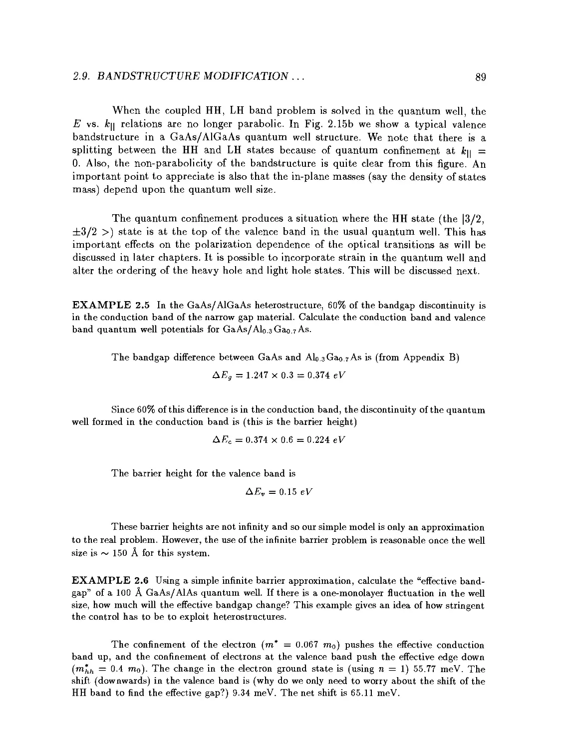
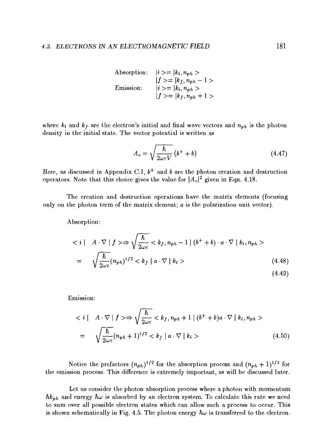
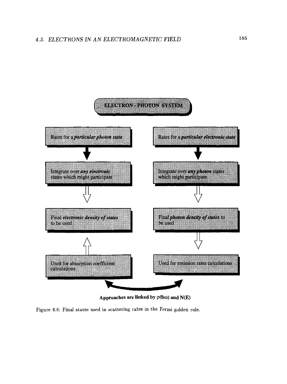
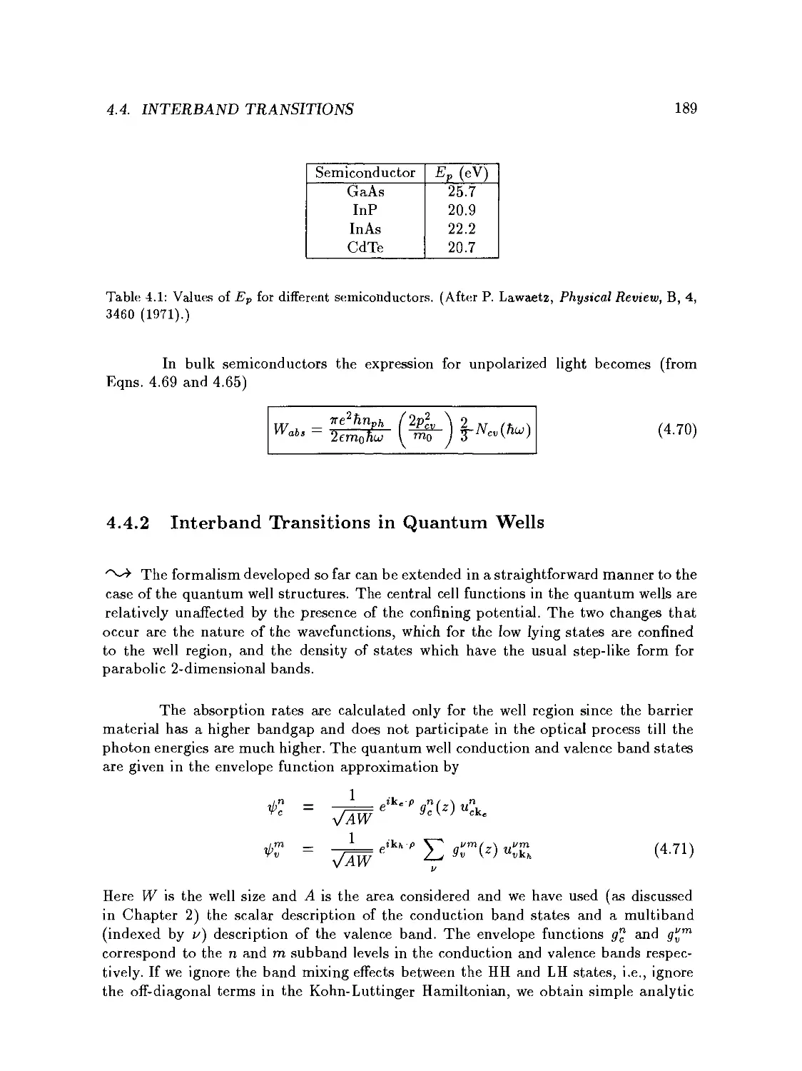
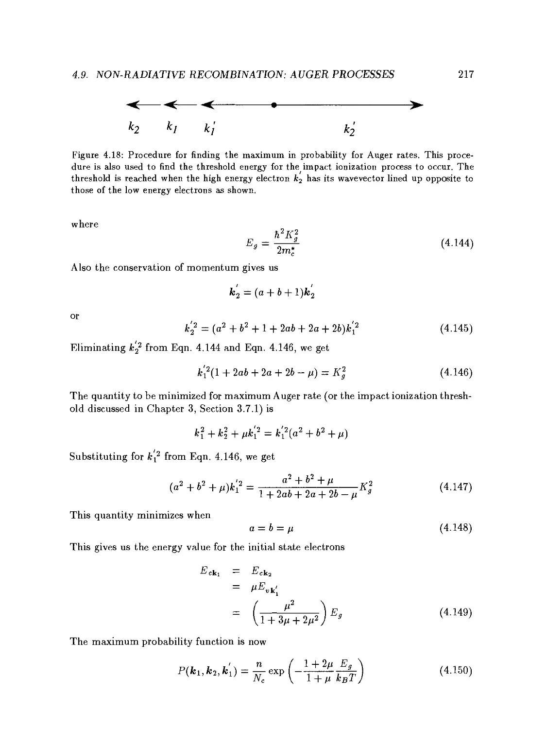
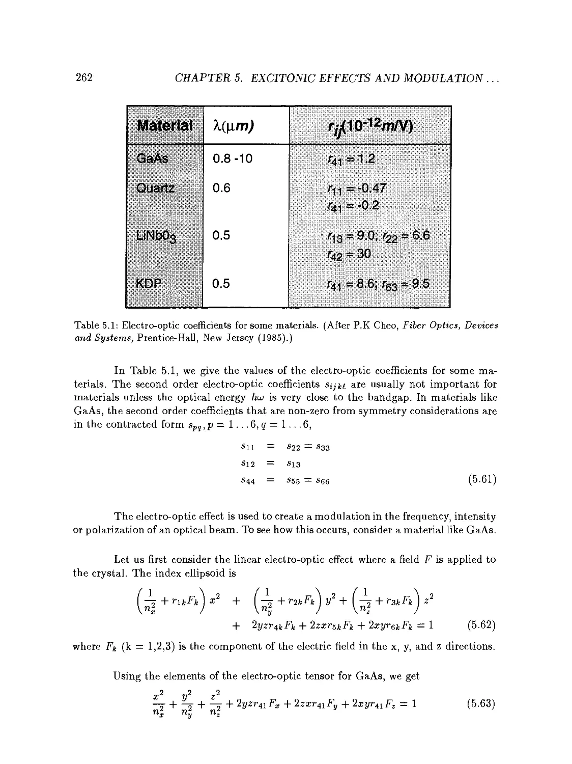
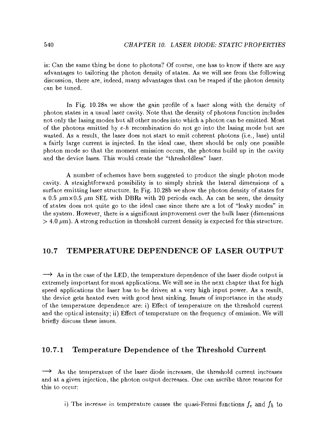
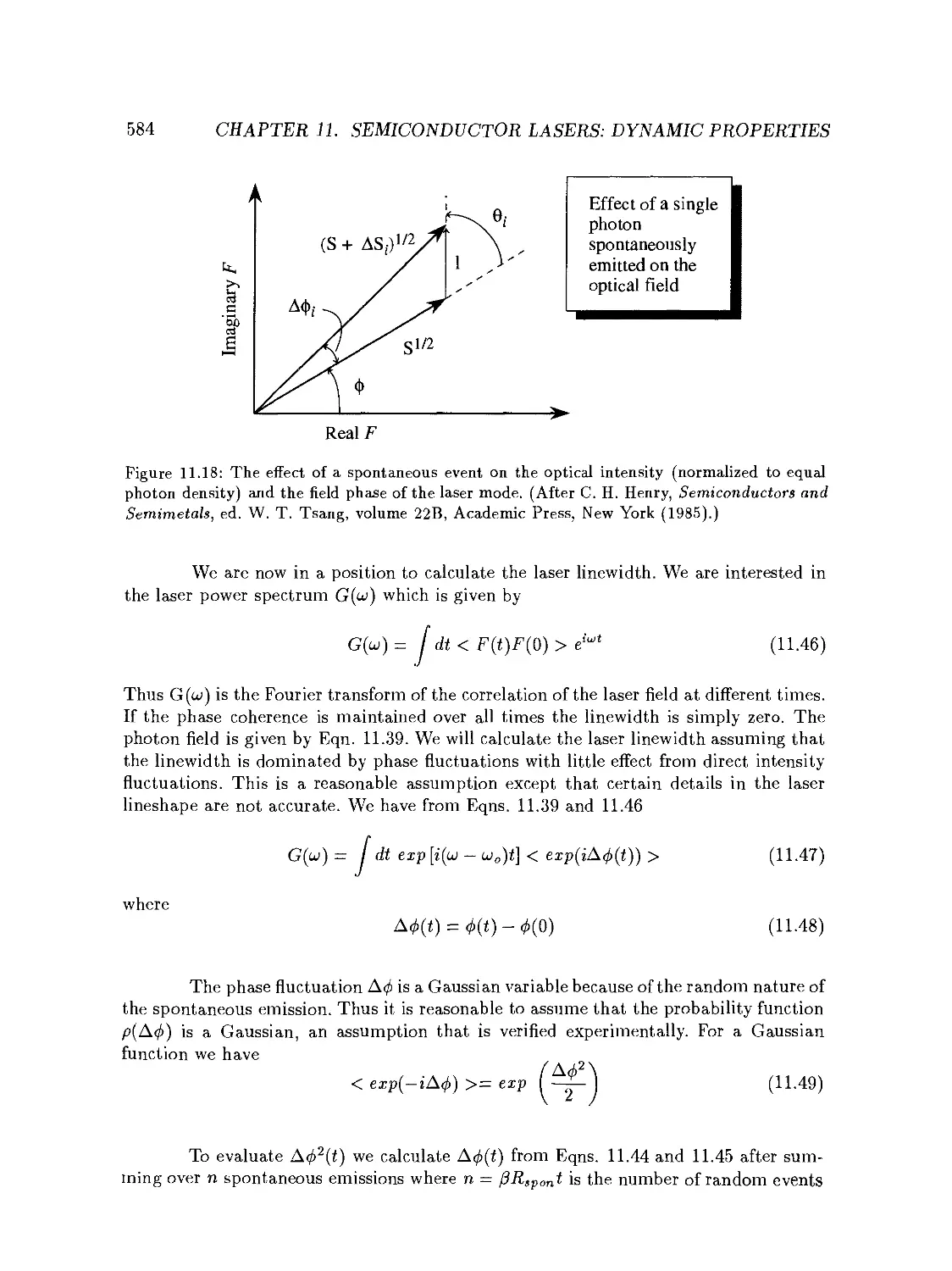
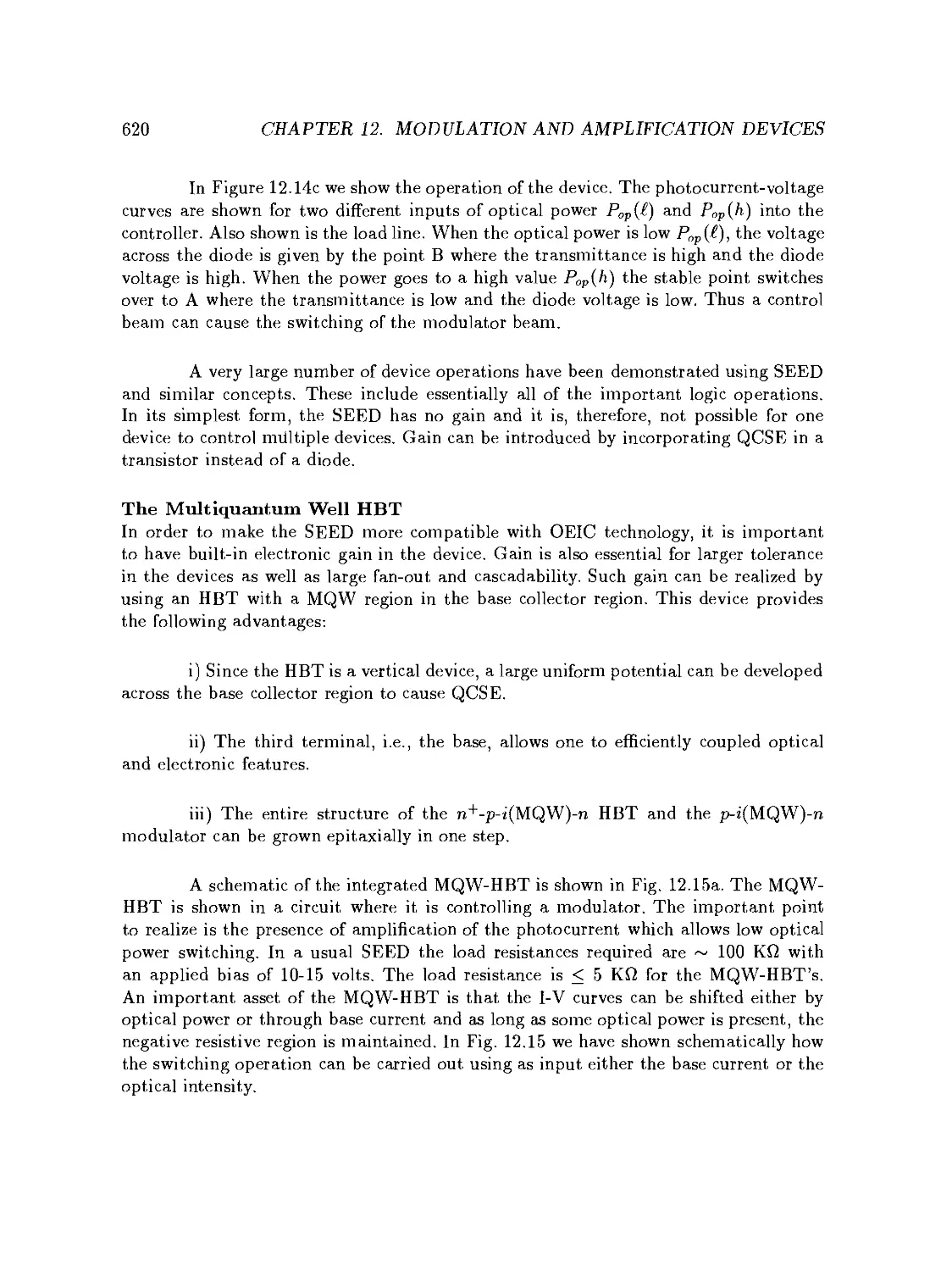
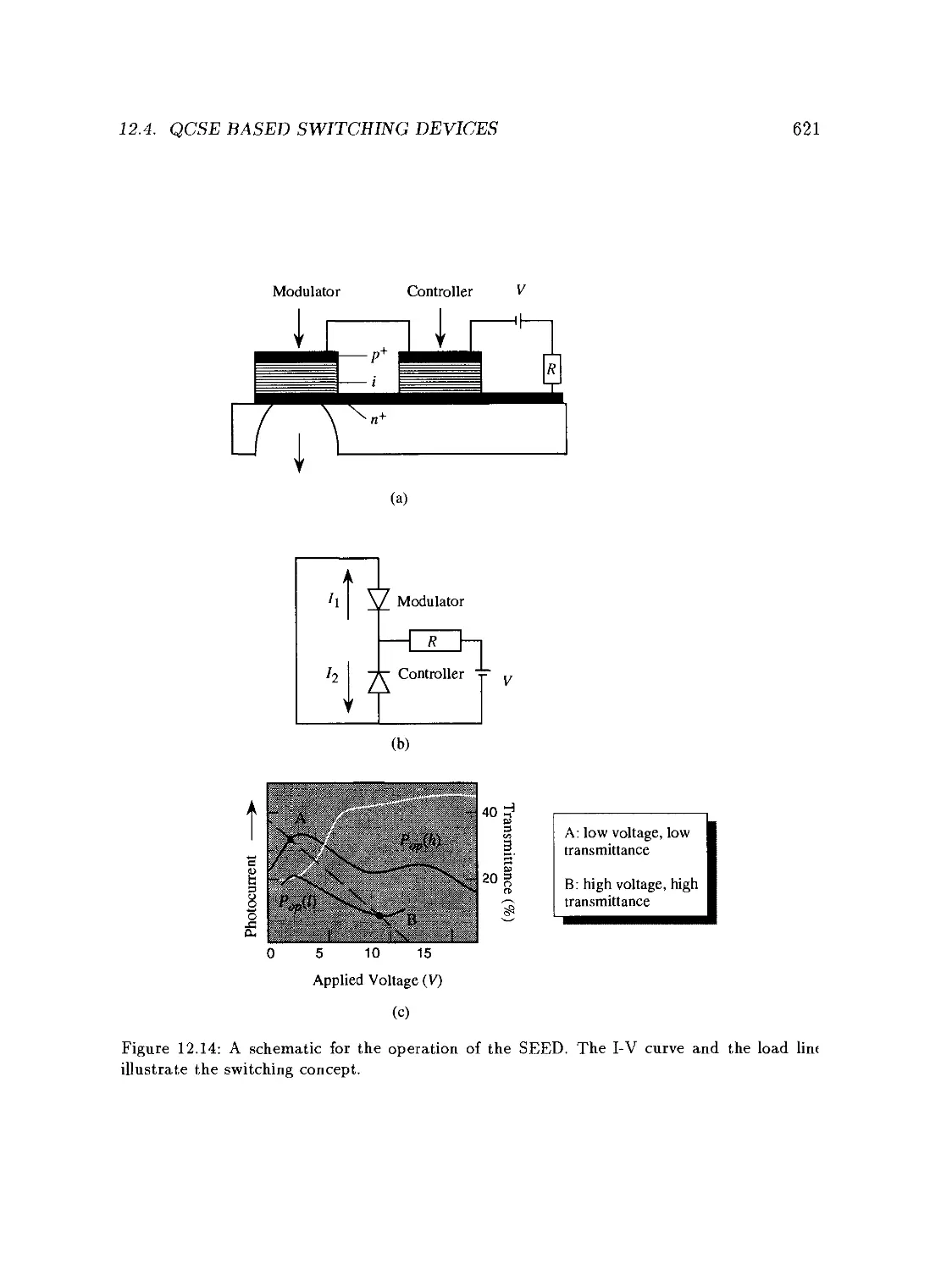
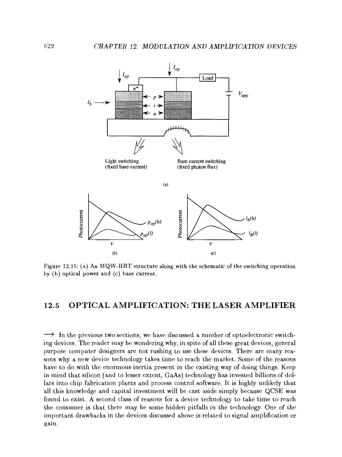
/


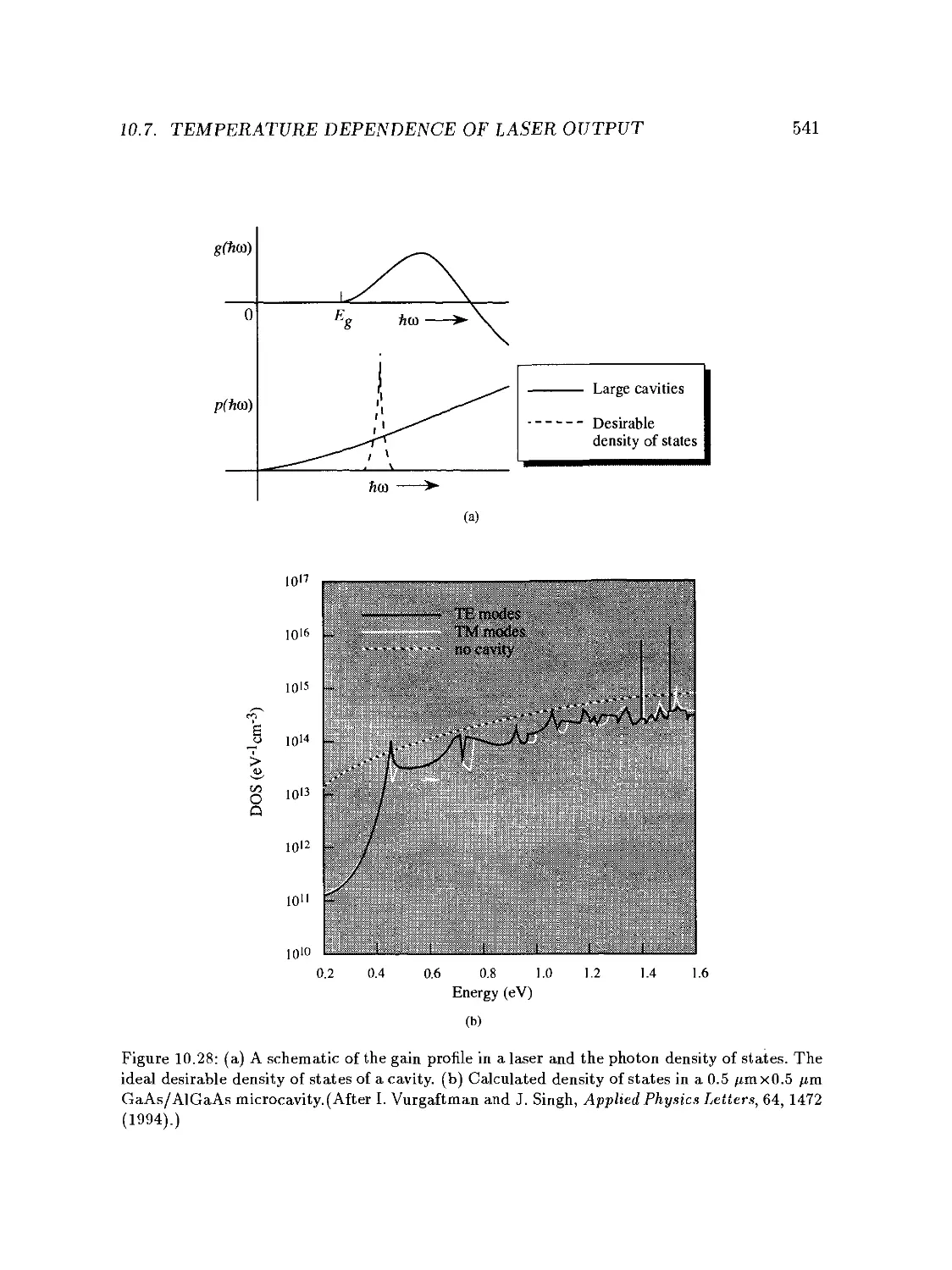


Text
SEMICONDUCTOR OPTOELECTRONICS
Physics and Technology
McGraw-Hill Series in Electrical and Computing Engineering
Senior Consulting Editor
Stephen W. Director, Carnegie Mellon University
Circuits and Systems
Communications and Signal Processing
Computer Engineering
Control Theory
Electromagnetics
Electronics and VLSI Circuits
Introductory
Power and Energy
Radar and Antennas
Previous Consulting Editors
Ronald N. Bracewell, Colin Cherry, James F. Gibbons, Willis W. Harman,
Hubert Heffner, Edward W. Herold, John G. Linvill, Simon Ramo,
Ronald A. Rohrer, Anthony E. Siegman, Charles Susskind,
Frederick E. Tennan, John G. Truxal, Ernst Weber, and John R. Whinnery
Electronics and VLSI Circuits
Senior Consulting Editor
Stephen W. Director, Carnegie Mellon University
Consulting Editor
Richard C. Jaeger, Auburn University
Colclaser and Diehl-Nagle: Materials and Devices for Electrical Engineers and Physicists
DeMicheli: Synthesis and Optimization of Digital Circuits
Elliott: Microlithography: Process Technology for IC Fabrication
Fabricius: Introduction to VLSI Design
Ferendeci: Physical Foundations of Solid State and Electron Devices
Fonstad: Microelectronic Devices and Circuits
Franco: Design with Operational Amplifiers and Analog Integrated Circuits
Geiger, Allen, and Strader: VLSI Design Techniques for Analog and Digital Circuits
Grinich and Jackson: Introduction to Integrated Circuits
Hodges and Jackson: Analysis and Design of Digital Integrated Circuits
Huelsman: Active and Passive Analog Filter Design: An Introduction
Ismail and Fiez: Analog VLSI: Signal and Information Processing
Laker and Sansen: Design of Analog Integrated Circuits and Systems
Long and Butner: Gallium Arsenide Digital Integrated Circuit Design
Millman and Grabel: Microelectronics
Millman and Halkias: Integrated Electronics: Analog, Digital Circuits, and Systems
Millman and Taub: Pulse, Digital, and Switching Waveforms
\g: Complete Guide to Semiconductor Devices
Offen: VLSI Image Processing
Roulston: Bipolar Semiconductor Devices
Ruska: Microelectronic Processing: An Introduction to the Manufacture of Integrated Circui
Schilling and Belove: Electronic Circuits: Discrete and Integrated
Seraphim: Principles of Electronic Packaging
Singh: Physics of Semiconductors and Their Heterostructures
Singh: Semiconductor Devices: An Introduction
Singh: Semiconductor Optoelectronics: Physics and Technology
Smith: Modern Communication Circuits
Sze: VLSI Technology
Taub: Digital Circuits and Microprocessors
Taub and Schilling: Digital Integrated Electronics
Tsividis: Operation and Modeling of the MOS Transistor
Wait, Huelsman, and Korn: Introduction to Operational and Amplifier Theory Applications
Yang: Microelectronic Devices
Zambuto: Semiconductor Devices
Also available from McGraw-Hill
Schaum's Outline Series in Electronics & Engineering
Most outlines include basic theory, definitions and hundreds of example problems solved
in step-by-step detail, and supplementary problems with answers.
Related titles on the current list include:
Analog & Digital Communications
Basic Circuit Analysis
Basic Electrical Engineering
Basic Electricity
Basic Mathematics for Electricity & Electronics
Digital Principles
Electric Circuits
Electric Machines & Electromechanics
Electric Power Systems
Schaum's Solved Problems Books
Each title in this series is a complete and expert source of solved problems with solutions
worked out in step-by-step detail.
Related titles on the current list include:
3000 Solved Problems in Calculus 2000 Solved Problems in Electronics
2500 Solved Problems in Differential Equations 3000 Solved Problems in Linear Algebra
3000 Solved Problems in Electric Circuits 2000 Solved Problems in Numerical Analysis
2000 Solved Problems in Electromagnetics 3000 Solved Problems in Physics
Available at most college bookstores, or for a complete list of titles and prices, write to:
Schaum Division
McGraw-Hill, Inc.
1221 Avenue of the Americas
New York, NY 10020
Electromagnetics
Electronic Circuits
Electronic Communication
Electronic Devices & Circuits
Electronic Technology
Feedback & Control Systems
Introduction to Digital Systems
Microprocessor Fundamentals
SEMICONDUCTOR
OPTOELECTRONICS
Physics and Technology
Jasprit Singh
University of Michigan
McGraw-Hill, Inc.
New York St. Louis San Francisco Auckland Bogoti Caracas
Lisbon London Madrid Mexico City Milan Montreal New Delhi
San Juan Singapore Sydney Tokyo Toronto
The editor was George T. Hoffman;
the production supervisor was Richard A. Ausburn.
The design manager was Joseph A. Piliero.
The cover was designed by Teresa Singh.
All illustrations were done by Teresa Singh.
R. R. Donnelley & Sons Company was printer and binder.
SEMICONDUCTOR OPTOELECTRONICS
Physics and Technology
Copyright © 1995 by McGraw-Hill, Inc. All rights reserved. Printed in the
United States of America. Except as permitted under the United States Copyright Act
of 1976, no part of this publication may be reproduced or distributed in any form
or by any means, or stored in a data base or retrieval system, without the prior written
permission of the publisher.
®
This book is printed on recycled, acid-free
paper containing 10% postconsumer waste.
1234567890 DOH DOH 90987654
ISBN 0-07-0S7b37-a
Library of Congress Catalog Card Number: 94-78280
About the Author
Jasprit Singh received his
Ph.D. in solid state physics
from the University of
Chicago. He has carried out
research in solid state
electronics at the University
of Southern California,
Wright Patterson Air Force
Base, and the University of
Michigan, Ann Arbor, where
he is currently a professor in
the Department of Electrical
Engineering and Computer
Science. His research
interests cover the area of
semiconductor materials and
their devices for information
processing. He is also the
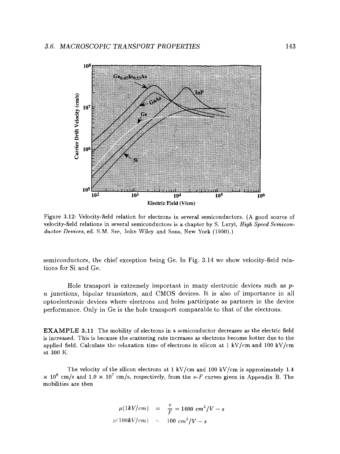
author of "Physics of
Semiconductors and Their
Heterostructures," McGraw-Hill
(1993); and "Semiconductor
Devices, An Introduction,"
McGraw-Hill (1994).
To
Nmala and Nihai
Contents
l
PREFACE xxii
INTRODUCTION xxv
1.1 The information age xxv
1.2 Demands of the information age xxvi
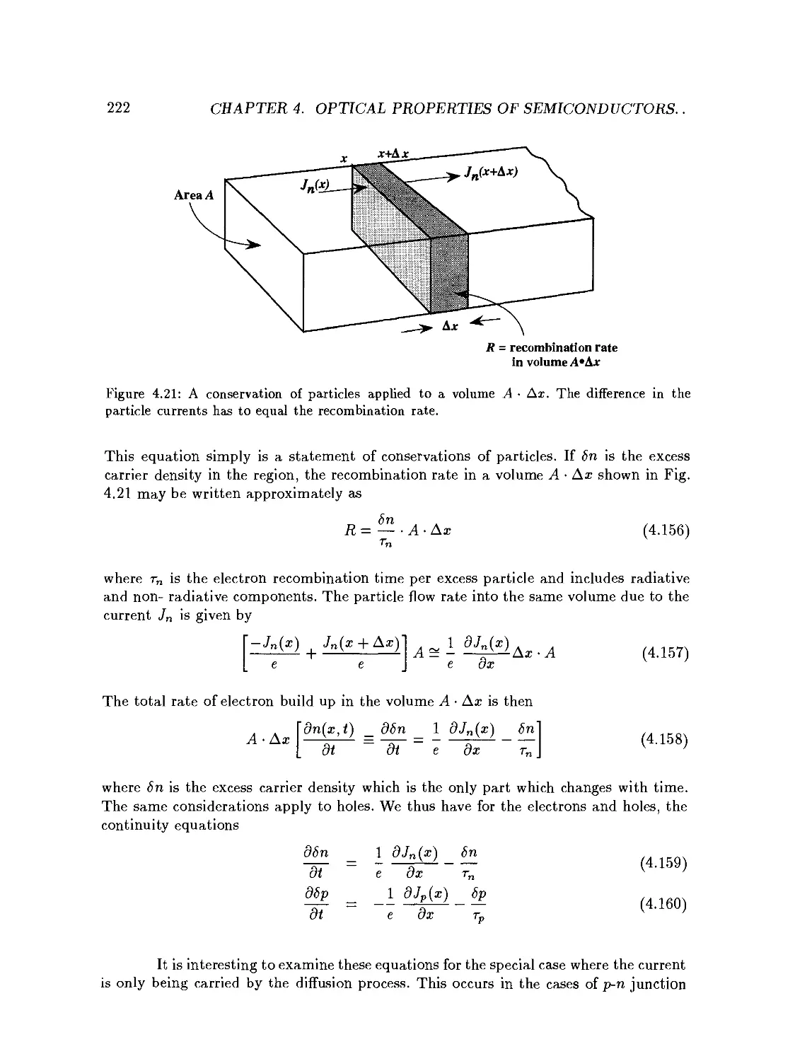
1.3 Demands on active devices xxix
1.4 Electronics and information systems xxiv
15 The promise of optical information processing xxxv
1.6 Role of this book xl
1.7 Guidelines for instructors xii
SEMICONDUCTORS: CRYSTAL STRUCTURE
AND TECHNOLOGY ISSUES l
1.1 Introduction 1
1.2 The complexity of solid state electronics 1
13 Periodicity of a crystal 3
1.4 Basic lattice types 4
1.4.1 The diamond and zinc blende structures 6
1.4.2 Notation to denote planes and points in a lattice: Miller indices 7
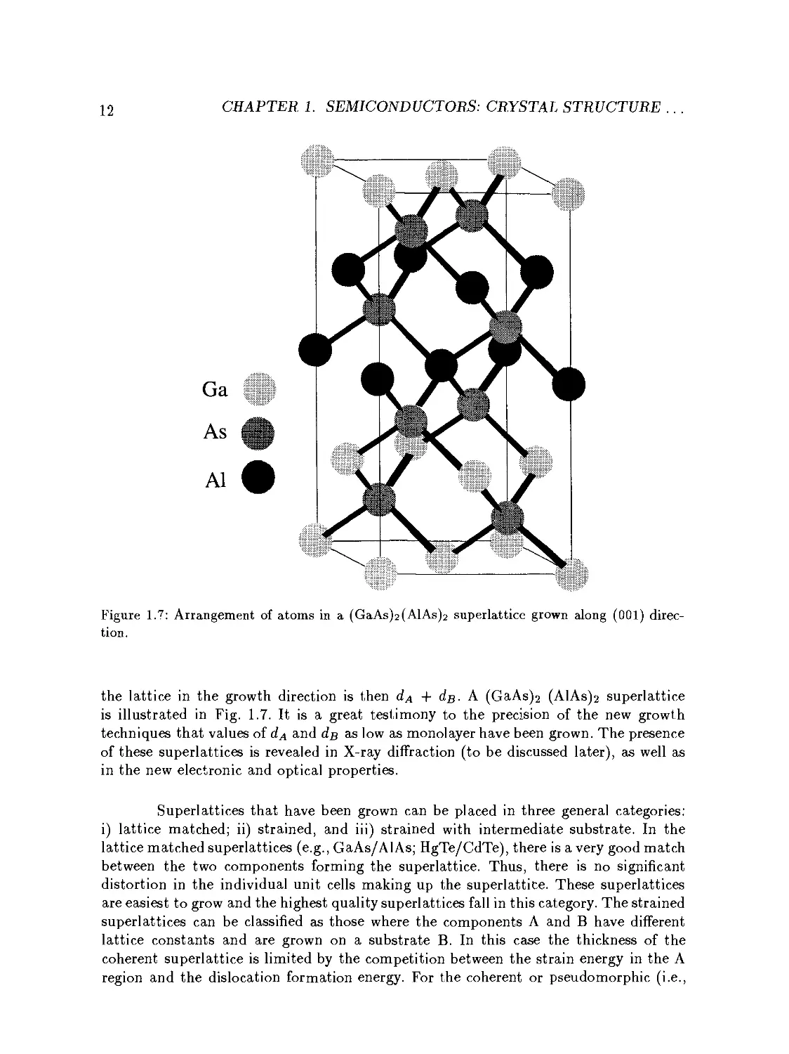
1.5 Artificial structures: superlattices
and quantum wells 11
CONTENTS
.6
.7
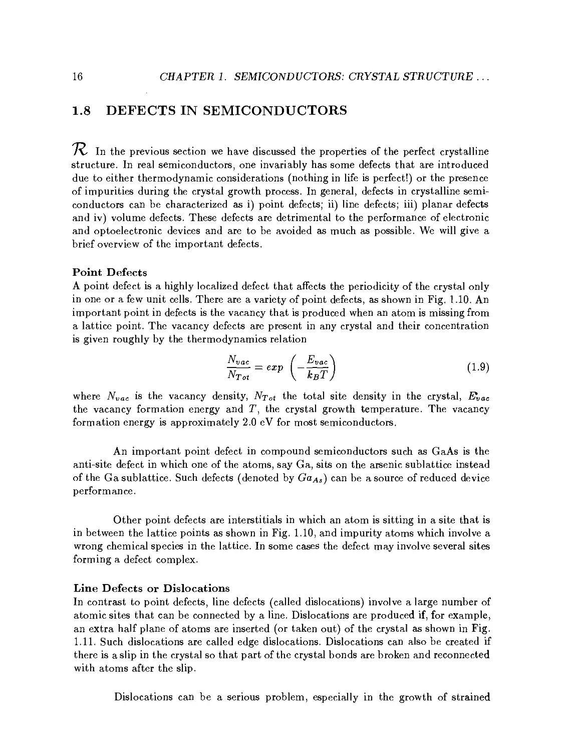
.8
.9
.10
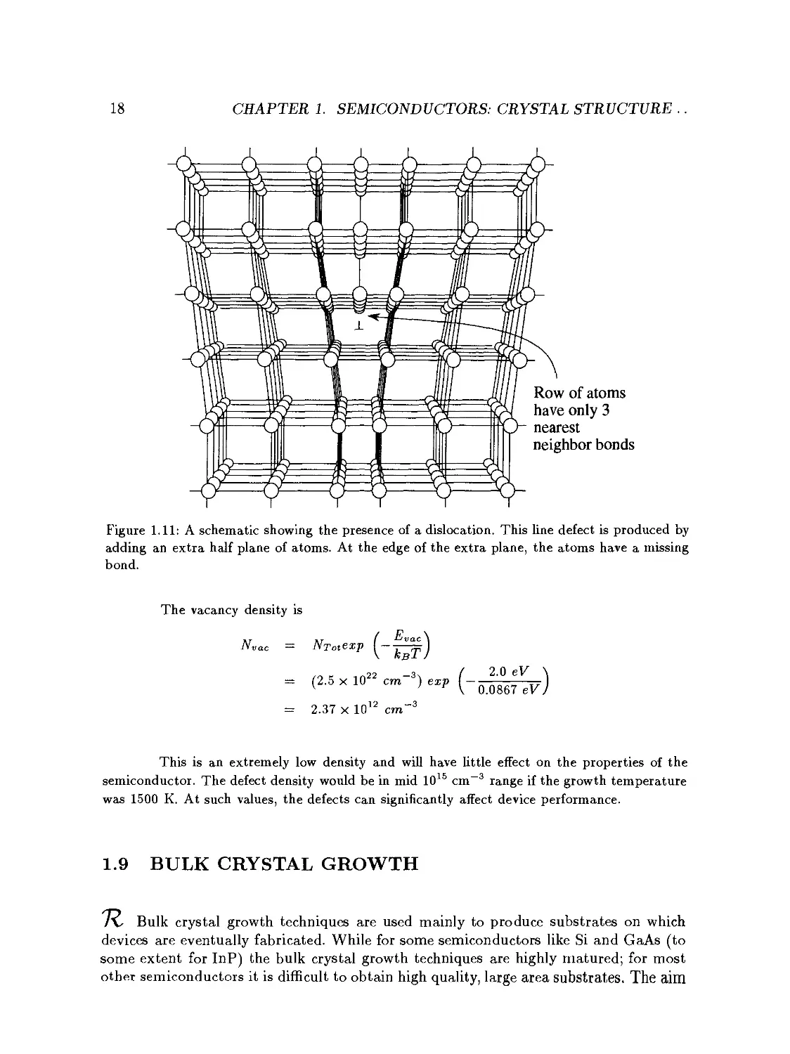
.11
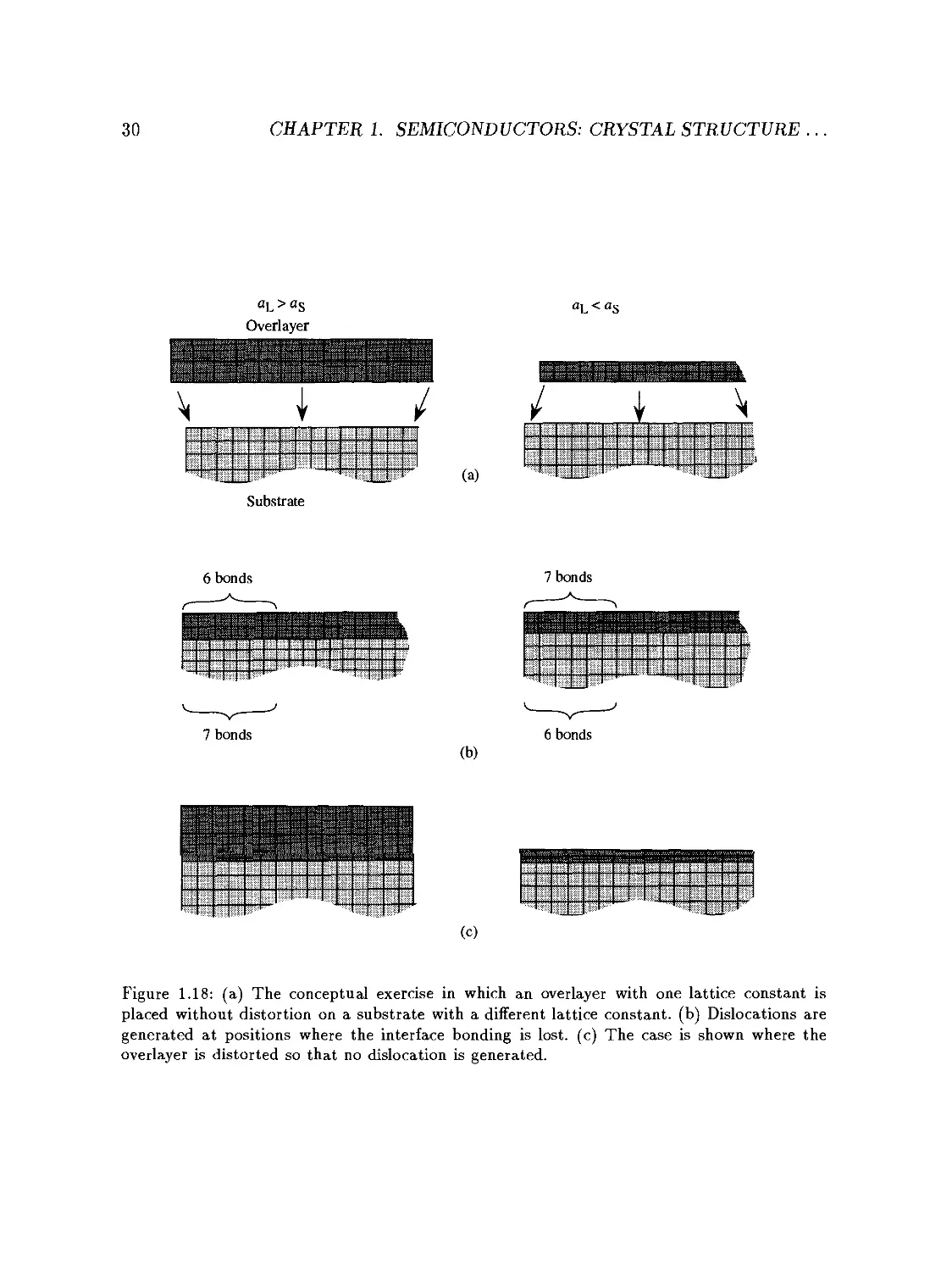
.12
.13
.14
.15
.16
.17
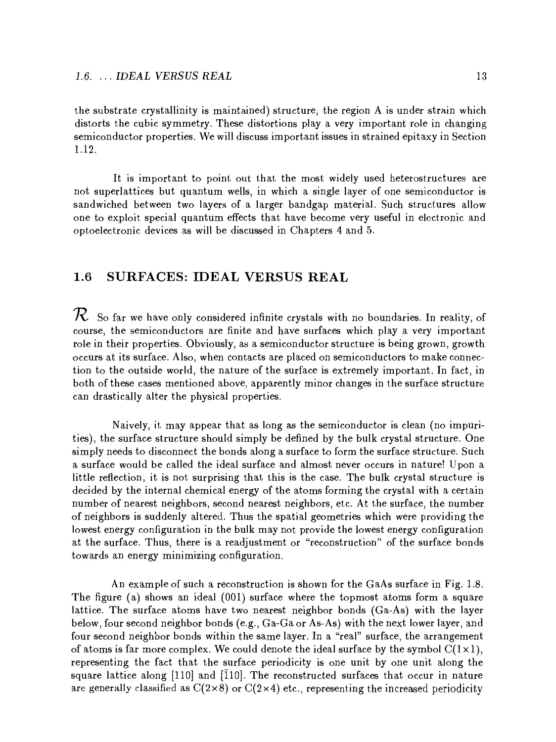
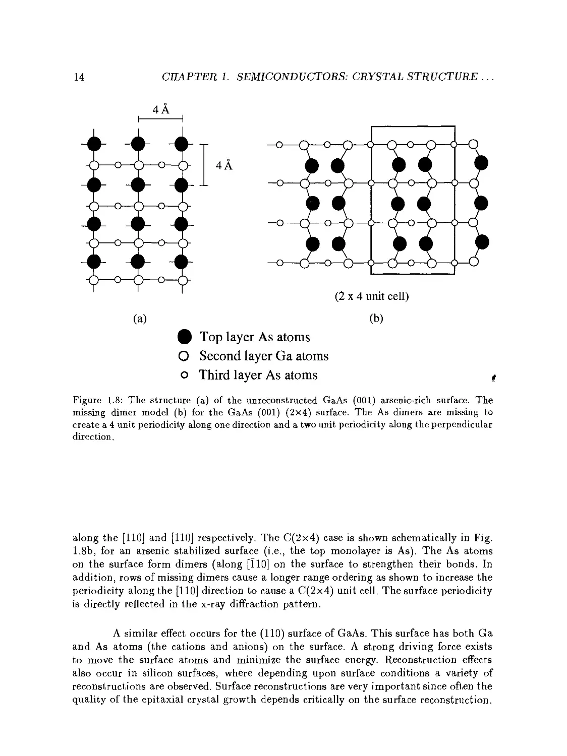
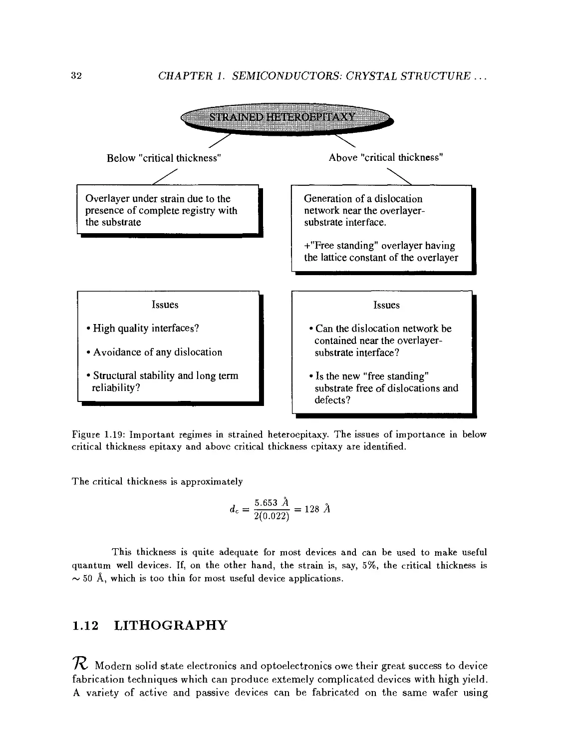
Surfaces: ideal versus real
Interfaces
Defects in semiconductors
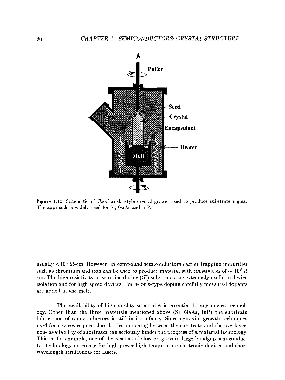
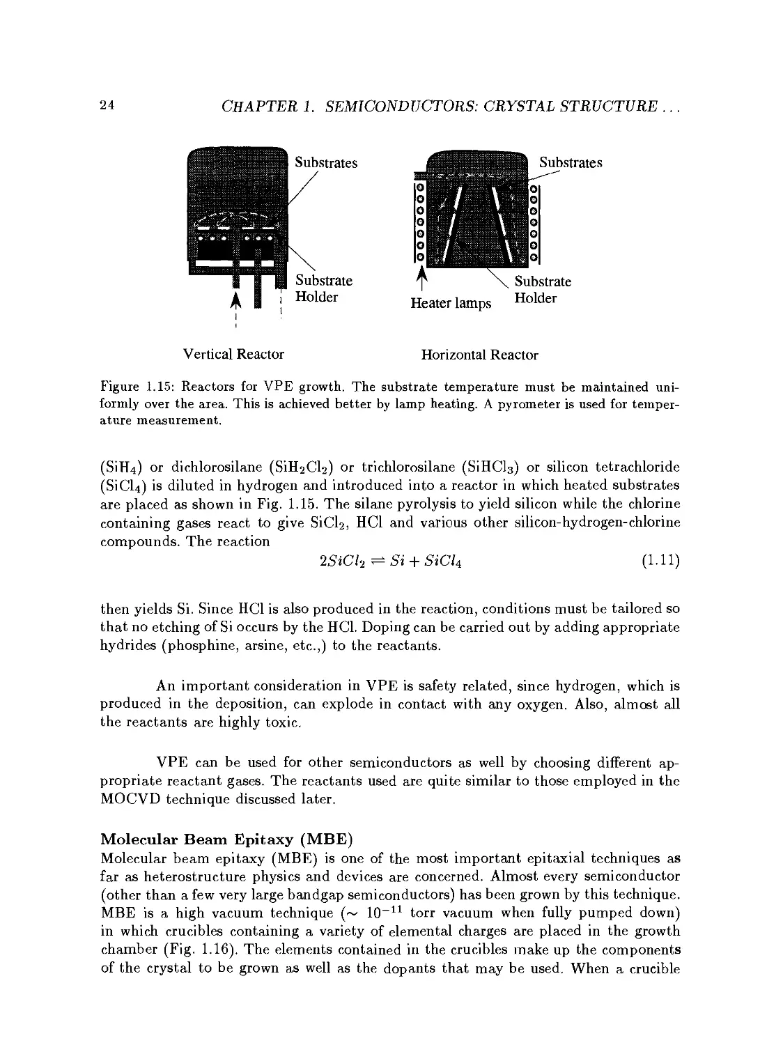
Bulk crystal growth
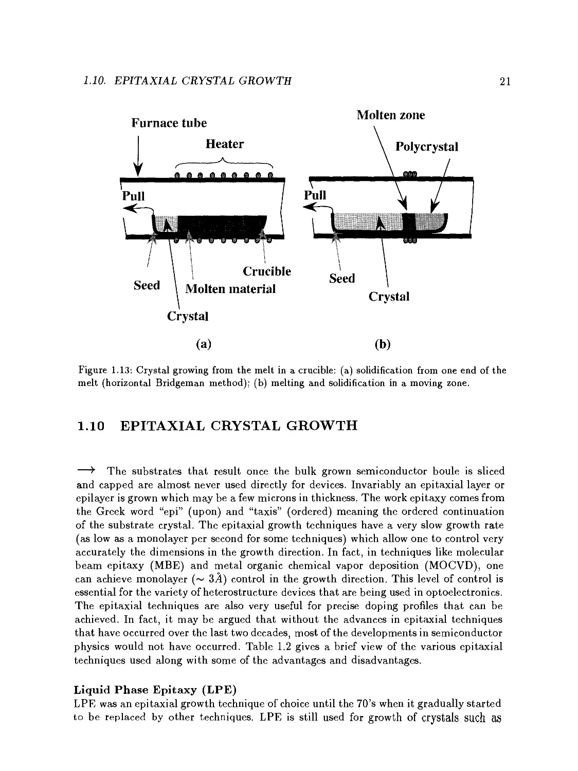
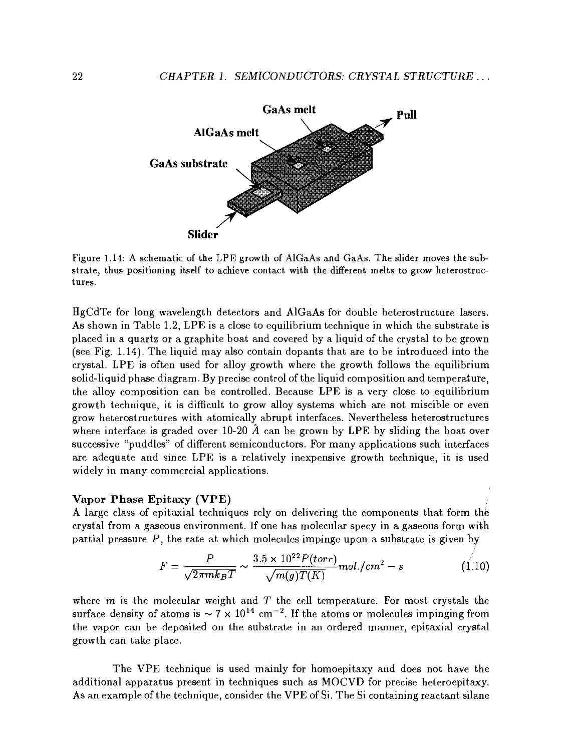
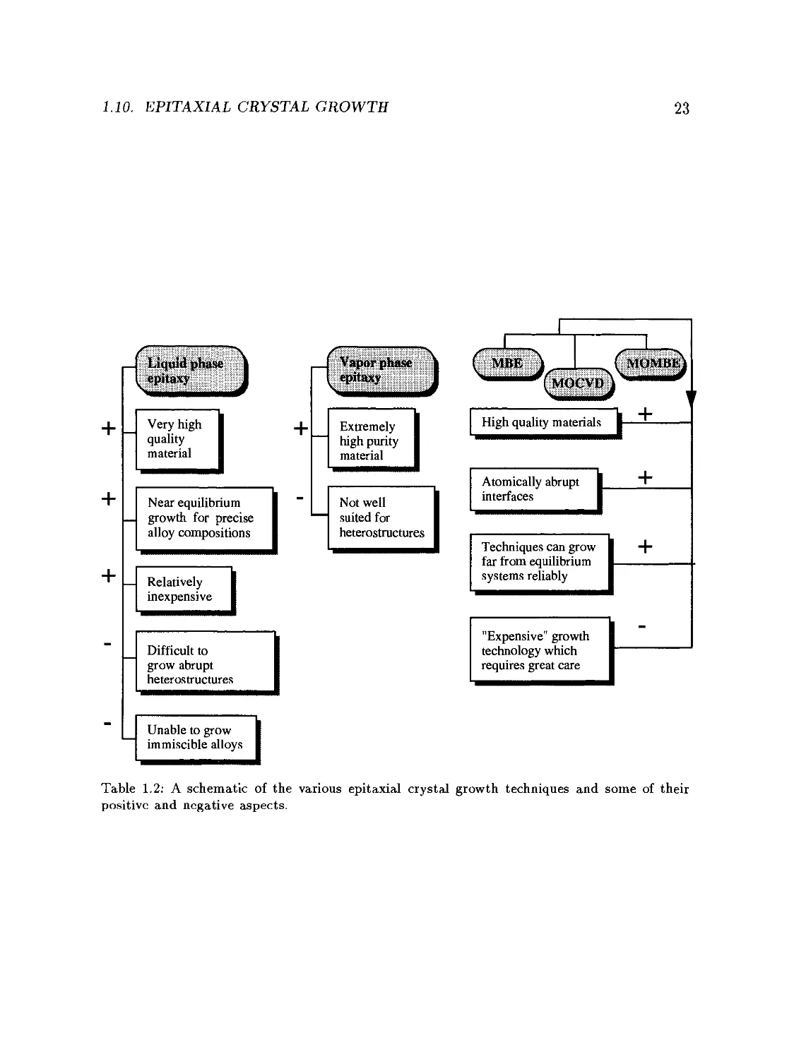
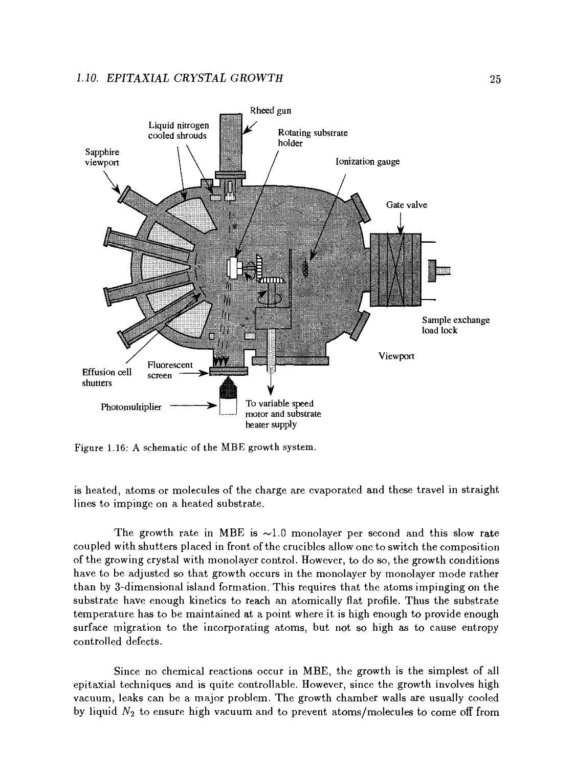
Epitaxial crystal growth
Strained heteroepitaxy
Lithography
1.12.1 Photoresist coating
1.12.2 Mask generation and image transfer
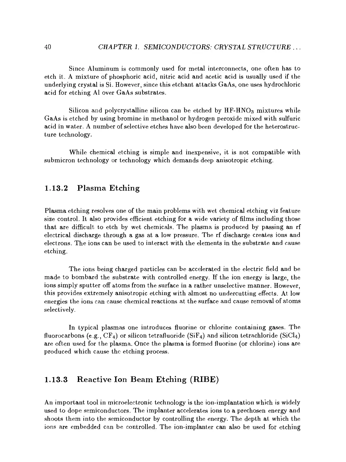
Etching
1.13.1 Wet chemical etching
1.13.2 Plasma etching
1.13-3 Reactive ion beam etching (RIBE)
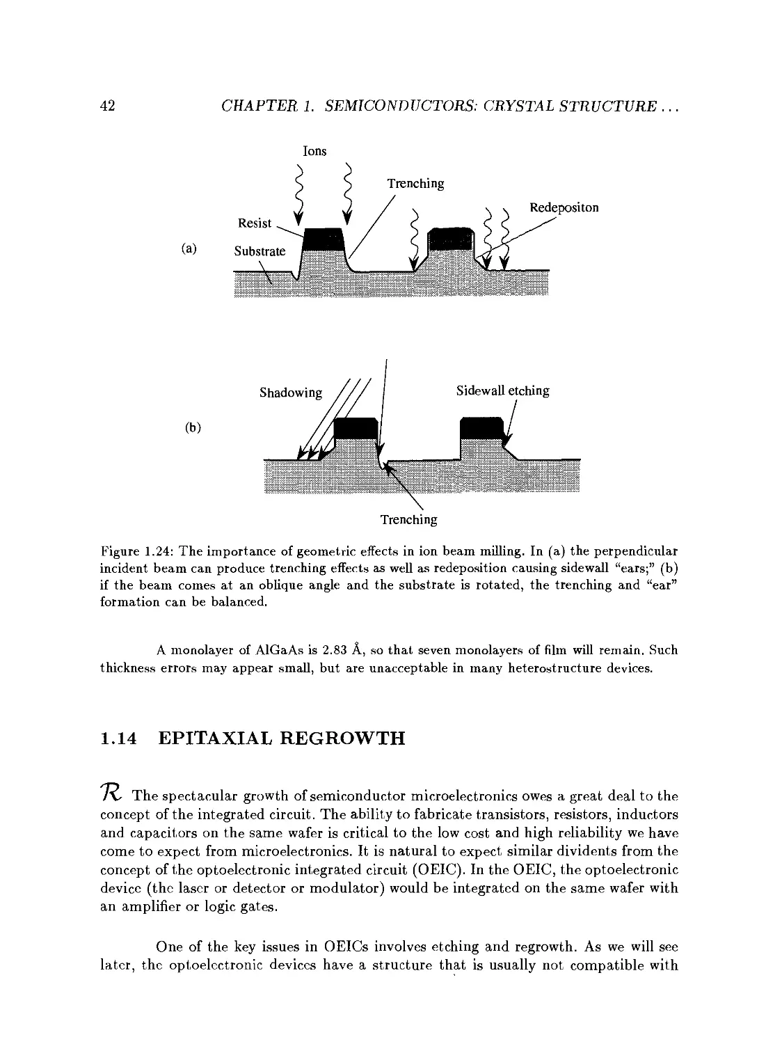
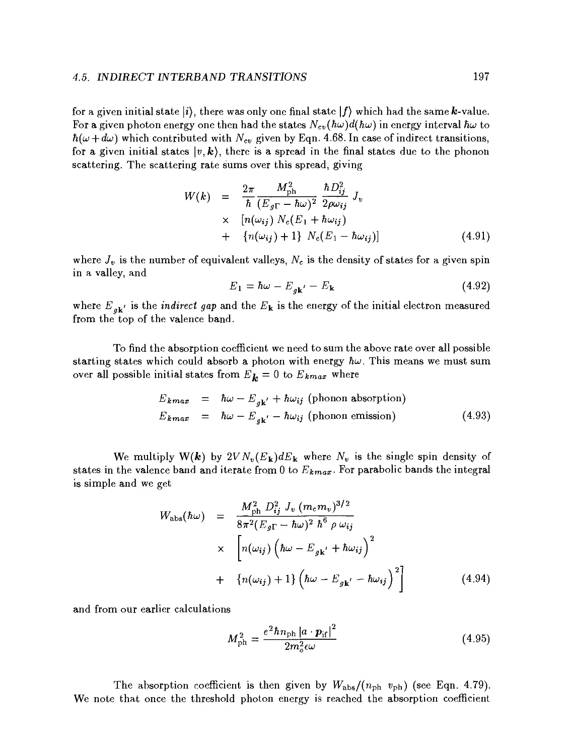
1.13.4 Ion beam milling
Epitaxial regrowth
Chapter summary
Problems
References
13
15
16
18
21
28
32
34
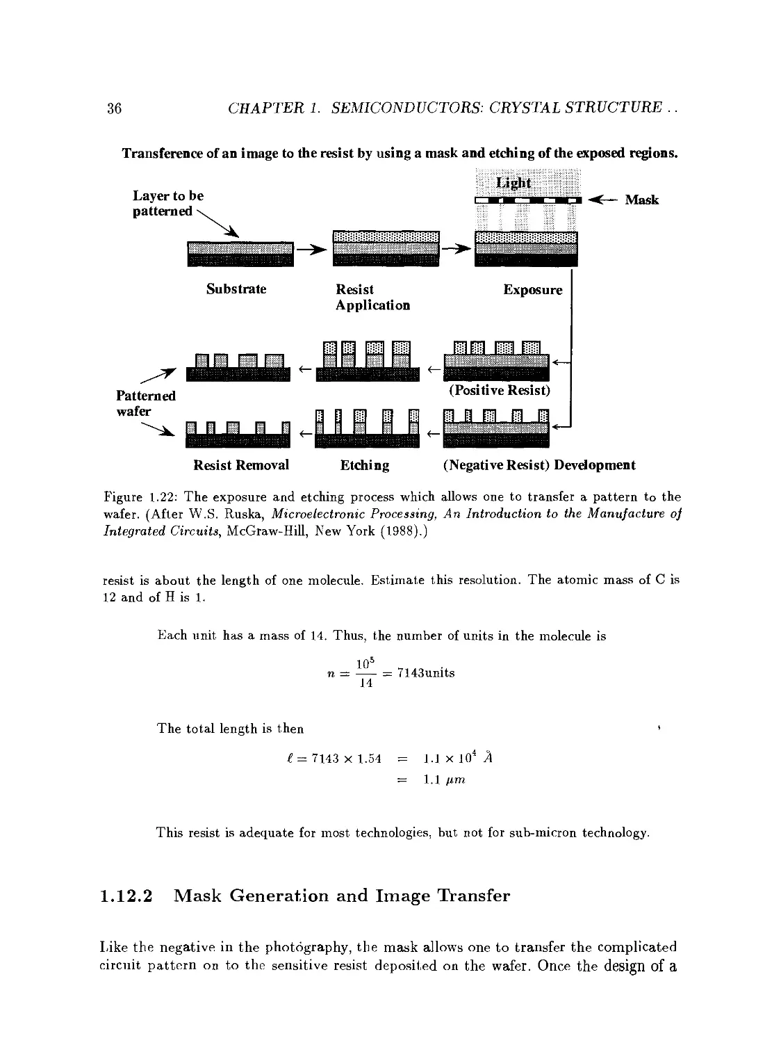
36
38
38
40
40
41
42
45
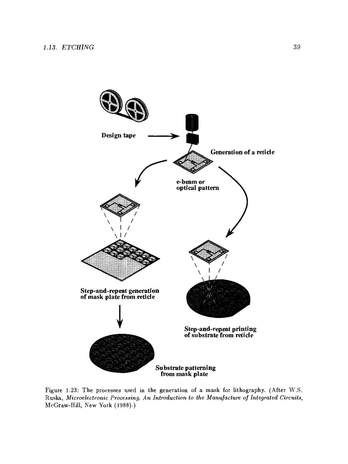
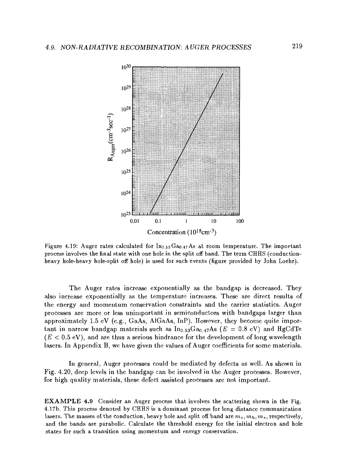
47
50
PROPERTIES OF SEMICONDUCTORS:
ELECTRONIC STATES 53
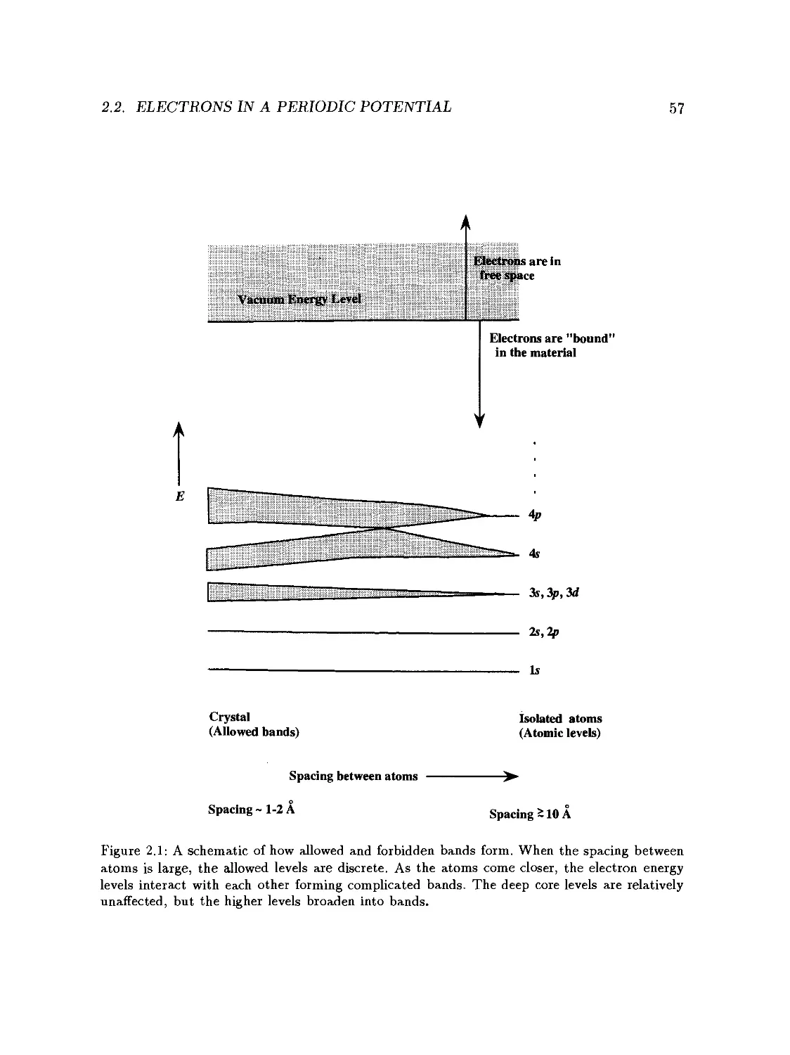
2.1 Introduction 53
2.2 Electrons in a periodic potential: Bloch theorem 53
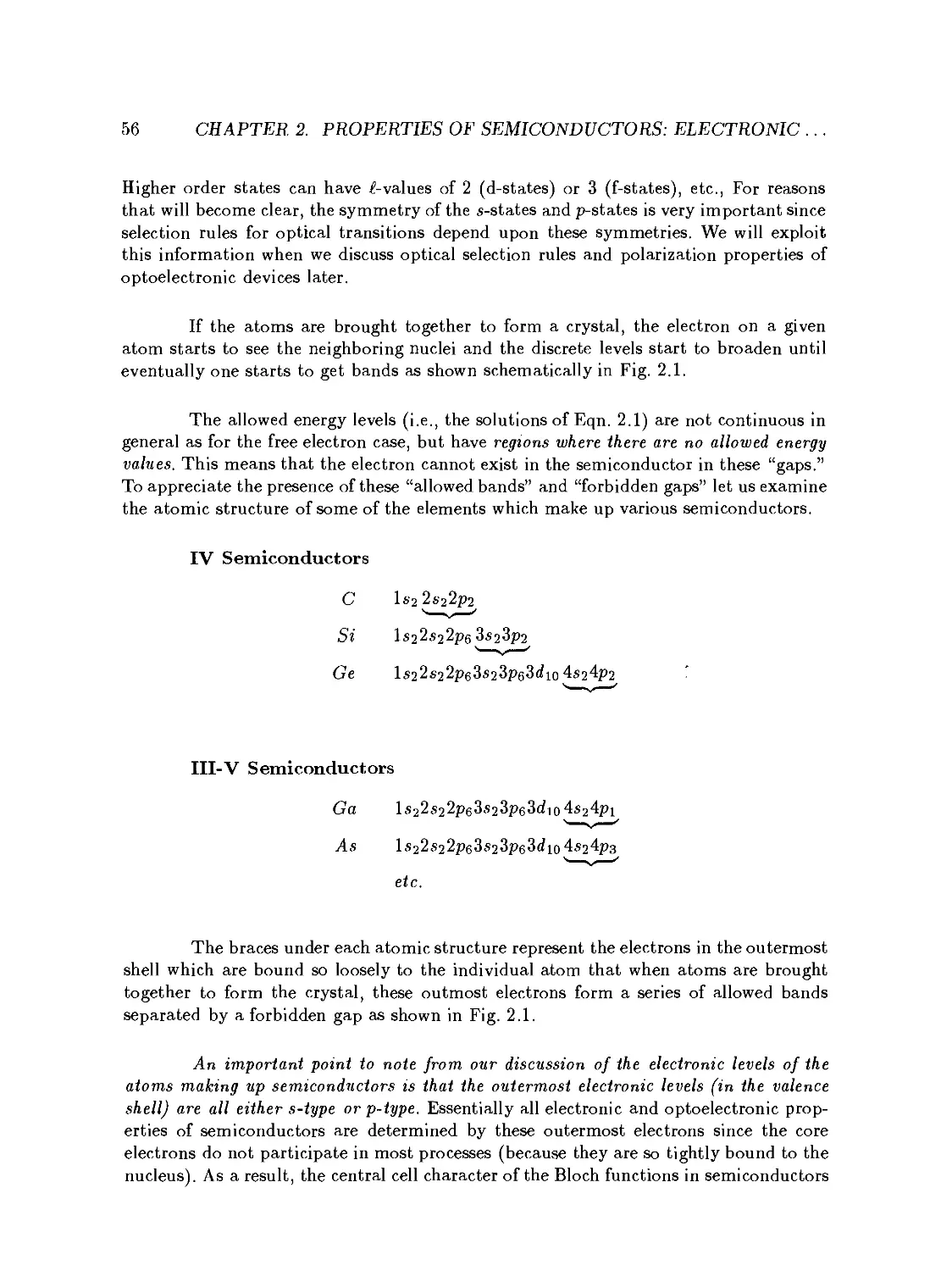
2.2.1 From atomic levels to bands 55
2.2.2 The crystal momentum 59
2.3 Metals, semiconductors and insulators 61
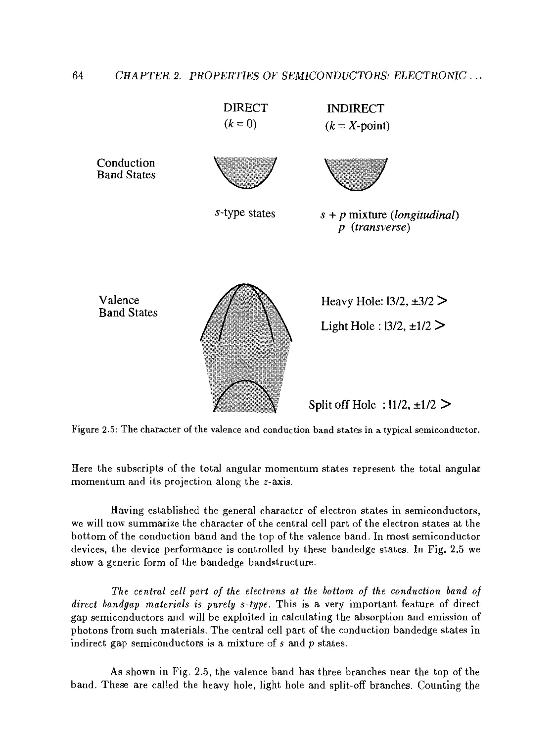
2.4 Properties of conduction and valence bandedge states 63
'ONTENTS
XI
3
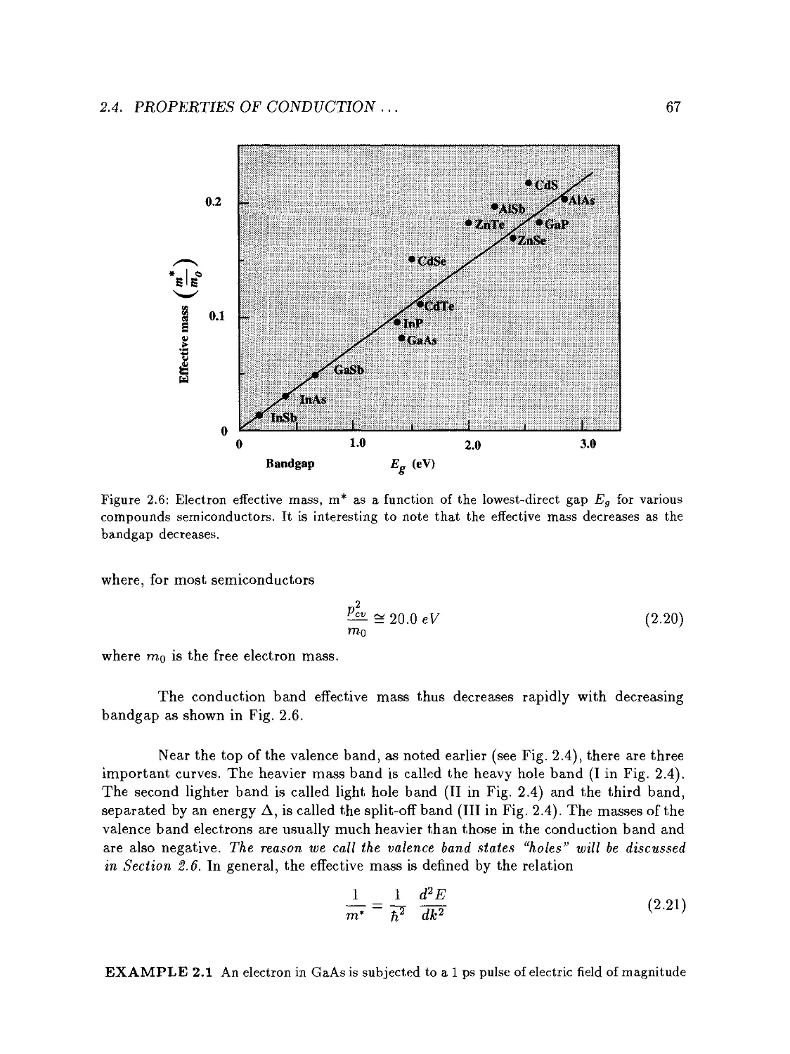
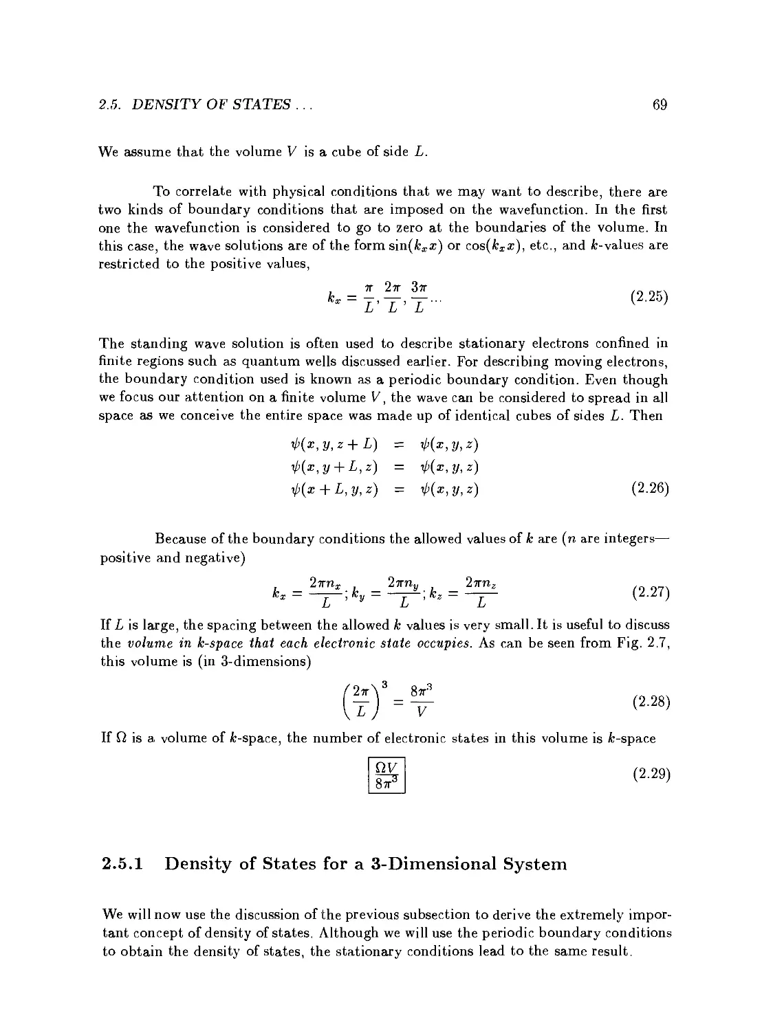
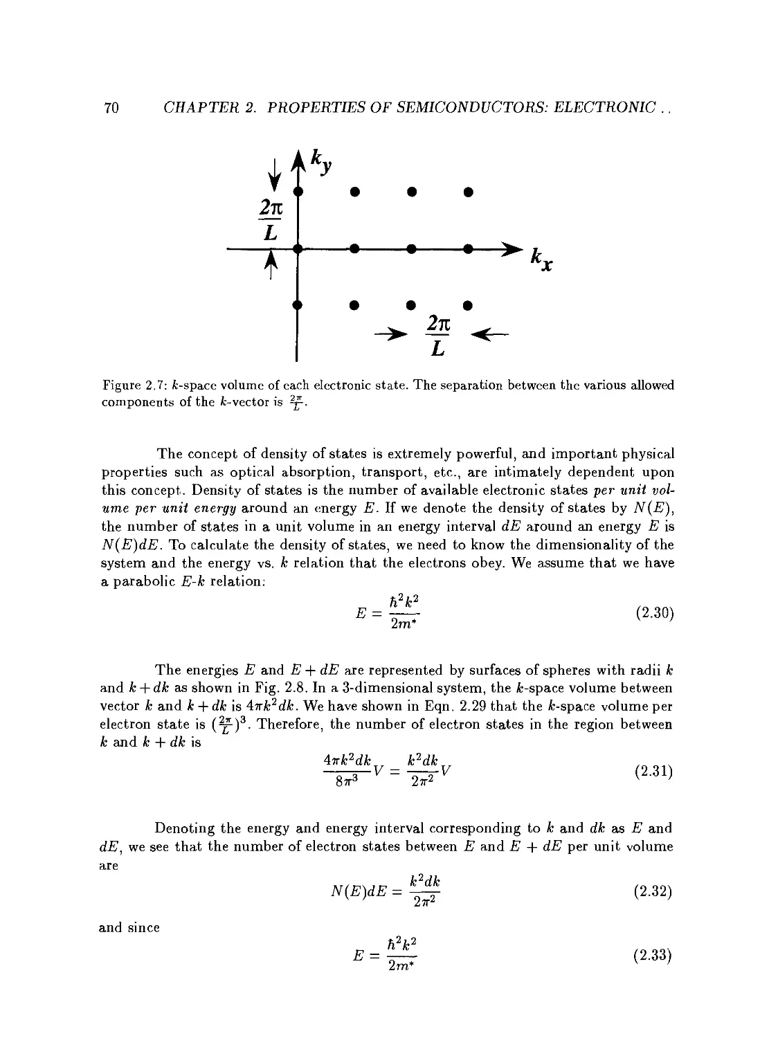
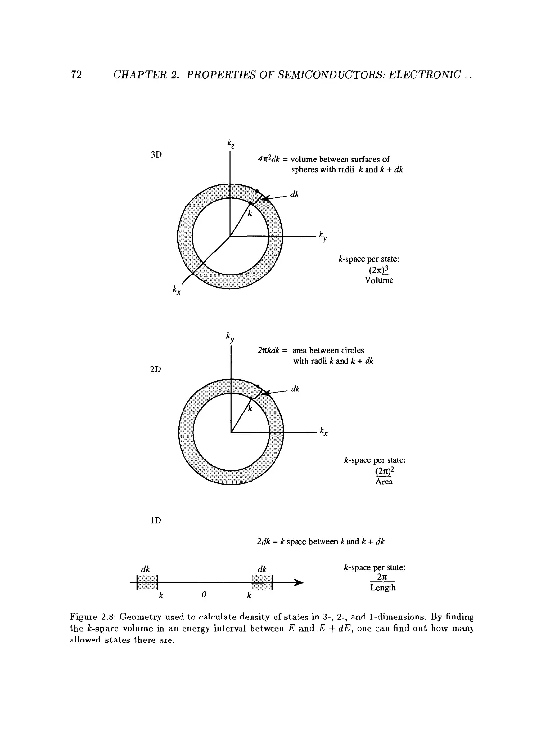
2.5 Density of states 68
2.5.1 Density of states for a 3-dimensional system 69
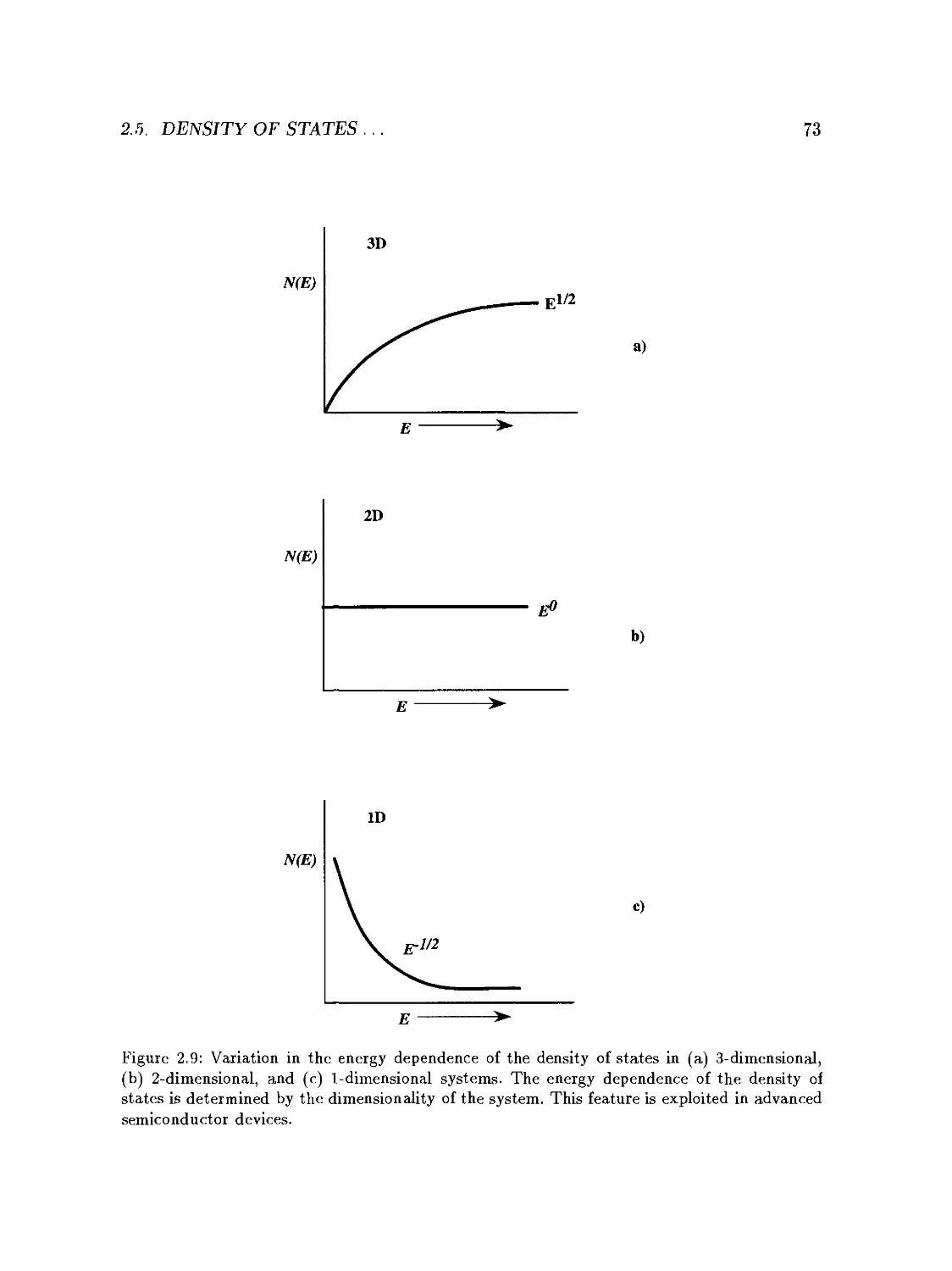
2.5.2 Density of states in sub-3-dimensional systems 71
2.6 Holes in semiconductors 75
2.7 Bandstructure of some semiconductors 77
2.8 Modification of bandstructure by alloying 80
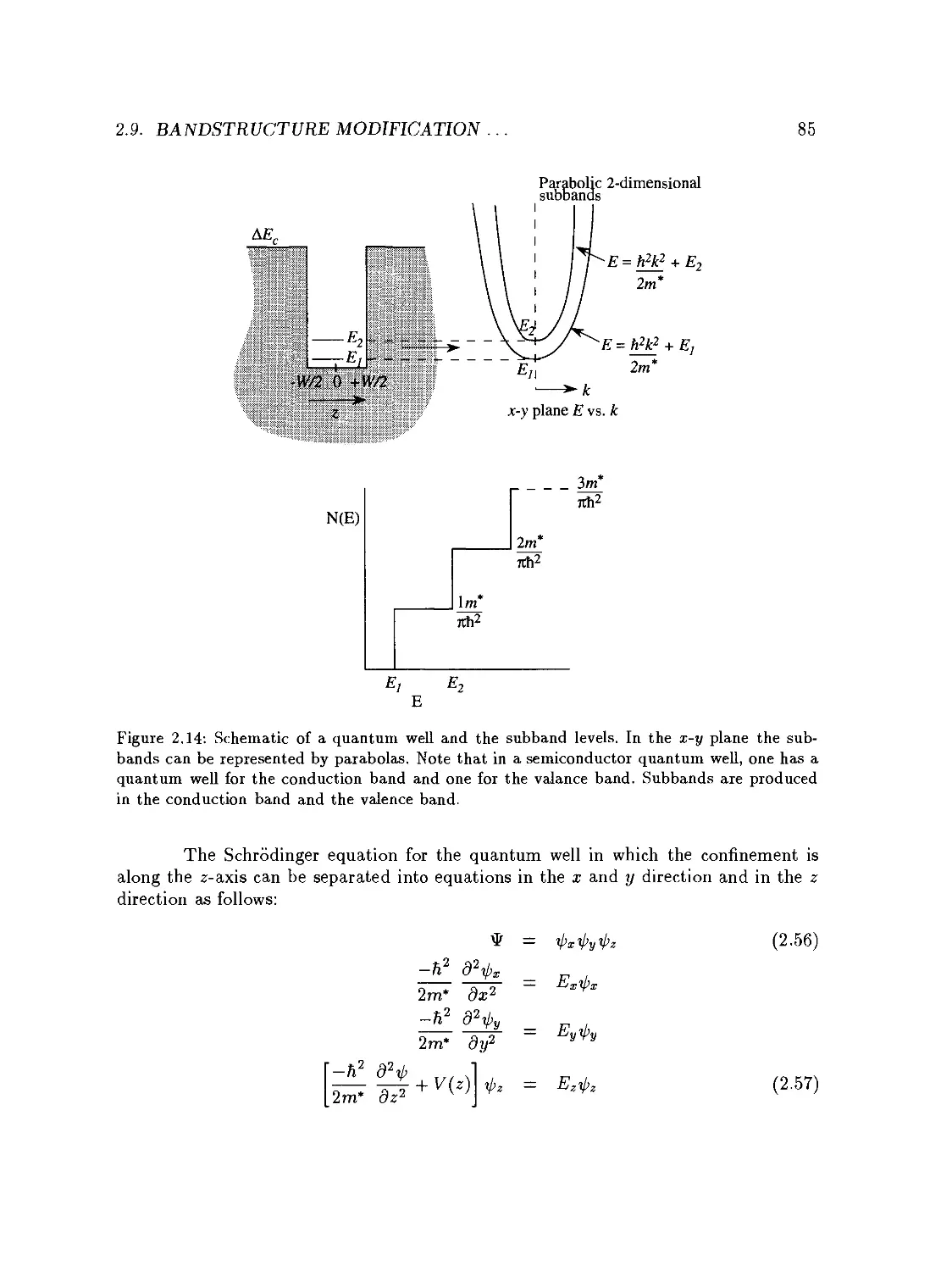
2.9 Bandstructure modification by heterostructures 82
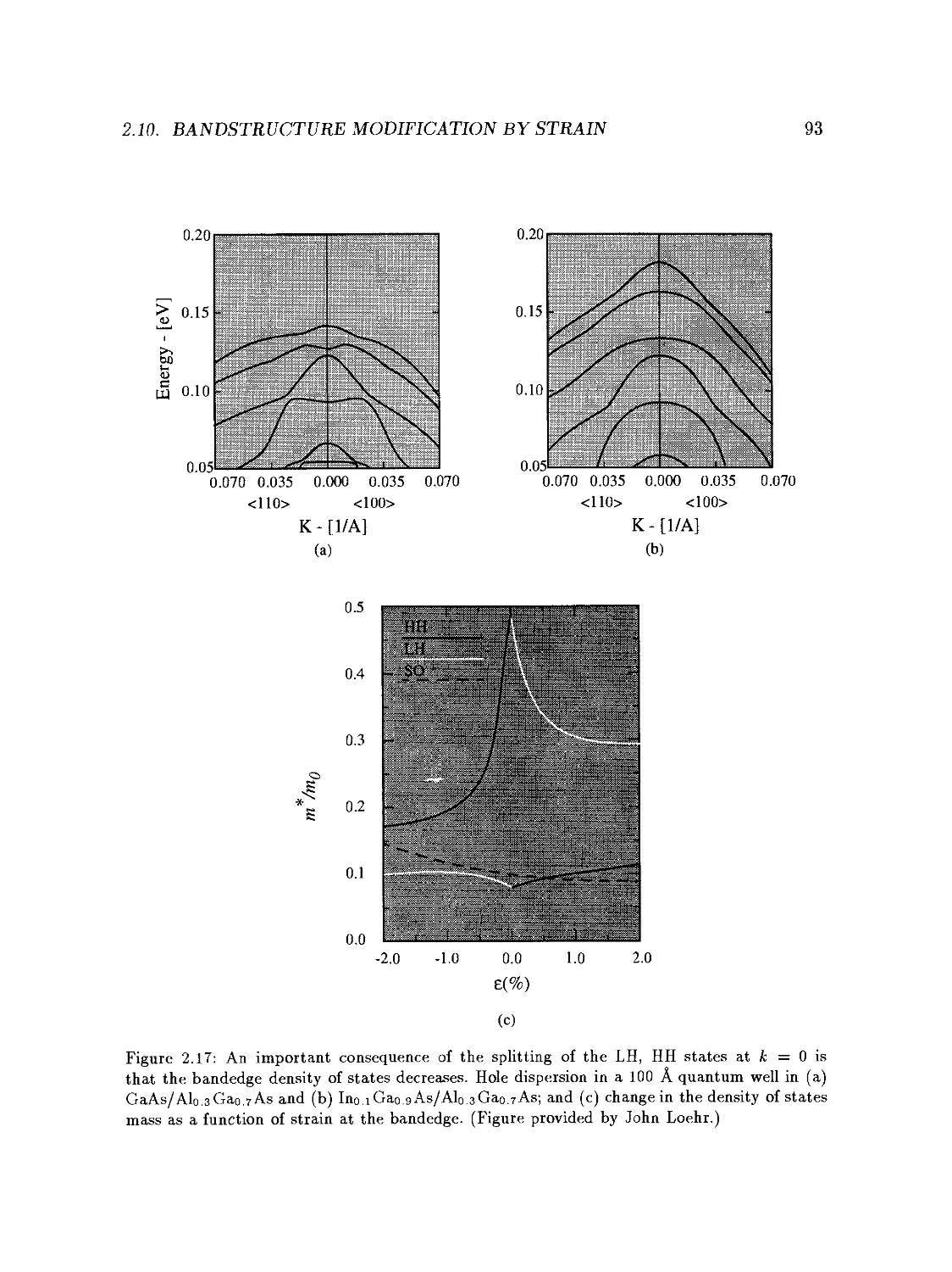
2.10 Bandstructure modification by strain 90
2.11 Intrinsic carrier concentration 95
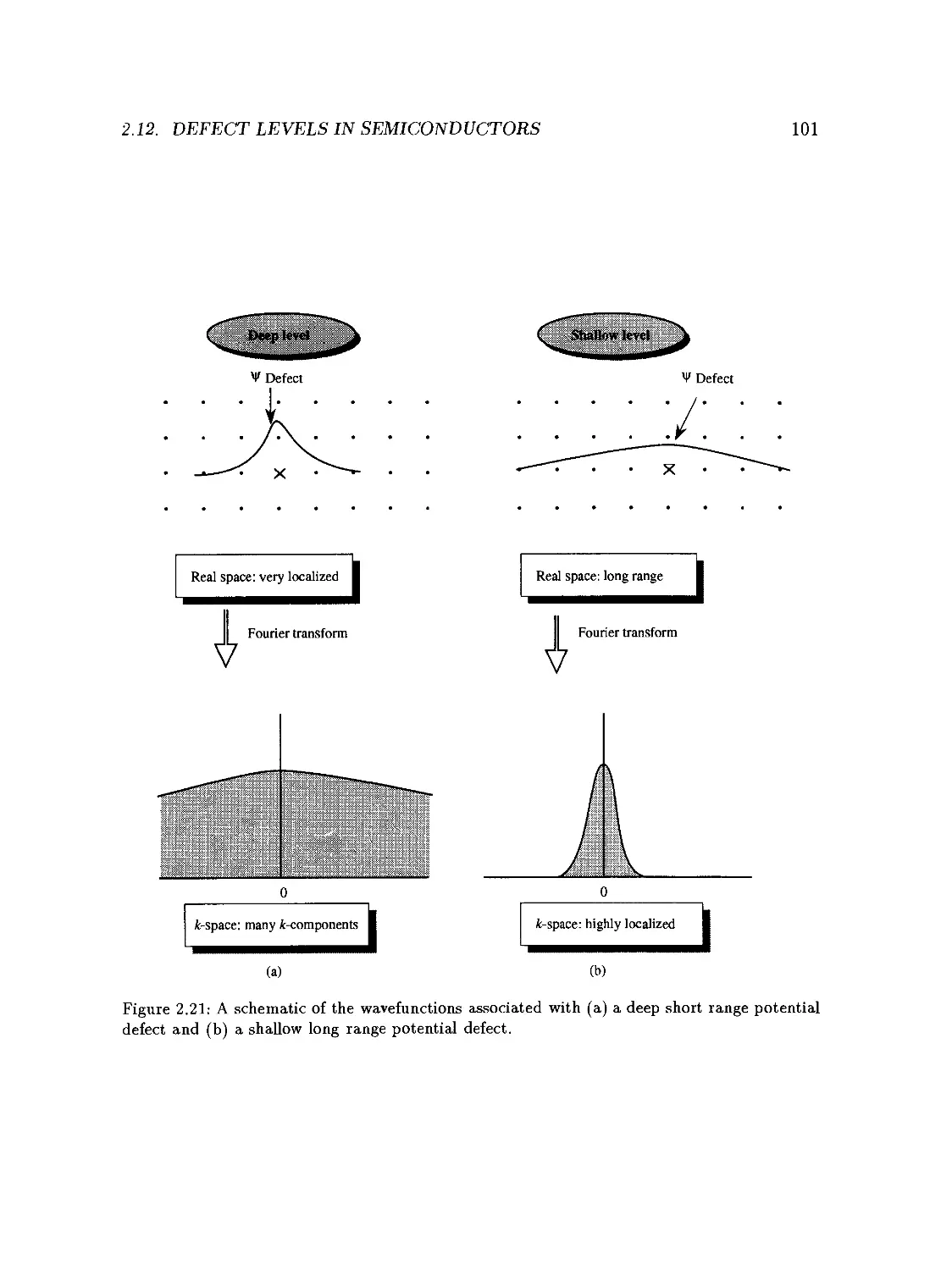
2.12 Defect levels in semiconductors 99
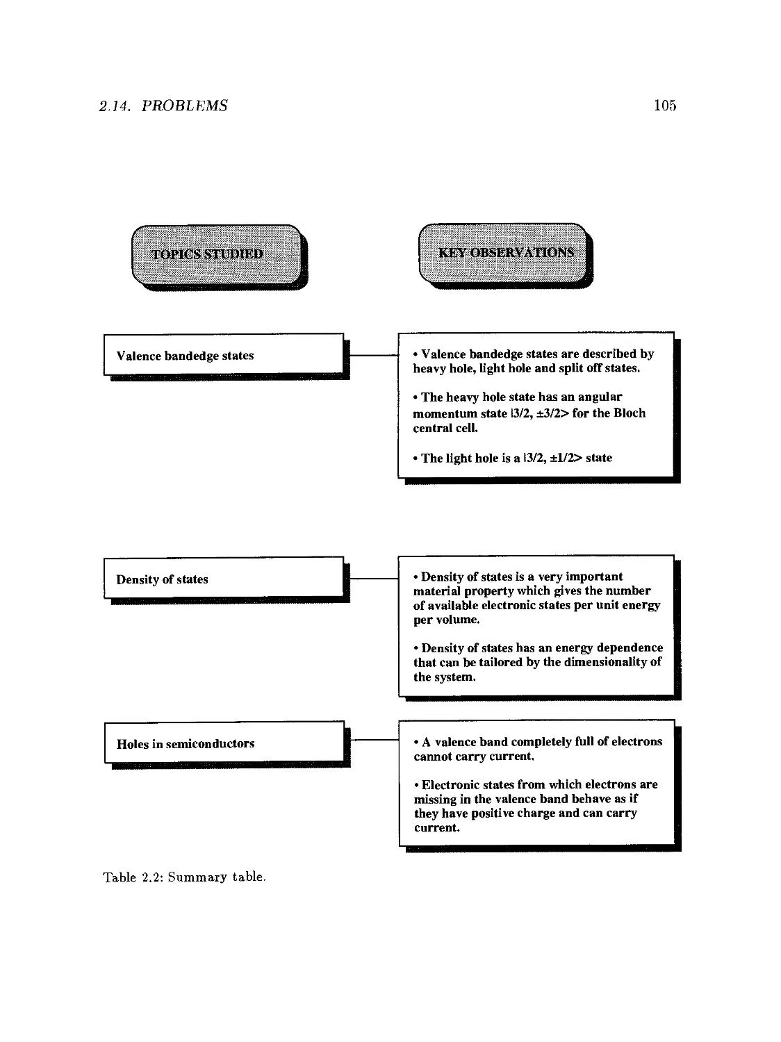
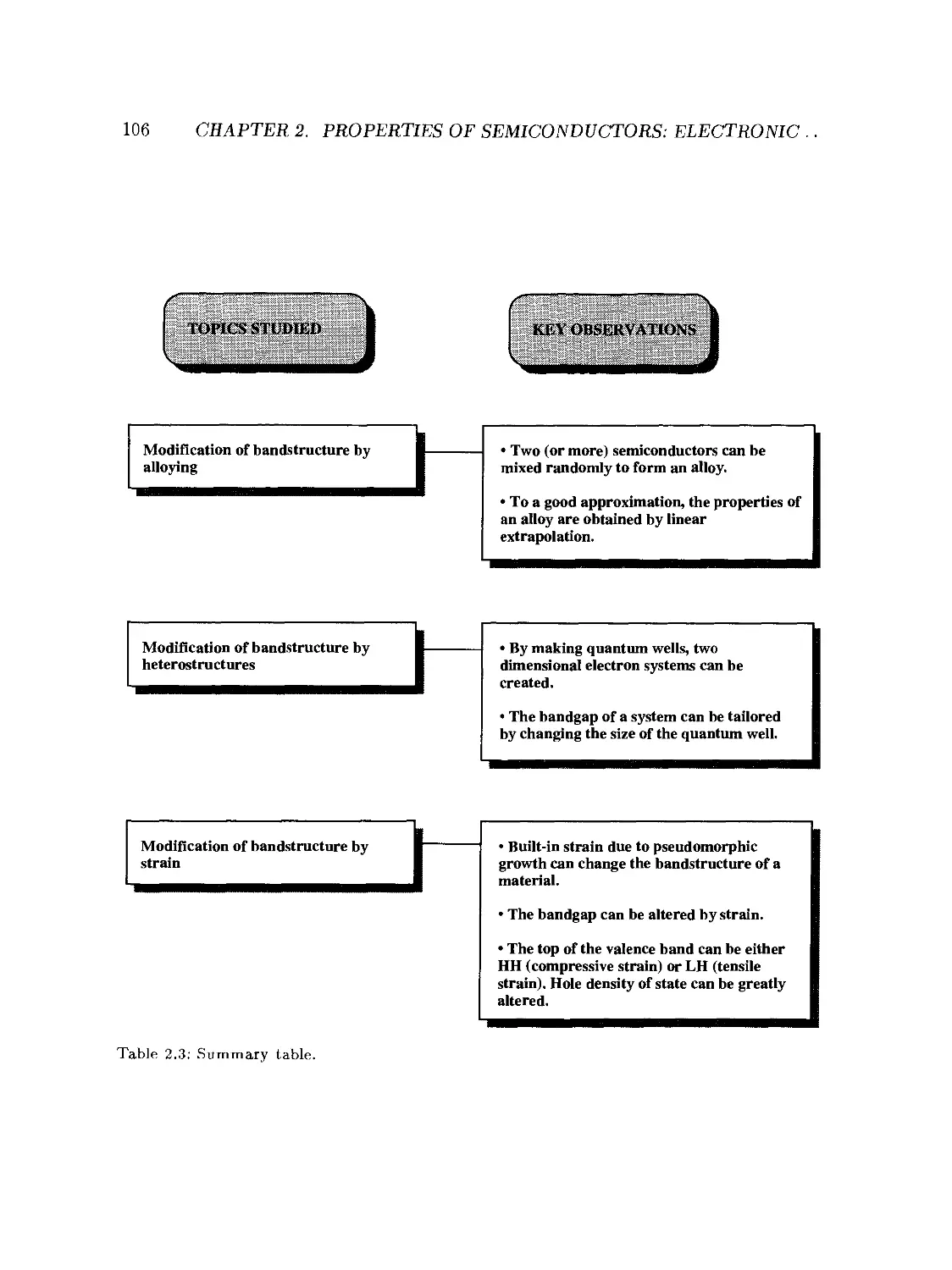
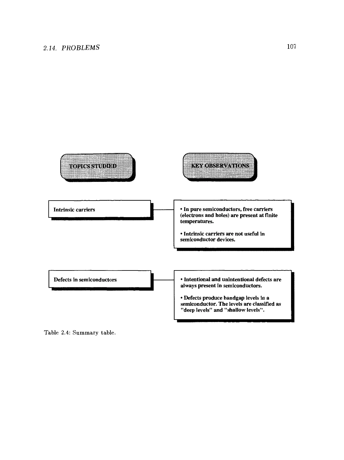
2.13 Chapter summary 102
2.14 Problems 103
2.15 References 111
DOPING AND CARRIER TRANSPORT 113
3.1 Introduction 113
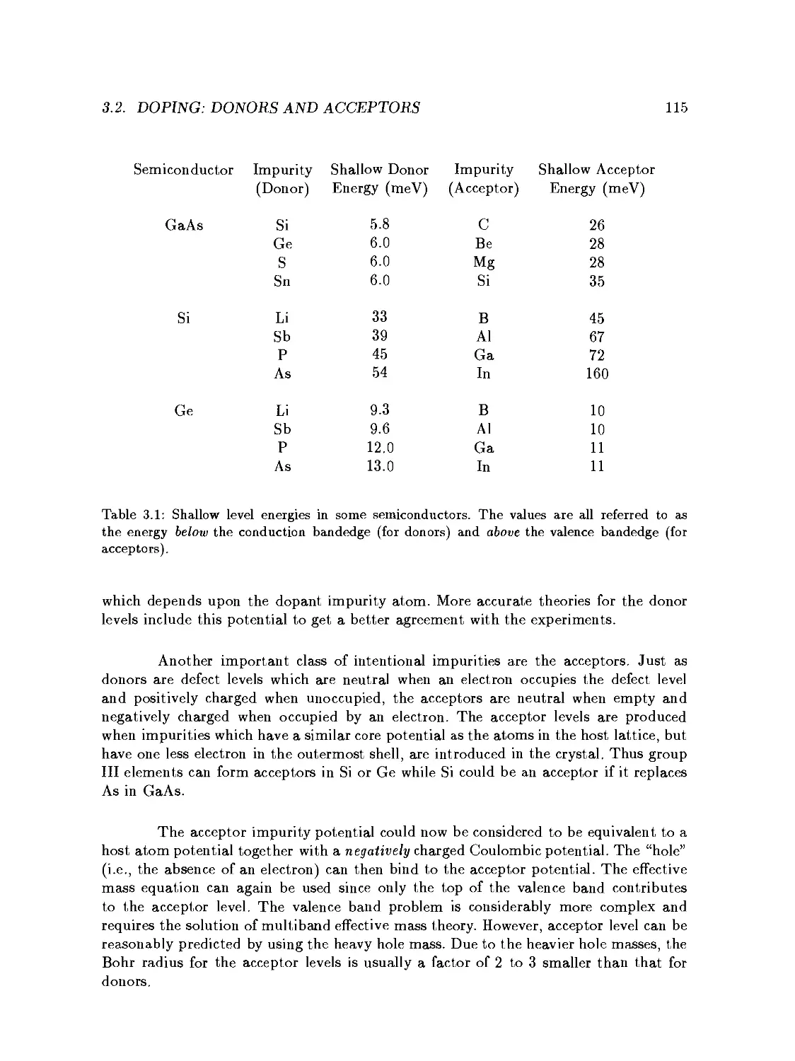
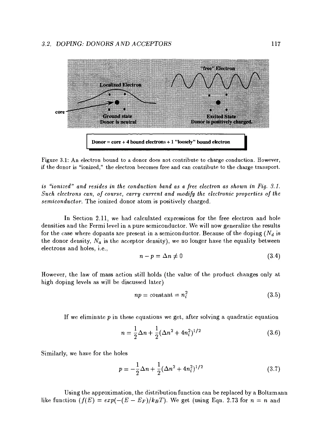
3.2 Doping: donors and acceptors 113
3.2.1 Extrinsic carrier density 116
3.2.2 Heavily doped semiconductors 122
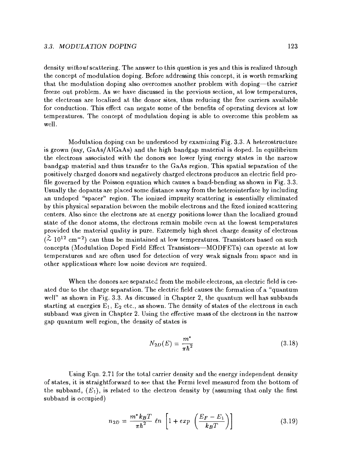
3.3 Modulation doping 122
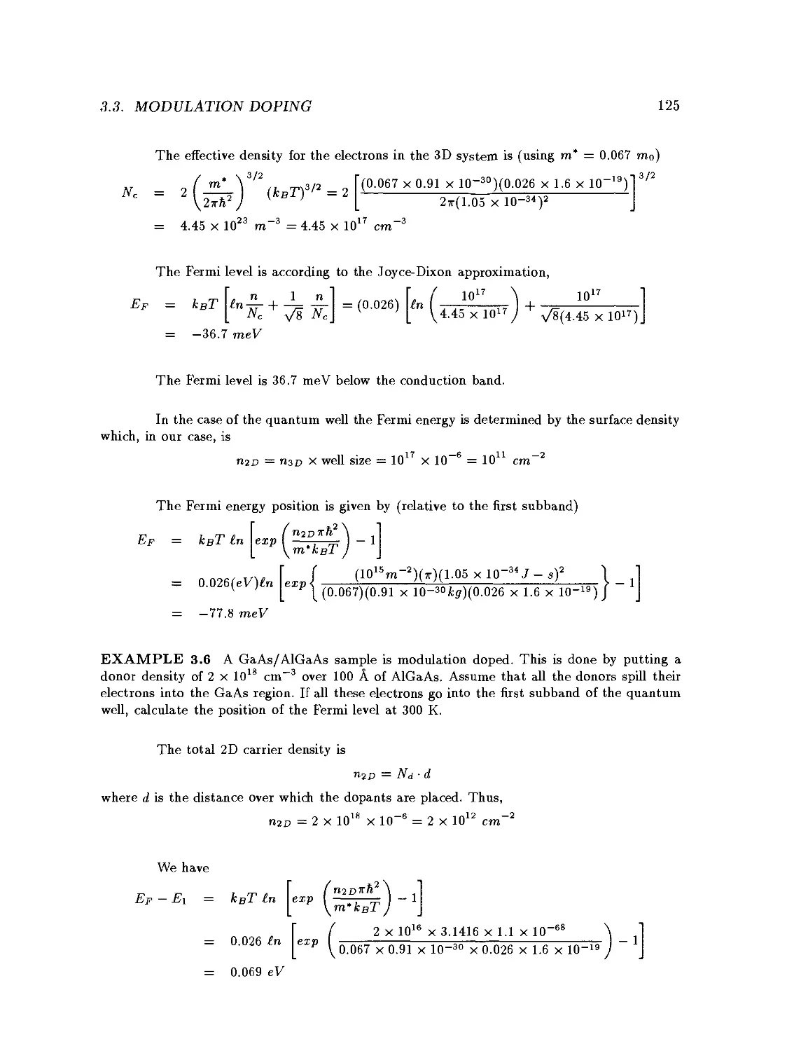
3.4 Transport in semiconductors: a conceptual picture 126
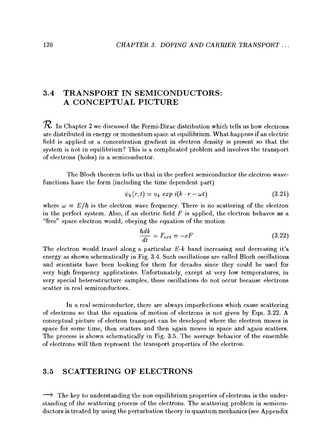
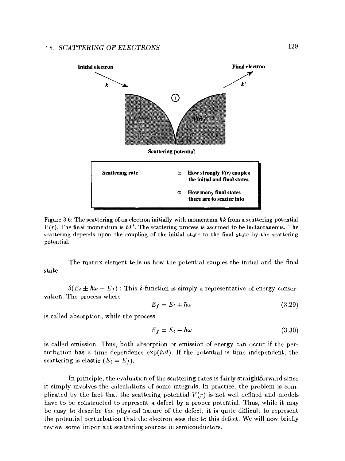
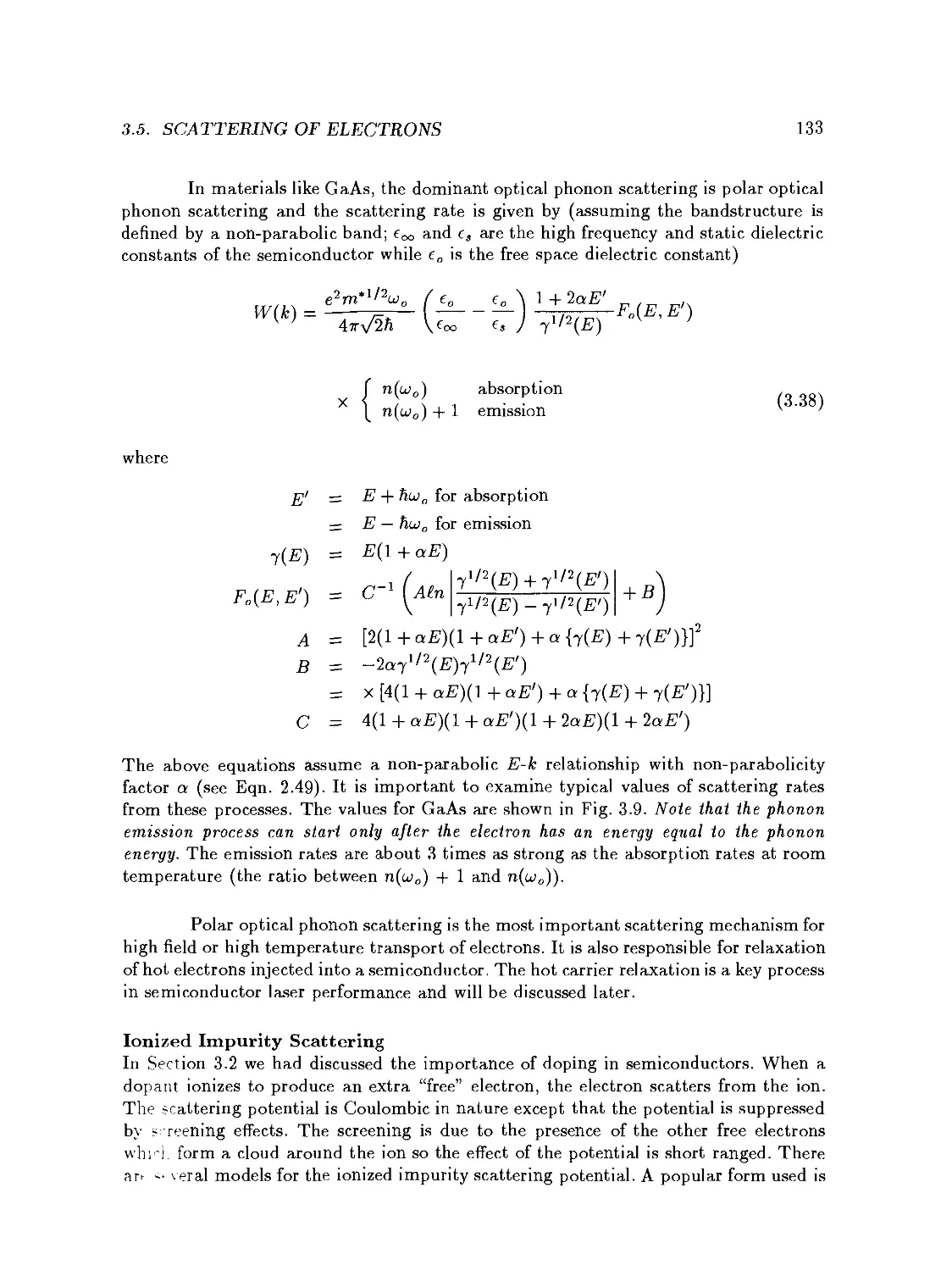
3.5 Scattering of electrons 126
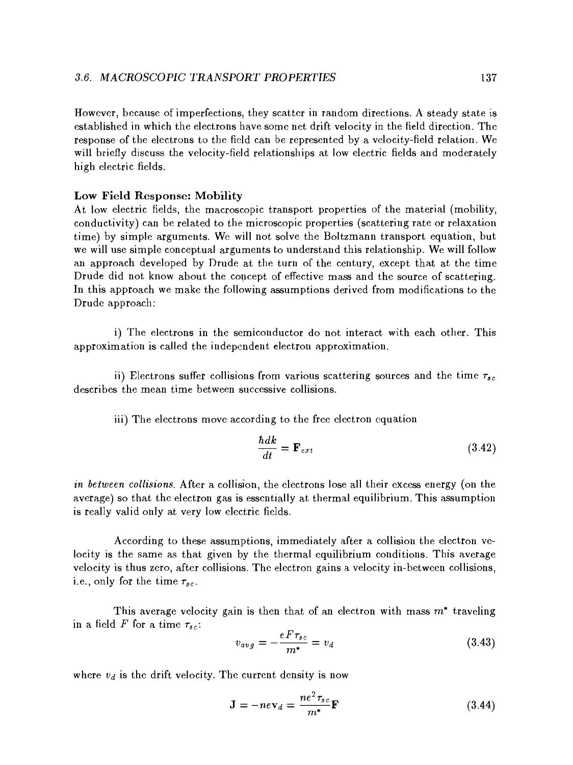
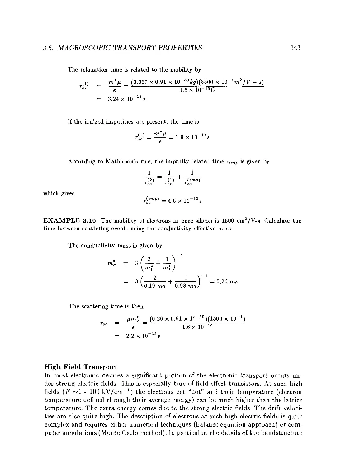
3.6 Macroscopic transport properties 136
3.6.1 Velocity-electric field relations in semiconductors 136
3.6.2 Transport of holes 142
3.7
Very high field transport: breakdown phenomena 145
CONTENTS
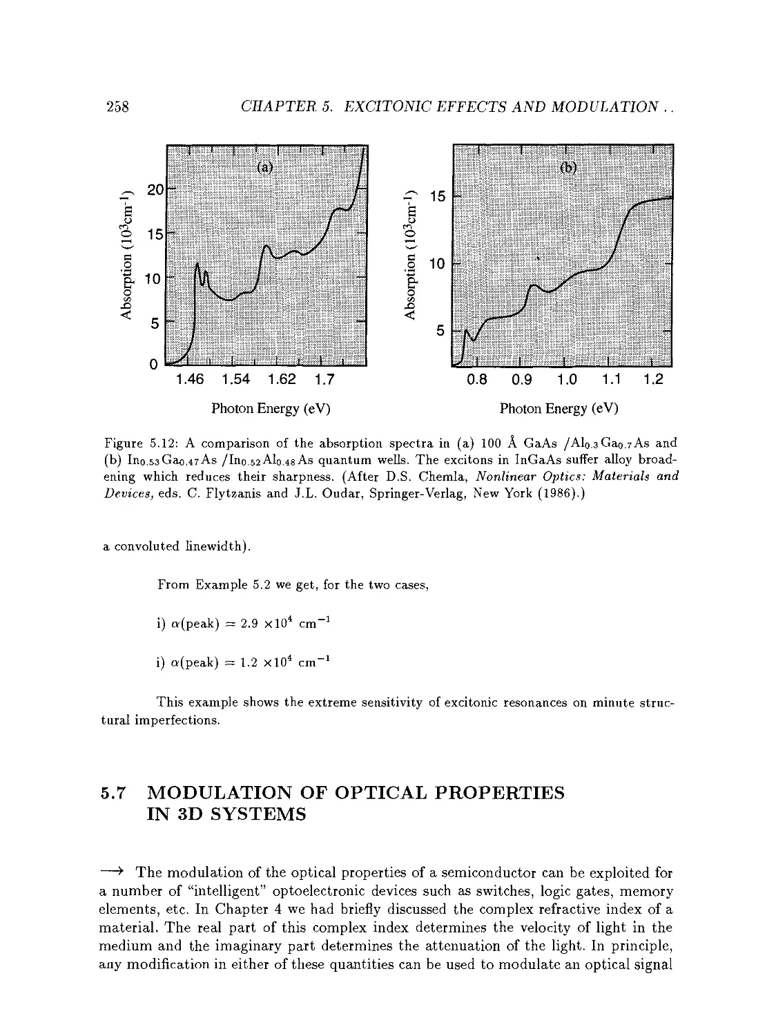
3-71 Impact ionization or avalanche breakdown 14
3.8 Carrier transport by diffusion U
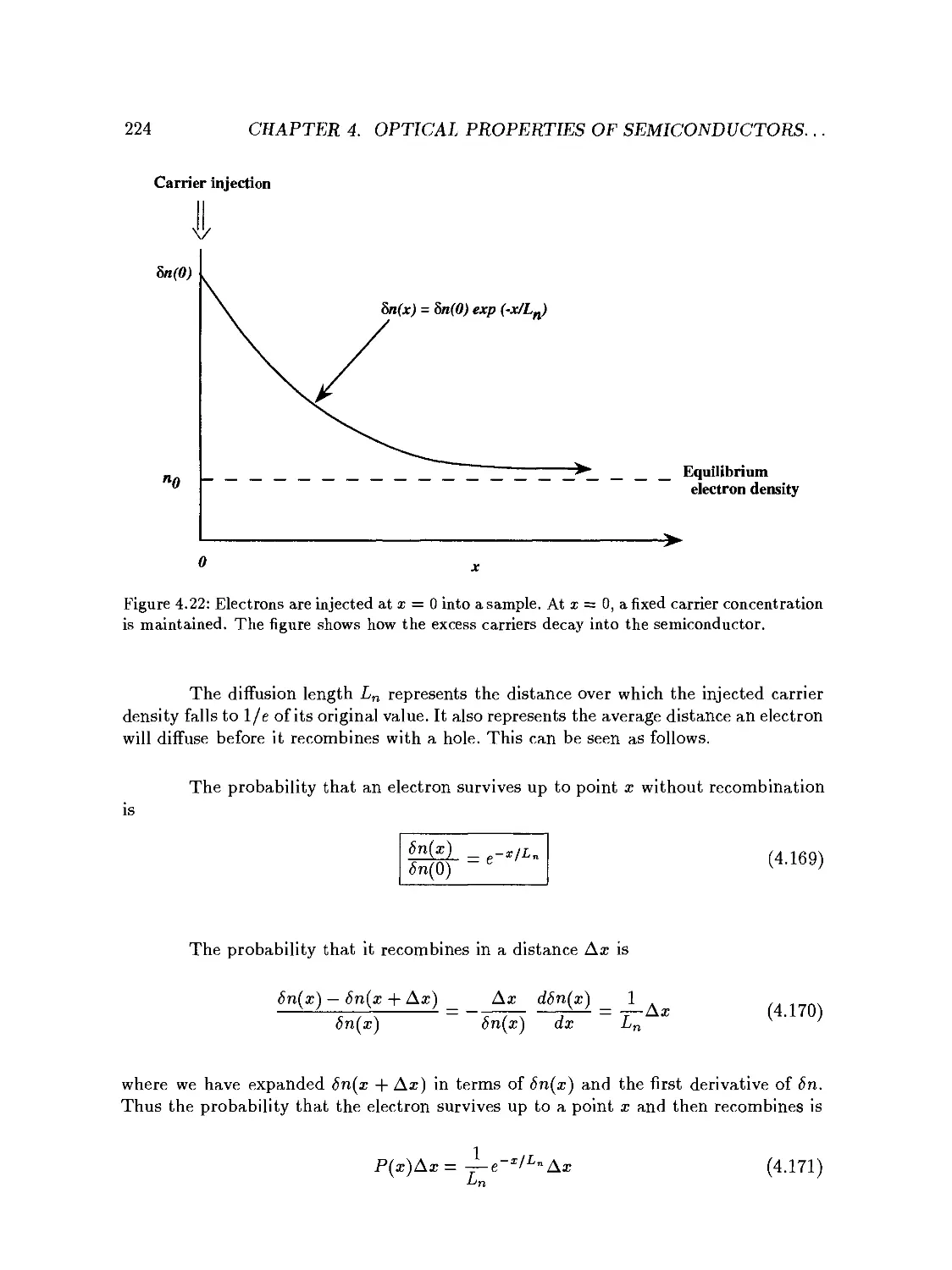
39 Carrier injection and thermalization 15
3-9.1 Carrier relaxation in 3D systems 15
392 Carrier relaxation in 2D systems 15
3-9.3 Carrier relaxation in ID systems 15
3-9.4 Carrier relaxation in quantum dots 15
3.10 Charge injection and quasi-Fermi levels 16
3.10.1 Quasi-Fermi levels 16
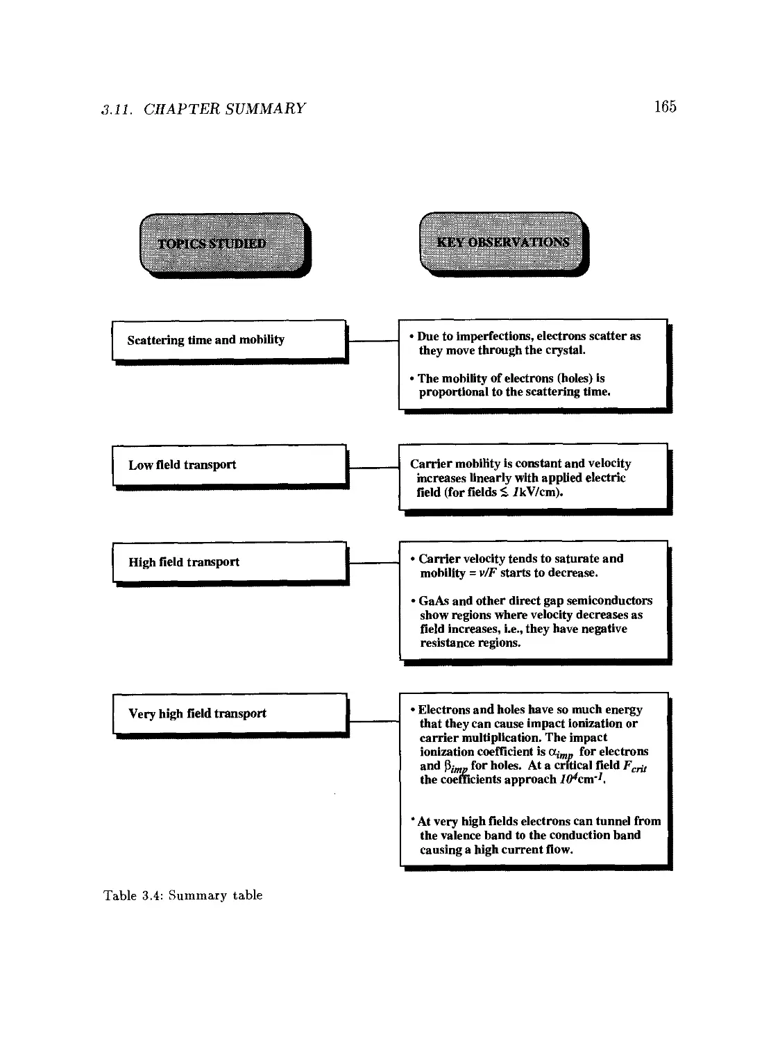
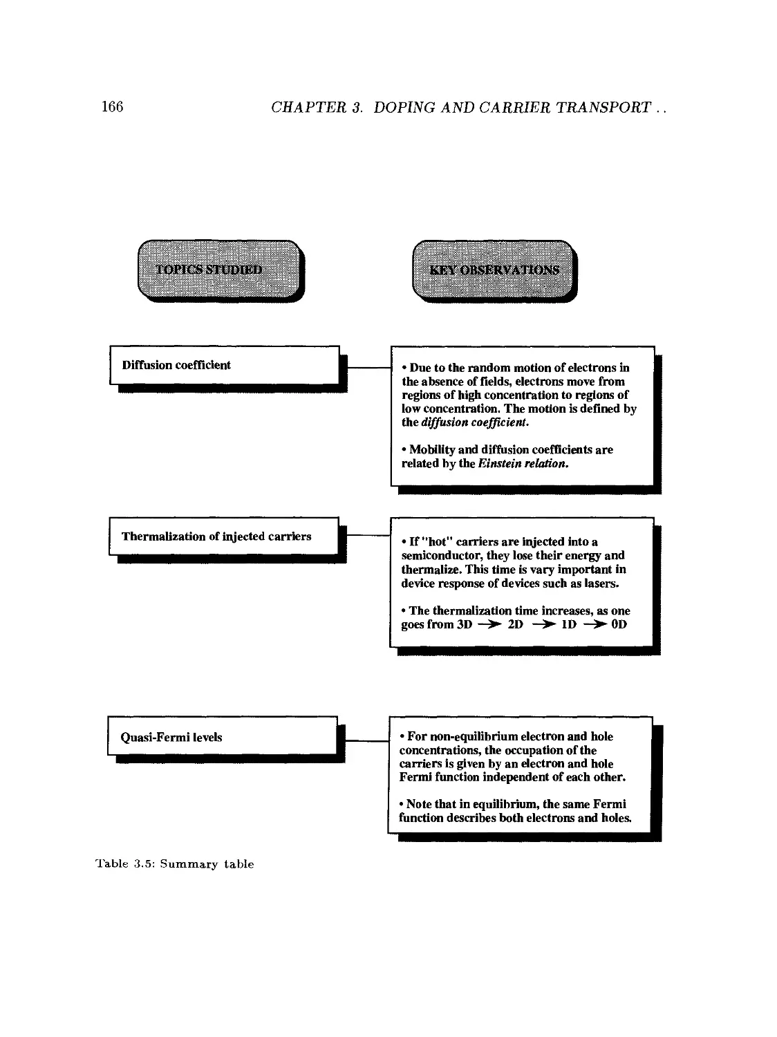
3.11 Chapter summary 16
312 Problems 16
3.13 References 16
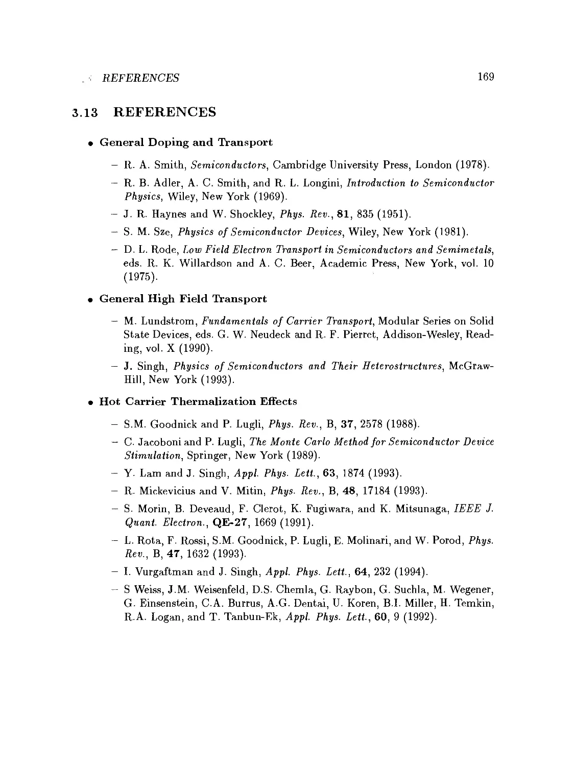
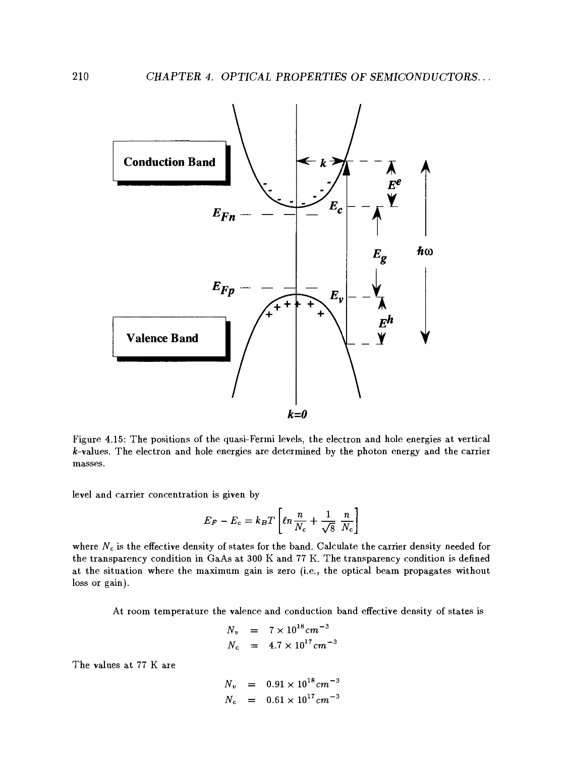
OPTICAL PROPERTIES OF SEMICONDUCTORS 17
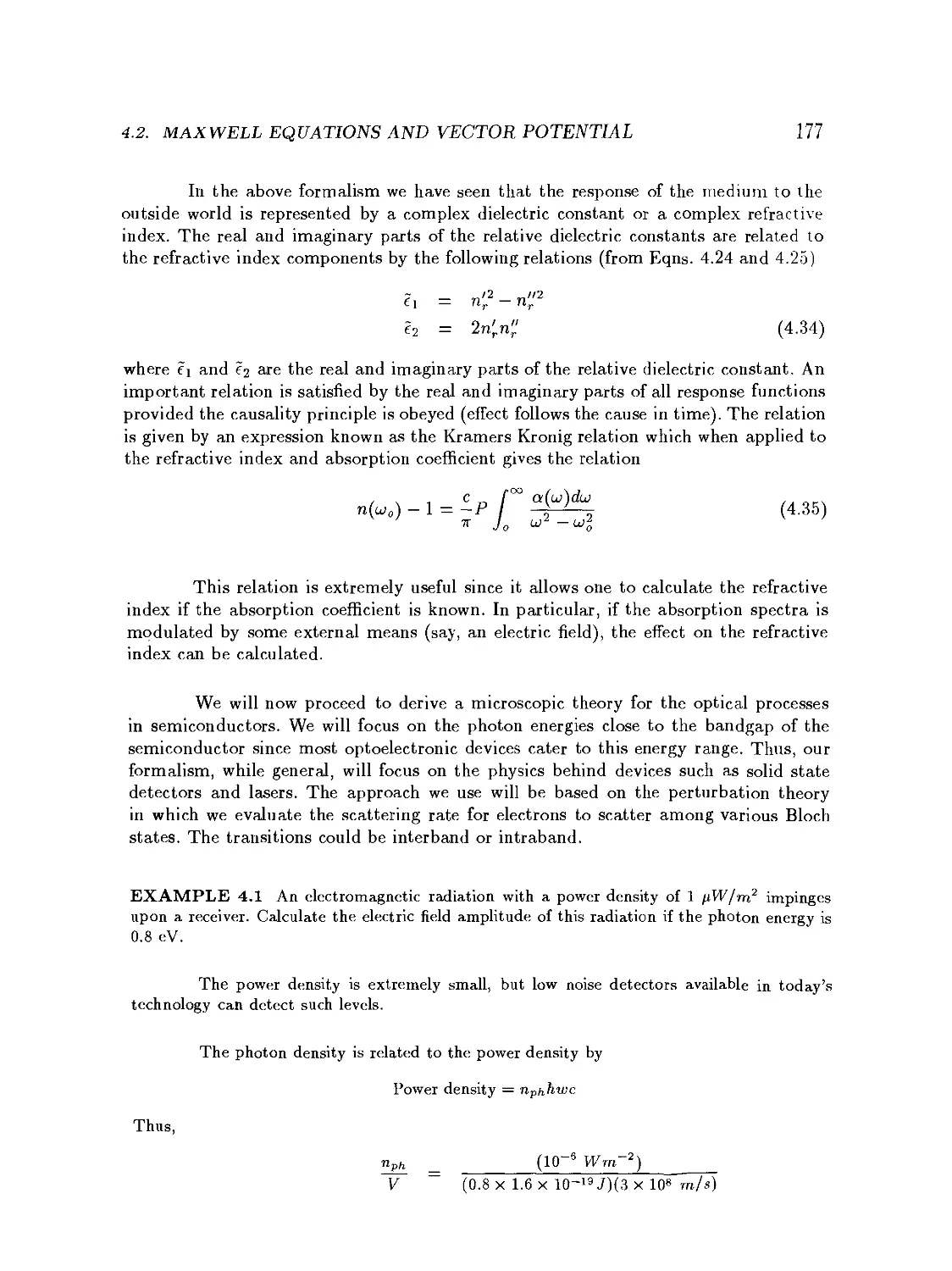
4.1 Introduction 17
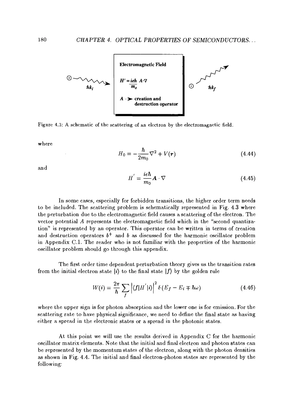
4.2 Maxwell equations and vector potential 17
4.3 Electrons in an electromagnetic field 17
4.4 Interband transitions 1?
4.4.1 Interband transitions in bulk semiconductors 1?
4.4.2 Interband transitions in quantum wells 1?
4.5 Indirect interband transitions 15
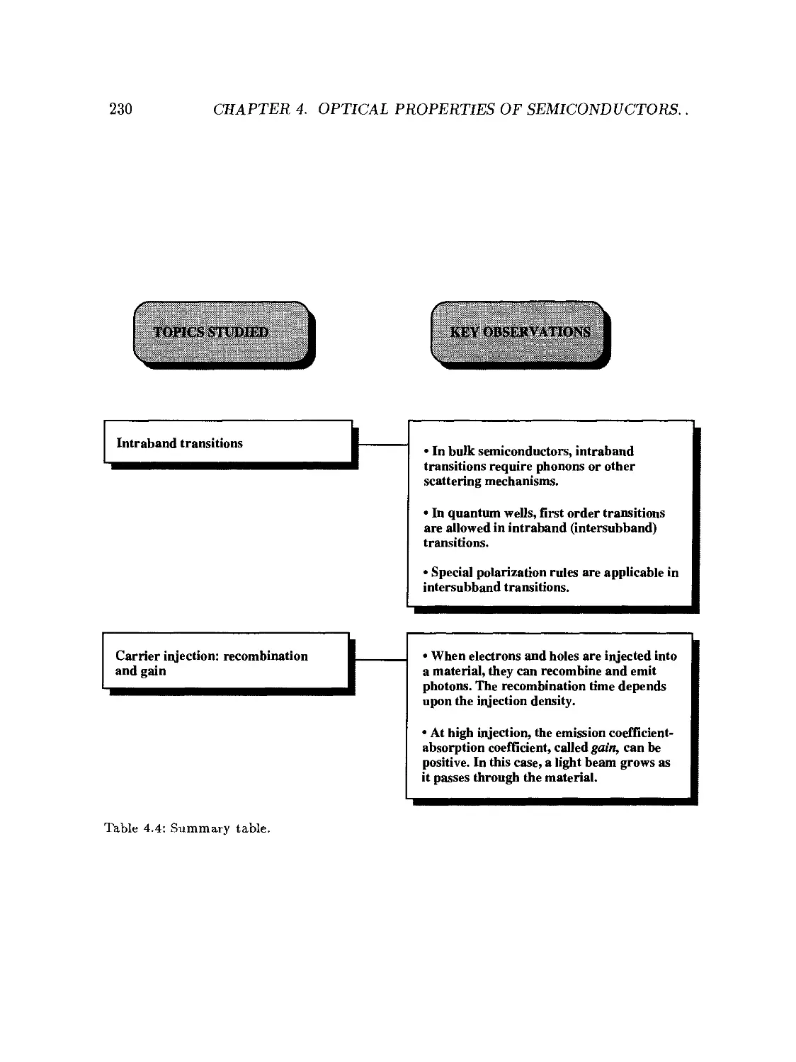
4.6 Intraband transitions 2C
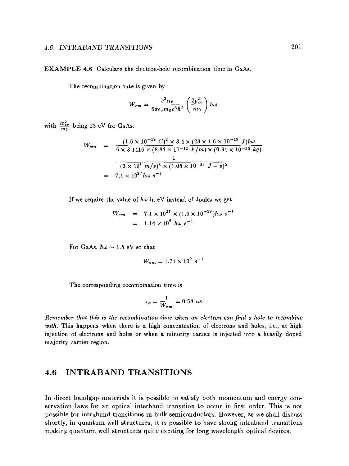
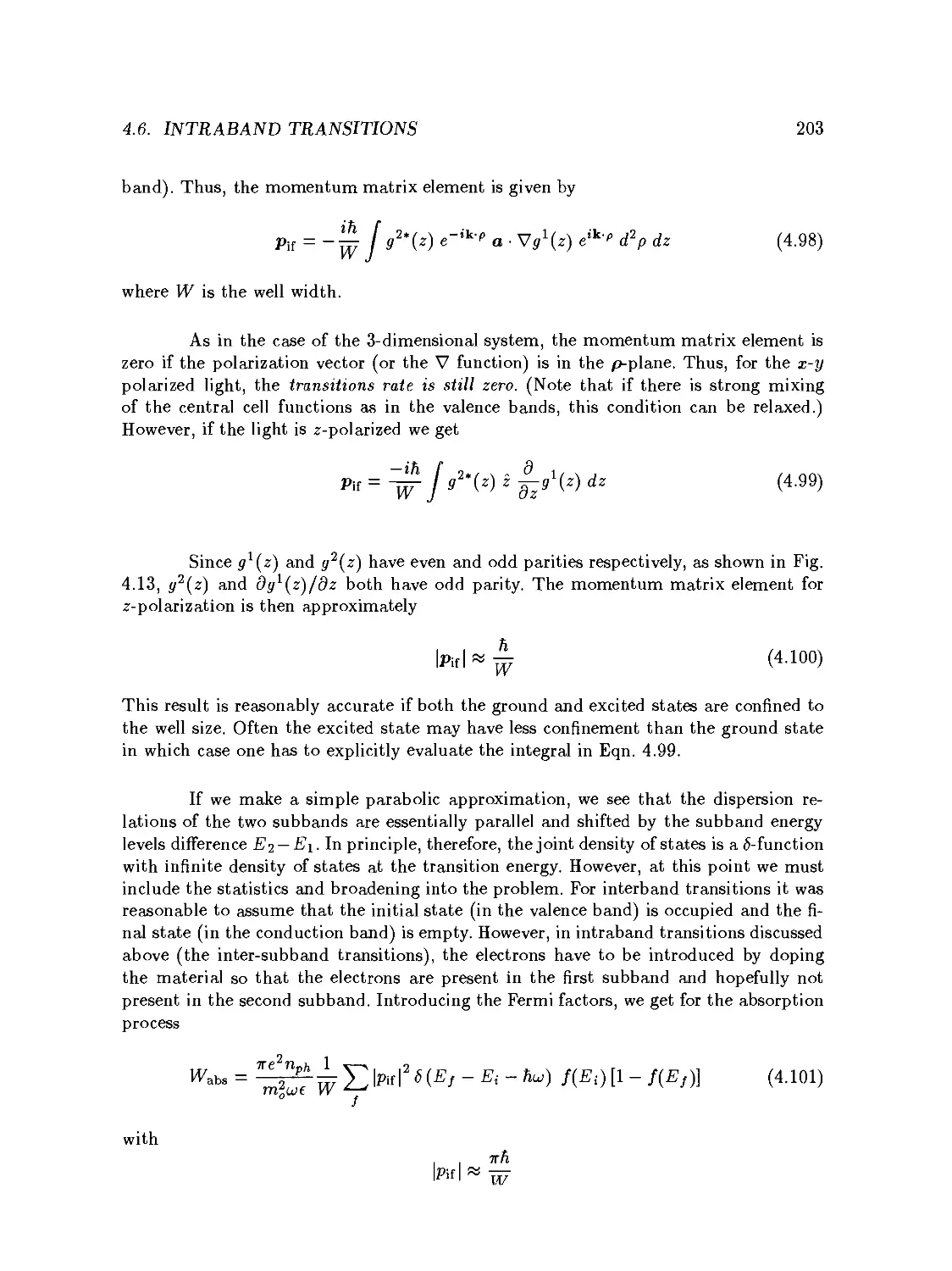
4.6.1 Intraband transitions in bulk semiconductors 2C
4.6.2 Intraband transitions in quantum wells 2C
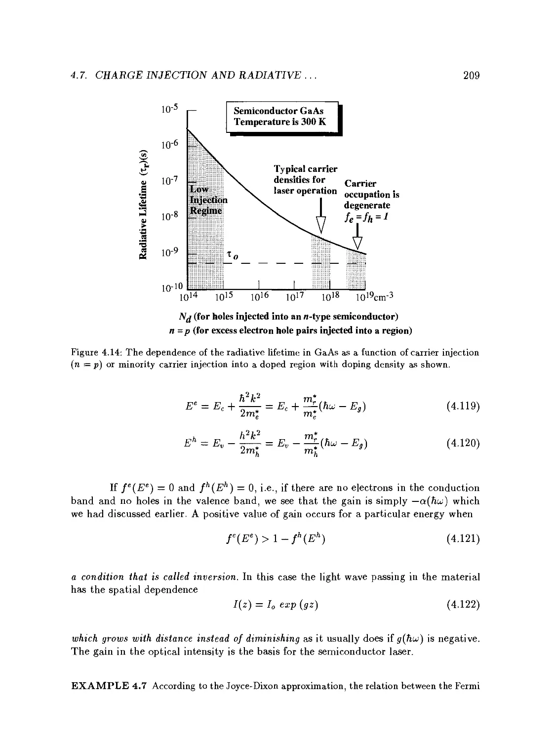
4.7 Charge injection and radiative recombination 2C
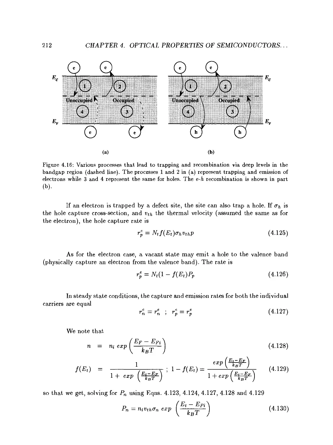
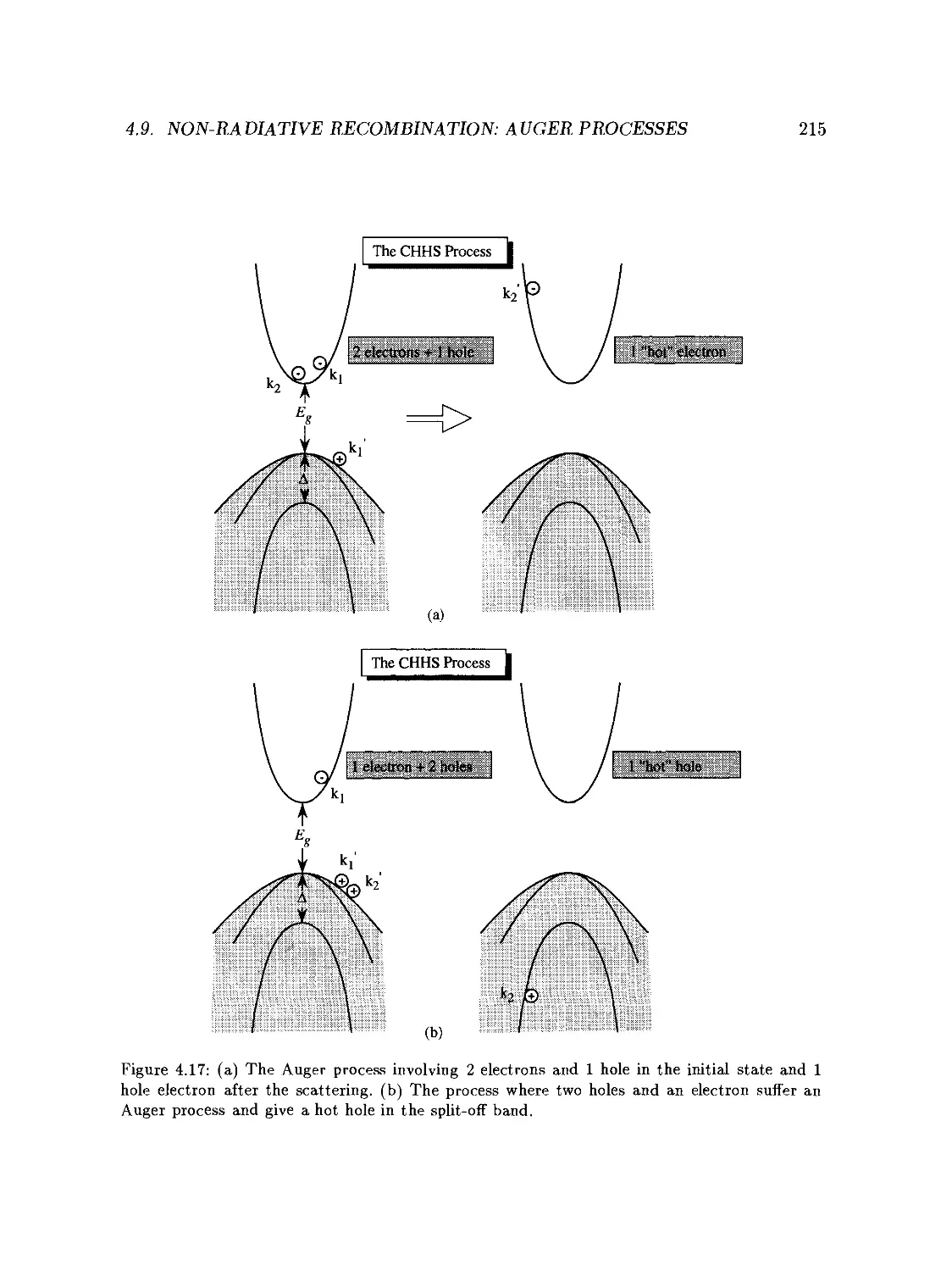
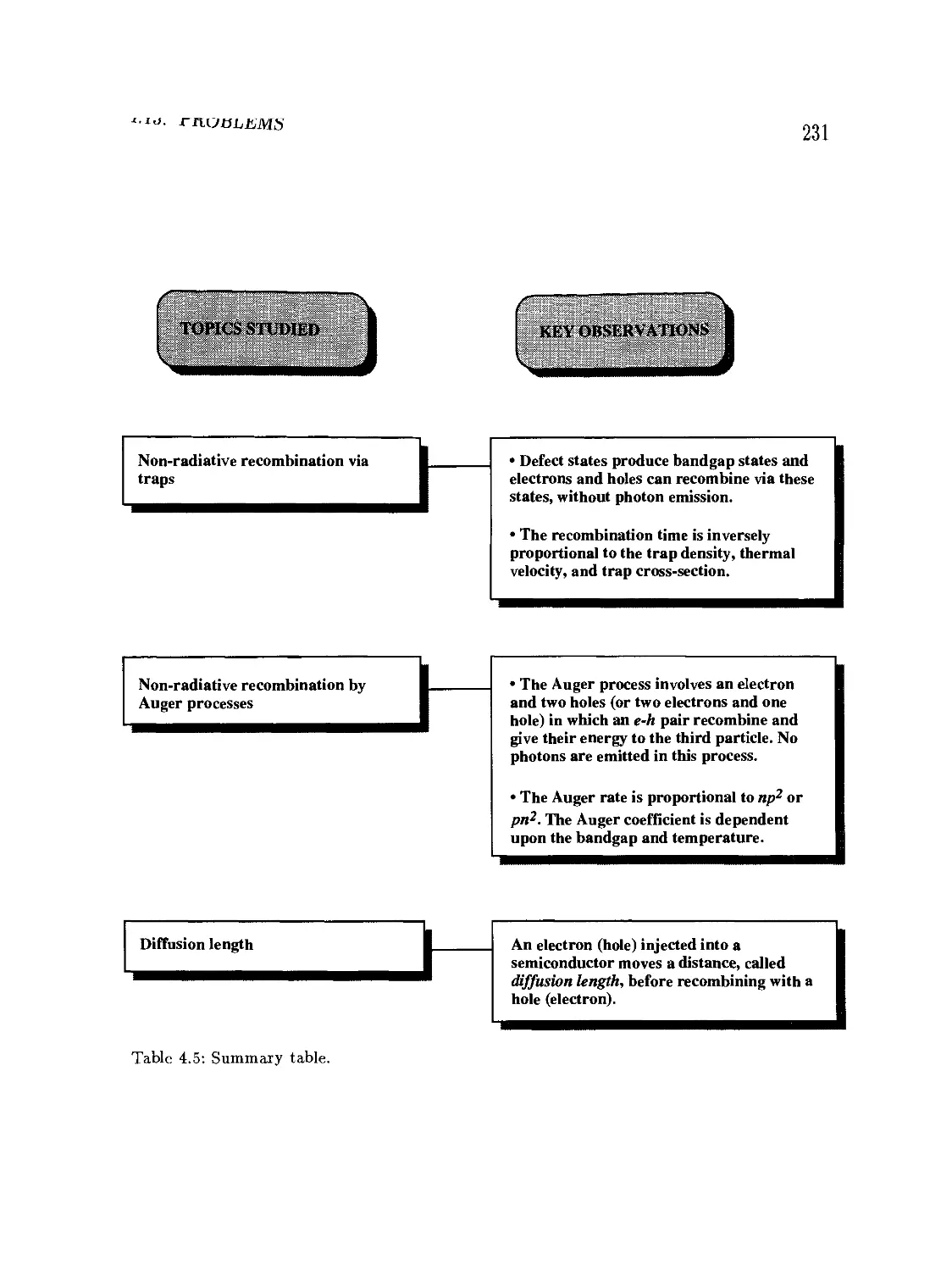
4.8 Charge injection: non-radiative effects 21
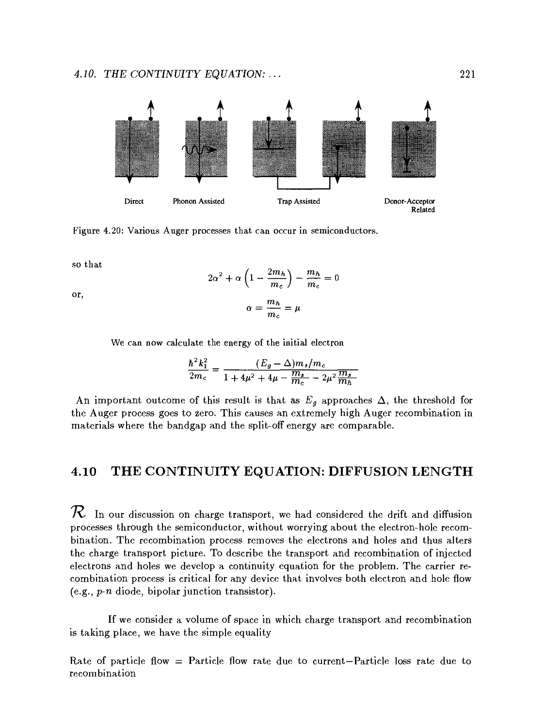
4.9 non-radiative recombination: Auger processes 21
4.10 The continuity equation: diffusion length 22
CONTENTS
xiii
5
4.11 Charge injection and bandgap renormalization 226
4.12 Chapter summary 227
4.13 Problems 227
4.14 References 232
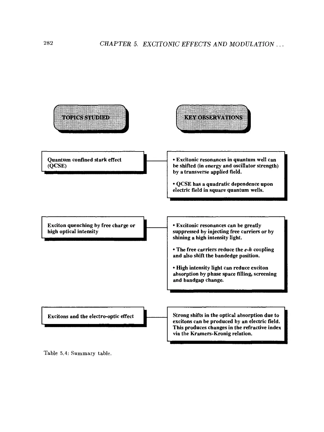
EXCITONIC EFFECTS AND MODULATION OF
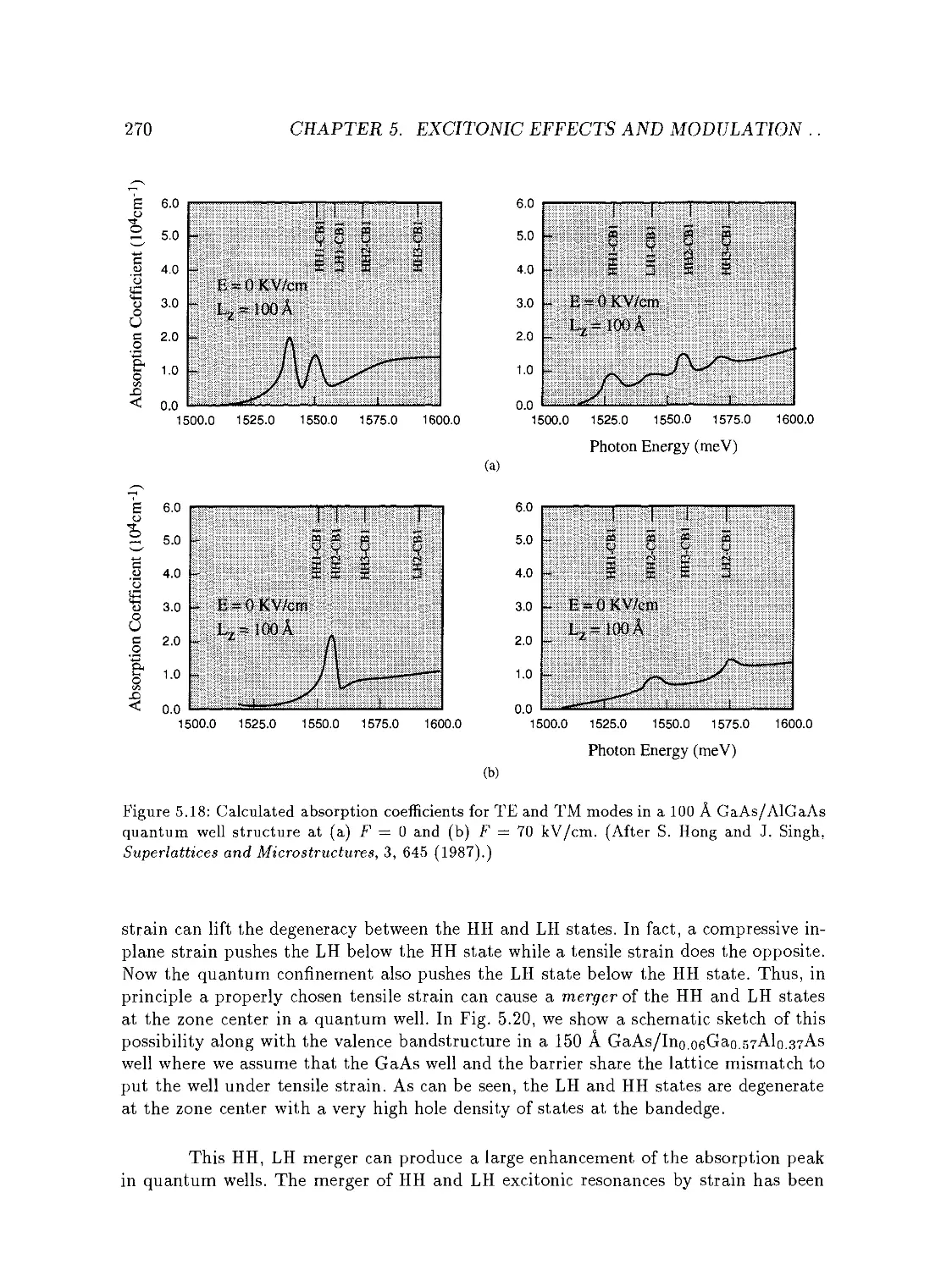
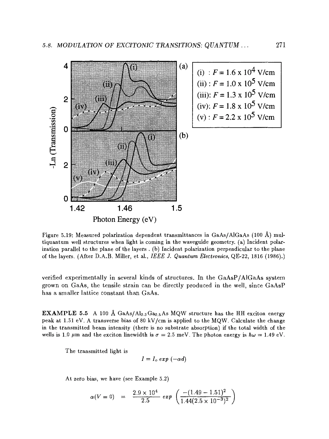
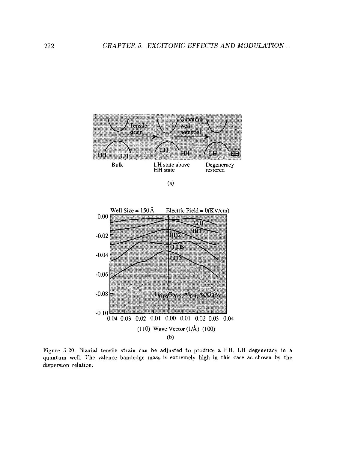
OPTICAL PROPERTIES 234
5.1 Introduction 234
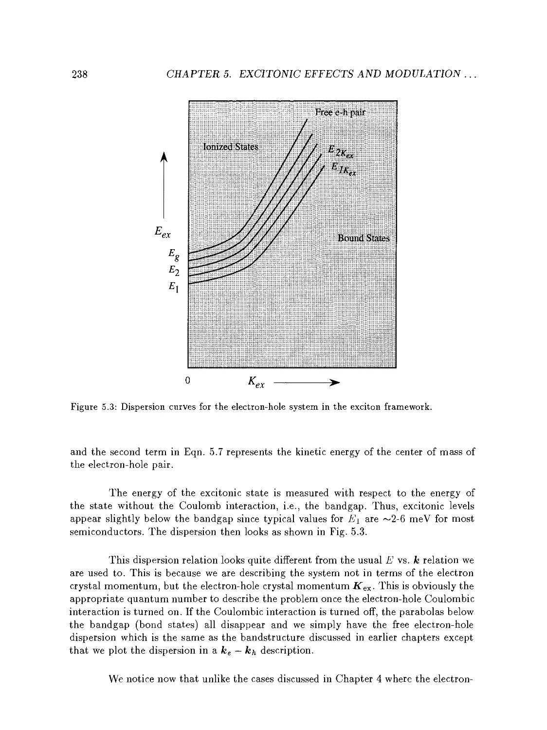
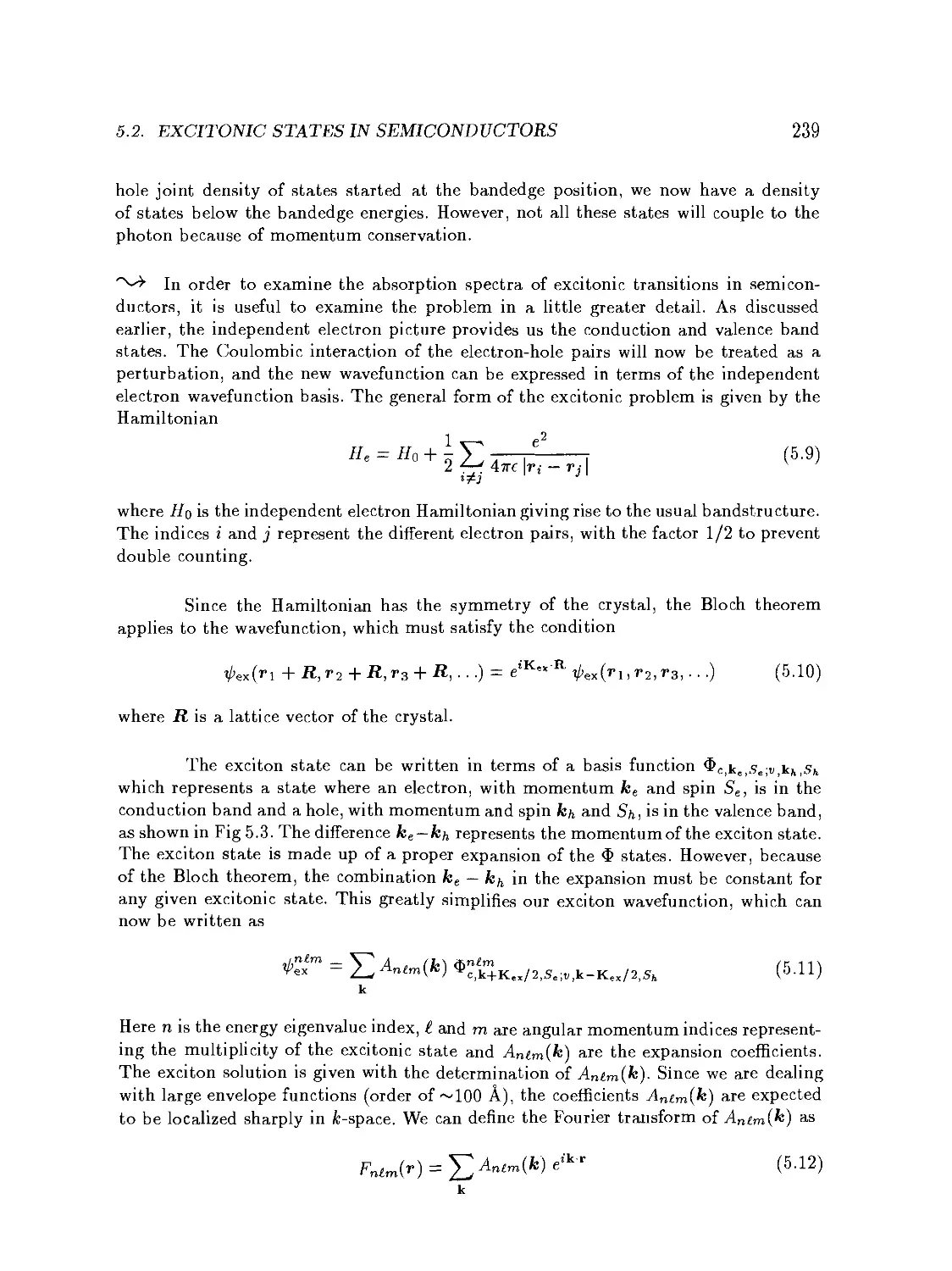
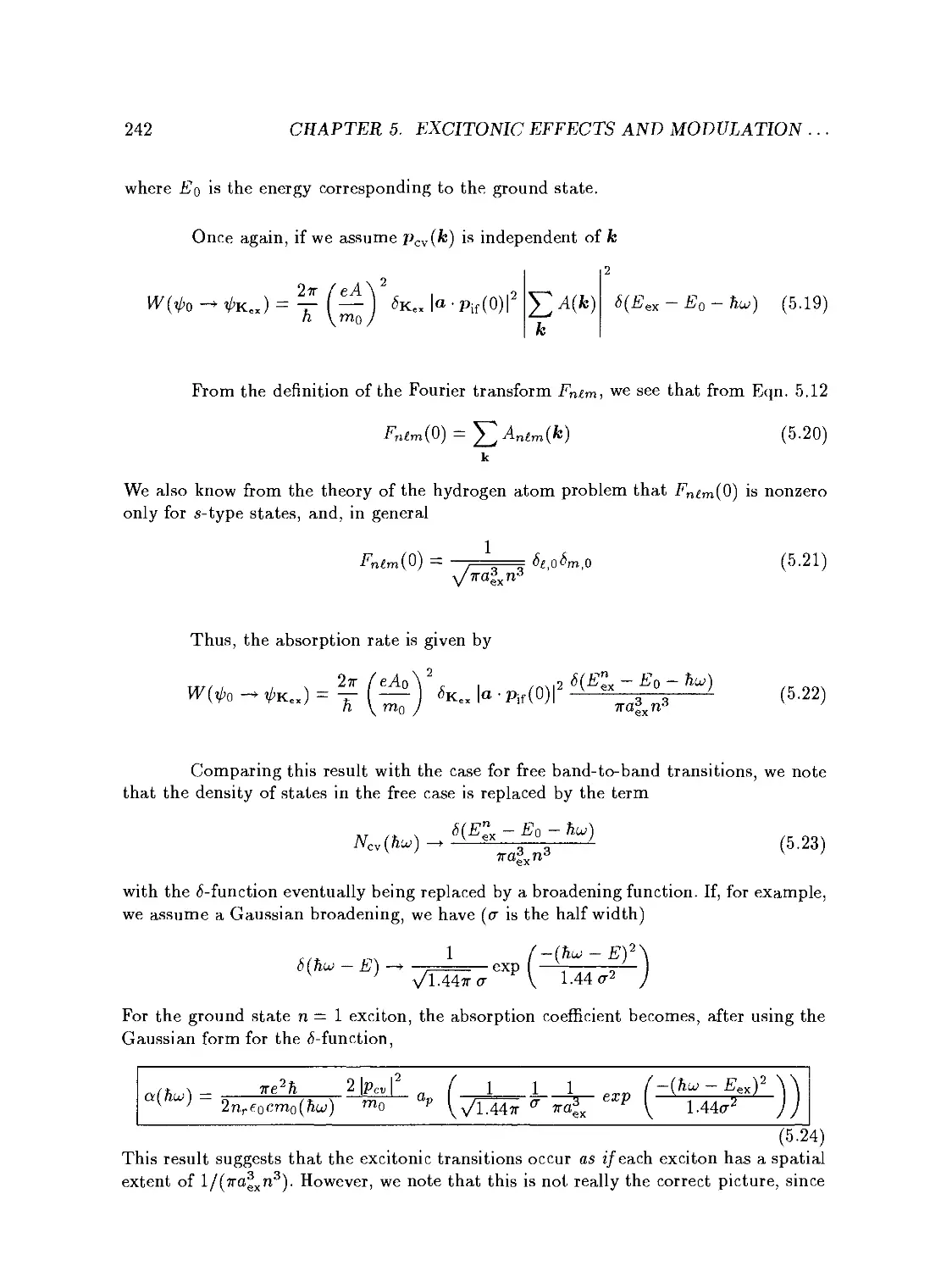
5.2 Excitonic states in semiconductors 236
5.3 Optical properties with inclusion
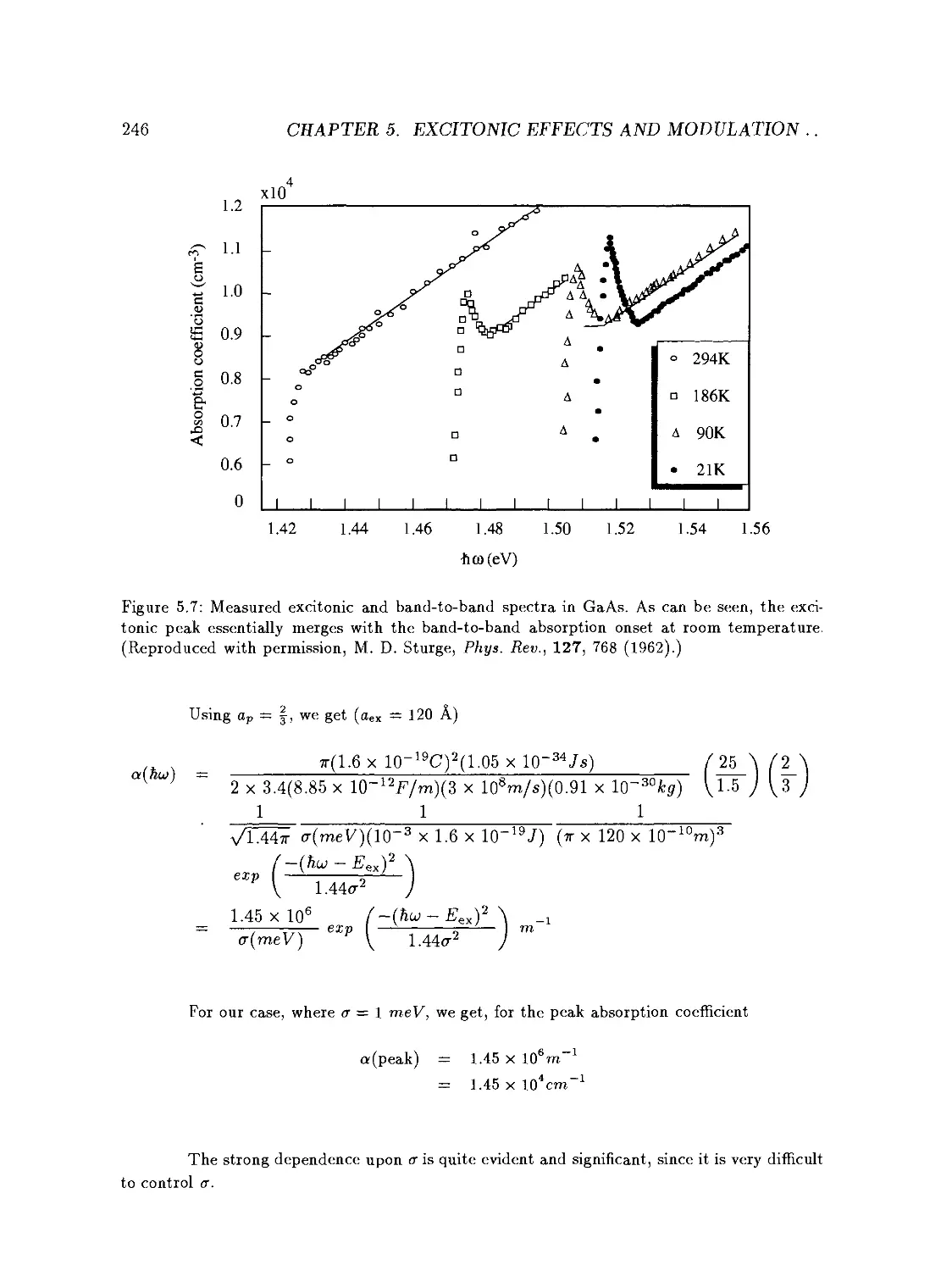
of excitonic effects 241
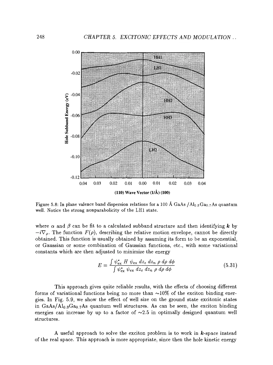
5.4 Excitonic states in quantum wells 247
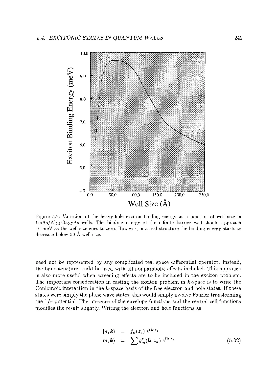
5.5 Excitonic absorption in quantum wells 251
5.6 Excitonic broadening effects 254
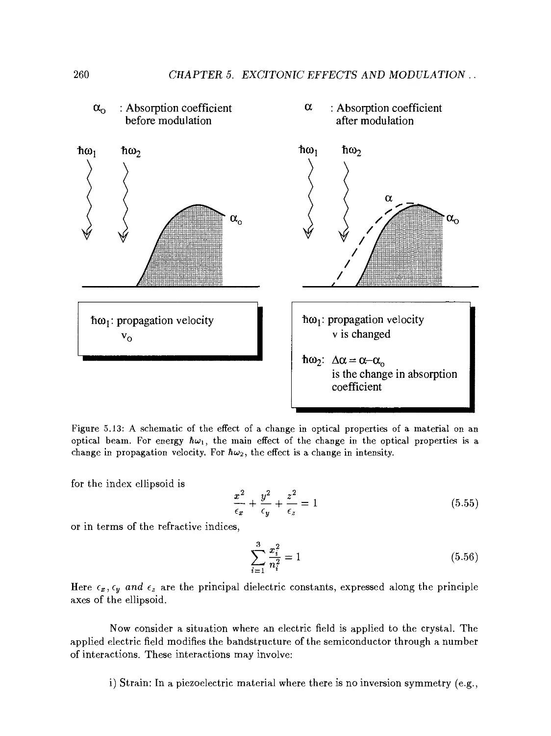
5.7 Modulation of optical properties in 3d systems 258
5.7.1 The electro-optic effect 259
5.8 Modulation of excitonic transitions:
quantum confined Stark effect 265
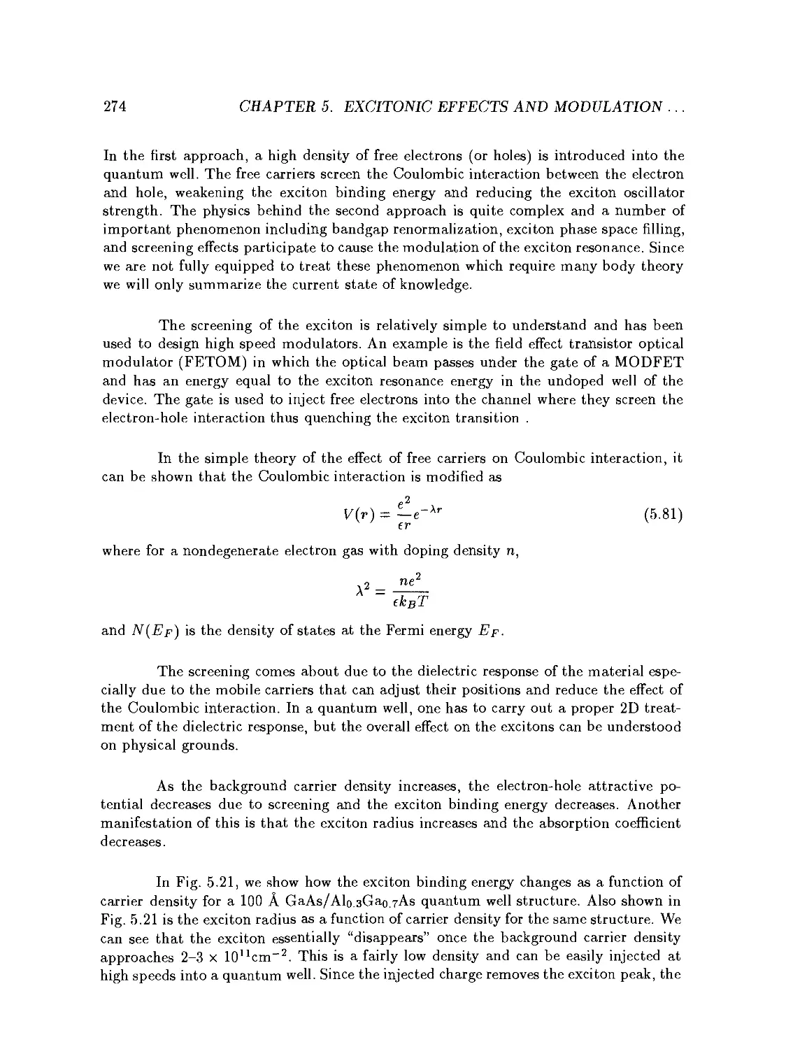
5.9 exciton quenching 273
5.10 Refractive index modulation due to
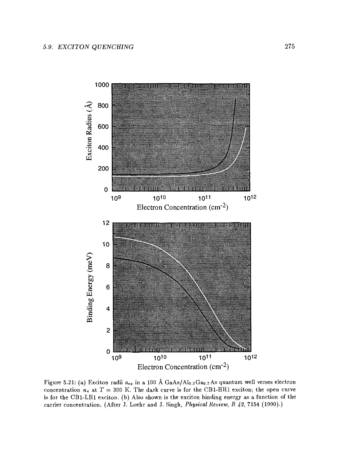
exciton modulation 276
5.11 Excitonic effects in sub 2d systems 278
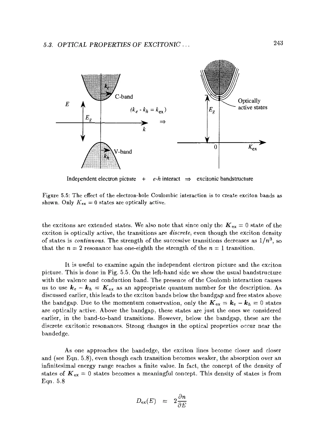
5.12 Chapter summary 279
5.13 Problems 279
5.14 References 284
CONTENTS
6
7
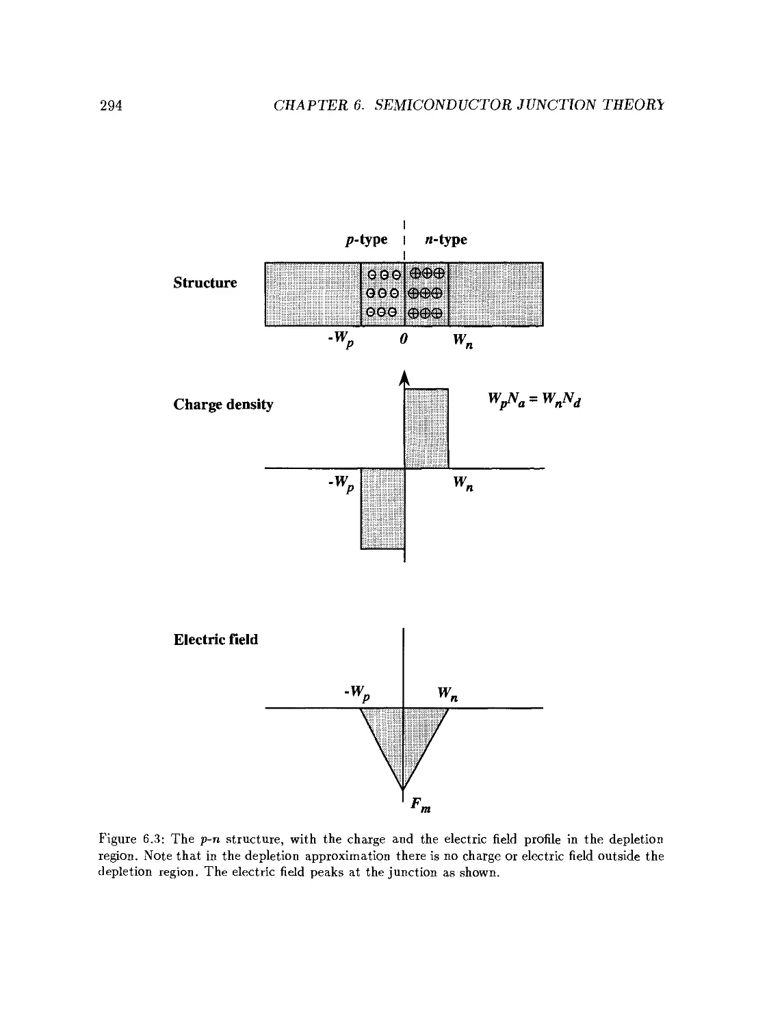
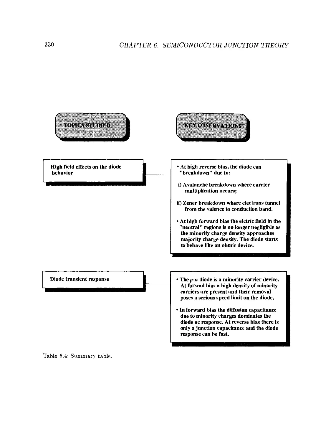
SEMICONDUCTOR JUNCTION THEORY 286
6.1 Introduction 286
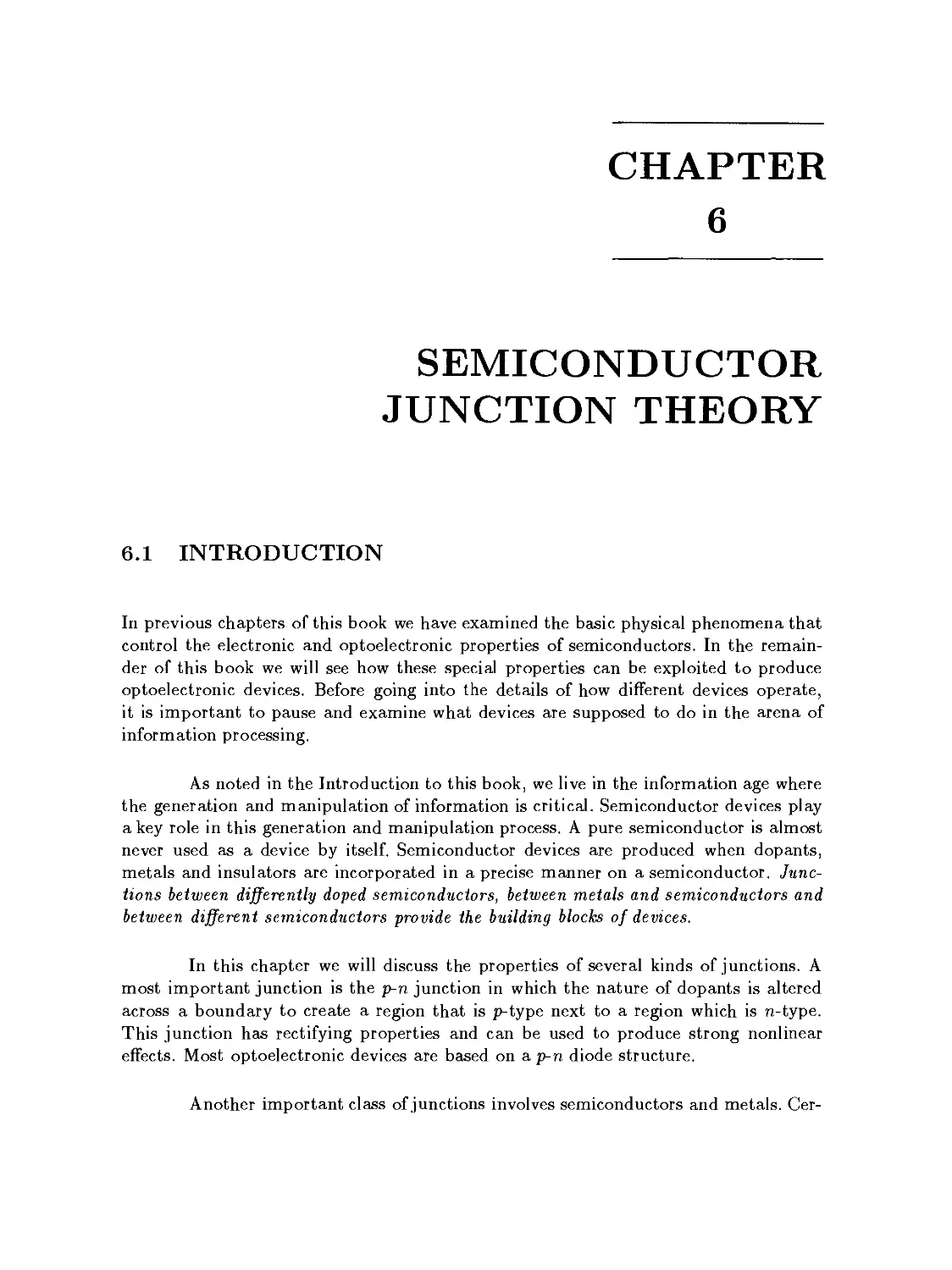
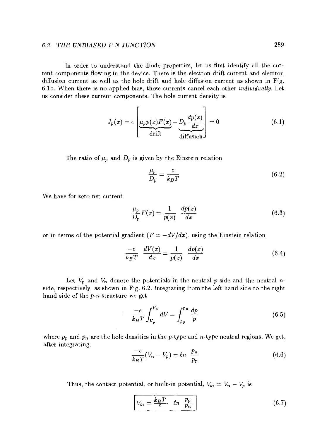
6.2 The unbiased p-n junction 287
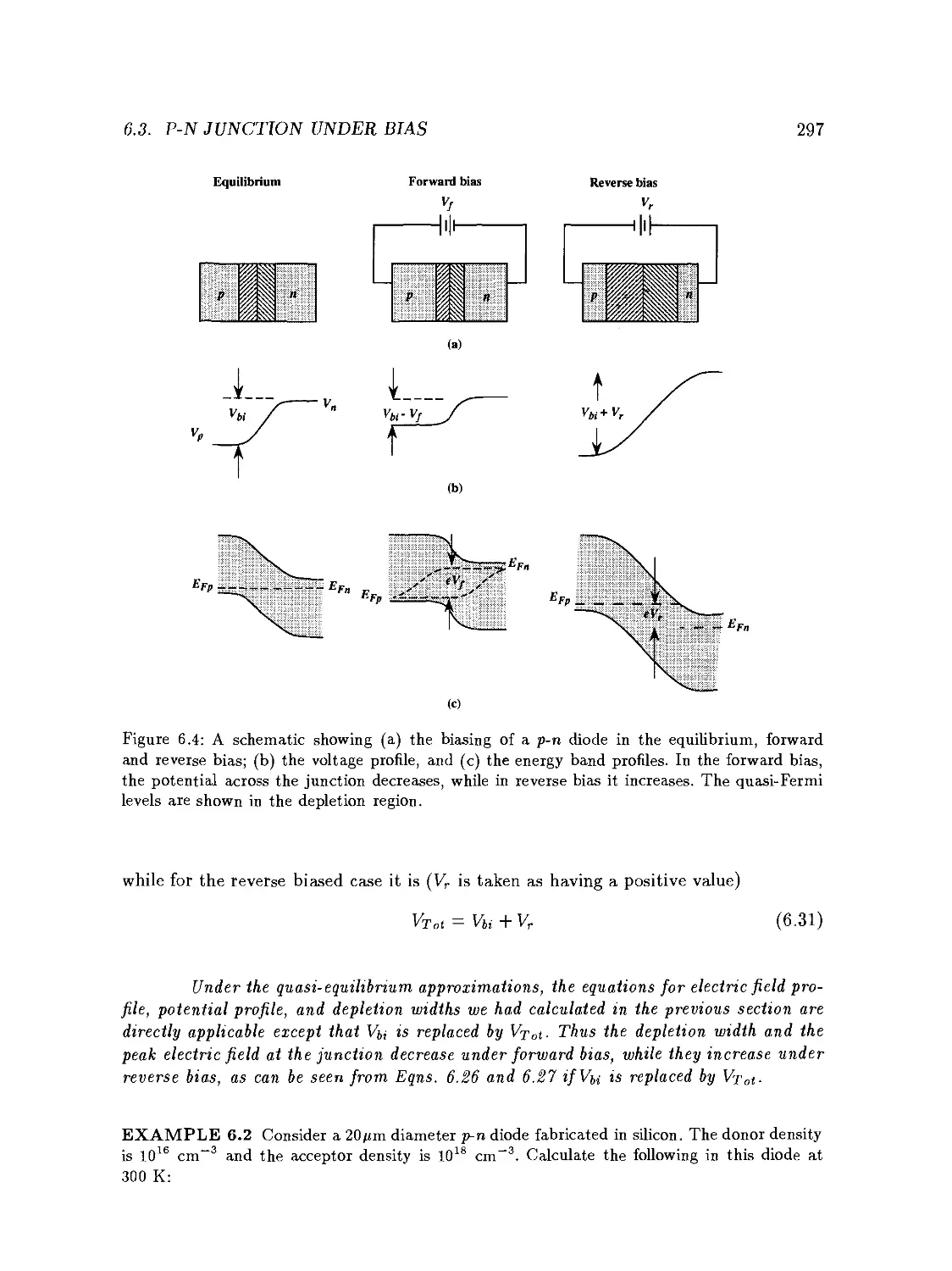
6.3 p-n junction under bias 296
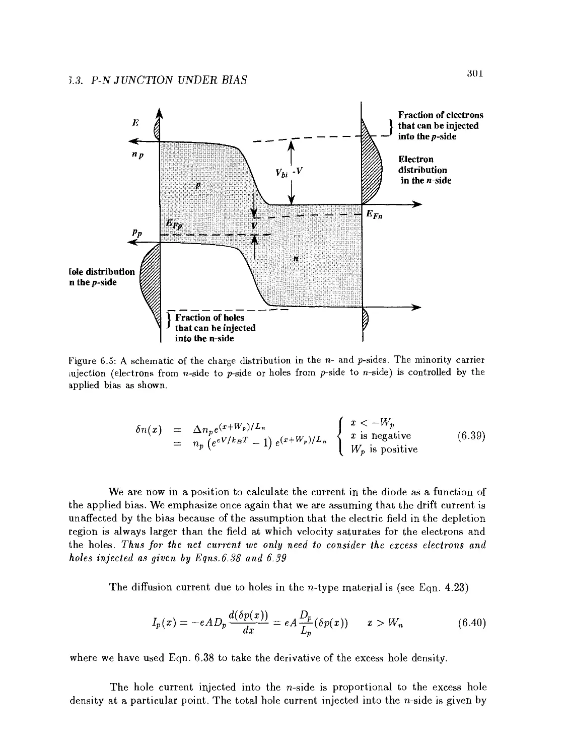
6.3.1 Charge injection and current flow 299
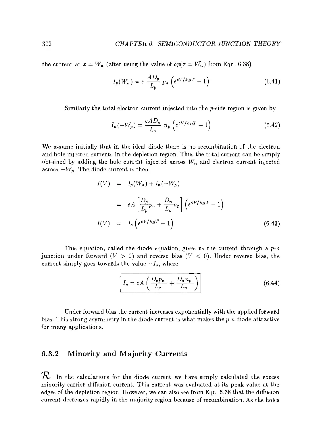
6.3.2 Minority and majority currents 302
6.4 The real diode: consequences of defects 307
6.5 High voltage effects in diodes 254
6.5-1 Forward bias: high injection region 309
6.5-2 Reverse bias: impact ionization 310
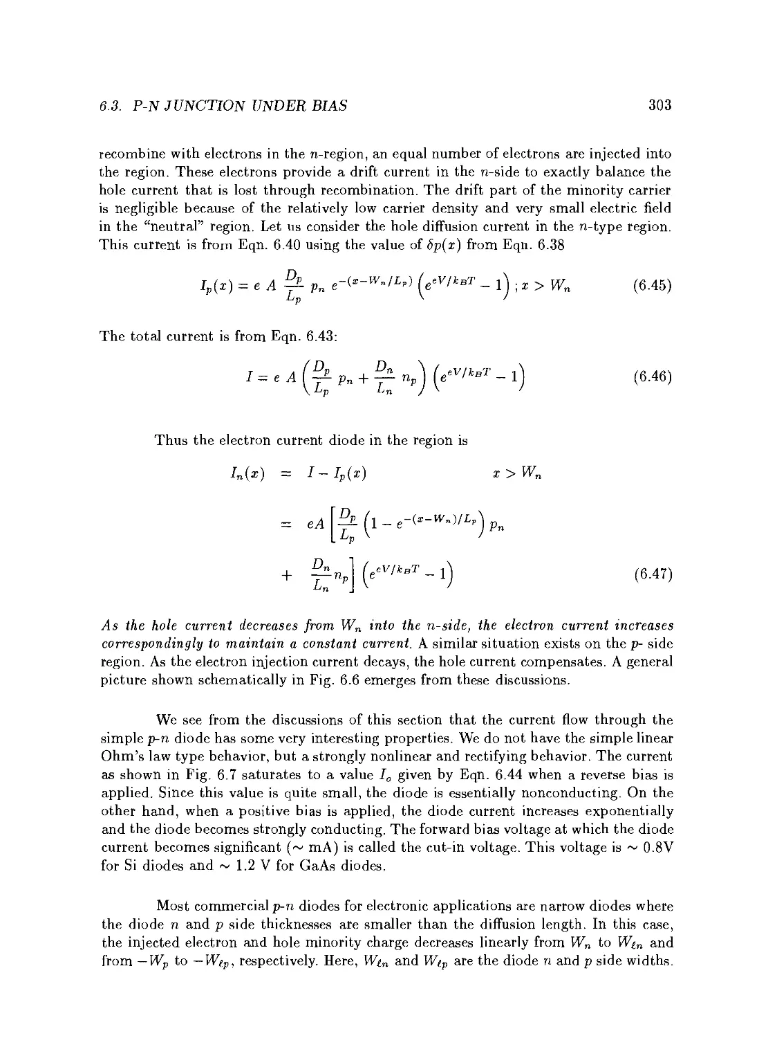
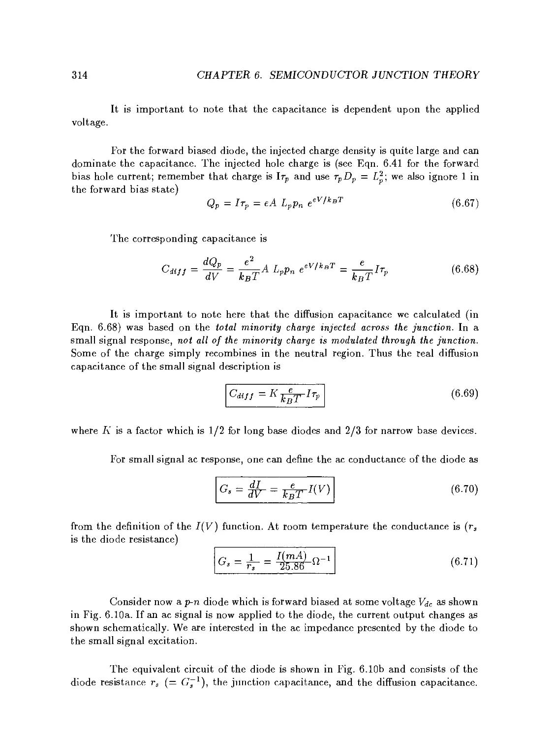
6.6 AC RESPONSE OF THE P-N DIODE 312
6.6.1 Small signal equivalent circuit of a diode 313
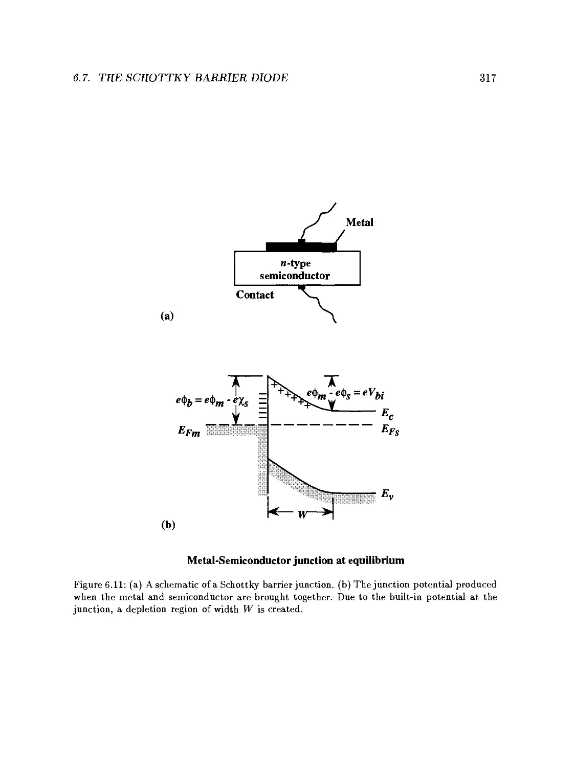
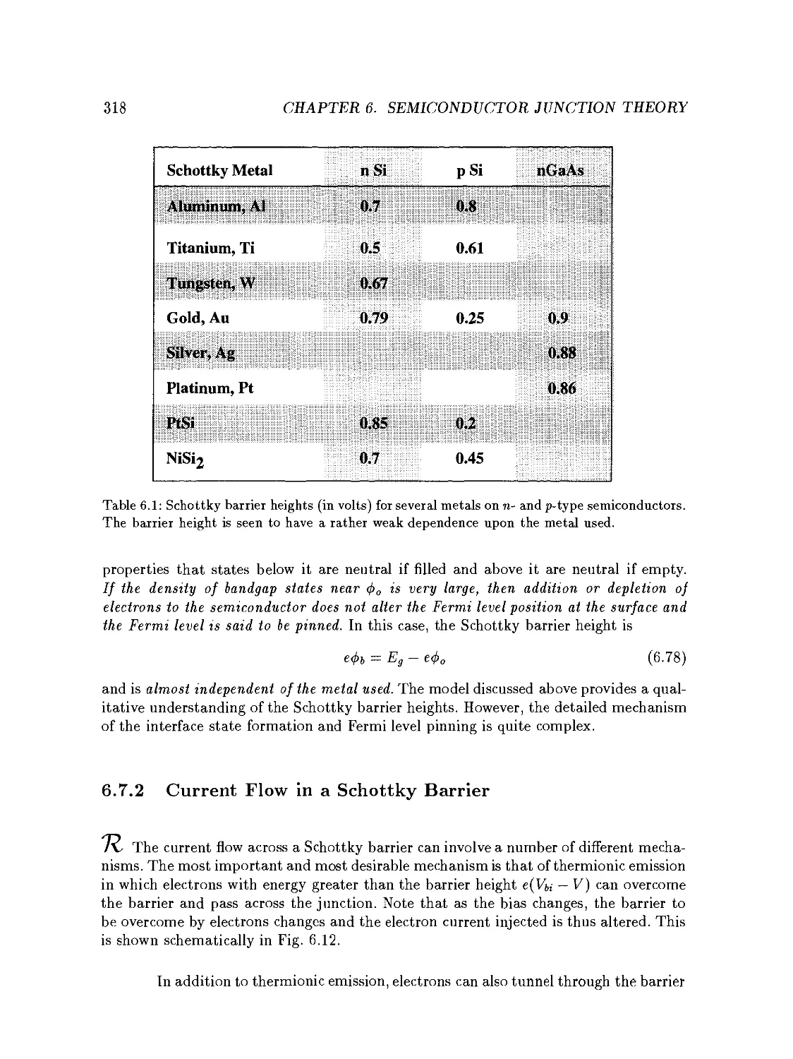
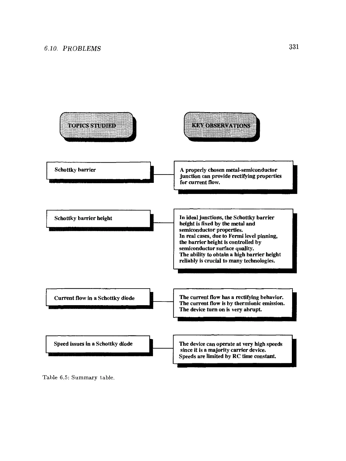
6.7 The Schottky barrier diode 316
6.7.1 Schottky barrier height 316
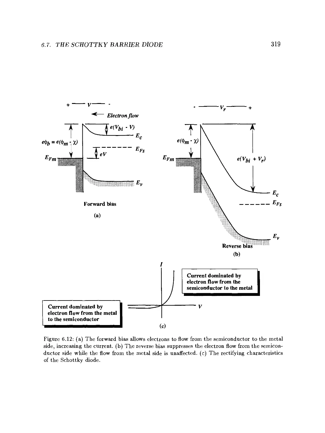
6.7.2 Current flow in a Schottky barrier 318
6.7.3 Small signal circuit of a Schottky diode 323
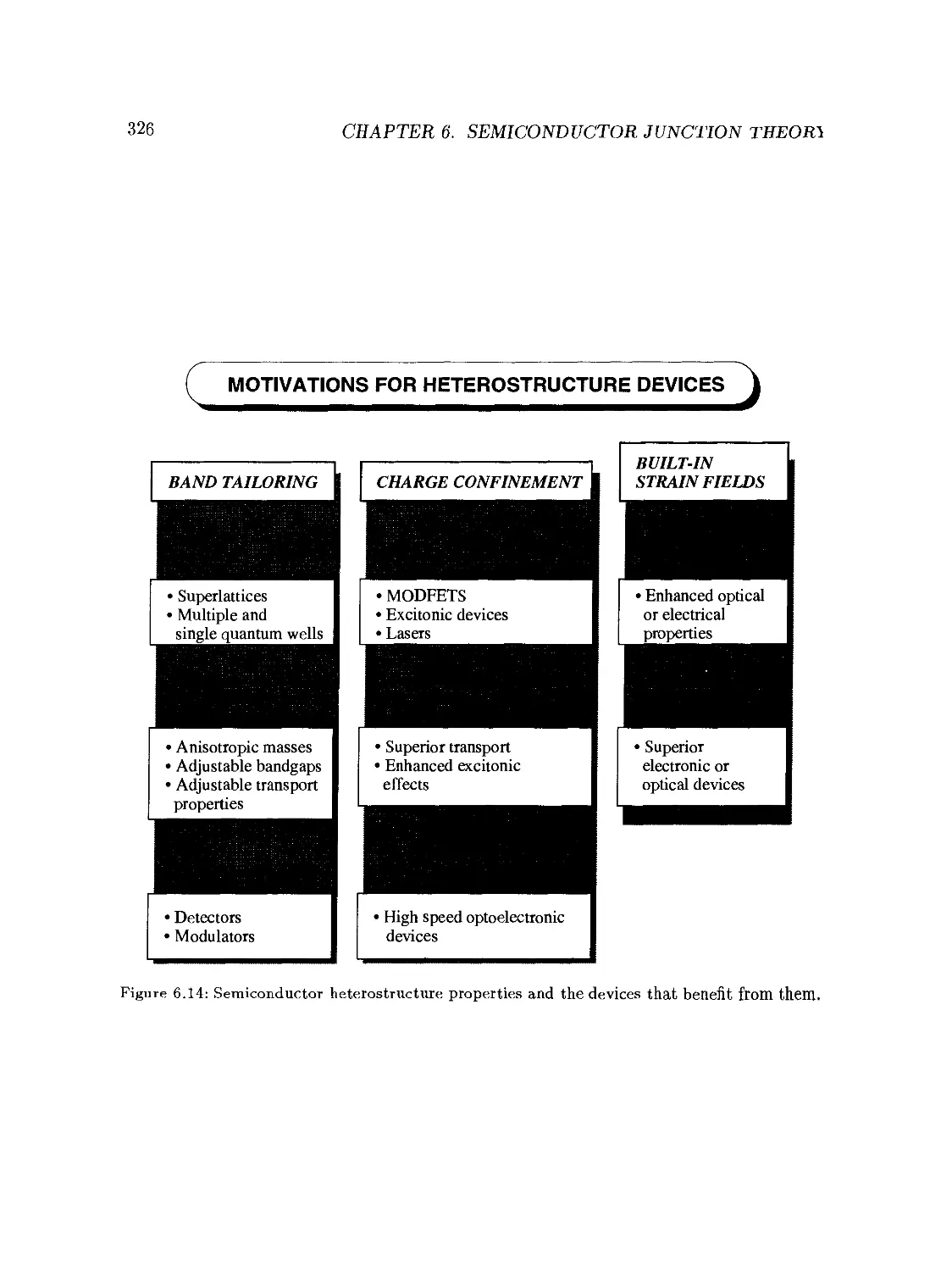
6.8 Heterostructure junctions 325
6.9 Chapter summary 327
6.10 Problems 327
6.11 References 334
OPTOELECTRONIC DETECTORS 336
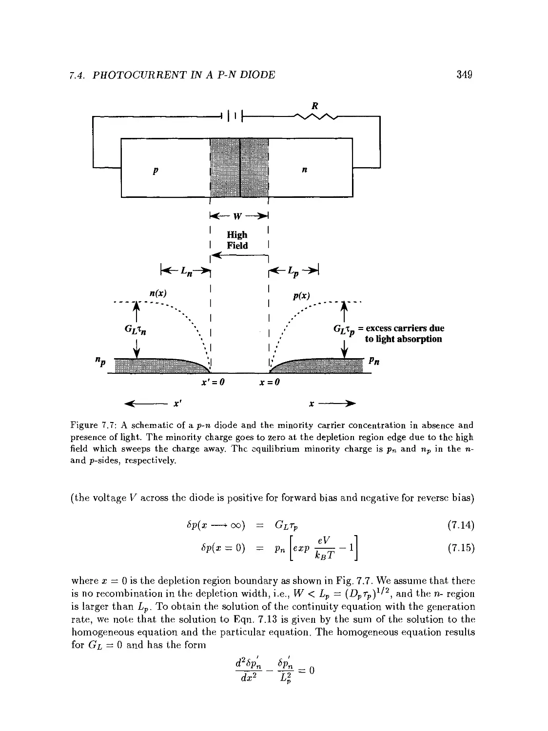
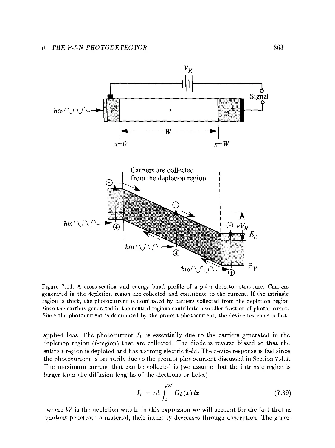
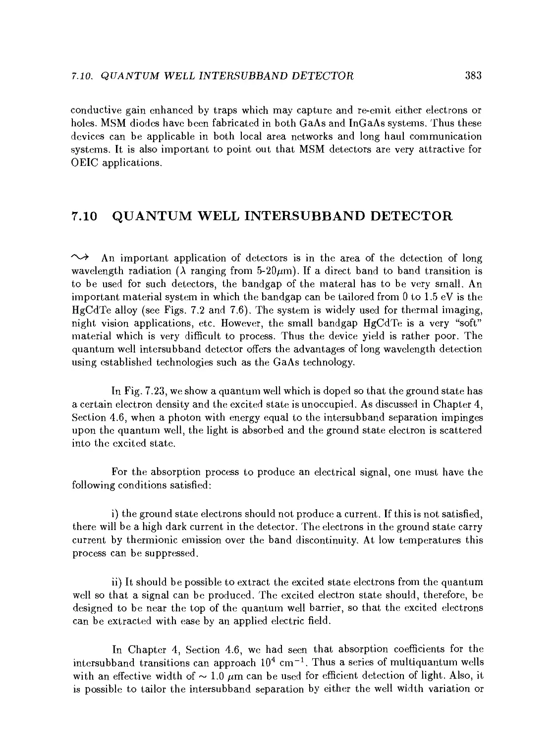
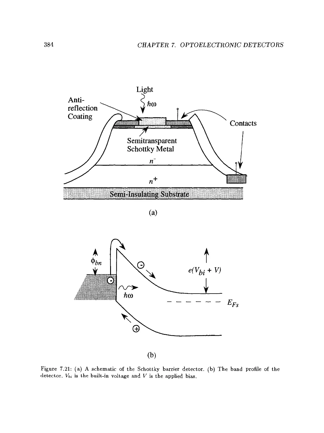
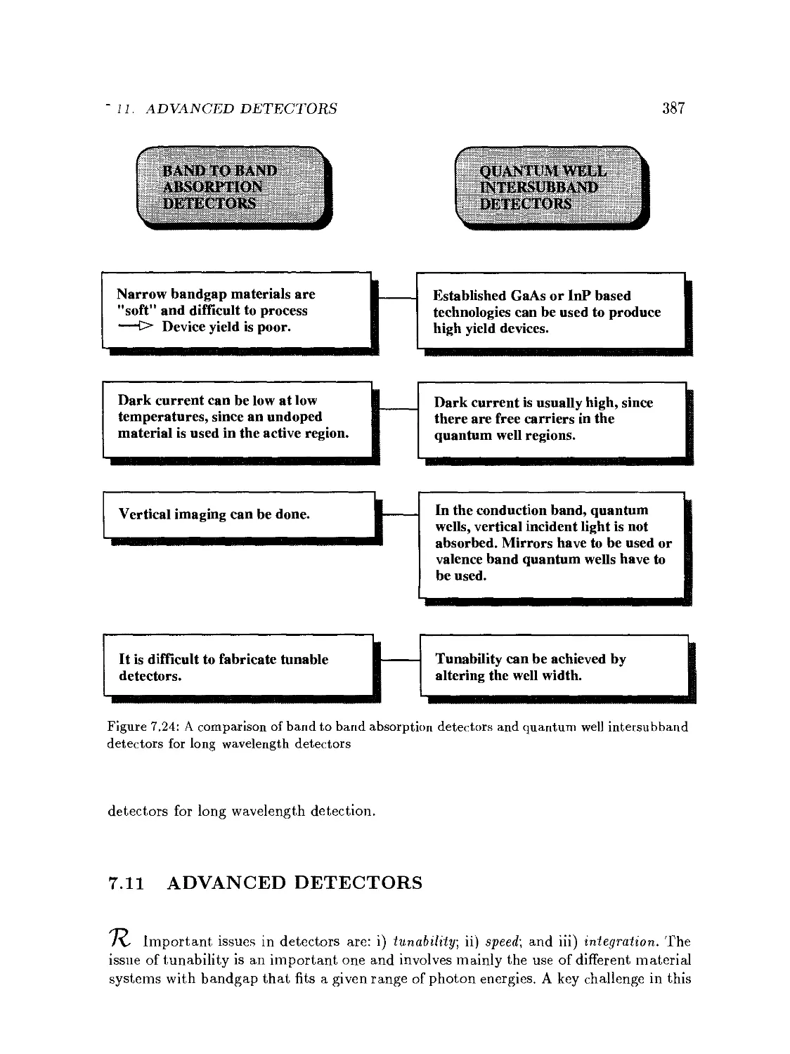
7.1 Introduction 336
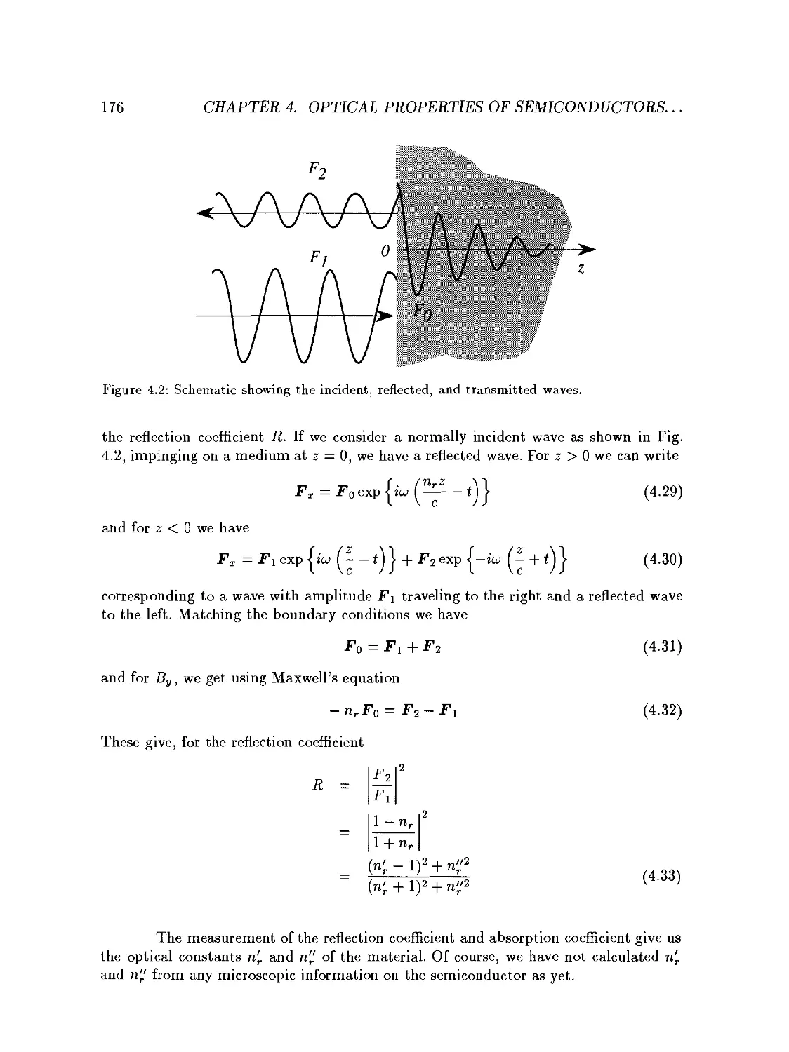
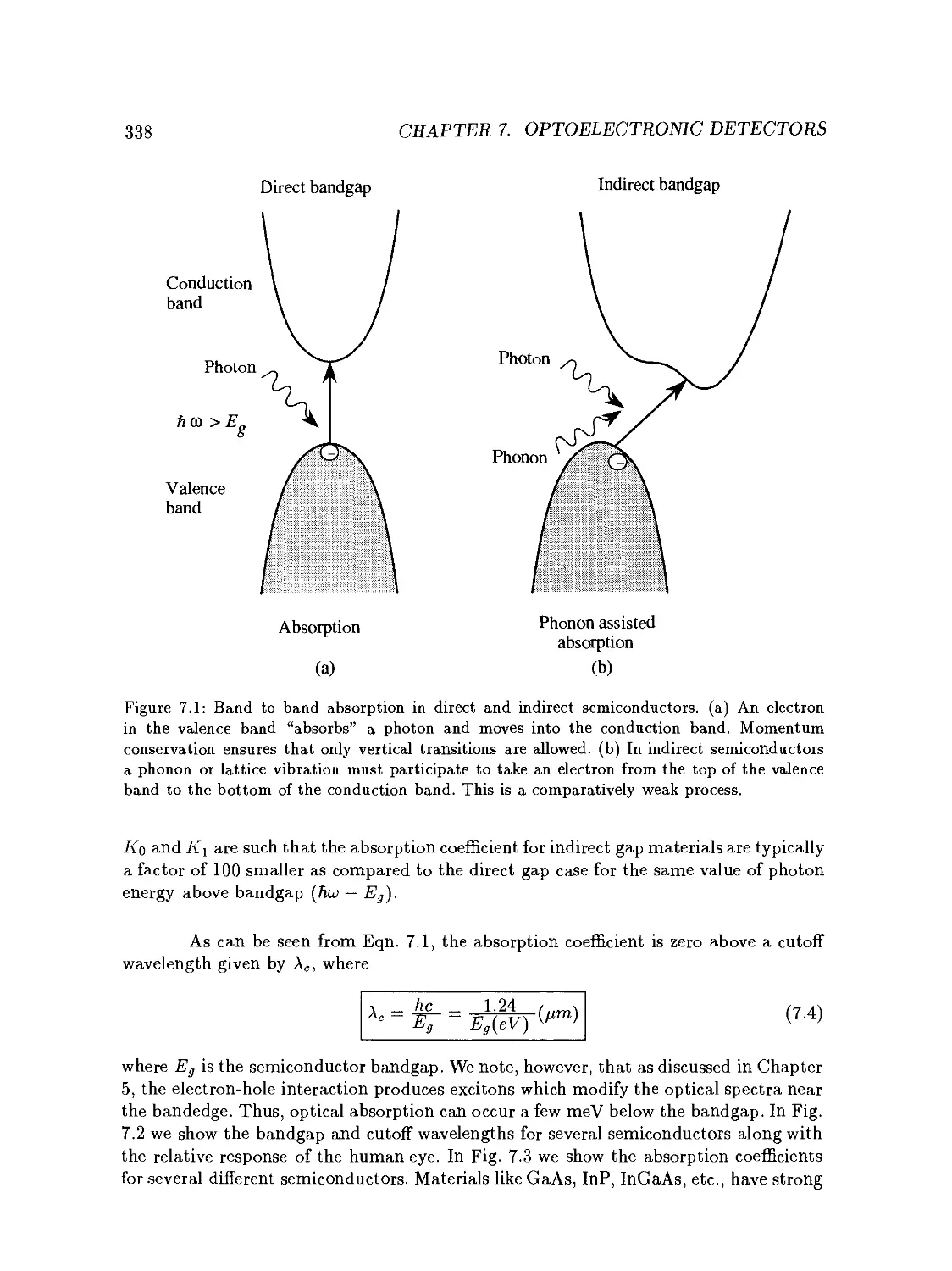
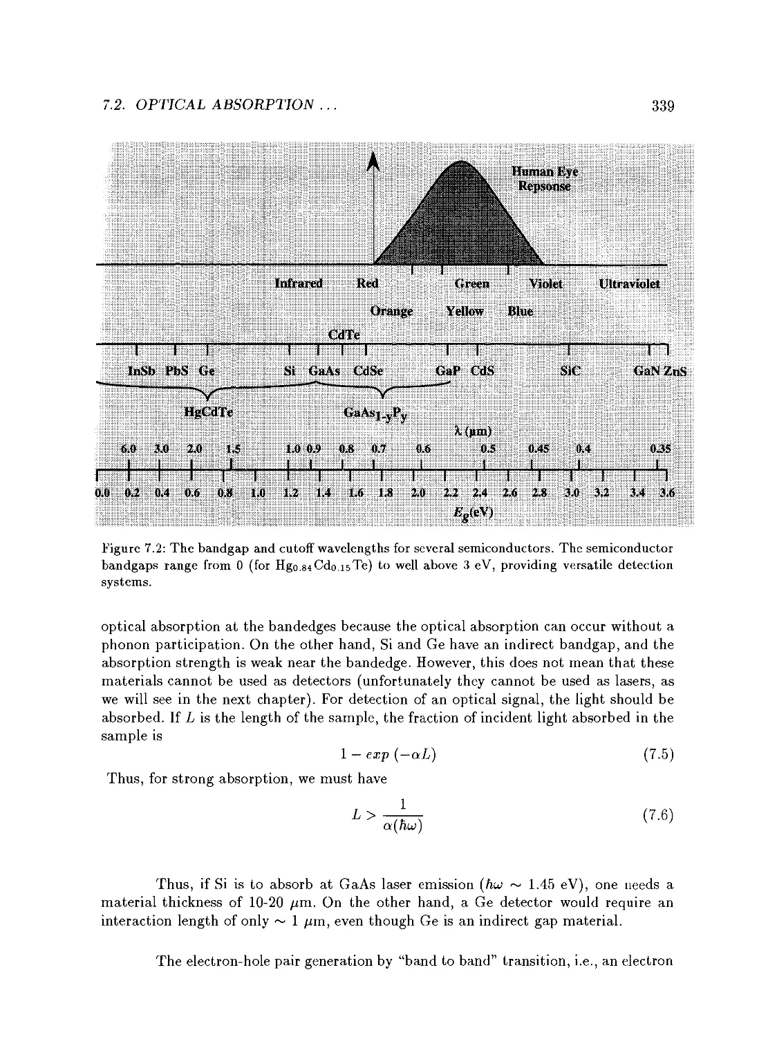
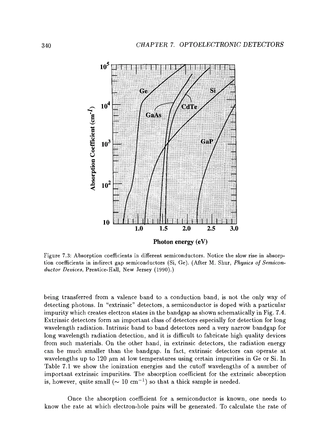
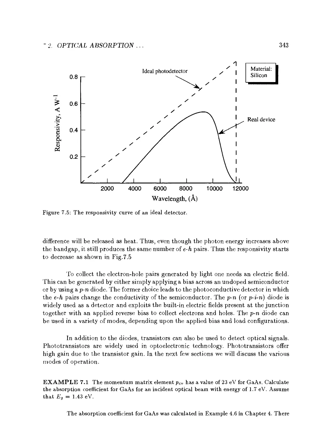
7.2 Optical absorption in a semiconductor 337
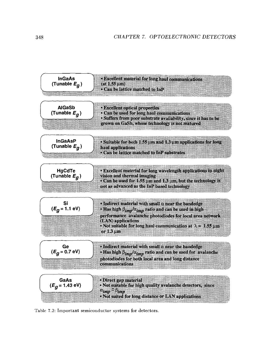
7.3 Materials for optical detectors
CONTENTS
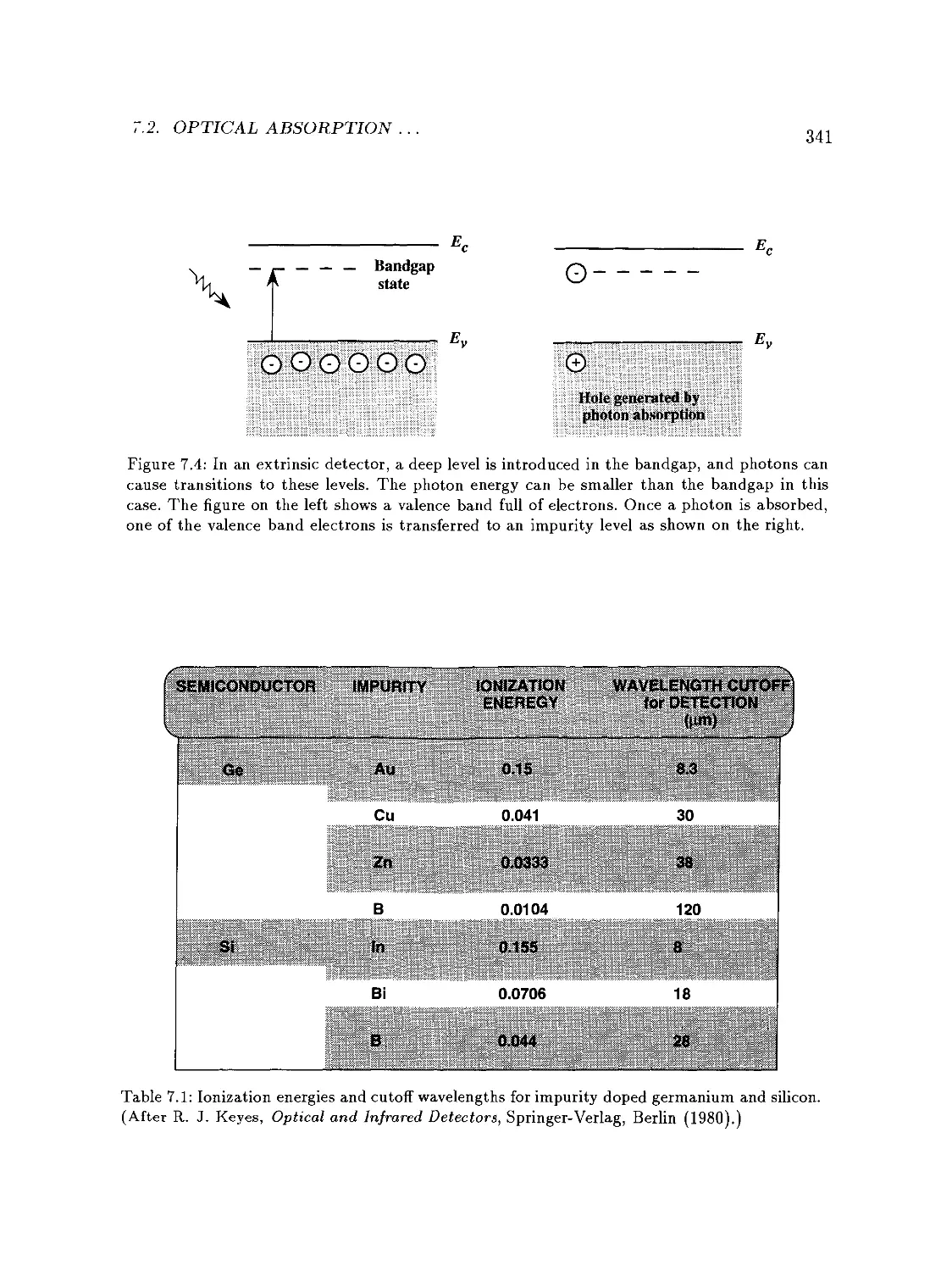
xv
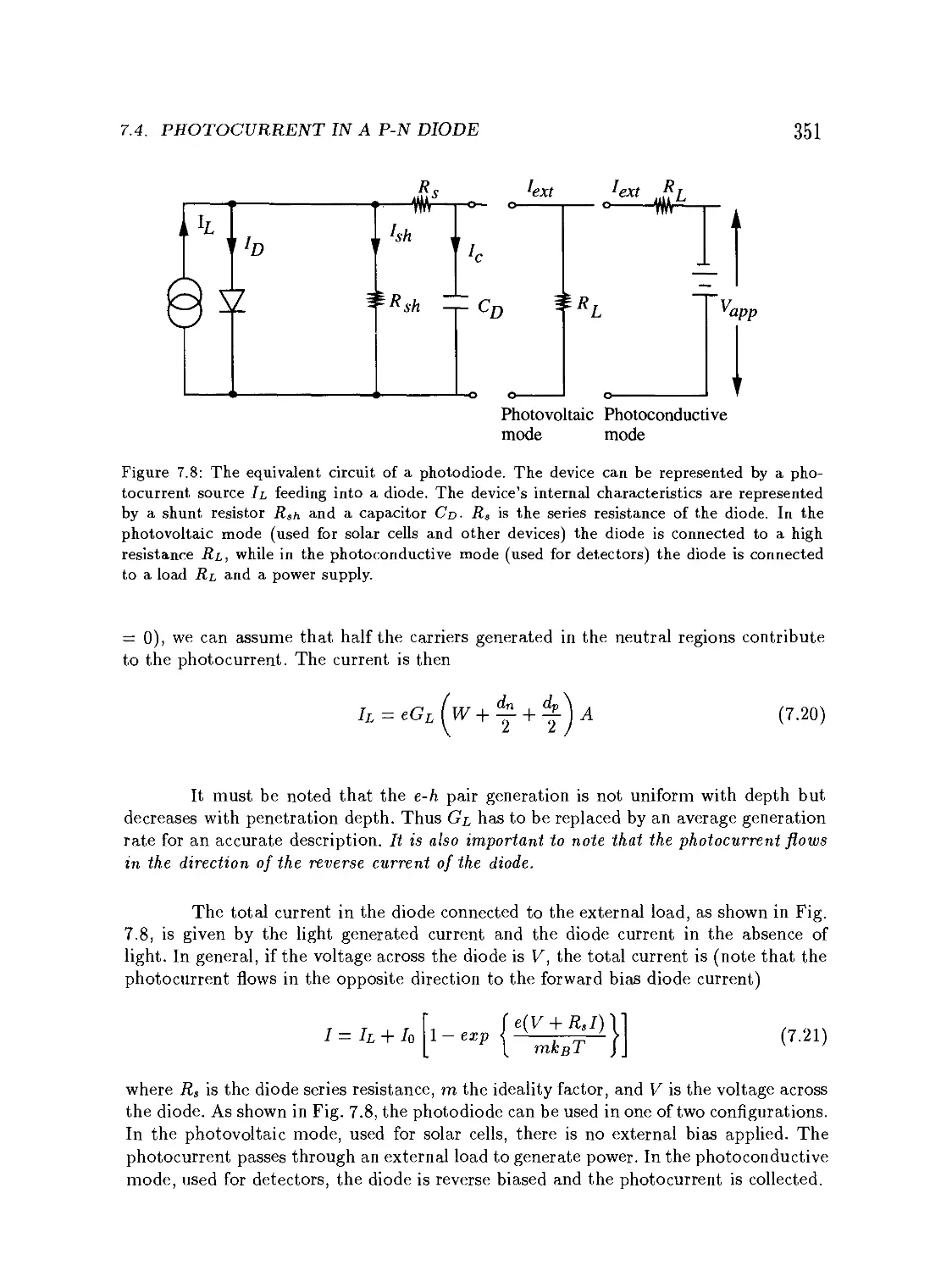
7.4 Photocurrent in a p-n diode 347
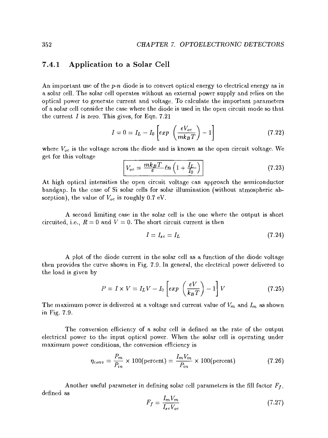
7.4.1 Application to a solar cell 352
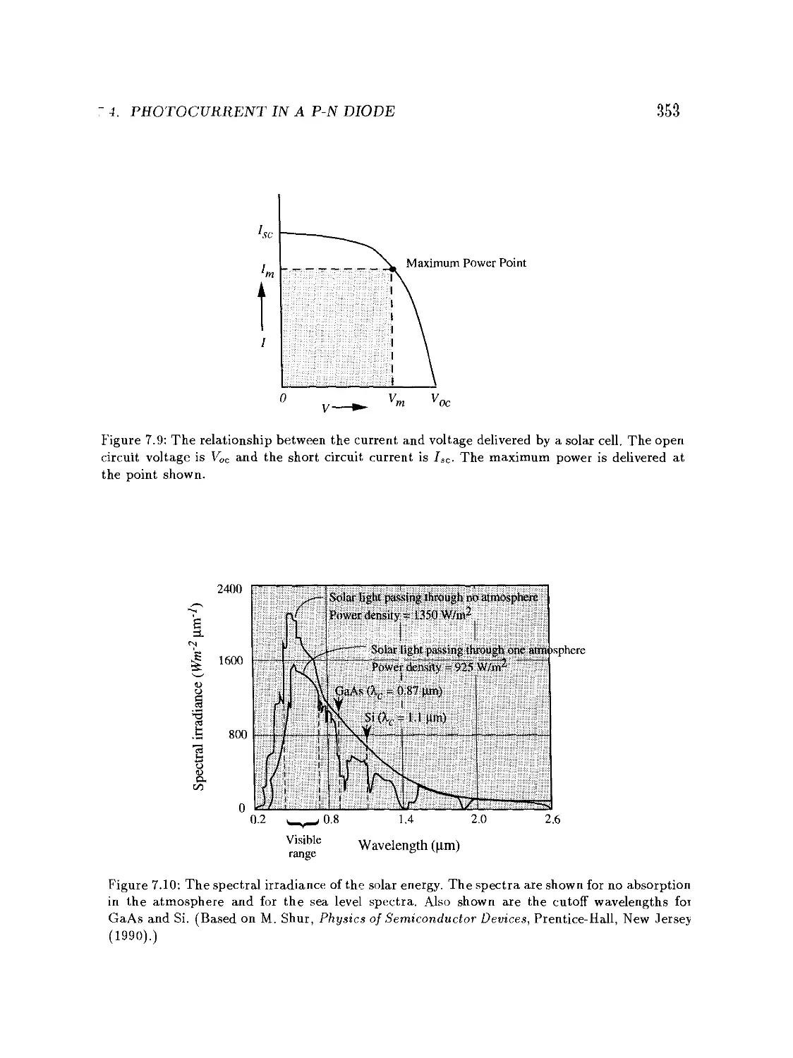
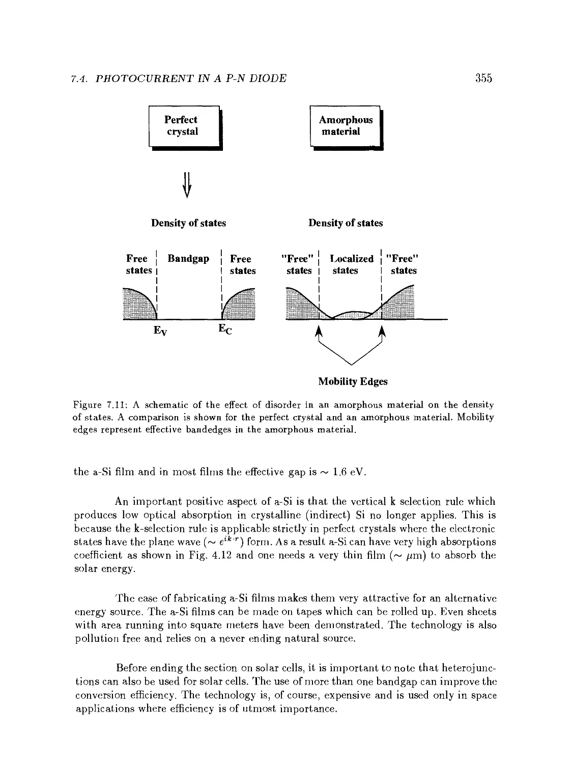
7.4.2 Amorphous silicon solar cells 354
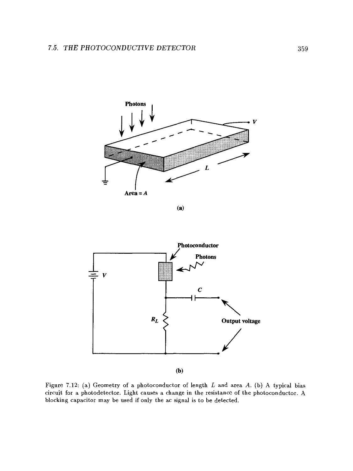
7.5 The photoconductive detector 358
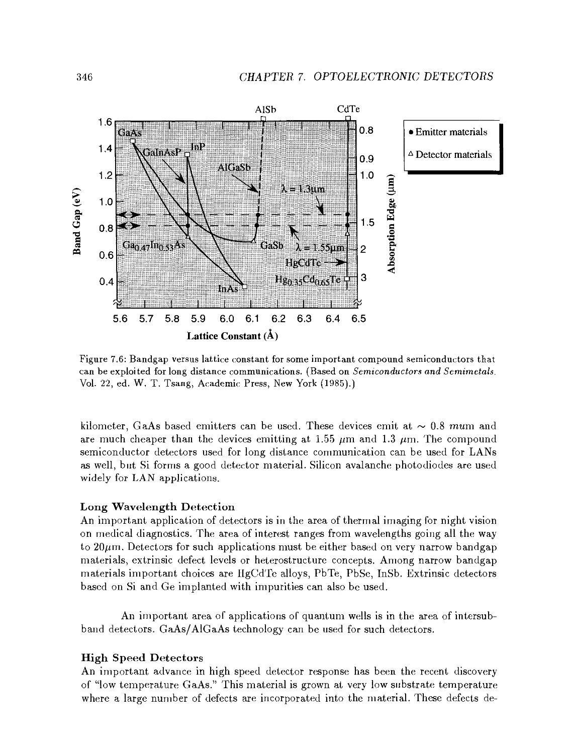
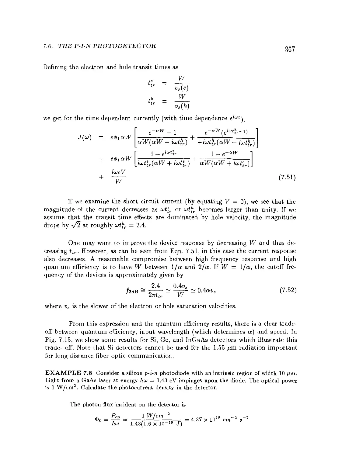
7.6 The p-i-n photodetector 362
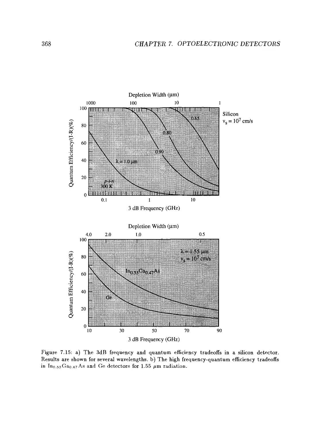
7.6.1 Material choice and frequency response of a p-i-n detector 364
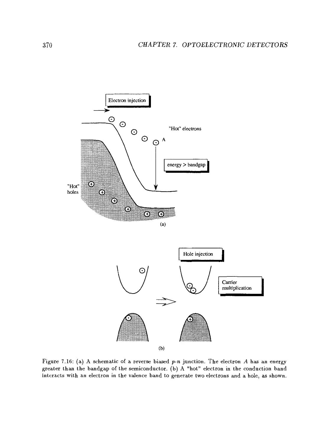
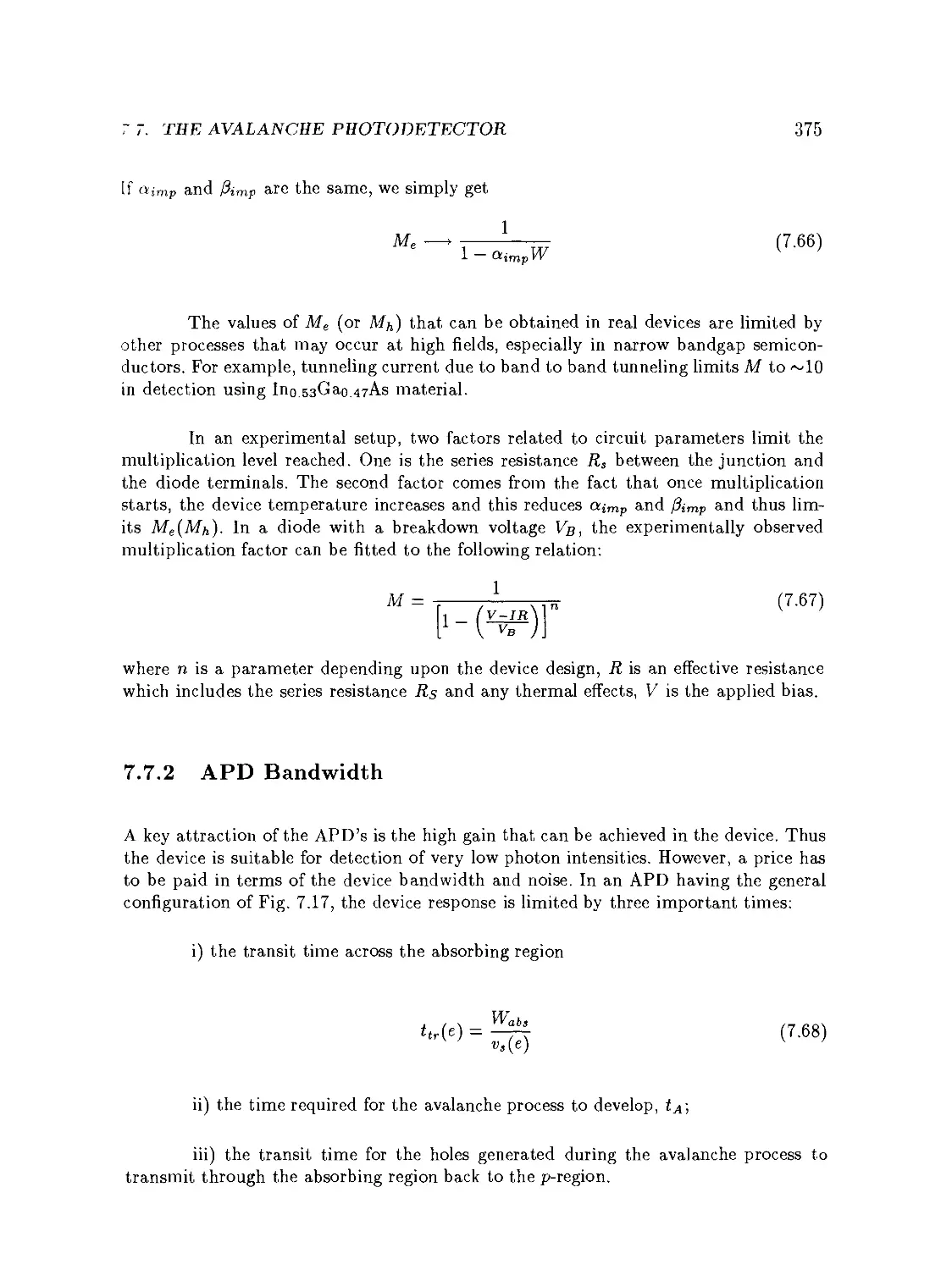
7.7 The avalanche photodetector 369
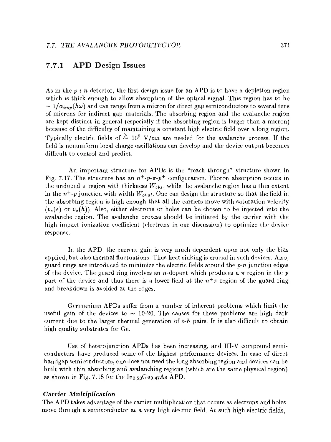
7.7.1APD design issues 371
7.7.2 APD bandwidth 375
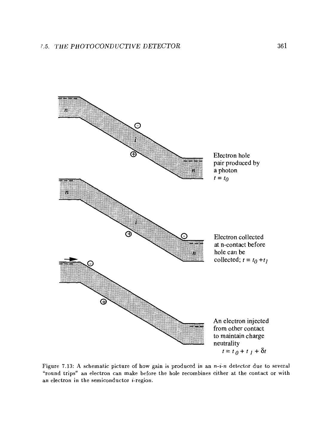
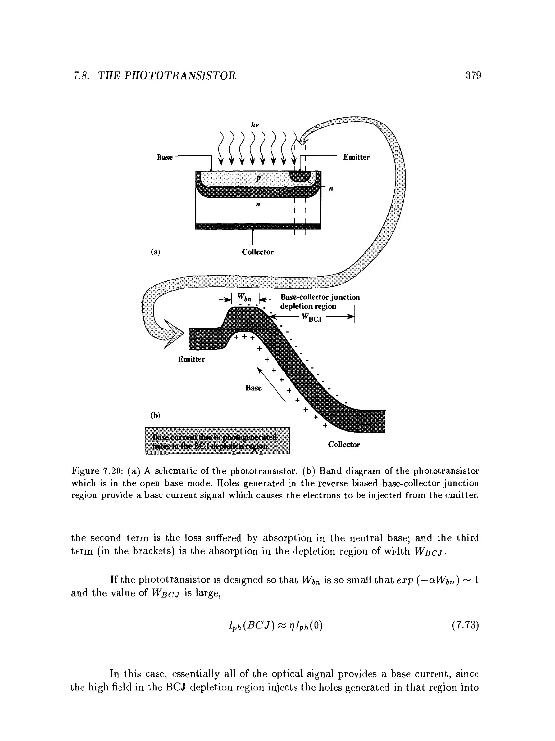
7.8 The phototransistor 378
7.9 Metal-semiconductor detectors 381
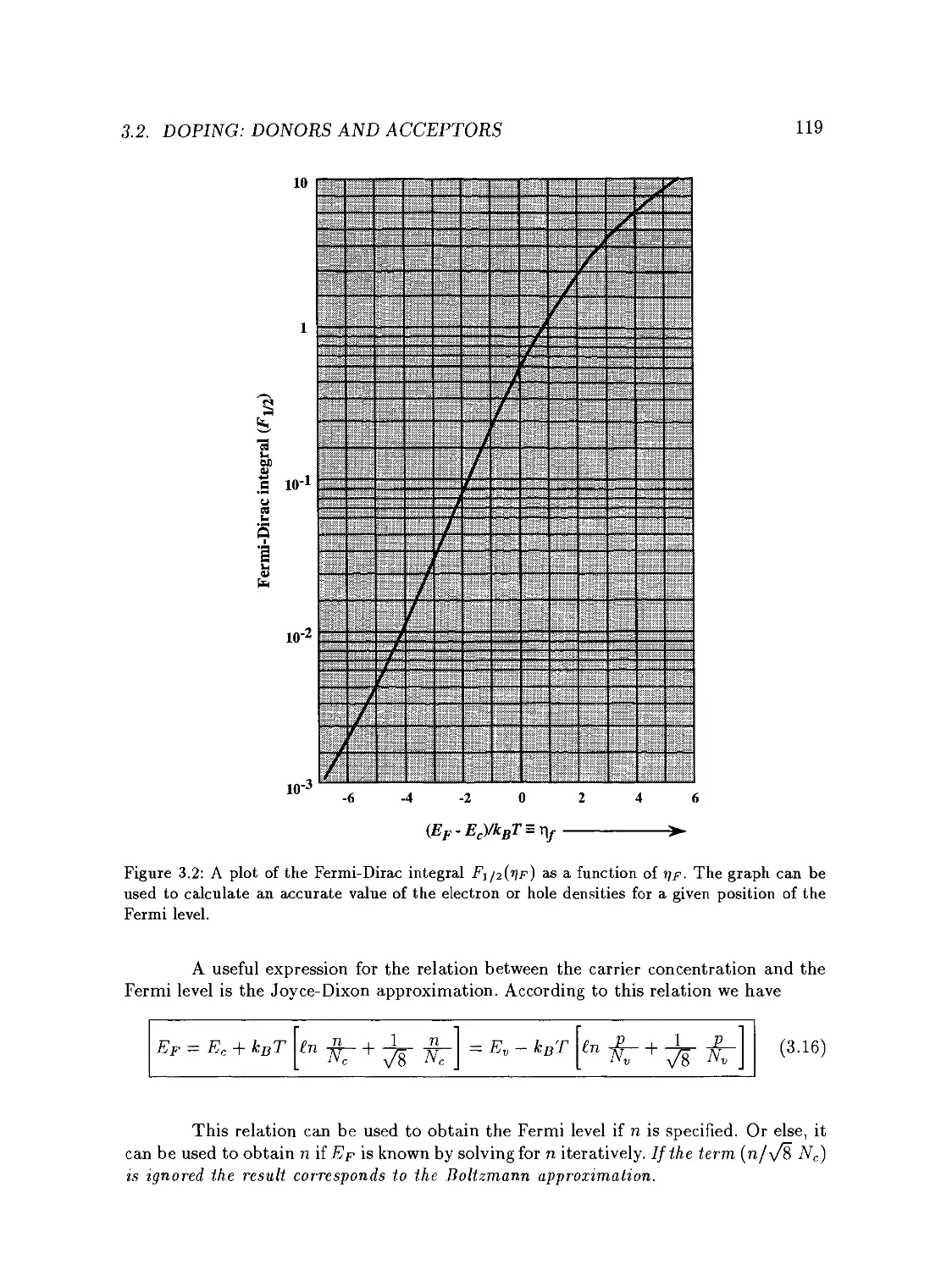
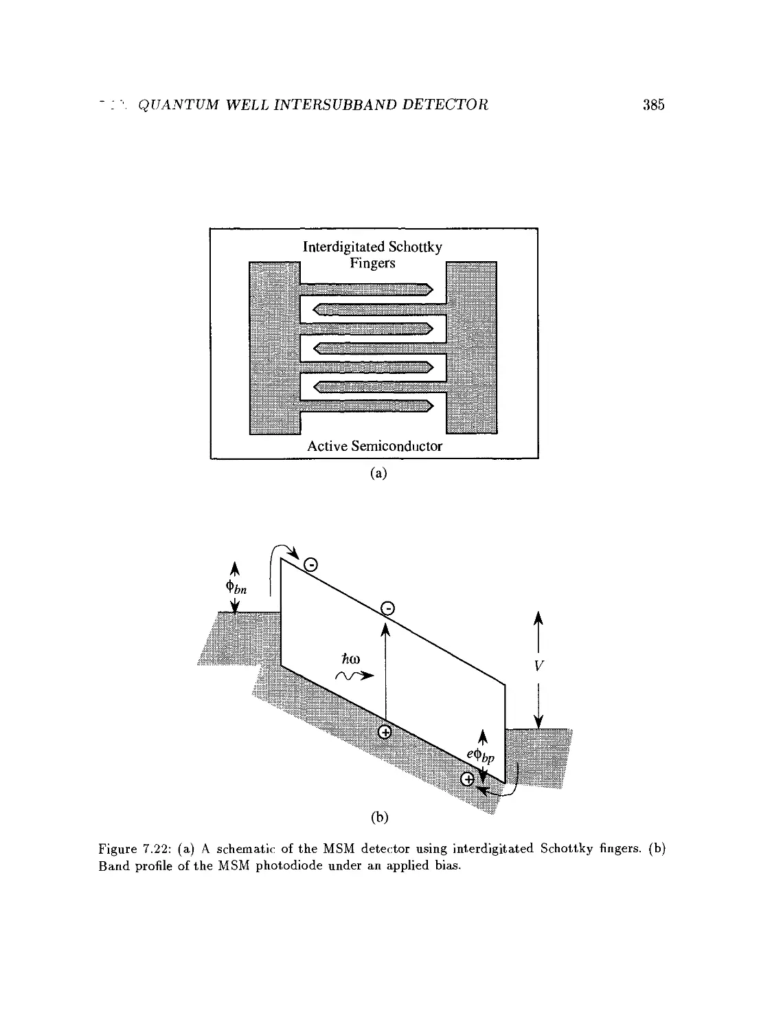
7.10 Quantum well intersubband detector 383
7.11 Advanced detectors 387
7.12 Chapter summary 390
7.13 Problems 395
7.14 References 398
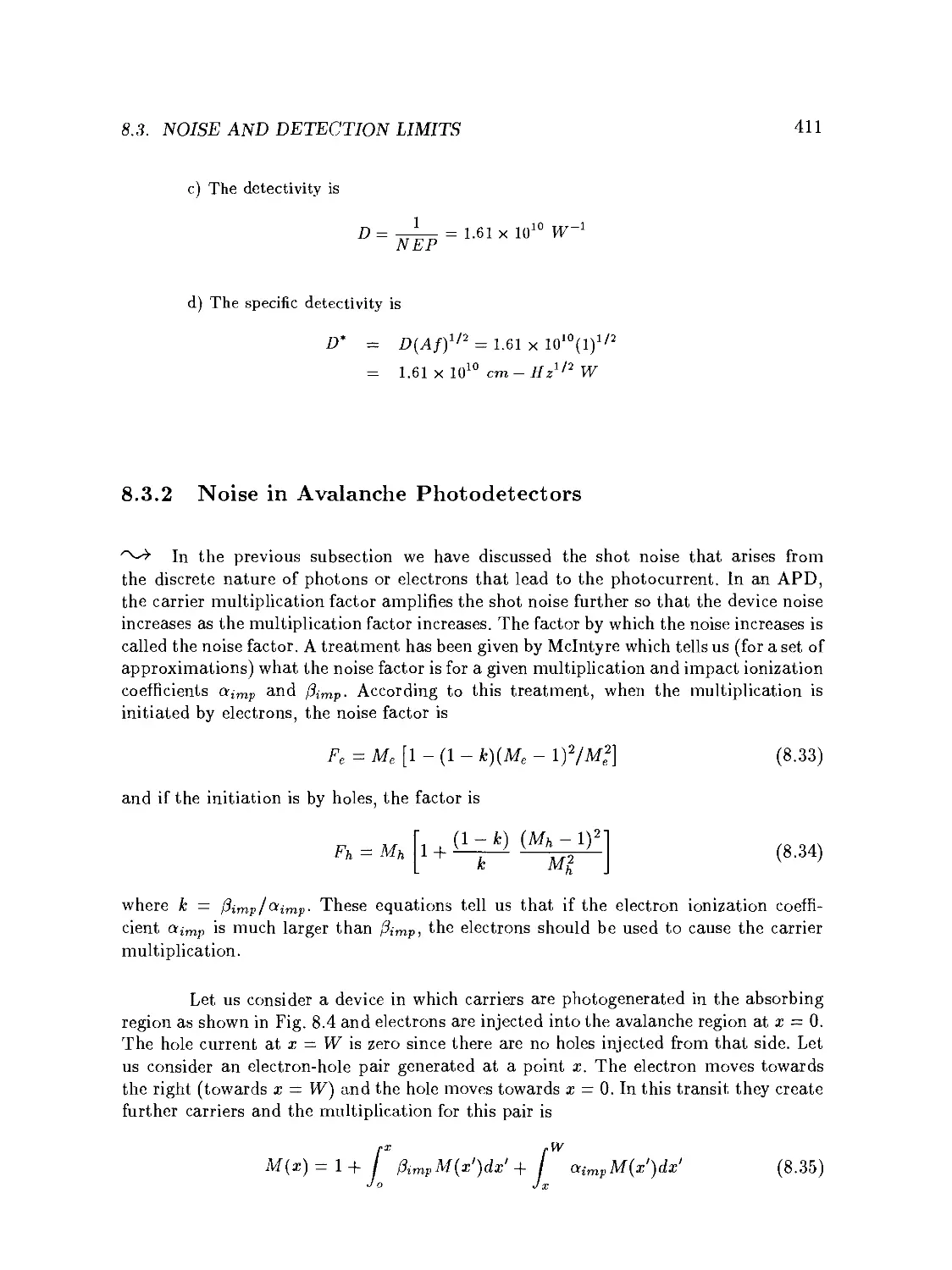
8
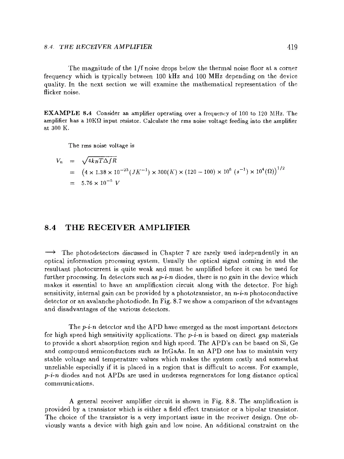
NOISE AND THE PHOTORECEIVER 399
8.1 Introduction 399
8.2 Modulation and detection schemes 400
8.2.1 Amplitude modulation 400
8.2.2 Frequency modulation 401
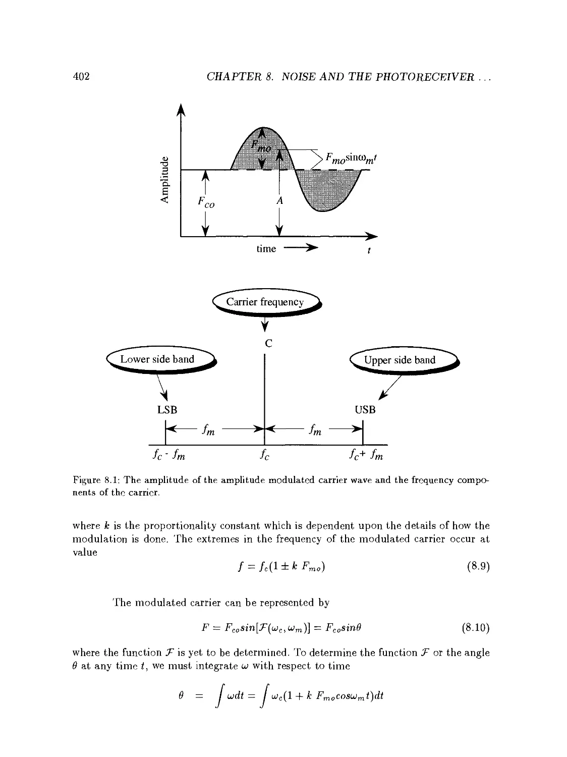
8.2.3 Intensity modulation 405
8.3 Noise and detection limits 405
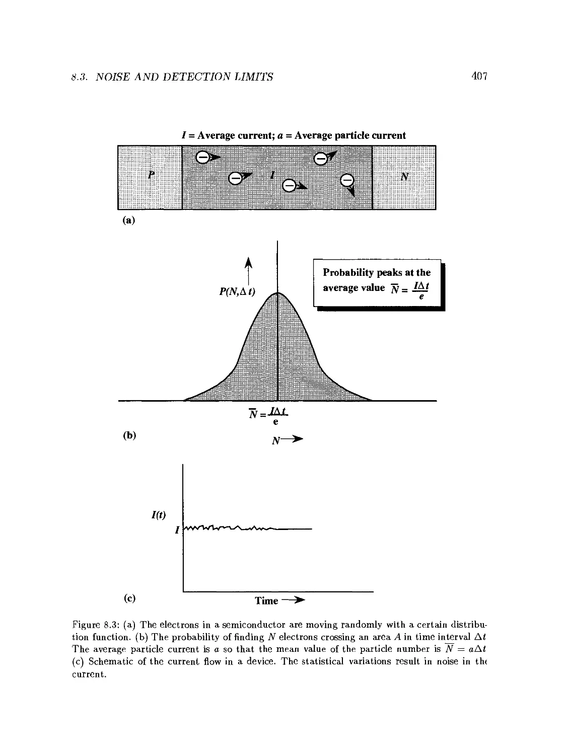
8.3.1 Shot noise 406
8.3.2 Noise in avalanche photodetectors 411
8.3.3 Noise in resistors and electronic devices 415
8.3.4 Flicker noise 418
CONTENTS
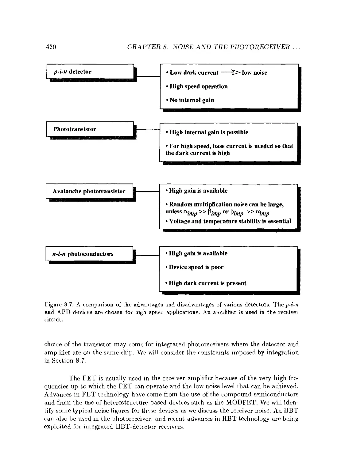
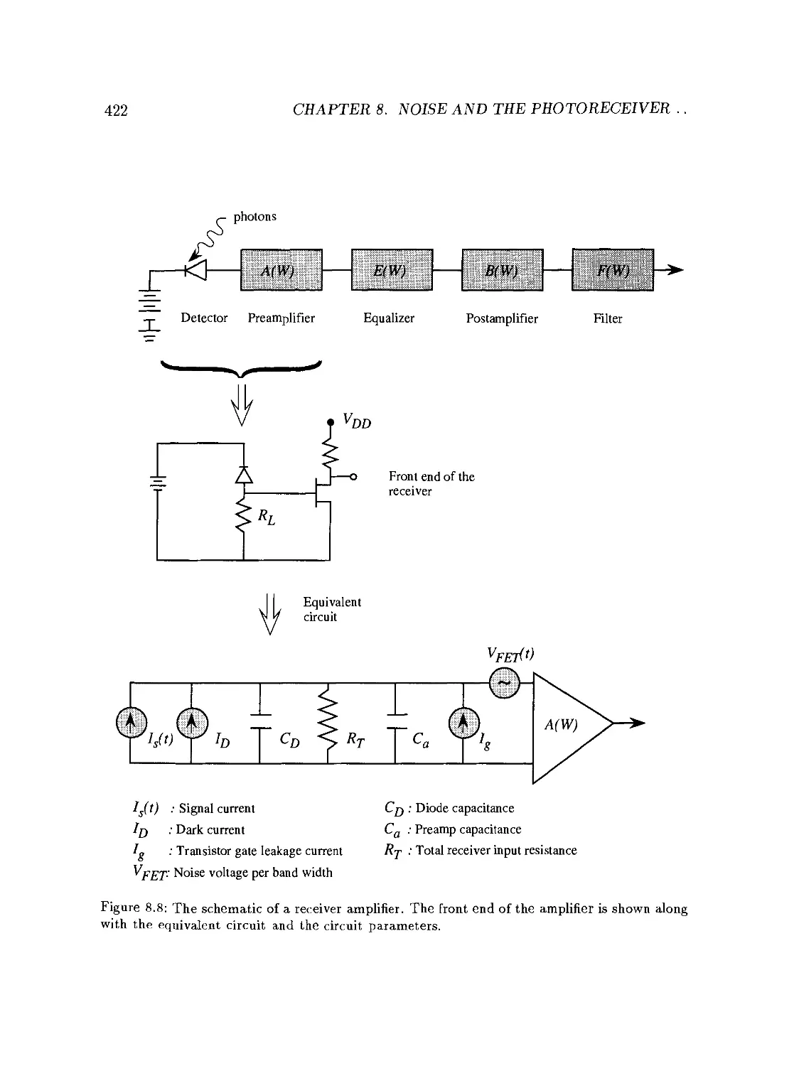
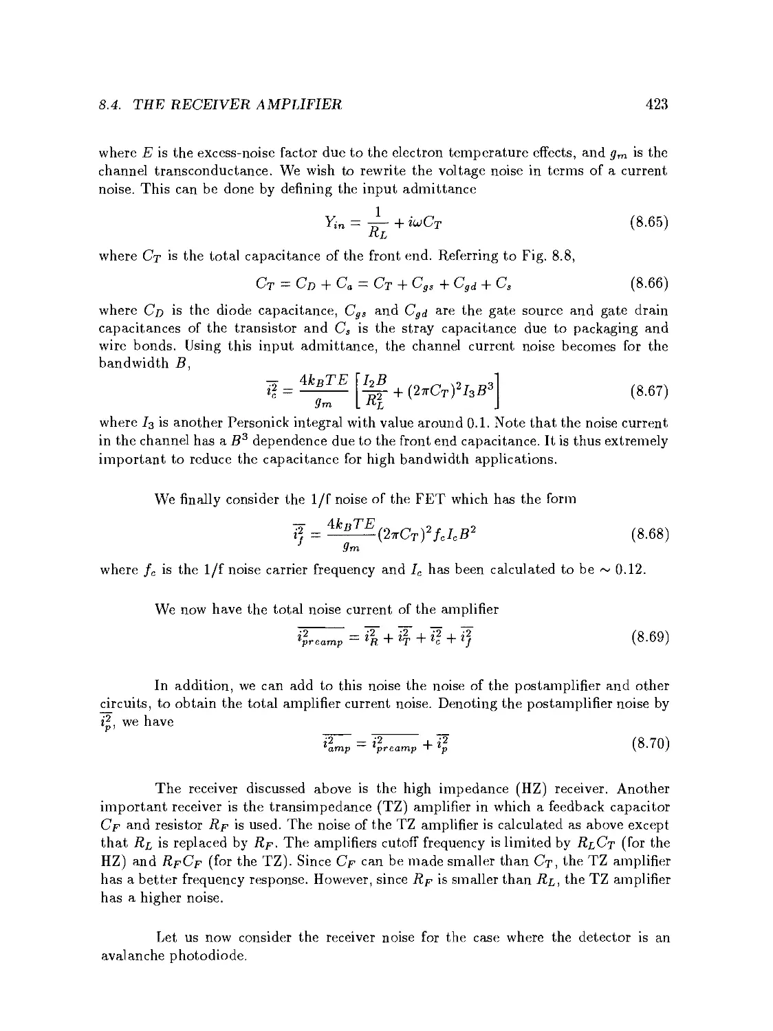
8.4 The receiver amplifier 419
8.4.1APD receiver noise 424
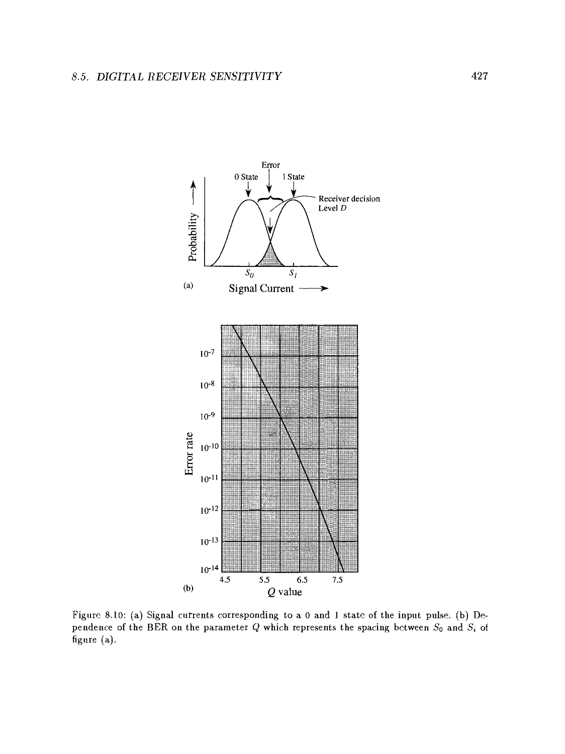
8.5 Digital receiver sensitivity 425
8.5.1 APD receiver sensitivity 429
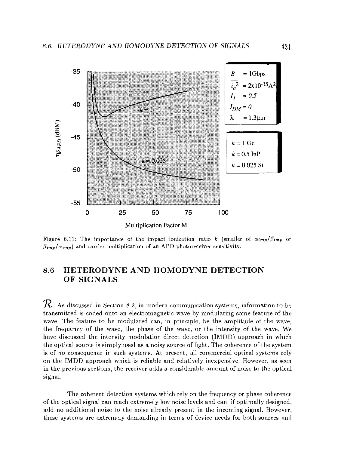
8.6 Heterodyne and homodyne detection of signals 431
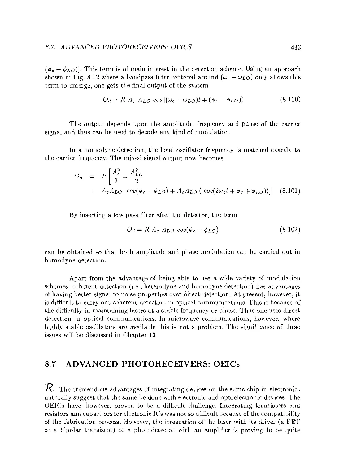
8.7 Advanced photoreceivers: oeics 433
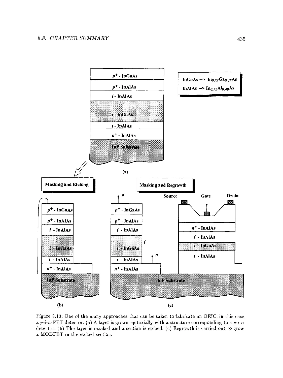
8.8 Chapter summary 434
8.9 Problems 436
8.10 References 440
THE LIGHT EMITTING DIODE 441
9.1 Introduction 441
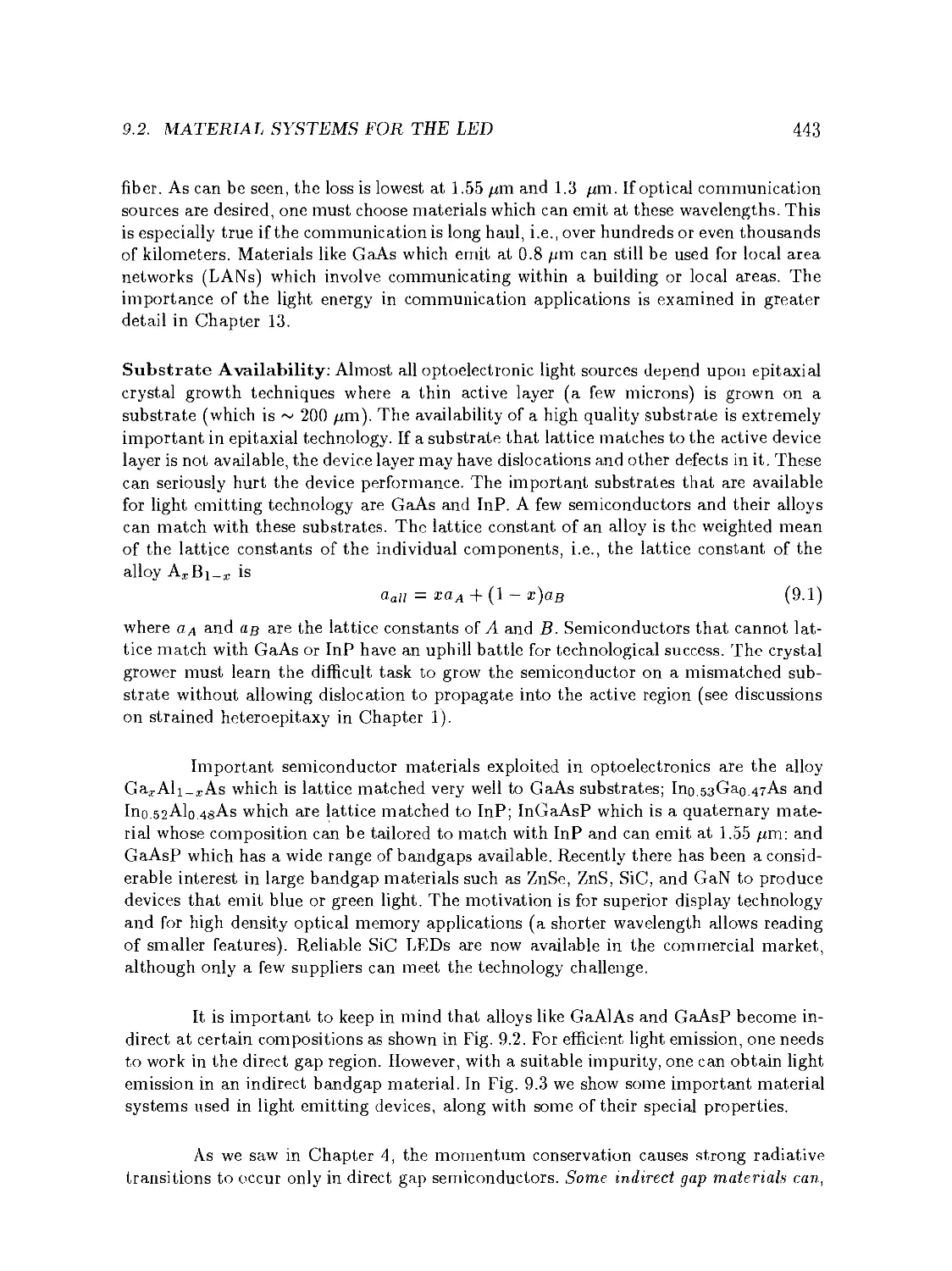
9.2 Material systems for the led 442
9.3 Operation of the led 444
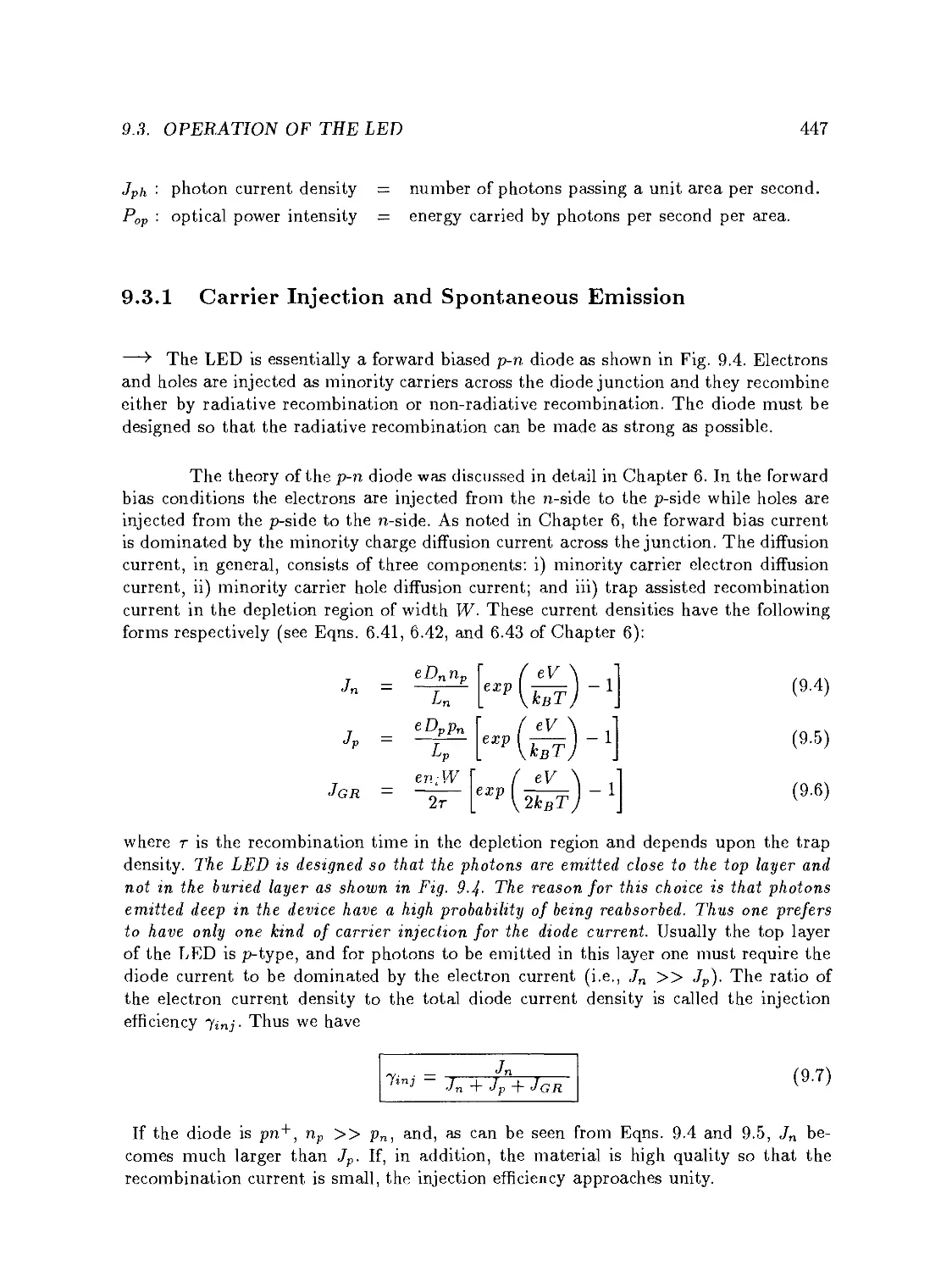
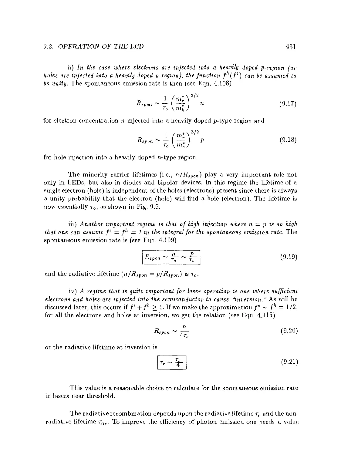
9.3.1 Carrier injection and spontaneous emission 447
9.4 External quantum efficiency 456
9.5 Advanced led structures 459
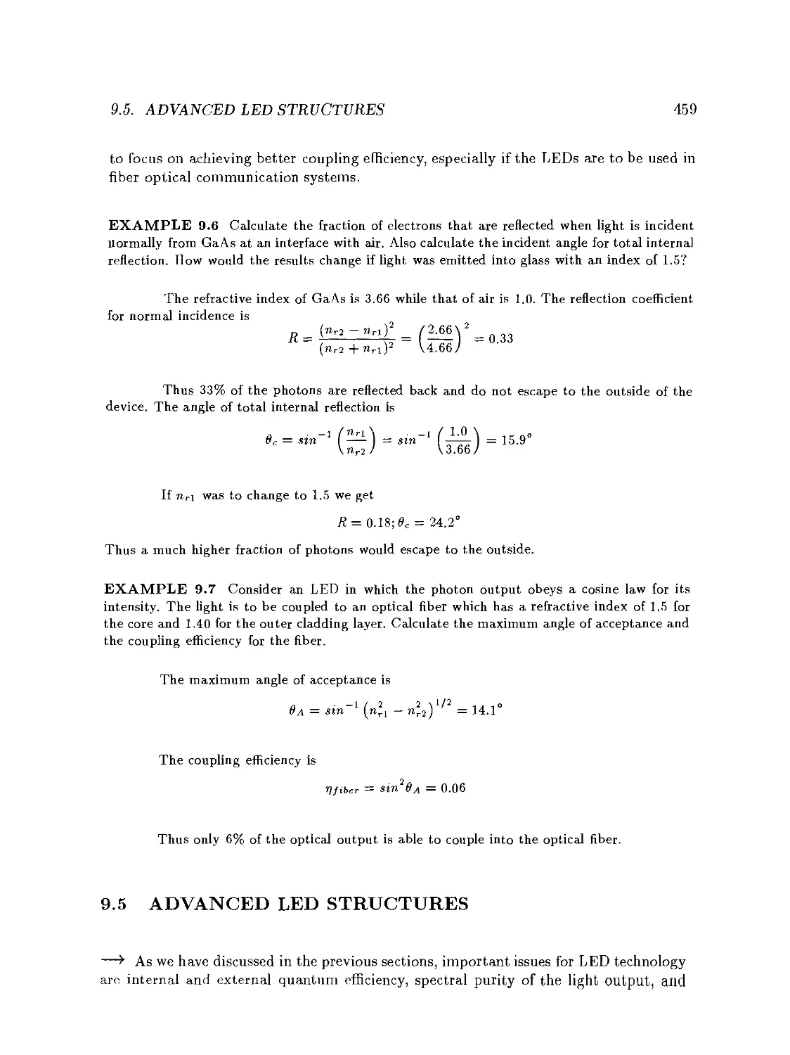
9-5.1 Heterojunction LED 460
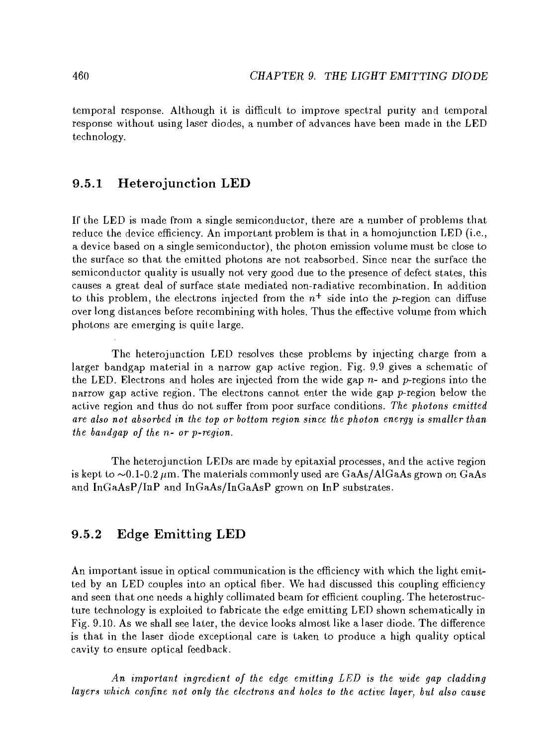
9.5.2 Edge Emitting LED 460
9.5.3 Surface emitting LED 462
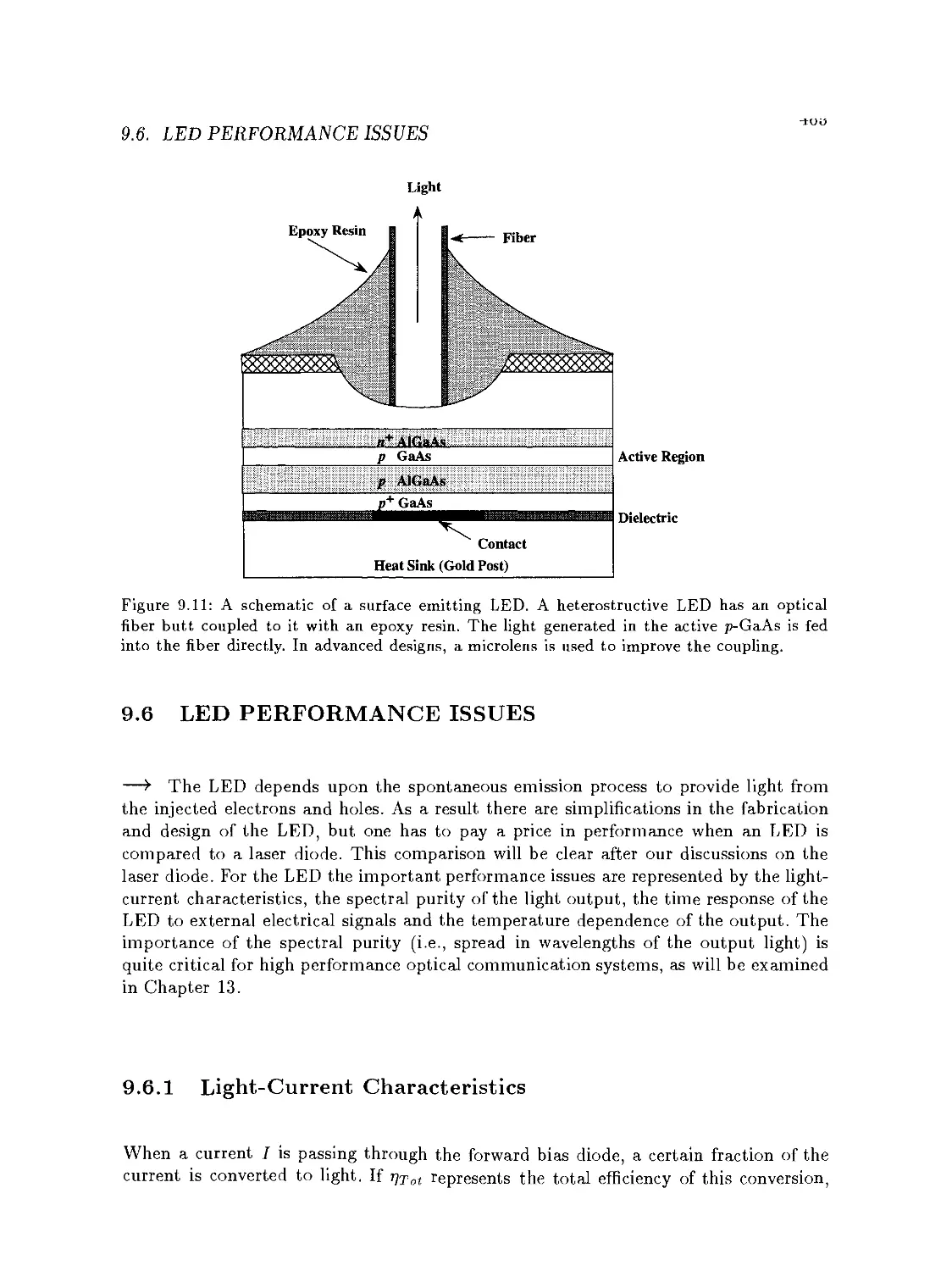
9.6 LED performance issues 463
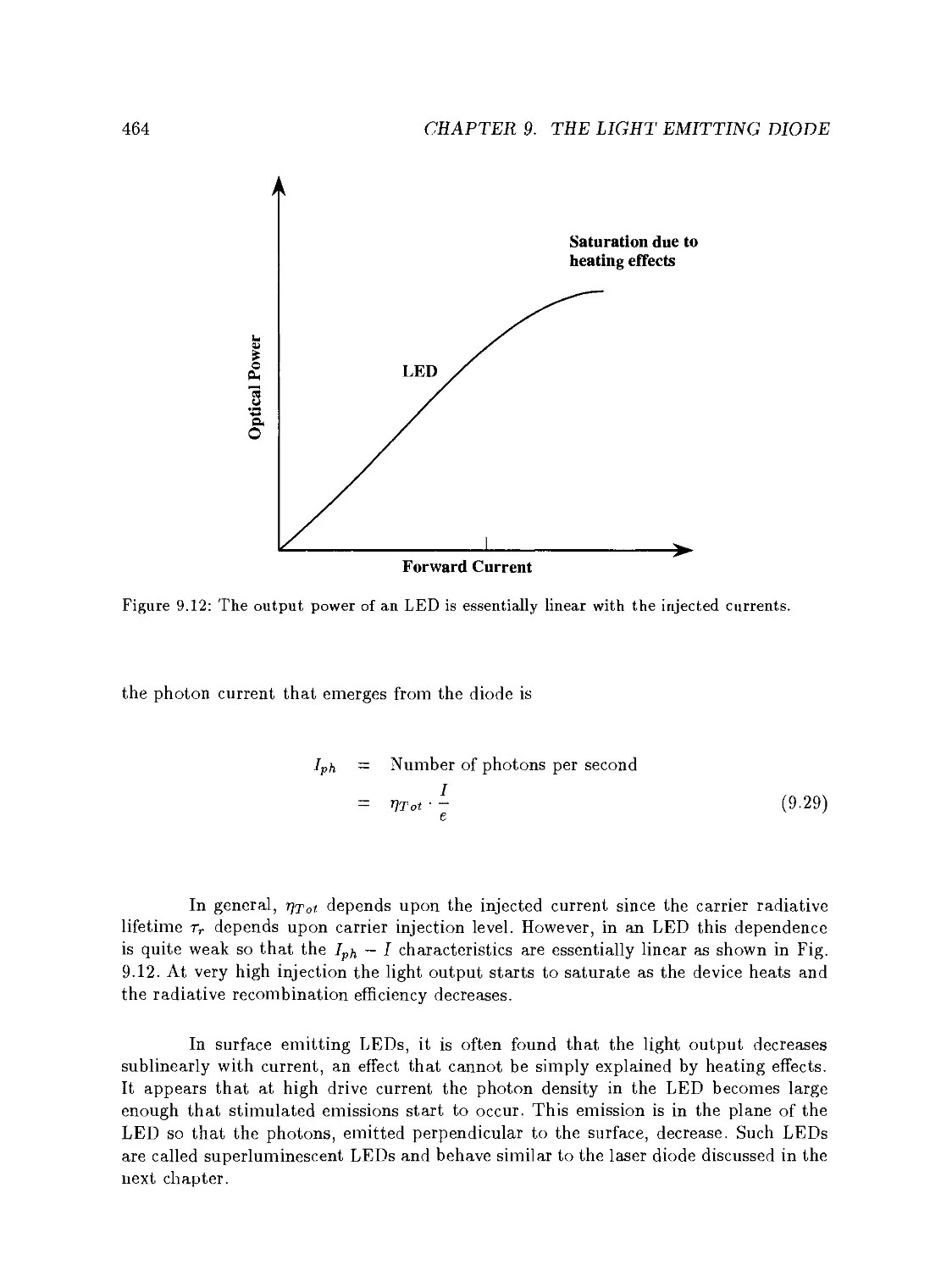
9.6.1 Light-current characteristics 463
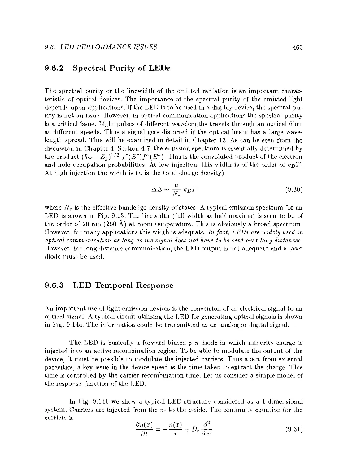
9.6.2 Spectral purity of LEDs 465
9-6.3 LED temporal response 465
9.6.4 Temperature dependence of LED emission 471
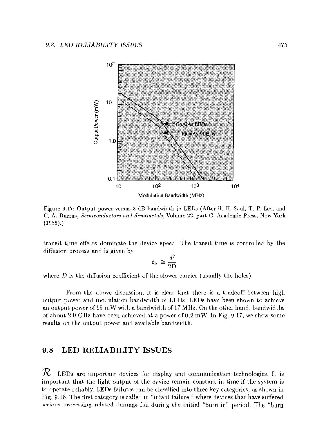
9.7 Output power and modulation bandwidth 472
9.8
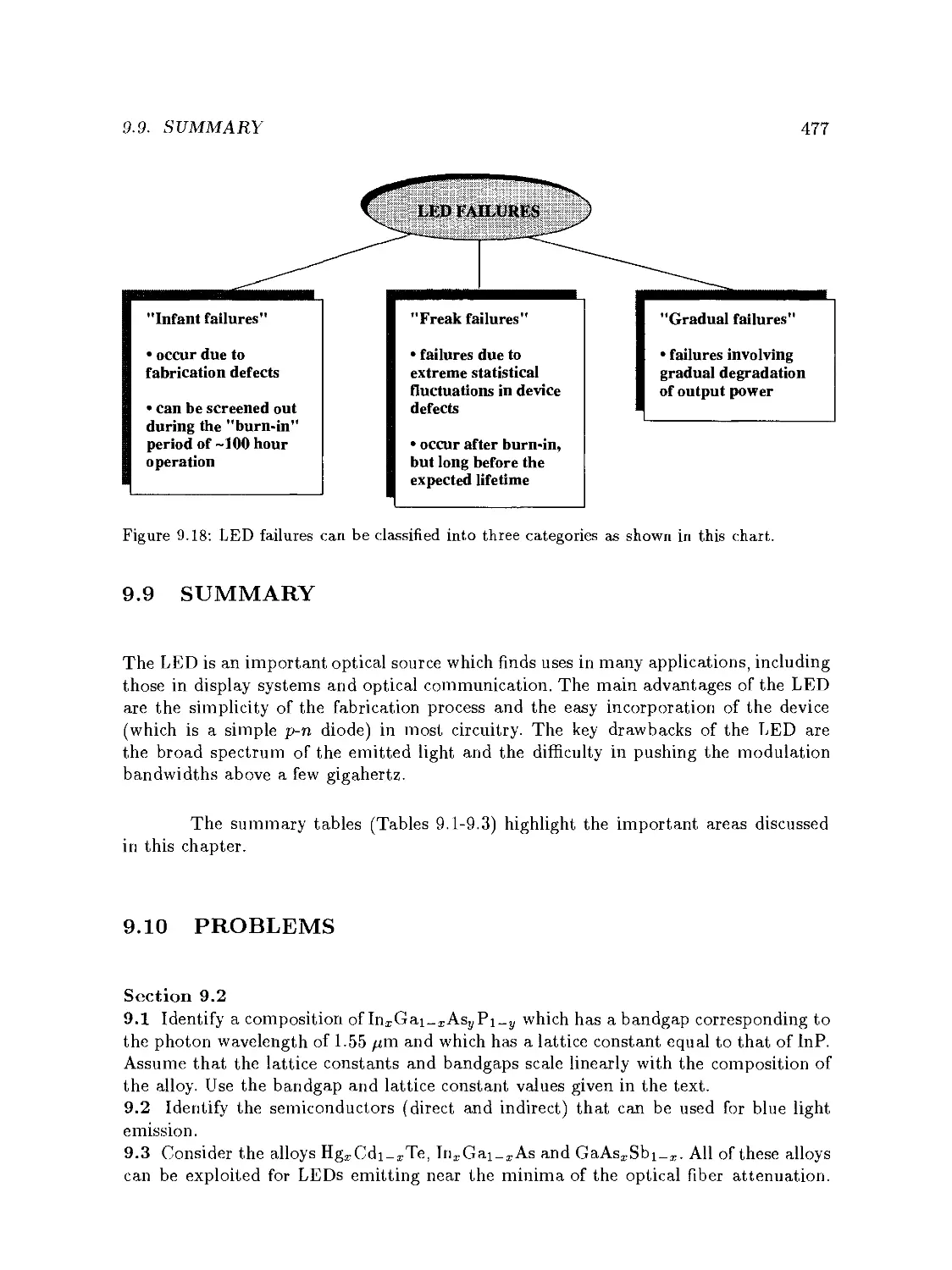
LED reliability issues
475
CONTENTS
xvii
10
9.9 Chapter summary 477
9.10 Problems 477
9.11 References 483
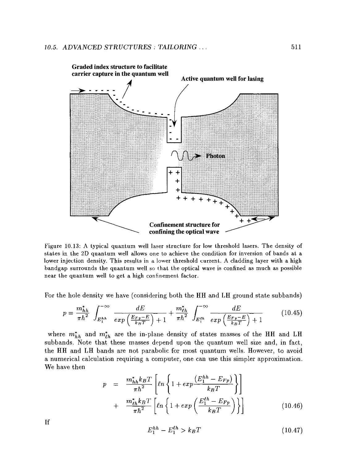
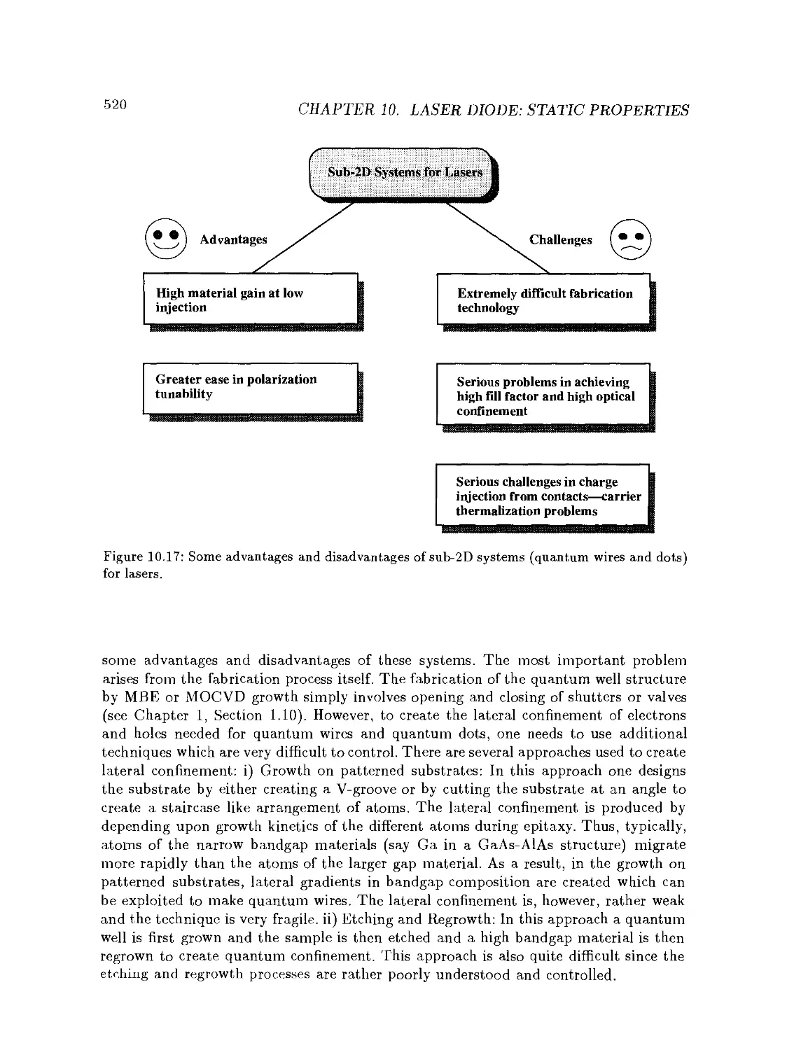
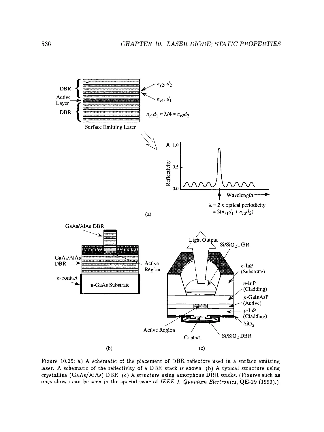
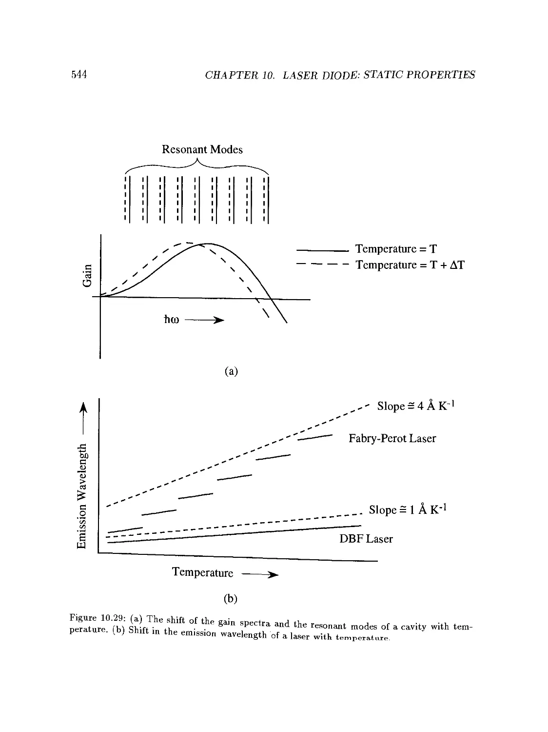
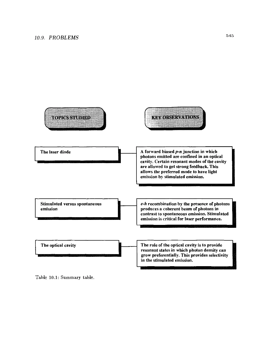
LASER DIODE: STATIC PROPERTIES 484
10.1 Introduction 484
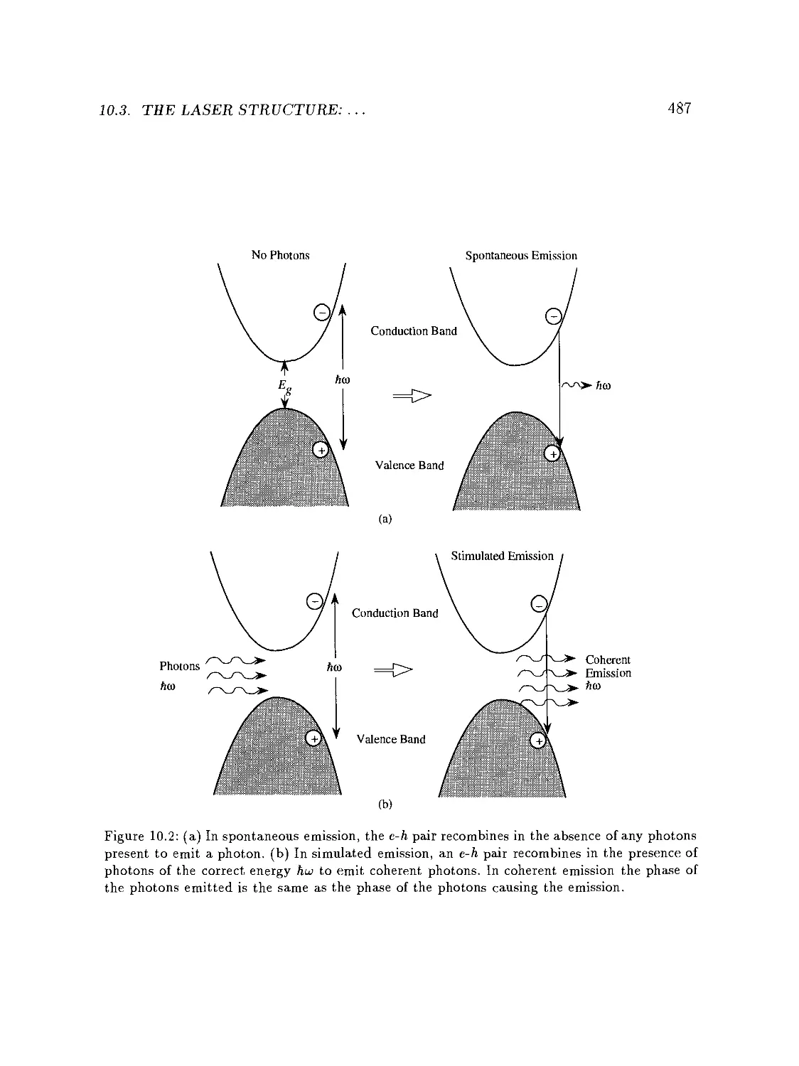
10.2 Spontaneous and stimulated emission 485
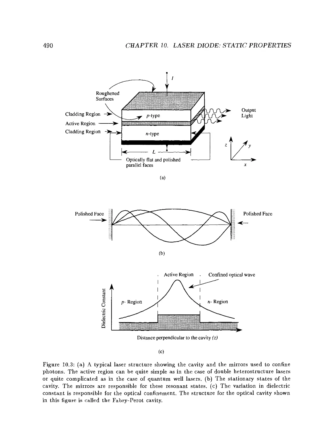
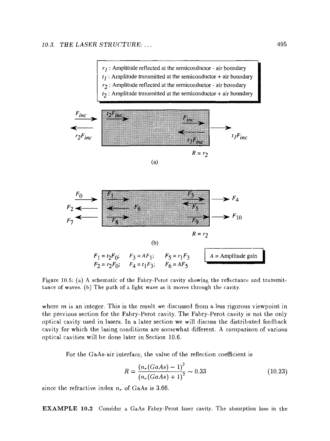
10.3 The laser structure: the optical cavity 486
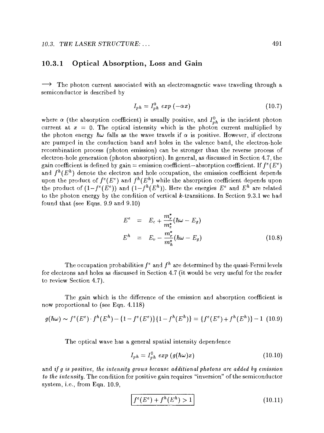
10.3.1 Optical absorption, loss and gain 491
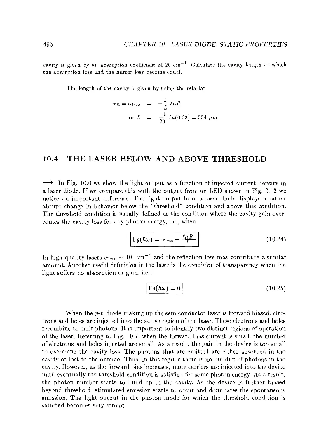
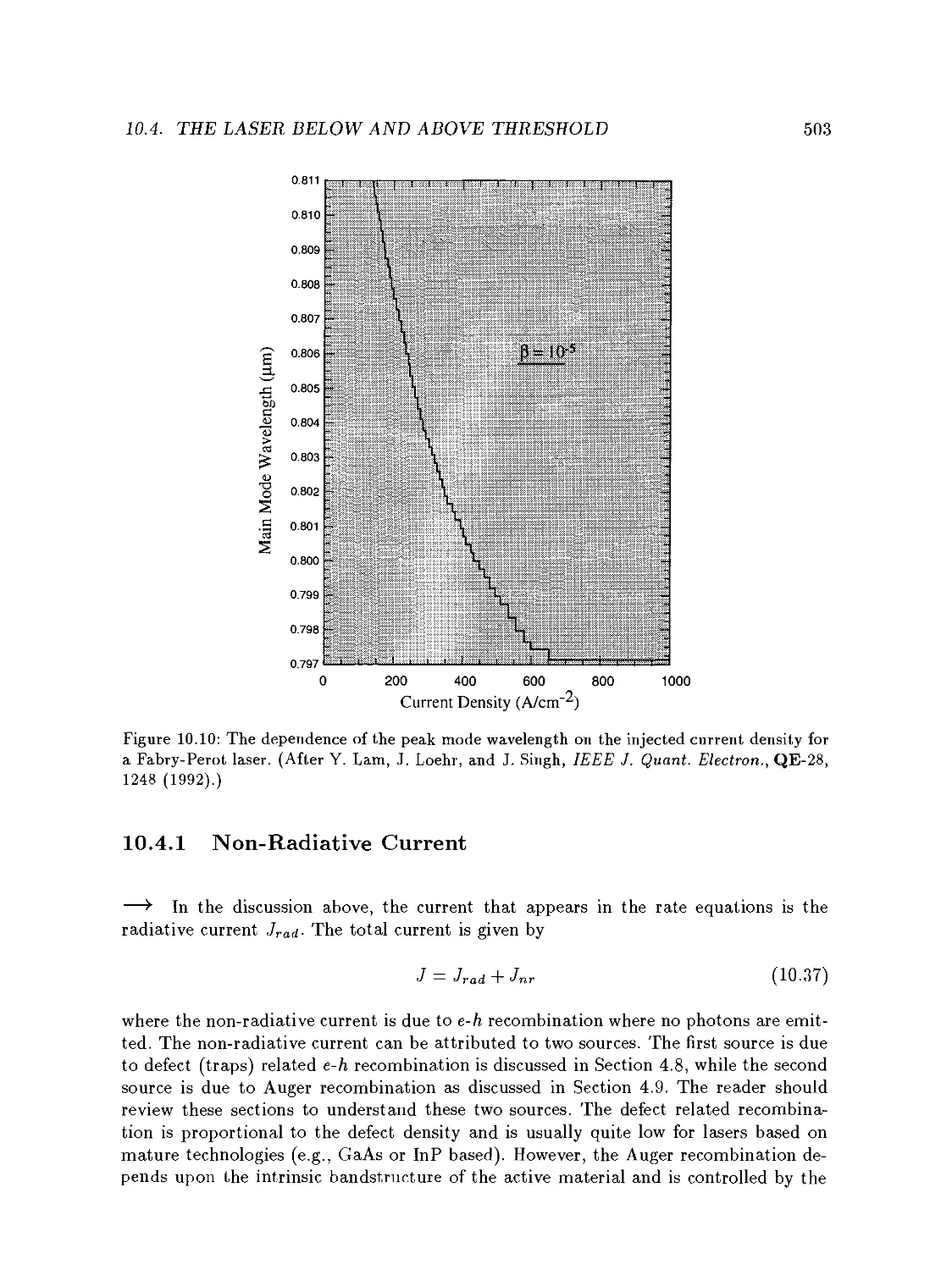
10.4 The laser below and above threshold 496
10.4.1 Non-radiative current 503
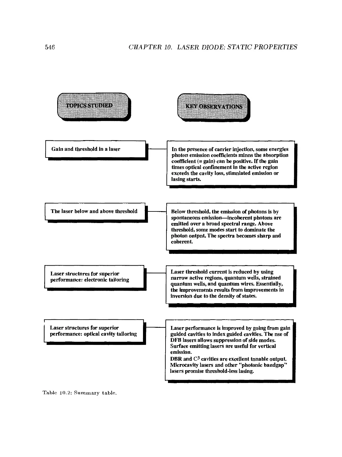
10.5 Advanced structures: tailoring electronic
structure 507
10.5.1 Double heterostructure lasers 508
10.5-2 Quantum well lasers 508
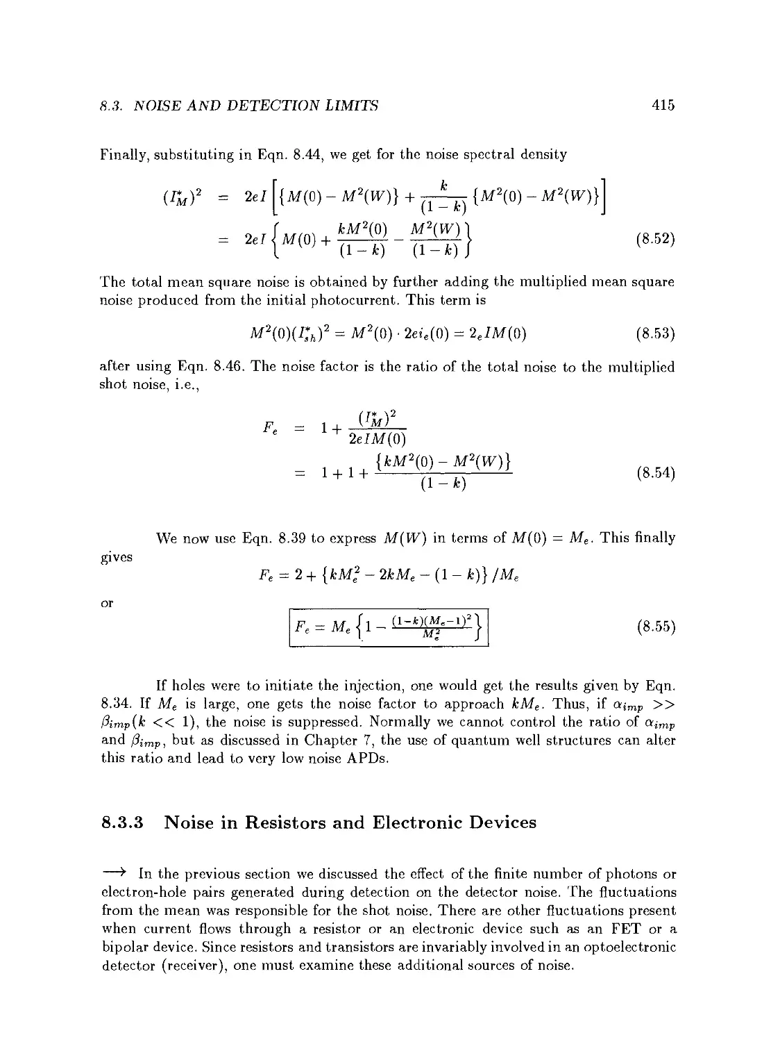
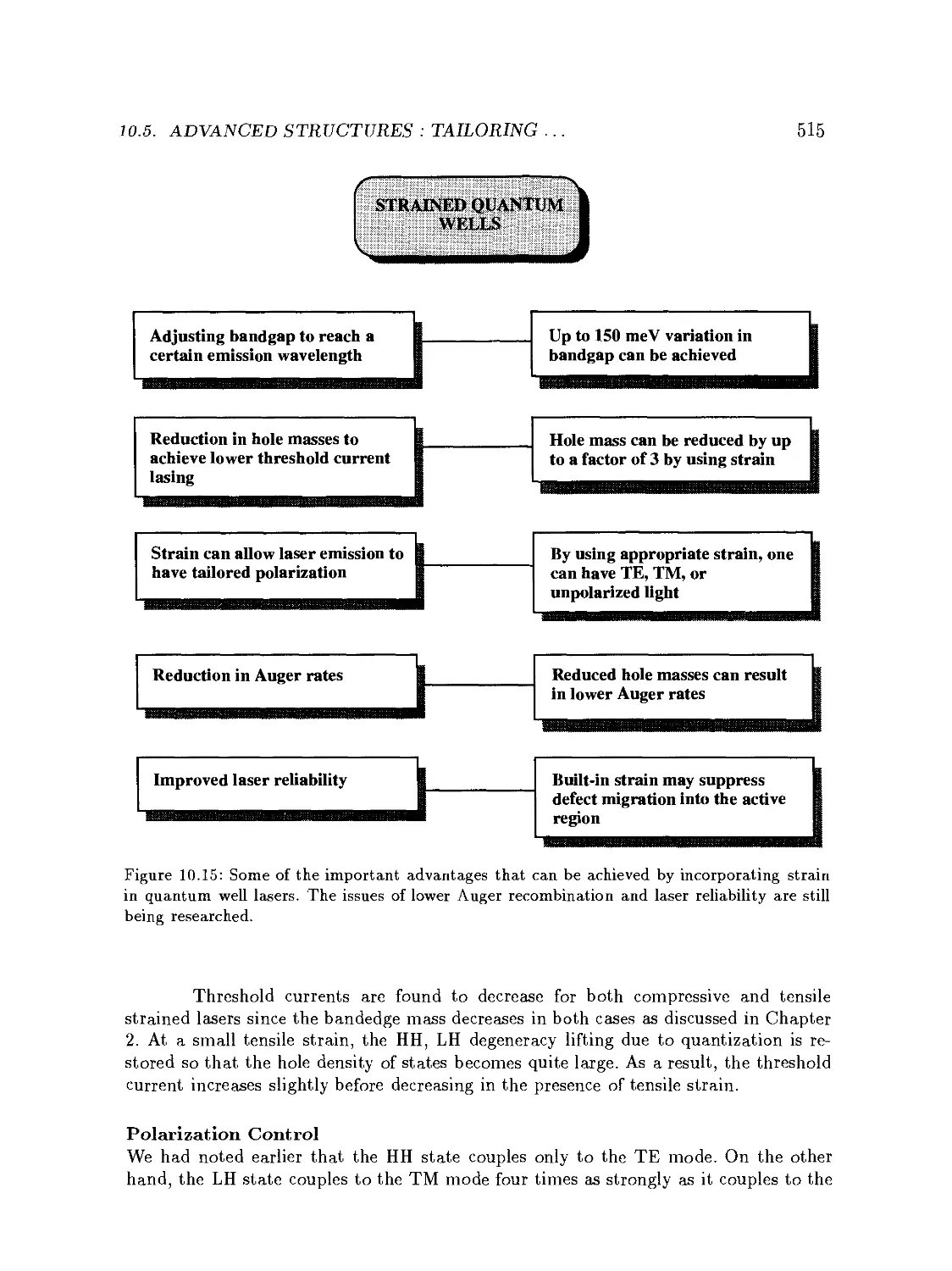
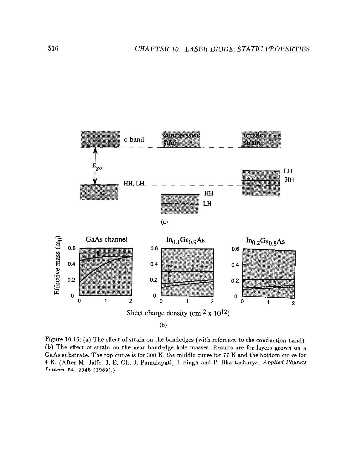
10.5.3 Strained quantum well lasers 514
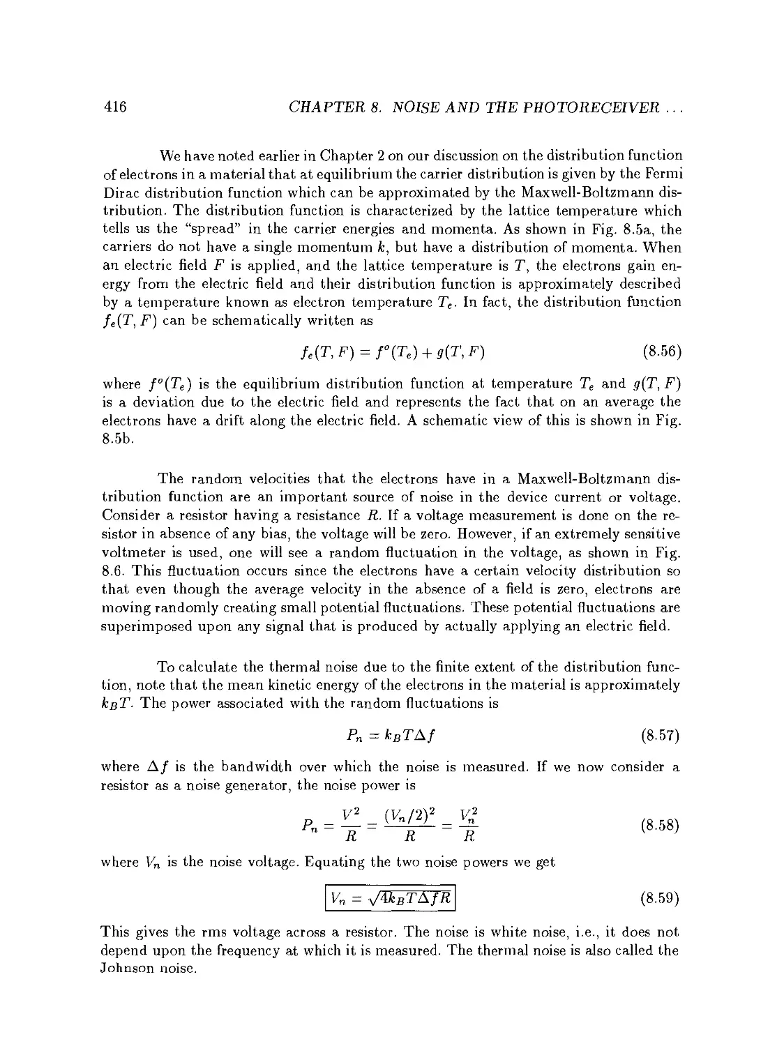
10.5.4 Quantum wire and quantum dot lasers 518
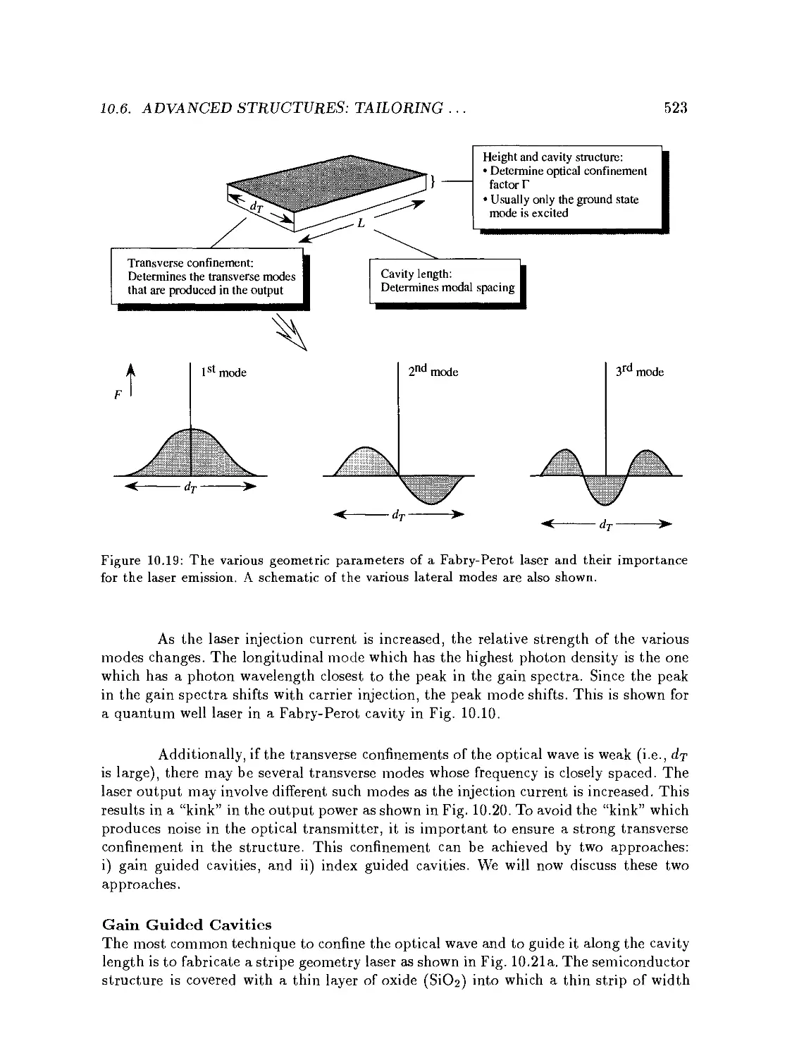
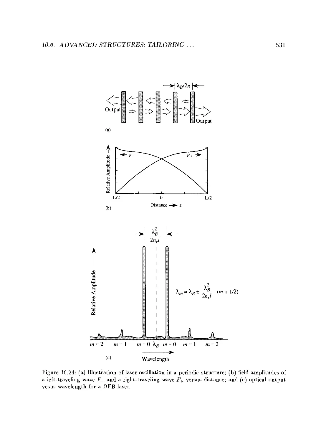
10.6 Advanced structures: tailoring the cavity 521
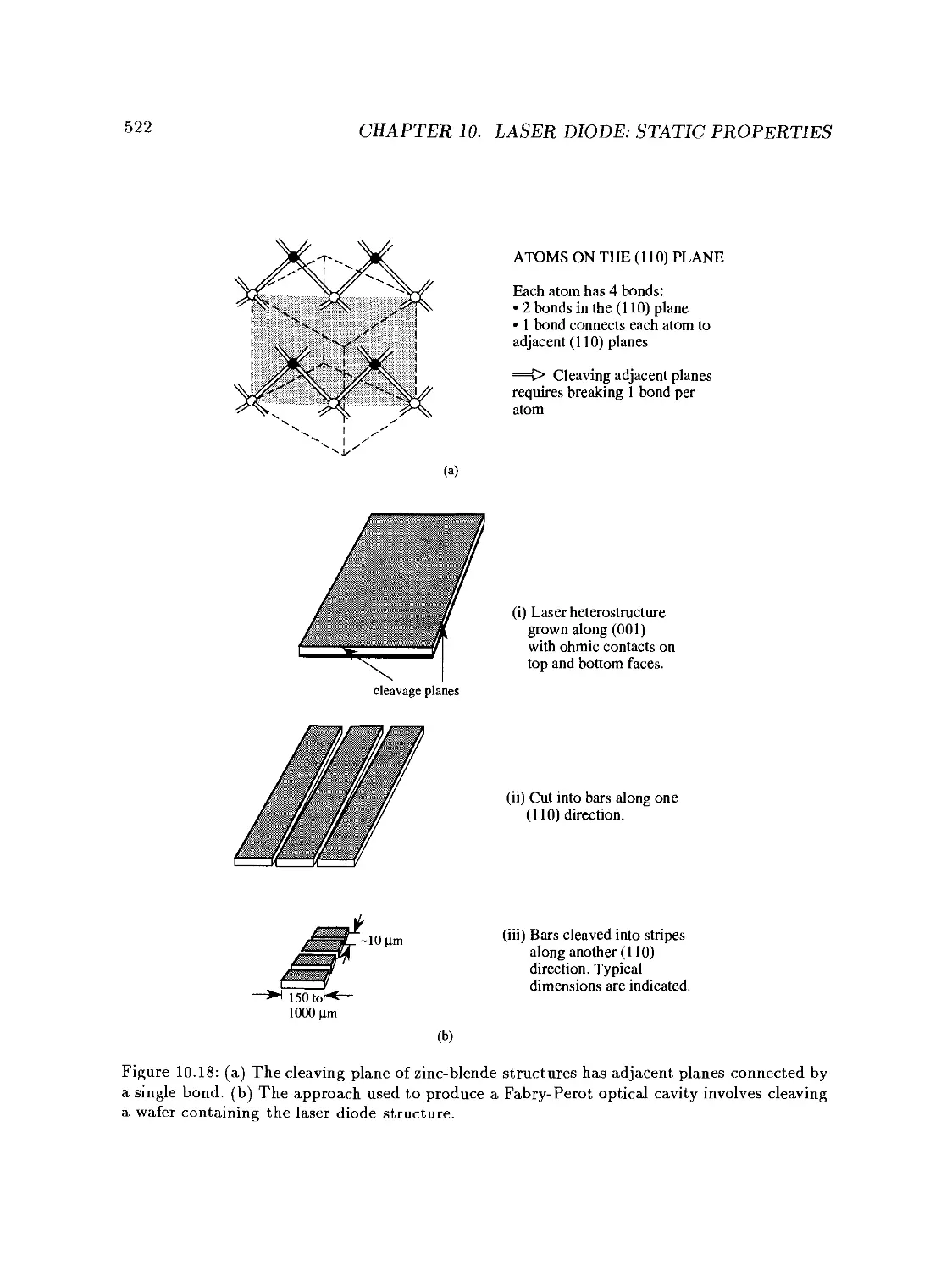
10.6.1 Issues in a Fabry-Perot cavity 521
10.6.2 The distributed feedback lasers 526
10.6.3 The surface emitting laser 534
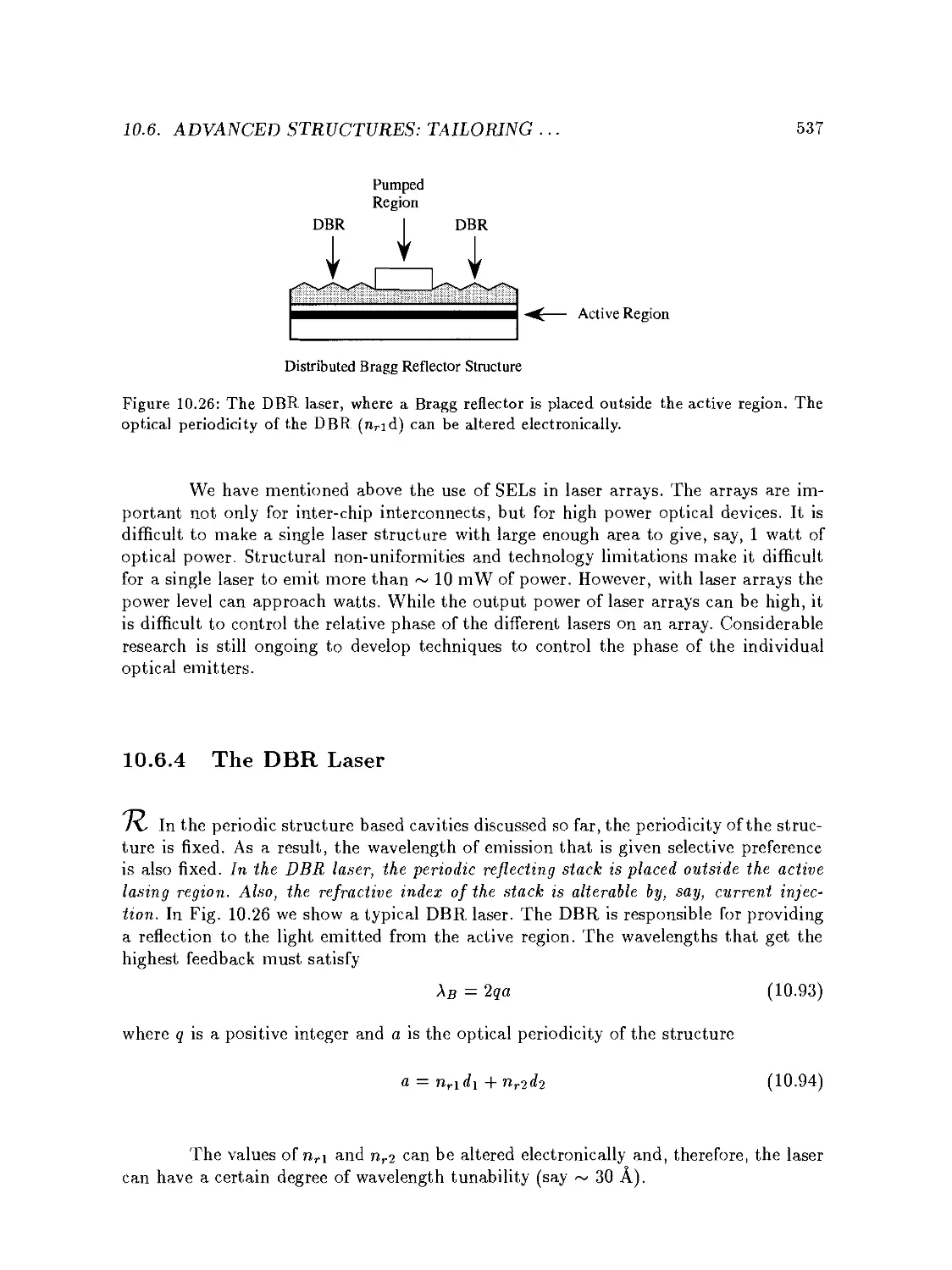
10.6.4 The DBR laser 537
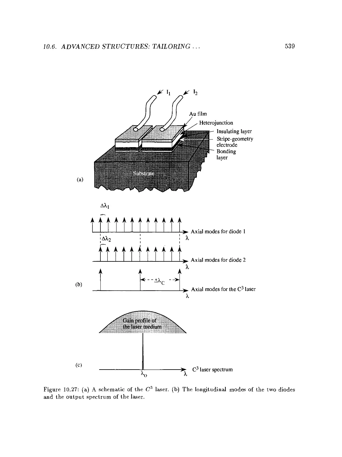
10.6.5 Cleaved coupled cavity laser 538
10.6.6 The microcavity laser—thresholdless laser? 538
10.7 Temperature dependence of laser output 540
10.7.1 Temperature dependence of the threshold current 540
10.7.2 Temperature dependence of the emission frequency 542
10.8 Chapter summary 543
10.9 Problems 543
10.10 References
xviii CONTENTS
11
12
SEMICONDUCTOR LASERS:
DYNAMIC PROPERTIES 553
11.1 Introduction 553
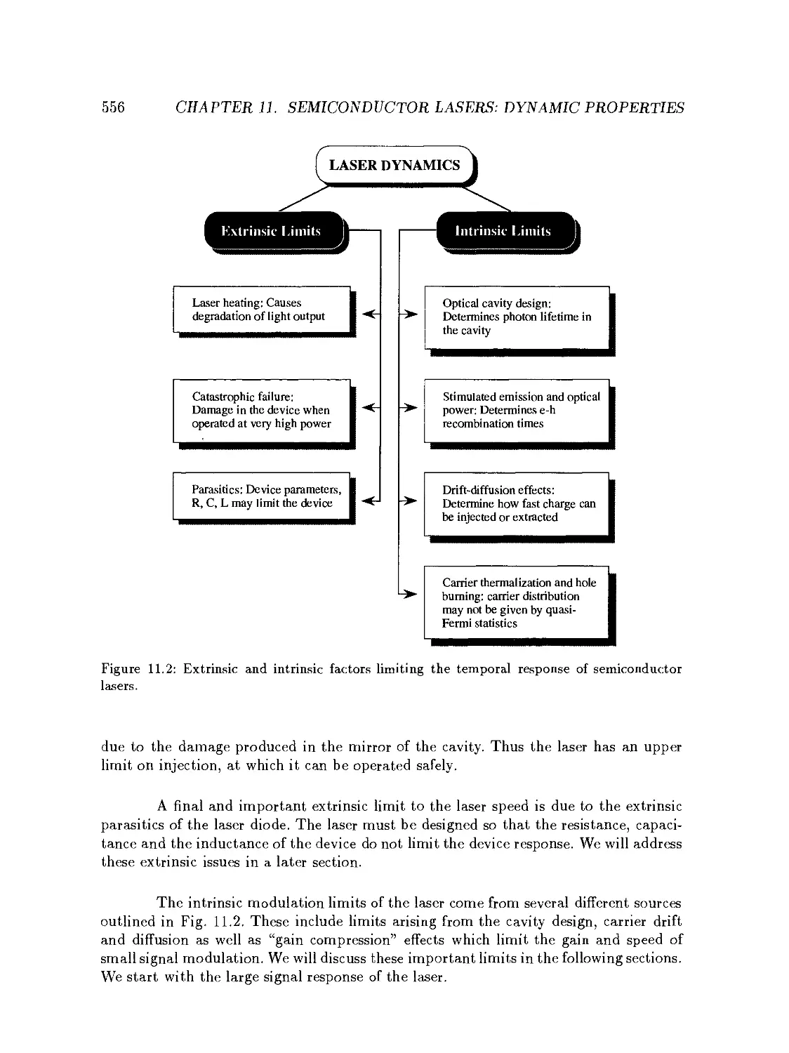
11.2 Important issues in laser dynamics 554
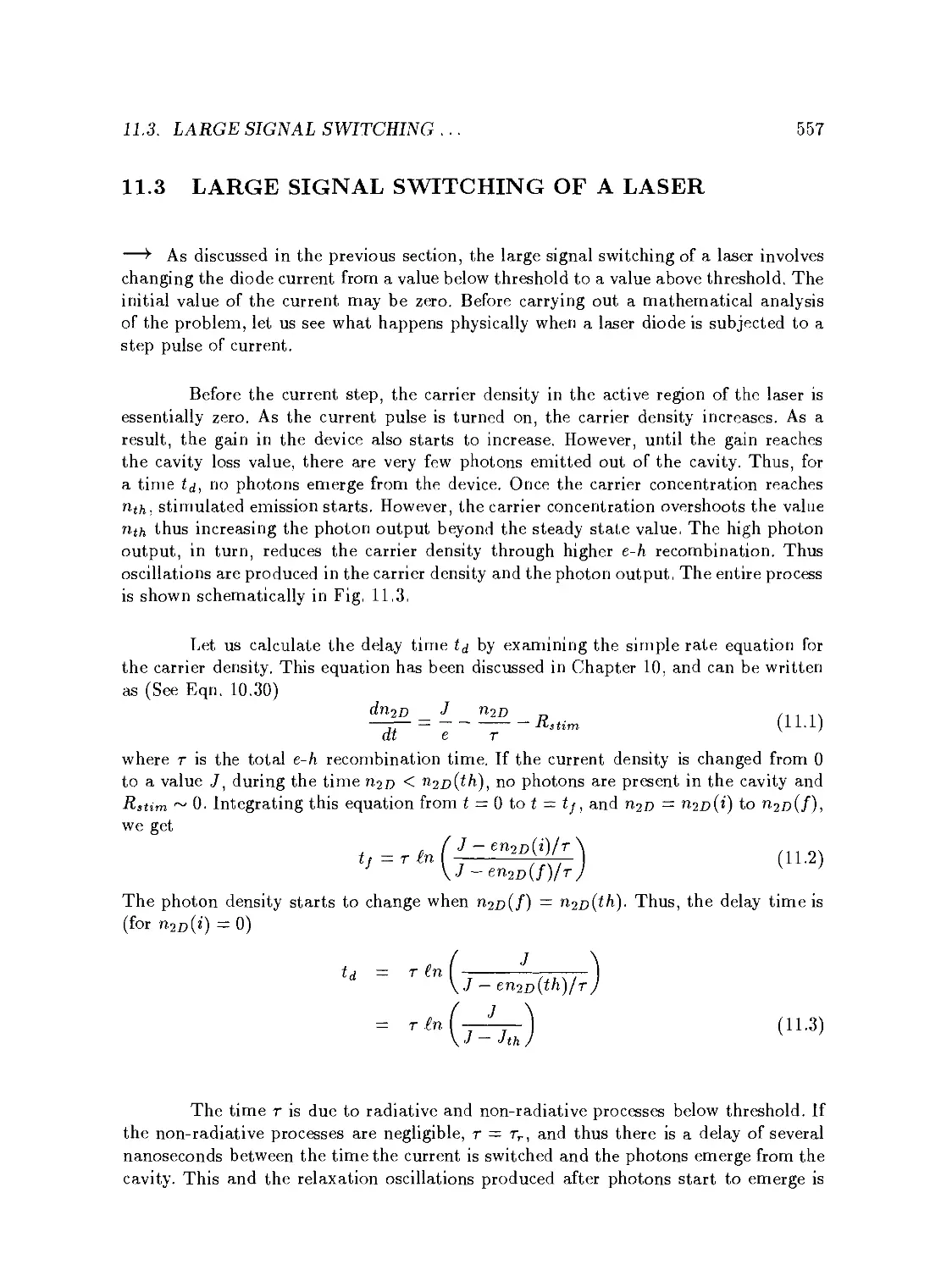
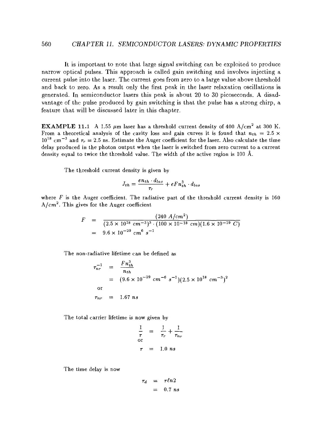
11.3 Large signal switching of a laser 557
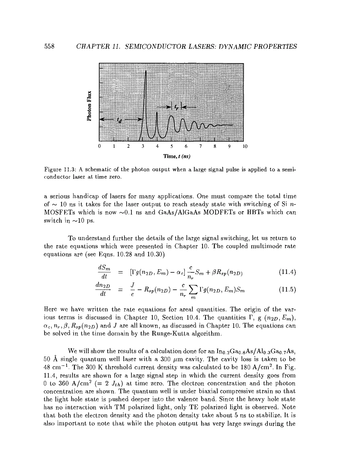
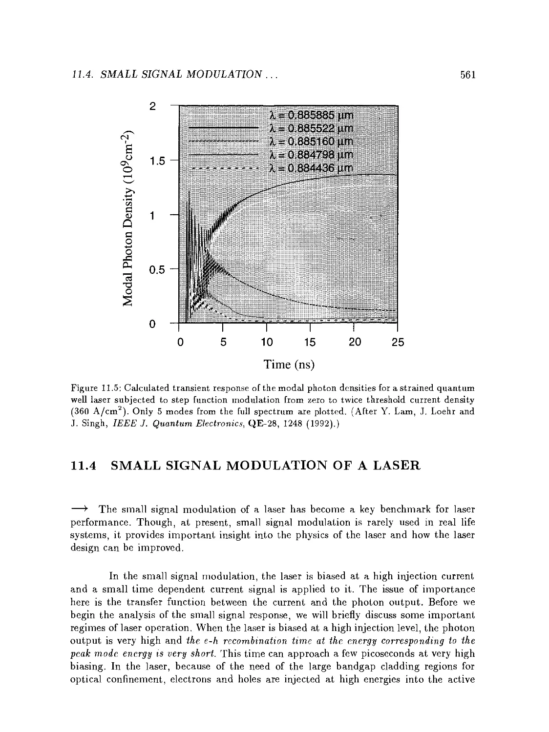
11.4 Small signal modulation of a laser 561
11.4.1 Small signal response: linear theory 563
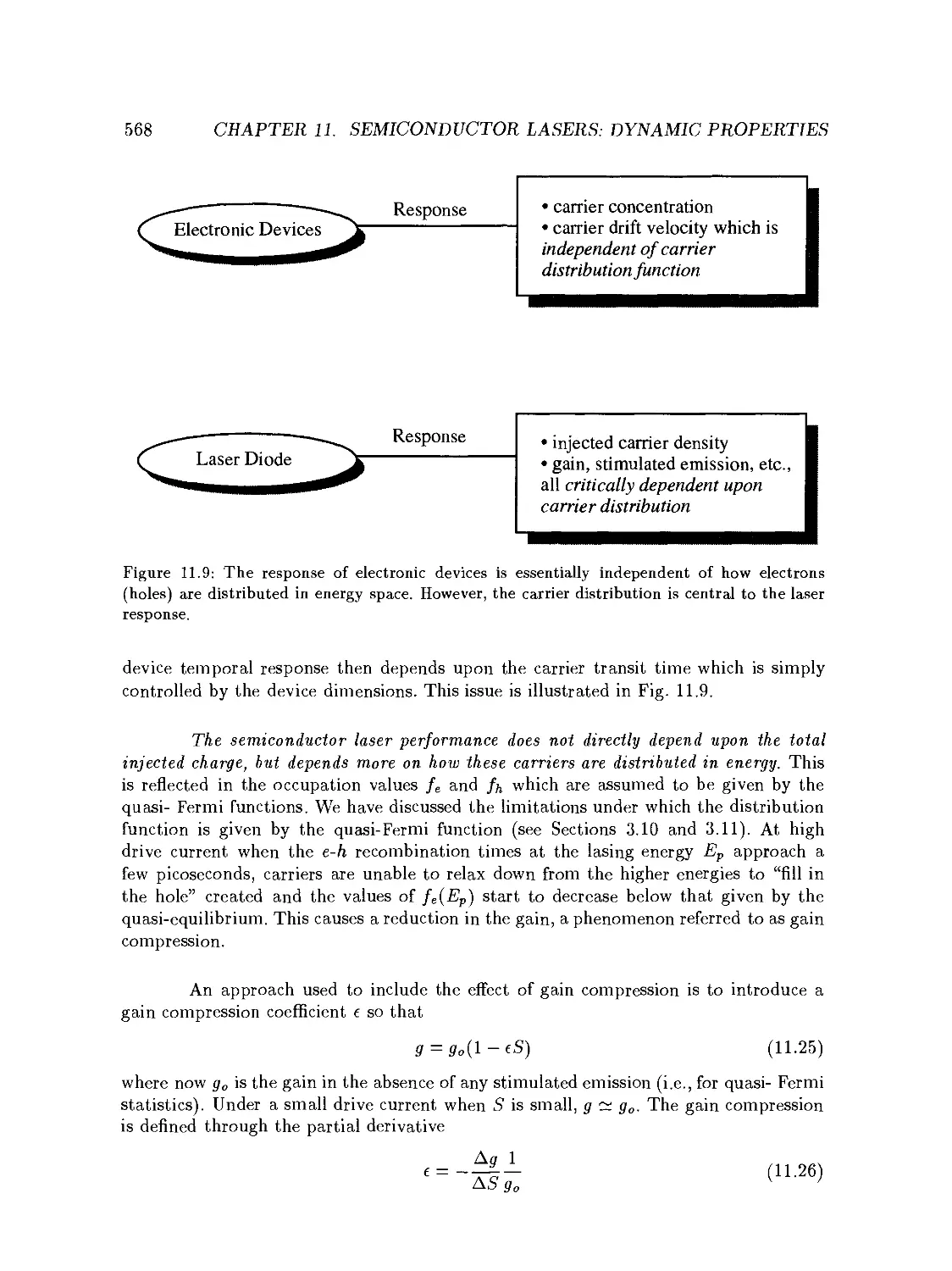
11.4.2 Gain compression effects 566
11.4.3 Drift-diffusion considerations in laser modulation 569
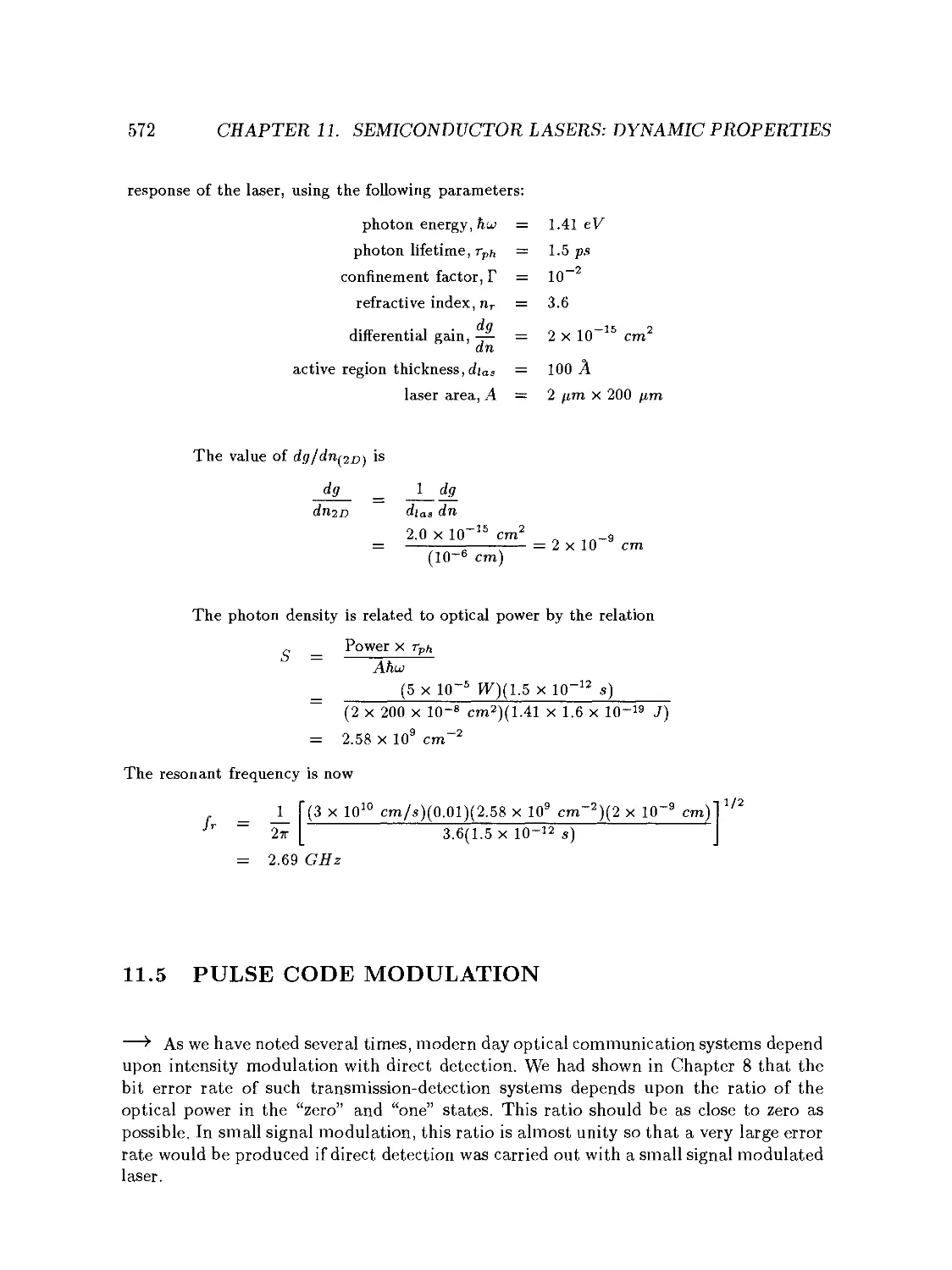
11.5 Pulse code modulation 572
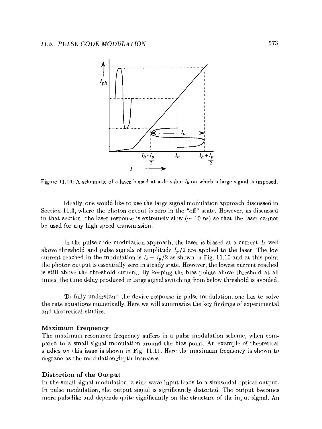
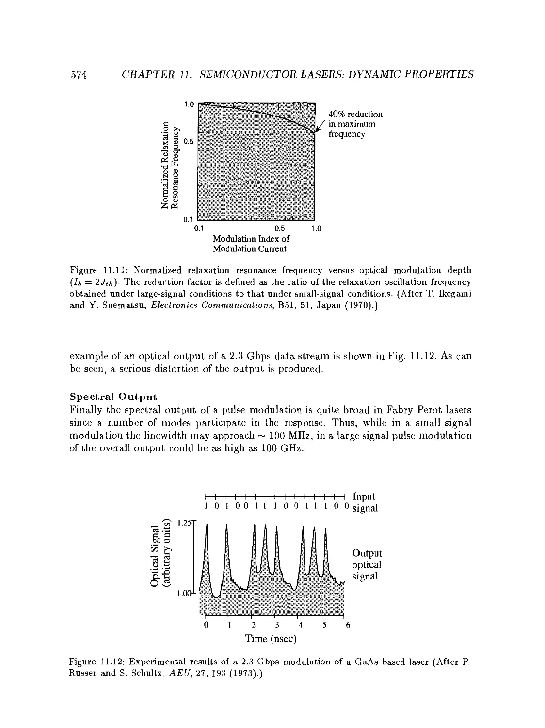
11.6 Extrinsic effects on laser modulation 575
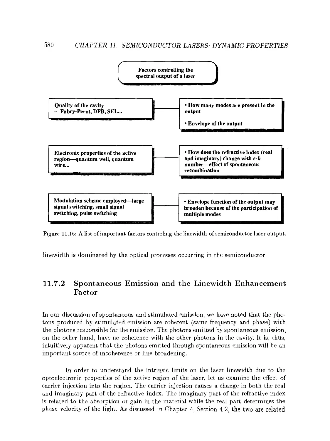
11.7 Spectral output and laser linewidth 578
11.7.1 The optical cavity 578
11.7.2 Spontaneous emission and the linewidth enhancement factor 580
11.7.3 Spectra under modulation 585
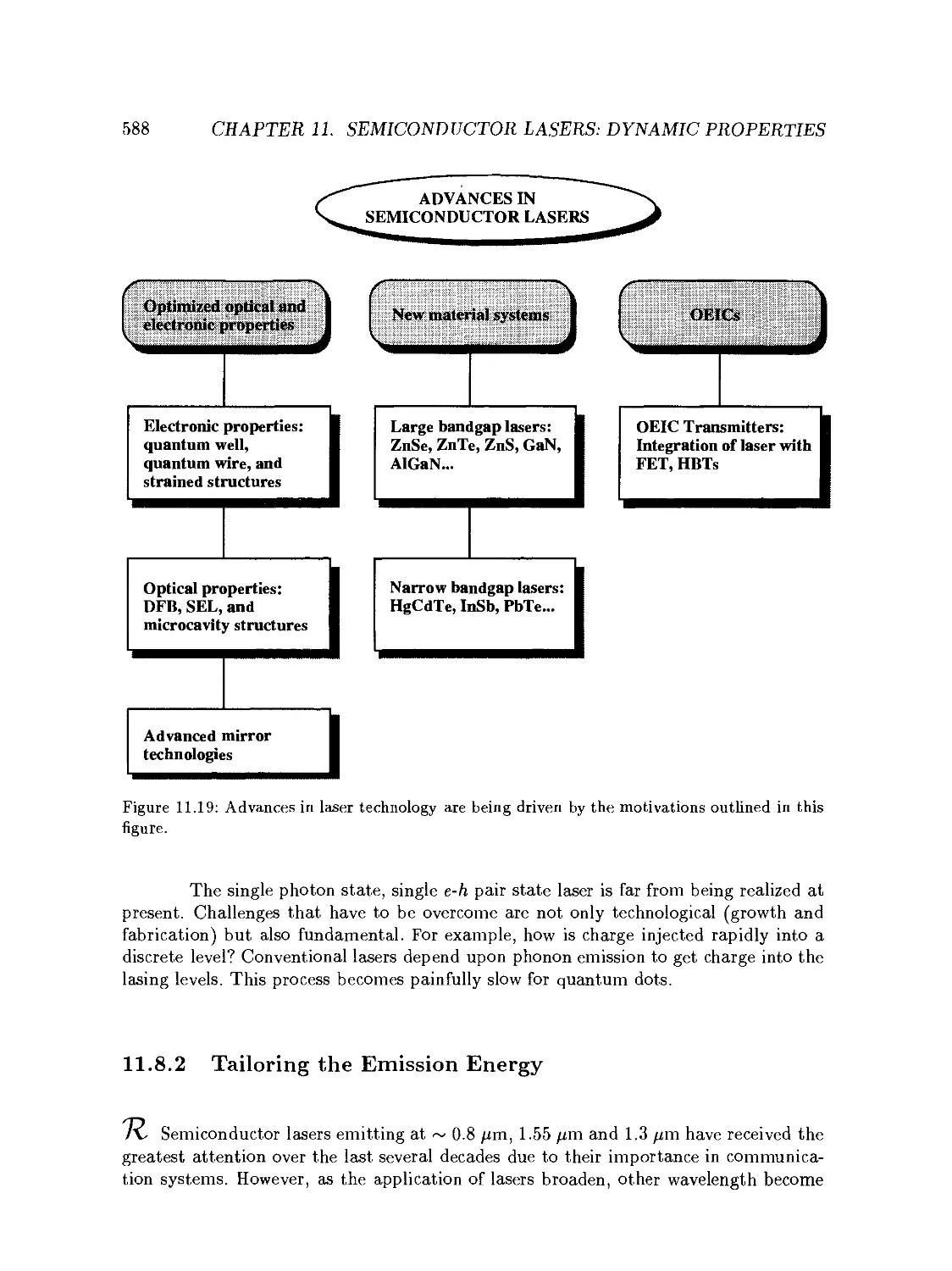
11.8 Advanced structures 587
11.8.1 The quest for the dream laser 587
11.8.2 Tailoring the emission energy 588
11.8.3 OEIC laser transmitters 589
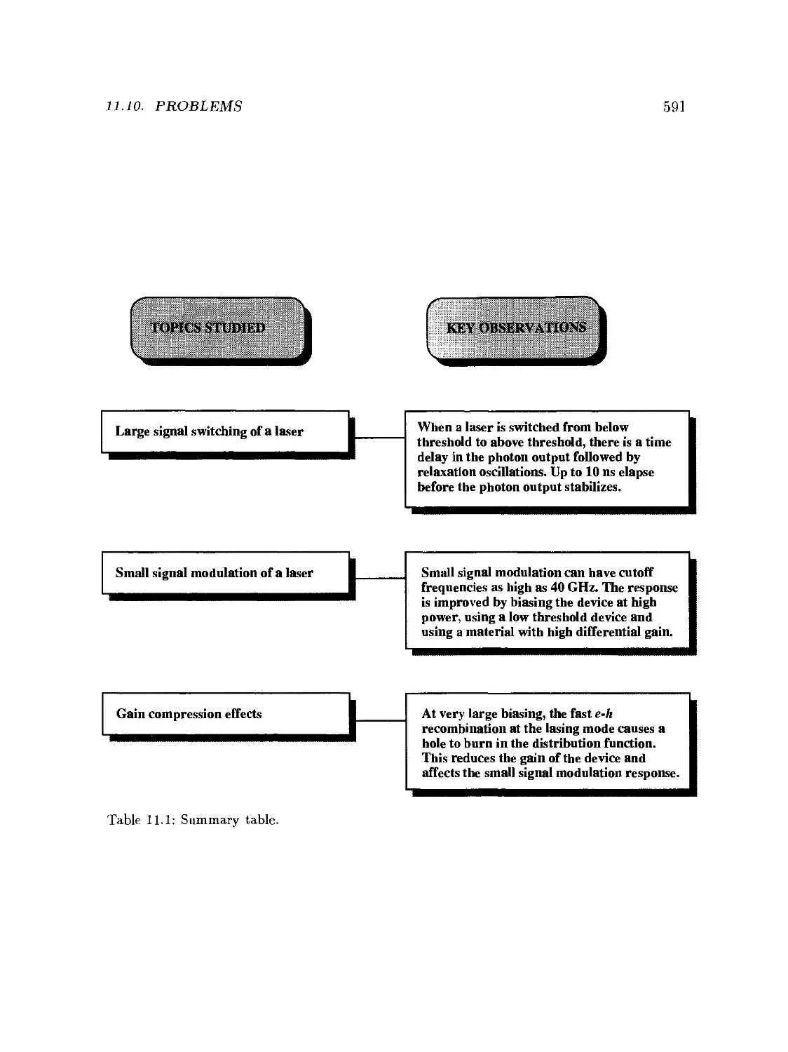
11.9 Chapter summary 590
11.10 Problems 590
11.11 References 595
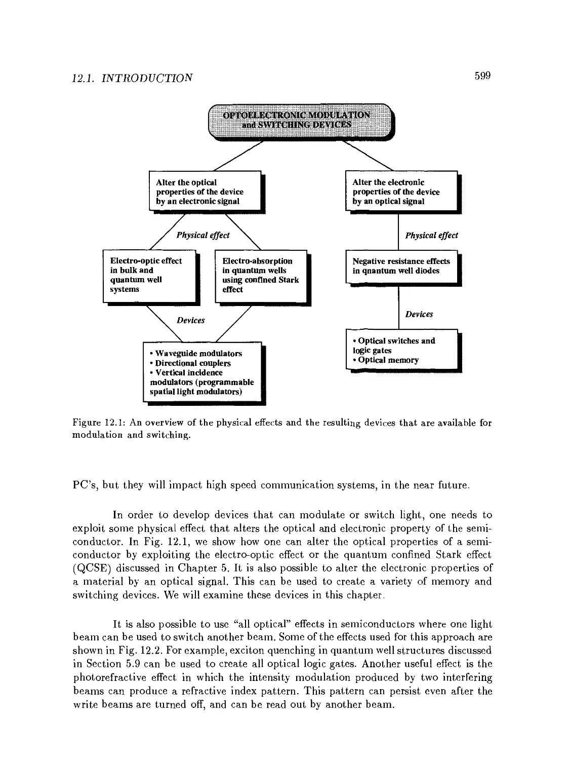
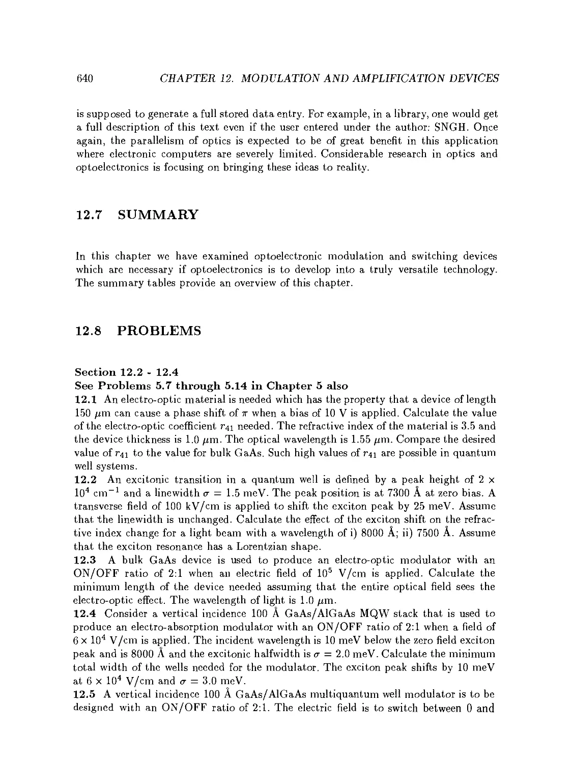
MODULATION AND AMPUFICATION DEVICES 598
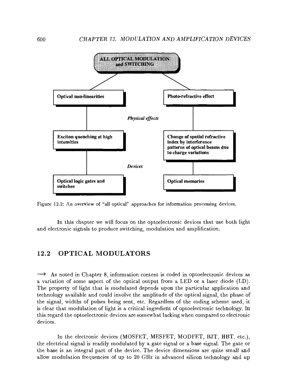
12.1 Introduction 598
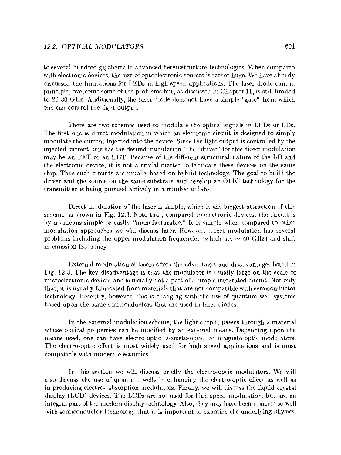
12.2 Optical modulators 600
CONTENTS
xix
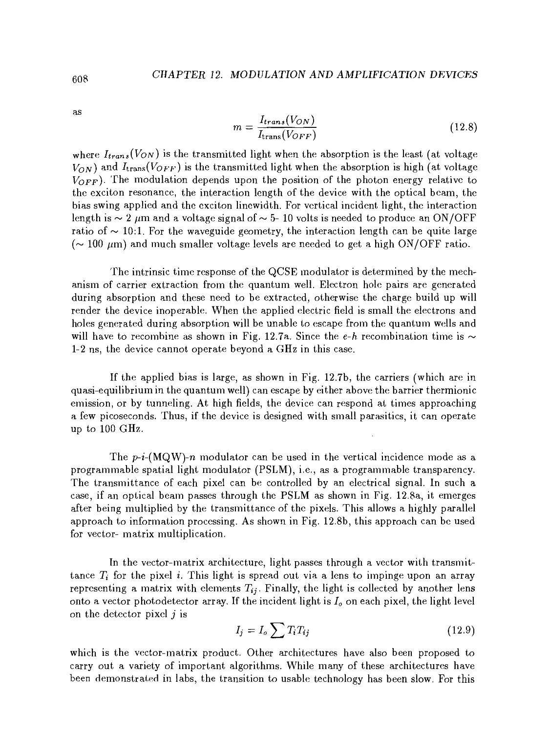
13
12.2.1 Electro-optic modulators 602
12.2.2 Electro-absorption modulators 606
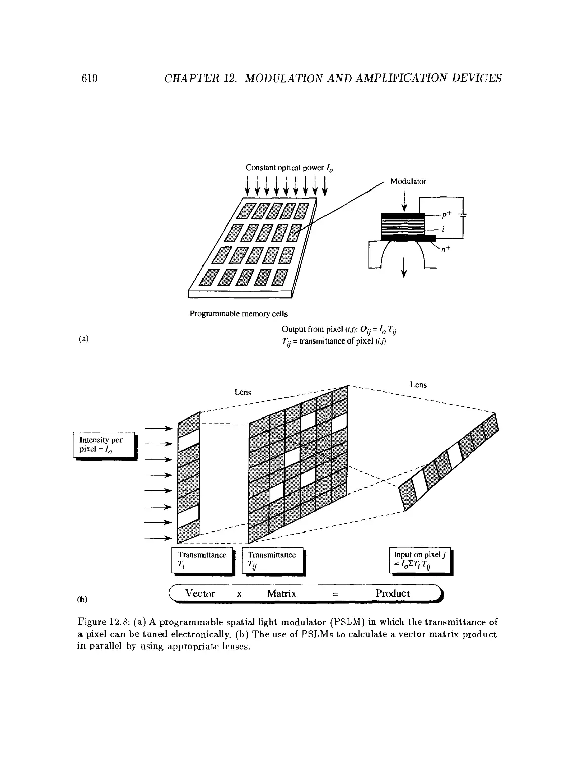
12.2.3 Liquid crystal devices 609
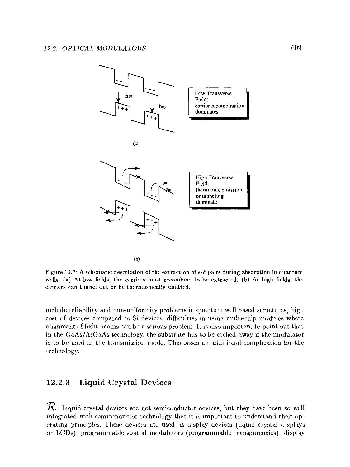
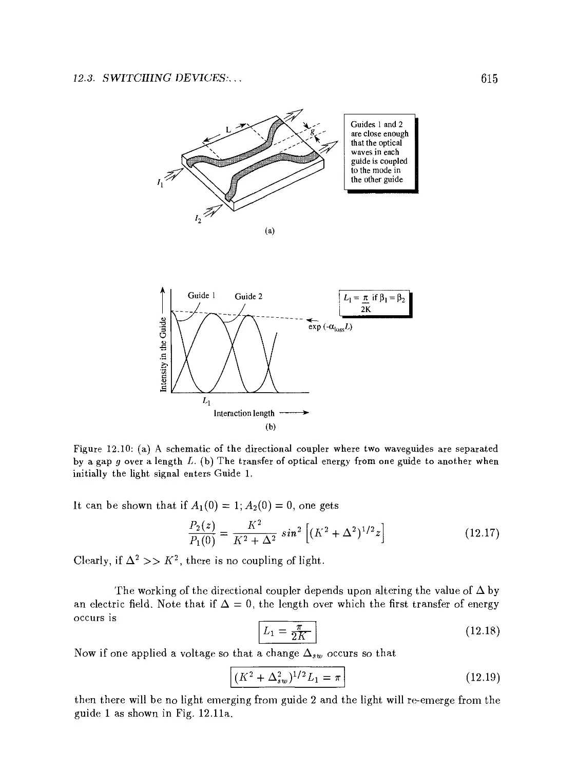
12.3 Switching devices: directional couplers 613
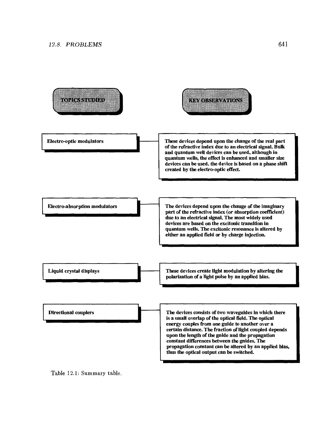
12.4 qcse based switching devices 617
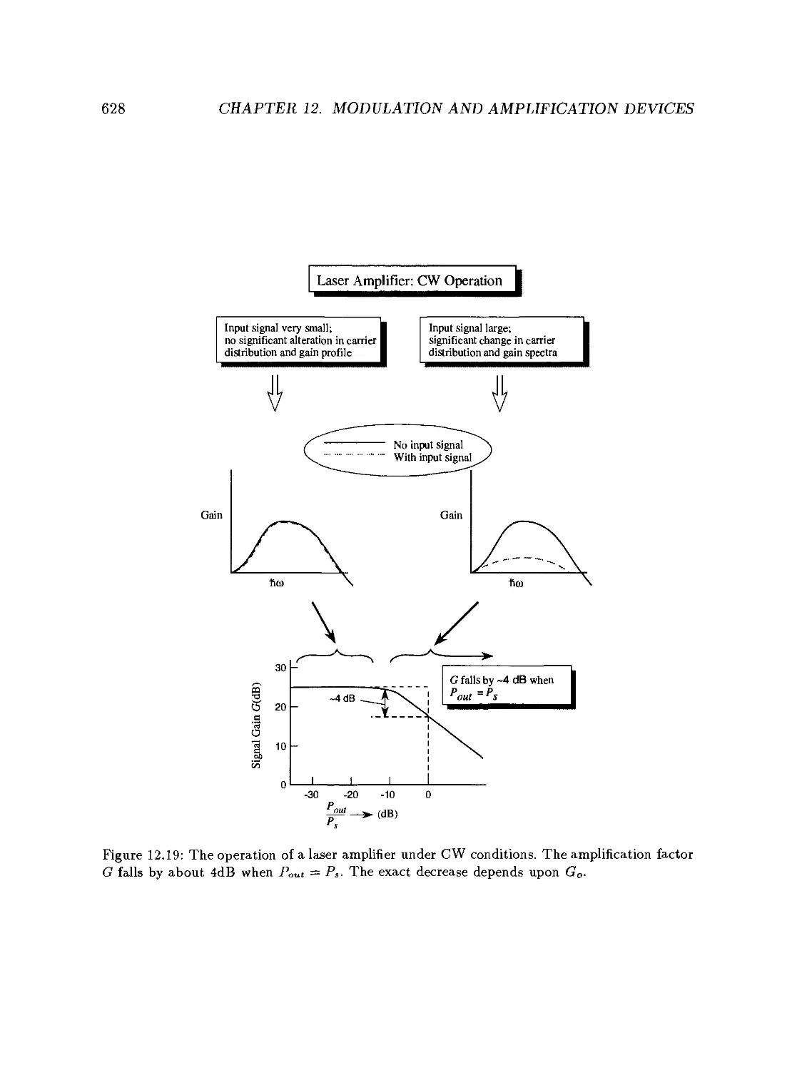
12.5 Optical amplification: the laser amplifier 622
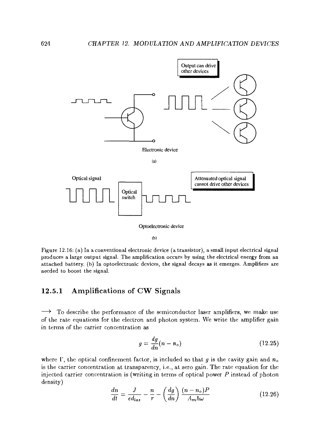
12.5.1 Amplifications of CW signals 624
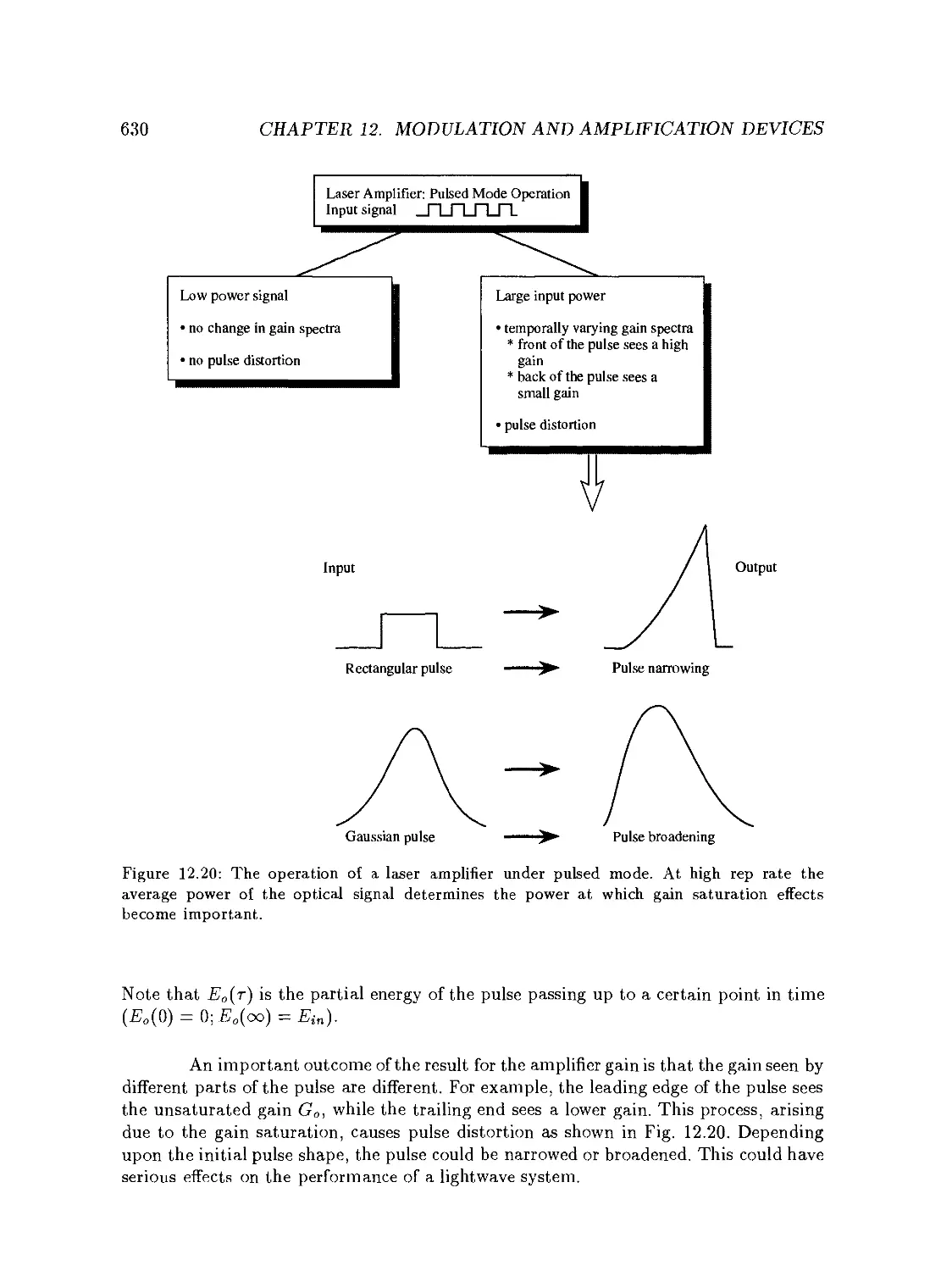
12.5.2 Pulse amplification and pulse shaping 627
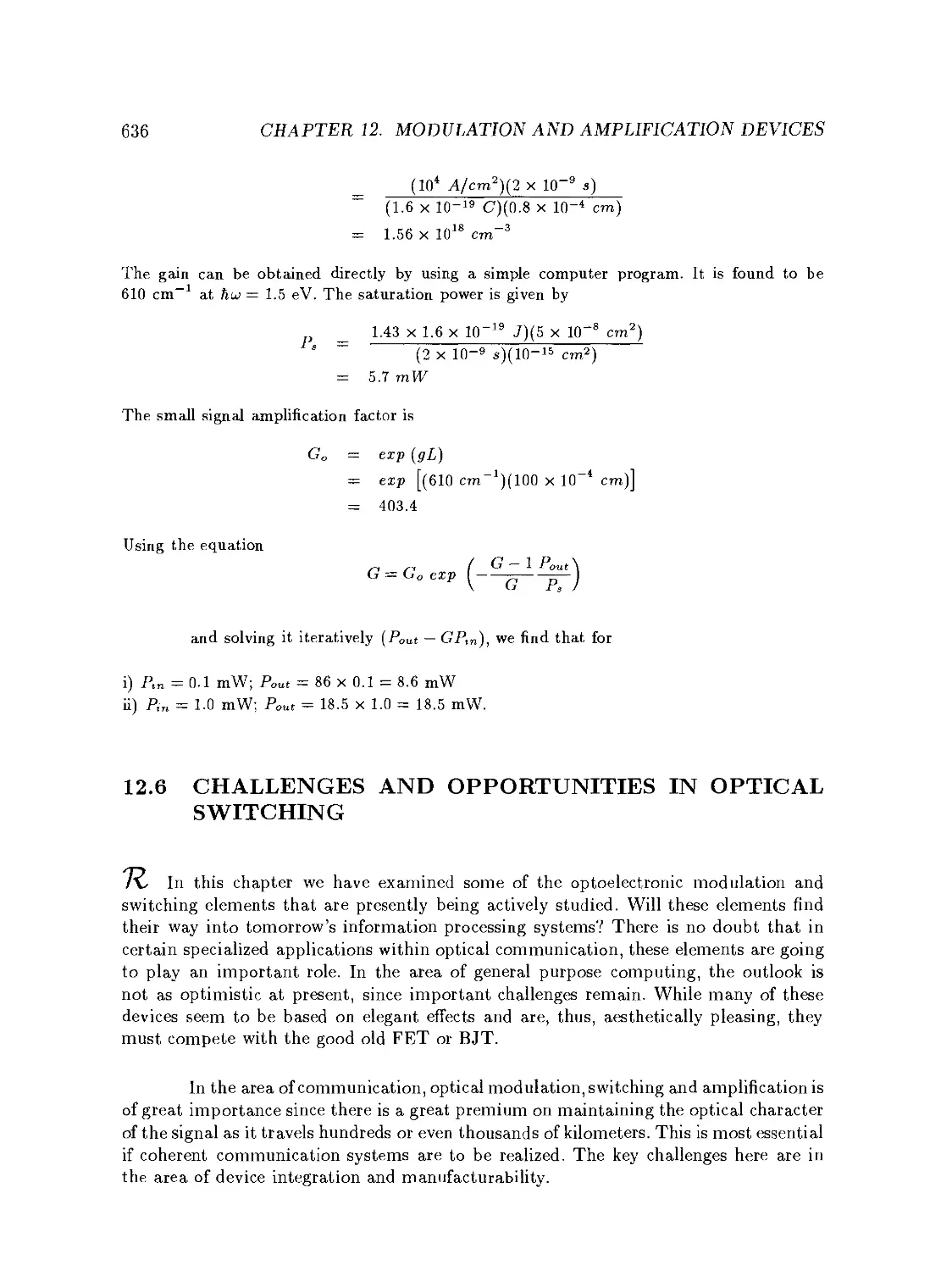
12.6 Challenges and opportunities in optical switching 636
12.7 Chapter summary 640
12.8 Problems 640
12.9 References 643
OPTICAL COMMUNICATION SYSTEMS:
DEVICE NEEDS 645
13.1 Introduction 645
13-2 a conceptual picture of the optical
communication system 646
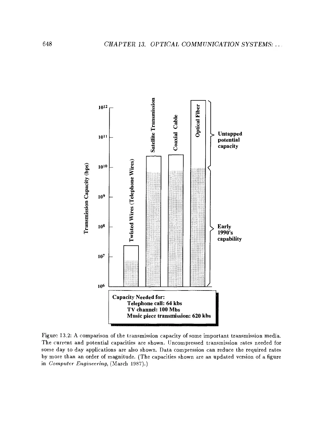
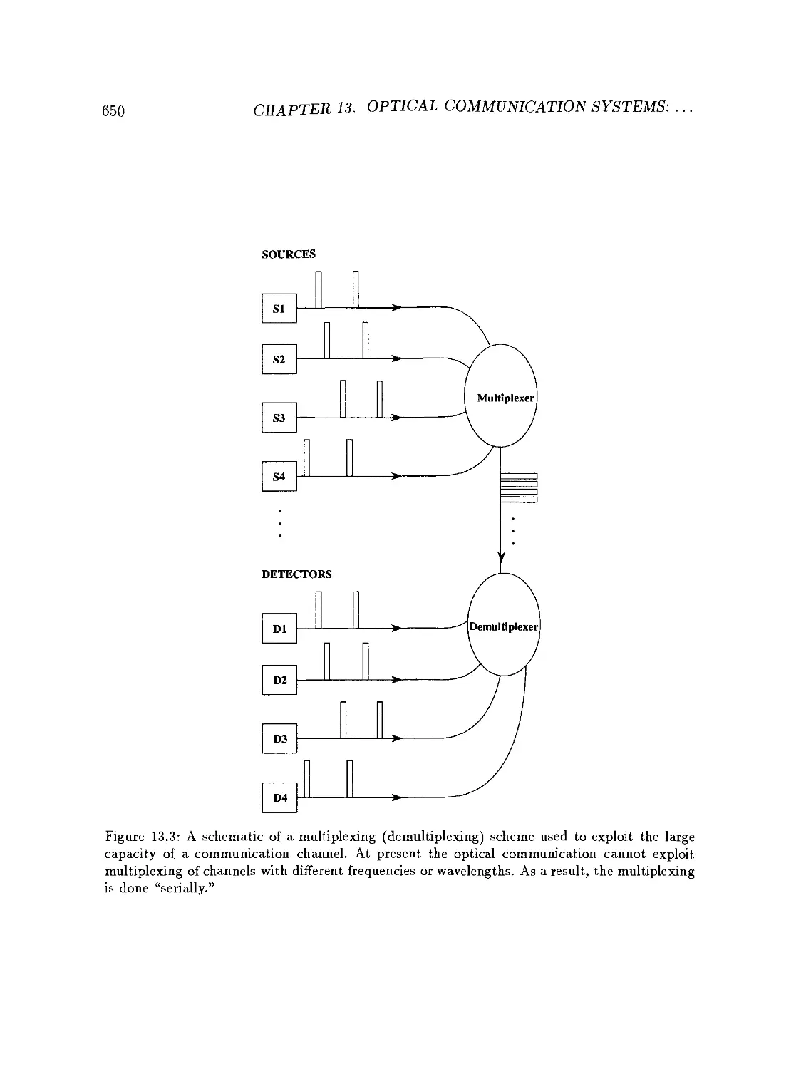
13.3 Information content and channel capacity 649
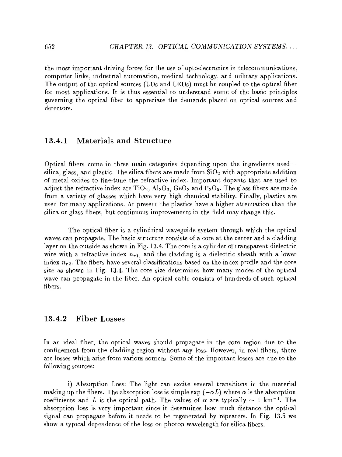
13.4 Some properties of optical fibers 617
13.4.1 Materials and structure 651
13.4.2 Fiber losses 652
13.4.3 Acceptance angle and numerical aperture 653
13.4.4 Multipath dispersion 656
13.4.5 Material dispersion 658
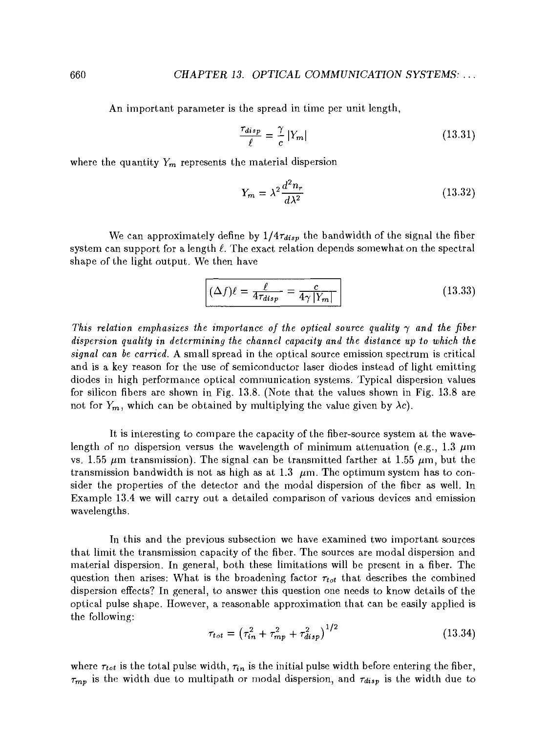
13.4.6 Signal attenuation and detector demands 662
13.5 Coherent communication systems:
device requirements 666
n CONTENTS
A
B
C
13.6 Chapter summary 668
13.7 Problems 668
13.8 References 669
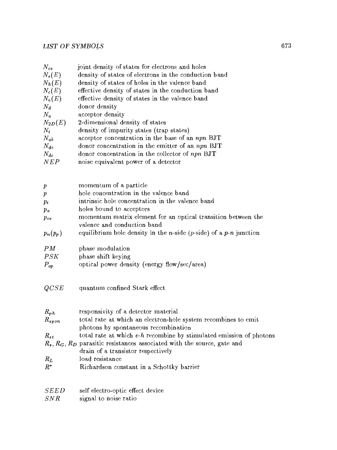
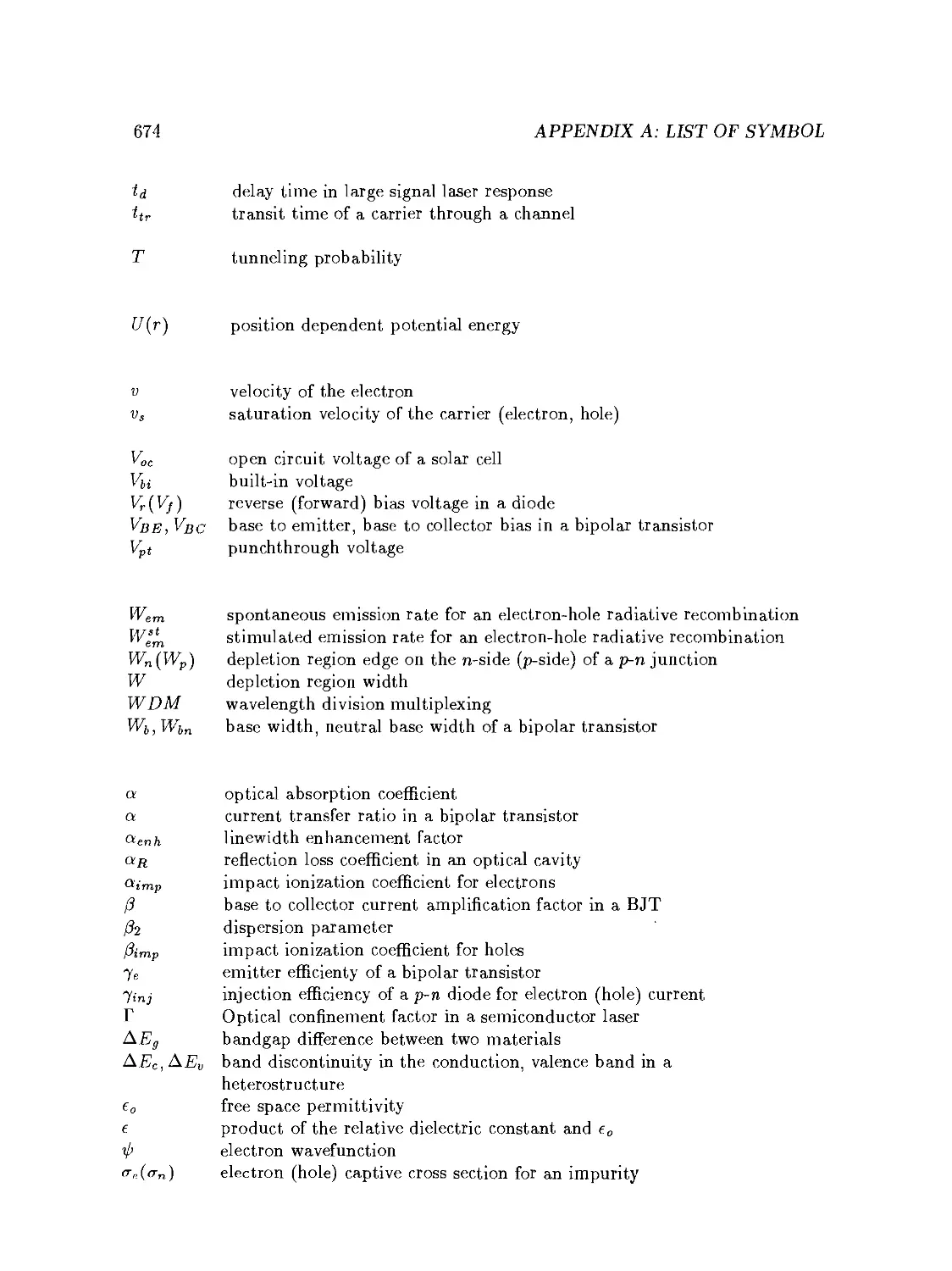
LIST OF SYMBOLS 670
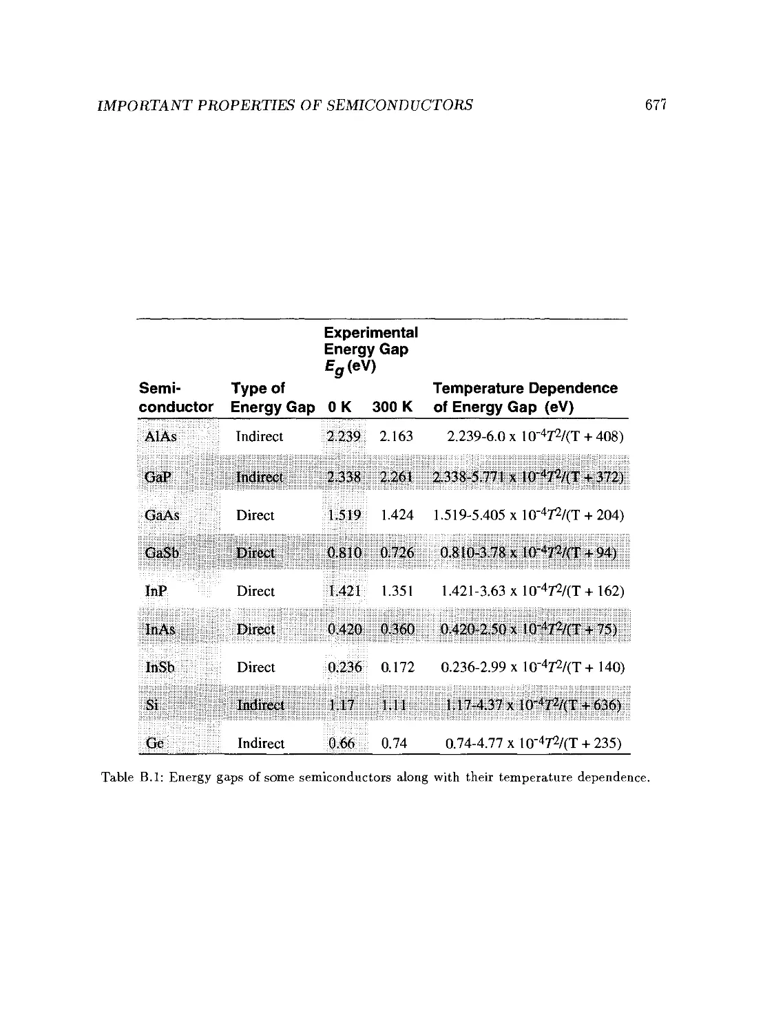
IMPORTANT PROPERTIES OF
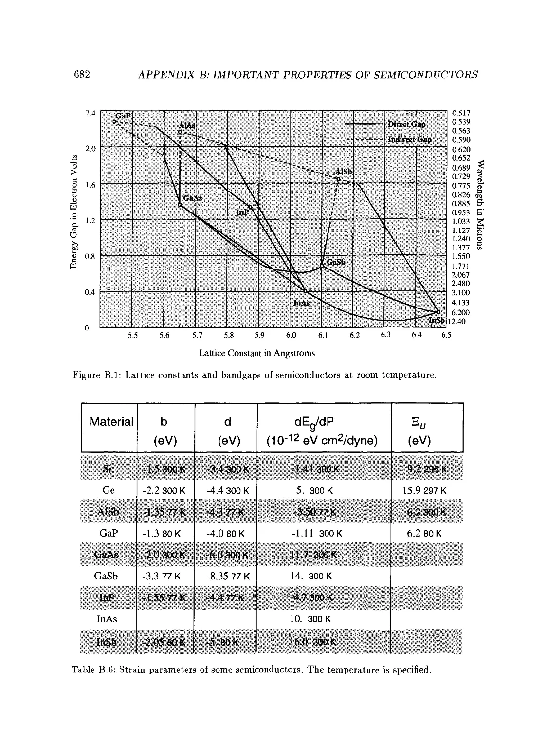
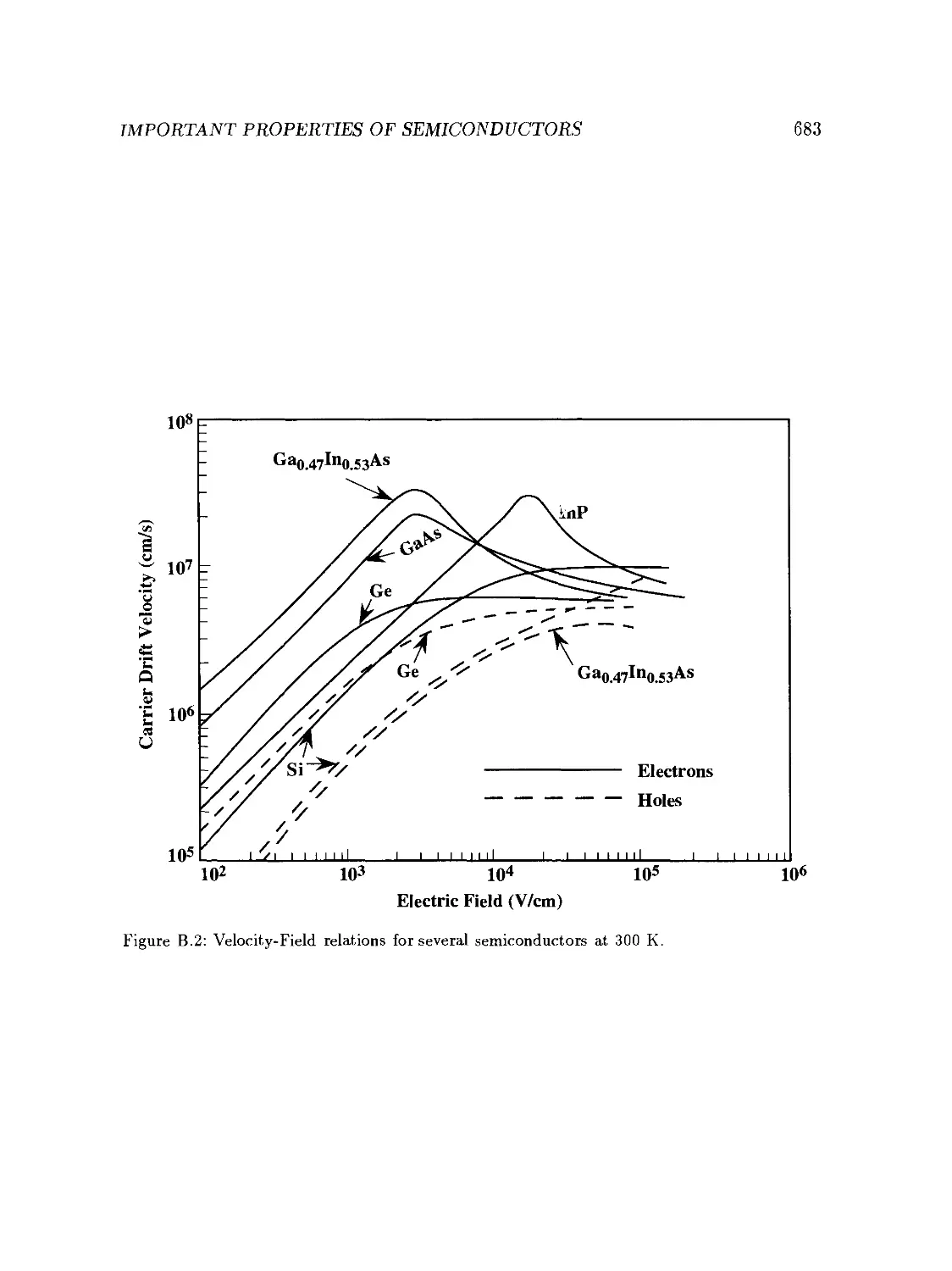
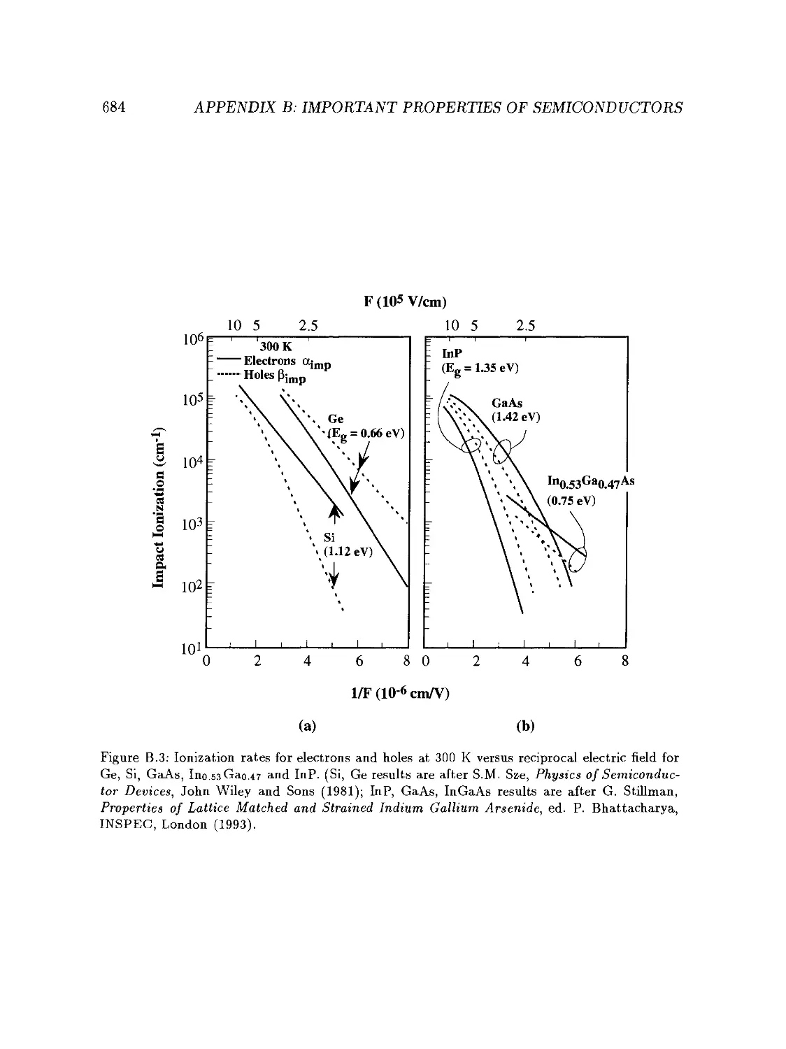
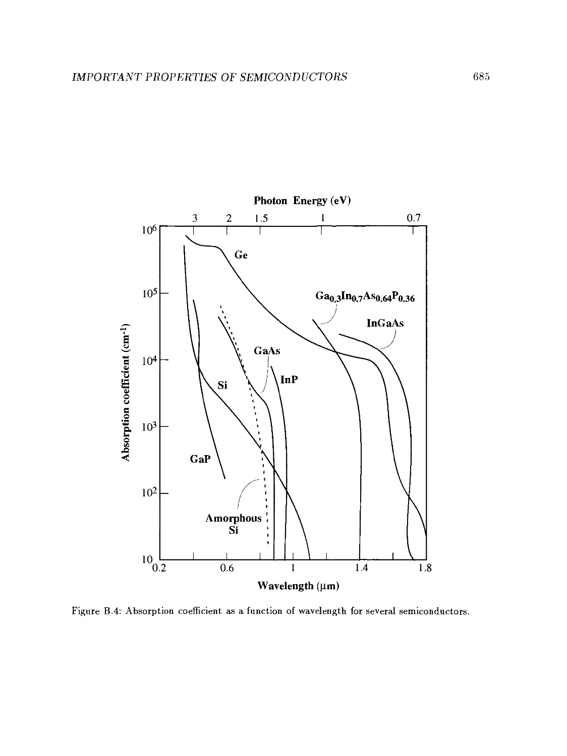
SEMICONDUCTORS 676
IMPORTANT QUANTUM MECHANICS
CONCEPTS 687
C.l The harmonic oscillator problem: spontaneous and
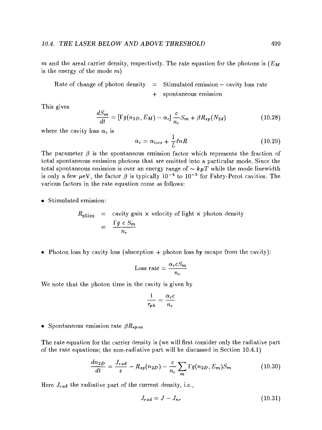
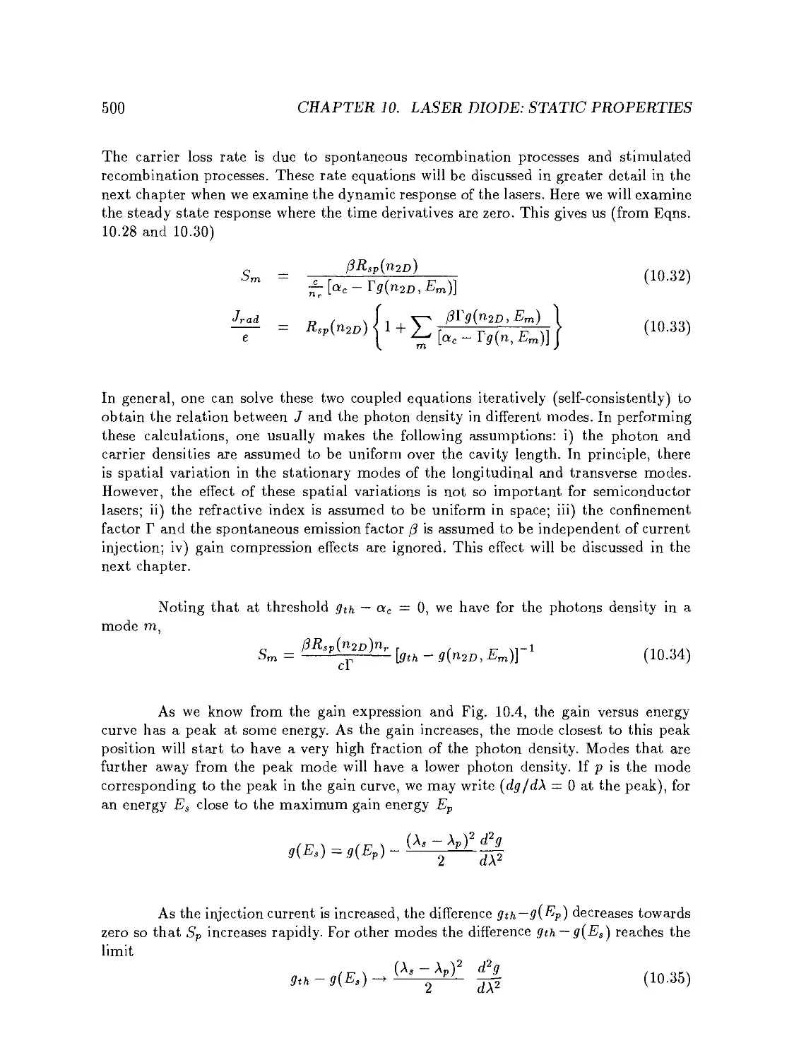
stimulated emission 687
C.2 Time dependent perturbation theory and the fermi
GOLDEN RULE 689
C.2 Eigenvalue method to solve coupled equations 691
U BIPOLAR TRANSISTOR ACTION 695
D.l The bipolar transistor 695
D. 1.1 Current flow in a BJT 698
D.2 BJT design limitations: the need for band tailoring
AND HBTS 701
CONTENTS
xxi
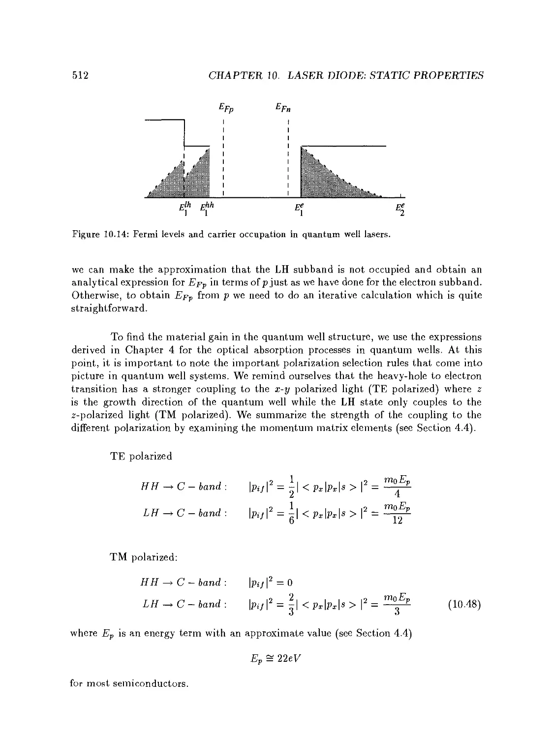
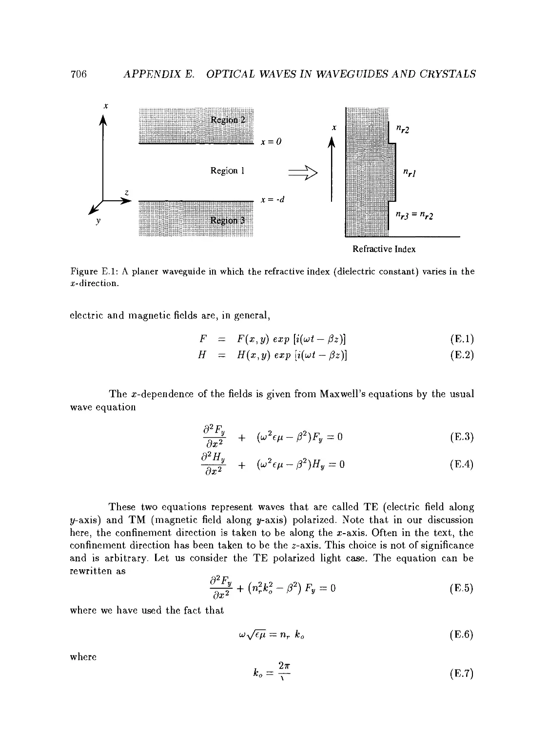
E OPTICAL WAVES IN WAVEGUIDES
AND CRYSTALS 705
E.l Guided optical modes in planer waveguides 705
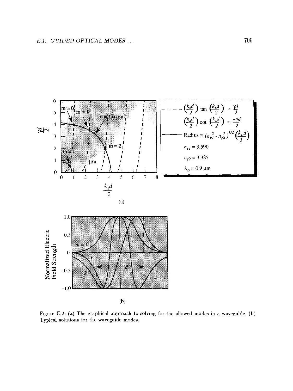
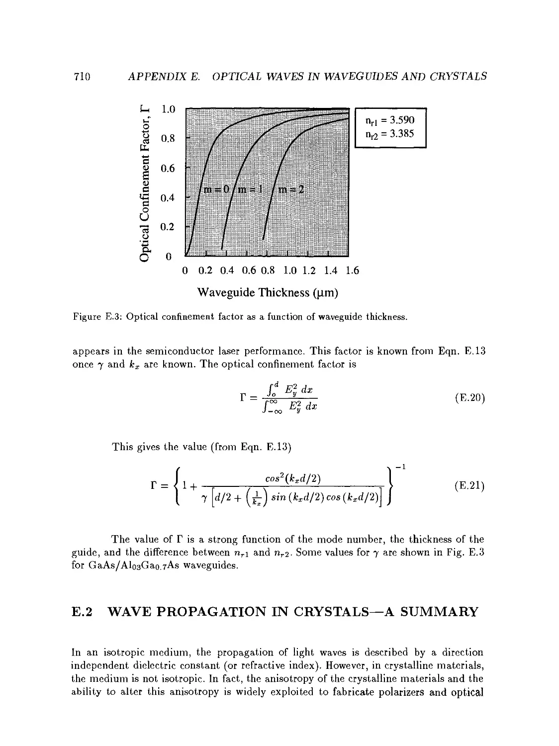
E. 1.1 Optical confinement factor 708
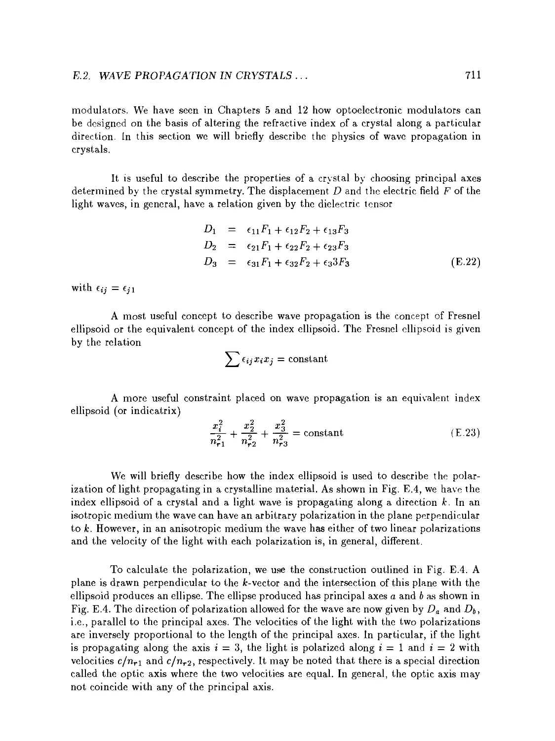
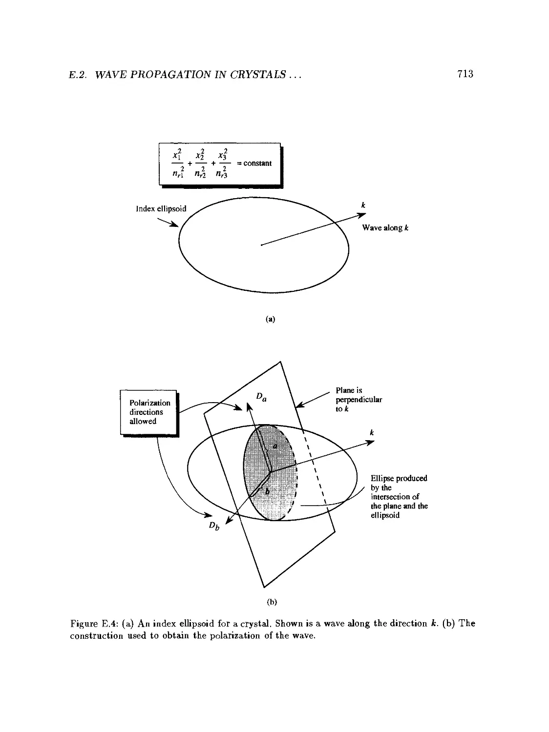
E.2 Wave propagation in crystals—a summary 710
INDEX
714
Preface
In 1988 the trans-Atlantic undersea cable TAT-8 was placed between North America
and Europe using semiconductor optoelectronic components in a most demanding and
harsh environment. The unsuccessful lawsuit of the satellite communication companies
to block TAT-8 signified that the powerful electronic devices had met their match in
communication applications. Today optoelectronic networks promise 500 TV stations
(to the utter disgust of some and utter delight of others) where you can interactively
demand movies, boxing matches, and order a variety of goodies. Indeed, when Wall street
takeover/merger specialists use the words "optical networks" as freely as "aggressive
growth mutual funds," the message is clear—optoelectronics is here!
With the maturing of semiconductor optoelectronic technology, the number of
Universities offering optoelectronic courses and the breadth and depth of these courses
is rapidly increasing. However, in this transient mode, it is not yet established what
sort of knowledge base is necessary to train students of this field. A typical electrical
engineer takes about 20 courses directly related to his or her field to get a Bachelors and
about 10 more to get a Masters. Optoelectronics has not yet reached the stature where
Universities can devote a similar effort for optoelectronics students. Of course, some of
the traditional electronics courses are important for the student of optoelectronics as
well. To develop a thorough understanding of optoelectronic devices, a user must have
the following understanding:
Semiconductor Technology: It is important for the student to understand the state
of technology and how devices are fabricated. It is also important to appreciate the chal-
langes faced by the difficult technologies of optoelectronic integrated circuits (OEICs)
or quantum wire lasers.
Physics of Semiconductors: The physics behind concepts such as effective mass,
mobility, absorption coefficient, bandstructure, etc., should be understood. Also, the
importance of semiconductor alloys and heterostructures should be appreciated. The
interactions of photons and electrons, and concepts such as spontaneous and stimulated
emission, excitonic and electro-optic effects are to be understood.
Semiconductor Optoelectronic Devices: The physical interactions between photons
XXI11
and semiconductors have to be exploited to design and optimize a variety of information
processing devices.
System Needs and New Device Challanges: Since optoelectronic devices are not
very mature at this stage (compared to electronic devices), it is important for the
student to know what improvements can be made and the resulting payoffs. For this it
is important to understand system needs.
It is admittedly difficult for any textbook to address all the needs outlined
above in any real depth. As a result, textbooks tend to focus on one or two areas
without providing the student a global picture. In this textbook, I have touched upon
all the needs while providing an in depth coverage of two key topics—device physics and
device design. The reader will find that the areas of technology and systems is covered
in enough detail to provide a much needed appreciation of the challenges faced here.
The areas of semiconductor physics, electron-photon interactions, and optoelectronic
devices are covered in great depth.
This book is written primarily as a textbook for one or more optoelectronic
courses. However, where appropriate, I have provided discussions on the state of the art
issues. By offering a balanced discussion and about 150 worked examples, I hope that
this textbook will not only serve the coursework needs for students, but would also be
a long term resource for their future careers.
This manuscript was typed by Ms. Izena Goulding, to whom I am extremely
grateful. The figures, cover design, and the typesetting of this book were done by Teresa
Singh, my wife. She also provided the support without which this book would not be
possible. I am also indebted to my students, past and present: Dr. John Hinckley, Prof.
Songcheol Hong, Dr. Mark Jaffe, Dr. John Loehr, Prof. Yeeloy Lam, and Mr. Igor
Vurgaftman. I am extremely grateful to George Hoffman, my editor, for providing me
valuable input from an outstanding group of referees. The referees were generous in
providing positive criticism which I believe greatly benefited the book. I would like to
thank Professor Joe Campbell of the University of Texas at Austin, Professor James
Coleman of the University of Illinois at Urbana-Champaign, Professor Karl Hess of the
University of Illinois at Urbana-Champaign, Professor Marek Osinski of the University
of New Mexico, and Dr. Daniel Renner of the Ortel Corporation. I am also grateful to
Professor Pallab Bhattacharya of the University of Michigan for valuable discussions.
This book shares some sections with the other two books, "Physics of
Semiconductors and Their Heterostructures" (1993) and "Semiconductor Devices: An
Introduction" (1994) which I have written, published by McGraw-Hill.
An Instructor's Manual is available to professors wishing to use this text. This
manual has solutions to the end of chapter problems. In addition, a computer disc is
available to address the following class of problems: i) electron and hole levels in quantum
x.v iv
PREFACE
wells (4 band k.p model for holes); ii) optical confinement factor for a waveguide; iii)
laser gain in quantum well lasers; iv) effect of strain on quantum well bandstructure
and laser performance.
Please write, on your department stationary, to McGraw-Hill for a copy of this
manual.
Jasprit Singh
INTRODUCTION
1.1 THE INFORMATION AGE
"Knowledge is power," says an ad campaign for a new business which exploits computer
hookups and the latest in medical technologies to provide a health care package.
Information and its distilled form—knowledge—has become a survival tool for all of us. It is
hard to imagine a world without computers, satellites, undersea fiber networks,
televisions, fax machines, laser printers, and a myriad of other information processing tools.
And, of course, just a few decades ago none of these gadgets were available. What has
made us so dependent on information and its rapid processing? Whether we like it or
not, most of the livelihoods of workers in industrially developed countries are intimately
tied to the ability to access and process information—preferably before our competition
does it!
Regardless of what the information is, we want to process it faster, with less
inaccuracies, at a lower cost, with a system which consumes less space, etc.. In fact, the
driving forces for new technologies can range from the need to diagnose tumors in the
brain to the diagnosis of a poisonous gas in a factory. It is estimated that at present
(mid-nineties), over ten trillion bits of information are generated each day! Most of these
bits can be attributed to the television industry, which should not be surprising to the
reader.
The modern age of information processing has been ushered in by the electronic
devices, particularly the mass produced high density semiconductor devices. These
devices process information at blinding speeds, crunching numbers at speeds of millions
of instructions per second. Electronic devices are deeply entrenched in any information
processing system, and for good reason. Can optoelectronic devices, which exploit light
and electrons, make inroads into the domain of electronic devices? Over the last decade,
optoelectronic devices have started to make an impact on the information processing
scene. This impact has been felt most in the area of information communication and
information storage and retrieval. However, so far the impact has been less in the area
of "intelligent" information processing. To understand the challenges facing
optoelectronics and the potential payoffs, we examine the demands placed upon devices that are
XXVI
INTRODUCTION
to be successful in information processing.
1.2 DEMANDS OF THE INFORMATION AGE
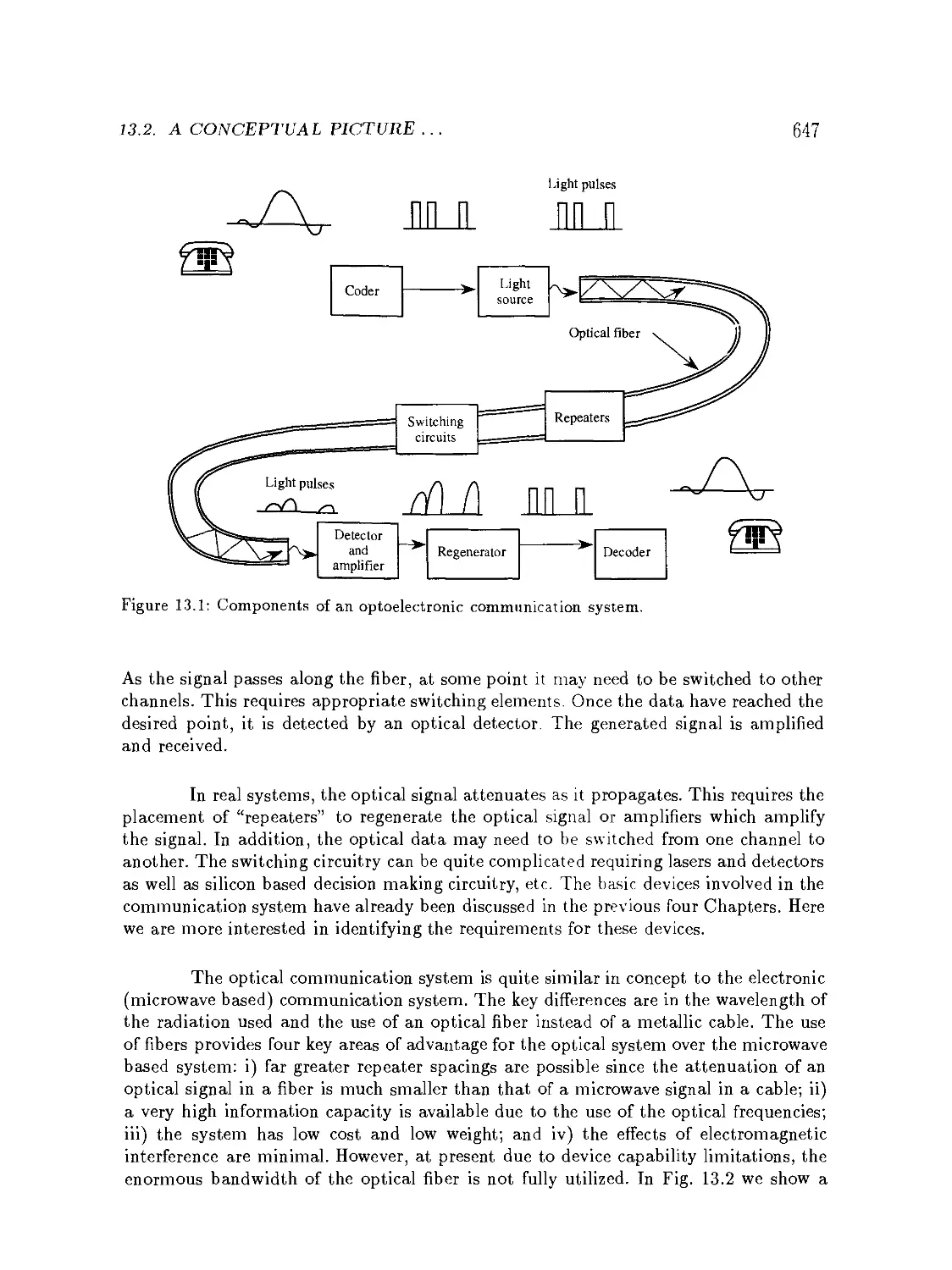
As noted in the previous section, we live in an age where acquiring, manipulating, and
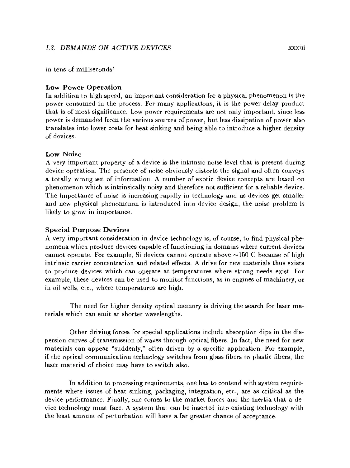
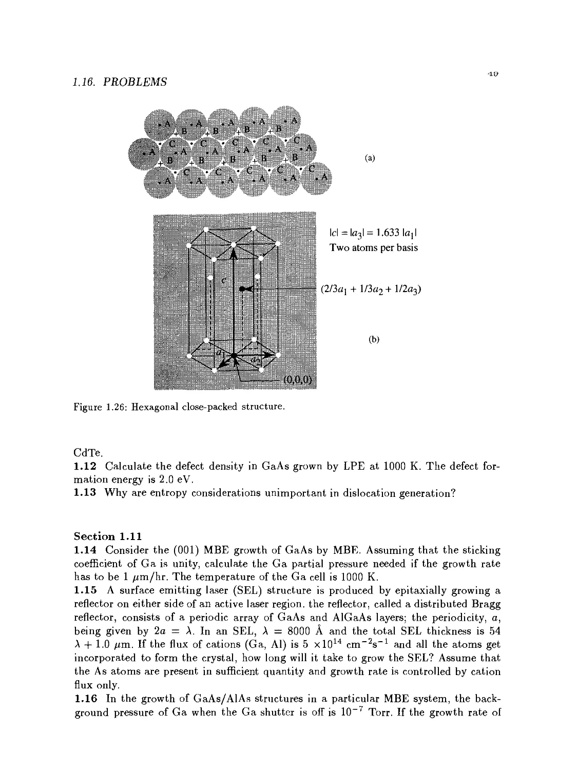
transmitting information is of utmost importance. In Fig. 1.1 we show some of the
important functions that need to be carried out in order to survive in the information age.
Regardless of what medium is used to produce the devices—water, electrons, photons,
beads, etc.,—the devices must be able to provide at least some of these functions. Let us
briefly examine these functions and see what sort of requirements they put on devices.
Information Reception/Detection
This is, of course, one of the most important functions in an information system. For
example, in our own case we receive information about the world we live in by our eyes,
nose, skin, ears, and tongue. Our five senses allow us to obtain important information
about our surroundings and this information is conveyed to our main processing unit—
our brain. Devices which hope to serve as sensors/detectors must have a well-defined
response to an external input. They must convert the input information into a form
which can be used for further processing.
Information Enhancement/Amplification
Very often the information that is received is of either very poor quality, or is too "weak"
to be directly useful. In such cases, the information must be amplified or enhanced. We
often ask people to repeat themselves louder, since we cannot hear them well. Many
hearing impaired people need hearing aids which can amplify the sound coming in.
Thus, amplifiers are an essential part of an information processing system. To be able
to amplify information, the device must have the very important characteristic of gain,
i.e., a small change in input should result in a large change in output. In times bygone,
a message was often conveyed by beating a code on drums. However, every half a mile
or so, one had to have a new drummer who would hear the faint drums and send forth
a more amplified code to the next drummer. In this particular example, it is interesting
to note that the response of the second drummer to the input is non-linear. Thus, if
for some reason he hears a much fainter drumbeat (due to the wind direction), he still
beats out a signal of the same high strength.
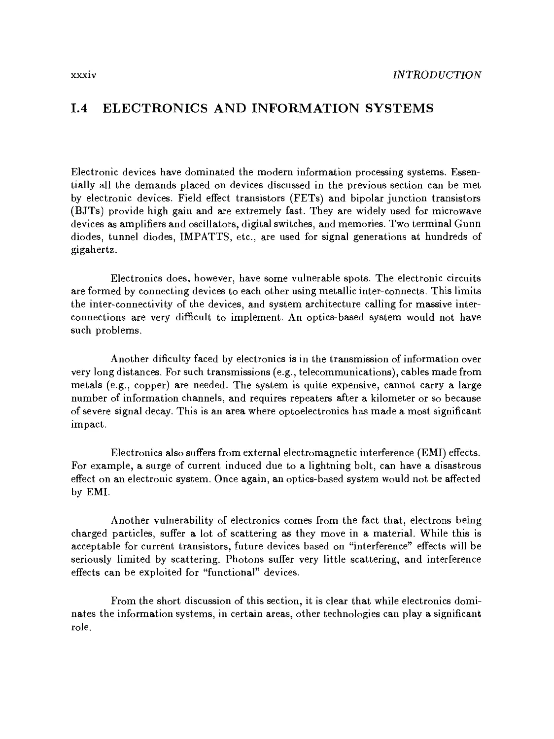
Gain and non-linear response to information are highly desirable properties
of devices. A non-linear response can distinguish between two closely spaced pieces of
information, as shown in Fig. 1.2. A linear response between input and output would not
be able to distinguish the inputs as well. Moreover, if the inputs were noisy, as shown
by the shaded area, the non-linear response would still maintain a very high degree of
separation.
1.2. DEMANDS OF THE INFORMATION AGE
xxvu
Information
reception/detection
Information manipulation
Information retrieval from
memory
Information
enhancement/amplification
Information transfer
Information generation
1
Information display
Figure 1.1: Necessary functions to survive in the "information age."
Information Manipulation
This is, of course, the most important aspect of information processing. When some
information comes in, much of it may be redundant or in a form that is not
appropriate. Invariably, it has to be manipulated, which may mean carrying out processes like
addition, subtraction, division, multiplication, comparison with previous information,
extracting a "signature" of the information, etc.
Memory-
Memory is obviously essential in an information processing system. We are all frustrated
when, at some crucial moment, our memory fails us. The process of learning, comparing,
selecting, and reusing information all require memory. The memory device should be
able to store information by, perhaps, changing the state of the device, and then one
should be able to retrieve the information (i.e., be able to WRITE/READ). This page
that you are reading is a form of a memory—perhaps the most influential kind of memory
in the history of mankind. The walls of the caves in which our ancestors lived thousands
of years ago were a kind of memory.
Memory is an area where semiconductors have been most challenged. Even in
high technology applications, semiconductor memories are not the only game in town.
Optical memories based on a plastic disc (the compact disc), magnetic tape memories,
XX VI11
INTRODUCTION
3
a,
- Linear
Non-linear
6 oLX -
Input >■
Figure 1.2: The advantages of a non-linear input-output response in distinguishing closely-
spaced inputs. A linear response system cannot separate the input signals I\ and I2 (with
response Oli and Ol2) as well as the non-linear response (with response Ojvi and On2- Also,
the non-linear device has a better noise immunity, as shown by the shaded areas.
magnetic bubble memories, etc., all form important spokes of the memory technology,
along with semiconductor memories.
Information Transfer
An important function in an information processing system is to be able to transfer the
information or the results obtained after manipulating the information into a storage or
memory. For example, when an image is seen by our eye, the information is sent to the
brain via the optic nerve in a well-defined sequence so that the brain knows that there is
a door to the right, a chair in front, a blackboard to the left, etc. Any scrambling in this
transfer process can lead to serious disabilities. Such transfer devices are most useful
when two or three dimensional information must pass through a one dimensional path.
A most popular case where this happens is in the case of a video camera. In a video
camera, a two dimensional view is recorded and sent sequentially via charge coupled
devices (CCDs) to a memory. Since a precise sequence is maintained in this transfer,
the scene can later be easily reconstructed if the sequence is known.
Information Generation
Another important step in information technology is the generation of information. We
generate information by a variety of means, ranging from our speech, to hand actions,
facial expressions, writing, etc. Of course, in each case the real information is generated
by the firing of neurons in the brain.
1.3. DEMANDS ON ACTIVE DEVICES
XXIX
Information can be generated in semiconductor technology by the
semiconductor laser or by a microwave device. By coupling semiconductor technology with other
technologies, information can be generated in the form of sound waves as well.
Information Display
The saying, "A picture is worth a thousand words," seems to be coming more and more
valid as the amount of information becomes greater and greater. Often in our daily life,
a single facial expression conveys more information than any speech or writing could.
Displaying information is extremely important and has great impact on human
experience. Consider the enormous sum of money spent by companies on advertisements.
Displays need not just be pictures—they can be words conveying information as well.
Display technology is one of the fastest growing technologies in recent years. Nations
and companies vie fiercely to obtain an edge in display technology. New display
technologies, such as high density television (HDTV), flat panel displays, programmable
transparencies, etc., hold keys to the economic success of many companies. Graphic
workstations have already transformed the lives of designers of houses, automobiles,
and microelectronic chips. Semiconductor technology has coupled extremely well with
liquid crystal technology to produce displays. Also for active displays and light sources,
semiconductor devices such as LEDs and laser diodes serve an important need.
1.3 DEMANDS ON ACTIVE DEVICES
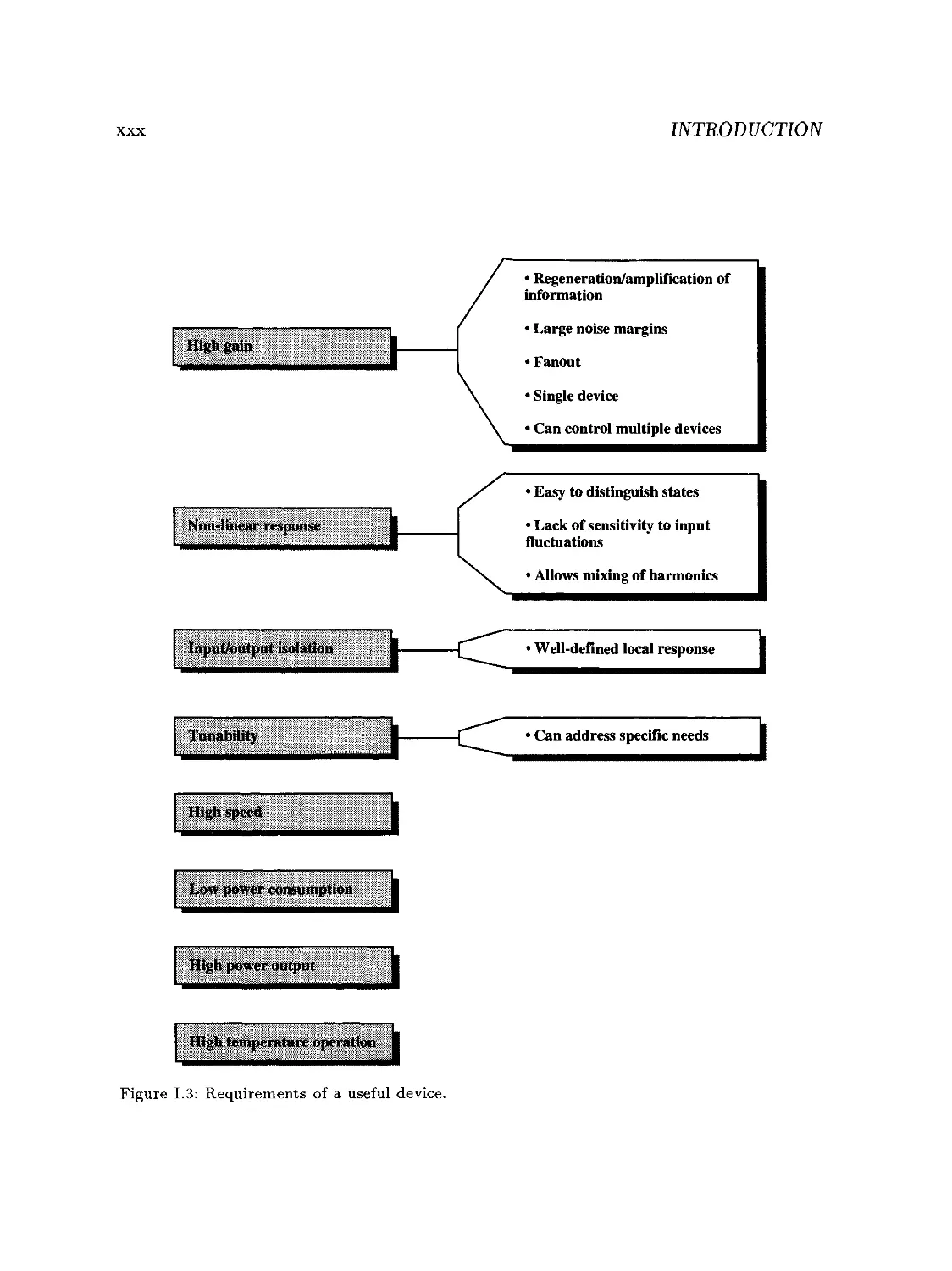
Based on our previous discussions of the information processing needs, the demands
on active devices are summarized in Fig. 1.3. In order for a device to succeed, it must
display a physical phenomenon that leads to one or more of the properties mentioned in
Fig 1.3. Let us briefly discuss all of these requirements, along with other requirements
coming from fabrication and market forces, in this section.
Non- Linear Response
Whether the task to be accomplished by a device is image enhancement or simple
addition of two numbers, the key property a device must possess is the ability to distinguish
between two "closely spaced" pieces of information. We have already discussed, in the
previous section via Fig. 1.2, the advantage of a non-linear response over a linear
response.
Another consequence of a nonlinear response is manifested when two inputs are
simultaneously inputted into the device. Consider the two inputs to have a form
hn = ^1 COS Wit + h COSU^
XXX
INTRODUCTION
High gain
Nun-linear response
• Regeneration/amplification of
information
• Large noise margins
• Fanout
• Single device
• Can control multiple devices
• Easy to distinguish states
• Lack of sensitivity to input
fluctuations
• Allows mixing of harmonics
[
Inpul/iiutput isolation
' Well-defined local response
Tunabilitv
t-<Z
• Can address specific needs
High speed
Low power consumption
Mi till power output
Ilifili leinpiTHtiirr operation
Figure 1.3: Requirements of a useful device.
1.3. DEMANDS ON ACTIVE DEVICES
XXXI
and let us assume a simple physical response of the form
I0 = al + f3I2
where a is the linear response coefficient and j3 represents a non-linear coefficient. Of
course, the real output function may be more complicated. The output of the device to
the input is now
I0 = Ot[I\ COSWi^ + I2 COSU^] + /? [if COS1 U>\t + l\ COS2 U>2t + 27l72 COS LJ]t CoSU^]
Noting that
cos(a) cos(6) = - [cos(a + b) + cos(a — 6)]
we have
/0 = a [/1 cosui\t + I2 cos u>2t] + (3
P
^-(l + cos2w!i)
I2
+ " -^-(1 + 2 cos(w2i) + /t/2 {cos(wi + u>2) + cos(wi - u>2)t)
The output now has signals of frequencies not only u>\ and ui2, but also 2wi, 2ui2
as well as most importantly (wi + u>2) and (wi - u>2). Thus the non linearity is able to
"mix" the two input signals and provide sum and difference signals. This is extremely
useful for communication where a signal to be transmitted (say at audio frequencies)
can be "carried" on a high frequency and then decoded.
Gain in the Device
If a physical phenomenon is to lead to a viable device, an important requirement is the
presence of gain in the output-input relation. Thus, a small change in the input should
produce a large change in the output. In most applications of devices, a "regeneration"
of information is required, i.e., the output of previous step is used to generate another
output in successive steps. The ability to introduce gain is one of the most powerful
ingredients of most electronic devices, as we shall briefly discuss. Lack of gain has also
been one of the pitfalls of many promising exotic device ideas.
The ability to provide gain (or amplify the incoming signal) is not only
important for signal regeneration, it is also very useful, along with nonlinear effects, in
providing large noise tolerances, especially in digital technologies. One of the great strengths
of digital technologies comes from this "noise immunity" of the processed signal at each
step of the processing. Thus, in most processing systems, an analog signal is converted
to a digital signal (by A/D converters) in spite of the fact that a slight loss of accuracy
XXX11
INTRODUCTION
is suffered in this conversion. However, after this initial loss, the digital signal can then
be processed by many complex steps and its integrity is maintained by the presence of
high gain devices.
Another advantage of a high gain device is that a single output can drive a
number of other devices (i.e., have a large "fanout"). This is an obvious plus, since
complex circuitry can be designed based on a large fanout.
Input-Output Isolation
We have all had an experience when, during a conversation, a listener suddenly starts
speaking while we are still speaking, causing great confusion. The human body is
designed in such a way that it is difficult to shut off our ears and so it is usually not possible
to attain input-output isolation during conversation. For devices, the isolation between
the input signal and the output signal is essential for most applications. This ensures
a well defined response of the device and the system for a given set of inputs. One of
the key attractions of three terminal devices (that are well designed) is the isolation
between the gate (or base in a bipolar device) of an FET and the output at the drain
(or the collector). This is often not possible in two terminal devices, causing serious
difficulties in technologies that have attempted to use these devices.
Tunable Response
One of the driving forces of the modern technology is tunability of device response. This
may involve optical devices that can emit in important frequency windows (e.g., blue
or green light for displays; 1.55 /im lasers for low loss transmission in fibers, etc.), or
special structures which have unusual input-output characteristics. A tunable response,
especially if it is achieved while maintaining the other device requirements, is of great
importance for the development of technology.
High Speed Operation
The ability to process information at a faster and faster rate is, of course, the main
reason for advances in device technology. Physical phenomenon which are "fast" and
can be harnessed to produce viable devices are constantly being researched. However,
it must be realized, based on the discussions of this section, that every "femtosecond"
phenomenon is not going to lead to a device. Thus, while it may be popular to discuss
how a femtosecond laser may be able to transmit all the information in the world's
libraries in a second, usually such claims do not survive a closer scrutiny.
The issue of speed is usually a simple one in some technologies, such as
microwave technology or optical communication. Here, "faster" materials (e.g., Si —+
GaAs/InGaAs —»■) drive the technology for microwave applications. However, in the
case of the all purpose computation systems, the speed issue is rather complex and
"architecture and layout" play as much, if not more, of a role in the overall speed of a
system. Let us not forget that one of the fastest computers (at least for some operations,
like recognition, association, etc.)—the human brain—has devices that can only switch
1.3. DEMANDS ON ACTIVE DEVICES
XXXI11
in tens of milliseconds!
Low Power Operation
In addition to high speed, an important consideration for a physical phenomenon is the
power consumed in the process. For many applications, it is the power-delay product
that is of most significance. Low power requirements are not only important, since less
power is demanded from the various sources of power, but less dissipation of power also
translates into lower costs for heat sinking and being able to introduce a higher density
of devices.
Low Noise
A very important property of a device is the intrinsic noise level that is present during
device operation. The presence of noise obviously distorts the signal and often conveys
a totally wrong set of information. A number of exotic device concepts are based on
phenomenon which is intrinsically noisy and therefore not sufficient for a reliable device.
The importance of noise is increasing rapidly in technology and as devices get smaller
and new physical phenomenon is introduced into device design, the noise problem is
likely to grow in importance.
Special Purpose Devices
A very important consideration in device technology is, of Course, to find physical
phenomena which produce devices capable of functioning in domains where current devices
cannot operate. For example, Si devices cannot operate above ~150 C because of high
intrinsic carrier concentration and related effects. A drive for new materials thus exists
to produce devices which can operate at temperatures where strong needs exist. For
example, these devices can be used to monitor functions, as in engines of machinery, or
in oil wells, etc., where temperatures are high.
The need for higher density optical memory is driving the search for laser
materials which can emit at shorter wavelengths.
Other driving forces for special applications include absorption dips in the
dispersion curves of transmission of waves through optical fibers. In fact, the need for new
materials can appear "suddenly," often driven by a specific application. For example,
if the optical communication technology switches from glass fibers to plastic fibers, the
laser material of choice may have to switch also.
In addition to processing requirements, one has to contend with system
requirements where issues of heat sinking, packaging, integration, etc., are as critical as the
device performance. Finally, one comes to the market forces and the inertia that a
device technology must face. A system that can be inserted into existing technology with
the least amount of perturbation will have a far greater chance of acceptance.
XXXIV
INTRODUCTION
1.4 ELECTRONICS AND INFORMATION SYSTEMS
Electronic devices have dominated the modern information processing systems.
Essentially all the demands placed on devices discussed in the previous section can be met
by electronic devices. Field effect transistors (FETs) and bipolar junction transistors
(BJTs) provide high gain and are extremely fast. They are widely used for microwave
devices as amplifiers and oscillators, digital switches, and memories. Two terminal Gunn
diodes, tunnel diodes, IMPATTS, etc., are used for signal generations at hundreds of
gigahertz.
Electronics does, however, have some vulnerable spots. The electronic circuits
are formed by connecting devices to each other using metallic inter-connects. This limits
the inter-connectivity of the devices, and system architecture calling for massive
interconnections are very difficult to implement. An optics-based system would not have
such problems.
Another dificulty faced by electronics is in the transmission of information over
very long distances. For such transmissions (e.g., telecommunications), cables made from
metals (e.g., copper) are needed. The system is quite expensive, cannot carry a large
number of information channels, and requires repeaters after a kilometer or so because
of severe signal decay. This is an area where optoelectronics has made a most significant
impact.
Electronics also suffers from external electromagnetic interference (EMI) effects.
For example, a surge of current induced due to a lightning bolt, can have a disastrous
effect on an electronic system. Once again, an optics-based system would not be affected
by EMI.
Another vulnerability of electronics comes from the fact that, electrons being
charged particles, suffer a lot of scattering as they move in a material. While this is
acceptable for current transistors, future devices based on "interference" effects will be
seriously limited by scattering. Photons suffer very little scattering, and interference
effects can be exploited for "functional" devices.
From the short discussion of this section, it is clear that while electronics
dominates the information systems, in certain areas, other technologies can play a significant
role.
1.5. THE PROMISE OF OPTICAL INFORMATION ...
XXXV
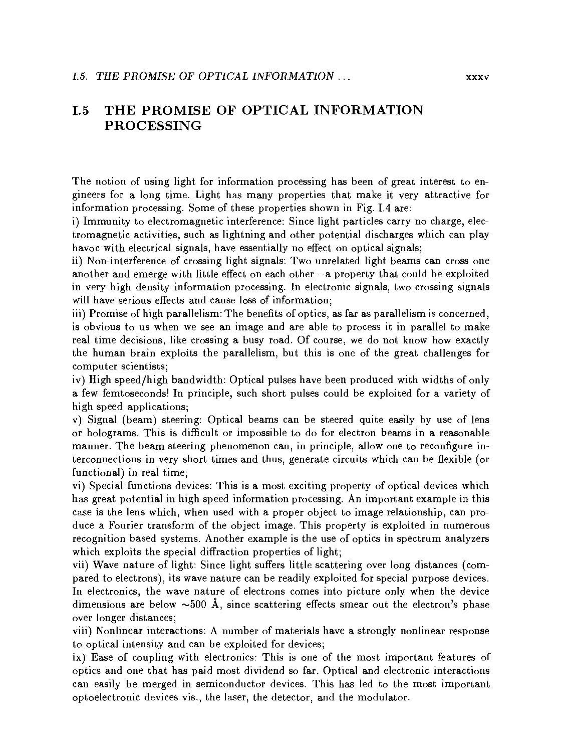
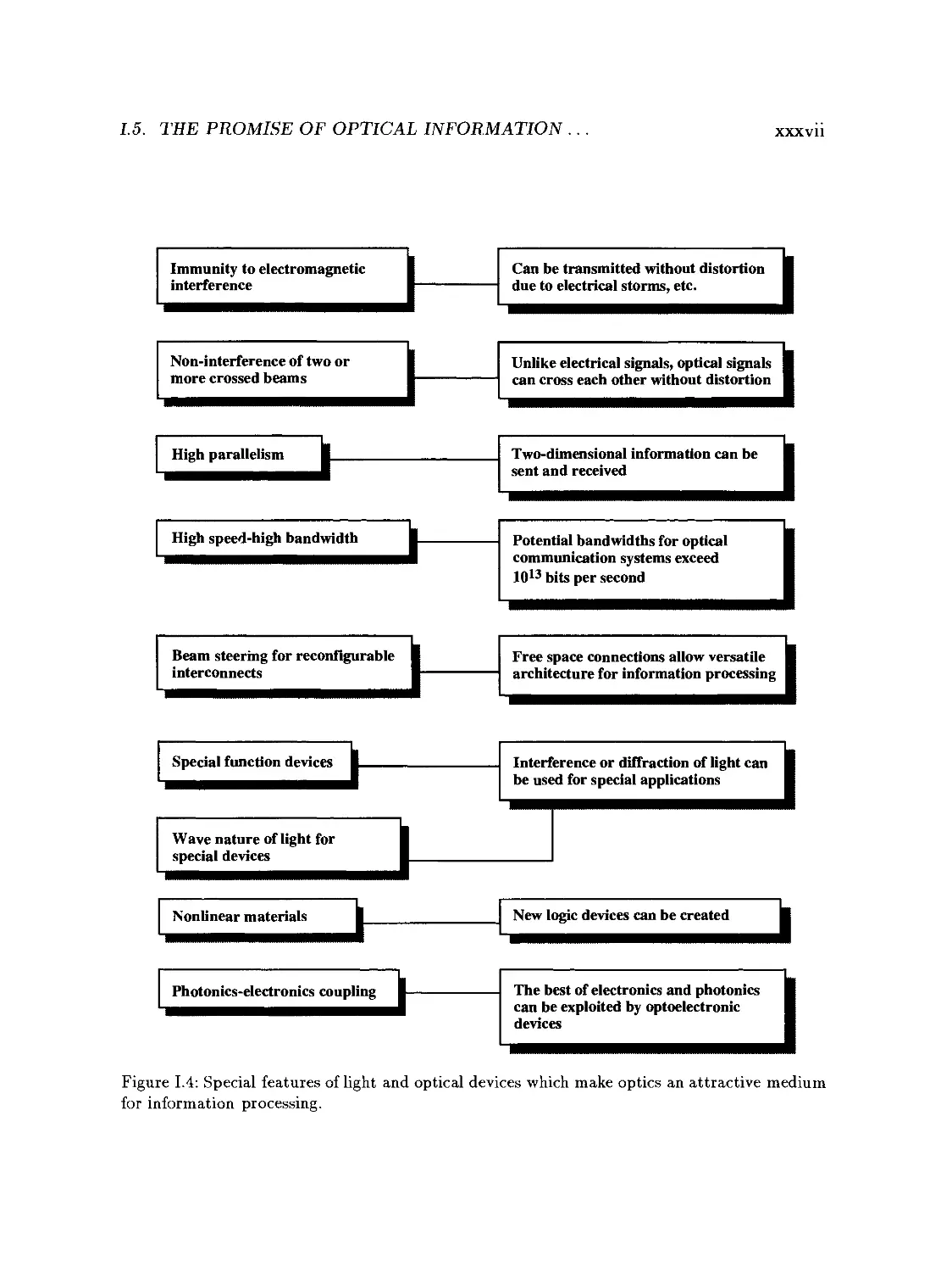
1.5 THE PROMISE OF OPTICAL INFORMATION
PROCESSING
The notion of using light for information processing has been of great interest to
engineers for a long time. Light has many properties that make it very attractive for
information processing. Some of these properties shown in Fig. 1.4 are:
i) Immunity to electromagnetic interference: Since light particles carry no charge,
electromagnetic activities, such as lightning and other potential discharges which can play
havoc with electrical signals, have essentially no effect on optical signals;
ii) Non-interference of crossing light signals: Two unrelated light beams can cross one
another and emerge with little effect on each other—a property that could be exploited
in very high density information processing. In electronic signals, two crossing signals
will have serious effects and cause loss of information;
iii) Promise of high parallelism: The benefits of optics, as far as parallelism is concerned,
is obvious to us when we see an image and are able to process it in parallel to make
real time decisions, like crossing a busy road. Of course, we do not know how exactly
the human brain exploits the parallelism, but this is one of the great challenges for
computer scientists;
iv) High speed/high bandwidth: Optical pulses have been produced with widths of only
a few femtoseconds! In principle, such short pulses could be exploited for a variety of
high speed applications;
v) Signal (beam) steering: Optical beams can be steered quite easily by use of lens
or holograms. This is difficult or impossible to do for electron beams in a reasonable
manner. The beam steering phenomenon can, in principle, allow one to reconfigure
interconnections in very short times and thus, generate circuits which can be flexible (or
functional) in real time;
vi) Special functions devices: This is a most exciting property of optical devices which
has great potential in high speed information processing. An important example in this
case is the lens which, when used with a proper object to image relationship, can
produce a Fourier transform of the object image. This property is exploited in numerous
recognition based systems. Another example is the use of optics in spectrum analyzers
which exploits the special diffraction properties of light;
vii) Wave nature of light: Since light suffers little scattering over long distances
(compared to electrons), its wave nature can be readily exploited for special purpose devices.
In electronics, the wave nature of electrons comes into picture only when the device
dimensions are below ~500 A, since scattering effects smear out the electron's phase
over longer distances;
viii) Nonlinear interactions: A number of materials have a strongly nonlinear response
to optical intensity and can be exploited for devices;
ix) Ease of coupling with electronics: This is one of the most important features of
optics and one that has paid most dividend so far. Optical and electronic interactions
can easily be merged in semiconductor devices. This has led to the most important
optoelectronic devices vis., the laser, the detector, and the modulator.
XXXVI
INTRODUCTION
It is obvious from the above brief discussion that optics has the potential of
playing a major role in the information processing age. Nevertheless, so far it has not
fully met this potential. Only in special purpose systems (spectrum analyzers, remote
imaging by radar recognition, etc.,) is optics used to carry out processing of information.
In most other areas, optics plays a more passive role, serving as carrier of information
while leaving all the active processing to electronics. This is not to say that optical logic
and processing devices have not been developed. It is just that in the serial oriented
computation that we are currently used to, these devices have not favorably competed
with existing electronic devices. It may well be that conceptual changes in computing
are required; ones which will exploit the inherent parallelism of optics before optical
devices become viable in general purpose computation.
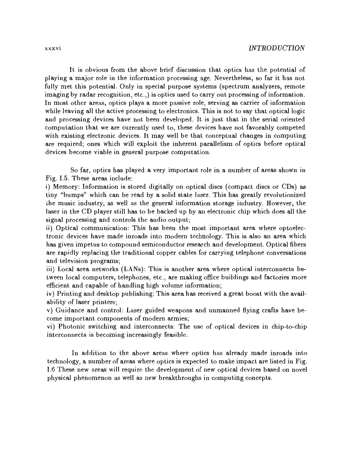
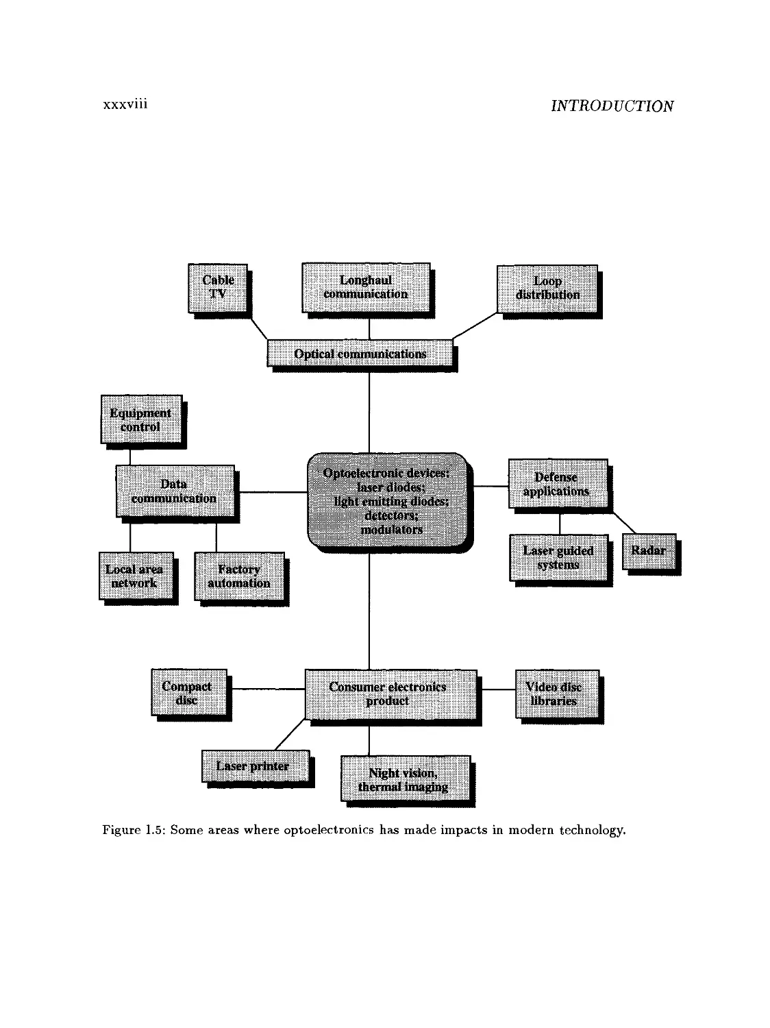
So far, optics has played a very important role in a number of areas shown in
Fig. 1.5. These areas include:
i) Memory: Information is stored digitally on optical discs (compact discs or CDs) as
tiny "bumps" which can be read by a solid state laser. This has greatly revolutionized
the music industry, as well as the general information storage industry. However, the
laser in the CD player still has to be backed up by an electronic chip which does all the
signal processing and controls the audio output;
ii) Optical communication: This has been the most important area where
optoelectronic devices have made inroads into modern technology. This is also an area which
has given impetus to compound semiconductor research and development. Optical fibers
are rapidly replacing the traditional copper cables for carrying telephone conversations
and television programs;
iii) Local area networks (LANs): This is another area where optical interconnects
between local computers, telephones, etc., are making office buildings and factories more
efficient and capable of handling high volume information;
iv) Printing and desktop publishing: This area has received a great boost with the
availability of laser printers;
v) Guidance and control: Laser guided weapons and unmanned flying crafts have
become important components of modern armies;
vi) Photonic switching and interconnects: The use of optical devices in chip-to-chip
interconnects is becoming increasingly feasible.
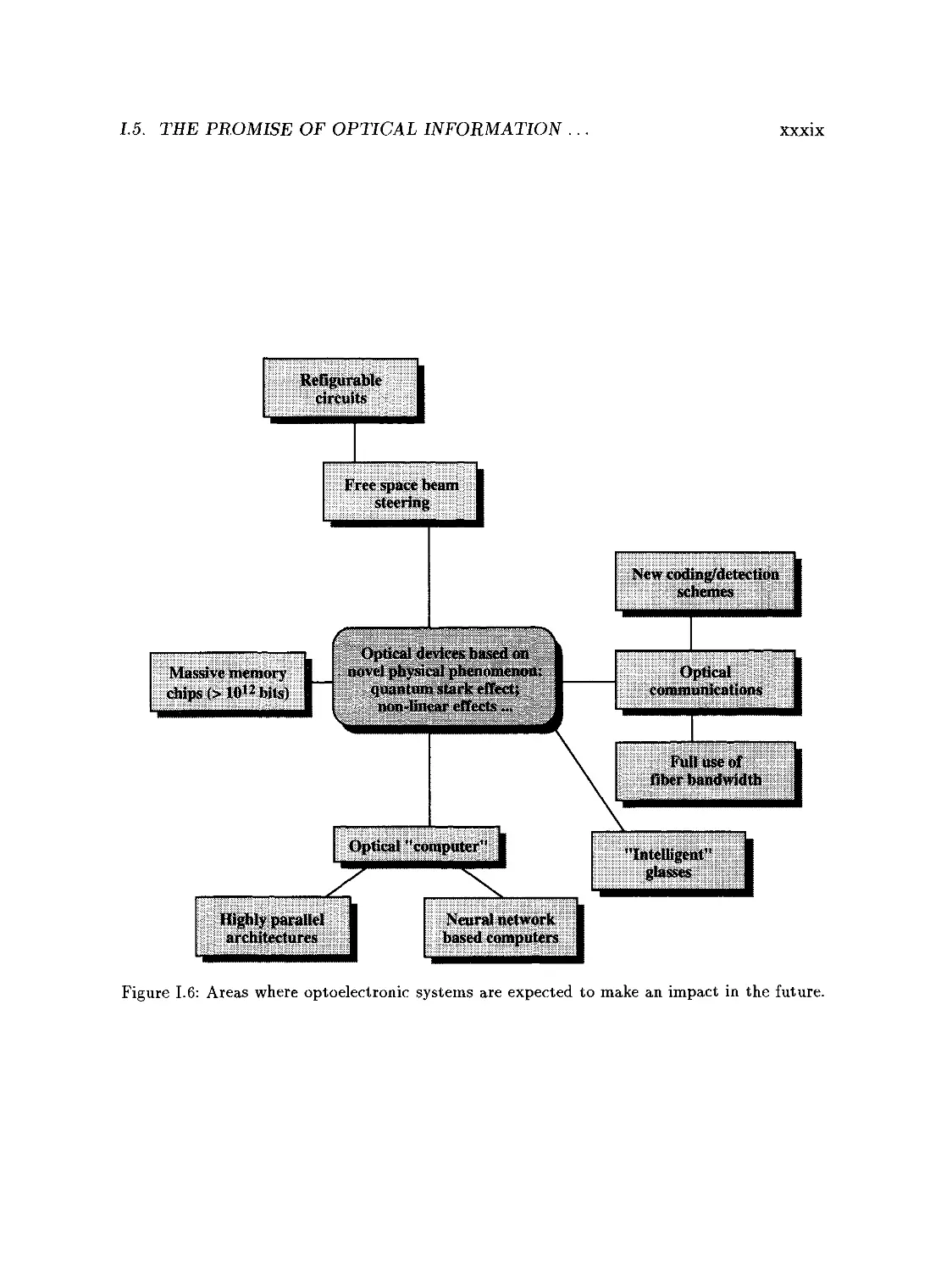
In addition to the above areas where optics has already made inroads into
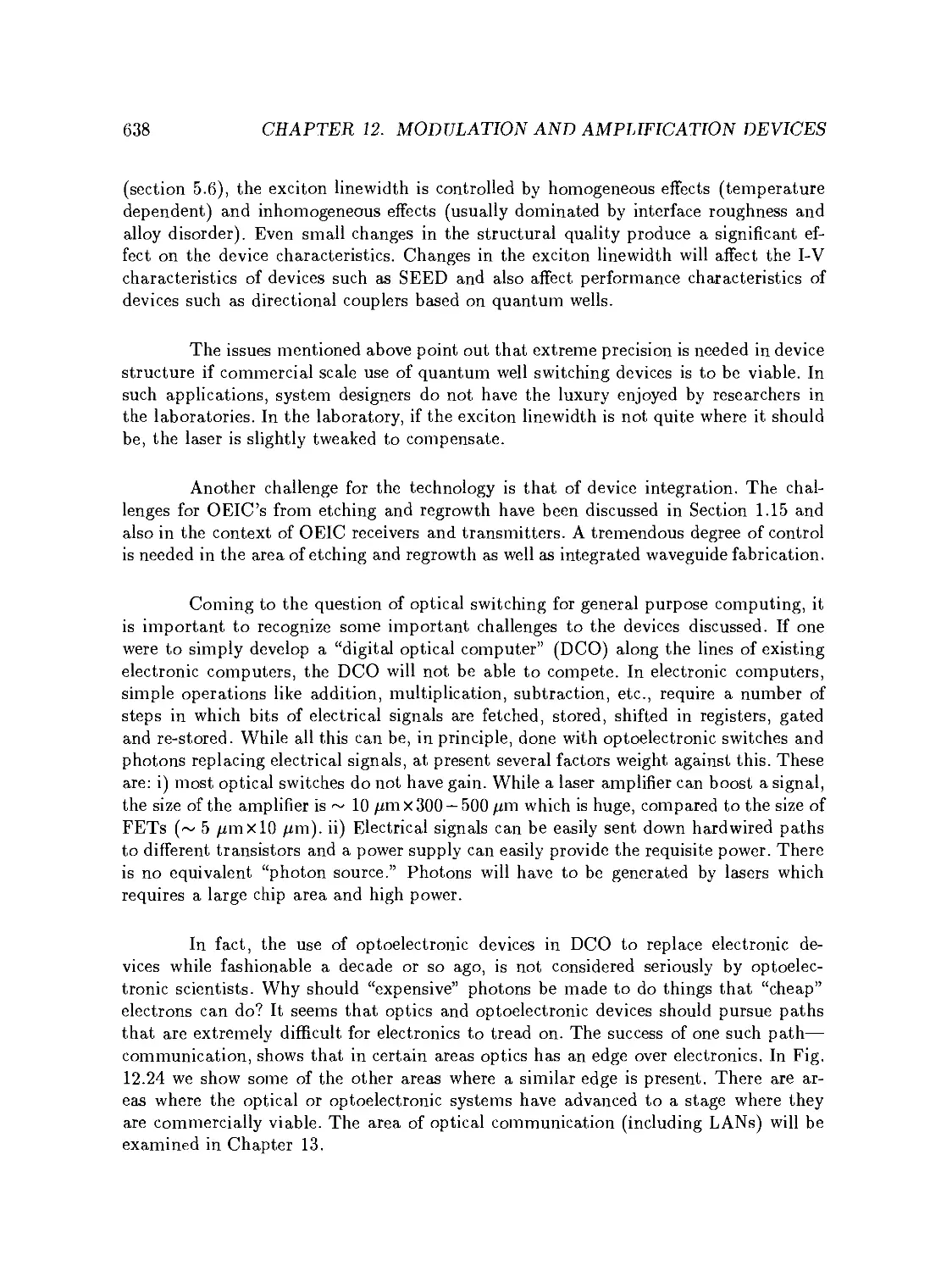
technology, a number of areas where optics is expected to make impact are listed in Fig.
1.6 These new areas will require the development of new optical devices based on novel
physical phenomenon as well as new breakthroughs in computing concepts.
1.5. THE PROMISE OF OPTICAL INFORMATION ...
XXXVll
Immunity to electromagnetic
interference
Can be transmitted without distortion
due to electrical storms, etc.
Non-interference of two or
more crossed beams
Unlike electrical signals, optical signals
can cross each other without distortion
1
High parallelism
High speed-high bandwidth
Two-dimensional information can be
sent and received
]
Potential bandwidths for optical
communication systems exceed
1013 bits per second
Beam steering for reconfigurable
interconnects
Free space connections allow versatile
architecture for information processing
Special function devices
Wave nature of light for
special devices
Interference or diffraction of light can
be used for special applications
Nonlinear materials
New logic devices can be created
Photonics-electronics coupling
The best of electronics and photonics
can be exploited by optoelectronic
devices
Figure 1.4: Special features of light and optical devices which make optics an attractive medium
for information processing.
XXXV111
INTRODUCTION
Longhaul
communication
Optical communications
Optoelectronic dv\ ices:
laser diodes:
light emitting diudov:
dt-lci tors;
modulators
Consumer electronics
product
Night vision,
thermal imaging
Loop
distribution
Defense
applications
Laser guided
systems
\
Figure 1.5: Some areas where optoelectronics has made impacts in modern technology.
THE PROMISE OF OPTICAL INFORMATION ...
XXXIX
Reflgurable
circuits
Massive memory
chips (> 1012bits)
Free space beam
steering
H
Optical devices based on
novel physical phenomenon:
quantum stark effect;
non-linear effects...
Optical "computer"
Highly parallel
architectures
Neural network
based computers
New coding/detection
schemes
Optical
communications
Full use of
fiber bandwidth
Intelligent"
glasses
ure 1.6: Areas where optoelectronic systems are expected to make an impact in the future.
xl
INTRODUCTION
Semiconductor*:
structure, growth,
processing
Chapter 1
Dopini; and transport
Chapter 3
)
Oplii'iil absorption \
and eiiiLssioii I
I hapler4 J
/ \
r xcilonic riltrcts iind |
I'lerli n-oplii' effect I
Chapter 5 I
Optical cnmmunicalion
demands
Chapter 13
Optical mixluljtors
mid switches
Chapter 12
Noise and
photoreccivers
Chapter 8
Semiconductor lasers
hapten 10 and 11
j
Figure 1.7: A flowchart of the topics covered in this book.
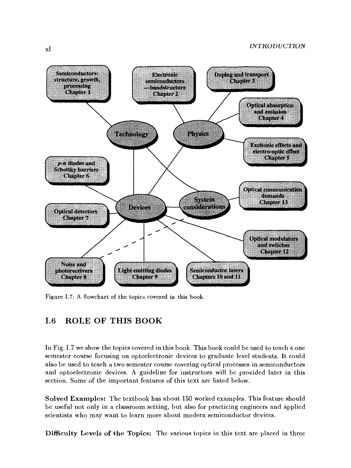
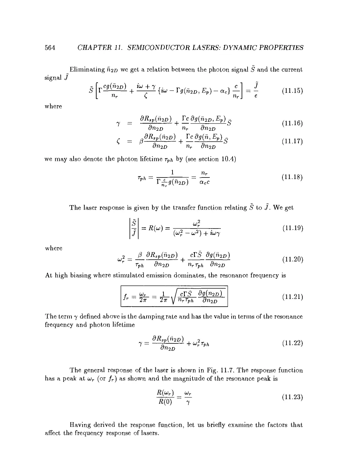
1.6 ROLE OF THIS BOOK
In Fig. 1.7 we show the topics covered in this book. This book could be used to teach a one
semester course focusing on optoelectronic devices to graduate level students. It could
also be used to teach a two semester course covering optical processes in semiconductors
and optoelectronic devices. A guideline for instructors will be provided later in this
section. Some of the important features of this text are listed below.
Solved Examples: The textbook has about 150 worked examples. This feature should
be useful not only in a classroom setting, but also for practicing engineers and applied
scientists who may want to learn more about modern semiconductor devices.
Difficulty Levels of the Topics: The various topics in this text are placed in three
1.7. GUIDELINES FOR INSTRUCTORS
xli
rategories and are identified by three symbols discussed below:
—^ : These topics are relatively easy and appropriate for a lower level one semester
course on optoelectronics for beginning graduate students.
^-^ : The sections are somewhat difficult and/or appropriate for students who have
had some introduction to semiconductor optoelectronic devices. In an introductory class,
the instructor may decide to skip these sections entirely or just summarize the results
without going through the mathematical derivations. These topics can be covered in a
second course on optoelectronics.
: The sections are presented for review or informative reading. The instructors may
choose to assign these sections as reading assignments.
Units: The book uses SI units throughout. Many worked out examples provide the
units at each step. The student may notice the use of centimeters at some places and
meters at others. Also, the energy unit is Joules in some places and electron volt at
others. These are to conform to standard practices and should not cause the student
any difficulty.
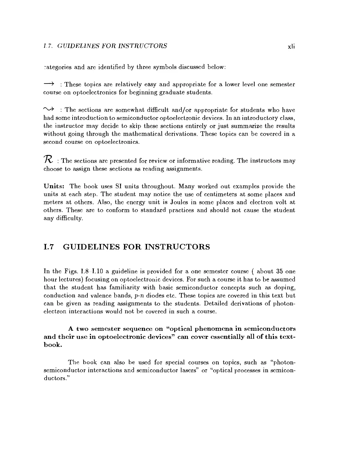
1.7 GUIDELINES FOR INSTRUCTORS
In the Figs. 1.8-1.10 a guideline is provided for a one semester course ( about 35 one
hour lectures) focusing on optoelectronic devices. For such a course it has to be assumed
that the student has familiarity with basic semiconductor concepts such as doping,
conduction and valence bands, p-n diodes etc. These topics are covered in this text but
can be given as reading assignments to the students. Detailed derivations of photon-
electron interactions would not be covered in such a course.
A two semester sequence on "optical phenomena in semiconductors
and their use in optoelectronic devices" can cover essentially all of this
textbook.
The book can also be used for special courses on topics, such as "photon-
semiconductor interactions and semiconductor lasers" or "optical processes in
semiconductors."
xlii
INTRODUCTION
• Discussion of crystal structure; epitaxial
growth techniques 1 lecture
• Strained epitaxy, quantum wells 1 lecture
* Most of this chapter can be given as a reading assignment
Chapter
]
i
• A general discussion ofE-k diagram,
conduction and valence band, holes
• Density of states concepts in 3-D, 2-D, 1-D;
bandstructure of some materials
• Bandstructure modification by alloying,
quantum wells, and strain
1 lecture
2 lectures
1 lecture
Chapter
1
i
• Concept of doping mobility, velocity-field
relations, high field breakdown, a,mp, P,mp
• Diffusion related transport
• Quasi-Fermi level concepts
2 lectures
1 lecture
Figure 1.8: Suggested topics for a 1 semester course oriented towards basic optoelectronic
devices. A 2 semester course could cover all the topics of this text.
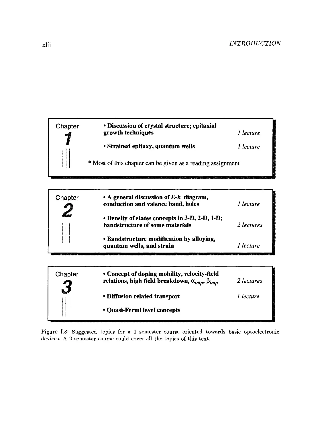
Chapter
1
1.7. GUIDELINES FOR INSTRUCTORS
xliii
Chapter
m
• (No derivations: just statement of results with
some physical explanations)
• Optical absorption coefficient
• Recombination/photon emission
• Non-radiative recombination
• Quantum well effects
I lecture
1 lecture
1 lecture
1 lecture
Chapter
5
i
i
• (No derivations: just statement of results with
some physical explanations)
• Excitonic effects
• Electro-optic effects
1 lecture
1 lecture
Chapter * The student is expected to understand basic
junction theory. The theory can be reviewed and
the chapter can be assigned for reading. 2 lectures
Figure 1.9: Suggested topics for a 1 semester course oriented towards basic optoelectronic
devices (con't.).
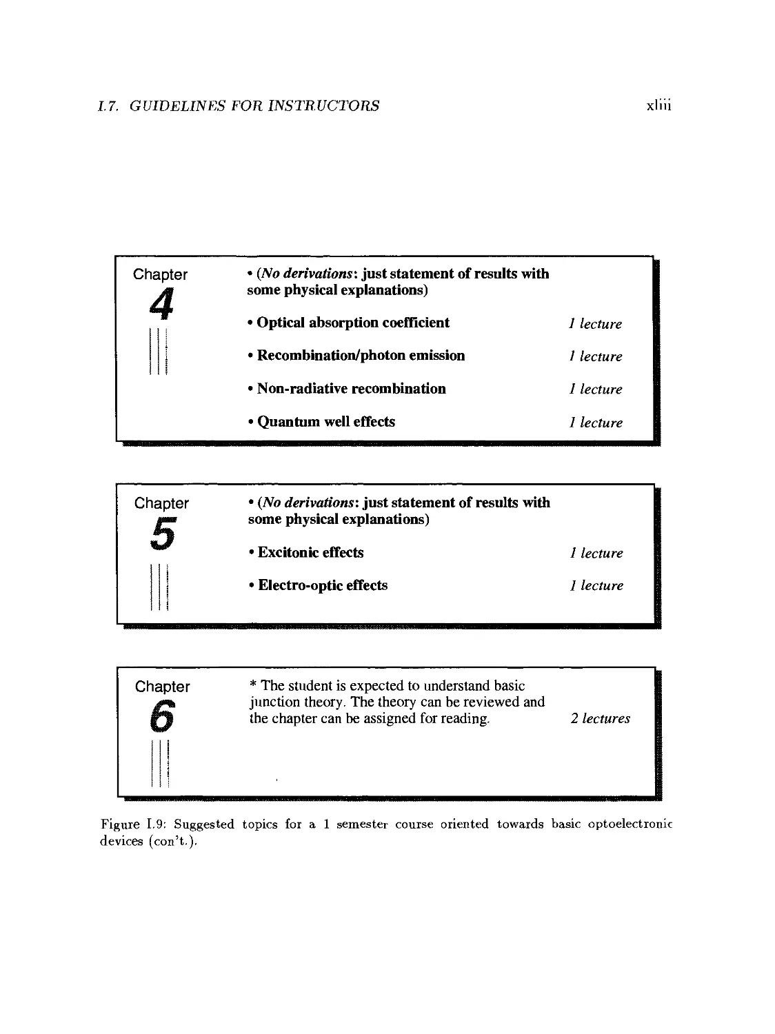
xliv
INTRODUCTION
Chapter
my>
i
* Optical absorption and materials for
detectors
• Photocurrent in ap-n diode
• Photocurrent and p-i-n detector
* Avalanche photodetector
• Phototransistor and MSM detector
1 lecture
1 lecture
1 lecture
1 lecture
1 lecture
Chapter * Basic noise sources and noise issues
in the receiver amplifier 2 lectures
Chapter • Basic operation of the LED 2 lectures
• Advanced LEDs and LED time
response 2 lectures
Figure 1.10: Suggested topics for a 1 semester course oriented towards basic optoelectronic
devices (con't.).
1.7. GUIDELINES FOR INSTRUCTORS
xlv
Chapter
10
• Basic laser operation: importance of
spontaneous and stimulated emission
• The laser below and above threshold
• Advanced laser diodes
2 lectures
1 lecture
1 lecture
Chapter
11
• Rate equations solution for large
signal and small signal laser dynamics 2 lectures
• Laser linewidth issues / lecture
Chapter
• Basic operation of electro-optic
and electro-absorption modulators
• Very brief overview of exciton
based logic devices
2 lectures
1 lecture
* Could be covered if topics in chapters 1, 2, and 3 are covered in less
class time
Chapter • Very brief overview of device
„m f»*k requirements for a communication
§ mj system
/ lecture
* Could be covered if topics in chapters 1, 2, and 3 are covered in less
class time
Figure I.ll: Suggested topics for a 1 semester course oriented towards basic optoelectronic
devices (con't.).
CHAPTER
1
SEMICONDUCTORS:
CRYSTAL STRUCTURE
AND TECHNOLOGY
ISSUES
1.1 INTRODUCTION
This textbook deals with the optoelectronic devices which are designed to provide the
key components of the information age. The devices we will address are all based on
semiconductors. Semiconductors are currently the basis of most electronic devices used
in information processing and it makes sense to use the same materials for optoelectronic
devices. In this chapter we will discuss the physical characteristics of semiconductors.
We will also discuss how semiconductors are manufactured and give an overview of the
various techniques used to fabricate devices. We will also discuss some of the challenges
that remain to be overcome in the device fabrication arena, particularly in regard to
optoelectronic devices.
1.2 THE COMPLEXITY OF SOLID STATE ELECTRONICS
In semiconductor devices, whether electronic or optoelectronic, we are interested
in the behavior of a very large number of negatively charged electrons moving through
positively charged fixed ions. In general, it is difficult to solve a problem where there
are a large number of interacting particles.
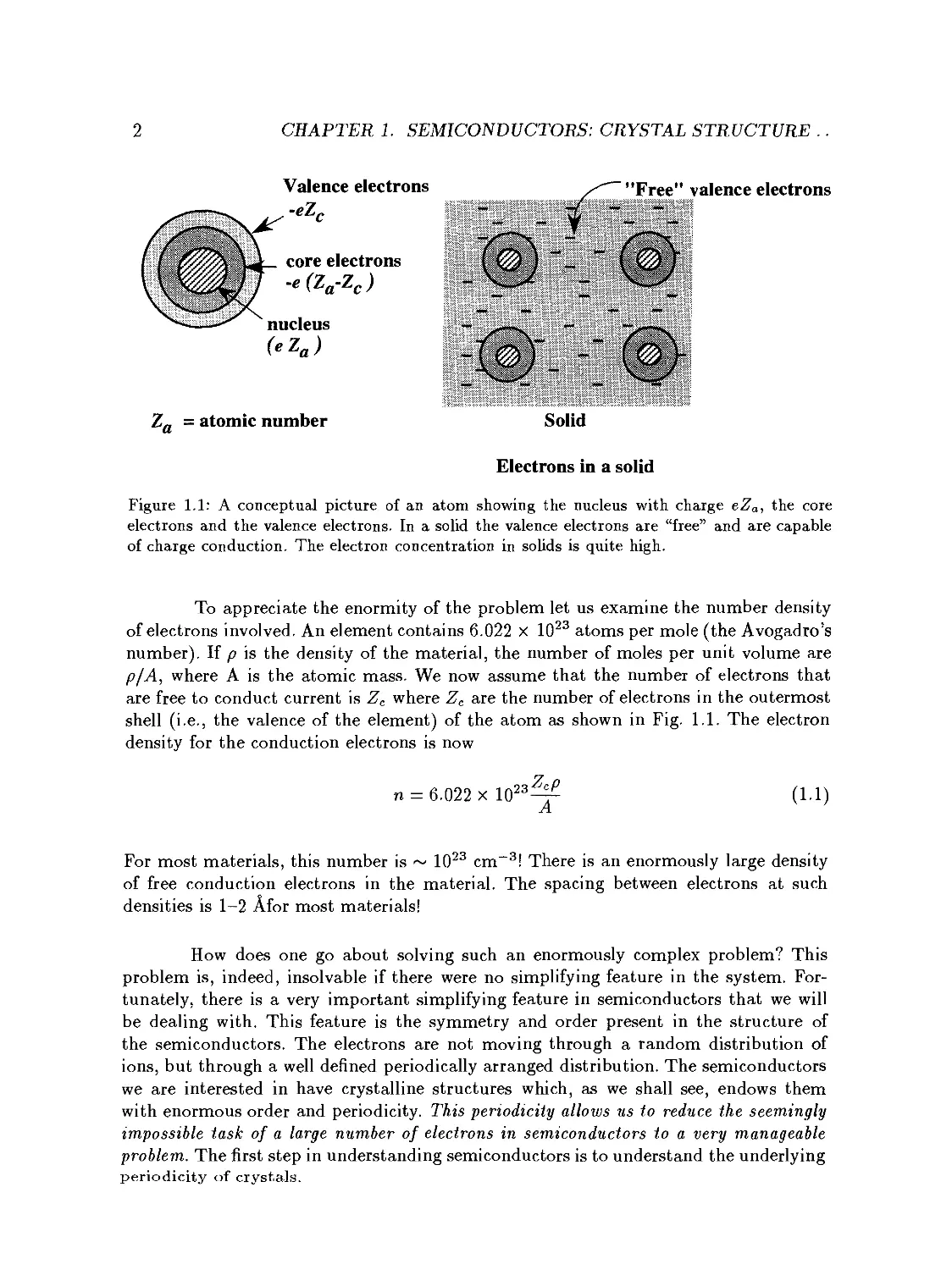
2 CHAPTER 1. SEMICONDUCTORS: CRYSTAL STRUCTURE ..
Valence electrons /— "Free" valence electrons
Z„ = atomic number Solid
Electrons in a solid
Figure 1.1: A conceptual picture of an atom showing the nucleus with charge eZa, the core
electrons and the valence electrons. In a solid the valence electrons are "free" and are capable
of charge conduction. The electron concentration in solids is quite high.
To appreciate the enormity of the problem let us examine the number density
of electrons involved. An element contains 6.022 X 10²³ atoms per mole (the Avogadro's
number). If p is the density of the material, the number of moles per unit volume are
p/A, where A is the atomic mass. We now assume that the number of electrons that
are free to conduct current is Zc where Zc are the number of electrons in the outermost
shell (i.e., the valence of the element) of the atom as shown in Fig. 1.1. The electron
density for the conduction electrons is now
n = 6.022 x 10²³^r C11)
A '
For most materials, this number is ~ 1023 cm"3! There is an enormously large density
of free conduction electrons in the material. The spacing between electrons at such
densities is 1-2 Afor most materials!
How does one go about solving such an enormously complex problem? This
problem is, indeed, insolvable if there were no simplifying feature in the system.
Fortunately, there is a very important simplifying feature in semiconductors that we will
be dealing with. This feature is the symmetry and order present in the structure of
the semiconductors. The electrons are not moving through a random distribution of
ions, but through a well defined periodically arranged distribution. The semiconductors
we are interested in have crystalline structures which, as we shall see, endows them
with enormous order and periodicity. This periodicity allows us to reduce the seemingly
impossible task of a large number of electrons in semiconductors to a very manageable
problem. The first step in understanding semiconductors is to understand the underlying
periodicity of crystals.
1.3. PERIODICITY OF A CRYSTAL
3
1.3 PERIODICITY OF A CRYSTAL
Crystals are made up of identical building blocks, the block being an atom or a group
of atoms. While in "natural" crystals the crystalline symmetry is fixed by nature, new
advances in crystal growth techniques are allowing scientists to produce artificial crystals
with modified crystalline structure. These advances depend upon being able to place
atomic layers with exact precision and control during growth, leading to "superlattices".
The underlying periodicity of crystals is the key which controls the properties of the
electrons inside the material. Thus by altering crystalline structure artificially, one is
able to alter electronic properties.
To understand and define the crystal structure, two important concepts are
introduced. The lattice represents a set of points in space which forma periodic structure.
Each point sees an exact similar environment. The lattice is by itself a mathematical
abstraction. A building block of atoms called the basis is then attached to each lattice
point yielding the crystal structure.
An important property of a lattice is the ability to define three vectors ai, a2,
a3, such that any lattice point R' can be obtained from any other lattice point R by a
translation
R' = R+ mtai + m2a2 + m3a3 (1.2)
where m\, m2, m3 are integers. Such a lattice is called Bravais lattice. The entire lattice
can be generated by choosing all possible combinations of the integers mi, m2, m3 .
The crystalline structure is now produced by attaching the basis to each of these lattice
points.
lattice + basis = crystal structure (1-3)
The translation vectors ai, a2, and a3 are called primitive if the volume of the cell
formed by them is the smallest possible. There is no unique way to choose the primitive
vectors. One choice is to pick
ai to be the shortest period of the lattice
a2 to be the shortest period not parallel to ai
a3 to be the shortest period not coplanar with a! and a2
It is possible to define more than one set of primitive vectors for a given
lattice, and often the choice depends upon convenience. The volume cell enclosed by the
primitive vectors is called the primitive unit cell.
Because of the periodicity of a lattice, it is useful to define the symmetry of the
structure. The symmetry is defined via a set of point group operations which involve
4
CHAPTER 1. SEMICONDUCTORS: CRYSTAL STRUCTURE ..
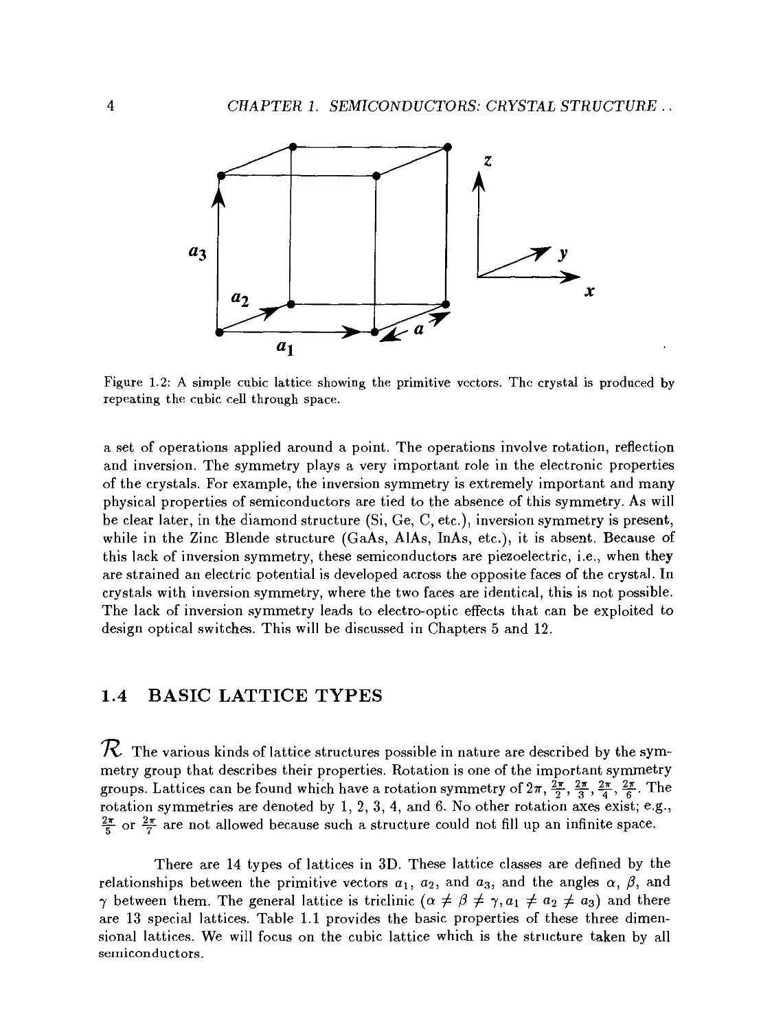
Figure 1.2: A simple cubic lattice showing the primitive vectors. The crystal is produced by
repeating the cubic cell through space.
a set of operations applied around a point. The operations involve rotation, reflection
and inversion. The symmetry plays a very important role in the electronic properties
of the crystals. For example, the inversion symmetry is extremely important and many
physical properties of semiconductors are tied to the absence of this symmetry. As will
be clear later, in the diamond structure (Si, Ge, C, etc.), inversion symmetry is present,
while in the Zinc Blende structure (GaAs, AlAs, InAs, etc.), it is absent. Because of
this lack of inversion symmetry, these semiconductors are piezoelectric, i.e., when they
are strained an electric potential is developed across the opposite faces of the crystal. In
crystals with inversion symmetry, where the two faces are identical, this is not possible.
The lack of inversion symmetry leads to electro-optic effects that can be exploited to
design optical switches. This will be discussed in Chapters 5 and 12.
1.4 BASIC LATTICE TYPES
The various kinds of lattice structures possible in nature are described by the
symmetry group that describes their properties. Rotation is one of the important symmetry
groups. Lattices can be found which have a rotation symmetry of 2tt, ^, ^, ^£, ^-. The
rotation symmetries are denoted by 1, 2, 3, 4, and 6. No other rotation axes exist; e.g.,
t?- or ~ are not allowed because such a structure could not fill up an infinite space.
There are 14 types of lattices in 3D. These lattice classes are defined by the
relationships between the primitive vectors ai, 02, and a3, and the angles a, /?, and
7 between them. The general lattice is triclinic (a ^ (3 ^ 7,01 ^ a2 ^ a3) and there
are 13 special lattices. Table 1.1 provides the basic properties of these three
dimensional lattices. We will focus on the cubic lattice which is the structure taken by all
semiconductors.
1.4. BASIC LATTICE TYPES
5
System
Number Restrictions on
of conventional cell axes
lattices and singles
Triclinic
Monoclinic
Orthorhombic
Tetragonal
Cubic
Trigonal
Hexagonal
1
2
4
2
3
1
1
Ol ^ 02 ^ C3
Ql ^ a2 ^ a3
a = 7 = 90" ^ /?
ai ^ a2 ^ a3
a = /? = 7 = 90"
ai = a2 ^ a3
a = f3 = y = 90"
fll = 02 = 03
a = /? = 7 = 90"
a = /? = 7< 120", ^90"
ai = 02 7^ 03
a = /? = 90"
7= 120"
Table 1.1: The 14 Bravais lattices in 3-dimensional systems and their properties.
There are 3 kinds of cubic lattices: simple cubic, body centered cubic, and face
centered cubic.
Simple cubic: The simple cubic lattice shown in Fig. 1.2 is generated by the primitive
vectors
ax, ay,az (1-4)
irhere the x, y, z are unit vectors.
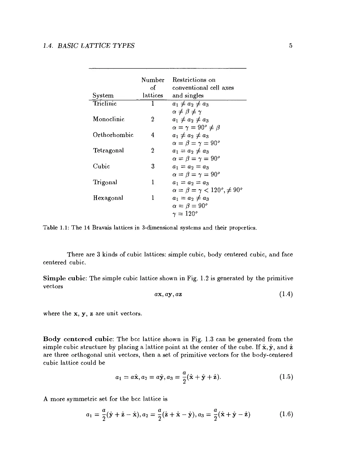
Body centered cubic: The bcc lattice shown in Fig. 1.3 can be generated from the
simple cubic structure by placing a lattice point at the center of the cube. If x, y, and z
are three orthogonal unit vectors, then a set of primitive vectors for the body-centered
cubic lattice could be
ai = ax, a2 = ay, a3 = -(x + y + z).
(1.5)
A more symmetric set for the bcc lattice is
ai = g (y + z ~ *)> °2 = 2 ^ + * ~ ^' °3 = 2 ^ + ^ ~ ^
(1.6)
6 CHAPTER 1. SEMICONDUCTORS: CRYSTAL STRUCTURE ...
^
az
X
^ >\
^
v^
Figure 1.3: The body centered cubic lattice along with a choice of primitive vectors.
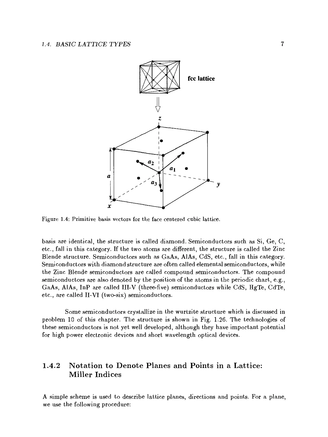
Face Centered Cubic: Another equally important lattice for semiconductors is the
face-centered cubic (fee) Bravais lattice. To construct the face-centered cubic Bravais
lattice add to the simple cubic lattice an additional point in the center of each square
face (Fig. 1.4).
A symmetric set of primitive vectors for the face-centered cubic lattice (see Fig.
1.4) is
Qi = g (d + £)> a2 = 2(* + *)' °3 = 2 (* + y) (LT)
The face-centered cubic and body-centered cubic Bravais lattices are of great
importance, since an enormous variety of solids crystallize in these forms with an atom
(or ion) at each lattice site. Essentially all semiconductors of interest for electronics and
optoelectronics have fee structure.
1.4.1 The Diamond and Zinc Blende Structures
Most semiconductors of interest for electronics and optoelectronics have an underlying
fee lattice. However, they have two atoms per basis. The coordinates of the two basis
atoms are
(000) and (-4,^4) (1.8)
Since each atom lies on its own fee lattice, such a two atom basis structure may be
thought of as two inter-penetrating fee lattices, one displaced from the other by a
translation along a body diagonal direction (^\\)-
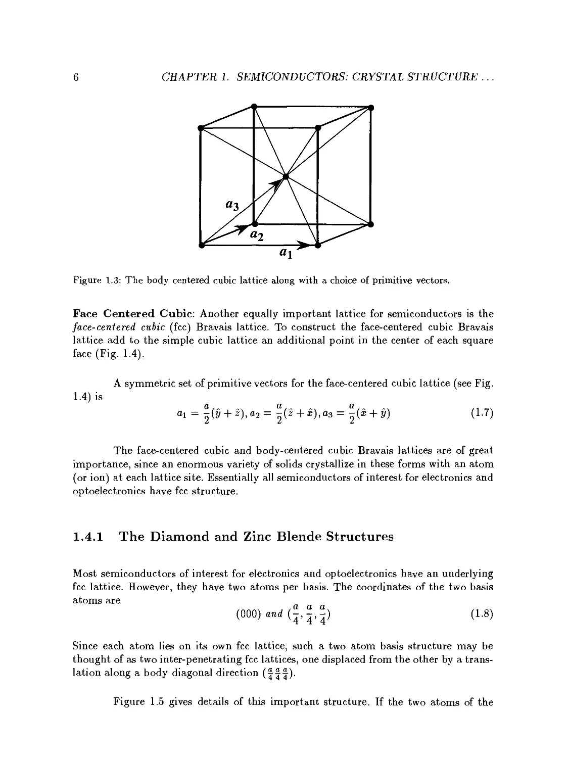
Figure 1.5 gives details of this important structure. If the two atoms of the
1.4. BASIC LATTICE TYPES
7
Figure 1.4: Primitive basis vectors for the face centered cubic lattice.
basis are identical, the structure is called diamond. Semiconductors such as Si, Ge, C,
etc., fall in this category. If the two atoms are different, the structure is called the Zinc
Blende structure. Semiconductors such as GaAs, AlAs, CdS, etc., fall in this category.
Semiconductors with diamond structure are often called elemental semiconductors, while
the Zinc Blende semiconductors are called compound semiconductors. The compound
semiconductors are also denoted by the position of the atoms in the periodic chart, e.g.,
GaAs, AlAs, InP are called III-V (three-five) semiconductors while CdS, HgTe, CdTe,
etc., are called II-VI (two-six) semiconductors.
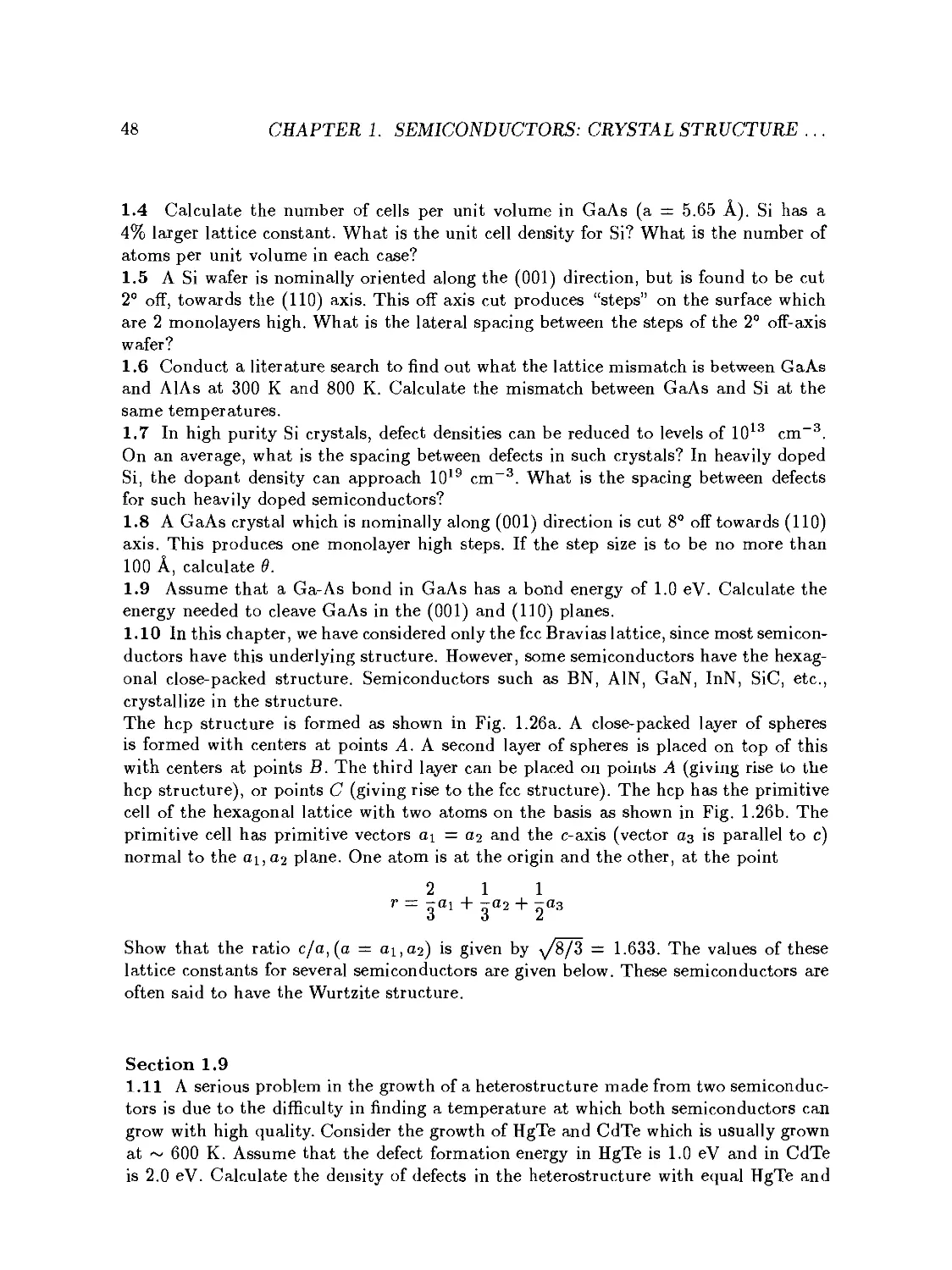
Some semiconductors crystallize in the wurtzite structure which is discussed in
problem 10 of this chapter. The structure is shown in Fig. 1.26. The technologies of
these semiconductors is not yet well developed, although they have important potential
for high power electronic devices and short wavelength optical devices.
1.4.2 Notation to Denote Planes and Points in a Lattice:
Miller Indices
A simple scheme is used to describe lattice planes, directions and points. For a plane,
we use the following procedure:
CHAPTER 1. SEMICONDUCTORS: CRYSTAL STRUCTURE
Figure 1.5: The zinc blende crystal structure. The structure consists of the interpenetrating
fee lattices, one displaced from the other by a distance (f f f) along the body diagonal. The
underlying Bravais lattice is fee with a two atom basis. The positions of the two atoms is (000)
and (fff).
(1) Define the x, y, z axes (primitive vectors).
(2) Take the intercepts of the plane along the axes in units of lattice
constants.
(3) Take the reciprocal of the intercepts and reduce them to the smallest
integers.
The notation (hkl) denotes a family of parallel planes.
The notation (hkl) denotes a family of equivalent planes.
To denote directions, we use the smallest set of integers having the same ratio
as the direction cosines of the direction.
In a cubic system the Miller indices of a plane are the same as the direction
perpendicular to the plane. The notation [ ] is for a set of parallel directions; < > is
for a set of equivalent direction. Fig. 1.6 shows some examples of the use of the Miller
indices to define planes.
EXAMPLE 1.1 The lattice constant of silicon is 5.43 A. Calculate the number of silicon
atoms in a cubic centimeter. Also calculate the number density of Ga atoms in GaAs which
has a lattice constant of 5.65 A.
Silicon has a diamond structure which is made up of the fee lattice with two atoms
on each lattice point. The fee unit cube has a volume a3. The cube has eight lattice sites at the
1.4. BASIC LATTICE TYPES
9
ATOMS ON THE (110) PLANE
Each atom has 4 bonds:
• 2 bonds in the (110) plane
• 1 bond connects each atom to
adjacent (110) planes
=v> Cleaving adjacent planes
requires breaking 1 bond per atom
I
I
-K
ATOMS ON THE (001) PLANE
2 bonds connect each atom to
adjacent (001) plane
Atoms are either Ga or As in a
GaAs crystal
=u> Cleaving adjacent planes
requires breaking 2 bonds per atom
,^-
*£
*£
ATOMS ON THE (111) PLANE
Could be either Ga or As
1 bond connecting an adjacent
plane on one side
3 bonds connecting an adjacent
plane on the other side
Figure 1.6: Some important planes in the cubic system along with their Miller indices. This
figure also shows how many bonds connect adjacent planes. This number determines how easy
or difficult it is to cleave the crystal along these planes.
10
CHAPTER 1. SEMICONDUCTORS: CRYSTAL STRUCTURE ..
cube edges. However, each of these points is shared with eight other cubes. In addition, there
are six lattice points on the cube face centers. Each of these points is shared by two adjacent
cubes. Thus the number of lattice points per cube of volume a3 are
In silicon there are two silicon atoms per lattice point. The number density is, therefore,
4x2 4x2 „ „„„ „22 / 3
Nsi = —3- = jt-z r—y-j = 4.997 x 10²² atoms/cm3
a3 (5.43 x 10 8)3
In GaAs, there is one Ga atom and one As atom per lattice point. The Ga atom
density is, therefore,
NGa = -5- = tt-tz in ,,.- = 2.22 x 10²² atoms/cm3
aJ (5.65 x 10⁻⁸)3 '
There are an equal number of As atoms.
EXAMPLE 1.2 In semiconductor technology, a Si device on a VLSI chip represents one
of the smallest devices while a GaAs laser represents one of the larger devices. Consider a
Si device with dimensions (5x2x1) /1m3 and a GaAs semiconductor laser with dimensions
(200 x 10 x 5) /1m3. Calculate the number of atoms in each device.
From Example 1.1 the number of Si atoms in the Si transistor are
Ns, = (5x 10²² atoms/cm3)(10 x 10-12 cm3) =5x 10¹¹ atoms
The number of Ga atoms in the GaAs laser are
NGa = (2.22 x 10²²)(104 x 10~12) = 2.22 x 10¹⁴ atoms
An equal number of As atoms are also present in the laser.
EXAMPLE 1.3 Calculate the surface density of Ga atoms on a Ga terminated (001) GaAs
surface.
In the (001) surfaces, the top atoms are either Ga or As leading to the terminology
Ga terminated (or Ga stabilized) and As terminated (or As stabilized), respectively. A square
of area a2 has four atoms on the edges of the square and one atom at the center of the square.
The atoms on the square edges are shared by a total of four squares. The total number of
atoms per square is
N(a2) = 7 + 1=2
4
The surface density is then
2
ii* -2
Ng" = I = ^«B m-8^2 = 626 X 10 Cm"
a2 (5.65 X 10 8)2
1.5. ARTIFICIAL STRUCTURES: ...
11
EXAMPLE 1.4 Calculate the height of a GaAs monolayer in the (001) direction.
In the case of GaAs, a monolayer is defined as the combination of a Ga and As atomic
layer. The monolayer distance in the (001) direction is simply
Amt = l = ^-= 2.825 A
1.5 ARTIFICIAL STRUCTURES: SUPERLATTICES AND
QUANTUM WELLS
K So far in this chapter we have discussed crystal structures that are present in
natural semiconductors. These structures are the lowest free energy configuration of the solid
state of the atoms. Since the electronic and optical properties of the semiconductors is
completely determined by the crystal structure, scientists have been intrigued with the
idea of fabricating artificial structures or superlattices. Since the mid-70's, these ideas
have been gaining ground, inspired by the pioneering work of Esaki and Tsu at IBM. The
key to growing artificial structures with tailorable crystal structure and hence tailorable
optical and electronic properties has been the progress in hetero-epitaxy. Heteroepitax-
ial crystal growth techniques such as molecular beam epitaxy (MBE) and metal-organic
chemical vapor deposition (MOCVD) have made a tremendous impact on
semiconductor physics and technology. From very high speeds, low noise electronic devices used
for satellite communications to low threshold lasers for communication, semiconductor
devices are being made by these techniques. Although, so far, only compound
semiconductors have benefitted from these growth techniques, it appears that silicon technology
is on the threshold of using hetero-epitaxy for faster devices, by combining Si with Si-Ge
alloys.
MBE or MOCVD are techniques which allow monolayer (~3 A) control in
the chemical composition of the growing crystal. These techniques will be examined
in brief in Section 1.10. Nearly every semiconductor extending from zero bandgap (a-
Sn,HgCdTe) to large bandgap materials such as ZnSe,CdS, etc., has been grown by
epitaxial techniques such as MBE and MOCVD. In MBE, atoms or molecules of the
species to be grown impinge upon the substrate in high vacuum. In MOCVD, the
impinging species are complex molecules containing the atoms which are to form the
crystal and a dissociative chemisorption reaction occurs at the surface.
Since the heteroepitaxial techniques allow one to grow heterostructures with
atomic control, one can change the periodicity of the crystal in the growth direction.
This leads to the concept of superlattices where two (or more) semiconductors A and
R are grown alternately with thicknesses dA and dg respectively. The periodicity of
CHAPTER 1. SEMICONDUCTORS: CRYSTAL STRUCTURE ...
Figure 1.7: Arrangement of atoms in a (GaAs)2(AlAs)2 superlattice grown along (001)
direction.
the lattice in the growth direction is then dA + rig. A (GaAs)2 (AlAs)2 superlattice
is illustrated in Fig. 1.7. It is a great testimony to the precision of the new growth
techniques that values of d& and dg as low as monolayer have been grown. The presence
of these superlattices is revealed in X-ray diffraction (to be discussed later), as well as
in the new electronic and optical properties.
Superlattices that have been grown can be placed in three general categories:
i) lattice matched; ii) strained, and iii) strained with intermediate substrate. In the
lattice matched superlattices (e.g., GaAs/AlAs; HgTe/CdTe), there is a very good match
between the two components forming the superlattice. Thus, there is no significant
distortion in the individual unit cells making up the superlattice. These superlattices
are easiest to grow and the highest quality superlattices fall in this category. The strained
superlattices can be classified as those where the components A and B have different
lattice constants and are grown on a substrate B. In this case the thickness of the
coherent superlattice is limited by the competition between the strain energy in the A
region and the dislocation formation energy. For the coherent or pseudomorphic (i.e.,
1.6. ... IDEAL VERSUS REAL
13
the substrate crystallinity is maintained) structure, the region A is under strain which
distorts the cubic symmetry. These distortions play a very important role in changing
semiconductor properties. We will discuss important issues in strained epitaxy in Section
1.12.
It is important to point out that the most widely used heterostructures are
not superlattices but quantum wells, in which a single layer of one semiconductor is
sandwiched between two layers of a larger bandgap material. Such structures allow
one to exploit special quantum effects that have become very useful in electronic and
optoelectronic devices as will be discussed in Chapters 4 and 5.
1.6 SURFACES: IDEAL VERSUS REAL
So far we have only considered infinite crystals with no boundaries. In reality, of
course, the semiconductors are finite and have surfaces which play a very important
role in their properties. Obviously, as a semiconductor structure is being grown, growth
occurs at its surface. Also, when contacts are placed on semiconductors to make
connection to the outside world, the nature of the surface is extremely important. In fact, in
both of these cases mentioned above, apparently minor changes in the surface structure
can drastically alter the physical properties.
Naively, it may appear that as long as the semiconductor is clean (no
impurities), the surface structure should simply be defined by the bulk crystal structure. One
simply needs to disconnect the bonds along a surface to form the surface structure. Such
a surface would be called the ideal surface and almost never occurs in nature! Upon a
little reflection, it is not surprising that this is the case. The bulk crystal structure is
decided by the internal chemical energy of the atoms forming the crystal with a certain
number of nearest neighbors, second nearest neighbors, etc. At the surface, the number
of neighbors is suddenly altered. Thus the spatial geometries which were providing the
lowest energy configuration in the bulk may not provide the lowest energy configuration
at the surface. Thus, there is a readjustment or "reconstruction" of the surface bonds
towards an energy minimizing configuration.
An example of such a reconstruction is shown for the GaAs surface in Fig. 1.8.
The figure (a) shows an ideal (001) surface where the topmost atoms form a square
lattice. The surface atoms have two nearest neighbor bonds (Ga-As) with the layer
below, four second neighbor bonds (e.g., Ga-Gaor As-As) with the next lower layer, and
four second neighbor bonds within the same layer. In a "real" surface, the arrangement
of atoms is far more complex. We could denote the ideal surface by the symbol C(l x 1),
representing the fact that the surface periodicity is one unit by one unit along the
square lattice along [110] and [110]. The reconstructed surfaces that occur in nature
are generally classified as C(2x8) or C(2x4) etc., representing the increased periodicity
14 CIIAPTER 1. SEMICONDUCTORS: CRYSTAL STRUCTURE ...
4k
(a) (b)
0 Top layer As atoms
O Second layer Ga atoms
o Third layer As atoms <
Figure 1.8: The structure (a) of the unreconstructed GaAs (001) arsenic-rich surface. The
missing dimer model (b) for the GaAs (001) (2x4) surface. The As dimers are missing to
create a 4 unit periodicity along one direction and a two unit periodicity along the perpendicular
direction.
along the [IlO] and [110] respectively. The C(2x4) case is shown schematically in Fig.
1.8b, for an arsenic stabilized surface (i.e., the top monolayer is As). The As atoms
on the surface form dimers (along [110] on the surface to strengthen their bonds. In
addition, rows of missing dimers cause a longer range ordering as shown to increase the
periodicity along the [110] direction to cause a C(2x4) unit cell. The surface periodicity
is directly reflected in the x-ray diffraction pattern.
A similar effect occurs for the (110) surface of GaAs. This surface has both Ga
and As atoms (the cations and anions) on the surface. A strong driving force exists
to move the surface atoms and minimize the surface energy. Reconstruction effects
also occur in silicon surfaces, where depending upon surface conditions a variety of
reconstructions are observed. Surface reconstructions are very important since often the
quality of the epitaxial crystal growth depends critically on the surface reconstruction.
1.7. INTERFACES
15
AlAs (perfect crystal)
1 ^ l<- x ->l I 1
GaAs (perfect crystal)
Figure 1.9: A schematic picture of the interfaces between materials with similar lattice constants
such as GaAs/AlAs. No loss of crystalline lattice and long range order is suffered in such
interfaces. The interface is characterized by islands of height A and lateral extent A.
1.7 INTERFACES
/v Like surfaces, interfaces are an integral part of semiconductor devices. We have
already discussed the concept of heterostructures and superlattices which involve
interfaces between two semiconductors. These interfaces are usually of high quality with
essentially no broken bonds, except for dislocations in strained structures (to be
discussed later). There is, nevertheless, an interface roughness of one or two monolayers
which is produced because of either non-ideal growth conditions or imprecise shutter
control in the switching of the semiconductor species. The general picture of such a
rough interface is as shown in Fig. 1.9 for epitaxially grown interfaces. The crystallinity
and periodicity in the underlying lattice is maintained, but the chemical species have
some disorder on interfacial planes. Such a disorder is quite important in many electronic
and opto-electronic devices.
One of the most important interfaces in electronics is the Si/SiC>2 interface.
This interface and its quality is responsible for essentially all of the modern consumer
electronic revolution. This interface represents a situation where two materials with very
different lattice constants and crystal structures are brought together. However, in spite
of these large differences the interface quality is quite good. It appears that the interface
has a region of a few monolayers of amorphous or disordered Si/SiC>2 region creating
fluctuations in the chemical species (and consequently in potential energy) across the
interface. This interface roughness is responsible for reducing mobility of electrons and
holes in MOS devices. It can also lead to "trap" states, which can seriously deteriorate
device performance if the interface quality is poor.
Finally, we have the interfaces formed between metals and semiconductors.
Structurally, these important interfaces are hardest to characterize. These interfaces
are usually produced in presence of high temperatures and involve diffusion of metal
elements along with complex chemical reactions. The "interfacial region" usually extends
over several hundred Angstroms and is a complex non-crystalline region.
16
CHAPTER 1. SEMICONDUCTORS: CRYSTAL STRUCTURE ...
1.8 DEFECTS IN SEMICONDUCTORS
In the previous section we have discussed the properties of the perfect crystalline
structure. In real semiconductors, one invariably has some defects that are introduced
due to either thermodynamic considerations (nothing in life is perfect!) or the presence
of impurities during the crystal growth process. In general, defects in crystalline
semiconductors can be characterized as i) point defects; ii) line defects; iii) planar defects
and iv) volume defects. These defects are detrimental to the performance of electronic
and optoelectronic devices and are to be avoided as much as possible. We will give a
brief overview of the important defects.
Point Defects
A point defect is a highly localized defect that affects the periodicity of the crystal only
in one or a few unit cells. There are a variety of point defects, as shown in Fig. 1.10. An
important point in defects is the vacancy that is produced when an atom is missing from
a lattice point. The vacancy defects are present in any crystal and their concentration
is given roughly by the thermodynamics relation
1100 / &V0LC \ /1 nx
— exp —-—— (1.9)
NTot V kBTJ
where Nvae is the vacancy density, Nr0t the total site density in the crystal, E\,ac
the vacancy formation energy and T, the crystal growth temperature. The vacancy
formation energy is approximately 2.0 eV for most semiconductors.
An important point defect in compound semiconductors such as GaAs is the
anti-site defect in which one of the atoms, say Ga, sits on the arsenic sublattice instead
of the Ga sublattice. Such defects (denoted by Ga^s) can be a source of reduced device
performance.
Other point defects are interstitials in which an atom is sitting in a site that is
in between the lattice points as shown in Fig. 1.10, and impurity atoms which involve a
wrong chemical species in the lattice. In some cases the defect may involve several sites
forming a defect complex.
Line Defects or Dislocations
In contrast to point defects, line defects (called dislocations) involve a large number of
atomic sites that can be connected by a line. Dislocations are produced if, for example,
an extra half plane of atoms are inserted (or taken out) of the crystal as shown in Fig.
1.11. Such dislocations are called edge dislocations. Dislocations can also be created if
there is a slip in the crystal so that part of the crystal bonds are broken and reconnected
with atoms after the slip.
Dislocations can be a serious problem, especially in the growth of strained
1.8. DEFECTS IN SEMICONDUCTORS
17
Vacancy
Point Defects
• Effect is localized
to a few atomic
sites
Substitutional
Figure 1.10: A schematic showing some important point defects in a crystal. (Adapted from
J.W. Mayer and S.S. Lau, Electronic Material Science: For Integrated Circuits in Si and GaAs,
MacMillan, New York (1990).)
heterostructures (to be discussed later). In optoelectronic devices, dislocations can ruin
the device performance and render the device useless. Thus the control of dislocations
is of great importance.
Planar Defects and Volume Defects
Planar defects and volume defects are not important in single crystalline materials,
but can be of importance in polycrystalline materials. If, for example, silicon is grown
on a glass substrate, it is likely that polycrystalline silicon will be produced. In the
polycrystalline material, small regions of Si (~ a few microns in diameter) are perfectly
crystalline, but are next to microcrystallites with different orientations. The interface
between these microcrystallites are called grain boundaries. Grain boundaries may be
viewed as an array of dislocations.
Volume defects can be produced if the crystal growth process is poor. The
crystal may contain regions that are amorphous or may contain voids. In most epitaxial
techniques used in modern optoelectronics, these defects are not a problem. However,
the developments of new material systems such as diamond (C) or SiC are hampered
by such defects.
EXAMPLE 1.5 Consider an equilibrium growth of a semiconductor at a temperature of
1000 K. The vacancy formation energy is 2.0 eV. Calculate the vacancy density produced if
the site density for the semiconductor is 2.5 x 1022 cm-3.
18 CHAPTER 1. SEMICONDUCTORS: CRYSTAL STRUCTURE ..
Figure 1.11: A schematic showing the presence of a dislocation. This line defect is produced by
adding an extra half plane of atoms. At the edge of the extra plane, the atoms have a missing
bond.
The vacancy density is
NVac - Nrotexp (-7-^)
= (2.5 x 1022 cm'3) exp (_-MiL_)
v J y \ 0.0867 eVJ
= 2.37 x 1012 cm"3
This is an extremely low density and will have little effect on the properties of the
semiconductor. The defect density would be in mid 1015 cm-3 range if the growth temperature
was 1500 K. At such values, the defects can significantly affect device performance.
1.9 BULK CRYSTAL GROWTH
K Bulk crystal growth techniques are used mainly to produce substrates on which
devices are eventually fabricated. While for some semiconductors like Si and GaAs (to
some extent for InP) the bulk crystal growth techniques are highly matured; for most
other semiconductors it is difficult to obtain high quality, large area Substrates. The aim
1.9. BULK CRYSTAL GROWTH
19
of the bulk crystal growth techniques is to produce single crystal boules with as large a
diameter as possible and with as few defects as possible. In Si the boule diameters have
reached 30 cm with boule lengths approaching 100 cm. Large size substrates ensure low
cost device production.
For the growth of boules from which substrates are obtained, one starts out
with a purified form of the elements that are to make up the crystal. One important
technique that is used is the Czochralski (CZ) technique. In the Czochralski technique
shown in Fig. 1.12, the melt of the charge (i.e., the high quality polycrystalline material)
is held in a vertical crucible. The top surface of the melt is just barely above the melting
temperature. A seed crystal is then lowered into the melt and slowly withdrawn. As the
heat from the melt flows up the seed, the melt surface cools and the crystal begins
to grow. The seed is rotated about its axis to produce a roughly circular cross-section
crystal. The rotation inhibits the natural tendency of the crystal to grow along certain
orientations to produce a faceted crystal.
The CZ technique is widely employed for Si, GaAs, and InP and produces long
ingots (boules) with very good circular cross-section. For Si up to 100 kg ingots can be
obtained. In the case of GaAs and InP the CZ technique has to face problems arising
from the very high pressures of As and P at the melting temperature of the compounds.
Not only does the chamber have to withstand such pressures, also the As and P leave
the melt and condense on the sidewalls. To avoid the second problem one seals the melt
by covering it with a molten layer of a second material (e.g., boron oxide) which floats
on the surface. The technique is then referred to as liquid encapsulated Czochralski, or
the LEC technique.
A second bulk crystal growth technique involves a charge of material loaded in
a quartz container. The charge may be composed of either high quality polycrystalline
material or carefully measured quantities of elements which make up a compound
crystal. The container called a "boat" is heated till the charge melts and wets the seed
crystal. The seed is then used to crystallize the melt by slowly lowering the boat
temperature starting from the seed end. In the gradient-freeze approach the boat is pushed
into a furnace (to melt the charge) and slowly pulled out. In the Bridgeman approach,
the boat is kept stationary while the furnace temperature is temporally varied to form
the crystal. The approaches are schematically shown in Fig. 1.13.
The easiest approach for the boat technique is to use a horizontal boat. However,
the shape of the boule that is produced has a D-shaped form. To produce circular cross-
sections vertical configurations have now been developed for GaAs and InP.
In addition to producing high purity bulk crystals, the techniques discussed
above are also responsible for producing crystals with specified electrical properties.
This may involve high resistivity materials along with n- or p-type materials. In Si it is
difficult to produce high resistivity substrated by bulk crystal growth and resistivities are
20
CHAPTER 1. SEMICONDUCTORS: CRYSTAL STRUCTURE ...
Puller
Seed
Crystal
Encapsulant
— Heater
Figure 1.12: Schematic of Czocharlski-style crystal grower used to produce substrate ingots.
The approach is widely used for Si, GaAs and InP.
usually <104 fl-cm. However, in compound semiconductors carrier trapping impurities
such as chromium and iron can be used to produce material with resistivities of ~ 10s Cl
cm. The high resistivity or semi-insulating (SI) substrates are extremely useful in device
isolation and for high speed devices. For n- or p-type doping carefully measured dopants
are added in the melt.
The availability of high quality substrates is essential to any device
technology. Other than the three materials mentioned above (Si, GaAs, InP) the substrate
fabrication of semiconductors is still in its infancy. Since epitaxial growth techniques
used for devices require close lattice matching between the substrate and the overlayer,
non- availability of substrates can seriously hinder the progress of a material technology.
This is, for example, one of the reasons of slow progress in large bandgap
semiconductor technology necessary for high power-high temperature electronic devices and short
wavelength semiconductor lasers.
1.10. EPITAXIAL CRYSTAL GROWTH 21
Crystal
(a) (b)
Figure 1.13: Crystal growing from the melt in a crucible: (a) solidification from one end of the
melt (horizontal Bridgeman method); (b) melting and solidification in a moving zone.
1.10 EPITAXIAL CRYSTAL GROWTH
—► The substrates that result once the bulk grown semiconductor boule is sliced
and capped are almost never used directly for devices. Invariably an epitaxial layer or
epilayer is grown which may be a few microns in thickness. The work epitaxy comes from
the Greek word "epi" (upon) and "taxis" (ordered) meaning the ordered continuation
of the substrate crystal. The epitaxial growth techniques have a very slow growth rate
(as low as a monolayer per second for some techniques) which allow one to control very
accurately the dimensions in the growth direction. In fact, in techniques like molecular
beam epitaxy (MBE) and metal organic chemical vapor deposition (MOCVD), one
can achieve monolayer (~ 3A) control in the growth direction. This level of control is
essential for the variety of heterostructure devices that are being used in optoelectronics.
The epitaxial techniques are also very useful for precise doping profiles that can be
achieved. In fact, it may be argued that without the advances in epitaxial techniques
that have occurred over the last two decades, most of the developments in semiconductor
physics would not have occurred. Table 1.2 gives a brief view of the various epitaxial
techniques used along with some of the advantages and disadvantages.
Liquid Phase Epitaxy (LPE)
LPE was an epitaxial growth technique of choice until the 70's when it gradually started
to be replaced by other techniques. LPE is still used for growth of crystals such &S
22
CHAPTER 1. SEMICONDUCTORS: CRYSTAL STRUCTURE ...
GaAs melt
\
AlGaA* iiicll
GaAs substrate
Figure 1.14: A schematic of the LPE growth of AlGaAs and GaAs. The slider moves the
substrate, thus positioning itself to achieve contact with the different melts to grow heterostruc-
tures.
HgCdTe for long wavelength detectors and AlGaAs for double heterostructure lasers.
As shown in Table 1.2, LPE is a close to equilibrium technique in which the substrate is
placed in a quartz or a graphite boat and covered by a liquid of the crystal to be grown
(see Fig. 1.14). The liquid may also contain dopants that are to be introduced into the
crystal. LPE is often used for alloy growth where the growth follows the equilibrium
solid-liquid phase diagram. By precise control of the liquid composition and temperature,
the alloy composition can be controlled. Because LPE is a very close to equilibrium
growth technique, it is difficult to grow alloy systems which are not miscible or even
grow heterostructures with atomically abrupt interfaces. Nevertheless heterostructures
where interface is graded over 10-20 A can be grown by LPE by sliding the boat over
successive "puddles" of different semiconductors. For many applications such interfaces
are adequate and since LPE is a relatively inexpensive growth technique, it is used
widely in many commercial applications.
Vapor Phase Epitaxy (VPE)
A large class of epitaxial techniques rely on delivering the components that form the
crystal from a gaseous environment. If one has molecular specy in a gaseous form with
partial pressure P, the rate at which molecules impinge upon a substrate is given by
P 3.5 x 10²²P(torr) , , 2 - .
F = . , ^ v >-mo\./cm2 - s (1.10)
V2irmkBT y/m(g)T{K)
where m is the molecular weight and T the cell temperature. For most crystals the
surface density of atoms is ~ 7 x 1014 cm-2. If the atoms or molecules impinging from
the vapor can be deposited on the substrate in an ordered manner, epitaxial crystal
growth can take place.
The VPE technique is used mainly for homoepitaxy and does not have the
additional apparatus present in techniques such as MOCVD for precise heteroepitaxy.
As an example of the technique, consider the VPE of Si. The Si containing reactant silane
1.10. EPITAXIAL CRYSTAL GROWTH
23
Liquid phase
epitaxy
J
KVapor phase
epitaxy
Very high
quality
material
Near equilibrium
growth for precise
alloy compositions
Relatively
inexpensive
Difficult to
grow abrupt
heterostructures
Unable to grow
immiscible alloys
}
Extremely
high purity
material
Not well
suited for
heterostructures
1
1
Q MBE ^
High quality materials
Atomically abrupt I
interfaces
Techniques can grow
far from equilibrium
systems reliably
"Expensive" growth
technology which
requires great care
1
)—'
1 +
J
+
+
-
Table 1.2: A schematic of the various epitaxial crystal growth techniques and some of their
positive and negative aspects.
24 CHAPTER 1. SEMICONDUCTORS: CRYSTAL STRUCTURE ...
Vertical Reactor Horizontal Reactor
Figure 1.15: Reactors for VPE growth. The substrate temperature must be maintained
uniformly over the area. This is achieved better by lamp heating. A pyrometer is used for
temperature measurement.
(SiH4) or dichlorosilane (SiH^C^) or trichlorosilane (SiHQs) or silicon tetrachloride
(SiCU) is diluted in hydrogen and introduced into a reactor in which heated substrates
are placed as shown in Fig. 1.15. The silane pyrolysis to yield silicon while the chlorine
containing gases react to give SiCb, HCl and various other silicon-hydrogen-chlorine
compounds. The reaction
2SiCl2 — St + SiCU (1-11)
then yields Si. Since HCl is also produced in the reaction, conditions must be tailored so
that no etching of Si occurs by the HCl. Doping can be carried out by adding appropriate
hydrides (phosphine, arsine, etc.,) to the reactants.
An important consideration in VPE is safety related, since hydrogen, which is
produced in the deposition, can explode in contact with any oxygen. Also, almost all
the reactants are highly toxic.
VPE can be used for other semiconductors as well by choosing different
appropriate reactant gases. The reactants used are quite similar to those employed in the
MOCVD technique discussed later.
Molecular Beam Epitaxy (MBE)
Molecular beam epitaxy (MBE) is one of the most important epitaxial techniques as
far as heterostructure physics and devices are concerned. Almost every semiconductor
(other than a few very large bandgap semiconductors) has been grown by this technique.
MBE is a high vacuum technique (~ 10-U torr vacuum when fully pumped down)
in which crucibles containing a variety of elemental charges are placed in the growth
chamber (Fig. 1.16). The elements contained in the crucibles make up the components
of the crystal to be grown as well as the dopants that may be used. When a crucible
1.10. EPITAXIAL CRYSTAL GROWTH
25
Liquid niiiugcn
Rheed gun
Ri'ldiinii Mih-.ir.uo
holder
ni/.niun gauge
I'luori'M'i'iii .
Effusion .-I ^h
0 u screen •»- -
shutters
Photomultiplier
Sample exchange
load lock
Viewport
I
To variable speed
motor and substrate
heater supply
Figure 1.16: A schematic of the MBE growth system.
is heated, atoms or molecules of the charge are evaporated and these travel in straight
lines to impinge on a heated substrate.
The growth rate in MBE is ~1.0 monolayer per second and this slow rate
coupled with shutters placed in front of the crucibles allow one to switch the composition
of the growing crystal with monolayer control. However, to do so, the growth conditions
have to be adjusted so that growth occurs in the monolayer by monolayer mode rather
than by 3-dimensional island formation. This requires that the atoms impinging on the
substrate have enough kinetics to reach an atomically fiat profile. Thus the substrate
temperature has to be maintained at a point where it is high enough to provide enough
surface migration to the incorporating atoms, but not so high as to cause entropy
controlled defects.
Since no chemical reactions occur in MBE, the growth is the simplest of all
epitaxial techniques and is quite controllable. However, since the growth involves high
vacuum, leaks can be a major problem. The growth chamber walls are usually cooled
by liquid N? to ensure high vacuum and to prevent atoms/molecules to come off from
26 CHAPTER 1. SEMICONDUCTORS: CRYSTAL STRUCTURE ...
the chamber walls.
The low background pressure in MBE allows one to use electron beams to
monitor the growing crystal. The reflection high energy electron diffraction (RHEED)
techniques relies on electron diffraction to monitor both the quality of the growing
substrate and the layer by layer growth mode. As each monolayer gets filled up, one can
see this reflected in the RHEED intensity by the naked eye!
While MBE is a simple and elegant growth technique (conceptually), it cannot
be used conveniently for all semiconductors. For example, phosphides are often not
grown by MBE due to the danger in handling elemental phosphorus. Also elements with
very low vapor pressures are difficult to use since it is not easy to heat the crucibles
beyond —1500 K. Silicon epitaxy in MBE, for example, requires e-beam evaporation
where an electron beam is used to knock off Si atoms for growth.
MBE is a relatively safe technique and has become the technique of choice for
the testing of almost all new ideas on heterostructure physics.
Metal Organic Chemical Vapor Deposition (MOCVD)
Metal organic chemical vapor deposition (MOCVD) is another important growth
technique widely used for heteroepitaxy. Like MBE, it is also capable of producing monolayer
abrupt interfaces between semiconductors. A typical MOCVD system is shown in Fig.
1.17. Unlike in MBE, the gases that are used in MOCVD are not made of single
elements, but are complex molecules which contain elements like Ga or As to form the
crystal. Thus the growth depends upon the chemical reactions occurring at the heated
substrate surface. For example, in the growth of GaAs one often uses Triethyl Gallium
and Arsine and the crystal growth depends upon the following reaction:
Ga(CH3)3 + AsH3 — GaAs + 3C#4 (1.12)
One advantage of the growth occurring via a chemical reaction is that one can
use lateral temperature control to carry out local area growth. Laser assisted local area
growth is also possible for some materials and can be used to produce new kinds of
device structures. Such local area growth is difficult in MBE.
There are several varieties of MOCVD reactors. In the atmospheric MOCVD
the growth chamber is essentially at atmospheric pressure. One needs a large amount of
gases for growth in this case, although one does not have the problems associated with
vacuum generation. In the low pressure MOCVD the growth chamber pressure is kept
low. The growth rate is then slower as in the MBE case.
The use of the MOCVD equipment requires very serious safety precautions. The
gases used are highly toxic and a great many safety features have to be incorporated
1.10. EPITAXIAL CRYSTAL GROWTH
27
Chemical reaction at the heated
substrate deposits GaAs or AlAs.
Mass flow controllers control the
species deposited.
Mass-flow
controllers
Heated
wafer
Exhaust line
:NJe:h£g£.
Scrubber
Exhaust
Mass-flow
TMGa : Gallium containing organic compound
TMAl : Aluminum containing organic compound
ASH3 : Arsenic containing compound
Figure 1.17: Schematic diagram of an MOCVD system employing alkyds (trimethyl gallium
(TMGa) and trimethyl aluminum (TMAl) and metal hydride (arsine) material sources, with
hydrogen as a carrier gas.
28
CHAPTER 1. SEMICONDUCTORS: CRYSTAL STRUCTURE ...
to avoid any deadly accidents. Safety and environmental concerns are important issues
in almost all semiconductor manufacturing since quite often one has to deal with toxic
and hazardous materials.
In addition to MBE and MOCVD one has hybrid epitaxial techniques often
called MOMBE (metal organic MBE) which try to combine the best of MBE and
MOCVD. In MBE one has to open the chamber to load the charge for the materials to
be grown while this is avoided in MOCVD where gas bottles can be easily replaced from
outside. Additionally, in MBE one has occasional spitting of material in which small
clumps of atoms are evaporated off on to the substrate. This is avoided in MOCVD and
MOMBE.
EXAMPLE 1.6 Consider the growth of GaAs by MBE. The Ga partial pressure in the
growth chamber is 10~s Torr, and the Ga cell temperature is 900 K. Calculate the flux of Ga
atoms on the substrate.
The mass of Ga atoms is 70 g/mole. The flux is (from Eqn. 1.10)
r,22
V70 x 900
= 5.27 x 10¹⁴atoms/cm
Note that the surface density of Ga atoms on GaAs is ~ 6.3 x 1014 cm-2. Thus, if
all of the Ga atoms were to stick, the growth rate would be ~0.8 monolayer per second. This
assumes that there is sufficient arsenic to provide As in the crystal.
1.11 STRAINED HETEROEPITAXY
^ We have noted earlier that in an epitaxial process, the overlayer that is grown on
the substrate could have a lattice constant that may differ from that of the substrate.
Such epitaxy is called strained epitaxy and is one of the important emerging areas of
crystal growth studies. The motivation for strained epitaxy is two fold:
i) Incorporation of built-in strain: When a lattice mismatched semiconductor
is grown on a substrate and the thickness of the overlayer is very thin (this will be
discussed in detail later), the overlayer has a built-in strain. This built-in strain has
important effects on the electronic and optoelectronic properties of the material and
can be exploited for high performance devices.
ii) Availability of alternate substrate: We have noted that in semiconductor
technology, high quality substrates are only available for Si, GaAs and InP (quartz
substrates are also available and used for some applications). Most semiconductors are not
1.11. STRAINED HETEROEPITAXY
29
lattice-matched to these substrates. How can one grow these semiconductors epitaxi-
ally? One solution that has emerged is to grow the overlayer on a mismatched substrate.
If the conditions are right, a lot of dislocations are generated and eventually the over-
layer forms its own substrate. This process (to be discussed later in this section) allows a
tremendous flexibility in semiconductor technology. Not only can it, in principle, resolve
the substrate availability problem, it also allows the possibility of growing GaAs on Si,
CdTe on GaAs, etc. Thus different semiconductor technologies can be integrated on the
same wafer.
Strained Heteroepitaxy for Built-in Strain
Consider a case where an overlayer with lattice constant a/, is grown on a substrate
with lattice constant as- This situation is shown schematically in Fig. 1.18. The strain
between the two materials is defined as
Consider a conceptual exercise where you are depositing a monolayer of the overlayer
on the substrate. If the lattice constant of the overlayer is maintained to be a^, it is
easy to see that after every 1/e bonds between the overlayer and the substrate, either a
bond is missing or an extra bond appears as shown in Fig. 1.18b. In fact, there would
be a row of missing or extra bonds since we have a 2-dimensional plane. These defects
are the dislocations. The presence of these dislocations costs energy to the system since
a number of atoms do not have proper chemical bonding at the interface.
An alternative to the case shown in Fig. 1.18b is the case shown in Fig. 1.18c.
Here all the atoms at the interface of the substrate and the overlayer are properly bonded
by adjusting the in-plane lattice constant of the overlayer to that of the substrate. This
causes the overlayer to be under strain and the system has a certain amount of strain
energy. This strain energy grows as the overlayer thickness increases. In the strained
epitaxy, the choice between the state of the structure shown in Fig. 1.18b and the state
shown in Fig. 1.18c is decided by free energy minimization considerations. Theoretical
and experimental studies have focussed on these considerations for over six decades,
and the importance of these studies has grown since the advent of heteroepitaxy. The
general observations can be summarized as follows:
i) If the lattice mismatch e is less than a critical value eci (~0.1), the first
monolayer of the overlayer can be grown on a thick substrate without dislocations.
If the lattice mismatch lies between eci and ec2 (~0.14), the first monolayer of the
overlayer has dislocations, although a metastable state can be produced in which there
are no dislocations and there is perfect registry between the overlayer and the substrate.
If e > ec2, the first monolayer always has an array of dislocations.
ii) For small lattice mismatch (e < 0.1), the overlayer initially grows in perfect
registry with the substrate, as shown in Fig. 1.18c. However, as noted before, the strain
energy will grow as the overlayer thickness increases. As a result, it will eventually be
30
CHAPTER 1. SEMICONDUCTORS: CRYSTAL STRUCTURE ...
«L>«S
Overlayer
aL<"s
i
rmihi riwK
\
I
/
/
i
\
Xt~f- (a)
Substrate
6 bonds
7 bonds
LI
?:g^:;i;::!■;:;; w-.w^
%M
^■^:mm^^m^^^\^::?
1 bonds
6 bonds
(b)
(c)
Figure 1.18: (a) The conceptual exercise in which an overlayer with one lattice constant is
placed without distortion on a substrate with a different lattice constant, (b) Dislocations are
generated at positions where the interface bonding is lost, (c) The case is shown where the
overlayer is distorted so that no dislocation is generated.
1.11. STRAINED HETEROEPITAXY
31
favorable for the overlayer to generate dislocations. In simplistic theories this occurs at
an overlayer thickness called the critical thickness, dc, which is approximately given by
In reality, the point in growth where dislocations are generated is not so clear cut and
depends upon growth conditions, surface conditions, dislocation kinetics, etc. However,
one may use the criteria given by Eqn. 1.14 for loosely characterizing two regions of
overlayer thickness for a given lattice mismatch. Below critical thickness, the overlayer
grows without dislocations and the film is under strain. Above critical thickness, the
film has a dislocation array, and after the dislocation arrays are generated, the overlayer
grows without strain with its free lattice constant.
In Fig. 1.19 we summarize how the discussions presented here impact upon
semiconductor optoelectronic technology. We will see in the next chapter that as a
crystal is strained, its electronic and optical properties can be altered. Thus, by growing
an overlayer on a substrate with a small lattice mismatch, one can incorporate strain in
a film as long as the thickness is below the critical thickness. One needs a strain value of
about 1% so that the critical thickness is a few hundred angstroms (at the most). This
usually involves growing a quantum well structure in which the strained region forms
the well region and is surrounded by a lattice matched region.
While strained epitaxy below critical thickness is an extremely powerful tool
for tailoring the optoelectronic properties of semiconductors, epitaxy beyond the critical
thickness is important to provide new effective substrates for new material growth. As
shown in Fig. 1.19, for these applications the key issues center around ensuring that the
dislocations generated stay near the overlayer-substrate interface and do not propagate
into the overlayer as shown in Fig. 1.20. A great deal of work has been done to study
this problem. Often thin superlattices in which the individual layers have alternate signs
of strain are grown to "trap" or "bend" the dislocations. It is also useful to build the
strain up gradually.
EXAMPLE 1.7 Estimate the critical thickness for Ino.3Gao.7As grown on a GaAs substrate.
The lattice constant of an alloy is given by the Vegard's law:
a{Ino.iGao.iAs) = 0.3ainAs + O.TaGaAs
= 5.775 A
The strain is
5.653- 5.775
5.653
32
CHAPTER 1. SEMICONDUCTORS: CRYSTAL STRUCTURE
SIRAIM-DH) n.ROI-Tn.WY
Below "critical thickness"
Above "critical thickness"
Overlayer under strain due to the
presence of complete registry with
the substrate
Generation of a dislocation
network near the overlayer-
substrate interface.
+"Free standing" overlayer having
the lattice constant of the overlayer
Issues
■ High quality interfaces?
■ Avoidance of any dislocation
• Structural stability and long term
reliability?
Issues
• Can the dislocation network be
contained near the overlayer-
substrate interface?
■ Is the new "free standing"
substrate free of dislocations and
defects?
Figure 1.19: Important regimes in strained heteroepitaxy. The issues of importance in below
critical thickness epitaxy and above critical thickness epitaxy are identified.
The critical thickness is approximately
, 5.653 A 10 =.
d< = 2(0322) = 128 A
This thickness is quite adequate for most devices and can be used to make useful
quantum well devices. If, on the other hand, the strain is, say, 5%, the critical thickness is
~ 50 A, which is too thin for most useful device applications.
1.12 LITHOGRAPHY
K Modern solid state electronics and optoelectronics owe their great success to device
fabrication techniques which can produce extemely complicated devices with high yield.
A variety of active and passive devices can be fabricated on the same wafer using
1.12. LITHOGRAPHY 33
Dislocation Propagation:
Missing rows of atoms
Figure 1.20: Strained epitaxy above critical thickness. On the left hand side is shown a structure
in which the dislocations are confined near the overlayer-substrate interface. This is a desirable
mode of epitaxy . On the right hand side, the dislocations are penetrating the overlayer, rending
it useless for most optoelectronic applications.
lateral patterning techniques based on lithography. Since crystal growth processes do not
produce any controlled lateral variations in material properties, lithographic techniques
are needed to alter the lateral properties of the wafer. Modern solid state circuits (ICs)
contain millions of devices on the same chip. Lithography plays a central role in the
success of the solid state technology. Lithographic techniques allow one to fabricate
complex and dense circuits. They also allow one to obtain high speed performance by
reducing key device dimensions. Indeed, advances in lithographic techniques are one of
the most important driving forces for advances in device performance. Optoelectronic
devices and chips have not yet reached the state that electronic chips have, in terms
of integration. However, most of the lithographic techniques are shared by the two
technologies.
The technique of lithography to alter lateral properties of a surface is an ancient
one. Many lithograph masterpieces hang around the world's museums. "Batik" paintings
and t-shirts also rely on the concepts of lithography. The lithography process involves
taking a certain design created in a computer or by an artist and transferring it onto
the semiconductor wafer. A number of steps are involved in this process. While new
advances in lithographic techniques are introducing continual changes in the individual
steps, the following discussion will provide an overview of the current state of the art.
34 CHAPTER 1. SEMICONDUCTORS: CRYSTAL STRUCTURE ...
1.12.1 Photoresist Coating
The semiconductor wafer in its virgin form has little irreversible sensitivity to optical
or electron beams. Such a sensitivity is needed if a pattern of device and circuits is to
be transferred to the wafer. To make the wafer (which is usually covered by a thin oxide
film or some other dielectric passivation material) sensitive to an image, a photoresist is
spread on the wafer by a process called spin coating. For the resist to be reliable it must
satisfy three criteria: i) it must have good bonding to the substrate; ii) its thickness
must be uniform; and iii) the thickness should be reliably controlled over different wafer
runs.
Spin-coating has emerged as the most reliable technique for photoresist
application. As shown in Fig. 1.21, a small puddle of the resist is applied to the center of the
wafer which is held to a spindle by a vacuum chuck. The spindle is now spun at a rate
of 2000-8000 rpm for 10 to 60 seconds. During the first couple of seconds of spinning,
most of the resist is thrown off and carefully drained away. The remaining resist forms
a thin layer whose thickness is controlled by the spin speed (thickness oc -4=, where w is
the spin frequency). An edge bead is formed which is several times the thickness of the
film. A variety of details are introduced (e.g. variable spin-speed; applying the puddle
to an already spinning wafer, etc.) to obtain more uniform resists. The thickness of the
resists are usually in the range of 0.7 to 1.0 ^m. For very fine lithography thicker films
are deposited.
It must be noted that the resist is not deposited on untreated wafers since the
untreated wafers typically have hydroxyl (OH) groups attached to the surface. These
produce poor adhesion and must be removed by a prebake at 200-250 C for 30-60
minutes. An adhesion promoting primer is then applied before resist application. For
Si02 covered wafers, hexamethyl disilazane (HMDS) is used. Once the resist is applied,
it is soft baked at 90 to 100 C to improve adhesion to the oxide.
Once the resist is ready, it is exposed to an optical image through a mask (to
be discussed next) for a certain exposure time as shown in Fig. 1.22. The resist is then
developed by washing it in a solvent which dissolves away the regions of higher solubility.
A resist which becomes more soluble when exposed to illumination is called positive. Its
image is identical to the opaque image on the mask plate. A resist that loses solubility
when illuminated is called negative.
The first materials which proved to have a high sensitivity and etchant
resistance for successful microelectronic photoresists were negative resists. These were based
on polyisoprene in the form of cyclized rubber. The resist consists of isoprene molecules
(a hydrocarbon containing double carbon bonds and the basic building block of
rubber) and a photo-sensitive N3 group radical. When light falls on the resist, the radical
causes formation of long chains from the individual isoprene hydrocarbons causing poly-
1.12. LITHOGRAPHY
35
Figure 1.21: The process of spin coating a wafer starts the lithographic process.
merization of the of the isoprene. The polymerized region is highly insoluble while the
unexposed part is soluble.
The negative resist has an advantage that its solubility is almost digital. There
is a tremendous contrast between exposed and unexposed regions. However, since it is
based on chain formation, its resolution is limited to 2-3 ^m.
The positive resist is not based on chain formation and can produce much
sharper resolution. The resist relies upon molecules where N2 is bonded to a hydrocarbon
with benzene like structure. Exposure to light causes the dissociation of the N2 group
producing a carboxylic acid. This can be dissolved and washed away in an alkaline
solution such as dilute sodium hydroxide.
Once a resist is in place, one needs to expose it with an optical image containing
the pattern to be transferred to the wafer. This requires the fabrication and use of a
mask.
EXAMPLE 1.8 A negative resist is made up of molecules with a mass of 10s amu. The
molecule is a straight chain of CH2 units with a C-C spacing of 1.54 A. The resolution of the
36
CHAPTER 1. SEMICONDUCTORS: CRYSTAL STRUCTURE
Transference of an image to the resist by using a mask and etching of the exposed regions.
Light
Layer to be
patterned
Mask
Patterned
wafer
Substrate
nnnry
Resist Removal
Resist
Application
Exposure
(Positive Resist)
I El ,1 1
Etching
(Negative Resist) Development
Figure 1.22: The exposure and etching process which allows one to transfer a pattern to the
wafer. (After W.S. Ruska, Microelectronic Processing, An Introduction to the Manufacture of
Integrated Circuits, McGraw-Hill, New York (1988).)
resist is about the length of one molecule. Estimate this resolution. The atomic mass of C is
12 and of H is 1.
Each unit has a mass of 14. Thus, the number of units in the molecule is
10s
n = = 7143unlts
14
The total length is then
£ = 7143 x 1.54 = 1.1 x 10⁴ A
= 1.1 (im
This resist is adequate for most technologies, but not for sub-micron technology.
1.12.2 Mask Generation and Image Transfer
Like the negative in the photography, the mask allows one to transfer the complicated
circuit pattern on to the sensitive resist deposited on the wafer. Once the design of a
1.12. LITHOGRAPHY
37
device is done, a large scale (100 times or even larger) replica is prepared on paper and
transferred to rubylith which is a transparent plastic sheet coated with a thin layer of
red plastic. The pattern transfer involves cutting out the thin unwanted red plastic. In
the early days of microelectronics, the desired pattern was cut by hand and reduction
cameras would then reduce the pattern to its desired value. These days, as shown in
Fig. 1.23 computer aided design (CAD) software programs allow one to directly generate
a design tape which is then analyzed and "written" on to a mask plate. The pattern
on the final mask plate can be generated optically or by electron beam writing. The
electron beam (e beam) produces much finer features and can be controlled with greater
precision.
The mask plate which is later used to repeatedly transfer patterns to different
wafers must be transparent (at proper positions) to the radiation used for final pattern
transfer. The mask should also have good mechanical and thermal properties. Quartz
or borosilicate glasses are often used for ultraviolet light lithography. The regions of the
mask that are to be opaque are covered with metallic chrome or iron oxide.
Usually only the basic building block of the device or circuit is produced first
on the mask. This single pattern is called a reticle, and a step and repeat camera (or
stepper) is used to create the entire pattern from the reticle. The reticle can be used to
generate a wafer size mask plate or, in some cases, may be directly used to generate the
entire pattern on the wafer by the stepper, as shown in Fig. 1.23.
Once the mask plate is made and the resist is deposited, the next step is to
transfer the pattern on the mask to the wafer. For feature sizes greater than 0.25 ^m,
one uses optical equipment for the pattern transfer. The limit of ~0.25 /mi is governed
by the wavelength of the light available. Most materials become opaque to light once the
wavelength goes below ~1000 A. If electromagnetic radiation is to be used, one must
go down to x-ray lithography with A ~40-80 A. Another way to decrease feature size is
by use of e-beam lithography.
The patterns to be printed in microelectronics can be classified as windows and
lines. The windows may be used to allow doping diffusion or to make connections with a
conductor through an insulator. The conducting interconnects and resistors are usually
formed into line patterns. The imaging process involves transferring an ideal image to
the mask and then from the mask to the wafer. Once the image is transferred, the
resist is developed and etching is carried out. In all these steps, the ideal pattern in the
designers mind is gradually lost. This occurs even if the design considerations are well
within the image transferring technology.
38 CHAPTER 1. SEMICONDUCTORS: CRYSTAL STRUCTURE ...
1.13 ETCHING
Like the chisel and the drill for the carpenter and the sculptor, etchants are an
important tool for the microelectronics processing engineer. The etchants allow one to
remove material in a selective manner, once the resist has been patterned. The choice
and control of the etching process is crucial if the features in the resist film are to become
a part of the substrate.
An ideal etching process must be able to remove a layer of semiconductor from
the region where there is no resist. The etchant should not attack the resist, nor should
it penetrate under the resist causing undercuts. It should also attack only one layer
and should be self limiting (e.g., should etch SiC>2 and not Si, etc.). A number of
techniques are developed to carry out etching. These are discussed below. Once etching is
finished, one must remove the resist material by either other etchants or by the "lift
off" technique. We will now briefly review the etching approaches.
1.13.1 Wet Chemical Etching
The simplest and most commonly employed etching technique is the wet chemical
etching in which the wafer is simply soaked in a liquid chemical which dissolves away the
semiconductor. The etching process involves a chemical reaction in which the elements
of the film to be etched react with the etching solution. The reaction products can then
be rinsed away. The rate of the etching is proportional to the etch time and is usually
isotropic. The isotropic nature of the wet etching is not very suitable for devices where
very sharp sidewalls are to be produced.
The etch rate depends upon the concentration of the chemicals used in the
etchant and the temperature of the solution. The etchants are usually either acids
(Hydrofluoric acid- HF; Nitric acid-HNOs; Acetic acid-H4C202; Sulfuric acid-H^SO^
Phosphoric acid-H3P04) or alkaline solutions of Ammonium Hydroxide (NH4OH). The
etchants are usually diluted in water according to well established recipes.
In many devices, an important film to be etched is Si02- This film is etched
with HF solutions and the ease and control of this process is one of the reasons for the
success of the Si-technology. Usually the HF is buffered with NH4F to produce buffered
oxide etch (BOE) which is stable and has a very long shelf life.
An important film that is often used for passivation is silicon nitride (Sis^).
This film can also be etched by BOE, but the rate is much slower than the Si02 rate.
Thus, if a SisN4 film is on top of an Si02 film and only the SisN4 film is to be etched,
one cannot use BOE. In such cases H3PO4 is used.
1.13. ETCHING
39
Generation of a reticle
Step-and-repeat generation
of mask plate from reticle
\
Step-and-repeat printing
of substrate from reticle
Substrate patterning
from mask plate
Figure 1.23: The processes used in the generation of a mask for lithography. (After W.S.
Ruska, Microelectronic Processing, An Introduction to the Manufacture of Integrated Circuits,
McGraw-Hill, New York (1988).)
40 CHAPTER 1. SEMICONDUCTORS: CRYSTAL STRUCTURE ...
Since Aluminum is commonly used for metal interconnects, one often has to
etch it. A mixture of phosphoric acid, nitric acid and acetic acid is usually used if the
underlying crystal is Si. However, since this etchant attacks GaAs, one uses hydrochloric
acid for etching Al over GaAs substrates.
Silicon and polycrystalline silicon can be etched by HF-HNO3 mixtures while
GaAs is etched by using bromine in methanol or hydrogen peroxide mixed with sulfuric
acid in water. A number of selective etches have also been developed for the heterostruc-
ture technology.
While chemical etching is simple and inexpensive, it is not compatible with
submicron technology or technology which demands deep anisotropic etching.
1.13.2 Plasma Etching
Plasma etching resolves one of the main problems with wet chemical etching viz feature
size control. It also provides efficient etching for a wide variety of films including those
that are difficult to etch by wet chemicals. The plasma is produced by passing an rf
electrical discharge through a gas at a low pressure. The rf discharge creates ions and
electrons. The ions can be used to interact with the elements in the substrate and cause
etching.
The ions being charged particles can be accelerated in the electric field and be
made to bombard the substrate with controlled energy. If the ion energy is large, the
ions simply sputter off atoms from the surface in a rather unselective manner. However,
this provides extremely anisotropic etching with almost no undercutting effects. At low
energies the ions can cause chemical reactions at the surface and cause removal of atoms
selectively.
In typical plasmas one introduces fluorine or chlorine containing gases. The
fluorocarbons (e.g., CF4) or silicon tetrafluoride (SiF4) and silicon tetrachloride (SiCU)
are often used for the plasma. Once the plasma is formed fluorine (or chlorine) ions are
produced which cause the etching process.
1.13.3 Reactive Ion Beam Etching (RIBE)
An important tool in microelectronic technology is the ion-implantation which is widely
used to dope semiconductors. The implanter accelerates ions to a prechosen energy and
shoots them into the semiconductor by controlling the energy. The depth at which the
ions are embedded can be controlled. The ion-implanter can also be used for etching
1.13. ETCHING
41
by using appropriate ions and it provides focusing of the ion beam. At low energies,
tbe vms cau be used to selectively etcb ve*y small feature svies. Tb.e advantages ate tlie
same as for plasma etching.
1.13.4 Ion Beam Milling
The ion beam milling is another application of the ions in "chiseling" off material from
a substrate. The ion milling requires a focussed beam of ions of energy high enough that
the ions can physically knock out atoms from the film. The focus is on removing the
atoms physically rather than through a chemical reaction. The process is thus highly
directional and can produce extremely anisotropically etched structures. Ion milling is
particularly advantageous if the etching involves small patterns, very steep walls or
materials which are relatively inert and cannot be etched by chemical reactions.
The ion milling is dominated by geometric effects as shown in Fig. 1.24. In Fig.
1.24a, we show a substrate with a resist in the process of being etched by a perpendicular
ion-beam. The impact of the beam causes the substrate material to fly off randomly.
Some of the material can get redeposited on the etched sides forming "ears." Ions
bounding off the edges can cause "trenches" to be formed around the resist pattern.
These effects are controlled by impinging the beam at a slight angle and rotating the
substrate.
The resolution of ion beam milling is controlled by the ion-beam spot size and
can reach 0.1 /im or less.
EXAMPLE 1.9 A 0.2 /im film of AlGaAs is to be etched. The etching rate is 1.0 //m/hour.
Calculate the time needed for the etching. If the rate changes by -1%, calculate the number of
monolayers of AlGaAs that will remain unetched.
The time needed for the etching is
0.2
t = — = 0.2 hour
A -1% error in the etch rate means that the thickness etched is
d = 0.2 x 0.99 = 0.198 fim
The unetched film remaining is
Ad = 0.2-0.198 = 0.002 pm
= 20 A
42
CHAPTER 1. SEMICONDUCTORS: CRYSTAL STRUCTURE ...
Ions
Redepositon
Shadowing
Sidewall etching
(b)
Trenching
Figure 1.24: The importance of geometric effects in ion beam milling. In (a) the perpendicular
incident beam can produce trenching effects as well as redeposition causing sidewall "ears;" (b)
if the beam comes at an oblique angle and the substrate is rotated, the trenching and "ear"
formation can be balanced.
A monolayer of AlGaAs is 2.83 A, so that seven monolayers of film will remain. Such
thickness errors may appear small, but are unacceptable in many heterostructure devices.
1.14 EPITAXIAL REGROWTH
The spectacular growth of semiconductor microelectronics owes a great deal to the
concept of the integrated circuit. The ability to fabricate transistors, resistors, inductors
and capacitors on the same wafer is critical to the low cost and high reliability we have
come to expect from microelectronics. It is natural to expect similar dividents from the
concept of the optoelectronic integrated circuit (OEIC). In the OEIC, the optoelectronic
device (the laser or detector or modulator) would be integrated on the same wafer with
an amplifier or logic gates.
One of the key issues in OEICs involves etching and regrowth. As we will see
later, the optoelectronic devices have a structure that is usually not compatible with
1.14. EPITAXIAL REGROWTH
43
the structure of an electronic device. The optimum layout then involves growing one of
the device structures epitaxially and then masking the region to be used as, say, the
optoelectronic device and etching away the epitaxial region. Next a regrowth is done to
grow the electronic device with a different structure. The process is shown schematically
in Fig. 1.25. While this process looks simple conceptually, there are serious problems
associated with etching and regrowth.
A critical issue in the epitaxial growth of a semiconductor layer is the quality of
the semiconductor-vacuum interface. This semiconductor surface must be "clean," i.e.,
there should be no impurity layers (e.g., an oxide layer) on the surface. Even if a fraction
of a monolayer of the surface atoms have impurities bonded to them, the quality of the
epitaxial layer suffers drastically. The growth may occur to produce microcrystalline
regions separated by grain boundaries or may be amorphous in nature. In either case,
the special properties arising from the crystalline nature of the material (to be discussed
in the next chapter) are then lost.
In Section 1.6 we had discussed the issue of surface reconstruction. In most
epitaxial growths, not only is it important to have a clear surface from which to start
with, it is also important to maintain a special reconstruction during growth. The
reconstructions are a representation of the vapor pressure (e.g., the Ga to As ratio in the
growth of GaAs) and are, therefore, critical to high quality growth.
The issue of surface cleanliness and surface reconstruction can be addressed
when one is doing a single epitaxial growth. For example, a clean wafer can be loaded
into the growth chamber and the remaining impurities on the surface can be removed by
heating the substrate. The proper reconstruction (which can be monitored by RHEED)
can be ensured by adjusting the substrate temperature and specy overpressure. Now
consider the problems associated with etching after the first epitaxial growth has
occurred. As the etching starts, foreign atoms or molecules are introduced on the wafer as
the semiconductor is etched. The etching process is quite damaging and as it ends, the
surface of the etched wafer is quite rough and damaged. In addition, in most growth
techniques the wafer has to be physically moved from the high purity growth chamber
to the etching system. During this transportation, the surface of the wafer may collect
some "dirt." During the etching process this "dirt" may not be etched off and may
remain on the wafer. As a result of impurities and surface damage, when the second
epitaxial layer is grown after etching, the quality of the layer suffers.
A great deal of processing research in OEICs focusses on improving the etch-
ing/regrowth process. So far the OEICs fabricated in various laboratories have
performances barely approaching the performance of hybrid circuits. Clearly the problem of
etching/regrowth is hampering the progress in OEIC technology.
It may be noted that the etching regrowth technology is also important in
creating quantum wires and quantum dots which require lateral patterning of epitaxial
44
CHAPTER 1. SEMICONDUCTORS: CRYSTAL STRUCTURE ...
Structure of the electronic device Structure of the optoelectronic device
APPROACH
Growth of the optoelectronic device structure
Substrate
I
Mask a portion of the layer
I
Regrowth of the electronic device structure
Etch back
OEIC
Figure 1.25: The importance of regrowth is clear when one examines the difference in the
structure of electronic and optodectronic devices. Etching and regrowth is essential for fabrication
of optoelectronic integrated circuits (OEIC).
1.15. CHAPTER SUMMARY
45
lOl'lt'SSll Dill)
V
J
hn OHM.KV\ | lo.vs
V
)
Periodicity and crystal structure
Crystalline materials have an underlying
periodicity. Important semiconductors have
either a diamond structure or a zinc-blende
structure.
Superlattices and quantum wells
Epitaxial techniques allow one to have
heterostructures in which several
semiconductors can be incorporated to
produce new crystal structures.
Surfaces and interfaces
Surfaces and interfaces are an extremely
important component of semiconductor
devices. The quality of the surface or the
interface is critical in device performance.
Table 1.3: Summary table.
layers.
1.15 CHAPTER SUMMARY
In this chapter we have discussed the important structural properties of semiconductors
and their heterostructures. The semiconductors we will be dealing with in most
optoelectronic devices have a zinc blende or diamond structure. We have discussed the important
growth techniques used in producing the semiconductors. We have also identified the
important techniques used to fabricate devices. Tables 1.3 to 1.5 give an overview of the
issues that have emerged from this chapter.
46
CHAPTER 1. SEMICONDUCTORS: CRYSTAL STRUCTURE ...
r
TOPICS STUMP.!)
1
KKY OBSERVATIONS
)
Bulk and epitaxial crystal growth
Bulk crystal growth techniques are used to
produce wafers that are used as substrates
for electronic and optoelectronic devices.
Epitaxial crystal growth techniques are used
to produce high quality layers on which
active devices are fabricated.
Techniques like MBE and MOCVD in which
monolayer control is possible are responsible
for heterostructure growth.
Strained heteroepitaxy
Epitaxy of strained layers is becoming
increasingly important. The problem of
controlling dislocations is a serious one and
represents a key challenge in this area.
Lithography and pattern generation
Semiconductor devices usually involve
complicated layer structures which have to
be patterned. Masks are generated and
images are transferred to the semiconductor
wafer.
Table 1.4: Summary table.
1.16. PROBLEMS
4T
roi'icssn mkd
\.
)
Etching of semiconductor
Etching is an important step in device
fabrication. The challenges involve etching
without damage and with a high degree of
precision.
Regrowth after etching
Regrowth after etching offers a key obstacle
that has to be overcome if OEICs are to
become reliable and manufacturable.
Table 1.5: Summary table.
1.16 PROBLEMS
Section 1.4
1.1 a) Find the angles between the tetrahedral bonds of a diamond lattice.
b) What are the direction cosines of the (111) oriented nearest neighbor bond along the
x,y,z axes.
1.2 Consider a semiconductor with the zinc blende structure (such as GaAs).
a) Show that the (100) plane is made up of either cation or anion type atoms.
b) Draw the positions of the atoms on a (110) plane assuming no surface reconstruction.
c) Show that there are two types of (111) surfaces: one where the surface atoms are
bonded to three other atoms in the crystal, and another where the surface atoms are
bonded to only one. These two types of surfaces area called the A and B surfaces,
respectively.
1.3 Suppose that identical solid spheres are placed in space so that their centers lie
on the atomic points of a crystal and the spheres on the neighboring sites touch each
other. Assuming that the spheres have unit density, show that density of such spheres
is the following for the various crystal structures:
fee
bee
sc
diamond
y/2Tt/Q = 0.74
V3tt/8 = 0.68
tt/6 = 0.52
V^tt/16 = 0.34
48 CHAPTER 1. SEMICONDUCTORS: CRYSTAL STRUCTURE ...
1.4 Calculate the number of cells per unit volume in GaAs (a = 5.65 A). Si has a
4% larger lattice constant. What is the unit cell density for Si? What is the number of
atoms per unit volume in each case?
1.5 A Si wafer is nominally oriented along the (001) direction, but is found to be cut
2° off, towards the (110) axis. This off axis cut produces "steps" on the surface which
are 2 monolayers high. What is the lateral spacing between the steps of the 2° off-axis
wafer?
1.6 Conduct a literature search to find out what the lattice mismatch is between GaAs
and AlAs at 300 K and 800 K. Calculate the mismatch between GaAs and Si at the
same temperatures.
1.7 In high purity Si crystals, defect densities can be reduced to levels of 1013 cm-3.
On an average, what is the spacing between defects in such crystals? In heavily doped
Si, the dopant density can approach 1019 cm-3. What is the spacing between defects
for such heavily doped semiconductors?
1.8 A GaAs crystal which is nominally along (001) direction is cut 8° off towards (110)
axis. This produces one monolayer high steps. If the step size is to be no more than
100 A, calculate 9.
1.9 Assume that a Ga-As bond in GaAs has a bond energy of 1.0 eV. Calculate the
energy needed to cleave GaAs in the (001) and (110) planes.
1.10 In this chapter, we have considered only the fee Bravias lattice, since most
semiconductors have this underlying structure. However, some semiconductors have the
hexagonal close-packed structure. Semiconductors such as BN, A1N, GaN, InN, SiC, etc.,
crystallize in the structure.
The hep structure is formed as shown in Fig. 1.26a. A close-packed layer of spheres
is formed with centers at points A. A second layer of spheres is placed on top of this
with centers at points B. The third layer can be placed on points A (giving rise to the
hep structure), or points C (giving rise to the fee structure). The hep has the primitive
cell of the hexagonal lattice with two atoms on the basis as shown in Fig. 1.26b. The
primitive cell has primitive vectors a\ = a^ and the c-axis (vector 03 is parallel to c)
normal to the a\, 02 plane. One atom is at the origin and the other, at the point
2 1 1
r=3ai + 3a2+2°3
Show that the ratio c/a,(a = 01,02) is given by ^/8/3 = 1.633. The values of these
lattice constants for several semiconductors are given below. These semiconductors are
often said to have the Wurtzite structure.
Section 1.9
1.11 A serious problem in the growth of a heterostructure made from two
semiconductors is due to the difficulty in finding a temperature at which both semiconductors can
grow with high quality. Consider the growth of HgTe and CdTe which is usually grown
at ~ 600 K. Assume that the defect formation energy in HgTe is 1.0 eV and in CdTe
is 2.0 eV. Calculate the density of defects in the heterostructure with equal HgTe and
1.16. PROBLEMS
4»
.A .A -A -A -A
_ B - B -1} • B
• c • c • c • c ■ c
A .A .A >A .A «A
^ B - B
• C •
.A . A
B , B . B
C ■ C • C • C
.A .A ■ *
(a)
/\.Z
K2X-^-
/-
i
/
^
Id = la3l = 1.633 Ifl^
Two atoms per basis
(2/3a\ + l/3a2 + l/2a3)
(b)
(0.0,0)
Figure 1.26: Hexagonal dose-packed structure.
CdTe.
1.12 Calculate the defect density in GaAs grown by LPE at 1000 K. The defect
formation energy is 2.0 eV.
1.13 Why are entropy considerations unimportant in dislocation generation?
Section 1.11
1.14 Consider the (001) MBE growth of GaAs by MBE. Assuming that the sticking
coefficient of Ga is unity, calculate the Ga partial pressure needed if the growth rate
has to be 1 ^m/hr. The temperature of the Ga cell is 1000 K.
1.15 A surface emitting laser (SEL) structure is produced by epitaxially growing a
reflector on either side of an active laser region, the reflector, called a distributed Bragg
reflector, consists of a periodic array of GaAs and AlGaAs layers; the periodicity, a,
being given by 2a = A. In an SEL, A = 8000 A and the total SEL thickness is 54
A + 1.0 ^m. If the flux of cations (Ga, Al) is 5 xlO14 cm~2s-1 and all the atoms get
incorporated to form the crystal, how long will it take to grow the SEL? Assume that
the As atoms are present in sufficient quantity and growth rate is controlled by cation
flux only.
1.16 In the growth of GaAs/AlAs structures in a particular MBE system, the
background pressure of Ga when the Ga shutter is off is 10~7 Torr. If the growth rate of
50 CHAPTER 1. SEMICONDUCTORS: CRYSTAL STRUCTURE ...
AlAs is 1 ^m/hr, what fraction of Ga atoms are incorporated in the AlAs region? The
Ga cell is at 1000 K.
Section 1.12
1.17 Estimate the critical thickness for growth of GaAs on Si.
1.18 A strained quantum well laser has to madefromInxGa1_xAs on a GaAs substrate.
If the minimum thickness of the region is 50 A, calculate the maximum composition of
In that can be tolerated. Assume that the lattice constant of the alloy can be linearly
interpolated from its components.
1.19 Assume that in a semiconductor alloy, the lattice constant scales as a linear
weighted average. Find the composition of the InxGa!_xAs alloy that lattice matches
with an InP substrate.
1.20 Calculate the critical thickness for the growth of AlAs on a GaAs substrate.
Section 1.13
1.21 To produce lateral confinement of electronic states in a semiconductor, the feature
sizes of the device have to be ~100 A. Calculate the energy of photons and electrons
that can be used in such a lithography.
1.22 In optoelectronics, the smallest feature sizes of typical lasers are ~5 ftm.
However, for laser known as distributed feedback (DFB) lasers, the smallest feature size is
~1000 A. Discuss the kind of lithography systems that can be used for the two kinds of
lasers.
1.23 In a particular resist spinner, the initial deposit of resist on a 3 inch GaAs wafer
is 0.2 cm high. After a spin at 4000 rpm, the resist thickness is 1 ftm. How much resist
has been wasted in this spin?
Section 1.14
1.24 Selective etchents are often used in microelectronic technology. Consider an etch
that etches GaAs at the rate of 1 ^m/hr and Alo.3Gao.7As at 500 A/hr. AlGaAs is used
as an etch stop in a heterostructure where 0.5 ^m of GaAs has to be etched. If the
AlGaAs layer is 30 A, what should be the tolerance in the etching time?
1.17 REFERENCES
• Crystal Structures
— J. M. Buerger, Introduction to Crystal Geometry, McGraw-Hill (1971).
— M. Lax, Symmetry Principles in Solid State and Molecular Physics, Wiley
(1974). Has a good description of the Brillouin zones of several structures in
Appendix E.
1.17. REFERENCES
51
- J. F. Nye, Physical Properties of Crystals, Oxford (1985).
- F. C. Phillips, An Introduction of Crystallography, Wiley (1971).
• Crystal Growth: Heterostructures
- A. Y. Cho, Journal of Vacuum Science Technology, vol. 8, 531 (1971).
- F. Rosenberger, Fundamentals of Crystal Growth, Springer (1979).
- G. Haas and M. H. Francombe, C. E. C. Wood in Physics of Thin Films,
Academic Press (1980).
• X-Ray Diffraction: General
- N. W. Ashcroft and N. D. Mermin, Solid-State Physics, Holt, Rinehart and
Winston, New York (1976).
- R. B. Leighton, Principles of Modern Physics, McGraw-Hill, New York (1959).
- Segmueller and A. E. Blakeslee, J. Appl. Crystallogr., 6, 19 (1973).
- B. E. Warren, X-Ray Diffraction, Addison-Wesley (1969).
• Diffraction from Surfaces and Crystal Growth RHEED
- P. L. Gourley, and R. M. Biefeld, J. Vac. Set. Technol., Bl, 383 (1983).
- B. A. Joyce, Rep. Prog. Phys, 48, 1637 (1985).
- W. T. Tsang, Semiconductors and Semimetals, eds. R. K. Willardson and A.
C. Beer, Academic Press, New York, vol.22, Part A (1985).
- J. M. VanHove, P. R. Pukite, G. J. Whaley, A. M. Worchak, and P. I. Cohen,
J. Vac. Sci. Technol., B3, 1116 (1985).
• Point Defects in Semiconductors
- P.K. Bhattacharya and S. Dhar, Deep Levels in III-V Compound
Semiconductors Grown by Molecular Beam Epitaxy, Semiconductors and Semimetals,
eds. A.C. Willardson and C. Beer, Academic Press, New York, vol. 26 (1988).
- E.N. Economou, Green's Functions in Quantum Physics, Springer-Verlag,
Berlin (1979).
- G.F. Foster and J.C. Slater, Phys. Rev., 96, 1208 (1954).
- H.F. Matare, Defect Electronics in Semiconductors, Wiley-Interscience. New
York (1971).
- S. Pantelides, Rev. Mod. Phys., 50, 797 (1978).
• Dislocations and Lattice Mismatched Epitaxy
- S. Amelinckx, Dislocations in Solids, ed. F.R.N. Nabarro, North-Holland,
New York (1988).
52 CHAPTER 1. SEMICONDUCTORS: CRYSTAL STRUCTURE ...
- C.A.B Ball and J.H. van der Merwe, Dislocations in Solids, ed. F.R.N. Nabarro,
North-Holland, New York, vol. 5 (1983).
- H.F. Matare, Defect Electronics in Semiconductors, Wiley-Interscience, New
York (1971).
- J.W. Mathews and A.E. Blakeslee, J. Cryst. Growth, 27, 118 (1974).
- J.Y. Tsao, B.W. Dodson, S.T. Picraux, and D.M. Cornelison, Phys. Rev.
Lett., 59, 2455 (1987).
- J.H. van der Merwe, J. Appl. Phys., 34, 117 (1963).
- J.H. van der Merwe, J. Appl. Phys., 34, 123 (1963).
• Microelectronic Processing
- J.W. Mayer and S.S. Lau, Electronic Materials Science: For Integrated
Circuits in Si and GaAs, MacMillan, New York (1990).
- W.S. Ruska, Microelectronic Processing: An Introduction to the Manufacture
of Integrated Circuits, McGraw-Hill, New York (1988).
- P.K.L. Yu and P.C. Chan, Introduction to GaAs Technology, ed. C. Wang,
Wiley, New York (1988).
CHAPTER
2
PROPERTIES OF
SEMICONDUCTORS:
ELECTRONIC STATES
2.1 INTRODUCTION
In the previous chapter we have seen that in semiconductor crystals, there is a certain
periodicity in the way in which atoms are arranged. This periodicity has a profound
influence on the properties of electrons inside the semiconductor. In this chapter we
will examine the electronic properties of semiconductors. The electronic properties are
represented by what is called the bandstructure which defines the energy levels that
an electron can have in the semiconductor. Essentially all the transport and optical
properties of a semiconductor are determined by the bandstructure.
We will also examine approaches that can be exploited to modify the
bandstructure and thus modify and optimize optoelectronic devices. These approaches, based on
alloying (mixing) of semiconductors and upon the use of heterostructures, are widely
used in modern optoelectronics.
2.2 ELECTRONS IN A PERIODIC POTENTIAL:
BLOCH THEOREM
The electrons are one of the elementary particles of nature with mass 0.91 x 10 kg
and negative charge with magnitude 1.6 x 10~19 C or 4.8 x 10~10 esu. The mass of
K
54 CHAPTER 2. PROPERTIES OF SEMICONDUCTORS: ELECTRONIC ...
the electrons is, of course, a universal constant, and it determines the response of the
electrons to external forces.
To understand semiconductor devices, we need to know what happens to
electrons when they enter a semiconductor and how they respond to external forces. In a
simple minded classical approach, it may appear that as electrons move through the
semiconductor, they will suffer scattering from the fixed ions. While this seems
intuitively reasonable, it turns out that electrons moving in periodic structures do not scatter
at all! Only the presence of imperfections causes scattering. To understand the properties
of electrons in semiconductors, we first study their properties in the perfectly periodic
crystal. Then we allow for imperfections which cause scattering and affect their
transport properties. In this chapter we will study the perfect system. In chapter 3 we will
study the effect of imperfections.
The description of the electron in the semiconductor has to be via the Schrodinger
equation
-h1
2 mo
V2 + U(r)
ip(r) = Etp(r)
(2.1)
where U(r) is the background potential seen by the electrons. Due to the crystalline
nature of the material, the potential U(r) has the same periodicity, R, as the lattice
U(r) = U(r + R)
(2.2)
As a result, we expect the electron probability to be same in all unit cells of the crystal
because each cell is identical. If the potential was random, this would not be the case.
The Bloch theorem gives us the form of the electron wavefunction in a periodic
structure and states that the eigenfunctions are the product of a plane wave e**'r times
a function Ufc(r) which has the same periodicity as the periodic potential. Thus
ipk(r)
„ikr
«*(r)
(2.3)
is the form of the electronic function. The "cell" periodic part Ufc(r) has the same
periodicity as the crystal, i.e.,
Uk(r) = uk(r + R)
(2.4)
The wavefunction has the property
eik<r+R)Uk(r + R) = eikruk(r)e
eikRMr)
ik-R
(2.5)
2.2. ELECTRONS IN A PERIODIC POTENTIAL
55
2.2.1 From Atomic Levels to Bands
The Bloch theorem tells us that the electron wavefunction in a crystal has a particularly
simple form: it is the product of a cell periodic part and a plane wave. While this
greatly simplifies the Schrodinger equation for the electron in the crystal, the problem
is still quite complicated. However, the size of the problem is reduced greatly due to the
periodicity. Methods like the tight binding method, orthogonalized plane wave method,
pseudopotential method, k p perturbation method, etc., are used to obtain the solution
for the electronic levels. These solutions provide the energy of the electron as a function
of the quantity k appearing in the Block theorem. This E vs. k relation is called the
bandstructure of the semiconductor. In addition, one also obtains the central cell part
of the wavefunction which is of great importance in optical transitions.
We will not discuss the derivation of the bandstructure of semiconductors;
merely provide the student important facts regarding the bandstructure. To better
understand the bandstructure and the makeup of the central cell part of the Bloch state,
we start with a brief discussion of an isolated atom. In Fig. 2.1 we show the energy
spectra of a typical isolated atom. The spectra is made up of two regions: i) bound
states in which the electron is bound to the nucleus by Coulombic interactions, and ii)
free state where the electron is free. These two regions are separated by the "vacuum
energy" Evac as shown, which is chosen as the zero of energy.
In the bound state, the electron energy is negative with respect to the vacuum
level. The allowed energy levels are discrete as shown in Fig. 2.1 and are separated from
each other by a region of "forbidden gap". The electron wavefunction in general is given
by a form VWn where the index n is a positive integer (1, 2, 3 . ..), called the principle
quantum number, the index £ is the angular momentum quantum number and gives
the value of the orbital angular momentum of the electron's motion around the nucleus.
Its values are h,2h,?>h .... Finally, the index n gives the value of the projection of the
angular momentum along the z-axis. It's values can be 0, ±h, ±27i....
From atomic physics we have the following:
n=l: The orbital angular momentum can only be zero, i.e., £ = 0 and m = 0. The
£ = 0 state is also called an s-state. The s-state is a spherically symmetrical state
in space as shown in Fig. 2.2. The n = 1, £ = 0, m=0 state is denoted by Is in
atomic physics notation.
n=2: £ can take a value of 0 or 1. The £ = 1 state is called a p-state and p-states have
a dumbbell shaped form in real space as shown in Fig. 2.2. Being a vector, the
p-states can have components Px,Py and pz as shown in Fig. 2.2. The n = 2, £ =
0 state is called 2s and n = 2, I — 1 state is called 2p state.
56 CHAPTER 2. PROPERTIES OF SEMICONDUCTORS: ELECTRONIC ...
Higher order states can have ^-values of 2 (d-states) or 3 (f-states), etc., For reasons
that will become clear, the symmetry of the s-states and p-states is very important since
selection rules for optical transitions depend upon these symmetries. We will exploit
this information when we discuss optical selection rules and polarization properties of
optoelectronic devices later.
If the atoms are brought together to form a crystal, the electron on a given
atom starts to see the neighboring nuclei and the discrete levels start to broaden until
eventually one starts to get bands as shown schematically in Fig. 2.1.
The allowed energy levels (i.e., the solutions of Eqn. 2.1) are not continuous in
general as for the free electron case, but have regions where there are no allowed energy
values. This means that the electron cannot exist in the semiconductor in these "gaps."
To appreciate the presence of these "allowed bands" and "forbidden gaps" let us examine
the atomic structure of some of the elements which make up various semiconductors.
IV Semiconductors
C ls22s22p2
Si Is22s22p6 3«23p2
Ge ls22s22p63s23p63(/io4s24p2 -
III-V Semiconductors
Ga ls22s22p63s23p63dio4s24pi
As ls22s22p63«23p63(/io4s24p3
etc.
The braces under each atomic structure represent the electrons in the outermost
shell which are bound so loosely to the individual atom that when atoms are brought
together to form the crystal, these outmost electrons form a series of allowed bands
separated by a forbidden gap as shown in Fig. 2.1.
An important point to note from our discussion of the electronic levels of the
atoms making up semiconductors is that the outermost electronic levels (in the valence
shell) are all either s-type or p-type. Essentially all electronic and optoelectronic
properties of semiconductors are determined by these outermost electrons since the core
electrons do not participate in most processes (because they are so tightly bound to the
nucleus). As a result, the central cell character of the Bloch functions in semiconductors
2.2. ELECTRONS IN A PERIODIC POTENTIAL
57
Vacuum Energy Level
Electrons are in
free space
Electrons are "bound"
in the material
Crystal
(Allowed bands)
Isolated atoms
(Atomic levels)
Spacing between atoms
Spacing - 1-2 A
Spacing ~ 10 A
Figure 2.1: A schematic of how allowed and forbidden bands form. When the spacing between
atoms is large, the allowed levels are discrete. As the atoms come closer, the electron energy
levels interact with each other forming complicated bands. The deep core levels are relatively
unaffected, but the higher levels broaden into bands.
58 CHAPTER 2. PROPERTIES OF SEMICONDUCTORS: ELECTRONIC ...
,?-type function
A*
p^-type function
negative
A*
negative
pv-type function
A Z Pz'tyP6 function
positive
P'».iiive
negative
Figure 2.2: The spatial character of the s, px,py and pz functions. The s function is isotropic
while px,Py,Pz functions have odd parity, i.e., they change sign when x —<■ —i, y —<■ —y, z —► — z.
2.2. ELECTRONS IN A PERIODIC POTENTIAL
59
are adequately described by s- and p-type functions. In general, the central cell part
can be written for the electrons in a bulk semiconductor as
2 4
j = l n = l
where the first summation represents the sum over the two atoms that make up a
unit cell of the diamond or zinc blende structure, and the second sum represents the
4 atomic-like functions s, Px,py,Pz discussed above. The coefficients a,„ represent the
relative mixtures of the atomic-like functions in the central cell part of the electronic
state. At certain special values of k, the central cell part becomes a pure combination
of only s-type states or only p-type states as will be discussed later. A pure state has a
well defined spatial symmetry which is important for "selection rules" in scattering as
will be discussed later.
2.2.2 The Crystal Momentum
What is the significance of the wavevector k that appears in the electron wavefunction
in the Bloch's theorem? For the free space electron, the k that appears in the electron
wavefunction is related to the momentum of the electron by p = hk. For electrons
moving in free space there are two very important laws which are used to describe their
properties: i) Newton's second law of motion which tells us how the electron's trajectory
evolves in the presence of an external force, and ii) the law of conservation of momentum
which allows us to determine the electron's trajectory when there is a collision. We are
obviously interested in finding out what the analogous laws are when an electron is
inside a crystal and not in free space.
The quantity hk takes on exactly the same role for the electron in the perfect
semiconductor as a "momentum." However, hk only reacts to the external forces such as
an electric field as if it was the momentum of the electron. It is called crystal momentum
because it includes the effect of the atoms in the crystal on the electrons. Let us examine
the correspondence of the equations satisfied by the electron crystal momentum and the
electron momentum in free space:
Electron momentum relations:
z, ft'*2
Free space : E =
Crystal : E = E{k) (2.7)
The relation between E and k in the material is the semiconductor bandstructure.
Equation of motion (in the absence of any collisions): The equation of motion
60 CHAPTER 2. PROPERTIES OF SEMICONDUCTORS: ELECTRONIC .
Important high symmetry points
F point: kx = 0 = ky = k-
X point: kx = 2k ; k„=kz = 0
L point: kx = ky = kz = n_
a = lattice constant (cube edge)
Figure 2.3: The fc-vector for the electrons in a crystal is limited to a space called the Brillouin
zone. The figure shows the Brillouin zone for the fee lattice relevant for most semiconductors.
The values and notations of certain important fc-points are also shown. Most semiconductors
have bandedges of allowed bands at one of these points.
is the same for the free electron k and the crystal momentum k
hdk
j. Fext (2-8)
at
Collisions of electrons: Momentum is conserved in collisions just as in free space. In
reality, there are some rare scattering processes in semiconductors where momentum is
not conserved. However, for most cases of interest, momentum is conserved.
Thus the only effect of the crystal is to modify the E vs. k relation which can be quite
complicated for real semiconductors. The vector k for the electron is related to the
wavelength A of the electron wavefunction by
k=2-^ (2.9)
The shortest wavelength that is allowed in a crystal is governed by spacing between
the lattice points in space. Thus the wavelength ranges from infinite to lattice spacing
distances. The value of k correspondingly varies from 0 to some finite values determined
by the lattice spacing. In the fee lattice which is the lattice for most semiconductors, the
fc-vector values are thus confined to a volume called the Brillouin zone. This Brillouin
zone is shown in Fig. 2.3. The origin of the Brillouin zone is k = (0,0,0) and this point
is called the T-point. There are other points in the Brillouin zone that occur at high
symmetry points. These are all denoted by standard notations and are given in Fig. 2.3.
These points are important because the bandedges of the allowed bands generally occur
at fc-values corresponding to these points.
2.3. METALS, SEMICONDUCTORS AND INSULATORS 61
2.3 METALS, SEMICONDUCTORS AND INSULATORS
We have discussed in Section 2.2 that the solution of the electron problem in
a crystal gives an E vs. k relationship which has regions of allowed bands separated
by forbidden bandgaps. The question now arises: which of these allowed states are
occupied by electrons and which are unoccupied? Two important situations arise when
we examine the electron occupation of allowed bands: In one case we have a situation
where an allowed band is completely tilled with electrons while the next allowed band
is separated in energy by a gap Eg and is completely empty at 0 K. In a second case,
the highest occupied band is only half full (or partially full).
At this point a very important concept needs to be introduced. When an allowed
band is completely filled with electrons, the electrons in the band cannot conduct any
current. This important concept is central to the special properties of semiconductors.
The electrons being Fermions cannot carry any net current in a tilled band since
an electron can only move into an empty state. One can imagine a net cancellation of
the motion of electrons moving one way and those moving the other. Because of this
effect, when we have a material in which a band is completely filled, while the next
allowed band is separated in energy and empty, the material has, in principle, infinite
resistivity and is called an insulator or a semiconductor. The material in which a band
is only half full with electrons has a very low resistivity and is called a metal.
The band that is normally filled with electrons at 0 K in semiconductors is called
the valence band while the upper unfilled band is called the conduction band. The energy
difference between the vacuum level and the highest occupied electronic state in a metal
is called the metal work function. The energy between the vacuum level and the bottom
of the conduction band is called the electron affinity.
Although in what follows, we are anticipating some results that are to be
discussed later, it is important to summarize a very important difference between metals
and semiconductors. The metals have a very high conductivity because of the very large
number of electrons that can participate in current transport. It is difficult to alter the
conductivity of metals in any simple manner as a result of this. On the other hand,
semiconductors have zero conductivity at 0 K and quite low conductivity at finite
temperatures, but it is possible to alter their conductivity by orders of magnitude. This is
the key reason why semiconductors can be used for active devices.
We have already discussed that the solution of the Schrodinger equation leads to
the bandstructure of the semiconductor. The top of the valence band of most
semiconductors occurs at k=0, i.e., at effective momentum equal to zero. A typical bandstructure
of a semiconductor near the top of the valence band is shown in Fig. 2.4.
62 CHAPTER 2. PROPERTIES OF SEMICONDUCTORS: ELECTRONIC ...
Direct
conduction
band
Direct
bandgap
Valence
band
' • • .f . ■ •
Indirect
bandgap
Indirect
conduction
band
1
k = 0
I Heavy Hole Band
II Light Hole Band
III SpHt-OffBand
A^ Split-Off Energy
k-
Figure 2.4: Schematic of the valence band, direct bandgap and indirect bandgap conduction
bands. The conduction band of the direct gap semiconductor is shown in the solid line while
the conduction band of the indirect semiconductor is shown in the dashed line. The curves I,
II, III in the valence band are called heavy hole, light hole and split-off hole states, respectively.
The reason why valence band states are called holes will be discussed in Section 2.6.
The bottom of the conduc ion band in some semiconductors occurs at k=0.
Such semiconductors are called duect bandgap materials and, for reasons discussed in
Chapter 4, are "optically active." Semiconductors such as GaAs, InP, InGaAs, etc., are
direct bandgap semiconductors. In other semiconductors, the bottom of the conduction
band does not occur at the k=0 point but at certain other points. Such semiconductors
are called indirect semiconductors. Examples are Si, Ge, AlAs, etc. These materials have
very weak interactions with light and cannot be used for efficient optical devices. The
reasons are based on momentum conservation rules in optical transitions which make it
difficult to have strong transitions in indirect semiconductors.
2.4. PROPERTIES OF CONDUCTION ...
63
2.4 PROPERTIES OF CONDUCTION AND VALENCE
BANDEDGE STATES
—^ The Bloch theorem tells us that the wavefunction of the electron is made up
of a plane wave part and a central cell part that is periodic. When the appropriate
Schrodinger equation is solved, one obtains both the energy of the electron as a function
of the wavevector k and the central cell part. The character of the central cell part is very
important in optoelectronic devices. Important selection rules determining the strength
of the photon-electron interactions depend upon the nature of the central cell function.
As noted in Section 2.2, the valence band and conduction bands arise from the
outermost shell electron states of the atoms making up the semiconductor. In essentially
all semiconductors, the outermost shell electron states of the atoms have an s-type or
p-type character. As a result, the central cell part of the wavefunction is made up of a
combination of s and p-type states.
In atomic physics terminology, the electron in the s-type state has zero orbital
angular momentum and the function is isotropic in space. The p-type state, on the other
hand, has an orbital angular momentum of ti and is anisotropic in space as shown in
Fig. 2.2. There are three independent p-functions: px,Py, and pz.
In addition to the orbital angular momentum of an electron state, one also has
an angular momentum due to the spin of the electron. An electron has a spin ti/2 and can
have a magnitude + ti/2 or - ti/2. Often the spin is denoted by + 1/2 or - 1/2, assuming
that it is expressed in units of h. It is useful to express the states of the electron not in
terms of orbital angular momentum and spin but in terms of total angular momentum.
The total angular momentum states are related to the orbital angular momentum and
spin states by a simple transformation which is given by the following relation for the
states with an orbital angular momentum of h (the p-states):
$3/2,3/2 = ^= (|Px > +t|pj, >) T
$3/2,-3/2 = ~ (\Px > -i\py >) I (2.10)
$3/2,1/2 = ^J= [{\Px > +i\Py >) I ~2|p, >T]
$3/2,-1/2 = ^|[(|p*>-t|pB>)T+2|p,>i] (2-11)
$1/2,1/2 = 7/j K\Px > +i\Py >) I +\P* >T]
$1/2,-1/2 = ^[(lp«>-t|pj,>)T+|p, >i] (2'12)
64 CHAPTER 2. PROPERTIES OF SEMICONDUCTORS: ELECTRONIC ..
DIRECT INDIRECT
(* = 0) (* = X-point)
Conduction
Band States
s-type states s + p mixture (longitudinal)
p (transverse)
Valence // \\ Heavy Hole: 13/2, ±3/2 >
Band States / / \ \
/ / \ \ Light Hole: 13/2, ±1/2 >
Split off Hole : 11/2, ±1/2 >
Figure 2.5: The character of the valence and conduction band states in a typical semiconductor.
Here the subscripts of the total angular momentum states represent the total angular
momentum and its projection along the z-axis.
Having established the general character of electron states in semiconductors,
we will now summarize the character of the central cell part of the electron states at the
bottom of the conduction band and the top of the valence band. In most semiconductor
devices, the device performance is controlled by these bandedge states. In Fig. 2.5 we
show a generic form of the bandedge bandstructure.
The central cell part of the electrons at the bottom of the conduction band of
direct bandgap materials is purely s-type. This is a very important feature of direct
gap semiconductors and will be exploited in calculating the absorption and emission of
photons from such materials. The central cell part of the conduction bandedge states in
indirect gap semiconductors is a mixture of s and p states.
As shown in Fig. 2.5, the valence band has three branches near the top of the
band. These are called the heavy hole, light hole and split-off branches. Counting the
w w
r\
2.4. PROPERTIES OF CONDUCTION ...
65
spin degeneracy (i.e, spin up (+ 1/2) and spin down (— 1/2) have the same energy),
each branch is 2-fold degenerate. The central cell character of these states is p-type. In
terms of the total angular momentum states, we use the following notation for these
states:
Heavy Hole State: $(3/2,±3/2)
Light Hole State: $(3/2,±i/2)
Split Off State: $(i/2,±i/2)
where the makeup of these states in terms of the p-component has already been given.
Due to the simplicity of the conduction bandedge, the E vs. k relation near
the conduction bandedge is given by simple parabolic relations that will be discussed
for direct and indirect materials later in this section. However, the problem is more
complicated for the valence band because of the very strong interaction of the heavy
hole and light hole states. A very useful description of the bandstructure is given by
the Kohn-Luttinger formulation according to which the bandstructure is given by the
solution of the following equation:
(2.13)
Hhh
b*
c*
0
6
Hih
0
c*
c
0
Hih
-6*
0
c
-6
Hhh
$(3/2,3/2)
$(3/2,1/2)
$(3/2,-1/2)
$(3/2,-3/2)
= E
$(3/2,3/2)
$(3/2,1/2)
$(3/2,-1/2)
. $(3/2,-3/2)
where the coefficients Hhh, Hih, c, b are
h2
Hhh
Hih
b =
2 mo
n2
2 mo
-Vzih2
mo
\/3fi2
2 mo
[(7i + 72) (k2x + kl) + (71-272)*!]
[(71-72)^ + ^)+ (71+272) fc,2]
73 {kx - iky) kz
[72 {k2x - k2y) - 2il3kxky]
(2.14)
The quantities 71, 72 and 73 are the Kohn-Luttinger parameters. These can be
obtained by fitting experimentally obtained hole masses. The eigenstates of the Kohn-
Luttinger Hamiltonian are the angular momentum states which are related to the p
states. The Kohn-Luttinger matrix can be extended very easily to the quantum well
problem in a manner to be discussed in Section 2.9. It may be noted that the 4x4
matrix equation can be reduced to two 2x2 matrix equations , and the E vs. k relations
can be solved analytically (see Problem 13 and the paper by Broido and Sham (1985)).
66 CHAPTER 2. PROPERTIES OF SEMICONDUCTORS: ELECTRONIC ...
Near the valence bandedge, the HH, LH states can be represented by an energy
momentum relation of the following form
Ev(k) = ^- {Ak2 ± [Bk* + C {klk2y + k2ykl + klkl)}"2} (2.15)
where A, B, and C are dimensionless parameters. The upper sign is for HH and the
lower one is for the LH states. As an example for Si, we have A = 4.0, B = 1.1, and
C = 4.1 with m*hh = 0.49 m0, m*lh = 0.16 m0. For Ge we have A - 13.1, B = 8.3, and
C = 12.5, giving m*ft = 0.29 m0, m*lh = 0.047 m0.
Near the conduction bandedges (occurring at k = k0 ) it is usually possible to
represent the bandstructure by a simple relation of the form
£(*,*.) = £<*.)+»a E {ki^:i? (2-16)
Z/71 -
l = x,y,z l
where the index i represents the x,y,z components of k or k0. For direct bandgap
materials k0 = (0,0,0).
If the bandstructure is isotropic as is the case for direct gap semiconductors,
the relation becomes
m = E<+2^ (2"17)
where Ec is the conduction bandedge, and the bandstructure is a simple parabola with
equal energy surfaces being the surfaces of a sphere.
For indirect materials like Si, the bottom of the conduction band occurs at
six equivalent points: ^ (0.85,0,0), ^ (0,0.85,0), ^ (0,0,0.85) and their inverses. The
energy momentum relation has the form
£« = a + 0 + Sf <218>
where ki is the longitudinal part of k (i.e., parallel to the fc-value at the bandedge) and
kt is the transverse part measured from the conduction bandedge fc-value. The constant
energy surface of the bandstructure is an ellipsoid.
Near the bandedges, the electrons in semiconductors behave as if they have a
mass m* which is called the effective mass. For direct gap semiconductors, the effective
mass of the electrons at the conduction bandedge is given by the following approximate
relation which results from detailed bandstructure calculations
m* rriQ Eg
(2.19)
2.4. PROPERTIES OF CONDUCTION ...
67
Bandgap
Eg (eV)
Figure 2.6: Electron effective mass, m* as a function of the lowest-direct gap Eg for various
compounds semiconductors. It is interesting to note that the effective mass decreases as the
bandgap decreases.
where, for most semiconductors
where mo is the free electron mass.
S20.0eV
m0
(2.20)
The conduction band effective mass thus decreases rapidly with decreasing
bandgap as shown in Fig. 2.6.
Near the top of the valence band, as noted earlier (see Fig. 2.4), there are three
important curves. The heavier mass band is called the heavy hole band (I in Fig. 2.4).
The second lighter band is called light hole band (II in Fig. 2.4) and the third band,
separated by an energy A, is called the split-off band (III in Fig. 2.4). The masses of the
valence band electrons are usually much heavier than those in the conduction band and
are also negative. The reason we call the valence band states "holes" will be discussed
in Section 2.6. In general, the effective mass is defined by the relation
1
Ti2 dP
(2.21)
EXAMPLE 2.1 An electron in GaAs is subjected to a 1 ps pulse of electric field of magnitude
68 CHAPTER 2. PROPERTIES OF SEMICONDUCTORS: ELECTRONIC ..
10 kV/cm. Assuming that there is no scattering, calculate the energy of the electron at th(
end of the pulse.
The electrons obey the equation (in the absence of scattering)
hdk
-df = eF
After a time t the change in the electron momentum is
hkf = eFt
and the change in energy is
(hkf)2 _ (eFt)2
AE =
2m* 2m*
[1.6 x 1(T19 (C) x 106 (Vim) x 10~12 s\
~ 2 x 0.067 x 0.91 x 10-30 kg
= 2.1 x 10~19 J
1.31 eV
1.6 x 10⁻¹⁹
The scattering of electrons does not allow such high energy to be reached in steady
state. In fact in steady state conditions, due to scattering, the energy of the electron on an
average is ~ 0.3 eV.
2.5 DENSITY OF STATES
^ The electronic states in a semiconductor have a plane wave form modulated by
the central cell part. Also, as we have seen near the bandedges, it is possible to write
the energy momentum relation in the simple parabolic form
E=V^~ (2-22)
2m* v '
where the quantity m* is the effective mass. If we consider a volume L3 = V of the
material, suppressing the cell periodic part of the wavefunction, we have
m = ~e^kr (2.23)
where the factor -4?? comes because we wish to have one electron per volume V or
V V
I
d3r | V(r) |2 = 1 (2.24)
2.5. DENSITY OF STATES . . .
69
We assume that the volume V is a cube of side L.
To correlate with physical conditions that we may want to describe, there are
two kinds of boundary conditions that are imposed on the wavefunction. In the first
one the wavefunction is considered to go to zero at the boundaries of the volume. In
this case, the wave solutions are of the form sin(fc^x) or cos(kxx), etc., and fc-values are
restricted to the positive values,
X L L L v '
The standing wave solution is often used to describe stationary electrons confined in
finite regions such as quantum wells discussed earlier. For describing moving electrons,
the boundary condition used is known as a periodic boundary condition. Even though
we focus our attention on a finite volume V, the wave can be considered to spread in all
space as we conceive the entire space was made up of identical cubes of sides L. Then
ip(x,y,z+L) = ip(x,y,z)
ip(x,y + L,z) = ip(x,y,z)
rP(x + L,y,z) = 1>(x,y,z) (2.26)
Because of the boundary conditions the allowed values of k are (n are integers—
positive and negative)
_ 1imx u _ 2irny K _ 2imz
Kx — J , Ky — j , Rz — j \z-zl)
If L is large, the spacing between the allowed k values is very small. It is useful to discuss
the volume in k-space that each electronic state occupies. As can be seen from Fig. 2.7,
this volume is (in 3-dimensions)
2tt\3 8tt3
LJ ~ V (2-28)
If Cl is a volume of fc-space, the number of electronic states in this volume is fc-space
(2.29)
8P
2.5.1 Density of States for a 3-Dimensional System
We will now use the discussion of the previous subsection to derive the extremely
important concept of density of states. Although we will use the periodic boundary conditions
to obtain the density of states, the stationary conditions lead to the same result.
70 CHAPTER 2. PROPERTIES OF SEMICONDUCTORS: ELECTRONIC ..
" o • • •
2k
L
1'
<
• • •
L
Figure 2.7: &-space volume of each electronic state. The separation between the various allowed
components of the &-vector is ^-.
The concept of density of states is extremely powerful, and important physical
properties such as optical absorption, transport, etc., are intimately dependent upon
this concept. Density of states is the number of available electronic states per unit
volume per unit energy around an energy E. If we denote the density of states by N(E),
the number of states in a unit volume in an energy interval dE around an energy E is
N(E)dE. To calculate the density of states, we need to know the dimensionality of the
system and the energy vs. k relation that the electrons obey. We assume that we have
a parabolic E-k relation:
E^ (2.30)
The energies E and E + dE are represented by surfaces of spheres with radii k
and k + dk as shown in Fig. 2.8. In a 3-dimensional system, the fc-space volume between
vector k and k + dk is Airk2dk. We have shown in Eqn. 2.29 that the fc-space volume per
electron state is (t^-)3- Therefore, the number of electron states in the region between
k and k + dk is
Aitk2dk„r k2dk
8tt3
V =
2tt2
■V
(2.31)
Denoting the energy and energy interval corresponding to k and dk as E and
dE, we see that the number of electron states between E and E + dE per unit volume
N(E)dE =
k2dk
2tt2
and since
2l2
E
h'k
1m*
(2.32)
(2.33)
2.5. DENSITY OF STATES ...
71
2 _ ^/2(m*fl2Ell2dE
AT QIC — q
(2.34)
and
y ' V2Tr2h3
(2.35)
An electron is a "Fermion" and can have two possible spin states with a given energy.
Accounting for spin, the density of states obtained above is simply multiplied by 2:
N(E) = *T
(2.36)
2.5.2 Density of States in Sub-3-Dimensional Systems
Let us now consider a 2D system, a concept that has become a reality with use of
quantum wells. Similar arguments (see Fig. 2.8) show that the density of states for a
parabolic band is (including spin)
N(E)
wh2
(2.37)
spin)
Finally, in a ID system or a "quantum wire," the density of states is (including
N(E) = v^™*' 2 ff-1/2
(2.38)
We note that as the dimensionality of the system changes, the energy
dependence of the density of states also changes. As shown in Fig. 2.9, for a 3-dimensional
system we have a E1'2 dependence; for a 2-dimensional system we have no energy
dependence; and for a 1-dimensional system we have an E~1' dependence.
One may wonder why we are interested in 2- and 1-dimensional systems since
our life is 3-dimensional. It is possible, indeed, to create semiconductor heterostructures
where the electron feels it is in a 2-dimensional space or even in a 1-dimensional space.
For direct bandgap semiconductors, the density of states mass for the
conduction band is the same as the effective mass discussed above
ldos
(2.39)
72 CHAPTER 2. PROPERTIES OF SEMICONDUCTORS: ELECTRONIC ..
3D
4i0-dk = volume between surfaces of
spheres with radii k and k + dk
i-space per state:
(27t)3
Volume
2D
2Ttkdk = area between circles
with radii k and k + dk
i-space per state:
(27t)2
Area
ID
2dk = k space between k and k + dk
dk
dk
-k
0
i-space per state:
27t
Length
Figure 2.8: Geometry used to calculate density of states in 3-, 2-, and 1-dimensions. By finding
the &-space volume in an energy interval between E and E + dE, one can find out how many
allowed states there are.
2.5. DENSITY OF STATES ...
73
N(E)
a)
N(E)
2D
E°
b)
N(E)
ID
c)
-1/2
Figure 2.9: Variation in the energy dependence of the density of states in (a) 3-dimensional,
(b) 2-dimensional, and (c) 1-dimensional systems. The energy dependence of the density of
states is determined by the dimensionality of the system. This feature is exploited in advanced
semiconductor devices.
74 CHAPTER 2. PROPERTIES OF SEMICONDUCTORS: ELECTRONIC ...
For materials like silicon in which the effective mass is different in various
directions, the density of states mass for one valley is
m*d0, = (mim2m3)1/3 (2.40)
where m\,m2 and m^ are the effective masses in the three principle directions. For
silicon
m\ = m\ ; m* = m? = 7713 (2-41)
Since silicon has 6 conduction bandedge valleys, the density of states calculated for one
valley must be multiplied by six to obtain the total density of states.
In the case of valance band masses, there is the heavy hole and light hole mass.
One can define the effect of both these bands by an effective density of states mass given
by (the mass for holes to be discussed next is positive)
*3
mdos
i2={™T+<T) (2-42)
EXAMPLE 2.2 Calculate the density of states of a 3D system and a 2D system at an energy
of 0.1 eV, if the effective mass is rao.
The density of states in a 3D system (including the spin of the electron) is given by
(E is the energy in Joules)
n{e) = yw*1"
7T2fc3
y/2(0.91 x IP'30 kg)(E1/2)
~ tt2(1.05 x 10⁻³⁴J-s)3
= 1.07 x 1056£1/2J_1m-3
Expressing E in eV and the density of states in the commonly used units of eV 1 cm 3,
we get
N(E) = 1.07 x 1056 x(1.6x 10'19)3/2(1.0x lO-6)
= 6.8 x 10²¹£1/2 eV~l cm'3
at E = 0.1 eV we get
N(E) = 2.15 x I021ey_1cm~3
For a 2D system the density of states is independent of energy and is
wh2
N(E)= f^-= 4.21 x 10u eV
2.6. HOLES IN SEMICONDUCTORS
75
EXAMPLE 2.3. Due to ^-conservation rules, the optical transitions in semiconductors are
"'vertical," i.e., the initial electron &-value in the valence band and the final electron &-value
in the conduction band are equal. How exact is this "vertical transition rule" in GaAs (Eg =
1.5 eV), a HgCdTe alloy with bandgap of 0.1 eV and a "blue laser" CdSe material with bandgap
of 2.8 eV?
In a scattering of an electron from the valence band to conduction band (or absorption
of a photon), the energy and momentum have to be conserved. Since the photon energy is
roughly equal to the bandgap, the corresponding fc-vector of the photon is
_ 27r _ (hw) _ Eg
p \Ph hv hv
where v is the velocity of light in the material. For GaAs the photon fc-vector is
1.5 x 1.6 x 10-19 J
Kph
108 m/s x 1.05 x 10⁻³⁴ J ■
2.29 x 10⁷ m~l
This is essentially negligible on the scale of k used in the bandstructure which ranges
from 0 to ~ 1010 m-1. The transitions thus appear to be "vertical." The kph values for a
HgCdTe alloy (Eg = 0.1 eV) is 1.53 x 10⁶m_1 and for CdSe (Eg = 2.8 eV) is 4.27 x 10⁷m-1.
2.6 HOLES IN SEMICONDUCTORS
n As noted in the previous section, semiconductors are defined as materials in which
the valence band is full of electrons and the conduction band is empty at 0 K. At finite
temperatures some of the electrons leave the valence band and occupy the conduction
band. The valence band is then left with some unoccupied states. Let us consider the
situation as shown in Fig. 2.10 where an electron with momentum ke is missing from
the valence band.
When all the valence band states are occupied, the sum over all wavevector
states is zero, i.e.,
£k,- = 0 = ]T ki+ke (2.43)
k.*k.
This result is just an indication that there are as many positive k states occupied
as negative. Now in the situation where the electron at wavevector ke is missing, the
total wavevector is
]T k! = -ke (2.44)
k.*k.
76 CHAPTER 2. PROPERTIES OF SEMICONDUCTORS: ELECTRONIC ■ ■ ■
Electron |
removed
Conduction
band
, Wavevector associated with
the missing electron
Valence
band
Figure 2.10: Diagram illustrating the wavevector of the missing electron ke. The wavevector of
the system with the missing electron is — ke, which is associated with the hole.
The missing state is called a hole and the wavevector of the system —ke is
attributed to it. It is important to note that the electron is missing from the state
ke and the momentum associated with the hole is at —ke. The position of the hole is
depicted as that of the missing electron. But in reality the hole wavevector k/j is —ke,
as shown in Fig. 2.10.
kh = -ke (2.45)
Note that the hole is a representation for the valence band with a missing electron. As
discussed earlier, if the electron is not missing the valence band electrons cannot carry
any current. However, if an electron is missing the current flow is allowed. If an electric
field is applied, all the electrons move in the direction opposite to the electric field. This
results in the unoccupied state moving in the field direction. The hole thus responds as
if it has a positive charge. It therefore responds to external electric and magnetic fields
F and B, respectively, according to the equation of motion
h^ = e[F + vhxB]
at
where hkh and Vh are the momentum and velocity of the hole.
(2.46)
Thus, the equation of motion of holes is that of a particles with a positive charge
e. The mass of the hole has a positive value, although the electron mass in its valence
band is negative. For most semiconductors, the split off band energy shown in Fig.2.4 is
quite large, therefore there is a negligible hole in this band. As a result it is sufficient to
2.7. BANDSTRUCTURES OF SOME SEMICONDUCTORS
77
only consider the heavy hole and the light hole bands. It is important to point out that
the terms heavy hole and light hole should not always be associated with the effective
mass of the hole states. Under certain conditions (e.g. when the material is under strain
— a topic we will discuss later) the valence band mass can be altered considerably. It is
then possible that the light hole mass can be actually heavier than the heavy hole mass
in some directions. The term heavy hole and light hole should in general be associated
with the angular momentum state of the band as discussed earlier.
When we discuss the conduction band properties of semiconductors we refer to
electrons, but when we discuss the valence band properties, we refer to holes. This is
because in the valence band, only the missing electrons or holes lead to charge transport
and current flow.
2.7 BANDSTRUCTURES OF SOME SEMICONDUCTORS
K We will now examine special features of some semiconductors. Of particular interest
are the bandedge properties since they dominate the transport and optical properties.
We will examine some important semiconductors in this section. The optoelectronic
technology relies on both elemental and compound semiconductors. Thus while silicon
is the material of choice for electronic applications, materials like GaAs, AlAs, InAs,
InP, GaSb, HgTe, CdTe etc. all play an important role in optoelectronics.
Silicon
Silicon is the unchallenged material of choice for electronic products. The bandstructure
of Si is shown in Fig. 2.11a. The bandgap is 1.1 eV with the bottom of the conduction
band occurring at k = (0.85—, 0, 0) and the five other equivalent points, where a is the
lattice constant (5.43 A). The bandstructure near the conduction band minima is {k is
measured from the bandedge value)
_„ h2kf h2k2
^)=2#+24
where m* = 0.98 mo and m* = 0.19 mo, and gives ellipsoid constant energy surfaces.
78 CHAPTER 2. PROPERTIES OF SEMICONDUCTORS: ELECTRONIC ..
Silicon
£« = l.leV
at 300 K
Gallium Arsenide
at 300 K
T point: k = (0,0,0)
3T point: k = 2n (1,0,0)
a
L point :k = £(1,1,1)
a
Conduction Band:
Lowest Valley: T- valley
Upper Valley: L-valley
(a)
l [ill] r [ioo] x
■<—k~•>■
(b)
l [ill] r [ioo] x
<—k~•>•
Figure 2.11: (a) Bandstructure of Si. Although the bandstructure of Si is far from ideal,
having an indirect bandgap, high hole masses and small spin-orbit splitting, processing related
advantages make Si the premier semiconductor for consumer electronics, (b) Bandstructure o:
GaAs.
Being an indirect material, Si has very poor optical properties and cannot b(
used to make lasers. The reason for this is the need for "vertical k" transitions ir
optical processes due to momentum conservations (see Example 2.3). The details o:
optical processes will be given in Chapter 4. The hole transport properties of Si are alsc
quite poor, since the hole masses are quite large. However, for electronic devices, silicor
is the material of choice because of its highly reliable processing technology.
GaAs
The bandstructure of GaAs is shown in Fig. 2.11b. The bandgap is direct which if
the chief attraction of GaAs. The direct bandgap ensures excellent optical properties o
GaAs as well as superior electron transport in the conduction band. The bandedge E vs
k relation is quite isotropic leading to spherical equal energy surfaces. The bandstructure
can be represented by the relation
2J.2
E =
h'k
~2m*
with m* = 0.067 mo. A better relationship is the non-parabolic approximation
n2P
2m*
= E(l + aE)
(2.48;
(2.49
with a = 0.67 eV x. The values of the hole masses are m*hh = 0.45 m,Q\m*h ~ 0.1 mo.
2.7. BANDSTRUCTURES OF SOME SEMICONDUCTORS
79
Germanium
= 0.6«ev
3 |" at 300 K
Indium Arsenide I Indium Phosphide I
l [ill] r [ioo]x
(c)
l [ill] r [ioo] x
(d)
Figure 2.12: (a) Bandstructure of Ge. (b) Bandstructure of AlAs. (c) Bandstructure of InAs.
Since no good substrate matches InAs directly, it is often used as an alloy (InGaAs, InAlAs,
etc.,) for devices, (d) Bandstructure of InP. InP is a very important material for high speed
devices as well as a substrate and barrier layer material for semiconductor lasers.
80 CHAPTER 2. PROPERTIES OF SEMICONDUCTORS: ELECTRONIC ...
The bandstructure of several other semiconductors is shown in Fig. 2.12 along
with brief comments about their important properties. It is also important to note
that the bandgap of semiconductors, in general, decreases as the temperature increases.
The temperature dependence of the bandgap for several semiconductors is given in
Appendix B. The bandgap of GaAs, for example, is 1.51 eV at 0 K and 1.43 eV at
room temperature. These changes have very important consequences for both electronic
and optoelectronic devices. The temperature variation alters the laser frequency in solid
state lasers, and alters the response of modulators and detectors. For most materials
the decrease in the bandgap around room temperature is about 0.5 meV/K.
The bandstructure and bandgap picture we have discussed so far is called the
single electron picture. It represents the case where the valence band is filled with
electrons and the conduction band is empty. When electrons and holes are injected
into the conduction and valence bands respectively, the bandgap is slightly reduced as
discussed in Chapter 4.
2.8 MODIFICATION OF BANDSTRUCTURE
BY ALLOYING
—► Since essentially all the electronic and optical properties of semiconductor devices
are dependent upon the bandstructure, an obvious question that arises is—can the
bandstructure of a material be changed? The ability to tailor the bandstructure can
obviously become a powerful tool in the hands of an insightful engineer. Novel devices
can be conceived and designed for superior and tailorable performance. The answer
to the question above is an emphatic yes. The bandstructure of semiconductors can,
indeed, be changed and over the last decade this has become one of the driving forces
in semiconductor physics.
In principle, many physical phenomena can modify the electronic bandstruc-
tures but we will focus on three important ones, since these are widely used for band
tailoring. These three phenomena involve: i) alloying of two or more semiconductors;
ii) use of heterostructures to cause quantum confinement or formation of "superlat-
tices;" iii) use of strained epitaxy. These three concepts are increasingly being used for
improved performance electronic and optical devices and their importance is expected
to become greater with each passing year. In this section we will briefly examine the
effect of alloying on the bandstructure.
When two semiconductors A and B are mixed via an appropriate growth
technique, one has the following properties of the alloy.
8. MODIFICATION OF BANDSTRUCTURE
81
The crystalline structure of the lattice: In most semiconductors the two (or more)
mponents of the alloy have the same crystal structure so that the final alloy also
is the same crystalline structure. For the same lattice structure materials the lattice
>nstant obeys the Vegard's law for the alloy Ax B\-x
aaUoy = xaA + (1 - x)aB (2.50)
Bandstructures of alloys: The bandstructure of alloys is difficult to calculate in princi-
e since alloys are not perfect crystals even if they have a perfect lattice. This is because
e atoms are placed randomly and not in any periodic manner. A simple approach used
r the problem is called the virtual crystal approximation according to which the band-
ructure of the alloy AXB\-X is simply the weighted bandstructure of the individual
mdstructures of A and B. Thus the bandgap is given by
Ef°y = xEf + (1 - x)Ef (2.51)
In most alloys, however, there is a bowing effect arising from the increasing
sorder due to the alloying. One usually defines the bandgap described by the relation
Efoy =a + bx + Cx2 (2.52)
here C is the bowing parameter. In the Appendix B we show how the bandgaps of
trio us materials combinations change as alloys are made. Most properties of alloys
in be approximately obtained by a linear averaging of the individual properties of the
imponents of the alloy.
The relations given above for the lattice constant and bandgap are strictly valid
there is a good "mixing" in the alloy formation process. Thus, if an alloy AXB\-X is
own, the probability on an average that an A type atom is surrounded by a B type
om should be (1-x) and the probability that a B type atom has an A type register
lould be x. If this is true, the alloy is called a random alloy. If, on the other hand, the
•obability that an A type atom is next to a B type atom is smaller than x, the alloy
clustered or phase separated.
It is essential that an alloy not be phase separated, otherwise the material is not
:ry useful for optoelectronic devices and cannot be used in any reliable device process,
ertain semiconductor combinations are not allowed by thermodynamics to produce a
iscible (or random) alloy at some compositions. The key reason for this is that the
im of the bond energies between A type atoms and B type atoms is larger than twice
le bond energies between A and B type bonds. Thus, in the lowest free energy the
'stem prefers to be segregated. The growth of such alloys is quite difficult if a miscible
ate is to be reached and non-equilibrium growth approaches are used to overcome the
latural dislike" of such materials for each other.
82 CHAPTER 2. PROPERTIES OF SEMICONDUCTORS: ELECTRONIC ..
EXAMPLE 2.4 Calculate the bandgap of Alo.3Gao.7As and Alo.6Gao.4As. Use the virtus
crystal approximation with the following values for the conduction band energies measure
from the top of the valence band (at 300 K): 1.43 eV and 1.91 eV for the GaAs T-point and X
point respectively. For Al As the corresponding values are 2.75 eV and 2.15 eV. In the virtus
crystal approximation one calculates the position of an energy point in an alloy by simpl
taking the weighted average of the same energy points in the alloy components.
For the Alo.3Gao.7As alloy, the T- and X-point energies are
E(T - point) = 2.75(0.3) + (1.43)(0.7) = 1.826 eV
E(X - point) = 2.15(0.3) + (1.91)(0.7) = 1.982 eV
For the Alo.6Gao.4As system, the energies are
E(T- point) = 2.75(0.6) + (1.43)(0.4) = 2.22 eV
E(X - point) = 2.15(0.6) +(1.91)(0.4) = 2.05 eV
We see that in the Alo.3Gao.7As, the lowest conduction band point is at the T-point and tli
bandgap is direct. However, for the Alo.6Gao.4As, the lowest conduction band is at the X-poii
and the material is indirect.
2.9 BANDSTRUCTURE MODIFICATION
BY HETEROSTRUCTURES
—► In Chapter 1, we have discussed some important epitaxial crystal growth tect
niques, such as MBE and MOCVD. Using these epitaxial growth techniques, it is pof
sible to grow a sequence of semiconductor layers so that a narrow bandgap materii
is surrounded by a larger bandgap material. In some semiconductors making up sue
a heterostructure, the bandgap of the narrow gap material is completely enclosed b
the bandgap of the larger gap material. An important example is the GaAs and th
AlrGai_rAs system, which have a very good match of their lattice constants. In Fij
2.13a we show schematically the change in the potential created when a heterostruc
ture is formed. Quantum wells are formed in both the conduction band and the valenc
bands. As a result, the electrons and holes are unable to move freely in the cryst;
growth (confinement) direction. They can still move freely in the plane perpendicula
to the growth direction.
2.9. BANDSTRUCTURE MODIFICATION ...
83
An extremely important parameter in the quantum well problem is the band-
edge discontinuity produced when two semiconductors are brought together. As shown
in Fig. 2.13a, a part of the bandgap discontinuity (EgA — EgB) of two semiconductors
A and B would appear in the conduction band and a part would appear in the valence
band. It may appear from a simple minded electron affinity rule based upon lining up
the vacuum energy as shown in Fig. 2.13b that the conduction band discontinuity is
simply
AEC = e(XB - XA) (2.53)
Unfortunately, the problem is not so simple because of charge transfer that occurs when
the two semiconductors are brought together. The interface bonds involve elements of
different chemical properties and as a result, there is a charge sharing across these bonds
which can be considered to produce an interface dipole. This produces a correction to
the simple electron affinity model. A number of theoretical models have been proposed
to calculate the bandedge discontinuities, but there is sufficient uncertainty that, other
than simple trends, it is difficult to predict exact values. Experimental evaluations of the
discontinuities are still being carried out, especially for new semiconductor combinations.
It is useful to point out that the band discontinuities obey the transitivity
relation, i.e., if the discontinuity between A and B is AEfB and that between B and
C is AEBC, then the discontinuity between A and C is AEfB - AEBC. Note that the
important semiconductor system of GaAs and AlAs has a discontinuity ratio given by
AEC „ 60. 65
A^ = 40tG35 <2-54)
i.e., 60 to 65% of the direct bandgap difference between AlGaAs and GaAs is in the
conduction band.
Once the band discontinuity is known, the bandstructure of a quantum well
structure can be calculated. The simplest way to do this to use the effective mass theory
in which the electron in each region of the structure is represented by its effective mass.
The effect of the quantum well is to impose a background confining potential.
84 CHAPTER 2. PROPERTIES OF SEMICONDUCTORS: ELECTRONIC ...
A
t
EA
1
B
AEf. = ?
T
EB
if
A£v = ?
AEV -<VVX
JC = ?
(a)
eX"
eX
■'vac
vac
B
AEc = e(xB-lA)
Electron affinity rule
does not work f»*\
(b)
Figure 2.13: (a) An extremely important issue in the properties of a quantum well is the
bandedge discontinuity AEC (and AEV), which defines the confining potential, (b) The electron
affinity rule suggests that the conduction band discontinuity is determined by the electron
affinity difference. Unfortunately, the rule does not work.
The simple quantum well structure such as shown in Fig. 2.14 is one of the most
studied heterostructure. It's simple square well shape allows for easy solutions which are
quite accurate and can be used to do first order comparisons with many experiments.
The Schrodinger equation for the electron states in the quantum well can be written in
a simple approximation as
ft2V2
" 2m*
+ V(z)
V> = Exp
(2.55)
where m* is the effective mass of the electron. The equation written above is strictly
valid only for the conduction band of direct bandgap materials where the effective mass
has a simple isotropic form. For the valence band to a first approximation, one can use
the heavy hole mass m*hh and the light hole mass m*th to represent the problem. A more
accurate equation will be discussed later.
2.9. BANDSTRUCTURE MODIFICATION ...
85
AE„
— /■„
Parabolic 2-dimensional
subbands
E=h2k2 + E-,
-W/2 0 +W/2
2m*
E = hW + E,
2m*
*~k
x-y plane £" vs. k
\m*
7th2
2m*
7th2
3m*
7th2
Figure 2.14: Schematic of a quantum well and the subband levels. In the x-y plane the sub-
bands can be represented by parabolas. Note that in a semiconductor quantum well, one has a
quantum well for the conduction band and one for the valance band. Subbands are produced
in the conduction band and the valence band.
The Schrodinger equation for the quantum well in which the confinement is
along the z-axis can be separated into equations in the x and y direction and in the z
direction as follows:
* =
-n2 d2i>x
2m* da:2
-h2 d2ipy
2m*
-h2 d^f,
1m* dz
2+V(z)
dy2
Exil>x
Ey^y
EZ^Z
(2.56)
(2.57)
Wx
i>y
—
=
V J-'x
1
86 CHAPTER 2. PROPERTIES OF SEMICONDUCTORS: ELECTRONIC ..
The solutions along the x,y plane in the quantum well are very simple and cai
be written as
h2k2
e<*,-;£? "^. (2.58
2m*
h?k2
eikyV''E»=2^ (2'59
where Lx, Ly represent the dimensions for normalization along the x and y direction. I
the potential V(z) is assumed to be zero in the quantum well and infinite outside thi
well of dimension W, the z-direction solutions are quite simple and are given by:
a/2 n-KZ
ipz = —j= cos ——, n is odd
a/2 . n-Kz .
sin -rrr, n is even (2.60
VW W '
2^W (2-61
The total energy of the electron is then (measured from the bulk material bandedge)
„, , , , *2h2n2 n2k2x n2k2y
2m*Wz 2m* 2m*
This gives a series of subbands for n = 1,2,3 ... as shown in Fig. 2.14. In eaci
subband, the electron behaves as if it is in a 2-dimensional world and the density o
states thus have a 2-dimensional step like behavior, as shown in Fig. 2.14. Such a stej
like density of states is exploited for optoelectronic devices as we will discuss later.
2.9. BANDSTRUCTURE MODIFICATION ...
87
The energy values given above are valid only for an infinite quantum well
potential as discussed above. For a finite quantum well potential, the results for the energy
values are not analytical, but can be obtained by solving a simple set of equations given
below:
faW\
atari —- = /? (2.63)
'aW
acot (_) = -/? (2.64)
irhere
l2m*E
V =
hm*(V0 - E)
Those values of energy which satisfy either of these sets of equations are allowed.
The energy values one obtains by this more accurate treatment are somewhat smaller
than the values given by Eqn. 2.61 and the difference is more pronounced for the higher
subband energies.
The Valence Bands in a Quantum Well
^~^ The valence bandstructure in a quantum well can be obtained simply if one assumes
that one has two uncoupled bands—the heavy hole band and the light hole band. Thus
one would get a subband structure for the heavy hole and one for the light hole. This
is shown schematically in Fig. 2.15a. However, it can be seen from the discussions in
Section 2.4 that there is a strong coupling between the light hole and heavy hole bands
so that for an accurate treatment, one cannot use the uncoupled band Schrodinger
equation. One has to solve a four-band equation of the form
[H - V(z)} Vk = E^!k (2.65)
where H is the 4-band k -p hamiltonian given by Eqns. 2.13 and 2.14, and \t is the
valence band function which has the general form
4
** = £^(*)u, ei>"P (2-66)
where k is in the x-y plane, p is a spatial vector in the x-y plane, the uv represent the
four states (two for HH, LH and two for their spin states), and gv(z) is the envelope
function in the z-direction. The 4-band equation can be reduced to two band equations
as discussed in Problem 2.13.
88 CHAPTER 2. PROPERTIES OF SEMICONDUCTORS: ELECTRONIC ...
-HH1
-LH1
"HH2
HH1
(a)
HH2 LH1
Well Size = 100A
0.00
>
W
•a
1
o
X
-0.02 -
-0.04 -
-0.06
-0.08
-0.10
-0.12
0.04 0.03 0.02 0.01 0.00 0.01 0.02 0.03 0.04
(110) Wave Vector (1/A) (100)
(b)
Figure 2.15: (a) The simple description of the valence bandstructure in a quantum well. The
light hole and heavy hole bands are treated independently using parabolic bands, (b) The
coupling between HH and LH bands causes the valence bandstructure to have strong non-
parabolicity.
2.9. BANDSTRUCTURE MODIFICATION ...
89
When the coupled HH, LH band problem is solved in the quantum well, the
E vs. k\\ relations are no longer parabolic. In Fig. 2.15b we show a typical valence
bandstructure in a GaAs/AlGaAs quantum well structure. We note that there is a
splitting between the HH and LH states because of quantum confinement at k\\ —
0. Also, the non-parabolicity of the bandstructure is quite clear from this figure. An
important point to appreciate is also that the in-plane masses (say the density of states
mass) depend upon the quantum well size.
The quantum confinement produces a situation where the HH state (the |3/2,
±3/2 >) state is at the top of the valence band in the usual quantum well. This has
important effects on the polarization dependence of the optical transitions as will be
discussed in later chapters. It is possible to incorporate strain in the quantum well and
alter the ordering of the heavy hole and light hole states. This will be discussed next.
EXAMPLE 2.5 In the GaAs/AlGaAs heterostructure, 60% of the bandgap discontinuity is
in the conduction band of the narrow gap material. Calculate the conduction band and valence
band quantum well potentials for GaAs/Alo.3Gao.7As.
The bandgap difference between GaAs and Alo.3Ga0 7AS is (from Appendix B)
AEg = 1.247 x 0.3 = 0.374 eV
Since 60% of this difference is in the conduction band, the discontinuity of the quantum
well formed in the conduction band is (this is the barrier height)
AEC - 0.374 x 0.6 = 0.224 eV
The barrier height for the valence band is
AEV = 0.15 eV
These barrier heights are not infinity and so our simple model is only an approximation
to the real problem. However, the use of the infinite barrier problem is reasonable once the well
size is ~ 150 A for this system.
EXAMPLE 2.6 Using a simple infinite barrier approximation, calculate the "effective band-
gap" of a 100 A GaAs/AlAs quantum well. If there is a one-monolayer fluctuation in the well
size, how much will the effective bandgap change? This example gives an idea of how stringent
the control has to be to exploit heterostructures.
The confinement of the electron (to* = 0.067 to0) pushes the effective conduction
band up, and the confinement of electrons at the valence band push the effective edge down
(m*hh — 0.4 Too). The change in the electron ground state is (using n = 1) 55.77 meV. The
shift (downwards) in the valence band is (why do we only need to worry about the shift of the
HH band to find the effective gap?) 9.34 meV. The net shift is 65.11 meV.
90 CHAPTER 2. PROPERTIES OF SEMICONDUCTORS: ELECTRONIC ..
The effective bandgap is thus 65.11 meV larger than the bulk GaAs bandgap.
If the well size changes by one monolayer (e.g., goes from 100 A to 102.86 A), th
change in the electron level is
AEC = E,
(100)2
(102.86)2
3.06 meV
= Ec x 0.055
The hole energy changes by
&Ehh = Ehh x 0.055 = 0.51meV.
Thus, the bandgap changes by 3.56 meV for a one monolayer variation. In optica
frequencies this represents a change of 0.86 Terrahertz, which is too large a shift for man;
optoelectronic applications.
2.10 BANDSTRUCTURE MODIFICATION BY STRAIN
rs-^ In Chapter 1, Section 1.11, we have discussed how one can introduce a built-ii
strain in an epitaxial layer by growing it on a lattice mismatched substrate. As Ion;
as the mismatched epitaxial layer is below the critical thickness, the strain produced i
uniform and no dislocations are produced. As a result of this uniform strain, the in-plan
lattice constant of the epitaxial layer adjusts to exactly fit the in-plane lattice constan
of the substrate. The out-of-plane lattice constant then adjusts according to the Poissoi
law to a new lattice constant. For example, if e is the strain between an overlayer /
with lattice constant a a and a substrate with lattice constant as, and growth occurs ii
the (001) direction, the strain tensor produced is given by
as — aA
e —
aA
^xx ~ ^
= e
-2Ci2
Ci
(2.67
where C12 and C\ \ are the force constants of the material. In the fee based semiconducto
crystals, there is no off-diagonal term by symmetry for the (001) growth. As a resul
of the strain, the cubic symmetry of the x, y, z is no longer present in the system
This cubic symmetry is the reason we have a degeneracy between the heavy hole stat<
and the light hole state at the top of the valence band. The presence of strain wher
eXx = eyy 7^ f-zz produces a lifting of the HH, LH degeneracy which plays a ver;
significant role in optoelectronic devices.
2.10. BANDSTRUCTURE MODIFICATION BY STRAIN
91
The strain tensor generated by (001) epitaxy produces a lifting of the HH, LH
degeneracy by shifting these bands by an amount given by
AEhh(e) =
AElh(e) =
Cu — Ci2\ , fCu+2Ci2
2od + bd'
, Cn — Ciz\ , (Cj\\-\-2C\2
(2.68)
(2.69)
where ad and 6<j are the deformation potentials. The deformation potential b^ is negative.
The shifts given above are referenced to the conduction bandedge which is then assumed
to have a fixed position.
As a result of the splitting between the HH and LH bands, we can have a
situation where the HH is either on the top of the valence band (for an epilayer with
lattice constant larger than that of the substrate) or the LH is on the top of the valence
band. This situation is shown in Fig. 2.16. We will exploit these possibilities when
designing semiconductor lasers for specific applications. An important consequence of
the splitting between the HH and LH states is that the density of states mass in the
valence band decreases dramatically as a function of strain. In Fig. 2.17 we show the
effect of the strain on the near bandedge density of states mass for InxGa]_xAs system
grown on GaAs. We can see that the mass can be reduced by up to a factor of 3.
It is also interesting to note that while the normal quantum confinement due
to a quantum well produces a situation where the HH state is at the top of the valence
band, the strain can put the HH or LH state on the top. An interesting corollary is
also that the strain can restore the degeneracy of the HH, LH splitting due to quantum
confinement. This situation is produced as shown in Fig. 2.18 by introducing a small
tensile strain in the quantum well. The merger of the HH, LH states produces a very
high density of hole states at the bandedge which can be exploited for some optical
modulation applications.
It is important to note that the magnitude of the splitting that can be produced
between the HH and LH states can be ~100 meV which is quite large and can have a
profound effect on optoelectronic properties.
EXAMPLE 2.7 Calculate the heavy hole-light hole splitting produced when Ino.2Gao.8As
is grown on a (001) GaAs substrate. Assume that the structure is pseudomorphic and the
deformation potential is given by bd = -2.0 eV. The force constants are C\\ = 11.5 x 10n
dynes/cm2; C12 = 5.5 x 10n dynes/cm2.
92 CHAPTER 2, PROPERTIES OF SEMICONDUCTORS: ELECTRONIC ..
Tensile strain in
growth plane
., ±l/2>
13/2, ± 3/2>
l3/2,±3/2> !3/2,±l/2>
±3/2>
13/2, ±l/2> \
Figure 2.16: The consequence of pseudomorphic strain on the bandedges of a direct bandgap
semiconductor. The valence band degeneracy at k = 0 is Efted as the HH and LH states ar<
split as shown.
The splitting produced by a pseudomorphic strain is (in eV)
AEhh - AElh - 2bd
'C„ +2C12
= -5.91e
The strain between Ino.2Gao.8As and GaAs is
5.653-5.734 „ „., ,
£= 5.653 =-°-°14
Thus the splitting is
AEhh - AEeh = 0.085 eV
2.10. BANDSTRUCTURE MODIFICATION BY STRAIN
93
0.20
0.05
0.20
0.15
0.10
0.05
0.070 0.035 0.000 0.035 0.070
<110> <100>
K - [1/A]
(a)
0.070 0.035 0.000 0.035
<110> <100>
K-[l/A]
(b)
0.070
o
^
0.5
0.4
0.3 -
0.2
0.1
0.0
-2.0
(c)
Figure 2.17: An important consequence of the splitting of the LH, HH states at k = 0 is
that the bandedge density of states decreases. Hole dispersion in a 100 A quantum well in (a)
GaAs/Alo,3Gao.7As and (b) Ino.1Gao.9As/Alo.3Gao.7As; and (c) change in the density of states
mass as a function of strain at the bandedge. (Figure provided by John Loehr.)
94 CHAPTER 2. PROPERTIES OF SEMICONDUCTORS: ELECTRONIC ..
\/ \ /oi.antimi»i:ll\ /
— Irn-ilc <iidin ^ 'pceniial ^-^
- -> - - >
/7\
HH" HI
Bulk
KM
LH state above
HH state
(a)
I II
Degeneracy
restored
llll
Well Size = 150A
004 0.03 0.02 0.01 0.00 0.0] 0.02 0.03 0.04
(110) Wave Vector (1/A) (100)
(b)
Figure 2.18: (a) By incorporating a tensile strain in the quantum well, the LH, HH degeneracy
lifted by quantum confinement can be restored, (b) Calculated bandstructure of a 150 A
quantum well in which tensile strain is introduced to cause a merger of the heavy hole and light
hole states. (Reproduced with permission from S. Hong, et. al., Physical Review, B, 37, 878
(1988).)
2.11. INTRINSIC CARRIER CONCENTRATION
95
EXAMPLE 2.8 Estimate the pseudomorphic strain needed in a 100 A quantum well to
cause a merger of the HH and LH states at the top of the valence band. Assume the following
parameters:
bd = -2.0 eV; Cn = 12.0 x 10¹¹ dynes/cm2; Ci2 = 6 x 10¹¹ dynes/cm2;
m*hh = 0.45mo;ma = 0.1mo
In this problem we have to ensure that the HH-LH splitting due to strain exactly
balances the splitting due to the quantum confinement. The quantum confinement splitting is
given approximately by (note that the hole mass is taken as positive, while the electron mass
in the valence band is negative)
AEhh - AEih
fc2_2
— ft 7T
2W2
-lh
(1.05 x IP"34 Js)2(w2
~ 2 x (100 x 10-10 m)2
= 4.64 x 10~21 J
= 29 meV
(0.45 x 9.1 x 10-31 kg) (0.1 x 9.1 x lO"31 kg)
The splitting produced by strain has to have an opposite effect, i.e.,
AEih - AEhh = -2bd (Cll^Cl2) £ = 0-029 eV
Thus a tensile strain of 0.005 is needed.
2.11 INTRINSIC CARRIER CONCENTRATION
—► We have discussed in the previous sections that a semiconductor is characterized
by the fact that at zero Kelvin, the valence band is completely occupied while the
conduction band is completely empty. We also saw that a completely full band does not
conduct charge. Thus, at low temperatures the pure semiconductor offers an extremely
high resistance to current transport. At finite temperatures, the occupation of electrons
and holes is described by the Fermi distribution function given by
f(E) = , . . \e-e„ (2-7°)
1 + exp
E — Ef
kBT
As the temperature is raised, the Fermi distribution function smears and some electrons
are emitted from the valence band into the conduction band. Now there are electrons in
the conduction band and holes in the valence band which can carry current. However,
such current carrying electrons produced by raising the temperature, known as intrinsic
carriers, are not useful in semiconductor devices and often are a nuisance. The intrinsic
carriers often are a source of limitation for high temperature operation of devices, since
they cannot be controlled effectively by electric fields.
96 CHAPTER 2. PROPERTIES OF SEMICONDUCTORS: ELECTRONIC ...
The intrinsic carrier concentration depends upon the bandgap and temperature
as well as the details of the bandedge masses. We will assume that the bandedge density
of states for electrons and holes originate from parabolic E-k relationships. The
conduction and valence band density of states are shown in Fig. 2.19 along with the position
of a Fermi level.
The concentration of electrons in the conduction band is
/»0O
n= Ne(E)f(E)dE (2.71)
Jec
where Ne(E) is the electron density of states near the conduction bandedge and f(E)
is the Fermi function. Using the appropriate expressions for Ne and / we get, for a 3D
system, (the conduction band density of states starts at E = Ec as shown in Fig. 2.19)
If the chemical potential is far from the bandedge, then the unity in the
denominator can be neglected. This approximation, called the Boltzmann approximation,
is valid when n is small (~ 1016 cm-3 for most semiconductors), and is usually valid
for intrinsic concentrations. Then we get
n =
=
here
Nc =
1 /2mp
2*2 V h2 ,
o fm*ekBT"
V 27rft2 ,
Jm\kBT^
V 2irh2 .
3/2
1
3/2
3/2
exp U^\ J\e - Ec)1'2 exp{-E/kBT)dE
exp[{EF - Ec)/kBT] = JVC exp[(EF - Ec)/kBT]
(2.73)
Nc is known as the effective density of states at the conduction bandedge. Note that
the units of the density of states Ne are eV_1 cm-3 while those of the effective density
of states Nc are cm-3.
The carrier concentration is known when Ep is calculated. To find the intrinsic
carrier concentration, this requires finding the hole concentration p as well.
2.11. INTRINSIC CARRIER CONCENTRATION
97
f(E)NJE)dE
Figure 2.19: A schematic of the density of states of the conduction and valence band. Ne and
Nh are the election and hole density of states. Also shown is the Fermi function giving the
occupation probability for the electrons. The resulting electron and hole concentrations are
shown. For an intrinsic semiconductor n = p, since each electron produced in the conduction
band leaves behind a hole in the valence band.
The hole distribution function fh is given by (remember the hole is the absence
of an electron)
1 - fe = 1 -
1
1
= exp —
(EF-E)'
kBT
(2.74)
The approximation is again based on our assumption that Ep — E » kBT,
which is a good approximation for pure semiconductors. Carrying out the mathematics
similar to that for electrons, we find that
= 2
m*hkBT\
2nh2 J
Nvexp [(Ev ■
3/2
exp [(Ev
- EF)/kBT)
EF)/kBT]
(2.75)
(2.76)
where ./Vd is the effective density of states for the valence bandedge.
In the expressions above it is important to note that the relevant masses are
the density of states masses. These were given in Eqns. 2.39 to 2.42.
98 CHAPTER 2. PROPERTIES OF SEMICONDUCTORS: ELECTRONIC ...
One can define a total density of states mass for silicon by the expression
m:=(6)2/3(m;m;2)1/3 (2.77)
This takes into account the presence of six valleys. If the effective mass given above is
used, there is no further need to account for the six valleys.
In intrinsic semiconductors, the electron concentration is equal to the hole
concentration since each electron in the conduction band leaves a hole in the valence band.
If we multiply the electron and hole concentrations, we get
*™*\3/2.
"P=4(f^) {mtmiy'exp{-Eg/kBT)
(2.78)
and since for the intrinsic case n = n{ — p — pi, we have from the square root of the
equation above
m = pt = 2 (f^)3/2 (m*em*hf4 exp[-(Ec + Ev)/2kBT]
(2.79)
If we set n = p, we also obtain the Fermi level position measured from the
valence bandedge using Eqns. 2.3 and 2.5. We denote the intrinsic Fermi level by Epi
exp (2EFi/kBT) = {m*h/m*efl'iexp(Eg/kBT) (2.80)
EFi = Z*±M^ + \kBTLn(mllm\)
Thus the Fermi level of an intrinsic material lies close to the midgap.
(2.81)
We note that the carrier concentration increases exponentially as the bandgap
decreases and has a strong temperature dependence. In electronic devices where current
has to be modulated by some means, the concentration of intrinsic carriers is fixed by
the temperature and therefore is detrimental to device performance. Once the intrinsic
carrier concentration increases to ~ 1015 cm-3, the material becomes unsuitable for
electronic devices. A growing interest in high bandgap semiconductors such as diamond
(C), SiC etc., is partly due to the potential applications of these materials for high
temperature devices where, due to their larger gap, the intrinsic carrier concentration
remains low up to very high temperatures. We note that the product np calculated above
is independent of the Fermi level Ep. This is an expression of the law of mass action.
This result is valid not only for the intrinsic case but also when we have dopants. The
assumption made for the particular derivation simply required that Ep is far from the
bandedges. At room temperature, the np product is 2.25 x 1020 cm-6, 5.76 x 1026 cm-6
and 3.24 x 1012 cm-6 for Si, Ge, and GaAs, respectively. The corresponding intrinsic
carrier densities are 1.5 x 1010 cm-3, 2.4 x 1013 cm-3 and 1.8 x 106 cm-3, respectively.
12. DEFECT LEVELS IN SEMICONDUCTORS
99
It is quite clear from the discussion above that pure semiconductors have a
ry low concentration of carriers that can conduct current. One must compare the room
mperature concentrations of ~ 1011 cm-3 to the carrier concentrations of ~ 1021 cm-3
r metals. Indeed, pure semiconductors would have little use by themselves.
12 DEFECT LEVELS IN SEMICONDUCTORS
C We have seen that in a perfectly periodic structure, the electronic spectra consists
regions of allowed energy band and regions where there is a bandgap. In a real
ystal, as discussed in Chapter 1, Section 1.9, there are a number of defects that
e present. These defects may be native defects (vacancies, anti-site defects, etc) or
:trinsic defects (chemical impurities) which are intentionally introduced in the crystal
are unintentional.
The defects of key interest in semiconductors are the point defects which create
local disturbance in the crystal structure as discussed in Chapter 1. The effect of this
ystal disturbance can be of two kinds as shown in Fig. 2.20:
The disturbance may create a potential profile which differs from the periodic potential
ily over one or a few unit cells. This potential is deep and localized and the defect is
died a deep level defect.
) The disturbance may create a long range potential disturbance which may extend
/er tens or more unit cells. Such defects are called shallow level defects.
Associated with the defects are new electronic states that are called defect
vels. These new electronic states can be produced in the regions of allowed bands (i.e.,
ie conduction or valence band) in which case their effects are minimal. However, the
ew levels could be produced in the bandgap region in which case they can greatly alter
ie electronic and optical properties of the semiconductor.
The bandgap levels have associated with them a wavefunction which no longer
as a Bloch form (i.e., a form having a plane wave part exp(ifc • r)). However, in general,
ie defect level can be expressed in terms of the perfect crystal states 4>k{v) . The deep
efect has associated with it a wavefunction that is highly localized in space as shown
i Fig. 2.21a, and as a consequence is made up of a large number of fc-states. Thus the
'ourier transform of the deep level function has essentially all k-values in more or less
qual proportion.
100 CHAPTER 2. PROPERTIES OF SEMICONDUCTORS: ELECTRONIC ..
Crystal structure
1
Defect
ruin
nru
Deep potential
Long range potential
Figure 2.20: A schematic of a point defect in a crystal. The effect of the defect on the crystal
background potential can be such that a "deep potential" variation is produced in a narrow
spatial region or a long range disturbance is created.
2.12. DEFECT LEVELS IN SEMICONDUCTORS
101
V Defect
:/:
Real space: very localized
Real space: long range
Fourier transform
Fourier transform
it-space: many it-components
(a)
it-space: highly localized
(b)
Figure 2.21: A schematic of the wavefunctions associated with (a) a deep short range potential
defect and (b) a shallow long range potential defect.
102 CHAPTER 2. PROPERTIES OF SEMICONDUCTORS: ELECTRONH
The wavefunction associated with a shallow long range impurity is extend*
real space as shown in Fig. 2.21b and is made up of only a few fc-value functions ar
from the bandedge states. The most important shallow defect levels are dopants
will be discussed in the next chapter.
Normally, deep level defects are to be avoided as much as possible in semi
ductors. The key reason for this is that an electron in the defect level is "trapped"
the defect since the wavefunction of the electron is localized in space. Such elect
cannot participate in current flow very easily. However, in the case of indirect gap rr
rials, deep level defects are often purposely introduced to increase the optical resp
of the material. The physical concepts involved are simple to understand. Conside
indirect material like Si. If a photon with energy just larger than the bandgap impi
on the material it cannot scatter an electron in the valence band to the conduction 1
since the photon momentum is not able to provide enough momentum to conserve
mentum in the process. However, if a deep level is introduced, the wavefunction o!
deep level has all fc-values present in it and, therefore, an optical transition is poss
2.13 SUMMARY
In this chapter we have discussed the bandstructure of semiconductors and 1
heterostructures. Essentially all optical and transport properties of semiconductors
controlled by the bandstructure. We summarize the key findings of this chapter in T?
2.1—2.4.
2.14. PROBLEMS
103
2.14 PROBLEMS
Sections 2.2-2.7
2.1 Consider electrons at the bottom of the conduction band in silicon. If an electric
field pulse of 10 kV/cm is applied for lOps along the (100) direction, what are the
energies of the electrons at the end of the pulse if there is no scattering? Remember that
Si has six equivalent conduction band minimas and, for the (100) and (100) valleys,
the electron moves with its longitudinal mass while for the other 4 valleys the electrons
move with transverse mass.
2.2 When a photon impinges upon a semiconductor, it can take an electron from the
valence band to the conduction band. The momentum is conserved in such transitions.
Calculate the momentum that a 2.0 eV photon carries. The electron in the valence band
can go into the conduction band with the momentum change of the photon.
2.3 Use the data given in the Appendix B to identify semiconductors with bandgaps
large enough to emit photons with wavelength less than 0.5 ^m.
2.4 An electron at the top of the valence band in silicon is to be transferred in a
momentum conserving scattering process to the bottom of the conduction band. Calculate
how much momentum is needed to cause this scattering.
2.5 The effective mass of a conduction band electron in a semiconductor is 0.1 mo-
Calculate the energy of this electron if the fc-vector is 0.3 A-1. If the electron affinity
of this semiconductor is 10 eV, calculate the energy of the electron measured from the
vacuum level.
2.6 Plot the conduction band and valence band density of states in Si, Ge and GaAs
from the bandedges to 0.5 eV into the bands. Use the units eV-1 cm-3. Use the following
data:
Si : m* = m\ — 0.98 m0
m2 = m3 = m* = 0-19 mo
m*hh = °-49 mo
m*lh = 0.16 mo
Ge :m*t = 1.64 mo
m* = 0.082 mo
m*hh = 0.29 mo
m*lh = 0.044 mo
GaAs : m* = m*dos = 0.067 mo
m*hh - 0.5 mo
m*lh = 0.08 mo
104
CHAPTER 2. PROPERTIES OF SEMICONDUCTORS: ELECTRONIC ..
li)ri(.ssirniM)
J
KF.YO]ISF.K\ VI IONS
^.
Electrons in a periodic potential
• The electron suffers no scattering. The
wavefunction has a form \|/£ - «^e,**r
where u^ is periodic.
• Bandgaps and allowed bands result.
•M is an effective momentum of the
electron.
• The central cell function u^ has an s-type
and/or p-type form.
Semiconductors and metals
• If at 0 K the highest occupied band is filled
with electrons (the valence bands) and the
next band is empty and separated by a
bandgap (the conduction band), a
semiconductor results.
• If the highest occupied band is partially
filled with electrons, a metal results.
• The conduction bandedge states in direct
bandgap semiconductors is s-type and the
E-k relation is parabolic.
• For indirect bandgap materials, the E-k
band is not isotropic and is defined by
different effective masses in different
directions.
Table 2.1: Summary table.
2.14. PROBLEMS
105
i ones s [i dud
J
KKYOBSKRVATIONS
V
)
Valence bandedge states
• Valence bandedge states are described by
heavy hole, light hole and split off states.
• The heavy hole state has an angular
momentum state 13/2, ±3/2> for the Bloch
central cell.
• The light hole is a 13/2, ±l/2> state
Density of states
• Density of states is a very important
material property which gives the number
of available electronic states per unit energy
per volume.
• Density of states has an energy dependence
that can be tailored by the dimensionality of
the system.
Holes in semiconductors
• A valence band completely full of electrons
cannot carry current.
• Electronic states from which electrons are
missing in the valence band behave as if
they have positive charge and can carry
current.
Table 2.2: Summary table.
106
CHAPTER 2. PROPERTIES OF SEMICONDUCTORS: ELECTRONIC ..
TOPICS STUDIED
J
KEY OBSERVATIONS
V
Modification of bandstructure by
alloying
• Two (or more) semiconductors can be
mixed randomly to form an alloy.
• To a good approximation, the properties of
an alloy are obtained by linear
extrapolation.
Modification of bandstructure by
heterostructures
• By making quantum wells, two
dimensional electron systems can be
created.
• The bandgap of a system can be tailored
by changing the size of the quantum well.
Modification of bandstructure by
strain
• Built-in strain due to pseudomorphic
growth can change the bandstructure of a
material.
• The bandgap can be altered by strain.
• The top of the valence band can be either
HH (compressive strain) or LH (tensile
strain). Hole density of state can be greatly
altered.
Table 2.3: Summary table.
2.14. PROBLEMS
107
TOPICS STUDIED
J
r
K.KY OBSERVATIONS
V
)
Intrinsic carriers
• In pure semiconductors, free carriers
(electrons and holes) are present at finite
temperatures.
• Intrinsic carriers are not useful in
semiconductor devices.
Defects in semiconductors
• Intentional and unintentional defects are
always present in semiconductors.
• Defects produce bandgap levels in a
semiconductor. The levels are classified as
"deep levels" and "shallow levels".
Table 2.4: Summary table.
108 CHAPTER 2. PROPERTIES OF SEMICONDUCTORS: ELECTRONIC ...
2.7 The wavevector of a conduction band electron in GaAs is k = (0.1, 0.1, 0.0) A-1.
Calculate the energy of the electron measured from the conduction bandedge.
2.8 A conduction band electron in silicon is in the (100) valley and has a k- vector of
— (1.0, 0.1, 0.1). Calculate the energy of the electron measured from the conduction
bandedge. Here a is the lattice constant of silicon.
2.9 An electron in the T-valley of GaAs is to be transferred to the L-valley. Using the
bandstructure of GaAs estimate the smallest fc-vector change that is needed for this
transition. The electron in the T-valley must have an energy equal to the position of the
L- valley.
2.10 Calculate the energies of electrons in GaAs and InAs conduction band with k-
vectors (0.01, 0.01, 0.01) A-1. Refer the energies to the conduction bandedge values.
2.11 Consider an electron at the bottom of the conduction band in GaAs. An electric
field of 104 V/cm is applied to the materials in the ^-direction. Calculate the time it
takes the electron to reach the Brillouin zone. Consult the bandstructure of GaAs to
see what the electron energy is at this point. What happens to the electron after it has
reached the Brillouin zone edge?
2.12 An electric field of 105 V/cm is applied for 0.1 ps to holes at the top of the valence
band in GaAs. Calculate the hole energies at the end of the pulse. Note that holes will
move in both the heavy-hole and light-hole bands.
2.13 Express the heavy hole and light hole masses along [001], [011], and [111] directions
in terms of the Kohn-Luttinger parameters. Hint: The 4 x 4 k ■ p matrix can be reduced
to two doubly degenerate (in the absence of external fields) 2x2 equations of the form
Hhh b - ic
(b-ic)* Hlh
i> = Eip
where i\> is a 1 x 2 vector (Broido and Sham, 1985).
2.14 Assuming k conservation, what is the phonon wavevector which can take an
electron in the GaAs T-valley to the L-valley? Also calculate the phonon vector which causes
scattering of silicon electrons at the bottom of the conduction band to other equivalent
valleys.
Section 2.8
2.15 According to the virtual crystal approximation for the electronic properties of
alloys (discussed in the text), the high symmetry point (i.e., bandedges and other
symmetry points like X point, L point, etc) energy of the alloy is simply given by a
composition weighted averaging of the values for the individual semiconductors. Based on
this, calculate the bandgap of SirGei_r alloy as x goes from 1.0 to 0. Note that the
conduction bandedge is X-like in Si and L-like in Ge.
2.16 Using the Vegard's Law for the lattice constant of an alloy (i.e., lattice constant
is the weighted average), find the bandgaps of alloys made in InAs, InP, GaAs, GaP
which can be lattice matched to InP.
2.14, PROBLEMS
109
2.17 For long haul optical communication, the optical transmission losses in a fiber
dictate that the optical beam must have a wavelength of either 1.3 /im or 1.55 /im.
Which alloy combinations lattice matched to InP have a bandgap corresponding to
these wavelengths?
2.18 Using the virtual crystal approximation upto what Al composition does the
alloy AlrGai_rAs remain a direct gap semiconductor? What is the maximum bandgap
achievable in the direct alloy? (see Example 2.4).
2.19 Consider the alloy system Sii_rGer. Using the virtual crystal approximation,
calculate the positions of the T, X, and L point energies in the lowest conduction band.
Use the top of the valence band as a reference. At what Ge composition does the
conduction bandedge change from X-like to L-like?
2.20 Using the bandstructure of GaAs and AlAs, calculate the conduction band
minima at T, X, L points in k\xG&\-xks alloy, as x varies from 0 to 1.
2.21 Calculate the composition of HgrCdi_rTe which can be used for a night vision
detector with bandgap corresponding to a photon energy of 0.1 eV. Bandgap of CdTe
is 1.6 eV and that of HgTe is —0.3 eVat low tempertures around 4 K.
Section 2.9
2.22 At room temperature the bandgap of GaAs is 1.43 eV. Assuming an infinite
barrier approximation, what is the well size of a GaAs/AlAs quantum well which can
produce an effective bandgap of 1.50 eV?
2.23 If a 100 A cubic dot of GaAs is embedded in AlAs, what is the approximate
bandgap of the quantum dot? Assume an infinite barrier model. Use an effective mass
of 0.067 mo and 0.4 mo for the electron and heavy holes, respectively.
2.24 In the Ino.53Gao.47As/InP system, 40% of the bandgap discontinuity is in the
conduction band. Calculate the conduction and valence band discontinuities. Calculate
the effective bandgap of a 100 A quantum well. Use the infinite potential approximation
and the finite potential approximation and compare the results.
2.25 Compare the electron and HH ground state energies in a GaAs/Alo.3Gao.7As well
for infinite potential and finite potential models as a function of well size. The well size
goes from 40 A to 150 A.
2.26 Consider the GaAs/AlrGai_r As (0 < x < 1). Assume that the band discontinuity
distribution between the conduction and valence band is given by
AEC = O.QAEg (direct)
AEV = OAAEg (direct)
where A indirect) is the bandgap discontinuity between AlGaAs (even if the material
is indirect) and GaAs. Calculate the valence and conduction band offsets as a function
of Al composition. Notice that the conduction band offset starts to decrease as Al
composition increases beyond ~0.4.
110 CHAPTER 2. PROPERTIES OF SEMICONDUCTORS: ELECTRONIC ...
2.27 Calculate the first and second subband energy levels for the conduction band
in a GaAs/Al0.3Gao 7AS quantum well as a function of well size. Assume a 60:40 rule
for AEC:AEV. Also, calculate the energy levels if an infinite barrier approximation was
being used.
2.28 Calculate the first two valence subband levels for heavy hole and light hole states
in a GaAs/Alo.3Gao.7As quantum well as a function of the well size. Note that to find
the subband levels (at k\\ = 0), one does not need to include the Coupling of the heavy
hole and light hole states.
2.29 Using the Eigenvalue method described in appendix C.3, write the valence band
4x4 Schrodinger equation (using the Kohn-Luttinger formalism discussed in the text)
as a difference equation. Write a computer program to solve this 4./V X 4./V matrix
equation where N is the number of grid points used to describe the region of the well and
the barrier. Using the parameter values 71 = 6.85, 72 = 2.1, and 73 = 2.9, calculate the
E vs. fey diagram for the valence band in a 100 A GaAs/Alo.3Gao.7As quantum well.
You will need to find a proper mathematical library through your computer center to
diagonalize the large matrix.
Section 2.10
2.30 Calculate the splitting between the heavy hole and light hole states at the zone
edge when In0 2Ga0 gAs is grown lattice matched to GaAs.
2.31 Consider a 100 A GaAsP/Alo.3Gao.7As quantum well. At what composition of P
will be zone center heavy hole and light hole states merge?
2.32 Consider a 100 A InxGai_xAs/Al0 3GA0.7AS (001) quantum well structure.
Calculate the heavy hole effective mass near the zone edge along the (100) and (110) direction
as x goes from 0 to 0.3, by solving the Kohn-Luttinger equation. You may write the
Kohn-Luttinger equation in the difference form and solve it by calling a matrix solving
subroutine from your computer library.
2.33 A 150 A InrGai_rAs quantum well is to be designed so that the HH-LH
separation is |&sT at 300 K. Calculate the In composition needed, assuming the infinite
potential approximation.
Section 2.12
2.34 Calculate the effective density of states at the conduction and valence bands of
Si and GaAs at 77 K, 300 K and 500 K.
2.35 Calculate the intrinsic carrier concentration of Si, Ge and GaAs as a function of
temperature from 4 K to 600 K. Assume that the bandgap is given by
E9(T) = Eg(0)-^
where Eg(0), a, and f3 are given by
St : Eg(0)= 1.17 eV;cr = 4.37 x 10~4 eV A'-1;/? = 636 K
Ge : Eg(0) = 0.74 eV;a = 4.77 x 10~4 eV /T1;/? = 235 K
GaAs : Eg(0)= 1.519 eV;a = f>.4x 10-4 eV A'-1;/? =204 K
2.15. REFERENCES
111
2.15 REFERENCES
• General Bandstructure
— F. Bassani, in Semiconductors and Semimetals, eds. R. K. Willardson and
A. C. Beer, Academic Press, New York, vol. 1, p. 21 (1966).
— For general electronic properties a good reference is; H. C. Casey, Jr. and
M. B. Panish, Heterostructure Lasers, Part A, Fundamental Principles, and
Part B, Materials and Operating Characteristics, Academic Press, New York
(1978).
— J. R. Chelikowsky and M.L. Cohen, Physical Review, B, 14, 556 (1976).
— G. C. Fletcher, Electron Band Theory of Solids, North-Holland, Amsterdam
(1971).
— W. A. Harrison, Electronic Structure and Properties of Solids, W. H.
Freeman, San Francisco (1980).
— E. 0. Kane, Semiconductors and Semimetals, eds. R. K. Willardson and A.
C. Beer, Academic Press, New York, vol. 1, p. 81 (1966).
— J. C. Phillips, Bonds and Bands in Semiconductors, Academic Press, New
York (1973).
— K. Seeger, Semiconductor Physics: An Introduction, Springer, Berlin (1985).
— H. F. Wolf, Semiconductors, Wiley-Interscience, New York (1971).
• The k.p Method
— D. A. Broido and L. J. Sham, Phys. Rev., B, 31, 888 (1985).
— E. 0. Kane, /. Phys. Chem. Solids, 8, 38 (1959).
— E. 0. Kane, in Semiconductors and Semimetals, eds. R. K. Willardson and
A. C. Beer, Academic Press, New York, vol. 1, p. 81 (1966).
— P. Lawaetz, Phys. Rev., B, 4, 3460 (1971).
— J. Luttinger, Phys. Rev., 102, 1030 (1956).
— J. Luttinger and W. Kohn, Phys. Rev., 97, 869 (1955).
• Semiconductor Alloys: Electronic Properties
— S. Adachi, /. Appl. Phys., 58, R-l (1985).
— For general alloy property values a good reference text is Casey, H. C, Jr.
and M. B. Panish, Hetero structure Lasers, Pari A, Fundamental Principles,
Part B, Materials and Operating Characteristics, Academic Press, New York
(1978).
— For details of various methodologies beyond the virtual crystal approximation
a good text is E. N. Economou, Green's Functions in Quantum Physics,
Springer-Verlag, New York (1979).
112 CHAPTER 2. PROPERTIES OF SEMICONDUCTORS: ELECTRONIC ...
• Heterojunctions
- R. S. Bauer, P. Zurcher and H. W. Sang, Appl. Phys. Lett., 43, 663 (1983).
- W. A. Harrison, J. Vac. Set. Technol, 14, 1016 (1977).
- H. Kroemer, in Molecular Beam Epitaxy and Heterostructures, eds. L. L.
Chang and K. Ploog, NATO ASI Series E, No. 87, Martinus Nijhoff,
Dordrecht, Netherlands (1985).
- A. G. Milnes and D. L. Feucht, Heterojunctions and Metal Semiconductor
Junctions, Academic Press, New York (1972).
- J. Tersoff, Phys. Rev. Lett, 56, 2755 (1986).
- C. G. Van de Welle and R. M. Martin, J. Vac. Sci. Technol, B, 4, 1055
(1986).
• Bandstructure in Quantum Wells
- For a simple discussion of electrons in quantum wells any book on basic
quantum mechanics is adequate. An example is L. Schiff, Quantum Mechanics,
McGraw-Hill, New York (1968).
- H. Akera, S. Wakahana, and T. Ando, Surf. Sci., 196, 694 (1988).
- E. Bangerk and G. Landwehr, Superlattices and Microstructures, 1, 363
(1985).
- D. A. Broido and L. J. Sham, Phys. Rev., B, 31, 888 (1985).
- S. C. Hong, M. Jaffe, and J. Singh, IEEE J. Quant. Electron., QE-23, 2181
(1987).
- G. D. Sanders and Y. C. Chang, Phys. Rev., B, 31, 6892 (1985).
- V. Sankaran and J. Singh, Appl. Phys. Lett., 59, 1963 (1991).
- U. Ukenberg and M. Altarelli, Phys. Rev., B, 30, 3569 (1984).
• Bandstructure Modification by Epitaxially Produced Strain
- J. M. Hinckley and J. Singh, Phys. Rev., B, 42, 3546 (1990).
- H. Kato, N. Iguchi, S. Chika, M. Nakayama, and N. Sano, Jap. J . Appl.
Phys., 25, 1327 (1986).
- B. K., Laurich, K. Elcess, C. G. Fonstad, J. G. Berry, C. Mailhiot, and D. L.
Smith, Phys. Rev. Lett., 62, 649 (1989).
- C. Mailhiot and D. L. Smith, J. Vac. Set. Technol, A, 5, 2060 (1987).
- C. Mailhiot and D. L. Smith, Phys. Rev., B, 35, 1242 (1987).
- E. P. O'Reilly, Semicond. Sci. Technol, 4, 121 (1989).
- G. C Osbourn, J. Appl. Phys., 53, 1586 (1982).
- G. C. Osbourn, J. Vac. Sci. Technol, B, 3, 1586 (1985).
- R. People, IEEE J. Quant. Electron., QE-22, 1696 (1986).
- J. Singh, Physics of Semiconductors and Their Hetero structures, McGraw-
Hill, New York (1993).
CHAPTER
3
DOPING AND
CARRIER TRANSPORT
3.1 INTRODUCTION
In Chapter 2 we have examined the important electronic properties of semiconductors.
We have seen that in pure semiconductors the density of electrons (holes) that can
participate in current flow is extremely small. In fact, pure semiconductors are rarely
used for device applications by themselves. Semiconductors become useful when one
uses the concept of doping to alter, in a controllable manner, the density of carriers
that can carry current. In this chapter we will examine the physics behind doping.
An important consideration in electronic and optoelectronic devices is how electrons
respond to electric fields and concentration gradients in carrier density. To understand
this response we need to examine the transport theory which will also be discussed in
this chapter.
Another important issue in optoelectronic devices is how "hot" electrons or
"hot" holes (highly energetic carriers) injected into a semiconductor lose their energy.
This energy relaxation process is extremely important in the dynamic performance of
many optoelectronic devices and will be examined.
3.2 DOPING: DONORS AND ACCEPTORS
/V We have seen that the free carriers that can carry current in pure semiconductors
have a very low density. To increase the free carrier density, impurities known as dopants
114
CHAPTER 3. DOPING AND CARRIER TRANSPORT ...
are introduced. The dopants are chosen from the periodic table so that they either have
an extra electron in their outer shell compared to the host semiconductor, or have
one less electron. The resulting dopant is called a donor or acceptor. The donor atom
is treated as a shallow defect (see Section 2.12) and the electron-donor interaction is
represented by a Coulombic potential. The problem is solved by a simple analogy to
the hydrogen atom problem. The donor produces a shallow level whose energy is simply
given by the hydrogen atom problem in quantum mechanics, except that the mass of
the electron is replaced by the effective mass at the conduction bandedge:
E'=E--4?k^-n=lx- (31)
A series of energy levels are produced, with the ground state energy level
p4m*
Ed = E,
2(47re)2ft2
= B'-U-«(S)(7),«V (32»
The values of the ground state donor energy are shown for some semiconductors
in Table 3.1.
At this point we introduce another effective mass called the conductivity
effective mass m* which tells us how electrons respond to external potentials. This mass is
used for donor energies as well as for charge transport in an electric field. For direct
bandgap materials like GaAs, this is simply the effective mass. For materials like Si the
conductivity mass is
k+-k)" (m»
In indirect bandgap materials the density of states mass is different from the
conductivity mass. The density of states mass represents the properties of the electrons
at a constant energy surface in the bandstructure. The conductivity mass, on the other
hand, gives the response of electrons to an external potential.
According to the simple picture of the donor impurity discussed above, the
donor energy levels depend only upon the host crystal (through e and m*) and not
on the nature of the dopant. According to Eqn. 3.1, the donor energies for Ge, Si, and
GaAs should be 0.006 V, 0.025, and 0.007 eV, respectively. However, as can be seen from
Table 3.1, there is a small deviation from these numbers, depending upon the nature of
the dopant. This difference occurs because the real impurity potential perturbation is
not simply the Coulombic potential as assumed by us, but has a short range correction
3.2. DOPING: DONORS AND ACCEPTORS
115
Semiconductor Impurity Shallow Donor Impurity Shallow Acceptor
(Donor) Energy (meV) (Acceptor) Energy (meV)
GaAs
Ge
Si
Ge
S
Sn
Li
Sb
P
As
Li
Sb
P
As
5.8
6.0
6.0
6.0
33
39
45
54
9.3
9.6
12.0
13.0
C
Be
Mg
Si
B
Al
Ga
In
B
Al
Ga
In
26
28
28
35
45
67
72
160
10
10
11
11
Table 3.1: Shallow level energies in some semiconductors. The values are all referred to as
the energy below the conduction bandedge (for donors) and above the valence bandedge (for
acceptors).
which depends upon the dopant impurity atom. More accurate theories for the donor
levels include this potential to get a better agreement with the experiments.
Another important class of intentional impurities are the acceptors. Just as
donors are defect levels which are neutral when an electron occupies the defect level
and positively charged when unoccupied, the acceptors are neutral when empty and
negatively charged when occupied by an electron. The acceptor levels are produced
when impurities which have a similar core potential as the atoms in the host lattice, but
have one less electron in the outermost shell, are introduced in the crystal. Thus group
III elements can form acceptors in Si or Ge while Si could be an acceptor if it replaces
As in GaAs.
The acceptor impurity potential could now be considered to be equivalent to a
host atom potential together with a negatively charged Coulombic potential. The "hole"
(i.e., the absence of an electron) can then bind to the acceptor potential. The effective
mass equation can again be used since only the top of the valence band contributes
to the acceptor level. The valence band problem is considerably more complex and
requires the solution of multiband effective mass theory. However, acceptor level can be
reasonably predicted by using the heavy hole mass. Due to the heavier hole masses, the
Bohr radius for the acceptor levels is usually a factor of 2 to 3 smaller than that for
donors.
116
CHAPTER 3. DOPING AND CARRIER TRANSPORT ...
EXAMPLE 3.1 Calculate the donor and acceptor level energies in GaAs and Si. The shallow
level energies are in general given by
(e/eo)2
The conduction band effective mass in GaAs is 0.067 mo and t = 13.2fo, and we get
for the donor level
Ed(GaAs) = Ec - 5.5 meV
The problem in silicon is a bit more complicated since the effective mass is not so
simple. For donors we need to use the conductivity mass which is given by
. 3 mo
where m\ and m\ are the longitudinal and transverse masses for the silicon conduction band.
Using m\ = 0.98 and m*t — 0.2 mo, we get
Using t = 11.9eo, we get
m£. = 0.26 mo
Ed(Si) = 25meV
The acceptor problem is much more complicated due to the degeneracy of the heavy
hole and light hole band. The simple hydrogen atom problem does not give very accurate results.
However, a reasonable approximation is obtained by using the heavy hole mass (~ 0.45 mo for
GaAs, ~ 0.5 mo for Si), we get
Ea(Si) = 48 meV
Ea(GaAs) =* 36 meV
This is the energy above the valence bandedge. However, it must be noted that the use of the
heavy hole mass is not strictly valid.
3.2.1 Extrinsic Carrier Density
In the lowest energy state of the donor atom, the extra electron of the donor is trapped
at the donor site and occupies the donor level Ed- Such an electron cannot carry any
current and is not useful for changing the electronic properties of the semiconductor. At
very low temperatures, the donor electrons are, indeed, tied to the donor sites and this
effect is called carrier freeze out. At higher temperatures, however, the donor electron
3.2. DOPING: DONORS AND ACCEPTORS
117
core
"free" Electron
• «
Ground state
Donor is neutral
Excited State
Donor is positively charged.
Donor = core + 4 bound electrons + 1 "loosely" bound electron
Figure 3.1: An electron bound to a donor does not contribute to charge conduction. However,
if the donor is "ionized," the electron becomes free and can contribute to the charge transport.
is "ionized" and resides in the conduction band as a free electron as shown in Fig. 3.1.
Such electrons can, of course, carry current and modify the electronic properties of the
semiconductor. The ionized donor atom is positively charged.
In Section 2.11, we had calculated expressions for the free electron and hole
densities and the Fermi level in a pure semiconductor. We will now generalize the results
for the case where dopants are present in a semiconductor. Because of the doping (AT<j is
the donor density, Na is the acceptor density), we no longer have the equality between
electrons and holes, i.e.,
n-p=An^0 (3.4)
However, the law of mass action still holds (the value of the product changes only at
high doping levels as will be discussed later)
np = constant = n{
(3.5)
If we eliminate p in these equations we get, after solving a quadratic equation
n=l-\n+l-{\n2 + Anffl2 (3.6)
Similarly, we have for the holes
p=-1-An+1-(An2 + 4n2)1'2
(3.7)
Using the approximation, the distribution function can be replaced by a Boltzmann
like function (f(E) = exp(-(E - EF)/kBT). We get (using Eqn. 2.73 for n = n and
118
CHAPTER 3. DOPING AND CARRIER TRANSPORT ...
n - rii)
_n_ _ JEF-EF,)/kBT
Tli ~
and similarly from Eqn. 2.75 (n; = p{)
£_ _ p-(EF-EF,)/kBT
(3.8)
(3.9)
where EF is the Fermi level corresponding to the doped semiconductor. This gives us
the simple equation
n-p An ((EF- EFi)
= = 2 sinh -—=—'-
Tli Tli V KflJ
(3.10)
When the semiconductor is doped n-type (p-type), the Fermi level moves
towards the conduction (valence) bandedge. In this case, the Boltzmann approximation
is not very good and the simple expressions relating the carrier concentration and the
Fermi level are not very accurate. The carrier density is
n =
1
2^2
mi,
(E- Ec)ll2dE
exp
(t^) + i
(3.11)
Defining
E-E,
T) =
\T]F =
Ef — Ec
ksT IcbT
~ W \ h2 ) Jo
riWdri
exp (tj - T)F) + 1
(3.12)
(3.13)
The integral is called the Fermi-Dirac integral (or Fermi half integral)
T]l/2dr]
Fl
I*(JIf) = /
exp (r] — t]f) + 1
and, using the definition of the effective density Nc
2
n = -rNcFl/2(r}F)
(3.14)
(3.15)
The value of this integral is plotted in Fig. 3.2 and can be used to calculate the
carrier density for a given position of the Fermi level or r)F.
3.2. DOPING: DONORS AND ACCEPTORS
119
u
OD
fa
10
1
yl
0-2
10-'
-6-4-2 0 2 4 6
(% - £c)/*Br = nf >-
Figure 3.2: A plot of the Fermi-Dirac integral Fi/2(''IF) as a function of T)f- The graph can be
used to calculate an accurate value of the electron or hole densities for a given position of the
Fermi level.
A useful expression for the relation between the carrier concentration and the
Fermi level is the Joyce-Dixon approximation. According to this relation we have
EF = Ec + kBT
+
1
y/S Nc
E„ - kBT
*fc + jr*-
78 Nv
(3.16)
This relation can be used to obtain the Fermi level if n is specified. Or else, it
can be used to obtain n if Ep is known by solving for n iteratively. If the term (n/\/S Nc)
is ignored the result corresponds to the Boltzmann approximation.
120
CHAPTER 3. DOPING AND CARRIER TRANSPORT ...
At room temperature and above, the donors and acceptors are essentially all
ionized. Three regions can be identified. At low temperatures, the electrons are localized
at the donors so that the free carrier density is very low. This is the freezeout regime. At
higher temperatures (fcsT ~ Ec — Ed), the donors are ionized and the free carrier density
(electrons) is essentially equal to the donor density. This is the saturation regime. Finally,
at very high temperatures, the intrinsic carrier density dominates. We will assume that
we are in the saturation region where the free electron density is equal to the donor
density for n-type materials and hole density is equal to acceptor density for p-type
materials.
EXAMPLE 3.2 A sample of GaAs has a free electron density of 1017 cm-3. Calculate the
position of the Fermi level using the Boltzmann approximation and the Joyce-Dixon
approximation at 300 K.
In the Boltzmann approximation, the carrier concentration and the Fermi level are
related by the following equation (Ef is measured from the bandedge):
= kBT
= 0.026
In —
Nc
In
101
4.45 x 10ir
= -0.039 eV
The Fermi level is 39 meV below the conduction band. In the Joyce-Dixon
approximation we have
EF = kBT
= 0.026
„ / n \ In
en(Tc) + JtTc
In
101
+
101
^4.45 xlO17/ v/8(4.45 xlO17).
= -0.039 + 0.002 = -0.037 eV
The error produced by using the Boltzmann approximation (compared to the more
accurate Joyce-Dixon approximation) is 2 meV.
EXAMPLE 3.3 Assume that the Fermi level in silicon coincides with the conduction band-
edge at 300 K. Calculate the electron carrier concentration using the Boltzmann approximation,
the Joyce-Dixon approximation, and the Fermi-Dirac integral.
In the Boltzmann approximation, the carrier density is simply
n = Nc = 2.78 x 1019 cm'3
According to the Joyce-Dixon approximation, the carrier density is obtained from the
3.2. DOPING: DONORS AND ACCEPTORS
121
solution of the equation
EF = 0 = kBT
, n n
£n— +
'Nc ^/sNc.
This gives
— = 0.76 or n - 2.11 x 1019cm-3
From the Fermi-Dirac integral we see that at qF = 0, Fi/2(0) == 0.65
n = -^0^,2(0) = 0.74ATC
V7T
We see that the Joyce-Dixon result gives a very close match with the exact calculation
using the Fermi-Dirac integral. However, in this case the Boltzmann approximation gives a
higher charge density.
EXAMPLE 3.4 A semiconductor is said to be rc-type degenerate when the probability that
the conduction bandedge electronic levels are occupied by electrons is close to unity. Similarly
one can define a p-type degenerate semiconductor. Assume a criterion that the Fermi level has
to be ~ 3ksT into the band before the material can be called degenerate. What are the free
electron densities in Si and GaAs before the semiconductors are rc-type degenerate?
We will use the Joyce-Dixon approximation
EF = ~EC = kBT
n In
Using Ef — —Ec — ZksT we get
— — 4 4
Ne
If we were to use the Fermi-Dirac integral, jPi/2(3) = 4, which gives
n 2x4
Ne v^
= 4.51
The two results are quite similar. For Si this leads to a carrier density of
u = 4.4x 2.78 x 1019 = 1.22 x 1020 cm'3
For GaAs the density for degeneracy is
u = 4.4x 4.45 x 1017 = 1.96 x 1018 cm'3
It must be noted, however, that the condition for degeneracy used in this example is somewhat
arbitrary.
122
CHAPTER 3. DOPING AND CARRIER TRANSPORT ...
3.2.2 Heavily Doped Semiconductors
In the theory discussed so far, we have made several important assumptions which
are valid only when the doping levels are low: i) we have assumed that the bandstructure
of the host crystal is not seriously perturbed and the bandedge states are still described
by simple parabolic bands; ii) the dopants are assumed to be independent of each other
and their potential is thus a simple Coulombic potential. These assumptions become
invalid as the doping levels become higher. The Bohr radius of the impurity states is
of the order of 100 A. Thus when the average spacing of the impurity atoms reaches
this level, the potential seen by the impurity electron is influenced by the neighboring
impurities. In a sense this is like the problem of electrons in atoms. When the atoms are
far apart, we get discrete atomic levels. However, when the atomic separation reaches
a few angstroms, as in a crystal, we get electronic bands. At high doping levels we get
impurity bands. Several other important effects occur at high doping levels. All these
effects require us to abandon our simple picture that works well for low doping levels.
The many body effects which self-consistently include the effects of other free electrons
present in the system at high doping levels are an important area of research. This is
especially so for low dimensional systems such as quantum wells and quantum wires.
An important effect of heavy doping is the narrowing of the bandgap. This can
have serious effects on performance of devices such as bipolar transistors. In silicon, if
Nd is the donor density (cm-3), the bandgap narrowing is given by a simple expression:
This expression gives reasonable agreement with experiments at low doping
levels. At high doping levels it over-estimates the bandgap narrowing. However, due to
its simplicity, we can use it to get an estimate of bandgap narrowing.
3.3 MODULATION DOPING
We have already discussed how doping is an integral part of semiconductor devices.
The purpose behind doping of semiconductors is to controllably change the free carrier
density in the semiconductor. This requires that the dopant be ionized. When the donor
is ionized, a positively charged ion is present in the crystal. This fixed charged center
causes scattering for the free electron. As discussed in Section 3.5, ionized impurity
scattering is an important scattering mechanism in carrier transport. Scattering causes a
deterioration in the transport properties of electrons as we will study later in this chapter.
An obvious question that arises is whether one can have a controllable free electron
3.3. MODULATION DOPING
123
density without scattering. The answer to this question is yes and this is realized through
the concept of modulation doping. Before addressing this concept, it is worth remarking
that the modulation doping also overcomes another problem with doping—the carrier
freeze out problem. As we have discussed in the previous section, at low temperatures,
the electrons are localized at the donor sites, thus reducing the free carriers available
for conduction. This effect can negate some of the benefits of operating devices at low
temperatures. The concept of modulation doping is able to overcome this problem as
well.
Modulation doping can be understood by examining Fig. 3.3. A heterostructure
is grown (say, GaAs/AlGaAs) and the high bandgap material is doped. In equilibrium
the electrons associated with the donors see lower lying energy states in the narrow
bandgap material and thus transfer to the GaAs region. This spatial separation of the
positively charged donors and negatively charged electrons produces an electric field
profile governed by the Poisson equation which causes a band-bending as shown in Fig. 3.3.
Usually the dopants are placed some distance away from the heterointerface by including
an undoped "spacer" region. The ionized impurity scattering is essentially eliminated
by this physical separation between the mobile electrons and the fixed ionized scattering
centers. Also since the electrons are at energy positions lower than the localized ground
state of the donor atoms, the electrons remain mobile even at the lowest temperatures
provided the material quality is pure. Extremely high sheet charge density of electrons
(~ 1012 cm-2) can thus be maintained at low temperatures. Transistors based on such
concepts (Modulation Doped Field Effect Transistors—MODFETs) can operate at low
temperatures and are often used for detection of very weak signals from space and in
other applications where low noise devices are required.
When the donors are separated from the mobile electrons, an electric field is
created due to the charge separation. The electric field causes the formation of a "quantum
well" as shown in Fig. 3.3. As discussed in Chapter 2, the quantum well has subbands
starting at energies Ei, E2 etc., as shown. The density of states of the electrons in each
subband was given in Chapter 2. Using the effective mass of the electrons in the narrow
gap quantum well region, the density of states is
m*
N2D(E) = —2 (3-18)
Using Eqn. 2.71 for the total carrier density and the energy independent density
of states, it is straightforward to see that the Fermi level measured from the bottom of
the subband, {E\), is related to the electron density by (assuming that only the first
subband is occupied)
m ksT
"20 = ~t~ in
■wn
. Ep - E\
1 + exp
P [ kBT
(3.19)
CHAPTER 3. DOPING AND CARRIER TRANSPORT ...
Ionized Donors
Gate
Metal
n+AlGaAs
Donor Layer
AlGaAs
Spacer
GaAs
Buffer
S.I.
Substrate
Figure 3.3: A modulation doped heterostructure showing the band profile and the layer
sequence. The electrons are transferred to the narrow gap semiconductor where one has a 2-
dimensional electron gas (2DEG).
EF-El= kBT in
exp
niDith,
m*kBT
(3.20)
EXAMPLE 3.5 The electrons in GaAs can be treated as if they have a mass of 0.067 mo-
Consider a 3D bulk GaAs where there are 1017 electrons per cubic centimeter, and a 2D GaAs
quantum well which is 100 A wide which also has the same electron density. Calculate the
Fermi level position in each case at 300 K. Use the Joyce-Dixon approximation for the 3D
system.
3.3. MODULATION DOPING
125
The effective density for the electrons in the 3D system is (using m* = 0.067 mo)
N, = 2
TO
3/2
(kBT)3/2 = 2
2ttS2
4.45 x 10" to_j =4.45 x 101' cm
(0.067 x 0.91 x 1Q-30)(0.026 x 1.6 x 10~19)
2tt(1.05 x 10⁻³⁴)2
3/2
The Fermi level is according to the Joyce-Dixon approximation,
EF = kBT
= -36.7 meV
n _1 n_
nNc + ^8 Nc
(0.026)
In
101
+
101
4.45 xlO17/ ^8(4.45 x 10ir)
The Fermi level is 36.7 meV below the conduction band.
In the case of the quantum well the Fermi energy is determined by the surface density
which, in our case, is
ri2D = "3D x well size = 10 x 10_ = 10 cm~
The Fermi energy position is given by (relative to the first subband)
(n2DKh2\ ,
£XP {^ksT) ~ \
(1015to-2)(7t)(1.05 x 1Q-34 J - sf
Ef = ksT in
= 0.026(eV)ln
= -77.8 meV
exp
(0.067)(0.91 x 1O-3°&0)(O.O26 x 1.6 x 10~19)
EXAMPLE 3.6 A GaAs/AlGaAs sample is modulation doped. This is done by putting a
donor density of 2 x 1018 cm-3 over 100 A of AlGaAs. Assume that all the donors spill their
electrons into the GaAs region. If all these electrons go into the first subband of the quantum
well, calculate the position of the Fermi level at 300 K.
The total 2D carrier density is
"2D = Nd ■ d
where d is the distance over which the dopants are placed. Thus,
n2D = 2 x 1018 x 10~6 = 2 x 1012 cm~2
We have
Ef-Ei = kBT In
= 0.026 In
= 0.069 eV
exp
exp
IJ2DTJ
- 1
m*kBT t
2 x 1016 x 3.1416 x 1.1 x!0~68
0.067 x 0.91 x 10-30 x 0.026 x 1.6 x 1Q-19
- 1
126
CHAPTER 3. DOPING AND CARRIER TRANSPORT ...
3.4 TRANSPORT IN SEMICONDUCTORS:
A CONCEPTUAL PICTURE
In Chapter 2 we discussed the Fermi-Dirac distribution which tells us how electrons
are distributed in energy or momentum space at equilibrium. What happens if an electric
field is applied or a concentration gradient in electron density is present so that the
system is not in equilibrium? This is a complicated problem and involves the transport
of electrons (holes) in a semiconductor.
The Bloch theorem tells us that in the perfect semiconductor the electron wave-
functions have the form (including the time dependent part)
ipk(r,t) = Uk exp i{k ■ r — wt) (3-21)
where lo = E/h is the electron wave frequency. There is no scattering of the electron
in the perfect system. Also, if an electric field F is applied, the electron behaves as a
"free" space electron would, obeying the equation of the motion
^ = Fext = -eF (3.22)
The electron would travel along a particular E-k band increasing and decreasing it's
energy as shown schematically in Fig. 3.4. Such oscillations are called Bloch oscillations
and scientists have been looking for them for decades since they could be used for
very high frequency applications. Unfortunately, except at very low temperatures, in
very special heterostructure samples, these oscillations do not occur because electrons
scatter in real semiconductors.
In a real semiconductor, there are always imperfections which cause scattering
of electrons so that the equation of motion of electrons is not given by Eqn. 3.22. A
conceptual picture of electron transport can be developed where the electron moves in
space for some time, then scatters and then again moves in space and again scatters.
The process is shown schematically in Fig. 3.5. The average behavior of the ensemble
of electrons will then represent the transport properties of the electron.
3.5 SCATTERING OF ELECTRONS
—^ The key to understanding the non-equilibrium properties of electrons is the
understanding of the scattering process of the electrons. The scattering problem in
semiconductors is treated by using the perturbation theory in quantum mechanics (see Appendix
3.5. SCATTERING OF ELECTRONS 127
Figure 3.4: The motion of an electron in a band in absence of any scattering and in the presence
of an electric field. The electron oscillates in fc-space gaining and losing energy from the field.
C.2). We are interested in solving the quantum mechanics problem formally represented
by
H<t> = E<t> (3.23)
where H is the full hamiltonian (potential energy + kinetic energy operator) of the
problem. This hamiltonian is, in our case, the sum of the hamiltonian of the perfect crystal
H0 and the energy operator V corresponding to the imperfection causing scattering.
Thus,
H = H0 + V (3.24)
We know how to solve the problem
H0ip = Ei>
(3.25)
128
CHAPTER 3. DOPING AND CARRIER TRANSPORT
Injection
Free Flight
Collision
Collision
Collision
Z=0 Z *-
Figure 3.5: A schematic view of an electron as it moves under an electric field in a
semiconductor. The electron suffers a scattering as it moves. In between scattering the electron moves
according to the "free" electron equation of motion.
which just gives us the bandstructure of the semiconductor. In the perturbation theory,
one uses the approach that the effect of the perturbation V is to cause scattering of
the electron from one perfect crystalline state to another. This theory works well if the
perturbation is small. The effect of the scattering is shown schematically in Fig. 3.6.
The rate of scattering for an electron initially in state i to a state / in the presence of
a perturbation of the form
V(r,t) = V(r)exp(iwT) (3.26)
is given by the Fermi golden rule (discussed in Appendix C)
Wn = ^\M,
6(Ei ±hu-Ef)
(3.27)
where the various quantities in the equation represent the following:
2£.
Y'- this is a factor that appears from the details of the calculations.
by
Mij | : The quantity is called the matrix element of the scattering and is given
Mij = [rfV(r)rPid3
(3.28)
' 5. SCATTERING OF ELECTRONS 129
Initial electron Final electron
Scattering potential
Scattering rate a How strongly V(r) couples
the initial and final states
a How many final states
there are to scatter into
Figure 3.6: The scattering of an electron initially with momentum hk from a scattering potential
V(r). The final momentum is hk'. The scattering process is assumed to be instantaneous. The
scattering depends upon the coupling of the initial state to the final state by the scattering
potential.
The matrix element tells us how the potential couples the initial and the final
state.
6(Ei ± huj — Ef) : This (^-function is simply a representative of energy
conservation. The process where
Ef = Ei + tiw (3.29)
is called absorption, while the process
Ef = E{- hu> (3.30)
is called emission. Thus, both absorption or emission of energy can occur if the
perturbation has a time dependence exp(iwt). If the potential is time independent, the
scattering is elastic (Ei = Ef).
In principle, the evaluation of the scattering rates is fairly straightforward since
it simply involves the calculations of some integrals. In practice, the problem is
complicated by the fact that the scattering potential V(r) is not well defined and models
have to be constructed to represent a defect by a proper potential. Thus, while it may
be easy to describe the physical nature of the defect, it is quite difficult to represent
the potential perturbation that the electron sees due to this defect. We will now briefly
review some important scattering sources in semiconductors.
130 CHAPTER 3. DOPING AND CARRIER TRANSPORT ...
Phonon Scattering
In Chapter 1, we had discussed the crystalline structure in which atoms were at fixed
periodic positions. In reality, the atoms in the crystal are vibrating. These lattice
vibrations are called phonons and they satisfy an equation of motion similar to that of
masses coupled to each other by springs. The properties of the lattice vibrations are
represented by the relation between the vibration, amplitide, «, frequency, w, and the
wavevector q. The vibration of a particular atom is given by
Ui(q) = uoi exp i(q ■ r — ut) (3.31)
which has the usual plane wave form that all solutions of periodic structures have. Recall
that in a semiconductor there are two kinds of atoms in a basis. This results in a w vs.
k relation shown in Fig. 3.7. This relation which is for GaAs is typical of all compound
semiconductors. One notices two kinds of lattice vibrations denoted by acoustic and
optical. Additionally, there are two transverse and one longitudinal modes of vibration
for each kind of vibration. The acoustic branch can be characterized by vibrations where
the two atoms in the basis of a unit cell (i.e., Ga and As for GaAs) vibrate with the
same sign of the amplitude as shown in Fig. 3.7b. In optical vibrations, the two atoms
with opposing amplitudes are shown.
While the dispersion relations represent the allowed lattice vibration modes,
an important question is how many such modes are actually being excited at a given
temperature. In quantum mechanics the modes are called phonons and the number of
phonons with frequency lo are given by
nw = -. r (3.32)
The lattice vibration problem is mathematically similar to the harmonic
oscillator problem (discussed in Appendix C.l). The quantum mechanics of the harmonic
oscillator problem tells us that the energy in the mode frequency w is then
Ew = {nw + -)hw (3.33)
Note that even if there are no phonons in a particular mode, there is a finite "zero
point" energy ^hw in the mode.
The vibrations of the atoms produces three kinds of potential disturbances that
result in the scattering of electrons. The phonon scattering is a key source of scattering
and limits the performance of both electronic and optoelectronic devices. A schematic of
the potential disturbance created by the vibrating atoms is shown in Fig. 3.8. In a simple
physical picture, one can imagine the lattice vibrations causing spatial and temporal
fluctuations in the conduction and valence band energies. The electrons (holes) then
3.5. SCATTERING OF ELECTRONS
131
LO
TO
LA
V'""
TA
GaAs.
-
>- 0.06
0.05
- 0.04 >
0.03
- 0.02
0.01
0
0 [100] ->- 1.0
Reduced wave number k/Kmax
(a)
Optical mode
->. *
Acoustical mode
-»► k
The two atoms
on the unit cell
vibrate in
opposing motion.
The two atoms
in the unit cell
vibrate along the
same direction.
(b)
Figure 3.7: (a) Typical dispersion relations of a semiconductor (GaAs in this case), (b) The
displacement of atoms in the optical and acoustic branches of the vibrations are shown. The
motion of the atoms is shown for small k vibrations.
scatter form these disturbances. The acoustic phonons produce a strain field in the
crystal and the electrons see a disturbance which produces a potential of the form
VAP = D
du
dx
(3.34)
where D is called a deformation potential (units are eV) and ~ is the amplitude gradient
of the atomic vibrations.
The optical phonons produce a potential disturbance which is proportional to
the atomic vibration amplitude, since in the optical vibrations the two atoms in the
132
CHAPTER 3. DOPING AND CARRIER TRANSPORT ...
Atomic
displacement
Bandedge
positions
Figure 3.8: A schematic showing the effect of atomic displacement on bandedge energy levels in
real space. The lattice vibrations cause spatial and time dependent variations in the bandedges
from which the electrons scatter.
basis vibrate opposing each other
where D„ (units are eV/cm) is the optical deformation potential.
Vop - D0u
(3.35)
In compound semiconductors where the two atoms in the basis of the crystal
structure, an extremely important scattering potential arises additionally from optical
phonons. Since the two atoms are different, there is an effective positive and negative
charge e* on each atom. When optical vibrations take place, the effective dipole in
the unit cell vibrates causing polarization fields from which the electron scatters. This
scattering, called polar optical phonon scattering has a scattering potential of the form
Vpo ~ e*u (3.36)
The effective charge is related to the dc and high frequency dielectric constants
of the semiconductor. In phonon scattering, the energy-momentum conservation laws
require that the scattering primarily occurs with small q values, unless the electron
moves from one valley to another. As a result, in acoustic phonon scattering, the electron
energy does not change much after scattering (since lo —+ 0 at q —+ o). However, for
optical phonons, the scattering can increase or decrease the electron energy by hw0
depending upon whether absorption or emission of phonons has occurred.
The acoustic phonon scattering rate for an electron with energy Ek to any other
state is given by
( = ^kBTN(Ek)
hpvf
(3.37)
where N(E).) is the electron density of states, p is the density of the semiconductor, vs
is the sound velocity and T is the temperature.
3.5. SCATTERING OF ELECTRONS
133
In materials like GaAs, the dominant optical phonon scattering is polar optical
phonon scattering and the scattering rate is given by (assuming the bandstructure is
defined by a non-parabolic band; fM and e5 are the high frequency and static dielectric
constants of the semiconductor while e0 is the free space dielectric constant)
W(k) =
1/2^
4%y/2h
1 + 1aE'
FB(E, E')
n(w0) absorption
n(w0) + 1 emission
(3.38)
where
7(E)
F0(E,E')
E' = E + hwB for absorption
= E — hw0 for emission
E{\ + aE)
j1'2(E) + jl'\E')
= C
Aln
+ B
7l/2(£)_7l/2(£/)
A = [2(l+aE)(l+aE') + a{j(E)+7(E')}f
B = -2a71/2(S)71/2(S')
= X [4(1 + aE){\ + aE') + a \7(E) + j(E')}}
C = 4(l + aE)(l + aE')(l + 2aE)(l + 2aE')
The above equations assume a non-parabolic E-k relationship with non-parabolicity
factor a (see Eqn. 2.49). It is important to examine typical values of scattering rates
from these processes. The values for GaAs are shown in Fig. 3.9. Note that the phonon
emission process can start only after the electron has an energy equal to the phonon
energy. The emission rates are about 3 times as strong as the absorption rates at room
temperature (the ratio between n(w0) + 1 and n(wB)).
Polar optical phonon scattering is the most important scattering mechanism for
high field or high temperature transport of electrons. It is also responsible for relaxation
of hot electrons injected into a semiconductor. The hot carrier relaxation is a key process
in semiconductor laser performance and will be discussed later.
Ionized Impurity Scattering
In Section 3.2 we had discussed the importance of doping in semiconductors. When a
dopant ionizes to produce an extra "free" electron, the electron scatters from the ion.
The scattering potential is Coulombic in nature except that the potential is suppressed
by screening effects. The screening is due to the presence of the other free electrons
win-i: form a cloud around the ion so the effect of the potential is short ranged. There
art ■=• veral models for the ionized impurity scattering potential. A popular form used is
134
CHAPTER 3. DOPING AND CARRIER TRANSPORT ..
Polar Optical I'honon hinismon
Acousiir Phnnun .Scattering
I I I
0.00 0.10 0.20 0.30 0.40 0.50 0.60 0.70 0.80 0.90 1.00
Energy (eV)
Figure 3.9: A comparison of the scattering rates due to acoustic and optical phonons for GaAs
electrons at room temperature.
the screened Coulombic potential
where
V(r) =
e2 e-Ar
ekBT
(3.39)
(3.40)
with n the free electron density. The scattering rate then becomes, for an electron with
energy Ek and momentum hk
(3.41)
where TV/ is the ionized impurity density.
3.5. SCATTERING OF ELECTRONS
135
While the phonon and impurity scattering are the dominant scattering processes
for most transport problems, electron-electron scattering, electron-hole scattering, alloy
potential scattering, etc., can also play an important role.
EXAMPLE 3.7 Calculate the polar optical phonon emission rate for an electron in GaAs
with energy 0.2 eV. Use the following parameters:
W0
TlWo
ts
to
too
to
n(w0)
a
=
=
=
=
=
=
5.4 x 10¹³rad/s
36 meV
13.2
10.9
0.33
0.6 eV~l
The scattering rate is given by
(1.6 x 1Q-19C)2(0.067 x 0.9 x 10~30fcg)1/2(5.4 x 1013rad/s)(1.33)
4II(1.414)(1.05 x 10⁻³⁴ J-a)(8.84 x 10~12 F/m)
* (A U\ /H2(0.6er')(0.164eF)\ ,
V 10.9 13.2/ \ (0.224 x 1.6 x 10~19 J)1/2 J o[ ' ;
2.43 x 10¹² F0{E,E') s~l
The value of F0{E, E') can be found to be 2.87. Thus, the emission rate is
W(k) = 7.0 x 10¹²s_1
EXAMPLE 3.8 Consider a semiconductor with effective mass m* = 0.26 m0. The optical
phonon energy is 50 meV. The carrier scattering relaxation time is 10~13 sec at 300 K. Calculate
the electric field at which the electron can emit optical phonons on the average.
In this problem we have to remember that an electron can emit an optical phonon
only if it's energy is equal to (or greater than) the phonon energy. According to the transport
theory, the average energy of the electrons is (vd is the drift velocity)
E - -kBT + -™*vd
In our case, this has to be 50 meV at 300 K. Since ksT ~ 26 meV at 300 K, we have
-m*v2d ~ 50 - 39 = 11 meV
136
CHAPTER 3. DOPING AND CARRIER TRANSPORT ...
2 _ 2 x (11 x 10~3 x 1.6 x 10~12erg)
Vd ~ (0.91 x 10-2r x 0.26s)
vd = 1.22 x 107 cm/s
Also we know that
erF
vd = —-
TO*
Substituting for Vd, we get (for the average electrons)
_ (0.26 x 0.91 x 10~27g)(1.22 x 107 cm/s)
(4.8 x 10⁻¹⁰ esu)(1013 s)
= 60.14 esu/cm = 18.04kV/cm
The results discussed correspond approximately to silicon. Of course, since the
distribution function has a spread, electrons start emitting optical phonons at a field lower than the
one calculated above for the average electron.
3.6 MACROSCOPIC TRANSPORT PROPERTIES
/v The scattering rates discussed in the previous section are only one of the ingredients
of a transport theory. Note that the scattering rates are dependent upon the energy of
the electron. What energy should be used to obtain transport properties? Clearly, an
averaging must be carried out over the ensemble of the electrons in the semiconductor.
However, this requires knowing the distribution function, which is only known at
equilibrium. Since the scattering processes and the distribution function are inter-related at
non-equilibrium, the problem is very complicated and various numerical and computer
simulation techniques are developed to solve the problem.
Two important approaches to understanding transport in semiconductors are
the solution of the Boltzmann transport equation using numerical methods and the
Monte Carlo method using computer simulations. We will summarize the results of such
theories by examining the drift velocity versus electric field relations in semiconductors.
3.6.1 Velocity-Electric Field Relations in Semiconductors
—► When an electron distribution is subjected to an electric field, the electrons tend
to move in the field direction (opposite to the field F) and gain velocity from the field
3.6. MACROSCOPIC TRANSPORT PROPERTIES
137
However, because of imperfections, they scatter in random directions. A steady state is
established in which the electrons have some net drift velocity in the field direction. The
response of the electrons to the field can be represented by a velocity-field relation. We
will briefly discuss the velocity-field relationships at low electric fields and moderately
high electric fields.
Low Field Response: Mobility
At low electric fields, the macroscopic transport properties of the material (mobility,
conductivity) can be related to the microscopic properties (scattering rate or relaxation
time) by simple arguments. We will not solve the Boltzmann transport equation, but
we will use simple conceptual arguments to understand this relationship. We will follow
an approach developed by Drude at the turn of the century, except that at the time
Drude did not know about the concept of effective mass and the source of scattering.
In this approach we make the following assumptions derived from modifications to the
Drude approach:
i) The electrons in the semiconductor do not interact with each other. This
approximation is called the independent electron approximation.
ii) Electrons suffer collisions from various scattering sources and the time rsc
describes the mean time between successive collisions.
iii) The electrons move according to the free electron equation
f = '- (»2>
in between collisions. After a collision, the electrons lose all their excess energy (on the
average) so that the electron gas is essentially at thermal equilibrium. This assumption
is really valid only at very low electric fields.
According to these assumptions, immediately after a collision the electron
velocity is the same as that given by the thermal equilibrium conditions. This average
velocity is thus zero, after collisions. The electron gains a velocity in-between collisions,
i.e., only for the time tsc.
This average velocity gain is then that of an electron with mass m* traveling
in a field F for a time t$c:
Vavg = 1T-Vd (3.43)
m*
where Vj is the drift velocity. The current density is now
ne2T.r
J = -nevd = -F (3.44)
138 CHAPTER 3. DOPING AND CARRIER TRANSPORT ...
Comparing this with the Ohm's law result for conductivity <x
J = ctF (3.45)
we have
(3.46)
The resistivity of the semiconductor is simply the inverse of the conductivity. From the
definition of mobility /i, for electrons
vd = fiF (3.47)
we have
(3.48)
Notice that the mobility has an explicit -V dependence in it. Additionally tsc
decreases with m* also as we had discussed in the previous section due to the dependence
of scattering rates on the density of states. Thus the mobility has a strong dependence
on the carrier mass. The effective mass to be used in these transport parameters is the
conductivity mass. In Appendix B we show mobilities of some pure semiconductors.
The simple formulation above allows us to relate microscopic quantities such
as effective mass and scattering time to a macroscopic property such as conductivity or
mobility. The macroscopic quantity can be easily measured in the laboratory.
Low Field Mobility in Silicon
Si has a rather low electron mobility as compared to the mobilities in direct bandgap
materials. Fortunately, in electronic devices high field transport dominates the device
performance allowing Si devices to perform rather well. In Fig. 3.10 we show typical
mobilities for Si as a function of temperature and doping. For high quality samples,
the mobility continues to increase as the temperature decreases since ionized impurity
scattering is absent and the lattice or phonon scattering decreases with temperature.
However, for doped samples the mobility shows a peak at low temperatures and then
decreases, since impurity scattering dominates transport at lower temperatures in doped
materials.
Low Field Mobility in GaAs
The electrons in GaAs have a superior low field mobility as compared to the case in
Si. This is mainly due to the lower density of states at the bandedge. Room
temperature mobilities in high quality GaAs samples are ~ 8500 cm2V~ls~l compared to only
ne2rsc
5—
m
it — ^T~SC
3.6. MACROSCOPIC TRANSPORT PROPERTIES
139
10 io2
Temperature, T (K)
(a)
1
Impurity Concentration (cmJ)
(b)
Figure 3.10: (a) Mobility of electrons in silicon as a function of doping and temperature; (b)
mobility of electrons and holes in silicon as a function of doping at 300 K. (After S. Sze, Physics
of Semiconductor Devices, John Wiley and Sons, New York (1981).)
140
CHAPTER 3. DOPING AND CARRIER TRANSPORT ...
2,000,000
1,000,000
500,000
<*!.
.a
o
20,000
10,000
5,000
2,000
Modulation Doped
GaAs/AIGaAs
5 10 20 50 100 200 400
Temperature (K)
Figure 3.11: Typical mobility versus temperature for a modulation doped and uniformly doped
(bulk GaAs) semiconductor structure. Mobilities as high as 107 cm2/V-s have been achieved at
4 K in modulation doped structures, where scattering from dopants can be essentially removed
by spatially separating the electrons from the dopants. (After the work of A.C. Gossard.)
~ 1500 cm2V~ls~l for Si. Figure 3.11 shows a typical plot of mobility versus
temperature for GaAs. Also shown is the mobility in a modulation doped GaAs/Alo.3Gao.7As
structure where ionized impurity scattering is suppressed.
Another semiconductor of considerable importance for high speed devices is
Ino.53Gao.47As. The material has a very high room temperature mobility of ~11,000
cm2V~ls~l. At low temperatures the mobility is dominated by alloy scattering effects,
and is less than the mobility in pure GaAs. Low field mobilities of different materials
are given in Appendix B.
EXAMPLE 3.9 The mobility of electrons in pure GaAs at 300 K is 8500 cm2/V-s. Calculate
the relaxation time. If the GaAs sample is doped at Nd = 1017 cm-3, the mobility decreases
to 5000 cm2/V-s. Calculate the relaxation time due to ionized impurity scattering.
3.6. MACROSCOPIC TRANSPORT PROPERTIES
141
The relaxation time is related to the mobility by
i) _ m*n _ (0.067 x 0.91 x 10~30fcg)(8500 x 10~4m2/V - s)
1.6 x 10~19C
= 3.24xl0_13s
If the ionized impurities are present, the time is
r(2) =mV = 19x 10-i3s
e
According to Mathieson's rule, the impurity related time Timp is given by
1
_(2) ~
_(*"*p) .
' sc
1
Tsc
= 4.6
+
X
1
(imp)
'sc
10 S
which gives
EXAMPLE 3.10 The mobility of electrons in pure silicon is 1500 cm2/V-s. Calculate the
time between scattering events using the conductivity effective mass.
The conductivity mass is given by
■x( 2 j. 1 ^ _1
ma = 3 — + —
V m, m,
3 f + \ =0.26 m0
V0.19 m0 0.98 mo J
The scattering time is then
uml _ (0.26 x 0.91 x 1Q-30)(1500 x 10~4)
e 1.6 X 10-19
= 2.2 x 10_13s
High Field Transport
In most electronic devices a significant portion of the electronic transport occurs
under strong electric fields. This is especially true of field effect transistors. At such high
fields (F ~1 - 100 kV/cm~') the electrons get "hot" and their temperature (electron
temperature defined through their average energy) can be much higher than the lattice
temperature. The extra energy comes due to the strong electric fields. The drift
velocities are also quite high. The description of electrons at such high electric fields is quite
complex and requires either numerical techniques (balance equation approach) or
computer simulations (Monte Carlo method). In particular, the details of the bandstructure
142 CHAPTER 3. DOPING AND CARRIER TRANSPORT ...
become very important. We will consider two generic cases: Si and GaAs which are
representative of transport in indirect and direct bandgap materials. The velocity-field
relations for several semiconductors are shown in Appendix B.
High Field Transport in Si
As discussed in Chapter 2, the bottom of conduction band in Si has six equivalent
valleys. Up to electric fields of ~100 kV/cm-1, the electrons remain in these valleys. As
the field is increased, the velocity of the electrons increases steadily. However, gradually,
as the electrons get hotter and occupy higher energy states, the scattering rates start to
increase as well. This is mainly due to the increase in density of states with energy. The
velocity eventually saturates as shown in Fig. 3.12 at a value of ~ 1.2 x 107 cm/s-1.
The monotonic increase and then saturation of velocity with electric field is
generic of all indirect bandgap semiconductors (AlAs, Ge, etc.,) where electrons remain
in the same lower valleys with a high effective mass.
High Field Transport in GaAs
Electron transport in GaAs has some very remarkable features which are exploited for
microwave applications. These features are related to the negative differential
resistance in the v-F relationships. In GaAs and other direct bandgap semiconductors, the
conduction band minima are made up of a single valley with a very light mass m* =
0.067 mo (the so-called T- valley). Slightly higher up in energy, separated by ~0.3 eV,
is a heavy mass valley (the L-valley) with m* = 0.22 mo as shown in Fig. 3.13a. At
electric fields below ~3 kV/cm-1, the electrons are primarily in the T-valley where they
have low mass and a high mobility. The peak velocity in pure GaAs can reach a value
of ~ 2 x 107 cm/s-1 at ~2.5 kV/cm-1 as shown in Fig. 3.12. As the field increases,
the fraction of electrons in the upper valley starts to increase as shown in Fig. 3.13b.
Since the upper valley electrons are heavy, the electron velocity decreases even though
the field is increasing. Eventually when most of the electrons are in the upper valley,
the velocity saturates at ~ 107 cm/s-1.
The results described for GaAs are typical of electron transport in most direct
bandgap semiconductors. A material system that has become very important for high
frequency microwave devices is Ino.53Gao.47As. This material has a very small carrier
mass (m* = 0.04 mo) and a large intervalley separation (Ai?£_r ~ 0.55 eV) which
gives it a superior v-F relation than that of GaAs. The peak velocity in Ino.53Gao.47As
is ~ 2.4 x 107 cm/s"1.
3.6.2 Transport of Holes
Hole transport is considerably more complex than electron transport, because of tho
complexity of the valence bandstructure. The density of states is very high for mosi
3.6. MACROSCOPIC TRANSPORT PROPERTIES
143
>
102
103 104
Electric Field (V/cm)
10s
10«
Figure 3.12: Velocity-field relation for electrons in several semiconductors. (A good source of
velocity-field relations in several semiconductors is a chapter by S. Luryi, High Speed
Semiconductor Devices, ed. S.M. Sze, John Wiley and Sons, New York (1990).)
semiconductors, the chief exception being Ge. In Fig. 3.14 we show velocity-field
relations for Si and Ge.
Hole transport is extremely important in many electronic devices such as p-
n junctions, bipolar transistors, and CMOS devices. It is also of importance in all
optoelectronic devices where electrons and holes participate as partners in the device
performance. Only in Ge is the hole transport comparable to that of the electrons.
EXAMPLE 3.11 The mobility of electrons in a semiconductor decreases as the electric field
is increased. This is because the scattering rate increases as electrons become hotter due to the
applied field. Calculate the relaxation time of electrons in silicon at 1 kV/cm and 100 kV/cm
at 300 K.
The velocity of the silicon electrons at 1 kV/cm and 100 kV/cm is approximately 1.4
x 106 cm/s and 1.0 x 107 cm/s, respectively, from the v-F curves given in Appendix B. The
mobilities are then
n(lkV/cm) = j = 1400 cm2/V - s
litWOkV/cm) -- 100 cm2/V-s
144
CHAPTER 3. DOPING AND CARRIER TRANSPORT ...
m* = 0.22mn
m* = 0.067m„
(a)
■a
>
0 10 20 30 40 SO
Electric field (*V/cm)
(b)
Figure 3.13: (a) The bandstructure of GaAs. At low fields, the electrons are all in the low mass
F-valley. At high fields the electrons transfer by scattering into the high mass, low mobility
L-valley, (b) The occupation of the F-valley in GaAs electron transport as a function of electric
field.
The corresponding relaxation times are
MUV/cm) = (0-26 x 0.91 x ^W^^ UT^'/V - .) = ^ x ^
„™>t,/ x (0.26 x 0.91 x 10_30)(100 x 10-4) , JO ,„_i4
Tsc(W0kV/cm) = i — —3^ '- = 1.48 x 10 l s
Thus the scattering rate has dramatically increased at the higher field.
EXAMPLE 3.12 The average electric field in a particular 2.0 /im GaAs device is 5 kV/cm.
Calculate the transit time of an electron through the device a) if the low field mobility value
of 8000 cm2/V-s is used; b) if the saturation velocity value of 107 cm/s is used.
If the low field mobility is used, the average velocity of the electron is
v= fiF = (8000 cm jV - s) x (5 x 10³ V/cm) = 4 x 107 cm/s
5.7. VERY HIGH FIELD TRANSPORT: ...
14{
10
8
6
g
1 .
=■ 2
(
1
'1 = WOK
C.i-
l^
/ ^*
IS Sl
V 1
) S 10
E (*V/cm)
"""^
IS 2(
Figure 3.14: Si and Ge hole drift velocity vs. electric field relations. Ge has the best hole
transport of all semiconductors. However, the material is not widely used because of processing
related difficulties.
The transit time through the device becomes
L 2.0 x 10~4cm
rtr = — =
V
4 x 10⁷
cm/s = Sps
The transit time, if the saturation velocity (which is the correct velocity value) is used, is
L 2 x 1CT4
rtr = — =
v
10r
20ps
3.7 VERY HIGH FIELD TRANSPORT:
BREAKDOWN PHENOMENA
—> When the electric field becomes extremely high (~100fcl/cm~1), the semiconductor
suffers a "breakdown" in which the current has a "runaway" behavior. The breakdown
occurs due to carrier multiplication which arises from the two sources discussed below.
By carrier multiplication we mean that the number of electrons and holes that can
participate in current flow increases. Of course, the total number of electrons is always
conserved.
3.7.1 Impact Ionization or Avalanche Breakdown
In the transport considered in the previous sections, the electron (hole) remains in the
same band during the transport. At very high electric fields, this does not hold true. In
146
CHAPTER 3. DOPING AND CARRIER TRANSPORT ...
Final state has
two electrons
+ one hole
Figure 3.15: The impact ionization process where a high energy electron scatters from a valence
band electron producing two conduction band electrons and a hole. Hot holes can undergo a
similar process. Both energy and momentum conservation are required in such a process. Thus
the initiating electron must have an energy above a minimum threshold.
the impact ionization process shown schematically in Fig. 3.15, an electron which is "very
hot" scatters with an electron in the valence band via the Coulombic interaction and
knocks it out into the conduction band. The initial electron must provide enough energy
to bring the valence band electron up into the conduction band. Thus the initial electron
should have energy slightly larger than the bandgap (measured from the conduction band
minimum). In the final state we now have two electrons in the conduction band and one
hole in the valence band. Thus the number of current carrying charges have multiplied,
and the process is often called avalanching. Note that the same could happen to "hot
holes" that could then trigger the avalanche.
In order for the impact ionization process to begin, the initiating electron with
momentum tiki must have enough energy to knock an electron from the valence band to
the conduction band. Thus the initial electron must overcome a threshold energy before
the carrier multiplication can begin. For most semiconductors, this threshold energy is
essentially equal to the bandgap of the material
Ekl(th) = Eg (3.49)
where Es is the material bandgap.
For the purpose of device applications, the current in the device, once avalanch-
Mj)
Initial
state has
one
electron
7. VERY HIGH FIELD TRANSPORT: ...
147
F (105 v/cm)
E
u
^-^
B
O
'■£
I
c
I
106
105
104
103
102
=-
;
_
10 5 2.5
300 K
Electrons 04™,
Holes Pimp
\ \^.
v\ \ * Ge
\\ \ '^Eo = 0.66 eV)
• \ \ '• /
\\v/
. Si \
*. (1.12 eV) \
*
10 5
2.5
InP
^ (Eg = 135eV)
GaAs
53Ga0.47As
V)
J i_
6 8 0
1/F (10-6 cmA')
(a)
(b)
Figure 3.16: Ionization rates for electrons and holes at 300 K versus reciprocal electric field for
Ge, Si, GaAs, Ino.53Gao.47 and InP. (Si, Ge results are after S.M. Sze, Physics of
Semiconductor Devices, John Wiley and Sons (1981); InP, GaAs, InGaAs results are after G. Stillman,
Properties of Lattice Matched and Strained Indium Gallium Arsenide, ed. P. Bhattacharya,
INSPEC, London (1993).)
ing starts, is given by
dl(t) T dl(z)
—±+ =atI or —r-
at az
(3.50)
where I is the current and at or az represent the average rate of ionization per unit
time or distance respectively.
The coefficients az (or simple <i;mp) for electrons and fiz (or /?,mp) for holes
depend upon the bandgap of the material in a very strong manner. This is because,
as discussed above, the process can only start if the initial electron has a kinetic
energy equal to a certain threshold (roughly equal to the bandgap). This is achieved for
lower electric fields in narrow gap mat-rials. In Fig. 3.16 we show the impact ionization
coefficients £■■!■ some materials.
148
CHAPTER 3. DOPING AND CARRIER TRANSPORT ...
If the electric field is constant so that cximp is constant, the number of times an
initial electron will suffer impact ionization after travelling a distance x is
N(x) = j©- = exp (aimpx)
(3.51)
Of course, the "daughter" electrons and holes produced will also ionize further.
A critical breakdown field Fcrit is defined where
ftimp or ftimp approaches
104 cm"1. When a;mp (/?«mp) approaches 104 cm-1, there is about one impact
ionization when a carrier travels a distance of one micron. Values of the critical field are
given for several semiconductors in Appendix B. The avalanche process places an
important limitation on the power output of devices. Once the process starts, the current
rapidly increases due to carrier multiplication and the control over the device is lost. The
push for high power devices is one of the reasons for research in large gap semiconductor
devices. It must be noted that in devices such as avalanche photodetectors, the process
is exploited for high gain detection. The avalanche photodetectors are important high
performance photon detectors and will be discussed in Chapter 7.
EXAMPLE 3.13 Using the results in Fig. 3.16 for the impact ionization coefficients, calculate
the number of secondary electrons generated by an electron travelling a distance of 1.0 j«m in
silicon at a field of 3 x 10⁶ V/cm-1.
The impact ionization coefficient for electrons is approximately 2 x 10 cm- at a
field of 3 x 10SV cm-1 in silicon. The number of secondary electrons generated by a single
initiating electron is
I(x
)
7.4
= exp (aimpW) = exp (2 x 104 x 10 4)
Thus a single electron causes 7.4 impact ionization events (on an average) as it moves
a distance of 1.0 /im. Of course, these secondary electrons and holes will further generate more
e- h pairs as they participate in the process.
EXAMPLE 3.14 According to one formalism for impact ionization scattering, only those
electrons that are "lucky" enough to move in an electric field without scattering can gain
enough energy to cause impact ionization. If electrons need to gain about a bandgap of energy
to cause impact ionization and the scattering rates are ~ 1013 s_1, estimate the electric field
at which impact ionization becomes important in GaAs.
The bandstructure in GaAs can be represented by the equation (for the conduction
band)
ad+ „*(*» = ££
. S. CARRIER TRANSPORT BY DIFFUSION
149
*here to* = 0.067 too and a (= 0.6 eV~x) is called the non-parabolicity factor. If a = 0, we
lave the usual parabolic E-k relation. The value of k at the point where the electron energy is
1.5 eV (= bandgap of GaAs) is given by
2 _ 2m'E(l + aE)
~ R5
_ 2 x (0.067 x 0.91 x lQ-30fcg)(1.5 x 1.6 x 10~19 J)(l + 0.6 x 1.5)
(1.05 x 10~34J-s)2
= 5.04 x 10¹⁸to~2
= 2.25 x 10⁹to_1
If an electron is moving without scattering starting at k — 0, after time rsc, its &-value
is
, eFr
where F is the applied field. Using k = 2.25 x 10⁹to_1 and r = 10~13 s, the field is
hk _ (1.05 x 10⁻³⁴ J - s)(2.25 x 10⁹to_1)
F =
er (1.6 x 10~19C) x (10-13s)
= 1.47x10⁷V/to
= 1.47x10s V/cm
3.8 CARRIER TRANSPORT BY DIFFUSION
So far we have studied carrier transport due to drift in an electric field. It is
intuitively easy to see why the force due to an electric field would cause electrons to
move a certain way. However, there is another important transport mechanism which
does not involve such direct forces. This is the diffusion process. Whenever there is a
gradient in the concentration of a species of mobile particles, the particles diffuse from
the regions of high concentration to the regions of low concentration. This diffusion
is due to the random motion of the particles which tends to increase the disorder or
entropy of the system.
In the case of electrons (or holes), as the particles move they suffer random
collisions as we had discussed earlier in the previous section. The collision process can
be described by the mean free path I and the mean collision time tsc. The mean free path
is the average distance the electron (hole) travels in between successive collisions. These
collisions are due to the various scattering processes that were discussed for the drift
problem. In between the collisions the electrons move randomly with equal probability
150
CHAPTER 3. DOPING AND CARRIER TRANSPORT ,..
of moving in any direction (remember there is no electric field). We are interested in
finding out how the electrons move (diffuse) when there is a concentration gradient in
space.
The net flux of particles is given by
<i>n(x,t) =
e
£TSC
dn(x,t)
dx
-.-D.OigL
(3.52)
where D„ is the diffusion coefficient of the electron system and clearly depends upon the
scattering processes which control I and the tsc. Since the mean free path is essentially
VthTsc where v^h is the mean thermal speed, the diffusion coefficient depends upon the
temperature as well.
Because of this electron and hole flux, a current can flow in the structure which
in the absence of an electric field is given by (current is just charge multiplied by particle
flux)
3tot(diff) = 3n(diff) + 3p(diff)
eUn dx
-eDp^
(3.53)
While both electrons and holes move in the direction of less concentration of electrons
and holes respectively, the currents they carry are opposite due to their charge difference.
In many electronic devices the charge moves under the combined influence of
electric fields and concentration gradients. The current is then given by
J„(x) = -eiinn(x)F(x) + eDn^
3p(x) = eW(x)F(x) - eDp^
(3.54)
While using such a relation it is important to keep in mind that the electron and
hole mobilities are not constant values. They are constant only at low electric fields. At
high fields the mobilities decrease and the product /iF reaches a constant corresponding
to the saturation velocity. Thus the drift current saturates and becomes independent of
the field.
given by
There is a simple relation between the mobility and the diffusion coefficient
Dn kBT
(3.55)
3.8. CARRIER TRANSPORT BY DIFFUSION 151
Ge
Si
GaAs
Dn
(cm2/s)
100
35
220
DP
(cm2/s)
50
12.5
10
Hn
(cm2V-s)
3900
1350
8500
Up
(cm2/V-
1900
480
400
s)
Table 3.2: Low field mobility and diffusion coefficients for several semiconductors at room
temperature. The Einstein relation is satisfied quite well.
which is called the Einstein relation. A similar relation exists for the holes.
We list in Table 3.2 the mobilities and diffusion coefficients for a few
semiconductors at room temperature. The Einstein relation is seen to be satisfied quite well.
At high electric fields the mobility decreases as an inverse of the electric field
because of the decrease in the scattering time tsc. The diffusion coefficient also decreases
at high fields. At high fields the Einstein relation does not hold as well as it does at low
fields, since the electron distribution function is quite complicated.
EXAMPLE 3.15 In an ra-type GaAs crystal at 300 K, the electron concentration varies as
n(x) = 1016 exp I — y ) cm~ ■ i > 0
where L is 1/im. Calculate the diffusion current density at i = 0 if the electron diffusion
coefficient is 220 cm2/s
The diffusion current density is
Jn(diff) = eDn —
ax x=o
= (1.6xlO-C)(220c^)(^^)
= 3.5 kA/cm
Note that in this problem the diffusion current of electrons changes with the position
in space. Since the total current is constant in the absence of any source or sink of current,
some other current must be present to compensate for the spatial change in electron diffusion
current.
152
CHAPTER 3. DOPING AND CARRIER TRANSPORT ...
EXAMPLE 3.16 Use the velocity-field relations for electrons in silicon to obtain the diffusion
coefficient at an electric field of 1 kV/cm and 10 kV/cm at 300 K.
According to the v-F relations given in Appendix B, the velocity of electrons in silicon
is ~ 1.4 x 106 cm/s and ~ 7 x 106 cm/s at 1 kV/cm and 10 kV/cm. Using the Einstein relation
we have for the diffusion coefficient
n _ nksT _ vksT
~ ~~e ~ eF
This gives
DtUV/cm-1) - (1-4xl04^)(0-026xl.6xl0-19J)
= 3.64 x 10_3m2/s = 36.4 cm2/s
DdOkV/cm-1) - (7xi04W*)(0.026xl.6xl0-19J)
( ' ' ~ (1.6 x 10-i9C)(10°Vm-i)
= 1.82 x 10_3m2/s= 18.2 cm2/s
The diffusion coefficient decreases with the field because of the higher scattering rate at higher
fields.
3.9 CARRIER INJECTION AND THERMALIZATION
^^ In both electronic and optoelectronic devices electrons and holes are injected
into a semiconductor either by an external biasing circuit or by absorption of light, and
usually these carriers are injected under non-equilibrium conditions. For example, in the
optical absorption process to be discussed in the next chapter, electrons (holes) can be
generated at energies much greater than the thermal energies (~ ksT). Similarly, in a
Schottky diode or a p-n diode, carriers may be injected at high energies. These excess
energy carriers are called hot electrons and, as shown in Fig. 3.17a, they lose their excess
energies to reach energies corresponding to the conditions in the semiconductor.
If hole electrons are injected into a region of semiconductor where there is no
electric field, the electrons will lose energy until they come in thermal equilibrium with
the semiconductor lattice. In this state they will, on an average, have no net gain or loss
of energy. If the hot electrons are injected in a region with an electric field, they will
gain or lose energy until they are described by the distribution function of the electrons
corresponding to the applied field. This process of carrier relaxation takes a time, say
ireiax, and is shown schematically in Fig. 3.17b.
The carrier thermalization time is an extremely important parameter for the
3.9. CARRIER INJECTION AND THERMALIZATION
153
high speed performance of optoelectronic devices. This is especially true in
semiconductor lasers and, as we shall discuss in Chapter 11, leads to important limitations.
The carrier thermalization is due to the scattering processes that we discussed in the
transport section of this chapter. Let us take a brief overview of the scattering processes
and their role in the energy loss phenomenon:
Optical Phonon Emission and Absorption
Optical phonon emission is the most important energy loss mechanism and in each
scattering event the electron loses energy equal to Hlo0 as discussed in Section 3.5. The
rate of scattering from a state k to a state k' is given by (the total scattering rate to all
possible states k' was given in Section 3.5.)
J n{u}0)6{E{k') - E{k) — hu0) absorption ,„ rfix
X ( (n(w0) + l)8{E{k') - E{k) + hw0) emission (6M)
where V is the volume of the system (rates are normalized to unit volume), and {k—k1) =
q is the change in the wavevector of the electron due to the phonon with wavevector q.
It is important to note the temperature dependence of the scattering rate via n{u0) and
the dependence upon the wavevector change {k — k') = q. The scattering is dominated by
the small q scattering and decreases for large q values. This has important consequences
for thermalization in low dimensional systems, as will be discussed later.
The optical phonon absorption is another important energy exchange
mechanism. The electron gains energy from the lattice by this process. The absorption rate
is smaller than the emission rate by a factor n{w0)/{n{w0) + 1), a factor that is about
1/3 for GaAs at 300 K (of course, if the electron energy is less than fko0, it cannot emit
an optical phonon). For the hot carrier thermalization problem, there is a competition
between energy loss by phonon emission and energy gain by phonon absorption. At low
temperature, where n{u0) is small, the emission rate dominates, but as temperature
increases, the rate n{w0)/{n{w0) + 1) approaches unity and it takes longer for the carriers
to thermalize.
An important issue in regard to optical phonons is that if the electrons emit a
high density of optical phonons, the phonon density n{w0) can become higher than the
equilibrium value given by Eqn. 3.32. This is referred to as the hot phonon problem. As
a result of this, the value of n{u>0) can be quite large and the emission and absorption
rates can approach unity. This causes the carrier thermalization time to be longer.
Acoustic Phonon Scattering
The acoustic phonon scattering rates are usually in the range of ~ 109 s_1 compared to
optical phonon rates that can be ~ 1012 s-1. Thus, normally acoustic phonon scattering
154
CHAPTER 3. DOPING AND CARRIER TRANSPORT ...
Energy loss by a
hot electron
(a)
f(E)
>■ k
Hot electrons
t = u
f(E)
ti >t„
m
1 > lo + ^relax
(b)
Figure 3.17: (a) An electron injected at a high energy at time i0 is shown to lose its energy by
a series of scattering events, (b) A schematic of how a hot carrier distribution loses its energy
to reach the thermal distribution function.
3.9. CARRIER INJECTION AND THERMALIZATION
155
is not very important for energy loss. Also, since the acoustic phonon energies at small
phonon wavevector is ~ 1-2 meV, the energy loss is very small. However, if the electron
is at an energy below the optical phonon energy hu>0, the only way for it to lose its
energy is by acoustic phonons.
Impurity Scattering
Impurity scattering, while very important for carrier mobility, does not cause energy loss
since it is an elastic scattering. Other defect scattering processes such as alloy scattering
also do not result in energy loss.
Electron-Electron Scattering
At high electron (hole) injection density the electrons can scatter from each other by
Coulombic interaction. The scattering matrix element is quite similar to that in electron-
ionized impurity scattering. When two electrons scatter from each other, the total energy
does not change. Thus, the electron-electron scattering is only important for
randomizing the electron energy, not for net energy loss.
Electron-Hole Scattering
Electron-hole scattering is another important Coulombic interaction mediated scattering
process. This scattering process can use energy loss for electrons or for holes, although
the total electron-hole energy is conserved in the scattering process. As we shall see
later, this is an important process for carrier relaxation in quantum dot structures.
3.9.1 Carrier Relaxation in 3D Systems
In 3-dimensional systems, the polar optical phonon scattering is the dominant energy
loss mechanism. The density of states is continuous so that the electrons with energy
greater than hw0 can always find states into which they can scatter. As seen from Fig.
3.9, the polar optical emission rates are 1012 —1013 s_1. As a result, the carrier relaxation
takes 1-2 picoseconds.
At low temperatures, the hot phonon bottleneck discussed earlier can become
an important issue since the hot phonons ensure that the emission and absorption rates
become almost equal so that the electrons are unable to lose their energies.
The relaxation time of 1-2 ps for hot carriers in 3D systems is extremely
important in determining the ultimate bandwidth of devices that depend upon carrier
injection at high energies. These devices include semiconductor lasers, Schottky diodes
and a wide variety of electronic devices.
156 CHAPTER 3. DOPING AND CARRIER TRANSPORT ...
3.9.2 Carrier Relaxation in 2D Systems
The key difference between the 3D system and the 2D system is the density of states.
A typical quantum well has a series of subbands in, say, the conduction band, as shown
schematically in Fig. 3.18. The quantum well configuration chosen in Fig. 3.18
corresponds to a typical graded index quantum well laser configuration. Consider a situation
where an electron is injected into a high lying subband under non-equilibrium
conditions. The scattering processes for the electron can be classified as intra-subband where
the electron does not change its subband and inter-subband where the electron moves
from one subband to another after scattering. It is obvious that if a hot electron
injected into, say, the 3rd or 4th subband is to lose its energy, it must suffer inter-subband
scattering.
The wavefunction of the electron in a quantum well has the form
i>n(z, k\\) = gn{z) exp (ik\\ ■ p) (3.57)
where the functions gn(z) have symmetries shown in Fig. 3.18. It is clear that for an
intra-subband transition the value of gn(z) in the initial and final state is unchanged
and the scattering potential simply couples the initial k\\ value to the final k\\ value. The
scattering rates are quite similar to those in the 3D system except for the modification
of the density of states.
In the inter-subband transitions the initial and final states have a different
envelope function, say gn(z) and gn>(z) and the scattering potential must couple the
two states. If the quantum well width is small, this corresponds to a large change in
the wavelength of the electron in the z-direction. As noted above, polar optical phonon
scattering has a strong dependence upon the wavelength change and as a result inter-
subband scattering rates can be a bit smaller compared to the intra-subband rates. As
a result, the carrier relaxation process can be slowed down.
In Fig. 3.19 we show some results from computer simulation calculations of
carrier relaxation in quantum well structures. Typical relaxation times for 50-80A wells
are ~ 10 ps which are somewhat larger than the times encountered in 3D systems.
An important point to note here is the effect of screening of potentials at high
carrier density. At high carrier injection, the free carrier density reduces the scattering
potential by modifying the dielectric response of the material. As a result the relaxation
time increases.
The carrier relaxation time of ~ 10 ps in quantum wells has important
consequences in limiting the temporal performance of quantum well lasers. We will discuss
these effects in Chapter 11.
3.9. CARRIER INJECTION AND THERMALIZATION
157
0.08
0.25
0.20
~ 0.15
>
X. 0.10
| 0.05
0.00
-L4 \
-
=-'* £2/_
"T i 1 1 1 I I
X S°"""!
"S
, . . ,
f
/
1 1 1 1
JF "j
x i r t t i ■
-1000 -500 0 500
Position (Angstrom)
1000
Figure 3.18: A schematic of the subband levels and electronic wavefunctions in a quantum well.
A hot electron must suffer inter-subband scattering to lose its energy. The structure is a typical
laser structure where electrons are "funneled" into a quantum well of narrow dimensions. The
well shown here is 50 A wide (after the work of Y. Lam and J. Singh.)
158
CHAPTER 3. DOPING AND CARRIER TRANSPORT ..
0.5
0.4
t 0.3
0.2
0. 1
0.0
jaj
I I i I | I I ! I | I I!
Initial injection
Rapid 3D
thermalization
Slower 2D
thermalization
•V
II. HUt ill
\
wbity 'TTuViWrtnifi
iiiitiii i mi i t lim inun
I i t l I l l i i I I l I I
0.0
5.0 10.0
Time (ps)
(a)
15.0
I I I I I II I I I M I I I M I I
I I t I I I I 1 1 IMllllll
-2000 -1000 0 1000 2000
Position (Angstrom)
(b)
Figure 3.19: Carrier relaxation in a 50A GaAs/Al0.3Gao.7As quantum well, (a) The energy
versus time of a typical hot electron injected into a 3D "funnel" from which it relaxes into the
quantum well, (b) The trajectory followed by the electron (Y. Lam and J. Singh.)
3.9. CARRIER INJECTION AND THERMALIZATION
159
S
>
0\
10.0
8.0
6.0 -
S 4.0
O
Q
2.0
0.0
140.0
0.00 .05 .10 .15 .20 .25
E-Ec(eV)
E„
Bandedge of bulk GaAs
0.0
0.00 .02 .04 .06 .08 .10
Ev-E(eV)
Ey -O Bandedge of bulk GaAs
Figure 3.20: Density of states in the conduction and valence bands of a 100A X
100AGaAs/Alo.3Gao.7As quantum wire. A broadening function is used to broaden the
density of states singularities. (After I. Vurgaftman and J. Singh.)
3.9.3 Carrier Relaxation in ID Systems
In 1D systems (quantum wires) the density of states of the conduction band has
singularities as shown in Fig. 3.20. It is important to point out that due to the strong valence
band mixing and non-parabolic effects, the valence band density of states does not have
the kind of sharp singularities seen in the conduction band, as shown in Fig. 3.20. For
the conduction band, the singularities in the density of states produce singularities in
the scattering rates as well. As a result of this, the relaxation times can be quite large
in quantum wires, approaching 100 ps. These long times can have serious consequences
for the dynamic performance of quantum wire lasers.
3.9.4 Carrier Relaxation in Quantum Dots
The density of states in a quantum dot system are a collection of discrete 6- functions. In
reality, there is some broadening of these states due to the finite lifetime of the electrons
in these states (AE ■ At ~ h). For an infinite barrier case, the energy levels for a dot of
160
CHAPTER 3. DOPING AND CARRIER TRANSPORT ...
dimensions Lx x Ly x Lz are at (for a parabolic isotropic effective mass band)
E(£,m,n)
1m*
Tl """ Tl "*" Tl
(3.58)
where t,m,n takes the values 1, 2 3, ... . Since the subband separation is, in general,
different from the optical phonon energy hw0, it is not possible to couple different
subband states. It may be noted that the phonon dispersion relation is different from
the bulk phonon dispersion so that the phonon energies may have a greater spread for
energies. Nevertheless, it is, in general, difficult to have available the phonon energies
to allow efficient inter-subband energies. As a result, the hot electrons suffer from a
"phonon bottleneck". If only phonon scattering were to occur, the carriers will take up
to several nanoseconds to relax.
It has been seen experimentally that the relaxation into quantum dots is not
limited strongly by the phonon bottleneck as expected. This is explained on the basis
of the electron-hole scattering. The hole density of states is quite continuous, even in
narrow quantum dots due to the greater mass of holes, and due to the strong non-
parabolic effects. As a result, the holes can relax quite fast in the quantum dots. The
hot electrons can scatter from holes and lose their energies to the holes and, as a result,
the electrons can relax in several hundred picoseconds.
The hot carrier relaxation times discussed in this section are of great importance
in the temporal dependence of optoelectronic devices and will be used in later chapters.
As seen in this section, as the dimensionality of a structure becomes smaller, the time
taken for carrier relaxation increases. However, there are other effects that benefit the
device performance as the dimensions decrease.
3.10 CHARGE INJECTION AND QUASI-FERMI LEVELS .
—^ If electrons and holes are injected into a semiconductor, either by external contacts
or by optical excitation, the system may not be in equilibrium, and the question then
arises: What kind of distribution function describes the electron and hole occupation?
We know that in equilibrium the electron and hole occupation is represented by the
Fermi function. A new function is needed to describe the system when the electrons and
holes are not in equilibrium.
3.10.1 Quasi-Fermi Levels
We know that in equilibrium the distribution of electrons and holes is given by the
Fermi function which is defined once one knows the Fermi level. Also the product of
3.10. CHARGE INJECTION AND ...
161
electrons and holes, np is a constant. If excess electrons and holes are injected into
the semiconductor, clearly the same function will not describe the occupation of states.
Under certain assumptions the electron and hole occupation can be described by the
use of quasi-Fermi levels. These assumptions are:
i) The electrons are essentially in thermal equilibrium in the conduction band
and the excess holes are in equilibrium in the valence band. This means that the electrons
are neither gaining nor losing energy from the crystal lattice atoms.
ii) The electron-hole recombination time is much larger than the time for the
electrons and holes to reach equilibrium within the conduction and valence band,
respectively.
As discussed in the previous section, in most problems of interest, the time to
reach equilibrium in the same band is approximately a few picoseconds while the e-h
recombination time is anywhere from a nanosecond to a microsecond. Thus, the above
assumptions are usually met. In this case, the quasi-equilibrium electron and holes can
be represented by an electron Fermi function fe (with electron Fermi level) and a hole
Fermi function fh (with a different hole Fermi level). We now have
/•OO
n= Ne(E)fe(E)dE (3.59)
rEv
where
p= [ " Nh(E)fh(E)dE (3.60)
J — OO
m=^(^) + 1 (361)
1
fh(E) = i-r(E) = i-___,e-ef
i
ET7-EVT-, (3-62)
«*> (W +1
At equilibrium Epn = Efp- If excess electrons and holes are injected into the
semiconductor, the electron Fermi level EFn moves towards the conduction band, while
the hole Fermi level Epp moves towards the valence band. The ability to define quasi-
Fermi levels Epn and EfP provides us a very powerful approach to solve non- equilibrium
problems which are, of course, of greatest interest in devices.
By defining separate Fermi levels for the electrons and holes, one can study
the properties of excess carriers using the same relationship between Fermi level and
162
CHAPTER 3. DOPING AND CARRIER TRANSPORT ...
carrier density as we developed for the equilibrium problem. Thus, in the Boltzmann
approximation we have
n = Nc exp
p = Nv exp
(EFn-Ec)
kBT
(Ev-EFp)
kBT
(3.63)
In the more accurate Joyce-Dixon approximation we have
{EFn-Ec)^kBT[tn^- + -^\ (3.64)
with a similar expression for Ev — Epp.
EXAMPLE 3.17 Using Boltzmann statistics calculate the position of the electron and hole
quasi-Fermi levels when an e-h density of 101 cm-3 is injected into pure (undoped) silicon at
300 K.
The electron and hole densities are related to the quasi-Fermi levels by the equations
nc = Nc exp [(EFn - Ec)/kBT\
pv = Nv exp [(Ev - EFp)/kBT\
Recall that when we were discussing carrier concentrations in semiconductors in
equilibrium, we used similar equations, except Efu and Efp were the same. Here, since we are not
at equilibrium, the two are different.
At room temperature for Si we have
Nc = 2.8 x 1019 cm"3
Nv = 1.04 x 1019 cm~3
If nc = pv = 1017 cm'6, we obtain (kBT = 0.026 eV)
n
Epn = kBT £n
Nc
+ EC
= Ec- 0.146 eV
Efv = Ev — ksT
in
Nv
= Ev + 0.121 eV
Since in Si, the bandgap is Ec — Ev = l.leV, we have
EFn-EFp = (Ec-Ev) -(0.146 + 0.121)
= 1.1-0.267 = 0.833 eV
3.11. CHAPTER SUMMARY
163
If we had injected only 1015 cm 3 electrons and holes, the difference in the quasi-Fermi
levels would be
EFn-EFp = (Ec -£„)- (0.266 + 0.24)
= 1.1 -0.506 = 0.59 eV
Thus as the carrier injection is increased, the separation increases.
3.11 CHAPTER SUMMARY
In this chapter we have discussed the basic transport phenomena upon which
electronic and optoelectronic devices are based. All devices involve some physical response to
external perturbations. These perturbations are usually electric fields or electromagnetic
fields. The device performance depends upon how electrons respond to these external
stimuli. The summary tables (Tables 3.3-3.5) highlight the concepts discussed in this
chapter.
164
CHAPTER 3. DOPING AND CARRIER TRANSPORT ...
TOPICS STUDIED
)
KI-VOISM'.m VIIONS
)
Donors and acceptors in
semiconductors
These are defects that are introduced to
provide free carriers in the conduction or
the valence band.
In this approach, dopants are placed in a
larger bandgap material of a
heterostructure. Free carriers then are
provided to the narrower gap region.
Carrier freezeout is avoided and impurity
scattering is greatly diminished.
Carrier scattering from
imperfections
Lattice vibrations, ionized impurities and
other defects cause scattering of electrons.
Optical phonon is a dominant scattering
which alters the energy of the electrons.
Table 3.3: Summary table
3.11. CHAPTER SUMMARY
165
lOI'ICS STl'DIKI)
S.
J
KM ORSKKVMIOVS
S»
)
Scattering time and mobility
1 Due to imperfections, electrons scatter as
they move through the crystal.
> The mobility of electrons (holes) is
proportional to the scattering time.
Low field transport
Carrier mobility is constant and velocity
increases linearly with applied electric
field (for fields < /kV/cm).
High field transport
1 Carrier velocity tends to saturate and
mobility = v/F starts to decrease.
> GaAs and other direct gap semiconductors
show regions where velocity decreases as
field increases, i.e., they have negative
resistance regions.
Very high field transport
> Electrons and holes have so much energy
that they can cause impact ionization or
carrier multiplication. The impact
ionization coefficient is a,„,_ for electrons
and $im„ for holes. At a critical field Fcr#
the coefficients approach lO^cmr1.
' At very high fields electrons can tunnel from
the valence band to the conduction band
causing a high current flow.
Table 3.4: Summary table
166
CHAPTER 3. DOPING AND CARRIER TRANSPORT
lOI'lCSSTl HIFD
J
Kl- Y OBSERVATIONS
)
Diffusion coefficient
}
• Due to the random motion of electrons in
the absence of fields, electrons move from
regions of high concentration to regions of
low concentration. The motion is defined by
the diffusion coefficient.
• Mobility and diffusion coefficients are
related by the Einstein relation.
• If "hot" carriers are injected into a
semiconductor, they lose their energy and
thermalize. This time is vary important in
device response of devices such as lasers.
• The thermalization time increases, as one
goes from 3D —>■ 2D —>■ ID —>■ OD
Quasi-Fermi levels
\
• For non-equilibrium electron and hole
concentrations, the occupation of the
carriers is given by an electron and hole
Fermi function independent of each other.
• Note that in equilibrium, the same Fermi
function describes both electrons and holes.
Table 3.5: Summary table
3.12. PROBLEMS
167
3.12 PROBLEMS
Sections 3.2-3.3
3.1 Calculate the density of electrons in silicon if the Fermi level is 0.2 eV below the
conduction band at 300 K. Compare the results by using the Boltzmann approximation,
the Joyce-Dixon approximation and the Fermi-Dirac integral.
3.2 In a GaAs sample at 300 K, the Fermi level coincides with the valence bandedge.
Calculate the hole density using a) the Boltzmann approximation and b) the Joyce-
Dixon approximation. Also calculate the electron density using the law of mass action.
3.3 The electron density in a silicon sample at 300 K is 1016 cm-3. Calculate Ec — Ef
and the hole density using the Boltzmann approximation.
3.4 A GaAs sample is doped n-type at 5 x 1017 cm-3. Assume that all the donors are
ionized. What is the position of the Fermi level at 300 K?
3.5 The shrinking of bandgap with doping is a serious problem in bipolar junction
transistors where one has to play an optimization game between band shrinkage and
doping. Plot the band shrinkage in n-type Si as a function of doping up to a doping
density of 5 x 1018 cm-3 at 300 K.
3.6 Calculate the position of the Fermi level with respect to the bottom of the first sub-
band in a GaAs modulation doped structure that has an electron density of 1012 cm-2
at 300 K.
3.7 An InGaAs/InP modulation doped structure has 5 x 1012 cm-2 electrons in the
InGaAs channel at 77 K. If the electron effective mass is 0.042 mo, calculate the position
of the Fermi level. Assume that a single subband is occupied.
Sections 3.4-3.6
3.8 Consider a sample of GaAs with electron effective mass of 0.067 mo. If an electric
field of 1 kV/cm is applied, what is the drift velocity produced if
a)rJC=10-13s
b) tsc = 10-12s
c) tsc — 10-11s? How does the drift velocity compare to the average thermal speed of
the electrons at room temperature?
3.9 Assume that at room temperature the electron mobility in Si is 1300 cm2/V-s. If
an electric field of 100 V/cm is applied, what is the excess energy of the electrons? How
does it compare with the thermal energy? If you assume that the mobility is unchanged,
how does the same comparison work out at a field of 5 V/cm? (Excess energy = ^m*v2d
where vj is the drift velocity.)
3.10 Show that the average energy gained between collisions is
6Eav = \m*{nF)2
where F is the applied electric field. If the "optical phonon" energies in GaAs and Si
are 36 meV and 47 meV, and the mobilities are 8000 cm2/V-s and 1400 cm2/V-s,
respectively, what are the electric fields at which optical phonon emission can start?
168
CHAPTER 3. DOPING AND CARRIER TRANSPORT ...
3.11 The electron mobility of Si at 300 K is 1400 cm2/V-s. Calculate the mean free
path and the energy gained in a mean free path at an electric field of 1 kV/cm. Assume
that the mean free path = Vth ■ tsc where v^h is the thermal velocity of the electron
(vth ~ 2.0 x 107 cm/s).
3.12 The mobility of electrons in the material InAs is ~ 35,000 cm2/V-s at 300K
compared to a mobility of 1400 cm2/V-s for silicon. Calculate the scattering times in
the two semiconductors. Use Appendix B for carrier mass information.
3.13 Use the velocity-field relations for Si and GaAs to calculate the transit time of
electrons in a 1.0 ^m region for a field of 1 kV/cm-1 and 50 kV/cm-1.
3.14 The velocity of electrons in silicon remains ~1 x 107 cm s_1 between 50 kV/cm-1
and 200 kV/cm-1. Estimate the scattering times at these two electric fields.
Section 3.7
3.15 The power output of a device depends upon a maximum voltage that the device
can tolerate before impact ionization generated carriers become significant (say 10%
excess carriers). Consider a device of length L over which a potential V drops uniformly.
What is the maximum voltage that can be tolerated by an Si and a diamond device for
L — 1 /im and L = 0.5 ^m? Use the values of the critical fields given in the Appendix B.
3.16 An electron in a silicon device is injected in a region where the field is 500 kV cm"1.
The length of this region is 1.0 ^m. Calculate the number of impact ionization events
that occur for the incident electron.
3.17 In the previous problem, if a hole is injected under the same conditions, how many
ionizing events will occur for the incident hole?
Sections 3.8, 3.9
3.18 In a silicon sample at 300 K, the electron concentration drops linearly from
1018 cm-3 to 1016 cm-3 over a length of 2.0 ^m. Calculate the current density due to
the electron diffusion current. Use the diffusion constant values given in this chapter.
3.19 In a GaAs sample, it is known that the electron concentration varies linearly. The
diffusion current density at 300 K is found to be 100 A/cm2. Calculate the slope of the
electron concentration.
3.20 In a GaAs sample the electrons are moving under an electric field of 5 kV cm-1
and the carrier concentration is uniform at 1016 cm-3. The electron velocity is the
saturated velocity of 107 cm/s"1. Calculate the drift current density. If a diffusion current
has to have the same magnitude, calculate the concentration gradient needed. Assume
a diffusion coefficient of 100 cm2/s.
REFERENCES
169
3.13 REFERENCES
• General Doping and Transport
- R. A. Smith, Semiconductors, Cambridge University Press, London (1978).
- R. B. Adler, A. C. Smith, and R. L. Longini, Introduction to Semiconductor
Physics, Wiley, New York (1969).
- J. R. Haynes and W. Shockley, Phys. Rev., 81, 835 (1951).
- S. M. Sze, Physics of Semiconductor Devices, Wiley, New York (1981).
- D. L. Rode, Low Field Electron Transport in Semiconductors and Semimetals,
eds. R. K. Willardson and A. C. Beer, Academic Press, New York, vol. 10
(1975).
• General High Field Transport
- M. Lundstrom, Fundamentals of Carrier Transport, Modular Series on Solid
State Devices, eds. G. W. Neudeck and R. F. Pierret, Addison-Wesley,
Reading, vol. X (1990).
- J. Singh, Physics of Semiconductors and Their Heterostructures, McGraw-
Hill, New York (1993).
• Hot Carrier Thermalization Effects
- S.M. Goodnick and P. Lugli, Phys. Rev., B, 37, 2578 (1988).
- C. Jacoboni and P. Lugli, The Monte Carlo Method for Semiconductor Device
Stimulation, Springer, New York (1989).
- Y. Lam and J. Singh, Appl. Phys. Lett, 63, 1874 (1993).
- R. Mickevicius and V. Mitin, Phys. Rev., B, 48, 17184 (1993).
- S. Morin, B. Deveaud, F. Clerot, K. Fugiwara, and K. Mitsunaga, IEEE J.
Quant. Electron., QE-27, 1669 (1991).
- L. Rota, F. Rossi, S.M. Goodnick, P. Lugli, E. Molinari, and W- Porod, Phys.
Rev., B, 47, 1632 (1993).
- I. Vurgaftman and J. Singh, Appl. Phys. Lett., 64, 232 (1994).
- S Weiss, J.M. Weisenfeld, D.S. Chemla, G. Raybon, G. Suchla, M. Wegener,
G. Einsenstein, C.A. Burrus, A.G. Dentai, U. Koren, B.I. Miller, H. Temkin,
R.A. Logan, and T. Tanbun-Ek, Appl. Phys. Lett., 60, 9 (1992).
CHAPTER
4
OPTICAL PROPERTIES
OF SEMICONDUCTORS
4.1 INTRODUCTION
■R. This text deals with the physics and technology of the optoelectronic devices
based on semiconductors. These devices depend upon the interactions of photons or
electromagnetic fields with semiconductors. It is therefore essential to understand the
interaction of photons with the electrons in a semiconductor. This interaction is
described by the scattering theory in which the electrons scatter from one state to another
by the photon field. In the previous chapter we have examined the effect of
imperfections on scattering of electrons. Perturbations such as ionized impurities, phonons, etc.,
cause scattering of an electron from an initial Bloch state to another state.
Electromagnetic radiation or photons cause a similar scattering process and the problem can be
treated by using time dependent perturbation theory as we treated the electron-phonon
scattering problem provided the photon intensities are not too high. The photons can
introduce scattering within a band as well as between bands as shown in the Fig. 4.1.
The interband scattering involving valence and conduction band states is, of course,
most important for optical devices such as lasers and detectors. In addition to the
band-to-band transitions, increasing interest has recently focussed on excitonic states
especially in quantum well structures. The exciton-photon interaction in semiconductor
structures contains important physics and is also of great technical interest for high
speed modulation devices and optical switches.
We will briefly review some important concepts in electromagnetic theory and
then discuss the interactions between electrons and photons. We will focus on the
special aspects of this interaction for semiconductor electrons, especially those relating to
4.2. MAXWELL EQUATIONS AND VECTOR POTENTIAL
171
Figure 4.1: Intraband and interband scattering of an electron from an initial state ki to a final
state kf.
selection rules.
We will first discuss a macroscopic theory for the optical effects in materials.
In this formalism, the details of the Bloch states and the bandstructure are ignored
and are instead represented by macroscopic quantities such as conductivity, dielectric
constant, etc. The Kramers-Kronig relation will also be discussed. Next, we will discuss
the one-electron picture of optical-semiconductor interactions where the details of the
Bloch states and the bandstructure are critical. Band-to-band and intraband absorption
coefficients will be discussed. Both 3-dimensional and 2-dimensional systems will be
covered. We will also focus on the selection rules and "gain" in semiconductor structures,
considerations which are extremely important in solid state lasers.
While the single electron picture which gives us the E vs. k relation provides a
good description of optical processes for photon energies above the bandgap, just below
the bandgap there are extremely important optical interactions involving the electron-
hole system. These processes, known as excitonic processes, are becoming increasingly
important for technological applications such as high speed switches and modulators.
We will discuss the exciton related effects in Chapter 5.
4.2 MAXWELL EQUATIONS AND VECTOR POTENTIAL
—t The properties of electromagnetic fields in a medium are described by the four
Maxwell equations. Apart from the electric (F) and magnetic (2?) fields and velocity of
light, the effects of the material are represented by the dielectric constant, permeability
(we will assume that the permeability /i = fia), electrical conductivity, etc., We start
172
CHAPTER 4. OPTICAL PROPERTIES OF SEMICONDUCTORS...
with the four Maxwell equations
dB
VxF+ — = 0
V D = p
V-B = 0 (4.1)
where F and H are the electric and magnetic fields, D = eF, B = /iH, J, and p are
the current and charge densities. In dealing with the electron-photon interactions, it is
convenient to work with the vector and scalar potentials A and <j> respectively, which
are defined through the equations
w - -£-v,
B = V xA (4.2)
The first and fourth Maxwell equations are automatically satisfied by these
definitions. The potentials A and <j> are not unique, but can be replaced by a new set
of potentials A and <f> given by
A - A + V\
*' = *-£ (4-3)
The new choice of potentials does not have any effect on the physical fields F
and B. To at least partially remove the arbitrariness of the potentials A and <f>, we
define certain transformations called the gauge transformations which restrict them.
Before considering these transformations let us rewrite the Maxwell equations in terms
of A and <f>.
The second and third Maxwell equations become
1 „ „ , d2A d<j>
Ho at2 dt
-V-A + V2^ = P- (4.4)
Now
giving us
V x V x A - V(V • A) - V2A (4.5)
1 „ „ d<f,\ 1 2 . d2A
Ho Ot J iio
v(-v-A+ew -zVA+e^ = J <4-6)
4.2. MAXWELL EQUATIONS AND VECTOR POTENTIAL
173
|(V.A) + V^ = ^ (4.7)
We will now impose certain restrictions on A and <f> to further simplify these equations.
Note that these restrictions have no implications on F and B fields as can be easily
verified from their descriptions in terms of A and <f>. The purpose of working in different
gauges is mathematical elegance and simplicity.
Since the vector potential A is defined in terms of its curl: B = V x A, its
divergence (V ■ A) is arbitrary. Choice of a particular gauge is equivalent to the choice
of the the value of V • A.
In a gauge known as the Lorentz gauge, widely used in relativistic
electrodynamics, we choose
V.A+^- = 0 (4.8)
This is equivalent to imposing the following restriction on the arbitrary quantity
X
dt2 V &.
With this choice of x we get for the Maxwell equations
1 rv2 „ d2A
—V2A-e—- = J
Ho at2
W-£ = "f MO)
This form of Maxwell's equations is extremely useful for generalizing to
relativistic electrodynamics. In dealing with electron-photon interactions, a most useful
gauge is the radiation or Coulomb gauge. If J = 0 and p = 0, we can choose the
constant background potential <f> = 0. In addition we can choose V • A = 0. In this case
the solutions for the vector potential are represented by plane wave transverse
electromagnetic waves. We will be working in this gauge. It is useful to establish the relation
between the vector potential A and the photon density which represents the optical
power. The time dependent solution for the vector potential solution of Eqn. 4.10 with
J = 0 is
A(r,t) = A0{exp[i(k-r -Lot)}+ c.c.} (4.11)
with
k2 = e/i0w2
Note that in the MKS units (e^o)1/2 is the velocity of light c (3 x 10⁸ ms_1). The
electric and magnetic fields are
174
CHAPTER 4. OPTICAL PROPERTIES OF SEMICONDUCTORS...
= — 2wAq sin(fc • r — wt)
B = V x A
= — 2fc x Aq sin(fc • r — wt)
(4.12)
The Poynting vector S representing the optical power is
S = (Fx H)
Ho
vk2\A0\ sin2(fc r - wt)k
(4.13)
where v is the velocity of light in the medium (= c/Vc) and k is a unit vector in the
direction of fc. Here e is the relative dielectric constant. The time averaged value of the
power is
< S>t
-k2vk2\Ao\'
Ho
= 2venoL02 \A0\ k
|fc| = w/v
(4.14)
(4.15)
The energy density is then
2ew2\A0\
(4.16)
Also, if the photon mode occupation is npft, the energy density is (for a volume V)
TlphtlLO
V
Equating these two, we get
l^ol2^
(4.17)
(4.18)
The phonon number density rip^/V is a physically measurable quantity which according
to this relation tells us the strength of the vector potential. Eqn 4.18 is extremely useful
since it allows us to relate the photon number density to the vector potential A which
appears in the electron-photon interaction as we will see later in this chapter.
Having established these basic equations for the electromagnetic field, we will
now develop a macroscopic picture of the photon-material interactions. Going back to
the Maxwell's equations and writing J — aF, we get the wave equation for the electric
field (after eliminating the B-field)
V2F = €»„
d2F dF
(4.19)
4.2. MAXWELL EQUATIONS AND VECTOR POTENTIAL
175
This represents a wave propagating with dissipation. The general solution can be chosen
to be of the form
F = F0exp{i(k-r-wt)} (4.20)
so that k is given by
— k2 = —e[iBw2 — <j[iBiu} (4.21)
or (c = (e^o)-1/2)
In general, k is a complex number. In free space where a = 0 we simply have
(e=l)
Jfe = lo/c (4.23)
In a medium, the phase velocity is modified by dividing c by a complex refractive
index given by
Bp=fe+^iy/a (4.24)
We can write the complex refractive index in terms of its real and imaginary
parts
nr = n'r + in" (4.25)
so that
k=?>+K« (4.26)
c c v '
The electric field wave Eqn. 4.20 now becomes (for propagations in the +z direction)
F = Foexpff. (<1 -01 exp (^^) (4.27)
c
The velocity of the wave is reduced by n'r to c/n'r and its amplitude is damped
exponentially by a fraction exp (—2im"/n'r) per wavelength. The damping of the wave is
associated with the absorption of the electromagnetic energy. The absorption coefficient
a is described by the absorption of the intensity (i.e., square of Eqn. 4.27)
2n"u
a = -^- (4.28)
Note that in the absence of absorption, n'r = nr, and the refraction index will simply
be denoted by nr. The absorption coefficient can be measured for any material system
and it provides information on n". Another quantity which can be easily measured is
176
CHAPTER 4. OPTICAL PROPERTIES OF SEMICONDUCTORS...
Figure 4.2: Schematic showing the incident, reflected, and transmitted waves.
the reflection coefficient R. If we consider a normally incident wave as shown in Fig.
4.2, impinging on a medium at z = 0, we have a reflected wave. For z > 0 we can write
FJ. = F0exp{tw(— -*)} (4.29)
and for z < 0 we have
Fx = Fi exp |tw (- -1) } + F2 exp j-tw (- + *)} (4-30)
corresponding to a wave with amplitude F\ traveling to the right and a reflected wave
to the left. Matching the boundary conditions we have
Fq = F\ + F2
and for By, we get using Maxwell's equation
-nrF0 = F2-FY
These give, for the reflection coefficient
R :
(4.31)
(4.32)
F2
Fx
2
1 — nr
1 +
nr
111
K - i)2 + <
{n'r + l)2 + n'p
(4.33)
The measurement of the reflection coefficient and absorption coefficient give us
the optical constants n'r and n" of the material. Of course, we have not calculated n'r
and n'J from any microscopic information on the semiconductor as yet.
4.2. MAXWELL EQUATIONS AND VECTOR POTENTIAL
177
In the above formalism we have seen that the response of the medium to the
outside world is represented by a complex dielectric constant or a complex refractive
index. The real and imaginary parts of the relative dielectric constants are related to
the refractive index components by the following relations (from Eqns. 4.24 and 4.25)
6, = n?-n'!2
h = 2n'X (4-34)
where ?i and ?2 are the real and imaginary parts of the relative dielectric constant. An
important relation is satisfied by the real and imaginary parts of all response functions
provided the causality principle is obeyed (effect follows the cause in time). The relation
is given by an expression known as the Kramers Kronig relation which when applied to
the refractive index and absorption coefficient gives the relation
»W -l = ^f 4^ (4-35)
This relation is extremely useful since it allows one to calculate the refractive
index if the absorption coefficient is known. In particular, if the absorption spectra is
modulated by some external means (say, an electric field), the effect on the refractive
index can be calculated.
We will now proceed to derive a microscopic theory for the optical processes
in semiconductors. We will focus on the photon energies close to the bandgap of the
semiconductor since most optoelectronic devices cater to this energy range. Thus, our
formalism, while general, will focus on the physics behind devices such as solid state
detectors and lasers. The approach we use will be based on the perturbation theory
in which we evaluate the scattering rate for electrons to scatter among various Bloch
states. The transitions could be interband or intraband.
EXAMPLE 4.1 An electromagnetic radiation with a power density of 1 fiW/rn? impinges
upon a receiver. Calculate the electric field amplitude of this radiation if the photon energy is
0.8 eV.
The power density is extremely small, but low noise detectors available in today's
technology can detect such levels.
The photon density is related to the power density by
Power density = nph.hwc
Thus,
nph = (1CT6 Wm-2)
V ~ (0.8xl.6xlO-19J)(3xl08m/s)
178
CHAPTER 4. OPTICAL PROPERTIES OF SEMICONDUCTORS...
= 2.6 x 10⁴ m~3
From Eqn. 4.18 we have
14 I2 = (2.6 x 1Q4 m-3)(1.05 x 10~34 J - s)
1 2x (8.84 x 10-12 F/m)(1.22 x 1015 rad/s)
The electric field amplitude is
|F0| = 2wA0 = 2.745 x 10~2 V/m
= 2.745 x 10~4 V/cm
At the other extreme of optical powers, femtosecond lasers can now produce power
densities of 1016 W/m2! At such high intensities, a material can suffer impact ionization due
to the high electric field present.
4.3 ELECTRONS IN AN ELECTROMAGNETIC FIELD
The electron carries a negative charge which interacts with the electric and
magnetic fields of the electromagnetic radiation. The force on the electron due to the electric
field is simply the charge times the field and that due to the magnetic field is the Lorentz
force determined by the cross product of the electron velocity and the field. The energy
associated with this interaction determines the interaction Hamiltonian that is
responsible for electron scattering. The Hamiltonian describing the interactions between a
charge, e, and the electromagnetic field is
H = ^(p-eA)2 + e<t> + V(r)
= £-0-^p-A+A-rt+^A2+e*+v^ (4-36)
Here A is the vector potential and V(r) is any background crystal potential.
We use the general commutation result for a space dependent function f(r) and
the momentum p
[f(r),p] - f(r)p-pf(r)
= ih1£f(r) (4-37)
which can be explicitly verified by using /(r) = x; x2, etc., This then allows us to write
e . eA ■ p ieh _ . ,. oox
-p-A^-7r~--—-V-A (4.38)
2mo 2mo 2mo
4.3. ELECTRONS IN AN ELECTROMAGNETIC FIELD
179
The Hamiltonian becomes
H = £ e-A-p+^-V-A+^A2 + e<f> + V(r) (4.39)
2m0 m0 2m0 2m0
We will now use the perturbation theory to study the effect of the
electromagnetic radiation on the electron. In the quantum theory of radiation, the electromagnetic
field is written in terms of creation and destruction operators, in analog with the
harmonic oscillator problem discussed in Appendix C. We will outline this approach, often
called the second quantization approach.
The Schrodinger equation to be solved is
<9V>
ih
dt
+
h „9 ieh . __ ieh ,„
_V2 + A • V + —(V • A)
2m0 m0c 2m0
2mo
A2+e<f> + V(r)
4>
(4.40)
We will work in the radiation gauge (V-A— <f> = 0), and use the time dependent
theory which results in scattering rates given by the Fermi golden rule. We assume that
the optical power and consequently A is small, so that
ieh A
A
m0
V
2mo
K,
e2A2
2ml
eA_
P
ieh A _
A-V
m
(4.41)
For an optical power of 1 W/cm2 the photon density of a 1 eV energy beam
109 cm-3. Using an electron velocity of 106 cm/s, one finds that
tA_
P
10
-5
(4.42)
Thus, even for an optical beam carrying 1 MW/cm2, the value of eA/p is small
enough that perturbation theory can be used. We will, therefore, only retain the first
order term in A.
The Schrodinger equation is now written as
ih^ = (H0 + H')rP
(4.43)
180
CHAPTER 4. OPTICAL PROPERTIES OF SEMICONDUCTORS.,,
Electromagnetic Field
H' = ieh A-7
m0
A ->- creation and
destruction operator
0
-hkt
Figure 4.3: A schematic of the scattering of an electron by the electromagnetic field.
/here
and
H0 = - — V2 + V(r)
H' = ^A-V
m0
(4.44)
(4.45)
In some cases, especially for forbidden transitions, the higher order term needs
to be included. The scattering problem is schematically represented in Fig. 4.3 where
the perturbation due to the electromagnetic field causes a scattering of the electron. The
vector potential A represents the electromagnetic field which in the "second
quantization" is represented by an operator. This operator can be written in terms of creation
and destruction operators 6+ and 6 as discussed for the harmonic oscillator problem
in Appendix C.l. The reader who is not familiar with the properties of the harmonic
oscillator problem should go through this appendix.
The first order time dependent perturbation theory gives us the transition rates
from the initial electron state \i) to the final state |/) by the golden rule
W[i)
= y£|(/l# \i) 6(Ef-EiThu)
(4.46)
where the upper sign is for photon absorption and the lower one is for emission. For the
scattering rate to have physical significance, we need to define the final state as having
either a spread in the electronic states or a spread in the photonic states.
At this point we will use the results derived in Appendix C for the harmonic
oscillator matrix elements. Note that the initial and final electron and photon states can
be represented by the momentum states of the electron, along with the photon densities
as shown in Fig. 4.4. The initial and final electron-photon states are represented by the
following:
4,3. ELECTRONS IN AN ELECTROMAGNETIC FIELD
181
Absorption: |t >= \ki,nph >
l/>= \kf,nph-l>
Emission: \i >= \ki,nph >
l/>= \kf,nph + l >
where ki and kj are the electron's initial and final wave vectors and nph is the photon
density in the initial state. The vector potential is written as
^=vS(6++6) (4-47)
Here, as discussed in Appendix C.l, 6+ and 6 are the photon creation and destruction
operators. Note that this choice gives the value for \A0\2 given in Eqn. 4.18.
The creation and destruction operations have the matrix elements (focusing
only on the photon term of the matrix element; a is the polarization unit vector).
Absorption:
< j | A ■ V | / >=> \j —- < kf, nph - 1 | (6+ + 6) • a ■ V | kiy nph >
= V^(^)1/2 <kf\a-V\ki> (4.48)
(4.49)
Emission:
< i
A- V | />=> J— <kf,nph + l | (6++6)o-V | ki,nph >
= J—(nph+l)1/2<kj \a-V\ki > (4.50)
Notice the prefactors (nph)1/2 for the absorption process and (nph + l)1/2 for
the emission process. This difference is extremely important, as will be discussed later.
Let us consider the photon absorption process where a photon with momentum
hkph and energy hw is absorbed by an electron system. To calculate this rate we need
to sum over all possible electron states which can allow such a process to occur. This
is shown schematically in Fig. 4.5. The photon energy hw is transferred to the electron.
182 CHAPTER 4. OPTICAL PROPERTIES OF SEMICONDUCTORS...
ABSORPTION:
O
"Destroy"
a photon
Final state
EMISSION:
Initial state
Final state
€>
"Create"
a photon
Figure 4.4: (a) A schematic of an absorption process where a photon is absorbed (destroyed)
and the energy and momentum of the electron is altered; (b) the emission of a photon where
a photon is created.
4.3. ELECTRONS IN AN ELECTROMAGNETIC FIELD
183
To find the total scattering rate we integrate over the final electron density of states
Wabs = \ * (^f) £ | [Ma.p)ea» -fcrfV |2 .6(Et-E, + hu,) (4.51)
final states
The sum over the final states essentially gives the density of states corresponding
to either the electron states, or the photon states. In the above expression, if we are
considering the rate at which a photon is absorbed, this involves summing over any
possible electronic levels, as long as the energy conservation is obeyed. One may, instead,
be interested in the problem where a single electron with momentum k{ is scattered into
a final state with momentum kj. In this case the final states sum would be over all photon
states that can cause such transitions and would involve the photon density of states.
These two approaches are illustrated in Fig. 4.6.
The rate of an electron hki to emit any photon and reach a state with
momentum hkj is similarly
Wem = T ^ (*("L+1)) £ ' Jma-P)e'ik,h'r^r I' -KEi-Es-hu)
final states
(4.52)
we notice that the emission term can be rewritten as stimulated and spontaneous
emission terms
Wem = W,t + W,pm {4.53)
where
= £l*** £ |/*;e-""-'(a-p)iM8r|2
h m* 2we „ f-i J
final states
• S(Ei -Ej- hu) (4.54)
Wspm = \—2^- £ \U}e-iKhri>idZr\2 (4.55)
h mi 2lo€ f—* J '
final states
• 8(Ei -Ef- tw)
The stimulated emission is due to the initial photons present in the system and
the emitted photons maintain phase coherence with the initial photons. The spontaneous
emission comes from the perturbations due to the vacuum state (i.e., nph = 0) energy
fluctuations and the emitted photons are incoherent with no phase relationship. The
difference between these two kinds of processes is the key to understanding the
differences between a light emitting diode (to be discussed in Chapter 9) and the laser diode
(Chapters 10 and 11).
Let us now focus on the semiconductor electronic states involved in the
absorption or emission process. The photon momentum hkph for most energies of interest
184
CHAPTER 4. OPTICAL PROPERTIES OF SEMICONDUCTORS...
Conduction
band
Photon
Valence
band
"Vertical
ink
Photon
Absorption
(a)
Emission
(b)
Figure 4.5: Band to band absorption and emission in semiconductors. In (a) an electron in
the valence band absorbs a photon and moves into the conduction band; (b) In the reverse
process an electron in the conduction band emits a photon and moves "vertically" down into
the valence band.
in solid state devices (hw ~ 0.1 - 2.0 eV) is extremely small compared to the electron
momentum so that momentum conservation requires that
K{ — Kj
Thus, in first order perturbation theory, the electronic transitions due to photons are
"vertical" in the E-k description. An example for interband transitions is shown in Fig.
4.5. The approximation of neglecting kph is called the dipole approximation. In the
dipole approximation the momentum matrix element, (the integral within the vertical
bars in Eqns. 4.51 and 4.52) which we denote by ptj becomes quite simple.
Let us consider the initial and final states which have the Bloch function form.
The momentum matrix element is in the dipole approximation
where we choose
Pa = ~ih J K,f VVr^d3
(4.56)
\i) = V:
k,<
= e!'k'ruM
I/) = V>M'
4.3. ELECTRONS IN AN ELECTROMAGNETIC FIELD
185
I.LKC I RON - PHOTON SYSTKM
J
Kates tor a particular photon state
R.iii."-1 m lI particular electronic slate
J
Integrate over any electronic
states which might participate
InlcctaU.' mci any photon sidles
uhk'l. im^'hi p;inicip,itL-
Final electronic density of states
tn be used
F in;i] photon density oj \tates to
hr used
Used for absorption coefficient
calculations
Used for emission rates calculations
Approaches are linked by p(ftro) and N(E)
Figure 4.6: Final states used in scattering rates in the Fermi golden rule.
186
CHAPTER 4. OPTICAL PROPERTIES OF SEMICONDUCTORS...
where u^i is the cell periodic part of the Bloch state and t, t are the band indices.
Carrying out the differentiation we can write
pif = hki J rj>lit, ^i d3r -ihj u*^, (Vuk,,) ci(ki-k')-r dzr (4.57)
In the next section, we will examine the selection rules explicitly, for semiconductor
systems of interest.
4.4 INTERBAND TRANSITIONS
4.4.1 Interband Transitions in Bulk Semiconductors
^^ Let us consider the selection rules for band-to-band transitions in direct gap
semiconductors as shown in Fig. 4.7. We will now use our understanding of the nature of
conduction and valence band state central cell functions. The first term on the right-
hand side of the momentum matrix element (Eqn. 4.57) is zero because of orthogonality
of Bloch states. The second term requires (u*i, Vuk£ is periodic)
fcj — kj = 0
so that the interband transitions are "vertical" transitions. The interband matrix
element is, therefore (&,- = kj — k)
(«ck|PaKk) (4.58)
where wck and uv^ represent the conduction band and valence band central cell states.
For near bandedge transitions we will assume that u^ and u^k are given by
their zone center values. We remind ourselves that in this case the central cell states are
(See Chapter 2 for a discussion on the central cell states in the conduction and valence
band states),
• Conduction band:
uc0 = \s) (4.59)
where \s) is a spherically symmetric state.
• Valence band:
Heavy hole states: |3/2, 3/2) = =L (\px) + i\py)) T
V2
|3/2)-3/2> = -U(|P„>-i|py»l
V2 (4.60)
Light hole states: |3/2, 1/2) = =1- [(\px) + i\py)) I -2|p,) |]
|3/2, -1/2) = -L [(\px) - i\py)) 1 +2|p,> >|]
4.4. INTERBAND TRANSITIONS
187
Conduction Band
Valence Band
. ... T. , ft A-/ 1 I \
«• l . \ in.1 mh }
T
A A
i
E"
k=0
Figure 4.7: The positions of the electron and hole energies at vertical fc-values. The electron
and hole energies are determined by the photon energy and the carrier masses.
From symmetry we see that only the matrix elements of the form
(Pr\Pr\s) = (Py\Py\s) = (Pz\Pz\s) = Pcv
are nonzero. Thus, for band-to-band transition, the only allowed transitions have the
following matrix elements
(HH|pe|«) = (HH|p„|«) = -j={px\px\s)
(LH|pc|s) = (LH|py|s) = -={px\px\s)
and
2 2
{LE\pz\s) = -={px\px\s) = -j=Pcv
It is important to note that
<HH|p,|«)=0
(4.61)
(4.62)
(4.63)
(4.64)
188 CHAPTER 4. OPTICAL PROPERTIES OF SEMICONDUCTORS...
It is very useful to examine the matrix element square for light polarized along
various orientations. This polarization dependence is accentuated in quantum wells
because the HH and LH states are no longer degenerate in that case.
z-polarized light: HH —> c-band: No coupling
LH —> c-band: |pif| = |
x-polarized light: HH —> c-band:
LH —> c-band:
y-polarized light: HH —> c-band: |j>if |^ = ^
LH —> c-band: |pif| = |
IPifl = 5
12 j_
6
IPifl
(p^iPxis)r
(p*b*is)r
(Par|Pa:|s>r
(p*ip*k>r
(Px\Px\s)\"
(4.65)
We see that the z-polarized light has no coupling to the HH states. Of course,
the states have the pure form only at fc = 0. Away from fc = 0, the HH state and
LH states have some mixture. For x-y polarized light the light couples three times as
strongly to the HH states as to the LH states. In quantum well structures where the
HH, LH degeneracy is lifted, the selection holes have important consequences for lasers
and detectors and their polarization dependent properties.
It is convenient to define a quantity
2
Ep = —|(p*br|s)|'
m0
(4.66)
The values of Ep for several semiconductors are given in Table 4.1.
As a result of the vertical transitions we have, as shown in Fig. 4.7, the equality
(using the parabolic band approximation)
hui — E0
2 \m* m*
h2P
2 ml
(4.67)
where m* is the reduced mass of the e-h system. The final state density of states in the
summation are thus the reduced density of states given by
7r2n
and we have from Eqn. 4.51
Wahs = *e2*"P* | (a-p)cv |2 Ncv(hw)
emihu}
(4.68)
(4.69)
4.4. INTERBAND TRANSITIONS
189
Semiconductor
GaAs
InP
InAs
CdTe
EP (eV)
25.7
20.9
22.2
20.7
Table 4.1: Values of Ep for different semiconductors. (After P. Lawaetz, Physical Review, B, 4,
3460 (1971).)
In bulk semiconductors the expression for unpolarized light becomes (from
Eqns. 4.69 and 4.65)
"-■ = SanS- (%■) §-"-<•«>
(4.70)
4.4.2 Interband Transitions in Quantum Wells
^~^ The formalism developed so far can be extended in a straightforward manner to the
case of the quantum well structures. The central cell functions in the quantum wells are
relatively unaffected by the presence of the confining potential. The two changes that
occur are the nature of the wavefunctions, which for the low lying states are confined
to the well region, and the density of states which have the usual step-like form for
parabolic 2-dimensional bands.
The absorption rates are calculated only for the well region since the barrier
material has a higher bandgap and does not participate in the optical process till the
photon energies are much higher. The quantum well conduction and valence band states
are given in the envelope function approximation by
in
1>.
1
.ik.P „n
£(*)«*.
Vaw
7 = y^,k"'E<mWuX
(4.71)
Here W is the well size and A is the area considered and we have used (as discussed
in Chapter 2) the scalar description of the conduction band states and a multiband
(indexed by v) description of the valence band. The envelope functions g" and gvvm
correspond to the n and m subband levels in the conduction and valence bands
respectively. If we ignore the band mixing effects between the HH and LH states, i.e., ignore
the off-diagonal terms in the Kohn-Luttinger Hamiltonian, we obtain simple analytic
190
CHAPTER 4. OPTICAL PROPERTIES OF SEMICONDUCTORS...
results for the absorption and emission rates. Note that the momentum matrix element
now undergoes the following change when we go from our 3-dimensional calculation to
a quasi-2-dimensional one
^tf? = ^E«mls,")/c,'(k,"kk)'P«m|P-K>d2p (4-72)
V
where (<?^m|<?") denotes the overlap between the z-dependent envelope functions of the
conduction and valence bands. For symmetrical potentials one has the approximate
condition that
D<mi^>^™ (4-73)
V
This condition is not exact and can be changed if there is any asymmetry present (e.g.,
if there is a transverse electric field present).
When expressing the photon absorption rate in terms of the final electronic
density of states, the changes discussed above can be represented by a modified density
of states which for parabolic bands in a 3D system given by
Trti
}-^C\9nc)e{Enm-huj) (4.74)
to be replaced in a 2D system by
N™(1*>) _
w
and
^nm —
m*
irh2W
Egap +
+ E™ (4.75)
Here mr is the reduced electron hole mass. The ^-function is the Heaviside step function.
In the emission process, if we are interested in the recombination of an electron and
hole (for well-defined ke = fcft), we integrate over the final density of photon states.
In general, one can alter the photon density of states as well in heterostructures. If
this is done, the recombination rate can change in quantum well structures. In fact,
considerable work is being carried out to modify photon density of states by using
specially tailored heterostructures. In this chapter we will assume that the photons are
still 3-dimensional, with the dispersion relation u> — vk.
Before summarizing and comparing the results for the optical absorption and
electron-hole recombination in bulk and quantum well structures, we will briefly relate
the absorption coefficient to the absorption rate. It is useful to talk about absorption
coefficient rather than the rate at which a photon is absorbed. If we consider a beam of
4.4. INTERBAND TRANSITIONS
191
photons traveling along the x-axis, we can write the continuity equation for the photon
density
dn
ph
dt
at
+
vol
d(vnph)
dx
(4.76)
where the first term represents the absorption rate of photons and the second term
represents the photons leaving due to the photon current. Here v is the velocity of light.
In steady state we have, in general
nph(x) = noexp(-ax)
which defines the absorption coefficient. Also
dnph
at
Wabs
(4.77)
(4.78)
and in steady state we have
Wabs = otvnph
~ vnph
(4.79)
Let us now summarize the absorption coefficients for interband and inter-subband
transitions discussed above.
Bulk Semiconductors: Interband Transitions
ire2h 1
°w=^rnirio^iJV-w
(4.80)
with
Ncv(tuo)
V2(m*rfl2{hu-Eg)ll2
TT2H3
for parabolic electron-hole bands. The polarization dependence of the absorption
coefficient is contained in the matrix element \a pif| , nr is the refractive index of the
material.
Quantum Well: Interband Transitions
«<*"> = ^t;jk i« • ^i2 ^^f^- £.,*. *- '(*- - m
(4.81)
192 CHAPTER 4. OPTICAL PROPERTIES OF SEMICONDUCTORS...
Here, for parabolic bands, we have
ml
N2D = -£ (4.82)
and f„m represents the overlap between the n and m subband overlap functions. This
function is close to unity for n = m and close to zero, otherwise.
As discussed earlier, if we are interested in calculating the recombination rate
of an electron with a hole at the same k value, we integrate over all possible photon
states into which emission could occur. For total emission, we have
Wem = ^ftr{nph +1} |a 'Pif |2 pa{hw)
(4.83)
where pa is the photon density of states for the polarization a. The total photon density
of states is given by (there are 2 transverse modes for each fc value)
(4.84)
for photons emitted in the 3-dimensional space. For a given polarization, the photon
density of states is one third of the value in Eqn. 4.84. For quantum well structures
the rate is simply modified by the overlap of the envelope functions of the electron and
hole states. If this envelope function is unity, the emission rates are the same as in bulk,
unless the structure is designed to change the photon density of states.
For npft = 0, the emission rate is called the spontaneous emission rate Wspon
and it's inverse is the e-h recombination time t0. The time t0 represents the time taken
by an electron in a state k to recombine with an available hole in the state k.
It is useful to examine some numerical values of the absorption coefficient and
the recombination time for, say, a common system like GaAs. In Fig. 4.8 and Fig. 4.9 we
show the absorption coefficient for GaAs and a 100 A GaAs /Alo.3Gao.7As quantum well
structure. In the bulk semiconductor the absorption coefficient starts at tko — Eg, with
a zero value and initially increases as (hw — Eg)ll2. It also has a l/hw behavior which
only influences the absorption coefficients at high energies where the density of states
is not parabolic anymore. Because of the degeneracy of the HH and LH states, there is
no polarization dependence of the absorption coefficient near the bandgap region.
The absorption coefficient in the quantum well structure is quite distinct from
the bulk case mainly because of the density of states function. Another difference arises
because of the lifting of the HH, LH degeneracy which makes the absorption coefficient
strongly polarization dependent as discussed earlier.
In quantum wells, the \/W dependence of the absorption coefficient is quite
interesting and somewhat misleading. We note that this dependence came from our
4.5. INDIRECT INTERBAND TRANSITIONS
193
ioe
105
Photon Energy (eV)
1.5 1
~l 1
0.7
Ca03tn0.7Aso.MlY'ih
J
Wavelength (urn)
Figure 4.8: Absorption coefficient for several semiconductors. In a real situation, the effects of
the e-h interaction discussed in Chapter 5 causes the absorption coefficient to be modified at
the bandedge.
assumption that the wavefunction is localized a distance equal to the well size. The
l/W dependence suggests that the absorption coefficient can be increased indefinitely
by decreasing W, the well size. This is, however, not true. As shown schematically in Fig.
4.10, as the well size is narrowed, the wavefunctions of the electron and hole no longer
are confined to the well size. The region of interest for the electrons starts increasing
beyond W. Also, because of the different masses of the electron and hole, the electron
function starts spreading beyond the well at a larger well size making the overlap from
less than unity. Thus, depending upon the material, the optimum well size is ~ 50 A
(for GaAs) to 80 A (for Ino.53Gao.47As).
4.5 INDIRECT INTERBAND TRANSITIONS
^^ In the previous section we discussed the interactions between photons and electrons
194
CHAPTER 4. OPTICAL PROPERTIES OF SEMICONDUCTORS...
2.0
•£>
1.0 -
0.0
- !
<J 0
13
t
J
i
1
t
J"
1 '
1.4
1.5
1.6
1.7
1.9
Photon Energy (eV)
Figure 4.9: Absorption coefficient in a 100 A GaAs/Alo.3Gao.7As quantum well structure for
in-plane polarized light. The HH transition is about three times stronger than the LH transition
in this polarization. The higher subbands become closer spaced and eventually one gets the 3D
absorption coefficient.
Figure 4.10: Schematic representation of the effect of well size on electron and hole wave-
functions and the associated overlap integrals. The overlap integral decreases at very narrow
quantum well sizes.
- 5. INDIRECT INTERBAND TRANSITIONS
195
Figure 4.11: Typical processes responsible for optical absorption in indirect bandgap
semiconductors. The photon energy need not be equal to the vertical energy, since the intermediate
transitions are "virtual," i.e., the electron does not reside there for any length of time.
in direct bandgap material where vertical transitions in fc-space are allowed. However,
photons also cause interband transitions in indirect semiconductors where the bandedges
are at different fc-points. Thus, optical absorption is observed in Si and Ge although the
absorption rate is far weaker than for GaAs.
Transitions between electron states that are not vertical in fc-space are called
indirect transitions and they can be mediated by a phonon interaction. The phonons
are required to ensure momentum conservation in the process.
A typical process in the interband transition is shown in Fig. 4.11. The process
is second order in which the electron is first scattered by a photon to the direct band
conserving momentum and then scattering to the indirect band by a phonon. While
momentum is conserved in the intermediate process, the energy is not conserved since
this process is virtual and the time-energy uncertainty ensures that there is no energy
conservation requirement. The overall process, however, does conserve energy. The
scattering rate is again given by the Fermi golden rule except that the matrix element is a
196
CHAPTER 4. OPTICAL PROPERTIES OF SEMICONDUCTORS...
second order matrix element
W
_ 2tt r
~~h J
J2(f\Hper\n)(n\Hper\i)
Ei — E„
6{E} - Ei)
d3k
(2tt)3
where |n) is an intermediate state, and the perturbation is
-"per = -"ph + -Hep
(4.85)
(4.86)
where Hph is the electron-photon interaction discussed so far and Hep is the electron-
phonon interaction discussed in Chapter 3. In general, the processes shown in Fig. 4.11
can contribute to the scattering process. However, the processes which involve first a
photon interaction are stronger since the denominator is smaller for them (denominator
is ~ direct bandgap), than for the processes involving the phonon first (denominator is
~ \Evr — Evx | or \Evr — Evl | which are larger than the direct bandgap). The scattering
rate is then
W(k) = ^J {|Mem|2 + |Mabs|2} 6(Ej - Ei)^ (4.87)
The matrix elements Mem and Mabs correspond to the cases where first a photon
is absorbed and then a phonon is either emitted or absorbed. Note that the photon
energy hw is smaller than the direct bandgap, but the intermediate transition can occur
since energy need not be conserved. The form of the matrix elements is
Mabs
Mel
(c, fc + q\H$*\c, fc)|2 (c, k\H^\v, k)
(Egr - fiLjf
{c,k-q\H^\c,k
(c,k\H^\v,k)
(Egr - hwf
(4.88)
The phonon scattering is due to the optical phonon intervalley scattering. Its
matrix element is
hDl
Mt
n{wij)
n(uij) + 1
(4.89)
for the absorption and emission processes respectively. Here Dy is the deformation
potential, p is the mass density, and u>ij is the phonon frequency which connects the T
valley to the zone edge valley. It is useful to point out that due to the indirect nature of
the transition, the rates calculated earlier for direct gap semiconductors are essentially
lowered by a factor equal to
Ml_
(Egr - hwf
(4.90)
This factor is typically 10 2 to 10 3 and has a temperature dependence due to
the temperature dependence of the phonon occupation n(wij). For direct gap transitions,
4.5. INDIRECT INTERBAND TRANSITIONS
197
for a given initial state |j), there was only one final state |/) which had the same fc-value.
For a given photon energy one then had the states Ncv(hu)d(hu}) in energy interval hw to
ti(w-\-dw) which contributed with Ncv given by Eqn. 4.68. In case of indirect transitions,
for a given initial states \v,k), there is a spread in the final states due to the phonon
scattering. The scattering rate sums over this spread, giving
W(k) =
2tt
Mp2h
— /
h (EgT - hw)2 2puij
x [n(u>ij) Nc^Ei+Hwij)
+ {«K-) + l} NdEi-huij)]
(4.91)
where Jv is the number of equivalent valleys, Nc is the density of states for a given spin
in a valley, and
E1=Huj- EgV, - Ek (4.92)
where E .' is the indirect gap and the E^ is the energy of the initial electron measured
from the top of the valence band.
To find the absorption coefficient we need to sum the above rate over all possible
starting states which could absorb a photon with energy hw. This means we must sum
over all possible initial states from E^ = 0 to Ekmax where
Ekmax = hu — EgVii + fiLOij (phonon absorption)
Ekmax = hu} — E -i — hwij (phonon emission)
(4.93)
We multiply W(fc) by 2VNv(Ek)dEk. where Nv is the single spin density of
states in the valence band and iterate from 0 to Ekmax- For parabolic bands the integral
is simple and we get
Wab.(M
Mp2h D*. Jv (mcmv)3'2
8ir2(Egr - huf h6 p wy
X Tl(wy) ( hh> - Egk' + hwij)
+ {n(wij) + 1} (hu - Egv, - toy) j
and from our earlier calculations
M,
2 _ e2hnph \a ■ pi{\
Ph
2m2 eu)
(4.94)
(4.95)
The absorption coefficient is then given by VFabs/(nph ^ph) (see Eqn. 4.79).
We note that once the threshold photon energy is reached the absorption coefficient
198 CHAPTER 4. OPTICAL PROPERTIES OF SEMICONDUCTORS..
S
106
105
104
10:<
10-
10
3
-
- \
_
Photon
2 1.5
i T
~\Oc
", \^
\Si ',
' ' \
Amorphous Si •
...i i .. i
Energy (eV)
1
1
\ i
0.7
1
1 ....
0.2 0.6 1 1.4
Wavelength (nm)
1.8
Figure 4.12: Absorption coefficient of Si. For the direct gap material, the absorption coefficient is
very strong once the photon energy exceeds the bandgap. For indirect materials the absorption
coefficient rises much more gradually. Note that amorphous silicon has an absorption coefficient
almost like a direct gap semiconductor, since fc-selection is not applicable.
1
increases as (hw — i?th) in contrast to the direct gap case where the energy dependence
was (hw — Eg) .
In Fig. 4.12 we show typical absorption measurements for Si, Ge, and amorphous
silicon. We note the low absorption coefficient at near the bandgap in Si when compared
to the results for a direct gap material like GaAs (Fig. 4.8). Once the photon energies
reach the direct gap region, the absorption coefficient increases rapidly since direct
transitions are possible. Notice that here we have only considered phonons as a scattering
process. Other scattering processes such as alloy scattering, impurity scattering, etc.,
can also cause optical absorption in indirect semiconductors. As a result, "poor" quality
indirect semiconductors have a better absorption coefficient than pure indirect materials.
An example of absorption in amorphous silicon (a-Si) is shown in Fig. 4.12. As can be
seen in this amorphous material, the absorption coefficient is quite strong.
EXAMPLE 4.2 A 1.6 eV photon is absorbed by a valence band electron in GaAs. If the
bandgap of GaAs is 1.41 eV, calculate the energy of the electron and heavy hole produced by
the photon absorption.
4.5. INDIRECT INTERBAND TRANSITIONS
199
The electron, heavy-hole, and reduced mass of GaAs are 0.067mo, 0.45too, and 0.058mo
respectively. The electron and the hole generated by photon absorption have the same
momentum. The energy of the electron is
m*
Ee = Ec + -±{hu>-Eg)
Ee-Ec = ^^(1.6 -1.41) = 0.164 eV
0.067v ;
The hole energy is
n
= -0.025 eV
The electron by virtue of its lower mass is created with a much greater energy than the hole.
EXAMPLE 4.3 In silicon, an electron from the top of the valence band is taken to the
bottom of the conduction band by photon absorption. Calculate the change in the electron
momentum. Can this momentum difference be provided by a photon?
The conduction band minima for silicon are at a fc-value of — (0.85, 0, 0). There are
five other similar bandedges. The top of the valence band has a fc-value of 0. The change in
the momentum is thus
hAk = J?j- (0.85) = (1.05 x ID"3*) (5 ^ ^iQ_10) (0.85)
= 1.03 x 10⁻²⁴ kg m s'1
A photon which has an energy equal to the silicon bandgap can only provide a
momentum of
hkvh = ft • -r-
The A for silicon bandgap is 1.06 j«m and thus the photon momentum is about a factor
of 600 too small to balance the momentum needed for the momentum conservation. The lattice
vibrations produced by thermal vibration are needed for the process.
EXAMPLE 4.4 The absorption coefficient near the bandedges of GaAs and Si are ~ 104 cm-1
and 103 cm-1 respectively. What is the minimum thickness of a sample in each case which can
absorb 90% of the incident light?
The light absorbed in a sample of length L is
labs 1 / r\
j— = 1 — exp ( — aL)
line
L = - • - Lb
I ln (x _ ^t)
a \ line)
200
CHAPTER 4. OPTICAL PROPERTIES OF SEMICONDUCTORS..
Using t**1 equal to 0.9, we get
1 trie
L(GaAs) = -~ In (0.1) = 2.3 x 10⁻⁴cm
= 2.3 /ira
= 23 nm
Thus an Si detector requires a very thick active absorption layer to function.
104
L(Si) = -± in (0.1)
EXAMPLE 4.5 Calculate the absorption coefficient of GaAs as a function of photon
frequency.
The joint density of states for GaAs is (using a reduced mass of 0.065mo)
_ V2(m'rf2(E-Eg)K2
1.414 X (0.065 x 0.91 X 10"30 kgf'2(E - Eg)1'2
~ 9.87 X (1.05 x 10-34)3
= 1.78xl054(£-ftu>)1/2 J-1 m-3
The absorption coefficient is for unpolarized light
a(tiu>)
Te2h (2plv\ Ncv(hu>) 2
2nrccom0 \ ran I hui 3
The term ^ is ~23.0 eV for GaAs. This gives
a(%w)
a(hw)
3.1416 X (1.6 x 10~19 C)2(1.05 x 10~34 J - s)
2 X 3.4 x (3 X 108 m/s)(8.84 x 10~12 {F/mf)
(23.0 x 1.6 X 10-19 J) (hw-Eg)1/2 x L7g x 1()54 x 2
hw ' 3
(0.91 x 10⁻³⁰ kg)
{hu>-Egfl2
2.25 x 10
Here the energy and hw are in units of Joules. It is usual to express the energy in eV,
and the absorption coefficient in cm-1. This is obtained by multiplying the result by
(1.6 x 10⁻¹⁹)1/2 100
«(M = 5.6 x io4 &LzMl cm-i
For GaAs the bandgap is 1.5 eV at low temperatures and 1.43 eV at room
temperatures. From the value of a, we can see that a few microns of GaAs are adequate to absorb a
significant fraction of light above the bandgap.
4.6. INTRABAND TRANSITIONS
201
EXAMPLE 4.6 Calculate the electron-hole recombination time in GaAs.
The recombination rate is given by
with ^Ess. being 23 eV for GaAs.
67re07noc3ft2 y mo
TTlQ
Wt
em —
(1.6 X 10~19 Cf x 3.4 x (23 x 1.6 x 10~19 J)hu
6 x 3.1416 x (8.84 x 10-12 F/m) X (0.91 x lO"30 kg)
1
' (3 x 10⁸ m/s)3 x (1.05 X 10-34 J - s)2
7.1 x 1027few s_1
If we require the value of hu) in eV instead of Joules we get
Wem = 7.1 X 1027 X (1.6 X 10~19)?IW S'1
= 1.14 x 10⁹ few s_1
For GaAs, hu) ~ 1.5 eV so that
Wem = 1.71 X 10⁹ S_1
The corresponding recombination time is
1
To= W
rv ei
0.58 ns
Remember that this is the recombination time when an electron can find a hole to recombine
with. This happens when there is a high concentration of electrons and holes, i.e., at high
injection of electrons and holes or when a minority carrier is injected into a heavily doped
majority carrier region.
4.6 INTRABAND TRANSITIONS
In direct bandgap materials it is possible to satisfy both momentum and energy
conservation laws for an optical interband transition to occur in first order. This is not
possible for intraband transitions in bulk semiconductors. However, as we shall discuss
shortly, in quantum well structures, it is possible to have strong intraband transitions
making quantum well structures quite exciting for long wavelength optical devices.
202
CHAPTER 4. OPTICAL PROPERTIES OF SEMICONDUCTORS...
4.6.1 Intraband Transitions in Bulk Semiconductors
'N-^ For bulk semiconductors, the intraband transitions must involve a phonon or some
other scattering mechanism (ionized impurity, defects, etc.) discussed in Chapter 3 to
ensure momentum conservation. The second order process is essentially similar to the
one we dealt with for indirect processes. The free carrier absorption, as absorption due
to intraband transitions is called, is quite important particularly for lasers since it is
responsible for losses in the cladding layers of the laser. We will not calculate the free
carrier absorption rates in detail here. A good source for their evaluation is B. K. Ridley
(1982). We will only note that for acoustic phonon assisted processes the absorption
coefficient is
_ x 128 ar e h ne
^'.vW.-fc (4'96)
where af is the fine structure constant (« 1/137), ne is the free carrier density, nr the
refractive index, and /iac the mobility due to acoustic phonon scattering. The absorption
coefficient is inversely proportional to the square of the frequency.
4.6.2 Intraband Transitions in Quantum Wells
^~^ As we have seen in this chapter, quantum well structures can produce remarkable
changes in the optical properties of semiconductor structures. Nowhere are the changes
more impressive than in the area of intraband transitions. As we have seen, the intraband
transitions in bulk semiconductors are forbidden in the first order. This is because it is
not possible to obey both energy and momentum conservation in such transitions. The
momentum conservation is due to the plane wave part of the Bloch states. In quantum
well structures, the electronic states are no longer of the plane wave form in the growth
direction making it possible to have intraband transitions for certain polarizations of
light. Since the intraband (or inter-subband) transition energy can be easily varied by
changing the well size, these transitions have great importance for far infrared detectors
and modulators.
Let us consider the intraband (inter-subband) transitions for the quantum well
case. Due to the confinement in the z-direction, the subband functions can be written
as (say, the first two functions)
^(fe.z) = g\z) eik» «ik(r)
V>2(fc,z) = g2{z) eik» u2nk(r) (4.97)
We are once again interested in vertical transitions since the photon momentum is very
small. The functions gl and g2 are orthogonal and to a good approximation the central
cell functions are same for the different subbands (this especially true for the conduction
4.6. INTRABAND TRANSITIONS
203
band). Thus, the momentum matrix element is given by
Pif = ~% j 92*(z) e-ik-» a ■ Vgl(z) e^> d2p dz (4.98)
where W is the well width.
As in the case of the 3-dimensional system, the momentum matrix element is
zero if the polarization vector (or the V function) is in the p-plane. Thus, for the x-y
polarized light, the transitions rate is still zero. (Note that if there is strong mixing
of the central cell functions as in the valence bands, this condition can be relaxed.)
However, if the light is z-polarized we get
p^ = wjg2t{z)zhliz)dz (4-99)
Since gl(z) and g2(z) have even and odd parities respectively, as shown in Fig.
4.13, g2{z) and dgl(z)/dz both have odd parity. The momentum matrix element for
z-polarization is then approximately
|Pifl«^ (4-10°)
This result is reasonably accurate if both the ground and excited states are confined to
the well size. Often the excited state may have less confinement than the ground state
in which case one has to explicitly evaluate the integral in Eqn. 4.99.
If we make a simple parabolic approximation, we see that the dispersion
relations of the two subbands are essentially parallel and shifted by the subband energy
levels difference E? — E\. In principle, therefore, the joint density of states is a 6-function
with infinite density of states at the transition energy. However, at this point we must
include the statistics and broadening into the problem. For interband transitions it was
reasonable to assume that the initial state (in the valence band) is occupied and the
final state (in the conduction band) is empty. However, in intraband transitions discussed
above (the inter-subband transitions), the electrons have to be introduced by doping
the material so that the electrons are present in the first subband and hopefully not
present in the second subband. Introducing the Fermi factors, we get for the absorption
process
W^ = ^P^^-'£\pit\26(EJ-Ei-nu) /(£;)[!-/(£/)] (4.101)
TTl0Lut VV
with
204
CHAPTER 4. OPTICAL PROPERTIES OF SEMICONDUCTORS...
*OH=>
.„' *»b)
(a)
n
E2I
Ei
r^) = £2+^g
«-£(■>(*),£,+ *g
(b)
W„fo
z-polarized
(c)
Figure 4.13: A schematic presentation of the (a) envelope functions, (b) bandstructure, and
(c) absorption rate for z-polarized light in a quantum well.
If we assume that the second subband is empty, the sum over the final states is
zero except at resonance where we have
^26(Ef-Ei-hu>)f(Ei) = Ne
J
(4.102)
where Ne is the electron concentration in the first subband. The density of states at
resonance is infinite for the simple parabolic band giving an infinite absorption rate.
However, in reality the nonparabolicity and scattering mechanisms introduce some
broadening in the density of states. If we assume a Gaussian broadening, the two-dimensional
density of states becomes
N(E) =
^exp(-^f^)
y/\ AAira
(4.103)
4.7. CHARGE INJECTION AND RADIATIVE ...
205
where a is the linewidth of the transition. The linewidth may have contributions from
both homogeneous (phonon related) and inhomogeneous (structural imperfections)
effects.
The absorption coefficient for the z-polarized light now becomes
a(hw) =
„.» iP/NM-^^-)
m20cnre0 fiu} W y/\AAir<T
(4.104)
ith
IPifl
2*2
The absorption coefficient increases rapidly with decreasing well size although
it is important to note again that as the well size becomes very small, the electronic
states are no longer confined to the well size as assumed by us. For a transition which
is only 1-2 meV wide, the absorption coefficient could reach 104 cm-1, making such
transitions useful for detectors or modulators.
4.7 CHARGE INJECTION AND RADIATIVE
RECOMBINATION
—► In the formalism for interband transitions discussed so far, we have assumed that
the initial electron state is occupied with unity probability while the final state is empty.
In actual experimental situations this may, of course, not be true. In this section we
will discuss the important optical properties which play a key role in the performance
of light emitting diodes and laser diodes.
Spontaneous Emission Rate
When electrons and holes are injected into the conduction and valence bands of a
semiconductor, they recombine with each other as we have discussed earlier. In then
absence of any photon density in the cavity (i.e., nph = 0), the emission rate is the
spontaneous emission rate which has a value of ~ 1/(0.5 ns), provided an electron
is present in the state fc and a hole is present in the same state fc in the valence
band. In reality, however, the rate depends upon the occupation probabilities of the
electron and hole with the same k-value. Therefore, we have to include the distribution
functions for electrons and holes and integrate over all possible electronic states. Thus,
the recombination rate is (units are cm~3s~1)
R.
spon
2 f ,(% ,2eVfio, f 1 3
206
CHAPTER 4. OPTICAL PROPERTIES OF SEMICONDUCTORS...
x 5(Ee(k) - Eh(k) - hu)
x fe(Ee(k))fh(Eh(k))
(4.105)
The integral over d(hw) is to find the rate for all photons emitted and the integration
over d3k is to get the rate for all the occupied electron and hole states. The prefactor
2/3 comes about since we are considering emission into any photon polarization so that
we average the matrix element square \a • pl{\ .
The extension to quantum well structures is the usual one giving (the rate here
is per unit area)
R,
spon —
f ,t ,2e2nrfiwr f d2k ,
x 5«(fc)-<(fc)-M
x fe(Een(k))fh(Ehm(k))
(4.106)
Using the definition of the time t0 we have (t0 = pp^—<:
RsPon = - I' d{hw)Ncv{f{Ee)}{fh{Eh)}
To J
(4.107)
The spontaneous recombination rate is quite important for both electronic and
optoelectronic devices. It is important to examine the rate for several important cases.
We will give results for the electron hole recombination for the following cases:
i) Minority carrier injection: If n ^> p and the sample is heavily doped, we
can assume that fe(Ee) is close to unity. We then have for the rate at which holes will
recombine with electrons,
R.
spon
1 fd(hu})Ncvfh(Eh) - 1 Id{hu>)Nhfh(&) (£
To J T0 J \rnh
3/2
t0 \mt
3/2
(4.108)
Thus the recombination rate is proportional to the minority carrier density
(holes in this case). This condition is useful for p-n diodes and bipolar transistors which
will be discussed later.
4.7. CHARGE INJECTION AND RADIATIVE ...
207
ii) Strong injection: This case is important when a high density of both
electrons and holes is injected. We can now assume that both fe and fh are sharp step
functions and we get approximately
Rspon =-=■?- (4.109)
To T0
iii) Weak injection: In this case we can use the Boltzmann distribution to
describe the Fermi functions. We have
* * „_ / (Ec-EFn)\ f (EFp-Ev)\ f (fig, - Eg)
fef =exp^-^r^iexpi-^fcr^iexpt-s^(4n°)
The spontaneous emission rate now turns out to be
R^ = ^0{i^k) np (4111)
If we write the total charge as equilibrium charge plus excess charge,
n = n0 + An;p= po+An (4.112)
we have for the excess carrier recombination (note that at equilibrium the rates of
recombination and generation are equal)
If An = Ap, we can define the rate of a single excess carrier recombination as
^r-, where
At low injection rr is much larger than t0 and is a result of the fact that at low injection,
electrons have a low probability to find a hole with which to recombine.
iv) Inversion condition: Another useful approximation occurs when the
electron and hole densities are such that fe+fh — 1. This is the condition for inversion
when the emission and absorption coefficients become equal. If we assume in this case
fe ~ fh — 1/2, we get the approximate relation
Rspon = ^- = -r- (4.H5)
4r0 At0
208
CHAPTER 4. OPTICAL PROPERTIES OF SEMICONDUCTORS...
The recombination lifetime is approximately At0 in this case. This is a useful
result to estimate the threshold current of semiconductor lasers.
The gain and recombination processes discussed here are extremely important
in both electronic and optoelectronic devices that will be discussed later. We point out
from the above discussion that the recombination time for a single excess carrier can be
written in many situations in the form
t - A"
~r — » —
(4.116)
For minority carrier injection or strong injection rr = r0. In general, Rspon has a
strong carrier density dependence as does rr. A typical curve showing the dependence of
rr on the carrier density is shown in Fig. 4.14. Note that the radiative lifetime in GaAs
can range from microseconds to nanoseconds, depending upon the injection density.
Gain in a Material
In the previous sections we have discussed how a photon impinging upon a
semiconductor can be absorbed by moving an electron from the valence to conduction band.
The photon beam thus decays as it moves through the semiconductor. The process of
absorption requires the valence band states to have electrons present and conduction
band states to have no electrons. What happens if the valence band has holes and the
conduction band has electrons? Normally, such a situation does not occur, but if
electrons are injected into the conduction band and holes into the valence band (as happens
for light emitting devices discussed in Chapters 9 and 10), this could occur. Under such
conditions the electron-hole pairs could recombine and emit more photons than could
be absorbed. Thus one must talk about the emission coefficient minus the absorption
coefficient. This term is called the gain of the material. If the gain is positive, an optical
beam will grow as it moves through the material instead of decaying. In the simple
parabolic bands we have the gain g(hw) given by the generalization of Eqn. 4.80 (gain
= emission coefficient — absorption coefficient)
9^ = n Cm*f\^ I a •*' I' *MM[/e(£e) - (1 - fk(Eh))]
(4.117)
The term in the square brackets arises since the emission of photons is
proportional to fe ■ fh, while the absorption process is proportional to (1 — /e) • (1 — fh). The
difference of these terms appears in Eqn. 4.117.
The energies Ee and Eh are (see Fig. 4.15) determined by noting the following
(see Eqn. 4.67)
h2k2
4.7. CHARGE INJECTION AND RADIATIVE ...
209
j
Radiatn
10"5
10"6
10-7
10-8
10-9
10-10
1C
Low
Injection
Regime
— — -
I4 10
Semiconductor GaAs
Temperature is 300 K
^ Typical carrier
^v densities for
>. laser operation
1 1 1111
5 10'6 10'7 10'8
1
|
Carrier
occupation is
degenerate
fe=fh = l
111
10'9cm-3
Nrf (for holes injected into an fl-type semiconductor)
n =p (for excess electron hole pairs injected into a region)
Figure 4.14: The dependence of the radiative lifetime in GaAs as a function of carrier injection
(n = p) or minority carrier injection into a doped region with doping density as shown.
2 1.2
H'k
Ee = Ec + —T = Ec + -±(hu - Eg)
2 m
m*
Eh
2m*h m*h
(4.119)
(4.120)
If fe(Ee) — 0 and fh(Eh) = 0, i.e., if there are no electrons in the conduction
band and no holes in the valence band, we see that the gain is simply — a(hui) which
we had discussed earlier. A positive value of gain occurs for a particular energy when
fe(Ee)> l-fh(Eh)
(4.121)
a condition that is called inversion. In this case the light wave passing in the material
has the spatial dependence
I(z) = I0 exp(gz) (4.122)
which grows with distance instead of diminishing as it usually does if g(hu>) is negative.
The gain in the optical intensity is the basis for the semiconductor laser.
EXAMPLE 4.7 According to the Joyce-Dixon approximation, the relation between the Fermi
210
CHAPTER 4. OPTICAL PROPERTIES OF SEMICONDUCTORS...
Conduction Band
Valence Band
il(0
k=0
Figure 4.15: The positions of the quasi-Fermi levels, the electron and hole energies at vertical
fc-values. The electron and hole energies are determined by the photon energy and the carrier
masses.
level and carrier concentration is given by
EF-EC = kBT
n 1 n
Nc ^8 Nc
where Nc is the effective density of states for the band. Calculate the carrier density needed for
the transparency condition in GaAs at 300 K and 77 K. The transparency condition is denned
at the situation where the maximum gain is zero (i.e., the optical beam propagates without
loss or gain).
At room temperature the valence and conduction band effective density of states is
Nv = 7 x 1018cm-3
Nc
The values at 77 K are
4.7 x 10"cm"
Nv = 0.91 x 1018cm-3
Nc = 0.61 x 1017 cm'3
4.8. CHARGE INJECTION: ...
211
In the semiconductor laser, an equal number of electrons and holes are injected into
the active region. We will look for the transparency conditions for photons with energy equal
to the bandgap. The approach is very simple: i) choose a value of n or p; ii) calculate Ef from
the Joyce-Dixon approximation; iii) calculate fe 4- fh — 1 and check if it is positive at the
bandedge. The same approach can be used to find the gain as a function of hw.
For 300 K we find that the material is transparent when n ~ 1.1 x 1018 cm-3 at 300 K
and n ~2.5 xlO17 cm-3 at 77 K. Thus a significant decrease in the injected charge occurs as
temperature is decreased.
4.8 CHARGE INJECTION: NON-RADIATIVE EFFECTS
^^ In perfect semiconductors, there are no allowed electronic states in the bandgap
region. However, in real semiconductors there are always intentional or unintentional
impurities which produce electronic levels which are in the bandgap. These impurity
levels can arise from chemical impurities or from native defects such as a vacancy or an
anti-site defect (i.e., in compound semiconductors, an atom on the wrong sublattice—Ga
on an As site, for example).
The bandgap levels are states in which the electron is "localized" in a finite
space near the defect unlike the usual Bloch states which represent the valence and
conduction band states, and which are extended in space. As the "free" electrons move
in the allowed bands, they can be trapped by the defects (see Fig. 4.16). The defects
can also allow the recombination of an electron and hole without emitting a photon as
was the case in the previous section. This non-radiative recombination competes with
radiative recombination, and can have a positive or negative impact depending upon
the device. For example, in a laser the non-radiative recombination is not desirable, but
it is purposely increased in p-n diodes to increase the speed. We will briefly discuss the
non-radiative processes involving a midgap level with density N-f.
An empty state can be assigned a capture cross-section ae so that physically
if an electron comes within this area around a trap, it will be captured. If Vth is the
velocity of the electron and n is the concentration of the electrons, the capture rate is
rcn = Nt(l - f(Et))aevthn (4.123)
where /(£«) is the occupation probability of the trap state at energy Et. Once an
electron is trapped at the defect site, it can be re-emitted with a rate Pn from each site.
The total emission rate is then
r'n = Ntf(Et)Pn
(4.124)
212
CHAPTER 4. OPTICAL PROPERTIES OF SEMICONDUCTORS...
E' !0 l.._
Unoccupied K Occupied ,
0 ^ © :
Ev :- c
0 0
(a) (b)
Figure 4.16: Various processes that lead to trapping and recombination via deep levels in the
bandgap region (dashed line). The processes 1 and 2 in (a) represent trapping and emission of
electrons while 3 and 4 represent the same for holes. The e-h recombination is shown in part
(b).
If an electron is trapped by a defect site, the site can also trap a hole. If ah is
the hole capture cross-section, and Vth the thermal velocity (assumed the same as for
the electron), the hole capture rate is
rcp = Ntf(Et)<rhvthp (4.125)
As for the electron case, a vacant state may emit a hole to the valence band
(physically capture an electron from the valence band). The rate is
rl = Nt(l - f(Et)Pp (4.126)
In steady state conditions, the capture and emission rates for both the individual
carriers are equal
r°n = < ; rCp = r'P (4-127)
We note that
n = rii exp ( F F' j (4.128)
i exp (Ei~S.F)
so that we get, solving for Pn using Eqns. 4.123, 4.124, 4.127, 4.128 and 4.129
Pn - riiVth<Tn exp f * Fl j (4.130)
4.8. CHARGE INJECTION: ...
213
Similarly
PP = nivthVp exP-
Et — Epj
kBT
(4.131)
We are interested in the rate of change of the mobile electron and hole
concentrations, which is now
~dn , . -dp__c __e (4132)
dt
r" — v" — = v — v
n n dn p p
Defining
1 1
-jr?—- and t„ = »r
NtVthVn P NtVth<Tp
we get for the recombination rate (after a little tedious mathematics)
(4.133)
Rt
—dn
dt
-dp
np - n?
dt
+ Th
n + rii exp
I Et-Ewi \
rn P+n{ exp ( EkBTFi)
(4.134)
This expression is known as the Shockley, Read, Hall (SRH) equation for recombination
rate via deep levels in the bandgap. To simplify this expression we make the following
assumptions: i) rnr = rn = rp; ii) Et = Ef%, i.e., the trap levels are essentially at midgap
level; iii) np ^> nf under the injection conditions. This gives
Rt =
np
rnr(n + p)
(4.135)
The time constant rnr depends upon the impurity density, the cross-section
associated with the defect and the electron thermal velocity as seen in Eqn. 4.133.
Typically the cross-sections are in the range 10~13 to 10~15 cm2.
We will see in Chapter 6 how the nonradiative recombination leads to non-ideal
I-V characteristics for the p-n diode.
EXAMPLE 4.8 A silicon sample has an impurity level of 1015 cm-3. These impurities
create a midgap level with a cross-section of 10-14 cm-2. Calculate the electron trapping time
at 300 K and 77 K.
We can obtain the thermal velocities of the electrons by using the relation
1 « 2 3 , rr>
-m vth = -kbJ-
214
CHAPTER 4. OPTICAL PROPERTIES OF SEMICONDUCTORS...
This gives
«th(300 K) = 2 x 107 cm/s
vth(77 K) = 1 x 107 cm/s
The electron trapping time is then
^300A') = lO^xlorxlO-^5*10"9*
rnr(77 K) = 1015 x 1 x 107 x 10~14 = 10~8 s
In silicon the e-h recombination by emission of photon is of the range of 1 ms to 1 /us
so that the non-radiative (trap related) lifetime is much shorter.
4.9 NON-RADIATIVE RECOMBINATION:
AUGER PROCESSES
^^ In Chapter 3 we had discussed the impact ionization process in which a "hot"
electron (hole) with energy greater than the bandgap can scatter from an electron (hole) in
the valence band (conduction) to produce two electrons (holes) and a hole (electron).
The impact ionization is mediated by the Coulombic interaction between charged
particles. A reverse process can also occur in which an electron and hole recombine and
the excess energy is transferred to either an electron or a hole as shown in Fig. 4.17.
The important point to note is that no photons are produced in this process so that an
electron-hole pair is lost without any photon output.
In Fig. 4.17a, we show a process called conduction-conduction-heavy hole-
conduction or CCHC, the individual words representing the state of the carriers involved
in the Auger process. After the scattering, an electron-hole pair is lost and one is left
with a hot electron. The hot electron subsequently loses its excess energy by emitting
phonons as discussed in Chapter 3.
In Fig. 4.17b we show a different process called CHHS (standing for conduction-
heavy hole-heavy hole-split off) in which two holes and an electron interact to produce
a hot hole in the split-off band.
To calculate the Auger rates we must discuss the occupation statistics of the
various electrons and hole states involved in the process. We need to weigh the rate
with the probability that state fc2 is full, fcx is empty and fci is full. If we assume
nondegenerate statistics, the occupation factor becomes
PikukiX) = /(fci) /(*2) (l -/(fci)) (4.136)
4.9. NON-RADIATIVE RECOMBINATION: AUGER PROCESSES
215
The CHHS Process
2 electrons + 1 hole
o
I "hoi" electron J
(a)
Figure 4.17: (a) The Auger process involving 2 electrons and 1 hole in the initial state and 1
hole electron after the scattering, (b) The process where two holes and an electron suffer an
Auger process and give a hot hole in the split-off band.
216
CHAPTER 4. OPTICAL PROPERTIES OF SEMICONDUCTORS...
?here
/(fci) = Ni^y-w
f(k2) = — exp
1-«*'■» = ^(iSr) <"">
Here n and p are the electron and hole carrier densities and Nc, Nv are the conduction
and valence band effective density of states.
This gives the total probability factor
„., , ' np n ( Eck2 + Evl.>■+ Eckl \
P(fci,fca,fci) = wN-.^l Wf J
* Tc^{ k^ J <4-138>
We have assumed that the final state fc2 is always available, since it is a high energy
electron state in the conduction band (or an electron state deep in the valence band).
It is useful to examine the energy at which the exponent of Eqn. 4.138
maximizes. This involves finding the extremum of the expression (in the parabolic band
approximation)
1 i 2 i Kl _ l 1.2 i 1.2 . .1.2
where
„ = £ (4140)
The probability factor will maximize for the lowest energy values of fci, fci and fc2 which
are consistent with energy and momentum conservation. Since fc2 is the largest vector,
we line up fci, fclt and fc2 with fc2 in the opposite direction as shown in Fig. 4.18. Thus
we choose
fci + k[ + fc2 = -fe2 (4.141)
We also write
fci = afci
fc2 = bk[. (4.142)
We now have from conservation of energy
k'f = (a2 + 62 + fill? + K] (4.143)
4.9. NON-RADIATIVE RECOMBINATION: AUGER PROCESSES
217
-< -< -< • >-
*2 kl k'j fc2'
Figure 4.18: Procedure for finding the maximum in probability for Auger rates. This
procedure is also used to find the threshold energy for the impact ionization process to occur. The
threshold is reached when the high energy electron k2 has its wavevector lined up opposite to
those of the low energy electrons as shown.
where
n2K2
E„ = -—2- (4.144)
3 2m* v ;
Also the conservation of momentum gives us
fc2 = (a + 6 + l)fc2
or
k'2 = (a2 + 62 + 1 + lab + la + 2b)k[2 (4.145)
Eliminating fc22 from Eqn. 4.144 and Eqn. 4.146, we get
k[2(l + lab + 2a + 2b-n) = Kg (4.146)
The quantity to be minimized for maximum Auger rate (or the impact ionization
threshold discussed in Chapter 3, Section 3.7.1) is
k\ + k\ + nk[2 = k[2(a2 + b2 + fi)
Substituting for k2 from Eqn. 4.146, we get
(a2 + b2 + n)k[2 = , °' + f+^ K2 (4.147)
v F; : 1 + lab + la + 26 - n 9 v '
This quantity minimizes when
a = b = n (4.148)
This gives us the energy value for the initial state electrons
-Eck! = £ck3
"2 "Eg (4.149)
, 1 + 3fi + In2
The maximum probability function is now
*■<*'•*•■*;>=£•»>(-££&) (4150)
218
CHAPTER 4. OPTICAL PROPERTIES OF SEMICONDUCTORS...
and the energy of the high energy electron is (this is the impact ionization threshold for
direct gap semiconductors, where the initial electron is the "hot" carrier)
E* = TTIE' (4151)
If /i <C 1, we have the approximation
EcK*(l+»)Eg (4.152)
The higher the value of this threshold energy, the smaller the Auger rate, since the
occupation factor decreases with increased energy. The threshold depends upon the
bandgap, and the rate of the electron and hole masses. We had noted in Chapter 2 that
the strain in a system can affect the hole masses and thus, the Auger rates.
To solve the general integral for the Auger rates (or the impact ionization
process), one needs to evaluate the multiple integral (these are rates for a particular
electron at fci; the total rate over all electrons will involve a further integral over fci, as
well)
W'Auger(fcl)
'(
/■
m)
i3k2 I d3k[
^(Ecki + Eck2
1 1
(2t)6
jd3k2
-E t'
VK.
\M\2 P(
~Eck'J
,fc2,fcl)
(4.153)
The matrix element |M|2 has been mentioned before and is the screened Coulombic
matrix element used for ionized impurity scattering. For most purposes it is adequate
to use the screening length A = 0. In general, one has to explicitly evaluate the overlap
integrals by using an accurate bandstructure description. Typical results for such a
calculation are shown in Fig. 4.19 where we show the Auger recombination rate for the
narrow bandgap material Ino.53Gao.47As (£■<, as 0.8 eV) which is widely used for
longdistance optical communication systems. The Auger rate is approximately proportional
to n3 (for the laser n — p), and is often written in the form
W = R\uger
= Fn3 (4.154)
where F is the Auger coefficient. This relation is, however, only approximate and breaks
down at high injection where the statistics change from nondegenerate Boltzmann-like
to degenerate Fermi-Dirac statistics.
An approximate treatment for the Auger rates can be made if one assumes
parabolic bands and a simple form for the overlap integrals involving the central cell
functions. The result is
W—h = 4^^3(1+;)i/2g//2exP {-4^} (4-155)
4.9. NON-RADIATIVE RECOMBINATION: AUGER PROCESSES 219
<
O.ui u.i i iu iOO
Concentration (1018crrr3)
Figure 4.19: Auger rates calculated for Ino.53Gao.47As at room temperature. The important
process involves the final state with one hole in the split off band. The term CHHS (conduction-
heavy hole-heavy hole-split off hole) is used for such events (figure provided by John Loehr).
The Auger rates increase exponentially as the bandgap is decreased. They
also increase exponentially as the temperature increases. These are direct results of
the energy and momentum conservation constraints and the carrier statistics. Auger
processes are more or less unimportant in semiconductors with bandgaps larger than
approximately 1.5 eV (e.g., GaAs, AlGaAs, InP). However, they become quite
important in narrow bandgap materials such as In0 53Ga0 47AS (E = 0.8 eV) and HgCdTe
(U < 0.5 eV), and are thus a serious hindrance for the development of long wavelength
lasers. In Appendix B, we have given the values of Auger coefficients for some materials.
In general, Auger processes could be mediated by defects as well. As shown in
Fig. 4.20, deep levels in the bandgap can be involved in the Auger processes. However,
for high quality materials, these defect assisted processes are not important.
EXAMPLE 4.9 Consider an Auger process that involves the scattering shown in the Fig.
4.17b. This process denoted by CHHS is a dominant process for long distance communication
lasers. The masses of the Conduction, heavy hole and split off band are rac, rrih, ms, respectively,
and the bands are parabolic. Calculate the threshold energy for the initial electron and hole
states for such a transition using momentum and energy conservation.
220
CHAPTER 4. OPTICAL PROPERTIES OF SEMICONDUCTORS...
Let fci and kx be the initial fc-vectors for the electron and hole, respectively, and fc2
and k2 be the vectors corresponding to the split-off hole and the heavy hole, respectively (as
shown in Fig. 4.17b). Momentum conservation gives us
fc2 = &i + &! + k2
Energy conservation give us
Ekl +Eg-Ek2-A = -£fci - £fc,
We choose fcj = k2, and define a variational parameter a, where
k1 — aki
We have
k2 = fci(2a + l)
Also, from energy conservation, we get
h2k2 a2n2k2 /E, AX n2k22 h2k2, A 2 A ,
+ + (Eg - A) = -T—2- = -—-(1 + \u + 4a)
Solving for k(, we get
,,2 (Eg-A)(2ms/h2)
Kl ~ n 2
■< . a ■> . a m. lam,
1 + 4«2 + 4a - ^ ^
To minimize £fe2 we must minimize
'2
2mc mh 2mh \ mcJ
Substituting for k2, we find that the function to be maximized is
/(«)
(^+%")
l + 4a2+4a- m» 2c*2m'
mc m/j
Equating §£ = 0, we get
1 + 4a + 4a 2a 4a = 2a H 8a + 4 — 4a
\ mc mh) \ mcJ \ mh/
4.10. THE CONTINUITY EQUATION: ...
221
Direct
Phonon Assisted
1
t
*t-
t
t
Trap Assisted
Figure 4.20: Various Auger processes that can occur in semiconductors.
Donor-Acceptor
Related
so that
or,
\ mc ) mc
mh
We can now calculate the energy of the initial electron
h2k\ _ (Eg-A)ms/mc
2mc
i + W + ip-%*r-2p*m-
mh
An important outcome of this result is that as Eg approaches A, the threshold for
the Auger process goes to zero. This causes an extremely high Auger recombination in
materials where the bandgap and the split-off energy are comparable.
4.10 THE CONTINUITY EQUATION: DIFFUSION LENGTH
In our discussion on charge transport, we had considered the drift and diffusion
processes through the semiconductor, without worrying about the electron-hole
recombination. The recombination process removes the electrons and holes and thus alters
the charge transport picture. To describe the transport and recombination of injected
electrons and holes we develop a continuity equation for the problem. The carrier
recombination process is critical for any device that involves both electron and hole flow
(e.g., p-n diode, bipolar junction transistor).
If we consider a volume of space in which charge transport and recombination
is taking place, we have the simple equality
Rate of particle flow = Particle flow rate due to current—Particle loss rate due to
recombination
222
CHAPTER 4. OPTICAL PROPERTIES OF SEMICONDUCTORS.
x+&x_
Area A
R = recombination rate
in volume A*kx
Figure 4.21: A conservation of particles applied to a volume A ■ Ax. The difference in the
particle currents has to equal the recombination rate.
This equation simply is a statement of conservations of particles. If 6n is the excess
carrier density in the region, the recombination rate in a volume A ■ Ax shown in Fig.
4.21 may be written approximately as
R= — -A-Ax (4.156)
7"n
where t„ is the electron recombination time per excess particle and includes radiative
and non- radiative components. The particle flow rate into the same volume due to the
current /„ is given by
-Jn(x) Jn(x + Ax)
e e
a^1-^1ax-a
e ox
(4.157)
The total rate of electron build up in the volume A ■ Ax is then
'dn{x,t) _ ddn _ 1 dJn(x) 6n
A ■ Ax
dt
dt
dx
(4.158)
where 6n is the excess carrier density which is the only part which changes with time.
The same considerations apply to holes. We thus have for the electrons and holes, the
continuity equations
ddn _ 1 8Jn(x) 6n
dt e dx rn
86p _ 1 dJp(x) 6p
dt e dx tv,
(4.159)
(4.160)
It is interesting to examine these equations for the special case where the current
is only being carried by the diffusion process. This occurs in the cases of p-n junction
4.10. THE CONTINUITY EQUATION: ...
223
transports as well as in the bipolar transistors. Writing the diffusion currents as (see
Eqn. 3.53)
Jn(diff) = e-Dn^
JP(diff) = -eDp
86n
)x~
ddp
dx
have
ddn
ddp
D,
= D,
d26n 6n
dx2 rn
d28p 6p
(4.161)
(4.162)
(4.163)
(4.164)
These equations will be used when we discuss the transient time responses of
the p-n diodes and bipolar transistors. These equations are also used to study the steady
state charge profile in these devices. In steady state we have (the time derivative is zero)
(4.165)
where Ln(Lp) defined as DnTn(DpTp) are called the diffusion lengths for reasons that
will be clear below.
Consider first the case where due to some external injection mechanism an
excess electron density 6n(0) is maintained at the semiconductor edge x = 0 as shown
in Fig. 4.22. If na is the equilibrium density, we are interested in finding out how the
excess density varies with position. The general solution of the second order differential
Eqn. 4.165 is
6n(x) = Aiex/L"+A2e-x'Ln (4.166)
Since for large values of x, 6n(x) must go to zero, we must require that Ai = 0. Note
that we can only impose this condition if the sample is large. Since 6n(0) is known and
fixed by the injection condition, we have
A2 = 6n(0)
(4.167)
The solution is then
6n(x) = 6n(0)e-x'L«
(4.168)
224
CHAPTER 4. OPTICAL PROPERTIES OF SEMICONDUCTORS...
Carrier injection
&n(0)
n0 -
8n(x) = 8n(0) exp (-x/Ln)
Equilibrium
electron density
Figure 4.22: Electrons are injected at i = 0 into a sample. At i = 0, a fixed carrier concentration
is maintained. The figure shows how the excess carriers decay into the semiconductor.
The diffusion length Ln represents the distance over which the injected carrier
density falls to 1/e of its original value. It also represents the average distance an electron
will diffuse before it recombines with a hole. This can be seen as follows.
The probability that an electron survives up to point x without recombination
(4.169)
6n(0)
The probability that it recombines in a distance Ax is
6n(x) — 6n(x + Ax) Ax d6n(x) 1
6n(x) 6n(x) dx Ln
(4.170)
where we have expanded 8n(x + Ax) in terms of 6n(x) and the first derivative of 6n.
Thus the probability that the electron survives up to a point x and then recombines is
P(x)Ax= -—e-x/L"Ax
(4.171)
4 10. THE CONTINUITY EQUATION: ...
225
Thus the average distance an electron can move and then recombine is
f°° f°° xe~xlLn
< x > = / xP(x)dx — I — dx
Jo Jo L'n
= Ln (4.172)
This average distance (= y/Dnrn) depends upon the recombination time and
the diffusion constant in the material. In the derivations of this section, we used a simple
form of recombination rate
5n
R=— (4.173)
Tn
where t„ is given in terms of the radiative and non-radiative rates as
f = I + J- (4.174)
>n >r 'nr
The simple 6n/rn form is valid, for example, for minority carrier recombination
(p ;> n). These equations are therefore used widely to discuss minority carrier injection.
EXAMPLE 4.10 In a p-type GaAs sample, electrons are injected from a contact. If the
minority carrier mobility is 4000 cm2/V-s at 300 K, calculate the diffusion length for the
electrons.
The diffusion constant is given by the Einstein relation
H ksT
Dn =
e
n2 /!/ „\ w /I oo v, m-23/
(QAm'/V -s)x (1.38 x 10~2J(J/A") x 300 K)
(1.6xlO-19C)
= 1.04 x 10_2m2/s
The diffusion length is
Ln = vDnT
If we use the recombination time corresponding to the radiation recombination time
(r = 0.6 ns), we get
Ln =
= 2.5 fim
In silicon rn can be quite a bit larger unless some impurity levels are induced. Without
the impurities rn can range from 10~3 to 10~6 s and Ln can be quite large.
226 CHAPTER 4. OPTICAL PROPERTIES OF SEMICONDUCTORS...
4.11 CHARGE INJECTION AND BANDGAP
RENORMALIZATION
In our discussions of the semiconductor bandstructure we have not discussed whether
the E vs. k relation will change if one introduces extra electrons in the conduction band
or holes in the valence band. In fact, without explicitly stating this, the bandstructure
we have discussed so far is for the case where all the electrons are in the valence band
and the conduction band is empty. What happens when the situation is changed, either
by doping or by e-h injection? An e-h pair will have a Coulombic interaction with each
other. A manifestation of this interaction is the exciton, which will be discussed in the
next chapter. However, the presence of the excess electrons in the conduction band or
holes in the valence band also shifts the bandgap energy, decreasing it slightly. This
phenomenon is often called bandgap renormalization.
The bandgap renormalization effect has to be treated by the many body theory,
since the energy seen by a carrier depends upon the presence of other electrons and
holes. Extensive experimental and theoretical work has been done to study how the
bandgap changes with carrier density for both bulk and quantum well systems. We will
not discuss the many body treatment here, but simply provide an approximate result
for the bandgap shrinkage. In bulk materials, the bandgap shrinkage is given by
AEg = -K{nll3 + pll3)
For GaAs, the constant K is such that we have (expressing n and p in cm-3)
AEg = -1.6 x 10"8(nI/3 + P1/3) eV
From this equation we see that if n = p — 1018 cm-3, the change in the bandgap is
~ — 32 meV. While this is a small quantity, it can have an important effect on devices
such as laser diodes, since the light emission will shift due to the bandgap change.
In quantum well systems, it is found that the bandgap change is proportional
to ("2D)1^3 a* h'Sn carrier densities, and is proportional to ("2D)^2 a*' 'ow carrier
densities. Here, r^D 's *ne 2-dimensional electron density and is assumed to be the same
as the hole density. Carrier density is considered high if it is greater than ~ 5xlOn cm-2.
At an injection of 1012 cm-2, the shift in the bandgap is ~ —35 meV.
In addition to the bandgap renormalization, the presence of the Coulombic
interaction between the e-h pairs also increases the absorption coefficient and gain near the
bandedge. The basis for this is discussed in the next chapter. Away from the bandedge
the effect is not important.
4.12. CHAPTER SUMMARY
227
4.12 CHAPTER SUMMARY
In this chapter we have discussed the basic physical phenomena upon which
electronic and optoelectronic devices are based. All devices involve some physical response to
external perturbations. These perturbations are usually electric fields or electromagnetic
fields. The device performance depends upon how electrons respond to these external
stimuli. The summary tables (Tables 4.2-4.5) highlight the concepts discussed in this
chapter.
4.13 PROBLEMS
Sections 4.4-4.6
4.1 Identify the various semiconductors (including alloys) that can be used for light
emission at 1.55 ^m. Remember that light emission occurs at an energy near the band-
gap.
4.2 Calculate and plot the optical absorption coefficients in GaAs, InAs, and InP as a
function of photon energy assuming a parabolic density of states.
4.3 Consider a 100 A GaAs/Alo.3Gao.7As quantum well structure. Assuming that the
problem can be treated as that with an infinite barrier, calculate the absorption spectra
for in-plane and out-of-plane polarized light for E < 100 meV from the effective band-
edge. Assume the simple uncoupled model for the HH and LH states.
4.4 Calculate and plot the overlap of an electron and heavy hole ground state envelope
function in a GaAs/Alo.3Gao.7As quantum well as a function of well size from 20 A to
200 A. Assume a 60:40 value for AEC:AEV. At what well size does the overlap
significantly differ from unity?
4.5 Calculate the gain in a GaAs region as a function of injected carrier density at
room temperature. Plot your results in the form of gain vs. energy.
4.6 Estimate the strength of the intraband transitions in a 100 A GaAs/
Alo.3Gao.7As quantum well structure at an electron carrier concentration of 1012 cm-2.
Assume an infinite barrier model and a linewidth (full width at half maximum) of 1 meV
for the transition.
4.7 Calculate the electron-hole recombination time t0 for an HgCdTe alloy which has
a bandgap of 0.1 eV. The momentum matrix element is the same as for GaAs.
Section 4.7
4.8 In a GaAs sample at 300 K, equal concentrations of electrons and holes are injected.
If the carrier density is n — p — 1017 cm-3, calculate the electron and hole Fermi levels
using the Boltzmann and Joyce-Dixon approximations.
4.9 In a p-type GaAs doped at Na - 1018 cm-3, electrons are injected to produce
a minority carrier concentration of 1015 cm-3. What is the rate of photon emission
assuming that all e-h recombination is due to photon emission ? What is the optical
228
CHAPTER 4. OPTICAL PROPERTIES OF SEMICONDUCTORS.
r
I
TOI'U'S.STl'MKD
J
KKY OUSKKVA TIONS
Maxwell's equations and vector
potentials
• Photons are described by the electric field
and magnetic fields, satisfying Maxwell's
equations.
• Instead of working with the electric and
magnetic fields, it is more useful
mathematically to work with the vector
potential.
Complex refractive index
• The flow of electromagnetic radiation in a
material is described by a complex
refractive index.
• The real part of the index gives the speed
of light and the imaginary part gives the
attenuation (absorption).
• The real and imaginary parts are related
by Kramers-Kronig relation.
Electron-photon interactions
• Electrons-photons interact with each other
in the first order.
• The interaction can cause absorption or
emission of photons.
• The absorption process is proportional to
the photon density n_A.
Table 4.2: Summary table.
4.13. PROBLEMS
229
r~
TOPICS STUDIED
\
)
KKVf)RSKRV4IIONS
)
Spontaneous and stimulated
emission
The emission of photons has two
components:
• spontaneous emission in which emitted
photons are incoherent and the rate is
independent of the photons in the system,
• stimulated emission in which the photons
emitted are coherent with the photons
already present and the rate is proportional
to the existing photon density.
Interband transitions in
semiconductors
• In direct gap semiconductors, the electron
transitions are "vertical" in &-space, due to
momentum conservation.
• Special polarization selection rates are
applicable for LH->- c-band and HH->-
c-band transitions.
• In quantum wells, the step density of states
alters the absorption profile.
• In indirect semiconductors, phonons (or
impurities) are needed for optical
transitions; the rates are quite small,
compared to the rates for direct gap
semiconductors.
Table 4.3: Summary table.
230
CHAPTER 4. OPTICAL PROPERTIES OF SEMICONDUCTORS..
iones mi dii:i)
J
Kn ousi:k\ vnovs
\
)
Intraband transitions
• In bulk semiconductors, intraband
transitions require phonons or other
scattering mechanisms.
• In quantum wells, first order transitions
are allowed in intraband (intersubband)
transitions.
• Special polarization rules are applicable in
intersubband transitions.
Carrier injection: recombination
and gain
• When electrons and holes are injected into
a material, they can recombine and emit
photons. The recombination time depends
upon the injection density.
• At high injection, the emission coefficient-
absorption coefficient, called gain, can be
positive. In this case, a light beam grows as
it passes through the material.
Table 4.4: Summary table.
'■"■ rnutfhEMS
231
1'OPIOS SH 1)11.1)
J
KIT OBSIRWI IONS
Non-radiative recombination via
traps
• Defect states produce bandgap states and
electrons and holes can recombine via these
states, without photon emission.
• The recombination time is inversely
proportional to the trap density, thermal
velocity, and trap cross-section.
Non-radiative recombination by
Auger processes
• The Auger process involves an electron
and two holes (or two electrons and one
hole) in which an e-h pair recombine and
give their energy to the third particle. No
photons are emitted in this process.
• The Auger rate is proportional to np2 or
pn2. The Auger coefficient is dependent
upon the bandgap and temperature.
An electron (hole) injected into a
semiconductor moves a distance, called
diffusion length, before recombining with a
hole (electron).
Table 4.5: Summary table.
232 CHAPTER 4. OPTICAL PROPERTIES OF SEMICONDUCTORS...
output power? The photon energy is hw — 1.41 eV.
4.10 Calculate the electron carrier density needed to push the electron Fermi level to
the conduction bandedge in GaAs. Also calculate the hole density needed to push the
hole Fermi level to the valence bandedge. Calculate the results for 300 K and 77 K.
4.11 Calculate and plot the 300 K recombination rate in GaAs as a function of
electron (hole) carrier density. Cover the electron (hole) density range from 1014 cm-3 to
1018 cm-3 in your calculations. Estimate the carrier density dependence of the
recombination rate in the low carrier density and high carrier density regime.
Section 4.8
4.12 The radiative lifetime of a GaAs sample is 1.0 ns. The sample has a defect at the
midgap with a capture cross-section of 10~15 cm2. At what defect concentration does
the non-radiative lifetime become equal to the radiative lifetime at i) 77 K and ii) 300 K?
Section 4.9
4.13 Electrons are injected into a p-type silicon sample at 300 K. The electron-hole
radiative lifetime is 1 fxs. The sample also has midgap traps with a cross-section of
10~15 cm2 and a density of 1016 cm-3. Calculate the diffusion length for the electrons
if the diffusion coefficient is 30 cm2/s.
4.14 REFERENCES
• Maxwell's Equations; Gauge Transformation
J. D. Jackson, Classical Electrodynamics, John Wiley and Sons, New York
(1975).
• Macroscopic Theory of Optical Processes
J. D. Jackson, Classical Electrodynamics, John Wiley and Sons, New York
(1975).
- W. Jones and N. H. March, Theoretical Solid State Physics, Dover, New York,
vol. 2 (1973).
- E. Kreyszig, Advanced Engineering Mathematics, John Wiley and Sons, New
York (1962).
- F. Stern, "Elementary Theory of the Optical Properties of Solids," Solid State
Physics, Academic Press, New York, vol. 15 (1963).
- B.K. Ridley, Quantum Processes in Semiconductors, Oxford Press, New York
(1982).
- J. M. Ziman, Principles of the Theory of Solids, Cambridge (1972).
4.14. REFERENCES
233
• Microscopic Theory of Optical Processes in Semiconductors
- F. Bassani and G. P. Parravicini, Electronic States and Optical Transitions
in Solids, Pergamon Press, New York (1975).
- W. Jones and N. H. March, Theoretical Solid State Physics, Dover, New York,
vol. 2 (1973).
• Optical Processes in Quantum Wells
- S. Hong and J. Singh, Superlattices and Micro structures, 3, 645 (1987).
- R. C.Miller, D. A. Kleinman, W. A. Nordland, and A. C. Gossard, Phys.
Rev., B, 22, 863 (1980).
- G. D. Sanders and Y. C. Chang, Phys. Rev., B, 31, 6892 (1985).
- J. S. Weiner, D. A. B. Miller, D. S. Chemla, T. C. Damen, C. A. Burrus,
T. H. Wood, A. C. Gossard, and W. Wiegman, Appl. Phys. Lett., 47, 1148
(1985).
• Optical Processes in Indirect Semiconductors
- F. Bassani and G. P. Parravicini, Electronic States and Optical Transitions
in Solids, Pergamon, New York (1975).
- W. C. Dash and R. Newman, Phys. Rev., 99, 1151 (1955).
- H. R. Phillip and E. A. Taft, Phys. Rev., 113, 1002 (1959).
- H. R. Phillip and E. A. Taft, Phys. Rev. Lett, 8, 13 (1962).
• Intraband Transitions in Quantum Wells
- D. D. Coon and R. P. G. Karunasiri, Appl. Phys. Lett, 45, 649 (1984).
- A. Harwitt and J. S. Harris, Appl. Phys. Lett., 50, 685 (1987).
- B. F.Lavine , K. K. Choi, C. G. Bathea, J. Walker and R. J. Malik, Appl.
Phys. Lett, 50, 1092 (1987).
• Auger Processes
- A.R. Beattie, J. Phys. Chem. Solids, 49, 589 (1988).
- A.R. Beattie and P.T. Landsberg, Proceedings of the Royal Society, A 249,
16 (1959).
- A. Haug, J. Phys. Chem. Solids, 49, 599 (1988).
- Y. Jiang, M.C. Teich, and W.I. Wang, Appl. Phys. Lett, 57, 2922 (1990).
- J.P. Loehr and J. Singh, IEEE J. Quant. Electron., QE-29, 2583 (1993).
- A. Sugimura, IEEE J. Quant. Electron., QE-18, 352 (1982).
• Bandgap Renormalization
- H.C. Casey and F. Stern, J. Appl. Phys., 47, 631 (1976).
- S Schmitt-Rink, C. Ell, and H. Haug, Phys. Rev., B, 38, 3342 (1988).
- D.A. Kleinmann and R.C. Miller, Phys. Rev., B, 32, 2266 (1985).
CHAPTER
5
EXCITONIC EFFECTS
AND MODULATION OF
OPTICAL PROPERTIES
5.1 INTRODUCTION
In our discussion of bandstructure,transport and optical properties of semiconductors
we made the independent electron approximation. The energy spectrum of the
electrons is independent of the presence or absence of other electrons. The effect of other
electrons is only manifested through the occupation probabilities without altering the
bandstructure. This approach is usually valid for many important physical
phenomena like transport in nondegenerate semiconductors or optical absorption away from
the bandedges. In reality, of course, there is a Coulombic interaction between an
electron and another electron or hole. Some very important properties are modified by such
interactions. We already mentioned the effects of strong electron-charged impurity
interactions in heavily doped semiconductors. The electron-hole interaction is also important
for bandgap narrowing in lasers and other devices with strong charge injection. The full
theory of the electron-electron interaction depends upon many body theory, which is
beyond the scope of this text. However, fortunately, there is one important problem,
that of excitonic effects in semiconductors, that can be addressed by simpler theoretical
techniques.
The exciton problem can be motivated by the simple schematic of Fig. 5.1. On
the left-hand side, we show the bandstructure of a semiconductor with a full valence
band and an empty conduction band. Under these conditions there are no allowed states
in the bandgap. Now consider the case where there is one electron in the conduction
5.1. INTRODUCTION
235
Coulombic
Interaction
Figure 5.1: (a) The bandstructure in the independent electron picture and (b) the Coulombic
interaction between the electron and hole which would modify the band picture.
band and one hole in the valence band. In this new configuration, the Hamiltonian
describing the electronic system has changed. We now have an additional Coulombic
interaction between the electron and the hole. The electronic bandstructure should thus
be modified to reflect this change. In fact, the problem is somewhat similar to the case of
a dopant where the electron-ionized impurity interaction modifies the electronic states
by introducing impurity levels in the forbidden gap region. The electron-hole system,
coupled through the Coulombic interaction, is called the exciton and will be the subject
of this chapter.
In bulk semiconductors, excitons are usually observable optically, only in very
high purity samples, due to their rather small binding energies. In poorer quality
samples, the excitonic optical resonances often merge with the band-to-band transitions.
These bulk transitions are, therefore, mainly studied from the point of view of material
characterization. However, with the advent of heterostructure technology, the study of
excitonic transitions in quantum wells has become an extremely important area, both
from the point of view of new physics and of new technology. We will see in this
chapter that due to quantum confinement, the exciton binding energy is greatly increased.
This, and improved optical transition strength, allows one to observe extremely sharp
resonances in quantum well optical spectra. Moreover, the energy, or strength, of these
resonances can be controlled easily by simple electronics or optics. This ability allows one
to use the excitonic transitions for high speed modulation of optical signals, as well as
for optoelectronic switches, which could serve important functions in future information
processing systems.
The modulation of optical properties is an essential ingredient for advanced
236
CHAPTER 5. EXCITONIC EFFECTS AND MODULATION ..
Mott Exciton Frenkel Exciton
ooooq/ooooqbo
o o o 06 obo o(qo o
oobcJ)opO(J)oooo
oooopcpooooo
oooodobooooo
Figure 5.2: A conceptual picture of the periodic envelope function extent of the Frenkel and
Mott excitons. The Frenkel exciton periodic function is of the extent of a few unit cells while
the Mott exciton function extends over many unit cells.
optoelectronic systems. While a number of different stimulii can modulate the optical
properties of a material (electric field, magnetic field, strain field ) only electric field
induced modulation can produce high speed operation. In the bulk form, most
semiconductors do not have very good modulation properties. However, these properties can be
greatly enhanced in quantum wells. In this chapter we will examine the physics behind
various optical modulation approaches.
5.2 EXCITONIC STATES IN SEMICONDUCTORS
—► Two important classes of excitons exist depending upon the extent of the periodic
envelope function. When the envelope function is confined to just a few unit cells,
the excitons are classified as Frenkel excitons. Due to their restricted spatial extent, the
Heisenberg uncertainty principle indicates that their treatment necessitates dealing with
the full bandstructure of the semiconductors. On the other hand, if the envelope function
extends over several hundred Angstroms, near bandedge electron and hole states can
be used to describe them. Such excitons are called Mott excitons and are responsible
for the excitonic physics in semiconductors (see Fig. 5.2). The effective mass theory can
be used to describe these excitons and accordingly the problem is represented by the
following Schrodinger equation
2m*
-V?-
-V?-
AltE \re - Th
V'ex = Erps
(5.1)
5.2. EXC1TONIC STATES IN SEMICONDUCTORS
237
Here m* and m*h are the electron and hole effective masses and \re — r/,| is the difference
in coordinates defining the Coulombic interaction between the electron and the hole.
We will shortly discuss in more detail the makeup of the exciton wavefunction V'ex- The
problem is now the standard two-body problem, which can be written as a one-body
problem, by using the following transformation
fc =
R =
m*eke + m*hkh
m* + m*h
m*ere + m*hrh
m*e+m*h
K = ke-kh (5.2)
The Hamiltonian then becomes
= h2K2 fh2k2 e2 \
~ 2(m* + m*) + \ 2m* 47re|r|J ( ' '
where m* is the reduced mass of the electron-hole system. The Hamiltonian consists
of two parts, the first term giving the description for the motion of center of mass of
the electron-hole system, while the second term describing the relative motion of the
electron-hole system. The first term gives a plane wave solution
V>cm = eiKK (5.4)
while the solution to the second term satisfies
'h2k2 e2
Aire \r I
F(r) = EF(r) (5.5)
This is the usual hydrogen atom problem and F(r) can be obtained from the
mathematics of that problem. The general exciton solution is now (writing Kex = K)
V>nK„ = eiK"R Fn(r) <pc(re) 4>v{vh) (5.6)
where <j>c and <j>v represent the central cell nature of the electron and hole bandedge
states used in the effective mass theory. The excitonic energy levels are then
E»K" = E» + WW'** (5J)
with E„ being the eigenvalues of the hydrogen atom-like problem
m*e4 1
En = ^^ -L (5.8)
238
CHAPTER 5. EXCITONIC EFFECTS AND MODULATION ...
'ex
En
Free e-h pair
Ionized States
Bound States
K.
ex
Figure 5.3: Dispersion curves for the electron-hole system in the exciton framework.
and the second term in Eqn. 5.7 represents the kinetic energy of the center of mass of
the electron-hole pair.
The energy of the excitonic state is measured with respect to the energy of
the state without the Coulomb interaction, i.e., the bandgap. Thus, excitonic levels
appear slightly below the bandgap since typical values for E\ are ~2-6 meV for most
semiconductors. The dispersion then looks as shown in Fig. 5.3.
This dispersion relation looks quite different from the usual E vs. k relation we
are used to. This is because we are describing the system not in terms of the electron
crystal momentum, but the electron-hole crystal momentum Kex. This is obviously the
appropriate quantum number to describe the problem once the electron-hole Coulombic
interaction is turned on. If the Coulombic interaction is turned off, the parabolas below
the bandgap (bond states) all disappear and we simply have the free electron-hole
dispersion which is the same as the bandstructure discussed in earlier chapters except
that we plot the dispersion in a ke — kh description.
We notice now that unlike the cases discussed in Chapter 4 where the electron-
5.2. EXCITONIC STATES IN SEMICONDUCTORS
239
hole joint density of states started at the bandedge position, we now have a density
of states below the bandedge energies. However, not all these states will couple to the
photon because of momentum conservation.
'N^' In order to examine the absorption spectra of excitonic transitions in
semiconductors, it is useful to examine the problem in a little greater detail. As discussed
earlier, the independent electron picture provides us the conduction and valence band
states. The Coulombic interaction of the electron-hole pairs will now be treated as a
perturbation, and the new wavefunction can be expressed in terms of the independent
electron wavefunction basis. The general form of the excitonic problem is given by the
Hamiltonian
He = H0 + lT —-^ - (5.9)
2 *-^ Aire r; - rA y
where Hq is the independent electron Hamiltonian giving rise to the usual bandstructure.
The indices i and j represent the different electron pairs, with the factor 1/2 to prevent
double counting.
Since the Hamiltonian has the symmetry of the crystal, the Bloch theorem
applies to the wavefunction, which must satisfy the condition
V-ex^i + R,r2 + R,r3 + R,...) = eiK» R 1p<tx(rl, r2, r3, •..) (5.10)
where R is a lattice vector of the crystal.
The exciton state can be written in terms of a basis function <$>c,k.c,Se;vtkh,SK
which represents a state where an electron, with momentum ke and spin Se, is in the
conduction band and a hole, with momentum and spin kh and Sh, is in the valence band,
as shown in Fig 5.3. The difference fce —fc/j represents the momentum of the exciton state.
The exciton state is made up of a proper expansion of the $ states. However, because
of the Bloch theorem, the combination ke — kh in the expansion must be constant for
any given excitonic state. This greatly simplifies our exciton wavefunction, which can
now be written as
<m = £^m(fc) ^K„/2,5.;U,k-K„/2,5k (5-H)
k
Here n is the energy eigenvalue index, I and m are angular momentum indices
representing the multiplicity of the excitonic state and Anim{k) are the expansion coefficients.
The exciton solution is given with the determination of Anim(k). Since we are dealing
with large envelope functions (order of ~100 A), the coefficients Anim{k^ are expected
to be localized sharply in fc-space. We can define the Fourier transform of Anim(k) as
Fnta(') = E^')e'k" (5'12)
k
240
CHAPTER 5. EXCITONIC EFFECTS AND MODULATION
Conduction band
Valence band
Figure 5.4: Schematic picture of an exciton in the Bloch representation. The state
^c,ke,5e|v,kfc,5fc represents an extra electron of wave vector ke and spin Se in the conduction
band and a hole of wave vector kh and spin Sh in the valence band.
This real space envelope function Fnem(r) is the same as we introduced in our
simple derivation earlier and which obeys the hydrogen atom-like equation (ignoring
exchange interactions):
Ecv(-iV,K,x)-
Airer
Fnim(r) = EsxFntm(r)
(5.13)
Here Ecv(—iV, -K"ex) represents the operator obtained by expanding Ec(k +
-K"ex/2) — Ev(k — .K"ex/2) in powers of fc and replacing fc by —iV. The exchange term
is usually very small and will be ignored. The dielectric constant, in general, can be
quite complicated, especially if the free carrier density is large. At low carrier densities
(n < 1014 cm-3), the static dielectric constant is a good approximation to e. It is
important to note that this effective mass like equation is valid only if Fnim{r) is
extended in space, i.e., Anim(k) is peaked in fc-space.
For a simple parabolic band, we have already discussed the solution of the
exciton problem. The exciton energy levels are
Et
Ea
2ft2(47re)2 n2
5.3. OPTICAL PROPERTIES OF EXCITONIC ...
241
= Eg-^ (5.14)
I*.
where i?eX denotes the exciton Rydberg. The kinetic energy of the electron-hole pair is
to be added to Eqn. 5.14 for the total exciton energy.
The exciton envelope functions are the hydrogen atom-like functions, e.g., the
ground state is
F100(r) = -1L=e-r'a™ (5.15)
\Afl:
with aex = (erno/eom*) ag (o,b = Bohr radius = 0.529 A). The exciton radius aex is
~100 A for most semiconductors. Thus, the exciton is spread over a large number of
unit cells, and the use of the effective mass equation is justified.
5.3 OPTICAL PROPERTIES WITH INCLUSION OF
EXCITONIC EFFECTS
^^ Excitonic effects have very dramatic consequences for the optical properties of
semiconductors, especially near the bandedges. Below the bandedge, there is a strong
and sharp excitonic absorption/emission transition. Also just above the bandgap, there
is a strong enhancement of the absorption process especially in 3D systems.
As discussed in Chapter 4, in the absence of excitonic effects, the absorption
coefficient can be written as
a(hco) = — — / _— \a -pif(fc)|2 6(Ec(k) - Ev(k) - hco) (5.16)
For allowed transitions we can assume that pif is independent of fc giving us the
absorption coefficient
a(hu>) = 0 if hu> < Eg
2 t
= -= — |o-Pif|2-iVcv(^) i{hu>Eg (5.17)
where Ncv(hu>) is the joint density of states.
If the excitonic effects are accounted for, these expressions are modified. We
will again work in the dipole approximation and consider a transition from the ground
state (all electrons are in the valence band) to the excited exciton state. This transition
rate is, according to the Fermi golden rule
2
2tt feA^ 2
W(^ -> fco = T f - ] fc..
^A(fc)a-pcv(fc)
k
8(Eex - Eq - hu>) (5.18)
242
CHAPTER 5. EXCITONIC EFFECTS AND MODULATION ...
where Eq is the energy corresponding to the ground state.
Once again, if we assume pcv(fc) is independent of fc
27r f eA \ „ , ,.,,2
W(4,0 - Vk„) = ~-r- ( — ) «K„|o-pif(0)|
n \ mo
fc
8(E<SX -E0- hco) (5.19)
From the definition of the Fourier transform Fnem, we see that from Eqn. 5.12
Fnim(0) = ^2Anlm(k) (5.20)
We also know from the theory of the hydrogen atom problem that Fn^m(0) is nonzero
only for s-type states, and, in general
Fntm(0) =
\Afl?x«J
StfiSm.O
(5.21)
Thus, the absorption rate is given by
w(. . . 2* feAoV ,n„2 SjE^ -E0- fa,)
(5.22)
Comparing this result with the case for free band-to-band transitions, we note
that the density of states in the free case is replaced by the term
Ncv(hu>)
6(£e"x -E0- 6c,)
(5.23)
with the 6-function eventually being replaced by a broadening function. If, for example,
we assume a Gaussian broadening, we have (a is the half width)
6(hu> - E)
\f\AA~n a
exp
■(hu - Ef
1.44 <t2
For the ground state n = 1 exciton, the absorption coefficient becomes, after using the
Gaussian form for the 6-function,
a(hu>) =
ite2h 1\pcv\2
2nre0cm0(hw) mo p
/ill
VVL447T a «4
exp |
'-(hu-E*x)2 \\
, 1-44^ ))
This result suggests that the excitonic transitions occur as if each exciton has a spatial
extent of l/(iralxn3). However, we note that this is not really the correct picture, since
5.3. OPTICAL PROPERTIES OF EXCITONIC ...
243
('-band
We ' 'ih= *ex >
Optically
active states
.V-band
Independent electron picture + e-h interact => excitonic bandstructure
Figure 5.5: The effect of the electron-hole Coulombic interaction is to create exciton bands as
shown. Only Ke* = 0 states are optically active.
the excitons are extended states. We also note that since only the .K"ex = 0 state of the
exciton is optically active, the transitions are discrete, even though the exciton density
of states is continuous. The strength of the successive transitions decreases as 1/n3, so
that the n — 2 resonance has one-eighth the strength of the n — 1 transition.
It is useful to examine again the independent electron picture and the exciton
picture. This is done in Fig. 5.5. On the left-hand side we show the usual bandstructure
with the valence and conduction band. The presence of the Coulomb interaction causes
us to use ke — kh = -K"ex as an appropriate quantum number for the description. As
discussed earlier, this leads to the exciton bands below the bandgap and free states above
the bandgap. Due to the momentum conservation, only the .K"ex = fce — fej, = 0 states
are optically active. Above the bandgap, these states are just the ones we considered
earlier, in the band-to-band transitions. However, below the bandgap, these are the
discrete excitonic resonances. Strong changes in the optical properties occur near the
bandedge.
As one approaches the bandedge, the exciton lines become closer and closer
and (see Eqn. 5.8), even though each transition becomes weaker, the absorption over an
infinitesimal energy range reaches a finite value. In fact, the concept of the density of
states of -K"ex = 0 states becomes a meaningful concept. This density of states is from
Eqn. 5.8
244
CHAPTER 5. EXCITONIC EFFECTS AND MODULATION ...
n
Re:
(5.25)
Extending the expression for the transition rates (Eqn. 5.22), by including a final state
density of excitonic states we get
Wtyo-lM = ~(—) «K„|a-Pif(0)|5
£
EA(fc)
SiE^-Eo-hu,)
2ir f eA0
(£) l» ^'
_1 1_
(5.26)
This expression is valid near the bandedge. If we compare this expression with
the free electron-hole absorption rate near the bandedge, we see that the difference is
that the density of states has been replaced by l/(ira^xRex) or, near the bandedge, the
absorption coefficient is
<(fcw « Eg) - aF
2tt Rli2
(hu-Eg)1'*
(5.27)
where ap is the absorption without excitonic effects. Thus, instead of a going to zero
at the bandedge, it becomes a constant. By examining the nature of the "free" hydrogen
atom-like states for the exciton above the bandedge, it can be shown that the absorption
coefficient is given by the relation
/here
aex(hu> > Eg) - aF
Re
sinh irx
(5.28)
(hu, - Esyi*
When Eg — hu> ^> i?eX, the results reduce to the band-to-band transitions calculated in
Chapter 4. These effects are shown in Fig. 5.6.
From these discussions it is clear that the excitonic transitions greatly modify
the independent electron absorption spectra, especially near the bandedges. In Fig. 5.7,
we show a low temperature measurement of the excitonic and band-to-band absorption
in GaAs. The excitonic peak is clearly resolved here. The binding energy of the
exciton in GaAs is ~ 4 meV. Since the exciton line is broadened by background impurity
potential fluctuations, as well as phonons, it is possible to see such transitions only in
high purity semiconductors, at low temperatures. In fact, the observation of excitons in
bulk semiconductors is a good indication of the quality of the sample. For narrow band-
gap semiconductors like In0,53Ga0 47AS, the excitons are difficult to observe, because
5.3. OPTICAL
PROPERTIES OF EXCITONIC ...
245
oc(fico)
n=l
n-2
EG-R,
ex
Figure 5.6: A schematic picture of the absorption spectra with (solid line) and without (dashed
line) excitonic effects.
of the even small binding energy. In such materials, the exciton-related transitions are
seen better in low temperature luminescence experiments. In these experiments, carriers
are pumped into the material with a laser. The carriers relax into the low lying
excitonic states in extremely short time scales (picoseconds) and then recombine, emitting
photons with appropriate energies. At low temperatures, the band-to-band transitions
are eliminated, since the electrons and holes thermalize into the excitonic states, from
where they recombine, In such a spectrum, one sees not just the "free" exciton, which
arises from the electron-hole system discussed above, but also various kinds of "bound"
excitons. These bound excitons do not have the exp(«.K"ex ■ R) dependence in their
wavefunctions and are bound to local impurities such as donors or acceptors.
EXAMPLE 5.1 Consider a ground state exciton in GaAs having a halfwidth of a =1.0 meV.
Calculate the peak absorption coefficient for the excitonic resonance.
The optical absorption coefficient is given for excitonic transitions by
a(hui)
ire2h
2 |Pc
2nre0cm0(hw) m0
\/1.447T & ira
exp
1.44<72
We have for GaAs (we will express a in units of meV for convenience)
^-^25eV
246
CHAPTER 5. EXCITONIC EFFECTS AND MODULATION ..
1.2
<n
6
o
c
<u
o
£
u
o
o
c
n
fr
o
V3
X)
<
1.1
1 0
0.9
0.8
07
0.6
xlO
o^°
co°
o
o
_ o
1 1
ft*
1 1
o 9^
D
D
D
D
D
1 1 1 1
I
A
m
A
m
A
m
A
m
i i i i
Sii
^y
° 294K
n 186K
a 90K
• 21K
1 1
1.42 1.44 1.46 1.48 1.50
•nco(eV)
1.52
1.54 1.56
Figure 5.7: Measured excitonic and band-to-band spectra in GaAs. As can be seen, the
excitonic peak essentially merges with the band-to-band absorption onset at room temperature
(Reproduced with permission, M. D. Sturge, Phys. Rev., 127, 768 (1962).)
y(hu))
Using ap = |, we get (aex = 120 A)
tt(1.6 x 1Q-19C)2(1.05 x 10~34Jg) / 25_
2x 3.4(8.85 x 10~12F/m)(3 x 108m/s)(0.91 x 10~30%) \1.5
1 1 1
^/TMir a{meV){\Q-3 x 1.6 x lO"19/) (it x 120 x lO"10™)3
'-(hw-E^)2
exp
1.44<72
1.45 x10s (~{hw-Emf \ _!
— —-— exp —^- r—-— I m
a(meV) \ 1.44<r2
For our case, where a = 1 meV, we get, for the peak absorption coefficient
a(peak) = 1.45 x 10⁶m 1
= 1.45 x 104cm_1
The strong dependence upon a is quite evident and significant, since it is very difficult
to control a.
5.4. EXCITONIC STATES IN QUANTUM WELLS
247
5.4 EXCITONIC STATES IN QUANTUM WELLS
^^ The ability to fabricate quantum well structures, where the electrons and holes can
be strongly confined in the growth direction, has allowed excitonic resonances to assume
an important technological aspect. The motivation for exciton studies is based equally
between material characterization, pure physics, and "optical information processing."
The highly controllable nature of the excitonic resonances lends itself to many
versatile devices. The main reason for the interest in excitonic resonances in quantum well
structures is the enhanced binding energy of the confined electron-hole system. Simple
variational calculations show that the binding energy of a 2-dimensional electron-hole
system with Coulombic interaction is four times that of the 3-dimensional system. In
reality, of course, a quantum well system is not a 2-dimensional system, but is a quasi-2-
dimensional system. The actual binding energy is, therefore, somewhat smaller than the
4 i?ex value. Nevertheless, the increased binding energy allows the excitonic transitions
to persist up to high temperatures.
We address the exciton problem in the quantum well in the same manner as
we addressed the 3-dimensional problem. The exciton state is again a Bloch state, with
-K"ex being a 2-dimensional quantum number in the plane of the quantum well. The
kinetic energy of the exciton has the same form as for the 3D problem. The relative
coordinate problem is then given by the Hamiltonian
-h2 (i d a l a2 \ h2 d2 h2 a
H = 7T-Z -7TP7T +
2m* \p dp dp p1 d<f>2 J 2me dz\ 1myldz\
e2
~ 'a i \ + Vew{ze) + Vhw{zh) (5.29)
Here Vew, Vhw are the confining potentials, me and m^ are the in-plane effective masses
of the electron and the hole, and fi is the reduced mass. The first term is the kinetic
energy operator in the plane of the quantum well. The dielectric constant e is the static
dielectric constant, if there are no free carriers present. Otherwise, it is the screened
dielectric constant, of the form used in the ionized impurity scattering problem. We will
return to the screening problem later.
Unlike the 3D problem, the Hamiltonian of Eqn. 5.29 has no simple analytical
solution, even if one assumes that the electron and hole states have a parabolic band-
structure. While the parabolic approximation is a good approximation for the electrons,
it is a very poor approximation for the hole states, as can be seen from the in-plane
valence bandstructure in a 100 AGaAs/Alo.3Gao.7As quantum well structure shown in
Fig. 5.8. As can be seen, the valence subbands are highly parabolic and the light hole
state (LH1) even has a "negative" curvature at the zone center making the zone center
reduced mass very large. It is possible to include these nonparabolic effects by using
simple expressions of the form
Eh(k)=ak2 + (3k4 (5.30)
248 CHAPTER 5. EXCITONIC EFFECTS AND MODULATION ..
0.00 | , .
0.04 0.03 0.02 0.01 0.00 0.01 0.02 0.03 0.04
(110) Wave Vector (1/A) (100)
Figure 5.8: In plane valence band dispersion relations for a 100 A GaAs /Alo.3Gao.7As quantum
well. Notice the strong nonparabolicity of the LHl state.
where a and j3 can be fit to a calculated subband structure and then identifying k by
—iVp. The function F(p), describing the relative motion envelope, cannot be directly
obtained. This function is usually obtained by assuming its form to be an exponential,
or Gaussian or some combination of Gaussian functions, etc., with some variational
constants which are then adjusted to minimize the energy
E _ J^ex H ^ex dze dzn p dp d<j>
/ V"ex ^ex dze dzn p dp d<j>
This approach gives quite reliable results, with the effects of choosing different
forms of variational functions being no more than ~10% of the exciton binding
energies. In Fig. 5.9, we show the effect of well size on the ground state excitonic states
in GaAs/Al0.3Gao.7As quantum well structures. As can be seen, the exciton binding
energies can increase by up to a factor of ~2.5 in optimally designed quantum well
structures.
A useful approach to solve the exciton problem is to work in fc-space instead
of the real space. This approach is more appropriate, since then the hole kinetic energy
5.4. EXCITONIC STATES IN QUANTUM WELLS
249
10.0
200.0
250.0
Well Size (A)
Figure 5.9: Variation of the heavy-hole exciton binding energy as a function of well size in
GaAs/Alo.3Gao.7As wells. The binding energy of the infinite barrier well should approach
16 meV as the well size goes to zero. However, in a real structure the binding energy starts to
decrease below 50 A well size.
need not be represented by any complicated real space differential operator. Instead,
the bandstructure could be used with all nonparabolic effects included. This approach
is also more useful when screening effects are to be included in the exciton problem.
The important consideration in casting the exciton problem in fc-space is to write the
Coulombic interaction in the fc-space basis of the free electron and hole states. If these
states were simply the plane wave states, this would simply involve Fourier transforming
the 1/r potential. The presence of the envelope functions and the central cell functions
modifies the result slightly. Writing the electron and hole functions as
\n, k)
\m, k)
fn(ze) eik»<
Y,9vm{k,zh)e*»»
(5.32)
250
CHAPTER 5. EXCITONIC EFFECTS AND MODULATION ..
respectively, we need to evaluate the matrix elements of the Coulombic potential
V(pe,ze;ph,zh)
[\Pe ~ Phf + (ze -Zhf
1/2
(5.33
in the electron-hole product state basis. The fe-space representation can be shown ti
have the form
V(k-k';ze,zh) = -^ /d2A>ee-i<k-k'>-',« V(pe,ze;0,zh)
= — _elk-k'||^-^| /534
27rer|fc-fc|
The full Hamiltonian in fc-space is now
H = H°e+H°h + V (5.35
where H° and H° simply give the E vs. fc relations for the electron and hole subbands
The exciton wavefunction then obeys the equation
H\i>ex) = Eex\ipex) (5.36
The optically active exciton function (i.e., Kex — 0), is expanded as usual, ii
the electron-hole basis with expansion coefficients Gnm(k), the indices n,m representing
various subband levels
iv>ex) = X) Z) /d2k I"- fe> im- _fc>Gnm^ (5-37
An eigenvalue equation can now be set up for the Gnm(k) by taking matri:
elements of Eqn.5.29 between states |n,fc)|m, —fc) and \n k )\m , —fc ), using Eqn.5.3'
for the Coulombic potential matrix elements. Additionally, for narrow quantum well:
(W « 150 A) it is also reasonable to assume that the intersubband coupling is weak
i.e.,
(n,k\ (m,-k\V\n'k) \m' ,-k) = 0 (5.38
unless m = m , n = n . This results in an eigenvalue equation
[£ex - Een{k) + Ehm(~k)\ Gnm(k) =
j d2k' J dze j dzh fn(Ze) fn(Ze)
X <C (-fc, zh) 9vm(-k , zh) V(k - k ■ ze,zh) Gnm(k') (5.39
5.5. EXCITONIC ABSORPTION IN QUANTUM WELLS
251
This equation can be solved numerically, by discretizing fe-space and using the
fact that the exciton function has a finite extent in fe-space (~0.01 A-1). Alternately,
the problem can be solved by variational techniques. Once the coefficients G„m(k) are
known, the real-space dependence of the exciton function can be obtained by Fourier
transformation, i.e.,
lC(A>,Ze,zk) = ^fn(ze)J d2k eik^J29vm(-k,zh) Gnm(k) (5.40)
In Fig. 5.10, we show the CB1-HH1 (ground state) exciton wavefunction. Both
the fe-space and real-space functions are shown. We note that G(p) has an exponential
dependence i/>ex ~ exp(—p/aex), where aex can be used to define the exciton Bohr
radius. In Fig. 5.10, we show that as free carriers (ne) are injected into the material,
the exciton radius increases. This effect will be discussed later in Section 5.9 and results
from the screening of the e-h Coulombic interaction. It is interesting to note that the
exciton radius decreases steadily as the well size is decreased. This is consistent with
the increasing binding energy of the exciton.
5.5 EXCITONIC ABSORPTION IN QUANTUM
WELLS
'N-^ The absorption spectra in quantum wells is given by the same formalism that
was used for the case of bulk semiconductors. We simply need to represent the exciton
envelope function by the function appropriate for the quantum well. The absorption
coefficient is given by
2
6(hu>-Ee*m) (5.41)
The matrix elements pnm(fc) are given by the central cell part used for the 3-dimensional
problem, as well as the overlap of the envelope function as used in the Chapter 4 for
band-to-band absorption
Pnm(k) = £ \d\ [/„» p U£(t) fdz ft(z) <4(M)
The selection rules and polarization dependencies discussed in Chapter 3 for band to
band transitions, still hold for the excitonic transitions.
The absorption coefficient is often also written in terms of oscillator
»(k")
52fc
nrmficWhw
XI G"m(k) a-pnm(k)
k.n.m
252
CHAPTER 5. EXCITONIC EFFECTS AND MODULATION ..
6 -
■ ;/tJ=UIO"
\ «, = 1.5x10"
■A\ n,, = 3.3x10"
/ \ ^ ^
0.00
0.01
(a)
0.02
*(A-i)
0.03
0.04
(b)
PA
800
Figure 5.10: The (a) fc-space and (b) real space exciton wavefunction defined by vfcGn(fc)
and Gn(p) for the CBl-HHl exciton in a 100 A GaAs/Alo.3Gao.7As quantum well structure.
(After J. Loehr and J. Singh, Phys. Rev., B 42, 7154 (1990).)
5.5. EXCITONIC ABSORPTION IN QUANTUM WELLS
253
strengths f„m as
nm
where the oscillator strength per unit area is defined by (hw = E^m)
2 f
fnm = „ex /r> \9 / " » "nm(«!) O ' PnmC8)
(5.43)
The oscillator strength is a better measure of the excitonic absorption because
it does not involve the <5-function. The <5-function will eventually be replaced by a
broadening function whose value will be sample and temperature dependent as we will see
below. Since quantum confinement decreases the spatial extent of the exciton function,
the oscillator strength increases as the exciton is confined.
If the 2D exciton function can be represented by an exciton radius aex, then as
in the 3D case, the absorption coefficient becomes
a(hu}) = ™2h f 2M2 \ a fill ex (-(hu-Eex)'
(5.44)
EXAMPLE 5.2 Consider a 100 A GaAs/Alo.3Gao.7As quantum well structure grown along
(001) with a halfwidth of 1 meV. The exciton radius is | the bulk value in GaAs. Calculate
the peak of the HH ground state exciton resonance for i-polarized light.
The excitonic absorption coefficient is
ire2h [2\pcv\2 \ ( 1 1 1 (-{hw - Eex)2
a Rw) = -r — a„ —. n— exp — ^—-—
2nre0cm0hu} \ m0 J \^/lA4ir & Wita2^ \ 1.44<r2
Notice from Example 5.1 that the effect of quantization has been essentially the replacement
1 ^ 1
7roex(3D)3 Wiraex(QW)3
Thus, the excitonic absorption becomes I usingaex(QWr) = 4- aex(3D)) for light
polarized along the i-axis where ap = i-
,* , 2-9 xlQ6 f-(hu;-Eex)2
alhui) = —; —— exp — ^——
v ; a(meV) F \ 1.44<r2
For a — 1 meV, we get the peak value of
a(peak) = 2.9 x l06ra_1
= 2.9 x l04cra_1
254 CHAPTER 5. EXCITONIC EFFECTS AND MODULATION ...
What would the peak value be for a 2-polarized light?
5.6 EXCITON BROADENING EFFECTS
^~^ We have seen from the previous discussions that the exciton absorption resonance
includes a (5-function. In real systems the (5-function is always broadened. This line
broadening or linewidth is extremely important from both a physics and a technological
point of view. In general, the peak of the exciton absorption is inversely proportional to
the linewidth of the resonance. This puts a tremendous premium on reducing the exciton
linewidth (in a reliable manner). Unfortunately, small variations in growth of quantum
wells can change the exciton linewidth by as much as 100%! In fact, the exciton linewidth
is one of the serious hurdles in using exciton based devices in reliable technology.
The excitonic transitions are broadened by two important kinds of fluctuations:
inhomogeneous and homogeneous. The inhomogeneous linewidth is due to local potential
fluctuations which arise due to imperfections in the structure. Homogeneous broadening,
on the other hand, is due to fluctuations which are extended in nature and influence
the entire excitonic spectra. The main inhomogeneous broadening sources are:
1. Interface roughness.
2. Alloy potential fluctuations.
3. Well to well fluctuations in multiquantum well spectra.
4. Background impurity broadening.
In high purity materials the impurity broadening is usually negligible (if background
density < 1015cm-3). The homogeneous broadening mechanisms are:
1. Acoustic phonon scattering.
2. Optical phonon scattering.
3. Other mechanisms which may affect the exciton lifetime such as tunneling,
recombination, etc.
The treatment of inhomogeneous broadening usually follows the approach
developed to study electronic states in disordered materials. Line broadening arises due
to spatially localized fluctuations which are capable of shifting the excitonic emission
energy. In general, one may describe these fluctuations by concentration fluctuations
5.6. EXCITON BROADENING EFFECTS
255
in the mean compositions C\ and Cg of the structure. For example C^ and Cg may
represent the fraction of the islands and the valleys representing interface roughness in a
quantum well, or the mean composition of the alloy in the treatment of alloy broadening.
The width of the concentration fluctuation occurring over a region f3 (which is an area
for interface roughness treatment and a volume for the treatment of alloy broadening)
is given by (Lifshitz, 1969):
6P = 2^C^CBa (5>45)
where a is the smallest extent over which the fluctuation can take place. Again for the
treatment of interface roughness, a is the average area of the two-dimensional islands
representing the interface roughness and for alloy broadening, a is the volume of the
smallest cluster in the alloy. For a perfectly random alloy, this is the volume per cation.
The shift in the excitonic energy due to this fluctuation is then
2<r(J!) = 6P\9\l-^ (5.46)
where |\tL is the fraction of the exciton sensing the region (3, and dEex/dC represents
the rate of change in the exciton energy with change in the concentration. To obtain the
linewidth of the absorption, one needs to identify the volume (or area) (3. For interface
roughness broadening, this area is ~ 3rgX and the linewidth is given by
2-B=2V^—^»,'s° (M7)
where a2D is the real extent of the two-dimensional islands representing the interface
roughness, <5o their height, and rex is the exciton Bohr radius in the lateral direction
parallel to the interface. dEex/dW is the change of the exciton energy as a function of
well size.
Apart from interface roughness fluctuations in the same well, often one has to
contend with intra-well fluctuations. Most optical devices using excitonic transitions
use more than one well, i.e., use multiquantum wells that are produced by opening
and shutting off fluxes of one or other chemical species. There is invariably a
monolayer or so of variation in the well sizes across a stack of quantum wells. For a 100 A
GaAs/Alo.3Gao 7AS quantum well, a monolayer fluctuation can produce ~ 1.5 meV
change in the exciton resonance energy. This change arises almost entirely from the
changes in subband levels since the exciton binding energy does not vary significantly
with a monolayer change in the well size. In high quality GaAs/AlGaAs multiquantum
well samples, an absorption linewidth of 3-4 meV is achievable.
In the GaAs based system, the well material is a binary material with no alloy
scattering. In cases like Ino.53Gao.47As/InP or Ino.53Gao.47As/Ino.52Alo.48As, one
additionally has alloy broadening effects. These effects can also be of the order of 3-5 meV
256
CHAPTER 5. EXCITONIC EFFECTS AND MODULATION ...
and are given by similar treatments. If C^ and Cg are the mean concentrations of the
two alloy components and Vc is the average alloy cluster size (= unit cell for random
alloy), the linewidth is given approximately by
2(7
internal
alloy
llAC°AC%Vc dEe
37rrfxW0 dCA
(5.48)
where dEex/dCA represents the change in the exciton resonance with changes in
composition. If the barrier material is also an alloy, there is a contribution to the linewidth
from the barrier as well
2 ^external
^alloy
'lAC°C°BVc dEe
37rrfxLeff
dCA
(5.49)
where Leff is an effective length to which the exciton wavefunction penetrates in the
barrier and has to be calculated numerically. Leff is approximately equal to twice the
distance over which the exciton wavefunction falls to 1/e of its initial value. Typically
this is on the order of a few monolayers. The well size dependence of the exciton linewidth
is quite apparent from the results of Fig. 5.11 and are due to the increase in dEex/dW
with decreasing well size.
Finally, to examine the homogeneous broadening note that the exciton state is
optically created at the Kex = 0 state. The acoustic and optical phonons interact with
the exciton causing either a transition to a Kex ^ 0 state in the same quantum level or
even ionization of the exciton. This homogeneous broadening effect can be calculated in
a manner similar to the one used for electron-phonon scattering. The linewidth is given
approximately by
2<T = ■7T7T^ — (5.50)
and has the form
2<7 = aT +
W(Kex = 0)
exp(hLo0/kBT)
(5.51)
where the first term is due to acoustic phonon scattering and the second is due to
optical phonons. At room temperature, the homogeneous linewidth due to phonons is
~3-4 meV, implying that the exciton lifetime is ~ 0.2 ps.
The consequences of the exciton linewidth on devices cannot be emphasized
enough. While the homogeneous linewidths are controlled by the temperature or other
controllable effects, the inhomogeneous effects are dependent upon sample quality. This
places a heavy burden on the crystal grower. In this context, it is useful to compare the
effect of, say, one-monolayer fluctuation in the interface quality on an MODFET versus
an exciton based device. The effect on room temperature mobility of a MODFET is less
than 1%, while the effect on exciton linewidth at room temperature is ~30%!
5.6. EXCITON BROADENING EFFECTS
257
10.0
9.0
8.0
7.0
6.0
>
a
jj 5.0
D
4.0
3.0
2.0
1.0
0.0
Q 50 100 150 200
w0(A)
Figure 5.11: Variation of exciton linewidth as a function of well size for a one monolayer interface
roughness. The half width a is given for island size extents of (a) 20 A; (b) 80 A; (c) 100 A for
the GaAs/Al0.3Gao.7As system.
In Fig. 5.12 we show the comparison of the excitonic spectra in a 100 A
GaAs/Alo.3Ga0.7As and 100 A Ino.53Gao.47As/Ino.52Alo.48As quantum well structure.
The large reduction in the InGaAs spectra is primarily due to the alloy broadening of
the exciton peak.
EXAMPLE 5.3 A multiquantum well (MQW) stack is used in an exciton absorption
measurement. The nominal thickness of the GaAs/Alo.3Gao 7 As wells is 100 A. Consider two cases:
i) There is no structural disorder and the exciton halfwidth is given by a homogeneous width
a = 1 meV; ii) In addition to the above broadening, there is a structural disorder in the
MQW stack described by a one monolayer rms fluctuation in the well size. Calculate the peak
absorption coefficients in the two cases.
A one monolayer charge in the well size at 100 A produces a shift in the HH exciton
energy of ~ 1.5 meV, due to the shift in the subband energies (there is essentially no change
in the binding energies). For simplicity, we assume that the linewidths from the homogeneous
and inhomogeneous contributions simply add (in reality, the homogeneous broadening may be
better described by a Lorentzian function, rather than a Gaussian function; also one has to use
258
CHAPTER 5. EXCITONIC EFFECTS AND MODULATION ..
^ 20
S
© 15
Absorption
u en o
*
■***
'J
i | i 1 i
(a)
i i i 1 i
i ' /
/ "—
1 i
^ 15
6
o
o
o 10
Absorpt
5
i I !
(b)
_ ■ J
J \ i i l
t
-
i
1.46 1.54 1.62 1.7
Photon Energy (eV)
0.8 0.9 1.0 1.1 1.2
Photon Energy (eV)
Figure 5.12: A comparison of the absorption spectra in (a) 100 A GaAs /Alo.3Gao.7As and
(b) Ino.53Gao.47As /Ino.52Alo.48As quantum wells. The excitons in InGaAs suffer alloy
broadening which reduces their sharpness. (After D.S. Chemla, Nonlinear Optics: Materials and
Devices, eds. C. Flytzanis and J.L. Oudar, Springer-Verlag, New York (1986).)
a convoluted linewidth).
From Example 5.2 we get, for the two cases,
i) a(peak) = 2.9 xlO4 cm-1
i) a(peak) = 1.2 xlO4 cm-1
This example shows the extreme sensitivity of excitonic resonances on minute
structural imperfections.
5.7 MODULATION OF OPTICAL PROPERTIES
IN 3D SYSTEMS
—► The modulation of the optical properties of a semiconductor can be exploited for
a number of "intelligent" optoelectronic devices such as switches, logic gates, memory
elements, etc. In Chapter 4 we had briefly discussed the complex refractive index of a
material. The real part of this complex index determines the velocity of light in the
medium and the imaginary part determines the attenuation of the light. In principle,
any modification in either of these quantities can be used to modulate an optical signal
5.7. MODULATION OF OPTICAL PROPERTIES IN 3D SYSTEMS 259
propagating in the medium. Of course, as we know from the Kramer's-Kronig relation
the real and imaginary part of the refractive index are related to each other.
When the refractive index of a material is modified, the effect on a light beam
propagating in the material can be classified into two categories, depending upon the
photon energy. As shown in Fig. 5.13, if the photon energy is in a region where the
absorption coefficient is zero, the effect of the modification of the refractive index is to
alter the velocity of propagation of light. On the other hand, if the photon energy is in a
region where the absorption coefficient is altered, the intensity of light emerging from the
sample will be altered. These two approaches for the modification of the optical
properties by a applied electric field are called the electro-optic and the electro-absorption
approaches, respectively.
In the electro-optic effect, an applied is used to alter the phase velocity of a
propagating signal and this effect can be exploited in an interference scheme to alter
the polarization or intensity of the light. We will first discuss this approach.
5.7.1 The Electro-Optic Effect
^~^ The electro-optic effect depends upon the modification of the refractive index of
a material by an applied electric field. Before discussing the electro-optic effect, let us
review some important optical properties of crystalline materials.
We had discussed in Chapter 4, section 4.2, how the Maxwell's equations and
the material properties (e, ji) determine the propagation of light in a material. In general,
the medium is anisotropic and the material properties are described by the relation
Dx = (xxFx + £xyFy + exzFz
Uy — £yx"x i £yy"y i *yZFz
Dz = €zxFx + €zyFy + ezzFz (5.52)
or in the short form
3
If one examines the energy density of the optical wave and imposes the conditions that
the energy must be independent under the transformation i —+ — i, we get
eij = eji (5.54)
Further reduction in the number of the independent e^ can be achieved, depending upon
the symmetry of the crystal structure. A most useful way to describe the propagation of
light in the medium is via the index ellipsoid as discussed in Appendix E. The equation
260
CHAPTER 5. EXCITONIC EFFECTS AND MODULATION
0Co : Absorption coefficient
before modulation
oc : Absorption coefficient
after modulation
ticO| fia>2
fia>i: propagation velocity
tiC0|: propagation velocity
v is changed
tico2: Aa = oc-oc0
is the change in absorption
coefficient
Figure 5.13: A schematic of the effect of a change in optical properties of a material on an
optical beam. For energy hwi, the main effect of the change in the optical properties is a
change in propagation velocity. For h,u>2, the effect is a change in intensity.
for the index ellipsoid is
x2 y2 z2 ,
— + — + — = 1
or in terms of the refractive indices,
Exi
(5.55)
(5.56)
Here ex, ey and ez are the principal dielectric constants, expressed along the principle
axes of the ellipsoid.
Now consider a situation where an electric field is applied to the crystal. The
applied electric field modifies the bandstructure of the semiconductor through a number
of interactions. These interactions may involve:
i) Strain: In a piezoelectric material where there is no inversion symmetry (e.g.,
5.7. MODULATION OF OPTICAL PROPERTIES IN 3D SYSTEMS 261
GaAs, CdTe, etc.) the two atoms in the basis of the crystal have different charges. The
electric field may cause a distortion in the lattice and, as a result, the bandstructure
may change. This may cause a change in the refractive index.
ii) Distortion of the excitonic features: In the previous sections we discussed
the optical properties of the exciton. The presence of an electric field can modify the
excitonic spectra and thus alter the electronic spectra and, hence, the optical spectra
of the material.
In general, the change in the refractive index may be written as
nij(F) - n,j(0) = An,-j = rijkFk + sijktFkFi (5.57)
where Fi is the applied electric field component along the direction i and r^j. and
Sijkt are the components of the electro-optic tensor. In materials like GaAs where the
inversion symmetry is missing, rijk is non-zero and one has a linear term in the electro-
optic effect. The linear effect is called the Pockel effect. In materials like Si where one
has inversion symmetry r;^ = 0 and the lowest order effect is due to the quadratic
effect (known as the Kerr effect).
In general, rijk has 27 elements, but since the tensor is invariant under the
exchange of i and j, there are only 18 independent terms. It is common to the use of
contracted notation rtm where £ = 1, ... 6 and m = 1,2, 3. The standard contraction
arises from the identification of i,j = 1,1; 2,2; 3,3; 2,3; 3,1;1,2 by £ = 1, 2, 3, 4, 5, 6,
respectively. The 18 coefficients are further reduced by the symmetry of the crystals. In
semiconductors such as GaAs, it turns out that the only non-zero coefficients are
7-41
^52 = ^41
r63 = r41 (5.58)
Thus, a single parameter describes the linear electro-optic effect. The value of GaAs is
r41 = 1.2 x 10⁻¹² m/V. An important class of electro-optic materials are ferroelectric
peroskites such as LiNbC>3 and LiTaC>3 which have trigonal symmetry and materials
such as KDP (potassium dihydrogen phosphate) which have tetragonal symmetry). For
the trigonal materials the non-zero tensor components are
^22 = -rn = -nsi
^l = ^42 = ^33
na = r23 (5.59)
For KDP the non-zero elements are
r4i = rs2
r63 (5.60)
262
CHAPTER 5. EXCITONIC EFFECTS AND MODULATION ...
Material
GaAs
Quartz
LiNb03
KDP
\{\im)
0.8-10
0.6
0.5
0.5
r;y(10-12m/V)
r41 = 1.2
ru =-0.47
r41 = -0.2
/-13 = 9.0;r22 = 6.6
r42 = 30
r41 = 8.6; r63 = 9.5
Table 5.1: Electro-optic coefficients for some materials. (After P.K Cheo, Fiber Optics, Devices
and Systems, Prentice-Hall, New Jersey (1985).)
In Table 5.1, we give the values of the electro-optic coefficients for some
materials. The second order electro-optic coefficients Sijkt are usually not important for
materials unless the optical energy hw is very close to the bandgap. In materials like
GaAs, the second order coefficients that are non-zero from symmetry considerations are
in the contracted form spq,p = 1...6, q = 1...6,
*11 = «22 = *33
«12 = «13
*44 = *55 = *66
(5.61)
The electro-optic effect is used to create a modulation in the frequency, intensity
or polarization of an optical beam. To see how this occurs, consider a material like GaAs.
Let us first consider the linear electro-optic effect where a field F is applied to
the crystal. The index ellipsoid is
1
+ nkFk)x' + l — +r2kFkjy'+l:^ + r3kFk)z'
+ 2yzr4kFk + 2zxrbkFk + 2xyr6kFk = 1 (5.62)
where Fk (k = 1,2,3) is the component of the electric field in the x, y, and z directions.
Using the elements of the electro-optic tensor for GaAs, we get
x y z"
~T + ~2 + ~T + 2Vzr4iFx + 2zxr4iFy + 2xyrAlFz = 1
(5.63)
5.7. MODULATION OF OPTICAL PROPERTIES IN 3D SYSTEMS
263
Let us now simplify the problem by assuming that the electric field is along the
< 001 > direction
Fx = Fy = 0, F, = F (5.64)
We now rotate the axes by 45° so that the new principal axes are
x'
y'
z'
-
=
=
X
7i~
X
z
y
V2
y
V2
(5.65)
In terms of this new set of axes, the index of ellipsoid is written as
x2 y2 z'2
—^ + —n>+—ro=}- (5.66)
where the new indices are
1 ,
nx = no + 2nor4iF
1 ,
ny = n0--n^r41F
nz = n0 (5.67)
where n0 is the index in absence of the field (= ). As a result of this change
in the indices along the x and y axes, for light along < Oil > (x ) and < Oil > (y)
directions, a phase retardation occurs due to the field. The phase retardation for a wave
that travels a distance L is, (nz — n0)
A^(x') = -c(nz-nx)L^^~n30rAlFL^
A^(y') = ^(n'z-n'y)L^ = jn30r41FL^ (5.68)
The quantity £i represents the overlap of the optical wave with the region where
the electric field is present:
6 = ^//F|FPhoton'2rfA M9)
where Photon ^s *^e ph°ton field- For bulk devices £i ~ 1.
Let us now extend our study to the second order term in the elctro-optic effect.
264
CHAPTER 5. EXCITONIC EFFECTS AND MODULATION ..
Using the contracted notiation, for quadratic electro-optic coefficients, the index
ellipsoid can be written as
-1+s11F2 + s12F2 + s12F2)x2
+ [^ + s12F2 + snF2 + s12F2)y2
+
-^ + s12F2 + sl2F2 + snF2) z2
+2yz(2s44FyFz) + 2zx(2s44FxFz) + 2xy(2s44FyFx) = 1 (5.70)
In the presence of an electric field, F, in the z direction, Eqn. 5.70 can be rewritten as
^+s12F2)x2 +
+ sl2F2)y2
+ [^ + sllF2)z2 = l
(5.71)
This index ellipsoid can be rewritten as
with
and
x2 + y2 z2 _ 1
n2 nl ~~
na = n- -n3s12F2
ne = n- -/TsiiF
(5.72)
(5.73)
(5.74)
The phase retardation due to the applied field is thus given by
A$ = -(ne - n0)L£2 = ^n3(s12 - sn)F2L£2
C A
where £2 is an overlap of the square of the electric field and the optical field given by
6 =
hll
F'\R
photon
dA
(5.75)
The total phase change between waves travelling along x' and y' then becomes
after adding the effects of the linear and quadratic electro-optic effects
-^n30[r41F^ + (s12-sn)F%}
A<t>(x')
A<j>(y') = ^n3[r41F6+(*i2-*ii)F26]
(5.76)
5.8. MODULATION OF EXCITONIC TRANSITIONS: QUANTUM ... 265
The phase charges produced by the electric field can be exploited for a number of
important switching or modulation devices. These devices will be discussed in Chapter
12.
EXAMPLE 5.4 A bulk GaAs device is used as an electro-optic modulator. The device
dimension is 1 mm and a phase change of 90° is obtained between light polarized along < Oil >
and < 011 >. The wavelength of the light is 1.5 /im. Calculate the electric field needed if £i = 1.
The phase change produced is (£ = 1)
Acj> = T-R30r4il'I = —
8n%r4lL
(1.5 x IP"6 m)
8(3.3)3(1.2 x 10~12 m/V)(10-3 m)
= 4.35 x 10⁶ V/m
If the field is across a 10 jim thickness, the voltage needed is 4.35 V.
5.8 MODULATION OF EXCITONIC TRANSITIONS:
QUANTUM CONFINED STARK EFFECT
'N^ We have seen that by confining the excitonic wavefunction in a quantum well, the
binding energy greatly increases along with the oscillator strength. This has allowed
excitonic transitions to persist up to high temperatures without merging into the band-
to-band transitions. When static electric fields are applied to a 3D semiconductor, the
energy term
eFze - eFzh
must be added to the exciton Hamiltonian to solve the problem. The electric field ionizes
the exciton state by pulling apart the electron hole pair. This causes a broadening of
the exciton peak and also shifts the peak somewhat by the Stark effect. This effect is
known as Franz-Keldysh effect and was first discovered theoretically in 1958. The shift
of the absorption to lower energies can be understood as due to tunneling of an electron
between the top of the valence band and bottom of the conduction band due to a photon.
In fact, all energies are in principle possible for these transitions along the electric field
since the energy gap between the valence and conduction band is a triangular potential
well whose height is the energy gap and the width is z — Eg/(eF) where F is the electric
field. In presence of a photon of energy hu}, the barrier height becomes (Eg — hw) and
the tunneling probability depends exponentially on this parameter. Thus, even when
the photon energy approaches zero, there is a finite probability of such transitions.
CHAPTER 5. EXCITONIC EFFECTS AND MODULATION ..
+ F
T 10000 -
c
<u
'5
4-1
o
U
c
o
&
o
<
5000
(a)F =
(b)F =
(c)F =
= 0
= 1.6x
= 4.8x
l^V/cm
104V/cm
1.43
1.48
Photon Energy (eV)
Figure 5.14: Absorption spectra at various electric fields for a parallel field . The insert shows
schematically the distortion of the Coulomb potential of electron and applied field. The zeroes
are displaced as shown by the dashed line clarity. (After D. S. Chemla, Nonlinear Optics:
Materials and Devices, Springer-Verlag, New York (1986).)
We will focus our attention to the absorption spectra in quantum wells in
presence of an electric field. The electric field can be either longitudinal (in the plane of the
well) or transverse (in the growth direction). The longitudinal field problem is similar
to the bulk problem and the excitonic transition essentially disappears at at fairly low
field (< 10 kV/cm) as shown in Fig. 5.14. The absorption edge shifts to lower energy
as in the case of the bulk problem.
The transverse field problem is of great interest, since the exciton does not field
ionize, since the electron and hole states are confined, because of the high barriers of the
potential well. As a result, exciton transitions can persist up to electric fields of greater
than 100 kV/cm. This effect is known as Quantum Confined Stark Effect (QCSE) and
has been used to design new optoelectronic devices ranging from modulators to switches.
The QCSE can be understood on the basis of the same formalism as the one discussed
for the exciton and band to band transitions in absence of the electric field as long as
one can assume that the quantum well subband levels are reasonably confined states. In
principle, the quantum well states are quasi-bound states in presence of the field with
5.8. MODULATION OF EXCITONIC TRANSITIONS: QUANTUM ... 267
ft
(a)
- 10000
O
O
&
o
<
5000
(1)F =
(2)F =
(3)F=
= 0
= 1.6 >
4.8 x
. 104V/cm
104V/cm
1.43 1-48
Photon Energy (eV)
(b)
Figure 5.15: Absorption spectra at various electric fields for parallel fields. The insert shows
schematically the distortion of the Coulomb potential of electron and applied field. The zeroes
are displaced as shown by the dashed line clarity. (After D. S. Chemla, Nonlinear Optics:
Materials and Devices, Springer-Verlag, New York (1986).)
the wavefunction primarily peaked in the quantum well region. Electrons and holes
created in the form of a wavepacket in the well will eventually tunnel out of the well. In
the addressing exciton problem, one assumes that the subband states are localized in
the well and the exciton can be made up of only the confined states. There are several
effects that occur in the presence of the transverse electric field:
1. The intersubband separations change. The field pushes the electron and hole
functions to opposite sides making the ground state intersubband separation smaller.
This effect is the dominant term in changing the exciton resonance energy.
2. Due to the separation of the electron and hole wavefunction, the binding energy
of the exciton decreases. This effect is shown in Fig. 5.17.
In Figs. 5.16 and 5.17, we show the variation in the intersubband separation and exciton
binding energies with applied fields. As can be seen from these figures, the change in the
268
CHAPTER 5. EXCITONIC EFFECTS AND MODULATION ...
1.58
1.56 s.
1.52 -
1.48 -
1.46
Electric Field (KV/cm)
Figure 5.16: Variation of the ground state HH and LH (to conduction band ground
state) intersubband transition energies as a function of electric field. The well is a
100 A GaAs/Al0.3Gao.7As.
\£
'o 11
li 10
U
OJ
C
W 9
W)
c
'•& 8
c
s
c 7
o
u
>i 6
—
...
—
LH1 ---^^
HH1
iii:
20 40 60 80
Electric Field (KV/cm)
100
Figure 5.17: The variation in the exciton binding energy in a 100 A GaAs/Alo.3Gao.7As
quantum well as a function of electric field. The HH and LH exciton results are shown.
5.8. MODULATION OF EXClTONIC TRANSITIONS: QUANTUM ... 269
exciton binding energy is only ~2-3 meV while the intersubband energies are altered
by up to 20 meV. The QCSE is, therefore, primarily determined by the intersubband
effect.
While the exact calculation of the intersubband separation requires numerical
techniques, one can estimate these changes by using perturbation theory. This approach
gives reasonable results for low electric fields. The problem can be defined by the Hamil-
tonian
H = H0 + eFz (5.77)
where Hq is the usual quantum well Hamiltonian. The eigenfunctions of Ho are tpn and
in the square quantum well, the ground state function ip\ has an even parity so that the
first order correction to the subband energy is
A£(1> = (</>i |eF^i) (5.78)
which is zero. Thus, one has to calculate the second order perturbation by using the
usual approach. For the infinite barrier quantum well, the states ipn are known and it is,
therefore, possible to calculate the second order correction. If the field is small enough
such that
"^ « 2^ ^
i.e., the perturbation is small compared to the ground state energy then it can be shown
that the ground state energy changes by
.(2) _ J_ (15 _ A m*e2F2Wi
' ' ' ^ h
*E\' = 5Z3 ( -2 - 1 3 (5-80)
One sees that the second order effect increases with m* and has a strong well size
dependence. This would suggest that for best modulation one should use a wide well.
However, in wide wells the exciton absorption decreases and also the HH, LH separation
becomes small. Optimum well sizes are of the order of ~100 A for modulators.
A most important consequence of QCSE is that an optical beam with a
frequency near the exciton resonance can be modulated by applying an electric field across,
say, a p-i(MQW)-n region. This is an obvious use of the QCSE. In fact, a number of
devices can also be designed on this basis and will be discussed in Chapter 12. We note
that the matrix element in the excitonic absorption obeys the same polarization selection
rules as the ones we discussed in Chapter 4 for band to band transitions. In Fig. 5.18,
we show the TE and TM absorption spectra calculated for a 100 A GaAs/Alo.3Gao.7As
quantum well. As can be seen, in the TE mode, the LH exciton strength is
approximately a third of the HH exciton strength. In the TM mode on the other hand, there
is no HH transition allowed in accordance with our discussions in Chapter 4. Measured
dependent spectra in similar structures is shown in Fig. 5.19.
In the context of polarization dependence of the absorption spectra, it is very
interesting to see the effect of strain on the spectra. We noted in Chapter 2 that epitaxial
270
CHAPTER 5. EXCITONIC EFFECTS AND MODULATION ..
o
e
o
Coef
c
o
e-
Absc
6.0
5.0
4.0
3.0
2.0
1.0
0.0
1£
-
r
i.
00.0
I
2. s.
= 0KV,Vm
, = 100 A
A
A A
J\f\ ^
y\iy
1525.0 1550.0
I
5
|
^^*
!
1575.0
v
E
___
1600.0
6.0
5.C
4.0
3.0
2.0
1.0
0.0
1
E
o
o
(A
3
6.0
5.0
o 4.0
o
s
u 3.0
o
U
S 2.0
1.0 -
0.0
r
1
- E = 0KV/cm
Lz=i00A
. _i——-'i
1
s
w
s
1
9
i
1 '
a;
1500.0 1525.0 1550.0 1575.0 1600.0
(a)
(b)
Li = 0 KV/cm
1500.0 1525.0 1550.0 1575.0 1600.0
Photon Energy (meV)
6.0
5.0
4.0
3.0
2.0
1.0
o.c
- E =
' t 1
i
=
~
=
0 KV.'v
= 100 A
"1
22
"'j
=
•III
r^
:
s
.7
=
I
it
f<
=
i
1500.0 1525.0 1550.0 1575.0
Photon Energy (meV)
1600.0
Figure 5.18: Calculated absorption coefficients for TE and TM modes in a 100 A GaAs/AlGaAs
quantum well structure at (a) F = 0 and (b) F = 70 kV/cm. (After S. Hong and J. Singh,
Superlattices and Microstructures, 3, 645 (1987).)
strain can lift the degeneracy between the HH and LH states. In fact, a compressive in-
plane strain pushes the LH below the HH state while a tensile strain does the opposite.
Now the quantum confinement also pushes the LH state below the HH state. Thus, in
principle a properly chosen tensile strain can cause a merger of the HH and LH states
at the zone center in a quantum well. In Fig. 5.20, we show a schematic sketch of this
possibility along with the valence bandstructure in a 150 A GaAs/Ino.o6Gao.57Alo.37As
well where we assume that the GaAs well and the barrier share the lattice mismatch to
put the well under tensile strain. As can be seen, the LH and HH states are degenerate
at the zone center with a very high hole density of states at the bandedge.
This HH, LH merger can produce a large enhancement of the absorption peak
in quantum wells. The merger of HH and LH excitonic resonances by strain has been
5.8. MODULATION OF EXCITONIC TRANSITIONS: QUANTUM ... 271
(i)
(ii)
(iii)
(iv)
(v):
F=1.6xl04V/cm
F= 1.0 x 10⁵ V/cm
F=1.3xl05 V/cm
F = 1.8 xlO5 V/cm
F = 2.2 x 10⁵ V/cm
1.42 1.46
Photon Energy (eV)
Figure 5.19: Measured polarization dependent transmittances in GaAs/AlGaAs (100 A) mul-
tiquantum well structures when light is coming in the waveguide geometry, (a) Incident
polarization parallel to the plane of the layers . (b) Incident polarization perpendicular to the plane
of the layers. (After D.A.B. Miller, et al., IEEE J. Quantum Electronics, QE-22, 1816 (1986).)
verified experimentally in several kinds of structures. In the GaAsP/AlGaAs system
grown on GaAs, the tensile strain can be directly produced in the well, since GaAsP
has a smaller lattice constant than GaAs.
EXAMPLE 5.5 A 100 A GaAs/Al0.3Gao.sAs MQW structure has the HH exciton energy
peak at 1.51 eV. A transverse bias of 80 kV/cm is applied to the MQW. Calculate the change
in the transmitted beam intensity (there is no substrate absorption) if the total width of the
wells is 1.0 fiva and the exciton linewidth is a = 2.5 meV. The photon energy is %u) — 1.49 eV.
The transmitted light is
I = 10 exp (—ad)
At zero bias, we have (see Example 5.2)
,.. n, 2.9 x 10⁴ ( -(1.49-1.51)
a(V = 0) = — exp '
2.5
1.44(2.5 x 10⁻³)
-3\2
272
CHAPTER 5. EXCITONIC EFFECTS AND MODULATION ..
\J
Tensile
strain
HH [.ll
Bulk
W Quantum . ,
well \ /
potential v—'
HH
Lll suite above
HH state
(a)
LH
HH
Degeneracy
restored
Well Si/o = 150 \ Electric Field = 0(KV/cm)
0.00
-0.02 -
-0.04
-0.06 -
-0.08
-0.10
0.04 0.03 0.02 0.01 0.00 0.01 0.02 0.03 0.04
(110) Wave Vector (1 /A) (100)
(b)
Figure 5.20: Biaxial tensile strain can be adjusted to produce a HH, LH degeneracy in a
quantum well. The valence bandedge mass is extremely high in this case as shown by the
dispersion relation.
5.9. EXCITON QUENCHING
273
At a bias of 80 kV/cm, the exciton peak shifts by ~20 meV, as can be seen from Fig.
5.17. The absorption coefficient is
tn< bom,/ x 2.9 xlO4 ( -(1.49-1.49)2 ^
= 1.2 x 104 cm'1
The ratio of the transmitted intensity is
I(F - 80 kV/cm)
I(F = 0)
Thus, an ON/OFF ratio is 3.3:1 for this modulator.
EXAMPLE 5.6 A small tensile strain is used to cause the HH and LH excitonic states to
merge in a 100 A GaAs/Alo.3Gao.7 As well. The quantum well is grown along the (001) direction.
Calculate the absorption coefficient for light polarized along the z-direction and along the i
(or y) direction. The exciton linewidth is a = 1.0 meV.
When the HH and LH states are coincident, the total coupling of the z-polarized light
gives, for the momentum matrix element, (see Eqn. 4.66)
3 cv
and for the x-polarized light,
Lp2 + L P2 = ?_ p2
9 fi r ^
In Example 5.2, we calculated the excitonic transition strength using av = A- for
x-polarized light, coupling only to the HH state. The absorption strength thus increases to 3.9
xlO4 cm- for the peak value.
5.9 EXCITON QUENCHING
^•^ In the previous section we discussed an extremely powerful approach used to
modulate the excitonic transitions in quantum wells. There are several other approaches
which can also modulate the exciton spectra and have been used to design various
devices. Two important categories of these techniques are:
1. Quenching of the exciton by free carriers.
2. Quenching of the exciton by creation of a high density of excitons by high optical
intensity.
274 CHAPTER 5. EXCITONIC EFFECTS AND MODULATION ...
In the first approach, a high density of free electrons (or holes) is introduced into the
quantum well. The free carriers screen the Coulombic interaction between the electron
and hole, weakening the exciton binding energy and reducing the exciton oscillator
strength. The physics behind the second approach is quite complex and a number of
important phenomenon including bandgap renormalization, exciton phase space filling,
and screening effects participate to cause the modulation of the exciton resonance. Since
we are not fully equipped to treat these phenomenon which require many body theory
we will only summarize the current state of knowledge.
The screening of the exciton is relatively simple to understand and has been
used to design high speed modulators. An example is the field effect transistor optical
modulator (FETOM) in which the optical beam passes under the gate of a MODFET
and has an energy equal to the exciton resonance energy in the undoped well of the
device. The gate is used to inject free electrons into the channel where they screen the
electron-hole interaction thus quenching the exciton transition .
In the simple theory of the effect of free carriers on Coulombic interaction, it
can be shown that the Coulombic interaction is modified as
e2
V(r)=—e~Xr (5.81)
er
where for a nondegenerate electron gas with doping density n,
eksT
and N(Ef) is the density of states at the Fermi energy Er-
The screening comes about due to the dielectric response of the material
especially due to the mobile carriers that can adjust their positions and reduce the effect of
the Coulombic interaction. In a quantum well, one has to carry out a proper 2D
treatment of the dielectric response, but the overall effect on the excitons can be understood
on physical grounds.
As the background carrier density increases, the electron-hole attractive
potential decreases due to screening and the exciton binding energy decreases. Another
manifestation of this is that the exciton radius increases and the absorption coefficient
decreases.
In Fig. 5.21, we show how the exciton binding energy changes as a function of
carrier density for a 100 A GaAs/Alo.3Gao.7As quantum well structure. Also shown in
Fig. 5.21 is the exciton radius as a function of carrier density for the same structure. We
can see that the exciton essentially "disappears" once the background carrier density
approaches 2-3 X 10ucm-2. This is a fairly low density and can be easily injected at
high speeds into a quantum well. Since the injected charge removes the exciton peak, the
5.9. EXCITON QUENCHING
275
1000
<>< 8oo
3
'"§ 600 h
a
I 400
x
W
200
I ! f MUM 1 1 1 t tfhl Pit! MTTi
0 I i... 1 1.1.11111 i I I i MHI ' i ' i hiiiI
109 101° 1011 1012
Electron Concentration (cm"2)
12
>
O
c
W
c
g
10 -
1 ! M liill rTTTTTrn 1 i I ! MMi
0 i i t i I Hill 1 lit lllii i .i. tTthii
109 1010 1011 1012
Electron Concentration (cm"2)
Figure 5.21: (a) Exciton radii aex in a 100 A GaAs/Alo.3Gao.7 As quantum well verses electron
concentration ne at T — 300 K. The dark curve is for the CBl-HHl exciton; the open curve
is for the CBl-LHl exciton. (b) Also shown is the exciton binding energy as a function of the
carrier concentration. (After J. Loehr and J. Singh, Physical Review, B 42, 7154 (1990).)
276 CHAPTER 5. EXCITONIC EFFECTS AND MODULATION ...
absorption coefficient can be modulated rapidly by this process. We note that in addition
to the effect noted above, the injected carriers also renormalize the bandgap by shrinking
the gap somewhat. At the carrier concentrations of ~ 10ucm_2, the screening effects
are, however, more dominant. This phenomenon has been used in creating electronic
devices which can modulate an optical signal by charge injection.
Another area of intense research in exciton physics is the area of nonlinear
effects. At low optical intensity, the optical constants of the material are essentially
independent of the optical intensity. However, as the optical intensity is increased, excess
carriers are generated and these carriers affect the optical constants causing them to be
highly dependent upon the intensity. A number of devices have been proposed on the
basis of such effects. In this text we will not attempt to describe the physics behind the
optical nonlinearities. We will simply review a few cases.
When the optical intensity generates electron-hole pairs, the optical absorption
is affected by phase space filling. In the case of the free electron-hole pairs, this effect
is simply due to the band filling effects manifested in the product term fe(E) ■ fh(E)
which we discussed when discussing the gain in a laser. While the free electron-hole
pairs, which are Fermions, clearly obey the exclusion principle, the situation for the
excitonic states, which are bound states, is not as clear. These composite particles are
essentially bosons when their concentration is small, but obey Fermi statistics when
their concentration is high. Thus, phase space filling effects occur in the case of excitons
once the exciton density starts approaching ~ 1012cm-2.
In addition to the phase space filling effects, the free electron-hole pairs, as
well as excitons, cause the screening of the Coulombic interaction as discussed already
and thus reduce the absorption coefficient. As discussed earlier, this causes the exciton
wavefunction to increase in real space causing a decrease in the oscillator strength.
5.10 REFRACTIVE INDEX MODULATION DUE TO
EXCITON MODULATION
^^ So far in this chapter we considered how the exciton transitions affect the
absorption coefficient. We also addressed the issue of how the exciton absorption can be
modulated. While this provides an excellent means to modulate an optical signal with
energy at the exciton resonance, the signal is modulated by absorption. In many
applications, the absorption of the optical signal is not desirable. Particular examples are
the "directional coupler" and the Mach-Zender interferometer shown in Fig. 5.22, which
will be discussed in Chapter 12. In the directional coupler, for example, an optical beam
is fed into a waveguide and is brought close to another waveguide which is close enough
that the evanescent wave can couple with the other guide. The picture is very similar to
5.10. REFRACTIVE INDEX MODULATION DUE TO EXCITON ,..
277
Input
Input
Output
Output
(a)
Input
^6
<:
UZZZZZZZZ22
Y//////////A
Output
(b)
Electrode to introduce
phase changes in one
arm
Figure 5.22: A schematic of optical devices which rely upon changes produced in refractive
index and phase for switching optical signals, (a) A directional coupler; (b) the Mach-Zender
interferometer.
two coupled pendulums. The optical energy sloshes back and forth between the
waveguides and can come out from the other end via either of the two guides depending upon
the coupling coefficient, the distance traveled, and the variation in the refractive index
of the two guides.
In bulk semiconductors, the electro-optic effect described by the electric fields
required to alter the relative phase enough to cause switching are extremely high, making
them unable to compete with materials like Lithium Niobate for waveguide switching.
However, in quantum well structures, since the exciton peak is so strong and can be
modulated easily, large changes in the refractive index can be produced. Additionally,
since there are strong selection rules for TE and TM modes in quantum wells and, in
particular, for strained quantum wells, one can exploit these for altering the polarization
of the transmitted light. In quantum well structures, the electro-optic effect is essentially
controlled by the Stark effect shift of the excitonic and band-to-band transitions. The
effect has been studied by a number of workers and utilized for devices. To determine
the effect of excitonic and band-to-band absorption on the refractive index we use the
278
CHAPTER 5. EXCITONIC EFFECTS AND MODULATION ...
Kramers-Kronig transform yielding the result
n^)-l=C-pj ?P± (5.82)
f Jo w -^
It has been observed experimentally that the total area under the absorption
curve (for energies slightly above the bandgap) remains constant with the application
of electric field. This reflects the sum rules that hold for excitonic and band-to-band
absorption: as the electric field breaks the reflection symmetry of the potential, the parity-
allowed transitions have their absorption strengths decreased and the parity-forbidden
transitions start increasing in strength causing the total area to remain approximately
constant.
The effect of the electric field can be studied assuming that the excitonic
broadening is a Lorentzian function with half-width T, centered at u>
A("-"') = -n r,2 , r21 (5.83)
■K [(W — W )Z + 1 Z\
The Kramers-Kronig transform is then carried out by using the result
A(a,-a/)_ -["o2-"'2 + r2
7
Jo
dijj
[W2+a/2 + r2]2-4w2w'2
(5.84)
obtained by contour integration. The change in the refractive index can now be
calculated from the shift of the exciton peak. The effect is quadratic for square quantum
wells, since QCSE is a quadratic effect for such wells. A number of groups have
examined the electro-optic effect including the effect of strain. One can see a strong quadratic
effect corresponding to the quadratic Stark effect. The inclusion of strain separates the
LH state making the effect stronger.
It is important to note that while the exciton linewidth is extremely important
in electro-absorption effects where the exciton resonance is used to create e-h pairs, it
is not as important in electro-optic effects where the exciton resonance is at a higher
energy than the energy of the photon.
5.11 EXCITONIC EFFECTS IN SUB 2D SYSTEMS
In this chapter we have seen that as one goes from a 3D system to a 2D system, the
excitonic features become more prominent and show remarkable modulation
characteristics. The question naturally arises: Would this trend of imporved properties persist, as
5.12. SUMMARY
279
one goes towards ID and 2D systems? A number of theoretical studies have shown that,
indeed, the excitonic binding energy becomes larger in quantum wires or dots. Also, the
electro-optic effects are expected to greatly improve.
It must be pointed out, however, that the fabrication technology for quantum
wires and dots is rather immature at present. Thus, structural imperfections are present
that tend to mar the optical effects possible. Thus, while a number of groups have
observed excitonic spectra in quantum wires and dots, the expected superior excitonic
properties have not been demonstrated. However, as technology matures, improved
effects are expected.
An area which has recently drawn some attention is the microcavity structure
in which the electron states are confined by a quantum well and the photon states are
also confined by an optical cavity. In this case, there is a strong photon-exciton coupling
which promises very strong non-linear optical effects.
5.12 SUMMARY
In this chapter we have examined some of the physics in the excitonic phenomenon
in bulk and quantum well structures. The enhanced excitonic binding energy and the
modulation techniques that can be applied in quantum well structures have made this
area of research very exciting. The physics of excitons in low-dimensional systems is by
no means exhausted. In fact, exciton physics in quantum wires and quantum dots is
at a very nascent stage at present. In these structures, the exciton effects are expected
to be even stronger and more versatile than for the quantum well structures. In Tables
5.2-5.4, we present the key findings of this chapter.
5.13 PROBLEMS
5.1 Assume a simple parabolic density of states mass for the electrons and holes and
calculate the exciton binding energies in GaAs, Ino.53Gao.47As and InAs. What is the
exciton Bohr radius in each case?
5.2 Assume a Gaussian exciton linewidth of 1 meV half-width at half maximum and
plot the absorption coefficient due to the ground state exciton resonance in each of the
three semiconductors of problem 1.
5.3 Assume a hydrogenic form of the ground state exciton function. Using the
variational method, show that a 2D exciton has four times the binding energy of the 3D
exciton. Also calculate the in-plane Bohr radius of the 2D exciton.
5.4 Assume that the exciton radius aex scales roughly as inverse of the exciton binding
280
CHAPTER 5. EXCITONIC EFFECTS AND MODULATION ...
'loi'irssii niKi)
)
KEY OBSERVATIONS
DNS I
Excitonic states in semiconductors
• Excitonic states represent the coupled e-h
system where the electron and holes are
coupled by the Coulombic interaction.
• The lowest exciton state lies at an energy
below the single electron picture bandgap.
Excitons and optical absorption
• Sharp absorption (emission) peaks are
produced below the semiconductor bandgap.
• There is an enhancement of optical
absorption at the bandgap due to the
excitonic states.
Excitons in quantum wells
• In quantum wells, the exciton binding
energy increases over the bulk binding
energy.
• Excitonic absorption (oscillator strength)
increases in quantum well, so that extremely
sharp excitonic resonances are observable at
room temperature.
Table 5.2: Summary table.
5.13. PROBLEMS
TOPICS SIX'DIED
)
KI'YORSr.RVM'IONS
\
)
Linewidth of excitonic resonances
• Excitonic linewidth is controlled by
homogeneous and inhomogeneous
broadening.
• Homogeneous linewidth is due to exciton-
phonon scattering effects.
• Inhomogeneous effects are due to structural
imperfections in the system.
The electro-optic effect
• The application of an electric field can alter
the refractive index of a semiconductor. This
causes light propagating in different
directions to develop a relative phase shift
which can be controlled by the field.
• In bulk semiconductors, the electro-optic
effect is linear with the field.
• In quantum wells, the electro-optic effect
has a strong quadratic component, especially
near the exciton resonance.
Table 5.3: Summary table.
282
CHAPTER 5. EXCITONIC EFFECTS AND MODULATION ...
TOPICS STUDIED
)
KEY OBSERVATIONS
)
Quantum confined stark effect
(QCSE)
• Excitonic resonances in quantum well can
be shifted (in energy and oscillator strength)
by a transverse applied field.
• QCSE has a quadratic dependence upon
electric field in square quantum wells.
Exciton quenching by free charge or
high optical intensity
• Excitonic resonances can be greatly
suppressed by injecting free carriers or by
shining a high intensity light.
• The free carriers reduce the e-ft coupling
and also shift the bandedge position.
• High intensity light can reduce exciton
absorption by phase space filling, screening
and bandgap change.
Strong shifts in the optical absorption due to
excitons can be produced by an electric field.
This produces changes in the refractive index
via the Kramers-Kronig relation.
Table 5.4: Summary table.
5.13. PROBLEMS
283
energy. Using the in-plane dependence of the exciton envelope function as exp(—p/aex),
use the results of Fig. 5.10 to plot the well size dependence of the exciton peak
absorption strength of the heavy hole ground state exciton. Use a 4 meV (HWHM) Gaussian
width. In general, the linewidth may increase with decreasing well size.
5.5 Using the results of the simple perturbation theory (Eqn.5.80) calculate the electric
field dependence of the HH exciton emission energy in a 100 A GaAs quantum well.
How does the position of the LH exciton (ground state) vary?
5.6 Design a GaAs quantum well (you may assume an infinite barrier) so that the
ground state exciton resonance is at 1.5 eV. Calculate the peak absorption coefficient
at this energy. If the quantum well width decreases by one monolayer, what is the
absorption coefficient at 1.5 eV? Assume that:
exciton radius aex = 80 A
electron mass m* = 0.067 mo
hole mass m*h = 0.45 mo
exciton halfwidth a — 2.0 meV
GaAs bandgap Eg = 1.43 eV
1 monolayer dmi — 2.86 A
Also assume that the exciton binding energy is 8.0 meV.
5.7 Consider a bulk GaAs electro-optic device on which an electric field is applied in
the z-direction. The field is switched between 0 and 105 V/cm. Calculate the length of
the device needed to produce a phase change of 7r/2 between the light waves polarized
along < Oil > and < 011 >. The wavelength of the light is 1.3 \s,va.
5.8 Consider a 100 A GaAs quantum well in which the heavy-hole exciton resonance
has a halfwidth of a = 3 meV. A transverse electric field is switched between 0 and
60 kV/cm. Calculate the change in the absorption coefficient at a photon energy
coincident with the peak of the exciton at ?ero field. If the total length of the active region
is 2.0 ^m, calculate the modulation depth that can be achieved (modulation depth =
Iph(F = 60 kV/cm)/Iph(F = 0). You may ignore the effect of the light hole exciton.
5.9 Consider a 100 A In0.53Ga0 47AS quantum well device in which the exciton halfwidth
is a = 5 meV. An optical beam impinges on the device with an energy 10 meV below
the zero field exciton resonance. The active length of the device is 3.0 ^m. Calculate the
minimum electric field needed to produce an optical intensity modulation of 2:1 relative
to the zero field transmission intensity. Exciton radius may be taken as 120 A in the
well.
5.10 Assume that the absorption coefficient due to excitonic transitions is given
adequately by the exciton radius. Calculate the change in the peak of the absorption
coefficient as a function of free carriers in a 100 A quantum well using the information
provided in this chapter. The exciton halfwidth is a — 3 meV.
5.11 In a normal incidence GaAs/Al GaAs quantum well modulator based on Stark
effect, the substrate (GaAs) has to be removed. Discuss the reasons for this. Calculate
the minimum composition of In in a 100 A InGaAs/AlGaAs quantum well so that the
substrate removal is not necessary.
5.12 Consider a 100 A Ino.2Gao.8As quantum well (grown lattice matched on a GaAs
substrate) in which the ground state HH exciton at zero applied field is at 1.4 eV.
284
CHAPTER 5. EXCITONIC EFFECTS AND MODULATION ...
Estimate the position of the ground LH exciton. Note that the strain induced splitting
between HH and LH is 6 e eV where e is the lattice mismatch.
5.13 In problem 5.12, a transverse electric field of 105 V/cm is applied. Estimate the
change in the refractive index for the TE and TM polarized light at ku> = 1.3 eV. The
exciton halfwidth is cr = 3 meV and the exciton radius can be assumed to be 100 A for
both the HH and LH excitons.
5.14 A 100 A GaAs quantum well has a heavy-hole exciton resonance at 1.5 eV with a
halfwidth of 3 meV. Calculate the change in the refractive index produced by a
transverse electric field of 105 V/cm at a photon energy of 1.4 eV. Use the Kramers Kronig
relation and assume that the change in solely due to the change in the excitonic effects.
Consider both HH and LH excitons and assume that aex = 100 A for both cases.
Consider the TE and TM polarized light separately.
5.15 In non-linear exciton "bleaching," one needs approximately 5 X 1011 cm-2 e-h
pairs to cause the bleaching of the exciton. If the e-h recombination time is 1.0 ns, what
is the optical power density needed to cause bleaching in 100 A quantum wells? The
absorption coefficient is 104 cm-1 for the impinging optical beam with energy 1.5 eV.
5.14 REFERENCES
• General
— F. Bassani and G. P. Parravicini, Electronic States and Optical Transitions
in Solids, Pergamon Press, New York (1975).
— J. 0. Dimmock, in Semiconductors and Semimetals, eds. R. K. Willardson
and A. C. Beer, Academic Press, New York, vol. 3 (1967).
— R. J. Elliott, in Polarons and Excitons, eds. C. G. Kuper and G. D. Whitfield,
Plenum Press, Englewood Cliffs (1963).
— "Theory of Excitons," by R. S. Knox, Solid State Physics, Academic Press,
New York, vol. Suppl. 5 (1963).
- Y. Onodera and Y. Toyozawa, /. Phys. Soc. Japan, 22, 833 (1967).
- D. C. Reynolds, C. W. Litton, E. B. Smith, and K. K. Bajaj, Sol. St. Comm.,
44, 47 (1982).
- M. D. Sturge, Phys. Rev., 127, 768 (1962).
• Excitons in Quantum Wells
- G. Bastard, E. E. Mendez, L. L. Chang, and L. Esaki, Phys. Rev. B, 26, 1974
(1982).
— "Nonlinear Interactions and Excitonic Effects in Semiconductor
Quantum Wells," by D. S. Chemla, in Nonlinear Optics: Materials and
Devices, eds. C. Flytzanis and J. L. Oudar, Springer-Verlag (1986).
- R. L. Green and K. K. Bajaj, /. Vac. Set. Technol, Bl, 391 (1983).
14. REFERENCES
285
- J. P. Loehr and J. Singh, Phys. Rev. B, 42, 7154 (1990).
- R. C. Miller, D. A. Kleinman, W. A. Nordland, and A. C. Gossard, Phys.
Rev. B, 22, 863 (1980).
- G. D. Sanders and Y. C. Chang, Phys. Rev. B, 31, 6892 (1985).
• Exciton Broadening Effects in Quantum Wells
- J. Lee, E. S. Koteles, and M. 0. Vassell, Phys. Rev. B, 32, 5512 (1986).
- I. M. Lifshitz, Adv. Phys., 13, 483 (1969).
- J. Singh and K. K. Bajaj, Appl. Phys. Lett, 48, 1077 (1986).
- C. Weisbuch, R. Dingle, A. C. Gossard, and W. Wiegmann, /. Vac. Set.
Technol, 17, 1128 (1980).
• Quantum Confined Stark Effect
- J. D. Dow and D. Redfield, Phys. Rev. B, 1, 3358 (1970).
- E. E. Mendez, G. Bastard, L. L. Chang, and L. Esaki, Phys. Rev. B, 26, 7101
(1982).
- D. A. B. Miller, D. S. Chemla, T. C. Damen, A. C. Gossard, W.Wiegmann,
T. H. Wood, and C. A. Burrus, Phys. Rev. Lett, 53, 2173 (1984).
- D. A. B. Miller, J. S. Weiner, and D. S. Chemla, IEEE J. Quant. Electron.,
QE-22, 1816 (1986).
• Exciton Quenching
- C. Flytzanis and J. L. Oudar, editors, Nonlinear Optics: Materials and
Devices, Springer-Verlag, New York (1985).
- H. Haug and S. Schmitt-Rink, Prog. Quant. Electron., 9, 3 (1984).
- W. H. Knox, R. F. Fork, M. C. Downer, D. A. B. Miller, D. S. Chemla,
and C. V. Shank, in Ultrafast Phenomenon IV, eds. D. H. Anston and K. B.
Eisenthal, Springer-Verlag (1984).
• Electro-Optic Effect
- J. Pamulapati, J. P. Loehr, J. Singh, and P. K. Bhattacharya, /. Appl. Phys.,
69, 4071 (1991).
- J. S. Weiner, D. A. B. Miller, D. S. Chemla, T, C. Damen, C.A.Burrus, T.
H. Wood, A. C. Gossard, and W. Wiegmann, Appl. Phys. Lett, 47, 1148
(1985).
- J. E. Zucker, T. L. Hendrickson, and C. A. Burrus, Appl. Phys. Lett., 52,
945 (1988).
CHAPTER
6
SEMICONDUCTOR
JUNCTION THEORY
6.1 INTRODUCTION
In previous chapters of this book we have examined the basic physical phenomena that
control the electronic and optoelectronic properties of semiconductors. In the
remainder of this book we will see how these special properties can be exploited to produce
optoelectronic devices. Before going into the details of how different devices operate,
it is important to pause and examine what devices are supposed to do in the arena of
information processing.
As noted in the Introduction to this book, we live in the information age where
the generation and manipulation of information is critical. Semiconductor devices play
a key role in this generation and manipulation process. A pure semiconductor is almost
never used as a device by itself. Semiconductor devices are produced when dopants,
metals and insulators are incorporated in a precise manner on a semiconductor.
Junctions between differently doped semiconductors, between metals and semiconductors and
between different semiconductors provide the building blocks of devices.
In this chapter we will discuss the properties of several kinds of junctions. A
most important junction is the p-n junction in which the nature of dopants is altered
across a boundary to create a region that is p-type next to a region which is n-type.
This junction has rectifying properties and can be used to produce strong nonlinear
effects. Most optoelectronic devices are based on a p-n diode structure.
Another important class of junctions involves semiconductors and metals. Cer-
6.2. THE UNBIASED P-N JUNCTION
287
tain kinds of metal-semiconductor junctions called Schottky barriers can be used to
provide a highly rectifying current-voltage relation that can be exploited for many device
applications. Another class of junctions involves an insulator or a large gap
semiconductor. In the case of Si-technology the insulator junction involves oxides or nitrides of
Si. For GaAs technology one often uses AlGaAs.
The junctions we are about to discuss occasionally form important devices by
themselves. This is especially true of optoelectronic devices where the p-n diode forms
the basis of detectors, light emitting diodes, lasers and a variety of modulators. The
topics discussed in this chapter have, most likely, been covered in detail by students
using this book for an optoelectronics course. This chapter may then, in that case, be
used simply for review.
6.2 THE UNBIASED P-N JUNCTION
K As noted in the previous section, the p-n junction is one of the most important
junctions in solid-state electronics. The fabrication techniques used to formp- and n-type
regions involve i) epitaxial procedures where the dopant species are simply switched at
a particular instant in time; ii) ion-implantation in which the dopant ions are implanted
at high energies into the semiconductor. The junction is obviously not as abrupt as
in the case of epitaxial techniques; iii) diffusion of dopants into an oppositely doped
semiconductor.
We will assume in our analysis that the p-n junction is abrupt, even though
this is really only true for epitaxially grown junctions. Let us first discuss the properties
of the junction in the absence of any external bias where there is no current flowing in
the diode.
What happens when the p- and n-type materials are made to form a junction
and there is no externally applied field? We know that in absence of any applied bias,
there is no current in the system and the Fermi level is uniform throughout the structure.
This gives the schematic view of the junction shown in Fig. 6.1a. Three regions
can be identified:
i) The p-type region at the far left where the material is neutral and the bands
are flat. The density of acceptors exactly balances the density of holes;
ii) The n-type region in the far right where again the material is neutral and
the density of immobile donors exactly balances the free electron density;
288
CHAPTER 6. SEMICONDUCTOR JUNCTION THEORY
Neutral p-region
©0©
09©
Neutral n-region
-wPA oAwn
negatively positively
charged charged
region region
(a)
F Electric Field Direction
Holes
C
Diffusion Particle Mow
Drift Particle Mow
^ Diffusion Current Row
< Drift Current Flow
Electrons
{^
Diffusion Particle Flow
Drift Particle Flow
Diffusion Current Flow
Drift Current Flow
(b)
Figure 6.1: (a) An idealized model of the p-n junction without bias showing the neutral and
the depletion areas, (b) A schematic showing various current and particle flow components in
the p-n diode at equilibrium. For electrons, the current flow is in the direction opposite to
that of the particle flow. Electrons that enter the depletion region from the p-side and holes
that enter the depletion region from the »-side are swept away and are the source of the drift
components.
iii) The depletion region where the bands are bent and a field exists which
has swept out the mobile carriers leaving behind negatively charged acceptors in the
p-region and positively charged donors in the n-region as shown in Fig. 6.1a.
In the depletion region, which extends a distance Wp in the p-region and a
distance W„ in the n-region, an electric field exists. Any electrons or holes in the depletion
region are swept away by this field. Thus a drift current exists which counterbalances
the diffusion current which arises because of the difference in electron and hole densities
across the junction.
6.2. THE UNBIASED P-N JUNCTION
289
In order to understand the diode properties, let us first identify all the
current components flowing in the device. There is the electron drift current and electron
diffusion current as well as the hole drift and hole diffusion current as shown in Fig.
6.1b. When there is no applied bias, these currents cancel each other individually. Let
us consider these current components. The hole current density is
Jp(x) = e
^p(x)F(x)-Dp^
drift
diffusion-
(6.1)
The ratio of fip and Dp is given by the Einstein relation
Up _ e
Dp kBT
(6.2)
We have for zero net current
Dp K) p(x) dx
(6.3)
or in terms of the potential gradient (F = —dV/dx), using the Einstein relation
-e dV(x) __ 1 dp(x)
kgT dx p(x) dx
(6.4)
Let Vp and Vn denote the potentials in the neutral p-side and the neutral n-
side, respectively, as shown in Fig. 6.2. Integrating from the left hand side to the right
hand side of the p-n structure we get
—e
B± JV,
/ dV =
Jvv JPp
dp
(6.5)
where pp and pn are the hole densities in the p-type and n-type neutral regions. We get,
after integrating,
^L(Vn-Vp) = tn £■ (6.6)
kBl pp
Thus, the contact potential, or built-in potential, Vj, = Vn — Vp is
vH = ML
Pn
(6.7)
290
CHAPTER 6. SEMICONDUCTOR JUNCTION THEORY
Hole Density ■
Structure
Potential profile
Band profile
Fermi level
Figure 6.2: A schematic showing the p-n diode and the potential and band profiles. The voltage
Vbi is the built-in potential at equilibrium. The expressions derived in the text can be extended
to the cases where an external potential is added to Vbi.
If we had started with the electron drift and diffusion currents we would have
obtained, by the same arguments,
Vb,
= k£^ tn Up
(6.8)
where n„ and np are the electron densities in the n-type and p-type regions. Remember
that the law of mass action tells us that
nnPn - nppp - n\
(6.9)
6.2. THE UNBIASED P-N JUNCTION
291
We can thus write the following equivalent expressions
Pp. _ peVbi/kBT _ ^n.
= e
n„
(6.10)
In this relation Vj,- is the built-in voltage in the absence of any external bias.
Under the approximations discussed later, a similar relation holds when an external bias
Vext is applied to alter Vj,- to Vj,- + Vext, and will be used when we calculate the effect
of external potentials on the current flow.
Let us now calculate the width of the depletion region for the diode under no
applied bias. The calculation in the presence of a bias Vext will follow the same approach
and Vbi will simply be replaced by Vu + Vext- We note that in the depletion region,
the mobile carrier density of electrons and holes is very small compared to the fixed
background charge. This leads to the depletion approximation discussed earlier. With
this approximation, there is a region of negative charge (due to acceptors) extending
from the junction to the point Wp on the p-side and a region of positive charge (due to
donors) extending the junction to W„. The total negative and positive charge has the
same magnitude, so that we have the equality
AWpNa = AWnNd (6.11)
where A is the cross-section of the p-n structure, and Na and N* are the uniform doping
densities for the acceptors and donors.
The Poisson equations for the structure are
<fV{x)
dx2
= 0 - oo < x < -Wp (6.12)
cPV(x) _ eNa
dx
i
€
cPV{x) _ eNj_
dx2 e
d?V{x)
- Wp < x < 0 (6.13)
0 < x < Wn (6.14)
dx2
= 0 Wn < x < oo (6.15)
The potential in the neutral p-side is
V(x) = VP - oo < x < -Wp (6.16)
where Vp is defined as the potential in the neutral p-type region.
292
CHAPTER 6. SEMICONDUCTOR JUNCTION THEORY
The electric field in the p-side of the depletion region is from the solution of the
Poisson equation
F(x) = _£^_£^ -Wp<x<0 (6.17)
The electric field reaches a peak value at x = 0. The potential is given by integrating
Eqn. 6.17,
v{x)=eJ^+eJ^+eN^l + Vp _Wp<x<, ((U8)
Carrying out a similar analysis for the ra-side of the depletion region and n-side
of the neutral region we get
V(x) = Vn Wn < x < oo
F(x) = 0 (6.19)
where Vn is the potential at the neutral n-side.
F{x)=eJ^x_e_N^ 0<x<Wn (6.20)
v(.) = _£^ + £^i£ _ £^ + Vb o<x<wn (6.21)
From this discussion, the potential difference between points — Wp and 0 is
eN„W2
V(0) - V(-Wp) = —^-B- (6.22)
Similarly the potential difference between the points W„ and 0 is
V{Wn)-V{Q) = e-^p^ (6.23)
Thus the built-in potential is
V(Wn)-V{-Wp) = Vbi = ^ + e-^l (6.24)
Recalling that the charge neutrality gives us
NdWn = NaWp (6.25)
6.2. THE UNBIASED P-N JUNCTION
293
we get the following set of relationships:
WW.-)={^
Na(Na + Nd)
1/2
(6.26)
Wn(Vbi)=\^-
Ng
Nd{Na + Nd)
1/2
(6.27)
W(VU) = Wp(Vhi) + Wn{Vbi) = (W2(VM) + W?(VM) + 2W„(VM)WP(VM))
1/2
W{Vh,)- [-?*-{ NN |
(6.28)
From these discussions, we can draw the following important conclusions about
the diode:
i) The electric field in the depletion region peaks at the junction and decreases
linearly towards the depletion region edges.
ii) The potential drop in the depletion region has a quadratic form.
We remind ourselves that this procedure can be extended to find the electric
fields, potential and depletion widths for arbitrary values of Vp and V„ under quasi-
equilibrium approximations. Thus we can directly use these equations when the diode is
under external bias V, by simply replacing Va by Vu + V. The applied bias can increase
the total potential or decrease it as will be discussed later.
The results of the calculations carried out above are schematically shown in
Fig. 6.3. Shown are the charge density and the electric field profiles. Notice that the
electric field is nonuniform in the depletion region, peaking at the junction with a peak
value (the sign of the field simply reflects the fact that in our study the field is pointing
towards the negative x-axis)
eNdWn
e
eNaWp
(6.29)
Notice that the depletion in the p- and n-sides can be quite different. If Na 3>
Nd, the depletion width Wp is much smaller than Wn. Thus a very strong field exists
over a very narrow region in the heavily doped side of the junction. In such abrupt
junction (p+n or n+p) the depletion region exists primarily on the lightly doped side.
294
CHAPTER 6. SEMICONDUCTOR JUNCTION THEORY
p-type I «-type
Structure
000
000
000
©©©
©@©
©®©
■w„
o w„
Charge density
-W„
WpNa = WnNd
W„
Electric field
Figure 6.3: The p-n structure, with the charge and the electric field profile in the depletion
region. Note that in the depletion approximation there is no charge or electric field outside the
depletion region. The electric field peaks at the junction as shown.
6.2. THE UNBIASED P-N JUNCTION
295
In the depletion approximation we have assumed that the mobile carrier density
is zero. However, this is not strictly true. Since we know the potential profile we can
evaluate the mobile carrier density and the drift and diffusion currents. We will do this
in the general case where an external bias is applied.
EXAMPLE 6.1 A silicon diode is fabricated by starting with an ra-type (Nd = 1016 cm-3)
substrate, into which indium is diffused to form as a p-type region doped at 1018 cm-3.
Assuming that an abrupt p+ —n junction is formed by the diffusion process, i) calculate the Fermi
level positions in the p- and rc-regions; ii) determine the contact potential in the diode; iii)
calculate the depletion widths on the p- and rc-side.
To find the positions of the Fermi levels, we can use either of the following equivalent
relations. We assume complete ionization of the dopants. For the rc-side we have
For the p-side we have
nn = rii exp
nn = Nc exp
pP = ni exp
-(Ef% — Efu)
kBT
— (Ec — Efu)
kBT
(Ef% — Efp)
kBT
PP = Nv exp
(Ev — Efp)
kB~T
where nn = Nd\Pp = Na and n,,Nc,Nv are the intrinsic carrier concentration, conduction
band effective density of states, and valence band effective density of states. Using the effective
density of states relations, we have (A^c = 2.8 x 1019cm~3; f, = lx 1019cm~3 at 300 K)
nn
EFn = Ec + kBT In
Nc
= Ec- (0.026 eV) x 7.937
= Ec - 0.206 eV
EFp = Ev- kBT In
Pp_
Nv
= Ev + (0.026 eV) x 2.3
= Ev + 0.06 eV
The built-in potential is given by
eVu = Eg- 0.06 - 0.206 eV
= 1.1-0.06-0.206
= 0.834 eV
The reader should verify that the results obtained are equivalent to those obtained if
we use the relations involving intrinsic carrier concentrations and Eqn. 6.8 for V),,.
296
CHAPTER 6. SEMICONDUCTOR JUNCTION THEORY
The depletion width on the p-side is given by
1/2
WP(VM) =
2eVhi
Nd
x
Na(Na + Nd)_
2 x (11.9 x 8.84 x 10~12F/m) x 0.834(F)
(1.6 xlO-19C)
1022m~3
I024m~3 x (1.01 x 1024m-
1/2
= 3.2 x 10 9m = 32 A
The depletion width on the n-side is 100 times longer
Wn(Vo) = 0.32 urn
This is an example of how abrupt the depletion region is on the heavily doped p-side.
It is important to note again that even heavier doping can further reduce the depletion width
and carriers can simply tunnel into the bands. This concept is used to make ohmic contacts,
and is discussed further in this chapter
6.3 P-N JUNCTION UNDER BIAS
n Let us now consider the situation where an external potential is applied across the
p and n regions. In the presence of the applied bias, the balance between the drift and
diffusion currents will no longer exist and a net current flow will occur. In general, one
needs a numerical treatment to understand the behavior of the p-n diode under bias.
However, under quasi-equilibrium conditions, one can use the previous results for the
biased diode as well.
In Fig. 6.4 we show the schematic profiles of the depletion region, potential
profile, and the band profiles in equilibrium, forward bias, and reverse biasp-n diode in
reverse bias. In forward bias Vj, the p- side is at a positive potential with respect to
the n-side. In reverse bias case, the p-side is at a negative potential —Vr with respect
to the n-side. Remember that the way we plot the energy bands includes the negative
electron charge so the energy bands have the opposite sign of the potential profile.
In the forward bias case, the potential difference between the n- and p-side is
(Vj is taken as having a positive value)
VTot = Vhi - Vj (6.30)
6.3. P-N JUNCTION UNDER BIAS
297
Equilibrium
Forward bias
Reverse bias
Hili-
(a)
(b)
EFn p ,S > S
T_
(c)
Figure 6.4: A schematic showing (a) the biasing of a p-n diode in the equilibrium, forward
and reverse bias; (b) the voltage profile, and (c) the energy band profiles. In the forward bias,
the potential across the junction decreases, while in reverse bias it increases. The quasi-Fermi
levels are shown in the depletion region.
while for the reverse biased case it is (Vr is taken as having a positive value)
Vrct = Vhi + Vr (6.31)
Under the quasi-equilibrium approximations, the equations for electric field
profile, potential profile, and depletion widths we had calculated in the previous section are
directly applicable except that Vu is replaced by Vr0t- Thus the depletion width and the
peak electric field at the junction decrease under forward bias, while they increase under
reverse bias, as can be seen from Eqns. 6.26 and 6.21 ifVu is replaced by Vr0t-
EXAMPLE 6.2 Consider a 20//m diameter p-n diode fabricated in silicon. The donor density
is 1016 cm-3 and the acceptor density is 1018 cm-3. Calculate the following in this diode at
300 K:
298
CHAPTER 6. SEMICONDUCTOR JUNCTION THEORY
i) The depletion widths and the electric field profile under reverse biases of 0, 2, 5,
and 10 V, and under a forward bias of 0.5 V.
ii) What are the charges in the depletion region for these biases?
Let us start with calculating Va, the built-in potential for the diode. This could be
done as discussed in Example 6.1 .
., kBT pp
Vb, = in —
e pn
For our diode pp = 1018 cm 3. The value of pn is obtained by the law of mass action
ra,2 (1.45 x 1010cm-3)2 „ , _3
P» = — = 77u5 =3 '- = 2-1 x 10 cm
nn l016cra J
Thus (kBT at 300 K = 0.026 eV)
Vbl = 0.026(F) x 31.5 = 0.819F
which is essentially the same as we got in Example 6.1 using a different approach.
The depletion widths are now (as in Example 6.1)
Vr = 0 : WP(0.819 V) = 32 A
Wn(0.819 V) = 0.32 iim
VT = 2V : Wp(2.819F) = 32(A)x(|^)1/2 = 58.9l
W„(2.819 V) = 0.589 /im
K = 5F : Wp(5.819 V) = 84.5 A
W„(5.819 V) = 0.845 /im
Vr = 10 V : Wp(l0.8l9 V) = 115.1 A
W„(l0.8l9 V) = 1.151 nm
/031QN1'2
F/=0.5F : Wp(0.319 V) = Z2 (A) x (__j - 20.3 A
W„(0.319 V) = 0.203 nm
The peak fields in the diode are given by
P _ eNdWn
r rn —
€
(1.6 x 10⁻¹⁹ C) (1022 m"3) (0.32 x 10~6 m)
Fm(Fr-0F) - __________
6.3. P-N JUNCTION UNDER BIAS
299
= -4.95 x 10⁶ V/m = -4.95 x 10* V/cm
Fm(Vr = 2V) = -4.95 xl04x!MMi^i = -9.11 x^V/cm
Fm(Vr = 57) = -1.3 x 10⁵ V/cm
Fm(VT = 10 V) = -1.78 x 10⁶ V/cm
Fm(Vf = 0.5 V) = -3.14 x 10⁴ V/cm
We can see that at a reverse bias of ~10 V, the peak field is beginning to approach
the breakdown field for Si which is around 3 x 10⁵ V/cm.
The charge in the n- or p-side depletion region is
Q = eNdWnA = eNaWpA
where A is the area of the diode.
Q(VT = 0) = (1.6 x 10~19C) x (l022m~3) x (0.32 x 10~6m) x k (lO x 10 6mf
= 1.61 x 10~13C
The charge can be obtained at other biases by simply using the various depletion
widths.
6.3.1 Charge Injection and Current Flow
/v We will now examine how the applied bias changes the various current
components in the p-n diode. The presence of the bias increases or decreases the electric
field in the depletion region. However, under moderate external bias, the electric field
in the depletion region is always higher than the field for carrier velocity saturation
(F ~ lOkVcm~ ). Thus the change in electric field does not alter the drift part of the
electron or hole current in the depletion region. Regardless of the bias, electrons or holes
that come into the depletion region are swept out and contribute to the same current
independent of the field. The situation is quite different for the diffusion current.
Remember that the diffusion current depends upon the gradient of the carrier density. As
the potential profile is greatly altered by the applied bias, the carrier profile changes
accordingly, greatly affecting the diffusion current. Let us evaluate the mobile carrier
densities across the depletion region. Recall that at no applied bias we have the relation
(see Eqn. 6.7)
EL = eeVb./kBT (6 32)
Pn
300
CHAPTER 6. SEMICONDUCTOR JUNCTION THEORY
In the presence of the applied bias, under the assumptions of quasi-equilibrium,
the same mathematics used in the equilibrium case leads to the conditions
P_t^A = ee(Vb,-V)/kBT (6 33)
p(wn)
We assume that the injection of mobile carriers is small (low level injection) so
that the majority carrier densities are essentially unchanged because of injection, i.e.,
p(—Wp) = pp. Taking the ratio of Eqns. 6.32 and 6.33 we get (V has a positive value
for forward bias and a negative value for reverse bias)
P(Wn) _ peV/kBT
e
Pn
(6.34)
where we have assumed that p(—Wp) = pp. This equation suggests that the hole minority
carrier density at the edge of the n-side depletion region can be increased dramatically if
one applies a forward bias. Conversely, in reverse bias, this injection is greatly reduced.
This is simply a consequence of the hole distribution being described by a Boltzmann
distribution. Only those holes from the p-side that can overcome the potential barrier
Vm — V can be injected over into the n-side, as shown in Fig. 6.5. In forward bias, this
barrier decreases so that more change can be injected across the barrier. In reverse bias,
the barrier increases so that less charge can be injected.
A similar consideration gives, for the electrons injected as a function of applied
bias
"(-Wp) _ peV/kBT
(6.35)
The excess carriers injected across the depletion regions are
Ap„ = P(Wn) - Pn = Pn(eeV'kBT - 1) (6.36)
Anp = n(-Wp) -np = np(eeV'kBT - 1) (6.37)
From our discussions of Chapter 4 (Section 4.10), we know that the excess
minority carriers that are introduced will decay into the majority region due to
recombination with the majority carriers. The decay is simply given by the appropriate
diffusion lengths (Lp for holes; Ln for electrons). Thus the carrier densities of the
minority carriers outside the depletion region are (see Section 4.10)
6p(x) = &pne(-(x~w^lL^
= Pn(eeV'k°T-l)e-(*-w»»L> x>Wn (6.38)
13. P-N JUNCTION UNDER BIAS
301
lole distribution
n the p-side
Fraction of electrons
that can be injected
into the p-side
Electron
distribution
in the n-side
Figure 6.5: A schematic of the charge distribution in the n- and p-sides. The minority carrier
iiijection (electrons from n-side to p-side or holes from p-side to n-side) is controlled by the
applied bias as shown.
6n(x)
Anpe(x+w*yL»
= n,
?eeV/kBT _ ^ e(x + Wp)/Ln
X <-Wp
x is negative
Wp is positive
(6.39)
We are now in a position to calculate the current in the diode as a function of
the applied bias. We emphasize once again that we are assuming that the drift current is
unaffected by the bias because of the assumption that the electric field in the depletion
region is always larger than the field at which velocity saturates for the electrons and
the holes. Thus for the net current we only need to consider the excess electrons and
holes injected as given by Eqns.6.38 and 6.39
The diffusion current due to holes in the n-type material is (see Eqn. 4.23)
Ip(x) = -eADpd^P}x)) = eA^(6p(x)) x > Wn (6.40)
where we have used Eqn. 6.38 to take the derivative of the excess hole density.
The hole current injected into the n-side is proportional to the excess hole
density at a particular point. The total hole current injected into the n-side is given by
302
CHAPTER 6. SEMICONDUCTOR JUNCTION THEORY
the current at x = Wn (after using the value of 6p(x = Wn) from Eqn. 6.38)
AD,
Ip{Wn) = e^pn(e^f^-l
(6.41)
Similarly the total electron current injected into the p-side region is given by
(e*v/kBT __ ^ (6 42)
In(-Wp) = , nn
Ln
We assume initially that in the ideal diode there is no recombination of the electron
and hole injected currents in the depletion region. Thus the total current can be simply
obtained by adding the hole current injected across Wn and electron current injected
across — Wp. The diode current is then
I(V) = Ip(Wn) + In(-Wp
A,
Dn
Y~Pn + 7-rip
hp Ln
= eA
I(V) = I0(eeVlk°T-\
^eeV/kBT _ l
(6.43)
This equation, called the diode equation, gives us the current through a p-n
junction under forward (V > 0) and reverse bias (V < 0). Under reverse bias, the
current simply goes towards the value —I0, where
eA{^I~
Dnnp
(6.44)
Under forward bias the current increases exponentially with the applied forward
bias. This strong asymmetry in the diode current is what makes the p-n diode attractive
for many applications.
6.3.2 Minority and Majority Currents
In the calculations for the diode current we have simply calculated the excess
minority carrier diffusion current. This current was evaluated at its peak value at the
edges of the depletion region. However, we can also see from Eqn. 6.38 that the diffusion
current decreases rapidly in the majority region because of recombination. As the holes
6.3. P-N JUNCTION UNDER BIAS
303
recombine with electrons in the n-region, an equal number of electrons are injected into
the region. These electrons provide a drift current in the n-side to exactly balance the
hole current that is lost through recombination. The drift part of the minority carrier
is negligible because of the relatively low carrier density and very small electric field
in the "neutral" region. Let us consider the hole diffusion current in the n-type region.
This current is from Eqn. 6.40 using the value of 6p(x) from Eqn. 6.38
Ip(x) = eA^Pn c-(«-w-/i,) L°v/kBT - l) ; x > Wn (6.45)
Lp V /
The total current is from Eqn. 6.43:
I = e A (%- Pn + g- np) (e<v"°°T - l) (6.46)
Thus the electron current diode in the region is
In(x) = I - Ip(x) x > Wn
eA
D„
Bi (l _ e-<.-"W,) pn
LP
+ ~rnP
ijn
(eeV,kBT _ ^ (g 47)
As the hole current decreases from Wn into the n-side, the electron current increases
correspondingly to maintain a constant current. A similar situation exists on the p- side
region. As the electron injection current decays, the hole current compensates. A general
picture shown schematically in Fig. 6.6 emerges from these discussions.
We see from the discussions of this section that the current flow through the
simple p-n diode has some very interesting properties. We do not have the simple linear
Ohm's law type behavior, but a strongly nonlinear and rectifying behavior. The current
as shown in Fig. 6.7 saturates to a value I„ given by Eqn. 6.44 when a reverse bias is
applied. Since this value is quite small, the diode is essentially nonconducting. On the
other hand, when a positive bias is applied, the diode current increases exponentially
and the diode becomes strongly conducting. The forward bias voltage at which the diode
current becomes significant (~ mA) is called the cut-in voltage. This voltage is ~ 0.8V
for Si diodes and ~ 1.2 V for GaAs diodes.
Most commercial p-n diodes for electronic applications are narrow diodes where
the diode n and p side thicknesses are smaller than the diffusion length. In this case,
the injected electron and hole minority charge decreases linearly from Wn to Win and
from —Wp to —Wtp, respectively. Here, Win and Wtp are the diode n and p side widths.
304
CHAPTER 6. SEMICONDUCTOR JUNCTION THEORY
(a)
-W„
W„
(b)
Equilibrium
minority charge
Hole current
Total current
(c)
Electron current
Hole current (minority)
Figure 6.6: (a) A schematic showing the p-n structure under bias. The minority carrier
distribution is shown in (b) while the form of the minority and majority current in the rc-side is shown
in (c). The minority carrier decays to essentially a zero value in a long diode. However, if the
diode is narrow, the minority carrier continues to be significant up to the contact region, where
it rapidly goes to zero. As the minority current (e.g., the hole current on the ra-side) decays
into the neutral region, the majority current (e.g., electron current on the rc-side) increases so
that the total current is uniform in the device.
6.3. P-N JUNCTION UNDER BIAS
305
Vw
:it.u
n
Reverse current due
to drift current in
the depletion region
£>
Forward bias current
dominated by minority
carrier injection
Diode symbol
Figure 6.7: The highly nonlinear and rectifying I-V current of the p-n diode. The strong
nonlinear response makes the diode a very important device for a number of applications.
For the narrow diode, the prefactor of the diode current changes (i.e., the term Ln or
Lp in the denominator is replaced by a smaller term (W\n — Wn) or (\Wip — Wpl))- The
prefactor becomes
h = eA
DpPn
+
Dnnp
(W,„-Wn) + (\Wlp-Wp\)
(6.48)
Thus the effect of the narrower diode is simply to change the value of the prefactor
I0. The diode still has the same rectifying properties. However, as the diode becomes
narrower, the rectifying properties get worse since the reverse current (= I0) starts to
increase.
EXAMPLE 6.3 Consider an ideal diode model for a silicon p-n diode with N<t = 1016 cm-3
and Na = 1018 cm-3. The diode area is 10~3 cm2.
The transport properties of the diode are given by the following values at 300 K:
^ Dp = 7.8 cm2 s 1; D„-
= 1300 cm2 F_1s_1
33 cm2 s"1
306
CHAPTER 6. SEMICONDUCTOR JUNCTION THEORY
„2 T7-1.-1
^p = 100 cm' V-1s-1; /i„ = 280 cm' V~ls'
P ~ Slde 1 Dp = 2.6 cm2 5-1; D„ = 7.3 cm2 s'1
(Note that the mobility is a lot lower in the heavily doped p-side because of the increased
ionized impurity scattering). Assume that rn = tp = 10"~6s. Calculate the diode current.
We need to calculate the minority carrier diffusion length to obtain the diode current.
The hole diffusion length on the rc-side is
Lp = y/DpTp = (7.8 (cm2 s'1) x 1.0 x 10~6 s)1'2 =2.79 x 10~3 cm
The electron diffusion length on the p-side is
Ln = VDnrn = (7.3 x 10_6)1/2 = 2.7 x 10"
The prefactor I0 of the current is now
L = eA
Dp Dn
-j-Pn + -j—rip
Lip Xjn
where
2 2
_ Mj Mj
Pn — \ ftp =
nn Pp
Using m = 1.45 x 101Qcm and assuming that the dopants are fully ionized, we get
h = (1.6 x 10~19C) (l0-7m2)
7.8 x lQ-4(m23~1)
7.3 x 10_4(m2a-1) „ ,
+ —^—,n\, , x2.1
2.7 x 10-s(m)
0.94 x 10_14,4
2.79 x 10-s(m)
8/ -3)
x (2.1 x 1010to-3)
x 10" (m
Note that the second term corresponding to the electron injection into the heavily
doped p-side does not contribute much to the saturation current. The current is thus dominated
by the hole current (the first term) component. Thus by proper doping one can ensure that
the current is carried by either electron injection or hole injection. This is exploited in design
of light emitting diodes as discussed in the next example.
The diode current is simply
W = /0[exp(-^)-l
6.4. THE REAL DIODE: ...
307
6.4 THE REAL DIODE: CONSEQUENCES OF DEFECTS
In the calculations above we have assumed that the semiconductor is perfect,
i.e., there are no defects and associated bandgap states which may lead to trapping,
recombination, or generation terms. In Chapter 4 (Section 4.8) we had discussed the
effects of bandgap states produced by defects. In our analysis of the diode ideal, we have
assumed that the electrons and holes injected across the depletion region barrier, are
not able to recombine with each other. Only when they enter the neutral regions are
they able to recombine with the majority carriers. This recombination in the neutral
region is described via the diffusion lengths Ln and Lp that appear in the expression
for I„.
In a real diode, a number of sources may lead to bandgap states. The states
may arise if the material quality is not very pure so that there are chemical impurities
present. The doping process itself can cause defects such as vacancies, interstitials, etc.
Let us assume that the density of such deep level states is N-f. We will assume that the
location of the deep level is at the center of the bandgap.
In Section 4.8 we had addressed this problem and shown how the Shockley,
Hall, Read recombination comes about. The electron-hole recombination rate per unit
volume is given by (see Eqn. 4.136; we denote rnr of Eqn. 4.135 by t)
R, = -J*— (6.49)
r(n +p)
where n and p are the electron-hole concentration, and the recombination time t is
given by (see Eqn. 4.133)
t = —— (6.50)
Ntvtha
where vth is the thermal velocity of the electron (assumed same for the hole) and a is the
capture cross-section of the trap for the electron or hole. As electrons and holes enter
the depletion region, one possible way they can cross the region without overcoming the
potential barrier is to recombine with each other. This leads to an additional current
flow mechanism. This current, called the generation-recombination current, must be
added to the current calculated so far by us.
Note that at the edges of the depletion width we have from Eqns. 6.33 and 6.34,
(using the relation nnpn = n\ = ppnp)
n(-Wp)Pp(-Wp) = n} exp (j^j = p(Wn)nn(Wn) (6.51)
We assume the np product remains constant in the depletion region as well.
308
CHAPTER 6. SEMICONDUCTOR JUNCTION THEORY
This can be shown to be the case by detailed numerical calculations. We thus get (using
n = p for the maximum recombination rate) from Eqns. 6.49 and 6.51
Rt =
rii
It
(..
iV
2reXP\lkBT
(6.52)
The recombination current is now simply (current is equal to charge times
volume times rate)
T eAWni ( eV \
In = eAWRt = -^— exp ^_J
I°nn exp I
lGR exP
eV
\2kB~T
(6.53)
where W is the depletion width. At zero applied bias, a generation current of Iq balances
out the recombination current.
The generation-recombination current has an exponential dependence on the
voltage as well, but the exponent is different. The generation-recombination current is
Igr = Ir-Ig = Ir-Ir(V = 0)
( — )
\2kBTj
— T°
— LGR
( eV \ 1
exp | ^—— ) — 1
(6.54)
The total device current now becomes
I = L
exp(^f)-\
+ I°r,
GR
exp
eV
2kBT
-1
I - I'
exp
\mkBT J
(6.55)
The prefactor IqR can be much larger than Ia for real devices. Thus at low
applied voltages the diode current is often dominated by the second term. However, as
the applied bias increases, the injection current starts to dominate. We thus have two
regions in the forward I- V characteristics of the diode as shown in Fig. 6.8.
At low applied bias the plot of p^r and log(7) has a slope of 1/2 which turns
over to 1.0 at higher voltages. The parameter m of Eqn. 6.56 is called the diode ideality
factor. If the diode is of high quality, m is close to unity, otherwise it approaches a value
of 2.
6.5. HIGH VOLTAGE EFFECTS IN DIODES
309
log(/)
^y
Reverse bias
Region
1
• Dominated by 1
generation- |
recombinationi
Slope V
= 1/2 /\
Region
2 /
Slope
-1.0
V
Forward bias
/Kegi
3
>*
High injection
region
• Diode becomes
like an Ohmic
device
Figure 6.8: The I-V characteristics of a real diode. At low biases, the recombination effects are
quite pronounced leading to a curve with slope 1/2. At higher biases the slope becomes closer
to unity. At still higher biases the behavior becomes more ohmic as discussed in Section 6.5.1.
6.5 HIGH VOLTAGE EFFECTS IN DIODES
In the derivations discussed so far for the diode properties, we have made several
important assumptions. Some have been explicitly made while some are implicit in
the equations we have used for current as a function of electric field. Many of these
assumptions break down at large applied voltages.
6.5.1 Forward Bias: High Injection Region
One of the assumptions made by us was that the injection of minority carriers was at a
fairly low level, so that essentially no voltage dropped across the bulk of the structure.
All the voltage was assumed to be dropping over the depletion region. However, as
the forward bias is increased, the injection level increases and eventually the injected
minority carrier density becomes comparable to the majority carrier density. When this
happens, an increasingly larger fraction of the external bias drops across the undepleted
region. The diode current will then stop growing exponentially with the applied voltage,
but will tend to saturate as shown as Region 3 in Fig. 6.8. The minority carriers that
are injected move not only under diffusion effects but also under the electric field that is
310 CHAPTER 6. SEMICONDUCTOR JUNCTION THEORY
now present in the undepleted region. As the forward bias increases, the devices start to
have more of an ohmic behavior, where the current-voltage relation is given by a simple
linear expression. The current is now controlled by the resistance of the n- and p-type
regions as well as the contact resistance. It must be noted, however, that at the high
current densities involved, the device may heat and suffer burnout.
6.5.2 Reverse Bias: Impact Ionization
—^ As the reverse bias is increased, the diode current may abruptly run away with
the current being only limited by the external circuit (see Fig. 6.8). This phenomenon
is called breakdown. An important cause for breakdown is impact ionization. After
breakdown occurs at voltage Vrb, the current is given by
(6.56)
where Rl is the resistance in the circuit and includes the effect of the diode resistance.
In Chapter 3 (Section 3.8) we had discussed the transport of carriers under very
high electric fields and had discussed the impact ionization phenomena. Under very high
electric fields, the electron (for example) acquires so much energy that it can scatter
from an electron in the valence band knocking it into the conduction band. The final
result is that instead of one initial electron to carry current, we have two electrons in the
conduction band and one hole in the valence band. This results in current multiplication
and the initial current I„ becomes
l'0 = M(V)h (6.57)
where M is a factor that depends upon the impact ionization rate.
In Chapter 3 we had discussed the impact ionization coefficients a!mp and
Pimp for the electrons and holes. These coefficients depend upon the material bandgap
and the applied electric field. One can define a critical electric field Fcrit for a given
semiconductor at which the impact ionization rate becomes large. At Fcrit otimp or /3{mp
approaches ~ 104 cm-1 and values of Fcrn for different materials are given in Appendix
B. The value of 104 cm-1 is chosen so that an impact ionization occurs over a micron
of distance which represents a typical device dimension of modern devices.
In the previous sections we have discussed the maximum electric field in a p-n
junction as a function of applied bias. Once the applied bias becomes so large that
Fm = Fcru, the impact ionization process starts to become dominant and the current
shows a runaway behavior. If we consider a one-sided abrupt p+n junction, the depletion
Vr ~ Kb
Rl
6.5. HIGH VOLTAGE EFFECTS IN DIODES
311
width is essentially in the n-side, and the values of Fm and W are from Eqns.6.29 and
6.28,
Fm = ™^-; W =
2eVr
eNd
1/2
(6.58)
where we have neglected the built-in field Vu for the depletion width. The breakdown
field Vbd is given by the reverse bias at which Fm becomes Fcrit- This gives from Eqn.
6.58
^ = &"
(6.59)
Note that as shown in Appendix B, Fcru has a dependence upon the doping density
also.
In narrow bandgap materials, breakdown can also occur by Zener breaddown
which involves band to band tunneling of electrons. The tunneling probability is given
by
A^/2^E3g12
rwexM 377TF
(6.60)
where Eg is the bandgap of the semiconductor, m* is the reduced mass of the electron-
hole system, and F is the field in the depletion region.
EXAMPLE 6.4 A silicon p+n diode has a doping of Na = 1019 cm-3, Nd = 1016 cm-3.
Calculate the 300 K breakdown voltage of this diode using the parameters given in Appendix
B. If a diode with the same c jNd value were to be made from diamond, calculate the breakdown
voltage.
The critical fields of silicon and diamond are (at a doping of 1016 cm-3) ~ 4 x 10s F/cm
and 107 F/cm. The breakdown field is
V (W - c(Fct")2 - (1L9)(8-85 >< 10-14^/cm)(4 x 10V/cm)2 _
The breakdown for diamond is
Vbd(C) = 51.7 x
107
4 x 10s
= 32.3 W\
One can see the tremendous potential of diamond for high power applications where the device
must operate under high applied potentials.
312
CHAPTER 6. SEMICONDUCTOR JUNCTION THEORY
R
I—|l I)—
-T7TZ
Vout
S*
t
Forward
current
Reverse
saturation
current
v Reverse
current = (VQ-VZ)/R
Figure 6.9: The use of the breakdown effect in the reverse biased p-n diode for a voltage
clamping circuit. The current saturates to a value determined by the external circuit resistor,
while the output voltage is clamped at the diode breakdown voltage. The circuit is thus very
useful as a voltage regulator.
6.6 AC RESPONSE OF THE P-N DIODE
—*■ So far in this chapter we have discussed the dc characteristics of the p-n diode.
It is important to note that most applications of diodes will involve transient or ac
properties of the diode. The transient properties of the diode are usually not very
appealing, especially for high speed applications. The p-n diode is a minority carrier
device, i.e., it involves injection of electrons into a p- type region and holes into an
n-side region. In the forward bias conditions where the diode is in a conducting state,
the current flow is due to the minority charge injection. If this diode is to be switched,
this excess charge must be removed. The device time response, therefore, depends upon
how fast one can alter the minority charge that has been injected in the forward bias.
For the reverse biased case, where no minority charge injection occurs, the
device speed can be quite high and is dominated by the device RC time constant. Let
us examine the response of the p-n diode to large and small signals.
6.6. AC RESPONSE OF THE ...
313
6.6.1 Small Signal Equivalent Circuit of a Diode
—^ In order to analyze and design circuits using p-n diodes, it is essential to extract
information on the diode small signal capacitance and resistance. The diode capacitance
arises from two distinct regions of charges: i) The junction capacitance arises from the
depletion region where there is a dipole of fixed positive and negative charge; and ii)
The diffusion capacitance is due to the region outside the depletion region where
minority carrier injection has introduced charges. Under reverse biased conditions, there
are essentially no injected carriers and the junction capacitance dominates. The
diffusion capacitance due to injected carriers dominates under forward bias conditions. The
capacitance is in general defined by the relation
C-
dV
(6.61)
We had calculated the junction depletion width earlier (see Eqn. 6.28 with Vu
replaced by the total bias Vu — V)
W
2e{Vbi-V) [Na+Nd
NaNd
1/2
(6.62)
The depletion region charge is
\Q\=eA WnNd = eA WpNa
(6.63)
where we had shown earlier (see Eqns. 6.26 through 6.28)
Wn =
Na
Na+Nd
W;WP =
Nd
Na + Nd
W
(6.64)
Thus
|«|=£££"=*
2ee(Vu - V)
NdNa
Nd + Na
1/2
(6.65)
The junction capacitance is then
(6.66)
314
CHAPTER 6. SEMICONDUCTOR JUNCTION THEORY
voltage
It is important to note that the capacitance is dependent upon the applied
For the forward biased diode, the injected charge density is quite large and can
dominate the capacitance. The injected hole charge is (see Eqn. 6.41 for the forward
bias hole current; remember that charge is \tp and use rpDp = l?\ we also ignore 1 in
the forward bias state)
Qp = Irp = eA LpPn eeV/kBT (6.67)
The corresponding capacitance is
Cdiff =
dQp = e2
dV ~ kBT
A Lppn
0eV/kBT _
W*'
(6.68)
It is important to note here that the diffusion capacitance we calculated (in
Eqn. 6.68) was based on the total minority charge injected across the junction. In a
small signal response, not all of the minority charge is modulated through the junction.
Some of the charge simply recombines in the neutral region. Thus the real diffusion
capacitance of the small signal description is
c
dill
K
wrlTp
(6.69)
where K is a factor which is 1/2 for long base diodes and 2/3 for narrow base devices.
For small signal ac response, one can define the ac conductance of the diode as
(6.70)
_ dl
Gs = 1&- = -,ArI(V)
from the definition of the I(V) function. At room temperature the conductance is (rs
is the diode resistance)
Gs - FT - 25.86 "
(6.71)
Consider now a p-n diode which is forward biased at some voltage Vdc as shown
in Fig. 6.10a. If an ac signal is now applied to the diode, the current output changes as
shown schematically. We are interested in the ac impedance presented by the diode to
the small signal excitation.
The equivalent circuit of the diode is shown in Fig. 6.10b and consists of the
diode resistance rs (= G~l), the junction capacitance, and the diffusion capacitance.
6.6. AC RESPONSE OF THE ...
315
Slope = //r.
Figure 6.10: (a) A p-n diode is biased at a dc voltage Vdc and a small signal modulation
is applied to it. (b) The equivalent circuit of a forward biased diode. At reverse bias the
diffusion capacitance vanishes. The diode resistance is given by the differential slope of the I-V
characteristics (rs = GJ1). The resistance R3 is the series resistance of the neutral n- and p-
regions, and the capacitance Cp is the capacitance associated with the diode packaging.
In the forward bias condition, the diffusion capacitance will dominate and we have the
following relation between the current is and the applied voltage signal vs:
- Gsvs +^diff-jr
(6.72)
If we assume an input voltage which has a frequency u> (v, ~ v° exp (jcot)), we
get
G,vs + juiCdijjv,
(6.73)
and the admittance of the diode becomes
V = — = Gs + jujCdiff
v.
(6.74)
Using a value of K = 1/2, we get the admittance
juelrp
el
+
(6.75)
In Fig. 6.10b we show the equivalent circuit of a packaged diode where we
have the additional series resistance Rs associated with the diode n- and p-type neutral
regions and a capacitance Cp associated with the diode packaging. As discussed, at
forward bias the diffusion capacitance dominates, while at reverse bias the junction
capacitance is dominant.
316
CHAPTER 6. SEMICONDUCTOR JUNCTION THEORY
6.7 THE SCHOTTKY BARRIER DIODE
A metal-semiconductor junction can, under appropriate conditions, be an active
device capable of strongly nonlinear response. The resulting Schottky barrier diode and
the Schottky barrier are widely used in extremely important applications, including
the metal semiconductor photodetector discussed in Chapter 7. The Schottky diode has
characteristics that are essentially similar to those of the p-n diode except that for many
applications it has a much faster response.
6.7.1 Schottky Barrier Height
The basic Schottky barrier is shown in Fig. 6.11a. The height of the barrier at
the semiconductor-metal junction (Fig. 6.11b), defined as the difference between the
semiconductor conduction band at the junction and the metal Fermi level, is called the
Schottky barrier. While in an ideal case the barrier would be given by
e<j>h = e<j>m - e<j>s + (Ec - EFs) = e<j>m - e\s (6.76)
in real metal-semiconductor juntions it is found that the Schottky barrier is independent
of the metal species.
The electrons coming from the semiconductor into the metal face a barrier
denoted by eVj, as shown in Fig. 6.11b. The potential eVa is called the built-in potential
of the junction and is given by
eVbi = e4>m — e<j>s (6-77)
The height of the potential barrier can be altered by applying an external bias as was
the case in the p-n diode, and the junction can be used for rectification as we shall
see below. One can have a p-type Schottky barrier using a metal-p-type semiconductor
junction where we choose a metal so that the barrier exists for p-type transport. In
this case, at equilibrium the electrons are injected from the metal to the semiconductor
causing a negative charge on the semiconductor side. The bands are bent once again
and a barrier is created for hole transport.
We have mentioned that it is found experimentally that the Schottky barrier
height is almost independent of the metal employed as can be seen from Table 6.1. This
can be understood qualitatively in terms of a model based upon nonideal surfaces. In
this model the metal-semiconductor interface has a distribution of interface states which
may arise from the presence of chemical defects (e.g., an oxide film) or broken bonds,
etc. The defect region leads to a distribution of electronic levels in the bandgap at
the interface. The distribution may be characterized by a neutral level <f>0 having the
6.7. THE SCHOTTKY BARRIER DIODE
317
Metal
n-type
semiconductor
Contact
(a)
eH = e(s>m ■ eXs
EFm
r~.
e$m-e§s=eVbi
(b)
W-A
Metal-Semiconductor junction at equilibrium
Figure 6.11: (a) A schematic of a Schottky barrier junction, (b) The junction potential produced
when the metal and semiconductor are brought together. Due to the built-in potential at the
junction, a depletion region of width W is created.
318 CHAPTER 6. SEMICONDUCTOR, JUNCTION THEORY
Schottky Metal
Aluminum, Al
Titanium, Ti
Tungsten, W
Gold, Au
Silver, Ag
Platinum, Pt
PtSi
NiSi2
nSi
0.7
0.5
0.67
0.79
0.85
0.7
p Si
0.8
0.61
0.25
0.2
0.45
nGaAs
0.9
0.88
0.86
Table 6.1: Schottky barrier heights (in volts) for several metals on n- and p-type semiconductors.
The barrier height is seen to have a rather weak dependence upon the metal used.
properties that states below it are neutral if filled and above it are neutral if empty.
If the density of bandgap states near <j>0 is very large, then addition or depletion of
electrons to the semiconductor does not alter the Fermi level position at the surface and
the Fermi level is said to be pinned. In this case, the Schottky barrier height is
efo = Eg- e<j>0 (6.78)
and is almost independent of the metal used. The model discussed above provides a
qualitative understanding of the Schottky barrier heights. However, the detailed mechanism
of the interface state formation and Fermi level pinning is quite complex.
6.7.2 Current Flow in a Schottky Barrier
n The current flow across a Schottky barrier can involve a number of different
mechanisms. The most important and most desirable mechanism is that of thermionic emission
in which electrons with energy greater than the barrier height e{Vu — V) can overcome
the barrier and pass across the junction. Note that as the bias changes, the barrier to
be overcome by electrons changes and the electron current injected is thus altered. This
is shown schematically in Fig. 6.12.
In addition to thermionic emission, electrons can also tunnel through the barrier
6.7. THE SCHOTTKY BARRIER DIODE
319
Ef
-Fm'
Electron flow
le(VbfV>
J'V
>Fs
-Fm
Forward bias
(a)
"-FS
Reverse bias
(b)
Current dominated by
electron flow from the metal
to the semiconductor
Current dominated by
electron flow from the
semiconductor to the metal
(c)
Figure 6.12: (a) The forward bias allows electrons to flow from the semiconductor to the metal
side, increasing the current, (b) The reverse bias suppresses the electron flow from the
semiconductor side while the flow from the metal side is unaffected, (c) The rectifying characteristics
of the Schottky diode.
320
CHAPTER 6. SEMICONDUCTOR JUNCTION THEORY
to generate current. This can be important if the semiconductor is heavily doped so
that the depletion width is small. Other current mechanisms that are less important
in high quality Schottky barriers may involve minority carrier injection, trap related
recombination, etc. We will examine the dominant thermionic emission related current.
Thermionic Emission Current
If we assume that the tunneling current is negligible, the electrons that cross the metal-
semiconductor junction must have energies greater than the barrier height at the
junction. As an electron enters the semiconductor through a contact and travels towards the
junction, its path in the neutral junction is simply determined by the drift-diffusion
processes. At the junction it must pass over the barrier and only those electrons which have
energies greater than the barrier will pass. The current is thus limited by the junction
barrier and not the neutral region drift- diffusion in high quality semiconductors.
We assume that the electrons in the semiconductor region are distributed
according to Boltzmann statistics. Thus the fraction of electrons with energy greater than
the barrier of (Vj; — V) is (V is positive for the forward biased diode and negative for
the reverse biased case)
(Vbi-vy
m = nB exp
—e-
knT
(6.79)
where nB is the electron density in the neutral region. The density n0 is given in terms
of the effective density of electrons Nc as
(Ec - EFs)
kBT
nB = Nc exp
Thus (note that the metal side barrier e^j = eVu + Ec — Efs),
nt, = Nc exp
jefo-eV)
kBT
(6.80)
(6.81)
If the electrons are considered to be moving randomly, the average flux of
electrons impinging on the metal-semiconductor barrier is < v > rcj/4, where < v > is the
average speed of the electrons. The corresponding current is then (A is the device area)
eA < v >
Nc exp
-e(4>h-V)
kBT
(6.82)
When the applied bias V is zero, the current flow from the metal into the
semiconductor Ims must balance the current flow from the semiconductor to the metal.
Thus
—eA < v > .r / e<f>b
Lm(V = 0)
-Nc exp-
knT
(6.83)
6.7. THE SCHOTTKY BARRIER DIODE
321
When a potential V is applied, the barrier seen by the electrons coming from
the metal side is unchanged and 7ms remains a constant (= Is). Thus the net current
at an applied bias V is, from Eqns. 6.82 and 6.83
7 = 7.
sm ±ms
1ms — As
exp
(t$t)
i
(6.84)
For a Maxwell-Boltzmann distribution of electrons, the average velocity can be
shown to be related to the temperature by the relation
< v > =
fSkBT\
\ wm* J
1/2
(6.85)
Substituting for the effective conduction band density Nc, we get for Is — 7sm(V
0) from Eqn. 6.83
'■^(S^-)1* »>{-(&-)}
(6.86)
The quantity in the parentheses is called the Richardson constant and is denoted by
R*. Its numerical value is given by
R*
m*ekf3
2n2H3
=* 129 | — | A cm-2I<-2
(6.87)
A detailed formalism shows that the simple theory above gives too large a value
of R*. The more accurate value is ~ 60 A cm~27i'~2. Also, one has to decide what value
of effective mass to use in different semiconductors. It has been shown that the following
values are appropriate for the conduction bands:
Si(< 100 > directions)
Si(< 111 > direction)
GaAs
Ge(< 100 > direction)
Ge (< 111 > direction)
m
m0
m*
m0
m*
mo
m*
mo
m*
mo
= 2.05
= 2.15
= 0.067
= 1.19
= 1.07
322
CHAPTER 6. SEMICONDUCTOR JUNCTION THEORY
Approximate values for the effective Richardson constant taking these issues into
account are: electrons in Si, ~ 110 A cm~2K~2; electrons in GaAs, 8 A cm~2 K~2;
holes in Si, ~ 32 A cm~2 K~2; holes in GaAs ~ 74 A cm~2 K'"1.
The saturation current in the Schottky barrier turns out to be much higher
than that in a p-n diode with similar built-in voltage. This results in a turn on voltage
for forward bias conducting state at a very low applied bias, but also results in a high
reverse current. In Fig. 6.12, the band configurations in forward and reverse bias are
shown along with the I-V characteristics. It is important to note that the electrons in
the semiconductor side see a variable potential barrier as the applied bias changes, while
the current from the metal side remains essentially unchanged.
EXAMPLE 6.5 A W-rc-type Si Schottky barrier has a doping of 1016 cm 3 and an area of
10~3 cm2.
(a) Calculate the 300 K diode current at a forward bias of 0.3 V.
(b) Consider an Si p+ — n junction diode with the same area with doping of Na = 101
and Nd = 1016 cm-3, and rp = t„
have the same current as the Schottky diode? Dp — 10.5 cm2/s.
From Table 6.1 the Schottky barrier of W on Si is 0.67 V. Using an effective Richardson
constant of 110 A cm-2 A'-1, we get for the reverse saturation current (see Eqn. 6.86)
2 j.r-2^ „ ,„nn vs2 .__ I -0-67(eV)
(10-'cm2) x (1WA cm-'K-') x (300A')2 exp Q Q26(eV)
6.37 x W~8A
For a forward bias of 0.3 V, the current becomes (neglecting 1 in comparison to
exp (0.3/0.026))
I - 6.37 x 10"8A eip(0.3/0.026)
In the case of the p-n diode, we need to know the appropriate diffusion coefficients
and lengths. The diffusion coefficient is 10.5 cm2/s, and using a value of rp = 10_6s we get
Lp = 3.24 x 10_ cm. Using the results for the abrupt p+ — n junction, we get for the saturation
current (pn = 2.2 x 104 cm-3) from Eqn. 6.48 (note that the saturation current is essentially
due to hole injection into the rc-side for a p+-n diode)
h = (10-3cm2) x (1.6 x 10-19C) x iH^!Zi^L x (2.25 x 104cm'3)
v ; v ; (3.24 x 10⁻³cm) v ;
6.7. THE SCHOTTKY BARRIER DIODE
323
This is an extremely small value of the current. At 0.3 V, the diode current becomes
I = hexp (^1) =1.2xl0-9A
a value which is almost six orders of magnitude smaller than the value in the Schottky diode.
For the p-n diode to have the same current that the Schottky diode has at 0.3 V, the voltage
required is 0.71 V.
This example highlights the very important differences between Schottky and junction
diodes. The Schottky diode turns on (i.e., the current is ~1 mA) at 0.3 V while the p—n diode
turns on closer to 0.7 V.
6.7.3 Small Signal Circuit of a Schottky Diode
—^ The small signal equivalent circuit of a Schottky diode is shown in Fig. 6.13. One
has the parallel combination of the resistance
Rd = % (6.88)
and the differential capacitance of the depletion region. The depletion capacitance has
the form which we had calculated earlier for the p-n diode
Cd = A
eNde
2(Vhi- V)\
1/2
(6.89)
These circuit elements are in series with the series resistance Rs (which includes
the contact resistance and the resistance of the neutral doped region of the
semiconductor) and the parasitic inductance. Finally, one has to include the device geometry
capacitance
Cgeom = ^ (6.90)
where L is the device length.
There is a very important difference between the equivalent circuit of the
Schottky diode and the p-n diode discussed in this Chapter. This has to do with the absence
of the diffusion capacitance which dominates the forward bias capacitance of a p-n diode.
This allows a very fast response of the Schottky diode which is exploited in a number
of applications, as we shall see at the end of this chapter.
324
CHAPTER 6. SEMICONDUCTOR JUNCTION THEORY
"geom
Hh
L-WrJ
s s
j^ nwsi.
R;
Figure 6.13: Equivalent circuit of a Schottky diode. The Schottky diode being a majority
carrier device does not have the diffusion capacitance that hampers p-n diode performance in
the forward bias mode.
EXAMPLE 6.6 Consider the Schottky and p-n diodes of Example 6.5. Compare the ac
performance of the diodes when the devices are forward biased at 10 mA.
The applied bias for the Schottky diode corresponding to a 10 mA forward current is
given by
V = ^-tn-j- = 0.026(F) x 11.7
= 0.31 V
We need to find the built-in voltage Vt>, which is equal to the Schottky barrier height
minus the value of E'~EF, . The Fermi level position in the neutral semiconductor (Efs) with
respect to the conduction band is given by
Ec — Efs =
tnbrd
^ 0.026(eF) x In
2.8 x 10¹⁹(cm~3)
1016(cro-3)
0.2 eV
The built-in potential is
Vbl = 4>b --(Ec - Ef) = 0.66-0.2
= 0.46F
The diode capacitance is now
^ ^-3/ 2^ /(l.6 x 10-'9C) x (8.84 x 10-14 x 11.9F/cm) x(1016cm-3)
Cd = 10 (cm )\ - - -.—rr - - - -
V ;V 2 x (0.16(F))
6.8. HETEROSTRUCTURE JUNCTIONS
325
= 72.5pF
The small signal resistance of the Schottky (and p-n) diode is given by the derivation
of the voltage with respect to current
kBT 1_ 0.026(F) _
K- e I~ 10-*(A) -2Ml
In the p-n diode, the junction capacitance and the small signal resistance will be
the same as those in the Schottky diode. However, we now have to consider the diffusion
capacitance.
The diffusion capacitance is given by (see Eqn. 6.69)
e r \Q-2(A) x 10~6(s) ln_7rn
C*„ = _/rp=_L2__LU 3.8X10 rF
The diffusion capacitance completely dominates the pn diode response. The RC time
constant for the Schottky diode is 1.88 x 10_1Q s, while that of the p-n diode is 9.9 x 10~7 s.
Thus the pn diode is almost 1000 times slower.
6.8 HETEROSTRUCTURE JUNCTIONS
n We have discussed in chapter 2 the effects of heterostructures on the elecronic
properties of a structure. Heterostructure based devices have made their presence felt
in a number of technologies. The area of optoelectronics has benefitted perhaps the most
from heterostructures.
In Fig.6.14 we show some of the motivations for the use of heterostructures
based devices. We have already dicussed the important bandstructure related issues in
heterostructures in Chapter 2, Section 2.9. There we discussed the importance of band
discontinuities in determining the properties of the heterostructure.
An important benefit in heterojuntion diodes is the improvement in the injection
efficiency. This injection efficiency is important for light emitting devices as well as for
bipolar transistors. In Appendix D we discuss this important issue and the advantages
of heterojunctions.
326
CHAPTER 6. SEMICONDUCTOR JUNCTION THEOm
MOTIVATIONS FOR HETEROSTRUCTURE DEVICES
.)
Figure 6.14: Semiconductor heterostructure properties and the devices that benefit from them.
6.9. CHAPTER SUMMARY
327
6.9 CHAPTER SUMMARY
In this chapter we have addressed one of the most important semiconductor
structures—the p-n diode. We have observed how the use of the special properties
of semiconductors—viz. large change in carrier concentrations controllable by external
fields together with the basic transport, recombination phenomena—lead to a highly
nonlinear device response. We have also examined the Schottky barrier diode and the
ohmic contact which form important components of the optoelectronic devices. The
summary tables (Tables 6.3-6.6) highlight the key findings of this chapter.
6.10 PROBLEMS
Section 6.2
6.1 An abrupt GaAs p-n diode has Na = 1017 cm-3 and Nd = 1015 cm-3.
a) Calculate the Fermi level positions at 300 K in the p and n regions.
b) Draw the equilibrium band diagram and determine the contact potential Vu.
6.2 Consider the sample discussed in Problem 6.1. The diode h =s a diameter of 50^m.
Calculate the depletion widths in the n and p regions. Also calc ate the charge in the
depletion regions and plot the electric field profile in the diode.
6.3 An abrupt silicon p-n diode at 300 K has a doping of Na = 1018 cm-3, Nd =
1015 cm"3. Calculate the built-in potential and the depletion widths in the n and p
regions.
6.4 A Ge p-n diode has Na = 5 x 1017 cm-3 and Nd = 1017 cm-3. Calculate the
built-in voltage at 300 K. At what temperature does the built in voltage decrease by
1%?
Section 6.3
6.5 The diode of Problem 6.1 is subjected to bias values of: i) Vj =0.1 V; ii) Vj =
0.5 V; iii) VT = 1.0V; iv) Vr = 5.0 V. Calculate the depletion widths and the maximum
field Fm under these biases.
6.6 Consider a p+n Si diode with Na = 1018 cm"3 and Nd = 1016 cm"3. The hole
diffusion coefficient in the n-side is 10 cm2/s and rp = 10~7 s. The device area is 10~4 cm2.
Calculate the reverse saturation current and the forward current at a forward bias of
0.4 V at 300 K.
6.7 Consider a p+n silicon diode with area 10~4 cm2. The doping is given by Na =
1018 cm-3 and Nd = 1017 cm-3. Plot the 300 K values of the electron and hole currents
I„ and Ip at a forward bias of 0.4 V. Assume Tn = rp — l^s and neglect recombination
328
CHAPTER 6. SEMICONDUCTOR JUNCTION THEORY
r~
TOPICS Mri)IEI>
V.
J
ki;t oksi-:r\ ittovs
V
)
p-n junction diode
}
A semiconductor device which has
rectifying properties. The device is
conducting for one bias and blocking
for the reverse bias.
Built-in voltage
\
The potential barrier seen by electrons
(holes) as they move from the n-side to
the/7-side conduction (valence) band
under no external bias.
Depletion approximation
\
The semiconductor junction region is made
up of a region of high electric field with no
mobile carriers and a region of no field
which is neutral, i.e., the mobile carrier
density equal to the dopant density.
Depletion width
The width of the region with negligible
mobile carrier density. The width is
controlled by the doping density and the
applied bias. In an abrupt junction, e.g.,
ap+n junction, the depletion width extends
essentially in the low doped n-region.
Table 6.2; Summary table.
6.10. PROBLEMS
329
i ones sii niij)
)
KV\ OIJSI-.RWriONS
j
Diode current
The diode current is controlled by the
minority carrier injection over a
potential barrier.
In the forward bias condition the minority
carrier is increased exponentially.
In reverse bias the minority injection is
negligible and the reverse current is due
to the majority carrier flow.
Narrow diode properties
If the diode thickness is comparable to the
minority diffusion lengths, the diode is
considered narrow.
The narrow diode has a high saturation
current.
Recombination - generation
effects on the diode current
I
The recombination of carriers in the
depletion region have two key effects on
the diode current:
i) The saturation current is increased;
ii) The diode forward current has a voltage
pMf >
\mkBT)
dependence given by exp/eVp \
where m > 1.
Table 6.3: Summary table.
330
CHAPTER 6. SEMICONDUCTOR JUNCTION THEORY
'i ones s ii dim)
f
Ki:VOBSl'R\ VIIOVS
)
High field effects on the diode
behavior
• At high reverse bias, the diode can
"breakdown" due to:
i) Avalanche breakdown where carrier
multiplication occurs;
ii) Zener breakdown where electrons tunnel
from the valence to conduction band.
• At high forward bias the elctric field in the
"neutral" regions is no longer negligible as
the minority charge density approaches
majority charge density. The diode starts
to behave like an ohmic device.
Diode transient response
' The p-n diode is a minority carrier device.
At forwad bias a high density of minority
carriers are present and their removal
poses a serious speed limit on the diode.
' In forward bias the diffusion capacitance
due to minority charges dominates the
diode ac response. At reverse bias there is
only a junction capacitance and the diode
response can be fast.
Table 6.4: Summary table.
6.10. PROBLEMS
331
TOPICS STl'DIKI)
V
)
KM OltSKKX.VIIONS
V*
)
Schottky barrier
\
A properly chosen metal-semiconductor
junction can provide rectifying properties
for current flow.
I
Schottky barrier height
In ideal junctions, the Schottky barrier
height is fixed by the metal and
semiconductor properties.
In real cases, due to Fermi level pinning,
the barrier height is controlled by
semiconductor surface quality.
The ability to obtain a high barrier height
reliably is crucial to many technologies.
Current flow in a Schottky diode
i
The current flow has a rectifying behavior.
The current flow is by thermionic emission.
The device turn on is very abrupt.
Speed issues in a Schottky diode
I
The device can operate at very high speeds
since it is a majority carrier device.
Speeds are limited by RC time constant.
Table 6.5: Summary table.
332
CHAPTER 6. SEMICONDUCTOR JUNCTION THEORY
effects. Dn = 20 cm2/s; and Dp = 10 cm2/s.
6.8 A GaAs LED has a doping profile of Na = 1017 cm-3, Nd = 1018 cm-3 at 300 K.
The minority carrier time is rn = 10_s s; rp = 5 x 10⁻⁹ s. The electron diffusion
coefficient is 100 cm2 s"1 while that of the holes is 20 cm2 s-1. Calculate the ratio of the
electron injected current to the total current.
6.9 The diode of Example 6.8 has an area of 1mm2 and is operated at a forward bias of
0.5 V. Assume that 50% of the minority carriers injected recombine with the majority
charge to produce photons. Calculate the rate of the photon generation in the n- and
p-side of the diode.
6.10 Consider a GaAs p-n diode with a doping profile of Na = 1016 cm-3, Nd =
1017 cm-3 at 300 K. The minority carrier lifetimes are rn = 10-7 s; rp = 10-s s. The
electron and hole diffusion coefficients are 150 cm2/s and 24cm2/s, respectively.
Calculate and plot the minority carrier current density in the neutral n and p regions at a
forward bias of 1.0 V.
6.11 Consider a p-n diode made from InAs at 300 K. The doping is Na = 1016 cm-3 =
Nd. Calculate the saturation current density if the electron and hole density of states
masses are 0.02 mo and 0.4 mo, respectively. Compare this value with that of a silicon
p-n diode doped at the same levels. The diffusion coefficients are Dn = 800 cm2/s;
Dp = 30 cm2/s. The carrier lifetimes are rn = tp = 10_8s for InAs. For the silicon diode
use the values Dn = 30 cm2/s; Dp = 10 cm2/s; rn = tp — 10-7s.
6.12 Consider a p-n diode in which the doping is linearly graded. The doping is given
by
Nd-Na = Gx
so that the doping is p-type at x < 0 and n-type at x > 0. Show that the electric field
profile is given by
F(*) = {G
x -[-
where W is the depletion width given by
■l2e(VM-V)l1/3
W =
eG
6.13 A silicon diode is being used as a thermometer by operating it at a fixed forward
bias current. The voltage is then a measure of the temperature. At 300 K, the diode
voltage is found to be 0.6 V. How much will the voltage change if the temperature
changes by 1 K?
Section 6.4
6.14 Consider a GaAs p-n diode with Na = 1017 cm'3, Nd = 1017 cm-3. The diode
area is 10-3 cm2 and the minority carrier mobilities are (at 300 K) \in = 3000 cm2/V-s;
fip = 200 cm2/V-s. The electron-hole recombination times are 10-8s(rp = rn = t).
Calculate the diode current at a reverse bias of 5 V. Plot the diode forward bias current
including generation recombination current between 0.1 V and 1.0 V.
6.10. PROBLEMS
333
6.15 A long base GaAs abrupt p-n junction diode has an area of 10 3 cm2, Na =
101S cm-3,^ = 10l7cm-3,rp = rn = 10_s s, Dp = 6cm2s-' and D„ = 100 cm2s_1.
Calculate the 300 K diode current at a forward bias of 0.3 V and a reverse bias of 5 V.
The electron-hole recombination time in the depletion regions is 10_rs.
Section 6.5
6.16 The critical field for breakdown of silicon is 4 xlO5 V/cm. Calculate the n-side
doping of an abrupt p+n diode that allows one to have a breakdown voltage of 30 V.
6.17 Consider an abrupt p+n GaAs diode at 300 K with a doping of Nj =■ 1016 cm-3.
Calculate the breakdown voltage. Repeat the calculation for a similarly doped p+n diode
made from diamond. Use Appendix B for the data you may need.
6.18 What is the width of the potential barrier seen by electrons during band to band
tunneling in an applied field of 5 x 10⁵ V/cm in GaAs, Si and In0.53Gao.47As(i?p =
0.8 V)?
6.19 The tunneling probability in a triangular potential barrier was discussed in
Chapter 1. If the electron effective mass is 0.5 mo, and the semiconductor bandgap is 1.0 eV,
at what applied field does the tunneling probability become 10~10?
6.20 Consider an Si p - n diode with Na = 101S cm~3;Nd = 101S cm-3. Assume
that the diode will break down by Zener tunneling if the peak field reaches 106 V/cm.
Calculate the reverse bias at which the diode will break down.
Section 6.6
6.21 A p+ — n silicon diode has an area of 10-2 cm2. The measured junction capacitance
is given by (at 300 K)
-^ = 5x 10⁸(2.5-4V)
where C is in units of /iF and V is in volts. Calculate the built-in voltage and the
depletion width at zero bias. What are the dopant concentrations of the diode?
6.22 In a long base n+p diode, the slope of the Cdiff versus Ip plot is 1.6 x 1Q~5F/A.
Calculate the electron lifetime, the stored charge, and the value of the diffusion
capacitance at If = 1 mA.
6.23 Consider a Si p+n diode with a long base. The diode is forward biased (at 300 K)
at a current of 2 mA. The hole lifetime in the n-region is l0~r s. Assume that the
depletion capacitance is negligible and calculate the diode impedance at the frequency
of 100 KHz, 100 MHz, and 500 MHz.
Section 6.7
6.24 Assume the ideal Schottky barrier model with no interface states for an n-type
Si with Nd = 1016 cm-3. The metal work function is 4.5 eV and the Si electron affinity
is 4 eV. Calculate the Schottky barrier height, built-in voltage, and depletion width at
no external bias. Assume T = 300 K.
6.25 A GaAs sample has a uniform n-type doping of 1016 cm-3 and a uniform density
of surface states given by 5 x 1012 cm-2 eV~l. The position of the neutral level at the
surface is 0.5 eV above the valence band. Calculate how much the position of the Fermi
334 CHAPTER 6. SEMICONDUCTOR JUNCTION THEORY
level at the surface will alter away from <f>„ if the depletion width in the semiconductor
is a) 0.2 /im; b) 0.5 ^m. Calculate the surface voltages that produce these depletion
widths. Remember that the depletion region charge is equal to the surface state charge.
6.26 The capacitance of a Pt-n-type GaAs Schottky diode is given by
5- = 1.0 x 10⁵ - 2.0 x 10⁵V
The diode area is 0.1 cm2. Calculate the built-in voltage Vj», the barrier height, and the
doping concentration.
6.27 Calculate the mean thermal speed of electrons in Si and GaAs at 77 K and 300 K.
m*Si = 0.3 m0;m*GaAs = 0.067 m0.
6.28 Calculate the saturation current density in an Au Schottky diode made from
retype GaAs at 300 K. Use the Schottky barrier height values given in Table 6.2.
6.29 Consider an Au n-type GaAs Schottky diode with 50 ^m diameter. Plot the
current voltage characteristics for the diode between a reverse voltage of 2 V and a
forward voltage of 0.5 V.
6.30 A Schottky barrier is formed between Al and n-type silicon with a doping of 10l6
cm-3. Calculate the theoretical barrier if there are no surface states. Compare this with
the actual barrier height. Use the data in the text.
6.31 Calculate and plot the I-V characteristics of a Schottky barrier diode between W
and n-type Si doped at 5 x 1016 cm-3 at 300 K. The junction area is 1 mm2. Plot the
results from a forward current of 0 to 100 mA.
6.11 REFERENCES
• General
- M. S. Tyagi, Introduction to Semiconductor Materials and Devices, John
Wiley and Sons, New York (1991).
- B. G. Streetman, Solid State Electronic Devices, Prentice-Hall, Englewood
Cliffs, NJ (1980).
- E. S. Yang, Fundamentals of Semiconductor Devices, McGraw-Hill, New York
(1978).
• Diode Breakdown
- M. H. Lee and S. M. Sze, "Orientation Dependence of Breakdown Voltage in
GaAs," Solid State Electronics 23, 1007 (1980).
- S. M. Sze, Physics of Semiconductor Devices, John Wiley and Sons, New
York (1981).
- S. M. Sze and G. Gibbons, Applied Physics Letters, 8, 112 (1986).
• Temporal Response of Diodes
11. REFERENCES 335
- R. H. Kingston, "Switching Time in Junction Diodes and Junction
Transistors," Proc. IRE, 42, 829 (1954).
- M. S. Tyagi, Introduction to Semiconductor Material and Devices, John Wiley
and Sons, New York (1991).
CHAPTER
7
OPTOELECTRONIC
DETECTORS
7.1 INTRODUCTION
One of the most important roles of information processing devices is to detect
information. In electronics, the presence or absence of information is detected by devices such as
field effect transistors, bipolar transistors, diodes, etc. These electronic "detectors" have
properties such as high gain, tunability, low noise operation, etc., which have given
electronics such a powerful role in information processing systems. However, these devices
are not suitable for detecting optical frequency (~ 1014 Hz) signals. To detect optical
signals, the light has to be converted into an electrical signal (current or voltage) which
can then be amplified by one of the electronic devices mentioned above. In this chapter
we will discuss the optoelectronic detectors which exploit the interaction of photons
with electrons in a semiconductor to detect light.
While a great deal of progress has been made in the area of optical detectors,
compared to microwave detectors, the field is relatively immature. Optoelectronic
system designers still do not have wavelength or frequency selective detectors, or tunable
detectors. This puts a tremendous handicap on the systems designer, as we will
discuss in Chapter 13. The fact that, in spite of these handicaps, optoelectronics systems
can compete with electronic systems is a testament to the tremendous potential of this
technology.
In this chapter we will discuss the various optical detectors that are available. In
the next chapter we will discuss the important noise considerations that limit detector
performance as well as the various detection schemes that are used.
7.2. OPTICAL ABSORPTION ...
337
7.2 OPTICAL ABSORPTION IN A SEMICONDUCTOR
^ In order for a semiconductor device to be useful as a detector, some property of
the device should be affected by radiation. The most commonly used property is the
conversion of light into electron-hole pairs which can be detected in a properly chosen
electric circuit.
When light impinges on a semiconductor, it can scatter an electron in the
valence band into the conduction band. This process, called the absorption of a photon,
was discussed in Chapter 4. In order to take the electron from the fully occupied valence
band to the empty conduction band, the photon energy must be at least equal to the
bandgap of the semiconductors. We will summarize some of the results discussed in
Chapter 4 (Sections 4.4 and 4.8), which the reader should review to understand this
and the next chapter.
The photon absorption process is strongest when the photon can directly cause
an electron in the valence band to go into the conduction band. Since the photon
momentum is extremely small on the scale of the electron momentum, the conservation
of momentum requires that the electron-hole transitions are vertical in k-space, as shown
in Fig. 7.1a . Such transitions are only possible near the bandedge for direct bandgap
semiconductors. For such semiconductors one can write the absorption coefficient as
■OH = _?»!»_ %!! ^-W-«.)■" p.!,
■AnrcmQ€o tko 7r2fi
where m* is the reduced e-h mass, nr is the refractive index, hw the photon energy,
Eg the band gap and pcv is a momentum matrix element which allows the transition
to take place. For direct gap semiconductors, when the various values for the constants
are plugged into Eqn. 7.1, the absorption coefficient turns out to be tiw, Eg in eV (see
Example 4.5)
/* n ~ „ me (ml \3/2 (hu- E,)1/2
a(M = 4 x 10⁶ (^j * j^—
cm
(7.2)
When a semiconductor does not have a direct bandgap, vertical k transitions
are not possible and the electrons can absorb a photon only if a phonon (or lattice
vibration) participates in the process as shown in Fig. 7.1b. Such processes are not as
strong as the ones which do not involve a phonon. They lead to an absorption coefficient
which has the form
"indirect = (*<> + MT)) {hu> - Egf (7.3)
where A'o is a constant and K\(T) is a temperature dependent factor. As temperature
increases, A'i(T) increases and the absorption coefficient increases. This is because the
temperature allows more lattice vibrations to be present in the material. The prefactors
338
CHAPTER 7. OPTOELECTRONIC DETECTORS
Direct bandgap
Indirect bandgap
Conduction
band
Photon
fid) > En
Valence
band
Photon
Phonon
Absorption
(a)
Phonon assisted
absorption
(b)
Figure 7.1: Band to band absorption in direct and indirect semiconductors, (a) An electron
in the valence band "absorbs" a photon and moves into the conduction band. Momentum
conservation ensures that only vertical transitions are allowed, (b) In indirect semiconductors
a phonon or lattice vibration must participate to take an electron from the top of the valence
band to the bottom of the conduction band. This is a comparatively weak process.
A'o and A'j are such that the absorption coefficient for indirect gap materials are typically
a factor of 100 smaller as compared to the direct gap case for the same value of photon
energy above bandgap (hu — Eg).
As can be seen from Eqn. 7.1, the absorption coefficient is zero above a cutoff
wavelength given by Ac, where
_ he _ 1.24
W - Eg(eV)
(nm)
(7.4)
where Eg is the semiconductor bandgap. We note, however, that as discussed in Chapter
5, the electron-hole interaction produces excitons which modify the optical spectra near
the bandedge. Thus, optical absorption can occur a few meV below the bandgap. In Fig.
7.2 we show the bandgap and cutoff wavelengths for several semiconductors along with
the relative response of the human eye. In Fig. 7.3 we show the absorption coefficients
for several different semiconductors. Materials likeGaAs, InP, InGaAs, etc., have strong
7.2. OPTICAL ABSORPTION ...
__j j r
InSb PbS Ge
V*"
HgCdTe
6.0 3.0 2^> 1,5
Human Eye
Repsonse
Infrared Red Green Violet Ultraviolet
Orange Yellow Blue
CdTe
Si GaAs CdSe
n—r~
GaP CdS
SiC
1.0 0,9
I I.
GaAs|_yPy
0.8 0.7
{. 1
6.6
0.5
0.45
-L
0.4
GaNZnS
035
i—i—|—i—, |—i 'i 'i "i—n—m i—r~T—m
0.0 »3 0.4 0.6 0.8 1.0 1.2 1.4 1.6 1.8 2.0 2.2 2.4 2.6 2^ 3.0 3.2 3.4 3.6
Figure 7.2: The bandgap and cutoff wavelengths for several semiconductors. The semiconductor
bandgaps range from 0 (for Hgo.84Cdo.15Te) to well above 3 eV, providing versatile detection
systems.
optical absorption at the bandedges because the optical absorption can occur without a
phonon participation. On the other hand, Si and Ge have an indirect bandgap, and the
absorption strength is weak near the bandedge. However, this does not mean that these
materials cannot be used as detectors (unfortunately they cannot be used as lasers, as
we will see in the next chapter). For detection of an optical signal, the light should be
absorbed. If L is the length of the sample, the fraction of incident light absorbed in the
sample is
1 — exp (—aL) (7-5)
Thus, for strong absorption, we must have
ayhio)
Thus, if Si is to absorb at GaAs laser emission (hu> ~ 1.45 eV), one needs a
material thickness of 10-20 /im. On the other hand, a Ge detector would require an
interaction length of only ~ 1 /xm, even though Ge is an indirect gap material.
The electron-hole pair generation by "band to band" transition, i.e., an electron
340
CHAPTER 7. OPTOELECTRONIC DETECTORS
Photon energy (eV)
Figure 7.3: Absorption coefficients in different semiconductors. Notice the slow rise in
absorption coefficients in indirect gap semiconductors (Si, Ge). (After M. Shur, Physics of
Semiconductor Devices, Prentice-Hall, New Jersey (1990).)
being transferred from a valence band to a conduction band, is not the only way of
detecting photons. In "extrinsic" detectors, a semiconductor is doped with a particular
impurity which creates electron states in the bandgap as shown schematically in Fig. 7.4.
Extrinsic detectors form an important class of detectors especially for detection for long
wavelength radiation. Intrinsic band to band detectors need a very narrow bandgap for
long wavelength radiation detection, and it is difficult to fabricate high quality devices
from such materials. On the other hand, in extrinsic detectors, the radiation energy
can be much smaller than the bandgap. In fact, extrinsic detectors can operate at
wavelengths up to 120 //m at low temperatures using certain impurities in Ge or Si. In
Table 7.1 we show the ionization energies and the cutoff wavelengths of a number of
important extrinsic impurities. The absorption coefficient for the extrinsic absorption
is, however, quite small (~ 10 cm-1) so that a thick sample is needed.
Once the absorption coefficient for a semiconductor is known, one needs to
know the rate at which electron-hole pairs will be generated. To calculate the rate of
7.2. OPTICAL ABSORPTION ...
341
\
Bandgap
state
6OOO0O
o
©
Hole generated by
photon absorption
Figure 7.4: In an extrinsic detector, a deep level is introduced in the bandgap, and photons can
cause transitions to these levels. The photon energy can be smaller than the bandgap in this
case. The figure on the left shows a valence band full of electrons. Once a photon is absorbed,
one of the valence band electrons is transferred to an impurity level as shown on the right.
SEMICONDUCTOR IMPURITY
Gc
Au
Cu
IONIZATION
ENEREGY
0.15
0.041
WAVELENGTH CUTOFF
for DETECTION
(nm)
8.3
I
30
Zn
0.0333
38
Si
B
In
Bi
B
0.0104
0.155
0.0706
0.044
120
8
18
28
Table 7.1: Ionization energies and cutoff wavelengths for impurity doped germanium and silicon.
(After R. J. Keyes, Optical and Infrared Detectors, Springer-Verlag, Berlin (1980).)
342
CHAPTER 7. OPTOELECTRONIC DETECTORS
e-h pair generation, consider an optical beam with intensity POp(0) impinging upon a
semiconductor per unit area. The intensity at a point x is given by (intensity has units
of W/cm2)
Pop(x) = Pop(0) exp (-ax) (7.7)
The energy absorbed per second per unit area in a thickness region of thickness dx.
between points x and x + dx is (dx is very small)
Pop(x + dx) - Pop(x) = Pop(0)[exp(-a(x+dx)) - exp(-ax)]
= Pop(0) [exp(-ax)]adx (7.8)
If this absorbed energy produces e-h pairs of energy hu>, the rate of the carrier generation
is Gl (rate per unit volume)
Gl = aPM = aJph(x)
(7.9)
where Jph is the photon flux density impinging at point x (flux has units of cm 2 s ').
When light impinges upon a semiconductor and generates e-h pairs, the detector
performance depends upon collecting these carriers and thus changing the conductivity
of the material or generating a voltage signal. In the absence of an electric field or a
concentration gradient, the e-h pairs will recombine with each other and not generate a
detectable signal. An important property of the detector is described by its responsivity
which gives the current produced by a certain optical power. The responsivity Rph is
defined by
Rph
!l/A__Jl
op
(7.10)
where 1^ is the photocurrent produced in a device of area A and Ji is the photocurrent
density. The quantum efficiency of the detector is defined by
VQ =
Pop/*"
Tiui
= Rph
(7.11)
The quantum efficiency essentially tells us how many carriers are collected for
each photon impinging on the detector. Improving tjq is one of the important design
considerations for the detector and will be discussed later.
The responsivity of a detector has a strong dependence upon the wavelength of
the impinging photons. If the wavelength is above the cutoff wavelength, the photons
will not be absorbed and no photocurrent will be generated. When the wavelength
is smaller than Ac, the photon energy will be larger than the bandgap energy and the
- 2. OPTICAL ABSORPTION ...
343
2000 4000 6000 8000 10000 12000
Wavelength, (A)
Figure 7.5: The responsivity curve of an ideal detector.
difference will be released as heat. Thus, even though the photon energy increases above
the bandgap, it still produces the same number of e-h pairs. Thus the responsivity starts
to decrease as shown in Fig.7.5
To collect the electron-hole pairs generated by light one needs an electric field.
This can be generated by either simply applying a bias across an undoped semiconductor
or by using a p-n diode. The former choice leads to the photoconductive detector in which
the e-h pairs change the conductivity of the semiconductor. The p-n (or p-i-n) diode is
widely used as a detector and exploits the built-in electric fields present at the junction
together with an applied reverse bias to collect electrons and holes. The p-n diode can
be used in a variety of modes, depending upon the applied bias and load configurations.
In addition to the diodes, transistors can also be used to detect optical signals.
Phototransistors are widely used in optoelectronic technology. Phototransistors offer
high gain due to the transistor gain. In the next few sections we will discuss the various
modes of operation.
EXAMPLE 7.1 The momentum matrix element pcv has a value of 23 eV for GaAs. Calculate
the absorption coefficient for GaAs for an incident optical beam with energy of 1.7 eV. Assume
that Eg = 1.43 eV.
The absorption coefficient for GaAs was calculated in Example 4.6 in Chapter 4. There
344
CHAPTER 7. OPTOELECTRONIC DETECTORS
we found that for GaAs the coefficient is
a(hw) = 5.6 x 10⁴ i t—^ cm 1
where %ui and Eg are expressed in eV. For our case we get
a(hw = 1.7eV) = 4.21 x 10* i^Zi = 6j x io3cro_1
v ; 1.7
EXAMPLE 7.2 A Ge detector is to be used for an optical communication system using a
GaAs laser with emission energy of 1.43 eV. Calculate the depth of the detector needed to be
able to absorb 90% of the optical signal entering the detector.
From Fig. 7.3 we see that at hw = 1.43 eV, a ^ 2.5 x 104 cm-1. The length of
material required to absorb 90% of the light is given by
L = --In (1 - 0.9) = 7— - rv = 0.92 /tm
a y ' (2.5 x 10*cm-1)
Thus a rather thin region of Ge can absorb a large fraction of light emitted from a
GaAs laser. Of course, if the light was emitted by an Ino.53Gao.47 As laser (hw ~ 0.8 eV), Ge
would not be as suitable a material.
EXAMPLE 7.3 An optical intensity of 10 W/cm2 at a wavelength of 0.75 fim is incident
on a GaAs detector. Calculate the rate at which electron- hole pairs will be produced at this
intensity at 300 K. If the e-h recombination time is 10-9 s, calculate the excess carrier density.
From Fig. 7.3, the absorption coefficient of GaAs at this wavelength is ~ 7 x 103 cm-1.
The e-h generation rate is (0.75 /im wavelength is equivalent to a photon of 1.65 eV)
«£» = (7xlO'Cm-1)(10^-') = 23 3 ,-*
hw (1.65 x 1.6 x 10-19 J)
The excess carrier density is
Sn = Sp = GLT = (2.65 x 1023 cm'3 s-1)(l0-9 s)
= 2.65 x 1014 cm~3
7.3 MATERIALS FOR OPTICAL DETECTORS
K Essentially all optical detectors based upon semiconductors depend upon
converting an optical signal to an electrical signal. This involves the creation of electron-hole
7.3. MATERIALS FOR OPTICAL DETECTORS
345
pairs. Since essentially all semiconductors have some electronic response to an optical
signal provided that the wavelength of the photons is properly chosen, there is a wide
selection of materials to choose from. Even indirect bandgap materials which cannot be
used for the reverse process of efficient light emission can be excellent detectors. In the
following sections we will discuss some important detectors and some of the material
issues involved. In this section we will discuss some broader driving forces in the choice
of semiconductor detector materials.
Substrate Availability
Semiconductor technology presently uses only a very few materials for the substrates
on which active devices are grown. These are Si, GaAs, Ge and InP. Other substrates
are available but are either available in very small sizes (a few millimeters), or have
a high defect density, or are simply too expensive (> $100.00 per cm2). As a result,
the choice of semiconductor materials for detectors is limited to those which have a
good lattice matching with the aforementioned substrates. In some cases it is possible
to grow a lattice mismatched epitaxial layer and cause dislocations to be trapped near
the interfacial region between the epilayer and the substrate. However, this is not an
optimum situation since reliability of devices based on such an approach is not very
good.
Semiconductor alloys are widely used for detectors and one can find
compositions which lattice match to some substrate.
Long Distance Communication Applications
For long distance communications, the photons with wavelength of 1.55 /im or 1.3 fim are
used since the transmission losses in an optical fiber are very low at these wavelengths.
A detector is thus needed to respond to these energies. Clearly GaAs cannot respond
at these photon energies because its cutoff wavelength is ~ 0.8 fi m.
Among compound semiconductors, the alloy systems of InGaAs, InGaAsP,
GaAlSb, HgCdTe can all be tailored to respond at these energies as shown in Fig.
7.6. The materials with potential for emission at 1.55 fim and 1.3 fim (i.e., Eg
corresponds to these wavelengths) are identified. The detector bandgap must be somewhat
lower than the photon energy so that the absorption coefficient is significant. The most
widely used detector material is Ino.53Gao.47As lattice matched to InP for long haul
communication. This material has a matured technology, partly because it is also used
for high frequency modulation doped field effect transistors.
In addition to compound semiconductors, Ge is also used for long haul
communication. This detector is used as an avalanche photodetector to improve the gain of
the device.
Local Area Networks
In the local area networks (LANs), where the optical signal has to propagate about a
346
CHAPTER 7. OPTOELECTRONIC DETECTORS
AlSb
>
i
o
e
a
«
CdTe
Q
I
I
In As1
I
X= l.tym
... A_i
- is - - -:
tiaSb A.= 1.55pm
llKCdTc—>■
•lPij^-'tl().(,.s'''c|
_L
_|_
i
0.8
0.9
1.0
1.5
2
5.6 5.7 5.8 5.9 6.0 6.1 6.2 6.3
Lattice Constant (A)
6.4 6.5
V
OJD
T3
w
e
g
"■3
a
L,
o
0)
• Emitter materials
A Detector materials
Figure 7.6: Bandgap versus lattice constant for some important compound semiconductors that
can be exploited for long distance communications. (Based on Semiconductors and Semimetals.
Vol. 22, ed. W. T. Tsang, Academic Press, New York (1985).)
kilometer, GaAs based emitters can be used. These devices emit at ~ 0.8 mum and
are much cheaper than the devices emitting at 1.55 pm and 1.3 ^m. The compound
semiconductor detectors used for long distance communication can be used for LANs
as well, but Si forms a good detector material. Silicon avalanche photodiodes are used
widely for LAN applications.
Long Wavelength Detection
An important application of detectors is in the area of thermal imaging for night vision
on medical diagnostics. The area of interest ranges from wavelengths going all the way
to 20//m. Detectors for such applications must be either based on very narrow bandgap
materials, extrinsic defect levels or heterostructure concepts. Among narrow bandgap
materials important choices are HgCdTe alloys, PbTe, PbSe, InSb. Extrinsic detectors
based on Si and Ge implanted with impurities can also be used.
An important area of applications of quantum wells is in the area of intersub-
band detectors. GaAs/AlGaAs technology can be used for such detectors.
High Speed Detectors
An important advance in high speed detector response has been the recent discovery
of "low temperature GaAs." This material is grown at very low substrate temperature
where a large number of defects are incorporated into the material. These defects de-
7.4. PHOTOCURRENT IN A P-N DIODE
347
crease the e-h recombination time to ~ 1 ps in contrast to about 1 ns for high quality
GaAs. The very short response time leads to high speed optical detection systems.
In Table 7.2 we present a brief summary of the different material systems and
their key properties that can be exploited for detectors.
7.4 PHOTOCURRENT IN A P-N DIODE
—* When light impinges upon a semiconductor to create electron-hole pairs, some of
the carriers are collected at the contact and lead to the photocurrent. Let us consider a
long p-n diode in which excess carriers are generated uniformly at a rate Gl- Fig. 7.7
shows a p-n diode with a depletion region of width W. The electron-hole pairs generated
in the depletion region are swept rapidly by the electric field existing in the region. Thus
the electrons are swept into the n-region while the holes are swept into the p-region.
The photocurrent arising from the photons absorbed in the depletion region is thus
■/
IL1=A-e GL-dx = A-eGLW (7.12)
Jo
where A is the diode area and we have assumed a uniform generation rate in the diode.
Since the electrons and holes contributing to Ili move under high electric fields, the
response is very fast, and this component of the current is called the prompt photocurrent.
In addition to the carriers generated in the depletion region, e-h pairs are
generated in the neutral n- and p-regions of the diode. On physical grounds, we may expect
that holes generated within a distance Lp (the diffusion length) of the depletion region
edge (x = 0 of Fig. 7.7) will be able to enter the depletion region from where the electric
field will sweep them into the p-side. Similarly, electrons generated within a distance
L„ of the x' = 0 side of the depletion region will also be collected and contribute to
the current. Thus the photocurrent should come from all carriers generated in a region
(W + L„ + Lp). A quantitative analysis reaches the same conclusion as shown below.
We will use the diode theory and the approximations used in Chapter 6 to
obtain the photocurrent. We start with the continuity equation assuming that e-h pairs
are generated uniformly at a rate Gl. The steady state continuity equation for holes in
the n-region is (see Eqn. 4.164 and add the generation term Gl)
dHpn 6pn
dx2
DP^--^ + GL = 0 (7.13)
where Dp and rp are the hole (minority carrier) diffusion coefficient and recombination
time. The excess carrier density is 6pn — p(x) — pn. We use the boundary conditions
348
CHAPTER 7. OPTOELECTRONIC DETECTORS
InGaAs
(Tunable Eg)
~-\
• Excellent nintcrial for long haul communications
(at 1.55 urn)
• Can he lattice matched lo InP
AIGaSb I • Excellent optical properties
(Tunable E_) I • Can be used for long haul communications
-^ • Suffers from poor substrate availability, since it has to be
grown on (iaSh, whose technology is not matured
V_
InGaAsP
(Tunable Eg)
• Suitable for both 1.55 urn and 1.3 Jim applications for long
j haul applications
-y • Can be lattice matched to InP substrates
HgCdTe
(Tunable Eg)
• Kxcellent material for long wavelength applications in night
vision and thermal imaging
J • Can be used for 1.55 >im and 1.3 um, but the technology is
not as advanced as the InP based technology
Si
(Eg=1.1eV)
• Indirect material with small u near the bandedge
• Has high (\w„A«/,„m ratio and can he used in high
performance avalanche photodindes for local area network
(IAN) applications
• Not suitable for long haul communication at A. = 1.55 pin
or 1.3 |im
Ge
(Eg = 0.7eV)
• Indirect material with small a near the handedgc
• Has high ^imp^imp ratio and can he used for avalanche
phntodiodes for both local area and long distance
communications
GaAs • Direct gap material
(Eg = 1.43 eV) • Not suitable for high quality avalanche detectors, since
--/ aimp ~ Pimp
• Not suited for long distance or LAN applications
Table 7.2: Important semiconductor systems for detectors.
7.4. PHOTOCURRENT IN A P-N DIODE
349
GtT_ = excess carriers due
to light absorption
x' = 0
Figure 7.7: A schematic of a p-n diode and the minority carrier concentration in absence and
presence of light. The minority charge goes to zero at the depletion region edge due to the high
field which sweeps the charge away. The equilibrium minority charge is pn and np in the n-
and p-sides, respectively.
(the voltage V across the diode is positive for forward bias and negative for reverse bias)
6p(x —► oo) = GLrp
6p(x = 0)
Pn
exp
eV
kBT
(7.14)
(7.15)
where x = 0 is the depletion region boundary as shown in Fig. 7.7. We assume that there
is no recombination in the depletion width, i.e., W < Lp = {Dprpyl2, and the n- region
is larger than Lp. To obtain the solution of the continuity equation with the generation
rate, we note that the solution to Eqn. 7.13 is given by the sum of the solution to the
homogeneous equation and the particular equation. The homogeneous equation results
for Gl = 0 and has the form
d26pn 6pn
dx2 LI
= 0
350
CHAPTER 7. OPTOELECTRONIC DETECTORS
with a solution for the long diode (see Eqn. 4.168) as
6pn = A exp
The particular equation has the form
tPn _ GL
LI Dp
or 6pn = Gltp. The resulting solution is thus
6pn = A exp ( -— ] + GLrp
Using the boundary condition given by Eqn. 7.15 at x = 0, we obtain the value
for the constant A. This gives the final solution for the excess holes in the neutral n-
region
8p{x)
Pn{exp GSr)-1}"^7
exp I -=— J +Gltp
(7.16)
If the diode is operated in the short circuit mode so that the diode voltage is
zero, or in a reverse bias mode, we can assume that 6p(x — 0) is essentially zero. This
gives us
6p(x) = Gltp
I-exp (—)
(7.17)
so that the hole current, due to carriers absorbed in the neutral n-region, is
eGLLpA (7.18)
'* = "■*£
x=0
The electron current can be similarly calculated, so that the total current, due
to carriers in the neutral region and the depletion region, is
II = InL + Ipl + 1l\ = eGL(Lp +Ln + W)A
(7.19)
It is important to note that the photocurrent contribution from the neutral
regions has a slower time response since carriers are collected by diffusion under almost
no electric fields. In case the widths of the neutral regions dp and dn of the diode are
smaller than Lp and Ln, and if ohmic boundary conditions are used (6p(dn) = 6n(dp)
7.4. PHOTOCURRENT IN A P-N DIODE
351
'ext
lext tRj
R,
V,
app
Photovoltaic Photoconductive
mode mode
Figure 7.8: The equivalent circuit of a photodiode. The device can be represented by a
photocurrent source II feeding into a diode. The device's internal characteristics are represented
by a shunt resistor Rsh and a capacitor Cd- Rs is the series resistance of the diode. In the
photovoltaic mode (used for solar cells and other devices) the diode is connected to a high
resistance Rl, while in the photoconductive mode (used for detectors) the diode is connected
to a load Rl and a power supply.
= 0), we can assume that half the carriers generated in the neutral regions contribute
to the photocurrent. The current is then
h = «G,
W + l + f
A
(7.20)
It must be noted that the e-h pair generation is not uniform with depth but
decreases with penetration depth. Thus Gl has to be replaced by an average generation
rate for an accurate description. It is also important to note that the photocurrent flows
in the direction of the reverse current of the diode.
The total current in the diode connected to the external load, as shown in Fig.
7.8, is given by the light generated current and the diode current in the absence of
light. In general, if the voltage across the diode is V, the total current is (note that the
photocurrent flows in the opposite direction to the forward bias diode current)
I=h + Io
1 — exp
\e{V + RJ)X
\ mkBT J
(7.21)
where Rs is the diode series resistance, m the ideality factor, and V is the voltage across
the diode. As shown in Fig. 7.8, the photodiode can be used in one of two configurations.
In the photovoltaic mode, used for solar cells, there is no external bias applied. The
photocurrent passes through an external load to generate power. In the photoconductive
mode, used for detectors, the diode is reverse biased and the photocurrent is collected.
352
CHAPTER 7. OPTOELECTRONIC DETECTORS
7.4.1 Application to a Solar Cell
An important use of the p-n diode is to convert optical energy to electrical energy as in
a solar cell. The solar cell operates without an external power supply and relies on the
optical power to generate current and voltage. To calculate the important parameters
of a solar cell consider the case where the diode is used in the open circuit mode so that
the current I is zero. This gives, for Eqn. 7.21
I = 0 = IL - 70
exp
(^-) - 1
\mkBTJ
(7.22)
where Voc is the voltage across the diode and is known as the open circuit voltage. We
get for this voltage
Voc=rnkfL£n(i + Il^
(7.23)
At high optical intensities the open circuit voltage can approach the semiconductor
bandgap. In the case of Si solar cells for solar illumination (without atmospheric
absorption), the value of Voc is roughly 0.7 eV.
A second limiting case in the solar cell is the one where the output is short
circuited, i.e., R = 0 and V = 0. The short circuit current is then
/=/.
h
(7.24)
A plot of the diode current in the solar cell as a function of the diode voltage
then provides the curve shown in Fig. 7.9. In general, the electrical power delivered to
the load is given by
P = I x V = ILV - 70 exp (j£j\ - 1
V
(7.25)
The maximum power is delivered at a voltage and current value of Vm and Im as shown
in Fig. 7.9.
The conversion efficiency of a solar cell is defined as the rate of the output
electrical power to the input optical power. When the solar cell is operating under
maximum power conditions, the conversion efficiency is
P IV
Vconv = -~ x lOO(percent) = m m x lOO(percent)
fin *in
(7.26)
Another useful parameter in defining solar cell parameters is the fill factor Ff,
defined as
f —
7
I.cVm
(7.27)
- 4. PHOTOCURRENT IN A P-N DIODE
353
Maximum Power Point
Figure 7.9: The relationship between the current and voltage delivered by a solar cell. The open
circuit voltage is Voc and the short circuit current is Isc. The maximum power is delivered at
the point shown.
1
c/5
2400
1600
Solar light passing through no atmosphere
Power density = 1350 W/m2
800
itm >sphere
Visible
range
Wavelength (|a,m)
Figure 7.10: The spectral irradiance of the solar energy. The spectra are shown for no absorption
in the atmosphere and for the sea level spectra. Also shown are the cutoff wavelengths foi
GaAs and Si. (Based on M. Shur, Physics of Semiconductor Devices, Prentice-Hall, New Jersey
(1990).)
354
CHAPTER 7. OPTOELECTRONIC DETECTORS
In most solar cells the fill factor is ~ 0.7.
In the solar cell conversion efficiency, it is important to note that photons
which have an energy hco smaller than the semiconductor bandgap will not produce
any electron- hole pairs. Also, photons with energy greater than the bandgap will
produce electrons and holes with the same energy (EgJ regardless of how large (hui — Eg)
is. The excess energy fiui — Eg is simply dissipated as heat. Thus the solar cell efficiency
depends quite critically on how the semiconductor bandgap matches with the solar
energy spectra. In Fig. 7.10 we show the solar energy spectra. Also shown are the cutoff
wavelengths for silicon and GaAs. GaAs solar cells are better matched to the solar
spectra and provide greater efficiencies. However, the technology is more expensive when
compared to Si technology. Thus GaAs solar cells are used for space applications while
silicon (or amorphous silicon) solar cells are used for applications where cost is a key
factor.
7.4.2 Amorphous Silicon Solar Cells
n As we have noted in Chapters 1 and 2, most of the properties of semiconductors
arise from the crystalline nature of the material. This includes the concept of bandgap
and bandedges. The atoms in a crystalline material are arranged in a perfect lattice and
as a result it is quite expensive to fabricate single crystal devices. In contrast amorphous
materials have an arrangement of atoms which is not perfect, but on a local scale the
atoms still have the same number of nearest and second neighbor atoms as in a perfect
crystal.
Amorphous silicon films are deposited by chemical vapor deposition techniques
at fairly low temperatures (~ 600°C). In the deposition process a good deal of hydrogen
is incorporated in the film which appears to benefit the film quality by tying up broken
bonds in the Si lattice. Amorphous silicon films can be deposited on almost any substrate
which makes them very inexpensive and versatile.
The electronic properties of amorphous silicon (a-Si) are not as bad as one
would naively expect. The lack of long range order produces a material with poor
transport properties, but the presence of short range order has important consequences. The
density of states of a typical a- Si film are shown in Fig. 7.11. Unlike its crystalline
counterpart, there is a high density of allowed states in the bandgap region. However, these
states are strongly "localized," i.e., their extent in space is quite small. As one moves out
of the bandgap region, the states became "extended" or "free" like the Bloch functions
of the perfect crystal. When the nature of the electronic states change from localized
to extended, the corresponding mobility changes from very low (< 1.0 cm2 V~l s_1) to
reasonably high values (~ 10 cm2 V~l s_1). The point in energy where this transition
occurs is called the mobility edges. The mobility edges define an effective bandgap for
7.4. PHOTOCURRENT IN A P-N DIODE
355
Perfect
crystal
Amorphous
material
v
Density of states
Density of states
Free
states
Bandgap
Free
states
"Free"
states
Ev
Ef
Mobility Edges
Figure 7.11: A schematic of the effect of disorder in an amorphous material on the density
of states. A comparison is shown for the perfect crystal and an amorphous material. Mobility
edges represent effective bandedges in the amorphous material.
the a-Si film and in most films the effective gap is ~ 1.6 eV.
An important positive aspect of a-Si is that the vertical k selection rule which
produces low optical absorption in crystalline (indirect) Si no longer applies. This is
because the k-selection rule is applicable strictly in perfect crystals where the electronic
states have the plane wave ('•
Jfcr
) form. As a result a-Si can have very high absorptions
coefficient as shown in Fig. 4.12 and one needs a very thin film ('•
solar energy.
fim) to absorb the
The ease of fabricating a-Si films makes them very attractive for an alternative
energy source. The a-Si films can be made on tapes which can be rolled up. Even sheets
with area running into square meters have been demonstrated. The technology is also
pollution free and relies on a never ending natural source.
Before ending the section on solar cells, it is important to note that heterojunc-
tions can also be used for solar cells. The use of more than one bandgap can improve the
conversion efficiency. The technology is, of course, expensive and is used only in space
applications where efficiency is of utmost importance.
356
CHAPTER 7. OPTOELECTRONIC DETECTORS
EXAMPLE 7.4 Consider a long Si p-n junction that is reverse biased with a reverse bias
voltage of 2 V. The diode has the following parameters (all at 300 K):
Diode area,
p-side doping,
ra-side doping,
Electron diffusion coefficient
Hole diffusion coefficient,
Electron minority carrier lifetime,
Hole minority carrier lifetime,
A
Na
Nd
Dn
Dp
Tn
Tv
=
=
=
=
=
=
=
104 urn2
2 x 1016 cm'3
1016 cm'3
20 cm2Is
12 cm2Is
10-8 s
10-8 s
Electron-hole pair generation rate by light, Gl = 10 cm s
Calculate the photocurrent. The electron length diffusion length is
Ln = VDnTn = [(20)(l0"8)]l'2 = 4.5 fim
The hole diffusion length is
Lp = y/Dvrv = [(12)(10"8)]1/2 = 3.46 urn
To calculate the depletion width, we need to find the built-in voltage,
The depletion width is now
- - {¥(*&?)<* ♦*>}"■
/2(11.9)(8.85 x IP"14) /(2 x 1016 + 1016)^ ] 1/2
\ (1.6 xlO-19) \^(2xl016)(1016)y/1 ;J
= 0.73 urn
We see in this case that Ln and Lp are larger than W. The prompt photocurrent is thus a
small part of the total photocurrent. The photocurrent is now
IL = eAGL(W + Ln + Lp)
= (1.6 x 10"19 C)(10* x 10~8 cm2)(1022 cm'3 «_1)(8.69 x 10~4 cm)
= 0.137 mA
The photocurrent is much larger than the reverse saturation current 7o and its
direction is the same as the reverse current.
7.4. PHOTOCURRENT IN A P-N DIODE
357
EXAMPLE 7.5 Consider an Si solar cell at 300 K with the following parameters:
Area, A = 1.0 cm2
Acceptor doping, Na = 5 x 1017 cm~3
Donor doping, Nd = 1016 cm~3
Electron diffusion coefficient, Dn = 20 era2/*
Hole diffusion coefficient, Dp = 10 cm2/s
Electron recombination time, rn = 3 x 10⁻⁷ s
Hole recombination time,
Photocurrent,
= 10"
II
25 mA
Calculate the open circuit voltage of the solar cell.
To find the open circuit voltage, we need to calculate the saturation current 7o, which
is given by
Also,
Thus,
7o = A
eUn7ip eUpin
hn
Aen,
Dn
+
-D„
LnNa LpNd
Ln = yjDnTn = [(20)(3 x 10"7)] ' = 24.5 jtm
Lp = y/DpTp = [(10)(10_7)] = 10.0 urn
7o = (l)(1.6x 10_19)(1.5 x 10
= 3.66 x 10_n A
The open circuit voltage is now
20
+
10
(24.5 x 10⁻⁴)(5 x 10¹⁷) (10 x 10-4)(1016)
v«
/„ (l + ^)= (0.026)/n(l + 5f^L)= 0.53 V
EXAMPLE 7.6 A single solar cell of area 1 cm2 has a photocurrent of II = 25 mA and a
diode saturation current of 3.66 xlO-11 A at 300 K. a) Calculate the open circuit voltage and
short circuit current of the solar cell; b) calculate the power extracted from each cell if the fill
factor is 0.8; c) if a solar power system requires a power of 10 W at a voltage level of 10 V,
calculate the number of solar cells needed in series and the number of rows in parallel for such
a solar cell array. (This diode has the same features as the diode considered in Example 7.5.)
The open circuit voltage was calculated in Example 7.5 and is 0.53 V.
The short circuit current is simply II = 25 mA.
The power per solar cell is
P = 0.8/scVoc = 0.8(25 x 10_3)(0.53) = 1.06 mW
358
CHAPTER 7. OPTOELECTRONIC DETECTORS
The number of solar cells needed in series to produce an output voltage of 10 V is
(each cell produces approximately Vm ~ (Ff)1^2 ~ 0.9VOC)
N(series) = ~ 24 cells
v ; 0.9 x 0.53
The number of rows needed to produce a power of 10 W is now (7m ~ 0.97s
low
N(parallel) = ——. - r- = 45 rows
; 10V(25 x 10-3 x 0.9A)
Thus the system needs a total of 1080 solar cells to meet the specifications.
7.5 THE PHOTOCONDUCTIVE DETECTOR
—^ The photoconductive detector is the simplest of the detectors and consists of a
simple region of semiconductor across which a bias is applied as shown in Fig. 7.12a.
When light with a proper wavelength impinges upon the semiconductor, e-h pairs are
created which are then collected by the electric field. The change in current is detected
by a circuit of the form shown in Fig. 7.12b. An important benefit of the photoconductive
detector is the gain in the device, i.e., one can collect more than one electron (or hole) for
each photon impinging. Let us examine the operation of the photoconductive detector
and the gain mechanism.
When light impinges on the i-region, e-h pairs are generated which change the
material conductivity. The electric field in the device causes the electrons and holes to
move in opposite directions, leading to current. The carriers are present in the system
until they either recombine or are collected at the contacts. Consider the case where
we have an n-i-n structure with an e-h recombination rate R^ which is equal to the
photogeneration rate
Reh = 6n/rp = GL (7.28)
where rp is the effective recombination time for the excess carriers. Let us assume that
we have a lightly doped n-type device where the electrons dominate the conductivity.
In the absence of the light signal, the conductivity is (no and po are the electron and
hole densities in dark)
o0 = e (unfio + UpPo) (7.29)
If the optical signal generates an excess carrier density of 6n = 6p, the
conductivity becomes
<t = e[[in(n0 +6n) + np(po + 6p)] (7.30)
7.5. THE PHOTOCONDUCTIVE DETECTOR 359
Area = A
(a)
-=- V
(b)
Figure 7.12: (a) Geometry of a photoconductor of length L and area A. (b) A typical bias
circuit for a photodetector. Light causes a change in the resistance of the photoconductor. A
blocking capacitor may be used if only the ac signal is to be detected.
Photoconductor
j£ Photons
C
HI—
Rl ^ Output voltage
360
CHAPTER 7. OPTOELECTRONIC DETECTORS
The excess carrier density is given by (see Eqn. 7.28)
6p = Sn = GLrp (7.31)
where Gl is the e-h pair generation rate. The change in the conductivity of the material
due to the optical signal is called the photoconductivity and is given by Eqn. 7.29 and
7.30 as
A<r = e6p(fxn + up) (7.32)
In the presence of an electric field F, the current density is given by
J = (Jd + JL) = (to + Aa)F (7.33)
where Jd is the dark current density of the detector. The photocurrent is thus
IL = JLA - e6p(nn + HV)AF
= eGLrp(vn + ^P)AF (7.34)
One must keep in mind that finF and fxpF represent the electron and hole
velocities. In high electric fields, finF and npF simply are the saturation velocities
independent of the field. Let us define the transit time of the electrons in the device by
Ur = -^ (7.35)
The photocurrent now becomes, after expressing nnF in terms of ttr and L using Eqn.
10.34,
This is the photocurrent generated in the circuit. We may define the primary
photocurrent as
ILp = eGLAL (7.37)
This would be the photocurrent if each e-h pair simply contributed one charge at the
contact, i.e., if there was no gain in the device. The gain of the photoconductive detector
is now
(7.38)
G^ = ^r = S-(1 + fr)
The gain in the device arises because the electron goes around the circuit several
times before it can recombine with a photogenerated hole. Each time the electron goes
through the circuit it contributes to the current as shown schematically in Fig. 7.13.
7.5. THE PHOTOCONDUCTIVE DETECTOR
361
Electron hole
pair produced by
a photon
t = t0
Electron collected
at n-contact before
hole can be
collected; t - t0 +t]
An electron injected
from other contact
to maintain charge
neutrality
t=t0 + t] + bt
Figure 7.13: A schematic picture of how gain is produced in an n-i-n detector due to several
"round trips" an electron can make before the hole recombines either at the contact or with
an electron in the semiconductor j-region.
362
CHAPTER 7. OPTOELECTRONIC DETECTORS
If rp is large and ttr is small, a very large gain can be produced. In Si based
devices where rp can be very large, gains of 1000 or more can be obtained. However, the
improved gain comes at the expense of speed, since the speed is controlled by rp and
not ttr. Thus the gain bandwidth product is essentially constant.
While the photoconductive n-i-n detector can produce a large gain, it suffers
from the presence of a large dark current noise in the detector. As can be seen from Eqn.
7.29, even in dark the device can have a high conductivity and thus have a large dark
current. In contrast, a reverse biased p-n or p-i-n diode has a very low dark current,
thus allowing a large signal to noise ratio.
EXAMPLE 7.7 Consider a GaAs photoconductor (n-type) with a length of 25 fim and an
area of 10~6 cm2. The minority carrier lifetime is 10_r s. A voltage of 5 V is applied across
the detector. Calculate the gain of the device using a constant mobility model with {in =
8000 cm2/V-s and fip = 1000 cm2/V-s. Also calculate the gain if an appropriate velocity-field
relation is used. The electron transit time is (for a constant mobility model)
, L _ L2 (25 xlO-4 cm)2 _ , cg „ in-io
tr ~~ VnF ~ »nV ~ (8000 cm2K-is-i)(5 V) ~~ *
The gain is
Gph = t\1 + lTn) = 1.56 x io-" s{1 + m-o)= 64L2
If we assume a proper velocity-field relation, v(e) = 1.5 x 107 cm/s; v(h) = 2 x 106 cm/s at
the applied field of 2 kV/cm, the transit time is
The gain is
L 25 x 10~4 „,0
ttr = -TT = 7- = !-6T X 10 s
v(e) 1.5 xlO7
O'-TS&F* ' + I&-""
The error produced is minimal at the low fields of the detector. If the applied field was higher,
the error in using the constant mobility model would become larger.
7.6 THE P-I-N PHOTODETECTOR
—^ An important mode of operation of the p-n (or p-i-n) diode under illumination
is when the diode is under reverse bias conditions. The reverse bias is, however, not so
strong that there are breakdown effects as in the avalanche photodiode to be discussed
in the next section.
A schematic of the band profile of a p-i-n detector is shown in Fig. 7.14. Since
the device is in reverse bias, the diode current in dark is To and is independent of the
6. THE P-I-N PHOTODETECTOR
363
TicoOAA-
x=0
V
R
1
Signal
W
x=W
Carriers are collected
from the depletion region
Figure 7.14: A cross-section and energy band profile of a p-i-n detector structure. Carriers
generated in the depletion region are collected and contribute to the current. If the intrinsic
region is thick, the photocurrent is dominated by carriers collected from the depletion region
since the carriers generated in the neutral regions contribute a smaller fraction of photocurrent.
Since the photocurrent is dominated by the prompt photocurrent, the device response is fast.
applied bias. The photocurrent Ii is essentially due to the carriers generated in the
depletion region (i-region) that are collected. The diode is reverse biased so that the
entire i-region is depleted and has a strong electric field. The device response is fast since
the photocurrent is primarily due to the prompt photocurrent discussed in Section 7.4.1.
The maximum current that can be collected is (we assume that the intrinsic region is
larger than the diffusion lengths of the electrons or holes)
.eA
/ Gl(x)(1x
Jo
(7.39)
where W is the depletion width. In this expression we will account for the fact that as
photons penetrate a material, their intensity decreases through absorption. The gener-
364
CHAPTER 7. OPTOELECTRONIC DETECTORS
ation rate at a point x is given from Eqn. 7.9 by
GL(x) = aJph(0) exp(-ax) (7.40)
where Jph(0) is the photon flux (number per cm2 per second) at x = 0. The photocurrent
is then
IL=eAJph(0)[l-exp(-aW)} (7.41)
If R is the reflectivity of the surface (i.e., the fraction of photons that actually go into
the device is 1 — R), the photocurrent is
h = eAJph(0)(I -R)[1- exp(-aW)}
One measure of the detector efficiency is the ratio of the photocurrent density
to the incident flux,
Vdet = , Th,n. = (I - R) [1 - exp(-aW)} (7.42)
For high efficiency one must have a small R (by placing anti-reflective coatings)
and a long W. However, if W is too long the electron transit time that controls the
device speed becomes too large, reducing the device speed. High speed devices have W
of about a micron or less and can operate at speeds in excess of 10 GHz.
7.6.1 Material Choice and Frequency Response
of a P-I-N Detector
The foremost issue in the detector design is to work with a material which has a good
absorption coefficient for the frequencies to be detected. For communication applications
where GaAs/AlGaAs (hu> ~ 1.45 eV) sources are used (usually for local area networks),
Si detectors are adequate unless high speeds are required. The Si detectors must have an
absorption length of > 10 ^m. For longer wavelength applications, Ge detectors are used.
An important wavelength is the 1.55 ^m used for long haul communications since the
fiber propagation loss is a minimum. For high speed applications one requires direct gap
detectors so that the active absorption length can be brought down to a micron or less.
Thus InGaAs detectors are now widely used for long haul communication applications
(see Chapter 13).
In the case of night vision applications, materials like Hga7Cd1_a;Te, InAs, and
InSb, which have very narrow bandgaps, are used. One problem with the narrow gap
materials is a high dark current (7o of the diode). To reduce Iq, the devices are cooled
often to liquid He temperature. The various materials available and their bandgaps are
shown in Fig. 7.2.
7.6. THE P-l-N PHOTODETECTOR
365
Once a material choice is made, the important issues in device design are:
i) Minimizing surface reflection: This is usually done by applying anti-reflective
coatings which can reduce the reflection losses from as high as 40% to 2-3%;
ii) Maximizing the absorption in the depletion region: For high detector
efficiency one must have as large absorption as possible in the depletion width as seen from
Eqn. 7.42. However, for speed it is not always a good option to increase the depletion
width. Often metal mirrors can be used to increase the optical interaction length of the
device by causing the optical beam to take more than one path through the device ;
iii) Minimizing carrier recombination: For improved efficiency one also wants
as little recombination as possible in the depletion region. This requires the use of high
purity material so that there is no trap related recombination;
iv) Minimize transit time: For the purpose of high speed, the transit times must
be minimized, which means the depletion region should be as short as possible.
In addition to the above issues, the device time response is controlled by the
circuit issues. The equivalent circuit of the diode is given by Fig. 7.7. We assume that
the diode output is fed into an amplifier. The diode capacitance Co is, for the reverse
bias case, (see Eqn. 6.67)
CD = - (7.43)
where W is the device depletion width. The diode has a series resistance Rs and
conductance Go- For high frequency response the capacitance and resistance are each to be
minimized, which usually means reducing the area A since if W is increased too much
the device is limited by transit time effects.
If the device capacitance and resistance are optimized, the transit time limits
the device response. The effect of the transit time is to prevent the photocurrent from
following the optical power modulation at high frequencies. The transit time is controlled
by the width of the depletion region and the saturation velocity.
Consider an input optical flux of the form
$(t) = $0 + fae*"* (7.44)
To study the temporal response of the detector to this input optical signal we start with
the current continuity equations for the electrons and holes,
| = J-l+G-lv.Jp
at r e
dn Sn _ 1 __ T ,_ .r*
— = + G+-V-Jn (7.45
dt r e
366
CHAPTER 7. OPTOELECTRONIC DETECTORS
We now assume that in the depletion region of the reverse biased p-i-n diode
the current flow is dominated by drift process and the carriers move with saturation
velocities, Thus we have (vs(h), vs(e) are the hole and electron saturation velocities),
Jp = evs(h)p
Jn = ev„(e)n
(7.46.
The total current is the sum of the conduction current and the displacement
current
7-7 7 9F
J — Jp + Jn + €s "TjT"
(7-47)
We now carry out a small signal analysis for this problem by assuming that the
carrier generation, carrier densities, and current all have dc and ac components that
follow the optical signal, i.e.,
G(x,t) = G0(x) + Gi(x) exp (icot)
p(x,t) = po(x) + pi(x) exp (icot)
n(x,t) = no(x) + ni(x) exp (icot)
(7.48)
Using these equations in the current continuity equations give us
dJpi _._ Jpi
dx
dJnl
dx
ILO-
+ VjJ
v,(h)
Jnl
vs(e)
-eGi
eGi
(7.49)
Note that the generation rate is Gi = a<f>iexp(—ax). These equations are subject to the
boundary conditions
Jnl(O) = 0
Jhi(W) = 0
The solution to the differential equations then becomes
Jpi(x) = —ae<^)]
-ax _ e-aW e lt(k)
(a - ico/vs(h))
Jnl(x)
-ae<^i
e ■»•(*> — e
a — iuj/vs(h)
The total current in the device is now
1 r
(Jnl(x) + Jpi(x)) + t
dE
~dt
dx
(7.50)
7.6. THE P-I-N PIIOTODETECTOR
367
Defining the electron and hole transit times as
r -
,h _
w
vs(e)
W
vs(h)
we get for the time dependent currently (with time dependence eiut\
jh
icoeV
+
W
,-aW
1
+
e-^JeKr-i)
aW(aW - iu>t?r) +iwt?r(aW ~ iuitfr
1 - eiwt'* 1 - e~aw
+
icotetr(aW + icotetr) aW(aW + iu>tet
(7.51)
If we examine the short circuit current (by equating V = 0), we see that the
magnitude of the current decreases as ujt\T or ujt\T becomes larger than unity. If we
assume that the transit time effects are dominated by hole velocity, the magnitude
drops by \/2 at roughly cotfr = 2.4.
One may want to improve the device response by decreasing W and thus
decreasing ttr. However, as can be seen from Eqn. 7.51, in this case the current response
also decreases. A reasonable compromise between high frequency response and high
quantum efficiency is to have W between 1/a and 2/a. If W = 1/a, the cutoff
frequency of the devices is approximately given by
^e^s°-w = Mn- ("2)
where vs is the slower of the electron or hole saturation velocities.
From this expression and the quantum efficiency results, there is a clear
tradeoff between quantum efficiency, input wavelength (which determines a) and speed. In
Fig. 7.15, we show some results for Si, Ge, and InGaAs detectors which illustrate this
trade- off. Note that Si detectors cannot be used for the 1.55 ^m radiation important
for long distance fiber optic communication.
EXAMPLE 7.8 Consider a silicon p-i-n photodiode with an intrinsic region of width 10 ^m.
Light from a GaAs laser at energy hu> = 1.43 eV impinges upon the diode. The optical power
is 1 W/cm2. Calculate the photocurrent density in the detector.
The photon flux incident on the detector is
POI, 1 W/cm,-2
$o
op
1.43(1.6 x 10⁻¹⁹ J)
368
CHAPTER 7. OPTOELECTRONIC DETECTORS
s
=3
c
a
3
o
1000
100mn t i i
Depletion Width (\xm)
100 10
Silicon
vs = 107 cm/s
1 10
3 dB Frequency (GHz)
w
S
a
&
4.0
100
80
60
40
20
10
2.0
Depletion Width (|xm)
1.0 0.5
-^
~
, ..J,,,
'/• -
1
vIn0,S3G%47As.
\ ! i
-"1
X= iJ5 jJum
. v^sslO^cm/s '•
i : 1
30 50 70
3 dB Frequency (GHz)
90
Figure 7.15: a) The 3dB frequency and quantum efficiency tradeoffs in a silicon detector.
Results are shown for several wavelengths, b) The high frequency-quantum efficiency tradeoffs
in Ino.53Gao.47As and Ge detectors for 1.55 /im radiation.
7.7. THE AVALANCHE PHOTODETECTOR
369
The absorption coefficient for Si at GaAs wavelength (i.e., photons with energy 1.43 eV) is
~700 cm~ . The photocurrent density is (assuming no reflection losses)
JL = e$a{l —exp-(aW)}
= (1.6 x 10~19)(4.37 x 10¹⁸) {l — exp (-700 x 10~3)}
= 0.352 A/cm2
One can see from this example that Si detectors are capable of producing acceptable
response to GaAs photons. Since Si technology is so advanced, one uses Si detectors for GaAs
lasers.
7.7 THE AVALANCHE PHOTODETECTOR
► In addition to the p-i-n detector discussed in the previous section, an important
class of detectors uses the impact ionization or avalanche process to obtain very high
gain devices. While in the p-i-n detector the gain of the detector can, at most, be unity;
in the avalanche photodetector (APD), very large gains can be achieved.
In Chapter 3, Section 3.7.1, we had discussed the basis for the avalanche process
in which a high energy electron (hole) creates an electron-hole pair. Usually this process,
occurring at high electric fields, limits the high power operation of electronic devices,
but in APDs it is exploited to multiply carriers generated by a photon. The electron
and holes generated by photon absorption can be used to cause avalanching, as shown
in Fig. 7.16. The output signal is thus enhanced.
It must be noted that the avalanche process requires the initial electron to have
an energy somewhat greater than the bandgap energy as discussed in Chapter 3. The
impact ionization coefficients for the electrons and holes are denoted by at-mp and /?;mp.
In Appendix B we show the value of aimp and /?jmp for some important semiconductors.
Because of carrier multiplication, the APD has a very high gain and is thus used
widely for optical communication systems. However, since the multiplication process is
random, the device is quite noisy. The noise level depends upon the carrier multiplication
factor and the a,mp/A'mp ratio. A number of material systems including Ge, Si, and
many III-V compound semiconductors have been used in designing photodetectors. In
the next section we will discuss some of the design issues for APDs. The noise issues
will be discussed in the next chapter.
370
CHAPTER 7. OPTOELECTRONIC DETECTORS
Electron injection
"Hot" electrons
energy > bandgap I
Hole injection
oy
Carrier
multiplication
r\
/S~\
(b)
Figure 7.16: (a) A schematic of a reverse biased p-n junction. The electron A has an energy
greater than the bandgap of the semiconductor, (b) A "hot" electron in the conduction band
interacts with an electron in the valence band to generate two electrons and a hole, as shown.
7.7. THE AVALANCHE PHOTODETECTOR
371
7.7.1 APD Design Issues
As in the p-i-n detector, the first design issue for an APD is to have a depletion region
which is thick enough to allow absorption of the optical signal. This region has to be
~ ^/®imp(hu) and can range from a micron for direct gap semiconductors to several tens
of microns for indirect gap materials. The absorbing region and the avalanche region
are kept distinct in general (especially if the absorbing region is larger than a micron)
because of the difficulty of maintaining a constant high electric field over a long region.
Typically electric fields of ~ 105 V/cm are needed for the avalanche process. If the
field is nonuniform local charge oscillations can develop and the device output becomes
difficult to control and predict.
An important structure for APDs is the "reach through" structure shown in
Fig. 7.17. The structure has an n+-p-ir-p+ configuration. Photon absorption occurs in
the undoped ir region with thickness Wabs, while the avalanche region has a thin extent
in the n+-p junction with width Wavai- One can design the structure so that the field in
the absorbing region is high enough that all the carriers move with saturation velocity
(vs(e) or vs(h)). Also, either electrons or holes can be chosen to be injected into the
avalanche region. The avalanche process should be initiated by the carrier with the
high impact ionization coefficient (electrons in our discussion) to optimize the device
response.
In the APD, the current gain is very much dependent upon not only the bias
applied, but also thermal fluctuations. Thus heat sinking is crucial in such devices. Also,
guard rings are introduced to minimize the electric fields around the p-n junction edges
of the device. The guard ring involves an n-dopant which produces a it region in the p
part of the device and thus there is a lower field at the n+ir region of the guard ring
and breakdown is avoided at the edges.
Germanium APDs suffer from a number of inherent problems which limit the
useful gain of the devices to ~ 10-20. The causes for these problems are high dark
current due to the larger thermal generation of e-h pairs. It is also difficult to obtain
high quality substrates for Ge.
Use of heterojunction APDs has been increasing, and III-V compound
semiconductors have produced some of the highest performance devices. In case of direct
bandgap semiconductors, one does not need the long absorbing region and devices can be
built with thin absorbing and avalanching regions (which are the same physical region)
as shown in Fig. 7.18 for the Ino.ssGao.47As APD.
Carrier Multiplication
The APD takes advantage of the carrier multiplication that occurs as electrons and holes
move through a semiconductor at a very high electric field. At such high electric fields,
CHAPTER 7. OPTOELECTRONIC DETECTORS
Photons
Oxide
(a)
Avalanche
region
Absorption
region
VR^
Wabs
(b)
ts
u ■
•c
3
(c)
Figure 7.17: (a) A schematic of the reach through APD. (b) The cross-section of the APD
showing the regions for absorption and avalanching. In the structure shown, the electrons are
responsible for starting the multiplication process, (c) The electric field profile in the APD
structure. The strong field at the n+p junction causes the avalanche process.
7.7. THE AVALANCHE PHOTODETECTOR
373
P"In0.53Ga0.47 As
w+ In0.53Ga0.47As
«"InP
Top
contact
n+ -lnP substrate
Back contact
■ha
Figure 7.18: A schematic cross-section of a back illuminated InGaAs/InP avalanche photodiode.
Due to the short absorption region, in the direct gap semiconductors, one can have the same
region for absorption and avalanche processes.
the carriers are moving with saturation velocity and the current is simply proportional
to the number of electrons and holes. The electron current has a spatial increment given
by
8ie = ieaimpdx + ih/3impdx (7.53)
where the first term is the contribution to excess electrons due to the electron current
over a distance dx and the second term is due to the excess electrons due to the hole
current. We thus have
di„
(7.54)
dx
— ^e&imp "T IhPimp
A similar equation exists for the hole current derivative. Even though both the
electron and hole current change with spatial position, the total current is constant over
the device
/ = ie(x) + ih(x) = constant (7.55)
Let us consider a case where we have an avalanche region extending from x = 0 to
x — W and at x — W, only electrons are injected. Thus we have
ih(W) = 0; ie(W) = I (7.56)
Expressing ih(x) in terms of ie(x) and I by using Eqn. 7.55, we get from Eqn. 7.54
die(x)
[ptimp Pimp)^e\X) — Pimp^
(7.57)
374
CHAPTER 7. OPTOELECTRONIC DETECTORS
This equation is of the form
^T + Py=Q (7.58)
dx
and has a standard solution given by
. _ te(0) + Jo fcmpl exp {- f*(aimp - PimP)dx'} dx
exp {-Jo(aimp -/3imp)dx'}
The multiplication factor for the device can be denned by the relation
te(0) te(0) V
i.e., the ratio of the electron current injected at x = 0 and the total current in the
device. We get
_ *e(0) + ie(W) fQ Pimp txp {- /*(aimp - Pimp)dx'} dx
ie(0) exp |-/0 (aimp- Pimp)dx>
Using standard solutions for the integral
exp I - I (aimp ~ PimP)dx > = 1- / (aimp-pimp) exp < - / (aimp - fiimv)dx > dx
(7.62)
we get
M. = w
1 - /„ a.imp exp{- f*(aimp - pimp)dx'}dx
M* = : 7w 7-7T. (7-63)
The condition for breakdown is when Me —► oo, i.e., when
pW px
/ aimp exp{- {aimp - Pimp)dx'}dx - I (7.64)
Jo Jo
If the avalanche process is taking under a uniform electric field, the values of
aimp,Pimp have no spatial dependence and we have
M, = l
1 - aimp J0 exp{-(aimp - PimP)x}dx
[1 - exp{-(aimp - PimP)W}]
(7.
atm —0lTn i- o*,y\ y-x-imp Himp
r 7. THE AVALANCHE PHOTODETECTOR
375
If a imp and Pimp are the same, we simply get
Me -^ 1—— (7.66)
1 - aimpW
The values of Me (or M^) that can be obtained in real devices are limited by
other processes that may occur at high fields, especially in narrow bandgap
semiconductors. For example, tunneling current due to band to band tunneling limits M to ~10
in detection using Ino.53Gao.47As material.
In an experimental setup, two factors related to circuit parameters limit the
multiplication level reached. One is the series resistance Rs between the junction and
the diode terminals. The second factor comes from the fact that once multiplication
starts, the device temperature increases and this reduces ajmp and Pimp and thus
limits Me(Mh). In a diode with a breakdown voltage Vb, the experimentally observed
multiplication factor can be fitted to the following relation:
M = - ~ — (7.67)
1-{*&)]
where n is a parameter depending upon the device design, R is an effective resistance
which includes the series resistance Rs and any thermal effects, V is the applied bias.
7.7.2 APD Bandwidth
A key attraction of the APD's is the high gain that can be achieved in the device. Thus
the device is suitable for detection of very low photon intensities. However, a price has
to be paid in terms of the device bandwidth and noise. In an APD having the general
configuration of Fig. 7.17, the device response is limited by three important times:
i) the transit time across the absorbing region
<„M=5§ (7.M)
ii) the time required for the avalanche process to develop, t^;
iii) the transit time for the holes generated during the avalanche process to
transmit through the absorbing region back to the p-region.
376
CHAPTER 7. OPTOELECTRONIC DETECTORS
Time
Time
Figure 7.19: The avalanche build-up process shown as a function of time, (a) Only electrons are
causing the carrier multiplication, (b) Both electrons and holes are causing the multiplication.
(After J. Gowar, Optical Communication Systems, Prentice-Hall, Englewood Cliffs, New Jersey
(1989).)
ttr(h)
Wabs
v.(h)
(7.69)
The avalanche delay time t^ depends upon the value of otimp/Pimp- If ("imp ^
Pimp: just a single pass of the electrons across Wavai generates the entire avalanche
process as shown in Fig. 7.19. However, for a general ctimplflimp ratio, the delay time is
t - MPimPWava,
OHmpVs(e)
(7.70)
7.7. THE AVALANCHE PHOTODETECTOR
377
The overall device response time is then (denning Pimp/^imp = k)
_ Wahs + Mk Waval , Wais + Waval ln n. ,
r = T\ + 7T\ (7J1)
vs(e) vs(h)
It is important to note that for large multiplication values, the produce y- is a
constant. The gain-bandwidth product thus remains a constant for a device with large
multiplication. This outcome is similar to that observed in the case of photoconductors
as well. Thus, if one wants a very high detectivity for very weak optical signals, one
has to sacrifice the device speed. Another important conclusion from the Eqn. 7.71
is that gain-bandwidth product can be optimized by choosing a material system with
&imp *&* pimp ■
EXAMPLE 7.9 Consider a typical avalanche photodiode with the following parameters:
Incident optical power,
Efficiency,
Optical frequency,
Breakdown voltage,
Diode voltage,
Dark current,
Parameter n' for the multiplication
rop ■ A
Vdet
V
VB
V
h
=
=
=
=
=
=
=
50 mW
90%
4.5 xlO14 H
35 V
34 V
10 nA
2
Assume that the series resistance is negligible. Calculate the a) multiplication factor;
b) photon flux; c) photocurrent.
a) The multiplication factor from Eqn. 7.67 is
M ■
-(£)'
-i
= 16.67
b) The photon flux is
j = PppA (50_x 10~3 W)
Ph hv (6.625 x 10⁻³⁴ Js)(4.5 x 10¹⁴ Hz)
= 1.68 x 10¹⁷ s_1
c) The unmultiplied photocurrent is
II = eridetlph = (1.6 x lO""19 6')(1.51 x 10¹⁷ s'1)
= 24.16 mA
The multiplied photocurrent is
M-Il- (24.16 mA)(l6.67) = 0.4 A
378
CHAPTER 7. OPTOELECTRONIC DETECTORS
7.8 THE PHOTOTRANSISTOR
—► While the APD discussed above provides very high gain detection, it is an
inherently high noise device due to the random nature of the carrier multiplication process.
Another device which can produce gain and function as a detector is the bipolar
transistor. The phototransistor, the name for the bipolar device used for optical detection,
provides high gain due to the transistor action. The device is also a low noise device
when compared to an APD.
The. bipolar transistor is essentially a device with two coupled p-n diodes, as
shown in Fig. 7.20a. The n-p-n transistor is discussed in Appendix D, where we present
the underlying operation principles of current gain and transistor action. In this
subsection, we. will use. the results derived in Appendix D to understand how the phototransistor
works.
When a bipolar device is biased in the forward active mode (i.e., the emitter-
base junction (EBJ) is forward biased and the base-collector junction (BCJ) is reverse
biased), the band profile has the form shown in Fig. 7.20b. Normally, in a bipolar
transistor, the injection of a small base current causes a small change in the forward
bias across the EBJ, causing a large injection of current in the forward biased junction.
If the base width is small and the base is of high quality, essentially all of this current
is collected in the collector. The current gain, defined as the ratio of the collector and
base current, can be quite high (see Example 7.10).
In the case of the phototransistor, the base current is not provided by an
external supply (often there is no base contact on the phototransistor), but via an optical
signal. Light shining on the device creates electron-hole pairs. These pairs are generated
throughout the device, although in an HBT, the emitter can be made of a layer bandgap
material and hence, designed to be transparent.
The phototransistor doping levels are designed so that the EBJ depletion width
is quite small, while the BCJ depletion width is large, so that the optical signal is
absorbed primarily in the BCJ depletion region. This also requires a small width for the
base. The photogenerated holes in the BCJ depletion region provide the base current, as
shown in Fig. 7.20b. The fraction of the photon current absorbed in the BCJ depletion
region is
IpHTB«\P = *> exp i-aW>") t1 - exP (-<*Wbcj)] (7.72)
where r\ is the quantum efficiency of the material (77 ~ 1 for a high quality material);
7.8. THE PHOTOTRANSISTOR
379
Base
(a)
_>J Win |<- Base-collector junction
■ - - depletion region i
Emitter
(b)
Base current due to phvtogi-neratcd
holes in the BCJ depletion region
Figure 7.20: (a) A schematic of the phototransistor. (b) Band diagram of the phototransistor
which is in the open base mode. Holes generated in the reverse biased base-collector junction
region provide a base current signal which causes the electrons to be injected from the emitter.
the second term is the loss suffered by absorption in the neutral base; and the third
term (in the brackets) is the absorption in the depletion region of width Wbcj-
If the phototransistor is designed so that Wbn is so small that exp (—aWbn) ~ 1
and the value of Wbcj is large,
Iph(BCJ)tsriIph(0)
(7.73)
In this case, essentially all of the optical signal provides a base current, since
the high field in the BCJ depletion region injects the holes generated in that region into
380
CHAPTER 7. OPTOELECTRONIC DETECTORS
the base. The optical gain of the device is then {Is = eIph{BCJ))
where /? is the current gain of the device. The dependence of /? on the device parameters
is discussed in Appendix D (see also Example 7.10).
The phototransistor does not have a very good high frequency response due to
the very large capacitance associated with the base-collector junction. However, it finds
important uses due to its low noise and high gain.
Phototransistors can be designed using heterojunction bipolar transistors. As
discussed in Appendix D, heteroj unctions allow one to achieve very high emitter
efficiencies and yet achieve low base resistance. Thus, both gain speed and device speed
are improved.
EXAMPLE 7.10 This example will examine the dependence of current gain on the
minority carrier recombination in the base. Consider a silicon npn transistor with the following
parameters at 300 K:
Emitter doping, Nde = 5 x 1017 cm"3
Base doping, Nab — 1017 cm~3
Base width, Wbn = 1-0 V-m
Diffusion coefficient, D0 = De = 20 cm} js
Calculate the current gain for the two cases: i) minority carrier lifetime for the electrons
and holes = 10-6 s; ii) minority carrier lifetime = 10~8 s. Such a reduction in hfetime can be
obtained in silicon by introducing defects (see Appendix D for the mathematics used in this
Example).
In the first case, the diffusion lengths are
Le - VDeTe = (20 x 10_6)1/2 = 44.7 fim
L\, = 44.7 fim
Also we have
n\ (1.5 xlO10)2 2 _3
P<° = A^= 5x10" =4-5xl° °m
_ n? . (1.5xl0"Y 22£,,103 -a
nbo ~ 7Cb" 10" -2.25x10 cm
The current gain a is
_ ^ _ PeoDeWbn
Tlt,oDbLe
1 __ on
2L\
7.9. METAL-SEMICONDUCTOR DETECTORS
381
(4.5 x 10²)(20)(1.0 x 10'
1-
(1.0 x 10'
(2.25 x 10³)(20)(44.7 x 10~4)J [~ 2(44.7 x 10-
= (1 - 4.47 x 10~3)(1 - 2.5 X 10⁻⁴) = (0.9955)(0.9998)
= 0.9953
The current gain is dominated in this case by the emitter efficiency since the base
transport factor (second term) is close to unity. The current gain /? is
P
\-a
= 210.7
In the second case, we have
Le = VDeTe = (20 x 10~8)1/2 = 4.47 fim
Lb = 4.47 iim
The current gain a is
(4.5 x 10²)(20)(1.0 x IP"4)
1-
1-
(lx 10"
2(4.47 x 10-
(2.25 x 10³)(20)(4.47 x 10~4)
= [l - 4.47 x 10⁻³] [l - 2.5 x 10⁻²] = (0.9955)(0.974)
= 0.9696
In this case the base transport factor is dominating the current gain reduction. The gain f) is
,0 = 3.19
One sees a big loss in /? as the minority carrier time decreases.
7.9 METAL-SEMICONDUCTOR DETECTORS
—* An extremely important class of photodetectors involves the use of a Schottky
barrier produced between a metal and a lightly doped semiconductor. We have discussed
the workings of the Schottky barrier in Chapter 6. As discussed in that chapter, we had
seen that a key advantage of the Schottky barrier device is that being a majority carrier
device, it does not suffer from speed delays arising from minority carrier lifetime issues.
Schottky barrier based devices involve two kinds of configuration. In Fig. 7.21a
we show a device which is a simple mesa structure with an n+ layer on a semi-insulating
substrate. The active absorbing layer is lightly doped (Nd ~ 1015 cm-3) and a thin
semitransparent metal layer is deposited on it. The metal film is thick enough to allow
382
CHAPTER 7. OPTOELECTRONIC DETECTORS
the Schottky barrier formation (~300-400 A) but thin enough to allow light to pass
through. For high performance the metal film is coated with dielectric anti-reflection
coatings and the device area is kept as small as 10~5 cm2 (~50 //m diameter mesa
diodes).
The band profile of the Schottky barrier diode is shown in Fig. 7.21b along. Also
shown are the Schottky barrier height efibn and the potential drop across the barrier.
When light impinges upon the diode, the diode can respond in two important regimes:
i) hco > e^j„: In this case, electrons can be excited in the metal barrier to
overcome the Schottky barrier height. As a result, a photocurrent will flow in the device.
This current will add to the dark current in the reverse bias diode.
ii) hu> > Eg: In this case, e-h pairs will be created in the semiconductor. As in
the case of the photodiode, the carriers generated in the depletion region will be swept
out to produce photocurrent.
In high speed devices the depletion region is less than a micron so that device
speeds can be extremely high. With proper design Schottky barrier diodes can operate
up to 150 GHz.
A second class of metal semiconductor detectors is the metal-semiconductor-
metal (MSM) detector in which two Schottky barriers are placed in a planar geometry
close to each other. In actual design the approach used is the interdigitated scheme
shown in Fig. 7.22a. The spacing between the fingers is ~l-5 fim so that when a bias is
applied between the contacts, the region between the fingers can be completely depleted.
As seen in Fig. 7.22b, when a bias is applied across the fingers, one junction
becomes reverse biased, while the other one becomes forward biased. However, since the
semiconductor is depleted, the current in the forward biased junction is not the usual
high electron forward bias current. Instead, the dark current in the forward biased
junction is due to the hole current injected from the metal over the barrier e<f>\,p as
shown in Fig. 7.22b. As a result, under a strong applied bias, the dark current of the
device is equal to the reverse saturation currents from electrons and holes. As discussed
in Chapter 6, we have for the dark current density
J = A* x^e~e^bn^kBT 4- JCT1 e~^'hr^B'J'
where A*n and A* are the electron and hole effective Richardson constants. The dark
current density is usually higher than that achievable in p-i-n diodes for reasons
discussed in Chapter 6. However, sufficiently low dark current can be achieved for most
applications.
The MSM detectors are found to have internal gain, often at even low applied
biases where impact ionization cannot occur. This suggests the possibility of photo-
7.10. QUANTUM WELL INTERSUBBAND DETECTOR
383
conductive gain enhanced by traps which may capture and re-emit either electrons or
holes. MSM diodes have been fabricated in both GaAs and InGaAs systems. Thus these
devices can be applicable in both local area networks and long haul communication
systems. It is also important to point out that MSM detectors are very attractive for
OEIC applications.
7.10 QUANTUM WELL INTERSUBBAND DETECTOR
'N-/* An important application of detectors is in the area of the detection of long
wavelength radiation (A ranging from 5-20/^m). If a direct band to band transition is
to be used for such detectors, the bandgap of the materal has to be very small. An
important material system in which the bandgap can be tailored from 0 to 1.5 eV is the
HgCdTe alloy (see Figs. 7.2 and 7.6). The system is widely used for thermal imaging,
night vision applications, etc. However, the small bandgap HgCdTe is a very "soft"
material which is very difficult to process. Thus the device yield is rather poor. The
quantum well intersubband detector offers the advantages of long wavelength detection
using established technologies such as the GaAs technology.
In Fig. 7.23, we show a quantum well which is doped so that the ground state has
a certain electron density and the excited state is unoccupied. As discussed in Chapter 4,
Section 4.6, when a photon with energy equal to the intersubband separation impinges
upon the quantum well, the light is absorbed and the ground state electron is scattered
into the excited state.
For the absorption process to produce an electrical signal, one must have the
following conditions satisfied:
i) the ground state electrons should not produce a current. If this is not satisfied,
there will be a high dark current in the detector. The electrons in the ground state carry
current by thermionic emission over the band discontinuity. At low temperatures this
process can be suppressed.
ii) It should be possible to extract the excited state electrons from the quantum
well so that a signal can be produced. The excited electron state should, therefore, be
designed to be near the top of the quantum well barrier, so that the excited electrons
can be extracted with ease by an applied electric field.
In Chapter 4, Section 4.6, we had seen that absorption coefficients for the
intersubband transitions can approach 104 cm-1. Thus a series of multiquantum wells
with an effective width of ~ 1.0 fxm can be used for efficient detection of light. Also, it
is possible to tailor the intersubband separation by either the well width variation or
384
CHAPTER 7. OPTOELECTRONIC DETECTORS
Anti-
reflection
Coating
Light
Semitransparent
Schottky Metal
n
Contacts
Semi-Insulating Substrate
(a)
t
e(Vbi + V)
'Fs
(b)
Figure 7.21: (a) A schematic of the Schottky barrier detector, (b) The band profile of the
detector. Vbi is the built-in voltage and V is the apphed bias.
QUANTUM WELL INTERSUBBAND DETECTOR
385
Interdigitated Schottky
Fingers
>
<
>
<
>
<
>
Active Semiconductor
(a)
(b)
Figure 7.22: (a) A schematic of the MSM detector using interdigitated Schottky fingers, (b)
Band profile of the MSM photodiode under an applied bias.
386
CHAPTER 7. OPTOELECTRONIC DETECTORS
(a)
Figure 7.23: (a) A schematic of the electron wavefunction in the ground state and the excited
state. The photon causes transitions to the excited state from where the electrons are collected
as shown in (b).
by the barrier height variation. Thus an extremely versatile device can be fabricated.
We had discussed in Chapter 4 that for the conduction band quantum well
in which the central cell symmetry of the states is pure s-type, the light is absorbed
only if it is incident z-polarized. Here z is the quantum well growth direction. Thus,
for vertical incidence, there is no absorption. This is an important drawback for such
detectors. One way to overcome this problem is to use etched mirrors on the surface to
reflect vertically incident light so that it has a z-polarization. Another way to avoid this
is to use the intersubband transitions in the valence band where, due to the mixed nature
of the HH and LH states, the z-polarization rule is not valid. However, the poor hole
transport properties and the difficulty in reducing the dark current reduce the detector
performance. In Fig. 7.24, we show a comparison of the band to band and intersubband
'11. ADVANCED DETECTORS
387
N.
ii \M) ronwn
-XltSOKIMION
1)K I'M TORS
)
r~
QUANTUM WELL
INTERSUUBAND
DETECTORS
)
Narrow bandgap materials are
"soft" and difficult to process
—O Device yield is poor.
Established GaAs or InP based
technologies can be used to produce
high yield devices.
Dark current can be low at low
temperatures, since an undoped
material is used in the active region.
Dark current is usually high, since
there are free carriers in the
quantum well regions.
Vertical imaging can be done.
In the conduction band, quantum
wells, vertical incident light is not
absorbed. Mirrors have to be used or
valence band quantum wells have to
be used.
It is difficult to fabricate tunable
detectors.
Tunability can be achieved by
altering the well width.
Figure 7.24: A comparison of band to band absorption detectors and quantum well intersubband
detectors for long wavelength detectors
detectors for long wavelength detection.
7.11 ADVANCED DETECTORS
/V Important issues in detectors are: i) tunability; ii) speed; and iii) integration. The
issue of tunability is an important one and involves mainly the use of different material
systems with bandgap that fits a given range of photon energies. A key challenge in this
388
CHAPTER 7. OPTOELECTRONIC DETECTORS
context is the detection of long wavelength photons (A ~ 10 - 14 /mi). This range is
important for night vision applications, thermal imaging (for medical applications), and
vision through fog. Two approaches are being pursued for long wavelength detection.
These involve the use of narrow gap materials such as HgCdTe alloy or InAsSb alloy
or multiquantum well structures. In narrow gap alloys the difficulty arises due to the
inherent "softness" of the material which makes it easier to produce defects and makes
processing difficult. Nevertheless, focal plane arrays are now made from HgCdTe alloys
and their heterostructures.
The intra-subband levels in a quantum well can be tailored to any arbitrary
separation by adjusting the quantum well geometry. If the lower level is filled with
electrons, photons can be detected by exciting electrons to upper subbands from which
they can be collected.
The speed of detectors is essentially controlled by the RC time constant and
the transit time for the carriers. The device speed design issues are thus similar to those
for electronic devices. The devices are made as small as possible and for high speed
materials such as InGaAs, it is possible to have bandwidths approaching 150 GHz with
current technology.
An important class of detectors for high speed and integration is the Schottky
metal-semiconductor detector. This detector is easy to fabricate and has an extremely
high speed. Schottky detectors have been shown to have 3dB bandwidths approaching
160 GHz.
The advent of heteroepitaxy has allowed one to make a number of advances
in detector technology. We have already discussed the inter-subband detector for long
wavelength application. A number of other devices has been proposed and demonstrated
using the concepts of heterostructures often coupled with the ability to abruptly alter
the doping in epitaxial growth. We will give a brief review of some such devices.
APDs Based on Quantum Wells
In our discussions on the APD performance issues, we noted that the ratio of a,mp and
Pimp is quite important. In the next chapter, when we discuss noise in APDs, we will
see that for low noise applications one must have a;mp >> Pimp or j3imp » a,-mp.
For a given material system, the relation between aimp and /?jmp depends upon the
details of the bandstructure and the relative scattering rates of electrons and holes.
It is, therefore, not possible to alter the aimp//3imp ratio for a given semiconductor.
However, in quantum well structures, the ratio can be considerably altered.
A number of experimental studies have confirmed the potential of quantum
wells to alter a!mp/Amp- The theoretical understanding of the processes involved is not
quite complete although several effects seem to be important. As shown in Fig. 7.25,
when electrons and holes travel across a heterostructure, the transport process of the
7.11. ADVANCED DETECTORS
389
Figure 7.25: The use of quantum well structures to alter a,mp/'/3,mP. In the figure, electron
impact ionization is enhanced due to the large gain in the energy of electrons as they enter the
well region. Asymmetry in AEC and AEv as well as difference in electron, hole transport can
alter aimp//3i
individual carriers can be considerably altered. Several causes may lead to the change
in atimp /Pimp- These are:
i) A strong asymmetry in AEc/AEy: If AEC is much larger than AEy as shown
in Fig. 7.25, as electrons go across the barrier they gain an energy AEC when they enter
the well region. The holes, on the other hand, only gain an energy AEC. As a result,
&imp can be enhanced since a larger fraction of electrons have enough energy to impact
ionize.
ii) Suppression of hole transport by trapping in wells: The value of
Q-imp IPimp
can be altered if the energy gain of one of the carriers (say the hole) can be suppressed.
This could occur if the holes with heavier masses get trapped in the valence band
quantum well during their transport. This would reduce /?jmp and thus alter OCimp I Pimp •
iii) Carrier carries scattering related "multiplication:" In this approach,
applicable at low electric fields, one assumes that a certain fraction of electrons and holes
390
CHAPTER 7. OPTOELECTRONIC DETECTORS
are trapped in the quantum wells. "Hot" electrons or holes can knock these trapped
carriers out and as a result enhance the current. This process does not involve band to
band multiplication. It involves allowing trapped carriers to become mobile.
The use of quantum well structures in APDs has resulted in some of the lowest
noise photodetectors. Both GaAs and Inp based technologies have been used.
Modulated Barrier Photodiodes
In our discussion of the Schottky barrier photodiode we have seen how a built-in
potential barrier can be exploited for photodetection. However, the Schottky barrier height is
a material parameter which cannot be altered. A device called modulated barrier diode
or camel diode (because of its band profile) offers the versatility of a variable barrier
height. The device structure is shown in Fig. 7.26 and consists of a n+p+n~ structure.
The p+ region is kept thin enough that it is completely depleted at zero bias as shown
in Fig. 7.26. As shown in Fig. 7.26, the barrier to carrier injection, say from the n+ side,
can be varied by an external bias.
The modulated barrier photodiode can be made from a heterostructure where
the top region can be a transparent wide bandgap material so that the optical absorption
occurs in the p+n~ depletion region. When photons are absorbed in the device, electrons
and holes are produced as shown in Fig. 7.26b. The electrons are swept away by the
field while the holes are trapped in the triangular potential well. The hole lifetime is
then determined by recombination time with electrons and thermionic emission over the
barrier. Due to the large and tailorable hole lifetime, a high gain can be obtained in the
device.
Exciton Based Detectors
In Chapter 5, we have discussed the excitonic phenomenon in semiconductors. The
excitons produce sharp resonances in the absorption spectra just below the bandedges.
As discussed in Chapter 5, these resonances are particularly strong in quantum well
structures. Since the width of these resonances is ~ 2 meV, it is possible to exploit them
for a variety of detection schemes. In Chapter 12, we will discuss how the absorption
and photocurrent can be exploited for a variety of optoelectronic devices. The sharpness
of the excitonic resonances allows one to use them for wavelength selective detection,
an area of great interest in optical communications. However, as discussed in Chapter
5 and 12, a number of technology challenges remain for excitonic devices.
7.12 CHAPTER SUMMARY
In this chapter we have examined optoelectronic devices which can convert an
optical signal to an electrical signal. Most of these devices depend upon band to band
'12. CHAPTER SUMMARY
391
Modulated Barrier Diode
n+
P4
n
Variable barrier
height
Forward bias
=P> E,.
Reverse bias
Zero Bias Band Profile
(a)
Band Profile Under Bias
(b)
Figure 7.26: (a) A modulated barrier diode along with the band profile. The barrier height for
carrier injection from the n+ side can be tailored by varying the applied bias as shown, (b)
Electron and hole generation when light impinges on the diode.
392
CHAPTER 7. OPTOELECTRONIC DETECTORS
IOPUSSTl WEI)
]
KV.\ OBSKRVAIIONS
V
)
Optical absorption in semiconductors
i
• Process by which a photon creates e-h pairs
in semiconductors.
• The process can involve an electron moving
from a valence band to conduction band OR
from valence band to an impurity level in
the bandgap.
Cutoff wavelength for absorption
• In band to band absorption, the photon
energy must be larger than the bandgap
to allow optical absorption.
Responsivity, R
• The ratio of the photocurrent to the optical
power impinging upon the semiconductor.
)
Quantum efficiency, t\q
Table 7.3: Summary table.
• Tells us what fraction of photons result in
e-h pairs collected at the contacts.
)
transitions in which electrons are transferred from the valence band to the conduction
band by the photons. The key findings of this chapter are summarized by the chapter
summary tables (Tables 7.3-7.5).
7.12. CHAPTER SUMMARY
393
lOl'K'SS 111)11 I)
V
]
KM OHM K\ VI IONS
\
J
Solar cell
\
• A p-n diode operated with no external bias.
• Presence of optical intensity creates an
output voltage and current which can be
used to convert photons to electrical power.
Photoconductive detector
\
• A simple n-i-n {or p-i-p) detector in which
the conductivity changes when light is
incident.
• The detector can have high gain if the
recombination time is larger than the
transit time. This allows an electron to
go around the circuit several times before
recombining with a hole.
p-i-n detector
• A reverse biased p-i-n detector.
• The device has high speed, although it has
no gain.
• Carriers generated in the i-region are
collected very efficiently to provide
a high performance detector.
Table 7.4: Summary table.
394
CHAPTER, 7. OPTOELECTRONIC DETECTORS
roi'irs.Mi nil n
•*-
J
M-\ OltSKK\ \ I IONS
Avalanche photodetector, APD
\
• A reverse biased junction where electric fields
are so high as to cause carrier multiplication.
• By proper device design, gain of up to 100 can
be achieved.
• The device is, however, not fast and is quite noisy.
Phototransistor
I
• A detector based upon BJT technology.
• Current due to carriers generated hi the base
can be amplified to produce a high gain detector.
Metal-semiconductor detector
• A high performance detector that uses a Schottky
barrier to sweep the e-h pairs to generate
photocurrent.
• The device is simple to fabricate and integrate
with other devices.
Quantum well intra-snbband detector
I
• Using a doped quantum well, transitions between
subbands can be used for light detection.
• By tailoring quantum well size, the device can
be tuned.
Table 7.5: Summary table.
7.13. PROBLEMS
395
7.13 PROBLEMS
Section 7.2
7.1 The bandgap of the Hgi^xCd^Te alloy is given by the expression
Eg{x) = -0.3+ 1.9a; (eV)
Calculate the composition of an alloy which gives a cutoff wavelength of a) 10 pm; b)
5.0 fim.
7.2 Calculate the cutoff wavelength for a GaAs detector. If the cutoff wavelength is to
be decreased to 0.7 fim, how much AlAs must be added to a GaAs? Assume that the
bandgap of Gai-^Al^As is given by
Eg(x)= 1.43+ 1.25a; (eV)
as long as x < 0.4.
7.3 Calculate the absorption coefficient for GaAs for photons with energy 1.8 eV.
Calculate the fraction of this light absorbed in a GaAs sample of thickness of 0.5 /im.
7.4 An optical power density of 1 W/cm2 is incident on a GaAs sample. The photon
energy is 2.0 eV and there is no reflection from the surface. Calculate the excess electron-
hole carrier densities at the surface and 0.5 ^m from the surface. The e-h recombination
time is 10~8 s.
7.5 Assume that all the photons in an optical beam produce an electron-hole pair
in a Ge detector. If all the carriers are collected calculate the responsivity for photon
energies of a) 0.7 eV; b) 1.0 eV; c) 2.0 eV.
Section 7.4
7.6 Consider a long Si p-n junction with a reverse bias of 1 V at 300 K. The diode has
the following parameters:
Diode area,
p-side doping,
n-side doping,
Electron diffusion coefficient,
Hole diffusion coefficient,
Electron minority carrier lifetime,
Hole minority carrier lifetime,
Optical absorption coefficient,
Optical power density,
Photon energy,
A
Na
Nd
Dn
Dp
Tn
TP
a
p
1 Op
hu
—
—
=
—
=
=
=
=
=
=
1 cm2
3 x 1017 cm~3
1017 cm'3
12 cm2/s
8 cm2/s
10~7 s
10-7 s
103 cm~l
10 W/cm2
1.7 eV
Calculate the photocurrent in the diode.
7.7 Consider a long Si p-n junction solar cell with an area of 4 cm2 at 300 K. The solar
396
CHAPTER 7. OPTOELECTRONIC DETECTORS
cell has the following parameters:
n-type doping,
p-type doping,
Electron diffusion coefficient,
Hole diffusion coefficient,
Electron minority carrier lifetime,
Hole minority carrier lifetime,
Photocurrent,
Diode ideality factor,
Nd
Na
Dn
Dp
Tn
TP
h
m
—
=
=
=
=
=
=
=
1018 cm'3
3 x 1017 cm~3
15 cm2/s
7.5 cm2/s
10-7 s
1(T7 s
1.0 A
1.25
Vapp
Ve
Vh
Tn
rv
= 1.0 V
= 6 x 106 cm/s
= 106 cm/s
= 10~7 s
= 10-8 s
Calculate the open circuit voltage of the diode. If the fill factor is 0.75, calculate the
maximum power output.
7.8 Consider the solar cell of problem 7.7. A solar system is to be developed from such
cells to deliver a power of 15 W at a voltage level of 5 V. Calculate the total number of
solar cells needed.
Section 7.5
7.9 Consider a GaAs photoconductor in which carriers are generated at a rate of
Gl = 1020 cm-3 s_1. The device area is (10 /im xlO /im) and the length is 10 fim. The
material parameters are:
Background doping, Nd = 1016 cm'3;Na - 0
Applied voltage,
Electron velocity at the applied field,
Hole velocity at the applied field,
Electron lifetime,
Hole lifetime,
Calculate the excess carrier concentration, the steady state photocurrent, and the pho-
toconductive gain.
7.10 Consider a silicon photoconductor at 300 K with the following parameters:
Background doping, Nd = 1015 cm'3
Electron mobility, /i„ = 1200 cm2/V — s
Hole mobility, /ip = 400 cm2/V - s
Electron lifetime, r„ = 10-6 s
Hole lifetime, rp = 5 x 10⁻⁷ s
Detector area, A — 10~4 cm2
Detector length, L = 100 fim
A bias of 5 V is applied to the detector. Calculate the dark current. If light falls on the
detector to produce a generation rate of 1021 cm-3 s_1, calculate the excess
concentration, the photoconductivity, and device gain.
7.11 Consider the detector of Problem 10.10. Calculate the gain-bandwidth product
of the photoconductive detector.
7.13. PROBLEMS
397
Section 7.6
7.12 Consider a long silicon p-n photodiode at 300 K on which light from a GaAs laser
(hco = 1.43 eV) is impinging. The optical power density is 10-2 W/cm2. The diode has
the following parameters:
Device area,
n-type doping,
p-type doping,
Electron diffusion coefficient,
Hole diffusion coefficient,
Electron minority carrier lifetime,
Hole minority carrier lifetime,
Absorption coefficient,
A
Nd
Na
Dn
DP
Tn
TP
a
=
=
=
=
=
=
=
=
10-6 cm2
5 x 1016 cm'3
1017 cm~3
20 cm2/s
12 cm2/s
1.5 x 10~7 s
10"7 s
700 cm,-1
A reverse bias voltage of 5 V is applied to the diode. Assume that the carrier generation
rate is uniform. Calculate the prompt photocurrent and the total photocurrent in the
detector.
7.13 Consider a GaAs p-i-n detector with an intrinsic layer width of 1.0/im. Optical
power density (photon energy 1.6 eV) of 0.1 W/cm2 impinges upon the detector.
The absorption coefficient for the active region is 104 cm-1. Calculate the prompt
photocurrent of the device. The device area is 10~4 cm2.
7.14 Consider a silicon p-i-n photodetector in which the i layer is 10.0 /im thick.
Calculate the maximum quantum efficiency of this detector if only light absorbed in
the undoped region contributes to the photocurrent. The absorption coefficient is 103
cm-1. Also calculate the minimum thickness of the i-region needed to ensure a quantum
efficiency of 0.8. There are no reflection losses.
Section 7.7
7.15 Using the data for ocimp and /?,-mp in the text, calculate the ratio k = Pimp/onmp
for Si, Ge, and GaAs as a function of electric field.
7.16 An avalanche photodetector has an avalanche region of 5 /jm and the electric field
is such that ocimp = Pimp = 104 cm-1. Calculate the multiplication factor of the device.
Section 7.8
7.17 Consider a Si n-p-n transistor with the following parameters:
Db = 20 cm2 s~l
Nde = 5 x 1018 cm'3
Ndc = 5 x 1014 cm'3
TB -TE = 10~7 S
A = 10"2 cm2
De = 10 cm2 s l
Nab = bx 1016 cm'3
Wb = 1.0 pm
n2 = 2.25 x 1020 cm'3
Calculate the collector current in the active mode with an applied emitter base bias of
0.5 V. What is the collector current when the base current is now increased by 20%?
7.18 A Si npn transistor at 300 K has an area of 1 mm2, base width of 1.0 pm, dopings
398
CHAPTER 7. OPTOELECTRONIC DETECTORS
of Nde = 1018 cm-3, Nab = 1017 cm"3, Ndc = 1016 cm-3. The minority carrier lifetimes
are te = 10~7 = tb;tc — 10-6 s. Calculate the collector current in the active mode for
a) Vbe = 0.5 V, b) Ie = 2.5 mA, and c) Ib = 5 fiA. The base diffusion coefficient is
A = 20 cmV1.
7.19 Consider the transistor of Problem 7.17 above. Calculate the ratio of photons
absorbed in the neutral base and in the depletion region of the base collector junction
when the BCJ is reverse biased at 3 volts. Assume that a = 5 x 103 cm-1. Calculate the
optical gain in the forward active mode. Assume that the quantum efficiency is unity.
Calculate the gain for light incident through the emitter.
7.20 Discuss the conflicts between designing a high speed bipolar transistor and a high
gain phototransistor.
Section 7.9
7.21 Design a GaAs/Alo.3Gao.7As quantum well intersubband detector to detect 14 fim
radiation using the conduction subbands. Assume that 60% of the bandgap
discontinuity is in the conduction band for the GaAs/AlGaAs system.
7.22 Discuss the polarization selection rules for conduction band inter-subband
detectors. Discuss the reasons why the rules are relaxed in valence subband detectors.
7.14 REFERENCES
• General
— Excellent discussions on detectors appear in Semiconductors and Semimeials,
Vol. 22 part D, ed. W. T. Tsang, Academic Press, Orlando (1985).
— P. K. Bhattacharya, Semiconductor Optoelectronic Devices, Prentice-Hall,
Englewood Cliffs, NJ (1994).
— J. Gowar, Optical Communication Systems, Prentice-Hall, Englewood Cliffs,
NJ (1989).
— M. Ito and O. Wada, IEEE J. Quantum Electronics, QE-22, 1073 (1986).
— J. I. Pankove, Optical Processes in Semiconductors, Dover Publications, New
York (1977).
— J. Singh, Physics of Semiconductors and Their Heterostructures, McGraw-
Hill, New York (1993).
— J. Wilson and J. F. B. Hawkes, Optoelectronics: An Introduction, Prentice-
Hall, Englewood Cliffs, NJ (1983).
CHAPTER
8
NOISE AND THE
PHOTORECEIVER
8.1 INTRODUCTION
In the previous chapter we have discussed important semiconductor detectors that are
used in modern optoelectronic systems. We have also discussed the electrical response of
these detectors to an optical input. An important issue that we have not discussed is the
noise in the detection process. Noise is present in every signal and in every detection
system and represents an undesirable component of the signal that interferes with a
successful interpretation of the received signal.
Noise has many sources. For example, in a lecture hall if some students are
gossiping, the noise is produced on top of the professor's lecture. On the other hand,
if the professor has a bad cold, the lecture may contain noise produced by wheezing
and coughing. In optoelectronic systems, noise is a serious problem that limits the
performance of detectors. The noise is produced in the optical source, the optoelectronic
detector, and the amplifier circuit. We will examine these noise sources in this chapter.
The performance of a detection system is closely tied to the coding scheme used
to transmit information. The information to be sent on an optical wave may involve
coding the information in the intensity, amplitude, frequency, or phase of the wave. The
detection system must then be able to decode this signal by using an appropriate circuit.
At present, the dominant coding scheme involves intensity modulation (IM) with direct
detection. This coding has a relatively high noise level, compared to coding schemes that
involve frequency, phase, or amplitude modulation. However, since the state of the art
in semiconductor optoelectronic systems is not so developed, and amplitude, frequency,
400
CHAPTER 8. NOISE AND THE PHOTORECEIVER ...
and phase modulation schemes are not fully exploited. However, as devices evolve, these
schemes will be used to fully exploit the potential of optical communication. We start
this chapter with a brief review of the coding schemes that can be used in sending and
detecting information.
8.2 MODULATION AND DETECTION SCHEMES
Optoelectronic detectors are used for a variety of applications, one of the most
important being in the area of communications. The information to be transmitted
is coded into a carrier beam (an optical beam for optical communication) which is
then transmitted over an appropriate medium. The detector system is responsible for
decoding the information sent. The design and performance of the detection system
is intimately tied to the coding scheme used. At present, limitations placed by the
performance of semiconductor optoelectronic sources and detectors do not allow one
to use the full range of coding schemes available. Nevertheless, we will examine these
schemes briefly since eventually, as devices advance, the system designer will be offered
these choices.
The optical beam that carries the information is characterized by its amplitude,
frequency, or wavelength and phase as well as its intensity (which is determined by the
amplitude). All of these parameters can be modulated to code information provided
that devices exist to code and decode the parameters.
8.2.1 Amplitude Modulation
/v Amplitude modulation (AM) is an important modulation scheme widely used to
send information using microwaves. The field of the carrier wave is represented by
Fc = Fcosinuict (8.1)
and that of the modulation signal by
Fm - Fmosincomt (8.2)
In amplitude modulation, the maximum amplitude Fc0 of the carrier wave is
made proportional to the instantaneous modulating voltage Fmosinuimt. The
modulation index is defined as
F
mo
t1 co
(8.3)
8.2. MODULATION AND DETECTION SCHEMES
401
The amplitude of the amplitude modulated carrier becomes (see Fig. 8.1)
A = Fc0 + Fm = Fc0 + Fmosincjmt
= Fco + mFcosinu>mt
= Fc0{\ + msincomt) (8.4)
The field associated with the modulated carrier wave is now
F = Asinwct = Fc0(l + msinwmt)sinujct
= Fcosmwct + cos(ujc -um)t —cos{coc + ujm)t (8.5)
The amplitude modulated carrier contains three terms : i) the unmodulated
carrier term (see Fig. 8.1); ii) an upper side band (USB) with frequency coc + u>m; iii) a
lower side band (LSB) with frequency uic —um.
It must be kept in mind that the optical carrier frequencies are in the range of
1014— 1015 Hz while the modulating frequencies are (limited by the electronics and the
optical transmitter (lasers)) ~ 1010 Hz. In order to be able to decode the information
being sent, it should be possible to have a detection system that can isolate the USB
or the LSB. The theory behind the detection will be discussed in Section 8.6, but is is
important to note that while in the microwave domain it is possible to do such detection,
in the optical regime severe challenges still remain.
8.2.2 Frequency Modulation
Another important modulation scheme used widely in transmission of signals is
the frequency modulation (FM) approach, shown in Fig. 8.2. As the name implies, the
carrier signal frequency is modulated in this approach. Once again the unmodulated
carrier wave can be written as
Fc = Fcosin(coct + <f>) (8.6)
where we have included a phase term for completeness. If the modulating signal is (we
choose a cosine term for simplicity)
Fm = Fmocos<jmt (8.7)
the frequency of the modulated signal is
f = /c(l + k Fmocoscomt) (8.8)
402
CHAPTER 8. NOISE AND THE PHOTORECEIVER ...
I wnsmmmt
time
Carrier frequency
Jc' Jn
fc
Jc+ Jn
Figure 8.1: The amplitude of the amplitude modulated carrier wave and the frequency
components of the carrier.
where k is the proportionality constant which is dependent upon the details of how the
modulation is done. The extremes in the frequency of the modulated carrier occur at
value
/ = /c(l±*Fmo) (8.9)
The modulated carrier can be represented by
F = Fcosin[T{u)c,um)) = Fcosin6
(8.10)
where the function T is yet to be determined. To determine the function T or the angle
8 at any time t, we must integrate cj with respect to time
6 = Iu>dt= fuJc(l + kFmoc
J)dt
_v2. MODULATION AND DETECTION SCHEMES
403
= coc / (1 + k Fmocoscomt)dt
k Fmou>csinu}mt
= Uct +
k Fmofcsinu>mt /dun
= U!ct+ (8.11)
Jm
Defining
we get
S = kFmofc (8.12)
(8.13)
_6_
We now get, for the modulated carrier signal
F = Fcosin I u>ct + —sinu>mt
\ Jm
= Fcosin(ajct+ mfsinajmi) (8-14)
where mj is the modulation index. The FM signal has a number of frequencies present
unlike the AM signal which had the USB and LSB present. The particular form of the
FM signal allows one to write the signal in terms of a Bessel function expansion of the
form
F = FC0{J0(m,f)sinu>ct
+ J\(m,j) [sin(uc + wm)t - sin(ujc - um)t}
+ J2{mj) [sin(u>t + 2u>m)t + sin{u>c - 2um)i\
+ Jzimj) [sin(u>c + 3um)t - sm(uc - 3u>m)i]
+ ..-} (8.15)
As a result, the signal has not only the carrier frequency ujc but a number of
other frequency terms. The functions Jm fall off as m increases, so that only the first five
or six terms are important. Nevertheless, it is clear that the FM signal requires a larger
spectral width for transmission. The higher bandwidth needed is, however, compensated
by the lower noise that is possible in FM detection systems.
Closely related to the FM scheme is the phase modulation scheme where the
modulating signal modulates the phase of a carrier signal.
In the discussion above, we have discussed the modulation by an analog signal.
These days, increasingly, digital coding schemes are being used. In this case, amplitude,
404
CHAPTER 8. NOISE AND THE PHOTORECEIVER
C/3
60
3
T3
O
C/3
60
<*S
u5
Amplitude Modulation
Frequency Modulation I
(0
Frequency vs. time in FM I
■f (d)
Figure 8.2: A schematic of the AM and FM modulated carrier signal.
«.3. NOISE AND DETECTION LIMITS
405
frequency, or phase is not varied continuously, but can be one of two values corresponding
to 0 and 1 bits. The modulation schemes are then called amplitude, frequency, or phase
shift keying, i.e., ASK, FSK, and PSK, respectively.
In order to use the approaches described so far, the optical transmitter should
be extremely stable in its amplitude, frequency, and phase. We will discuss these
requirements and the limitations of modern lasers, which are used as transmitters, in
Chapters 10 and 11. In addition to the source, the detection system also needs to be of
extremely high performance. We will discuss, in Section 8.6, the detection approaches
used for these "coherent" detection schemes. The term "coherent" detection is used
because of the need to have frequency (phase) stable sources and detection systems.
These schemes are extremely promising because of the very low noise that is introduced
in these schemes, and because of the possibility of super wideband frequency division
multiplexing. These issues will be discussed in Chapter 13. However, at present, no
commercial system uses these coherent schemes because of the extremely high cost of the
system, mainly due to the immature state of optoelectronic devices, as far as coherence
is concerned. In fact, the present state of coherent systems for optical communication
has been compared to the pre-1930 state of radio communication.
8.2.3 Intensity Modulation
We will discuss in Section 8.6 the theory behind detection of AM or FM signals. As noted
earlier, the devices needed to carry out such detection are not perfected at present and
as a result the most common approach used for transmitting signals is by intensity
modulation (IM). The intensity modulation is the simplest modulation scheme in which
the optical power of an optical source is modulated to send a signal. The signal is then
directly detected by the detection. Such a modulation is compatible with detectors that
have been discussed in the previous chapter. However, two important disadvantages
exist in the intensity modulation scheme. The noise levels produced are quite high and
the full bandwidth of the optical system cannot be used. In Chapter 13 we will discuss
the bandwidth issues. In this chapter we will focus on the noise produced during the
detection of intensity modulated transmission and its direct detection.
8.3 NOISE AND DETECTION LIMITS
In the previous chapter, we have discussed a number of important optical detectors.
To assess the quality of the photodetectors, important figure of merit parameters have
been developed. An important parameter refers to the weakest (dc) source of radiation
that can be detected.
406
CHAPTER 8. NOISE AND THE PHOTORECETVER ...
To understand the detection limits we will discuss the noise of the detectors.
8.3.1 Shot Noise
—> The electrons (or photons) which make up the device current optical signal are
discrete particles carrying discrete charge. There are fluctuations in the number of the
particles impinging upon a detector or passing through an electrode due to the statistical
fluctuations present in any ensemble. Thus, if one sits at an electrode and counts the
number of electrons coming in a certain time interval At, the number will vary as shown
schematically in Fig. 8.3. The shorter the time interval of interrogation, the larger the
variation.
We assume that the variation in the number of electrons (the treatment also
applies to photons) coming in during a time interval At is given by a Poisson
distribution. According to this statistical distribution, if a At is the average number of particles
passing in a time interval At, the probability of getting N particles in the interval At
is (for N much larger than one)
„/., a x 1 / (N-aAt)2\ 1 / AAT2\ /olc.
where N is the average value (= aAt) and AN is the fluctuation from the average value.
This probability function is shown in Fig. 8.3b. This function maximizes when
N = 7J=aAt (8.17)
as expected. The rms deviation of the Poisson distribution, i.e., the noise, is found, from
statistics, to be
\J(AN)2 = yJ(N - ~Nf = y/N (8.18)
It is important to point out that this noise, called the shot noise, would occur in
the photon stream that is impinging upon a detector, or the current flowing in the
detector resulting from the e-h pair generation since both events involve discrete particles.
As a result, the output current has a noise shown schematically in Fig. 8.3c.
The average signal in the device is given by N (= aAt). An important device
parameter is the ratio between the signal generated and the random noise. The signal
to noise ratio (SNR) for the shot noise limited detector becomes (from Eqn. 8.18)
SNR = X. = V=N = \fa~Ai
(8.19)
8.3. NOISE AND DETECTION LIMITS
407
/ = Average current; a = Average particle current
p
A'
(a)
Probability peaks at the
average value ]v = ^*
e
(b)
N=1AL
e
N—
I(t)
(c)
Time
Figure 8.3: (a) The electrons in a semiconductor are moving randomly with a certain
distribution function, (b) The probability of finding ./V electrons crossing an area A in time interval At
The average particle current is a so that the mean value of the particle number is N = aAt
(c) Schematic of the current flow in a device. The statistical variations result in noise in the
current.
408
CHAPTER 8. NOISE AND THE PHOTORECEIVER ...
Note that if the current through the device is 7, the quantity a, which is the
particle current, is given by
a = - (8.20)
We see from Eqn. 8.19 that the SNR increases with the decrease in the
observation time interval At. Denoting the bandwidth of the device by /, we have
(8.21)
(8.22)
SNR =
As can be expected on physical grounds, the SNR gets worse as the device is operated
at higher frequencies. The rms noise in the current of the detector is called the shot
noise current (hh) and is (from Eqns. 8.18,8.19and 8.20)
Lh = e
3*
= ^L = V^77
153
(8.23)
In addition to the shot noise, there are many other sources of noise encountered
by the detection system. Often the signal produced by a detector in response to an
optical signal is amplified by a receiver amplifier. The receiver amplifier produces its
own noise. Another source of noise is due to the background thermal noise associated
with the blackbody radiation. At a given temperature T, according to the Planck's
theory of blackbody radiation, radiation of all different wavelengths exist according to
the distribution function
2c
N(X) = p r number/s/(area x unit wavelength) (8.24)
exp-^
1
The photons with energy tiuj > Eg will create noise by creating e-h pairs.
However, if ksT is small compared to the bandgap, the noise level due to the thermal
background is negligible. Thus at most optical frequencies, the thermal noise is not
significant. However, the thermal noise plays an important role in the receiver amplifier
resistance noise, as will be discussed later.
An important figure of merit for a detector is the minimum detectable signal
that would produce the same rms output as that generated by the noise. This is given by
the noise equivalent power (NEP). Let us consider the case of the detector that is limited
by the shot noise. The optical power density Pop needed to produce a photocurrent Ii
is (see Eqn. 7.10)
lL h" (8.25)
Pop ■ A —
1Q*
8.3. NOISE AND DETECTION LIMITS
409
For the noise equivalent power we equate the noise current Ish to II. This gives, from
Eqn. 8.23,
IL = Ish = [2e(IL+I0)f]1/2 (8.26)
where I0 is the dark current of the detector. If Io <C II, we get
h = 2e/
(8.27)
The optical power required at bandwidth / is now from Eqn. 8.25
Pop-A=NEP=^jf-
(8.28)
The NEP of the ideal quantum detector is given by the above equation with the quantum
efficiency tjq = 1.
and
If h ~> II wz have, from Eqn. 8.26,
IL ~ (2eI0fY'2
Pop-A = NEP =
= (2el0fy/2hco
(8.29)
(8.30)
The detectivity of the detector is defined by
£> =
1
NEP
(8.31)
The detectivity or NEP depends upon the area of the detector as well as the
bandwidth of the detector. A quantity called the specific detectivity, D*, is defined
which accounts for the variable bandwidth and detector area:
u - NEP
(8.32)
In the choice of a detector, once the bandwidth requirements are met, one chooses
a detector with the highest D* values. In Example 8.3 below, we discuss typical values
of the parameters discussed above.
In the discussion above we have not included the effects of the random carrier
multiplication processes that occur in an avalanche device. In an APD, the absorbed
410
CHAPTER 8. NOISE AND THE PHOTORECEIVER ...
photocarriers are injected into an avalanche region and not only is the injected pho-
tocurrent multiplied, the noise is also amplified. We will discuss this issue in the next
subsection.
EXAMPLE 8.1 A flux of 8 x 10⁶ particles/s impinges on a detector. Calculate the maximum
bandwidth at which the SNR for the device is unity for a shot noise limited case.
From Eqn. 8.19
SNR = 1= Z8*108'-1
2/s"»
or / = 4 x 10⁶ Hz
EXAMPLE 8.2 A shot noise limited detector is to operate at 1 GHz. Calculate the current
level needed to ensure an SNR of 100 (or 40 dB).
The particle current is given by Eqn. 8.19 and 8.21 as
a = (SNR)2(2f)
= (100)2(2 x 1095_1) = 2 x 10¹³particles/s
The electric current is
I = ea = (1.6 x 10⁻¹⁹C)(2 x lO^s-1) = 3.2 x 10⁻⁶ A
EXAMPLE 8.3 A detector has the following parameters:
Detector area, A = 1 cm
Detection wavelength, A =1.0 fim
Quantum efficiency, tjq — 20%
Bandwidth, / = 1 Hz
Noise current, Ish — 10 pA
Calculate the a) responsivity, b) noise equivalent power, c) detectivity, and d) specific
detectivity of the device.
a) The responsivity is given by
R=noe= (0.2)(1.6xlO-»C) =
hu 1.242 x 1.6 x 10-" J a '
b) The noise equivalent power is from Eqns. 8.26 and 8.27 (equating II — Ish) as
NEP :
L.hhui _ (10 x 10~12 A)(1.2i2 x 1.6 x 10~19 J)
VQe (0.2)(1.6 x 10"19 C)
= 62 pW
8.3. NOISE AND DETECTION LIMITS
411
c) The detectivity is
D = -Wep = L61 x 10l° w~l
d) The specific detectivity is
D* = D{Aff12 = 1.61 x 10¹⁰(1)1/2
= 1.61 x 1010 cm-Hz1'2 W
8.3.2 Noise in Avalanche Photodetectors
/%^ In the previous subsection we have discussed the shot noise that arises from
the discrete nature of photons or electrons that lead to the photocurrent. In an APD,
the carrier multiplication factor amplifies the shot noise further so that the device noise
increases as the multiplication factor increases. The factor by which the noise increases is
called the noise factor. A treatment has been given by Mclntyre which tells us (for a set of
approximations) what the noise factor is for a given multiplication and impact ionization
coefficients a,mfl and /?,-mp. According to this treatment, when the multiplication is
initiated by electrons, the noise factor is
Fe = Me [1 - (1 - k)(Me - lf/M?} (8.33)
and if the initiation is by holes, the factor is
Fh = Mh
1 +
(1-*) (Mh-1)
Ml
(8.34)
where k = Pimp/aim!,. These equations tell us that if the electron ionization
coefficient aimp is much larger than Pimp, the electrons should be used to cause the carrier
multiplication.
Let us consider a device in which carriers are photogenerated in the absorbing
region as shown in Fig. 8.4 and electrons are injected into the avalanche region at x = 0.
The hole current at x — W is zero since there are no holes injected from that side. Let
us consider an electron-hole pair generated at a point x. The electron moves towards
the right (towards x = W) and the hole moves towards x = 0. In this transit they create
further carriers and the multiplication for this pair is
rx .W
M{x)=l+ ptm},M(x')dx'+ aimpM(x')dx' (8.35)
Jo Jj
412
CHAPTER 8. NOISE AND THE PHOTORECEIVER ...
Avalanche region
71
0
@
"W
U°)
0
p
; ;:;
;.-•"
N *v ^.
v--i
;.v-;
Photogeneration x = 0
of e-h pairs
■^\Z\/^~ Incident
light
x= W
Figure 8.4: The model used for the noise factor calculation assumes that electrons injected at
x = 0 initiate the multiplication. At x = W, there are no holes so that the hole current is zero
here.
where the first integral gives the hole contribution and the second integral gives the
electron contribution. If we differentiate Eqn. 8.35, we get
dM(x)
= -(aimp - 0imP)M(x)
which has the solution
M(x) - M(0)exp < - / (aimp - pimp)dx'
(8.36)
(8.37)
The term Af (0) refers to the carriers generated at x=0, and in this case, since
only the electrons are the source of multiplication, Af(0) is defined as Me, the electron
multiplication factor.
If we substitute x - W in Eqn. 8.35 we get
M(W) = 1 + / f3impM(x')dx'
Jo
k fw
= 1 + jz TT / (aimp - PimP)M(x')dx'
(1-K) Jo
(8.38)
8.3. NOISE AND DETECTION LIMITS
413
Substituting for the integrand from Eqn. 8.36, we get
. rW
M(W) = 1 - —— / dM(x')
*■ "■ Jo
= 1 + j4^ [M(0) - M(W)]
or
M(W) - 1 = * {Af(0) - 1} (8.39)
At this point it is also useful to exploit the same approach to evaluate an integral
that will be used later for the noise calculation. Thus we have
fW 2k fw
2/ /3impM2(x)dx = / (aimp-f3imp)M2(x)dx
-2k fw
= w^)LM{i)dM
_t. rw
Y^-r{M2(0)-M2(W)} (8.40)
Let us now consider the basis of the noise theory. We assume that the carriers
generated at a point x are multiplied by the factor M and the carriers are generated
randomly (i.e., they satisfy the Poisson distribution) and carry the full shot noise.
An analysis for the shot noise was developed in Section 8.31 and it was found
that the noise in the current was given by
(Ish)2 = 2 elf (8.41)
where / is the bandwidth of the detector. The average current is / and there is no
multiplication. It is useful to describe the noise per unit bandwidth (shot noise spectral
density I*sh)
(i;h)2 = 2 e / (8.42)
The electron current generated in an element dx is given by
die(x) = {aimpie(x) + f3imPih(x)} dx (8.43)
and associated with this current is a shot noise spectral density 2edie(x). Due to the
I try
multiplication process, both the current die(x) and the rms current noise {2edie(x)} '
414 CHAPTER 8. NOISE AND THE PHOTORECEIVER ...
are multiplied by M(x). The total mean square noise spectral density (^) is a sum of
the noise originating from the total avalanche region
(I*Mf = / M2(x)2e die(x) (8.44)
Jo
Integrating by parts, we have
/w .w am( \
M\x)die(x) = M2(x)ie(x)\cv - ie(x)M(x)^P-dx
= M2(W)ie(W) - M2(0)ie(o)
+ 2 / (aimp — f3imp)ie(x)M2(x)dx (8.45)
Jo
where we have used Eqn. 8.36 for dM/dx to simplify the integral.
To evaluate the integral on the right side of Eqn. 8.45, we note that the total
current is
/ = ie(x) + ih(x) = M(0)te(0) = ie(W) (8.46)
since at x = W, there is no hole current. Also,
dz (x 1
—-,—- = ocimpie(x) + (3impih(x) (8.47)
so that we have, after elimination ih(x) from Eqns. 8.46 and 8.47,
dz i x 1
(aimp - Pimp)ie(x) = ' - Pimp I (8.48)
Substituting this in the integrand on the right hand side of Eqn. 8.45, we get
(for Eqn. 8.45)
fw
/ M2(x)die(x) = M2(W)ie(W)-M2(0)ie(0)
Jo
r-W r-W
+ 2 / M2(x)die(x) -21 f3impM2{x)dx (8.49)
Jo Jo
This gives
j M2(x)die(x) = M2(0)ie(0)-M2(W)ie(W) + 2I (jimpM2(x)dx (8.
Jo Jo
50)
Using Eqn. 8.46 for the first term and Eqn. 8.40 for the integral on the right hand side,
we get
/ M2(x)die(x)={M(0)-M2(W)}l+- tt{M2[Q)-M2(W)} (8.51)
Jo (1 — k)
8.3. NOISE AND DETECTION LIMITS
415
Finally, substituting in Eqn. 8.44, we get for the noise spectral density
k
{I*mY = 2e/
{M(0) - M\W)} + ——- {M2(0) - M2(W)}
= *<{"«»♦ 7^-HI
(8.52)
The total mean square noise is obtained by further adding the multiplied mean square
noise produced from the initial photocurrent. This term is
M2(0)(i:h)2 = M2(0) ■ 2eie(0) = 2e/M(0)
(8.53)
after using Eqn. 8.46. The noise factor is the ratio of the total noise to the multiplied
shot noise, i.e.,
* \2
Fe = 1 +
Cm)
2e/M(0)
{kM2(0)~ M2(W)\
1 + 1+ (1-k)
(8.54)
gives
We now use Eqn. 8.39 to express M(W) in terms of Af(0) = Me. This finally
Fe = 2 + {£Me2 - 2/bMe - (1 - *)} /Me
Fe = Me{i-^rl)2}
(8.55)
If holes were to initiate the injection, one would get the results given by Eqn.
8.34. If Me is large, one gets the noise factor to approach kMe. Thus, if ar;mp >>
Pimp(k << 1), the noise is suppressed. Normally we cannot control the ratio of a;mp
and /3imp, but as discussed in Chapter 7, the use of quantum well structures can alter
this ratio and lead to very low noise APDs.
8.3.3 Noise in Resistors and Electronic Devices
—► In the previous section we discussed the effect of the finite number of photons or
electron-hole pairs generated during detection on the detector noise. The fluctuations
from the mean was responsible for the shot noise. There are other fluctuations present
when current flows through a resistor or an electronic device such as an FET or a
bipolar device. Since resistors and transistors are invariably involved in an optoelectronic
detector (receiver), one must examine these additional sources of noise.
416
CHAPTER 8. NOISE AND THE PHOTORECEIVER ...
We have noted earlier in Chapter 2 on our discussion on the distribution function
of electrons in a material that at equilibrium the carrier distribution is given by the Fermi
Dirac distribution function which can be approximated by the Maxwell-Boltzmann
distribution. The distribution function is characterized by the lattice temperature which
tells us the "spread" in the carrier energies and momenta. As shown in Fig. 8.5a, the
carriers do not have a single momentum k, but have a distribution of momenta. When
an electric field F is applied, and the lattice temperature is T, the electrons gain
energy from the electric field and their distribution function is approximately described
by a temperature known as electron temperature Te. In fact, the distribution function
/e(T, F) can be schematically written as
fe(T,F) = f°(Te) + g(T,F) (8.56)
where f°(Te) is the equilibrium distribution function at temperature Te and g(T, F)
is a deviation due to the electric field and represents the fact that on an average the
electrons have a drift along the electric field. A schematic view of this is shown in Fig.
8.5b.
The random velocities that the electrons have in a Maxwell-Boltzmann
distribution function are an important source of noise in the device current or voltage.
Consider a resistor having a resistance R. If a voltage measurement is done on the
resistor in absence of any bias, the voltage will be zero. However, if an extremely sensitive
voltmeter is used, one will see a random fluctuation in the voltage, as shown in Fig.
8.6. This fluctuation occurs since the electrons have a certain velocity distribution so
that even though the average velocity in the absence of a field is zero, electrons are
moving randomly creating small potential fluctuations. These potential fluctuations are
superimposed upon any signal that is produced by actually applying an electric field.
To calculate the thermal noise due to the finite extent of the distribution
function, note that the mean kinetic energy of the electrons in the material is approximately
ksT. The power associated with the random fluctuations is
Pn=kBTAf (8.57)
where A/ is the bandwidth over which the noise is measured. If we now consider a
resistor as a noise generator, the noise power is
P„ = ^=(^2!=| (8,8,
where Vn is the noise voltage. Equating the two noise powers we get
Vn = y/4kBTAfR (8.59)
This gives the rms voltage across a resistor. The noise is white noise, i.e., it does not
depend upon the frequency at which it is measured. The thermal noise is also called the
Johnson noise.
8.3. NOISE AND DETECTION LIMITS
417
No field
Temperature = T
(a)
Temperature = Te I
©
k *-
(b)
Figure 8.5: (a) The equilibrium distribution characterized by a carrier temperature which is
the same as the lattice temperature, (b) In the presence of an electric field, the electrons get
heated and drift in the field direction. The distribution function can be solved into a hot carrier
random distribution and a drift distribution as shown.
418
CHAPTER 8. NOISE AND THE PHOTORECEIVER ...
<F>
A/W\A
t
° ^y^w/^^^nv^v
R
time
Figure 8.6: The voltage measurement versus time across a resistor.
If a current consists of several resistances connected in series or in parallel, one
simply finds the equivalent resistance which is then used in the noise voltage expression.
In addition to the noise in resistors (or inductors), active devices such as
transistors also contribute noise. The source of noise in these devices may be either due
to particle number fluctuations (shot noise) or due to carrier velocity distributions. In
a field effect transistor, the gate leakage current leads to a shot noise term and one
has an additional noise in the channel due to the distribution in the electron velocities
in the device channel. In the bipolar device, noise is produced due to the shot noise
fluctuations in the base current, and the thermal noise from the collector current.
The channel noise is usually treated as a thermal noise, but one has to remember
that one should use the carrier temperature Te discussed above in the noise expression.
In the next section we will discuss the noise and sensitivity issues in the receiver-amplifier
and will discuss the important contributions to noise coming from the detector, the load
resistors and the amplifier in a reception system.
8.3.4 Flicker Noise
—y Another source of device noise is the flicker or the 1/f noise which has the
special behavior that its spectral distribution is inversely proportional to the frequency.
This noise can usually be ignored at high frequencies except in some amplifiers where
upconversion can create noise at high frequencies.
The flicker noise is due to the random trapping and recombination effects
involving bandgap states in device structures. As the frequency increases, the slow response
of the trap states reduces the noise.
8.4. THE RECEIVER AMPLIFIER
419
The magnitude of the 1/f noise drops below the thermal noise floor at a corner
frequency which is typically between 100 kHz and 100 MHz depending on the device
quality. In the next section we will examine the mathematical representation of the
flicker noise.
EXAMPLE 8.4 Consider an amplifier operating over a frequency of 100 to 120 MHz. The
amplifier has a 10KQ input resistor. Calculate the rms noise voltage feeding into the amplifier
at 300 K.
The rms noise voltage is
Vn = y/AksTAfR
= (4 x 1.38 x 10-23(JiT"1) x 300(7^') x (120 - 100) x 106 (s_1) x 104(Q))1/2
= 5.76 x 10~5 V
8.4 THE RECEIVER AMPLIFIER
—► The photodetectors discussed in Chapter 7 are rarely used independently in an
optical information processing system. Usually the optical signal coming in and the
resultant photocurrent is quite weak and must be amplified before it can be used for
further processing. In detectors such as p-i-n diodes, there is no gain in the device which
makes it essential to have an amplification circuit along with the detector. For high
sensitivity, internal gain can be provided by a phototransistor, an n-i-n photoconductive
detector or an avalanche photodiode. In Fig. 8.7 we show a comparison of the advantages
and disadvantages of the various detectors.
The p-i-n detector and the APD have emerged as the most important detectors
for high speed high sensitivity applications. The p-i-n is based on direct gap materials
to provide a short absorption region and high speed. The APD's can be based on Si, Ge
and compound semiconductors such as InGaAs. In an APD one has to maintain very
stable voltage and temperature values which makes the system costly and somewhat
unreliable especially if it is placed in a region that is difficult to access. For example,
p-i-n diodes and not APDs are used in undersea regenerators for long distance optical
communications.
A general receiver amplifier circuit is shown in Fig. 8.8. The amplification is
provided by a transistor which is either a field effect transistor or a bipolar transistor.
The choice of the transistor is a very important issue in the receiver design. One
obviously wants a device with high gain and low noise. An additional constraint on the
420
CHAPTER 8. NOISE AND THE PHOTORECEIVER ...
p-i-n detector
• Low dark current ^> low noise
• High speed operation
• No internal gain
Phototransistor
• High internal gain is possible
• For high speed, base current is needed so that
the dark current is high
Avalanche phototransistor
• High gain is available
• Random multiplication noise can be large,
unless aimp » $imp or $imp » cc^
• Voltage and temperature stability is essential
n-i-n photoconductors
}
• High gain is available
• Device speed is poor
• High dark current is present
Figure 8.7: A comparison of the advantages and disadvantages of various detectors. The p-i-n
and APD devices are chosen for high speed applications. An amplifier is used in the receiver
circuit.
choice of the transistor may come for integrated photoreceivers where the detector and
amplifier are on the same chip. We will consider the constraints imposed by integration
in Section 8.7.
The FET is usually used in the receiver amplifier because of the very high
frequencies up to which the FET can operate and the low noise level that can be achieved.
Advances in FET technology have come from the use of the compound semiconductors
and from the use of heterostructure based devices such as the MODFET. We will
identify some typical noise figures for these devices as we discuss the receiver noise. An HBT
can also be used in the photoreceiver, and recent advances in HBT technology are being
exploited for integrated HBT-detector receivers.
8.4. THE RECEIVER AMPLIFIER
421
Let us start with a p-i-n detector which is part of the front end of a
photoreceiver. The APD detector based photoreceiver can be studied by a simple extension of
the p-i-n study. We have in Fig. 8.8 the block diagram of the photoreceiver. We will
focus only on the preamplifier. The equalizer is used to reshape the input pulse which
is distorted during the transmission and detection. The post amplifier further amplifies
the pulse and the filter sets the bandwidth of the receiver. Since the noise depends upon
the bandwidth, the filter also limits the noise.
The equivalent circuit of a high-impedance FET front end with the detector is
shown in Fig. 8.8. The load resistor Ri is used to bias the photodiode and the Johnson
noise from thermal fluctuations is given by a noise current
tt 4kBTB
Rt
(8.60)
where Rt is the total resistance that is the sum of Rl and the amplifier resistance and
B is the bandwidth. The expression above is modified somewhat because of the specific
details of the shape of the optical pulse. For example, for a rectangular pulse the noise
current is modified as
*h = p (8-61)
where I2 is called Personick integral with a value ~ 0.55. For other shaped pulses, the
Personick integral has a slightly different value.
In addition to the Johnson noise, we have the shot noise due to the currents in
the input circuit. These currents are
fr(t) = Ig + Id + L(t) (8.62)
where Ig is the sum of the gate leakage current and the shunt currents, Id is the diode
dark current ( = I0 for the reverse bias diode), and Ia(t) is the current due to the optical
signal. In high performance systems where the optical signal is extremely weak we can
ignore I,(t) in the shot noise calculations. Thus we have for the shot noise
q:=2e(Ig + ID)I2B (8.63)
Let us now address the channel noise of the FET. This noise also has a source
similar to the Johnson noise, i.e., it arises from the distribution function of the electrons
as they move from the source to the drain of the FET. However, as discussed in the
previous sections, the carriers are not described by a lattice temperature but by a carrier
temperature Te which is greater than the lattice temperature. The FET noise can be
written in terms of the noise voltage per unit bandwidth
4kBTE
Vfet = -f (8-64)
422
CHAPTER 8. NOISE AND THE PHOTORECEIVER ..
photons
_r
<r-
A(W)
E(W)
Detector Preamplifier Equalizer
B(W)
Postamplifier
F(W)
Filter
Ri
Front end of the
receiver
Equivalent
circuit
IJt) : Signal current
Id : Dark current
I a '■ Transistor gate leakage current
VfET: Noise voltage per band width
Cjy : Diode capacitance
Ca : Preamp capacitance
Rj : Total receiver input resistance
Figure 8.8: The schematic of a receiver amplifier. The front end of the amplifier is shown along
with the equivalent circuit and the circuit parameters.
8.4. THE RECEIVER AMPLIFIER
423
where E is the excess-noise factor due to the electron temperature effects, and gm is the
channel transconductance. We wish to rewrite the voltage noise in terms of a current
noise. This can be done by defining the input admittance
Yin = -±-+ icoCT (8.65)
Rl
where Ct is the total capacitance of the front end. Referring to Fig. 8.8,
CT = CD + Ca = CT + Cgs + Cgd + Cs (8.66)
where Co is the diode capacitance, Cgs and Cgd are the gate source and gate drain
capacitances of the transistor and Cs is the stray capacitance due to packaging and
wire bonds. Using this input admittance, the channel current noise becomes for the
bandwidth B,
^=^BTEll^ + {27rCT)2iJ (g67)
9m L -ft
where I3 is another Personick integral with value around 0.1. Note that the noise current
in the channel has a B3 dependence due to the front end capacitance. It is thus extremely
important to reduce the capacitance for high bandwidth applications.
We finally consider the 1/f noise of the FET which has the form
? UBTE(2irCT)2feIeB2 (868)
9m
where fc is the 1/f noise carrier frequency and Ic has been calculated to be ~ 0.12.
We now have the total noise current of the amplifier
tfreamp = *fl + 4 + *? + «/ (8-69)
In addition, we can add to this noise the noise of the postamplifier and other
circuits, to obtain the total amplifier current noise. Denoting the postamplifier noise by
li, we have
lamp — lpreamp + lp (o.70)
The receiver discussed above is the high impedance (HZ) receiver. Another
important receiver is the transimpedance (TZ) amplifier in which a feedback capacitor
Cf and resistor Rp is used. The noise of the TZ amplifier is calculated as above except
that Ri is replaced by Rp. The amplifiers cutoff frequency is limited by RlCt (for the
HZ) and RpCp (for the TZ). Since Cf can be made smaller than Ct, the TZ amplifier
has a better frequency response. However, since Rp is smaller than Rl, the TZ amplifier
has a higher noise.
Let us now consider the receiver noise for the case where the detector is an
avalanche photodiode.
424
CHAPTER 8. NOISE AND THE PHOTORECEIVER ...
8.4.1 APD Receiver Noise
—y We have noted in the previous sections that the multiplication process of the
APD generates noise because of the random nature of the multiplication process. The
multiplication related noise is described by the excess noise factor Fe discussed earlier
and the multiplication M. The shot noise can now be written as in analogy with the
p-i-n case
^~ = 2e (lDu + M2FJDM) hB (8.71)
where Idu — unmultiplied dark current due to the detector, and FET gate leakage
current.
Idm — the dark current of the APD which is multiplied.
The first term on the right hand side_of Eqn. 8.71 simply gives the p-i-n noise
■2
P-
current discussed earlier and was denoted by i\ = (ip_,-_„). Thus we have
i\PD = i2p-t-n + 2eM2FJDMI2B (8.72)
The remaining contributions to the noise in the amplifier are the same as those
discussed for the p-i-n photoreceiver.
EXAMPLE 8.5 Consider a photoreceiver with the following device parameters:
Load resistance (adjusted so thatiJiCV = ir/B) Rl = 106 - 10~3Q
FET leakage current Ig = 10 nA
p — i — radark current Id = 70 nA
FET transconductance gm = 50millisiemanns
FET excess noise factor E = 2.0
Total preamp capacitance Ct = 1.0 pF
p — i — radiode capacitance Cd = 0.5 pF
FET 1/f noise corner frequency fc = 25 MHz
Calculate the total noise current of the photoreceiver as a function of the bandwidth.
8.5. DIGITAL RECEIVER SENSITIVITY
425
10"13
^ 10-16
o
10-18
100 200 500
Bandwidth (MHz)
1000
2000
5000
Figure 8.9: The noise current arising from various sources in the receiver amplifier of Example
8.5.
Note that the receiver resistance is adjusted to ensure that the device can operate
at the desired bit rate. This makes the noise i2R proportional to B2 and the channel noise
proportional to B3. The individual noise contributions are shown in Fig. 8.9. It is clear that at
high bit rates, the FET noise arising from the channel dominates all noise sources. It is thus
critical to obtain a high performance FET for a photoreceiver.
8.5 DIGITAL RECEIVER SENSITIVITY
—t We will now consider the effect of the receiver noise on the overall performance
of a digital communication system. Let us assume that the signal current noise has a
Gaussian form. In Fig. 8.10a we show the signal produced in a digital receiver when
the input optical pulse corresponds to the 0 or 1 state. The signal has a spread due to
the noise and the width of the Gaussian pulse is given by the standard deviation a. As
shown in Fig. 8.10a, the overlapping region of the signals at 0 and 1 state represents the
probability of error. Assuming that the decision level D to distinguish between 0 and 1
426
CHAPTER 8. NOISE AND THE PHOTORECEIVER ...
is set symmetrically between So and St, the bit error rate is
BER=vb/g~exp (-t) dx=\erfc (^) (873)
i'here
a
Q = 1^^ (8,4)
The higher the receiver sensitivity, the larger will | D— S0 | or | D-S\ | be, and
smaller will the BER be. In Fig. 8,10b we show the BER as a function of the parameter
Q. For a BER of 10~9, a guideline value for optical communication, Q = 6.
Let us consider a p-i-n photoreceiver where the rms noise current defines the
signal width a
/ \ 1/2
* = [ilmv) (8-75)
If the detected optical power in the state 0 and 1 is po and pl: we have from
Eqns, 8.74 and 8.75,
D~So = D~l^ = Q(1^)", (8J6)
where we assume that the noise level in the receiver is not affected much by the optical
signal and is determined primarily by the detector dark current and the transistor noise.
The difference between the optical power level in the two states is
1/2
_ 2<5 he [i2ampj
Pi ~ Po = ^r '- (8.77)
6 A
and
D=leX(p1+P0)
I he
The optimum decision point for the detector is midway between the two power
levels. The mean power received by the receiver is p and is given by
VP = Pif + Po(l-f) (8.79)
8.5. DIGITAL RECEIVER SENSITIVITY
427
Error
0 State
1 State
Signal Current
Receiver decision
Level D
10"
io-8
10-9
2 10-10
O
lO"11
io-'
10"
10"
\
\
\
,-
\
4.5
(b)
5.5 6.5
<2 value
7.5
Figure 8.10: (a) Signal currents corresponding to a 0 and 1 state of the input pulse, (b)
Dependence of the BER on the parameter Q which represents the spacing between So and S, of
figure (a).
428
CHAPTER 8. NOISE AND THE PHOTORECEIVER ...
where r\ is the efficiency of power conversion for the amplifier and includes both the
detector quantum efficiency and the optical coupling efficiency. The probability of l's
and O's in the signal is given by / and 1 — / and for most cases we can assume / = 1/2.
Thus
1P=kpi+Po) (8-80)
Defining the extinction ratio r in the off/on ratio of the optical power
_ £o
Pi
we get
rjp =
_(l + r)Qhc (ilmp)
1/2
(l-r)eA
(8.81)
(8.82)
This is the minimum detectable power in the p-i-n photoreceiver and defines
the sensitivity of the receiver. The BER requirements are reflected by the presence in
this equation of the parameter Q. If the optical signals are coming so that po is zero,
r = 0 and we have
IP-
Q he
ramp J
1/2
(8.83)
The minimum detectable power needed to reach a level of BER decreases with
increasing A, as long as A is below the cutoff wavelength. Usually the sensitivity of the
receiver is defined in dBm as discussed in Example 8.6 below.
EXAMPLE 8.6 Consider the photoreceiver discussed in Example 8.5. Calculate the
sensitivity of the receiver in a communication system assuming that the ratio between optical power
for the 0 and 1 state is 0. The required BER is 10~9, and the wavelength is 1.3 ^m.
The sensitivity is given by
VPptn
Q he
e\
l lamp I
1/2
Vppin(dBm) = lOlog
VPpin
10-3{W)
(8.84)
(8.85)
For A = 1.3 ^m with Q = 6 for a BER of 10 9, we have
Qhc
eA
5.7K
(8.86)
8.5. DIGITAL RECEIVER SENSITIVITY
429
Using the values of ilmp calculated in Example 8.5, (assuming that the front end
receiver dominates the noise) we get the receiver sensitivity. For example, at 2 GHz the detector
sensitivity is —30 dBm while at 500 MHz it is —38.6 dBm.
8.5.1 APD Receiver Sensitivity
—► We have noted earlier than in an APD, the multiplication process adds to the noise
of the detector. However, the signal also gets multiplied and, therefore, an optimization
point occurs where the receiver sensitivity is maximum. We can extend the case of the
p-i-n receiver to the APD receiver by writing in analogy to the previous case
noise for the state 1
il + 2e
he
M2F(M)IlBpl
(8.87)
where the first term comes from the unmultiplied current and the second term comes
from the excess noise of the multiplied current. I\ is a Personick integral with a value
of ~ 0.5 for rectangular pulses. Similarly for the zero state
,■2 _
= noise for the state 0
eA
= i2a + 2e( — )M'F(M)hBPo
(8.88)
For simplicity, we assume that the dark current generated by the APD is zero
and is only coming from the receiver. This gives, as for the the p-i-n receiver,
D_eXMp1 = Q
D
he
eXMp0
he
= Q
il+2e[^)M2F(M)I1Bp1
il+2e [^)M2F(M)I1Bp0
1/2
1/2
(8.89)
(8.90)
As in the case of the p-i-n receiver, when we solve for the receiver sensitivity,
we get
+ (2eQF(M)hB)2 T
<K>
(1-rf
l/2>
(8.91)
430
CHAPTER 8. NOISE AND THE PHOTORECETVER .
If the optical source has a value r = 0, i.e., no photons in the off state, we g€
IP APD
Qhc
^r\1/2
M
+ eQF{M)hB
lVl A
(8.9:
We have already discussed the excess noise factor F(M) which depends upon tl
ratio of a,mp to /3,-mp. The APD multiplication factor has an important effect on the stal
receiver sensitivity. We see from Eqn. 8.92 that the first term in the sensitivity decrease
as M increases, while the second term containing F(M) increases as M increases. Tt
sensitivity reaches an optimum value at a particular value of M
value of i\ and the ratio of a,-mp to /3,-mp.
Moptimum for a give
In Fig. 8.11 we show the dependence of tjpapd on M for several values <
^imp/Pimp ratio. Other parameters used for the results are also given in Fig. 8.11. Th
sensitivity in dBm is defined by
WAPD(dBm) = lOlog
IP apd
1 x 10⁻³watt
(8.9c
The extreme importance of the ionization coefficient ratio k is apparent froi
the results in Fig. 8.11. The very small value of k in silicon shows has attractive silico
is for low noise APD receivers. However, keep in mind that Si will not respond to th
1.3 fim system considered in Fig. 8.11.
If the dark current 1dm of the APD is not zero, the receiver sensitivity can b
shown to be
VPAPD
+
^")2 + 2ef^) Q2F(M)IDMI2B
M
e\
he
Q2F(M)hB
1/2
(8.94
where the second term in the bracket arises from the multiplication of the APD dar
current.
8.6. HETERODYNE AND HOMODYNE DETECTION OF SIGNALS
431
Is
-35
-40
-45
-50
-55
25
50
75
Multiplication Factor M
B
i 2
h
lDM
X
= lGbps
= 2xlO"15A2
= 0.5
= 0
= 1.3um
k= 1 Ge
k = 0.5 InP
k = 0.025 Si
100
Figure 8.11: The importance of the impact ionization ratio k (smaller of cuimp/Pimp or
Pimp/a imp) and carrier multiplication of an APD photoreceiver sensitivity.
8.6 HETERODYNE AND HOMODYNE DETECTION
OF SIGNALS
As discussed in Section 8.2, in modern communication systems, information to be
transmitted is coded onto an electromagnetic wave by modulating some feature of the
wave. The feature to be modulated can, in principle, be the amplitude of the wave,
the frequency of the wave, the phase of the wave, or the intensity of the wave. We
have discussed the intensity modulation direct detection (IMDD) approach in which
the optical source is simply used as a noisy source of light. The coherence of the system
is of no consequence in such systems. At present, all commercial optical systems rely
on the IMDD approach which is reliable and relatively inexpensive. However, as seen
in the previous sections, the receiver adds a considerable amount of noise to the optical
signal.
The coherent detection systems which rely on the frequency or phase coherence
of the optical signal can reach extremely low noise levels and can, if optimally designed,
add no additional noise to the noise already present in the incoming signal. However,
these systems are extremely demanding in terms of device needs for both sources and
432
CHAPTER 8. NOISE AND THE PHOTORECEIVER .
receivers. At present, the state of the art in optoelectronic devices is such that thes
systems can only be used in laboratories or in controlled field tests. We will consider, i
this section, how one decodes a signal coded in frequency or phase by the use of a loc;
oscillator.
Consider a carrier wave with electric field given by
Fc(t) = Accos(ujct + 4>c) (8.95
where Ac,uic and <j>c represent the amplitude, frequency and phase of the wave. If th
signal impinges on a detector directly, the detector output will provide an average
irradiance if the detector is slow compared to l/coc. The output will be
0d = R A2C < cos2(uct + <f>)>
- M (,.*
where R is the responsivity of the detector. Thus a detector that is slow will onl
respond to A2., and it will not be possible to use frequency or phase modulation, ;
direct detection is used. However, it is possible to overcome this drawback by using th
concept of heterodyne or homodyne detection.
In the scheme used for heterodyne detection, the incoming signal is mixed wit!
the signal of a local oscillator as shown in Fig. 8.12. The local oscillator generates
signal of the form
FLo{t) = ALOcos(coLO + <{>lo) (8.97
where ojlo and uic are chosen to be quite close. The detector output is now
0d = R([Fc(t) + FLO(t)}2)
= R(F2(t) + F2LO(t) + 2Fc{t) • FLO(t))
= R
A2 A2
~2 + ~2^ + 2AcAlo (cos(w^ + <^) ' cos(w£0* + <t>Lo))
(8.98
The average of the cosine terms is given by
{cos(coci + <j>c) ■ cos(coLOi + <j>lo)) = ^ (cos[(uic + u>co)t + ((pc + <i>Lo)]
+ cos[(u>c-coLO)t + ((t>c-<l>Lo)}) (8.99
In the heterodyne detection scheme, ujc and coLo are chosen to be very close to each othe
so that the detector can follow the temporal variation of the term COs[(ojc— UL,o)t H
8.7. ADVANCED PHOTORECEIVERS: OEICS
433
(4>c — <j>Lo)]- This term is of main interest in the detection scheme. Using an approach
shown in Fig. 8.12 where a bandpass filter centered around (u>c —^>lo) only allows this
term to emerge, one gets the final output of the system
Od = R Ac ALO cos [(wc - ujLo)t + (<i>c - <Plo)\ (8.100)
The output depends upon the amplitude, frequency and phase of the carrier
signal and thus can be used to decode any kind of modulation.
In a homodyne detection, the local oscillator frequency is matched exactly to
the carrier frequency. The mixed signal output now becomes
Od = R
Ac , \o
2 ' 2
+ AcALO cos(<{>c-<i>Lo) + AcALo( cos(2coct+<j>c + <{>Lo))] (8.101)
By inserting a low pass filter after the detector, the term
Od = RAc ALO cos(4>c - <t>LO) (8.102)
can be obtained so that both amplitude and phase modulation can be carried out in
homodyne detection.
Apart from the advantage of being able to use a wide variety of modulation
schemes, coherent detection (i.e., heterodyne and homodyne detection) has advantages
of having better signal to noise properties over direct detection. At present, however, it
is difficult to carry out coherent detection in optical communications. This is because of
the difficulty in maintaining lasers at a stable frequency or phase. Thus one uses direct
detection in optical communications. In microwave communications, however, where
highly stable oscillators are available this is not a problem. The significance of these
issues will be discussed in Chapter 13.
8.7 ADVANCED PHOTORECEIVERS: OEICs
The tremendous advantages of integrating devices on the same chip in electronics
naturally suggest that the same be done with electronic and optoelectronic devices. The
OEICs have, however, proven to be a difficult challenge. Integrating transistors and
resistors and capacitors for electronic ICs was not so difficult because of the compatibility
of the fabrication process. However, the integration of the laser with its driver (a FET
or a bipolar transistor) or a photodetector with an amplifier is proving to be quite
434
CHAPTER 8. NOISE AND THE PHOTORECEIVER ..
Band pass
Wc-COo
—^ Receiver
output
co0
Local
oscillator
Figure 8.12: A schematic of the heterodyne detection. A beam splitter (mixer) mixes tl
incoming modulated signal with a coherent signal generated by a local oscillator. The outpi
signal in the receiver can then detect amplitude, frequency or phase modulation.
a challenge because of the inherent incompatibilities in these devices. For exampl
the laser requires a p-i-n structure which is quite different from the structure of an
transistor. This incompatibility requires that if the system is to remain planar, dee
etching and regrowth must be carried out as shown in Fig. 8.13.
The area of regrowth is still in its infancy. Also, it is clear that when a materi.
is etched, certain defects are left on the surface so that, after regrowth, bandgap stat<
are created which can trap electrons. A great deal of effort in OEIC technology is bein
devoted to develop less damaging etches and better regrowth techniques.
In OEICs, if regrowth is to be completely avoided, one can integrate devices c
different levels (i.e., on different heights on the wafer). This, however, is not an optimui
approach, although it does provide working circuits. A number of schemes have bee
reported and are being pursued to advance OEIC technology. Nearly all kinds of differei
electronic and optical devices have been integrated, and recent results have indicate
performance levels approaching those in hybrid technologies. Of course, it is expecte
that as progress continues, the OEICs will achieve better performance and certain]
better reliability than hybrid circuits. Advances in OEIC technology are essential 1
realize the full promise of optoelectronics.
8.8 CHAPTER SUMMARY
In this chapter we have examined the noise present in detectors and in electron
devices used for amplification. Important issues in photoreceiver sensitivity have als
been discussed. The key findings of this chapter are summarized by the chapter summai
Beam
splitter
Signal
8.8. CHAPTER SUMMARY
435
Masking and Etching
P-
p+ - InGaAs
InAlAs
i - InAlAs
i - InGaAs
i - InAlAs
n+ - InAlAs
InP Substrate
(b)
p+ - InGaAs
p+ - InAlAs
i - InAlAs
i- InGaAs
i - InAlAs
n+ - InAlAs
InP Substrate
(a)
InGaAs —> lno.53^&0,47^-s
InAlAs => Ino.52Alfl4gAs
r
Source
p+ - InGaAs
p+ - InAlAs
i - InAlAs
i -InGaAs
i - InAlAs
«+ - InAlAs
Masking and Regrowth I
Gate
Drain
n+ - InAlAs
i - InAlAs
i -InGaAs
i - InAlAs
InP Substrate
(c)
Figure 8.13: One of the many approaches that can be taken to fabricate an OEIC, in this case
a p-i-n-FET detector, (a) A layer is grown epitaxially with a structure corresponding to a p-i-n
detector, (b) The layer is masked and a section is etched, (c) Regrowth is carried out to grow
a MODFET in the etched section.
436
CHAPTER 8. NOISE AND THE PHOTORECEIVER .,
ioimcssh mi-1)
v
J
r~
Kl-N OK.M.KVMIONS
V
Modulation schemes for
communication
Analog modulation schemes such as AM and
FM can in principle optimize the potential of
optoelectronic communication.
However, at present, due to lack of
sophisticated devices, intensity modulation is
used.
Shot noise in a source and detector
The discrete nature of the electrons and
photons results in a noise called shot noise.
The randomness in the particle current is
responsible for the noise.
Noise equivalent power (NEP)
The minimum optical power needed to
produce a photocurrent equal to the noise
current of the detector
Detectivity (D,D*)
Table 8.1: Summary table,
tables (Tables 8.1-8.3).
8.9 PROBLEMS
Detectivity (D) is defined as the inverse of
the NEP. D* is defined asD(Af)in, where A
is the device area and/the handwidth.
Section 8.3
8.1 A detector receives digital data from an optical source. On an average, the bit 1
has 50 photons in it and the bit 0 has 25 photons. Assuming that the photons obey a
Poisson distribution, estimate the bit error rate arising from the random noise.
8.2 A p-i-n detector which is limited by shot noise is to be operated at 10 GHz.
8.9. PROBLEMS
437
A"
TOPICS STI.DIKO
J
KKY OUSKRVATIONS
J
Excess noise in an APD
The random impact ionization process adds
to the shot noise of an APD.
The excess noise depends upon the 0tjmp/|3lmp
ratio and is minimized in materials where
this rate is very large or very small.
Noise in resistors and transistors
The temperature and field controlled
distribution function causes noise due to
current flow. Since different carriers move
with different velocities, noise is produced.
Flicker noise
This noise is produced by the random
trapping/recombination of carriers.
The noise falls off as 1//.
The receiver amplifier
In high performance systems, the detector
signal has to be amplified using a receiver
amplifier. The amplifier noise limits the
detection capabilities.
Table 8.2: Summary table.
438
CHAPTER 8. NOISE AND THE PHOTORECEIVER
r
TOPICS STITJIKD
D
Kl \ OKSI KV.MIONS
^
J
Digital receiver sensitivity
For intensity modulated signals, the bit
error rate (BER) depends upon bandwidth,
power levels in the high and low state, and
the receiver noise current.
Coherent detection of signals
Table 8.3: Summary table.
Coherent detection schemes such as
heterodyming and homodyning can allow
systems to exploit the full potential of optical
communication. However, the lack of stable
optical sources prevents present systems
from exploiting these techniques.
Calculate the photocurrent needed to ensure a signal to noise ratio of 60 dB.
8.3 The D* value for an HgCdTe detector for 10 fxm radiation is found to be 5 x 1010 cm
Hz1/2W~1 at 77 K. The detector is to be used in an imaging array which is to operate
at a bandwidth of 100 Hz. The area of the detector is 10~4 cm2. Calculate the minimum
power that can be detected.
8.4 A detector material is to be selected for a night vision imaging application. The
detector area is to be 10-4 cm2 and it should be able to detect radiation with power
levels one millionth of the daytime power levels. The imaging system is to operate at
a bandwidth of 100 Hz. The daytime power levels are 0.1 W/cm2. Calculate the D* of
the detector needed.
8.5 A transimpedance amplifier is to be used in a p-i-n photoreceiver. The system is
described by the following parameters:
8.9. PROBLEMS
439
Feedback resistance RF = 105 - 103ft
FET leakage current Ig = 5 nA
p — i — rcdark current Id = 50 nA
FET transconductance 2m = 60 millisiemanns
FET excess noise factor E = 2.0
Preamp capacitance Ct = 1-5 P-P
Diode capacitance Co = 0.2 pi7"
FET 1/f corner frequency /c = 20 M#z
Calculate the various noise contributions for the photoreceiver at 100 Mbps and 1 Gbps.
Assume that RfCr = n/B is maintained so that the receiver is not RC limited.
Section 8.3
8.6 Consider a p-i-n photoreceiver with a total noise current given by i\ = 2 x 10-15 A2
at B = 1 Gbps. The receiver is used in a communication system with a BER = 10~6
and A = 1.3 ^m. The system is such that in the extinction ratio is r = 0. Calculate
the receiver sensitivity. If an APD were to be used with zero dark current, calculate the
optimum sensitivity that can be achieved. What is the optimum multiplication factor?
Assume that k= 0.5 and 5 = 1 Gbps.
8.7 In the previous problem, calculate the sensitivity of the APD if the APD dark
current is 10 nA.
8.8 In most optical sources used for optical digital communication, the source emits
photons in both ON and OFF state so that the extinction ratio r = p0/pi > 0. Calculate
the sensitivity of a p-i-n receiver in which i\ = 2 x 10~15A2, BER = 10-9, A = 1.3 ^m
as a function of r. Calculate the results as r goes from 0 to 1.
8.9 An APD photoreceiver is used in a 1.3 ^m communication system operating at
1 Gbps. The k value for the APD material is 0.5 and the dark current in the APD is
zero. The noise in the amplifier is i\ = 2 x 10~15A2. Calculate the optimum receiver
sensitivity at a BER = 10-9. How does the sensitivity change if due to a temperature
change the APD dark current changes to 100 nA?
8.10 Consider the APD photoreceiver of the previous problem. Calculate the optimum
multiplication factor. If a voltage instability changes the biasing so that the optimum
multiplication factor drops to half its value, calculate the change in the receiver
sensitivity. The dark current is zero.
440
CHAPTER 8. NOISE AND THE PHOTORECEIVER ...
8.10 REFERENCES
• General
— An excellent discussion of photoreceiver design is given in articles by T.
Kaneda, by S. R. Forrest, and by J. C. Campbell in Semiconductors and
Semimetals, Volume 22, part D, Academic Press, New York (1985).
— J. Gowar, Optical Communication Systems, Prentice-Hall, Englewood Cliffs,
NJ (1989).
— R. J. Mclntyre, "Multiplication Noise in Uniform Avalanche Diodes," IEEE
Transactions on Electron Devices, ED-13, 164 (1966).
— The integrals I\,h discussed in the receiver noise are discussed by S. D.
Personick, Bell System Technical Journal, 52, 843 (1973).
CHAPTER
9
THE LIGHT
EMITTING DIODE
9.1 INTRODUCTION
Optical signal generation in the optical regime is essential for a variety of passive
and active information processing functions. Optical signals are used for communication
where the superior overall performance of optical fibers as a carrier of information
is rapidly replacing metallic cables. Optical signals are needed for display devices to
project information. Optical beams are required for memory systems based on optical
reading. Both incoherent and coherent light emitting devices are needed for a variety
of applications in communication and display. Light emitting devices are also being
considered for applications involving active decision making roles. As a result switches,
and logic devices are being proposed and demonstrated using light emitting devices.
The light emitting diode (LED) is one of the simplest optoelectronic devices
which has found important applications as a display device as well as an optical signal
generator for optical communication. Compared to the laser diode, the fabrication of the
LED is very simple since it does not require any special optical cavity for its operation.
However, one pays the price in terms of low optical output, broad and incoherent spectra,
and slow device response. In this chapter we will explore the physics behind the operation
of the LED . The laser diode will be explored in the next two chapters. These two devices
are providing a major thrust in the advancement of optoelectronic information systems.
The reader is advised to review our discussions in Chapter 4 on optical processes in
semiconductors (Sections 4.4 and 4.7).
442
CHAPTER 9. THE LIGHT EMITTING DIODE
9.2 MATERIAL SYSTEMS FOR THE LED
/v The simplicity of the light emitting diode (LED) makes it a very attractive device for
display and communication applications. It gives way to the laser diode in applications
where modulation speeds above ~ 5 GHz are needed or where spectrally pure optical
output is needed. The spectral width of the optical output of an LED is of the order
of ksT which translates into a wavelength spread of 300-400 A at room temperature.
Although this is a large value, the LED produces a single color to the human eye. Thus
the LEDs can be used very effectively in color displays. An important recent application
of LEDs is in providing tail lights in automobiles, an application that could make LEDs
very important commercial devices.
The basic LED is a p-n junction which is forward biased to inject electrons
and holes into the p- and n-sides respectively. The injected minority charge recombines
with the majority charge in the depletion region or the neutral region. In direct band
semiconductors, this recombination leads to light emission since radiative
recombination dominates m high quality materials. In indirect gap materials, the light emission
efficiency is quite poor and most of the recombination paths are non-radiative which
generate heat rather than light- We will now examine the important issues which govern
the material systems that are used for LEDs.
Light emitting devices are one class of devices that have given impetus to the
compound semiconductor industry. Since Si is an indirect gap material, and the radiative
recombination is very poor, this material, which dominates all other areas of electronics,
finds itself handicapped when it comes to light emission.
In Appendix B, Fig. B.l, we show the bandgaps of a variety of compound
semiconductors along with their lattice constants. The direct gap regions are denoted
by the solid line while the indirect gap materials are denoted by the dashed line. As can
be seen, a wide range of combinations is available to the device designer.
We will briefly outline some of the important considerations in choosing a
semiconductor for LEDs or laser diodes. The reader should revisit the discussion on materials
used for detectors (section 7.3).
Emission Energy: The light emitted from the device is very close to the semiconductor
bandgap since the injected electrons and holes are described by quasi-Fermi distribution
functions. The desire to have a particular emission energy may arise from a number
of motivations. In Fig. 7.2 we show the response of the human eye to radiation of
different wavelengths. Also shown are the bandgaps of some semiconductors. If a color
display is to be produced that is to be seen by people, one has to choose an appropriate
semiconductor. Very often one has to choose an alloy since there is a greater flexibility
in the bandgap range available. In Fig. 9.1 we show the loss characteristics of an optical
9.2. MATERIAL SYSTEMS FOR THE LED
443
fiber. As can be seen, the loss is lowest at 1.55 um and 1.3 um. If optical communication
sources are desired, one must choose materials which can emit at these wavelengths. This
is especially true if the communication is long haul, i.e., over hundreds or even thousands
of kilometers. Materials like GaAs which emit at 0.8 /urn can still be used for local area
networks (LANs) which involve communicating within a building or local areas. The
importance of the light energy in communication applications is examined in greater
detail in Chapter 13.
Substrate Availability: Almost all optoelectronic light sources depend upon epitaxial
crystal growth techniques where a thin active layer (a few microns) is grown on a
substrate (which is ~ 200 ^m). The availability of a high quality substrate is extremely
important in epitaxial technology. If a substrate that lattice matches to the active device
layer is not available, the device layer may have dislocations and other defects in it. These
can seriously hurt the device performance. The important substrates that are available
for light emitting technology are GaAs and InP. A few semiconductors and their alloys
can match with these substrates. The lattice constant of an alloy is the weighted mean
of the lattice constants of the individual components, i.e., the lattice constant of the
alloy A^Bi-j, is
aaU = xaA + (l- x)aB (9.1)
where aA and as are the lattice constants of A and B. Semiconductors that cannot
lattice match with GaAs or InP have an uphill battle for technological success. The crystal
grower must learn the difficult task to grow the semiconductor on a mismatched
substrate without allowing dislocation to propagate into the active region (see discussions
on strained heteroepitaxy in Chapter 1).
Important semiconductor materials exploited in optoelectronics are the alloy
Gaj.Ali_j,As which is lattice matched very well to GaAs substrates; Ino.53Gao.47As and
Ino.52Alo.4sAs which are lattice matched to InP; InGaAsP which is a quaternary
material whose composition can be tailored to match with InP and can emit at 1.55 fxm: and
GaAsP which has a wide range of bandgaps available. Recently there has been a
considerable interest in large bandgap materials such as ZnSe, ZnS, SiC, and GaN to produce
devices that emit blue or green light. The motivation is for superior display technology
and for high density optical memory applications (a shorter wavelength allows reading
of smaller features). Reliable SiC LEDs are now available in the commercial market,
although only a few suppliers can meet the technology challenge.
It is important to keep in mind that alloys like GaAlAs and GaAsP become
indirect at certain compositions as shown in Fig. 9.2. For efficient light emission, one needs
to work in the direct gap region. However, with a suitable impurity, one can obtain light
emission in an indirect bandgap material. In Fig. 9.3 we show some important material
systems used in light emitting devices, along with some of their special properties.
As we saw in Chapter 4, the momentum conservation causes strong radiative
transitions to occur only in direct gap semiconductors. Some indirect gap materials can,
444 CHAPTER 9. THE LIGHT EMITTING DIODE
•T
J
a
5>,
B
O
•■a
S
9
B
S
■«-»
St
u
<u
a
u.
100
so
20
10
s
2
1
0.5
0.2
0.1
0.05
0.6 0.8 1.0 1.2 1.4 1.6 1.8 2.0
Wavelengths, microns
Figure 9.1: Optical attenuation vs. wavelength for an optical fiber. Primary loss mechanisms are
identified as absorption and scattering. See Chapter 13 for details on how the loss mechanisms
affect device requirements.
however, have a reasonable radiative efficiency if they are doped with certain impurities.
The impurities create levels in the bandgap and photon absorption is allowed by moving
electrons into these levels. The absorption and emission rates are, however, smaller than
those for direct gap semiconductors. The GaAsP alloy system is one semiconductor
system in which impurity levels have been widely used to produce LEDs. However,
since the light emission efficiency is poor, it has not been possible to use these impurity
levels to produce laser diodes. The need for higher radiative efficiencies for laser diodes
will become clear when we discuss their physics in Section 9.3.
9.3 OPERATION OF THE LED
—y The LED is a forward biased p-n diode in which electrons and holes are injected into
a region where they recombine. In general, the electron-hole recombination process can
occur by radiative and nonradiative channels. Under the condition of minority carrier
recombination or high injection recombination, as shown in Chapter 4 (Sections 4.7 and
4.8), one can define a lifetime for carrier recombination. If rr and rnr are the radiative
Infrared
absorption
tail from
lattice
transitions
l.SS\lm loss - 0.2 dBAan
1.3\im loss-0.5dB/km
Rayleigh
/ scattering
9.3. OPERATION OF THE LED
445
>
„ 60
ttl
n.
es
M
"8
a
3.0
2.5
2.0
1.5
1.0
0.5
Eg = 3.018 "
— /
- E..U /""
^ Eg = 1.424
Alj.Gaj_j.As
- T = 300 K
_
'"':
""■n,
1
0
GaAs
0.4
1.0
AlAs
>
4)
so
n.
es
an
>>
erg
a
w
3.0
2.5
2.0
1.5
— T = 300 K
- GaAS/.xPx
~~ /
/
/
— /
/Eg'
/ 2.261
X = 0.45 * V~->,
- E„ = 1.977 t ^S
\^__^^"^Indirect
— ^ / band
*r /
— ^ /
*r /
*r /
_ /Direct
/ band
-/Eg = 1.424
"1 1 1 1 II 1 1 1
0 0.2 0.4
GaAs
0.6 0.8 1.0
GaP
(a)
(b)
Figure 9.2: Bandgap of (a) Al^Gaj-^As and (b) GaAsj-zPic as a function of alloy composition.
Note that the bandgap changes from direct to indirect as shown. (After H. C. Casey and M.
B. Panish, Heterostructure Lasers, Academic Press, New York (1978).)
and non-radiative lifetimes, the total recombination time is (for, say, an electron)
The internal quantum efficiency for the radiative processes is then defined as
-i- 1
VQr = T^TT- = T—— (9-3)
In high quality direct gap semiconductors, the internal efficiency is usually close to unity.
In indirect materials the efficiency is of the order of 10-2 to 10-3.
Before starting the discussion on light emission, let us remind ourselves of some
important definitions and symbols used in this chapter:
Iph '■ photon current = number of photons passing a cross-section per second
446
CHAPTER 9. THE LIGHT EMITTING DIODE
Important Material
Systems
Comments
Inj.jGaj. ASyPj •, x = A7y for lattice
match to InP
Eg = 1.35 - 0.72y + 0.12y2 eV
• Lattice matched to InP
• Wide range of emission energies can he
accessed (-0.8 to 1.35 eV)
• Material technology is quite advanced and
can he exploited for communication
applications.
AlGaAs
Eg = 1.43 + 1.25x eV; x < 0.35
• Lattice matched to GaAs
• Technology is quite advanced and can he
used for LANs.
]
• Material hecomes indirect at* = 0.45
• With N doping the LED can operate even
if the material is indirect and green light
emission (A, = 0.55 |lm) can he achieved.
• The versatile material can provide red
(GaAso.6Pa4); orange(GaAsa35P065:N),
and yellow (GaAso^PogjrN) as well.
SiC, GaN, ZnS, ZnSe—
large gap materials which can emit
hlue light and heyond
• Important materials for hlue light
emission (for displays, memories)
• Technology is not mature, hut rapid
progress is heing made.
Figure 9.3: Important material systems for light emission. LEDs can be made from indirect
materials with an appropriate impurity, but the emission efficiency is low.
9.3. OPERATION OF THE LED
447
Jph '■ photon current density = number of photons passing a unit area per second.
Pop : optical power intensity = energy carried by photons per second per area.
9.3.1 Carrier Injection and Spontaneous Emission
—> The LED is essentially a forward biased p-n diode as shown in Fig. 9.4. Electrons
and holes are injected as minority carriers across the diode junction and they recombine
either by radiative recombination or non-radiative recombination. The diode must be
designed so that the radiative recombination can be made as strong as possible.
The theory of the p-n diode was discussed in detail in Chapter 6. In the forward
bias conditions the electrons are injected from the n-side to the p-side while holes are
injected from the p-side to the n-side. As noted in Chapter 6, the forward bias current
is dominated by the minority charge diffusion current across the junction. The diffusion
current, in general, consists of three components: i) minority carrier electron diffusion
current, ii) minority carrier hole diffusion current; and iii) trap assisted recombination
current in the depletion region of width W■ These current densities have the following
forms respectively (see Eqns. 6.41, 6.42, and 6.43 of Chapter 6):
Jn
J„ =
eDnnp
Jgr
Ln
eDppn
LP
enLW
1r
( eV
£XP [krf
/ eV
£XP fe
/ eV
exp
-1
-1
- 1
(9.4)
(9.5)
(9.6)
where r is the recombination time in the depletion region and depends upon the trap
density. The LED is designed so that the photons are emitted close to the top layer and
not in the buried layer as shown in Fig. 9-4- The reason for this choice is that photons
emitted deep in the device have a high probability of being reabsorbed. Thus one prefers
to have only one kind of carrier injection for the diode current. Usually the top layer
of the LED is p-type, and for photons to be emitted in this layer one must require the
diode current to be dominated by the electron current (i.e., Jn >> Jp). The ratio of
the electron current density to the total diode current density is called the injection
efficiency jinj- Thus we have
Jn
7inJ ~ Jn + Jp + ^
GR
(9.7)
If the diode is pn+, np >> pn, and, as can be seen from Eqns. 9.4 and 9.5, Jn
becomes much larger than Jp. If, in addition, the material is high quality so that the
recombination current is small, the injection efficiency approaches unity.
448
CHAPTER 9. THE LIGHT EMITTING DIODE
Electron injection
Photons
will
emerge
from ^1
the device
Photons
p
n
Burial
region
^V\j\>-
TOP
LAYER
z-Fn
Photons will
be absorbed
in the device
BURIED
LAYER
Hole injection
Figure 9.4: In a forward biased p-n junction, electrons and holes are injected as shown. In the
figure, the holes injected into the buried n region will generate photons which will not emerge
from the surface of the LED. The electrons injected will generate photons which are near the
surface and have a high probability to emerge.
Once the minority charge (electrons) is injected into the doped neutral region
(p-type), the electrons and holes will recombine to produce photons. They may also
recombine non-radiatively via defects or via phonons. The radiative recombination
process was discussed in Chapter 4, and we will briefly review it for the direct bandgap
semiconductors.
As discussed in Chapter 4, the radiative process is "vertical," i.e., the fc-value
of the electron and that of the hole are the same in the conduction and valence bands,
respectively. From Fig. 9.5 we see that the photon energy and the electron and hole
energies are related by
2J.2
Ti'k
fiv-Eg = —
1
1
— +
m* m
h2ki
Imt
(9.8)
where m* is the reduced mass for the e-h system. The electron and hole energies are
related to the photon energy by the relations
Ee = Ec
h2k2
1ml
= Er
Eh =
h2k>
Ev — -z—r — Ev
1ml
e
(9.9)
(9.10)
9.3. OPERATION OF THE LED
449
If an electron is available in a state k, and a hole is also available in the state
k (i.e., the Fermi functions for the electrons and holes satisfy fe(k) = fh (k) = 1), the
radiative recombination rate is given by (see Eqns. 4.83 and 4.84 and Example 4.6)
t0 Sireom'c^n
where nr is the refractive index of the semiconductor, mo the free electron mass, and
pcv the momentum matrix elements between the conduction and valence bands. It turns
out that Pcv does not vary too much between semiconductors and has a value given by
the equation
It?
J^L^22eV (9.12)
m0
Thus the emission rate turns out to be (see Examples 4.6 or 9-1)
Wem ~ 1.14 x l09Tiui(eV) s"1 (9.13)
and the recombination time becomes (Tloj is expressed in electron volts)
(9.14)
r _ 0.88 ns
0 ~ Tico(eV)
The recombination time discussed above is the shortest possible spontaneous
emission time since we have assumed that the electron has a unit probability of finding
a hole with the same k-value.
When carriers are injected into the semiconductors (see Section 4.7) the
occupation probabilities for the electron and hole states are given by the appropriate quasi-
Fermi levels. The e-h recombination process is determined by the spontaneous emission
which implies that the photon density of the emission is quite low so that stimulated
emission is not significant. The emitted photons leave the device volume so that the
photon density never becomes high in the e-h recombination region. In a laser diode
the situation is different, as we shall see later. The photon emission rate is given by
integrating the emission raJte Wem over all the electron-hole pairs after introducing the
appropriate Fermi functions. There are several important limits of the spontaneous rate
which were discussed in Chapter 4. The reader is advised to review the discussions in
Section 4.7. We will summarize them here:
i) In the case where the electron and hole densities n and p are small (non-
degenerate case), the Fermi functions have a Boltzmann form [exp{—E/kBT)). The
recombination rate then becomes (see Eqn. 4.111)
1 / 2jrfi2m! \3/2 ,n1_,
V = r PFTT »P (9-15)
1t0 \kBTm*em*hJ
450
CHAPTER 9- THE LIGHT EMITTING DIODE
Conduction [
hand
Valence
hand
-
T ~ ~
**
~^£~ -
k >
' 2me
1
k
hat
\2mh
f
Figure 9.5: A schematic of the E-k diagram for the conduction and valence bands. Optical
transitions are vertical; i.e., A;-vector of the electron in the valence band and in the conduction
band is the same.
The rate of photon emission depends upon the product of the electron and hole densities.
If we were to define the lifetime of a single electron injected into a lightly doped (p —
Na < 10l7cm-3) p-type region with hole density p, it would be given from Eqn. 9.15 by
R
spon
TV
1 ( IvVrK \3P
l¥7\kBTm-eml I P
(9.16)
The time rr in this regime is very long (hundreds of nanoseconds), as shown in Fig. 9.6
and becomes smaller as p increases.
9.3. OPERATION OF THE LED
451
ii) In the case where electrons are injected into a heavily doped p-region (or
holes are injected into a heavily doped n-region), the function f (fe) can be assumed to
be unity. The spontaneous emission rate is then (see Eqn. 4.108)
ftspon ^
m„
3/2
for electron concentration n injected into a heavily doped p-type region and
Rs
1
ml
3/2
(9.17)
(9.18)
for hole injection into a heavily doped n-type region.
The minority carrier lifetimes (i.e., n/Rspon) play a very important role not
only in LEDs, but also in diodes and bipolar devices. In this regime the lifetime of a
single electron (hole) is independent of the holes (electrons) present since there is always
a unity probability that the electron (hole) will find a hole (electron). The lifetime is
now essentially r0, as shown in Fig. 9.6.
iii) Another important regime is that of high injection where n = p is so high
that one can assume fe = fh = 1 in the integral for the spontaneous emission rate. The
spontaneous emission rate is (see Eqn. 4.109)
R
spo
n
(9.19)
and the radiative lifetime (n/Rspon = p/Rspon) is r0.
iv) A regime that is quite important for laser operation is one where sufficient
electrons and holes are injected into the semiconductor to cause "inversion." As will be
discussed later, this occurs if fe + fh > 1. If we make the approximation fe~fh = 1/2,
for all the electrons and holes at inversion, we get the relation (see Eqn. 4.115)
4r„
or the radiative lifetime at inversion is
Ti-
(9.20)
(9.21)
This value is a reasonable choice to calculate for the spontaneous emission rate
in lasers near threshold.
The radiative recombination depends upon the radiative lifetime rr and the non-
radiative lifetime rnr. To improve the efficiency of photon emission one needs a value
452
CHAPTER 9. THE LIGHT EMITTING DIODE
10"5
,-6
s
>
cs
as
io-
10-7
10"
10"
10
■10
Low
Injection
2ime
Semiconductor GaAs
Temperature is 300 K
Typical carrier
densities for
laser operation
Carrier
occupation is
degenerate
fe=fh = J
i
10
14
10
15
1016
10
17
101
1019!
Cm"
Nrf (for holes injected into an «-type semiconductor)
n = p (for excess electron hole pairs injected into a region)
Figure 9.6: Radiative lifetimes of electrons or holes in a direct gap semiconductor as a function of
doping or excess charge. The figure gives the lifetimes of a minority charge (a hole) injected into
an ra-type material. The figure also gives the lifetime behavior of electron-hole recombination
when excess electrons and holes are injected into a material as a function of excess carrier
concentration.
of r,. as small as possible and rnr as large as possible. To increase rnr one must reduce
the material defect density. This includes improving surface and interface qualities.
From our discussion rr can be reduced by increasing the p-type doping in the
region where the injected electrons recombme with holes. However, this reduces the
injection efficiency ji„j as can be seen from Eqns. 9.J, and 9.7. The total internal quantum
efficiency is
Vint = JinjVQr (9.22)
Thus to maximize the value of rjint, one needs to optimize the p-side doping so
that it is not so low that i]Qr is poor, but not so high that ~finj is low.
EXAMPLE 9.1 In most direct gap semiconductors, the momentum matrix element Pcv is
given by
9 2 2
= 22eV or = lleK
m0 mo
9.3. OPERATION OF THE LED
453
Calculate the electron-hole recombination time r0 for GaAs. Remember that t0 is defined as
the recombination time for an electron in state k to recombine with a hole in state k, i.e., /e
= 1, fh = 1.
The spontaneous emission rate is given by
1 4 e2 nrhu)\pcv\2
Wem =
T0 3 4.we0 mlc3h2
Using hu) = 1.5 eV, nr = 3.5, and |pCt>| as given, we get
1 4 (1.6 x Kr19C)2 x (3.5) x (l.5 x 1.6 x 10~w j)
To ~ 3 (4 x 3.1416 x 8.85 x lO'^F/m) x (9.1 x 10~31A;9)
(ll.O x 1.6 x 10⁻¹⁹ J)
(3 x 10⁸ m/sf x (1.05 x 10"34 Jsf
= 1.67 x 10⁹ s'1
or
t0 = 0.6 ns
EXAMPLE 9.2 Calculate the e-h recombination time when an excess electron and hole
density of 1015 cm-3 is injected into a GaAs sample at room temperature.
Since 1015 cm- or 102 m~3 is a very low level of injection, the recombination time
is given by Eqn. 9.16 as
1 = i / 2wh2m;. V/2
TV 2t0 \kBTmtm*h J
i / 2*e ^3/2
2t0 \ksTmt + m*h
Using To = 0.6 ns and fc^T = 0.026 eV, we get for m* = 0.067m0, m*h — 0.45mo,
1
tt 2 x (0.6 x 10-9 s)
2 x 3.1416 x (1.05 x 10~34 Js
(0.026 x 1.6 x 10-19 J) x (0.517 x 9.1 x lO"31 kg)
3/2
tv = 5.7 x 10⁻⁶ s ^ 9.5 x 10³ro
We see from this example, that at low injection levels, the carrier lifetime can be very
long. Physically, this occurs because at such a low injection level, the electron has a very small
probability of finding a hole to recombine with.
EXAMPLE 9.3 In two n+p GaAs LEDs, ra+ >> p so that the electron injection efficiency
is 100% for both diodes. If the non-radiative recombination time is 10_7s, calculate the 300 K
454
CHAPTER 9. THE LIGHT EMITTING DIODE
internal radiative efficiency for the diodes when the doping in the p-region for the two diodes
is 1016 cm-3 and 5 x 1017 cm-3.
When the p-type doping is 10 6 cm-3, the hole density is low and the e-h
recombination time for the injected electrons is given by Eqn. 9.16 as
, 3/2
i i / 2wh'm: x
rr 2t0 \kBTmtml
P
From the previous example, we can see that for p equal to 1016 cm 3, we have (in the
previous example the value of p was ten times smaller)
Tr = 5.7 X 10~7<S
In the case where the p doping is high, the recombination time is given by the high
density limit (see Eqn. 9.17) as
1
Tr
Tr
=
Rspon _ 1 / m* \
n r0\m*hJ
^_~20T0~12ns
For the low doping case, the internal quantum efficiency for the diode is
For the heavier doped p-region diode, we have
«- = ,, jo-* =o-83
"■" 20X10-9
Thus, there is an increase in the internal efficiency as the p doping is increased. Of course, as
discussed in the text, this increase cannot continue with p doping since eventually the injection
efficiency will decrease.
EXAMPLE 9.4 Consider a GaAs p-n diode with the following parameters at 300 K:
Electron diffusion coefficient, Dn = 30 cm2/V — s
Hole diffusion coefficient, Dp = 15 cm /V — s
p-side doping, Na = 5 x 1016 cm~3
n-side doping, Nd
Electron minority carrier lifetime, rn = 10"
Hole minority carrier lifetime, tp = 10"
Calculate the injection efficiency of the LED assuming no recombination due to traps.
9.3. OPERATION OF THE LED
455
The intrinsic carrier concentration in GaAs at 300 K is 2 x 106 cm 3. This gives
Pn
n\ (2 x 10⁶)2 s _3
-~— = - -7— = 8 x 10 cm
Na 5 x 10¹⁶
n\ _ (2 x 10⁶)2
Nd 5 x 10"
x 10 cm'
The diffusion lengths are
Ln = ^/DnTn = [(30)( 10-8)] 1/2 = 5.47 fim
Lp = \/Dptp= [(15)(10~7)]1/2 = 12.25 fim
The injection efficiency is now (assuming no recombination via traps)
eDnnpo
?'»> = eJ.n,, L' sDpPn7 = °-98
f I r
(9.23)
EXAMPLE 9.5 Consider the p-n+ diode of the previous example. The diode is forward
biased with a forward bias potential of 1 V. If the radiative recombination efficiency r)Qr = 0.5,
calculate the photon flux and optical power generated by the LED. The diode area is 1mm 2.
The electron current injected into the p-region will be responsible for the photon
generation. This current is
In =
AeDnnf
hn
exp
\kBT)
_ (10~2 cm2)(1.6 x 10~19 C)(30 cm2/s)(8 x 10~5 cm'
~ 5.47 x 10⁻⁴ cm
= 0.35 mA
exp
(—)-■
V0.026/
The photons generated per second are
In
e
(0.35 x IP"3 A)(0.5)
1.6 x 10⁻¹⁹ C
= 1.09 x 10¹⁵ s"1
Iph — „ ■ VQr — 1 a _ 1n_19
Each photon has an energy of 1.41 eV (= bandgap of GaAs). The optical power is
thus
Power = (1.09 x 10¹⁵ s-1)(1.41)(1.6 x 10⁻¹⁹ J)
= 0.25 mW
It must be kept in mind that not all of this light will be useful due to reabsorption or reflection
from the GaAs-air interface. The next subsection discusses the overall efficiency of the diode.
456
CHAPTER 9. THE LIGHT EMITTING DIODE
9.4 EXTERNAL QUANTUM EFFICIENCY
—^ In the previous section we have seen how photons are created in an LED structure.
For these photons to emerge from the device, great care must be taken in the design of
the LED. There are three main loss mechanisms for the emitted photons: i) the emitted
photons can be reabsorbed in the semiconductor by creating an electron-hole pair; ii) a
certain fraction of photons will be reflected back at the semiconductor-air interface; and
iii) some photons impinge upon the surface with angles greater than the critical angle
thus suffering total internal reflection.
To minimize the absorption of the photons, it is essential that the photons be
emitted near the surface so that a good fraction of the photons do not have to travel long
distances to the surface. This criterion was considered in our discussion of the injection
efficiency jinj in the previous subsection. Note that for direct gap materials, a photon
can only travel a micron or so before getting absorbed. // must be noted, however,
that the active emission volume cannot be placed too close to the surface, otherwise
non-radiative recombination processes mediated by surface defects will reduce the device
efficiency.
Photons that are able to make it to the semiconductor-air surface have to suffer
reflection from the surface, as shown in Fig. 9.7a. Those that are reflected are lost. If
nr2 is the refractive index of the semiconductor and nr\ the index of air, the reflection
coefficient is (for vertical incident light),
fl=f^^lV (9.24)
This loss is called the Fresnel loss. For a GaAs LED, if we choose nri = 3.66, nr\ —
1.0, we get a loss of 0.33, i.e., 33% of the photons cannot get through. To avoid this
excessive loss, usually the device is encapsulated in a dielectric dome, as shown in Fig.
9.7b. The dielectric has a refractive index of ~ 1.6 and this allows a greater fraction of
photons to emerge.
Finally, one has the loss of photons due to total internal reflection. If light
impinges at a surface from a region of high refractive index (nri > nr\), it is totally
reflected back if the angle of incidence is greater than a critical angle 8q where
ec = *,-' (Si) (,.»,
For the GaAs-air surface, the critical angle is 15.9°. Once again, use of the dome
encapsulation suppresses this loss.
In addition to the three loss mechanisms discussed above, for many applica-
9.4. EXTERNAL QUANTUM EFFICIENCY
457
\
Emitted Photon
nr2 nrl
/
ZJ
Incident
Reflected
Transmitted
(a)
ynr2 + nrlJ
LED
Dielectric Encapsulation
Contact Leads
(b)
Figure 9.7: (a) The LED structure along with a schematic of the reflection and transmission
of light at the semiconductor surface, (b) The dielectric encapsulation used to improve the
transmission of photons generated. The presence of the dielectric reduces the reflection losses
from the GaAs-air surface.
458
CHAPTER 9. THE LIGHT EMITTING DIODE
2
*2>*a\
$i<*asT
/
/
I
r I
' r
»r2
\ "r/ jS
\/
nr2
-^
Fiber Cladding
Fiber Core
Fiber Cladding
Loss
0^ = Maximum Acceptance Angle
$ = §c = Critical Angle for Total Internal Reflection
Figure 9.8: An optical fiber is made up of a core region of index nr\ and an outer cladding region
of index nri (nr\ > nri). If the light is incident at an angle d\ < 6a so that the light suffers
total internal reflection in the fiber, the light is coupled successfully into the fiber. Optical
waves coming at an angle greater than 6a are not able to propagate in the fiber.
tions, the photons have to be coupled into special devices. For example, for optical
communications, the light must be coupled into an optical fiber. If light is to be coupled
into an optical fiber it must enter it on an angle so that it suffers total internal
reflection, as shown in Fig. 9.8. If nr\ and nri are the refractive indices of the core and the
cladding region, the maximum angle of acceptance, 6 a, is given by (the result is derived
in Chapter 13)
6A - sin x (n2rl - n2r2) = sin 1(An)
where An is called the numerical aperture of the fiber.
(9.26)
The photons emerging from the LED have an angular distribution between 0
0 and 8 = 7r/2. Let us assume that the distribution has a form
Iph(Q) = IqcosB
(9.27)
so that there is higher probability of photons emerging normally where the photons
travel the least distance through the semiconductor and thus suffer the least losses.
A source which has the cosine distribution given by Eqn. 9.27 is called a Lambertian
source. The fraction of the light coupled into the fiber is then
_ f°A Iph(6)sin0d6
Vfiber — ^jr/2
V IPh{0)sin6d6
sin
(9.28)
This value for r/fiber is quite small (~ 10%) so that a great deal of design has
9.5. ADVANCED LED STRUCTURES
459
to focus on achieving better coupling efficiency, especially if the LEDs are to be used in
fiber optical communication systems.
EXAMPLE 9.6 Calculate the fraction of electrons that are reflected when light is incident
normally from GaAs at an interface with air. Also calculate the incident angle for total internal
reflection. How would the results change if light was emitted into glass with an index of 1.5?
The refractive index of GaAs is 3.66 while that of air is 1.0. The reflection coefficient
for normal incidence is
n _ (»r2 — »rl) _ /
(nr2 + «rl)2 V
2-66V = 0.33
(nr2 + "ri)2 V4.66/
Thus 33% of the photons are reflected back and do not escape to the outside of the
device. The angle of total internal reflection is
-£)"*-(&)-''■••
If nr\ was to change to 1.5 we get
7? = 0.18;6»c = 24.2°
Thus a much higher fraction of photons would escape to the outside.
EXAMPLE 9.7 Consider an LED in which the photon output obeys a cosine law for its
intensity. The light is to be coupled to an optical fiber which has a refractive index of 1.5 for
the core and 1.40 for the outer cladding layer. Calculate the maximum angle of acceptance and
the coupling efficiency for the fiber.
The maximum angle of acceptance is
a -1/2 2 \ !/2 -, , .o
0a = sin {nrl — nr2) = 14.1
The coupling efficiency is
n/iber = sin 8a = 0.06
Thus only 6% of the optical output is able to couple into the optical fiber.
9.5 ADVANCED LED STRUCTURES
—► As we have discussed in the previous sections, important issues for LED technology
arc internal and external quantum efficiency, spectral purity of the light output, and
460
CHAPTER 9. THE LIGHT EMITTING DIODE
temporal response. Although it is difficult to improve spectral purity and temporal
response without using laser diodes, a number of advances have been made in the LED
technology.
9.5.1 Heterojunction LED
If the LED is made from a single semiconductor, there are a number of problems that
reduce the device efficiency. An important problem is that in a homojunction LED (i.e.,
a device based on a single semiconductor), the photon emission volume must be close to
the surface so that the emitted photons are not reabsorbed. Since near the surface the
semiconductor quality is usually not very good due to the presence of defect states, this
causes a great deal of surface state mediated non-radiative recombination. In addition
to this problem, the electrons injected from the n+ side into the p-region can diffuse
over long distances before recombining with holes. Thus the effective volume from which
photons are emerging is quite large.
The heterojunction LED resolves these problems by injecting charge from a
larger bandgap material in a narrow gap active region. Fig. 9.9 gives a schematic of
the LED. Electrons and holes are injected from the wide gap n- and p-regions into the
narrow gap active region. The electrons cannot enter the wide gap p-region below the
active region and thus do not suffer from poor surface conditions. The photons emitted
are also not absorbed in the top or bottom region since the photon energy is smaller than
the bandgap of the n- or p-region.
The heterojunction LEDs are made by epitaxial processes, and the active region
is kept to ~0.1-0.2 fim. The materials commonly used are GaAs/AlGaAs grown on GaAs
and InGaAsP/InP and InGaAs/InGaAsP grown on InP substrates.
9.5.2 Edge Emitting LED
An important issue in optical communication is the efficiency with which the light
emitted by an LED couples into an optical fiber. We had discussed this coupling efficiency
and seen that one needs a highly collimated beam for efficient coupling. The heterostruc-
ture technology is exploited to fabricate the edge emitting LED shown schematically in
Fig. 9.10. As we shall see later, the device looks almost like a laser diode. The difference
is that in the laser diode exceptional care is taken to produce a high quality optical
cavity to ensure optical feedback.
An important ingredient of the edge emitting LED is the wide gap cladding
layers which confine not only the electrons and holes to the active layer, but also cause
9.5. ADVANCED LED STRUCTURES
GaAs
Active
AlxGaj_xAs Region AlxGaj.xAs
©@©1
Injection
§3o
m
>• Light
Injection
.©©
Transparent
Region
Figure 9.9: A heterojunction LED uses a narrow gap semiconductor for the active region. The
photons that are emitted are not reabsorbed in the top or bottom layers, which are transparent
to the emitted radiation.
''•'** 9. THE LIGHT EMITTING DIODE
Figure 9.10: A schematic of an edge emitting LED. The active region is Ino.47Gao.53As (Eg =
0.8 eV) surrounded by confining layers fabricated from InGaAsP (Eg ~1.0 eV). The confining
layers cause the light to be coupled out through the edge of the device.
the emitted photons to travel along the LED axis and emerge from the edge of the device.
This optical cavity will be discussed in more detail when we discuss the laser diode.
Due to the superior collimation of the edge emitting LED (~30° width
perpendicular to the layer and ~ 120° parallel to the layer) the coupling efficiency to a fiber
is greatly improved.
9.5.3 Surface Emitting LED
An important class of LEDs is the surface emitting LED first realized by Burrus and
Dawson in 1970. A schematic of this LED is shown in Fig. 9.11. An optical fiber is butt
coupled to the LED by etching a hole in the LED and attaching the fiber by epoxy
resin. The LED itself is a heterostructure LED with a thin active region of low bandgap
surrounded by wide gap regions.
The photons emitted are directly coupled to the optical fiber. In various
advanced structures a microlens is placed on the LED to improve the coupling efficiency.
9.6. LED PERFORMANCE ISSUES
/t+AlGaAs.
p GaAs
p AlCaAs
p+GaAs
T
Contact
Heat Sink (Gold Post)
Active Region
Dielectric
Figure 9.11: A schematic of a surface emitting LED. A heterostructive LED has an optical
fiber butt coupled to it with an epoxy resin. The light generated in the active p-GaAs is fed
into the fiber directly. In advanced designs, a microlens is used to improve the coupling.
9.6 LED PERFORMANCE ISSUES
—> The LED depends upon the spontaneous emission process to provide light from
the injected electrons and holes. As a result there are simplifications in the fabrication
and design of the LED, but one has to pay a price in performance when an LED is
compared to a laser diode. This comparison will be clear after our discussions on the
laser diode. For the LED the important performance issues are represented by the light-
current characteristics, the spectral purity of the light output, the time response of the
LED to external electrical signals and the temperature dependence of the output. The
importance of the spectral purity (i.e., spread in wavelengths of the output light) is
quite critical for high performance optical communication systems, as will be examined
in Chapter 13.
9.6.1 Light-Current Characteristics
When a current / is passing through the forward bias diode, a certain fraction of the
current is converted to light. If r]Tot represents the total efficiency of this conversion,
464
CHAPTER 9. THE LIGHT EMITTING DIODE
t
Power
Optical
k
LED,/
1
Saturation due to
heating effects
>■
Forward Current
Figure 9.12: The output power of an LED is essentially linear with the injected currents.
the photon current that emerges from the diode is
Iph = Number of photons per second
= rjTot ■ -
(9.29)
In general, r\Tot depends upon the injected current since the carrier radiative
lifetime rr depends upon carrier injection level. However, in an LED this dependence
is quite weak so that the Iph — I characteristics are essentially linear as shown in Fig.
9.12. At very high injection the light output starts to saturate as the device heats and
the radiative recombination efficiency decreases.
In surface emitting LEDs, it is often found that the light output decreases
sublinearly with current, an effect that cannot be simply explained by heating effects.
It appears that at high drive current the photon density in the LED becomes large
enough that stimulated emissions start to occur. This emission is in the plane of the
LED so that the photons, emitted perpendicular to the surface, decrease. Such LEDs
are called superluminescent LEDs and behave similar to the laser diode discussed in the
next chapter.
9.6. LED PERFORMANCE ISSUES
465
9.6.2 Spectral Purity of LEDs
The spectral purity or the linewidth of the emitted radiation is an important
characteristic of optical devices. The importance of the spectral purity of the emitted light
depends upon applications. If the LED is to be used in a display device, the spectral
purity is not an issue. However, in optical communication applications the spectral purity
is a critical issue. Light pulses of different wavelengths travels through an optical fiber
at different speeds. Thus a signal gets distorted if the optical beam has a large
wavelength spread. This will be examined in detail in Chapter 13. As can be seen from the
discussion in Chapter 4, Section 4.7, the emission spectrum is essentially determined by
the product {hco-Eg)1/2 fe(Ee)fh(Eh). This is the convoluted product of the electron
and hole occupation probabilities. At low injection, this width is of the order of ksT.
At high injection the width is (n is the total charge density)
AE-^ksT (9.30)
where Nc is the effective bandedge density of states. A typical emission spectrum for an
LED is shown in Fig. 9.13. The linewidth (full width at half maxima) is seen to be of
the order of 20 nm (200 A) at room temperature. This is obviously a broad spectrum.
However, for many applications this width is adequate. In fact, LEDs are widely used in
optical communication as long as the signal does not have to be sent over long distances.
However, for long distance communication, the LED output is not adequate and a laser
diode must be used.
9.6.3 LED Temporal Response
An important use of light emission devices is the conversion of an electrical signal to an
optical signal. A typical circuit utilizing the LED for generating optical signals is shown
in Fig. 9.14a. The information could be transmitted as an analog or digital signal.
The LED is basically a forward biased p-n diode in which minority charge is
injected into an active recombination region. To be able to modulate the output of the
device, it must be possible to modulate the injected carriers. Thus apart from external
parasitics, a key issue in the device speed is the time taken to extract the charge. This
time is controlled by the carrier recombination time. Let us consider a simple model of
the response function of the LED.
In Fig. 9.14b we show a typical LED structure considered as a 1-dimensional
system. Carriers are injected from the n- to the p-side. The continuity equation for the
carriers is
dn(x}_ «(£) D f_ f93n
dt ~ r +Dndx? (9'dl)
466
CHAPTER 9. THE LIGHT EMITTING DIODE
Conduction band
}
kRT
'ph
k„T
k„T
1ia>
Figure 9.13: In an LED, the electrons and holes are distributed over an energy width of ~ HbT.
Since all the e-h pairs contribute to the optical output, the LED output is quite broad with
a width roughly equal to UbT. The shape of the output depends upon the carrier occupation
function and the density of states function.
where the first term is due to carrier recombination (including non-radiative processes)
and the second term is the diffusive component of the particle current flow. The electric
field in a forward biased junction are small and so we ignore the drift current. Consider
a small signal bias applied to the diode resulting in a carrier density
n(x, i) = n0(x) + ni(x)exp(i<jjt)
(9.32)
Substituting this in Eqn. 9.31, we get, comparing the dc and ac components
d2n0
dx2
d2m
dx2
= 0
ni(l + iuir)
0
(9.33)
(9.34)
9.6. LED PERFORMANCE ISSUES
Input Electrical
Signal ^ R
l
time
V t
LED
A/V/
Optical
Signal
time
Transistor
(a)
ALXjaj.^As GaAs ALpa^As
f Active region)
O
(b)
x = 0
x = d
(c)
Frequency co
Figure 9.14: (a) A schematic of a circuit for modulation of the output of an LED. (b) Geometry
of the LED used to study the intrinsic temporal response to an ac signal, (c) The response of
the LED falls with frequency as shown. The 3dB bandwidth is indicated.
468
CHAPTER 9. THE LIGHT EMITTING DIODE
Defining the lengths
Ln = {Dnr)1'2
Ln(uj) =
Dnr
1 + iur
1/2
we get
d2ni{x) _ n\{x)
dx2
KH
We can define the temporal response of the LED by the response
eJphi(u>)
r(u>)
Jl(w)
(9.35)
(9.36)
(9.37)
(9.38)
i.e., the ratio of the ac part of the photon current density to the ac part of the electron
current density. Let us assume that only electrons are responsible for the current flow.
Then we have
ni(x = 0) = m(0) (9.39)
We also assume that all the carriers recombine by the time they reach the edge of the
active region d; i.e., Ln << d
m(d) = 0 (9.40)
This gives the solution of the Eqn. 9.37
ni(x) = n\(Q)exp
and the photon current density becomes
M")
i [d
Jph(co) = - I n\(x)dx
r Jo
ni(0)L„(w)
Als
Ji(w) = eDn
dni(x)
dx
DnUljO)
Ln{0j)
This gives for the temporal response function
IM^)|2 i
(9.41)
(9.42)
(9.43)
(9.44)
(9.45)
r(w) =
rDn (1+uV)1/2
(9.46)
9.6. LED PERFORMANCE ISSUES
469
This expression shows the importance of the recombination time r in the bandwidth
limits that can be reached in LEDs. The modulated bandwidth fc is defined at the
frequency where the power is one-half that of the zero frequency value
Dr 1
/<= = ^ = «zr (9-47)
Iff IffT
and
\ = T + ^ (9-48)
' 'r 'nr
For high quality devices r ~ rr. The LED response as a function of frequency
is shown in Fig. 9.14c.
In Fig. 9.6 we had shown the dependence of the radiative lifetime on the
carrier density or the doping of the active region. As the LED drive current increases,
the recombination time decreases and the modulation bandwidth thus decreases. This
dependence is, indeed, seen experimentally as shown in Fig. 9.15. Note that the carrier
density in the active region is proportional to J/d, where J is the current density and
d is the active region thickness.
The modulation bandwidth can also be increased by increasing the doping of
the active region. The higher p-doping allows the injected electrons to recombine with
holes in a shorter time.
The ultimate bandwidth is controlled by the time r0 for an e-h recombination
(with fe — fh = 1) which, as discussed earlier, has a value of ~0.5 us. Thus, the LED
cutoff frequency can approach a gigahertz.
The limits arising from the radiative recombination is a key difference between
LEDs and laser diodes. The laser diodes operate not under conditions of spontaneous
emission, but stimulated emission. As we shall see later, the stimulated emission depends
upon the photon density present and can result in recombination times approaching
10 ps.
EXAMPLE 9.8 An AlGaAs(ra) - GaAs(t') - AlGaAs(p) LED is operated at 300 K at current
density levels of 100 A/cm2, 500 A/cm2 and 1000 A/cm2. The width of the active region is
1.0 fim. Calculate the 3 dB cutoff frequency for the two operating points. Assume that the
temporal response is limited by the e-h recombination time and the efficiency is unity. Use the
information given in Fig. 9.6.
The current density in the LED is (for unity efficiency)
_ end
7V
470 CHAPTER 9. THE LIGHT EMITTING DIODE
n _ J _ p
tt ed rr
For a current density of 100 A/cm we have
(100 A/cm
rr (1.6 x 10⁻¹⁹ C)(1.0 x 10⁻⁴cm;
= 6.25 x 1024 cm~3 s"1
From Fig. 9.6 we see that this value occurs for the combination
n = 6 x 1016 cm~3;Tr ~ 10~8 s
Thus the cutoff frequency is
fc = —!— = 15.9 MHz
2lTTr
When the drive current is 500 A/cm-2, we get
n i io in25 -3 -1
— = 3.38 x 10 cm s
Tt
Once again from Fig. 9.6, we see that this occurs when
n ^ 3 x 1017 cm~3- r,S8x 10-9 s
The cutoff frequency is now
fc = 20 MHz
When the current density is 1000 A/cm2, we get
fc = 35 MHz
EXAMPLE 9.9 Consider the diode of the previous example. Calculate the cutoff frequencies
at the same injection levels if the diode active region width is 0.1 ^m.
For the 0.1 ^m case we have
J = 100 A/cm2
n
Tt
Using Fig. 9.6 we now get
fc = 35 MHz
J = 500 A/cm2
n
Tt
so that, from Fig. 9.6,
Tr = 3 X 10 9 S
9.6. LED PERFORMANCE ISSUES
471
InGaAsP LEDs
v d = 2.7 urn
A d = 1.7 urn
o d = 1.0 urn
o d = 0.42 urn
1 I I I 111 i ' i ' i nil i i i i i ml I i i i i ml
1 10 102 103
I/d (mA (xm-1)
Figure 9.15: Modulation bandwidth as a function of normalized drive current density for
InGaAsP LEDs with different active region thicknesses. (After O. Wada, Y. Yamakoshi, M. Abe,
Y. Yishitoni, and T. Sakwai, IEEE J. Quantum Electronics, QE-17, 174 (1981).)
and
fc = 53MHz
= WOOA/cm2
= 6.25 x 1027 cm~3 s'1
Q* 2 x 10-9 s
fc = 80 MHz
We see that the diode with the narrower width has a better time response for the
same current density.
9.6.4 Temperature Dependence of LED Emission
In the previous subsection on light output as a function of current, we had noted that
the output power saturates at high current due to heating effects. The temperature
of the diode influences the e-h recombination efficiency through two phenomenon: i)
Leakage of injected carriers into the contact regions at high temperatures; ii) Auger
processes that contribute to non-radiative recombination.
In the LED which is a forward biased p-n diode, carriers are injected from the
doped sides into an active region where they recombine. Ideally, the carriers should
theimalize in the active region as shown schematically in Fig. 9.16a and recombine to
J
n
Tr
7V
and
472
CHAPTER 9. THE LIGHT EMITTING DIODE
emit photons. However, as temperature increases, the distribution of the injected charge
is wider as shown in Fig. 9.16b, so that an increasing fraction of the charge can leak
across the active region. The leakage current will not contribute to the photon emission
process and thus reduce the optical power.
As an LED is pumped harder by increasing the drive current, the device heats,
and as a result, the leakage current increases. The leakage current depends upon the
device design. For example, if the active region is wide, the leakage may be small. The
leakage current can be quite serious in most devices and contribute as much as 20-30%
of the total current. One can suppress the LED heating at high drive current by using
a pulsed source of current.
The Auger process is another important mechanism for non-radiative
recombination. We have discussed the physics behind the Auger process in Chapter 4. The
Auger process involves three carriers in the initial state which could be 2 electrons and
a hole or one electron and two holes. The end product after the Auger recombination
is one hot electron or hole with no emission of a photon. The recombination rate is
strongly dependent on carrier density (oc n3), the bandgap of the material operating
temperature and details of the bandstructure. The net effect is that for narrow gap based
LEDs (Eg < 1.0 eV), the Auger process can be an important source of non-radiative
recombination. The process also has a strong temperature dependence.
The net effect of the carrier leakage and Auger processes produces an optical
output from a LED which has a form
Iph = IPh(0)exp (- — ) (9.49)
where T\ is a temperature that depends upon the material bandgap and the LED design
parameters. The temperature T\ should be as large as possible to ensure temperature
independence of LEDs. For 1.3 /zm LEDs based on InGaAsP, the value of T\ is in the
range of 180-200 K while for GaAs based LEDs it is 300-350 K.
In addition to the optical power dependence upon temperature, it is important
to note that the bandgap of all semiconductors decreases with temperature. As a result,
the peak of the emission spectra of the LED will shift to higher wavelengths as
temperature increases. This shift is an approximately 3.5 KK~l for GaAs LEDs and 6 KK~l
for InGaAsP LEDs.
9.7 OUTPUT POWER AND MODULATION BANDWIDTH
—► In addition to high modulation speed, for many applications one needs high output
power. These demands include applications in communications and display systems. The
9.7. OUTPUT POWER AND MODULATION BANDWIDTH
473
Injected carriers
Injected carriers
Low Temperature
=C> low leakage current
(a)
Leakage current
High Temperature
=C> injected charge is spread
out in energy
higher leakage current
Leakage current
(b)
Figure 9.16: (a) A schematic of a charge injection in a LED at low temperature. All the injected
carriers recombine in the active region, (b) At higher temperatures, due to the energy spread
(~ I:bT) of the injected carriers, a greater fraction of charge can leak, reducing the radiative
efficiency.
474
CHAPTER 9. THE LIGHT EMITTING DIODE
use of LEDs in automobile brake lights are an example where brightness is of importance.
As high power LEDs become available, other applications will emerge.
The two demands of power and bandwidth usually conflict with each other. We
have discussed the dependence of the LED bandwidth on the radiative recombination
time. For high optical power one needs a device with a long active region as can be seen
from the following considerations. The photon current is
I
IPh = 1-
e
ndA
= t) (9.50)
where d is the width of the active region, rj is the efficiency of the LED, A the diode
area, and n is the injected carrier density.
We see from Eqn. 9.50 that the optical power generated by the LED is
Optical Power = Iph.hu
hu n d A
= rj (9.51)
Note that as discussed in Section 9.4, care has to be taken in LED design to
ensure a high external quantum efficiency so that the generated optical power is not
lost.
To increase the optical power of the device, one has the following design
considerations:
i) Injected carrier density: It would appear from Eqn. 9.51 that by increasing n,
the output power could increase indefinitely. However, this is not possible because of the
problems of heating, Auger recombination and high leakage current as discussed in the
previous section. Thus the maximum injection density is limited to about 1018 cm~3.
At such injection densities, rr is about 1 to 2 nanoseconds.
ii) Device area: Increasing the device area can obviously increase the output
power. Thus, for applications where output power is the only consideration, the device
area can be very large. However, one cannot increase the device area indefinitely due
to constraints placed by device fabrication technology. As the device area increases, the
probability that the device will have defects also increases. This can cause catastrophic
failure of the device. Also, as the device area is increased, the capacitance of the device
increases and thus the device modulation speed suffers.
iii) Active gain thickness: The output power can be increased if the active region
thickness d is increased. This causes a limitation on the bandwidth of the LED since
9.8. LED RELIABILITY ISSUES
475
102
E
1
3
o
10
1.0
0.1
C.aAlAs LKDs
InriaAsPLEDs
I I N
10 102 103
Modulation Bandwidth (MHz)
104
Figure 9.17: Output power versus 3-dB bandwidth in LEDs (After R. H. Saul, T. P. Lee, and
C. A. Burrus, Semiconductors and Semimetals, Volume 22, part C, Academic Press, New York
(1985).)
transit time effects dominate the device speed. The transit time is controlled by the
diffusion process and is given by
_f_
ttr ~ 2D
where D is the diffusion coefficient of the slower carrier (usually the holes).
From the above discussion, it is clear that there is a tradeoff between high
output power and modulation bandwidth of LEDs. LEDs have been shown to achieve
an output power of 15 mW with a bandwidth of 17 MHz. On the other hand, bandwidths
of about 2.0 GHz have been achieved at a power of 0.2 mW. In Fig. 9.17, we show some
results on the output power and available bandwidth.
9.8 LED RELIABILITY ISSUES
LEDs are important devices for display and communication technologies. It is
important that the light output of the device remain constant in time if the system is
to operate reliably. LEDs failures can be classified into three key categories, as shown in
Fig. 9.18. The first category is called in "infant failure," where devices that have suffered
serious processing related damage fail during the initial "burn in" period. The "bum
476
CHAPTER 9. THE LIGHT EMITTING DIODE
in" involves operating the device at a high power level for up to 100 hours. Devices
that survive this burn in usually have a large mean time to failure (MTTF). Advanced
fabrication and processing techniques including starting from a high quality substrate
with low defect density can greatly reduce the infant failures.
A small fraction of devices can fail shortly after the burn in due to extreme
combinations of the random defects that are present in every device. This combination
of "bad luck" results in what is called freak failure.
Most of the devices survive the first few hundred hours of operation and then
go on to have a MTTF of up to 106 hours for GaAs based devices and up to 109 hours
of InP based 1.3 ^m devices. These are adequate for system applications. The MTTF
is defined differently depending upon the system demands. In communication systems
the optical power coupled into the fiber determines to a large extent (along with the
optical wavelength) the repeater spacing (see Chapter 13). As a result MTTF is defined
in terms of the time taken for the power output to decrease to a certain fraction of the
original value. In a system with enough tolerance MTTF may be defined as the time
taken for the power to drop by 50% (-3 dB). However, in systems designed with high
repeater spacings the MTTF may be defined as the time taken for a 20% (-1 dB) power
drop.
Failure in LEDs is gradual in contrast to laser diodes where the failure is
catastrophic. Since the light output of the LED is linear with current, the failure mechanism
involves an increase in the non-radiative recombination due to various kinds of defects. In
the early stages of LED and LD development, an important defect mechanism involved
migration of dislocations into the active device region. These defects which contribute
strong non-radiative centers are called dark line defects (they appear as dark lines in
electroluminescence). These defects create a catastrophic failure in LDs, but in LEDs
the effect is a gradual decrease in light output. The dark line defect formation process
involves a climb of substrate defects into the active region. This is found to occur in
GaAs based devices but not in the InP based 1.3 ^m devices. As a result, InP based
devices have a longer MTTF.
Testing and controlling reliability of LEDs (and lasers) remains an important
challenge. Researchers are constantly looking for testing techniques that allow
elimination of devices that have a poor MTTF without long time testing. Also, the influence
of substrate and processing (including metals used in contact formation ) is still being
actively studied.
9.9. SUMMARY
477
"Infant failures"
• occur due to
fabrication defects
• can be screened out
during the "burn-in"
period of -100 hour
operation
"Freak failures"
• failures due to
extreme statistical
fluctuations in device
defects
• occur after burn-in,
but long before the
expected lifetime
"Gradual failures"
• failures involving
gradual degradation
of output power
Figure 9.18: LED failures can be classified into three categories as shown in this chart.
9.9 SUMMARY
The LED is an important optical source which finds uses in many applications, including
those in display systems and optical communication. The main advantages of the LED
are the simplicity of the fabrication process and the easy incorporation of the device
(which is a simple p-n diode) in most circuitry. The key drawbacks of the LED are
the broad spectrum of the emitted light and the difficulty in pushing the modulation
bandwidths above a few gigahertz.
The summary tables (Tables 9.1-9.3) highlight the important areas discussed
in this chapter.
9.10 PROBLEMS
Section 9.2
9.1 Identify a composition of InxGai-xAs^Pi-^ which has a bandgap corresponding to
the photon wavelength of 1.55 ^m and which has a lattice constant equal to that of InP.
Assume that the lattice constants and bandgaps scale linearly with the composition of
the alloy. Use the bandgap and lattice constant values given in the text.
9.2 Identify the semiconductors (direct and indirect) that can be used for blue light
emission.
9.3 Consider the alloys Hg^Cdi-^Te, In^Gai-^As and GaAsj;Sbi_x. All of these alloys
can be exploited for LEDs emitting near the minima of the optical fiber attenuation.
478
CHAPTER 9. THE LIGHT EMITTING VIOVE
TOPICS STUDIED
J
KKYOBSKRVATIO.NS
)
Light emitting diode (LED)
}
A/j-h diode which is forward biased.
Electrons and holes recombine to
produce photons.
Internal radiative efficiency, T|gr
Fraction of e-h pairs that produce photons.
Efficiency is improved if xr is small and
Xnr is large.
e-h recombination time, x0
The time in which an electron occupying a
state in the conduction band recombiiies
with a hole occupying the same momentum
state in the valence band.
Occupation factor is unity for the electron
and hole.
Spontaneous recombination rate,
"spon
Lifetime, xr
Recombination rate for given injection
density of electrons and holes.
The occupation factor is not unity in
general for the electron or hole and the
carrier lifetime is larger than x0_
Table 9.1: Summary tabic.
9.10. PROBLEMS
479
KH'KSMl IIII-'I)
)
KEY OBSERVATIONS
V
)
External coupling efficiency of LEDs
For coupling to the external world, the
photons generated must emerge out of the
p-n diode and in some cases be coupled to
an optical fiber.
Fraction of light coupled into an
optical fiber
The coupling efficiency is sin^G^, where
9^ is the maximum angle of acceptance.
Spectral purity of LED output
The LED output is quite broad (~ kpT),
since all of the occupied e-h states
participate in photon emission with no
preference.
Table 9.2: Summary table.
480
CHAPTER 9. THE LIGHT EMITTING DIODE
TOPICS STUDIED
\.
]
KEY OBSERVATIONS
J
Advanced LED structures
Heterojunction concepts allow a very high
efficiency for LEDs.
Edge emitting and surface emitting LEDs
have superior coupling to optical fibers.
LED performance
The light-current curve of the LED is
essentially linear except for high drive
current when the light output saturates.
The spectral purity of LEDs is rather poor,
being about 200-300 A.
The time response of the LED is controlled
by e-h recombination. LEDs can be
operated at S1 GHz.
High temperature response of the LED
suffers because of leakage current and
Auger recombination.
LED reliability
]
LEDs are highly reliable devices, once they
have undergone an initial "burn in" of
-100 hours.
Table 9.3: Summary table.
9.10. PROBLEMS
481
Calculate the change in the emission energy for a 1% change in the alloy composition
for each of these systems.
9.4 An important emerging semiconductor for LEDs is the material SiC. Calculate the
emission wavelength for LEDs made from SiC. Discuss the improvement possible in the
memory density if SiC were to be used, instead of GaAs, in reading optical discs.
Section 9.3
9.5 Calculate the e-h radiative recombination time r0 (i.e., for fe = 1 = fh) for carriers
in Hgi-^Cd^Te (Eg(eV) = —0.3 + 1.9x) for x between 0.5 and 1.0. The momentum
matrix element is given by
2»2
^2L = 22 eV
mo
Assume that the refractive index is 3.7 and is independent of composition.
9.6 Consider an Ino.53Gao.47As sample at 300 K in which excess electrons and hole
are injected. The excess density is 1015 cm-3. Calculate the rate at which photons are
generated in the system. The bandgap is 0.8 eV and carrier masses are m* = 0.042mo;
m*h = 0.4m0. Also calculate the photon emission rate if the same density is injected at
77 K. (Use the low injection approximation.) Assume that the refractive index and the
momentum matrix element is the same as in GaAs (given in the text).
9.7 Determine the error in the position of the Fermi levels £>„ and Efp calculated
from the Boltzmann and Joyce-Dixon approximations for GaAs when the free carrier
density n = p ranges from 1015 cm-3 to 1018 cm-3. Calculate the results at 77 K and
300 K.
9.8 Consider a GaAs p-n+ junction LED with the following parameters at 300 K:
Electron diffusion coefficient,
Hole diffusion coefficient,
n-side doping,
p-side doping,
Electron minority carrier lifetime,
Hole minority carrier lifetime,
Dn
Dp
Nd
Na
Tn
TP
-
=
—
—
=
=
25 cm2 js
12 cm2/s
5 x 1017 cm,-3
1016 cm~3
10 ns
10 ns
Calculate the injection efficiency of the LED assuming no trap related recombination.
9.9 The diode in Problem 9.8 is to be used to generate an optical power of 1 mW. The
diode area is 1 mm2 and the external radiative efficiency is 20%. Calculate the forward
bias voltage required.
9.10 Consider the GaAs LED of Problem 9.8. The LED has to be used in a
communication system. The binary data bits 0 and 1 are to be coded so that the optical pulse
output is 1 nW and 50 ^W. If the external efficiency factor is 10%, calculate the forward
bias voltages required to send the 0's and l's. The LED area is 1 mm2.
Section 9.4
9.11 Light from a GaAs LED is to be coupled to an external transmission system. A
482
CHAPTER 9. THE LIGHT EMITTING DIODE
dome of a dielectric is placed over the LED. Calculate the refractive index of the dome
if the reflection coefficient for the normally incident photons from the GaAs into the
dome is to be 10%.
9.12 The light from a GaAs LED is coupled into an optical fiber which has refractive
indices of 1.51 and 1.47 for the core and the cladding layers. Calculate the maximum
angle of acceptance for the fiber. The LED has a Lambertian (cosine) output. Calculate
the coupling efficiency for the diode.
Section 9.5
9.13 Discuss why in a homojunction LED it is important to ensure that the electron
injection current is dominant, but in a heterojunction LED this is not important.
9.14 Discuss the reasons why the edge emitting LED has a better coupling efficiency
to an optical fiber than a surface emitting LED.
Section 9.6
9.15 Consider an AlGaAs/GaAs heterojunction LED. The injection densities for
electrons and holes are equal and are both 1017 cm-3 in the active GaAs region. Calculate
the position of the emission peak energy if ^(GaAs) is 1.43 eV. Calculate the shift in
the peak position if the injection density is increased to 1018 cm-3. The temperature is
300 K.
9.16 In the previous problem, calculate the spectral width at the two injection densities
at 300 K and 77 K.
9.17 Discuss whether a GaAs LED or an Si LED will have a broader spectral width if
the light output power is the same.
9.18 A heterojunction LED based on GaAs is biased at 100 A/cm2 current density
at 300 K. The active layer of the LED is 0.5 ^m. Calculate the cutoff frequency of the
diode. If the temperature of operation changes to 400 K, calculate the change in the
cutoff frequency. Assume that the cutoff frequency is limited by the radiative lifetime.
Use the information provided by Fig. 9.6.
9.19 Consider two heterojunction LEDs based on GaAs biased at 100 A/cm2. In one
case, the active region is undoped while, in the other, the region is p-type doped at
1018 cm-3. The active layer thickness is 1.0 ^m. Compare the radiative lifetime limited
modulation bandwidth of the two LEDs at 300 K.
9.20 A GaAs LED is to be used in a local area network. The fiber system used puts a
restriction on the light emitter that the peak wavelength should not shift by more than
±50 A. Calculate the level of temperature control needed for this device.
Section 9.7
9.21 A GaAs LED is to be designed with an output power of 5.0 mW. The maximum
device area that can be allowed is 100 ^m2. Estimate the thickness of the active region
needed. The efficiency of the device is 20%. The maximum injection density is 1018 cm-3.
9.11. REFERENCES
483
9.22 A 0.1 mm2 SiC LED has a total overall optical efficiency of 2%. If the maximum
current density is limited to 50 kA/cm2, calculate the output power of this device. How
does this value compare to the optical power of a typical flashlight you may have at
home?
9.11 REFERENCES
• General
— H. Kressel and J. K. Butler, Semiconductor Lasers and Heterojunction LEDs,
Academic Press, New York (1977).
— R. Baets, "Heterostructures in III-V Optoelectronic Devices," Solid State
Electronics, 30, 1175 (1987).
— Articles in Semiconductors and Semimetals, ed. W. T. Tsang, Volume 22,
part C, Academic Press, New York (1985).
— W. T.Tsang, "High Speed Photonic Devices," High Speed Semiconductor
Devices, ed. S. M. Sze, Wiley-Interscience, New York (1990).
CHAPTER
10
LASER DIODE: STATIC
PROPERTIES
10.1 INTRODUCTION
The LED discussed in the previous chapter is an important optical source which finds
uses in many applications, including those in display systems and optical
communication. The LED is not, however, a device of choice for many high performance
applications. The main advantages of the LED are the simplicity of the fabrication process
and the easy incorporation of the device (which is a simple p-n diode) in most circuitry.
The key drawbacks of the LED are the broad spectrum of the emitted light and the
difficulty in pushing the modulation bandwidths above a gigahertz. We have already
discussed the sources of these limitations. In Fig. 10.1 we show the important
limitations of the LED. The laser diode is able to overcome these limitations by exploiting
special properties of optical cavities and stimulated emission. As a result the
semiconductor laser diode provides an extremely sharp emission line with linewidth up to two
orders of magnitude narrower than that of an LED. The modulation bandwidth of the
laser diode approaches 50 GHz and can be even higher in principle. Also, because of
its superior spatial coherence, the laser beam does not spread as much as beams from
other sources and can thus be focused to give a very high intensity.
What are the basic differences that allow the laser diode to have such a
performance edge over the LED? This is the subject of this chapter. In this chapter we will
focus on the static properties of lasers while in the next chapter we will address the
dynamic properties of the laser diode.
10.2. SPONTANEOUS AND STIMULATED . . .
485
LED EMISSION
Spectral output is
broad ~kgT
Use an optical cavity to
enhance emission of
certain photon states
Temporal response is
limited by spontaneous
emission
Use stimulated emission
to enhance e-h
recombination rates
LASER DIODE
e~h recombination in a
high quality optical cavity
Figure 10.1: A schematic description of how the LED performance can be improved by
exploiting an optical cavity.
10.2 SPONTANEOUS AND STIMULATED EMISSION
—* The semiconductor laser diode operates as a forward bias p-n junction just as the
LED studied in the previous sections. However, while the structure appears similar to
the LED as far as the electron and holes are concerned, it is quite different from the
point of view of the photons.
As in the case of the LED, electrons and holes arc injected into an active
region by forward biasing the laser diode. At low injection, these electrons and holes
recornbine radiatively via the spontaneous emission process to emit photons. However,
the laser structure is so designed that at higher injections the emission process occurs by
stimulated emission. In chapter 4 we have discussed the difference between spontaneous
and stimulated emission. The stimulated emission process provides spectral purity to
the photon output, provides coherent photons, and offers high speed performance. Thus
the key difference between the LED and the laser diode arises from the difference between
486
CHAPTER 10. LASER DIODE: STATIC PROPERTIES
spontaneous and stimulated emission.
Let us develop an understanding of this difference using Fig, 10,2. Consider
an electron with wave vector k and a hole with a wave vector k in the conduction
and valence bands, respectively, of a semiconductor. In the case shown in Fig. 10,2a,
initially there are no photons in the semiconductor. The electron and hole recombine to
emit a photon as shown, and this process is the spontaneous emission. The spontaneous
emission rate was discussed in the context of the LED.
In the case of Fig. 10.2b, we show the electron-hole pair along with photons of
energy tiuj equal to the electron-hole energy difference. In this case, in addition to the
spontaneous emission rate, one has an additional emission rate called the stimulated
emission process. The stimulated emission process is proportional to the photon density
(of photons with the correct photon energy to cause the e-h transition). The photons
that are emitted are in phase (i.e., same energy and wave vector) with the incident
photons. As discussed in Chapter 4, the rate for stimulated emission is
W;U*») = Wem(hco) ■ nph(hco) (10.1)
where nPh(hu>) is the photon occupation number and Wem is the spontaneous emission
rate discussed earlier. In the LED, when photons are emitted by spontaneous emission,
they are lost either by reabsorption or simply leave the structure. Thus nPh(hu>) remains
extremely small and stimulated emission cannot get started.
Consider now the possibility that when photons are emitted via spontaneous
emission, an optical cavity is designed so that photons with a well defined energy are
selectively confined in the semiconductor structure. If this is possible, two important
effects occur: i) the photon emission for photons with the chosen energy becomes stronger
due to stimulated emission; li) the e-h recombination rate increases as can be seen by
Eqn. 10.1. These two effects are highly desirable since they produce an optical spectrum
with very narrow emission lines and the light output can be modulated at high speeds as
outlined in Fig. 10.1.
The challenge for the design of the laser is, therefore, to incorporate an optical
cavity that ensures that the photons that are emitted are allowed to build up in the
semiconductor device so that stimulated emission can occur.
10.3 THE LASER STRUCTURE: THE OPTICAL CAVITY
—y While both the LED and the laser diode use a forward biased p-n junction to
inject electrons and holes to generate light, the laser structure is designed to create
an "optical cavity" which can "guide" the photons generated. The optical cavity is
10.3. THE LASER STRUCTURE: ...
487
No Photons
Spontaneous Emission
Conduction Band
Valence Band
(a)
~-v>- fia,
Stimulated Emission
Conduction Band
Valence Band
(b)
Coherent
Emission
Figure 10.2: (a) In spontaneous emission, the e-h pair recombines in the absence of any photons
present to emit a photon, (b) In simulated emission, an e-h pair recombines in the presence of
photons of the correct energy hu> to emit coherent photons. In coherent emission the phase of
the photons emitted is the same as the phase of the photons causing the emission.
CHAPTER 10. LASER DIODE: STATIC PROPERTIES
essentially a resonant cavity in which the photons have multiple reflections. Thus, when
photons are emitted, only a small fraction is allowed to leave the cavity. As a result,
the photon density starts to build up in the cavity. A number of important cavities
are used for solid state lasers. These are the Fabry-Perot cavity, cavities for distributed
feedback lasers containing periodic gratings, surface emitting laser cavities containing
specially designed reflectors, etc.. For semiconductor lasers, the most widely used cavity
is the Fabry-Perot cavity shown in Fig. 10-3a. The important ingredient of the cavity is
a polished mirror surface which assures that resonant modes are produced in the cavity
as shown in Fig. 10.3b. These resonant modes are those for which the wavelengths of
the photon satisfy the relation
L = q\/2 (10.2)
where q is an integer, L is the cavity length, and A is the light wavelength in the material
and is related to the free space wavelength by
A=— (10.3)
nr
where nr is the refractive index of the cavity. The spacing between the stationary modes
is given by
Ak=j (10.4)
As can be seen from Fig. 10.3a, the Fabry-Perot cavity has mirrored surfaces on
two sides. The other sides are roughened so that photons emitted through these sides
are not reflected back and are not allowed to build up. Thus only the resonant modes
are allowed to build up and participate in the stimulated emission process.
While the optical cavity can confine the photons with certain characteristics,
it must be noted that the active region of the laser in which electron-hole pairs are
recombining may only occupy a small fraction of the optical cavity. It is important that
a large fraction of the optical waveform overlap with the active region since only this
fraction will be responsible for stimulated emission. As a result, it is important to design
the laser structure so that the optical wave has a high probability of being in the region
where e-h pairs are recombining.
If a planar heterostructure of the form shown in Fig. 10-3c is used to confine the
optical wave in the ^-direction, the optical equation has the form (this is the Helmholtz
equation discussed in Appendix E)
*$1 + (!!£! -*.) a<„ = o 00.5,
where F is the electric field representing the optical wave. The dielectric constant e(z)
is chosen to have a ^-direction variation so that the optical wave is confined in the
^-direction as shown in Fig. 10.3c. This requires the cladding layers to be made from a
10.3. THE LASER STRUCTURE: ...
489
large bandgap material. This leads to a structure similar to the one discussed for the
heterostructure LED in Section 9.4.1.
Many advances in laser physics are being driven by superior optical cavities. In
the above discussion the optical confinement is improved by the heterostructure cladding
layers. This is straightforward to do in an epitaxial process. It is somewhat difficult to
produce dielectric constant variation in the plane of the laser, i.e., in the y-direction.
Thus, usually, the laser is fabricated as a stripe of width ~ 10 /zm—50 /zm. The strip is
produced by etching. It is also possible to produce "buried" lasers where the y-direction
optical confinement is produced by doping or defect introduction since these processes
can also change the dielectric constant. In section 10-6 we will discuss the advanced
cavity structure being used for lasers.
An important parameter of the laser cavity is the optical confinement factor T,
which gives the fraction of the optical wave in the active region,
_ Jactive region \F\Z)\ "-z , „>
!\F{z)?dz (1U'b)
This confinement factor is almost unity for "bulk" double heterostructure lasers
where the active region is ~ 1.0 fim, while it is as small as 1% for advanced quantum
well lasers. However, in spite of the small value of T, quantum well lasers have superior
performance because of their superior electronic properties owing to their 2- dimensional
density of states.
EXAMPLE 10.1. Consider a GaAs laser with a cavity length of 200 nm. Calculate the
frequency separation of the resonant modes.
The frequency separation is given by
- c - 3 x 1()10 - n H
~ 2^X ~ 2(3.66)(200xl0-*) ~ 2 x 10 Hz
The energy separation of the modes is
(6.64 x 10⁻³⁴)(2 x 10n)
h&v = i ^— '- = 0.83 meV
1.6 x 10⁻¹⁹
The linewidth of each of these lines under lasing conditions is smaller than this separation, so
that one can see single modes.
490
CHAPTER 10. LASER DIODE: STATIC PROPERTIES
Roughened
Surfaces
Cladding Region
Active Region
Cladding Region
Output
drw>- Light
Optically flat and polished
parallel faces
(a)
Polished Face
o
U
Polished Face
(b)
Active Region
Confined optical wave
Distance perpendicular to the cavity (z)
(c)
Figure 10.3: (a) A typical laser structure showing the cavity and the mirrors used to confine
photons. The active region can be quite simple as in the case of double heterostructure lasers
or quite complicated as in the case of quantum well lasers, (b) The stationary states of the
cavity. The mirrors are responsible for these resonant states, (c) The variation in dielectric
constant is responsible for the optical confinement. The structure for the optical cavity shown
in this figure is called the Fabry-Perot cavity.
10.3. THE LASER STRUCTURE: ...
491
10.3.1 Optical Absorption, Loss and Gain
—^ The photon current associated with an electromagnetic wave traveling through a
semiconductor is described by
Iph = I°ph exp (-ax) (10.7)
where a (the absorption coefficient) is usually positive, and I°h is the incident photon
current at x = 0. The optical intensity which is the photon current multiplied by
the photon energy hu> falls as the wave travels if a is positive. However, if electrons
are pumped in the conduction band and holes in the valence band, the electron-hole
recombination process (photon emission) can be stronger than the reverse process of
electron-hole generation (photon absorption). In general, as discussed in Section 4.7, the
gain coefficient is defined by gain = emission coefficient—absorption coefficient. If fe(Ee)
and fh(Eh) denote the electron and hole occupation, the emission coefficient depends
upon the product of fe(Ee) and fh(Eh) while the absorption coefficient depends upon
the product of (l-fe(Ee)) and (l-fh(Eh)). Here the energies Ee and Eh are related
to the photon energy by the condition of vertical k-transitions. In Section 9.3.1 we had
found that (see Eqns. 9.9 and 9.10)
Ee = Ec + ^(hco-Eg)
m*
Eh = Ev r-(hu>-E9) (10.8)
mh
The occupation probabilities fe and fh are determined by the quasi-Fermi levels
for electrons and holes as discussed in Section 4.7 (it would be very useful for the reader
to review Section 4.7).
The gain which is the difference of the emission and absorption coefficient is
now proportional to (see Eqn. 4.118)
g(hu,)~r(Ee)-fh(Eh)-{l-f(Ee)}{l-fh(Eh)} = {r(Ee) + fh(Eh)}-l (10.9)
The optical wave has a general spatial intensity dependence
Iph = I°ph exp (g(hco)x) (10.10)
and if g is positive, the intensity grows because additional photons are added by emission
to the intensity. The condition for positive gain requires "inversion" of the semiconductor
system, i.e., from Eqn. 10.9,
fe(Ee)+fh(Eh) >1
(10.11)
492
CHAPTER 10. LASER DIODE: STATIC PROPERTIES
The quasi-Fermi levels must penetrate their respective bands for this condition
to be satisfied. In Section 4.7, we had given the expression for the gain in a bulk
semiconductor
g(huj)
ite2ti 1
m,Qcnr£o tiuj
— \a ■ Pcv\2Ncv(hco)[fe(Ee) + fh(Eh) - 1]
(10.12)
Note that if fe = 0 = fh, the gain is just — a(hu>), the negative of the absorption
coefficient.
If one uses the values of the density of states and a value of the momentum
matrix element typical of direct gap semiconductors, one finds that the gain is given for
GaAs for unpolarized light by (hu>, Eg are in eV)
1/9
g(hu>) S 5.6 x lO4^"]^) [fe(Ee) + fh(Eh) - l] cm,-1
(10.13)
The prefactor for a different semiconductor A can be obtained by multiplying
the ratio (m*(A)/m*(GaAs))3'2. To evaluate the actual gain in a material as a function
of carrier injection n(= p), one has to find the electron and hole quasi-Fermi levels and
the occupation probabilities fe(Ee) and fh(Eh), where Ee and Eh are related to too by
Eqn. 10.8. The procedure is described in more detail through Examples 10.3 and 10.4.
It must be noted that the laser operates under conditions where fe and fh are
larger than 0.5. In this high injection limit, the occupation probabilities are not given
accurately by the Boltzmann statistics. A useful approach is to use the Joyce-Dixon
approximation for the position of the Fermi levels. For a given injection density n{— p),
the position of the quasi-Fermi levels is given by
EFn = Ec + kBT
Efp - Ev - kBT
'e p , l p
tn— +
(10.14)
(10.15)
where Nc and ./V„ are the effective density of states at the conduction and valence bands.
With these expressions the gain can be calculated as a function of photon energy
for various levels of injection densities n(= p). At low injections, fe and fh are quite
small and the gain is negative. However, as injection is increased, for electrons and holes
near the bandedges, fe and fh increase and gain can be positive. However, even at high
injections, for hco >> Eg, the gain is negative. The general form of the gain-energy
curves for different injection levels is shown in Fig. 10.4.
10.3. THE LASER STRUCTURE: . . .
493
1.42 1.46 1.50
Photon Energy (eV)
Figure 10.4: Gain vs. photon energy curves for a variety of carrier injections for GaAs at 300 K.
The electron and hole injections are the same. The injected carrier densities are increased in
steps of 0.25 x 1018 cm-3 from the lowest value shown.
The gain discussed above is called the material gain and comes only from the
active region where the recombination is occurring. Often this active region is of very
small dimensions. In this case, one needs to define the cavity gain which is given by
Cavity gain = g(hu>)F
(10.16)
where T is the fraction of the optical intensity overlapping with the gain medium as
discussed in Section 10.3. The value of T is almost unity for double heterostructure
lasers and ~0.01 for quantum well lasers. In quantum well lasers, the overall cavity gain
can still be very high since the gain in the quantum well is very large for a fixed injection
density when compared to bulk semiconductors.
// is important to note that the 6-function in energy conservation of too =
Ee + Eh + Eg is broadened by a 1 to 2 meV Lorentian function to represent the lifetime
of the carrier states. Thus the material gain is not "sharp" in 2D or ID systems. The
effect of the broadening is to "smoothen" out the gain curves. This is done by convoluting
the gain given by Eqn. 10.13 with a broadening function.
In order for the laser oscillations to start, it is essential that when photons are
emitted in the laser cavity, the gain associated with the cavity is able to surmount the
loss suffered by the photons. The photon loss consists of two parts: i) loss because of
absorption of the photons in the cladding regions and contacts of the laser; ii) loss due
494
CHAPTER 10. LASER DIODE: STATIC PROPERTIES
to the photons emerging from the cavity.
The cavity loss a;oss is primarily due to free carrier absorption of the light.
As noted in Chapter 4, Section 4.6.1, this is a second order process and in high quality
materials this loss can be as low as 10 cm-1. It must be noted that the loss is dependent
upon doping and defects in the material and, therefore, the material quality should be
very good, especially in regions where the optical wave is confined.
To study the photon losses by reflection and transmission from the cavity, let
us consider a Fabry-Perot cavity whose reflection coefficient and transmission coefficient
is shown in Fig. 10.5a. Let us consider a wave with field Fo incident on one edge of the
cavity as shown in Fig. 10.5b and let us follow this wave as it moves through the cavity.
It is straightforward to show that the transmitted and the reflected fields are
given by (refer to Fig. 105b)
-Ftrans = F4 + -Flo + • ■ ■ = z TTT^0
1 — A2r[
Fre{ = F2 + F7 + ...= [r2+ /J^ajfl) (10.17)
The gain of the wave when it moves a distance L is given by
A = exp [fe + ^)i] (10.18)
where gtot consists of gain in the cavity and any loss term a]oss(gtot = Tg — ajoss)-
Laser action occurs when non-zero -Ftrans and Fref exist when Fo is zero, i.e.,
photon generation in the cavity is sufficient to create photons outside the cavity. This
requires a certain value of gtot — ^Qth- For lasings to start, we must have
A2r\ = 1 (10.19)
The real part of this condition gives (using Eqn. 10-18)
9t«t(th) = Tgth - ajoss = jinr^2 (10.20)
or (R = r\)
rgth=a]oss-^£nR (10.21)
The phase part of the lasing condition (Eqn. 10.19) requires that
k=~ (10.22)
Lj
10.3. THE LASER STRUCTURE: ...
495
rj : Amplitude reflected at the semiconductor - air boundary
tj : Amplitude transmitted at the semiconductor + air boundary
T2 : Amplitude reflected at the semiconductor - air boundary
*2 : Amplitude transmitted at the semiconductor + air boundary
r2Finc
(a)
R = n
F2^-
F7
(b)
-<— Ft
F* >
''3>
*rr
'9 *
^
^
R = r2
F5 = riF3
F\=t2F& F3=AF\>
F2 = r2F0; FA = txF3; F6 = AF5
A = Amplitude gain
Figure 10.5: (a) A schematic of the Fabry-Perot cavity showing the reflectance and transmit-
tance of waves, (b) The path of a light wave as it moves through the cavity.
where m is an integer. This is the result we discussed from a less rigorous viewpoint in
the previous section for the Fabry-Perot cavity. The Fabry-Perot cavity is not the only
optical cavity used in lasers. In a later section we will discuss the distributed feedback
cavity for which the lasing conditions are somewhat different. A comparison of various
optical cavities will be done later in Section 10.6.
For the GaAs-air interface, the value of the reflection coefficient is
\2
R = (nr(GaAs) - l)'
(nr{GaAs) + l)2
since the refractive index nr of GaAs is 3.66.
0.33
(10.23)
EXAMPLE 10.2 Consider a GaAs Fabry-Perot laser cavity. The absorption loss in the
496
CHAPTER 10. LASER DIODE: STATIC PROPERTIES
cavity is given by an absorption coefficient of 20 cm 1. Calculate the cavity length at which
the absorption loss and the mirror loss become equal.
The length of the cavity is given by using the relation
oiR = aioss = —— InR
Li
or L = — £n(0.33) = 554 am
20 v ' P
10.4 THE LASER BELOW AND ABOVE THRESHOLD
—y In Fig. 10.6 we show the light output as a function of injected current density in
a laser diode. If we compare this with the output from an LED shown in Fig. 9.12 we
notice an important difference. The light output from a laser diode displays a rather
abrupt change in behavior below the "threshold" condition and above this condition.
The threshold condition is usually denned as the condition where the cavity gain
overcomes the cavity loss for any photon energy, i.e., when
rg(hu>) = a]oss - £j£-
(10.24)
In high quality lasers ajoss ~ 10 cm-1 and the reflection loss may contribute a similar
amount. Another useful definition in the laser is the condition of transparency when the
light suffers no absorption or gain, i.e.,
Tg(hui) = 0 (10.25)
When the p-n diode making up the semiconductor laser is forward biased,
electrons and holes are injected into the active region of the laser. These electrons and holes
recombine to emit photons. It is important to identify two distinct regions of operation
of the laser. Referring to Fig. 10.7, when the forward bias current is small, the number
of electrons and holes injected are small. As a result, the gain in the device is too small
to overcome the cavity loss. The photons that are emitted are either absorbed in the
cavity or lost to the outside. Thus, in this regime there is no buildup of photons in the
cavity. However, as the forward bias increases, more carriers are injected into the device
until eventually the threshold condition is satisfied for some photon energy. As a result,
the photon number starts to build up in the cavity. As the device is further biased
beyond threshold, stimulated emission starts to occur and dominates the spontaneous
emission. The light output in the photon mode for which the threshold condition is
satisfied becomes very strong.
10.4. THE LASER BELOW AND ABOVE THRESHOLD 497
!
I
Jth J
Injected Current Density
Figure 10.6: The light output as a function of current injection in a semiconductor laser. Above
threshold, the presence of a high photon density causes stimulated emission to dominate.
Below the threshold the device essentially operates as an LED except that there
is a higher cavity loss in the laser diode since photons cannot escape from the device
due to the mirrors. Let flOSs be the fraction of photons that cannot escape from the
device. The photon current output is given by
Iph = (1 —loss) (total e — h recombination per second)
= (1 —loss) (electron particle current) (10.26)
i.e.,
Iph = (1 - floss) (AsponMfl.) = (1 - floss)- (10.27)
where A is the laser cavity area, dias is the thickness of the active layer where the
recombination is occurring, and / is the injected current. The light output Iph is lower
than a corresponding output in an LED due to the high value of the photon loss term
floss- This situation is shown schematically in Fig. 10.7a.
In order to understand the laser operation above threshold we will consider the
interaction of the photons and the electrons via the rate equations. In this chapter,
we will not discuss the dynamic response of the laser as this is examined in the next
chapter. We will also postpone a detailed discussion of the spectral purity of the laser.
Here we will focus on the light output as a function of injection for the various modes
of the laser. We will write the equations relevant to two dimensional (areal) quantities.
Thus, in the following Sm and N2D are the photon population per unit area in the mode
Spontaneous Stimulated
Emission —>■ Emission —>■
Below threshold —>- Above threshold
498
CHAPTER 10. LASER DIODE: STATIC PROPERTIES
e-h in Bands
Gain Spectrum
Light Emission
Cavity Resonant Modes
n<nth
J<Jth
+ + +"
\
11 1 1 11 11
11 1 11111
1 111 11 1 1
1 111 11 1 1
s—^
-hay ->-\
cavity loss
(a)
I I I I II I
I I I I I I I
I I I I I II
I I I I I I I
h- tBr ->\
*co -
(b)
Dominant Mode
n = nth
J>Jth
,<****'*
/
(c)
•ft co
Figure 10.7: (a) The laser below threshold. The gain is less than the cavity loss and the light
emission is broad as in an LED. (b) The laser at threshold. A few modes start to dominate
the emission spectrum, (c) The laser above threshold. The gain spectrum does not change but,
due to the stimulated emission, a dominant mode takes over the light emission.
10.4. THE LASER BELOW AND ABOVE THRESHOLD
499
m and the areal carrier density, respectively. The rate equation for the photons is {Em
is the energy of the mode m)
Rate of change of photon density = Stimulated emission — cavity loss rate
+ spontaneous emission
This gives
dS c
-£- = [Tg(n2D,EM) - etc] —Sm + /3Rsp(N2d) (10.28)
where the cavity loss ac is
occ = aioss + jinR (10.29)
The parameter (3 is the spontaneous emission factor which represents the fraction of
total spontaneous emission photons that are emitted into a particular mode. Since the
total spontaneous emission is over an energy range of ~ ksT while the mode linewidth
is only a few fxeV, the factor f3 is typically 10~4 to 10-5 for Fabry-Perot cavities. The
various factors in the rate equation come as follows:
•
Stimulated emission:
-ftgtim = cavity gain x velocity of light x photon density
Tg cSm
Photon loss by cavity loss (absorption + photon loss by escape from the cavity):
Loss rate =
nr
We note that the photon time in the cavity is given by
1 _ «c£
rph nr
• Spontaneous emission rate (3RSpon
The rate equation for the carrier density is (we will first consider only the radiative part
of the rate equations; the non-radiative part will be discussed in Section 10.4.1)
^~ =^l- Rsp(n2D) - ^ E T9{n2D, Em)Sm (10.30)
r m
Here Jrad the radiative part of the current density, i.e.,
Jrad=J-Jnr (10.31)
500
CHAPTER 10. LASER DIODE: STATIC PROPERTIES
The carrier loss rate is due to spontaneous recombination processes and stimulated
recombination processes. These rate equations will be discussed in greater detail in the
next chapter when we examine the dynamic response of the lasers. Here we will examine
the steady state response where the time derivatives are zero. This gives us (from Eqns.
10.28 and 10.30)
Sm = e . ^(;20) F ,. (10.32)
"rad
*-<->{1+?i£W} (1"3)
In general, one can solve these two coupled equations iteratively (self-consistently) to
obtain the relation between J and the photon density in different modes. In performing
these calculations, one usually makes the following assumptions: i) the photon and
carrier densities are assumed to be uniform over the cavity length. In principle, there
is spatial variation in the stationary modes of the longitudinal and transverse modes.
However, the effect of these spatial variations is not so important for semiconductor
lasers; ii) the refractive index is assumed to be uniform in space; iii) the confinement
factor T and the spontaneous emission factor /? is assumed to be independent of current
injection; iv) gain compression effects are ignored. This effect will be discussed in the
next chapter.
Noting that at threshold gth — ac = 0, we have for the photons density in a
mode m,
Sm = — r —Wth- g{n2D,Em)\ (10.34)
As we know from the gain expression and Fig. 10.4, the gain versus energy
curve has a peak at some energy. As the gain increases, the mode closest to this peak
position will start to have a very high fraction of the photon density. Modes that are
further away from the peak mode will have a lower photon density. If p is the mode
corresponding to the peak in the gain curve, we may write (dg/d\ = 0 at the peak), for
an energy Es close to the maximum gain energy Ep
g(Es)-g(Ep) -^
As the injection current is increased, the difference gth-g(Ep) decreases towards
zero so that Sp increases rapidly. For other modes the difference gth — g(Es) reaches the
limit
gtH-g(E.)-+£i^£ jg (10.35)
70.4. THE LASER. BELOW AND ABOVE THRESHOLD
501
Injection current
density (A/cm2)
10.0J,h5600
5.0 Jth 2800 I
2.0 Jth 1120
dU
1.5Jth840 Jj
1.0 Jth 560 IJJ
0.8 J,h 448 [[J
Photon density
in peak mode
(per cm2)
3.8x10¹⁰
6.0 x10⁹
5.6 X10⁸
2.1 X10⁸
12.4x10⁶
3.6 x10⁴
0.792 0.796 0.800
Laser Wavelength (ii.m)
"! 1
0.804
Figure 10.8: The spectral output of a quantum well laser as a function of injected current.
Results are for a 50 AGaAs/Alo.3Gao ?As laser with threshold current density of 560 A/cm2.
(After Y. Lam, Loehr, and Singh, IEEE J. Quant. Electron., QE-28, 1248 (1992).)
At or around threshold current, a large number of modes of the laser cavity
participate in the photon emission. However, as the laser is driven harder, the main
peak starts to dominate and the other modes become relatively weak. This is shown in
Figs. 10.7 and 10.8.
Several important observations must be made regarding the solutions of the
steady state rate equations:
i) The carrier density in the active region increases initially as the laser is
pumped from the zero current, but as the carrier density is simply
n2D =
JradTr
(10.36)
once stimulated emission starts and rr starts to rapidly decrease, the value of112D tends
to a saturation value. A typical result is shown in Fig. 10.9. Note that the carrier
concentration dependence on current is to some extent controlled by the factor (3. A
large value of /? means that more e-h recombination is being coupled to the laser mode.
ii) The total photon output versus current has a kink as shown in Fig. 10.6 when
the lasing starts to occur. For a laser cavity with high /?, coherent emission starts to
occur at very low pumping since there is a less fraction of wasted photons. It is possible
to increase (3 by designing special optical cavities as discussed later in this chapter.
However, the value of (3 is ~ 10-4 — 10-5 for present state of the art lasers.
502
CHAPTER 10. LASER DIODE: STATIC PROPERTIES
16
14
o
ON
O
c 8
Q
a
o 6
a,
4
2
0
0 200 400 600 800 1000
Current Density (A/cm-2)
Figure 10.9: A typical dependence of photon density and electron (hole) density in a Fabry-Perot
laser. The results are shown for an 80 A GaAs/Alo.aGao.rAs quantum well laser. (Courtesy of
Y. Lam).
iii) The peak mode of emission shifts with current level since the gain curve's
peak shifts slightly as the device is pumped. Additionally, the effective bandgap of the
semiconductor changes slightly as e-h pairs are injected. In Fig. 10.10 we show a typical
shift in the peak mode wavelength as the device is injected with current.
iv) The Fabry-Perot cavity provides no preference for one or another of the
allowed longitudinal modes. All of the modes can, in principle, lase. The mode selectivity
is provided by the gain spectrum, i.e., from the electronic properties of the active region.
Thus, the envelope of the spectral output of the Fabry-Perot laser has several modes. The
envelope width depends upon the current injection level as we have discussed already.
We will discuss later how by a proper design of the optical cavity, a greater mode
selectivity can be produced.
The performance of the semiconductor laser depends upon both the properties
of the active region making up the laser and the optical cavity causing photon selection.
In the next sections, we will discuss how these two issues can be optimized to produce
state of the art lasers.
(■
.
f i% = in ^
|U vf-_
\\ - ;n-'
<
■< /
■ ''i _—^
■ _
->
—>
-
t
IT
//'
/ I
3.5
3
2.5
2
1.5
1
0.5
c
Q
c
o
w
10.4. THE LASER BELOW AND ABOVE THRESHOLD 503
Wavelength (urn)
Mode
Main
0.811
0.810
0.809
0.808
0.807
0.806
0.805
0.804
0.803
0.802
0.801
0.800
0.799
0.798
0.797
0 200 400 600 800 1000
Current Density (A/cm-2)
Figure 10.10: The dependence of the peak mode wavelength on the injected current density for
a Fabry-Perot laser. (After Y. Lam, J. Loehr, and J. Singh, IEEE J. Quant. Electron., QE-28,
1248 (1992).)
10.4.1 Non-Radiative Current
—► In the discussion above, the current that appears in the rate equations is the
radiative current Jrad- The total current is given by
J = Jrad + Jnr (10.37)
where the non-radiative current is due to e-h recombination where no photons are
emitted. The non-radiative current can be attributed to two sources. The first source is due
to defect (traps) related e-h recombination is discussed in Section 4.8, while the second
source is due to Auger recombination as discussed in Section 4.9. The reader should
review these sections to understand these two sources. The defect related
recombination is proportional to the defect density and is usually quite low for lasers based on
mature technologies (e.g., GaAs or InP based). However, the Auger recombination
depends upon the intrinsic bandstructure of the active material and is controlled by the
504
CHAPTER 10. LASER DIODE: STATIC PROPERTIES
bandgap, carrier masses and operating temperature. The Auger rate can be written as
RAngev = Fn3 (10.38)
where F is the Auger coefficient and is given for several semiconductors in Appendix
B. Note the very strong dependence of the Auger recombination on the carrier density.
We have discussed above that the carrier density in the laser saturates at a value nth(=
n2D(th) ■ dias). When the carrier density reaches nth, the cavity gain is equal to the
cavity loss, so that nth does not depend upon the non-radiative processes. The threshold
current can be written as
= en*hdla, (1Q39)
Jnr(th) = eFn3hdlas (10.40)
Here dias is the width of the active region of the laser. The total threshold current is
Jth = Jr(th) + Jnr(th) (10.41)
The Auger part of the threshold current depends upon the bandgap of the material and
the operating temperature. In GaAs based lasers, this part is quite negligible, but for
1.3 fj,m and 1.55 ^m lasers, the Auger current can be significant.
We note finally that depending upon the laser design, a certain fraction of
the injected electrons and holes will leak across the active region and recombine in the
neutral p and n regions. This leakage current was discussed for the LEDs in the previous
chapter. This current has to be added to the total current. The leakage current becomes
quite large as temperature increases and is an important factor in the temperature
dependence of the laser threshold current.
77 may be noted from the discussion of this section that, for a low threshold
current, it is useful to use a p-doped active region. This is due to the much heavier hole
masses which cause the value of fh to be much smaller than fe for the same carrier
injection. By p-doping, one can increase fh and thus lower the injection density needed
for threshold. In Example 10.7, we examine the difference that p-doping can make in
this regard.
We also point out that in a semiconductor laser under lasing conditions the
injected carrier density is ~ 1018. At such a density there is a bandgap renormalization
effect as discussed in chapter 4, Section 4.11. This effect causes the effective bandgap to
be about 25 meV smaller than the low carrier density bandgap. Also at such densities
there are essentially no excitonic effects.
EXAMPLE 10.3 According to the Joyce-Dixon approximation, the relation between the
Fermi level and carrier concentration is given by Eqns. 10.14 and 10.15. Calculate the carrier
density needed for the transparency condition in GaAs at 300 K and 77 K. The transparency
10.4. THE LASER BELOW AND ABOVE THRESHOLD
505
condition is defined at the situation where the maximum gain is zero (i.e., the optical beam
propagates without loss or gain). Calculate the transparency condition at hu> = Eg.
At room temperature the valence and conduction band effective density of states is
Nv = 7 x 1018 cm-3
Nc = 4.7 x 1017 cm-3
The values at 77 K are
Nv = 0.91 x 1018 cm~3
Nc = 0.61 x 1017 cm~3
In the semiconductor laser, an equal number of electrons and holes are injected into
the active region. We will look for the transparency conditions for photons with energy equal
to the bandgap. The approach is very simple: i) choose a value of n or p; ii) calculate Efh and
Efp from the Joyce-Dixon approximation: iii) calculate fe + f — 1 and check if it is positive
at the bandedge. The same approach can be used to find the gain as a function of hu>.
For 300 K we find that the material is transparent when n ~ 1.1 x 1018 cm-3 at 300 K
and n ~2.5 xlO17 cm-3 at 77 K. Thus a significant decrease in the injected charge occurs as
temperature is decreased.
EXAMPLE 10.4 Consider a GaAs double heterostructure laser at 300 K. The optical
confinement factor is unity. Calculate the threshold carrier density assuming that it is 20% larger
than the density for transparency. If the active layer thickness is 2.0 fim, calculate the threshold
current density.
From Example 10.3 we see that at transparency
n= 1.1 x 1018 cm"3
The threshold density is then
nth = 1.32 x 1018 cm"3
The radiative recombination time is approximately four times r0, i.e., ~2.4 ns. The current
density then becomes
_ e ■ nth ■ diaS _ (1.6 x 10~19 C)(1.32 x IP18 cm~3)(2 x 10~4 cm)
th ~ n~ ~ 2.4 x 10⁻⁹ s
= 1.76 x 10⁴ A/cm2
EXAMPLE 10.5 In Chapter 2 we had discussed the density of states for electrons. Calculate
the density of states for photons using similar arguments.
506
CHAPTER 10. LASER DIODE: STATIC PROPERTIES
Just like the electron states, the photon states also have a phase dependence exp (ik-r).
However, the dependence of the energy of the A;-vector is different. The photon "dispersion
relation" is (k = 2ir/\)
hui = — — hvk
A
where v is the light velocity.
As in the case of the electrons, the A;-space occupied by each photon state is V/(2w)3,
where V is the volume of the space in which photons are confined. The number of states having
energy between hu> and hu> + d(hu>) is then (p(hui) is the density of photon states)
P(hu)d(hu)V
The density of states is then
p(hu) =
^.irk2dk^/
(2tt)3
u2d(hu})V
2w2v3h
u,2
2w2v3h
In general, there are two different polarization modes for the light (both the modes
are transverse, i.e., if the light is travelling in the z direction, the polarization can be in x or
y direction). Thus the total photon density of states is twice the result obtained.
EXAMPLE 10.6 Consider a GaAs optical cavity which has a length of 200 fim and the
reflectivity of the mirrors is 0.33. The absorption loss in the cavity is 10 cm-1. Calculate the
time spent by a photon in the cavity before it is absorbed or emitted. The time is called the
photon lifetime tvh.
The loss coefficient for the photon is
1 „ D ,„ £n(0.33)
atot = aioss + ctR = aioss -InK = 10—- -—r
L 2 x 10~2
This represents the inverse distance travelled by the photon before it is either absorbed
or emitted from the cavity. The lifetime is therefore (v — velocity of light)
1 3.6 _ncl
Tph ~ vatot ~ 3x 10>°x 65.43 _ &I P"
EXAMPLE 10.7 Consider two double heterostructure GaAs/AlGaAs lasers at 300 K. One
laser has an undoped active region while the other one is doped p-type at 8 x 1017 cm-3.
Calculate the threshold current densities for the two lasers if the cavity loss is 50 cm-1 and
the radiative lifetime at lasing is 2.4 ns for both lasers. The active region width is 0.1 /jm.
10.5. ADVANCED STRUCTURES : TAILORING ...
507
This example is chosen to demonstrate the advantages of p-type doping in threshold
current reduction. Since holes are already present in the active region, one does not have to
inject as much charge to create gain. However, it must be noted that too much p-doping can
cause an increase in cavity loss and even non-radiative traps (some dopants can be incorporated
on unintended sites in the crystal).
To solve this problem, a computer program should be written. This program should
calculate the quasi-Fermi levels for the electrons and holes and then evaluate the gain.
We have
Efu — Ec + A;bT
Efp — Ev — UbT
n 1 n
tnNc + ^lNc
tn Nv+ ^sNv
where n is the electron (and hole) density injected and
Ptot = P +PA
where pa is the acceptor density. For the undoped laser, one finds that at approximately
1.1 x 1018 cm-3 the laser reaches the threshold condition. For the doped laser we get a value
of n = p — 8.5 x 1017 cm-3. The threshold current densities in the two cases are
J(undoped)
J(doped)
(1.1 x 10'8 cm~3)(0.1 x 10~4 cm)(1.6 x 10~19 C)
(2.4 x 10⁻⁹ s)
733 A/cm2
(8.5 x 10'7 cm~3)(0.1 x 10~4 cm)(1.6 x 10~'9 C)
(2.4 x 10⁻⁹ s)
566 A/cm
10.5 ADVANCED STRUCTURES: TAILORING
ELECTRONIC STRUCTURE
One of the most important applications of semiconductor lasers is in the area of optical
communications, where a key driving force for superior laser design is low threshold
current and high modulation bandwidth. Other motivations include lasers with emission
frequencies that are important for particular applications. These include long wavelength
lasers for communication, short wavelength lasers for optical memory applications, etc.
It is also very important to have lasers with very narrow emission linewidth if wavelength
division multiplexing or coherent detection is to be feasible for optical communication.
508
CHAPTER 10. LASER DIODE: STATIC PROPERTIES
In this chapter we will address the issues of low threshold and spectral purity
in lasers. The issue of high bandwidth will be discussed in the next chapter. The laser
performance is controlled by both electronic and optical properties. In Fig 10.11 we
show the approaches being pursued to enhance laser performance. As can be seen, these
approaches involve novel designs for both the electronic states and the photonic states.
We will discuss the physics behind these approaches in this and the next section.
10.5.1 Double Heterostructure Lasers
—► The first successful lasers involved the use of active layers of thickness dias ~ 1 fim.
The optical confinement factors in these layers were very high (r ~ 1.0). It is important
to note that the 3D density of electrons (holes) required to produce the transparency
condition is a value n (transparency) which is independent of the active layer thickness
ifT ~ 1.0. The value of n (transparency) is very close to nth in high quality structures.
The current density needed at threshold is, however, related to the 2D carrier density
(see Eqn. 10.36) as
j _ enthdia, _ en2j>(threshold)
Tr{Jth) Tr{Jth)
Thus, in devices with thick active layers, the threshold current is proportional
to the active layer thickness. This is indeed seen in actual devices (see Fig. 10.12).
Once dias becomes much smaller than the emission wavelength, the value of
the optical confinement starts to decrease. Also for very small values of dias (~ 100 A)
quantum effects become important. The advantages of quantum well lasers are discussed
next.
10.5.2 Quantum Well Lasers
—► In quantum well lasers, the active region where e-h recombination takes place is
only about a hundred Angstroms. A typical quantum well laser structure is shown in
Fig. 10.13. A narrow bandgap region is surrounded by a wider gap region to form the
quantum well. Surrounding the quantum well is the wide gap bandgap cladding layer.
Often the quantum well is surrounded by a region which "funnels" the electrons and
holes into the well. Such structures are called graded index separate (GRIN) confinement
structures.
Quantum well lasers have gained wide acceptance as high speed low threshold
lasers. Their advantage in low threshold applications comes from the special density of
(10.42)
10.5. ADVANCED STRUCTURES : TAILORING ...
509
\I>V\MTI>I.W.K
SI KIT I THIS
V
J
Tunability of electronic spectra
Tunability of photonic spectra
Quantum wells
Strained quantum wells
Quantum wires ?
Quantum dots ? ?
DFB, DBR gratings
DBR for surface emission
Micrncavilies for altering r%
spontaneous emission
Periodic dielectrics for photon
bandgaps O f
Figure 10.11: Approaches used to fabricate advanced semiconductor lasers. Question marks are
placed after approaches where considerable technological challenges remain and whose merit is
not yet established.
states that quasi-2D systems have. We have discussed the density of states of 3D, 2D
and ID systems in Chapter 2. In Fig. 10.14 we show the density of states for parabolic
bands in a quantum well. The important point to note is that the density of states goes
to zero at the bandedge in a 3D system, while for the 2D (and ID system), the density
of states is non-zero. As a result, when carriers are injected into a quantum well system,
the product of occupation number and density of states at the bandgap increases much
more rapidly than in 3D system. Even though the confinement factor T is small in a
quantum well, the cavity gain given by the product Tg can be improved by going to a
quantum well system.
Let us consider a narrow quantum well case where only the ground states of
the conduction band and valence band subbands are occupied. Let Ef, E\h and E[h
represent the ground states of the electron, heavy hole and light hole as shown in Fig.
510
CHAPTER 10. LASER DIODE: STATIC PROPERTIES
1=
s
Q
s
i>
u
u
s
U
©
J3
Vi
i>
u
JS
H
I
4*
3000
2500
2000
1500
1000
500
0
—
-
—
—
.—
-
Ml
■MM N
/ ■— =4800A/Km2\im
/ dUis
IlilllllMllllllllllll
Active Region Thickness dfag (fim)
Figure 10.12: Dependence of threshold current in double heterostructure lasers on width of the
active region. The threshold current density decreases with the active layer thickness because
the 2-dimensional sheet charge density of the injected charge needed for the threshold condition
decreases inversely with the active layer thickness. At very small active layer thicknesses d ~
50 A, the threshold current density increases because the optical wave confinement factor goes
towards zero so that the cavity gain is almost zero.
10.14. In the limit of single band occupation we have
dE
m*e f
Trn Je
E' '*P (^fiH + 1
or
m*ekBT
Tth2
EFn = El + kBT in
£n < 1 + exp
exp
EFn ~ E
kBT
nwh
:KkB~f
l)}
(10.43)
(10.44)
10.5. ADVANCED STRUCTURES : TAILORING ...
511
Graded index structure to facilitate
carrier capture in the quantum well
Active quantum well for lasing
/\T[y>- Photon
Confinement structure for
confining the optical wave
Figure 10.13: A typical quantum well laser structure for low threshold lasers. The density of
states in the 2D quantum well allows one to achieve the condition for inversion of bands at a
lower injection density. This results in a lower threshold current. A cladding layer with a high
bandgap surrounds the quantum well so that the optical wave is confined as much as possible
near the quantum well to get a high confinement factor.
For the hole density we have (considering both the HH and LH ground state subbands)
dE . m*,h /-°° dE
I Ehh
_ mhh f
in JeI
exp
(EFr
l irk2 Je[*
exp
(EFp-E\
\ kBT )
+ 1
(10.45)
where m*hh and rrr,
ith are the in-plane density of states masses of the HH and LH
subbands. Note that these masses depend upon the quantum well size and, in fact,
the HH and LH bands are not parabolic for most quantum wells. However, to avoid
a numerical calculation requiring a computer, one can use this simpler approximation.
We have then
lhhKB
kRT
irk
m*thkBT
Ti-r
If
£n < 1 + exp
£n <1 + exp
{Eh,h - EFp)
kBT
plh
E1 — Efp
kBT
Enn _ Etn > fcfiT
(10.46)
(10.47)
512
CHAPTER 10. LASER DIODE: STATIC PROPERTIES
EFp
EFn
t
' i t
:>...
' »*. 1
plh phh
*f
H
Figure 10.14: Fermi levels and carrier occupation in quantum well lasers.
we can make the approximation that the LH subband is not occupied and obtain an
analytical expression for Efp in terms of p just as we have done for the electron subband.
Otherwise, to obtain Efp from p we need to do an iterative calculation which is quite
straightforward.
To find the material gain in the quantum well structure, we use the expressions
derived in Chapter 4 for the optical absorption processes in quantum wells. At this
point, it is important to note the important polarization selection rules that come into
picture in quantum well systems. We remind ourselves that the heavy-hole to electron
transition has a stronger coupling to the x-y polarized light (TE polarized) where z
is the growth direction of the quantum well while the LH state only couples to the
2-polarized light (TM polarized). We summarize the strength of the coupling to the
different polarization by examining the momentum matrix elements (see Section 4.4).
TE polarized
HH -► C - band
LH ->C - band
|2 _ 1 i ^ „ |„ |„ ^ |2 _ moEp
\Pif\ = «l <Px\Px\s >
\Pif\'2 = ^1 <Px\Px\s >
moEp
12
TM polarized:
HH-^C-band: \pi}\2 = 0
LH -> C - band
\Pif\2 = ol <Px\Px\s > |2
moEp
where Ep is an energy term with an approximate value (see Section 4.4)
(10.48)
Ep £? 22eK
for most semiconductors.
10.5. ADVANCED STRUCTURES : TAILORING ...
513
The polarization detection rules have important effects on quantum well lasers
where the HH and LH bands are not degenerate and, therefore, their occupations are
different. In general, since the HH band is closer to Epv than the LH band, there is a
stronger inversion in the HH band. As a result, the light output is primarily TE polarized,
i.e., the polarization is perpendicular to the growth direction taken to be z-axis. In the
presence of strain, this can be altered as will be discussed in the next subsection.
The TE and TM polarization gain in the quantum well can now be written for
the mth valence band subband and nth conduction band subband as
9nm(hu>) = Te Nnm(hu)\Pnm\2 [fe(Een(k)) + fh{Ehm) - l] (10.49)
nrc mfiWeonco
where Nnm(hu>) is the joint density of the electron-hole bands. The momentum matrix
element is
Vnr,
Jg:n(z)g™(z)dzJ2 <*\P*\<> (10.50)
where g*n(z) and g™(z) are the electron and hole envelope functions and u™ is the
central cell part of the hole state. The overlap between the envelope functions of the
bands is essentially unity for n = m (i.e., CB\ —► HHl or CBl —► LHl) and zero
for n ^ m (e.g., CBl —> HHl or CB'2 —+ LHl, etc.,) unless there is a strong electric
field applied across the quantum well. The momentum matrix elements of pa have been
discussed in detail in Chapter 4 and are given in Eqn. 10.48.
The important point to note is the following when considering the advantage of
quantum well lasers over double heterestructure lasers. In double heterostructure lasers
where the confinement factor T ~ 1.0. the cavity gain can easily approach 104 cm~l.
However, in a high quality cavity, the hsses are only ~ 30 — 50 cm-1, so that one does
not really need or use such a high potential gain. In a quantum well laser, the cavity
gain Tg can only approach 100 cm"1 at the most. However, this is quite adequate. Thus
one can reduce the threshold current greatly by using quantum well lasers.
It is important to note that the quantum well structure may not always be
better than a wider double heterostructure laser. This is especially true in narrow gap
materials where the Auger effects dominate. Due to the smaller optical confinement
factor, the quantum well laser requires a higher material gain at threshold compared
to a wide laser. As a result, the value of nth is larger in a quantum well laser. In the
presence of Auger processes, the threshold current is given by
Jth = t-^^ + eEn\hdlas (10.51)
rr
where the second term comes from the Auger processes. Due to the increase in nth
in quantum wells, it is not necessary that Jth will always decrease with reduced active
layer thickness. Thus, in presence of strong Auger processes an optimum width exists for
lasers which could be larger than the usual 50-100 A for the case where Auger processes
are unimportant.
514
CHAPTER 10. LASER DIODE: STATIC PROPERTIES
10.5.3 Strained Quantum Well Lasers
^■^ In Chapter 2 (section 2.10) we discussed the modification of bandstructure that
is possible due to built-in strain. This strain can be produced by using an epitaxial
layer with a lattice constant that is different from that of the substrate. The strain
has a dramatic influence on the optical properties of the system. In Chapter 4 we have
examined the effect of the built-in strain on the optical properties and the reader is
advised to review that discussion. There are several motivations for using strain in
quantum well lasers as outlined in Fig. 10.15. We will briefly discuss each of them.
Bandgap tunability
As noted in Chapter 2, the built-in strain (we will consider (001) growth) allows one to
tailor the bandgap of the semiconductor. The strain causes a splitting of the HH and
LH strate and the "bulk" bandgaps change as shown in Fig. 10.16a:
C-band -► HH
r^ T-. r> /Cn — Cu\ ,fCn + 2Ci2\ /m ro\
Eg = El0 + 2a I ^- )€ + b[ c^[ )e (10'52)
C-band -► LH
E9 = E90 + 2a (^^) e - b (^r^) e (10.53)
where e is the strain (as,ai are the substrate and overlayer lattice constants)
e = — - 1 (10.54)
and C's are the force constants. The a and b are the deformation potentials. For
compressive strain, e is negative and the HH state is above the LH state. For tensile strain
the reverse occurs. Note that effects of alloying and quantum confinement are over and
above the values given above. For the InGaAs system grown on GaAs, the change in
the bandgap is approximately 6e eV.
Reduced Threshold Current
One of the most important motivations for using strain in quantum wells is the reduction
in threshold current that is possible. An important consequence of strain is to lift the
degeneracy of the HH and LH states which causes a reduction in the in-plane hole
density of states mass. The HH, LH splitting can reach 100 meV for a strain of ~ 2%,
and the hole density of states mass can decrease by up to a factor of 3 as shown in Fig.
10.16b. The reduced hole mass allows the inversion condition to be reached at a lower
injection density.
10.5. ADVANCED STRUCTURES : TAILORING ...
515
STRAINED QUANTUM
WELLS
V
)
Adjusting bandgap to reach a
certain emission wavelength
Up to 150 meV variation in
bandgap can be achieved
Reduction in hole masses to
achieve lower threshold current
lasing
Hole mass can be reduced by up
to a factor of 3 by using strain
Strain can allow laser emission to
have tailored polarization
By using appropriate strain, one
can have TE, TM, or
unpolarized light
Reduction in Auger rates
Reduced hole masses can result
in lower Auger rates
Improved laser reliability
Built-in strain may suppress
defect migration into the active
region
Figure 10.15: Some of the important advantages that can be achieved by incorporating strain
in quantum well lasers. The issues of lower Auger recombination and laser reliability are still
being researched.
Threshold currents are found to decrease for both compressive and tensile
strained lasers since the bandedge mass decreases in both cases as discussed in Chapter
2. At a small tensile strain, the HH, LH degeneracy lifting due to quantization is
restored so that the hole density of states becomes quite large. As a result, the threshold
current increases slightly before decreasing in the presence of tensile strain.
Polarization Control
We had noted earlier that the HH state couples only to the TE mode. On the other
hand, the LH state couples to the TM mode four times as strongly as it couples to the
516
CHAPTER 10. LASER DIODE: STATIC PROPERTIES
r
E
c-band
HH,LH_
ccmipifSMW
scram
tensile
mi am
LH
HH
HH
LH
(a)
i
fcirective ma
0.6
0.4
0.2
n
GaAs channel
1
In0 jGaQ9As
In02Gao8As
0 12 0 12 0
Sheet charge density (cm-2 x 10¹²)
(b)
Figure 10.16: (a) The effect of strain on the bandedges (with reference to the conduction band),
(b) The effect of strain on the near bandedge hole masses. Results are for layers grown on a
GaAs substrate. The top curve is for 300 K, the middle curve for 77 K and the bottom curve for
4 K. (After M. Jaffe, J. E. Oh, J. Pamulapati, J. Singh and P. Bhattacharya, Applied Physics
Letters, 54, 2345 (1989).)
10.5. ADVANCED STRUCTURES : TAILORING ...
517
TE mode. Since the strain can alter the HH, LH separation, and hence their occupation
at threshold, it is possible to tailor the emission polarization of the laser light. For many
applications, it is important to have unpolarized light. In an unstrained quantum well
since the HH is above the LH, the light is slightly more TE polarized than TM polarized.
By incorporating a small tensile strain unpolarized light can be obtained.
Reduction in Auger Rates
In Chapter 4, section 4.9, we had discussed the Auger rates in semiconductors. An
important parameter in the Auger rates is the minimum threshold energy that carriers
must have to instigate the Auger process. This minimum energy comes about due to
momentum and energy conservation as discussed in Section 4.9. The strain in the system
alters the hole masses and, as a result, the minimum energy for the Auger process also
is changed. The threshold energy was calculated for the CHHS process and CCHC
processes in Chapter 2, Section 2.9. There we found that the threshold energy depends
upon the hole and electron masses as well as the difference between Eg and the split-off
energy A.
If A is unaltered by strain, as the hole mass decreases Eth increases which
means that the probability of electrons and holes at these energies will be low and the
Auger coefficients will be low. However, if A approaches the bandgap, the Auger rates
could increase. Of course, since the Auger rate is Fn^h, the decrease in nth with strain
certainly suppresses the Auger rates.
Laser Reliability
In the initial period of strained epitaxy, it was believed that the pseudomorphic devices
would have a poor long term reliability due to the built-in strain energy. However, almost
a decade of testing has shown that both electronic and optoelectronic devices exploiting
strain seem to have better reliability than lattice matched devices!
It appears that defect propagation through a strained region is suppressed and
defects trying to enter a strained region are repelled away. This unexpected benefit of
strain is perhaps one of the most important benefits since device reliability is such an
important issue in systems.
From the discussion of this subsection it is clear that strain provides a
remarkable degree of tailorability in semiconductor lasers. It is, therefore, not surprising that
strained quantum well lasers are being researched and developed by a very large number
of optoelectronics groups around the world.
EXAMPLE 10.8 Consider two 80 A quantum well lasers: an unstrained GaAs/Alo.3Gao.7 As;
and another in which 20% excess In is added in the well region (i.e., with a Ino.2Gao.8 As). The
following parameters define the devices
518
CHAPTER 10. LASER DIODE: STATIC PROPERTIES
GaAs/Alo.3Gao.7As laser:
El - Ec(GaAs) = 40 meV
Ev(Go,As)-Ehh = 10 meV
Ev(GaAs)-E\„ = 30 meV
m* = 0.067 mo
m*hh = 0.5 m0
m*th = 0.15 m0
Ino.2Gao.sAs/Alo.3Gao.7As laser:
E\ - Ec(InGaAs) = 40 meV
Ev(InGaAs) - ElHH = 10 meV
Ev(InGaAs) - E\H = 0.12 meV
m* = 0.067 mo
m*hh = 0.25 mo
Calculate the carrier densities needed for transparency for the two lasers at 300 K.
We note that the energy difference between the HH and LH states in the unstrained
quantum well is 20 meV which is smaller than fcsT. Thus there will be a small contribution
from the light hole occupation. For the strained laser, there will be no light hole occupation.
To find the transparency density we use Eqns. 10.44 and 10.47 to calculate Epn and
Efp. Note that Efp has to be obtained iteratively if LH states are occupied. Once Epn and
Efp are known as a function of carrier injection, it is straightforward to find the density at
which fe + fh = 1 at the effective bandedge energy. The following values are found:
n2n(GaAs well) ~ 10 cm~
n2D(InGaAs well) ~ 6.5 x 10u cm-2
We see from this example the importance of reducing hole masses to reduce the carrier
injection needed for transparency (or the threshold condition). This translates into a reduced
threshold current density.
10.5.4 Quantum Wire and Quantum Dot Lasers
^■^ From the discussions of the previous subsections, the reader may have started
thinking about what an ideal bandstructure or density of states would be for low threshold
lasers. For low threshold, the term fe + fh — 1 should be positive for the lowest possible
10.5. ADVANCED STRUCTURES : TAILORING ...
519
injection. This places the following demands on the density of states: i) the density of
states should be high at the lasing energy and low at other energies so that all the
carriers injected into the diode can be used to improve fe and fh at the lasing energy;
ii) the electron and hole density of states should be symmetric so that both fe and fh
can be high at low injection. These considerations were the motivating forces for the
quantum well and then the strained quantum well lasers. The next logical step is the
quantum wire laser and even the quantum dot laser.
The quantum wire structure has a singular density of states if the energy
momentum relation is parabolic. The density of states for each subband is (En is the
subband energy)
N(E) = V2^-—-(E-En)-1'2 (10.55)
irn
Expressing m* in units of mo and E in eV, we have
/ *\i/2
N(E)=(—) (E-En)-^2(l.626xl07)eV-1 cm-1 (10.56)
\moJ
The conduction bandedge can be described quite well by parabolic bands, but the
valence band density of states is highly non-parabolic as shown in Fig. 3.20.
For a parabolic band the carrier concentration in a given subband is
/>0O
n= / N{E)f{E)dE (10.57)
If we assume that the occupation function is given by the Boltzmann
approximation, we have
[2 m*l'2(kBT)1'2
n = v^—n—e
Due to the bandedge singularity in the density of states, the gain near the bandgap
energy is much greater than that in the quantum well case for a similar 3-dimensional
injection density. As a result, it is possible to obtain a lower threshold current density.
In the quantum dot, the density of states are due to the discrete energy levels in
the structure. As a result, one has ^-function density of states. It is, therefore, possible
to get inversion with a very small charge injection. Of course, each dot may only have
2 to 3 electrons and holes at threshold!
From the discussion above, it would appear that quantum wire and quantum
dot lasers would be fabricated and marketed by every optoelectronic house. However,
the rosy picture painted above has some important hinderances. In Fig. 10.17 we show
R^ (10-58»
520
CHAPTER 10. LASER DIODE: STATIC PROPERTIES
Sub-2D Systems for Lasers
'• • '
Advantages
High material gain at low
injection
Challenges
Extremely difficult fabrication
technology
Greater ease in polarization
tunability
Serious problems in achieving
high fill factor and high optical
confinement
Serious challenges in charge
injection from contacts—carrier
thermalization problems
Figure 10,17: Some advantages and disadvantages of sub-2D systems (quantum wires and dots)
for lasers.
some advantages and disadvantages of these systems. The most important problem
arises from the fabrication process itself. The fabrication of the quantum well structure
by MBE or MOCVD growth simply involves opening and closing of shutters or valves
(see Chapter 1, Section 1.10). However, to create the lateral confinement of electrons
and holes needed for quantum wires and quantum dots, one needs to use additional
techniques which are very difficult to control. There are several approaches used to create
lateral confinement: i) Growth on patterned substrates: In this approach one designs
the substrate by either creating a V-groove or by cutting the substrate at an angle to
create a staircase like arrangement of atoms. The lateral confinement is produced by
depending upon growth kinetics of the different atoms during epitaxy. Thus, typically,
atoms of the narrow bandgap materials (say Ga in a GaAs-AlAs structure) migrate
more rapidly than the atoms of the larger gap material. As a result, in the growth on
patterned substrates, lateral gradients in bandgap composition are created which can
be exploited to make quantum wires. The lateral confinement is, however, rather weak
and the technique is very fragile, ii) Etching and Regrowth: In this approach a quantum
well is first grown and the sample is then etched and a high bandgap material is then
regrown to create quantum confinement. This approach is also quite difficult since the
etching and regrowth processes are rather poorly understood and controlled.
10.6. ADVANCED STRUCTURES: TAILORING ...
521
Quantum wire lasers have been fabricated by both approaches outlined above,
but their performance has not been comparable to quantum well lasers so far.
An important concern in sub-2D systems has to do with carrier injection and
thermalization. We have discussed this issue in Section 3.11 and it's consequences on
laser dynamics will be discussed in the next chapter. However, the slow relaxation
process creates a serious problem in the use of sub-2D lasers for high speed applications.
10.6 ADVANCED STRUCTURES: TAILORING
THE CAVITY
10.6.1 Issues in a Fabry-Perot Cavity
^■^ A commonly used laser cavity structure is the Fabry-Perot cavity having a waveg-
uiding structure of length L and width dy as shown in Fig. 10.3. In this cavity, there
are a number of optical modes which can form stationary states as discussed before. As
a laser is pumped, the gain becomes positive and eventually the cavity loss is overcome.
At this point, a number of the optical modes can start to have stimulated emission. As
a cavity is pumped harder, a few modes, whose frequency lies close to the peak energy
in the gain curve, start to get much stronger as discussed before and shown in Fig.
10.7. Nevertheless, several modes are usually emitted during the laser operation. Thus
the modal purity of the Fabry-Perot laser is not very good. The spacing between these
Fabry-Perot modes is given by (see Section 10.3)
Ak = w/L Au>=-%- (10.59)
where v is the velocity of light. The photon modes that the e-h recombination can emit
in a Fabry-Perot cavity are essentially the same as in a bulk semiconductor. This is
because of the large size of the cavity compared to the wavelength of light.
The Fabry-Perot cavity is one of the simplest optical cavities used for
semiconductor lasers. It is simply produced by cleaving a semiconductor wafer along the
cleavage planes (110) or (110) for (001) direction grown wafer as shown in Fig. 10.18.
The cleavage produces high quality mirrors with reflectivity of ~ 0.3 to 0.4 depending
upon the semiconductor. Typical lengths of the cavity range from 150 //m to 1 mm
depending upon the application of the laser diode.
The Fabry-Perot cavity also has a certain lateral dimension, d?, which
determines the transverse modes of the light that is emitted. As a result, the output of the
Fabry-Perot mode not only has a number of longitudinal modes present, but in general
may also have several transverse modes present as shown in Fig. 10.19.
522
CHAPTER 10. LASER DIODE: STATIC PROPERTIES
ATOMS ON THE (110) PLANE
Each atom has 4 bonds:
• 2 bonds in the (110) plane
• 1 bond connects each atom to
adjacent (110) planes
Cleaving adjacent planes
requires breaking 1 bond per
atom
/
k
(i) Laser heterostructure
grown along (001)
with ohmic contacts on
top and bottom faces.
cleavage planes
(ii) Cut into bars along one
(110) direction.
-10 nm
150 tol-
1000 Jim
(b)
(iii) Bars cleaved into stripes
along another (110)
direction. Typical
dimensions are indicated.
Figure 10.18: (a) The cleaving plane of zinc-blende structures has adjacent planes connected by
a single bond, (b) The approach used to produce a Fabry-Perot optical cavity involves cleaving
a wafer containing the laser diode structure.
10.6. ADVANCED STRUCTURES: TAILORING ...
523
Height and cavity structure:
• Determine optical confinement
factor r
• Usually only the ground state
mode is excited
Transverse confinement:
Determines the transverse modes
that are produced in the output
■ t
1st mode
Cavity length:
Determines modal spacing
2nd mode
3rd mode
- df-
■ dj-
Figure 10.19: The various geometric parameters of a Fabry-Perot laser and their importance
for the laser emission. A schematic of the various lateral modes are also shown.
As the laser injection current is increased, the relative strength of the various
modes changes. The longitudinal mode which has the highest photon density is the one
which has a photon wavelength closest to the peak in the gain spectra. Since the peak
in the gain spectra shifts with carrier injection, the peak mode shifts. This is shown for
a quantum well laser in a Fabry-Perot cavity in Fig. 10.10.
Additionally, if the transverse confinements of the optical wave is weak (i.e., dx
is large), there may be several transverse modes whose frequency is closely spaced. The
laser output may involve different such modes as the injection current is increased. This
results in a "kink" in the output power as shown in Fig. 10.20. To avoid the "kink" which
produces noise in the optical transmitter, it is important to ensure a strong transverse
confinement in the structure. This confinement can be achieved by two approaches:
i) gain guided cavities, and ii) index guided cavities. We will now discuss these two
approaches.
Gain Guided Cavities
The most common technique to confine the optical wave and to guide it along the cavity
length is to fabricate a stripe geometry laser as shown in Fig. 10.21a. The semiconductor
structure is covered with a thin layer of oxide (SiC>2) into which a thin strip of width
524
CHAPTER 10. LASER DIODE: STATIC PROPERTIES
Narrow stripe
• single transverse mode
Wide stripe
• multiple transverse modes
Injection current
Figure 10.20: The shift in transverse modes participating in the optical output of a laser produce
kinks in the light output-current curves.
d,T = 2 — 10 ^m is etched. The contact is now made through this stripe as shown. This
allows the injected current to be confined into a very narrow region. A similar effect is
created in the ridge laser shown in Fig. 10.21b.
The current is injected through a narrow opening of width, dy, as shown in
Fig. 10.21c, but the current spreads out under the stripe as shown in Fig. 10.21d. This
spreading is due to the diffusive nature of the current flow and is controllable by the
device design. The carrier concentration under the stripe has a nonuniform behavior
as shown in Fig. 10.21e. Since the refractive index of a material is dependent upon
the carrier density, the index profile also becomes nonuniform as shown in Fig. 10.21f.
Finally, the gain of the device has a nonuniform behavior shown schematically in Fig.
10.21g.
The important point to note from Fig. 10.21 is that not only is the real part
of the refractive index nonuniform in the y-direction, the gain is highly nonuniform. In
fact, the index step produced is very small and is not the main factor in determining
the transverse mode behavior. The real part of the refractive index changes due to the
carrier injection under the stripe and the change is such that an anti-guiding effect is
produced. However, due to the strongly nonuniform gain profile, the gain produces a
guiding effect.
It is difficult to produce single transverse mode operation in a gain guided laser
unless one goes to a very narrow stripe (~ 2 ^m). However, at such narrow stripes,
the threshold current of the device increases significantly since a large fraction of the
current spreads out and is wasted. For single transverse mode output index guided
optical cavities are designed.
Light
output
Narrow / Wide
stripe / stripe
10.6. ADVANCED STRUCTURES: TAILORING ...
525
Stripe Geometry Laser |
Metal.
Oxide
p+GaAs
p-AlxGa|_xAs_
GaAs
n-AlxGa|_xAs
«+Substrate
Metal
(a)
Ridge Laser
p+ region,
Dielectric
p -region
(wide gap)"
lasing region .
(narrow gap)
n-region
(wide gap)
ana
n+ region (wide gap)
(b)
Stripe width
p+-GaAs
n-AlvGai vAs
(c)
(d)
(e)
(f)
(g)
Metal
- Oxide
Active layer
Carrier
concentration
profile
Index profile I
Gain/loss
profile
Figure 10.21: (a) The stripe geometry laser, (b) the ridge laser, (c) the current injection into
the laser, (d) the current density profile, (e) the electron (hole) density profile in the active
region, (f) The refractive index profile, and (g) the gain and loss profile.
Index Guided Cavities
Index guided cavities rely on a step in the index profile in the lateral direction. An
example is shown in Fig. 10.22. Such a device is also called a buried heterostructure
laser. The device fabrication is much more complex. To produce a lateral index step, one
requires to first grow an epitaxial layer with a structure similar to the normal laser, The
structure is then etched down leaving a few micron regions. Regrowth is then carried
out to surround the active region by a large bandgap material.
The buried heterostructure laser, if fabricated correctly, does not suffer from
kinks in the light-current curve. The output is single mode and the threshold current
is very small. Of course, to take full advantage of the electronic properties, the active
526
CHAPTER 10. LASER DIODE: STATIC PROPERTIES
p-AlxGaj_xAs
rc-GaAs
Metal
Optical
output
Figure 10.22: Index guided laser cavities. Etching and regrowth techniques are employed to
produce buried active regions.
region must contain quantum well structures.
10.6.2 The Distributed Feedback Lasers
^-^ The Fabry-Perot cavity laser, although easy to fabricate, suffers from a number
of drawbacks. Since a simple mirror is used to create the stationary states, there is
no special preference given to a particular optical mode as far as the optical cavity is
concerned. The determination as to which modes will dominate is left entirely up to
the gain spectra determined by the electronic properties of the active region. Since the
mode spacing is only 4-5 A, and the gain spectra is rather fiat on this scale, several
modes end up lasing in the Fabry-Perot cavity. Of course, as discussed earlier, at high
powers the side modes are suppressed relative to the peak mode. Nevertheless, at most
operating conditions the laser linewidth is ~ 20 A for Fabry-Perot cavity, even though
each mode is extremely narrow. The question naturally arises: Can the cavity itself
10,6. ADVANCED STRUCTURES: TAILORING ...
527
Excited region
p-GaAs
Si02film
«-GaAs substrate
Au-Ge-Ni contact
Output
Optical Wave Field
p-GaAs
P-A\q ^GaQ 7As
p-AlGaAs
p-GaAs (active)
«-A1q 3GaQ 7As
Figure 10.23: The distributed feedback structure incorporates a periodic grating in the laser
structure. The confined optical wave senses the periodic grating as shown. (After K. Aiki, IEEE
Journal of Quantum Electronics, QE-12, 601 (1976).)
provide mode selection? After all, in electronic circuits, resonant cavities can be designed
with tremendous mode selectivity. Indeed, where would the microwave field be without
resonant cavities? While, in semiconductor optoelectronics, one cannot design mode
selective optical cavities with as much ease as in electronics, there are some solutions.
An important approach towards design of a mode selective optical cavity is the
distributed feedback (DFB) structure. The DFB approach to create strong mode
selectivity is based upon the propagation of waves in periodic structures. We know that in
periodic structures, special effects occur when the wavelength of the wave approaches the
wavelength of the periodic structure. In semiconductor crystals, this leads to bandgaps
and Bragg reflections. Similar effects occur for optical waves, as we shall discuss below.
In the DFB structure, a periodic grating is incorporated into the laser structure
as shown in Fig. 10.23. The fabrication process is by no means trivial and involves
growing the basic laser structure, etching a periodic structure and regrowing the top
layer. The grating should be as close as possible to the active region so that the optical
wave interacts strongly with the grating. However, since the placement of the grating
creates defects, the grating cannot be too close to the active region. The difficulty in the
fabrication of the DFB lasers is manifested in a cost that is a thousand times greater
than that of a Fabry-Perot laser.
The wave equation for the optical wave field is given in general by (we will focus
528
CHAPTER 10, LASER DIODE: STATIC PROPERTIES
on the ^-direction propagation in the analysis given below)
82F
8z2
+ k2F = 0 (10.60)
where k is determined by the complex refractive index N and the free space wavevector
fC q cLS
k2 = N2k20 (10.61)
The real part of the refractive index has a uniform part and a periodic part
n„ (z) = nr0 + ^2 noeiGz (10.62)
G=2-^ (10.63)
a
and a is the grating periodicity. Out of all the Fourier coefficients of the expansion, the
dominant one will be the Ist order harmonic coefficient tiq1 corresponding to G\ = 2ir/a.
In addition to the real part of the refractive index, due to the gain in the
structure, there is an imaginary part given by
nri = ^f (10.64)
Substituting the real and imaginary parts of the refractive index for N2, and making
the approximations
^-) ~ 0
£) - ° (io65)
we get for the wave equation
d2F
8z2
yhere
+ (p2 + ipg)F =-k0p^nGeiGz F (10.66)
P = k0nr0 (10.67)
If the right hand side were zero, i.e., if there is no periodic variation of the
refractive index, the solution of the wave equation is a wave with a wave vector (3 whose
10,6, ADVANCED STRUCTURES; TAILORING ...
529
amplitude grows in space due to the gain term. However, due to the periodic variation,
the general solution to the equation has a form
F(z) = J2 Faoexp(iaz) (10.68)
a
where Fao(z) is an (slowly varying) amplitude describing the propagating wave.
We are interested in the case where the wavevector is close to the half Bragg
wavelength (this the Is' order Bragg reflection point):
Pb = ^ (10.69)
The field at the Bragg zone edge consists of two counter propagating waves
given by (a = f3B and a = —fiB in Eqn. 10.68)
F(z) = F+(z)exp(i/3Bz) + F-(z)exp(-i/3Bz) (10.70)
with essentially little mixture from other terms of Eqn. 10.68. Substituting this solution
in the wave equation (Eqn. 10.66) and comparing terms of equal phase, we get two
coupled equations (we ignore second derivative terms of F+{z) and F-(z))
9~t + (f-W = '***■-
~ + &-i6)F- = iKcF+ (10.71)
dz v2
where 6 defines the shift in frequency from the Bragg reflection frequency
6=£zJk~{,-{,B = ?ZL(u-UB) (10.72)
ZfjB c
and Kc defines the coupling factor for the Is' order refractive index of the periodic
grating nGl = Anri
Kc = ^ (10.73)
Lao
The system of the two coupled equations now describes the propagation of
waves in the DFB structure. As shown in Fig. 10.24a, the wave F+ and F- build up
from each edge of the structure. The boundary conditions for the waves are
To solve the coupled mode equations we assume a general form for the wave
amplitudes
F_ = Cie" + C2e-^
F+ = Die-»z + D2e-»z (10.75)
530
CHAPTER 10. LASER DIODE: STATIC PROPERTIES
From the symmetry of the problem we can note that either
F+(z) = -F-(-z)
or
F+(z) = F-(-z) (10.76)
Thus we have the impositions
Ci =±D2,C2 = ±D1 (10.77)
Also from the boundary conditions,
1=^ = -^ <10re>
This yields the following form for F_ and F+
F-(z) = sinhj I z + —
F+(z) = ±sinhy(z--) (10.79)
Substituting the spatial dependence in the coupled equations we get from Eqn.
10.71
—ysinn— + io\ cosh,—— = ± i Kc cosh —
' 2 \2 / 2 2
-ycosh^— + (| - id) sinh^— = =f i Kc sinh ?— (10.80)
Equivalently, taking the difference and sum of the two equations, we get
7 + (I - is) = ± i Kc e^L
7 - (| - id) = T i Kc e^L (10.81)
Multiplying these equations we get
72 = #£+(f-«)2 (10.82)
Remember that in this solution -f represents the rate at which the optical waves
build up as they propagate, 6 is the normalized separation of the optical frequency from
10.6. ADVANCED STRUCTURES: TAILORING
531
■cc
Output
=>
C
=>
-H
c;
X>
V2«
<= !
X>|
««-
1-—r-
! ■—u
' Out
(a)
(b)
Distance —^- z
a,
S
<
2^
t>m - ^-fi ±
2n,i
(m + 1/2)
m = 2 m=l m = 0 Xd m = 0 m=l m = 2
(c)
Wavelength
Figure 10.24: (a) Illustration of laser oscillation in a periodic structure; (b) field amplitudes of
a left-traveling wave F- and a right-traveling wave F+ versus distance; and (c) optical output
vesus wavelength for a DFB laser.
532
CHAPTER 10. LASER DIODE: STATIC PROPERTIES
the Bragg frequency, and g is the gain in the cavity. We are interested in developing an
understanding of the threshold conditions for various lasing modes. In general, we need
a computer to solve for this information, but if we assumed that the gain is large, i.e.,
g » I<c, we can write from Eqn. 10.82
7 s | - i6 (10.83)
and from Eqn. 10.81, we get
2 (! - id) ~ ± i Kc exp (| - i6\ L (10.84)
Multiplying this by its complex conjugate, we get the condition
K2
c = exp(-gL) (10.85)
(*f + *2)
This equation represents the condition for laser oscillation in the DFB structure.
Comparing this equation with Eqn. 10.21 for the Fabry Perot structure, we note that
the term (Tg —aioss) of the Fabry-Perot laser corresponds to g in this equation and the
mirror reflectivity corresponds to an effective reflectivity
K2
n (10.86)
l(i + 62)
The important point to note is that the effective reflectivity decreases sharply
as 62 increases, i.e., as one moves away from the Bragg condition. The allowed modes
of the system are obtained by equating the phase of the terms in Eqn. 10.84. This gives
1 \ 9/>
m+- ] ir + tan-1— = 6L (10.87)
where m = 0, ± 1 .... For small values of 6, we get (near the Bragg condition)
6=j.(m+±)T (10.88)
and the frequency of the mode is
v=VB±*b{m+^ (10-89)
There are no allowed waves at the Bragg frequency i>b- Around the Bragg
condition, the modes are arranged symmetrically (in our simple formalism). The mode
10.6. ADVANCED STRUCTURES: TAILORING ...
533
spacing is the same as in a Fabry-Perot laser, but the gain needed for laser oscillation is
lowest for the m—0 modes, and increases rapidly for the other modes as shown in Fig.
10.24c. As a result, the side modes are severely suppressed in the DFB laser.
For an optimum design, the gain peak of the active region of the laser must
coincide in energy (or frequency) with the main mode of the DFB structure. This would
produce a single mode output. It may be noted that higher order harmonics of the
grating would similarly produce a strong mode selective laser. For short wavelength
lases, the 2nd or 3rd order reflection is used since it is difficult to fabricate very fine
gratings. For longer wavelength lasers (1.55 /zm) the 1" order effect is usually exploited.
The DFB laser is the device of choice for high performance communication
systems. As discussed in the next chapter, the single mode output of this laser allows
one to reach linewidths of a few MHz without the need of external feedback. In principle,
such lasers can be used for coherent detection applications.
EXAMPLE 10.9 Consider a 1000 ^m DFB laser tuned to a 1.55 ;tm light emission. The
effective (i.e., weighted with the optical intensity) first order periodic variation of the refractive
index is Anri = 0.001. Calculate the effective reflectivity for the main mode and the first side
mode at lasing. Also calculate the gain needed for these two modes to lase.
For this device we have
Ac = = 10.13 cm
- Ao
6(m = 0) = —, r = 15.7 cm"1
K ' (1000 x 10-4 cm) x 2
8(m=l) = 3 x£(m = 0) =47.1 cm-1
The effective reflectivity depends upon the gain in the device as can be seen from Eqn. 10.86.
For the m = 0 mode to lase, we find that the cavity gain is ~ 28 cm-1. The effective reflectivity
is then
R(m = 0) = 5.8%
R(m = 1) = 1.06%
Thus a strong difference exists for the two adjacent modes. This relative difference is created
by the small periodic perturbations in the structure and not due to any external mirrors. The
gain needed to lase in the m = 0 and m = 1 states can be obtained from the Eqns. 10.85 and
10.87
g(m = 0) =■ 28 cm'1
g(m = 1) =■ 47 cm'1
Thus, the DFB structure produces a strong enhancement in the gain needed if the side mode at
n = 1 is to lase in the structure. The Fabry Perot cavity does not produce any such selection.
534
CHAPTER 10. LASER DIODE: STATIC PROPERTIES
10.6.3 The Surface Emitting Laser
^■^ In the discussion of semiconductor lasers, so far, we have discussed "edge emitting"
lasers where the laser output comes out from the edge and is parallel to the substrate
on which the device is grown. As noted earlier the lasing condition has the form
(TgH - <*c) =-jtnR (10.90)
where L is the cavity length. Usually R has a value of ~ 0.3, so that to ensure a
reasonably low threshold, the laser length L has to be ~ 100 fim. Thus the edge emitting laser
is a fairly large device on the scale of other microelectronic devices such as transistors.
Additionally, it is difficult to produce a high density array of edge emitting lasers on
a single chip. While this may not be a serious problem for the usual optical
communication applications, it places a severe limitation on the use of lasers for high density
optical interconnects for computer chips.
The surface emitting laser (SEL) or the vertical cavity surface emitting laser
(VCSEL) overcomes the problems outlined above. These lasers can be produced in very
high density on a single wafer and the light output emerges perpendicular to the wafer.
The devices can also be made very small so that threshold currents can be in the range
of sub-milliamperes.
In the SEL, the mirrors are placed not at the edges of the laser, but at the
top and the bottom of the device. However, since it is difficult to epitaxially grow very
thick layers, the thickness of the cavity is limited to ~ 10 /zm. If the reflectivity is
maintained at around 0.3, the reflection losses will approach 103 cm-1 or higher. This
would cause the threshold current to be extremely high. This problem is overcome by
developing mirrors with very high reflection coefficient. For example, if the reflectivity
of the mirrors can be made to be 0.99, the mirror loss becomes only 10 cm-1 which is
quite acceptable for low threshold current density lasers. Thus the success of the SEL
depends upon incorporating very high reflectivity mirrors in the structure.
In the previous section we have discussed how a periodic structure can be used
to create an effective reflectivity for light with a wavelength that matches the spatial
periodicity. This concept of distributed Bragg reflectors (DBRs) is used in the SEL
to produce high quality mirrors. The DBR provides the very high reflectivity needed
to compensate for the short cavity length. A typical DBR structure is shown in Fig.
10.25a. The active region of the SEL is essentially similar to that of a Fabry Perot
cavity. However, the cladding layers are chosen as DBRs which consist of a periodic
arrangement of layers with thicknesses d\ and d2 and refractive indices nr\ and nr2 as
shown in Fig. 10.25a. The periodicity is chosen so that
nridi + nr2d2 = A/2 (10.91)
which corresponds to the Bragg reflection condition for an optical beam with wavelength
10.6. ADVANCED STRUCTURES: TAILORING ...
535
A = 4s- where nr is the effective refractive index. The wavelength A is chosen to coincide
with the peak in the gain curve.
The DBR structure can be formed from crystalline materials like GaAs/AlAs
or from amorphous materials such as Si/Si02 as shown in Figs. 10.25b and 10.25c. As
seen in our discussion of the DFB structure, the reflectivity of a DBR structure is highly
dispersive. The reflectivity is very high at the Bragg condition and drops off strongly
when the wavelength is different from the Bragg condition wavelength. A schematic of
the reflectivity is shown in Fig. 10.25a.
To carry out an accurate analysis of the SEL, the reflectivity of the DBRs has
to be carefully calculated. Numerous methods have been developed and the interested
reader is referred to the references at the end of this chapter. For wide SEL with device
lateral diameters greater than ~ 10 A, the reflectivity is given by
2N
R
^^W I (10-92)
vi+te)'
where nr\ is smaller than nr2 and we have chosen d\ = c/2 Here N is the number of
periods used in the DBR. The reflectivity can easily reach 99% if a proper combination
of N and nr\/nr2 is used. The reflectivity is somewhat lower if the diameter of the
cavity starts to approach a few times A.
Laser arrays can be fabricated using the SEL concept and such arrays have been
shown to have output optical power approaching 1 watt. However, the SEL structure
does face some difficulties, especially when compared to the edge emitting device. These
difficulties arise from the following considerations:
i) Charge injection: The presence of the DBR mirrors causes considerable
difficulty in charge injection into the SEL. Great care has to be taken in developing a low
resistance path to the active region. If the charge is to be injected through the DBR,
this structure is to be doped. The thick DBR offers significant resistance to the current
flow. If ring contacts are to be used to inject charge directly into the active region, by
passing the DBR, current crowding effects become significant. In this case the edges of
the device carry the current while the center has very low current flow. Improvements
in SEL technology are likely to come from innovative techniques for DBR fabrication
and charge injection.
ii) Device heating: The high resistance in the SEL current path causes
considerable device heating. As a result, it becomes difficult to operate the device at high drive
current. At high drive current, device heating causes loss in the device efficiency due to
current leakage and Auger recombination (for low bandgap materials) and the optical
output tends to saturate.
536
CHAPTER 10. LASER DIODE: STATIC PROPERTIES
DBR
Active
Layer
DBR
{
I
• nr2> d2
■nrl,dl
nridi - XIA = ris>d.
r2"2
Surface Emitting Laser
A l.o
> 0.5 -
0.0
/wvv Vaaaa
(a)
A Wavelength *
X = 2 x optical periodicity
= 2(nrldx + nr2d2)
GaAs/AlAs DBR
GaAs/AlAs
DBR ~^-
Light Output
Si/SiO, DBR
^ Active
Region
n-contact
n-GaAs Substrate
T=r7"=r
n-InP
(Substrate)
n-InP
^(Cladding)
p-GalnAsP
(Active)
p-InP
y (Cladding)
Active Region
(b)
Contact
(c)
Si02
Si/SiQ2DBR
Figure 10.25: a) A schematic of the placement of DBR reflectors used in a snrface emitting
laser. A schematic of the reflectivity of a DBR stack is shown, (b) A typical structure using
crystalline (GaAs/AlAs) DBR. (c) A structure using amorphous DBR stacks. (Figures such as
ones shown can be seen in the special issue of IEEE J. Quantum, Electronics, QE-29 (1993).)
10.6. ADVANCED STRUCTURES: TAILORING ...
537
Pumped
Region
DBR I DBR
i X i
Active Region
Distributed Bragg Reflector Structure
Figure 10.26: The DBR laser, where a Bragg reflector is placed outside the active region. The
optical periodicity of the DBR (nrid) can be altered electronically.
We have mentioned above the use of SELs in laser arrays. The arrays are
important not only for inter-chip interconnects, but for high power optical devices. It is
difficult to make a single laser structure with large enough area to give, say, 1 watt of
optical power. Structural non-uniformities and technology limitations make it difficult
for a single laser to emit more than ~ 10 mW of power. However, with laser arrays the
power level can approach watts. While the output power of laser arrays can be high, it
is difficult to control the relative phase of the different lasers on an array. Considerable
research is still ongoing to develop techniques to control the phase of the individual
optical emitters.
10.6.4 The DBR Laser
/v In the periodic structure based cavities discussed so far, the periodicity of the
structure is fixed. As a result, the wavelength of emission that is given selective preference
is also fixed. In the DBR laser, the periodic reflecting stack is placed outside the active
lasing region. Also, the refractive index of the stack is alterable by, say, current
injection. In Fig. 10,26 we show a typical DBR laser. The DBR is responsible for providing
a reflection to the light emitted from the active region. The wavelengths that get the
highest feedback must satisfy
Xb = 2qa (10.93)
where q is a positive integer and a is the optical periodicity of the structure
a = nridi + rar2</2 (10.94)
The values of nr\ and nri can be altered electronically and, therefore, the laser
can have a certain degree of wavelength tunability (say ~ 30 A).
538
CHAPTER 10. LASER DIODE: STATIC PROPERTIES
10.6.5 Cleaved Coupled Cavity Laser
Another important structure satisfying the need for spectrally pure and tunable
laser output is the cleaved coupled cavity (C3) laser. A schematic of the C3 laser is
shown in Fig. 10.27a and consists of two independent gain or index guided laser diodes
optically coupled with each other by a space less than 5 /mi. Each laser diode has a
Fabry-Perot cavity with slightly different length so that the longitudinal modes of each
laser are not exactly overlapping as shown in Fig. 10.27b.
To fabricate the C3 laser, a regular Fabry-Perot laser is formed through cleaving.
This laser is covered with a thin Au layer and recleaved near the middle. The Au film
keeps the two parts connected and the two diodes can now be mounted on a Cu heat
sink with a small separation between them.
The C3 laser can be operated in a tuning or nontuning mode. One of the lasers
is operated above threshold while the second one is kept below threshold for creating
a tunable light source. The longitudinal modes of the second laser are controlled by
carrier injection which alters the refractive index of the laser and thus the wavelength
(free space) of the photons that get feedback. If nT\ and nr2 are the refractive indices
of the two lasers and L\ and L2 their lengths, we have for the spacing of the modes
AA, =
1nr\L\
AA2 = ^ (,0.95)
As shown in Fig. 10.27b, the modes that coincide will get a constructive feedback
while the others will be suppressed. The spectral spacing of the C3 laser is then
AAc = A^ = X (10.96)
|AA!-AA2| 2\nrlLl-nr2L2\ '
Thus the mode spacing is much larger than that of a single laser and only one allowed
mode falls in the energy range where the gain is high. As a result, a single mode emission
is observed. By changing the value of nr2 by current injection, the peak mode can shift
by one Fabry-Perot mode of the lasing diode. A tunability of ~ 150 Acan be achieved
by this approach.
10.6.6 The Microcavity Laser—Thresholdless Laser?
/v We have seen in the previous section, how by using quantum wells, quantum wires
and quantum dots, the electronic density of states can be altered. The obvious question
10.6. ADVANCED STRUCTURES: TAILORING ...
539
J* h # h
(a)
Au film
/ Heterojunction
Insulating layer
Stripe-geometry
electrode
Bonding
layer
AX,
AAAAaAAAAAAa
(b)
■^- Axial modes for diode 1
Axial modes for diode 2
Axial modes for the C3 laser
(c)
->► C3 laser spectrum
Figure 10.27: (a) A schematic of the C3 laser, (b) The longitudinal modes of the two diodes
and the output spectrum of the laser.
540
CHAPTER 10. LASER DIODE: STATIC PROPERTIES
is: Can the same thing be done to photons? Of course, one has to know if there are any
advantages to tailoring the photon density of states. As we will see from the following
discussion, there are, indeed, many advantages that can be reaped if the photon density
can be tuned.
In Fig. 10.28a we show the gain profile of a laser along with the density of
photon states in a usual laser cavity. Note that the density of photons function includes
not only the lasing modes but all other modes into which a photon can be emitted. Most
of the photons emitted by e-h recombination do not go into the lasing mode but are
wasted. As a result, the laser does not start to emit coherent photons (i.e., lase) until
a fairly large current is injected. In the ideal case, there should be only one possible
photon mode so that the moment emission occurs, the photons build up in the cavity
and the device lases. This would create the "thresholdless" laser.
A number of schemes have been suggested to produce the single photon mode
cavity. A straightforward possibility is to simply shrink the lateral dimensions of a
surface emitting laser structure. In Fig. 10.28b we show the photon density of states for
a 0.5 pmx0.5 /jm SEL with DBRs with 20 periods each. As can be seen, the density
of states does not quite go to the ideal case since there are a lot of "leaky modes" in
the system. However, there is a significant improvement over the bulk laser (dimensions
> 4.0 fim). A strong reduction in threshold current density is expected for this structure.
10.7 TEMPERATURE DEPENDENCE OF LASER OUTPUT
—► As in the case of the LED, the temperature dependence of the laser diode output is
extremely important for most applications. We will see in the next chapter that for high
speed applications the laser has to be driven at a very high input power. As a result,
the device gets heated even with good heat sinking. Issues of importance in the study
of the temperature dependence are: i) Effect of temperature on the threshold current
and the optical intensity; ii) Effect of temperature on the frequency of emission. We will
briefly discuss these issues.
10.7.1 Temperature Dependence of the Threshold Current
—^ As the temperature of the laser diode increases, the threshold current increases
and at a given injection, the photon output decreases. One can ascribe three reasons for
this to occur:
i) The increase in temperature causes the quasi-Fermi functions fe and fh to
10.7. TEMPERATURE DEPENDENCE OF LASER OUTPUT
541
g(hm)
p(fl(0)
Large cavities
Desirable
density of states
10"
1016
1015
1010
TE modes
TM modes
no cavity
i
i
0.2 0.4 0.6 0.8 1.0 1.2 1.4 1.6
Energy (eV)
(b)
Figure 10.28: (a) A schematic of the gain profile in a laser and the photon density of states. The
ideal desirable density of states of a cavity, (b) Calculated density of states in a 0.5 fimx0.5 fim
GaAs/AlGaAs microcavity.(After I. Vurgaftman and J. Singh, Applied Physics Letters, 64, 1472
(1994).)
542
CHAPTER 10. LASER DIODE: STATIC PROPERTIES
"smear" out more. As a result, the condition for inversion fe + fh> 1 requires a higher
injection carrier density to be fulfilled. This increases the threshold current. This effect
arises in all semiconductor lasers.
ii) The increase in the temperature causes the electrons and holes distribution
to be spread out into higher energies. As a result, a greater fraction of the injected
charge can cross over the active region and end up in the cladding or contact region.
This leakage current wad described for the LED in the previous chapter. The leakage
current depends upon the design of the laser and can be suppressed by using a wide
active region or a GRIN structure for quantum well lasers.
iii) Increase in temperature causes more electrons and holes to possess energies
greater than the threshold energy needed for Auger recombination. This, coupled with
the increase in the threshold carrier density, causes the Auger recombination to increase
exponentially with temperature. The Auger processes are particularly important for
narrow gap materials.
As a result of the three effects discussed above the threshold current density of
a laser can, in general, be described by the form
Jth(T) = Jt°hexp(T/T0) (10.97)
A large value of T0 is desirable. Typical values in GaAs lasers are ~ 120 K. For long
wavelength lasers (A = 1.55 /im), T0 values are smaller (~ 50 K).
10.7.2 Temperature Dependence of the Emission Frequency
—► For many applications it is important that the laser frequency remain stable over
the operating conditions. If the temperature changes, the emission frequency shifts.
There are two effects that control the shift of the laser frequency:
i) Change in the semiconductor bandgap causes the entire gain spectrum to
shift to lower energies as the temperature increases. The bandgap change in most
semiconductors is about -0.5 meV/K. This would cause the gain spectra to change by ~ 3 to
4A/K if there were no additional factors as shown in Fig. 10.29a. However, in the laser
the emission depends not just on the position of the gain peak, but on the Fabry-Perot
mode that is closest to the gain peak. This brings us to the second effect.
ii) As temperature changes, the thermal expansion of the laser cavity and the
change in the refractive index alters the position of the resonant modes. The resonant
modes are given by (q is an integer)
qXq=2L;Xq = ^l (10.98)
10.8. CHAPTER SUMMARY
543
If the effective cavity length increases due to the temperature, the positions of the modes
will shift relative to the gain spectra which is itself shifting with temperature. This is
shown schematically in Fig. 10.29b. For most semiconductors, the overall effect is to
produce a shift in the resonant wavelengths of about 1 A A'-1.
As a result of the two effects, the emission wavelength of a Fabry-Perot laser
has a behavior schematically shown in Fig. 10.29b. The emission wavelength shifts by ~
1 A A'-1 until an adjacent mode becomes closer to the gain peak. Thus mode hopping
occurs. However, in the case of a DFB laser where the lasing mode is not selected by
the gain peak but by the spacing of the grating, the mode hopping does not occur and
the lasing wavelength shifts by only about 1 A A'-1 over a wide temperature range as
shown in Fig. 10.29b.
10.8 CHAPTER SUMMARY
/v In this chapter we have discussed light emitting devices using semiconductors.
The summary tables (Tables 10.1-10.3) highlight the important areas discussed in this
chapter.
10.9 PROBLEMS
Section 10.3
10.1 Consider a GaAs laser with a cavity length of 75 fim. Calculate the number of
allowed longitudinal modes in an energy width Eg ± \ksT where Eg = 1.43 eY and T
= 300 K.
10.2 Consider two optical cavities, one a Fabry-Perot cavity with a length of 100 /im
and a mirror reflectivity of 0.33 and another with a length 10 /jm. What should be the
mirror reflectivity of the second cavity to ensure that a photon emitted inside spends the
same time in the two cavities before escaping? Cavity loss due to absorption is 10 cm-1.
10.3 Consider a Fabry-Perot cavity of length 100 /im. The mirror reflectivity is 0.33
and the absorption loss in the cavity is 20 cm-1. Calculate the photon lifetime rph. The
refractive index in the cavity is 3.6.
Section 10.4
10.4 Consider the semiconductor alloy InGaAsP with a bandgap of 0.8 eV. The electron
and hole masses are 0.04 mo and 0.35 mo, respectively. Calculate the injected electron
and hole densities needed at 300 K to cause inversion for the electrons and holes at the
bandedge energies. How does the injected density change if the temperature is 77 K?
544
CHAPTER 10. LASER DIODE: STATIC PROPERTIES
Resonant Modes
Temperature = T
Temperature = T + AT
(a)
„..- Slope^AK-1
Fabry-Perot Laser
. Slope = 1 A K'1
DBF Laser
Temperature >■
(b)
2atrure°'S Shlft^f " ^ ^ *** ^^ ™d the resonailt ™des of a cavity with
temperature, (b) Shift in the emission wavelength of a laser with ten,Pe,^e.
10.9. PROBLEMS
545
TOPICS STUDIED
J
KEY OBSERVATIONS
The laser diode
A forward biased p-n junction in which
photons emitted are confined in an optical
cavity. Certain resonant modes of the cavity
are allowed to get strong feedback. This
allows the preferred mode to have light
emission bv stimulated emission.
Stimulated versus spontaneous
emission
e-h recombination by the presence of photons
produces a coherent beam of photons in
contrast to spontaneous emission. Stimulated
emission is critical for laser performance.
The optical cavity
The role of the optical cavity is to provide
resonant states in which photon density can
grow preferentially. This provides selectivity
in the stimulated emission.
Table 10.1: Summary table.
546
CHAPTER 10. LASER DIODE: STATIC PROPERTIES
ropirssii lJihi)
J
KEY OBSERVATIONS
J
Gain and threshold in a laser
In the presence of carrier injection, some energies
photon emission coefficients minns the absorption
coefficient (= gain) can be positive. If the gain
times optical confinement in the active region
exceeds the cavity loss, stimnlated emission or
lasing starts.
The laser below and above threshold
Below threshold, the emission of photons is by
spontaneons emission—incoherent photons are
emitted over a broad spectral range. Above
threshold, some modes start to dominate the
photon ontpnt. The spectra becomes sharp and
coherent.
Laser structnres for superior
performance: electronic tailoring
Laser threshold current is reduced by using
narrow active regions, quantum wells, strained
quantum wells, and quantum wires. Essentially,
the improvements results from improvements in
inversion due to the density of states.
Laser structures for superior
performance: optical cavity tailoring
Laser performance is improved by going from gain
guided cavities to index guided cavities. The nse of
DFB lasers allows suppression of side modes.
Surface emitting lasers are useful for vertical
emission.
DBR and C3 cavities are excellent tnnable output.
Microcavity lasers and other "photonic bandgap"
lasers promise threshold-less lasing.
Tabic 10.2: Summary table.
10.9. PROBLEMS
547
Use the Joyce-Dixon approximation.
10.5 Consider a GaAs based laser at 300 K. Calculate the injection density required
at which the inversion condition is satisfied at i) the bandedges; ii) at an energy of fiui
= Eg + ksT. Use the Joyce-Dixon approximation.
10.6 Consider a GaAs based laser at 300 K. A gain of 30 cm-1 is needed to overcome
cavity losses at an energy of hu> = Eg + 0.026 eV. Calculate the injection density
required. Also, calculate the injection density if the laser is to operate at 400 K.
10.7 Consider the laser of the previous problem. If the time for e-h recombination is
2.0 ns at threshold, calculate the threshold current density at 300 K and 400 K. The
active layer thickness is 2.0 fim and the optical confinement is unity.
10.8 Two GaAs/AlGaAs double heterostructure lasers are fabricated with active region
thicknesses of 2.0 fim and 0.5 /im. The optical confinement factors are 1.0 and 0.8,
respectively. The carrier injection density needed to cause lasing is 1.0 x 1018 cm-3 in
the first laser and 1.1 x 1018 cm-3 in the second one. The radiative recombination times
are 1.5 ns. Calculate the threshold current densities for the two lasers.
10.9 Consider a laser in which the carriers masses could be tuned. Assume that the hole
density of states mass is 0.5 mo while the electron density of states mass changes from
0.02 mo to 0.2 mo- Calculate and plot the transparency density needed at an energy of
Eg + kftT where Eg is 1.4 eV. The temperature is 300 K.
10.10 In the previous problem, the electron mass was tuned. Consider now the case
where the electron mass is fixed at 0.067 mo and the hole mass varies between 0.1 mo
and 0.5 mo. Calculate the corresponding transparency density.
10.11 Calculate the temperature dependence of the transparency condition injection
density from 77 K to 400 K. Use the energy hu = Eg + kgT to define the point where
fe+fh = 1. The electron mass is 0.067 mo and the hole mass is 0.45 mo.
10.12 Consider a 1.55 /jm laser operating at 77 K and 300 K. A cavity loss of 40
cm-1 exists in this laser. The other laser parameters are:
r = o.i
m* = 0.04 mo
m*h = 0.4 mo.
Auger coefficient
F = 10"28 cm6 s-1 at 300 K
F = 10~30 cm6 s'1 at 77 K
dlas — 0.1 fim
Calculate the threshold carrier density needed at 77 K and 300 K. If the radiative
lifetime at threshold is 2ns calculate the radiative and non-radiative current densities
at threshold.
10.13 Consider the previous problem. Repeat the problem if the active region is doped
p-type at 8 x 1017 cm-3. Assume that the Auger process involves CHHS transitions.
10.14 Consider a GaAs/Alo.3Gao.7As laser with an active region thickness of 0.1 ^m
548
CHAPTER 10. LASER DIODE: STATIC PROPERTIES
at 300 K. The active region is doped p-type at 1.0 x 1018 cm-3. The cavity loss is
50 cm-1 and T = 0.12. Calculate the transparency density for the bandgap energy and
the threshold density for this device.
10.15 Consider the device of the previous problem. Calculate the threshold current
density if the radiative lifetime at threshold is 2.4 ns. What would the threshold current
density be if the device active region was undoped and the lifetime was unchanged?
Consider only the radiative current.
10.16 Consider a GaAs/Alo.3Gao 7AS laser with an active region thickness of 0.1 ^m
at 300 K. Calculate the gain curves versus energy for injection densities of 0; 8.0 x
1017 cm-3; 1.0 x 1018 cm"3 and 1.30 x 1018 cm-3.
10.17 Consider a laser with an active region bandgap of 0-8 eV and a thickness of 0.1
^m with T = 0.1. Calculate the threshold current for the device at 300 K. The device
is described by the following parameters:
Spontaneous emission
Laser length
Laser width
Auger coefficient
electron mass
hole mass
cavity loss
lifetime
at threshold
F
m*e
mh
C*c
= 3.0 ns
= 300 jim
= 10 fj,m
= 10-28 cm6
= 0.04 m0
= 0.4 m0
= 40 cm~l
10.18 Consider a laser emitting at 1.3 /im with a threshold current of 1 mA. The laser
is biased at 10 mA so that you can assume that all the photons are being emitted in a
single mode. Calculate the photon density in the peak mode in the cavity which has a
dimension 5 /^mxl50 ^m and a loss ac = 40 cm-1. What is the output power of the
device at this bias? The cavity refractive index is 3.3.
10.19 Consider a GaAs/Alo 2Gao.4As laser of active layer thickness of 0.2 fj,m and
T = 0.2. Calculate the ratio between the photon densities in the peak mode and the
next closest mode when the device is biased at 1.5 Jth and 5.0 Jth- The device has the
following parameters:
m*
m*h
?
Tr
ac
cavity length L
=
=
=
=
=
=
0.067 m0
0.5 mo
10"5
2.4 ns at threshold density
50 cm~l
200 um
Section 10.5
10.20 Show that for the allowed quantum well transitions, the gain can be written as
follows for Ep = 22 eV, nr = 3.6, (W is in A; Uuj in eV):
TE polarized; HH -* C-band
10.9. PROBLEMS
549
*(M=l-44xlO»(£) (I) (^) [MEr(k)) + fh(E»)-l)cm-i
The values for the gain of the other transitions can be obtained from Eqn. 10.48.
10.21 Calculate the carrier density needed to reach a peak TE gain of 1000 cm-1 in a
100 A GaAs/AlGaAs quantum well at 300 K. Assume the following parameters:
(m* = 0.067 mo; m*HH = 0.45 mo; m*LH = 0.45 mo):
Eel - Ec(GaAs) = 33 meV
Ee2 - Ec(GaAs) = 120 meV
Ev(GaAs)- Ehhi = 8 meV
Ev(GaAs) - Elhi = 20 meV
Use a Gaussian broadening function of halfwidth 1.3 meV. What is the peak TM gain
at the same injection?
10.22 Consider a 80 A GaAs/Al0.3Gao.7As quantum well laser with T = 0.02. Calculate
the threshold carrier density and threshold current for the following device parameters.
Eel - Ec(GaAs)
Ev(GaAs) - Ehhi
Ev(GaAs)-ELH
m*
™*HH
™LH
ac
=
=
—
=
—
=
=
40 meV
12 meV
20 meV
0.067 m0
0.45 mo
0.4 mo
50 cm-1
The radiative lifetime is 2.5 ns. Assume a halfwidth of 1.0 meV for a Gaussian broadening
for the gain.
10.23 Calculate the gain and dg/dn in a 100 A GaAs/Alo.3Gao.7As quantum well and
compare it to the case of a "bulk" GaAs/AlGaAs quantum well. Plot the results versus
hco for injection densities of 8 x 1017 cm-3; 1018 cm"3; 2 x 1018 cm"3; 3 x 1018 cm-3
and 4 xlO18 cm-3. (You can convert the 3D density to a 2D density by multiplying by
the well width).
10.24 Design an InGaAs 80 A quantum well laser which would emit at 1.55 ^m. The
laser has to be grown on an InP substrate. If the system has any strain include the
strain effects using the deformation potentials from the Appendix B.
10.25 Design a 100 A quantum well semiconductor laser grown on an InP substrate
which has an almost equal mixture of the TE and TM polarized light. Calculate the
effective bandgap of the structure. Assume that m* = 0.067 mo; m*hh = 0.045 mo; and
m*lh = 0.01 mo.
10.26 Design the composition of an 80 A GaAsP quantum well laser which has a
pure TM polarized light emission. The substrate to be used is GaAs. The barrier region
550
CHAPTER 10. LASER DIODE: STATIC PROPERTIES
is Alo.3Gao.7As. Calculate the effective bandgap of the structure. Assume that m* =
0.067 m0;m*hh = 0.45 mo; and m*lh = 0.1 mo-
10.27 Consider a 100 A GaAsZAlo.3Gao.7As quantum well laser and a 100 A
Ino.3Gao.7As/Alo.3Gao.7As laser. Compare the gain and differential gain curves for the
two lasers near threshold. What can you say about threshold current and side mode
suppression of the two lasers? The devices are defined by the following parameters.
GaAs well (cavity loss for both lasers is 40 cm-1 and confinement factor is 0.002):
s well:
<
™*HH
™*LH
El - Ec(GaAs)
Ev(GaAs)- ElHH
Ev(GaAs)-ElH
m*
mHH
E\ — Ec(InGaAs)
Ev(InGaAs) - ElHH
Ev(InGaAs) - ElLH
=
-
=
=
-
—
=
=
=
=
=
0.067 mo
0.5 mo
0.5 mo
33 meV
8 meV
20 meV
0.067 mo
0.2 m0
33 meV
8 meV
120 meV
Assume that the gain is broadened by a Gaussian function with halfwidth of 1.5 meV.
Temperature is 300 K.
Note that for the compressive strain
Ev(InGaAs) = EV(HH)
and
Egap(GaAs) = 1.43 eV
Egap(In03Gao.7As) = 1.25 eV
Section 10.6
10.28 In the discussion on the DFB laser we have seen that two symmetric modes
around the Bragg peak have equal reflectivities. In a real DFB laser, the output is
single mode. Discuss the reasons for this.
10.10. REFERENCES
551
10.10 REFERENCES
• General
- H. Kressel and J. K. Butler, Semiconductor Lasers and Heterojunction LEDs,
Academic Press, New York (1977).
- R. Baets, "Heterostructures in III-V Optoelectronic Devices," Solid State
Electronics, 30, 1175 (1987).
- G. P. Agrawal and N. K. Datta, Long- Wavelength Semiconductor Lasers, Van
Nostrand Reinhold, New York (1986).
- A. E. Siegman, Lasers, University Science books, Mill Valley, CA (1986).
- Articles in Semiconductors and Semimetals, ed. W. T. Tsang, Volume 22,
Parts B and C, Academic Press, New York (1985).
- Special issues of IEEE Journal of Quantum Electronics are regularly
produced to address issues in semiconductor lasers. For example, see the issues
QE-29, June (1993) and QE-30, February (1994).
• Advanced Laser Structures; Quantum Well and Strained Quantum Well
- W. T. Tsang, Applied Physics Letters, 39, 786 (1981).
- N. Holonyak, Jr., R. M. Kolbas, W. D. Laidig, B. A. Vojak, K. Hess, R. D.
Dupuis, and P. D. Dapkus, J. Applied Physics, 51, 1328 (1980).
- Y. Arakawa and A. Yariv, IEEE J. Quantum Electronics, QE-22, 1887 (1986).
- W. D. Laidig, P. J. Caldwell, Y. F. Lin, and C. K. Peng, Applied Physics
Letters, 44, 653 (1984).
- N. Chand, E. E. Becker, J. P. Vander Ziel, S. N. G. Chu, and N. K. Dalta,
Applied Physics Letters, 58, 1704 (1991).
- E. Yablanovitch and E. O. Kane, J. Lightwave Technology, 4, 504 (1986).
- U. Koren, M. Oron, M. G. Young, B. I. Miller, J. L. D. Miguel, G. Raybon,
and M. Chien, Electron. Lett., 26 465 (1990).
- J. P. Loehr and J. Singh, IEEE J. Quantum. Electron., 27 708 (1991).
- I. Suemune, L. A. Coldren, M. Yamanishi, and Y. Kan, Appl. Phys. Lett., 53
1378 (1988).
- S. D. Offsey, W. J. Schaff, P. J. Tasker, and L. F. Eastman, IEEE Photon.
Tech. Lett., 2, 9 (1990).
• Advanced Laser Structure: Optical Cavities
- Articles in special issue of IEEE J. Quantum Electronics, QE-29 (June 1993).
Excellent discussion on surface emitting lasers appear in this issue.
552 CHAPTER 10. LASER DIODE: STATIC PROPERTIES
- H. Kogelnik and C. V. Shank, J. Applied Physics, 43, 2327 (1972). This is a
classic paper on DFB structures.
— Articles in Semiconductors and Semimetals, Volume 22B, Academic Press,
New York (1985).
CHAPTER
11
SEMICONDUCTOR
LASERS: DYNAMIC
PROPERTIES
11.1 INTRODUCTION
In the previous chapter we have discussed important steady state properties of the
semiconductor laser diode. In this chapter the dynamics of the laser diode will be discussed.
The semiconductor laser is an important device in the information processing age with
the special feature that it can code and send information in the form of spectrally pure
optical waves. However, no matter how pleasing the words "information processing by
photons" sound, the laser must compete with alternate electronic devices. An
important consideration in this competition is the temporal response of the device. In sheer
speed, the laser cannot compete with a state of the art compound semiconductor FET
or an HBT which can operate at hundreds of gigahertz (a laser is hard pressed at 50
GHz). However, the parallelism offered by optics allows a potential bandwidth which is
in terrahertz. In this chapter we will address the following issues:
(i) What limits the laser time response for large and small signal modulation?
(ii) What controls the linewidth of laser emission under modulation? The line-
width issue is closely tied to the laser dynamics.
554 CHAPTER 11. SEMICONDUCTOR LASERS: DYNAMIC PROPERTIES
11.2 IMPORTANT ISSUES IN LASER DYNAMICS
The laser diode is used to produce an optical output which must be modulated to
be useful for information transmission. The most important and simplest approach to
modulation is direct modulation in which the current through the laser is modulated.
Depending upon the application, one can divide the modulation techniques into the
three categories outlined below and shown in Fig. 11.1.
Large Signal Modulation
In this approach the laser is turned ON and OFF, i.e., the current goes from well above
the threshold value to a value below threshold. This kind of modulation may be used
for "optical interconnects," or for certain logic applications. The response of the laser
to such a modulation is extremely slow (~ 10 ns) as we shall see later. Large signal
modulation is not used for optical communication due to the slow response and due to
the spectral width of the output. In fact, the large signal response of a laser is not much
better than that of a LED.
Small Signal Modulation
In the small signal modulation approach the laser is biased at a point well above
threshold and a small ac signal is applied to it. This approach produces the highest frequency
response for the laser. It also provides insight into the fundamental limitations of the
laser. Modulation bandwidth approaching 50 GHz can be achieved in a small signal
modulation approach.
Pulse Code Modulation
Pulse code modulation is the most widely used scheme for modern optical
communication. The approach falls between the large signal and small signal modulation
approaches. The laser is biased well above threshold and a current (voltage) pulse is
applied so that the current goes to a high value and a low value as shown in Fig. 11.1.
The important point to note is that even in the low state, the diode current remains
above the threshold current. In the pulse code modulation scheme the laser can operate
at up to a few tens of GHz.
The overall modulation response of semiconductor lasers is controlled by both
extrinsic and intrinsic factors as shown schematically in Fig. 11.2. The extrinsic limits
arise from a variety of sources as shown in Fig. 11.2. An important restriction is due to
the laser heating produced when the laser is biased at a high current. The high current
biasing is necessary to operate the device at high speeds as will be shown later. The
heat produced causes a deterioration in the device parameters such as gain spectra,
threshold current, etc..
Another important issue in lasers biased at high power is the catastrophic
degeneration produced by facet damage. This produces a catastrophic failure of the laser
11.2. IMPORTANT ISSUES IN LASER DYNAMICS
555
Large signal modulation
Jth
'ph
1
.
time
:ime
.
>■
Small signal modulation
Jth
'ph
time
time
Pulse code modulation
Jth
'ph
time
time
Figure 11.1: Three different modulation approaches used for direct modulation of lasers.
556 CHAPTER 11. SEMICONDUCTOR LASERS: DYNAMIC PROPERTIES
LASER DYNAMICS J
Extrinsic Limits
Laser hearing: Causes
degradation of light output
Catastrophic failure:
Damage in the device when
operated at very high power
Parasitics: Device parameters,
R, C, L may limit the device
Intrinsic Limits
Optical cavity design:
Determines photon lifetime in
the cavity
Stimulated emission and optical
power: Determines e-h
recombination times
Drift-diffusion effects:
Determine how fast charge can
be injected or extracted
Carrier thermalization and hole
burning: carrier distribution
may not be given by quasi-
Fermi statistics
Figure 11.2: Extrinsic and intrinsic factors limiting the temporal response of semiconductor
lasers.
due to the damage produced in the mirror of the cavity. Thus the laser has an upper
limit on injection, at which it can be operated safely.
A final and important extrinsic limit to the laser speed is due to the extrinsic
parasitics of the laser diode. The laser must be designed so that the resistance,
capacitance and the inductance of the device do not limit the device response. We will address
these extrinsic issues in a later section.
The intrinsic modulation limits of the laser come from several different sources
outlined in Fig. 11.2. These include limits arising from the cavity design, carrier drift
and diffusion as well as "gain compression" effects which limit the gain and speed of
small signal modulation. We will discuss these important limits in the following sections.
We start with the large signal response of the laser.
11.3. LARGE SIGNAL SWITCHING ...
557
11.3 LARGE SIGNAL SWITCHING OF A LASER
—y As discussed in the previous section, the large signal switching of a laser involves
changing the diode current from a value below threshold to a value above threshold. The
initial value of the current may be zero. Before carrying out a mathematical analysis
of the problem, let us see what happens physically when a laser diode is subjected to a
step pulse of current.
Before the current step, the carrier density in the active region of the laser is
essentially zero. As the current pulse is turned on, the carrier density increases. As a
result, the gain in the device also starts to increase. However, until the gain reaches
the cavity loss value, there are very few photons emitted out of the cavity. Thus, for
a time tj, no photons emerge from the device. Once the carrier concentration reaches
nth, stimulated emission starts. However, the carrier concentration overshoots the value
nth thus increasing the photon output beyond the steady state value, The high photon
output, in turn, reduces the carrier density through higher e-h recombination. Thus
oscillations are produced in the carrier density and the photon output, The entire process
is shown schematically in Fig, 11,3,
Let us calculate the delay time td by examining the simple rate equation for
the carrier density. This equation has been discussed in Chapter 10, and can be written
as (See Eqn. 10.30)
dn2D _ J n2D
_ Kstim l11-1)
at e r
where r is the total e-h recombination time. If the current density is changed from 0
to a value J, during the time n2u < n2D(th)t no photons are present in the cavity and
Rstim ~ 0. Integrating this equation from t = 0 to t = tj, and n2o = n2o{i) to n2o(f),
we get
J - en2D(i)/r'
t.=r£n[- —^)->> (H.2)
The photon density starts to change when n2u(f) = n2£>(th). Thus, the delay time is
(for n2D(i) = 0)
tj = r In
J
J - en2D(th)/r
= '"lAl (1U)
The time r is due to radiative and non-radiative processes below threshold. If
the non-radiative processes are negligible, r = rr, and thus there is a delay of several
nanoseconds between the time the current is switched and the photons emerge from the
cavity. This and the relaxation oscillations produced after photons start to emerge is
558 CHAPTER 11. SEMICONDUCTOR LASERS: DYNAMIC PROPERTIES
0123456789 10
Time, / (ns)
Figure 11.3: A schematic of the photon output when a large signal pulse is applied to a
semiconductor laser at time zero.
a serious handicap of lasers for many applications. One must compare the total time
of ~ 10 ns it takes for the laser output to reach steady state with switching of Si n-
MOSFETs which is now -0.1 ns and GaAs/AlGaAs MODFETs or HBTs which can
switch in ~10 ps.
To understand further the details of the large signal switching, let us return to
the rate equations which were presented in Chapter 10. The coupled multimode rate
equations are (see Eqns. 10.28 and 10.30)
[Tg(n2D,Em) - ac] —Sm + /3Rsp(n2D) (11.4)
^-Rsp(n2D)-^-YlT9(n^,Em)Sm (11.5)
r m
Here we have written the rate equations for areal quantities. The origin of the
various terms is discussed in Chapter 10, Section 10.4. The quantities T, g (ii2D,Em),
ac, nr,{3, Rsp{ri2D) and J are all known, as discussed in Chapter 10. The equations can
be solved in the time domain by the Runge-Kutta algorithm.
We will show the results of a calculation done for an Ino.2Gao.8As/Alo.3Gao.7As,
50 A single quantum well laser with a 300 //m cavity. The cavity loss is taken to be
48 cm-1. The 300 K threshold current density was calculated to be 180 A/cm2. In Fig.
11.4, results are shown for a large signal step in which the current density goes from
0 to 360 A/cm2 (= 2 Jth) at time zero. The electron concentration and the photon
concentration are shown. The quantum well is under biaxial compressive strain so that
the light hole state is pushed deeper into the valence band. Since the heavy hole state
has no interaction with TM polarized light, only TE polarized light is observed. Note
that both the electron density and the photon density take about 5 ns to stabilize. It is
also important to note that while the photon output has very large swings during the
I
dt
dn2p
dt
11.3. LARGE SIGNAL SWITCHING ...
559
2 1.5
c
u
Q
c
o
o
0-
6
c
u
Q
c
S
-t—»
53
Figure 11.4: Calculated transient response of the electron and photon densities for a strained
quantum well laser subjected to step function modulation from zero to twice threshold current
density (360 A/cm2). (After Y. Lam, J. Loehr and J. Singh, IEEE J. Quantum Electronics,
QE-28, 1248 (1991).)
relaxation oscillations (up to 3 times the final steady state value), the electron density
changes by only ~ 10% during the oscillations. This is because of the extremely strong
dependence of the photon output on g — gth-
In Fig. 11.4, we see how the total photon output behaves. It is useful to
examine how the photons in individual longitudinal modes behave during the large signal
switching. This effect is shown for the same laser considered above during switching (in
Fig. 11.5). It is important to note that it takes a much longer time for the individual
modes to reach steady state. For example, even though the total photon density is seen
to stabilize in 5 ns for this laser, it takes ~ 25 ns for the individual modes to stabilize.
This, of course, seriously limits the switching performance for applications where the
spectral output is of importance.
The large signal switching is somewhat improved if there are strong Auger
effects in the laser. The Auger rates tend to suppress the relaxation oscillations and can
also reduce the delay time, t^. Of course, this is not a very desirable way to improve the
laser performance.
560 CHAPTER 11. SEMICONDUCTOR LASERS: DYNAMIC PROPERTIES
It is important to note that large signal switching can be exploited to produce
narrow optical pulses. This approach is called gain switching and involves injecting a
current pulse into the laser. The current goes from zero to a large value above threshold
and back to zero. As a result only the first peak in the laser relaxation oscillations is
generated. In semiconductor lasers this peak is about 20 to 30 picoseconds. A
disadvantage of the pulse produced by gain switching is that the pulse has a strong chirp, a
feature that will be discussed later in this chapter.
EXAMPLE 11.1 A 1.55 fim laser has a threshold current density of 400 A/cm2 at 300 K.
From a theoretical analysis of the cavity loss and gain curves it is found that nth = 2.5 x
1018 cm-3 and rr = 2.5 ns. Estimate the Auger coefficient for the laser. Also calculate the time
delay produced in the photon output when the laser is switched from zero current to a current
density equal to twice the threshold value. The width of the active region is 100 A.
The threshold current density is given by
, enth, -dias „ 3 ,
Jth = r er nth ■ a,ias
Tr
where F is the Auger coefficient. The radiative part of the threshold current density is 160
A/cm2. This gives for the Auger coefficient
(240 A/cm2)
(2.5 x 1018 cm-3)3 ■ (100 x 10-18 cm)(1.6 x lO"19 C)
The non-radiative lifetime can be denned as
-i _ E*k
Uth
-29 -6
(9.6 x 10~29 cm~6 s_1)(2.5 x 10¹⁸ cr
or
Tnr = 1-67 ns
The total carrier lifetime is now given by
T
or
1 1
— + —
1.0 ns
The time delay is now
rd = rinl
= 0.7 ns
11.4. SMALL SIGNAL MODULATION ...
o
ON
o
a
Q
a
o
o
43
Oh
13
xi
o
A. = 0.885885 Jim
/, = 0.885522 nm
?„ = 0.885160 Jim
A. = 0.884798 Jim
/. = 0.884436 pm_
Time (ns)
Figure 11.5: Calculated transient response of the modal photon densities for a strained quantum
well laser subjected to step function modulation from zero to twice threshold current density
(360 A/cm2). Only 5 modes from the full spectrum are plotted. (After Y. Lam, J. Loehr and
J. Singh, IEEE J. Quantum Electronics, QE-28, 1248 (1992).)
11.4 SMALL SIGNAL MODULATION OF A LASER
—y The small signal modulation of a laser has become a key benchmark for laser
performance. Though, at present, small signal modulation is rarely used in real life
systems, it provides important insight into the physics of the laser and how the laser
design can be improved.
In the small signal modulation, the laser is biased at a high injection current
and a small time dependent current signal is applied to it. The issue of importance
here is the transfer function between the current and the photon output. Before we
begin the analysis of the small signal response, we will briefly discuss some important
regimes of laser operation. When the laser is biased at a high injection level, the photon
output is very high and the e-h recombination time at the energy corresponding to the
peak mode energy is very short. This time can approach a few picoseconds at very high
biasing. In the laser, because of the need of the large bandgap cladding regions for
optical confinement, electrons and holes are injected at high energies into the active
562 CHAPTER 11. SEMICONDUCTOR LASERS: DYNAMIC PROPERTIES
Carrier injection
Carriur ^
extraction
V
Carrier
ihermalization
i -A/W ^
[*•"+■
■v 7\
(a)
High current
Low current
(b)
Figure 11.6: (a) A schematic of the various processes involved in injecting charge into the active
region of a laser, (b) The electron and hole distribution functions at low and high drive current.
region. This is schematically shown in Fig. 11.6 for a quantum well laser.
Before electrons and holes can recombine, they have to drift and diffuse across
the cladding regions and thermalize into the active region. The thermalization process
is an important one since the electron and holes are injected quite "hot" into the active
region. In all our discussions on the material gain, we have assumed that the carriers are
described by quasi-Fermi distribution functions. This in turn is based on the assumption
that e-h recombination rates are slower than the rates of optical phonon emission which
is responsible for carrier thermalization. The reader should re-examine Sections 3.11
and 3.12 for a discussion of these issues.
At low injection current levels, the e-h recombination rate is slow (rst!m ~ 50 ps)
and the quasi-Fermi approximation is valid. However, at high injection, the carriers are
unable to relax down and thermalize fast enough and the distribution function develops
a "hole" as shown in Fig. 11.6b. Since electron thermalization times are slower than
those of holes due to the small electrons density of states, the "hole" is expected to
be produced in the electron distribution. The result of the spectral hole in the carrier
distribution is to cause a reduction of the gain at a given carrier concentration. This
phenomenon is called gain compression and results in rate equations that are somewhat
11.4. SMALL SIGNAL MODULATION ...
563
modified from the ones discussed so far.
We will first discuss the laser small signal response under conditions of linear
response, i.e., gain is independent of optical power and only depends upon the carrier
concentration. Then we will discuss the effect and importance of gain compression.
11.4.1 Small Signal Response: Linear Theory
—y To understand the response of the laser to a small signal with frequency u>, let us
return to the photon and carrier density rate equations for the mode m
dS„
dt
dn2D
dt
= [Tg(n2D,Em) - ac]—Sm + (3Rsp(n2D)
- R,P{n2D) y^r'gi(n2D,Em)S„
(11.6)
(11.7)
Here we have explicitly included the Auger current Ja- We will initially assume that Ja
is zero and later comment on the influence of the Auger processes. In the small signal
theory we apply a current signal
J = J + Jexp(iut) = J + A J
which causes a variation in the carrier density and the photon density
n2D — n2D + h2Dexp(icjt) - ii2D + An2£>
Sm - Sm + Smexp(iu>t) - Sm + ASm
We also assume that the gain and spontaneous rate can also be linearized:
g(h2D + An2D,Em) ~ g(h2D,Em) + ^D' m> An2D
dn2D
Rsp(n2D + An2D) ~ Rsp(n2D) + —-^
dn
2D
(11.8)
(11.9)
(11.10)
(11.11)
(11.12)
In the small signal modulation, the laser is usually biased well above threshold
for maximum available bandwidth (we will see this below), and at such high biasing,
the main mode of the laser dominates. Thus it is sufficient to carry out a single mode
study for the small signal response. Substituting the small signal variations into the
rate equations and retaining only the first order terms in the small signals, we get the
equations
Tg— + ac —
n2D
_dg ^g 0dRsp(n2D)
n2D
dn2D nr
dg
dn2D
on2D nr on2D
J
e
-TgS
(11.13)
(11.14)
564 CHAPTER 11. SEMICONDUCTOR LASERS: DYNAMIC PROPERTIES
signal J
^here
Eliminating h2o we get a relation between the photon signal S and the current
'cg(n2D) iui + y c
r — '- + —— [ioj - Tg(n2D, Ep) - ac} —
lip (^ Ttf
_ dRsp(n2D) Tcdg(n2p,Ep) -
dn2o nr dn2o
/■ - adR'p(n^) , Tcd9(n,Ep)-
on2D nr on2D
J_
e
we may also denote the photon lifetime rph by (see section 10.4)
1
Tph =
T^-g(n2D) acc
(11.15)
(11.16)
(11.17)
(11.18)
The laser response is given by the transfer function relating S to J. We get
R(u) =
i'here
(wj? _ w2) + fay
2 _ /? dRsp(h2D) cTS dg(n2D)
(11.19)
r rph dn2D nrTph dn2D
At high biasing where stimulated emission dominates, the resonance frequency is
(11.20)
f _ wr _ 1 / erg dg(n2D)
Jr ~ 2tT ~ ^Fy nrrph Qn2D
(11.21)
The term 7 defined above is the damping rate and has the value in terms of the resonance
frequency and photon lifetime
dRsp(n2D)
dn2D
+ u;rph
(11.22)
The general response of the laser is shown in Fig. 11.7. The response function
has a peak at cor (or fr) as shown and the magnitude of the resonance peak is
R(ur) _ ttv
R(0) ~ 7
(11.23)
Having derived the response function, let us briefly examine the factors that
affect the frequency response of lasers.
11.4. SMALL SIGNAL MODULATION ...
565
-40 II t I I I I .1 i I I I I I i
0 10 20 30
Frequency (GHz)
Figure 11.7: A typical small signal frequency dependent response for semiconductor lasers.
• The Injection Current and Threshold Current
It is clear from the transfer function calculation that a laser's high frequency response
will improve as the photon density S becomes higher. Equivalently, if the laser is biased
at high injection current value, the device will operate better. A low threshold current
laser is important since the photon density will be higher at the same injection current
in a lower threshold laser as discussed in the previous chapter.
It must be appreciated that one cannot simply drive the laser at a very high
current value due to extrinsic effects briefly mentioned in Section 11.1. At high injection
heating and high photon density induced effects will degrade the laser performance.
These effects will be discussed in Section 11.6.
• Auger Effects
The Auger effects have two important effects on the laser performance. Since a fraction
of the current is not available for creating photons, one has to drive the laser at a higher
current to reach a certain value of S (compared to the case of Ja = 0). In addition, the
damping factor becomes
j(Auger) = 7(Ja = 0) + lJJ^l (11.24)
e an2D
As a result, the damping factor increases and the device response suffers.
566 CHAPTER 11. SEMICONDUCTOR LASERS: DYNAMIC PROPERTIES
• Photon Lifetime
The expression for the frequency response suggests that the photon lifetime should be
made as small as possible. However, one has to be very careful since the photon lifetime
is strongly coupled to the gain and the threshold current. The photon lifetime can be
decreased by using a shorter length cavity, but this increases the cavity loss and, as a
result, a higher ri2D(th) is needed to reach the same gain. Thus, there is an optimum
cavity length for a given laser. Typical optimum lengths for quantum well lasers are
around 100 ^m.
• Differential Gain
The appearance of the differential gain g„ shows that the device response can be
improved by choosing the active region of the 1 aser to have a high differential gain. In
Chapter 10 we had discussed how this can be done by using quantum well structures
and strained quantum well structures. In Fig. 11.8, we show calculated high frequency
response of unstrained and strained quantum well lasers. The effect of cavity length is
also shown.
From the discussion of this section, it may appear that small signal frequency
response (say, the 3dB cutoff frequency) can be pushed to a very high value. The obvious
question is: how high is the cutoff frequency in real laser diodes? Unfortunately, the
cutoff frequency has not reached very high values, in spite of a tremendous amount
of effort on pushing this limit. Lasers have been demonstrated to perform up to ~ 40
GHz. State of the art quantum well lasers have been shown to operate up to ~ 35 GHz.
While these numbers are impressive, they are rather embarrassingly low when compared
to state of the art microwave devices. Cutoff frequencies of up to 300 GHz have been
demonstrated in modulation doped FETs based on InGaAs technology.
What is causing the laser diodes to come up against this high frequency
performance wall, while electronic devices continue to march forward? The answer to this
question lies in a variety of intrinsic and extrinsic factors. We will now examine some
of the intrinsic factors.
11.4.2 Gain Compression Effects
^~^ At the end of the previous subsection, we made an important observation regarding
the cutoff frequencies of semiconductor lasers and FETs. To understand one important
reason for the difference in the performance of the two devices, let us examine the
importance of carrier distribution function in the device response. In Chapter 3 we
discussed the transport properties of charged carriers in semiconductors. We find that the
carrier drift velocity at high fields is essentially independent of the distribution function.
For example, for GaAs the distribution function changes enormously between, say, a field
of 10 KV/cm and 100 kV/cm, but the drift velocity is ~ 107 cm/s for these fields. The
11.4. SMALL SIGNAL MODULATION ...
567
20
10
0
-10
-20
-30
-40
(a)
ln0 3Ga0 7As (on GaAs)
Total Photon Density
= 8.7x10⁹/cm2
5x50AWells, p=10"5
j_
10 20
Frequency (GHz)
30
dg~2.8x10⁻¹⁵cm2
dri
— 50 urn : J = 6760 A/cm2
75 urn
— 100 )xm
— 200 \xm
— 250nm:J = 1300 A/cm2
20
10
0
-10
-20
-30
-40
(b)
GaAs (on GaAs)
Total Photon Density
= 8.7x10⁹/cm2
5 x50A Wells, p = 10"5
i i i i
10 20
Frequency (GHz)
30
Figure 11.8: Small signal response of (a) a strained and (b) an unstrained quantum well laser.
The results are given for the same output photon density. The improved performance in the
strained laser is due to an improvement in ^. (After Y. Lam, J. Loehr, and J. Singh, IEEE
J. Quantum Electronics, QE-28, 1248 (1992)")
568 CHAPTER 11. SEMICONDUCTOR LASERS: DYNAMIC PROPERTIES
Response
• carrier concentration
• carrier drift velocity which is
independent of carrier
distribution function
Response
• injected carrier density
• gain, stimulated emission, etc.,
all critically dependent upon
carrier distribution
Figure 11.9: The response of electronic devices is essentially independent of how electrons
(holes) are distributed in energy space. However, the carrier distribution is central to the laser
response.
device temporal response then depends upon the carrier transit time which is simply
controlled by the device dimensions. This issue is illustrated in Fig. 11.9.
The semiconductor laser performance does not directly depend upon the total
injected charge, but depends more on how these carriers are distributed in energy. This
is reflected in the occupation values fe and fh which are assumed to be given by the
quasi- Fermi functions. We have discussed the limitations under which the distribution
function is given by the quasi-Fermi function (see Sections 3.10 and 3.11). At high
drive current when the e-h recombination times at the lasing energy Ep approach a
few picoseconds, carriers are unable to relax down from the higher energies to "fill in
the hole" created and the values of fe{Ep) start to decrease below that given by the
quasi-equilibrium. This causes a reduction in the gain, a phenomenon referred to as gain
compression.
An approach used to include the effect of gain compression is to introduce a
gain compression coefficient e so that
g =g0(l-eS)
(11.25)
where now g0 is the gain in the absence of any stimulated emission (i.e., for quasi- Fermi
statistics). Under a small drive current when S is small, g ~ g0. The gain compression
is defined through the partial derivative
A9 j_
'&Sg0
(11.26)
11.4. SMALL SIGNAL MODULATION ...
569
Typical values of e are found to be 1 — 5 x 10~17 cm3 from experiments. Monte Carlo
calculations have been carried out to obtain c from the carrier thermalization times on
quantum wells and are found to be ~ 1.1 x 10~17 cm3. We can see that once the photon
density in the laser cavity approaches 1015 cm-3, the gain of the laser starts to decrease
and it becomes increasingly harder to generate a higher power from the device.
If the gain compression effects are included, it can be shown that the maximum
—3dB bandwidth is given by
23/2tt
f-3dBmax = ,, (11.27)
where the K factor is given by
The differential gain dg/dn is in the range of 7x 10~16 cm2 under high biasing conditions.
Using a value of rph = 1.0 ps and e = 1.0 x 10~17 cm3, we find
f-3dBmax~90GHz (11.29)
Such a value has not yet been observed in lasers, perhaps because of limitations due to
drift-diffusion effects and due to extrinsic considerations to be discussed in Section 11.6.
It may be noted that quantum wire lasers where carrier thermalization is quite
a bit slower than for quantum wells, the gain compression coefficient is expected to be
quite large so that f-zdBmax maybe no more than 20 GHz.
11.4.3 Drift-Diffusion Considerations in Laser Modulation
—^ A final topic of importance in the small signal modulation of lasers is the time
required for electrons and holes to diffuse or drift from the contacts into the active
region of the device. This does not involve the parasitics of the device which will be
discussed in Section 11.6. The Fabry-Perot laser has a total thickness of ~ 1 to 2 /zm
over which carriers have to be transported.
The laser is a forward-biased p-n junction so that the electric fields over the
structure are rather small. The carrier transport is thus mainly governed by low field
transport properties. The time taken for carriers to diffuse across ~ 0.5 fim is around
20 ps which is a significant time. High speed lasers have to be designed to minimize the
distance over which carriers are to diffuse.
EXAMPLE 11.2 In this example we will explore some of the important time scales involved
in the laser operation.
570 CHAPTER 11. SEMICONDUCTOR LASERS: DYNAMIC PROPERTIES
A semiconductor laser has a threshold current density of 200 A/cm2 at 300 K. The
spontaneous emission time is 2.0 ns. The laser is driven at an output power of 2.0 milliwatt (in a
single mode operation). Calculate the average stimulated emission time for the e-h system. Also
calculate the stimulated emission time for those electrons and holes whose energies correspond
to the laser emission energy of 1.41 eV.
Device area, A = 2.0 x 200 jim2
Laser linewidth, A(ftw) = 10-4 eV
Width of optical mode = 1.0 /im
Photon lifetime, rph = 1.5 ps
Radiative efficiency = 100%
We first calculate the threshold density nth{1D),
(200A/cm2)(2.0 x 10~9 s)
nt/,(2D)
(1.6 X 10⁻¹⁹ C)
= 2.5 x 1012 cm'2
Assuming that stimulated emission starts after threshold,
Power = (J~^)- hu'A
or
(J-Jth) =
(1.6 x IP"19 C)(2 x IP'3 W)
(1.41 x 1.6 x 10~19 J)(2 x 200 x 10~8 cm2)
= 709.2 A/cm2
The average stimulated emission time for the e-h ensemble is (of course, only a very
small fraction of this ensemble is actually participating in the stimulated emission process)
1 = {J-Jth)
r(average) ent/,(2D)
_ (709.2 A/cm2)
(1.6 x 10⁻¹⁹ C)(2.5 x 1012 cm-2)
r(average) = 0.564 ns
One simple way to calculate the stimulated emission time for e-h that have the correct
energy corresponding to 1.41 eV is to say that the density of such electrons is approximately
n(stimulated) = nth—
kBT
12 _2, (10~4 eV)
= (2 5 x 10 cm )—^ '-—
1 ;(26 x 10-3 eK)
= 9.6 x 109 cm~2
11.4. SMALL SIGNAL MODULATION ...
571
The stimulated emission time is then
, . , .. 1.6 x 10⁻¹⁹ C 9.6 x 109 cm'2 _
r(stimulated) = i ,„ n 'KA , =- '- = 2.17 ps
K ' (709.2 A cm2) F
Another way to estimate this time is to calculate the photon occupation number for
the lasing mode. The photon density in the cavity is
S(2D) = Power-V
A ■ hu
(2x IP'3 W)(1.5 x IP'12 S)
(2 x 200 x 10-8 cm2)(1.41 x 1.6 x 10"19 J)
3.32 x 109 cm~2
The photon 3D density is (the optical mode is confined to 1.0 fim)
_. ^, 3.32 x 109 cm~2 n 13 _,
S 3D) = = 3.32 x 10" cm 3
v ; 1.0 x 10⁻⁴ cm)
To calculate the photon occupation nph we note that
- g(3D)
p " p(hu;) ■ A(hu)
where p(hu>) is the photon density of states. At 1.41 eV, we have
p(hu) 2 4.1 x 1014 cm~3 eV'1
This gives
3.32 x 1013 cm-3
n„h
(4.1 x 1014 cm-3 e^-1)(10-4 eV)
810
From the discussions of Chapter 4 (W!t = Wsp0n nph)
Tspon
Tst =
Tlpk
810
= 2.96 ps
This value is quite close to the value calculated earlier. We see from this example how the
build-up photons in a laser affects the e-h recombination.
EXAMPLE 11.3 A semiconductor laser is driven at high injection so that it operates in single
mode and emits a power of 5 milliwatts. Calculate the resonant frequency for the dynamical
572 CHAPTER 11. SEMICONDUCTOR LASERS: DYNAMIC PROPERTIES
response of the laser, using the following parameters:
photon energy, hu> = 1.41 eV
photon lifetime, rph —
confinement factor, T =
refractive index, nr =
differential gain, — =
an
active region thickness, dias =
laser area,A =
The value of dg/dn^o) is
dg _ 1 dg
dU2D dl
as fll
_ 2.0 x 10~15 cm2
~ (10-6 cm)
1.5 ps
10~2
3.6
2 x 10"
100 A
2 fim x
15 2
cm
200
fim
2 x 10 9 cm
The photon density is related to optical power by the relation
_ Power x Tph
Ahu
_ (5 x 10~5 W)(1.5 x 10~12 s)
~ (2 x 200 x 10-8 cm2)(1.41 x 1.6 x 10-19 J)
= 2.58 x 109 cm"2
The resonant frequency is now
1/2
* - h
(3 x 1010 cm/s)(0.01)(2.58 x 109 cm~2)(2 x 10~9 cm)
3.6(1.5 x 10⁻¹² s)
= 2.69 GHz
11.5 PULSE CODE MODULATION
—► As we have noted several times, modern day optical communication systems depend
upon intensity modulation with direct detection. We had shown in Chapter 8 that the
bit error rate of such transmission-detection systems depends upon the ratio of the
optical power in the "zero" and "one" states. This ratio should be as close to zero as
possible. In small signal modulation, this ratio is almost unity so that a very large error
rate would be produced if direct detection was carried out with a small signal modulated
laser.
11.5. PULSE CODE MODULATION
573
2 T
/ >■
Figure 11.10: A schematic of a laser biased at a dc value h on which a large signal is imposed.
Ideally, one would like to use the large signal modulation approach discussed in
Section 11.3, where the photon output is zero in the "off" state. However, as discussed
in that section, the laser response is extremely slow (~ 10 ns) so that the laser cannot
be used for any high speed transmission.
In the pulse code modulation approach, the laser is biased at a current h well
above threshold and pulse signals of amplitude Ip/2 are applied to the laser. The low
current reached in the modulation is h — Ip/2 as shown in Fig. 11.10 and at this point
the photon output is essentially zero in steady state. However, the lowest current reached
is still above the threshold current. By keeping the bias points above threshold at all
times, the time delay produced in large signal switching from below threshold is avoided.
To fully understand the device response in pulse modulation, one has to solve
the rate equations numerically. Here we will summarize the key findings of experimental
and theoretical studies.
Maximum Frequency
The maximum resonance frequency suffers in a pulse modulation scheme, when
compared to a small signal modulation around the bias point. An example of theoretical
studies on this issue is shown in Fig. 11.11. Here the maximum frequency is shown to
degrade as the modulation.depth increases.
Distortion of the Output
In the small signal modulation, a sine wave input leads to a sinusoidal optical output.
In pulse modulation, the output signal is significantly distorted. The output becomes
more pulselike and depends quite significantly on the structure of the input signal. An
574 CHAPTER 11. SEMICONDUCTOR LASERS: DYNAMIC PROPERTIES
1.0
fi 0.5
O 0)
2 o<
0.1
_i_
_i_
j I t i i '
40% reduction
in maximum
frequency
0.1 0.5
Modulation Index of
Modulation Current
1.0
Figure 11.11: Normalized relaxation resonance frequency versus optical modulation depth
(/(, = 2Jth)- The reduction factor is defined as the ratio of the relaxation oscillation frequency
obtained under large-signal conditions to that under small-signal conditions. (After T. Ikegami
and Y. Suematsu, Electronics Communications, B51, 51, Japan (1970).)
example of an optical output of a 2.3 Gbps data stream is shown in Fig. 11.12. As can
be seen, a serious distortion of the output is produced.
Spectral Output
Finally the spectral output of a pulse modulation is quite broad in Fabry Perot lasers
since a number of modes participate in the response. Thus, while in a small signal
modulation the linewidth may approach ~ 100 MHz, in a large signal pulse modulation
of the overall output could be as high as 100 GHz.
Ifl
c
Wl
C/3
^4
t)
CJj
O
cfl
C
3
r
Tl
a
o
l-l
C3
1.25T
1.001
I I I I I I I 1 I I I I I I I Input
101001110011100 signal
Output
optical
signal
-4-
0 12 3 4 5 6
Time (nsec)
Figure 11.12: Experimental results of a 2.3 Gbps modulation of a GaAs based laser (After P.
Russer and S. Schultz, AEU, 27, 193 (1973).)
11.6. EXTRINSIC EFFECTS ON LASER MODULATION 575
11.6 EXTRINSIC EFFECTS ON LASER MODULATION
—► So far in this chapter we have discussed the intrinsic limits to laser modulation. We
have noticed in Fig. 11.2 that there are important extrinsic limits to laser modulation
that can seriously handicap the laser performance. The dominant extrinsic limitations
on laser performance are due to: i) laser heating at high biasing; ii) damage of facets
at high photon output; iii) parasitic effects due to the capacitance and resistance of the
device. We will briefly discuss these issues.
Laser Heating
We have seen that in order to be able to modulate the laser at high speeds, the laser
must be biased at as high a photon output as possible. This requires a very large
current in the forward biased p-n diode. As a result, a large amount of heat is produced
in the device and it is essential that the heat be extracted. If the laser starts to heat,
essentially every performance parameter starts to degrade. Thus heat sinking of the
laser is a critical technology component of every high speed transmitter. However, in
spite of heat sinking, there is a limit to how much heat can be extracted from a laser.
This limits the current at which the laser can be biased which, in turn, may limit the
high speed response of the laser.
Catastrophic Failure
An important limitation of a laser biased at a very high drive current is due to the
catastrophic failure of the laser structure. This is an important issue for the lifetime and
reliability of the laser. At a high drive current, damage can occur in the laser facets which
can reduce the reflectivity R so that the cavity loss increases. This changes the threshold
current and lowers the photon output. Eventually, failure can occur. Additional failure
mechanisms may involve diffusion of non-radiative centers into the active region which
may further reduce the laser lifetime. Thus, while high speed performance demands that
the laser be biased at a very high photon output, the laser lifetime will be significantly
reduced.
Parasitic Effects
The semiconductor laser is an optoelectronic device whose design has to be carefully
optimized if it is to perform at high speeds. One has to consider both the intrinsic circuit
parameters of the device and the extrinsic parameters arising from wire bonding, contact
resistances and device capacitance. The laser diode is a forward biased p-n diode and
normally a forward biased p-n diode has a very slow response because of the rather
slow e-h recombination time. However, as we have seen, this recombination time is
dramatically reduced because of the stimulated emissions that occurs in the laser cavity.
The intrinsic laser is described by the rate equations which describe the relationship
between current and photon output. An equivalent circuit designed to describe these
equations has been given by Morishita et. al., (1979) and is shown in Fig. 11.13. The
laser diode can be modelled by a parallel RLC circuit as shown. The various elements
576 CHAPTER 11. SEMICONDUCTOR LASERS: DYNAMIC PROPERTIES
of the circuit are (for a bias current of /)
Rt = Rd
Ith _ 1
/
U =
Ct =
RdTph
r
Rd
where
and
Rd =
2kBT
eh
Id =
zrAd
las
(11.30)
(11.31)
(11.32)
(11.33)
(11.34)
This equivalent circuit has a response that is described by an impedance that peaks at
the resonance frequency and is essentially zero elsewhere.
To the intrinsic equivalent circuit one usually adds another resistance Rsp due
to the spontaneous emission process as shown in Fig. 11.13a. This extra resistance is
extremely small in comparison to other effects and can be ignored especially at high
biasing.
To consider the effect of extrinsic parasitics one constructs an equivalent circuit
of the laser as shown in Fig. 11.13b. Important additional parasitics are generated due
to the bond wire inductance to contact the laser contact and the capacitance between
the top and the back plane. A good bond wire inductance should not be more than
1 nH. The real parasitic limit arises from the capacitance. This capacitance depends
upon whether the laser is fabricated on a conducting substrate or a semi-insulating (SI)
substrate.
The fabrication of lasers on conducting substrates is technologically simpler
than on a SI substrate. This is due to the ease of contact formation on the backside.
However, one has to pay the prices due to the additional capacitance associated with the
substrate. In simple stripe geometry lasers, the parasitic capacitance can be ~ 100 pF
which is too large for high speed applications. In buried channel lasers, the capacitance
is reduced by including a p-type blocking layer that reduces the capacitance between
the top and bottom contacts to ~ 10 pF.
For high frequency response the lasers have to be fabricated on SI substrates.
A typical buried channel device is shown in Fig. 11.14. With such lasers it is possible
to reach modulation frequencies approaching 50 GHz.
11.6. EXTRINSIC EFFECTS ON LASER MODULATION
577
(a)
Oxide
p-GaAs
- p-GaAlAs
- p-GaAs
n-GaAlAs
n-GaAs
(b)
Parasitic
capacities
Bond wire
inductance
Parasitic
capacitance
s Contact
resistance
Intrinsic
diode
Figure 11.13: (a) The equivalent circuit of an intrinsic laser diode, (b) The geometry of a laser
diode and a simple equivalent circuit.
SI Substrate
Figure 11.14: A typical buried channel laser fabricated on a SI substrate to reduce parasitic
effects.
578 CHAPTER 11. SEMICONDUCTOR LASERS: DYNAMIC PROPERTIES
11.7 SPECTRAL OUTPUT AND LASER LINEWIDTH
^-^ Since one of the most important applications of semiconductor lasers is in the
area of communication, the linewidth of the optical output (along with stability of the
frequency) is, perhaps, the most important feature. This is of special importance for
applications involving coherent detection using AM or FM schemes. While at present
most system applications involve direct detection in which the intensity modulation is
used to code information, advances in the linewidth control are making it feasible for
coherent detection to be possible.
The linewidth of the LED discussed in Chapter 9 was found to be ~ kgT which,
at 300 K, is ~ 26 meV or 39 THz! Semiconductor lasers can do much better as we shall
discuss in this section. While in this section we will focus on the linewidth of the laser, it
must be kept in mind that it is important that the laser frequency remain stable as well.
One of the important challenges in this regard is temperature control. Semiconductor
lasers depend upon band to band transitions and 1 K change of temperature effects most
semiconductors bandgaps by ~ 0.5 meV (~ 0.75 THz). Thus temperature stability is
essential.
As we discuss the various factors responsible for laser linewidth, it is useful to
examine the demands placed on lasers for various optical communication systems. These
demands and their underlying reasons will be discussed in Chapter 13. Fig. 11.15 gives
an overview of the demands placed on laser linewidths. As can be seen, the demands
become more stringent as one tries to exploit the full potential of optical communication.
The various factors controlling the laser linewidth are outlined in Fig. 11.16.
The factors range from the cavity quality to modulation schemes used. We will now
discuss these controlling factors.
11.7.1 The Optical Cavity
The optical cavity is a critical component of the semiconductor laser and without the
cavity, the laser will perform like a LED. We have discussed the various optical cavities
used for lasers in the previous chapter (Section 10.6). The optical cavity plays a role in
two aspects of the laser output. The first one involves the number of laser modes that
the output has. The second one concerns the. width of each mode. We have discussed
in Chapter 10 how the Fabry-Perot cavity allows a number of longitudinal modes to
lase while the DFB laser usually transmits a single longitudinal mode. In the Fabry-
Perot laser, the mode separation is typically 4-5 A and if, say, 4 modes participate, the
output could have a width of ~15 A. Additionally, when the laser is modulated, the
11.7. SPECTRAL OUTPUT AND LASER LINEWIDTH
579
Demands placed on laser linewidth
by various communication systems
J
Local area networks using
single X
• 20-30 A quite adequate
• for some applications, 200-300 A
(LED output) can be adequate
Long distance networks
using single X
}
• 1-2 A if repeater spacings are to
approach -100 km
• need DFB lasers
Multi-X. (WDM) systems
• 1-2 A for -20 different wavelengths
communication
Coherent detection schemes
• KHz to MHz linewidths are needed
(1 A = 12.5 GHz at 1.55 urn)
Figure 11.15: Important linewidth requirements for various optical communication schemes.
envelope width could be even higher. Clearly, the Fabry-Perot laser cannot be used for
wavelength division multiplexing or coherent detection. One has to use a DFB laser for
these applications.
In this chapter we will be concerned with the linewidth of a single mode of a
laser output. This corresponds to either a DFB laser or a Fabry-Perot laser driven at
very high injection current. The width of the transmission spectra of an optical cavity
is given by (AcoAt ~ 1)
1 c \£nR\
Tph nr L
Aco =
(11.35)
where rp^ is the photon time in the cavity. In gas lasers where L, the cavity length,
can be as large as several meters, the transmission resonance width is extremely narrow
and can dominate to control and determine the laser linewidth. In semiconductor lasers,
the optical cavity is quite short and the transmission resonance width is in the range of
THz and, therefore, provides no selectivity to produce a narrow linewidth output. The
intrinsic quality of a resonant cavity is often described by the quality factor, Q, defined
as ijj/Aijj. For the semiconductor lasers, the Q-factor is not very high so that the laser
580
CHAPTER 11. SEMICONDUCTOR LASERS: DYNAMIC PROPERTIES
Factors controlling the
spectral output of a laser
J
Quality of the cavity
—Fabry-Perot, DFB, SEL...
• How many modes are present in the
output
• Envelope of the output
Electronic properties of the active
region—quantum well, quantum
• How does the refractive index (real
and imaginary) change with e-h
number—effect of spontaneous
recombination
Modulation scheme employed—large
signal switching, small signal
switching, pulse switching
* Envelope function of the output may
broaden because of the participation of
multiple modes
Figure 11.16: A list of important factors controling the linewidth of semiconductor laser output.
linewidth is dominated by the optical processes occurring in the semiconductor.
11.7.2 Spontaneous Emission and the Linewidth Enhancement
Factor
In our discussion of spontaneous and stimulated emission, we have noted that the
photons produced by stimulated emission are coherent (same frequency and phase) with
the photons responsible for the emission. The photons emitted by spontaneous emission,
on the other hand, have no coherence with the other photons in the cavity. It is, thus,
intuitively apparent that the photons emitted through spontaneous emission will be an
important source of incoherence or line broadening.
In order to understand the intrinsic limits on the laser linewidth due to the
optoelectronic properties of the active region of the laser, let us examine the effect of
carrier injection into the region. The carrier injection causes a change in both the real
and imaginary part of the refractive index. The imaginary part of the refractive index
is related to the absorption or gain in the material while the real part determines the
phase velocity of the light. As discussed in Chapter 4, Section 4.2, the two are related
11.7. SPECTRAL OUTPUT AND LASER LINEWIDTH
581
by the Kramers-Kronig relation.
If An'r and An" are the changes in the real and imaginary parts of the refractive
index, we have
Aff = ^"r (11.36)
c
where Ag is the change in the gain due to the carrier injection. For small changes in
the refractive index, the Kramer's-Kronig relations give
where P is the principal part of the integral. Since the change in the gain in the cavity is
known as a function of carrier injection, it is straightforward to calculate An'r(E) also.
A typical value of An^. and An" is shown in Fig. 11.17 when a laser is taken from zero
current to the threshold value.
The change that occurs in the real part of the refractive index alters the
wavelength of the lasing mode and thus causes a broadening of the emission line. An
important parameter is the rate of the real and imaginary part of the change in the refractive
index. This ratio is called the linewidth enhancement factor aenh evaluated at the lasing
energy Uujlas
_ An'r(hu>las)
«enft - A IU% r (11.38)
An'/(hu>ias)
This factor plays an important role in the spectral width of a single lasing mode. It
is important to note that, in general, the peak in the gain curves and the peak in the
dg/dn curve will not coincide. The value of An'r goes to zero at the peak position of
the dg/dn curve (An" oc Ag). Thus aenh will be low at the point were the dg/dn
peak occurs. A reduction in aenh(fi<^>ias) thus involves choosing a structure for which
the peaks in g and dg/dn coincide.
The spontaneous emission that occurs in the laser (even in the high injection
lasing condition) causes fluctuations of the phase and amplitude of the optical field.
These fluctuations have an important effect on the coherence or linewidth of the laser
output. As the ratio of the spontaneous emission to total emission decreases, the effect
of these fluctuations is reduced, so that the laser linewidth (of a single mode) decreases
with output power.
We will present a simple treatment for the single mode laser linewidth for a
semiconductor laser. So far, in our treatment of the rate equations of the photon density
and the carrier density, we have considered only the average values of these quantities.
For the laser linewidth or coherence we need to examine the fluctuations in the laser
photon field. We write the photon field as (<j0 is the frequency of the laser mode)
F = (Pop)1/2exp(-i<j>)exp(ico0t) (11.39)
582 CHAPTER 11. SEMICONDUCTOR LASERS: DYNAMIC PROPERTIES
Lasing energy
'3
O
■^H
x
o
o
Oi
c
XI
U
— — — Cavity loss
x\4 =
nJ
n2
n/~
■■nth (lasing)
0
Difference between the peaks
ofgand^j
dn
aenh:
vnr" (tKOlas)
can be minimized by
bringing the peaks in
g and dg closer
dn
\U
(c)
Figure 11.17: (a) The gain g(hu>) of a semiconductor laser as a function of injection density,
(b) The value of the change in the gain as the carrier density is changed, (c) The changes in
the real and imaginary part of the refractive index.
11.7. SPECTRAL OUTPUT AND LASER LINEWIDTH
583
where / is the photon intensity, and <j> is the phase of the field. We normalize the intensity
so that the average value of Pop gives S the photon density in the laser mode. We have
already discussed in Chapter 10 the rate equation for the photon density. In the case of
a transient phenomenon, the carrier concentration and, hence, the gain of the laser will
change. As discussed earlier, this will produce a change in the refractive index which, in
turn, will alter the phase of the electric field associated with the optical field. The rate
of change of the phase is given by
Y = kAv (11.40)
where Av is the change in the velocity of the light due to the refractive index variation
away from the steady state value. This gives us the expression
d(j> u>
— = —Sn'r
at nr
_ vaenh(Tg - ac)
(11.41)
I Q
— = v(Tg - ac)S + /3Rspon (11.42)
The second equation is just the rate equation we have used to describe the
photon density earlier. To complete the equations we must add the noise sources, due to
fluctuations in the rate equations. We refer to Fig. 11.18 where we show what happens
when the photon number (or intensity) changes by unity due to spontaneous emission
in the lasing mode. The fluctuation in the photon field intensity (normalized to photon
density) and the photon field phase by the event i is
ASi = l + 2S1/2cos0i (11.43)
A*, = f# (11.44)
Note that on average the fluctuations add up to zero. However, they introduce important
phase incoherences that lead to the laser linewidth.
We note that the phase is affected by intensity fluctuations in addition to the
fluctuation given by Eqn. 11.44. This fluctuation called delayed phase fluctuation is
given from Eqns. 11.41, 11.42 and 11.43 as
A^(delay) = ^cosOf (11.45)
This additional phase fluctuation is a characteristic of the semiconductor laser due to
the presence of aenh and is not present in gas lasers.
584 CHAPTER 11. SEMICONDUCTOR LASERS: DYNAMIC PROPERTIES
Effect of a single
photon
spontaneously
emitted on the
optical Field
RealF
Figure 11.18: The effect of a spontaneous event on the optical intensity (normalized to equal
photon density) and the field phase of the laser mode. (After C. H. Henry, Semiconductors and
Semimetals, ed. W. T. Tsang, volume 22B, Academic Press, New York (1985).)
We are now in a position to calculate the laser linewidth. We are interested in
the laser power spectrum G(oj) which is given by
G(w)= l dt<F(t)F(Q)>eiwt
(11.46)
Thus G(cj) is the Fourier transform of the correlation of the laser field at different times.
If the phase coherence is maintained over all times the linewidth is simply zero. The
photon field is given by Eqn. 11.39. We will calculate the laser linewidth assuming that
the linewidth is dominated by phase fluctuations with little effect from direct intensity
fluctuations. This is a reasonable assumption except that certain details in the laser
lineshape are not accurate. We have from Eqns. 11.39 and 11.46
G(u>)= I dt exp[i(u>-u>0)t]<exp(iA<f>(t))> (11.47)
where
aw) = m - m
(11.48)
The phase fluctuation A<f> is a Gaussian variable because of the random nature of
the spontaneous emission. Thus it is reasonable to assume that the probability function
p(A<j>) is a Gaussian, an assumption that is verified experimentally. For a Gaussian
function we have
< exp(-iA<f) >= exp ( ~~- ) (11.49)
To evaluate A<j)2(t) we calculate A(j>(t) from Eqns. 11.44 and 11.45 after
summing over n spontaneous emissions where n = /3Rspont is the number of random events
11.7. SPECTRAL OUTPUT AND LASER LINEWIDTH
585
occurring in time t
1 "
i = \
(11.50)
Taking a square of this and averaging, we get
<AA*)>=^P(1+ ««*)*
This gives, for the power spectrum (from Eqns. 11.48 and 11.51)
G(u>) = J
dtexp
i(u> - w0) -
pt^spon\
45 /
(11.51)
(11.52)
This results in a Lorentzian power spectrum with a full width at half maximum (FWHM)
of
Af=?R^(l + alh)
(11.53)
The importance of the linewidth enhancement factor aenh is quite apparent. The
linewidth enhancement factor can be tailored to some extent by tailoring the density of
states of the active region. For double heterostructure lasers the value of aenh is found
to be ~ 7. However, lower values have been suggested for quantum well and quantum
wire lasers.
The inverse power dependence of laser linewidths has been seen in a number of
lasers. Laser linewidths as low as kilohertz have been observed in high power DFB lasers
where the combination of high power and superior optical cavity have been exploited.
Such lasers can be used for coherent detection schemes, although the stability of the
laser line is still a challenge. It is observed that the intercept of the laser linewidth at
infinite power is not zero, but a finite value. This additional effect is traced to a 1/f
noise related to defects and traps in the laser structure.
11.7.3 Spectra Under Modulation
When the laser is under modulation, the spectral output of the laser tends to
broaden. The level of broadening depends upon the modulation scheme that is being
used. In large signal modulation where the laser is taken from below threshold to above
threshold, a large number of modes participate in the photon output and the linewidth
is dominated by the envelope function of the various modes. The linewidth is in the
range of hundreds of terrahertz (several ten Angstroms).
586 CHAPTER 11. SEMICOND UCTOR LASERS: D YNAMIC PROPERTIES
In pulse code modulation, the laser linewidth can be maintained at a relatively
low value. However, due to the nonlinear response of the laser, sidebands may appear
in the laser output (see Chapter 8, Section 8.2). The output broadens and the emission
frequency shifts. In addition, during the switching process, the phase of the optical
field shifts, as can be seen from Eqn. 11.41. An associated change in frequency is then
produced
This phenomenon is called "chirp" and produces a spread of ~ 10-20 GHz during pulse
code modulation. In the next chapter we will discuss the effect of chirp on the broadening
or compression of optical pulses.
It must be noted that in this section, we have considered the properties of the
laser as it is modulated by direct current injection. If the modulation is external, as will
be discussed in the next chapter, the issues are quite different.
EXAMPLE 11.4 Consider a Fabry Perot cavity of length 400 ^m and mirror reflectivity of
0.33. Calculate the bandwidth of the resonant states of the cavity. The refractive index of the
Cavity is 36. The linewidth of a typical laser mode is 100 MHz for the laser. What does the
Cavity length have to be if the optical cavity is to set the limit on the laser linewidth?
The bandwidth of the resonant state is
c\tnR\
Aw =
nrL
(3 x 1010 cm/s)(1.109)
(3.66)(400 x 10"
-4
2.27 x 10n Hz
This bandwidth is much larger than the laser linewidth. If the resonant mode bandwidth is to
be smaller than the laser linewidth, the cavity length has to be 91 cm. Such a length cannot
be achieved in semiconductor technology unless external feedback approaches are used.
EXAMPLE 11.5 The linewidth enhancement factor in a laser is found to be 7. Calculate the
laser linewidth if the laser is emitting a power of 10 milliwatts at a photon energy of 1.41 eV.
The laser parameters are given below:
Stripe width
Laser length
Threshold current density
Photon lifetime
Spontaneous emission factor/9
The spontaneous emission rate (areal) is
„ „ Jth (200 Al
e (1.6 x 10-
= 1.25 x 1020 cm~
5 iim
200 iim
200 A/cm2
1 ps
io-6
2\
cm )
-» C)
2 -1
S
11.8. ADVANCED STRUCTURES
To calculate the photon density (also areal) we have
, Shu>
Power = A -
Tph
or
S
(10-2^)(1Q-12 s)
(1.41 x 1.6 x 10~19 J)(5 x 200 x lO"8 cm)
4.43 x 109 cm~2
The laser linewidth is now
A/ =
_ pRsponjl + Otenh)
4xS
10~5(1.25 x IP20 cm-2 3-^(1 +49)
~ 4?r(4.43 x 109 cm~2)
= 1.12 MHz
11.8 ADVANCED STRUCTURES
As we have seen in this and the previous chapter, the semiconductor laser is
a complex device which depends upon both the electronic and optical properties of
the semiconductor structure. As shown in Fig. 11.19, advances in semiconductors are
occurring from the use of structures and materials that can optimize both the optical
and electronic properties. Advances are also occurring due to the desire to use new
materials for either short wavelength or long wavelength lasers. Finally, the desire to
have OEICs is leading to research and development in the new lasers.
11.8.1 The Quest for the Dream Laser
The ideal laser would have zero threshold current and a very high bandwidth.
Conventional lasers do not satisfy these requirements for several reasons, all related to the
electronic and photonic properties of the semiconductor laser structure. The electronic
states of the semiconductor form a continuum so that when earners are injected they
occupy energies not only corresponding to the lasing mode but also to the non-lasing
modes. Emission in the non-lasing modes is a drain on the laser current. To avoid this
drain, one has to either design a semiconductor structure with discrete energy states
(quantum dot) or use a cavity where non-lasing photon states are forbidden. As shown
in Fig. 11.19, this has led to research into sub-3D semiconductor structures for electronic
bandstructure. Also research involving microcavity lasers is motivated by the desire to
alter the photon bandstructure.
588 CHAPTER 11. SEMICONDUCTOR LASERS: DYNAMIC PROPERTIES
ADVANCES IN
SEMICONDUCTOR LASERS
Optimized optical and
electronic properties
]
Electronic properties: I
quantum well, 1
quantum wire, and 1
strained structures 1
Optical properties: 1
DFB, SEL, and 1
microcavity structures 1
Advanced mirror I
technologies I
New material systems
)
OEICs
Large bandgap lasers:
ZnSe, ZnTe, ZnS, GaN,
AlGaN...
J
OEIC Transmitters:
Integration of laser with
FET, HBTs
Narrow bandgap lasers:
HgCdTe, InSb, PbTe...
Figure 11.19: Advances in laser technology are being driven by the motivations outlined in this
figure.
The single photon state, single e-h pair state laser is far from being realized at
present. Challenges that have to be overcome are not only technological (growth and
fabrication) but also fundamental. For example, how is charge injected rapidly into a
discrete level? Conventional lasers depend upon phonon emission to get charge into the
lasing levels. This process becomes painfully slow for quantum dots.
11.8.2 Tailoring the Emission Energy
/v Semiconductor lasers emitting at ~ 0.8 ^m, 1.55 /zm and 1.3 /zm have received the
greatest attention over the last several decades due to their importance in
communication systems. However, as the application of lasers broaden, other wavelength become
11.8. ADVANCED STRUCTURES
589
important as well. For example, the desire for high density optical memories, which can
be read by lasers, is fueling research into short wavelength lasers. Similarly, the desire
to send free space optical signals through fog, clouds, etc., is encouraging work in the
area of long wavelength lasers.
The challenges in short wavelength (A ~ 0.5 ^m) or longwavelength (A ~
2.5 ^m) lasers are primarily technological. The short wavelength materials are ZnS,
ZnSe, ZnTe, GaN, AlGaN, etc., where bandgaps are above 2.0 eV. These materials are
quite difficult to grow because of their very high melting points. More importantly, it
is extremely difficult to dope the materials reliably. Since ohmic contacts depend upon
very high doping, the ohmic contact technology in these materials is quite
undeveloped. However, great strides have been made recently in the ZnSe, ZnTe system for
applications as green or blue lasers.
The technology of the narrow bandgap materials is also very challenging. These
materials are inherently "soft" and fragile and it is very easy to create defects and
damage. Another important challenge for these materials is the very high Auger
recombination in the lasers fabricated from them. As a result, these lasers can only operate
at low temperatures (77 K) and in pulsed mode. It is possible that quantum well
structures and especially strained quantum well structures will benefit this area. Also, the
potential of using intersubband transitions discussed in the context of longwavelength
detectors (Section 7.10) for light emission is quite strong.
11.8.3 OEIC Laser Transmitters
The present day optical transmitters involve hybrid technology where a high speed
transistor (a bipolar device or a FET) drives a laser diode. There are many advantages
in going towards an integrated technology where the laser and the driver are fabricated
on the same chip. The advantages include better manufacturing yield, better potential
performance due to the reduction in parasitics, and perhaps a transition to an OEIC
where thousands (or even millions) of lasers and transistors are placed on the same
chip. Such chips could find use in imaging technologies as well as in future "optical
computers."
Of course, along with the advantages of integrated technologies, there are some
serious challenges. Consider the structure of a typical edge emitting laser. The laser is
typically 3-4 ^m "high" and has a material structure which is quite incompatible with
a transistor structure. If the laser is a vertical cavity laser, the structure is even higher
(~ 10 fxm) with Bragg reflectors. Also, for the edge emitting laser, high quality mirrors
have to be defined at the edges. This may require cleaving of the structure. Also, the
lateral structure of the laser requires one to define a narrow stripe or buried region
so that a single transverse mode is excited. Finally, the laser performance is extremely
590 CHAPTER 11. SEMICONDUCTOR LASERS: DYNAMIC PROPERTIES
sensitive to the temperature of the device so that a very efficient heat sinking mechanism
has to be used.
From the discussion above, it is clear that all the difficulties of etching and
regrowth have to be surmounted for OEIC transmitters. The presence of defects and
dislocations has a much more disastrous effect on lasers than on photoreceivers so that
the demands are more severe on OEIC transmitters than on OEIC receivers.
A great deal of work on integrated transmitters has focussed on the fabrication
of mirrors. Microcleaving techniques are being developed along with the use of dry
etching such as ion beam milling to produce the mirrors. The etched mirrors do not
have the performance that can be reached in cleaved mirrors due to the lack of atomic
abruptness at the edge. However, rapid progress is being made in this area.
As the reader can surmise, the laser fabrication process is not as simple as
the fabrication of transistors or photodiodes. The need for high quality mirrors makes
the process cumbersome. The problem becomes even more serious if the laser is the
DFB laser. The problems of including gratings into a laser are quite serious and the
manufacturing yield of DBF lasers is very poor. As a result, a DFB laser can cost
several thousand dollars (1993), while a Fabry-Perot laser costs a few dollars.
11.9 SUMMARY
In this chapter we have examined the dynamic response of semiconductor lasers. The
dynamic response is critical for applications of lasers in optoelectronic information
processing systems. We also examined the issue of laser linewidth. In Tables 11.1-11.2 we
summarize the findings of this chapter.
11.10 PROBLEMS
Unless otherwise stated, assume that the temperature is 300 K and radiative efficiency
is unity.
Section 11.3
11.1 A GaAs/AlGaAs laser has a threshold current density of 200 A/cm-2. In a large
signal switching, the laser is switched from zero current to 4 times the threshold current.
Calculate the time delay before photon emission if the carrier lifetime is 2 ns.
11.2 A 1.55 ^m quantum well laser has a threshold carrier density of 2 x 1012 cm-2.
The radiative lifetime is 2.5 ns and the Auger coefficient is 10~28 cm6 s_1. Calculate the
11.10. PROBLEMS
591
r
I'OI'KS STLD1KD
}
KEY OBSERVATIONS
V
J
When a laser is switched from below
threshold to above threshold, there is a time
delay in the photon output followed by
relaxation oscillations. Up to 10 ns elapse
before the photon output stabilizes.
Small signal modulation of a laser
Small signal modulation can have cutoff
frequencies as high as 40 GHz. The response
is improved by biasing the device at high
power, using a low threshold device and
using a material with high differential gain.
Gain compression effects
At very large biasing, the fast e-h
recombination at the lasing mode causes a
hole to burn in the distribution function.
This reduces the gain of the device and
affects the small signal modulation response.
Table 11.1: Summary table.
592 CHAPTER 11. SEMICONDUCTOR LASERS: DYNAMIC PROPERTIES
topics s ri mi:n
)
KEY OBSERVATIONS
)
Pulse code modulation of lasers
The laser output is not very faithful to the
input signal. The output spectra can be
broadened and the output frequency limits
are lower than the small signal limits.
• For high speed modulation, a laser has to
be biased at a very high photon density.
Heating and damage limit how high this bias
point can be.
• Parasitics have to be carefully reduced for
high speed lasers.
• In multimode lasers (Fabry-Perot), the
laser linewidth is controlled by the envelope
function of the output. The linewidth is
-10A in such lasers.
• In single mode lasers (DFB), the linewidth
is controlled by phase and intensity
fluctuations due to spontaneous emission.
Linewidth of a few MHz can be achieved
without any external cavities.
Table 11.2: Summary table.
11.10. PROBLEMS
593
time delay for a large signal switching in which the current density is switched from 0.5
Jth to 3.0 Jth- Assume that the Auger rate can be evaluated using the carrier density
nth- The active layer thickness is 100 A.
11.3 Describe in mathematical detail how the Auger coefficient can be evaluated by
measuring the time delay in a large signal switching in a laser. Assume that rr is known
as a function of carrier density.
11.4 Write a computer program to study the large signal switching of a laser. Write the
program so it can calculate the photon density evolution in 5 modes of a Fabry-Perot
laser (as shown in Fig. 11.5).
11.5 The switching time of a 2.5 ^m laser is found to be much faster than that of a
0.8 ^m laser. Discuss the possible reasons for this.
Section 11.4
11.6 Consider a GaAs/AlGaAs laser at 77 K and 300 K with the optical confinement
factor T = 1.0. Calculate dg/dn for the laser near threshold if the cavity loss is 100 cm-1.
What can you say about the effect of temperature on the small signal modulation?
11.7 Calculate the differential gain near threshold of an 80 A GaAs/Alo sGao^As
quantum well laser. The cavity loss is 30 cm-1. Temperature is 300 K and the optical
confinement factor is 0.01.
11.8 A GaAs/AlGaAs quantum well laser has a threshold density of ri2D{ih) = 2 x
1012 cm-2. The laser is driven well above threshold so that the photon density in the
peak mode is 4 x 109 cm-2. The factor f3 for the laser is 10-5. Estimate the stimulated
emission lifetime for the electron-hole pairs that have energies appropriate for the lasing
mode if the spontaneous emission lifetime is 2.4 ns.
11.9 Discuss the effect of decreasing the cavity length of a Fabry-Perot laser on the
modulation speed of the laser.
11.10 Consider a GaAs/AlGaAs quantum well laser with a cavity loss of 40 cm-1. The
device is denned by the following parameters at 300 K:
m* = 0.067 mo
m*hh - 0-45 '"o
E\ - Ec(GaAs) = 33 meV
Et(GaAs)- EJjh = 8 meV
rr = 2.4 ns
dlas = 2 x 100 A
You may ignore the LH band contribution. Calculate the resonant frequency fr of the
laser at an injection current density of 2 Jth and bJth- You may assume a single mode
operation and an optical confinement of 0.025.
11.11 Consider the previous problem. What does the injection current density have
to be to push the resonance frequency to reach 25 GHz? Assume no gain compression
effects. Estimate the stimulated e-h lifetime at the lasing energy. If the carrier thermal-
ization time is 10 ps, is the assumption of no gain compression valid? What is the source
594 CHAPTER 11. SEMICONDUCTOR LASERS: DYNAMIC PROPERTIES
of the poor high speed performance of this laser?
11.12 Compare the differential gain at threshold for a lattice matched and strained
quantum well laser with the following parameters at 300 K (well size in each case is
100 A).
Lattice matched laser:
0.04 m0
0.45 mo
0.8 eV
2.0 ns
50 cm-1
0.015
0.04 m0
0.2 m0
0.8 eV
2.0 ns
50 cm-1
0.015
You only need to consider the HH states for the valence band. What does this problem
tell you about the high speed performance of lattice matched versus strained lasers?
11.13 Discuss the qualitative reasons for gain compression and why it suppresses the
high speed performance of lasers.
11.14 The carrier thermalization time in a quantum well laser is found to be 5.0 ps. At
what photon density do you expect gain compression effects to be important? Assume
that the laser mode width is 10-4 eV.
11.15 Calculate the time taken for electrons to diffuse across a 1.0 ^m region where
the mobility is 8000 cm2/V-s.
11.16 Discuss the reasons why as one goes from 3D to 2D to ID to 0D systems, the
carrier thermalization times increase.
Section 11.5
11.17 Write a computer program to solve the rate equations of a laser for a pulse code
modulation scheme.
Section 11.8
11.18 Consider a GaAs/AlGaAs double heterostructure laser at 300 K. If ac — 50 cm-1
and T = 1.0, calculate the peak energy positions of the gain and differential gain at
Strained laser:
Ee ~ EHH
r
m„
m
Ee_ — Ef.
HH
HH
Tr
Oic
r
11.11. REFERENCES
595
threshold. Also calculate the linewidth enhancement factor for the laser.
11.19 Calculate the separation in the positions of the peak of the gain and differential
gain in a bulk GaAs and an 80 A quantum well GaAs/AlGaAs laser at 300 K. For the
quantum well, assume that only the ground states of the electron and the heavy hole
are to be included. The material gain needed for lasing is 50 cm-1 for the bulk laser,
and 3000 cm-1 for the quantum well laser.
11.11 REFERENCES
• Large Signal Response
— P. J. Herre and V. Barabas, IEEE Journal of Quantum Electronics, 25, 1794
(1989).
— H. Kressel and J. K. Butler, Semiconductor Lasers and Heterojunction LEDs,
Academic, Orlando (1977).
— Y. Lam, J. P. Loehr, and J. Singh, IEEE Journal of Quantum Electronics,
28, 1248 (1992).
— D. Marcuse and T. Lee, IEEE Journal of Quantum Electronics, 19, 1397
(1983).
• Small Signal Response
— G. P. Agrawal and N. K. Datta, Long-Wavelength Semiconductor Lasers, Van
Nostrand Reinhold, New York (1986).
— Y. Lam, J. P. Loehr, and J. Singh, IEEE Journal of Quantum Electronics,
29, 42, (1993).
— K. Y. Lau and A. Yariv, IEEE Journal of Quantum Electronics, 21, 121
(1985).
— Lau, K. Y. and A. Yariv, Semiconductors and Semimetals, Volume 22, part
B, ed. W. Tsang, Academic Press, New York (1985).
— P. A. Morton, R. A. Logan, T. Tanbun-Ek, R. F. Sciortino, Jr., A. M. Sergent,
R. K. Montgomery, and B. T. Lee, Electronic Letters, 28, 1256 (1992).
— K. Petermann, Laser Diode Modulation and Noise, Kluwer Academic, Tokyo
(1988).
— I. Suemune, L. A. Coldren, M. Yamanishi, and Y. Kan, Applied Physics
Letters, 5a3, 1378 (1988).
— S. Weisser, J. D. Ralston, E. C. Larkins, I. Esquivias, P. A. Tasker, J. Fleiss-
ner, and J. Rosenweig, Electronic Letters, 28, 2141 (1992).
• Gain Compression Effects
— G. P. Agrawal and N. K. Datta, Long Wavelength Semiconductor Lasers, Von
Norstrand Reinhold, New York (1986).
CHAPTER 11. SEMICONDUCTOR LASERS: DYNAMIC PROPERTIES
~ J. E.Bowers, Solid State Electronics, 30, 1 (1987).
- Y. Lam, Static and Dynamic Properties of Pseudomorphic Quantum Well
Lasers, Ph.D. Thesis, University of Michigan, Ann Arbor, MI (1993).
- A. Tomita, IEEE Photonics Technology Letters, 4, 342 (1992).
- I. Vurgaftman and J. Singh, Journal of Applied Physics, 74, 6451 (1993).
• Drift Diffusion Effects in Lasers
- S. Kan C, D. Vassilovski, T. C. Wu, and K. Y. Lau, Applied Physics Letters,
61, 751 (1992).
- R. Nagarajan, M. Ishikawa, T. Fukushina, R. S. Geels, and J. E. Bowers,
IEEE Journal of Quantum Electronics, 28, 1990 (1992).
• Pulse Modulation of Lasers
- W. Harth and D. Siemsen, AEU, 28, 391 (1974).
- K. Y. Lau and A. Yariv, Semiconductors and Semimetals, Volume 22B, ed.
W. Tsang, Academic Press, New York (1985).
- P. Russer and S. Schultz, AEU, 27, 193 (1973).
- R. Tell and S. T. Eng, Electronics Letters, 16, 497 (1980).
• Spectral Width of Lasers
- G. P. Agrawal, W. B. Joyce, R. W. Dixon, and M. Lax, Applied Physics
Letters, 43, 11 (1983).
- B. Diano, P. Spano, M. Tambarini, and S. Piazolla, IEEE Journal of Quantum
Electronics, QE-19, 226 (1983).
- C. H. Henry, Semiconductors and Semimetals, Volume 22B, ed. W. Tsang,
Academic Press, New York (1985).
- C. H. Henry, IEEE Journal of Quantum Electronics, QE-18, 259 (1982).
- C. H. Henry, R. A. Logan, and K. A. Bertness, Journal of Applied Physics,
52, 4453 (1981).
- D. Welford and A. Mooradian, Applied Physics Letters, 40, 865 (1982).
• Extrinsic Limits to Laser Performance
- J. Katz, S. Margalit, C. Harder, D. P. Wilt, and A. Yariv, IEEE Journal of
Quantum Electronics, QE-17, 4 (1981).
- M. Morishita, T. Ohmi, and J. Nishizawa, Solid State Electronics, 22, 951
(1979).
- K. L. Yu, U. Koren, T. R. Chen, P. C. Chen, and A. Yariv, Electronic Letters,
17, 790 (1981).
11.11. REFERENCES
597
• Advanced Structures: Wide Gap Lasers
- M. A. Haase, J. Oui, J. M. DePuydt, and H. Cheng, Applied Physics Letters,
59, 1272 (1991).
- H. Hagerolt, H. Jeon, A. V. Nurmikko, W. Xie, D. E. Grillo, M. Kobayashi,
and R. L. Gunshor, Applied Physics Letters, 60, 2825 (1992).
- I. Suemune, H. Masato, N. Kakanishi, K. Yamada, Y. Kan, and M. Yaman-
ishi, Journal of Crystal Growth, 101, 754 (1990).
• Advanced Structures: Narrow Gap Lasers
- S. J. Eglesh and H. K. Choi, Applied Physics Letters,
- N. Koguchi, T. Kiyowasa, and S. Takahashi, Journal of Crystal Growth, 81,
400 (1987).
- J. Singh and R. Zucca, Journal of Applied Physics, 72, 2043 (1992).
- M. Tacke, B. Spanger, A. Lambrecht, P. R. Norton, and H. Bottner, Applied
Physics Letters, 53, 2260 (1988).
- M. Zandian, J. M. Arias, R. Zucca, R. V. Gil. and S. H. Shin, Applied Physics
Letters, 59, 1022 (1991).
• Advanced Structures: OEIC Transmitters
- M. Kuno, T. Sanada, H. Nobuhara, M. Makiuchi, T. Fugii, O. Wada, and T.
Sakurai, Applied Physics Letters, 49, 1575 (1986).
- O. Wada, "Recent Progress in OEICs," SPIE Proceeding, No. 797, 224 (1987).
CHAPTER
12
MODULATION AND
AMPLIFICATION
DEVICES
12.1 INTRODUCTION
In the last several chapters we have discussed semiconductor devices that can detect
and generate light. While these devices are of obvious importance in the information
processing age we live in, they are not "intelligent" devices. Intelligence comes from
manipulating information—switching, modulating and carrying out arithmetic and logic
operations. In the electronic domain, the flip-flops, registers, and logic gates, all based
on transistor technology provide the intelligent devices that run today's computers,
microprocessors and even optoelectronic systems.
Consider an optical signal as it carriers a data bit from New York and heads
to Tokyo. There is obviously no single one to one optical fiber connection between the
two end points. The data bit has to go through several repeaters and exchanges as it
goes along. The repeaters are there to compensate for the optical power loss suffered in
transmission. At present the repeaters convert the optical pulse to an electronic pulse,
amplify it and reconvert it to a boosted optical pulse. The same is done in the switching
exchanges. Thus all the data manipulation is done by the same electronic devices that
run our personal computers (PC's). All this seems rather embarrassing to the
proponents of optics and "optical computing," but at present there are few optoelectronic
devices that can compete with the transistor in data manipulation. However, intelligent
optoelectronic devices are improving rapidly and are beginning to make a serious impact
on technology. It may still be a long time before these devices find their way into our
12.1. INTRODUCTION
599
<)1>TCI-.!.E<"IRONIC MODI,LATION
and SWITCHING DEVICES
J
Alter the optical
properties of the device
by an electronic signal
Physical effect
Electro-optic effect
in bulk and
quantum well
systems
Electro-absorption
in quantum wells
using confined Stark
effect
Devices
• Waveguide modulators
• Directional couplers
• Vertical incidence
modulators (programmable
spatial light modulators)
Alter the electronic
properties of the device
by an optical signal
Physical effect
Negative resistance effects
in qnantum well diodes
Devices
• Optical switches and
logic gates
• Optical memory
Figure 12.1: An overview of the physical effects and the resulting devices that are available for
modulation and switching.
PC's, but they will impact high speed communication systems, in the near future.
In order to develop devices that can modulate or switch light, one needs to
exploit some physical effect that alters the optical and electronic property of the
semiconductor. In Fig. 12.1, we show how one can alter the optical properties of a
semiconductor by exploiting the electro-optic effect or the quantum confined Stark effect
(QCSE) discussed in Chapter 5. It is also possible to alter the electronic properties of
a material by an optical signal. This can be used to create a variety of memory and
switching devices. We will examine these devices in this chapter.
It is also possible to use "all optical" effects in semiconductors where one light
beam can be used to switch another beam. Some of the effects used for this approach are
shown in Fig. 12.2. For example, exciton quenching in quantum well structures discussed
in Section 5.9 can be used to create all optical logic gates. Another useful effect is the
photorefractive effect in which the intensity modulation produced by two interfering
beams can produce a refractive index pattern. This pattern can persist even after the
write beams are turned off, and can be read out by another beam.
600
CHAPTER 12. MODULATION AND AMPLIFICATION DEVICES
ALL OPTICAL MODULATION
and SWITCHING
Optical non-linearities
Photo-refractive effect
Physical effects
Exciton quenching at high
intensities
Change of spatial refractive
index by interference
patterns of optical beams due
to charge variations
Devices
Optical logic gates and
switches
Optical memories
Figure 12.2: An overview of "all optical" approaches for information processing devices.
In this chapter we will focus on the optoelectronic devices that use both light
and electronic signals to produce switching, modulation and amplification.
12.2 OPTICAL MODULATORS
—> As noted in Chapter 8, information content is coded in optoelectronic devices as
a variation of some aspect of the optical output from a LED or a laser diode (LD).
The property of light that is modulated depends upon the particular application and
technology available and could involve the amplitude of the optical signal, the phase of
the signal, widths of pulses being sent, etc. Regardless of the coding scheme used, it
is clear that modulation of light is a critical ingredient of optoelectronic technology. In
this regard the optoelectronic devices are somewhat lacking when compared to electronic
devices.
In the electronic devices (MOSFET, MESFET, MODFET, BJT, HBT, etc.),
the electrical signal is readily modulated by a gate signal or a base signal. The gate or
the base is an integral part of the device. The device dimensions are quite small and
allow modulation frequencies of up to 20 GHz in advanced silicon technology and up
12.2. OPTICAL MODULATORS
601
to several hundred gigahertz in advanced heterostructure technologies. When compared
with electronic devices, the size of optoelectronic sources is rather huge. We have already
discussed the limitations for LEDs in high speed applications. The laser diode can, in
principle, overcome some of the problems but, as discussed in Chapter 11, is still limited
to 20-30 GHz. Additionally, the laser diode does not have a simple "gate" from which
one can control the light output.
There are two schemes used to modulate the optical signals in LEDs or LDs.
The first one is direct modulation in which an electronic circuit is designed to simply
modulate the current injected into the device. Since the light output is controlled by the
injected current, one has the desired modulation. The "driver" for this direct modulation
may be an FET or an HBT. Because of the different structural nature of the LD and
the electronic device, it is not a trivial matter to fabricate these devices on the same
chip. Thus such circuits are usually based on hybrid technology. The goal to build the
driver and the source on the same substrate and develop an OEIC technology for the
transmitter is being pursued actively in a number of labs.
Direct modulation of the laser is simple, which is the biggest attraction of this
scheme as shown in Fig. 12.3. Note that, compared to electronic devices, the circuit is
by no means simple or easily "manufacturable." It is simple when compared to other
modulation approaches we will discuss later. However, direct modulation has several
problems including the upper modulation frequencies (which are ~ 40 GHz) and shift
in emission frequency.
External modulation of lasers offers the advantages and disadvantages listed in
Fig. 12.3. The key disadvantage is that the modulator is usually large on the scale of
microelectronic devices and is usually not a part of a simple integrated circuit. Not only
that, it is usually fabricated from materials that are not compatible with semiconductor
technology. Recently, however, this is changing with the use of quantum well systems
based upon the same semiconductors that are used in laser diodes.
In the external modulation scheme, the light output passes through a material
whose optical properties can be modified by an external means. Depending upon the
means used, one can have electro-optic, acousto-optic, or magneto-optic modulators.
The electro-optic effect is most widely used for high speed applications and is most
compatible with modern electronics.
In this section we will discuss briefly the electro-optic modulators. We will
also discuss the use of quantum wells in enhancing the electro-optic effect as well as
in producing electro- absorption modulators. Finally, we will discuss the liquid crystal
display (LCD) devices. The LCDs are not used for high speed modulation, but are an
integral part of the modern display technology. Also, they may have been married so well
with semiconductor technology that it is important to examine the underlying physics.
602
CHAPTER 12. MODULATION AND AMPLIFICATION DEVICES
Circuit is relatively simple and
compact.
Circuit is "big" by microelectronic
standards.
Cumbersome arrangement.
Difficult to fine-tnne.
Device speed is controlled by
processes internal to the laser,
i.e., e-h recombination times,
cavity length, etc.
Device speeds are controlled by
modnlator properties and can be quite
fast, if new technologies are used.
Emission frequency can alter as
drive current is altered.
Emission frequency is unaffected.
Only the output intensity is
altered with ease. For phase,
amplitude and frequency
modulation, additional care is
needed in circuit design.
Phase content can be altered.
Figure 12.3: A comparison of the advantages (+) and disadvantages (-
and external modulation of laser diodes.
of internal (or direct)
The reader should review Section 5.7 and 5.8 where the basic effects which are
exploited for electro-optic modulation are discussed. Here we will simply discuss how
the effects are exploited in devices.
12.2.1 Electro-Optic Modulators
Electro-optic modulators can produce amplitude, frequency or phase modulation in an
optical signal by exploiting the electro-optic effect in which the optical properties of a
crystal can be altered by an electric field. A number of crystals exist which have desirable
response behavior. These include potassium dihydrogen phosphate (KDP), ferroelectric
peroskites such as LiNbOs and LiTaOa as well as semiconductors such as GaAs and
12.2. OPTICAL MODULATORS
603
CdTe.
In general, the refractive index of a crystal is not isotropic and is described in
terms of an index ellipsoid (or indicatrix). The equation for the indicatrix, along the
principle axis a;;, is (see Section 5.7 and Appendix E.2)
t| = l (1")
where nr; are the principle refractive indices. When an electric field is applied along a
particular direction, the refractive indices are affected. However, because of anisotropy,
different indices are affected differently. In uniaxial crystals, there are two axis, say xi
and X2, along which the refractive index is the same, say nr0, and one along which the
index is nre. These are called the ordinary and extraordinary indices, respectively.
When a linearly polarized light wave enters the modulator as shown in Fig.
12.4, it resolves into two components. In general, as discussed in Appendix E.2, the two
directions have a different refractive index and a phase (j> develops between them after
they propagate a distance L. Consider an input signal that is linearly polarized and
given by
F0
Fx = —?= exp(iu>t)
V2
p
Fy = Vl exp(iut)
After transmission through the modulator, the wave emerges with a general polarization
given by
Fx = ~ exp(iu>t + idi) (12.2)
v2
Fy = ~ exp(iu>t + i02) (12.3)
with the phase difference given by <f> = 82 —0\. If <j> is tt/2, the output beam is circularly
polarized and if it is tt, it is linearly polarized with polarization 90° with respect to the
input beam. If the output beam passes through a polarizer at 90° with respect to the
input beam polarizer as shown in Fig. 12.4, the modulation ratio is given by
^■= sin2^ (12.4)
Lin *,
Thus if <j> can be controlled by an electric field, the intensity can be modulated. For
GaAs, the electric field dependent phase is given by (see Section 5.7)
4>=2lLn3rr41^[ (12.5)
604
CHAPTER 12. MODULATION AND AMPLIFICATION DEVICES
Linearly Elliptically
polarized polarized Output
light q Modulating light polarizer
Bias dependent phase delay is
produced between two
polarization directions
Figure 12.4: The use of an electro-optic device to modulate an optical signal. The applied
bias introduces a phase change between light travelling in two polarization directions and the
output light is modulated.
where A is the wavelength of light, L the device length, nr the GaAs refractive index, r$\
the electro-optic coefficient for GaAs, V the transverse applied bias, and d the thickness
of the modulator. Similar results are obtained for other electro-optic materials.
It may be noted that the electric field can be applied in a transverse or
longitudinal way to the modulator. When a transverse field is applied, the effect is called
Kerr effect. On the other hand, when the field is longitudinal the effect is called Pockel
effect.
It is clear from Eqn. 12.5 that a high electro-optic coefficient can allow one
to achieve a modulation using a smaller interaction length for the same applied field.
However, the electro-optic coefficients of most materials are rather small (~ 10~12 m/V),
so that for realistic bias values, the length required is quite long (millimeters or more).
As noted above, the small values of the electro-optic coefficients force one to
make external modulators from long devices that are incompatible with modern
microelectronics. Thus there is an intense search for materials with improved physical
properties. An important advance in this direction is due to quantum well structures.
In Chapter 5 we have discussed the effect of the e-h Coulombic interaction on the
optical absorption spectra. The e-h pair is the exciton and it results in sharp peaks in the
absorption (or transmission) spectra as discussed in Chapter 5. If an electric field is
applied perpendicular to the quantum wells, the exciton peak is shifted. This phenomenon,
shown in Fig. 12.5 and discussed in detail in Section 5.8, is called the Quantum Confined
Stark Effect (QCSE) and can be used for optical modulation. The modulation scheme is
shown in Fig. 12.5, where a MQW structure is placed in a p-i(MQW)-n structure. The
p-i-n structure is reverse biased and an optical signal can be modulated by applying
a modulated electrical signal to the structure. If an optimum structure is designed in
which the carriers can be swept out rapidly, the modulation speeds could reach ~ 100
GHz.
12.2. OPTICAL MODULATORS
605
F = 0
N
F 0
rX
J^L
\
S 10000
u
o
<
5000
(1)F =
(2)F =
(3)F =
= 0
: 1.6 X
:4.8X
104V/cm
104V/cm
1.43 1-48
Photon Energy (eV)
Figure 12.5: The quantum confined Stark effect in which a transverse electric field alter the
optical absorption spectra in a quantum well.(After D.S. Chemla, Nonlinear Optics: Materials
and Devices, Springer-Verlag, New York (1986).)
Modulators based on QCSE can be used in two modes, as discussed in Chapter
5, Section 5.8. In the electro-optic mode the optical frequency is below the exciton
energy so that no absorption occurs. In this case, the electric field shifts the exciton
position which alters the refractive index. The benefit of using quantum wells is that
the electro-optic coefficient can increase by up to two orders of magnitude over the bulk
value. Thus devices can be of the order of 100 /jm, instead of the order of a centimeter.
The other mode of operation is based on actual light absorption. Such modulators are
called electro absorption modulators.
The excitonic absorption for the heavy hole exciton is given approximately by
(see Section 5.8)
/t , 2.9 x 10³ f (Eex - Tiuj)2
aex(hu!) = —^——exp <! ,_ . } cm
Wo
y/2o
(12.6)
where W is the well in size A, a is the exciton linewidth in eV, and Eex is the position
of the exciton peak energy. For example, the peak absorption is ~ 1.45 x 104 cm-1 if
W = 100 A and a ~ 2 meV.
606
CHAPTER 12. MODULATION AND AMPLIFICATION DEVICES
The shift in the exciton energy with applied field is approximately
AEex 2 -3 x 1(T20 (m*e + m*hh) F2W4(eV) (12.7)
where F is the applied field in V/cm and m*, m*hh are the electron and heavy- hole
masses in units of free electron mass.
The shift in the excitonic absorption resonance results in a change in the real
part of the dielectric constant of the device. This effect can be calculated by using the
Kramers- Kronig relationship and was discussed in Section 5.8. As can be seen from
the quadratic nature of the shift in the exciton resonance, the change in the refractive
index is also quadratic.
In order for the electro-optic effect to be as strong as possible, it is necessary
for the optical beam to be as close to the exciton resonance as possible. However, it
cannot be too close, otherwise the light will be absorbed which is not desirable. Thus,
an optimization has to be done between the closeness of the photon energy to the
exciton resonance, the voltage applied for switching and the interaction length of the
device. Due to the strong quadratic electro-optic effect, it is possible to obtain a good
modulation ratio in devices as small as 100 /im.
In Section 5.9 we have discussed how the exciton resonance can be quenched due
to screening of the Coulombic interaction when charge is injected into the device. This
approach can be exploited to produce an effective optical modulator. A device using this
effect is called the barrier reservoir and quantum well electron transfer (BRAQWET)
modulator. By introducing charge in the channel well, the optical properties are
modified.
12.2.2 Electro-Absorption Modulators
In the electro-absorption mode changes in the imaginary part of the refractive index are
exploited. The energy of the incoming photon is close to the exciton resonance and by
applying an electric field, the transmittance of the device is changed.
In Fig. 12.6 we show a typical arrangement for using QCSE in optical
modulation. The light signal could impinge vertically or in a waveguide mode. The device itself
is ap- i(MQW)-n reverse biased diode. Depending upon the energy of the photons, the
device could be normally ON (i.e., high transmittance at no bias) or normally OFF as
shown.
The modulation depth that can be reached is quite large (see Example 12.2)
even when the active region is only a few microns. The modulation depth may be denned
12.2. OPTICAL MODULATORS
to] to2
(a)
V = 0
ftW] Normally ON
fta>2 Normally OFF
p+GaAs
p+AlGaAs
/-GaAs/AlGaAs
n+AlGaAs
n+GaAs >
substrate
(b)
Vertical
incidence
modulator
= V
MQW region
(0
SiQ2
Waveguide
incidence
modulator
n-Substrate
Figure 12.6: (a) The QCSE absorption effect can be used to modulate an optical signal.
Normally ON or normally OFF devices can be produced. The QCSE can be used in quantum well
based modulators either for (b) vertical incidence light or for (c) light incidence in a waveguide
geometry. Both GaAs based and InP based devices have been demonstrated.
608
CHAPTER 12. MODULATION AND AMPLIFICATION DEVICES
as
m = I^Von) (12g)
hransyVoFF)
where Itr<ms{VoN) is the transmitted light when the absorption is the least (at voltage
Von) and Itrans{VoFF) is the transmitted light when the absorption is high (at voltage
Voff)- The modulation depends upon the position of the photon energy relative to
the exciton resonance, the interaction length of the device with the optical beam, the
bias swing applied and the exciton linewidth. For vertical incident light, the interaction
length is ~ 2 /jm and a voltage signal of ~ 5- 10 volts is needed to produce an ON/OFF
ratio of ~ 10:1. For the waveguide geometry, the interaction length can be quite large
(~ 100 fim) and much smaller voltage levels are needed to get a high ON/OFF ratio.
The intrinsic time response of the QCSE modulator is determined by the
mechanism of carrier extraction from the quantum well. Electron hole pairs are generated
during absorption and these need to be extracted, otherwise the charge build up will
render the device inoperable. When the applied electric field is small the electrons and
holes generated during absorption will be unable to escape from the quantum wells and
will have to recombine as shown in Fig. 12.7a. Since the e-h recombination time is ~
1-2 ns, the device cannot operate beyond a GHz in this case.
If the applied bias is large, as shown in Fig. 12.7b, the carriers (which are in
quasi-equilibrium in the quantum well) can escape by either above the barrier thermionic
emission, or by tunneling. At high fields, the device can respond at times approaching
a few picoseconds. Thus, if the device is designed with small parasitics, it can operate
up to 100 GHz.
The p-i-(MQW)-n modulator can be used in the vertical incidence mode as a
programmable spatial light modulator (PSLM), i.e., as a programmable transparency.
The transmittance of each pixel can be controlled by an electrical signal. In such a
case, if an optical beam passes through the PSLM as shown in Fig. 12.8a, it emerges
after being multiplied by the transmittance of the pixels. This allows a highly parallel
approach to information processing. As shown in Fig. 12.8b, this approach can be used
for vector- matrix multiplication.
In the vector-matrix architecture, light passes through a vector with
transmittance T, for the pixel i. This light is spread out via a lens to impinge upon an array
representing a matrix with elements T,j. Finally, the light is collected by another lens
onto a vector photodetector array. If the incident light is I0 on each pixel, the light level
on the detector pixel j is
I^hY^TiTa (12.9)
which is the vector-matrix product. Other architectures have also been proposed to
carry out a variety of important algorithms. While many of these architectures have
been demonstrated in labs, the transition to usable technology has been slow. For this
12.2. OPTICAL MODULATORS
Low Transverse
Field:
carrier recombination
dominates
(a)
High Transverse
Field:
thermionic emission
or tunneling
dominate
(b)
Figure 12.7: A schematic description of the extraction of e-h pairs during absorption in quantum
wells, (a) At low fields, the carriers must recombine to be extracted, (b) At high fields, the
carriers can tunnel out or be thermionically emitted.
include reliability and non-uniformity problems in quantum well based structures, high
cost of devices compared to Si devices, difficulties in using multi-chip modules where
alignment of light beams can be a serious problem. It is also important to point out that
in the GaAs/AlGaAs technology, the substrate has to be etched away if the modulator
is to be used in the transmission mode. This poses an additional complication for the
technology.
12.2.3 Liquid Crystal Devices
n Liquid crystal devices are not semiconductor devices, but they have been so well
integrated with semiconductor technology that it is important to understand their
operating principles. These devices are used as display devices (liquid crystal displays
or LCDs), programmable spatial modulators (programmable transparencies), display
610
CHAPTER 12. MODULATION AND AMPLIFICATION DEVICES
(a)
Constant optical power I0
WWwwwwwww
/nnano
//7/JOUt
/finnan
/fifiugn
Programmable memory cells
Output from pixel (ij): Oy = I0 Ty
Tji = transmittance of pixel (ij)
Modulator
Lens
Input on pixely'
(b)
( Vector
Matrix
Product
Figure 12.8: (a) A programmable spatial light modulator (PSLM) in which the transmittance of
a pixel can be tuned electronically, (b) The use of PSLMs to calculate a vector-matrix product
in parallel by using appropriate lenses.
12.2. OPTICAL MODULATORS
611
Background Light
Polarizer to select
light which is
properly
polarized
Glass plate
orienting
the liquid crystal
molecules
Liquid-
crystal
Glass plate
orienting the liquid
crystal molecules
perpendicular to the
first plate
Back
reflector
Figure 12.9: A schematic of an LCD showing how an electric field can cause light to reflect
back or scatter. The arrows show the orientation of the molecules of the liquid crystal. In
the absence of a field, the incoming light is reflected back. An ac electric field disturbs the
orientation sequence, causing no reflection and the device looks dark.
screens for laptop computers, and a host of other applications.
Liquid crystals are materials which have rod-like molecules that are free to
twist in the crystal around certain axis. In the temperature range of 10 to 50°C
the molecules form a nice ordered sequence. Since the molecules have strong dielectric
anisotropics, the ordered sequence can be disturbed by a strong enough electric field.
The molecules also have optical anisotropics so that when light passes through them,
the molecules can cause a change in the polarization of the light.
LCDs are fabricated by placing a crystal in between two glass plates, as shown
in Fig. 12.9 The glass plates have a preferential direction (produced by rubbing or some
other lithographic technique) so that these directions orient the liquid crystal molecules.
The plates are oriented so that the preferential directions are perpendicular to each other
causing a 90° (or even a 270°) twist in the liquid crystal molecules.
If light polarized along the molecules on the top impinges on the LCD, it changes
its polarization by 90° as it goes to the back plate which is reflecting. As a result the
612
CHAPTER 12. MODULATION AND AMPLIFICATION DEVICES
light is reflected back.
If an ac electric field (ac field is used to avoid electromigration) is applied to
the LCD, the orientation of the molecules is disturbed so that the light is scattered
instead of being reflected back. Thus the device can appear bright or dark and can be
used for a variety of applications. Since in this text we have focused on semiconductor
optoelectronic devices, we will not discuss liquid crystals in any detail. It is important,
however, to realize that these materials are the basis for many new technologies and,
therefore, hold the key to explosive growth of new information processing systems.
EXAMPLE 12.1 Calculate the length required for a GaAs electro-optic modulator for
maximum modulation depth. The parameters for the device are the following:
Refractive index, n = 3.6
Electro-optic coefficient, rn = 1.2 x 10⁻¹² m/V
Voltage swing, V = 10 V
Device thickness, d = 1.0 fim
Optical wavelength, A = 1.0 fim
The length is given by
Xd (lQ-*)(10-i)
2n3r4iV _ 2(3.6)3(1.2 x 10⁻¹⁰)(10)
= 0.893 cm
This is a long device on the scale of microelectronics where one could have thousands
of devices on the same size GaAs chip.
EXAMPLE 12.2 Consider an electro-absorption modulator based on 100 A GaAs/
Alo.3Gao.7As quantum well structures. The active layer thickness consists of 1 fim of GaAs
wells. In absence of the electric field, the optical signal energy Coincides with the exciton
energy. Calculate the ON/OFF ratio if a field of 70 kV/cm is applied. The exciton linewidth
a is 3 meV.
In the absence of the field, the absorption coefficient is (hu> = Eex)
a(0) = ,,„ ' X ,„ ,, = 0.97 x 104 cm'1
K ' (100)(3 x 10⁻³)
When a field is applied, the shift in the exciton energy is
AEex = 3xlO-20(m; + m;)fV
= -(3 x 10_20)(0.51)(7 x 10⁴)2(100)4 = 7.5 meV
The new absorption coefficient is
(AEe
tr\ 2.9 xlO3
a{F) = (100)(3x 10⁻³)* "P
y/2a2
12.3. SWITCHING DEVICES:...
613
= 1.16 x 102 cm 1
The ON/OFF ratio in the transmitted light is
I(F = 70 kV/cm) _ exp(-a(F)L)
I(F = 0) ~ exp(-a(0)L)
exp {-(1.16 x 10²)(1Q-4)} _ Q.988 _
~~ exp{-(0.97x 10⁴)(10-4)} ~ 0.38 ~2'
Thus a fairly large modulation can be obtained with just a micron of material, using
reasonable applied biases.
12.3 SWITCHING DEVICES: DIRECTIONAL COUPLERS
^^ In the previous section we have seen how the electro-optic effect can be used to
modulate an optical signal. By changing the refractive index of a material, one can
introduce a phase modulation, polarization modulation or. through interference of two
beams, an intensity modulation. It is straightforward to use the same concept for
switching applications. An important application in switching is satisfied by the directional
coupler.
The directional coupler in its basic form couples two optical inputs fi and f2
to two outputs 0\ and Oi as shown in Fig. 12.10. The device should be able to connect
an entering optical signal to either 0\ or Oi- Such a device is extremely important in
communication applications, where it can be used to route signals.
To understand the basic operation of the directional coupler, consider two single
mode waveguides on the same substrate as shown in Fig. 12.10. The two guides are
parallel to each other and are separated by a gap g over a length L. Outside the interaction
length i, the guides separate out as shown. The reason the two waveguides are brought
close to each other is to provide a small coupling between the optical modes of the two
guides. As the waves progress through the structure, the optical energy transfers back
and forth between the two guides much like the problem of two coupled pendulums.
This feature together with the electro-optic effect can be exploited to make switching
devices.
In the discussion of the DFB laser, we had considered the equations of motion for
two coupled optical modes. We will use the same equations to understand the operation
of the directional coupler. Let A\ and Ai be the amplitudes of the optical modes in
the guide 1 and 2. We assume that the propagation constants in the two guides are
614
CHAPTER 12. MODULATION AND AMPLIFICATION DEVICES
the same. Also let K represent the coupling coefficient for the two guides. The coupled
mode equations are
^p = -i$A2(z)-iKAx(z) (12.10)
The propagation constant is
/? = /?r-i22p (i2.li)
where aioss is the loss coefficient in the guide and j3r is the real part of the propagation
constant.
that
Let us assume that initially, light is coupled only into the guide 1 at z = 0, so
Ai(0) = 1
A2(0) = 0 (12.12)
It can be seen that the solutions to the coupled mode equations are
Ai(z) = cos (KzyP*
A2(z) = -isin {Kz)eipz (12.13)
The optical power in the guides at a point z is
Px(z) = AlA*1=cos2(Kz)e~a^"z
P2(z) = A2A*2=sin2{Kz)e~a^"z (12.14)
As can be seen from these equations and as shown in Fig. 12.10b, the power
sloshes back and forth between the two guides as the signal propagates. A complete
transfer of power occurs when the signal propagates a distance
L = ~ (12.15)
If the guides are not phase matched (/?i ^ /32), the entire light is not coupled
from one guide to another. If we write
A = |/?i-ft|#0 (12.16)
12.3. SWITCHING DEVICES:...
Guides 1 and 2
are close enough
that the optical
waves in each
guide is coupled
to the mode in
the other guide
Guide 2
t, = _Jt ifP, = P2
2K
exp (-alQsst)
Interaction length *■
(b)
Figure 12.10: (a) A schematic of the directional coupler where two waveguides are separated
by a gap g over a length L. (b) The transfer of optical energy from one guide to another when
initially the light signal enters Guide 1.
It can be shown that if Ai(0) = 1; ^(0) = 0, one gets
Pi{z) K2
Pi(0) lO
!L^ „•«»[(*» +A3)1"*]
(12.17)
Clearly, if A2 >> K2, there is no coupling of light.
The working of the directional coupler depends upon altering the value of A by
an electric field. Note that if A = 0, the length over which the first transfer of energy
occurs is
I>i = 7JT (12-18)
Now if one applied a voltage so that a change A,w occurs so that
(K> + AWL1=t
(12.19)
then there will be no light emerging from guide 2 and the light will re-emerge from the
guide 1 as shown in Fig. 12.11a.
616
CHAPTER 12. MODULATION AND AMPLIFICATION DEVICES
v=
2nd
0=s>
guide
light emerges
Pin'
1 in
from the
= 0
(a)
S
S
H 0
l\ A
/111/
Voltage
Drive voltage V
Q
(b)
Figure 12.11: (a) A directional coupler where the length is chosen so that complete transfer
occurs at zero applied bias. When the bias is changed, the light coupling can be changed,
(b) A "push-pull" electrode arrangement for a directional coupler to double the phase change
between the guides.
The switching is controlled by the coupling coefficient K and the strength of
the electro- optic effect and the bias applied (through A). In order that the voltage level
needed is small, it is important that the material have a large electro-optic effect. The
coupling coefficient depends exponentially on the separation g, since the coupling is due
to the evanescent waves in each guide.
In order to require less total applied potential, it is common to use a "push-
pull" electrode arrangement as shown in Fig. 12.11b. The total shift A is then doubled.
The shift A has been discussed in Section 5.9 and is given by the expression
tnro
2A
[refJEy + (Sl2-Sn)E2y}
(12.20)
12.4. QCSE BASED SWITCHING DEVICES
617
where rejj is the effective electro-optic coefficient. For GaAs the value to be used is of
r4i. The quadratic terms S\2 and S\\ are essentially zero for bulk devices but can be
large for quantum well devices.
For directional coupler devices based on bulk materials (LiNbOs, GaAs, LjTaOs,
etc.,) the size of the device is fairly large, since the electro-optic coefficient is not so large.
Typically the devices require an interaction length of ~ 1 cm and a bias voltage of ~
5-10 V. The use of quantum well structures are allowing smaller device structures due
to the improved electro-optic effect related to the excitonic features.
12.4 QCSE BASED SWITCHING DEVICES
^■^ We have discussed in the previous section how QCSE can be exploited to modulate
an optical signal. Can the effect be exploited to make switches that can be controlled
electronically or optically? The answer is yes, and over the last decade a very large
variety of arithmetic and logic devices have been demonstrated using this effect. To
understand the use of QCSE in switching devices, it is important to examine the photocurrent
produced when light shines on the p-i(MQW)-n diode. The device photocurrent is the
same as a p-t-n detector discussed in Chapter 7, Section 7.6 except that the absorption
coefficient depends upon the applied field. As a result, the photocurrent has a strong
dependence upon the electric field or the voltage across the device.
In order for the photocurrent to flow in the p-i-n device with multiquantum wells
in the intrinsic region, the e-h pairs that are produced must be extracted. As discussed
in the previous section, and as shown in Fig. 12.12, there are two regions of operation: i)
at low applied fields, the carriers are unable to escape from the wells and recombine with
each other. The collection efficiency, and hence the photocurrent, is extremely small in
this case; ii) At high fields (F > 20 kV/cm) the carriers are able to escape by thermionic
emission and tunneling and the photocurrent is simply proportional to the optical flux
and the absorption coefficient. At high biasing, the photocurrent is simply given by
I(ph) = Ae GL-dx (12.21)
Jo
where
a
Pop(x)
GL(x) = fv"; (12.22)
Assuming a uniform carrier generation rate Gl, we have
r, ,. Aea(V)PopW
Kph) = \l °P (12.23)
618
CHAPTER 12. MODULATION AND AMPLIFICATION DEVICES
"ess
.y=-'ji
C v
t
Monochromatic light
Photon energy
t
Strong tunneling/
thermionic emission
Figure 12.12: The excitonic spectra of a reverse biased p-t(MQW)-n modulator. The photocur-
rent produced essentially follows the absorption-voltage relation once the applied field is strong
enough for e-h collection by tunneling a thermionic emission.
12.4. QCSE BASED SWITCHING DEVICES
619
Tailoring of I-V characteristics in a/>-/(MQW)-n diode
(a)
u
■fico
F = 0
F>0
Kph)
«^jwwy
7
A-J
Kph)
(b)
Figure 12.13: (a) Excitonic absorption spectra in the absence and presence of a field, (b)
Current-voltage and transmittance-voltage curves at different wavelengths.
where W is the width of the active region (i.e., the well parts of the region). Since a is
field dependent, the photocurrent is also field dependent.
In Fig. 12.12 we show how the device can have a photocurrent that has a
negative differential resistance in it. In fact, by a suitable choice of position of the
incidents photon energy, one can have an I(ph) — V relationship that is tailorable as
shown in Fig. 12.13. Such a tailorability is not possible in the conventional electronic
devices and this can be exploited for a variety of devices.
The Self Electro-Optic Effect Device (SEED)
The first use of QCSE device as an optical switch was the SEED where the strong
negative resistance in the p-i-(MQW)-n device is used for low power switching. In Fig. 12.14a
we show a schematic of the device in which two parallel p-i(MQW)-n diodes are
connected in series to a load resistance R. One of the diodes is a modulator through which
the light can transmit while the other one can be called a controller. The equivalent
circuit is shown in Fig. 12.14b.
620
CHAPTER 12. MODULATION AND AMPLIFICATION DEVICES
In Figure 12.14c we show the operation of the device. The photocurrent-voltage
curves are shown for two different inputs of optical power P0p{() and Pop(h) into the
controller. Also shown is the load line. When the optical power is low Pop(£), the voltage
across the diode is given by the point B where the transmittance is high and the diode
voltage is high. When the power goes to a high value Pop(h) the stable point switches
over to A where the transmittance is low and the diode voltage is low. Thus a control
beam can cause the switching of the modulator beam.
A very large number of device operations have been demonstrated using SEED
and similar concepts. These include essentially all of the important logic operations.
In its simplest form, the SEED has no gain and it is, therefore, not possible for one
device to control multiple devices. Gain can be introduced by incorporating QCSE in a
transistor instead of a diode.
The Multiquantum Well HBT
In order to make the SEED more compatible with OEIC technology, it is important
to have built-in electronic gain in the device. Gain is also essential for larger tolerance
in the devices as well as large fan-out and cascadability. Such gain can be realized by
using an HBT with a MQW region in the base collector region. This device provides
the following advantages:
i) Since the HBT is a vertical device, a large uniform potential can be developed
across the base collector region to cause QCSE.
ii) The third terminal, i.e., the base, allows one to efficiently coupled optical
and electronic features.
iii) The entire structure of the n+-p-i(MQW)-n HBT and the p-i(MQW)-n
modulator can be grown epitaxially in one step.
A schematic of the integrated MQW-HBT is shown in Fig. 12.15a. The MQW-
HBT is shown in a circuit where it is controlling a modulator. The important point
to realize is the presence of amplification of the photocurrent which allows low optical
power switching. In a usual SEED the load resistances required are ~ 100 KQ with
an applied bias of 10-15 volts. The load resistance is < 5 KQ, for the MQW-HBT's.
An important asset of the MQW-HBT is that the I-V curves can be shifted either by
optical power or through base current and as long as some optical power is present, the
negative resistive region is maintained. In Fig. 12.15 we have shown schematically how
the switching operation can be carried out using as input either the base current or the
optical intensity.
12.4. QCSE BASED SWITCHING DEVICES
621
Modulator
(a)
Modulator
i
Controller ^
(b)
t
rre
tocu
.c
CU
r a
/V\
-•"v^N
V»Sn^
i
-
p^m
^^Sv—
*C""B
IN t
40 S1
as
3
5 10 15
Applied Voltage (V)
(c)
A: low voltage, low
transmittance
B: high voltage, high
transmittance
Figure 12.14: A schematic for the operation of the SEED. The I-V curve and the load line
illustrate the switching concept.
622
CHAPTER 12. MODULATION AND AMPLIFICATION DEVICES
\'«r
Load
n >
•£1
-r V,
y^X
app
Light switching
(fixed base-current)
Base current switching
(fixed photon flux)
(a)
Figure 12.15: (a) An MQW-HBT structure along with the schematic of the switching operation
by (b) optical power and (c) base current.
12.5 OPTICAL AMPLIFICATION: THE LASER AMPLIFIER
—t In the previous two sections, we have discussed a number of optoelectronic
switching devices. The reader may be wondering why, in spite of all these great devices, general
purpose computer designers are not rushing to use these devices. There are many
reasons why a new device technology takes time to reach the market. Some of the reasons
have to do with the enormous inertia present in the existing way of doing things. Keep
in mind that silicon (and to lesser extent, GaAs) technology has invested billions of
dollars into chip fabrication plants and process control software. It is highly unlikely that
all this knowledge and capital investment will be cast aside simply because QCSE was
found to exist. A second class of reasons for a device technology to take time to reach
the consumer is that there may be some hidden pitfalls in the technology. One of the
important drawbacks in the devices discussed above is related to signal amplification or
gain.
12.5. OPTICAL AMPLIFICATION: THE LASER AMPLIFIER
623
Apart from special purpose applications, most switching applications require a
signal to cause the switching of not one but many devices. This property, called the fan-
out, is especially important for general purpose switching devices. In electronic devices
the ability to provide gain or amplification ensures that fan-out is quite high. If optical
signals are to be a part of a switching circuit, it is necessary that the optical signal
not suffer attenuation as it passes through a device. In Fig. 12.16a we show that in
an electronic transistor, the input signal is significantly amplified (either in voltage or
current level). On the other hand, in the optoelectronic devices considered so far, the
output signal is attenuated.
How can one amplify an optical signal so that the signal does not attenuate as
it passes through a device? Conceptually, the solution is quite simple. In fact, in our
discussion of semiconductor lasers, we have discussed the concept of gain. If the gain of
a medium is positive an optical wave grows as
Iph(z) = Iph(z = O)exp(gz) (12.24)
This concept can be carried further in a laser cavity to produce the laser
amplifier. The laser amplifier is essentially a laser without feedback. The structure is biased
with positive gain, as shown in Fig. 12.17a. In this state there are essentially no photons
emanating from the cavity, i.e., S ~ 0. When an optical signal enters the cavity as shown
in Fig. 12.17b, the presence of the photons causes an onset of stimulated emission, so
that a coherent and amplified signal emerges from Ike cavity.
The laser amplifier can operate as either a travelling wave amplifier (TWA) or
a Fabry-Perot amplifier. In the TWA mode, the optical signal simply makes a single
pass through the cavity and the signal grows during this pass. In the Fabry-Perot cavity,
the signal goes through multiple passes since it is reflected at the mirrors. The TWA
mode is specially attractive for high speed applications where pulses with subpicosecond
width can be amplified.
In Fig. 12.18 we show the important performance parameters of an amplifier
and how they impact performance. Important issues that need to be addressed are the
width of the gain spectra which determines how suitable the amplifier is for WDM
applications and for ultrashort pulse amplification. The bandwidth of several terrahertz
of semiconductor amplifiers is adequate for many applications, but needs to be enhanced
for some optical communication applications. The issues of gain saturation, noise and
chirp of the amplifier will be discussed below.
We divide the amplifier study into two areas: i) amplification of CW signals
or pulses of width greater than a nanosecond; ii) amplification of short pulses (Ins to
subpicosecond). For CW applications we can assume that the gain and the injection
carrier density in the amplifier are time independent, while for short pulses, the time
dependence is significant and plays an important role.
624
CHAPTER 12. MODULATION AND AMPLIFICATION DEVICES
Output can drive
other devices
€)
jimi
Electronic device
(a)
Attenuated optical signal
cannot drive other devices
"Ln_TLTL
Optical signal
uuin
Optoelectronic device
(b)
Figure 12.16: (a) In a conventional electronic device (a transistor), a small input electrical signal
produces a large output signal. The amplification occurs by using the electrical energy from an
attached battery, (b) In optoelectronic devices, the signal decays as it emerges. Amplifiers are
needed to boost the signal.
12.5.1 Amplifications of CW Signals
—> To describe the performance of the semiconductor laser amplifiers, we make use
of the rate equations for the electron and photon system. We write the amplifier gain
in terms of the carrier concentration as
,= _(„-»„)
(12.25)
where T, the optical confinement factor, is included so that g is the cavity gain and n0
is the carrier concentration at transparency, i.e., at zero gain. The rate equation for the
injected carrier concentration is (writing in terms of optical power P instead of photon
density)
dn _ J n (dg\ (n — n0)P
dt edias r \dnj Amhu>
(12.26)
12.5. OPTICAL AMPLIFICATION: THE LASER AMPLIFIER
625
p
I
n
Cavity biased
just below
threshold
(a)
Incoming
optical signal
hco
(h)
Figure 12.17: (a) The laser amplifier biased just under threshold so that there is no photon
output, (b) An input signal causes stimulated emission so that the output signal is amplified.
where Am is the area of the optical mode. For amplification of CW optical signals or
pulses with widths longer than the carrier recombination time r, we can assume steady
state conditions. Using the value of n at dn/dt = 0, we get for the amplifier gain
9
1 + P/Ps
(12.27)
where g0 is the low power gain and Ps is called saturation power. These quantities are
given by
go = ^.(J^-n0) (12.28)
dn \edias
Ps = hu Aml ( r
dn
(12.29)
The above equations show that when the optical signal impinges on the
amplifier, the gain decreases for a fixed injection current. This is quite understandable and
arises from the increased net e-h recombination rate due to the stimulated emission.
As a result, the injected carrier density for a fixed current decreases causing the gain
saturation effect. This effect plays an important role in the amplification and alteration
of pulse shapes of optical pulses as will be discussed later.
626
CHAPTER 12. MODULATION AND AMPLIFICATION DEVICES
PROPERTIES OF LASER AMPLIFIERS
CONTROLLING DEVICE PERFORMANCE
Gain bandwidth
)
A large gain bandwidth allows the
amplifier to be useful for wavelength
division multiplexing (WDM)
applications and for amplification of
short pulses (<1 ps)
Gain saturation
>
• Gain saturation can limit the amplifier
performance in WDM applications
through cross saturation.
• Pulse shape distortion can occur.
• Pulse compression benefits can be
exploited to generate short pulses.
Amplifier noise
>
Spontaneous emission noise can add
to the signal noise.
J
Amplifier induced chirp
>
Amplifier induced chirp can be
exploited for pulse compression.
J
Figure 12.18: Important features of a laser amplifier and their implications.
12.5. OPTICAL AMPLIFICATION: THE LASER AMPLIFIER
627
It may be noted that if the amplifier is being used for amplifying a number
of pulses at different frequencies (say, in a wavelength division multiplexing system),
the gain saturation effect for a particular wavelength pulse is determined by the power
in all the channels. This causes cross-saturation, an effect that is quite undesirable in
lightwave systems.
To find the gain g, a pulse propagating through an amplifier, we note that the
power variation in space is given by
dP_
dz
= gP
g0P
l + P/Ps
(12.30)
Integration of this equation over the length L of the amplifier gives an implicit
equation for the amplifier factor G
,-, Pout ,-, I G ~ 1 "OUt \ /10 01\
G= _ = Go «,(-__j (12.31)
where
Go = exp (g0L) (12.32)
We see that the amplification factor G decreases as Pout approaches Ps. Depending
upon Go, the amplification factor falls by a factor of ~ 2.5 when Pout is equal to Ps.
The decrease of the amplification factor with power output is shown in Fig. 12.19. Note
that for semiconductor laser amplifiers Ps is about 5-10 mW.
12.5.2 Pulse Amplification and Pulse Shaping
^-^ For most practical applications, the laser amplifier is used to amplify optical pulses.
The large bandwidth of the semiconductor amplifiers (several terrahertz) allow them to
amplify subpicosecond optical pulses. However, to study this process we need to consider
the time dependence of the amplifier gain and injection density. From Eqns. 12.25 and
12.26 we can write
dg = 9_^1_9P
dt r Es K '
where we have defined
Es=ku> Am/(dg/dn) (12.34)
If we write the amplitude of the electric field of the pulse as
F = P1/2exp(i^>) (12.35)
628
CHAPTER 12. MODULATION AND AMPLIFICATION DEVICES
Laser Amplifier: CW Operation
Input signal very small; I
no significant alteration in carrier I
distribution and gain profile I
Input signal large;
significant change in carrier
distribution and gain spectra
Gain
Figure 12.19: The operation of a laser amplifier under CW conditions. The amplification factor
G falls by about 4dB when Pout = Ps- The exact decrease depends upon Ga-
12.5. OPTICAL AMPLIFICATION: THE LASER AMPLIFIER
629
we get as discussed in Chapter 11, Section 11.7.2, for the optical power and the phase
2
dP
„ - (12.36)
dt 2 K '
dt = vgP (12.37)
Transforming to the reduced time given by
z
r = t-- (12.38)
v
and ignoring the first term in Eqn. 12.33 we get (we can transform from d/dt to d/dz)
^ = g(z,r)P(z,r) (12.39)
j~z = -^aenhg(z,T) (12.40)
dg_ _ g(z,r)P(z,r)
dr ~ Es (UAl)
Note that the gain has a position dependence and a r dependence. Integrating
Eqn. 12.39 over space we get
Pout(r) = Pin{r)exp [h(r)] (12.42)
where
Kr)= I g(z,r)dz (12.43)
Jo
To obtain /i(r) we integrate Eqn. 12.41 over the amplifier length after replacing
gP by dP/dz. This gives
Tr = -^[p-'(r)-p«(r)l
= _^(l)(ek_i) (12.44)
Integration of this equation gives /i(r) and one gets for the gain of the structure, G(r) =
exp h
Q
G(T) = G0 - (G0 - l)exp [-E0(r)/E.] {UAb)
where
E0(r) = f Pin(r')dr' (12.46)
J — CO
Go = exp (g0L) (12.47)
630
CHAPTER 12. MODULATION AND AMPLIFICATION DEVICES
Laser Amplifier: Pulsed Mode Operation
input signal _n_n_n_rL
Low power signal
• no change in gain spectra
• no pulse distortion
Input
Large input power
• temporally varying gain spectra
* front of the pulse sees a high
gain
* back of the pulse sees a
small gain
• pulse distortion
V
Rectangular pulse
Output
Pulse narrowing
Gaussian pulse
Pulse broadening
Figure 12.20: The operation of a laser amplifier under pulsed mode. At high rep rate the
average power of the optical signal determines the power at which gain saturation effects
become important.
Note that E0(r) is the partial energy of the pulse passing up to a certain point in time
(Eo(0) = 0;Eo(oo) = Ein).
An important outcome of the result for the amplifier gain is that the gain seen by
different parts of the pulse are different. For example, the leading edge of the pulse sees
the unsaturated gain G0, while the trailing end sees a lower gain. This process, arising
due to the gain saturation, causes pulse distortion as shown in Fig. 12.20. Depending
upon the initial pulse shape, the pulse could be narrowed or broadened. This could have
serious effects on the performance of a lightwave system.
12.5. OPTICAL AMPLIFICATION: THE LASER AMPLIFIER
631
In addition to pulse distortion, gain saturation can have an effect on the chirp
of the pulse. As discussed in Chapter 11, chirp arises from the frequency shifting of an
optical signal during a time dependent process. The time dependence results in a change
in the gain which alters the refractive index through the linewidth enhancement factor.
This in turn causes a phase modulation which produces chirp. The optical pulse
modulates its own phase as it moves through the amplifier due to the gain saturation effect.
This phenomenon is called saturation-induced self-phase modulation. The frequency
chirp is given by
1 d+ (12.48)
2tt dr
From Eqns. 12.40 and 12.44 we get
Ai/,
Qenft dh
4tt dr
aenhPin(r)
4*ES
(G(r)-l)
(12.49)
The chirp imposed by the amplifier can be exploited for pulse compression in a
properly designed lightwave system. To see how this process works we will summarize
some key features of wave propagation. We will consider a Gaussian pulse which has a
certain spread in time and frequency. We consider the initial pulse amplitude to be of
the form
F(0,t)-
exp
1 + iC
t2
= F0 exp ( — 27^2 ) exp(-i<j>)
(12.50)
Here F0 is the field amplitude, T0 describes the pulse halfwidth and C is a parameter
called chirp parameter. A value of C ^ 0 causes the frequency of the pulse to change
with time. The frequency change is given by
i Ct
6u> —
ot n
(12.51)
The Fourier transform of the field is given by
F(0,u>) = Fo
2*7?
1 + iC
1/2
exp
,2t2
2(1 +iC).
and the spectral width (at 1/e intensity point) is given by
(1 + C2)1'2
Aw„
(12.52)
(12.53)
In the absence of any chirp, the spectral width satisfies the relation
Aco0T0 = 1 (12.54)
632
CHAPTER 12. MODULATION AND AMPLIFICATION DEVICES
Such a pulse is called transform limited and has the narrowest spectrum associated with
a pulse of temporal width given by T0. The chirp enhances the spectral width by a factor
of (1 + C2)1/2. The propagation of the pulse in a medium can, in general, be described
by
F (z,co) =F (0,w) exp (i0z) (12.55)
and, in general, we can write the propagation vector as an expansion around the peak
frequency u>0
0(co)
nru 1 o 1 q
= Po + Pi Aw + x 02 Aw2 + « AsAw-
c z 0
whe
0m =
%0
dcor>
(12.56)
(12.57)
The parameter 0\ is the inverse of the group velocity, 02 is related to the material
dispersion, etc.
The propagation of the pulse under consideration is given by
1 r°° ~
F(z,t) = — / F(z,U)e-'^cLj
^ J-oo
= ^fF(0,co)exp
i02ui2z i03u)3z . '
■SL-— 1 not
duj (12.58)
Ignoring the 03 term which is acceptable as long as one is not near the zero
dispersion point where 02 — 0, we get
F(z,t)
F T
[T?-i02z(l + iC)}
1/2
exp
(l + iC)f
2[T*-i02z(l + iC)}
(12.59)
From the above equation we see that a Gaussian pulse maintains its Gaussian
shape, although the width of the pulse changes as
Ti(z)
I+^r)vr
1/2
where T^{z) is the half width after a propagation over a distance z.
(12.60)
One defines a distance called dispersion length Ld given by
T2
LA =
02
(12.61)
12.5. OPTICAL AMPLIFICATION: THE LASER AMPLIFIER
633
o
t:
o
CD
c
'c
Q)
■D
CO
O
CO
4 -
0 0.5 1 1.5 2
Propagation Distance (units of Ld)
Figure 12.21: The effect of chirp on the broadening of a pulse as it propagates through a
medium with positive /?2-
As can be seen from Eqn. 12.60 an unchirped pulse broadens by a factor of i/2 at
z = Ld- The chirped pulse may broaden or compress depending upon the relative signs
of /?2 and C. If /?2 and C have the same sign, the chirped Gaussian pulse broadens
monotonically with propagation at a rate faster than the unchirped pulse as shown in
Fig. 12.21. However, if /?2 and C have opposite sign (i.e., foC < O), the pulse initially
shrinks and then broadens. The pulse width is minimum at
The minimum width is given by
Tm
\C\Ld
1 + C*2
T0
- (1 + C*2)1/2
and we get a transform limited pulse, since
(12.62)
(12.63)
Aw0T™n = 1
(12.64)
This feature of pulse compression can be exploited in lightwave systems. In
Chapter 13 we discuss the properties of the optical fibers used for optical communication.
634
CHAPTER 12. MODULATION AND AMPLIFICATION DEVICES
These fibers are characterized by the parameters 0\,02,0s, etc., discussed above. For
long distance communication at 1.55 ^m, the value of 02 is about —18 ps/km. The
combination of chirp produced in a laser amplifier and the dispersion produced in the
fiber has been exploited to produce optical pulses as short as 2 ps.
It may be noted that gain saturation is not the only means to produce pulse
compression. Due to the finite bandwidth of the gain spectra, the group velocity has a
frequency dependence which can be exploited for pulse compression. This approach is
useful only for ultrashort pulses of width ~ 1 ps.
In this section we have discussed some of the important issues of semiconductor
amplifiers. In this context it is important to point out an extremely important
development in fiber amplifiers—the erbium doped fiber amplifier. The physics of the fiber
amplifiers is qualitatively similar to that of the semiconductor laser amplifier. In the
erbium doped (and other rare earth ion doped) fiber amplifiers (EDFAs), erbium ions
are placed inside the fiber core during the fabrication process. The doped ions have
associated with them energy bands at different wavelengths. In Fig. 12.22 we show the
energy spectra of the erbium ions in a fiber. The levels that are exploited are the <W15/2
and 4^3/2- Carriers are excited by a 1.48 /im laser (a strained InGaAs laser can be used)
by optical pumping. The relaxing carriers can produce emission and gain over a broad
spectrum ranging from 1.5 ^m to 1.56 /im. Use of other rare earth ions can produce
amplifiers at other spectral regions.
The development of EDFAs has revolutionized the optical communication
systems. The loss of the optical signal as it travels can be compensated by these fiber
amplifiers thus eliminating the need to convert to electrical signals and reconvert to
optical signals.
EXAMPLE 12.3 Calculate the saturation power Ps for a GaAs/AlGaAs amplifier. The
optical mode area is 1.0 fim xl.O^m, the e-h recombination time is 2.0 ns and the differential
gain is 10~15 cm2.
The saturation power is (hu> = 1.43 eV)
(1.43 x 1.6 x 10~19 J)(10~8 cm2)
" ~ (2.0 x 10⁻⁹ s)(10-15 cm2)
= 1.14 mW
EXAMPLE 12.4 Consider a GaAs/AlGaAs amplifier biased at a current density of 104 A/cm2
Calculate the amplification factor if two long optical pulses with hu> = 1.5 eV and initial power
0.1 mW and 1.0 mW pass through the traveling wave amplifier. The device is described by the
following parameters:
12.5. OPTICAL AMPLIFICATION: THE LASER AMPLIFIER
Vacuum level
4/,
1/2
4/n«[
4/
15/2 I
Emission at ~1.53 ixm
Pump energy
at 1.48 ixm
Core levels
Optical pumping produces a gain extending
from 1.50 |nm to 1.56 u,m
Figure 12.22: The energy diagram of erbium ions in a silicon fiber. Gain is produced
pumping electrons from the 4^15/2 level to the broader 4(13/2 band.
Device length, L
Pulse mode area, Am
Differential gain, -7—
an
Optical confinement factor, T
e-h recombination time, r
Active region width, dias
= 100 fim
= 5 x 10"8
1 n-15
10 cm
1.0
2.0 ns
0.8 fim
cm
2
The injection density (at no input optical power) is given by
Jt
n = ——
edia,
636 CHAPTER 12. MODULATION AND AMPLIFICATION DEVICES
(104 A/cm2)(2 x IP"9 s)
(1.6 x 10"19 C)(0.8 x 10"4 cm)
= 1.56 x 1018 cm~3
The gain can be obtained directly by using a simple computer program. It is found to be
610 cm- at hu> = 1.5 eV. The saturation power is given by
1.43 x 1.6 x 10~19 J)(5 x 10~8 cm2)
" ~ ' (2 x 10⁻⁹ s)(10-15 cm2)
= 5.7 mW
The small signal amplification factor is
Ga = exp (gL)
= exp [(610 cm_1)(100 x 10"4 cm)]
= 403.4
Using the equation
s~i r< ( G — 1 P0ut \
G = G0exp ^-_^__j
and solving it iteratively (Pout — GP,n), we find that for
i) p,n = 0.1 mW; Pout = 86 x 0.1 = 8.6 mW
ii) P,n = 1.0 mW; Pout = 18.5 x 1.0 = 18.5 mW.
12.6 CHALLENGES AND OPPORTUNITIES IN OPTICAL
SWITCHING
/v In this chapter we have examined some of the optoelectronic modulation and
switching elements that are presently being actively studied. Will these elements find
their way into tomorrow's information processing systems? There is no doubt that in
certain specialized applications within optical communication, these elements are going
to play an important role. In the area of general purpose computing, the outlook is
not as optimistic at present, since important challenges remain. While many of these
devices seem to be based on elegant effects and are, thus, aesthetically pleasing, they
must compete with the good old FET or BJT.
In the area of communication, optical modulation, switching and amplification is
of great importance since there is a great premium on maintaining the optical character
of the signal as it travels hundreds or even thousands of kilometers. This is most essential
if coherent communication systems are to be realized. The key challenges here are in
the area of device integration and manufacturability.
12.6. CHALLENGES AND OPPORTUNITIES ...
637
60.0
50.0 -
40.0
30.0
20.0
10.0
(iaAvAf ,li(Jn7-\s
10(1 A
11 'K1- 2 86) A
-—. M
i Knit ?H(»A
\
0.0 20.0 40.0 60.0
Electric Field (kV/m)
80.0
100.0
Figure 12.23: The effect of one monolayer variation in well size on the sum of the conduction
and HH subbands as a function of the electric field. The solid line is for a 100 A GaAs/
Alo.3Gao.7 As well. The upper and lower limits are for the cases where the well size changes by
a monolayer distance (= 2.83 A).
Let us consider the case of a quantum well modulator or switch which exploits
excitonic resonances and their dependence on applied field. We point out three key
critical device parameters that determine the performance of the device: i) exciton line-
width; ii) fluctuations in quantum well size; iii) temperature fluctuations. The following
observations are relevant to the excitonic properties :
• Peak absorption coefficient is inversely proportional to the exciton linewidth.
• Peak position (approximately) is inversely proportional to the square of the well size.
• Peak position shifts by ~ 0.5 meV for each degree change of the temperature around
300 K.
In Fig. 12.23 we show the variation of the quantum well subband energy (exciton
energy = Eg + subband energy - exciton binding energy) as a function of field for a one
monolayer variation in well size for a GaAs/Alo.3Gao.7As well. Remembering that the
laser line that we are trying to modulate or switch is less than 1 microelectron volt, it
is easy to see the need of extreme precision in the device fabrication.
The exciton linewidth is another serious concern. As discussed in Chapter 5
638 CHAPTER 12. MODULATION AND AMPLIFICATION DEVICES
(section 5.6), the exciton linewidth is controlled by homogeneous effects (temperature
dependent) and inhomogeneous effects (usually dominated by interface roughness and
alloy disorder). Even small changes in the structural quality produce a significant
effect on the device characteristics. Changes in the exciton linewidth will affect the I-V
characteristics of devices such as SEED and also affect performance characteristics of
devices such as directional couplers based on quantum wells.
The issues mentioned above point out that extreme precision is needed in device
structure if commercial scale use of quantum well switching devices is to be viable. In
such applications, system designers do not have the luxury enjoyed by researchers in
the laboratories. In the laboratory, if the exciton linewidth is not quite where it should
be, the laser is slightly tweaked to compensate.
Another challenge for the technology is that of device integration. The
challenges for OEIC's from etching and regrowth have been discussed in Section 1.15 and
also in the context of OEIC receivers and transmitters. A tremendous degree of control
is needed in the area of etching and regrowth as well as integrated waveguide fabrication.
Coming to the question of optical switching for general purpose computing, it
is important to recognize some important challenges to the devices discussed. If one
were to simply develop a "digital optical computer" (DCO) along the lines of existing
electronic computers, the DCO will not be able to compete. In electronic computers,
simple operations like addition, multiplication, subtraction, etc., require a number of
steps in which bits of electrical signals are fetched, stored, shifted in registers, gated
and re-stored. While all this can be, in principle, done with optoelectronic switches and
photons replacing electrical signals, at present several factors weight against this. These
are: i) most optical switches do not have gain. While a laser amplifier can boost a signal,
the size of the amplifier is ~ 10 fim x 300 — 500 /zm which is huge, compared to the size of
FETs (~ 5 /zmXlO /im). ii) Electrical signals can be easily sent down hardwired paths
to different transistors and a power supply can easily provide the requisite power. There
is no equivalent "photon source." Photons will have to be generated by lasers which
requires a large chip area and high power.
In fact, the use of optoelectronic devices in DCO to replace electronic
devices while fashionable a decade or so ago, is not considered seriously by
optoelectronic scientists. Why should "expensive" photons be made to do things that "cheap"
electrons can do? It seems that optics and optoelectronic devices should pursue paths
that are extremely difficult for electronics to tread on. The success of one such path—
communication, shows that in certain areas optics has an edge over electronics. In Fig.
12.24 we show some of the other areas where a similar edge is present. There are
areas where the optical or optoelectronic systems have advanced to a stage where they
are commercially viable. The area of optical communication (including LANs) will be
examined in Chapter 13.
12.6. CHALLENGES AND OPPORTUNITIES ...
639
C
APPLICATIONS
}
c
COMMENTS
}
Analog Computing:
• Synthetic aperture radar (SAR)
• Spectrum analyzers
• Coherent matched filtering
These areas are quite mature with
commercial optical processors
available. The highly parallel
nature of optics together with
special transfer functions of optical
devices are used.
Optical Interconnects:
• Local area networks (LANs)
h
Most local networks are now
linked with an optical fiber
backbone, this provides a several
hundred Mbps capability.
Optical Storage
Optical discs with read/write
capabilities are available and are
fast becoming the medium of
choice for computer disc memory.
Figure 12.24: Areas of information processing where optoelectronics is competing effectively
with electronics.
An area where optical processing has been viable for several decades is analog
processing of a signal using certain natural transfer functions of optical elements. The
most widely used one is the capability of a lens to do a Fourier transform. Optical
storage has also developed greatly over the last several years so that optical read/write
discs are now available at competitive prices.
There are other application areas where optoelectronics is likely to make
significant impact in near future. These include the area of massive interconnection of
devices and chips using lasers, holograms and detectors. Also, optical switching devices
are expected to allow optical "on the fly" recognition of headers (addresses) on a data
stream so that a decision can be made at a local node if the data is for that node. We
have briefly discussed in this chapter the use of PSLMs for vector-matrix multiplication.
Similar architectures have been designed for matrix-matrix multiplication and matrix
inversion which are key computations for several classes of important problems.
Another important problem is that of associative memory where a partial input
640
CHAPTER 12. MODULATION AND AMPLIFICATION DEVICES
is supposed to generate a full stored data entry. For example, in a library, one would get
a full description of this text even if the user entered under the author: SNGH. Once
again, the parallelism of optics is expected to be of great benefit in this application
where electronic computers are severely limited. Considerable research in optics and
optoelectronics is focusing on bringing these ideas to reality.
12.7 SUMMARY
In this chapter we have examined optoelectronic modulation and switching devices
which are necessary if optoelectronics is to develop into a truly versatile technology.
The summary tables provide an overview of this chapter.
12.8 PROBLEMS
Section 12.2 - 12.4
See Problems 5.7 through 5.14 in Chapter 5 also
12.1 An electro-optic material is needed which has the property that a device of length
150 /zm can cause a phase shift of 7r when a bias of 10 V is applied. Calculate the value
of the electro-optic coefficient r$\ needed. The refractive index of the material is 3.5 and
the device thickness is 1.0 //m. The optical wavelength is 1.55 /zm. Compare the desired
value of r4i to the value for bulk GaAs. Such high values of r$\ are possible in quantum
well systems.
12.2 An excitonic transition in a quantum well is defined by a peak height of 2 x
104 cm-1 and a linewidth a = 1.5 meV. The peak position is at 7300 A at zero bias. A
transverse field of 100 kV/cm is applied to shift the exciton peak by 25 meV. Assume
that the linewidth is unchanged. Calculate the effect of the exciton shift on the
refractive index change for a light beam with a wavelength of i) 8000 A; ii) 7500 A. Assume
that the exciton resonance has a Lorentzian shape.
12.3 A bulk GaAs device is used to produce an electro-optic modulator with an
ON/OFF ratio of 2:1 when an electric field of 105 V/cm is applied. Calculate the
minimum length of the device needed assuming that the entire optical field sees the
electro-optic effect. The wavelength of light is 1.0 /zm.
12.4 Consider a vertical incidence 100 A GaAs/AlGaAs MQW stack that is used to
produce an electro-absorption modulator with an ON/OFF ratio of 2:1 when a field of
6 x 10⁴ V/cm is applied. The incident wavelength is 10 meV below the zero field exciton
peak and is 8000 A and the excitonic halfwidth is a = 2.0 meV. Calculate the minimum
total width of the wells needed for the modulator. The exciton peak shifts by 10 meV
at 6 x 10⁴ V/cm and a = 3.0 meV.
12.5 A vertical incidence 100 A GaAs/AlGaAs multiquantum well modulator is to be
designed with an ON/OFF ratio of 2:1. The electric field is to switch between 0 and
12.8. PROBLEMS
641
loi'icssinmi)
s_
J
MA OBSKRV VIIONS
Electro-optic modulators
These devices depend upon the change of the real part
of the refractive index due to an electrical signal. Bulk
and quantum well devices can be used, although in
quantum wells, the effect is enhanced and smaller size
devices can be used, the device is based on a phase shift
created by the electro-optic effect.
Electro-absorption modulators
The devices depend upon the chauge of the imaginary
part of the refractive index (or absorption coefficient)
due to an electrical signal. The most widely used
devices are based on the excitonic transition in
quantum wells. The excitonic resonance is altered by
either an applied field or by charge injection.
Liquid crystal displays
These devices create light modulation by altering the
polarization of a light pulse by an applied bias.
Directional couplers
The devices consists of two waveguides in which there
is a small overlap of the optical field. The optical
energy couples from one guide to another over a
certain distance. The fraction of light coupled depends
upon the length of the gnide and the propagation
constant differences between the gnides. The
propagation constant can be altered by an applied bias,
thus the optical output can be switched.
Table 12.1: Summary table.
642
CHAPTER 12. MODULATION AND AMPLIFICATION DEVICES
lOI'KS^ri DIM)
]
hM OHSKRNAriO.NS
Quantum confined Stark effect based
switching devices
The photocnrrent of ap-i(MQW)-n diode
has a negative resistance region which can
be exploited for switching devices.
Switching can be done for the optical or
electronic state of the device. Gam can be
introduced by incorporating the MQW
region in a transistor.
Optical amplifier
Optical gain can be obtained by biasing a
laser cavity just below threshold. When an
optical signal enters the cavity, It is
amplified.
The amplification saturates at high input
intensity creating pulse distortion.
Subpicosecond pulse can be amplified by
the laser amplifier.
Table 12.2: Summary table.
70 kV/cm. The exciton linewidth is 5.0 meV. Calculate the thickness of the active region
needed for this device after optimizing the structure for the choice of input light energy.
Section 12.5
12.6 An InGaAsP/InP amplifier is designed to amplify 1.55 /zm optical signals.
Calculate the saturation power for the following device parameters:
"8 cm2
InGaAsP bandgap,Es = 0.76 eV
Optical mode area, Am = 2 x 10"
e-h recombination time, r = 2 ns
Differential gain for the amplifier, 5 x 10-15 cm2
12.7 Consider the amplifier discussed in the previous problem. The device is biased to
give a cavity gain of 400 cm-1 and the device length is 200 //m. A CW optical signal of
0.01 mW power enters the amplifier. Calculate the power of the output signal.
12.8 Discuss the differences between gain saturation of an amplifier discussed in this
chapter and gain compression discussed in the previous chapter on high speed laser
response.
12.9 An amplifier is designed to amplify a 1 /zW signal to 1 mW level. Calculate the
output signal power when a 2 mW signal is incident on this amplifier. The value of Ps
12.9. REFERENCES
643
for the amplifier is 10 mW.
12.10 A laser amplifier is used in a three channel amplification system. The channels
are separated by 1 GHz. The amplifier is able to amplify each signal by 30 dB in isolation
when Pin/Pg = 10-3. Calculate the amplification when all channels are carrying optical
signals. The e-h recombination time is 1.5 ns.
12.9 REFERENCES
• Electro-optic Effect and the Directional Coupler
- Buckman, A. B., Guided Wave Photonics, Saunders College Publishing, Har-
court Brace Javanovich College Publisher, Orlando, FL (1992).
- Hammer, J. M., "Modulation and Switching in Dielectric Waveguides,"
Integrated Optics, ed. T. Tamir, Springer-Verlag, New York (1982). Also see
other articles in this book.
- Wegener, M., T. Y. Chang, I. Bar-Joseph, J. M. Kuo, and D. S. Chemla,
Applied Physics Letters, 55, 583 (1989).
- Zucker, J. E., I. Bar-Joseph, G. Sucha, U. Koren, B. I. Miller, and D. S.
Chemla, Electronic Letters, 24, 458 (1988).
• QCSE Based Switching Devices
- Hinton, H. S. and J. E. Midwinter, eds., "Photonic Switching; Progress in
Lasers and Electro-Optics," Series ed. P. W. E. Smith, IEEE Press, New
York (1990).
- Li, W-Q, S. Goswami, P. K. Bhattacharya, and J. Singh, "A Programmable
Memory Cell Using Quantum Confined Stark Effect in a Multi-Quantum
Well Heterojunction Bipolar Transistor," Electronics Letters, 27, pp. 31-32
(1991).
- Miller, D. A. B., D. S. Chemla, T. C. Damen, T. H. Wood, C. A. Burris,
A. C. Gossard, and W. Wigemann, "The Quantum WE11 Self-Electro-optic
Effect Device: Optoelectronic Bistability and Oscillation and Self-Linearized
Modulation," IEEE Journal of Quantum Electronics, QE-21, 1462 (1985).
- Miller, A. B., D. S. Chemla, T. C. Damen, T. H. Wood, C. A. Burrus, A. C.
Gossard, and W. Wigemann, "Novel Optical Level Shifter and Self-Linearized
Optical Modulator Using a Wuantum Well Self Electroptic Effect Device,"
Optics Letters, 9, 567 (1984).
- Wheatley, P., P. J. Bradley, M. Whitehead, G. Parry, J. E. Midwinter, P.
Mistry, M. A. Pate, and J. S. Roberts, "Novel Nonresonant Optical Logic
Device," Electronics Letters, 92, (1985).
644
CHAPTER 12. MODULATION AND AMPLIFICATION DEVICES
• Laser Amplifiers
- Agrawal, G. P., Fiber-Optic Communication Systems, John Wiley and Sons,
New York (1992).
- Lowery, A. J., "Pulse Compression Mechanisms in Semiconductor Laser
Amplifiers," IEEE Proceedings, Part J., vol. 136, p. 141 (1989).
- Saileh, T. and T. Mules, "Gain Saturation Characteristics of Travelling Wave
Semiconductor Laser Amplifiers in Short Optical Pulse Amplification," IEEE
Journal of Quantum Electronics, QE-26, 2086 (1990).
- Wiesenfeld, J. M., G. Eisenstein, R. S. Tucker, G. Rayban, and P. B. Hansen,
"Distortionless Picosecond Pulse Amplification and Gain Compression in a
Travelling Wave InGaAsP Optical Amplifier," Applied Physics Letters, 53,
1239 (1988).
- Yamamoto, Y. and T. Kimura, "Coherent Optical Fiber Transmission
Systems," IEEE Journal of Quantum Electronics, QE-17, 919, (1981).
• Optical Information Processing
- Abu, Y. S. and D. Psaltis, "Optical Neural Computers," Scientific American,
256, 66 (1987).
- Athale, R. A. and W. C. Collins, "Optical Matrix-Matrix Multiplier Based
on Outer Product Decomposition," Applied Optics, 21, 2089 (1982).
- Casasent, D., "Coherent Optical Pattern Recognition: Review," Optical
Engineering, 24, 26 (1985).
- Feitelson, D. G., Optical Computing: A Survey for Computer Scientists, MIT
Press, Cambridge (1988).
- Miller, D. A. B., "Quantum Wells for Optical Information Processing,"
Optical Engineering, 26, 368 (1987).
- J. Singh, S. Hong, P. Bhattacharya, R. Sahai, C. Lastufka, and H. Sobel,
"Systems Requirements and Feasibility Studies for Optical Modulators Based
on GaAs/AlGaAs Multiquantum Well Structures for Optical Processing,"
Journal of Lightwave Technology, 6, p. 818 (1988).
CHAPTER
13
OPTICAL
COMMUNICATION
SYSTEMS: DEVICE
NEEDS
13.1 INTRODUCTION
The fall of Troy was communicated to Queen Clytemnestra in 1184 B.C. by a series of
line of sight beacons of fires covering 900 km! Today light has again become a medium
of choice for communication of information, Optical communication systems provide a
shining example of an area where optoelectronic devices are providing superior
overall performance than electronic devices, Optical communication networks have given a
major boost to the compound semiconductor technology and have already established
themselves as the high performance networks of choice.
In the modern information age, the era of optical communication was launched
with the invention of the LED and the laser and the availability of low loss optical
fibers. Without the optical fiber, there would be no optical communication. Because
of the central role of optical fibers in the communication system, it is essential that
the optoelectronic devices be compatible with the demands placed by the fiber on light
sources and detectors. It is fair to say that a large fraction of research in semiconductor
optoelectronics is motivated by the desire to optimize and exploit the potential of the
optical fiber. While optoelectronic devices are used in a variety of applications, the
demands of a high performance communication system are extremely stringent.
646
CHAPTER 13. OPTICAL COMMUNICATION SYSTEMS: ...
In the previous chapters we discussed some important performance parameters
of detectors and light sources. An important question in the reader's mind must be:
What is an adequate performance for an optoelectronic device? Is an LED emitting a
150 A spectral width optical beam at 8800 A with a 100 /iW power adequate for a
1 Gbps transmission system? Why does one need a laser source with a 0.001 A spectral
width for a coherent system? What should be the detectivity of a detector to qualify
for an optical communication system? These questions cannot be answered without
understanding the fundamentals of a communication system in general and the optical
fiber in particular.
While optical communication systems have been used in local area network
(LAN) applications (within a building) for several decades, the most important system
that established the superiority of optical communication was the TAT-8, the eighth
transatlantic link . This fiber optics based cable connected Tuckerton, New Jersey to
Penmarch in France. The single mode fiber system provided a 280 Mbps capacity
system using InGaAsP LDs (A = 1.3 /zm) and InGaAs p-i-n photodetectors. TAT-7, the
predecessor of TAT-8, based on metal cables carried 5000 voice circuits while TAT-8
carried 37,800. The launch of TAT-8 was not without opposition. The chief opposition
came from satellite companies which anticipated a big loss in business (rightly so) if
an optical fiber link was available between North America and Europe. However, the
satellite lobby was not able to stop the progress of optical fiber communication in spite
of their shortlived legal battles against the optical communication companies. Optical
communication has been growing by leaps and bounds and promises to turn individual
homes into major information exchange centers.
13.2 A CONCEPTUAL PICTURE OF THE OPTICAL
COMMUNICATION SYSTEM
K Optical communication is one of the fastest growing segments of optoelectronics.
This is in spite of the fact that the ideal optoelectronic devices that can exploit the full
potential of optical communication still do not exist. For example the potential of
coherent communication is not yet exploited because optoelectronic devices are not yet as
developed as electronic devices. Consequently, a very small capacity of the optical
system is used at present. This, of course, suggests that the future of optical communication
will be even brighter.
The chief advantage of the optical communication system comes from the
properties of the optical fiber which is the medium used to convey information. In Fig. 13.1
we show a typical optoelectronic communication system layout. The information to be
transmitted (data, voice, etc.), is first coded onto an optical signal. This requires a
proper driver or modulator and an optical source. The signal is next coupled to an
optical fiber, which is a key component which has made optical communication possible.
13.2. A CONCEPTUAL PICTURE ...
647
SB
Light pulses
1
Coder
Light
source
Detector
and
amplifier
Figure 13.1: Components of an optoelectronic communication system.
As the signal passes along the fiber, at some point it may need to be switched to other
channels. This requires appropriate switching elements. Once the data have reached the
desired point, it is detected by an optical detector. The generated signal is amplified
and received.
In real systems, the optical signal attenuates as it propagates. This requires the
placement of "repeaters" to regenerate the optical signal or amplifiers which amplify
the signal. In addition, the optical data may need to be switched from one channel to
another. The switching circuitry can be quite complicated requiring lasers and detectors
as well as silicon based decision making circuitry, etc, The basic devices involved in the
communication system have already been discussed in the previous four Chapters. Here
we are more interested in identifying the requirements for these devices.
The optical communication system is quite similar in concept to the electronic
(microwave based) communication system. The key differences are in the wavelength of
the radiation used and the use of an optical fiber instead of a metallic cable. The use
of fibers provides four key areas of advantage for the optical system over the microwave
based system: i) far greater repeater spacings are possible since the attenuation of an
optical signal in a fiber is much smaller than that of a microwave signal in a cable; ii)
a very high information capacity is available due to the use of the optical frequencies;
iii) the system has low cost and low weight; and iv) the effects of electromagnetic
interference are minimal. However, at present due to device capability limitations, the
enormous bandwidth of the optical fiber is not fully utilized. In Fig. 13.2 we show a
CHAPTER 13. OPTICAL COMMUNICATION SYSTEMS: ..
a
a
a
a
U
a
©
s
a
u
H
1012
10"
10'»
10»
108
10? -
106
I
c
2
a
a
W
73
■a
a
c
U
i
I
> Untapped
potential
capacity
v Early
' 1990*s
capability
Capacity Needed for:
Telephone call: 64 kbs
TV channel: 100 Mbs
Music piece transmission: 620 kbs
Figure 13.2: A comparison of the transmission capacity of some important transmission media.
The current and potential capacities are shown. Uncompressed transmission rates needed for
some day to day applications are also shown. Data compression can reduce the required rates
by more than an order of magnitude. (The capacities shown are an updated version of a figure
in Computer Engineering, (March 1987).)
13.3. INFORMATION CONTENT AND CHANNEL ...
649
comparison of the currently available and potentially available transmission capacity of
several systems. Clearly the optical fiber has an enormous potential. However, to reach
this potential it is essential that coherent detection systems be available. These issues
will be discussed later in this chapter.
13.3 INFORMATION CONTENT AND CHANNEL
CAPACITY
—*■ In modern optical communication systems, the information to be sent is coded
onto the optical signal in a digital manner. Thus the optical pulse goes between a high
and a low value. Once the transmission is complete, it should be possible to convert the
optical signal to recover the original signal. An important question in this regard is the
following: If an analog signal has a maximum frequency content fm, at what rate must
the signal be sampled for transmission so that it can be reproduced faithfully at the
receiving end7 According to the sampling theorem the signal must be sampled at a rate
that is at least twice the maximum frequency in orderto recover the original signal. Thus
the transmission rate needed depends upon the information that has to be transmitted.
A typical telephone call needs a transmission rate of 64 kbps, while the transmission
of a high quality compact disc musical piece requires a rate of 620 kbps (see Example
13.1). The transmission rate required for television is ~ 75 Mbps.
The capacity of usual optical fiber systems is, in principle, well over terrabit/s
(~ 10% of the optical frequency), so that to maximize the system performance the
information from different sources is multiplexed as shown schematically in Fig. 13.3. At
present there are no practical optical systems which can use frequency division
multiplexing (FDM) in which a number of frequency channels are used as carrier frequencies
and the information is coded as to these frequencies. This would be the optimum
system but at present it is difficult to develop transmission and detection systems that can
send out and carry out "coherent" detection to selectively decode the information on
the carrier frequencies. Research in the area of narrow linewidth stable laser sources is
to a large part driven by the desire for coherent optical systems.
Another related multiplexing scheme is wavelength division multiplexing (WDM)
in which sources emit the information coded in different "color" or "wavelength" light.
These colors can travel down an optical fiber without interference. However, this scheme
is also at a research level at the moment because there are no reliable tunable optical
sources that can emit at different closely spaced wavelengths. Also, the standard optical
detectors have broadband responsivity and cannot select a particular wavelength. With
WDM it should be possible to reach upto a 100 Gbps transmission capacity.
Due to the lack of optoelectronic devices that can serve FDM or WDM schemes,
CHAPTER 13. OPTICAL COMMUNICATION SYSTEMS: ...
SOURCES
SI
S2
S3
S4
DETECTORS
Dl
D2
D3
D4
Figure 13.3: A schematic of a multiplexing (demultiplexing) scheme used to exploit the large
capacity of a communication channel. At present the optical communication cannot exploit
multiplexing of channels with different frequencies or wavelengths. As a result, the multiplexing
is done "serially."
13.4. SOME PROPERTIES OF OPTICAL FIBERS
651
the massively parallel transmission capabilities of optical fibers are lost. In fact the status
of the optical communication is similar to the status of microwave transmission in the
1930's. Thus at present, the advantages are mainly due to cost, reliability, and size
reductions. Ofcourse, as advanced devices become available the full potential will be
reached.
A commonly used multiplexing scheme is time division multiplexing (TDM) in
which information is sent in a serial manner with information being sent in different
time slots. Such a scheme does not exploit the full capabilities of optical communication
but is compatible with existing devices.
Important requirements for optoelectronic devices are based upon the
requirements placed by optical fibers. In the next section we will examine the properties of
optical fibers.
EXAMPLE 13.1 In speech transmission the audio frequency range is 300 to 3400 Hz.
Calculate the sampling rate needed for sending an audio signal in a telephone line.
According to the sampling theorem, the rate has to be 6800 s_1. However, the
international standard is to use a sampling rate of 8000 s~ to improve the margin of error. Also one
uses 8 bits per sample to transmit the speech in a clear manner. This requires a transmission
rate of 64 kbps.
EXAMPLE 13.2 It is required to transmit an encyclopedia stored in a computer having
10,000 pages of written text. Estimate the information content of the encyclopedia. A
communication channel is available with a transmission capacity of 500 Mbps. Calculate the time
taken for transmission.
Let us assume that on an average a page has 45 lines, each with 12 words and each
word has 6 letters. In the ASCII code, each letter is represented by 7 bits. The total information
content of the encyclopedia is then
(104)(45)(12)(6)(7) = 2.268 x 108 bits
Using the transmission capability of the channel, the time of transmission is
2.268 x 108 bits
t = ——■ — = 0.4536 s
500 x 106 bps
13.4 SOME PROPERTIES OF OPTICAL FIBERS
The superior properties of the fiber when compared to the metallic cables have been
652 CHAPTER 13. OPTICAL COMMUNICATION SYSTEMS: ...
the most important driving forces for the use of optoelectronics in telecommunications,
computer links, industrial automation, medical technology, and military applications.
The output of the optical sources (LDs and LEDs) must be coupled to the optical fiber
for most applications. It is thus essential to understand some of the basic principles
governing the optical fiber to appreciate the demands placed on optical sources and
detectors.
13.4.1 Materials and Structure
Optical fibers come in three main categories depending upon the ingredients used—
silica, glass, and plastic. The silica fibers are made from Si02 with appropriate addition
of metal oxides to fine-tune the refractive index. Important dopants that are used to
adjust the refractive index are TiC>2, AI2O3, GeC>2 and P2O5. The glass fibers are made
from a variety of glasses which have very high chemical stability. Finally, plastics are
used for many applications. At present the plastics have a higher attenuation than the
silica or glass fibers, but continuous improvements in the field may change this.
The optical fiber is a cylindrical waveguide system through which the optical
waves can propagate. The basic structure consists of a core at the center and a cladding
layer on the outside as shown in Fig. 13.4. The core is a cylinder of transparent dielectric
wire with a refractive index nrl, and the cladding is a dielectric sheath with a lower
index nr2- The fibers have several classifications based on the index profile and the core
size as shown in Fig. 13.4. The core size determines how many modes of the optical
wave can propagate in the fiber. An optical cable consists of hundreds of such optical
fibers.
13.4.2 Fiber Losses
In an ideal fiber, the optical waves should propagate in the core region due to the
confinement from the cladding region without any loss. However, in real fibers, there
are losses which arise from various sources. Some of the important losses are due to the
following sources:
i) Absorption Loss: The light can excite several transitions in the material
making up the fibers. The absorption loss is simple exp (—aL) where a is the absorption
coefficients and L is the optical path. The values of a are typically ~ 1 km-1. The
absorption loss is very important since it determines how much distance the optical
signal can propagate before it needs to be regenerated by repeaters. In Fig. 13.5 we
show a typical dependence of the loss on photon wavelength for silica fibers.
13.4. SOME PROPERTIES OF OPTICAL FIBERS
653
J*
a
u
V7
-
a <
a
-^
10 um
"r2
«r7
"r"!
a - 25-50 um
V7
[I
I I
Single-mode
step index
fiber
Multimode
step index
fiber
Multimode
graded index
fiber
Figure 13.4: Structures of various kinds of optical fibers. Depending upon the size of the inner
core, one or more modes of optical waves can propagate in the fiber. The single mode fibers are
used for long haul high performance networks while the multimode fibers (which are cheaper)
are used for LANs.
ii) Scattering Loss: In the fabrication process used for optical fibers, some
irregularities are produced which can cause scattering losses. Improved techniques are
reducing these losses.
iii) Bending Losses: If the optical fiber is bent too tightly (say, in circles of
radius of a few millimeters), the light cannot bend along with the fiber and some of the
lights can ooze out and be lost.
13.4.3 Acceptance Angle and Numerical Aperture
The Optical fiber is a carrier of the optical information, and one of the important
parameters of an optical fiber based system is the efficiency with which light can be coupled
into a fiber from an optical source. This requires that the incident light arrive with such
an angle that it suffers a total internal reflection at the core-cladding layer interface as
shown in Fig. 13.6.
654
CHAPTER 13. OPTICAL COMMUNICATION SYSTEMS: ..
100 r
50
«
•9
a
20
10
■S 2
3 >
0.5
0.2 -
0.1
0.05
Infrared
absorption
tail from
lattice
transitions
1.55 \xm loss ~ 0.2 dB/km
1.3 |im loss ~ 0.5 dB/km
* * Jy
Rayleigh
scattering
J_
I
I
i
0.6 0.8 IX) 1.2 1.4 1.6
Wavelengths, microns
1.8
2.0
Figure 13.5: Attenuation in optical fibers as a function of wavelength. Low transmission losses
occur at 1.3 ^m and 1.55 fim. The loss figures are decreasing further as the fiber technology
improves.
The critical angle for total internal reflection can be obtained by applying SnelPs
law to an optical beam propagating from a medium with index nrl to a medium with
index nri. The angles of incidence and refraction are given by
siri(j)<2
nrl
(13.1)
For total reflection ^2 = 90° so that the critical angle <f>\ = <j>\c is
, . -,n,2
(pic = sin
(13.2)
Now let us consider the case of an optical fiber in which light is incident from
a medium with index nr0 into the fiber as shown in Fig. 13.6. We wish to find the
maximum angle of acceptance for the fiber. According to Snell's law,
nr,sinb
\C0S(j)\
(13.3)
13.4. SOME PROPERTIES OF OPTICAL FIBERS
655
ft
TO
If*
Cladding nr2
Core nrj
fa = 90° - 97
9 = 9A
Figure 13.6: The geometry used to calculate the acceptance angle for an optical fiber. When
the incident angle exceeds a value 0 a, the ray is not able to propagate within the optical fiber.
The total internal reflection between the core and the cladding layer interface
occurs when
sinfa > — (13.4)
"rl
or
COS(j>i < 1 - -f-
2 \ 1/2
Vi
(13.5)
Using Eqns. 13.3 and 13.5 we get for the limit on sin#
• /i ( 2 2 \ 1/2
riroSind < (nrl - nr2)
sind < (n2rl - n2r2)
(13.6)
(13.7)
The maximum angle of acceptance is now
9A = sin l [jjL (n2rl - n2r2)
1/2
(13.8)
The quantity (n^ — n22) is called the numerical aperture (NA) of the fiber.
As can be seen from this analysis, the light gathering properties of the optical
fiber depend critically on nT0,nTi, and nr2. Improving the light gathering power and
reducing losses are the key driving forces for research in fiber optics. As discussed in
Chapter 9, in an LED, the light output is not very well collimated. As a result, a smaller
fraction of light emitted is coupled into a fiber as compared to the light coupled from a
laser diode.
656
CHAPTER 13. OPTICAL COMMUNICATION SYSTEMS: ...
13.4.4 Multipath Dispersion
A very important issue in optical fibers, especially in fibers with a wide core, is the
problem of multipath dispersion. This problem arises from the fact that there are a
number of paths that an optical beam can take to traverse a certain length of a fiber.
Let us assume that light signals come at angles between 6 = 0 (axial ray) to 8 = 8A
(extreme ray). The two extreme paths are defined by the axial ray and the most oblique
ray which enters at an angle corresponding to <fric, as discussed above. The rays travel
with a velocity v given by
v = c/nr\ (13.9)
and take a time
in
nr\£
(13.10)
v c
for the axial ray to travel across a fiber of length L The extreme ray effectively has to
travel a distance l/sin^u. The time taken is (using the value of sin<f>\c from Eqn. 13.2)
t. =
nT\l _ n2rl£
csiri(j>ic nr2C
(13.11)
Thus, if a source sends in the two rays, the time difference between them when
they emerge from the fiber is (Anr = nr2 — nr\)
— t/i l e_
nr\t
1
"rl
nr2
nri£Anr
nr2c
(13.12)
The multipath or model dispersion is given by the time spread per unit length,
i~ ~ nr2C
(13.13)
As shown in Fig. 13.7, the input pulse spreads in time as it passes through the
fiber and emerges with a width rmp. The multipath dispersion is closely related to the
bandwidth the fiber can support over a given distance. To a good approximation the
bandwidth A/ limited by the multipath dispersion is simply
2A/~ —
Tm.r>
(13.14)
The bandwidth distance product is, therefore, (from Eqns. 13.13 and 13.14)
(13.15)
J 2nriAnr
13.4. SOME PROPERTIES OF OPTICAL FIBERS 657
Light source
Output pulses
Figure 13.7; Due to multipath delays (and material dispersion delays) an optical pulse spreads
as it passes through an optical fiber. The pulse spreading determines the maximum bandwidth
the fiber can carry (in serial transmission) over a certain distance.
For a high bandwidth distance product, the value of Anr should be small.
Since the numerical aperture is proportional to Anr, this means that for high frequency
transmission, the numerical aperture should be small. However, it must be kept in mind
that reducing rmp by reducing the numerical aperture can have a negative effect on the
coupling of light into the fiber, especially if the light source is not highly collimated
as is the case for an LED. Thus, to collect sufficient light, one needs a fiber with high
numerical aperture and this in turn can reduce the bandwidth distance product. In
semiconductor lasers, on the other hand, it is possible to get highly collimated beams
and thus use fibers with high bandwidth-distance products.
To improve the bandwidth-distance product for a fiber, special approaches are
taken. An important approach is the graded index fiber in which the index of the core is
varied as shown in Fig. 13.4. The grading allows one to have a much higher bandwidth-
distance product compared to the step index fiber.
A fiber that is increasingly dominating advanced optical systems is the single
mode fiber. As the diameter of the core of the fiber starts to become comparable to the
wavelength of light, the simple ray picture developed above breaks down. One has to
consider the proper waveguide theory where the Maxwell equations are solved in the
fiber. We will only give the relevant results here. As the fiber dimensions shrink, one
eventually reaches a stage where only one mode of radiation can propagate in the optical
fiber. Fibers having such parameters are called single mode fibers. The condition for a
658
CHAPTER 13. OPTICAL COMMUNICATION SYSTEMS: ...
step index fiber of core diameter a as shown in Fig. 13.4 is
(13.16)
2,fl(n;1-»;a)1/a < 2_405
By choosing a small core diameter, a single mode fiber can be fabricated. The
cladding diameter is kept at 60-100 fim to maintain the strength of the fiber. Since one
has a single mode propagating in a single mode fiber, there is no multipath dispersion.
13.4.5 Material Dispersion
In addition to the multipath delay problem discussed above, another limitation on the
capacity of the optical fiber is placed by the material dispersion of the fiber. The
material dispersion arises from the variation of the refractive index of the optical fiber
with wavelength. Because of the variation, radiation with different wavelength travels
a different optical path and thus a time delay is introduced. Of course, if an optical
signal has a single wavelength, one would not be concerned with material dispersion.
However, even the purest optical sources have some spread in the wavelength which
makes material dispersion a serious problem.
In a material in which the dielectric constant is dependent upon the wavelength
of light, one can define a phase velocity vp which defines the phase change of a signal
and the group velocity vg which describes the rate of energy transfer by the signal. We
have
vp = £ (13.17)
and
v, = % (13.18)
If the material has no dispersion the group velocity and the phase velocity are the
same. We can also define the ordinary refractive index nr for the phase and the group
refractive index Nr. These are related to the respective velocities by
nr = — (13.19)
vp
Nr = — (13.20)
In general nr and Nr are a function of the wavelength A. We can write (using
Eqns. 13.17 through 13.20)
Nr
c dk d /umr\ dnr ,.,„„,.
— =c-r = c—( — )=nr+w-r± (13.21)
va dui dui \ c ) dco '
13.4. SOME PROPERTIES OF OPTICAL FIBERS
659
We also have
Since
dnr
dui
OJ
duj
~d~X
dnr dX
dX dui
2-kc
2ttc
~ ~~>?
(13.22)
(13.23)
(13.24)
and we get, from Eqns. 13.21, 13.22, 13.23, and 13.24,
.T 1-Kcdnr ( A2
Nr = nr —
This gives for the group velocity,
A dX V27TC
dnr
{lx
Nr nr — Xdnr/dX
An impulse of light at a fixed A travels a distance £ of the fiber in a time
t =
nr — X
dnr
~dX
(13.25)
(13.26)
(13.27)
If the optical signal is made up of a spread of wavelengths there will be a spread
in the time intervals taken by the different wavelengths to traverse the fiber. If AA is
the wavelength spread, the time spread is given by differentiating Eqn. 13.27 to get
At _ £ d2nr
AA ~~c ~dX?
(13.28)
An important property of an optical signal is, therefore, the spread in
wavelengths AA over which the optical has, say, 50% or higher spectral power. The relative
spectral width of the source is defined by
(13.29)
AA
A
=
Alo
OJ
An impulse, after travelling a distance £ through the fiber, will have a half power
spread in time rdisp given by (tvhjP = At)
Tdisp
' x a > d2nr £ ., / d2nr
(13.30)
660
CHAPTER 13. OPTICAL COMMUNICATION SYSTEMS: ...
An important parameter is the spread in time per unit length,
T^L = l\Ym\ (13.31)
£ c
where the quantity Ym represents the material dispersion
V. = A>£ (13.32)
We can approximately define by l/4rd!ip the bandwidth of the signal the fiber
system can support for a length I. The exact relation depends somewhat on the spectral
shape of the light output. We then have
(A/)£ - 3^T - 47 |V„
(13.33)
This relation emphasizes the importance of the optical source quality y and the fiber
dispersion quality in determining the channel capacity and the distance up to which the
signal can be carried. A small spread in the optical source emission spectrum is critical
and is a key reason for the use of semiconductor laser diodes instead of light emitting
diodes in high performance optical communication systems. Typical dispersion values
for silicon fibers are shown in Fig. 13.8. (Note that the values shown in Fig. 13.8 are
not for Ym, which can be obtained by multiplying the value given by Ac).
It is interesting to compare the capacity of the fiber-source system at the
wavelength of no dispersion versus the wavelength of minimum attenuation (e.g., 1.3 //m
vs. 1.55 fim transmission). The signal can be transmitted farther at 1.55 /zm, but the
transmission bandwidth is not as high as at 1.3 /zm. The optimum system has to
consider the properties of the detector and the modal dispersion of the fiber as well. In
Example 13.4 we will carry out a detailed comparison of various devices and emission
wavelengths.
In this and the previous subsection we have examined two important sources
that limit the transmission capacity of the fiber. The sources are modal dispersion and
material dispersion. In general, both these limitations will be present in a fiber. The
question then arises: What is the broadening factor Ttot that describes the combined
dispersion effects? In general, to answer this question one needs to know details of the
optical pulse shape. However, a reasonable approximation that can be easily applied is
the following:
not = {rfn + rlp + TJisp) (13.34)
where Ttot is the total pulse width, r,-„ is the initial pulse width before entering the fiber,
rmp is the width due to multipath or modal dispersion, and Tdisp is the width due to
13.4. SOME PROPERTIES OF OPTICAL FIBERS
661
No dispersion
1.0 1.2 14
Wavelength (urn)
Figure 13.8: A typical dispersion curve versus wavelength for silica optical fibers. Notice that
the dispersion goes to zero at ~ 1.3 fim. Note also from Fig. 13.5 that the attenuation is lowest
in the silica fiber at 1.55 fim, although the attenuation is not too high at 1.3 fim.
the material dispersion. As noted earlier, for a single mode fiber we can assume that
'mp
= 0.
Soliton Communication Systems
/v In this chapter we have seen that when optical pulses propagate in a fiber, they
broaden and suffer distortion due to the fiber dispersion. The dispersion essentially
causes different optical frequencies to propagate with different group velocities. In
Chapter 11 we discussed the concept of self phase modulation in laser amplifiers. This effect
occurs in fibers also where the refractive index of the fiber is dependent upon the optical
intensity due to non-linear effects. The refractive index of silica fibers is given by
nr +
ri2rP
Aejj
where Aejj is the effective cross-section of the optical beam and U2r ~ 3.2 x 10~16 cm2/W
It is possible to exploit the group velocity dispersion and self phase modulation to
propagate optical pulses without distortion. The pulses, however, have to be generated in
a special way in order to exploit this possibility. Optical pulses that do travel undis-
torted are called solitons. The optical soliton that is launched into a fiber must have
the amplitude of the form
[7(0, r) = sech(r)
to propagate undistorted. The pulse like soliton propagation occurs when the dispersion
662
CHAPTER 13. OPTICAL COMMUNICATION SYSTEMS: ...
parameter /?2 (see Chapter 11) is negative, i.e., the material has anomalous dispersion.
While solitons have been known to exist for decades and their presence in optical
fibers was shown in 1973, only recently have they received attention as something of
practical use. Remarkable progress has been made in soliton studies and it has been
shown that they can propagate over thousands of kilometers. This of course, makes
them very attractive for optical communication. However, challenges remain before they
can be used in practical systems. These challenges include generation of solitons from
semiconductor lasers in a practical manner. Optical pulses produced by semiconductor
lasers do not normally have the hyperbolic secant form required by solitons. Pulses have
to be reshaped by passing them though fiber or amplifiers, an approach that requires
significant improvements. Nevertheless, considerable improvements in transmission rate
are expected when practical soliton networks become available.
EXAMPLE 13.3 An optical fiber has a minimum attenuation point at 1.55 fim. Calculate
the maximum bandwidth-distance product for the fiber for an LED and a laser diode emitting
at this wavelength. The spectral widths for the two sources are 300 A and 30 A, respectively,
and the fiber dispersion is given by
,2 d2nr
dX2
I A=1.55/im
= -o.oi
The bandwidth-distance product is given by
Af-£ =
This gives for the LED
— (—)
4Ym \A\)
Af.l = (3 x 10"W.)(1.55 x 10-W) = 3 Rz . cm
J 4x (0.01) x (300 x 10-8 cm)
= 0.3875 GHz ■ km
For the laser diode the value becomes ten times greater. Based upon this example,
if this LED is to be used to send a signal over a 10 km fiber, the maximum bandwidth is
38.75 MHz.
13.4.6 Signal Attenuation and Detector Demands
An extremely important consideration in fiber optics is the attenuation suffered by light
as it travels through the fiber. The success of the optical fiber communication system
owes a great deal to the low attenuation suffered by the electromagnetic waves as they
travel in the fiber. The original proposal to use fiber as a communication medium was
13.4. SOME PROPERTIES OF OPTICAL FIBERS
663
made by Kao and Hockham, who estimated that an attenuation figure of 20 dB/km was
needed if fibers were to be competitive. The attenuation in dB/km is given by
Attenuation = 10lo9Mpi/Pj) dB/km (13 35)
L/
where P; is the initial optical power and Pj is the power left after travelling a distance
L (in km). Note also that the absorption coefficient a also defines the ratio of P; and
Pf via the equation
Q- = exp (-aL) (13.36)
Pi
Thus, for example, an attenuation of 20 dB/km corresponds to an absorption
coefficient of 4.6 km-1. Modern optical fibers are capable of attenuation as low as
0.2 dB/km at certain wavelengths. The attenuation curve for the most widely used
silica fiber is shown in Fig. 13.5. It may be noted that fibers with high attenuation may
be selected for certain special applications because they may have to be used in adverse
environment, like under high radiation dosage. Under high radiation certain fibers do
not degrade as much as other fibers and thus provide a better system.
The attenuation in the fiber is due to various scattering processes that occur
causing light to be scattered or absorbed as it travels in the fiber. The improvements
in the fiber attenuation have resulted from a detailed understanding of the absorption
process. All fibers have minimas in the attenuation curve at some special wavelengths.
The choice of the optical source and the detection system is greatly influenced by these
special wavelengths. For example, as shown in Fig. 13.5, the most widely used silica
fibers have an attenuation minimum at 1.55 //m. There is also a local minimum at
1.3 /zm. The selection of an operating wavelength is affected by considerations such
as fiber dispersion, attenuation, source spectral purity, as well as demands imposed
upon the system. For example, if the communication system is for a local area network
(LAN), a GaAs based source (A ~ 0.88 /jm) may be chosen due to the advanced level of
GaAs based optoelectronics and electronics. However, for long distance communication,
the concerns of dispersion and attenuation are quite important. Example 13.4 brings
out some very important features that influence choice of devices for communication
systems.
EXAMPLE 13.4 Consider the specifications of the components of an optoelectronic
communication system shown in Table 12.1. The detector sesitivity is such that the minimum power
needed to detect a signal is given by 0.1 nW/Mbps.
Calculate the repeater spacing needed if the system is to be used for transmission of
data at i) 100 Mbps; ii) 1.0 Gbps. Assume that the cable coupling losses and splicing losses
are included in the attenuation specifications provided.
664
CHAPTER 13. OPTICAL COMMUNICATION SYSTEMS: ...
Source
LED
Laser diode (LD-1)
Laser diode (LD-2)
Fiber Type
Graded index
Single mode
Emission Wavelength
Wavelength
(fim)
A = 0.88
A = 1.3
A = 1.55
A = 0.88
A = 1.3
A = 1.55
(fxm)
0.88
1.3
1.55
0.88
1.3
1.55
0.88
1.3
1.55
Spectral Width
(A)
300
300
300
30
30
30
3.0
3.0
3.0
Power Coupled to
the Fiber (/zW)
50
50
50
1000
1000
1000
1000
1000
1000
Modal Dispersion
(ns/km)
0.5
0.5
0.5
0.0
0.0
0.0
Material Dispersion
(t^) (ps/km-nm)
70
2
20
70
2
20
Attenuation
(dB/km)
1.5
0.6
0.2
1.5
0.6
0.2
Table 13.1: Specifications for the optical fibers and optical sources.
Given the system component specifications, the repeater spacing is determined by
pulse spreading (dispersion) considerations or by attenuation considerations. The dispersion
limit is determined by the source spectral purity and the dispersion in the fiber, while the
attenuation limit is determined by the minimum power needed for detection. Let us consider
the case of the LED first.
A
Pi
P^
Pi
0.88 iim;0.1 Gbps transmission; Pi = 5 x 10 5 W
Detector minimum power required = (10-10 W/Mbps)(l00 Mbps) = 10~8 W
50 x 10~6 W
io-8 w
: 5 x 10J
From Eqn. 13.35 we get (attenuation is 1.5 dB/km)
latt
10log{5 x 10³
1.5
24.7 km
A material dispersion of 70 ps/km-nm corresponds to a value of the dispersion
parameter Ym = 0.018. Taking the bit rate B as 2A/ we get for the single mode (SM) fiber (see
Eqn. 13.33)
L = ld,sp(SM) = 2B^XYm = 2-4 km
13.4. SOME PROPERTIES OF OPTICAL FIBERS
665
Source
LED
LD-1
LD-2
Wavelength
(/mi)
0.88
1.33
1.55
0.88
1.33
1.55
0.88
1.33
1.55
Repeater Spacing
for SM fiber (km)
0.1 Gbps
2.4(D)
61(A)
78(D)
24(D)
61(A)
78(D)
33 (A)
61(A)
250 (A)
1.0 Gbps
0.24 (D)
45(A)
7.8 (D)
2.4(D)
45(A)
7.8 (D)
24(D)
45(A)
200 (A)
Repeater Spacing
for GI Fiber (km)
0.1 Gbps
2.35 (D)
10.0 (D)
6.2 (D)
10.0 (D)
10.0 (D)
10.0 (D)
10.0 (D)
10.0 (D)
10.0 (D)
1 Gbps
0.24 (D)
1.0 (D)
0.6(D)
1.0 (D)
1.0 (D)
1.0 (D)
1.0 (D)
1.0 (D)
1.0 (D)
Table 13.2: Calculated results for repeater spacings for the design problem of Example 13.4.
The symbol D is for dispersion limited; A is for attenuation limited.
which is smaller than the length obtained from attenuation considerations.
Thus for the single mode fiber, the dispersion limit is the one which sets the repeater
spacing of 2.4 km for the LED at 0.88 fim. In the case of the graded index fiber, we must
include the effect of the modal dispersion. The total broadening is
Ttot {Tmp
1/2
using Tmp/£ = 0.5 ns/km and Tdiap/i = 2.07 ns/km for the modal and material dispersion
broadening, we get
—2- = 2.13 ns/km
This gives for the repeater distance for the graded index (GI) fiber for bandwidth B
= 108 bps
109
L(GI) = f = 2.35 km
y ' 2 x 108 x 2.13
Thus the repeater spacing is a little smaller in the graded index fiber.
Similar calculations for the other device combinations give the repeater spacings
listed in Table 13.2.
This example shows the complicated interplay between the various component
specifications in deciding the performance of the total system. The reader is urged to
carefully examine the repeater distances given in Table 13.2. The reader can look for the
following comparisons: i) the LED has a poor performance for 0.88 fim transmission,
but can perform reasonably well if it is used at 1.33 fj,m or 1.55 fj,m; ii) the 1.33 fim
source does not perform as well as the 1.55 f/,m source in a single mode fiber at low
transmission rates, but performs better at a high transmission rate.
666
CHAPTER 13. OPTICAL COMMUNICATION SYSTEMS: ...
13.5 COHERENT COMMUNICATION SYSTEMS:
DEVICE REQUIREMENTS
As we have discussed the various optoelectronic devices in this text, we have
repeatedly mentioned the limitations of these devices. These limitations arise from the
difficulties in developing stable narrow bandwidth devices. Coherent communications is
an area where these limitations are felt the most. The present status of optical
communications is similar to the status of microwave communication before 1930. The transmitter
simply produces a noisy output that is detected by the detector. In modern electronic
communication, even the simplest radio receiver uses a local oscillator to detect the AM
or FM signals sent over the airwaves. While optical communication is far from reaching
this state, progress is being made in coherent optical communication. Coherent optical
communication has been demonstrated in a number of labs and in some field trials.
Coherent communication can improve the overall system performance by improving the
receiver sensitivity and by eventually allowing FDM transmission.
The coherent system places extremely stringent limitations on the device
performance of the lasers and detectors. For example the laser linewidth has to be very
small so that the coded information can be detected without loss due to lack of
coherence. A conservative rule of thumb says that the intermediate frequency A.fip should
be given by
A//F = 2x S + 12x Af,i (13.37)
where B is the bit rate and A/s; is the sum of the linewidths of the transmitter and local
oscillator lasers. Thus if the different assigned channels are to be placed at separation of
say 5 GHz each the laser linewidths have to be in the range of 20 MHz for a few gigabit
per second transmission. The linewidth of a Fabry Perot laser is in the range of a few
THz so that these lasers cannot be used at all. The DFB lasers are certainly capable
of providing the required performance. However, the dificulty of fabricating DFB lasers
causes their price to be almost a factor of thousand greater than the price of a Fabry
Perot laser ( a few dollars versus a few thousand dollars). Moreover, not all commercial
DFB lasers have the high performance needed for a coherent system.
In addition to the narrow linewidths needed, automated circuitry is needed to
stabilize the laser output and in the case of the local oscillator, to search and lock at the
incoming optical signal. As a result, the system is extremely expensive and will remain
so for some time to come. The various components needed are described below:
Low Linewidth Lasers
As we have noted already, linewidths of a few tens of MHz are needed in a coherent
system. As discussed in Chapter 11, the DFB lasers operated at very high injection
can produce such linewidths. It is now possible to buy commercial DFB lasers with the
desired performance. In fact if external cavities are used in a feedback loop, linewidths
of a few kilohertz can be achieved.
13.5. COHERENT COMMUNICATION SYSTEMS: ...
667
Polarization Maintaining Optical Fibers
It is important that the polarization state of the signal be maintained during
transmission through the optical fiber. Ordinary optical fibers permit the transmission of two
polarization modes of light. As a result, geometric variations and polarization dispersion
cause fluctuations in the signal polarization. Special fibers are now available the allow
propagation of a single polarization and maintain the polarization of the signal.
Polarization Independent Devices
It is important to develop optical transmitters and receivers which are polarization
insensitive. Thus one would not have to worry about the polarization state of the signal.
We have seen in Chapter 10 that quantum well lasers emit TE polarized light
preferentially. However, the use of a small tensile strain can merge the HH and LH states and
allow polarization insensitive response.
Improved Modulation Schemes
In Chapter 11 we discussed the intensity modulation of a laser by direct modulation of
the current flow into the device. For coherent communication systems, the frequency,
phase or amplitude of the light has to be modulated. In digital systems a shift in these
quanities has to be produced. The frequency shift is produced by a weak current bias
modulation. At high biasing the frequency of the laser shifts due to the fluctuation in
the carrier density. The frequency shift in AlGaAs lasers is found to be ~ 500 MHz/mA
at a modulation rate of 1 GHz. This effect can be used in FSK modulation.
Phase locking techniques are needed for phase and amplitude modulation schemes
This requires master-slave lasers which are coupled by a feedback loop. A photodetector
serves as a phase detector. A frequency modulation of the slave laser is converted to
phase modulation. Amplitude modulation is also possible in a phase-locked mode with
no FM or PM provided the loop gain is high. Needless to say, compared to the IM-DD
approach, the coherent modulation is quite complex.
Tunable Optical Filters
Coherent optical receivers offer two advantages over the incoherent systems. As discussed
before these are: i) improved receiver sensitivity; and ii) super wideband FDM. In the
FDM approach hundreds of channels, each ~ 10 GHz wide could be used for optical
communication. At present even if single channel coherent systems become available,
FDM is not possible because of non-availability of optical filters capable of selecting
frequencies with a few GHz bandwidth. In absence of such filters, a large power loss is
suffered if the FDM signal is shared equally by a number of detectors. There is
considerable ongoing research in tunable optical filters but the performance is still inadequate.
To summarize this section coherent communication has a great promise and
rapid advances are occuring in the field. However, the present cost is too high to compete
with incoherent communication systems.
668
CHAPTER 13. OPTICAL COMMUNICATION SYSTEMS: ...
13.6 CHAPTER SUMMARY
K In this chapter we have discussed some of the driving forces behind modern
optoelectronic information processing systems. The optical communication system is one of
the most important systems which is exploiting the best of optics and electronics. We
discussed the device demands placed by the communication systems on light sources,
detectors, switches, etc. We have noted that many of the device needs remain unfulfilled
so that the full potential of the optical communication system has not yet been achieved.
Many of the device needs for the communication systems are quite generic and other
optoelectronic systems also make similar demands.
13.7 PROBLEMS
Section 13.3
13.1 A CD is to be broadcast digitally over a communication channel. The disc has
60 minutes of music covering a bandwidth of 20 kHz. The recording has a dynamic
range of 80 dB. Calculate the transmission rate and the total information content of the
transmission. Dynamic range is given by
20log^±
^noise
For a digital transmission, a 80 dB dynamic range means that Ag- naiMnoise = 104.
This requires one to have 14 digital bits assigned to each sampling (214 = 1.6 x 10⁴).
13.2 A television channel is to be broadcast over a transmission system. The signal
occupies a total of 5.5 MHz bandwidth and requires a dynamic range of 50 dB. What is
the capacity needed if the signal is to be transmitted digitally? Recently, some telephone
companies have suggested that by using data compression/decompression technologies
they can send a TV signal over telephone wires. If the capacity of copper wires is ~ 10
Mbps, what level of compression is needed to send a TV signal?
13.3 Using the information given in Fig. 13.2 on the present (early 1990's) capacity
of various transmission systems, estimate the number of TV channels that can be sent
simultaneously over the four transmission media mentioned in Fig. 13.2. Assume that
each TV channel needs ~ 100 Mbps capacity.
Section 13.4
13.4 Calculate the distance an optical signal will travel before it falls to a hundredth
of its initial value in optical fibers with attenuations of i) 20 dB/km; ii) 2 dB/km; and
iii) 0.2 dB/km.
13.8. REFERENCES
669
13.5 Calculate the maximum acceptance angles 9a for the following step index fibers:
i) nri = 1.470; nr2 = 1-45; nro = 1.0
ii) nr\ = 1.46; nr2 = 1.4; nr0 = 1.0
13.6 Calculate the multipath dispersion parameter rmp/£ for the two fibers of Problem
13.5. Also calculate the bandwidth-distance product.
13.7 In order to exploit the low loss, low dispersion window of silica fibers, an optical
source emitting at 1.3 /jm is selected. Why is it not possible to use silicon detectors for
this technology?
13.8 An LED is used as an optical source for an LAN. The LED emits at 0.8 ^m, and
15.0/^W of optical power is coupled into afiber with attenuation of 2 dB/km. An InGaAs
p-i-n detector with detection limits denned by a minimum power of 1.0 nW/Mbps
receives the signal. If the source to detector spacing is 1 km and the system performance
is governed by signal attenuation, calculate the maximum transmission rate possible.
13.9 Discuss the reasons why the simple detectors discussed in Chapter 10 cannot
exploit the capacity of an optical fiber.
13.10 A GaAs/AlGaAs laser emitting at 0.88 ^m is to be used in an LAN. Assume
that the material dispersion of the fiber sets the limit of the system performance. The
parameter Ym describing the material dispersion has a value of 0.025. Calculate the
maximum spectral width AA of the laser if a 1 Gbps transmission is to occur with a
repeater or detector spacing of 2 km.
13.8 REFERENCES
• General
- G.P. Agrawal, Fiber Optic Communication Systems, John Wiley and Sons,
New York (1992).
- T. Edwards, Fiber Optic Systems: Network Applications, John Wiley and
Sons, New York (1989).
- J. Gowar, Optical Communication System. Prentice-Hall, Englewood Cliffs,
NJ (1984).
APPENDD
A
LIST OF SYMBOLS
a lattice constant (edge of the cube for the semiconductor fee lattice)
AM amplitude modulation
ASK amplitude shift keying
B base transport factor in a bipolar transistor
B bandwidth
BER bit error rate in a transmission stream
c velocity of light
C chirp parameter
Cj, Cd junction, diffusion capacitance in a p-n diode
dj elastic force constants
dias active region thickness of a laser
Dn electron diffusion coefficient
Dp hole diffusion coefficient
Db diffusion coefficient in the base of a bipolar transistor
Dc diffusion coefficient in the collector of a bipolar transistor
De diffusion coefficient in the emitter of a bipolar transistor
D, D* detectivity, specific detectivity of a detector
DBR distributed Bragg reflector
DFB distributed feedback (laser)
LIST OF SYMBOLS
671
e magnitude of the electron charge
E energy of a particle
Ef Fermi level
Ef{ intrinsic Fermi level
Efu electron quasi-Fermi level
Efp hole quasi-Fermi level
Ee(Eh) energy of an electron (hole) in an optical absorption or emission measured
from the bandedges
EC(EV) conduction (valence) bandedge
Eex exciton binding energy
f(E) occupation probability of an electron state with energy E at equilibrium.
This is the Fermi-Dirac function
fe(E) occupation function for an electron in non-equilibrium state. This is the
quasi-Fermi function
fh(E) occupation function for a hole = 1 — fe(E)
fx cutoff frequency for unit current gain
fmax available power gain is unity at this frequency
F electric field
F Auger coefficient
Fext external force such as an electric or magnetic force
Ff fill factor of a solar cell
FDM frequency division multiplexing
FM frequency modulation
FSK frequency shift keying
9,9th gain, threshold gain
gm transconductance of a transistor
go output conductance of a transistor
Gl electron-hole generation rate due to a light beam
Gph gain of a detector
h Planck's constant divided by 2ir
H magnetic field
IMDD intensity modulation direct detection
Iph photon particle current
672
APPENDIX A: LIST OF SYMBOLS
Ie, Ib, Ic emitter, base, and collector current in a BJT
lEn, lEp electron, hole part of the emitter current in an npn BJT
II photocurrent due to an optical signal
Id drain current in an FET
I0 reverse bias saturation current in a p-n diode
Is reverse bias saturation current in a Schottky diode
Igr generation recombination current in a diode
Igr prefactor for the generation recombination current
Isc short circuit current of a solar cell
J current density
Ji photocurrent density
Jph photon particle current density
Boltzmann constant
mean free path between successive collisions
Ln diffusion length for electron
Lp diffusion length for holes
mo free electron mass
m* electron mass
m*h hole mass
m'dos density of states mass
m* conductivity mass
m£ft mass of the heavy hole
m*lh mass of the light hole
m* reduced mass of the electron-hole system
M, Me, Mh multiplication factor, multiplication factor for electrons,
mulitplication factor for holes
n electron concentration in the conduction band
ni intrinsic electron concentration in the conduction band
na electrons bound to the donors
nr refractive index
nph(hu>) photon density of photons with energy hui
np(np) equilibrium electron density in the p-side (n-side) of a p-n junction
nth threshold carrier density for a laser
NA numerical aperture
OF SYMBOLS
Ncv joint density of states for electrons and holes
Ne(E) density of states of electrons in the conduction band
Nh{E) density of states of holes in the valence band
NC{E) effective density of states in the conduction band
NV{E) effective density of states in the valence band
Nd donor density
Na acceptor density
N2d(E) 2-dimensional density of states
Nt density of impurity states (trap states)
Nab acceptor concentration in the base of an npn BJT
Nde donor concentration in the emitter of an npn BJT
Ndc donor concentration in the collector of npn BJT
NEP noise equivalent power of a detector
P
P
Pi
Pa
Pcv
Pn(Pp)
PM
PSK
p
rop
momentum of a particle
hole concentration in the valence band
intrinsic hole concentration in the valence band
holes bound to acceptors
momentum matrix element for an optical transition between the
valence and conduction band
equilibrium hole density in the n-side (p-side) of a p-n junction
phase modulation
phase shift keying
optical power density (energy flow/sec/area)
QCSE quantum confined Stark effect
R
•spon
Rph responsivity of a detector material
total rate at which an electron-hole system recombines to emit
photons by spontaneous recombination
Rst total rate at which e-h recombine by stimulated emission of photons
Rs, Rg, Rd parasitic resistances associated with the source, gate and
drain of a transistor respectively
Rl load resistance
R* Richardson constant in a Schottky barrier
SEED self electro-optic effect device
SNR signal to noise ratio
674
APPENDIX A: LIST OF SYMBOL
id delay time in large signal laser response
ttr transit time of a carrier through a channel
T tunneling probability
U(r) position dependent potential energy
v velocity of the electron
vs saturation velocity of the carrier (electron, hole)
Voc open circuit voltage of a solar cell
Va built-in voltage
Vr(Vf) reverse (forward) bias voltage in a diode
Vbe, Vqc base to emitter, base to collector bias in a bipolar transistor
Vpt punchthrough voltage
Wst
" em
spontaneous emission rate for an electron-hole radiative recombination
.. em stimulated emission rate for an electron-hole radiative recombination
Wn(Wp) depletion region edge on the ra-side (p-side) of a p-n junction
W depletion region width
WDM wavelength division multiplexing
Wij Win base width, neutral base width of a bipolar transistor
a optical absorption coefficient
a current transfer ratio in a bipolar transistor
ttenh linewidth enhancement factor
an reflection loss coefficient in an optical cavity
Qimp impact ionization coefficient for electrons
(3 base to collector current amplification factor in a BJT
02 dispersion parameter
/3imP impact ionization coefficient for holes
7e emitter efficienty of a bipolar transistor
jinj injection efficiency of a p-n diode for electron (hole) current
T Optical confinement factor in a semiconductor laser
AEg bandgap difference between two materials
AEC, AEV band discontinuity in the conduction, valence band in a
heterostructure
e0 free space permittivity
£ product of the relative dielectric constant and e0
4> electron wavefunction
^fi(^n) electron (hole) captive cross section for an impurity
LIST OF SYMBOLS
<j conductivity of a material
fi mobility of a material
fin(fip) electron (hole) mobility
rsc scattering time between successive collisions. Also called relaxation
time
u frequency
r0 rate at which an electron recombines radiatively with a hole at the
same momentum value
rr radiative recombination time for e-h pair
rnr non-radiative recombination time for a e-h pair
rn lifetime of an electron to recombine with a hole
rp lifetime of a hole to recombine with an electron
rsd storage delay time in a diode
Tph photon lifetime in a laser cavity
6n excess electron density in a region. This is the density above the
equilibrium density
6p excess hole density in a region
(j>m metal work function
Xs electron affinity of a semiconductor
(j), work function of a semiconductor
d>ms difference between a metal and semiconductor work function
(fib barrier height seen by electrons coming from a metal towards a
semiconductor
Ac cutoff wavelength of a detector
i]q quantum efficiency of a detector
Vconv power conversion efficiency of a solar cell
r]det efficiency of a detector to convert an optical signal current to an
electrical current
r]Qr radiative quantum efficiency of electron-hole recombination
Ifiher coupling efficiency for a optical fiber
8A acceptance angle for an optical fiber
APPENDD
B
IMPORTANT
PROPERTIES OF
SEMICONDUCTORS
The data and plots shown in this Appendix are extracted from a number of sources. A
list of useful sources is given below. Note that impact ionization coefficient and Auger
coefficients of many materials are not known exactly.
• S. Adachi, J. Appl. Phys., 58, Rl (1985).
• H.C. Casey, Jr. and M.B. Panish, Heterostructure Lasers, Part A, "Fundamental
Principles;" Part B, "Materials and Operating Characteristics," Academic Press,
N.Y. (1978).
• Landolt-Bornstein, Numerical Data and Functional Relationship in Science and
Technology, Vol. 22, Eds. O. Madelung, M. Schulz, and H. Weiss, Springer-Verlog,
N.Y. (1987).
• S.M. Sze, Physics of Semiconductor Devices, Wiley, N.Y. (1981). This is an
excellent source of a variety of useful information on semiconductors.
IMPORTANT PROPERTIES OF SEMICONDUCTORS
Experimental
Energy Gap
Eg(eV)
Semi- Type of Temperature Dependence
conductor Energy Gap 0 K 300 K of Energy Gap (eV)
AlAs
GaP
GaAs
GaSb
InP
InAs
InSb
Si
Ge
Indirect
Indirect
Direct
Direct
Direct
Direct
Direct
Indirect
Indirect
2.239
2.338
1.519
0.810
1.421
0.420
0.236
1.17
0.66
2.163
2.261
1.424
0.726
1.351
0.360
0.172
1.11
0.74
2.239-6.0 x 10⁻⁴T2/(T + 408)
2.338-5.771 x 10-47"2/{T + 372)
1.519-5.405 x 10-472/(T + 204)
0.810-3.78 xi0"4j2/(T +94)
1.421-3.63 x 10-472/(T+ 162)
0.420-2.50 x 10"472/(T + 75)
0.236-2.99 x 10⁻⁴T2/(T + 140)
1.17-4.37 xi0"4r2/(T + 636)
0.74-4.77 x 10⁻⁴r2/(T + 235)
Table B.l: Energy gaps of some semiconductors along with their temperature dependen
678 APPENDIX B: IMPORTANT PROPERTIES OF SEMICONDUCTORS
Material
AlAs
AlSb
GaN
GaP
GaAs
GaSb
Ge
InP
I n As
InSb
Si
Electron Mass
(mo)
0.1
0.12
0.19
0.82
0.067
0.042
Hi/ = 1.64
mt = 0.082
0.073
0.027
0.13
m, = 0.98
mt = 0.19
Hole Mass
(«o)
»rdos = 0.98
mdos = 0*60
aides = ®«^&
mlh = 0.082
mhh = 0.45
«dos = 9M
mlh = 0.044
mhh = 0.28
««dos = ft*64
mdos=0.4
H!dos = 0.4
mih = 0.16
mhh = 0.49
Table B.2: Electron and hole masses for several semiconductors. Some uncertainty remains in
the value of hole masses for many semiconductors.
IMPORTANT PROPERTIES OF SEMICONDUCTORS
679
Direct Energy Gap
Compound E„ (eV)
AljJn^ P 1.351 + 2.23*
A^Ga^As 1.424 + 1.247*
AlxInj.,. As 0.360 + 2.012* + 0.698*2
MxGaUx Sb 0.726 + 1.129* + 0.368*2
Aljtlniu: Sb 0.172 + 1.621* + 0.43*2
Ga^In^ P 1.351 + 0.643* + 0.786*2
Gaj-In^As 0.36 + 1.064*
Ga^In^ Sb 0.172 + 0.139* + 0.415*2
GaPxAsi^ 1.424 + 1.150* + 0.176*2
GaAs^b^ 0.726 + 0.502* + 1.2*2
InPjAs!.* 0.360 + 0.891* + 0.101*2
InAsxSbLX 0.18+ 0.41*+ 0.58*2
Table B.3: Compositional dependence of the energy gaps of the binary III-V ternary alloys at
300 K. (After Casey and Panish (1978).)
APPENDIX B: IMPORTANT PROPERTIES OF SEMICONDUCTORS
Semiconductor
C
Ge
Si
oc-SiC
GaSb
GaAs
GaP
InSb
InAs
InP
CdTe
PbTe
Bandgap (eV)
300K
5.47
0.66
1.12
2.996
0.72
1.42
2.26
0.17
0.36
1.35
1.56
0.31
Mobility at 300 K fcm2/V-s)
Electrons
800
3900
1500
400
5000
8500
110
8000
33000
4600
1050
6000
Holes
1200
1900
450
50
850
400
75
1250
460
150
100
4000
4: Bandgaps, electron and hole mobilities of some semiconductors.
IMPORTANT PROPERTIES OF SEMICONDUCTORS
681
I Breakdown Electric Fields in Semiconductors I
Material
Bandgap Breakdown Electric
(eV) Field(V/cm)
GaAs
Ge
InP
Si
In0.53Ga0.47As
c
SiC
Si02
Si3N4
1.43
0.664
1.34
1.1
0.8
5.5
2.9
9
5
4xl05
105
3 x 10⁵
2x10⁵
107
2-3 x 10*
107
107
Table B.5: Breakdown electric fields in some semiconductors.
682 APPENDIX B: IMPORTANT PROPERTIES OF SEMICONDUCTORS
o
>
53
a.
a
2.4
2.0
1.6
1.2
| 0.8
0.4
— t —
I
X
**
. -, .1
AfcftS
\
\
a.
<j«i
— i —
„„
US
....
*"*"*
1
x«p\
. . . .i. *. .
*",*,i»
"'**"■«*-
InAs
„ AlSb
1
t
t
t
[GaSb
....!....
.........
Indirect Gap
,..,1,,,.
5.5
5.6
5.7
5.8
5.9
6.0
6.1
6.2
6.3
Lattice Constant in Angstroms
0.517
0.539
0.563
0.590
0.620
0.652
0.689
0.729
0.775
0.826
0.885
0.953
1.033
1.127
1.240
1.377
1.550
1.771
2.067
2.480
3.100
4.133
6.200
2.40
3
<
o
TO
br
13
2
o
y
V)
6.4
6.5
Figure B.l: Lattice constants and bandgaps of semiconductors at room temperature.
Material
Si
(k-
AlSb
C'.iiP
GaAs
CiiiSb
FnP
InAs
InSb
b
(eV)
-1.5 300 K
-:.: 300 k
-1.35 77 K
-1 * 80 K
-2.0 300 K
- * * 77 K
-1.55 77 K
-2.05 80 K
d
(eV)
-3.4 300 K
-4.4 300 K
-4.3 77 K
-4.0 80 K
-6.0 300 K
-X.1S77K
-4.4 77 K
-5. 80 K
dEg/dP
(10-12eVcm2/dyne)
-1.41 300 K
5 300 K
-3.50 77 K
-1.1 1 300 K
11.7 300 K
14. 300 K
4.7 300 K
10. 300 K
16.0 300 K
(eV)
9.2 295 K
15.4 297 K
6.2 300 K
ft.2 80 K
Table B.6: Strain parameters of some semiconductors. The temperature is specified.
IMPORTANT PROPERTIES OF SEMICONDUCTORS
683
10»
o
_©
"a*
•E
Q
u
Ga047In0 53As
In0.53As
Electrons
Holes
I i i i i i 11 ii i
102 103 104 105
Electric Field (V/cm)
Figure B.2: Velocity-Field relations for several semiconductors at 300 K.
106
684 APPENDIX B: IMPORTANT PROPERTIES OF SEMICONDUCTORS
F (105 v/cm)
S
o
e
.©
"■3
A
N
'a
o
1—1
+i
Imp;
106
105
104
103
102
ml
10 5 2.5
! ' 300K
: Electrons Ojmp
- HolesPimp
: '\ \\ Ge
''t\ \ •<E„ = 0.66eV)
- * \ \ w/%
* ^V \ Wf %
*, \ \r *
* \ \ \
J»l \
=■ ^ \
= '• Si \
: \ (1.12 eV) \
10 5
2.5
InP
(Eg = 1.35 eV)
GaAs
\S\\ (1.42 eV)
In0.53Ga0.47As
(0.75 eV)
J i_
6 8 0
1/F (10-6 cm/V)
(a)
(b)
Figure B.3: Ionization rates for electrons and holes at 300 K versus reciprocal electric field for
Ge, Si, GaAs, Ino.53Gao.47 and InP. (Si, Ge results are after S.M. Sze, Physics of
Semiconductor Devices, John Wiley and Sons (1981); InP, GaAs, InGaAs results are after G. Stillman,
Properties of Lattice Matched and Strained Indium Gallium Arsenide, ed. P. Bhattacharya,
INSPEC, London (1993).
IMPORTANT PROPERTIES OF SEMICONDUCTORS
685
106
105-
e
i 104 h
'0
ss
4>
o
o
e
i io3h
o
102
10
0.2
Photon Energy (eV)
1.5 1
0.7
1 1.4
Wavelength (|im)
1.8
Figure B.4: Absorption coefficient as a function of wavelength for several semiconductors.
686 APPENDIX B: IMPORTANT PROPERTIES OF SEMICONDUCTORS
Material
Auger Coefficient
(cm6s-1)
Comments
'n0.53Ga0.47As
GalnAsP
GalnAsSb
~ 10-28 at 300 K
-6x10-28at Eg = 0.8eV
at 300 K
~ 1.2 x 10⁻²⁷ at Eg = 0.7 eV
at 300 K
-6x10-27at Eg = 0.4 eV
at 300 K
For a compilation of results in
literature, see J Shah in
"Indium Gallium Arsenide,"
ed. P. Bhattacharya, INSPEC,
London (1992).
Based on work of A.
Sugimura, Quantum
Electronics, QE-18, 352
(1982).
Table B.7: Auger coefficients of some semiconductors. Considerable uncertainty still exists in
the Auger coefficients. The values given are only rough estimates.
APPENDIS
C
IMPORTANT
QUANTUM
MECHANICS
CONCEPTS
C.l THE HARMONIC OSCILLATOR PROBLEM:
SPONTANEOUS AND STIMULATED EMISSION
The solution to the harmonic oscillator problem in quantum mechanics provides one of
the most widely used results in semiconductor physics. The problems of scattering of
electrons by phonons as well as absorption and emission of photons make direct use of
our understanding of the harmonic oscillator problem. The Hamiltonian for the problem
is
In classical physics, the energy of the harmonic oscillator can start at zero and increase
continuously. The different energy values correspond to different amplitudes. The
frequency of the classical oscillator is
(C.2)
In quantum mechanics, however, the energy of the oscillator does not start from zero
and does not change continuously. The energy values allowed are given by
En= (n+^)hu>c for n =0,1,2,... (C.3)
688 APPENDIX C. IMPORTANT QUANTUM MECHANICS CONCEPTS
with the general state being denoted by \n).
One defines a raising operator cJ which operates on an energy state defined
by the quantum number n and produces a state with a quantum number n + 1. The
lowering operator a operates on a state with quantum number n and produces a state
with quantum number n — 1. When the lowering operator operates on the vacuum state
(quantum number 0) the outcome is zero.
We may write
H=Ua+^\hcoc (C.4)
The operator a}a has eigenvalues which are zero and positive integers which represent
the number of "quanta" of energy present in a given state.
The mathematics of the harmonic oscillator problem is extremely useful in
connection with quantization of the wavefields associated with particles (i.e., treating
the wavefields or probability amplitudes as operators—just like we treat x and p as
operators). In such a treatment, also, the operators a} and a appear as combinations of
wavefields and have the effect of raising or lowering the number of quanta or particles
in a given state. In this context, these operators are called the creation and destruction
operators. This concept is extremely useful in semiconductor physics when we discuss
the scattering of electrons from phonons or photons. The photon field is represented
by a particular state where the occupation (number) of photons of various modes is
well-defined. During scattering, the electron absorbs or emits photons, thus changing
the occupation of the final state.
It is useful to find the matrix representation of the operators at, a. We note
that the only nonvanishing elements are (n — l|a|n) for the operator a. Similarly, the
only nonvanishing element for a\ is (n|aT|n — 1) which is just the complex conjugate of
(n — l|a|n). The diagonal element of a*a is (n|aTa|n) = (n|aT|n )(n \a\n) = |An|2 = n.
Thus, apart from a phase factor, which we can choose to be unity
(n|al|n — 1) = y/n
= (n-l\a\n) (C.5)
This gives the matrix elements for the operators cJ and a. It is important to note that
as seen from Eqn C.5 the matrix element for the process in which a quanta is created
or emitted (i.e., one involving the creation operator) yields a term (n(initialstate) + 1,
while the one where a quanta is destroyed or absorbed has a term n(initialstate). Thus
the creation or emission rate (proportional to the square of the matrix element) has
a term proportional to n(initial) (the stimulated rate) and a term independent of the
initial particles (the spontaneous rate). The importance of these two rates for light
emission devices is brought in Chapters 9, 10 and 11 where we discuss LEDs and LDs.
C.2. TIME DEPENDENT PERTURBATION THEORY ...
689
C.2 TIME DEPENDENT PERTURBATION THEORY AND
THE FERMI GOLDEN RULE
The time dependent perturbation theory has been used extensively in this text to
address the problem of scattering of electrons by photons. The expressions for the
scattering rates are given by the Fermi golden rule, given in this appendix. The general
Hamiltonian of interest is of the form
H = H0 + H (C.6)
where
H0uk - Ekuk (C.7)
and Ek, Uk are known. The effect of H is to cause transitions between the states Uk-
The time dependent Schrodinger equation is
ih^t = H^ (C.8)
The approximation will involve expressing i/> as an expansion of the eigenfunc-
tions un exp(—iEnt/h) of the unperturbed time dependent functions
4>=YJ*n{t)une-iE«tln (C.9)
n
We write
Ukn = r (CIO)
We assume that initially the system is in a single, well-defined state given by
= hm (C.ll)
To the first order we have at time /
"P® = i*f W'(*')N eiWkmt' dt' (c-12)
We choose the constant of integration to be zero since a\ is zero at time t —► —oo,
when the perturbation is not present.
Consider the case where the perturbation is harmonic, except that it is turned
on at t = 0 and turned off at t = to- Let us assume that the time dependence is given
by
(k\H(t')\m) = 2(k\H'(0)\m) smcot (C.13)
690
APPENDIX C. IMPORTANT QUANTUM MECHANICS CONCEPTS
sin2 2 (°ww)f0
G)to,-CO
Figure C.l: The ordinate is proportional to the probability of finding the system in a state k
after the perturbation has been applied to time to.
Carrying out the integration until time / > to in Eqn. C.12, we get
,(0
(t > t0) =
_ (k\H (0)|m) f exp[(ukm + u)t0] - 1 exp[(u>km - co)to] - 1
in
Wfcm+W
Wfcm-W
(C.14)
The structure of this equation says that the amplitude is appreciable, only if the
denominator of one or the other term is practically zero. The first term is important
if cokm ~ —w> or Ek » Em — hui . The second term is important if u>km » w or
Ek « Em + hco
Thus, the first order effect of a harmonic perturbation is to transfer, or to
receive from the system, the quanta of energy hu. If we focus on a system where \m)
is a discrete state, \k) is one of the continuous states, and Ek > Em, so that only the
second term is important, the first order probability to find the system in the state k
after the perturbation is removed is
a{l\t>t0) =4|<*|if'(0)|m>
sin2 [\(QJkm - u)to]
(C.15)
The probability function has an oscillating behavior as shown in Fig.C.l. The
probability is maximum when u>km — w, and the peak is proportional to t\. However,
the uncertainty in frequency Au> = u>km — oj, is non-zero for the finite time to. This
uncertainty is in accordance with the Heisenberg uncertainty principle
Au> At = Au> t0 ~ 1
(C.16)
C.3. EIGENVALUE METHOD TO SOLVE COUPLED ...
691
If there is a spread in the allowed values of (u>km —oj), which may occur either
because the initial and/or final states of the electron are continuous, or because the
perturbation has a spread of frequencies co, it is possible to define a scattering rate per
unit time. The total rate per unit time for scattering into any final state, is given by
Wm = r E \ait\t>t0)i (C17)
final states
If to is large, the sum over the final states only includes the final states where u>km — hu> =
0, i.e., energy is conserved in the process.
If we assume that \(k\H I'm)]2 does not vary over the (infinitesimally) small
spread in final states, we can write
x = -{u>km -oj)t0 (C.18)
and use the integral
f
— 2-2 i
x sin x ax — tt
to get
Wm = T E S(JUjkm-nu)\(k\H\m)\2 (C.19)
final states
This is the Fermi golden rule, which is used widely in our text. It is interesting to note
that an identical expression occurs for scattering rate from fixed defects when Born
approximation is used for scattering.
In a given scattering problem, one has to pay particular attention to the
conditions under which the golden rule has been derived. The more important condition is
that the time of interaction of the pertubation be essentially infinite. If the interaction
time is finite, the ^-function of the Golden Rule changes over to the broadened function
of Fig.C.l. Thus, the energy conservation is not strictly satisfied and the final state of
the electron is not well-defined.
C.3 EIGENVALUE METHOD TO SOLVE COUPLED
EQUATIONS
A very large class of problems, in classical mechanics and quantum mechanics, can
be written in the form of a matrix equation, which can be solved by eigenvalue solvers.
Such eigenvalue solvers are generally available at most computer centers. These libraries
provide subroutines which can be called to solve the matrix for both eigenvalues and
eigenfunctions. Both the Schrodinger equation and the wave equation for photons can
692 APPENDIX C. IMPORTANT QUANTUM MECHANICS CONCEPTS
be addressed by the formulation given here, provided we are interested in spatially
confined states. Examples are the electron problem in a quantum well and the modes
of a waveguide.
The general equation to be solved is
#tf = EV
(C.20)
where # is an n x n matrix, E is an eigenvalue which can have n values, and ^ and is
an n-dimensional vector. In general, the eigenfunction ^ can be expanded in terms of
an orthonormal basis set {ipn}
* = J>n^n (C.21)
A wavefunction ^t- is known when all the an's are known for that function.
Substituting Eqn. C.21 in Eqn. C.20, multiplying successively by tp\, i/>2, ■ ■ • ,i/>* and
integrating, we get a set of equations
H\\ — E H\2 #13
#21 (#22 — E) #23
#nl
Nn
#
n3
whe
H„
'I
#ln
#2n
(Hnn - E)
1pm H l/>„ d3r
an/>i
02^2
an4>n
= 0
(C.22)
(C.23)
This is the standard form of the eigenvalue problem. It can be solved analytically if n
is small (say less than 4), but, in general, will require numerical techniques.
The general, Schrodinger equation (the approach can be used for the wave
equation also)
2m
V2tf + VV = EV
(C.24)
can be expressed in terms of a matrix equation. This approach is very useful if we
are looking for bound or quasi-bound states in a spatially varying potential V. Let us
consider the scalar Schrbdinger equation (or the single band equation often used to
describe electrons in the conduction band). Let us assume that the eigenfunction we
are looking for is confined in a region L as shown in Fig.C.2. We divide this region
into equidistant £ mesh points Xi, each separated in real space by a distance Ax. The
wavefunction we are looking for is now of the form
tf =^fl„V>n
(C.25)
C.3. EIGENVALUE METHOD TO SOLVE COUPLED ...
V(x)
Region of confinement of *P
Figure C.2: A potential profile in which a wavefunction is confined.
where i/>„ are simply functions at the mesh point which are normalized within the
interval centered at xn and are zero outside that interval.
We can also write the differential equation as a general difference equation
'*(jr,--l)-2*(z<) + *(x< + l)
2 m
Ax2
+ VV
£tf
C.26)
Once again, substituting for the general wavefunction Eqn. C.26 and taking an outer
product with V"i > V52i ■■■■*-'/. we get a set of £ equations (remember that we are assuming
ao = at+i — 0, i.e., the wavefunction is localized in the space L) which can be written
in the matrix form as
(*l)
B
0
B
A(x2)
B
0
B
A(x3) ■
■ 0
■ 0
■ 0
0
0
0
nth
as 4>3
B A(xt) J |_ at ipt
= 0
(C27)
A(x{)
B
mAx2
h2
+ V(xi) - E
2mAx2
This £ x £ set of equations can again be solved by calling an appropriate
subroutine from a computer library to get the eigenvalues En and wavefunctions i/>„. In
general we will get £ eigenvalues and eigenfunctions. The lowest lying state is the ground
state, while the others are excited states. Note that the conditions imposed by us on the
wavefunction, viz. the function goes to zero outside our confinement distance L, may
694 APPENDIX C. IMPORTANT QUANTUM MECHANICS CONCEPTS
not apply to some of the excited states. To check for the accuracy of the condition, one
should increase L and see that there is no change in the eigenenergies and eigenfunctions
of interest.
APPENDI?
D
BIPOLAR
TRANSISTOR ACTION
D.l THE BIPOLAR TRANSISTOR
In Chapter 7 we have discussed the phototransistor which is a low noise, high gain
detector of light. The working of the phototransistor depends upon the bipolar transistor
which allows a small electrical signal to be amplified. In this appendix we will examine
the operation of the bipolar device. Results derived in this appendix are used in Chapter
7 for the phototransistor.
The bipolar transistor is essentially made from two back to back p-n diodes. The
n-p-n device shown in Fig. D.l has an emitter, a base and a collector. The bipolar device
has a complex physical orientation of current flow, as the carriers from the emitter are
injected "vertically" across the base while the base charge is injected from the "side" of
the device as can be seen in Fig. D.la. However, unless the emitter area is very narrow,
the device can be understood using a 1-dimensional analysis.
In general, a number of currents can be identified in the bipolar device as shown
in Fig. D.lb. The symbols for the doping density are (for the n-p-n device): Nde—donor
density in the emitter; Nat—acceptor density in the base; Nde—donor density in the
collector.
We will consider the bipolar device under the forward active mode, i.e., when
the emitter base junction (EBJ) is forward biased and the base collector junction (BCJ)
is reverse biased. This produces a high current gain /?.
696
APPENDIX D. BIPOLAR TRANSISTOR ACTION
Base
contact
Emitter
contact
SiQ2^-
1&B = Emitter current injected into the base = /£„
lBE = Base current injected into the emitter = /£„
Ire = Recombination current in the base region
lffc = Hole current injected across reverse biased-base collector junction
l^p = Electron current injected across reverse biased-base collector junction
InC= Electron current coining from the emitter (=/c)
Figure D.l: A schematic of an Si BJT showing the 3-dimensional nature of the structure and
the current flow. Along the section AA', the current flow can be assumed l-dimensional. The
various current components in a BJT are also shown.
D.l. THE BIPOLAR TRANSISTOR
697
Emitter
J"8
'eo-
Peo-
<BE
Base
->\±-
11
wb
Pbo
nbo
VCB
—>i£B/r<— w,
depletion
layer
bn
(a)
-I CBJ
depletion
layer
Collector
Ul
nb<xb - °>
nf,(x)
Pe<xes<>
\
*b=wb
-Pco
xc = 0
nb<xb =wb)
(b)
Figure D.2: (a) The equilibrium carrier concentrations of electrons and holes and positions of
the junction depletion regions in the npn transistor, (b) Minority carrier distributions in the
emitter, base, and collector regions. In the simple model considered initially, we assume that
the actual base width Wt, and the natural base width W\,n are equal.
698
APPENDIX D. BIPOLAR TRANSISTOR ACTION
D.l.l Current Flow in a BJT
In order to derive the various current components flowing in the bipolar device we will
make use of our understanding of the p-n junction developed in Chapter 5. In that
chapter, we had made a number of approximations regarding the charge density and
current flow across a p-n junction. We will retain those approximations for the study of
the bipolar device.
For simplicity we will use the different axes and origins as shown in Fig D.2.
The distances are labelled and xc as shown and are measured from the edges of
the depletion region. The base width is Wi, but the width of the "neutral" base region
is Win as shown. We assume that Wb and Wbn are equal. Later we will study the effect
of the two widths being different. Using the p-n diode theory we have the following
relations for the excess carrier densities in the various regions (see Section 5.3.1):
Spe(xe = 0) = excess hole density at the emitter side the of EBJ
(emitter-base junction)
= Peo[exp(eVBE/kBT)-l] (D.l)
6nb(xb = 0) = excess electron density on the base side of EBJ
= nb0[exp(eVBE/kBT)~l] (D.2)
6ni(xi = Wb) — excess electron density at the base side of the CBJ
(collector-base junction)
= nbo[exp(-eVCB/kBT)-l] (D.3)
6pc(xc = 0) = excess hole density at the collector side of the CBJ
= Pco[exp(-eVCB/kBT)-l] (D.4)
In these expressions the subscripts peo,nt,0, and pco represent the minority
carrier equilibrium densities in the emitter, base, and the collector, respectively. The total
minority carrier concentrations pe in the emitter, n& in the base and pc in the
collector are shown schematically in Fig. D.2b. The majority carrier densities are neo (=
Nde),Pbo (= Nab), and Nco (= A^c) for the emitter, base, and collector. We will assume
that the emitter and collector regions are longer than the hole diffusion lengths Lp, so
that the hole densities decrease exponentially away from base regions.
In the base region, the excess electron density is given at the edges of the neutral
base region by the Eqns. D.ll and D.12. To obtain the electron density in the base we
must solve the continuity equation using these two boundary conditions. The continuity
equation is
d2Snb(xb) Snb(xb)
d^ L
2 =0 (D.5)
Jb
D.l. THE BIPOLAR TRANSISTOR
699
Upon solving for this equation we get for the excess carriers
Srn(xb) =
n-bo
nnh (^)
+sinh
xb
sinh
exp
Win - XI
eVCB\
' kBT )
6XP l J^T )
(D.6)
The form of the total minority carrier densities (i.e., background and excess)
is shown in Fig. D.2b. The electron distribution in the base is almost linear as can be
seen and is assumed to be so for devices where the base width is much smaller than
the minority carrier diffusion length. Once the excess carrier spatial distributions are
known, we can calculate the currents as we did for the p-n diode. We assume that the
emitter-base currents are due to carrier diffusion once the device is biased. We have,
for a device of area A and diffusion coefficients Db and De in the base and emitter,
respectively
T — TEB
lEn - ln
Iev = I,
BE
eADh
-eAD,
d6nb(x)
dxi
dSp(x)
dxe
xb = 0
xc-0
(D.7)
(D.8)
These are the current components shown in Fig. D.lb and represent the emitter
current components III and IV. Assuming an exponentially decaying hole density into
the emitter, we have, as in the case of a, p-n diode
Iep
-A
eDepeo
exp
eVBE\ _ 1
kBT J
(D.9)
Using the electron distribution derived earlier (Eqn. D.6), we have for the
electron part of the emitter current
lEn
eADbnbo \ (Win - xi
-. r- < cosh
Lbsinh[^j I V Lb
, eVBE\ ,
exp | ——— ) — 1
kBT )
-cosh
Xb
Lb
eADbmo
, eVcB i 1
exp —:—— ) — 1
kBT
Lbsinh (&».}
eVCB
exp I —
kBT
cosh
-1
Wbn
exp
(eVBE\
\kBT J
(D.10)
700
APPENDIX D. BIPOLAR TRANSISTOR ACTION
Note that for high emitter efficiency and high current gain the hole current into
the emitter Iep can be reduced if the emitter is very heavily doped so that peo is very
small. We will return to this issue later. The total emitter current is now
Is
lEn + Iep = -
eADbnb0
. £XP {Wf) ~ \
Lb
+
coth
Wbn \ eADepeo
eADinio
Li,si
'«* fe)
+
exp I —
eVcB
kBT
(D.ll)
The collector current components can be obtained by using the same approach. Thus
we have
tbc
= eADt
dSrib(xb)
I?c = eADv
dxb
dSp(xc)
Xb-Wbn
xc = 0
(D.12)
(D.13)
Using Eqn. D.12 at Xb = Wbn (— Wb), we have
eADbUbo
jBC _
Lbsinh(Wbn/Lb)
exp
+
eADbUbo
coth
Wbn
eVBE\ _ /
kBT) _
eVcB\
kBT J
exp
(D.14)
The hole current from the collector side is the same as for a reverse biased p-n
junction:
BC _ eADcpc
p ' Lr
exp [--^t) ~ \
(D.15)
The way we have defined the currents, the two current components flow along
+x direction. If we define Ic as the total current flowing from the collector into the
base, we have
-Ic =
eADcPco eADbi
eADbn
bo
Lb si
™ (^)
~coth[~LT)\ [exp[-TBT) ~ l
\kBT )
(D.16)
We now have all the various current components in the bipolar device (IB = Ie — \Ic\)-
It is interesting to point out that if the base region Wbn is much smaller than the
diffusion length, the electron gradient in the base region is simply given by the linear
value
d6rib(xb) 6ni,(xb) — 8nb(xb = 0)
dxb
Wbn
(D.17)
D.2. BJT DESIGN LIMITATIONS: ...
701
If we assume that the emitter efficiency is essentially unity, reverse collector
current is negligible, and Wb is much smaller than Lb, we get
Is = -
Ic =
Ib =
eADbribo
Win
eADinbo
Wbn
eADbtiboWbn
1L\
exp
exp
kBT
eVBE
exp
ksT
eVBE_\
kBT )
-1
-1
1
(D.18)
(D.19)
(D.20)
D.2 BJT DESIGN LIMITATIONS:
TAILORING AND HBTs
THE NEED FOR BAND
In the BJT, once a material system is chosen (say Si, Ge, GaAs, etc.), the only flexibility
one has in the device design is the doping levels and the device dimensions. We will
show in this section why this is a serious handicap for high performance devices. Let
us examine the material parameters controlling the device performance parameters. We
have (a is the ratio of the collector current to the emitter current)
a —
1
peoDeWbn
1-
wr
1L\
nboDbL
and the current gain /?, the ratio of the collector current to the base current, is
1
(D.21)
(D.22)
For a to be close to unity and f3 to be high, it is essential that: i) the emitter
doping be much higher than the base doping (peo S> n&0); and ii) base width be as small
as possible. In fact, the product PboWb, called the Gummel number, should be as small
as possible.
A small base with relatively low doping (usually in BJTs neo ~ 102-103p&o)
introduces a large base resistance which affects the device performance. However, a far
greater problem arises from the bandgap shrinking of the emitter region which is very
heavily doped. If the emitter has a different bandgap (due to heavy doping) than the
base, the equations for the excess hole and electrons injected across the EBJ change and
affect the transistor performance.
If we assume that hole injection across the EBJ is a dominant factor, the current
gain of the device becomes
0 =
a HboDbLg
1 - a PeoDeWbn
(D.23)
702
APPENDIX D. BIPOLAR TRANSISTOR ACTION
If the emitter bandgap shrinks by AEg due to doping, the hole density for the
same doping changes by an amount which can be evaluated using the change in the
intrinsic carrier concentration,
nie (Eg - AEg) = nie (Eg) exp {^~) (D.24)
where AEg is positive in our case. Thus the value of pe0 changes as
peo(Eg-AEg) a n2ie{Eg-AEg) (D.25)
= Peo(Eg)exp(^j (D.26)
As a result of the bandgap decrease, the gain of the device decreases as (for the
case where Lb > Win)
DbNdeLe (
Peo _ Nai
Tibo Nde
AEg
kBT
where we have used the fact that
„ AT .
(D.28)
where Nab and Nde are the acceptor and donor levels in the base and emitter,
respectively. As a result of this for a fixed base doping, as the emitter doping is increased,
initially the current gain increases, but then as bandgap shrinkage increases, the current
gain starts to decrease .
From the discussion above, it is clear that the conflicting requirements of heavy
emitter doping, low base doping, small base width, etc., as shown in Fig. D.3, cannot
be properly met by a single bandgap structure. This had led Shockley and Kroemer in
the 50's to conceive of bipolar devices where the bandgap could change from one region
to another. Typically, in these heterojunction bipolar transistors (HBJT or HBT), the
emitter could be made from a wide gap material. This would dramatically suppress the
injection of holes from the base to the emitter. If AEV is the difference between the
emitter and base valence band lineups, then we have once again for emitter injection
limited gain (for Lb > Wtn)
The structure now has a band profile as shown in Fig. D.4. Typically AEv/ksT
is chosen to be ~ 5, so that an improvement of 102 occurs. Now one can dope the base
very heavily without paying the penalty of low gain.
D.2. BJT DESIGN LIMITATIONS: ...
703
Requirements for a bipolar device
• High gain
• High emitter efficiency
• High speed
Demands and Problems for a bipolar junction transistor
( Demands J
Heavy emitter doping
Low base doping
Narrow base width
f Problems J
Bandgap shrinkage causing base
injection
High base resistance
Solution: HettTOJuiu-lion Hlpdar Transistors
• Emitter can be heavily doped using a semiconductor with a bandgap larger than
the base semiconductor.
• Base can be heavily doped and be made narrow without increasing base resistance.
• Collector can be chosen from a material to increase breakdown voltage.
Figure D.3: Conflicting requirements for high performance BJTs. Band tailoring offers
reconciliation of all these requirements.
704
APPENDIX D. BIPOLAR TRANSISTOR ACTION
nGaAlAs
«+GaAs
«+GaAs
(a)
Emitter ->.
(n)
■<- Base
(P)
Barrier for
electron injection
Emitter
in)
I
Barrier for ^T bin
electron injectioi
r
-~1 <
Barrier for
hole injection
f
-ge
i
Barrier for
hole injection
±
Homojunction Transistor
Heterojunction Transistor
*-Eg = Ege'Egb
(b)
Figure D.4: (a) A schematic of a heterojunction bipolar transistor made from GaAs and Al-
GaAs. (b) The band profile for a homojunction and heterojunction transistor. In the
homojunction device, the barrier seen by the electrons injected from the emitter into the base and holes
injected from the base to the emitter is the same. In the HBT these barriers are different. The
spike shown in the HBT conduction band is smoothed out by using a grading in the bandgap
between the emitter and the base.
APPENDIX
E
OPTICAL WAVES IN
WAVEGUIDES AND
CRYSTALS
E.l GUIDED OPTICAL MODES IN PLANER
WAVEGUIDES
In this text we have seen the use of heterostructures to alter the properties of both
electronic and optical states. The heterostructures provide either a spatial variation in
the potential seen by the electrons, or a spatial variation in the refractive index seen
by light waves. The resulting structures are often called quantum wells and optical
waveguides, respectively. We have studied the properties of quantum well structures in
some detail in the text. Mathematically, the waveguide problem is similar and in this
appendix, we will summarize some properties of the optical modes in planer waveguides.
Let us consider a planer waveguide structure as shown in Fig. E.l. The
waveguide has a three layer structure, as shown, where a high refractive index material is
surrounded by a low refractive index material. The thickness of the guide is d, as shown.
Although in general, the refractive indices (dielectric constants) of regions surrounding
the guide can be different, we will discuss the case where nr2 = »V3, as shown in Fig.
E.l.
Let us consider the case of a wave propagating along the 2-axis. Assuming that
there is no spatial variation of the wave in the {/-direction, the wave equation for the
706 APPENDIX E. OPTICAL WAVES IN WAVEGUIDES AND CRYSTALS
x
A
z
Renk.n 2
Region 3
x = 0
x
A
Region 1 ^>
x=-d
I nr2
nrl
nr3 = nr2
Refractive Index
Figure E.l: A planer waveguide in which the refractive index (dielectric constant) varies in the
z-direction.
electric and magnetic fields are, in general,
F = F(x,y)exp[i(u)t- 0z)]
H = H(x,y) exp [i(u>t - 0z)]
(E.l)
(E.2)
The z-dependence of the fields is given from Maxwell's equations by the usual
wave equation
d2Fy
dx2
d2Hy
dx2
2XBV = o
+ (u2€n-^)Ft
+ (u2en-p2)Hy = 0
(E.3)
(E.4)
These two equations represent waves that are called TE (electric field along
j/-axis) and TM (magnetic field along y-axis) polarized. Note that in our discussion
here, the confinement direction is taken to be along the x-axis. Often in the text, the
confinement direction has been taken to be the 2-axis. This choice is not of significance
and is arbitrary. Let us consider the TE polarized light case. The equation can be
rewritten as
d2Fy
dx2
where we have used the fact that
where
+ (nX - /32) Fy = 0
w-y/e/7 = nr k0
2w
(E.5)
(E.6)
(E.7)
E.l. GUIDED OPTICAL MODES ...
707
is the free space wave vector.
From Eqn. E.5 we can see that, in general, the solutions will either have the
form
Fy ~ exp (i kxx) if n2rk20 > j32 (E.8)
whe
re
kx = y/n*k* - f32 (E.9)
or the form
Fy~ exp(-yx) itn2k2<p2 (E.10)
where
7 = sj($2-n2kl (E.ll)
Equations E.8 and E.10 represent oscillatory and decaying waves. The
waveguide is designed so that for some modes, the field has a general form given by Eqn. E.8
in the guiding region and the form given by Eqn. E.ll in the cladding region. Referring
to Fig. E.l, we get the following solutions for the electric field:
{A exp — yx 0 < x < oo
B cos(kxx) + C sin(kxx) -d<x<0 (E.12)
D exp j(x + d) —oo < x < —d
where y and kx are given by Eqns. E.9 and E.ll applied with the appropriate refractive
indices.
Using the continuity of Fy and -^ across the boundaries at x — 0 and x = — d,
we get the general solution
A' exp (—yx) 0 < x < oo
Fy = { A'[cos(kxx)-(y/kT) sin(kxx)] -d<x<0 (E.13)
A'[cos(kxd) + (y/kx)sin(kxd)] exp [y(x + d)] — oc < x < — d
As noted earlier
7 = \]P ~ n22k2 (E.14)
"-.T
V^»m*2 - P2 (E.15)
The solutions of this problem (i.e., the values of y or kx) are given by using
these solutions in the wave equation (Eqn. E.5). This gives two transcendental equations,
either of which has to be satisfied by the solutions
kxd kTd yd ,„ „x
-4- tan -£- = ~~ (E.16)
2 2 2 v '
708 APPENDIX E. OPTICAL WAVES IN WAVEGUIDES AND CRYSTALS
or
kTd kTd yd .„ ,_.
-JL- cot -Z- = -1- (E.17)
2 2 2 y '
The first of these equations results in modes that have even parity, while the
second equation gives modes with odd parity. The modes are denoted by m = 0,1, 2 ...
The transcendental Eqns. E.16 and E.17 can be solved by numerical techniques. One
useful approach is a graphical technique shown in Fig. E.2a. One starts out with plotting
curves in the yd/2,kxd/2 plane which satisfy Eqns. E.16 or E.17. Note that a large
number of kx values satisfy the equations for a given value of j. Next, we note that we
have the equality
M
2
= R{df (E.18)
We therefore draw a circle with radius R(d). For a given value of nri,nr2 and
d, there is one such circle. The intersection of this circle with the first set of curves
gives the desired solutions. There may be a number of allowed solutions for a given
waveguide thickness. As the waveguide thickness increases, the number of allowed modes
also increases, as shown in Fig. E.2a. To find the cutoff mode for a given thickness, we
note that (kxd/2)tan(kxd/2) intersects the (kxd/2) axis at values of mw/2. Thus the
thickness at which a mode m is just allowed is given by
R(dc) = -y
(E.19)
2 (nh ~ nhf2
Once kx (or 7) is known, the propagation constant 0 is known for a given free
space k0 from the relation
k2x = n2rlk20 - 02
Typical modal profile is shown in Fig. E.2b.
E.l.l Optical Confinement Factor
An important parameter in optical waveguides is the fraction of the optical energy in
the guide region (region 1 of Fig. E.l). This is the optical confinement factor T that
E.l. GUIDED OPTICAL MODES ...
709
Hh
____(^)tan(M)=|
(^)cot(^)=f
Radius =(n?,.n?2jnQf)
nr, = 3.590
nr2 - 3.385
>.0 = 0.9 um
(a)
u
1.0
0.5
'-as
O D
3 -0.5
-1.0
HI = 0/ /
Tl \K / /
AV
"V
(b)
Figure E.2: (a) The graphical approach to solving for the allowed modes in a waveguide, (b)
Typical solutions for the waveguide modes.
710 APPENDIX E. OPTICAL WAVES IN WAVEGUIDES AND CRYSTALS
0 0.2 0.4 0.6 0.8 1.0 1.2 1.4 1.6
Waveguide Thickness (|im)
Figure E.3: Optical confinement factor as a function of waveguide thickness.
appears in the semiconductor laser performance. This factor is known from Eqn. E.13
once 7 and kx are known. The optical confinement factor is
-co El **
I.
(E.20)
This gives the value (from Eqn. E.13)
cos2{kxd/2)
1 +
d/2 + (±\ sin (kxd/2) cos (kxd/2)
(E.21)
The value of V is a strong function of the mode number, the thickness of the
guide, and the difference between nr\ and nr2- Some values for 7 are shown in Fig. E.3
for GaAs/Alo3Gao.7As waveguides.
E.2 WAVE PROPAGATION IN CRYSTALS—A SUMMARY
In an isotropic medium, the propagation of light waves is described by a direction
independent dielectric constant (or refractive index). However, in crystalline materials,
the medium is not isotropic. In fact, the anisotropy of the crystalline materials and the
ability to alter this anisotropy is widely exploited to fabricate polarizers and optical
E.2. WAVE PROPAGATION IN CRYSTALS ...
711
modulators. We have seen in Chapters 5 and 12 how optoelectronic modulators can
be designed on the basis of altering the refractive index of a crystal along a particular
direction. In this section we will briefly describe the physics of wave propagation in
crystals.
It is useful to describe the properties of a crystal by choosing principal axes
determined by the crystal symmetry. The displacement D and the electric field F of the
light waves, in general, have a relation given by the dielectric tensor
D\ = i\\F\ + C12F2 + C13F3
D2 = £21^1 + e22^2 + £23^3
D3 = c31F1 + e32F2 + c3^F3 (E.22)
With £,-j = £ji
A most useful concept to describe wave propagation is the concept of Fresnel
ellipsoid or the equivalent concept of the index ellipsoid. The Fresnel ellipsoid is given
by the relation
y^tijXiXj = constant
A more useful constraint placed on wave propagation is an equivalent index
ellipsoid (or indicatrix)
.jj^ -ji*' -ji*'
-j- + -y- + -j- = constant (E.23)
nrl nr2 nr3
We will briefly describe how the index ellipsoid is used to describe the
polarization of light propagating in a crystalline material. As shown in Fig. E.4, we have the
index ellipsoid of a crystal and a light wave is propagating along a direction k. In an
isotropic medium the wave can have an arbitrary polarization in the plane perpendicular
to k. However, in an anisotropic medium the wave has either of two linear polarizations
and the velocity of the light with each polarization is, in general, different.
To calculate the polarization, we use the construction outlined in Fig. E.4. A
plane is drawn perpendicular to the k-vector and the intersection of this plane with the
ellipsoid produces an ellipse. The ellipse produced has principal axes a and b as shown in
Fig. E.4. The direction of polarization allowed for the wave are now given by Da and £)j,
i.e., parallel to the principal axes. The velocities of the light with the two polarizations
are inversely proportional to the length of the principal axes. In particular, if the light
is propagating along the axis i = 3, the light is polarized along i = 1 and i = 2 with
velocities c/nT\ and c/nr2, respectively. It may be noted that there is a special direction
called the optic axis where the two velocities are equal. In general, the optic axis may
not coincide with any of the principal axis.
712 APPENDIX E. OPTICAL WAVES IN WAVEGUIDES AND CRYSTALS
As discussed in Chapter 5, one can alter the refractive index along one of the
principal axis and as a result add an optical delay for one of the polarizations. This can
lead to switching devices as discussed in Chapter 12.
E.2. WAVE PROPAGATION IN CRYSTALS ..
713
2 2 2
X\ X% X3
— + — + — = constant
2 2 2
nr\ nr2 «r3
Index ellipsoid
Wave along k
(a)
Plane is
perpendicular
Ellipse produced
by the
intersection of
the plane and the
ellipsoid
(b)
Figure E.4: (a) An index ellipsoid for a crystal. Shown is a wave along the direction k. (b) The
construction used to obtain the polarization of the wave.
Absorption coefficient, 175,685
Absorption coefficient for indirect
semiconductors, 194
Absorption coefficients of materials, 340
Absorption coefficient in bulk 191
Absorption coefficient in
quantum wells, 191
Absorption losses in a
laser diode, 496
Absorption rates for photons, 188
Acceptance angle of an
optical fiber, 458,653
Acceptors, 114
Acoustic phonon, 131
Acoustic phonon scattering, 132
Advanced devices,
'detectors, 387
LED, 460
lasers, 509
Advanced laser structures, 587
AlAs bandstructure, 79
AlGaAs bandgap, 444
All optical modulation, 600
Alloys,
bandgaps of, 679
bandstructures of, 81
lattice constant, 81
Amorphous Si,
localized states, 354
mobility in, 354
optical absorption, 198
solar cells, 354
Amplifier gain, 624
Amplification of CW signals, 624
Amplifier,
high impedence, 423
transimpedence, 423
Amplifier noise, 423
Amplitude modulation, 400
modulation index, 400
side bands, 401
amplitude shift keying, ASK, 405
Antisite defects, 16
As-stabilized surface, 10
Associative memory, 639
Atomic level notation, 55
Atomic levels in semiconductors, 56
Attenuation of signals, 662
Auger effects, 559
Auger processes, 214
CCHS, 214
CHHS, 214
Auger coefficient, 214,686
in LEDs, 472
in LDs, 504
threshold condition, 217
Avalanche breakdown, 145
Avalanche breakdown fields, 681
Avalanche photodetector,
avalanche region, 371
bandwidth, 375
carrier multiplication, 374,412
design issues, 371
excess noise factor, 411
heat sinking, 371
noise, 411,424
reach-through structure, 371
receiver sensitivity, 429
Avogadro's number, 2
Bandgap discontinuity, 83
Bandgap discontinuity in
GaAs/AlAs, 83
Bandgap narrowing by doping, 122
Bandgap renormalization, 226,504
INDEX
715
Bandgaps of alloys, 679
Bandgaps of semiconductors, 677
Bandstructure.
of AlAs, 79
of GaAs, 78
of Ge, 79
of quantum wells 85
of heterostructures, 82
of InAs, 79
of InP, 79
of Si, 66,77
temperature variation of, 80,677
strain effects, 90
Bandstructures of alloys, bowing
parameter, 80
Bandstructures of alloys, 80
Basis of a crystal structure, 3
Bipolar transistor.
base current, 701
collector current, 701
current flow, 700
current gain, 701
current voltage relations, 701
emitter current, 699
emitter efficiency, 701
Bit error rate (BER), 426
Black body radiation, 408
Bloch oscillations, 126
Bloch theorem, 54
Blue light emission, 443
Body-centered cubic, 5
Boltzmann approximation, 96
Bravais Lattice, 5
Breakdown electric field, 681
Bridgeman technique, 19
Brillouin zone, 60
Broadening function for gain, 493
Built-in potential, p-n diode, 289
Built-in strain, 29
Burn-in period for LEDs, 475
Camel diode, 390
Capture cross-section, 211
Carrier density, 116,118
Carrier distribution, 568
Carrier freeze out, 120
Carrier thermalization, 152
in 3D, 155
in 2D, 156
in ID, 159
in 0D, 159
Catastrophic failure of a laser, 575
Challenges in optical switching, 636
CCHS Auger process, 214
CHHS Auger process, 214
Chirp of a pulse, 631
Chirp and pulse propagation, 633
Chirp in a laser, 586
Circularly polarized light, 603
Cleaved coupled cavity, 538
constructive feedback, 538
mode spacing, 538
Cleaving of a Fabry-Perot
laser, 522
Coherent communication needs, 666
Coherent detection, 405,431
Computer aided design, 37
Compressive strain, 92
Conduction band, 61
Conductivity effective mass, 114
Conductivity, 138
constructive feedback in a
cleaved coupled cavity laser. 538
Continuity equations, 221
Coulombic interaction, 237
Coupled mode treatment
of DFB lasers, 528
Coupling coefficient of guides
in directional couplers, 614
Creation operator, 180,688
Critical breakdown field, 681
Critical thickness, 31
Critical thickness of InGaAs, 31
Cross saturation in WDM, 627
Crystal growth,
bulk, 18
Bridgeman technique, 19
Czochralsky technique, 19
Epitaxial, 21
Liquid phase epitaxy, 21
716
INDE1.
Crystal growth cont'd,
MBE, 21,24
MOCVD, 21,26
Vapor phase epitaxy, 22
Crystal momentum, 59
cutoff frequency of lasers, 566
Cutoff wavelength, 338
Czochralsky technique, 19
Deep levels, 99
Defects in a semiconductor, 16,99
Deformation potentials, 91,131,682
Degenerate condition, 121
Density of states for excitons, 243
Density of states in a
3-Dimensional system, 69
Density of states in a
2-Dimensional system, 71
Density of states in a
1-Dimensional system, 71
Density of states mass, 74
Destruction operator, 180,688
Detectivity, 409
Detectors,
advanced, 390
avalanche, 369
comparison of, 420
current-voltage relation, 347
detectivity, 409
Materials for, 346,348
Metal semiconductor, 382
MSM, 382
noise, 405
photoconductive, 358
phototransistor, 378
p-i-n, 362
quantum well inter-subband, 383
specific detectivity, 409
Diamond structure, 6
Differential gain peak, 581
Diffusion, 149
Diffusion coefficient, 150
Diffusion length, 221
Digital optical computer, 638
Digital receiver sensitivity, 425
Direct and external modulation, 602
Directional couplers, 613
coupling coefficient of guides, 614
electro-optic effect, 613
phase matched guides, 614
push pull, 616
signal routing, 613
Dislocations, 16,30
Dislocation bending, 31
Dispersion effects in pulse
propagation, 632,658
Dispersion length in an
optical amplifier, 632
Distributed Bragg reflector
laser, 534
Distributed feedback laser,
Bragg frequency, 529
cost issues, 527
coupled mode treatment, 528
grating in, 527
linewidth, 533,585,666
mode spacing, 526
side mode suppression, 531
Distribution functions,
Fermi function, 95
non-equilibrium, 416
quasi-Fermi, 160
Donor, 114
Donor energy level, 115
Doping, 114
Double heterostructure lasers, 508
Drift diffusion effect, 569
Drift velocity, 137
Drift velocity saturation, 142
Dynamics of a laser, 554
E-beam lithography, 37
Edge emitting, 460
Effective mass, 66
Effective masses of semiconductors, 678
Effective density of states, 96
Eigenvalue method, 691
Einstein relation, 150
Electro-absorption modulator, 606
Electron photon interaction, 178
INDEX
717
Electron phonon scattering, 130
Electron photon scattering, 180
Electro-optic effect, 259
Electro-optic effect in
directional couplers, 613
Electro-optic modulation, 602
Electro-optic tensor, 261
Ellipsoid, constant energy, 66
Emission rate in a LED, 449
Epitaxial crystal growth, 21
Epitaxial regrowth, 42,435
Equation of motion, 59
for holes, 76
Equivalent circuit,
of a photodiode, 351
of a laser, 577
of a photoconductive detector, 359
of a receiver amplifier, 419
Erbium doped fiber amplifier, 634
levels in, 635
optical pumping of, 634
Etching, 38
ion beam milling, 41
plasma, 40
reactive ion beam, 40
wet chemical, 38
Excess noise factor in APDs, 411
Excitonic devices reliability, 637
Excitons,
absorption, 242
density of states, 243
dispersion relation, 238
effect of carrier density, 252
energy in bulk, 237
enhancement in absorption, 244
Frenkel, 236
Hamiltonian, 237
in quantum wells, 247
in lasers, 504
in sub 2D systems, 278
linewidth, 254
Mott, 236
polarization dependence, 271
quenching, 273
refractive index change, 276
Excitons, cont'd,
spectra in GaAs, 246
under longitudinal field, 266
under transverse field, 267
wavefunction, 241
Exciton based detector, 390
Extinction ratio, 428
Extraordinary index, 603
Extrinsic detectors, 340
Extrinsic limits on lasers, 556
Fabry-Perot cavity, 488,521
cleaving of, 522
mode spacing in, 488
performance issues in, 521
Face-centered cubic, 6
Ferm
Ferm
Ferm
Ferm:
Ferm
Ferm
95
distribution function,
energy, 96
golden rule, 128,689
half integral, 119
level at equilibrium, 96
level in a 2D system, 124
Filled bands, 61
Flicker noise, 418
Flux of atoms in vapor
phase growth, 22
Forbidden energy regions, 55
Force constants, 90
Franz-Keldysh effect, 265
Frequency division multiplexing, FDM
649
Frequency modulation, 401
Bessel functions, 403
Frequency shift keying, FSK, 405
T-point, 60
T- valley occupation, 144
Ga-stabilized surface, 10
GaAs, bandstructure, 78
GaAs, density of atoms, 10
GaAs, electro-optic effect, 262
GaAs, excitons in, 258
GaAs, low temperature grown, 346
GaAs, mobility, 138
GaAsP bandgap, 444
718
Gain compression, 566
Gain energy curves, 493
Gain guided laser, 523
Gain in a material, 208
Gain saturation in an
optical amplifier, 625
Gain in a photoconductive
detector, 360
Gain in a phototransistor, 380
Gain switching, 560
Gauge invariance, 172
Ge bandstructure, 79
Ge APDs, 371
Generation rate for e-h pairs, 342
Grating in a DFB laser, 527
Gummel number for a bipolar
transistor, 701
Harmonic oscillator problem
in quantum mechanics, 687
HBTs,
band tailoring and, 701
GaAs/AlGaAs, 704
Heavily doped semiconductors, 122
Heavy hole band, 63
Helmhotz equation, 689
Heterodyne detection, 431
Heterostructure bandstructure, 82
Heterostructures, motivations for, 325
HgCdTe for long wavelength
detectors, 346
High field transport in GaAs, 142
High field transport in Si, 142
High frequency operation,
of an APD, 375
of an LED, 534
laser, 555
of a p — i — n detector, 312
High impedence amplifier, 423
Hole bands, 62
Hole bands, splitting of 89
Hole bands, HH-LH merger 94
Holes in semiconductors, 75
Hole masses, 678
Hole masses, effect of strain 93,516
INDE]
Hole transport, 142
Homodyne detection, 431
Human eye response, 339
Ideal detector responsivity, 343
Imaginary part of refractive index, 581
Impact ionization, 145
in a p — n diode, 310
Impact ionization coefficients, 147,684
InAs bandstructure, 79
Index ellipsoid, 260,711
Index ellipsoid and polarization 603
Index guided laser, 525
Indirect semiconductors, absorption
coefficient 194,337
InGaAs, APDs 371
InGaAs, excitons 258
Information content, 649
Injection efficiency of a LED, 447
InP bandstructure, 79
InSb for long wavelength
detectors, 346
Insulator, 61
Intensity fluctuation and
laser noise, 583
Intensity modulation, 405
Interband scattering by
photons, 186
Interband transitions in
quantum wells, 189
Interfaces, 15
Interface roughness, 15
Interstitial defects, 16
Inter-subband quantum
well detector, 383
Intrinsic carrier concentration, 95
Inversion condition for a laser, 209,491
Inversion symmetry, 4
Ion beam milling, 41
Ionized dopants, 117
Ionized impurity scattering, 133
Joint density of states 188
Johnson noise, 416,421
Joyce-Dixon approximation, 119,492
INDEX
719
^-conservation rules, 337
KDP, electro-optic effect 262
Kerr effect, 261
Kinks in laser output, 524
Kohn Luttinger formulation, 65
in a quantum well, 87
reduction to a 2-band problem, 108
Krammer-Kronig relation, 177
and electro-optic effect, 278
L-point, 60
Lambertian source, 458
Large signal modulation, 554
Large signal switching
of a laser, 557
gain switching, 560
Laser diode,
absorption losses in a
laser diode, 496
cleaved coupled cavity, 538
demands for an optical
communication system, 666
design issues, 509
distributed Bragg reflector
laser, 534
distributed feedback laser, 526
double heterostructure lasers, 508
high speed performance, 575
inversion condition, 491
light output, 497
microcavity laser, 538
optical gain, 491
optical cavity, 488
peak mode, 500
quantum well laser, 508
quantum wire laser, 518
spectral purity of, 578
strained quantum well, 514
surface emitting, 534
temperature dependence, 540
the need for, 485
threshold condition, 496
threshold current reduction, 508
time response, 575
transparency condition, 496
Laser dynamics. 554
linewidth. 585
catastrophic failure, 575
equivalent circuit. 576
extrinsic effects. 575
laser heating, 575
parasitic effects. 575
semi-insulating substrate. 576
Laser power spectrum. 584
Lasing modes, 494
Lattice, 3
Lattice constants of semiconductors. 682
Lattice types, 4
Law of mass action, 98
light current relation in
laser, 497
Light emitting diode (LED),
advanced structures, 460
carrier injection and spontaneous
emission, 447
comparison with a laser, 485
coupling to a fiber, 456
edge emitting, 460
emission rate, 449
external quantum efficiency, 456
Fresnel loss 456
heterostructure, 460,462
injection efficiency, 447
internal quantum efficiency, 445
light-current relation, 463
materials for, 442
modulation bandwidth, 469
output power, 474
spectral purity, 465
substrate availability, 443
superluminescent, 464
surface emitting, 462
radiative lifetime, 450
reliability, 475
temperature dependence of emission,
471
temporal response, 465
Light hole band, 63
Line defects, 16
Linearly polarized light, 603
720
INDE]
Line width,
exciton homogeneous, 254
exciton inhomogeneous, 254
excitonic in quantum wells, 257
of DFB lasers, 533,585,666
Linewidth enhancement
factor, 581
Liquid crystal devices, 609
rod like molecules, 609
twist in, 611
Liquid phase epitaxy, 21
List of symbols, 670
Lithography, 32
LiNb<93, electro-optic effect 262
LiTaOs, electro-optic effect 262
Local area networks (LAN), 345
Local oscillator, 432
Long wavelength detectors,
HgCdTe, 346
InSb, 346
PbSe, 346
PbTe, 346
Low pass filter, 433
Lucky electron in impact ionization, 148
Mach Zender interferometer, 277
Mask generation, 36
Material dispersion effects
in pulse propagation, 632,658
Materials for detectors, 346,348
Matrix element for scattering, 128
Matrix element, momentum, 67
Maximum bandwidth, 569
Maximum bandwidth in quantum wires,
569
Maxwell's equations, 171
MBE, 11,21,24
Mean free path, 150
Metal, 61
Metal-semiconductor detector,
band profile, 382
Schottky barrier, 381
Semi-transparent metal, 381
Microcavity laser, 538
Miller indices, 7
Mobility, 137
in GaAs, 680
in Ge, 680
in Si, 680
Mobility of electrons and holes, 680
MOCVD, 11,21,26
Mode hopping in a laser, 543
Mode spacing in an optical cavity, 4i
MODFET 123
sheet charge density, 123
Modulation devices, 599
Modulation doping, 122
and carrier freeze out, 122
and scattering, 122
Modulation index, 400
Modulation techniques,
amplitude modulation, 400
frequency modulation, 401
phase modulation, 405
Monte Carlo method, 141
MSM detector,
applications in OEIC, 383
dark current, 382
gain, 382
interdigitated fingers, 385
Multipath dispersion in an
optical fiber, 656
Multiplexing, 649
Negative resistance due to
excitonic absorption, 619
Noise,
equivalent power, 408
nicker noise, 418
in a amplifier, 423
in an APD, 411,424
in a resistor, 415
in a transistor, 416
Johnson noise, 416
shot noise, 406
thermal, 416
transistor noise, 421
voltage, 416
white noise, 416
Non-equilibrium distribution, 416
INDEX
721
Non-radiative recombination,
Auger processes, 214
capture cross section, 211
Shockley. Read, Hall, 213
in a laser, 503
Numerical aperture of an
optical fiber, 653
Ohm's law, 138
Optical absorption, 337
Optical amplification, 622
amplification of CW signals, 624
amplifier gain, 624
chirp of a pulse, 631
coherent signal, 623
cross saturation in WDM. 627
dispersion length. 632
fan out. 623
gain of signals. 622
gain saturation, 625
group velocity effects, 632
material dispersion, 632
output power, 629
pulse amplification, 627
pulse compression, 632
pulse distortion, 628
reduced time treatment, 629
saturation power, 625
spectral width, 631
spreading of a pulse, 632
transform limited pulse, 632
traveling wave amplifier, 623
Optical cavity, 488
Optical communication system, 646
Optical computing, 598
Optical confinement, 489,708
Optical fibers,
attenuation, 662
acceptance angle, 458,653
losses, 652
material, 652
material dispersion, 658
multipath dispersion, 656
numerical aperture, 653
structure and modes, 652
Optical gain, 491
Optical non-linearities, 600
Optical phonon, 131
Optical processing, challanges of, 636
Optical switching, 636
Optoelectronic integrated circuits (OEIC),
433,588
Ordinary index, 603
P functions, 58
Packing density of crystals. 47
Parabolic bands, 66
Parasitic effects in a laser, 575
PbSe for long wavelength
detectors, 346
PbTe for long wavelength
detectors, 346
Peak mode of a laser, 500
shift in, 503
Periodic potential, 54
Periodicity of a crystal, 3
Personick integral, 421
Phase fluctuation, 583
Phase matched guides in
directional couplers, 614
Phase rate equation, 583
Phase retardation due to
electro-optic effect, 263
Phonon emission, 153
Phonon occupation, 130
Phonon scattering, 130
Photoconductive detector, 358
dark conductivity, 358
equivalent circuit, 359
gain in a, 360
transit time, 360
Photocurrent,
due to QCSE, 617
in a p-i-n detector, 363
in ap-n diode, 350
Photon density of states, 192,571
Photon density tailoring, 540
Photon emission, 192,499
Photon field, 581
Photon lifetime, 499,566
722
Photon occupation, 174,486
p-i-n detector,
antireflecting coating, 364
design issues, 365
efficiency, 364
materials for, 364
photocurrent, 363
temporal response, 366
Photoconductive mode of a
detector, 351
Photoresist coating, 34
Photoresist, negative, 34
Photoresist, positive, 34
Phototransistor,
HBT, 378
frequency response, 380
gain, 380
light absorbed, 379
quantum efficiency, 378
Photovoltaic mode, 351
Planar defects, 17
Planck's theory, 408
Plasma etching, 40
Pockel effect, 261
p-n diode,
in forward bias, 296
ac response, 312
carrier injection, 303
depletion width, 293
diffusion capacitance, 314
drift and diffusion current, 288
electric field in a, 292
generation-recombination current, 308
ideality factor, 308
in reverse bias, 302
junction capacitance, 313
minority and majority current, 303
narrow diode, 303
Poisson equation in a, 291
recombination rate due to traps, 308
saturation current, 302
tunneling, 311
under high injection, 309
Point defects, 16
Poisson distribution, 406
INDE.
Poisson equation in a p-n diode, 291
Polar optical phonon scattering, 132
Polarization of light
selection rules, 188
Polarization of light in
switching, 603
Power output from an amplifier, 629
Power output of a LED, 474
Poynting vector, 174
Preamplifier, 422
Preamplifier noise, 423
Primitive vectors, 3
Primitive unit cell, 3
Principal dielecric constants, 260,711
Programmable spatial
light modulator, 608
Pulse code
modulation, PCM 554,572
PCM, cont'd,
output distortion, 573
spectral output, 574
Pulse compression, 632
Pulse propagation and chirp, 633
Q-factor of a cavity, 579
laser linewidth factors, 580
Quantum confined Stark effect, QCSE
265,604,617
based devices, 617
BRAQWET device, 606
electro-absorption modulator, 606
exciton absorption, 605
modulation depth, 608
modulator response, 608
multi-quantum well HBT, 620
negative resistance, 619
normally OFF modulator, 606
normally ON modulator, 606
self electro-optic device, 619
shift in exciton peak, 606
Quantum efficiency, 342
Quantum efficiency of an LED, 456
Quantum efficiency of a
p — i — n detector 364
Quantum well structure, 11,21
INDEX
Quantum well.
absorption coefficient. 191
excitomc effects. 247,253
exciton linewidth, 257
intraband absorption, 202
Quantum well APDs, 388
Quantum well bandstructure, 85
effective bandgap of a, 86
energy bands, 86
Quantum well lasers, 508
Quantum well lasers, strained 514
Quantum wire lasers, 518
Quantum well inter-subband detector,
detection process, 386
polarization selection, 386
Quasi-Fermi levels, 160,492
Radiative lifetime,
under strong injection, 206,451
under weak injection, 206,451
under inversion, 206,451
Radiative recombination, 205
Radiative recombination
time in GaAs, 207
Random alloy, 81
Rate equations for a
laser, 499,558
Real part of refractive index, 581
Receiver amplifier, 419
Receiver sensitivity, 425,428
Reach-through structure, 371
Regrowth, epitaxial, 42,525
Regrowth issues in OEICs, 42
Reflection coefficients for
vertical incident light, 176
Refractive index, 175
Refractive index, change
due to excitons 276
Refractive index, complex, 175
Relaxation oscillations, 558
Reliability of LEDs, 475
Renormalization of bandgap, 226,504
Responsivity, 342
RHEED, 26
Richardson constant, 327
723
S functions, 58
Saturation velocity, 142
Scattering of electrons, 126
Scattering from
lattice vibrations, 130
Scattering potential, 128
Scattering time, 137
Schottky barrier diode, 316
capacitance, 323
current flow, 318
Richardson constant. 321
small signal response. 323
thermionic emission. 320
Schrodinger equation, 54
Selection rules, 188
Self electro-optic device, SEED 619
Semiconductor, 61
Semi-insulating substrate, 20
Shot noise, 406
Shot noise current, 408
Si bandstructure, 66,77
Si effective masses, 77
Si, density of atoms, 10
Si, mobility, 138
SiC for LEDs, 443
Side mode suppression in
DFB lasers, 531
Signal-to-noise ratio, 406
Simple cubic, 5
Si02-Si interface, 15
Small signal modulation
of lasers,
cutoff frequency, 566
damping function, 564
dependence on Auger effects, 565
dependence on differential gain, 566
dependence on injection current, 565
dependence on photon lifetime, 566
electron devices versus a laser, 568
electron injection and thermaliza-
tion, 562
gain compression coefficient, 568
gain compression effects, 566
resonant frequency, 564
small signal response function, 564
724
INDEX
Small signal modulation
of lasers, cont'd
stimulated recombination time, 562
thermalization times, 562
Solar cell,
amorphous Si, 354
conversion efficiency, 352
fill factor, 352
open circuit voltage, 352
short circuit current, 352
Solar spectrum, 353
Soliton communication system, 661
Specific detectivity, 501
Spectra under modulation, 585
Spectral output of lasers, 578
laser linewidth, 578
laser linewidth requirements, 579,666
optical cavity dependence, 578
Spectral purity of a LED, 465
Specific detectivity, 409
Spin coating, 34
Spontaneous emission, 486,688
Spontaneous emission and noise, 584
Spontaneous emission factor, 501
Stimulated emission, 486,688
Stimulated emission time, 571
Strain, advantages in lasers , 514
Strain and bandstructure modification,
90,93
Strained epitaxy, motivations, 28,32
Strained heteroepitaxy, 28
Strained heteroepitaxy, dislocations, 31
Strained InGaAs 91
Strained quantum well lasers
Auger rates, 517
bandgap tunability, 514
built-in strain, 514
effective mass reduction, 516
laser reliability, 517
reduced threshold current, 514
Subbands, 86
Substrates for detectors, 345
Superlattices, 11
Superluminescent LED, 464
Surfaces, 13
Surfaces reconstruction, 13
Surface emitting laser, 534
charge injection difficulty, 535
arrays, 535
reflectivity, 535
Surface emitting LED, 462
TE polarized light, 558
TE polarized light absorption, 271,277,512
Temperature dependence of bandgap, 80,677
Temperature dependence of a
laser output, 540
Temperature dependence of a
LED output, 471
Temporal response,
of a laser, 554
of an LED, 469
Tensile strain, 92
Thermal noise, 416
Thermionic Current, 320
Threshold condition for Auger
processes, 217
Threshold condition for a
laser, 496
Time delay, 557
TM polarized light, 558
TM polarized light absorption, 271,277,512
Transconductance, 421
Transform limited pulse, 632
Transimpedence amplifier, 423
Transistor noise 421,423
Transmission capacity of some
transmission approaches, 648
Transport in semiconductors, 126
Traveling wave amplifier, 623
Valence band, 61
Valence band in quantum wells, 87
Valence band states, 63
Vacancies, 16
Vapor phase epitaxy, 22
Variational method, 248
Vector-matrix architecture, 608
Vector potential, 172
Vegard's law, 81
INDEX
Velocity^field relations, 136,683 X-point, 60
Virtual crystal approximation, 81
Zener diode, 311
Wave equation, 172 Zero point energy 130
Wave propagation in crystals, 710 Zinc blende structure, 6
Waveguide modes, 706
Wavelength division multiplexing, WDM
649
Wavelength selective detection, 390
Wet chemical etching, 38
white noise, 416
Wurtzite structure, 49
Quantity
Planck's constant
Velocity of light
Electron charge
Electron volt
Mass of an electron
FREQUENTLY USED QUANTITIES
Permittivity of vacuum
Boltzmann constant
Thermal voltage at 300 K
Symbol
h
h = h/2n
c
e
eV
m0
107
h
kBT/e
Value
6.626x10⁻³⁴ J-s
1.055 x 10⁻³⁴ J-s
2.998 x 10⁸m/s
1.602 x 10⁻¹⁹ C
1.602 x 10⁻¹⁹ J
9.109 x 10⁻³¹ kg
8.85 x 10-i4Fcm-l
= 8.85x 10-i2Fm-i
8.617 x 10⁻⁵eVK-l
0.026 V
Wavelength - energy relation: \(\xm) = 1.24
£(eV)
Linewidth 8E = 1 meV =J> 5v = 0.243 THz
Linewidth 8£= 1 meV ^ f bX = 19.4 A @ X= 1.55 Jim
I Sk = 6.2 A @ X = 0.88 urn
Material
Si (300 K)
Ge (300 K)
GaAs (300 K)
Conduction Band
Effective Density
(Nc)
2.78 x 1019 cm-3
1.04 x 1019 cm-3
4.45 x 1017 cm-3
Valence Band
Effective Density
0V
9.84x1018 cm-3
6.0x1018 cm-3
7.72x1018 cm-3
Intrinsic Carrier
Concentration
1.5x1010 cm-3
2.33x1013 cm-3
1.84x106 cm-3
Material
C
Si
SiC
Ge
A1N
A1P
AlAs
GaN
GaP
GaAs
GaSb
InN
InP
InAs
InSb
ZnS
ZnS
ZnSe
ZnTe
CdS
CdS
CdSe
CdTe
PbS
PbSe
PbTe
Crystal
Structure
DI
DI
ZB
DI
W
ZB
ZB
W
ZB
ZB
ZB
W
ZB
ZB
ZB
ZB
W
ZB
ZB
W
ZB
W
ZB
R
R
R
Bandgap
(eV)
5.50,1
1.1242,1
2.416,1
0.664,1
6.2, D
2.45,1
2.153,1
3.44, D
2.272,1
1.424, D
0.75, D
1.89, D
1.344, D
0.354. D
0.230, D
3.68. D
3.9107, D
2.822, D
2.394, D
2.501, D
2.50, D
1.751, D
1.475, D
0.41, D*
0.278, D*
0.310, D*
Static
Dielectric
Constant
5.570
11.9
9.72
16.2
e=9.14
9.8
10.06
£|l = 10.4
£± = 9.5
11.11
13.18
15.69
—
12.56
15.15
16.8
8.9
e=9.6
9.1
8.7
£=9.38
—
£|l= 10.16
£± = 9.29
10.2
169.
210.
414.
Lattice
Constant
(A)
3.5668
5.431
4.3596
5.658
a = 3.111
c = 4.981
5.4635
5.660
a = 3.175
c = 5.158
5.4505
5.653
6.0959
a = 3.5446
c= 8.7034
5.8687
6.058
6.479
5.4102
a = 3.8226
c = 6.6205
5.668
6.104
a = 4.1362
c=6.714
5.818
a = 4.2999
c= 7.0109
6.482
5.936
6.117
6.462
Density
(gm-cm-3)
3.5153
2.3290
3.166
5.323
3.255
2.401
3.760
6.095
4.138
5.318
5.6137
6.81
4.81
5.667
5.775
4.079
4.084
5.266
5.636
4.82
—
5.81
5.87
7.597
8.26
8.219
Data given are room temperature values (300 K).
Key: DI: diamond; R: rocksalt; W: wurtzite; ZB: zinc-blende
*: gap at L point: D: direct; I: indirect; £y: parallel to oaxis; £j_: perpendicular to c-axis